Application Note 49 PIN Diode Drivers AN 0049
User Manual: AN-0049
Open the PDF directly: View PDF ![]() .
.
Page Count: 6
PIN Diode Drivers
INTRODUCTION
The DH0035/DH0035C is a TTL/DTL compatible, DC
coupled, high speed PIN diode driver. It is capable of deliver-
ing peak currents in excess of one ampere at speeds up to
10 MHz. This article demonstrates how the DH0035 may be
applied to driving PIN diodes and comparable loads which
require high peak currents at high repetition rates. The sa-
lient characteristics of the device are summarized in
Table 1
.
TABLE 1. DH0035 Characteristics
Parameter Conditions Value
Differential Supply 30V Max.
Voltage (V
+
−V
−
)
Output Current 1000 mA
Maximum Power 1.5W
t
delay
PRF =5.0 MHz 10 ns
t
rise
V
+
−V
−
=20V 15 ns
10%to 90%
t
fall
V
+
−V
−
=20V 10 ns
90%to 10%
PIN DIODE SWITCHING REQUIREMENTS
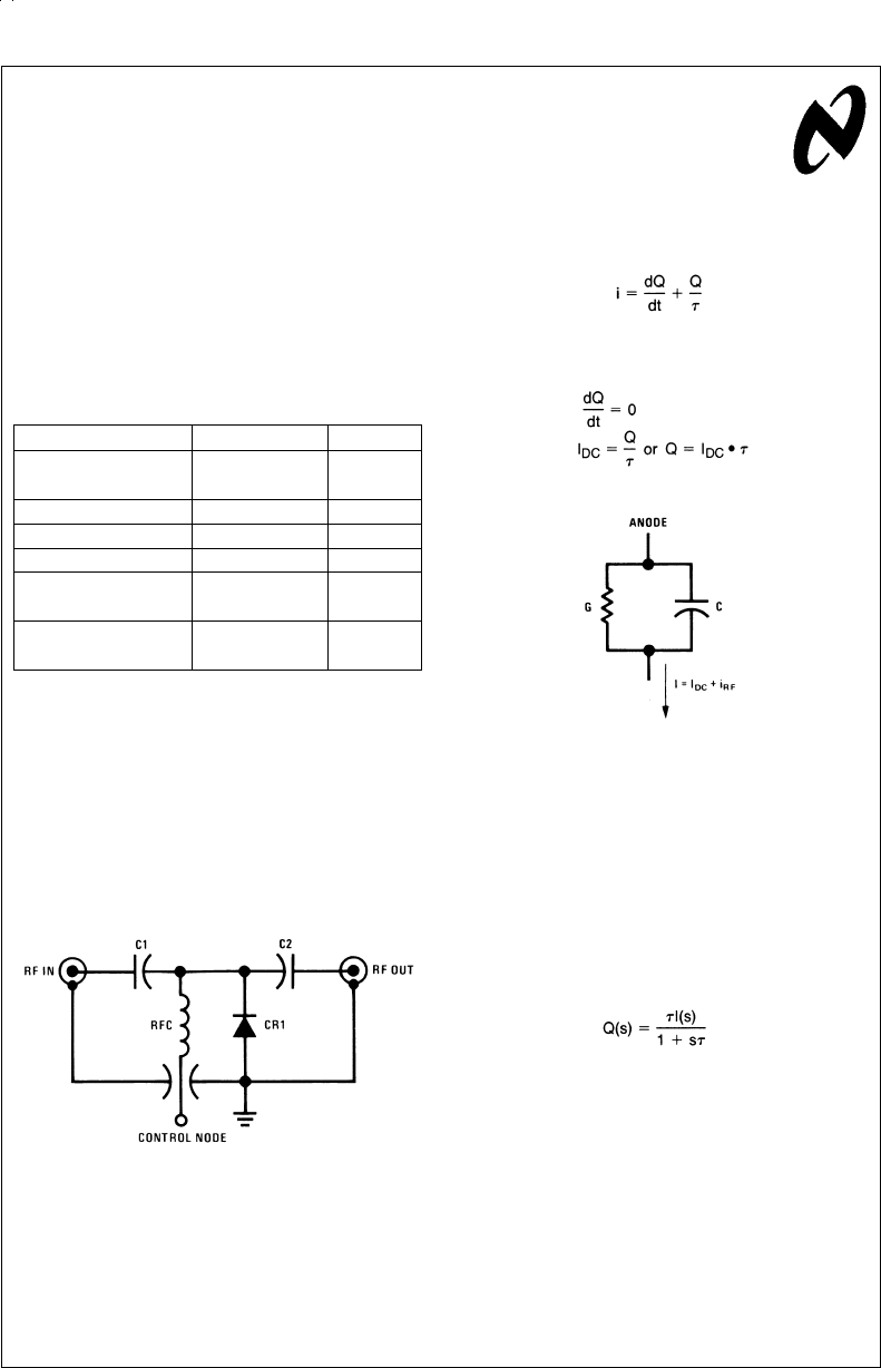
Figure 1
shows a simplified schematic of a PIN diode switch.
Typically, the PIN diode is used in RF through microwave fre-
quency modulators and switches. Since the diode is in shunt
with the RF path, the RF signal is attenuated when the diode
is forward biased (“ON”), and is passed unattenuated when
the diode is reversed biased (“OFF”). There are essentially
two considerations of interest in the “ON” condition. First, the
amount of “ON” control current must be sufficient such that
RF signal current will not significantly modulate the “ON” im-
pedance of the diode. Secondly, the time required to achieve
the “ON” condition must be minimized.
The charge control model of a diode
1,2
leads to the charge
continuity equation given in
Equation (1)
.
(1)
where: Q =charge due excess minority carriers
τ=mean lifetime of the minority carriers
Equation (1)
implies a circuit model shown in
Figure 2
. Under
steady conditions hence:
(2)
where: I =steady state “ON” current.
The conductance is proportional to the current, I; hence, in
order to minimize modulation due to the RF signal, I
DC
@
i
RF
. Typical values for I
DC
range from 50 mA to 200 mA de-
pending on PIN diode type, and the amount of modulation
that can be tolerated.
The time response of the excess charge, Q, may be evalu-
ated by taking the Laplace transform of
Equation (1)
and
solving for Q:
(3)
Solving
Equation (3)
for Q(t) yields:
Q(t) =L
−1
[Q(s)] =Iτ(1−e
−t/τ
) (4)
The time response of Q is shown in
Figure 3
. As can be
seen, several carrier lifetimes are required to achieve the
steady state “ON” condition (Q =I
DC
•τ).
AN008750-1
FIGURE 1. Simplified PIN Diode Switch
AN008750-2
I=Total Current
IDC =SS Control Current
iRF =RF Signal Current
FIGURE 2. Circuit Model for PIN Switch
National Semiconductor
Application Note 49
March 1986
PIN Diode Drivers AN-49
© 1999 National Semiconductor Corporation AN008750 www.national.com
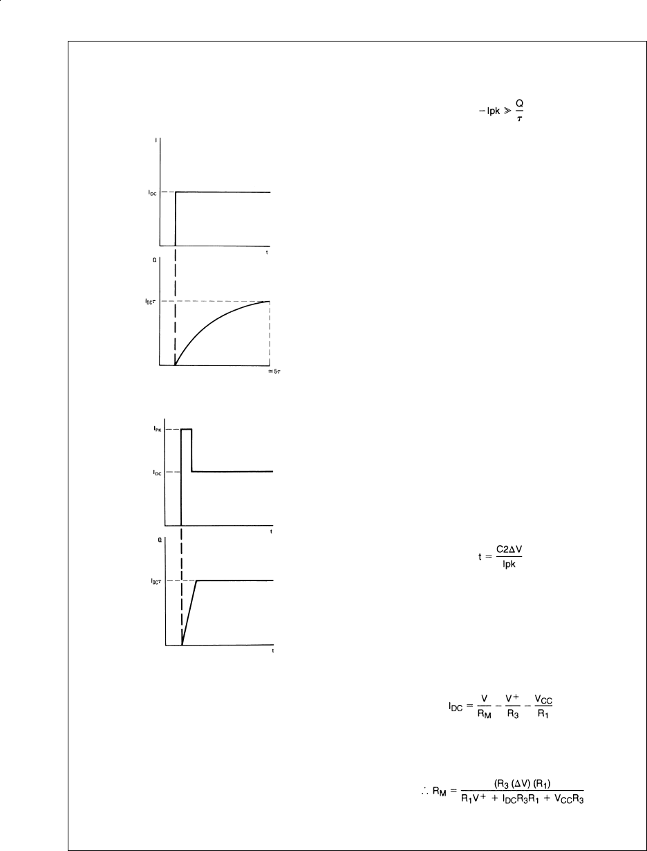
The time response of the charge, hence the time for the di-
ode to achieve the “ON” state could be shortened by apply-
ing a current spike, Ipk, to the diode and then dropping the
current to the steady state value, I
DC
, as shown in
Figure 4
.
The optimum response would be dictated by:
(Ipk) (t) =τ•I
DC
(5)
The turn off requirements for the PIN diode are quite similar
to the turn on, except that in the “OFF” condition, the steady
current drops to the diode’s reverse leakage current.
A charge, I
DC
•τ, was stored in the diode in the “ON” condi-
tion and in order to achieve the “OFF” state this charge must
be removed. Again, in order to remove the charge rapidly, a
large peak current (in the opposite direction) must be applied
to the PIN diode:
(6)
It is interesting to note an implication of
Equation (5)
.Ifthe
peak turn on current were maintained for a period of time,
say equal to τ, then the diode would acquire an excess
charge equal to Ipk •T. This same charge must be removed
at turn off, instead of a charge I
DC
•τ, resulting in a consid-
erably slower turn off. Accordingly, control of the width of turn
on current peak is critical in achieving rapid turn off.
APPLICATION OF THE DH0035 AS A PIN DIODE
DRIVER
The DH0035 is specifically designed to provide both the cur-
rent levels and timing intervals required to optimally drive
PIN diode switches. Its schematic is shown in
Figure 5
. The
device utilizes a complementary TTL input buffer such as the
DM7830/DM8830 or DM5440/DM7440 for its input signals.
Two configurations of PIN diode switch are possible: cath-
ode grounded and anode grounded. The design procedures
for the two configurations will be considered separately.
ANODE GROUND DESIGN
Selection of power supply voltages is the first consideration.
Table I reveals that the DH0035 can withstand a total of 30V
differentially. The supply voltage may be divided symmetri-
cally at ±15V, for example. Or asymmetrically at +20V and
−10V. The PIN diode driver shown in
Figure 6
, uses ±10V
supplies.
When the Q output of the DM8830 goes high a transient cur-
rent of approximately 50 mA is applied to the emitter of Q
1
and in turn to the base of Q
5
.
Q
5
has an h
fe
=20, and the collector current is h
fe
x50or
1000 mA. This peak current, for the most part, is delivered to
the PIN diode turning it “ON” (RF is “OFF”).
Ipk flows until C
2
is nearly charged. This time is given by:
(7)
where: ∆V=the change in voltage across C
2
.
Prior to Q
5
’s turn on, C
2
was charged to the minus supply
voltage of −10V. C
2
’s voltage will rise to within two diode
drops plus a V
sat
of ground:
V=|V
−
| − Vf(PIN Diode) − Vf
CR1
−V
satQ5
(8)
for V
−
=−10V, ∆V=8V.
Once C
2
is charged, the current will drop to the steady state
value, I
DC
, which is given by:
(9)
where: V
CC
=5.0V
R
1
=250Ω
R
3
=500Ω
(10)
AN008750-3
FIGURE 3.
AN008750-4
FIGURE 4.
www.national.com 2
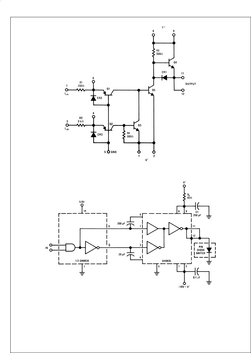
AN008750-5
FIGURE 5. DH0035 Schematic Diagram
AN008750-6
FIGURE 6. Cathode Grounded Design
www.national.com3
For the driver of
Figure 6
, and I
DC
=100 mA, R
M
is 56Ω
(nearest standard value).
Returning to
Equation (7)
and combining it with
Equation (5)
we obtain:
(11)
Solving
Equation (11)
for C
2
gives:
(12)
For τ=10 ns, C
2
=120 pF.
One last consideration should be made with the diode in the
“ON” state. The power dissipated by the DH0035 is limited to
1.5W (see Table I). The DH0035 dissipates the maximum
power with Q
5
“ON”. With Q
5
“OFF”, negligible power is dis-
sipated by the device. Power dissipation is given by:
(13)
where: D.C. =Duty Cycle =
In terms of I
DC
:
(14)
For the circuit of
Figure 6
anda50
%duty cycle, P diss =
0.5W.
Turn-off of the PIN diode begins when the Q output of the
DM8830 returns to logic “0” and the Q output goes to logic
“1”. Q
2
turns “ON”, and in turn, causes Q
3
to saturate. Simul-
taneously, Q
1
is turned “OFF” stopping the base drive to Q
5
.
Q
3
absorbs the stored base charge of Q
5
facilitating its rapid
turn-off. As Q
5
’s collector begins to rise, Q
4
turns “ON”. At
this instant, the PIN diode is still in conduction and the emit-
ter of Q
4
is held at approximately −0.7V. The instantaneous
current available to clear stored charge out of the PIN diode
is:
(15)
where:
h
fe
+1=current gain of Q
4
=20
V
BE Q4
=base-emitter drop of Q
4
=0.7V
V
f(PIN)
=forward drop of the PIN diode =0.7V
For typical values given, Ipk =400 mA. Increasing V
+
above
10V will improve turn-off time of the diode, but at the ex-
pense of power dissipation in the DH0035. Once turn-off of
the diode has been achieved, the DH0035 output current
drops to the reverse leakage of the PIN diode. The attendant
power dissipation is reduced to about 35 mW.
CATHODE GROUND DESIGN
Figure 7
shows the DH0035 driving a cathode grounded PIN
diode switch. The peak turn-on current is given by:
(16)
=800 mA for the values shown.
The steady state current, I
DC
, is set by Rp and is given by:
(17)
where: 2V
BE
=forward drop of Q
4
base emitter junction
plus V
f
of the PIN diode =1.4V.
www.national.com 4
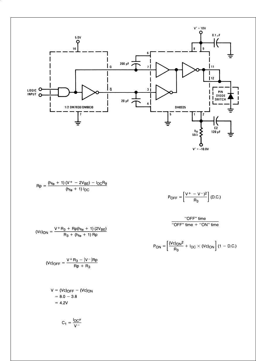
In terms of Rp,
Equation (17)
becomes:
(18)
For the circuit of
Figure 7
, and I
DC
=100 mA, Rp is 62Ω
(nearest standard value).
It now remains to select the value of C
1
. To do this, the
change in voltage across C
1
must be evaluated. In the “ON”
state, the voltage across C
1
, Vc, is given by:
(19)
For the values indicated above, (Vc)
ON
=3.8V.
In the “OFF” state, Vc is given by:
(20)
=8.0V for the circuit of
Figure 7
.
Hence, the change in voltage across C
1
is:
(21)
The value of C
4
is given, as before, by
Equation (12)
:
(22)
For a diode with τ=10 ns and I
DC
=100 mA, C
1
=250 pF.
Again the power dissipated by the DH0035 must be consid-
ered. In the “OFF” state, the power dissipation is given by:
(23)
where: D.C. =duty cycle =
The “ON” power dissipation is given by:
(24)
where: (Vc)
ON
is defined by
Equation (19)
.
Total power dissipated by the DH0035 is simply P
ON
+P
OFF
.
Fora50
%duty cycle and the circuit of
Figure 7
, P diss =
616 mW.
The peak turn-off current is, as indicated earlier, equal to
50 mA x h
fe
which is about 1000 mA. Once the excess stored
charge is removed, the current through Q
5
drops to the di-
odes leakage current. Reverse bias across the diode =
V
−
−V
sat
≅−10V for the circuit of
Figure 7
.
AN008750-7
FIGURE 7. Anode Grounded Driver
www.national.com5

REPETITION RATE CONSIDERATIONS
Although ignored until now, the PRF, in particular, the “OFF”
time of the PIN diode is important in selection of C
2
,R
M
, and
C
1
, Rp. The capacitors must recharge completely during the
diode “OFF” time. In short:
4R
M
C
2
≤t
OFF
(25)
4 RpC
1
≤t
OFF
(26)
CONCLUSION
The circuit of
Figure 7
was breadboarded and tested in con-
junction with a Hewlett-Packard 33622A PIN diode.
I
DC
was set at 100 mA, V
+
=10V, V
−
=10V. Input signal to
the DM8830 was a 5V peak, 100 kHz, 5 µs wide pulse train.
RF turn-on was accomplished in 10–12 ns while turn-off took
approximately 5 ns, as shown in
Figure *NO TARGET FOR
fig NS0292*
and
Figure *NO TARGET FOR fig NS0292*
.
In practice, adjustment C
2
(C
1
) may be required to accom-
modate the particular PIN diode minority carrier lifetime.
SUMMARY
A unique circuit utilized in the driving of PIN diodes has been
presented. Further a technique has been demonstrated
which enables the designer to tailor the DH0035 driver to the
PIN diode application.
REFERENCES
1. “Pulse, Digital, & Switching Waveforms”, Jacob Millman
& Herbert Taub,
McGraw-Hill Book
Company, Inc., New
York, N.Y.
2. “Models of Transistors and Diodes”, John G. Linvill,
McGraw-Hill Book
Company, Inc., New York, N.Y.
3.
National Semiconductor AN-18,
Bert Mitchell, March
1969.
4.
Hewlett-Packard
Application Note 314, January 1967.
LIFE SUPPORT POLICY
NATIONAL’S PRODUCTS ARE NOT AUTHORIZED FOR USE AS CRITICAL COMPONENTS IN LIFE SUPPORT DE-
VICES OR SYSTEMS WITHOUT THE EXPRESS WRITTEN APPROVAL OF THE PRESIDENT OF NATIONAL SEMI-
CONDUCTOR CORPORATION. As used herein:
1. Life support devices or systems are devices or sys-
tems which, (a) are intended for surgical implant into
the body, or (b) support or sustain life, and whose fail-
ure to perform when properly used in accordance
with instructions for use provided in the labeling, can
be reasonably expected to result in a significant injury
to the user.
2. A critical component is any component of a life support
device or system whose failure to perform can be rea-
sonably expected to cause the failure of the life support
device or system, or to affect its safety or effectiveness.
National Semiconductor
Corporation
Americas
Tel: 1-800-272-9959
Fax: 1-800-737-7018
Email: support@nsc.com
www.national.com
National Semiconductor
Europe Fax: +49 (0) 1 80-530 85 86
Email: europe.support@nsc.com
Deutsch Tel: +49 (0) 1 80-530 85 85
English Tel: +49 (0) 1 80-532 78 32
Français Tel: +49 (0) 1 80-532 93 58
Italiano Tel: +49 (0) 1 80-534 16 80
National Semiconductor
Asia Pacific Customer
Response Group
Tel: 65-2544466
Fax: 65-2504466
Email: sea.support@nsc.com
National Semiconductor
Japan Ltd.
Tel: 81-3-5639-7560
Fax: 81-3-5639-7507
AN-49 PIN Diode Drivers
National does not assume any responsibility for use of any circuitry described, no circuit patent licenses are implied and National reserves the right at any time without notice to change said circuitry and specifications.
