Application Note 74 LM139/LM239/LM339 A Quad Of Independently Functioning Comparators AN 0074
User Manual: AN-0074
Open the PDF directly: View PDF ![]() .
.
Page Count: 20
LM139/LM239/LM339 A
Quad of Independently
Functioning Comparators
INTRODUCTION
The LM139/LM239/LM339 family of devices is a monolithic
quad of independently functioning comparators designed to
meet the needs for a medium speed, TTL compatible com-
parator for industrial applications. Since no antisaturation
clamps are used on the output such as a Baker clamp or
other active circuitry, the output leakage current in the OFF
state is typically 0.5 nA. This makes the device ideal for sys-
tem applications where it is desired to switch a node to
ground while leaving it totally unaffected in the OFF state.
Other features include single supply, low voltage operation
with an input common mode range from ground up to ap-
proximately one volt below V
CC
. The output is an uncommit-
ted collector so it may be used with a pull-up resistor and a
separate output supply to give switching levels from any volt-
age up to 36V down to a V
CE SAT
above ground (approx. 100
mV), sinking currents up to 15 mA. In addition it may be used
as a single pole switch to ground, leaving the switched node
unaffected while in the OFF state. Power dissipation with all
four comparators in the OFF state is typically 4 mW from a
single 5V supply (1 mW/comparator).
CIRCUIT DESCRIPTION
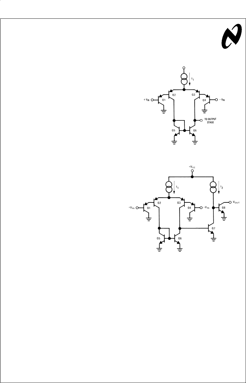
Figure 1
shows the basic input stage of one of the four com-
parators of the LM139. Transistors Q
1
through Q
4
make up a
PNP Darlington differential input stage with Q
5
and Q
6
serv-
ing to give single-ended output from differential input with no
loss in gain. Any differential input at Q
1
and Q
4
will be ampli-
fied causing Q
6
to switch OFF or ON depending on input sig-
nal polarity. It can easily be seen that operation with an input
common mode voltage of ground is possible. With both in-
puts at ground potential, the emitters of Q
1
and Q
4
will be at
one V
BE
above ground and the emitters of Q
2
and Q
3
at 2
V
BE
. For switching action the base of Q
5
and Q
6
need only
go to one V
BE
above ground and since Q
2
and Q
3
can oper-
ate with zero volts collector to base, enough voltage is
present at a zero volt common mode input to insure com-
parator action. The bases should not be taken more than
several hundred millivolts below ground; however, to prevent
forward biasing a substrate diode which would stop all com-
parator action and possibly damage the device, if very large
input currents were provided.
Figure 2
shows the comparator with the output stage added.
Additional voltage gain is taken through Q
7
and Q
8
with the
collector of Q
8
left open to offer a wide variety of possible ap-
plications. The addition of a large pull-up resistor from the
collector of Q
8
to either +V
CC
or any other supply up to 36V
both increases the LM139 gain and makes possible output
switching levels to match practically any application. Several
outputs may be tied together to provide an ORing function or
the pull-up resistor may be omitted entirely with the com-
parator then serving as a SPST switch to ground.
Output transistor Q
8
will sink up to 15 mA before the output
ON voltage rises above several hundred millivolts. The out-
put current sink capability may be boosted by the addition of
a discrete transistor at the output.
The complete circuit for one comparator of the LM139 is
shown in
Figure 3
. Current sources I
3
and I
4
are added to
help charge any parasitic capacitance at the emitters of Q
1
and Q
4
to improve the slew rate of the input stage. Diodes D
1
and D
2
are added to speed up the voltage swing at the emit-
ters of Q
1
and Q
2
for large input voltage swings.
AN007385-1
FIGURE 1. Basic LM139 Input Stage
AN007385-2
FIGURE 2. Basic LM139 Comparator
National Semiconductor
Application Note 74
January 1973
LM139/LM239/LM339—A Quad of Independently Functioning Comparators AN-74
© 1999 National Semiconductor Corporation AN007385 www.national.com
Biasing for current sources I
1
through I
4
is shown in
Figure 4
.
When power is first applied to the circuit, current flows
through the JFET Q
13
to bias up diode D
5
. This biases tran-
sistor Q
12
which turns ON transistors Q
9
and Q
10
by allowing
a path to ground for their base and collector currents.
Current from the left hand collector of Q
9
flows through di-
odes D
3
and D
4
bringing up the base of Q
11
to2V
BE
above
ground and the emitters of Q
11
and Q
12
to one V
BE
.Q
12
will
then turn OFF because its base emitter voltage goes to zero.
This is the desired action because Q
9
and Q
10
are biased
ON through Q
11
,D
3
and D
4
so Q
12
is no longer needed. The
“bias line” is now sitting at a V
BE
below +V
CC
which is the
voltage needed to bias the remaining current sources in the
LM139 which will have a constant bias regardless of +V
CC
fluctuations. The upper input common mode voltage is V
CC
minus the saturation voltage of the current sources (appoxi-
mately 100 mV) minus the 2 V
BE
of the input devices Q
1
and
Q
2
(or Q
3
and Q
4
).
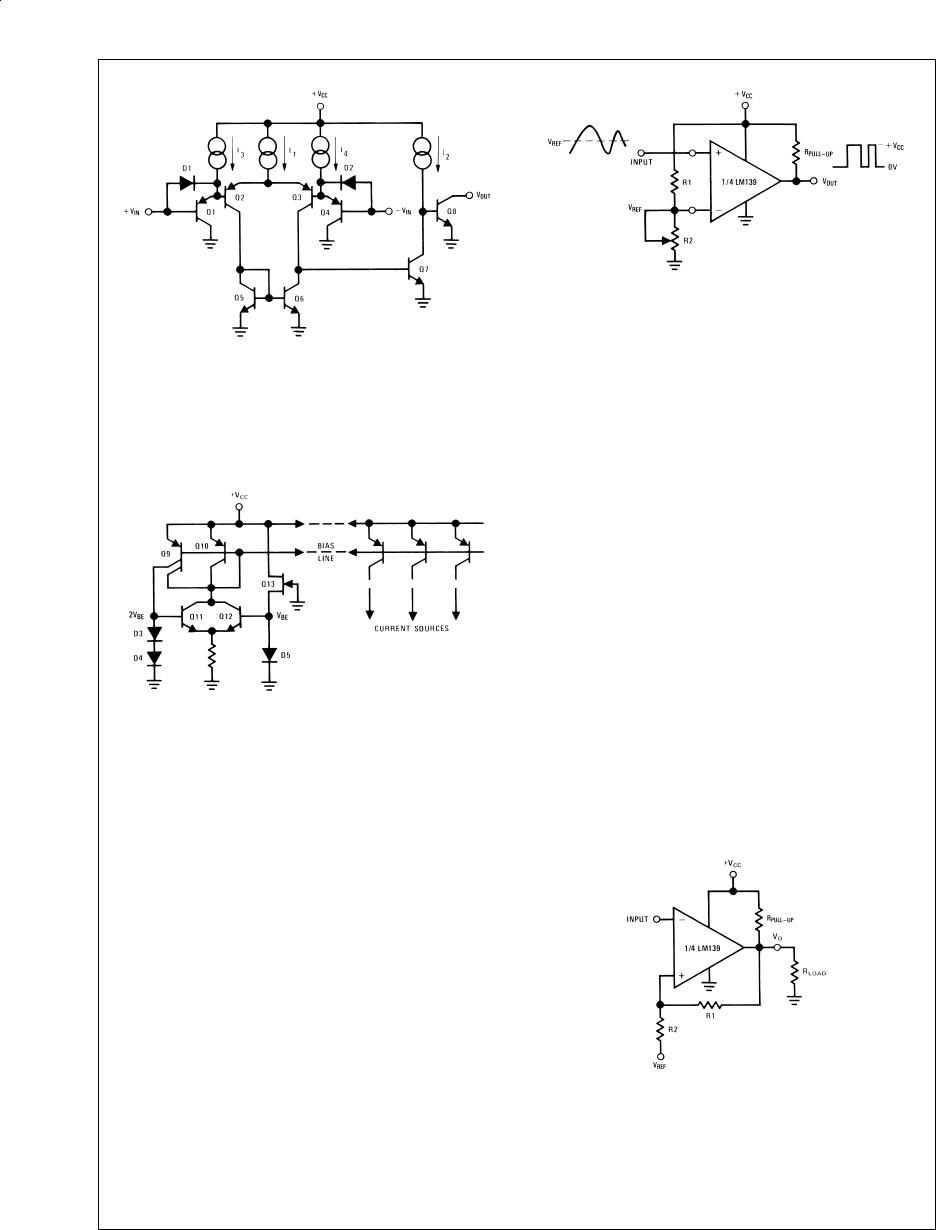
COMPARATOR CIRCUITS
Figure 5
shows a basic comparator circuit for converting low
level analog signals to a high level digital output. The output
pull-up resistor should be chosen high enough so as to avoid
excessive power dissipation yet low enough to supply
enough drive to switch whatever load circuitry is used on the
comparator output. Resistors R
1
and R
2
are used to set the
input threshold trip voltage (V
REF
) at any value desired within
the input common mode range of the comparator.
COMPARATORS WITH HYSTERESIS
The circuit shown in
Figure 5
suffers from one basic draw-
back in that if the input signal is a slowly varying low level
signal, the comparator may be forced to stay within its linear
region between the output high and low states for an unde-
sireable length of time. If this happens, it runs the risk of os-
cillating since it is basically an uncompensated, high gain op
amp. To prevent this, a small amount of positive feedback or
hysteresis is added around the comparator.
Figure 6
shows
a comparator with a small amount of positive feedback. In or-
der to insure proper comparator action, the components
should be chosen as follows:
R
PULL-UP
<R
LOAD
and
R
1
>R
PULL-UP
This will insure that the comparator will always switch fully up
to +V
CC
and not be pulled down by the load or feedback. The
amount of feedback is chosen arbitrarily to insure proper
switching with the particular type of input signal used. If the
output swing is 5V, for example, and it is desired to feedback
1%or 50 mV, then R
1
≈100 R
2
. To describe circuit operation,
assume that the inverting input goes above the reference in-
put (V
IN
>V
REF
). This will drive the output, V
O
, towards
ground which in turn pulls V
REF
down through R
1
. Since
V
REF
is actually the noninverting input to the comparator, it
too will drive the output towards ground insuring the fastest
possible switching time regardless of how slow the input
moves. If the input then travels down to V
REF
, the same pro-
cedure will occur only in the opposite direction insuring that
the output will be driven hard towards +V
CC
.
AN007385-3
FIGURE 3. Complete LM139 Comparator Circuit
AN007385-4
FIGURE 4. Current Source Biasing Circuit
AN007385-5
FIGURE 5. Basic Comparator Circuit
AN007385-6
FIGURE 6. Comparator with Positive Feedback to
Improve Switching Time
www.national.com 2
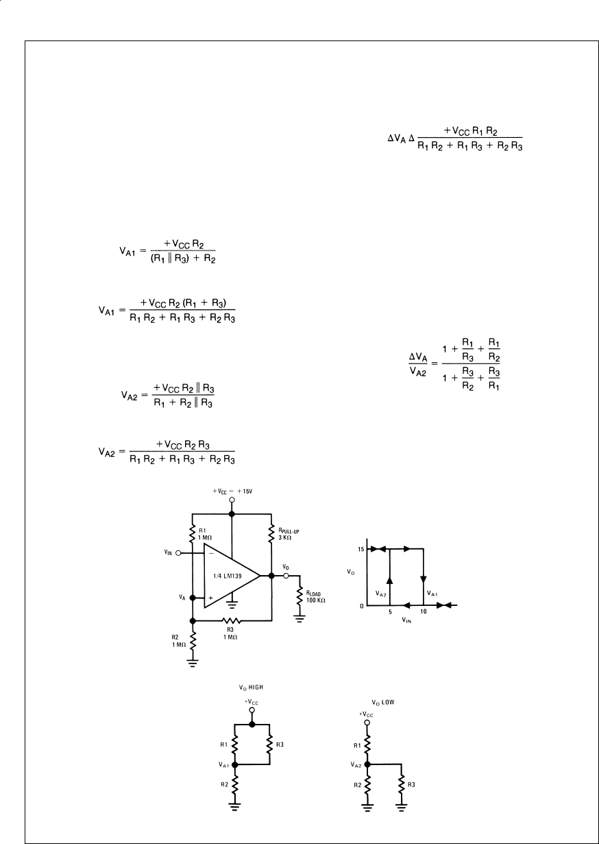
Putting hysteresis in the feedback loop of the comparator
has far more use, however, than simply as an oscillation sup-
pressor. It can be made to function as a Schmitt trigger with
presettable trigger points. A typical circuit is shown in
Figure
7
. Again, the hysteresis is achieved by shifting the reference
voltage at the positive input when the output voltage V
O
changes state. This network requires only three resistors
and is referenced to the positive supply +V
CC
of the com-
parator. This can be modeled as a resistive divider, R
1
and
R
2
, between +V
CC
and ground with the third resistor, R
3
, al-
ternately connected to +V
CC
or ground, paralleling either R
1
or R
2
. To analyze this circuit, assume that the input voltage,
V
IN
, at the inverting input is less than V
A
. With V
IN
≤V
A
the
output will be high (V
O
=+V
CC
). The upper input trip voltage,
V
A1
, is defined by:
or
(1)
When the input voltage V
IN
, rises above the reference volt-
age (V
IN
>V
A1
), voltage, V
O
, will go low (V
O
=GND). The
lower input trip voltage, V
A2
, is now defined by:
or
(2)
When the input voltage, V
IN
, decreases to V
A2
or lower, the
output will again switch high. The total hysteresis, ∆V
A
, pro-
vided by this network is defined by:
∆V
A
=V
A1
−V
A2
or, subtracting equation 2 from equation 1
(3)
To insure that V
O
will swing between +V
CC
and ground,
choose:
R
PULL-UP
<R
LOAD
and (4)
R
3
>R
PULL-UP
(5)
Heavier loading on R
PULL-UP
(i.e. smaller values of R
3
or
R
LOAD
) simply reduces the value of the maximum output
voltage thereby reducing the amount of hysteresis by lower-
ing the value of V
A1
. For simplicity, we have assumed in the
above equations that V
O
high switches all the way up to
+V
CC
.
To find the resistor values needed for a given set of trip
points, we first divide equation (3) by equation (2). This gives
us the ratio:
(6)
AN007385-7
FIGURE 7. Inverting Comparator with Hysteresis
www.national.com3
If we let R
1
=nR
3
, equation (6) becomes:
(7)
We can then obtain an expression for R
2
from equation (1)
which gives
(8)
The following design example is offered:
Given: V
+
=+15V
R
LOAD
=100 kΩ
V
A1
=+10V
V
A2
=+5V
To find: R
1
,R
2
,R
3
,R
PULL-UP
Solution:
From equation (4) R
PULL-UP
<R
LOAD
R
PULL-UP
<100 kΩ
so let R
PULL-UP
=3kΩ
From equation (5) R
3
>R
LOAD
R
3
>100 kΩ
so let R
3
=1MΩ
and since R
1
=nR
3
this gives R
1
=1R
3
=1MΩ
These are the values shown in
Figure 7
.
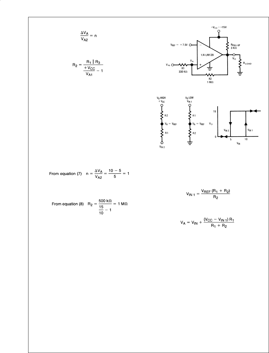
The circuit shown in
Figure 8
is a non-inverting comparator
with hysteresis which is obtained with only two resistors, R
1
and R
2
. In contrast to the first method, however, this circuit
requires a separate reference voltage at the negative input.
The trip voltage, V
A
, at the positive input is shifted about
V
REF
as V
O
changes between +V
CC
and ground.
Again for analysis, assume that the input voltage, V
IN
,islow
so that the output, V
O
, is also low (V
O
=GND). For the out-
put to switch, V
IN
must rise up to V
IN 1
where V
IN 1
is given
by:
(9)
As soon as V
O
switches to +V
CC
,V
A
will step to a value
greater than V
REF
which is given by:
(10)
To make the comparator switch back to its low state (V
O
=
GND) V
IN
must go below V
REF
before V
A
will again equal
V
REF
. This lower trip point is now given by:
AN007385-8
FIGURE 8. Non-Inverting Comparator with Hysteresis
www.national.com 4
(11)
The hysteresis for this circuit, ∆V
IN
, is the difference between
V
IN 1
and V
IN 2
and is given by:
or
(12)
As a design example consider the following:
Given: R
LOAD
=100 kΩ
V
IN 1
=10V
V
IN 2
=5V
+V
CC
=15V
To find: V
REF
,R
1
,R
2
and R
3
Solution:
Again choose R
PULL-UP
<R
LOAD
to minimize loading, so let
R
PULL-UP
=3kΩ
From equation (12)
From equation (9)
To minimize output loading choose
R
2
>R
PULL-UP
or R
2
>3kΩ
so let R
2
=1MΩ
The value of R
1
is now obtained from equation (12)
These are the values shown in
Figure 8
.
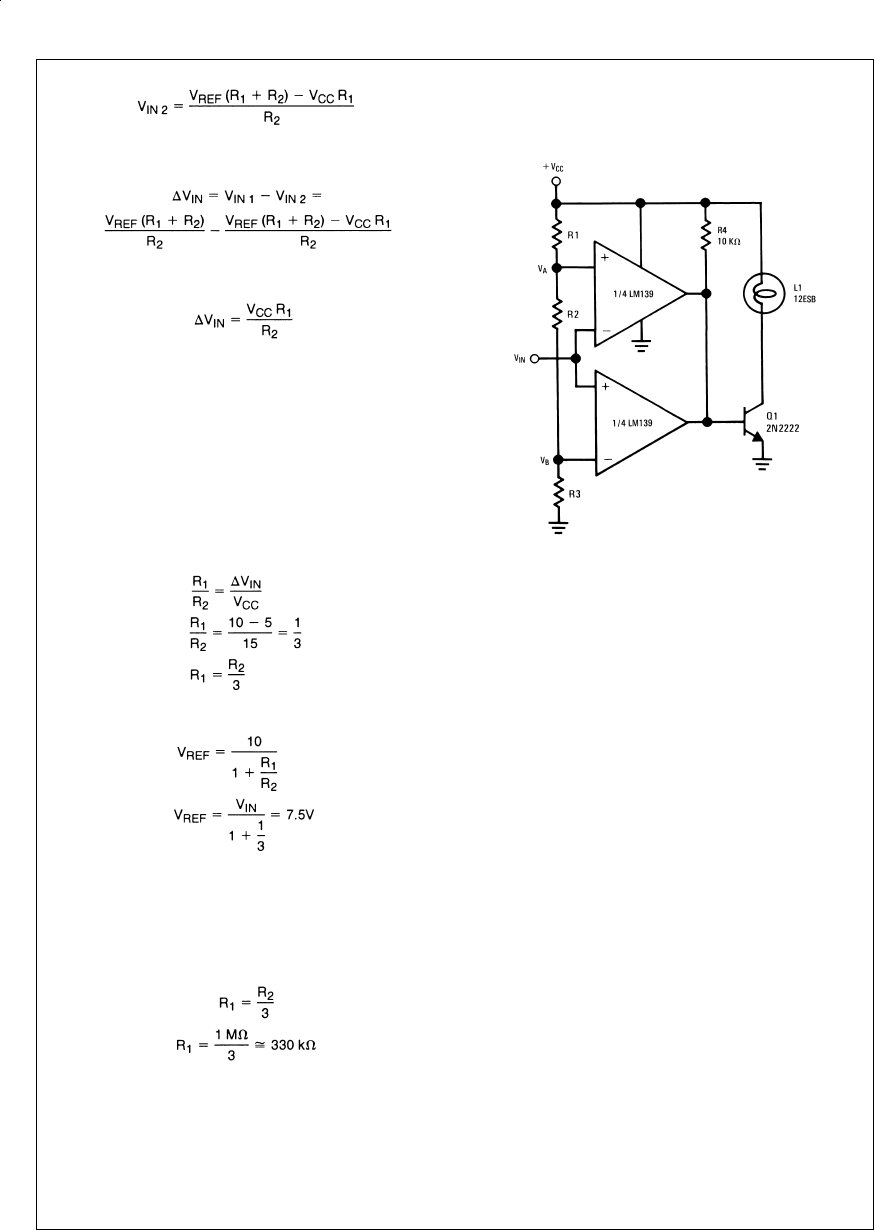
LIMIT COMPARATOR WITH LAMP DRIVER
The limit comparator shown in
Figure 9
provides a range of
input voltages between which the output devices of both
LM139 comparators will be OFF.
This will allow base current for Q
1
to flow through pull-up re-
sistor R
4
, turning ON Q
1
which lights the lamp. If the input
voltage, V
IN
, changes to a value greater than V
A
or less than
V
B
, one of the comparators will switch ON, shorting the base
of Q
1
to ground, causing the lamp to go OFF. If a PNP tran-
sistor is substituted for Q
1
(with emitter tied to +V
CC
) the
lamp will light when the input is above V
A
or below V
B
.V
A
and V
B
are arbitrarily set by varying resistors R
1
,R
2
and R
3
.
ZERO CROSSING DETECTOR
The LM139 can be used to symmetrically square up a sine
wave centered around zero volts by incorporating a small
amount of positive feedback to improve switching times and
centering the input threshold at ground (see
Figure 10
). Volt-
age divider R
4
and R
5
establishes a reference voltage, V
1
,at
the positive input. By making the series resistance, R
1
plus
R
2
equal to R
5
, the switching condition, V
1
=V
2
, will be sat-
isfied when V
IN
=0. The positive feedback resistor, R
6
,is
made very large with respect to R
5
(R
6
=2000 R
5
). The re-
sultant hysteresis established by this network is very small
(∆V
1
<10 mV) but it is sufficient to insure rapid output volt-
age transitions. Diode D
1
is used to insure that the inverting
input terminal of the comparator never goes below approxi-
mately −100 mV. As the input terminal goes negative, D
1
will
forward bias, clamping the node between R
1
and R
2
to ap-
proximately −700 mV. This sets up a voltage divider with R
2
and R
3
preventing V
2
from going below ground. The maxi-
mum negative input overdrive is limited by the current han-
dling ability of D
1
.
AN007385-9
FIGURE 9. Limit Comparator with Lamp Driver
www.national.com5
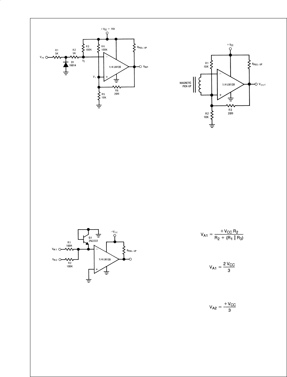
COMPARING THE MAGNITUDE OF VOLTAGES OF
OPPOSITE POLARITY
The comparator circuit shown in
Figure 11
compares the
magnitude of two voltages, V
IN 1
and V
IN 2
which have oppo-
site polarities. The resultant input voltage at the minus input
terminal to the comparator, V
A
, is a function of the voltage di-
vider from V
IN 1
and V
IN 2
and the values of R
1
and R
2
. Diode
connected transistor Q
1
provides protection for the minus in-
put terminal by clamping it at several hundred millivolts be-
low ground. A 2N2222 was chosen over a 1N914 diode be-
cause of its lower diode voltage. If desired, a small amount of
hysteresis may be added using the techniques described
previously. Correct magnitude comparison can be seen as
follows: Let V
IN 1
be the input for the positive polarity input
voltage and V
IN 2
the input for the negative polarity. If the
magnitude of V
IN 1
is greater than that of V
IN 2
the output will
go low (V
OUT
=GND). If the magnitude of V
IN 1
is less than
that of V
IN 2
, however, the output will go high (V
OUT
=V
CC
).
MAGNETIC TRANSDUCER AMPLIFIER
A circuit that will detect the zero crossings in the output of a
magnetic transducer is shown in
Figure 12
. Resistor divider,
R
1
and R
2
, biases the positive input at +V
CC
/2, which is well
within the common mode operating range. The minus input
is biased through the magnetic transducer. This allows large
signal swings to be handled without exceeding the input volt-
age limits. A symmetrical square wave output is insured
through the positive feedback resistor R
3
. Resistors R
1
and
R
2
can be used to set the DC bias voltage at the positive in-
put at any desired voltage within the input common mode
voltage range of the comparator.
OSCILLATORS USING THE LM139
The LM139 lends itself well to oscillator applications for fre-
quencies below several megacycles.
Figure 13
shows a
symmetrical square wave generator using a minimum of
components. The output frequency is set by the RC time
constant of R
4
and C
1
and the total hysteresis of the loop is
set by R
1
,R
2
and R
3
. The maximum frequency is limited only
by the large signal propagation delay of the comparator in
addition to any capacitive loading at the output which would
degrade the output slew rate.
To analyze this circuit assume that the output is initially high.
For this to be true, the voltage at the negative input must be
less than the voltage at the positive input. Therefore, capaci-
tor C
1
is discharged. The voltage at the positive input, V
A1
,
will then be given by:
(13)
where if R
1
=R
2
=R
3
then
(14)
Capacitor C
1
will charge up through R
4
so that when it has
charged up to a value equal to V
A1
, the comparator output
will switch. With the output V
O
=GND, the value of V
A
is re-
duced by the hysteresis network to a value given by:
(15)
using the same resistor values as before. Capacitor C
1
must
now discharge through R
4
towards ground. The output will
return to its high state (V
O
=+V
CC
) when the voltage across
the capacitor has discharged to a value equal to V
A2
. For the
circuit shown, the period for one cycle of oscillation will be
twice the time it takes for a single RC circuit to charge up to
one half of its final value. The period can be calculated from:
AN007385-10
FIGURE 10. Zero Crossing Detector
AN007385-11
FIGURE 11. Comparing the Magnitude of Voltages of
Opposite Polarity
AN007385-12
FIGURE 12. Magnetic Transducer Amplifier
www.national.com 6
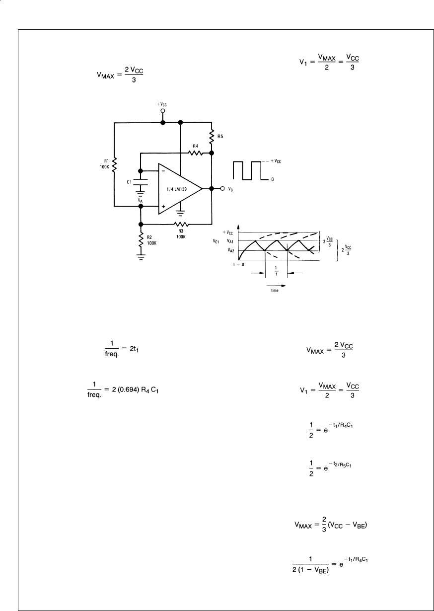
V
1
=V
MAX
e
−t
1
/RC
(16)
where
(17)
and
(18)
One period will be given by:
(19)
or calculating the exponential gives
(20)
Resistors R
3
and R
4
must be at least 10 times larger than R
5
to insure that V
O
will go all the way up to +V
CC
in the high
state. The frequency stability of this circuit should strictly be
a function of the external components.
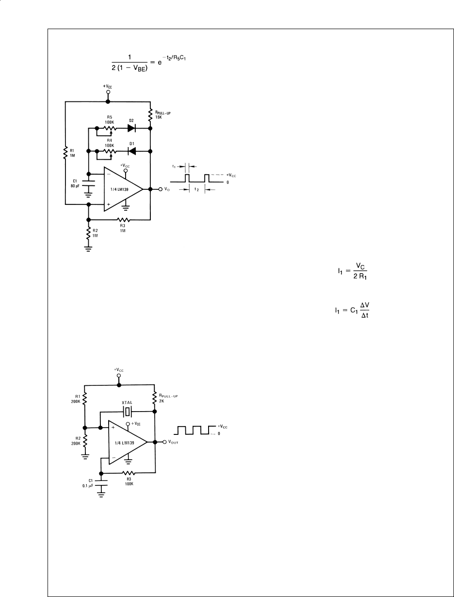
PULSE GENERATOR WITH VARIABLE DUTY CYCLE
The basic square wave generator of
Figure 13
can be modi-
fied to obtain an adjustable duty cycle pulse generator, as
shown in
Figure 14
, by providing a separate charge and dis-
charge path for capacitor C
1
. One path, through R
4
and D
1
will charge the capacitor and set the pulse width (t
1
). The
other path, R
5
and D
2
, will discharge the capacitor and set
the time between pulses (t
2
). By varying resistor R
5
, the time
between pulses of the generator can be changed without
changing the pulse width. Similarly, by varying R
4
, the pulse
width will be altered without affecting the time between
pulses. Both controls will change the frequency of the gen-
erator, however. With the values given in
Figure 14
, the
pulse width and time between pulses can be found from:
V
1
=V
MAX
(1−e
−t
1
/R
4
C
1) risetime (21a)
V
1
=V
MAX
e
−t
2
/R
5
C
1falltime (21b)
where
(22)
and
(23)
which gives
(24)
t
2
is then given by:
(25)
These terms will have a slight error due to the fact that V
MAX
is not exactly equal to
2
⁄
3
V
CC
but is actually reduced by the
diode drop to:
(26)
therefore
(27)
AN007385-13
FIGURE 13. Square Wave Generator
www.national.com7
and
(28)
CRYSTAL CONTROLLED OSCILLATOR
A simple yet very stable oscillator can be obtained by using
a quartz crystal resonator as the feedback element.
Figure
15
gives a typical circuit diagram of this. This value of R
1
and
R
2
are equal so that the comparator will switch symmetrically
about +V
CC
/2. The RC time constant of R
3
and C
1
is set to
be several times greater than the period of the oscillating fre-
quency, insuring a 50%duty cycle by maintaining a DC volt-
age at the inverting input equal to the absolute average of
the output waveform.
When specifying the crystal, be sure to order series resonant
along with the desired temperature coefficient and load ca-
pacitance to be used.
MOS CLOCK DRIVER
The LM139 can be used to provide the oscillator and clock
delay timing for a two phase MOS clock driver (see
Figure
16
). The oscillator is a standard comparator square wave
generator similar to the one shown in
Figure 13
. Two other
comparators of the LM139 are used to establish the desired
phasing between the two outputs to the clock driver. A more
detailed explanation of the delay circuit is given in the sec-
tion under “Digital and Switching Circuits.”
WIDE RANGE VCO
A simple yet very stable voltage controlled oscillator using a
mimimum of external components can be realized using
three comparators of the LM139. The schematic is shown in
Figure 17a
. Comparator 1 is used closed loop as an integra-
tor (for further discussion of closed loop operation see sec-
tion on Operational Amplifiers) with comparator 2 used as a
triangle to square wave converter and comparator 3 as the
switch driving the integrator. To analyze the circuit, assume
that comparator 2 is its high state (V
SQ
=+V
CC
) which drives
comparator 3 to its high state also. The output device of
comparator 3 will be OFF which prevents any current from
flowing through R
2
to ground. With a control voltage, V
C
,at
the input to comparator 1, a current l
1
will flow through R
1
and begin discharging capacitor C
1
, at a linear rate. This dis-
charge current is given by:
(29)
and the discharge time is given by:
(30)
∆V will be the maximum peak change in the voltage across
capacitor C
1
which will be set by the switch points of com-
parator 2. These trip points can be changed by simply alter-
ing the ratio of R
F
to R
S
, thereby increasing or decreasing
the amount of hysteresis around comparator 2. With R
F
=
100 kΩand R
S
=5kΩ, the amount of hysteresis is approxi-
mately ±5%which will give switch points of +V
CC
/2 ±750
mV from a 30V supply. (See “Comparators with Hysteresis”).
As capacitor C
1
discharges, the output voltage of compara-
tor 1 will decrease until it reaches the lower trip point of com-
parator 2, which will then force the output of comparator 2 to
go to its low state (V
SQ
=GND).
AN007385-14
FIGURE 14. Pulse Generator with Variable Duty Cycle
AN007385-15
FIGURE 15. Crystal Controlled Oscillator
www.national.com 8
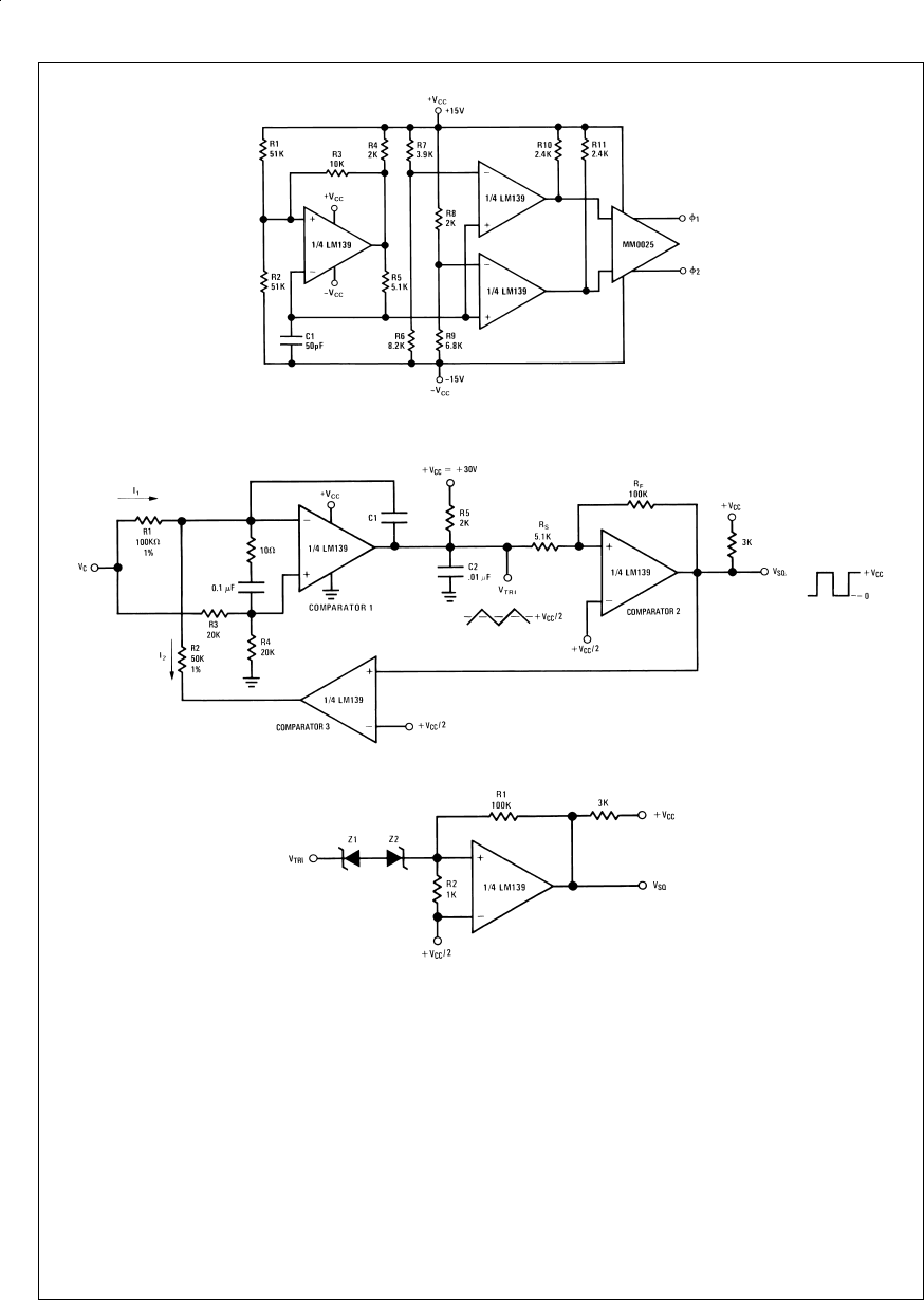
This in turn causes comparator 3 to go to its low state where
its output device will be in saturation. A current l
2
can now
flow through resistor R
2
to ground. If the value of R
2
is cho-
sen as R
1
/2 a current equal to the capacitor discharge cur-
rent can be made to flow out of C
1
charging it at the same
rate as it was discharged. By making R
2
=R
1
/2, current l
2
will equal twice l
1
. This is the control circuitry which
guararantees a constant 50%duty cycle oscillation indepen-
dent of frequency or temperature. As capacitor C
1
charges,
the output of comparator 1 will ramp up until it trips compara-
tor 2 to its high state (V
SQ
=+V
CC
) and the cycle will repeat.
The circuit shown in
Figure 17a
uses a +30V supply and
gives a triangle wave of 1.5V peak-to-peak. With a timing ca-
pacitor, C
1
equal to 500 pF, a frequency range from approxi-
mately 115 kHz down to approximately 670 Hz was obtained
with a control voltage ranging from 50V down to 250 mV. By
reducing the hysteresis around comparator 2 down to ±150
mV (R
f
=100 kΩ,R
S
=1kΩ) and reducing the compensat-
ing capacitor C
2
down to .001 µF, frequencies up to 1 MHz
may be obtained. For lower frequencies (f
o
≤1 Hz) the timing
capacitor, C
1
, should be increased up to approximately 1 µF
to insure that the charging currents, l
1
and l
2
, are much
larger than the input bias currents of comparator 1.
Figure 17b
shows another interesting approach to provide
the hysteresis for comparator 2. Two identical Zener diodes,
Z
1
and Z
2
, are used to set the trip points of comparator 2.
When the triangle wave is less than the value required to Ze-
ner one of the diodes, the resistive network, R
1
and R
2
, pro-
AN007385-16
FIGURE 16. MOS Clock Driver
AN007385-17
(a)
AN007385-18
(b)
FIGURE 17. Voltage Controlled Oscillator
www.national.com9
vides enough feedback to keep the comparator in its proper
state, (the input would otherwise be floating). The advantage
of this circuit is that the trip points of comparator 2 will be
completely independent of supply voltage fluctuations. The
disadvantage is that Zeners with less than one volt break-
down voltage are not obtainable. This limits the maximum
upper frequency obtainable because of the larger amplitude
of the triangle wave. If a regulated supply is available,
Figure
17a
is preferable simply because of less parts count and
lower cost.
Both circuits provide good control over at least two decades
in frequency with a temperature coefficient largely depen-
dent on the TC of the external timing resistors and capaci-
tors. Remember that good circuit layout is essential along
with the 0.01 µF compensation capacitor at the output of
comparator 1 and the series 10Ωresistor and 0.1 µF capaci-
tor between its inputs, for proper operation. Comparator 1 is
a high gain amplifier used closed loop as an integrator so
long leads and loose layout should be avoided.
DIGITAL AND SWITCHING CIRCUITS
The LM139 lends itself well to low speed (<1 MHz) high
level logic circuits. They have the advantage of operating
with high signal levels, giving high noise immunity, which is
highly desirable for industrial applications. The output signal
level can be selected by setting the V
CC
to which the pull-up
resistor is connected to any desired level.
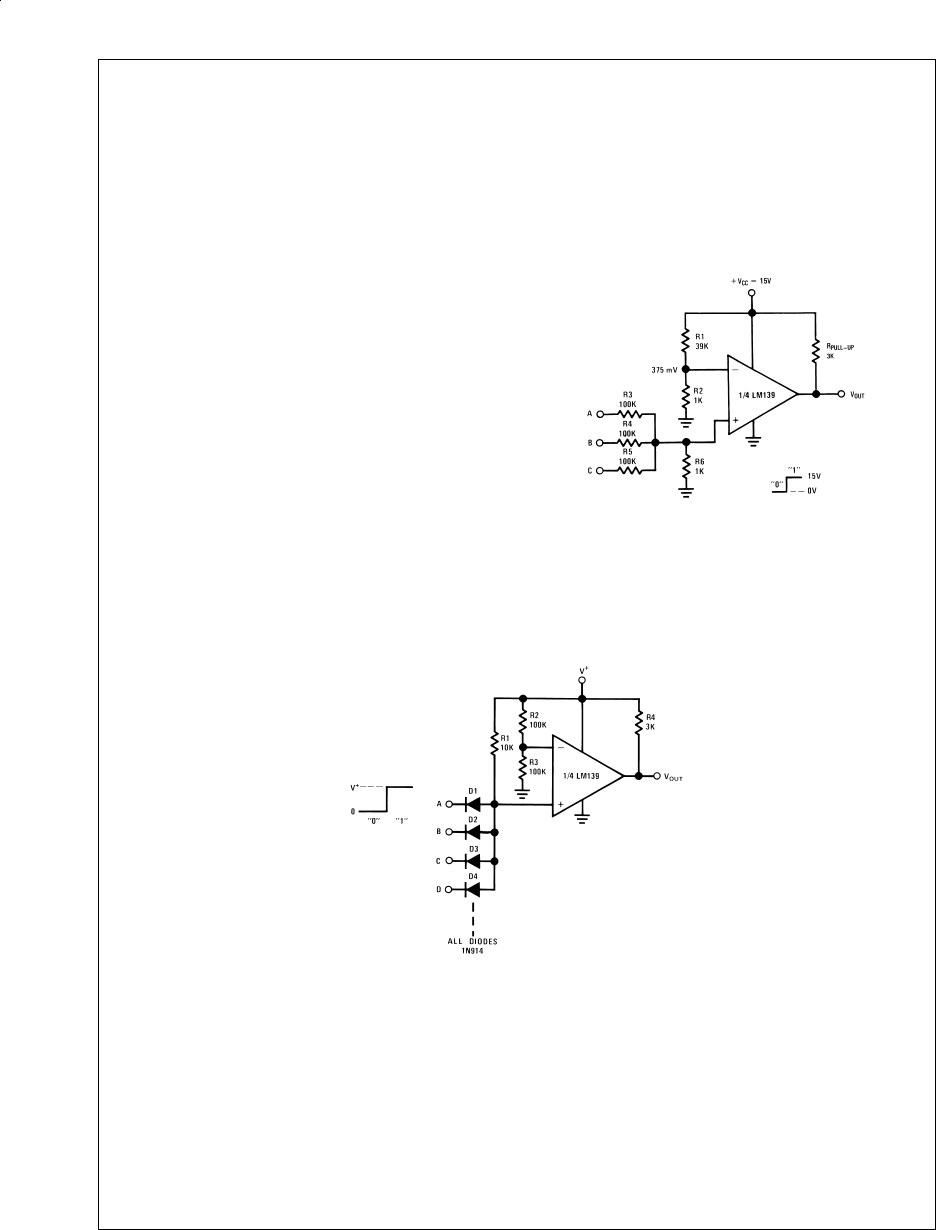
AND/NAND GATES
A three input AND gate is shown in
Figure 18
. Operation of
this gate is as follows: resistor divider R
1
and R
2
establishes
a reference voltage at the inverting input to the comparator.
The non-inverting input is the sum of the voltages at the in-
puts divided by the voltage dividers comprised of R
3
,R
4
,R
5
and R
6
. The output will go high only when all three inputs are
high, causing the voltage at the non-inverting input to go
above that at inverting input. The circuit values shown work
for a “0” equal to ground and a “1” equal +15V. The resistor
values can be altered if different logic levels are desired. If
more inputs are required, diodes are recommended to im-
prove the voltage margin when all but one of the inputs are
the “1” state. This circuit with increased fan-in is shown in
Figure 19
.
To convert these AND gates to NAND gates simply inter-
change the inverting and non-inverting inputs to the com-
parator. Hysteresis can be added to speed up output transi-
tions if low speed input signals are used.
OR/NOR GATES
The three input OR gate (positive logic) shown in
Figure 20
is achieved from the basic AND gate simply by increasing R
1
thereby reducing the reference voltage. A logic “1” at any of
the inputs will produce a logic “1” at the output. Again a NOR
gate may be implemented by simply reversing the compara-
tor inputs. Resistor R
6
may be added for the OR or NOR
function at the expense of noise immunity if so desired.
AN007385-19
VOUT =A•B•C
FIGURE 18. Three Input AND Gate
AN007385-20
VOUT =A•B•C•D
FIGURE 19. AND Gate with Large Fan-In
www.national.com 10
OUTPUT STROBING
The output of the LM139 may be disabled by adding a clamp
transistor as shown in
Figure 21
. A strobe control voltage at
the base of Q
1
will clamp the comparator output to ground,
making it immune to any input changes.
If the LM139 is being used in a digital system the output may
be strobed using any other type of gate having an uncommit-
ted collector output (such as National’s DM5401/DM7401).
In addition another comparator of the LM139 could also be
used for output strobing, replacing Q
1
in
Figure 21
,ifde-
sired. (See
Figure 22
.)
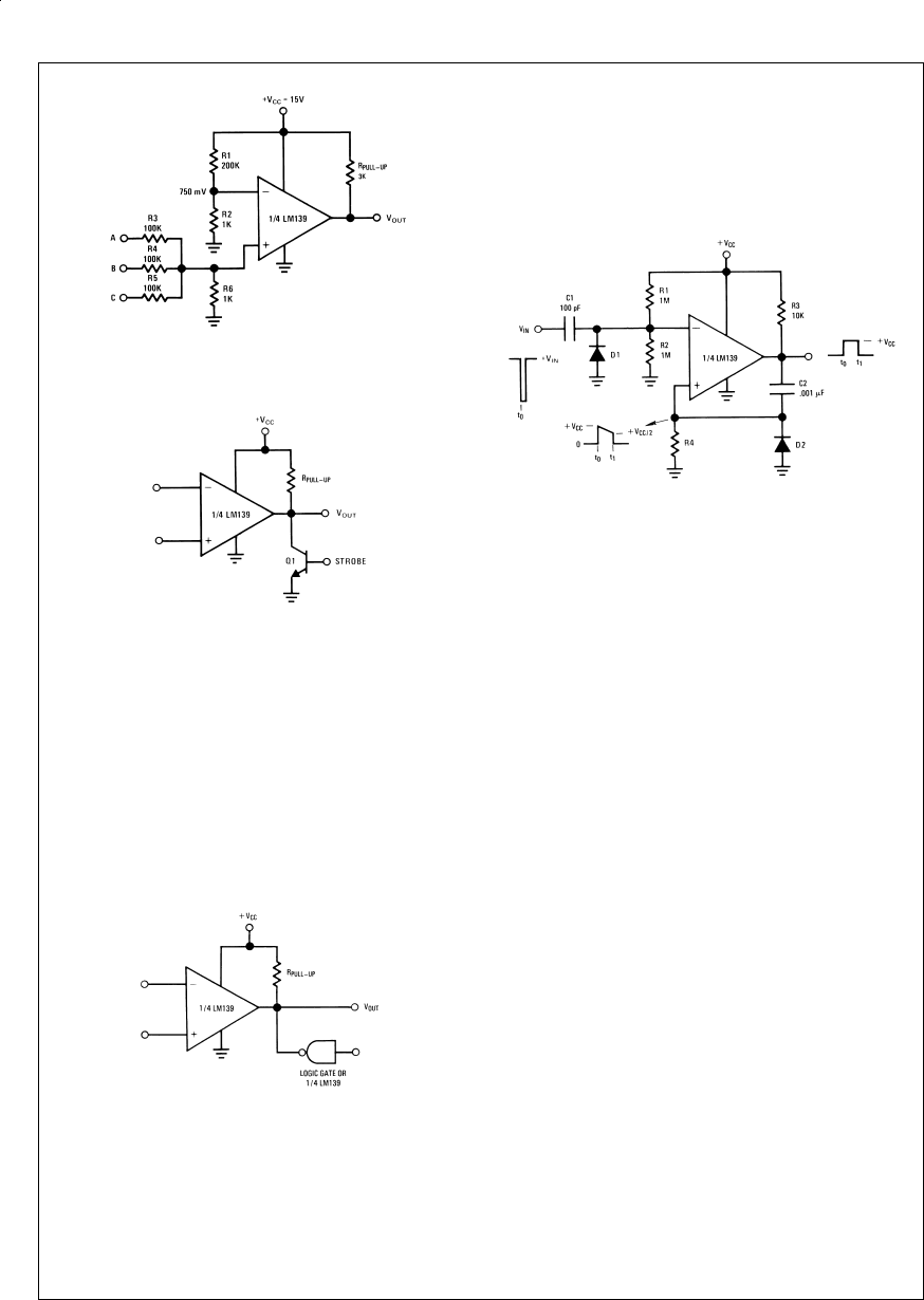
ONE SHOT MULTIVIBRATORS
A simple one shot multivibrator can be realized using one
comparator of the LM139 as shown in
Figure 23
. The output
pulse width is set by the values of C
2
and R
4
(with R
4
>10
R
3
to avoid loading the output). The magnitude of the input
trigger pulse required is determined by the resistive divider
R
1
and R
2
. Temperature stability can be achieved by balanc-
ing the temperature coefficients of R
4
and C
2
or by using
components with very low TC. In addition, the TC of resistors
R
1
and R
2
should be matched so as to maintain a fixed ref-
erence voltage of +V
CC
/2. Diode D
2
provides a rapid dis-
charge path for capacitor C
2
to reset the one shot at the end
of its pulse. It also prevents the non-inverting input from be-
ing driven below ground. The output pulse width is relatively
independent of the magnitude of the supply voltage and will
change less than 2%for a five volt change in +V
CC
.
The one shot multivibrator shown in
Figure 24
has several
characteristics which make it superior to that shown in
Fig-
ure 23
. First, the pulse width is independent of the magni-
tude of the power supply voltage because the charging volt-
age and the intercept voltage are a fixed percentage of
+V
CC
. In addition this one-shot is capable of 99%duty cycle
and exhibits input trigger lock-out to insure that the circuit will
not re-trigger before the output pulse has been completed.
The trigger level is the voltage required at the input to raise
the voltage at point A higher than the voltage at point B, and
is set by the resistive divider R
4
and R
10
and the network R
1
,
R
2
and R
3
. When the multivibrator has been triggered, the
output of comparator 2 is high causing the reference voltage
at the non-inverting input of comparator 1 to go to +V
CC
. This
prevents any additional input pulses from disturbing the cir-
cuit until the output pulse has been completed.
The value of the timing capacitor, C
1
, must be kept small
enough to allow comparator 1 to completely discharge C
1
before the feedback signal from comparator 2 (through R
10
)
switches comparator 1 OFF and allows C
1
to start an expo-
nential charge. Proper circuit action depends on rapidly dis-
charging C
1
to a value set by R
6
and R
9
at which time com-
parator 2 latches comparator 1 OFF. Prior to the
establishment of this OFF state, C
1
will have been com-
pletely discharged by comparator 1 in the ON state. The time
delay, which sets the output pulse width, results from C
1
re-
charging to the reference voltage set by R
6
and R
9
. When
the voltage across C
1
charges beyond this reference, the
output pulse returns to ground and the input is again reset to
accept a trigger.
BISTABLE MULTIVIBRATOR
Figure 25
is the circuit of one comparator of the LM139 used
as a bistable multivibrator. A reference voltage is provided at
the inverting input by a voltage divider comprised of R
2
and
R
3
. A pulse applied to the SET terminal will switch the output
high. Resistor divider network R
1
,R
4
, and R
5
now clamps
the non-inverting input to a voltage greater than the refer-
ence voltage. A pulse now applied to the RESET Input will
AN007385-21
VOUT =A+B+C
FIGURE 20. Three Input OR Gate
AN007385-22
FIGURE 21. Output Strobing Using a Discrete
Transistor
AN007385-23
FIGURE 22. Output Strobing with TTL Gate
AN007385-24
FIGURE 23. One Shot Multivibrator
www.national.com11
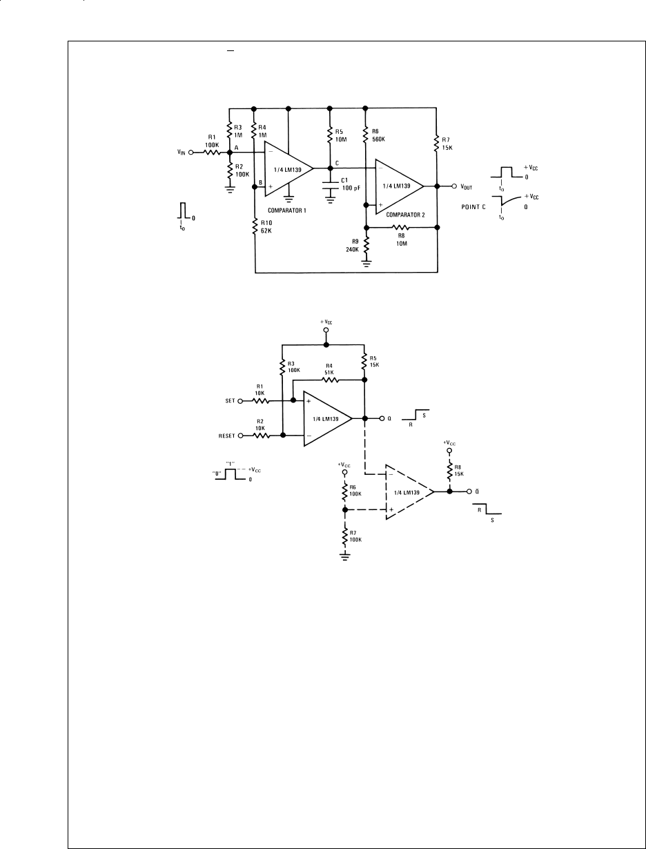
pull the output low. If both Q and Q outputs are needed, an-
other comparator can be added as shown dashed in
Figure 25
.
Figure 26
shows the output saturation voltage of the LM139
comparator versus the amount of current being passed to
ground. The end point of 1 mV at zero current along with an
R
SAT
of 60Ωshows why the LM139 so easily adapts itself to
oscillator and digital switching circuits by allowing the DC
output voltage to go practically to ground while in the ON
state.
AN007385-25
FIGURE 24. Multivibrator with Input Lock-Out
AN007385-26
FIGURE 25. Bistable Multivibrator
www.national.com 12
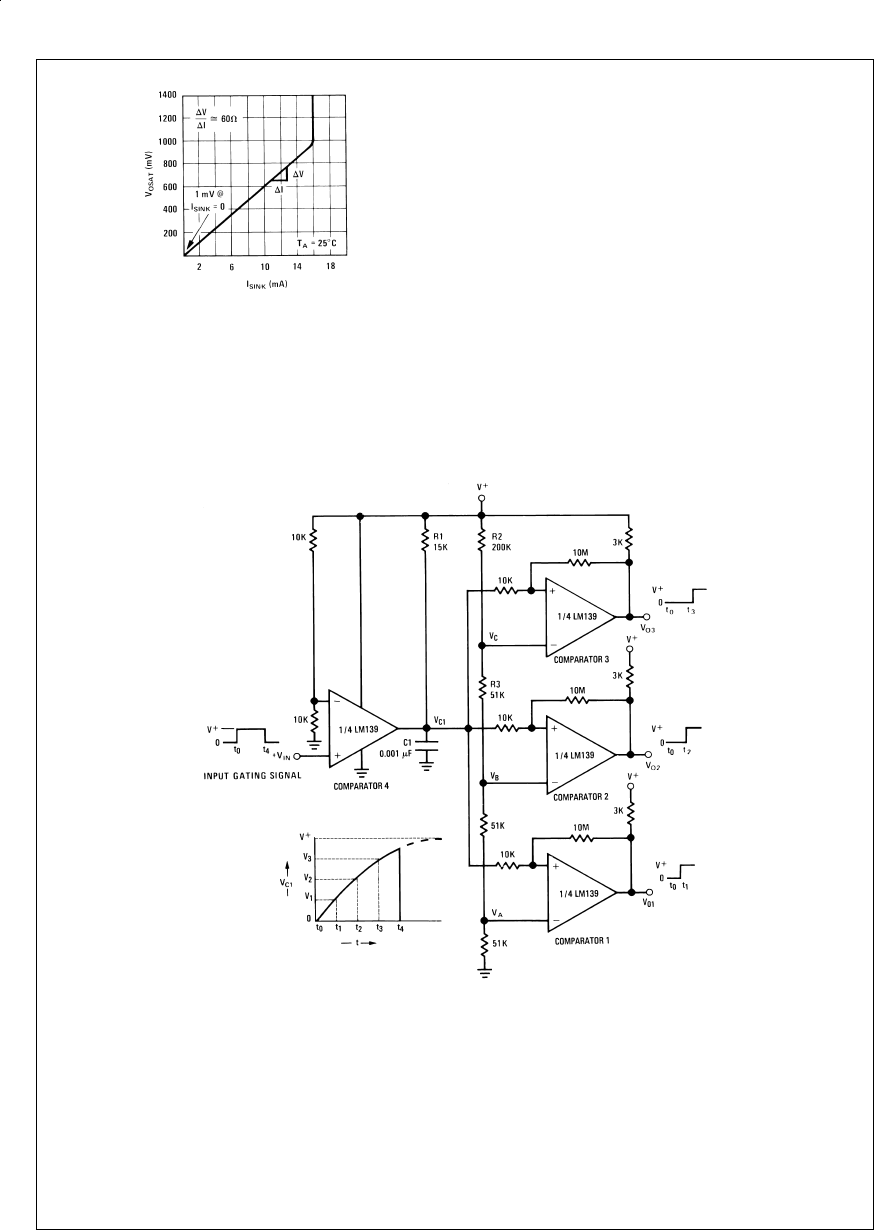
TIME DELAY GENERATOR
The final circuit to be presented “Digital and Switching Cir-
cuits” is a time delay generator (or sequence generator) as
shown in
Figure 27
.
This timer will provide output signals at prescribed time inter-
vals from a time reference t
o
and will automatically reset
when the input signal returns to ground. For circuit evalua-
tion, first consider the quiescent state (V
IN
=O) where the
output of comparator 4 is ON which keeps the voltage across
C
1
at zero volts. This keeps the outputs of comparators 1, 2
and 3 in their ON state (V
OUT
=GND). When an input signal
is applied, comparator 4 turns OFF allowing C
1
to charge at
an exponential rate through R
1
. As this voltage rises past the
present trip points V
A
,V
B
, and V
C
of comparators 1, 2 and 3
respectively, the output voltage of each of these comparators
will switch to the high state (V
OUT
=+V
CC
). A small amount
of hysteresis has been provided to insure fast switching for
the case where the R
C
time constant has been chosen large
to give long delay times. It is not necessary that all compara-
tor outputs be low in the quiescent state. Several or all may
be reversed as desired simply by reversing the inverting and
non-inverting input connections. Hysteresis again is optional.
LOW FREQUENCY OPERATIONAL AMPLIFIERS
The LM139 comparator can be used as an operational am-
plifier in DC and very low frequency AC applications
(≤100 Hz). An interesting combination is to use one of the
comparators as an op amp to provide a DC reference volt-
age for the other three comparators in the same package.
Another useful application of an LM139 has the interesting
feature that the input common mode voltage range includes
ground even though the amplifier is biased from a single
supply and ground. These op amps are also low power drain
devices and will not drive large load currents unless current
is boosted with an external NPN transistor. The largest appli-
cation limitation comes from a relatively slow slew rate which
restricts the power bandwidth and the output voltage re-
sponse time.
AN007385-27
FIGURE 26. Typical Output Saturation Characteristics
AN007385-28
FIGURE 27. Time Delay Generator
www.national.com13
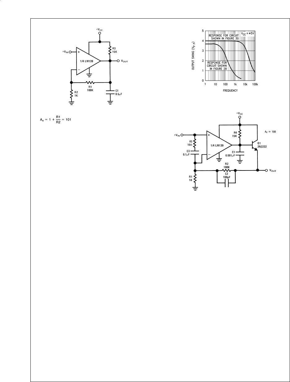
The LM139, like other comparators, is not internally fre-
quency compensated and does not have internal provisions
for compensation by external components. Therefore, com-
pensation must be applied at either the inputs or output of
the device.
Figure 28
shows an output compensation
scheme which utilizes the output collector pull-up resistor
working with a single compensation capacitor to form a
dominant pole. The feedback network, R
1
and R
2
sets the
closed loop gain at1+R
1
/R
2
or 101 (40 dB).
Figure 29
shows the output swing limitations versus frequency. The
output current capability of this amplifier is limited by the
relatively large pull-up resistor (15 kΩ) so the output is
shown boosted with an external NPN transistor in
Figure 30
.
The frequency response is greatly extended by the use of
the new compensation scheme also shown in
Figure 30
. The
DC level shift due to the V
BE
of Q
1
allows the output voltage
to swing from ground to approximately one volt less than
+V
CC
. A voltage offset adjustment can be added as shown in
Figure 31
.
AN007385-29
FIGURE 28. Non-Inverting Amplifier
AN007385-30
FIGURE 29. Large Signal Frequency Response
AN007385-31
FIGURE 30. Improved Operational Amplifier
www.national.com 14
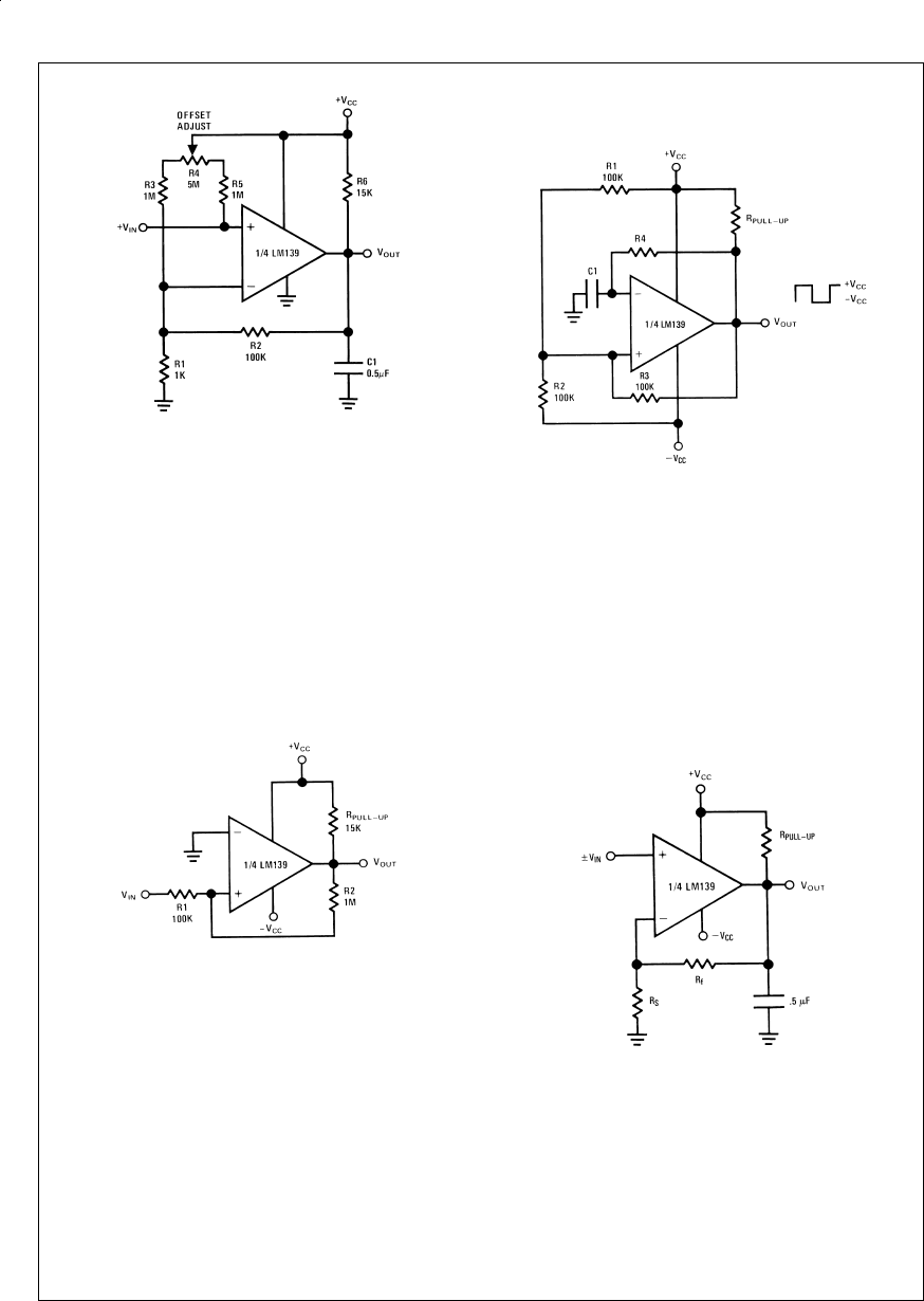
DUAL SUPPLY OPERATION
The applications presented here have been shown biased
typically between +V
CC
and ground for simplicity. The
LM139, however, works equally well from dual (plus and mi-
nus) supplies commonly used with most industry standard
op amps and comparators, with some applications actually
requiring fewer parts than the single supply equivalent.
The zero crossing detector shown in
Figure 10
can be imple-
mented with fewer parts as shown in
Figure 32
. Hysteresis
has been added to insure fast transitions if used with slowly
moving input signals. It may be omitted if not needed, bring-
ing the total parts count down to one pull-up resistor.
The MOS clock driver shown in
Figure 16
uses dual supplies
to properly drive the MM0025 clock driver.
The square wave generator shown in
Figure 13
can be used
with dual supplies giving an output that swings symmetrically
above and below ground (see
Figure 33
). Operation is iden-
tical to the single supply oscillator with only change being in
the lower trip point.
Figure 34
shows an LM139 connected as an op amp using
dual supplies. Biasing is actually simpler if full output swing
at low gain settings is required by biasing the inverting input
from ground rather than from a resistive divider to some volt-
age between +V
CC
and ground.
All the applications shown will work equally well biased with
dual supplies. If the total voltage across the device is in-
creased from that shown, the output pull-up resistor should
be increased to prevent the output transistor from being
pulled out of saturation by drawing excessive current,
thereby preventing the output low state from going all the
way to −V
CC
.
AN007385-32
Av≅100
FIGURE 31. Input Offset Null Adjustment
AN007385-33
FIGURE 32. Zero Crossing Detector Using Dual
Supplies
AN007385-34
FIGURE 33. Squarewave Generator Using Dual
Supplies
AN007385-35
FIGURE 34. Non-Inverting Amplifier Using Dual
Supplies
www.national.com15

MISCELLANEOUS APPLICATIONS
The following is a collection of various applications intended
primarily to further show the wide versatility that the LM139
quad comparator has to offer. No new modes of operation
are presented here so all of the previous formulas and circuit
descriptions will hold true. It is hoped that all of the circuits
presented in this application note will suggest to the user a
few of the many areas in which the LM139 can be utilized.
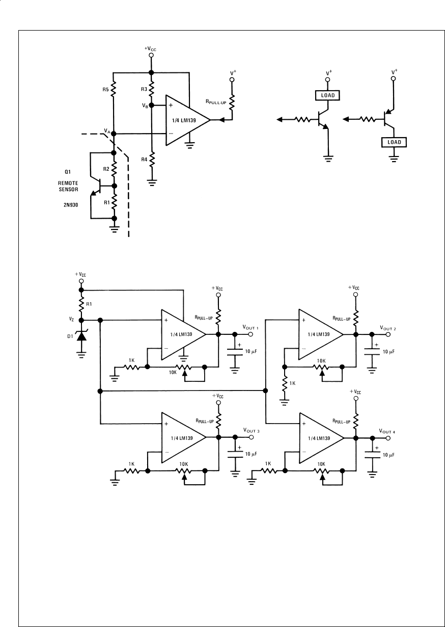
REMOTE TEMPERATURE SENSOR/ALARM
The circuit shown in
Figure 35
shows a temperature
over-range limit sensor. The 2N930 is a National process 07
silicon NPN transistor connected to produce a voltage refer-
ence equal to a multiple of its base emitter voltage along with
temperature coefficient equal to a multiple of 2.2 mV/˚C.
That multiple is determined by the ratio of R
1
to R
2
. The
theory of operation is as follows: with transistor Q
1
biased
up, its base to emitter voltage will appear across resistor R
1
.
Assuming a reasonably high beta (β≥100) the base current
can be neglected so that the current that flows through resis-
tor R
1
must also be flowing through R
2
. The voltage drop
across resistor R
2
will be given by:
I
R1
=I
R2
and
V
R1
=V
be
=l
R1
R
1
so
(31)
As stated previously this base-emitter voltage is strongly
temperature dependent, minus 2.2 mV/˚C for a silicon tran-
sistor. This temperature coefficient is also multiplied by the
resistor ratio R
1
/R
2
.
This provides a highly linear, variable temperature coefficient
reference which is ideal for use as a temperature sensor
over a temperature range of approximately −65˚C to +150˚C.
When this temperature sensor is connected as shown in
Fig-
ure 35
it can be used to indicate an alarm condition of either
too high or too low a temperature excursion. Resistors R
3
and R
4
set the trip point reference voltage, V
B
, with switching
occuring when V
A
=V
B
. Resistor R
5
is used to bias up Q
1
at
some low value of current simply to keep quiescent power
dissipation to a minimum. An l
Q
near 10 µA is acceptable.
Using one LM139, four separate sense points are available.
The outputs of the four comparators can be used to indicate
four separate alarm conditions or the outputs can be OR’ed
together to indicate an alarm condition at any one of the sen-
sors. For the circuit shown the output will go HIGH when the
temperature of the sensor goes above the preset level. This
could easily be inverted by simply reversing the input leads.
For operation over a narrow temperature range, the resistor
ratio R
2
/R
1
should be large to make the alarm more sensitive
to temperature variations. To vary the trip points a potentiom-
eter can be substituted for R
3
and R
4
. By the addition of a
single feedback resistor to the non-inverting input to provide
a slight amount of hysteresis, the sensor could function as a
thermostat. For driving loads greater than 15 mA, an output
current booster transistor could be used.
FOUR INDEPENDENTLY VARIABLE, TEMPERATURE
COMPENSATED, REFERENCE SUPPLIES
The circuit shown in
Figure 36
provides four independently
variable voltages that could be used for low current supplies
for powering additional equipment or for generating the ref-
erence voltages needed in some of the previous comparator
applications. If the proper Zener diode is chosen, these four
voltages will have a near zero temperature coefficient. For
industry standard Zeners, this will be somewhere between
5.0 and 5.4V at a Zener current of approximately 10 mA. An
alternative solution is offered to reduce this 50 mW quies-
cent power drain. Experimental data has shown that any of
National’s process 21 transistors which have been selected
for low reverse beta (β
R
<.25) can be used quite satisfacto-
rily as a zero T.C. Zener. When connected as shown in
Fig-
ure 37
, the T.C. of the base-emitter Zener voltage is exactly
cancelled by the T.C. of the forward biased base-collector
junction if biased at 1.5 mA. The diode can be properly bi-
ased from any supply by adjusting R
S
to set l
q
equal to 1.5
mA. The outputs of any of the reference supplies can be cur-
rent boosted by using the circuit shown in
Figure 30
.
www.national.com 16
AN007385-36
FIGURE 35. Temperature Alarm
AN007385-37
FIGURE 36. Four Variable Reference Supplies
www.national.com17
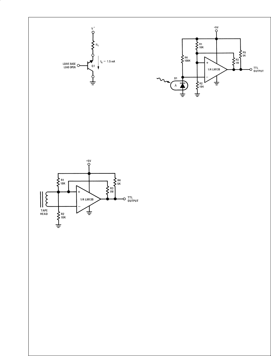
DIGITAL TAPE READER
Two circuits are presented here–a tape reader for both mag-
netic tape and punched paper tape. The circuit shown in
Fig-
ure 38
, the magnetic tape reader, is the same as
Figure 12
with a few resistor values changed. With a 5V supply, to
make the output TTL compatible, anda1MΩfeedback re-
sistor, ±5 mV of hysteresis is provided to insure fast switch-
ing and higher noise immunity. Using one LM139, four tape
channels can be read simultaneously.
The paper tape reader shown in
Figure 39
is essentially the
same circuit as
Figure 38
with the only change being in the
type of transducer used. A photo-diode is now used to sense
the presence or absence of light passing through holes in the
tape. Againa1MΩfeedback resistor gives ±5 mV of hyster-
esis to insure rapid switching and noise immunity.
PULSE WIDTH MODULATOR
Figure 40
shows the circuit for a simple pulse width modula-
tor circuit. It is essentially the same as that shown in
Figure
13
with the addition of an input control voltage. With the input
control voltage equal to +V
CC
/2, operation is basically the
same as that described previously. If the input control volt-
age is moved above or below +V
CC
/2, however, the duty
cycle of the output square wave will be altered. This is be-
cause the addition of the control voltage at the input has now
altered the trip points. These trip points can be found if the
circuit is simplified as in
Figure 41
. Equations 13 through 20
are still applicable if the effect of R
C
is added, with equations
17 through 20 being altered for condition where V
C
≠
+V
CC
/2.
Pulse width sensitivity to input voltage variations will be in-
creased by reducing the value of R
C
from 10 kΩand alter-
nately, sensitivity will be reduced by increasing the value of
R
C
. The values of R
1
and C
1
can be varied to produce any
desired center frequency from less than one hertz to the
maximum frequency of the LM139 which will be limited by
+V
CC
and the output slew rate.
AN007385-38
Q1 =National Process 21 Selected for Low Reverse β
FIGURE 37. Zero T.C. Zener
AN007385-39
FIGURE 38. Magnetic Tape Reader with TTL Output
AN007385-40
FIGURE 39. Paper Tape Reader With TTL Output
www.national.com 18
POSITIVE AND NEGATIVE PEAK DETECTORS
Figures 42, 43
show the schematics for simple positive or
negative peak detectors. Basically the LM139 is operated
closed loop as a unity gain follower with a large holding ca-
pacitor from the output to ground. For the positive peak de-
tector a low impedance current source is needed so an addi-
tional transistor is added to the output. When the output of
the comparator goes high, current is passed through Q
1
to
charge up C
1
. The only discharge path will be the 1 MΩre-
sistor shunting C
1
and any load that is connected to V
OUT
.
The decay time can be altered simply by changing the 1 MΩ
resistor higher or lower as desired. The output should be
used through a high impedance follower to avoid loading the
output of the peak detector.
For the negative peak detector, a low impedance current
sink is required and the output transistor of the LM139 works
quite well for this. Again the only discharge path will be the 1
MΩresistor and any load impedance used. Decay time is
changed by varying the 1 MΩresistor.
CONCLUSION
The LM139 is an extremely versatile comparator package of-
fering reasonably high speed while operating at power levels
in the low mW region. By offering four independent compara-
tors in one package, many logic and other functions can now
be performed at substantial savings in circuit complexity,
parts count, overall physical dimensions, and power con-
sumption.
For limited temperature range application, the LM239 or
LM339 may be used in place of the LM139.
It is hoped that this application note will provide the user with
a guide for using the LM139 and also offer some new appli-
cation ideas.
AN007385-41
FIGURE 40. Pulse Width Modulator
AN007385-81
VA=UPPER TRIP POINT
AN007385-82
VB=LOWER TRIP POINT
FIGURE 41. Simplified Circuit For
Calculating Trip Points of
Figure 40
AN007385-43
FIGURE 42. Positive Peak Detector
AN007385-44
FIGURE 43. Negative Peak Detector
www.national.com19

LIFE SUPPORT POLICY
NATIONAL’S PRODUCTS ARE NOT AUTHORIZED FOR USE AS CRITICAL COMPONENTS IN LIFE SUPPORT DE-
VICES OR SYSTEMS WITHOUT THE EXPRESS WRITTEN APPROVAL OF THE PRESIDENT OF NATIONAL SEMI-
CONDUCTOR CORPORATION. As used herein:
1. Life support devices or systems are devices or sys-
tems which, (a) are intended for surgical implant into
the body, or (b) support or sustain life, and whose fail-
ure to perform when properly used in accordance
with instructions for use provided in the labeling, can
be reasonably expected to result in a significant injury
to the user.
2. A critical component is any component of a life support
device or system whose failure to perform can be rea-
sonably expected to cause the failure of the life support
device or system, or to affect its safety or effectiveness.
National Semiconductor
Corporation
Americas
Tel: 1-800-272-9959
Fax: 1-800-737-7018
Email: support@nsc.com
www.national.com
National Semiconductor
Europe Fax: +49 (0) 1 80-530 85 86
Email: europe.support@nsc.com
Deutsch Tel: +49 (0) 1 80-530 85 85
English Tel: +49 (0) 1 80-532 78 32
Français Tel: +49 (0) 1 80-532 93 58
Italiano Tel: +49 (0) 1 80-534 16 80
National Semiconductor
Asia Pacific Customer
Response Group
Tel: 65-2544466
Fax: 65-2504466
Email: sea.support@nsc.com
National Semiconductor
Japan Ltd.
Tel: 81-3-5639-7560
Fax: 81-3-5639-7507
AN-74 LM139/LM239/LM339—A Quad of Independently Functioning Comparators
National does not assume any responsibility for use of any circuitry described, no circuit patent licenses are implied and National reserves the right at any time without notice to change said circuitry and specifications.
