LH0024 And LH0032 High Speed Op Amp Applications AN 0253
User Manual: AN-0253
Open the PDF directly: View PDF ![]() .
.
Page Count: 12
TL/H/7313
LH0024 and LH0032 High Speed Op Amp Applications AN-253
National Semiconductor
Application Note 253
January 1982
LH0024 and LH0032 High
Speed Op Amp
Applications
INTRODUCTION
The LH0024 and LH0032 are very high speed general pur-
pose operational amplifiers exhibiting 70 MHz bandwidths,
500 V/ms slew rates and 100 to 300 ns settling time to
0.1%. The LH0032 has the added advantage of FET input
characteristics. Both, however, can drive loads with peak
currents of 100 milliamperes (mA). The op amps are stable
without external compensation when operating at closed-
loop gains of more than 100. Both are constructed with thick
film hybrid technology and are actively trimmed for consist-
ent device performance. Table I summarizes the typical per-
formance data for these op amps. Additional information
may be obtained from the respective data sheets.
This note is divided into three parts, with the first giving a
general description of the circuit topology of each op amp.
In the following section, several high performance applica-
tions are discussed. Finally, the last section consolidates all
application techniques into an integral design approach,
much of which is applicable to any high frequency circuit.
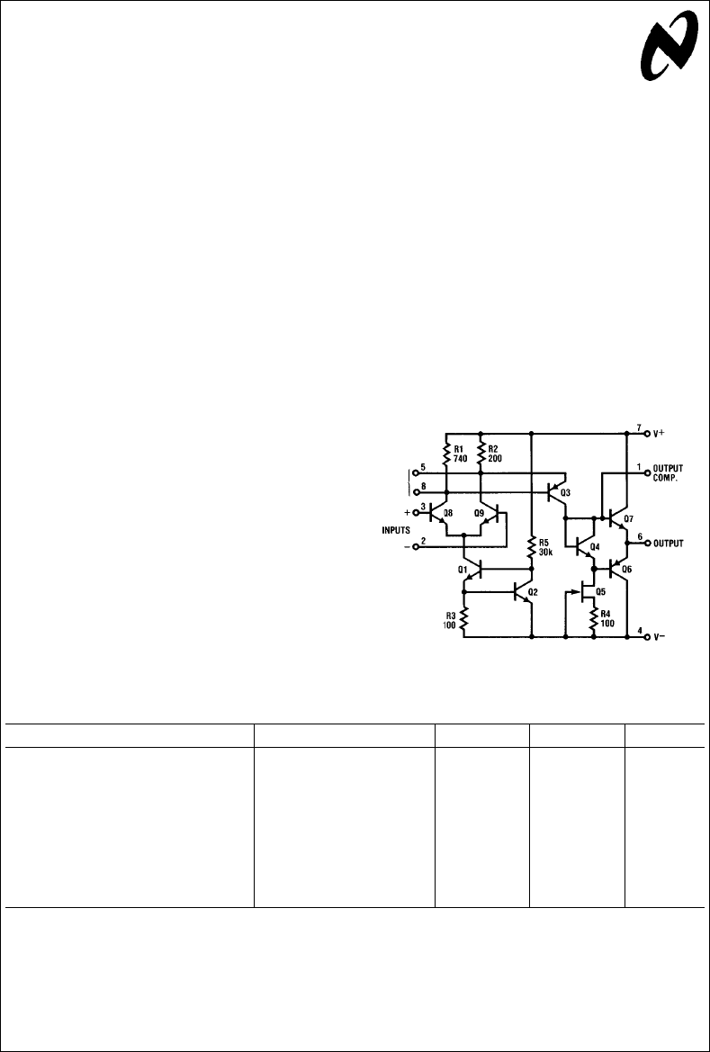
LH0024 CIRCUIT DESCRIPTION
The LH0024 contains two gain stages: One is a differential
NPN pair and the other is a single-ended PNP stage. The
complete schematic is shown in
Figure 1
.
The input stage differential pair, Q8 and Q9, is biased at
6 mA by a current source made up of Q1, Q2, R3, and R5.
First stage differential voltage gain is typically 2. Its output is
applied differentially from base to emitter of the second
stage transistor Q3 which has a gain of about 1,700. This
stage also converts the differential signal to a single-ended
output.
Current source Q5 and R4 provide 5 mA of DC bias current
and a high impedance load to Q3. Overall amplifier gain is
the product of the gains of the two stagesÐ2 x 1700 e
3,400, or 71 dB.
The output complementary pair with class B bias provides a
low impedance sourcing and sinking output drive. Although
the class B bias contributes a small amount of cross-over
distortion, it is barely detectable in closed loop operation.
LH0032 CIRCUIT DESCRIPTION
The LH0032 is a general purpose operational amplifier simi-
lar to the LH0024, but with JFET input devices instead of
bipolar. As a result, the LH0032 DC input bias and offset
currents are three orders of magnitude lower than the
LH0024. Its output drive capability is improved due to the
use of a larger package with lower thermal resistance, and
its class AB output, which is normally biased on, virtually
eliminates cross-over distortion.
The improved DC performance is due, in part, to the incor-
poration of monolithic dual junction FETs in the input stage
of the LH0032, providing matched DC tracking and good
TL/H/7313–1
FIGURE 1. Complete LH0024 Schematic Diagram
TABLE I.
Typical
Performance Characteristics
Parameter (TAe25§C) Conditions LH0024 LH0032 Units
Input Offset Voltage 2 2 mV
Input Bias Current 15 mA10pA
Large Signal Voltage Gain VOUT eg10V 71 70 dB
fe1 kHz, RLe1kX
Slew Rate AVea
1, DVIN e20V 500 500 V/ms
Small Signal Rise Time AVea
1, DVIN e1V 8 8 ns
Settling Time to 1.0% of Final Value AVeb
1, DVIN e20V 80 100 ns
Settling Time to 0.1% of Final Value 275 300 ns
Unity Gain Bandwidth (uncompensated) 70 70 Mhz
C1995 National Semiconductor Corporation RRD-B30M115/Printed in U. S. A.
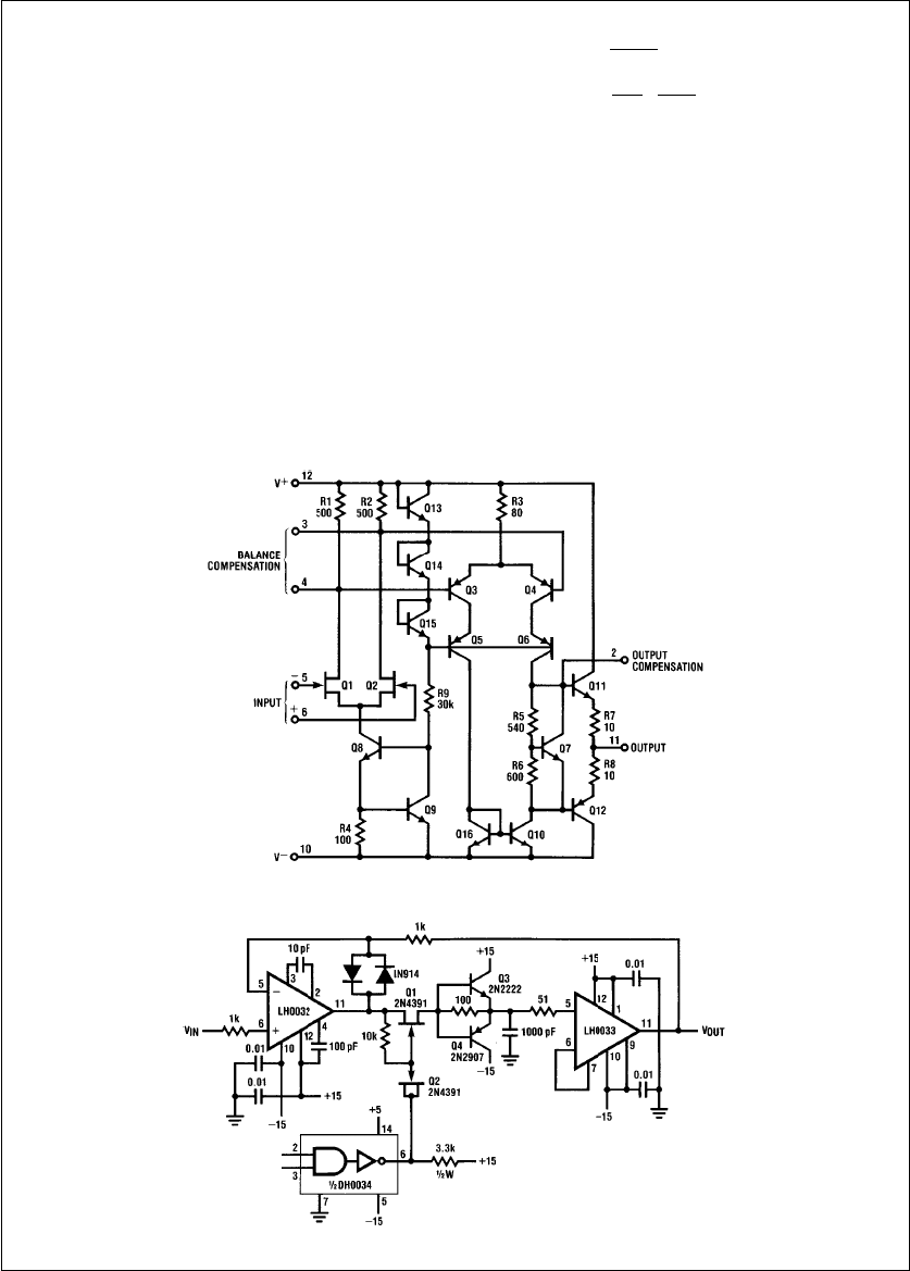
common-mode input characteristics. First stage operating
current is set at 6 mA by the current source made up of
transistors Q8 and Q9 and resistors R4 and R9, as shown in
Figure 2
. The first stage voltage gain is:
AV(1st stage) egmRLe1.4 (1)
Where: gm e3.5 mmho
RLeR1
ll
(b3a1) (re3 a2R3)
The second stage consists of two identical pairs of differen-
tial PNP transistors in a cascode configuration. Each side
operates at 5 mA set by the emitter resistor R3 and the bias
of the first stage. The differential amplifier Q3 and Q4 feeds
the common-base pair Q5 and Q6 with the base voltage
fixed at Vab1.9 volts by the diode string Q13–A15. Thus
the collectors of the differential pair Q3 and Q4 are held at
one VBE drop more positive than the reference voltage. Any
signal amplified by the differential stage produces only a
very small change in Q3 nd Q4 collector voltage. Conse-
quently, the Miller effect on Q3 and Q4 (base-to-collector
capacitances) is virtually eliminated. Using hybrid qmodel
of the transistor, the voltage gain of the cascode stage may
be approximated as:
AV(2nd stage) egm4 xR
eq j1,400 (2)
Where: gm4 e5mA
0.026V
Req e1
hob6
ll
1
hoe10
ll
(b11 a1) (RL)
Notice that the full differential gain is realized with the use of
the current mirror Q10 and Q16, which also provides high
active load resistance to the PNP cascoded pair, resulting in
high amplifier gain.
The collector output of the cascode stage is buffered by a
pair of complementary emitter follower transistors, Q11 and
Q12. This class AB output stage is normally biased at 1 mA
by the 1.8 VBE voltage produced by Q7, R5, and R6. The
emitter degeneration resistors provide protection from ther-
mal runaway.
APPLICATIONS OF THE LH0024/LH0032
Applications of the high speed LH0024 and LH0032 range
from video amplifiers to sampling circuits. The applications
described below include high speed sample and hold cir-
cuits, photo-detector amplifiers, fast settling digital to analog
converters and buffered amplifiers.
TL/H/7313–2
FIGURE 2. Complete LH0032 Schematic Diagram
TL/H/7313–3
FIGURE 3. High Speed Sample and Hold Circuit
2
A High Speed S/H Circuit
High Speed sample-and-hold circuits require high slew rate
and fast settling amplifiers. The LH0032 is ideal for these
applications. An example is shown in
Figure 3
.
The complementary emitter-follower Q3 and Q4 sources or
sinks large peak current to rapidly charge or discharge the
hold capacitor during step changes, thus effectively buffer-
ing the FET switch, Q1, whose rD(ON) would otherwise slow
the charge time. The LH0033 FET-input amplifier buffers the
output signal, providing 100 mA drive capability.
The circuit exhibits a 10V acquisition time of 900 ns to 0.1%
accuracy and a droop rate of only 100 mV/ms at 25§C ambi-
ent condition. An even faster acquisition time can be ob-
tained using a smaller value hold-capacitor. By decreasing
the value from 1000 pF to 220 pF, the acquisition time im-
proves to 500 ns for a 10V step. However, droop rate in-
creases to 500 mV/ms.
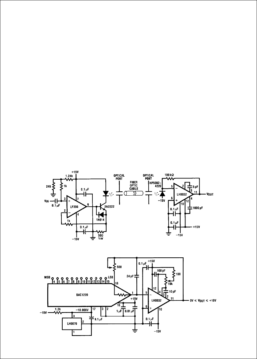
Fiber Optic Transmitter-Receiver Applications
Many fiber optic applications require analog drivers and re-
ceivers operating in the megahertz region where many so-
called wide-band op amps simply run out of steam. Packed
with 70 MHz gain-bandwidth product (unity gain compensat-
ed), the LH0032 is quite suitable for optical communication
applications up to 3.5 MHz.
Figure 4
demonstrates a com-
plete analog transmission system using this device.
The transmitter incorporates the LF356 to drive the light
emitter. The LED is normally biased at 50 mA operating
current. The input is capacitively coupled and ranges from
0V to 5V, modulating the LED current from 0 mA to
100 mA. The circuit can be easily modified to operate from a
single a15V power supply. The only requirement is that the
amplifier must be biased within the input common mode
range.
The receiver circuit uses an LH0032 configured as a trans-
impedance amplifier. A photodiode with 0.5 amp per watt
responsivity such as the Hewlett-Packard type HP5082-
4220, generates 50 mV signal at the receiver output for
1mW of light input.
Expectedly, the bandwidth of the entire optical link rests on
the receiver circuit. Therefore, if the response time is to be
optimized, one should reverse bias the photodiode to mini-
mize junction capacitance. As a result, rise time improves
more than 2 orders of magnitude. Next, the feedback resis-
tor value should be chosen to be as large as possible in
order to maximize sensitivity within the limits of allowable
bandwidth degradation. Using 100 kXfeedback resistor, the
maximum system bandwidth is 3.5 MHz.
Fast Settling 12-BIT D/A Converter
A high resolution, fast-settling DAC can be constructed us-
ing the LH0032. Its low input bias current causes no signifi-
cant DC error in conversion accuracy. Great care must be
exercised in circuit layout to assure highest performance. A
single point analog ground should be used with the digital
ground separated. A complete circuit with 12-bit resolution
is shown in
Figure 5
. The converter typically settles to
(/2 LSB in 800 ns for a 10V full-scale swing. Similarly, 10-bit
or 8-bit resolution DACs may be constructed using the
DAC1020 or DAC0808, respectively.
TL/H/7313–4
FIGURE 4. Fiber Optic Link
TL/H/7313–5
FIGURE 5. Fast Settling DAC
3
Buffered Amplifier
Whenever higher output current is required, a buffer amplifi-
er may be added to the loop as shown in
Figure 6
. The
LH0033 boosts the output drive capability to g100 mA con-
tinuous and g400 mA peak.
TL/H/7313–6
FIGURE 6. Wide Band Amplifier
with 100 mA Output Capability
Despite its 100 MHz bandwidth, the LH0033 introduces
about 15 degrees of phase lag at the LH0032 unity-gain
frequency of 70 MHz. As a result, phase margin is degraded
by the same amount. Slight overcompensation may be re-
quired in order to restore adequate phase margin. One way
is to increase the feedback capacitor from 5 pF to a slightly
larger value, 6 to 8 pF should be sufficient. If the load is
predominantly capacitive, the total phase shift of the buffer
stage may exceed 180§and appear as negative impedance
seen looking into the input of the buffer. The 51Xresistor
restores some real resistance to alleviate this condition and
prevents potential oscillation. In cases where the load ca-
pacitance is relatively large, up to 100Xmay be necessary
to compensate for it.
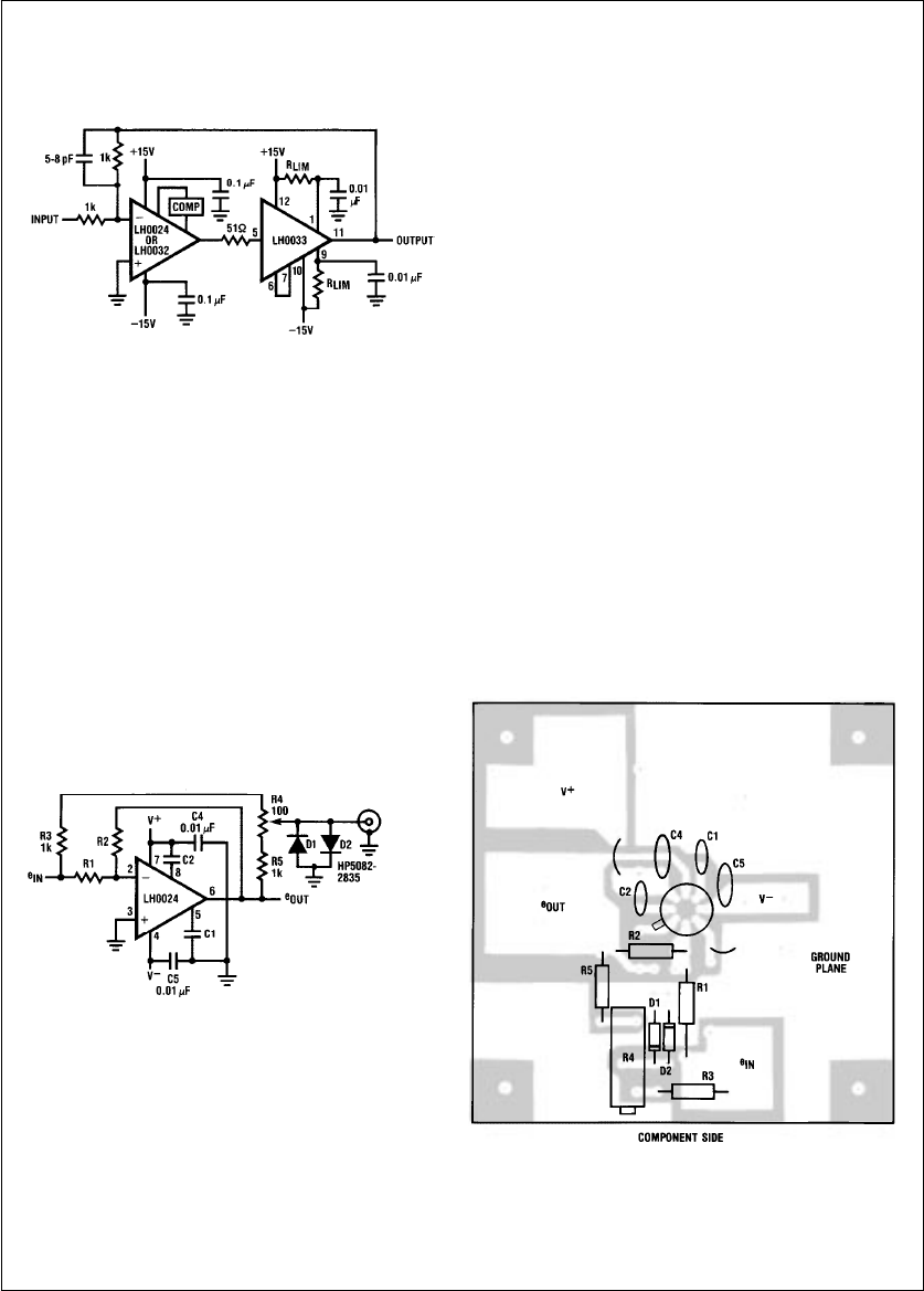
DESIGN CONSIDERATIONS
Optimizing LH0024/32 Performance
The LH0024 and LH0032 allow considerable flexibility in de-
signing high performance circuits if care is taken in the way
they are used and implemented. Indeed, the printed circuit
board layout in high frequency circuits is as important as the
design of the hybrid devices themselves.
It is good practice to use ground plane PC board design. It
provides a low resistance, low inductance path, and reduc-
es stray signal coupling to sensitive circuitry. A double-sided
ground plane is usually better and should be considered.
In addition, signal trace connections should be kept as short
and wide as possible. Avoid closely-spaced parallel signal
traces as signal cross-coupling may occur. Circuit elements
should be placed close to the amplifier, particularly critical
components that directly affect the amplifier’s frequency re-
sponse, such as compensation capacitors. If at all possible,
one should maintain single point ground throughout the cir-
cuit to minimize signal phase delay.
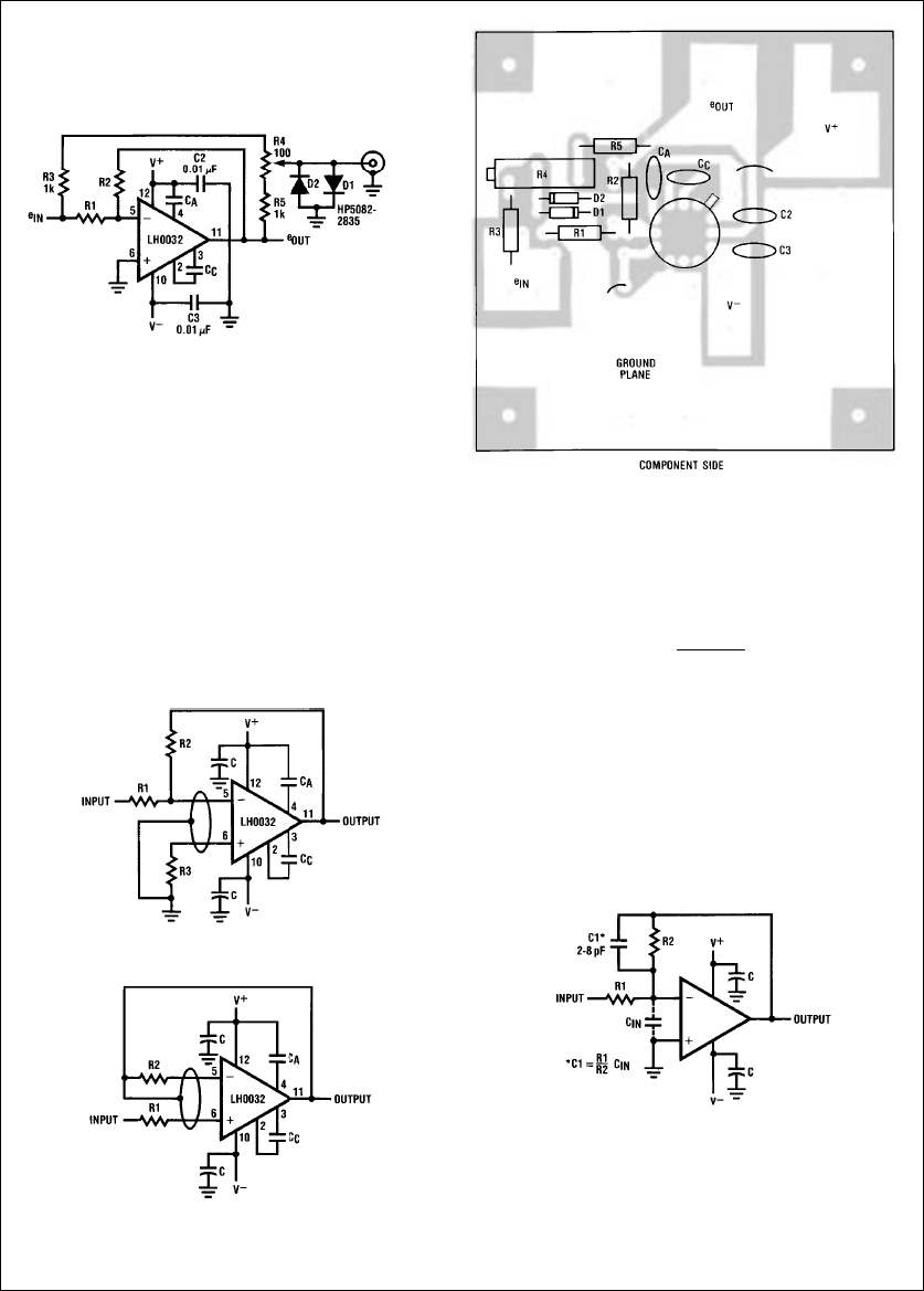
Examples of single-sided PC layouts for the LH0024 and
LH0032 are shown in
Figure 7
and
Figure 8
, respectively.
The layouts include a settling time test circuit, optional in-
verting or noninverting mode. Note that the summing junc-
tion side of the feedback resistor is kept very close to the
device pin, thus minimizing lead capacitance. The power
supply decoupling capacitors should also be kept close to
the device pins, preferably */8 of an inch.
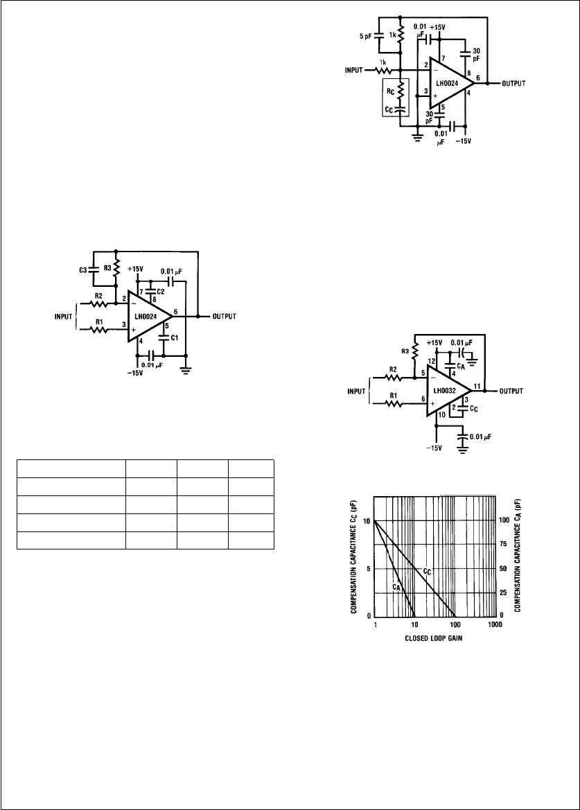
Input Guarding and Bootstrapping
In applications where input leakage currents are important,
trace guarding, such as used in sample and hold circuits,
can improve performance at no additional cost.
TL/H/7313–7
TL/H/7313–8
FIGURE 7. Single-Sided Sample PC Layout for LH0024
4
TL/H/7313–9
TL/H/7313–12
FIGURE 8. Single-Sided Sample PC Layout for LH0032
The guard conductor serves to intercept leakage currents
from inputs to the surrounding circuit. It is most effective
when it is driven to the same potential as the guarded cir-
cuit.
Figures 9
and
10
show how the technique is imple-
mented in inverting and non-inverting configurations, re-
spectively.
One other benefit of input guarding is the reduction of input
stray capacitance effects. A comprehensive discussion of
this technique is described in Application Note AN-63.
TL/H/7313–10
FIGURE 9. Guarding Inverting Figure Amplifier
TL/H/7313–11
FIGURE 10. Guarding Non-Inverting
Unity Gain Amplifier
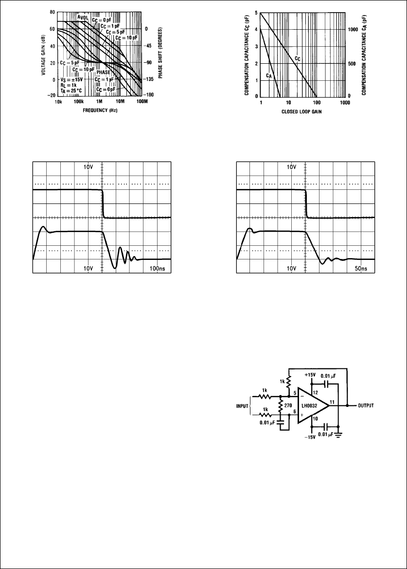
Input Capacitance Cancellation
The intrinsic input capacitance of the amplifier cannot be
totally eliminated by the input guarding technique. This input
capacitance introduces a pole in the amplifier response at
the frequency given by:
fpe1
2qRSCIN
(3)
This pole may become extremely important as, for example,
aC
IN of 5 pF (typical input capacitance of the LH0024 and
LH0032) with a 500Xeffective source resistance creates a
pole at about 64 MHzÐwell before the amplifier’s natural
frequency response rolls off to unity gain at 70 MHz. If
closed-loop gain is unity, more than 135§total phase lag is
introduced even before the crossover frequency is reached
and will destroy phase margin. Oscillation is certain to oc-
cur. The solution is to cancel its effect. As shown in
Figure
11
, the lead capacitor C1 across the feedback resistor is
used to introduce a zero in the loop response such that it
exactly cancels the pole caused by the input RC network.
TL/H/7313–13
FIGURE 11. Compensating Amplifier Input Capacitance
5
Ideally, the ratio of input capacitance CIN to lead capacitor
C1 should equal the closed-loop gain of the amplifier. Under
this condition, exact pole-zero cancellation is realized.
Note that Equation (3) dictates the use of source resistance
values less than 1 kXin circuits operating at or near unity
gain to keep fPgreater than 70 MHz.
Frequency Compensation
High-performance wideband op amps such as the LH0024
and LH0032 require external frequency compensation, de-
pending on the closed-loop gain. Optimum AC performance
will be affected by a given circuit and its layout. Several
compensation techniques are recommended and the best
should be selected according to the particular application.
Each is discussed in the following sections.
Compensating the LH0024
Table II provides a guide to compensate the LH0024 at sev-
eral values of closed-loop gain.
Figure 12
shows the basic
scheme.
TL/H/7313–14
FIGURE 12. LH0024 Frequency Compensation Circuit
When operating with closed-loop gain of b1, C3 is required
and may need slight adjustment to completely cancel the
input capacitance of the device, typically 5 pF.
TABLE II
Closed-Loop Gain C1 C2 C3
100 0 0 0
20 0 0 0
10 0 20 pF 1 pF
1 30pF 30pF 5pF
An alternate technique for compensation at a closed-loop
gain of 1 is to use an input RC lag compensation network as
shown in
Figure 13
.
With 1 kXresistor values in the circuit, RCand CCshould be
82Xand 0.047 mF, respectively. The difficulty in using this
compensation is its involved calculation and experimenting
required in order to find the optimum RCand CCvalues if
resistors other than 1 kXare used when the above RCand
CCvalues are no longer valid and must be redetermined.
For this reason, optimum compensation is almost always
determined empirically, as were the values given.
TL/H/7313–15
FIGURE 13. Input RC Lag Compensation Circuit
Compensating the LH0032
With the LH0032, two compensation schemes may be used,
depending on the designer’s specific needs.
The first technique is shown in
Figure 14
. It offers the best
0.1% settling time for a g10V square wave input. The com-
pensation capacitors CCand CAshould be selected from
Figure 15
for various closed-loop gains.
Figure 16
shows
how the LH0032 frequency response is modified for differ-
ent value compensation capacitors.
Although this approach offers the shortest settling time, the
falling edge exhibits overshoot up to 30% lasting 200 to
300 ns.
Figure 17
shows the typical pulse response.
TL/H/7313–16
FIGURE 14. LH0032 Frequency Compensation Circuit
TL/H/7313–17
FIGURE 15. Recommended Value of
Compensation Capacitor vs. Closed-Loop
Gain for Optimum Settling Time
6
TL/H/7313–18
FIGURE 16. The Effect of Various
Compensation Capacitors on LH0032
Open Loop Frequency Response
TL/H/7313–20
FIGURE 18. Recommended Value of
Compensation Capacitor vs. Closed-Loop
Gain for Optimum Slew Rate
TL/H/7313–19
FIGURE 17. LH0032 Unity Gain Non-Inverting
Large Signal Pulse Response:
TAe25§C, CCe10 pF, CAe100 pF
TL/H/7313–21
FIGURE 19. LH0032 Unity Gain Non-Inverting
Large Signal Pulse Response:
CCe5 pF, CAe1000 pF
If obtaining minimum ringing at the falling edge is the pri-
mary objective, a slight modification to the above is recom-
mended. It is based on the same circuit as that of
Figure 14
.
The values of the unity gain compensation capacitors CC
and CAshould be modified to 5 pF and 1000 pF, respective-
ly.
Figure 18
shows the suitable capacitance to use for vari-
ous closed-loop gains. The resulting unity gain pulse re-
sponse waveform is shown in
Figure 19
. The settling time to
1% final value is actually superior to the first method of
compensation. However, the LH0032 suffers slow settling
thereafter to 0.1% accuracy at the falling edge, and nearly
four times as much at the rising edge, compared to the pre-
vious scheme. Note, however, that the falling edge ringing is
considerably reduced. Furthermore, the slew rate is consist-
ently superior using this compensation because of the
smaller value of Miller capacitance CCrequired. Typical im-
provement is as much as 50%. A more detailed discussion
of this effect is provided in the Slew Response section of
this Application Note.
The second compensation scheme works well with both in-
verting or non-inverting modes.
Figure 20
shows the circuit
schematic, in which a 270Xresistor and a 0.01 mF capacitor
are shunted across the inputs of the device. This lag com-
pensation introduces a zero in the loop modifying the re-
sponse such that adequate phase margin is preserved at
unity gain crossover frequency. Note that the circuit requires
no additional compensation.
TL/H/7313–22
FIGURE 20. LH0032 Non-Compensated
Unity Gain Compensation
7
Output Drive Capability
The LH0024 and LH0032 op amps are designed to deliver,
but not to exceed, g100 mA peak output current for dura-
tions under 1 ms at duty cycles under 1%.
The output drive capability of these op amps is limited pri-
marily by device power dissipation.
Figure 21
shows the
maximum drive capabilities under various conditions. These
limits should be observed. Furthermore, the open loop gain
decreases slightly as a result of increased output loading.
For this reason, continuous output current should be kept
under 50 mA.
LH0024
TL/H/7313–23
LH0032
TL/H/7313–24
FIGURE 21. Continuous Output Drive Capability
Capacitive Load Compensation
Capacitive loads cause increased phase shifts in such a
way that phase margin decreases toward an unstable state
and oscillating may result. The cure is to overcompensate
the op amp and to isolate the load with a series resistor
(100 to 200X) as shown in
Figure 22
. For example, an un-
terminated coaxial cable presents a capacitive load. Slight
overcompensation may be required to maintain stability.
TL/H/7313–25
FIGURE 22. Output Protection
when Driving Capacitive Load
Power Dissipation
A simple design rule that is often bent, if not broken, is that
relating to power dissipation. The limits for the LH0024 and
LH0032 are shown in
Figure 23
. Under no circumstances
should these guidelines be exceeded within the temperature
range specified. The total power dissipation can be easily
calculated from the following equation:
PTotal ePQaPOut (4)
Where: PQethe quiescent power at a given supply
voltage and current as specified by the data
sheet, and,
POut ethe drive power dissipated in the device
output stage, computed as the net rms collec-
tor-emitter voltage of the output transistor times
the load current.
Determining power dissipation when driving a capacitive
load is more involved. The peak power required to charge or
discharge the load capacitor is:
PPeak eCL(DV)2
t(5)
Where: DVethe change in voltage across CL.
teIPeak charging time into CL.
Over a full charge and discharge cycle, the power is directly
roportional to the frequency of the input pulse waveform. As
the pulse repetition frequency increases, so does power dis-
sipation.
LH0024
TL/H/7313–26
LH0032
TL/H/7313–27
FIGURE 23. Maximum Power Dissipation
8
Short Circuit Protection
Since the LH0024 and LH0032 have no internal short circuit
protection, their relatively high drive capability can sustain
current levels sufficient to destroy the devices if high fre-
quency oscillation is induced. This can occur with a large
capacitance load. To design in protection, a current limiting
resistor Rsc should be inserted at the output of the amplifier
inside the feedback loop as shown in
Figure 22
. The value
of Rsc can be determined from the following equation:
Rsc eVa
Isc
(6)
Where: Vais the power supply voltage.
Heat Sinking Considerations
Under severe environmental and electrical operating condi-
tions, a low thermal resistance heat sink should be used to
assure safe operation. The following is a list of heat sinks
from various sources recommended for the TO-8 case style:
Thermalloy 2240A, 33§C/W
Wakefield 215CB, 30§C/W
IERC, UP-TO 8-48CB, 15§C/W
Heat sinks for the TO-5 case style are readily available from
many manufacturers. A reasonably priced clip-on unit from
Thermalloy, Model 2228B, offers modest thermal resistance
of 35§C/W.
Case Grounding
Grounding the case of the device offers improved immunity
from circuit cross-talk, but it compromises additional stray
capacitance to every device pin (usually 1– 2 pF). In the rare
situation where case grounding is required, slight recompen-
sation may be necessary. However, most applications are
not demanding enough to warrant its use.
There are several ways to strap, or ground the case. For the
LH0032, the best approach is to solder a small metal wash-
er or a small piece of wire between the base of the device
metal can and the base of an unassigned lead post. Dedi-
cating pin 7 of the LH0032 for this purpose is recommend-
ed, although any other ‘‘no connection’’ pin is acceptable.
High temperature solder should be used to avoid solder re-
flow during normal assembly operations.
The LH0024 has no unused pins available, and thus is not
readily adaptable to case strapping. An alternative approach
is to use an electrically conductive heatsink with a PC
board-mountable option, such as Thermalloy type 2230C-5.
In all uses of case grounding, be on the lookout for ground-
induced noise into the signal path. In short, be sure the
ground is a
quiet
ground.
Power Supply Bypass
Power supply pins must be bypassed in all cases to prevent
oscillation. A 0.01 mFto0.1mF disc or monolithic ceramic
capacitor at each supply pin to ground is adequate. The
capacitors should be placed no more than (/2 inch from the
device pins.
Adjustment of Offset Voltages
When required, the offset voltage of the operational amplifi-
ers may be nulled using a balance potentiometer as shown
in
Figure 24
. The 100Xseries resistors prevent any adverse
oscillation or malfunction when the pot is shorted to either
end of the adjustment range.
TL/H/7313–28
FIGURE 24. Offset Voltage Adjustment
Slew Response Improvement
Slew rate is the internally limited maximum rate of rise, or
fall, at maximum amplifier output swing when driven by a
large signal step input. It is primarily limited by the operating
current of the input stage. When overdriven by a step fuc-
tion, the input stage operating current charges or discharg-
es the effective circuit capacitance of the second stage.
The rate of charge is:
dV
dt
eIInput Stage
CNode
(7)
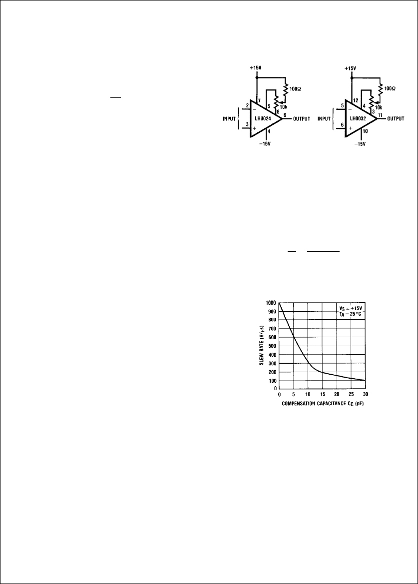
In the case of the LH0032, where Miller Compensation is
used, the external capacitance adds to the internal circuit
capacitance, resulting in reduced slew rate.
Figure 25
illus-
trates this effect as a function of the capacitance value.
TL/H/7313–29
FIGURE 25. LH0032 Slew Rate vs. Frequency
Compensation Capacitance
9
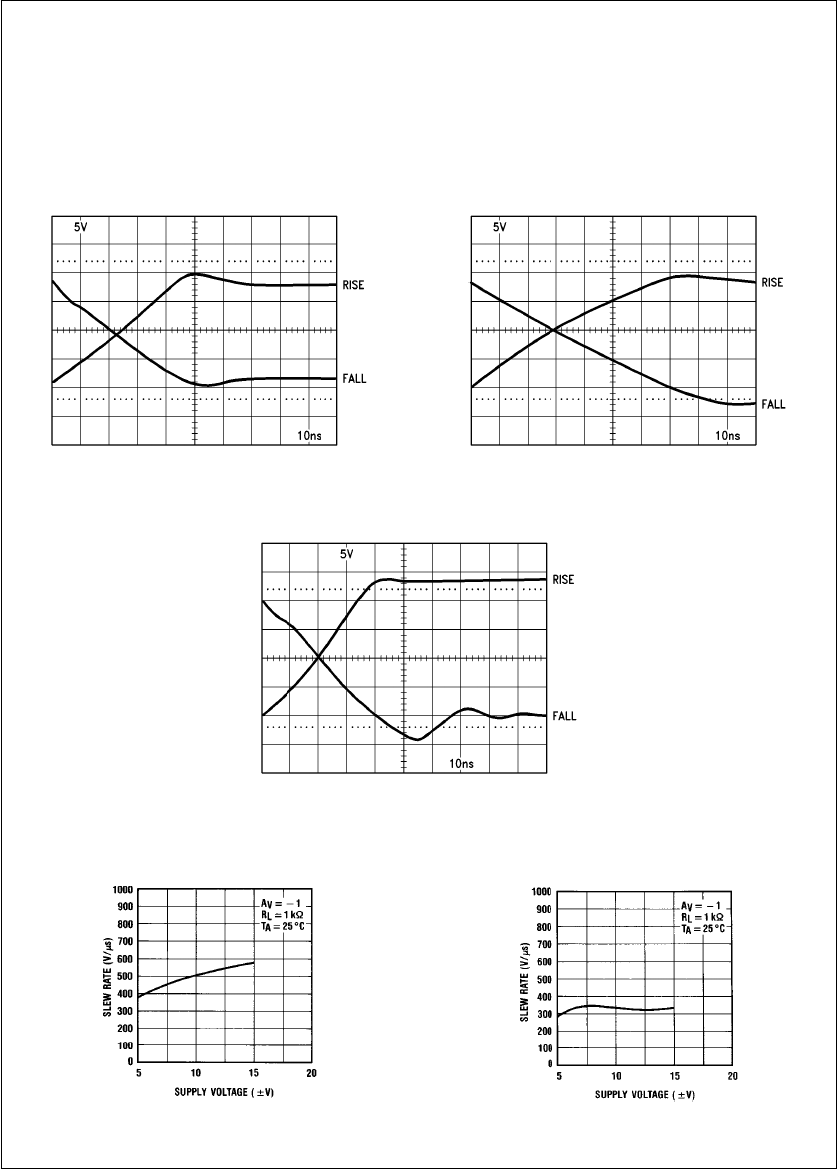
Figures 26
,
27
, and
28
demonstrate the rising and falling
slew capabilities of the LH0024 and LH0032. Notice the im-
proved slew rate peformance of the LH0032 using the alter-
native compensation technique in
Figure 28
compared to
Figure 27
. The difference is due to the smaller Miller capaci-
tance used in the former.
The LH0024 does not use Miller Compensation, so slew
rate is not compromised. Consequently, large signal fre-
quency response is significantly higher than that of the
LH0032.
Finally, power supply voltage affects slew rate. As the volt-
age decreases, input stage operating current decreases ac-
cordingly. The net effect is a reduction in the slew rate as
the available charging current drops off.
Figure 29
shows
the typical slew response of each op amp as a function of
supply voltage.
TL/H/7313–30
FIGURE 26. LH0024 Slew Response,
Unity Gain Inverting Mode
TL/H/7313–31
FIGURE 27. LH0032 Slew Response,
Unity Gain Inverting Mode, Standard Compensation
(CCe10 pF, CAe100 pF)
TL/H/7313–32
FIGURE 28. LH0032 Slew Response, Unity Gain
Inverting Mode, Improved Compensation
(CCe5 pF, CAe1000 pF)
LH0024
TL/H/7313–33
LH0032
TL/H/7313–34
FIGURE 29. Slew Rate Response as a Function of Supply Voltages
10
Settling Time
Settling time is the time between the start of a step input to
the time it takes the output to settle to within a specified
error band of the final voltage. This parameter is heavily
influenced by the frequency compensation of the amplifier
(degree of damping). Undercompensation results in exces-
sive phase shift, overshoot and ringing, and therefore, a
long settling time. Equally poor performance results from
overcompensation, which yields an overdamped system,
slow decay and, again, a long settling time.
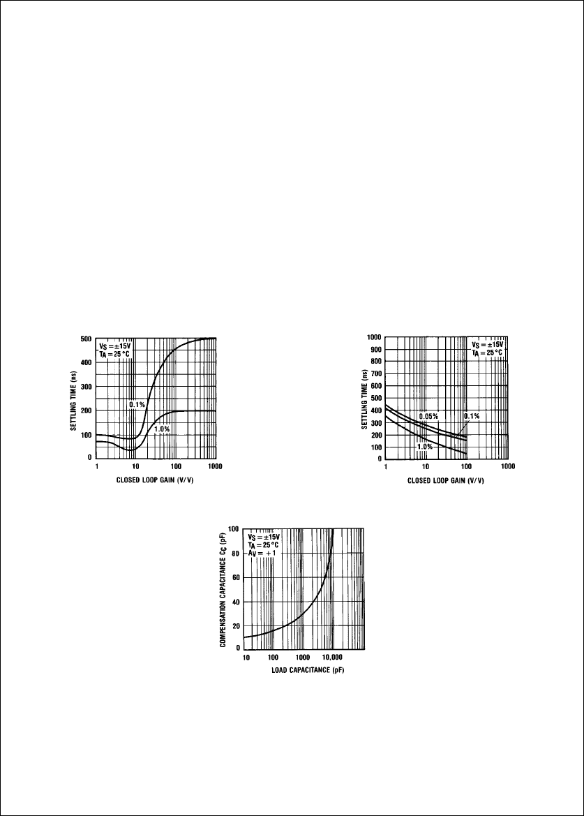
Expectedly, settling time is affected by the loop gain of the
amplifier.
Figure 30
illustrates this effect for these two devic-
es.
One of the most demanding applications is driving a capaci-
tive load in a circuit such as a high speed sample-and-hold,
where accuracy and fast settling time are both important.
Because of the additional phase shift introduced by driving
the sampling capacitor, the LH0032 must be recompensat-
ed.
Figure 31
presents the optimum compensation to obtain
fastest settling time under these conditions.
CONCLUSION
At first glance, the LH0024 and LH0032 seem harmless
enough. A more in-depth look reveals the challenges in ap-
plying these high performance op amps. The ultimate capa-
bilities that can be extracted are a direct function of careful
engineering. With prudence, these devices are harmless in-
deed.
Application of these high performance amplifiers requires an
understanding of compensation and layout technique. With
the information presented in this note, the designer should
be able to enjoy the benefits of their superior capabilities.
REFERENCES
1. National Semiconductor
Special Functions Databook.
2. R. K. Underwood, ‘‘New Design Techniques for FET Op
Amps’’ National Semiconductor AN-63, March 1972.
3. J. Wong, J. Sherwin, ‘‘Applications of Wide-Band Buffer
Amplifiers’’ National Semiconductor AN-227, October
1979.
4. ‘‘LH0082 Optical Communication Receiver’’ Data Sheet,
National Semiconductor Corp.
5. E. Miller, ‘‘Introduction to Practical Fiber Optics’’ National
Semiconductor AN-244, May 1980.
LH0024
TL/H/7313–35
LH0032
TL/H/7313–36
FIGURE 30. Settling Time vs. Closed-Loop Gain
TL/H/7313–37
FIGURE 31. Frequency Compensation vs. Load Capacitance
11

AN-253 LH0024 and LH0032 High Speed Op Amp Applications
LIFE SUPPORT POLICY
NATIONAL’S PRODUCTS ARE NOT AUTHORIZED FOR USE AS CRITICAL COMPONENTS IN LIFE SUPPORT
DEVICES OR SYSTEMS WITHOUT THE EXPRESS WRITTEN APPROVAL OF THE PRESIDENT OF NATIONAL
SEMICONDUCTOR CORPORATION. As used herein:
1. Life support devices or systems are devices or 2. A critical component is any component of a life
systems which, (a) are intended for surgical implant support device or system whose failure to perform can
into the body, or (b) support or sustain life, and whose be reasonably expected to cause the failure of the life
failure to perform, when properly used in accordance support device or system, or to affect its safety or
with instructions for use provided in the labeling, can effectiveness.
be reasonably expected to result in a significant injury
to the user.
National Semiconductor National Semiconductor National Semiconductor National Semiconductor
Corporation Europe Hong Kong Ltd. Japan Ltd.
1111 West Bardin Road Fax: (
a
49) 0-180-530 85 86 13th Floor, Straight Block, Tel: 81-043-299-2309
Arlington, TX 76017 Email: cnjwge
@
tevm2.nsc.com Ocean Centre, 5 Canton Rd. Fax: 81-043-299-2408
Tel: 1(800) 272-9959 Deutsch Tel: (
a
49) 0-180-530 85 85 Tsimshatsui, Kowloon
Fax: 1(800) 737-7018 English Tel: (
a
49) 0-180-532 78 32 Hong Kong
Fran3ais Tel: (
a
49) 0-180-532 93 58 Tel: (852) 2737-1600
Italiano Tel: (
a
49) 0-180-534 16 80 Fax: (852) 2736-9960
National does not assume any responsibility for use of any circuitry described, no circuit patent licenses are implied and National reserves the right at any time without notice to change said circuitry and specifications.
