HPC MICROWIRE/PLUS Master Slave Handshaking Protocol AN 0474
User Manual: AN-0474
Open the PDF directly: View PDF ![]() .
.
Page Count: 8
TL/DD/9140
HPC MICROWIRE/PLUS Master-Slave Handshaking Protocol AN-474
National Semiconductor
Application Note 474
Richard Lazovick
June 1988
HPC MICROWIRE/PLUSTM
Master-Slave Handshaking
Protocol
INTRODUCTION
This applications note describes how to use National Semi-
conductor’s MICROWIRE/PLUS to communicate between
two members of the HPC family of microcontrollers, and will
discuss the implications of adding other MICROWIRETM pe-
ripherals. MICROWIRE/PLUS (mWIRE) may be effectively
used to communicate between chips, such as in Small Area
Networks (SANs). Possible applications range from setting
up a communications network within an automobile to home
security systems. Among the standard MICROWIRE periph-
erals available are display drivers (LCD, VF, LED), memo-
ries (RAM, EEPROM), A/D converters, and frequency gen-
erators/timers. Each MICROWIRE peripheral requires its
own handshaking protocol, however the HPC’s MICRO-
WIRE is flexible enough to work with any peripheral and
allows you to define your own handshaking protocol when
having two HPC family members communicate.
MICROWIRE
MICROWIRE/PLUS is an extension of National Semicon-
ductor’s MICROWIRE communications interface. It allows
high speed two way serial communications between a mas-
ter processor and one or more slave processors or periph-
erals. MICROWIRE/PLUS uses only three wires plus chip
selects, therefore it saves on intricate bus routing and does
not waste 8-bit ports.
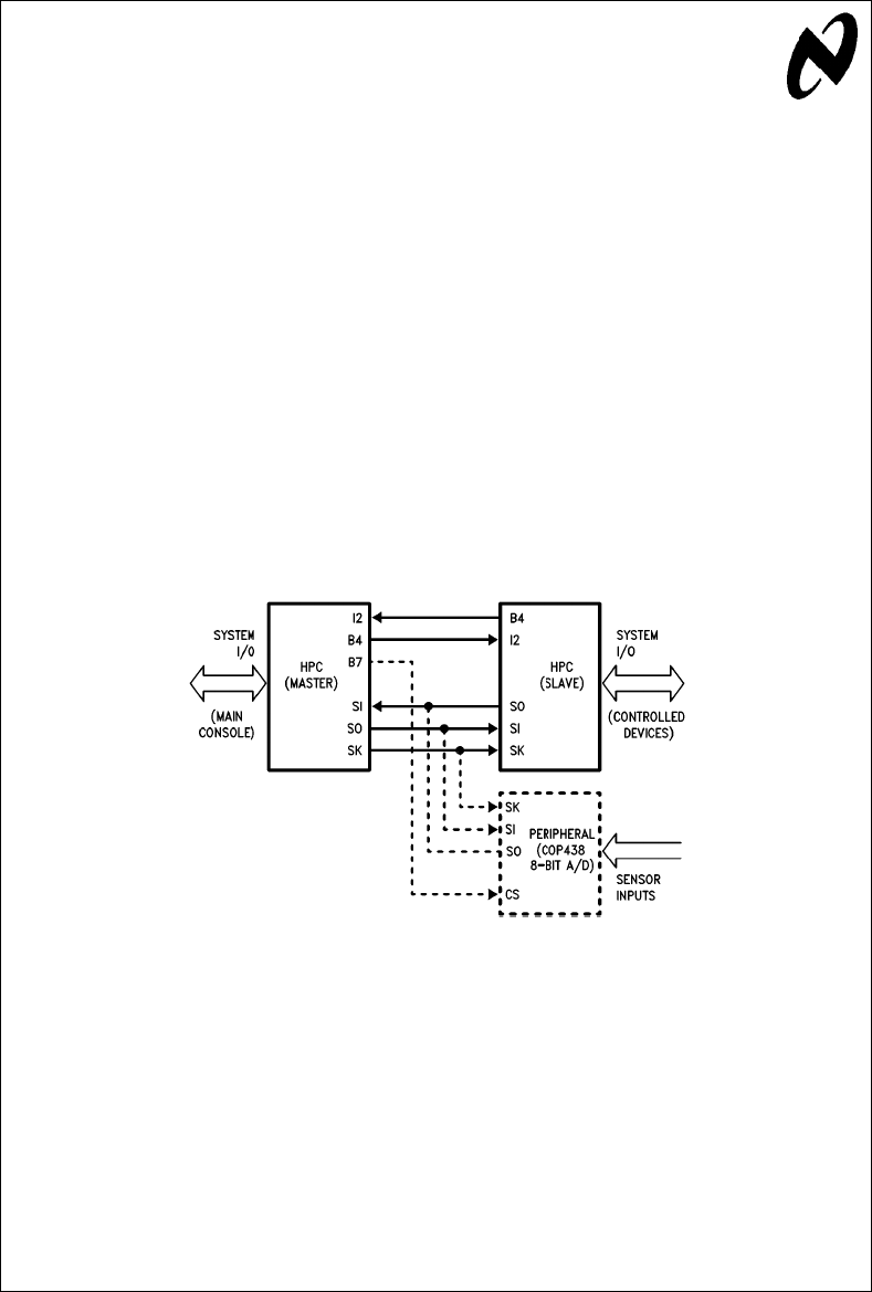
Figure 1
shows the block diagram of a
sample application using two HPC family members and an
8-bit A/D peripheral to monitor and control certain environ-
mental conditions within a system.
MICROWIRE/PLUS has an 8-bit parallel-loaded, serial shift
register (SIO) using SI as the serial input and SO as the
serial output. The contents of the SIO register may be ac-
cessed through any of the memory access instructions. SK
is the clock for the SIO register (see
Figure 2
). The SK clock
signal can be provided by an internal or external source.
The internal clock rate is programmable by the DIVBY regis-
ter. Data to be transmitted from the SIO register is shifted
out on the falling edge of the SK clock. Serial data on the SI
pin is latched in on the rising edge of the SK clock (see
Figure 3
mWIRE Timing).
TL/DD/9140–1
FIGURE 1. HPC mWIRE Block Diagram
(Environmental Control System)
TRI-STATEÉis a registered trademark of National Semiconductor Corporation.
MICROWIRETM and MICROWIRE/PLUSTM are trademarks of National Semiconductor Corporation.
C1995 National Semiconductor Corporation RRD-B30M105/Printed in U. S. A.
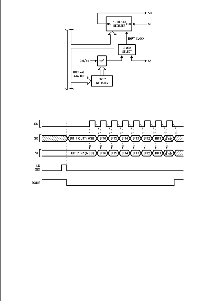
TL/DD/9140–2
Note: The most significant bit is shifted out first. The SO pin reflects the contents of the MSB in the SIO register.
FIGURE 2. MICROWIRE/PLUS Block Diagram
TL/DD/9140–3
Note: The first bit of every eight bits in the SIO register being shifted out will have a longer duration then the other bits. This results from the hardware
implementation used for MICROWIRE.
*This bit becomes valid immediately when the transmitting device loads its SIO register.
²Arrows indicate points at which SI is sampled.
FIGURE 3. mWIRE Timing
2
AmWDONE flag in the IRPD (Interrupt Pending) register
indicates when the data shift is completed.
The HPC can enter the MICROWIRE/PLUS mode as a
master or a slave. The mWMODE control bit in the IRCD
(Interrupt Condition) register determines whether the HPC is
a master or slave. The shift clock is generated internally
when the HPC is configured as a master. An externally gen-
erated shift clock on the SK pin is used when the HPC is
configured as a slave. When the HPC is a master, the
DIVBY register allows the SK clock frequency to be pro-
grammed in 14 selectable steps from 122 Hz to 1 MHz
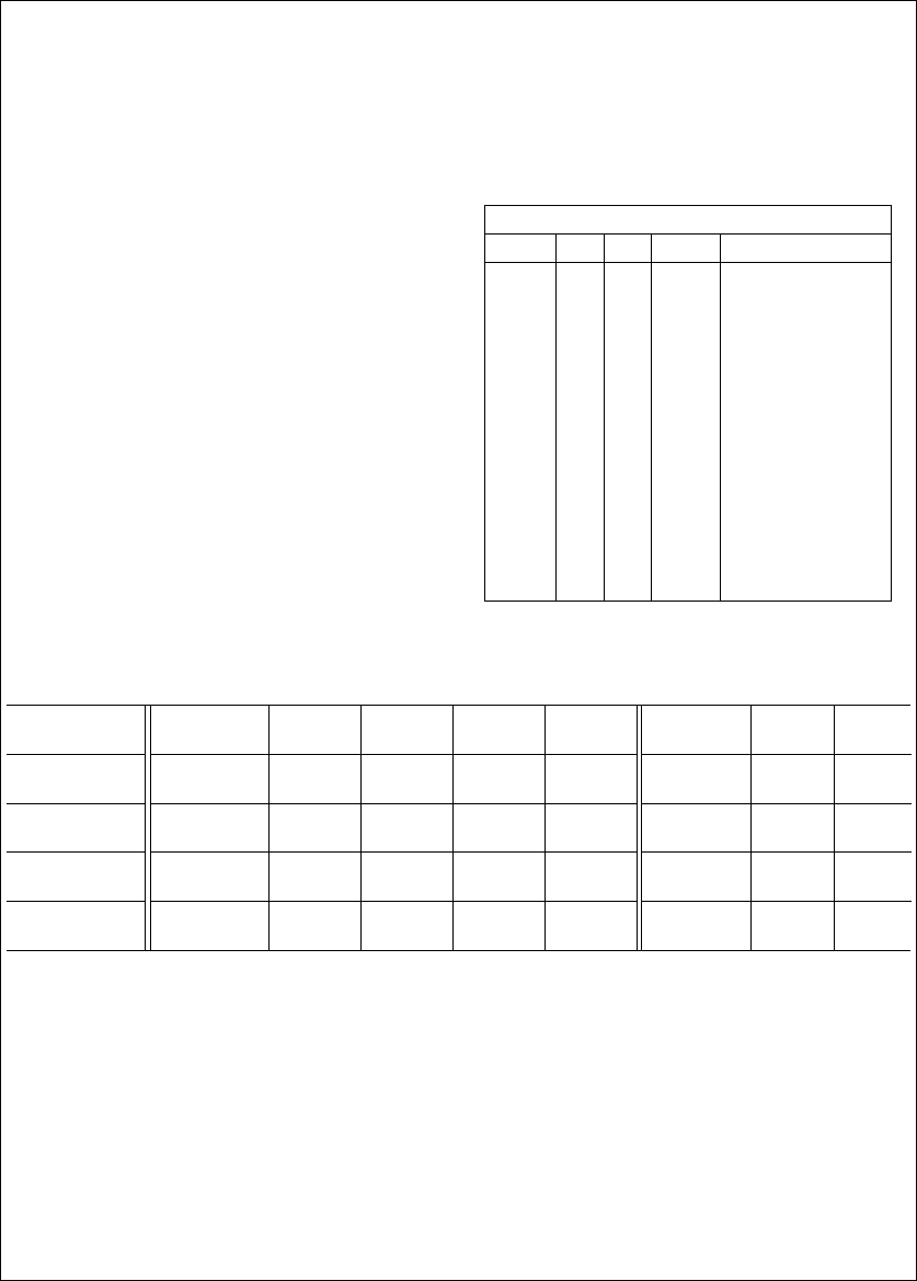
when CKI is 16 MHz (see Table I).
HOW TO USE MICROWIRE/PLUS
To use MICROWIRE, start by setting up the B port appropri-
ately for the MICROWIRE functions. The SO and SK func-
tions are multiplexed onto Port B pins B5 and B6 respective-
ly. For the master, set bits 5 and 6 in the DIRB register
(direction register for Port B) to set SO and SK as outputs.
For the slave, set bit 5 and reset bit 6 in the DIRB register to
set SO as an output and SK as an input . The BFUN register
(Port B function register) is used to set SO and SK as alter-
nate functions in the master and only SO as an alternate
function in the slave. The MICROWIRE/PLUS mode can be
enabled or disabled any time under program control. This is
done through the BFUN register. Placing a ‘‘1’’ in the corre-
sponding bit location causes the alternate function to be
activated, a ‘‘0’’ causes the alternate function to be dis-
abled. It is good practice to initialize the output pins by set-
ting PORTB (Port B data register) to a known state.
The SI function is multiplexed onto Port I pin I5. This pin is
always an input and the SI function is automatically selected
when in the MICROWIRE mode. Setting the mWMODE con-
trol bit, bit 1, in the IRCD register will enable the part to be a
master, resetting the bit will make it a slave. For the master,
the DIVBY register has to be initialized to set the appropri-
ate SK frequency (see Table I.). For example if the crystal
frequency is 16 MHz and an SK frequency of 1 MHz is de-
sired, load the least significant nibble of the DIVBY register
with 2 (16 MHz/16 e1 MHz).
For a summary of the register and pin configurations for the
master and slave modes see Table II.
TABLE I. HPC mWIRE DIVBY Register
mWIRE SK Divisor
MSB LSB CLOCK
0 0 0 0 not allowed
0 0 0 1 not recommended*
0 0 1 0 CKI/16
0 0 1 1 CKI/32
0 1 0 0 CKI/64
0 1 0 1 CKI/128
0 1 1 0 CKI/256
0 1 1 1 CKI/512
1 0 0 0 CKI/1024
1 0 0 1 CKI/2048
1 0 1 0 CKI/4096
1 0 1 1 CKI/8192
1 1 0 0 CKI/16384
1 1 0 1 CKI/32768
1 1 1 0 CKI/65536
1 1 1 1 CKI/131072
*This option uses timer T3 output, but does not generate a square wave.
(See HPC users manual for more details.)
TABLE II. mWIRE Register and Pin Conditions for Master and Slave Operation
Operation mWMODE BFUN BFUN DIRB DIRB PIN PIN PIN
bit B5 B6 B5 B6 B5 B6 I5
MICROWIRE 1 1111 SOINT. SI
Master SK
MICROWIRE 1 1101 TRI- INT. SI
Master STATEÉSK
MICROWIRE 0 1010 SOEXT. SI
Slave SK
MICROWIRE 0 1000 TRI- EXT. SI
Slave STATE SK
3

DEFINING THE MASTER/SLAVE HANDSHAKING
PROTOCOL
There are a few things to keep in mind when defining a
handshaking protocol for the HPC:
1) Only the master can generate SK clocks.
2) As 8 bits are shifted into the SIO register, the 8 bits al-
ready in there are shifted out.
3) After 8 bits are shifted into (or out of) the SIO register the
MICROWIRE done (mWIRE DONE) flag gets set.
4) ANY access to the SIO register in the master that per-
forms a write operation causes the contents of SIO to be
shifted out.
5) No data will be shifted into or out of the slave’s SIO
register if its mWIRE DONE flag is set.
6) Any write to the SIO register in the master or slave resets
its mWIRE DONE flag.
Keeping the above six points in mind, let’s look at one pos-
sible handshaking protocol between a master HPC and a
slave HPC. Number two above tells us we can send and
receive data at the same time, however since only the mas-
ter initiates data transfer we want to be sure the slave is
ready before we get started with the exchange. Since the
master initiates the transfer process there is no need for the
master’s MICROWIRE routine to be interrupt driven (though
it can be if it is desired to have the slave initiate data trans-
fers also). On the other hand, since the slave will be off
doing other tasks it is most effective to have its MICRO-
WIRE routine be interrupt driven.
A FEW THINGS TO NOTE ABOUT THE PROGRAMS
The following programs refer to the system configuration
shown in
Figure 1.
This example code does a simple data
transfer. The master reads in data on Port D, sends it via
MICROWIRE to the slave, and reads it back. They both start
by initializing the chip mode and number of wait states
(PSW), disabling interrupts, setting the DIVBY register as
necessary, initializing Port B, and enabling the appropriate
MICROWIRE mode (IRCD). Then the slave continues with
its main code (a wait loop) until interrupted. When the mas-
ter decides it’s ready to send MICROWIRE data, it signals
the slave by setting the slave interrupt pin on Port B, then it
waits for the slave to respond.
Meanwhile, the slave goes into action. It clears the
mWDONE flag and loads the SIO register (X A, SIO), then
notifies the master that it is ready to continue. Once the
master realizes the slave is ready to continue, it removes
the interrupt signal to the slave (RESET PORTB.SLAVI),
reads in the data to be sent (LD A, PORTD), and starts
transmitting it (X A, SIO). At the same time the master reads
in the data received at the last data exchange with the
slave. Then the master loops until it is done transferring
data and loops again until the slave is finished with its inter-
rupt routine. In a real program the master would be off exe-
cuting code and not having to wait in these loops. Once the
transmission is complete the slave reads in the new data
(LD A, SIO), lets the master know it is done with its interrupt
routine (RESET PORTB.MASTR), and re-enables interrupts
as it returns to the main routine (RETI).
In the master’s code there is only one access to the SIO
register and that access is an exchange. Remember point
Ý4, we can take advantage of the exchange instruction (X
A, SIO), which is a read-modify-write instruction. Therefore,
with one instruction, we can read the data from the previous
transfer into the accumulator, and write the data to be trans-
ferred into the SIO register. If this method is not practical,
then separate read and write instructions must be used.
When accessing the SIO register be sure the mWIRE DONE
flag is set so you know the data is not changing. At other
times we have to be sure the flag is reset or no data will
ever be transferred (shifted in or out). Notice that the
‘‘X A, SIO’’ was used to reset the mWIRE DONE flag as well
as load the register with the data to be sent.
4
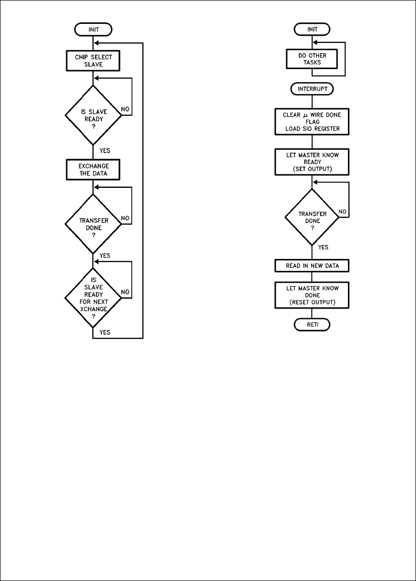
MASTER’S Flow Chart
TL/DD/9140–4
SLAVE’S Flow Chart
TL/DD/9140–5
MASTER’s SAMPLE CODE
;
;VARIABLE DECLARE
;
PSW 4M(00C0)
BFUN 4W(0F4) ;Port B ALTERNATE FUNCTION REGISTER
DIRB 4W(0F2) ;Port B DIRECTION REGISTER
PORTB 4W(0E2) ;Port B DATA REGISTER
PORTD 4M(0104) ;Port D (INPUT PORT)
ENIR 4M(0D0) ;INTERRUPT ENABLE REGISTER
IRPD 4M(0D2) ;INTERRUPT PENDING REGISTER
IRCD 4M(0D4) ;INTERRUPT CONDITION REGISTER
SIO 4M(0D6) ;SERIAL I/O REGISTER
PORTI 4M(0D8) ;INTERRUPT (AND uWIRE SERIAL IN) INPUT PORT
DIVBY 4W(018E) ;TIMER DIVIDE BY REGISTER
SLAVI 44 ;SLAVE INTERRUPT BIT (IN Port B)
uWDONE 40 ;uWIRE DONE BIT (IN IRPD)
uWMODE 41 ;uWIRE MASTER/SLAVE BIT (IN IRCD)
SK 46 ;uWIRE SERIAL CLOCK (IN Port B)
SLAVR 42 ;SLAVE RESPONSE BIT (IN Port B)
5

MASTER’s SAMPLE CODE (Continued)
.40F800 ;START PROGRAM
BEGIN:
LD PSW,008 ;SINGLE CHIP MODE, 1 WAIT STATE
LD ENIR,00 ;DISABLE ALL INTERRUPTS
LD DIVBY,02222 ;uWIRE CLOCK 4/16
LD DIRB,0FFFF ;Port B ALL OUTPUTS
LD BFUN,00060 ;ONLY SO & SK HAVE ALTERNATE FUNCTIONS
LD PORTB,00000 ;INIT PORTB TO ALL ZEROs
SET IRCD.uWMODE ;SET THIS HPC AS MASTER
DOITAG: ;JUMP TO HERE TO DO IT AGAIN
SET PORTB.SLAVI ;NOTIFY SLAVE (INTERRUPT THE SLAVE)
WAIT:
IF PORTI.SLAVR ;SLAVE READY?
JP SLAVRS ;GO SEND/RECEIVE uWIRE DATA
JP WAIT ;NO IT IS NOT READY YET
SLAVRS:
RESET PORTB.SLAVI ;REMOVE SLAVE NOTIFIER
LD A,PORTD ;LOAD A W/ DATA TO SEND
X A,SIO ;SEND NEW DATA AND READ DATA FROM
;...LAST uWIRE EXCHANGE
DONE:
IF IRPD.uWDONE ;WAIT TILL DONE EXCHANGING
JP CONT ;uWIRE IS DONE
JP DONE ;uWIRE NOT DONE (KEEP TESTING)
CONT:
IF PORTI.SLAVR ;IS SLAVE READY TO CONTINUE?
JP CONT ;NO
JP DOITAG ;START ALL OVER (DO IT AGAIN)
.END BEGIN
SLAVE’s SAMPLE CODE
;
;VARIABLE DECLARE
;
PSW 4M(00C0)
BFUN 4W(0F4) ;Port B ALTERNATE FUNCTION REGISTER
DIRB 4W(0F2) ;Port B DIRECTION REGISTER
PORTB 4W(0E2) ;Port B DATA REGISTER
6

SLAVE’s SAMPLE CODE (Continued)
ENIR 4M(0D0) ;INTERRUPT ENABLE REGISTER
IRPD 4M(0D2) ;INTERRUPT PENDING REGISTER
IRCD 4M(0D4) ;INTERRUPT CONDITION REGISTER
SIO 4M(0D6) ;SERIAL I/O REGISTER
SO 45 ;uWIRE SERIAL OUTPUT PIN (ON Port B)
MASTR 44 ;MASTER RESPONSE BIT (IN Port B)
uWDONE 40 ;uWIRE DONE BIT (IN IRPD)
uWMODE 41 ;uWIRE MASTER/SLAVE BIT (IN IRCD)
INT2 42 ;INTERRUPT 2 BIT
.40FFFA ;INT2 - INTERRUPT VECTOR
.WORD MASNOT ;...MASTER NOTIFICATION
.40F800 ;START PROGRAM
BEGIN:
LD PSW,008 ;SINGLE CHIP MODE, 1 WAIT STATE
LD ENIR,01 ;DISABLE ALL INTERRUPTs, BUT ENABLE GIE
LD DIRB,0FF10 ;Port B UPPER, & MASTR ARE OUTPUTS
;...(use LD DIRB,0FF30 to set SO as an
;...output if not using any peripherals)
LD BFUN,00020 ;ONLY SO HAS ALTERNATE FUNCTION
;...NOTE: SK is NOT an alternate
;...function in the slave!
LD PORT B,00000 ;INIT PORTB TO ALL ZEROS
RESET IRCD.uWMODE ;SET THIS HPC AS A SLAVE
SET IRCD.INT2 ;SET INT2 INTERRUPT (0) POLARITY
SET ENIR.INT2 ;ENABLE EXTERNAL INTERRUPT TO
;...RECEIVE SLAVE RESPONSE
PAU:
JP PAU ;WAIT HERE FOR INTERRUPT FROM MASTER
MASNOT: ;uWIRE INTERRUPT ROUTINE
X A,SIO ;CLEAR uWDONE FLAG (AND LOAD DATA FROM
;...ACCUMULAT0R TO SEND)
SET PORTB.SO ;ENABLE SO (needed only if using a peripheral)
SET PORTB.MASTR ;NOTIFY MASTER THAT READY TO CONTINUE
NOTDN:
IF IRPD.uWDONE ;WAIT TILL DONE SHIFTING
JP DONE ;DONE, GO CONTINUE
JP NOTDN ;NOT DONE, CONTINUE LOOPING
DONE:
LD A,SIO ;READ IN NEW DATA
RESET PORT B.SO ;TRI-STATE SO (needed only if
; using a peripheral)
RESET PORTB.MASTR ;REMOVE SIGNAL TO MASTER
RETI
.END BEGIN
7

AN-474 HPC MICROWIRE/PLUS Master-Slave Handshaking Protocol
ADDING PERIPHERALS OR ANOTHER SLAVE
Adding another slave HPC or a peripheral to the above Mi-
crowire configuration can add more power to your design
with minimal extra cost and design time. In
Figure 1,
an
extra peripheral is shown in dotted outline form. The hard-
ware and software modifications are straightforward, how-
ever there are a few considerations to keep in mind:
Ð Tri-state the SO pin on the slave HPC by resetting B5 in
the DIRB register when the slave is not ‘chip-selected’
by the master.
Ð When adding more HPC slaves, the master’s and
slave’s routines remain the same. Only different B port
pins for chip select and I or B port pins for slave ac-
knowledge need to be used.
Ð For peripherals the principals of operation are still the
same and so are the initialization procedures, however
some of the code will have to be modified to accommo-
date the specific handshaking required by the peripheral.
(Note: some of the peripherals require 16 or more con-
secutive bits without interruption of the SK clock. To pro-
vide continuous SK clocks, set up the accumulator with
next byte of data to send, loop until mWDONE is set,
then exchange the contents of the accumulator and the
SIO register (X A, SIO). The above steps will provide
nearly continuous SK clocksÐthe slower the SK clock is
set for, the more continuous they will appear.)
APPLICATIONS
Now that you are more familiar with MICROWIRE/PLUS,
where can you get experience using it?
Ð It can be used in a security system where the on-site
master lets the periphery slaves know which security
codes they can now let in, while at the same time the
slaves monitor fire alarms and smoke detectors.
Ð It can be used in automotive brakes to allow all the
wheels to communicate with each other. The wheels
can trade information on road conditions and a master
can monitor all four wheels to coordinate them and
check for malfunctions.
Ð It can be used in a robot arm to allow each joint to make
the decision as to how it will help the entire arm reach its
final position. This application is one example of how
MICROWIRE/PLUS can be used for system task parti-
tioning.
Ð It can be used in a MUX-WIRING system.
When using MICROWIRE to communicate between two
chips on the same board, a high data rate can be used.
When communicating over longer distances, slower speeds
should be used.
SUMMARY
MICROWIRE/PLUS can be a very powerful tool that can
easily add power to a microcontroller based system. It is
easy to use and does not require much hardware to imple-
ment. To add a new feature to your current design, choose
a peripheral and add a small amount of code. To start using
MICROWIRE, define the handshake protocol best suited for
your application keeping in mind the six points given above
in the ‘Defining the Master/Slave Handshaking Protocol’
section. Then initialize the appropriate registers: BFUN,
DIRB, PORTB, DIVBY, and IRCD. The MICROWIRE circuit-
ry will then run independent of the CPU except to exchange
data between the SIO register and the CPU, and to initiate
the data exchange between the master and slaves. With a
CPU clock of 16 MHz, MICROWIRE/PLUS may achieve a
maximum data rate of 1 MHz. MICROWIRE can be used to
add display controllers, A/D’s, memories, timers, and even
other microcontrollers to an HPC microcontroller based de-
sign. Remember MICROWIRE/PLUS is not a trivial piece of
very fine wire, it is a high speed two way serial communica-
tions interface!
Lit. Ý100474
LIFE SUPPORT POLICY
NATIONAL’S PRODUCTS ARE NOT AUTHORIZED FOR USE AS CRITICAL COMPONENTS IN LIFE SUPPORT
DEVICES OR SYSTEMS WITHOUT THE EXPRESS WRITTEN APPROVAL OF THE PRESIDENT OF NATIONAL
SEMICONDUCTOR CORPORATION. As used herein:
1. Life support devices or systems are devices or 2. A critical component is any component of a life
systems which, (a) are intended for surgical implant support device or system whose failure to perform can
into the body, or (b) support or sustain life, and whose be reasonably expected to cause the failure of the life
failure to perform, when properly used in accordance support device or system, or to affect its safety or
with instructions for use provided in the labeling, can effectiveness.
be reasonably expected to result in a significant injury
to the user.
National Semiconductor National Semiconductor National Semiconductor National Semiconductor
Corporation Europe Hong Kong Ltd. Japan Ltd.
1111 West Bardin Road Fax: (
a
49) 0-180-530 85 86 13th Floor, Straight Block, Tel: 81-043-299-2309
Arlington, TX 76017 Email: cnjwge
@
tevm2.nsc.com Ocean Centre, 5 Canton Rd. Fax: 81-043-299-2408
Tel: 1(800) 272-9959 Deutsch Tel: (
a
49) 0-180-530 85 85 Tsimshatsui, Kowloon
Fax: 1(800) 737-7018 English Tel: (
a
49) 0-180-532 78 32 Hong Kong
Fran3ais Tel: (
a
49) 0-180-532 93 58 Tel: (852) 2737-1600
Italiano Tel: (
a
49) 0-180-534 16 80 Fax: (852) 2736-9960
National does not assume any responsibility for use of any circuitry described, no circuit patent licenses are implied and National reserves the right at any time without notice to change said circuitry and specifications.
