Interfacing The DP8420A/21A/22A To Z280/Z80000/Z8000 Microprocessor AN 0546
User Manual: AN-0546
Open the PDF directly: View PDF ![]() .
.
Page Count: 4

TL/F/9740
Interfacing the DP8420A/21A/22A to the Z280/Z80000/Z8000 Microprocessor AN-546
National Semiconductor
Application Note 546
Webster (Rusty) Meier, Jr. and Joe Tate
May 1989
Interfacing the
DP8420A/21A/22A to the
Z280/Z80000/Z8000
Microprocessor
I INTRODUCTION
This application note describes how to interface the Z280
microprocessor to the DP8422A DRAM controller (also ap-
plicable to DP8420A/21A). It is assumed that the reader is
already familiar with Z280 and the DP8422A modes of oper-
ation. The interface to the Z80000 and Z8000 is similar to
the interface described in this application note.
II DESCRIPTION OF DESIGN, ALLOWING OPERATION
AT 10 MHz (AND ABOVE) WITH 1 WAIT STATE IN NOR-
MAL ACCESSES AND 1 WAIT STATE DURING BURST
ACCESSES
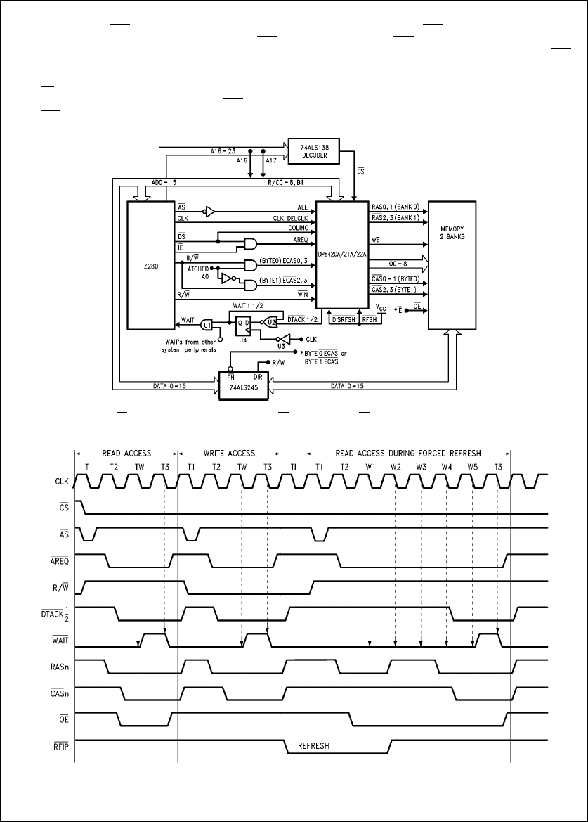
The block diagram of this design is shown driving two banks
of DRAM, each bank being 16 bits in width, giving a maxi-
mum memory capacity of up to 16 Mbytes (using 4 M-bit c
1 DRAMs). By choosing a different RAS and CAS configura-
tion mode (see programming mode bits section of DP8422A
data sheet) this application can support 4 banks of DRAM,
giving a memory capacity of up to 32 Mbytes (using 4 M-bit
c1 DRAMs).
The memory banks are interleaved on every four word (16-
bit word) boundry. This means that the address bit (A3) is
tied to the bank select input of the DP8422A (B1).
Address bits A2,1 are tied to the most significant row and
column address inputs (R9,C9 for 1 Mbit DRAMs) to support
burst accesses using static column mode DRAMs. Since
this application assumes the use of static column DRAMs
the column address strobe (CAS) is left low throughout the
entire burst access. If the user desires to use nibble mode
or page mode DRAMs the CAS outputs must be toggled,
the ECAS inputs the DP8422A can be used for this purpose
(DS of the Z280 could be ‘‘OR’’ed with the current ECAS
inputs). If nibble mode DRAMs are used the COLINC input
of the DP8422A need not be driven.
Address bit A0 is used to produce the two byte select data
strobes along with the byte/word signal (B/W). These byte
selects (Byte 0 ECAS and Byte 1 ECAS) are used in byte
reads and writes as well as selects for the transceivers.
If the majority of accesses made by the Z280 are sequen-
tial, the Z280 can be doing burst accesses most of the time.
Each burst of four words can alternate memory banks, al-
lowing one memory bank to be precharging (RAS pre-
charge) while the other bank is being accessed (Bank se-
lect, B1, tied to address A3). This is a higher performance
memory system then a non-interleaved memory system
(bank select on the higher address bits). Each separate
memory access to the same memory bank may require ex-
tra wait states to be inserted into the CPU access cycles to
allow for the RAS precharge time, if two periods or more of
RAS precharge were programmed.
This application allows 1 or more wait states to be inserted
in normal accesses and 1 or more wait states to be inserted
during burst accesses of the Z280. The number of wait
states can be adjusted through the WAITIN input of the
DP8422A.
The logic shown in this application note forms a complete
Z280 memory sub-system, no other logic is needed. This
sub-system automatically takes care of:
A. arbitration between Port A, Port B, and refreshing the
DRAM;
B. the insertion of wait states to the processor (Port A and
Port B) when needed (i.e., if RAS precharge is needed,
refresh is happening during a memory access, the other
Port is currently doing an access . . .etc);
C. performing byte writes and reads to the 16-bit words in
memory;
D. normal and burst access operations.
The external wait logic (U1, U2, U3, U4; see
Figure 1
)is
needed to support burst accesses of the Z280. During burst
accesses the Z280 WAIT input is sampled every falling
clock edge. What is worse is that the WAIT input needs one
half clock period setup time and the DS signal (used to tog-
gle ECAS0–3 and thereby toggle the DP8422A WAIT out-
put) takes close to one half of a clock period to transition
high. This leaves no time for the DP8422A WAIT output to
transition between states. The external flip-flop is used to
provide extra fast response time for normal access wait
states and to toggle when doing a burst mode access. If the
user is not going to do burst accesses the WAIT output can
be tied directly to the WAIT input of the Z280 (U1, U2, U3,
U4 would not be needed). Also all this logic could easily be
put into a PALÉif desired.
By using the ‘‘output control’’ pins of some external latches
(74ALS373’s), this application can easily be used in a dual
access application. The addresses could be TRI-STATEÉ
through these latches, the write input (WIN), lock input
(LOCK), and ECAS0–3 inputs must also be able to be TRI-
STATE (a 74AS244 could be used for this purpose). By mul-
tiplexing the above inputs (through the use of the above
parts and similar parts for Port B) the DP8422A can be used
in a dual access application. If this design is used in a dual
access application the tRAC and tCAC (required RAS and
CAS access time required by the DRAM) will have to be
recalculated since the time to RAS and CAS is longer for
the dual access application (see TIMING section of this ap-
plication note).
PALÉis a registered trademark of and is used under license from Monolithic Memories, Inc.
TRI-STATEÉis a registered trademark of National Semiconductor Corporation.
C1995 National Semiconductor Corporation RRD-B30M115/Printed in U. S. A.

III Z280 DESIGN, 10 MHz WITH 1 WAIT STATE DURING
NORMAL ACCESSES AND 1 WAIT STATE DURING
BURST ACCESSES, PROGRAMMING MODE BITS
Programming Description
Bits
R0 e0 RAS low two clocks, RAS precharge
R1 e1 of two clocks, this setup
will only guarantee 93.5 ns RAS
precharge (at 10 MHz) from refresh
RAS high to access RAS low. If more
RAS precharge is desired the user
should program three periods of RAS
precharge.
R2 e0 DTACK one half is chosen. DTACK
R3 e1 low first rising CLK edge
after access RAS is low.
R4 e0 No WAIT states during burst accesses
R5 e0
R6 e0 If WAITIN e0, add one clock to
DTACK. WAITIN may be tied high or
low in this application depending upon
the number of wait states the user
desires to insert into the access.
R7 e1 Select DTACK
R8 e1 Non-interleaved Mode
R9 eX
C0 eX Select based upon the input
C1 eX ‘‘DELCLK’’ frequency. Example: if the
C2 eX input clock frequency is 10 MHz then
choose C0,1,2 e1,0,1 (divide by five,
this will give a frequency of 2 MHz).
C3 eX
C4 e0 RAS groups selected by ‘‘B1’’. This
C5 e0 mode allows two RAS outputs to go
C6 e1 low during an access, and allows byte
writing in 16- or 32-bit words.
C7 e1 Column address setup time of 0 ns
C8 e1 Row address hold time of 15 ns
C9 e1 Delay CAS during write accesses to
one clock after RAS transitions low
B0 e0 Latches latch on ALE input low
B1 e0 Access mode 0
ECAS0e0 CASn not extended beyond RASn
0eProgram with low voltage level
1eProgram with high voltage level
XeProgram with either high or low voltage level
(don’t care condition)
IV Z280 TIMING CALCULATIONS FOR DESIGN AT
10 MHz WITH 1 WAIT STATE DURING NORMAL
ACCESSES AND 1 WAIT STATE DURING BURST
ACCESSES
1. Minimum ALE high setup time to CLOCK high if using the
on-chip latches and more then one RAS bank (DP8422A-
20 needs 29 ns, Ý301b):
100 ns (one clock period) b20 ns (AS valid maximum
delay, Ý3 of Z280 data sheet) b11 ns (74ALS04B max
delay) e69 ns
2A. Minimum address setup time to ALE low (DP8422A-20
needs 3 ns, Ý306):
25 ns (address setup to AS high, Ý20 Z280 data sheet)
a1 ns (74ALS04B min delay) e26 ns
2B. Minimum address hold time to ALE low (DP8422A-20
needs 10 ns, Ý305):
20 ns (address hold from AS high, Ý22 of Z280 data
sheet) a1 ns (74ALS04B min delay) e21 ns
2C. Minimum address setup to CLOCK high (DP8422A-20
needs bank address setup to CLOCK of 20 ns, Ý303):
100 ns (one clock period) b20 ns (max clock to ad-
dress valid, Z280 data sheet Ý2) e80 ns
3. Minimum CS setup time to clock high (DP8422A-20
needs 14 ns, Ý300): 80 ns (Ý2C above) b22 ns (max
74ALS138 decoder) e58 ns
4. Determining tRAC during a normal access (RAS access
time needed by the DRAM):
250 ns (two and one half clock periods to do the ac-
cess) b32 ns (CLK to RAS low max, DP8422A-20
Ý307) b30 ns (Z280 data setup time, Ý9) b10 ns
(74ALS245A max delay) e178 ns
Therefore the tRAC of the DRAM must be 178 ns or
less. (One can see that if zero wait states would have
been programmed the tRAC would have been 84 ns (us-
ing DP8422A-25, has faster CLK to RAS low of 26 ns)
184–100 (one clock)).
5. Determining tCAC during a normal access (CAS access
time) and column address access time needed by the
DRAM:
250 ns b89 ns (CLK to CAS low on DP8422A-20,
Ý308a) b30 ns b10 ns e121 ns
Therefore the tCAC of the DRAM must be 121 ns or
less.
6. Determining the column address access time needed
during a static column mode burst access:
20 ns (two clocks to do the access, Ex. mid T3 to mid
TBW to mid T4) b35 ns (DS high, Z280 parameter Ý8)
b43 ns (COLINC asserted to address outputs of
DP8420A-20 incremented, Ý27) b30 ns (Z280 data
setup time, Ý9) b10 ns (74ALS245A max delay) e82
ns
Therefore the column address access time of the
DRAM must be 82 ns or less. (One can see that if zero
wait states would have been programmed the column
address access time would have been less then 0 ns
(82 b100 (one clock))).
7. Maximum time to DTACK one half low (74ALS374 D
type flip-flop needs 10 ns setup to CLK):
100 ns (One clock, mid T2 in mid TW) b33 ns (DTACK
one half low from CLK high on DP8422A-20, Ý18) b12
ns (max delay on 74ALS02 e55 ns
8. Minimum WAIT setup time to CLK low (Z280 WAIT input
needs 50 ns, Ý14):
100 ns (one clock period) b16 ns (74ALS374 max de-
lay) b14 ns (74ALS08 max delay) e70 ns
9. Minimum RAS precharge (DP8422A programmed with 2
clock periods of RAS precharge):
Since the AREQ input of the DP8422A will go high from
DS and IE both being high the AREQ high setup to
clock rising edge (DP8422A parameter Ý29b, 19 ns)
parameter is violated. This means that the rising clock
edge following AREQ high may or may not be counted.
2
Since that first rising clock edge could be counted, and
would give less RAS precharge time, we must assume
this condition in the calculation of the minimum RAS
precharge. Therefore:
200 ns (2 clock periods) b50 ns (half clock period
before both IE and DS transition high) b35 ns (IE and
DS high, Z280 parameters Ý8 and Ý19) b5.5 ns
(74AS08 max delay) b16 ns (DP8422A RAS high to
RAS low difference parameter Ý50) e93.5 ns
Therefore, the user should guarantee that the DRAM
he is using needs a RAS precharge time of 93.5 ns or
less. If more RAS precharge time is needed the user
should program the DP8422A with 3 periods of RAS
precharge (R0, R1) during programming.
Note: Calculations can be performed for different frequencies and/or differ-
ent combinations of wait states by substatuting the appropriate values
into the above equations.
TL/F/9740–1
*The user may want to gate CS (‘‘OR’’ Gate) with the signals that produce OE to the DRAMs and EN to the transceivers
FIGURE 1. 10 MHz Z280 Design (Z-bus Interface), 1 Wait State in Normal Accesses, 1 Wait State in Burst Accesses
TL/F/9740– 2
FIGURE 2. Z280 Access Cycles and Refresh (1 Wait State during Normal Access Cycles)
3
AN-546 Interfacing the DP8420A/21A/22A to the Z280/Z80000/Z8000 Microprocessor
TL/D/9740– 4
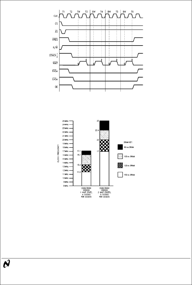
FIGURE 3. Z280 Burst Access Cycle (1 Wait State in Normal and Burst Accesses)
DRAM Speed vs Processor Speed (DRAM Speed
References the RAS Access Time, tRAC, of the DRAM.
Using DP8422A-25 Timing Specifications)
TL/D/9740– 5
Lit. Ý100546
LIFE SUPPORT POLICY
NATIONAL’S PRODUCTS ARE NOT AUTHORIZED FOR USE AS CRITICAL COMPONENTS IN LIFE SUPPORT
DEVICES OR SYSTEMS WITHOUT THE EXPRESS WRITTEN APPROVAL OF THE PRESIDENT OF NATIONAL
SEMICONDUCTOR CORPORATION. As used herein:
1. Life support devices or systems are devices or 2. A critical component is any component of a life
systems which, (a) are intended for surgical implant support device or system whose failure to perform can
into the body, or (b) support or sustain life, and whose be reasonably expected to cause the failure of the life
failure to perform, when properly used in accordance support device or system, or to affect its safety or
with instructions for use provided in the labeling, can effectiveness.
be reasonably expected to result in a significant injury
to the user.
National Semiconductor National Semiconductor National Semiconductor National Semiconductor
Corporation Europe Hong Kong Ltd. Japan Ltd.
1111 West Bardin Road Fax: (
a
49) 0-180-530 85 86 13th Floor, Straight Block, Tel: 81-043-299-2309
Arlington, TX 76017 Email: cnjwge
@
tevm2.nsc.com Ocean Centre, 5 Canton Rd. Fax: 81-043-299-2408
Tel: 1(800) 272-9959 Deutsch Tel: (
a
49) 0-180-530 85 85 Tsimshatsui, Kowloon
Fax: 1(800) 737-7018 English Tel: (
a
49) 0-180-532 78 32 Hong Kong
Fran3ais Tel: (
a
49) 0-180-532 93 58 Tel: (852) 2737-1600
Italiano Tel: (
a
49) 0-180-534 16 80 Fax: (852) 2736-9960
National does not assume any responsibility for use of any circuitry described, no circuit patent licenses are implied and National reserves the right at any time without notice to change said circuitry and specifications.
