LM6361/LM6364/LM6365 Fast Op Amps Offer High Speed At Low Power Consumption AN 0549
User Manual: AN-0549
Open the PDF directly: View PDF ![]() .
.
Page Count: 6
TL/H/9773
LM6361/LM6364/LM6365 Fast VIP Op Amps
Offer High Speed at Low Power Consumption AN-549
National Semiconductor
Application Note 549
Wanda Garrett
June 1989
LM6361/LM6364/LM6365
Fast VIPTM Op Amps Offer
High Speed at Low
Power Consumption
The LM6361/LM6364/LM6365 family of op amps are wide-
bandwidth monolithic amplifiers which offer improved speed
and stability over many other op amps, at low cost, with
little-to-no penalty in power supply consumption.
These advantages are due to a new process, developed by
National Semiconductor, which provides lateral PNP transis-
tors with nearly the gain and speed characteristic of NPN
transistorsÐwhile the NPNs maintain their usual high per-
formance. This allows the use of both NPN and PNP transis-
tors in the signal path, where previously the PNP transistors
severely limited the speed of linear devices. (Standard later-
al PNPs have 1/10th the gain and 1/200th the bandwidth of
standard NPN transistors.)
Traditional high-speed op amps often either used all-NPN
circuitry (which usually severely limits the input, output, and
power supply voltage ranges); used feed-forward tech-
niques (which reduce stability); or resorted to costly hybrid
design. Amplifiers made from this new process (dubbed VIP,
for ‘‘Vertically-Integrated PNP’’) operate from a 5V to 30V
(total) supply voltage, and have standard input and output
voltage ranges. In addition, they require comparatively little
supply current, and are available in standard 8-pin dual-in-
line packages.
The first devices produced with this process are three op
ampsÐeach with the same basic design but compensated
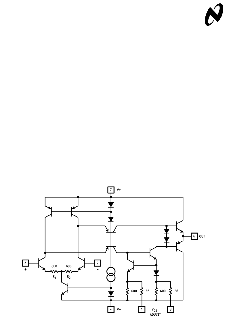
to different degrees. The schematic of the unity-gain-stable
LM6361 (see
Figure 1
) has a simple but effective form. The
VIP transistors can now be used in the signal path, so a
fairly traditional NPN differential input stage can be followed
by a folded cascode wide-bandwidth gain stage. The input
stage uses emitter-degeneration resistors to reduce its
transconductance (Gm). The bandwidth of the amplifiers is
then set by the ratio of Gmto compensation capacitance.
This also determines the stability of the amplifier.
The compensation capacitance is stray capacitance (about
0.5 pF) which is seen lumped together at the front of the
output stage. This output stage has a classic AB design, but
since it contains a VIP transistor it has the speed necessary
for a high speed amplifier. Additional capacitance on the
output effectively increases the total compensation capaci-
tance, increasing the stability of the amplifier but also reduc-
ing the bandwidth. This ‘‘compensation’’ is not ideal, howev-
er, so transient response may be degraded.
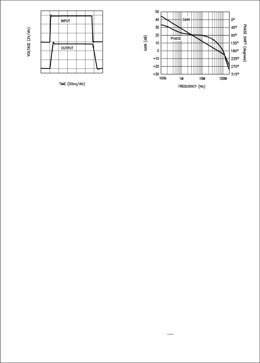
The step response
(Figure 2)
demonstrates the stability of
the LM6361. The amplifier was set up as a unity-gain follow-
er, with a 6V input step. The output has a small overshoot
and settles quickly to its final value. This well-behaved re-
sponse is due to the simplicity of the compensation, which
can be seen in the frequency response
(Figure 3)
. It shows
a smooth one-pole rolloff beyond 50 MHz; where the gain
has dropped to unity, with a phase margin of 45§; the next
pole is introduced after 100 MHz.
TL/H/9773–1
FIGURE 1. LM6361 Simplified Schematic. For LM6364, R1 and R2 are 150X; for LM6365, R1 and R2 are Omitted.
VIPTM is a trademark of National Semiconductor Corporation.
C1995 National Semiconductor Corporation RRD-B30M115/Printed in U. S. A.
TL/H/9773–2
FIGURE 2. Step Response of LM6361 in Unity-Gain
(Follower) Configuration
TL/H/9773–3
FIGURE 3. Frequency Response of LM6361
(Closed Loop Gain e45 dB)
The LM6364 and LM6365 are based on the LM6361 design.
The LM6361’s 600Xemitter degeneration resistors are re-
duced to 150Xin the 6364 to produce an op amp with gain-
bandwidth product of 175 MHz, stable to a minimum gain of
5. In the 6365 the resistors are eliminated altogether, for a
GBW of 725 MHz and minimum gain of 25. All three devices
have slew rates guaranteed (and 100% tested) to be over
200 V/ms (the slew rates are typically 300 V/ms).
Since the emitter degeneration resistors contribute to offset
voltage and input voltage noise, the device with the widest
bandwidth also has the best DC specs. The high gain of the
transistors used in the common design, combined with the
configuration used, give these op amps their high speed
without consuming a lot of power. Supply current is guaran-
teed to be less than 6.8 mA (with g15V supplies) for each
of the three devices.
The LM6361, LM6364, and LM6365 are guaranteed for op-
eration over the commercial temperature range (0§Cto
70§C). In addition, there are two other versions of each am-
plifier available: LM62XX, rated for operation over the indus-
trial b25§Ctoa
85§C range, and delivering improved DC
input specifications over the LM63XX parts; and LM61XX,
which is rated for the military temperature range (b55§Cto
a
125§C), with the same improved DC specifications as the
industrial versions.
These VIP amplifiers were optimized for high AC perform-
ance at low power consumption, while offering an ease of
use previously found only in low speed parts. They are ex-
pected to bring a new level of performance and affordability
to applications such as filtering, 8-bit data acquisition, video
and communications, and general high frequency signal
processing.
GENERAL HIGH-SPEED CIRCUIT DESIGN TECHNIQUES
The LM6361/LM6364/LM6365 op amp family can tolerate
circuit-building techniques appropriate for op amps of much
lower bandwidth. However, for best performance, any high-
speed circuit (and many DC precision circuits) should be
built using what is often called ‘‘good RF design.’’ Power
supply bypassing is very important: most op amps will re-
quire 0.01 mFto0.1mF good ceramic capacitors at each
power supply pin, and an additional 2.2 mFto10mF tanta-
lum nearby for extra noise reduction. These VIP op amps do
not require as much bypassing as other op amps in their
speed class; for most applications, 0.01 mF bypass capaci-
tors are adequate. However, their stability (especially that of
the wider gain-bandwidth LM6365) is enhanced when good
bypassing is used.
Power supply bypassing is added to negate the effects of
lead inductance from the power supply wires. This induc-
tance causes ‘‘glitches’’ on the power supply lines every
time the op amp has to deliver power to a transient load;
these glitches normally work their way into other sensitive
parts of your circuit. In addition, the inductance can create
small tank circuits with stray capacitance, which often will
cause a marginally stable circuit to oscillate.
For these reasons, keep all leads short (especially to the
input pins), and make sure the ground paths are low-imped-
ance, especially where larger currents will be flowing. Mini-
mize stray capacitance (especially in the forms of sockets
and parallel board traces). Stray capacitance allows signal
coupling from one pin or input or lead to another, which can
cause noise and/or oscillation.
All of the circuits shown here were built on copper-clad
board (used as a ground plane), with the op amps in sockets
for convenienceÐexcept for the input and output pins,
which were soldered directly into the circuits.
1 MHz VOLTAGE-TO-FREQUENCY CONVERTER
The classic charge-pump voltage-to-frequency converter is
limited in maximum frequency by the integrator amplifier.
For example, op amps with 1 MHz gain-bandwidth products
limit converters to a maximum frequency of about 10 kHz
(for 0.1% accuracy or better). Higher-speed converters
(500 kHz and up) must either incorporate the very-high-
speed (usually hybrid) op amps, or turn to another, more
complex, design.
The LM6365 can be used in the charge-pump V-to-F to pro-
duce a 1 MHz (at 10V) output signal, as shown in
Figure 4
.
Offset and full-scale trims allow more than two-decade op-
eration with 0.1% linearity, as shown in
Figure 5
. Careful
power supply bypassing and layout are important to reduce
noise and stray capacitance which will degrade perform-
ance.
The wide-bandwidth nature of the LM6365 provide the fast
switching necessary for 1 MHz operation, with little degrada-
tion in accuracy for inputs up to 11V (10% overrange). Like-
wise, the 0.1% linearity holds for inputs down to 50 mV.
The circuit gain is described by the equation:
f
VIN
e1/(2 #Vz#Rin #Cfb)
e100 kHz/V
where Vzis the output clamp voltage, 3.5V, and Rin and Cfb
are the components noted on the schematic
(Figure 4)
.
2

TL/H/9773–4
FIGURE 4. 1 MHz V-to-F Converter
TL/H/9773–5
FIGURE 5. Nonlinearity of LM6365 Voltage-to-
Frequency Converter (of
Figure 4
) is 0.1%
To calibrate the circuit, first adjust the gain potentiometer
until a 10.00V input produces a 1.000 MHz output. Then
adjust the offset potentiometer until a 50 mV input produces
a 5.0 kHz signal. Repeat adjustments until both ends of the
input range produce the correct output frequencies. The
0.15 mF input capacitance improves the linearity of the cir-
cuit.
All leads must be kept very short, especially those connect-
ed to the inputs of the LM6365, to minimize stray capaci-
tance which affects the gain and linearity. In addition, the
LM6365 power supply pins must be bypassed with 4.7 mF
tantalum and 0.01 mF ceramic capacitors to keep lead in-
ductance from affecting the circuit’s stability.
HIGH-FREQUENCY ACTIVE FILTERS
The LM6361 can be used in active filters at frequencies
which often require special designs to achieve even ade-
quate performance. For example, even though a 1 MHz low-
pass filter could be constructed taking advantage of the nat-
ural bandwidth of an op amp such as a 741, the designer
would find the cutoff varying with the unit-to-unit variation of
741 bandwidths, and the filter would only have a one-pole
slope. A two-pole active filter with good performance at this
frequency is difficult to realize with most standard op amps.
Either the amplifier’s own bandwidth is too low, or in the
case of many decompensated fast op amps, the low gain
needed for the wide bandwidth may render the amplifier un-
stable. However, the LM6361 can easily be used to provide
a 1 MHz cutoff with a 2-pole rolloff, as shown in
Figure 6
.
And because the cutoff frequency is not set by amplifier
bandwidth, but by the R-C network, it can be trimmed for
accuracy.
²1% tolerance
*matching determines
filter precision TL/H/9773–6
FIGURE 6. 1 MHz Low-Pass Filter
Figure 7
shows the frequency response of the low-pass fil-
ter. The gain rolls off at a steady 12 dB/octave until 6 MHz,
where the gain is down 35 dB.
TL/H/9773–7
FIGURE 7. Frequency Response of Low-Pass Filter
(Reference
Figure 6
)
3
TL/H/9773–8
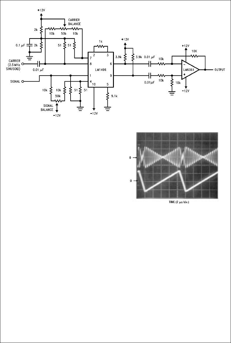
FIGURE 8. Modulator with Single-Ended Output Centered about Ground
VIDEO/COMMUNICATIONS APPLICATIONS
In systems such as some local area networks, where a sig-
nal is modulated onto a carrier for transmission, and is de-
modulated for use, an amplifier may have to pass this multi-
plexed signal. The carrier frequency depends on the system
in which it’s usedÐsome LANs have 10 MHz basebands,
and radio and other broadcasting systems often use carriers
of 10 MHz or less. Signals transmitted may be AM-audio, or
perhaps some analog information from a transducer or sen-
sor.
Special video circuits which are often used in these sys-
tems, such as the LM1496 modulator/demodulator and
LM733/LM592 differential amplifiers, have differential out-
puts with common-mode voltage several volts above
ground. This differential signal may be fine for transmitting
on a twisted pair, but for sending through coax or for obser-
vation/monitoring, it would be better if it were single-ended.
To convert the outputs to a signal which is single-ended,
referenced to ground, requires a wide-bandwidth amplifier.
Unity-gain stability is helpful if no additional gain is needed,
but a less stable amplifier could be used if it is allowed suffi-
cient noise gain. The LM6361 works well in this circuit, hav-
ing a bandwidth of 50 MHz at unity gain. When higher gain is
required, the LM6364 may be used.
In the circuit of
Figure 8
, an LM1496 is used to modulate an
analog signal (lower trace,
Figure 9
) with a 2.5 MHz sine-
wave carrier. The output of the LM1496 is a differential sig-
nal with a common-mode voltage of 8V. An LM6361 is used
to convert this signal to a single-ended one centered about
ground (upper trace,
Figure 9
).
The LM1496 requires quite a bit of balancing, using the two
potentiometers shown, to obtain the lowest possible distor-
tion. The LM1496 is the dominant source of distortion,
which is caused by the application of an unbalanced carrier
or modulating signal to the LM1496. The balance of the
system can be checked on a scope, but for most accurate
measurements a spectrum analyzer should be used.
TL/H/9773–9
FIGURE 9. Bottom Trace: Signal Input to
Multiplexer of
Figure 8
( 200 mV/div)
Top Trace: Output of Multiplexer (2 V/div)
VIDEO AMPLIFIER
The LM6361/LM6364/LM6365 series of amplifiers is also
suitable for use in video amplifier systems. A key parameter
of any amplifier used in video applications, especialy NTSC
color television systems, is the differential gain and phase it
adds to the circuit (Note 1). An NTSC Vectorscope can be
used to check these parameters, analyzing the output of an
amplifier whose input is from an NTSC signal generator.
Note 1: Differential gain, in an NTSC color television system, is a change in
color subcarrier amplitude due to a change in the luminance signal
while hue and saturation of the original signal are held constant. In
an amplifier, it relates to the variation of closed-loop gain with com-
mon-mode input voltage. It should be (ideally) zero.
Differential phase is a phase change of the chrominance signal by
the luminance signal while the original chrominance signal is held
constant. In an amplifier, it relates to the variation of phase shift
with common-mode input voltage. It should also be (ideally) zero.
4
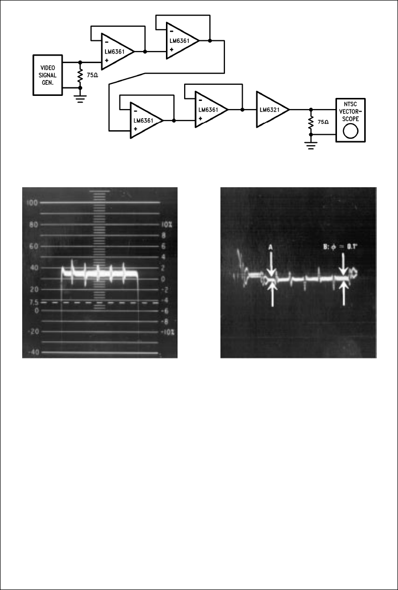
TL/H/9773–10
FIGURE 10. Test Circuit for Differential Gain,
Differential Phase Measurements
TL/H/9773–11
FIGURE 11. DIfferential gain of four cascaded LM6361s
plus buffer (see
Figure 10
). Differential gain, measured
by change in level from the 1st (leftmost) horizontal bar
to the 6th (rightmost), is less than 0.5% for the network.
TL/H/9773–12
FIGURE 12. Differential phase of four cascaded
LM6361s plus buffer (see
Figure 10
). Differential phase,
based on the spread in the two lines at point B when
the spread at point A is nulled, is 0.1§for the network.
To adequately measure the differential gain and phase of
these op amps, the error produced by four LM6361 voltage
followers, connected in series (see
Figure 10
), was mea-
sured. A Tektronix 144 NTSC Signal Generator provided the
input signal, and a Tektronix 520 NTSC Vectorscope was
used to monitor the error. Since the Vectorscope input
needed 75Xtermination, an LM6321 buffer was added to
prevent loading of the LM6361s. The LM6321 added less
than 0.1% differential gain, and less than 0.02§differential
phase, to the measurement.
Figure 11
shows the differential gain of the four LM6361
followers (plus buffer) of
Figure 10
to be less than 0.5%, or
an average of less than 0.12% for each LM6361. The differ-
ential phase measurement for the same circuit is made with
the Vectorscope displaying the picture of
Figure 12
, with
one side of the display zeroed as shown (point A). The
spread of lines at point B represents the differential phase,
which is 0.1§for the network (0.02§for each follower), as
measured with the Vectorscope. These measurements indi-
cate that a video signal will suffer very little degradation
when amplied with one of these devices.
REFERENCES
‘‘200 MHz PNP Transistors Spawn Fast Analog Chips,’’ by
Monticelli, Wright, Small and Geczy.
Electronic Design
, Au-
gust 21, 1986, page 111.
‘‘Intuitive IC Op Amps,’’ by Thomas M. Frederiksen.
Nation-
al Semiconductor Technology Series
, RR Donnelley &
Sons, 1984.
Tektronix Type 520/R520 NTSC Vectorscope Instruction
Manual
, 1969. Pages 2.2– 2.20.
5

LM6361/LM6364/LM6365 Fast VIP Op Amps
AN-549 Offer High Speed at Low Power Consumption
Lit. Ý100549
LIFE SUPPORT POLICY
NATIONAL’S PRODUCTS ARE NOT AUTHORIZED FOR USE AS CRITICAL COMPONENTS IN LIFE SUPPORT
DEVICES OR SYSTEMS WITHOUT THE EXPRESS WRITTEN APPROVAL OF THE PRESIDENT OF NATIONAL
SEMICONDUCTOR CORPORATION. As used herein:
1. Life support devices or systems are devices or 2. A critical component is any component of a life
systems which, (a) are intended for surgical implant support device or system whose failure to perform can
into the body, or (b) support or sustain life, and whose be reasonably expected to cause the failure of the life
failure to perform, when properly used in accordance support device or system, or to affect its safety or
with instructions for use provided in the labeling, can effectiveness.
be reasonably expected to result in a significant injury
to the user.
National Semiconductor National Semiconductor National Semiconductor National Semiconductor
Corporation Europe Hong Kong Ltd. Japan Ltd.
1111 West Bardin Road Fax: (
a
49) 0-180-530 85 86 13th Floor, Straight Block, Tel: 81-043-299-2309
Arlington, TX 76017 Email: cnjwge
@
tevm2.nsc.com Ocean Centre, 5 Canton Rd. Fax: 81-043-299-2408
Tel: 1(800) 272-9959 Deutsch Tel: (
a
49) 0-180-530 85 85 Tsimshatsui, Kowloon
Fax: 1(800) 737-7018 English Tel: (
a
49) 0-180-532 78 32 Hong Kong
Fran3ais Tel: (
a
49) 0-180-532 93 58 Tel: (852) 2737-1600
Italiano Tel: (
a
49) 0-180-534 16 80 Fax: (852) 2736-9960
National does not assume any responsibility for use of any circuitry described, no circuit patent licenses are implied and National reserves the right at any time without notice to change said circuitry and specifications.
