Introduction To Power MOSFETs And Their Applications AN 0558
User Manual: AN-0558
Open the PDF directly: View PDF ![]() .
.
Page Count: 16
TL/G/10063
Introduction to Power MOSFETs and Their Applications AN-558
National Semiconductor
Application Note 558
Ralph Locher
December 1988
Introduction to Power
MOSFETs
and Their Applications
INTRODUCTION
The high voltage power MOSFETs that are available today
are N-channel, enhancement-mode, double diffused, Metal-
Oxide-Silicon, Field Effect Transistors. They perform the
same function as NPN, bipolar junction transistors except
the former are voltage controlled in contrast to the current
controlled bi-polar devices. Today MOSFETs owe their
ever-increasing popularity to their high input impedance and
to the fact that being a majority carrier device, they do not
suffer from minority carrier storage time effects, thermal run-
away, or second breakdown.
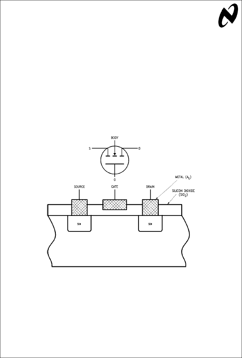
MOSFET OPERATION
An understanding of the operation of MOSFETs can best be
gleaned by first considering the later MOSFET shown in
Figure 1
.
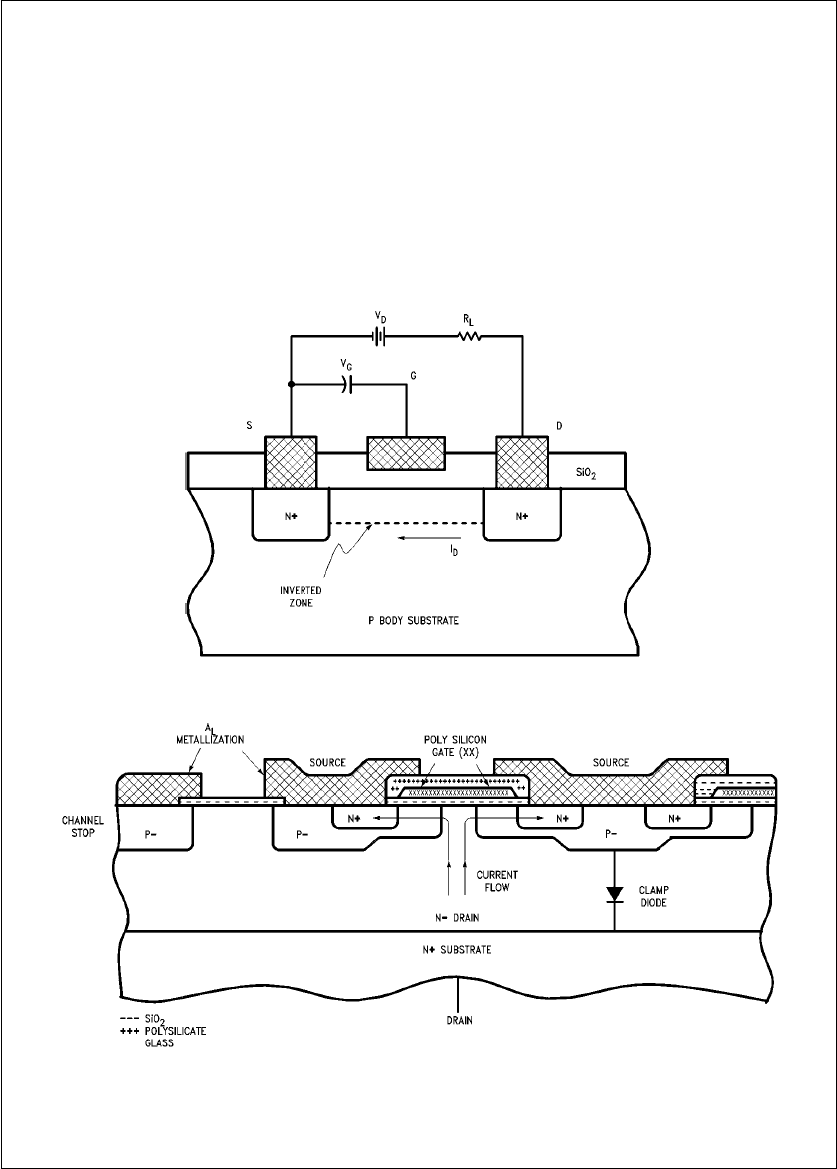
With no electrical bias applied to the gate G, no current can
flow in either direction underneath the gate because there
will always be a blocking PN junction. When the gate is
forward biased with respect to the source S, as shown in
Figure 2
, the free hole carriers in the p-epitaxial layer are
repelled away from the gate area creating a channel, which
allows electrons to flow from the source to the drain. Note
that since the holes have been repelled from the gate chan-
nel, the electrons are the ‘‘majority carriers’’ by default. This
mode of operation is called ‘‘enhancement’’ but it is easier
to think of enhancement mode of operation as the device
being ‘‘normally off’’, i.e., the switch blocks current until it
receives a signal to turn on. The opposite is depletion mode,
which is a normally ‘‘on’’ device.
TL/G/10063–1
FIGURE 1. Lateral N-Channel MOSFET Cross-Section
C1995 National Semiconductor Corporation RRD-B30M115/Printed in U. S. A.
The advantages of the lateral MOSFET are:
1. Low gate signal power requirement. No gate current can
flow into the gate after the small gate oxide capacitance
has been charged.
2. Fast switching speeds because electrons can start to
flow from drain to source as soon as the channel opens.
The channel depth is proportional to the gate volage and
pinches closed as soon as the gate voltage is removed,
so there is no storage time effect as occurs in bipolar
transistors.
The major disadvantages are:
1. High resistance channels. In normal operation, the
source is electrically connected to the substrate. With no
gate bias, the depletion region extends out from the Na
drain in a pseudo-hemispherical shape. The channel
length L cannot be made shorter than the minimum de-
pletion width required to support the rated voltage of the
device.
2. Channel resistance may be decreased by creating wider
channels but this is costly since it uses up valuable silicon
real estate. It also slows down the switching speed of the
device by increasing its gate capacitance.
Enter vertical MOSFETs!
The high voltage MOSFET structure (also known as DMOS)
is shown in
Figure 3
.
TL/G/10063–2
FIGURE 2. Lateral MOSFET Transistor Biased for Forward Current Conduction
TL/G/10063–3
FIGURE 3. Vertical DMOS Cross-Sectional View
2
The current path is created by inverting the p-layer under-
neath the gate by the identical method in the lateral FETs.
Source current flows underneath this gate area and then
vertically through the drain, spreading out as it flows down.
A typical MOSFET consists of many thousands of Na
sources conducting in parallel. This vertical geometry
makes possible lower on-state resistances (RDS(on)) for the
same blocking voltage and faster switching than the lateral
FET.
There are many vertical construction designs possible, e.g.,
V-groove and U-groove, and many source geometries, e.g.,
squares, triangles, hexagons, etc. All commercially available
power MOSFETs with blocking voltages greater than 300V
are manufactured similarly to
Figure 3
. The many considera-
tions that determine the source geometry are RDS(on), input
capacitance, switching times and transconductance.
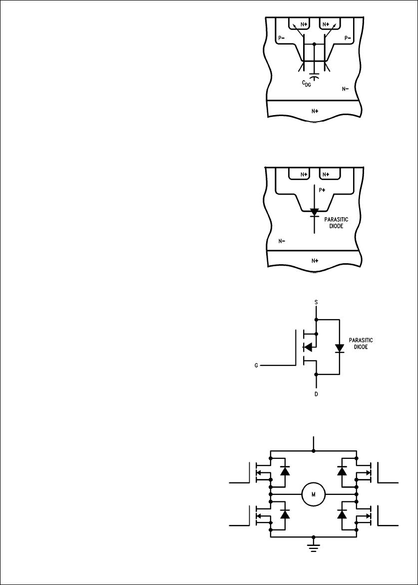
PARASITIC DIODE
Early versions of MOSFETs were very susceptible to volt-
age breakdown due to voltage transients and also had a
tendency to turn on under high rates of rise of drain-to-
source voltage (dV/dt), both resulting in catastrophic fail-
ures. The dV/dt turn-on was due to the inherent parasitic
NPN transistor incorporated within the MOSFET, shown
schematically in
Figure 4a
. Current flow needed to charge
up junction capacitance CDG acts like base current to turn
on the parasitic NPN.
The parasitic NPN action is suppressed by shorting the Na
source to the Pabody using the source metallization. This
now creates an inherent PN diode in anti-parallel to the
MOSFET transistor (see
Figure 4b
). Because of its exten-
sive junction area, the current ratings and thermal resist-
ance of this diode are the same as the power MOSFET.
This parasitic diode does exhibit a very long reverse recov-
ery time and large reverse recovery current due to the long
minority carrier lifetimes in the N-drain layer, which pre-
cludes the use of this diode except for very low frequency
applications, e.g., motor control circuit shown in
Figure 5
.
However in high frequency applications, the parasitic diode
must be paralleled externally by an ultra-fast rectifier to en-
sure that the parasitic diode does not turn on. Allowing it to
turn on will substantially increase the device power dissipa-
tion due to the reverse recovery losses within the diode and
also leads to higher voltage transients due to the larger re-
verse recovery current.
CONTROLLING THE MOSFET
A major advantage of the power MOSFET is its very fast
switching speeds. The drain current is strictly proportional to
gate voltage so that the theoretically perfect device could
switch in 50 ps– 200 ps, the time it takes the carriers to flow
from source to drain. Since the MOSFET is a majority carrier
device, a second reason why it can outperform the bipolar
junction transistor is that its turn-off is not delayed by minori-
ty carrier storage time in the base. A MOSFET begins to
turn off as soon as its gate voltage drops down to its thresh-
old voltage.
TL/G/10063–41
a. MOSFET Transistor Construction
Showing Location of the
Parasitic NPN Transistor
TL/G/10063–42
b. Parastic Diode
TL/G/10063–43
c. Circuit Symbol
FIGURE 4
TL/G/10063–4
FIGURE 5. Full-Wave Motor Control Circuit
3
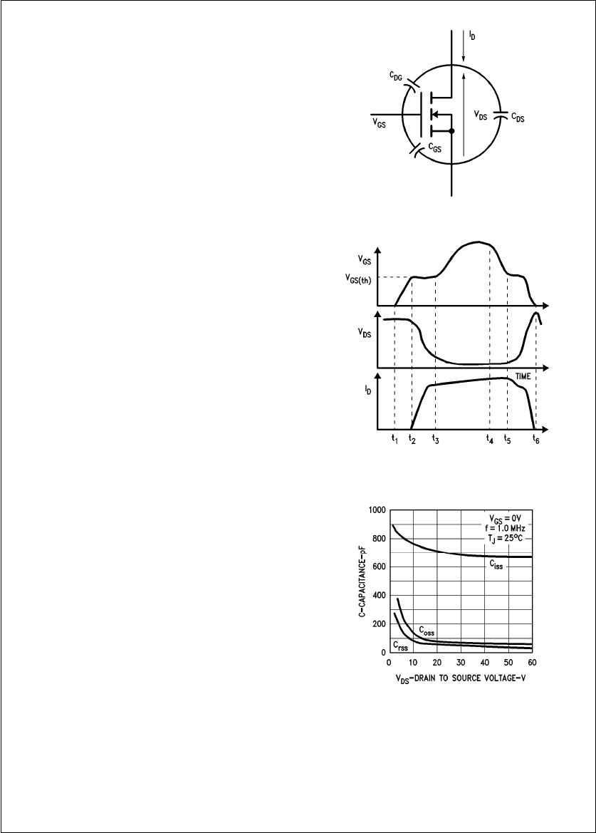
SWITCHING BEHAVIOR
Figure 6
illustrates a simplified model for the parasitic ca-
pacitances of a power MOSFET and switching voltage
waveforms with a resistive load.
There are several different phenomena occurring during
turn-on. Referring to the same figure:
Time interval t1ktkt2:
The initial turn-on delay time td(on) is due to the length of
time it takes VGS to rise exponentially to the threshold volt-
age VGS(th). From
Figure 6
, the time constant can be seen
to be RSxC
GS. Typical turn-on delay times for the National
Semiconductor IRF330 are:
td(on) eRScCGS cIn (1 bVGS(th)/VPK)
For an assumed gate signal generator impedance of RSof
50Xand CGS of 600 pF, tdcomes to 11 ns. Note that since
the signal source impedance appears in the tdequation, it is
very important to pay attention to the test conditions used in
measuring switching times.
Physically one can only measure input capacitance Ciss,
which consists of CGS in parallel with CDG. Even though
CGS ll CDG, the latter capacitance undergoes a much
larger voltage excursion so its effect on switching time can-
not be neglected.
Plots of Ciss,C
rss and Coss for the National Semiconductor
IRF330 are shown in
Figure 7
below. The charging and dis-
charging of CDG is analogous to the ‘‘Miller’’ effect that was
first discovered with electron tubes and dominates the next
switching interval.
Time interval t2ktkt3:
Since VGS has now achieved the threshold value, the
MOSFET begins to draw increasing load current and VDS
decreases. CDG must not only discharge but its capacitance
value also increases since it is inversely proportional to
VDG, namely:
CDG eCDG(0)/(VDG)n(2)
Unless the gate driver can quickly supply the current re-
quired to discharge CDG, voltage fall will be slowed with the
attendant increase in turn-on time.
Time interval t3ktkt4:
The MOSFET is now on so the gate voltage can rise to the
overdrive level.
Turn-off interval t4ktkt6:
Turn-off occurs in reverse order. VGS must drop back close
to the threshold value before RDS(on) will start to increase.
As VDS starts to rise, the Miller effect due to CDG re-occurs
and impedes the rise of VDS as CDG recharges to VCC.
Specific gate drive circuits for different applications are dis-
cussed and illustrated below.
TL/G/10063–5
a. MOSFET Capacitance Model for Power MOSFET
TL/G/10063–6
b. Switching Waveforms for Resistive Load
FIGURE 6
TL/G/10063–7
FIGURE 7. Typical Capacitances of the National IRF330
4
MOSFET CHARACTERIZATION
The output characteristics (IDvs VDS) of the National Semi-
conductor IRF330 are illustrated in
Figures 8
and
9
.
The two distinct regions of operation in
Figure 8
have been
labeled ‘‘linear’’ and ‘‘saturated’’. To understand the differ-
ence, recall that the actual current path in a MOSFET is
horizontal through the channel created under the gate oxide
and then vertical through the drain. In the linear region of
operation, the voltage across the MOSFET channel is not
sufficient for the carriers to reach their maximum drift veloci-
ty or their maximum current density. The static RDS(on), de-
fined simply as VDS/IDS, is a constant.
As VDS is increased, the carriers reach their maximum drift
velocity and the current amplitude cannot increase. Since
the device is behaving like a current generator, it is said to
have high output impedance. This is the so-called ‘‘satura-
tion’’ region. One should also note that in comparing
MOSFET operation to a bipolar transistor, the linear and
saturated regions of the bipolar are just the opposite to the
MOSFET. The equal spacing between the output IDcurves
for constant steps in VGS indicates that the transfer charac-
teristic in
Figure 9
will be linear in the saturated region.
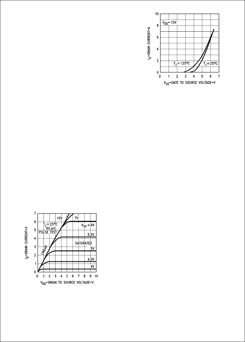
IMPORTANCE OF THRESHOLD VOLTAGE
Threshold voltage VGS(th) is the minimum gate voltage that
initiates drain current flow. VGS(th) can be easily measured
on a Tektronix 576 curve tracer by connecting the gate to
the drain and recording the required drain voltage for a
specified drain current, typically 250 mA or 1 mA. (VGS(th) in
Figure 9
is 3.5V. While a high value of VGS(th), can appar-
ently lengthen turn-on delay time, a low value for power
MOSFET is undesirable for the following reasons:
1. VGS(th) has a negative temperature coefficient
b7 mV/§C.
2. The high gate impedance of a MOSFET makes it suscep-
tible to spurious turn-on due to gate noise.
3. One of the more common modes of failure is gate-oxide
voltage punch-through. Low VGS(th) requires thinner ox-
ides, which lowers the gate oxide voltage rating.
TL/G/10063–8
FIGURE 8. Output Characteristics
TL/G/10063–9
FIGURE 9. Transfer Characteristics
POWER MOSFET THERMAL MODEL
Like all other power semiconductor devices, MOSFETs op-
erate at elevated junction temperatures. It is important to
observe their thermal limitations in order to achieve accept-
able performance and reliability. Specification sheets con-
tain information on maximum junction temperature (TJ(max)),
safe areas of operation, current ratings and electrical char-
acteristics as a function of TJwhere appropriate. However,
since it is still not possible to cover all contingencies, it is
still important that the designer perform some junction cal-
culations to ensure that the device operate within its specifi-
cations.
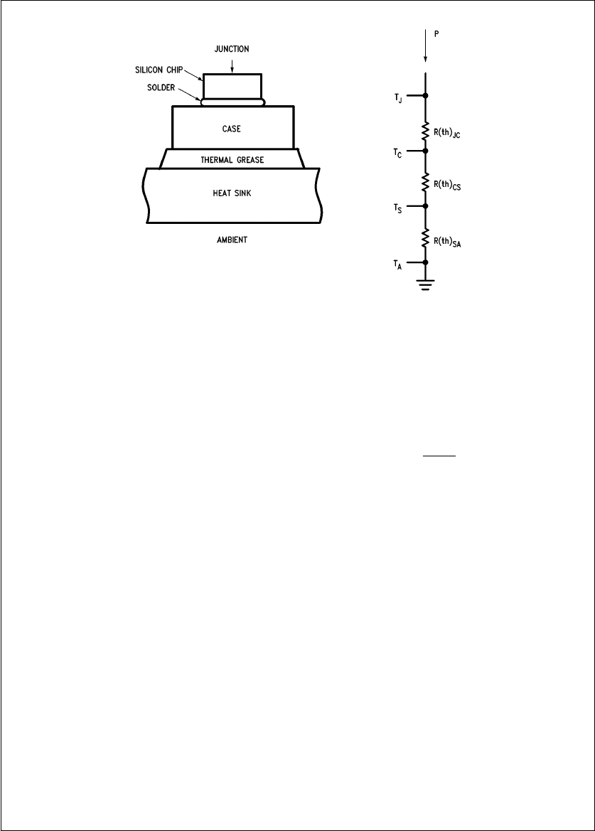
Figure 10
shows an elementary, stead-state, thermal model
for any power semiconductor and the electrical analogue.
The heat generated at the junction flows through the silicon
pellet to the case or tab and then to the heat sink. The
junction temperature rise above the surrounding environ-
ment is directly proportional to this heat flow and the junc-
tion-to-ambient thermal resistance. The following equation
defines the steady state thermal resistance R(th)JC between
any two points x and y:
R(th)JC e(TybTx)/P (3)
where:
Txeaverage temperature at point x (§C)
Tyeaverage temperature at point y (§C)
Peaverage heat flow in watts.
Note that for thermal resistance to be meaningful, two tem-
perature reference points must be specified. Units for
R(th)JC are §C/W.
The thermal model show symbolically the locations for the
reference points of junction temperature, case temperature,
sink temperature and ambient temperature. These tempera-
ture reference define the following thermal references:
R(th)JC: Junction-to-Case thermal resistance.
R(th)CS: Case-to-Sink thermal resistance.
R(th)SA: Sink-to-Ambient thermal resistance.
Since the thermal resistances are in series:
R(th)JA eR(th)JC aR(th)CS aR(th)SA. (4)
5
TL/G/10063–10
FIGURE 10. MOSFET Steady State Thermal Resistance Model
The design and manufacture of the device determines
R(th)JC so that while R(th)JC will vary somewhat from device
to device, it is the sole responsibility of the manufacturer to
guarantee a maximum value for R(th)JC. Both the user and
manufacturer must cooperate in keeping R(th)CS to an ac-
ceptable maximum and finally the user has sole responsibili-
ty for the external heat sinking.
By inspection of
Figure 10
, one can write an expression for
TJ:
TJeTAaPx [R(th)JC aR(th)CS aR(th)SA](5)
While this appears to be a very simple formula, the major
problem in using it is due to the fact that the power dissipat-
ed by the MOSFET depends upon TJ. Consequently one
must use either an iterative or graphical solution to find the
maximum R(th)SA to ensure stability. But an explanation of
transient thermal resistance is in order to handle the case of
pulsed applications.
Use of steady state thermal resistance is not satisfactory for
finding peak junction temperatures for pulsed applications.
Plugging in the peak power value results in overestimating
the actual junction temperature while using the average
power value underestimates the peak junction temperature
value at the end of the power pulse. The reason for the
discrepancy lies in the thermal capacity of the semiconduc-
tor and its housing, i.e., its ability to store heat and to cool
down before the next pulse.
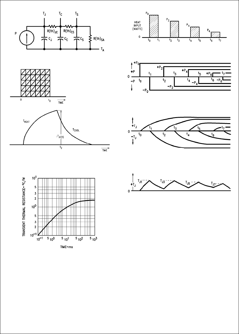
The modified thermal model for the MOSFET is shown in
Figure 11
. The normally distributed thermal capacitances
have been lumped into single capacitors labeled CJ,C
C
,
and CS. This simplification assumes current is evenly distrib-
uted across the silicon chip and that the only significant
power losses occur in the junction. When a step pulse of
heating power P is introduced at the junction,
Figure 12a
shows that TJwill rise at an exponential rate to some steady
state value dependent upon the response of the thermal
network. When the power input is terminated at time t2,T
J
will decrease along the curve indicated by Tcool in
Figure
12a
back to its initial value. Transient thermal resistance at
time t is thus defined as:
Z(th)JC eDTJC(t)
P(6)
The transient thermal resistance curve approaches the
steady state vaule at long times and the slope of the curve
for short times is inversely proportional to CJ. In order that
this curve can be used with confidence, it must represent
the highest values of Z(th)JC for each time interval that can
be expected from the manufacturing distribution of prod-
ucts.
While predicting TJin response to a series of power pulses
becomes very complex, superposition of power pulses of-
fers a rigorous numerical method of using the transient ther-
mal resistance curve to secure a solution. Superposition
tests the response of a network to any input function by
replacing the input with an equivalent series of superim-
posed positive and negative step functions. Each step func-
tion must start from zero and continue to the time for which
TJis to be computed. For example,
Figure 13
illustrates a
typical train of heating pulses.
6
TL/G/10063–11
FIGURE 11. Transient Thermal Resistance Model
TL/G/10063–12
a. Junction Temperature Response to a
Step Pulse of Heating Power
TL/G/10063–13
b. Transient Thermal Resistance Curve
for National Semiconductor IRF330 MOSFET
FIGURE 12
TL/G/10063–14
a. Heat Input
TL/G/10063–15
b. Equivalent Heat Input by
Superposition of Power Pulses
TL/G/10063–16
c. Junction Temperature Response
to Individual Power Pulses of b
TL/G/10063–17
d. Actual TJ
FIGURE 13. Use of Superposition to Determine Peak TJ
7
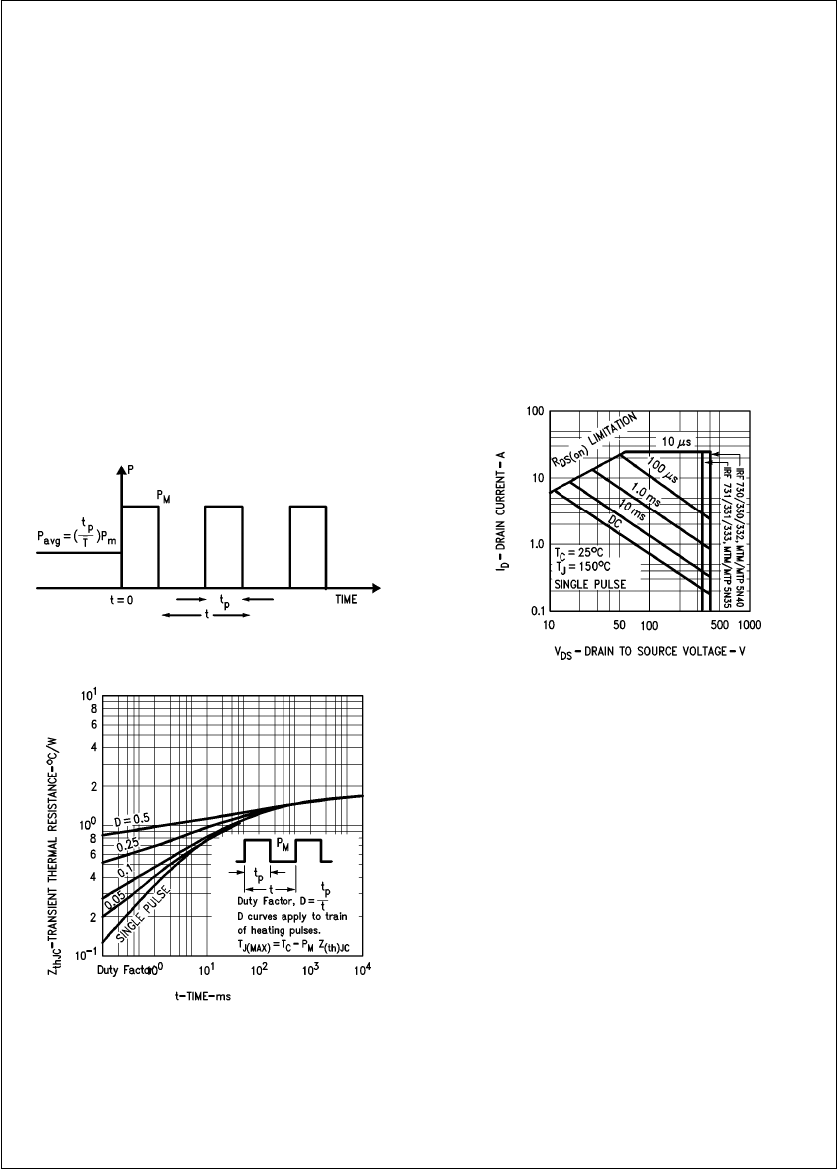
TJat time t is given by:
TJ(t) eTJ(0) a&
h
ie0
Pi (7)
[Z(th)JC (tnbti)bZ(th)JC (tnbtia1)]
The usual use condition is to compute the peak junction
temperature at thermal equilibrium for a train of equal ampli-
tude power pulses as shown in
Figure 14
.
To further simplify this calculation, the bracketed expression
in equation (G) has been plotted for all National Semicon-
ductor power MOSFETs, as exemplified by the plot of
Z(th)JC in
Figure 14b
. From this curve, one can readily calcu-
late TJif one knows PM,Z
(th)JC and TCusing the expres-
sion:
(8)TJeTCaPMcZ(th)JC
Example: Compute the maximum junction temperature for a
train of 25W, 200 ms wide heating pulses repeated every
2 ms. Assume a case temperature of 95§C.
Duty factor e0.1
From
Figure 14b:
Z(th)JC e0.55§C/W
Substituting into Equation (H):
TJ(Max) e95 a25 c0.55 e108.75 §C
TL/G/10063–18
a. Train of Power Pulses
TL/G/10063–19
b. Normalized Z(th)JC for National Semiconductor
IRF330 for Power Pulses Typified in
Figure 14a
FIGURE 14
SAFE AREA OF OPERATION
The power MOSFET is not subject to forward or reverse
bias second breakdown, which can easily occur in bipolar
junction transistors. Second breakdown is a potentially cata-
strophic condition in bi-polar transistors caused by thermal
hot spots in the silicon as the transistor turns on or off.
However in the MOSFET, the carriers travel through the
device much as if it were a bulk semiconductor, which ex-
hibits a positive temperature coefficient of 0.6%/§C. If cur-
rent attempts to self-constrict to a localized area, the in-
creasing temperature of the spot will raise the spot resist-
ance due to the positive temperature coefficient of the bulk
silicon. The ensuing higher voltage drop will tend to redis-
tribute the current away from the hot spot.
Figure 15
deline-
ates the safe areas of operation of the National Semicon-
ductor IRF330 device.
Note that the safe area boundaries are only thermally limit-
ed and exhibit no derating for second breakdown. This
shows that while the MOSFET transistor is very rugged, it
may still be destroyed thermally by forcing it to dissipate too
much power.
TL/G/10063–20
FIGURE 15. Safe Area of Operation of the
National Semiconductor IRF330 MOSFET Transistor
ON-RESISTANCE RDS(on)
The on-resistance of a power MOSFET is a very important
parameter because it determines how much current the de-
vice can carry for low to medium frequency (less than
200 kHz) applications. After being turned on, the on-state
voltage of the MOSFET falls to a low value and its RDS(on)
is defined simply as its on-state voltage divided by on-state
current. When conducting current as a switch, the conduc-
tion losses PCare:
PCeI2D(RMS) xR
DS(on) (9)
To minimize RDS(on), the applied gate signal should be large
enough to maintain operation in the linear or ohmic region
as shown in
Figure 8
. All National Semiconductor MOSFETs
will conduct their rated current for VGS e10V, which is also
the value used to generate the curves of RDS(on) vs IDand
TJthat are shown in
Figure 16
for the National Semiconduc-
tor IRF330. Since RDS(on) increases with TJ,
Figure 16
plots
this parameter as a function of current for room ambient and
elevated temperatures.
8
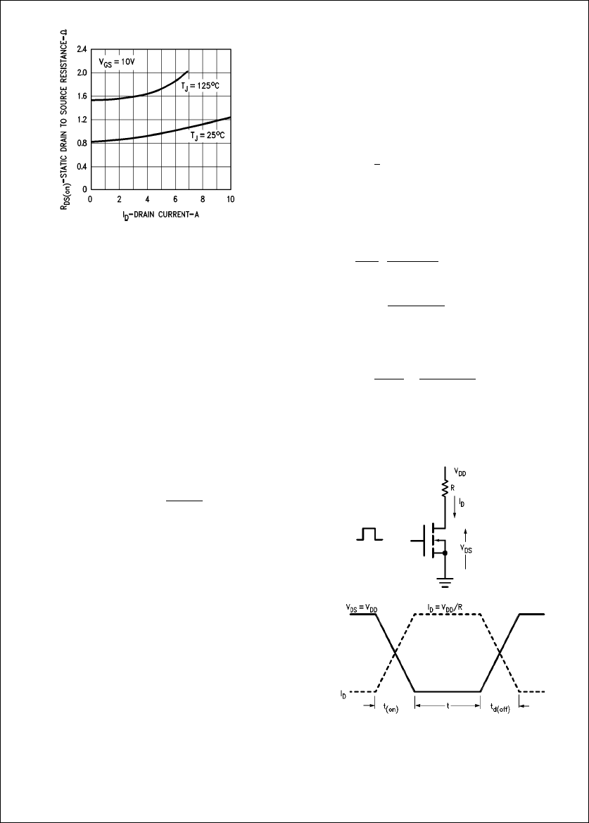
TL/G/10063–21
FIGURE 16. RDS(on) of the
National Semiconductor IRF330
Note that as the drain current rises, RDS(on) increases once
IDexceeds the rated current value. Because the MOSFET is
a majority carrier device, the component of RDS(on) due to
the bulk resistance of the Nbsilicon in the drain region
increases with temperature as well. While this must be tak-
en into account to avoid thermal runaway, it does facilitate
parallel operation of MOSFETs. Any inbalance between
MOSFETs does not result in current hogging because the
device with the most current will heat up and the ensuing
higher on-voltage will divert some current to the other devic-
es in parallel.
TRANSCONDUCTANCE
Since MOSFETs are voltage controlled, it has become nec-
essary to resurrect the term transconductance gfs, com-
monly used in the past with electron tubes. Referring to
Fig-
ure 8
,g
fs equals the change in drain current divided by the
change in gate voltage for a constant drain voltage. Mathe-
matically:
gfs (Siemens) edID(A)
dVGS(V) (10)
Transconductance varies with operating conditions, starting
at 0 for VGS kVGS(th) and peaking at a finite value when
the device is fully saturated. It is very small in the ohmic
region because the device cannot conduct any more cur-
rent. Typically gfs is specified at half the rated current and
for VDS e20V. Transconductance is useful in designing
linear amplifiers and does not have any significance in
switching power supplies.
GATE DRIVE CIRCUITS FOR POWER MOSFETs
The drive circuit for a power MOSFET will affect its switch-
ing behavior and its power dissipation. Consequently the
type of drive circuitry depends upon the application. If on-
state power losses due to RDS(on), will predominate, there is
little point in designing a costly drive circuit. This power dis-
sipation is relatively independent of gate drive as long as
the gate-source voltage exceeds the threshold voltage by
several volts and an elaborate drive circuit to decrease
switching times will only create additional EMI and voltage
ringing. In contrast, the drive circuit for a device switching at
200 kHz or more will affect the power dissipation since
switching losses are a significant part of the total power
dissipation.
Compare to a bi-polar junction transistor, the switching loss-
es in a MOSFET can be made much smaller but these loss-
es must still be taken into consideration. Examples of sever-
al typical loads along with the idealized switching wave-
forms and expressions for power dissipation are given in
Figures 17
to
19
.
Their power losses can be calculated from the general ex-
pression:
PDe#1
u#u
oID(t) #VDS(t)dt J#fs(11)
where: fseSwitching frequency.
For the idealized waveforms shown in the figures, the inte-
gration can be approximated by the calculating areas of tri-
angles:
Resistive load:
PDeV2DD
RÐt(on) at(off)
6aRDS(on) #T(#fs
Inductive load:
PDeVCL Imt(off)fs
2aPc
where:
PCeconduction loss during period T.
Capacitive load:
PDe#CV2DD
2aV2DDRDS(on)
R2TJfs
Gate losses and blocking losses can usually be neglected.
Using these equations, the circuit designer is able to esti-
mate the required heat sink. A final heat run in a controlled
temperature environment is necessary to ensure thermal
stability.
TL/G/10063–23
FIGURE 17. Resistive Load Switching Waveforms
9
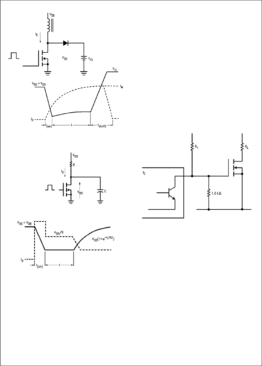
TL/G/10063–24
FIGURE 18. Clamped Inductive
Load Switching Waveforms
TL/G/10063–25
FIGURE 19. Capacitive Load Switching Waveforms
Since a MOSFET is essentially voltage controlled, the only
gate current required is that necessary to charge the input
capacitance Ciss. In contrast to a 10A bipolar transistor,
which may require a base current of 2A to ensure saturation,
a power MOSFET can be driven directly by CMOS or open-
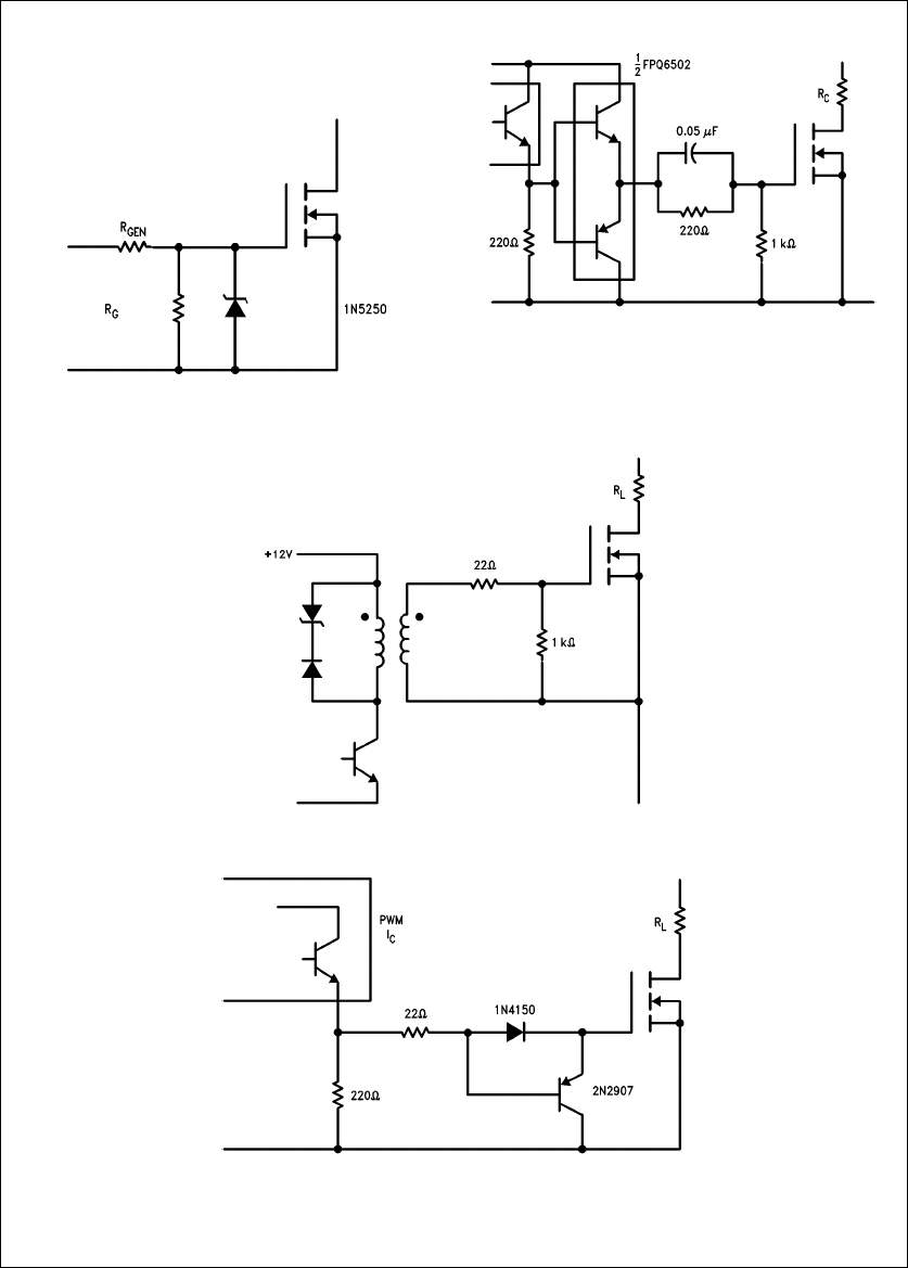
collector TTL logic circuit similar to that in
Figure 20
.
Turn-on speed depends upon the selection of resistor R1,
whose minimum value will be determined by the current
sinking rating of the IC. It is essential that an open collector
TTL buffer be used since the voltage applied to the gate
must exceed the MOSFET threshold voltage of 5V. CMOS
devices can be used to drive the power device directly since
they are capable of operating off 15V supplies.
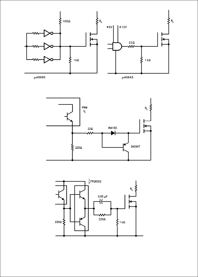
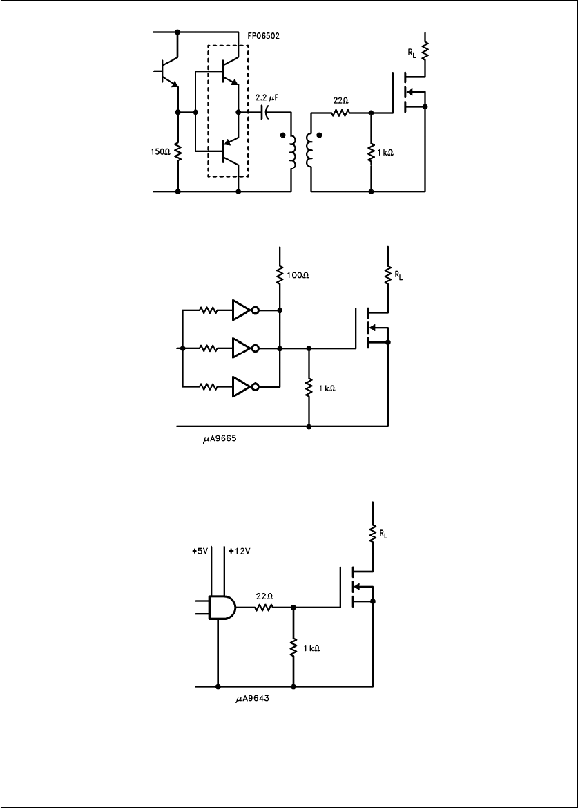
Interface ICs, originally intended for other applications, can
also be used to drive power MOSFETs, as shown below in
Figure 21
.
Most frequently switching power supply applications employ
a pulse width modulator IC with an NPN transistor output
stage. This output transistor is ON when the MOSFET
should be ON, hence the type of drive used with open-col-
lector TTL devices cannot be used.
Figures 22
and
23
give
examples of typical drive circuits used with PWM ICs.
TL/G/10063–26
FIGURE 20. Open Collector TTL Drive Circuit
10
TL/G/10063–27
FIGURE 21. Interface ICs Used to
Drive Power MOSFETs
TL/G/10063–28
FIGURE 22. Circuit for PWM IC Driving MOSFET.
The PNP Transistor Speeds Up Turn-Off
TL/G/10063–29
FIGURE 23. Emitter Follower with Speed-Up Capacitor
11
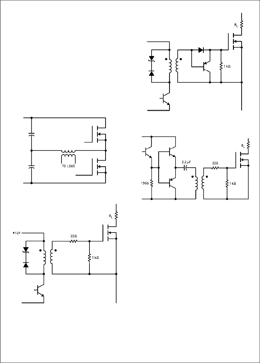
Isolation: Off-line switching power supplies use power MOS-
FETs in a half-bridge configuration because inexpensive,
high voltage devices with low RDS(on) are not available.
Since one of the power devices is connected to the positive
rail, its drive circuitry is also floating at a high potential. The
most versatile method of coupling the drive circuitry is to
use a pulse transformer. Pulse transformers are also nor-
mally used to isolate the logic circuitry from the MOSFETs
operating at high voltage to protect it from a MOSFET fail-
ure.
The zener diode shown in
Figure 25
is included to reset the
pulse transformer quickly. The duty cycle can approach
50% with a 12V zener diode. For better performance at
turn-off, a PNP transistor can be added as shown in
Figure
26
.
Figure 27
illustrates an alternate method to reverse bias the
MOSFET during turn-off by inserting a capacitor in series
with the pulse transformer. The capacitor also ensures that
the pulse transformer will not saturate due to DC bias.
TL/G/10063–30
FIGURE 24. Half-Bridge Configuration
TL/G/10063–31
FIGURE 25. Simple Pulse Transformer Drive
Circuit. The Transistor May Be a
Part of a PWM IC if Applicable.
TL/G/10063–32
FIGURE 26. Improved Performance at Turn-Off
with a Transistor
TL/G/10063–33
FIGURE 27. Emitter Follower Driver
with Speed-Up Capacitor
Opto-isolators may also be used to drive power MOSFETs
but their long switching times make them suitable only for
low frequency applications.
SELECTING A DRIVE CIRCUIT
Any of the circuits shown are capable of turning a power
MOSFET on and off. The type of circuit depends upon the
application. The current sinking and sourcing capabilities of
the drive circuit will determine the switching time and switch-
ing losses of the power device. As a rule, the higher the
gate current at turn-on and turn-off, the lower the switching
losses will be. However, fast drive circuits may produce ring-
ing in the gate and drain circuits. At turn-on, ringing in the
gate circuit may produce a voltage transient in excess of the
maximum VGS rating, which will puncture the gate oxide and
destroy it. To prevent this occurrence, a zener diode of the
appropriate value may be added to the circuit as shown in
Figure 28
. Note that the zener should be mounted as close
as possible to the device.
At turn-off, the gate voltage may ring back up to the thresh-
old voltage and turn on the device for a short period. There
is also the possibility that the drain-source voltage will ex-
ceed its maximum rated voltage due to ringing in the drain
circuit. A protective RC snubber circuit or zener diode may
be added to limit drain voltage to a safe level.
12
Figures 29– 34
give typical turn-on and turn-off times of vari-
ous drive circuits for the following test circuit:
Device: National Semiconductor IRF450, VDD e200V,
Load e33Xresistor.
TL/G/10063–34
FIGURE 28. Zener Diode to Prevent Excessive
Gate-Source Voltages
DRIVE CIRCUIT TURN-ON/TURN-OFF TIMES
TL/G/10063–35
Note: Voltage Fall Time e17 ns, Voltage Rise Time e20 ns
FIGURE 29. Emitter Follower PWM
TL/G/10063–36
Note: Voltage Fall Time e50 ns, Voltage Rise Time e112 ns
FIGURE 30. Simple Pulse Transformer
TL/G/10063–37
Note: Voltage Fall Time e50 ns, Voltage Rise Time e16 ns
FIGURE 31. Pulse Width Modulator
13
TL/G/10063–38
Note: Voltage Fall Time e63 ns, Voltage Rise Time e74 ns
FIGURE 32. Pulse Transformer with Speed-Up Capacitor
TL/G/10063–39
Note: Voltage Fall Time e200 ns, Voltage Rise Time e84 ns
FIGURE 33. Interface Drive
TL/G/10063–40
Note: Voltage Fall Time e70 ns, Voltage Rise Time e30 ns
FIGURE 34. Interface Drive
14

15

AN-558 Introduction to Power MOSFETs and Their Applications
LIFE SUPPORT POLICY
NATIONAL’S PRODUCTS ARE NOT AUTHORIZED FOR USE AS CRITICAL COMPONENTS IN LIFE SUPPORT
DEVICES OR SYSTEMS WITHOUT THE EXPRESS WRITTEN APPROVAL OF THE PRESIDENT OF NATIONAL
SEMICONDUCTOR CORPORATION. As used herein:
1. Life support devices or systems are devices or 2. A critical component is any component of a life
systems which, (a) are intended for surgical implant support device or system whose failure to perform can
into the body, or (b) support or sustain life, and whose be reasonably expected to cause the failure of the life
failure to perform, when properly used in accordance support device or system, or to affect its safety or
with instructions for use provided in the labeling, can effectiveness.
be reasonably expected to result in a significant injury
to the user.
National Semiconductor National Semiconductor National Semiconductor National Semiconductor
Corporation Europe Hong Kong Ltd. Japan Ltd.
1111 West Bardin Road Fax: (
a
49) 0-180-530 85 86 13th Floor, Straight Block, Tel: 81-043-299-2309
Arlington, TX 76017 Email: cnjwge
@
tevm2.nsc.com Ocean Centre, 5 Canton Rd. Fax: 81-043-299-2408
Tel: 1(800) 272-9959 Deutsch Tel: (
a
49) 0-180-530 85 85 Tsimshatsui, Kowloon
Fax: 1(800) 737-7018 English Tel: (
a
49) 0-180-532 78 32 Hong Kong
Fran3ais Tel: (
a
49) 0-180-532 93 58 Tel: (852) 2737-1600
Italiano Tel: (
a
49) 0-180-534 16 80 Fax: (852) 2736-9960
National does not assume any responsibility for use of any circuitry described, no circuit patent licenses are implied and National reserves the right at any time without notice to change said circuitry and specifications.
