Realizing Trigonometric Functions With The Multifunction Converter LH0094 AN 0637
User Manual: AN-0637
Open the PDF directly: View PDF ![]() .
.
Page Count: 6
TL/K/10497
Realizing Trigonometric Functions with the Multi-Function Converter LH0094 AN-637
National Semiconductor
Application Note 637
Hans Palouda
August 1989
Realizing Trigonometric
Functions with the Multi-
Function Converter LH0094
This note discusses how to use the LH0094 to generate
output voltages that are the sine and the cosine of the input
voltage. Circuits are developed and the elements dimen-
sioned. Special emphasis is given to the procedure.
The LH0094 can be used to generate a wide variety of out-
put voltages as a function of three input voltages. One appli-
cation is to generate trigonometric functions.
The LH0094’s transfer function is dependent on three in-
puts, Vx, Vy, and Vz:
EoeVy c(Vz/Vx)m, (eq. 1)
with m between 0.1 and 10. All voltages are positive. Two
resistors are used to set the value of m (R1, R2 in
Figure 2
).
Eois the output voltage of the LH0094. In this application Vx
and Vy are held constant at 10V.
In order to be realized by the LH0094 the trig function needs
to be approximated by a polynomial. This can be done by a
Taylor series:
f(x) ef(xo) axcfÊ(xo) a(x2/2)cf×(xo) a...
where xo is the point where the series is developed. This is
also the point of highest accuracy and therefore chosen
close to the middle of the range of x.
The remainder of the series is truncated, because the
LH0094 can provide only one exponential function. For the
Taylor series this is the x2term. The constant and linear
terms are added with a summing amplifier
(Figure 3)
.
A better approximation can be achieved if the highest expo-
nent is made a fraction rather than an integer as is the case
for the Taylor series. The LH0094 can accommodate this
easily. The values of the coefficients and of the exponent
can then be determined in such a way that the error within
the value range of x is minimized.
In algebra the independent variable is normally called x. In
this application the independent variable is the input voltage
Vz, while the dependent variable, normally called y, is the
output voltage VOUT.
TL/K/10497–1
The independent variable has been named Vz to conform with the conven-
tion of the LH0094. Both Vy and Vz are voltages.
FIGURE 1. Sinus Function to be Realized
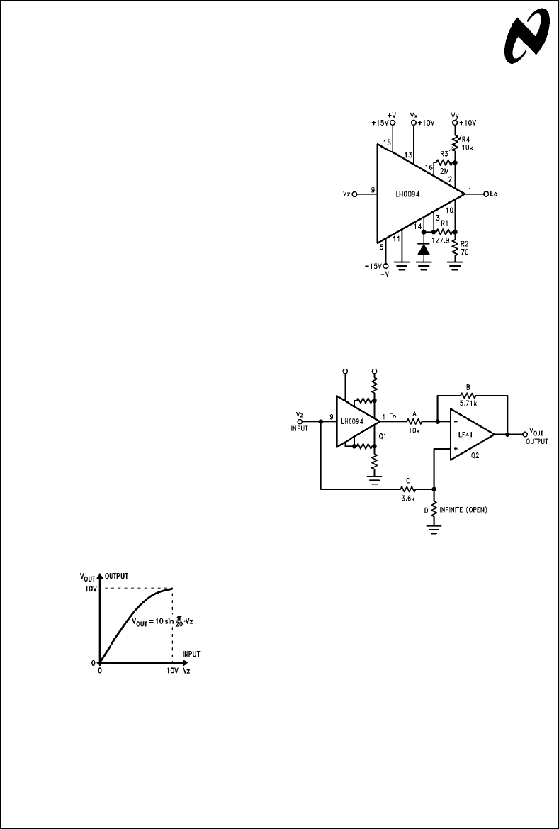
TL/K/10497–2
The clamp diode is for protection. The potentiometer R4 is used to trim the
output Eoto 10V when all 3 inputs Vx, Vy, and Vz are at a10V.
FIGURE 2. The Multifunction Generator LH0094
Connected to Realize the Function
Eoe10 c(Vz/10) 2.827
TL/K/10497–3
Q1 is the LH0094 connected as shown in
Figure 2
. Its output is proportional
to the exponential part of the transfer function.
FIGURE 3. Circuit to Realize the Sine Function
I. REALIZING THE FUNCTION y esin x
1. OBJECTIVE
A circuit needs to be designed where the output voltage is
the sine of the input voltage, as shown in
Figure 1
. The
basic function is
yesin x.
If substitutions are made: x eccVz and y eVOUT/k, the
function becomes
VOUT ekcsin c cVz (eq. 2)
C1995 National Semiconductor Corporation RRD-B30M75/Printed in U. S. A.

This equation connects input and output voltage by a sine
function. The values of k and c can be determined so that
these boundary conditions are met:
at VIN eVz e0V ... V
OUT e0V and the argument
ccVz e0 radians, at VIN eVz e10V . . . VOUT e10V
and the argument c cVz eq/2 rad.
Both k and 1/c have the dimension of a voltage, and there-
fore the value of the sine (VOUT/k) and its argument (c c
Vz) remain without dimension. In the following equations all
voltages need to be measured in Volts.
2. DEVELOPMENT OF A REALIZABLE FUNCTION
From eq. 2 and its boundary conditions it can be shown that
ce1
10V
c
q
2and k e10V
The desired function (eq. 2) becomes
VOUT
10V
esin q
2
cVZ
10V, or, in a shorter form,
VOUT e10 sin (Vz cq/20), (eq. 3)
where Vz is the input voltage.
Because the LH0094 can only create an exponential func-
tion, the sine function in eq. 3 needs to be substituted by a
polynomial. The approximation
sin x exbxm/6.28, (eq. 4)
with x eVz cq/20 and m e2.827
lets the desired function be written as
VOUT e10 [Vzcq/20 b(Vzcq/20)m/6.28]. (eq. 5)
This approximation is accurate for Vz from 0V to a10V with
a theoretical accuracy of 0.23%.
3. DEVELOPMENT OF THE CIRCUIT
3a. Realization of the Exponential Term
The first task is to realize a function proportional to Vzm.
Then it can be scaled and added to the other terms to yield
the required transfer function (eq. 5).
Figure 2
shows how to connect the LH0094 to perform the
exponential portion of the desired function (eq. 5). From eq.
1 and with the input voltages Vx eVy ea
10V the transfer
function of the LH0094 becomes
Eoe10 c(Vz/10)m. (eq. 6)
From eq. 4 it is known that m e2.827
The value of m is set by R1 and R2, with
me(R1 aR2)/R1
(from the datasheet) and the recommendation that
R1 aR2 e200X
(approximately). Suitable values are
R1 e127.89X,
R2 e70X.
R3 and the potentiometer R4 in
Figure 2
serve to trim the
maximum output Eoto a10V when the input voltage Vz e
a10V.
Both Vx and Vy should be connected to a regulated a10V,
since the accuracy of this voltage directly influences the
accuracy of the output voltage.
3b. Circuit to Realize the Sine Function
Figure 3
shows the schematic for the complete circuit. Q1 is
the LH0094 connected as shown in
Figure 2
to perform the
exponential term of the transfer function (eq. 5). The output
voltage Eois amplified by Q2, which also adds some frac-
tion of the input voltage Vz coming through C and D, thus
accommodating the linear term of the desired transfer func-
tion (eq. 5).
4. TRANSFER FUNCTIONS
The transfer function of the circuit in
Figure 3
is
VOUT eb
E
o
B
A
aVz cD
CaD
cAaB
A
bB/A is the inverting voltage gain, (AaB)/A is the non-in-
verting voltage gain. Vz cD/(CaD) is the fraction of the
input voltage which is fed into the non-inverting input.
With eq. 6 used to substitute for Eo, the transfer function
becomes
VOUT eb
10 Vzm
10mcB
A
aVz D
CaD
cAaB
A(eq. 7)
The transfer function to be realized is (from eq. 5):
VOUT eVzcq/2 bVzmc10 c(q/20)m/6.28 (eq. 8)
5. DIMENSIONING THE CIRCUIT PARAMETERS
For the two transfer functions, eq. 7 and eq. 8, to be identi-
cal, in both functions the coefficients of Vzmmust be equal,
and also the coefficients of Vz must be equal to each other.
b10 Vzm
10mcB
A
eb
10 c(q/20)m/6.28
With m e2.827 (eq. 4) this results in
B/A e0.5708. (eq. 9)
The linear coefficients set equal give
D
CaD
cAaB
A
eq/2
With the known value for B/A (eq. 9) this yields
C/D e0 (eq. 10)
or D einfinite, or open, C having a finite value.
6. DIMENSIONING OF THE RESISTORS
10 kXis a good first choice for both load and source imped-
ances. Load impedances need to be larger than 2 kX.
Sources driving Q2 can be quite high, if the LF411 is cho-
sen, because of its FET input. However, the impedances
should not be too high, because of the time constants
formed together with the circuit capacitances. Below 1 MX
this concern will not arise.
If A is chosen as A e10 kX,
B becomes (eq. 9) . . . B e0.5708 A e5.708 kX.
D is infinite,
C is chosen so it is approximately equal to
AcB/(A aB) e3.6 kX.
In this case both inputs of the op-amp Q2 see the same
impedance.
7. LIST OF RESISTORS
R1 e127.89 A e10k
R2 e70 B e5.708k
R3 e2M C e3.6k, 5%
R4 e10k POT D eopen
II. REALIZING THE FUNCTION y ecos x
1. OBJECTIVE
A circuit needs to be designed where the output voltage is
the cosine of the input voltage, as shown in
Figure 1
. The
basic function is
yecos x.
2
If substitutions are made: x eccVz and y eVOUT/k, the
function becomes
VOUT ekccos c cVz (eq. 11)
This equation connects input and output voltage by a cosine
function (see
Figure 4
). The values of k and c can be deter-
mined so that these boundary conditions are met:
at VIN eVz e0V ... V
OUT e10V and the argument
ccVz e0 radians, at VIN eVz e10V . . . VOUT e0V
and the argument c cVz eq/2 rad.
Both k and 1/c have the dimension of a voltage, and there-
fore the value of the cosine (VOUT/k) and its argument (c c
Vz) remain without dimension. In the following equations all
voltages need to be measured in Volts.
TL/K/10497–4
The independent variable has been named Vz to conform with the conven-
tion of the LH0094. Both Vy and Vz are voltages.
FIGURE 4. Cosine Function to be Realized
2. DEVELOPMENT OF A REALIZABLE FUNCTION
From eq. 2 and its boundary conditions it can be shown that
ce1
10V
c
q
2and k e10V
The desired function (eq. 2) becomes
VOUT
10V
ecos q
2
cVz
10V, or, in a shorter form,
VOUT e10 cos (Vz cq/20), (eq. 12)
where Vz is the input voltage.
Because the LH0094 can only create an exponential func-
tion, the cosine function in eq. 12 needs to be substituted by
a polynomial.
The approximation
cos x e1a0.2325 x bxm/1.445, (eq. 13)
with x eVz cq/20 and m e1.504,
allows the desired function to be written as
VOUT e10 [1a0.2325 Vz cq/20 b
(Vz cq/20)m/1.445 ]. (eq. 14)
This approximation is accurate for Vz from 0V to a10V with
a theoretical accuracy of 0.75%.
3. DEVELOPMENT OF THE CIRCUIT
3a. Realization of the Exponential Term
The LH0094 is used to realize a function proportional to
(Vz)m, which will then be scaled and added to the other
voltages which correspond to the remainder of the terms in
eq. 13.
From eq. 1, with Vx and Vy held constant at a10V, the
transfer function of the LH0094 becomes
Eoe10 (Vz/10)m. (eq. 15)
Figure 5
shows how to connect the LH0094 to perform the
exponential portion of the desired transfer function (eq. 14).
The resistors R1 and R2 set the value of m (from the data-
sheet):
me(R1 aR2)/R1.
For m e1.504 (eq. 13), and the recommendation that R1
aR2 be approximately 200X, suitable values are R1 e
65.52Xand R2 e130X.
R3 and the potentiometer R4 in
Figure 2
serve to trim the
maximum output Eoto 10V when the input voltage Vz e
10V.
Both Vx and Vy should be connected to a regulated a10V,
since the accuracy of this voltage directly influences the
accuracy of the circuit.
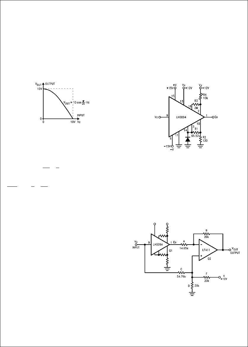
TL/K/10497–5
The clamp diode is for protection. R4 trims the output voltage to 10V when
all three inputs Vx, Vy, and Vz, are at a10V.
FIGURE 5. The LH0094 Connected to
Output the Function Eoe10 c(Vz/10)1.504
3b. Circuit to Realize the Cosine Function
Figure 6
shows the schematic for the complete circuit. Q1 is
the LH0094 connected as shown in
Figure 5
to perform the
exponential term of the desired transfer function (eq. 14).
The output voltage Eois amplified by Q2, which also adds
some fraction of the input voltage Vz coming through C, as
well as a constant voltage coming through R.
TL/K/10497–6
Q1 is the LH0094 connected as per
Figure 5
. Its output is proportional to the
exponential term in the transfer function.
FIGURE 6. Circuit to Realize the Cosine Function
3

4. TRANSFER FUNCTIONS
The transfer function of this circuit
(Figure 3)
is
VOUT eb
E
o
B
A
aA
a
B
A#Vz R
ll
D
CaR
ll
D
aVC
ll
D
FaC
ll
DJ,
where R
ll
DeRcD/(RaD), and C
ll
DeCcD/(CaD).
The factor (bB/A) is the inverting voltage gain, (AaB)/A
the non-inverting voltage gain. The term zc(R
ll
D)/(CaR
ll
D) describes the fraction of the input voltage fed into the
non-inverting input, and V c(C
ll
D)/(FaC
ll
D) is the DC
voltage at the non-inverting input. The op-amp sums and
amplifies all three voltages.
With eq. 15 used to substitute for Eo, the transfer function of
the circuit becomes
VOUT eb
10 Vzm
10mcB
A
aAaB
A (eq. 16)
#Vz R
ll
D
CaR
ll
D
aVC
ll
D
FaC
ll
DJ
The transfer function to be realized is (eq. 14):
VOUT e10 [1a0.2325 Vzcq/20b(Vzcq/20)m/1.445].
5. DIMENSIONING OF THE CIRCUIT PARAMETERS
For the two transfer functions (eq. 14, 16) to be identical, in
both functions the coefficients of Vzmmust be equal, the
coefficients of Vz must be equal, and the constants must be
equal.
The coefficients of Vzmset equal give
b10 Vzm
10mcB
A
eb
10 (q/20)m/1.445
This yields B/A e1.365. (eq. 17)
The linear coefficients set equal give
AaB
A
cF
ll
D
CaF
ll
D
e10 (0.2325) c
q
20 (eq. 18)
This yields
C
F
ll
D
e#B
A
a1Jc
q
2
c1
0.2325
e5.475 ea (eq. 19)
The coefficients of the constants set equal give
#B
A
a1JcVcC
ll
D
FaC
ll
D
e10, or, with V e10V,
F
C
ll
D
e#B
A
a1Jc10
10
b1e1.3649 eb (eq. 20)
Eq. 19 and eq. 20 are two equations for the three unknowns
C, D, and R. This means one of the unknowns can be cho-
sen. This makes sense, because in voltage dividers it is the
ratio of resistors that counts. The terms a and b are used as
abbreviations for easier use.
The resistor D will be chosen and considered known. With
this premise it can be shown the equations 19 and 20 yield
CeDc(acbb1)/(b a1) e2.7373 D (eq. 21)
FeDc(acbb1)/(a a1) e0.9997 D (eq. 22)
6. DIMENSIONING OF THE RESISTORS
10 kXis a good choice for both load and source impedanc-
es. Load impedances need to be larger than 2 kX. Sources
driving Q2 can be quite high, if the LF411 is chosen, be-
cause of its FET input. However, the impedances should not
be too high, because of the time constants formed together
with the circuit capacitances. Below 1 MXthis concern will
not arise.
6a. First Round of Dimensioning
If A is chosen, as first try, A1 e10 kX,
B becomes (eq. 17) B1 e1.3649 A1 e13.649 kX.
D is chosen as D1 e10 kX,
C then becomes (eq. 21) C1 e2.7373 D1 e27.373 kX,
and F becomes (eq. 22) F1 e0.99968 D1 e9.9968 kX
6b. Second Round of Dimensioning
The values of the resistors are in the proper range as far as
loading and input impedance are concerned. However, for
reasons of accuracy the amplifier Q2 needs source imped-
ances on its inverting and non-inverting inputs that are ap-
proximately equal.
A1
ll
B1 eA1 cB1/(A1aB1) e5.772 kX
C1
ll
D1
ll
F1 e1/(1/C1 a1/D1 a1/F1) e4.227 kX
These values are relatively close to each other, but it is easy
to make them even closer. The scaling factor is
5.772/4.227 e1.3653, and with it the new values for C, D
and F become
C2 e1.365 C1 e(1.365) c(27.373) e37.373 kX,
D2 e1.365 D1 e(1.365) c(10) e13.653 kX
F2 e1.365 F1 e(1.365) c(9.9968) e13.649 kX
The resistors A1 and B1 remain unchanged:
A2 eA1 e10 kX
B2 eB1 e13.649 kX
6c. Final Dimensions
Three resistors have about the same value: B1, D2, and F2.
If they are all made 13.65 kXthe error is 0.02%. This error
will in most cases be negligible. To get standard values the
three resistors can be set 20 kX. The remaining resistors A1
and C2 will be proportionally scaled with a factor of
20/13.65 e1.4652. Since all resistors are scaled by the
same factor, all the previously established relationships, like
voltage attenuation and impedance matching, remain un-
changed.
7. LIST OF RESISTORS
R1 e65.52 A e14.652k
R2 e130 B e20k
R3 e2M C e54.759k
R4 e10k POT D e20k
Fe20k
For good accuracy the voltage V ea
10V needs to be
regulated and is best connected to Vx and Vy, which need
to be regulated as well.
4
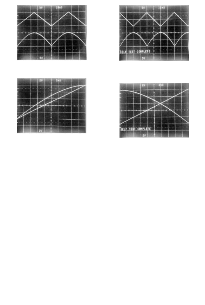
TL/K/10497–7
FIGURE 7. Input and Output Voltage of the Sine Circuit
TL/K/10497–8
FIGURE 8. Input and Output Voltage
of the Sine Circuit, Detail
TL/K/10497–9
FIGURE 9. Input and Output Voltage
of the Cosine Circuit
TL/K/10497–10
FIGURE 10. Input and Output Voltage
of the Cosine Circuit, Detail
5

AN-637 Realizing Trigonometric Functions with the Multi-Function Converter LH0094
LIFE SUPPORT POLICY
NATIONAL’S PRODUCTS ARE NOT AUTHORIZED FOR USE AS CRITICAL COMPONENTS IN LIFE SUPPORT
DEVICES OR SYSTEMS WITHOUT THE EXPRESS WRITTEN APPROVAL OF THE PRESIDENT OF NATIONAL
SEMICONDUCTOR CORPORATION. As used herein:
1. Life support devices or systems are devices or 2. A critical component is any component of a life
systems which, (a) are intended for surgical implant support device or system whose failure to perform can
into the body, or (b) support or sustain life, and whose be reasonably expected to cause the failure of the life
failure to perform, when properly used in accordance support device or system, or to affect its safety or
with instructions for use provided in the labeling, can effectiveness.
be reasonably expected to result in a significant injury
to the user.
National Semiconductor National Semiconductor National Semiconductor National Semiconductor National Semiconductores National Semiconductor
Corporation GmbH Japan Ltd. Hong Kong Ltd. Do Brazil Ltda. (Australia) Pty, Ltd.
2900 Semiconductor Drive Livry-Gargan-Str. 10 Sumitomo Chemical 13th Floor, Straight Block, Rue Deputado Lacorda Franco Building 16
P.O. Box 58090 D-82256 F4urstenfeldbruck Engineering Center Ocean Centre, 5 Canton Rd. 120-3A Business Park Drive
Santa Clara, CA 95052-8090 Germany Bldg. 7F Tsimshatsui, Kowloon Sao Paulo-SP Monash Business Park
Tel: 1(800) 272-9959 Tel: (81-41) 35-0 1-7-1, Nakase, Mihama-Ku Hong Kong Brazil 05418-000 Nottinghill, Melbourne
TWX: (910) 339-9240 Telex: 527649 Chiba-City, Tel: (852) 2737-1600 Tel: (55-11) 212-5066 Victoria 3168 Australia
Fax: (81-41) 35-1 Ciba Prefecture 261 Fax: (852) 2736-9960 Telex: 391-1131931 NSBR BR Tel: (3) 558-9999
Tel: (043) 299-2300 Fax: (55-11) 212-1181 Fax: (3) 558-9998
Fax: (043) 299-2500
National does not assume any responsibility for use of any circuitry described, no circuit patent licenses are implied and National reserves the right at any time without notice to change said circuitry and specifications.
