Radiation Design Considerations Using CMOS Logic AN 0926
User Manual: AN-0926
Open the PDF directly: View PDF ![]() .
.
Page Count: 10

TL/F/11650
Radiation Design Considerations Using CMOS Logic AN-926
National Semiconductor
Application Note 926
Michael Maher
January 1994
Radiation Design
Considerations Using
CMOS Logic
INTRODUCTION
Today’s rapidly changing global political climate is signifi-
cantly impacting the military strategies of Free World coun-
tries. Important decisions are being made regarding each
country’s defense and military equipment needs. Regard-
less of these ongoing political changes, however, the threat
of nuclear weaponry use remains a viable possibility. As
long as a first-strike capability exists, radiation-hardened
strategic and tactical systems will be designed.
In addition, radiation-resistance techniques increasingly fo-
cus toward space communication and exploration as more
countries participate in the aerospace arena. As man ven-
tures deeper and deeper into space, it is increasingly neces-
sary to harden systems against space’s natural radiation
environments.
Designing and producing a radiation-hardened system is
time extensive and financially expensive. Rather than meet
premature demises due to inadequate radiation design, myr-
iad precautions must be taken to ensure that satellites, for
example, will survive their full life expectancies. Sometimes
orbiting the Earth in excess of ten years, satellites incur very
high costs due to emphasis on performance, reliability, and
radiation resistance. Radiation hardening entire systems is a
paramount concern.
Historically, radiation-sensitive space systems have been
shielded in various materials. But because the payload
pound-to-thrust cost ratio is also a critical concern, this ap-
proach is becoming unacceptable. Better methods, such as
radiation-hardened ICs, are required to harden a system.
The severity of radiation exposure in space differs from that
incurred in the tactical arena. While shielding space sys-
tems is very expensive, protection can be economical in
tactical radiation environments, with notable exceptions be-
ing avionic systems, some tank systems, and shipboard
equipment. While most failed systems in tactical equipment
can be easily replaced, military conditions and requirements
usually mandate that electronic systems remain fully func-
tional throughout any nuclear event.
Lastly, today’s commercial market requires limited radiation
protection measures. Here shielding is generally the most
viable and economical approach.
INCORPORATING RADIATION DESIGN
Starting at the
conceptual stage
is the most efficient and
cost-effective approach to designing a radiation-hardened
system. This is where proper evaluation and selection of
semiconductor technology and other factors occur, i.e., de-
termining the extent of shielding, selecting viable existing
technologies, and evaluating prototype futuristic IC technol-
ogies that will offer full availability by the time the system is
in production.
Good decision making significantly lowers costs and in-
creases the opportunity to keep a production schedule.
Most critical at the conceptual stage is a thorough under-
standing of the system’s mission relative to its potential radi-
ation environments. Depending on the mission, for example:
satellite (commercial or military), tactical avionics system
(nuclear event), or commercial application (nuclear power
plant or medical), decisions can be made to utilize different
types of components in different circuit applications.
MISSION
Initial design decisions for space systems are based on
whether it will be used in a military or commercial applica-
tion. Radiation hardness requirements also differ if a satel-
lite is in low orbit, high orbit, geosynchronous orbit, or polar
orbit. Semiconductors in a satellite experience varying de-
grees of radiation degradation depending on whether they
are resident on the satellite’s exterior panels or are buried
within its body. In space environments, major exposure
comes from gamma ray irradiation and Single Event Phe-
nomena (SEP).
Tactical systems (such as those in aircraft, shipboard,
ground hardware, or equipment housed in missile silos or
ground bunkers) each have distinct and unique radiation re-
quirements. When designing a system, it must be known if
that system must operate throughout a nuclear event or if it
will be shut down until the event has passed. Systems sub-
jected to a nuclear event must withstand gamma ray dose
rate irradiation and neutron radiation.
The commercial environment has the easiest-to-
accommodate radiation hardness levels. Although some
equipment parts are exposed to severe hostile radiation en-
vironments, most parts can be protected with lead shielding
or thick cement walls. Major concerns in the commercial
environment stem from gamma ray total dose irradiation
and neutron radiation.
RADIATION ENVIRONMENTS
The more knowledgeable a designer is about radiation envi-
ronments and their adverse affects, the greater the potential
for proper technology selection and parts utilization for a
cost effective, radiation-hardened design. System and cir-
cuit designers contend with five major radiation environ-
ments:
#Total Dose Ionization (Gamma Ray)
#Transient Irradiation (Dose RateÐGamma Ray)
#Single Event Phenomena
#Neutron Radiation
#Electrical Magnetic Pulse (EMP)
EMP and neutron irradiation environments are not a con-
cern for CMOS logic radiation design. Neutron radiation is
not a factor as long as the fluence is under 1013 neu-
tron/cm2. At the present time, EMP environment is ad-
dressed at the system level, not by the component’s tech-
nology.
RADIATION DESIGN CONSIDERATIONS
Digital logic design, and CMOS technology in particular, pro-
vides inherent system hardness against radiation degrada-
tion. Beyond its high radiation resistance characteristics,
CMOS logic (such as FACTTM and FACT Quiet SeriesTM
FASTÉand TRI-STATEÉare registered trademarks of National Semiconductor Corporation.
FACTTM and FACT Quiet SeriesTM are trademarks of National Semiconductor Corporation.
C1995 National Semiconductor Corporation RRD-B30M75/Printed in U. S. A.

from National) offers the lowest power consumption, high
advanced bipolar speeds, high packing density, and high
noise immunity. Immune to neutron radiation and offering
excellent total dose, transient (dose rate), and single event
effects characteristics, CMOS logic is recommended for
sockets previously occupied by other technologies. For ex-
ample, while ECL is very hard in the total dose environment,
it is susceptible in neutron and single event effects environ-
ments. The recessed oxide and walled emitters of advanced
bipolar logic technology (FASTÉ, ALS) make it susceptible
to neutron, total dose, dose rate, and Single Event Effects
(SEE).
When designing a radiation-hardened CMOS system circuit,
devices which use NAND gates are more tolerant than
those with NOR gates. As NAND gates have p-MOSFETs in
parallel with n-MOSFETs in series, both leakage current of
the n-channel and increased threshold voltage of the
p-channels are minimized. The NOR gate design has
p-channel MOSFETs in series with n-channel MOSFETs in
parallel connection and degrades more quickly in a total
dose environment than NAND circuits.
As the number of inputs increases for a particular gate, radi-
ation degradation accelerates as total dose levels increase.
Depending on circuitry, CMOS device response may de-
grade, e.g., a flip-flop comprised of NAND gates has a dif-
ferent total dose degradation than one using inverters and
transmission gates.
As the circuit’s complexity increases, radiation degradation
shifts from circuit parameter failure to circuit functionality
radiation failure. Therefore, a microprocessor may fail func-
tionality prior to circuit parameter failure. This also holds
true for gate array designs. Each gate array has its own
radiation response because of the internal metal connec-
tions to each cell; radiation hardness characteristics change
with the design of each gate array’s personalization.
To ensure the best RHA (Radiation Hardness Assurance)
design, it is necessary to understand the complete radiation
response of each component in the system circuit, e.g.,
what electrical parameters are affected by which radiation
environments. This includes variable data and functionality
(attribute) data to the level of radiation failure. Variable data
as performed in a step-stress radiation approach permits
observance of non-monotonic behavior for each electrical
parameter’s radiation response. For example, standby cur-
rent of a non-hardened field oxide is non-linear and exhibits
significant increases in value above its pre-radiation value.
As 90% of all space projects require less than 100 krad(Si),
radiation-hardened products such as FACT AC logic easily
provide more than the required amount of resistance.
In space, the two most important radiation effects are total
dose ionization (at a low dose rate) and single event effects.
In the tactical environment, major concerns are transient
(dose rate) radiation and neutron effects.
When designing a radiation-hardened system, guidelines
must be established based on the system’s mission and its
required survivability. Following the conceptual phase of
system design, proper components must be determined and
selected for the investigative Engineering Development
Phase. This critical design phase is often the most costly as
component testing procedures include components, circuit
board, systems assembly, and software documentation.
Following identification of the radiation environment, radia-
tion test procedures must be established. A Hardness As-
surance Plan and Program must also be instituted. Estab-
lishing a Change Control Board ensures that any modifica-
tions to the circuit design do not impact the system’s hard-
ness assurance.
Once a system design is approved to radiation-hardness
criteria, other documentation must be initiated that will pre-
vent compromise to the established radiation hardness lev-
el. Written specifications must include radiation test condi-
tions. Acceptance test procedures must be in place to en-
sure that components identified to HCI (Hardness Critical
Items) specifications are properly tested. Lists must be es-
tablished that identify those components and processes
which are classified as HCI.
Part procurement drawings, assembly drawing schematics,
and purchase orders require complete specifications of radi-
ation requirememts, including a
worst-case
circuit analysis.
Worst-case analysis requires extensive system and circuit
knowledge with respect to different radiation environments.
Factors to consider include:
#Analysis of which circuit functions must operate through
a particular radiation environment and those that would
not
#The amount of available radiation shielding
#Selecting manufacturers with radiation-resistant
components
One of the most costly efforts when radiation hardening a
system is piece-part radiation testing. Here each compo-
nent’s radiation response is determined by different radia-
tion environment simulators. Depending on the irradiation
level, neutron testing can cost $2,000 to $4,000; for total
dose testing, from $2,500 to $8,000, depending on the num-
ber of required radiation levels and the circuit’s complexity.
SELECTION OF RHA COMPONENTS
Once a technology is selected, the next step is choosing
Radiation Hardness Assured (RHA) components. Utilizing
RHA devices reduces cost, improves reliability, and ensures
the system’s radiation hardware requirements. RHA compo-
nent qualification does not guarantee these devices are im-
pervious to adverse radiation effects, but that they have
end-point electrical values which account for radiation-
effects-generated responses.
If the system’s manufacturer determines RHA acceptability
via its own radiation testing program, the system’s cost will
significantly increase. In addition to the system manufactur-
er’s involvement in comprehensive radiation testing, the
OEM bears the cumbersome burden of scheduling and pur-
chasing very costly radiation time at test facilities.
A better, significantly less expensive approach for OEMs
who need RHA product is working with component manu-
facturers qualified to RHA.
Test results taken at varying radiation levels enable RHA
vendors to specify irradiation limits for radiation-sensitive
parameters. Care must be used in selecting RHA compo-
nents. In general, RHA devices are qualified for neutron en-
vironment and total dose irradiation but are not specified for
transient (Dose Rate) environment or Single Event Phenom-
ena.
There are concerns associated with RHA components. A
radiation design engineer must examine the vendor’s data
for any outstanding issues, annealing, lot-to-lot variation,
wafer-to-wafer variation, and radiation test conditions. It is
2

important to select a semiconductor manufacturer that pro-
vides either the specified data or eliminates that particular
concern. By choosing the correct technology and the cor-
rect component manufacturer, a radiation-hardened system
can be produced with minimal cost, fewer components, and
maximum survivability. The technology of choice to meet
these radiation requirements is a CMOS with a thin epitaxial
layer or silicon-on-insulator (SOS or SiO2process). Nation-
al’s FACT logic has been built on thin Epi since 1987.
TOTAL DOSE ENVIRONMENT AND DIGITAL LOGIC
CMOS DESIGN
A. Design Consideration
Ionization radiation in a total dose environment affects the
gate and field oxide of a CMOS semiconductor. When using
CMOS technology, most vendors utilize the enhancement
mode design of CMOS MOSFETs. This ensures the
MOSFET will only turn ON when the proper threshold volt-
age is attained. When gamma rays strike the gate oxide that
has an electrical field across it, photons generate electron-
hole pairs. The electrons are swept out of the gate oxide
leaving behind the holes (trapped charge). (Holes are actu-
ally positrons which have a positive charge with the mass of
an electron.) This trapped charge causes threshold voltages
to change. A positive trapped charge causes n-channel
MOSFETs to approach depletion mode while p-channel
MOSFETs are driven further into enhancement. Other gen-
erated charges (referred to as radiation interface states)
cause the n-channel MOSFET threshold voltage to in-
crease. P-channel MOSFETs are slightly affected by inter-
face states. Trapped-positive charge and interface-state
generation combine with subsequent annealing effects to
constitute Time Dependent Effects (TDE) of total dose ioni-
zation.
Total dose radiation can degrade parameters to the point
where a circuit’s operation is detrimentally effected. To pre-
vent this, designers must understand degradation, how de-
vice parameters are affected, and how to achieve a
radiation-hardened design by properly applying the device in
both the circuit and in the system.
The two major parametric concerns are leakage currents
and propagation times. Depending on a vendor’s CMOS
processing, other parametrics (such as VIL,V
IH,V
OL,V
OH)
may also change. With National’s FACT logic, the only de-
graded parameters are ICC (Standby Current) and IOZ
(TRI-STATEÉleakage current). All other DC and AC param-
eters remain within published pre-rad limits.
B. Total Dose Testing
To ensure a device’s total dose resistance meets the re-
quired radiation hardness level, post-irradiation parametric
values must be taken. Values can be ascertained only by
component testing each device type. This is followed by
careful evaluation of characterization data.
Total dose testing is performed using either a gamma or a
low energy x-ray source. Gamma rays are usually generated
by a Cobalt-60 or a Cesium-137 source. Another source of
ionization radiation is an electron accelerator. Because
most total dose testing is performed on finished product, the
gamma rays or electron beam must have energy equal to or
greater than 1 MeV at the oxide level.
Low-energy x-rays are the newest approach to total dose
testing. Its advantage is testing during fabrication, rather
than waiting for packaged die. Using low-energy x-rays, the
radiation hardness integrity of the gate oxide is analyzed as
soon as polysilicon deposition and definition are completed.
Because low-energy x-ray sources employ a photo-electric
effect rather than the Compton Scattering effect, absorbtion
rate and damage differ from values obtained via gamma ray
sources and electron accelerators. The radiation damage
ratio between low-energy x-ray and Cobalt-60 sources var-
ies between 1.35 to 1.8. Total dose absorption from a low-
energy x-ray source is expressed in rad(SiO2); gamma ray
and electron accelerator sources express absorption in
rad(Si). At 1.1 MeV, absorption is approximately equal for
both silicon (Si) and silicon dioxide (SiO2). To prevent large
errors and misleading information between the different
sources, care must be taken and correlations made.
During total dose testing, device irradiation is under bias. In
addition, radiation boards should be constructed to provide
worst case
radiation bias conditions. For CMOS logic devic-
es, all inputs should be electrically connected to HIGH or
LOW to prevent device oscillation or excess drawing of cur-
rent; output pins may be either loaded or open-circuited.
Test fixtures/boards must not distort the radiation field uni-
formity.
There are several methods of performing total dose testing:
in-flux, in-situ, and remote testing. In-flux testing requires
that devices be exposed to radiation while electrical para-
metric tests are conducted. In-situ testing requires that elec-
trical parametric tests be made on the devices-under-test
(DUT) while not being exposed to radiation. With remote
testing, electrical parametric tests are performed on the de-
vices which are physically removed from the exposure test
chamber. When performing remote testing, it may be neces-
sary to employ a mobile power supply to apply bias to the
test fixture and DUT. This permits transfer of irradiated de-
vices from the radiation area to another location for electri-
cal parametric measurements while keeping devices under
bias except for electrical parametric testing times.
Part of the ionization irradiation process is review of Time
Dependent Effects (TDE). Annealing tests cause TDE
changes in the electrical parameters (i.e., trapped charges
during and after radiation exposure) that emulate the low
dose rate environment of space. When considering TDE ef-
fects, additional testing is required, such as a standard irrad-
iation test followed by a combination of additional irradiation
and accelerated temperature anneal.
C. Characterization Data
Characterization data is derived from thorough total dose
radiation testing. For each particular device, it defines the
radiation response to each radiation environment.
Radiation-sensitive parameters are identified, and the radia-
tion environments in which they pose problems are defined.
By using characterization data to better understand a func-
tion’s response in each radiation environment, designers
can tailor their approach to hardening the circuit and sys-
tem’s design. Data also identifies radiation-sensitive param-
eters, enabling designers to adjust system circuitry for mini-
mal parametric degradation or for evaluating applicability of
various vendors’ products.
Characterization data is used to determine device design
margins, and subsequently of the circuit design. However,
the most important use of characterization data is establish-
ment of parameter end point limits for device qualification.
3

For example, a system designer typically specifies a radia-
tion level of 3 krad(Si) for devices to be used in the tactical
environment. To eliminate lot acceptance testing, a design
margin of 10x total dose level [30 krad(Si)]would have to
be attained with an acceptable parametric-end-point limit
and no functional failure of the device.
Figure 1
illustrates
FACT characterization data. It shows a
worst-case
condi-
tion, depicting one of only two parameters for which FACT
technology is radiation sensitive, i.e., ICC (TRI-STATE leak-
age current). IOZ is only of concern if the device has
TRI-STATE outputs.
Another example of total dose degradation is an increase in
propagation time. By taking CMOS radiation characteriza-
tion data and substituting these values in an AC circuit-
timing simulator, a logic race or a contention condition can
be detected.
Finally, design margin is an important concept in CMOS log-
ic design and is used if a device function fails to meet or if it
exceeds the radiation requirements of a specific project or
application. Basically, design margin is a ratio of total dose
radiation failure level versus specified total dose radiation
failure level of the design. Design margins are determined
by statistical analysis methods and can be applied as de-
vice, circuit, or system criteria. For CMOS logic, a design
margin greater than 10 but less than 100 eliminates both lot
acceptance tests and periodic radiation testing. A CMOS
device possessing a design margin greater than 100 re-
quires minimal radiation testing. If the CMOS device’s de-
sign margin is less than 10, it must have lot acceptance
testing and specified controls.
TRANSIENT (DOSE RATE) RADIATION
A. Design Consideration
Transient irradiation is primarily associated with a nuclear
explosion and is a major concern for circuit and system de-
signers of tactical equipment. Dose rate radiation is the
amount of total dose irradiation given in specified time inter-
vals.
This transient radiation pulse is expressed in rad(Si)/s or
rad(SiO2)/s. In the real world, the nuclear event is over with-
in milli-seconds, although it can continue up to a minute
when delayed components are considered. In the dose rate
simulated environment, the pulse width ranges from 3 ns to
10 ms depending on the type of irradiating equipment being
utilized. When a transient radiation pulse hits a device, the
ionizing radiation is a function of time and is not constant.
The affect of the dose rate pulse is generation of excess
charge in a short period of time. This quantity of excess
charge is dependent upon the total ionizing dose utilized.
The concentration of these excess carriers is determined by
the dose rate and carrier lifetime. Excess charge results
when the ionizing pulse occurs at a faster rate than can be
recombined. When a threshold level of excess charge is
attained in a CMOS device, these radiation-induced effects
can cause temporary effects or catastrophic failures:
#Upset (soft error)
#Latchup
#Junction burn-out
Other effects are short transient pulse on the output and
saturated outputs which depend upon the amount of photo-
current (excess charge) generated and the output loading.
Upset of output data is a
soft
error since there is no perma-
nent damage. Combinatorial circuits will upset then return to
their original state. This type of upset generates a transient
voltage at the output pin which might or might not affect the
next IC device. Sequential logic circuits are the devices
which upset and remain in this condition until the affected
device is reset.
While logic upset may be acceptable for some projects, the
dose rate threshold level is important as the designer must
work around the upset condition. Latchup is a result of a
sufficiently large quantity of radiation-induced photocurrent
which initiates a parasitic Silicon-Controlled Rectifier (SCR).
Once activated, this SCR acts as a low resistance path be-
tween ground and power supply. This condition usually
leads to catastrophic failure, such as blown bond wires or
metalization on the die.
Junction burnout is another catastrophic failure which oc-
curs in the dose rate environment. This failure is generated
when sufficiently large photocurrent is accumulated in the
sensitive junction and cannot be distributed from this region
quickly enough. As a result, thermal energy is increased to a
level which causes junction burnout. For most technologies,
the junction area is fairly large and heat can be dissipated.
At very high dose rate levels, junction burnout becomes a
major concern.
B. Dose Rate Testing
Transient irradiation testing is performed by several ap-
proaches of which the primary testers are Linear Accelera-
tor (LINAC) and Flash X-Ray. A third type of transient irradi-
ator utilizes a laser approach. In its embryonic state, the
laser technique has some limitations. The LINAC is used in
the electron beam mode and is capable of providing both a
narrow pulse and wide pulse ranging from 3 ns to 10 ms
pulse widths; the pulse must have an energy level greater
than 10 MeV. The Flash X-Ray (FXR) machine is limited to
narrow pulse widths and is operated in the photon mode.
For both approaches, the total dose is generally limited to
500 rad(Si) g200.
When considering upset testing, an analysis of the circuit’s
topology should be done prior to testing. This eliminates
unnecessary testing of certain test paths and minimizes the
amount of required testing.
Worst case
test conditions for
upset utilize the lowest permitted power supply voltage for
the system’s application and a wide dose rate pulse of
greater than 200 ns. All modes of operation should be in-
vestigated and tested, i.e., TRI-STATE, shift-left, etc. Static
and dynamic operations of the device must be evaluated for
dose rate sensitivity. If a clock signal is associated with the
DUT, then the relative position of the radiation pulse with
respect to the CLOCK signal’s transition edge becomes an
important factor. Upset levels are affected by the internal
inductance of the device and associated test circuitry. Care
must be taken to minimize parasitic inductance since this
will give upset levels that are lower than the device’s true
upset level. To compensate for this parasitic inductance, a
capacitor can be added to the test circuit.
Worst case
test conditions for Dose Rate latchup testing
are highest utilized power supply voltage, highest anticipat-
ed temperature, and the shortest dose rate pulse width. In-
vestigating existence of latchup
windows
is also recom-
mended. Latchup
windows
are regions of dose rate levels
where the device will latchup; areas below or above
4

this region will not latchup. Performing four dose rate levels
per decade is acceptable to determine latchup
windows
.
When performing dose rate testing for upset, latchup, and
burnout, it is important to perform both functional and para-
metric testing of the DUT after each test. This determines if
any of the previously-mentioned effects occurred or if any
parametric degraded as a result of total dose.
C. Dose Rate Characterization Data
When the circuit designer has dose rate test data, decisions
can be made on latchup prevention and upset correction
methodologies. Upset threshold levels, determined by dose
rate testing, will assist in selection of parts and design mar-
gin analysis. From the dose rate testing, it is necessary to
determine if the device has pulse width or current sensitivity.
If the device’s dose rate upset response indicates that it is a
function of pulse width, then an extreme pulse width value
must be used in radiation design calculations and transient
irradiation tests. Otherwise, the device’s dose rate response
is dependent upon current and any dose rate pulse width
less than the value can be employed.
When a transient pulse is detected by the system’s nuclear
event detector (NED), data can be stored in radiation-hard-
ened memory and recovered at a later time when the nucle-
ar event has passed or dissipated. Another technique is dis-
allowing present data of a transient irradiation, and recycling
the computer for data retransmission before the nuclear
event. Still other approaches are used when operation
through a nuclear event is necessary.
The best method is utilization of devices that are very insen-
sitive to upset or that demonstrate high upset levels. Avoid
the use of CMOS memory devices which do not otherwise
employ an internal split or partitioning of the power supply
rail; otherwise, rail span collapse will occur. Rail span col-
lapse is the reduction of power supply voltage below a value
due to the induced dose rate photocurrent. When this oc-
curs, the memory cells farthest from the power supply bond
pad will be the easiest to upset.
Other approaches use circuit schemes. This requires addi-
tional components to compensate for photocurrent generat-
ed by transient radiation, such as employment of a differen-
tial amplifier to reject common-mode primary currents or the
use of filter circuits to prevent radiation-induced voltage
transients from propagating to the circuit’s outputs. The in-
crease in components has several associated penalties:
#Increased cost
#Increased board area
#Decreased circuit speed
Choosing the appropriate radiation-resistant products mini-
mizes these penalties, providing additional upset protection.
Evaluation of characterization data determines the ap-
proach to be used. Burnout can be either metal lines (due to
a metal defect or the current density for that particular line
or bond wire being exceeded) or junction burnout. To pre-
vent burnout, a current-limiting resistor isolates the power
supply from the device, thereby limiting the radiation-
induced photocurrent. This resistor also assists in prevent-
ing latchup. The penalty paid for using this resistor is higher
power consumption and decreased device speed.
One approach to latchup elimination is using dielectric isola-
tion devices (CMOS/SOS, CMOS/SOI) or CMOS-Epi prod-
uct.
CMOS/SOS and CMOS/SOI products are inherently latch-
up immune. CMOS/SOS is somewhat costly; CMOS/SOI is
a new product with a minimum track record. CMOS-Epi has
the best solution when cost and performance are consid-
ered. However, care must be exercised when selecting
CMOS-Epi parts since thick epitaxial layers greater than
10 mm should be avoided and the substrate and Epi must
have low resistivities as permitted by the process technolo-
gy. When using CMOS-bulk devices, the substrate should
be gold lapped or neutron irradiated in order to reduce the
minority carrier lifetime of the substrate. This will reduce the
combined gains of the parasitic bipolar transistors that con-
stitute the parasitic SCR to much less than one (gain m1).
SINGLE EVENT EFFECTS (SEE) AND CMOS DIGITAL
LOGIC DESIGN
A. Design Considerations
Single Event Effects (SEE) are predominantly associated
with trapped radiation in space. They were observed in the
early 1960s, but were not of concern until the latter half of
the 1970s. As technology evolved to decreased geometries,
feature sizes, and gate oxide volume as well as increased
device speed, the energy required for gate switching was
reduced. As a result, low energies (0.5 pico joules) can now
switch device gates, making SEE-charged particles an im-
portant radiation environment.
SEE hardness design is dependent on mission require-
ments and circuit application of the device. Mission require-
ments affecting SEE design include orbit placement, time
duration in space, and orbit inclination. Single Event Phe-
nomena (SEP) is generated by three charged particles: al-
pha, protons, and heavy ions.
#The alpha particleÐthe weakest of these particles in
causing SEE problemsÐcauses upset in sequential logic
or memory devices. Thorium, a radioactive material used
in ceramic packages, is a source for alpha particles.
#High-energy protons originate in the Van Allen Belts or
by solar flares. Only those protons having energy greater
than 10 MeV will cause a single event problem.
#Heavy ions are also caused by solar flares and galactic
cosmic rays.
The detrimental results of SEE on electronic systems in-
clude transients, soft errors, and permanent damage. Single
Event transient spikes are generally associated with combi-
natorial logic circuits. The transient spike resulting from a
Single Event strike has a short time duration, but could con-
tain sufficient energy to cause a subsequent sequential or
combinatorial logic input to change. While combinatorial log-
ic outputs have transient upset, the inputs will force the out-
put to its original state. Soft errors are temporary Single
Event upsets and are defined as
bit flips
.
Latchup is the major permanent damage caused by SEP.
This and other effects, such as funnel effect, result when a
high-energy charged particle passes through a sensitive
area. As the charged particle passes through the sensitive
volume, it deposits energy along its path. The rate of energy
loss in the material is Linear Energy Transfer (LET). This
energy loss generates a plasma of electron-hole pairs. If
5

this plasma occurs in a depletion area of the sensitive re-
gion, induced current is generated. This induced current is
primarily collected from the depletion region and the funnel
region. It consists of:
#
Drift:
Generated in the depletion region and part of the
prompt portion of the induced current.
#
Funnel Charge:
Generated in the funnel region, located
below the depletion area of the sensitive area. The fun-
nel region results from instantaneous distortion of electri-
cal fields, deep into the silicon. The currrent caused by
the funneling effect is greater than the drift component
and is quickly drawn back into the sensitive region’s con-
tact.
#
Diffusion:
The delayed portion of the total induced SEE
current. The diffusion region is located below the funnel
region.
Figure 2
shows the composite drawing of the in-
duced SEE current.
Induced current is a function of the circuit’s parameter, the
voltage applied at the sensitive node, and node capaci-
tance. The amount of charge required to generate a change
of state in a memory cell or sequential logic device is de-
fined as the
critical
charge. Associated with the
critical
charge are the sensitive nodes of an IC device. Sensitive
nodes are the reversed-biased nodes; e.g., the OFF drains
of the p- and n-channels of a memory cell. The collected
charge at these sensitive nodes causes a voltage transient
to be developed and applied to other cross-coupled invert-
ers of the memory cell or sequential logic device that gener-
ates the change of state at the output of the device.
Latchup is another major concern in the Single Event Ef-
fects environment and can affect devices manufactured on
CMOS, bipolar, and ECL processes. Because of heavy ions,
latchup in CMOS technologies is generally associated with
a CMOS bulk technology or with CMOS devices fabricated
on a thick epitaxial (Epi) substrate. While similar to Transient
(Dose Rate), SEE latchup is generated by heavy ions. Since
SEE latchup usually has catastrophic results, designers
must carefully select components that will be impervious to
a single particle strike. It is therefore necessary to select
devices which are fabricated with guard rings, built on a very
thin Epi, or that utilize dielectrically-isolated CMOS technol-
ogies (SOS, SOI). National’s FACT product is manufactured
on a very thin epitaxial layer. At extremely high LET levels,
FACT remains immune to latchup from heavy ions.
B. Single Event Testing
There are several sources for performing Single Event test-
ing. The two major sources are the cyclotron machine and
Van de Graaff accelerators. The cyclotron apparatus pro-
vides maximum capability of providing a variety of heavy ion
species at different magnitudes of energies. As a result, a
wide level of penetration depths into the device can be at-
tained. The usual maximum ion energy level approximates
2 MeV/nucleon for this radiation source. Using the cyclotron
is expensive and time consuming. Some of the problems
associated with these machines are beam diagnostics, e.g.,
the amount of time it takes to change ion species or ion
energies [3].
The second source for testing SEP is the Tandem Van de
Graaff Generator. This testing approach is less expensive
than the cyclotron. A limiting factor, however, is its usable
energy, i.e., the higher Z ion species’ range is limited. It is
much easier to change ion species in a short time. Addition-
ally, the Van de Graaff machine can determine low LET
thresholds of sensitive devices where lower energy, lower Z
ions of continuously variable energies are needed [3].
When performing SEP testing, the company requesting this
test supplies support personnel, DUT boards, a device exer-
ciser, and any additional support equipment such as data
reduction equipment or diagnostic equipment. The user
must also select the ion species and LET threshold. The
user will determine the test philosophy and prepare a test
plan based upon the selection of the radiation source. When
using the cyclotron or Van de Graaff machine, DUTs must
be unlidded. The user is responsible for all hardware opera-
tion and a number of dry runs may have to be performed
before all is acceptable. Test facility personnel will perform
beam uniformity measurements, flux measurement, energy
measurements, and other diagnostic activity in order to en-
sure beam accuracy. Facility personnel are responsible for
all other activities associated with the radiation source, such
as beam dosimetry.
C. Characterization Data
It is important to know what constitutes characterization
data for Single Effect design. By using SEE characterization
data, circuit simulation is a proven means to ensure that the
circuit and system will be hardened to this environment. The
circuit designer must obtain specific information from the
vendor concerning SEE testing, the different temperatures
under which testing was performed, the range of angle of
incidence, dimension of the sensitive volume, feature size
and process information, cross-sectional area, the LET val-
ues for upset and for latchup, and the critical charge value
that causes inversion of output data. Employing this data in
an SEE simulation program will provide the designer with
additional data, such as the particle count and the minimum
LET energy necessary to generate the critical charge within
the specified volume that will cause upset. Data obtained
through the simulation is then compared and validated with
the vendor’s test data. Performing several more simulations
and using several different values of critical charge, a plot of
critical charge versus error rate can be generated. This type
of plot is particular to each memory cell device or other
sequential logic device being utilized in the system’s design.
In memory cells, the approach for increasing the SEU hard-
ness level is use of polysilicon
feedback
resistors. The re-
sistor decouples the sensitive nodes of the
off
n- and
p-channel devices. Other approaches employ circuit diodes
and active devices in the feedback. This is done by increas-
ing the RC time of the feedback loop, allowing more time for
the circuit to recover from SEU high and increasing the
charge required on the gate to cause a
bit-flip
. When using
polysilicon cross-coupled resistors, temperature becomes a
factor as the negative co-efficient of these resistors increas-
es the resistance when the device is exposed to decreased
temperatures. As a result, the memory circuit becomes
slower at colder temperatures.
Other sequential devices such as data latches require addi-
tional internal circuitry rather than resistors, thus adding to
chip size. Resistors also increase power consumption and
decrease device speed.
From a system perspective, SEP can be addressed in sev-
eral ways. Ground Control personnel maintain a circumven-
tion scheme for shutting the system down when under im-
6
mediate threat. Another method is utilizing circuit redundan-
cy; this is founded on the precept that the probability of the
same two circuits being hit by an ion at the same time is
very low. Use of Error Detection and Correction (EDAC) is
another approach, as is use of two-level parity code.
FACT logic is built on a CMOS-Epi process which utilizes a
very thin Epi and low substrate resistivity. The result is a
product line which truncates the funnel effect, limits the
amount of charge collection, and is latchup immune to LET
t120 MeV/mg/cm2. Recently, several FACT device types
were tested for SEU and all devices had an LET t40 MeV/
mg/cu2and a cross-sectional area t2c10b5.
USING FACT LOGIC
The system’s mission and its associated radiation environ-
ment direct the testing for obtaining radiation design data.
This knowledge assists the designer in making the proper
component selection. This same radiation characterization
data defines the restrictive conditions for the circuitry’s de-
sign and the necessary design trade-offs.
When possible, CMOS-Epi product should be used in radia-
tion-hardened design. Only where required or imperative
should radiation-hardness-dedicated CMOS devices be em-
ployed. This reduces system cost. National’s FACT logic
family is the most radiation-resistant ACMOS logic family
available to Military/Aerospace designers and is the Ad-
vanced CMOS logic family of choice for radiation applica-
tions. Its tolerance exceeds that of other logic families. As
long as the neutron fluence is under 1013n/cm2; neutron
radiation does not affect the FACT product line.
FACT logic provides high radiation resistance in all environ-
ments. For total ionization dose, its 100 krad(Si) capability
provides the same post-irradiation drive as its preradiation
value with propagation time deltas of less than 0.5 ns at
high dose rate levels. At lower space dose rates, FACT logic
is superior to other logic families. FACT is resistant to total
ionization radiation because of its thin gate oxide and low
temperature processing.
FACT’s Epi (Epitaxial Layer), p-well design, and low-resistiv-
ity substrate provide inherent latchup immunity and high up-
set tolerance in both Dose Rate and Single Event Phenom-
ena Environments. Because of this technology, fewer parts
are needed to provide the required radiation hardness level.
This minimizes the use of circumvention schemes or other
conventional radiation hardening techniques. Use of FACT
product reduces weight, board space, and is a very cost
effective approach to radiation-hardened system design.
NATIONAL’S LOGIC TEST PHILOSOPHY
National Semiconductor offers a solution that reduces the
need for extensive shielding measures while maintaining
cost effectiveness. By testing inherently radiation-resistant
standard devices, National provides products that offer you:
#Custom testing as outlined in customer SCDs (Source
Control Drawings)
#Guaranteed specifications for reliable radiation designs
#Cost effectiveness
#Timely delivery
Through National’s Mil/Aero Logic Radiation Program,
products are fully qualified with respect to different radiation
environments. Complete Total Dose radiation data is sup-
plied with each customer order, certifying radiation resist-
ance to the level specified in each SCD.
National recognizes that radiation resistance needs differ
within tactical and space environments. Our radiation resist-
ance program is flexible to individually address your require-
ments, according to your radiation and processing needs.
Several process flows are available, including Level S, Level
B, Standard Military Drawings (SMDs), MIL-STD-883, and
Source Control Drawings (SCDs).
FACT products are manufactured in a DESC-certified JAN
Class S wafer fabrication facility. All of the company’s logic
radiation research and development is performed in Nation-
al’s South Portland, Maine, Radiation Effects Laboratory
(REL). This REL is:
#Certified by the National Institute of Standards and Tech-
nology (NIST).
#Licensed by the Nuclear Regulatory Commission (NRC)
to handle neutron-irradiated material. This REL capability
permits testing product for both total dose and neutron
irradiation. National currently is contracting Sandia Na-
tional Labs to perform neutron irradiation.
#Certified by the Defense Electronic Supply Center
(DESC) for Lab Suitability. This certification signifies that
our REL has met all government requirements to perform
total dose testing. This certification is one of only two
presently granted by DESC.
Lab Suitability certification denotes that testing per-
formed at National’s South Portland REL facility and the
data generated are fully recognized and acceptable by all
government agencies, their contractors, and subcontrac-
tors. This qualifies the south Portland REL to support
JAN Class S RHA programs for FACT product as well as
for any customer-requested testing that requires total
dose data from a DESC-certified laboratory.
REL research includes evaluation of National’s logic fami-
lies as well as any other products requested by customers.
National is in the process of qualifying FACT devices to
RHA (Radiation Hardness Assurance) standards, with ap-
proval expected by mid-year, 1991. At that time, FACT AC
JAN Class S and B devices will bear an ‘‘R’’ designation as
part of the JM38510 Slash Sheet number, denoting RHA
certification to 100 krad(Si); FACT ACT a ‘‘D’’ as part of the
SMD number, signifying RHA certification to 10 krad(Si). Na-
tional will also be submitting data on its FACT Quiet Series
and FACT FCT SMD products, also for RHA certification to
10 krad(Si), or a ‘‘D’’ designator.
Note: This text was used as the basis for an article published in the Janu-
ary, 1991, edition of the German magazine
Design & Elektronik,
‘‘Strahlungsfeste Designs mit CMOS-Logik.’’
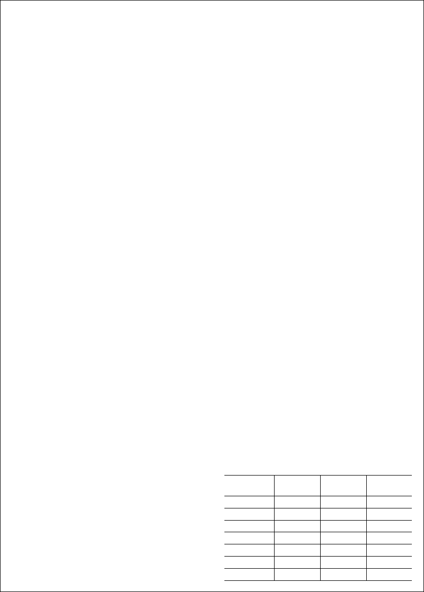
TABLE I. Example of Radiation Characterization
Data for ICC (Standby Current)
Part Type: 54AC00 Quad 2-Input NAND Gate
Dose Rate: 142 rad(Si)/sec
Parameter: ICC
Dose Level Minimum Mean Maximum
[krad(Si)]Value (mA) Value (mA) Value (mA)
Pre-radiation 0.019 0.047 0.340
5 0.413 0.616 1.024
10 7.870 13.631 22.907
50 43.033 74.330 136.920
80 43.033 61.289 105.630
100 11.736 43.033 74.329
150 11.736 37.817 74.329
7
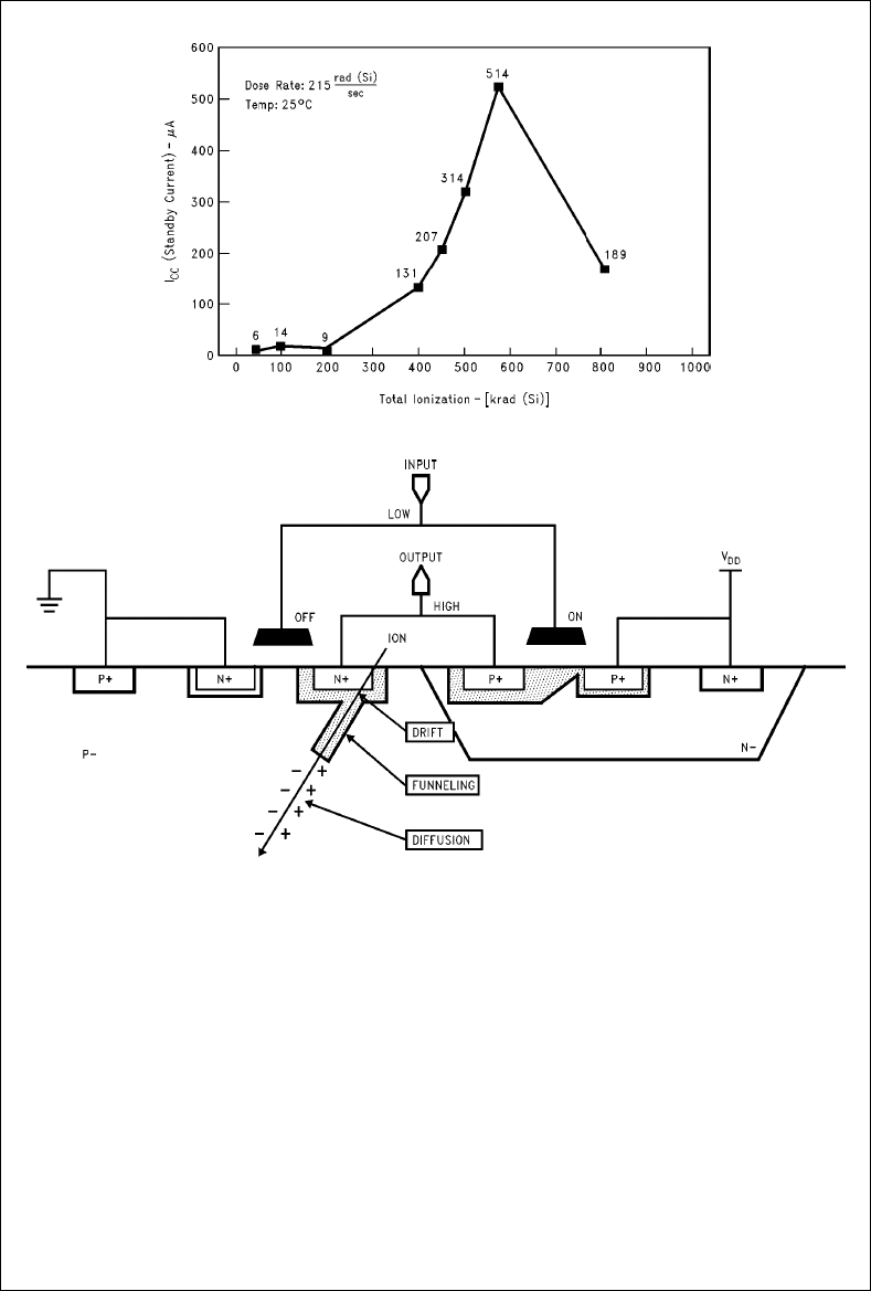
54AC245ÐOctal Bidirectional Transceiver
TL/F/11650–1
FIGURE 1. ICC (Standby Current) Versus Total Dose
TL/F/11650–2
FIGURE 2. Single Event Effects Generated Currents [7]
8
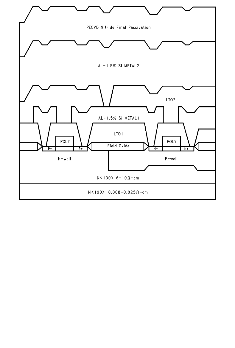
TL/F/11650–3
FIGURE 3. Final Processed Cross-Section of the FACT Technology
9
AN-926 Radiation Design Considerations Using CMOS Logic
LIFE SUPPORT POLICY
NATIONAL’S PRODUCTS ARE NOT AUTHORIZED FOR USE AS CRITICAL COMPONENTS IN LIFE SUPPORT
DEVICES OR SYSTEMS WITHOUT THE EXPRESS WRITTEN APPROVAL OF THE PRESIDENT OF NATIONAL
SEMICONDUCTOR CORPORATION. As used herein:
1. Life support devices or systems are devices or 2. A critical component is any component of a life
systems which, (a) are intended for surgical implant support device or system whose failure to perform can
into the body, or (b) support or sustain life, and whose be reasonably expected to cause the failure of the life
failure to perform, when properly used in accordance support device or system, or to affect its safety or
with instructions for use provided in the labeling, can effectiveness.
be reasonably expected to result in a significant injury
to the user.
National Semiconductor National Semiconductor National Semiconductor National Semiconductor National Semiconductores National Semiconductor
Corporation GmbH Japan Ltd. Hong Kong Ltd. Do Brazil Ltda. (Australia) Pty, Ltd.
2900 Semiconductor Drive Livry-Gargan-Str. 10 Sumitomo Chemical 13th Floor, Straight Block, Rue Deputado Lacorda Franco Building 16
P.O. Box 58090 D-82256 F4urstenfeldbruck Engineering Center Ocean Centre, 5 Canton Rd. 120-3A Business Park Drive
Santa Clara, CA 95052-8090 Germany Bldg. 7F Tsimshatsui, Kowloon Sao Paulo-SP Monash Business Park
Tel: 1(800) 272-9959 Tel: (81-41) 35-0 1-7-1, Nakase, Mihama-Ku Hong Kong Brazil 05418-000 Nottinghill, Melbourne
TWX: (910) 339-9240 Telex: 527649 Chiba-City, Tel: (852) 2737-1600 Tel: (55-11) 212-5066 Victoria 3168 Australia
Fax: (81-41) 35-1 Ciba Prefecture 261 Fax: (852) 2736-9960 Telex: 391-1131931 NSBR BR Tel: (3) 558-9999
Tel: (043) 299-2300 Fax: (55-11) 212-1181 Fax: (3) 558-9998
Fax: (043) 299-2500
National does not assume any responsibility for use of any circuitry described, no circuit patent licenses are implied and National reserves the right at any time without notice to change said circuitry and specifications.
