An Analysis And Performance Evaluation Of A Passive Filter Design Technique For Charge Pump PLL's 1001
User Manual: AN-1001
Open the PDF directly: View PDF ![]() .
.
Page Count: 8
TL/W/12473
An Analysis and Performance Evaluation of a Passive Filter
Design Technique for Charge Pump Phase-Locked Loops AN-1001
National Semiconductor
Application Note 1001
William O. Keese
May 1996
An Analysis and
Performance Evaluation
of a Passive Filter
Design Technique for
Charge Pump
Phase-Locked Loops
The high performance of today’s digital phase-lock loop
makes it the preferred choice for generation of stable, low
noise, tunable local oscillators in wireless communications
applications. This paper investigates the design of passive
loop filters for Frequency Synthesizers utilizing a Phase-
Frequency Detector and a current switch charge pump such
as National Semiconductor’s PLLatinumTM Series. Passive
filter design for a TYPE II third order phase-lock loop is dis-
cussed in depth, with some discussion of higher order filters
included. Specific test results are presented for a GSM syn-
thesizer design. Optimization of phase-lock loop perform-
ance with respect to different parameters is discussed.
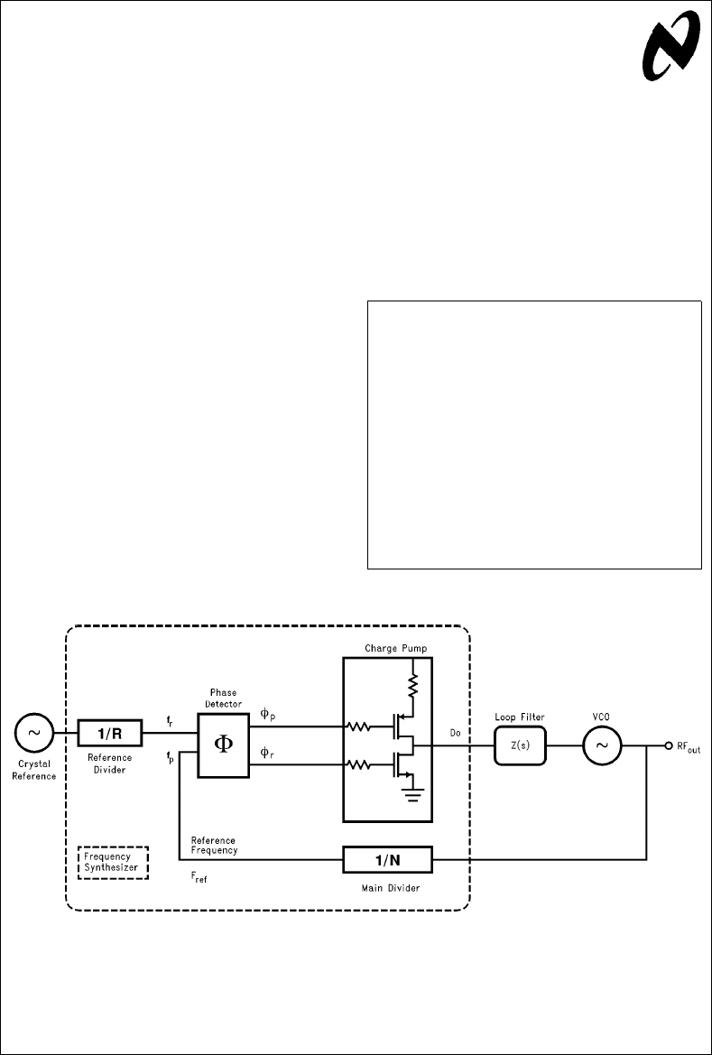
The basic phase-lock-loop configuration we will be consid-
ering is shown in
Figure 1
. The PLL consists of a high-stabil-
ity crystal reference oscillator, a frequency synthesizer such
as the National Semiconductor LMX2315TM, a voltage con-
trolled oscillator (VCO), and a passive loop filter. The fre-
quency synthesizer includes a phase detector, current
mode charge pump, and programmable frequency dividers.
A passive filter is desirable for its simplicity, low cost, and
low phase noise.
In most standard PLL’s there are several design parameters
which can be treated as constant values. This linear approx-
imation provides a good estimation of loop performance.
The values of the PLL filter design constants depend on
the specific application. For example, Kwis determined by
the synthesizer charge pump output current magnitude. The
notation and definitions for these values along with standard
units used throughout this paper are given in Table I below.
TABLE I. PLL Filter Design Constants
Kvco - (MHz/Volt)
Voltage Controlled Oscillator (VCO) Tuning Voltage
constant. The frequency vs voltage tuning ratio.
Kw- (mA/2qrad)
Phase detector/charge pump constant. The ratio of the
current output to the input phase differential.
RFopt - (MHz)
Radio Frequency output of the VCO at which the loop
filter is optimized.
Fref - (kHz)
Frequency of the phase detector inputs. Usually equiva-
lent to the RF channel spacing.
N
Main divider ratio. Equal to RFopt/Fref.
TL/W/12473–1
FIGURE 1. Basic Charge Pump Phase Locked Loop
Reprinted with permission from Argus Business.
PLLatinumTM is a trademark of National Semiconductor Corporation.
C1996 National Semiconductor Corporation RRD-B30M56/Printed in U. S. A. http://www.national.com
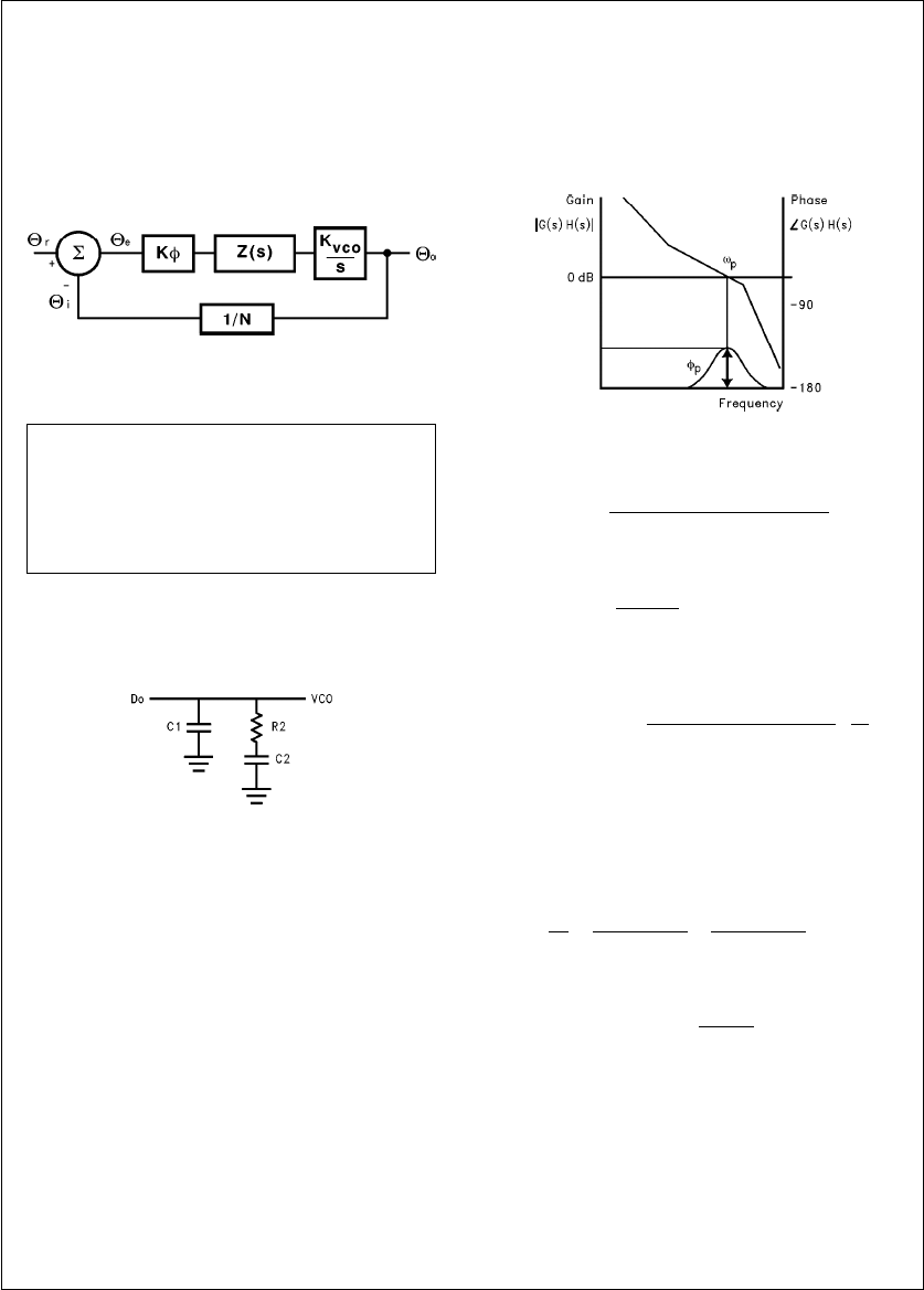
Some basic knowledge of control loop theory is necessary
in order to understand PLL filter dynamics. For a more thor-
ough treatment consult references [1]through [6]. A linear
mathematical model representing the phase of the PLL in
the locked state is presented in
Figure 2
. An additional inte-
grator is needed in the transfer function for the forward gain
and is usually lumped together with the VCO in the litera-
ture, references [1-4]. Using the simplified diagram in
Figure
2
, and feedback theory, one may obtain the equations for
the phase transfer functions presented in Table II.
TL/W/12473–2
FIGURE 2. PLL Linear Model
TABLE II. PLL Phase Transfer Functions
Forward loop gain eG(s) eHo/He
eKwZ(s) Kvco/s
Reverse loop gain eH(s) eHi/Hoe1/N
Open loop gain eH(s) G(s) eHi/He
eKwZ(s)Kvco/Ns
Closed loop gain eHo/HreG(s)/ [1aH(s) G(s)]
The standard passive loop filter configuration for a type II
current mode charge pump PLL is shown in
Figure 3
. The
loop filter is a complex impedance in parallel with the input
capacitance of the VCO, or in other words, a driving point
immitance.
TL/W/12473–3
FIGURE 3. 2nd Order Passive Filter
The phase detector’s current source outputs pump charge
into the loop filter, which then converts the charge into the
VCO’s control voltage. The shunt capacitor C1 is recom-
mended to avoid discrete voltage steps at the control port
of the VCO due to the instantaneous changes in the charge
pump current output. A low pass filter section may be need-
ed for some high performance synthesizer applications that
require additional rejection of the reference sidebands,
known as spurs.
One method of filter design uses the open loop gain band-
width and phase margin to determine the component val-
ues. Locating the point of minimum phase shift at the unity
gain frequency of the open loop response as shown in
Fig-
ure 4
ensures loop stability. The phase relationship between
the pole and zero also allows easy determination of the loop
filter component values. The phase margin, wp, is defined
as the difference between 180§and the phase of the open
loop transfer function at the frequency, 0p, corresponding
to 0-dB gain. The phase margin is chosen between 30§and
70§. When designing for a higher phase margin you trade off
higher stability for a slower loop response time and less
attenuation of Fref. A common rule of thumb is to begin your
design with a 45§phase margin.
TL/W/12473–4
FIGURE 4. Open Loop Response Bode Plot
The impedance of the second order filter in
Figure 3
is
Z(s) es(C2 #R2) a1
s2(C1 #C2 #R2) asC1 asC2 (1)
Define the time constants which determine the pole and
zero frequencies of the filter transfer function by letting
T1 eR2 #C1 #C2
C1 aC2 (2a) T2 eR2 #C2 (2b)
Thus the 3rd order PLL Open Loop Gain in Table II can be
calculated in terms of frequency, 0, the filter time constants
T1 and T2, and the design constants Kw, Kvco, and N.
G(s) #H(s) Àsej#0ebKpd #Kvco (1 aj0#T2)
02C1 #N(1aj0#T1) #T1
T2 (3)
From equation 3 we can see that the phase term will be
dependent on the single pole and zero such that the phase
margin is determined in equation 4. The available phase
margin therefore is proportional to the ratio of C1 and C2.
w(0)etanb1(0#T2) btanb1(0#T1) a180§(4)
By setting the derivative of the phase margin equal to zero
as shown in equation 5,
dw
d0eT2
1a(0#T2)2bT1
1a(0#T1)2e0(5)
the frequency point corresponding to the phase inflection
point is found in terms of the filter time constants T1 and T2.
This relationship is given in equation 6.
0pe1/0T2 #T1 (6)
http://www.national.com 2
To insure loop stability, we want the phase margin to be
maximum when the magnitude of the open loop gain equals
1. Equation 3 then gives
C1 eKpd #Kvco #T1
0p2#N#T2 Ó(1 aj0p#T2)
(1 aj0p#T1) Ó(7)
Therefore, if the loop bandwidth, 0p, and the phase margin,
wp, are specified, equations 1 through 7 allow us to calcu-
late the two time constants, T1 and T2.
The formulas for T1 and T2 are shown in equations 8 and 9.
T1 esec wpbtan wp
0p
(8)
T2 e1
0p2#T1 (9)
From the time constants, T1, T2, and the loop bandwidth,
0p, the values for C1, R2, and C2 are obtained in equations
10 to 12.
C1 eT1
T2 #Kpd #Kvco
0p2#N01a(0p#T2)2
1a(0p#T1)2(10)
C2 eC1 ##T2
T1 b1J(11)
R2 eT2
C2 (12)
Current switching noise in the dividers and the charge pump
at the reference rate, Fref, may cause unwanted FM side-
bands at the RF output. In wireless communications, the
phase detector comparison frequency is generally a multiple
of the RF channel spacing. These spurious sidebands can
cause noise in adjacent channels. Additional filtering of the
reference spurs is often times necessary, depending on
how narrow your loop filter is. This is usually the case in
today’s TDMA digital cellular standards, such as GSM, PDC,
PHS, or IS-54. The sub-millisecond lock times necessary for
switching between channel frequencies makes a relatively
wide loop filter mandatory. For these performance critical
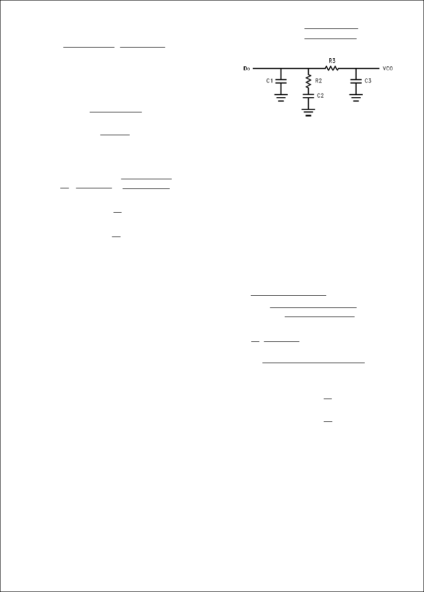
synthesizer applications placing a series resistor and a
shunt capacitor prior to the VCO provides a low pass pole
for more attenuation of unwanted spurs. The use of a pas-
sive loop filter eliminates the noise contributions from an op
amp in an active filter. This is critical due to the strict RMS.
phase error, and integrated phase noise requirements. The
recommended filter configuration is shown in
Figure 5
.
The added attenuation from the low pass filter is:
ATTEN e20 log [(2qFref #R3 #C3)2a1](13)
Defining the additional filter time constant as
T3 eR3 #C3 (14)
Then in terms of the attenuation of the reference spurs add-
ed by the low pass pole we have
T3 e010(ATTN/20) b1
(2q#Fref)2(15)
TL/W/12473–5
FIGURE 5. 3rd Order Lowpass Filter
The additional pole must be lower than the reference fre-
quency, in order to significantly attenuate the spurs, but
must be at least 5 times higher than the loop bandwidth, or
the loop will almost assuredly become unstable. In order to
compensate for the added low pass section, the filter com-
ponent values are recalculated using the new open loop
unity gain frequency, 0c, as in equation 17. The degradation
of phase margin caused by the added low pass is then miti-
gated by slightly increasing C1 and C2 while slightly de-
creasing R2. Note that 0cis slightly k0p, therefore the
frequency jump lock time will increase. Although not exact,
the linear assumptions used in this design technique pro-
vide suprisingly good results for loop filter bandwidths of up
to (/5 of the reference rate. The derivation of 0cis included
in the appendix.
T2 e1/[0c2#(T1 aT3)](16)
0cetan w#(T1 aT3)
[(T1 aT3)2aT1 #T3]c
(17)
Ð01a(T1 aT3)2aT1 #T3
[tan w#(T1 aT3)]2b1(
C1 eT1
T2
Kpd #Kvco
0c2#Nc
(18)
Ð(1 a0c2#T22)
(1 a0c2#T12)(1a0
c
2#T32)((/2
Similar to the 2nd Order filter we have
C2 eC1 ##T2
T1 b1J;(11)
R2 eT2
C2 (12)
The only component values that need to be determined
comprise the added low pass pole. Since these values are
solely determined from equations 13 and 14, their values
are somewhat arbitrary. It is not prudent, however to have a
capacitor value for C3 which is equal to or greater than the
other capacitors. As rule of thumb choose C3 sC1/10,
otherwise T3 will interact with the primary poles of the filter.
Likewise, choose R3 at least twice the value of R2. When
selecting C3 you must also take into account the input ca-
pacitance of the VCO tuning varactor diode which will add in
parallel.
http://www.national.com3
The following example is a typical synthesizer developed for
the Global System Mobile (GSM) digital cellular standard
using the described filter design technique. The RF channel
spacing is 200 kHz, and a typical synthesizer frequency
range is from 865 MHz– 915 MHz. Since the addition of a
low pass filter will reduce the closed loop bandwidth slightly,
select an initial design value which is slightly larger than
desired.
Example
Kvco e20 MHz/V.
Kphi e5mA
RFopt e900 MHz
Fref e200 kHz
NeRFopt/Fref e4500
0pe2q*20 kHz e1.256e5
wpe45§
ATTEN e20 dB
T1 esec wpbtan wp
0p
e3.29
e
b6
T3 e010(20/20) b1
(2q#200
e
3)2
e2.387
e
b6
0ce(3.29
e
b6a2.387
e
b6)
[(3.29
e
b6a2.387
e
b6)2a3.29
e
b6#2.387
e
b6]c
Ð01a(3.29
e
b6a2.387
e
b6)2a3.29
e
b6#2.387
e
b6
[(3.29
e
b6a2.387
e
b6)]2b1(
0ce7.045
e
4
T2 e1
(7.045
e
4)2#(3.29
e
b6a2.387
e
b6) e3.549
e
b5
C1 e3.29
e
b6
3.549
e
b5
(5.0
e
b3) #20
e
a6
(7.045
e
4)2#4500 c
Ð[1a(7.045
e
4)2#(3.549
e
b5)2]
[1a(7.045
e
4)2#(3.29
e
b6)2
ll
1a(7.045
e
)2#(2.39
e
b6)2]((/2
C1 e1.085 nF
C2 e1.085 nF ##3.55
e
b5
3.29
e
b6b1Je10.6 nF;
R2 e3.55
e
b5
10.6
e
b9e3.35 kX;
if we choose R3 e22 kX;
then C3 e2.34
e
b6
22
e
3e106 pF
Converting the calculated numbers to standard component
values gives the filter shown in the test board schematic for
the synthesizer implementation,
Figure 6
.
Test results for the PLL loop filter design using a National
Semiconductor LMX2315 Frequency Synthesizer are shown
in the following pages. A 10 MHz crystal oscillator was used
as the reference oscillator input signal. The supply voltage
was 5V, and the entire current consumption, including the
VCO, was k15 mA.
TL/W/12473–6
FIGURE 6. Test Fixture Schematic
http://www.national.com 4
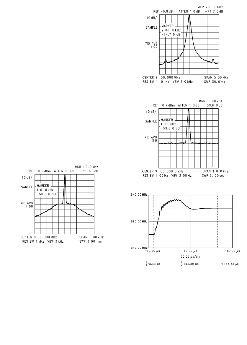
Figures 7
to
9
show HP8566 Spectrum Analyzer measure-
ments of the RF output. The measured closed loop filter
bandwidth is between 15 kHz and 17.5 kHz. The reference
spurious level is s70 dBc, due to the loop filter attenuation
and the low spurious noise level of the LMX2315. The
phase noise level at 1 kHz offset in
Figure 9
is b79.5 dBc/
Hz. This correlates to a phase noise floor of s150 dBc/Hz.
The relatively flat PLL closed loop characteristics gives a
measured RMS. phase error of k2§, and is also an indicator
of good loop stability.
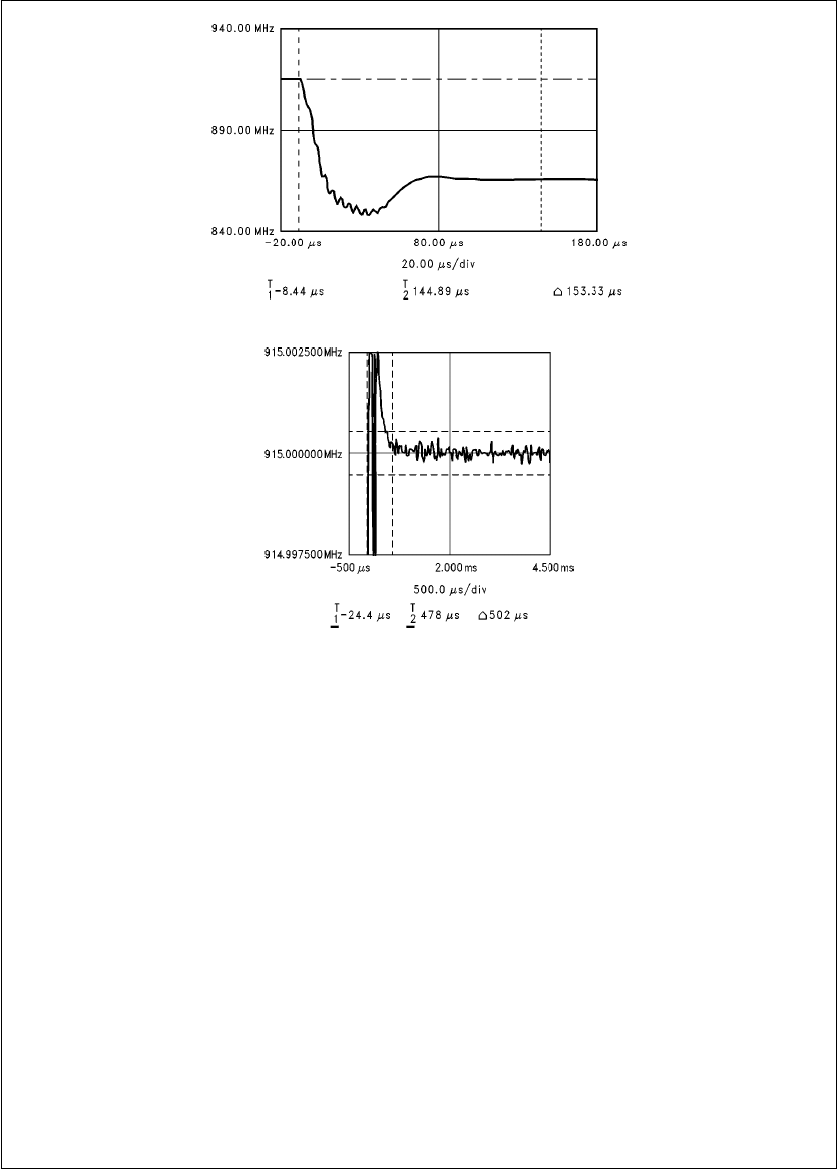
Of concern in any PLL loop filter design is the time it takes
to lock in to a new frequency when switching channels. The
HP53310A Modulation Domain Analyzer plots in
Figures 10
and
11
show the positive and negative switching waveforms
for a frequency jump of 865 MHz– 915 MHz. The well bal-
anced charge pump of the LMX2315 frequency synthesizer
causes the waveforms to be nearly inverted replicas of each
other. Narrowing the frequency span of the HP53310A Mod-
ulation Domain Analyzer enables evaluation of the frequen-
cy lock time to within g500 Hz. The lock time is seen in
Figure 12
to be k500 ms for a frequency jump of 50 MHz.
CONCLUSION
An analysis of a frequency domain design technique for
passive filters in charge pump phase-locked loops was pre-
sented. Measurements of a PLL designed using this method
show good results in a practical synthesizer realization. The
results demonstrate a high performance synthesizer in con-
junction with a passive loop filter provide a fast switching,
low noise frequency source for today’s challenging digital
wireless telecommunications standards.
TL/W/12473–7
FIGURE 7. PLL Output Spectrum 100 kHz span
TL/W/12473–8
FIGURE 8. PLL 200 kHz Reference spurs
TL/W/12473–9
FIGURE 9. PLL Close in Phase Noise
TL/W/12473–12
FIGURE 10. PLL Positive Frequency Jump Waveform
http://www.national.com5
TL/W/12473–11
FIGURE 11. PLL Negative Frequency Jump Waveform
TL/W/12473–10
FIGURE 12. PLL Frequency Jump Lock Time
http://www.national.com 6
APPENDIX
Derivation of
0
c
The impedance of the loop filter shown in
Figure 5
is
ZT(s) e
Z(s) ##1
sC3J
Z(s) aR3 a#1
sC3J(19)
where Z(s) is given by equation 1.
Knowing that C1 t10 C3;
and by substituting T3 eR3 #C3
along with equations 2a, 2b.
simplifies the third order equation for the open loop gain to
G(s) #H(s) Àsej#0
ebKpd #Kvco (1 aj0#T2)
02C1 #N(1aj0#T1) #T1
T2 #1
(1 aj0#T3) (20)
w(0)*(1 a0#T2) #(1 b0#T1) #(1 b0#T3) (21)
Similar to equation 9
T2 e1
02(T1 aT3) (22)
Substituting (22) into (21) gives
w(0)*2b02#T1 #T3 bj0#(T1 aT3) a
j
0#(T1 aT3)
b
j
0#T1 #T3
(T1 aT3) (23)
Thus
tanwe
b0#(T1 aT3) b0#T1 #T3
(T1 aT3) a1
0#(T1 aT3)
2b02#T1 #T3 (24)
Assuming (25)
02#T1 #T2 m2
After some manipulation we arrive at the characteristic equation
02a02 tan w#(T1 aT2)
[(T1 aT3)2aT1 #T3]b1
(T1 aT3)2aT1 #T3 e0(26)
Taking the negative root, and multiplying through gives the expression for the closed loop bandwidth, 0c, equation (20).
0cetan w#(T1 aT3)
[(T1 aT3)2aT1 #T3]#Ð01a(T1 aT3)2aT1 #T3
[tan w#(T1 aT3)]2b1(
REFERENCES
[1]Rohde, Ulrich L.,
Digital PLL Frequency Synthesizers Theory and Design,
Prentice-Hall, 1983
[2]Egan, W.F.,
Frequency Synthesis by Phase Lock,
John Wiley & Sons, 1981.
[3]Best, Roland E.,
Phase-Locked Loops Theory, Design, and Applications,
2nd ed., McGraw-Hill Inc, 1993.
[4]Gardner, F.M.,
Phase-Locked Loop Techniques,
2nd ed., John Wiley & Sons, 1980
[5]Gardner, F.M.,
Charge-Pump Phase-Lock Loops,
IEEE Trans. Commun., vol. COM-28, pp 1849– 1858, Nov 1980
[6]Barker, Cynthia,
Introduction to Single Chip Microwave PLLs,
National Semiconductor Application Note, AN885, March
1993
http://www.national.com7

An Analysis and Performance Evaluation of a Passive Filter
AN-1001 Design Technique for Charge Pump Phase-Locked Loops
LIFE SUPPORT POLICY
NATIONAL’S PRODUCTS ARE NOT AUTHORIZED FOR USE AS CRITICAL COMPONENTS IN LIFE SUPPORT
DEVICES OR SYSTEMS WITHOUT THE EXPRESS WRITTEN APPROVAL OF THE PRESIDENT OF NATIONAL
SEMICONDUCTOR CORPORATION. As used herein:
1. Life support devices or systems are devices or 2. A critical component is any component of a life
systems which, (a) are intended for surgical implant support device or system whose failure to perform can
into the body, or (b) support or sustain life, and whose be reasonably expected to cause the failure of the life
failure to perform, when properly used in accordance support device or system, or to affect its safety or
with instructions for use provided in the labeling, can effectiveness.
be reasonably expected to result in a significant injury
to the user.
National Semiconductor National Semiconductor National Semiconductor National Semiconductor
Corporation Europe Hong Kong Ltd. Japan Ltd.
1111 West Bardin Road Fax:
a
49 (0) 180-530 85 86 13th Floor, Straight Block, Tel: 81-043-299-2308
Arlington, TX 76017 Email: europe.support
@
nsc.com Ocean Centre, 5 Canton Rd. Fax: 81-043-299-2408
Tel: 1(800) 272-9959 Deutsch Tel:
a
49 (0) 180-530 85 85 Tsimshatsui, Kowloon
Fax: 1(800) 737-7018 English Tel:
a
49 (0) 180-532 78 32 Hong Kong
Fran3ais Tel:
a
49 (0) 180-532 93 58 Tel: (852) 2737-1600
http://www.national.com
Italiano Tel:
a
49 (0) 180-534 16 80 Fax: (852) 2736-9960
National does not assume any responsibility for use of any circuitry described, no circuit patent licenses are implied and National reserves the right at any time without notice to change said circuitry and specifications.
