Application Note 1056 STN Using FPD Link AN
User Manual: AN-1056
Open the PDF directly: View PDF ![]() .
.
Page Count: 4
STN Application Using
FPD-Link
INTRODUCTION
The advantages of using the FPD-Link chipset in a notebook
application are to reduce the number of conductors, the size
of the cables, and to allow the system designer to reduce
EMI. Currently some notebook manufacturers are willing to
use STN-DD (Super Twist Neumatic-Dual Drive) panels as
an option for flat panel display over TFT (Thin Film Transis-
tor) panels because they are lower in cost. Therefore, it is
important to show that FPD-Link is able to support STN
panel applications. This application note will explain how a
designer would use FPD-Link to support a 640x480 STN-DD
panel, but higher resolution STN panels can also be imple-
mented with minor changes.
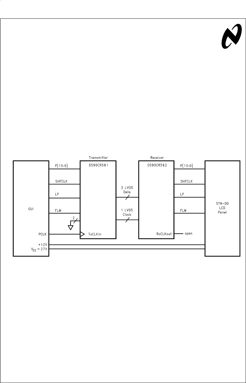
The system connection for the STN-DD panel with FPD-Link
requires a graphics controller connecting to the FPD-Link
transmitter on the motherboard. The receiver is then con-
nected to the transmitter by LVDS lines. The STN panel is
connected to the FPD-Link receiver outputs as shown in
Fig-
ure 1
.
The system connection that was bench verified usedaCand
T 65550 flat panel GUI accelerator, National’s 6-bit color
FPD-Link chipset (DS90CF561/2), and a 640x480 color
STN-DD LCD panel (Sharp LM64C08P). Notice that the
+12V supply and V
EE
(+27V) are connected directly from the
graphics card (50 pin connector) to the STN panel to supply
power to the panel for the back light. The V
EE
must be ad-
justed to +27V (panel specific) by turning a potentiometer
(50 kΩ) on the graphics controller card. The V
DD
(+5V) is
also supplied by the graphics card which powers the
FPD-Link devices and the STN panel. Thus no additional
power rails are required in the application.
TIMING CONSIDERATION
The timing requirement for STN-DD panels is different from
TFT panels because the STN panel uses a SHFCLK which
has a variable frequency — it is not free running — as shown
in
Figure 2
. However, the FPD-Link transmitter and receiver
requires a free running clock (a constant frequency) to allow
the PLL (Phase Lock Loop) to latch and strobe the data bits.
When the PLL is active, the color bits, LP (Horizontal Sync),
and FLM (Vertical Sync) are transferred through the LVDS
data lines. To obtain a free running clock for the FPD-Link,
pin number 102 on either the 65548 or the 65550 GUIs can
be configured and used through software. Pin 102 is titled
PCLK/WEC#and is set to a particular frequency depending
upon the panel being driven. On our bench example, the fre-
quency of the PCLK was set for 25 MHz to support the
640x480 STN-DD panel. The PCLK is passed to the Tx-
CLKin pin (FPD-Link transmitter) for the PLL to be opera-
tional. The receiver also uses the PCLK to strobe the data
bits, but is not required to recreate the PCLK. The STN panel
does not require the PCLK, so the RxCLKout should be left
open as shown in
Figure 1
.
The relationship between the clock signals is shown in
Fig-
ure 2
. The SHFCLK repeats every three data cycles (every
eight PCLK cycles). 16 bits of data are transferred per data
cycle (6 greens, 6 reds, and 4 blues). Thus each data cycle
provides 5-
1
⁄
3
pixels. The reason 8 PCLK cycles are needed
per T-shfclk is to properly capture and recreate the SHFCLK
signal. Note 1 PCLK cycle equals to 1 pulse of the SHFCLK.
By referencing the PCLK, 2 pixels are displayed for each
PCLK cycle and each pixel has 3 data bits. A total of 16 pix-
els and 48 data bits are latched at each T-shfclk. The SHF-
CLK is about 9 MHz and can treated and transferred simi-
larly to a data bit to meet panel requirements with no
problems. Thus the SHFCLK is passed to the receiver on a
data signal pin, not the TxCLKin pin. The receiver recreates
the SHFCLK and this signal is passed to the STN panel. For
AN012879-1
FIGURE 1. STN-DD Panel Application Using FPD-Link Chipset
National Semiconductor
Application Note 1056
Michael Hinh
September 1996
STN Application Using FPD-Link AN-1056
© 1998 National Semiconductor Corporation AN012879 www.national.com

the FPD-Link to sample the data correctly, the edges of the
PCLK and SHFCLK must align at the start of a T-shfclk cycle
as shown in
Figure 2
. If there is skew in the PCLK to data re-
lationship the designer can vary the length of the PCLK line
or add delay elements to shift the clock edge so it will line up
with the data bits correctly.
SOFTWARE/PROGRAMMING CONSIDERATION
In order for the GUI to interface to the STN-DD color panel,
the designer must load the BMP (Bios Modification Program)
VGA BIOS driver so that the data can be seen on the
STN-DD panel after configuration. If the program is not set
for STN-DD panel operation, the designer must modify the
BMP VGA BIOS driver by using the BMP configuration pro-
gram and set the extended register for STN-DD panel con-
figuration. The parameters for 640x480 color STN-DD panel
are defined in the GUI datasheet (i.e. 65548 table #9) re-
garding the 16-bit interface with frame acceleration. Note, it
is important to use the internal frame buffer in order for the
PCLK/WEC#, pin 102, to output the required free-running
clock. If it is set for external frame buffering, this may be dis-
abled by setting FR1A[7] =00 or by setting the frame buffer
to internal in the BMP configuration program. Any modifica-
tion in the VGA BIOS driver must be saved for changes to
take place when the VGA BIOS driver is loaded again.
BIT MAPPING CONSIDERATION
The 6-bit color FPD-Link chipset used in this application is
designed for 21 input bits and a clock input for the PLL. The
640x480 STN-DD panel uses 16-bit color, LP, FLM, SHFCLK
for a total of 19 bits. Two input bits are not used in this appli-
cation and should be tied to ground because floating inputs
may cause unneeded switching on the LVDS lines and in-
creased power dissipation. The mapping of these bits is
shown in
Figure 3
. The bits were mapped this way in order to
isolate color bits from each other. If there are any bits miss-
ing at the panel, the designer can easily troubleshoot the
problem because each LVDS line will correspond to a group
of color bits (R, G, B). Note that in a 16-bit STN application,
blue only supports 4 bits, while green and red are 6 bits
each. The SHFCLK has been mapped to a data bit position
along with the other two control lines.
AN012879-2
FIGURE 2. 640x480 STN-DD Panel PCLK vs. SHFCLK
AN012879-3
FIGURE 3. Timing Information and Bit Mapping for the 640x480 STN-DD Panel
www.national.com 2

CONCLUSION
National’s FPD-Link chipset can easily be used in STN-DD
panel applications with only minor changes to provide the
free-running PCLK signal. This was verified by using a
640x480 STN-DD panel, but higher resolution can also be
achieved by using the 8-bit FPD-Link capable of operating at
higher speed SHFCLK/PCLK. Minor software configuration
changes have to be made to the GUI by the use of a BMP
program. FPD-Link can support a variety of STN-DD panels
at 640x480, 800x600, to 1024x768 resolution. The only dif-
ference between these resolutions are number of bits trans-
ferred and clock frequency, which FPD-Link chipset can sup-
port.
Any GUI accelerator that supports a free-running clock can
be used in a FPD-Link/STN application. This bench testing
verified the STN application using the 65548 and the 65550
GUI devices. However, if the GUI accelerator can not sup-
port this free-running clock an external work around requir-
ing external logic and a PLL can be used to generate this
clock. The designer should check with the GUI manufactur-
ers to verify that it can support the clock needed for a
FPD-Link/STN application.
APPENDIX
Bench Procedure to Program the GUI (65548/65550) for a
free-running clock
1. Load the BMP configuration program to modify the BMP
VGA BIOS driver.
At the prompt: type [BMP32 RAM32.EXE].
2. Use the tab key to move through the 40 pages. On page
3, select the panel that the GUI has to drive, set the ana-
log display boot type to Simultanous boot mode, select
the BUS type (PCI or VL), select the product type. On
page 17, Set the dot clock frequency for simultaneous
display mode. For 640x480 STN panel, DCLK =
25 MHz.
3. On page 6, enter the parameters for SM Boot, which are
defined by C and T datasheet (65548 table #9). The pa-
rameters are in Bold text.
4. On page 20, enter the simultaneous video extended reg-
isters parameters specified by C and T (table #9) to drive
the STN panel that was selected.
5. To obtain a free-running clock. On page 17, set the
frame buffer to internal or embedded. On page 6, enter
the frame buffer control parameter (XR6F-1B).
6. Save the BMP program changes as a RAM32.EXE file.
7. Exit the BMP program and load the VGA BIOS driver. At
the prompt: type [RAM32.EXE], the driver is then loaded
and the STN panel should display the DOS prompt.
8. If the STN panel is not displaying the DOS prompt, then
turn off the computer and reload the BMP Program to
modify the VGA BIOS driver because the configuration
was not correctly set.
www.national.com3

LIFE SUPPORT POLICY
NATIONAL’S PRODUCTS ARE NOT AUTHORIZED FOR USE AS CRITICAL COMPONENTS IN LIFE SUPPORT DE-
VICES OR SYSTEMS WITHOUT THE EXPRESS WRITTEN APPROVAL OF THE PRESIDENT OF NATIONAL SEMI-
CONDUCTOR CORPORATION. As used herein:
1. Life support devices or systems are devices or sys-
tems which, (a) are intended for surgical implant into
the body, or (b) support or sustain life, and whose fail-
ure to perform when properly used in accordance
with instructions for use provided in the labeling, can
be reasonably expected to result in a significant injury
to the user.
2. A critical component in any component of a life support
device or system whose failure to perform can be rea-
sonably expected to cause the failure of the life support
device or system, or to affect its safety or effectiveness.
National Semiconductor
Corporation
Americas
Tel: 1-800-272-9959
Fax: 1-800-737-7018
Email: support@nsc.com
www.national.com
National Semiconductor
Europe Fax: +49 (0) 1 80-530 85 86
Email: europe.support@nsc.com
Deutsch Tel: +49 (0) 1 80-530 85 85
English Tel: +49 (0) 1 80-532 78 32
Français Tel: +49 (0) 1 80-532 93 58
Italiano Tel: +49 (0) 1 80-534 16 80
National Semiconductor
Asia Pacific Customer
Response Group
Tel: 65-2544466
Fax: 65-2504466
Email: sea.support@nsc.com
National Semiconductor
Japan Ltd.
Tel: 81-3-5620-6175
Fax: 81-3-5620-6179
AN-1056 STN Application Using FPD-Link
National does not assume any responsibility for use of any circuitry described, no circuit patent licenses are implied and National reserves the right at any time without notice to change said circuitry and specifications.
