Application Note 1085 FPD Link PCB And Interconnect Design In Guidelines AN
User Manual: AN-1085
Open the PDF directly: View PDF ![]() .
.
Page Count: 11
FPD-Link PCB and
Interconnect Design-In
Guidelines
INTRODUCTION
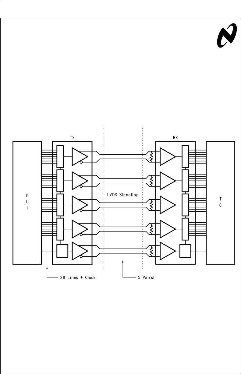
The Flat Panel Display Link (FPD-Link) Transmitter’s func-
tion is to convert a wide parallel TTL bus into a smaller faster
LVDS interface, and the Receiver’s function is to recover the
data and re-generate the wide TTL bus. The system block
diagram is shown in
Figure 1
. FPD-Link delivers multiple
benefits to Notebook and Monitor LCD applications. These
include the following: The smaller LVDS interface is simpler
to route between the motherboard and the LCD panels (i.e.,
through the hinge). The LVDS drivers are capable of driving
long cables at high speeds for monitor applications. The
smaller cables and connectors (up to 80%reduction in the
number of required conductors) are lower cost since they are
physically smaller. LVDS supports higher bandwidth service
with a reduction in EMI due to the differential scheme (odd
mode), the reduced signal swing (only z300 mV), and the
use of current mode drivers (soft transitions, and reduced
spikes). To gain the maximum benefits of LVDS and FPD-
Link high speed PCB and interconnect design is
required
.
This application note focuses on the requirements of the
PCB and interconnect to provide an error free, low emission
LVDS interface.
FUNCTION OF THE TX
The Transmitter (TX) accepts the wide parallel (21-bit or 28-
bit) TTL bus and converts it to 3 or 4 higher speed serialized
LVDS data streams. To operate the TX only data and clock
must be applied. The chip does not require control signals,
as it provides transparent data transmission. Depending
upon the device used, the data on the TX inputs is strobed
into the TX on either the rising or falling edge of the clock sig-
nal. The particular edge is noted within the device ID with “R”
or “F” respectively. Some devices provide a pin to select R or
F operation (e.g., DS90C383/A). The clock is then fed to a
PLL type circuit that is used to generate strobes that inter-
nally clock out the serialized LVDS data streams. A power-
down pin is also supported. Asserting this pin shuts down the
PLL and also puts the driver outputs into TRI-STATE®. This
mode disables the LVDS load loop current and also reduces
I
CC
to µAs, saving power when the display is not needed.
LOCATION OF TX ON PCB
The transmitter should be located as close to the interface as
possible
(
see
Figure 2)
. This is done to minimize the PCB
LVDS overall trace length (see following section on differen-
tial traces) and thus skew as well. Skew is generally propor-
tional to length, thus a shorter interconnect nominally has
less skew associated with it. If the TX is located within 2
inches of the connector, mitering (trace length compensation
TRI-STATE®is a registered trademark of National Semiconductor Corporation.
AN100098-1
FIGURE 1. Link System Block Diagram
National Semiconductor
Application Note 1085
John Goldie
June 1999
FPD-Link PCB and Interconnect Design-In Guidelines AN-1085
© 1999 National Semiconductor Corporation AN100098 www.national.com
to generate zero skew) is not required. If the TX is more than
2 inches away, mitering should be employed. Also, it is not a
requirement of the TX device to be located adjacent to the
GUI device. Recall the GUI-TX interface is a slow speed bus
(compared to the LVDS bus) and has less timing constraints.
However, the connection between the GUI and the TX
should be designed such that the parallel RGB traces are
also of equal length to avoid excessive skew and a resulting
set-up or hold violation at the TX input pins. In the extreme
case (if electrical length is >1/2 rise time), signal termination
may be required on the GUI interface. Note, the RGB data
lines are level sensitive only, while the clock line is edge sen-
sitive. If the interconnect between the GUI and the TX is
long, (becomes as a transmission line), termination for the
clock (FPSHIFT) signal should be considered.
TX GROUND AND POWER
The TX is a high speed— high performance device. The de-
vice includes a PLL type circuit that operates at ƒ or 3.5Xƒ
MHz (device specific, where ƒ is the clock frequency) and
LVDS drivers that toggle in the hundreds of Megabits per
second range (up to 455 Mbps 65MHz clock rate!). This re-
quires a solid ground and power distribution reference for the
device. V
CC
noise should not exceed 100 mV
pp
. If it does,
separated power and ground planes should be used for the
PLLV
CC
and PLLGND pins. To enable good power/ground
reference a minimum of a 4 layer PCB is recommended. Two
sided boards or flex circuit are generally not recommended
for placement of the TX or RX devices. EMI emission control
starts with solid power and ground planes. If the TX is an op-
tion to the application and is intended to be located on a
small daughter card, the daughter card should also be 4 lay-
ers and employ multiple connections to power and ground
(low impedance connection).
TX BYPASS
The TX includes three separate V
CC
(power supply) and
GND references. These are for the digital logic, LVDS driv-
ers, and PLL portions of the chip. To obtain supply noise of
less than 100 mV
pp
; close by-passing is required. Do not lo-
cate by-pass capacitors at the end of small traces, rather
connect them adjacent to the device pins as close as pos-
sible. Bulk capacitance of 4.7 µF to 10 µF should also be
near by. Wide traces with multiple power/GND via (2 are rec-
ommended) should be employed on bypass connections.
The ideal case would use 0.1 µF//0.01 µF//0.001 µF capaci-
tors on each supply pin. If space is restricted do not eliminate
the PLL by-passing as this is most critical of low noise opera-
tion. 0805 or 1206 chip capacitors are recommended as they
offer the lowest inductance and can be mounted very close
to the device pins. With this type of layout, parasitic induc-
tance will be in the 1.5 nH to 2 nH range, where as locating
the capacitor at the end of a short narrow trace can have an
inductance as high as 15 nH! Using multiple capacitors in
parallel provides good bypassing across a wider range of
frequency, also the ESR is lowered and a low impedance at
high frequency is provided.
GUI — TX INTERFACE
The connection between the GUI controller and the TX de-
vice should utilize standard PCB design techniques. The
data (R, G, and B), control, and clock lines should all be of
equal length in order to prevent any skew being introduced
between clock and data. As with any clock line, signal quality
is of concern. Avoid unnecessary via, sharp bends or other
discontinuities. A direct point-to-point link is best for the clock
and its signal quality. Other clock signals should be kept
away from the clock and data lines to avoid unwanted cou-
pling. Provision for termination may be required on the Clock
signal at the TX input. If the GUI has drive level options
(6 mA–8 mA or 12 mA modes, device specific), testing has
shown that operating the clock in high drive and the data in
AN100098-2
FIGURE 2. TX and RX Location
www.national.com 2

low offers the best balance between clock signal quality
(sharp) and noise generation from the GUI data output pins.
Unused TX input pins should be tied to GND on the5Vse-
ries and may be left floating or tied to GND on the 3.3 V se-
ries to prevent unwanted switching and the lowest chip
power dissipation. The 3.3 V devices feature internal pull
down resistors on the inputs (see datasheets).
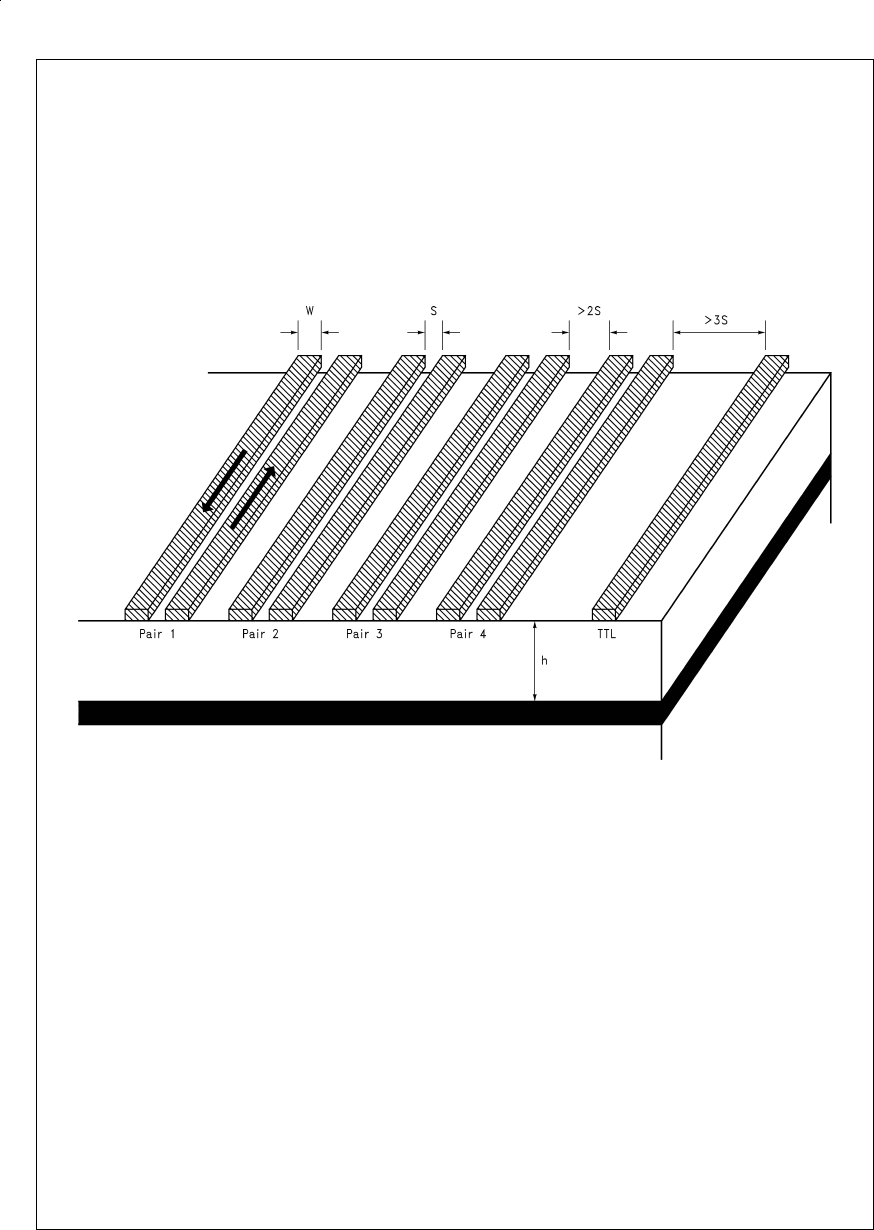
TX — CONNECTOR INTERFACE
The traces that connect the TX LVDS outputs to the connec-
tor should be minimized in length as discussed above in the
section on TX Location. In addition TTL/CMOS single-ended
lines should be located on a different signal layer or kept
away (at least “3S”) from the LVDS lines to minimize any
coupling of noise onto the LVDS lines and out onto the inter-
connect as shown in
Figure 3
. Guard ground traces may be
placed between the LVDS lines and the other signals to fur-
ther isolate the two, once again they should be at least 2S
away from the closely-coupled differential pair. Corruption of
LVDS data is not an issue due to the receiver’s common
mode rejection; minimizing common mode noise (EMI) is the
reason for the spacing and isolation. Unused LVDS driver
output pins should be left open, as this will minimize power
dissipation.
www.national.com3
The use of true differential traces further enhances the noise
rejection capabilities of differential data transmission and re-
duces / limits the generation of unwanted emissions. Differ-
ential traces are recommended for use on the LVDS output
of the TX (and input to the receiver also). They differ only
slightly from standard PCB traces. The distance between the
two signal traces (“S”) that compose the differential pair is
also controlled (minimized). This distance is critical to specify
correctly as it is related to both the differential-mode charac-
teristic impedance of the trace pair and also related to the
differential noise margin of the system. Standard traces are
laid out for 50Ωimpedance. Two traces separated far apart
from each other will present a differential mode characteristic
impedance of twice the single-ended impedance, but will not
AN100098-3
FIGURE 3. LVDS PCB Layout
www.national.com 4
provide the maximum noise rejection benefit and defeat the
differential signaling. The spacing between the traces should
be kept to a minimum to maximize the differential noise re-
jection (differential noise margin is equal to the minimum sig-
nal swing less the maximum receiver thresholds
(250 mV–100 mV = 150 mV)). This minimum distance be-
tween the traces of a pair assures that any external noise
coupled onto the pair will be seen as common mode, and re-
jected by the receivers. To adjust trace impedance set “S” to
a minimum spacing between metal lines), and adjust the
width of the trace to the desired impedance (see AN-905 for
equations). When the two lines are close, the differential im-
pedance is no longer twice the single-ended impedance (it is
a factor of <2). The distance between adjacent LVDS differ-
ential pairs should be at least 2S or greater as shown in
Fig-
ure 4
. The distance between an LVDS signal and a large
swing TTL or CMOS signal should be 3S or more, or even
better the TTL/CMOS signaling should be located on a differ-
ent signal plane. The electrical length of the LVDS traces
should be matched to minimize any skew created in the path
between TX and RX. Lastly, it is desirable to have S <h,
again ensuring that maximum coupling occurs between the
pair and not with the plane below.
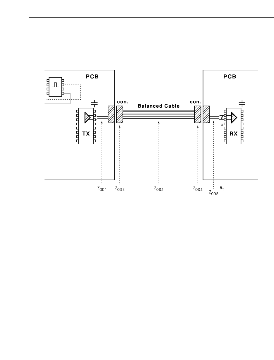
Microstrip traces (outside layer) are usually employed for
this interconnect. The microstrip geometry and the fact that
the traces are on the outer layer enable higher impedances
more easily. It is also possible to design the interconnect
without any via, thus a better signaling environment. On the
down side, stripline (embedded) traces offer greater shield-
ing due to their encasement. Either microstrip or stripline
traces can be used, as long as they are matched to the ca-
ble’s differential-mode characteristic impedance. This is
shown in
Figure 2
where Z
OD1
represents the TX PCB im-
pedance and Z
OD3
is the cable (interconnect) impedance. It
is recommended that all impedances should be within 10%
of the target impedance (typically 100Ω) to minimize any re-
flections. Note that a 10%difference in impedance will cre-
ate a reflection of 5%. Reducing the magnitude of reflections
will lower the EMI of the system.
THE INTERCONNECT
LVDS drivers and receivers are intended to operate on a
wide variety of media. Depending upon the system’s needs
the media may vary due to a number of parameters includ-
ing: length of interconnect, amount of shielding required, di-
mensions of the hinge that the cable must pass through
(notebook application), and of course cost. FPD-Link (LVDS)
has been demonstrated on flat ribbon cable, FEC (flex) inter-
connect, shielded twisted pair, and twin axial cables. An im-
portant parameter to understand is the differential-mode
characteristic impedance of the media. For many common
cables this is typically about 100Ω(see cable datasheet). As
discussed above to minimize any common mode noise gen-
eration the TX PCB interconnect, the interconnecting media,
the RX PCB interconnect, and the termination should all
match (within 10%) in characteristic impedance (differential
mode). Electrical length of the data and clock signals should
be of equal length. Conductors of different length composing
a pair will cause a modulation of common mode and radiate
more. Pairs of different length will impact the receivers data
recovery by impacting the correct strobing of data. Remem-
ber that the timing of the LVDS data line is 7X tighter than of
the TTL bus. The amount of tolerable skew between any two
conductors is clock speed dependent, but should be kept to
less than 100 ps–350 ps (data rate dependent, 65
MHz–32.5 MHz). On a typical high performance cable (3M
MDR) skew is specified at only 30 ps/meter. For flex circuit
interconnects, similar design recommendations as dis-
cussed in the “TX — connector interface” section above
AN100098-4
FIGURE 4. Differential Trace Spacing
www.national.com5
should be employed. Even through LVDS operates as true
odd-mode differential drivers, a signal common (Ground)
connection is required between the two systems to establish
a common-mode return path. The bulk of the LVDS load cur-
rent is returned to the driver within the pair as LVDS is a true
odd-mode differential driver unlike some less superior solu-
tions. This is very important for emission reasons, as the
closely-coupled differential pair creates a small ring antenna,
compared to a ON/OFF differential driver that returns current
via the PWR or GND connections (thus creating a larger ring
antenna). However, for common mode return, a signal com-
mon connection of low impedance is required for low emis-
sion operation. Typically assigning one pair (two conductors)
is sufficient for this purpose (as it has 1/2 the DCR of a single
line). Shield ground references should be tied off to quiet
ground references, typically frame ground at each end if em-
ployed. FPD-Link (LVDS) may be used on a wide variety of
media from flat cable to twin-ax to standard twisted pair
cables. Length is a factor of cable performance, balance,
and skew, thus application dependent.
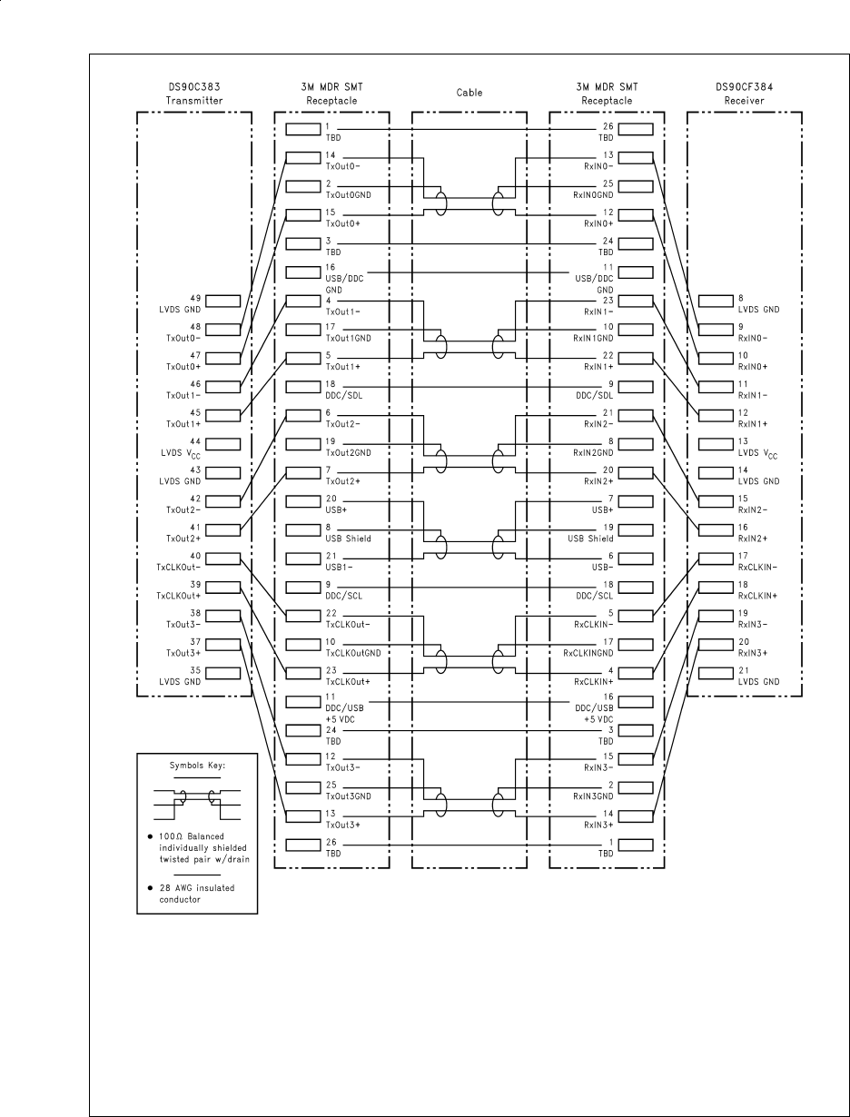
CONNECTORS
For intra-box applications (motherboard to panel in a note-
book) the connector is typically very small since it is internal
to the box and is only connected upon assembly of the sys-
tem. These connectors have the advantage that they do not
adversely effect the signal quality greatly, since they are
electrically small and present more of a small lumped load to
the signal.
Larger connectors used between boxes (desktop PC to ex-
ternal monitor application) are more critical since they are
electrically long and may react as a transmission line seg-
ment. High performance connectors are available that pro-
vide controlled impedance and matched electrical length of
the pins (no skew). The 3M MDR system is one such cabling
system that meets the needs of the application for cable and
connector requirements. It offers a zero skew SMT connec-
tor, controlled impedance, low crosstalk, and very low skew
(see reference in the appendix). Other connectors that have
been employed include standard SCSI connectors, and also
DB15 connectors.
TERMINATION
The use of a termination resistor is required. Due to the high
speed edge rates of LVDS drivers a matched termination will
prevent the generation of any signal reflections, and reduce
EMI. Termination is typically implemented with a single sur-
face mount resistor connected across the signal pair as
close to the receiver inputs as possible (no more than 1/2
inch away if the termination is placed in front of the receiver
inputs). If the resistor is too far away from the receiver inputs,
the line between the resistor and the receiver input takes on
transmission line behavior and reflections may occur at the
receiver inputs defeating the purpose of the termination re-
sistor altogether! Also the use of an external resistor allows
for a variety of media to be used. Since characteristic imped-
ance is media dependent, the proper termination resistance
may be employed to match the particular application. The re-
sistor should be selected to within 2%of the nominal differ-
ential impedance (100Ω) of the media. If PCB space is tight,
a fly-by termination may also be used. The two termination
methods are shown in
Figure 5
. In either case the resulting
stub should be kept as short as possible.
Note: The
complete
interconnect between the TX output and the RX input is a high speed transmission line. Driver edge rates are in the 300 ps–700 ps range. The
TX PCB traces, connectors, cable media, and RX PCB traces are all part of the system. Their impedances should be matched within 10%to maintain signal
quality and generate the lowest amount of emissions. There are 4–6 impedances to consider, depending upon the application (the size of the connector).
These are shown in
Figure 2
as ZOD1,Z
OD2,Z
OD3,Z
OD4 ,Z
OD5, and RT. Also, minimize extra transitions (board or layer transitions, etc.) here to make this
total interconnect as clean as possible.
FUNCTION OF THE RX
The Receiver (RX) accepts the 3 or 4 high speed serialized
LVDS data streams and converts them back to a wide paral-
lel TTL bus. The RX device is the complementary function to
the TX device. Depending upon the device used, the data on
the RX output is strobed by the RxclkOUT on either the rising
or falling edge of the clock signal. The particular edge is
noted within the device ID with an “R” or “F” respectfully. All
devices (R & F) utilize the rising edge of the LVDS Clock sig-
nal to strobe the data on the RX LVDS data inputs. A power-
down pin is also supported. Asserting this pin shuts down the
PLL and also locks the RX outputs to the current state or low
state (device specific, see datasheets). This mode saves
power when the display is not needed.
LOCATION OF RX ON PCB/PANEL SIDE
The receiver should be located close to the interface con-
nector as shown in
Figure 2
. This is done to minimize the
PCB LVDS trace length. (See the section on differential
traces.) It is not a requirement of the RX device to be located
adjacent to the timing controller. The connection between the
timing controller and the RX should be designed such that
the parallel RGB traces are of equal length to avoid skew
and a resulting set-up or hold violation at the timing controller
input pins.
AN100098-5
FIGURE 5. Termination Layout — Standard and Fly-By
www.national.com 6
CONNECTOR — RX INTERFACE
The PCB traces that connect the LVDS lines from the con-
nector to the termination resistor and RX inputs should be
minimized in length as discussed above in the section on TX
Location for the same reasons. In addition any TTL/CMOS
single-ended line should be located on a different signal
layer or kept away from the LVDS lines to limit any coupling
of noise onto the LVDS lines and back out onto the intercon-
nect. Guard ground traces may be placed between the LVDS
lines and other signals to further isolate the two. Corruption
of LVDS data is not an issue due to the receiver’s common
mode rejection, minimizing common mode noise (EMI) is the
reason for the isolation. The use of true differential traces fur-
ther enhances the noise rejection capabilities of differential
data transmission. Differential traces are recommended for
use on the LVDS input of the RX (and output of the drivers).
They differ only slightly from standard PCB traces. The dis-
tance between the two signal traces that compose the differ-
ential pair is also controlled. This distance is critical to
specify correctly as it is related to both the differential-mode
characteristic impedance of the pair and also related to the
differential noise margin of the system and emissions. Stan-
dard traces are laid out for 50Ωimpedance. Two traces
separated far apart from each other will present a differential
mode characteristic impedance of twice the single-ended im-
pedance but will not provide the maximum noise rejection
benefit and defeat the differential signaling. The spacing be-
tween the traces should be kept to a minimum to maximize
the differential noise rejection (differential noise margin is
equal to the minimum signal swing less the maximum re-
ceiver thresholds (250 mV–100 mV = 150 mV)). This mini-
mum distance between the traces of a pair assures that any
external noise coupled onto the pair will be seen as common
mode, and rejected by the receivers. To adjust trace imped-
ance set “S” to a minimum, and adjust the width of the trace
to the desired impedance (see AN-905 for equations). The
distance between adjacent LVDS differential pairs should be
at least 2S or greater. The distance between a LVDS signal
and a large swing TTL or CMOS signal should be 3S or
more, or even better the TTL/CMOS signaling should be lo-
cated on a different signal plane. The electrical length of the
LVDS traces should be matched to minimize any skew cre-
ated in the path between TX and RX. (See figures in the TX
section.)
RX GROUND AND POWER
The RX is a high speed high performance device. The de-
vice includes a PLL circuit that operates at ƒ (where ƒ is the
clock frequency) MHz and accepts LVDS data in the hun-
dreds of Megabits per second range. This requires a solid
ground and power distribution reference to the device. V
CC
noise should not exceed 100 mV
pp
. To enable good power/
ground reference a minimum of a 4 layer PCB is required.
Two sided boards or flex circuit are generally not recom-
mended. EMI emission control starts with solid power and
ground planes.
RX BYPASS
The RX includes three separate V
CC
(power supply) and
GND references. These are for the digital logic, LVDS receiv-
ers, and PLL portions of the chip. To obtain supply noise of
less than 100 mV
pp
close by-passing is required. Do not lo-
cate by-pass capacitors at the end of small traces, rather
connect them adjacent to the device pins as close as pos-
sible. Bulk capacitance of 4.7 µF to 10 µF should also be
near by. Wide traces with multiple power/GND via (2 are rec-
ommended) should be employed on bypass connections.
The ideal case would use 0.1 µF//0.01 µF//0.001 µF capaci-
tors on each supply pin. If space is restricted do not eliminate
the PLL by-passing as this is most critical of low noise opera-
tion. 0805 or 1206 chip capacitors are recommended as they
offer the lowest inductance and can be mounted very close
to the device pins. With this type of layout, parasitic induc-
tance will be in the 1.5 nH to 2 nH range, where as locating
the capacitor at the end of a short narrow trace can have an
inductance as high as 15 nH! Using multiple capacitors in
parallel provides good bypassing across a wider range of
frequency, also the ESR is lowered and a low impedance at
high frequency is provided.
RX — TIMING CONTROLLER INTERFACE
The connection between the RX and the timing controller
should utilize standard PCB design techniques. The data
lines (R, G, and B), control, and clock should all be of equal
length in order to prevent any skew being introduced be-
tween clock and data. As with any clock line, signal quality is
of concern. Avoid unnecessary via, sharp bends or other dis-
continuities. A direct point to point link is best for the clock
and its signal quality.
RECOMMENDED COLOR BIT MAPPING
A recommended bit mapping is provided in
Tables 1, 2
and
also graphically shown in
Figure 6
.
Table 1
lists the RGB bit
numbers, TX input pin name, TX input pin number, RX output
pin name, and RX output pin number for 8-bit color mapping.
This is recommended for use with the DS90C383/A and
DS90CF384 (56-lead TSSOP package) devices.
Table 2
lists the same information for 6-bit color mapping. This is rec-
ommended for use with the DS90C363/A and DS90CF364
(48-lead TSSOP package) devices. Note that this mapping
allows for direct inter-operation of 8-bit color TX with a 6-bit
RX device. The additional resolution bits for 8-bit graphics
are located on LVDS data channel 3 (TxOUT3+ and
TxOUT3−) and are the LSBs.
TABLE 1. Recommended 8-Bit Color Mapping (for 56L Devices)
Color Bit TX Input Name TX Pin Number RX Input Name RX Pin Number
R0-LSB+2 TxIN0 51 RxOUT0 27
R1 TxIN1 52 RxOUT1 29
R2 TxIN2 54 RxOUT2 30
R3 TxIN3 55 RxOUT3 32
R4 TxIN4 56 RxOUT4 33
R5-MSB TxIN6 3 RxOUT6 35
R6-LSB TxIN27 50 RxOUT27 7
www.national.com7
TABLE 1. Recommended 8-Bit Color Mapping (for 56L Devices) (Continued)
Color Bit TX Input Name TX Pin Number RX Input Name RX Pin Number
R7-LSB+1 TxIN5 2 RxOUT5 34
G0-LSB+2 TxIN7 4 RxOUT7 37
G1 TxIN8 6 RxOUT8 38
G2 TxIN9 7 RxOUT9 39
G3 TxIN12 11 RxOUT12 43
G4 TxIN13 12 RxOUT13 45
G5-MSB TxIN14 14 RxOUT14 46
G6-LSB TxIN10 8 RxOUT10 41
G7-LSB+1 TxIN11 10 RxOUT11 42
B0-LSB+2 TxIN15 15 RxOUT15 47
B1 TxIN18 19 RxOUT18 51
B2 TxIN19 20 RxOUT19 53
B3 TxIN20 22 RxOUT20 54
B4 TxIN21 23 RxOUT21 55
B5-MSB TxIN22 24 RxOUT22 1
B6-LSB TxIN16 16 RxOUT16 49
B7-LSB+1 TxIN17 18 RxOUT17 50
ENABL TxIN26 30 RxOUT26 6
VSYNC TxIN25 28 RxOUT25 5
HSYNC TxIN24 27 RxOUT24 3
RESERVED TxIN23 (Note 1) 25 RxOUT23 2
Note 1: Connect TxINPUT23 to ground if unused.
TABLE 2. Recommended 6-Bit Color Mapping (for 48L Devices)
Color Bit TX Input Name TX Pin Number RX Input Name RX Pin Number
R0-LSB TxIN0 44 RxOUT0 24
R1 TxIN1 45 RxOUT1 26
R2 TxIN2 47 RxOUT2 27
R3 TxIN3 48 RxOUT3 29
R4 TxIN4 1 RxOUT4 30
R5-MSB TxIN5 3 RxOUT5 31
G0-LSB TxIN6 4 RxOUT6 33
G1 TxIN7 6 RxOUT7 34
G2 TxIN8 7 RxOUT8 35
G3 TxIN9 9 RxOUT9 37
G4 TxIN10 10 RxOUT10 39
G5-MSB TxIN11 12 RxOUT11 40
B0-LSB TxIN12 13 RxOUT12 41
B1 TxIN13 15 RxOUT13 43
B2 TxIN14 16 RxOUT14 45
B3 TxIN15 18 RxOUT15 46
B4 TxIN16 19 RxOUT16 47
B5-MSB TxIN17 20 RxOUT17 1
ENABL TxIN20 25 RxOUT20 5
VSYNC TxIN19 23 RxOUT19 4
HSYNC TxIN18 22 RxOUT18 2
www.national.com 8
RECOMMENDED CONNECTOR PINOUT
For monitor applications where the system (PC) is provided
by one manufacturer and the Flat Panel Display is provided
by another a standardized connector (mechanical specifica-
tions and pinout) is required along with the standardized
color bit mapping to ensure inter-operation. As noted above
the 3M MDR High Speed Differential Transmission system is
an ideal cable for this application from a skew, impedance,
and connector point of view for long cables (10 meter). The
26 position connector is becoming popular for use with a
FPD-Link digital interface supporting 6-bit or 8-bit color.
Enough contacts are provided to also support DDC/SDL and
USB along with power and ground lines and a few spares.
This pinout is referred to in the 3M documentation as the
F26-7 pinout for use with version 9.3 MDR cable (p/n 14526-
EZ8B-XXX-07C Series). This pinout is shown in
Figure 7
.In
addition a standardization effort in under way to specify a 28
position connector and a variety of cable media (standard
twisted pair cables to twin-ax cables - application
dependent).
AN100098-6
FIGURE 6. Recommended Color Bit Mapping
www.national.com9
SUMMARY
High speed PCB and Interconnect design practices should
be employed to ensure an error free low emission design for
the FPD-Link devices. The interconnect is a transmission
line due to the high speed edge rates of the LVDS signals
(500 ps typical). Tight skew control is required to minimize
emissions and proper data recovery of the RX devices.
Matching impedances within 10%is recommended to re-
duce the creation of reflections (even mode) along the
interconnect/cable.
AN100098-7
FIGURE 7. 26-Pin MDR Pinout
www.national.com 10

GENERALIZED PCB RECOMMENDATIONS OF LVDS
AND LINK APPLICATIONS
LVDS features fast edge rates, therefore the interconnect
between transmitters and receivers will act as a transmission
line. The PCB traces that form this interconnect must be de-
signed with care. The following general guidelines should be
adhered to:
•Hand route or review very closely auto-routed traces.
•Locate the Transmitters and Receivers close to the con-
nectors to minimize PCB trace length for off PCB applica-
tions.
•Traces should be designed for differential impedance
control (space between traces needs to be controlled).
See AN-905 for equations.
•Minimize the distance between traces of a pair to maxi-
mize common mode rejection.
•Place adjacent LVDS trace pairs at least twice (>2S) as
far away (as the distance between the conductors of the
pair).
•Place TTL/CMOS (large dV signals) far away from LVDS,
at least three times (>3S) away or on a different signal
layer.
•Match electrical length of all LVDS lines.
•Keep stubs as short as possible.
•Avoid crossing slots in the ground plane.
•Avoid 90˚ bends (use two 45s).
•Minimize the number of via on LVDS traces.
•Maintain equal loading on both traces of the pair to pre-
serve balance.
•Match impedance of PCB trace to connector to media
(cable) to termination to minimize reflections (emissions)
for cabled applications (typically 100Ωdifferential mode
impedance).
•Select a termination resistor to match the differential
mode characteristic impedance of the interconnect, 2%
tolerance is recommended.
•Locate the termination within 1/2 (<1) inch of the receiver
inputs if not using a fly-by termination method.
•Use surface mount components to minimize parasitic L
and C for bypass caps and termination resistors.
•Use a 4 layer PCB (minimum).
•Bypass each LVDS package at the device pin (Bulk by-
pass nearby also) with parallel capacitors (0.1 µF//0.01
µF//0.001 µF) on each of the supply pins (V
CC
, LVDS
V
CC
, and PLL V
CC
).
APPENDIX
Related FPD-Link and LVDS Application Notes from Na-
tional:
AN-XXX Topic
AN-1032 Introduction to FPD-Link
AN-1035 PCB Design Recommendations
AN-1056 STN Panel Applications
AN-1059 SKEW and Jitter Calculations
AN-1084 Links in Parallel
AN-905 Differential Impedance Calculations
Related Application Notes
High speed LVDS Transmission Information:
High Performance Shielded Twin-ax Cable Assembly, Part
Number 14526
SMT R/A Receptacle (26 position), Part Number 10226-
1210VE
3M Tech Paper: “Selecting the “Right” Right Angle Intercon-
nects: Surface Mount vs Through-hole” by Francis G. Hart
3M Electronics products Division, Austin, Texas; Kay To-
hyama, Yamagata 3M Limited, Yamagata, Japan.
LIFE SUPPORT POLICY
NATIONAL’S PRODUCTS ARE NOT AUTHORIZED FOR USE AS CRITICAL COMPONENTS IN LIFE SUPPORT
DEVICES OR SYSTEMS WITHOUT THE EXPRESS WRITTEN APPROVAL OF THE PRESIDENT AND GENERAL
COUNSEL OF NATIONAL SEMICONDUCTOR CORPORATION. As used herein:
1. Life support devices or systems are devices or
systems which, (a) are intended for surgical implant
into the body, or (b) support or sustain life, and
whose failure to perform when properly used in
accordance with instructions for use provided in the
labeling, can be reasonably expected to result in a
significant injury to the user.
2. A critical component is any component of a life
support device or system whose failure to perform
can be reasonably expected to cause the failure of
the life support device or system, or to affect its
safety or effectiveness.
National Semiconductor
Corporation
Americas
Tel: 1-800-272-9959
Fax: 1-800-737-7018
Email: support@nsc.com
National Semiconductor
Europe Fax: +49 (0) 1 80-530 85 86
Email: europe.support@nsc.com
Deutsch Tel: +49 (0) 1 80-530 85 85
English Tel: +49 (0) 1 80-532 78 32
Français Tel: +49 (0) 1 80-532 93 58
Italiano Tel: +49 (0) 1 80-534 16 80
National Semiconductor
Asia Pacific Customer
Response Group
Tel: 65-2544466
Fax: 65-2504466
Email: sea.support@nsc.com
National Semiconductor
Japan Ltd.
Tel: 81-3-5639-7560
Fax: 81-3-5639-7507
www.national.com
FPD-Link PCB and Interconnect Design-In Guidelines AN-1085
National does not assume any responsibility for use of any circuitry described, no circuit patent licenses are implied and National reserves the right at any time without notice to change said circuitry and specifications.
