Application Note 1108 Channel Link PCB And Interconnect Design In Guidelines AN
User Manual: AN-1108
Open the PDF directly: View PDF ![]() .
.
Page Count: 8
Channel-Link PCB and
Interconnect Design-In
Guidelines
LINK INTRODUCTION
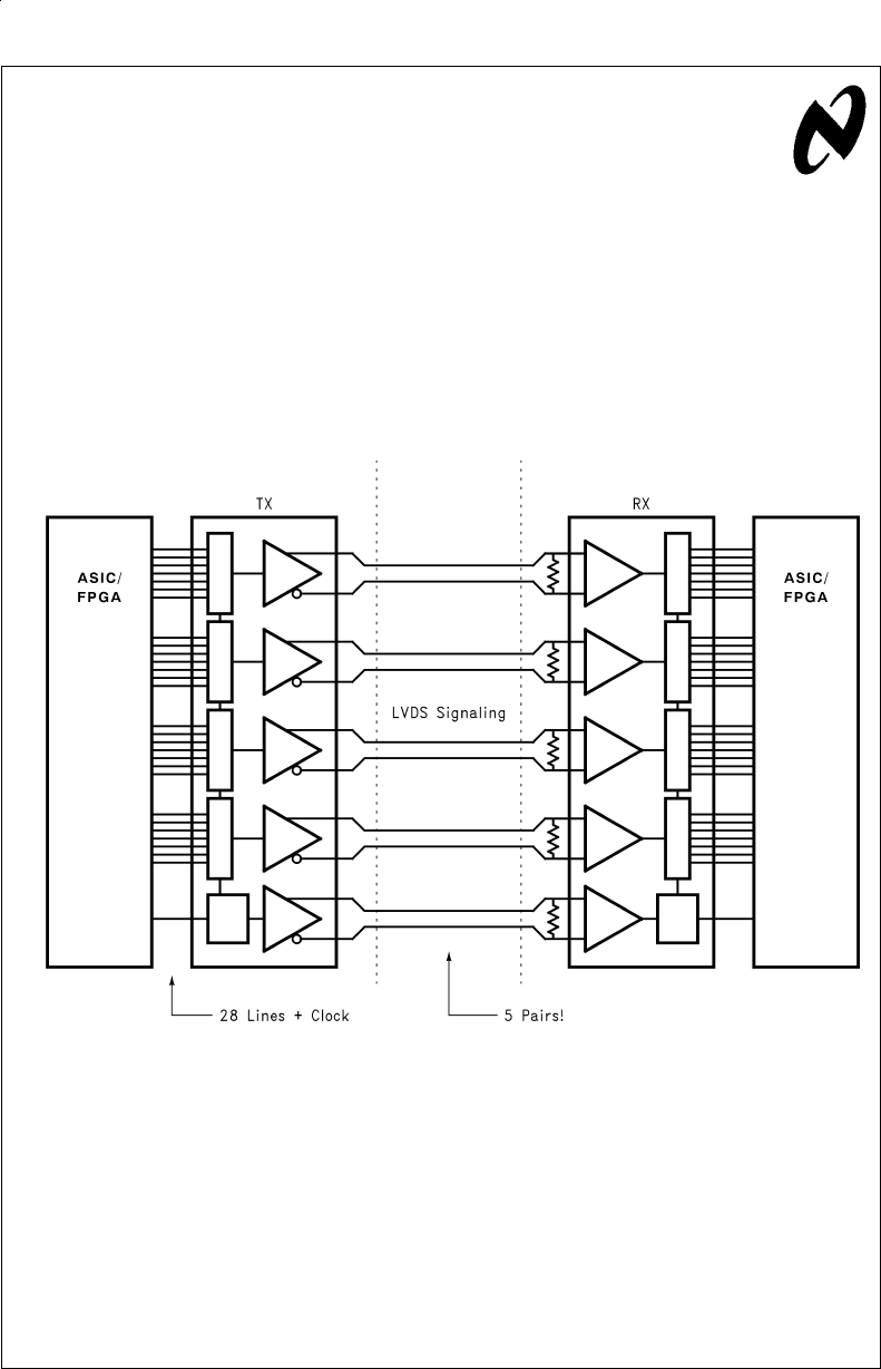
The Channel Link Transmitter’s function is to convert a wide
parallel TTL bus into a smaller faster LVDS interface, and the
Receiver’s function is to recover the data and re-generate
the wide TTL bus. The system block diagram is shown in
Fig-
ure 1
. Channel Link delivers multiple benefits to Datacom
and Telecom applications. These include a smaller LVDS in-
terface which saves PCB space, simplifying the task of PCB
trace layout. The LVDS drivers are capable of driving long
cables (up to 10 meters) at high speeds. The smaller cables
and connectors are lower cost since they are physically
smaller (up to 80%reduction in the number of required
conductors/pins). LVDS supports higher bandwidth service
with a reduction in EMI due to the differential scheme (odd
mode), the reduced signal swing (only z300 mV), and the
use of current mode drivers (soft transitions, and reduced
spikes). To gain the maximum benefits of LVDS and Channel
Link, high speed PCB and interconnect design is
required
.
This application note focuses on the requirements of the
PCB and interconnect to provide an error free, low emission
LVDS interface.
FUNCTION OF THE TX AND RX
The Transmitter (TX) accepts the wide parallel (21-bit or 28-
bit) TTL bus and converts it to 3 or 4 higher speed serialized
LVDS data streams. Applications may employ the full pay-
load (21 or 28 bits) of the chipset or only a portion (i.e. 14,
16, 17, 18, 20 bit wide). To operate the TX, only data and
clock must be applied. The chip does not require control sig-
nals, as it provides transparent data transmission. Data on
the TX inputs is strobed into the TX on the rising edge of the
clock signal. This edge is denoted within the device ID with
the “R” designation. The clock is then fed to a PLL type cir-
cuit that is used to generate strobes that internally clock out
the serialized LVDS data streams. A powerdown pin is also
supported. Asserting this pin shuts down the PLL and also
puts the driver outputs into TRI-STATE®. This mode disables
the LVDS load loop current and also reduces I
CC
to µAs, sav-
ing power when the link is not needed. The 3.3V TX devices
feature high impedance bus pins when the device is pow-
ered off.
The Receiver (RX) accepts the 3 or 4 high speed serialized
LVDS data streams and converts them back to a wide paral-
lel TTL bus. The RX device is the complementary function to
the TX device. Data on the RX output is strobed by the RX-
CLKout on the rising edge of the clock signal. This edge is
denoted within the device ID with an “R”. The RXs utilize the
rising edge of the LVDS Clock signal to strobe the data on
TRI-STATE®is a registered trademark of National Semiconductor Corporation.
AN100882-1
FIGURE 1. Link System Block Diagram
National Semiconductor
Application Note 1108
John Goldie
August 1998
Channel-Link PCB and Interconnect Design-In Guidelines AN-1108
© 1998 National Semiconductor Corporation AN100882 www.national.com
the RX LVDS data inputs. A powerdown pin is also sup-
ported. Asserting this pin shuts down the PLL and also locks
the RX outputs to the current state or low state (device spe-
cific, see datasheets). This mode saves power when the link
is not needed. The 3.3V RX devices also feature high imped-
ance bus pins when the device is powered off. This feature
enables multi-drop applications for single TX to multiple RX
configurations.
LOCATION OF TX AND RX ON THE PCB
The transmitter should be located as close to the connector
as possible
(
see
Figure 2)
. This is done to minimize the
LVDS PCB overall trace length (see following section on dif-
ferential traces) and skew as well. Skew is generally propor-
tional to length, thus a shorter interconnect has nominally
less skew associated with it. If the TX is located within 2
inches of the connector, serpentine (trace length compensa-
tion to generate zero skew) is not required. If the TX is more
than 2 inches away, equal length traces should be em-
ployed. It is not a requirement of the TX device to be located
adjacent to the ASIC/FPGA (bus controller) device. Recall
the ASIC-TX interface is a slow speed bus (compared to the
LVDS bus) and has fewer timing constraints. However, the
connection between the ASIC and the TX should be de-
signed such that the parallel bus traces are also of equal
length to avoid excessive skew which could cause a set-up
or hold violation at the TX input pins. In the extreme case (if
electrical length is 1/2 rise time), signal termination may be
required on the ASIC-TX interface. Note, the bus data lines
are level sensitive only, while the clock line is edge sensitive.
If the interconnect between the ASIC and the TX is long, (be-
comes a transmission line), termination for the clock signal
should be considered. Input voltages applied to the TX input
pins should remain within the VCC to GND range. Exceeding
the ABS MAX ratings of the input pins increases noise in the
device (and jitter) and can falsely trigger the ESD protection
circuitry.
The receiver should also be located close to the connector
as shown in
Figure 2
. This is done to minimize the LVDS
PCB trace length. (see the section on differential traces.) It is
not a requirement of the RX device to be located adjacent to
the destination controller (ASIC/FPGA). If the distance is
greater than a few inches, or for high fanouts (more than 2),
external buffering of the RX outputs should be employed.
The connection between the controller and the RX should be
designed such that the parallel data bus traces are of equal
length to avoid skew which could cause a set-up or hold vio-
lation at the ASIC controller input pins.
DEVICE GROUND AND POWER
The TX and RX are high speed— high performance devices.
The devices include a PLL type circuit that operates at ƒ or
3.5Xƒ MHz (device specific, where ƒ is the clock frequency)
and LVDS drivers and receivers that toggle in the hundreds
of Megabits per second range (up to 462 Mbps at a 66MHz
clock rate!). This requires a solid ground and power distribu-
tion reference for the device. V
CC
noise should not exceed
100 mV
pp
. If it does, separated power and ground planes
should be used for the PLLV
CC
and PLLGND pins. To enable
good power/ground reference a minimum of a 4 layer PCB is
recommended. Two sided boards or flex circuit are generally
not recommended for placement of the TX or RX devices.
EMI emission control starts with solid power and ground
planes.
DEVICE BYPASS
The TX and RX have three separate V
CC
(power supply) and
GND references. These are for the digital logic, LVDS, and
PLL portions of the chip. To obtain supply noise of less than
100 mV
pp
; close by-passing is required. Do not locate by-
pass capacitors at the end of small traces, rather connect
AN100882-2
FIGURE 2. TX and RX Location
www.national.com 2

them adjacent to the device pins as close as possible. Bulk
capacitance of 4.7 µF to 10 µF should also be near by. Wide
traces with multiple power/GND via (2 are recommended)
should be employed on bypass connections. The ideal case
would use 0.1 µF//0.01 µF//0.001 µF capacitors on each sup-
ply pin. If space is restricted do not eliminate the PLL by-
passing as this is most critical of low noise operation. 0805
or 1206 chip capacitors are recommended as they offer the
lowest inductance and can be mounted very close to the de-
vice pins. With this type of layout, parasitic inductance will be
in the 1.5 nH to 2 nH range, whereas locating the capacitor
at the end of a short narrow trace can have an inductance as
high as 15 nH! Using multiple capacitors in parallel provides
good bypassing across a wider range of frequency, also the
ESR is lowered and a low impedance at high frequency is
provided.
ASIC — TX INTERFACE
The connection between the ASIC controller and the TX de-
vice should utilize standard PCB design techniques. The
data bus and clock lines should all be of equal length in order
to prevent any skew being introduced between clock and
data. As with any clock line, signal quality is of concern.
Avoid unnecessary via, sharp bends or other discontinuities.
A direct point-to-point link is best for the clock and its signal
quality. Other clock signals should be kept away from the
clock and data lines to avoid unwanted coupling. Provision
for termination may be required on the clock signal at the TX
input. If the ASIC has drive level options (6 mA–8 mA or 12
mA modes, device specific), testing has shown that operat-
ing the clock in high drive and the data in low offers the best
balance between clock signal quality (sharp) and noise gen-
eration from the ASIC data output pins. Unused TX input
pins should be tied to GND on the 5 V series and may be left
floating or tied to GND on the 3.3 V series to prevent un-
wanted switching and the lowest chip power dissipation. The
3.3 V devices feature internal pull down resistors on the in-
puts (see datasheets).
RX — ASIC CONTROLLER INTERFACE
The connection between the RX and the ASIC controller
should utilize standard PCB design techniques. The data
lines and clock should all be of equal length in order to pre-
vent any skew being introduced between clock and data. As
with any clock line, signal quality is of concern. Avoid unnec-
essary vias, sharp bends or other discontinuities. A direct
point to point link is best for the clock and its signal quality. If
a high fanout of the RX output is required (more than 2
loads), external buffering is recommended.
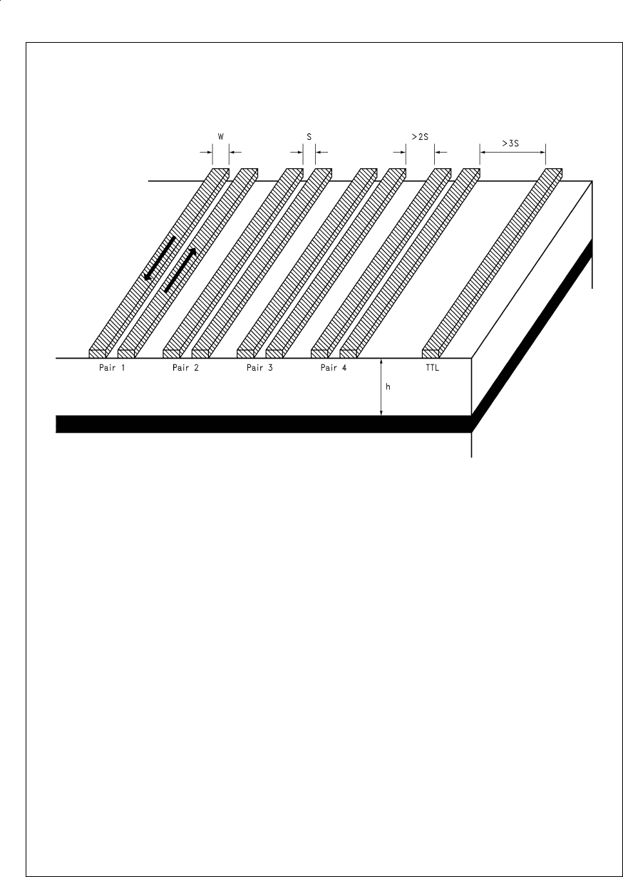
LVDS DEVICE — CONNECTOR INTERFACE
The traces that connect the TX LVDS outputs to the connec-
tor and the connector to the RX inputs should be minimized
in length as discussed above in the section on TX/RX loca-
tion. In addition TTL/CMOS single-ended lines should be lo-
cated on a different signal layer or kept away (at least “3S”)
from the LVDS lines to minimize any coupling of noise onto
the LVDS lines and out onto the interconnect as shown in
Figure 3
. Guard ground traces may be placed between the
LVDS lines and the other signals to further isolate the two,
they should be at least 2S away from the closely-coupled dif-
ferential pair. Corruption of LVDS data is not an issue due to
the receiver’s common mode rejection; minimizing common
mode noise (EMI) is the reason for the spacing and isolation.
Unused LVDS driver output pins should be left open, as this
will minimize power dissipation. Unused RX inputs should
also be left open (not terminated).
www.national.com3
The use of true differential traces further enhances the noise
rejection capabilities of differential data transmission and re-
duces / limits the generation of unwanted emissions. Differ-
ential traces are recommended for use on the LVDS outputs
of the TX and inputs to the RX. They differ only slightly from
standard PCB traces. The distance between the two signal
traces (“S”) that compose the differential pair is also con-
trolled (minimized). This distance is critical to specify cor-
rectly as it is related to both the differential-mode character-
istic impedance of the trace pair and also related to the
differential noise margin of the system. Standard traces are
laid out for 50Ωimpedance. Two traces separated far apart
from each other will present a differential mode characteristic
impedance of twice the single-ended impedance, but will not
provide the maximum noise rejection benefit and defeat the
differential signaling. The spacing between the traces should
be kept to a minimum to maximize the differential noise re-
jection (differential noise margin is equal to the minimum sig-
nal swing less the maximum receiver thresholds
(250 mV–100 mV = 150 mV)). This minimum distance be-
tween the traces of a pair assures that any external noise
coupled onto the pair will be seen as common mode, and re-
jected by the receivers. To adjust trace impedance set “S” to
a minimum spacing between metal lines), and adjust the
AN100882-3
FIGURE 3. LVDS PCB Layout
www.national.com 4
width of the trace to the desired impedance (see AN-905 for
equations). When the two lines are close, the differential im-
pedance is no longer twice the single-ended impedance (it is
a factor of <2). The distance between adjacent LVDS differ-
ential pairs should be at least 2S or greater as shown in
Fig-
ure 4
. The electrical length of the LVDS traces should be
matched to minimize any skew created in the path between
TX and RX. Lastly, it is desirable to have S <h, again ensur-
ing that maximum coupling occurs between the pair and not
with the plane below.
Microstrip traces (outside layer) are usually employed for
this interconnect. The microstrip geometry and the fact that
the traces are on the outer layer enable higher impedances
more easily. It is also possible to design the interconnect
without any via, thus a better signaling environment. On the
down side, stripline (embedded) traces offer greater shield-
ing due to their encasement. Either microstrip or stripline
traces can be used, as long as they are matched to the ca-
ble’s differential-mode characteristic impedance. This is
shown in
Figure 2
where Z
OD1
represents the TX PCB im-
pedance and Z
OD3
is the cable (interconnect) impedance. It
is recommended that all impedances should be within 10%
of the target impedance (typically 100Ω) to minimize any re-
flections. Note that a 10%difference in impedance will cre-
ate a reflection of 5%. Reducing the magnitude of reflections
will lower the EMI of the system.
TERMINATION AT THE RX INPUTS
The use of a termination resistor is required. Due to the high
speed edge rates of LVDS drivers a matched termination will
prevent the generation of any signal reflections, and reduce
EMI. Termination is typically implemented with a single sur-
face mount resistor connected across the signal pair as
close to the receiver inputs as possible (no more than 1/2
inch away if the termination is placed in front of the receiver
inputs). If the resistor is too far away from the receiver inputs,
the line between the resistor and the receiver input takes on
transmission line behavior and reflections may occur at the
receiver inputs defeating the purpose of the termination re-
sistor altogether! Also the use of an external resistor allows
for a variety of media to be used. Since characteristic imped-
ance is media dependent, the proper termination resistance
may be employed to match the particular application. The re-
sistor should be selected to within 2%of the nominal differ-
ential impedance (100Ω) of the media. If PCB space is tight,
a fly-by termination may also be used. The two termination
methods are shown in
Figure 5
. In either case the resulting
stub should be kept as short as possible.
AN100882-4
FIGURE 4. Differential Trace Spacing
www.national.com5

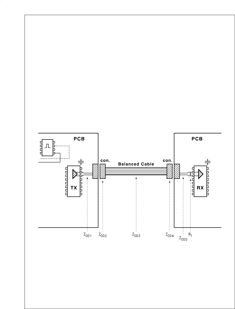
Note: The
complete
interconnect between the TX output and the RX input is a high speed transmission line. Driver edge rates are in the 300 ps–700 ps range. The
TX PCB traces, connectors, cable media, and RX PCB traces are all part of the system. Their impedances should be matched within 10%to maintain signal
quality and generate the lowest amount of emissions. There are 4–6 impedances to consider, depending upon the application (the size of the connector).
These are shown in
Figure 2
as ZOD1,Z
OD2,Z
OD3,Z
OD4 ,Z
OD5, and RT. Also, minimize extra transitions (board or layer transitions, etc.) here to make this
total interconnect as clean as possible.
CONNECTORS
For intra-box applications (board to board in a box) the con-
nector is typically very small since it is internal to the box and
is only connected upon assembly of the system. These con-
nectors have the advantage that they do not adversely effect
the signal quality greatly, since they are electrically small and
present more of a small lumped load to the signal.
Larger connectors used between boxes (box to box applica-
tion) are more critical since they are electrically long and
may react as a transmission line segment. High performance
connectors are available that provide controlled impedance
and matched electrical length of the pins (no skew). The 3M
MDR system is one such cabling system that meets the
needs of LVDS applications for cable and connector require-
ments. It offers a zero skew SMT connector, controlled im-
pedance, low crosstalk, and very low skew (see reference in
the appendix). Other connectors that have been employed
include standard SCSI connectors, and also DB15 connec-
tors to name a few.
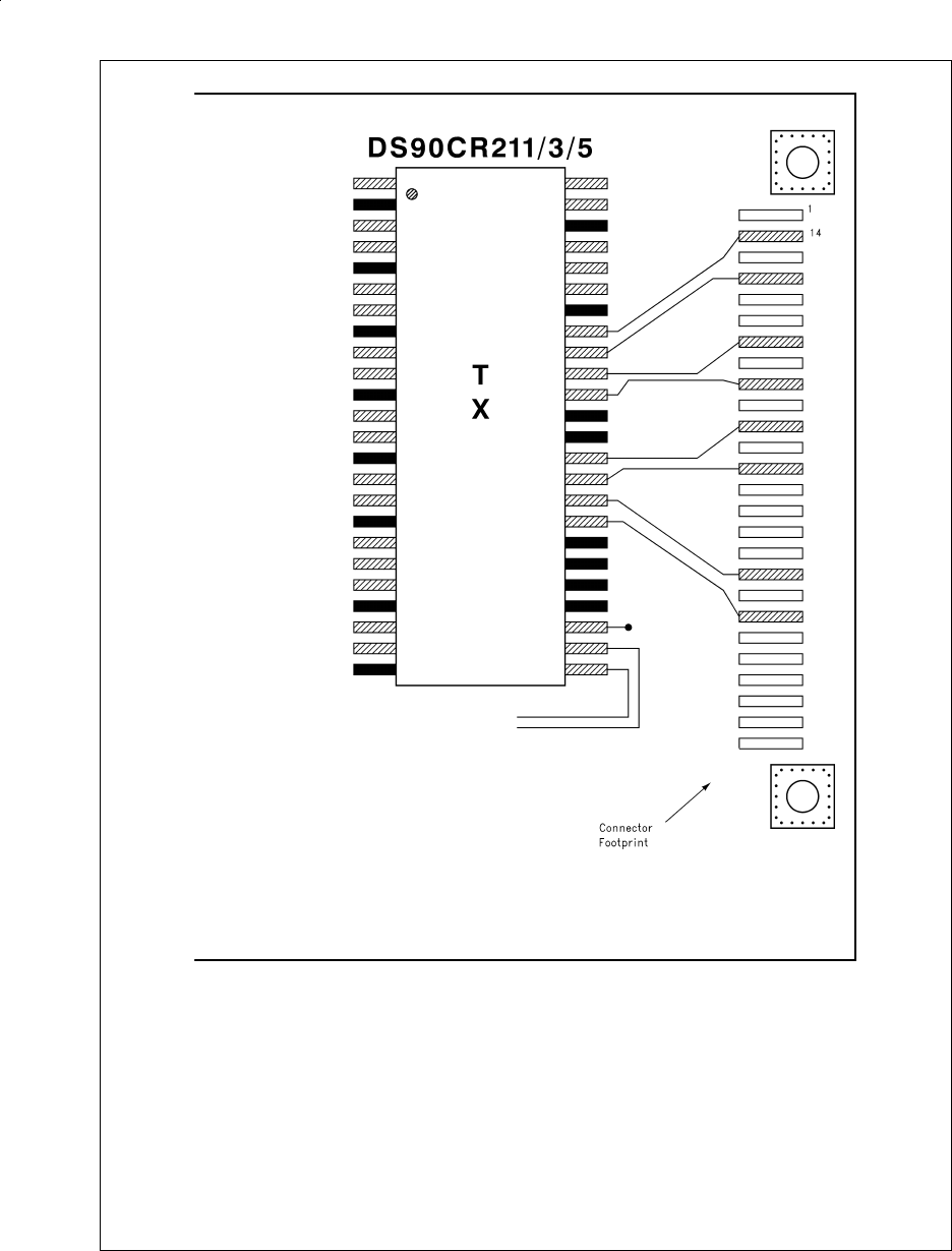
CONNECTOR PINOUT
Connector Pinout is application dependent. General guide-
lines to follow are given below.
On multiple row connectors, the pair should be routed on ad-
jacent pins in the same row to minimize skew within the pair.
Another option is to employ single row low skew surface
mount connectors (see reference).
A signal common (ground) path should also be provided
near the pairs to provide a low impedance near by return
path for common mode noise picked up along the cable. This
will help to reduce unwanted EMI.
THE INTERCONNECT
LVDS drivers and receivers are intended to operate on a
wide variety of media. Depending upon the system’s needs
the media may vary due to a number of parameters includ-
ing: length of interconnect, amount of shielding required,
physical dimensions of the system, and of course cost.
Channel Link (LVDS) has been demonstrated on flat ribbon
cable, FEC (flex) interconnect, shielded twisted pair, and
twin axial cables. An important parameter to understand is
the differential-mode characteristic impedance of the media.
For many common cables this is typically about 100Ω(see
cable datasheet). As discussed above to minimize any com-
mon mode noise generation the TX PCB interconnect, the
interconnecting media, the RX PCB interconnect, and the
termination should all match (within 10%) in characteristic
impedance (differential mode). Electrical length of the data
and clock signals should be of equal length. Conductors of
different length composing a pair will cause a modulation of
common mode and radiate more. Pairs of different length will
impact the receivers data recovery by impacting the correct
strobing of data. Remember that the timing of the LVDS data
line is 7X tighter than of the TTL bus. The amount of tolerable
skew between any two conductors is clock speed depen-
dent, but should be kept to less than 100 ps–400 ps (data
rate dependent, 66 MHz–20 MHz) with the Link chips. On a
typical high performance cable (3M MDR) skew is specified
at only 30 ps/meter. For flex circuit interconnects, similar de-
sign recommendations as discussed in the “LVDS
Device — connector interface” section above should be em-
ployed. Even through LVDS operates as true odd-mode dif-
ferential drivers, a signal common (Ground) connection is re-
quired between the two systems to establish a common-
mode return path. The bulk of the LVDS load current is
returned to the driver within the pair as LVDS is a true odd-
mode differential driver. This is very important for emission
reasons, as the closely-coupled differential pair creates a
small ring antenna. However, for common mode return, a
signal common connection of low impedance is required for
low emission operation. Typically assigning one pair (two
conductors) is sufficient for this purpose (as it has 1/2 the
DCR (DC resistance) of a single line). Shield ground refer-
ences should be tied off to quiet ground references, typically
frame ground at each end if employed. Channel Link (LVDS)
may be used on a wide variety of media (flat cable, twin-ax,
standard twisted pair,...cables). Length is a factor of cable
performance, balance, skew, and clock speed, thus it is ap-
plication dependent.
AN100882-5
FIGURE 5. Termination Layout — Standard and Fly-By
www.national.com 6

General guidelines for different types of cable are given next:
for very short distance applications (less than 0.3 meter) flat
cable or flex circuit has been employed. For medium dis-
tance applications (less than 7 meters) standard twisted pair
cables have been employed. For application exceeding 5
meters, typically twin-ax cables have been employed due to
their inherent low skew between pairs. Greater than 10
meter applications are possible, however sampling margin,
skew, and impedance control must be carefully reviewed.
The Channel Link chipsets are offered currently in 3 speed
families. Very general conservative guidelines for How far?
How fast? are given below for the chipsets:
•40MHz Family →up to 10 meters
•66MHz Family →up to 5 meters
•85MHz Family →up to 2 meters
BIT MAPPING
The bit mapping for the 21 and 28 bit chipsets are shown in
the respective datasheets. Bit mapping is the same for all 21
bit parts (40, 66, and 85MHz families). Bit mapping is the
same for all 28 bit parts (40, 66, 85MHz families). Note that
the 21 and 28 bit part families are mapped differently. Mixing
3.3V and 5V devices is also possible, since all devices ad-
here to the LVDS interface standard.
If less than 21 or 28 bits are required, multiple options to dis-
able particular bits are possible. The following options are
possible:
If there are 7 unused bits, then it is possible to utilize only 2
LVDS data streams (21 bit chipset example). This will lower
the size of the interconnect required. Unused TX inputs
should be left open on the 3.3V family (and tied to GND on
the 5V family of TXs). The unused LVDS channel outputs
should also be left open to minimize current (power dissipa-
tion). Unused RX inputs may also be left open, as these in-
puts feature a failsafe feature that pulls the plus input high
and the minus input low, preventing unwanted transitions.
Unused RX outputs should also be left open to minimize
power dissipation.
If there are only one to seven unused bits in the application,
then bits on each channel may be disabled. This can be
used to enhance signal quality on the cable as well for long
cable applications. By disabling two data bits in the data
stream (tie one HIGH and the other LOW), inserts guaran-
teed transitions on the data channel and improves (opens)
the eye pattern (reduces ISI distortion of NRZ data).
CHIPSET OPERATION
The Channel Link chipset provides transparent data trans-
mission with minimum control overhead. Data and clock sim-
ply need to be applied to the transmitter input pins. Once the
TX PLL is locked (10ms max) and the RX PLL is locked
(10ms max), data transmission is enabled.
MHz and Mbps
Mega Hertz and “Mega bits per second” are two terms that
are commonly confused. Mega Hertz (MHz) is a measure of
the clock period applied to the TX clock input. Mega bit per
second is the information rate, and for NRZ data is the mea-
sure of a single bit width. It is also important to indicate
where the bit rate is being measured. For the Link chipset,
there are three different possible bps values. These are:
1. the bit rate on a single TX input
2. the bit rate on a single LVDS data channel
3. the bit rate on the entire link (3 or 4 LVDS channels com-
bined)
For example, with a 66MHz clock, and with data strobed on
the rising edge, the bit rate on a single TX input is 66Mbps.
The bit rate on a LVDS channel is 7X the input rate, or
462Mbps. The bit rate on the entire 28 bit Channel Link is 4X
the LVDS channel rate, or 1.848Gbps.
SUMMARY
High speed PCB and Interconnect design practices should
be employed to ensure an error free, low emission design for
the Channel Link devices. The interconnect is a transmission
line due to the high speed edge rates of the LVDS signals
(500 ps typical). Tight skew control is required to minimize
emissions and proper data recovery at the RX devices.
Matching impedances within 10%is recommended to re-
duce the creation of reflections (even mode) along the
interconnect/cable.
GENERALIZED PCB RECOMMENDATIONS OF LVDS
AND LINK APPLICATIONS
LVDS features fast edge rates, therefore the interconnect
between transmitters and receivers will act as a transmission
line. The PCB traces that form this interconnect must be de-
signed with care. The following general guidelines should be
adhered to:
•Hand route or review very closely auto-routed traces.
•Locate the Transmitters and Receivers close to the con-
nectors to minimize PCB trace length for off PCB applica-
tions.
•LVDS traces should be designed for differential imped-
ance control (space between traces needs to be con-
trolled). See AN-905 for equations.
•Minimize the distance between traces of a pair to maxi-
mize common mode rejection.
•Place adjacent LVDS trace pairs at least twice (2S) as far
away (as the distance between the conductors of the
pair).
•Place TTL/CMOS (large dV signals) far away from LVDS,
at least three times (3S) away or on a different signal
layer.
•Match electrical length of all LVDS lines.
•Keep stubs as short as possible.
•Avoid crossing slots in the ground plane.
•Avoid 90˚ bends (use two 45s).
•Minimize the number of via on LVDS traces.
•Maintain equal loading on both traces of the pair to pre-
serve balance.
•Match impedance of PCB trace to connector to media
(cable) to termination in order to minimize reflections
(emissions) for cabled applications (typically 100Ωdiffer-
ential mode impedance).
•Select a termination resistor to match the differential
mode characteristic impedance of the interconnect, 2%
tolerance is recommended.
•Locate the termination within 1/2 (<1) inch of the receiver
inputs if not using a fly-by termination method.
•Use surface mount components to minimize parasitic L
and C for bypass caps and termination resistors.
•Use a 4 layer PCB (minimum).
www.national.com7

•Bypass each LVDS package at the device pin (Bulk by-
pass nearby also) with parallel capacitors (0.1 µF//0.01
µF//0.001 µF) on each of the supply pins (V
CC
, LVDS
V
CC
, and PLL V
CC
).
APPENDIX
Related Channel Link and LVDS Application Notes from
National:
AN-XXX Topic
AN-905 Differential Impedance Calculations
AN-1041 Introduction to Channel Link
AN-1059 SKEW and Jitter Calculations
AN-1084 Links in Parallel
AN-1109
Multidrop Applications with
Channel Link
Related Application Notes
High speed LVDS Transmission Information:
High Performance Shielded Twin-ax Cable Assembly, Part
Number 14526
SMT R/A Receptacle (26 position), Part Number 10226-
1210VE
3M Tech Paper: “Selecting the “Right” Right Angle Intercon-
nects: Surface Mount vs Through-hole” by Francis G. Hart
3M Electronics products Division, Austin, Texas; Kay To-
hyama, Yamagata 3M Limited, Yamagata, Japan.
LIFE SUPPORT POLICY
NATIONAL’S PRODUCTS ARE NOT AUTHORIZED FOR USE AS CRITICAL COMPONENTS IN LIFE SUPPORT DE-
VICES OR SYSTEMS WITHOUT THE EXPRESS WRITTEN APPROVAL OF THE PRESIDENT OF NATIONAL SEMI-
CONDUCTOR CORPORATION. As used herein:
1. Life support devices or systems are devices or sys-
tems which, (a) are intended for surgical implant into
the body, or (b) support or sustain life, and whose fail-
ure to perform when properly used in accordance
with instructions for use provided in the labeling, can
be reasonably expected to result in a significant injury
to the user.
2. A critical component in any component of a life support
device or system whose failure to perform can be rea-
sonably expected to cause the failure of the life support
device or system, or to affect its safety or effectiveness.
National Semiconductor
Corporation
Americas
Tel: 1-800-272-9959
Fax: 1-800-737-7018
Email: support@nsc.com
www.national.com
National Semiconductor
Europe Fax: +49 (0) 1 80-530 85 86
Email: europe.support@nsc.com
Deutsch Tel: +49 (0) 1 80-530 85 85
English Tel: +49 (0) 1 80-532 78 32
Français Tel: +49 (0) 1 80-532 93 58
Italiano Tel: +49 (0) 1 80-534 16 80
National Semiconductor
Asia Pacific Customer
Response Group
Tel: 65-2544466
Fax: 65-2504466
Email: sea.support@nsc.com
National Semiconductor
Japan Ltd.
Tel: 81-3-5620-6175
Fax: 81-3-5620-6179
AN-1108 Channel-Link PCB and Interconnect Design-In Guidelines
National does not assume any responsibility for use of any circuitry described, no circuit patent licenses are implied and National reserves the right at any time without notice to change said circuitry and specifications.
