Application Note 1115 DS92LV010A Bus LVDS Transceiver Ushers In A New Era Of High Performance Backplane Design AN
User Manual: AN-1115
Open the PDF directly: View PDF ![]() .
.
Page Count: 6
DS92LV010A Bus LVDS
Transceiver Ushers in a
New Era of
High-Performance
Backplane Design
Bus LVDS (BLVDS) is a new family of bus interface circuits
invented by National Semiconductor based on LVDS tech-
nology. This family of interface devices is optimized for multi-
point cable and backplane applications. The DS92LV010A is
the first member of this family and is a single transceiver de-
vice which supports operation at 155 Mbps in heavily loaded
(20 Card) backplane applications. It differs from standard
LVDS in providing increased drive current to handle double
terminations that are required in the multi-point application.
BLVDS drivers are also enhanced in their contention protec-
tion, and feature balanced output impedance.
BUS LVDS
BLVDS features a low voltage differential signal of z250 mV
and fast transition times. This allows the drivers to support
applications ranging from low speeds at a few MHz (or even
DC) to high speeds in the 500 MHz range and even beyond.
Additionally, the low voltage swing minimizes power dissipa-
tion and noise generation. The differential data transmission
scheme provides a ±1V common mode range and live inser-
tion (hot plug) of devices into an active bus.
In the past, the bus driving problem was solved by increasing
the drive current of the standard logic single-ended drivers
(244 function). With standard logic swings and increased
drive current, application speeds were increased to the
10 MHz – 20 MHz range, but not faster. Since increasing
drive current alone was not enough, the next enhancement
was made. As before, the drive current was once again
raised; however, the signal swing was also reduced. Thus
BTL (Backplane Transceiver Logic) was invented which sup-
ports 80 mA-sink capability and a 1V signal swing. This ap-
proach easily drives heavily loaded backplanes up to the 50
MHz – 66 MHz range. However, it is still single-ended (like
generic TTL), and only provides about 400 mV of noise mar-
gin. To break the 100 MHz barrier, a single-ended, reduced
swing approach is not feasible since noise margin is already
at the minimum acceptable level.
Bus LVDS removes the need for a large amount of drive cur-
rent, by reducing the signal swing an order of magnitude
from TTL levels. With the small swing, drive current can be
reduced to 10 mA. To double the noise margin over that of
the reduce-swing, single-ended technologies, BLVDS uses a
differential data transmission scheme similar to LVDS but
enhanced for multi-point applications. This enables
the 250 mV swings to operate at 100s of Mbps, while dou-
bling noise margin and reducing noise generation. It also
supports live-insertion of devices into an active bus due to
the receiver common-mode rejection capability. The first of a
series of devices for BLVDS applications is the
DS92LV010A. The DS92LV010A “Single Bus LVDS Trans-
ceiver” device’s performance is the scope of this application.
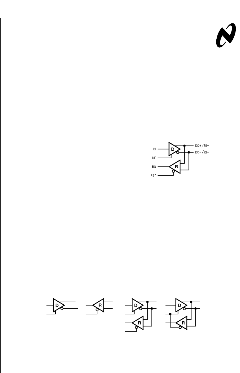
THE DEVICE
The DS92LV010A is a highly versatile 8-pin compact device.
It provides one line driver and one receiver with common bus
pins. The common bus I/O pins reduce bus loading to a mini-
mum (5 pF typical). The logic side of the device supports four
pins for maximum flexibility. The four pins are driver input
(DI), driver enable (DE) – active high, receiver output (RO),
and receiver enable (RE*) – active low. The four inputs are
CMOS inputs with TTL compatible thresholds. They also
present high impedance in power-off conditions and will not
load down the driving gate. The block diagram is shown in
Figure 1
. This allows the device to be configured as a driver,
a receiver, or a transceiver. Both the driver and receiver
functions can be enabled simultaneously to support a loop
back function. Or, the DE and RE* pins may be tied together
to form a direction control pin. The possible configurations
are shown in
Figure 2
.
TRI-STATE®is a registered trademark of National Semiconductor Corporation.
AN100939-1
FIGURE 1. DS92LV010A Bus LVDS Single Transceiver
AN100939-2
FIGURE 2. Device Configurations
National Semiconductor
Application Note 1115
John Goldie
July 1998
DS92LV010A Bus LVDS Transceiver Ushers in a New Era of High-Performance
Backplane Design AN-1115
© 1998 National Semiconductor Corporation AN100939 www.national.com
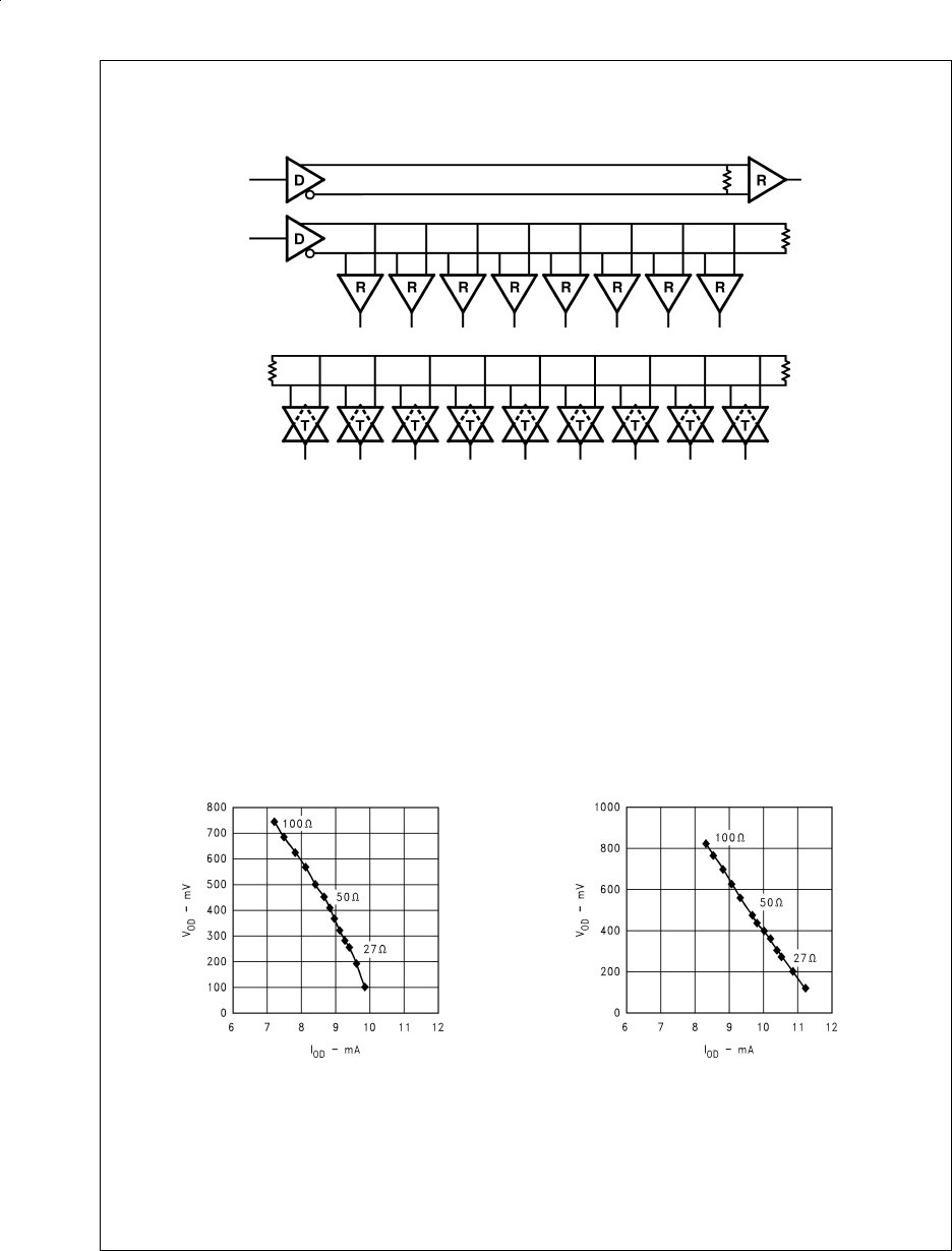
The DS92LV010A may be used in standard LVDS Point-to-
Point applications, Multi-drop data distribution applications,
or in a classical multi-point bus application. It may be em-
ployed for use on data buses, or for clock distribution. Point-
to-Point, Multi-drop, and Multi-point bus configurations are
shown in
Figure 3
.
The DS92LV010A may also be powered from a 5V or a 3.3V
rail directly. Respective parameters are listed separately in
the datasheet. BLVDS bus characteristics and AC parameter
performance is similar for either power supply operation.
This allows the device to be used in a wide variety of appli-
cations.
THE DRIVER
The driver translates standard TTL levels to differential
BLVDS levels. The driver output levels are nominally 1.375V
and 1.125V providing a 250 mV differential signal across a
27Ωload. The offset voltage (V
OS
) of the driver is nominally
1.25V. When the driver input is logic high (>2V), the true out-
put is also high (BLVDS High) while the inverting output is
low (BLVDS Low), thus yielding a +250 mV differential output
voltage. Mathematically the differential voltage is calculated
as A−B, or 1.375 – 1.125 =+250 mV. For a low driver input
(<0.8V) the true output is low while the inverting output is
high, thus yielding a –250 mV differential output voltage.
Again, mathematically this is calculated as A−B, or 1.125 –
1.375 =−250 mV. The differential output signal swing (Vss)
is twice V
OD
, typically 500 mV with the 27Ωload across the
driver outputs.
Figure 4
illustrated the I
OD
vs V
OD
curve for
the device when operating for a 3.3V or 5V rail. Data points
are shown for 100Ω,90Ω,80Ω,70Ω,60Ω,50Ω,45Ω,40Ω,
35Ω,30Ω,27Ω,20Ωand 10Ωdifferential loads.
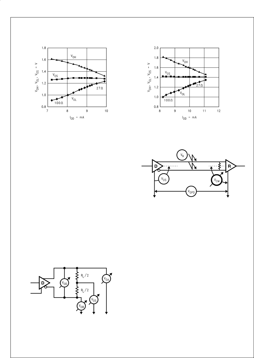
Output impedance is balanced on the BLVDS driver. The
sourcing impedance is matched to the sinking impedance.
This can be seen in the slope of the respective V
OH
/I
OH
and
V
OL
/I
OL
curves for the device. These curves are shown in
Figure 5
. By subtracting the V
OL
curve from the V
OH
curve,
the differential output voltage curve can be drawn (see
Fig-
ure 4
). This curve provides V
OD
/I
OD
information discussed
above. Since the device has a fixed output impedance, the
differential output voltage will vary depending upon the ap-
plied termination load. With a 27Ωload, the nominal V
OD
is
250 mV (I
OD
=9.4 mA). With a 100Ωload, the nominal V
OD
is 725 mV (I
OD
=7.25 mA) when the device is powered from
a 3.3V rail. The single termination load to typically employed
AN100939-3
FIGURE 3. Bus Configurations: Point-to-Point, Multi-Drop, and Multi-Point
I
OD
vs V
OD
(V
CC
=3.3V)
AN100939-4
I
OD
vs V
OD
(V
CC
=5V)
AN100939-5
FIGURE 4. I
OD
vs V
OD
Curves
www.national.com 2
in point-to-point applications (single-direction) where a termi-
nation is only needed at the far end of the line (see
Figure 3
).
Also plotted on the V
OH
/I
OD
(I
OH
) and V
OL
/I
OD
(I
OL
) is the
driver offset voltage (V
OS
). The flatness of this line is also a
measure of balanced output impedance. For LVDS and
BLVDS drivers, this driver offset voltage is typically 1.25V.
The offset voltage is also one component of the common
mode voltage at the receiver input on the bus. The active sig-
nal levels present at the receiver input is a function of four
components:
1. The active driver offset voltage— V
OS
2. Any ground potential difference between the
devices — V
GPD
3. Any longitudinally coupled noise (common
mode) — V
noise
4. The active driver differential output voltage— V
OD
Mathematically this is: V
CM
=V
OS
±V
GPD
±V
noise
±0.5V
OD
. For LVDS and BLVDS systems, a ±1V common
mode range is typically allowed, which is around the driver
offset voltage of +1.25V. Therefore the input common-mode
voltage range is +125 mV to +2.375V. This assumes an off-
set of +1.25V, a differential voltage of 250 mV and the com-
bination of ground potential difference (V
GPD
) and noise
(V
Noise
)is±
1V maximum. Note, how V
OD
,V
OS
and V
CM
are
related.
Figures 6, 7
illustrate the measurement of these
common data transmission parameters.
FAULT TOLERANT AND CONTENTION SAFE
The driver is also very fault tolerant. Being a current mode
device, output current is regulated. Shorting a high output to
ground results in a small fault current. Even with a logic-high
output shorted to ground, fault power dissipation is limited to
less than 100 mW (IOS
MAX
xV
CC
=>20 mA x 5V). A low
driver output can also be shorted to a supply rail without ex-
cessive current or damage to the device. In this case output
short current is limited to typically 15 mA, minimizing fault
current power dissipation. If multiple drivers are enabled at
the same time, the drivers will scale back output current until
a compliance voltage is met. This prevents damage to the
drivers under contention conditions that may occur due to
software error, or hardware configuration. The DS92LV010A
features a rugged I/O.
NOISE MINIMIZER
The ‘010 driver is a current mode device, and output loop
current is controlled. This provides multiple benefits to the
end system. First, dynamic power dissipation increases
slowly as switching frequency is increased. This enables the
device to operate at high data rates, easily exceeding
V
OH
,V
OL
,V
OS
vs I
OD
(V
CC
=3.3V)
AN100939-6
V
OH
,V
OL
,V
OS
vs I
OD
(V
CC
=5V)
AN100939-7
FIGURE 5. I
OH
vs V
OH
and I
OL
vs V
OL
Curves
AN100939-8
FIGURE 6. V
OA
,V
OB
,V
OD
, and V
OS
Driver Measurements
V
CM
=V
OS
±V
GPD
±V
Noise
±0.5 V
OD
AN100939-9
FIGURE 7. The Three Components of V
CM
www.national.com3

155 Mbps. The current mode driver also minimizes shoot-
through current in the driver output stage during transitions;
thus a flat I
CC
vs frequency curve is obtained without a lot of
noise generated on the power and ground planes of the
board. Lastly, the current mode outputs provide soft transi-
tions with less high frequency content, reducing generated
EMI. Crosstalk can also be a problem in high-density appli-
cations where signal lines are closely spaced in backplane
routing channels. BLVDS drivers help to reduce system
crosstalk since their voltage swings are so small and
crosstalk is proportional to amplitude.
HIGH IMPEDANCE BUS PINS
The bus pins (DO/RI) provide high-impedance to the bus
when the device is in TRI-STATE®or powered-off. This is ex-
tremely important in multi-point applications. Communication
between other active nodes should not be impacted if one or
more of the devices on the bus is powered-off. The
DS92LV010A supports this feature along with glitch-free bus
pins on power-up and down. Until V
CC
OK is reached, the
driver output pins are held in TRI-STATE by an internal cir-
cuit. At V
CC
-OK (typically 2.5V), the outputs follow the en-
ables pins. If the driver enable (DE) is low out this point; the
driver outputs will remain off, and will not disturb traffic on the
bus while it is being powered-up. Bus loading presented by
the transceiver is also minimized since small geometry de-
vices are used in the output of the driver (10 mA). Addition-
ally, driver output and receiver input pins are connected to-
gether internally to reduce bus loading (only two pads
required instead of four). The bus pins typically present a
small 5 pF load. The light loading helps to maintain a high
working impedance for the bus.
AC PERFORMANCE
The DS92LV010A driver provides tight AC parameter limits
to support 155 Mbps operation. Driver rise and fall times are
typically 300 ps and are specified at 2 ns maximum. This
supports a ratio of 1-to-3 of transition time to unit interval and
provides a good balance between waveshape and noise
generation. Slew rate of the driver is held to typically 1 V/ns.
Also of importance is the propagation delay through the
driver for system timing calculations. Propagation delay is
specified at 3 ns typical and 5 ns maximum. Skew (pulse
skew) is typically 200 ps, and specified to be less than 1 ns.
Enable / Disable times are less than 10 ns, allowing for quick
turn around on the bus. Refer to the datasheet for complete
AC parameter limits, and conditions.
THE RECEIVER
The receiver is a high-gain, high-speed device. It detects dif-
ferential voltages as small as 20 mV (100 mV threshold
spec) and amplifies them to full CMOS levels with a propa-
gation delay of only 5 ns. The bus pins are high impedance
(greater than 200 kΩ) to minimize loading effects to the bus
(see High Impedance Bus Pins – section above). The High-
impedance loading to the bus pins is also presented when
the device is powered-off. This allows for communication be-
tween other active nodes on the bus, while the power is off to
some of the nodes. This is especially important in applica-
tions that employ multiple receiver or transceiver (multi-
point) devices. The receiver output transition times are con-
trolled to limit switching noise from disturbing the bus, and
from generating system noise. The receiver’s performance
and features are discussed next.
RECEIVER FAILSAFE
The receiver also supports a Failsafe function. For three dif-
ferent input conditions, a stable HIGH output level on the re-
ceiver will be obtained. The three conditions occur due to dif-
ferent system configurations and events, they are:
1. Open Inputs
2. Terminated Inputs
3. Shorted Inputs
An “Open Inputs” condition occurs when a powered-up card
or node is removed from the bus. If this node does not in-
clude the termination resistor, then the inputs are now open.
Internal to the receiver, the plus input is pulled high, and the
minus input is pulled low with high impedance resistive net-
works in the 200 kΩrange.
A “Terminated Inputs” condition occurs under multiple sce-
narios. This can occur when the bus is idle (no active driver),
when all drivers are powered-off, or when a card is removed
from the bus and it includes the termination resistor, then the
inputs are “terminated”. Once again, internal bias network
will set the output high for these conditions. Under this con-
dition, a small differential voltage is created, if there is differ-
ential noise, then additional external failsafe resistors may
be required. Recall that the receiver is a high-gain, high-
speed device, and its function is to detect small (amplitude
and duration) differential pulses and amplify them to full
CMOS levels. If this is the case – see the section on “Exter-
nal Failsafe Biasing”.
“Shorted Inputs” condition occurs when the “plus” input is
shorted to the “minus” input and the resulting differential volt-
age is 0V. Shorted input failsafe is not supported across the
common mode range of the receiver. It is defined as the in-
put pins “shorted” together and no external common mode
voltage applied. It is typically not a good approach to pull
both inputs to the same common mode point also. This can
cause distortion to the first driven bit of valid data when the
bus becomes active.
External Failsafe Bias resistors can be used to boost the fail-
safe protection in noisy applications. The external bias resis-
tors should be an order of magnitude greater than the termi-
nation resistor to minimize loading effects to active drivers.
The common mode point should be set to the 1.2V – 1.5V
range, and for the DS92LV010A should be always below
1.7V (see datasheet).
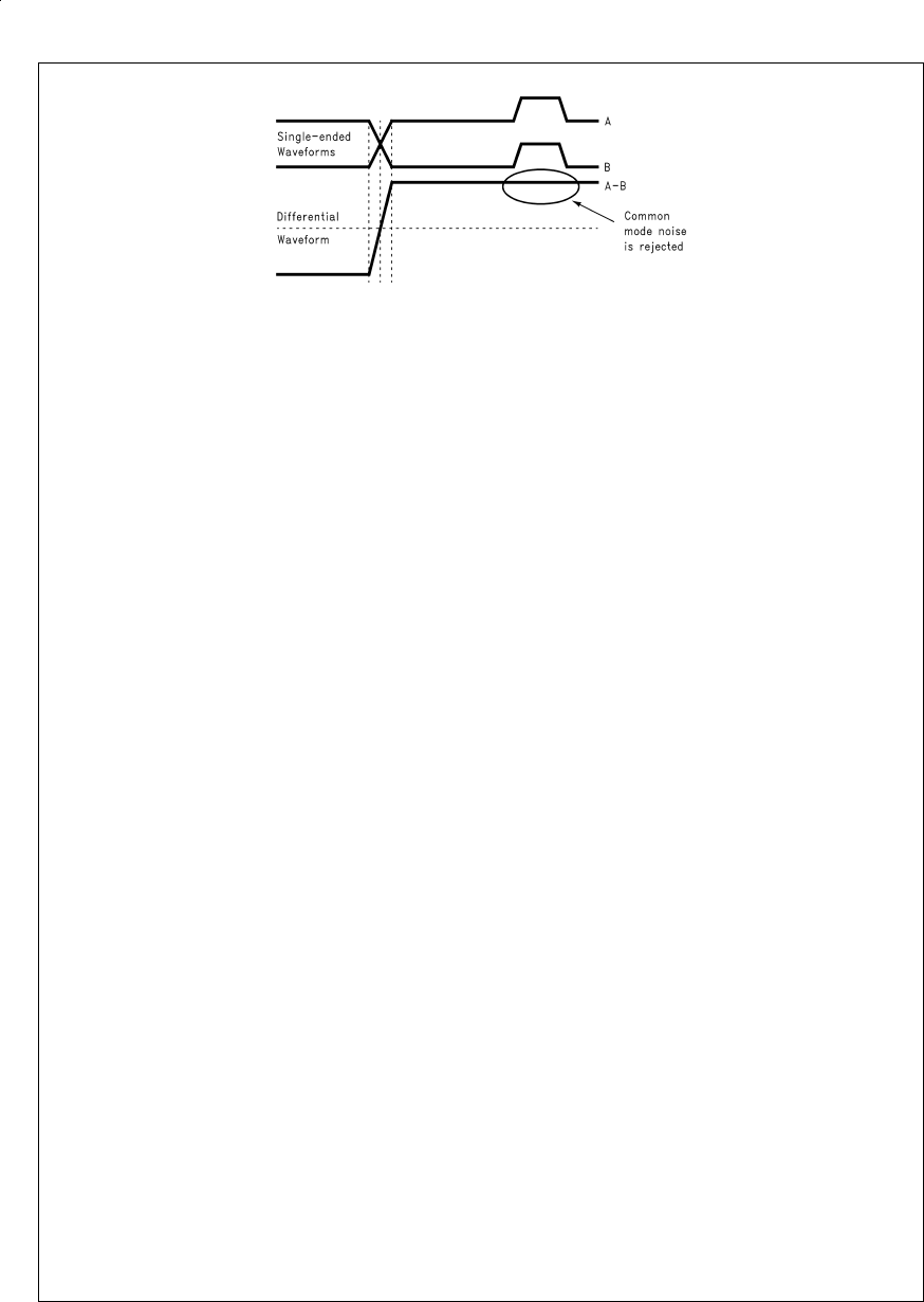
COMMON MODE RANGE
The receiver detects differential voltages, and rejects com-
mon mode voltages. The input stage design of the receiver is
optimized for switching performance over the common mode
range. This is the minimum common mode range of the de-
vice (GND to +2.4V). Input voltages may be up to one diode
below ground, and also as high as one diode above the de-
vice’s V
CC
potential. Exceeding this range may forward bias
the ESD protection circuitry of the device and clamping of
the active signal. The three components of the common
mode voltage seen at a receiver input are shown in
Figure 7
.
Noise coupled equally onto both lines is shown in
Figure 8
.
This noise is seen in the single-ended waveforms and not in
the differential waveform (A−B). To preserve the common
mode rejection of the receiver, twisted-pair cable and closely
coupled differential traces should be used as interconnect.
This will help ensure that noise is coupled equally to both
lines, and will be seen as common-mode and rejected.
www.national.com 4
AC PERFORMANCE
The DS92LV010A receiver like the driver provides tight AC
parameter limits to support 155 Mbps operation. Propagation
delay through the receiver for system timing calculations is
specified at 5 ns typical and 12 ns maximum. Skew, or pulse
skew is typically 500 ps, and specified to be less than 2 ns.
The receiver’s rise and fall times are typically 1.5 ns and are
specified at 4.0 ns maximum. Transition times are smooth
and balanced through the use of graduated turn-on circuitry.
This provides a symmetrical waveshape and generates little
noise. Enable/Disable times are less than 13 ns, allowing for
quick turn around on the bus. Refer to the datasheet for com-
plete AC parameter limits, and conditions.
BACKPLANE BENEFITS
The DS92LV010A is a highly versatile transceiver designed
to deliver Megabits @millwatts. The concept of BLVDS and
differential data transmission also improves many aspects of
system design. These topics are discussed next briefly, and
are the subject of other National Bus LVDS application
notes.
COMMON SUPPLY RAILS
Unlike other high-performance technologies, the
DS92LV010A Bus LVDS Single Transceiver is powered from
common logic power rails of 5V or 3.3V. ECL is also a high-
performance technology, but requires unique supply rails
such as −5.2V ECL or ±2.5V for split-rail ECL operation.
These unique rails may complicate system power generation
and distribution. They also complicate the task of interfacing
directly to standard logic devices and other non-ECL applica-
tion specific devices (ASICs).
PASSIVE TERMINATION SIMPLIFIES BACKPLANE,
ELIMINATES ACTIVE DEVICES, AND IMPROVES
RELIABILITY!
BLVDS eliminates the need for a special termination pull-up
rail (V
t
). Again this simplifies system power generation and
termination voltage distribution. It eliminates the need for ac-
tive termination devices commonly required by the open-
collector/drain single-ended technologies. This reduction in
termination complexity improves system reliability, and
saves PCB space.
LIVE INSERTION SUPPORT
The differential transmission scheme supports live insertion
of cards into active busses. This is due to the fact that when
a card is plugged into the bus the resulting glitch is seen as
common mode and ignored by active receivers. The driver
also includes a glitch-free power up circuit that keeps the
driver outputs in high-impedance until powered-up and en-
abled. To ensure power biasing of the devices, standard
power sequencing is recommended. Ground should be ap-
plied first, then power, and then I/O pins on insertion. For re-
moval, the reverse order is recommended.
BLVDS ACHIEVES MEGABITS @MILLIWATTS!
BLVDS drivers are capable of operating at 100’s of Mbps in
heavily loaded backplane applications. The data throughput
is achieved by the combination of differential data transmis-
sion and a small signal swing. However, not only is Megabit
service provided by BLVDS, but also ultra low power dissipa-
tion is provided. This is gained by the use of a core sub-
micron CMOS process, a current mode driver and also the
small signal swing. With these low power levels, standard IC
packaging may be employed, and also the integration of digi-
tal blocks is enabled. The DS92LV1021/1210 Bus LVDS Se-
rializer / Deserializer is an example of integration that BLVDS
has enabled. These devices include the BLVDS PHY (Line
Driver, Receiver, or Transceiver functional block), and also
the serial-parallel / parallel-serial conversion, clock embed-
ding, clock recovery functions and digital control circuitry all
in a 28L SSOP package. These devices operate at
400 Mbps, and together consume typically less than
250 mW of power (at maximum switching rate).
SUMMARY
The DS92LV010A is the first of a series of devices for high-
speed multi-point applications. The device can operate in the
100 Mbps – 155 Mbps range while consuming minimal
power and directly interface with standard logic devices. The
Bus LVDS products provide designers with new alternatives
for solving high-speed multipoint bus interface problems.
AN100939-10
FIGURE 8. Coupled Noise is Common Mode and is Rejected
www.national.com5

LIFE SUPPORT POLICY
NATIONAL’S PRODUCTS ARE NOT AUTHORIZED FOR USE AS CRITICAL COMPONENTS IN LIFE SUPPORT DE-
VICES OR SYSTEMS WITHOUT THE EXPRESS WRITTEN APPROVAL OF THE PRESIDENT OF NATIONAL SEMI-
CONDUCTOR CORPORATION. As used herein:
1. Life support devices or systems are devices or sys-
tems which, (a) are intended for surgical implant into
the body, or (b) support or sustain life, and whose fail-
ure to perform when properly used in accordance
with instructions for use provided in the labeling, can
be reasonably expected to result in a significant injury
to the user.
2. A critical component in any component of a life support
device or system whose failure to perform can be rea-
sonably expected to cause the failure of the life support
device or system, or to affect its safety or effectiveness.
National Semiconductor
Corporation
Americas
Tel: 1-800-272-9959
Fax: 1-800-737-7018
Email: support@nsc.com
www.national.com
National Semiconductor
Europe Fax: +49 (0) 1 80-530 85 86
Email: europe.support@nsc.com
Deutsch Tel: +49 (0) 1 80-530 85 85
English Tel: +49 (0) 1 80-532 78 32
Français Tel: +49 (0) 1 80-532 93 58
Italiano Tel: +49 (0) 1 80-534 16 80
National Semiconductor
Asia Pacific Customer
Response Group
Tel: 65-2544466
Fax: 65-2504466
Email: sea.support@nsc.com
National Semiconductor
Japan Ltd.
Tel: 81-3-5620-6175
Fax: 81-3-5620-6179
AN-1115 DS92LV010A Bus LVDS Transceiver Ushers in a New Era of High-Performance
Backplane Design
National does not assume any responsibility for use of any circuitry described, no circuit patent licenses are implied and National reserves the right at any time without notice to change said circuitry and specifications.
