AP 610_Flash_Memory_In System_Code_and_Data_Update_Techniques_Feb95 610 Flash Memory In System Code And Data Update Techniques Feb95
User Manual: AP-610_Flash_Memory_In-System_Code_and_Data_Update_Techniques_Feb95
Open the PDF directly: View PDF ![]() .
.
Page Count: 16
AP-610
APPLICATION
NOTE
Flash Memory
In-System Code and
Data Update Techniques
BRIAN
DIPERT
SENIOR TECHNICAL
MARKETING ENGINEER
February 1995
I Order Number: 292163-002
Information in this document is provided solely to enable use of Intel products. Intel assumes no liability whatsoever, including
infringement
of
any patent or copyright, for sale and use of Intel products except as provided in Intel's Terms and Conditions
of
Sale for such products.
Intel Corporation makes no warranty for the use of its products and assumes no responsibility for any errors which may appear
in
this document nor does it make a commitment to update the information contained herein.
Intel retains the right to make changes to these specifications at any time, without notice.
Contact your local Intel sales office
or
your distributor to obtain the latest specifications before placing your product order.
MDS is an ordering code only and
is
not used as a product name or trademark
of
Intel Corporation.
Intel Corporation and Intel's FASTPATH are not affiliated with Kinetics, a division
of
Excelan, Inc. or its FASTPATH trademark
or products.
'Other
brands and names are the property
of
their respective owners.
Additional copies of this document or other Intel literature may be obtained from:
Intel Corporation
Literature Sales
P.O. Box 7641
Mt. Prospect, I L 60056-7641
or call 1-800-879-4683
@INTELCORPORATION 1995 CG-041493
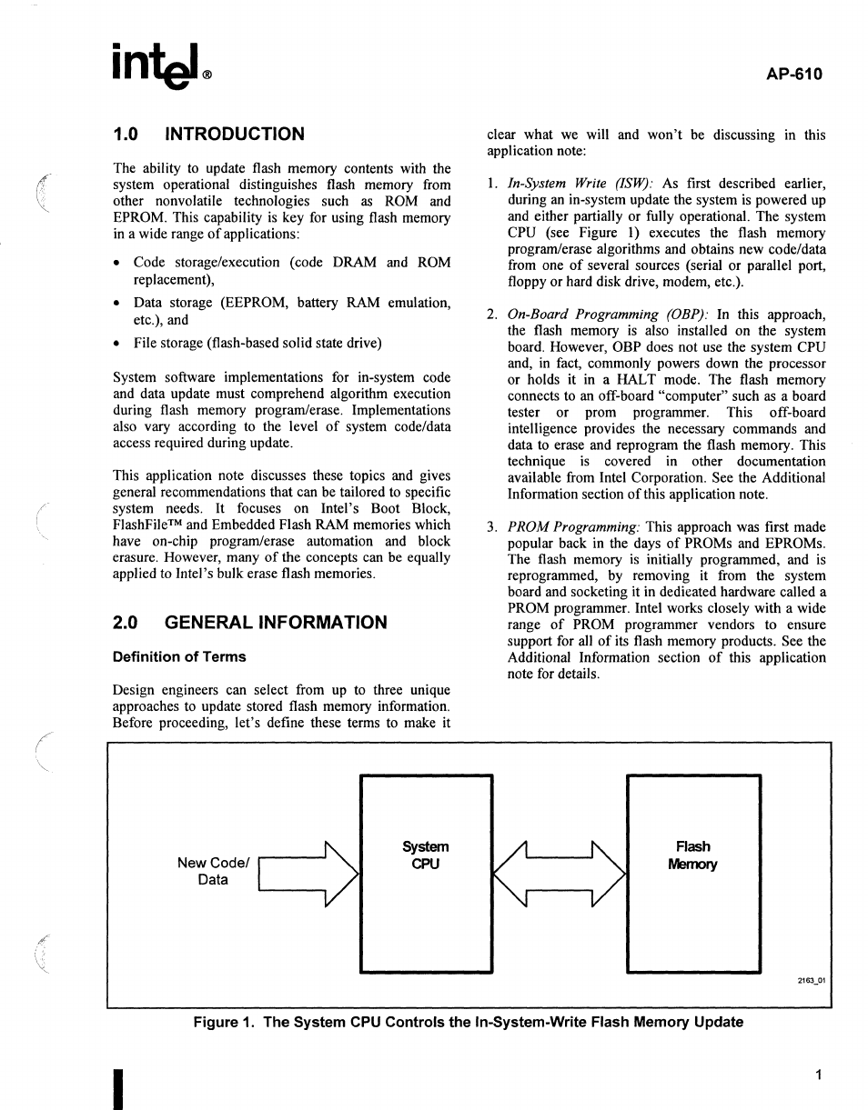
1.0 INTRODUCTION
The ability
to
update flash memory contents with the
system operational distinguishes flash memory from
other nonvolatile technologies such
as
ROM
and
EPROM. This capability
is
key for using flash memory
in
a wide range
of
applications:
• Code storage/execution (code DRAM and ROM
replacement),
• Data storage (EEPROM, battery
RAM
emulation,
etc.), and
• File storage (flash-based solid state drive)
System software implementations for in-system code
and data update must comprehend algorithm execution
during flash memory program/erase. Implementations
also vary according to the level
of
system code/data
access required during update.
This application note discusses these topics and gives
general recommendations that can
be
tailored to specific
system needs.
It
focuses on Intel's Boot Block,
FlashFile™ and Embedded Flash RAM memories which
have on-chip program/erase automation and block
erasure. However, many
of
the concepts can
be
equally
applied to Intel's bulk erase flash memories.
2.0 GENERAL INFORMATION
Definition
of
Terms
Design engineers can select from
up
to three unique
approaches to update stored flash memory information.
Before proceeding, let's define these terms to make it
New Codel
,--
__
.....J
Data
System
CPU
AP-610
clear what
we
will and won't be discussing
in
this
application note:
1.
In-System
Write
(ISW):
As
first described earlier,
during
an
in-system update the system
is
powered
up
and either partially or fully operational. The system
CPU (see Figure
1)
executes the flash memory
program/erase algorithms and obtains new code/data
from
one
of
several sources (serial or parallel port,
floppy or hard disk drive, modem, etc.).
2.
On-Board Programming
(OBP):
In
this approach,
the flash memory
is
also installed on the system
board. However, OBP does not use the system CPU
and,
in
fact, commonly powers down the processor
or holds it
in
a HALT mode. The flash memory
connects to
an
off-board "computer" such
as
a board
tester or prom programmer. This off-board
intelligence provides the necessary commands and
data to erase and reprogram the flash memory. This
technique
is
covered
in
other documentation
available from Intel Corporation. See the Additional
Information section
of
this application note.
3.
PROM Programming: This approach was first made
popular back
in
the days
of
PROMs and EPROMs.
The flash memory
is
initially programmed, and
is
reprogrammed,
by
removing it from the system
board and socketing it
in
dedicated hardware called a
PROM programmer. Intel works closely with a wide
range
of
PROM programmer vendors to ensure
support for all
of
its flash memory products. See the
Additional Information section
of
this application
note
for
details.
Flash
I\IIemory
Figure 1. The System CPU Controls the In-System-Write Flash Memory Update
I
AP-610
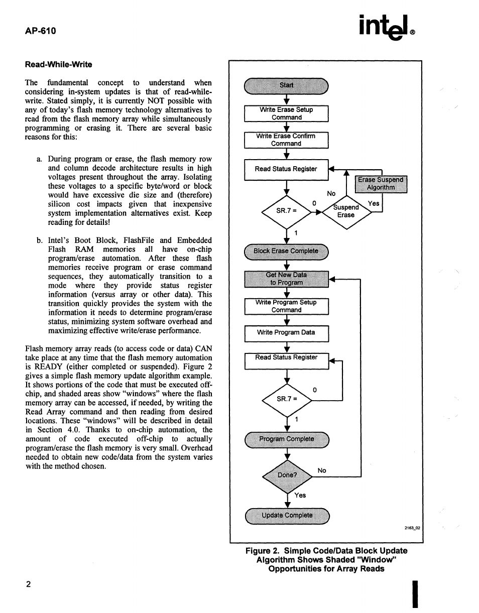
Read-While-Write
The fundamental concept to understand when
considering in-system updates
is
that
of
read-while-
write. Stated simply, it
is
currently NOT possible with
any
of
today's flash memory technology alternatives
to
read from the flash memory array while simultaneously
programming or erasing
it.
There are several basic
reasons
for
this:
a.
During program or erase, the flash memory row
and column decode architecture results in high
voltages present throughout the array. Isolating
these voltages to a specific byte/word or block
would have excessive die size and (therefore)
silicon cost impacts given that inexpensive
system implementation alternatives exist. Keep
reading for details!
b.
Intel's Boot Block, FlashFile and Embedded
Flash RAM memories
all
have on-chip
program/erase automation. After these flash
memories receive program or erase command
sequences, they automatically transition
to
a
mode where they provide status register
information (versus array or other data). This
transition quickly provides the system with the
information it needs
to
determine program/erase
status, minimizing system software overhead and
maximizing effective write/erase performance.
Flash memory array reads (to access code or data) CAN
take place at any time that the flash memory automation
is
READY (either completed or suspended). Figure 2
gives a simple flash memory update algorithm example.
It
shows portions
of
the code that must be executed off-
chip, and shaded areas show "windows" where the flash
memory array can be accessed,
if
needed,
by
writing the
Read Array command and then reading
from
desired
locations. These "windows" will
be
described in detail
in Section 4.0. Thanks
to
on-chip automation, the
amount
of
code executed off-chip
to
actually
program/erase the flash memory
is
very small. Overhead
needed
to
obtain new code/data from the system varies
with the method chosen.
2
Figure
2.
Simple Code/Data Block Update
Algorithm Shows Shaded "Window"
Opportunities for Array Reads I
What Amount of System Functionality
Is
Needed During Update?
The answer to the above question
is
key to
understanding the amount
of
software architecting
needed to integrate flash memory into your design. Use
the following question
as
a reference for where
to
continue reading:
Q.
Can you dedicate the system exclusively to the flash
memory update and ignore
all
other non-related
interrupts? Said another way, can you take the system
"off-line" during flash memory updates?
AI.
If
your answer
is
"yes," the software implementation
is
very straightforward. See Sections 3.0 and 5.0.
A2.
If
your answer
is
"no," the specific software
implementation varies. One approach uses redundant
system memory
to
separate the execution and
storage/backup regions. Another technique eliminates
this redundancy but depends on an understanding
of
interrupt latency, interrupt frequency and its variability
with time. See Sections 4.0 and 5.0.
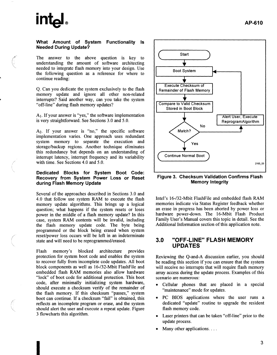
Dedicated Blocks for System Boot Code:
Recovery from System Power Loss or Reset
during Flash Memory Update
Several
of
the approaches described
in
Sections 3.0 and
4.0 that follow use system RAM to execute the flash
memory update algorithms. This brings
up
a logical
question; what happens
if
the system resets or loses
power
in
the middle
of
a flash memory update?
In
this
case, system RAM contents will be invalid, including
the flash memory update code. The byte being
programmed or the block being erased when system
reset/power loss occurs will
be
left
in
an
indeterminate
state and will need to
be
reprogrammed/erased.
Flash memory's blocked architecture provides
protection for system boot code and enables the system
to recover fully from incomplete code updates.
All
boot
block components
as
well
as
16-/32-Mbit FlashFile and
embedded flash RAM memories also allow hardware
"lock"
of
boot code for additional protection. This boot
code, after minimally initializing system hardware,
should execute a checksum verify
of
the remainder
of
the flash memory.
If
this checksum "passes," system
boot can continue.
If
a checksum "fail"
is
obtained, this
reflects an incomplete program or erase, and the system
should alert the user and execute a repeat update. Figure
3 flowcharts this algorithm.
I
AP-610
c'-
__
s_ta,.....rt
__
~)
+
( Continue Normal
Boot)
Figure
3.
Checksum Validation Confirms Flash
Memory Integrity
Intel's 16-/32-Mbit FlashFile and embedded flash RAM
memories indicate via Status Register feedback whether
an
erase
in
progress
has
been aborted
by
power loss or
hardware power-down. The 16-Mbit Flash Product
Family User's Manual covers this topic in detail. See the
Additional Information section
of
this application note.
3.0 "OFF-LINE" FLASH MEMORY
UPDATES
Reviewing the Q-and-A discussion earlier, you should
be
reading this section
if
you can ensure that the system
will receive no interrupts that will require flash memory
array access during the update process. Examples
of
this
scenario
are
numerous:
• Cellular phones that are placed
in
a special
"maintenance" mode for updates.
•
PC
BIOS applications where the user runs a
dedicated "update" routine to upgrade the resident
flash memory code.
• Laser printers that can
be
taken "off-line" prior to the
update process.
• Many other applications
....
3
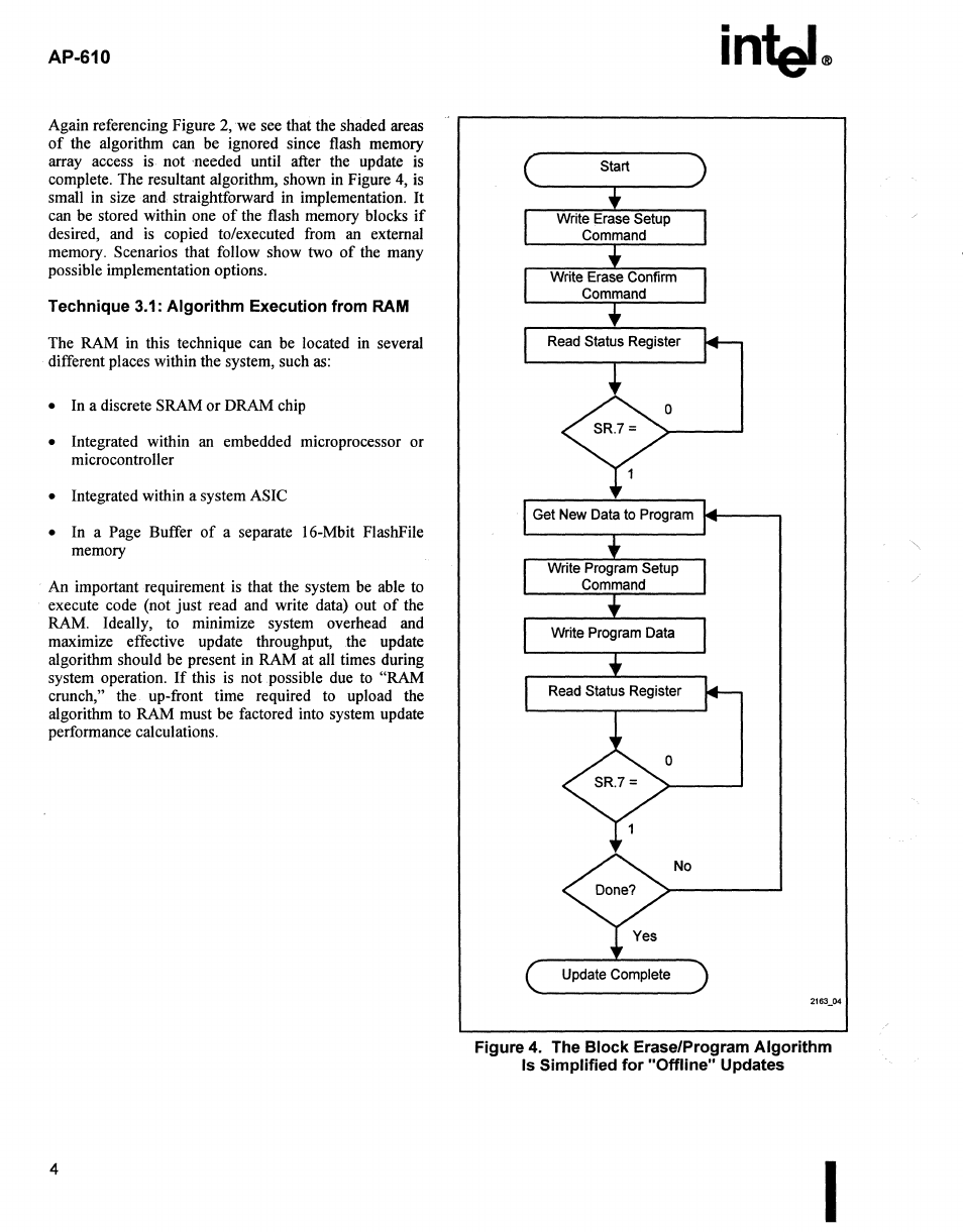
AP-610
Again referencing Figure
2,
we
see that the shaded areas
of
the algorithm can be ignored since flash memory
array access
is
not -needed until after the update is
complete. The resultant algorithm, shown
in
Figure
4,
is
small
in
size and straightforward
in
implementation.
It
can be stored within one
of
the flash memory blocks
if
desired, and
is
copied to/executed from
an
external
memory. Scenarios that follow show two
of
the many
possible implementation options.
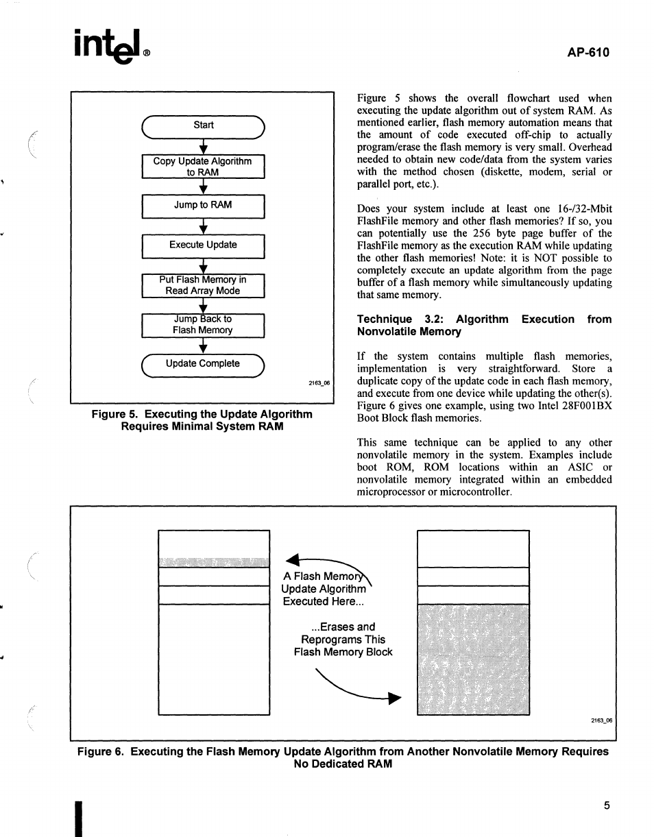
Technique 3.1: Algorithm Execution from RAM
The RAM in this technique can be located
in
several
different places within the system, such
as:
•
In
a discrete SRAM or DRAM chip
• Integrated within
an
embedded microprocessor or
microcontroller
• Integrated within a system ASIC
• In a Page Buffer
of
a separate l6-Mbit FlashFile
memory
An important requirement
is
that the system
be
able to
execute code (not just read and write data) out
of
the
RAM. Ideally, to minimize system overhead and
maximize effective update throughput, the update
algorithm should
be
present
in
RAM at all times during
system operation.
If
this
is
not possible
due
to "RAM
crunch," the up-front time required to upload the
algorithm to RAM must be factored into system update
performance calculations.
4
Figure 4. The Block Erase/Program Algorithm
Is Simplified for "Offline" Updates
I
Update Complete
AP-610
Figure 5 shows the overall flowchart used when
executing the update algorithm out
of
system
RAM.
As
mentioned earlier, flash memory automation means that
the amount
of
code executed off-chip
to
actually
program/erase the flash memory
is
very small. Overhead
needed
to
obtain
new
code/data from the system varies
with the method chosen (diskette, modem, serial or
parallel port, etc.).
Does your system include at least one l6-/32-Mbit
FlashFile memory
and
other flash memories?
If
so,
you
can potentially
use
the 256 byte page buffer
of
the
FlashFile memory
as
the execution RAM while updating
the other flash memories! Note: it
is
NOT possible
to
completely execute
an
update algorithm from the page
buffer
of
a flash memory while simultaneously updating
that same memory.
Technique
3.2:
Algorithm
Execution
from
Nonvolatile Memory
Figure
5.
Executing
the
Update
Algorithm
Requires
Minimal
System
RAM
If
the system contains multiple flash memories,
implementation
is
very straightforward. Store a
duplicate copy
of
the update code
in
each flash memory,
and execute
from
one device while updating the other(s}.
Figure 6 gives one example, using two Intel
28FOO
IBX
Boot Block flash memories.
This same technique can be applied
to
any other
nonvolatile memory in the system. Examples include
boot
ROM,
ROM locations within an ASIC or
nonvolatile memory integrated within an embedded
microprocessor or microcontroller.
~
Update Algorithm
Executed Here
...
...
Erases
and
Reprograms This
Flash Memory Block
Figure
6.
Executing
the
Flash
Memory
Update
Algorithm
from
Another
Nonvolatile
Memory
Requires
No
Dedicated
RAM
I 5
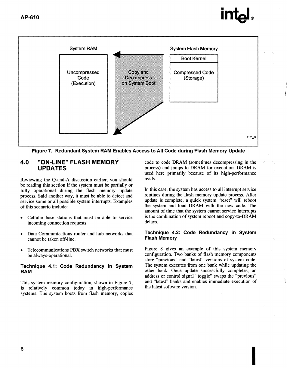
AP-610
System
RAM
Uncompressed
Code
(Execution)
System Flash Memory
Boot Kernel
Compressed Code
(Storage)
Figure
7.
Redundant System RAM Enables Access
to
All Code
during
Flash Memory Update
4.0 "ON-LINE" FLASH MEMORY
UPDATES
Reviewing the Q-and-A discussion earlier, you should
be reading this section
if
the system must
be
partially or
fully operational during the flash memory update
process. Said another way, it must
be
able to detect and
service some or all possible system interrupts. Examples
of
this scenario include:
• Cellular base stations that must
be
able to service
incoming connection requests.
• Data Communications router and hub networks that
cannot be taken off-line.
• Telecommunications PBX switch networks that must
be
always-operational.
Technique 4.1: Code Redundancy in System
RAM
This system memory configuration, shown
in
Figure
7,
is relatively common today in high-performance
systems. The system boots from flash memory, copies
6
code to code DRAM (sometimes decompressing
in
the
process) and jumps to DRAM for execution. DRAM
is
used here primarily because
of
its high-performance
reads.
In this case, the system has access to all interrupt service
routines during the flash memory update process. After
update
is
complete, a quick system "reset" will reboot
the system and load DRAM with the new code. The
amount
of
time that the system cannot service interrupts
is
the combination
of
system reboot and copy-to-DRAM
delays.
Technique 4.2: Code Redundancy
in
System
Flash Memory
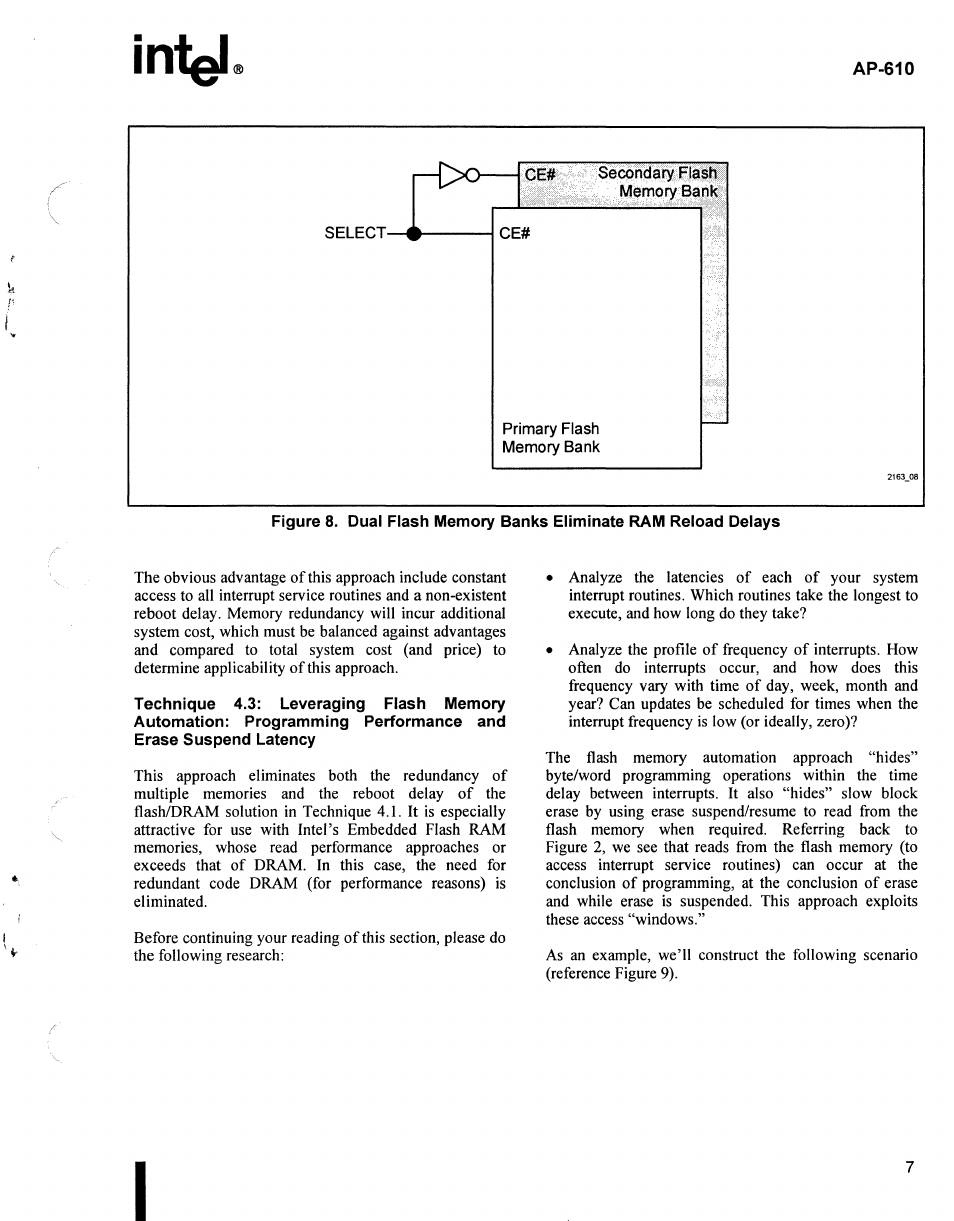
Figure 8 gives
an
example
of
this system memory
configuration. Two banks
of
flash memory components
store "previous" and "latest" versions
of
system code.
The system executes from one bank while updating the
other bank. Once update successfully completes, an
address or control signal "toggle" swaps the "previous"
and "latest" banks and enables immediate execution
of
the latest software version.
I
k
r
I
"
I
\
~
AP-610
SELECT~
___
---l
Primary Flash
Memory Bank
Figure
8.
Dual Flash Memory
Banks
Eliminate RAM Reload Delays
The obvious advantage
of
this approach include constant
access to all interrupt service routines and a non-existent
reboot delay. Memory redundancy will incur additional
system cost, which must
be
balanced against advantages
and compared
to
total system cost (and price) to
determine applicability ofthis approach.
Technique
4.3: Leveraging Flash Memory
Automation:
Programming
Performance
and
Erase
Suspend
Latency
This approach eliminates both the redundancy
of
multiple memories and the reboot delay
of
the
flash/DRAM solution
in
Technique 4.1.
It
is
especially
attractive for
use
with Intel's Embedded Flash RAM
memories, whose read performance approaches or
exceeds that
of
DRAM.
In
this case, the need for
redundant code DRAM (for performance reasons)
is
eliminated.
Before continuing your reading
of
this section, please
do
the following research:
I
• Analyze the latencies
of
each
of
your system
interrupt routines. Which routines take the longest to
execute, and how long
do
they take?
• Analyze the profile
of
frequency
of
interrupts. How
often do interrupts occur, and how does this
frequency vary with time
of
day, week, month and
year? Can updates be scheduled for times when the
interrupt frequency
is
low (or ideally, zero)?
The flash memory automation approach "hides"
byte/word programming operations within the time
delay between interrupts.
It
also "hides" slow block
erase
by
using erase suspend/resume to read from the
flash memory when required. Referring back to
Figure
2,
we
see that reads from the flash memory (to
access interrupt service routines) can occur at the
conclusion
of
programming, at the conclusion
of
erase
and while erase
is
suspended. This approach exploits
these access "windows."
As
an
example, we'll construct the following scenario
(reference Figure 9).
7
AP-61 0
8
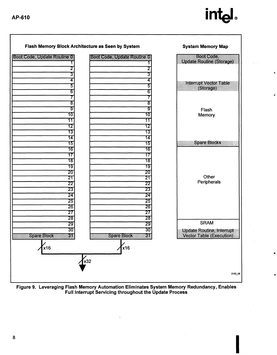
Flash Memory Block Architecture as Seen by System System Memory Map
Flash
Memory
Other
Peripherals
SRAM
Figure
9.
Leveraging Flash Memory Automation Eliminates System Memory Redundancy, Enables
Full Interrupt Servicing
throughout
the Update Process
I
AP-610
Interrupt
Interrupt Period (1/Frequency)
Figure 10. Available Time between System Interrupts Enable Flash Memory Programming
Components
Two 28FOl6SV flash memories (5V Vee,
12V
Vpp),
each x16, interfacing to a x32 system
bus
Small system SRAM
Timings
System interrupt frequency (period) = every 200
~s.
Longest interrupt service routine latency =
50
~s.
Flash memory per-location programming time = 6
~s
(typical)
Flash memory erase suspend latency = I 0
~s
(typical)
Interrupts During Programming
Looking first at programming (Figure
10),
we
see that
the goal
is
to execute at least one programming
operation within the period between interrupts. In the
scenario described above, subtracting interrupt service
routine latency from interrupt period gives a
ISO
~s
"window"
in
which programming can occur. At 6
~s
per
double-word,
up
to
25
locations can
be
programmed
within each interrupt period.
I
200
~s
(interrupt period) -
50
~s
(ISR latency) -
ISO
~s
(programming "window")
ISO
~s
(window)/6
~s
(programming time per location)
=
25
locations
Intel's 16-/32-Mbit FlashFile memories contain on-chip
page buffers, each 256 bytes
in
size, that dramatically
increase effective per-byte programming performance.
For example (averaged over a page), typical
programming performance for the Intel
28FO
16SV
is
2.1
~s/byte
at
5V
Vee and
12V
VPP.
Using these page
buffers may,
in
some cases, allow the system to program
even more bytes within each interrupt programming
"window."
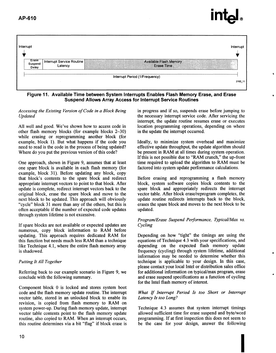
Interrupts During Erase
Now for erase.
If
an
interrupt occurs during erase, the
system must
be
able
to
suspend erase, read the flash
memory array and service the interrupt, all before the
next interrupt. Looking at Figure
II,
adding erase
suspend latency to interrupt service routine latency and
subtracting from interrupt period shows that 140
~s
of
flash memory erase automation can execute between
each interrupt. Obviously, block erase time will extend
beyond that specified
in
the device datasheet since erase
is
being repeatedly suspended.
200
~s
(interrupt period) -[10
~s
(erase suspend
latency) +
50
~s
(ISR latency)] = 140
~s
(erase
"window")
9
AP-610
Interrupt Interrupt
•
Interrupt Period (1/Frequency)
Figure 11. Available Time between System Interrupts Enables Flash Memory Erase, and Erase
Suspend Allows Array Access for Interrupt Service Routines
Accessing the Existing Version
of
Code in a Block Being
Updated
All well and good. We've shown how to access code
in
other flash memory blocks (for example blocks 2-30)
while erasing or reprogramming another block (for
example, block
1).
But what happens
if
the code you
need to read
is
the code
in
the process
of
being updated?
Where
do
you put the previous version
of
this code?
One approach, shown
in
Figure
9,
assumes that at least
one spare block
is
available
in
each flash memory (for
example, block 31). Before updating any block, copy
that block's contents to the spare block and redirect
appropriate interrupt vectors to point to that block. After
update
is
complete, redirect interrupt vectors back to the
original block, erase the spare block and move to the
next block to be updated. This approach will obviously
"cycle" block
31
more than any
of
the others, but this
is
often acceptable
if
the number
of
expected code updates
through system lifetime
is
not excessive.
If
spare blocks
are
not available or expected updates
are
numerous, copy block information to RAM before
updating. This approach requires dedicated RAM for
this function but needs much less RAM than a technique
like Technique 4.1, where the entire flash memory array
is
shadowed.
Putting It
All
Together
Referring back to our example scenario
in
Figure
9,
we
conclude with the following summary.
Component block 0
is
locked and stores system boot
code and the flash memory update routine. The interrupt
vector table, stored
in
an
unlocked block to enable its
revision, is copied from flash memory to RAM on
system power-up. During flash memory update, interrupt
vector table contents point to the flash memory update
routine, also copied to RAM. When
an
interrupt occurs,
this routine determines via a bit "flag"
if
block erase
is
10
in
progress and
if
so, suspends erase before jumping to
the necessary interrupt service code. After servicing the
interrupt, the update routine resumes erase or executes
location programming operations, depending on where
in
the update the interrupt occurred.
Ideally, to minimize system overhead and maximize
effective update throughput, the update algorithm should
be
present
in
RAM at
all
times during system operation.
Ifthis
is
not possible due to "RAM crunch," the up-front
time required to upload the algorithm to RAM must
be
factored into system update performance calculations.
Before erasing and reprogramming a flash memory
block, system software copies block contents to the
spare block and appropriately redirects the interrupt
vector table. After block erase/reprogram completes, the
update routine redirects interrupts back to the block,
erases the spare block and moves to the next block to
be
updated.
Program/Erase Suspend Performance, Typical/Max
vs.
Cycling
Depending on how "tight" the timings are using the
equations
of
Technique 4.3 with your specifications, and
depending on the expected flash memory update
frequency (cycling) through system lifetime, additional
information may
be
needed to determine whether this
technique
is
applicable to your design.
In
this case,
please contact your local Intel or distribution sales office
for additional information on typical/max program, erase
and erase suspend specifications
as
a function
of
cycling
for the Intel flash memory
of
interest.
What
If
Interrupt Period Is too Short or Interrupt
Latency Is too Long?
Technique 4.3 assumes that system interrupt timings
allowed sufficient time for erase suspend and byte/word
programming.
If
at first inspection this does not seem to
be
the case for your design, answer the following
I

questions
in
the process
of
further analyzing your
system interrupt profile:
• Do interrupts occur fairly regularly
as
a function
of
time, or
in
bursts
of
activity followed
by
periods
of
"quiet?"
If
the latter, your system software can hold
off
attempting location programming or resuming
erase until it detects a specified time span
of
system
"inactivity. "
•
Do
one or several interrupt service routines have
substantially longer latencies than others?
If
so,
system software can hold
off
attempting
programming or initiating/resuming erase when these
specific interrupts occur.
In
some cases, it may
be
difficult to hold off
programming due to a fixed data write transfer rate to
the flash memory subsystem.
In
these cases, a small
RAM FIFO can potentially
be
integrated within the
intcrface logic (ASIC, FPGA, etc.). This FIFO acts
as
a
buffer between system and flash memory and
accommodates programming delays due to interrupt
bursts or long ISR latencies.
As
an alternative, the approaches described
in
Techniques
4.1
and 4.2 can
be
reviewed to determine
applicability with your system design criteria.
Programming (Writing) during Erase
Some system designs require both the ability to quickly
read code from flash memory and to quickly write
information to flash memory
in
response
to
an
interrupt.
Intel's 16-Mbit FlashFile memories offer enhanced on-
Order
Number
AP-61 0
chip automation that, among its features, automatically
suspends block erase to service queued programming
operations to other blocks.
5.0 CONCLUSION
Intel has developed a wide range
of
documentation and
other collateral
to
assist you
in
developing system
software solutions and profiling cycling through system
lifetime. Please contact your local Intel or Distribution
Sales Office for more information on Intel's flash
memory products.
6.0 ADDITIONAL INFORMATION
Documentation
Device datasheets provide in-depth information on
device operating modes and specifications.
The 16-Mbit Flash Product Family User's Manual (order
#297372) gives detailed information
on
the enhanced
automation
of
Intel's 16-/32-Mbit F1ashFile and
Embedded Flash RAM memories. Included flowcharts
assist you
in
developing system software.
The following application notes deal specifically with
software interfacing to Intel flash memories:
Document
292046 AP-316 "Using Flash Memory for In-System Reprogrammable
Nonvolatile Storage"
292059 AP-325 "Guide to First Generation Flash Memory Reprogramming"
292077 AP-341 "Designing
an
Updateable BIOS Using Flash Memory"
292095 AP-360 "28F008SA Software Drivers"
292099 AP-364 "28F008SA Automation and Algorithms"
292148 AP-604 "Using Intel's Boot Block Flash Memory Parameter Blocks to Replace
EEPROM"
292126 AP-377 "16-Mbit Flash Product Family Software Drivers"
NOTES:
Please call the Intel Literature Center
at
1-800-548-4725 to request Intel documentation. International customers should contact
their local Intel or distribution sales office.
Additional information can be requested from Intel's automated FaxBACK* system
at
1-800-628-2283
or
916-356-3105
(+44(0)793-496646 in Europe).
I
11
AP-610
FLASH
Builder
This Windows-based utility
is
a hypertext aid to
understanding the automation
of
Intel's 16-Mbit
FlashFile and Embedded Flash
RAM
memories.
FLASHBuilder automatically generates code segments
in
C or ASM-86 for flash memory program/erase that
you can easily "paste" into your system software.
It
also
includes a cycling utility
and
power/perfonnance
benchmark utilities
for
the 28F016XS and 28F016XD.
FLASHBuilder
is
available
from
the Intel Literature
Center via order number #297508.
It
can also
be
downloaded from the Intel
BBS
at
916-356-3600
(+44(0)793-49-6340
in
Europe).
VHDL and Verilog Models
VHDL functional simulation models for the 28FOI6SV,
28F016XD and 28F016XS
are
available
now;
please
REVISION HISTORY
Number Description
001 Original Version
contact your local Intel or distribution sales office.
Verilog models for these devices will
be
available
in
early
1995.
PROM Programming Support
Intel works closely with a large number
of
world-wide
PROM
programmer vendors to ensure timely support
for
its flash memory products. This programming support
infonnation, updated frequently,
is
available on
FaxBACK.
On-Board Programming
An
application note will
be
available
in
early
1995
that
discusses hardware and software recommendations for
OBP
using either a board tester or PROM programmer.
Contact your local Intel or distribution sales office for
more
details.
002 Removed page buffer references for Embedded Flash RAM memories
12 I
intel®
ALABAMA
Intel
Corp.
4024 Medford Drive
Huntsville 35802
Tel: (205) 883-6137
FAX: (205) 883-4826
ARIZONA
tlntel
Corp.
410
North
44th
Street
Suite 500
Phoenix 85008
Tel: (800) 628-8686
FAX: (602) 244-0446
CALIFORNIA
Intel Corp.
3550
Watt Avenue
Suite 140
Sacramento 95821
Tel: (800) 628-8686
FAX: (916) 488-1473
tlntel
Corp.
9655
Granite Ridge Drive
3rd
Floor, Suite
4A
San Diego 92123
Tel: (800) 628-8686
FAX: (619) 467-2460
Intel Corp.
1781
Fox
Drive
San
Jose
95131
Tel: (800) 628-8686
FAX: (408) 441-9540
'tlntel
Corp.
1551 N. Tustin Avenue
Suite
800
Santa
Ana
92701
Tel: (800) 628-8686
"TWX:
910-595-1114
FAX: (714) 541-9157
tlntel
Corp.
15260 Ventura Boulevard
Suite
360
Sherman Oaks 91403
Tel: (800) 628-8686
FAX: (818) 995-6624
Intel Corp.
120
Birmingham
Suoe 110-114
Cardiff,
CA
92007
Tel: (619) 942-8938
FAX: (619) 942-2849
Intel
Corp.
300
N. Continental Blvd.
Suite
100
EI
Segundo
90245
Tel: (800) 628-8686
FAX: (310) 640-7133
COLORADO
·tlntel Corp.
600 S. Cherry St.
Suoe
700
Denver
80222
Tel: (800) 628-8686
"TWX:
910-931-2289
FAX: (303) 322-8670
CONNECTICUT
tlntel Corp.
40
Old Ridgebury Road
Suite
311
Danbury
a6Sn
Tel: (800) 628-8686
FAX: (203) 778-2168
FLORIDA
tlntel Corp.
800 Fairway Drive
Suite
160
Deerfield
Beach
33441
Tel: (800) 628-8686
FAX: (305) 421-2444
tSales
and Service Office
"Field Application Location
NORTH AMERICAN SALES OFFICES
Intel Corp. '"tlntel Corp.
·tlntel
Corp.
2250 Lucien
Way
lincroft
Center 5000
Quorum
Drive
Suite 100, Room 8 125 Half Mile Road Suite 750
Maitland 32751 Red
Bank
07701 Dallas 75240
Tel: (800) 628-8686 Tel: (800) 628-8686 Tel: (800) 628-8686
FAX: (407) 660-1283GEORGIA FAX: (908) 747-0983NEW YORK FAX:
(214)233-1325
tlntel
Corp. "Inlel Corp.
"tlnlel
Corp.
20515 SH
249
20
Technology Park 850 Cross Keys Office Park Suite 401
Suite
150
Fairport 14450
Norcross 30092 Tel: (800) 628-8686 Houston 77070
Tel: (800) 628-8686
"TWX:
510-253-7391 Tel: (800) 628-8686
FAX: (404) 448-0875 FAX: (716) 223-2561
"TWX:
910-881-2490
FAX: (713) 376-2891
IDAHO
"tlntel
Corp.
UTAH
Intel Corp. 2950 Express Dr. South
9456 Fairview Ave., Suite C Suite 130
tlntel
Corp.
Boise 83704 Islandia 11722 428 East
6400
South
Tel: (800) 628-8686 Tel: (800) 628-8686 Suite
135
FAX: (208) 377-1052
"TWX:
510-227-6236 Murray
84107
FAX: (516) 348-7939 Tel: (800) 628-8686
ILLINOIS
FAX: (801) 268-1457
"tlntel
Corp.
OHIO
Intel Corp.
Woodfield Corp. Center
111
"Intel Corp. 2581 E. Cobblestone
Way
300 N. Martingale Road 56 Milford Dr., Suite 205 Sandy,
UT
84093
Suite 400 Hudson 44236 Tel: (801) 942-8820
Schaumburg 60173 Tel: (800) 628-8686 FAX: (801) 942-8815
FAX: (216) 528-1026
Tell: (800) 628-8686
"tlntel
Corp.
WASHINGTON
FAX: (708) 605-9762 3401 Park Center Drive
tlntel
Corp.
INDIANA
Suite 220 2800 156th Avenue
SE
Dayton 45414 Suite
105
tlntel
Corp. Tel: (800) 628-8686 Bellevue 98007
8041 Knue Road
"TWX:
810-450-2528 Tel: (800) 628-8686
Indianapolis 46250 FAX: (513) 890-8658 FAX: (206) 746-4495
Tel: (800) 628-8686
OKLAHOMA
FAX: (317) 577-4939
WISCONSIN
MARYLAND
Intel Corp. Intel Corp.
6801 N. Broadway 400
N.
Executive Dr.
'tlntel
Corp. Suite
115
Suite 401
131
National BUsiness Parkway Oklahoma City 73162 Brookfield 53005
Suite 200 Tel: (800) 628-8686 Tel: (800) 628-8686
Annapolis Junction 20701 FAX: (405) 840-9819 FAX: (414) 789-2746
Tel: (800) 628-8686
OREGON
FAX: (301) 206-3678
CANADA
MASSACHUSETTS
tlntel
Corp.
15254
NW
Greenbrier Pkwy.
BRITISH
COLUMBIA
'tlntel
Corp. Building B
Westford Corp. Center Beaverton 97006 Intel Semiconductor
of
5 Car1isle Road Tel: (800) 628-8686 Canada, Ltd.
2nd Floor
"TWX:
910-467-8741 999
Canada
Place
Westford 01886 FAX: (503) 645-8181 Suite 404,
#11
Tel: (800) 628-8686
PENNSYLVANIA
Vancouver
V6C
3E2
"TWX:
710-343-6333 Tel: (800) 628-8686
FAX: (508) 692-7867
*tlntel
Corp. FAX: (604) 844-2813
MICHIGAN
925 Harvest Drive
ONTARIO
Suite
200
tlntel
Corp. Blue Bell 19422
tlnlel
Semiconductor
of
7071 Orchard Lake Road Tel: (800) 628-8686 Canada, Ltd.
Suite
100
FAX: (215) 641-0785 2650 Queensview Drive
West Bloomfield 48322 Suite 250
Tel: (800) 628-8686
SOUTH
CAROLINA
Ottawa K2B
aH6
FAX: (313) 851-8770 Intel Corp. Tel: (800) 628-8686
Intel Corp.
7403
Parklane Rd., Suite 4 FAX: (613) 820-5936
32255
N. Western Hwy. Columbia 29223
tlntel
Semiconductor
of
Suite
212,
Tri Atria Tel: (800) 628-8686 Canada, Ltd.
Farmington Hills 48334 FAX: (803) 788-7999
190
Anwell
Drive
Tel: (800) 628-8686 Intel Corp. Suite 500
FAX: (313) 851-8770
100
Executive Cenler Drive Rexdale
M9W
6H8
MINNESOTA
Suoe 109,
B183
Tel: (800) 628-8686
Greenville 29615 FAX: (416) 675-2438
tlntel
Corp. Tel: (800) 628-8686
QUEBEC
3500
W.
80th SI. FAX: (803) 297-3401
Suite 360
tlntel
Semiconductor
of
Bloomington 55431
TEXAS
Canada, Ltd.
Tel: (800) 628-8686
tlntel
Corp. 1 Rue Holiday,
Tour
West
"TWX:
910-576-2867 8911
N.
Capital
of
Texas Hwy. Suite 320
FAX: (612) 831-6497 Suite 4230
Pt.
Claire
H9R
SN3
NEW
JERSEY
Austin 78759 Tel: (800) 628-8686
Tel: (800) 628-8686 FAX: 514-694-0064
Intel Corp. FAX: (512) 338-9335
2001 Route 46, Suite 310
Parsippany
07054~
1315
Tel: (800) 628-8686
FAX: (201) 402-4893
UNITED STATES, Intel Corporation
2200 Mission College Blvd., P.O. Box 58119, Santa Clara, CA 95052-8119
Tel: (408) 765-8080
JAPAN, Intel Japan K.K.
5-6 Tokodai, Tsukuba-shi, Ibaraki-ken 300-26
Tel: 0298-47-8511
FRANCE, Intel Corporation S.A.R.L.
1,
Rue Edison,
BP
303, 78054 Saint-Quentin-en-Yvelines Cedex
Tel: (33) (1) 30 57 70 00
UNITED KINGDOM, Intel Corporation (U.K.) Ltd.
Pipers Way, Swindon, Wiltshire, England SN3 1
RJ
Tel: (44) (0793) 696000
GERMANY, Intel GmbH
Dornacher Strasse 1
8016 Feldkirchen bei Muenchen
Tel: (49) 089/90992-0
HONG KONG, Intel Semiconductor Ltd.
32/F Two Pacific Place, 88 Queensway, Central
Tel: (852) 844-4555
CANADA, Intel Semiconductor of Canada, Ltd.
190 Attwell Drive, Suite 500
Rexdale, Ontario M9W 6H8
Tel: (416) 675-2105
Printed
in
USAl0395/7.5K/MS TS
Memory Products I
