Apollo Lake SoC SPI And Signed Master Image Profile (SMIP) Programming Guide APL_BXT & SMIP Programing Rev1p0 APL BXT
User Manual: APL_BXT SPI & SMIP Programing Guide Rev1p0
Open the PDF directly: View PDF ![]() .
.
Page Count: 81
- Apollo Lake SoC SPI and Signed Master Image Profile (SMIP) Programming Guide
- Contents
- 1 Introduction
- 2 SPI Flash Architecture
- 3 SPI Flash Compatibility Requirement
- 4 Flash Descriptor
- 5 Serial Flash Discoverable Parameter (SFDP)
- 6 BIOS Configuration for SPI Flash Access
- 6.1 Unlocking SPI Flash Device Protection for Apollo Lake Platform
- 6.2 Locking SPI Flash via Status Register
- 6.3 SPI Protected Range Register Recommendations
- 6.4 Recommendations for Flash Configuration Lockdown and Vendor Component Lock Bits
- 6.5 Host Vendor Specific Component Control Registers (VSCC)
- 6.6 Host VSCC Register Settings
- 7 Intel® TXE Disable for Debug/ Flash Burning Purposes
- 8 Recommendations for SPI Flash Programming in Manufacturing Environments
- 9 Flash Descriptor SoC Configuration
- 9.1 SoC Descriptor Record 0 (Flash Descriptor Records)
- 9.2 SoC Descriptor Record 1 (Flash Descriptor Records)
- 9.3 SoC Descriptor Record 2 (Flash Descriptor Records)
- 9.4 SoC Descriptor Record 3 (Flash Descriptor Records)
- 9.5 SoC Descriptor Record 4 (Flash Descriptor Records)
- 9.6 SoC Descriptor Record 5 (Flash Descriptor Records)
- 9.7 SoC Descriptor Record 6 (Flash Descriptor Records)
- 9.8 SoC Descriptor Record 7 (Flash Descriptor Records)
- 9.9 SoC Descriptor Record 8 (Flash Descriptor Records)
- 9.10 SoC Descriptor Record 9 (Flash Descriptor Records)
- 9.11 SoC Descriptor Record 10 (Flash Descriptor Records)
- 9.12 SoC Descriptor Record 11 (Flash Descriptor Records)
- 9.13 SoC Descriptor Record 12a (Flash Descriptor Records)
- 9.14 SoC Descriptor Record 12b (Flash Descriptor Records)
- 9.15 SoC Descriptor Record 13 (Flash Descriptor Records)
- 9.16 SoC Descriptor Record 14 (Flash Descriptor Records)
- 9.17 SoC Descriptor Record 15 (Flash Descriptor Records)
- 10 Signed Master Image Profile (SMIP)
- 11 Apollo Lake TXE SMIP Configurations
- 12 SMIP Configurations
- 12.1 Apollo Lake Platform SMIP Configurations (APL A and B-Step)
- 12.1.1 Mod-Phy Lane Configuration Dependency with TXE SMIP
- 12.1.2 Mod-Phy Lane 2
- 12.1.3 Mod-Phy Lane 3
- 12.1.4 Mod-Phy Lane 4
- 12.1.5 Mod-Phy Lane 8
- 12.1.6 TCO_NO_REBOOT
- 12.1.7 RESETBUTTON_DEBOUNCE_DIS
- 12.1.8 LJ1PLL_SETTINGS_FORCE_COLD_RESET
- 12.1.9 S0IX_VR_RAMP_TIMER
- 12.1.10 LJ1PLL_RW_CONTROL_1_DEFAULT
- 12.1.11 LJ1PLL_RW_CONTROL_2_DEFAULT
- 12.1.12 LJ1PLL_RW_CONTROL_3_DEFAULT
- 12.1.13 LJ1PLL_RW_CONTROL_5_DEFAULT
- 12.1.14 LCPLL_RW_CONTROL_1_DEFAULT
- 12.1.15 LCPLL_RW_CONTROL_2_DEFAULT
- 12.1.16 PMIC/VR Configuration
- 12.1.17 IASecureRdWrInValidAddrRange[0] to [12]
- 12.1.18 IAInsecureRdWrInValidAddrRange[0] to [14]
- 12.1.19 IAI2CVRRdWrInValidAddrRange[0]
- 12.1.20 InsecureWrRegBitMskAddr[0] to [1]
- 12.1.21 SecureWrRegBitMskAddr[0]
- 12.1.22 I2C_VR_COMMON_CONFIG
- 12.1 Apollo Lake Platform SMIP Configurations (APL A and B-Step)

Document Number: CDI/IBP# 559702
Apollo Lake SoC SPI and Signed
Master Image Profile (SMIP)
Programming Guide
June 2016
Revision 1.0
Intel Confidential

2Intel Confidential CDI/IBP# 559702
You may not use or facilitate the use of this document in connection with any infringement or other legal analysis concerning Intel products described
herein. You agree to grant Intel a non-exclusive, royalty-free license to any patent claim thereafter drafted which includes subject matter disclosed
herein.
No license (express or implied, by estoppel or otherwise) to any intellectual property rights is granted by this document.
Intel technologies' features and benefits depend on system configuration and may require enabled hardware, software or service activation. Performance
varies depending on system configuration. No computer system can be absolutely secure. Check with your system manufacturer or retailer or learn
more at intel.com.
Intel technologies may require enabled hardware, specific software, or services activation. Check with your system manufacturer or retailer.
The products described may contain design defects or errors known as errata which may cause the product to deviate from published specifications.
Current characterized errata are available on request.
Intel disclaims all express and implied warranties, including without limitation, the implied warranties of merchantability, fitness for a particular purpose,
and non-infringement, as well as any warranty arising from course of performance, course of dealing, or usage in trade.
All information provided here is subject to change without notice. Contact your Intel representative to obtain the latest Intel product specifications and
roadmaps
Copies of documents which have an order number and are referenced in this document may be obtained by calling 1-800-548-4725 or visit
www.intel.com/design/literature.htm.
Intel processor numbers are not a measure of performance. Processor numbers differentiate features within each processor family, not across different
processor families. Go to: http://www.intel.com/products/processor_number.
The original equipment manufacturer must provide TPM functionality, which requires a TPM-supported BIOS. TPM functionality must be initialized and
may not be available in all countries.
Intel, Core and the Intel logo are trademarks of Intel Corporation in the U.S. and/or other countries.
*Other names and brands may be claimed as the property of others.
Copyright © 2015-2016, Intel Corporation. All Rights Reserved.

CDI/IBP# 559702 Intel Confidential 3
Contents
1Introduction..............................................................................................................9
1.1 Overview ...........................................................................................................9
1.2 Terminology .....................................................................................................10
1.3 Reference Documents........................................................................................11
2 SPI Flash Architecture............................................................................................13
2.1 Descriptor Mode................................................................................................13
2.2 Serial Flash Discoverable Parameter (SFDP)..........................................................13
2.3 SPI Fast Read...................................................................................................13
2.4 Intel® Trusted Platform Module (Intel® TPM) on SPI Bus ........................................13
2.5 Boot Flow for APL SoC........................................................................................13
2.6 Flash Regions ...................................................................................................14
2.6.1 Flash Region Layout................................................................................14
2.6.2 Flash Region Sizes..................................................................................15
2.7 Hardware Sequencing........................................................................................15
3 SPI Flash Compatibility Requirement.......................................................................17
3.1 Apollo Lake SoC SPI Flash Requirements ..............................................................17
3.1.1 General Requirements.............................................................................17
3.1.2 JEDEC ID (Opcode 9Fh) ..........................................................................18
3.1.3 Multiple Page Write Usage Model ..............................................................18
3.1.4 Hardware Sequencing Requirements.........................................................19
3.2 APL SoC SPI AC and DC Electrical Compatibility Guidelines......................................19
4 Flash Descriptor ......................................................................................................21
4.1 Flash Descriptor Content ....................................................................................22
4.1.1 Descriptor Signature and Map..................................................................23
4.1.1.1 FLVALSIG - Flash Valid Signature
(Flash Descriptor Records).........................................................23
4.1.1.2 FLMAP0 - Flash Map 0 Register
(Flash Descriptor Records).........................................................23
4.1.1.3 FLMAP1 - Flash Map 1 Register
(Flash Descriptor Records).........................................................24
4.1.1.4 FLMAP2—Flash Map 2 Register
(Flash Descriptor Records).........................................................24
4.1.2 Flash Descriptor Component Section.........................................................25
4.1.2.1 FLCOMP—Flash Components Register
(Flash Descriptor Records).........................................................25
4.1.2.2 FLILL—Flash Invalid Instructions Register
(Flash Descriptor Records).........................................................27
4.1.2.3 FLILL1—Flash Invalid Instructions Register
(Flash Descriptor Records).........................................................27
4.1.3 Flash Descriptor Region Section ...............................................................27
4.1.3.1 FLREG0—Flash Region 0 (Flash Descriptor) Register ..........................
(Flash Descriptor Records).........................................................29
4.1.3.2 FLREG1—Flash Region 1 (IFWI) Register
(Flash Descriptor Records).........................................................29
4.1.3.3 FLREG2—Flash Region 2 (Intel® TXE) Register
(Flash Descriptor Records).........................................................29
4.1.3.4 FLREG4—Flash Region 4 (Platform Data Region) Register
(Flash Descriptor Records).........................................................30
4.1.3.5 FLREG5—Flash Region 5 (Device Expansion) Register
(Flash Descriptor Records).........................................................30

4Intel Confidential CDI/IBP# 559702
4.1.4 Flash Descriptor Master Section................................................................30
4.1.4.1 FLMSTR1—Flash Master 1 (Host CPU/ BIOS) .................................31
4.1.4.2 FLMSTR2—Flash Master 2 (Intel® TXE) ........................................31
4.1.5 SoC Softstraps .......................................................................................31
4.1.6 Descriptor Upper Map Section...................................................................32
4.1.6.1 FLUMAP1—Flash Upper Map 1
(Flash Descriptor Records)..........................................................32
4.1.7 Intel® TXE Vendor Specific Component Capabilities Table.............................32
4.1.7.1 JID0—JEDEC-ID 0 Register
(Flash Descriptor Records)..........................................................32
4.1.7.2 VSCC0—Vendor Specific Component Capabilities 0
(Flash Descriptor Records)..........................................................33
4.1.7.3 JIDn—JEDEC-ID Register n
(Flash Descriptor Records)..........................................................33
4.1.7.4 VSCCn—Vendor Specific Component Capabilities n
(Flash Descriptor Records)..........................................................33
4.2 OEM Section .....................................................................................................34
4.3 Region Access Control ........................................................................................34
4.3.1 Intel Recommended Permissions for Region Access .....................................34
4.3.2 Overriding Region Access.........................................................................34
4.4 Intel® TXE Vendor-Specific Component Capabilities (Intel® TXE VSCC) Table ............35
4.4.1 How to Set a VSCC Entry in Intel® TXE VSCC Table for Apollo Lake Platforms .35
4.4.2 Intel® TXE VSCC Table Settings for Apollo Lake Systems .............................37
5 Serial Flash Discoverable Parameter (SFDP) ............................................................39
5.1 Overview..........................................................................................................39
5.2 Discoverable Parameter Opcode and Flash Cycle ....................................................39
5.3 Parameter Table Supported on SoC......................................................................39
5.4 Detailed JEDEC Specification ...............................................................................40
6 BIOS Configuration for SPI Flash Access..................................................................41
6.1 Unlocking SPI Flash Device Protection for Apollo Lake Platform ................................41
6.2 Locking SPI Flash via Status Register ...................................................................42
6.3 SPI Protected Range Register Recommendations....................................................42
6.4 Recommendations for Flash Configuration Lockdown and Vendor Component Lock Bits ..
42
6.4.1 Flash Configuration Lockdown ..................................................................42
6.4.2 Vendor Component Lock..........................................................................43
6.5 Host Vendor Specific Component Control Registers (VSCC)......................................43
6.6 Host VSCC Register Settings ...............................................................................47
7Intel
® TXE Disable for Debug/Flash Burning Purposes.............................................49
7.1 Intel® TXE Disable.............................................................................................49
7.1.1 Erasing/Programming Intel® TXE FW.........................................................49
8 Recommendations for SPI Flash Programming in Manufacturing Environments .......51
9 Flash Descriptor SoC Configuration..........................................................................53
9.1 SoC Descriptor Record 0 (Flash Descriptor Records) ...............................................53
9.2 SoC Descriptor Record 1 (Flash Descriptor Records) ...............................................53
9.3 SoC Descriptor Record 2 (Flash Descriptor Records) ...............................................54
9.4 SoC Descriptor Record 3 (Flash Descriptor Records) ...............................................56
9.5 SoC Descriptor Record 4 (Flash Descriptor Records) ...............................................57
9.6 SoC Descriptor Record 5 (Flash Descriptor Records) ...............................................58
9.7 SoC Descriptor Record 6 (Flash Descriptor Records) ...............................................59
9.8 SoC Descriptor Record 7 (Flash Descriptor Records) ...............................................59
9.9 SoC Descriptor Record 8 (Flash Descriptor Records) ...............................................61
9.10 SoC Descriptor Record 9 (Flash Descriptor Records) ...............................................61

CDI/IBP# 559702 Intel Confidential 5
9.11 SoC Descriptor Record 10 (Flash Descriptor Records).............................................62
9.12 SoC Descriptor Record 11 (Flash Descriptor Records).............................................62
9.13 SoC Descriptor Record 12a (Flash Descriptor Records) ...........................................62
9.14 SoC Descriptor Record 12b (Flash Descriptor Records) ...........................................62
9.15 SoC Descriptor Record 13 (Flash Descriptor Records).............................................63
9.16 SoC Descriptor Record 14 (Flash Descriptor Records).............................................63
9.17 SoC Descriptor Record 15 (Flash Descriptor Records).............................................63
10 Signed Master Image Profile (SMIP)........................................................................65
10.1 Overview .........................................................................................................65
10.2 SMIP Tools.......................................................................................................66
11 Apollo Lake TXE SMIP Configurations ......................................................................67
11.1 OEM TXE SMIP (APL) .........................................................................................67
11.1.1 USB DnX (Descriptor) of TXE SMIP ...........................................................67
11.1.2 Soft Strap Section of TXE SMIP ................................................................68
11.1.2.1 Soft Strap Section for Apollo Lake Platform (APL A and B-Step).......68
11.1.3 TPM Configuration and Boot Guard OEM Policy of TXE SMIP..........................80
12 SMIP Configurations................................................................................................81
12.1 Apollo Lake Platform SMIP Configurations (APL A and B-Step).................................81
12.1.1 Mod-Phy Lane Configuration Dependency with TXE SMIP .............................81
12.1.2 Mod-Phy Lane 2 .....................................................................................81
12.1.3 Mod-Phy Lane 3 .....................................................................................81
12.1.4 Mod-Phy Lane 4 .....................................................................................82
12.1.5 Mod-Phy Lane 8 .....................................................................................82
12.1.6 TCO_NO_REBOOT ..................................................................................82
12.1.7 RESETBUTTON_DEBOUNCE_DIS...............................................................82
12.1.8 LJ1PLL_SETTINGS_FORCE_COLD_RESET...................................................82
12.1.9 S0IX_VR_RAMP_TIMER...........................................................................83
12.1.10LJ1PLL_RW_CONTROL_1_DEFAULT...........................................................83
12.1.11LJ1PLL_RW_CONTROL_2_DEFAULT...........................................................83
12.1.12LJ1PLL_RW_CONTROL_3_DEFAULT...........................................................84
12.1.13LJ1PLL_RW_CONTROL_5_DEFAULT...........................................................84
12.1.14LCPLL_RW_CONTROL_1_DEFAULT............................................................85
12.1.15LCPLL_RW_CONTROL_2_DEFAULT............................................................85
12.1.16PMIC/VR Configuration............................................................................85
12.1.17IASecureRdWrInValidAddrRange[0] to [12]................................................86
12.1.18IAInsecureRdWrInValidAddrRange[0] to [14] .............................................87
12.1.19IAI2CVRRdWrInValidAddrRange[0] ...........................................................88
12.1.20InsecureWrRegBitMskAddr[0] to [1] .........................................................88
12.1.21SecureWrRegBitMskAddr[0].....................................................................89
12.1.22I2C_VR_COMMON_CONFIG......................................................................89
Figures
2-1 SPI Flash Regions Layout ..........................................................................................14
4-1 Flash Descriptor (APL SoC)........................................................................................21
5-1 SFDP Read Instruction Sequence................................................................................39
10-1SMIP Image Creation................................................................................................66
10-2SMIP Image Verification During Platform Bring Up........................................................66
Tables
4-1 Region Definition Template........................................................................................28
4-2 Region Entries in Descriptor.......................................................................................28

6Intel Confidential CDI/IBP# 559702
4-3 Flash Master Template ..............................................................................................30
4-4 Region Access Control Table Options...........................................................................34
4-5 Recommended Read/Write Settings for Platforms .........................................................34
4-6 Jidn - JEDEC ID Portion of Intel® TXE VSCC Table.........................................................35
4-7 Vsccn – Vendor-Specific Component Capabilities Portion of the Apollo Lake SoC Platforms..36
6-1 VSCC0 - Vendor-Specific Component Capabilities Register for SPI Component 0................43
6-2 VSCC1 - Vendor Specific Component Capabilities Register for SPI Component 1................45
6-3 Description of How WSR and WEWS is Used.................................................................46
10-1SMIP Descriptor Table...............................................................................................65

CDI/IBP# 559702 Intel Confidential 7
Revision History
Document
Number Revision
Number Description Revision Date
N/A 0.5 • Initial release June 2015
559702 0.55
• Updated “Number of GPIO Profiles” to be 4 bytes instead of 2 in
Section 11.1 and updated all offsets below this section
•Noted in Section 11.1.2 the outlined “Soft Straps” are for Apollo Lake
platform (BXT not covered yet)
• Removed “Secure Touch” Configurations from GPIO Feature and Pin
Configurations (set as reserved)
•Corrected Section 9.13 and Section 9.14 to be 64 bit in size
• Updated SMIP offset to be in hex indication in Section 11.1
• Added note in Section 11.1.1 that USB time will not be used at EOM
July 2015
559702 0.6
•Added Section 11.1.2.2 for Broxton softstrap layout of TXE FW SMIP
• Updated FLCOMP table in Section 4.1.2.1:
— Added “Default Value” column to set values according to Intel RVP
recommendations (default to hex: 125C02F5)
— Exposed “Read Clock Frequency” in bits 19:17
•In Section 9.8, changed “IFP_PRE_BOOT_SOURCE” not to be visible in FIT
•In Section 11.1.2.1.13, Record 12a, PCIe x4 straps:
— Exposed Root Port Configuration, bits 12:11. Updated default to 2’h1
— Exposed Lane Reversal, bit 10
•In Section 11.1.2.1.14, Record 12b, PCIe x2 straps:
— Exposed Root Port Configuration, bits 12:11
— Exposed Lane Reversal, bit 10
•Updated “Secure NFC Feature Configuration” to have 3 GPIO pins instead of
2
• Updated in GPIO SMIP sections:
—In “GPIO Feature Configuration of TXE SMIP (Profile 0)” and “GPIO Pin
Configuration of TXE SMIP (Profile 0)”, added “BXT Default Value”
column to all the GPIO Feature and Pin configurations outlining all the
defaults for BXT per BXT RVP
— Updated “Feature State” to default “Enable” where applicable
September
2015
559702 0.7
• Added clarify for Figure 2-1
• Added recommendation for best performance on SPI frequency in
Section 3.1
• Added clarification on SPI SFDP version requirement in Section 2.2
• Added Data Clear Security Policy in CSE SMIP in Section
• Added Platform SMIP Chapter 12, “SMIP Configurations”
• Added Mod-Phy Lane Dependency table between Platform Config SMIP &
TXE SMIP in Chapter 12, “SMIP Configurations”
• Set no usage bits to reserved:
—Section 9.3, bit 10
—Section 9.8, bits 20:16, 12:11
—Section 11.1.2.2.3, bit 10
—Section 11.1.2.2.3, bit 23
• Updated PUnit SMIP bits 9:6 with correct VR configuration default and
configuration options in Section 11.1.2.1.1 & Section 11.1.2.2.1
• Updated reserved bit default in Section 11.1.2.1.13, bit 14
• Update Secure NFC GPIO default configuration:
— BXT RVP: Reset Pin Number
— BXT RVP: FW Update Pin Number
• Removed RPMC configurations as it is not POR.
October 2015
559702 0.71 • Set the follow straps to reserved (Section 9.8):
— Bits 10:8, 15:13, & 25:21 December 2015

8Intel Confidential CDI/IBP# 559702
559702 0.8
• Added new“TPM Configuration and Boot Guard OEM Policy of TXE SMIP” to
align with BXT B1 silicon, deltas from BXT A1:
—“TXE Straps (Record 7)”: Updated/exposed bits 7:1 usages
—Added new“USBx Straps (Record 8b)” and adjusted record numbering
—Added new “FIA Straps (Record 9b)” and adjusted recording numbering
— Added updated Mex section to reflect new offsets now in “PCIe Straps
(Record 10)”
—Updated “ISH Straps (Record 8a)” bits 15:8 default to 8'h50 instead of
8'h80
•Added new “”
• Updated “Apollo Lake Platform SMIP Configurations (APL A and B-Step)”:
— “LJ1PLL_RW_CONTROL_1_DEFAULT”: Set bits 31:2 to reserved
— “LCPLL_RW_CONTROL_1_DEFAULT”: Set bits 31:2 to reserved
— “IASecureRdWrInValidAddrRange[0] to [12]”: Removed ranges
IASecureRdWrInValidAddrRange[13] to [31]
— “IAInsecureRdWrInValidAddrRange[0] to [14]”: Removed ranges
IAInsecureRdWrInValidAddrRange[15] to [31]
— “IAI2CVRRdWrInValidAddrRange[0]”: Removed ranges
IAI2CVRRdWrInValidAddrRange[1] to [31]
— “InsecureWrRegBitMskAddr[0] to [1]”: Removed ranges
InsecureWrRegBitMskAddr[2] to [15]
— “SecureWrRegBitMskAddr[0]”: Removed ranges
SecureWrRegBitMskAddr[1] to [15]
• Updates to “Soft Strap Section for Apollo Lake Platform (APL A and B-Step)”
—Section 11.1.2.1.10: Updated bits 3 & 2 defaults to be Non-XHC
—Section 11.1.2.1.12: Updated bit 11:10 & 9:8 config default to PCIE
—Section 11.1.2.1.13: Updated this section as record12a to be the x2
Controller not the x4 Controller configuration. Updated bits 12:11 to
reflect per x2 controller.
—Section 11.1.2.1.14: Updated this section as record 12b to be the x4
Controller not the x2 Controller configuration. Updated bits 12:11 to
reflect per the x4 controller. And added clarification for bit 10 (LNREV)
—Section 11.1.2.1.15: Updated to default for bits 1:0 and added usage
clarification.
• “TPM Configuration and Boot Guard OEM Policy of TXE SMIP”: Updated to be
specific for dTPM only and set bit 1 to reserved.
• “”: Updated bit 0 default to 0 (i.e. OEM Security)
January 2016
559702 1.0
• General Update: Removed references of Broxton Platform
• Updated table in Section 4.1.2.1 FLCOMP:
— Bits [19:17] to be 3'h6 instead of 1'h0
— Bits [3:00] to be 4'h4 instead of 4'h5
• Updated Section 11.1.1 USB DnX Bits 67:36 and 35:4 description should be
maximum 31 characters
• Set the following to reserved:
— “EXI Straps (Record 10)”: Set bits 23:22 and 21:20 to reserved
— “FIA Straps (Record 11)”: Set bits 23:22, 21:22, 19:18 and 15:14 to
reserved
— “SATA Straps (Record 13)”: Set bit 23:18 and15:4 to reserved as SATA
Ports 7 to 2 are not applicable for APL
• Corrected Section 11.1.2.1.15 bits 1:0 description to show correct default
per the default value
• Added note under “EXI Straps (Record 10)” and “FIA Straps (Record 11)”
• Added row a "TXE SMIP EXI (Record 10)" in table of “Mod-Phy Lane
Configuration Dependency with TXE SMIP”
•Section 11.1 updates:
— Set offset 0xC8 to 0x167C to reserved and removed all sections in
reference to these offsets as GPIO configurations have moved to TXE
NVARs and no longer in TXE SMIP.
— Set 0x16C4 to reserved.
June 2016
Document
Number Revision
Number Description Revision Date

CDI/IBP#: 559702 Intel Confidential 9
Introduction
1Introduction
1.1 Overview
This document is intended for OEMs and software vendors to clarify various aspects of
programming the SPI flash and eMMC as well as SMIP on mIA based platforms. The
current scope of this document is for Intel® microarchitecture code name Apollo Lake
only for SPI and eMMC based platforms.
SMIP (Signed Master Image Profile) is a 16KB OEM signed critical sub-partition in the
IFWI Image used for platform-specific data that firmware and software may find
necessary in generating specific platform behavior.
SMIP is functionally similar to SPI soft straps. SPI Soft straps were only write-
protected. SMIP is signature protected providing a common mechanism for all FW
storage media.
Note: SPI storage media is still required to carry descriptor settings relevant to SPI access.
Currently, SMIP architecture supports configuration settings for TXE, PMC, and IAFW.
SMIP starts with SMIP Descriptor Table (SDT), which describes the size and offset of
each of these blocks. The SMIP referred to as OEM SMIP, as it is configurable by OEMs
using FIT Tool.
FIT tool will support SMIP input for various components through its GUI. OEMs can
customize the SMIP settings and generate updated IFWI as required. Refer Chapter 10,
“Signed Master Image Profile (SMIP)” and Chapter 12, “SMIP Configurations” for more
details on SMIP layout and FIT support.
There will be differences in configuration recommendations for SMIP per platform.
While SMIP layout will be the same for APL, configuration differences will apply. SPI
related configurations only apply to APL, but all SMIP configurations apply to both
platforms for SPI and eMMC. Separate sections and special notes will be in this
document for platform specific recommendations.
The OEM SMIP sub-partition (SMIP = Signed Master Image Profile) contains OEM-
signed configuration parameters for the platform. The sub-partition contains the
following:
•A directory
• A partition manifest
• An SMIP structure, with a signed manifest
Here’s an outline of the chapters to follow:
Chapter 2, “SPI Flash Architecture”
• Overview of SPI flash, Descriptor, Flash Layout, compatible SPI flash.
Chapter 3, “SPI Flash Compatibility Requirement”
• Overview of compatibility requirements for Apollo Lake products.

Introduction
10 Intel Confidential CDI/IBP#: 559702
Chapter 4, “Flash Descriptor”
• Overview of the descriptor and Descriptor record definition
Chapter 5, “Serial Flash Discoverable Parameter (SFDP)”
• Overview of the SFDP definition.
Chapter 6, “BIOS Configuration for SPI Flash Access”
• Describes how to configure BIOS for SPI flash access.
Chapter 7, “Intel® TXE Disable for Debug/Flash Burning Purposes”
• Methods of disabling Intel Management Engine for debug purposes.
Chapter 8, “Recommendations for SPI Flash Programming in Manufacturing
Environments”
• Recommendations for manufacturing environments.
Chapter 9, “Flash Descriptor SoC Configuration”
• Flash Descriptor SoC Soft Strap Section.
Chapter 10, “Signed Master Image Profile (SMIP)”
•Overview of SMIP.
Chapter 11, “Apollo Lake TXE SMIP Configurations”
• Description and outline of TXE SMIP configurations
Chapter 12, “SMIP Configurations”
Description and outline of SMIP configurations
1.2 Terminology
Term Description
APL Apollo Lake Platform
BIOS Basic Input-Output System
BPDT Boot Partition Descriptor Table
CRB Customer Reference Board
Intel® FPT Intel® Flash Programming Tool - programs the SPI flash
FPT Flash Partition Table
Intel® FIT Intel® Flash Image Tool – creates a flash image from separate binaries
FW Firmware
Intel® TXE Intel® Trusted Execution Engine (Intel® TXE FW)
IFWI Integrated Firmware Image
NVM Non-Volatile Memory
LPC Low Pin Count Bus- bus on where legacy devices such a FWH reside
LVSCC Lower Vendor Specific Component Capabilities
S-BPDT Secondary Boot Partition Descriptor Table
SMIP Signed Master Image Profile
CDI/IBP#: 559702 Intel Confidential 11
Introduction
1.3 Reference Documents
§ §
SFDP Serial Flash Discoverable Parameter
SoC System-on-a-Chip
SPI Serial Peripheral Interface – refers to serial flash memory in this document
UVSCC Upper Vendor Specific Component Capabilities
VSCC Vendor Specific Component Capabilities
Document Document # / Location
Apollo Lake External Design Specification
(EDS) Contact your Intel field representative.
Intel Flash Image Tool (FIT) \System Tools\Flash Image Tool of latest Intel® TXE kit from VIP.
The Kit MUST match the platform you intend to use the flash tools
for.
Intel Flash Programming Tool (FPT) \System Tools\Flash Programming Tool of latest Intel® TXE from
VIP. The Kit MUST match the platform you intend to use the flash
tools for.
FW Bring Up Guide Root directory of latest Intel® Trusted Execution Engine kit from
VIP. The Kit MUST match the platform you intend to use the flash
tools for.
Term Description

CDI/IBP#: 559702 Intel Confidential 13
SPI Flash Architecture
2 SPI Flash Architecture
2.1 Descriptor Mode
Apollo Lake platform supports up to two SPI flash devices. The SPI flash connected to
Chip Select 0 must contain a valid Descriptor as defined in Chapter 4, “Flash
Descriptor”. The contents of the Descriptor provide platform configuration and enable
the SoC to securely manage storage among multiple users/purposes.
SPI flash must be connected directly to the APL SoC SPI bus.
Note: APL SoC SPI controller only supports Descriptor mode (does not support non-
descriptor mode).
Refer SPI Supported Feature Overview of the latest APL External Design
Specification (EDS) of Apollo Lake platform for more detailed information.
2.2 Serial Flash Discoverable Parameter (SFDP)
Serial flash with SFDP have their supported capabilities and commands stored inside
the serial flash devices. The controller will discover the attributes needed to operate.
APL SoC requires SPI flash devices support JEDEC standard JESD216 SDFDP v1.0
(Serial Flash Discoverable Parameters). Revision A (JESD216A) or later is strongly
recommended but not mandatory. SFDP provides a consistent method of describing the
functional and feature capabilities of SPI devices in a standard set of internal parameter
tables. These parameter tables can be interrogated by the SoC to enable adjustment
needed to accommodate divergent feature from multiple vendors.
Refer Chapter 5, “Serial Flash Discoverable Parameter (SFDP)” for more information.
2.3 SPI Fast Read
Note: Refer SPI for Flash section of the latest APL External Design Specification (EDS) of
Apollo Lake platform for more detailed information. 50-MHz support requires SPI
component that meet 66-MHz timing.
2.4 Intel® Trusted Platform Module (Intel® TPM) on
SPI Bus
APL SoC supports Intel TPM on the SPI bus.
Refer Serial Peripheral Interface (SPI) section of the latest APL SoC External
Design Specification (EDS) of Apollo Lake platform for more detailed information.
2.5 Boot Flow for APL SoC
Refer Boot BIOS strap in the Functional Straps of the latest External Design
Specification (EDS) of Apollo Lake platform for more detailed information.
SPI Flash Architecture
14 Intel Confidential CDI/IBP#: 559702
2.6 Flash Regions
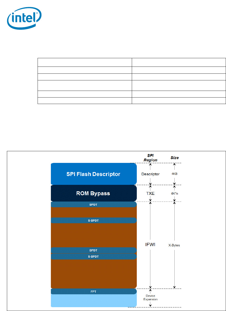
The controller can divide the SPI flash into separate regions below.
Note: This is ROM Bypass region as shown in Figure 2-1, and not TXE FW region. This region is only used in
pre-production environment.
2.6.1 Flash Region Layout
In the SPI controller, a 4K descriptor at the base of the SPI device splits the device into
regions and defines the access control to each region.
As seen in Figure 2-1, the descriptor defines at least the following device regions:
Region Content
0Descriptor
1 IFWI (Integrated Firmware Image)
2TXE ROM Bypass - Intel
® Trusted Execution Engine
Firmware (Intel® TXE FW) ROM Bypass
4 PDR (Platform Data Region)
5 Device Expansion
Figure 2-1. SPI Flash Regions Layout

CDI/IBP#: 559702 Intel Confidential 15
SPI Flash Architecture
1. TXE ROM Bypass Region: Starting from offset 4K. This region is used for TXE
ROM Bypass. When TXE ROM Bypass does not exist, this region size is 0.
2. IFWI Region: This region starts after TXE ROM Bypass region spanning over the
rest of the SPI flash until the next region (i.e. Device Expansion or other regions
defined by OEM). Size is estimated to be at 7MB.
3. Device Expansion: The Size is defined at build time estimated to be 1MB.
Note: FPT in the above diagram is Flash Partition Table for TXE FW usage.
2.6.2 Flash Region Sizes
SPI flash space requirements differ by platform and configuration. Refer to
documentation specific to your platform for BIOS and TXE ROM Bypass Region flash
size estimates.
Refer SPI Flash Regions section of the latest APL SoC External Design Specification
(EDS) of Apollo Lake platform for more detailed information.
2.7 Hardware Sequencing
Host/Bios and TXE may read/write /erase flash via Hardware Sequencing or Software
Sequencing registers.
APL SoC Hardware sequencing has been enhanced to include all operations the BIOS
needs to perform.
Note: Host / Bios Software Sequencing is not supported in Apollo Lake.
Note: OEM EC may also have access to IFWI region.
Hardware sequencing has a predefined list of opcodes, the SoC discovers the 4k and
64k erase opcodes via SFDP.
Refer Serial Peripheral Interface Memory Mapped Configuration Registers in
Apollo Lake External Design Specification (EDS) for more details.
§ §

CDI/IBP#: 559702 Intel Confidential 17
SPI Flash Compatibility Requirement
3SPI Flash Compatibility
Requirement
3.1 Apollo Lake SoC SPI Flash Requirements
• Apollo Lake SoC allows for up to two SPI flash devices to store BIOS, and Intel®
TXE FW.
—Intel
® TXE FW is required for Apollo Lake based platforms.
— Each SPI component can support up to 64 MB (128 MB total addressable) using
26-bit addressing
• 1.8V SPI I/O buffer VCC
• SPI Fast Read instruction is supported and frequency of 14MHz, 25MHz, 40MHz and
50MHz
• SPI Dual Output and Dual I/O Fast read instruction is supported with frequency of
14MHz, 25MHz, 40MHz and 50MHz
• SPI Quad Output and Quad I/O Fast read instruction is supported with frequency of
14MHz, 25MHz, 40MHz and 50MHz
Note: In order to meet best performance, frequencies above must use the highest SPI
configurations.
If there are two SPI components, both components have to support fast read in order
to enable Fast Read.
Flash devices that contain a QE bit must be configured with QE=1. No special
configuration is required for flash devices that support Quad mode but do not contain a
Quad Enable (QE) bit. Several manufacturers offer SKU’s with QE=1 by default.
3.1.1 General Requirements
• Erase size capability of: 4 KBytes erase must be supported uniformly across the
flash array. If 64k erase is also supported, then it must be supported uniformly
across the flash array.
• Serial flash device must ignore the upper address bits such that an address of
FFFFFFh aliases to the top of the flash memory.
• SPI Compatible Mode 0 support: Clock phase is 0 and data is latched on the rising
edge of the clock.
• If the device receives a command that is not supported or incomplete (less than 8
bits), the device must discard the cycle gracefully without any impact on the flash
content.
• An erase command (page, sector, block, chip and so on.) must set all bits inside the
designated area (page, sector, block, chip and so on.) to 1 (Fh).
• Status Register bit 0 must be set to 1 when a write, erase or write to status register
is in progress and cleared to 0 when a write or erase is NOT in progress.

SPI Flash Compatibility Requirement
18 Intel Confidential CDI/IBP#: 559702
• Devices requiring the Write Enable command must automatically clear the Write
Enable Latch at the end of Data Program instructions.
• The flexibility to perform a write between 1 byte to 64 bytes is required.
• SFDP fields: dword 1, bit 4 “Write Enable Instruction”. Dword 1, bit 3 “Volatile
Status Register”, both bits must be 0.
Intel Trusted Execution Engine Firmware must meet the SPI flash based BIOS
Requirements plus:
•2.2 Serial Flash Discoverable Parameter (SFDP)
•3.1.2 JEDEC ID (Opcode 9Fh)
•3.1.3 Multiple Page Write Usage Model
•3.1.4 Hardware Sequencing Requirements
Write protection scheme must meet guidelines as defined in Section 3.1 Apollo Lake
SoC SPI Flash Requirements.
3.1.2 JEDEC ID (Opcode 9Fh)
Since each serial flash device may have unique capabilities and commands, the JEDEC
ID is the necessary mechanism for identifying the device so the uniqueness of the
device can be comprehended by the controller (master). The JEDEC ID uses the opcode
9Fh and a specified implementation and usage model. This JEDEC Standard
Manufacturer and Device ID read method is defined in Standard JESD21-C, PRN03-NV1
and is available on the JEDEC website: www.jedec.org.
3.1.3 Multiple Page Write Usage Model
Intel platforms have firmware usage models require that the serial flash device support
multiple writes to a page (minimum of 512 writes) without requiring a preceding erase
command. BIOS commonly uses capabilities such as counters that are used for error
logging and system boot progress logging. These counters are typically implemented
by using byte-writes to ‘increment’ the bits within a page that have been designated as
the counter. The Intel firmware usage models require the capability for multiple data
updates within any given page. These data updates occur via byte-writes without
executing a preceding erase to the given page. Both the BIOS and Intel Management
Engine firmware multiple page write usage models apply to sequential and non-
sequential data writes.
Flash parts must also support the writing of a single byte 1024 times in a single 256-
byte page without erase. There will be 64 pages where this usage model will occur.
These 64 pages will be every 16 kilobytes.

CDI/IBP#: 559702 Intel Confidential 19
SPI Flash Compatibility Requirement
3.1.4 Hardware Sequencing Requirements
The following table contains a list of commands and the asSoCiated opcodes that a SPI-
based serial flash device must support in order to be compatible with hardware
sequencing.
3.2 APL SoC SPI AC and DC Electrical Compatibility
Guidelines
For all AC and DC electrical compatibility requirements, refer Apollo Lake Platform
External Design Specification (EDS).
§ §
Commands OPCODE Notes
Write to Status
Register 01h Writes a byte to SPI flash’s status register. Enable Write to
Status Register command must be run prior to this command
Program Data 02h Single byte or 64 byte write as determined by flash part
capabilities and software
Read Data 03h
Write Disable 04h
Read Status 05h Outputs contents of SPI flash’s status register
Write Enable 06h
Fast Read 0Bh
Enable Write to Status
Register 06h If write-status 01h requires a write-enable, then 06h must
enable write-status.
Erase Programmable/
Discoverable 4 Kbyte erase. Uses the value from SFDP (if available) else
value from VSCCn Erase Opcode register value
Erase Programmable/
Discoverable 64K erase.
Chip Erase C7h and/or 60
JEDEC ID 9Fh Refer Section 3.1.2 for more information.
Dual Output Fast Read 3Bh/ Discoverable Discoverable opcodes are obtained from each component’s
SFDP table
Read SFDP 5Ah Uses fast read timing with 8 wait states
Enable 32-bit
addressing mode B7h
Dual I/O Fast Read Discoverable Opcode is optained from each component’s SFDP table
Quad I/O Fast Read Discoverable Opcode is optained from each component’s SFDP table
CDI/IBP#: 559702 Intel Confidential 21
Flash Descriptor
4Flash Descriptor
The Flash Descriptor is a data structure that is programmed on the SPI flash part on
Apollo Lake based platforms. The Descriptor data structure describes the layout of the
flash as well as defining configuration parameters for the SoC. The descriptor is on the
SPI flash itself and is not in memory mapped space like SoC programming registers.
The maximum size of the Flash Descriptor is 4 KBytes. It requires its own discrete
erase block, so it may need greater than 4 KBytes of flash space depending on the flash
architecture that is on the target system.
The information stored in the Flash Descriptor can only be written during the
manufacturing process as its read/write permissions must be set to Read Only when
the computer leaves the manufacturing floor.
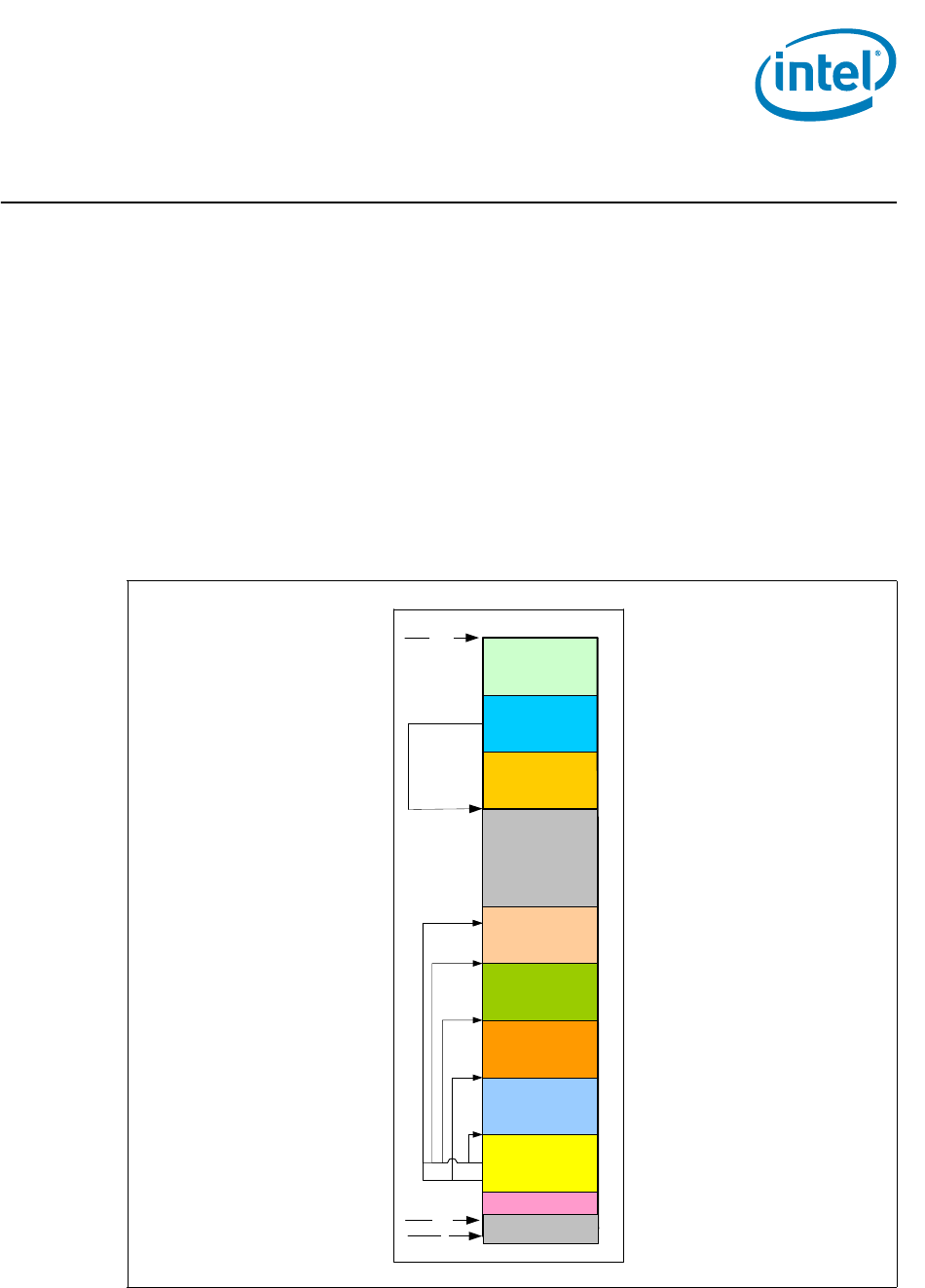
The Descriptor has 9 parts:
Figure 4-1. Flash Descriptor (APL SoC)
10h
4KB
TXE VSCC
Table
Descriptor
Upper MAP
OEM Section
Reserved
Signature
Descriptor
MAP
Component
Region
Master
SoC Soft
Straps
Reserved
0

Flash Descriptor
22 Intel Confidential CDI/IBP#: 559702
• The Flash signature at the bottom of the flash (offset 10h) must be 0FF0A55Ah in
order to be in Descriptor mode.
•The Reserved section at offset 0h is the first 16 bytes of the Flash Descriptor.
These bytes are simply reserved.
•The Flash Signature at the bottom of the flash (offset 10h) must be 0FF0A55Ah in
order to be in Descriptor mode.
•The Descriptor Map has pointers to the lower five descriptor sections as well as
the size of each.
•The Component section has information about the SPI flash part(s) the system. It
includes the number of components, density of each component, read, write and
erase frequencies and invalid instructions.
•The Region section defines the base and the limit of the IFWI, TXE ROM Bypass
region, Device Expansion regions as well as their size.
•The Master region contains the hardware security settings for the flash, granting
read/write permissions for each region and identifying each master.
• APL platform SoC Soft Strap sections contain Apollo Lake SoC configurable
parameters.
•The Reserved region between the top of the Soft Straps is for future SoC usage.
•The Descriptor Upper Map determines the length and base address of the Intel®
TXE VSCC Table.
•The Intel® TXE VSCC Table holds the JEDEC ID and the VSCC information for all
the SPI Flash part(s) supported by the NVM image. BIOS write and erase
capabilities depend on LVSCC and UVSCC register in SPIBAR memory space.
•OEM Section is 256 Byte section reserved at the top of the Flash Descriptor for
use by the OEM.
Refer SPI Supported Feature Overview and Flash Descriptor Records in the
Apollo Lake Platform External Design Specification (EDS).
4.1 Flash Descriptor Content
The following sections describe the data structure of the Flash Descriptor on the SPI
device. These are not registers or memory space within SoC. FDBAR - is address 0x0
on the SPI flash device on chip select 0.
Recommended flash descriptor map:
Region Name Starting Address
Signature 0x10
Component FCBA 0x30
Regions FRBA 0x40
Masters FMBA 0x80
SoC Straps FPSBA 0x100

CDI/IBP#: 559702 Intel Confidential 23
Flash Descriptor
4.1.1 Descriptor Signature and Map
4.1.1.1 FLVALSIG - Flash Valid Signature
(Flash Descriptor Records)
Memory Address:FDBAR + 010h Size: 32 bits
Recommended Value:0FF0A55Ah
4.1.1.2 FLMAP0 - Flash Map 0 Register
(Flash Descriptor Records)
Memory Address: FDBAR + 014h Size: 32 bits
Bits Description
31:00
Flash Valid Signature. This field identifies the Flash Descriptor sector as valid. If the contents at
this location do not return the expected value, then the Flash Descriptor region is assumed to be un-
programmed or corrupted and is not usable.
Flash Valid Signature[31:00]: 0FF0A55Ah
Bits Description
31:27 Reserved
26:24 Reserved
23:16
Flash Region Base Address (FRBA). This identifies address bits [11:4] for the Region portion of
the Flash Descriptor. Bits [24:12] and bits [3:0] are 0.
Set this value to 04h. This will define FRBA as 40h.
15:13 Reserved
12
Fingerprint sensor on shared flash/TPM SPI bus
0 : no fingerprint sensor is connected to CS1
1 : a fingerprint sensor is connected to CS1 and acting as a flash device
Note: Hardware does not use this field.
This value must be read directly from flash. It's not available via Host FDOC/FDOD registers.
11
Touch on dedicated SPI bus
0 : no touch device is connected to the dedicated Touch SPI bus
1 : a touch device is connected to the dedicated Touch SPI bus
Note: Hardware does not use this field.
This value must be read directly from flash. It's not available via Host FDOC/FDOD registers.
10 Reserved
9:08
Number Of Components (NC). This field identifies the total number of Flash Components. Each
supported Flash Component requires a separate chip select.
00 = 1 Component
01 = 2 Components
All other settings = Reserved
7:00
Flash Component Base Address (FCBA). This identifies address bits [11:4] for the Component
portion of the Flash Descriptor. Bits [24:12] and bits [3:0] are 0.
set this field to 03h. This will define FCBA as 30h

Flash Descriptor
24 Intel Confidential CDI/IBP#: 559702
4.1.1.3 FLMAP1 - Flash Map 1 Register
(Flash Descriptor Records)
Memory Address: FDBAR + 018h Size: 32 bits
Recommended Value:
4.1.1.4 FLMAP2—Flash Map 2 Register
(Flash Descriptor Records)
Memory Address: FDBAR + 01Ch Size: 32 bits
Bits Description
31:24
SoC Strap Length (PSL). Identifies the 1s based number of Dwords of SoC Straps to be read, up
to 255 DWs (1KB) max. A setting of all 0's indicates there are no SoC DW straps.
This field MUST be set to 13h
23:16
SoC Flash Strap Base Address (FPSBA). This identifies address bits [11:4] for the SoC Strap
portion of the Flash Descriptor. Bits [24:12] and bits [3:0] are 0.
Set this field to 10h. This will define FPSBA to 100h
15:11 Reserved
10:8
Number Of Masters (NM). This field identifies the total number of Flash Masters.
Set this field to 10b
Note: This field is not used by the Flash Controller.
7:0
Flash Master Base Address (FMBA). This identifies address bits [11:4] for the Master portion of
the Flash Descriptor. Bits [24:12] and bits [3:0] are 0.
Set this field to 08h. This will define FMBA as 80h
Bits Description
31:0 Reserved, set to 0

CDI/IBP#: 559702 Intel Confidential 25
Flash Descriptor
4.1.2 Flash Descriptor Component Section
4.1.2.1 FLCOMP—Flash Components Register
(Flash Descriptor Records)
The following section of the Flash Descriptor is used to identify the different SPI Flash
Components and their capabilities.
Memory Address: FCBA + 000h Size: 32 bits
Bits Default
Value Description
31 1'h0 Reserved
30 1'h0
Dual Output Fast Read Support
0 = Dual Output Fast Read is not supported
1 = Dual Output Fast Read is supported
Notes:
1. If the Dual Output Fast Read Support bit is set to 1b, the Dual Output Fast
Read instruction is issued in all cases where the Fast Read would have been
issued
2. The Frequencies supported for the Dual Output Fast Read are the same as
those supported by the Fast Read Instruction
3. If more than one Flash component exists, this field can only be set to “1” if
both component support Dual Output Fast Read
4. The Dual output Fast Read is only supported using the 3Bh opcode and dual
read only affect the read data, not the address phase.
5. This field only has effect if the SFDP parameter table is not detected. If the
SDFDP parameter table is detected, this field is ignored and SFDP discovered
parameter is used instead
6. This bit will be deprecated as all supported devices will contain SFDP
29:27 3'h2
Read ID and Read Status Clock Frequency.
001 = 50MHz
010 = 40MHz
100 = 25MHz
110 = 14MHz
All other Settings = Reserved
Note: If more than one Flash component exists, this field must be set to the
lowest common frequency of the different Flash components.
26:24 3'h2
Write and Erase Clock Frequency.
001 = 50MHz
010 = 40MHz
100 = 25MHz
110 = 14MHz
All other Settings = Reserved
Note: If more than one Flash component exists, this field must be set to the
lowest common frequency of the different Flash components.
23:21 3'h2
Fast Read Clock Frequency. This field identifies the frequency that can be used
with the Fast Read instruction. This field is undefined if the Fast Read Support field
is '0'.
001 = 50MHz
010 = 40MHz
100 = 25MHz
110 = 14MHz
All other Settings = Reserved
Note: If more than one Flash component exists, this field must be set to the
lowest common frequency of the different Flash components.

Flash Descriptor
26 Intel Confidential CDI/IBP#: 559702
20 1'h1
Fast Read Support.
0 = Fast Read is not Supported
1 = Fast Read is supported
If the Fast Read Support bit is a '1' and a device issues a Direct Read or issues a
read command from the Hardware Sequencer and the length is greater than 4
bytes, then the SPI Flash instruction should be “Fast Read”. If the Fast Read Support
is a '0' or the length is 1-4 bytes, then the SPI Flash instruction should be “Read”.
If the Fast Read Support bit is a '1', SoC will issue a fast read command everywhere
a read command would have been issued, independent of the number of bytes
being read. This bit applies to flash accesses, not Touch or TPM.
Reads to the Flash Descriptor always use the Read command independent of the
setting of this bit.
Notes:
1. If more than one Flash component exists, this field can only be set to '1' if both
components support Fast Read.
2. It is strongly recommended to set this bit to 1b
19:17 3'h6 Read Clock Frequency.
110 = 17MHz
All other settings = Reserved
16 1'h0 Reserved
15 1'h0 Reserved
14 1'h0 Reserved
13 1'h0 Reserved
12 1'h0 Reserved
11:10 1'h0 Reserved
9 1'h1 Reserved, set to ‘1’
8 1'h0 Reserved
7:04 4'hF Reserved
3:00 4'h4 Reserved
Bits Default
Value Description

CDI/IBP#: 559702 Intel Confidential 27
Flash Descriptor
4.1.2.2 FLILL—Flash Invalid Instructions Register
(Flash Descriptor Records)
Memory Address: FCBA + 004h Size: 32 bits
4.1.2.3 FLILL1—Flash Invalid Instructions Register
(Flash Descriptor Records)
Memory Address: FCBA + 008h Size: 32 bits
4.1.3 Flash Descriptor Region Section
The following section of the Flash Descriptor is used to identify the different Regions of
the NVM image on the SPI flash.
Flash Regions:
• Bit 26 represents a linear address when 2 Flash components are used and the
linear address exceeds 64MB. Bit 26 is never driven during the SPI address phase.
The registers support up to 128MB of addressable Flash using 2 64MB flash
components.
Bits Description
31:24 Invalid Instruction 3. Refer definition of Invalid Instruction 0
Set to: 0xAD
23:16 Invalid Instruction 2. Refer definition of Invalid Instruction 0
Set to: 0x60
15:8 Invalid Instruction 1. Refer definition of Invalid Instruction 0
Set to: 0x42
7:0
Invalid Instruction 0.
Set to: 0x21
Opcode for an instruction that the Flash Controller should protect against, such as Chip Erase. This
byte should be set to 0 if there are no invalid instructions to protect against for this field. Opcodes
programmed in the Software Sequencing Opcode Menu Configuration and Prefix-Opcode
Configuration are not allowed to use any of the Invalid Instructions listed in this register.
Bits Description
31:24 Invalid Instruction 7. Refer definition of Invalid Instruction 0
Set to: 0xC7
23:16 Invalid Instruction 6. Refer definition of Invalid Instruction 0
Set to: 0xC4
15:8 Invalid Instruction 5. Refer definition of Invalid Instruction 0
Set to: 0xB9
7:0 Invalid Instruction 4. Refer definition of Invalid Instruction 0
Set to: 0xB7
Flash Descriptor
28 Intel Confidential CDI/IBP#: 559702
• If a particular region is not using SPI Flash, the particular region should be disabled
by setting the Region Base to all 1's, and the Region Limit to all 0's (base is higher
than the limit)
• For each region except FLREG0, the Flash Controller must have a default Region
Base of 7FFFh and the Region Limit to 0000h within the Flash Controller in case the
Number of Regions specifies that a region is not used.
• Flash region limit field is inclusive, i.e. an address is valid if base[26:12] <=
address[26:12] <= limit[26:12]. Other checks prevent any single access from
crossing a 4k address boundary.
• Each Region entry follows the template in Table 4-1. Each row in the Table 4-2
represents a Region entry in the descriptor. Most masters are given permission to
access their region(s) independent of the descriptor FLMSTR setting, refer Section
4.1.4, “Flash Descriptor Master Section”.
Table 4-1. Region Definition Template
Bits Description
31 Reserved
30:16 Region Limit. This specifies bits 26:12 of the ending address for this Region.
15 Reserved
14:0 Region Base. This specifies address bits 26:12 for the Region Base.
Table 4-2. Region Entries in Descriptor
Offset from FRBA Register Name Region Name
0 FLREG0 Descriptor
4h FLREG1 IFWI
8h FLREG2 TXE1
Notes:
1. This is ROM Bypass region as shown in Figure 2-1, “SPI Flash Regions Layout”. This region is only used in
pre-production environment.
10h FLREG4 PDR
14h FLREG5 Device Expansion #1

CDI/IBP#: 559702 Intel Confidential 29
Flash Descriptor
4.1.3.1 FLREG0—Flash Region 0 (Flash Descriptor) Register
(Flash Descriptor Records)
Memory Address: FRBA + 000h Size: 32 bits
Recommended Value: 00000000h
4.1.3.2 FLREG1—Flash Region 1 (IFWI) Register
(Flash Descriptor Records)
Memory Address: FRBA + 004h Size: 32 bits
4.1.3.3 FLREG2—Flash Region 2 (Intel® TXE) Register
(Flash Descriptor Records)
Memory Address: FRBA + 008h Size: 32 bits
Bits Description
31 Reserved
30:16
Region Limit. This specifies bits 26:12 of the ending address for this Region.
Notes:
1. Set this field to 0b. This defines the ending address of descriptor as being FFFh.
2. Region limit address Bits[11:0] are assumed to be FFFh
15 Reserved
14:0 Region Base. This specifies address bits 26:12 for the Region Base.
Note: Set this field to all 0s. This defines the descriptor address beginning at 0h.
Bits Description
31 Reserved
30:16
Region Limit. This specifies bits 26:12 of the ending address for this Region.
Notes:
1. Must be set to 0000h if BIOS region is unused (on Firmware hub)
2. Ensure BIOS region size is a correct reflection of actual BIOS image that will be used in the
platform
3. Region limit address Bits[11:0] are assumed to be FFFh
15 Reserved
14:0 Region Base. This specifies address bits 26:12 for the Region Base.
Note: If the BIOS region is not used, the Region Base must be programmed to 7FFFh
Bits Description
31 Reserved
30:16
Region Limit. This specifies bits 26:12 of the ending address for this Region.
Notes:
1. This region hold ROM Bypass
2. Region limit address Bits[11:0] are assumed to be FFFh
15 Reserved
14:0 Region Base. This specifies address bits 26:12 for the Region Base.

Flash Descriptor
30 Intel Confidential CDI/IBP#: 559702
4.1.3.4 FLREG4—Flash Region 4 (Platform Data Region) Register
(Flash Descriptor Records)
Memory Address: FRBA + 010h Size: 32 bits
4.1.3.5 FLREG5—Flash Region 5 (Device Expansion) Register
(Flash Descriptor Records)
Memory Address: FRBA + 014h Size: 32 bits
4.1.4 Flash Descriptor Master Section
These DWORDs in flash define which regions each master may access using
programmed accesses. They do not apply to direct reads.
Each Master entry in the descriptor follows the template in Table 4-3. Each row in
Table 4.1.4.1 represents a Master entry in the descriptor.
Bits Description
31 Reserved
30:16
Region Limit. This specifies bits 26:12 of the ending address for this Region.
Notes:
1. If PDR Region is not used, the Region Limit must be programmed to 0000h
2. Ensure PDR region size is a correct reflection of actual PDR image that will be used in the
platform
3. Region limit address Bits[11:0] are assumed to be FFFh
15 Reserved
14:0 Region Base. This specifies address bits 26:12 for the Region Base.
Note: If the Platform Data region is not used, the Region Base must be programmed to 7FFFh
Bits Description
31 Reserved
30:16
Region Limit. This specifies bits 26:12 of the ending address for this Region.
Notes:
1. If Device Expansion Region is not used, the Region Limit must be programmed to 0000h
2. Region limit address Bits[11:0] are assumed to be FFFh
15 Reserved
14:0 Region Base. This specifies address bits 26:12 for the Region Base.
Note: If the Device Expansion region is not used, the Region Base must be programmed to 7FFFh
Table 4-3. Flash Master Template
Bits Description
31:20
Master Region Write Access:
Each bit [31:20] corresponds to Regions [11:0]. If the bit is set, this master can erase and write
that particular region through register accesses.
Note: The flash controller may ignore some bits in each register because Masters are granted
default permission to their regions, e.g. BIOS has default R/W permission to BIOS regions.
Table 4.1.4.1.
19:8 Master Region Read Access:
Each bit [19:8] corresponds to Regions [11:0]. If the bit is set, this master can read that particular
region through register accesses.

CDI/IBP#: 559702 Intel Confidential 31
Flash Descriptor
4.1.4.1 FLMSTR1—Flash Master 1 (Host CPU/ BIOS)
Memory Address: FMBA + 000h Size: 32 bits
4.1.4.2 FLMSTR2—Flash Master 2 (Intel® TXE)
Memory Address: FMBA + 004h Size:32 bits
4.1.5 SoC Softstraps
Refer Chapter 9, “Flash Descriptor SoC Configuration” for details.
7:4 Extended Region Write Access:
Each bit [7:4] corresponds to Regions [15:12]. If the bit is set, this master can erase and write that
particular region through register accesses.
3:0 Extended Region Read Access:
Each bit [3:0] corresponds to Regions [15:12]. If the bit is set, this master can erase and write that
particular region through register accesses.
Table 4-3. Flash Master Template
Bits Description
Bits Description
31:20
Master Region Write Access: Each bit [31:20] corresponds to Regions [11:0]. If the bit is set,
this master can erase and write that particular region through register accesses.
Note: Bit 21 and 26 are does not care as the primary master always has read/write permission to its
primary region
19:8
Master Region Read Access: Each bit [19:8] corresponds to Regions [11:0]. If the bit is set, this
master can read that particular region through register accesses.
Note: Bit 9 and 14 are don’t care as the primary master always read/write permission to its
primary region.
7:0 Reserved
Bits Description
31:20
Master Region Write Access: Each bit [31:20] corresponds to Regions [11:0]. If the bit is set,
this master can erase and write that particular region through register accesses.
Note: Bit 22 is a does not care as the primary master always has read/write permission to its
primary region
19:8
Master Region Read Access: Each bit [19:8] corresponds to Regions [11:0]. If the bit is set, this
master can read that particular region through register accesses.
Note: Bit 10 is a does not care as the primary master always read/write permission to its primary
region.
7:0 Reserved

Flash Descriptor
32 Intel Confidential CDI/IBP#: 559702
4.1.6 Descriptor Upper Map Section
4.1.6.1 FLUMAP1—Flash Upper Map 1
(Flash Descriptor Records)
Memory Address:FDBAR + EFCh Size: 32 bits
Note: The Upper MAP is used by BIOS and TXE FW. HW does not read this section.
4.1.7 Intel® TXE Vendor Specific Component Capabilities Table
Entries in this table allow support for a SPI flash part for Intel Trusted Execution Engine
capabilities.
Since Flash Partition Boundary Address (FPBA) has been removed, UVSCC and LVSCC
has been replaced with VSCC0 and VSCC1 in Apollo Lake Platform. VSCC0 is for SPI
component 0 and VSCC1 is for SPI component 1.
Each VSCC table entry is composed of two 32 bit fields: JEDEC IDn and the
corresponding VSCCn value.
Refer 4.4 Intel® TXE Vendor-Specific Component Capabilities (Intel® TXE VSCC) Table
for information on how to program individual entries.
4.1.7.1 JID0—JEDEC-ID 0 Register
(Flash Descriptor Records)
Memory Address: VTBA + 000h Size: 32 bits
Bits Default Description
31:16 0 Reserved
15:8 1 Intel® TXE VSCC Table Length (VTL). Identifies the 1s based number of
DWORDS contained in the VSCC Table. Each SPI component entry in the table is 2
DWORDS long.
7:0 1 Intel® TXE VSCC Table Base Address (VTBA). This identifies address bits
[11:4] for the VSCC Table portion of the Flash Descriptor. Bits [26:12] and bits
[3:0] are 0.
Bits Description
31:24 Reserved
23:16 SPI Component Device ID 1. This field identifies the second byte of the Device ID of the SPI Flash
Component. This is the third byte returned by the Read JEDEC-ID command (opcode 9Fh).
15:08 SPI Component Device ID 0. This field identifies the first byte of the Device ID of the SPI Flash
Component. This is the second byte returned by the Read JEDEC-ID command (opcode 9Fh).
7:00 SPI Component Vendor ID. This field identifies the one byte Vendor ID of the SPI Flash
Component. This is the first byte returned by the Read JEDEC-ID command (opcode 9Fh).

CDI/IBP#: 559702 Intel Confidential 33
Flash Descriptor
4.1.7.2 VSCC0—Vendor Specific Component Capabilities 0
(Flash Descriptor Records)
Memory Address: VTBA + 004h Size: 32 bits
Note: VSCC0 applies to SPI flash that connected to CS0.
4.1.7.3 JIDn—JEDEC-ID Register n
(Flash Descriptor Records)
Memory Address: VTBA + (n*8)h Size:32 bits
“n” is an integer denoting the index of the Intel® TXE VSCC table. Refer 4.1.7.1 JID0—
JEDEC-ID 0 Register (Flash Descriptor Records) for details.
4.1.7.4 VSCCn—Vendor Specific Component Capabilities n
(Flash Descriptor Records)
Memory Address: VTBA + 004h + (n*8)h Size: 32 bits
“n” is an integer denoting the index of the Intel® TXE VSCC table. Refer 4.1.7.2
VSCC0—Vendor Specific Component Capabilities 0 (Flash Descriptor Records) for
details.
Bits Description
31:16 Reserved
15:8 Erase Opcode (EO). This field must be programmed with the Flash erase instruction opcode that
corresponds to the erase size that is in BES.
7:5
Quad Enable Requirements (QER)
000 = Device does not have a QE bit. Device detects 1-1-4 and 1-4-4 reads based on instruction.
DQ3 / HOLD# functions as hold during instruction phase.
001 = QE is bit 1 of status register 2. It is set via Write Status with two data bytes where bit 1 of
the second byte is one. It is cleared via Write Status with two data bytes where bit 1 of the
second byte is zero. Writing only one byte to the status register has the side effect of clearing
status register 2, including the QE bit. The 100b code is used if writing one byte to the status
register does not modify status register 2.
010 = QE is bit 6 of status register 1. It is set via Write Status with one data byte where bit 6 is
one. It is cleared via Write Status with one data byte where bit 6 is zero.
011 = QE is bit 7 of status register 2. It is set via Write status register 2 instruction 3Eh with one
data byte where bit 7 is one. It is cleared via Write status register 2 instruction 3Eh with one
data byte where bit 7 is zero. The status register 2 is read using instruction 3Fh.
100 = QE is bit 1 of status register 2. It is set via Write Status with two data bytes where bit 1 of
the second byte is one. It is cleared via Write Status with two data bytes where bit 1 of the
second byte is zero. In contrast to the 001b code, writing one byte to the status register does
not modify status register 2.
101 = QE is bit 1 of the status register 2. Status register 1 is read using Read Status instruction
05h. Status register 2 is read using instruction 35h. QE is set via Write Status instruction 01h
with two data bytes where bit 1 of the second byte is one. It is cleared via Write Status with
two data bytes where bit 1 of the second byte is zero.
other = reserved
Note: Refer Table note#1 below for details.
4:0 Reserved set to 00101b
Note: The manufacturers information included in the QER list are for guidance purpose. Some manufacturer
devices operate as shown in the table above. Check manufacturer’s data sheet for exact
requirements.

Flash Descriptor
34 Intel Confidential CDI/IBP#: 559702
4.2 OEM Section
Memory Address: F00h Size: 256 Bytes
256 Bytes are reserved at the top of the Flash Descriptor for use by the OEM (F00h -
FFFh). The information stored by the OEM can only be written during the manufacturing
process as the Flash Descriptor read/write permissions must be set to Read Only when
the computer leaves the manufacturing floor. The SoC Flash controller does not read
this information. FFh is suggested to reduce programming time.
4.3 Region Access Control
Regions of the flash can be defined from read or write access by setting a protection
parameter in the Master section of the Descriptor. There are only two masters that
have the ability to access other regions: CPU/BIOS, and Intel® TXE Firmware running
on SoC.
4.3.1 Intel Recommended Permissions for Region Access
The following Intel recommended read/write permissions are necessary to secure
Intel® TXE and Intel® TXE FW.
The table below shows the values to be inserted into the Flash Image Tool (FIT). The
values below will provide the access levels described in the table above.
4.3.2 Overriding Region Access
Once access Intel recommended Flash settings have been put into the flash descriptor,
it may be necessary to update the TXE FW with a Host program or write a new Flash
descriptor.
Table 4-4. Region Access Control Table Options
Master Read/Write Access
Region (#) CPU and BIOS TXE
Descriptor (0) Read Only Read Only
IFWI (1) Read / Write Read only
TXE ROM Bypass (2) Not Accessible Read / Write
PDR (4) Read / Write Not Accessible
Device Expansion (5) Not Accessible Read / Write
Notes:
1. Descriptor, Device Expansion and PDR region is not a master, so they will not have Master R/W access.
2. Descriptor should NOT have write access by any master in production systems.
3. PDR region should only have read and/or write access by CPU/Host. TXE should NOT have access to PDR
region.
Table 4-5. Recommended Read/Write Settings for Platforms
BIOS TXE
Read 000‡ 0011 = 0x‡3 0010 0111 = 0x27
Write 000‡ 0010 = 0x‡2 010 0100 = 0x24
Note: ‡ = Value dependent on if PDR is implemented and if Host access is desired per OEM.

CDI/IBP#: 559702 Intel Confidential 35
Flash Descriptor
Assert GPIO_118 HIGH during the rising edge of RSM_RST_N to set the Flash
descriptor override strap.
This strap should only be visible and available in manufacturing or during product
development.
After this strap has been set you can use a host based flash programming tool like
FPT.exe to write/read any area of serial flash that is not protected by Protected Range
Registers. Any area of flash protected by Protected range Registers will still NOT be
writable/readable.
Refer 6.3 SPI Protected Range Register Recommendations for more details.
4.4 Intel® TXE Vendor-Specific Component
Capabilities (Intel® TXE VSCC) Table
The Intel® TXE VSCC Table defines how the Intel® TXE will communicate with the
installed SPI flash if there is no SFDP table found. This table is defined in the descriptor
and is the responsibility of who puts together the NVM image. VSCCn registers are
defined in memory space and must be set by BIOS. This table must define every flash
part that is intended to be used. The size (number of max entries) of the table is
defined in 4.1.6.1 FLUMAP1—Flash Upper Map 1 (Flash Descriptor Records). Each Table
entry is made of two parts: the JEDEC ID and VSCC setting.7
If using Flash Image Tool (FIT) refer System Tools user guide in the Intel® TXE FW kit
and the respective FW Bring up Guide on how to build the image. If not, refer 4.1.6.1
FLUMAP1—Flash Upper Map 1 (Flash Descriptor Records) through Section 4.2 OEM
Section.
4.4.1 How to Set a VSCC Entry in Intel® TXE VSCC Table for
Apollo Lake Platforms
VSCC0 needs to be programmed in instances where there is only SPI component in the
system. When using an asymmetric flash component (part with two different sets of
attributes based on address) VCSCC0 and VSCC1 will need to be used. This includes if
the system is intended to support both symmetric AND asymmetric SPI flash parts.
Refer Section 337H4.4.2 Intel® TXE VSCC Table Settings for Apollo Lake Systems.
Refer text below the table for explanation on how to determine Intel Trusted Execution
Engine VSCC value.
Table 4-6. Jidn - JEDEC ID Portion of Intel® TXE VSCC Table
Bits Description
31:24 Reserved.
23:16 SPI Component Device ID 1: This identifies the second byte of the Device ID of the SPI Flash
Component. This is the third byte returned by the Read JEDEC-ID command (opcode 9Fh).
15:8 SPI Component Device ID 0: This identifies the first byte of the Device ID of the SPI Flash
Component. This is the second byte returned by the Read JEDEC-ID command (opcode 9Fh).
7:0 SPI Component Vendor ID: This identifies the one byte Vendor ID of the SPI Flash Component.
This is the first byte returned by the Read JEDEC-ID command (opcode 9Fh).

Flash Descriptor
36 Intel Confidential CDI/IBP#: 559702
Erase Opcode (EO) and Block/Sector Erase Size (BSES) should be set based on
the flash part and the firmware on the platform. For Intel® TXE enabled platforms this
should be 4 KB.
Table 4-7. Vsccn – Vendor-Specific Component Capabilities Portion of the Apollo Lake
SoC Platforms
Bits Description
31:16 Reserved
15:8 Erase Opcode (EO). This field must be programmed with the Flash erase instruction opcode that
corresponds to the erase size that is in BES.
7:5
Quad Enable Requirements (QER)
000 = Part does not require a Quad Enable bit to be set, either because Quad is not supported or
because the manufacturer permanently enables Quad capability (e.g. Micron, Numonyx).
001 = Part requires bit 9 in status register 2 to be set to enable quad IO. Writing one byte to status
register clears all bits in register 2, therefore status register writes MUST be two bytes. If
the status register is unlocked and SFDP bits WSR or VSCC WSR is 1 then SPI controller can-
not use the quad output, quad IO features of this part because the hardware will automati-
cally write one byte of zeros to status register with every write/erase. (e.g. Winbond, AMIC,
Spansion).
010 = Part requires bit 6 of status register 1 to be set to enable quad IO. If the status register is
unlocked and SFDP WSR bit or VSCC WSR is 1 then flash controller cannot use the quad out-
put, quad IO features of this part because the hardware will automatically write one byte of
zeros to status register with every write/erase (e.g. Macronix).
011 = Part requires bit 7 of the configuration register to be set to enable Quad (e.g. Atmel).
100 = Part requires bit 9 in status register 2 to be set to enable quad IO. Writing one byte to the
status register does not clear the second byte (SST/Microchip, Winbond).
Note: Refer Table note#6 below for details.
4
Write Enable on Write Status (WEWS)
0 = 50h is the opcode used to unlock the status register on SPI flash if WSR (bit 3) is set to 1b.
1 = 06h is the opcode used to unlock the status register on SPI flash if WSR (bit 3) is set to 1b.
Note: Refer Table Note #4 below for a description how this bit is used.
3
Write Status Required (WSR)
0 = No automatic write of 00h will be made to the SPI flash’s status register)
1 = A write of 00h to the SPI flash’s status register will be sent on EVERY write and erase
performed by Intel® TXE to the SPI flash.
Note: Refer Table Note #5 below for a description how this bit is used.
2Write Granularity (WG).
0 = 1 Byte
1 = 64 Bytes
1:0
Block/Sector Erase Size (BES). This field identifies the erasable sector size for all Flash
components.
00 = 256 Bytes
01 = 4 K Bytes
10 = 8 K Bytes
11 = 64K Bytes
Notes:
1. Bit 3 (WEWS) and/or bit 4 (WSR) should not be set to ‘1’ if there are non volatile bits in the SPI flash’s
status register. This may lead to premature flash wear out.
2. This is not an atomic (uninterrupted) sequence. The SoC will not wait for the status write to complete
before issuing the next command, potentially causing SPI flash instructions to be disregarded by the
SPI flash part. If the SPI flash component’s status register is non-volatile, then BIOS should issue an
atomic software sequence cycle to unlock the flash part.
3. If both bits 3 (WSR) and 4 (WEWS) are set to 1b, then sequence of 06h 01h 00h is sent to unlock the
SPI flash on EVERY write and erase that Intel Trusted Execution Engine firmware performs.
4. If bit 3 (WSR) is set to 1b and bit 4 (WEWS) is set to 0b then sequence of 50h 01h 00h is sent to unlock
the SPI flash on EVERY write and erase that Intel Trusted Execution Engine firmware performs.
5. If bit 3 (WSR) is set to 0b and bit 4 (WEWS) is set to 0b or 1b then sequence of 60h is sent to unlock
the SPI flash on EVERY write and erase that Processor performs.
6. The manufacturers information included in the QER list are for guidance purpose. Some manufacturer
devices operate as shown in the table above. Check manufacturer’s datasheet for exact
requirements.

CDI/IBP#: 559702 Intel Confidential 37
Flash Descriptor
Write Status Required (WSR) or Write Enable on Write Status (WEWS) should
be set on flash devices that require an opcode to enable a write to the status register.
Intel® TXE Firmware will write a 00h to status register to unlock the flash part for every
erase/write operation. If this bit is set on a flash part that has non-volatile bits in the
status register then it may lead to pre-mature wear out of the flash.
• Set the WSR bit to 1b and WEWS to 0b if the Enable Write Status Register opcode
(50h) is needed to unlock the status register. Opcodes sequence sent to SPI flash
will bit 50h 01h 00h.
• Set the WSR bit to 1b AND WEWS bit to 1b if write enable (06h) will unlock the
status register. Opcodes sequence sent to SPI flash will bit 06h 01h 00h.
•Set the WSR bit to 0b AND WEWS bit to 0b or 1b, if write enable (06h) will unlock
the status register. Opcodes sequence sent to SPI flash will bit 06h
•WSR or WEWS should be not be set on devices that use non volatile
memory for their status register. Setting this bit will cause operations to be
ignored, which may cause undesired operation. Ask target flash vendor if this is the
case for the target flash. Refer 356H6.1 Unlocking SPI Flash Device Protection for Apollo
Lake Platform and 358H6.2 Locking SPI Flash via Status Register for more information.
Erase Opcode (EO) and Block/Sector Erase Size (BES) should be set based on the
flash part and the firmware on the platform.
Write Granularity (WG) bit should be set based on the capabilities of the flash
device. If the flash part is capable of writing 1 to 64 bytes (or more) with the 02h
command you can set this bit 0 or 1. Setting this bit high will result in faster write
performance. If flash part only supports single byte write only, then set this bit to 0.
Bit ranges 31:16 are reserved and should set to all zeros.
4.4.2 Intel® TXE VSCC Table Settings for Apollo Lake Systems
To understand general guidelines for BIOS VSCC settings on different SPI flash devices,
refer VSCCommn.bin Content application note (VSCCommn_bin Content.pdf under
Flash Image Tool directory).
§ §
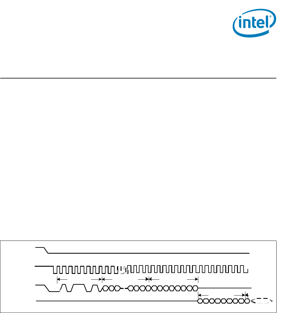
CDI/IBP#: 559702 Intel Confidential 39
Serial Flash Discoverable Parameter (SFDP)
5Serial Flash Discoverable
Parameter (SFDP)
5.1 Overview
As the feature set of serial flash progresses, there is an increasing amount of
divergence as individual vendors find different solution to adding new functionality such
as speed and addressing.
These guidelines are a standard that will allow for individual vendors to have their value
add features, but will allow for a controller to discover the attributes needed to operate.
5.2 Discoverable Parameter Opcode and Flash Cycle
The discoverable parameter read opcode behaves like a fast read command. The
opcode is 5Ah and the address cycle is 24 bit long. After the opcode 5Ah is clocked in,
there are 24 bit of address clocked in. There will then be eight clock (8 wait states)
before valid data is clocked out. There is flexibility in the number of wait states, but
they must be byte aligned (multiple of 8 wait states).
SFDP read must update at a frequency between 17 MHz and 48 MHz with a single byte
of wait state.
5.3 Parameter Table Supported on SoC
The flash controller first checks for a valid SFDP header. The value of the major and
minor revision fields in the SFDP header are don’t care. If a valid SFDP header is found,
the controller supports auto discovery of the Component Property Parameter Table
(CPPT).
The following capabilities are only supported on SoC if CPPT is successfully discovered
and parameter values indicate that they are supported. These capabilities are not
supported as default.
•Quad I/O Read
• Quad Output Read
Figure 5-1. SFDP Read Instruction Sequence
Wait States
24 B it
Address
Dis covery
Opcode
0
1
23 76 5432 1 0
76543210
6543210 7 8 9 10 28 29 3031
212322
32 33343536373839 4041424344454647
7
CS#
CLK
SI
SO
Data Byte Data Byte
Addr + 1h
Hi gh Z

Serial Flash Discoverable Parameter (SFDP)
40 Intel Confidential CDI/IBP#: 559702
•Dual I/O read
• Block /Sector Erase size
Note: If SFDP is valid and advertises 4 Kbyte erase capability, then BES is taken from the
SFDP table, otherwise it is taken from the BIOS VCSS table.
Note: Apollo Lake platform supports on SFDP compliant SPI parts. When using SFDP 1.5 and
above, there is no need to apply a VSCC entry in FIT since QER bit will be read from the
SFDP table.
SoC will also read the following opcode from parameter table and store to SoC if SFDP
is valid and the following function is supported.
• Erase Opcode
• Dual Output Fast Read Opcode
• Dual I/O Fast Read Opcode
• Quad Output Fast Read Opcode
• Quad I/O Fast Read Opcode
5.4 Detailed JEDEC Specification
Refer www.jedec.com JESD216 for detailed SFDP specification on SPI.
§ §

CDI/IBP#: 559702 Intel Confidential 41
BIOS Configuration for SPI Flash Access
6BIOS Configuration for SPI
Flash Access
6.1 Unlocking SPI Flash Device Protection for Apollo
Lake Platform
BIOS must account for any built in protection from the flash device itself. BIOS must
ensure that any flash based protection will only apply to IFWI region only. It should not
affect the TXE ROM Bypass region.
All the SPI flash devices that meet the SPI flash requirements in the Apollo Lake
External Design Specification (EDS) will be unlocked by writing a 00h to the SPI flash’s
status register. This command must be done via an atomic software sequencing to
account for differences in flash architecture. Atomic cycles are uninterrupted in that it
does not allow other commands to execute until a read status command returns a ‘not
busy’ result from the flash.
Some flash vendors implement their status registers in NVM flash (non-volatile
memory). This takes much more time than a write to volatile memory. During this
write, the flash part will ignore all commands but a read to the status register (opcode
05h). The output of the read status register command will tell the SoC when the
transaction is done.
Recommended flash unlocking sequence:
• Write enable (06h) command will have to be in the prefix opcode configuration
register.
• The “write to status register” opcode (01h) will need to be an opcode menu
configuration option.
• Opcode type for write to status register will be ‘01’: a write cycle type with no
address needed.
• The FDATA0 register should to be programmed to 0000 0000h.
• Data Byte Count (DBC) in Software Sequencing Flash Control register should be
000000b. Errors may occur if any non zero value is here.
• Set the Cycle Opcode Pointer (COP) to the “write to status register” opcode.
• Set to Sequence Prefix Opcode Pointer (SPOP) to Write Enable.
• Set the Data Cycle (DS) to 1.
• Set the Atomic Cycle Sequence (ACS) bit to 1.
• To execute sequence, set the SPI Cycle Go bit to 1.
Refer Serial Peripheral Interface Memory Mapped Configuration Registers in
the Apollo Lake External Design Specification (EDS) for more detailed information.

BIOS Configuration for SPI Flash Access
42 Intel Confidential CDI/IBP#: 559702
6.2 Locking SPI Flash via Status Register
Flash vendors that implement their status register with non-volatile memory can be
updated a limited number of times. This means that this register may wear out before
the desired endurance for the rest of the flash. It is highly recommended that BIOS
vendors and customers do NOT use the SPI flash’s status register to protect the flash in
multiple master systems.
BIOS should try to minimize the number of times that the system is locked and
unlocked.
Care should be taken when using status register based SPI flash protection in multiple
master systems such as Intel® TXE FW. BIOS must ensure that any flash based
protection will apply to IFWI region only. It should not affect the TXE ROM Bypass
region.
Contact your desired flash vendor to see if their status register protection bits volatile
or non-volatile. Flash parts implemented with volatile systems do not have this
concern.
6.3 SPI Protected Range Register Recommendations
The SoC has a mechanism to set up to 5 address ranges from HOST access. These are
defined in PR0, PR1, PR2, PR3 and PR4 in the SoC EDS. These address ranges are NOT
unlocked by assertion of Flash descriptor Override.
It is strongly recommended to use a protected range register to lock down the factory
default portion of Intel® TXE FW region. The runtime portion should be left unprotected
as to allow BIOS to update it.
It is strongly recommended that if Flash Descriptor Override strap (which can be
checked by reading FDOPSS (0b Flash Descriptor override is set, 1b not set) in
SoC memory space (SPIBAR+C4h bit 13)) is set, do not set a Protected range to
cover the Intel® TXE FW factory defaults. This would allow a flashing of a complete
image when the Flash descriptor Override strap is set.
6.4 Recommendations for Flash Configuration
Lockdown and Vendor Component Lock Bits
6.4.1 Flash Configuration Lockdown
It is strongly recommended that BIOS sets the Host Flash Configuration Lock-Down
(FLOCKDN) bits (located at SPIBAR + 04h) to ‘1’ on production platforms. If these bits
are not set, it is possible to make register changes that can cause undesired host,
Intel® TXE functionality as well as lead to unauthorized flash region access.
Refer HSFS— Hardware Sequencing Flash Status Register in the Serial Peripheral
Interface Memory Mapped Configuration Registers section and HSFS— Hardware
Sequencing Flash Status Register in the SPI Flash Programing Registers section in
the Apollo Lake External Design Specification (EDS).

CDI/IBP#: 559702 Intel Confidential 43
BIOS Configuration for SPI Flash Access
6.4.2 Vendor Component Lock
It is strongly recommended that BIOS sets the Vendor Component Lock (VCL) bits.
These bits are located in the BIOS VSCC0 registers. VCL applies the lock to both VSCC0
and VSCC1 even if VSCC1 is not used. Without the VCL bits set, it is possible to make
Host VSCC register(s) changes in that can cause undesired host SPI flash functionality.
Refer VSCC— Vendor Specific Component Capabilities Register in the Apollo Lake
External Design Specification (EDS) for more information.
6.5 Host Vendor Specific Component Control
Registers (VSCC)
VSCC are memory mapped registers are used by the SoC when BIOS reads, programs
or erases the SPI flash via Hardware sequencing.
Flash Partition Boundary Address (FBPBA) has been removed and UVSCC and LVSCC
has been replaced with VSCC0 and VSCC1 in Apollo Lake SoC platform. VSCC0 is for
SPI component 0 and VSCC1 is for SPI component 1. SPI controller will determine
which VSCC (VCSCC0 or VCSCC1) to be used by comparing Flash Linear Address (FLA)
with size of SPI component 0 (C0DEN). When FLA <= C0DEN then VSCC0 will be used;
whereas FLA > C0DEN then VSCC1 will be used. If one SPI flash component used in the
system, VSCC0 needs to be set.
Refer VSCC— Lower Vendor Specific Component Capabilities Register in the
Apollo Lake External Design Specification (EDS).
Refer text below the tables for explanation on how to determine VSCC register values.
Table 6-1. VSCC0 - Vendor-Specific Component Capabilities Register for SPI Component
0 (Sheet 1 of 3)
Bit Description
31
Component Property Parameter Table Valid (CPPTV) - RO:
This bit is set to a 1 if the Flash Controller detects a valid SFDP Component Property Parameter
Table in SPI Component 0
If CPPTV bit is ‘0’, software must configure the VSCC register appropriately. If CPPTV bit is ‘1’, the
corresponding parameter values discovered via SFDP will be used. In most cases, software is not
required to configure the VSCC register. However, if the SFDP table indicates an erase size other
than 4k byte, then the software is required to program the VSCC.EO register with the correct erase
opcode.
30:24 Reserved
23
Vendor Component Lock (VCL): — RW/L:
'0': The lock bit is not set
'1': The Vendor Component Lock bit is set.
This register locks itself when set.
This bit applies to both VSCC0 and VSCC1
All bits locked by (VCL) will remained locked until a global reset.
22:16 Reserved

BIOS Configuration for SPI Flash Access
44 Intel Confidential CDI/IBP#: 559702
15:8
Erase Opcode (EO)— RW:
This register is programmed with the Flash erase instruction opcode required by the vendor’s Flash
component. Software must program this register if the SFDP table for this component does not
show 4 kByte erase capability
This register is locked by the Vendor Component Lock (VCL) bit.
Note: If CPPTV is 1 and the SPDP0 table shows 4k erase capability, the SFDP0 erase code is used
instead of this register
7:5
Quad Enable Requirements (QER)
000 = Part does not require a Quad Enable bit to be set, either because Quad is not supported or
because the manufacturer permanently enables Quad capability (e.g. Micron, Numonyx).
001 = Part requires bit 9 in status register 2 to be set to enable quad IO. Writing one byte to status
register clears all bits in register 2, therefore status register writes MUST be two bytes. If the
status register is unlocked and SFDP bits WSR or VSCC WSR is 1 then SPI controller cannot
use the quad output, quad IO features of this part because the hardware will automatically
write one byte of zeros to status register with every write/erase. (e.g. Winbond, AMIC,
Spansion).
010 = Part requires bit 6 of status register 1 to be set to enable quad IO. If the status register is
unlocked and SFDP WSR bit or VSCC WSR is 1 then flash controller cannot use the quad out-
put, quad IO features of this part because the hardware will automatically write one byte of
zeros to status register with every write/erase (e.g. Macronix).
011 = Part requires bit 7 of the configuration register to be set to enable Quad (e.g. Atmel).
100 = Part requires bit 9 in status register 2 to be set to enable quad IO. Writing one byte to the
status register does not clear the second byte (SST/Microchip, Winbond).
Note: This register is locked by the Vendor Component Lock (VCL) bit.
4
Write Enable on Write Status (WEWS) — RW:
‘0’ = 50h will be the opcode used to unlock the status register on the SPI flash if WSR (bit 3) is set
to 1b.
‘1’ = 06h will be the opcode used to unlock the status register on the SPI flash if WSR (bit 3) is set
to 1b.
This register is locked by the Vendor Component Lock (VCL) bit.
Note: Refer Table 6-3 for a description of how these bits is used.
3
Write Status Required (WSR) — RW:
‘0’ = No automatic write of 00h will be made to the SPI flash’s status register.
‘1’ = A write of 00h to the SPI flash’s status register will be sent on EVERY write and erase to the
SPI flash performed by Host and GbE.
This register is locked by the Vendor Component Lock (VCL) bit.
Note: Refer Table 6-3 for a description of how these bits is used.
2
Write Granularity (WG) — RW:
0: 1 Byte
1: 64 Byte
This register is locked by the Vendor Component Lock (VCL) bit.
Notes:
1. If more than one Flash component exists, this field must be set to the lowest common write
granularity of the different Flash components
2. If using 64 B write, BIOS must ensure that multiple byte writes do not occur over 256 B
boundaries. This will lead to corruption as the write will wrap around the page boundary on
the SPI flash part. This is a feature in page writable SPI flash.
Table 6-1. VSCC0 - Vendor-Specific Component Capabilities Register for SPI Component
0 (Sheet 2 of 3)
Bit Description

CDI/IBP#: 559702 Intel Confidential 45
BIOS Configuration for SPI Flash Access
1:0
Block/Sector Erase Size (BES)— RW:
This field identifies the erasable sector size for Flash components.
Valid Bit Settings:
00: 256 Byte
01: 4 KByte
10: 8 KByte
11: 64 K
This register is locked by the Vendor Component Lock (VCL) bit.
Hardware takes no action based on the value of this register. The contents of this register are to be
used only by software and can be read in the HSFSTS.BERASE register in both the BIOS and the
GbE program registers if FLA is less than FPBA.
Table 6-2. VSCC1 - Vendor Specific Component Capabilities Register for SPI Component 1
(Sheet 1 of 2)
Bit Description
31
Component Property Parameter Table Valid (CPPTV) - RO:
This bit is set to a 1 if the Flash Controller detects a valid SFDP Component Property Parameter
Table in SPI Component 1
If CPPTV bit is ‘0’, software must configure the VSCC register appropriately. If CPPTV bit is ‘1’, the
corresponding parameter values discovered via SFDP will be used. In most cases, software is not
required to configure the VSCC register. However, if the SFDP table indicates an erase size other
than 4k byte, then the software is required to program the VSCC.EO register with the correct erase
opcode.
30:16 Reserved
15:8
Erase Opcode (EO)— RW:
This register is programmed with the Flash erase instruction opcode required by the vendor’s Flash
component.
This register is locked by the Vendor Component Lock (VCL) bit.
7:5
Quad Enable Requirements (QER)
000 = Part does not require a Quad Enable bit to be set, either because Quad is not supported or
because the manufacturer permanently enables Quad capability (e.g. Micron, Numonyx).
001 = Part requires bit 9 in status register 2 to be set to enable quad IO. Writing one byte to status
register clears all bits in register 2, therefore status register writes MUST be two bytes. If the
status register is unlocked and SFDP bits WSR or VSCC WSR is 1 then SPI controller cannot
use the quad output, quad IO features of this part because the hardware will automatically
write one byte of zeros to status register with every write/erase. (e.g. Winbond, AMIC,
Spansion).
010 = Part requires bit 6 of status register 1 to be set to enable quad IO. If the status register is
unlocked and SFDP WSR bit or VSCC WSR is 1 then flash controller cannot use the quad out-
put, quad IO features of this part because the hardware will automatically write one byte of
zeros to status register with every write/erase (e.g. Macronix).
011 = Part requires bit 7 of the configuration register to be set to enable Quad (e.g. Atmel).
100 = Part requires bit 9 in status register 2 to be set to enable quad IO. Writing one byte to the
status register does not clear the second byte (SST/Microchip, Winbond).
Note: This register is locked by the Vendor Component Lock (VCL) bit.
4
Write Enable on Write to Status (WEWS) — RW:
‘0’ = 50h will be the opcode used to unlock the status register if WSR (bit 3) is set to 1b.
‘1’ = 06h will be the opcode used to unlock the status register if WSR (bit 3) is set to 1b.
This register is locked by the Vendor Component Lock (VCL) bit.
Refer Table 6-3 for a description of how these bits is used.
Table 6-1. VSCC0 - Vendor-Specific Component Capabilities Register for SPI Component
0 (Sheet 3 of 3)
Bit Description

BIOS Configuration for SPI Flash Access
46 Intel Confidential CDI/IBP#: 559702
Erase Opcode (EO) and Block/Sector Erase Size (BSES) should be set based on
the flash part and the firmware on the platform.
•Either Write Status Required (WSR) or Write Enable on Write Status
(WEWS) should be set on flash devices that require an opcode to enable a write to
the status register. BIOS will write a 00h to the SPI flash’s status register to unlock
the flash part for every erase/write operation. If this bit is set on a flash part that
has non-volatile bits in the status register then it may lead to pre-mature wear out
of the flash and may result in undesired flash operation. Refer Table 6-3 for a
description of how these bits are set and what is the expected operation from the
controller during erase/write operation.
3
Write Status Required (WSR) — RW:
‘0’ = No automatic write of 00h will be made to the SPI flash’s status register
‘1’ = A write of 00h to the SPI flash’s status register will be sent on EVERY write and erase to the
SPI flash performed by Host and GbE.
This register is locked by the Vendor Component Lock (VCL) bit.
Note: Refer Table 6-3 for a description of how these bits is used.
2
Write Granularity (WG) — RW:
0: 1 Byte
1: 64 Byte
This register is locked by the Vendor Component Lock (VCL) bit.
If more than one Flash component exists, this field must be set to the lowest common write
granularity of the different Flash components.
If using 64 B write, BIOS must ensure that multiple byte writes do not occur over 256 B
boundaries. This will lead to corruption as the write will wrap around the page boundary on the SPI
flash part. This is a feature in page writeable SPI flash.
1:0
Block/Sector Erase Size (BES)— RW: This field identifies the erasable sector size for all Flash
components.
Valid Bit Settings:
00: 256 Byte
01: 4 KByte
10: 8 KByte
11: 64 K
This register is locked by the Vendor Component Lock (VCL) bit.
Hardware takes no action based on the value of this register. The contents of this register are to be
used only by software and can be read in the HSFSTS.BERASE register in both the BIOS and the
GbE program registers if FLA is less than FPBA.
Table 6-2. VSCC1 - Vendor Specific Component Capabilities Register for SPI Component 1
(Sheet 2 of 2)
Bit Description
Table 6-3. Description of How WSR and WEWS is Used
WSR WEWS Flash Operation
1b 0b If the Enable Write Status Register opcode (50h) is needed to unlock the status
register. Opcodes sequence sent to SPI flash will bit 50h 01h 00h.
1b 1b If write enable (06h) will unlock the status register. Opcodes sequence sent to
SPI flash will bit 06h 01h 00h.
0b 0 or 1b Sequence of 60h is sent to unlock the SPI flash on EVERY write and erase that
Processor or Intel GbE FW performs.

CDI/IBP#: 559702 Intel Confidential 47
BIOS Configuration for SPI Flash Access
Note: WSR or WEWS should be not be set on devices that use non volatile memory
for their status register. Setting this bit will cause operations to be ignored, which
may cause undesired operation. Ask target flash vendor if this is the case for the target
flash. Refer 356H6.1 Unlocking SPI Flash Device Protection for Apollo Lake Platform and 358H6.2
Locking SPI Flash via Status Register for more information.
Write Granularity (WG) bit should be set based on the capabilities of the flash
device. If the flash part is capable of writing 1 to 64 bytes (or more) with the 02h
command you can set this bit 0 or 1. Setting this bit high will result in faster write
performance. If flash part only supports single byte write only, then set this bit to 0.
Setting this bit high requires that BIOS ensure that no multiple byte write operation
does not cross a 256 Byte page boundary, as it will have unintended results. This is a
feature of page programming capable flash parts.
Vendor Component Lock (VCL) should remain unlocked during development, but
locked in shipping platforms. When VCL and FLOCKDN are set, it is possible that you
may not be able to use in system programming methodologies including Intel Flash
Programming Tool if programmed improperly. It will require a system reset to unlock
this register and BIOS not to set this bits. Refer 354H6.4 Recommendations for Flash
Configuration Lockdown and Vendor Component Lock Bits for more details.
All reserved bits should set to zeros.
6.6 Host VSCC Register Settings
To understand general guidelines for VSCC settings with different SPI flash devices,
refer VSCCommn.bin content application note (VSCCommn_bin Content.pdf under
Flash Image Tool directory). VSCCommn.bin contains SPI devices vendor ID, device ID
and recommended VSCC values.
§ §

CDI/IBP#: 559702 Intel Confidential 49
Intel® TXE Disable for Debug/Flash Burning Purposes
7Intel® TXE Disable for Debug/
Flash Burning Purposes
This chapter is purely for debug purposes. Intel® TXE FW is the only supported
configuration for Apollo Lake SoC SPI-based system.
7.1 Intel® TXE Disable
For purposes of in system programming the flash, Intel® TXE can be temporarily
disabled using GPIO_118 (Manufacturing mode jumper or Flash descriptor override
jumper) asserted HIGH on the rising edge of RSM_RST_N.
Note: This is only valid as long as you do not specifically set the variable Flash Descriptor
Override Pin-Strap Ignore in the Flash Image Tool to false.
7.1.1 Erasing/Programming Intel® TXE FW
If CPU/Host has access to TXE FW, then one could either erase/program the TXE FW to
all FFh. If there is no access, then one must assert GPIO_118 (Flash descriptor override
strap) HIGH during the rising edge of RSM_RST_N. If there are Protected Range
registers set, then you will not be able to program this w/o a BIOS option to turn off
this protected range. (Refer 6.3 SPI Protected Range Register Recommendations) for
more detail.
This depends on the board booting HW defaults for clock configuration. If any clock
configuration is required for booting the platform that is not in the HW defaults, then
this option may not work for you.
§ §

CDI/IBP#: 559702 Intel Confidential 51
Recommendations for SPI Flash Programming in Manufacturing Environments
8Recommendations for SPI Flash
Programming in Manufacturing
Environments
It is recommended that the Intel® TXE be disabled when you are programming the
IFWI region. Intel® TXE FW performs regular reads the TXE FW within the IFWI region.
Therefore some bits may be changed after programming. Note that not all of these
options will be optimal for your manufacturing process.
Any method of programming SPI flash where the system is not powered will
not result in any interference from Intel® TXE FW. The following methods are
for Intel® TXE FW:
• Program via In Circuit Test – System is not fully powered here.
• Program via external flash burn-in solution.
• Assert GPIO_118 HIGH (Flash Descriptor Override Jumper) on the rising edge of
RSM_RST_N.
§ §
CDI/IBP#: 559702 Intel Confidential 53
Flash Descriptor SoC Configuration
9Flash Descriptor SoC
Configuration
The following section describes functionality and how to set soft strapping for a target
platform. Improper setting of soft straps can lead to undesired operation and may lead
to returns/recalls.
9.1 SoC Descriptor Record 0 (Flash Descriptor
Records)
Flash Address:FPSBA + 000h Size: 32 bit
Default Flash Address: 100h
9.2 SoC Descriptor Record 1 (Flash Descriptor
Records)
Flash Address: FPSBA + 004h Size: 32 bit Default value: ff0000h
Default Flash Address: 104h
Offset
from 0 Bits Default
Value Description Usage FIT
Visible
0x100h 31:0 Refer
Section
This configuration is replicated from Section
11.1.2.1, “Soft Strap Section for Apollo Lake
Platform (APL A and B-Step)”
Yes
Offset
from 0 Bits Default
Value Description Usage FIT
Visible
0x104h
31:24 8'h00 Reserved No
23:16 8'hff Reserved No
15:0 16'h0 Reserved No

Flash Descriptor SoC Configuration
54 Intel Confidential CDI/IBP#: 559702
9.3 SoC Descriptor Record 2 (Flash Descriptor
Records)
Flash Address:FISBA + 008h Size: 8 bit Default value: c8000000h
Default Flash Address: 108h
Offset from
0Bits Default
Value Description Usage FIT
Visible
0x108h
31:30 2'h3 Reserved No
29 1'h0 Reserved No
28 1'h0 Reserved No
27:25 3'h4 Reserved No
24 1'h0 Reserved No
23 1'h0 Reserved No
22:20 3'h0 Reserved No
19:17 3'h0 Reserved No
16 1'h0 Reserved No
15 1'h0 Reserved No
14 1'h0
SPI Stop Prefetch on Flush Pending
(SPI_SPFP):
0: Pre-fetching is allowed to complete prior to
the flushing (default)
1: Pre-fetching is prematurely ended if flushing
event is detected.
This soft-strap determines
the reset t value of the BIOS
Flash Program Register
AFC.SPFP bit.
Yes
13 1'h0
SPI Host Software Sequencing Enable
Default (spi_host_ss_enable_default):
0: host software sequencing defaults to disabled
(default)
1: host software sequencing defaults to enabled
This strap sets the default
value of the CSME
ICE.HSSEN register.
Yes
12 1'h0
SPI enable device 1 deep powerdown
(SPI_EN_D1_DEEP_PWRDN):
0: flash controller does not implement enter/exit
deep powerdown for this device (default)
1: flash controller implements enter/exit deep
powerdown to this device if it discovers
capability via SFDP
Yes
11 1'h0
SPI enable device 0 deep powerdown
(SPI_EN_D0_DEEP_PWRDN):
0: flash controller does not implement enter/exit
deep powerdown for this device (default)
1: flash controller implements enter/exit deep
powerdown to this device if it discovers
capability via SFDP
Yes
10 1'h0 Reserved No

CDI/IBP#: 559702 Intel Confidential 55
Flash Descriptor SoC Configuration
0x108h
(Cont’d)
91'h0
SPI Enable Delay before erase busy poll
(SPI_DLY_ER_BUSY_POLL):
'0': SPI controller must start polling immediately
after issuing the erase command (default)
'1': SPI controller may delay the start of issuing
read_status to poll for flash device busy after an
erase operation
Yes
81'h0
SPI Enable Delay before write busy poll
(SPI_DLY_WR_BUSY_POLL):
'0': SPI controller must start polling immediately
after issuing the write command (default)
'1': SPI controller may delay the start of issuing
read_status to poll for flash device busy after a
write operation
Yes
71'h0Reserved No
6:4 3'h0
Boot Block Size (BOOT_BLOCK_SIZE):
This strap was previously known as Top Swap
Block Size.
000: 64KB: Invert A16 if Top Swap is enabled
(default)
001: 128KB: Invert A17 if Top Swap is enabled
010: 256KB: Invert A18 if Top Swap is enabled
011: 512KB: Invert A19 if Top Swap is enabled
100: 1MB: Invert A20 if Top Swap is enabled
101-111 : Reserved
This soft strap only applies
when booting from SPI. Boot
from LPC (FWH) only
supports a 64KB boot block
size (Invert A16) and this
soft strap value is a don't
care.
Note: No bits are inverted
if a Reserved
encoding is
programmed.
Yes
31'h0
Quad I/O Read Enable (QIORE):
'0': Quad I/O Read is disabled (default)
'1': Quad I/O Read is enabled
This soft-strap only has
effect if Quad I/O Read is
discovered as supported via
the SFDP.
Yes
21'h0
Quad Output Read Enable (QORE):
'0': Quad Output Read is disabled (default)
'1': Quad Output Read is enabled
This soft-strap only has
effect if Quad Output Read is
discovered as supported via
the SFDP.
Yes
11'h0
Dual I/O Read Enable (DIORE):
'0': Dual I/O Read is disabled (default)
'1': Dual I/O Read is enabled
This soft-strap only has
effect if Dual I/O Read is
discovered as supported via
the SFDP.
Yes
01'h0
Dual Output Read Enable (DORE):
'0': Dual Output Read is disabled (default)
'1': Dual Output Read is enabled
This soft-strap only has
effect if Dual Output Read is
discovered as supported via
the SFDP.
If parameter table is not
detected via the SFDP, this
bit has no effect and Dual
Output Read is controlled via
the Flash Descriptor.
Component Section.Dual
Output Fast Read Support
bit.
Yes
Offset from
0Bits Default
Value Description Usage FIT
Visible

Flash Descriptor SoC Configuration
56 Intel Confidential CDI/IBP#: 559702
9.4 SoC Descriptor Record 3 (Flash Descriptor
Records)
Flash Address:FISBA + 00ch Size: 32 bit Default value: 665h
Default Flash Address: 10ch
Offset from
0Bits Default
Value Description Usage FIT
Visible
0x10ch
31:24 8'h0 Reserved No
23:16 8'h0 Reserved No
15 1'h0
Touch Spread Spectrum Clock Enable
(spi_touch_spread_spectrum_clock_ena
ble):
0: disable spread-spectrum clock source, use
ring oscillator
1: enable spread-spectrum clock source
Enable the use of the spread-
spectrum clock source when
generating the SPI_CLK for
Touch
Yes
14 1'h0 Reserved No
13:11 3'h0 Reserved No
10:8 3'h6
SPI TPM Clock Frequency (STCF):
000: 120MHz
001: 60MHz
010: 48MHz
011: 40 MHz (not supported)
100: 30 MHz
101: 24 MHz (not supported)
110: 17 MHz (default)
111: Reserved
This field identifies the serial
clock frequency for TPM on SPI.
This field is undefined if the TPM
on SPI is disabled either by soft-
strap or fuse.
This field is defined with a broad
range to support SoC
implementations. The listed
frequencies are approximate.
Yes
71'h0Reserved No
6:4 3'h6
Touch Maximum Frequency
(TOUCH_MAX_FREQ):
000: 120MHz
001: 60MHz
010: 48MHz
011: 40 MHz (not supported)
100: 30 MHz
101: 24 MHz (not supported)
110: 17 MHz (default)
111: Reserved
This field allows the OEM to set
an upper limit on the frequency
for Touch transactions. CSxE
firmware will used the value in
this field along with data from
the Touch device's capability
register to program the Touch
Controller Configuration
Register.
Yes
3:0 4'h5
SPI Idle to Deep Power Down Timeout
Default
(SPI_IDLE_DEEP_PWRDN_DEFAULT_TIM
E):
Specifies the time in microseconds that the
Flash Controller waits after all activity is idle
before commanding the flash devices to Deep
Powerdown.
Time = 2^N microseconds
5 = Default
Yes

CDI/IBP#: 559702 Intel Confidential 57
Flash Descriptor SoC Configuration
9.5 SoC Descriptor Record 4 (Flash Descriptor
Records)
Flash Address:FISBA + 010h Size: 32 bit Default value: 00h
Default Flash Address: 110h
Note: The SoC provides a method for blocking writes and reads to specific ranges in the SPI flash when the
Protected Ranges are enabled. This is achieved by checking the read or write cycle type and the address
of the requested command against the base and limit fields of a Read or Write Protected range.
Protected range (Host PRn, TXE PRn, IE PRn), Host GPR0, and TXE WPR0 register protections apply to
all flash accesses except direct reads (BIOS, TXE). The register protections also do not apply to SPI
controller hardware-initiated descriptor reads. The BIOS PRn protected range registers only apply to
BIOS accesses, the TXE PRn protected range registers only apply to TXE accesses, etc. In contrast, the
TXE's WPR0 and the host GPR0 apply to all masters. The range specified in the Flash Range registers
are allowed to span any addresses, independent of whether that master has read or write access to the
region(s) in, or partially in, the protected address range.
Offset from
0Bits Default
Value Description Usage FIT
Visible
0x110h
31 32'h0
Write Protection Enable:
0 = Ignore Base and Limit Fields in GPR0
1 = Base and Limit fields are valid in GPR0
and write/erases must be blocked by HW
(directed to addresses between base and
limit)
Base/limit are inclusive Yes
30:16 15’h000
Protected Range Limit:
0000h = Protected Range Limit Address 0FFFh
0001h = Protected Range Limit Address 1FFFh
0002h = Protected Range Limit Address 2FFFh
...
5FFFh = Protected Range Limit Address
5FFFFFFh
6FFFh = Protected Range Limit Address
6FFFFFFh
7FFFh = Protected Range Limit Address
7FFFFFFh
This field corresponds to FLA
(Flash Linear Address) address
bits 26:12 and specifies the
upper limit of the protected
range. Address bits 11:0 are
assumed to be FFFh for the limit
comparison. Any address
greater than the value
programmed in this field is
unaffected by this protected
range.
Note: If either Write or Read
protection is enabled,
then Limit must be
configured greater than
or equal to Base.
Yes
15 1’h0
Read Protection Enable:
0 = Ignore Base and Limit Fields in GPR0
1 = Base and Limit fields are valid in GPR0
and reads must be blocked by HW (directed to
addresses between base and limit)
Base/limit are inclusive Yes
14:0 15’h0
Protected Range Base:
0000h = Protected Range Base Address
0000h
0001h = Protected Range Base Address
1000h
0002h = Protected Range Base Address
2000h
...
5FFFh = Protected Range Base Address
5FFF000h
6FFFh = Protected Range Base Address
6FFF000h
7FFFh = Protected Range Base Address
7FFF000h
This field corresponds to FLA
(Flash Linear Address) address
bits 26:12 and specifies the
lower base of the protected
range. Address bits 11:0 are
assumed to be 000h for the
base comparison. Any address
less than the value programmed
in this field is unaffected by this
protected range.
Note: Note: If either Write or
Read protection is
enabled, then Limit
must be configured
greater than or equal
to Base
Yes

Flash Descriptor SoC Configuration
58 Intel Confidential CDI/IBP#: 559702
9.6 SoC Descriptor Record 5 (Flash Descriptor
Records)
Flash Address:FPSBA + 014h Size: 32 bit Default value: 600304h
Default Flash Address: 114h
Offset from
0Bits Default
Value Description Usage FIT
Visible
0x114h
31:29 3'h0 Reserved No
28:26 3'h0 Reserved No
25 1'h0 Reserved No
24 1'h0 Reserved No
23 1'h0 Reserved No
22 1'h1 Reserved No
21 1'h1 Reserved No
20:19 2'h0 Reserved No
18:16 3'h0 Reserved No
15:13 3'h0 Reserved No
12 1'h0 Reserved No
11:10 2'h0 Reserved No
91'h1Reserved No
81'h1Reserved No
7:6 2'h0 Reserved No
5:3 3'h0 Reserved No
21'h1Reserved No
11'h0Reserved No
01'h0Reserved No

CDI/IBP#: 559702 Intel Confidential 59
Flash Descriptor SoC Configuration
9.7 SoC Descriptor Record 6 (Flash Descriptor
Records)
Flash Address:FPSBA + 018h Size: 32 bit Default value: 10 0000h
Default Flash Address: 118h
9.8 SoC Descriptor Record 7 (Flash Descriptor
Records)
Flash Address:FPSBA + 01ch Size: 32 bit Default value: 00h
Default Flash Address: 11ch
Offset from
0Bits Default
Value Description Usage FIT
Visible
0x118h
31:27 5'h0 Reserved No
26:24 3'h0 Reserved No
23 1'h0 Reserved No
22 1'h0 Reserved No
21:20 2'h1 Reserved No
19 1'h0 Reserved No
18:16 3'h0 Reserved No
15 1'h0 Reserved No
14:12 3'h0 Reserved No
11:9 3'h0 Reserved No
81'h0Reserved No
7:5 3'h0 Reserved No
4:2 3'h0 Reserved No
11'h0Reserved No
01'h0Reserved No
Offset from
0Bits Default
Value Description Usage FIT
Visible
0x11ch
31 1'h0 Reserved No
30 1'h0 Reserved No
29 1'h0 Reserved No
28 1'h0 Reserved No
27 1'h0 Reserved No
26 1'h0 Reserved No
25 1'h0 Reserved No
24 1'h0 Reserved No
23 1'h0 Reserved No
22 1'h0 Reserved No
21 1'h0 Reserved No
20 1'h0 Reserved No

Flash Descriptor SoC Configuration
60 Intel Confidential CDI/IBP#: 559702
0x11ch
(Cont’d)
19 1'h0 Reserved No
18 1'h0 Reserved No
17 1'h0 Reserved No
16 1'h0 Reserved No
15 1'h0 Reserved No
14 1'h0 Reserved No
13 1'h0 Reserved No
12 1'h0 Reserved No
11 1'h0 Reserved No
10 1'h0 Reserved No
91'h0Reserved Yes
81'h0Reserved Yes
71'h0
SPI Soft Strap Emulation of IFP DnX Boot
Disabled
(SSS_EMUL_IFP_DNX_BOOT_SOURCE_DI
SABLED):
0 = DnX Enabled (default)
1 = DnX Disabled
Yes
61'h0
SPI Soft Strap Emulation of IFP SPI Boot
Source Disabled
(SSS_EMUL_IFP_SPI_BOOT_SOURCE_DIS
ABLED):
0 = SPI Boot Source Enabled (default)
1 = SPI Boot Source Disabled
Yes
51'h0
SPI Soft Strap Emulation of IFP UFS Boot
Source Disabled
(SSS_EMUL_IFP_UFS_BOOT_SOURCE_DI
SABLED)
0 = UFS Boot Source Enabled (default)
1 = UFS Boot Source Disabled
Yes
41'h0
SPI Soft Strap Emulation of IFP eMMC
Boot Source Disabled
(SSS_EMUL_IFP_EMMC_BOOT_SOURCE_
DISABLED)
0 = eMMC Boot Source Enabled (default)
1 = eMMC Boot Source Disabled
Yes
31'h0
SPI Soft Strap Emulation IFP Pre Boot
Source Enable
(SSS_EMUL_EN_IFP_PRE_BOOT_SOURCE
):
0 = Use real IFP fuses (default)
1 = Use SPI soft strap emulation bits
This must be enabled first
before using the straps noted
below as dependent. If not
enabled, the dependent straps
will be ignored.
Dependent straps [bits 7:4]:
SSS_EMUL_IFP_*_BOOT_SOU
RCE_DISABLED
This strap will be set by FIT
automatically if any of the
boot source emulation IFPs
are enabled.
No
Offset from
0Bits Default
Value Description Usage FIT
Visible

CDI/IBP#: 559702 Intel Confidential 61
Flash Descriptor SoC Configuration
9.9 SoC Descriptor Record 8 (Flash Descriptor
Records)
Flash Address:FPSBA + 020h Size: 32 bit
Default Flash Address: 120h
9.10 SoC Descriptor Record 9 (Flash Descriptor
Records)
Flash Address:FPSBA + 024h Size: 32 bit
Default Flash Address: 124h
0x11ch
(Cont’d)
21'h0
SPI Soft Strap Emulation Override SoC
Device Reuse HVM fuse value
(SSS_EMUL_HVM_OVR_SoC_DEV_REUSE_
PROHIBITED):
0 = Use real value of SoC Dev Reuse prohibited
HVM fuse (default)
1 = Override SoC Dev Reuse HVM fuse value
with 1 (i.e disallow it)
This allows engineering /
validation to dynamically
change behavior of systems
for testing flows in which SoCs
do not get re-used, without
pre-ordering them.
Yes
11'h0
SPI Soft Strap Emulation Enable
(SSS_EMUL_EN):
0 = SPI Soft Strap Emulation Disabled
(default)
1 = SPI Soft Strap Emulation Enabled
Enables the capability to
emulate IFPs. This strap must
be enable first to enable the
emulation of any IFP fuse.
Yes
01'h0
TXE ROM Bypss Enable Softstrap
(CSE_ROM_Bypass_Enable_Softstrap):
0 = TXE ROM Bypass disabled (default)
1 = TXE ROM Bypass enabled
ROM Bypass can be achieved
through this IFP emulation
strap or through the HW strap
on pre-production silicon only.
Yes
Offset from
0Bits Default
Value Description Usage FIT
Visible
Offset from
0Bits Default
Value Description Usage FIT
Visible
0x120h 31:0 Refer
Section This configuration is replicated from Section
11.1.2.1.9, “ISH Straps (Record 8)” No
Offset from
0Bits Default
Value Description Usage FIT
Visible
0x124h 31:0 Refer
Section This configuration is replicated from Section
11.1.2.1.10, “USBx Straps (Record 9)” Yes

Flash Descriptor SoC Configuration
62 Intel Confidential CDI/IBP#: 559702
9.11 SoC Descriptor Record 10 (Flash Descriptor
Records)
Flash Address:FPSBA + 028h Size: 32 bit
Default Flash Address: 128h
9.12 SoC Descriptor Record 11 (Flash Descriptor
Records)
Flash Address:FPSBA + 02ch Size: 32 bit
Default Flash Address: 12ch
9.13 SoC Descriptor Record 12a (Flash Descriptor
Records)
Flash Address:FPSBA + 030h Size: 64 bit
Default Flash Address: 130h
9.14 SoC Descriptor Record 12b (Flash Descriptor
Records)
Flash Address:FPSBA + 038h Size: 64 bit
Default Flash Address: 138h
Offset from
0Bits Default
Value Description Usage FIT
Visible
0x128h 31:0 Refer
Section This configuration is replicated from Section
11.1.2.1.11, “EXI Straps (Record 10)” Yes
Offset from
0Bits Default
Value Description Usage FIT
Visible
0x12ch 31:0 Refer
Section This configuration is replicated from Section
11.1.2.1.12, “FIA Straps (Record 11)” Yes
Offset from
0Bits Default
Value Description Usage FIT
Visible
0x130h 63:0 Refer
Section
This configuration is replicated from Section
11.1.2.1.13, “PCIe (x2 Controller) Straps
(Record 12a)”
Yes
Offset from
0Bits Default
Value Description Usage FIT
Visible
0x138h 63:0 Refer
Section
This configuration is replicated from Section
11.1.2.1.14, “PCIe (x4 Controller) Straps
(Record 12b)”
Yes

CDI/IBP#: 559702 Intel Confidential 63
Flash Descriptor SoC Configuration
9.15 SoC Descriptor Record 13 (Flash Descriptor
Records)
Flash Address:FPSBA + 040h Size: 32 bit
Default Flash Address: 140h
9.16 SoC Descriptor Record 14 (Flash Descriptor
Records)
Flash Address:FPSBA + 044h Size: 32 bit
Default Flash Address: 144h
9.17 SoC Descriptor Record 15 (Flash Descriptor
Records)
Flash Address:FPSBA + 048h Size: 32 bit
Default Flash Address: 148h
§ §
Offset from
0Bits Default
Value Description Usage FIT
Visible
0x140h 31:0 Refer
Section This configuration is replicated from Section
11.1.2.1.15, “SATA Straps (Record 13)” Yes
Offset from
0Bits Default
Value Description Usage FIT
Visible
0x144h 31:0 Refer
Section This configuration is replicated from Section
11.1.2.1.16, “SMBus Straps (Record 14)” Yes
Offset from
0Bits Default
Value Description Usage FIT
Visible
0x148h 31:0 Refer
Section This configuration is replicated from Section
11.1.2.1.17, “IPC SPI Straps (Record 15)” Yes

CDI/IBP#: 559702 Intel Confidential 65
Signed Master Image Profile (SMIP)
10 Signed Master Image Profile
(SMIP)
10.1 Overview
Signed Master Image Profile (SMIP) contains platform-specific data that firmware
and software may find necessary in generating specific platform behavior. Currently,
only an OEM-signed SMIP is in use.
The SMIP is required to begin with a SMIP Descriptor Table (SDT) that helps locate the
remaining blocks within the SMIP. Required blocks in SMIP are those dedicated for TXE,
PMC, IAFW respectively in that order. SDT structure is defined below.
Table 10-1. SMIP Descriptor Table
Name Offset Size
(Bytes) Description
Number of
Descriptors 0 2 Number of SMIP blocks (‘n’) inside this SMIP structure
Size of SMIP 2 2 Size, in bytes, of this SMIP structure (including the SDT
structure)
Block 0 Type 4 2
Type of block 0. Can be one of the following:
0 = TXE
1 = PMC
2 = IAFW
Block 0 Offset 6 2 Offset of block 0
Block 0 Length 8 2 Length of block 0 in bytes
Block 0 Reserved 10 2 Must be 0
Block 1 Type 12 2
Block 1 Offset 14 2
Block 1 Length 16 2 Length of block 1 in bytes
Block 1 Reserved 18 2 Must be 0
...
Block ‘n-1’ Type
Block ‘n-1’ Offset
Block ‘n-1’
Reserved
Block ‘n-1’
Reserved
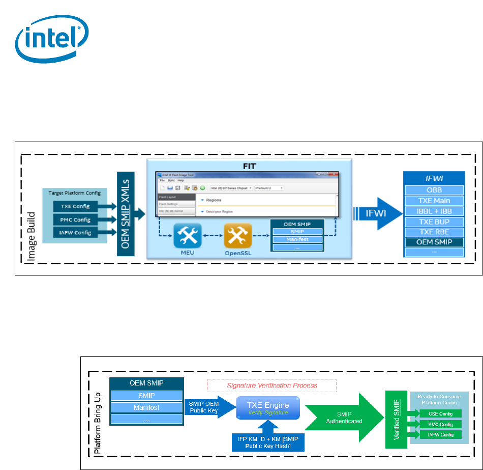
Signed Master Image Profile (SMIP)
66 Intel Confidential CDI/IBP#: 559702
10.2 SMIP Tools
As you can see below, this is a high level of how SMIP is created using FIT:
As shown in the figure above, FIT will generate the SMIP binary given the XML
configuration of each strap. Internally, FIT will call MEU (Manifest Extension Utility) and
OpenSSL to create the SMIP manifest and sign it given the SMIP key. During Boot,
SMIP is verified by TXE engine then given to each component as trusted configuration.
§ §
Figure 10-1. SMIP Image Creation
Figure 10-2. SMIP Image Verification During Platform Bring Up

CDI/IBP#: 559702 Intel Confidential 67
Apollo Lake TXE SMIP Configurations
11 Apollo Lake TXE SMIP
Configurations
11.1 OEM TXE SMIP (APL)
11.1.1 USB DnX (Descriptor) of TXE SMIP1
Offset: Starting at offset 0x000 of TXE SMIP
SMIP
Offset Size in
Bytes Description Comments
0x0 72 USB Descriptor Refer Section 11.1.1, “USB DnX (Descriptor) of TXE
SMIP”below for details on the straps
0x48 128 Soft Straps Refer Section 11.1.2, “Soft Strap Section of TXE
SMIP”below for details on the straps
0xC8 5624 Reserved
0x16C0 4 TPM Configuration and Boot Guard OEM Policy Refer Section 11.1.3, “TPM Configuration and Boot
Guard OEM Policy of TXE SMIP”
0x16C4 2 Reserved
1. This section only applies to platforms booting with eMMC / UFS. On APL SPI platforms, this is not
POR.
Offset
from 0x0 Bytes Default
Value Description Usage FIT
Visible
0x000h
71:70 16’h0 Reserved No
69 8'h1E1
Notes:
1. This field will not be used at EOM
USB Ping Time-out:
0x1E = 30 seconds time-out
Time-out in SECONDS
Used by ROM DnX logic to wait for
ping from host before timing out
If this field is set to 0 then cable
detection is DISABLED
Yes
68 8'h1E2
2. This field will not be used at EOM
USB Enumeration Time-out
0x1E = 30 seconds time-out
Time-out in SECONDS
Used by ROM DnX logic to wait for
enumeration from host before
timing out.
If this field is set to 0 then cable
detection is DISABLED
Yes
67:36 32'h00 USB String Descriptor 2:
Null terminated Ascii string used by ROM to
communicate product string (31 characters)
to recovery host
If this descriptor is not defined by
OEM, identified by all 0’s, ROM will
use default descriptors
Yes
35:4 32'h00 USB String Descriptor 1:
Null terminated Ascii string used by ROM to
communicate manufacturer string (31
characters) to recovery host.
If this descriptor is not defined by
OEM, identified by all 0’s, ROM will
use default descriptors.
Yes
3:0 16'h0 Reserved No

Apollo Lake TXE SMIP Configurations
68 Intel Confidential CDI/IBP#: 559702
11.1.2 Soft Strap Section of TXE SMIP
11.1.2.1 Soft Strap Section for Apollo Lake Platform (APL A and B-Step)
Offset: Starting at offset 0x48 of TXE SMIP
11.1.2.1.1 PUnit Straps (Record 0)
Offset
from
0x48 Bits Default
Value Description Usage FIT
Visible
0x00h
31:23 8’h0 Reserved, set to ‘0’ No
22 1’h0
Thermal Throttle Unlock
(THERMAL_THROTTLE_UNLOCK):
0 = Locked (default)
1 = Unlocked
Soft strap configured by the OEM to
'allow' disabled thermal throttling.
Typical manufacturing recipes for our
silicon force thermal throttling to be
enabled. However, for some select
products, customers wish to disable
thermal throttling. For those products,
the SoC must be fused to allow for
thermal throttling disable
(THERMAL_THROTTLE_UNLOCK=1)
*and* this strap must be set by the
customer. Both conditions being true will
allow customers to successfully disable
thermal throttling by writing the
IA32_MISC_ENABLES MSR.
Yes
21 1’h0
Extended Reliability Enable
(EXTENDED_RELIABILITY_ENABLE):
0 = Disable (default)
1 = Enable
Soft strap configured by the OEM to
define whether or not the extended
reliability mode is enabled for this part.
When the extended reliability mode is
enabled, the IA/GT/IUNIT max ratio
offset fuses are used to clip the
respective maximum clock frequency to
acceptable levels for the extended
reliability. Typically, this feature is used
in conjunctions with in-vehicle or other
applications that are subject to a
greater range of thermal stress and/or
longer lifetime reliability requirements
Yes
20 1’h0
Soft SVID Disable
(SOFTSTRAP_SVID_DISABLE):
0 = Enable (default)
1 = Disable
Software configurable strap disable for
SVID. Used for debug purposes only Yes
19:16 4'h6
Rail 3 SVID ID (SVID_RAIL3_ID):
0 = I2C VR Type
1 = SVID VR Type
6 = Whiskey Cove PMIC VR Type
(default)
This contains the PMIC Rail ID for SVID
Rail 3. PCODE uses this to program the
SVID_RAIL3_CONFIG_AND_STATUS
register during reset.
Yes
15 1’h1
Rail 3 Alert Polling Enable
(SVID_RAIL3_VALID):
0 = SVID OR I2C VR Type
1 = Whiskey Cove PMIC VR Type
(default)
This bit defines whether the STATUS1
register for Rail 3 must be polled on
Alert# assertions or not. Yes
14:11 4'h2
Rail 2 SVID ID (SVID_RAIL2_ID):
0 = SVID OR I2C VR Type
2 = Whiskey Cove PMIC VR Type
(default)
This contains the PMIC Rail ID for SVID
Rail 2. PCODE uses this to program the
SVID_RAIL2_CONFIG_AND_STATUS
register during reset.
Yes

CDI/IBP#: 559702 Intel Confidential 69
Apollo Lake TXE SMIP Configurations
11.1.2.1.2 SPI Straps (Record 1)
11.1.2.1.3 SPI Straps (Record 2)
11.1.2.1.4 SPI Straps (Record 3)
0x00h
(Cont’d)
10 1'h1
Rail 2 Alert Polling Enable
(SVID_RAIL2_VALID):
0 = SVID OR I2C VR Type
1 = Whiskey Cove PMIC VR Type
(default)
This bit defines whether the STATUS1
register for Rail 2 must be polled on
Alert# assertions or not. Yes
9:6 4'h2
Rail 1 SVID ID (SVID_RAIL1_ID):
0 = I2C VR Type
1 = Whiskey Cove PMIC VR Type
2 = SVID VR Type (default)
This contains the PMIC Rail ID for SVID
Rail 1, aka Vnn. PCODE uses this to
program the
SVID_RAIL1_CONFIG_AND_STATUS
register during reset.
Yes
51'h1
Rail 1 Alert Polling Enable
(SVID_RAIL1_VALID):
0 = I2C VR Type
1 = SVID OR Whiskey Cove PMIC VR
Type (default)
This bit defines whether the STATUS1
register for Rail 1 must be polled on
Alert# assertions or not. Yes
4:1 4'h5
Rail 0 SVID ID (SVID_RAIL0_ID):
0 = SVID OR I2C VR Type
5 = Whiskey Cove PMIC VR Type
(default)
This contains the PMIC Rail ID for SVID
Rail 0, i.e. Vccgi. PCODE uses this to
program the
SVID_RAIL0_CONFIG_AND_STATUS
register during reset.
Yes
01'h1
Rail 0 Alert Polling Enable
(SVID_RAIL0_VALID):
0 = I2C VR Type
1 = SVID OR Whiskey Cove PMIC VR
Type (default)
This bit defines whether the STATUS1
register for Rail 0 must be polled on
Alert# assertions or not. Yes
Offset
from
0x48 Bits Default
Value Description Usage FIT
Visible
0x004h 31:0 Refer
Section
This configuration is replicated from Section
9.2, “SoC Descriptor Record 1 (Flash
Descriptor Records)”
Yes
Offset
from
0x48 Bits Default
Value Description Usage FIT
Visible
0x008h 31:0 Refer
Section
This configuration is replicated from Section
9.3, “SoC Descriptor Record 2 (Flash
Descriptor Records)”
Yes
Offset
from
0x48 Bits Default
Value Description Usage FIT
Visible
0x00ch 31:0 Refer
Section
This configuration is replicated from Section
9.4, “SoC Descriptor Record 3 (Flash
Descriptor Records)”
Yes
Offset
from
0x48 Bits Default
Value Description Usage FIT
Visible

Apollo Lake TXE SMIP Configurations
70 Intel Confidential CDI/IBP#: 559702
11.1.2.1.5 SPI Straps (Record 4)
11.1.2.1.6 SPI Straps (Record 5)
11.1.2.1.7 SPI Straps (Record 6)
11.1.2.1.8 TXE Straps (Record 7)
11.1.2.1.9 ISH Straps (Record 8)
Offset
from
0x48 Bits Default
Value Description Usage FIT
Visible
0x010h 31:0 Refer
Section
This configuration is replicated from Section
9.5, “SoC Descriptor Record 4 (Flash
Descriptor Records)”
Yes
Offset
from
0x48 Bits Default
Value Description Usage FIT
Visible
0x014h 31:0 Refer
Section
This configuration is replicated from Section
9.6, “SoC Descriptor Record 5 (Flash
Descriptor Records)”
Yes
Offset
from
0x48 Bits Default
Value Description Usage FIT
Visible
0x018h 31:0 Refer
Section
This configuration is replicated from Section
9.7, “SoC Descriptor Record 6 (Flash
Descriptor Records)”
Yes
Offset
from
0x48 Bits Default
Value Description Usage FIT
Visible
0x01ch 31:0 Refer
Section This configuration is replicated from does
notdoes not Yes
Offset
from
0x48 Bits Default
Value Description Usage FIT
Visible
0x020h
31:27 5'h0 Reserved No
26:25 2'h0 Reserved No
24 1'h0 Reserved No
23:16 8'h0 Reserved No
15:8 8'h50 Reserved No
7:0 8'h07 Reserved No

CDI/IBP#: 559702 Intel Confidential 71
Apollo Lake TXE SMIP Configurations
11.1.2.1.10 USBx Straps (Record 9)
Offset
from
0x48 Bits Default
Value Description Usage FIT
Visible
0x024h
31:15 17’h0 Reserved No
14 1'h0
USB3/SSIC Port 7 Ownership
(USB3_SSIC_PORT7_STRAP):
0 = USB3 (default)
1 = SSIC
Straps to decide Port 7 Ownership
between USB3/SSIC when owned by
XHC.
Yes
13 1'h0
USB3/SSIC Port 6 Ownership
(USB3_SSIC_PORT6_STRAP):
0 = USB3 (default)
1 = SSIC
Straps to decide Port 6 Ownership
between USB3/SSIC when owned by
XHC.
This strap should be programmed to
0 since port6 is not SSIC capable.
Yes
12 1'h0
USB3/SSIC Port 5 Ownership
(USB3_SSIC_PORT5_STRAP):
0 = USB3 (default)
1 = SSIC
Straps to decide Port 5 Ownership
between USB3/SSIC when owned by
XHC.
This strap should be programmed to
0 since port5 is not SSIC capable.
Yes
11 1'h0
USB3/SSIC Port 4 Ownership
(USB3_SSIC_PORT4_STRAP):
0 = USB3 (default)
1 = SSIC
Straps to decide Port 4 Ownership
between USB3/SSIC when owned by
XHC.
This strap should be programmed to
0 since port4 is not SSIC capable.
Yes
10 1'h0
USB3/SSIC Port 3 Ownership
(USB3_SSIC_PORT3_STRAP):
0 = USB3 (default)
1 = SSIC
Straps to decide Port 3 Ownership
between USB3/SSIC when owned by
XHC.
This strap should be programmed to
0 since port3 is not SSIC capable.
Yes
91'h0
USB3/SSIC Port 2 Ownership
(USB3_SSIC_PORT2_STRAP):
0 = USB3 (default)
1 = SSIC
Straps to decide Port 2 Ownership
between USB3/SSIC when owned by
XHC.
This strap should be programmed to
0 since port2 is not SSIC capable.
Yes
81'h0
USB3/SSIC Port 1 Ownership
(USB3_SSIC_PORT1_STRAP):
0 = USB3 (default)
1 = SSIC
Straps to decide Port 1 Ownership
between USB3/SSIC.
This strap should be programmed to
0 since Port1 is not SSIC capable.
Yes
71'h0Reserved No
61'h0
XHC Port 7 Ownership
(XHC_PORT7_OWNERSHIP_STRAP):
0 = XHC (default)
1 = Non-XHC
Straps to decide XHCI Port 7
Ownership between XHCI and non-
XHCI.
Since XHC_PORT7_OWNERSHIP
fuse is set to 2'b10, this strap is
don't care.
Yes

Apollo Lake TXE SMIP Configurations
72 Intel Confidential CDI/IBP#: 559702
0x024h
(Cont’d)
51'h0
XHC Port 6 Ownership
(XHC_PORT6_OWNERSHIP_STRAP):
0 = XHC (default)
1 = Non-XHC
Straps to decide XHCI Port 6
Ownership between XHCI and non-
XHCI.
Set it to “0” to assign that port to
XHCI. Setting it to “1” will disable
that port for XHCI and FIA can
assign that port to PCIe/SATA.
Yes
41'h0
XHC Port 5 Ownership
(XHC_PORT5_OWNERSHIP_STRAP):
0 = XHC (default)
1 = Non-XHC
Straps to decide XHCI Port 5
Ownership between XHCI and non-
XHCI.
Set it to “0” to assign that port to
XHCI. Setting it to “1” will disable
that port for XHCI and FIA can
assign that port to PCIe/SATA.
Yes
31'h0
XHC Port 4Ownership
(XHC_PORT4_OWNERSHIP_STRAP):
0 = XHC
1 = Non-XHC (default)
Straps to decide XHCI Port 4
Ownership between XHCI and non-
XHCI.
Set it to “0” to assign that port to
XHCI. Setting it to “1” will disable
that port for XHCI and FIA can
assign that port to PCIe/SATA.
Yes
21'h0
XHC Port 3 Ownership
(XHC_PORT3_OWNERSHIP_STRAP):
0 = XHC
1 = Non-XHC (default)
Straps to decide XHCI Port 3
Ownership between XHCI and non-
XHCI.
Set it to “0” to assign that port to
XHCI. Setting it to “1” will disable
that port for XHCI and FIA can
assign that port to PCIe/SATA.
Yes
11'h0
XHC Port 2 Ownership
(XHC_PORT2_OWNERSHIP_STRAP):
0 = XHC (default)
1 = Non-XHC
Straps to decide XHCI Port 2
Ownership between XHCI and non-
XHCI.
This strap should be programmed to
0 since Port2 is always owned by
XHCI.
Yes
01'h0
XHC Port 1 Ownership
(XHC_PORT1_OWNERSHIP_STRAP):
0 = XHC (default)
1 = Non-XHC
Straps to decide XHCI Port 1
Ownership between XHCI and non-
XHCI.
This strap should be programmed to
0 since Port1 is always owned by
XHCI.
Yes
Offset
from
0x48 Bits Default
Value Description Usage FIT
Visible

CDI/IBP#: 559702 Intel Confidential 73
Apollo Lake TXE SMIP Configurations
11.1.2.1.11 EXI Straps (Record 10)
Note: Refer Section 12, “SMIP Configurations” for details regarding mapping Combo Port to ModPHY Lane
number. Refer APL PDG and EDS for port and ModPHY Lane mappings.
Offset
from
0x48 Bits Default
Value Description Usage FIT
Visible
0x028h
31:24 8’h0 Reserved No
23:22 2'h0 Reserved No
21:20 2'h0 Reserved No
19:18 2'h0
PCIe/USB3 Combo Port 1 Strap
(PCIE_USB3_P1_STRP):
00 = Statically assigned to USB3 (default)
01 = Statically assigned to PCI Express
10 = Reserved
11 = Reserved
Yes
17:16 2'h0
PCIe/USB3 Combo Port 0 Strap
(PCIE_USB3_P0_STRP):
00 = Statically assigned to USB3 (default)
01 = Statically assigned to PCI Express
10 = Reserved
11 = Reserved
Yes
15:13 3'h0 Reserved Yes
12 1'h0
UFS Combo Port 0 Strap
(UFSCP0_STRP):
0 = Statically assigned to non-UFS Ports
(default)
1 = Statically assigned to UFS Port 0
Yes
11:8 4'h0 Reserved No
7:6 2'h0 Reserved No
51'h0
USB3/SSIC Combo Port 2 Strap
(USB3P2_SSICP2_STRP)
0 = Statically assigned to USB3 (default)
1 = Statically assigned to SSIC
Yes
41'h0
USB3/SSIC Combo Port 1 Strap
(USB3P1_SSICP1_STRP)
0 = Statically assigned to USB3 (default)
1 = Statically assigned to SSIC
Yes
3:0 4'h0 Reserved No

Apollo Lake TXE SMIP Configurations
74 Intel Confidential CDI/IBP#: 559702
11.1.2.1.12 FIA Straps (Record 11)
Note: Refer Section 12, “SMIP Configurations” for details regarding mapping Combo Port to ModPHY Lane
number. You may also Refer APL PDG and EDS for port and ModPHY Lane mappings.
Offset
from
0x48 Bits Default
Value Description Usage FIT
Visible
0x02ch
31:24 8’h0 Reserved No
23:22 2'h0 Reserved No
21:20 2'h0 Reserved No
19:18 2'h0 Reserved No
17:16 2'h0
USB3/SATA Combo Port 0 Strap
(USB3_SATA_P0_STRP):
00 = USB3 (default)
01 = SATA
10: Reserved
11 = Reserved
Yes
15:14 2'h0 Reserved No
13:12 2'h0
PCIe/USB3 Combo Port 2 Strap
(PCIE_USB3_P2_STRP):
00 = USB3 (default)
01 = PCIE
10: Reserved
11 = Reserved
Yes
11:10 2'h0
PCIe/USB3 Combo Port 1 Strap
(PCIE_USB3_P1_STRP):
00 = USB3
01 = PCIE (default)
10: Reserved
11 = Reserved
Yes
0x02ch
(Cont’d)
9:8 2'h0
PCIe/USB3 Combo Port 0 Strap
(PCIE_USB3_P0_STRP):
00 = USB3
01 = PCIE (default)
10: Reserved
11 = Reserved
Yes
7:3 8’h0 Reserved No
21'h1
Staggering Enable (SE):
0 = Disable
1 = Enable (default)
Yes
1:0 8’h0 Reserved No

CDI/IBP#: 559702 Intel Confidential 75
Apollo Lake TXE SMIP Configurations
11.1.2.1.13 PCIe (x2 Controller) Straps (Record 12a)
Offset
from
0x48 Bits Default
Value Description Usage FIT
Visible
0x030h
63:56 8'h0 Reserved No
55:48 8'h0 Reserved No
47 1'h0 Reserved No
46 1'h0 Reserved No
45 1'h0 Reserved No
44 1'h0 Reserved No
43 1'h0 Reserved No
42 1'h0 Reserved No
41 1'h0 Reserved No
40 1'h0 Reserved No
39:32 8'h0 Reserved No
31 1'h0
PCIe Port 3 Non-Common Clock With SSC
Mode Enable Strap (P3PNCCWSSCMES):
0 = Disabled (default)
1 = Enabled
Yes
30 1'h0
PCIe Port 2 Non-Common Clock With SSC
Mode Enable Strap (P2PNCCWSSCMES):
0 = Disabled (default)
1 = Enabled
Yes
29 1'h0
PCIe Port 1 Non-Common Clock With SSC
Mode Enable Strap (P1PNCCWSSCMES):
0 = Disabled (default)
1 = Enabled
Yes
28 1'h0
PCIe Port 0 Non-Common Clock With SSC
Mode Enable Strap (P0PNCCWSSCMES):
0 = Disabled (default)
1 = Enabled
Yes
27:24 4'h0 Reserved No
0x030h
(cont)
23:16 8'h0 Reserved No
15 1'h0 Reserved No
14 1'h1 Reserved No
13 1'h0 Reserved No
12:11 2'h0
Root Port Configuration (RPCFG):
01 = 1x2 Port 1 (x2), Port 2 (disabled)
00 = 2x1 Ports 1-2 (x1) (default)
No
10 1'h0 Lane Reversal (LNREV):
0 = No Lane Reversal (default)
1 = Lane Reversal
When “0”, PCIe Lanes 0-3 are not
reversed.
When “1”, PCIe Lanes 0-3 are
reversed.
No
9:8 2'h0 Reserved No
7:0 8'h0 Reserved No

Apollo Lake TXE SMIP Configurations
76 Intel Confidential CDI/IBP#: 559702
11.1.2.1.14 PCIe (x4 Controller) Straps (Record 12b)
Offset
from
0x48 Bits Default
Value Description Usage FIT
Visible
0x038h
63:56 8'h0 Reserved No
55:48 8'h0 Reserved No
47 1'h0 Reserved No
46 1'h0 Reserved No
45 1'h0 Reserved No
44 1'h0 Reserved No
43 1'h0 Reserved No
42 1'h0 Reserved No
41 1'h0 Reserved No
40 1'h0 Reserved No
39:32 8'h0 Reserved No
31 1'h0
PCIe Port 3 Non-Common Clock With SSC
Mode Enable Strap (P3PNCCWSSCMES):
0 = Disabled (default)
1 = Enabled
Not used No
30 1'h0
PCIe Port 2 Non-Common Clock With SSC
Mode Enable Strap (P2PNCCWSSCMES):
0 = Disabled (default)
1 = Enabled
Not used No
29 1'h0
PCIe Port 1 Non-Common Clock With SSC
Mode Enable Strap (P1PNCCWSSCMES):
0 = Disabled (default)
1 = Enabled
Corresponds to port 5 Yes

CDI/IBP#: 559702 Intel Confidential 77
Apollo Lake TXE SMIP Configurations
11.1.2.1.15 SATA Straps (Record 13)
0x038h
28 1'h0
PCIe Port 0 Non-Common Clock With SSC
Mode Enable Strap (P0PNCCWSSCMES):
0 = Disabled (default)
1 = Enabled
Corresponds to port 4 Yes
27:24 4'h0 Reserved No
23:16 8'h0 Reserved No
15 1'h0 Reserved No
14 1'h0 Reserved No
13 1'h0 Reserved No
12:11 2'h1
Root Port Configuration (RPCFG):
11: 1x4 Port 1 (x4), Ports 2-4 (disabled)
10: 2x2 Port 1 (x2), Port 3 (x2), Ports 2, 4
(disabled)
01: 1x2, 2x1 Port 1 (x2), Port 2 (disabled),
Ports 3, 4 (x1) (default)
00: 4x1 Ports 1-4 (x1)
No
10 1'h0
Lane Reversal (LNREV):
0 = No Lane Reversal (default)
1 = Lane Reversal
When “0”, PCIe Lanes 0-3 are not
reversed.
When “1”, PCIe Lanes 0-3 are
reversed.
No
9:8 2'h0 Reserved No
7:0 8'h0 Reserved No
Offset
from
0x48 Bits Default
Value Description Usage FIT
Visible
Offset
from
0x48 Bits Default
Value Description Usage FIT
Visible
0x040h
31:24 8’h0 Reserved No
23 1'h0 Reserved No
22 1'h0 Reserved No
21 1'h0 Reserved No
20 1'h0 Reserved No
19 1'h0 Reserved No
18 1'h0 Reserved No
17 1'h0
SATA/PCIe Select GPIO polarity for SATA
Port 1
(SATA_PCIE_Select_GPIO_polarity_for_Port
_1):
0 = PCIe will be set as MOD-PHY lane owner if
SATAXPCIE_SATAGP1 is detected with “0” and
SATA lane as owner if SATAXPCIE_SATAGP1 is
detected with “1” (default)
1 = SATA will be set as MOD-PHY lane owner if
SATAXPCIE_SATAGP1 is detected with “0” and
PCIe lane as owner if SATAXPCIE_SATAGP1 is
detected with “1”
Yes

Apollo Lake TXE SMIP Configurations
78 Intel Confidential CDI/IBP#: 559702
0x040h
(Cont’d)
16 1'h0
SATA/PCIe Select GPIO polarity for SATA
Port 0
(SATA_PCIE_Select_GPIO_polarity_for_Port
_0):
0 = PCIe will be set as MOD-PHY lane owner if
SATAXPCIE_SATAGP0 is detected with “0” and
SATA lane as owner if SATAXPCIE_SATAGP0 is
detected with “1” (default)
1 = SATA will be set as MOD-PHY lane owner if
SATAXPCIE_SATAGP0 is detected with “0” and
PCIe lane as owner if SATAXPCIE_SATAGP0 is
detected with “1”
Yes
15:14 2'h0 Reserved No
Offset
from
0x48 Bits Default
Value Description Usage FIT
Visible

CDI/IBP#: 559702 Intel Confidential 79
Apollo Lake TXE SMIP Configurations
0x040h
(Cont’d)
13:12 2'h0
Mod-PHY lane SATA Port 6
(SATA_PCIE_Select_for_Port_6):
00 = Statically assigned to SATA Port 0 (default)
01 = Statically assigned to PCIe
10 = Reserved
11 = Assigned based on SATA Port 7 GPIO pin and
polarity soft strap
Yes
11:10 2'h0
Mod-PHY lane SATA Port 5
(SATA_PCIE_Select_for_Port_5):
00 = Statically assigned to SATA Port 0 (default)
01 = Statically assigned to PCIe
10 = Reserved
11 = Assigned based on SATA Port 7 GPIO pin and
polarity soft strap
Yes
9:8 2'h0
Mod-PHY lane SATA Port 4:
(SATA_PCIE_Select_for_Port_4):
00 = Statically assigned to SATA Port 0 (default)
01 = Statically assigned to PCIe
10 = Reserved
11 = Assigned based on SATA Port 7 GPIO pin and
polarity soft strap
Yes
7:6 2'h0
Mod-PHY lane SATA Port 3
(SATA_PCIE_Select_for_Port_3):
00 = Statically assigned to SATA Port 0 (default)
01 = Statically assigned to PCIe
10 = Reserved
11 = Assigned based on SATA Port 7 GPIO pin and
polarity soft strap
Yes
5:4 2'h0
Mod-PHY lane SATA Port 2
(SATA_PCIE_Select_for_Port_2):
00 = Statically assigned to SATA Port 0 (default)
01 = Statically assigned to PCIe
10 = Reserved
11 = Assigned based on SATA Port 7 GPIO pin and
polarity soft strap
Yes
3:2 2'h0
Mod-PHY lane SATA Port 1
(SATA_PCIE_Select_for_Port_1):
00 = Statically assigned to SATA Port 0 (default)
01 = Statically assigned to PCIe
10 = Reserved
11 = Assigned based on SATA Port 7 GPIO pin and
polarity soft strap
Yes
1:0 2'h0
Mod-PHY lane SATA Port 0
(SATA_PCIE_Select_for_Port_0):
00 = Statically assigned to SATA Port 0 (default)
01 = Statically assigned to PCIe
10 = Reserved
11 = Assigned based on SATA Port 7 GPIO pin and
polarity soft strap
This strap should default to
"PCIE" as this port is assigned
to XHC. "PCIE" means "non-
SATA" in this case.
Yes
Offset
from
0x48 Bits Default
Value Description Usage FIT
Visible

Apollo Lake TXE SMIP Configurations
80 Intel Confidential CDI/IBP#: 559702
11.1.2.1.16 SMBus Straps (Record 14)
11.1.2.1.17 IPC SPI Straps (Record 15)
11.1.3 TPM Configuration and Boot Guard OEM Policy of TXE SMIP
§ §
Offset
from
0x48 Bits Default
Value Description Usage FIT
Visible
0x044h
31:8 24’h0 Reserved No
7:4 4'h0 Reserved No
31'h0Reserved No
21'h0Reserved No
11'h0Reserved No
01'h0Reserved No
Offset
from
0x48 Bits Default
Value Description Usage FIT
Visible
0x048h
31:2 30’h0 Reserved No
11'h0
Protected Range and Top Swap Override
(spi_strap_prr_ts_ovr):
0 = Set PRR_TS_OVR register to RO
(default)
1 = Set PRR_TS_OVR register to RW
Yes
01'h0Reserved No
Offset Bits Default
Value Description Usage FIT
Visible
0x16C0
31:8 1'h0 Reserved No
7:4 1'h0 Reserved No
31'h0Reserved No
21'h0
Discrete TPM location:
0 = LPC
1 = SPI
Yes
11'h0Reserved No
01'h0
dTPM Presence:
0 = dTPM not present
1 = dTPM present
Yes

CDI/IBP#: 559702 Intel Confidential 81
SMIP Configurations
12 SMIP Configurations
12.1 Apollo Lake Platform SMIP Configurations (APL A
and B-Step)
12.1.1 Mod-Phy Lane Configuration Dependency with TXE SMIP
APL
Config Mod-Phy Lane
0Mod-Phy Lane
1Mod-Phy Lane
2Mod-Phy Lane
3Mod-Phy Lane
4Mod-Phy Lane
8
Mod-Phy
Lane USB3 Only USB3 Only USB3 OR PCIe USB3 OR PCIe USB3 OR PCIe USB3 OR SATA
TXE SMIP:
FIA
(Record
11)
XHC_PORT1_OWNE
RSHIP_STRAP =
XHC
XHC_PORT2_OWNE
RSHIP_STRAP =
XHC
PCIE_USB3_P0_ST
RP = USB3 OR PCIE
PCIE_USB3_P1_ST
RP = USB3 OR PCIE PCIE_USB3_P2_ST
RP = USB3 OR PCIe USB3_SATA_P0_ST
RP = USB3 OR
SATA
TXE SMIP:
USBx
(Record 9) N/A N/A XHC_PORT3_OWNE
RSHIP_STRAP =
XHC OR Non-XHC
XHC_PORT4_OWNE
RSHIP_STRAP =
XHC OR Non-XHC
XHC_PORT5_OWNE
RSHIP_STRAP =
XHC OR Non-XHC
XHC_PORT6_OWNE
RSHIP_STRAP =
XHC OR Non-XHC
TXE SMIP:
SATA
(Record
13)
N/A N/A N/A N/A N/A
SATA_PCIE_Select_
for_Port_1 =
PCIE OR SATA
TXE SMIP
EXI
(Record
10)
N/A N/A PCIE_USB3_P0_ST
RP = USB3 OR PCIE PCIE_USB3_P1_ST
RP = USB3 OR PCIE
12.1.2 Mod-Phy Lane 2
12.1.3 Mod-Phy Lane 3
SMIP
Offset Bits Default
Value Description Usage/Comments FIT
Visible
0x0007 7:0 0x1
MODPHYLANE2
2'b00: USB3
2'b01: PCIe (default)
Others: Reserved
Muxed lane for APL, make sure
MODPHY soft straps match desired
lane configuration
Yes
SMIP
Offset Bits Default
Value Description Usage/Comments FIT
Visible
0x0008 7:0 0x1
MODPHYLANE3
2'b00: USB3
2'b01: PCIe (default)
Others: Reserved
Muxed lane for APL, make sure
MODPHY soft straps match desired
lane configuration
Yes

SMIP Configurations
82 Intel Confidential CDI/IBP#: 559702
12.1.4 Mod-Phy Lane 4
12.1.5 Mod-Phy Lane 8
12.1.6 TCO_NO_REBOOT
12.1.7 RESETBUTTON_DEBOUNCE_DIS
12.1.8 LJ1PLL_SETTINGS_FORCE_COLD_RESET
SMIP
Offset Bits Default
Value Description Usage/Comments FIT
Visible
0x0009 7:0 0x0
MODPHYLANE4
2'b00: USB3 (default)
2'b01: PCIe
Others: Reserved
Muxed lane for APL make sure
MODPHY soft straps match desired
lane configuration
Yes
SMIP
Offset Bits Default
Value Description Usage/Comments FIT
Visible
0x000d 7:0 0x0
MODPHYLANE8
2'b00: USB3 (default)
2'b10: SATA
Others: Reserved
Muxed lane for APL, make sure
MODPHY soft straps match desired
lane configuration
Yes
SMIP
Offset Bits Default
Value Description Usage/Comments FIT
Visible
0x000f 7:0 0x0
TCO_NO_REBOOT
1'b0 = reboot (default)
1'b1 = no_reboot
TCO is a software-controlled
platform-level watchdog timer.
Disabling of TCO_NO_REBOOT is
required for resetbreak to occur
when handling reset from TCO
source.
Yes
SMIP
Offset Bits Default
Value Description Usage/Comments FIT
Visible
0x0011 7:0 0x0
RESETBUTTON_DEBOUNCE_DIS
1'b0 = ENABLE_DEBOUNCE (default)
1'b1 = DISABLE_DEBOUNCE
Value to be programmed for the HW
bit to disable the reset button
debounce circuit. Debounce the
circuit may be required depending
on reset button hardware
Yes
SMIP
Offset Bits Default
Value Description Usage/Comments FIT
Visible
0x0012 7:0 0x0
LJ1PLL_SETTINGS_FORCE_COLD_RESET
0: Disable (default)
1: Enable
LJ1PLL settings will force a cold
reset when this is non-zero. Normal
usage is to force a cold reset (assert
this bit) if changes to LJ1PLL are
desired, otherwise BIOS is expected
to cause a cold reset for LJ1PLL
changes to take effect.
Yes

CDI/IBP#: 559702 Intel Confidential 83
SMIP Configurations
12.1.9 S0IX_VR_RAMP_TIMER
12.1.10 LJ1PLL_RW_CONTROL_1_DEFAULT
12.1.11 LJ1PLL_RW_CONTROL_2_DEFAULT
SMIP
Offset Bits Default
Value Description Usage/Comments FIT
Visible
0x0013 7:0 0xA0
S0IX_VR_RAMP_TIMER
0x01: 32 us
0x02: 64 us
...
0xA0: 5.12 ms
RTC clock timer value for Vnn/
Vccram rail ramp during S0ix exit.
The default value of 0hA0
corresponds to 5.12 ms. Precision is
32e-6.
Yes
SMIP
Offset Bits Default
Value Description Usage/Comments FIT
Visible
0x0018
31:2 0x0 Reserved No
1:1 0x0
Spread Spectrum Clocking, spread
enable (SSC_EN):
0x0=no frequency spreading;
0x1=enable frequency spreading on PLL
output clock
Yes
0:0 0x0 SSC_EN_OVR
SSC enable override
Yes
SMIP
Offset Bits Default
Value Description Usage/Comments FIT
Visible
0x001c
31:12 0x7D9C
Spread Spectrum Clocking: fractional
step configuration (SSC_FRAC_STEP):
Fraction of PLL ratio at which to take
frequency modulation steps. eg 0x200000 =
(2097152/2^20) * refclk freq = 0.125*19.2
= 2.4MHz steps.
Spread magnitude is determined by
the step size multiplied by the
number of steps in the modulation
period (see ssc_cyc_to_peak_m1
for steps per modulation period).
Yes
11:11 0x0 Reserved No
10:9 0x0
Spread Spectrum Clocking: spread
direction select (SSC_MODE):
0x0 = down-spread only (default)
0x1 = up-spread only
0x2 = center spread, start with down-spread
0x3 = center spread, start with up-spread
Yes
8:0 0x12B
Spread Spectrum Clocking: spread
period configuration
(SSC_CYC_TO_PEAK_M1):
Half the number of steps in the modulation
period minus 1. Period of modulation is
2*(value+1) multiplied by the step duration
(PLL refclk period). eg 0x12B = 2*(299+1) *
(1/19.2MHz) = 600 * 52.083ns = 31.25us.
Spread magnitude is determined by the step
size (integer + fractional) multiplied by the
number of steps in the modulation period
(Refer ssc_frac_step and ssc_ratio_step for
step size).
Yes

SMIP Configurations
84 Intel Confidential CDI/IBP#: 559702
12.1.12 LJ1PLL_RW_CONTROL_3_DEFAULT
12.1.13 LJ1PLL_RW_CONTROL_5_DEFAULT
SMIP
Offset Bits Default
Value Description Usage/Comments FIT
Visible
0x0020
31:25 0x0 Reserved No
24:18 0x0 LJPLL_OUT_RATIO
PLL Post-Divide Ratio: not used by ICLK PLLs
Yes
17:16 0x0
PLL PVD Ratio (LJPLL_PVD_RATIO):
0x0=1 (default)
0x1=2
0x2=4
0x3=8
Multiplier between VCO and output
clock frequency Yes
15:14 0x0 PLL RefClk Divide Ratio
(LJPLL_REF_RATIO): Not used by ICLK PLLs Yes
13:13 0x0
PLL Force On (LJPLL_FORCE_ON):
0x0 = no force, PLL obeys power state
0x1 = force the PLL on regardless of power
state
Yes
12:12 0x0
PLL Force Off (LJPLL_FORCE_OFF):
0x0 = no force, PLL obeys power state
0x1 = force PLL off regardless of power state
Yes
11:10 0x0 SEL_MIPICLK_C Not used by ICLK PLLs Yes
9:8 0x0 SEL_MIPICLK_A Not used by ICLK PLLs Yes
7:0 0x7D
Integer Feedback Ratio
(LJPLL_FB_RATIO):
Refclk frequency * value = PLL output clock
frequency; eg 19.2MHz * 125 = 2400MHz
Integer frequency multiplier; Yes
SMIP
Offset Bits Default
Value Description Usage/Comments FIT
Visible
0x0024
31:24 0x7D
Clock Bending, Integer
(PLL_RATIO_INT):
Refclk frequency * value = PLL output clock
frequency; eg 19.2MHz * 125 = 2400MHz
integer frequency multiplier Yes
23:0 0x0
Clock Bending, Fractional
(PLL_RATIO_FRAC):
shift PLL clock frequency by (value/
2^24)*refclk frequency. eg 0x200000 =
(2097152/2^24) * refclk freq = 0.125*19.2
= 2.4MHz
fractional frequency multiplier; Yes

CDI/IBP#: 559702 Intel Confidential 85
SMIP Configurations
12.1.14 LCPLL_RW_CONTROL_1_DEFAULT
12.1.15 LCPLL_RW_CONTROL_2_DEFAULT
12.1.16 PMIC/VR Configuration
SMIP
Offset Bits Default
Value Description Usage/Comments FIT
Visible
0x0028
31:2 0x0 Reserved No
1:1 0x0
Spread Spectrum Clocking, spread
enable (SSC_EN):
0x0=no frequency spreading;
0x1=enable frequency spreading on PLL
output clock
Yes
0:0 0x0 SSC_EN_OVR
SSC enable override
Yes
SMIP
Offset Bits Default
Value Description Usage/Comments FIT
Visible
0x002c
31:12 0x7D9C
Spread Spectrum Clocking: fractional
step configuration (SSC_FRAC_STEP):
Fraction of PLL ratio at which to take
frequency modulation steps. eg 0x200000 =
(2097152/2^20) * refclk freq = 0.125*19.2
= 2.4MHz steps.
Spread magnitude is determined by
the step size multiplied by the
number of steps in the modulation
period (refer ssc_cyc_to_peak_m1
for steps per modulation period).
Yes
11:11 0x0 Reserved No
10:9 0x0
Spread Spectrum Clocking: spread
direction select (SSC_MODE):
0x0 = down-spread only (default)
0x1 = up-spread only
0x2 = center spread, start with down-spread
0x3 = center spread, start with up-spread
Yes
8:0 0x12B
Spread Spectrum Clocking: spread
period configuration
(SSC_CYC_TO_PEAK_M1):
Half the number of steps in the modulation
period minus 1. Period of modulation is
2*(value+1) multiplied by the step duration
(PLL refclk period). eg 0x12B = 2*(299+1) *
(1/19.2MHz) = 600 * 52.083ns = 31.25us.
Spread magnitude is determined by the step
size (integer + fractional) multiplied by the
number of steps in the modulation period
(refer ssc_frac_step and ssc_ratio_step for
step size).
Yes
Description Usage/Comments FIT
Visible
PMIC/VR Configuration:
SVID VR - Discrete SVID (default)
I2C VR - TI TPS650941
I2C VR - RT DS5074A
I2C VR - Rohm BD2670MVW
These are the supported VR types for APL SoC. Intel FW
only supports this BOM list. Yes

SMIP Configurations
86 Intel Confidential CDI/IBP#: 559702
12.1.17 IASecureRdWrInValidAddrRange[0] to [12]
SMIP
Offset Bits Default
Value Description Usage/Comments FIT
Visible
0x0180 31:0 0x4E924
E92
IASecureRdWrInValidAddrRange[0]
Secure PMIC Black list Registers for HOST.
List of register ranges in PMIC which are
subject to write access control. Host does
NOT have access to these registers when
Secure.
PMIC addressing utilizes 2 bytes:
MSB (byte 1) is base address; LSB
(byte 0) is the offset. The range is
from bits[15:0] to bits [31:16].
For example, a value of
"0x56781234" means:
0x1234 [15:0]: PMIC base address
0x12, offset 0x34
0x5678 [31:16]: PMIC base address
0x56, offset 0x78
The PMIC address range from bits
[15:0] to bits [31:16] are
inaccessible for a secure HOST
Warning: Intel gives a
recommended default for this
configuration. Intel strongly
recommends not to change this
default. If OEM chooses to change
this default value, it will be at OEM
risk.
Yes
0x0184 31:0 0x4FCB
4FB5 IASecureRdWrInValidAddrRange[1] Refer Usage for:
“IASecureRdWrInValidAddrRange[0]
”
Yes
0x0188 31:0 0x5E305
E30 IASecureRdWrInValidAddrRange[2] Yes
0x018c 31:0 0x5E615
E3C IASecureRdWrInValidAddrRange[3] Yes
0x0190 31:0 0x5E6B
5E66 IASecureRdWrInValidAddrRange[4] Yes
0x0194 31:0 0x5FAD
5FAC IASecureRdWrInValidAddrRange[5] Yes
0x0198 31:0 0x6F356
F00 IASecureRdWrInValidAddrRange[6] Yes
0x019c 31:0 0x6FDB
6FD0 IASecureRdWrInValidAddrRange[7] Yes
0x01a0 31:0 0x6FE36
FDD IASecureRdWrInValidAddrRange[8] Yes
0x01a4 31:0 0x1A0A
1A07 IASecureRdWrInValidAddrRange[9] Yes
0x01a8 31:0 0x120A
1207 IASecureRdWrInValidAddrRange[10] Yes
0x01ac 31:0 0x140A
1407 IASecureRdWrInValidAddrRange[11] Yes
0x01b0 31:0 0x1C36
1C35 IASecureRdWrInValidAddrRange[12] Yes

CDI/IBP#: 559702 Intel Confidential 87
SMIP Configurations
12.1.18 IAInsecureRdWrInValidAddrRange[0] to [14]
SMIP
Offset Bits Default
Value Description Usage/Comments FIT
Visible
0x0200 31:0 0x4E924
E92
IAInsecureRdWrInValidAddrRange[0]
Insecure PMIC Black list Registers for HOST.
List of register ranges in PMIC which are
subject to write access control. Host does
NOT have access to these registers when
Secure.
PMIC addressing utilizes 2 bytes:
MSB (byte 1) is base address; LSB
(byte 0) is the offset. The range is
from bits[15:0] to bits [31:16].
For example, a value of
"0x56781234" means:
0x1234 [15:0]: PMIC base address
0x12, offset 0x34
0x5678 [31:16]: PMIC base address
0x56, offset 0x78
The PMIC address range from bits
[15:0] to bits [31:16] are
inaccessible for a secure HOST
Warning: Intel gives a
recommended default for this
configuration. Intel strongly
recommends not to change this
default. If OEM chooses to change
this default value, it will be at OEM
risk.
Yes
0x0204 31:0 0x4FCB
4FB5 IAInsecureRdWrInValidAddrRange[1] Refer Usage for:
“IAInsecureRdWrInValidAddrRange[
0]”
Yes
0x0208 31:0 0x5E185
E16 IAInsecureRdWrInValidAddrRange[2] Yes
0x020c 31:0 0x5E235
E22 IAInsecureRdWrInValidAddrRange[3] Yes
0x0210 31:0 0x5E305
E30 IAInsecureRdWrInValidAddrRange[4] Yes
0x0214 31:0 0x5E615
E3C IAInsecureRdWrInValidAddrRange[5] Yes
0x0218 31:0 0x5E6B
5E66 IAInsecureRdWrInValidAddrRange[6] Yes
0x021c 31:0 0x5FAD
5FAC IAInsecureRdWrInValidAddrRange[7] Yes
0x0220 31:0 0x6F356
F00 IAInsecureRdWrInValidAddrRange[8] Yes
0x0224 31:0 0x6FDB
6FD0 IAInsecureRdWrInValidAddrRange[9] Yes
0x0228 31:0 0x6FE36
FDD IAInsecureRdWrInValidAddrRange[10] Yes
0x022c 31:0 0x1A0A
1A07 IAInsecureRdWrInValidAddrRange[11] Yes
0x0230 31:0 0x120A
1207 IAInsecureRdWrInValidAddrRange[12] Yes
0x0234 31:0 0x140A
1407 IAInsecureRdWrInValidAddrRange[13] Yes
0x0238 31:0 0x1C36
1C35 IAInsecureRdWrInValidAddrRange[14] Yes

SMIP Configurations
88 Intel Confidential CDI/IBP#: 559702
12.1.19 IAI2CVRRdWrInValidAddrRange[0]
12.1.20 InsecureWrRegBitMskAddr[0] to [1]
SMIP
Offset Bits Default
Value Description Usage/Comments FIT
Visible
0x0280 31:0 0x00
IAI2CVRRdWrInValidAddrRange[0]
List of register ranges in I2C voltage
regulator which are subject to write access
control.
I2CVR addressing utilizes 2 bytes:
MSB (byte 1) is base address; LSB
(byte 0) is the offset. The range is
from bits[15:0] to bits [31:16]. For
example, value 0x56781234 would
indicate I2CVR base address 0x12,
offset 0x34 to I2CVR base address
0x56, offset 0x78 are inaccessible.
For example, a value of
"0x56781234" means:
0x1234 [15:0]: I2CVR base address
0x12, offset 0x34
0x5678 [31:16]: I2CVR base
address 0x56, offset 0x78
The I2CVR address range from bits
[15:0] to bits [31:16] are
inaccessible.
Warning: Intel gives a
recommended default for this
configuration. Intel strongly
recommends not to change this
default. If OEM chooses to change
this default value, it will be at OEM
risk.
Yes
SMIP
Offset Bits Default
Value Description Usage/Comments FIT
Visible
0x0300 31:0 0x03034
FD3
InsecureWrRegBitMskAddr[0]
Information for bitwise set or clear
permissions for the insecure blacklist
registers.
[7:0] = Register address offset
[15:8] = Register address device
[23:16] = Mask of bits which cannot
be SET on a write
[31:24] = Mask of bits which cannot
be CLEARED on a write
Warning: Intel gives a
recommended default for this
configuration. Intel strongly
recommends not to change this
default. If OEM chooses to change
this default value, it will be at OEM
risk.
Yes
0x0304 31:0 0xFFFD5
E24 InsecureWrRegBitMskAddr[1] Refer Usage for:
“InsecureWrRegBitMskAddr[0]” Yes

CDI/IBP#: 559702 Intel Confidential 89
SMIP Configurations
12.1.21 SecureWrRegBitMskAddr[0]
12.1.22 I2C_VR_COMMON_CONFIG
SMIP
Offset Bits Default
Value Description Usage/Comments FIT
Visible
0x0380
31:3 0x0 Reserved No
2:1 0x0
I2C_SPEED_MODE
0: STANDARD
1: FAST
2: FAST_PLUS
Ignored if
I2C_VR_COMMON_CONFIG.I2C_PR
ESENT = 0.
No
0:0 0x0
I2C_PRESENT
0: NOT_PRESENT
1: PRESENT
Yes
§ §
SMIP
Offset Bits Default
Value Description Usage/Comments FIT
Visible
0x0340 31:0 0x03034
FD3
SecureWrRegBitMskAddr[0]
Information for bitwise set or clear
permissions for the secure blacklist registers.
[7:0] = Register address offset
[15:8] = Register address device
[23:16] = Mask of bits which cannot
be SET on a write
[31:24] = Mask of bits which cannot
be CLEARED on a write
Warning: Intel gives a
recommended default for this
configuration. Intel strongly
recommends not to change this
default. If OEM chooses to change
this default value, it will be at OEM
risk.
Yes
