APX 5000/APX 6000/APX 6000XE/SRX 2200 Detailed Service Manual Series/APX5000 6000xe 68012002026 C APX5000
User Manual: -APX Series/APX5000 6000xe Detailed Service Manual 68012002026-C
Open the PDF directly: View PDF ![]() .
.
Page Count: 438 [warning: Documents this large are best viewed by clicking the View PDF Link!]
- Foreword
- Document History
- Table of Contents
- Foreword ii
- Document History iii
- List of Tables viii
- List of Figures x
- Commercial Warranty xv
- Chapter 1 Introduction 1-1
- Chapter 2 Radio Power 2-1
- Chapter 3 Theory of Operation 3-1
- Chapter 4 Troubleshooting Procedures 4-1
- Chapter 5 Troubleshooting Charts 5-1
- Chapter 6 Troubleshooting Waveforms 6-1
- Chapter 7 Troubleshooting Tables 7-1
- Chapter 8 Schematics, Boards Overlays, and Parts Lists 8-1
- Appendix A Replacement Parts Ordering A-1
- Glossary Glossary-1
- Index Index-1
- List of Tables
- List of Figures
- Commercial Warranty
- Chapter 1 Introduction
- Chapter 2 Radio Power
- Chapter 3 Theory of Operation
- 3.1 Transceiver Board
- 3.2 Controller
- 3.2.1 Controller Overview
- 3.2.2 DC Distribution
- 3.2.3 Clock Sources
- 3.2.4 OMAP Processor and Memory
- 3.2.4.1 OMAP Processor (U6302)
- 3.2.4.2 Memory
- 3.2.4.3 Asynchronous External Memory Interface
- 3.2.4.4 Flash Memory (6304)
- 3.2.4.5 CPLD Interface (U6101)
- 3.2.4.6 Synchronous External Memory Interface
- 3.2.4.7 Double Data Rate (DDR) Memory (U6301)
- 3.2.4.8 Multi-Media Card (MMC) Interface
- 3.2.4.9 eMMC Memory
- 3.2.4.10 Peripheral Devices
- 3.2.5 Audio
- 3.2.6 User Interface
- 3.2.7 RF Interface
- 3.2.8 Encryption
- 3.3 Global Positioning Sytem (GPS)
- 3.4 Accelerometer
- 3.5 Bluetooth
- Chapter 4 Troubleshooting Procedures
- Chapter 5 Troubleshooting Charts
- 5.1 List of Troubleshooting Charts
- 5.2 Main Troubleshooting Flowchart
- 5.3 Power-Up Failure
- 5.4 DC Supply Failure
- 5.5 Top/CID Display Failure
- 5.6 Main Display Failure
- 5.7 Volume Set Error
- 5.8 Channel Select Error
- 5.9 Keypad Error
- 5.10 Side Button Error
- 5.11 VOCON RX Audio Error
- 5.12 VOCON RX Audio Error
- 5.13 VOCON TX Audio Error
- 5.14 VOCON TX Audio Error
- 5.15 Keyload Failure
- 5.16 Secure Hardware Failure
- 5.17 eMMC Memory Failure
- 5.18 RX RF Failure
- 5.19 FGU Failure
- 5.20 FGU Power Failure
- 5.21 GPS Failure
- 5.22 Bluetooth Failure
- 5.23 PA Failure
- Chapter 6 Troubleshooting Waveforms
- 6.1 List of Waveforms
- 6.2 Clocks
- 6.3 Audio SSI
- 6.4 RX SSI
- 6.5 TX SSI
- 6.6 SPI
- 6.7 I2C BUS
- 6.8 One Wire
- 6.9 GCAI
- 6.10 USB
- 6.11 UART
- 6.12 SDRAM
- 6.13 FLASH CONTROL
- 6.14 Expandable Memory (eMMC)
- 6.15 Receive Baseband Signals
- 6.16 GPS
- 6.17 Bluetooth Troubleshooting Waveforms
- Bluetooth Command to TX 2.402 GHz CW
- Bluetooth Command to RX 2.402 GHz
- Low Frequency (LF) Command to TX 125 kHz CW
- Low Frequency (LF) Command to RX 125 kHz
- 6.17.1 Bluetooth Startup: Vmax of TP16
- 6.17.2 Bluetooth Startup: Timing Difference of TP9 to TP16
- 6.17.3 Bluetooth Startup: Timing Difference of TP5 to TP16 and Voltage Statistics
- 6.17.4 Bluetooth Startup: Timing Difference of TP4 to TP16 and Time Statistics
- 6.17.5 Bluetooth Startup: Timing Difference of TP4 to TP5 and Time Statistics
- 6.17.6 Bluetooth Startup: Vmax of TP5 and Time Statistics
- 6.17.7 Bluetooth Startup: Vmax of TP4 and Time Statistics
- 6.17.8 Bluetooth Startup: Vmax of TP5 and Voltage Statistics
- 6.17.9 Bluetooth Startup: Vmax of TP9 and Voltage Statistics
- 6.17.10 Bluetooth Startup: Vmax of TP10 and Time Statistics
- 6.17.11 Bluetooth Startup: Vmax of TP16 and Voltage Statistics
- 6.17.12 Bluetooth Startup: Vmax of TP13 and Voltage Statistics
- 6.17.13 Bluetooth Startup: Vmax of TP11 and Voltage Statistics
- 6.17.14 Bluetooth Startup: Timing Difference of TP13 to TP16 and Time Statistics
- 6.17.15 Bluetooth Startup: Timing Difference of TP10 to TP13 and Time Statistics
- 6.17.16 Bluetooth Startup: Timing Difference of TP11 to TP13 and Time Statistics
- 6.17.17 Bluetooth CW on Spectrum Analyzer
- 6.18 Bluetooth Steady-State
- 6.18.1 Expansion Board Waveforms – USB D+ Vmax and Packet Timing with Statistics
- 6.18.2 Expansion Board Waveforms – USB D- Vmax and Packet Timing with Statistics
- 6.18.3 Expansion Board Waveforms – VSW_3.6 Voltage Statistics
- 6.18.4 Expansion Board Waveforms – 32 kHz clock Vmax with Statistics
- 6.18.5 Expansion Board Waveforms – LF Coil with TX and RX
- 6.19 LF CW on Spectrum Analyzer
- Chapter 7 Troubleshooting Tables
- Chapter 8 Schematics, Boards Overlays, and Parts Lists
- 8.1 List of Transceiver Schematics and Board Overlays
- 8.2 List of VOCON Schematics and Board Overlays
- 8.3 List of Expansion Board Schematics and Overlays
- 8.4 Transceiver (RF) Boards: VHF
- 8.5 Transceiver (RF) Boards: UHF1
- 8.6 Transceiver (RF) Boards: UHF2
- 8.7 Transceiver (RF) Boards: 700–800 MHz
- 8.8 Controller Board
- 8.9 Expansion Board
- Appendix A Replacement Parts Ordering
- Glossary
- Index
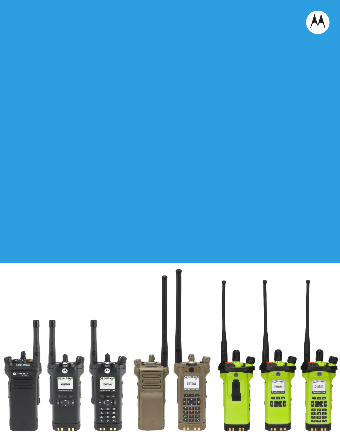
APX™ TWO-WAY RADIOS
APX 5000/ APX 6000/
APX 6000XE/ SRX 2200
Detailed Service
Manuals

ASTRO® APXTM 5000/ APXTM 6000/
APXTM 6000XE/ SRX 2200
VHF/700–800 MHz/UHF1/UHF2
Digital Portable Radios
Detailed Service Manual
Motorola Solutions
1303 E. Algonquin Rd.
Schaumburg, IL 60196-1078 U.S.A. 68012002028-C

Foreword
The information contained in this manual relates to all ASTRO® APXTM 5000/ APXTM 6000/ APXTM 6000XE/ SRX2200
digital portable radios, unless otherwise specified. This manual provides sufficient information to enable qualified service
shop technicians to troubleshoot and repair an ASTRO APX 5000/ APX 6000/ APX 6000XE/ SRX2200 digital portable
radio to the component level.
For details on the operation of the radio or level 1 or 2 maintenance procedures, refer to the applicable manuals, which are
available separately. A list of related publications is provided in the section, “Related Publications,” on page ix.
Product Safety and RF Exposure Compliance
ATTENTION!
This radio is restricted to occupational use only to satisfy FCC RF energy exposure requirements.
Before using this product, read the RF energy awareness information and operating instructions in the
Product Safety and RF Exposure booklet enclosed with your radio (Motorola Publication part number
6881095C98) to ensure compliance with RF energy exposure limits.
For a list of Motorola-approved antennas, batteries, and other accessories, visit the following web site
which lists approved accessories: www.motorolasolutions.com/APX
Manual Revisions
Changes which occur after this manual is printed are described in FMRs (Florida Manual Revisions). These FMRs provide
complete replacement pages for all added, changed, and deleted items, including pertinent parts list data, schematics, and
component layout diagrams. To obtain FMRs, contact the Customer Care and Services Division (refer to “Appendix A
Replacement Parts Ordering”).
Computer Software Copyrights
The Motorola products described in this manual may include copyrighted Motorola computer programs stored in
semiconductor memories or other media. Laws in the United States and other countries preserve for Motorola certain
exclusive rights for copyrighted computer programs, including, but not limited to, the exclusive right to copy or reproduce in
any form the copyrighted computer program. Accordingly, any copyrighted Motorola computer programs contained in the
Motorola products described in this manual may not be copied, reproduced, modified, reverse-engineered, or distributed in
any manner without the express written permission of Motorola. Furthermore, the purchase of Motorola products shall not
be deemed to grant either directly or by implication, estoppel, or otherwise, any license under the copyrights, patents or
patent applications of Motorola, except for the normal non-exclusive license to use that arises by operation of law in the
sale of a product.
Document Copyrights
No duplication or distribution of this document or any portion thereof shall take place without the express written permission
of Motorola. No part of this manual may be reproduced, distributed, or transmitted in any form or by any means, electronic
or mechanical, for any purpose without the express written permission of Motorola.
Disclaimer
The information in this document is carefully examined, and is believed to be entirely reliable. However, no responsibility is
assumed for inaccuracies. Furthermore, Motorola reserves the right to make changes to any products herein to improve
readability, function, or design. Motorola does not assume any liability arising out of the applications or use of any product
or circuit described herein; nor does it cover any license under its patent rights nor the rights of others.
Trademarks
MOTOROLA, MOTO, MOTOROLA SOLUTIONS and the Stylized M logo are trademarks or registered trademarks of
Motorola Trademark Holdings, LLC and are used under license. All other trademarks are the property of their respective
owners. ©2011–2012 Motorola Solutions, Inc. All rights reserved.
Before using this product, read the operating instructions
for safe usage contained in the Product Safety and RF
Exposure booklet enclosed with your radio.

Document History iii
Document History
The following major changes have been implemented in this manual since the previous edition:
Edition Description Date
68012002028-A Initial edition Aug 2011
68012002028-B Added APX 5000 info Sept 2011
68012002028-C Added UHF2 info
Added UHF1: NUE7369A
Added APX 6000XE and SRX 2200 info
Jun 2012

iv Document History
Notes

Table of Contents v
Table of Contents
Foreword.........................................................................................................ii
Product Safety and RF Exposure Compliance ............................................................................................ii
Manual Revisions ........................................................................................................................................ii
Computer Software Copyrights ...................................................................................................................ii
Document Copyrights ..................................................................................................................................ii
Disclaimer....................................................................................................................................................ii
Trademarks .................................................................................................................................................ii
Document History .........................................................................................iii
List of Tables ...............................................................................................viii
List of Figures ................................................................................................x
Commercial Warranty ..................................................................................xv
Limited Warranty .......................................................................................................................................xv
Chapter 1 Introduction ......................................................................... 1-1
1.1 General .......................................................................................................................................... 1-1
1.2 Notations Used in This Manual...................................................................................................... 1-2
Chapter 2 Radio Power ........................................................................ 2-1
2.1 General .......................................................................................................................................... 2-1
2.2 DC Power Routing – Transceiver Board........................................................................................ 2-2
2.3 DC Power Routing – VOCON Board ............................................................................................. 2-3
Chapter 3 Theory of Operation............................................................ 3-1
3.1 Transceiver Board ......................................................................................................................... 3-3
3.2 Controller ..................................................................................................................................... 3-24
3.3 Global Positioning Sytem (GPS).................................................................................................. 3-60
3.4 Accelerometer.............................................................................................................................. 3-62
3.5 Bluetooth...................................................................................................................................... 3-65
Chapter 4 Troubleshooting Procedures ............................................. 4-1
4.1 Handling Precautions..................................................................................................................... 4-1
4.2 Recommended Service Tools........................................................................................................ 4-2
4.3 Standard Bias Table ...................................................................................................................... 4-3

vi Table of Contents
4.4 Power-Up Self-Check Errors.......................................................................................................... 4-4
4.5 Power-Up Self-Check Diagnostics and Repair (Not for Field Use)................................................ 4-5
Chapter 5 Troubleshooting Charts ..................................................... 5-1
5.1 List of Troubleshooting Charts ....................................................................................................... 5-1
5.2 Main Troubleshooting Flowchart.................................................................................................... 5-3
5.3 Power-Up Failure ........................................................................................................................... 5-4
5.4 DC Supply Failure........................................................................................................................ 5-15
5.5 Top/CID Display Failure............................................................................................................... 5-22
5.6 Main Display Failure .................................................................................................................... 5-23
5.7 Volume Set Error ......................................................................................................................... 5-24
5.8 Channel Select Error.................................................................................................................... 5-25
5.9 Keypad Error................................................................................................................................ 5-26
5.10 Side Button Error ......................................................................................................................... 5-27
5.11 VOCON RX Audio Error............................................................................................................... 5-28
5.12 VOCON RX Audio Error............................................................................................................... 5-29
5.13 VOCON TX Audio Error ............................................................................................................... 5-30
5.14 VOCON TX Audio Error ............................................................................................................... 5-31
5.15 Keyload Failure ............................................................................................................................ 5-32
5.16 Secure Hardware Failure ............................................................................................................. 5-33
5.17 eMMC Memory Failure ................................................................................................................ 5-34
5.18 RX RF Failure .............................................................................................................................. 5-35
5.19 FGU Failure ................................................................................................................................. 5-46
5.20 FGU Power Failure ...................................................................................................................... 5-47
5.21 GPS Failure ................................................................................................................................. 5-48
5.22 Bluetooth Failure.......................................................................................................................... 5-49
5.23 PA Failure .................................................................................................................................... 5-55
Chapter 6 Troubleshooting Waveforms ............................................. 6-1
6.1 List of Waveforms .......................................................................................................................... 6-1
6.2 Clocks ............................................................................................................................................ 6-3
6.3 Audio SSI ....................................................................................................................................... 6-8
6.4 RX SSI ......................................................................................................................................... 6-12
6.5 TX SSI.......................................................................................................................................... 6-15
6.6 SPI ............................................................................................................................................... 6-18
6.7 I2C BUS ....................................................................................................................................... 6-22
6.8 One Wire...................................................................................................................................... 6-25
6.9 GCAI ............................................................................................................................................ 6-26
6.10 USB.............................................................................................................................................. 6-28
6.11 UART ........................................................................................................................................... 6-30
6.12 SDRAM ........................................................................................................................................ 6-32
6.13 FLASH CONTROL....................................................................................................................... 6-34
6.14 Expandable Memory (eMMC) ...................................................................................................... 6-39
6.15 Receive Baseband Signals .......................................................................................................... 6-48
6.16 GPS ............................................................................................................................................. 6-49
6.17 Bluetooth Troubleshooting Waveforms........................................................................................ 6-52
6.18 Bluetooth Steady-State ................................................................................................................ 6-72
6.19 LF CW on Spectrum Analyzer ..................................................................................................... 6-77

Table of Contents vii
Chapter 7 Troubleshooting Tables ..................................................... 7-1
7.1 List of Board and IC Signals .......................................................................................................... 7-1
Chapter 8 Schematics, Boards Overlays, and Parts Lists................ 8-1
8.1 List of Transceiver Schematics and Board Overlays ..................................................................... 8-1
8.2 List of VOCON Schematics and Board Overlays........................................................................... 8-2
8.3 List of Expansion Board Schematics and Overlays ....................................................................... 8-2
8.4 Transceiver (RF) Boards: VHF ...................................................................................................... 8-3
8.5 Transceiver (RF) Boards: UHF1 .................................................................................................. 8-25
8.6 Transceiver (RF) Boards: UHF2 .................................................................................................. 8-61
8.7 Transceiver (RF) Boards: 700–800 MHz ..................................................................................... 8-81
8.8 Controller Board......................................................................................................................... 8-129
8.9 Expansion Board ....................................................................................................................... 8-157
Appendix A Replacement Parts Ordering..............................................A-1
A.1 Basic Ordering Information ............................................................................................................A-1
A.2 Transceiver Board, VOCON Board and Expander Board Ordering Information............................A-1
A.3 Motorola Online .............................................................................................................................A-1
A.4 Mail Orders ....................................................................................................................................A-1
A.5 Telephone Orders..........................................................................................................................A-1
A.6 Fax Orders.....................................................................................................................................A-2
A.7 Parts Identification .........................................................................................................................A-2
A.8 Product Customer Service.............................................................................................................A-2
Glossary......................................................................................... Glossary-1
Index..................................................................................................... Index-1

viii List of Tables
List of Tables
Table 2-1. Batteries................................................................................................................................ 2-1
Table 2-2. Transceiver Voltage Regulators ............................................................................................ 2-3
Table 3-1. Battery Connector M101 ....................................................................................................... 3-5
Table 3-2. VOCON Connector J1001 .................................................................................................... 3-5
Table 3-3. Port Expander Pin Settings ................................................................................................. 3-20
Table 3-4. DC Supplies and Sources for Controller ............................................................................. 3-28
Table 3-5. MAKO’s LDO and Supplies................................................................................................. 3-29
Table 3-6. Pulse Switching Combination ............................................................................................. 3-31
Table 3-7. VOCON Clock Distribution .................................................................................................. 3-33
Table 3-8. Color Schemes ................................................................................................................... 3-48
Table 3-9. Key Map Matrix ................................................................................................................... 3-51
Table 3-10. P1 Pin Assignment.............................................................................................................. 3-54
Table 3-11. GCAI Connector Pin Assignment........................................................................................3-54
Table 3-12. Encryption Algorithms and Corresponding Kit Numbers..................................................... 3-58
Table 3-13. Power and I/O Pins for NI5500 ........................................................................................... 3-61
Table 3-14. SPI Interface ....................................................................................................................... 3-63
Table 3-15. Register Address Map ........................................................................................................ 3-64
Table 3-16. Bluetooth Host Processor UART I/O................................................................................... 3-71
Table 3-17. SPI I/O ................................................................................................................................ 3-72
Table 3-18. USB I/O............................................................................................................................... 3-72
Table 3-19. GPIO I/O ............................................................................................................................. 3-73
Table 4-1. Recommended Service Tools ............................................................................................... 4-2
Table 4-2. Standard Operating Bias – DC Voltages............................................................................... 4-3
Table 4-3. Standard Operating Bias – Clock Sources............................................................................ 4-3
Table 4-4. Power-Up Self-Check Error Codes .......................................................................................4-4
Table 4-5. Power-Up Self-Check Diagnostic Actions............................................................................. 4-5
Table 5-1. Troubleshooting Charts......................................................................................................... 5-1
Table 6-1. List of Waveforms ................................................................................................................. 6-1
Table 6-2. Bluetooth Command to TX.................................................................................................. 6-52
Table 6-3. Bluetooth Command to RX ................................................................................................. 6-53
Table 6-4. Low Frequency Command to TX ........................................................................................ 6-53
Table 6-5. Low Frequency Command to RX ........................................................................................ 6-53
Table 6-6. Bluetooth Test Points .......................................................................................................... 6-54
Table 7-1. List of Tables of Board and IC Signals .................................................................................. 7-1
Table 7-2. VOCON board to RF board connector Interface PIN-OUT ................................................... 7-2
Table 7-3. VOCON board to EXPANSION board connector Interface PIN-OUT ................................... 7-4
Table 7-4. VOCON board to Control Top with Top Display Interface PIN-OUT...................................... 7-7
Table 7-5. VOCON board to Front Display Interface PIN-OUT.............................................................. 7-9
Table 7-6. VOCON board to Keypad Interface PIN-OUT..................................................................... 7-10
Table 7-7. EXPANSION board to Accessory Connector (GCAI) Interface PIN-OUT ........................... 7-11
Table 7-8. EXPANSION board to Side Buttons Interface PIN-OUT ..................................................... 7-12
Table 7-9. EXPANSION board to Speaker and Microphones Interface PIN-OUT................................ 7-13
Table 7-10. EXPANSION board to AVR / JTAG Interface PIN-OUT ...................................................... 7-14
Table 7-11. Primary IC reference designators ....................................................................................... 7-15
Table 7-12. Overall GPIO pin functions across multiple boards............................................................. 7-16
Table 8-1. List of Transceiver Schematics and Board Overlays ............................................................ 8-1
Table 8-2. List of VOCON Schematics and Board Overlays.................................................................. 8-2
Table 8-3. List of VOCON Schematics and Board Overlays.................................................................. 8-2

List of Tables ix
Related Publications
APX 6000 User Guide Model 1 ................................................................................................ 68012001081
APX 6000 User Guide Model 2 ................................................................................................ 68012001080
APX 6000 User Guide Model 3 ................................................................................................ 68012001079
APX 6000 Quick Reference Card Model 1................................................................................. PMLN5715_
APX 6000 Quick Reference Card Model 2................................................................................. PMLN5716_
APX 6000 Quick Reference Card Model 3................................................................................. PMLN5717_
APX 5000/ APX 6000/ APX 6000Li/ APX 6000XE Digital Portable Radios Basic Service
Manual...................................................................................................................................... 68012002028
APX 6000/ APX 7000 Digital Portable Radios User Guide (CD)................................................ PMLN5335_
APX 5000 Digital Portable Radios User Guide (CD).................................................................. NNTN7930_
SRX 2200 User Guide Model 1.5 ............................................................................................. 68012005050
SRX 2200 User Guide Model 3 ................................................................................................ 68012005051
SRX 2200 Quick Reference Card Model 1.5.............................................................................. PMLN6131_
SRX 2200 Quick Reference Card Model 3................................................................................. PMLN6132_
SRX 2200 Digital Portable Radios User Guide (CD).................................................................. PMLN6045_
SRX 2200 Basic Service Manual ............................................................................................. 68012005052

xList of Figures
List of Figures
Figure 2-1. DC Power Distribution........................................................................................................... 2-2
Figure 3-1. APX 5000/ APX 6000/ APX 6000XE/ SRX 2200 Overall Block Diagram.............................. 3-2
Figure 3-2. Transceiver (VHF) Block Diagram (Power and Control Omitted).......................................... 3-3
Figure 3-3. Transceiver (UHF1 and UHF2) Block Diagram (Power and Control Omitted) ...................... 3-4
Figure 3-4. Transceiver (7/800) Block Diagram (Power and Control Omitted) ........................................ 3-4
Figure 3-5. Receiver Block Diagram (VHF)............................................................................................. 3-7
Figure 3-6. Receiver Block Diagram (UHF1 and UHF2) ......................................................................... 3-8
Figure 3-7. Receiver Block Diagram (7/800) ........................................................................................... 3-8
Figure 3-8. Transmitter Block Diagram (VHF) ....................................................................................... 3-11
Figure 3-9. Transmitter Block Diagram (UHF1 and UHF2) ................................................................... 3-11
Figure 3-10. Transmitter Block Diagram (7/800) ..................................................................................... 3-12
Figure 3-11. Synthesizer Block Diagram (VHF) ...................................................................................... 3-17
Figure 3-12. Synthesizer Block Diagram (UHF1 and UHF2)................................................................... 3-17
Figure 3-13. Synthesizer Block Diagram (7/800)..................................................................................... 3-18
Figure 3-14. Controller Interconnection Diagram .................................................................................... 3-24
Figure 3-15. Controller Electrical Overview............................................................................................. 3-26
Figure 3-16. Controller DC Block Diagram .............................................................................................. 3-27
Figure 3-17. V_SW_1.4 Switched Power Supply .................................................................................... 3-30
Figure 3-18. 5V Switched Power Supply ................................................................................................. 3-31
Figure 3-19. Power-up Timing Regulators............................................................................................... 3-32
Figure 3-20. VOCON Clock Architecture................................................................................................. 3-33
Figure 3-21. Overview of OMAP Interconnection with VOCON Peripherals ........................................... 3-34
Figure 3-22. OMAP Memory Interface..................................................................................................... 3-35
Figure 3-23. Timing of power-up and initialization of eMMC ................................................................... 3-37
Figure 3-24. eMMC Topography.............................................................................................................. 3-38
Figure 3-25. Block Diagram of VOCON and EXPANSION boards as related to eMMC ......................... 3-39
Figure 3-26. RX / TX SSI Configuration .................................................................................................. 3-40
Figure 3-27. Audio SSI Configuration...................................................................................................... 3-40
Figure 3-28. SPI and I2C Configuration .................................................................................................. 3-41
Figure 3-29. CPLD Block Diagram .......................................................................................................... 3-42
Figure 3-30. Audio TX Path Block Diagram............................................................................................. 3-43
Figure 3-31. VOCON RX Audio Path Block Diagram .............................................................................. 3-44
Figure 3-32. Control Top Block Diagram ................................................................................................. 3-45
Figure 3-33. Display Circuit Detail Overview Block Diagram................................................................... 3-46
Figure 3-34. Lighting Controller Overview............................................................................................... 3-49
Figure 3-35. Lighting Controller – SRX 2200 .......................................................................................... 3-50
Figure 3-36. Keypad Interface Outline..................................................................................................... 3-51
Figure 3-37. GCAI Signal Configuration.................................................................................................. 3-53
Figure 3-38. GCAI Connector.................................................................................................................. 3-53
Figure 3-39. GCAI Connector – Back View ............................................................................................. 3-55
Figure 3-40. VOCON to RF Board Interface............................................................................................ 3-56
Figure 3-41. APX 5000/ APX 6000/ APX 6000XE/ SRX 2200 Encryption Architecture .......................... 3-57
Figure 3-42. GPS Block Diagram (VHF/700–800 MHz) .......................................................................... 3-61
Figure 3-43. GPS Block Diagram (UHF1 and UHF2) .............................................................................. 3-62
Figure 3-44. Directions of the Detectable Accelerations ......................................................................... 3-62
Figure 3-45. Accelerometer Block Diagram............................................................................................. 3-63
Figure 3-46. Relation of Bluetooth Antenna Assembly to Expansion Board ........................................... 3-65
Figure 3-47. Bluetooth Connection Flowchart ......................................................................................... 3-66
Figure 3-48. Bluetooth/Controller Interface with Clock Sources.............................................................. 3-67
Figure 3-49. Bluetooth Functional Block Diagram ................................................................................... 3-67

List of Figures xi
Figure 3-50. Bluetooth Low-Frequency Circuit Block Diagram ............................................................... 3-68
Figure 3-51. Bluetooth Low-Frequency Pairing Data Path...................................................................... 3-68
Figure 3-52. Detailed Low-Frequency Transmit/Receive Paths .............................................................. 3-69
Figure 3-53. Chip Power-Up/Power-Down Sequence (Exernal Input/Output Shown) ............................ 3-69
Figure 3-54. Current Distribution Tree for Bluetooth Circuitry ................................................................. 3-70
Figure 3-55. Bluetooth LF UART Connection Block Diagram ................................................................. 3-71
Figure 3-56. Bluetooth USB Interface Too Main VOCON........................................................................ 3-73
Figure 6-1. 32 kHz Clock Waveform ....................................................................................................... 6-3
Figure 6-2. 4 MHz Clock Waveform ........................................................................................................ 6-4
Figure 6-3. 12 MHz Clock Waveform ...................................................................................................... 6-5
Figure 6-4. 16.8 MHz Clock Waveform ................................................................................................... 6-6
Figure 6-5. 24 MHz Clock Waveform ...................................................................................................... 6-7
Figure 6-6. Audio SSI – Red Tx Waveform ............................................................................................. 6-8
Figure 6-7. Audio SSI – Red Rx Waveform............................................................................................. 6-9
Figure 6-8. Audio SSI – Sync. Waveform.............................................................................................. 6-10
Figure 6-9. Audio SSI – BCLK. Waveform ............................................................................................ 6-11
Figure 6-10. RX SSI – CLK. Waveform ................................................................................................... 6-12
Figure 6-11. RX SSI – DA Waveform...................................................................................................... 6-13
Figure 6-12. RX SSI – FSync. Waveform................................................................................................ 6-14
Figure 6-13. TX SSI – TX CLK. Waveform.............................................................................................. 6-15
Figure 6-14. TX SSI – DA Waveform ...................................................................................................... 6-16
Figure 6-15. TX SSI – FSync. Waveform ................................................................................................ 6-17
Figure 6-16. SPI – CLK Waveform.......................................................................................................... 6-18
Figure 6-17. MOSI Waveform ................................................................................................................. 6-19
Figure 6-18. MISO Waveform ................................................................................................................. 6-20
Figure 6-19. CS Waveform...................................................................................................................... 6-21
Figure 6-20. I2C Bus – SCA Waveform .................................................................................................. 6-22
Figure 6-21. I2C Bus – SCA 5V Waveform ............................................................................................. 6-23
Figure 6-22. I2C Bus – SDA Waveform .................................................................................................. 6-24
Figure 6-23. 1-Wire Waveform ................................................................................................................ 6-25
Figure 6-24. GCAI – GPIO0 Waveform ................................................................................................... 6-26
Figure 6-25. GCAI – GPIO4 Waveform ................................................................................................... 6-27
Figure 6-26. USB – D- Waveform ........................................................................................................... 6-28
Figure 6-27. USB – D+ Waveform........................................................................................................... 6-29
Figure 6-28. UART – RX Waveform ........................................................................................................ 6-30
Figure 6-29. UART – TX Waveform ........................................................................................................ 6-31
Figure 6-30. SDRAM – CLK Waveform................................................................................................... 6-32
Figure 6-31. SDRAM – CLKX Waveform ................................................................................................ 6-33
Figure 6-32. FLASH CONTROL – ADV Waveform ................................................................................. 6-34
Figure 6-33. FLASH CONTROL – CS3 Waveform ................................................................................. 6-35
Figure 6-34. FLASH CONTROL – OE Waveform ................................................................................... 6-36
Figure 6-35. FLASH CONTROL – RDY Waveform................................................................................. 6-37
Figure 6-36. FLASH CONTROL – WE Waveform................................................................................... 6-38
Figure 6-37. eMMC: Power-On until Final Initialization Waveforms........................................................ 6-39
Figure 6-38. eMMC: Correct Detection, Configuration and Initialization Waveforms .............................. 6-40
Figure 6-39. eMMC: Failure to Properly Detect, Configure and Initialize Waveforms............................. 6-41
Figure 6-40. MMC_CLK @ < 400 kHz during “Clock Frequency Identification Mode”............................ 6-42
Figure 6-41. MMC_CLK @ < 24 MHz during “Clock Frequency Data Transfer Mode” ........................... 6-43
Figure 6-42. MMC_CMD actual waveform when probing with active probes; short wires;
GND pin soldered ............................................................................................................... 6-44
Figure 6-43. MMC_CMD misleading waveform when probing with passive probe; long wires;
GND clip ............................................................................................................................. 6-45
Figure 6-44. MMC_DAT0, MMC_DAT1, MMC_DAT2, MMC_DAT3 data lines during data
transmission between eMMC and OMAP ........................................................................... 6-46

xii List of Figures
Figure 6-45. F2_TIMER_OUT clock from CPLD into OMAP for eMMC operation .................................. 6-47
Figure 6-46. Received Baseband Waveforms.........................................................................................6-48
Figure 6-47. GPS TCXO Waveforms ...................................................................................................... 6-49
Figure 6-48. GPS RTC Waveforms ......................................................................................................... 6-50
Figure 6-49. GPS UART DATA Waveforms.............................................................................................6-51
Figure 6-50. Startup Waveforms – Vmax of TP16................................................................................... 6-55
Figure 6-51. Startup – Timing Difference of TP9 to TP16........................................................................ 6-56
Figure 6-52. Startup – Timing Difference of TP5 to TP16 and Voltage Statistics .................................... 6-57
Figure 6-53. Startup – Timing Difference of TP4 to TP16 and Time Statistics ........................................ 6-58
Figure 6-54. Startup – Timing Difference of TP4 to TP5 and Time Statistics .......................................... 6-59
Figure 6-55. Startup – Vmax of TP5 and Time Statistics......................................................................... 6-60
Figure 6-56. Startup – Vmax of TP4 and Time Statistics......................................................................... 6-61
Figure 6-57. Startup – Vmax of TP5 and Voltage Statistics..................................................................... 6-62
Figure 6-58. Startup – Vmax of TP9 and Voltage Statistics..................................................................... 6-63
Figure 6-59. Startup – Vmax of TP10 and Time Statistics....................................................................... 6-64
Figure 6-60. Startup – Vmax of TP16 and Voltage Statistics................................................................... 6-65
Figure 6-61. Startup – Vmax of TP13 and Voltage Statistics................................................................... 6-66
Figure 6-62. Startup – Vmax of TP11 and Voltage Statistics ................................................................... 6-67
Figure 6-63. Startup – Timing Difference of TP13 to TP16 and Time Statistics ...................................... 6-68
Figure 6-64. Startup – Timing Difference of TP10 to TP13 and Time Statistics ...................................... 6-69
Figure 6-65. Startup – Timing Difference of TP11 to TP13 and Time Statistics....................................... 6-70
Figure 6-66. Bluetooth CW on Spectrum Analyzer.................................................................................. 6-71
Figure 6-67. Expansion Board – USB D+ Vmax and Packet Timing with Statistics ................................ 6-72
Figure 6-68. Expansion Board – USB D- Vmax and Packet Timing with Statistics ................................. 6-73
Figure 6-69. Expansion Board – VSW_3.6 Voltage Statistics ................................................................. 6-74
Figure 6-70. Expansion Board – 32 kHz clock Vmax with Statistics........................................................ 6-75
Figure 6-71. Expansion Board – LF Coil with TX and RX Waveform Measured by a Conducted
Cable on LF Coil ................................................................................................................. 6-76
Figure 6-72. LF CW on Spectrum Analyzer............................................................................................. 6-77
Figure 8-1. NUD7120A Transceiver (RF) Board Overall Circuit Schematic ............................................ 8-3
Figure 8-2. NUD7120A Harmonic Filter Circuit ....................................................................................... 8-4
Figure 8-3. NUD7120A GPS Circuit ........................................................................................................ 8-5
Figure 8-4. NUD7120A Miscellaneous Connector Circuit ....................................................................... 8-6
Figure 8-5. NUD7120A Receiver Front End Circuit................................................................................. 8-7
Figure 8-6. NUD7120A Receiver Back End Circuit ................................................................................. 8-8
Figure 8-7. NUD7120A DC Power Circuit ............................................................................................... 8-9
Figure 8-8. NUD7120A Transmitter and Automatic Level Control Circuits............................................ 8-10
Figure 8-9. NUD7120A Frequency Generation Unit (Synthesizer) Circuit – 1 of 2 ............................... 8-11
Figure 8-10. NUD7120A Frequency Generation Unit (VCO) Circuit – 2 of 2 .......................................... 8-12
Figure 8-11. NUD7120A Mixer and IF Filter Circuits ...............................................................................8-13
Figure 8-12. NUD7120A Power Amplifier Circuit..................................................................................... 8-14
Figure 8-13. NUD7120A Transceiver (RF) Board Layout – Side 1 ......................................................... 8-15
Figure 8-14. NUD7120A Transceiver (RF) Board Layout – Side 2 ......................................................... 8-16
Figure 8-15. NUE7365A/ NUE7369A Transceiver (RF) Board Overall Circuit Schematic ...................... 8-25
Figure 8-16. NUE7365A/ NUE7369A UHF1 Harmonic Filter Circuit ....................................................... 8-26
Figure 8-17. NUE7365A/ NUE7369A GPS Circuit .................................................................................. 8-27
Figure 8-18. NUE7365A/ NUE7369A Miscellaneous Connector Circuit.................................................. 8-28
Figure 8-19. NUE7365A Receiver Front End Circuit............................................................................... 8-29
Figure 8-20. NUE7365A/ NUE7369A Receiver Back End Circuit ........................................................... 8-30
Figure 8-21. NUE7365A/ NUE7369A DC Power Circuit.......................................................................... 8-31
Figure 8-22. NUE7365A/ NUE7369A Transmitter and Automatic Level Control Circuits........................ 8-32
Figure 8-23. NUE7365A Frequency Generation Unit (Synthesizer) Circuit – 1 of 2................................ 8-33
Figure 8-24. NUE7365A Frequency Generation Unit (VCO) Circuit – 2 of 2........................................... 8-34
Figure 8-25. NUE7365A/ NUE7369A Mixer and IF Filter Circuits ........................................................... 8-35

List of Figures xiii
Figure 8-26. NUE7365A Power Amplifier Circuit..................................................................................... 8-36
Figure 8-27. NUE7365A Transceiver (RF) Board Layout – Side 1 ......................................................... 8-37
Figure 8-28. NUE7365A Transceiver (RF) Board Layout – Side 2 ......................................................... 8-38
Figure 8-29. NUE7369A Receiver Front End Circuit............................................................................... 8-48
Figure 8-30. NUE7369A Frequency Generation Unit (Synthesizer) Circuit – 1 of 2 ............................... 8-49
Figure 8-31. NUE7369A Frequency Generation Unit (VCO) Circuit – 2 of 2 .......................................... 8-50
Figure 8-32. NUE7369A Power Amplifier Circuit..................................................................................... 8-51
Figure 8-33. NUE7369A Transceiver (RF) Board Layout – Side 1 ......................................................... 8-52
Figure 8-34. NUE7369A Transceiver (RF) Board Layout – Side 2 ......................................................... 8-53
Figure 8-35. NUE7366A Transceiver (RF) Board Overall Circuit Schematic .......................................... 8-61
Figure 8-36. NUE7366A UHF2 Harmonic Filter Circuit ........................................................................... 8-62
Figure 8-37. NUE7366A GPS Circuit ...................................................................................................... 8-63
Figure 8-38. NUE7366A Miscellaneous Connector Circuit ..................................................................... 8-64
Figure 8-39. NUE7366A Receiver Front End Circuit............................................................................... 8-65
Figure 8-40. NUE7366A Receiver Back End Circuit ............................................................................... 8-66
Figure 8-41. NUE7366A DC Power Circuit ............................................................................................. 8-67
Figure 8-42. NUE7366A Transmitter and Automatic Level Control Circuits............................................ 8-68
Figure 8-43. NUE7366A Frequency Generation Unit (Synthesizer) Circuit – 1 of 2 ............................... 8-69
Figure 8-44. NUE7366A Frequency Generation Unit (VCO) Circuit – 2 of 2 .......................................... 8-70
Figure 8-45. NUE7366A Mixer and IF Filter Circuits...............................................................................8-71
Figure 8-46. NUE7366A Power Amplifier Circuit..................................................................................... 8-72
Figure 8-47. NUE7366A Transceiver (RF) Board Layout – Side 1 ......................................................... 8-73
Figure 8-48. NUE7366A Transceiver (RF) Board Layout – Side 2 ......................................................... 8-74
Figure 8-49. NUF6750A Transceiver (RF) Board Overall Circuit Schematic .......................................... 8-81
Figure 8-50. NUF6750A Harmonic Filter Circuit...................................................................................... 8-82
Figure 8-51. NUF6750A GPS Circuit ...................................................................................................... 8-83
Figure 8-52. NUF6750A Miscellaneous Connector Circuit...................................................................... 8-84
Figure 8-53. NUF6750A Receiver Front End Circuit ............................................................................... 8-85
Figure 8-54. NUF6750A Receiver Back End Circuit ............................................................................... 8-86
Figure 8-55. NUF6750A DC Power Circuit.............................................................................................. 8-87
Figure 8-56. NUF6750A Transmitter and Automatic Level Control Circuits............................................ 8-88
Figure 8-57. NUF6750A Frequency Generation Unit (Synthesizer) Circuit – 1 of 2................................ 8-89
Figure 8-58. NUF6750A Frequency Generation Unit (VCO) Circuit – 2 of 2........................................... 8-90
Figure 8-59. NUF6750A Mixer and IF Filter Circuits ...............................................................................8-91
Figure 8-60. NUF6750A Power Amplifier Circuit..................................................................................... 8-92
Figure 8-61. NUF6750A Transceiver (RF) Board Layout – Side 1.......................................................... 8-93
Figure 8-62. NUF6750A Transceiver (RF) Board Layout – Side 2.......................................................... 8-94
Figure 8-63. HLN5979B/ HLN5960AController Board Overall Schematic ............................................ 8-129
Figure 8-64. HLN5979B/ HLN5960A Controller Board Display, Controls and JTAG Schematics......... 8-130
Figure 8-65. HLN5979B Controller Board Display/Keypad Lighting Control Circuits ............................ 8-131
Figure 8-66. HLN5979B/ HLN5960A Controller Board LCD and Keypad Connector Circuits............... 8-132
Figure 8-67. HLN5979B/ HLN5960A Controller Board Expansion Board Interface Circuits ................. 8-133
Figure 8-68. HLN5979B Controller Board CPLD Circuit ....................................................................... 8-134
Figure 8-69. HLN5979B/ HLN5960A Controller Board OMAP User Interface Circuit ........................... 8-135
Figure 8-70. HLN5979B/ HLN5960A Controller Board Memory Interface Circuit ................................. 8-136
Figure 8-71. HLN5979B/ HLN5960A Controller Board Audio Circuit .................................................... 8-137
Figure 8-72. HLN5979B/ HLN5960A Controller Board MAKO/DC Circuits........................................... 8-138
Figure 8-73. HLN5979B/ HLN5960A Controller Board Serial Interface Circuit ..................................... 8-139
Figure 8-74. HLN5979B/ HLN5960A Controller Board RF Interface Circuit.......................................... 8-140
Figure 8-75. HLN5979B Controller Board Layout – Side 1 ................................................................... 8-141
Figure 8-76. HLN5979B Controller Board Layout – Side 2 ................................................................... 8-142
Figure 8-77. HLN5960A Controller Board Display/Keypad Lighting Control Circuits ............................ 8-148
Figure 8-78. HLN5960A Controller Board CPLD Circuit ....................................................................... 8-149
Figure 8-79. HLN5960A Controller Board Layout – Side 1 ................................................................... 8-150

xiv List of Figures
Figure 8-80. HLN5960A Controller Board Layout – Side 2 ................................................................... 8-151
Figure 8-81. HLN5978B Expansion Board Overall Circuit Schematic................................................... 8-157
Figure 8-82. HLN5977A/ HLN5978B Audio Circuit ............................................................................... 8-158
Figure 8-83. HLN5977A/ HLN5978B Secure Circuit ............................................................................. 8-159
Figure 8-84. HLN5978B Expandable Memory Circuit ........................................................................... 8-160
Figure 8-85. HLN5978B GPS Bluetooth Circuit – 1 of 2 ....................................................................... 8-161
Figure 8-86. HLN5978B GPS Bluetooth Circuit – 2 of 2 ....................................................................... 8-162
Figure 8-87. HLN5977A/ HLN5978B Expansion Board Layout – Side 1 .............................................. 8-163
Figure 8-88. HLN5977A/ HLN5978B Expansion Board Layout – Side 2 .............................................. 8-164

Commercial Warranty xv
Commercial Warranty
Limited Warranty
MOTOROLA COMMUNICATION PRODUCTS
I. What This Warranty Covers And For How Long
MOTOROLA SOLUTIONS INC. (“MOTOROLA”) warrants the MOTOROLA manufactured
Communication Products listed below (“Product”) against defects in material and workmanship
under normal use and service for a period of time from the date of purchase as scheduled below:
Motorola, at its option, will at no charge either repair the Product (with new or reconditioned parts),
replace it (with a new or reconditioned Product), or refund the purchase price of the Product during
the warranty period provided it is returned in accordance with the terms of this warranty. Replaced
parts or boards are warranted for the balance of the original applicable warranty period. All replaced
parts of Product shall become the property of MOTOROLA.
This express limited warranty is extended by MOTOROLA to the original end user purchaser only
and is not assignable or transferable to any other party. This is the complete warranty for the Product
manufactured by MOTOROLA. MOTOROLA assumes no obligations or liability for additions or
modifications to this warranty unless made in writing and signed by an officer of MOTOROLA.
Unless made in a separate agreement between MOTOROLA and the original end user purchaser,
MOTOROLA does not warrant the installation, maintenance or service of the Product.
MOTOROLA cannot be responsible in any way for any ancillary equipment not furnished by
MOTOROLA which is attached to or used in connection with the Product, or for operation of the
Product with any ancillary equipment, and all such equipment is expressly excluded from this
warranty. Because each system which may use the Product is unique, MOTOROLA disclaims
liability for range, coverage, or operation of the system as a whole under this warranty.
II. General Provisions
This warranty sets forth the full extent of MOTOROLA’s responsibilities regarding the Product.
Repair, replacement or refund of the purchase price, at MOTOROLA’s option, is the exclusive
remedy. THIS WARRANTY IS GIVEN IN LIEU OF ALL OTHER EXPRESS WARRANTIES. IMPLIED
WARRANTIES, INCLUDING WITHOUT LIMITATION, IMPLIED WARRANTIES OF
MERCHANTABILITY AND FITNESS FOR A PARTICULAR PURPOSE, ARE LIMITED TO THE
DURATION OF THIS LIMITED WARRANTY. IN NO EVENT SHALL MOTOROLA BE LIABLE FOR
DAMAGES IN EXCESS OF THE PURCHASE PRICE OF THE PRODUCT, FOR ANY LOSS OF
USE, LOSS OF TIME, INCONVENIENCE, COMMERCIAL LOSS, LOST PROFITS OR SAVINGS
OR OTHER INCIDENTAL, SPECIAL OR CONSEQUENTIAL DAMAGES ARISING OUT OF THE
USE OR INABILITY TO USE SUCH PRODUCT, TO THE FULL EXTENT SUCH MAY BE
DISCLAIMED BY LAW.
ASTRO APX 5000/ APX 6000/ APX 6000XE/ SRX 2200 Digital Portable Units One (1) Year
Product Accessories One (1) Year

xvi Commercial Warranty
III. State Law Rights
SOME STATES DO NOT ALLOW THE EXCLUSION OR LIMITATION OF INCIDENTAL OR
CONSEQUENTIAL DAMAGES OR LIMITATION ON HOW LONG AN IMPLIED WARRANTY
LASTS, SO THE ABOVE LIMITATION OR EXCLUSIONS MAY NOT APPLY.
This warranty gives specific legal rights, and there may be other rights which may vary from state to
state.
IV. How To Get Warranty Service
You must provide proof of purchase (bearing the date of purchase and Product item serial number)
in order to receive warranty service and, also, deliver or send the Product item, transportation and
insurance prepaid, to an authorized warranty service location. Warranty service will be provided by
Motorola through one of its authorized warranty service locations. If you first contact the company
which sold you the Product, it can facilitate your obtaining warranty service. You can also call
Motorola at 1-888-567-7347 US/Canada.
V. What This Warranty Does Not Cover
A. Defects or damage resulting from use of the Product in other than its normal and customary
manner.
B. Defects or damage from misuse, accident, water, or neglect.
C. Defects or damage from improper testing, operation, maintenance, installation, alteration,
modification, or adjustment.
D. Breakage or damage to antennas unless caused directly by defects in material workmanship.
E. A Product subjected to unauthorized Product modifications, disassemblies or repairs
(including, without limitation, the addition to the Product of non-Motorola supplied equipment)
which adversely affect performance of the Product or interfere with Motorola's normal
warranty inspection and testing of the Product to verify any warranty claim.
F. Product which has had the serial number removed or made illegible.
G. Rechargeable batteries if:
• any of the seals on the battery enclosure of cells are broken or show evidence of
tampering.
• the damage or defect is caused by charging or using the battery in equipment or service
other than the Product for which it is specified.
H. Freight costs to the repair depot.
I. A Product which, due to illegal or unauthorized alteration of the software/firmware in the
Product, does not function in accordance with MOTOROLA’s published specifications or the
FCC certification labeling in effect for the Product at the time the Product was initially
distributed from MOTOROLA.
J. Scratches or other cosmetic damage to Product surfaces that does not affect the operation of
the Product.
K. Normal and customary wear and tear.

Commercial Warranty xvii
VI. Patent And Software Provisions
MOTOROLA will defend, at its own expense, any suit brought against the end user purchaser to the
extent that it is based on a claim that the Product or parts infringe a United States patent, and
MOTOROLA will pay those costs and damages finally awarded against the end user purchaser in
any such suit which are attributable to any such claim, but such defense and payments are
conditioned on the following:
A. that MOTOROLA will be notified promptly in writing by such purchaser of any notice of such
claim;
B. that MOTOROLA will have sole control of the defense of such suit and all negotiations for its
settlement or compromise; and
C. should the Product or parts become, or in MOTOROLA’s opinion be likely to become, the
subject of a claim of infringement of a United States patent, that such purchaser will permit
MOTOROLA, at its option and expense, either to procure for such purchaser the right to
continue using the Product or parts or to replace or modify the same so that it becomes
noninfringing or to grant such purchaser a credit for the Product or parts as depreciated and
accept its return. The depreciation will be an equal amount per year over the lifetime of the
Product or parts as established by MOTOROLA.
MOTOROLA will have no liability with respect to any claim of patent infringement which is based
upon the combination of the Product or parts furnished hereunder with software, apparatus or
devices not furnished by MOTOROLA, nor will MOTOROLA have any liability for the use of ancillary
equipment or software not furnished by MOTOROLA which is attached to or used in connection with
the Product. The foregoing states the entire liability of MOTOROLA with respect to infringement of
patents by the Product or any parts thereof.
Laws in the United States and other countries preserve for MOTOROLA certain exclusive rights for
copyrighted MOTOROLA software such as the exclusive rights to reproduce in copies and distribute
copies of such Motorola software. MOTOROLA software may be used in only the Product in which
the software was originally embodied and such software in such Product may not be replaced,
copied, distributed, modified in any way, or used to produce any derivative thereof. No other use
including, without limitation, alteration, modification, reproduction, distribution, or reverse
engineering of such MOTOROLA software or exercise of rights in such MOTOROLA software is
permitted. No license is granted by implication, estoppel or otherwise under MOTOROLA patent
rights or copyrights.
VII. Governing Law
This Warranty is governed by the laws of the State of Illinois, USA.

xviii Commercial Warranty
Notes

Chapter 1 Introduction
1.1 General
This manual includes all the information needed to maintain peak product performance and
maximum working time for the ASTRO APX 5000/ APX 6000/ APX 6000XE/ SRX 2200 radio. This
detailed level of service (component level) is typical of the service performed by some service
centers, self-maintained customers, and distributors.
Use this manual in conjunction with the ASTRO APX 5000/ APX 6000/ APX 6000XE/ SRX 2200
VHF (136–174 MHz), UHF1 (380–470 MHz), UHF2 (450–520 MHz) and 764–870 MHz Digital
Portable Radios Basic Service Manual (Motorola part number 68012002028), which can help in
troubleshooting a problem to a particular printed circuit (PC) board.
Conduct the basic performance checks outlined in the basic service manual first to verify the need to
analyze the radio and to help pinpoint the functional problem area. In addition, you will become
familiar with the radio test mode of operation, which is a helpful tool. If any basic receive or transmit
parameters fail to be met, the radio should be aligned according to the radio alignment procedure.
Included in other areas of this manual are functional block diagrams, detailed theory of operation,
troubleshooting charts and waveforms, schematics, and parts lists. You should become familiar with
these sections to aid in determining circuit problems. Also included are component location diagrams
to aid in locating individual circuit components and some IC diagrams, which identify some
convenient probe points.
“Chapter 3, Theory of Operation,” on page 3-1, contains detailed descriptions of the operations of
many circuits. Once you locate the problem area, review the troubleshooting flowchart for that circuit
to fix the problem.
1-2 Introduction: Notations Used in This Manual
1.2 Notations Used in This Manual
Throughout the text in this publication, you will notice the use of warnings, cautions, and notes.
These notations are used to emphasize that safety hazards exist, and care must be taken and
observed.
NOTE: An operational procedure, practice, or condition that is essential to emphasize.
CAUTION indicates a potentially hazardous situation which, if
not avoided, might result in equipment damage.
WARNING indicates a potentially hazardous situation
which, if not avoided, could result in death or injury.
DANGER indicates an imminently hazardous
situation which, if not avoided, will result in death or
injury.
Chapter 2 Radio Power
This chapter provides a detailed circuit description of the power distribution of an ASTRO APX 5000/
APX 6000/ APX 6000XE/ SRX 2200 radio.
2.1 General
In the ASTRO APX 5000/ APX 6000/ APX 6000XE/ SRX 2200 radio, power (B+) is distributed to two
boards: the transceiver (RF) board and the VOCON board (see Figure 2-1 on page 2-2).
Power for the radio is provided through a battery supplying a nominal 7.5 Vdc directly to the
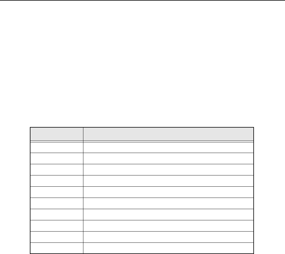
transceiver. The following battery types and capacities are available:
Table 2-1. Batteries
Part Number Description
NNTN7033 4100 mAh IMPRES Li-Ion, Intrinsically Safe, Rugged
NNTN7034 4200 mAh IMPRES Li-Ion, Rugged
NNTN7035 2000 mAh IMPRES NiMH, Intrinsically Safe, Rugged
NNTN7036 2000 mAh IMPRES NiMH, Intrinsically Safe, IP67
NNTN7037 2100 mAh IMPRES NiMH, IP67
NNTN7038 2900 mAh IMPRES Li-Ion, IP67
NNTN7573 2100 mAh IMPRES NiMH, Rugged
NNTN8092 2300 mAh IMPRES Li-Ion, Intrinsically Safe, Rugged
NNTN8182 2900 mAh Li-Ion, Rugged, Military
PMNN4403 2150 mAh IMPRES Li-Ion, Slim, IP67

2-2 Radio Power: DC Power Routing – Transceiver Board
Figure 2-1. DC Power Distribution
B+ from the battery is electrically switched to most of the radio, rather than routed through the On/
Off/volume control knob, S2. The electrical switching of B+ supports a keep-alive mode. Under
software control, even when the On/Off/volume control knob has been turned to the Off position,
power remains on until the MCU completes its power-down, at which time the radio is physically
powered down.
2.2 DC Power Routing – Transceiver Board
NOTE: Refer to Table 8-1, “List of Transceiver Schematics and Board Overlays,” on page 8-1 for a
listing of schematics showing the transceiver board DC power routing components.
Connector M101, the B-plus assembly, connects the battery to the transceiver board. Component
E200 forms a power-line filter for signal DC_ RAW_B+, which supplies battery voltage to the
transmitter section. Fuse F200 and filter C202, L200, C203 supply fused B plus to the VOCON
board.
In turn, the VOCON board supplies VSW1 regulated 3.6 Vdc, 2.78 Vdc, and 1.85 Vdc. The
3.6 Vdc supplies regulator U201 and controls switch Q201 which supplies fuse B+ to regulator U200.
Regulator U201 supplies regulator U202 which in turn supplies regulator U203. The 2.78 Vdc
supplies the Trident IC U702, 16.8 MHz crystal circuit and Logic Expander IC U703. The 1.85 sets
the logic level for the SPI and SSI data.
The transceiver board has four regulators 5 Vdc (U200), 3 Vdc (U201), 1.8 Vdc (U202) and 1.5 Vdc
(U203). The 5 volt regulator supplies the FGU section, transmitter ALC and receiver back end. The
3 volt regulator supplies dc for the receiver front ends, mixer, receiver back end and GPS.
The 1.8 volt regulator supplies dc for the receiver front end and mixer. The 1.5 volt regulator supplies
dc for the buffers in the FGU section.
Fuse
5Vdc
3Vdc
Battery
7.5 Volts
(Nominal)
RF Board VOCON Board
1.8Vdc
1.5Vdc
BATT
M101
RAW B+
3Vdc
1.8 Volts
1.5Volts
P101
FB+
3.6Vdc
1.85Vdc
PMOS
Switch SW_B+
MAKO
SW2
LD02
LDO3
LD04
LD06
LD07
LD09
LDO10
VBUS1
VBUS2
LD08
External SW
External SW
External LDO
1.875Vdc
1.55Vdc
2.775Vdc
2.775Vdc
2.8Vdc
2.8Vdc
3.0Vdc
3.3Vdc
5Vdc
5Vdc
5.4Vdc
1.4Vdc
1.85Vdc External
LDO
3.6Vdc
2.23Vdc
5.4Vdc
5.4Vdc
SW_B+
2.23Vdc
5Vdc
FB+
3.6Vdc
3.6Vdc
3.6Vdc
2.23Vdc
3.6Vdc
External
SW
3.6Vdc
Expansion Board
1.85Vdc
3.6Vdc
5.4Vdc
5.4Vdc
2.775Vdc
Audio PA
3.3Vdc
2.8Vdc
3.3Vdc
2.8Vdc 5Vdc

Radio Power: DC Power Routing – VOCON Board 2-3
The transceiver regulated power supplies are summarized in Table 2-2.
2.3 DC Power Routing – VOCON Board
NOTE: Refer to Table 8-2, “List of VOCON Schematics and Board Overlays,” on page 8-2 for a listing
of schematics showing the VOCON board DC power routing components.
Refer to “3.2.2 DC Distribution” on page 3-27 for details on DC Power Routing for VOCON Board.
Table 2-2. Transceiver Voltage Regulators
Reference
Designator
IC
Name
Output
Signal Name Description
U200 LP2989 DC_LIN_5V Regulated 5.0 Vdc
U201 LP5900 DC_LIN_3V Regulated 3.0 Vdc
U202 LP5900 DC_LIN_1_8V Regulated 1.8 Vdc
U203 LP5952 DC_LIN_1_5V Regulated 1.5 Vdc

2-4 Radio Power: DC Power Routing – VOCON Board
Notes

Chapter 3 Theory of Operation
This chapter provides a detailed circuit description of the ASTRO APX 5000/ APX 6000/
APX 6000XE/ SRX 2200 transceiver and VOCON boards. When reading the theory of operation,
refer to the appropriate schematic and component location diagrams located in the back of this
manual. This detailed theory of operation can help isolate the problem to a particular component.
The ASTRO APX 5000/ APX 6000/ APX 6000XE radio, which is a single-band synthesized radio, is
available in the VHF (136–174 MHz), 7/800 (764–870 MHz), UHF1 (380–470 MHz) and
UHF2 (450–520 MHz) frequency bands. The ASTRO SRX 2200 radio is available in the
VHF (136–174 MHz) and UHF1 (380–470 MHz) frequency bands. The UHF1 band SRX 2200 is
available with a low power setting that limits the transmit power to 0.25 watt.
All ASTRO APX 5000/ APX 6000/ APX 6000XE/ SRX 2200 radios are capable of both analog
operation (12.5 kHz or 25 kHz bandwidths), ASTRO mode operation (12.5 kHz digital only), and
X2-TDMA mode (25 kHz only).
The ASTRO APX 5000/ APX 6000/ APX 6000XE/ SRX 2200 radio (Figure 3-1) consists of the
following:
•VOCON Board – contains a dual-core processor which includes both the microcontroller unit
(MCU) and a digital signal processor (DSP) core, the processor's memory devices, an audio
and power supply support integrated circuit (IC), a digital support IC, and an external audio
power amplifier.
•Transceiver (XCVR) Board – contains all transmit, receive, and frequency generation circuitry,
including the digital receiver back-end IC and the reference oscillator.
•Expansion Board
- Standard – contains the internal audio power amplifier circuitry and a Type III secure IC.
- Full-Feature – contains the internal audio power amplifier circuitry, a combination Global
Positioning System (GPS)/Bluetooth 2.1 IC and support circuitry, a 3-axes digital
accelerometer, an e-MMC NAND flash, and a Type III secure IC.
•Top Display – 112 pixels x 32 pixels, transflective monochrome liquid crystal display (LCD).
•Control Top – contains five switches: On/Off & Volume Knob, a 16 position Channel/Frequency
Knob with concentric 2 position switch (for Secure Enable/Disable operation), a 3 position
toggle switch for Zone Selection, and a push button switch used for Emergency calling. The
control top also includes a TX/RX LED that is solid amber upon receive, red on PTT, and blinks
amber on secure TX/RX.
•Front Display (Dual-Display Version only) – 130 pixels x 130 pixels, transflective color LCD.
•Keypad (Dual-Display Version Only) – Limited keypad version has a 3 x 2 Menu keypad with
a 4-way navigation button; Full keypad version also has a 3 x 4 alphanumeric keypad.
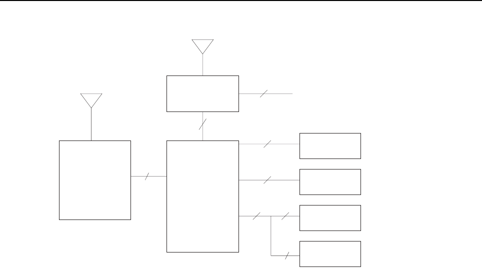
3-2 Theory of Operation:
Figure 3-1. APX 5000/ APX 6000/ APX 6000XE/ SRX 2200 Overall Block Diagram
Antenna
Transceiver
Board
40
VOCON
Board
Expansion
Board
Bluetooth
Antenna
80
16 External Accessory Connector
External Antenna
Top Display
Controls Top
50 20
30
Front Display
Keypad
22
20

Theory of Operation: Transceiver Board 3-3
3.1 Transceiver Board
The transceiver (XCVR) board performs the transmitter and receiver functions necessary to translate
between voice and data from the VOCON board and the modulated radio-frequency (RF) carrier at
the antenna. The transceiver board contains all the radio’s RF circuits for the following major
components:
• Receiver
• Transmitter
• Frequency Generation Unit (FGU)
Figure 3-2 illustrates the VHF transceiver board block diagram, Figure 3-3 and Figure 3-4 illustrates
the UHF1, UHF2 and 7/800 transceiver block diagrams.
Figure 3-2. Transceiver (VHF) Block Diagram (Power and Control Omitted)
FGU
Transmitter
Receiver
SP3T
Atten
GPS
2nd
LO
Digital
RF Atten
SP3T Rf Switch
coupler
Rev
Power
Detector
Log
Amp
FET
VHF
TRIDENT IC
LOGIC
EXPANDER
LOOP
FILTER
PRESCALAR
BUFFER
RX SSI Data
16.8MHz
BUFFER
PRE
BUFFER
÷
2
TX LO
RX LO
TX
BUFFER
VHF TX
VHF TX
VHF RX
*
16.8MHz
RX SSI Clock
RX SSI Frame Sync
Indicates Sub-shield
VHF LNA
Mixer
Harmonic
Filter
Driver
Amplifier
*
Abacus

3-4 Theory of Operation: Transceiver Board
Figure 3-3. Transceiver (UHF1 and UHF2) Block Diagram (Power and Control Omitted)
Figure 3-4. Transceiver (7/800) Block Diagram (Power and Control Omitted)
FGU
Transmitter
Receiver
SP3T
Atten
GPS
2nd
LO
Digital
RF Atten
SP3T Rf Switch
coupler
Rev
Power
Detector
Log
Amp
FET
UHF
TRIDENT IC
LOGIC
EXPANDER
LOOP
FILTER
PRESCALAR
BUFFER
RX SSI Data
16.8MHz
BUFFER
PRE
BUFFER
TX LO
RX LO
TX
BUFFER
UHF TX
UHF RX
*
16.8MHz
RX SSI Clock
RX SSI Frame Sync
Indicates Sub-shield
UHF LNA
Mixer
Harmonic
Filter
Driver
Amplifier
*
Abacus
GPS
SP2T
Aux
FGU
Transmitter
Receiver
SP3T
Atten
GPS
2nd
LO
Digital
RF Atten
SP3T Rf Switch
coupler
Rev
Power
Detector
Log
Amp
FET
7/800
TRIDENT IC
LOGIC
EXPANDER
LOOP
FILTER
PRESCALAR
BUFFER
RX SSI Data
16.8MHz
BUFFER
PRE
BUFFER
TX LO
RX LO
TX
BUFFER
7/800 TX
7/800 RX
*
16.8MHz
RX SSI Clock
RX SSI Frame Sync
Indicates Sub-shield
7/800 LNA1 LNA2
700
800 Mixer
Harmonic
Filter
Driver
Amplifier
*
Abacus
SP2T
Aux

Theory of Operation: Transceiver Board 3-5
3.1.1 Interconnections
This section describes the various interconnections for the transceiver board.
3.1.1.1 Battery Connector M101
Battery connector M101 solders to the transceiver printed circuit board. The connector has 5 gold
plated contacts that mate with the battery, two contacts for positive, two for negative and one for the
Dig_Battery_Data. Signal descriptions are in Table 3-1.
3.1.1.2 VOCON Connector J1001
VOCON connector J1001 is a 40 pin board to board connector that connects to XCVR board
connector P101. This is a digital interface carrying DC power, control, and data between the XCVR
and VOCON boards.
Table 3-2 lists the connector pins, their signals, and functions. SPI refers to serial peripheral
interface, which is the control bus from the microprocessor. SSI is the serial synchronous interface
bus for data to and from the DSP. There is a RX SSI bus for demodulated data from the receiver and
a TX SSI bus for modulation data to the transmitter.
Table 3-1. Battery Connector M101
Pin No. Signal Description
1 DC_BATT Battery positive terminal, nominally 7.5 Vdc
2 Dig_Battery_Data Battery status, from battery to VOCON
3 Ground Battery negative terminal, tied to PCB ground
Table 3-2. VOCON Connector J1001
Pin
No. VOCON Signal XCVR Signal XCVR
I/O Type Description
1 GROUND GROUND – – –
2 EEPROM_SPI_CS DIG_CTRL_SPI_EEPROM_PE I spi SPI EEprom chip select
3 16.8_MHZ_SINEWAVE CLK_16_8MHZ O rf 16.8 MHz reference clock
4 GROUND GROUND – – –
5 GROUND GROUND – – –
6 V_EXT_1.85 DC_LIN_1_875_D I dc Regulated 1.85 V
7 RF_BRD_RSTB DIG_CTRL_RSTB I/O control Reset
8 V_2.8_RF DC_LIN_2_775V I dc Regulated 2.775 V
9 DMCS DIG_CTRL_SSI_TRIGGER I ssi SSI Trigger
10 F2_PARAMP DIG_CTRL_IO49 I control TX Slot enable
11 RX_FSYNC DIG_DATA_SSI_RX_FS O ssi RX SSI frame sync

3-6 Theory of Operation: Transceiver Board
12 TX_INH DIG_CTRL_TX_INHIBIT_TYPE_1 I control TX inhibit control for
secure
13 RX_DA DIG _DATA _SSI _RX _DOUTA O ssi RX SSI data
14 RF_DAC_SPI_CS DIG_CTRL_SPI_DAC_PE I spi SPI DAC chip select
15 RX_CLK CLK_SSI_RX O ssi RX SSI clock
16 ISET ANA_CTRL_ISET I control MAKO Ramp
17 TX_FSYNC DIG_TX_SSI_FS I ssi TX SSI frame sync
18 TX_DA_CONN DIG_DATA_TX_SSI I ssi TX SSI data
19 TX_CLK DIG_TX_SSI_CLK I ssi TX SSI clock
20 V_Coin_Cell V_Coin_Cell – dc Coin cell battery
21 GPS_ANT RF_GPS O rf GPS_RF signal
22 ABACUS_SPI_CS DIG_CTRL_SPI_ABACUS_PE I spi SPI Abacus chip select
23 F2_SYNCB DIG_SYNCB I control Synchronize RX SSI data
24 GROUND GROUND – – –
25 LOCK_DET_A DIG_CTRL_LOCK O status FGU lock detect
26 BSTAT DIG_BATTERY_DATA I/O 1 wire IMPRES Battery status
27 TRIDENT_SPI_CS DIG_CTRL_SPI_TRIDENT_PE I spi SPI Trident chip select
28 UNSW_B+ DC_FUSED _B+ O dc Fused B+ to VOCON
29 SPI_DSP_MISO DIG_DATA_SPI_MISO O spi SPI data out
30 UNSW_B+ DC_FUSED _B+ O dc Fused B+ to VOCON
31 SPI_DSP_MOSI DIG_DATA_SPI_MOSI I/O spi SPI data I/O
32 UNSW_B+ DC_FUSED _B+ O dc Fused B+ to VOCON
33 SPI_DSP_CLK DIG_SPI_CLK I spi SPI clock
34 UNSW_B+ DC_FUSED _B+ O dc Fused B+ to VOCON
35 GROUND GROUND – – –
36 UNSW_B+ DC_FUSED _B+ O dc Fused B+ to VOCON
37 VCC_SW_3.6 DC_SW1_3_6V I dc Regulated 3.6 V
38 GROUND GROUND – – –
39 GROUND GROUND – – –
40 GROUND GROUND – – –
Table 3-2. VOCON Connector J1001 (Continued)
Pin
No. VOCON Signal XCVR Signal XCVR
I/O Type Description

Theory of Operation: Transceiver Board 3-7
3.1.1.3 Antenna Port J101
Antenna port J101 is a surface-mount, miniature coaxial connector for the antenna cable.
3.1.1.4 Serial EEPROM
The electrically erasable programmable memory (EEPROM), U101, holds all of the transceiver
tuning data. This allows transceivers to be tuned in the factory and installed in the field without
retuning.
3.1.1.5 Power Conditioning Components
DC power-conditioning components include zener diodes, capacitors, ferrite beads, a power
inductor, and the fuse. Diodes VR200 and VR101 provide over-voltage protection. Ferrite beads
(designated E, etc.) and capacitors suppress electromagnetic interference from the transceiver.
The power-line filter consisting of L200, C202, and C203 suppresses digital noise from the VOCON
board switching power supplies that could degrade the transmitter spectral purity.
Ground clips M103 and M104 make contact between the transceiver board ground and the radio
chassis. The chassis connection is a necessary electrical reference point to complete the antenna
circuit path. Shields SH1 through SH14 appear on the schematic to show their connection to ground.
3.1.2 Receiver
In the VHF radio, the RF signal is received at the antenna and is routed through a Receive/Transmit
Multi Switch (SP3T). In the UHF1, UHF2 and 7/800 radio, the signal goes from the antenna and is
routed through an Auxiliary Switch before the Multi Switch (SP3T) IC. After the switch, the RF signal
passes through a diplexer circuit and a controllable external 15 dB attenuator. The output of the
attenuator leads to the receiver front end section.
• VHF band (See Figure 3-5.)
• UHF1 and UHF2 bands (See Figure 3-6.)
• 7/800 band (See Figure 3-7.)
Figure 3-5. Receiver Block Diagram (VHF)
VHF
Abacus III
2nd
LO
18Mhz
CLK
CLK
Dec.
Filter
LO
ADC
ΣΔ
PER
SP3T DPLXR
To
RF/Vocon
Connector
GPS
SSI

3-8 Theory of Operation: Transceiver Board
Figure 3-6. Receiver Block Diagram (UHF1 and UHF2)
Figure 3-7. Receiver Block Diagram (7/800)
UHF
Abacus III
2nd
LO
18Mhz
CLK
CLK
Dec.
Filter
LO
ADC
ΣΔ
PER
SP3T DPLXR
To
RF/Vocon
Connector
GPS
SSI
AUX
Abacus III
2nd
LO
18Mhz
CLK
CLK
Dec.
Filter
LO
ADC
ΣΔ
PER
SP3T DPLXR
To
RF/Vocon
Connector
GPS
SSI
AUX
700/800

Theory of Operation: Transceiver Board 3-9
3.1.2.1 VHF Front-End
From the attenuator, U1149, a VHF signal is routed to the first pre-selector filter followed by a Low
Noise Amplifier (LNA) and a second pre-selector filter. Both filters are discrete and fixed designs and
are used to band limit the incoming energy and suppress known spurious responses such as Image
and the ½ IF spur. The LNA active device is an NPN transistor (U302) with active bias provided by
transistor pair Q302.
The output of the second pre-selector filter is applied to the RF port of the Mixer IC via balun
transformer, T503. The Mixer IC, U506, is driven by a Local Oscillator (LO) signal generated by the
Trident synthesizer IC, U702, at the LO port to down-convert the RF signal to a 109.65 MHz
intermediate frequency (IF). It is a passive, high linearity design with balanced inputs at the RF and
IF ports and internal LO buffer. The down converted IF signal is passed through a 3-pole crystal filter,
FL501, and an IF amplifier, Q503, which drive the input of the Analog to Digital Converter IC, U601
3.1.2.2 UHF1 Front-End
From the attenuator, U1149, a UHF1 signal is routed to the first pre-selector filter followed by a Low
Noise Amplifier (LNA) and a second pre-selector filter. Both filters are discrete and tunable designs
and are used to band limit the incoming energy and suppress known spurious responses such as
Image spur. The LNA active device is an NPN transistor (U2032) with active bias provided by
transistor pair Q2022. The output of the second pre-selector filter is applied to a discrete Low Pass
Filter (LPF). The output of the LPF is applied to the RF port of the Mixer IC via a balun transformer,
T503. The Mixer IC, U506, is driven by a Local Oscillator (LO) signal generated by the Trident
synthesizer IC, U702, at the LO port to down-convert the RF signal to a 109.65 MHz intermediate
frequency (IF). It is a passive, high linearity design with balanced inputs at the RF and IF ports and
internal LO buffer. The down converted IF signal is passed through a 3-pole crystal filter, FL501, and
an IF amplifier, Q503, which drives the input of the Analog to Digital Converter IC, U601.
3.1.2.3 UHF2 Front-End
From the attenuator, U1149, a UHF2 signal is routed to the first pre-selector filter followed by a Low
Noise Amplifier (LNA) and a second pre-selector filter. Both filters are discrete and tunable designs
and are used to band limit the incoming energy and suppress known spurious responses such as
Image spur. The LNA active device is an NPN transistor (U2032) with active bias provided by
transistor pair Q2022. The output of the second pre-selector filter is applied to a discrete Low Pass
Filter (LPF). The output of the LPF is applied to the RF port of the Mixer IC via a balun transformer,
T503. The Mixer IC, U506, is driven by a Local Oscillator (LO) signal generated by the Trident
synthesizer IC, U702, at the LO port to down-convert the RF signal to a 109.65 MHz intermediate
frequency (IF). It is a passive, high linearity design with balanced inputs at the RF and IF ports and
internal LO buffer. The down converted IF signal is passed through a 3-pole crystal filter, FL501, and
an IF amplifier, Q503, which drives the input of the Analog to Digital Converter IC, U601.

3-10 Theory of Operation: Transceiver Board
3.1.2.4 700/800 Front-End
From the attenuator, U1149, a 700 MHz or 800 MHz band signal is routed to an SPST band select
switch, U402, which selects the 700 or the 800 band signal and routes it to the appropriate first pre-
selector filter, FL401. A second band select switch, U404, selects the output of the appropriate filter
and applies it to an LNA followed by a similar pre-selector filter/ band-select switch circuit. The signal
is then routed to second LNA, U407, whose output is applied to a discrete image filter. Both
preselector filters are Surface Acoustic Wave designs (EPCOS B4232) used to band limit the
received energy and suppress known spurious responses such as Image and the ½ IF spur. The
output of the discrete image filter is applied to the RF port of the Mixer IC, U506, via a balun
transformer, T503. The Mixer IC is driven by an LO signal generated by the Trident synthesizer IC,
U702, and applied to the LO port to down-convert the RF signal to a 109.65 MHz intermediate
frequency (IF). The IF signal is passed through a crystal filter, FL501, and an IF amplifier, Q503,
which drive the input of the Analog to Digital Converter IC, U601.
3.1.2.5 Analog To Digital Converter
The ADC used in APX/ SRX is the AD9864 IC, U601, from Analog Devices. The IC front end down
converts the first IF to a second IF, a 2.25 MHz signal, by mixing a 107.4 MHz LO signal generated
by an integrated synthesizer and external VCO with active device U602 and resonator L604. The
second IF is sampled at 18 MHz, a signal generated by an integrated clock synthesizer and VCO
device with external resonator L605.
The sampled signal is decimated by a factor of 900 to 20 kHz and converted to SSI format at the
ADC's output. The Serial Synchronous Interface (SSI) serial data waveform is composed of a 16 bit
in-phase word (I) followed by a 16 bit Quadrature word (Q). A 20 kHz Frame Synch and 1.2MHz
clock waveform are used to synchronize the SSI IQ data transfer to the Digital Signal Processor IC
(OMAP) for post-processing and demodulation. The clock frequency is adjustable and is selected
automatically by software to prevent self quieting.
3.1.3 Transmitter
The transmitter takes modulated RF from the FGU and amplifies it to the rated output power to
produce the modulated carrier at the antenna.
NOTE: Refer to Table 8-1, “List of Transceiver Schematics and Board Overlays,” on page 8-1 for a
listing of transmitter-related schematics that will aid in the following discussion.
The transmitter (Figure 3-8 on page 3-11) for the VHF radio consists of one LDMOS high power
transistor for the VHF band. The same topology applied for the 7/800 radio
(Figure 3-10 on page 3-12) where one LDMOS high power transistor is used for the 7/800 MHz
band. Similarly for UHF1 and UHF2 radios, one LDMOS transistor is used to cater for the UHF1/
UHF2 band which is depicted by Figure 3-9 on page 3-11. The high power transistor is driven by an
RF driver IC that receives its input signal from the voltage controlled oscillator. Transmitter power is
controlled by a discrete power control circuit that senses the output of a directional coupler and
adjusts PA control voltage to maintain the correct power level. The TX signals pass through their
respective harmonic filters, a TX/RX switch, and embedded directional coupler, a RF switch and then
the antenna. The SP2T switch just before the antenna does not exist on the VHF radio.
The UHF1 SRX 2200 is available with a low power setting that limits the transmit power to 0.25 watt.
The rest of the APX 5000/ APX 6000 radios and the SRX 2200 VHF radio are able to be limited to
1 watt minimum output power.

Theory of Operation: Transceiver Board 3-11
Figure 3-8. Transmitter Block Diagram (VHF)
Figure 3-9. Transmitter Block Diagram (UHF1 and UHF2)
Trident IC
Synthesizer
Loop Filter
TX VCO
Module
RX VCO
Module
RF Switch Matrix
TX Buffer Amp
TX Driver Amplifier
Transmitter FET VHF
Harmonic LP Filter
Antenna Connector
Directional
Coupler
SP3T RF Switch
To RX
Reverse Power Detection
TX SSI from VOCON
Log Amp Power Detector
Digital RF Attenuator
S
Ref. Oscillator
Trident IC
Synthesizer
Loop Filter
TX VCO
Module
RX VCO
Module
RF Switch Matrix
TX Buffer Amp
TX Driver Amplifier
Transmitter FET UHF
Harmonic LP Filter Directional
Coupler
SP3T RF Switch
To RX
SP2T
Reverse Power Detection
TX SSI from VOCON
Log Amp Power Detector
Digital RF Attenuator
To Antenna
To RMT Port
S
Ref. Oscillator

3-12 Theory of Operation: Transceiver Board
Figure 3-10. Transmitter Block Diagram (7/800)
Trident IC
Synthesizer
Loop Filter
TX VCO
Module
RX VCO
Module
RF Switch Matrix
TX Buffer Amp
TX Driver Amplifier
Transmitter FET 7/800
Harmonic LP Filter Directional
Coupler
SP3T RF Switch
To RX
SP2T
Reverse Power Detection
TX SSI from VOCON
Log Amp Power Detector
Digital RF Attenuator
To Antenna
To RMT Port
S
Ref. Oscillator

Theory of Operation: Transceiver Board 3-13
3.1.3.1 Driver Amplifier
The driver amplifier IC (VHF – U902, UHF1 – U1602, UHF2 – U1500 and 7/800 – U1002) contains
one LDMOS FET amplifier stages and an internal resistor bias networks. Pin 16 is the RF input.
Modulated RF from the FGU, at a level of +3 dBm ±2 dB, is coupled through a blocking capacitor to
the gate of FET-1. An LC inter-stage matching network connects the first stage output VD1 to the
second stage input G2. The RF output from the drain of FET-2 is pin 6 (RFOUT1). Gain control is
provided by a voltage applied to pin 1 (VCNTRL). Typical output power is about +27 dBm (500 mW)
with VCNTRL at 5.5 V.
VHF: L901 and C904 are the components for the inter-stage matching network. Components C907,
C910, L904, C913, C914, L905 and C916 provide the match to the final device Q901. C907 also
serves as a DC block.
UHF1: L1601 and C1604 is the inter-stage matching network of the driver amplifier IC, C1607,
C1610, L1604, C1613, C1614, L1605 and C1616 serve as matching circuit of the driver IC to the
final device of Q1601. Capacitor C1607 also works as DC block to the circuit.
UHF2: L1501 and C1504 is the inter-stage matching network of the driver amplifier IC. C1508,
C1509, C1510, C1511, L1502, L1503, and L1504 serve as matching circuit of the driver IC to the
final device of Q1500. Capacitor C1510 also works as DC block to the circuit.
700–800 MHz: L1002, C1002 and C1004 are the inter-stage matching network. Components C1013
and C1023 match the output impedance to the input of the final device (Q1001); capacitor C1013
also serves as the DC block.
3.1.3.2 Power Amplifier Transistor
The power amplifier transistors, Q901, Q1013, Q1500 and Q1601 are LDMOS FETs housed in a
high-power, surface-mount, ring package. To prevent thermal damage, it is essential that the heat
sink of the power module be held in place against the radio chassis using the RF board screw. All
FETs are matched using a lowpass topology. Drain bias is applied through L906 for the VHF, L1606
for UHF1, L1505 for UHF2 and L1007 for the 7/800 MHz. Gain is dynamically controlled by adjusting
the gate bias. The gate is insulated from the drain and source so that gate bias current is essentially
zero
VHF: The output match consists of elements L907, C920, C921, L908, C922, L909, C924, L910,
C923 and C928. Gate bias is applied through R903, R904, R905, C915 and C917.
UHF1: C1620, C1621, C1622, L1609, C1624, L1610, C1623, C1628 and C1625 are the elements of
the output matching network apart from a transmission-line structure. The Gate biasing is applied
through a biasing network consists of R1603, R1604, R1605, C1615 and C1617.
UHF2: C1516, C1517, C1518, C1520, C1521, C1527, and L1507 are the elements of the output
matching network apart from a transmission-line structure. The Gate biasing is applied through a
biasing network consists of R1502, R1503, R1504 and C1522.
700–800 MHz: The input impedance-matching network is C1013 and C1023. A transmission-line
structure and C1019, C1020, L009 and C1021 form the output-matching network. Gate bias applied
through R1003, R1004, C1015 and R1005.
3.1.3.3 Directional Coupler
A directional coupler senses the transmitter forward and reverse power as control signals in the
transmitter's automatic level control (ALC) loop. Isolated ports are terminated with external resistors.
VHF/UHF1/UHF2/700–800 MHz: The directional coupler consists of three embedded transmission
lines.

3-14 Theory of Operation: Transceiver Board
3.1.3.4 Harmonic Filter
The harmonic filter is a high-power, low-loss, low-pass filter. Its purpose is to suppress transmitter
harmonics. The filter also improves receiver out-of-band rejection. The appropriate shield over the
filter must be in place to achieve the required stop band rejection.
VHF: The harmonic filter uses discrete components. The pass band is up to 190 MHz, and the stop
band is above 260 MHz.
UHF1: The harmonic filter applies discrete components as the circuit line up. The pass band is up to
470 MHz while the stop band is above 740 MHz.
UHF2: The harmonic filter applies discrete components as the circuit line up. The pass band is up to
520 MHz while the stop band is above 1000 MHz.
700–800 MHz: The harmonic filter uses both discrete components and transmission lines. The pass
band is up to 870 MHz, and the stop band is above 1500 MHz.
3.1.3.5 Antenna Switch
NOTE: Refer to Table 8-1, “List of Transceiver Schematics and Board Overlays,” on page 8-1 for a
listing of schematics that will aid in the following discussion.
The antenna switch consists of a single pole triple-throw IC designated U1102. The IC is connected
to the output of the two harmonic filters and it is connected to the receiver. The output of the switch is
connected to the directional coupled via the inductor L1108. Control lines V1_V2 and V3 control the
routing of the signal paths. During Rx operation, V3 is set high and V1_V2 is low. During Tx
operation, V3 is set low and V1_V2 is high. This is the same case for VHF, UHF1, UHF2 and 7/800
radios.
There is a second IC designated U1111 at the output of the radio. This switch routes RF power to the
main antenna or to the accessory GCAII connector on the side of the radio. This switch is controlled
by control line DIG_CNTRL_RMT which connects to pin 13 of the IC. When this signal level is high,
the power is routed to the antenna and when it is low the power is routed to the accessory connector.
NOTE: This switch does not exist on VHF radios.
3.1.3.6 Reverse Power Protection
The radio, while in receive mode is constantly monitoring the input power from the antenna. This
power is sensed by the directional coupler and channeled into an RF detector U1106. The matching
network between the coupler and the detector consists of R1107, L1102, C1105 and C1107. Once
the input RF level exceeds a certain limit the detector trips a logic circuit then enables attenuation to
protect the RF front end. This serves as to protect the front end from large signal damage.
3.1.3.7 Transmitter Power Control
In TX mode, the transmitter Automatic Level Control (ALC) section enables the transmitter and
controls TX power in all modes. Power control is based on a unique dual control loop approach
which utilizes voltage control in one loop and current control in the other. The voltage control loop is
normally used in all transmit modes. The only time the current control loop controls TX power is
during the end of a TX slot in TDMA (Phase 2) mode in the event transmitter saturation is detected.
Several other functions included in the TX ALC section of the radio are RX/TX switching, thermal
cutback of power, current cutback of power, and reverse power detection with a means to disable the
receiver in the event of high reverse power at the antenna port.

Theory of Operation: Transceiver Board 3-15
3.1.3.7.1 Voltage Control Mode
The heart of the voltage control loop is a logarithmic amplifier based power control IC, U1105. Quad
DAC, U1125, receives the power tuning values via the SPI bus and converts them into a voltage at
“VOUTB.” Resistors, R1121 and R1122, form a voltage divider to set the full-scale value of the DAC,
in this case approximately 1.4V. This power set voltage is then fed to the power control IC through
the current cutback op amp, U1130, and then into a lesser-of-two voltage decision circuit, consisting
of U1126 and U1127. This circuit, used exclusively in voltage control mode, provides the important
function of combining the MAKO ramp output with the DAC power set voltage to permit power
leveling since the MAKO DAC max amplitude cannot be controlled during TDMA mode. In all other
TX modes, the MAKO output is a fixed voltage, approximately 1.5V, which is always higher than the
DAC control voltage. The lesser-of-two circuit will then select the smaller input, the set voltage from
U1125, resulting in immediate TX turn on in analog or ASTRO mode. IN TDMA mode, the MAKO line
is a piecewise linear ramp whose timing is in accordance with Phase 2 requirements. At t = 0, the
ramp line is smaller than the TX set voltage so the MAKO ramp will control the TX power level,
resulting in a slower ramping up of the TX power. This continues until the MAKO ramp output
reaches the level of the power tuning DAC (which is always lower than the MAKO ramp maximum)
which causes control of TX power to be turned over to the power tuning DAC.
The output of the selector circuit passes through a 2nd order low pass filter (U1142) and then to the
log amp, U1105. The low pass filter performs the dual function of improving transient ACPR by
transforming a linear ramp with corners into a smooth second order waveform and by acting as a
reconstruction filter for the DAC. The log amp converts RF power fed back from the TX PA into a
current which is summed with the current from the conversion of the setpoint voltage from DAC
U1125. Any imbalance between the RF input level and the level corresponding to the setpoint
voltage is corrected at the VAPC output of the log amp which in turn drives the control voltage input
of the RFPA. The setpoint voltage effectively nulls the error in the loop caused by changes in the RF
level fed back to the log amp. RF from the RFPA is coupled through a directional coupler embedded
in the PC board and passed through a LC equalizer and then to digital attenuator, U1112, which is
used to implement thermal cutback in the event of an over-temperature condition.
Current protection and limiting in voltage control mode is provided by cascaded difference amplifiers,
U1129 and U1130. A fixed threshold is provided by voltage divider, R1169 and R1170. SPDT switch,
U1144, changes the current limit threshold based on the type of battery present. This threshold is
based on the conversion characteristic of the current shunt monitor circuit of U1101. The output of
the current shunt monitor is fed to the first stage of the difference amplifier. The setpoint voltage for
the log amp is fed through the second stage of the difference amplifier. When the current shunt
monitor voltage exceeds the fixed threshold, the first stage produces an output greater than 0V.
Once the output of the first stage (U1129) is greater than zero, this value is subtracted from the
setpoint voltage to the log amp in the second stage (U1130), resulting in a progressive cutback of
power in the event PA current continues to climb above the threshold.
3.1.3.7.2 Thermal Cutback
Thermal cutback works only in voltage control mode, which is the primary mode of TX power control.
Temperature is sensed by IC U1103 and is located next to both RFPA finals. Comparators, U1113
and U1114, establish two temperature trip points. The combined logic of the comparators and logic
gate, U1121, together with the truth table of the digital attenuator IC, U1112, determine the amount of
attenuation of the RF feedback to the log amp. Rated TX power is achieved with the attenuator at its
maximum attenuation of 7 dB. The first temperature threshold will subtract 3 dB of TX power and the
next (highest) trip point an additional 3 dB for 6 dB total.

3-16 Theory of Operation: Transceiver Board
3.1.3.7.3 Current Control Mode
In TDMA mode, excessive transient adjacent channel splatter caused by the RFPA, when it is under
a greater degree of compression than is expected at nominal supply voltage, is mitigated through a
system of saturation detection and switching of the TX power control mode from the voltage control
loop to the current control loop. Comparator U1131 compares the log amp output in voltage control
mode to a threshold voltage from DAC “C”, which sets the threshold for handover to current control
mode and establishes the upper supply rail for the output of current loop integrator, U1104. This
threshold is tuned in the factory to correspond to transmitter rated power which means that the
threshold for handover occurs at a level corresponding to rated power minus 6% (9% for VHF radios)
which is set by divider R1162 and R1163. When PA saturation exceeds this threshold and the MAKO
T/R control signal (DIG_GPIO49) and DIG_DMCS combine logically to signal the end of the data
portion of the TX slot, D-flip flop U1132 latches which in turn switches (via U1133 SPDT switch) the
output of the current loop integrator, U1104, as a control voltage to the PA of the radio.
Integrator, U1104, acts as a PI (Proportional Integral) controller in current mode. Current feedback
from the PA is obtained through current shunt resistor R1103 and sent to the current shunt monitor/
current to voltage converter, U1101. U1101 has a known gain characteristic for the current-to-voltage
conversion. The MAKO ramp is passed through a RC low pass filter for smoothing and on to the
current control integrator where it is proportioned with the voltage output of the current shunt monitor.
The integrator supply voltage comes from DAC “C” of the Quad DAC, U1125. By way of tuning the
DAC “C” value to match TX rated (tuned) power, this approach fixes the upper limit of the control
voltage in current control mode to correspond to the tuned power level, further reducing excess
adjacent channel splatter.
3.1.3.7.4 PA Offset, Control Voltage Gain Scaling
An offset voltage is applied to the control voltage at a summing junction made up of R1174 and
R1154 as a means of further improving transient adjacent channel splatter in the VHF band by
pre-biasing the PA. The output of DAC “A” is summed with either the output of the log amp or the
integrator through R1174.
The value for DAC “A” has been established and fixed in the firmware. This offset value is padded to
the control voltage and is sent to a non-inverting, gain-scaling amplifier, U901 (VHF) or U1601
(UHF1) or U1501 (UHF2) or U1001 (7/800 MHz) and then to the PA driver and final.
3.1.4 Frequency Generation Unit (FGU)
The frequency-generation function is performed by several ICs; multiple voltage-controlled
oscillators (VCOs); and associated circuitry. The reference oscillator provides a frequency standard
to the Trident IC, which controls the VCOs via the port expander. There are also buffers that amplify
the VCO signal to the correct level for the next stage. Figure 3-11 below shows a block diagram of
the FGU Section.
VHF: Two VCOs are employed: one to generate the first RX LO and the other to generate the
transmit injection signals.
UHF1: Two VCOs generate the first Rx LO and two VCOs generate the transmit-injection signals.
UHF2: Two VCOs generate the first Rx LO and two VCOs generate the transmit-injection signals.
700–800 MHz: Two VCOs generate the first RX LO and three VCOs generate the transmit-injection
signals.
NOTE: Refer to Table 8-1, “List of Transceiver Schematics and Board Overlays,” on page 8-1 for a
listing of FGU-related schematics that will aid in the following discussion.

Theory of Operation: Transceiver Board 3-17
Figure 3-11. Synthesizer Block Diagram (VHF)
Figure 3-12. Synthesizer Block Diagram (UHF1 and UHF2)
TRIDENT IC
LOGIC
EXPANDER
LOOP
FILTER
PRESCALAR
BUFFER
16.8MHz
16.8MHz
BUFFER
PRE
BUFFER
2
TX LO
RX LO
TX
BUFFER
VHF DIVIDE-BY-2
2
ND
HARMONIC FILTER
VHF TX
VHF RX
TRIDENT IC
LOGIC
EXPANDER
LOOP
FILTER
PRESCALAR
BUFFER
16.8MHz
16.8MHz
BUFFER
PRE
BUFFER
TX LO
RX LO
TX
BUFFER
UHF RX
UHF TX

3-18 Theory of Operation: Transceiver Board
Figure 3-13. Synthesizer Block Diagram (7/800)
3.1.4.1 Reference Oscillator Y701
The radio's frequency stability and accuracy is derived from the Voltage-Controlled Temperature-
Compensated Crystal Oscillator (VCTCXO), Y701. This 16.8 MHz oscillator is controlled by the
voltage from the AUX_DAC pin of the Trident IC, U702, that can be programmed through a serial
peripheral interface (SPI). The oscillator output at pin 3 is coupled through capacitor C736 to the
Trident IC reference oscillator input. This reference is then passed through an internal buffer and is
then coupled to the external BJT buffer (comprised of U746 and supporting circuitry) via C739.
These buffers provide isolation for the 16.8 MHz output to the VOCON board and ABACUS IC.
Components L753 and C754 form a low-pass filter to reduce the harmonics of the 16.8 MHz.
3.1.4.2 Trident IC U702
The Trident IC, U702, is a multiple protocol, multiple band transceiver Motorola-proprietary, CMOS
IC, with built-in dual-port modulation. The Trident IC incorporates frequency division and comparison
circuitry to keep the VCO signals stable. The Trident IC is controlled by the MCU through a serial
bus. All of the synthesizer circuitry is enclosed in rigid metal cans on the transceiver board to reduce
interference effects. Separate power supply inputs are used for the various functional blocks on the
IC. Inductors L727, L733, L735, L738 and L741 provide isolation between the IC and the different
power supplies. Host control is through a four-wire, smart SPI interface (pins D8, D9, D10 and C11).
Some of the Trident IC functions include frequency synthesis, reference clock generation,
modulation control, voltage multiplication and filtering, near-integer spurious reduction, RF
divide-by-two and auxiliary SPI.
3.1.4.3 Synthesizer
Frequency synthesis functions include a low band and high band mode prescaler, a phase detector,
a programmable loop divider and its control logic, a charge pump, and a lock detector output.
Fractional-N synthesizer principles of operation are covered in detail in the manufacturers' literature.
No similar discussion will be attempted here.
3.1.4.4 Clocks
U702, pin K5 (REF_IN), is the 16.8 MHz reference oscillator input from the VCTCXO (Y701).
TRIDENT IC
LOGIC
EXPANDER
LOOP
FILTER
PRESCALAR
BUFFER
16.8MHz
16.8MHz
BUFFER
PRE
BUFFER
TX LO
RX LO
TX
BUFFER
7/800 RX
7/800 TX

Theory of Operation: Transceiver Board 3-19
3.1.4.5 Modulation
To support many voice, data, and signaling protocols, APX 5000/APX 6000/APX 6000XE/SRX 2200
radios must modulate the transmitter carrier frequency over a wide audio frequency range, from less
than 10 Hz up to more than 6 kHz. The Trident IC supports audio frequencies down to zero Hz by
using dual-port modulation. The digital audio signal at pin F11 (TXD) is transferred to the Trident
baseband circuitry via the TX Serial Synchronous Interface (SSI) bus. The data is then internally
divided into high and low-frequency components, which modify both the synthesizer dividers and the
external VCOs through a signal on HP_MOD_OUT (pin L9). The DSP scaling is adjusted to achieve
a flat modulation frequency response during the transmitter modulation balance calibration.
3.1.4.6 Voltage Multiplier and Superfilter
Pins H10 (VMULT2) and H11 (VMULT1) together with diode arrays D722 and D723 and their
associated capacitors form the voltage multiplier. The voltage multiplier generates 10.625 Vdc to
supply the phase detector and charge-pump output stage at pin F1 (MN_CP_VCC).
The superfilter is an active filter that provides a low-noise supply for the VCOs. The input is a
regulated 5 Vdc from DC_LIN_5V at pin K4 (SF_SPLY). The output is a superfiltered voltage at pin
J5 (SF_OUT).
3.1.4.7 Loop Filter
The components connected to pins G3 (MN_CP) and G2 (MN_ADAPT_CP) form a 4th-order, RC
low-pass filter. Current from the charge-pump output, MN_CP, is transformed to voltage
ANA_VTUNE, which modulates the VCOs. Extra current is supplied by MN_ADAPT_CP for rapid
phase-lock acquisition during frequency changes. The lock detector output pin B4
(TEST1_LCKDET) goes to a logic “1” to indicate when the phase-lock loop is in lock.

3-20 Theory of Operation: Transceiver Board
3.1.4.8 Port Expander
U703 is a port expander that is controlled by the auxiliary SPI of the Trident IC; pins A7
(ASPI_DATA), B7 (ASPI_CLK) and C6 (ACE1_GPO7). Data sent on the main SPI bus with a specific
header, tells the Trident IC to pass the data (via the auxiliary SPI lines) onto the port expander SPI
lines, pins 32 (SCLK), 33 (DIN) and 34 (CS). The port expander then translates this auxiliary SPI
data and turns on and off the select lines for the various VCOs, switches (that select the correct RF
path for either VHF, UHF Range 1 or 7/800) and other logic external to the FGU. Table 3-3 below
shows the logic settings for the port expander for the various bands.
Table 3-3. Port Expander Pin Settings
VHF TX
PIN NO.12345678 9 10 12 13 14 15
LOGIC 000000HH000000
PIN NO. 16 17 18 19 21 22 23 24 25 26 27 28 29 30
LOGIC 0 H000HHH0H0000
VHF RX
PIN NO. 1234 5 6 7 8 9 1012131415
LOGIC HHHH0000000000
PIN NO.161718192122 23 24 25 26 27 28 29 30
LOGIC 00000H00000000
700 TX
PIN NO. 1 2 3 4 56789 1012131415
LOGIC 0 0 0 0 H000H00000
PIN NO. 161718192122 23 24 25 26 27 28 29 30
LOGIC 00000H0000HH00
700 RX
PIN NO. 1 2 345678910 12 13 14 15
LOGIC 0 0 H0H0000H0000
PIN NO. 161718192122 23 24 25 26 27 28 29 30
LOGIC 00000H0000000H
7/800 TX
PIN NO. 1234567891012131415
LOGIC H0000H00000000
PIN NO. 161718192122 23 24 25 26 27 28 29 30
LOGIC 00000H0000HH00
800 TX
PIN NO. 1 2 3 4 5678910 12 13 14 15
LOGIC 0 0 0 0 H0000H0000
PIN NO. 161718192122 23 24 25 26 27 28 29 30
LOGIC 00000H0000HH00
800 RX
PIN NO. 1 2 3456789 1012131415
LOGIC 0 0 H0H000H00000
PIN NO. 161718192122 23 24 25 26 27 28 29 30
LOGIC 00000H00H0000H

Theory of Operation: Transceiver Board 3-21
UHF
UHF R1 TX
(380–445)
PIN NO.12345678910
12 13 14 15
LOGIC 0000000000H000
PIN NO. 16 17 18 19 21 22 23 24 25 26 27 28 29 30
LOGIC 0 H000H H H00H0H0
UHF R1 TX
(445–470)
PIN NO.1234567891012
13 14 15
LOGIC 00000000000H00
PIN NO. 16 17 18 19 21 22 23 24 25 26 27 28 29 30
LOGIC 0 H000H H H00H0H0
UHF R1 RX
(380–449.65)
PIN NO. 1 2345678 9 10 12 13 14 15
LOGIC 0 HH000HH000000
PIN NO. 161718192122 23 24 25 26 27 28 29 30
LOGIC 0 0 0 0 0 HH0000000
UHF R1 RX
(449.65–470)
PIN NO. 1 234567 8 9 1012131415
LOGIC 0 HH000H000000H
PIN NO. 161718192122 23 24 25 26 27 28 29 30
LOGIC 0 0 0 0 0 HH0000000
UHF R2 TX
(450–520)
PIN NO.1234567891012
13 14 15
LOGIC 00000000000H00
PIN NO. 16 17 18 19 21 22 23 24 25 26 27 28 29 30
LOGIC 0 H000H H H00H0H0
UHF R2 RX
(450–520)
PIN NO. 1 234567 8 9 1012131415
LOGIC 0 HH000H000000H
PIN NO. 161718192122 23 24 25 26 27 28 29 30
LOGIC 0 0 0 0 0 HH0000000
Table 3-3. Port Expander Pin Settings (Continued)

3-22 Theory of Operation: Transceiver Board
3.1.4.9 Buffers and VCOs
Q774 and surrounding circuitry is the prescalar buffer that takes the output of the VCOs and feeds
the prescalar input to the Trident IC, pin G1 (M_PRSC).
Q713 and surrounding circuitry is a buffer that provides the correct drive level to the receiver section
(via the transmission line TL_RX_LO) and to the input to the TX buffer (Q842 and surrounding
circuitry). Q712 and surrounding circuitry provide the bias to the buffer. The buffer formed by Q713
and its associated circuitry is called a “pre-buffer” at this stage.
R712, R713 and R714 help provide some extra isolation to the receiver.
Q842 and surrounding circuitry is the transmit injection buffer. The transmit injection buffer provide
the correct drive level to the transmitter section (via the transmission line TL_TX_LO). Q703 and
surrounding circuitry provide the bias to the transmit injection buffer.
VHF: The TX and RX VCOs used for the VHF band are contained in Y704 and Y707 respectively. To
select the VHF TX VCO, pin 3 (SEL1) must be at a high logic level and pin 5 (SEL2) at a low logic
level, on Y704. The VHF TX output of Y704, pin 1 (POUT) goes to pin 4 (RF1) of U709. The output of
U709, pin 1 (RFC), is then split into two signals. One to the prescalar buffer input and the other to the
pre-buffer. The output of the prebuffer is then fed to pin 1 (RFC) of U710. The VHF TX signal then
goes to the divide-by-two circuitry in the Trident IC, pin J2 (ESC_IN). Resistors R703, R704 and
capacitors C705, C748 and C747 provide the correct bias for the divide-by-two output. The output of
the divide-by-two circuitry, pin K1 (ESCD2_OUT) then goes through a 'second harmonic filter'
(comprised of C800, C801, C803 and L802) and attenuator (comprised of R709, R710 and R711).
The output of the attenuator is then fed to the transmit buffer (Q842 and surrounding circuitry). The
output of the transmit injection buffer, then goes to the transmit section via the TL_TX_LO
transmission line.
To select the VHF RX VCO, pin 3 (SEL1) must be at a high logic level and pin 5 (SEL2) at a low logic
level, on Y707. The output of the VHF RX VCO, pin 1 (POUT) of Y707 goes to pin 8 (RF3) of U709.
The output of U709, pin 1 (RFC) is split into two signals, one to the prescalar buffer (Q774) and the
other to the pre-buffer. The output of the pre-buffer is then fed to pin 1 (RFC) of U710. The output of
U710, pin 5 (RF2) then goes to the attenuator (comprised of R712, R713 and R714) and then fed to
the receiver section via the TL_RX_LO transmission line.
UHF1: The TX and RX VCOs used for UHF1 are contained in Y705 and Y704. To select the UHF RX
VCO from (380–450 MHz), pin 3 (SEL1) must be at a high logic level and pin 5 (SEL 2) at a low logic
level, on Y704. To select UHF RX VCO (450–470 MHz), pin 3 (SEL1) must be at a low logic level
and pin 5 (SEL 2) at a high logic level, on Y704. The UHF RX VCO output of Y704, pin 1 (POUT), is
then fed to pin 4 (RF1) of switch U709. The output of U709, pin 1 (RFC), is then split into two signals.
One to the prescalar buffer input and the other to the pre-buffer. The output of the prebuffer is then
fed to pin 1 (RFC) of U710. The output of U710, pin 5 (RF2) then goes to the attenuator (comprised
of R712, R713 and R714) and then fed to the receiver section via the TL_RX_LO transmission line.
To select the UHF TX VCO (380–445 MHz), pin 3 (SEL1) must be at a high logic level and pin 5
(SEL2) at a low logic level, on Y705. To select the UHF TX VCO (445–470 MHz), pin 3 (SEL1) must
be at a low logic level and pin 5 (SEL2) at a high logic level, on Y705. The UHF TX VCO output of
Y705, pin 1 (POUT), is then fed to pin 5 (RF2) of switch U709. The output of U709, pin 1 (RFC), is
then split into two signals. One to the prescalar buffer input and the other to the pre-buffer. The
output of the prebuffer is then fed to pin 1 (RFC) of U710. The output of U710, pin 4 (RF1) then goes
to the transmit injection buffer (comprised of Q842 and surrounding circuitry).

Theory of Operation: Transceiver Board 3-23
UHF2: The TX and RX VCOs used for UHF2 are contained in Y705 and Y704. To select UHF RX
VCO (450–520 MHz), pin 3 (SEL1) must be at a low logic level and pin 5 (SEL 2) at a high logic level,
on Y704. The UHF RX VCO output of Y704, pin 1 (POUT), is then fed to pin 4 (RF1) of switch U709.
The output of U709, pin 1 (RFC), is then split into two signals. One to the prescalar buffer input and
the other to the pre-buffer. The output of the prebuffer is then fed to pin 1 (RFC) of U710. The output
of U710, pin 5 (RF2) then goes to the attenuator (comprised of R712, R713 and R714) and then fed
to the receiver section via the TL_RX_LO transmission line.
To select the UHF TX VCO (450–520 MHz), pin 3 (SEL1) must be at a low logic level and pin 5
(SEL2) at a high logic level, on Y705. The UHF TX VCO output of Y705, pin 1 (POUT), is then fed to
pin 5 (RF2) of switch U709. The output of U709, pin 1 (RFC), is then split into two signals. One to the
prescalar buffer input and the other to the pre-buffer. The output of the prebuffer is then fed to pin 1
(RFC) of U710. The output of U710, pin 4 (RF1) then goes to the transmit injection buffer (comprised
of Q842 and surrounding circuitry).
700–800 MHz: The TX and RX VCOs used for 700–800 MHz are contained in Y706 and Y707. To
select the 700 RX VCO, pin 5 (SEL2) must be at a high logic level and pin 3 (SEL1) at a low logic
level, on Y706. The 700 RX VCO output of Y706, pin 1 (POUT), is then fed to pin 5 (RF2) of switch
U709. The output of U709, pin 1 (RFC), is then split into two signals. One to the prescalar buffer
input and the other to the pre-buffer. The output of the prebuffer is then fed to pin 1 (RFC) of U710.
The output of U710, pin 5 (RF2) then goes to the attenuator (comprised of R712, R713 and R714)
and then fed to the receiver section via the TL_RX_LO transmission line.
To select the 800 RX VCO, pin 3 (SEL1) must be at a high logic level and pin 5 (SEL2) at a low logic
level, on Y706. The 800 RX VCO output of Y706, pin 1 (POUT), is then fed to pin 5 (RF2) of switch
U709. The output of U709, pin 1 (RFC), is then split into two signals. One to the prescalar buffer
input and the other to the pre-buffer. The output of the prebuffer is then fed to pin 1 (RFC) of U710.
The output of U710 (RF2) then goes to the attenuator (comprised of R712, R713 and R714) and
then fed to the receiver section via the TL_RX_LO transmission line.
To select the 700 TX VCO, pin 3 (SEL1) must be at a high logic level and pin 5 (SEL2) at a low logic
level, on Y706. The 700 TX VCO output of Y706, pin 1 (POUT), is then fed to pin 5 (RF2) of switch
U709. The output of U709, pin 1 (RFC), is then split into two signals. One to the prescalar buffer
input and the other to the pre-buffer. The output of the prebuffer is then fed to pin 1 (RFC) of U710.
The output of U710, pin 4 (RF1) then goes to the transmit injection buffer (comprised of Q842 and
surrounding circuitry). The output of the transmit buffer, then goes to the transmit section via the
TL_TX_LO line.
To select the 800 TX VCO, pin 5 (SEL2) must be at a high logic level and pin 3 (SEL1) at a low logic
level, on Y706. The 800 TX VCO output of Y706, pin 1 (POUT), is then fed to pin 5 (RF2) of switch
U709. The output of U709, pin 1 (RFC), is then split into two signals. One to the prescalar buffer
input and the other to the pre-buffer. The output of the prebuffer is then fed to pin 1 (RFC) of U710.
The output of U710, pin 4 (RF1) then goes then goes to the transmit injection buffer (comprised of
Q842 and surrounding circuitry). The output of the transmit injection buffer, then goes to the transmit
section via the TL_TX_LO line.
To select the 7/800 TX VCO, pin 5 (SEL2) must be at a high logic level and pin 3 (SEL1) at a low
logic level, on Y707. The 7/800 talk around VCO output of Y707, pin 1 (POUT), is then fed to pin 8
(RF3) of switch U709. The output of U709, pin 1 (RFC), is then split into two signals. One to the
prescalar buffer input and the other to the pre-buffer. The output of the prebuffer is then fed to pin 1
(RFC) of U710. The output of U710, pin 4 (RF1) then goes then goes to the transmit injection buffer
(comprised of Q842 and surrounding circuitry). The output of the transmit injection buffer, then goes
to the transmit section via the TL_TX_LO line

3-24 Theory of Operation: Controller
3.2 Controller
3.2.1 Controller Overview
This section provides a detailed circuit description of the APX 5000/APX 6000/APX 6000XE/
SRX 2000 controller design. The controller design consists of the following board and flexes:
Printed Circuit Boards
• VOCON Board
• Expansion Board
• GCAI Connector Board
Flexes
• Control Top (Top Display, Buttons, Knobs)
• Front Chassis Display
• Front Chassis Keypad
• GCAI (Global Core Accessory Interface)
• Side Controls
• Audio Side Microphone / Speaker / Bluetooth Antenna
• Data Side Microphone
The controller interconnection diagram (Figure 3-14) shows the various physical components of the
design, along with how they are all connected. It also shows the key distinguishes between a flex
connection and a board-to-board connection. A brief description of each of the components is
provided below.
Figure 3-14. Controller Interconnection Diagram
VOCON
Board Expansion
Board
Audioside
Speaker
& Mic;
BT Antenna
Top Display
Side
Controls
Top
Controls
Front
Display
GCAI
Data
Mic RF Board
= Board to Board
= Flex
KEY
Keypad

Theory of Operation: Controller 3-25
3.2.1.1 Main Controller Components and Connections
3.2.1.1.1 VOCON Board
The VOCON Board contains the OMAP1710 dual-core processor, FLASH and SDRAM memory,
Audio circuitry (MAKO and CODEC IC's), a Complex Programmable Logic Device (CPLD), and
interfaces to the other components in the controller design.
Connectors
• RF Board – J1001
• Control Top – J2101
• Keypad – J2303
• Front Display – J2304
• Expansion Board – J4001
3.2.1.1.2 Expansion Board
The expansion board contains the Class D internal audio power amplifier with speaker connections,
a Global Positioning System (GPS)/Bluetooth 2.1 combination IC and support circuitry, a 3-axes
digital accelerometer, a Type III encryption IC, a 4GB e-MMC NAND flash, and connector interfaces
to the GCAI board and side controls flex.
Connectors
• VOCON Board – P2001
• Side Controls – J2005
• GCAI – J2004
3.2.1.1.3 GCAI Connector / Board
The GCAI Connector Board contains the side connector pins, and interfaces to the expansion board
through a flex. The board has this flex connector, along with components for ESD protection.
3.2.1.2 Top Controls / Flex
The control top contains the top display, the main RF antenna, and five switches: On/Off & Volume
Knob, a 16-position Channel/Frequency Switch with concentric 2-position switch (for secure enable/
disable operation), a 3 position toggle switch for Zone Selection, and a toggle switch used for
Emergency Calling. The control top also includes an TX/RX LED that is solid amber upon receive,
red on PTT, and blinking amber on secure RX.
3.2.1.2.1 Top Display
The Top Display is a FSTN transflective monochrome liquid crystal display (LCD) with a multi-color
backlight (White, Red, Green, and Amber), which connects to the Control Top Flex (see Section
3.2.1.2: "Top Controls / Flex").
3.2.1.2.2 Front Display
The Front Display is a QVGA transflective color LCD, 130 pixels x 130 pixels with a white backlight.
The display connects through a flex directly to a 22-pin connector located on the VOCON board.
3.2.1.2.3 Keypad / Flex
The keypad flex features a 3 x 2 Menu keypad with 4- way navigation button, and a 3 x 4
alphanumeric keypad. The keypad connects through a flex directly to a 20-pin connector on the
VOCON board.

3-26 Theory of Operation: Controller
3.2.1.2.4 Data-Side Microphone
The data-side microphone is mounted on the front chassis and connects directly to the VOCON
board through a set of pogo pins mounted on the VOCON board.
3.2.1.2.5 Side Controls Flex
The side controls flex contains the PTT, Side Top button, Side Middle button and Side Bottom button.
The flex connects to the Expansion Board through a 10-pin connector.
3.2.1.2.6 Audio-Side Microphone, Speaker, and Bluetooth Antenna
The audio-side microphone and speaker flex assembly connects to the expansion board through
spring clips. The Bluetooth antenna is also part of this flex assembly and also connects to the
expansion board through spring clips.
3.2.1.2.7 RF Board
The RF board connects to the VOCON through a 40-pin board to board connector.
NOTE: See Table 7-2 on page 7-2 for pin assignments
3.2.1.3 Controller Electrical Architecture
An overview of the Controller electrical architecture is shown in Figure 3-15 below. The major
components and electrical interfaces are shown.
Figure 3-15. Controller Electrical Overview
OMAP 1710
Processor
FLASH
64 MB
Front
Display
Side
Conn -
GCAI
GPS/ BT Chipset
(TINL5500)
CPLD
SDRAM
32 MB
Audio SSI 1
Class D
Audio PA
MACE
Secure
IC
MAKO IC
e-MMC
Flash Memory
Top Display
Main
Speaker
Dual
Microphones
Radio
Battery
+
-
4.096 MHz Clk
Lighting
Controller
USB / UART
SPI
Keypad /
Switches
I2C
SPI
SoSSI
Keypad
SSI
32 kHz ClkEMIFS
SDIO 2
UART 2
EMIFS
EMIFF
SPI GPIOSSI
Accessory
Audio
Codec
VOCON
Expansion
Module
GCAI
SPI
RF Board
GPS/BT Module
(TINL5500 &
ATMEL AVR32)

Theory of Operation: Controller 3-27
The functional blocks of the controller are:
• DC Distribution
• Clock Sources
• Processor / Memory
• e-MMC Expandable Memory (expansion board)
•CPLD
• Audio – Internal and External
• MAKO
• User Interfaces
• RF Board Interface
• Type III Encryption Processor (expansion board)
• GPS/Bluetooth Combination IC (expansion board)
3.2.2 DC Distribution
SW_B+ supply comes from a pass FET (Q6501) that is powered by UNSW_B+ (battery voltage).
The FET is activated once the power switch is in its on position. SW_B+ supplies the power for the
entire controller. SW_B+ supplies MAKO and the external regulators. MAKO and the external
regulators then regulate the voltage to the desired level. (See Figure 3-16.)
OMAP's core is supplied by VCC_SW_1.4 (U6507). 1.85 LDO supplies OMAP's IO, FLASH, CPLD,
DDR, and MACE. See 3-4Table 3-4. for DC supplies and sources.
Figure 3-16. Controller DC Block Diagram
LDO2
LDO3
SW2
LDO4
LDO6
LDO7
LDO9
LDO10
SW5
VBUS1
VBUS2
External SW
TPS62050
MAKO
SW_B+
SW_B+
SW_B+
V_SW_3.6
SW1_3.6V
SW5_5.4V
1.55V
1.875V
V_EXT_1.85
2.23V
2.775V
2.775V
2.775V
3.0V
3.3V
LDO8
SW_B+ 5.0V
5.0V
5.0V
EXSW_1.4V
800mA Max
400mA Max
120mA Max
150mA Max
100mA Max
50mA Max
100mA Max
50mA Max
70mA Max
1.5A Max
500mA Max
500mA Max
25mA Max
800mA Max
Ext SW
TPS62050
Ext LDO
TPS73601
Ext LDO
LP38693
SW1 3.6V
External SW
TPS62110 External Switcher Replaced
Switcher MAKO’s Switchr 5
3-28 Theory of Operation: Controller
Table 3-4. DC Supplies and Sources for Controller
V_SW_3.60
V_SW_1.4
V_EXT_1.85
V_SW_5
VBUS1
VBUS2
V_1.875
V_2.75D
V_2.775
V_3.0A
SW_B+
OMAP CORE X
OMAP IO X
DDR X
FLASH X
CPLD X
MACE X
CODEC X X
GPS
LGHT FRNT X X X
LGHT TOP X X
RF BOARD X X X
MAKO X X X
CLASS D PA X
TOP DSPLY X X
FRNT DSPLY X X
USB SPLY X
16.8 SQR X
Theory of Operation: Controller 3-29
3.2.2.1 DC Distribution Major Components
The controller's DC section is made up of MAKO and external regulators. This section will give an
overview of the schematics and circuitry that makes up the major supplies of the DC architecture.
3.2.2.1.1 MAKO
MAKO (U6501) is a custom power management IC manufactured by Atmel. MAKO controls almost
all of the LDO supplies to the controller. Table 3-5 illustrates all of MAKO's LDO and the supplies that
feed them. Figure 3-16 shows all of MAKO's LDOs their voltage level and components that can be
accessed to verify operation. Figure 3-16 also shows where the battery supply and on off switch can
be accessed. MAKO is also responsible for the timing sequence for the enabling of the regulators
which is discussed further in section 3.1.3.7.1 and section 3.1.3.7.3 on pages 3-15 and
3-16.
Table 3-5. MAKO’s LDO and Supplies
Name Ref Description Level
ON_OFF_SWITCH F_MECH_SW ON/OFF Switch. Radio on when GND GND
UNSW_B+ F_UNSW_B+ Radio Battery Voltage 9 – 6 V
SW_B+ R6593 Radio Supply Voltage 9 – 6 V
V_SAVE C6538 LDO Output Present When Battery is Attached 2.5 V
V_1.875 C6581 LDO Output 1.875 V
V_1.55 R6561 LDO Output 1.55 V
V_2.775D R6563 LDO Output 2775 V
V_2.775_EXP R6562 LDO Output 2.775 V
V_2.8_RF R6564 LDO Output 2.8 V
V_5.0A R6565 LDO Output 5.0 V
V_3.3 R6566 LDO Output 3.3 V
V_3.0A R6567 LDO Output 3.0 V
3-30 Theory of Operation: Controller
3.2.2.1.2 External Regulators: V_SW_1.4, V_SW_3.60
The controller board contains two TPS62050 regulators in order to regulate voltages of 1.4V and
3.6V. The TPS62050 is a synchronous step-down adjustable regulator. The switching regulator is
capable of sourcing 800mA. Its output can be adjusted by using a voltage divider tied to the feedback
pin. The regulators are powered from SW_B+. Figure 3-17 is the schematic for the V_SW_1.4
regulator that illustrates the supporting circuitry for the TPS62050.
Figure 3-17. V_SW_1.4 Switched Power Supply
V_1.55
10UF 4.7UF
C6586C6584
330PF
C6570
R6568
V_SW_1.4
301K
C6582
L6505
6.8PF
10UH
SW1V4_FB
U6507
TPS62050
SW_B+
VCC_SW1.4_VIN
R6548
R6554
R6558
R6552
R6547
C6569
DNP
0
10UF
0
0
165K
100K
EN PG
VIN
FB
GND
LBI
SYNC
PGND
SW
LBO
1
7
9
10
4
26
3
5
8

Theory of Operation: Controller 3-31
3.2.2.1.3 External Switcher 5
The controller board uses an external TI regulator (TPS62110, U6505) to regulate to 5.4V. The
TPS62110 is a 1.5A capable synchronous step down converter. The output is adjusted using a
voltage divider to the feedback pin. The regulator is powered from SW_B+. Figure 3-18 illustrates the
SW5 circuitry. The SW5 circuit also includes or-gate logic that facilitates implementation of current
saving PFM mode when the radio is in standby mode.
Figure 3-18. 5V Switched Power Supply
APX 5000/APX 6000/APX 6000XE/SRX 2200 has Pulse Switching option.
Mode 1: Pulse Frequency Modulation (PFM). A relatively noisy but highly efficient pulsing mode for
Switched power supplies.
Mode 2: Pulse Width Modulation (PWM). Pulsing mode that is cleaner than PFM, used when risk of
RF interference is present which includes both transmit and receive radio modes.
Table 3-6. Pulse Switching Combination
PA_SHTDN 5V_PWM_EN SYN MODE
000PFM
011PWM
101PWM
111PWM
29 L6504
C6560 C6567
V_SW_5
VIN U6505
TPS62110
VOUT
EN
SYNC
C6567
SW_B+
BGAP_COMP
PA_SHTDN
5V_PWM_EN
30

3-32 Theory of Operation: Controller
3.2.2.1.4 Power-up Timing
The powering up of the radio starts with the MAKO. Once the radio knob is turned to the 'ON' position
and battery voltage is supplied, a pass FET is activated to deliver battery voltage to MAKO and
external regulators. The external 3.6 V is first turned on then MAKO activates its 24.576 MHz clock,
and the remaining regulators begin to turn on. Once all the regulators have turned on, MAKO
releases its reset. The CPLD is then powered on from the 1.875 V external regulator and takes
MAKO 24.576 MHz clock and divides it to 32.768 kHz in order to provide for OMAP. OMAP starts to
power up upon receiving voltages 1.4 V, 1.85 V, and the 32.768 kHz clock. OMAP than activates it 12
MHz clock and releases its reset. It then starts to run the boot loader stored in flash. A more detailed
timing view of the regulators is shown in Figure 3-19.
Figure 3-19. Power-up Timing Regulators
fet_en
rcosc_en
rcosc
sw1_enldo
sw1_en
20ms
1ms
210us
sw1_on
1ms
4ms
24mhz_clk
600us
extldo_2.23V
4ms
v9_on
v4_on
1ms
1ms
v3_on
extsw_1.4
2ms
v8_on 1ms
1ms
v2_on
extldo_1.85
1ms
v6_on 1ms
1ms
v7_on
v10_on
sys_rstx
14ms
1ms

Theory of Operation: Controller 3-33
3.2.3 Clock Sources
The VOCON board contains multiple crystal clock sources. These sources are active upon power-
up. Secondary clock frequencies are derived on the VOCON board from these crystal sources. In
addition to the crystal frequencies, the VOCON receives a 16.8 MHz sine wave from the RF board,
which is shaped into square wave and fed to the OMAP timer input. Screen shots and test points for
these clock signals are shown in Chapter 6.
Figure 3-20. VOCON Clock Architecture
Table 3-7. VOCON Clock Distribution
Clock
Source
Frequency Type Description Clock Recipient Suggested Probe
Points
Y6501 24.576 MHz Crystal
Oscillator
MAKO 24 MHz & tapped into
CPLD
U6501, U6101 R6574
Y6502 32.768 kHz Crystal
Oscillator
MAKO RTC U6501 C6541
Y6601 12 MHz Crystal
Oscillator
OMAP CPU Clock U6302 C6601
U6302 96 MHz OMAP GPIO DDR Clocks
(Complementary signals)
U6301 TP6307 & TP6308
U6101 4.096 MHz CPLD GPIO MACE Clock U2510 (to
Expansion Board)
R6113
U6101 32.768 kHz CPLD GPIO OMAP Boot-Up clock & GPS/
Bluetooth digital clock
U6302 & U2401
(Expansion Board)
R6114 (GPS/BT) &
R6115 (OMAP)
Y701
(RF
board)
16.8 MHz Crystal
Oscillator
RF Frequency Synthesizer
IC (Trident) TCXO
U6302 R6218
GPS
26 MHz
OMAP
MAKO
CPLD
DDR
SQUARING
TRIDENT
RF BOARD VOCON
EXPANSION
24.576 MHz
32.768 kHz
12 MHz
4.096 MHz
32.768 kHz
16.8 MHz
96 MHz
MACE

3-34 Theory of Operation: Controller
3.2.4 OMAP Processor and Memory
3.2.4.1 OMAP Processor (U6302)
The OMAP1710 dual core processor lies at the center of the VOCON design. The processor
features utilized in the VOCON design include:
• ARM9 CPU core
• C55X DSP core
• 16KB shared internal RAM
• SSI Interfaces
• USB Interfaces
• Timers & Watchdog Timers
• Keyboard Matrix Interface
• 1-Wire Interface
• Multimedia Card
• LCD Controller
• I2C Interface
• SPI interface
• External Memory Synchronous Interface
• External Memory Asynchronous Interface
•UARTs
•GPIOs
Figure 3-21. Overview of OMAP Interconnection with VOCON Peripherals
OMAP 1710
Processor
FLASH
64 MB
Front
Display
Side
Conn -
GCAI
GPS/ BT Chipset
(TINL5500)
CPLD
SDRAM
32 MB
Audio SSI 1
Class D
Audio PA
MACE
Secure
IC
MAKO IC
e-MMC
Flash Memory
Top Display
4.096 MHz Clk
Lighting
Controller
USB / UART
SPI
Keypad /
Switches
I2C
SPI
SoSSI
Keypad
SSI
32 kHz ClkEMIFS
SDIO 2
UART 2
EMIFS
EMIFF
SPI GPIOSSI
Codec
VOCON
Expansion
Module
GCAI
SPI
RF Board
GPS/BT Module
(TINL5500 &
ATMEL AVR32)
Theory of Operation: Controller 3-35
3.2.4.2 Memory
In addition to the internal RAM, the OMAP 1710 Processor (U6302) features three distinct external
memory interfaces. All memory devices except the eMMC memory, is located on the VOCON board,
as elaborated in Figure 3-21. The external memory interface is shown in Figure 3-22.
Figure 3-22. OMAP Memory Interface
3.2.4.3 Asynchronous External Memory Interface
The EMIFS is used for transferring data between the ARM or DSP cores and the 64 MB External
NOR Flash memory (U6304). The Flash memory is a non-volatile memory unit, primarily used to
store the radio's executable code, along with device configuration values, event logs, and
initialization codes. The flash memory is primarily accessed during the VOCON’s power up and
power down cycles.
3.2.4.4 Flash Memory (6304)
The Flash memory located in close proximity to the OMAP processor is a 64 MB Numonyx 65nm
StrataFlash. The flash interface uses 16 data bits and 25 address bits. The flash IC is enabled by
OMAP processor's CS3 line. The flash IC also features a WAIT line that is capable of halting data
flow between the processor and flash IC while operating in synchronous read mode.
3.2.4.5 CPLD Interface (U6101)
The CPLD (U6101) registers are also mapped to the Asynchronous External Memory Interface.
These registers control the CPLD GPIO pins and enable the OMAP to expand its GPIO capability via
memory mapped IO.
SDATA_15:0
SADD_15:0
DDR_CTRL_10:0
SDCLK
SDCLKX
FADD_25:1
FDATA_15:0
NF_ADV
NF_CS1
NF_CS3
NF_OE
NF_WE
NF_WP
FCLK
NF_RP
FRDY
EMIFF
EMIFS
OMAP
DDR
SDRAM
DDR_CTRL_10:0
A13:0
DQ15:0
CK
CK#
A24:0
DQ15:0
EN_CE
EN_RST
EN_WE
EN_WP
CLK
WAIT
ADV
EN_WE
ADDR_4:0
DATA_4:0
CPLD_ADV
CPLD_R/W
CPLD_CS
FLASH MEMORY CPLD
WAIT_SW_EN

3-36 Theory of Operation: Controller
3.2.4.6 Synchronous External Memory Interface
This interfaces the OMAP to a 32 MB Double Data Rate (DDR) RAM IC (U6301). Upon boot-up
OMAP configures this interface to operate in synchronous mode at 96MHz. This volatile memory unit
is primarily accessed during code execution.
3.2.4.7 Double Data Rate (DDR) Memory (U6301)
The 32MB DDR Synchronous DRAM IC is interfaced to the OMAP using 13 address bits and a 16bit
data bus. The DDR IC is driven by a complementary clock signal originating from the OMAP IC. The
DDR clock is initialized to 96MHz by the OMAP boot code. Additional control signals are also
dedicated for the DRAM interface, as illustrated in Figure 8-70. “ HLN5979B/ HLN5960A Controller
Board Memory Interface Circuit” on page 8-136.
3.2.4.8 Multi-Media Card (MMC) Interface
The OMAP processor’s MMC interface is used for a 4GB external e-MMC NAND flash memory. This
external memory is located on the expansion board. The VOCON board is connected to the
expansion board through connector J4001.
3.2.4.9 eMMC Memory
The MMC2 port interface on the OMAP processor is configured as a Secure Digital interface used for
memory modules. The memory module uses a 10bit interface, which include 4 bit wide bi-directional
data bus, command line, clock and three direction control bits. The SDIO signals are conveyed to the
expansion board via J4001. A 4GB eMMC is the only size used on the expansion board.
The Micron eMMC is a communication and mass data storage device that includes a
Multi-Media Card (MMC) interface, a NAND Flash component, and a controller on an advanced
11-signal bus, which is compliant with the MMC system specification. Its low cost, small size, Flash
technology independence, and high data throughput make e MMC ideal for smart phones, digital
cameras, PDAs, MP3 players, and other portable applications. The nonvolatile eMMC draws no
power to maintain stored data, delivers high performance across a wide range of operating
temperatures, and resists shock and vibration disruption.
The MMC specification defines the communication protocol between a host and a device. The
protocol is independent of the NAND Flash features included in the device and the device handles its
management functions internally, making them invisible to the host processor.
Micron eMMC incorporates advanced technology for defect and error management. If a defective
block is identified, the device completely replaces the defective block with one of the spare blocks.
This process is invisible to the host and does not affect data space allocated for the user. The device
also includes a built-in error correction code (ECC) algorithm to ensure that data integrity is
maintained.
The card-specific data (CSD) register provides information about accessing the device contents. The
CSD register defines the data format, error correction type, maximum data access time, and data
transfer speed, as well as whether the DS register can be used. The programmable part of the
register (entries marked with W or E in the following table) can be changed by the PROGRAM_CSD
(CMD27) command. The maximum READ and WRITE data block lengths are 512 bytes, and the
device size is 4095.
In order to accurately identify memory that is greater than 1GB, there is an additional register to
consider. The 512-byte extended card-specific data (ECSD) register defines device properties and
selected modes. The most significant 320 bytes are the properties segment. This segment defines
device capabilities and cannot be modified by the host. The lower 192 bytes are the modes segment.
The modes segment defines the configuration in which the device is working. The host can change
the properties of modes segments using the SWITCH command.

Theory of Operation: Controller 3-37
A GPIO named "MMC_RESET" will be used to soft-reset the eMMC card. This will be an output from
CPLD ball C7. This ball is on output high out of reset. On power-up software should drive the pin low
for at least 5ms and then drive it high. After reset is driven high, software needs to wait 250ms before
sending command CMD0 (argument = 0). Refer to the sw code to see how to add delays with
MMC_CLK running for at least 74 clock cycles after any reset occurs. If not, the eMMC will fail to
initialize and will not open since the OMAP does not run the clock continuously, so waiting 250ms
with no clock running will not configure eMMC correctly.
Figure 3-23. Timing of power-up and initialization of eMMC
VCCQ,min
VCCQ,max
VCCQ
VCC,max
VCC,min
Supply voltage
Power-up time Supply ramp-up time First CMD1 to card ready
Initialization sequence CMD1 CMD1 CMD2CMD1 NCC NCC NCC
Optional repetitions of CMD1
until the card is responding
with busy bit set
Initialization delay =
the longest of 1ms, 74 clock cycles,
the supply ramp-up time,
or the boot operation period.
Control logic
working
voltage range
Memory field
working
voltage range
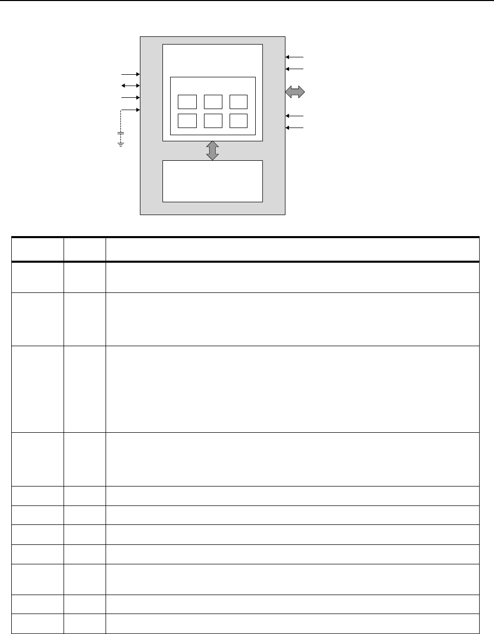
3-38 Theory of Operation: Controller
Figure 3-24. eMMC Topography
RST_n
CMD
CLK
VDDI
VCC
VCCQ
DAT[7:0]
VSS
*
VSSQ
*
MMC
controller
e·MMC
NAND Flash
Registers
OCR CSD RCA
CID ECSD DSR
* internally connected.
Note: 1. VSS and VSSQ are connected internally.
Symbol Type Description
CLK Input Clock: Each cycle of the clock directs a transfer on the command line and on the data
line(s). The frequency can vary between the minimum and the maximum clock frequency.
CMD I/O Command: This signal is a bidirectional command channel used for command and
response transfers. The CMD signal has two bus modes: open-drain mode and push-pull
mode (see Operating Modes). Commands are sent from the MMC host to the device, and
responses are sent from the device to the host.
DAT[7:0] I/O Data I/O: These are bidirectional data signals. The DAT signals operate in push-pull
mode. By default, after power-on or assertion of the RST_n signal, only DAT0 is used for
data transfer. The MMC controller can configure a wider data bus for data transfer either
using DAT[3:0] (4-bit mode) or DAT[7:0] (8-bit mode). eMMC includes internal pull-up
resistors for data lines DAT[7:1]. Immediately after entering the 4-bit mode, the device
disconnects the internal pull-up resistors on the DAT[3:1] lines. Upon entering the 8-bit
mode, the device disconnects the internal pull-ups on the DAT[7:1] lines.
RST_n Input Reset: The RST_n signal is used by the host for resetting the device, moving the device
to the pre-idle state. By default, the RST_n signal is temporarily disabled in the device.
The host must set ECSD register byte 162, bits[1:0] to 0x1 to enable this functionality
before the host can use it.
VCC Supply VCC: NAND interface (I/F) I/O and NAND Flash power supply.
VCCQ Supply VCCQ: eMMC controller core and eMMC I/F I/O power supply.
VSS1Supply VSS: NAND I/F I/O and NAND Flash ground connection.
VSSQ1Supply VSSQ: eMMC controller core and eMMC I/F ground connection.
VDDI Internal voltage node: At least a 0.1μF capacitor is required to connect VDDI to ground. A
1μF capacitor is recommended. Do not tie to supply voltage or ground.
NC – No connect: No internal connection is present.
RFU – Reserved for future use: No internal connection is present. Leave it floating externally.

Theory of Operation: Controller 3-39
Figure 3-25. Block Diagram of VOCON and EXPANSION boards as related to eMMC
P2001
F2_Timer_out
VCC_1.85v
VCC_2.775
MMC
V4_2775D
V_SW_3.6 V_EXT_1.85v
V_2.775_EXP
AVR_STATUS_1.8
AVR_STATUS_3.3
J4001
OMAP
1710
U6302
eMMC
AVR
U2415
CPLD
U6101
MAKO
U6501
Expansion Board VOCON Board
Voltage
translator
LDO
U6508
jumper
R6562
MMC_CMD
MMC_CLK
EMMC_RESET
MMC_DAT0
MMC_DAT1
MMC_DAT2
MMC_DAT3
3-40 Theory of Operation: Controller
3.2.4.10 Peripheral Devices
The OMAP processor is equipped with multiple buses and interfaces that are configured for
peripheral interconnection.
3.2.4.10.1 Receive and Transmit SSI
These two interfaces are dedicated for communicating with the RF deck digital interface, carrying
receive and transmit base band signals. The OMAP processor generates the clock and FSYNC
signals for the receive SSI interface. The RF deck generates these signals for the transmit SSI
interface.
Figure 3-26. RX / TX SSI Configuration
3.2.4.10.2 Audio SSI
OMAP's McBSP1 interface is configured as a SSI interface dedicated to carry transmit and receive
audio data to peripheral devices. The peripherals connected to this bus include MAKO, Audio
CODEC, MACE and CPLD. The bus also connects to the option board via J3001. MAKO generates
the clock and frame sync signals for this bus.
Figure 3-27. Audio SSI Configuration
RF BOARD
TRIDENT
ABACUS
RX_FSYNC
RX_CLK
RX_DA
TX_FSYNC
TX_CLK
TX_DA
VOCON BOARD
OMAP 1710
MAKO
TI
CODEC
MACE
McBSP 2
McBSP 1
RX SSI
TX SSI
3
3
VC_FSYNC
VC_DCLK
SYNC
BCLK
MACE/CODEC
FSYNC
MACE/
CODEC_CLK
McBSP 2
CPLD
MCLK
WCLK
OMAP
MACE
MCBSP1
SSC 0
(Black)
SSC 1
( Red )
BLACK or
RED RX
RED RX
RED TX
CODECs
CPLD
BLACK or
RED TX
0
0
1
1
Mux A
PA 28 (GPIO)
Hi_Sec */Normal
SSC 2
(Sniffer)
RD 2
RD 0
TD 0
RD 1
TD 1
TD 3
Mux B
Expansion Board
Vocon Board
Theory of Operation: Controller 3-41
3.2.4.10.3 ARM SPI
This SPI interface is controlled by OMAP's ARM core. Devices connected to this bus include MAKO,
display controllers and the audio CODEC.
3.2.4.10.4 DSP SPI
This SPI interface is controlled by the DSP core of the OMAP processor. This bus is used to
configure and control devices on the RF deck.
Figure 3-28. SPI and I2C Configuration
3.2.4.10.5 1-Wire
The OMAP's 1-wire line is available on the GCAI pin 16. The signal is routed to the side connector
via J4001.
3.2.4.10.6 USB
The OMAP CPU's USB port is routed to the side connector via J4001. The USB signals on the side
connector are illustrated in Figure 3-21, on page 3-34.
OMAP 1710
TOP DISPLAY
McBSP3 SPIF
DSP SPI
FRONT DISPLAY
MAKO
TI CODEC
ARM SPI
I2C LIGHTING
CONTROLLERS
3
SPI_CLK
SPI_MOSI
SPI_MISO
MAKO_CS
TOP_DIS_CS
CPLD
Inverter
I2C_SCL
I2C_SDA
COLOR_DIS_CS
SPI_DSP_CLK
SPI_DSP_MOSI
SPI_DSP_MISO
DAC_CS
EEPROM_CS
ABACUS_CS
ABACUS_CS
DSP SPI
TRIDENT
ABACUS
EEPROM
DAC
RF BOARD VOCON BOARD
CODEC_CS
I2C

3-42 Theory of Operation: Controller
3.2.4.10.7 UARTs
Two of OMAP's UARTs are configured for peripheral interfacing.
The four-wire UART1, which is capable of hardware flow control, is available on the side connector
for accessory devices. The signals are level translated via MAKO and routed to the side connector
via J4001.
OMAP's UART2, which is a two wire interface, capable of software flow control only, is connected to
the GPS receiver IC on the expansion board. The signals are routed to the expansion board via
J4001.
3.2.4.10.8 CPLD (U6101)
The CoolRunner IC is a complex programmable logic device (CPLD) programmed specifically for the
APX/ SRX product line. The CoolRunner IC is flash based and comes pre-programmed. It is
contained in an 8x8mm, 132 BGA package with 0.5mm ball spacing. The primary functions of the
CPLD are clock generation, GPIO expansion, SSI clock and frame sync direction control, F2
multiplexing, secure data control, main display off-loading, and clock inversion.
An external linear regulator, U6508, supplies the CPLD's 1.875 V core voltage. The 1.875 V core
voltage is used for the CPLD’s internal logic and I/O buffers. MAKO's 24.576 MHz clock source is
used by the CPLD to generate a 32.768 kHz clock for OMAP booting, real time clock/timer, and for
GPS. It is also used to generate 4.096 MHz for the MACE IC.
The CPLD is controlled through OMAP's EMIFS interface. It supports 31 configurable GPIOs. It also
supports 20 input only pins that are accessible through an EMIFS read operation. Some of the
GPIOs supported by the CPLD include GCAI_GPIO_0, F2_PARAMP_MON, and USB_CURR_LIM.
Some examples of the inputs the CPLD is programmed to support are some of the top and side
controls buttons (SEC_CLEAR, FREQ_SEL, MON, SIDE_1, SIDE_2, and TG0) and board ID.
Figure 3-29 below shows the basic CPLD interfaces.
Figure 3-29. CPLD Block Diagram
EMIFS
24MHz
F2 Timer
F2 Select
GCAI GPIO0
KEYLD_MISSING
KL_SWITCH
CPLD
MAKO
OMAP 1710
Processor
32kHz to OMAP
32kHz to GPS
4.096MHz to MACE
GPIOs
GPIs

Theory of Operation: Controller 3-43
3.2.5 Audio
The audio section of the VOCON design consists of:
• TI AIC33 voice CODEC
• TI TPA2034D1 class-D audio power amplifier
• MAKO audio sub-block
3.2.5.1 TX Audio path
The TX audio paths begin with three microphones. There are two internal microphones and one
external microphone path going to the GCAI connector.
The internal microphone paths start with two microphones that are embedded within the radio. Both
of the microphones are biased with a 4.7 V supply that is generated by the MAKO IC. This supply is
solely dedicated to biasing the microphones. The microphone signals are AC coupled into the 16 bit
TI AIC33 stereo CODEC on the MIC3R and MIC3L input pins. The TI AIC33 CODEC allows both
microphone signals to be amplified, and simultaneously sampled and converted into digital data. The
data is sent to the OMAP1710's DSP through the McBSP1 port where the DINC (dual input noise
canceller) can process the data for both microphones and provide a high level of noise suppression.
The digital data is sent to the OMAP1710 through the audio SSI (synchronous serial interface) bus
where the MAKO IC is used as the interface's clock and frame sync generator.
Figure 3-30. Audio TX Path Block Diagram
The external microphone path will also be supported by the TI AIC33 CODEC, using the LINE1LP
pin on the IC. The LINE1LP is multiplexed with the MIC3R within the CODEC, and selected as the
input when the external microphone path is chosen as the TX audio source. Similar to the internal
microphone signals, the TI CODEC amplifies and samples the external microphone signal. The
digital data is also sent to the OMAP1710's DSP through the McBSP1 port using the audio SSI bus.
Portable TX Audio Architecture
OMAP DSP
MAKO
Audio Stereo Codec (TI AIC33)
SSI
SSI
MCBSP1 VC_DCLK
VC_FSYNC
VC_TX
VC_RX
SSI
LEFT
ADC
RIGHT
ADC
DSP SPI SPI
MIC BIAS
Reset Out Reset
External/
Accessory
Microphone
Internal
Microphone 1
Internal
Microphone 2
I2C I2C
Line 1L
Mic 3R
Mic 3L
Note: All three microphones will be
routed to the AIC33 CODEC. In Tx
mode, MAKO will only be used to
generate the microphone bias. Both
internal microphones will be sampled
on adjacent SSI slots. The external
microphone can be sampled on either
slot.
5
4
6
1

3-44 Theory of Operation: Controller
3.2.5.2 RX Audio path
The RX audio path supports two internal speakers and one external speaker.
Figure 3-31. VOCON RX Audio Path Block Diagram
The RX internal audio path begins with the digital audio samples being sent from the OMAP1710's
McBSP1 port to the TI AIC33 CODEC through the audio SSI bus. As in the TX audio paths, the
MAKO IC is also used to generate the clock and frame sync for the audio SSI bus. Once the audio
data is received by the TI CODEC, the CODEC proceeds to convert the data to analog and
implements the volume control. The analog signal in the CODEC is then fully differential and gets
sent out to the power amplifier through pins LEFT_LOP and LEFT_LOM. The TI TPA2034D1 Class
D audio power amplifier accepts a fully differential analog input signal and will also drive a
4 Ohm loudspeaker differentially.
The external speaker path is almost identical to the internal speaker path. The digital audio data is
sent from the OMAP1710's McBSP1 port to the TI AIC33 CODEC for digital to analog conversion
and volume control. The external speaker path uses the MAKO IC's class-AB audio power amplifier
to drive 16 Ohm to 28 Ohm external speakers. The input to MAKO IC's audio power amplifier is fully
differential and comes from the TI CODEC's RIGHT_LOP and RIGHT_LOM. The output of the
MAKO IC's audio amplifier is also fully differential and available on pins EXT_SPKR_P and
EXT_SPKR_M.
MAKO
Class D
TI
TPA2034D1
OMAP DSP
SSI
MCBSP1
Switch
Low-Pass Filter
20kHz Corner
ARM SPI SPI
SPI
Shutdown
OMAP GPIOs
AB AMP
AB AMP
External/
Accessory Speaker
~ 16-20 Ohms
Large Internal
Speaker
~ 4 Ohms
SSI
I2C
I2C
RIGHT LINE
OUT
LEFT LINE
OUT
TI CODEC
DSP
SPI
SSI
7
8
11
12
Test Point Descriptions
VOCON Bot Board Overlay
9
Expan Top Board Overlay
10
13
14
15
Theory of Operation: Controller 3-45
3.2.6 User Interface
3.2.6.1 Control Top
The control top contains an On/Off & Volume Knob (S3), a sixteen-position Channel/Frequency
Switch with programmable concentric two-position switch (S2), a three-position (A,B,C)
Programmable Toggle Switch (S4), and an orange programmable Top Button (S1). The Control Top
also includes a TX/RX LED that is solid amber upon receive, red on PTT, and blinks amber on
secure RX. Additionally, the Control Top includes a transflective FSTN display. Control Top
components are mounted on a flex circuit which connects to controller board connector J2101.
When the On/Off & Volume Knob (S3) is switched to the 'ON' position, the switch is grounded and
MECH_SW is pulled low. MECH_SW is an input to MAKO (U6501). The logic low input enables an
external FET (Q6501) gate voltage, FET_ENX, which switches UN_SW_B+ to SW_B+ and turns the
radio on. Volume is also controlled through S3 and is an input to MAKO. The VOL signal is
connected to a potentiometer biased between ground and 2.775 V (R6563) from MAKO. When the
volume knob is turned, the VOL signal level is converted to a code word by MAKO's ADC and read
by OMAP through SPI.
Switch S4 is the three-position, binary-coded, toggle switch typically used for expanded Zone/
Channel Selection. Two outputs of the switch,TOGGLE_0 and TOGGLE_1, are biased to 1.875 V.
The third output is grounded. Two-bit codewords from the switch are read by OMAP through the
CPLD's EMIFS interface and indicate which of the three positions is set.
The orange programmable Top Button (S1) is typically used for emergency. It is also biased to
1.875 V (R6507) and is an input (EMERG_BTN_X) to the CPLD. A button press is detected when
EMERG_BTN_X is pulled low.
Like the three-position switch, the Frequency Switch (S3) is also binary coded. S3's output pins are
connected to GPIO pins of the CPLD which provide a four-bit binary word (signals FREQ_SEL_0,
FREQ_SEL_1, FREQ_SEL_2, and FREQ_SEL_3) to OMAP indicating which of the 16 pins of the
switch is set. This switch provides an additional output, SEC_CLEAR, which is typically used for
coded or clear mode selection. Selecting clear mode pulls this signal to a logic low, and it can be
monitored from R2135.
Figure 3-32. Control Top Block Diagram
CPLD
Frequency Switch
ABC
Toggle
Switch
Concentric
ON/OFF SW
Volume POT
Emergency
Switch
MAKO
Top
Display
TX/RX
LED
Intelligent
Lighting
OMAP
FPC Vocon Bd
pg
3-46 Theory of Operation: Controller
3.2.6.2 APX 5000/ APX 6000/ APX 6000XE/ SRX 2200 LCD Display Modules
3.2.6.2.1 QVGA
The APX 5000/APX 6000/APX 6000XE/SRX 2200 radio can have up to 2 displays (QVGA and
FSTN) depending upon the particular feature set and radio model ordered. The main Transflective
1.6" color display is a QVGA (130 x RGB x 130) active matrix TFT (Thin Film Transistor) LCD. A
display flex connects the front display to the J2304 22-pin connector on VOCON board. The QVGA
display uses the 8-bit Special optimized Screen Interface (SoSSI) for data and commands.
Figure 3-33. Display Circuit Detail Overview Block Diagram
The QVGA LCD Module operates using V_2.775D and V_EXT_1.85. The V_2.775D is the module’s
analog supply voltage sourced by LDO6 of MAKO. The V_EXT_1.85 is the module’s IO voltage
sourced by the 1.85V external LDO regulator. An 8-bit parallel bus is used for data and command
communication between OMAP’s SoSSI interface and LCD driver IC. The F_DISP_DATA_CMD
signal indicated the type of data being sent to the driver. A ‘0’ corresponds to command data and a
‘1’ corresponds to display data. Data only travels in one direction, from OMAP to display driver.
Therefore F_DISP_RW line will always be low. Display data is latched on the falling edge of the
F_DISP_RW_EN signal.
The SoSSI interface uses the LCD DMA controller/bus to allow the LCD module to access system
memory. Therefore the transfer of pixel data process will require less CPU processing power. An
initiate DMA transfer command is used and display data is transferred to the LCD module
automatically without intervention thus offloading the processor.
OMAP
(R/W)
(D/C)
(CLK 4MHz)
(RST)
(D2)
(D3)
(D4)
(D5)
(D6)
(D7)
(D0)
(D1)
LCD_HSYNC
LCD_AC
LCD_PCLK
RST_OUT
LCD_PIXEL_0
LCD_PIXEL_1
LCD_PIXEL_2
LCD_PIXEL_3
LCD_PIXEL_4
LCD_PIXEL_5
LCD_PIXEL_6
LCD_PIXEL_7
MAKO
(V_2.775D)
(BOARD ID)
V06_O
ATOD_5
VOUT
DNP
DISPLAY
FLEX CONNECTOR
J2304 PINS
V_EXT_1.85 (.004mA TYP.)
DNP
CPLD (INVERT)
IO87 IO39
0 Ω
47 Ω
12
F_DISP_RW
3
F_DISP_DATA_CMD
8
F_DISP_RW_EN (CLK)
18
OMAP_RESET To display driver (NT39123)
on display module.
19
F_DISP_DATA_0
F_DISP_DATA_1
F_DISP_DATA_2
F_DISP_DATA_3
F_DISP_DATA_4
F_DISP_DATA_5
F_DISP_DATA_6
F_DISP_DATA_7
F_DISP_BD_ID
V_2.775D (.68mA TYP.)
14
15
4
5
16
6
17
22
7
2
47 Ω
47 Ω
47 Ω
10k Ω
1.85V
V-REG

Theory of Operation: Controller 3-47
Prior to the LCD interpreting any commands, the correct display power-up sequence must be
initiated. First the V_EXT_1.85 (1.875 V) and V_2.775D (2.775 V) supplies must be at 90% or above
threshold and stable for 10us, and then reset can be asserted high. After OMAP de-asserts the reset
out signal (OMAP_RESET) the SLPOUT command can be sent. Now configuration commands are
ready to be sent to the LCD module.
The QVGA LCD module is only intended to operate up to +80°C due to ghosting effects. Therefore
software will shut off the display and backlight if the +80°C limit is reached. The display and backlight
will remain off until temperature drops below +75°C. The temperature sensor, U6401, for the display
cut-off is located near the top display connector and is input into MAKO A/D Channel 3, pin M14.
For enhanced display readability, the default backlight is set to a dim state while the radio is in
Standby mode; however, the backlight turns to full brightness through a button press, call receive,
emergency call, and other status indicators. See Section 3.2.6.3: "Intelligent Lighting" for the display
backlight operation.
3.2.6.2.2 FSTN
All APX 5000/APX 6000/APX 6000XE/SRX 2200 Radios are equipped with a caller ID (CID) top
display. This top display is a 1.1", Transflective, FSTN (Film compensated Super Twisted Nematic)
32 row x 112 column LCD with black pixels on a light background. This display is a component of the
control top sub-assembly with all interconnections passing through control top FPC. The display is
controlled via OMAP's 3 wire SPI interface to program the display driver IC registers and send data/
image information to the display. The active low chip select line, T_DISP_SPI_CS, is sent from the
OMAP GPIO_5 pin P3. The T_DISP_DATA_CMD line indicates whether the data being sent across
the SPI bus is register/command settings or if it's data/image information. The display driver contains
internal GRAM, which stores the current display content information, and the data/image information
is only sent when the display content needs to be updated.
Prior to sending any information to the LCD driver, the proper power-up sequence must be
instantiated. First, the V_EXT_1.85 and V_2.775D voltage supplies must be stable for at least 1 ms.
Next, the active low reset line, T_DISP_RESET, to the LCD driver must see a low pulse of 10 usec or
longer prior to communicating to the LCD driver. Then, the register setting information will be sent to
the display driver, followed by the image/data information.
The top LCD contains various LEDs for multiple backlight color combinations depending upon the
mode of operation. The programmable default backlight setting is off in standby mode, but will
illuminate to max brightness during a button push, call receive, receive mode, low battery, out of
range, emergency, etc. The details of the top display backlight settings are listed in Section 3.2.6.3:
"Intelligent Lighting". The top display contains 2 parallel side firing white LEDs and 2 parallel Red-
Green side firing bi-color LEDs.

3-48 Theory of Operation: Controller
3.2.6.3 Intelligent Lighting
The APX 5000/APX 6000/APX 6000XE/SRX 2200 radio is equipped with numerous LEDs to provide
intelligent lighting features. The VOCON board contains 2 lighting controller devices, which
illuminate all the LEDs throughout the radio, as shown in Figure 3-34. The main lighting controller,
U2204, provides white illumination to the main QVGA color display, and white keypad backlights.
The secondary lighting controller, U2201, generates illumination for the top display backlight and TX/
RX indicator lamp. Both lighting controller devices are controlled through OMAPs I2C interface (SCL
and SDA). Some of the intelligent lighting color schemes are shown in Table 3-8.
3.2.6.3.1 Main Lighting Controller
The boost lighting controller, U2204, provides backlight functionality for the main color QVGA
display, and the white backlight on the keypad. Switcher 3.6 (V_SW_3.60) is used as main input
voltage for the controller, while external 1.85 (V_EXT_1.85) is used for IO voltage. The controller
communicates with the OMAP via standard I2C communication protocol. This communication allows
the OMAP chip to enable, disable, and control the brightness of each LED. A reset line issued by
OMAP, OMAP_RESET, can be used to set the device in reset. The charge pump capability of the
lighting controller is currently not used. Refer to Figure 3-34.
The QVGA display has 3 LEDs powered by the external 3.6 regulator, V_SW_3.6. The cathode
output (negative) of each LED is fed back into the LED driver to control the current thus controlling
the brightness of the LEDs. The front display backlights are controlled by bank B of the LED
controller.
The keypad backlighting uses 4 white LEDs for illumination. The keypad backlighting operates
similar to the main QVGA display LEDs. The LEDs are powered by the external 3.6 regulator,
V_SW_3.6. The cathode output (negative) of the LEDs is fed back into bank A of the LED driver to
control the current thus controlling the brightness of the LEDs.
Table 3-8. Color Schemes
Color
Default White
Out of Range Red
Low Battery Red
Emergency Amber
Call Received Green
Call Paged Green

Theory of Operation: Controller 3-49
3.2.6.3.2 Secondary Lighting Controller
As previously mentioned the secondary lighting controller provides illumination to the top display
backlight and Tx/Rx indicator lamp. The lighting controller and LEDs are powered by switcher 5
(V_SW_5). This lighting controller device uses a PWM output to control the dimming modes of
operation for each LED. The device is controlled through the I2C interface, however, the I2C
interface require an input high voltage between 3 V – 5.5 V, thus the level translator (U2202) is used
to boost these signals to 5V logic.
Figure 3-34 shows the major connection scheme to this secondary lighting controller. The white,
green, and red top display LEDs are connected to the lighting controller PWM outputs through ESD
filter inductors L2204, L2203, L2202, respectively. The TX/RX status indicator LED uses a tri-color
red, green, amber (RGA) LED.
Figure 3-34. Lighting Controller Overview
FRONT DISPLAY
LED DRIVER
(LM27965)
10
VIN
V_SW_3.6
V-REG
VOUT
KEYPAD
12
20
21
11
15
16
17
18
D1A
D2A
D3A
D4A
D1B
D2B
D3B
RESET
SCL
SDIO
OMAP
RST_OUT
(I2C) SCL
(I2C) SDA
LED DRIVER
(LP3943)
PWR LED0
V_SW_5
V-REG
VOUT
RESET
SCL
SDA
LED1
LED2
LED4
LED5
LED6
A0
A1
A2
LEVEL
SHIFT
1.85V
1
TOP DISPLAY
25
15
17
8
26
24
23
R
G
W
A
G
R
FRONT DISPLAY
WHITE BACKLIGHT
KEYPAD WHITE
ILLUMINATION
TX/RX
STATUS
TOP DISPLAY
BACKLIGHT
3-50 Theory of Operation: Controller
3.2.6.3.3 Secondary Lighting Controller – SRX 2200
Figure 3-35 shows the major connection scheme to this secondary lighting controller exclusively for SRX 2200.
A lighting system has been put into place to accommodate night profiles. These profiles shift both
displays and the keypad to a lower brightness. The LM27965 Lighting Controller, which controls the
Front Display and Keypad during normal operation, is disabled during Night Operation/ Night Vision
operation. The LM3943 is the only operating backlight driver during this mode and lower brightness
levels are achieved by routing separate lines and decreasing the duty cycle of its pulse width
modulated signal.
Figure 3-35. Lighting Controller – SRX 2200
RADIO TOP LIGHTING
V_EXT_1.85 V_LED_TOP
C2201 C2202
R2201
0.1UF 0.1UF
200K
SCL2
EN
GND
SDA1
SCL1
SDA2
7
2
54
63
1
8
U2202
V_EXT_1.85
SCL_5V
SDA_5VI2C_DATA
PCA9306
I2C_CLK
IC2_TRANS_VREF2
VREF1
VREF2
R2243
V_LED_TOP
10K
OMAP_RESET_5V
C2221
1
3
2
Q2202
DNP
0.1UF
DTC114YKAF
OMAP_RESET
47K
10K
LED DRIVERS
R2235
V_SW_5 V_LED_TOP
0
R2206
R2204 C2203
R2207
V_LED_TOP
V_LED_TOP
3.3K 0.1UF
0
3.3K
LED15
GND2
GND1
SCL
RST
SDA
A0
A1
A2
LED12
LED11
LED10
LED9
LED8
LED13
LED7
LED6
VDD
LED14
LED0
LED1
LED2
LED3
LED4
LED5
21
20
19
18
11
10
8
7
6
5
4
3
17
16
15
14
13
12
2
1
25
9
24
23
22
U2201
LP3943
4 KEYPAD
NV PROFILE ALTERNATE
CURRENT DRAIN PATHS
3 FRONT DISPLAY
2 TOP DISPLAY (RED & WHITE)
TX_RX_GREEN_LED
KP_LED4_NVG
KP_LED3_NVG
TX_RX_AMBER_LED
TOP_DISP_WHITE_LED
TOP_DISP_NVG_W
TX_RX_RED_LED
KP_LED2_NVG
KP_LED1_NVG
F_DISP_LED3_NVG
F_DISP_LED2_NVG
F_DISP_LED1_NVG
TOP_DISP_NVG_R
TOP_DISP_GREEN_LED
TOP_DISP_RED_LED
R2262
R2261
R2260
R2259
R2258
R2257
R2256
R2255
R2247
R2215
11K
430
82K
7.5K
7.5K
7.5K
11K
11K
11K
11K
C2220
R2241
V_LED_FRONT
1UF
0
FRONT DISPLAY AND KEYPAD LIGHTING
NC
NC
NC
23
11
8
12
13
6
14
5
15
3
4
16
KP_LED3
KP_LED2
F_DISP_LED1_RETURN
KP_LED4
KP_LED1
F_DISP_LED3_RETURN
F_DISP_LED2_RETURN
U2204
LM27965
VIN
RESET
ISET
C1_P
C1_N
C2_P
C2_N
VIO
CTGND
GND1
GND2
SDIO
SCL
NC
NC
NC
NC
7
24
2
1
10
17
20
21
19
22
I2C_CLK
OMAP_RESET
I2C_DATA
IN
IO
D1A
D1B
D2B
D1C
D3B
NC1
NC2
D2A
D3A
D4A
D5A
POUT
18
9
G1
R2242
V_SW_3.60
0
C2217
1UF
R2245
U2205
V_EXT_1.85
2SC5663
12.4K
F_DISP_AND_KP_ISET
R2244
23
1
V_LED_TOP
10K
ISET SWITCH
LED 7 ON = NV MODE
LED 7 OFF = DEFAULT MODE
F_DISP_KP_NVG_MODE

Theory of Operation: Controller 3-51
3.2.6.4 Keypad
The Dual Display Model contains a 21 button keypad, which translates to a 5x5 row and column
keypad matrix as shown in Figure 3-36. The keypad also contains LEDs for the backlighting of the
keys, which is described in more detail in Section 3.2.6.3: "Intelligent Lighting". Every key is
assigned a particular row and column to identify the unique key, as shown in keypad mapping Ta bl e
3-9. The keypad flex also contains 2, 6-channel filters that each row and column signal passes
through. Each row of the keypad contains an external pull-up resistor, and all the rows are interrupt
based inputs to OMAP. The columns are driven low by default in OMAP. When a key is pressed, the
corresponding key row and column are shorted together and causes a low level to be input on the
corresponding row in OMAP. Upon receiving the row interrupt, the OMAP IC is then programmed to
scan the column output to determine which corresponding column was selected that generated the
interrupt.
Figure 3-36. Keypad Interface Outline
Table 3-9. Key Map Matrix
Key Row, Column Map Key Row, Column Map
{0 , 4 33 , 2
|1 , 4 42 , 0
}2 , 4 52 , 1
H4 , 0 62 , 2
<4 , 1 71 , 0
U0 , 3 81 , 1
D4 , 2 91 , 2
>1 , 3 *0 , 0
*FPC = Flexible Printed Circuit
OMAP
ROW
COLUMN
KEYPAD FPC

3-52 Theory of Operation: Controller
3.2.6.5 Side Controls
The side controls include three programmable, momentary, pushbutton switches (Side Button 1
[SB1], Side Button 2 [SB2], Top Side Button [MON]) and a Push-To-Talk switch [PTT]. These
components interface to the expansion board via connector J2005 through a two-piece, bonded flex
circuit. A board-to-board connection routes the side controls signals from expansion board connector
P2001 to connector J4001 of the controller board. See Chapter 7 for pin out names and numbers.
Side button 1 (R4006), side button 2 (R4007) and the top side button (R6101) are inputs to the CPLD
and are biased to 1.875V. A button press is detected when the OMAP reads a 'LO' state from the
CPLD EMIFS interface. PTT (R4005) is connected directly to OMAP and a button press is detected
when a LO state is read.
3.2.6.6 GCAI
The GCAI (Global Communications Accessory Interface) connector is a 15 pin interface located on
the side of the radio. The connector interfaces the radio with accessories and is used for
programming. When the OMAP (U6501) detects that an accessory has been attached through a
logic low on GPIO0, it will identify the device by reading the GCAI_ONE_WIRE line. Once the device
type is identified, the appropriate signals are multiplexed through MAKO to the GCAI connector for
the particular device. Figure 3-37 is a block diagram of the GCAI interface.
Mounted to the side connector is a printed circuit board that houses ESD protection circuitry and an
auxiliary RF connector. The universal side connector interfaces with the expansion board via the P1
connector of a flex circuit and the J2004 connector of the expansion board. A board-to-board
connection routes universal side connector signals through expansion board connector P2001 to the
controller board. The figures below show the connections and signal assignments from the universal
connector to the controller board.
P2 , 3 00 , 1
13 , 0 #0 , 2
23 , 1
Table 3-9. Key Map Matrix (Continued)
Key Row, Column Map Key Row, Column Map

Theory of Operation: Controller 3-53
Figure 3-37. GCAI Signal Configuration
Figure 3-38. GCAI Connector
2
6
7
8
9
10
11
12
D+
D-
Vbus
One-Wire ONE_WIRE
GPIO_4
GPIO_3
Preamp
USB
XCVR
1
3
4
5
One-Wire
GPIO_0
Ext Mic
GCAI
CONNECTOR
UART1_TX
UART1_RX
UART1_TX
UART1_RX
OPT_GPIO_3
OPT_GPIO_2
OPT_GPIO_0GPIO
MAKO
OMAP1710
EXT
PA
KF Switch
CPLD
GPO
ONE_WIRE_GCAI
BATT_STATUS
VBUS
D+
D-
SPKR+
SPKR-
GND
MIC+
MIC-
OPTA_SEL_2
OPTA_SEL_1
OPTA_SEL_0
KEYFAIL CONTROL
KEYFAIL
MACE
TXEN
DAT
SE0
USB
PORT 0
GPIO
GPIO
Front View Side View
AB C
1
3
5
7
9
11
2
4
6
8
10
12
9
8
P1
16
1

3-54 Theory of Operation: Controller
Table 3-10. P1 Pin Assignment
P1 PIN ASSIGNMENT SIDE CONNECTOR SIGNAL
1 GCAI_VBUS_5V
2 GCAI_VBUS_5V
3GND
4 GCAI_USB_P_GPIO1 / TxDc / FillReq
5 GCAI_USB_N_GPIO2 / RxDc / FillData
6GND
7 GCAI_GPIO0 / PwrOn
8 GCAI_CTS_GPIO_4 / KeyFail / FillClk
9GCAI_MIC_P
10 GCAI_MIC_N
11 GCAI_SPKR_N / LineOut-
12 GCAI_SPKR_P / LineOut+
13 GND
14 GCAI_RTS_GPIO_3 / OTG-ID / FillSen
15 GND
16 GCAI_ONE_WIRE
Table 3-11. GCAI Connector Pin Assignment
PIN ASSIGNMENT SIGNAL
AGND
B GCAI_RF_INPUT
CGND
1 GCAI_GPIO0 / PwrOn
2 GCAI_ONE_WIRE
3 GCAI_VBUS_5V
4 GCAI_USB_P_GPIO1 / TxDc / FillReq
5 GCAI_USB_N_GPIO2 / RxDc / FillData
6GND
7 GCAI_SPKR_P / LineOut+
8 GCAI_SPKR_N / LineOut-
9 GCAI_RTS_GPIO_3 / OTG-ID / FillSen
10 GCAI_MIC_P


3-56 Theory of Operation: Controller
3.2.7 RF Interface
The VOCON to RF board interface through connector J1001. See Figure 3-40.
Figure 3-40. VOCON to RF Board Interface
The major interfaces are the TX and RX SSI buses, the SPI Bus with associated chip selects, the
synchronization signals (DMCS,SYNCB), the 16.8 MHz clock, MAKO VDDs and I/O's, and the
TX Inhibit from the Option Board.
3.2.7.1 TX SSI
The TX SSI interface provides the SSI data from the OMAP's DSP to the Trident IC on the RF board.
The interface contains 3 signals, the TX frame sync, TX clock, and TX Data signals. The pin
numbers for both the RF connector and OMAP IC are also shown in Figure 3-40.
3.2.7.2 RX SSI
The RX SSI interface provides the SSI data from the Abacus IC on the RF board to the OMAP's
DSP. The interface contains 3 signals, the RX frame sync, RX clock, and RX Data signals. The pin
numbers for both the RF connector and OMAP IC are shown in Figure 3-40.
3.2.7.3 Synchronization
The DMCS and SYNCB signals are used for synchronization between the RF and VOCON boards.
These signals route from the OMAP IC timer outputs through the CPLD to the RF board. The DMCS
signal connects to the Trident IC and the SYNCB connects to the ABACUS IC. The pin numbers for
both of the signals are shown in Figure 3-40.
RF - VoCon Interface
OMAP
TX SSI
RX SSI
SPI
ABCS
TRCS
EEPROM_CS
DMCS
SYNCB
LOCK
TEMP
16.8MHz
TUNE
ISET
BATT
VSW1
V2775
GND
BSTAT
TXINH
CPLD
3
3
3
McBSP3
GPIO59
GPIO17
GPIO28
GPIO56
McBSP2
McBSP2
TIMER.PWM2
GPIO7
TIMER.EXTCLKBUFFER
RSTB
5
MAKO
VDD
VSW1
V6
POR
ATOD_5
FE_TUNE1
PWR_CTRL
OPTION BOARD
9
ONE_WIRE_BATT
RF CONNECTOR
LDO2LDO2
GPIO61/SPIF_CS2DAC_CS
L3
V6
G19
T19
V15
M20
Y5
N18
TIMER.PWM1
TX_RX
L14
A1 1
L3
N1
L13
N14,P14,AA1733,31,29
22
27
2
25
14
19,17,21
15,11,13
Y6,W7,AA5
V7,W6,P10
9
23
3
28,30,
32,34,36
37
6
8
7
20
18
16
26
12
1,4,5,10,24,
35,38,39,40
ATOD_4
C1
56
L8
L12
D2

Theory of Operation: Controller 3-57
3.2.7.4 MAKO Interface
MAKO supplies some DC regulation and I/O support for the RF board. The main battery supply is
provided by the RF board and is connected to MAKO. Regulated DC supplies based on this battery
voltage are then provided by MAKO to the RF board. These supplies are VSW1, LDO2, and V6. The
Power On Reset (POR) reset signal is also provided by MAKO to reset the RF board.
The One-Wire signal from the battery is provided by the RF board to MAKO's One-Wire
segmentation circuit, which then connects the One-Wire data path to the OMAP IC. The TUNE,
ISET, and TEMP signals are also interfaced to the MAKO IC.
3.2.7.5 TX Inhibit
The TX Inhibit I/O is reserved for future Option Board use, and is available at pin 12 for the RF
connector and pin 56 of the option board connector.
3.2.8 Encryption
The encryption circuitry is placed on the expansion board and interfaces to the VOCON through the
J4001-P2001 connector. The encryption circuitry is designed to digitally encrypt and decrypt voice
and ASTRO data in the APX 5000/APX 6000/APX 6000XE/SRX 2200 radio. The Motorola Advanced
Crypto Engine (MACE) IC is the main component in the encryption design, and has some discrete
support circuitry along with the interfaces to the VOCON IC's (CPLD, OMAP, and Audio CODEC).
NOTE: The MACE IC is NOT serviceable. The information contained in this section is only intended
to help determine whether a problem is due to the MACE IC or the radio itself.
Figure 3-41 below shows the Encryption architecture for the APX 5000/APX 6000/APX 6000XE/SRX
2200 radio.
Figure 3-41. APX 5000/ APX 6000/ APX 6000XE/ SRX 2200 Encryption Architecture
MACE
(Secure IC)
OMAP
AUDIO
CODEC
Vocon Bd
SSI SSI
Key
Zeroize
Tamper
Key
Fail
CPLD
CLK SSI GPIO
Key
Retention

3-58 Theory of Operation: Controller
As shown in Figure 3-41 above, the encryption design consists of 5 blocks:
• MACE IC
• Key Loading
• Key Retention
•Tamper
• Key Zeroize.
3.2.8.1 MACE IC
The encryption module uses the MACE IC and an encryption key variable to perform its encode/
decode function. The encryption key variable is loaded into the MACE IC, via the GCAI (side)
connector, from a hand-held, key variable loader (KVL). The MACE IC contains the particular
encryption algorithm purchased. Table 3-12 lists the encryption algorithms and their corresponding
kit numbers.
Once the MACE IC has its encryption keys and algorithm, it communicates with the radio' s host
processor (OMAP) through the Synchronous Serial Interface (SSI) bus. Both commands and audio
(clear and encrypted) are sent through the SSI bus. A communications failure between the host
processor and the secure module will be indicated as an ERROR 09/10 message on the display.
Table below lists the encryption algorithms and their corresponding kit numbers.
The MACE IC relies on a 4 MHz clock source provided by the CPLD, the clock is connected to
MACE's XIN pin (U2510-P5).
3.2.8.2 Key Loading / Fail
Key variables are loaded into the MACE IC through the keyfail line. The signal originates from the
GCAI connector (pin 8 of J2004) and is passed through the expansion board to the VOCON board.
The signal is then selected by a multiplexer (U4003) controlled by CPLD output, KEYFAIL_CTRL,
and the signal is routed back to the expansion board to the MACE's KYLD pin (U2510-B10).
Table 3-12. Encryption Algorithms and Corresponding Kit Numbers
KIT Number Description
NNTN8171_ APX 5000/APX 6000/APX 6000XE/SRX 2200 DVP-XL KIT
NNTN8172_ APX 5000/APX 6000/APX 6000XE/SRX 2200 DVP-XL KIT with Bluetooth
NNTN8173_ APX 5000/APX 6000/APX 6000XE/SRX 2200 AES KIT
NNTN8174_ APX 5000/APX 6000/APX 6000XE/SRX 2200 AES KIT with Bluetooth
NNTN8175_ APX 5000/APX 6000/APX 6000XE/SRX 2200 DES/DES-XL/DES-OFB KIT
NNTN8176_ APX 5000/APX 6000/APX 6000XE/SRX 2200 DES/DES-XL/DES-OFB KIT with Bluetooth
NNTN8177_ APX 5000/APX 6000/APX 6000XE/SRX 2200 NO ALGO BASIC VERSION
NNTN8178_ APX 5000/APX 6000/APX 6000XE/SRX 2200 NO ALGO BASIC VERSION with Bluetooth

Theory of Operation: Controller 3-59
3.2.8.3 Key Retention
The key variables are retained within the MACE IC's memory (SRAM or FLASH). The keys can be
infinite key retention or 30-seconds key retention, depending on how the codeplug is set up. When
set to infinite key retention, the keys are stored in the FLASH memory inside the MACE IC. When set
to 30-second retention, the keys are stored in SRAM, and will be erased when the radio's battery is
removed (after the 30 second delay). The key retention delay circuit controls this time through a
comparator op-amp circuit (U2526). When the battery is removed, VSAVE (nominally 2.5 V) will
eventually drop to 0V after 30 seconds, which will result in a 0V output from U2526. This output is the
input to the CONT_1.875 regulator (U2525), which is nominally 3.3 V. When the regulator's output is
0 V, the keys in MACE's SRAM will be erased.
3.2.8.4 Tamper
The tamper function is intended to erase the encryption keys in a tampering situation. If the radio
chassis is opened during operation, the tamper signal, which is normally connected to ground
through spring contact M2533, will be disconnected from ground. This will be sensed by MACE
through its tamper pin TPR0 (U2510-M2). Once this condition is sensed, the encryption keys will be
erased.
3.2.8.5 Key Zeroize
The encryption keys can also be manually erased if infinite key retention is not turned on in
codeplug, by holding down the Side Top button and emergency buttons during radio power-up.
These two button inputs both connect to a dual transistor Q2537, which will release the
Key_ZEROIZE signal sensed by MACE's TPR0 (U2510-M2). Once this condition is sensed (floating
high), the encryption keys will be erased.
To troubleshoot the encryption circuitry, refer to the flowcharts in Chapter 5 “Troubleshooting
Charts”.

3-60 Theory of Operation: Global Positioning Sytem (GPS)
3.3 Global Positioning Sytem (GPS)
The APX 6000/APX 6000XE/SRX 2200 GPS architecture employs the Texas Instruments NL5500
GPS IC (U2401) which decodes GPS signals at 1575.42 MHz (L1 band). It is capable of producing a
final position solution including full tracking and data decode capability. The GPS signal is received
by the main RF/GPS combination antenna. The GPS signal is then diplexed at the antenna port via a
series resonant network, C1309 and L1305 which provides a very low capacitive load to the
transceiver. The signal is routed through a low noise amplifier (LNA, U1304) on the RF board (and a
SAW filter, FL1301 for UHF1 and UHF2 radios) and its output is applied to the RF-Vocon interface
connectors (P101 to J1001) where it is eventually routed to the expansion board via the J4001 and
P2001 connectors for processing by the GPS IC. Additional GPS diplexing components include
C1150, L1114, C1122, and L1103 which provide proper termination at the Peregrine switch (U1102)
output to minimize GPS signal leakage at the antenna port tap point at C1301. When the GPS signal
reaches the expansion board, it goes through a SAW filter (FL2401), LNA (U2404), and a second
SAW filter (FL2403), which then connects to the NL5500’s GPS RF input (U2401 pin L2). The
NL5500 IC is connected to the main OMAP processor via UART2. It is a two wire UART interface
(TX and RX with no handshaking).
NOTE: The enable signal for the LNA U1304 on the RF board is generated by the GPS IC, and DC
coupled onto the GPS RF signal which goes through the RF-Vocon-Expansion Interconnect.
The GPS receiver is setup in an autonomous continuous navigation mode where the current position
is updated once per second. The GPS receiver continuously tracks satellites for as long as the radio
is powered on to ensure the best possible accuracy. In the event the radio loses visibility of the
satellites due to terrain or environmental factors such as driving through a tunnel or entering a
building, the GPS will temporarily lose its position fix. If the signal outage is long enough, a power
savings algorithm will then cycle the GPS in and out of a sleep mode to save battery life until the
radio has moved back into an environment where the GPS signal is present.
The following table lists the power, clock, and I/O connections from the GPS IC to various
peripherals.
Theory of Operation: Global Positioning Sytem (GPS) 3-61
.
Figure 3-42. GPS Block Diagram (VHF/700–800 MHz)
Table 3-13. Power and I/O Pins for NI5500
Signal Name Type NL5500 ball(s) Source/Destination [ref]
(board
Description
VBAT Power A2, H1, D8 VSW_3.6 [U6504] (Vocon) Main NL5500 power supply
VDDS Power B3, G10, K5, E2 VCC_1.85 [U6508] (Vocon) I/O Power Supply
VDD_TCXO Power G1 VSW_3.6 [U6504] (Vocon) TCXO Power Supply
RTC_CLK Clock H9 CPLD IO74 [U6101] (Vocon) 32kHz RTC
TCXO_CLK_LV Clock F1 TCXO [Y2204] (Expansion) 26MHz TCXO
GPS_nShutdown Input D5 CPLD IO91 [U6101] (Vocon) GPS Reset
GPS_UART_TX Output F5 OMAP pin R9 [U6302]
(Vocon)
GPS UART TX to OMAP UART RX
GPS_UART_RX Input E3 OMAP pin M18 [U6302]
(Vocon)
OMAP UART TX to GPS UART RX
LNA_ENABLE Output H6 LNA [U1304] (RF) + LNA
[U2404] (Expansion)
GPS External LNA Enable
GPS_LNA_IN Input L2 GPS antenna/front-end GPS RF Input from antenna
GPS IC
TI NL5500
GPS_LNA_IN (L2)
GPS_EXT_LNA_EN (H6)
TCXO_CLK_LV (F1)
TCXO
26MHz,
<0.5ppm
GPS_UART_TX (F5)
GPS_UART_RX (E3)
UART2 Rx (R9)
UART2 Tx (M18)
[OMAP 1710]
GPS Tx
GPS Rx
GPS_NSHUTDOWN (D5)
RTC_CLK (H9) 32kHz RTC
[CPLD]
IO74 (E2)
IO91 (D12)
Reset
External Regulators
1.8V
(VCC_1.85)
2.8V
LNA Enable
LNA
Expansion Board
A
nt
LNA
RF Board
RF-VOCON-Exp
Interconnect
3.6V
(VSW_3.6)
3.0V
SAW SAW
VDD_TCXO (G1)
VBAT VDDS
3-62 Theory of Operation: Accelerometer
Figure 3-43. GPS Block Diagram (UHF1 and UHF2)
3.4 Accelerometer
3.4.1 General Overview
Accelerometer capabilities are achieved by the 3-axes “nano” accelerometer IC (LIS331DL) located
on the expansion board. The LIS331DL is a digital output linear accelerometer in a LGA package. It
is powered by the 3.3 LDO regulator placed in the expansion board. The complete device includes a
sensing element and an IC interface to provide the signal to the AVR IC. When acceleration is
applied to the sensor, an imbalance in capacitance is produced. This imbalance is measured and
converted to an analog voltage that is finally available to the user by an analog to digital converter.
The acceleration data is accessed through an SPI interface and presented to the AVR.
Figure 3-44. Directions of the Detectable Accelerations
NOTE: Please refer to User Guide and CPS for further details.
GPS IC
TI NL5500
GPS_LNA_IN (L2)
GPS_EXT_LNA_EN (H6)
TCXO_CLK_LV (F1)
TCXO
26MHz,
<0.5ppm
GPS_UART_TX (F5)
GPS_UART_RX (E3)
UART2 Rx (R9)
UART2 Tx (M18)
[OMAP 1710]
GPS Tx
GPS Rx
GPS_NSHUTDOWN (D5)
RTC_CLK (H9) 32kHz RTC
[CPLD]
IO74 (E2)
IO91 (D12)
Reset
External Regulators
1.8V
(VCC_1.85)
2.8V
LNA Enable
LNA
Expansion Board
A
nt
LNA
RF Board
RF-VOCON-Exp
Interconnect
3.6V
(VSW_3.6)
3.0V
SAW SAW
VDD_TCXO (G1)
VBAT VDDS
SAW
X
YZ

Theory of Operation: Accelerometer 3-63
Figure 3-45. Accelerometer Block Diagram
The registers embedded on the LIS331DL are accessed through SPI serial interface. The following
pins are responsible for the SPI communication.
CS is the serial port enable and it is controlled by the AVR (SPI Master). It goes low at the start of the
transmission and toggles high at the end. SPC is the serial port clock and it is also controlled by the
AVR. It is stopped high when the CS is high (no transmission). SDI and SDO are respectively the
serial data input and output. These lines are driven at the falling edge of SPC and should be capture
at the rising edge of SPC.
Table 3-14. SPI Interface
Pin Name Pin Description
CS SPI Enable
SPC SPI Serial Port Clock
SDI SPI Serial Data Input
SDO SPI Serial Data Output
3.3V LDO
Core
and
I/O
Voltage
Accelerometer
LIS331DLH
(Bus Slave)
SPI
Accelerometer
Data Bus AVR
AT32UC3A
(Bus Master)
Interrupts

3-64 Theory of Operation: Accelerometer
The following table provides a list of the registers and their respective addresses used for the
accelerometer IC (LIS331DL).
NOTE: Refer to the part data sheet for a detailed explanation of the registers.
Table 3-15. Register Address Map
Name Type Register Address Default Comment
Hex Binary
Reserved (do not modify) 00 – 0E Reserved
WHO_AM_I r 0F 000 1111 110010 Dummy register
CTRL_REG1 rw 20 010 0000 111
CTRL_REG2 rw 21 010 0001 0
CTRL_REG3 rw 22 010 0010 0
CTRL_REG4 rw 23 010 0011 0
CTRL_REG5 rw 24 010 0100 0
HP_FILTER_RESET r 25 010 0101 Dummy register
REFERENCE rw 26 010 0110 0
STATUS_REG r 27 010 0111 0
OUT_X_L r 28 010 1000 output
OUT_X_H r 29 010 1001 output
OUT_Y_L r 2A 010 1010 output
OUT_Y_H r 2B 010 1011 output
OUT_Z_L r 2C 010 1100 output
OUT_Z_H r 2D 010 1101 output
Reserved (do not modify) 2E – 2F Reserved
INT1_CFG rw 30 011 0000 0
INT1_SOURCE r 31 011 0001 0
INT1_THS rw 32 011 0010 0
INT1_DURATION rw 33 011 0011 0
INT2_CFG rw 34 011 0100 0
INT2_SOURCE r 35 011 0101 0
INT2_THS rw 36 011 0110 0
INT2_DURATION rw 37 011 0111 0
Reserved (do not modify) 38 – 3F Reserved
Theory of Operation: Bluetooth 3-65
3.5 Bluetooth
The Bluetooth feature allows the radio the ability to connect wirelessly to a Bluetooth accessory or
data terminal. This feature is implemented using a combination Bluetooth/GPS integrated circuit (IC,
U2401), a low-frequency receiver (NFC, U2403), and a host controller (U2415) with external 16 MB
SDRAM (U2413) located on the expansion board. The Bluetooth IC sends data to the host controller
processor over an HCI USART link. The host controller processor communicates to the OMAP
processor on the VOCON board through a dedicated USB port.
Each APX accessory that is capable of Bluetooth communication will have its own unique Bluetooth
address. An external audio accessory headset can establish a digital connection using a low-data
rate GFSK modulated signal hopping on 79 x 1 MHz wide Bluetooth channels from 2402 MHz to
2480 MHz in the ISM band. Bluetooth uses a frequency hopping spread spectrum (FHSS) technique
to spread the RF power across the spectrum to reduce the interference and spectral power density.
The frequency hopping allows the channel to change up to 1600 times a second (625 us time slot)
based on a pseudo random sequence. If a packet is not received on one channel, the packet will be
retransmitted on another channel.
The Bluetooth feature is accompanied by a Low-Frequency (LF) detection circuit. Once a radio has
the Bluetooth feature enabled, a user can tap their LF enabled Bluetooth audio accessory with the
radio at the pairing spot to establish a secure Bluetooth connection. The LF circuit provides the
ability of a secure pairing connection with a Bluetooth accessory by sending secure messages
including the BT address of the external accessory during pairing. The LF circuit uses a 125 kHz
signal to communicate the secure pairing information over a dedicated SPI bus between the
Bluetooth accessory and the AVR32 processor.
Low-frequency transmission is done by the host controller itself using a NOR gate. The Bluetooth
antenna is made of a flexible PCB and is a modified PIFA with a 2.5 dBi gain. The Bluetooth antenna
is mounted in the APX 5000/APX 6000/APX 6000XE/SRX 2200 speaker assembly:
Figure 3-46. Relation of Bluetooth Antenna Assembly to Expansion Board
Expansion
Board
(BT & LF)
Vocon
Board Speaker
&
Mic
Speaker Assembly
80-pin
2-pin
4-pin
BT
Antenna
= Spring Contact
= Board to Board
= Flex
KEY

3-66 Theory of Operation: Bluetooth
To connect a Bluetooth accessory, the blue pairing indicators on the accessory and the radio should
be brought close to each other with the Bluetooth feature enabled and on in the radio. The
LF/Bluetooth connection flow is shown in Figure 3-47.
Figure 3-47. Bluetooth Connection Flowchart
Radio and Accy Power Up
Able to pair
Initial NFC Pairing
Not able to
re-establish pairing If Link Breaks
a
appears solid
SW tries to re-establish
connection for 'x' mins.
Standby Icon (flashing)
Icon no longer Solid.
b
appears.
Module requires NFC re-pairing
With radio and accy. already on,
re-attempt pairing procedure.
Refer to Bluetooth pairing
flowchart and/or User Guide
a
appears solid
Connect
sound
Disconnect
sound
Disconnect After X min
search - BAD
Reconnect
Connected
Bad
sound
Connect sound
a
appears solid
Connect Sound
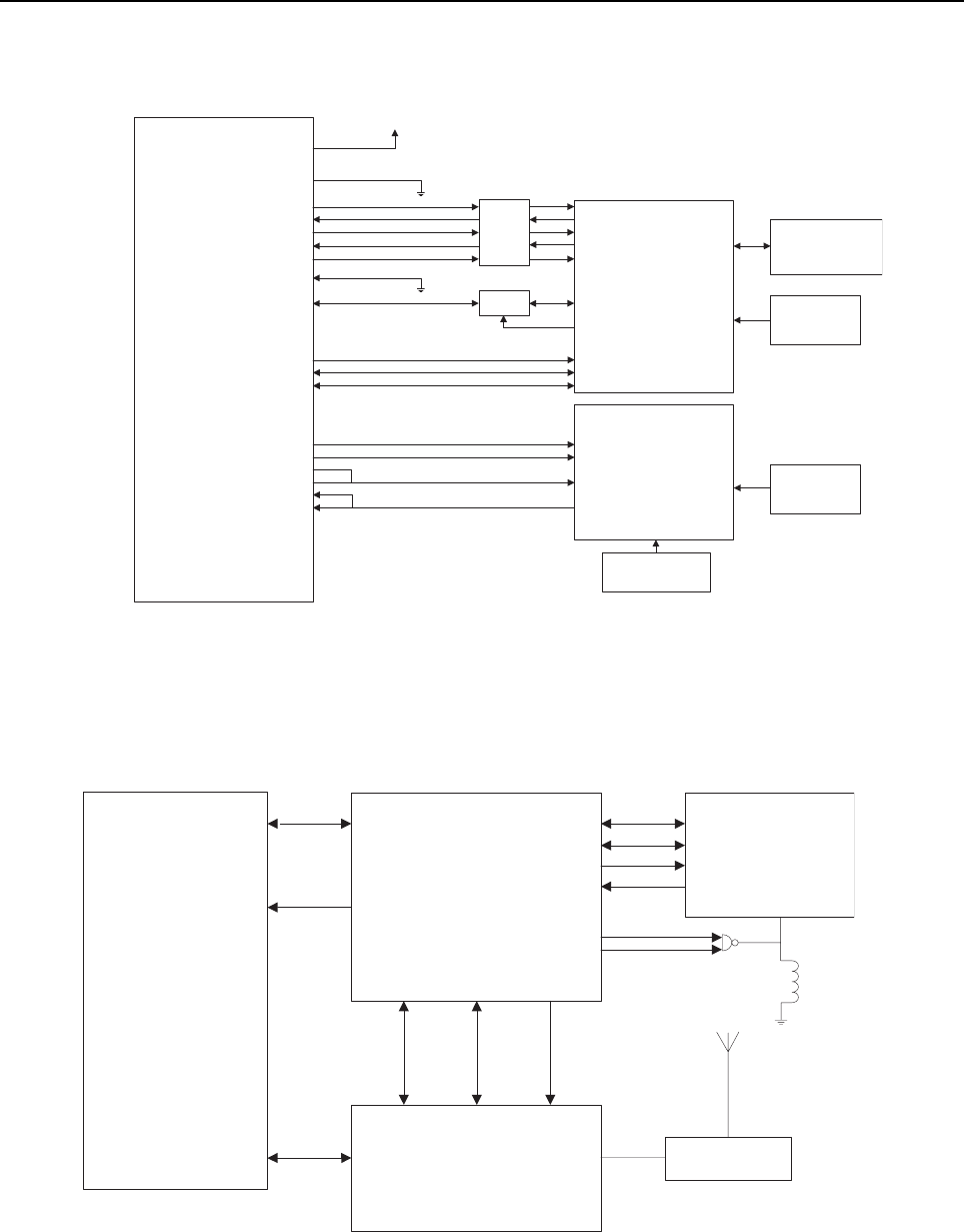
Theory of Operation: Bluetooth 3-67
Figure 3-48. Bluetooth/Controller Interface with Clock Sources
The Bluetooth IC transceiver is connected to a dedicated Bluetooth antenna. Between the IC and
antenna is a band-pass filter as sown in is shown in Figure 3-49.
Figure 3-49. Bluetooth Functional Block Diagram
Bluetooth Block
APX 5000/
APX 6000/
APX 6000XE/
SRX2200
VOCON Board
80-pin
connector
16 MB
SDRAM
12 MHz
32.768
KHz
26 MHz TCXO
NL5500
BT/GPS
SW_B+
SW_B+
UC3_RESET
VOLTAGE
TRANSLATION
1.8V - 3.3V
VOLTAGE
TRANSLATION
1.8V - 3.3V
BT_PTT
USB_BOOT
AVR_STATUS_1.8
RESET_N
PB17 (GPIO49)
PA20 (GPIO20)
PA21 (GPIO21)
PB07 (GPIO39)
PA29
ATMEL AVR32
AT32UC3A0512
PA30
BT_SPARE_DIR
D12
D11
E12
F1
C3
A2
B10
D10
J2
M8
VBUS
DP
DM
AUD_CLK
AUD_FSTNC
AUD_IN
AUD_OUT
AC_SPKR_UNMUTE_1.8
OPT_BD_DETECT
BT_SPARE_1.8
GROUND
OPT_BD_GPIO_0_OPT_RST
OPT_BD_GPIO_5(OMAP GPIO7)
OPT_BD_GPIO_2
OMAP P18
OMAP K15
OPT_BD_GPIO_4
OMAP K14
CPLD GPIO 29
OPT_USB_DP
OPT_USB_DM
SSI_CLK
SSI_FSYNC
SSI_BLACK_RX
SSI_RED_RX
SSI_BLACK_TX
SSI_RED_TX
APX 5000/ APX 6000/
APX 6000XE/ SRX2200
Expansion Board
80-PIN CONNECTOR
OMAP_GPIO7
USB1
BT_PTT
USB
GPIO
USART0 GPIO
SSI
BT_HCI
PCM_AUD
BT_WAKE BT_EN
BT_RF 2.45 GHz BPF
BT
Antenna
LF
Antenna
TI NL5500
Bluetooth/GPS
GPIO
TC1 OCA
ANTENNA
WAKEUP
TX_CLK
UART
SPI
NFC
BLOCK
USART1 TX
GPIO
TIMER1
ATMEL AVR32
AT32UC3A0512
USART1
SPI0
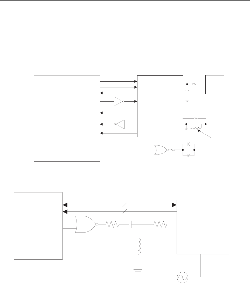
3-68 Theory of Operation: Bluetooth
To verify the Bluetooth transmitter is operational, an RCMP command can be sent to transmit a
constant carrier waveform on a Bluetooth frequency. To verify the LF transmit feature is operational,
an RCMP command can be sent to transmit a constant carrier waveform at 125 kHz. There are
similar RCMP commands for verifying BT/LF RSSI when a CW BT/LF signal is applied near the
antennas of the BT/LF circuitry.
The Low-Frequency block diagram below shows the main connections:
Figure 3-50. Bluetooth Low-Frequency Circuit Block Diagram
Figure 3-51. Bluetooth Low-Frequency Pairing Data Path
Low-Frequency Block
LF TX
LF Coil
LF RX
ATMEL AVR32
AT32UC3A0512
SPI0_SCK SCL
SDI
SDO
CS
WAKE
LF1P
LFN
32768 Hz
Clock
DAT
CL_DAT
XIN
Low Frequency
Receiver
AS3930
SPI0_MOSI
SPI0_MISO
NFC_CS
NFC_INT
NFC_UART_RX
NFC_UART_MAN_CLK
NFC_UART_TX
TC1_OCA
SPI
UART
125 KHz Clock
Micro-
Processor
LF Device
UART_TX_Data
+
ANTENNA COIL
32 KHz
CLK_IN
ANT_IN
UART
SPI

Theory of Operation: Bluetooth 3-69
Figure 3-52. Detailed Low-Frequency Transmit/Receive Paths
3.5.1 Bluetooth Power
Our Bluetooth IC operates from a 3.6V (U6504, VBAT) switching regulator located on the VOCON
board to supply the Bluetooth IC core and a 1.85V (U6508, VDDS) supply for the I/O. It has a
shutdown (U2415 pin L3) that must be high for operation to work. The power-up/down sequence
required for operation is shown in Figure 3-53.
Figure 3-53. Chip Power-Up/Power-Down Sequence (Exernal Input/Output Shown)
32KHZ_3.3V
R2457M3
15K
C2475M3
1000PF
R2474M3
270K
O/P
NFC
ANTENNA
L2407M3
6.8 mH
1
C2457M3
18PF
U2412M3
NL17SZ02
R2475M3
150
USART1_TX
R2477M3
100K
7
16 15 R24
1
G1
R2476M3
100K
TC1_OCA
4
TX path
I/P
GPS_BT_3.3V
12 1
9
1
6
8
1
2
SCL CL_DAT
DAT
SDO
XOUT
WARE
NC1
NC2
VCC
CS
SDI
XIN
LFN
LFP
VSS
GND
CTGND
C2465M3
1UF U2403M3
AS3930
51009360002
11
13
5
4
3
RX path
NFC_CS_INV
C2454M3
220PF
1%
APX 5000/ APX 6000/
APX 6000XE/ SRX2200
Partial Current Tree
7.5V Batt
VDDS
VBAT
VDD1P8
RTC
Startup
CLK_REQ_POL
TCXO_CLK_REQ
VDD_TCXO
Hi Z - PD
Max 36.5 ms
5 ms
Analog PORz (~135 RTC cycles) +
Efuse shifting (~1000 RTC cycles)
Max time from clock request/
voltage to TCXO_CLK availability
Hi Z - PD
TCXO_CLK
REF_CLK_REQ
(OR of
nshutdown
pins)
<2.5ms
or

3-70 Theory of Operation: Bluetooth
The host processor operates from a 3.3V LDO regulator (U2402). The 1.85V regulator enables the
3.3V LDO regulator output. The LF receiver IC is powered from a 3.3V LDO regulator (U2402).
Figure 3-54 is a partial current tree showing the flow of current from the battery to the Bluetooth-
related major components sourced by the 3.6V switching regulator on the VOCON.
Figure 3-54. Current Distribution Tree for Bluetooth Circuitry
3.5.2 Bluetooth Clocks
The Bluetooth IC requires a 26 MHz TCXO (Y2204, TCXO_CLK) for the core and a 32.768 kHz
(U6101 pin E2 on vocon, RTC_CLK) slow clock for the USART. This is the same clock used for the
GPS portion of the BT/GPS combination IC.
The host processor IC requires a 12 MHz crystal oscillator (Y2475) clock. The LF receiver IC
requires a 32.768 kHz (U6101 pin E2 on vocon, RTC_CLK) clock.
7.5V Batt
3.6V Switcher
800mA TPS 62050
2.23V LDO
TPS 73601
1.85V LDO
LP38693SD
J4001 pin41 J1001 pin 37 VCP_IN
Vocon
Expansion
P2001 pin 41
TI NL5500
BT/GPS
3.3V LDO
500mA LP2989
J2001 pin 11
JTAG
AS3930A
Low Freq.
ST LIS3331DL
Accelerometer
Logic & Level
8 x Level Shifters
1 x Inverter
Logic & Level
1 x NOR
12 MHz OSC
AT32UC3A
AVR32
16MB SDRAM
SW_B+
V_SW_3.60
VSW_3.6
GPS_BT_3.3V

Theory of Operation: Bluetooth 3-71
3.5.3 Bluetooth I/Os.
The communication between the Bluetooth IC and the host controller is by a four-wire HCI USART0
bus (RX, TX, CTS, RTS). The Bluetooth IC receives a firmware update over USART0 each time it is
powered on. The LF receiver IC transmits its data over the USART1 s used for displaying debugging
messages.
Figure 3-55. Bluetooth LF UART Connection Block Diagram
Table 3-16. Bluetooth Host Processor UART I/O
Signal Name Pad Name GPIO MUX
Function
Expansion Board
Schematic Name
I/O
USART0 – RXD PA00 0 A BT_UART_TX_3.3V I
USART0 – TXD PA01 1 A BT_UART_RX_3.3V O
USART0 – RTS PA03 3 A BT_UART_CTS_3.3V O
USART0 – CTS PA04 4 A BT_UART_RTS_3.3V I
USART1 – RXD PA05 5 A USART1_RX I
USART1 – TXD PA06 6 A USART1_TX O
USART1 – CLK PA07 7 A USART1_CLK I
USART2 – RXD PB29 61 A AVR_USART2_RX I
USART2 – TXD PB30 62 A AVR_USART2_TX O
JTAG Connector
ATMEL AVR32
AT32UC3A0512 TI NL 5500
Bluetooth/GPS
Low Frequency
Receiver AS3930
LF Transmit
(OR Gate)
Pin 19
Pin 20
Pin 12
Pin 13
PB29
PB30
PA00
PA01
PA03
PA04
PA05
PA07
PA06
J6
H6
J7
J8
K11
J10
L12
A4
B5
B4
B7
9
10
HCI_TX
HCI_RX
HCI_CTS
HCI_RTS
DAT
CL_DAT
Debug RX
Debug TX
K6
K7
USART2
USART0
USART1
= Level Translator. 3.3volts on AVR side

3-72 Theory of Operation: Bluetooth
The Bluetooth IC shutdown (U2415 pin L3) and wakeup (U2415 pin K3) pins are also connected to
the host controller. A Bluetooth PTT pin on the host controller (U2415 pin J2) tells the OMAP (U6302
pin Y5) when the user pressed the PTT button on the Bluetooth accessory. As the BT IC I/O is 1.8V,
but the host controller I/O is 3.3V, level shifters are employed for interconnection between the two.
The host processor IC is connected to the LF receiver IC by a four-wire SPI bus. This SPI bus also
communicates with an on-board accelerometer. The LF transmitter circuit uses a 125 kHz signal
(U2415 pin M3) that is turned on and off (OOK) by the USART1_TX signal (U2415 pin L12).
The host processor is connected to the 3.3V SDRAM using a synchronous interface. The host
processor is connected to the OMAP on the vocon by a full-speed USB (D11 & D12). VBus is a
sense line only.
Table 3-17. SPI I/O
Signal Name Pad Name GPIO MUX
Function
Expansion Board
Schematic Name
I/O
SPIP – NPCS[2] PA09 9 B SPIO_CS2 O
SPIP – NPCS[0] PA10 10 A NFC_CS O
SPIP – MISO PA11 11 A SPIO_MISO I
SPIP – MOSI PA12 12 A SPIO_MOSI O
SPIP – SCK PA13 13 A SPIO_CLK O
Table 3-18. USB I/O
Signal Name Pin Name Pad Name Expansion Board
Schematic Name
I/O
GPIO19 C12 PA19 USB_BOOT_3.3V I
GPIO20 D10 PA20 ATMEL_BOOT I
DP D11 – BT_AVR_USB_DP I/O
DM D12 – BT_AVR_USB_DM I/O
VBUS E12 – BT_AVR_VBUS I

Theory of Operation: Bluetooth 3-73
Figure 3-56. Bluetooth USB Interface Too Main VOCON
The ATMEL bootloader is being used as a first stage bootloader that will jump to the Motorola
bootloader, which is a stage two bootloader. GPIO20 is used by the ATMEL bootloader to trap in
Flash mode. GPIO19 will be used by the Motorola bootloader to trap in Flash mode. Both pins are
active low.
The Bluetooth audio is sent over a two-channel PCM/SSI interface to the audio codec (U6405) on
the VOCON board.
Table 3-19. GPIO I/O
Signal Name Pad Name GPIO Expansion Board
Schematic Name
I/O
GPIO41 PB09 41 BT_HOST_WAKEUP_3.3V I
GPIO49 PB17 49 BT_PTT_3.3V O
GPIO50 PB18 50 BT_SHUTDOWN_3.3V O
GPIO51 PB19 51 BT_WAKEUP_3.3V O
USB_BOOT
ATMEL_BOOT
APX 5000/ APX 6000/ APX 6000XE/ SRX2200
Expansion Board 80-pin Connector
JTAG Connector
ATMEL AVR32
AT32UC3A0512
PA19
VBUS
DP
DM
USB
PA20
C12
E12
D11
D12
D10
Pin 43
Pin 31
Pin 35
Pin 33
Pin 15
Pin 3
Pin 2
Factory Test Points
= Level Translator. 3.3 volts on AVR side


Chapter 4 Troubleshooting Procedures
The purpose of this chapter is to aid in troubleshooting problems with the
ASTRO APX 5000/APX 6000/APX 6000XE/SRX2200 radio. It is intended to be detailed enough to
localize the malfunctioning circuit and isolate the defective component. It also contains a listing of
service tools recommended for PC board repair at the component level.
4.1 Handling Precautions
Complementary metal-oxide semiconductor (CMOS) devices, and other high-technology devices,
are used in this family of radios. While the attributes of these devices are many, their characteristics
make them susceptible to damage by electrostatic discharge (ESD) or high-voltage charges.
Damage can be latent, resulting in failures occurring weeks or months later. Therefore, special
precautions must be taken to prevent device damage during disassembly, troubleshooting, and
repair. Handling precautions are mandatory for this radio, and are especially important in low-
humidity conditions. DO NOT attempt to disassemble the radio without observing the following
handling precautions.
1. Eliminate static generators (plastics, Styrofoam, etc.) in the work area.
2. Remove nylon or double-knit polyester jackets, roll up long sleeves, and remove or tie back
loose-hanging neckties.
3. Store and transport all static-sensitive devices in ESD-protective containers.
4. Disconnect all power from the unit before ESD-sensitive components are removed or
inserted unless otherwise noted.
5. Use a static-safeguarded workstation, which can be accomplished through the use of an
anti-static kit (Motorola part number 01-80386A82) or equivalent.This kit includes a wrist
strap, two ground cords, a static-control table mat and a static-control floor mat.
Most of the ICs are static sensitive devices. Do not attempt to
disassemble the radio or troubleshoot a board without first
referring to the following Handling Precautions section.

4-2 Troubleshooting Procedures: Recommended Service Tools
4.2 Recommended Service Tools
Table 4-1 lists recommended service tools that can be used for PC board repairs at the component
level. For listings of additional service tools, service aids, and test equipment that are recommended
for all levels of service, refer to the APX 5000/APX 6000/APX 6000XE/SRX2200 basic service
manual (see “Related Publications” on page ix).
Table 4-1. Recommended Service Tools
Motorola
Part Number Description Application
1110027B23 Speaker Module Seal Lubricant Used to ensure good sealing of the Speaker Module to the
Main Chassis.
5880384G68 SMA to BNC Adapter Adapts radio’s antenna port to BNC cabling of test
equipment.
66009254001 APX 5000/ APX 6000 Battery
Eliminator
Used in place of battery to connect radio to an external
power supply. Requires RLN4510_.
66009255001 Grille Eliminator Special tool used when pressure testing the radio.
Replaces the radio grille to seal the port vent.
66009256001 Volume Potentiometer Outer
Spanner Bit
Used to assemble and disassemble the spanner nut on the
volume potentiometer.
66009258001 Antenna Spanner Bit Used to assemble and disassemble the spanner nut on the
antenna bushing.
66009259001 Vacuum Adapter Submersible radios only. Connects the vacuum/pressure
hose to the radio.
66009260001 Board Analysis Fixture Special fixture that allows radio’s internal board to be
mounted externally. Provides easy access to electronic
circuits, required for board-level troubleshooting.
NLN9839_ Vacuum Pump Kit Submersible radios only. Vacuum pump with gauge and
vacuum hose. Requires 66009259001 Adapter Kit.
NTN4265_ Pressure Pump Kit Submersible radios only. Pressure pump with gauge and
pressure hose. Requires 66009259001 Adapter Kit.
DVN4233_ Customer Programming Software
(CPS) and Tuner Software
CPS allows customer-specific programming of modes and
features. Tuner software required to perform alignment of
radio parameters.
PMKN4012_ Programming Cable Used to program the radio through Customer
Programming Software and Tuner Software.
PMKN4013_ Programming/Service Cable Used to program and service the radio through Customer
Programming Software and Tuner Software.
RLN4510_ 7.5 Volt Universal Battery
Eliminator
Used in conjunction with the 66009254001 to adjust the
supply voltage to 7.5 Vdc. Allows a multimeter to be
attached for monitoring and adjusting voltage and current
levels.
RLN4460_ Portable Test Set Used for radio performance checks. Connects to radio’s
universal connector and allows remote switching and
signal injection/outputs for test equipment measurements.

Troubleshooting Procedures: Standard Bias Table 4-3
4.3 Standard Bias Table
Table 4-2 outlines some standard supply voltages and system clocks which should be present under
normal operation. These should be checked as a first step to any troubleshooting procedure.
Table 4-2. Standard Operating Bias – DC Voltages
Name Reference Description Level
MECH_SW F_MECH_SW ON/OFF Switch. Radio on when GND GND
UNSW_B+ F_UNSW_B+ Radio Battery Voltage 9-6V
SW_B+ C6592 Radio Supply Voltage 9-6V
V_SAVE C6538 LDO Output Present When Battery is Attached 2.5V
V_1.875 C6581 LDO Output 1.875V
V_1.55 R6561 LDO Output 1.55V
V_2.775D R6563 LDO Output 2775V
V_2.775_EXP R6562 LDO Output 2.775V
V_2.8_RF R6564 LDO Output 2.8V
V_5.0A R6565 LDO Output 5.0V
V_3.3 R6566 LDO Output 3.3V
V_3.0A R6567 LDO Output 3.0V
V_EXT_1.8 R2302 LDO Output 1.85V
V_SW_1.4 E6502 Switcher Output 1.4V
V_SW_3.60 C6561 Switcher Output 3.6V
V_2.23 C6573 LDO Output 2.23V
Table 4-3. Standard Operating Bias – Clock Sources
Clock
Source Reference Description Frequency
Y6501 R6578 MAKO 24MHz & tapped into CPLD 24.576MHz
Y6502 C6541 MAKO RTC 32.768KHz
Y6601 C6601 OMAP CPU Clock 12MHz
U6302 TP6307 and
TP6308
DDR Clocks (Complementary signals) 96MHz
U6101 R6114 MACE Clock 4MHz
U6101 R6115 GPS RTC clock 32.768KHz
Y701
(RF board)
R6218 RF Freq synth IC (Abacus) TCXO 16.8MHz

4-4 Troubleshooting Procedures: Power-Up Self-Check Errors
4.4 Power-Up Self-Check Errors
Each time the radio is turned on, the MCU and DSP perform a series of internal diagnostics. These
diagnostics consist of checking such programmable devices as the FLASH ROMs, the EEPROM,
and SRAM devices.
Problems detected during the power-up self-check routines are presented as error codes on the
radio’s display. For non-display radios, the problem is presented at power up by a single, low-
frequency tone. Table 4-4 lists possible error codes, a description of each error code, and a
recommended corrective action.
Table 4-4. Power-Up Self-Check Error Codes
Error Code/ Error
Message Description Corrective Action
01/02 FLASH ROM Codeplug Checksum Non-Fatal Error Reprogram the codeplug
01/12 Security Partition Checksum Non-Fatal Error Send radio to depot
01/20 ABACUS Tune Failure Non-Fatal Error Turn the radio off, then on
01/22 Tuning Codeplug Checksum Non-Fatal Error Send radio to depot
01/81 Host ROM Checksum Fatal Error Send radio to depot
01/82 FLASH ROM Codeplug Checksum Fatal Error Reprogram the codeplug
01/88 External RAM Fatal Error – Note: Not a checksum failure Send radio to depot
01/90 General Hardware Failure Fatal Error Turn the radio off, then on
01/92 Security Partition Checksum Fatal Error Send radio to depot
01/93 FLASHport Authentication Code Failure Send radio to depot
01/98 Internal RAM Fail Fatal Error Send radio to depot
01/A2 Tuning Codeplug Checksum Fatal Error Send radio to depot
02/81 DSP ROM Checksum Fatal Error Send radio to depot
02/88 DSP RAM Fatal Error – Note: Not a checksum failure Turn the radio off, then on
02/90 General DSP Hardware Failure (DSP startup message not
received correctly)
Turn the radio off, then on
09/10 Secure Hardware Error Turn the radio off, then on
09/90 Secure Hardware Fatal Error Turn the radio off, then on
Hardware board absent/
Hardware board absent
then
Man-Down Hw error
Expansion board is not connected properly to the radio Ensure the Expansion
board is fixed in place
Note: If the corrective action does not fix the failure, send the radio to the depot.

Troubleshooting Procedures: Power-Up Self-Check Diagnostics and Repair (Not for Field Use) 4-5
4.5 Power-Up Self-Check Diagnostics and Repair (Not for Field Use)
Table 4-5 lists additional action items that can be used for the diagnosis and resolution of the error
codes listed in Table 4-4 on page 4-4.
Table 4-5. Power-Up Self-Check Diagnostic Actions
Error Code/ Error
Message Diagnostic Actions
01/02 This non-fatal error will likely recover if the radio's power is cycled. In the event that this
does not resolve the issue, the radio should be reflashed. If the error remains, send the
radio to depot.
01/12 The radio should be sent to the depot for reflashing of the security codeplug.
01/20 Cycling radio power should resolve this issue.
01/22 The radio should be sent to the depot for reflash of the tuning codeplug followed by
retuning of the radio.
01/81 The radio should be sent to the depot for reflashing of the host code.
01/82 The radio should be sent to the depot for reflashing of the radio codeplug.
01/88 Reflashing of the radio should first be performed. If this fails to resolve the issue, send
the radio to depot.
01/90 Cycle power to radio. Continued failure indicates a likely IC failure In this event, radio
should be sent to the depot for isolation and repair of the problem IC.
01/92 The radio should be sent to the depot for reprogramming of the security codeplug.
01/93 The radio should be sent to the depot for reflashing of the host code.
01/98 Send radio to the depot.
01/A2 The radio should be sent to the depot for reflashing of the tuning codeplug followed by
re-tuning of the radio.
02/81 The radio should be sent to the depot for examination.
02/88 Cycle power to the radio. If this does not fix the problem, then the radio should be sent
to the depot for reflashing of the DSP code.
02/90 Cycle power to the radio. If this fails to fix the problem, then the radio should be sent to
the depot for reflashing of the DSP code.
09/10 Cycle power to the radio. If this fails then follow instructions in the secure hardware
failure troubleshooting flowchart.
09/90 Cycle power to the radio. If this fails then follow instructions in the secure hardware
failure troubleshooting flowchart.
Hardware board
failed
Bluetooth error. Send radio to depot for examination.
Hardware board
failed
then
Man-Down HW error
Man-Down feature unavailable. Send radio to depot for examination.

4-6 Troubleshooting Procedures: Power-Up Self-Check Diagnostics and Repair (Not for Field Use)
Hardware board
mismatch
Expansion board does not support bluetooth feature. Send radio to depot.
If the Expansion board type supports “Full feature” – “Mace/GPS/BT/SDMem Exp
Board”, updating the expansion board firmware should resolve the error message.
Hardware board
mismatch
then
Man-Down HW error
Expansion board does not support either bluetooth or Man-down feature or both.
If the Expansion board type supports “Full feature” – “Mace/GPS/BT/SDMem Exp
Board”, updating the expansion board firmware should resolve the error message.
Table 4-5. Power-Up Self-Check Diagnostic Actions (Continued)
Error Code/ Error
Message Diagnostic Actions

Chapter 5 Troubleshooting Charts
This section contains detailed troubleshooting flowcharts. These charts should be used as a guide in
determining the problem areas. They are not a substitute for knowledge of circuit operation and
astute troubleshooting techniques. It is advisable to refer to the related detailed circuit descriptions in
the theory of operation sections prior to troubleshooting a radio.
5.1 List of Troubleshooting Charts
Most troubleshooting charts (see Table 5-1) end up by pointing to an IC to replace. It is not always
noted, but it is good practice to verify supplies and grounds to the affected IC and to trace continuity
to the malfunctioning signal and related circuitry before replacing any IC. For instance, if a clock
signal is not available at a destination, continuity from the source IC should be checked before
replacing the source IC.
Table 5-1. Troubleshooting Charts
Troubleshooting Page
No.
Main Troubleshooting
Main Troubleshooting Flowchart 5-3
Power-Up Failure
VOCON Board 5-4
B+ Incorrect Voltage 5-5
Low LDO10 VCC_3.3 Voltage 5-6
Low LDO3 V_1.55 Voltage 5-7
Low LDO8 V_5.0A Voltage 5-8
Low VBUS2 Voltage 5-9
Low V_SW_1.4 Voltage 5-10
Low V_2.23 Voltage 5-11
Low V_SW_3.6 Voltage 5-12
Low V_SW_5 Voltage 5-13
Low V_EXT_1.85 Voltage 5-14
DC Supply
DC Supply 5 Volt Failure 5-15
DC Supply 3.6 Volt Failure 5-16
DC Supply 3 Volt Failure 5-17
DC Supply 1.85 Volt Failure 5-18
DC Supply 1.8 Volt Failure 5-19
DC Supply 1.5 Volt Failure 5-20
DC Supply 1.4 Volt Failure 5-21
Display
Top/CID Display Failure 5-22
Main Display Failure 5-23
Knob/ Button/ Keypad
Volume Set Error 5-24
Channel Select Error 5-25
Keypad Error 5-26
Side Button Error 5-27
VOCON
External Audio 5-28
Internal Audio 5-29
Backside Microphone 5-30
External Mic Failure 5-31
Keyload/ Secure Hardware/ Memory
Keyload Failure 5-32
Secure Hardware Failure 5-33
Table 5-1. Troubleshooting Charts (Continued)
Troubleshooting Page
No.

5-2 Troubleshooting Charts: List of Troubleshooting Charts
eMMC Memory Failure 5-34
RX RF
RX RF Failure 5-35
FGU
FGU Failure 5-46
FGU Power Failure 5-47
GPS
GPS Failure 5-48
Bluetooth Failure
Pairing Issue 5-49
LCD Indication 5-52
No Audio from Headset 5-54
PA Failure
Main 5-55
7/800 PA 5-56
VHF PA 5-57
Aux Antenna Switch 5-58
Multi Switch 5-59
VHF ALC 5-60
7/800 ALC 5-61
UHF1 PA 5-62
UHF1 ALC 5-63
UHF2 PA 5-64
UHF2 ALC 5-65
Table 5-1. Troubleshooting Charts (Continued)
Troubleshooting Page
No.

Troubleshooting Charts: Main Troubleshooting Flowchart 5-3
5.2 Main Troubleshooting Flowchart
Start
Good
power up
self test
Any Error
Message?
See Table for
error codes
Table 4.5
No No
Yes
Go to either Display
Failure(5.19,5.20)
or Vocon power up
failure flowchart
Chart 5.3
Yes
Does the
Radio
transmit?
No
Go to TX RF
troubleshooting
Flowchart(Chart
5.45)
Is there TX
deviation?
Go to VOCON
TX Audio error
Chart(5.11)
Receive Audio
present?
Go to RX RF/
Vocon audio
flowchart(chart
5.29/5.11)
No
No
RX SINAD
GOOD?
Buttons
Functional?
No
End
See Button Test
Flowchart(chart
5.10)
Yes
Yes
Yes
Yes
No

5-4 Troubleshooting Charts: Power-Up Failure
5.3 Power-Up Failure – VOCON Board
VOCON Board Power Up
Problem
Measure Voltage
at R6505
6 < V < 9?
Proceed to
Incorrect B+
Voltage Flow
Chart
Measure Voltage
at R6542
3.3 < V < 3.9
Proceed to Low
VCC_SW_3.6
Flow Chart
Use Oscilloscope
to Measure R6572
Freq = 24MHz
1.6 < V < 1.9
Inspect Y6501 and
All supporting
Circuitry
Repair or Replace
Part/s
Replace VOCON
Board
Are Parts Solder
Connections and
Placement Correct
No Yes
Measure All Probe
Spots from Above
Table
Voltages =
Level
Proceed to
Specified Flow
Chart in Table
Measure Voltage
at R6203
1.6 < V < 1.9
Replace VOCON
Board
No
Yes
No
Yes
No
Yes
No Yes
No
Use Oscilloscope
to Measure R6115
Yes Freq = 32kHz
1.6 < V < 1.9
Replace VOCON
Board
Use Oscilloscope
and High
Impedance Probe
to Measure
C6602
Freq = 12MHz
1.3 < V < 1.9
Inspect Y6601
Circuit
Repair or Replace
Part/s
Are Parts Solder
Connections and
Placement Correct
No
Yes
No
Yes No
Measure Voltage
at R2217
Yes
1.6 < V < 1.9
OMAP is Out of
Reset, Proceed to
Memory Flow
Chart
Yes
Replace VOCON
No
Name Ref Description Level V Flow Chart
VCC_1.875 C4001 LDO Output 1.875±10% Refer to note 1
VCC_1.55 R6561 LDO Output 1.55±10% Low LDO3 VCC_1.55 Voltage
VCC_2.775D R4011 LDO Output 2.775±10% Low LDO10 VCC_3.3 Voltage
VCC_2.775 R6563 LDO Output 2.775±10% Low LDO10 VCC_3.3 Voltage
VCC_2.8 R6564 LDO Output 2.8±10% Low LDO10 VCC_3.3 Voltage
VCC_5.0A R6565 LDO Output 5.0±10% Low LDO8 VCC_5.0A Voltage
VCC_3.3 R6566 LDO Output 3.3±10% Low LDO10 VCC_3.3 Voltage
VCC_3.0A R6567 LDO Output 3.0±10% Low LDO10 VCC_3.3 Voltage
VCC_SW_3.6 C6561 Switching Output 3.6±10% Low VCC_SW_3.6 Voltage
VCC_1.85 R6570 LDO Output 1.85±10% Low VCC_1.85 Voltage
VCC_SW_1.4 E6502 Switching Output 1.4±10% Low VCC_SW_1.4 Voltage
Note:
1. Probe C4001 and observe 1.875 V. If absent then return board to depot for repair.

Troubleshooting Charts: Power-Up Failure 5-5
Power-Up Failure – B+ Incorrect Voltage
B+ Incorrect Voltage
Check Voltage at
Test Point
F_UNSW_B+
(VOCON)
6 < V < 9?
Check Mating
Connector to RF
Board
Check Voltage at
R6505 (VOCON)
No
Yes
6 < V < 9?
Check Q6501
Circuit and
Replace any non
Functional Parts
Replace VOCON
Board
No
Yes
RF to Vocon
Connectors
ok?
Replace
Connector
No
Replace RF
Board, Check
F_UNSW_B+ Test
Point
Yes
6 < V < 9? Replace VOCON
Board
Replace RF Board
Yes
No

5-6 Troubleshooting Charts: Power-Up Failure
Power-Up Failure – Low LDO10 VCC_3.3 Voltage
Low LDO10 VCC_3.3
Voltage
Measure Radio
Current
Is Standby
Current more
than 15mA above
Average
Board has a short,
Replace VOCON
Yes
Inspect R6566
Connection
Is R6566
Soldered
Properly
Correct R6566
Soldering
Measure SW1 at
R6542
3.3 < V < 3.9?
Proceed To Low
VCC_SW_3.6
Voltage Flow
Chart
Likely MAKO
Problem, Replace
VOCON Board
No
No
Yes
No
Yes
Synopsis
This failure specifically refers to LDO10
but this flow chart can be used to
diagnose LDO9, lDO7, and LDO6. All
LDOs mentioned above are fed from the
same source and have very limited
differences. Please refer to schematic
and theory of operation section for
differences.

Troubleshooting Charts: Power-Up Failure 5-7
Power-Up Failure – Low LDO3 V_1.55 Voltage
Low LDO3 V_1.55
Voltage
Measure Radio
Current
Is Standby
Current more
than 15mA above
Average
Board has a short,
Replace VOCON
Yes
Inspect R6561
Connection
Is R6561
Soldered
Properly
Correct R6561
Soldering
No
No
Measure
V_2.23 at
R6513
2.0 < V < 2.4?
Proceed To Low
V_2.23 Voltage
Flow Chart
Likely MAKO
Problem, Replace
VOCON Board
No
Yes
Yes
Synopsis
This failure specifically refers to LDO3
but this flow chart can be used to
diagnose LDO2. All LDOs mentioned
above are fed from the same source
and have very limited differences.
Please refer to schematic and theory of
operation section for differences.

5-8 Troubleshooting Charts: Power-Up Failure
Power-Up Failure – Low LDO8 V_5.0A Voltage
Low LDO8 V_5.0A
Voltage
Measure Radio
Current
Is Standby
Current more
than 15mA above
Average
Board has a short,
Replace VOCON
Yes
Inspect R6565
Connection
Is R6565
Soldered
Properly
Correct R6565
Soldering
No
No
Measure Voltage
at C6593
6 < V < 9?
Proceed To
Incorrect B+
Voltage Flow
Chart
Likely MAKO
Problem, Replace
VOCON Board
Yes
No
Yes

Troubleshooting Charts: Power-Up Failure 5-9
Power-Up Failure – Low VBUS2 Voltage
Low VBUS2 Voltage
Measure
V_SW_5 at
C6567
5.1 < V < 5.6?
Proceed to Low
SW5 Volatge Flow
Chart
Measure VBUS1
Supply Volatge at
R6529
No
Yes
Inspect U6503 and
Supporting Ciruitry
Are Parts Solder
Connections and
Placement Correct
Check Placement
of Q6503
Repair Incorrect
Part/s
Is Part Placed
Correctly Replace Part
Replace VOCON
Yes
No
Yes
Yes
No

5-10 Troubleshooting Charts: Power-Up Failure
Power-Up Failure – Low V_SW_1.4 Voltage
Low V_SW_1.4 Voltage
Measure Radio
Current
Is Standby
Current more
than 15mA above
Average
Board has a short,
Replace VOCON
Yes
Measure SW_B+
Voltage at C6593
6 < V < 9?
Proceed to
Incorrect B+
Voltage
Measure Voltage
at C6586
1.45 < V <1.65
?
Proceed to Low
LDO3 V_1.5V
Voltage Flow
Chart
Inspect U6507 and
Supporting
Circuitry
Are Parts Solder
Connections and
Placement Correct
Replace or Repair
Part/s
Replace VOCON
Board
No
No
Yes
No
Yes
Yes
No

Troubleshooting Charts: Power-Up Failure 5-11
Power-Up Failure – Low V_2.23 Voltage
Low V_2.23 Voltage
Measure Radio
Current
Is Standby
Current more
than 15mA above
Average
Board has a short,
Replace VOCON
Yes
Measure Voltage
at R6573
3.3 < V < 3.9?
Proceed to Low
V_SW_3.6
Voltage Flow
Chart
Inspect U6506 and
Supporting
Circuitry
Are Parts Solder
Connections and
Placement Correct
Replace or Repair
Part/s
Replace VOCON
Board
No
Yes
No
Yes

5-12 Troubleshooting Charts: Power-Up Failure
Power-Up Failure – Low V_SW_3.6 Voltage
Low V_SW_3.6 Voltage
Measure Radio
Current
Is Standby
Current more
than 15mA above
Average
Board has a short,
Replace VOCON
Yes
Measure the
Voltage at R6524
6 < V < 9?
Proceed to
Incorrect B+
Voltage
Inspect U6504 and
All Supporting
Circuitry
Are Parts Solder
Connections and
Placement Correct
Replace or Repair
Part/s
Replace VOCON
Board
No
No
Yes
No
Yes

Troubleshooting Charts: Power-Up Failure 5-13
Power-Up Failure – Low V_SW_5 Voltage
Low V_SW_5 Voltage
Measure Radio
Current
Is Standby
Current more
than 15mA above
Average
Board has a short,
Replace VOCON
Yes
Measure the
Voltage at C6593
6 < V < 9?
Proceed to
Incorrect B+
Voltage
Inspect U6505 and
All Supporting
Circuitry
Are Parts Solder
Connections and
Placement Correct
Replace or Repair
Part/s
Replace VOCON
Board
No
No
Yes
No
Yes

5-14 Troubleshooting Charts: Power-Up Failure
Power-Up Failure – Low V_EXT_1.85 Voltage
Low V_EXT_1.85 Voltage
Measure Radio
Current
Is Standby
Current more
than 15mA above
average?
Board has a short,
Replace VOCON
Yes
Measure
V_SW_3.6
Voltage at R6510
Voltage =
V_SW_3.6
Proceed to
Incorrect
Voltage
V_SW_3.6
Measure Voltage
R6431 on
VCC_5.0A Side
4.8 < V < 5.2?
Proceed to Low
LDO8 VCC_5.0A
Voltage Flow
Chart
Are Parts Solder
Connections and
Placement Correct
Replace or Repair
Part/s
Replace VOCON
Board
No
No
Yes
Yes
No
Measure Voltage
at R6431 on
BGAP_COMP
Side
2.2 < V < 2.7?
Measure Voltage
at R6420 2.2 < V < 2.7?
Replace VOCON
Board
Inspect and Repair
U6409 and
Supporting
Circuitry
Inspect U6508 and
All Supporting
Circuitry
No
Yes
Yes
No No
Yes

Troubleshooting Charts: DC Supply Failure 5-15
5.4 DC Supply Failure
5.4.1 DC Supply 5 Volt Failure
V_SW_5 supply
Is radio
drawing > 100mA
from battery
or power
supply?
Voltage
level
correct?
Replace
VOCON
board
Yes
Yes
Yes
Yes
No
No
No
No
Replace board
with damaged
connectors
Are connectors J4001
to P2001 shorted or
damaged?
Check U6505 for
enable input and
voltage output lines
Check L6504
for damage
Verify SW_B+ is
present at C6565
Measure if USB accessories
are shorting VBUS line
Verify
UNSW_B+ is
present at
Test Point:
F_UNSW_B+
Check Q6505 and
Q6506 for damage
Check
Q6501
Replace
VOCON
board
Check Q6502 and
Q6503 for damage
Replace
VOCON
board
Voltage level correct
for V_SW_5
at C6567?
Remove accessory
or cable and replace
with good device
MAKO damaged
No
Yes
No
Yes
No
Remove
VOCON
shield(s)
No
Verify all other voltages are present
(i.e. 1.85, 1.4, etc) since if they are
absent, radio IC’s maybe preventing
MAKO from turning on and
generating V_SW_5
Verify connectors
J1001 to P101 are
seated correctly
and not damaged
Verify battery or
battery eliminator
contacts are
connecting to the
RF board’s
spring contacts
Remove RF board
and ohm across
P101
(pin 28 thru 36)
and B+
(battery contact)
at the RF board
and verify fuse
F200 is intact
(i.e. not blown)
Replace RF
board
No
No
Remove
VOCON
shield(s)
No
Yes
Yes
Refer to other
troubleshooting
charts for these
voltage supplies
No
No
Check for short
to GND at
J2001-49 and
P2001-51
Replace
Expansion
board
Check if
U2101
is drawing
excessive current for
audio controller
No
Yes

5-16 Troubleshooting Charts: DC Supply Failure
5.4.2 DC Supply 3.6 Volt Failure
V_SW_3.6 supply
Is radio
drawing > 100mA
from battery
or power
supply?
Remove
VOCON
shield(s)
Voltage
level
correct?
Replace
VOCON
board
Yes
Yes
Yes
No
No
No
Verify connectors
J1001 to P101 are
seated correctly
and not damaged
Verify battery or
battery eliminator
contacts are
connecting to the
RF board’s
spring contacts
Check U6504 and
verify enable input is
present
Check L6502
for damage
Verify SW_B+ is
present at C6565
Verify
UNSW_B+ is
present at
Test Point:
F_UNSW_B+
Remove RF board
and ohm across
P101
(pins 28 thru 36)
and B+
(battery contact)
at the RF board
and verify fuse
F200 is intact
(i.e. not blown)
Check for unstable output
voltage due to C6560,
C6561 or L6502 having
values that are out of spec
for U6504
Check
Q6501
Replace
VOCON
board
Check Q6502 and
Q6503 for damage
Replace
VOCON
board
Voltage level correct
for V_SW_3.6
at C6561?
MAKO
damaged
Replace RF
board
No
Yes
No
No
Remove
VOCON
shield(s)
No
Verify all other voltages are present
(i.e. 1.85, 1.4, etc) since if they are
absent, radio IC’s maybe preventing
MAKO from turning on and
generating V_SW_3.6
Yes
No
Check if U6508
is loading down
V_SW_3.6
No
No
Check for
short to GND
at J1001-37
or J4001-41
Check if
U2204 is
damaged
No
No
No
No
Yes
Replace board
with damaged
connectors
Are connectors
J4001 to P2001
shorted or
damaged?
Yes
Refer to other
troubleshooting
charts for these
voltage supplies
Check for
short to GND
at J2001-41,
P2001-28
Replace
Expansion
board
Check if
regulator U2402
is drawing
excessive current for
GPS_BT_3.3v sources
No
No
No
Check if
BlueTooth U2401
is drawing
excessive current
Yes
Check if
regulator U2405
is drawing
excessive current for
GPS_BT_2.8v sources

Troubleshooting Charts: DC Supply Failure 5-17
5.4.3 DC Supply 3 Volt Failure
Yes
Remove shield SH2B
Check voltage Pin B2 of
U201 Via C208
Voltage 3V
Yes
No Check Voltage Pin A2 of
U201 Via C207
Voltage 3.6V Replace U201
No
Check for open in the
branch, to the section you
are troubleshooting.
Check 40 Pin connector
P101 to J1001 Pin 37 for
an open
Yes
Refer to Vocon
troubleshooting guide for
the 3.6V SW1 supply.
Open found?
No
Replace 40 Pin
connector

5-18 Troubleshooting Charts: DC Supply Failure
5.4.4 DC Supply 1.85 Volt Failure
V_SW_1.85 supply
Is radio
drawing > 100mA
from battery
or power
supply?
Remove
VOCON
shield(s)
Voltage
level
correct?
Replace
VOCON
board
Yes
Yes
Yes
No
No
No
Verify connectors
J1001 to P101 are
seated correctly
and not damaged
Verify battery or
battery eliminator
contacts are
connecting to the
RF board’s
spring contacts
Check U6508 and
verify enable input
at R6543 is present
Verify SW_B+ is
present at C6565
Verify
UNSW_B+ is
present at
Test Point:
F_UNSW_B+
Remove RF board
and ohm across
P101
(pins 28 thru 36)
and B+
(battery contact)
at the RF board
and verify fuse
F200 is intact
(i.e. not blown) Check
Q6501
Replace
VOCON
board
Check Q6502 and
Q6503 for damage
Replace
VOCON
board
Voltage level correct
for V_EXT_1.85
at C6568?
MAKO
damaged
Replace RF
board
No
Yes
No
Remove
VOCON
shield(s)
No
Verify all other voltages are present
(i.e. 3.6, 1.4, etc) since if they are
absent, radio IC’s maybe preventing
MAKO from turning on and
generating V_EXT_1.85
No
Check if OMAP
U6302
is drawing
excessive curent
from V_EXT_1.85
thru E6501
No
Replace board
with damaged
connectors
Are connectors
J4001 to P2001
shorted or
damaged?
Yes
Refer to other
troubleshooting
charts for these
voltage supplies
Check for
damage to
Q6507
Check for
damage to
voltage
translators
U2202, etc
Check for
damage to
MUXES
U6601, U6103,
U6104, U6105
Check if
CPLD U6101,
Audio codec U6605,
DDR U6301, or
FLASH U6302
are drawing excessive
current from V_EXT_1.85
No No
No
NoNo
Yes
Check for
short to GND
at J2001-10,
P2001-28
Replace
Expansion
board
Check for
short to GND
at J1001-6,
J2101-29,
J2304-12,
J4001-28
No
Check if
MACE U2501,
eMMC U2301,
BlueTooth U2401
are drawing excessive
current from V_EXT_1.85
Check for
damage to
voltage
translators
U2406, U2407,
U2408, U2409,
U2410, U2478,
U2414, U2473
No
No
No
No Yes Yes

Troubleshooting Charts: DC Supply Failure 5-19
5.4.5 DC Supply 1.8 Volt Failure
Yes
Remove shield SH2B
Check voltage Pin B2 of
U202 Via C210
Voltage 1.8V
Yes
No Check Voltage Pin A2 of
U202 Via C209
Voltage 3V Replace U202
No
Check for open in the
branch, to the section you
are troubleshooting.
Refer to the RF Board.
DC Supply 3 Volt failure

5-20 Troubleshooting Charts: DC Supply Failure
5.4.6 DC Supply 1.5 Volt Failure
Remove shield SH2B
Check voltage Pin A3 of
U203 Via C212
Voltage 1.5V
Yes
No Check Voltage Pin A1 of
U203 Via C210
Voltage 1.8V Check Pin C3 and Pin C1
of U203 Via C209
No
Check for open in the
branch, to the section you
are troubleshooting.
Refer to the RF Board DC
Supply 1.8 Volt Failure
troubleshooting guide
Yes
Refer to the RF Board.
DC Supply 3 Volt failure.
Voltage 3V
No
Yes
Replace U203

Troubleshooting Charts: DC Supply Failure 5-21
5.4.7 DC Supply 1.4 Volt Failure
V_SW_1.4 supply
Is radio
drawing > 100mA
from battery
or power
supply?
Remove
VOCON
shield(s)
Voltage
level
correct?
Replace
VOCON
board
Yes
Yes
Yes
No
No
Verify connectors
J1001 to P101 are
seated correctly
and not damaged
Verify battery or
battery eliminator
contacts are
connecting to the
RF board’s
spring contacts
Check V_1.55 to
verify enable input
at U6507 is present
Verify SW_B+ is
present at C6565
Verify
UNSW_B+ is
present at
Test Point:
F_UNSW_B+
Remove RF board
and ohm across
P101
(pins 28 thru 36)
and B+
(battery contact)
at the RF board
and verify fuse
F200 is intact
(i.e. not blown) Check
Q6501
Replace
VOCON
board
Check Q6502 and
Q6503 for damage
Replace
VOCON
board
Voltage level correct
for V_SW_1.4
at C6586?
MAKO
damaged
Replace RF
board
No
Yes
No
Remove
VOCON
shield(s)
No
Verify all other voltages are present
(i.e. 3.6, 1.85, etc) sice if they are
absent, radio IC’s maybe preventing
MAKO from turning on and
generating V_SW_1.4
No
Check if OMAP U6302
is drawing excessive
curent from V_SW_1.4
thru E6502
No
Replace board
with damaged
connectors
Are connectors
J4001 to P2001
shorted or
damaged?
Yes
Check for
damage to
L6505
No
No
Yes
Refer to other
troubleshooting
charts for these
voltage supplies
No
Yes
No

5-22 Troubleshooting Charts: Top/CID Display Failure
5.5 Top/CID Display Failure
Replace Control Top
Assembly
No Top Display
1.8V < V < 2.0V?
Check DC on V_EXT_1.85
(pin 29 of J2101)
Problem
Resolved?
Check DC on V_2.775D
(pin 30 of J2101)
2.7V < V < 2.9V?
Check SPI CLK (R2136),
Data (Pin 39 of J2101),
and CS (Pin 43 of J2101)
Signals Present?
Check Mating Board
Connectors
Replace Board With
Bad Connectors As
Needed
End
Yes
No Proceed to DC
Flowchart
Replace Vocon
Board
No
Yes
Yes
Yes
No
No

Troubleshooting Charts: Main Display Failure 5-23
5.6 Main Display Failure
Replace LCD
No Main Display
Are Voltages
correct?
Check DC on the following:
Signal Probe Point
V_EXT_1.85 Pin 12 of J2304
V_2.775D Pin 2 of J2304
Problem
Solved?
Proceed to DC
Flowchart
End
Check the following signals:
Signal Probe Point Level
F_DISP_RW R2335 0V
F_DISP_DATA_CMD R2347 1.85V. Hi = Data. Low = Command
F_DISP_RW_EN R2342 1.85V. 4 MHz Square
OMAP_RESET R2343 1.85V
Signals Correct?
Check Vocon to front
display connector J2304
Connectors
Good?
Replace Back Chassis
Subassembly
Yes
Yes
No
Replace Vocon
Board
No Replace Board/
FPC Containing
Connectors
Yes
Yes
No
No

5-24 Troubleshooting Charts: Volume Set Error
5.7 Volume Set Error
VOLUME SET
ERROR
Verify operation of
volume control by
using Button Test flowchart
Check DC on V_2.775D
(Pin 5 of J2101)
Check DC voltage on
C110 while adjusting the
Volume Control Knob
from min to max
Verify connections
and top flex connections
Volume control
OK?
Does the
voltage vary?
V = ~2.775V? Replace
Controller Board
Refer to VoCon
RX Audio
Flowchart
Yes
No
No
2.7V < V < 2.9V Proceed to DC
Flowchart
No
No
Check DC Voltage on
C2110 with Volume set
at Max
No
Yes
Yes

Troubleshooting Charts: Channel Select Error 5-25
5.8 Channel Select Error
CHANNEL
SELECT ERROR
Verify operation of
Channel Select
switch by using
“Button Test”
flowchart
Disconnect the control top flex from
the controller board. Visually
inspect the control top flex for tears
or other damage. For each
channel in error, use the chart to
compare the continuity to ground
for each pin.
Reconnect the control top to
the controller and power on
the radio. Verify the logic
levels at R2130, R2129,
R2128, R2127 with chart.
Verify board to flex
connection.
Pass Button
Test?
Logic Good?
Pass visual
inspection and
continuity check?
Replace Control
Top
Replace controller
board
Verify code plug
programming
Yes
Yes
Yes
No
No
No
Physical
Position
RTA3
(R2130)
RTA2
(R2129)
RTA1
(R2128)
RTA0
(R2127)
Channel 1 1 0 1 0
Channel 2 1 0 1 1
Channel 3 1 1 1 1
Channel 4 1 1 1 0
Channel 5 1 1 0 0
Channel 6 1 1 0 1
Channel 7 1 0 0 1
Channel 8 1 0 0 0
Channel 9 0 0 0 0
Channel 10 0 0 1 0
Channel 11 0 0 1 1
Channel 12 0 1 1 1
Channel 13 0 1 1 0
Channel 14 0 1 0 0
Channel 15 0 1 0 1
Channel 16 0 0 0 1

5-26 Troubleshooting Charts: Keypad Error
5.9 Keypad Error
H
1
4
23
65
798
*#0
P
D
<>
U
Button Test
Place radio in Test Mode.
Press Side Top Button
so display reads CH TEST.
This places the radio in button
test mode. Then, press the
orange (Emergency) Top
Button to verify codes
displayed as shown in the
Button Table at right
Keys
correct?
Check signal
path integrity of
button in question
End
No
Yes
Navigation
Button
Synopsis
This chart relates to a failure in the button functions Basic Failure
modes are as follows:
1) Failure in control top, side controls, or keypad flex assembly
2) Bad Connection
3) Defective Switches or pads
4) Defective Vocon Board
Button Table
Button Code
PTT 1/0-1
Top Button (Emergency) 148/0-1
Side Button 1 96/0-1
Side Button 2 97/0-1
Side Button 3 98/0-1
Channel Select (Frequency) 4/0-15
Volume Control Knob 2/0-255
ABC Toggle Switch 67/0-2
Secure/Clear Select 65/0-1
135/1
128/1 130/1
136/1
132/1 133/1131/1
134/1129/1
51/150/149/1
52/1 53/1 54/1
55/1 56/1 57/1
58/1 48/1 59/1
Note:
Numbers codes with a /1 are for a button
pressed condition only. Number codes
with a /0 are for a button release
condition only.

Troubleshooting Charts: Side Button Error 5-27
5.10 Side Button Error
SIDE BUTTON
TEST
Verify operation of buttons by using
Button Test” flowchart
Verify physical connection between the side
controls flex, expansion board, and controller
board. Re-run button test.
Use a voltmeter to measure voltage at the
following resistors on the expansion board (1.875
V @ each point):
R2009 – PTT, R2010 – Side button 1, R2011 –
Side button 2, R2012 - Monitor
Monitor the voltages at each resistor while
pressing the corresponding button. The
voltages 0 V while the button is pressed.
Button check
OK?
Are the
voltages
present?
Button check
OK?
END
Replace controller
board
Verify buttons
enabled in CPS
Yes
No
No
No
Yes
Yes
Voltages = 0 while
button press? Re-run button test
Replace main
chassis
Yes
No

5-28 Troubleshooting Charts: VOCON RX Audio Error
5.11 VOCON RX Audio Error – External Audio
No audio out of External
Speaker
Measure Speaker
Lines on GCAI
Connector Using
Oscillscope
Examine VOCON
and GCAI
Connector on
Expansion Board
View SSI Signals
at R1004, R1005,
and R1006 Using
an Oscilloscope
Inspect Connector
to J1001 on
VOCON board
View SSI Audio
Data at R3015
Is Data Present Is Connector Damaged
or Soldered Improperly
Replace or Repair
Connector
Replace RF Board
Is Data Present
Is Data Present
Replace VOCON
Board
Measure PreAmp
Filter at R6416
and R6417
No
Yes
Yes
Yes
Yes
No
No
Yes
Inspect Connector
J4001
Inspect PreAmp
Filter
Values,
Placement OK?
Repair or Replace
Parts
Replace VOCON
Board
No
Yes
Yes
No
Replace or Repair
Connector
Replace
VoCon Board
Is Either Connector
Damaged or Soldered
Improperly
Measure Audio
at Vocon
Test Point
SPKR+ and SPKR-
Replace or Repair
Connector
Replace
Expansion Board
Audio Signal
Present
Audio Signal
Present
Audio Signal
Present
Replace External
Speaker
Measure Audio
Signal at Expansion
Board R2013 and
R2014
Yes
No
Replace Housing
and GCAI Board
YesNo
No
No
Connector Damaged
No
Yes

Troubleshooting Charts: VOCON RX Audio Error 5-29
5.12 VOCON RX Audio Error – Internal Audio
No audio out of
Main Speaker
Remove Internal Speaker
and measure Audio Signals
at Speaker Connector
Audio Signal
Present?
Replace
Internal Speaker
Measure audio at
GCAI connector
(External Speaker)
Follow No Audio
External Speaker
Flow Chart
Measure Audio at
Vocon, Expansion
Board Connector
J4001 Pin 2 and 4
Audio Signal
Present?
Audio Signal
Present?
Replace
Expansion Board
Measure SSI Signal
at J4001 Pin 27
Yes
No
No
Yes
No
No
No
Yes
SSI Signal
Present?
Verify, Inspect U6405
TLV320AIC33 and
components around it
U6405 IC
damaged or
missing parts
Replace U6405 IC or
replace/place
missing/damaged
parts
Replace
Vocon Board Replace
Vocon Board
Yes
Yes

5-30 Troubleshooting Charts: VOCON TX Audio Error
5.13 VOCON TX Audio Error – Backside Microphone
Backside Side Mic is
Inoperative
Isolate Problem,
Replace Backside
Mic
Is Backside Mic
Functional
Replace Backside
Mic
Replace RF Board
Is Backside Mic
Functional
Measure Mic Bias
at R6403
Replace RF Board
4.5 < V <4.9?
Inspect Mic Bias
Circuit U6402 and
Supporting
Circuitry
Are Parts Solder
Connections and
Placement Correct
Replace or Repair
Parts
Replace VoCon
Board
Inspect SSI Audio
Data using
Oscilloscope at
R3016
Is SSI Audio
Data Present
Replace VoCon
Board
View SSI Signals
at R1017, R1007,
and R1008 Using
an Oscilloscope
Is SSI RF Data
Present
Replace VoCon
Board
Examine
Connector J1001
Is Connector
Damaged or
Soldered
Improperly
Repair or Replace
Connector
Yes
No
Yes
No
Yes
No
No
Yes
No
Yes
No
Yes
No
Yes
Synopsis
This failure specifically refers to the
backside microphone but this flowchart
can be used to diagnose front side
microphone also. All mics mentioned
above have similar paths and have very
limited differences. Please refer to
schematic and theory of operation
section for differences.

Troubleshooting Charts: VOCON TX Audio Error 5-31
5.14 VOCON TX Audio Error – External Mic Failure
TX Audio error
External Mic
Test Internal
Side Mic Internal Side
Mic Funcional
Follow Vocon TX
Audio Error - Side
Mic Failure
Examin Vocon
and GCAI connector
on Expansion
Board
Replace or Repair
Connector
Measure Audio at
Vocon C6404
capacitor
Is either Connector
Damaged or Soldered
Improperly
Replace or Repair
Connector
Inspect Connector
J1001
Audio Signal
Present?
Is SSI RFData
Present?
Replace Expansion
Board
Measure Mic
Bias at R6404
No
Yes Yes
No
Yes
4.5 < V < 4.9?
Inspect Mic Bias
circuit U6402 and
Supporting Circuitry
Inspect SSI
Audio data at
R3016
SSI Audio Data
Present?
View SSI Signals
at R1017, R1007
and R1008 using
Oscilloscope
No
Yes
Yes
No
No
Measure Audio
Signal at Expansion
Board R2003
and L2002
Audio Signal
Present
Replace Housing
and GCAI Board
No
Yes
No
Yes
Parts Solder and
Placement Correct?
Replace
Vocon Board
Replace
Vocon Board
Connector
Damaged?
Yes
No Replace
Vocon Board
Replace or Replace
Parts
Yes
No

5-32 Troubleshooting Charts: Keyload Failure
5.15 Keyload Failure
KEYLOAD FAILURE
Synopsis
This failure relates to only secure equipped radios
and indicates a failure to load key with the KVL
indicated by the message “KEYFAIL” and keyfail
tones.
Typical failures would be :
1) Open between the GCAI connector and the
microprocessor which prevents the keyloading.
2) Use of the wrong KVL or keyload cable.
3) Failure of the secure circuitry.
4) No secure personality in the radio codeplug.
With KVL attached to radio
and radio on, verify display
message “KEYLOADING”
Initate a keyload
and verify activity
on VoCon board
at J4001_65
Correct
Equipment?
Activity?
Keyloading
Message”
displayed?
With KVL attached to the radio
and radio on, initiate a keyload
from the keyloader and look
for activity on keyload signal
at R2005 on expansion board.
Initate a keyload
and check for
activity at
J4001_38
Obtain correct KVL
and cable
Yes
No
Yes
No
Yes
No
Verify the radio has been programmed with the correct secure algorithm and
verify using the correct keyloader.
Algorithm options :
NNTN8171A APX 6000 DVP-XL KIT
NNTN8172A APX 6000 DVP-XL KIT with Bluetooth
NNTN8173A APX 6000 AES KIT
NNTN8174A APX 6000 AES KIT with Bluetooth
NNTN8175A APX 6000 DES/DES-XL/DES-OFB KIT
NNTN8176A APX 6000 DES/DES-XL/DES-OFB KIT with Bluetooth
NNTN8177A APX 6000 NO ALGO BASIC VERSION
NNTN8178A APX 6000 NO ALGO FULL VERSION with Bluetooth
Use KVL-3000 or later model keyloader with keyload cable number CKN 6904A
Verify GCAI data path.
Check the following
signals: GPIO0, One Wire
Repair connector using
programming failure
flowchart for details.
No
Initiate a keyload
and check for
activity at R2501 of
Expansion
Activity?
Inspect
U4003.
Measure
power pin5?
Activity?
Check and repair
expansion to
vocon connection
from P2001_65 to
J4001_65
Yes
No
Inspect GCAI
flex to board
connections and
Replace Radio
Housing if
necessary
Proceed to
DC Flow
chart
No
Inspect U4003
with keyloader
attached.
Measure mux
select pin6.
Yes
Yes
Replace U4003 Yes
Inspect Q4001 with
keyloader attached . .
Measure BJT input pin2.
No
No
Replace Expansion
Board Activity?
Yes
Check and repair
expansion to vocon
connection from
P2001_38 to
J4001_38
V = ~1.8V
V = ~0V
V = ~5.0V?
Replace Q4001 Yes
Replace VoCon
Board
No

Troubleshooting Charts: Secure Hardware Failure 5-33
5.16 Secure Hardware Failure
09/10 or 09/90
Secure Hardware Failure
Use an ohmmeter to electrically verify the following secure related
signals on the controller board and the Vdd levels:
Signal Probe Point Level
VDD_IOP R2509 1.875V
VDD_IOM R2511 1.875V
VDDC R2512 1.875V
Use an oscilloscope to verify activity
during power-up on expansion board:
Signal Probe Point
SSI_RED_RX_MACE P2001_54
SSI_MACE_DIN P2001_56
Replace expansion
board.
Are voltage levels
correct?
Are data signals
present?
Repair DC Voltage
Regulators
No
No
Yes
Yes
Synopsis
This failure relates only to secure
equipped radios and indicates a power
up self test failure for the secure
circuitry. More specifically this failure
indicates a failure in communications
between the DSP and the secure
circuitry. The secure circuitry is not
considered to be field repairable so
troubleshooting is limited to verifying a
problem with the secure circuitry and
replacing the controller if required.
Use an oscilloscope to verify clocks on expansion board:
Signal Probe Point Frequency
MACE CLOCK P2001_60 4 MHz
OPT_SSI_CLK P2001_44 1.5 MHz
OPT_SSI_FSYNC P2001_46 8 KHz
4 MHz
1.5 MHz
8 KHz
Are signals correct? No Check SSI clock
signals from CPLD
and repair circuitry
Yes
Make sure the radio is fully assembled. These
errors will occur if vocon or expansion boards are
not properly assembled. Also note a battery
removal and reattachment is needed after a
“Secure HW Upgrade” to clear errors.
Use an oscilloscope to verify clocks on VoCon board:
Signal Probe Point Frequency
MACE CLOCK R6113
SSI_OPT_CLK R6107
OPT_SSI_SYNC J4001_46
Are signals correct?
Examine connection
between VoCon and
Expansion J4001 & P2001
Yes
No
Use an oscilloscope to verify activity on VoCon board :
Signal Probe Point
SSI_RED_RX_MACE J4001_54
SSI_MACE_DIN J4001_56
Are data signals
present?
Yes
No

5-34 Troubleshooting Charts: eMMC Memory Failure
5.17 eMMC Memory Failure
eMMC ERROR
Install “FULL EXPANDER” board,
kit # HLN5978_
The “BASIC EXPANDER” board,
kit # HLN5977_
has no eMMC present.
Correct
version of
Expansion
board?
Synopsis
This failure relates to a non-critical memory failure for
radios equipped with an expansion board containing a
soldered eMMC part.
All necessary testpoints are located under the
Expansion board shields and VOCON board shields.
The memory signal lines are only traceable at series
zero-ohm jumpers, and is not accessible when the radio
is functionally assembled.
A special test fixture is required to access the signals,
along with short wires soldered at the desired testing
points. Signal integrity is affected by passive probes
and long test wires. Testing scripts for eMMC functional
operation are only possible with a special software build
which enables these test script commands.
Measure voltage
on R2313 on
Expansion board
and verify 1.85v
Measure voltage
on R2312 on
Expansion board
and verify 2.775v
Measure voltage on
R2465 on Expansion
board and verify
AVR_STATUS_3.3v
Voltage
present on
output of U2410
on Expansion
board?
Measure clock at TP6301
on VOCON and verify
F2_TIMER_OUT. See
Chapter 6 for waveform
Voltage
level
correct?
Voltage
level
correct?
Voltage
present at
R6570 at
VOCON?
Verify U6508 is
operating
correctly on
VOCON
Verify
connectors
J4001 to P2001
are seated
correctly and
not damaged
Use O-scope to verify
waveforms in Chapter 6
are present:
MMC_CLK,
MMC_CMD,
MMC_DAT0 thru
MMC_DAT3
Voltage
present at
R6562 at
VOCON?
MAKO
defective.
Replace
VOCON
Replace
VOCON
board
Replace
Expansion
board
Replace
VOCON
board
Verify
connectors
J4001 to P2001
are seated
correctly and
not damaged
Yes
Yes
Yes
Yes
Yes
Yes
Yes
Yes
No No
No
No
No
No
No
No
Yes
No
Yes
Voltage
level
correct?
No
Remove VOCON
shield(s)
Yes
Remove Exp Brd
shield(s)

Troubleshooting Charts: RX RF Failure 5-35
5.18 RX RF Failure – Page 1
Inject a carrier wave with -47dBm
into antenna port. Remove shield,
SH6A. Use a spectrum analyzer
and high-impedance RF probe to
measure the IF signal at the input
side of C601 going to the Abacus.
IF Frequency =
109.65 MHz?
Testing a
UHF1 or
UHF2?
Poor RX
sensitivity or
no RX audio
No No
Remove shield, SH5A. IF level
at the mixer (output side of
series resistor, R511) about:
VHF: -44 dBm?
UHF1: -45 dBm?
UHF2: -45 dBm?
700: -48 dBm?
800: -45 dBm?
Yes
Yes
Yes
1
Yes
Yes
Remove shield, SH11.
Measure RF input level at the
antenna port (input side of
C1301).
RF level
about -49
dBm?
Remove shield, SH13 for 700/800
or SH10 for UHF1 and UHF2.
Measure RF levels at the input side
of C1301 and the input side of L1108,
compute RF switch, U1111 loss.
(Skip if VHF).
Yes
RF switch
loss ~ 1 dB?
Check digital logic
to the RF switch
and replace U1111
if needed.
No
Measure RF levels at the output side of L1108 and
the input side of C1122, compute RF switch, U1102
loss.
Note: The 15 dB attenuator in the RF switch will be
enabled.
RF switch
loss <17dB?
No
Yes
Yes
Testing a
VHF
radio?
Measure RF level at
output side of C1149
and Pin 3 on U1149.
Yes
Testing a
7/800
radio?
Testing a
radio?
Testing a
700
channel?
No No
Yes
Yes
Loss ~ 15 dB? No
2
No
3
4
Inspect coaxial
antenna connector
and cable
assembly
Visual
inspection
OK?
Replace
bad part
Bad antenna
connector.
Replace cable
assembly.
No No
Yes
No
Check digital logic
to the RF switch
and replace U1102
if needed.
Check logic on
attenuator U1149
and replace
if needed.
UHF1 or UHF2
15
Remove SH5A.
Measure the LO
power going into the
mixer, U506, at the
output side of C599.
Remove shield, SH7.
Check the polarity
of T505 and check
to see that all pins
are grounded.
Visually inspect
windings
Remove SH7.
Measure the LO
power going into the
mixer, U506, at the
output side of C528.
Is the LO power
= -5 dBm?
Check FGU and
replace U506 if
needed.
Yes
Yes
No Testing a
UHF1 or
UHF2?
No
Yes
Replace T505
Check FGU and
replace U506 if
needed.
Is
polarity correct,
all pins gounded
and
windings look ok?
No
Note
: RF Test frequency used:
VHF: 154.275MHz
UHF1: 424.975MHz
UHF2: 485.075MHz
700: 769.0625MHz
800: 860.0625MHz
Measured with a high impedance probe for relative comparisons and troubleshooting only.
Actual S21 gain or loss may differ if the test point is not 50 ohms.

5-36 Troubleshooting Charts: RX RF Failure
RX RF Failure – Page 2
1
Remove shield,
SH6A. Measure
2nd LO at
TP601 on PCB
side 1
Signal
Present?
2nd LO: 107.4 MHz
Is the LO freq either
107.4 MHz or 111.9 MHz?
Measure
CLK_SSI_RX, TP106
DIG_DATA_SSI_RX_FS, TP111
DIG_DATA_SSI_RX_DOUTA, TP112
Observe 0 to 1.875Vdc
digital signals
Levels
OK?
Measure
CLK_SSI_RX at
TP106
CLK_SSI_RX
= 1.2 MHz?
DIG_DATA_SSI_RX_FS = 20 kHz
sync pulse
DIG_DATA_SSI_RX_FS
OK?
DIG_DATA_SSI_RX_DOUTA = 16-bit I,
16-bit Q.
DIG_DATA_SSI_RX_DOUTA
OK?
Go to VOCON RX
AUDIO flowchart
Yes
Yes
11
10
No
No
9
No
Yes
10
No
Yes
Yes
10
No
Q601-3 =
5.0 Vdc?
Q601-2 =
3.8 Vdc?
Check Voltage
Regulator U200
Replace
Q601
Remove SH6B for VHF and 700/800
or SH8 for UHF1 and UHF2.
Inspect 2nd LO VCO
Replace
U602
Repair
Defects
Visual
examination
OK?
2nd LO DC bias
No No
Yes
No
No
Yes
Sampling
Clock
present?
Check
Controller
No
Yes
Yes
Yes
Note: RF Test frequency used:
VHF: 154.275MHz
UHF1: 424.975MHz
UHF2: 485.075 MHz
700: 769.0625MHz
800: 860.0625MHz
Measured with a high impedance probe for relative comparisons and troubleshooting only.
Actual S21 gain or loss may differ if the test point is not 50 ohms.

Troubleshooting Charts: RX RF Failure 5-37
RX RF Failure – Page 3
2
Remove shield, SH3.
Measure RF levels at first
preselector filter and
compute filter loss.
VHF: Input side of C301 &
output side of C307.
Loss < 2 dB?
Check components
and replace defective
parts.
No
Measure RF levels at LNA
and compute LNA gain.
VHF: Input side of C311 and
output side of R307.
Gain about
18 dB?
Check LNA:
Check DC bias voltages of
U302 at the base (pin 1) &
collector (pin 3).
No
Is base voltage =
0.796 V? Collector
voltage = 1.563 V?
Replace
U302
Is base voltage = 1.017 V?
Collector voltage =
0.796 V? Emitter
voltage = 1.566 V?
Replace
Q302
Check DC input line voltages
and visually inspect and
replace defective
components if needed.
No
Yes
No
Yes
Measure RF levels at second
preselector filter and compute
filter loss.
VHF: input side of C318 & output
side of C326.
Loss < 6 dB?
Check components
and replace defective
parts.
No
Yes
8
Yes
Yes
Check DC bias voltages of
Q302 at the base (pin 2 or
5), collector (pin 3) & emitter
(pin 4).
Note: RF Test frequency used:
VHF: 154.275MHz
UHF1: 424.975MHz
UHF2: 485.075 MHz
700: 769.0625MHz
800: 860.0625MHz
Measured with a high impedance probe for relative comparisons and troubleshooting only.
Actual S21 gain or loss may differ if the test point is not 50 ohms.

5-38 Troubleshooting Charts: RX RF Failure
RX RF Failure – Page 4
3
Remove shield, SH3.
Measure RF levels at the
RF switch, U402, and
compute switch loss.
700: output side of C402 &
input side of C409.
Loss < 1 dB? No
Measure RF levels at the SAW filter,
FL401, and compute filter loss.
700: Output side of C409 and input
side of C413.
Loss < 3 dB?
No Replace
FL401
Measure RF levels at the RF
switch, U404, and compute switch
loss.
700: output side of C413 & input
side of C423.
Loss < 2 dB? No
Yes
Measure RF levels at LNA
and compute LNA gain.
700: input side of C423 and
output side of R406.
Gain about
10 dB?
Yes
Yes
No
Yes
Yes
Measure RF levels at the
RF switch, U403, and
compute switch loss.
700: output side of R406 &
input side of C411.
Loss < 1 dB? No
Measure RF levels at the SAW filter,
FL402, and compute filter loss.
700: Output side of C411 and input
side of C415.
Loss < 3 dB? No
Measure RF levels at the RF
switch, U405, and compute switch
loss.
700: output side of C415 & input
side of C430.
Loss < 1 dB? No
Yes
Measure RF levels at LNA
and compute LNA gain.
700: input side of C430 and
output side of R412.
Gain about
10 dB?
Yes
No
Yes
Replace
FL402
5
7
6
Check digital logic
to the RF switch
and replace U403 if
needed.
Check digital logic
to the RF switch
and replace U405 if
needed.
Check digital logic
to the RF switch
and replace U402 if
needed.
Check digital logic
to the RF switch
and replace U404 if
needed.
Note: RF Test frequency used:
VHF: 154.275MHz
UHF1: 424.975MHz
UHF2: 485.075MHz
700: 769.0625MHz
800: 860.0625MHz
Measured with a high impedance probe for relative comparisons and
troubleshooting only.
Actual S21 gain or loss may differ if the test point is not 50 ohms.

Troubleshooting Charts: RX RF Failure 5-39
RX RF Failure – Page 5
4
Remove shield, SH3.
Measure RF levels at the
RF switch, U402, and
compute switch loss.
800: output side of C402 &
input side of C408.
Loss < 2 dB? No
Measure RF levels at the SAW filter,
FL401, and compute filter loss.
800: output side of C408 and input
side of C412.
Loss < 2 dB? No Replace
FL401
Measure RF levels at the RF
switch, U404, and compute switch
loss.
800: output side of C412 & input
side of C423.
Loss < 2 dB? No
Yes
Measure RF levels at LNA
and compute LNA gain.
800: input side of C423 and
output side of R406.
Gain about
11 dB?
Yes
No
Yes
Yes
Yes
Measure RF levels at the
RF switch, U403, and
compute switch loss.
800: output side of R406 &
input side of C410.
Loss < 1 dB? No
Measure RF levels at the SAW filter,
FL402, and compute filter loss.
800: output side of C410 and input
side of C414.
Loss < 3 dB? No
Measure RF levels at the RF
switch, U405, and compute switch
loss.
800: output side of C414 & input
side of C430.
Loss < 1 dB? No
Yes
Measure RF levels at LNA
and compute LNA gain.
800: input side of C430 and
output side of R412.
Gain about
10 dB?
Yes
No
Yes
Replace
FL402
5
6
7
Check digital logic
to the RF switch
and replace U402 if
needed.
Check digital logic
to the RF switch
and replace U404 if
needed.
Check digital logic
to the RF switch
and replace U403 if
needed.
Check digital logic
to the RF switch
and replace U405 if
needed.
Note: RF Test frequency used:
VHF: 154.275MHz
UHF1: 424.975MHz
UHF2: 485.075 MHz
700: 769.0625MHz
800: 860.0625MHz
Measured with a high impedance probe for relative comparisons and
troubleshooting only.
Actual S21 gain or loss may differ if the test point is not 50 ohms.

5-40 Troubleshooting Charts: RX RF Failure
RX RF Failure – Page 6
Check LNA:
Check DC bias voltages for U406 at
the base (pin 1) & collector (pin 3).
Is base voltage =
0.778 V? and
collector voltage =
1.554 V?
Check DC bias voltages of Q402 at
the base (pin 2 or 5) , collector (pin
6) & emitter (pin 1).
Is base voltage = 1.024
V? Collector voltage =
0.777 V? Emitter
voltage = 1.554 V?
Check DC input line voltages
and visually inspect and
replace defective
components if needed.
No
Yes
No
Yes
Replace
U406
Replace
Q402
Check LNA:
Check DC bias voltages for U407 at
the base (pin 1) & collector (pin 3).
Is base voltage =
0.778 V? and
collector voltage =
1.552 V?
Check DC bias voltages of Q403 at
the base (pin 2 or 5), collector (pin
3) & emitter (pin 4).
Is base voltage = 1.025
V? Collector voltage =
0.778 V? Emitter voltage
= 1.552 V?
Check DC input line voltages
and visually inspect and
replace defective
components if needed.
No
Yes
No
Yes
Replace
U407
Replace
Q403
67
Note: RF Test frequency used:
VHF: 154.275MHz
UHF1: 424.975MHz
UHF2: 485.075 MHz
700: 769.0625MHz
800: 860.0625MHz
Measured with a high impedance probe for relative comparisons
and troubleshooting only. Actual S21 gain or loss may differ if
the test point is not 50 ohms.

Troubleshooting Charts: RX RF Failure 5-41
RX RF Failure – Page 7
5
Remove shield, SH7.
Measure RF levels at the
filter and compute filter
loss. Input side of C526
and output side of C503.
Filter Loss
<1 dB?
8
Visually inspect and
replace components if
necessary.
No
Yes
8
Remove SH5A and SH2.
Measure RF and IF level at
mixer and compute mixer
conversion loss. Pin 1 of
T503 and Pin 1 of T504.
Mixer loss
about 6dB?
Levels between
4-8 dB are
acceptable.
No
Yes
13
14
Note: RF Test frequency used:
VHF: 154.275MHz
UHF1: 424.975MHz
UHF2: 485.075 MHz
700: 769.0625MHz
800: 860.0625MHz
Measured with a high impedance probe for
relative comparisons and troubleshooting only.
Actual S21 gain or loss may differ if the
test point is not 50 ohms.

5-42 Troubleshooting Charts: RX RF Failure
RX RF Failure – Page 8
9Clock
Synthesizer
Measure tuning
voltage (Vt) at
R608
CLK_SSI_RX
< 1.2 MHz?
Vt = 3 Vdc? 10
Vt = 0 Vdc? 10
Remove SH6A, inspect
clock oscillator circuit
at U601-19,20
Visual
examination
OK?
Replace Varactor
VR601
Repair
Defects
No No
No
Yes
Yes
Yes
No
10
Remove SH6A,
inspect
components
Visual
examination
OK?
Check level shifters, U603 and U604 by
checking signal amplitudes using an
oscilloscope at R616, R617, R618. R616
and R617 belong to U603 and R618 belongs
to U604. Note: These resistors are not
placed. You will be probing the pads.
Repair
defects
No
Yes
Yes
Is the input side
pad of R616, R617
& R618 = 3 V?
Is the output side
pad of R616, R617
& R618 = 1.875 V?
Replace
Abacus,
U601
Replace level
shifters, either
U603, U604 or both.
Replace
Abacus,
U601
No
Yes
No
Yes
Note: RF Test frequency used:
VHF: 154.275MHz
UHF1: 424.975MHz
UHF2: 485.075 MHz
700: 769.0625MHz
800: 860.0625MHz
Measured with a high impedance probe for relative comparisons
and troubleshooting only.
Actual S21 gain or loss may differ if the test point is not 50 ohms.

Troubleshooting Charts: RX RF Failure 5-43
RX RF Failure – Page 9
TP602(Vdc) TP601 (MHz) Fvco
0.00 102.70
1.47 107.40
4.16 111.90
5.00 112.80
11
Measure control
voltage at TP602
Fvco too low?
<107.4 MHz
TP602 =
5 Vdc?
TP602 = 0
Vdc? 10
10
Remove Abacus
shield, SH6A, and
inspect second LO
VCO.
Visual
examination
OK?
Repair
defects
Replace
Varactor
VR602
No No
Yes
No
Yes
Yes
No
Yes
12
Remove IF filter shield,
SH2. Check IF filter and
LC matching networks.
Visual
inspection
OK?
Repair
Defects
Replace IF
filter, FL501.
No
Yes
Note: RF Test frequency used:
VHF: 154.275MHz
UHF1: 424.975MHz
UHF2: 485.075MHz
700: 769.0625MHz
800: 860.0625MHz
Measured with a high impedance probe for
relative comparisons and troubleshooting only.
Actual S21 gain or loss may differ if the
test point is not 50 ohms.

5-44 Troubleshooting Charts: RX RF Failure
RX RF Failure – Page 10
Check Mixer:
Remove shield, SH5A. Check the
polarity of T503 and check to
see that all pins are grounded.
Visually inspect windings.
Is the polarity
correct and all pins
are gounded?
13
Measure the LO power going into the mixer, U506,
For VHF & 7/800 radio, at the output side of C599.
For UHF1 radio, at the output side of C528.
Is the LO power
= -5 dBm? Testing a UHF radio?
Remove shield, SH2. Check
the polarity of T504 and check
to see that all pins are
grounded. Visually inspect
windings.
Is the polarity
correct and all pins
are gounded?
Is the polarity
correct and all pins
are gounded and the
windings look ok?
Replace
T503
Check FGU and
replace U506 if
needed.
Check FGU and
replace U506 if
needed.
Replace
T504
No
Yes
Yes
Remove shield, SH7. Check
the polarity of T505 and check
to see that all pins are
grounded. Visually inspect
windings.
Yes
No
No
Replace
T505
No
No
14
Remove shields, SH2 &
SH5C. Measure IF level at
XTAL filter and compute
XTAL filter loss, non
ground side of C515 and
non ground side of C516.
Loss:
VHF: < 3 dB?
700: < 4 dB?
800: < 3 dB?
UHF1: < 3 dB?
UHF2: < 3 dB?
Measure RF levels at IF
Amplifier and compute
gain, input side of C519
& output side of R511.
Gain approximately 12dB?
No problem
found.
12
No
Yes
Check LNA:
Check DC bias voltages
of Q503 at the base (pin
1) & collector (pin 3).
Is base voltage =
0.756 V?and
collector voltage =
1.560 V?
Check DC bias voltages of
Q501at the base (pin 2 or
5), collector (pin 3) and the
emitter (pin 4).
Is base voltage =
1.080 V? Collector
voltage = 0.756 V?
Emitter voltage = 1.583 V?
Check DC input line voltages
and visually inspect and
replace defective
components if needed.
No
Yes
No
Yes
Replace
Q503
Replace
Q501
Yes
No
14
Yes
Yes
Note: RF Test frequency used:
VHF: 154.275MHz
UHF1: 424.975MHz
UHF2: 485.075 MHz
700: 769.0625MHz
800: 860.0625MHz
Measured with a high impedance probe for
relative comparisons and troubleshooting only.
Actual S21 gain or loss may differ if the
test point is not 50 ohms.

Troubleshooting Charts: RX RF Failure 5-45
RX RF Failure – Page 11
15
Remove shield, SH3.
Measure RF levels at first
preselector filter and
compute filter loss.
UHF: Input side of C2035
& output side of C2039.
Loss < 3.5
dB?
Check components
and replace defective
parts.
Autotune the radio.
No
Measure RF levels at LNA
and compute LNA gain.
UHF: Input side of C2033
and output side of C2044.
Gain about
18 dB?
Check LNA:
Check DC bias voltages of
U2032 at the base (pin 1) &
collector (pin 3).
No
Is base voltage =
0.787 V? Collector
voltage = 1.56 V?
Replace
U2032
Is base voltage = 1.022
V? Collector voltage =
0.787 V? Emitter
voltage = 1.561 V?
Replace
Q2022
Check DC input line voltages
and visually inspect and
replace defective
components if needed.
No
Yes
No
Yes
Measure RF levels at second
preselector filter and compute
filter loss.
UHF: input side of C2059 &
output side of C2061.
Loss < 5
dB?
Check components
and replace defective
parts.
Autotune the radio.
No
Yes
8
Yes
Yes
Check DC bias voltages of
Q2022 at the base (pin 2 or
5), collector (pin 3) & emitter
(pin 4).
Remove shield, SH5A. Measure
RF levels at the filter and
compute filter loss. Output
side of C2061 and output side
of C510.
Filter Loss
< 3 dB?
Visually inspect
and replace
components if
necessary.
No
Yes
Note: RF Test frequency used:
VHF: 154.275MHz
UHF1: 424.975MHz
UHF2: 485.075 MHz
700: 769.0625MHz
800: 860.0625MHz
Measured with a high impedance probe for
relative comparisons and troubleshooting only.
Actual S21 gain or loss may differ if the
test point is not 50 ohms.

5-46 Troubleshooting Charts: FGU Failure
5.19 FGU Failure
VCO TX/RX
unlock
“Sniff ”
Frequency near
VCO shield
Sniff: Using an inductive field probe
as an antenna to measure
frequency. Place the probe
approximately ½ inch away from
components to be sniffed
Frequency
detected?
4.6V at
TP853?
No Remove
VCO shield.
No Remove
TRIDENT shield.
5V at
C742?
No Check
5V DC supply.
Remove
VCO shield.
Check control
Voltage at R764.
<1Vdc
>10Vdc
or drifting?
Check if VCO
Is locked using
spectrum analyzer.
VCO
Locked?
Yes
No
Check
VOCON board.
Yes
Check parts
around VCOs and
loop filter. If OK,
replace VCO.
Check parts
around U702.
If OK, replace
U702.
Yes
2.5V at
logic pins
on U703?
Yes
Yes
Replace VCO.
Check parts
around U703.
If OK, replace
U703.
Yes
7/800 TX6
700 TX / 800 RX
9
700 RX / 800 TX10
VHF TX8
UHF1 TX (445-470) / UHF2 TX (450-520)13
UHF1 TX (380-445)
12
UHF1 RX (450-470)15
UHF1 RX (380-450) / UHF2 RX (450-520)8
VHF RX4
Freq BandPin
7/800 TX / VHF RXY707
700 RX/TX 800 RX/TXY705
VHF TX / UHF1 RX / UHF2 RXY704
UHF1 TX / UHF2 TXY705
VCORef Des
Y706
No
No
Check power
on prescalar buffer
output ,C779 using
field probe.
Is power at
C779
>-15dBm?
Yes
No
Check parts around
Q774. If OK,
replace Q774.
1.5Vdc at
L701?
Yes
Check
1.5V DC supply.
Check parts
around U702.
If OK, replace
U702.
Is power at
U709 output
>-15dBm?
Yes
No
Is power at
VCO output
>-15dBm?
No
Note 1:
See Note 1
2.5V at
logic pins
on U709?
See Note 3
Yes
7
6
3
Freq BandPin
VHF TX/ UHF1 RX / UHF2 RX
VHF RX / 7/800 TX
700 RX/TX / 800 RX/TX /UHF1 TX/UHF2 TX
Freq BandPin
Note 3:
Check parts
around U703.
If OK, replace
U703.
Yes
Replace U709.
Note 2:
See Note 2
See Note 2
Remove
TRIDENT shield.
U709
No
No
Remove
TRIDENT shield.

Troubleshooting Charts: FGU Power Failure 5-47
5.20 FGU Power Failure
VCO TX/RX
Low Power
2.5Vdc on
U710 logic pin?
No Remove
VCO shield.
Yes
No
Yes
7/800 TX / VHF RXY707
700 RX/TX 800 RX/TXY706
VHF TX / UHF1 RX/ UHF2 RX
UHF1 TX/ UHF2 TX
Y704
Y705
VCORef Des
7
6
3VHF TX / UHF1 RX/ UHF2 RX
700 RX/TX / 800 RX/TX / UHF1 TX/ UHF2 TX
VHF RX / 7800 TX
Freq BandU709 Pin
Note 2: Note 3:
See Note 3
Remove
TRIDENT shield.
TX?
Check power
at input of U710
(pin 1).
Is power
> -20dBm?
No
Yes Yes Check parts
around U710. If
OK, replace U710.
See Note 1
Check parts
around U703. If
OK, replace U703.
1.5Vdc at
L806?
No
7
6
3
Pin
700 / 800 TX / 7/800 TX / UHF1 TX/ UHF2 TX
VHF TX
Freq BandPin
Note 1:
U710
Yes
Check 1.5Vdc
supply.
No
< 0.5Vdc at
Pin 3 of
Q712?
No
Yes Check parts
around Q712. If
OK, replace Q712.
Is power
at C810
> -20dBm?
Yes Check parts
around Q713. If
OK, replace Q713.
No
2.5Vdc on
U709 logic pin?
Yes
Is power
output of VCO
> -20dBm?
Yes
No
No
Check parts
around VCO. If
OK, replace VCO.
Check parts
around U703. If
OK, replace U703.
See Note 2
1.5Vdc at
L821?
Check 1.5Vdc
supply.
< 0.5Vdc at
Pin 3 of
Q703?
Yes
No
< 1.5Vdc on
Pin 2 of
Q714?
< 0.5Vdc on
Pin 6 of
Q714?
No
Check parts
around Q703. If
OK, replace Q703.
Check parts
around Q714. If
OK, replace Q714.
Check logic
in PA section.
Yes
No
Yes
Is power
at C830
> -20dBm?
No
Check parts
around Q842. If
OK, replace Q842.
2.5Vdc on
U710 logic pin? No
Yes
Check parts
around U703. If
OK, replace U703.
Yes
See Note 1
See Note 3
VHF TX?
No
Yes Is power
at C830
> -20dBm?
Yes
Is power
at C830
> -20dBm?
No
Yes
Check parts
around Q842. If
OK, replace Q842.
No
Is power
at C799
> -20dBm?
Check parts
around U702. If
OK, replace U702.
Yes
No
Check parts
around U709. If
OK, replace U709.
700 / 800 / VHF RX / UHF1 RX/ UHF2 RX

5-48 Troubleshooting Charts: GPS Failure
5.21 GPS Failure
START
No GPS Lock
GPS lock?
Verify the location feature is enabled,
replace antenna, and retry in a strong
signal environment (open sky)
Check for 32 kHz clock at TP2405, and
1.8V for GPS reset at TP2406
No
Yes The GPS receiver requires a working
antenna, and a direct view of the sky
in order to achieve a position fix
32 kHz and
reset ok?
Check U6101 (CPLD) pin E2 (IO74)
for 32 kHz output, and pin D12 (IO91)
for 1.8V on reset.
Re-flash radio with latest released
firmware
GPS lock?
Regulators
OK?
Radio firmware
was corrupted
Replace faulty
regulator
Replace GPS IC U2401
Check for 26 MHz at C2421
Remove expansion board shield and check
VBAT voltage for 3.5V (measured at R2413),
and VDDS for 1.8V (measured at R2415)
No
No
Yes
Yes
Yes
Is 26 MHz
present?
Replace Y2204
No
No
Verify communication with GPS IC by resetting radio while probing TP2047 and
TP2048 with an oscilloscope. Activity should be seen on both UART test points
for successful comm.
No comm
succesful?
Yes
Yes
Check for 1.8V on LNA enable
measured at TP2402 and C2409
1.8V?
Yes
Replace GPS IC U2401
Remove expansion board shield and
check regulator U2405 for 2.8V (measured
at C2403)
Regulator
OK?
Regulator
OK?
Replace faulty
regulator
Replace faulty
regulator
No
Yes
Yes
No
Measure the GPS total front-end gain @ 1575.42 MHz while
GPS IC is active (measured from antenna port to C2424).
Total gain should be approximately 18 dB.
~ 18 dB? No
Yes
Debug front-end for faulty
component (LNA’s U1304,
U2404, and SAW filters
FL1301, FL2401 and FL2403)
Replace GPS IC U2401
No
Check regulator U201 for 3V
on RF board (measured at C1305)

Troubleshooting Charts: Bluetooth Failure 5-49
5.22 Bluetooth Failure – Page 1 (Pairing Issue)
Was a BT
indicator
present?
Yes
No
Turn BT On
using button or
menu selection.
BT ON
button or
menu item
available?
Yes
No
In codeplug, ensure BT is enabled
and there is a menu/button/switch
to turn it on.
Clear keys for
radio and pod,
attempt to pair
again.
Pairing
Success?
Yes
No
Resolved
Was a BT
indicator
present?
Yes
No
Open radio and press down
on expansion board near LF
coil. Recycle radio power.
Were any LCD
error messages
displayed?
Yes
No
2
4
1

5-50 Troubleshooting Charts: Bluetooth Failure
Bluetooth Failure – Page 2 (Pairing Issue)
PAIRFAIL
on top
display?
Yes
No
PTT on headset
produces low-
tone from radio
Yes
No
Power off the POD headset, then
slightly turn and press firmly on the
earpiece connector to ensure it is
making good connection to the
POD. Power on the POD headset
and re-pair it with the APX radio.
Read codeplug. Write
Radio Wide-> Bluetooth->
reconnect timer to
‘immediate’. Reset Radio
and headset.
LF TX
Working?
See Section 6.17 &
Figure 6-72
See Section 6.17 &
Figure 6-66
See Section 6.17
See Section 6.17
Yes
No
LF RX
Working? Yes
Yes
No
No
Replace
expansion
board
AUD DEV
UNPAIRED
on top display
in first 10
seconds?
Yes
No
Pairing
Success? Yes
No
Resolved, radio never
released the pairing key of a
previous headset. Set up the
codeplug to have a menu item
for clearing BT pairing keys
and explain functionality.
Replace
expansion
board
Replace
expansion
board
BT TX
Working?
Yes
No
BT RX
Working?
Yes
No
Replace speaker module
in case BT antenna
is defective
Have you
already replaced
speaker module?
Yes
No
Replace expansion board
Intermittent Pairing
Failure?
3
2
7

Troubleshooting Charts: Bluetooth Failure 5-51
Bluetooth Failure – Page 3 (Pairing Issue)
BT Icon
with circle
seen?
Yes
No
Pairing was successful. If
there were no audio tones
during pairing, they may have
been disabled in the codeplug.
Using an oscilloscope, verify
the Bluetooth signals are within
the expected voltages and
timings by measuring the test
points from table 6-6 and using
the waveforms in sections 6.17
and 6.18 to verify the signals
are expected.
Was audio
heard from
headset?
Yes
No
Were
measured signals
as expected?
Yes
No
Were any
LCD error
messages
displayed?
Yes
No
Open radio and press down
on expansion board near LF
coil. Recycle radio power.
Replace
expansion board.
New issue, try replacing expansion board.
If issue persists, reload expansion board
SW using an SREC file and flashzap.
If issue still persists, contact engineering.
Resolved
3
7
6
1
4

5-52 Troubleshooting Charts: Bluetooth Failure
Bluetooth Failure – Page 4 (LCD Indication)
Clear All
Pairing
Failed?
Indication
just after
power-up?
Yes
No
No
Yes
Power off
radio. Open
radio and
press down on
expansion
board near LF
coil. Power
on radio
Replace
expansion
board
Try to enable BT again. If no
button is programmed to turn BT
on, use CPS to set a menu item to
turn it on. Recycle radio and retry.
BT ON
FAILED?
HW BRD
ABSENT?
BT ON
FAILED?
Yes
No
HW BRD
ABSENT?
Yes
No
No
Yes
Yes
No
If BT on/off soft - key or
pressing ‘CLR’ key in BT
menu triggers message, reload
radio SW and retry.
Clear All
Pairing
Failed?
Yes
No
Reload SW in
APX radio.
Enable BT and
recycle radio
power.
New or unknown
indication.
Contact SW for
detail.
Replace
expansion
board
BT ON
FAILED?
Yes
No
Replace
expansion
board
4
5

Troubleshooting Charts: Bluetooth Failure 5-53
Bluetooth Failure – Page 5 (LCD Indication)
Reload SW in APX
radio. Enable BT and
recycle radio power.
HW BRD
FAILED?
Open radio and press down
on expansion board near LF
coil. Recycle radio power.
HW BRD
FAILED?
Yes
No
Yes
No
HW BRD
FAILED?
Yes
No
Replace
expansion
board
HW BRD
MISMATCH
Yes
No
Expansion board is a
basic model (without
BT), but BT feature is
turned on in codeplug.
Explain to user they
need to upgrade their
expansion board to a
full-featured model.
Non-Bluetooth
LCD Indication:
Issue may not be
Bluetooth/LF
5

5-54 Troubleshooting Charts: Bluetooth Failure
Bluetooth Failure – Page 6 (No Audio from Headset)
BT Audio
Reroute
programmed in
the code plug?
Yes
No
Connect radio to PC
and read the codeplug.
PTT on headset
produces low -
tone from radio
Yes
No
Determine what button is
programmed for BT audio reroute
from the codeplug and press it.
Audio heard
through SU
without headset
paired?
Yes
No
Audio heard
through BT
headset?
Yes
No
Resolved
Power off the POD headset, then slightly turn
and press firmly on the earpiece connector to
ensure it is making good connection to the
POD. Power on the POD headset and re-
pair it with the APX radio.
Audio heard
through BT
headset?
Yes
No
Go to RX RF/Vocon audio
flowchart (5.11 or External
Speaker Audio Out Failure)
Try a different headset. If still fail,
replace expansion board and retry.
Resolved
6

Troubleshooting Charts: PA Failure 5-55
5.23 PA Failure – Main
Yes
No
Yes (not valid for VHF)
No
No or Low Power
7/800 PA
If PA proves to be
fine contiue onward
Is coax cable
OK?
Is RX sensitivity
OK? 4
3
No, check the coaxial
antenna cable for
continuity and proper
engagement
Replace
coaxial cable.
Measure Power at
several VHF, 7/800, UHF1,
or UHF2 test frequencies
depending on radio
1
UHF1 PA
7
VHF PA
2
UHF2 PA
9

5-56 Troubleshooting Charts: PA Failure
PA Failure – Page 1 (7/800 PA)
Yes
No
Yes
Yes
No
No
Yes
Yes
No
No
Yes
No
Yes
Yes
No
No
Yes
Yes
No
No
Yes
Yes
No
1
Is current less
than 350 mA?
Replace Q1001
Is current
approximately
500 mA?
Is current
greater than 2A?
Use a spectrum
analyzer and high-
impedance RF probe.
Measure RF_IN_2 at
C1001.
Is the frequency
correct?
Is the power
level about 3
dBm?
Is the power
appoximately 36
dBm?
See FGU
troubleshooting
charts.
Check U1110 and
see FGU
troubleshooting
charts.
Measure power at
C1022.
Replace U1002.
Measure power at
C1411, and calculte
harmonic filter loss.
Is the loss less
than 1 dB?
Repair any issues
with 1400 series parts
in the harmonic filter.
PA and harmonic
filter are functioning
properly.
Measure voltage at
pin 4 of U1001.
Is voltage
approximately 6
V?
Replace U1002 and
Q1001.
Measure TX current
at 7/800 test
frequencies.
Measure voltage at
pin 5 of U1001.
Is voltage
approximately 7
V?
Replace U1001.
Measure voltage at
pin 3 of Q1102.
Is voltage
approximately 0
V?
Replace Q1104.
Measure voltage at
pin 1 of Q1102.
Is voltage
greater than 1.5
V?
Replace Q1102.
Measure voltage at
pin 6 and 7 of U1119.
Are Pins 6 and
7, 5V and
2.775V
Replace U1119.
6
If power issue is not
resolved.
4

Troubleshooting Charts: PA Failure 5-57
PA Failure – Page 2 (VHF PA)
No
Yes
No No
Yes
Yes
No
Yes
No
No
Yes
Yes
No
No
Yes
Yes
No
No
Yes
Yes
Yes Yes
No
Yes
No
Yes
Yes
No
Yes
No
2
Remove shield SH9A. On a spectrum
analyzer measure input frequency
and power level at C901.
Is frequency and
spectrum of the
signal OK?
Is power level
above 0 dBm?
Was voltage
near 7.5 V?
See FGU
troubleshooting charts.
Measure power level
at pin 5 of U1110.
Was the change
in power level
more than 2 dB
higher?
Check voltage on pins 4 and
6 of U1110, pin 4 should be
near 0 V and pin 6 should
be near 2.775V.
See FGU
troubleshooting
charts.
Were the
voltages
correct?
See FGU
troubleshooting
charts.
Replace U1110.
Measure DC voltage
on C903 and C905.
Measure voltage
at pin 1 of Q1101.
Was voltage
near 3 V?
Trace voltages and check
for solderability issues on
R1102, Q1101, and Q1103.
Replace parts as necessary.
Measure inputs on pins 2
and 3 to AND gate U1119.
Pin 2 and 3 should be 5
and 2.775V respectively.
With the radio in RX mode,
measure the DC voltage
on both pins of L903.
Was voltage
near 7.5 V on
both sides?
Check L903 for solderability
issues and replace as
necessary.
With the radio in RX mode,
measure the DC voltage
on the drain of Q901.
Was voltage
near 7.5 V?
Check L906 under sheild SH9B
for solderability issues and
replace as necessary.
Is there 7.5 V on
C908?
Check E1101 for
solderability issues and
replace as necessary.
With the radio in RX mode,
measure the resistance on
the node shared by C916
and R906.
the resistance
Is
near 9.4k
Ohms?
Check resistors R901,
R902, R903, R904, and
R905 for resistance and
solderability issues and
replace as necessary.
If resistance is very low, in the
100's of ohms,and there are no
issues with the resistors then
there is a gate short on the PA.
Clear short or replace Q901.
In TX mode, measure the
voltage on pin 4 of U901.
Is the voltage
near 6 V?
the TX current
Is
between 300 and
900 mA?
The PA is likely damaged.
Replace Q901.
the TX current
Is
above 900 mA?
Lift shield SH9B and check
for solderability or part issues
on all 900 series parts.
Replace parts as necessary.
If no issues found, lift shield SH12
and check for solderability or part
issues on all 1200 series parts.
Replace parts as necessary.
4
TX current
Is
just above
stanby current?
If power issue is not
resolved.
The PA and Driver are likely damaged.
Replace Q901 and U902.
Is the voltage
below 4 V?
5
If the voltage is between 4 and 5.5V
working and power should be
then the control loop should be
available. Check the coaxial cables
and surface mounted coaxial connectors.
Were the
connections
OK?
3
Replace cables, or
connectors J101 or
J102.

5-58 Troubleshooting Charts: PA Failure
PA Failure – Page 3 (Aux Antenna Switch)
Yes No
Yes
No
No No
No No
No
Yes
Yes Yes
Yes
Yes
Is supply to
U1111 pin 12
near 3.3 V?
Is logic correct?
Is the pin
shorted?
Is the pin
shorted?
3
Is resistance
less than 10
Ohms?
Is resistance
less than 10
Ohms?
4
Were any pins
shorted?
Lift shield SH11 and
check switch U1111
for functionality.
In RX mode, and main antenna
mode measure resistance from
pin 28 to pin 1 of U1111. Then in
RX mode and auxiliary antenna
mode measure resistance from
pin 24 to 28.
Repeat resistance
measurement from center
pin of J101 and J102 to
pin 28 of U1111 for main
and auxiliary antenna
modes respectively.
Replace defective
antenna connector
J101 or J102.
Check pin 12 for
solder shorts.
Verify voltage divider
at R1183 and R1184
under sheild SH12.
Check pin 13 for
solder shorts.
Verify voltage at pin
22 of U703 under
sheild SH7. See
FGU trouble
shooting charts for
further information.
Clear short, or
replace U1111.
Clear short, or
replace U1111.
Verify logic to pin 13 of U1111.
Pin 13 should be near 2.775 V
for the main antenna and near 0
V for the auxiliary antenna port.
Check for solder
shorts on the RF pins
1,2,23,24, and 28.
Clear short, or
replace U1111.
If all else is OK, and
resistance is still high,
then replace U1111
and re-measure
power.

Troubleshooting Charts: PA Failure 5-59
PA Failure – Page 4 (Multi Switch)
No No
Yes Yes
No No
Yes
Yes
No
No
Yes
Yes
No
No
Yes
Yes
No
No
Yes
Yes
Yes
No
No
No
shorted?
13 14 15
TX 0 1 1
100
RX
No No
No
Yes
Pin
Yes
Yes
Yes
Yes
Is supply to
U1102 pin 12
near 3.3 V?
Is logic correct?
Is the pin
Are the pins
shorted?
4
Is resistance
less than 10
Ohms?
Were any pins
shorted?
Are any of the
pins shorted?
Is resistance
less than 10
Ohms? Are any of the
pins shorted?
Is resistance
less than 10
Ohms?
Are any of the
pins shorted?
Were all
resistances
correct?
Is resistance
greater than 20K
Ohms?
Are any of the
pins shorted?
Is resistance
greater than 20K
Ohms? Are any of the
pins shorted?
Lift shield SH12 and
check switch U1102
for functionality.
In RX mode, measure
resistance on U1102
from pin 9 to pin 28.
In RX mode, measure
resistance on U1102
from pin 3 to 28 and
from pin 22 to 28.
Clear short, or
replace U1102.
Clear short, or
replace U1102.
Clear short, or
replace U1102.
Clear short, or
replace U1102.
Clear short, or
replace U1102.
Clear short, or
replace U1102.
Clear short, or
replace U1102.
Remove ferrite bead E1101
to disable the PA's .
In TX mode, measure
resistance on U1102 from
pin 3 to pin 28.
In TX mode, measure
resistance on U1102
from pin 22 to pin 28.
In either TX mode,
measure resistance
on U1102 from pin 9
to 28.
Check for solder
shorts on the RF pins
1,2,23,24, and 28.
If all else is OK, and
resistance is still high,
then replace U1102
and re-measure
power.
Clear short, or
replace U1102.
Verify logic to pin 13, 14 and
15 of U1102, using the table
to the left for reference. Logic
high ~ 3 V, and logic low ~ 0 V.
Verify voltage
divider at R1183
and R1184 under
sheild SH12.
This logic is controlled by several
IC's that cannot be probed
because of the package type.
Check U1116, U1117, U1118,
and U1123 for any issues and
replace as necessary. If no
trouble found see FGU trouble
shooting charts for further TX
signaling information.
Check pins 8,
9, 27, 28 and
29 for solder
shorts.
Check pins 2,
3, 4, 21, 22, 23,
27, 28 and 29
for solder shorts.
Check pins 2, 3
and 4 for solder
shorts.
Check pins 21,
22 and 23 for
solder shorts.
Check pins 8,
9, 27, 28 and
29 for solder
shorts.
U1102 is functional,
follow PA specific
charts.
Check pin 12
for solder
shorts.
Check pins 13, 14
and 15 for solder
shorts.

5-60 Troubleshooting Charts: PA Failure
PA Failure – Page 5 (VHF ALC)
Remove SH9A & measure PA
PA control voltage at U901 pin 4
Measure voltage at
U901 pin 1
U901 pin 1
2.2V +/- 0.3V? Replace U901
Yes
YesYes
Yes
Yes
Yes
Yes
Yes
Yes
No
No
No
No
No
No
No
No
VC_OFFSET low,
remove SH12
U1133 pin 6
about 5V? TX in Current control mode?
U1133 pin 3 3.5V
+/- 0.5?
PA_OFFSET low, check
U1125 pin 1 for approx. 1V,
else replace U1133
R1181 5V?
Measure TP120
No
Yes
TP120 1.8V?
No
Yes
Check P101 or VOCON
signal DIG_CTRL_IO49
Replace U1139 or
associated logic
Remove SH11 and
measure U1142 pin4
U1142 pin 4
about 1.1V?
Measure thermal cutback circuit
output at U1113, U1114, and U1121
Yes
No
Pin 4 of U1113,
U1114, & U1121
at 0V (logic low)?
Replace log amp, U1105,
else U1112, else check
R1106 for 17 +/- 1 Ohm
Check temp sensor
U1103, else U1148
U1131, pin 4
is 5V? Replace U1132
No
Yes
TX is in current control mode, else PA is
saturated. Check SAT Reference tuning
per 12M to ensure tuning is not low.
Measure voltage divider
at power tuning DAC, top
of R1121
R1121 around
1.1V?
Power tuning is low, else
replace U1125, else U1137,
U1138.
Measure TP101 voltage
TP101 1.5V?
ANA_CTRL_ISET low. Check R1160
for wrong value, else check connector
P101, or MAKO IC on Vocon
Measure output
pin 4 of U1130
U1130 pin 4
approximately
1.1v?
U1101 Pin 1
< 1.3V?
No
U1127 pin 4
approximately
1.1V?
Transmitter PA overcurrent condition,
else check U1101, R1103.
Replace U1129, U1130
Replace U1142
Replace U1127,
else U1126
5

Troubleshooting Charts: PA Failure 5-61
PA Failure – Page 6 (7/800 ALC)
Measure voltage at U1001 pin 1
U1001 pin 1
2.2V +/- 0.3V? Replace U1001
Yes
Yes
Yes
No
Yes
Yes
Yes
Yes
Yes
Yes
Yes
No
No
No
No
No
No
No
No
VC_OFFSET low,
remove SH12
U1133 pin 6
about 5V? TX in Current control mode?
U1133 pin 3 4.5V
+/- 0.5?
PA_OFFSET low,
check U1125 pin 1
for approx. 1V, else
replace U1133
R1181 5V?
Measure TP120
No
TP120 1.8V? No
Yes
Check P101 or VOCON
signal DIG_CTRL_IO49
Replace U1139 or
associated logic
Remove SH11 and
measure U1142 pin4
U1142 pin 4
1.15V +/- 0.01V?
Measure thermal cutback circuit
output at U1113, U1114, and U1121
Yes
No
Pin 4 of U1113,
U1114, & U1121
at 0V (logic low)?
Replace log amp, U1105,
else U1112, else check
R1106 for 17 +/- 1 Ohm
Check temp sensor
U1103, else U1148
U1131, pin 4
is 5V?
Replace U1132
No
Yes TX is in current control mode, else PA is
saturated. Check SAT Reference tuning
per 12M to ensure tuning is not low.
Measure voltage divider
at power tuning DAC,
top of R1121
R1121 around
1.15V +/- 0.015?
Power tuning is low, else
replace U1125, else U1137,
U1138.
Measure TP101 voltage
TP101 1.5V?
ANA_CTRL_ISET low. Check R1160
for wrong value, else check connector
P101, or MAKO IC on Vocon
Measure output pin 4
of U1130
U1130 pin 4
approximately
1.15v?
U1101 Pin 1
< 1.3V?
U1127 pin 4
approximately
1.15V?
Transmitter PA overcurrent condition,
else check U1101, R1103.
Replace U1129, U1130
Replace U1142
Replace U1127,
else U1126
6
Remove SH9A & measure
PA control voltage at U1001 pin 4

5-62 Troubleshooting Charts: PA Failure
PA Failure – Page 7 (UHF1 PA)
Yes
No
7
Is current less
than 350 mA?
Use a spectrum
analyzer and high-
impedance RF probe.
Measure RF_IN_1 at
C1601.
Is the frequency
correct?
Is the power
level about 3
dBm?
Is the power
about 37 dBM
(24 dBm for SRX2200
low power)?
See FGU
troubleshooting
charts.
Check U1110 and
see FGU
troubleshooting
charts.
Measure power at
C1625.
Replace U1602.
Measure power at
C1822, and calculate
harmonic filter loss.
Is the loss less
than 1 dB?
Repair any issues
with 1800 series parts
in the harmonic filter.
PA and harmonic
filter are functioning
properly.
Measure TX current
at UHF1 test
frequencies.
If power issue is not
resolved.
4
No
No
No
Yes
Yes
Yes
Yes
Yes
No
Yes
Replace Q1601
Is current
approximately
500 mA?
Is current
greater than or
close to 2A, or
600mA for SRX 2200
low power?
No
Yes
Is voltage
approximate 6 V?
Measure DC voltage
at pin 4 of U1601
Measure voltage at
pin 5 of U1601
Is voltage
approximate 7 V?
Replace U1601
Measure voltage at
pin 3 of Q1101.
Measure voltage at
pin 1 of Q1101.
Measure DC voltage
at pin 4 of U1601
Was voltage
near 7.5 V
Was voltage
near 3 V
Trace voltages and check
for solderability issues on
R1102, Q1101, and Q1103.
Replace parts as necessary.
With the radio in RX
mode, measure the
DC voltage on
both pins of L1603
Was voltage
near 7.5 V?
Check L1606 under sheild
SH5 for solderability issues
and replace as necessary.
Measure inputs
on pins 2 and 3 to
AND gate U1119.
Pin 2 and 3 should
be 5 and 2.775V
respectively.
Measure voltage
at pin 1 of Q1101.
With the radio in RX
mode, measure the
resistance on the
node shared by
C1616 and R1605.
Is the resistance
near 9.4k
Ohms?
Check resistors R1601,
R1602, R1603, R1604, and
R1605 for resistance and
solderability issues and
replace as necessary.
If resistance is very low, in the
100's of ohms,and there are no
issues with the resistors then
there is a gate short on the PA.
Clear short or replace Q1601.
In TX mode, measure
the voltage on pin 4
of U1601.
Is the voltage
near 6 V?
Is the TX current
between 300 and 900 mA,
or 300 and 500 mA for
SRX 2200 low power?
The PA is likely
damaged. Replace
Q1601.
Is the TX current
above 900 mA, or
above 500mA for
SRX 2200 low power?
Lift shield SH5 and check
for solderability or part
issues on all 1600 series
parts. Replace parts as
necessary.
If no issues found, lift shield
SH10 and check for solderability
or part issues on all 1200 series
parts. Replace parts as
necessary.
4
Is TX current just
above standby
current?
If power issue is not
resolved.
The PA and Driver are likely
damaged. Replace Q1601
and U1602.
Is the voltage
below 4 V? 8
8
If the voltage is between 4 and 5.5 V then
the control loop should be working and
power should be available. Check the
coaxial cables and surface mounted coaxial
connectors.
Were the
connections
OK?
3
Replace cables, or
connectors J101 or
J102.
No
No
No
No
No
Yes
Yes
Yes
Yes
Yes
No
Yes Yes
Yes
Yes
Yes
No
No
Yes
No
Yes
Is voltage
approximate 0 V? Replace
U1601
No
No
Is voltage
greater than 1.5 V?
Measure voltage at
pin 2 and 3 of U1119
No
Are
Pins 2 and 3,
close to 5V and 2.775V
respectively?
Yes
Replace
U1119
Yes

Troubleshooting Charts: PA Failure 5-63
PA Failure – Page 8 (UHF1 ALC)
Measure voltage at
U1601 pin 1
U1601 pin 1
2.2V +/- 0.6V?
Replace U1601
Yes
Yes
Yes
Yes
Yes
Yes
Yes
Yes
Yes
Yes
Yes
No
No
No
No
No
No
NoNo
VC_OFFSET low,
remove shield SH10
U1133 pin 6
about 5V?
TX in Current control mode? U1133 pin 3 4.1V
+/- 0.6?
PA_OFFSET low,
check U1125 pin 1
for approx. 1V, else
replace U1133
R1181 close to 5V? Measure TP120
No
TP120 1.8V? No
No
Yes
Check P101 or VOCON
signal DIG_CTRL_IO49
Replace U1139 or
associated logic
Remove shield SH6 and
measure U1142 pin4
U1142 pin 4
1.00V +/- 0.3V?
Measure thermal cutback
circuit output at U1113,
U1114, and U1121
Pin 4 of U1113,
U1114, & U1121
at 0V (logic low)?
Replace log amp, U1105,
else U1112, else check
R1106 for 17 +/- 1 Ohm
Check temp sensor
U1103, else U1148
U1131, pin 4
is 5V? Replace U1132
No
Yes
TX is in current control mode, else PA is
saturated. Check SAT Reference tuning
per 12M to ensure tuning is not low.
Measure voltage divider
at power tuning DAC, top
of R1121
R1121 around
2.45 V +/- 0.15?
Power tuning is low, else
replace U1125, else U1137,
U1138.
Measure TP101
voltage
TP101
closed to 1.5V?
ANA_CTRL_ISET low. Check R1160
for wrong value, else check connector
P101, or MAKO IC on Vocon
Measure output
pin 4 of U1130
U1101 Pin 1
< 1.3V?
Transmitter PA overcurrent condition,
else check U1101, R1103.
Replace U1129, U1130
Yes
?
U1127 pin 4
approximately
1.10 +/- 0.05V
Replace U1126 and
U1127
Replace U1142
8
Remove shield SH1 & measure
PA control voltage at U1601 pin 4
U1130 pin 4
approximately
1.10 ± 0.05V

5-64 Troubleshooting Charts: PA Failure
PA Failure – Page 9 (UHF2 PA)
Yes
No
9
Is current less
than 350 mA?
Use a spectrum
analyzer and high-
impedance RF probe.
Measure RF_IN_1 at
C1500.
Is the frequency
correct?
Is the power
level about 3
dBm?
Is the power
about 37 dBM?
See FGU
troubleshooting
charts.
Check U1110 and
see FGU
troubleshooting
charts.
Measure power at
C1521.
Replace U1500.
Measure power at
C1707, and calculate
harmonic filter loss.
Is the loss less
than 1 dB?
Repair any issues
with 1700 series parts
in the harmonic filter.
PA and harmonic
filter are functioning
properly.
Measure TX current
at UHF2 test
frequencies.
If power issue is not
resolved.
4
No
No
No
Yes
Yes
Yes
Yes
Yes
No
Yes
Replace Q1500
Is current
approximately
500 mA?
Is current
greater than or
close to 2A?
No
Yes
Is voltage
approximate 6 V?
Measure DC voltage
at pin 4 of U1501
Measure voltage at
pin 5 of U1501
Is voltage
approximate 7 V?
Replace U1501
Measure voltage at
pin 3 of Q1101.
Measure voltage at
pin 1 of Q1101.
Measure DC voltage
at pin 4 of U1501
Was voltage
near 7.5 V
Was voltage
near 3 V
Trace voltages and check
for solderability issues on
R1102, Q1101, and Q1103.
Replace parts as necessary.
With the radio in RX
mode, measure the
DC voltage on
both pins of L1500
Was voltage
near 7.5 V?
Check L1505 under sheild
SH5 for solderability issues
and replace as necessary.
Measure inputs
on pins 2 and 3 to
AND gate U1119.
Pin 2 and 3 should
be 5 and 2.775V
respectively.
Measure voltage
at pin 1 of Q1101.
With the radio in RX
mode, measure the
resistance on the
node shared by
C1511 and R1502.
Is the resistance
near 9.4k
Ohms?
Check resistors R1502,
R1503, R1504, R1505 and
R1506 for resistance and
solderability issues and
replace as necessary.
If resistance is very low, in the
100's of ohms,and there are no
issues with the resistors then
there is a gate short on the PA.
Clear short or replace Q1500.
In TX mode, measure
the voltage on pin 4
of U1501.
Is the voltage
near 6 V?
Is the TX current
between 300
and 900 mA?
The PA is likely
damaged. Replace
Q1500.
Is the TX current
above 900 mA?
Lift shield SH5 and check
for solderability or part
issues on all 1500 series
parts. Replace parts as
necessary.
If no issues found, lift shield
SH10 and check for solderability
or part issues on all 1200 series
parts. Replace parts as
necessary.
4
Is TX current just
above standby
current?
If power issue is not
resolved.
The PA and Driver are likely
damaged. Replace Q1500
and U1500.
Is the voltage
below 4 V? 10
10
If the voltage is between 4 and 5.5 V then
the control loop should be working and
power should be available. Check the
coaxial cables and surface mounted coaxial
connectors.
Were the
connections
OK?
3
Replace cables, or
connectors J101 or
J102.
No
No
No
No
No
Yes
Yes
Yes
Yes
Yes
No
Yes Yes
Yes
Yes
Yes
No
No
Yes
No
Yes
Is voltage
approximate 0 V? Replace
U1501
No
No
Is voltage
greater than 1.5 V?
Measure voltage at
pin 2 and 3 of U1119
No
Are
Pins 2 and 3,
close to 5V and 2.775V
respectively?
Yes
Replace
U1119
Yes

Troubleshooting Charts: PA Failure 5-65
PA Failure – Page 10 (UHF2 ALC)
Measure voltage at
U1501 pin 1
U1501 pin 1
2.2V +/- 0.6V?
Replace U1501
Yes
Yes
Yes
Yes
Yes
Yes
Yes
Yes
Yes
Yes
Yes
No
No
No
No
No
No
NoNo
VC_OFFSET low,
remove shield SH10
U1133 pin 6
about 5V?
TX in Current control mode? U1133 pin 3 4.1V
+/- 0.6?
PA_OFFSET low,
check U1125 pin 1
for approx. 1V, else
replace U1133
R1181 close to 5V? Measure TP120
No
TP120 1.8V? No
No
Yes
Check P101 or VOCON
signal DIG_CTRL_IO49
Replace U1139 or
associated logic
Remove shield SH6 and
measure U1142 pin4
U1142 pin 4
1.00V +/- 0.3V?
Measure thermal cutback
circuit output at U1113,
U1114, and U1121
Pin 4 of U1113,
U1114, & U1121
at 0V (logic low)?
Replace log amp, U1105,
else U1112, else check
R1106 for 17 +/- 1 Ohm
Check temp sensor
U1103, else U1148
U1131, pin 4
is 5V? Replace U1132
No
Yes
TX is in current control mode, else PA is
saturated. Check SAT Reference tuning
per 12M to ensure tuning is not low.
Measure voltage divider
at power tuning DAC, top
of R1121
R1121 around
2.45 V +/- 0.15?
Power tuning is low, else
replace U1125, else U1137,
U1138.
Measure TP101
voltage
TP101
closed to 1.5V?
ANA_CTRL_ISET low. Check R1160
for wrong value, else check connector
P101, or MAKO IC on Vocon
Measure output
pin 4 of U1130
U1101 Pin 1
< 1.3V?
Transmitter PA overcurrent condition,
else check U1101, R1103.
Replace U1129, U1130
Yes
?
U1127 pin 4
approximately
1.10 +/- 0.05V
Replace U1126 and
U1127
Replace U1142
10
Remove Shield SH1 & measure
PA control voltage at U1501 pin 4
U1130 pin 4
approximately
1.10 ± 0.05V

5-66 Troubleshooting Charts: PA Failure
Notes

Chapter 6 Troubleshooting Waveforms
This chapter contains images of waveforms that might be useful in verifying operation of certain parts
of the circuitry. These waveforms are for reference only; the actual data depicted will vary depending
on operating conditions.
6.1 List of Waveforms
Table 6-1 lists each waveform and the page on which the waveform can be found.
Table 6-1. List of Waveforms
Waveform Page
No.
Clocks
32 kHz Clock 6-3
4 MHz Clock 6-4
12 MHz Clock 6-5
16.8 MHz Clock 6-6
24 MHz Clock 6-7
Audio SSI
Red Tx 6-8
Red Rx 6-9
SYNC. 6-10
BCLK 6-11
RX SSI
CLK. 6-12
DA 6-13
FSYNC. 6-14
TX SSI
CLK. 6-15
DA. 6-16
FSYNC. 6-17
SPI
CLK 6-18
MOSI 6-19
MISO 6-20
CS 6-21
I2C BUS
SCL 6-22
SCL 5V 6-23
SDA 6-24
One Wire
1-Wire 6-25
GCAI
GPIO0 6-26
GPIO4 / Keyfail during Keyload 6-27
USB
D- 6-28
D+ 6-29
UART
RX 6-30
TX 6-31
SDRAM
CLK 6-32
CLKX 6-33
FLASH CONTROL
ADV 6-34
CS3 6-35
OE 6-36
RDY 6-37
WE 6-38
Table 6-1. List of Waveforms (Continued)
Waveform Page
No.

6-2 Troubleshooting Waveforms: List of Waveforms
Expandable Memory (eMMC)
eMMC @ Power-On 6-39
eMMC @ Successful Initialization 6-40
eMMC Failure to Initialize 6-41
MMC_CLK @ < 400 kHz 6-42
MMC_CLK @ < 24 MHz 6-43
MMC_CMD: Correctly Measured 6-44
MMC_CMD: Incorrectly Measured 6-45
eMMC @ Data Transfer 6-46
eMMC : Clock 6-47
Receive Baseband Signals
Receive Baseband Signals 6-48
GPS
GPS TCXO (26 MHz TCXO) 6-49
GPS RTC (GPS 32 kHz RTC) 6-50
GPS UART (RX / TX) Data 6-51
Bluetooth Troubleshooting Waveforms
Bluetooth Startup: Vmax of TP16 6-55
Bluetooth Startup: Timing Difference of
TP9 to TP16
6-56
Bluetooth Startup: Timing Difference of
TP5 to TP16 and Voltage Statistics
6-57
Bluetooth Startup: Timing Difference of
TP4 to TP16 and Time Statistics
6-58
Bluetooth Startup: Timing Difference of
TP4 to TP5 and Time Statistics
6-59
Bluetooth Startup: Vmax of TP5 and
Time Statistics
6-60
Bluetooth Startup: Vmax of TP4 and
Time Statistics
6-61
Bluetooth Startup: Vmax of TP5 and
Voltage Statistics
6-62
Bluetooth Startup: Vmax of TP9 and
Voltage Statistics
6-63
Bluetooth Startup: Vmax of TP10 and
Time Statistics
6-64
Table 6-1. List of Waveforms (Continued)
Waveform Page
No.
Bluetooth Startup: Vmax of TP16 and
Voltage Statistics
6-65
Bluetooth Startup: Vmax of TP13 and
Voltage Statistics
6-66
Bluetooth Startup: Vmax of TP11 and
Voltage Statistics
6-67
Bluetooth Startup: Timing Difference of
TP13 to TP16 and Time Statistics
6-68
Bluetooth Startup: Timing Difference of
TP10 to TP13 and Time Statistics
6-69
Bluetooth Startup: Timing Difference of
TP11 to TP13 and Time Statistics
6-70
Bluetooth CW on Spectrum Analyzer 6-71
Bluetooth Steady-State
Expansion Board Waveforms – USB
D+ Vmax and Packet Timing with
Statistics
6-72
Expansion Board Waveforms – USB D-
Vmax and Packet Timing with Statistics
6-73
Expansion Board Waveforms –
VSW_3.6 Voltage Statistics
6-74
Expansion Board Waveforms – 32 kHz
clock Vmax with Statistics
6-75
Expansion Board Waveforms – LF Coil
with TX and RX
6-76
LF CW on Spectrum Analyzer
LF CW on Spectrum Analyzer 6-77
Table 6-1. List of Waveforms (Continued)
Waveform Page
No.

Troubleshooting Waveforms: Clocks 6-3
6.2 Clocks
6.2.1 32 kHz Clock
Trace 1: Trace recorded at R6115.
Figure 6-1. 32 kHz Clock Waveform

6-4 Troubleshooting Waveforms: Clocks
6.2.2 4 MHz Clock
Trace 1: Trace recorded at R6113.
Figure 6-2. 4 MHz Clock Waveform

Troubleshooting Waveforms: Clocks 6-5
6.2.3 12 MHz Clock
Trace 1: Trace recorded at C6601.
Figure 6-3. 12 MHz Clock Waveform

6-6 Troubleshooting Waveforms: Clocks
6.2.4 16.8 MHz Clock
Trace 1: Trace recorded at R6217.
Figure 6-4. 16.8 MHz Clock Waveform

Troubleshooting Waveforms: Clocks 6-7
6.2.5 24 MHz Clock
Trace 1: Trace recorded at C6592.
Figure 6-5. 24 MHz Clock Waveform

6-8 Troubleshooting Waveforms: Audio SSI
6.3 Audio SSI
6.3.1 Red Tx
Trace 1: Trace recorded at Pin 25 of J4001.
Figure 6-6. Audio SSI – Red Tx Waveform

Troubleshooting Waveforms: Audio SSI 6-9
6.3.2 Red Rx
Trace 1: Trace recorded at Pin 27 of J4001.
Figure 6-7. Audio SSI – Red Rx Waveform

6-10 Troubleshooting Waveforms: Audio SSI
6.3.3 SYNC.
Trace 1: Trace recorded at Pin 46 of J4001.
Figure 6-8. Audio SSI – Sync. Waveform

Troubleshooting Waveforms: Audio SSI 6-11
6.3.4 BCLK
Trace 1: Trace recorded at R6107.
Figure 6-9. Audio SSI – BCLK. Waveform

6-12 Troubleshooting Waveforms: RX SSI
6.4 RX SSI
6.4.1 CLK.
Trace 1: Trace recorded at R1006.
Figure 6-10. RX SSI – CLK. Waveform

Troubleshooting Waveforms: RX SSI 6-13
6.4.2 DA
Trace 1: Trace recorded at R1005.
Figure 6-11. RX SSI – DA Waveform

6-14 Troubleshooting Waveforms: RX SSI
6.4.3 FSYNC.
Trace 1: Trace recorded at R1004.
Figure 6-12. RX SSI – FSync. Waveform

Troubleshooting Waveforms: TX SSI 6-15
6.5 TX SSI
6.5.1 CLK.
Trace 1: Trace recorded at R1008.
Figure 6-13. TX SSI – TX CLK. Waveform

6-16 Troubleshooting Waveforms: TX SSI
6.5.2 DA.
Trace 1: Trace recorded at R1017.
Figure 6-14. TX SSI – DA Waveform

Troubleshooting Waveforms: TX SSI 6-17
6.5.3 FSYNC.
Trace 1: Trace recorded at R1007.
Figure 6-15. TX SSI – FSync. Waveform

6-18 Troubleshooting Waveforms: SPI
6.6 SPI
6.6.1 CLK
Trace 1: Trace recorded at R1003.
Figure 6-16. SPI – CLK Waveform

Troubleshooting Waveforms: SPI 6-19
6.6.2 MOSI
Trace 1: Trace recorded at Pin 31 of J1001.
Figure 6-17. MOSI Waveform

6-20 Troubleshooting Waveforms: SPI
6.6.3 MISO
Trace 1: Trace recorded at Pin 29 of J1001.
Figure 6-18. MISO Waveform

Troubleshooting Waveforms: SPI 6-21
6.6.4 CS
Trace 1: Trace recorded at R1018.
Figure 6-19. CS Waveform

6-22 Troubleshooting Waveforms: I2C BUS
6.7 I2C BUS
6.7.1 SCL
Trace 1: Trace recorded at R6208.
Figure 6-20. I2C Bus – SCA Waveform

Troubleshooting Waveforms: I2C BUS 6-23
6.7.2 SCL 5V
Trace 1: Trace recorded at R2204.
Figure 6-21. I2C Bus – SCA 5V Waveform

6-24 Troubleshooting Waveforms: I2C BUS
6.7.3 SDA
Trace 1: Trace recorded at R6209.
Figure 6-22. I2C Bus – SDA Waveform

Troubleshooting Waveforms: One Wire 6-25
6.8 One Wire
6.8.1 1-Wire
Trace 1: Trace recorded at R4009.
Figure 6-23. 1-Wire Waveform

6-26 Troubleshooting Waveforms: GCAI
6.9 GCAI
6.9.1 GPIO0
Trace 1: Trace recorded at D4001 after attaching an Accessory.
Figure 6-24. GCAI – GPIO0 Waveform

Troubleshooting Waveforms: GCAI 6-27
6.9.2 GPIO4 / Keyfail during Keyload
Trace 1: Trace recorded at Pin 65 of J4001 during Keyloading.
Figure 6-25. GCAI – GPIO4 Waveform

6-28 Troubleshooting Waveforms: USB
6.10 USB
6.10.1 D-
Trace 1: Trace recorded at TP F_GCAI_USB-.
Figure 6-26. USB – D- Waveform

Troubleshooting Waveforms: USB 6-29
6.10.2 D+
Trace 1: Trace recorded at TP F_GCAI_USB+.
Figure 6-27. USB – D+ Waveform

6-30 Troubleshooting Waveforms: UART
6.11 UART
6.11.1 RX
Trace 1: Trace recorded at TP F_BOOT_RX.
Figure 6-28. UART – RX Waveform

Troubleshooting Waveforms: UART 6-31
6.11.2 TX
Trace 1: Trace recorded at TP F_BOOT_TX.
Figure 6-29. UART – TX Waveform

6-32 Troubleshooting Waveforms: SDRAM
6.12 SDRAM
6.12.1 CLK
Trace 1: Trace recorded at TP6307.
Figure 6-30. SDRAM – CLK Waveform

Troubleshooting Waveforms: SDRAM 6-33
6.12.2 CLKX
Trace 1: Trace recorded at TP6308.
Figure 6-31. SDRAM – CLKX Waveform

6-34 Troubleshooting Waveforms: FLASH CONTROL
6.13 FLASH CONTROL
6.13.1 ADV
Trace 1: Trace recorded at R6314.
Figure 6-32. FLASH CONTROL – ADV Waveform

Troubleshooting Waveforms: FLASH CONTROL 6-35
6.13.2 CS3
Trace 1: Trace recorded at R6311.
Figure 6-33. FLASH CONTROL – CS3 Waveform

6-36 Troubleshooting Waveforms: FLASH CONTROL
6.13.3 OE
Trace 1: Trace recorded at R6312.
Figure 6-34. FLASH CONTROL – OE Waveform

Troubleshooting Waveforms: FLASH CONTROL 6-37
6.13.4 RDY
Trace 1: Trace recorded at R6316.
Figure 6-35. FLASH CONTROL – RDY Waveform

6-38 Troubleshooting Waveforms: FLASH CONTROL
6.13.5 WE
Trace 1: Trace recorded at R6313.
Figure 6-36. FLASH CONTROL – WE Waveform

Troubleshooting Waveforms: Expandable Memory (eMMC) 6-39
6.14 Expandable Memory (eMMC)
6.14.1 eMMC @ Power-On
Figure 6-37. eMMC: Power-On until Final Initialization Waveforms
MMC_CLK
MMC_CMD
MMC_DAT0
MMC_DAT1
Δ
X= 2.95s

6-40 Troubleshooting Waveforms: Expandable Memory (eMMC)
6.14.2 eMMC @ Successful Initialization
Figure 6-38. eMMC: Correct Detection, Configuration and Initialization Waveforms
CH4: CLK changes from <400KHz to about 24MHz after eMMC is opened and initialized
CH3: DAT0:
Activity only occurs when card is successfully initialized
CH2: MMC_CMD: dedicated command line only for configuration and card setup

Troubleshooting Waveforms: Expandable Memory (eMMC) 6-41
6.14.3 eMMC Failure to Initialize
Figure 6-39. eMMC: Failure to Properly Detect, Configure and Initialize Waveforms
CH4: CLK from OMAP to eMMC stays stuck at <400KHz and never transitions to 24MHz
CH3: no activity seen on MMC_DAT0
CH2: MMC_CMD line cycles until time-out

6-42 Troubleshooting Waveforms: Expandable Memory (eMMC)
6.14.4 MMC_CLK @ < 400 kHz
Figure 6-40. MMC_CLK @ < 400 kHz during “Clock Frequency Identification Mode”

Troubleshooting Waveforms: Expandable Memory (eMMC) 6-43
6.14.5 MMC_CLK @ < 24 MHz
Figure 6-41. MMC_CLK @ < 24 MHz during “Clock Frequency Data Transfer Mode”

6-44 Troubleshooting Waveforms: Expandable Memory (eMMC)
6.14.6 MMC_CMD: Correctly Measured
Figure 6-42. MMC_CMD actual waveform when probing with active probes; short wires; GND pin soldered

Troubleshooting Waveforms: Expandable Memory (eMMC) 6-45
6.14.7 MMC_CMD: Incorrectly Measured
Figure 6-43. MMC_CMD misleading waveform when probing with passive probe; long wires; GND clip

6-46 Troubleshooting Waveforms: Expandable Memory (eMMC)
6.14.8 eMMC @ Data Transfer
Figure 6-44. MMC_DAT0, MMC_DAT1, MMC_DAT2, MMC_DAT3 data lines during data transmission
between eMMC and OMAP

Troubleshooting Waveforms: Expandable Memory (eMMC) 6-47
6.14.9 eMMC : Clock
Figure 6-45. F2_TIMER_OUT clock from CPLD into OMAP for eMMC operation

6-48 Troubleshooting Waveforms: Receive Baseband Signals
6.15 Receive Baseband Signals
Trace 1: DIG_DATA_SSI_RX_FS at TP111 or
ABACUS_SSI 1 (RX_FSYNC) – R1004 of VOCON Main Board.
Trace 2: DIG_DATA_SSI_RX_DOUTA at TP112 or
ABACUS_SSI 2(RX_DA) – R1005 of VOCON Main Board.
Trace 3: CLK_SSI_RX at TP106 or
ABACUS_SSI 0 (RX_CLK) – R1006 of VOCON Main Board.
Figure 6-46. Received Baseband Waveforms

Troubleshooting Waveforms: GPS 6-49
6.16 GPS
6.16.1 GPS TCXO (26 MHz TCXO)
Trace 1: Trace recorded at C2421 at Expansion Board.
Figure 6-47. GPS TCXO Waveforms

6-50 Troubleshooting Waveforms: GPS
6.16.2 GPS RTC (GPS 32 kHz RTC)
Trace 1: Trace recorded at TP2405 of Expansion Board.
Figure 6-48. GPS RTC Waveforms

Troubleshooting Waveforms: GPS 6-51
6.16.3 GPS UART (RX / TX) Data
Trace 1: Trace recorded at TP2407 (TX) / TP2408 (RX) of Expansion Board.
Figure 6-49. GPS UART DATA Waveforms

6-52 Troubleshooting Waveforms: Bluetooth Troubleshooting Waveforms
6.17 Bluetooth Troubleshooting Waveforms
A Bluetooth radiated or conducted signal at 2.402 GHz and a LF radiated signal at 125 kHz can be
used to verify the receiver and transmitter on the radio are operational. Using an
APX 5000/APX 6000/APX 6000XE/SRX2200 debug fixture, the BT/LF signals can be verified. A
spectrum analyzer (such as an Aeroflex 3920 Digital Radio Test Set) can be connected to the debug
fixture to verify the presence of such signals. A signal generator can be connected to the debug
fixture to test the APX 5000/APX 6000/APX 6000XE/SRX2200 BT/LF receivers. Radiated Bluetooth
TX/RX testing should be performed before conducted testing is performed in the fixture since the
radio does not have to be opened for radiated testing. To test the presence of a radiated Bluetooth
TX signal, an external Bluetooth antenna should be connected to the input of the sprectrum analyzer.
To test the presence of a radiated Bluetooth RX signal, an external Bluetooth antenna should be
connected to the output of a signal generator set to TX CW 2.402 Ghz. The speaker grille of the
radio should be brought near the antenna during testing. The following is the procedure to activate
the Bluetooth/LF transmitter or receiver using RCMP commands:
To send an RCMP command, connect a RS-232 com port GCAI cable between the radio and PC.
Start HyperTerminal on com 1 (typical RS-232 port) using these settings: 9600 baud, 8-bit,
non-parity, stop bit = 1, HW flow control. Type, “AT#DEBUG”, then type “rcmpraw:000c”.
Bluetooth Command to TX 2.402 GHz CW
Connect a spectrum analyzer to the Bluetooth port of the test fixture with a 6 dB attenuator in-line.
Set the spectrum analyzer to 2.402 GHz center, 10 MHz span, RBW of 300 kHz, a VBW of 1 MHz,
and a sweep time of 2.5 ms. There are two commands to verify a spectrum analyzer can read a
2.402 GHz wave from the radio BT transmitter. Enter the rcmpraw:00390207 command first, then
enter rcmpraw:0039020100000F0006 (on SR 7.9 SW, use this command:
rcmpraw:0039020100000F, but be aware that the TX signal may time out in less than 10 minutes).
Successful Example Entry:
Type:rcmpraw:000c
Response:800c00
Type:rcmpraw:00390207
Response:8039000207
Type:rcmpraw:0039020100000F0006
Response:8039000201
Table 6-2. Bluetooth Command to TX
TEST RCMPRAW CMD RESPONSE
Bluetooth TX at 2.402 GHz
CW Modulation
rcmpraw: 00390207 Success: 8039000207
Failure: 8039010207
rcmpraw: 0039020100000F0006 Success: 8039000201
Failure: 8039010201

Troubleshooting Waveforms: Bluetooth Troubleshooting Waveforms 6-53
Bluetooth Command to RX 2.402 GHz
The RSSI should increase significantly in the presence of a 2.402 GHz nearby signal. Using an
external signal generator source signal of 2.402 GHz connected to the test fixture Bluetooth port,
send this command to read the 2.402 GHz RSSI:
If no signal is detected, the response will be 803900020d80.
If no test equipment is available, an APX radio with BT functional could be used to verify the test
radio. Hold the speaker grilles together on both radios. One radio could be used to TX while the
other radio is used to RX.
Low Frequency (LF) Command to TX 125 kHz CW
Set the spectrum analyzer at 125 kHz center, 10 MHz span, RBW of 1 kHz, a VBW of 3 kHz, and a
sweep time of 25 ms. Use this command to verify the LF coil is emitting a 125 kHz pulse by
connecting the test fixture LF port to a spectrum analyzer:
Low Frequency (LF) Command to RX 125 kHz
Use this command to verify the LF coil is receiving a 125 kHz pulse generated by a signal generator
connected to the test fixture LF port. The result contains the LF RSSI. This command is not in the
initial SW release but is included in SR 7.11 SW.:
If no signal is detected, the response will be 8039010305.
A fast verification that requires no additional test equipment can be done by sending the LF TX
command, then the LF RX command directly afterwards. If both the transmitter and receiver are
working, the response should be 803900030x, where x is typically between 4 and 6. Even if the
response passes, the LF coil may be physically damaged. It is best to open the radio and observe
the coil to ensure it is not damaged.
To test the LF RX using SR 7.9 SW, a POD accessory is required to verify communication.
Table 6-3. Bluetooth Command to RX
TEST RCMPRAW CMD RESPONSE
Bluetooth RX at 2.402 GHz rcmpraw:0039020D00 Success: 803900020dBB, where BB
is the RSSI in hex.
Failure: 803901
Table 6-4. Low Frequency Command to TX
TEST RCMPRAW CMD RESPONSE
Low Freq. 125 kHz TX rcmpraw: 00390303 Success: 8039000303*
Failure: 8039010303*
Note: * In SR 7.9 SW release, the response is 8039000302 for a success and 8039010302 for a failure.
Table 6-5. Low Frequency Command to RX
TEST RCMPRAW CMD RESPONSE
Low Freq. 125 kHz RX rcmpraw: 00390305 Success: 80390003BB, where BB is the RSSI in hex.
Failure: 803901

6-54 Troubleshooting Waveforms: Bluetooth Troubleshooting Waveforms
These are the Bluetooth-related conducted signals that can be measured from test points on the expansion
board. (See “HLN5977A/ HLN5978B Expansion Board Layout – Side 2” on page 8-164 for measurement
locations):
Table 6-6. Bluetooth Test Points
TP TP Name Net Name Description Voltage Measured
4 TP2416 VBUS USB VBUS 5 4.96
5 TP2413 BT_AVR_RESET BT AVR Reset 1.85 1.73
9 TP2005 VCC_1.85 VCC 1.85 1.85 1.86
10 TP2417 USB_BOOT_1.8V USB Boot 1.8V 1.8 1.81
11 TP2466 ATMEL_BOOT_5 Atmel Boot 3.3 3.04
12 TP2010 GND Ground 0 –
13 TP2011 VCC_2.775 VCC 2.775 2.775 2.74
14 TP2414 USB1_DP USB+ 3.3 3.43
15 TP2415 USB1_DM USB- 3.3 3.47
16 TP2007 VSW_3.6 VSW 3.6 3.51 3.49
17 TP2405 GPS_BT_32KHZ 32 kHz clock 1.85 1.87
19 TP2401 GND Ground 0 –

Troubleshooting Waveforms: Bluetooth Troubleshooting Waveforms 6-55
6.17.1 Bluetooth Startup: Vmax of TP16
Figure 6-50. Startup Waveforms – Vmax of TP16

6-56 Troubleshooting Waveforms: Bluetooth Troubleshooting Waveforms
6.17.2 Bluetooth Startup: Timing Difference of TP9 to TP16
Figure 6-51. Startup – Timing Difference of TP9 to TP16

Troubleshooting Waveforms: Bluetooth Troubleshooting Waveforms 6-57
6.17.3 Bluetooth Startup: Timing Difference of TP5 to TP16 and Voltage Statistics
Figure 6-52. Startup – Timing Difference of TP5 to TP16 and Voltage Statistics

6-58 Troubleshooting Waveforms: Bluetooth Troubleshooting Waveforms
6.17.4 Bluetooth Startup: Timing Difference of TP4 to TP16 and Time Statistics
Figure 6-53. Startup – Timing Difference of TP4 to TP16 and Time Statistics

Troubleshooting Waveforms: Bluetooth Troubleshooting Waveforms 6-59
6.17.5 Bluetooth Startup: Timing Difference of TP4 to TP5 and Time Statistics
Figure 6-54. Startup – Timing Difference of TP4 to TP5 and Time Statistics

6-60 Troubleshooting Waveforms: Bluetooth Troubleshooting Waveforms
6.17.6 Bluetooth Startup: Vmax of TP5 and Time Statistics
Figure 6-55. Startup – Vmax of TP5 and Time Statistics

Troubleshooting Waveforms: Bluetooth Troubleshooting Waveforms 6-61
6.17.7 Bluetooth Startup: Vmax of TP4 and Time Statistics
Figure 6-56. Startup – Vmax of TP4 and Time Statistics

6-62 Troubleshooting Waveforms: Bluetooth Troubleshooting Waveforms
6.17.8 Bluetooth Startup: Vmax of TP5 and Voltage Statistics
Figure 6-57. Startup – Vmax of TP5 and Voltage Statistics

Troubleshooting Waveforms: Bluetooth Troubleshooting Waveforms 6-63
6.17.9 Bluetooth Startup: Vmax of TP9 and Voltage Statistics
Figure 6-58. Startup – Vmax of TP9 and Voltage Statistics

6-64 Troubleshooting Waveforms: Bluetooth Troubleshooting Waveforms
6.17.10 Bluetooth Startup: Vmax of TP10 and Time Statistics
Figure 6-59. Startup – Vmax of TP10 and Time Statistics

Troubleshooting Waveforms: Bluetooth Troubleshooting Waveforms 6-65
6.17.11 Bluetooth Startup: Vmax of TP16 and Voltage Statistics
Figure 6-60. Startup – Vmax of TP16 and Voltage Statistics

6-66 Troubleshooting Waveforms: Bluetooth Troubleshooting Waveforms
6.17.12 Bluetooth Startup: Vmax of TP13 and Voltage Statistics
Figure 6-61. Startup – Vmax of TP13 and Voltage Statistics

Troubleshooting Waveforms: Bluetooth Troubleshooting Waveforms 6-67
6.17.13 Bluetooth Startup: Vmax of TP11 and Voltage Statistics
Figure 6-62. Startup – Vmax of TP11 and Voltage Statistics

6-68 Troubleshooting Waveforms: Bluetooth Troubleshooting Waveforms
6.17.14 Bluetooth Startup: Timing Difference of TP13 to TP16 and Time Statistics
Figure 6-63. Startup – Timing Difference of TP13 to TP16 and Time Statistics

Troubleshooting Waveforms: Bluetooth Troubleshooting Waveforms 6-69
6.17.15 Bluetooth Startup: Timing Difference of TP10 to TP13 and Time Statistics
Figure 6-64. Startup – Timing Difference of TP10 to TP13 and Time Statistics

6-70 Troubleshooting Waveforms: Bluetooth Troubleshooting Waveforms
6.17.16 Bluetooth Startup: Timing Difference of TP11 to TP13 and Time Statistics
Figure 6-65. Startup – Timing Difference of TP11 to TP13 and Time Statistics

Troubleshooting Waveforms: Bluetooth Troubleshooting Waveforms 6-71
6.17.17 Bluetooth CW on Spectrum Analyzer
Figure 6-66. Bluetooth CW on Spectrum Analyzer

6-72 Troubleshooting Waveforms: Bluetooth Steady-State
6.18 Bluetooth Steady-State
6.18.1 Expansion Board Waveforms – USB D+ Vmax and Packet Timing with
Statistics
Figure 6-67. Expansion Board – USB D+ Vmax and Packet Timing with Statistics

Troubleshooting Waveforms: Bluetooth Steady-State 6-73
6.18.2 Expansion Board Waveforms – USB D- Vmax and Packet Timing with
Statistics
Figure 6-68. Expansion Board – USB D- Vmax and Packet Timing with Statistics

6-74 Troubleshooting Waveforms: Bluetooth Steady-State
6.18.3 Expansion Board Waveforms – VSW_3.6 Voltage Statistics
Figure 6-69. Expansion Board – VSW_3.6 Voltage Statistics

Troubleshooting Waveforms: Bluetooth Steady-State 6-75
6.18.4 Expansion Board Waveforms – 32 kHz clock Vmax with Statistics
Figure 6-70. Expansion Board – 32 kHz clock Vmax with Statistics

6-76 Troubleshooting Waveforms: Bluetooth Steady-State
6.18.5 Expansion Board Waveforms – LF Coil with TX and RX
Figure 6-71. Expansion Board – LF Coil with TX and RX Waveform Measured by a Conducted Cable on LF Coil

Troubleshooting Waveforms: LF CW on Spectrum Analyzer 6-77
6.19 LF CW on Spectrum Analyzer
Figure 6-72. LF CW on Spectrum Analyzer

6-78 Troubleshooting Waveforms: LF CW on Spectrum Analyzer
Notes

Chapter 7 Troubleshooting Tables
7.1 List of Board and IC Signals
Due to the nature of the schematic-generating program, signal names might be different when they
are not directly connected to the same point. The tables in this chapter provide a cross reference to
the various pinouts for these signals. Table 7-1 lists and provides links to each of the tables in this
chapter.
Table 7-1. List of Tables of Board and IC Signals
Table No. Table Name Page No.
7-2 VOCON board to RF board connector Interface PIN-OUT 7-2
7-3 VOCON board to EXPANSION board connector Interface PIN-OUT 7-4
7-4 VOCON board to Control Top with Top Display Interface PIN-OUT 7-7
7-5 VOCON board to Front Display Interface PIN-OUT 7-9
7-6 VOCON board to Keypad Interface PIN-OUT 7-10
7-7 EXPANSION board to Accessory Connector (GCAI) Interface PIN-OUT 7-11
7-8 EXPANSION board to Side Buttons Interface PIN-OUT 7-12
7-9 EXPANSION board to Speaker and Microphones Interface PIN-OUT 7-13
7-10 EXPANSION board to AVR / JTAG Interface PIN-OUT 7-14
7-11 Primary IC reference designators 7-15
7-12 Overall GPIO pin functions across multiple boards 7-16

7-2 Troubleshooting Tables: List of Board and IC Signals
Table 7-2. VOCON board to RF board connector Interface PIN-OUT
Test Place
VOCON Board RF Transceiver Board Test
Place
signal name pin # pin # signal name
chassis GND J1001-1 P101-1 GND chassis
none EEPROM_SPI_CS J1001-2 P101-2 DIG_CTRL_SPI_EEPROM_PE TP113
C6201 16.8_MHZ_SINEWAVE J1001-3 P101-3 CLK_16_8_MHZ C754
chassis GND J1001-4 P101-4 GND chassis
chassis GND J1001-5 P101-5 GND chassis
F_VREF_1.875V V_EXT_1.85 J1001-6 P101-6 DC_LIN_1_875V_D TP124
none RF_BRD_RSTB J1001-7 P101-7 DIG_CTRL_RSTB R721
R6564 V_2.8_RF J1001-8 P101-8 DC_LIN_2_775V TP125
none DMCS J1001-9 P101-9 DIG_CTRL_SSI_TRIGGER TP114
none F2_PARAMP J1001-10 P101-10 DIG_CTRL_IO49 TP120
R1004 RX_FSYNC J1001-11 P101-11 DIG_DATA_SSI_RX_FS TP111
none TX_INH J1001-12 P101-12 DIG_CTRL_TX_INHIBIT_TYPE_1 R103
R1005 RX_DA J1001-13 P101-13 DIG_DATA_SSI_RX_DOUTA TP112
R1018 RF_DAC_SPI_CS J1001-14 P101-14 DIG_CTRL_SPI_DAC_PE TP115
R1006 RX_CLK J1001-15 P101-15 CLK_SSI_RX TP106
R6427 ISET J1001-16 P101-16 ANA_CTRL_ISET TP101
R1007 TX_FSYNC J1001-17 P101-17 DIG_TX_SSI_FS TP102
C1006 TX_DA_CONN J1001-18 P101-18 DIG_DATA_TX_SSI TP103
R1008 TX_CLK J1001-19 P101-19 DIG_TX_SSI_CLK TP104
R6505 V_COIN_CELL J1001-20 P101-20 M107 (battery) R104
L4001 GPS_ANT J1001-21 P101-21 RF_GPS TP105
none ABACUS_SPI_CS J1001-22 P101-22 DIG_CTRL_SPI_ABACUS_PE TP116
R1010 F2_SYNCB J1001-23 P101-23 DIG_SYNCB TP117
chassis GND J1001-24 P101-24 GND chassis
R1011 LOCK_DET_A J1001-25 P101-25 DIG_CTRL_LOCK TP109
none BSTAT J1001-26 P101-26 DIG_BATTERY_DATA C101
none TRIDENT_SPI_CS J1001-27 P101-27 DIG_CTRL_SPI_TRIDENT_PE TP118
F_UNSW_B+ UNSW_B+ J1001-28 P101-28 DC_FUSED_B+ C203
none SPI_DSP_MISO J1001-29 P101-29 DIG_DATA_SPI_MISO TP110
F_UNSW_B+ UNSW_B+ J1001-30 P101-30 DC_FUSED_B+ C203

Troubleshooting Tables: List of Board and IC Signals 7-3
none SPI_DSP_MOSI J1001-31 P101-31 DIG_DATA_SPI_MOSI TP107
F_UNSW_B+ UNSW_B+ J1001-32 P101-32 DC_FUSED_B+ C203
R1013 SPI_DSP_CLK J1001-33 P101-33 DIG_SPI_CLK TP108
F_UNSW_B+ UNSW_B+ J1001-34 P101-34 DC_FUSED_B+ C203
chassis GND J1001-35 P101-35 GND chassis
F_UNSW_B+ UNSW_B+ J1001-36 P101-36 DC_FUSED_B+ C203
R6510 V_SW_3.60 J1001-37 P101-37 DC_SW1_3_6V TP126
chassis GND J1001-38 P101-38 GND chassis
chassis GND J1001-39 P101-39 GND chassis
chassis GND J1001-40 P101-40 GND chassis
Table 7-2. VOCON board to RF board connector Interface PIN-OUT (Continued)
Test Place
VOCON Board RF Transceiver Board Test
Place
signal name pin # pin # signal name

7-4 Troubleshooting Tables: List of Board and IC Signals
Table 7-3. VOCON board to EXPANSION board connector Interface PIN-OUT
VOCON Board Expansion Board
Test
Place signal name pin # pin # signal name Test
Place
L4001 GPS_ANT J4001-1 P2001-1 GPS_ANT TP2402
R6414 PRE_CLASS_D_POS_DP J4001-2 P2001-2 AUD_PA_IN_P TP2008
chassis GND J4001-3 P2001-3 GND chassis
R6415 PRE_CLASS_D_NEG_DP J4001-4 P2001-4 AUD_PA_IN_N TP2009
none BT_AVR_RESET J4001-5 P2001-5 BT_AVR_RESET TP2413
R6308 PA_SHTDN J4001-6 P2001-6 AUD_PA_SHUTDOWN R2101
none BT_PTT J4001-7 P2001-7 BT_PTT none
none AUDIO_MIC_NEG_DP J4001-8 P2001-8 AUD_MIC_N none
none GPS_RX J4001-9 P2001-9 GPS_TX R2420
F_AUDIO_
MICP
AUDIO_MIC_POS_DP J4001-10 P2001-10 AUD_MIC_P C2001
none GPS_TX J4001-11 P2001-11 GPS_RX R2421
chassis GND J4001-12 P2001-12 GND chassis
none GPS_SHUTDOWN J4001-13 P2001-13 GPS_SHUTDOWN R2462
R6305 MMC2_CLK J4001-14 P2001-14 MMC_CLK R2301
chassis GND J4001-15 P2001-15 GND chassis
none MMC2_CMD J4001-16 P2001-16 MMC_CMD R2302
none GPS_BT_32KHZ J4001-17 P2001-17 GPS_BT_32KHZ none
none MMC2_DAT0 J4001-18 P2001-18 MMC_DAT0 R2303
R6123 EMMC_RESET J4001-19 P2001-19 EMMC_RESET TP2301
none MMC2_DAT1 J4001-20 P2001-20 MMC_DAT1 R2304
none ACC_SPKR_UNMUTE J4001-21 P2001-21 ACC_SPKR_UNMUTE_1.8 R2436
R6303 MMC2_DAT2 J4001-22 P2001-22 MMC_DAT2 R2305
none BT_SPARE_1.8 J4001-23 P2001-23 BT_SPARE_1.8 R2488
R6302 MMC2_DAT3 J4001-24 P2001-24 MMC_DAT3 R2306
R6118 SSI_RED_TX_CODEC J4001-25 P2001-25 SSI_RED_TX_CODEC none
chassis GND J4001-26 P2001-26 GND chassis
none SSI_RED_RX_CODEC J4001-27 P2001-27 SSI_RED_RX_CODEC none
F_VREF_1
.875V
V_EXT_1.85 J4001-28 P2001-28 VCC_1.85 TP2005

Troubleshooting Tables: List of Board and IC Signals 7-5
none AVR_STATUS_1.8 J4001-29 P2001-29 AVR_STATUS_1.8V none
OMAP_RE
SET_TP
OMAP_RESET J4001-30 P2001-30 OMAP_RESET_OUT none
C6544 VBUS1 J4001-31 P2001-31 VBUS1 none
none MACE_RESET J4001-32 P2001-32 MACE_RESET none
R6623 USB1_NEG_DP J4001-33 P2001-33 USB1_DM none
none MACE_WAKEUP J4001-34 P2001-34 MACE_WAKEUP TP2502
R6622 USB1_POS_DP J4001-35 P2001-35 USB1_DP none
none TX_INHIBIT J4001-36 P2001-36 TX_INHIBIT none
none EXP_BRD_ID J4001-37 P2001-37 EXP_BRD_TYPE R2021
none KEYFAIL J4001-38 P2001-38 KEYFAIL R2501
chassis GND J4001-39 P2001-39 GND chassis
none SECURE_HIGH_NORM J4001-40 P2001-40 MACE_SEC_CLR_MODE none
C6561 V_SW_3.60 J4001-41 P2001-41 VSW_3.6 TP2007
chassis GND J4001-42 P2001-42 GND chassis
none AVR_BOOT J4001-43 P2001-43 USB_BOOT_1.8V TP2417
R6107 SSI_OPT_CLK J4001-44 P2001-44 OPT_SSI_CLK R2503
C6405 V_2.775_EXP J4001-45 P2001-45 VCC_2.775 TP2011
none OPT_SSI_SYNC J4001-46 P2001-46 OPT_SSI_FSYNC R2513
chassis GND J4001-47 P2001-47 GND chassis
R6103 SSI_BLACK_RX J4001-48 P2001-48 SSI_BLACK_RX none
C6567 V_SW_5 J4001-49 P2001-49 VSW_5.4 TP2006
none SSI_BLACK_TX_MACE J4001-50 P2001-50 SSI_BLACK_TX_MACE none
C6567 V_SW_5 J4001-51 P2001-51 VSW_5.4 TP2006
R6102 HIGH_SECURE_DATA_GATE J4001-52 P2001-52 BLOCK_SSI_RED none
chassis GND J4001-53 P2001-53 GND chassis
none SSI_RED_RX_MACE J4001-54 P2001-54 SSI_RED_RX_MACE none
R6525 EMERG_BTN J4001-55 P2001-55 EMERG_BTN none
none SSI_MACE_TX_DIN J4001-56 P2001-56 SSI_MACE_TX_DIN none
R4005 PTT J4001-57 P2001-57 CONN_INT_PTT D2007
Table 7-3. VOCON board to EXPANSION board connector Interface PIN-OUT (Continued)
VOCON Board Expansion Board
Test
Place signal name pin # pin # signal name Test
Place

7-6 Troubleshooting Tables: List of Board and IC Signals
chassis GND J4001-58 P2001-58 GND chassis
R4007 SIDE_2 J4001-59 P2001-59 CONN_SB2 C2013
R6113 4MHZ_MACE_CLK J4001-60 P2001-60 MACE_CLOCK none
R4006 SIDE_1 J4001-61 P2001-61 CONN_SB1 C2016
chassis GND J4001-62 P2001-62 GND chassis
D6101 MONITOR J4001-63 P2001-63 MONITOR C2014
C6538 V_SAVE J4001-64 P2001-64 VSAVE D2521
none GPIO_4_CTS_KEYFAIL_FILLCLK J4001-65 P2001-65 GCAI_GPIO4_CTS R2005
C6590 VRTC J4001-66 P2001-66 VRTC C2527
D4001 GPIO_0 J4001-67 P2001-67 GCAI_GPIO0 R2004
none EXT_MIC_NEG_DP J4001-68 P2001-68 GCAI_EXT_MIC_N none
chassis GND J4001-69 P2001-69 GND chassis
R6404 EXT_MIC_POS_DP J4001-70 P2001-70 GCAI_EXT_MIC_P L2002
F_GCAI_U
SB+
GPIO_1_DP_TXDC_FILLREQ J4001-71 P2001-71 GCAI_USB_P_GPIO1 VR2002
SPKR- EXT_SPKR_NEG_DP J4001-72 P2001-72 GCAI_EXT_SPKR_N VR2006
F_GCAI_U
SB
GPIO_2_DM_RXDC_FILLDATA J4001-73 P2001-73 GCAI_USB_N_GPIO2 VR2003
SPKR+ EXT_SPKR_POS_DP J4001-74 P2001-74 GCAI_EXT_SPKR_P VR2005
chassis GND J4001-75 P2001-75 GND chassis
chassis GND J4001-76 P2001-76 GND chassis
F_V1BUS2 VBUS2 J4001-77 P2001-77 GCAI_VBUS_5V D2002
none GPIO_3_RTS_FILLSENSE J4001-78 P2001-78 GCAI_RTS_GPIO3 D2009
F_V1BUS2 VBUS2 J4001-79 P2001-79 GCAI_VBUS_5V D2002
F_GCAI_1
WIRE
GCAI_1WIRE_5V J4001-80 P2001-80 GCAI_ONE_WIRE D2001
Table 7-3. VOCON board to EXPANSION board connector Interface PIN-OUT (Continued)
VOCON Board Expansion Board
Test
Place signal name pin # pin # signal name Test
Place

Troubleshooting Tables: List of Board and IC Signals 7-7
Table 7-4. VOCON board to Control Top with Top Display Interface PIN-OUT
Test Place
VOCON Board Control Top with Top Display
signal name pin # pin # signal name
R2235 V_LED_TOP J2101-1 P1-1 TX/RX_LED_A
chassis GND J2101-2 P1-2 GND
chassis GND J2101-3 P1-3 GND
none FREQ_SW_LED_WHITE J2101-4 P1-4 RTA_LED_B
R6206 V_2.775D J2101-5 P1-5 V2A
none FREQ_SW_LED_GREEN J2101-6 P1-6 RTA_LED_G
none VOLUME J2101-7 P1-7 VOL
R2215 TX_RX_AMBER_LED J2101-8 P1-8 TX_LED_A
F_MECH_SW ON_OFF_SWITCH J2101-9 P1-9 MECH_SW
chassis GND J2101-10 P1-10 GND
R2133 TOGGLE_0_A J2101-11 P1-11 TG0
R2130 FREQ_SEL_3_CONN J2101-12 P1-12 RTA3
R2134 TOGGLE_1_A J2101-13 P1-13 TG1
R2129 FREQ_SEL_2_CONN J2101-14 P1-14 RTA2
none TX_RX_RED_LED J2101-15 P1-15 TX_LED_R
R2128 FREQ_SEL_1_CONN J2101-16 P1-16 RTA1
none TX_RX_GREEN_LED J2101-17 P1-17 TX_LED_G
R2127 FREQ_SEL_0_CONN J2101-18 P1-18 RTA0
D6501 EMERG_BTN J2101-19 P1-19 EMER
R2135 SEC_CLEAR_CONN J2101-20 P1-20 SEC_CLEAR
chassis GND J2101-21 P1-21 GND
chassis GND J2101-22 P1-22 GND
D2204 TOP_DISP_WHITE_LED J2101-23 P1-23 LED_W
D2202 TOP_DISP_GREEN_LED J2101-24 P1-24 LED_G
R2235 V_LED_TOP J2101-25 P1-25 VLED_A
D2203 TOP_DISP_RED_LED J2101-26 P1-26 LED_R
chassis GND J2101-27 P1-27 GND
chassis GND J2101-28 P1-28 GND
F_VREF_1.875V V_EXT_1.85 J2101-29 P1-29 VDDIO
R6563 V_2.775D J2101-30 P1-30 VDD

7-8 Troubleshooting Tables: List of Board and IC Signals
none T_DISP_DATA_CMD J2101-31 P1-31 D/C
none OMAP_TDO J2101-32 P1-32 OMAP_TDO
chassis GND J2101-33 P1-33 GND
none RTCK J2101-34 P1-34 RTCK
R2136 T_DISP_SPI_CLK2 J2101-35 P1-35 SCLK
R2117 TMS_CON J2101-36 P1-36 OMAP/MACE TMS
chassis GND J2101-37 P1-37 GND
R2107 NTRST J2101-38 P1-38 NTRST
none T_DISP_SPI_MOSI J2101-39 P1-39 SDA
none CPLD_TDO J2101-40 P1-40 CPLD_TDO
chassis GND J2101-41 P1-41 GND
R2118 CPLD_TMS_CON J2101-42 P1-42 CPLD TMS
none T_DISP_SPI_CS J2101-43 P1-43 CS
R2116 TCK_CON J2101-44 P1-44 TCK
chassis GND J2101-45 P1-45 GND
R2120 TDI_CON J2101-46 P1-46 TDI
R2108 T_DISP_RESET J2101-47 P1-47 RESET
none no connect J2101-48 P1-48 MACE_TDO
chassis GND J2101-49 P1-49 GND
nonew no connect J2101-50 P1-50 MACE_RTCK
Table 7-4. VOCON board to Control Top with Top Display Interface PIN-OUT (Continued)
Test Place
VOCON Board Control Top with Top Display
signal name pin # pin # signal name

Troubleshooting Tables: List of Board and IC Signals 7-9
Table 7-5. VOCON board to Front Display Interface PIN-OUT
Test Place
VOCON Board Front Display
signal name pin # pin # signal name
chassis GND J2304-1 J1-1 GND
C6203 V_2.775D J2304-2 J1-2 VDDIO
R2335 F_DISP_RW J2304-3 J1-3 VCI
R2345 F_DISP_DATA_1 J2304-4 J1-4 GND
R2348 F_DISP_DATA_3 J2304-5 J1-5 R/W
R2349 F_DISP_DATA_5 J2304-6 J1-6 D0
R2346 F_DISP_DATA_7 J2304-7 J1-7 D1
R2347 F_DISP_DATA_CMD J2304-8 J1-8 D2
chassis GND J2304-9 J1-9 D3
R2241 V_LED_FRONT J2304-10 J1-10 D4
R2337 F_DISP_LED3_RETURN J2304-11 J1-11 D5
F_VREF_1.875V V_EXT_1.85 J2304-12 J1-12 D6
chassis GND J2304-13 J1-13 D7
R2339 F_DISP_DATA_0 J2304-14 J1-14 E
R2340 F_DISP_DATA_2 J2304-15 J1-15 D/C
R2341 F_DISP_DATA_4 J2304-16 J1-16 RESET
R2338 F_DISP_DATA_6 J2304-17 J1-17 GND
R2342 F_DISP_RW_EN J2304-18 J1-18 LED1-
OMAP_RESET_
TP
OMAP_RESET J2304-19 J1-19 LED+
R2336 F_DISP_LED1_RETURN J2304-20 J1-20 LED2-
R2344 F_DISP_LED2_RETURN J2304-21 J1-21 LED3-
R6424 F_DISP_BD_ID J2304-22 J1-22 ID

7-10 Troubleshooting Tables: List of Board and IC Signals
Table 7-6. VOCON board to Keypad Interface PIN-OUT
Test Place
VOCON Board Keypad
signal name pin # pin # signal name
chassis GND J2303-1 P1-1 GND
none KP_COL_0 J2303-2 P1-2 KP_COL_0
C2326 KP_ROW_0 J2303-3 P1-3 KP_ROW_0
none KP_COL_1 J2303-4 P1-4 KP_COL_1
C2327 KP_ROW_1 J2303-5 P1-5 KP_ROW_1
none KP_COL_2 J2303-6 P1-6 KP_COL_2
C2328 KP_ROW_2 J2303-7 P1-7 KP_ROW_2
none KP_COL_3 J2303-8 P1-8 KP_COL_3
C2329 KP_ROW_3 J2303-9 P1-9 KP_ROW_3
none KP_COL_4 J2303-10 P1-10 KP_COL_4
C2330 KP_ROW_4 J2303-11 P1-11 KP_ROW_4
R2241 V_LED_FRONT J2303-12 P1-12 V_LED
chassis GND J2303-13 P1-13 GND
chassis GND J2303-14 P1-14 GND
R2355 KP_LED1 J2303-15 P1-15 KP_LED_1
R2354 KP_LED2 J2303-16 P1-16 KP_LED_2
R2353 KP_LED3 J2303-17 P1-17 KP_LED_3
R2352 KP_LED4 J2303-18 P1-18 KP_LED_4
chassis GND J2303-19 P1-19 GND
chassis GND J2303-20 P1-20 GND

Troubleshooting Tables: List of Board and IC Signals 7-11
Table 7-7. EXPANSION board to Accessory Connector (GCAI) Interface PIN-OUT
Test Place
Expansion Board VOCON Accessory Connector (GCAI)
signal name pin # pin # signal name
D2002 GCAI_VBUS_5V J2004-1 P1-1 GCAI_VBUS_5V
D2002 GCAI_VBUS_5V J2004-2 P1-2 GCAI_VBUS_5V
chassis GND J2004-3 P1-3 GND
VR2003 GCAI_USB_N_GPIO2 J2004-4 P1-4 GCAI_USB_N_GPIO2
VR2002 GCAI_USB_P_GPIO1 J2004-5 P1-5 GCAI_USB_P_GPIO1
chassis GND J2004-6 P1-6 GND
R2004 GCAI_GPIO0_1 J2004-7 P1-7 GCAI_GPIO0
R2005 GCAI_GPIO4_CTS_1 J2004-8 P1-8 GCAI_CTS_GPIO4
VR2001 GCAI_EXT_MIC_P_2 J2004-9 P1-9 GCAI_MIC_P
none GCAI_EXT_MIC_N J2004-10 P1-10 GCAI_MIC_N
R2025 GCAI_EXT_SPKR_N_1 J2004-11 P1-11 GCAI_SPKR_N
R2024 GCAI_EXT_SPKR_P_1 J2004-12 P1-12 GCAI_SPKR_P
chassis GND J2004-13 P1-13 GND
D2009 GCAI_RTS_GPIO3 J2004-14 P1-14 GCAI_RTS_GPIO3
chassis GND J2004-15 P1-15 GND
D2001 GCAI_ONE_WIRE_1 J2004-16 P1-16 GCAI_ONE_WIRE

7-12 Troubleshooting Tables: List of Board and IC Signals
Table 7-8. EXPANSION board to Side Buttons Interface PIN-OUT
Test Place
VOCON Board Side Buttons
signal name pin # pin # signal name
chassis GND J2005-1 P1-1 GND
chassis GND J2005-2 P1-2 GND
R2012 CON_MONIT
OR_1
J2005-3 P1-3 MON_B
R2011 CONN_SB2_1 J2005-4 P1-4 SB_2_B
chassis GND J2005-5 P1-5 GND
chassis GND J2005-6 P1-6 GND
R2010 CONN_SB1_1 J2005-7 P1-7 SB_1_B
R2009 CON_INT_PT
T_1
J2005-8 P1-8 PTT_B
chassis GND J2005-9 P1-9 GND
chassis GND J2005-10 P1-10 GND

Troubleshooting Tables: List of Board and IC Signals 7-13
Table 7-9. EXPANSION board to Speaker and Microphones Interface PIN-OUT
VOCON Board Microphone
spring/pin #
Data-Side
Microphone
signal name
signal name spring/pin #
DATA_MIC_POS_DP M6401-1 pad 1 mic +
DATA_MIC_NEG_DP M6401-2 pad 2 data-side microphone -
Expansion Board Microphone
spring/pin #
Speaker-Side
Microphone
signal name
signal name spring/pin #
AUD_MIC_P_1 M2005 pad 1 MIC_POS
AUD_MIC_N M2004 pad 2 MIC_NEG
Expansion Board Microphone
spring/pin #
4 Ohm Speaker
signal name
signal name spring/pin #
AUD_INT_SPKR_FILT_P M2003 pad 1 SPKR_POS
AUD_INT_SPKR_FILT_N M2002 pad 2 SPKR_NEG
Expansion Board BT
spring/pin #
BT Antenna
signal name
signal name spring/pin #
BLUETOOTH ANTENNA M2402
pad M2 BLUE_ANT
GND M2401

7-14 Troubleshooting Tables: List of Board and IC Signals
Table 7-10. EXPANSION board to AVR / JTAG Interface PIN-OUT
Test Place
Expansion Board
AVR / JTAG
signal name pin #
chassis GND J2001-1
none USB1_DM J2001-2
none USB1_DP J2001-3
none AVR_TCK J2001-4
R2026 AVR_MACE_TDO J2001-5
R2028 AVR_MACE_TDI J2001-6
R2030 AVR_MACE_TMS J2001-7
none BT_AVR_RESET_3.3V J2001-8
R2450 USB_BOOT_1.8V J2001-9
TP2005 VCC_1.85 J2001-10
R2493 GPS_BT_3.3V J2001-11
R2444 AVR_USART2_RX J2001-12
none AVR_USART2_TX J2001-13
chassis GND J2001-14
none VBUS1 J2001-15
none MACE_TCK J2001-16
none MACE_RTCK J2001-17
none MACE_NTRST J2001-18
none BT_HCI_RX J2001-19
none BT_HCI_TX J2001-20
TP2404 BT_TX_DBG J2001-21
chassis GND J2001-22

Troubleshooting Tables: List of Board and IC Signals 7-15
Table 7-11. Primary IC reference designators
Primary IC's Reference
designator Component Location
OMAP 1710 U6302 VOCON
(top-side)
DDR memory U6301 VOCON (top-side)
FLASH U6304 VOCON (top-side)
CPLD U6101 VOCON (top-side)
Audio Codec U6405 VOCON (top-side)
Front Lighting controller U2204 VOCON (top-side)
MAKO U6501 VOCON (bottom-side)
Top Lighting controller U2201 VOCON (bottom-side)
Class D Audio PA audio controller U2101 EXPANSION (top-side)
MACE U2510 EXPANSION (top-side)
eMMC U2301 EXPANSION (top-side)
BLUETOOTH & GPS combination IC U2401 EXPANSION (bottom-side)
BlueTooth AVR processor U2415 EXPANSION (bottom-side)
Low Frequency (LF) antenna L2407 EXPANSION (bottom-side)
SDRAM U2413 EXPANSION (bottom-side)
Accelerometer U2416 EXPANSION (bottom-side)
Battery contact springs M101 RF board (top-side)
Battery M107 RF board (top-side)
Peregrine AUX switch U1111 RF board (top-side)
VCO Y704 RF board (top-side)
VCO Y707 RF board (top-side)
PA Final stage device Q1001 RF board (top-side)
TX Driver U1002 RF board (top-side)
Mixer U506 RF board (top-side)
Trident U702 RF board (bottom-side)
TX/RX Multi-switch U1102 RF board (bottom-side)
Logic Expander U703 RF board (bottom-side)
Abacus III U601 RF board (bottom-side)

7-16 Troubleshooting Tables: List of Board and IC Signals
Table 7-12. Overall GPIO pin functions across multiple boards
Signal Name Description
Pin
or
Ball #
Active
State
SW Initialized HW Reset
Direction *PU State Direction
*PU
or
PD
TP6309 Class D audio PA
shutdown control
M7 0 Input PU
AUDIO_PA_SHT
DN
Engineering Test Point M8 Output 0 Output
CODEC_CS DSP SPI chip select for
TI dual CODEC
Y1 0 Output 1 Output
ABACUS_CS DSP SPI chip select for
Abacus IC
L3 0 Output 0 Output
TRIDENT_CS DSP SPI chip select for
Trident IC
V6 0 Output 0 Output
SYNTHESIZER_
LOCK
RF synthesizer lock
detect
V15 1=Lock Input None Input None
F2_TIMER_DM
CS
Timer output compare
for DMCS or SYNCB
M20 1 Output Input PD
MAKO_TX_RX Trigger for Mako DAC
ramp
L14 1=TX Output *Input None
EEPROM_CS RF EEPROM SPI chip
select
G19 0 Output 0 Output
OPTION_SPI_C
S
Option board SPI chip
select
W9 0 Output 0 Output
DAC_CS RF DAC chip select T19 0 Output Input PD
PUSH_TO_TAL
K
Push to talk button input T20 0 Input None Input PD
MAKO_INTX Mako main interrupt P15 0 Input None Input None
MAKO_USB_IN
TX
Mako USB interrupt AA9 0 Input None Input PD
MAKO_OPTION
_INTX
Mako Option interrupt Y12 0 Input None Input None
Unused and Unwired
OMAP Pin
M14 Input PD Input PD
TOP_DISPLAY_
CS
Top LCD SPI chip select P3 0 Output 1 Output
Unused and Unwired
OMAP Pin
V19 Output 0 Output
MAKO_CS Mako IC SPI chip select N15 1 Output Input PD

Troubleshooting Tables: List of Board and IC Signals 7-17
MORTABLE Specifies Mobile or
Portable hardware
W13 0=Portabl
e
Input None 0 Output
GCAI_GPIO3 GCAI pin 9, GPIO3 AA15 Input None 0 Output
GCAI_GPIO4 GCAI pin 12, GPIO4 R14 Input None Input PD
BLUETOOTH_P
TT
PTT signal from
Bluetooth AVR
Y5 0=Pressed Input PU Input PD
F2_TIMER_INP
UT_CAPTURE
Receives one of three
timing signals mux’ed
through CPLD - Abacus
Sync, DMCS, Ramp
DAC Trigger.
P20 Input PD Input PD
BT_AVR_STATU
S
AVR status read by
OMAP
P18 Input PU Input PD
ACC_SPKR_UN
MUTE
BT_Audio_Accessory_U
nmute signal
K15 Output Input PU
BT_SPARE_1.8 Bluetooth_Spare_GPIO K14 I/0 PD Input PD
ENC_WAKEUP MACE encryption
wakeup
A6 1 Output 1 Output
ENC_RESET MACE encryption reset B6 0 I/O PU 1 I/O PU
5V_PWM_EN Forces SW5 to PWM P14 1 Output PU 0 Output PU
GCAI_GPIO2 GCAI pin 5, GPIO2 C13 Input None Input None
GCAI_GPIO1 GCAI pin 4, GPIO1 C11 Input None Input None
GCAI_GPIO0 GCAI pin 1, GPIO0 M7 Input None Input None
GCAI_VBUS_I_
LIMIT
Current limit select for
GCAI VBUS
C6 1=500mA Output 0 Output
F2_PARAMP_M
ON
Factory use to test F2
transmit timing. Allows
TX/RX signal to appear
on GCAI GPIO3.
C5 1=Factory
Tes t
Output PU 0 Output PU
TOP_DISP_DAT
A_CTRL
Select for data or control
on top display
P12 1=data Output 0 Output
TOP_DISPLAY_
RESET
Reset for color front
display
M12 0 Output 1 Output
Unused and Unwired
OMAP Pin
N13 Output 0 Output
Table 7-12. Overall GPIO pin functions across multiple boards (Continued)
Signal Name Description
Pin
or
Ball #
Active
State
SW Initialized HW Reset
Direction *PU State Direction
*PU
or
PD

7-18 Troubleshooting Tables: List of Board and IC Signals
Unused and Unwired
OMAP Pin
M14 Output 0 Output
Unused and Unwired
OMAP Pin
N14 Output 0 Output
GPS_SHUTDO
WN
Shutdown to GPS D12 0 Output 0 Output
RF_RESET Reset to RF board A8 0 Output 0 Output
Unused and Unwired
OMAP Pin
B7 Output 0 Output
Unused and Unwired
OMAP Pin
B8 Output 1 Output
MMC_RESET MMC Card Reset C7 0 Output None 1 Output None
Unused and Unwired
OMAP Pin
J2 Input None Input None
Unused and Unwired
OMAP Pin
M8 Input None Input None
BT_USB_BOOT Bluetooth ‘boot’ signal P8 0 Output None Input None
BT_AVR_RESE
T
Bluetooth AVR32 Reset
signal
M13 0 Output None Input
KEY_FAIL_SWI
TCH
Enables keyload path
for MACE secure.
A12 1 Output 0 Output
SECURE_CLEA
R
Secure/Clear switch M6 TBD Input PU Input None
RTA3 Channel selector rotary
switch
N11 Input None Input 3
RTA2 Channel selector rotary
switch
K14 Input None Input None
RTA1 Channel selector rotary
switch
J13 Input None Input None
RTA0 Channel selector rotary
switch
K13 Input None Input None
EMERGENCY Emergency pushbutton N7 0=Pressed Input PU Input PU
TG1 Toggle switch N6 Input PU Input PU
TG0 Toggle switch N8 Input PU Input PU
SB2 Side button #2 N5 0=Pressed Input PU Input PU
Table 7-12. Overall GPIO pin functions across multiple boards (Continued)
Signal Name Description
Pin
or
Ball #
Active
State
SW Initialized HW Reset
Direction *PU State Direction
*PU
or
PD

Troubleshooting Tables: List of Board and IC Signals 7-19
SB1 Side button #1 M5 0=Pressed Input PU Input PU
MONITOR Monitor button P11 0=Pressed Input PU Input PU
CPLD_VER4 CPLD version identifier
bit 4
(REG) Register Register
CPLD_VER3 CPLD version identifier
bit 3
(REG) Register Register
CPLD_VER2 CPLD version identifier
bit 2
(REG) Register Register
CPLD_VER1 CPLD version identifier
bit 1
(REG) Register Register
CPLD_VER0 CPLD version identifier
bit 0
(REG) Register Register
BOARD_ID8 Controller Board ID bit 8 H12 Input PU Input PU
BOARD_ID7 Controller Board ID bit 7 H13 Input PU Input PU
BOARD_ID6 Controller Board ID bit 6 G13 Input PU Input PU
BOARD_ID5 Controller Board ID bit 5 F13 Input PU Input PU
BOARD_ID4 Controller Board ID bit 4 D13 Input PU Input PU
BOARD_ID3 Controller Board ID bit 3 E13 Input PU Input PU
BOARD_ID2 Controller Board ID bit 2 C14 Input PU Input PU
BOARD_ID1 Controller Board ID bit 1 D14 Input PU Input PU
BOARD_ID0 Controller Board ID bit 0 F14 Input PU Input PU
7/
800_LNA_MIXE
R_ON
Turn on 7/800 MHZ LNA
and mixer
30 1 Output Input None
800_PA_ON Turns on TX 7V to
second PA (800)
28 1 Output Input None
7/
800_MOD_CAP
_ACTIVE
Turns on mod switch in
for 7/800 MHz TX only
26 1 Output Input None
VHF_TX_ON Turns on TX 7V to first
PA (VHF) and RF path 3
(VCO page) for divide by
two
24 1 Output Input None
H67_VCO__PAT
H_ON
Turns on RF path for
H67 VCO
1 1 Output Input None
Table 7-12. Overall GPIO pin functions across multiple boards (Continued)
Signal Name Description
Pin
or
Ball #
Active
State
SW Initialized HW Reset
Direction *PU State Direction
*PU
or
PD

7-20 Troubleshooting Tables: List of Board and IC Signals
ALL_RX_ACTIV
E
Route LO to the mixer.
Must be on for all RX
modes.
3 1 Output Input None
H65_VCO_PATH
_ON
Enables the path for
VCO H65. Should be
enabled for 700TX TA,
700 RX, 800 RX, and
800 TX TA
5 1 Output Input None
H68_VCO_PATH
_ON
Selects the path for
VCO H68. Must be on
for VHF TX, UHFR1,
and UHFR2.
7 1 Output Input None
VHF_RX_ON Enables H67 VHF RX
VCO. Also turns on VHF
LNA.
2 1 Output Input None
TX_BUFFER_O
N
Enables the TX buffer.
On for all TX modes.
Also turns on log amp.
4 1 Output Input None
7/
800TX_VCO_O
N
Turns on VCO H67. 6 1 Output Input None
VHF_TX_UHF_
R1_VCO_ON
Turns on VCO H68, SEL
1. Used for VHF transmit
and UHF1 RX.
8 1 Output Input None
700TX/
800RX_VCO_O
N
Turns on SEL 1 on H65
VCO. For 700 TX TA
and 800 RX.
9 1 Output Input None
800TX/
700RX_VCO_O
N
Turns on SEL2 on H65
VCO. Used for 800 TX
TA and 700 RX.
10 1 Output Input None
UHF_TX_R1_V
CO_ON
Turns on VCO H66 SEL
1. Used for 380-450
12 1 Output Input None
UHF_TX_R2_V
CO_ON
This is to turn on VCO
H66 SEL 2. This would
be used for 450-520
13 1 Output Input None
700RX_FRONT_
END_ACTIVE
The enables the 700
path in the RX front end.
14 1 Output Input None
UHF_RX_R2_V
CO_ON
This enables VCO H68
SEL 2.
15 1 Output Input None
Table 7-12. Overall GPIO pin functions across multiple boards (Continued)
Signal Name Description
Pin
or
Ball #
Active
State
SW Initialized HW Reset
Direction *PU State Direction
*PU
or
PD

Troubleshooting Tables: List of Board and IC Signals 7-21
RF_BRD_ID_BI
T_0
RF Board ID bit 0 16 1 Input PU Input None
ATTENUATORS
_ON
Controls the front end
attenuators for both VHF
and 7/800 MHz, but
NOT in Tx. The
peregrine switch does
not have a mode where
it can be placed in TX
while attenuating the RX
path.
17 1 Output Input None
RF_BRD_ID_BI
T_1
RF Board ID bit 1 18 1 Input PU Input None
UNUSED1 Not connected. 19 1 Output Input None
RF_BRD_ID_BI
T_2
RF Board ID bit 2 21 1 Input PU Input None
REMOTE_ANTE
NNA_ACTIVE
Remote antenna select 22 1 Output Input None
H66_H68_PATH
_ACTIVE
Selects path for VHF
transmit, UR1 and UR2.
23 1 Output Input None
800RX_FRONT_
END_ACTIVE
Enables the 800 path in
the RX front end.
25 1 Output Input None
ALL_TX_ONLY_
EXCEPT_VHF_
TX
Enables RF path 1
(VCO page). On for all
transmit modes except
VHF transmit. Off for all
RX modes
27 1 Output Input None
H66_VCO_PATH
_ON
selects H66 VCOs path 29 1 Output Input None
NONE OMAP GPIO1
determines default state
of some EMIFS pins.
Latched on rising edge
of PWR_ON_RESET.
Pulled low on PCB
R19 Input PD 0 Input PD
NONE Unused, defaults to
UART2.BCLK in reset
mode 0. PD on PCB
Y4 Output None 0 Output None
Table 7-12. Overall GPIO pin functions across multiple boards (Continued)
Signal Name Description
Pin
or
Ball #
Active
State
SW Initialized HW Reset
Direction *PU State Direction
*PU
or
PD

7-22 Troubleshooting Tables: List of Board and IC Signals
OMAP_MPU_B
OOT
Pin pulled high on PCB
to select external boot
on EMIFS CS3 (flash
memory)
J20 Input None 1 Input None
RESET_MODE Determines reset mode
of OMAP. Latched on
rising edge of
PWR_ON_RESET.
Pulled low on PCB
(mode 0).
P12 Input None 0 Input None
MAKO_RESETX Master cold reset input
for entire 1710 chip,
controlled by Mako IC
R12 0 Input None Input None
MAKO_RESETX MPU (ARM9)
subsystem reset input,
tied to PWRON_RESET
(R12) on PCB
U20 0 Input None Input None
OMAP_RESET Reset output from
OMAP used for
CODEC, CPLD, Front
Display, Lighting
Controllers, MACE
Tamper ckt.
AA20 0 Output None 0 Output None
MMC2_CLOCK Clock for expanded
memory (e-MMC)
Y10 Output PD Input PD
MMC2_CLOCK_
FEEDBACK
Clock feedback for
expanded memory (e-
MMC)
R18 Input PD Input PD
MMC2_COMMA
ND
Command for expanded
memory (e-MMC)
Y8 I/O PU Input PD
MMC2_DATA_0 Data 0 for expanded
memory (e-MMC)
W8 I/O PU Input PD
MMC2_DATA_1 Data 1 for expanded
memory (e-MMC)
V8 I/O PU Input PD
MMC2_DATA_2 Data 2 for expanded
memory (e-MMC)
W15 I/O PU Input PD
MMC2_DATA_3 Data 3 for expanded
memory (e-MMC)
R10 I/O PU Input PD
UART1_TX UART1 Serial Transmit
Data
Y14 Output None 0 Output PD
Table 7-12. Overall GPIO pin functions across multiple boards (Continued)
Signal Name Description
Pin
or
Ball #
Active
State
SW Initialized HW Reset
Direction *PU State Direction
*PU
or
PD

Troubleshooting Tables: List of Board and IC Signals 7-23
UART1_RX UART1 Serial Receive
Data
V14 Input PU Input PD
UART1_RTS UART1 Request To
Send (output)
AA15 Output None 0 Output PD
UART1_CTS UART1 Clear To Send
(input)
R14 Input PU Input PD
UART3_TX UART3 Serial Transmit
Data
M18 Output None 0 Output PD
UART3_RX UART3 Serial Receive
Data
L14 Input PU Input PD
USB1_TXEN USB1 Transmit Enable W16 0 Output None Input None
USB1_DATA USB1 Bidirectional Data W14 I/O None 0 Output PD
USB1_SE0 USB1 Bidirectional
Single Ended Zero
R13 I/O None U Output PD
USB0_TXEN USB0 Transmit Enable W4 0 Output None 1 Output PD
USB0_DATA USB0 Bidirectional Data P9 I/O None Input None
USB0_SE0 USB0 Bidirectional
Single Ended Zero
R8 I/O None Input None
SSI_OMAP_CL
OCK
SSI Clock into OMAP G21 Input None Input None
SSI_OMAP_SY
NC
SSI Sync into OMAP H15 Input None Input None
SSI_OMAP_TX
D
SSI Serial Data from
CODEC
H20 Input None Input PD
SSI_OMAP_RX
D
SSI Serial Data to
CODEC
H18 Output None 0 Output PD
SPI_ARM_CLK ARM SPI Clock from
OMAP
U19 I/O PD Input None
SPI_ARM_MOSI ARM SPI Data from
OMAP
W21 I/O PD 0 Output PD
SPI_ARM_MISO ARM SPI Data into
OMAP
U18 Input PD Input PD
SPI_DSP_CLK DSP SPI Clock from
OMAP
N14 I/O PD Input None
SPI_DSP_MOSI DSP SPI Data from
OMAP
P14 Output PD Input PD
Table 7-12. Overall GPIO pin functions across multiple boards (Continued)
Signal Name Description
Pin
or
Ball #
Active
State
SW Initialized HW Reset
Direction *PU State Direction
*PU
or
PD

7-24 Troubleshooting Tables: List of Board and IC Signals
SPI_DSP_MISO DSP SPI Data into
OMAP
AA17 Input PD Input PD
GPS_UART_TX UART Data from OMAP
to GPS IC
M18 Output None 0 Output PD
GPS_UART_RX UART Data from GPS
IC to OMAP
R9 Input PU Input PD
16.8_MHZ_CLK Timer Reference Clock
Input
N18 Input None Input PD
TRIDENT_SSI[0] Transmit SSI Clock from
RF Board
Y6 Input PD Input PD
TRIDENT_SSI[1] Transmit SSI Frame
Sync from RF Board
W7 Input PD Input PD
TRIDENT_SSI[2] Transmit SSI Data from
OMAP
AA5 Output PD 0 Output PD
ABACUS_SSI[0] Receive SSI Clock from
RF Board
V7 I/O PD Input None
ABACUS_SSI[1] Receive SSI Frame
Sync from RF Board
W6 I/O PD Input None
ABACUS_SSI[2] Receive SSI Data from
RF Board
P10 Input PD Input PD
SCL I2C Clock T18 I/O None Input None
SDA I2C Data V20 I/O None Input None
RTCK JTAG Clock from
Controller
Y17 I/O None U Unknown None
TCK JTAG Clock from JTAG
box to Controller
W18 Input None Input PD
NTRST JTAG Reset from JTAG
box
Y18 Input None Input
OMAP_TMS JTAG Test Mode Select
from JTAG box
V17 Input Input PD
OMAP_TDO JTAG Data out from
Controller
AA19 Output 0 Output None
TDI JTAD Data in from
JTAG box to Controller
Y19 Input Input PD
NEMU0 Emulation pin 0, not
used, pulled high on
PCB
V16 I/O Input PU
Table 7-12. Overall GPIO pin functions across multiple boards (Continued)
Signal Name Description
Pin
or
Ball #
Active
State
SW Initialized HW Reset
Direction *PU State Direction
*PU
or
PD

Troubleshooting Tables: List of Board and IC Signals 7-25
Note:
* PU = Pull Up
* PD = Pull Down
NEMU1 Emulation pin 1, not
used, pulled high on
PCB
W17 I/O Input PU
Table 7-12. Overall GPIO pin functions across multiple boards (Continued)
Signal Name Description
Pin
or
Ball #
Active
State
SW Initialized HW Reset
Direction *PU State Direction
*PU
or
PD

7-26 Troubleshooting Tables: List of Board and IC Signals
Notes

Chapter 8 Schematics, Boards Overlays, and Parts Lists
This chapter contains the schematics, board overlays, and parts lists
for the APX 5000/APX 6000/APX 6000XE/SRX2200 radio. Use them
in conjunction with the theory of operation and the troubleshooting
procedures, charts, and waveforms to isolate a problem to the
component level.
When schematics are viewed online or as a PDF file, colors can be
seen that denote power and signal paths. The red color denotes
voltage paths, blue denotes the receive path, and green denotes the
transmit path.
The following tables list the pages where the schematics and board
overlays for the APX 5000/APX 6000 radio/APX 6000XE/SRX2200
are found.
8.1 List of Transceiver Schematics and Board
Overlays
Table 8-1. List of Transceiver Schematics and Board Overlays
Transceiver Board Schematic/Board Layout Page No.
VHF: NUD7120A
NUD7120A Transceiver (RF) Board Overall Circuit Schematic 8-3
NUD7120A Harmonic Filter Circuit 8-4
NUD7120A GPS Circuit 8-5
NUD7120A Miscellaneous Connector Circuit 8-6
NUD7120A Receiver Front End Circuit 8-7
NUD7120A Receiver Back End Circuit 8-8
NUD7120A DC Power Circuit 8-9
NUD7120A Transmitter and Automatic Level Control Circuits 8-10
NUD7120A Frequency Generation Unit (Synthesizer) Circuit – 1
of 2
8-11
NUD7120A Frequency Generation Unit (VCO) Circuit – 2 of 2 8-12
NUD7120A Mixer and IF Filter Circuits 8-13
NUD7120A Power Amplifier Circuit 8-14
NUD7120A Transceiver (RF) Board Layout – Side 1 8-15
NUD7120A Transceiver (RF) Board Layout – Side 2 8-16
UHF1: NUE7365A/ NUE7369A
NUE7365A/ NUE7369A Transceiver (RF) Board Overall Circuit
Schematic
8-25
NUE7365A/ NUE7369A UHF1 Harmonic Filter Circuit 8-26
NUE7365A/ NUE7369A GPS Circuit 8-27
NUE7365A/ NUE7369A Miscellaneous Connector Circuit 8-28
NUE7365A Receiver Front End Circuit 8-29
NUE7365A/ NUE7369A Receiver Back End Circuit 8-30
NUE7365A/ NUE7369A DC Power Circuit 8-31
NUE7365A/ NUE7369A Transmitter and Automatic Level
Control Circuits
8-32
NUE7365A Frequency Generation Unit (Synthesizer) Circuit – 1
of 2
8-33
NUE7365A Frequency Generation Unit (VCO) Circuit – 2 of 2 8-34
NUE7365A/ NUE7369A Mixer and IF Filter Circuits 8-35
NUE7365A Power Amplifier Circuit 8-36
NUE7365A Transceiver (RF) Board Layout – Side 1 8-37
NUE7365A Transceiver (RF) Board Layout – Side 2 8-38
NUE7369A Receiver Front End Circuit 8-48
NUE7369A Frequency Generation Unit (Synthesizer) Circuit – 1
of 2
8-49
NUE7369A Frequency Generation Unit (VCO) Circuit – 2 of 2 8-50
NUE7369A Power Amplifier Circuit 8-51
NUE7369A Transceiver (RF) Board Layout – Side 1 8-52
NUE7369A Transceiver (RF) Board Layout – Side 2 8-53
UHF2: NUE7366A
NUE7366A Transceiver (RF) Board Overall Circuit Schematic 8-61
NUE7366A UHF2 Harmonic Filter Circuit 8-62
Table 8-1. List of Transceiver Schematics and Board Overlays (Continued)
Transceiver Board Schematic/Board Layout Page No.
NUE7366A GPS Circuit 8-63
NUE7366A Miscellaneous Connector Circuit 8-64
NUE7366A Receiver Front End Circuit 8-65
NUE7366A Receiver Back End Circuit 8-66
NUE7366A DC Power Circuit 8-67
NUE7366A Transmitter and Automatic Level Control Circuits 8-68
NUE7366A Frequency Generation Unit (Synthesizer) Circuit – 1
of 2
8-69
NUE7366A Frequency Generation Unit (VCO) Circuit – 2 of 2 8-70
NUE7366A Mixer and IF Filter Circuits 8-71
NUE7366A Power Amplifier Circuit 8-72
NUE7366A Transceiver (RF) Board Layout – Side 1 8-73
NUE7366A Transceiver (RF) Board Layout – Side 2 8-74
7/800: NUF6750A
NUF6750A Transceiver (RF) Board Overall Circuit Schematic 8-81
NUF6750A Harmonic Filter Circuit 8-82
NUF6750A GPS Circuit 8-83
NUF6750A Miscellaneous Connector Circuit 8-84
NUF6750A Receiver Front End Circuit 8-85
NUF6750A Receiver Back End Circuit 8-86
NUF6750A DC Power Circuit 8-87
NUF6750A Transmitter and Automatic Level Control Circuits 8-88
NUF6750A Frequency Generation Unit (Synthesizer) Circuit – 1
of 2
8-89
NUF6750A Frequency Generation Unit (VCO) Circuit – 2 of 2 8-90
NUF6750A Mixer and IF Filter Circuits 8-91
NUF6750A Power Amplifier Circuit 8-92
NUF6750A Transceiver (RF) Board Layout – Side 1 8-93
NUF6750A Transceiver (RF) Board Layout – Side 2 8-94
Table 8-1. List of Transceiver Schematics and Board Overlays (Continued)
Transceiver Board Schematic/Board Layout Page No.

8-2 Schematics, Boards Overlays, and Parts Lists: List of VOCON Schematics and Board Overlays
8.2 List of VOCON Schematics and Board
Overlays
8.3 List of Expansion Board Schematics and
Overlays
Table 8-2. List of VOCON Schematics and Board Overlays
VOCON Board Schematic/Board Layout Page No.
HLN5979B/ HLN5960AController Board Overall Schematic 8-129
HLN5979B/ HLN5960A Controller Board Display, Controls and
JTAG Schematics
8-130
HLN5979B Controller Board Display/Keypad Lighting Control
Circuits
8-131
HLN5979B/ HLN5960A Controller Board LCD and Keypad
Connector Circuits
8-132
HLN5979B/ HLN5960A Controller Board Expansion Board
Interface Circuits
8-133
HLN5979B Controller Board CPLD Circuit 8-134
HLN5979B/ HLN5960A Controller Board OMAP User Interface
Circuit
8-135
HLN5979B/ HLN5960A Controller Board Memory Interface
Circuit
8-136
HLN5979B/ HLN5960A Controller Board Audio Circuit 8-137
HLN5979B/ HLN5960A Controller Board MAKO/DC Circuits 8-138
HLN5979B/ HLN5960A Controller Board Serial Interface
Circuit
8-139
HLN5979B/ HLN5960A Controller Board RF Interface Circuit 8-140
HLN5979B Controller Board Layout – Side 1 8-141
HLN5979B Controller Board Layout – Side 2 8-142
HLN5960A Controller Board Display/Keypad Lighting Control
Circuits
8-148
HLN5960A Controller Board CPLD Circuit 8-149
HLN5960A Controller Board Layout – Side 1 8-150
HLN5960A Controller Board Layout – Side 2 8-151
Table 8-3. List of VOCON Schematics and Board Overlays
Expansion Board Schematic Page No.
HLN5978B Expansion Board Overall Circuit Schematic 8-157
HLN5977A/ HLN5978B Audio Circuit 8-158
HLN5977A/ HLN5978B Secure Circuit 8-159
HLN5978B Expandable Memory Circuit 8-160
HLN5978B GPS Bluetooth Circuit – 1 of 2 8-161
HLN5978B GPS Bluetooth Circuit – 2 of 2 8-162
HLN5977A/ HLN5978B Expansion Board Layout – Side 1 8-163
HLN5977A/ HLN5978B Expansion Board Layout – Side 2 8-164

Schematics, Boards Overlays, and Parts Lists: Transceiver (RF) Boards: VHF 8-3
8.4 Transceiver (RF) Boards: VHF
Figure 8-1. NUD7120A Transceiver (RF) Board Overall Circuit Schematic
DC_LIN_1_875V_D
CLK_16_8_MHZ
RF_ANT
DIG_DATA_SSI_RX_FS
DIG_DATA_SSI_RX_DOUTA
CLK_SSI_RX
DIG_DATA_SPI_MOSI
DIG_SPI_CLK
RF_AUX
DIG_CTRL_IO49
DIG_CTRL_TX_INHIBIT_TYPE_1
DIG_CTRL_SSI_TRIGGER
DC_SW1_3_6V
DC_BATT
DC_LIN_2_775V
DIG_SYNCB
RF_GPS
DIG_CTRL_RSTB
DIG_CTRL_LOCK
DIG_DATA_TX_SSI
DIG_CTRL_SPI_TRIDENT_PE
DIG_CTRL_SPI_ABACUS_PE
DIG_TX_SSI_CLK
DIG_DATA_SPI_MISO
DIG_TX_SSI_FS
DIG_CTRL_SPI_DAC_PE
DC_FUSED_B+
ANA_CTRL_ISET
1
MACKINAW_CONN_MISC
DC_LIN_1_875V_D
ANA_CTRL_ISET
DIG_SSI_TRIGGER
DIG_TX_INHIBIT_TYPE1
DIG_SPI_DAC_PE
DIG_SPI_TRIDENT_PE
DIG_SPI_CLK
DIG_CTRL_IO49
CLK_16_8_MHZ
DIG_SYNCB
TL_GPS
CLK_SSI_RX
DIG_CTRL_SPI_ABACUS_PE
DIG_DATA_SPI_MOSI
DIG_SSI_TX_DATA
DIG_SSI_TX_CLK
DIG_CTRL_LOCK
DIG_CTRL_RSTB
DC_LIN_2_775V
TL_ANT
TL_AUX
DIG_DATA_SSI_RX_FS
DIG_DATA_RX_DOUTA
DIG_CTRL_T78H
DIG_XTRL_TR
DC_LIN_5V
DC_LIN_1_5V
DIG_CTRL_RMTH
DC_LIN_1_875V_D
DIG_CTRL_TXH1
DIG_SSI_TX_FS
TL_ANT
DC_LIN_3V
RF_GPS_DPLEX
DIG_CTRL_RMTH
RF_ANT TL_RF_GPS_OUT
DC_LIN_3V
MACKINAW_GPS 13
MACKINAW_GPS
DIG_CTRL_ATTH
NC
DIG_CTRL_I_LIMIT
DIG_CTRL_ATTH
DIG_CTRL_LOCK
DIG_TX_SSI_FS
DIG_CTRL_SPI_TRIDENT_PE
DIG_SPI_CLK
DC_LIN_5V
DIG_TX_SSI_CLK
DIG_DATA_SPI_MISO
DIG_CTRL_R78H
DIG_CTRL_RX7H
DIG_CTRL_RX8H
CLK_16_8_MHZ
TL_RX_LO
TL_TX_LO
DIG_DATA_SPI_MOSI
DIG_CTRL_TR
DIG_CTRL_RMTH
DIG_CTRL_RSTB
DC_LIN_2_775V
DC_LIN_1_5V
DC_LIN_1_875V_D
DIG_CTRL_FEBS
DIG_CTRL_TXH1
DIG_CTRL_T78H
DIG_DATA_TX_SSI
DIG_CTRL_SSI_TRIGGER
DIG_CTRL_BAND_SELECT
DIG_CTRL_RX78_LNA
DIG_CTRL_I_LIMIT
DIG_CTRL_RX78_SWI
7
MACKINAW_FGU
DIG_SPI_MISO
1
IF23
DC_LIN_3V
ANA_RX_FE_VTUNE
TL_RX_FE_BAND1_IN
DC_LIN_1_875V_D
IF
DIG_CTRL_RMTH
DIG_CTRL_TX_INH
DC_LIN_5V
DC_RAW_B+
VCONTROL
ANA_RX_FE_FILT_VTUNE
TXH
DC_LIN_3V
DIG_CTRL_RMTH
DC_LIN_1_875V_D
HF_OUT_1
RF_AUX
RX_IN
DIG_CTRL_ATTH
RF_ANT
TXH_2
TXH_1
DIG_SPI_CLK
DIG_DATA_SPI_MOSI
FILT_RAW_B+
DIG_GPIO49
DIG_DMCS
ANA_CTRL_VSET
ANA_CTRL_ISET
TX_7V
DIG_CTRL_I_LIMIT
DC_REF_B+
DC_REF_B+
ANA_TX_VCTRL
DC_LIN_5V
TL_ANT
TL_AUX
TX_7V
11
DIG_CTRL_I_LIMIT
MACKINAW_TX_ALC
1
IF8
1
IF6
1
IF7
1
IF5
DC_FUSED_B+
DC_RAW_B+
TL_LO2TX
FILT_RAW_B+
DC_SWI_3_6V
IF
DC_BATT
IF
IF
IF
TL_PA2HF_1
DC_BATT
DC_SWI_3_6V
DC_LIN_1_5V
DC_LIN_1_8V
DC_LIN_5V
DC_LIN_3V
DC_RAW_B+
DC_REF_B+
DC_FUSED_B+
MACKINAW_DC
MACKINAW_VHF_PA
1
IF10
DC_REF_B+
TL_PA2HF_1
9
DC_LIN_3V
2
DC_LIN_1_5V
DC_LIN_5V
DC_LIN_1_8V_A
IF
HF_OUT_1
RF_OUT_1
MACKINAW_TX_HF_VHF 12
MACKINAW_TX_HF_VHF
1
IF12
IF
TL_HF_OUT_1
CLK_16_8_MHZ
TL_LO2RX
1
IF15
1IF14
1IF13
IF
IF
IF
RF_RX_VHF_FE_OUT
DIG_CTRL_RXV
TL_RX_VHF_FE_IN
DC_LIN_1_8V_A
1IF22
IF
TL_RX_FE2MI_1
3
MACKINAW_RX_FE_VHF
DC_LIN_1_8V
TL_RX_LO
TL_RX_IF_OUT
DC_LIN_3V
TL_RX_B1_MIX_IN
MACKINAW_RX_MIXER_IF
5
DIG_CTRL_SPI_PC
DIG_RX_SYNCB
DIG_DATA_SPI_PD
DC_LIN_3V
DIG_CTRL_SPI_PE
TL_RX_IF_
DIG_RX_BE_DOUTB
CLK_16_8_MHZ
DIG_DATA_SSI_RX_FS
DIG_DATA_SSI_RX_DOUTA
CLK_SSI_RX
DC_LIN_5V
DC_LIN_1_875V_D
DIG_DATA_SPI_MOSI
DIG_SPI_CLK
DIG_CTRL_SPI_ABACUS_PE
TL_RX_IF2BE
DC_LIN_1_875V_D
DIG_SYNCB
MACKINAW_RX_BE
DIG_DATA_RX_DOUT
A
DIG_DATA_SSI_RX_FS
CLK_SSI_RX
6
2
1
SH2A
2
1
SH7
2
1
SH3
2
1
SH11
3
2
1
SH9A
1
SH5C
1
SH6B
1
SH5A
1
SH6A
1
SH2
2675932B012675872B01 2675874B01 2675933B012675873B01
260093230012600932500126009320001 26009321001
SHIELD
2
1
SH8
2
1
SH9B
2
1
SH2B
2
1
SH12
2600932700126009324001 2600931900126009326001

8-4 Schematics, Boards Overlays, and Parts Lists: Transceiver (RF) Boards: VHF
Figure 8-2. NUD7120A Harmonic Filter Circuit
C1204
RF_OUT_1
11PF
6.2PF
43.41NH
C1203
L1203
IN
C1220
8.2PF
L1209
43.41NH
C1207
24PF
43.41NH
C1221
5.1PF
9.1PF
HF_OUT_1
24PF
330PF
21
L1211
C1226
C1227
C1222
OUT

Schematics, Boards Overlays, and Parts Lists: Transceiver (RF) Boards: VHF 8-5
Figure 8-3. NUD7120A GPS Circuit
RF_ANT
DC_LIN_3V
IN
IN
C1301
.5PF 18NH
12PF C1309 L1305
1.8PF
C1302
GND1
GND2
OUT
GND3
IN
0
R1304
DNP
FARF6KA1G5754
FL1301
2
3
5
14
100NH
4.7PF
5.6NH
12PF1000PF
12PF
C1303
C1305
C1304
C1306
L1301
L1302
1
2
4BIAS
PON
VCCGND
DEG
AO
BGA615L7
U1304
3
75
AI 6TL_RF_GPS_OUT
1K
18PF
R1307
C1308
OUT
(FROM EXPANSION BOARD/GPS IC: GPS_LNA_PON)
DC BIAS FOR GPS LNA ADDED TO RF BOARD
12PF
C1307
18NH
DC_LIN_3V
L1303
12

8-6 Schematics, Boards Overlays, and Parts Lists: Transceiver (RF) Boards: VHF
Figure 8-4. NUD7120A Miscellaneous Connector Circuit
P101
P101
P101
P101
P101
P101
P101
P101
P101
P101
P101
P101
P101
P101
P101
P101
P101
P101
P101
P101
P101
P101
P101
P101
P101
P101
P101
P101
P101
P101
P101
P101
P101
P101
P101
P101
P101
P101
P101
P101
1
M104 1
M103
C102
R104
12
M107
SOCKET
0
DNP
0.1UF
DC_FUSED_B+
V_COIN_CELL
IN
40
39
38
36
35
37
34
33
31
30
32
29
28
27
26
25
23
22
24
21
20
19
18
17
16
15
14
13
12
11
5
4
1
10
9
8
7
6
3
2
TP125
1
TP124
1
TP114
1
TP113
TEST_POINT
TEST_POINT
DIG_CTRL_SPI_EEPROM_PE
TEST_POINT
CLK_16_8_MHZ
TEST_POINT
DC_LIN_2_775V
DIG_CTRL_RSTB
DC_LIN_1_875V_D
1
1
TP120
1
TP126
1
TP109
1
TP117
1
TP115
1
TP118
1
TP116
1
TP103
1
TP101
1
TP105
1
TP104
1
TP102
1
TP108
1
TP110
1
TP107
1
TP111
1
TP112
1
TP106
TEST_POINT
DIG_CTRL_SSI_TRIGGER
TEST_POINT
TEST_POINT
TEST_POINT
TEST_POINT
DIG_CTRL_SPI_DAC_PE
TEST_POINT
TEST_POINT
ANA_CTRL_ISET
TEST_POINT
DIG_TX_SSI_FS
CLK_SSI_RX TEST_POINT
TEST_POINT
DIG_DATA_TX_SSI
DIG_TX_SSI_CLK
TEST_POINT
TEST_POINT
TEST_POINT
TEST_POINT
DIG_DATA_SSI_RX_FS
DIG_CTRL_IO49
TEST_POINT
TEST_POINT
TEST_POINT
TEST_POINT
DIG_DATA_SSI_RX_DOUTA
RF_GPS
DC_SW1_3_6V
DIG_SYNCB
DIG_CTRL_LOCK
DIG_BATTERY_DATA
DIG_DATA_SPI_MOSI
DIG_DATA_SPI_MISO
DIG_SPI_CLK
DIG_CTRL_SPI_ABACUS_PE
DIG_CTRL_SPI_TRIDENT_PE
DIG_CTRL_TX_INHIBIT_TYPE_1
R103
10K
OUT
OUT
OUT
OUT
IN
OUT
IN
OUT
OUT
OUT
IN
OUT
OUT
IN
IN
IN
OUT
OUT
OUT
C
S
W
HOLD
D
VCCVSS
Q
GND
3
48
1
2
7
G1
5
6
U101
R101
M95320R
10K
OUT
THE NEW REMOTE RF CONNECTOR
1
TP123
1
TP122
3
2
1
J102
TEST_POINT
RF_AUX
TEST_POINT
RF_TEST
RF_ANT
IO
IO
G4
G3
G1
C
G2
5
4
3
2
1
J101
OUT
OUT
IO
IO
PIN1
PIN2
PIN3
3
2
1
M101
13
2VR101
C101
CONTACT
DC_BATT
330PF
20V
MMBZ5250B
OUT

Schematics, Boards Overlays, and Parts Lists: Transceiver (RF) Boards: VHF 8-7
Figure 8-5. NUD7120A Receiver Front End Circuit
DC_LIN_1_8V_A
DIG_CTRL_RXV
IN
IN
L303
L302
C306
C301
C302
L301
C303
C304
C305 C307
C308
TL_RX_VHF_FE_IN
36.60NH
18PF
120NH
36.60NH
4.7PF
24PF
18PF
27PF
5.1PF
27PF
62PF
IN
C326C324C322C320C318R307
C316
12PF 27PF15PF 5.6PF27PF
10 6.8PF
OUT
L310
L309
L308L307
C325 C327C321C319 C323
18PF
39NH
120NH
43PF
27PF 18PF
39NH
18PF
120NH
R308
C330
23
1U302
L305
L304
R306
C317
L306
C315
R305
C311
C310 C312
BFR380F
330PF
330PF
68NH
72NH
22PF .5PF
10
10
.5PF
4.7UF
5.6NH
2.7K
21
E301
6
Q302
R302
R301
BC858CD
75K
120K
1
2
4
3
5
Q302
R304R303
10K 33
BC858CD
C314C313
330PF 4.7UF

8-8 Schematics, Boards Overlays, and Parts Lists: Transceiver (RF) Boards: VHF
Figure 8-6. NUD7120A Receiver Back End Circuit
C641C643
R698
0
DC_LIN_5V
470PF 33PF
IN
R699
DC_LIN_3_0V
0
DC_LIN_3V
DC_LIN_1_875V_D IN
IN
C642
470PF
DC_LIN_3_0V
21
C601
C605
21
L601
TL_RX_IF_
3.9PF
220NH
.01UF
IN
21
E603
21
C616
21
C613
21
C612
21
C602
C604
21
C607
DC_LIN_3_0V
.01UF
100PF
.01UF
.01UF
100PF
2200PF
21
E602
21
DC_LIN_3_0V
21
E601
2
1
C603
21
C610
21
C611
100PF
100PF
.01UF
DC_LIN_3_0V
L603
L602
21
C615
150PF
10UH
10UH
2
1
R601
47
21
C621
21
C617
0.1UF
0.1UF
CXVL
LOP
LON
CXVM
VDDL
VDDP
IOUTL
GNDP
RREF
VDDQ
IOUTC
GNDQ
VDDC
GNDC
CLKP
CLKN
GNDS1
GNDD
PC
PD
GNDL
FREF
GNDS2
SYNCB
GNDH
FS
DOUTB
DOUTA
CLKOUT
VDDH
VDDD
PE
MXOP
MXON
GNDF
IF2N
IF2P
VDDF
GCP
GCN
VDDA
GNDA
VREFP
VREFN
VDDI
IFIN
CXIF
GNDI
GND3
11
12
39
40
48
6
9
1
2
43
42
38
47
5
4
37
45
3
10
7
8
41
44
46
14
17
13
24
23
15
21
16
22
18
G1
19
20
21
R603
100K
2
1
C622
21
C620
.33UF
0.1UF
21
E605
21
E604
21
C606
0.1UF
DC_LIN_3_0V
DC_LIN_3_0V
L605
C632
21
VR601
2
1
C624
2
1
R604
21
R608
21
C614
1SV279
390
100PF
.01UF
.33UF
10K
3.9UH
21
R611
21
C635
10K
.01UF
DC_LIN_3_0V
R615
R614
0DNP
0
DC_LIN_1_875V_D
DC_LIN_3_0V
21
E608
21
E609
DC_LIN_3_0V
21
C637
21
C634
DC_RX_BE_VDDD
DC_RX_BE_VDDH
0.1UF
0.1UF
27
26
33
25
34
36
32
31
35
30
29
28
R624
21
E607
21
E606
R610
0
DC_LIN_3_0V
100K
CLK_16_8_MHZ
DC_LIN_3_0V
DNP
DC_LIN_5_0V
IN
21
C633
1
C636
U601
.01UF
AD9864
0.1UF
21
C626
21
C628
2
1
C623
1000PF
.01UF
.01UF
23
1
Q601
21
C629
21
R607
100K
MMBTA13
0.1UF
RF_RX_BE_SUPFLTR_C
1
TP601
23
1
U602
21
C609
21
C608
2
1
R605
2
1
C630
2
1
C627
C625
21
C618
2
1
C619
2
1
R602
10K
3PF
390
TEST_POINT
33PF
18PF
BFR380F
62PF
27PF
1000PF 0.1UF
21
R609
2
1
L604
21
R606
C631
120NH
2.2K
10K
15PF
1TP602
21
R613
21
C640
21
C639
21
R612
21
VR602
2
1
C638
7.5K
1SV279
TEST_POINT
3300PF .01UF
0.1UF
2.4K
VCC
GND
VCC
GND
52
U603
5
2
U604
DC_LIN_1_875V_D
NC7WZ17
NC7WZ17
DC_LIN_1_875V_D
R616
DNP
DIG_RX_SYNCB
DIG_DATA_SSI_RX_FS
0
IN
OUT
NC
Y
GND VCC
A
OE
4
6
1
5
3
2
U607
DC_LIN_1_875V_D
NC7SZ125
61
U603
NC7WZ17
R623
DNP
0
43
U604
NC7WZ17
DIG_DATA_SSI_RX_DOUTA
CLK_SSI_RX
NC
OUT
OUT
DIG_RX_BE_DOUTB
OUT
R619
R618
R617
61
U604
43
U603
DNP
DNP
DNP0
0
NC7WZ17
NC7WZ17
0
DC_LIN_1_875V_D
DIG_DATA_SPI_PD
DIG_CTRL_SPI_PC
DIG_CTRL_SPI_PE
IN
IN
IN
A1
A2
VCCA
VCCB
GND
B1
B2
DIR
NC
R621
R620
A2
A1
D2
C1
B1
U606
0
DC_LIN_3_0V
DC_LIN_1_875V_D
SN74LVC2T45
DNP
DNP
D1
C2
B2
A2
A1 D1
D2
C2
B2
C1
B1
U605
DC_LIN_3_0V
SN74LVC2T45
A1
A2
VCCA
VCCB
GND
B1
B2
DIR

Schematics, Boards Overlays, and Parts Lists: Transceiver (RF) Boards: VHF 8-9
Figure 8-7. NUD7120A DC Power Circuit
F200
13
2VR200
L200
2
1
E201
21
E200
C200 C201 C202 C203
DC_RAW_B+
DC_FUSED_B+
DC_FUSE_A
1UF
2A
1.5UH
DC_BATT_A
.01UF 1UF
32V
1UF
MMBZ5250B
DC_BATT
20V
OUT
OUT
IN
22K
22K
R202
2
3
1
Q202
4.7K
MUN5212T
C213 C214
DC_SWI_3_6V
33PF
330PF
IN VEN
VIN
GND
VOUT B2
A2
A1
B1
U201
C208
C207
LP5900
1UF
1UF
DC_LIN_3V OUT
VEN
VIN
GND
VOUT B2
A2
A1
B1
U202
LP5900
C216C215 C209
330PF 33PF 1UF
C210
1UF
EN
VBATT
GND
VOUT
VIN
A3
A1
C1
B2
C3
U203
C212
4.7UF
LP5952
DC_LIN_1_5V
DC_LIN_1_8V
OUT
OUT
C217
R201
2
1
3
Q201
NTR1P02T1
100K 1UF
NC
NC
5
2
7
C205
4.7UF
U200
21
D200
MBR120LSFT1
LP2989
INPUT
SHUTDOWN
SENSE
BYPASS
GND
OUTPUT
ERROR
NC
8
6
4
1
C206
C204
.01UF
4.7UF
3
DC_REF_B+
DC_LIN_5V
OUT
OUT

8-10 Schematics, Boards Overlays, and Parts Lists: Transceiver (RF) Boards: VHF
Figure 8-8. NUD7120A Transmitter and Automatic Level Control Circuits
4
DC_LIN_3V
DC_REF_B+
DC_LIN_5V
DC_RAW_B+
IN
IN
IN
IN
R1184
R1183
1K
2.2K
DC_LIN_5V
DC_LIN_3.3V
C1101 C1102
.01UF 1UF
21
E1101
R1103
.02
VINPOS
VINNEG
VPOS
GND
OUT
5
3
4
1
2
U1101
C1139
R1141
R1108
C1103
DC_LIN_5V
INA138
10PF
.01UF
82K
510K
IN
V_POS NC
NO
COM
GND
NC
5
1
3
6
2
4
U1144
R1175
R1169
R1170
DC_LIN_5V
0
100K
340K
DC_LIN_5V
TS5A3159
25
4
1
3
U1143
LPV321M7X
DC_LIN_5V
R1140
R1138
R1139
R1142
25
4
1
3
U1129
DC_LIN_5V
100K 100K
LMV841
100K
100K R1143
R1146
R1144
R1145
25
4
1
3
U1130
DC_LIN_5V
100K
LMV841
100K
100K
100K
R1112
R1107 C1105
C1110
C1107
C1113
L1102
100PF .01UF
68 51
DNP
100PF
6.8NH
DC_LIN_3V
5.6PF
RFIN
VM
VOS
VCC
GND
VOUT
R1116
R1117
5
3
4
6
1
2
U1106
10K
75K
LTC5532
NC
NC
VOUT
GND2
VIN
GND1
DNC1
DNC2
C1160 C1161
64
2
1
5
3
U1150
.1UF
DC_LIN_5VREF
LT1790
1UF
C1138C1137
R1172
R1171
R1160
4.7K
.022UF
0
12K
ANA_CTRL_ISET
DIG_CTRL_I_LIMIT
.022UF
IN
IN
NC4
NC3
RES
RX
CTGND
GND4
GND3
GND2
GND1
VDD
V3
V2
V1
TX4
TX3
NC17
NC16
NC15
NC14
ANT
NC13
NC12
NC9
NC8
NC7
NC6
NC5
NC11
TX2
TX1
NC2
NC1 NC10
NC
NC
12
13
14
15
23
21
4
28
11
19
17
16
10
9
7
5
3
31
30
29
27
26
24
22
20
1
32
25
18
6
G1
28
U1102
PE42650
DC_LIN_3.3V
HF_OUT_1
V3
V1_V2
IN
A1
A2
VCCA
VCCB
GND
B1
B2
DIR
A2
A1
D1
D2
C2
B2
C1
B1
U1137
SN74LVC2T45
DC_LIN_1_875V_D
DIG_SPI_CLK
ANA_CTRL_VSET
DC_LIN_5V
IN
IN
IN
DIG_DMCS
DIG_CTRL_TX_INH
DIG_DATA_SPI_MOSI
IN
IN
IN
A1
A2
VCCA
VCCB
GND
B1
B2
DIR
A2
A1
D1
D2
C2
B2
C1
B1
U1138
DC_LIN_5VREF
DC_LIN_5V
DC_LIN_1_875V_D
SN74LVC2T45
D2
C1
B1
U1139
TX_INH
DC_LIN_5V
SN74LVC2T45
DC_LIN_1_875V_D
TXH_5V
TXH
IO49
OUT
A1
A2
VCCA
VCCB
GND
B1
B2
DIR
A2
A1
D1
C2
B2
VCC
GND
VCC
GND
C2
B1
A1
U1147
A2
C1
U1147
C2
B1
A1
U1146
A2
C1
U1146
74LVC1G08YZP
74LVC1G32YZP
74LVC1G32YZP
DIG_GPIO49
74LVC1G08YZP
DC_LIN_1_875V_D
IN
R1164
C1119
R1129
25
4
1
3
U1113
.01UF
10K
10K
DC_LIN_5V
LPV321M7X
DNP
R1125
R1126
DC_LIN_5V
39K
100K
DC_LIN_5V
POS
GND
VOUT 2
3
U1103
LM50
25
1
3
U1148
C1106
1
.01UF
DC_LIN_5V
LPV321M7X
R1166
R1165
R1127
R1128
200
200
22K
51K
R1167
C1120
R1130
25
4
1
3
U1114
LPV321M7X
.01UF
10K
DNP
10K
4
2
1
U1121
M74VHC1GT86
DC_LIN_5V
VCC
GND
5
3
U1121
M74VHC1GT86
22K
22K
2
3
1
Q1101
MUN5212T
VCC
GND
C2
B1
A1
U1119
A2
C1
U1119
TXH_1
DC_LIN_3V
74LVC1G08YZP
74LVC1G08YZP
TX_INH
IN
R1102
2
1
3
Q1103
FILT_RAW_B+
100K
NTR1P02T1
TX_7V OUT
DIG_CTRL_ATTH
IN
VOUTA
VDD
VOUTD
VOUTB
VOUTC 5
4
2
1
U1125
C1116
R1122
R1121
30K
75K
.1UF
DC_LIN_5V
AD5624R
DAC_C
CTGND
DIN
SCLK
GND
SYNC
VREFIN_
VREFOUT
C1165
10
9
6
7
3
8
G1
.1UF
C1140
C1128
R1137
25
4
1
3
U1126
LMV7275 10K
DC_LIN_5V
4700PF
.01UF
IN
V_POS NC
NO
COM
GND
R1182
R1178
5
1
3
6
2
4
U1127
R1135
0
10K
10K
DC_LIN_5V
TS5A3159
25
4
1
3
U1142
C1127
C1123
C1124
R1136
DC_LIN_5V
LPV321M7X
10K
.1UF
4700PF
.01UF
R1180
R1181
R1124
51
DNP
0
100K
RFIN
ENBL
VSET
VPOS
COMM
NC
VAPC
FLTR
NC
R1151
C1112
C1111
3
8
7
16
4
2
5
U1105
DC_LIN_5V
6800PF 10K
.1UF
AD8315
R1162
R1163
C1129
R1152
25
4
1
3
U1131
10K
LMV7275
DC_LIN_5V
150K
10K
.01UF
PR
VCCGND
Q*
D
CLR
CP
Q
VCC
GND
C2
B1
A1
U1136
A2
C1
U1136
C1130
8
3
5
7
4
2
1
6
U1132
DC_LIN_5V
NL17SZ74
.01UF
DC_LIN_5V
74LVC1G08YZP
74LVC1G08YZP
IN
V_POS NC
NO
COM
GND
R1176
R1177
5
1
3
6
2
4
U1133
0
1K
TS5A3159
DC_LIN_5V C1141
R1174
R1154
PA_OFFSET
VC
10K
.1UF
10K VCONTROL OUT
RF_ANT
RF_AUX
DIG_CTRL_RMTH
IN
OUT
OUT
C1162
FILT_RAW_B+
1UF
OUT
VCC
GND
VCC
GND
A2C1
U1118
52
U1117
DC_LIN_3V
NC7WZ04
74LVC1G32YZP
DC_LIN_3V
C2
B1
A1
U1118
61
U1117
NC7WZ04
V1_V2 V3
74LVC1G32YZP
VCC
GND
C2
B1
A1
U1116
A2C1
U1116
TXH_1
TXH_2
74LVC1G32YZP
DC_LIN_3V
74LVC1G32YZP
TXH_2
IN
25
4
1
3
U1141 R1158
R1110
C1108
1
3
10K
100K
DNP
DAC_C
.068UF
LPV321M7X
DC_LIN_5V
C1135
25
4
U1104
LPV321M7X
.01UF
DNP
R1104 R1105
COUPLER_REV
COUPLER_THROUGH
100100
COUPLER_FWD
C1142
R1168
L1108
C1125
R1106 C1104
L1101
15PF
DNP
0
5.45NH
47NH
DNP
27 5.1PF
1000PF
C1118
R1114 R1115
100 100
.01UF
DC_LIN_5V
ACG3
ACG2
ACG1
GND
V1
VDD
V2
V3
RF1
NC1
NC2
NC4
NC3
RF2 NC5
NC6
NC7
C1126
C1117
16
15
14
13
11
2
12
10
9
8
4
3
1
17
7
6
5
U1112
1000PF
3300PF
HMC468LP3E
VCC
GND
A2
C1
U1128
DC_LIN_5V
SN74LVC1G00
C2
B1
A1
U1128
SN74LVC1G00
RFIO1
RFIO2
GND
V1
V2
R1186
C1152
5
4
3
1
2
U1149
C1150
L1114
L1104 C1149
L1103 C1132
C1122
43
U1117
RF_RX_DIPLEX_OUT 0
1.2PF
11NH
100PF
4.7NH
0
DNP
6PF
2.2PF
AT267 330PF
NC7WZ04
DNP
ANA_RX_FE_FILT_VTUNE OUT
RX_IN OUT

Schematics, Boards Overlays, and Parts Lists: Transceiver (RF) Boards: VHF 8-11
Figure 8-9. NUD7120A Frequency Generation Unit (Synthesizer) Circuit – 1 of 2
DC_LIN_1_875V_D
DC_LIN_5V
DC_LIN_1_5V
DC_LIN_2_775V
IN
IN
IN
IN
K2
K3
A1
A2
A3
K1
K2
K3
A1
A2
A3
K1
1
2
3
6
5
4
D723
1
2
3
6
5
4
D722
C719
C718
C717
C716
L720
C715
IMN10
2.2UH
.1UF
IMN10
.1UF
.1UF
.1UF
DC_LIN_2_775V
.1UF
C725C724
10UF .1UF
DIG_DATA_AUX_SPI_MISO
NC
NC
NC
NC
NC
NC
NC
NC
NC
NC
NC
NC
NC
NC
NC
NC
NC
NC
NC
NC
NC
NC
NC
NC
NC
NC
L7
L8
J11
A10
F5
D2
D1
C2
C1
B6
A5
K7
G11
L6
K8
F8
J7
A3
A4
B5
J10
E2
E1
B1
B2
K6
D3
A6
C3
NC
NC
NC
NC
NC
NC
NC
NC
NC
NC
NC
NC
NC
NC
NC
NC
NC
H10
H11
F4
F6
K9
K4
J5
L4
H5
B10
C10
L5
K5
F3
E3
L11
L1
A11
A1
C5
E6
D5
E5
J8
H8
G10
L10
K10
K11
A7
B7
D6
C6 ESC_CPBIAS
ESC_CP
SF_BYP
REF_OSC_OUT
TXQ
NTXI
PHCLK
DEEPSLEEP
LVCC1
SDM_CLK_GEN_GND
RX_AGND2
SSI_GND
MAIN_GND
LGND1
VMULTI2
VMULTI1
SUB2
DMCS
TXFS
TXCLK
TXD
ESC_IN
MN_CP
SF_OUT
CLK_OUT
CLK_EMIT
M_PRSC
RXD
ESC_TEST
BP_Q
BP_QX
BP_I
QCAP
RSTB
SF_SPLY
EF_OUTP
EF_OUTM
INCR_DECR
REF_VCC
GPO2_TEST2
RX_EN_OUT
TM
SUB3
AGC_DAC
FBQ
SDM_VREFP
SDM_VAG
REF_IN
NTXQ
TXI
HP_MOD_OUT
MN_CP_GND
SUB1
ASPI_CLK
SPI_CLK
RXQ
RXQX
SCAN_EN
ICAP
ACE2_GPO8
TEST1_LCKDET
CEX
SPI_DW
SPI_DR
RXACQ
RXCLK
RXFS
BP_IX
SCAN_IN
GPO4_TEST4
GPO1_TEST1
RX_AVCC2
ASPI_VCC
SDM_CLK_GEN_VCC
RX_AVCC1
SF_GND
SDM_REF_VCC
SSI_VCC
TCLK
CLK_CP
CLK_BASE
MN_ADAPT_CP
M_PRSCX
SENS
AUX_DAC
ESC_CP_GND
MN_CP_VCC
MAIN_VCC
ESC_CP_VCC
CLK_VCC
ESC_VCC
TX_DAC_VCC
SDM_REF_GND
RX_AGND1
CLK_GND
DC_CAL_GPO5
RFSTEPA_GPO6
ESC_INX
ACE1_GPO7
SDM_VREFM
ASPI_GND
TX_GND
ESC_GND
TX_DAC_GND
ESCD2_OUT
ESCD2_OUTX
GPO3_TEST3
ASPI_DATA
RXIX
RXI
AGC_FLAG
AGC_REF
FBI
TEST2
NC3
NC4
NC5
NC6
NC1
NC2
NC
NC
NC
NC
NC
H7
G7
H6
G6
E7
C4
B4
E11
E10
J4
C8
C9
A9
B9
B11
C7
A2
D4
B3
E4
J6
F1
F2
G4
G5
G8
G9
H3
H4
J1
L2
J3
K3
H9
J9
A8
B8
F9
F11
F10
D10
D9
C11
E8
D11
E9
D7
G3
G2
H1
G1
L9
K2
K1
H2
J2
L3
F7
D8
U702
15H28
NC
NC
NC
NC
C705
R704
R703
C748
C747
C749
RF_PRESCALAR
.1UF
220PF
220PF
51
51
220PF
RF BRD ID
RF BRD ID
RF BRD ID
NOTE 1
NC
NC
NC
R754
R753
R752
R755
32
29
27
25
23
22
21
19
18
17
16
15
36
33
34
U703
5.6K
5.6K
39K 5.6K
MAX7301ATL
V_POS
GND1
GND2
P26
P27
P28
P7
P29
P6
P30
P5
P4
SCLK
DIN
CS
P31
DOUT
ISET
P24
P23
P22
P21
GND3
GND4
NC1
NC2
NC3
P8
P12
P9
P13
P10
P14
P11
P15
P16
P17
P18
P19
P20
P25
NC
NC
NC
NC
NC
NC
NC
NC
3
1
24
26
28
30
14
13
12
10
9
8
6
4
2
7
5
31
20
11
G1
39
38
37
40
DIG_DATA_AUX_SPI_MISO
R707
C758
35
0
.047UF
DC_LIN_2_775V
R706
C757
C756
0
10UF .1UF
DIG_CTRL_RMTH
DIG_CTRL_UR2
DIG_CTRL_FEBS
DIG_CTRL_T78H
DIG_CTRL_VR
DIG_CTRL_78T
DIG_CTRL_E
DIG_CTRL_TR
DIG_CTRL_TR
DIG_CTRL_D
DIG_CTRL_F
DIG_CTRL_C
DIG_CTRL_VTUR1
CLK_16_8_MHZ
DIG_CTRL_I_LIMIT
DIG_CTRL_ATTH
DIG_CTRL_RX8H
DIG_CTRL_RX7H
DIG_CTRL_TXH1
DIG_CTRL_R78H
OUT
OUT
OUT
OUT
OUT
OUT
IN
IN
IN
OUT
OUT
IN
IN
IN
OUT
OUT
OUT
OUT
OUT
OUT
OUT
OUT
OUT
OUT
OUT
OUT
OUT
OUT
OUT
OUT
OUT
OUT
OUT
OUT
OUT
OUT
OUT
DC_LIN_1_5V
DC_LIN_2_775V
ANA_CHARGE_PUMP
DC_SUPER_FILTER_5V
DIG_DATA_SPI_MOSI
RF_ESCORT
RF_ESCORT_DIV2_NONINV
DIG_TX_SSI_FS
DIG_SPI_CLK
RF_HP_MOD_OUT
DIG_DATA_SPI_MISO
DIG_CTRL_SPI_TRIDENT_PE
DIG_CTRL_LOCK
DIG_CTRL_SSI_TRIGGER
DIG_DATA_TX_SSI
DIG_TX_SSI_CLK
ANA_ADAPT_CHARGE_PUMP
NEED TO VERIFY RF BOARD ID FOR P1
NOTE 1:
C744
C742
L741
DC_LIN_5V
2.2UH
10UF
.1UF
R702
23
1U746
C754
L753
C752
R751
C750
R745
R743
C739
DC_LIN_2_775V_16_8_MHZ_IN
.1UF
22K
.01UF
0
270
47K
10PF
56PF
2.2UH
BFQ67W
NC
C726 L727
C730
L733
C734
L735
C737
L738
2.2UH 2.2UH
.1UF
2.2UH
.1UF
DC_LIN_2_775V
.1UF
DC_LIN_2_775V
2.2UH
.1UF
DC_LIN_1_875V_DDC_LIN_2_775V
R721
10K
RF_PRESCALAR
DIG_CTRL_RSTB
DC_LIN_1_875V_D
IN
IN
GND
NC2
NC3
NC4
VCONT
VCC
OUTPUT
NC1 NC
NC
NC
NC
1
4
3
8
7
6
5
2
Y701
C736
C732
R729
C731
L728
.01UF
39PF
390NH
.1UF
22K
DC_LIN_2_775V
1XTV16800VDA
16.8MHZ
DC_LIN_2_775V_16_8_MHZ_IN

8-12 Schematics, Boards Overlays, and Parts Lists: Transceiver (RF) Boards: VHF
Figure 8-10. NUD7120A Frequency Generation Unit (VCO) Circuit – 2 of 2
1
V1
V2
V3
RFC
NC
RF1
RF2
RF3
CGND
2
G1
U710
3
6
7
1
SKY13251
NC
4
5
C799
8
RF_ESCORT
100PF
OUT
NC
C801
L802
C800
C798
22PF
RF_ESCORT_DIV2_NONINV
1000PF 33NH
6.8PF
IN
R711R709
R710
C803
22PF 68
200
68
R717
R715
R716
R701
C851 R848 C836
R849
L846
C844
390NH
47PF
15
560
47PF
100
0TL_TX_LO
0
220PF
DNP
DNP
0
OUT
3
12
4
Q842
NE662M04
C702
R840
C838
43
5Q703
16
2
Q703
R832
L821
R827
R822
R833
R823
C830
220PF
56K
390NH
20K
100
BC858CD
220PF
15
6.2K 1000PF
DC_LIN_1_5V
15
BC858CD
NC
NC
NC
4
1
52
3
6
Q714
NTZD3154N R714R712
R713
C831
100PF 10
560 560
TL_RX_LO OUT
TP853
DC_LIN_1_5V
DC_SUPER_FILTER_5V
DC_LIN_5V
DIG_CTRL_TR
DIG_CTRL_E
DIG_CTRL_F
TEST_POINT
IN
IN
IN
IN
IN
IN
ANA_ADAPT_CHARGE_PUMP
ANA_CHARGE_PUMP
IN
IN
R764
C766
R767
C760 C763 C765 C768 C770
C769C762
R759 .039UF
.082UF.082UF
680
.082UF
68
1.2K
.082UF
.082UF
.016UF6800PF C703
DNP
100PF
ANA_VTUNE
SEL2
VTUNE
SEL1 NC
GND6
GND3
GND4
GND5
POUT
VCC
GND1
GND2
NC
DC_SUPER_FILTER_5V
7
11
5
3
1
4
12
10
9
8
6
2
Y704
C791 C796
V0225AZ
100PF
0.1UF
309MHZ/379MHZ
DIG_CTRL_VTUR1
DIG_CTRL_UR2
NC
V1
V2
V3
RFC
NC
RF1
RF2
RF3
CGND
NC
U709
7
6
3
1
8
5
4
2
G1
SKY13251
C701
4
3
5Q712
16
2
Q712
R815
C810
R809
R807
R808 R812
24
BC858CD
82K
5.6K
22K
220PF
BC858CD
82
220PF
C814 C816 L817 R819
33PF1000PF 390NH 270
R811
L806
DC_LIN_1_5V
39
390NH
NE662M04
C709
R705
R708
C704
R813
3
12
4
Q713
R818
C813
C820
220PF
DC_LIN_1_5V
10
100
62PF
8.2
1PF
680 220PF
100PF C775
R772
L701
13
2Q774
C777
R773
C771
33PF
390NH
NE68519 1000PF
33
5.6K
C779
R778
R776
39
100PF
180
1
TP780
TEST_POINT
RF_PRESCALAR OUT
DIG_CTRL_VTUR1
DIG_CTRL_UR2
RF_HP_MOD_OUT
DIG_CTRL_VR
DIG_CTRL_D
DIG_CTRL_78T
DIG_CTRL_C
IN
IN
IN
IN
IN
IN
IN
R761
R762
C759
C783
.22UF
11K
2200PF
270
SEL2
VTUNE
SEL1 NC
GND6
GND3
GND4
GND5
POUT
VCC
GND1
GND2
NC
7
11
5
3
1
4
12
10
9
8
6
2
Y707
C792 C795
DC_SUPER_FILTER_5V
0.1UF 100PF
266MHZ/809MHZ
V0225AZ
DIG_CTRL_VR
DIG_CTRL_78T

Schematics, Boards Overlays, and Parts Lists: Transceiver (RF) Boards: VHF 8-13
Figure 8-11. NUD7120A Mixer and IF Filter Circuits
C502
C501
L501
2PF
330PF
24NH
TL_RX_B1_MIX_IN
DNP
IN
P1
S3
S1
NC
S2
P2 4
2
3
6
1
5
T503
059248278
NC
NC
MIXBIAS
GND4
RF_M
RF_P
GND3
OUTB
OUTA
DVDD2
AVDD
GND5
CTGND
IF_M
GND2
IF_P
DVDD1
LG0
GND1
INB
INA
LG1
LG2 12
13
17
16
15
4
5
2
3
20
14
11
1
18
19
U506
6
8
10
9
7
21
P1
S3
S1
NC
S2
P2
4
2
3
6
1
5
T504
059248278
C514
L502
R502
68
43PF
47NH
R511
C522
C525
L506
R509
R508
3.3PF
2.7
10
15
15PF TL_RX_IF_OUT
150NH
OUT
21
E501
R504
R503
1
6
2
Q501
43
5Q501
R506
C520
C517
24K
3.3K 150
0.1UF
1000PF
BC858CD BC858CD
L507
23
1Q503
C521
1000PF
BFR380F
33NH
L505 R507
150NH 2.7K
R505
C518
180K
1000PF
GND1
OUT
GND3
GND2
GND4
IN
C523
1
FL501
C515
L503 31B01
6.8PF
220NH
470PF
C524
C516
4
6
5
3
2
C519
L504
27PF
390NH
18PF
2.7PF
DC_LIN_1_8V
IN
TL_RX_LO
DC_LIN_3V
IN
IN
C508
21
C506 C512
1000PF0.1UF 33PF
R501
C507
51
220PF
C599
100PF
C509 C513
100PF1000PF

8-14 Schematics, Boards Overlays, and Parts Lists: Transceiver (RF) Boards: VHF
Figure 8-12. NUD7120A Power Amplifier Circuit
FILT_RAW_B+
TX_7V_1
IN
IN
21
L902
21
C903
21
C902
330PF 110NH
.01UF
C901
RF_IN_1 330PF
IN
21
L901
R901
2
1
C912
R902
21
C904
25
4
1
3
U901
21
C905
330PF
10K
DNP
56PF
6.8NH
10K
.01UF
LMV841
VC_1
IN
RFIN
VCNTRL
VD1
G2
NC1
NC2
NC3
NC4
GND1
GND2
GND3
GND4
RFOUT1
RFOUT2
VG1
VG2
EP
3
214
17
616
15
10
9
8
13
12
5
4
11
17
U902
SRFIC5668 C928
L910
C924
C923
21
C925
11PF
18.5NH
16PF
TL_PA2HF_1
TL_PA1_5
7.5PF
TL_PA1_4
330PF
OUT
L909
C922
2
1
C918
L908
L907
Q901
21
L906
C921C920
330PF
TL_PA1_1
39PF
TL_PA1_2 1.65NH TL_PA1_3
30PF
5.5NH
39PF
13NH
23.75NH
21
L904
21
L905
21
R906
21
L903
21
C911
21
C913
21
C910
21
C919
21
C916
21
C914
21
C907
21
C908
330
TL_PA1_6
82PF
22NH
330PF .01UF
30PF
5.1PF
330PF
180NH
33NH
10PF
15PF
C930C929
21
C906
21
C909
330PF 330PF
3300PF 3300PF
L911
R904
21
R903
390NH
33K
10K
2
1
C915
21
R905
330PF
1K
7
6
5
3
2
1
8
4

Schematics, Boards Overlays, and Parts Lists: Transceiver (RF) Boards: VHF 8-15
Figure 8-13. NUD7120A Transceiver (RF) Board Layout – Side 1
L906_9
C918_9
C919_9
C921_9
C920_9 L908_9
L909_9
L907_9
R906_9
C923_9
C928_9
C922_9
C924_9
L910_9 C925_9
SH9B
SH12
U1116_11
U1118_11
R1184_11
U1119_11
U1144_11
R1183_11
R1105_11
R1104_11
U1106_11
L1102_11
R1116_11
C1107_11
C1110_11
C1113_11
C1105_11
R1117_11
R1112_11
R1143_11
R1145_11
R1121_11
R1107_11
R1115_11
R1114_11
46
3
C1
C2
A2
6
3
4
L1108_11
L1101_11
R1168_11
C1117_11
C1125_11
C1104_11
C1142_11
R1106_11
C1118_11
U1112_11
13
8
12
5
9
2
1
16
4
R1154_11
C1141_11
R1162_11
R1151_11
R1163_11
R1177_11
U1131_11
C1111_11
C1126_11
C1112_11
U1105_11
R1124_11
R1122_11
R1152_11
R1174_11
C1116_11
C1129_11
U1125_11
U1133_11
R1176_11
3
85
4
5
4
5
6
10
6
3
4
C1165_11
C1204_12
C1203_12
L1203_12
C1207_12
R1186_11
U1117_11
C1152_11
U1149_11
C1221_12
C1220_12
L1209_12
U1102_11
C1222_12
L1104_11
C1122_11
C1132_11
C1150_11
C1149_11
L1103_11
L1114_11
C1226_12 C1227_12
L1211_12
2517
9
6
43
5
43
L200_2
E201_2
F200_2
C201_2
U1139_11
D1
D2 A2
VR101_1
R103_1
R101_1
U101_1
C202_2
C203_2
C101_1
U1147_11
U1137_11
U1138_11
SH2A
U1146_11
3
2
58
4
C1
C2
A2
D1
D2 A2
D1
D2 A2
C207_2
Q201_2
C213_2
C214_2
C217_2
Q202_2
R201_2
R202_2
3
2
3
2
U203_2
D200_2
C212_2
SH2B
U202_2
C210_2
C209_2
C205_2
U200_2
C215_2
C216_2
U201_2
C208_2
C204_2
C206_2
A2
B1
A2
B1
8
54
A3
C1
C3
E605_6
E604_6
C624_6
C622_6
R603_6
R621_6
R608_6
VR601_6
C632_6
C606_6
C635_6
C614_6
C620_6
R604_6
E603_6
E602_6
L603_6
C610_6
C615_6
C607_6
C611_6
C616_6
C602_6
C604_6
C612_6
R601_6
R699_6
R698_6
C613_6
C642_6
C641_6
R610_6
R624_6
R623_6
R618_6
R617_6
R616_6
U604_6
U603_6
U607_6
TP602_6
C633_6
Q601_6
E607_6
E606_6
R607_6
C629_6
C628_6
C636_6
C605_6
C626_6
C623_6
C621_6
C617_6
C643_6
E601_6
C603_6
U601_6
L601_6
C601_6
L602_6
SH6A
3
2
48
36
12
24
6
4
3
6
43
6
4
3
R620_6
R619_6
U606_6
D1
D2A2
D1
D2
A2
E609_6
C634_6
C637_6
E608_6
R615_6
R614_6
U605_6
R611_6
L605_6
TP601_6
FL501_5
SH2
3
4
2
6
5
L503_5
C514_5
C515_5
L502_5
T504_5
C523_5
R502_5
3
6
4
C749_7
C725_7
R778_7
L753_7
C705_7
C747_7
C748_7
C752_7
R751_7
R703_7
R704_7
C744_7
C742_7
R743_7
L741_7
C739_7
C736_7
U746_7
C750_7
R702_7
C754_7
L728_7
C731_7
R745_7
Y701_7
SH7
4
2
3
3
2
L701_7
C771_7
C775_7
C737_7
C726_7
L738_7
L727_7
C800_7
C798_7
C715_7
R721_7
L720_7
L733_7
TP780_7
Q774_7
C779_7
C777_7
R772_7
R773_7
R776_7
U702_7
C730_7
C716_7
C718_7
D722_7 C724_7
C719_7
C717_7
C734_7
L735_7
D723_7
R729_7 C732_7
L1
64
3
L11
6
43
A11
R713_7
C831_7
R712_7
L821_7
Q703_7
R827_7 R822_7
Q714_7
R823_7
L846_7
Q842_7
C702_7
C836_7
C838_7
C844_7
C851_7
R849_7
R832_7
R833_7
R848_7
R701_7
U703_7
30
20
40
10
43
3
4
6
3
4
2
6
C803_7
C758_7
R709_7
R710_7
R752_7
R753_7
R754_7
L802_7
R707_7
C801_7
R755_7
R711_7
R714_7
C830_7
C799_7
U710_7
R840_7

8-16 Schematics, Boards Overlays, and Parts Lists: Transceiver (RF) Boards: VHF
Figure 8-14. NUD7120A Transceiver (RF) Board Layout – Side 2
5
4
3
2
J101_1
3
2
J102_1
TP123_1
TP122_1
2
3
M101_1
TP125_1
TP124_1
TP113_1
TP120_1
TP115_1
TP101_1
40
39
TP103_1
P101_1
TP126_1 TP118_1
2
TP114_1
TP104_1
TP102_1
TP109_1
TP105_1
54
5
4
3
4
6
3
2
4
3
3
3
5
4
3
5
3
4
R1146_11
R1169_11
R1103_11
R1139_11
R1110_11
R1108_11
U1141_11
C1102_11
C1103_11
C1101_11
C1139_11
U1101_11
R1141_11
R1144_11
R1142_11
R1138_11
R1140_11
R1170_11
R1175_11
U1129_11
L1301_13
U1130_11
C1303_13
C1307_13
C1305_13
C1308_13
L1302_13
U1304_13
R1307_13
C200_2
E200_2
VR200_2
C1301_13
R1304_13
C1306_13
C1309_13
L1305_13
FL1301_13
C1302_13
3
45
R1171_11
U1142_11
C1137_11
C1138_11
C1127_11
R1172_11
R1160_11
R1136_11
R1135_11
C1123_11
C1124_11
C1304_13 L1303_13
5
3
45
43
6
4
C1
C2
A2
8
5
54
3
4
3
R1158_11
U1104_11
C1130_11
C1108_11
R1137_11
R1178_11
U1143_11
U1126_11
C1135_11
C1128_11
C1140_11
U1127_11
U1136_11
U1132_11
R1181_11
R1180_11
R1182_11
U1128_11
4
6
3
SH11
U1150_11
C1161_11
C1160_11
L301_3
C302_3
C308_3
C301_3
C305_3
C307_3
C303_3
C306_3
C304_3
L302_3
34
32
6
L306_3
R307_3
L308_3
L307_3
R306_3
C316_3
C322_3
C323_3
C318_3
C321_3
C317_3
C319_3
L305_3
C310_3
C314_3
R308_3
L304_3
Q302_3
U302_3
C313_3
C315_3
C311_3
C312_3
C330_3
R302_3
R305_3
E301_3
R303_3
R301_3
R304_3
L303_3
SH3
L309_3
C324_3
C326_3
C320_3
L310_3
C327_3
C325_3
12
11
2
1
9
8
65
4
3
7
Y707_7
C768_7
C765_7
C760_7
C770_7
C763_7
C762_7
C766_7
C783_7
C769_7
C703_7
R764_7
R759_7
R767_7
R761_7 R762_7
C756_7
C757_7
R706_7
TP853_7
C759_7
901
8
7
6
5 4 3 2
12
11
Y704_7
0
C795_7
C792_7
4
3
2
3
46
L806_7
C704_7
C816_7
C814_7
SH8
R808_7
R807_7
Q712_7
C701_7
R815_7
R818_7
R812_7
R809_7
R811_7
L817_7
R819_7
R705_7
Q713_7
C709_7
C820_7
C791_7
C810_7
C813_7
C796_7 U709_7
R813_7
R708_7
R509_5
C516_5
SH5C
3
46
3
2
L506_5
L507_5
Q503_5
C525_5
C522_5
R508_5
R511_5
L505_5
E501_5
Q501_5
C519_5
C518_5
C520_5
C517_5
C521_5
R507_5
R506_5
R504_5
R505_5
R503_5
L504_5
C524_5
3
2
L604_6
C640_6
C638_6
C639_6
R613_6
R609_6
R606_6
R605_6
U602_6
C630_6
C627_6
C625_6
C631_6
R602_6
VR602_6
C619_6
C618_6
C608_6
C609_6
R612_6
SH6B
TP117_1
TP112_1
TP110_1
TP111_1
TP107_1
M104_1
TP106_1
TP116_1
TP108_1
64
3
T503_5
C502_5
C501_5
L501_5
R715_7
R716_7
R717_7
10
15
16
11 5
6
C599_5
C508_5
C513_5
C509_5
C507_5
R501_5
U506_5
SH5A
C512_5
C506_5
21
R104_1
C102_1
M107_1
5
3
4
5
3
4
5
5
3
4
3
4
R1126_11
R1130_11
R1128_11
R1167_11
U1114_11
U1113_11
M103_1
C1120_11 R1127_11
U1148_11 R1166_11
R1164_11
R1165_11
R1125_11
R1129_11
U1121_11
C1119_11
3
2
16
3
2
89
C901_9
L901_9
U902_9
Q1101_11
R1102_11
L902_9
C904_9
Q1103_11
C903_9
C902_9
5
3
4
2
3
C915_9
R904_9 L905_9
C916_9
L911_9
C905_9
C906_9
C909_9
C912_9
R903_9
R902_9
R901_9
U901_9
C929_9
C930_9
R905_9
C913_9
C914_9
L903_9
C911_9
C910_9
C908_9
C907_9
L904_9
SH9A
2
7
8
6
3
4
5
Q901_9
3
2
U1103_11
C1162_11
E1101_11
C1106_11

Schematics, Boards Overlays, and Parts Lists: Transceiver (RF) Boards: VHF 8-17
NUD7120A VHF Transceiver (RF) Board Parts
List
Ref.
Des. Part Number Description
C11 2113944A28 CAP CER CHP 18.0PF 50V 5%
C15 2113944A28 CAP CER CHP 18.0PF 50V 5%
C101 2113944A46 CAP CER CHP 330.0 PF 50V
5%
C102 NOT PLACED –
C200 2113945B02 CAP CER CHP 10,000PF 25V
10%
C201 2188468Y01 CAP CER 25V X7R 0805 1UF
C202 2188468Y01 CAP CER 25V X7R 0805 1UF
C203 2188468Y01 CAP CER 25V X7R 0805 1UF
C204 2113955D35 CAP,FXD,4.7UF,+10%,-10%,
16V-DC,1206,X7R,-55DEG
CMIN,125DEG CMAX
C205 2113955D35 CAP,FXD,4.7UF,+10%,-10%,
16V-DC,1206,X7R,-55DEG
CMIN,125DEG CMAX
C206 2113945B02 CAP CER CHP 10,000PF 25V
10%
C207 2113956B91 CAP,FXD,1UF,+10%,-10%,16V-
DC,0603,X5R,-55DEG CMIN,
85DEG CMAX,PB
C208 2113956B91 CAP,FXD,1UF,+10%,-10%,16V-
DC,0603,X5R,-55DEG CMIN,
85DEG CMAX,PB
C209 2113956B91 CAP,FXD,1UF,+10%,-10%,16V-
DC,0603,X5R,-55DEG CMIN,
85DEG CMAX,PB
C210 2113956B91 CAP,FXD,1UF,+10%,-10%,16V-
DC,0603,X5R,-55DEG CMIN,
85DEG CMAX,PB
C212 2113946D07 CAP,CHIP,4.7UF,+10%,-10%,
6.3V-DC,0603,X5R,-55DEG
CMIN,85DEG CMA
C213 2113944A46 CAP CER CHP 330.0 PF 50V
5%
C214 2113944A31 CAP CER CHP 33.0PF 50V 5%
C215 2113944A46 CAP CER CHP 330.0 PF 50V
5%
C216 2113944A31 CAP CER CHP 33.0PF 50V 5%
C217 2113956B91 CAP,FXD,1UF,+10%,-10%,16V-
DC,0603,X5R,-55DEG CMIN,
85DEG CMAX,PB
C301 2113944A30 CAP CER CHP 27.0PF 50V 5%
C302 2113944A28 CAP CER CHP 18.0PF 50V 5%
C303 2113944A28 CAP CER CHP 18.0PF 50V 5%
C304 2113944A81 CAP,FXD,24PF,+5%,-5%,50V-
DC,0402,C0G,-55DEG CMIN,
125DEG CMAX,PB
C305 2113944A17 CAP CER CHP 4.7PF 50V +/-
0.25PF
C306 2113944A35 CAP CER CHP 62.0PF 50V 5%
C307 2113944A18 CAP CER CHP 5.1PF 50V +/-
0.5PF
C308 2113944A30 CAP CER CHP 27.0PF 50V 5%
C310 2113946D07 CAP,CHIP,4.7UF,+10%,-10%,
6.3V-DC,0603,X5R,-55DEG
CMIN,85DEG CMA
C311 2113944A29 CAP CER CHP 22.0PF 50V 5%
C312 2113944A46 CAP CER CHP 330.0 PF 50V
5%
C313 2113944A46 CAP CER CHP 330.0 PF 50V
5%
C314 2113946D07 CAP,CHIP,4.7UF,+10%,-10%,
6.3V-DC,0603,X5R,-55DEG
CMIN,85DEG CMA
C315 2113944A46 CAP CER CHP 330.0 PF 50V
5%
C316 0613952Q25 CER CHIP RES 10.0 OHM 5
0402
C317 2175389H01 CAP,.5PF, CHIP, 0402,
CERAMIC, 50 V
C318 2113944A30 CAP CER CHP 27.0PF 50V 5%
C319 2113944A28 CAP CER CHP 18.0PF 50V 5%
C320 2113944A27 CAP CER CHP 15.0PF 50V 5%
C321 2113944A28 CAP CER CHP 18.0PF 50V 5%
C322 2113944A30 CAP CER CHP 27.0PF 50V 5%
C323 2113944A30 CAP CER CHP 27.0PF 50V 5%
C324 2113944A19 CAP CER CHP 5.6PF 50V +/-
0.5PF
C325 2113944A84 CAP,FXD,43PF,+5%,-5%,50V-
DC,0402,C0G,-55DEG CMIN,
125DEG CMAX,PB
C326 2113944A21 CAP CER CHP 6.8PF 50V +/-
0.5PF
C327 2113944A28 CAP CER CHP 18.0PF 50V 5%
Ref.
Des. Part Number Description
C330 2175389H01 CAP,.5PF, CHIP, 0402,
CERAMIC, 50 V
C501 NOT PLACED –
C502 2113944A46 CAP CER CHP 330.0 PF 50V
5%
C506 2113946B04 CAP CER CHP 0.10UF 10V 10%
C507 2113944A44 CAP CER CHP 220.0 PF 50V
5%
C508 2113945A09 CAP CER CHP 1000PF 50V
10%
C509 2113945A09 CAP CER CHP 1000PF 50V
10%
C512 2113944A31 CAP CER CHP 33.0PF 50V 5%
C513 2113944A40 CAP CER CHP 100.0PF 50V 5%
C514 2113944A84 CAP,FXD,43PF,+5%,-5%,50V-
DC,0402,C0G,-55DEG CMIN,
125DEG CMAX,PB
C515 2113944A21 CAP CER CHP 6.8PF 50V +/-
0.5PF
C516 2113944A11 CAP CER CHP 2.7PF 50V +/-
0.25PF
C517 2113946B04 CAP CER CHP 0.10UF 10V 10%
C518 2113945A09 CAP CER CHP 1000PF 50V
10%
C519 2113944A31 CAP CER CHP 33.0PF 50V 5%
C520 2113945A09 CAP CER CHP 1000PF 50V
10%
C521 2113945A09 CAP CER CHP 1000PF 50V
10%
C522 2113944A27 CAP CER CHP 15.0PF 50V 5%
C523 2113944A48 CAP CER CHP 470.0 PF 50V
5%
C524 2113944A30 CAP CER CHP 27.0PF 50V 5%
C525 2113944A61 CAP,FXD,.5PF,.25PF+/-,50V-
DC,0402,C0G,-55DEG
CMIN,125DEG CMAX
C599 2113944A40 CAP CER CHP 100.0PF 50V 5%
C601 2113945B02 CAP CER CHP 10,000PF 25V
10%
C602 2113945B02 CAP CER CHP 10,000PF 25V
10%
C603 2113945B02 CAP CER CHP 10,000PF 25V
10%
Ref.
Des. Part Number Description
C604 2113945B02 CAP CER CHP 10,000PF 25V
10%
C605 2113944A15 CAP CER CHP 3.9PF 50V +/-
0.25PF
C606 2113946B04 CAP CER CHP 0.10UF 10V 10%
C607 2113944A40 CAP CER CHP 100.0PF 50V 5%
C608 2113944A12 CAP CER CHP 3.0PF 50V +/-
0.25PF
C609 2113944A30 CAP CER CHP 27.0PF 50V 5%
C610 2113944A40 CAP CER CHP 100.0PF 50V 5%
C611 2113944A40 CAP CER CHP 100.0PF 50V 5%
C612 2113945B02 CAP CER CHP 10,000PF 25V
10%
C613 2113944A40 CAP CER CHP 100.0PF 50V 5%
C614 2113945B02 CAP CER CHP 10,000PF 25V
10%
C615 2113944A42 CAP CER CHP 150.0PF 50V 5%
C616 2113945A11 CAP CER CHP 2200PF 50V
10%
C617 2113946B04 CAP CER CHP 0.10UF 10V 10%
C618 2113944A31 CAP CER CHP 33.0PF 50V 5%
C619 2113944A35 CAP CER CHP 62.0PF 50V 5%
C620 2113946B04 CAP CER CHP 0.10UF 10V 10%
C621 2113946B04 CAP CER CHP 0.10UF 10V 10%
C622 2113946C07 CAP,FXD,.33UF,+10%,-10%,
10V-DC,0603,X5R,-55DEG
CMIN,85DEG CMAX
C623 2113945B02 CAP CER CHP 10,000PF 25V
10%
C624 2113946C07 CAP,FXD,.33UF,+10%,-10%,
10V-DC,0603,X5R,-55DEG
CMIN,85DEG CMAX
C625 2113944A28 CAP CER CHP 18.0PF 50V 5%
C626 2113945A09 CAP CER CHP 1000PF 50V
10%
C627 2113945A09 CAP CER CHP 1000PF 50V
10%
C628 2113945B02 CAP CER CHP 10,000PF 25V
10%
C629 2113946B04 CAP CER CHP 0.10UF 10V 10%
C630 2113946B04 CAP CER CHP 0.10UF 10V 10%
C631 2113944A27 CAP CER CHP 15.0PF 50V 5%
Ref.
Des. Part Number Description

8-18 Schematics, Boards Overlays, and Parts Lists: Transceiver (RF) Boards: VHF
C632 2113944A40 CAP CER CHP 100.0PF 50V 5%
C633 2113945B02 CAP CER CHP 10,000PF 25V
10%
C634 2113946B04 CAP CER CHP 0.10UF 10V 10%
C635 2113945B02 CAP CER CHP 10,000PF 25V
10%
C636 2113946B04 CAP CER CHP 0.10UF 10V 10%
C637 2113946B04 CAP CER CHP 0.10UF 10V 10%
C638 2113945A12 CAP CER CHP 3300PF 50V
10%
C639 2113945B02 CAP CER CHP 10,000PF 25V
10%
C640 2113946B04 CAP CER CHP 0.10UF 10V 10%
C641 2113944A31 CAP CER CHP 33.0PF 50V 5%
C642 2113944A48 CAP CER CHP 470.0 PF 50V
5%
C643 2113944A48 CAP CER CHP 470.0 PF 50V
5%
C701 2113944A44 CAP CER CHP 220.0 PF 50V
5%
C702 2113944A44 CAP CER CHP 220.0 PF 50V
5%
C703 NOT PLACED –
C704 2113944A35 CAP CER CHP 62.0PF 50V 5%
C705 2113944A44 CAP CER CHP 220.0 PF 50V
5%
C709 2113944A44 CAP CER CHP 220.0 PF 50V
5%
C715 2113945C31 CAP,FXD,.1UF,+10%,-10%,50V-
DC,0603,X7R,-55DEG CMIN,
125DEG CMAX
C716 2113945C31 CAP,FXD,.1UF,+10%,-10%,50V-
DC,0603,X7R,-55DEG CMIN,
125DEG CMAX
C717 2113945C31 CAP,FXD,.1UF,+10%,-10%,50V-
DC,0603,X7R,-55DEG CMIN,
125DEG CMAX
C718 2113945C31 CAP,FXD,.1UF,+10%,-10%,50V-
DC,0603,X7R,-55DEG CMIN,
125DEG CMAX
C719 2113945C31 CAP,FXD,.1UF,+10%,-10%,50V-
DC,0603,X7R,-55DEG CMIN,
125DEG CMAX
Ref.
Des. Part Number Description
C724 2113955D37 CAP,FXD,10UF,+10%,-10%,16V-
DC,1206,X7R,-55DEG CMIN,
125DEG CMAX
C725 2113945C31 CAP,FXD,.1UF,+10%,-10%,50V-
DC,0603,X7R,-55DEG CMIN,1
25DEG CMAX
C726 2113945C31 CAP,FXD,.1UF,+10%,-10%,50V-
DC,0603,X7R,-55DEG CMIN,
125DEG CMAX
C730 2113945C31 CAP,FXD,.1UF,+10%,-10%,50V-
DC,0603,X7R,-55DEG CMIN,
125DEG CMAX
C731 2113945C31 CAP,FXD,.1UF,+10%,-10%,50V-
DC,0603,X7R,-55DEG CMIN,
125DEG CMAX
C732 2113944A32 CAP CER CHP 39.0PF 50V 5%
C734 2113945C31 CAP,FXD,.1UF,+10%,-10%,50V-
DC,0603,X7R,-55DEG CMIN,
125DEG CMAX
C736 2113945B02 CAP CER CHP 10,000PF 25V
10%
C737 2113945C31 CAP,FXD,.1UF,+10%,-10%,50V-
DC,0603,X7R,-55DEG CMIN,
125DEG CMAX
C739 2113944A25 CAP CER CHP 10.0PF 50V +/-
0.5PF
C742 2113945C31 CAP,FXD,.1UF,+10%,-10%,50V-
DC,0603,X7R,-55DEG CMIN,
125DEG CMAX
C744 2113955D37 CAP,FXD,10UF,+10%,-10%,16V-
DC,1206,X7R,-55DEG CMIN,
125DEG CMAX
C747 2113944A44 CAP CER CHP 220.0 PF 50V
5%
C748 2113944A44 CAP CER CHP 220.0 PF 50V
5%
C749 2113945C31 CAP,FXD,.1UF,+10%,-10%,50V-
DC,0603,X7R,-55DEG CMIN,
125DEG CMAX
C750 2113945C31 CAP,FXD,.1UF,+10%,-10%,50V-
DC,0603,X7R,-55DEG CMIN,
125DEG CMAX
C752 2113945B02 CAP CER CHP 10,000PF 25V
10%
C754 2113944A34 CAP CER CHP 56.0PF 50V 5%
Ref.
Des. Part Number Description
C756 2113955D37 CAP,FXD,10UF,+10%,-10%,16V-
DC,1206,X7R,-55DEG CMIN,
125DEG CMAX
C757 2113945C31 CAP,FXD,.1UF,+10%,-10%,50V-
DC,0603,X7R,-55DEG CMIN,
125DEG CMAX
C758 2113946B02 CAP CER CHP 0.047UF 10V 10,
C759 2113945G95 CAP,FXD,.22UF,+10%,-10%,
50V-DC,0805,X7R,-55DEG
CMIN,125DEG CMAX
C760 2113944G97 CAP,FXD,.082UF,+5%,-5%,50V-
DC,1206,C0G,-55DEG
CMIN,125DEG CMAX
C762 2113945C26 CAP,FXD,.039UF,+10%,-10%,
50V-DC,0603,X7R,-55DEG
CMIN,125DEG CMA
C763 2113944G97 CAP,FXD,.082UF,+5%,-5%,50V-
DC,1206,C0G,-55DEG CMIN,
125DEG CMAX
C765 2113944G97 CAP,FXD,.082UF,+5%,-5%,50V-
DC,1206,C0G,-55DEG CMIN,
125DEG CMAX
C766 2113945C01 CAP CER CHP 6800PF 50V
10%
C768 2113944G97 CAP,FXD,.082UF,+5%,-5%,50V-
DC,1206,C0G,-55DEG
CMIN,125DEG CMAX
C769 2113945C20 CAP,FXD,.016UF,+10%,-10%,
50V-DC,0603,X7R,-55DEG
CMIN,125DEG CMA
C770 2113944G97 CAP,FXD,.082UF,+5%,-5%,50V-
DC,1206,C0G,-55DEG CMIN,
125DEG CMAX
C771 2113944A40 CAP CER CHP 100.0PF 50V 5%
C775 2113945A09 CAP CER CHP 1000PF 50V
10%
C777 2113944A31 CAP CER CHP 33.0PF 50V 5%
C779 2113944A40 CAP CER CHP 100.0PF 50V 5%
C783 2113944C55 CAP CER CHP 1200.OPF 50V
5%
C791 2113946B04 CAP CER CHP 0.10UF 10V 10%
C792 2113946B04 CAP CER CHP 0.10UF 10V 10%
C795 2113944A40 CAP CER CHP 100.0PF 50V 5%
C796 2113944A40 CAP CER CHP 100.0PF 50V 5%
C798 2113945A09 CAP CER CHP 1000PF 50V
10%
Ref.
Des. Part Number Description
C799 2113944A40 CAP CER CHP 100.0PF 50V 5%
C800 2113944A29 CAP CER CHP 22.0PF 50V 5%
C801 2113944A21 CAP CER CHP 6.8PF 50V +/-
0.5PF
C803 2113944A29 CAP CER CHP 22.0PF 50V 5%
C810 2113944A44 CAP CER CHP 220.0 PF 50V
5%
C813 2113944A63 CAP,FXD,1PF,.25PF+/-,50V-
DC,0402,C0G,-55DEG
CMIN,125DEG CMAX,P
C814 2113945A09 CAP CER CHP 1000PF 50V
10%
C816 2113944A31 CAP CER CHP 33.0PF 50V 5%
C820 2113944A44 CAP CER CHP 220.0 PF 50V
5%
C830 2113944A44 CAP CER CHP 220.0 PF 50V
5%
C831 2113944A40 CAP CER CHP 100.0PF 50V 5%
C836 2113944A33 CAP CER CHP 47.0PF 50V 5%
C838 2113945A09 CAP CER CHP 1000PF 50V
10%
C844 2113944A33 CAP CER CHP 47.0PF 50V 5%
C851 2113944A44 CAP CER CHP 220.0 PF 50V
5%
C901 2113944C04 CAP CER CHP 330.0PF 50V 5%
C902 2113944C04 CAP CER CHP 330.0PF 50V 5%
C903 2113945L49 CAP,FXD,.01UF,+5%,-5%,50V-
DC,0603,X7R,-55DEG CMIN,
125DEG CMAX,P
C904 2113944M36 CAP,FXD,56PF,+2%,-2%,50V-
DC,0603,C0G,-55DEG CMIN,
125DEG CMAX,PB
C905 2113945L49 CAP,FXD,.01UF,+5%,-5%,50V-
DC,0603,X7R,-55DEG CMIN,
125DEG CMAX,P
C906 2113944C04 CAP CER CHP 330.0PF 50V 5%
C907 2113944C04 CAP CER CHP 330.0PF 50V 5%
C908 2113944C04 CAP CER CHP 330.0PF 50V 5%
C909 2113944C04 CAP CER CHP 330.0PF 50V 5%
C910 2113944C23 CAP CER CHP 5.1PF 50V +/-
0.5PF
C911 2113945L49 CAP,FXD,.01UF,+5%,-5%,50V-
DC,0603,X7R,-55DEG CMIN,
125DEG CMAX,P
Ref.
Des. Part Number Description

Schematics, Boards Overlays, and Parts Lists: Transceiver (RF) Boards: VHF 8-19
C912 NOT PLACED –
C913 2113944M29 CAP,FXD,30PF,+2%,-2%,50V-
DC,0603,C0G,-55DEG CMIN,
125DEG CMAX,PB
C914 2113944M18 CAP,FXD,10PF,+2.5%,-2.5%,
50V-DC,0603,C0G,-55DEG
CMIN,125DEG CMA
C915 2113944C04 CAP CER CHP 330.0PF 50V 5%
C916 2113944M40 CAP,FXD,82PF,+2%,-2%,50V-
DC,0603,C0G,-55DEG
CMIN,125DEG CMAX,PB
C918 2113944C04 CAP CER CHP 330.0PF 50V 5%
C919 2113944M22 CAP,FXD,15PF,+2%,-2%,50V-
DC,0603,C0G,-55DEG CMIN,
125DEG CMAX,PB
C920 2113742J10 CAP 39.0 PF 5%
C921 2113742J10 CAP 39.0 PF 5%
C922 2113944M29 CAP,FXD,30PF,+2%,-2%,50V-
DC,0603,C0G,-55DEG CMIN,
125DEG CMAX,PB
C923 2113944M15 CAP,FXD,7.5PF,.1PF+/-,50V-
DC,0603,C0G,-55DEG CMIN,
125DEG CMAX
C924 2113944M19 CAP,FXD,11PF,+2%,-2%,50V-
DC,0603,C0G,-55DEG CMIN,
125DEG CMAX,PB
C925 2113944C04 CAP CER CHP 330.0PF 50V 5%
C928 2113944M23 CAP,FXD,16PF,+2%,-2%,50V-
DC,0603,C0G,-55DEG CMIN,
125DEG CMAX,PB
C929 2113945A12 CAP CER CHP 3300PF 50V
10%
C930 2113945A12 CAP CER CHP 3300PF 50V
10%
C1101 2113945B02 CAP CER CHP 10,000PF 25V
10%
C1102 2188468Y01 CAP CER 25V X7R 0805 1UF
C1103 2113945B02 CAP CER CHP 10,000PF 25V
10%
C1104 NOT PLACED –
C1105 2113944A19 CAP CER CHP 5.6PF 50V +/-
0.5PF
C1106 2113945B02 CAP CER CHP 10,000PF 25V
10%
C1107 2113944A40 CAP CER CHP 100.0PF 50V 5%
Ref.
Des. Part Number Description
C1108 2113946B03 CAP CER CHP 0.068UF 10V 10
C1110 2113944A40 CAP CER CHP 100.0PF 50V 5%
C1111 2113945Y02 CAP,FXD,.1UF,+10%,-10%,16V-
DC,0402,X7R,-55DEG CMIN,
125DEG CMAX
C1112 2113945B01 CAP CER CHP 6800PF 25V
10%
C1113 2113945B02 CAP CER CHP 10,000PF 25V
10%
C1116 2113945Y02 CAP,FXD,.1UF,+10%,-10%,16V-
DC,0402,X7R,-55DEG CMIN,
125DEG CMAX
C1117 2113945A12 CAP CER CHP 3300PF 50V
10%
C1118 2113945B02 CAP CER CHP 10,000PF 25V
10%
C1119 2113945B02 CAP CER CHP 10,000PF 25V
10%
C1120 2113945B02 CAP CER CHP 10,000PF 25V
10%
C1122 2175390H01 CAP, 2.2 PF, 0402, CERAMIC,
50V
C1123 2113945B02 CAP CER CHP 10,000PF 25V
10%
C1124 2113945A13 CAP CER CHP 4700PF 50V
10%
C1125 NOT PLACED –
C1126 2113945A09 CAP CER CHP 1000PF 50V
10%
C1127 2113945Y02 CAP,FXD,.1UF,+10%,-10%,16V-
DC,0402,X7R,-55DEG CMIN,
125DEG CMAX
C1128 2113945B02 CAP CER CHP 10,000PF 25V
10%
C1129 2113945B02 CAP CER CHP 10,000PF 25V
10%
C1130 2113945B02 CAP CER CHP 10,000PF 25V
10%
C1132 NOT PLACED –
C1135 NOT PLACED –
C1137 2113945B04 CAP,FXD,.022UF,+10%,-10%,
25V-DC,0402,X7R,-55DEG
CMIN,125DEG CMA
Ref.
Des. Part Number Description
C1138 2113945B04 CAP,FXD,.022UF,+10%,-10%,
25V-DC,0402,X7R,-55DEG
CMIN,125DEG CMA
C1139 2113944A25 CAP CER CHP 10.0PF 50V +/-
0.5PF
C1140 2113945A13 CAP CER CHP 4700PF 50V
10%
C1141 2113945Y02 CAP,FXD,.1UF,+10%,-10%,16V-
DC,0402,X7R,-55DEG CMIN,
125DEG CMAX
C1142 2113945A09 CAP CER CHP 1000PF 50V
10%
C1149 2113944A40 CAP CER CHP 100.0PF 50V 5%
C1150 2175392H01 CAP, 1.2PF, 0402, CERAMIC,
50V
C1152 2113944A46 CAP CER CHP 330.0 PF 50V
5%
C1160 2113945C31 CAP,FXD,.1UF,+10%,-10%,50V-
DC,0603,X7R,-55DEG CMIN,
125DEG CMAX
C1161 2113956B91 CAP,FXD,1UF,+10%,-10%,16V-
DC,0603,X5R,-55DEG CMIN,
85DEG CMAX,PB
C1162 2188468Y01 CAP CER 25V X7R 0805 1UF
C1165 2113945Y02 CAP,FXD,.1UF,+10%,-10%,16V-
DC,0402,X7R,-55DEG CMIN,
125DEG CMAX
C1203 2113944M19 CAP,FXD,11PF,+2%,-2%,50V-
DC,0603,C0G,-55DEG CMIN,
125DEG CMAX,PB
C1204 2113944M13 CAP,FXD,6.2PF,.1PF+/-,50V-
DC,0603,C0G,-55DEG CMIN,
125DEG CMAX
C1207 2113944M27 CAP,FXD,24PF,+2%,-2%,50V-
DC,0603,C0G,-55DEG CMIN,
125DEG CMAX,PB
C1220 2113944M16 CAP,FXD,8.2PF,.1PF+/-,50V-
DC,0603,C0G,-55DEG CMIN,
125DEG CMAX
C1221 2113944M27 CAP,FXD,24PF,+2%,-2%,50V-
DC,0603,C0G,-55DEG CMIN,
125DEG CMAX,PB
C1222 2113944C04 CAP CER CHP 330.0PF 50V 5%
C1226 2113944M11 CAP,FXD,5.1PF,.1PF+/-,50V-
DC,0603,C0G,-55DEG CMIN,
125DEG CMAX
Ref.
Des. Part Number Description
C1227 2113944M17 CAP,FXD,9.1PF,.1PF+/-,50V-
DC,0603,C0G,-55DEG CMIN,
125DEG CMAX
C1301 2113944M20 CAP,FXD,12PF,+2%,-2%,50V-
DC,0603,C0G,-55DEG CMIN,
125DEG CMAX,PB
C1302 2114036F74 CAP,FXD,1.8PF,.05PF+/-,25V-
DC,0402,C0G,-55DEG CMIN,
125DEG CMAX
C1303 2113944A26 CAP CER CHP 12.0PF 50V 5%
C1304 2113945A09 CAP CER CHP 1000PF 50V
10%
C1305 2113944A26 CAP CER CHP 12.0PF 50V 5%
C1306 2113944A17 CAP CER CHP 4.7PF 50V +/-
0.25PF
C1307 2113944A26 CAP CER CHP 12.0PF 50V 5%
C1308 2113944A28 CAP CER CHP 18.0PF 50V 5%
C1309 2175389H01 CAP,.5PF, CHIP, 0402,
CERAMIC, 50 V
D200 4813978A19 DIODE,RECT,MBR120,SM,SOD
-123,1A,20V,SHTK,PB-FREE
D722 4815011H01 DIODE TRIPLE
D723 4815011H01 DIODE TRIPLE
E200 2405688Z01 INDUCTOR FERRITE BEAD
E201 2405688Z01 INDUCTOR FERRITE BEAD
E301 2480640Z01 SURFACE MOUNT FERRITE
BEAD
E501 2480640Z01 SURFACE MOUNT FERRITE
BEAD
E601 2480640Z01 SURFACE MOUNT FERRITE
BEAD
E602 2480640Z01 SURFACE MOUNT FERRITE
BEAD
E603 2480640Z01 SURFACE MOUNT FERRITE
BEAD
E604 2480640Z01 SURFACE MOUNT FERRITE
BEAD
E605 2480640Z01 SURFACE MOUNT FERRITE
BEAD
E606 2480640Z01 SURFACE MOUNT FERRITE
BEAD
E607 2480640Z01 SURFACE MOUNT FERRITE
BEAD
Ref.
Des. Part Number Description

8-20 Schematics, Boards Overlays, and Parts Lists: Transceiver (RF) Boards: VHF
E608 2480640Z01 SURFACE MOUNT FERRITE
BEAD
E609 2480640Z01 SURFACE MOUNT FERRITE
BEAD
E1101 2405688Z01 INDUCTOR FERRITE BEAD
F200 6575834B01 FUSE SURFACE MOUNT
FL130 NOT PLACED –
FL501 4885631B01 XTAL FILT 3 POLE 109.65
MOTORO
J101 0909901V02 RECP SMT MCX
J102 0975886B01 RECEPTACLE, COAX CABLE
L200 2571269C01 INDUCTOR WW POWER 20%
L301 2414032F35 IDCTR,WW,120NH,5%,400MA,.
51OHM,CER,35 Q,860MHZ
SRF,SM,PB-FR
L302 2460591H08 HIGH Q, SURFACE MOUNT
COILS 36.6 NH
L303 2460591H08 HIGH Q, SURFACE MOUNT
COILS 36.6 NH
L304 2414017N22 IDCTR,CHIP,68NH,5%,400MA,
1.2OHM,CER,14 Q,800MHZ
SRF,SM,0603
L305 2415429H34 CHIP INDUCTOR
L306 2415427H13 CHIP INDUCTOR
L307 2414032F35 IDCTR,WW,120NH,5%,400MA,.
51OHM,CER,35 Q,860MHZ
SRF,SM,PB-FR
L308 2414032F35 IDCTR,WW,120NH,5%,400MA,
.51OHM,CER,35 Q,860MHZ
SRF,SM,PB-FR
L309 2415429H28 CHIP INDUCTOR
L310 2415429H28 CHIP INDUCTOR
L501 2415429H23 CHIP INDUCTOR
L502 2415429H30 CHIP INDUCTOR
L503 2414032F38 IDCTR,WW,220NH,5%,400MA,
.7OHM,CER,30 Q,630MHZ SRF,
SM,PB-FRE
L504 2414032F41 IDCTR,WW,390NH,10%,200MA,
1.5OHM,CER,40 Q,730MHZ
SRF,SM,PB-F
L505 2415429H39 CHIP INDUCTOR
L506 2415429H39 CHIP INDUCTOR
L507 2415427H12 CHIP INDUCTOR
Ref.
Des. Part Number Description
L601 2415429H43 CHIP INDUCTOR
L602 2466505A01 COIL INDUCTOR
L603 2466505A01 COIL INDUCTOR
L604 2414032D16 IDCTR,WW,120NH,5%,800MA,
.26OHM,CER,42 Q,1GHZ
SRF,SM,PB-FREE
L605 2462587Q54 IND CHIP 3,900 NH 10%
L701 2415429H47 CHIP INDUCTOR
L720 2480646Z20 COIL MULTI-LAYER
CHIP(2.20UH)
L727 2480646Z20 COIL MULTI-LAYER
CHIP(2.20UH)
L728 2415429H47 CHIP INDUCTOR
L733 2480646Z20 COIL MULTI-LAYER
CHIP(2.20UH)
L735 2480646Z20 COIL MULTI-LAYER
CHIP(2.20UH)
L738 2480646Z20 COIL MULTI-LAYER
CHIP(2.20UH)
L741 2480646Z20 COIL MULTI-LAYER
CHIP(2.20UH)
L753 2480646Z20 COIL MULTI-LAYER
CHIP(2.20UH)
L802 2415429H26 CHIP INDUCTOR
L806 2415429H47 CHIP INDUCTOR
L817 2414032F41 IDCTR,WW,390NH,10%,200MA,
1.5OHM,CER,40 Q,730MHZ
SRF,SM,PB-F
L821 2415429H47 CHIP INDUCTOR
L846 2414032F41 IDCTR,WW,390NH,10%,200MA,
1.5OHM,CER,40 Q,730MHZ
SRF,SM,PB-F
L901 2414017N10 IDCTR,CHIP,6.8NH,5%,600MA,
.22OHM,CER,10 Q,2.7GHZ
SRF,SM,0603
L902 2415429H37 CHIP INDUCTOR
L903 2414015A07 IDCTR,FXD,180NH,2%,750MA,
.77OHM,CER,25 Q,700MHZ
SRF,SM,1008
L904 2414017N18 IDCTR,CHIP,33NH,5%,600MA,
.71OHM,CER,12 Q,1.1GHZ
SRF,SM,0603
L905 2414017N16 IDCTR,CHIP,22NH,5%,600MA,
.54OHM,CER,12 Q,1.3GHZ
SRF,SM,0603
Ref.
Des. Part Number Description
L906 2460591E24 COIL AIR WOUND INDUC 23.75
L907 2471968L13 LOW PROFILE MINI SPRING
INDUCTOR
L908 2415428H01 AIR WOUND INDUCTOR
L909 2471968L11 13.0NH 2% LP AIRWOUND
INDUCTOR
L910 2415385H03 COIL SURFACE MOUNT AIR
WOUND
L911 2415429H47 CHIP INDUCTOR
L1101 2415429H30 CHIP INDUCTOR
L1102 2415429H10 CHIP INDUCTOR
L1103 2475393H01 INDUCTOR, 4.7NH, 0402, +/-
0.1NH
L1104 0613952R66 CER CHIP RES 0.0 +/-0.050
OHM
L1108 2409348J04 IND AIR CORE 5.45NH 5% 2214
L1114 2475394H01 INDUCTOR, 11NH, 0402, +/-2%
L1203 2460591D81 COIL AIR WOUND INDUC 43.41
L1209 2460591D81 COIL AIR WOUND INDUC 43.41
L1211 2460591D81 COIL AIR WOUND INDUC 43.41
L1301 2488090Y10 INDUCTOR,MULTILAYER,5.6N
H,1005,SMD,PB FREE
L1302 2488090Y25 INDUCTOR,MULTILAYER,100N
H,1005,SMD,PB FREE
L1303 2414017P16 IDCTR,CHIP,18NH,5%,300MA,
.76OHM,CER,9 Q,1.9GHZ SRF,
SM,0402,P
L1305 2475391H01 INDUCTOR, 18 NH, CHIP, 0402,
2% TOL
M1 3275623B03 PAD, THERMAL ELECTRIC,
MID-TIER
M2 75009299002 PAD, THERMAL
M3 1104959T01 COATING-CONTACT
M4 6071520M01 BATT COIN 3V LI
RECHARGEABLE
M101 2871616H01 CONNECTOR, BPLUS
M103 3987977Y04 CONT,CONN,1CONT,ANT UNIV
4.5MM,UC 1.8
M104 3987977Y04 CONT,CONN,1CONT,ANT UNIV
4.5MM,UC 1.8
M107 0985888K02 SKT RTC BTTY LEAP
P101 2887818K05 PLUG 40PIN MATING CNTCR
1.5MM
Ref.
Des. Part Number Description
PWB 84009363004 PCB, RF TRANSCEIVER
Q201 4813970A59 P-CH FET 1.0A 20V SOT-23
T&R
Q202 4813973A32 XSTR,BIP GP SS,NPN,SM,SC-
70,SMT,50V,.202W,100MA,PB-
FREE
Q302 4813973M75 XSTR,BIP GP SS,PNP,BC858,
SOT-563,SMT,-30V,.357W,-
100MA,100MHZ
Q501 4813973M75 XSTR,BIP GP SS,PNP,BC858,
SOT-563,SMT,-30V,.357W,-
100MA,100MHZ
Q503 4885316E32 TRANSISTOR, RF
Q601 4813973A04 XSTR,BIP GP SS,NPN,TA13,
SM,SOT-23,SMT,30V,.225W,
300MA,125MHZ,P
Q703 4813973M75 XSTR,BIP GP SS,PNP,BC858,
SOT-563,SMT,-30V,.357W,-
100MA,100MHZ
Q712 4813973M75 XSTR,BIP GP SS,PNP,BC858,
SOT-563,SMT,-30V,.357W,-
100MA,100MHZ
Q713 4805585Q32 TRANSITOR, NPN RF
Q714 4889394V04 XSTR,FET GEN PURPOSE
SMALL SIG,MOSFET,N-CH,
ENHN,SM,20V,.25W,P
Q774 4885061Y01 XSTR NPN 6V 30UA 12GHZ PB-
FREE
Q842 4805585Q32 TRANSITOR, NPN RF
Q901 5185633C90 MODULE,RING,XSTR,FET RF
POWER, VHF
Q1101 4813973A32 XSTR,BIP GP SS,NPN,SM,SC-
70,SMT,50V,.202W,100MA,PB-
FREE
Q1103 4813970A59 P-CH FET 1.0A 20V SOT-23
T&R
R101 0613952R01 CER CHIP RES 10K OHM 5%
0402
R103 0613952R01 CER CHIP RES 10K OHM 5%
0402
R104 0613952R66 CER CHIP RES 0.0 +/-0.050
OHM
R201 0613952R25 CER CHIP RES 100K OHM 5%
0402
R202 0613952Q89 CER CHIP RES 4700 OHM 5
0402
Ref.
Des. Part Number Description

Schematics, Boards Overlays, and Parts Lists: Transceiver (RF) Boards: VHF 8-21
R301 0613952R22 CER CHIP RES 75K OHM 5
0402
R302 0613952R27 CER CHIP RES 120K OHM 5%
0402
R303 0613952R01 CER CHIP RES 10K OHM 5%
0402
R304 0613952Q37 CER CHIP RES 33.0 OHM 5
0402
R305 0613952Q83 CER CHIP RES 2700 OHM 5
0402
R306 0613952Q25 CER CHIP RES 10.0 OHM 5
0402
R307 2113944A26 CAP CER CHP 12.0PF 50V 5%
R308 0613952Q25 CER CHIP RES 10.0 OHM 5
0402
R501 0613952Q42 CER CHIP RES 51.0 OHM 5
0402
R502 0613952Q45 CER CHIP RES 68.0 OHM 5
0402
R503 0613952R10 CER CHIP RES 24K OHM 5
0402
R504 0613952Q85 CER CHIP RES 3300 OHM 5
0402
R505 0613952R31 CER CHIP RES 180K OHM 5%
0402
R506 0613952Q53 CER CHIP RES 150 OHM 5
0402
R507 0613952Q75 CER CHIP RES 1200 OHM 5
0402
R508 0613952Q29 CER CHIP RES 15.0 OHM 5
0402
R509 0613952Q25 CER CHIP RES 10.0 OHM 5
0402
R511 0613952Q11 CER CHIP RES 2.7 OHM 5 0402
R601 0613952Q41 CER CHIP RES 47.0 OHM 5
0402
R602 0613952Q63 CER CHIP RES 390 OHM 5
0402
R603 0613952R25 CER CHIP RES 100K OHM 5%
0402
R604 0613952Q63 CER CHIP RES 390 OHM 5
0402
R605 0613952R01 CER CHIP RES 10K OHM 5%
0402
Ref.
Des. Part Number Description
R606 0613952R01 CER CHIP RES 10K OHM 5%
0402
R607 0613952R25 CER CHIP RES 100K OHM 5%
0402
R608 0613952R01 CER CHIP RES 10K OHM 5%
0402
R609 0613952Q81 CER CHIP RES 2200 OHM 5
0402
R610 0613952R25 CER CHIP RES 100K OHM 5%
0402
R611 0613952R01 CER CHIP RES 10K OHM 5%
0402
R612 0613952Q94 CER CHIP RES 7500 OHM 5
0402
R613 0613952Q82 CER CHIP RES 2400 OHM 5
0402
R614 0613952R66 CER CHIP RES 0.0 +/-0.050
OHM
R615 NOT PLACED –
R616 NOT PLACED –
R617 NOT PLACED –
R618 NOT PLACED –
R619 NOT PLACED –
R620 NOT PLACED –
R621 NOT PLACED –
R623 NOT PLACED –
R624 NOT PLACED –
R698 0613952R66 CER CHIP RES 0.0 +/-0.050
OHM
R699 0613952R66 CER CHIP RES 0.0 +/-0.050
OHM
R701 0613952Q49 CER CHIP RES 100 OHM 5
0402
R702 0613952R66 CER CHIP RES 0.0 +/-0.050
OHM
R703 0613952Q42 CER CHIP RES 51.0 OHM 5
0402
R704 0613952Q42 CER CHIP RES 51.0 OHM 5
0402
R705 0613952Q25 CER CHIP RES 10.0 OHM 5
0402
R706 0613952R66 CER CHIP RES 0.0 +/-0.050
OHM
Ref.
Des. Part Number Description
R707 0613952R66 CER CHIP RES 0.0 +/-0.050
OHM
R708 0613952Q49 CER CHIP RES 100 OHM 5
0402
R709 0613952Q45 CER CHIP RES 68.0 OHM 5
0402
R710 0613952Q56 CER CHIP RES 200 OHM 5
0402
R711 0613952Q45 CER CHIP RES 68.0 OHM 5
0402
R712 0613952Q67 CER CHIP RES 560 OHM 5
0402
R713 0613952Q25 CER CHIP RES 10.0 OHM 5
0402
R714 0613952Q67 CER CHIP RES 560 OHM 5
0402
R715 NOT PLACED –
R716 0613952R66 CER CHIP RES 0.0 +/-0.050
OHM
R717 NOT PLACED –
R721 0613952R01 CER CHIP RES 10K OHM 5%
0402
R729 0613952R09 CER CHIP RES 22K OHM 5%
0402
R743 0613952R17 CER CHIP RES 47K OHM 5%
0402
R745 0613952R09 CER CHIP RES 22K OHM 5%
0402
R751 0613952Q59 CER CHIP RES 270 OHM 5
0402
R752 0613952Q91 CER CHIP RES 5600 OHM 5
0402
R753 0613952Q91 CER CHIP RES 5600 OHM 5
0402
R754 0613952Q91 CER CHIP RES 5600 OHM 5
0402
R755 0613952R15 CER CHIP RES 39K OHM 5%
0402
R759 0613952Q69 CER CHIP RES 680 OHM 5
0402
R761 0613952Q59 CER CHIP RES 270 OHM 5
0402
R762 0613952R02 CER CHIP RES 11K OHM 5
0402
Ref.
Des. Part Number Description
R764 0613952Q75 CER CHIP RES 1200 OHM 5
0402
R767 0613952Q45 CER CHIP RES 68.0 OHM 5
0402
R772 0613952Q37 CER CHIP RES 33.0 OHM 5
0402
R773 0613952Q91 CER CHIP RES 5600 OHM 5
0402
R776 0613952Q39 CER CHIP RES 39.0 OHM 5
0402
R778 0613952Q55 CER CHIP RES 180 OHM 5
0402
R807 0613952R09 CER CHIP RES 22K OHM 5%
0402
R808 0613952R23 CER CHIP RES 82K OHM 5%
0402
R809 0613952Q91 CER CHIP RES 5600 OHM 5
0402
R811 0613952Q39 CER CHIP RES 39.0 OHM 5
0402
R812 0613952Q47 CER CHIP RES 82.0 OHM 5%
0402
R813 0613952Q69 CER CHIP RES 680 OHM 5
0402
R815 0613952Q34 CER CHIP RES 24.0 OHM 5
0402
R818 0613952Q23 CER CHIP RES 8.2 OHM 5 0402
R819 0613952Q59 CER CHIP RES 270 OHM 5
0402
R822 0613952R08 CER CHIP RES 20K OHM 5
0402
R823 0613952R19 CER CHIP RES 56K OHM 5%
0402
R827 0613952Q92 CER CHIP RES 6200 OHM 5
0402
R832 0613952Q29 CER CHIP RES 15.0 OHM 5
0402
R833 0613952Q49 CER CHIP RES 100 OHM 5
0402
R840 0613952Q29 CER CHIP RES 15.0 OHM 5
0402
R848 0613952Q29 CER CHIP RES 15.0 OHM 5
0402
R849 0613952Q67 CER CHIP RES 560 OHM 5
0402
Ref.
Des. Part Number Description

8-22 Schematics, Boards Overlays, and Parts Lists: Transceiver (RF) Boards: VHF
R901 0613952R01 CER CHIP RES 10K OHM 5%
0402
R902 0613952R01 CER CHIP RES 10K OHM 5%
0402
R903 0613952R01 CER CHIP RES 10K OHM 5%
0402
R904 0613952R13 CER CHIP RES 33K OHM 5%
0402
R905 0613952Q73 CER CHIP RES 1000 OHM 5
0402
R906 0613952Q61 CER CHIP RES 330 OHM 5
0402
R1102 0613952R25 CER CHIP RES 100K OHM 5%
0402
R1103 06009259001 LOW RESISTANCE THICK FILM
RESISTOR
R1104 0613952Q49 CER CHIP RES 100 OHM 5
0402
R1105 0613952Q49 CER CHIP RES 100 OHM 5
0402
R1106 0613952Q35 CER CHIP RES 27.0 OHM 5
0402
R1107 0613952Q45 CER CHIP RES 68.0 OHM 5
0402
R1108 0613952R23 CER CHIP RES 82K OHM 5%
0402
R1110 0613952R01 CER CHIP RES 10K OHM 5%
0402
R1112 NOT PLACED –
R1114 0613952Q49 CER CHIP RES 100 OHM 5
0402
R1115 0613952Q49 CER CHIP RES 100 OHM 5
0402
R1116 0613952R01 CER CHIP RES 10K OHM 5%
0402
R1117 0613952R22 CER CHIP RES 75K OHM 5
0402
R1121 0613952R12 CER CHIP RES 30K OHM 5
0402
R1122 0613952R22 CER CHIP RES 75K OHM 5
0402
R1124 0613952Q42 CER CHIP RES 51.0 OHM 5
0402
R1125 0613952R25 CER CHIP RES 100K OHM 5%
0402
Ref.
Des. Part Number Description
R1126 0613952R15 CER CHIP RES 39K OHM 5%
0402
R1127 0613952R18 CER CHIP RES 51K OHM 5
0402
R1128 0613952R09 CER CHIP RES 22K OHM 5%
0402
R1129 NOT PLACED –
R1130 NOT PLACED –
R1135 0613952R66 CER CHIP RES 0.0 +/-0.050
OHM
R1136 0613952R01 CER CHIP RES 10K OHM 5%
0402
R1137 0613952R01 CER CHIP RES 10K OHM 5%
0402
R1138 0613952R25 CER CHIP RES 100K OHM 5%
0402
R1139 0613952R25 CER CHIP RES 100K OHM 5%
0402
R1140 0613952R25 CER CHIP RES 100K OHM 5%
0402
R1141 0613952R42 CER CHIP RES 510K OHM 5
0402
R1142 0613952R25 CER CHIP RES 100K OHM 5%
0402
R1143 0613952R25 CER CHIP RES 100K OHM 5%
0402
R1144 0613952R25 CER CHIP RES 100K OHM 5%
0402
R1145 0613952R25 CER CHIP RES 100K OHM 5%
0402
R1146 0613952R25 CER CHIP RES 100K OHM 5%
0402
R1151 0613952R01 CER CHIP RES 10K OHM 5%
0402
R1152 0613952R01 CER CHIP RES 10K OHM 5%
0402
R1154 0613952R01 CER CHIP RES 10K OHM 5%
0402
R1158 NOT PLACED –
R1160 0613952R03 CER CHIP RES 12K OHM 5%
0402
R1162 0613952R29 CER CHIP RES 150K OHM 5%
0402
R1163 0613952R01 CER CHIP RES 10K OHM 5%
0402
Ref.
Des. Part Number Description
R1164 0613952R01 CER CHIP RES 10K OHM 5%
0402
R1165 0613952Q56 CER CHIP RES 200 OHM 5
0402
R1166 0613952Q56 CER CHIP RES 200 OHM 5
0402
R1167 0613952R01 CER CHIP RES 10K OHM 5%
0402
R1168 0613952R66 CER CHIP RES 0.0 +/-0.050
OHM
R1169 0613952P52 CER CHIP RES 340K OHM 1
0402
R1170 0613952P01 CER CHIP RES 100K OHM 1
0402
R1171 0613952R66 CER CHIP RES 0.0 +/-0.050
OHM
R1172 0613952Q89 CER CHIP RES 4700 OHM 5
0402
R1174 0613952R01 CER CHIP RES 10K OHM 5%
0402
R1175 0613952R66 CER CHIP RES 0.0 +/-0.050
OHM
R1176 0613952Q73 CER CHIP RES 1000 OHM 5
0402
R1177 0613952R66 CER CHIP RES 0.0 +/-0.050
OHM
R1178 0613952R01 CER CHIP RES 10K OHM 5%
0402
R1180 0613952R66 CER CHIP RES 0.0 +/-0.050
OHM
R1181 NOT PLACED –
R1182 0613952R01 CER CHIP RES 10K OHM 5%
0402
R1183 0613952Q73 CER CHIP RES 1000 OHM 5
0402
R1184 0613952Q81 CER CHIP RES 2200 OHM 5
0402
R1186 NOT PLACED –
R1304 0613952R66 CER CHIP RES 0.0 +/-0.050
OHM
R1307 0613952Q73 CER CHIP RES 1000 OHM 5
0402
SH2A 26009323001 SHIELD, DC FILTER
SH2B 26009326001 SHIELD, DC REGULATOR
Ref.
Des. Part Number Description
SH2 2675872B01 SHIELD, XTAL
SH3 26009321001 SHIELD, RX FRONT END
SH5A 2675874B01 SHIELD, MIXER
SH5C 2675933B01 SHIELD, IF AMP
SH6A 2675873B01 SHIELD, ABACUS
SH6B 2675932B01 SHIELD, 2ND LO VCO
SH7 26009325001 SHIELD, FGU
SH8 26009319001 SHIELD, VCO
SH9A 26009322001 SHIELD, RF PA
SH9B 26009327001 SHIELD, OUTPUT MATCH
SH11 26009320001 SHIELD, ALC
SH12 26009324001 SHIELD, HARMONIC FILTER
T503 2575851B01 RF TRANSFORMER BALUN
T504 2575851B01 RF TRANSFORMER BALUN
U101 5105443X07 EEPROM 32KBIT SERIAL SPI
BUS
U200 5188493T01 IC,VREG/SWG,LP2989,SM,MINI
SO-8 HI PRCN REG 5V
U201 5175771A99 LOW NOISE, 100MA LINEAR
REGULATOR
U202 5175772B02 LINEAR REGULATOR 100MA
1.8V
U203 5175772B01 LINEAR VOLTAGE
REGULATOR 350MA
U302 4885316E32 TRANSISTOR, RF
U506 5164852H82 IC, MIXER/ BUFFER
U601 5102495J14 IC,IF,IF DIGITILIZING
SUBSYSTEM IC,AD9864,QFN
U602 4885316E32 TRANSISTOR, RF
U603 5109522E84 IC DUAL SCHMITT TRIG
MICRO PAK
U604 5109522E84 IC DUAL SCHMITT TRIG
MICRO PAK
U605 5164852H16 IC TRANSCEIVER W/LEVEL
TRANSLATION
U606 5164852H16 IC TRANSCEIVER W/LEVEL
TRANSLATION
U607 5186311J24 IC,BFR,1BITS,NC7SZ125,ACTI
VE HIGH,B
U702 5164015H28 IC,TRIDENT,INTEG SYNTH,RX/
TX BSBND
U703 5175772B06 28-PORT I/O EXPANDER
Ref.
Des. Part Number Description

Schematics, Boards Overlays, and Parts Lists: Transceiver (RF) Boards: VHF 8-23
U709 5171972L01 SP3T RF SWITCH
U710 5171972L01 SP3T RF SWITCH
U746 4805218N63 RF TRANS SOT 323 BFQ67W
U901 5175143H01 WIDE SUPPLY RANGE OP AMP
U902 5115678H01 VHF/UHF/800/900 MHZ LDMOS
DRIVER IC
U1101 5188032U43 IC,SENSING CIRCUIT,INA138,
SM,SOT-23/5,1PER PKG
U1102 5175772B03 RECONFIGURABLE 10W SP5T/
3T RF SWITC
U1103 5185070Y01 IC TEMPERATURE SENSOR
PB-FREE
U1104 5185941F56 IC SINGLE LV LP OP
AMPLIFIER
U1105 5180390L83 IC,CNTLR,SM,1PER PKG
U1106 5175772B05 PRECISION RF DETECTOR
U1112 5175772B04 1 DB LSB GAAS MMIC
ATTENUATOR
U1113 5185941F56 IC SINGLE LV LP OP
AMPLIFIER
U1114 5185941F56 IC SINGLE LV LP OP
AMPLIFIER
U1116 5109522E93 2 INPUT OR GATE IN NANO
PACKAGE (C87)
U1117 5103535B53 IC,INVTR,DL,NC7WZ04L6X,2PE
R PKG,SC70
U1118 5109522E93 2 INPUT OR GATE IN NANO
PACKAGE (C87)
U1119 5109522E94 2 INPUT AND GATE IN NANO
PACKAGE (C87)
U1121 5114000B52 IC,XOR,LOGIC LEVEL
SHIFTER,1PER PKG,SM,SOT-
353,PB-FREE
U1125 51009382001 IC, QUAD DAC
U1126 5109817F77 IC COMPTR LM7275 5SC70
(D54)
U1127 5171779H01 SPDT ANALOG SWITCH
U1128 5188085K11 IC, SINGLE NAND GATE, 2-
INPUT, POSITIVE, 5 DSBGA,
PB-FREE
U1129 5175143H01 WIDE SUPPLY RANGE OP AMP
U1130 5175143H01 WIDE SUPPLY RANGE OP AMP
U1131 5109817F77 IC COMPTR LM7275 5SC70
(D54)
Ref.
Des. Part Number Description
U1132 5114007M28 IC,F-F/D,1PER PKG,17SZ74,N-I,
SM,SOIC8,PB-FREE
U1133 5171779H01 SPDT ANALOG SWITCH
U1136 5109522E94 2 INPUT AND GATE IN NANO
PACKAGE (C87)
U1137 5164852H16 IC TRANSCEIVER W/LEVEL
TRANSLATION
U1138 5164852H16 IC TRANSCEIVER W/LEVEL
TRANSLATION
U1139 5164852H16 IC TRANSCEIVER W/LEVEL
TRANSLATION
U1141 5185941F56 IC SINGLE LV LP OP
AMPLIFIER
U1142 5185941F56 IC SINGLE LV LP OP
AMPLIFIER
U1143 5185941F56 IC SINGLE LV LP OP
AMPLIFIER
U1144 5171779H01 SPDT ANALOG SWITCH
U1146 5109522E93 2 INPUT OR GATE IN NANO
PACKAGE (C87)
U1147 5109522E94 2 INPUT AND GATE IN NANO
PACKAGE (C87)
U1148 5185941F56 IC SINGLE LV LP OP
AMPLIFIER
U1149 5185941F45 ATTEN,VAR,14.4DBMIN,15.6DB
MAX,0-2000 MHZFREQ,50OHM,
PCMT,SOT
U1150 51009381001 LOW DROPOUT VOLTAGE
REFERENCE
U1304 5105739X13 IC, SIGE GPS LOW NOISE AMP
1575 MHZ
VR101 4813977M29 DIODE,VREF,MBZ5250,SM,SOT
-23,20V,.225W,ZEN
VR200 4813977M29 DIODE,VREF,MBZ5250,SM,SOT
-23,20V,.225W,ZEN
VR601 4805656W87 DIODE,VCTR, @ 15V,1SV279,
SOD-523/SC-79
VR602 4805656W87 DIODE,VCTR, @ 15V,1SV279,
SOD-523/SC-79
Y701 4871886H01 16.8 MHZ VCTXO .8PPM
Y704 5164852H68 IC, VCO MODULE
Y707 5164852H67 IC, VCO MODULE
Ref.
Des. Part Number Description

8-24 Schematics, Boards Overlays, and Parts Lists: Transceiver (RF) Boards: VHF
Notes

Schematics, Boards Overlays, and Parts Lists: Transceiver (RF) Boards: UHF1 8-25
8.5 Transceiver (RF) Boards: UHF1
Figure 8-15. NUE7365A/ NUE7369A Transceiver (RF) Board Overall Circuit Schematic
DC_LIN_1_875V_D
CLK_16_8_MHZ
RF_ANT
DIG_DATA_SSI_RX_FS
DIG_DATA_SSI_RX_DOUTA
CLK_SSI_RX
DIG_DATA_SPI_MOSI
DIG_SPI_CLK
RF_AUX
DIG_CTRL_IO49
DIG_CTRL_TX_INHIBIT_TYPE_1
DIG_CTRL_SSI_TRIGGER
DC_SW1_3_6V
DC_BATT
DC_LIN_2_775V
DIG_SYNCB
RF_GPS
DIG_CTRL_RSTB
DIG_CTRL_LOCK
DIG_DATA_TX_SSI
DIG_CTRL_SPI_TRIDENT_PE
DIG_CTRL_SPI_ABACUS_PE
DIG_TX_SSI_CLK
DIG_DATA_SPI_MISO
DIG_TX_SSI_FS
DIG_CTRL_SPI_DAC_PE
DC_FUSED_B+
ANA_CTRL_ISET
1
DC_LIN_1_875V_D
MACKINAW_CONN_MISC
DIG_DATA_SSI_RX_FS
DIG_CTRL_SPI_ABACUS_PE
DIG_DATA_RX_DOUTA
TL_AUX
TL_ANT
CLK_SSI_RX
DIG_SYNCB
CLK_16_8_MHZ
DIG_CTRL_RMTH
DIG_CTRL_TX_INH
DIG_DATA_SPI_MOSI
DIG_SPI_CLK
DIG_CTRL_I_LIMIT
TX_7V
TXH_1
TXH_2
FILT_RAW_B+
VCONTROL
DC_RAW_B+ RF_ANT
DC_LIN_5V
DIG_CTRL_ATTH
DIG_GPIO49
RX_IN
RF_AUX
HF_OUT_1
DC_LIN_1_875V_D
DIG_CTRL_RMTH
DC_LIN_3V
TXH
ANA_CTRL_VSET
ANA_RX_FE_FILT_VTUNE
DIG_DMCS
ANA_CTRL_ISET
SW_B+
1IF23
DC_LIN_1_875V_D
TL_ANT
DC_LIN_3V
TL_AUX
DC_LIN_5V 11
IF
DIG_CTRL_RMTH
MACKINAW_TX_ALC
SW_B+
DIG_CTRL_I_LIMIT
DIG_CTRL_TU1H
DIG_CTRL_SSI_TRIGGER
DIG_DATA_TX_SSI
DIG_CTRL_TXH1
DC_LIN_1_875V_D
DC_LIN_1_5V
DC_LIN_2_775V
DIG_CTRL_RSTB
DIG_CTRL_RMTH
DIG_CTRL_TR
DIG_DATA_SPI_MOSI
TL_TX_LO
TL_RX_LO
CLK_16_8_MHZ
DIG_DATA_SPI_MISO
DIG_TX_SSI_CLK
DC_LIN_5V
DIG_SPI_CLK
DIG_CTRL_SPI_TRIDENT_PE
DIG_TX_SSI_FS
DIG_CTRL_LOCK
DIG_CTRL_ATTH
DIG_CTRL_I_LIMIT
MACKINAW_FGU
DC_LIN_1_875V_D
DIG_CTRL_I_LIMIT
7
DC_LIN_5V
DC_LIN_1_5V
DC_BATT
DC_SWI_3_6V
DC_RAW_B+
DC_FUSED_B+
DC_LIN_3V
DC_LIN_5V
DC_LIN_1_5V
DC_LIN_1_8V
SW_B+
2
MACKINAW_DC
FILT_RAW_B+
RF_IN_1
TX_7V_1
VC_1
TL_PA2HF_1
1
IF8
1
IF6
1
IF7
1
IF5
IF
IF
IF
IF
MACKINAW_UHF1_PA
DC_LIN_1_5V
DC_LIN_1_8V_A
SW_B+
DC_LIN_5V
DC_LIN_3V
HF_OUT_1RF_OUT_1
1IF10
IF
MACKINAW_TX_HF_UHF1
1
IF12
IF
1
IF1
1
IF16
1IF14
IF
IF
IF
TL_RX_UHF1_FE_IN
RF_RX_UHF1_FE_OUT
ANA_RX_FE_TUNE
DC_LIN_1_8V_A
MACKINAW_RX_FE_UHF1
1
IF21
IF
RF_ANT TL_RF_GPS_OUT
DC_LIN_3V
MACKINAW_GPS
TL_ANT
DC_LIN_3V
13
MACKINAW_GPS
1
SH12
1
SH8
1
SH7
1
SH3
1
SH2
SHIELDSHIELD SHIELDSHIELD SHIELD
2
1
2
1
3
2
1
SH11SH6SH1
SHIELD SHIELD SHIELD
2
1
SH5
2
1
SH13
2
1
SH9
SHIELD SHIELD SHIELD
2
1
SH14
2
1
SH10
2
1
SH4
SHIELDSHIELD SHIELD
TL_RX_IF_OUT
DC_LIN_1_8V
DC_LIN_3V
TL_RX_LO
TL_RX_B1_MIX_IN
MACKINAW_RX_MIXER_IF
5
DIG_DATA_SPI_MOSI
DIG_SYNCB
DIG_CTRL_SPI_ABACUS_PE
DIG_SPI_CLK DIG_CTRL_SPI_PC
DIG_RX_SYNCB
DIG_DATA_SPI_PD
DC_LIN_3V
DIG_CTRL_SPI_PE
TL_RX_IF_
DIG_RX_BE_DOUTB
CLK_16_8_MHZ
DIG_DATA_SSI_RX_FS
DIG_DATA_SSI_RX_DOUTA
CLK_SSI_RX
DC_LIN_5V
DC_LIN_1_875V_D
CLK_SSI_RX
6
DIG_DATA_RX_DOUT
A
DIG_DATA_SSI_RX_FS
MACKINAW_RX_BE

8-26 Schematics, Boards Overlays, and Parts Lists: Transceiver (RF) Boards: UHF1
Figure 8-16. NUE7365A/ NUE7369A UHF1 Harmonic Filter Circuit
3.9PF
10.2NH
C1804
3.9PF
RF_OUT_1
C1803
L1803
IN
2.7PF
C1807
10.2NH
10.2NH
HF_OUT_1
C1821
9.1PF
L1811
4.7PF
100PF
R1801
C1820 C1826
C1827
C1822
L1809
3.9PF
0
6.8PF
OUT

Schematics, Boards Overlays, and Parts Lists: Transceiver (RF) Boards: UHF1 8-27
Figure 8-17. NUE7365A/ NUE7369A GPS Circuit
RF_ANT
DC_LIN_3V
IN
IN
C1305
100NH
L1301
3.3NH
C1306
.01UF
12PF
L1302
C1303
1000PF
C1304
27PF
GND1
GND2
OUT
GND3
IN
FARF6KA1G5754
DNP
R1304
5
3
0
14
FL1301
2
C1301
18NH
L1305
C1302
.5PF
1.8PF
C1309
12PF
DC_LIN_3V
L1303
4.7PF
C1310
100NH
5.6NH
L1306
AI
BIAS
PON
VCCGND
DEG
AO
3
2
1
U1304
18PF
4
BGA615L7
7
6TL_RF_GPS_OUT
C1308
5
OUT
C1307
R1307
1K
12PF

8-28 Schematics, Boards Overlays, and Parts Lists: Transceiver (RF) Boards: UHF1
Figure 8-18. NUE7365A/ NUE7369A Miscellaneous Connector Circuit
P101
P101
P101
P101
P101
P101
P101
P101
P101
P101
P101
P101
P101
P101
P101
P101
P101
P101
P101
P101
P101
P101
P101
P101
P101
P101
P101
P101
P101
P101
P101
P101
P101
P101
P101
P101
P101
P101
P101
P101
DIG_SPI_CLK
DIG_DATA_SPI_MOSI
DIG_DATA_SPI_MISO
DIG_DATA_SSI_RX_FS
ANA_CTRL_ISET
CLK_SSI_RX
DC_SW1_3_6V
DIG_TX_SSI_FS
DIG_DATA_TX_SSI
DIG_CTRL_LOCK
RF_GPS
DIG_TX_SSI_CLK
DIG_BATTERY_DATA
DIG_CTRL_IO49
DIG_CTRL_SPI_TRIDENT_PE
DIG_CTRL_RSTB
DIG_CTRL_SPI_EEPROM_PE
DC_LIN_1_875V_D
DIG_CTRL_SSI_TRIGGER
DIG_CTRL_SPI_DAC_PE
CLK_16_8_MHZ
DIG_CTRL_TX_INHIBIT_TYPE_1
DIG_DATA_SSI_RX_DOUTA
DIG_CTRL_SPI_ABACUS_PE
DIG_SYNCB
1
2
3
4
5
6
7
8
10
12
13
14
15
16
17
18
19
20
21
24
22
23
25
26
27
28
29
32
30
31
33
34
37
35
36
38
39
40
M103 1
M104
11
9
1
TEST_POINT
TEST_POINT
1
TEST_POINT
TP111
TEST_POINT
TP101
TEST_POINT
TEST_POINT
TEST_POINT
TEST_POINT
TEST_POINT
TEST_POINT
DC_FUSED_B+
V_COIN_CELL
TEST_POINT
TP102
1
TP104
1
11
TP103
1
TP118
1
TP113
1
1
TP109
1
TP126
1
1
TP125
1
DC_LIN_2_775V
TEST_POINT
TP114
TEST_POINT
TEST_POINT
TEST_POINT
TP106
TEST_POINT
TP112
TEST_POINT
TP115
TP124
1
TP120
TEST_POINT
TP105
TEST_POINT
TP117
TEST_POINT
TP116
TEST_POINT
TP110
TP107
TP108
TEST_POINT
IN
0.1UF
2K
21
R104
C102
M107
SOCKET
OUT
OUT
OUT
OUT
IN
OUT
10K
R103
OUT
IN
OUT
OUT
IN
OUT
OUT
IN
IN
IN
OUT
OUT
OUT
OUT
C
S
W
HOLD
D
VCC
VSS
Q
GND
10K M95320R
R101 U101
6
5
G1
7
2
1
8
4
3
THE NEW REMOTE RF CONNECTOR
G4
G3
G1
C
G2
TEST_POINT
TEST_POINT
RF_ANT
RF_AUX
J101
1
2
3
4
5
J102 1
2
3
TP122
1
TP123
1
IO
IO
OUT
OUT
IO
IO
PIN1
PIN2
PIN3
M101
CONTACT
20V
330PF
MMBZ5250B
DC_BATT
C101
VR101
2
31
1
2
3OUT

Schematics, Boards Overlays, and Parts Lists: Transceiver (RF) Boards: UHF1 8-29
Figure 8-19. NUE7365A Receiver Front End Circuit
18NH
7.5PF
1SV305
3.3PF
22PF
INPORT
TL_RX_UHF1_FE_IN
18NH
C2028 C2029
C2035
VR2005
12
L2009
L2010 VR2006
21
1SV305
IN
3.3PF
1SV305
15NH
0.1UF
2.7PF
1.8PF
91NH
5.6NH
L2008
C2038
C2039
L2015
VR2010
12
L2016
C2058
C2041
C2033
22PF
68PF
C2052 7.5PF
C2053
C2063
10K
7.5PF
22PF
OUTPORT
RF_RX_UHF1_FE_OUT
C2064
1
R2009
OUT
7.5PF
1SV305
22PF
3.3PF
18NH 18NH
C2056 C2057
C2059
VR2007
12
L2013 VR2008
2
L2014
1SV305
3.3PF
1SV305
9.1PF
2.7PF
82NH
5.6NH
2.2PF
15NH
C2060
L2012
C2061
L2017
VR2020
1
2
L2019
C2042
C2036
1.5PF
C2044
1K
0.1UF
100PF
INPORT
10K
C2054
C2055
R2008
R2011
ANA_RX_FE_TUNE
IN
Q2022
BC858CD
6
INPORT
10K
BC858CD
E2021
12
Q2022
2
R2023
1
75K
R2022
120K
R2021
DC_LIN_1_8V_A
IN
4
3
5100PF
2.7
33
4.7UF
R2024
C2023 C2024
R2025
C2025
10K
0.1UF
R2010
100PF
ANA_RX_FE_TUNE
1K
INPORT
C2026
R2006
IN
100PF
C2022
BFR380F
R2035
22NH
C2037
3
100PF
10K
C2020
L2034
C2032
1
2
L2036
L2035
R2007
DNP
1.2K
56NH
4.7UF
U2032
1.6NH
C2001
0.1UF
1K
R2001
2.4PF
DNP

8-30 Schematics, Boards Overlays, and Parts Lists: Transceiver (RF) Boards: UHF1
Figure 8-20. NUE7365A/ NUE7369A Receiver Back End Circuit
TEST_POINT
2
C608
23
U602
21
1
R602
390
BFR380F
27PF
C609
3PF
TP601
1000PF
C627
C631
C625
18PF 15PF
C630
2
R612
TEST_POINT
TP602
21
21
R613
21
C640
2
1
C639
21
R609
21
7.5K2.2K
.01UF
0.1UF
2.4K
0.1UF
1
E606
DC_LIN_3_0V
21
33PF
10K
62PF
1
L604
2
1
R606
21
C618
21
C619
21
120NH
2
1
R605
VR602
21
10K
1SV279
21
1
3300PF
C638
2
C628
.01UF
2
1
C626
21
2
1
C623
1000PF
.01UF
C617
0.1UF
21
C621
21
0.1UF
0
47
DC_LIN_3_0V
C642
R699
21
R601
470PF
DC_LIN_3V IN
TL_RX_IF_
L601
220NH
.01UF
21
C601
21
IN
2
3.9PF
C605
150PF
L603L602
1
C615
10UH
10UH
C603
.01UF
E601
DC_LIN_3_0V
21
E603
21
E602
1
21
C602
2
1
DC_LIN_3_0V
DC_LIN_3_0V
.01UF
2
1
1
2
C611
100PF
1
C604
2
C610
2
.01UF
100PF
21
E605
21
E604
2
1
C606
21
C614
0.1UF
.01UF
DC_LIN_3_0V
DC_LIN_3_0V
C613
C612
2
21
C616
21 1
21
C607
.01UF
100PF
100PF 2200PF
12
R603
100K
100PF
L605
3.9UH
R611
2
2
C635
2
C632
110K
1
1
2
VR601
2
1
C624
1
C622
2
1
R604
21
R608
2
1
C620 1SV279
390
.33UF
10K
.01UF
.33UF
DC_LIN_3_0V
0.1UF
R698
DC_LIN_5V
0
DC_LIN_1_875V_D
IN
IN
C643
470PF
MMBTA13
DC_LIN_3_0V
C641
23
Q601
33PF
1
21
C629
21
R607
100K 0.1UF
CXVL
LOP
LON
CXVM
VDDL
VDDP
IOUTL
GNDP
RREF
VDDQ
IOUTC
GNDQ
VDDC
GNDC
CLKP
CLKN
GNDS1
GNDD
PC
PD
GNDL
FREF
GNDS2
SYNCB
GNDH
FS
DOUTB
DOUTA
CLKOUT
VDDH
VDDD
PE
MXOP
MXON
GNDF
IF2N
IF2P
VDDF
GCP
GCN
VDDA
GNDA
VREFP
VREFN
VDDI
IFIN
CXIF
GNDI
GND3
17
14
13
24
23
15
21
16
22
18
G1
19
20
AD9864
U601
43
44
45
46
47
48
37
38
39
40
42
41
3
11
12
6
9
1
2
5
4
10
7
8
34
26
27
33
25
36
32
31
35
30
29
28
2DC_LIN_5_0V
2.01UF
C636
0.1UF
C633
CLK_16_8_MHZ
1
E607
1
1
IN
DC_LIN_3_0V
DNP
0
R624
R610
100K
2
C634
0.1UF
21
C637
1
0.1UF
12
E608
21
E609
R615
R614
DC_LIN_3_0V
DC_LIN_3_0V
0
DNP
0
DC_LIN_1_875V_D
NC
DIG_CTRL_SPI_PE
DIG_DATA_SPI_PD
NC7WZ17
43
U604
IN
IN
IN
A1
A2
VCCA
VCCB
GND
B1
B2
DIR
D1
C2
B2
U605
DC_LIN_1_875V_D
SN74LVC2T45
C2
GND
B1
B2
B2
A2
A1
DC_LIN_3_0V
A1
A2
VCCA
VCCB
DIR
R621
R620
A2
A1
D2
C1
B1
U606
0
0
DC_LIN_3_0V
DC_LIN_1_875V_D
SN74LVC2T45
DNP
DNP
NC C1
D1
D2
B1
R618
U603
NC7WZ17
0
4
DNP
DNP
NC7WZ17
1
0
U604
DNP
R619
R617
6
3
0
DIG_DATA_SSI_RX_DOUTA
CLK_SSI_RX
OUT
OUT
DNP
DIG_RX_BE_DOUTB
0
R623
OUT
IN
OUT
U607
DIG_DATA_SSI_RX_FS
NC
Y
GND VCC
A
OE
DC_LIN_1_875V_D
NC7SZ125
4
1
5
3
2
DNP
R616
1
U603
NC7WZ17
0
6
6
VCC
GND
VCC
GND
5
U603
52
U604
DC_LIN_1_875V_D
NC7WZ17
NC7WZ17
DC_LIN_1_875V_D
2
DIG_CTRL_SPI_PC

Schematics, Boards Overlays, and Parts Lists: Transceiver (RF) Boards: UHF1 8-31
Figure 8-21. NUE7365A/ NUE7369A DC Power Circuit
VR200
20V
MMBZ5250B
2
3
1
DC_BATT
IN
32V
2A
1UF
.01UF
C201
C200
12
F200
E201
1
E200
2
1UF
C217
NTR1P02T1
100K
4.7K
3
R201
R202
2
1
Q201
C202
DC_FUSED_B+
1UF
1UF
1.5UH
C203
DC_RAW_B+
L200
OUT
OUT
SW_B+ OUT
INPUT
SHUTDOWN
SENSE
BYPASS
GND
OUTPUT
ERROR
NC
4.7UF
LP2989
C204
D200
U200
1
6
8
4
1
3
.01UF
C206
MBR120LSFT1
2
NC
NC
4.7UF
C205
7
5
2
DC_LIN_5V OUT
22K
22K
MUN5212T
Q202
1
3
2
VEN
VIN
GND
VOUT
1UF
LP5900
C208
U201
B1
A1
A2
B2
1UF
C207
330PF 33PF
DC_SWI_3_6V
C214C213
IN
DC_LIN_3V
OUT
VEN
VIN
GND
VOUT
LP5900
U202
B2
1UF
33PF
330PF
C209
B1
A1
A2
C215 C216
1UF
C210
EN
VBATT
GND
VOUT
VIN
LP5952
4.7UF
C212
U203
C3
B2
C1
A1
DC_LIN_1_5V
DC_LIN_1_8V
A3
OUT
OUT

8-32 Schematics, Boards Overlays, and Parts Lists: Transceiver (RF) Boards: UHF1
Figure 8-22. NUE7365A/ NUE7369A Transmitter and Automatic Level Control Circuits
DC_RAW_B+
DC_LIN_3V
DC_LIN_5V
IN
IN
IN
1K
R1184
2.2K
DC_LIN_3.3V
R1183
DC_LIN_5V
.01UF 1UF
C1101 C1102
R1103 E1101
21
.02
VINPOS
VINNEG
VPOS
GND
OUT
82K
510K
R1108
C1139
U1101
2
4
3
5
1
C1103
10PF
INA138 R1141
.01UF
DC_LIN_5V
3
4
2
1
U1143
DC_LIN_5V
5
LPV321M7X
IN
V_POS NC
NO
COM
GND
NC
2
6
3
1
5
U1144
R1169
DC_LIN_5V
0
R1170
100K
4
R1175
TS5A3159
340K
DC_LIN_5V
NC
NC
.1UF
C1160
SW_B+ IN VOUT
GND2
VIN
GND1
DNC1
DNC2 C1161
1UF
DC_LIN_5VREF
LT1790
U1150
3
5
46
1
2
DIG_CTRL_I_LIMIT
ANA_CTRL_ISET
IN
IN
C1137
.022UF12K
R1172
C1138
0
R1160
R1171
4.7K
.022UF
DC_LIN_3.3V
1
3
5
7
9
10
21
15
23
13
14
2
4
NC4
NC3
RES
RX
CTGND
GND4
GND3
GND2
GND1
VDD
V3
V2
V1
TX4
TX3
NC17
NC16
NC15
NC14
ANT
NC13
NC12
NC9
NC8
NC7
NC6
NC5
NC11
TX2
TX1
NC2
NC1 NC10
12
PE42650
U1102
NC
NC
28
20
24
26
27
29
30
31
16
17
19
8
11
22
G1
6
18
25
32
V3
HF_OUT_1
V1_V2
IN
DIG_SPI_CLK
DC_LIN_1_875V_D
ANA_CTRL_VSET
IN
IN
IN A1
A2
VCCA
VCCB
GND
B1
B2
DIR
DC_LIN_5V
U1137
SN74LVC2T45
B1
C1
B2
C2
D2
D1 A1
A2
DIG_GPIO49
DIG_DMCS
DIG_DATA_SPI_MOSI
DIG_CTRL_TX_INH
IN
IN
IN
IN
A1
A2
VCCA
VCCB
GND
B1
B2
DIR
DC_LIN_1_875V_D
U1138
SN74LVC2T45
DC_LIN_5VREF
A1
A2
DC_LIN_5V
B1
C1C2
D1
B2
D2
CTGND
VOUTA
VDD
VOUTD
VOUTB
DIN
SCLK
GND
VOUTC
SYNC
VREFIN_
VREFOUT
DAC_C
.1UF
75K
30K
AD5624R
R1121
U1125
G1
8
3
7
6
9
1
2
10
C1116
C1165
.1UF
R1122
5
DC_LIN_5V
4
SN74LVC2T45
DC_LIN_5V
TX_INH
DC_LIN_1_875V_D
U1139
A1
A2
VCCA
VCCB
GND
B1
B2
DIR
VCC
GND
VCC
GND
U1146
74LVC1G32YZP
DC_LIN_1_875V_D
TXH_5V
IO49
TXH
B1
C1
B2
C2
D2
D1 A2
U1146
C1 A2
A1 C2
U1147
A2
A1
B1
C2
A1
74LVC1G08YZP
74LVC1G08YZP
U1147
B1
C1
74LVC1G32YZP
OUT
10K
DNP
.01UF
DC_LIN_5V
R1130
C1120
R1167
10K
10K
20K
DNP
DC_LIN_5V
LPV321M7X
LPV321M7X
10K
20K 200
LPV321M7X
U1113
3
1
4
5
2
U1114
3
1
4
5
2
R1126
R1129
R1128
C1119
R1127
R1164
R1166
U1148
3
1
4
5
2
47K
.01UF
DC_LIN_5V
10K
R1125
POS
GND
VOUT
DC_LIN_5V
LM50
200
.01UF
U1103
31
2
C1106
R1165
.068UF
C1108
R1110
3
1
4
52
10K
U1141
DC_LIN_5V
LPV321M7X
DAC_C
DNP100K
1
4
5
C1135
R1158
.01UF
2
3
DNP
LPV321M7X
U1104
U1129
LMV841
100K
100K 100K
3
2
3
1
5
R1144
DC_LIN_5V
1
100K
R1145
100K
100K
5
R1143
R1140 4
DC_LIN_5V
U1130
LMV841
R1142
R1146
R1138
100K
R1139
2
4
100K
VCC
GND
VCC
GND
TXH_2
74LVC1G32YZP
TXH_1
DC_LIN_3V
NC7WZ04
U1117
2
1
A1
B1
C2
U1118
C1 A2
U1118
A1
B1
C2
5
V1_V2
U1117
6
74LVC1G32YZP
V3
U1116
NC7WZ04
DC_LIN_3V
74LVC1G32YZP
DC_LIN_3V
VCC
GND
74LVC1G32YZP
U1116
C1 A2
RFIN
VM
VOS
VCC
GND
VOUT
51
68
U1106
2
1
6
4
L1102
C1113C1110
R1116
R1107
DC_LIN_3V
100PF
R1117
75K
LTC5532
6.8NH
10K
3
C1105
DNP
5.6PF
R1112
C1107
5
100PF
.01UF
C1162
DNP
FILT_RAW_B+
1UF
OUT
DIG_CTRL_RMTH
IN
DC_LIN_3.3V
RF_ANT OUT
RF_AUX OUT
G1
3
25
32
22
30
27
ANT1
R1
NC12
NC16
NC15
NC19
VDD
R2
NC2
NC3
NC5
NC4
NC6
NC7
NC8
NC10
NC9
GND1
GND2
GND3
GND4
GND5
GND6
CTGND
NC18
NC11
ANT2
NC17
NC14
NC13
NC1
INPUT_OUTPUT
VCTRL
PE42510
U1111
1
15
6
7
8
9
10
14
13
12
5
28
4
NC
NC
2
17
18
19
20
26
29
31
11
16
23
24
21
VCC
GND
M74VHC1GT86
DC_LIN_5V
M74VHC1GT86
U1121
35
U1121
1
2
4
R1102
100K
2TX_7V
Q1103
3
1
FILT_RAW_B+
NTR1P02T1
OUT
22K
22K
MUN5212T
1
2
Q1101
3
VCC
GND
B1
TXH_1
TXH_2
TX_INH
A1 74LVC1G08YZP
DC_LIN_3V
U1119
74LVC1G08YZP
U1119
C1 A2
C2
IN
IN
DIG_CTRL_ATTH
IN
R1137
.01UF
C1128
LMV7275
10K
4700PF
DC_LIN_5V
U1126
3
1
4
5
2
C1140
.1UFC1127
U1142
3
1
5
2
4
DC_LIN_5V
LPV321M7X
IN
V_POS NC
NO
COM
GND C1124
10K
R1136
10K
0
TS5A3159
DC_LIN_5V
10K
.01UF
R1135
C1123
U1127
4
2
6
3
1
5
R1178
R1182
4700PF
VCC
GND
DC_LIN_5V
U1128
SN74LVC1G00
B1
C2
U1128
C1 A2
SN74LVC1G00
A1
RFIN
ENBL
VSET
VPOS
COMM
NC
VAPC
FLTR
C1112
6800PF
5
2
4
6
7
3
1
AD8315
15K
R1151
U1105
8
51
100K
R1180
R1181
DNP
0
R1124
L1108
COUPLER_THROUGH
100
100
5.45NH
R1104 R1105
COUPLER_FWD
COUPLER_REV
C1125
5.6PF
C1104
DNP
100
R1168
6.8
R1106
33NH
L1101
1000PF
C1142
15PF
DNP
ACG3
ACG2
ACG1
GND
V1
VDD
V2
V3
RF1
NC1
NC2
NC4
NC3
RF2 NC5
NC6
NC7
13
5
6
7
2
11
14
15
1
C1118
HMC468LP3E
3300PF
U1112
17
8
9
10
12
C1117
DC_LIN_5V
4
3
1000PF
16
C1126
.01UF
100 100
R1115R1114
.01UF
C1129
DC_LIN_5V
10K
3
1
4
U1131
5
LMV7275
2
R1152
R1163
10K
.1UF
150K
R1162
DC_LIN_5V
C1111
NC
IN
V_POS NC
NO
COM
GND
10K
.1UF
10K
1K
VC
NL17SZ74
U1132
4
U1133
4
2
1
5
R1154
R1177
C1141
3
6
R1174
TS5A3159
R1176
C1130
PA_OFFSET
.01UF
DC_LIN_5V
0
PR
VCC
GND
Q*
D
CLR
CP
Q
VCC
GND
6
1
2
7
3
A2
U1136
A1
B1
C2
U1136
DC_LIN_5V
74LVC1G08YZP
C1
74LVC1G08YZP
DC_LIN_5V
5
8
RFIO1
RFIO2
GND
V1
V2
AT267
4
5
U1149
2
100PF
RF_RX_DIPLEX_OUT
C1150
4.7NH
11NH
1.2PF
1
R1186
6PF
C1149
C1122
2.2PF
3
L1114
L1104
DNP
C1132
0
L1103
0 DNP
NC7WZ04
U1117
34
330PF
C1152
ANA_RX_FE_FILT_VTUNE OUT
RX_IN OUT
VCONTROL OUT

Schematics, Boards Overlays, and Parts Lists: Transceiver (RF) Boards: UHF1 8-33
Figure 8-23. NUE7365A Frequency Generation Unit (Synthesizer) Circuit – 1 of 2
DC_LIN_5V
DC_LIN_1_875V_D
DC_LIN_2_775V
DC_LIN_1_5V
IN
IN
IN
IN
K2
K3
A1
A2
A3
K1
K2
K3
A1
A2
A3
K1
1
D723
3
IMN10
IMN10
D722
4
5
6
3
2
4
5
6
2
1
C718
DC_LIN_2_775V
C719
.1UF
.1UF
.1UF
.1UF
2.2UH
C715
L720
C716
C717
.1UF
DIG_DATA_AUX_SPI_MISO
10UF
C724
.1UF
C725
DC_LIN_2_775VDC_LIN_2_775V DC_LIN_2_775VDC_LIN_1_875V_D
.1UF
2.2UH
NC
C734
2.2UH
L733
2.2UH
C726 2.2UH
.1UF
.1UF
L738
C737C730
L727
L735
.1UF
NC
NC
NC
U702
15H28
NC
NC
NC3
ESC_CPBIAS
ESC_CP
SF_BYP
REF_OSC_OUT
TXQ
NTXI
PHCLK
DEEPSLEEP
NC4
LVCC1
SDM_CLK_GEN_GND
RX_AGND2
SSI_GND
MAIN_GND
LGND1
VMULTI2
VMULTI1
SUB2
DMCS
TXFS
TXCLK
TXD
ESC_IN
MN_CP
SF_OUT
CLK_OUT
CLK_EMIT
M_PRSC
RXD
ESC_TEST
BP_Q
BP_QX
BP_I
QCAP
RSTB
SF_SPLY
EF_OUTP
EF_OUTM
INCR_DECR
NC5
REF_VCC
GPO2_TEST2
RX_EN_OUT
TM
SUB3
AGC_DAC
FBQ
SDM_VREFP
SDM_VAG
REF_IN
NTXQ
TXI
HP_MOD_OUT
MN_CP_GND
SUB1
NC6
ASPI_CLK
SPI_CLK
RXQ
RXQX
SCAN_EN
ICAP
ACE2_GPO8
TEST1_LCKDET
CEX
SPI_DW
SPI_DR
RXACQ
RXCLK
RXFS
BP_IX
SCAN_IN
GPO4_TEST4
GPO1_TEST1
RX_AVCC2
ASPI_VCC
SDM_CLK_GEN_VCC
RX_AVCC1
SF_GND
SDM_REF_
VCC
SSI_VCC
TCLK
CLK_CP
CLK_BASE
MN_ADAPT_CP
M_PRSCX
SENS
AUX_DAC
ESC_CP_GND
MN_CP_VCC
MAIN_VCC
ESC_CP_VCC
TX_VCC
CLK_VCC
ESC_VCC
TX_DAC_VCC
SDM_REF_GND
RX_AGND1
CLK_GND
NC1
DC_CAL_GPO5
RFSTEPA_GPO6
ESC_INX
ACE1_GPO7
SDM_VREFM
NC2
ASPI_GND
TX_GND
ESC_GND
TX_DAC_GND
ESCD2_OUT
ESCD2_OUTX
GPO3_TEST3
ASPI_DATA
RXIX
RXI
AGC_FLAG
AGC_REF
FBI
TEST2
C1
D1
A6
D3
K6
B2
B1
E1
E2
J10
B5
A4
A3
J7
K8
L6
K7
A5
B6
C2
D2
F5
A10
J11
L8
L7
C3
F8
G11
NC
NC
NC
NC
NC
NC
NC
NC
NC
NC
NC
NC
NC
NC
NC
NC
NC
NC
NC
NC
NC
NC
NC
NC
NC
NC
NC
NC
NC
NC
NC
NC
NC
NC
NC
NC
NC
NC
NC
NC
NC
NC
NC
L4
K10
C10
A11
H11
C6
D6
B7
A7
K11
L10
G10
H8
J8
E5
D5
E6
C5
A1
L1
L11
E3
F3
K5
L5
B10
H5
J5
K4
K9
F6
F4
H10
NC
NC
NC
NC
NC
NC
NC
NC
D9
D10
D8
G3
F9
F11
D7
RF_PRESCALAR
F7
L3
J2
H2
K1
K2
L9
H1
G2
E9
D11
E8
C11
F10
C749
G1
.1UF
E11
J1
G7
L2
G8
B8
E4
C7
C8
C9
H9
B3
A9
A8
J9
K3
J3
H4
H3
G9
G5
G4
F2
F1
J6
D4
A2
B11
B9
J4
E10
B4
C4
E7
G6
H6
H7
DIG_CTRL_RSTB
RF_PRESCALAR
10K
R721
DC_LIN_1_875V_D
IN
IN
GND
NC2
NC3
NC4
VCONT
VCC
OUTPUT
NC1 NC
NC
NC
NC
7
390NH
R729
22K
DC_LIN_2_775V
16.8MHZ
1XTV16800VDA
.1UF
.01UF
L728
C731
C736
5
6
8
3
4
1
2
C732
100PF
Y701
DC_LIN_2_775V_16_8_MHZ_IN
C744
10PF
47K
0
.1UF
.1UF
10UF
2.2UH
DC_LIN_5V
DC_LIN_2_775V_16_8_MHZ_IN
C739
R743
R745
C750
L741
C742
U746
3
R702
1
2
22K
BFQ67W
180PF
C752
56PF
R751
270
560PF
C711C710
2.2UH
56PF
L753
C754
270PF
C712
R706
C756
.1UF10UF
0
C757
V_POS
GND1
GND2
P26
P27
P28
P7
P29
P6
P30
P5
P4
SCLK
DIN
CS
P31
DOUT
ISET
P24
P23
P22
P21
GND3
GND4
NC1
NC2
NC3
P8
P12
P9
P13
P10
P14
P11
P15
P16
P17
P18
P19
P20
P25
C758
DC_LIN_2_775V
R707
35
.047UF
MAX7301ATL
U703
0
DIG_DATA_AUX_SPI_MISO
29
32
33
25
15
16
17
18
21
23
27
22
19
36
34
RF BRD ID
RF BRD ID
RF BRD ID
NC
NC
5.6K
R755
39K R754 5.6K
R753
R752
5.6K
37
38
39
G1
NC
NC
NC
NC
NC
NC
NC
NC
NC
NC
NC
NC
NC
11
14
13
12
2
6
1
5
9
4
28
24
40
3
26
31
20
7
10
8
30
OUT
OUT
DC_LIN_1_5V
DC_LIN_2_775V
OUT
OUT
OUT
OUT
OUT
IN
IN
IN
OUT
OUT
IN
IN
OUT
OUT
OUT
OUT
OUT
OUT
OUT
OUT
OUT
OUT
OUT
OUT
OUT
OUT
OUT
OUT
OUT
ANA_CHARGE_PUMP
RF_HP_MOD_OUT
DIG_TX_SSI_FS
DIG_SPI_CLK
DIG_DATA_SPI_MOSI
DIG_CTRL_SPI_TRIDENT_PE
DIG_DATA_SPI_MISO
DIG_CTRL_LOCK
DIG_CTRL_TXH1
DIG_CTRL_G
DIG_CTRL_B
ANA_ADAPT_CHARGE_PUMP
DC_SUPER_FILTER_5V
DIG_CTRL_VTUR1
DIG_CTRL_C
DIG_CTRL_I_LIMIT
DIG_CTRL_TR
DIG_CTRL_UT2
DIG_CTRL_UT1
DIG_CTRL_UR2
DIG_CTRL_RMTH
DIG_CTRL_F
DIG_CTRL_TR
DIG_DATA_TX_SSI
DIG_CTRL_SSI_TRIGGER
DIG_TX_SSI_CLK
DIG_CTRL_ATTH
DIG_CTRL_TU1H
CLK_16_8_MHZ

8-34 Schematics, Boards Overlays, and Parts Lists: Transceiver (RF) Boards: UHF1
Figure 8-24. NUE7365A Frequency Generation Unit (VCO) Circuit – 2 of 2
15
TP853
TEST_POINT
DC_LIN_5V
DC_LIN_1_5V
DIG_CTRL_F
DC_SUPER_FILTER_5V
DIG_CTRL_TR
DIG_CTRL_G
IN
IN
IN
IN
IN
IN
ANA_CHARGE_PUMP
IN
ANA_ADAPT_CHARGE_PUMP
IN
.016UF
R767
R764
1.2K
.082UF
C766
6800PF
R759
C763 C768 C770
C769C762
.082UF
.039UF
.082UF
680
.082UF
68
C760
.082UF
C765
C703
100PF
DNP
ANA_VTUNE
NC
NC
V1
V2
V3
RFC
NC
RF1
RF2
RF3
CGND
U710
SKY13251
G1
7
6
3
18
5
4
2
C802
R807
R809
22K
L806
390NH 39
5.6K
R811
.22UF
DC_LIN_1_5V
BC858CD
1
5
BC858CD
4
220PF
R812
C701
Q712
6
Q712
2
3
82
R808
220PF
R815
82K
24
C810 NE662M04
1
R819
3
100PF
C816 L817
R813
2
4
Q713
C813
C814
1000PF
1PF
680
270
390NH
R705
10
C709C820
220PF
220PF
R708
100
DC_LIN_1_5V
8.2
62PF
R818
C704
390NH
L701
C771
100PF
C775
R772
Q774
3
NE68519
180
R773
5.6K
C779
1
2
R778
39
33
100PF 1000PF
C777
33PF
R776
RF_PRESCALAR OUT
TEST_POINT
TP780
R714R712
R713
TL_RX_LO
10
560 560
OUT
C831
100PF
NC
NC
1
2
4
5
3
6
Q714
NTZD3154N
NC
DC_LIN_1_5V
220PF
47PF
L846
C851
56K
R833
BC858CD
C806
L821
.22UF
6.2K
4
5Q703
R827
R822
20K
R823
C830
390NH
C702
3
BC858CD
R849
R848
R840
C844
6
Q703
R832
47PF 390NH
15
100
220PF
1000PF
15
0
C838
560
R716
220PF
C836
2
1
NE662M04
3
2
4
Q842
1
DNP
R701
00
100
DNP
R717R715
TL_TX_LO
OUT
DIG_CTRL_VTUR1
RF_HP_MOD_OUT
DIG_CTRL_UR2
DIG_CTRL_UT1
DIG_CTRL_B
DIG_CTRL_UT2
DIG_CTRL_C
IN
IN
IN
IN
IN
IN
IN
C759
.22UF
C783
R762
11K
220
1500PF
R761
NC
NC
SEL2
VTUNE
SEL1 NC
GND6
GND3
GND4
GND5
POUT
VCC
GND1
GND2
SEL2
VTUNE
SEL1 NC
GND6
GND3
GND4
GND5
POUT
VCC
GND1
GND2
C794
C791
100PF
C795
0.1UF
C792
DC_SUPER_FILTER_5V
0.1UF
V0225AZ
309MHZ/379MHZ
Y704
100PF
DC_SUPER_FILTER_5V
415MHZ/485MHZ
V0225AZ
Y705
NC
V1
V2
V3
RFC
NC
RF1
RF2
RF3
CGND
NC
4
8
2
G1
5
1
SKY13251
7
U709
3
6

Schematics, Boards Overlays, and Parts Lists: Transceiver (RF) Boards: UHF1 8-35
Figure 8-25. NUE7365A/ NUE7369A Mixer and IF Filter Circuits
IN DC_LIN_1_8V
TL_RX_B1_MIX_IN
L510
10NH
C507
4PF
6.8NH
22PF
7.5NH
C502
22PF
L501
C501
L511
1000PF
C510
IN
P1
S3
S1
NC
S2
P2
5
059248278
T503
6
3
2
4
1
MIXBIAS
GND4
RF_M
RF_P
GND3
OUTB
OUTA
DVDD2
AVDD
GND5
CTGND
IF_M
GND2
IF_P
DVDD1
LG0
GND1
INB
INA
LG1
LG2
DIG_RX_MIX_NC_1
NC
NC
DIG_RX_MIX_NC_2
18
19
20
17
U506
16
33PF
C512
2
5
C506
1000PF
1
0.1UF
12
C508
3
4
R501
C529
100PF
51
DNP
100PF
C528
TL_RX_LO
100K
R512
DNP
059248278
T505
1
6
IN P1
S3
S1
NC
S2
P2
2
5
3
4
DC_LIN_3V
IN
13
15
11
14
12
7
21
6
9
10
8
P1
S3
S1
NC
S2
P2
059248278
3
2
T504
5
4
1
6
0.1UF
24K
TL_RX_IF_OUT
3
5
BC858CD
R503
C517
6
1000PF
BC858CD
4
R508
C522
R511
2.7
3.3PF
Q503
1000PF
3
2.7K
150NH
2
C521
C525
BFR380F
150NH
L506
R507
1
10
15
15PF
3.3K
33NH
150
C520
R506
R509
L505
Q501
Q501 2
1
R504
L507
OUT
R505
1000PF
180K
C518
E501
12
470PF
6.8PF
GND1
OUT
GND3
GND2
GND4
IN
27PF
L504
390NH
C516
2.7PF
C515
1
FL501
L503
C523
2
3
31B01 18PF
220NH
C519
5
6
4
C524
C514
43PF
L502
47NH
R502
68
C509
1000PF 100PF
C513

8-36 Schematics, Boards Overlays, and Parts Lists: Transceiver (RF) Boards: UHF1
Figure 8-26. NUE7365A Power Amplifier Circuit
11K
R1603
FILT_RAW_B+
TX_7V_1
IN
IN
C1601
RF_IN_1 100PF
IN
1
R1601
3
VC_1
9.1K
IN U1601
LMV841
R1602
25
4
C1605
10K
.01UF
C1602
2
C1612
100PF
1
110NH
100PF
DNP
100PF
1
L1602
L1601
2
C1603
C1604
15NH
.01UF
11
10
14
1
16
15
9
8
VCNTRL
VD1
G2
NC1
NC2
NC3
NC4
GND1
GND2
GND3
GND4
RFOUT1
RFOUT2
VG1
VG2
EP
RFIN
13
12
5
4
17
3
2
7
6
U1602
SRFIC5668
C1608
1
180NH
2
100PF
C1607
1
L1603
2
C1611
.01UF100PF
47PF
C1614
L1604
L1605 C1616
3.9NH
C1610
6.8PF
C1613
33PF 3.9NH
56PF
C1606
100PF 3300PF
C1629
3300PF
C1609 C1630
100PF
.01UF
C1615
100PF
R1604 C1617
33K
2
1K
1
R1605
1.2PF
8NH
C1623
TL_PA2HF_1
C1624
L1609
C1628
L1610
C1622
C1621
C1625
2.55NH 100PF
3.9PF
16PF22PF 15PF
OUT
1
Q1601
C1619
C1620
DNP
15PF
150
DNP
C1618
R1606
21
2
L1606
23.75NH
100PF
47PF

Schematics, Boards Overlays, and Parts Lists: Transceiver (RF) Boards: UHF1 8-37
Figure 8-27. NUE7365A Transceiver (RF) Board Layout – Side 1
C1513_15
C1514_15
C1516_15
L1505_15
R1501_15
C1527_15 C1512_15
SH5
C1517_15
L1507_15
C1519_15
C1518_15
C1521_15
C1520_15
3
2
4
A2
3
2
A2
B1
8
5
B1
A3
C1
C3
U203_2
C210_2
C212_2
D200_2
U202_2
C209_2
C205_2
U201_2
C208_2
C206_2
C215_2
C216_2
SH14
U200_2
C207_2
C213_2
C214_2
C204_2
C217_2
Q201_2
R202_2
Q202_2
R201_2
3
17
9
25
6
4
5
43
C1700_17
L1700_17
C1704_17
C1152_11
U1149_11
C1701_17 C1705_17
L1701_17
U1117_11
C1132_11
C1150_11
L1104_11
R1186_11
C1122_11
C1149_11
L1114_11
L1103_11
L1702_17
C1702_17
C1706_17
U1102_11
C1703_17
C1707_17
16
4
5
4
13
8
12
9
8
5
6
4
4
3
3
5
56
10
C1118_11
R1124_11
C1111_11
C1117_11
U1112_11
R1162_11 R1163_11
C1126_11
C1112_11
U1105_11
R1151_11
R1174_11
R1154_11
C1141_11
R1152_11
R1177_11
U1131_11
U1133_11
C1129_11
C1165_11
R1143_11
R1122_11
R1121_11
R1176_11
U1125_11
C1116_11
2
3
C2
A2
46
1
C1
6
3
4
SH10
R1184_11
U1116_11
R1183_11
U1118_11
R1105_11
L1108_11
L1101_11
U1144_11
R1104_11
R1106_11
R1168_11
C1125_11
C1104_11
C1142_11
U1106_11
U1119_11
C1107_11
C1105_11
R1116_11
R1117_11
C1110_11
C1113_11
L1102_11
R1112_11
R1114_11
R1115_11
R1107_11
R1145_11
D1
D2 A2
C201_2
U1139_11
E201_2
5
8
4
A2
D2
3
2
D1
D2
A2
A2
D1
C2
C1
U101_1
R103_1
R101_1
F200_2
VR101_1
C101_1
U1137_11
C202_2
C203_2
U1146_11
U1147_11
U1138_11
L200_2
SH4
40
10
4
3
4
3
2
30
20
6
3
46
R714_7
U710_7
R713_7
R712_7
R822_7
R823_7 C831_7
Q703_7
R833_7
R832_7
R849_7
R827_7
C702_7
L821_7
C838_7
C806_7
Q842_7
Q714_7
R754_7
R753_7
R752_7
R848_7 C851_7
R701_7
C836_7
C844_7
R707_7
R755_7
C758_7
U703_7
L727_7
R840_7
C830_7
L846_7
A11
64
3
L738_7
C737_7
C726_7
R721_7
L733_7
C715_7
L720_7
D722_7
L1
L11
SH13
U702_7
C730_7
C716_7
C718_7
C717_7
4
64
23
3
C744_7
R743_7
L741_7
C739_7
C742_7
C736_7
C719_7
C734_7
L735_7
D723_7
L728_7
C731_7
R745_7
R729_7
C732_7
Y701_7
C724_7
3
2
R751_7
C752_7
C710_7
C711_7
U746_7
R702_7
L753_7
C754_7
C712_7
C750_7
L701_7
R773_7
R772_7
C777_7
C771_7
C775_7
C725_7
Q774_7
R776_7 R778_7
C779_7
TP780_7
C749_7
C514_5
L502_5
L503_5
C515_5
R502_5
C523_5
2
4
5
6
3
FL501_5
SH2
D1
D2
A2
D1
A2
D2
R619_6
U605_6
R620_6
U606_6
C632_6
C635_6
C622_6
R621_6
VR601_6
E605_6
R608_6
R604_6
C614_6
C620_6
C624_6
R699_6
C642_6
R698_6
C641_6
36
24
12
6
4
4
3
6
3
6
4
3
R623_6
R616_6
U603_6
U607_6
R610_6
R624_6
C633_6
E609_6
R618_6
R617_6
U604_6
C634_6
C637_6
E608_6
R615_6
R614_6
R611_6
U601_6
L605_6
C611_6
E604_6
C615_6
E603_6
E602_6
C616_6
C602_6
C604_6
C612_6
R603_6
C606_6
R601_6
C610_6
L603_6
C607_6
C613_6
3
2
48
TP602_6
Q601_6
E607_6
C643_6
TP601_6
E606_6
C628_6
C636_6
C626_6
C623_6
L601_6
R607_6
C629_6
C605_6
E601_6
C603_6
C621_6
C617_6
SH3
C601_6
L602_6
3
6
4
T504_5
6
4
3
T505_5
R512_5

8-38 Schematics, Boards Overlays, and Parts Lists: Transceiver (RF) Boards: UHF1
Figure 8-28. NUE7365A Transceiver (RF) Board Layout – Side 2
54
23
J101_1
23
TP123_1
J102_1
TP122_1
23
M101_1
TP103_1
TP118_1
TP126_1
40
39
TP124_1TP113_1 TP125_1 TP120_1
P101_1
TP114_1 TP102_1 TP105_1
TP104_1 TP109_1
TP101_1TP115_1
34
6
3
4
5
34
6
4
5
4
3
C1
85
C2
A2
U1150_11
C1160_11
C1161_11
C1130_11
R1137_11
U1126_11
C1128_11
C1140_11
R1181_11
R1178_11
R1180_11
U1136_11
U1132_11
U1128_11
U1143_11
R1182_11
R1160_11
C1127_11
U1127_11
R1171_11
U1142_11
R1172_11
C1137_11
C1138_11
4
3C1310
L1303
L1306 C1124_11
R1304_13
R1307_13
C1308_13
FL1301_13
C1306_13
L1305_13
C1302_13
34
6
5
34
5
4
5
34
3
R1170_11
R1175_11
R1146_11
R1169_11
U1130_11
R1158_11
R1144_11
R1142_11
R1138_11
C1108_11
C1304_13
C1307_13
U1104_11
C1123_11
C1305_13
R1135_11
C1135_11
L1301_13
C1303_13
L1302_13
U1304_13
C1301_13
C1309_13
9
R1136_11
U1111_11
3
25
3
2
17
43
5
3
5
4
5
4
SH6
U1101_11
R1103_11
R1110_11
R1141_11
C1103_11
R1140_11
U1129_11
U1141_11
C1102_11
E200_2
R1139_11
R1108_11
C1101_11
C1139_11
C200_2
VR200_2
2
L2012_19
R2008_19
C2056_19
L2036_19
L2019_19
VR2007_19
C2036_19
C2060_19
C2044_19
C2057_19
L2014_19
C2042_19
C2059_19
L2017_19
R2035_19
R2001_19
C2001_19
U2032_19
R2025_19
C2032_19
C2022_19
C2023_19
L2034_19
SH11
E2021_19
R2023_19
R2024_19
R2021_19
C2037_19
C2020_19
C2058_19
C2039_19
C2033_19
R2022_19
C2052_19
VR2010_19
L2008_19
L2009_19
L2010_19
L2015_19 R2006_19
R2007_19
VR2006_19
VR2005_19
C2053_19
L2016_19
C2038_19
C2035_19
C2029_19
C2041_19
R2010_19
C2028_19
C2025_19
C2026_19
3
4
6
R2009_19
R2011_19
VR2008_19
VR2020_19
C2055_19
C2063_19
C2054_19
C2064_19
C2061_19
L2013_19
C2024_19
L2035_19
Q2022_19
11 910 8 7
87
6
54
11
12
12
32
6
54
910
32
C791_7
Y705
Y704
C792_7
C703_7
C768_7
C765_7
C770_7
C763_7
C766_7
C769_7
R767_7
C783_7
R762_7
C756_7
TP853_7
C760_7
C762_7
R759_7
R764_7
C759_7
R761_7
C757_7
R706_7
4
3
2
3
4
6
L806_7
R811_7
R809_7
R818_7
C704_7
C816_7
C814_7
C802
Q712_7
L817_7
Q713_7
R819_7
C820_7
R813_7
C813_7
U709_7
C795_7
R705_7
C709_7
R708_7
C794_7
SH9
R808_7
R807_7
R812_7
R815_7 C701_7
C810_7
21
M107_1
10
15
16 11
6
4
3
56
C508_5
C528_5
SH7
R501_5
C529_5
C509_5
C512_5
C506_5
U506_5
C513_5
C510_5
C507_5
L510_5
T503_5
C502_5
R715_7
R717_7
C501_5
L511_5
L501_5
R716_7
3
2
3
46
R509_5
E501_5
R506_5
R511_5
C525_5
C522_5
L506_5
L507_5
Q503_5
R507_5
R508_5
C520_5
C521_5
L505_5
Q501_5
R503_5
R505_5
R504_5
C518_5
C517_5
C516_5
L504_5
C524_5
C519_5
SH12
32
TP117_1
TP110_1
R613_6
C640_6
C638_6
R609_6
VR602_6
L604_6
R612_6
C625_6
C631_6
C639_6
C630_6
C627_6
R606_6
R605_6
U602_6
R602_6 C619_6
C618_6
C608_6
C609_6
SH8
5
34
5
3
4
5
3
4
5
34
M104_1
TP112_1
TP106_1 TP116_1
TP111_1
R1128_11
TP108_1
TP107_1
M103_1
U1113_11
R1126_11
R1130_11
R1127_11
C1120_11
R1166_11
R1129_11
R1125_11
R1164_11
R1165_11
U1121_11 U1148_11
U1114_11
C1119_11
R104_1
C102_1
R1167_11
E1101_11
C1162_11
2
6
8
7
2
3
3
4
5
C1106_11
U1103_11
Q1601_17
3
16
2
9
2
3
2
8
5
34
3
C1615_17
C1617_17
R1605_17
R1604_17
R1603_17
C1616_17
L1605_17
R1601_17 R1602_17
U1601_17
C1614_17
C1610_17
C1607_17
L1604_17
SH1
C1613_17
C1609_17
C1630_17
C1612_17
C1606_17
C1629_17
C1605_17
L1603_17
C1611_17
C1608_17
U1602_17 R1102_11
L1602_17
C1601_17
Q1101_11
C1604_17
L1601_17
C1602_17
Q1103_11
C1603_17
2

Schematics, Boards Overlays, and Parts Lists: Transceiver (RF) Boards: UHF1 8-39
NUE7365A UHF1 Transceiver (RF) Board Parts
List
Ref.
Des. Part Number Description
C101 2113944A46 CAP,CHIP,330PF,+5%,-5%,50V-
DC,0402,C0G,-55DEG CMIN,
125DEG CMAX
C102 2113946B04 CAP,CHIP,.1UF,+10%,-10%,10V-
DC,0402,X5R,-55DEG CMIN,
85DEG CMAX
C200 2113945B02 CAP,CHIP,.01UF,+10%,-10%,
25V-DC,0402,X7R,-55DEG
CMIN,125DEG CMA
C201 2188468Y01 CAP,CHIP,1UF,+10,-10,25V-
DC,0805,X7R
C202 2188468Y01 CAP,CHIP,1UF,+10,-10,25V-
DC,0805,X7R
C203 2188468Y01 CAP,CHIP,1UF,+10,-10,25V-
DC,0805,X7R
C204 2113955D35 CAP,FXD,4.7UF,+10%,-10%,
16V-DC,1206,X7R,-55DEG
CMIN,125DEG CMAX
C205 2113955D35 CAP,FXD,4.7UF,+10%,-10%,
16V-DC,1206,X7R,-55DEG
CMIN,125DEG CMAX
C206 2113945B02 CAP,CHIP,.01UF,+10%,-10%,
25V-DC,0402,X7R,-55DEG
CMIN,125DEG CMA
C207 2113956B91 CAP,FXD,1UF,+10%,-10%,16V-
DC,0603,X5R,-55DEG CMIN,
85DEG CMAX,PB
C208 2113956B91 CAP,FXD,1UF,+10%,-10%,16V-
DC,0603,X5R,-55DEG CMIN,
85DEG CMAX,PB
C209 2113956B91 CAP,FXD,1UF,+10%,-10%,16V-
DC,0603,X5R,-55DEG CMIN,
85DEG CMAX,PB
C210 2113956B91 CAP,FXD,1UF,+10%,-10%,16V-
DC,0603,X5R,-55DEG CMIN,
85DEG CMAX,PB
C212 2113946D07 CAP,CHIP,4.7UF,+10%,-10%,
6.3V-DC,0603,X5R,-55DEG
CMIN,85DEG CMA
C213 2113944A46 CAP,CHIP,330PF,+5%,-5%,50V-
DC,0402,C0G,-55DEG CMIN,
125DEG CMAX
C214 2113944A31 CAP,CHIP,33PF,+5%,-5%,50V-
DC,0402,C0G,-55DEG CMIN,
125DEG CMAX,P
C215 2113944A46 CAP,CHIP,330PF,+5%,-5%,50V-
DC,0402,C0G,-55DEG CMIN,
125DEG CMAX
C216 2113944A31 CAP,CHIP,33PF,+5%,-5%,50V-
DC,0402,C0G,-55DEG CMIN,
125DEG CMAX,P
C217 2113956B91 CAP,FXD,1UF,+10%,-10%,16V-
DC,0603,X5R,-55DEG CMIN,
85DEG CMAX,PB
C501 2115153H41 CAP,FXD,22PF,+1%,-1%,50V-
DC,0402,C0G
C502 2115153H28 CAP,CER CHIP,4PF,.1PF+/-,
+.1%,-.1%,50V-DC,0402,C0G
C506 2113946B04 CAP,CHIP,.1UF,+10%,-10%,10V-
DC,0402,X5R,-55DEG CMIN,
85DEG CMAX
C507 2115153H41 CAP,FXD,22PF,+1%,-1%,50V-
DC,0402,C0G
C508 2113945A09 CAP,CHIP,1000PF,+10%,-10%,
50V-DC,0402,X7R,-55DEG
CMIN,125DEG CM
C509 2113945A09 CAP,CHIP,1000PF,+10%,-10%,
50V-DC,0402,X7R,-55DEG
CMIN,125DEG CM
C510 2113944A52 CAP,CHIP,1000PF,+5%,-5%,
50V-DC,0402,C0G,-55DEG
CMIN,125DEG CMAX
C512 2113944A31 CAP,CHIP,33PF,+5%,-5%,50V-
DC,0402,C0G,-55DEG CMIN,
125DEG CMAX,P
C513 2113944A40 CAP,CHIP,100PF,+5%,-5%,50V-
DC,0402,C0G,-55DEG CMIN,
125DEG CMAX
C514 2113944A84 CAP,FXD,43PF,+5%,-5%,50V-
DC,0402,C0G,-55DEG CMIN,
125DEG CMAX,PB
C515 2113944A21 CAP,CHIP,6.8PF,.5PF+/-,50V-
DC,0402,C0G,-55DEG CMIN,
125DEG CMAX
C516 2113944A63 CAP,FXD,1PF,.25PF+/-,50V-DC,
0402,C0G,-55DEG CMIN,
125DEG CMAX,P
C517 2113946B04 CAP,CHIP,.1UF,+10%,-10%,10V-
DC,0402,X5R,-55DEG CMIN,
85DEG CMAX
C518 2113945A09 CAP,CHIP,1000PF,+10%,-10%,
50V-DC,0402,X7R,-55DEG
CMIN,125DEG CM
Ref.
Des. Part Number Description
C519 2113944A31 CAP,CHIP,33PF,+5%,-5%,50V-
DC,0402,C0G,-55DEG CMIN,
125DEG CMAX,P
C520 2113945A09 CAP,CHIP,1000PF,+10%,-10%,
50V-DC,0402,X7R,-55DEG
CMIN,125DEG CM
C521 2113945A09 CAP,CHIP,1000PF,+10%,-10%,
50V-DC,0402,X7R,-55DEG
CMIN,125DEG CM
C522 2113944A27 CAP,CHIP,15PF,+5%,-5%,50V-
DC,0402,C0G,-55DEG CMIN,
125DEG CMAX,P
C523 2113944A48 CAP,CHIP,470PF,+5%,-5%,50V-
DC,0402,C0G,-55DEG CMIN,
125DEG CMAX
C524 2113944A36 CAP,CHIP,68PF,+5%,-5%,50V-
DC,0402,C0G,-55DEG CMIN,
125DEG CMAX,P
C525 2113944A61 CAP,FXD,.5PF,.25PF+/-,50V-
DC,0402,C0G,-55DEG CMIN,
125DEG CMAX
C528 2113944A40 CAP,CHIP,100PF,+5%,-5%,50V-
DC,0402,C0G,-55DEG CMIN,
125DEG CMAX
C529 2113944A40 CAP,CHIP,100PF,+5%,-5%,50V-
DC,0402,C0G,-55DEG CMIN,
125DEG CMAX
C601 2113945B02 CAP,CHIP,.01UF,+10%,-10%,
25V-DC,0402,X7R,-55DEG
CMIN,125DEG CMA
C602 2113945B02 CAP,CHIP,.01UF,+10%,-10%,
25V-DC,0402,X7R,-55DEG
CMIN,125DEG CMA
C603 2113945B02 CAP,CHIP,.01UF,+10%,-10%,
25V-DC,0402,X7R,-55DEG
CMIN,125DEG CMA
C604 2113945B02 CAP,CHIP,.01UF,+10%,-
10%,25V-DC,0402,X7R,-55DEG
CMIN,125DEG CMA
C605 2113944A15 CAP,CHIP,3.9PF,.25PF+/-,50V-
DC,0402,C0G,-55DEG CMIN,
125DEG CMA
C606 2113946B04 CAP,CHIP,.1UF,+10%,-10%,10V-
DC,0402,X5R,-55DEG CMIN,
85DEG CMAX
C607 2113944A40 CAP,CHIP,100PF,+5%,-5%,50V-
DC,0402,C0G,-55DEG CMIN,
125DEG CMAX
Ref.
Des. Part Number Description
C608 2113944A12 CAP,CHIP,3PF,.25PF+/-,50V-
DC,0402,C0G,-55DEG CMIN,
125DEG CMAX
C609 2113944A30 CAP,CHIP,27PF,+5%,-5%,50V-
DC,0402,C0G,-55DEG CMIN,
125DEG CMAX,P
C610 2113944A40 CAP,CHIP,100PF,+5%,-5%,50V-
DC,0402,C0G,-55DEG CMIN,
125DEG CMAX
C611 2113944A40 CAP,CHIP,100PF,+5%,-5%,50V-
DC,0402,C0G,-55DEG CMIN,
125DEG CMAX
C612 2113945B02 CAP,CHIP,.01UF,+10%,-10%,
25V-DC,0402,X7R,-55DEG
CMIN,125DEG CMA
C613 2113944A40 CAP,CHIP,100PF,+5%,-5%,50V-
DC,0402,C0G,-55DEG CMIN,
125DEG CMAX
C614 2113945B02 CAP,CHIP,.01UF,+10%,-10%,
25V-DC,0402,X7R,-55DEG
CMIN,125DEG CMA
C615 2113944A42 CAP,CHIP,150PF,+5%,-5%,50V-
DC,0402,C0G,-55DEG CMIN,
125DEG CMAX
C616 2113945A11 CAP,CHIP,2200PF,+10%,-10%,
50V-DC,0402,X7R,-55DEG
CMIN,125DEG CM
C617 2113946B04 CAP,CHIP,.1UF,+10%,-10%,10V-
DC,0402,X5R,-55DEG CMIN,
85DEG CMAX
C618 2113944A31 CAP,CHIP,33PF,+5%,-5%,50V-
DC,0402,C0G,-55DEG CMIN,
125DEG CMAX,P
C619 2113944A35 CAP,CHIP,62PF,+5%,-5%,50V-
DC,0402,C0G,-55DEG CMIN,
125DEG CMAX,P
C620 2113946B04 CAP,CHIP,.1UF,+10%,-10%,10V-
DC,0402,X5R,-55DEG CMIN,
85DEG CMAX
C621 2113946B04 CAP,CHIP,.1UF,+10%,-10%,10V-
DC,0402,X5R,-55DEG CMIN,
85DEG CMAX
C622 2113946C07 CAP,FXD,.33UF,+10%,-10%,
10V-DC,0603,X5R,-55DEG
CMIN,85DEG CMAX
C623 2113945B02 CAP,CHIP,.01UF,+10%,-10%,
25V-DC,0402,X7R,-55DEG
CMIN,125DEG CMA
Ref.
Des. Part Number Description

8-40 Schematics, Boards Overlays, and Parts Lists: Transceiver (RF) Boards: UHF1
C624 2113946C07 CAP,FXD,.33UF,+10%,-10%,
10V-DC,0603,X5R,-55DEG
CMIN,85DEG CMAX
C625 2113944A28 CAP,CHIP,18PF,+5%,-5%,50V-
DC,0402,C0G,-55DEG CMIN,
125DEG CMAX,P
C626 2113945A09 CAP,CHIP,1000PF,+10%,-10%,
50V-DC,0402,X7R,-55DEG
CMIN,125DEG CM
C627 2113945A09 CAP,CHIP,1000PF,+10%,-10%,
50V-DC,0402,X7R,-55DEG
CMIN,125DEG CM
C628 2113945B02 CAP,CHIP,.01UF,+10%,-10%,
25V-DC,0402,X7R,-55DEG
CMIN,125DEG CMA
C629 2113946B04 CAP,CHIP,.1UF,+10%,-10%,10V-
DC,0402,X5R,-55DEG CMIN,
85DEG CMAX
C630 2113946B04 CAP,CHIP,.1UF,+10%,-10%,10V-
DC,0402,X5R,-55DEG CMIN,
85DEG CMAX
C631 2113944A27 CAP,CHIP,15PF,+5%,-5%,50V-
DC,0402,C0G,-55DEG CMIN,
125DEG CMAX,P
C632 2113944A40 CAP,CHIP,100PF,+5%,-5%,50V-
DC,0402,C0G,-55DEG CMIN,
125DEG CMAX
C633 2113945B02 CAP,CHIP,.01UF,+10%,-10%,
25V-DC,0402,X7R,-55DEG
CMIN,125DEG CMA
C634 2113946B04 CAP,CHIP,.1UF,+10%,-10%,10V-
DC,0402,X5R,-55DEG CMIN,
85DEG CMAX
C635 2113945B02 CAP,CHIP,.01UF,+10%,-10%,
25V-DC,0402,X7R,-55DEG
CMIN,125DEG CMA
C636 2113946B04 CAP,CHIP,.1UF,+10%,-10%,10V-
DC,0402,X5R,-55DEG
CMIN,85DEG CMAX
C637 2113946B04 CAP,CHIP,.1UF,+10%,-10%,10V-
DC,0402,X5R,-55DEG CMIN,
85DEG CMAX
C638 2113945A12 CAP,CHIP,3300PF,+10%,-10%,
50V-DC,0402,X7R,-55DEG
CMIN,125DEG CM
C639 2113945B02 CAP,CHIP,.01UF,+10%,-10%,
25V-DC,0402,X7R,-55DEG
CMIN,125DEG CMA
Ref.
Des. Part Number Description
C640 2113946B04 CAP,CHIP,.1UF,+10%,-10%,10V-
DC,0402,X5R,-55DEG CMIN,
85DEG CMAX
C641 2113944A31 CAP,CHIP,33PF,+5%,-5%,50V-
DC,0402,C0G,-55DEG CMIN,
125DEG CMAX,P
C642 2113944A48 CAP,CHIP,470PF,+5%,-5%,50V-
DC,0402,C0G,-55DEG CMIN,
125DEG CMAX
C643 2113944A48 CAP,CHIP,470PF,+5%,-5%,50V-
DC,0402,C0G,-55DEG CMIN,
125DEG CMAX
C701 2113944A44 CAP,CHIP,220PF,+5%,-5%,50V-
DC,0402,C0G,-55DEG CMIN,
125DEG CMAX
C702 2113944A44 CAP,CHIP,220PF,+5%,-5%,50V-
DC,0402,C0G,-55DEG CMIN,
125DEG CMAX
C704 2113944A35 CAP,CHIP,62PF,+5%,-5%,50V-
DC,0402,C0G,-55DEG CMIN,
125DEG CMAX,P
C709 2113944A44 CAP,CHIP,220PF,+5%,-5%,50V-
DC,0402,C0G,-55DEG CMIN,
125DEG CMAX
C715 2113945C31 CAP,FXD,.1UF,+10%,-10%,50V-
DC,0603,X7R,-55DEG CMIN,
125DEG CMAX
C716 2113945C31 CAP,FXD,.1UF,+10%,-10%,50V-
DC,0603,X7R,-55DEG CMIN,
125DEG CMAX
C717 2113945C31 CAP,FXD,.1UF,+10%,-10%,50V-
DC,0603,X7R,-55DEG CMIN,
125DEG CMAX
C718 2113945C31 CAP,FXD,.1UF,+10%,-10%,50V-
DC,0603,X7R,-55DEG CMIN,
125DEG CMAX
C719 2113945C31 CAP,FXD,.1UF,+10%,-10%,50V-
DC,0603,X7R,-55DEG CMIN,
125DEG CMAX
C724 2113955D37 CAP,FXD,10UF,+10%,-10%,16V-
DC,1206,X7R,-55DEG CMIN,
125DEG CMAX
C725 2113945C31 CAP,FXD,.1UF,+10%,-10%,50V-
DC,0603,X7R,-55DEG CMIN,
125DEG CMAX
C726 2113945C31 CAP,FXD,.1UF,+10%,-10%,50V-
DC,0603,X7R,-55DEG CMIN,
125DEG CMAX
Ref.
Des. Part Number Description
C730 2113945C31 CAP,FXD,.1UF,+10%,-10%,50V-
DC,0603,X7R,-55DEG CMIN,
125DEG CMAX
C731 2113945C31 CAP,FXD,.1UF,+10%,-10%,50V-
DC,0603,X7R,-55DEG CMIN,
125DEG CMAX
C732 2113944A40 CAP,CHIP,100PF,+5%,-5%,50V-
DC,0402,C0G,-55DEG CMIN,
125DEG CMAX
C734 2113945C31 CAP,FXD,.1UF,+10%,-10%,50V-
DC,0603,X7R,-55DEG CMIN,
125DEG CMAX
C736 2113945B02 CAP,CHIP,.01UF,+10%,-10%,
25V-DC,0402,X7R,-55DEG
CMIN,125DEG CMA
C737 2113945C31 CAP,FXD,.1UF,+10%,-10%,50V-
DC,0603,X7R,-55DEG CMIN,
125DEG CMAX
C739 2113944A25 CAP,CHIP,10PF,+5%,-5%,50V-
DC,0402,C0G,-55DEG CMIN,
125DEG CMAX,P
C742 2113945C31 CAP,FXD,.1UF,+10%,-10%,50V-
DC,0603,X7R,-55DEG CMIN,
125DEG CMAX
C744 2113955D37 CAP,FXD,10UF,+10%,-10%,16V-
DC,1206,X7R,-55DEG CMIN,
125DEG CMAX
C749 2113945C31 CAP,FXD,.1UF,+10%,-10%,50V-
DC,0603,X7R,-55DEG CMIN,
125DEG CMAX
C750 2113945C31 CAP,FXD,.1UF,+10%,-10%,50V-
DC,0603,X7R,-55DEG CMIN,
125DEG CMAX
C752 2113945B02 CAP,CHIP,.01UF,+10%,-10%,
25V-DC,0402,X7R,-55DEG
CMIN,125DEG CMA
C754 2113944A34 CAP,CHIP,56PF,+5%,-5%,50V-
DC,0402,C0G,-55DEG CMIN,
125DEG CMAX,P
C756 2113955D37 CAP,FXD,10UF,+10%,-10%,16V-
DC,1206,X7R,-55DEG CMIN,
125DEG CMAX
C757 2113945C31 CAP,FXD,.1UF,+10%,-10%,50V-
DC,0603,X7R,-55DEG CMIN,
125DEG CMAX
C758 2113946B02 CAP,CHIP,.047UF,+10%,-10%,
10V-DC,0402,X5R,-55DEG
CMIN,85DEG CMA
Ref.
Des. Part Number Description
C759 2113945G95 CAP,FXD,.22UF,+10%,-10%,
50V-DC,0805,X7R,-55DEG
CMIN,125DEG CMAX
C760 2113944G97 CAP,FXD,.082UF,+5%,-5%,50V-
DC,1206,C0G,-55DEG CMIN,
125DEG CMAX
C762 2113945C26 CAP,FXD,.039UF,+10%,-10%,
50V-DC,0603,X7R,-55DEG
CMIN,125DEG CMA
C763 2113944G97 CAP,FXD,.082UF,+5%,-5%,50V-
DC,1206,C0G,-55DEG CMIN,
125DEG CMAX
C765 2113944G97 CAP,FXD,.082UF,+5%,-5%,50V-
DC,1206,C0G,-55DEG
CMIN,125DEG CMAX
C766 2113945C01 CAP,CHIP,6800PF,+10%,-10%,
50V-DC,0603,X7R,-55DEG
CMIN,125DEG CM
C768 2113944G97 CAP,FXD,.082UF,+5%,-5%,50V-
DC,1206,C0G,-55DEG CMIN,
125DEG CMAX
C769 2113945C20 CAP,FXD,.016UF,+10%,-10%,
50V-DC,0603,X7R,-55DEG
CMIN,125DEG CMA
C770 2113944G97 CAP,FXD,.082UF,+5%,-5%,50V-
DC,1206,C0G,-55DEG CMIN,
125DEG CMAX
C771 2113944A40 CAP,CHIP,100PF,+5%,-5%,50V-
DC,0402,C0G,-55DEG CMIN,
125DEG CMAX
C775 2113945A09 CAP,CHIP,1000PF,+10%,-10%,
50V-DC,0402,X7R,-55DEG
CMIN,125DEG CM
C777 2113944A31 CAP,CHIP,33PF,+5%,-5%,50V-
DC,0402,C0G,-55DEG CMIN,
125DEG CMAX,P
C779 2113944A40 CAP,CHIP,100PF,+5%,-5%,50V-
DC,0402,C0G,-55DEG CMIN,
125DEG CMAX
C783 2113944C53 CAP,CHIP,1500PF,+5%,-5%,
50V-DC,0603,C0G,-55DEG
CMIN,125DEG CMAX
C791 2113946B04 CAP,CHIP,.1UF,+10%,-10%,10V-
DC,0402,X5R,-55DEG CMIN,
85DEG CMAX
C792 2113946B04 CAP,CHIP,.1UF,+10%,-10%,10V-
DC,0402,X5R,-55DEG CMIN,
85DEG CMAX
Ref.
Des. Part Number Description

Schematics, Boards Overlays, and Parts Lists: Transceiver (RF) Boards: UHF1 8-41
C794 2113944A40 CAP,CHIP,100PF,+5%,-5%,50V-
DC,0402,C0G,-55DEG CMIN,
125DEG CMAX
C795 2113944A40 CAP,CHIP,100PF,+5%,-5%,50V-
DC,0402,C0G,-55DEG CMIN,
125DEG CMAX
C802 2113946B06 CAP,CHIP,.22UF,+10%,-10%,
10V-DC,0402,X5R,-55DEG
CMIN,85DEG CMAX
C806 2113946B06 CAP,CHIP,.22UF,+10%,-10%,
10V-DC,0402,X5R,-55DEG
CMIN,85DEG CMAX
C810 2113944A44 CAP,CHIP,220PF,+5%,-5%,50V-
DC,0402,C0G,-55DEG CMIN,
125DEG CMAX
C813 0613952Q69 RES,MF,680OHM,5%,.0625W,S
M,0402,200PPM/CEL,PB-FREE
C814 2113945A09 CAP,CHIP,1000PF,+10%,-10%,
50V-DC,0402,X7R,-55DEG
CMIN,125DEG CM
C816 2113944A40 CAP,CHIP,100PF,+5%,-5%,50V-
DC,0402,C0G,-55DEG CMIN,
125DEG CMAX
C820 2113944A44 CAP,CHIP,220PF,+5%,-5%,50V-
DC,0402,C0G,-55DEG CMIN,
125DEG CMAX
C830 2113944A44 CAP,CHIP,220PF,+5%,-5%,50V-
DC,0402,C0G,-55DEG CMIN,
125DEG CMAX
C831 2113944A40 CAP,CHIP,100PF,+5%,-5%,50V-
DC,0402,C0G,-55DEG CMIN,
125DEG CMAX
C836 2113944A33 CAP,CHIP,47PF,+5%,-5%,50V-
DC,0402,C0G,-55DEG CMIN,
125DEG CMAX,P
C838 2113945A09 CAP,CHIP,1000PF,+10%,-10%,
50V-DC,0402,X7R,-55DEG
CMIN,125DEG CM
C844 2113944A33 CAP,CHIP,47PF,+5%,-5%,50V-
DC,0402,C0G,-55DEG CMIN,
125DEG CMAX,P
C851 2113944A44 CAP,CHIP,220PF,+5%,-5%,50V-
DC,0402,C0G,-55DEG CMIN,
125DEG CMAX
C1101 2113945B02 CAP,CHIP,.01UF,+10%,-10%,
25V-DC,0402,X7R,-55DEG
CMIN,125DEG CMA
Ref.
Des. Part Number Description
C1102 2188468Y01 CAP,CHIP,1UF,+10,-10,25V-DC,
0805,X7R
C1103 2113945B02 CAP,CHIP,.01UF,+10%,-10%,
25V-DC,0402,X7R,-55DEG
CMIN,125DEG CMA
C1105 2113944A19 CAP,CHIP,5.6PF,.5PF+/-,50V-
DC,0402,C0G,-55DEG CMIN,
125DEG CMAX
C1106 2113945B02 CAP,CHIP,.01UF,+10%,-10%,
25V-DC,0402,X7R,-55DEG
CMIN,125DEG CMA
C1107 2113944A40 CAP,CHIP,100PF,+5%,-5%,50V-
DC,0402,C0G,-55DEG CMIN,
125DEG CMAX
C1108 2113946B03 CAP,CHIP,.068UF,+10%,-10%,
10V-DC,0402,X5R,-55DEG
CMIN,85DEG CMA
C1110 2113944A40 CAP,CHIP,100PF,+5%,-5%,50V-
DC,0402,C0G,-55DEG CMIN,
125DEG CMAX
C1111 2113945Y02 CAP,FXD,.1UF,+10%,-10%,16V-
DC,0402,X7R,-55DEG CMIN,
125DEG CMAX
C1112 2113945B02 CAP,CHIP,.01UF,+10%,-10%,
25V-DC,0402,X7R,-55DEG
CMIN,125DEG CMA
C1113 2113945B02 CAP,CHIP,.01UF,+10%,-10%,
25V-DC,0402,X7R,-55DEG
CMIN,125DEG CMA
C1116 2113945Y02 CAP,FXD,.1UF,+10%,-10%,16V-
DC,0402,X7R,-55DEG
CMIN,125DEG CMAX
C1117 2113945A12 CAP,CHIP,3300PF,+10%,-10%,
50V-DC,0402,X7R,-55DEG
CMIN,125DEG CM
C1118 2113945B02 CAP,CHIP,.01UF,+10%,-10%,
25V-DC,0402,X7R,-55DEG
CMIN,125DEG CMA
C1119 2113945B02 CAP,CHIP,.01UF,+10%,-10%,
25V-DC,0402,X7R,-55DEG
CMIN,125DEG CMA
C1120 2113945B02 CAP,CHIP,.01UF,+10%,-10%,
25V-DC,0402,X7R,-55DEG
CMIN,125DEG CMA
C1122 2175390H01 CAP,CER,2.2PF,50V-DC,C0G,
CAP, 2.2 PF, 0402, CERAMIC,
50V
Ref.
Des. Part Number Description
C1123 2113945B02 CAP,CHIP,.01UF,+10%,-10%,
25V-DC,0402,X7R,-55DEG
CMIN,125DEG CMA
C1124 2113945A13 CAP,CHIP,4700PF,+10%,-10%,
50V-DC,0402,X7R,-55DEG
CMIN,125DEG CM
C1126 2113945A09 CAP,CHIP,1000PF,+10%,-10%,
50V-DC,0402,X7R,-55DEG
CMIN,125DEG CM
C1127 2113945Y02 CAP,FXD,.1UF,+10%,-10%,16V-
DC,0402,X7R,-55DEG CMIN,
125DEG CMAX
C1128 2113945B02 CAP,CHIP,.01UF,+10%,-10%,
25V-DC,0402,X7R,-55DEG
CMIN,125DEG CMA
C1129 2113945B02 CAP,CHIP,.01UF,+10%,-10%,
25V-DC,0402,X7R,-55DEG
CMIN,125DEG CMA
C1130 2113945B02 CAP,CHIP,.01UF,+10%,-10%,
25V-DC,0402,X7R,-55DEG
CMIN,125DEG CMA
C1137 2113945B04 CAP,FXD,.022UF,+10%,-10%,
25V-DC,0402,X7R,-55DEG
CMIN,125DEG CMA
C1138 2113945B04 CAP,FXD,.022UF,+10%,-10%,
25V-DC,0402,X7R,-55DEG
CMIN,125DEG CMA
C1139 2113944A25 CAP,CHIP,10PF,+5%,-5%,50V-
DC,0402,C0G,-55DEG CMIN,
125DEG CMAX,P
C1140 2113945A13 CAP,CHIP,4700PF,+10%,-10%,
50V-DC,0402,X7R,-55DEG
CMIN,125DEG CM
C1141 2113945Y02 CAP,FXD,.1UF,+10%,-10%,16V-
DC,0402,X7R,-55DEG CMIN,
125DEG CMAX
C1142 2113945A09 CAP,CHIP,1000PF,+10%,-
10%,50V-DC,0402,X7R,-55DEG
CMIN,125DEG CM
C1149 2113944A40 CAP,CHIP,100PF,+5%,-5%,50V-
DC,0402,C0G,-55DEG CMIN,
125DEG CMAX
C1150 2175392H01 CAP,CER,1.2PF,50V-DC,C0G,
CAP, 1.2PF, 0402, CERAMIC,
50V
C1152 2113944A46 CAP,CHIP,330PF,+5%,-5%,50V-
DC,0402,C0G,-55DEG CMIN,
125DEG CMAX
Ref.
Des. Part Number Description
C1160 2113945C31 CAP,FXD,.1UF,+10%,-10%,50V-
DC,0603,X7R,-55DEG CMIN,
125DEG CMAX
C1161 2113956B91 CAP,FXD,1UF,+10%,-10%,16V-
DC,0603,X5R,-55DEG CMIN,
85DEG CMAX,PB
C1165 2113945Y02 CAP,FXD,.1UF,+10%,-10%,16V-
DC,0402,X7R,-55DEG CMIN,
125DEG CMAX
C1301 2113944M20 CAP,FXD,12PF,+2%,-2%,50V-
DC,0603,C0G,-55DEG CMIN,
125DEG CMAX,PB
C1302 2114036F74 CAP,FXD,1.8PF,.05PF+/-,25V-
DC,0402,C0G,-55DEG CMIN,
125DEG CMAX
C1303 2113944A26 CAP,CHIP,12PF,+5%,-5%,50V-
DC,0402,C0G,-55DEG CMIN,
125DEG CMAX,P
C1304 2113945A09 CAP,CHIP,1000PF,+10%,-10%,
50V-DC,0402,X7R,-55DEG
CMIN,125DEG CM
C1305 2113944A30 CAP,CHIP,27PF,+5%,-5%,50V-
DC,0402,C0G,-55DEG CMIN,
125DEG CMAX,P
C1306 2113945B02 CAP,CHIP,.01UF,+10%,-10%,
25V-DC,0402,X7R,-55DEG
CMIN,125DEG CMA
C1307 2113944A26 CAP,CHIP,12PF,+5%,-5%,50V-
DC,0402,C0G,-55DEG CMIN,
125DEG CMAX,P
C1308 2113944A28 CAP,CHIP,18PF,+5%,-5%,50V-
DC,0402,C0G,-55DEG CMIN,
125DEG CMAX,P
C1309 2175389H01 CAP,.5PF,CAP,.5PF, CHIP, 0402,
CERAMIC, 50 V
C1310 2113944A17 CAP,CHIP,4.7PF,.25PF+/-,50V-
DC,0402,C0G,-55DEG CMIN,
125DEG CMA
C1601 2113944M42 CAP,FXD,100PF,+2%,-2%,50V-
DC,0603,C0G,-55DEG CMIN,
125DEG CMAX,P
C1602 2113944M42 CAP,FXD,100PF,+2%,-2%,50V-
DC,0603,C0G,-55DEG CMIN,
125DEG CMAX,P
C1603 2113945L49 CAP,FXD,.01UF,+5%,-5%,50V-
DC,0603,X7R,-55DEG CMIN,
125DEG CMAX,P
Ref.
Des. Part Number Description

8-42 Schematics, Boards Overlays, and Parts Lists: Transceiver (RF) Boards: UHF1
C1604 2113944M42 CAP,FXD,100PF,+2%,-2%,50V-
DC,0603,C0G,-55DEG CMIN,
125DEG CMAX,P
C1605 2113945B02 CAP,CHIP,.01UF,+10%,-10%,
25V-DC,0402,X7R,-55DEG
CMIN,125DEG CMA
C1606 2113944A40 CAP,CHIP,100PF,+5%,-5%,50V-
DC,0402,C0G,-55DEG CMIN,
125DEG CMAX
C1607 2113944M42 CAP,FXD,100PF,+2%,-2%,50V-
DC,0603,C0G,-55DEG CMIN,
125DEG CMAX,P
C1608 2113944M42 CAP,FXD,100PF,+2%,-2%,50V-
DC,0603,C0G,-55DEG CMIN,
125DEG CMAX,P
C1609 2113944A40 CAP,CHIP,100PF,+5%,-5%,50V-
DC,0402,C0G,-55DEG CMIN,
125DEG CMAX
C1610 2113944M14 CAP,FXD,6.8PF,.1PF+/-,50V-
DC,0603,C0G,-55DEG CMIN,
125DEG CMAX
C1611 2113945L49 CAP,FXD,.01UF,+5%,-5%,50V-
DC,0603,X7R,-55DEG CMIN,
125DEG CMAX,P
C1613 2113944M30 CAP,FXD,33PF,+2%,-2%,50V-
DC,0603,C0G,-55DEG CMIN,
125DEG CMAX,PB
C1614 2113944M36 CAP,FXD,56PF,+2%,-2%,50V-
DC,0603,C0G,-55DEG CMIN,
125DEG CMAX,PB
C1615 2113944A40 CAP,CHIP,100PF,+5%,-5%,50V-
DC,0402,C0G,-55DEG CMIN,
125DEG CMAX
C1616 2113944M34 CAP,FXD,47PF,+2%,-2%,50V-
DC,0603,C0G,-55DEG CMIN,
125DEG CMAX,PB
C1617 2113945B02 CAP,CHIP,.01UF,+10%,-10%,
25V-DC,0402,X7R,-55DEG
CMIN,125DEG CMA
C1618 2113944M42 CAP,FXD,100PF,+2%,-2%,50V-
DC,0603,C0G,-55DEG CMIN,
125DEG CMAX,P
C1619 2113944M22 CAP,FXD,15PF,+2%,-2%,50V-
DC,0603,C0G,-55DEG CMIN,
125DEG CMAX,PB
C1620 2171741M01 CAP,FXD,47PF,+5%,-5%,50V-
DC,COG,HI Q CAP
Ref.
Des. Part Number Description
C1621 2171741M08 CAP,CER CHIP,22PF,+5%,-
5%,50V-DC,C0G,-55DEG CMIN,
125DEG CMAX,H
C1622 2113944M23 CAP,FXD,16PF,+2%,-2%,50V-
DC,0603,C0G,-55DEG CMIN,
125DEG CMAX,PB
C1623 2113944C08 CAP,CHIP,1.2PF,.25PF+/-,50V-
DC,0603,C0G,-55DEG CMIN,
125DEG CMA
C1624 2113944M22 CAP,FXD,15PF,+2%,-2%,50V-
DC,0603,C0G,-55DEG CMIN,
125DEG CMAX,PB
C1625 2113944M42 CAP,FXD,100PF,+2%,-2%,50V-
DC,0603,C0G,-55DEG CMIN,
125DEG CMAX,P
C1628 2113944M08 CAP,FXD,3.9PF,.1PF+/-,50V-
DC,0603,C0G,-55DEG CMIN,
125DEG CMAX
C1629 2113945A12 CAP,CHIP,3300PF,+10%,-10%,
50V-DC,0402,X7R,-55DEG
CMIN,125DEG CM
C1630 2113945A12 CAP,CHIP,3300PF,+10%,-10%,
50V-DC,0402,X7R,-55DEG
CMIN,125DEG CM
C1803 2113944M08 CAP,FXD,3.9PF,.1PF+/-,50V-
DC,0603,C0G,-55DEG CMIN,
125DEG CMAX
C1804 2113944M08 CAP,FXD,3.9PF,.1PF+/-,50V-
DC,0603,C0G,-55DEG CMIN,
125DEG CMAX
C1807 2113944M14 CAP,FXD,6.8PF,.1PF+/-,50V-
DC,0603,C0G,-55DEG CMIN,
125DEG CMAX
C1820 2113944M08 CAP,FXD,3.9PF,.1PF+/-,50V-
DC,0603,C0G,-55DEG CMIN,
125DEG CMAX
C1821 2113944M17 CAP,FXD,9.1PF,.1PF+/-,50V-
DC,0603,C0G,-55DEG CMIN,
125DEG CMAX
C1822 2113944M42 CAP,FXD,100PF,+2%,-2%,50V-
DC,0603,C0G,-55DEG CMIN,
125DEG CMAX,P
C1826 2113944M04 CAP,FXD,2.7PF,.1PF+/-,50V-
DC,0603,C0G,-55DEG CMIN,
125DEG CMAX
C1827 2113944M10 CAP,FXD,4.7PF,.1PF+/-,50V-
DC,0603,C0G,-55DEG CMIN,
125DEG CMAX
Ref.
Des. Part Number Description
C2020 2113946D07 CAP,CHIP,4.7UF,+10%,-10%,
6.3V-DC,0603,X5R,-55DEG
CMIN,85DEG CMA
C2022 2113944A40 CAP,CHIP,100PF,+5%,-5%,50V-
DC,0402,C0G,-55DEG CMIN,
125DEG CMAX
C2023 2113944A40 CAP,CHIP,100PF,+5%,-5%,50V-
DC,0402,C0G,-55DEG CMIN,
125DEG CMAX
C2024 2113946D07 CAP,CHIP,4.7UF,+10%,-10%,
6.3V-DC,0603,X5R,-55DEG
CMIN,85DEG CMA
C2025 2113944A40 CAP,CHIP,100PF,+5%,-5%,50V-
DC,0402,C0G,-55DEG CMIN,
125DEG CMAX
C2026 2113946B04 CAP,CHIP,.1UF,+10%,-10%,10V-
DC,0402,X5R,-55DEG CMIN,
85DEG CMAX
C2028 2115153H24 CAP,FXD,7.5PF,.1PF+/-,50V-
DC,0402,C0G
C2029 2115153H41 CAP,FXD,22PF,+1%,-1%,50V-
DC,0402,C0G
C2032 2115153H57 CAP,FXD,100PF,+1%,-1%,50V-
DC,0402,C0G
C2033 2115153H53 CAP,FXD,68PF,50V-DC,0402,
C0G
C2035 2115153H15 CAP,FXD,3.3PF,.1PF+/-,50V-
DC,0402,C0G
C2036 2115153H07 CAP,FXD,1.5PF,.1PF+/-,50V-
DC,0402,C0G
C2037 2115153H12 CAP,FXD,2.4PF,.1PF+/-,+4.2%,
-4.2%,50V-DC,0402,C0G
C2038 2115153H09 CAP,FXD,1.8PF,.1PF+/-,50V-
DC,0402,C0G
C2039 2115153H15 CAP,FXD,3.3PF,.1PF+/-,50V-
DC,0402,C0G
C2041 2113946B04 CAP,CHIP,.1UF,+10%,-10%,10V-
DC,0402,X5R,-55DEG CMIN,
85DEG CMAX
C2042 2115153H13 CAP,FXD,2.7PF,.1PF+/-,50V-
DC,0402,C0G
C2044 2115153H26 CAP,CER CHIP,9.1PF,.1PF+/-
,+.1%,-.1%,50V-DC,0402,C0G
C2052 2115153H41 CAP,FXD,22PF,+1%,-1%,50V-
DC,0402,C0G
Ref.
Des. Part Number Description
C2053 2115153H24 CAP,FXD,7.5PF,.1PF+/-,50V-
DC,0402,C0G
C2054 2113944A40 CAP,CHIP,100PF,+5%,-5%,50V-
DC,0402,C0G,-55DEG CMIN,
125DEG CMAX
C2055 2113946B04 CAP,CHIP,.1UF,+10%,-10%,10V-
DC,0402,X5R,-55DEG CMIN,
85DEG CMAX
C2056 2115153H24 CAP,FXD,7.5PF,.1PF+/-,50V-
DC,0402,C0G
C2057 2115153H41 CAP,FXD,22PF,+1%,-1%,50V-
DC,0402,C0G
C2058 2115153H13 CAP,FXD,2.7PF,.1PF+/-,50V-
DC,0402,C0G
C2059 2115153H15 CAP,FXD,3.3PF,.1PF+/-,50V-
DC,0402,C0G
C2060 2115153H11 CAP,FXD,2.2PF,.1PF+/-,50V-
DC,0402,C0G
C2061 2115153H15 CAP,FXD,3.3PF,.1PF+/-,50V-
DC,0402,C0G
C2063 2115153H41 CAP,FXD,22PF,+1%,-1%,50V-
DC,0402,C0G
C2064 2115153H24 CAP,FXD,7.5PF,.1PF+/-,50V-
DC,0402,C0G
D200 4813978A19 DIODE,RECT,MBR120,SM,SOD
-123,1A,20V,SHTK,PB-FREE
D722 4815011H01 DIODE,SWG,SM,300MA,80V,TR
P
D723 4815011H01 DIODE,SWG,SM,300MA,80V,TR
P
E200 2405688Z01 IDCTR,BEAD,FERR BEAD
E201 2405688Z01 IDCTR,BEAD,FERR BEAD
E501 2480640Z01 FLTR,FERR,SM,SUR MT FERR
BEAD
E601 2480640Z01 FLTR,FERR,SM,SUR MT FERR
BEAD
E602 2480640Z01 FLTR,FERR,SM,SUR MT FERR
BEAD
E603 2480640Z01 FLTR,FERR,SM,SUR MT FERR
BEAD
E604 2480640Z01 FLTR,FERR,SM,SUR MT FERR
BEAD
E605 2480640Z01 FLTR,FERR,SM,SUR MT FERR
BEAD
Ref.
Des. Part Number Description

Schematics, Boards Overlays, and Parts Lists: Transceiver (RF) Boards: UHF1 8-43
E606 2480640Z01 FLTR,FERR,SM,SUR MT FERR
BEAD
E607 2480640Z01 FLTR,FERR,SM,SUR MT FERR
BEAD
E608 2480640Z01 FLTR,FERR,SM,SUR MT FERR
BEAD
E609 2480640Z01 FLTR,FERR,SM,SUR MT FERR
BEAD
E1101 2405688Z01 IDCTR,BEAD,FERR BEAD
E2021 2480640Z01 FLTR,FERR,SM,SUR MT FERR
BEAD
F200 6575834B01 FUSE,FST BLW,2A,32V,FUSE
SUR MT
FL501 4885631B01 FLTR,MONOLITHIC CRYSTAL,
BANDPASS,109.65MHZ NOM,
-6.5MHZ MIN,6.5MH
FL1301 9102190J23 FLTR,SAW,BANDPASS,1.57542
GHZ NOM,SM,1.4X1.0MM,SMD,
PB-FREE
J101 0909901V02 CONN,RCPT,SMT MCX
J102 0975886B01 RF CONN,F,RECEPTACLE,
COAX CBL
L200 2571269C01 IDCTR,COIL,1.5UH,20%,2.9A,
.059OHM,FERR,SM,WW PWR
W18 COMP
L501 24012011014 IDCTR,WW,6.8NH,2%,1.5A,
.055OHM,CER,5.8GHZ SRF,SM,
0402 HI Q
L502 2415429H30 IDCTR,WW,47NH,5%,600MA,C
ER,SM,CHIP
L503 2414032F38 IDCTR,WW,220NH,5%,400MA,
.7OHM,CER,30 Q,630MHZ
SRF,SM,PB-FRE
L504 2414032F42 IDCTR,WW,470NH,10%,170MA,
2.5OHM,CER,40 Q,665MHZ
SRF,SM,PB-F
L505 2415429H39 IDCTR,WW,150NH,5%,280MA,
.92OHM,CER,SM,0603,CHIP
L506 2415429H39 IDCTR,WW,150NH,5%,280MA,
.92OHM,CER,SM,0603,CHIP
L507 2415427H12 IDCTR,WW,5.1NH,5%,800MA,
.083OHM,CER,SM,0402,CHIP
L510 24012011020 IDCTR,WW,1NH,2%,1.3A,.085O
HM,CER,4.7GHZ SRF,SM,0402
HI Q C
Ref.
Des. Part Number Description
L511 2478057A13 IDCTR,WW,7.5NH,2%,.08OHM,
CER,41 Q,5.3GHZ SRF,PCMT,
7.5 NH S
L601 2415429H43 IDCTR,WW,220NH,5%,300MA,
2.1OHM,CER,0
AWG,SM,0603,CHIP
L602 2466505A01 CHIP INDUCTOR,CHIP,10UH,
5%,150MA,FERR,0 AWG,SM,
PB-FREE
L603 2466505A01 CHIP INDUCTOR,CHIP,10UH,
5%, 150MA,FERR,0 AWG,SM,
PB-FREE
L604 2414032D16 IDCTR,WW,120NH,5%,800MA,
.26OHM,CER,42 Q,1GHZ SRF,
SM,PB-FREE
L605 24013028001 COIL FORM,3.9UH IDCTR
L701 2415429H47 IDCTR,WW,390NH,5%,100MA,
CER,SM,CHIP
L720 2480646Z20 IDCTR,FXD,2.2UH,10%,15MA,
SM,MULTI-LAYER CHIP
L727 2480646Z20 IDCTR,FXD,2.2UH,10%,15MA,
SM,MULTI-LAYER CHIP
L728 2415429H47 IDCTR,WW,390NH,5%,100MA,
CER,SM,CHIP
L733 2480646Z20 IDCTR,FXD,2.2UH,10%,15MA,
SM,MULTI-LAYER CHIP
L735 2480646Z20 IDCTR,FXD,2.2UH,10%,15MA,
SM,MULTI-LAYER CHIP
L738 2480646Z20 IDCTR,FXD,2.2UH,10%,15MA,
SM,MULTI-LAYER CHIP
L741 2480646Z20 IDCTR,FXD,2.2UH,10%,15MA,
SM,MULTI-LAYER CHIP
L753 2480646Z20 IDCTR,FXD,2.2UH,10%,15MA,
SM,MULTI-LAYER CHIP
L806 2415429H47 IDCTR,WW,390NH,5%,100MA,
CER,SM,CHIP
L817 2414032F41 IDCTR,WW,390NH,10%,200MA,
1.5OHM,CER,40 Q,730MHZ
SRF,SM,PB-F
L821 2415429H47 IDCTR,WW,390NH,5%,100MA,
CER,SM,CHIP
L846 2414032F41 IDCTR,WW,390NH,10%,200MA,
1.5OHM,CER,40 Q,730MHZ
SRF,SM,PB-F
L1101 2415429H26 IDCTR,WW,33NH,5%,600MA,
.22OHM,CER,SM,0603,CHIP
Ref.
Des. Part Number Description
L1102 2415429H10 IDCTR,WW,6.8NH,5%,700MA,.1
1OHM,CER,SM,0603,CHIP
L1103 2475393H01 IDCTR,COIL,4.7NH,2%,750MA,.
07OHM,SM,INDUCTOR, 4.7NH,
040
L1104 0613952R66 RES,MF,0OHM,5%,.0625W,SM,
0402,PB-FREE
L1108 2409348J04 IDCTR,5%,SM,AIR CORE 2214
L1114 2475394H01 IDCTR,COIL,11NH,2%,.14OHM,
SM,INDUCTOR, 11NH, 0402, +/-
2
L1301 2488090Y07 IDCTR,CHIP,3.3NH,5%,300MA,
CER,SM,0402,MULAY PB FREE
L1302 2488090Y25 IDCTR,CHIP,100NH,5%,90MA,C
ER,SM,0402,MULAY PB FREE
L1303 2414017P25 IDCTR,CHIP,100NH,5%,100MA,
5.5OHM,CER,8 Q,650MHZ
SRF,SM,0402
L1305 2475391H01 IDCTR,WW,18UH,2%,.27OHM,I
NDUCTOR, 18 NH, CHIP, 0402,
2
L1306 2488090Y10 IDCTR,CHIP,5.6NH,5%,300MA,
CER,SM,0402,MULAY PB FREE
L1601 2414017H14 IDCTR,CHIP,15NH,5%,3A,.32O
HM,CER,12 Q,1.5GHZ
SRF,SM,0603,PB-
L1602 2415429H37 IDCTR,WW,110NH,5%,300MA,.6
1OHM,CER,SM,0603,CHIP
L1603 2414015A07 IDCTR,FXD,180NH,2%,750MA,.
77OHM,CER,25 Q,700MHZ
SRF,SM,1008
L1604 2414017H07 IDCTR,CHIP,3.9NH,300MA,.14O
HM,CER,10 Q,3.4GHZ
SRF,SM,0603,P
L1605 2414017H07 IDCTR,CHIP,3.9NH,300MA,.14O
HM,CER,10 Q,3.4GHZ
SRF,SM,0603,P
L1606 2460591E24 IDCTR,AW,23.75NH,COIL 23.75
L1609 2415428H02 IDCTR,AW,2.55NH,5%,1.6A,AIR
,3 TURNS,SM,AIR WOUND
IDCTR
L1610 2415385H01 IDCTR,AW,8NH,2%,4A,.0026OH
M,AIR,3 TURNS,RH,140
Q,5GHZ SRF,SM,8
L1803 2471884M01 IDCTR,AW,10.2NH,5%,AIR,SM,
10.2NH SQ SPR
Ref.
Des. Part Number Description
L1809 2471884M01 IDCTR,AW,10.2NH,5%,AIR,SM,
10.2NH SQ SPR
L1811 2471884M01 IDCTR,AW,10.2NH,5%,AIR,SM,
10.2NH SQ SPR
L2008 2478057A09 IDCTR,WW,5.6NH,2%,1.7A,
.036OHM,CER,48 Q,6.6GHZ
SRF,SM,5.6 N
L2009 2478057A23 IDCTR,WW,18NH,2%,.066OHM,
CER,41 Q,3.3GHZ SRF,PCMT,
18 NH SU
L2010 2478057A23 IDCTR,WW,18NH,2%,.066OHM,
CER,41 Q,3.3GHZ
SRF,PCMT,18 NH SU
L2012 2478057A09 IDCTR,WW,5.6NH,2%,1.7A,
.036OHM,CER,48 Q,6.6GHZ
SRF,SM,5.6 N
L2013 2478057A23 IDCTR,WW,18NH,2%,.066OHM,
CER,41 Q,3.3GHZ
SRF,PCMT,18 NH SU
L2014 2478057A23 IDCTR,WW,18NH,2%,.066OHM,
CER,41 Q,3.3GHZ
SRF,PCMT,18 NH SU
L2015 2478057A41 IDCTR,WW,91NH,2%,440MA,
.58OHM,CER,1.65GHZ
SRF,SM,0306 HI Q
L2016 2414017P15 IDCTR,CHIP,15NH,5%,300MA,
.65OHM,CER,9 Q,1.95GHZ
SRF,SM,0402
L2017 2478057A40 IDCTR,WW,82NH,2%,510MA,
.46OHM,CER,1.8GHZ
SRF,SM,0306 HI Q
L2019 2414017P15 IDCTR,CHIP,15NH,5%,300MA,
.65OHM,CER,9 Q,1.95GHZ
SRF,SM,0402
L2034 2478057A29 IDCTR,WW,56NH,2%,610MA,
.3OHM,CER,5GHZ SRF,SM,
0306 HI Q CHI
L2035 2478057A24 IDCTR,WW,22NH,2%,.14OHM,
CER,44 Q,3.15GHZ SRF,PCMT,
22 NH SU
L2036 2415429H01 IDCTR,WW,1.6NH,5%,700MA,
.03OHM,CER,SM,0603,CHIP
M101 2871616H01 CONN,N/A,GLD,CONNECTOR,
BPLUS
M103 3987977Y04 CONT,CONN,1CONT,ANT UNIV
4.5MM,UC 1.8
Ref.
Des. Part Number Description

8-44 Schematics, Boards Overlays, and Parts Lists: Transceiver (RF) Boards: UHF1
M104 3987977Y04 CONT,CONN,1CONT,ANT UNIV
4.5MM,UC 1.8
M107 0985888K02 BATTERY CONNECTOR,SKT,
NI,LEAP
P101 2887818K05 RECTANGULAR CONNECTOR,
STKNG,2 ROW,RCPT,40CONT,
.5MM,GLD,VERT
PCB 84013067001 BOARD, PC, PORTABLE UHF1
Q201 4813970A59 XSTR,FET GP PWR,P-CH,
ENHN,SM,SOT-23,20V,.4W,PB-
FREE
Q202 4813973A32 XSTR,BIP GP SS,NPN,SM,SC-
70,SMT,50V,.202W,100MA,PB-
FREE
Q501 4813973M75 XSTR,BIP GP SS,PNP,BC858,
SOT-563,SMT,-30V,.357W,
-100MA,100MHZ
Q503 4885316E32 XSTR,BIP RF SML SGNL,SLCN,
BFR380F,SM,SMT,6V,380W,80A
,14MHZ,TR
Q601 4813973A04 XSTR,BIP GP SS,NPN,TA13,
SM,SOT-23,SMT,30V,.225W,
300MA,125MHZ,P
Q703 4813973M75 XSTR,BIP GP SS,PNP,BC858,
SOT-563,SMT,-30V,.357W,
-100MA,100MHZ
Q712 4813973M75 XSTR,BIP GP SS,PNP,BC858,
SOT-563,SMT,-30V,.357W,
-100MA,100MHZ
Q713 4805585Q32 XSTR,BIP RF SML SGNL,NPN,
NE662M04,SM,SOT-343,3.3V,
TRANSITO
Q714 4889394V04 XSTR,FET GP SS,MOSFET,
N-CH,ENHN,SM,20V,.25W,
PB-FREE TWO FETS
Q774 4885061Y01 XSTR,BIP RF SML SGNL,NPN,
SM,12GHZ
Q842 4805585Q32 XSTR,BIP RF SML SGNL,NPN,
NE662M04,SM,SOT-343,3.3V,
TRANSITO
Q1101 4813973A32 XSTR,BIP GP SS,NPN,SM,
SC-70,SMT,50V,.202W,100MA,
PB-FREE
Q1103 4813970A59 XSTR,FET GP PWR,P-CH,
ENHN,SM,SOT-23,20V,.4W,
PB-FREE
Ref.
Des. Part Number Description
Q1601 5185633C92 AMP MDL,MODULE,RING,
XSTR, FET RF POWER, UHF
Q2022 4813973M75 XSTR,BIP GP SS,PNP,BC858,
SOT-563,SMT,-30V,.357W,
-100MA,100MHZ
R101 0613952R01 RES,MF,10KOHM,5%,.0625W,S
M,0402,200PPM/CEL,PB-FREE
R103 0613952R01 RES,MF,10KOHM,5%,.0625W,S
M,0402,200PPM/CEL,PB-FREE
R104 0613952Q80 RES,MF,2KOHM,5%,.0625W,SM
,0402,200PPM/CEL,PB-FREE
R201 0613952R25 RES,MF,100KOHM,5%,.0625W,
SM,0402,200PPM/CEL,PB-
FREE
R202 0613952Q89 RES,MF,4.7KOHM,5%,.0625W,S
M,0402,200PPM/CEL,PB-FREE
R502 0613952Q45 RES,MF,68OHM,5%,.0625W,SM
,0402,200PPM/CEL,PB-FREE
R503 0613952R10 RES,MF,24KOHM,5%,.0625W,S
M,0402,200PPM/CEL,PB-FREE
R504 0613952Q85 RES,MF,3.3KOHM,5%,.0625W,S
M,0402,200PPM/CEL,PB-FREE
R505 0613952R31 RES,MF,180KOHM,5%,.0625W,
SM,0402,200PPM/CEL,PB-
FREE
R506 0613952Q53 RES,MF,150OHM,5%,.0625W,S
M,0402,200PPM/CEL,PB-FREE
R507 0613952Q75 RES,MF,1.2KOHM,5%,.0625W,S
M,0402,200PPM/CEL,PB-FREE
R508 0613952Q29 RES,MF,15OHM,5%,.0625W,SM
,0402,200PPM/CEL,PB-FREE
R509 0613952Q25 RES,MF,10OHM,5%,.0625W,SM
,0402,200PPM/CEL,PB-FREE
R511 0613952Q11 RES,MF,2.7OHM,5%,.0625W,S
M,0402,200PPM/CEL,PB-FREE
R601 0613952Q41 RES,MF,47OHM,5%,.0625W,SM
,0402,200PPM/CEL,PB-FREE
R602 0613952Q63 RES,MF,390OHM,5%,.0625W,S
M,0402,200PPM/CEL,PB-FREE
R603 0613952R25 RES,MF,100KOHM,5%,.0625W,
SM,0402,200PPM/CEL,PB-
FREE
R604 0613952Q63 RES,MF,390OHM,5%,.0625W,S
M,0402,200PPM/CEL,PB-FREE
R605 0613952R01 RES,MF,10KOHM,5%,.0625W,S
M,0402,200PPM/CEL,PB-FREE
Ref.
Des. Part Number Description
R606 0613952R01 RES,MF,10KOHM,5%,.0625W,S
M,0402,200PPM/CEL,PB-FREE
R607 0613952R25 RES,MF,100KOHM,5%,.0625W,
SM,0402,200PPM/CEL,PB-
FREE
R608 0613952R01 RES,MF,10KOHM,5%,.0625W,S
M,0402,200PPM/CEL,PB-FREE
R609 0613952Q81 RES,MF,2.2KOHM,5%,.0625W,S
M,0402,200PPM/CEL,PB-FREE
R610 0613952R25 RES,MF,100KOHM,5%,.0625W,
SM,0402,200PPM/CEL,PB-
FREE
R611 0613952R01 RES,MF,10KOHM,5%,.0625W,S
M,0402,200PPM/CEL,PB-FREE
R612 0613952Q94 RES,MF,7.5KOHM,5%,.0625W,S
M,0402,200PPM/CEL,PB-FREE
R613 0613952Z41 RES,MF,2.4KOHM,1%,.0625W,S
M,0402,200PPM/CEL,PB-FREE
R614 0613952R66 RES,MF,0OHM,5%,.0625W,SM,
0402,PB-FREE
R698 0613952R66 RES,MF,0OHM,5%,.0625W,SM,
0402,PB-FREE
R699 0613952R66 RES,MF,0OHM,5%,.0625W,SM,
0402,PB-FREE
R701 0613952Q49 RES,MF,100OHM,5%,.0625W,S
M,0402,200PPM/CEL,PB-FREE
R702 0613952R66 RES,MF,0OHM,5%,.0625W,SM,
0402,PB-FREE
R705 0613952Q25 RES,MF,10OHM,5%,.0625W,SM
,0402,200PPM/CEL,PB-FREE
R706 0613952R66 RES,MF,0OHM,5%,.0625W,SM,
0402,PB-FREE
R707 0613952R66 RES,MF,0OHM,5%,.0625W,SM,
0402,PB-FREE
R708 0613952Q49 RES,MF,100OHM,5%,.0625W,S
M,0402,200PPM/CEL,PB-FREE
R712 0613952Q67 RES,MF,560OHM,5%,.0625W,S
M,0402,200PPM/CEL,PB-FREE
R713 0613952Q25 RES,MF,10OHM,5%,.0625W,SM
,0402,200PPM/CEL,PB-FREE
R714 0613952Q67 RES,MF,560OHM,5%,.0625W,S
M,0402,200PPM/CEL,PB-FREE
R716 0613952R66 RES,MF,0OHM,5%,.0625W,SM,
0402,PB-FREE
R721 0613952R01 RES,MF,10KOHM,5%,.0625W,S
M,0402,200PPM/CEL,PB-FREE
Ref.
Des. Part Number Description
R729 0613952R09 RES,MF,22KOHM,5%,.0625W,S
M,0402,200PPM/CEL,PB-FREE
R743 0613952R17 RES,MF,47KOHM,5%,.0625W,S
M,0402,200PPM/CEL,PB-FREE
R745 0613952R09 RES,MF,22KOHM,5%,.0625W,S
M,0402,200PPM/CEL,PB-FREE
R751 0613952Q59 RES,MF,270OHM,5%,.0625W,S
M,0402,200PPM/CEL,PB-FREE
R752 0613952Q91 RES,MF,5.6KOHM,5%,.0625W,S
M,0402,200PPM/CEL,PB-FREE
R753 0613952Q91 RES,MF,5.6KOHM,5%,.0625W,S
M,0402,200PPM/CEL,PB-FREE
R754 0613952Q91 RES,MF,5.6KOHM,5%,.0625W,S
M,0402,200PPM/CEL,PB-FREE
R755 0613952R15 RES,MF,39KOHM,5%,.0625W,S
M,0402,200PPM/CEL,PB-FREE
R759 0613952Q69 RES,MF,680OHM,5%,.0625W,S
M,0402,200PPM/CEL,PB-FREE
R761 0613952Q57 RES,MF,220OHM,5%,.0625W,S
M,0402,200PPM/CEL,PB-FREE
R762 0613952R02 RES,MF,11KOHM,5%,.0625W,S
M,0402,200PPM/CEL,PB-FREE
R764 0613952Q75 RES,MF,1.2KOHM,5%,.0625W,S
M,0402,200PPM/CEL,PB-FREE
R767 0613952Q45 RES,MF,68OHM,5%,.0625W,SM
,0402,200PPM/CEL,PB-FREE
R772 0613952Q37 RES,MF,33OHM,5%,.0625W,SM
,0402,200PPM/CEL,PB-FREE
R773 0613952Q91 RES,MF,5.6KOHM,5%,.0625W,S
M,0402,200PPM/CEL,PB-FREE
R776 0613952Q39 RES,MF,39OHM,5%,.0625W,SM
,0402,200PPM/CEL,PB-FREE
R778 0613952Q55 RES,MF,180OHM,5%,.0625W,S
M,0402,200PPM/CEL,PB-FREE
R807 0613952R09 RES,MF,22KOHM,5%,.0625W,S
M,0402,200PPM/CEL,PB-FREE
R808 0613952R23 RES,MF,82KOHM,5%,.0625W,S
M,0402,200PPM/CEL,PB-FREE
R809 0613952Q91 RES,MF,5.6KOHM,5%,.0625W,S
M,0402,200PPM/CEL,PB-FREE
R811 0613952Q39 RES,MF,39OHM,5%,.0625W,SM
,0402,200PPM/CEL,PB-FREE
R812 0613952Q47 RES,MF,82OHM,5%,.0625W,SM
,0402,200PPM/CEL,PB-FREE
Ref.
Des. Part Number Description

Schematics, Boards Overlays, and Parts Lists: Transceiver (RF) Boards: UHF1 8-45
R813 2113944A63 CAP,FXD,1PF,.25PF+/-,50V-DC,
0402,C0G,-55DEG CMIN,
125DEG CMAX,P
R815 0613952Q34 RES,MF,24OHM,5%,.0625W,SM
,0402,200PPM/CEL,PB-FREE
R818 0613952Q23 RES,MF,8.2OHM,5%,.0625W,S
M,0402,200PPM/CEL,PB-FREE
R819 0613952Q59 RES,MF,270OHM,5%,.0625W,S
M,0402,200PPM/CEL,PB-FREE
R822 0613952R08 RES,MF,20KOHM,5%,.0625W,S
M,0402,200PPM/CEL,PB-FREE
R823 0613952R19 RES,MF,56KOHM,5%,.0625W,S
M,0402,200PPM/CEL,PB-FREE
R827 0613952Q92 RES,MF,6.2KOHM,5%,.0625W,S
M,0402,200PPM/CEL,PB-FREE
R832 0613952Q29 RES,MF,15OHM,5%,.0625W,SM
,0402,200PPM/CEL,PB-FREE
R833 0613952Q49 RES,MF,100OHM,5%,.0625W,S
M,0402,200PPM/CEL,PB-FREE
R840 0613952Q29 RES,MF,15OHM,5%,.0625W,SM
,0402,200PPM/CEL,PB-FREE
R848 0613952Q29 RES,MF,15OHM,5%,.0625W,SM
,0402,200PPM/CEL,PB-FREE
R849 0613952Q67 RES,MF,560OHM,5%,.0625W,S
M,0402,200PPM/CEL,PB-FREE
R1102 0613952R25 RES,MF,100KOHM,5%,.0625W,
SM,0402,200PPM/CEL,PB-
FREE
R1103 06009259001 RES,SHUNT,.02OHM,.25W,SMD
,LOW RESISTANCE THK FLM
RES
R1104 0613952Q49 RES,MF,100OHM,5%,.0625W,S
M,0402,200PPM/CEL,PB-FREE
R1105 0613952Q49 RES,MF,100OHM,5%,.0625W,S
M,0402,200PPM/CEL,PB-FREE
R1106 0613952Q21 RES,MF,6.8OHM,5%,.0625W,S
M,0402,200PPM/CEL,PB-FREE
R1107 0613952Q45 RES,MF,68OHM,5%,.0625W,SM
,0402,200PPM/CEL,PB-FREE
R1108 0613952R23 RES,MF,82KOHM,5%,.0625W,S
M,0402,200PPM/CEL,PB-FREE
R1110 0613952R01 RES,MF,10KOHM,5%,.0625W,S
M,0402,200PPM/CEL,PB-FREE
R1114 0613952Q49 RES,MF,100OHM,5%,.0625W,S
M,0402,200PPM/CEL,PB-FREE
Ref.
Des. Part Number Description
R1115 0613952Q49 RES,MF,100OHM,5%,.0625W,S
M,0402,200PPM/CEL,PB-FREE
R1116 0613952R01 RES,MF,10KOHM,5%,.0625W,S
M,0402,200PPM/CEL,PB-FREE
R1117 0613952R22 RES,MF,75KOHM,5%,.0625W,S
M,0402,200PPM/CEL,PB-FREE
R1121 0613952R12 RES,MF,30KOHM,5%,.0625W,S
M,0402,200PPM/CEL,PB-FREE
R1122 0613952R22 RES,MF,75KOHM,5%,.0625W,S
M,0402,200PPM/CEL,PB-FREE
R1124 0613952Q42 RES,MF,51OHM,5%,.0625W,SM
,0402,200PPM/CEL,PB-FREE
R1125 0613952R17 RES,MF,47KOHM,5%,.0625W,S
M,0402,200PPM/CEL,PB-FREE
R1126 0613952R08 RES,MF,20KOHM,5%,.0625W,S
M,0402,200PPM/CEL,PB-FREE
R1127 0613952R08 RES,MF,20KOHM,5%,.0625W,S
M,0402,200PPM/CEL,PB-FREE
R1128 0613952R01 RES,MF,10KOHM,5%,.0625W,S
M,0402,200PPM/CEL,PB-FREE
R1135 0613952R66 RES,MF,0OHM,5%,.0625W,SM,
0402,PB-FREE
R1136 0613952R01 RES,MF,10KOHM,5%,.0625W,S
M,0402,200PPM/CEL,PB-FREE
R1137 0613952R01 RES,MF,10KOHM,5%,.0625W,S
M,0402,200PPM/CEL,PB-FREE
R1138 0613952R25 RES,MF,100KOHM,5%,.0625W,
SM,0402,200PPM/CEL,PB-
FREE
R1139 0613952R25 RES,MF,100KOHM,5%,.0625W,
SM,0402,200PPM/CEL,PB-
FREE
R1140 0613952R25 RES,MF,100KOHM,5%,.0625W,
SM,0402,200PPM/CEL,PB-
FREE
R1141 0613952R42 RES,MF,510KOHM,5%,.0625W,
SM,0402,200PPM/CEL,PB-
FREE
R1142 0613952R25 RES,MF,100KOHM,5%,.0625W,
SM,0402,200PPM/CEL,PB-
FREE
R1143 0613952R25 RES,MF,100KOHM,5%,.0625W,
SM,0402,200PPM/CEL,PB-
FREE
Ref.
Des. Part Number Description
R1144 0613952R25 RES,MF,100KOHM,5%,.0625W,
SM,0402,200PPM/CEL,PB-
FREE
R1145 0613952R25 RES,MF,100KOHM,5%,.0625W,
SM,0402,200PPM/CEL,PB-
FREE
R1146 0613952R25 RES,MF,100KOHM,5%,.0625W,
SM,0402,200PPM/CEL,PB-
FREE
R1151 0613952R05 RES,MF,15KOHM,5%,.0625W,S
M,0402,200PPM/CEL,PB-FREE
R1152 0613952R01 RES,MF,10KOHM,5%,.0625W,S
M,0402,200PPM/CEL,PB-FREE
R1154 0613952R01 RES,MF,10KOHM,5%,.0625W,S
M,0402,200PPM/CEL,PB-FREE
R1160 0613952R03 RES,MF,12KOHM,5%,.0625W,S
M,0402,200PPM/CEL,PB-FREE
R1162 0613952R29 RES,MF,150KOHM,5%,.0625W,
SM,0402,200PPM/CEL,PB-
FREE
R1163 0613952R01 RES,MF,10KOHM,5%,.0625W,S
M,0402,200PPM/CEL,PB-FREE
R1164 0613952R01 RES,MF,10KOHM,5%,.0625W,S
M,0402,200PPM/CEL,PB-FREE
R1165 0613952Q56 RES,MF,200OHM,5%,.0625W,S
M,0402,200PPM/CEL,PB-FREE
R1166 0613952Q56 RES,MF,200OHM,5%,.0625W,S
M,0402,200PPM/CEL,PB-FREE
R1167 0613952R01 RES,MF,10KOHM,5%,.0625W,S
M,0402,200PPM/CEL,PB-FREE
R1168 0613952Q49 RES,MF,100OHM,5%,.0625W,S
M,0402,200PPM/CEL,PB-FREE
R1169 0613952P52 RES,MF,340KOHM,1%,.0625W,
SM,0402,200PPM/CEL,PB-
FREE
R1170 0613952P01 RES,MF,100KOHM,1%,.0625W,
SM,0402,200PPM/CEL,PB-
FREE
R1171 0613952R66 RES,MF,0OHM,5%,.0625W,SM,
0402,PB-FREE
R1172 0613952Q89 RES,MF,4.7KOHM,5%,.0625W,S
M,0402,200PPM/CEL,PB-FREE
R1174 0613952R01 RES,MF,10KOHM,5%,.0625W,S
M,0402,200PPM/CEL,PB-FREE
R1175 0613952R66 RES,MF,0OHM,5%,.0625W,SM,
0402,PB-FREE
Ref.
Des. Part Number Description
R1176 0613952Q73 RES,MF,1KOHM,5%,.0625W,SM
,0402,200PPM/CEL,PB-FREE
R1177 0613952R66 RES,MF,0OHM,5%,.0625W,SM,
0402,PB-FREE
R1178 0613952R01 RES,MF,10KOHM,5%,.0625W,S
M,0402,200PPM/CEL,PB-FREE
R1180 0613952R66 RES,MF,0OHM,5%,.0625W,SM,
0402,PB-FREE
R1182 0613952R01 RES,MF,10KOHM,5%,.0625W,S
M,0402,200PPM/CEL,PB-FREE
R1183 0613952Q73 RES,MF,1KOHM,5%,.0625W,SM
,0402,200PPM/CEL,PB-FREE
R1184 0613952Q81 RES,MF,2.2KOHM,5%,.0625W,S
M,0402,200PPM/CEL,PB-FREE
R1307 0613952Q73 RES,MF,1KOHM,5%,.0625W,SM
,0402,200PPM/CEL,PB-FREE
R1601 0613952Q96 RES,MF,9.1KOHM,5%,.0625W,S
M,0402,200PPM/CEL,PB-FREE
R1602 0613952R01 RES,MF,10KOHM,5%,.0625W,S
M,0402,200PPM/CEL,PB-FREE
R1603 0613952R02 RES,MF,11KOHM,5%,.0625W,S
M,0402,200PPM/CEL,PB-FREE
R1604 0613952R13 RES,MF,33KOHM,5%,.0625W,S
M,0402,200PPM/CEL,PB-FREE
R1605 0613952Q73 RES,MF,1KOHM,5%,.0625W,SM
,0402,200PPM/CEL,PB-FREE
R1606 0613952H61 RES,MF,330OHM,5%,.1W,SM,
0603,200PPM/CEL,PB-FREE
R1801 0685524Y01 RES,0OHM
R2006 0613952R01 RES,MF,10KOHM,5%,.0625W,S
M,0402,200PPM/CEL,PB-FREE
R2007 0613952R01 RES,MF,10KOHM,5%,.0625W,S
M,0402,200PPM/CEL,PB-FREE
R2008 0613952R01 RES,MF,10KOHM,5%,.0625W,S
M,0402,200PPM/CEL,PB-FREE
R2009 0613952R01 RES,MF,10KOHM,5%,.0625W,S
M,0402,200PPM/CEL,PB-FREE
R2010 0613952Q73 RES,MF,1KOHM,5%,.0625W,SM
,0402,200PPM/CEL,PB-FREE
R2011 0613952Q73 RES,MF,1KOHM,5%,.0625W,SM
,0402,200PPM/CEL,PB-FREE
R2021 0613952R22 RES,MF,75KOHM,5%,.0625W,S
M,0402,200PPM/CEL,PB-FREE
Ref.
Des. Part Number Description

8-46 Schematics, Boards Overlays, and Parts Lists: Transceiver (RF) Boards: UHF1
R2022 0613952R27 RES,MF,120KOHM,5%,.0625W,
SM,0402,200PPM/CEL,PB-
FREE
R2023 0613952R01 RES,MF,10KOHM,5%,.0625W,S
M,0402,200PPM/CEL,PB-FREE
R2024 0613952Q37 RES,MF,33OHM,5%,.0625W,SM
,0402,200PPM/CEL,PB-FREE
R2025 0613952Q11 RES,MF,2.7OHM,5%,.0625W,S
M,0402,200PPM/CEL,PB-FREE
R2035 0613952Q75 RES,MF,1.2KOHM,5%,.0625W,S
M,0402,200PPM/CEL,PB-FREE
SH1 26009322001 SHLD,CAN,STL,PLTD,SHIELD,
RF PA
SH2 2675872B01 SHLD,STL,SN PLT,SHIELD,
XTAL
SH3 2675873B01 SHLD,STL,SN PLT,SHIELD,
ABACUS
SH4 26009323001 SHLD,CAN,STL,PLTD,SHIELD,
DC FLTR
SH5 26009327001 SHLD,CAN,STL,PLTD,SHIELD,
OUT MATCH
SH6 26009320001 SHLD,CAN,STL,PLTD,SHIELD,
ALC
SH7 2675874B01 SHLD,STL,SN PLT,SHIELD,
MXR
SH8 2675932B01 SHLD,SHIELD, 2ND LO VCO
SH9 26009319001 SHLD,CAN,STL,PLTD,SHIELD,
VCO
SH10 26009324001 SHLD,CAN,STL,PLTD,SHIELD,
HAR FLTR
SH11 26009321001 SHLD,CAN,STL,PLTD,SHIELD,
RX FRNT END
SH12 2675933B01 SHLD,SHIELD, IF AMP
SH13 26009325001 SHLD,CAN,STL,PLTD
SH14 26009326001 SHLD,CAN,STL,PLTD,SHIELD,
DC REGLTR
T503 2575851B01 XFMR,BALUN,RF XFMR BALUN
T504 2575851B01 XFMR,BALUN,RF XFMR BALUN
T505 2575851B01 XFMR,BALUN,RF XFMR BALUN
U101 5105443X07 IC,SERIAL EEPROM,32/64
KBIT,DFN,EEPROM 32KBIT
SER SPI BUS
U200 5188493T01 IC,VREG/SWG,LP2989,SM,MINI
SO-8 HI PRCN REG 5V
Ref.
Des. Part Number Description
U201 5175771A99 IC,LNR V REGLTR,FXD,100MA,
VFBGA,LOW NOISE, 100MA
LINEAR REGL
U202 5175772B02 IC,LNR V REGLTR,FXD,1.8V,
100MA,VFBGA,LINEAR
REGLTR 100MA 1.8
U203 5175772B01 IC,LNR V REGLTR,FXD,1.5V,
350MA,VFBGA,LINEAR V
REGLTR 350MA
U506 5164852H82 IC,MXR,IC, MIXER/ BFR
U601 5102495J14 IC,IF,IF DIGITILIZING
SUBSYSTEM IC,AD9864,QFN
U602 4885316E32 XSTR,BIP RF SML SGNL,SLCN,
BFR380F,SM,SMT,6V,380W,80A
,14MHZ,TR
U603 5109522E84 IC,DUAL SCHMITT TRIG
MICRO PAK
U604 5109522E84 IC,DUAL SCHMITT TRIG
MICRO PAK
U605 5164852H16 IC,TRANSLATING,2PER PKG,
LVC2T45,TRANSCEIVER W/
VOLTAGE TRANSLATI
U606 5164852H16 IC,TRANSLATING,2PER PKG,
LVC2T45,TRANSCEIVER W/
VOLTAGE TRANSLATI
U607 5186311J24 IC,BFR,1PER PKG, NC7SZ125,
ACTIVE HIGH,BFR,3ST,SM,5.5
U702 5164015H28 IC,CUST,MULTI PROTOCOL/
BAND TRANSCVR IC,SM,BGA,
TRIDENT, INTEG
U703 5175772B06 IC,SERIAL INTERFACE I/O
EXPANDER,QFN,24BITS,28-
PORT I/O EXPA
U709 5171972L01 IC,SW,SP3T RF SW
U710 5171972L01 IC,SW,SP3T RF SW
U746 4805218N63 XSTR,GEN PURPOSE SMALL
SIG,SOT-323,BROADBAND &
XSTR BF
U1101 5188032U43 IC,SENSING CIRCUIT,INA138,
SM,SOT-23/5,1PER PKG,PB
FREE
U1102 5175772B03 RF SWITCH,RF SWITCH,10W,
RECONFIGURABLE 10W SP5T/
3T RF SWITC
U1103 5185070Y01 IC,TEMP SENS
Ref.
Des. Part Number Description
U1104 5185941F56 IC,OP AMP,1PER PKG,RAIL-
RAIL,SOIC,IC SNGL LV LP OP
AMP
U1105 5180390L83 IC,CNTLR,SM,1PER PKG
U1106 5175772B05 IC,LTC5532ES6,SOT-23,1PER
PKG,PRCN RF DET
U1111 5175771A26 IC,SW,50OHM,CMOS FET SW
SPDT, 10WATTS
U1112 5175772B04 IC,HMC468LP3E,QFN,1 DB LSB
GAAS MMIC ATTEN
U1113 5185941F56 IC,OP AMP,1PER PKG,RAIL-
RAIL,SOIC,IC SNGL LV LP OP
AMP
U1114 5185941F56 IC,OP AMP,1PER PKG,RAIL-
RAIL,SOIC,IC SNGL LV LP OP
AMP
U1116 5109522E93 GATE,OR,SN74LVC1G32YZPR,
1PER PKG,SM,2 INPUT IN
NANO PKG
U1117 5103535B53 IC,INVTR,DL,NC7WZ04L6X,2PE
R PKG,SC70
U1118 5109522E93 GATE,OR,SN74LVC1G32YZPR,
1PER PKG,SM,2 INPUT IN
NANO PKG
U1119 5109522E94 GATE,AND,1PER PKG,SM,2
INPUT IN NANO PKG
U1121 5114000B52 IC,XOR,LOGIC LEVEL
SHIFTER,1PER PKG,SM,SOT-
353,PB-FREE
U1125 5175206H01 IC,DAC,W/ 5 PPM/C INT REF
U1126 5109817F77 IC,COMPTR,LMV7275,SC70-5
U1127 5171779H01 IC,ANLG SW,SC70,SC70-6,
1PER PKG,SPDT ANLG SW
U1128 5188085K11 IC,NAND,SINGLE 2 INPUT,
SN74LVC1G00YZPR,SM,GATE,
POS,5 DSBGA,PB-
U1129 5175143H01 IC,WIDE SPLY RANGE OP AMP
U1130 5175143H01 IC,WIDE SPLY RANGE OP AMP
U1131 5109817F77 IC,COMPTR,LMV7275,SC70-5
U1132 5114007M28 IC,F-F/D,1PER PKG,17SZ74,
N-I,SM,SOIC8,PB-FREE
U1133 5171779H01 IC,ANLG SW,SC70,SC70-6,
1PER PKG,SPDT ANLG SW
U1136 5109522E94 GATE,AND,1PER PKG,SM,2
INPUT IN NANO PKG
Ref.
Des. Part Number Description
U1137 5164852H16 IC,TRANSLATING,2PER PKG,
LVC2T45,TRANSCEIVER W/
VOLTAGE TRANSLATI
U1138 5164852H16 IC,TRANSLATING,2PER PKG,
LVC2T45,TRANSCEIVER W/
VOLTAGE TRANSLATI
U1139 5164852H16 IC,TRANSLATING,2PER PKG,
LVC2T45,TRANSCEIVER W/
VOLTAGE TRANSLATI
U1141 5185941F56 IC,OP AMP,1PER PKG,RAIL-
RAIL,SOIC,IC SNGL LV LP OP
AMP
U1142 5185941F56 IC,OP AMP,1PER PKG,RAIL-
RAIL,SOIC,IC SNGL LV LP OP
AMP
U1143 5185941F56 IC,OP AMP,1PER PKG,RAIL-
RAIL,SOIC,IC SNGL LV LP OP
AMP
U1144 5171779H01 IC,ANLG SW,SC70,SC70-6,
1PER PKG,SPDT ANLG SW
U1146 5109522E93 GATE,OR,SN74LVC1G32YZPR,
1PER PKG,SM,2 INPUT IN
NANO PKG
U1147 5109522E94 GATE,AND,1PER PKG,SM,
2 INPUT IN NANO PKG
U1148 5185941F56 IC,OP AMP,1PER PKG,RAIL-
RAIL,SOIC,IC SNGL LV LP OP
AMP
U1149 5185941F45 ATTEN,VAR,14.4DBMIN,15.6DB
MAX,0-2000 MHZFREQ,50OHM,
PCMT,SOT-25
U1150 51009381001 IC,MICROPOWER SOT-23 V
REF
U1304 5105739X13 IC,AMP,SIGE,QFN,QFN,18DB,
1.57GHZMIN,1.57GHZMAX,
.9DB,SIGE GPS LO
U1601 5175143H01 IC,WIDE SPLY RANGE OP AMP
U1602 5115678H01 IC,RF AMPLIFIER,BGA,
TSSOP16EP,30MHZMIN,941MH
ZMAX,VHF/UHF/800
U2032 4885316E32 XSTR,BIP RF SML SGNL,SLCN,
BFR380F,SM,SMT,6V,380W,80A
,14MHZ,TR
VR101 4813977M29 DIODE,VREF,MBZ5250,SM,SOT
-23,20V,.225W,ZEN
VR200 4813977M29 DIODE,VREF,MBZ5250,SM,SOT
-23,20V,.225W,ZEN
Ref.
Des. Part Number Description

Schematics, Boards Overlays, and Parts Lists: Transceiver (RF) Boards: UHF1 8-47
VR601 4805656W87 DIODE,VCTR, @ 15V,1SV279,
SOD-523/SC-79,SOD-523/SC-
79
VR602 4805656W87 DIODE,VCTR, @ 15V,1SV279,
SOD-523/SC-79,SOD-523/SC-
79
VR2005 4815096H01 DIODE,VCTR, @ 10V,1SV305G,
SM,VCTR DIODE 1SV305
VR2006 4815096H01 DIODE,VCTR, @ 10V,1SV305G,
SM,VCTR DIODE 1SV305
VR2007 4815096H01 DIODE,VCTR, @ 10V,1SV305G,
SM,VCTR DIODE 1SV305
VR2008 4815096H01 DIODE,VCTR, @ 10V,1SV305G,
SM,VCTR DIODE 1SV305
VR2010 4815096H01 DIODE,VCTR, @ 10V,1SV305G,
SM,VCTR DIODE 1SV305
VR2020 4815096H01 DIODE,VCTR, @ 10V,1SV305G,
SM,VCTR DIODE 1SV305
Y701 4871886H01 OSC,TCXO,16.8MHZ,SM,16.8
MHZ VCTXO .8PPM
Y704 5164852H68 OSC,VOLTAGE CONTROLLED,
411MHZ MAX,270MHZ MIN,SM,
M9LX7WX2.5H,I
Y705 5164852H66 OSC,VOLTAGE CONTROLLED,
520MHZ MAX,380MHZ MIN,SM,
M9LX7WX2.5H,I
Ref.
Des. Part Number Description

8-48 Schematics, Boards Overlays, and Parts Lists: Transceiver (RF) Boards: UHF1
Figure 8-29. NUE7369A Receiver Front End Circuit
0.1UF
R2010
C2025
10K
C2021
A
NA_RX_FE_TUNE DNP
R2006
C2026 0.1UF
INPORT
100PF
9.1K
IN
C2058
1SV305
VR2010
15NH
C2041
L2016
21
L2015
C2038
0.1UF
2.7PF
1.8PF
91NH
C2052
C2039
L2008
21
VR2005
C2035
C2029
C2028
3.3PF
22PF
7.5PF
1SV305
3.3PF
22PF
5.6NH
TL_RX_UHF1_FE_IN
INPORT IN
21
VR2006
L2010 L2009
18NH
18NH 1SV305
7.5PF
R2007
C2053
10K
C2033
68PF
R2001
C2001
C2037
DNP
0.1UF
1K
2.4PF
DNP
22NH
100PF
L2035
R2035
3
1
C2032
L2034
1.2K
56NH
C2022C2020
100PF4.7UF
L2036
2
U2032
1.6NH
BFR380F C2036
1.5PF
9.1PF
C2044
R2008
C2055
C2054
R2011
0.1UF
100PF
INPORT
10K
ANA_RX_FE_TUNE
9.1K
IN
21
VR2008
L2013
21
VR2007
L2014
L2012
C2057
C2056
7.5PF
1SV305
22PF
18NH
5.6NH
18NH
1SV305
R2009
C2064
C2063
10K
7.5PF
22PF
RF_RX_UHF1_FE_OUT
OUT OUTPORT
C2042
L2019
21
VR2020
L2017
C2061
C2060
C2059
3.3PF
1SV305
2.7PF
82NH
3.3PF
2.2PF
15NH
INPORT DC_LIN_1_8V_A
IN
R2025
C2024C2023
100PF
2.7
4.7UF
R2022
R2024R2023
43
5
Q2022
16
2
Q2022
21
E2021
R2021 10K
347
BC858CD
BC858CD
33
75K
120K

Schematics, Boards Overlays, and Parts Lists: Transceiver (RF) Boards: UHF1 8-49
Figure 8-30. NUE7369A Frequency Generation Unit (Synthesizer) Circuit – 1 of 2
DC_LIN_1_5V
DC_LIN_2_775V
DC_LIN_1_875V_D
DC_LIN_5V
IN
IN
IN
IN
2.2UH
L720
C715
DC_LIN_2_775V
.1UF
.1UF
K2
K3
A1
A2
A3
K1
K2
K3
A1
A2
A3
K1
1
2
3
6
5
4
D723
1
2
3
6
5
4
D722
C719
C718
C717
C716
IMN10
.1UF
IMN10
.1UF
.1UF
C725C724
10UF .1UF
DIG_DATA_AUX_SPI_MISO
NC
NC
NC
NC
NC
NC
NC
NC
NC
NC
NC
NC
NC
NC
NC
NC
NC
NC
NC
NC
NC
NC
NC
NC
NC
NC
L7
L8
J11
A10
F5
D2
D1
C2
C1
B6
A5
K7
G11
L6
K8
F8
J7
A3
A4
B5
J10
E2
E1
B1
B2
K6
D3
A6
C3
.1UF
RF_PRESCALAR
G1
NC
NC
NC
NC
NC
NC
NC
NC
NC
NC
NC
NC
NC
C749
F9
F11
F10
H7
G7
H6
G6
E7
C4
B4
E11
E10
D10
D9
C11
J4
C8
C9
A9
B9
B11
C7
E8
D11
E9
D7
A2
D4
B3
E4
J6
F1
F2
G3
G2
G4
G5
H1
G8
G9
L9
K2
K1
H3
H4
H2
J2
J1
L2
J3
K3
L3
F7
H9
J9
D8
A8
B8
U702
15H28
NC3
ESC_CPBIAS
ESC_CP
SF_BYP
REF_OSC_OUT
DEEPSLEEP
NC4
LVCC1
SDM_CLK_GEN_GND
RX_AGND2
SSI_GND
MAIN_GND
LGND1
VMULTI2
VMULTI1
SUB2
DMCS
TXFS
TXCLK
TXD
ESC_IN
MN_CP
SF_OUT
CLK_OUT
CLK_EMIT
M_PRSC
RXD
ESC_TEST
BP_Q
BP_QX
BP_I
QCAP
RSTB
SF_SPLY
EF_OUTP
EF_OUTM
NC5
REF_VCC
GPO2_TEST2
RX_EN_OUT
TM
SUB3
AGC_DAC
SDM_VREFP
SDM_VAG
REF_IN
NTXQ
MN_CP_GND
SUB1
NC6
ASPI_CLK
SPI_CLK
RXQ
RXQX
SCAN_EN
ICAP
ACE2_GPO8
TEST1_LCKDET
CEX
SPI_DW
SPI_DR
RXACQ
RXCLK
RXFS
BP_IX
SCAN_IN
GPO4_TEST4
GPO1_TEST1
RX_AVCC2
ASPI_VCC
SDM_CLK_GEN_VCC
RX_AVCC1
SF_GND
SDM_REF_VCC
SSI_VCC
TCLK
CLK_CP
CLK_BASE
MN_ADAPT_CP
M_PRSCX
SENS
AUX_DAC
ESC_CP_GND
MN_CP_VCC
MAIN_VCC
ESC_CP_VCC
TX_VCC
CLK_VCC
ESC_VCC
TX_DAC_VCC
SDM_REF_GND
RX_AGND1
CLK_GND
NC1
DC_CAL_GPO5
RFSTEPA_GPO6
ESC_INX
ACE1_GPO7
SDM_VREFM
NC2
ASPI_GND
TX_GND
ESC_GND
TX_DAC_GND
ESCD2_OUT
GPO3_TEST3
ASPI_DATA
RXIX
RXI
AGC_FLAG
AGC_REF
TEST2
NC
NC
NC
NC
NC
NC
NC
NC
NC
NC
NC
NC
NC
NC
NC
NC
NC
H10
H11
F4
F6
K9
K4
J5
L4
H5
B10
C10
L5
K5
F3
E3
L11
L1
A11
A1
C5
E6
D5
E5
J8
H8
G10
L10
K10
K11
A7
B7
D6
C6
TXQ
NTXI
PHCLK
INCR_DECR
FBQ
TXI
HP_MOD_OUT
ESCD2_OUTX
FBI
R721
10K
DC_LIN_1_875V_D
RF_PRESCALAR
DIG_CTRL_RSTB
IN
IN
GND
NC2
NC3
NC4
VCONT
VCC
OUTPUT
NC1 NC
NC
NC
NC
1
4
3
8
7
6
5
2
Y701
C736
C732
R729
C731
L728
DC_LIN_2_775V
1XTV16800VDA
390NH
DC_LIN_2_775V_16_8_MHZ_IN
.01UF
.1UF
16.8MHZ
22K
100PF
DC_LIN_5V
L753
C750
DNP
C712
C711
C710
R702
23
1U746
C744
C742
L741
C754
C752
R751
R745
R743
C739
47K
10PF
270PF
56PF
2.2UH
560PF 56PF
22K
2.2UH
10UF
.1UF
.1UF
0
.01UF
DC_LIN_2_775V_16_8_MHZ_IN
270
BFQ67W
DNP DNP
DIG_CTRL_TU1H
CLK_16_8_MHZ
DIG_CTRL_ATTH
DIG_CTRL_TR
DIG_CTRL_F
DIG_CTRL_RMTH
DIG_CTRL_UR2
DIG_CTRL_UT1
DIG_CTRL_UT2
DIG_CTRL_TR
DIG_CTRL_I_LIMIT
DIG_CTRL_C
DIG_CTRL_VTUR1
DIG_CTRL_B
DIG_CTRL_G
DIG_CTRL_TXH1
OUT
OUT
OUT
OUT
OUT
OUT
OUT
OUT
OUT
OUT
OUT
OUT
OUT
OUT
OUT
OUT
DC_LIN_2_775V
DIG_TX_SSI_CLK
DIG_CTRL_SSI_TRIGGER
DIG_DATA_TX_SSI
DC_SUPER_FILTER_5V
ANA_ADAPT_CHARGE_PUMP
DC_LIN_1_5V
DIG_CTRL_LOCK
DIG_DATA_SPI_MISO
DIG_SPI_CLK
DIG_TX_SSI_FS
RF_HP_MOD_OUT
ANA_CHARGE_PUMP
DIG_CTRL_SPI_TRIDENT_PE
DIG_DATA_SPI_MOSI
OUT
OUT
OUT
OUT
IN
IN
IN
OUT
OUT
IN
IN
OUT
OUT
OUT
OUT
MAX7301ATL
V_POS
GND1
GND2
P26
P27
P28
P7
P29
P6
P30
P5
P4
SCLK
DIN
CS
P31
DOUT
ISET
P24
P23
P22
P21
GND3
GND4
NC1
NC2
NC3
P8
P12
P9
P13
P10
P14
P11
P15
P16
P17
P18
P19
P20
P25
NC
NC
NC
NC
NC
NC
NC
NC
NC
NC
NC
NC
NC
R707
C758
35
32
3
1
24
26
28
30
29
27
25
23
22
21
19
18
17
16
15
14
13
12
10
9
8
6
4
2
7
5
31
20
11
36
40
33
34
U703
0
.047UF
DC_LIN_2_775V
DIG_DATA_AUX_SPI_MISO
RF BRD ID
RF BRD ID
RF BRD ID
NC
NC
R754
R753
R752
5.6K
5.6K
5.6K
R755
G1
39
38
37
39K
0
.1UF
R706
C757
C756
10UF
DC_LIN_2_775V
2.2UH
L727
C730
L733 L735
C737
L738
DC_LIN_2_775V DC_LIN_2_775V
2.2UH
2.2UH
2.2UH
DC_LIN_1_875V_D
C726
C734
.1UF
.1UF .1UF
.1UF
NC

8-50 Schematics, Boards Overlays, and Parts Lists: Transceiver (RF) Boards: UHF1
Figure 8-31. NUE7369A Frequency Generation Unit (VCO) Circuit – 2 of 2
2
DC_LIN_1_5V
1
TP853
TEST_POINT
DC_SUPER_FILTER_5V
DC_LIN_5V
DIG_CTRL_TR
DIG_CTRL_G
DIG_CTRL_F
IN
IN
IN
IN
IN
IN
R764
ANA_CHARGE_PUMP
C766 C769C762
R759
ANA_ADAPT_CHARGE_PUMP
680
.016UF.039UF 6800PF
1.2K
IN
IN
R767
C760 C763 C765 C768 C770
.082UF
68
.082UF.082UF .082UF.082UF
C703
ANA_VTUNE
DNP
100PF
R761
R762
C759
220
11K
.22UF
RF_HP_MOD_OUT
IN
DIG_CTRL_C
DIG_CTRL_UT2
DIG_CTRL_B
DIG_CTRL_UT1
DIG_CTRL_UR2
DIG_CTRL_VTUR1
IN
IN
IN
IN
IN
IN
C783
1500PF 100PF
5NC
SEL2
VTUNE
SEL1 NC
GND6
GND3
GND4
GND5
POUT
VCC
GND1
GND2
7
11
3
1
4
12
10
9
8
6
2
Y704
C791
C794
309MHZ/379MHZ
DIG_CTRL_UR2
0.1UF
DC_SUPER_FILTER_5V
DIG_CTRL_VTUR1
V0225AZ
415MHZ/485MHZ
DIG_CTRL_UT2
NC
SEL2
VTUNE
SEL1 NC
GND6
GND3
GND4
GND5
POUT
VCC
GND1
GND2
7
11
5
3
1
4
12
10
9
8
6
2
Y705
C792
C795
DIG_CTRL_UT1
V0225AZ
0.1UF
100PF
DC_SUPER_FILTER_5V
NE68519
NE662M04
C709
R705
R708
C704
R813
L701
3
12
4
Q713
13
Q774
R818
C777C775
R773
R772
C771
C813
C820
L817 R819
DC_LIN_1_5V
33PF
100
390NH
220PF
270
1000PF
680
1PF
100PF 33
220PF
62PF
5.6K
8.2
10
390NH
BC858CD
C701
R808
220PF
6
220PF 82
C802
43
5Q712
1
2
Q712
R815
C810
R811
R809
R807
R812
C814 C816
.22UF
5.6K
24
1000PF
39
22K
100PF
82K
BC858CD
DC_LIN_1_5V
L806
390NH
7
NC
V1
V2
V3
RFC
NC
RF1
RF2
RF3
CGND
NC
6
3
1
8
5
4
2
G1
U709
SKY13251
C779
R778
R776
39
180
100PF
1
TP780
RF_PRESCALAR
TEST_POINT
OUT
47PF
R717R715
R716
R701
C851 R848 C836
560 560
10
220PF
100
15 TL_TX_LO
OUT
R849
L846
C844C838
560
1000PF 390NH
47PF
1
C806
C702
R840
4
3
5Q703
6
2
Q703
R832
L821
R827
R822
R833
R823
C830
6.2K
220PF
BC858CD
15
220PF 15
BC858CD
390NH
20K
.22UF
56K
DC_LIN_1_5V
100
3
12
4
Q842
NE662M04
NC
NC
NC
4
1
52
3
6
Q714
NTZD3154N R714R712
R713
C831
560560
10
100PF TL_RX_LO OUT
SKY13251
NC
NC
V1
V2
V3
RFC
NC
RF1
RF2
RF3
CGND
7
6
3
18
5
4
2
G1
U710

Schematics, Boards Overlays, and Parts Lists: Transceiver (RF) Boards: UHF1 8-51
Figure 8-32. NUE7369A Power Amplifier Circuit
FILT_RAW_B+
TX_7V_1
IN
IN
C1601
RF_IN_1 100PF
IN L1601
C1612
C1604
15NH
100PF
DNP
100PF
R1602
25
4
1
3
U1601
LMV841
10K
C1605
.01UF
R1601
9.1K
VC_1
IN
L1602
21
21
C1603C1602
100PF 110NH
.01UF
L1603
180NH
1
21
2
C1611
L1605
C1608
3.9NH
100PF .01UF
RFIN
VCNTRL
VD1
G2
NC1
NC2
NC3
NC4
GND1
GND2
GND3
GND4
RFOUT1
RFOUT2
VG1
VG2
EP
3
214
17
616
15
10
9
8
13
12
5
4
11
17
U1602
SRFIC5668
C1610 L1620
L1604
C1607
C1613 C1616
L1619
2.2PF 22NH 2.2NH
20PF
100PF
3.9NH
DNP
43PF
100PF
C1609C1629
3300PF
C1606 C1630
C1615R1604
R1603
C1617
100PF .01UF
3300PF
33K
22K
100PF
21
R1605
1K
R1606
4
C1620
C1618
7
6
5
3
2
1
8
Q1601
21
C1619
21
L1606
23.75NH
47PF
100PF
15PF
330
L1609
C1628
L1610
C1622 C1624
C1623
C1621
C1625
8NH
3.9PF
2.55NH
22PF
100PF
15PF16PF
TL_PA2HF_1
1.2PF
OUT

8-52 Schematics, Boards Overlays, and Parts Lists: Transceiver (RF) Boards: UHF1
Figure 8-33. NUE7369A Transceiver (RF) Board Layout – Side 1
C1618_17
L1606_17
C1620_17
C1619_17
C1621_17
R1606_17
C1622_17
SH5
L1609_17
C1628_17
C1623_17
L1610_17
C1624_17
C1625_17
C1803_18
C1804_18
C1807_18
L1803_18
C1821_18
C1826_18
L1809_18
L1811_18
C1822_18
C1827_18
R1801_18
C1820_18
17
9
2
25
1
4
6
3
4
5
3
U1117_11
C1152_11
U1149_11
C1132_11
C1150_11
L1104_11
R1186_11
C1122_11
C1149_11
L1103_11
L1114_11
U1102_11
L1108_11
U1118_11
R1106_11
R1104_11
R1105_11 L1101_11
R1168_11
C1125_11
C1104_11
C1142_11
SH10
R1184_11
U1116_11
R1183_11
U1144_11
3
A2
6
4
C1
4
3
6
U1119_11
U1106_11
C1107_11
C1105_11
C2
R1116_11
R1117_11
C1110_11
C1113_11
L1102_11
R1112_11
R1107_11
A2
B1
4
C3
C1
A3
B1
A2
85
U203_2
C210_2
D200_2
C212_2
U202_2
C209_2
C205_2
U201_2
C208_2
U200_2
C206_2
C215_2
C216_2
SH14
C207_2
C204_2
C213_2
2
3
2
3
C214_2
C217_2
Q201_2
Q202_2
R202_2
R201_2
D1
A2 D2
D1
36 24
48 12
A2 D2
U605_6
R619_6
E609_6
C634_6
C637_6
E608_6
R620_6
R615_6
R614_6
R611_6
U606_6
U601_6 E604_6
R621_6
R608_6
L605_6
R604_6
C632_6
C635_6
C622_6
VR601_6
E602_6
C610_6
C615_6
C611_6
E603_6
C607_6
C616_6
C602_6
C604_6
E605_6
R603_6 R699_6
C613_6
C606_6
C614_6
C620_6
C642_6
C624_6
L603_6
R601_6 R698_6
C641_6
3
46
R610_6
R618_6
U604_6
C612_6
3
3
2
3
4
4
6
6
R623_6
R617_6
R616_6
U603_6
U607_6
TP602_6
R624_6
R633_6
Q601_6
E607_6 E606_6
C628_6
C636_6
C626_6
C623_6
C643_6
TP601_6
SH3
R607_6
L601_6
C629_6
C605_6
C621_6
C617_6
E601_6
L602_6
C603_6
C601_6
5
6
3
2
4
FL501_5
SH2
64
3
C514_5
L502_5
T504_5
R502_5
L503_5
C515_5
C523_5
L738_7
L727_7
C715_7
L720_7
C737_7 C726_7
R721_7
L733_7
4
3
2
2
3
L741_7
C742_7
C734_7
C744_7
L753_7
R751_7
C752_7
C710_7
C711_7
R743_7
C739_7
C736_7
L735_7
U746_7
R702_7
C754_7
C712_7
L728_7
C731_7
R745_7
R729_7 C732_7
Y701_7
C750_7
L1
U702_7
L701_7
R773_7
R772_7
C777_7
C771_7
C775_7
SH13
C725_7
Q774_7 R776_7
R778_7
C779_7
TP780_7
C749_7
L11
3
4
6
4
A11
6
3
D722_7
C730_7
C716_7
C718_7
C719_7
C717_7
D723_7
C724_7
40
10
30 20
U703_7
R714_7
U710_7
R713_7
R752_7
R840_7
C830_7
R707_7
R755_7
C758_7
3
4
2
64
3
64
3
Q714_7
R712_7
R822_7
R823_7
C831_7
Q703_7
R833_7
R832_7
R849_7
R827_7
C702_7
C838_7
L821_7
C806_7
Q842_7
R754_7
R753_7
L846_7
R848_7
C844_7
C851_7
R701_7
C836_7
8
13
4
5
9
12
8
C1118_11
R1124_11
C1111_11
C1126_11
U1105_11
U1112_11
5
4
16
4
6
34
5
3
10 6
5
R1163_11
C1117_11
C1141_11
R1162_11
U1131_11
C1112_11
R1151_11
R1154_11
R1177_11
R1122_11
U1133_11
R1152_11
R1176_11
C1129_11
C1165_11
R1114_11
R1115_11
R1143_11
R1145_11 R1174_11
R1121_11
C1116_11
U1125_11
A2
D2
D1
C201_2
U1139_11
E201_2
F200_2
L200_2
R103_1
C202_2
4
85
D1 A2 D2
2
3
A2
A2
D2 C2
C1
D1
U101_1
R101_1
VR101_1
U1146_11
C101_1
U1147_11
U1137_11 U1138_11
C203_2
SH4
4
3
6
T505_5
R512_5

Schematics, Boards Overlays, and Parts Lists: Transceiver (RF) Boards: UHF1 8-53
Figure 8-34. NUE7369A Transceiver (RF) Board Layout – Side 2
54
23
J101_1
23
TP123_1
J102_1
TP122_1
23
M101_1
39 40
2
TP101_1
TP115_1
TP120_1
TP125_1
TP124_1
TP113_1
P101_1
TP118_1 TP103_1TP126_1
TP109_1
TP105_1
TP104_1
TP102_1
TP114_1
R1103_11
C1102_11
C200_2
E200_2
4
5
3
U1101_11
4
5
3
25
17
2
9
C1103_11
R1110_11
R1141_11
R1108_11
C1139_11
R1140_11
R1139_11
U1141_11
C1101_11
VR200_2
U1111_11
3
5
4
5
U1129_11
R1144_11
R1142_11
R1138_11
R1158_11
C1108_11
C1135_11
U1104_11
C1307_13
L1302_13
U1304_13
L1301_13
R1307_13
C1308_13
FL1301_13
R1304_13
C1303_13
C1306_13
C1309_13
L1305_13
C1302_13
C1301_13
4
3
3
43
5
4
6 4
3
4
5
5
C1128_11
U1143_11
R1169_11
R1170_11
R1175_11
R1146_11
U1130_11
R1136_11
R1135_11
U1142_11
C1123_11
C1127_11
C1124_11
C1305_13
C1310_13
C1304_13
L1303_13
L1306_13
3
3
43
6
A2
5
3
4
8
C2
C1
U1126_11
C1140_11
U1136_11
R1137_11
R1178_11
U1127_11
R1181_11
R1180_11
R1182_11
R1171_11
U1128_11
R1160_11
C1137_11
C1138_11
R1172_11
SH6
4
5
U1132_11
C1130_11
34
6
U1150_11
C1161_11
C1160_11
6
4
3
2
C2055_19
C2063_19
C2054_19
C2064_19
C2061_19
L2019_19
R2008_19
R2009_19
R2011_19
VR2008_19
VR2020_19
VR2007_19
C2056_19
L2014_19
C2060_19
C2042_19
L2012_19
L2013_19
L2036_19
U2032_19
C2036_19
C2057_19
E2021_19
C2024_19
R2024_19
R2025_19
C2059_19
C2044_19
L2035_19
L2017_19
R2023_19
C2020_19
R2035_19
R2001_19
C2032_19
C2022_19
C2023_19
C2001_19
L2034_19
Q2022_19
R2022_19
C2039_19
SH11
R2021_19
VR2010_19
C2037_19
C2058_19
C2033_19
VR2006_19
C2052_19
C2053_19
L2008_19
R2007_19
C2038_19
C2035_19
C2041_19
L2009_19
L2015_19
R2006_19
R2010_19
VR2005_19
C2028_19
C2026_19
L2010_19
C2021_19
L2016_19
C2029_19
C2025_19
C11
C795_7
SH9
12 6
1011 897
23 45
Y705_7
C768_7
C792_7
C770_7
C769_7
C783_7
C703_7
C765_7
C760_7
C762_7
C766_7
R767_7
R759_7
R764_7
C763_7
R762_7
R761_7
C759_7
C15
TP853_7
C756_7
C757_7
R706_7
89
34
7
6
5
10 11
12
2
Y704_7
6
16 10
6
5
3
15
4
11
C528_5 C529_5 R501_5
C512_5
C508_5
C506_5
U506_5
C513_5
C509_5
T503_5
C510_5
SH7
C501_5
C507_5
L511_5
L510_5
R716_7
L501_5
R715_7
R717_7
C502_5
23
4
6
4
3
L806_7
C814_7
C802_7
Q712_7
R811_7
R809_7
R808_7
R807_7
L817_7
R819_7
C816_7
Q713_7
R812_7
R818_7
R815_7 C701_7
C810_7
C813_7
U709_7
R705_7
R708_7
R813_7
C709_7
C820_7
C791_7
C794_7
C704_7
2
6
4
3
C525_5
L506_5
R509_5
R511_5
R508_5 C521_5
C522_5
E501_5
Q501_5
R505_5
R506_5
C520_5
C517_5
L504_5
L507_5
Q503_5
C516_5
L505_5
SH12
R503_5
R507_5
C524_5
C519_5
C518_5
R504_5
2
R609_6
L604_6
C638_6
R612_6
R613_6
C640_6
C639_6
R606_6
R605_6
VR602_6
SH8
U602_6
C630_6
C627_6
C625_6
C631_6
C618_6
C608_6
C609_6
R602_6 C619_6
TP117_1
M104_1
TP112_1
TP110_1
TP107_1
TP111_1
E1101_11
21
C1162_11
R104_1
M107_1
5
4
4
5
3
3
TP116_1
TP106_1
R1130_11
R1167_11
C1120_11
TP108_1
R1164_11
U1113_11
M103_1
R1126_11
R1165_11
U1121_11
C1119_11
R1129_11
R1125_11
43
5
43
5
R1128_11
R1127_11
R1166_11
U1114_11
U1148_11
C102_1
2
3
C1106_11
U1103_11
4
2
8
3
Q1601_17
5
6
7
3
2
3
2
2
Q1101_11
R1102_11
C1601_17
L1602_17
C1604_17
C1603_17
C1602_17
L1601_17
Q1103_11
16 9
8
C1611_17
C1608_17
U1602_17
3
4
5
3
R1602_17
R1603_17
R1601_17
C1615_17
C1617_17
C1610_17
C1616_17
R1605_17
R1604_17
L1619_17
C1613_17
C1607_17
L1604_17
L1620_17
U1601_17
C1630_17
C1605_17
L1605_17
SH1
C1612_17
C1606_17
C1609_17 C1629_17 L1603_17

8-54 Schematics, Boards Overlays, and Parts Lists: Transceiver (RF) Boards: UHF1
NUE7369A UHF1 Transceiver (RF) Board Parts
List
Ref.
Des. Part Number Description
C11 2113944A28 CAP CER CHP 18.0PF 50V 5%
C15 2113944A28 CAP CER CHP 18.0PF 50V 5%
C101 2113944A46 CAP CER CHP 330.0 PF 50V
5%
C102 2113946B04 CAP CER CHP 0.10UF 10V 10%
C200 2113945B02 CAP CER CHP 10,000PF 25V
10%
C201 2188468Y01 CAP CER 25V X7R 0805 1UF
C202 2188468Y01 CAP CER 25V X7R 0805 1UF
C203 2188468Y01 CAP CER 25V X7R 0805 1UF
C204 2113955D35 CAP,FXD,4.7UF,+10%,-10%,
16V-DC
C205 2113955D35 CAP,FXD,4.7UF,+10%,-10%,
16V-DC
C206 2113945B02 CAP CER CHP 10,000PF 25V
10%
C207 2113956B91 CAP,FXD,1UF,+10%,-10%,16V-
DC,0
C208 2113956B91 CAP,FXD,1UF,+10%,-10%,16V-
DC,0
C209 2113956B91 CAP,FXD,1UF,+10%,-10%,16V-
DC,0
C210 2113956B91 CAP,FXD,1UF,+10%,-10%,16V-
DC,0
C212 2113946D07 CAP,CHIP,4.7UF,+10%,-10%,
6.3V-
C213 2113944A46 CAP CER CHP 330.0 PF 50V
5%
C214 2113944A31 CAP CER CHP 33.0PF 50V 5%
C215 2113944A46 CAP CER CHP 330.0 PF 50V
5%
C216 2113944A31 CAP CER CHP 33.0PF 50V 5%
C217 2113956B91 CAP,FXD,1UF,+10%,-10%,16V-
DC,0
C501 2115153H41 CAP,CERAMIC CHIP,22PF,+1%,
-1%,
C502 2115153H28 CAP, CERAMIC, COG
C506 2113946B04 CAP CER CHP 0.10UF 10V 10%
C507 2115153H41 CAP,CERAMIC CHIP,22PF,+1%,
-1%,
C508 2113945A09 CAP CER CHP 1000PF 50V
10%
C509 2113945A09 CAP CER CHP 1000PF 50V
10%
C510 2113944A52 CAP CER CHP 1000.0 PF 50V
5%
C512 2113944A31 CAP CER CHP 33.0PF 50V 5%
C513 2113944A40 CAP CER CHP 100.0PF 50V 5%
C514 2113944A84 CAP,FXD,43PF,+5%,-5%,50V-
DC,04
C515 2113944A21 CAP CER CHP 6.8PF 50V +/-
0.5P
C516 2113944A11 CAP CER CHP 2.7PF 50V +/-
0.25
C517 2113946B04 CAP CER CHP 0.10UF 10V 10%
C518 2113945A09 CAP CER CHP 1000PF 50V
10%
C519 2113944A28 CAP CER CHP 18.0PF 50V 5%
C520 2113945A09 CAP CER CHP 1000PF 50V
10%
C521 2113945A09 CAP CER CHP 1000PF 50V
10%
C522 2113944A27 CAP CER CHP 15.0PF 50V 5%
C523 2113944A48 CAP CER CHP 470.0 PF 50V
5%
C524 2113944A30 CAP CER CHP 27.0PF 50V 5%
C525 2113944A13 CAP CER CHP 3.3PF 50V +/-
0.25
C528 2113944A40 CAP CER CHP 100.0PF 50V 5%
C529 2113944A40 CAP CER CHP 100.0PF 50V 5%
C601 2113945B02 CAP CER CHP 10,000PF 25V
10%
C602 2113945B02 CAP CER CHP 10,000PF 25V
10%
C603 2113945B02 CAP CER CHP 10,000PF 25V
10%
C604 2113945B02 CAP CER CHP 10,000PF 25V
10%
C605 2113944A15 CAP CER CHP 3.9PF 50V +/-
0.25
C606 2113946B04 CAP CER CHP 0.10UF 10V 10%
C607 2113944A40 CAP CER CHP 100.0PF 50V 5%
Ref.
Des. Part Number Description
C608 2113944A12 CAP CER CHP 3.0PF 50V +/-
0.25
C609 2113944A30 CAP CER CHP 27.0PF 50V 5%
C610 2113944A40 CAP CER CHP 100.0PF 50V 5%
C611 2113944A40 CAP CER CHP 100.0PF 50V 5%
C612 2113945B02 CAP CER CHP 10,000PF 25V
10%
C613 2113944A40 CAP CER CHP 100.0PF 50V 5%
C614 2113945B02 CAP CER CHP 10,000PF 25V
10%
C615 2113944A42 CAP CER CHP 150.0PF 50V 5%
C616 2113945A11 CAP CER CHP 2200PF 50V
10%
C617 2113946B04 CAP CER CHP 0.10UF 10V 10%
C618 2113944A31 CAP CER CHP 33.0PF 50V 5%
C619 2113944A35 CAP CER CHP 62.0PF 50V 5%
C620 2113946B04 CAP CER CHP 0.10UF 10V 10%
C621 2113946B04 CAP CER CHP 0.10UF 10V 10%
C622 2113946C07 CAP,FXD,.33UF,+10%,-10%,
10V-DC
C623 2113945B02 CAP CER CHP 10,000PF 25V
10%
C624 2113946C07 CAP,FXD,.33UF,+10%,-10%,
10V-DC
C625 2113944A28 CAP CER CHP 18.0PF 50V 5%
C626 2113945A09 CAP CER CHP 1000PF 50V
10%
C627 2113945A09 CAP CER CHP 1000PF 50V
10%
C628 2113945B02 CAP CER CHP 10,000PF 25V
10%
C629 2113946B04 CAP CER CHP 0.10UF 10V 10%
C630 2113946B04 CAP CER CHP 0.10UF 10V 10%
C631 2113944A27 CAP CER CHP 15.0PF 50V 5%
C632 2113944A40 CAP CER CHP 100.0PF 50V 5%
C634 2113946B04 CAP CER CHP 0.10UF 10V 10%
C635 2113945B02 CAP CER CHP 10,000PF 25V
10%
C636 2113946B04 CAP CER CHP 0.10UF 10V 10%
C637 2113946B04 CAP CER CHP 0.10UF 10V 10%
C638 2113945A12 CAP CER CHP 3300PF 50V
10%
Ref.
Des. Part Number Description
C639 2113945B02 CAP CER CHP 10,000PF 25V
10%
C640 2113946B04 CAP CER CHP 0.10UF 10V 10%
C641 2113944A31 CAP CER CHP 33.0PF 50V 5%
C642 2113944A48 CAP CER CHP 470.0 PF 50V
5%
C643 2113944A48 CAP CER CHP 470.0 PF 50V
5%
C701 2113944A44 CAP CER CHP 220.0 PF 50V
5%
C702 2113944A44 CAP CER CHP 220.0 PF 50V
5%
C704 2113944A35 CAP CER CHP 62.0PF 50V 5%
C709 2113944A44 CAP CER CHP 220.0 PF 50V
5%
C715 2113945C31 CAP,FXD,.1UF,+10%,-10%,50V-
DC,
C716 2113945C31 CAP,FXD,.1UF,+10%,-10%,50V-
DC,
C717 2113945C31 CAP,FXD,.1UF,+10%,-10%,50V-
DC,
C718 2113945C31 CAP,FXD,.1UF,+10%,-10%,50V-
DC,
C719 2113945C31 CAP,FXD,.1UF,+10%,-10%,50V-
DC,
C724 2113955D37 CAP,FXD,10UF,+10%,-10%,16V-
DC,
C725 2113945C31 CAP,FXD,.1UF,+10%,-10%,50V-
DC,
C726 2113945C31 CAP,FXD,.1UF,+10%,-10%,50V-
DC,
C730 2113945C31 CAP,FXD,.1UF,+10%,-10%,50V-
DC,
C731 2113945C31 CAP,FXD,.1UF,+10%,-10%,50V-
DC,
C732 2113944A40 CAP CER CHP 100.0PF 50V 5%
C734 2113945C31 CAP,FXD,.1UF,+10%,-10%,50V-
DC,
C736 2113945B02 CAP CER CHP 10,000PF 25V
10%
C737 2113945C31 CAP,FXD,.1UF,+10%,-10%,50V-
DC,
C739 2113944A25 CAP CER CHP 10.0PF 50V +/-
0.5
Ref.
Des. Part Number Description

Schematics, Boards Overlays, and Parts Lists: Transceiver (RF) Boards: UHF1 8-55
C742 2113945C31 CAP,FXD,.1UF,+10%,-10%,50V-
DC,
C744 2113955D37 CAP,FXD,10UF,+10%,-10%,16V-
DC,
C749 2113945C31 CAP,FXD,.1UF,+10%,-10%,50V-
DC,
C750 2113945C31 CAP,FXD,.1UF,+10%,-10%,50V-
DC,
C752 2113945B02 CAP CER CHP 10,000PF 25V
10%
C754 2113944A34 CAP CER CHP 56.0PF 50V 5%
C756 2113955D37 CAP,FXD,10UF,+10%,-10%,16V-
DC,
C757 2113945C31 CAP,FXD,.1UF,+10%,-10%,50V-
DC,
C758 2113946B02 CAP CER CHP 0.047UF 10V 10,
C759 2113945G95 CAP,FXD,.22UF,+10%,-10%,
50V-DC
C760 2113944G97 CAP,FXD,.082UF,+5%,-5%,50V-
DC,
C762 2113945C26 CAP,FXD,.039UF,+10%,-10%,
50V-D
C763 2113944G97 CAP,FXD,.082UF,+5%,-5%,50V-
DC,
C765 2113944G97 CAP,FXD,.082UF,+5%,-5%,50V-
DC,
C766 2113945C01 CAP CER CHP 6800PF 50V
10%
C768 2113944G97 CAP,FXD,.082UF,+5%,-5%,50V-
DC,
C769 2113945C20 CAP,FXD,.016UF,+10%,-
10%,50V-D
C770 2113944G97 CAP,FXD,.082UF,+5%,-5%,50V-
DC,
C771 2113944A40 CAP CER CHP 100.0PF 50V 5%
C775 2113945A09 CAP CER CHP 1000PF 50V
10%
C777 2113944A31 CAP CER CHP 33.0PF 50V 5%
C779 2113944A40 CAP CER CHP 100.0PF 50V 5%
C783 2113944C53 CAP CER CHP 1500.OPF 50V 5
C791 2113946B04 CAP CER CHP 0.10UF 10V 10%
C792 2113946B04 CAP CER CHP 0.10UF 10V 10%
C794 2113944A40 CAP CER CHP 100.0PF 50V 5%
Ref.
Des. Part Number Description
C795 2113944A40 CAP CER CHP 100.0PF 50V 5%
C802 2113946B06 CAP,CHIP,.22UF,+10%,-10%,
10V-D
C806 2113946B06 CAP,CHIP,.22UF,+10%,-10%,
10V-D
C810 2113944A44 CAP CER CHP 220.0 PF 50V
5%
C813 2113944A63 CAP,FXD,1PF,.25PF+/-,50V-DC,
04
C814 2113945A09 CAP CER CHP 1000PF 50V
10%
C816 2113944A40 CAP CER CHP 100.0PF 50V 5%
C820 2113944A44 CAP CER CHP 220.0 PF 50V
5%
C830 2113944A44 CAP CER CHP 220.0 PF 50V
5%
C831 2113944A40 CAP CER CHP 100.0PF 50V 5%
C836 2113944A33 CAP CER CHP 47.0PF 50V 5%
C838 2113945A09 CAP CER CHP 1000PF 50V
10%
C844 2113944A33 CAP CER CHP 47.0PF 50V 5%
C851 2113944A44 CAP CER CHP 220.0 PF 50V
5%
C1101 2113945B02 CAP CER CHP 10,000PF 25V
10%
C1102 2188468Y01 CAP CER 25V X7R 0805 1UF
C1103 2113945B02 CAP CER CHP 10,000PF 25V
10%
C1105 2113944A19 CAP CER CHP 5.6PF 50V +/-
0.5P
C1106 2113945B02 CAP CER CHP 10,000PF 25V
10%
C1107 2113944A40 CAP CER CHP 100.0PF 50V 5%
C1108 2113946B03 CAP CER CHP 0.068UF 10V 10
C1110 2113944A40 CAP CER CHP 100.0PF 50V 5%
C1111 2113945Y02 CAP,FXD,.1UF,+10%,-10%,16V-
DC,
C1112 2113945B01 CAP CER CHP 6800PF 25V
10%
C1113 2113945B02 CAP CER CHP 10,000PF 25V
10%
C1116 2113945Y02 CAP,FXD,.1UF,+10%,-10%,16V-
DC,
Ref.
Des. Part Number Description
C1117 2113945A12 CAP CER CHP 3300PF 50V
10%
C1118 2113945B02 CAP CER CHP 10,000PF 25V
10%
C1119 2113945B02 CAP CER CHP 10,000PF 25V
10%
C1120 2113945B02 CAP CER CHP 10,000PF 25V
10%
C1122 2175390H01 CAP, 2.2 PF, 0402, CERAMIC,
50
C1123 2113945B02 CAP CER CHP 10,000PF 25V
10%
C1124 2113945A13 CAP CER CHP 4700PF 50V
10%
C1126 2113945A09 CAP CER CHP 1000PF 50V
10%
C1127 2113945Y02 CAP,FXD,.1UF,+10%,-10%,16V-
DC,
C1128 2113945B02 CAP CER CHP 10,000PF 25V
10%
C1129 2113945B02 CAP CER CHP 10,000PF 25V
10%
C1130 2113945B02 CAP CER CHP 10,000PF 25V
10%
C1137 2113945B04 CAP,FXD,.022UF,+10%,-
10%,25V-D
C1138 2113945B04 CAP,FXD,.022UF,+10%,-
10%,25V-D
C1139 2113944A25 CAP CER CHP 10.0PF 50V +/-
0.5
C1140 2113945A13 CAP CER CHP 4700PF 50V
10%
C1141 2113945Y02 CAP,FXD,.1UF,+10%,-10%,16V-
DC,
C1142 2113945A09 CAP CER CHP 1000PF 50V
10%
C1149 2113944A40 CAP CER CHP 100.0PF 50V 5%
C1150 2175392H01 CAP, 1.2PF, 0402, CERAMIC,
50V
C1152 2113944A46 CAP CER CHP 330.0 PF 50V
5%
C1160 2113945C31 CAP,FXD,.1UF,+10%,-10%,50V-
DC,
C1161 2113956B91 CAP,FXD,1UF,+10%,-10%,16V-
DC,0
Ref.
Des. Part Number Description
C1165 2113945Y02 CAP,FXD,.1UF,+10%,-10%,16V-
DC,
C1301 2113944M20 CAP,FXD,12PF,+2%,-2%,50V-
DC,06
C1302 2114036F74 CAP,FXD,1.8PF,.05PF+/-,25V-
DC,
C1303 2113944A26 CAP CER CHP 12.0PF 50V 5%
C1304 2113945A09 CAP CER CHP 1000PF 50V
10%
C1305 2113944A30 CAP CER CHP 27.0PF 50V 5%
C1306 2113945B02 CAP CER CHP 10,000PF 25V
10%
C1307 2113944A26 CAP CER CHP 12.0PF 50V 5%
C1308 2113944A28 CAP CER CHP 18.0PF 50V 5%
C1309 2175389H01 CAP,.5PF, CHIP, 0402,
CERAMIC,
C1310 2113944A17 CAP CER CHP 4.7PF 50V +/-
0.25
C1601 2113944M42 CAP,FXD,100PF,+2%,-2%,50V-
DC,0
C1602 2113944M42 CAP,FXD,100PF,+2%,-2%,50V-
DC,0
C1603 2113945L49 CAP,FXD,.01UF,+5%,-5%,50V-
DC,0
C1604 2113944M42 CAP,FXD,100PF,+2%,-2%,50V-
DC,0
C1605 2113945B02 CAP CER CHP 10,000PF 25V
10%
C1606 2113944A40 CAP CER CHP 100.0PF 50V 5%
C1607 2113944M25 CAP,FXD,20PF,+2%,-2%,50V-
DC,06
C1608 2113944M42 CAP,FXD,100PF,+2%,-2%,50V-
DC,0
C1609 2113944A40 CAP CER CHP 100.0PF 50V 5%
C1610 2113944M02 CAP,FXD,2.2PF,.1PF+/-,50V-
DC,0
C1611 2113945L49 CAP,FXD,.01UF,+5%,-5%,50V-
DC,0
C1613 2113944M42 CAP,FXD,100PF,+2%,-2%,50V-
DC,0
C1615 2113944A40 CAP CER CHP 100.0PF 50V 5%
C1616 2113944M33 CAP,FXD,43PF,+2%,-2%,50V-
DC,06
Ref.
Des. Part Number Description

8-56 Schematics, Boards Overlays, and Parts Lists: Transceiver (RF) Boards: UHF1
C1617 2113945B02 CAP CER CHP 10,000PF 25V
10%
C1618 2113944M42 CAP,FXD,100PF,+2%,-2%,50V-
DC,0
C1619 2113944M22 CAP,FXD,15PF,+2%,-2%,50V-
DC,06
C1620 2171741M01 HIGH Q CAP
C1621 2171741M08 HIGH Q CAP, 22 PF
C1622 2113944M23 CAP,FXD,16PF,+2%,-2%,50V-
DC,06
C1623 2113944C08 CAP CER CHP 1.2PF 50V +/-
0.25
C1624 2113944M22 CAP,FXD,15PF,+2%,-2%,50V-
DC,06
C1625 2113944M42 CAP,FXD,100PF,+2%,-2%,50V-
DC,0
C1628 2113944M08 CAP,FXD,3.9PF,.1PF+/-,50V-
DC,0
C1629 2113945A12 CAP CER CHP 3300PF 50V
10%
C1630 2113945A12 CAP CER CHP 3300PF 50V
10%
C1803 2113944M08 CAP,FXD,3.9PF,.1PF+/-,50V-
DC,0
C1804 2113944M08 CAP,FXD,3.9PF,.1PF+/-,50V-
DC,0
C1807 2113944M14 CAP,FXD,6.8PF,.1PF+/-,50V-
DC,0
C1820 2113944M08 CAP,FXD,3.9PF,.1PF+/-,50V-
DC,0
C1821 2113944M17 CAP,FXD,9.1PF,.1PF+/-,50V-
DC,0
C1822 2113944M42 CAP,FXD,100PF,+2%,-2%,50V-
DC,0
C1826 2113944M04 CAP,FXD,2.7PF,.1PF+/-,50V-
DC,0
C1827 2113944M10 CAP,FXD,4.7PF,.1PF+/-,50V-
DC,0
C2020 2113946D07 CAP,CHIP,4.7UF,+10%,-10%,
6.3V-
C2022 2113944A40 CAP CER CHP 100.0PF 50V 5%
C2023 2113944A40 CAP CER CHP 100.0PF 50V 5%
C2024 2113946D07 CAP,CHIP,4.7UF,+10%,-10%,
6.3V-
Ref.
Des. Part Number Description
C2025 2113944A40 CAP CER CHP 100.0PF 50V 5%
C2026 2113946B04 CAP CER CHP 0.10UF 10V 10%
C2028 2115153H24 CAP, CERAMIC, COG
C2029 2115153H41 CAP,CERAMIC CHIP,22PF,+1%,
-1%,
C2032 2115153H57 CAP, CERAMIC, COG
C2033 2115153H53 CAP, CERAMIC, COG
C2035 2115153H15 CAP, CERAMIC, COG
C2036 2115153H07 CAP, CERAMIC, COG
C2037 2115153H12 CAP, CERAMIC, COG
C2038 2115153H09 CAP, CERAMIC, COG
C2039 2115153H15 CAP, CERAMIC, COG
C2041 2113946B04 CAP CER CHP 0.10UF 10V 10%
C2042 2115153H13 CAP, CERAMIC, COG
C2044 2115153H26 CAP, CERAMIC, COG
C2052 2115153H41 CAP,CERAMIC CHIP,22PF,+1%,
-1%,
C2053 2115153H24 CAP, CERAMIC, COG
C2054 2113944A40 CAP CER CHP 100.0PF 50V 5%
C2055 2113946B04 CAP CER CHP 0.10UF 10V 10%
C2056 2115153H24 CAP, CERAMIC, COG
C2057 2115153H41 CAP,CERAMIC CHIP,22PF,+1%,
-1%,
C2058 2115153H13 CAP, CERAMIC, COG
C2059 2115153H15 CAP, CERAMIC, COG
C2060 2115153H11 CAP, CERAMIC, COG
C2061 2115153H15 CAP, CERAMIC, COG
C2063 2115153H41 CAP,CERAMIC CHIP,22PF,+1%,
-1%,
C2064 2115153H24 CAP, CERAMIC, COG
D200 4813978A19 DIODE,RECT,MBR120,SM,SOD
-123,1
D722 4815011H01 DIODE TRIPLE
D723 4815011H01 DIODE TRIPLE
E200 2405688Z01 INDUCTOR FERRITE BEAD
E201 2405688Z01 INDUCTOR FERRITE BEAD
E501 2480640Z01 SURFACE MOUNT FERRITE
BEAD
E601 2480640Z01 SURFACE MOUNT FERRITE
BEAD
Ref.
Des. Part Number Description
E602 2480640Z01 SURFACE MOUNT FERRITE
BEAD
E603 2480640Z01 SURFACE MOUNT FERRITE
BEAD
E604 2480640Z01 SURFACE MOUNT FERRITE
BEAD
E605 2480640Z01 SURFACE MOUNT FERRITE
BEAD
E606 2480640Z01 SURFACE MOUNT FERRITE
BEAD
E607 2480640Z01 SURFACE MOUNT FERRITE
BEAD
E608 2480640Z01 SURFACE MOUNT FERRITE
BEAD
E609 2480640Z01 SURFACE MOUNT FERRITE
BEAD
E1101 2405688Z01 INDUCTOR FERRITE BEAD
E2021 2480640Z01 SURFACE MOUNT FERRITE
BEAD
F200 6575834B01 FUSE SURFACE MOUNT
FL501 91009300001 FILTER,MONOLITHIC
CRYSTAL,BAND
FL1301 9102190J23 FLTR,SAW,BANDPASS,1.57542
GHZ N
J101 0909901V02 RECP SMT MCX
J102 0975886B01 RECEPTACLE, COAX CABLE
L200 2571269C01 INDUCTOR WW POWER 20%
L501 24012011014 0402 HIGH Q CHIP INDUCTOR
L502 2415429H30 CHIP INDUCTOR
L503 2414032F38 IDCTR,WW,220NH,5%,400MA,
.7OHM,
L504 2414032F41 IDCTR,WW,390NH,10%,200MA,
1.5OH
L505 2415429H39 CHIP INDUCTOR
L506 2415429H39 CHIP INDUCTOR
L507 2415427H36 CHIP INDUCTOR
L510 24012011020 0402 HIGH Q CHIP INDUCTOR
L511 2478057A13 7.5 NH SURFACE MOUNT
INDUCTOR
L601 2415429H43 CHIP INDUCTOR
L602 2466505A01 COIL INDUCTOR
L603 2466505A01 COIL INDUCTOR
Ref.
Des. Part Number Description
L604 2414032D16 IDCTR,WW,120NH,5%,800MA,
.26OHM
L605 2414017Q54 IDCTR,FXD,3.9UH,10%,30MA,
.9OHM
L701 2415429H47 CHIP INDUCTOR
L720 2480646Z20 COIL MULTI-LAYER
CHIP(2.20UH)
L727 2480646Z20 COIL MULTI-LAYER
CHIP(2.20UH)
L728 2415429H47 CHIP INDUCTOR
L733 2480646Z20 COIL MULTI-LAYER
CHIP(2.20UH)
L735 2480646Z20 COIL MULTI-LAYER
CHIP(2.20UH)
L738 2480646Z20 COIL MULTI-LAYER
CHIP(2.20UH)
L741 2480646Z20 COIL MULTI-LAYER
CHIP(2.20UH)
L753 2480646Z20 COIL MULTI-LAYER
CHIP(2.20UH)
L806 2415429H47 CHIP INDUCTOR
L817 2414032F41 IDCTR,WW,390NH,10%,200MA,
1.5OH
L821 2415429H47 CHIP INDUCTOR
L846 2414032F41 IDCTR,WW,390NH,10%,200MA,
1.5OH
L1101 2415429H26 CHIP INDUCTOR
L1102 2415429H10 CHIP INDUCTOR
L1103 2475393H01 INDUCTOR, 4.7NH, 0402, +/-
0.1NH
L1104 0613952R66 CER CHIP RES 0.0 +/-0.050
OHM
L1108 2409348J04 IND AIR CORE 5.45NH 5% 2214
L1114 2475394H01 INDUCTOR, 11NH, 0402, +/-2%
L1301 2488090Y07 INDUCTOR,MULTILAYER,3.3N
H,1005
L1302 2488090Y25 INDUCTOR,MULTILAYER,100N
H,1005
L1303 2414017P25 IDCTR,CHIP,100NH,5%,100MA,
5.5O
L1305 2475391H01 INDUCTOR, 18 NH, CHIP, 0402,
2
L1306 2488090Y10 INDUCTOR,MULTILAYER,5.6N
H,1005
Ref.
Des. Part Number Description

Schematics, Boards Overlays, and Parts Lists: Transceiver (RF) Boards: UHF1 8-57
L1601 2414017H14 IDCTR,CHIP,15NH,5%,3A,
.32OHM,C
L1602 2415429H37 CHIP INDUCTOR
L1603 2414015A07 IDCTR,FXD,180NH,2%,750MA,
.77OH
L1605 2414017H07 IDCTR,CHIP,3.9NH,300MA,
.14OHM,
L1606 2460591E24 COIL AIR WOUND INDUC 23.75
L1609 2415428H02 AIR WOUND INDUCTOR
L1610 2415385H01 8 NH MINISPRING AIR CORE
INDUC
L1619 2414017H16 IDCTR,CHIP,22NH,5%,300MA,
.4OHM
L1620 2414017H04 IDCTR,CHIP,2.2NH,300MA,
.1OHM,C
L1803 2471884M01 10.2NH SQUARE SPRING
L1809 2471884M01 10.2NH SQUARE SPRING
L1811 2471884M01 10.2NH SQUARE SPRING
L2008 2478057A09 5.6 NH SURFACE MOUNT
INDUCTOR
L2009 2478057A23 18 NH SURFACE MOUNT
INDUCTOR
L2010 2478057A23 18 NH SURFACE MOUNT
INDUCTOR
L2012 2478057A09 5.6 NH SURFACE MOUNT
INDUCTOR
L2013 2478057A23 18 NH SURFACE MOUNT
INDUCTOR
L2014 2478057A23 18 NH SURFACE MOUNT
INDUCTOR
L2015 2478057A41 0306 HIGH Q CHIP INDUCTOR
L2016 2414017P15 IDCTR,CHIP,15NH,5%,300MA,
.65OH
L2017 2478057A40 0306 HIGH Q CHIP INDUCTOR
L2019 2414017P15 IDCTR,CHIP,15NH,5%,300MA,
.65OH
L2034 2478057A29 0306 HIGH Q CHIP INDUCTOR
L2035 2478057A24 22 NH SURFACE MOUNT
INDUCTOR
L2036 2415429H01 CHIP INDUCTOR
M1 3275623B03 PAD, THERMAL ELECTRIC,
MID-TIE
M2 75009299002 PAD, THERMAL
Ref.
Des. Part Number Description
M3 1104959T01 COATING-CONTACT
M4 6071520M01 BATT COIN 3V LI
RECHARGEABLE
M101 2871616H02 CONNECTOR, BPLUS
M103 3987977Y04 CONT,CONN,1CONT,ANT UNIV
4.
M104 3987977Y04 CONT,CONN,1CONT,ANT UNIV
4.
M107 0985888K02 SKT RTC BTTY LEAP
P101 2887818K05 PLUG 40PIN MATING CNTCR
1.5MM
PWB 84009550002 PCB, RF TRANSCEIVER
Q201 4813970A59 P-CH FET 1.0A 20V SOT-23
T&R
Q202 4813973A32 XSTR,BIP GP SS,NPN,SM,SC-
70,SM
Q501 4813973M75 XSTR,BIP GP
SS,PNP,BC858,SOT-5
Q503 4885316E32 TRANSISTOR, RF
Q601 4813973A04 XSTR,BIP GP
SS,NPN,TA13,SM,SOT
Q703 4813973M75 XSTR,BIP GP SS,PNP,BC858,
SOT-5
Q712 4813973M75 XSTR,BIP GP SS,PNP,BC858,
SOT-5
Q713 4805585Q32 TRANSITOR, NPN RF
Q714 4889394V04 XSTR,FET GEN PURPOSE
SMALL SIG
Q774 4885061Y01 XSTR NPN 6V 30UA 12GHZ PB-
FREE
Q842 4805585Q32 TRANSITOR, NPN RF
Q1101 4813973A32 XSTR,BIP GP SS,NPN,SM,SC-
70,SM
Q1103 4813970A59 P-CH FET 1.0A 20V SOT-23
T&R
Q1601 5185633C92 MODULE,RING,XSTR, FET RF
POWER
Q2022 4813973M75 XSTR,BIP GP SS,PNP,BC858,
SOT-5
R101 0613952R01 CER CHIP RES 10K OHM 5%
0402
R103 0613952R01 CER CHIP RES 10K OHM 5%
0402
Ref.
Des. Part Number Description
R104 0613952Q80 CER CHIP RES 2000 OHM 5
0402
R201 0613952R25 CER CHIP RES 100K OHM 5%
0402
R202 0613952Q89 CER CHIP RES 4700 OHM 5
0402
R502 0613952Q45 CER CHIP RES 68.0 OHM 5
0402
R503 0613952R10 CER CHIP RES 24K OHM 5
0402
R504 0613952Q85 CER CHIP RES 3300 OHM 5
0402
R505 0613952R31 CER CHIP RES 180K OHM 5%
0402
R506 0613952Q53 CER CHIP RES 150 OHM 5
0402
R507 0613952Q83 CER CHIP RES 2700 OHM 5
0402
R508 0613952Q29 CER CHIP RES 15.0 OHM 5
0402
R509 0613952Q25 CER CHIP RES 10.0 OHM 5
0402
R511 0613952Q11 CER CHIP RES 2.7 OHM 5 0402
R601 0613952Q41 CER CHIP RES 47.0 OHM 5
0402
R602 0613952Q63 CER CHIP RES 390 OHM 5
0402
R603 0613952R25 CER CHIP RES 100K OHM 5%
0402
R604 0613952Q63 CER CHIP RES 390 OHM 5
0402
R605 0613952R01 CER CHIP RES 10K OHM 5%
0402
R606 0613952R01 CER CHIP RES 10K OHM 5%
0402
R607 0613952R25 CER CHIP RES 100K OHM 5%
0402
R608 0613952R01 CER CHIP RES 10K OHM 5%
0402
R609 0613952Q81 CER CHIP RES 2200 OHM 5
0402
R610 0613952R25 CER CHIP RES 100K OHM 5%
0402
R611 0613952R01 CER CHIP RES 10K OHM 5%
0402
Ref.
Des. Part Number Description
R612 0613952Q94 CER CHIP RES 7500 OHM 5
0402
R613 0613952Q82 CER CHIP RES 2400 OHM 5
0402
R614 0613952R66 CER CHIP RES 0.0 +/-0.050
OHM
R633 0613952Q73 CER CHIP RES 1000 OHM 5
0402
R698 0613952R66 CER CHIP RES 0.0 +/-0.050
OHM
R699 0613952R66 CER CHIP RES 0.0 +/-0.050
OHM
R701 0613952Q49 CER CHIP RES 100 OHM 5
0402
R702 0613952R66 CER CHIP RES 0.0 +/-0.050
OHM
R705 0613952Q25 CER CHIP RES 10.0 OHM 5
0402
R706 0613952R66 CER CHIP RES 0.0 +/-0.050
OHM
R707 0613952R66 CER CHIP RES 0.0 +/-0.050
OHM
R708 0613952Q49 CER CHIP RES 100 OHM 5
0402
R712 0613952Q67 CER CHIP RES 560 OHM 5
0402
R713 0613952Q25 CER CHIP RES 10.0 OHM 5
0402
R714 0613952Q67 CER CHIP RES 560 OHM 5
0402
R715 0613952Q67 CER CHIP RES 560 OHM 5
0402
R716 0613952Q25 CER CHIP RES 10.0 OHM 5
0402
R717 0613952Q67 CER CHIP RES 560 OHM 5
0402
R721 0613952R01 CER CHIP RES 10K OHM 5%
0402
R729 0613952R09 CER CHIP RES 22K OHM 5%
0402
R743 0613952R17 CER CHIP RES 47K OHM 5%
0402
R745 0613952R09 CER CHIP RES 22K OHM 5%
0402
Ref.
Des. Part Number Description

8-58 Schematics, Boards Overlays, and Parts Lists: Transceiver (RF) Boards: UHF1
R751 0613952Q59 CER CHIP RES 270 OHM 5
0402
R752 0613952Q91 CER CHIP RES 5600 OHM 5
0402
R753 0613952Q91 CER CHIP RES 5600 OHM 5
0402
R754 0613952Q91 CER CHIP RES 5600 OHM 5
0402
R755 0613952R15 CER CHIP RES 39K OHM 5%
0402
R759 0613952Q69 CER CHIP RES 680 OHM 5
0402
R761 0613952Q57 CER CHIP RES 220 OHM 5
0402
R762 0613952R02 CER CHIP RES 11K OHM 5
0402
R764 0613952Q75 CER CHIP RES 1200 OHM 5
0402
R767 0613952Q45 CER CHIP RES 68.0 OHM 5
0402
R772 0613952Q37 CER CHIP RES 33.0 OHM 5
0402
R773 0613952Q91 CER CHIP RES 5600 OHM 5
0402
R776 0613952Q39 CER CHIP RES 39.0 OHM 5
0402
R778 0613952Q55 CER CHIP RES 180 OHM 5
0402
R807 0613952R09 CER CHIP RES 22K OHM 5%
0402
R808 0613952R23 CER CHIP RES 82K OHM 5%
0402
R809 0613952Q91 CER CHIP RES 5600 OHM 5
0402
R811 0613952Q39 CER CHIP RES 39.0 OHM 5
0402
R812 0613952Q47 CER CHIP RES 82.0 OHM 5%
0402
R813 0613952Q69 CER CHIP RES 680 OHM 5
0402
R815 0613952Q34 CER CHIP RES 24.0 OHM 5
0402
R818 0613952Q23 CER CHIP RES 8.2 OHM 5 0402
R819 0613952Q59 CER CHIP RES 270 OHM 5
0402
Ref.
Des. Part Number Description
R822 0613952R08 CER CHIP RES 20K OHM 5
0402
R823 0613952R19 CER CHIP RES 56K OHM 5%
0402
R827 0613952Q92 CER CHIP RES 6200 OHM 5
0402
R832 0613952Q29 CER CHIP RES 15.0 OHM 5
0402
R833 0613952Q49 CER CHIP RES 100 OHM 5
0402
R840 0613952Q29 CER CHIP RES 15.0 OHM 5
0402
R848 0613952Q29 CER CHIP RES 15.0 OHM 5
0402
R849 0613952Q67 CER CHIP RES 560 OHM 5
0402
R1102 0613952R25 CER CHIP RES 100K OHM 5%
0402
R1103 6009259001 LOW RESISTANCE THICK FILM
RESI
R1104 0613952Q49 CER CHIP RES 100 OHM 5
0402
R1105 0613952Q49 CER CHIP RES 100 OHM 5
0402
R1106 0613952Q21 CER CHIP RES 6.8 OHM 5 0402
R1107 0613952Q45 CER CHIP RES 68.0 OHM 5
0402
R1108 0613952R23 CER CHIP RES 82K OHM 5%
0402
R1110 0613952R01 CER CHIP RES 10K OHM 5%
0402
R1114 0613952Q49 CER CHIP RES 100 OHM 5
0402
R1115 0613952Q49 CER CHIP RES 100 OHM 5
0402
R1116 0613952R01 CER CHIP RES 10K OHM 5%
0402
R1117 0613952R22 CER CHIP RES 75K OHM 5
0402
R1121 0613952R12 CER CHIP RES 30K OHM 5
0402
R1122 0613952R22 CER CHIP RES 75K OHM 5
0402
R1124 0613952Q42 CER CHIP RES 51.0 OHM 5
0402
Ref.
Des. Part Number Description
R1125 0613952R09 CER CHIP RES 22K OHM 5%
0402
R1126 0613952Q96 CER CHIP RES 9100 OHM 5
0402
R1127 0613952R17 CER CHIP RES 47K OHM 5%
0402
R1128 0613952R09 CER CHIP RES 22K OHM 5%
0402
R1135 0613952R66 CER CHIP RES 0.0 +/-0.050
OHM
R1136 0613952R01 CER CHIP RES 10K OHM 5%
0402
R1137 0613952R01 CER CHIP RES 10K OHM 5%
0402
R1138 0613952R25 CER CHIP RES 100K OHM 5%
0402
R1139 0613952R25 CER CHIP RES 100K OHM 5%
0402
R1140 0613952R25 CER CHIP RES 100K OHM 5%
0402
R1141 0613952R42 CER CHIP RES 510K OHM 5
0402
R1142 0613952R25 CER CHIP RES 100K OHM 5%
0402
R1143 0613952R25 CER CHIP RES 100K OHM 5%
0402
R1144 0613952R25 CER CHIP RES 100K OHM 5%
0402
R1145 0613952R25 CER CHIP RES 100K OHM 5%
0402
R1146 0613952R25 CER CHIP RES 100K OHM 5%
0402
R1151 0613952R05 CER CHIP RES 15K OHM 5%
0402
R1152 0613952R01 CER CHIP RES 10K OHM 5%
0402
R1154 0613952R01 CER CHIP RES 10K OHM 5%
0402
R1160 0613952R03 CER CHIP RES 12K OHM 5%
0402
R1162 0613952R29 CER CHIP RES 150K OHM 5%
0402
R1163 0613952R01 CER CHIP RES 10K OHM 5%
0402
Ref.
Des. Part Number Description
R1164 0613952R01 CER CHIP RES 10K OHM 5%
0402
R1165 0613952Q56 CER CHIP RES 200 OHM 5
0402
R1166 0613952Q56 CER CHIP RES 200 OHM 5
0402
R1167 0613952R01 CER CHIP RES 10K OHM 5%
0402
R1168 0613952Q49 CER CHIP RES 100 OHM 5
0402
R1169 0613952P52 CER CHIP RES 340K OHM 1
0402
R1170 0613952P01 CER CHIP RES 100K OHM 1
0402
R1171 0613952R66 CER CHIP RES 0.0 +/-0.050
OHM
R1172 0613952Q89 CER CHIP RES 4700 OHM 5
0402
R1174 0613952R01 CER CHIP RES 10K OHM 5%
0402
R1175 0613952R66 CER CHIP RES 0.0 +/-0.050
OHM
R1176 0613952Q73 CER CHIP RES 1000 OHM 5
0402
R1177 0613952R66 CER CHIP RES 0.0 +/-0.050
OHM
R1178 0613952R01 CER CHIP RES 10K OHM 5%
0402
R1180 0613952R66 CER CHIP RES 0.0 +/-0.050
OHM
R1182 0613952R01 CER CHIP RES 10K OHM 5%
0402
R1183 0613952Q73 CER CHIP RES 1000 OHM 5
0402
R1184 0613952Q81 CER CHIP RES 2200 OHM 5
0402
R1307 0613952Q73 CER CHIP RES 1000 OHM 5
0402
R1601 0613952Q96 CER CHIP RES 9100 OHM 5
0402
R1602 0613952R01 CER CHIP RES 10K OHM 5%
0402
R1603 0613952R09 CER CHIP RES 22K OHM 5%
0402
Ref.
Des. Part Number Description

Schematics, Boards Overlays, and Parts Lists: Transceiver (RF) Boards: UHF1 8-59
R1604 0613952R13 CER CHIP RES 33K OHM 5%
0402
R1605 0613952Q73 CER CHIP RES 1000 OHM 5
0402
R1606 0613952H61 CER CHIP RES 330 OHM 5
0603
R1801 0685524Y01 RES,ZERO OHM,0805
R2006 0613952R01 CER CHIP RES 10K OHM 5%
0402
R2007 0613952R01 CER CHIP RES 10K OHM 5%
0402
R2008 0613952R01 CER CHIP RES 10K OHM 5%
0402
R2009 0613952R01 CER CHIP RES 10K OHM 5%
0402
R2010 0613952Q96 CER CHIP RES 9100 OHM 5
0402
R2011 0613952Q96 CER CHIP RES 9100 OHM 5
0402
R2021 0613952R22 CER CHIP RES 75K OHM 5
0402
R2022 0613952R27 CER CHIP RES 120K OHM 5%
0402
R2023 0613952R01 CER CHIP RES 10K OHM 5%
0402
R2024 0613952Q37 CER CHIP RES 33.0 OHM 5
0402
R2025 0613952Q11 CER CHIP RES 2.7 OHM 5 0402
R2035 0613952Q75 CER CHIP RES 1200 OHM 5
0402
SH1 26009322001 SHIELD, RF PA
SH2 2675872B01 SHIELD, XTAL
SH3 2675873B01 SHIELD, ABACUS
SH4 26009323001 SHIELD, DC FILTER
SH5 26009327001 SHIELD, OUTPUT MATCH
SH6 26009320001 SHIELD, ALC
SH7 2675874B01 SHIELD, MIXER
SH8 2675932B01 SHIELD, 2ND LO VCO
SH9 26009319001 SHIELD, VCO
SH10 26009324001 SHIELD, HARMONIC FILTER
SH11 26009321001 SHIELD, RX FRONT END
SH12 2675933B01 SHIELD, IF AMP
Ref.
Des. Part Number Description
SH13 26009325001 SHIELD, FGU
SH14 26009326001 SHIELD, DC REGULATOR
T503 2575851B01 RF TRANSFORMER BALUN
T504 2575851B01 RF TRANSFORMER BALUN
T505 2575851B01 RF TRANSFORMER BALUN
U101 51009861001 EEPROM 32KBIT SERIAL SPI
BUS
U101 5105443X07 EEPROM 32KBIT SERIAL SPI
BUS
U200 5188493T01 IC,VREG/SWG,LP2989,SM,MINI
SO-
U201 5175771A99 LOW NOISE, 100MA LINEAR
REGULA
U202 5175772B02 LINEAR REGULATOR 100MA
1.8V
U203 5175772B01 LINEAR VOLTAGE
REGULATOR 350MA
U506 5164852H82 IC, MIXER/ BUFFER
U601 5102495J14 IC,IF,IF DIGITILIZING SUBSYST
U602 4885316E32 TRANSISTOR, RF
U603 5109522E84 IC DUAL SCHMITT TRIG
MICRO PAK
U604 5109522E84 IC DUAL SCHMITT TRIG
MICRO PAK
U605 5164852H16 IC TRANSCEIVER W/LEVEL
TRANSLA
U606 5164852H16 IC TRANSCEIVER W/LEVEL
TRANSLA
U607 5186311J24 IC,BFR,1BITS,NC7SZ125,ACTI
VE H
U702 5164015H28 IC,TRIDENT,INTEG SYNTH,RX/
TX B
U703 5175772B06 28-PORT I/O EXPANDER
U709 5171972L01 SP3T RF SWITCH
U710 5171972L01 SP3T RF SWITCH
U746 4805218N63 RF TRANS SOT 323 BFQ67W
U1101 5188032U43 IC,SENSING
CIRCUIT,INA138,SM,S
U1102 5175772B03 RECONFIGURABLE 10W SP5T/
3T RF
U1103 5185070Y01 IC TEMPERATURE SENSOR
PB-FREE
Ref.
Des. Part Number Description
U1104 5185941F56 IC SINGLE LV LP OP
AMPLIFIER
U1105 5180390L83 IC,CNTLR,SM,1PER PKG
U1106 5175772B05 PRECISION RF DETECTOR
U1111 5175771A26 CMOS FET SWITCH SPDT,
10WATTS
U1112 5175772B04 1 DB LSB GAAS MMIC
ATTENUATOR
U1113 5185941F56 IC SINGLE LV LP OP
AMPLIFIER
U1114 5185941F56 IC SINGLE LV LP OP
AMPLIFIER
U1116 5109522E93 2 INPUT OR GATE IN NANO
PACKAG
U1117 5103535B53 IC,INVTR,DL,NC7WZ04L6X,
2PER PK
U1118 5109522E93 2 INPUT OR GATE IN NANO
PACKAG
U1119 5109522E94 2 INPUT AND GATE IN NANO
PACKA
U1121 5114000B52 IC,XOR,LOGIC LEVEL
SHIFTER,1PE
U1125 51009382001 IC, QUAD DAC
U1126 5109817F77 IC COMPTR LM7275 5SC70
(D54)
U1127 5171779H01 SPDT ANALOG SWITCH
U1128 5188085K11 IC, SINGLE NAND GATE, 2-
INPUT,
U1129 5175143H01 WIDE SUPPLY RANGE OP AMP
U1130 5175143H01 WIDE SUPPLY RANGE OP AMP
U1131 5109817F77 IC COMPTR LM7275 5SC70
(D54)
U1132 5114007M28 IC,F-F/D,1PER PKG,17SZ74,N-I,
S
U1133 5171779H01 SPDT ANALOG SWITCH
U1136 5109522E94 2 INPUT AND GATE IN NANO
PACKA
U1137 5164852H16 IC TRANSCEIVER W/LEVEL
TRANSLA
U1138 5164852H16 IC TRANSCEIVER W/LEVEL
TRANSLA
U1139 5164852H16 IC TRANSCEIVER W/LEVEL
TRANSLA
Ref.
Des. Part Number Description
U1141 5185941F56 IC SINGLE LV LP OP
AMPLIFIER
U1142 5185941F56 IC SINGLE LV LP OP
AMPLIFIER
U1143 5185941F56 IC SINGLE LV LP OP
AMPLIFIER
U1144 5171779H01 SPDT ANALOG SWITCH
U1146 5109522E93 2 INPUT OR GATE IN NANO
PACKAG
U1147 5109522E94 2 INPUT AND GATE IN NANO
PACKA
U1148 5185941F56 IC SINGLE LV LP OP
AMPLIFIER
U1149 5185941F45 ATTEN,VAR,14.4DBMIN,15.6DB
MAX,
U1150 51009381001 LOW DROPOUT VOLTAGE
REFERENCE
U1304 5105739X13 IC, SIGE GPS LOW NOISE AMP
157
U1601 5175143H01 WIDE SUPPLY RANGE OP AMP
U1602 5115678H01 VHF/UHF/800/900 MHZ LDMOS
DRIV
U2032 4885316E32 TRANSISTOR, RF
VR101 4813977M29 DIODE,VREF,MBZ5250,SM,SOT
-23,2
VR200 4813977M29 DIODE,VREF,MBZ5250,SM,SOT
-23,2
VR601 4805656W87 DIODE,VCTR, @
15V,1SV279,SOD-
VR602 4805656W87 DIODE,VCTR, @
15V,1SV279,SOD-
VR2005 4815096H01 VARACTOR DIODE 1SV305
VR2006 4815096H01 VARACTOR DIODE 1SV305
VR2007 4815096H01 VARACTOR DIODE 1SV305
VR2008 4815096H01 VARACTOR DIODE 1SV305
VR2010 4815096H01 VARACTOR DIODE 1SV305
VR2020 4815096H01 VARACTOR DIODE 1SV305
Y701 4871886H01 16.8 MHZ VCTXO .8PPM
Y704 5164852H68 IC, VCO MODULE
Y705 5164852H66 IC, VCO MODULE
Ref.
Des. Part Number Description

8-60 Schematics, Boards Overlays, and Parts Lists: Transceiver (RF) Boards: UHF1
Notes

Schematics, Boards Overlays, and Parts Lists: Transceiver (RF) Boards: UHF2 8-61
8.6 Transceiver (RF) Boards: UHF2
Figure 8-35. NUE7366A Transceiver (RF) Board Overall Circuit Schematic
2
1
2
1
DC_LIN_1_875V_D
TL_AUX
CLK_16_8_MHZ
DIG_SYNCB
CLK_SSI_RX
DIG_DATA_RX_DOUTA
DIG_DATA_SSI_RX_FS
DIG_CTRL_SPI_ABACUS_PE
DC_LIN_1_875V_D
CLK_16_8_MHZ
RF_ANT
DIG_DATA_SSI_RX_FS
DIG_DATA_SSI_RX_DOUTA
CLK_SSI_RX
DIG_DATA_SPI_MOSI
DIG_SPI_CLK
RF_AUX
DIG_CTRL_IO49
DIG_CTRL_TX_INHIBIT_TYPE_1
DIG_CTRL_SSI_TRIGGER
DC_SW1_3_6V
DC_BATT
DC_LIN_2_775V
DIG_SYNCB
RF_GPS
DIG_CTRL_RSTB
DIG_CTRL_LOCK
DIG_DATA_TX_SSI
DIG_CTRL_SPI_TRIDENT_PE
DIG_CTRL_SPI_ABACUS_PE
DIG_TX_SSI_CLK
DIG_DATA_SPI_MISO
DIG_TX_SSI_FS
DIG_CTRL_SPI_DAC_PE
DC_FUSED_B+
ANA_CTRL_ISET
TL_ANT
1
MACKINAW_CONN_MISC
DC_LIN_1_8V_A
DC_BATT
DC_SWI_3_6V
DC_RAW_B+
DC_FUSED_B+
DC_LIN_3V
DC_LIN_5V
DC_LIN_1_5V
DC_LIN_1_8V
SW_B+
DC_LIN_1_5V
SW_B+
DC_LIN_5V
2
DC_LIN_3V
MACKINAW_DC
15
IF7
IF
FILT_RAW_B+
RF_IN_1
TX_7V_1
VC_1
TL_PA2HF_1
1IF8
1IF6
1
1IF5
IF
IF
IF
TL_LO2TX
FILT_RAW_B+
mackinaw_uhf2_pa
RF_OUT_1 HF_OUT_2
1
IF10
IF 17
mackinaw_tx_hf_uhf2
IF23
IF
DC_LIN_5V
SW_B+
DIG_CTRL_I_LIMIT
DIG_CTRL_RMTH
DIG_CTRL_TX_INH
DIG_DATA_SPI_MOSI
DIG_SPI_CLK
DIG_CTRL_I_LIMIT
TX_7V
TXH_1
TXH_2
FILT_RAW_B+
VCONTROL
DC_RAW_B+ RF_ANT
DC_LIN_5V
DIG_CTRL_ATTH
DIG_GPIO49
RX_IN
RF_AUX
HF_OUT_1
DC_LIN_1_875V_D
DIG_CTRL_RMTH
DC_LIN_3V
TXH
ANA_CTRL_VSET
ANA_RX_FE_FILT_VTUNE
DIG_DMCS
ANA_CTRL_ISET
SW_B+
1
TL_ANT
11
DC_LIN_1_875V_D
TL_AUX
MACKINAW_TX_ALC
DC_LIN_1_5V
DC_LIN_1_875V_D
DC_LIN_5V
DIG_CTRL_I_LIMIT
7
DIG_CTRL_RMTH
DIG_CTRL_TU1H
DIG_CTRL_SSI_TRIGGER
DIG_DATA_TX_SSI
DIG_CTRL_TXH1
DC_LIN_1_875V_D
DC_LIN_1_5V
DC_LIN_2_775V
DIG_CTRL_RSTB
DIG_CTRL_RMTH
DIG_CTRL_TR
DIG_DATA_SPI_MOSI
TL_TX_LO
TL_RX_LO
CLK_16_8_MHZ
DIG_DATA_SPI_MISO
DIG_TX_SSI_CLK
DC_LIN_5V
DIG_SPI_CLK
DIG_CTRL_SPI_TRIDENT_PE
DIG_TX_SSI_FS
DIG_CTRL_LOCK
DIG_CTRL_ATTH
DIG_CTRL_I_LIMIT
MACKINAW_FGU
RF_ANT
DC_LIN_3V
13
MACKINAW_GPS
TL_ANT
DC_LIN_3V
TL_RF_GPS_OUT
IF
1
IF1
1
IF16
1
IF14
IF
IF
1
IF12
IF
TL_RX_UHF1_FE_IN
RF_RX_UHF1_FE_OUT
ANA_RX_FE_TUNE
DC_LIN_1_8V_A
1
IF21
IF
mackinaw_rx_fe_uhf2
SHIELD
1
2
3
SH9
SHIELD
SH5
2
1
SH14
SH10
2
1
SH4
2
1
SH13
2
1
2
1
SH11
2
1
SH6
SH1
1
SH12
1
SH8
1
SH7
1
SH3
1
SH2
SHIELD
SHIELD
SHIELD
SHIELD
SHIELD SHIELD
SHIELD
SHIELD
SHIELD SHIELDSHIELD
SHIELD
18PF
C11 C15
18PF
TL_RX_IF_OUT
DC_LIN_1_8V
DC_LIN_3V
TL_RX_LO
TL_RX_B1_MIX_IN
5
MACKINAW_RX_MIXER_IF
DIG_SPI_CLK
DIG_DATA_SPI_MOSI
DIG_CTRL_SPI_ABACUS_PE
DIG_SYNCB
DC_LIN_1_875V_D
DIG_CTRL_SPI_PC
DIG_RX_SYNCB
DIG_DATA_SPI_PD
DC_LIN_3V
DIG_CTRL_SPI_PE
TL_RX_IF_
DIG_RX_BE_DOUTB
CLK_16_8_MHZ
DIG_DATA_SSI_RX_FS
DIG_DATA_SSI_RX_DOUTA
CLK_SSI_RX
DC_LIN_5V
DC_LIN_1_875V_D
CLK_SSI_RX
6
DIG_DATA_RX_DOUT
A
DIG_DATA_SSI_RX_FS
MACKINAW_RX_BE

8-62 Schematics, Boards Overlays, and Parts Lists: Transceiver (RF) Boards: UHF2
Figure 8-36. NUE7366A UHF2 Harmonic Filter Circuit
RF_OUT_1
IN
DNP
1PF
C1706
1.5PF
C1705
C1707
L1702
C1703C1702
L1701
3.3PF
12.1NH
7.5PF
12.1NH 100PF
OUT
HF_OUT_2
12.1NH
C1701
C1704
L1700
C1700
6.8PF
3.3PF
2.2PF

Schematics, Boards Overlays, and Parts Lists: Transceiver (RF) Boards: UHF2 8-63
Figure 8-37. NUE7366A GPS Circuit
C1301 C1309
18NH
1.8PF
L1305
C1302
12PF .5PF
RF_ANT
DC_LIN_3V
IN
IN
FARF6KA1G5754
FL1301
GND1
GND2
OUT
GND3
IN 41
5
3
2
R1304
0
DNP
1000PF
C1304 C1305
C1303
27PF
12PF
L1302
L1301
C1306
3.3NH
.01UF
100NH
AI
BIAS
PON
VCCGND
DEG
AO
5
4
7
3
26
1
U1304
BGA615L7
C1308
TL_RF_GPS_OUT
18PF
OUT
C1307
R1307
12PF
1K
C1310
L1306
L1303
5.6NH
100NH
4.7PF
DC_LIN_3V

8-64 Schematics, Boards Overlays, and Parts Lists: Transceiver (RF) Boards: UHF2
Figure 8-38. NUE7366A Miscellaneous Connector Circuit
DIG_DATA_SSI_RX_DOUTA
DIG_CTRL_RSTB
DC_LIN_1_875V_D
DIG_CTRL_IO49
DIG_CTRL_TX_INHIBIT_TYPE_1
DIG_CTRL_SPI_DAC_PE
ANA_CTRL_ISET
CLK_16_8_MHZ
DIG_SPI_CLK
DIG_DATA_SPI_MOSI
DIG_DATA_SPI_MISO
DIG_DATA_SSI_RX_FS
CLK_SSI_RX
DC_SW1_3_6V
DIG_TX_SSI_FS
DIG_DATA_TX_SSI
DIG_CTRL_LOCK
DIG_CTRL_SPI_EEPROM_PE
DIG_CTRL_SSI_TRIGGER
DIG_CTRL_SPI_ABACUS_PE
DIG_SYNCB
RF_GPS
DIG_TX_SSI_CLK
DIG_BATTERY_DATA
DIG_CTRL_SPI_TRIDENT_PE
21
29
P101
40
P101
39
P101
38
P101
36
P101
35
P101
37
P101
34
P101
33
P101
31
P101
30
P101
32
P101
P101
28
P101
27
P101
26
P101
25
P101
23
P101
22
P101
24
P101
P101
20
P101
19
P101
18
P101
17
P101
16
P101
15
P101
14
P101
13
P101
12
P101
11
P101
10
P101
9
P101
8
7
P101
6
P101
5
P101
4
P101
3
P101
2
P101
1
P101
TEST_POINT
TEST_POINT
TEST_POINT
TP109
1
1
TEST_POINT
TEST_POINT
TP126
TEST_POINT
TP108
DC_FUSED_B+
1
TP120
1
1
1
TP114
1
TP117
1
TP115
1
TP118
1
TP116
1
TP103
1
TP101
TP105
1
TP104
1
TP102
1
1
TP110
1
TP107
1
TP111
1
TP112
TP106
TEST_POINT
TEST_POINT
TEST_POINT
TEST_POINT
TEST_POINT
TEST_POINT
TEST_POINT
TEST_POINT
TEST_POINT
TEST_POINT
TEST_POINT
TEST_POINT
TEST_POINT
IN
TP125
1
1
TP124
1
TP113
TEST_POINT DC_LIN_2_775V
TEST_POINT
TEST_POINT
C102
R104
12
M107
1
M104 1
M103
0.1UF
2K
SOCKET
R103
10K
OUT
OUT
OUT
OUT
IN
OUT
IN
OUT
OUT
OUT
OUT
IN
IN
OUT
OUT
IN
OUT
IN
OUT
OUT
C
S
W
HOLD
D
VCC
VSS
Q
GND
3
48
1
2
7
G1
5
6
U101
R101
10K M95320R
OUT
OUT
IO
IO
2
G4
G3
G1
C
G2
1
TP123
1
TP122
3
1
J102
5
4
3
2
1
J101
TEST_POINT
TEST_POINT
RF_ANT
RF_AUX IO
IO
CONTACT
3PIN1
PIN2
PIN3 2
1
M101
13
2
VR101
20V
MMBZ5250B
C101
330PF
DC_BATT OUT

Schematics, Boards Overlays, and Parts Lists: Transceiver (RF) Boards: UHF2 8-65
Figure 8-39. NUE7366A Receiver Front End Circuit
R2010
63
R2006
C2026
C2025
10K
440
0.1UF
100PF
9.1K
440
C2021
DNP
A
NA_RX_FE_TUNE
0.1UF
337
IN
3.6PF
C2028 5.1PF
21
VR2006
L2010 L2009
21
VR2005
C2029
18NH
1SV305
1SV305
18NH
5.1PF
C2052
16PF
C2058
L2015
C2039
L2008
C2035 2.4PF
2.4PF
47NH
4.7NH
C2041
L2016
21
VR2010
C2038
12NH
337
1SV305
0.1UF
1.5PF
TL_RX_UHF1_FE_IN
IN
21
DC_LIN_1_8V_A
E2021
INPORT
IN
Q2022
347
R2025
C2024C2023
R2024
43
BC858CD
100PF
2.7
33
4.7UF
BC858CD
R2021
R2023
5
1
6
2
Q2022
R2022
120K
10K
75K
ANA_RX_FE_TUNE
R2011
9.1K
IN
R2008
C2055
C2054
10K
0.1UF
100PF
DNP
R2002
C2036
C2044
7PF
DNP
1.5PF
10
3.6PF
C2033
R2007
C2022C2020
C2053
180PF
100PF4.7UF
10K
100PF
L2036
BFR380F
U2032
L2035
R2035
23
1
C2032
1.2K
24NH
1.6NH
10
R2001
C2001
C2037
L2034
72NH
2.4PF
DNP
1PF
RF_RX_UHF1_FE_OUT
C2061
C2042
L2019
21
VR2020
L2017
21
VR2008
L2013
21
VR2007
C2063
L2014
L2012
C2060
C2059
12NH
1SV305
1SV305
18NH 18NH
1SV305
5.6PF
1.5PF
2.4PF
16PF
51NH
3.9NH
2.4PF
C2064
3.6PF
OUT
R2009
10K
C2057
C2056
3.6PF 5.6PF

8-66 Schematics, Boards Overlays, and Parts Lists: Transceiver (RF) Boards: UHF2
Figure 8-40. NUE7366A Receiver Back End Circuit
2
C609
1
RF_RX_BE_VCO_OUT2
TEST_POINT
3PF
27PF
C608
12
TP601 1
1
0.1UF
R609
2.2K
1
1
R613
.01UF
C639 2.4K
1SV279
7.5K
3300PF
C638
12
VR602
12
2
R612
12
2
C640
2
TEST_POINT
TP602
1
0.1UF
1000PF
C627
12
C630
12
1
C625
R605
15PF
18PF
10K
C631
2
390
C618
2
120NH
62PF
10K
33PF
R602
1
C619
1212
R606
12
L604
12
BFR380F
U602 1
3
2
R698
DC_LIN_5V
Q601
C643
470PF
MMBTA13
100K
0
33PF
R607
12
1
32
C641
IN
0.1UF
C629
12
DC_LIN_3V
470PF
0
R699
C642
IN
DC_LIN_3_0V
DC_LIN_1_875V_D
IN
L601
2
220NH
DC_LIN_3_0V
.01UF
TL_RX_IF_
1
C601
12
IN
2
21
E601
DC_LIN_3_0V
.01UF
.01UF
DC_LIN_3_0V
DC_LIN_3_0V
.01UF
C603
1
C604
12
C602
12
E602
12
E603
12
10UH 10UH
150PF
3.9PF
C615
12
C605
L602 L603
2
47
R601
1
1
2
0.1UF
.01UF
0.1UF
C617
1
C621
12
C623
2
1
1
.01UF
1000PF
C628
2
C626
2
E606
DC_LIN_3_0V
12
C633
1K
0.1UF
C636
1
E607
12 DC_LIN_5_0V
100K
DC_LIN_3_0V
CLK_16_8_MHZ
0
DNP
R610
R624
IN
DNP DC_LIN_1_875V_D
0
0
DC_LIN_3_0V
R614
R615
E609
DC_LIN_3_0V
12
E608
12
2
0.1UF
C637
0.1UF
C634
12
1
U601
9
36
AD9864
CXVL
LOP
LON
CXVM
VDDL
VDDP
IOUTL
GNDP
RREF
VDDQ
IOUTC
GNDQ
VDDC
GNDC
CLKP
CLKN
GNDS1
GNDD
PC
PD
GNDL
FREF
GNDS2
SYNCB
GNDH
FS
DOUTB
DOUTA
CLKOUT
VDDH
VDDD
PE
MXOP
MXON
GNDF
IF2N
IF2P
VDDF
GCP
GCN
VDDA
GNDA
VREFP
VREFN
VDDI
IFIN
CXIF
GNDI
GND3 48
47
20
28
19
46
44
41
29
30
35
31
8
7
G1
10
18
22
3
32
45
37
16
21
34
4
5
15
38
42
43
2
1
23
24
25
13
33
17
26
6
27
40
39
14
12
11
C610
100PF
2
100PF
C611
1
12
2200PF
.01UF
C612
2
C607
100PF
100PF
1
12
C613
12
C616
12
1
100K
R603
2
DC_LIN_3_0V
DC_LIN_3_0V
0.1UF
C606
12
E604
12
E605
12
.01UF
C614
12
C632
100PF
390
1
1SV279
R608
10K
1
0.1UF
DC_LIN_3_0V
10K
3.9UH
C620
2
12
R604
2
VR601
1
2
R611
12
L605
C622
.33UF
.01UF
.33UF
12
C624
12
C635
12
DC_LIN_1_875V_D
DC_LIN_1_875V_D
VCC
GND
VCC
GND
NC7WZ17
5
NC7WZ17
U604
25
U603
2
NC
Y
GND VCC
A
OE
NC7SZ125
DC_LIN_1_875V_D
DIG_DATA_SSI_RX_FS
U607
2
5
1
6
4
IN
OUT
0
NC7WZ17
DNP
U603
16
R616
3
DNP
0
CLK_SSI_RX
DIG_DATA_SSI_RX_DOUTA
R623
OUT
OUT
NC7WZ17
0
0DNP
DNP
U603 34
R617
R618
NC
NC7WZ17
U604
34
D1
SN74LVC2T45
DC_LIN_3_0V
D2
B1
SN74LVC2T45
A1
A2
VCCA
VCCB
GND
B1
B2
DIR
A1
A2
VCCA
VCCB
GND
B1
B2
DIR
DNP
DNP
DC_LIN_1_875V_D
0
0
DC_LIN_1_875V_D
U605
B1
C1
B2
C2
D2
A1
A2
U606
C1
B2
C2
D1
A1
A2
R620
R621
U604
NC7WZ17
NC
0DNP
16
R619
DIG_CTRL_SPI_PC
DIG_DATA_SPI_PD
DIG_CTRL_SPI_PE
IN
IN
IN
DIG_RX_BE_DOUTB
OUT

Schematics, Boards Overlays, and Parts Lists: Transceiver (RF) Boards: UHF2 8-67
Figure 8-41. NUE7366A DC Power Circuit
13
2VR200
DC_BATT
MMBZ5250B
20V
IN
1UF
F200
21
E201
C200 C201
.01UF
2A
32V
22K
22K
2
3
1
Q202
MUN5212T R202
4.7K
LP5900
VEN
VIN
GND
VOUT B2
A2
A1
B1
U201
C208C207
1UF 1UF
C213 C214
DC_SWI_3_6V
33PF330PF
IN
NTR1P02T1
1
C217
R201
23
Q201
100K 1UF
E200
12 DC_RAW_B+
OUT
DC_FUSED_B+
L200
C202 C203
1.5UH
1UF 1UF
OUT
DC_LIN_5V
SW_B+
OUT
OUT
NC
NC
INPUT
SHUTDOWN
SENSE
BYPASS
GND
OUTPUT
ERROR
NC
8
6
5
2
4
3
7
1
U200
21 D200
C206
C205C204
MBR120LSFT1
.01UF
LP2989
4.7UF
4.7UF
DC_LIN_3V
OUT
C216C215 C209
330PF 33PF 1UF
VEN
VIN
GND
VOUT B2
A2
A1
B1
U202
LP5900
C210
1UF
LP5952
A3
EN
VBATT
GND
VOUT
VIN
A1
C1
B2
C3
U203
C212
4.7UF
DC_LIN_1_8V
DC_LIN_1_5V
OUT
OUT

8-68 Schematics, Boards Overlays, and Parts Lists: Transceiver (RF) Boards: UHF2
Figure 8-42. NUE7366A Transmitter and Automatic Level Control Circuits
4
1
DC_LIN_3V
DC_LIN_5V
DC_RAW_B+
IN
IN
IN
C1101 C1102
1UF
.01UF
R1184
R1183
DC_LIN_5V
DC_LIN_3.3V
2.2K
1K
21
E1101
R1103
.02
DC_LIN_5V
VINPOS
VINNEG
VPOS
GND
OUT
5
3
4
1
2
U1101
C1139
R1141
R1108
C1103
.01UF
INA138
10PF
510K
82K
IN
V_POS NC
NO
COM
GND
NC
5
1
3
6
2
4
U1144
TS5A3159
DC_LIN_5V
R1175
R1169
R1170
340K
100K
0
DC_LIN_5V
25
4
1
3
U1143
LPV321M7X
DC_LIN_5V
NC
NC
VOUT
GND2
VIN
GND1
DNC1
DNC2
C1160
4
5
3
U1150
SW_B+
.1UF
LT1790
IN
C1161
6
2
1
DC_LIN_5VREF
1UF
R1140
R1138
R1139
R1142
25
4
1
3
U1129
100K
100K
100K
DC_LIN_5V
100K
LMV841
R1143
R1146
R1144
R1145
25
4
1
3
U1130
LMV841
DC_LIN_5V
100K
100K
100K
100K
25
4
1
3
U1141
C1135
R1158
R1110
C1108
25
4
1
3
DC_LIN_5V
.022UF
10K
100K
DNP
DAC_C
LPV321M7X
.01UF
DNP
U1104
LPV321M7X
ANA_CTRL_ISET
DIG_CTRL_I_LIMIT
IN
IN
C1138
C1137
R1172
R1171
R1160
4.7K
.022UF
0
12K .022UF
DC_LIN_3.3V
NC4
NC3
RES
RX
CTGND
GND4
GND3
GND2
GND1
VDD
V3
V2
V1
TX4
TX3
NC17
NC16
NC15
NC14
ANT
NC13
NC12
NC9
NC8
NC7
NC6
NC5
NC11
TX2
TX1
NC2
NC1 NC10
12
13
14
15
23
21
4
2
10
9
7
5
3
1
32
25
18
6
G1
NC
NC
8
11
19
17
16
31
30
29
27
26
24
22
20
28
U1102
PE42650
C1
B1
A1
A2
VCCA
VCCB
GND
B1
B2
DIR
A2
A1
D1
D2
C2
B2
U1137
ANA_CTRL_VSET
DC_LIN_1_875V_D
DIG_SPI_CLK
SN74LVC2T45
DC_LIN_5V
IN
IN
IN
DC_LIN_1_875V_D
DC_LIN_5V
DC_LIN_5VREF
DIG_CTRL_TX_INH
DIG_DATA_SPI_MOSI
IN
IN
DIG_DMCS
DIG_GPIO49
IN
IN
TXH OUT
B2
DC_LIN_1_875V_D
74LVC1G32YZP
B1
C2 A1
A2
VCCA
VCCB
GND
B1
B2
DIR
VCC
GND
VCC
GND
C2
B1
A1
U1147
A2
C1
U1147
C2
B1
A1
U1146
A2
C1
U1146
A2
A1
D1
D2
C1
U1139
74LVC1G08YZP
74LVC1G08YZP
DC_LIN_1_875V_D
DC_LIN_5V
SN74LVC2T45
74LVC1G32YZP
U1138
SN74LVC2T45
B2 A1
A2
VCCA
VCCB
GND
B1
B2
DIR
A2
A1
D2
C2 C1
B1
D1
TX_INH
5
4
2
1
U1125
C1116
R1122
R1121
AD5624R
30K
75K
.1UF
DAC_C
DC_LIN_5V
CTGND
VOUTA
VDD
VOUTD
VOUTB
DIN
SCLK
GND
VOUTC
SYNC
VREFIN_VREFOUT
C1165
10
9
6
7
3
8
G1
.1UF
POS
GND
VOUT
25
1
3
U1148
C1106
2
3
U1103
DC_LIN_5V
.01UF
LM50
DC_LIN_5V
LPV321M7X
DC_LIN_5V
R1166
R1165
R1167
R1164
R1127
C1120
C1119
R1128
R1130
R1129
R1125
R1126
25
4
1
3
U1114
25
4
1
3
U1113
DC_LIN_5V
10K
10K
.01UF
200
.01UF
200
LPV321M7X
LPV321M7X
10K
DNP
DNP
10K
10K
22K
22K
9.1K
VCC
GND
4
2
1
U1121
53
U1121
M74VHC1GT86
M74VHC1GT86
DC_LIN_5V
V1_V2
HF_OUT_1
V3
IN
1000PF
C1142
R1168
C1125
R1106 C1104
L1101
DNP
15PF
33NH
6.8 100
DNP
5.6PF
L1108
R1104 R1105
5.45NH
100 100
R1114
100
ACG3
ACG2
ACG1
GND
V1
VDD
V2
V3
RF1
NC1
NC2
NC4
NC3
RF2 NC5
NC6
NC7
C1126
C1118
16
15
14
13
11
2
12
10
9
8
4
3
1
17
7
6
5
U1112
R1115
.01UF
1000PF
DC_LIN_5V
100
HMC468LP3E
C1117
3300PF
.01UF
C1140
C1128
R1137
25
4
1
3
U1126
DC_LIN_5V
4700PF
10K
LMV7275
R1178
IN
V_POS NC
NO
COM
GND
R1182
5
1
3
6
2
4
U1127
10K
TS5A3159
10K
DC_LIN_5V
R1135
0
25
4
U1142
C1127
C1123
C1124
R1136
DC_LIN_5V
.1UF
LPV321M7X
4700PF
.01UF
10K 1
3
R1180
R1181
R1124
0
100K
DNP
51 NC
VAPC
GND
FLTR
VPOS
RFIN
ENBL
COMM
VSET
NC
R1151
C1112
C1111
3
8
7
16
9
4
2
5
U1105
15K
6800PF
1
AD8315
.1UF
DC_LIN_5V
150K
R1162
R1163
C1129
R1152
25
4
1
3
U1131 LMV7275
DC_LIN_5V
10K
10K
.01UF
VCC
GND
C2
B1
A1
U1136
A2
C1
U1136
74LVC1G08YZP
DC_LIN_5V
74LVC1G08YZP
PR
VCC
GND
Q*
D
CLR
CP
Q
C1130
8
3
5
7
4
2
1
6
U1132
NL17SZ74
.01UF
DC_LIN_5V
IN
V_POS NC
NO
COM
GND
R1176
5
1
3
6
2
4
U1133
DC_LIN_5V
TS5A3159
1K
0
C1141
R1177
R1154
VC
.1UF
10K
R1174
10K
ANT1
R1
NC12
NC16
NC15
NC19
VDD
R2
NC2
NC3
NC5
NC4
NC6
NC7
NC8
NC10
NC9
GND1
GND2
GND3
GND4
GND5
GND6
CTGND
NC18
NC11
ANT2
NC17
NC14
NC13
NC1
INPUT_OUTPUT
VCTRL
NC
NC
12
13
16
11
14
10
9
8
7
6
5
4
31
29
26
24
21
20
19
18
17
15
1
28
32
30
27
25
22
3
G1
23
2
U1111
DC_LIN_3.3V
PE42510
DIG_CTRL_RMTH
IN
RF_AUX OUT
RF_ANT OUT
VCONTROL OUT
RX_IN OUT
L1103
DNP
C1132
2.2PF
1.2PF
C1150
L1104 100PF
RFIO1
RFIO2
GND
V1
V2
R1186
C1152
5
43
1
2
U1149
L1114
C1149
C1122
43
U1117
330PF
DNP
0
0
6PF
11NH
4.7NH
AT267
NC7WZ04
ANA_RX_FE_FILT_VTUNE OUT
R1112R1107 C1105
C1107
L1102
68
100PF
5.6PF DNP
6.8NH
51
RFIN
VM
VOS
VCC
GND
VOUT
C1110 C1113
5
3
4
6
1
2
U1106
.01UF LTC5532
100PF
DC_LIN_3V
R1116
R1117
10K
75K
U1116
74LVC1G32YZP
VCC
GND
C2
B1
A1
U1116
A2
C1
TXH_2
TXH_1
DC_LIN_3V
74LVC1G32YZP
DC_LIN_3V
VCC
GND
C2
B1
A1
U1118
A2
C1
U1118
74LVC1G32YZP
74LVC1G32YZP
61
U1117
V3
NC7WZ04
DC_LIN_3V
VCC
GND
52
U1117
NC7WZ04
V1_V2
C1162
1UF
FILT_RAW_B+
DNP
OUT
VCC
GND
A2
C1
U1128
C2
B1
A1
U1128
SN74LVC1G00
SN74LVC1G00
DC_LIN_5V
DIG_CTRL_ATTH
IN
TX_7V OUT
FILT_RAW_B+
R1102
2
1
3
Q1103
NTR1P02T1
100K
TXH_2
VCC
GND
C2
B1
A1
U1119
A2
C1
U1119
DC_LIN_3V
74LVC1G08YZP
74LVC1G08YZP
TX_INH
TXH_1
IN
IN
22K
2
3
1
Q1101
MUN5212T
22K

Schematics, Boards Overlays, and Parts Lists: Transceiver (RF) Boards: UHF2 8-69
Figure 8-43. NUE7366A Frequency Generation Unit (Synthesizer) Circuit – 1 of 2
DC_LIN_2_775V
DC_LIN_1_875V_D
DC_LIN_1_5V
DC_LIN_5V
IN
IN
IN
IN
DC_LIN_2_775V
L720
2.2UH
C716
.1UF
C715
C719
C718
C717
.1UF
.1UF
.1UF
.1UF
IMN10
D722
1
K2
K3
A1
A2
A3
K1
K2
K3
A1
A2
A3
K1
1
2
3
6
5
4
D723
2
3
6
5
4
IMN10
DIG_DATA_AUX_SPI_MISO
C725C724
10UF .1UF
NC
NC
NC
NC
NC
NC
NC
NC
NC
NC
NC
C749
F9
F11
F10
D10
D9
C11
E8
D11
E9
D7
G3
G2
H1
G1
L9
K2
K1
H2
J2
L3
F7
D8
U702
.1UF
15H28
NC
NC
H7
G7
H6
G6
E7
C4
B4
E11
E10
J4
C8
C9
A9
B9
B11
C7
A2
D4
B3
E4
J6
F1
F2
G4
G5
G8
G9
H3
H4
J1
L2
J3
K3
H9
J9
A8
B8
F8
NC
NC
NC
NC
NC
NC
NC
NC
NC
NC
NC
NC
NC
NC
NC
NC
NC
NC
NC
NC
NC
NC
NC
NC
NC
NC
L7
L8
J11
A10
F5
D2
D1
C2
C1
B6
A5
K7
G11
L6
K8
J7
A3
A4
B5
J10
E2
E1
B1
B2
K6
D3
A6
C3
L1 NC3
ESC_CPBIAS
ESC_CP
SF_BYP
REF_OSC_OUT
TXQ
NTXI
PHCLK
DEEPSLEEP
NC4
LVCC1
SDM_CLK_GEN_GND
RX_AGND2
SSI_GND
MAIN_GND
LGND1
VMULTI2
VMULTI1
SUB2
DMCS
TXFS
TXCLK
TXD
ESC_IN
MN_CP
SF_OUT
CLK_OUT
CLK_EMIT
M_PRSC
RXD
ESC_TEST
BP_Q
BP_QX
BP_I
QCAP
RSTB
SF_SPLY
EF_OUTP
EF_OUTM
INCR_DECR
NC5
REF_VCC
GPO2_TEST2
RX_EN_OUT
TM
SUB3
AGC_DAC
FBQ
SDM_VREFP
SDM_VAG
REF_IN
NTXQ
TXI
HP_MOD_OUT
MN_CP_GND
SUB1
NC6
ASPI_CLK
SPI_CLK
RXQ
RXQX
SCAN_EN
ICAP
ACE2_GPO8
TEST1_LCKDET
CEX
SPI_DW
SPI_DR
RXACQ
RXCLK
RXFS
BP_IX
SCAN_IN
GPO4_TEST4
GPO1_TEST1
RX_AVCC2
ASPI_VCC
SDM_CLK_GEN_VCC
RX_AVCC1
SF_GND
SDM_REF_VCC
SSI_VCC
TCLK
CLK_CP
CLK_BASE
MN_ADAPT_CP
M_PRSCX
SENS
AUX_DAC
ESC_CP_GND
MN_CP_VCC
MAIN_VCC
ESC_CP_VCC
TX_VCC
CLK_VCC
ESC_VCC
TX_DAC_VCC
SDM_REF_GND
RX_AGND1
CLK_GND
NC1
DC_CAL_GPO5
RFSTEPA_GPO6
ESC_INX
ACE1_GPO7
SDM_VREFM
NC2
ASPI_GND
TX_GND
ESC_GND
TX_DAC_GND
ESCD2_OUT
ESCD2_OUTX
GPO3_TEST3
ASPI_DATA
RXIX
RXI
AGC_FLAG
AGC_REF
FBI
TEST2
NC
NC
NC
NC
NC
NC
NC
NC
NC
NC
NC
NC
NC
NC
NC
NC
NC
H10
H11
F4
F6
K9
K4
J5
L4
H5
B10
C10
L5
K5
F3
E3
L11
A11
A1
C5
E6
D5
E5
J8
H8
G10
L10
K10
K11
A7
B7
D6
C6
RXQX
R721
DIG_CTRL_RSTB
RF_PRESCALAR
10K
DC_LIN_1_875V_D
IN
IN
GND
NC2
NC3
NC4
VCONT
VCC
OUTPUT
NC1 NC
NC
NC
NC
1
4
3
8
7
6
5
2
Y701
C732
R729
C731
L728
390NH
22K
DC_LIN_2_775V
16.8MHZ
1XTV16800VDA
.1UF
100PF
DC_LIN_2_775V_16_8_MHZ_IN
C712
C711
C710 C754
L753
C752
R751
2.2UH
270 270PF
56PF DNP
.01UF
DNP DNP
56PF
560PF
R702
23
1U746
C750
R745
0
22K
BFQ67W
DC_LIN_2_775V_16_8_MHZ_IN
.1UF
R743
C739
C736
10PF
47K
.01UF
C744
C742
L741
.1UF
2.2UH
DC_LIN_5V
10UF
.1UF
C726
DC_LIN_2_775V
NC
L727
C730
L733
C734
L735
C737
L738
2.2UH
2.2UH
2.2UH
DC_LIN_2_775V
.1UF
.1UF
DC_LIN_2_775V
2.2UH
.1UF
DC_LIN_1_875V_D
DIG_TX_SSI_FS
DIG_SPI_CLK
DIG_DATA_SPI_MOSI
DIG_CTRL_SPI_TRIDENT_PE
DIG_DATA_SPI_MISO
DIG_CTRL_LOCK
DC_LIN_1_5V
DIG_DATA_TX_SSI
DIG_CTRL_SSI_TRIGGER
DIG_TX_SSI_CLK
DC_LIN_2_775V
OUT
OUT
OUT
OUT
IN
IN
IN
OUT
OUT
IN
IN
ANA_CHARGE_PUMP
RF_HP_MOD_OUT
DIG_CTRL_TXH1
ANA_ADAPT_CHARGE_PUMP
DC_SUPER_FILTER_5V
DIG_CTRL_VTUR1
DIG_CTRL_C
DIG_CTRL_TR
DIG_CTRL_UT2
DIG_CTRL_UT1
DIG_CTRL_F
DIG_CTRL_TR
DIG_CTRL_TU1H OUT
OUT
OUT
OUT
OUT
OUT
OUT
OUT
OUT
OUT
OUT
OUT
OUT
DIG_CTRL_G
DIG_CTRL_B
DIG_CTRL_I_LIMIT
DIG_CTRL_UR2
DIG_CTRL_RMTH
DIG_CTRL_ATTH
CLK_16_8_MHZ
OUT
OUT
OUT
OUT
OUT
OUT
OUT
R706
C757
C756
.1UF10UF
0
RF BRD ID
RF BRD ID
RF BRD ID
NC
NC
R754
R753
R752
R755
5.6K
39K
5.6K
5.6K
R707
C758
U703
DC_LIN_2_775V
.047UF
MAX7301ATL
0
DIG_DATA_AUX_SPI_MISO
V_POS
GND1
GND2
P26
P27
P28
P7
P29
P6
P30
P5
P4
SCLK
DIN
CS
P31
DOUT
ISET
P24
P23
P22
P21
GND3
GND4
NC1
NC2
NC3
P8
P12
P9
P13
P10
P14
P11
P15
P16
P17
P18
P19
P20
P25
NC
NC
NC
NC
NC
NC
NC
NC
NC
NC
NC
NC
NC
35
32
3
1
24
26
28
30
29
27
25
23
22
21
19
18
17
16
15
14
13
12
10
9
8
6
4
2
7
5
31
20
11
36
G1
39
38
37
40
33
34

8-70 Schematics, Boards Overlays, and Parts Lists: Transceiver (RF) Boards: UHF2
Figure 8-44. NUE7366A Frequency Generation Unit (VCO) Circuit – 2 of 2
DIG_CTRL_F
1TP853
DC_SUPER_FILTER_5V
TEST_POINT
DC_LIN_5V
DC_LIN_1_5V
DIG_CTRL_TR
DIG_CTRL_G
IN
IN
IN
IN
IN
IN
ANA_ADAPT_CHARGE_PUMP
ANA_CHARGE_PUMP
IN
IN
680
.016UF
C769
R764
C766
R767
C760 C763 C765 C768 C770
C762
R759
1.2K
.082UF
6800PF
.082UF
.039UF
.082UF .082UF
68
.082UF
RF_HP_MOD_OUT
R761
R762
C759
C783
.22UF
11K
220
1500PF
IN
DIG_CTRL_VTUR1
DIG_CTRL_UR2
DIG_CTRL_UT1
DIG_CTRL_B
DIG_CTRL_UT2
DIG_CTRL_C
IN
IN
IN
IN
IN
IN
V0225AZ
3NC
SEL2
VTUNE
SEL1 NC
GND6
GND3
GND4
GND5
POUT
VCC
GND1
GND2
7
11
5
1
4
12
10
9
8
6
2
Y705
C792 C795
100PF
0.1UF
DC_SUPER_FILTER_5V
415MHZ/485MHZ
V0225AZ
NC
SEL2
VTUNE
SEL1 NC
GND6
GND3
GND4
GND5
POUT
VCC
GND1
GND2
7
11
5
3
1
4
12
10
9
8
6
2
Y704
C791 C794
DC_SUPER_FILTER_5V
0.1UF
309MHZ/379MHZ
100PF
V1
V2
V3
RFC
NC
RF1
RF2
RF3
CGND
7
6
3
1
8
5
4
2
G1
U709
SKY13251
NC
NC
C814 C816 L817 R819
100PF1000PF 270390NH
43
5Q712
BC858CD
C701 R812
220PF 82
Q712
R815
C810
R808
220PF
BC858CD
82K
24
C802
R811
R809
R807
L806
DC_LIN_1_5V
22K
390NH
39
5.6K
.22UF
16
2C709
R705
R708
C704
R813
L701
3
12
4
Q713
R818
C779
C777C775
R778
R776
C813
C820
DC_LIN_1_5V
390NH
100PF
NE662M04
10
180
8.2
62PF
220PF
39
1PF
680
1000PF
220PF
100
33PF
13
2Q774
R773
R772
C771
NE68519
5.6K
33
100PF
100PF
C703
DNP
NC
NC
V1
V2
V3
RFC
NC
RF1
RF2
RF3
CGND
7
6
3
18
5
4
2
G1
U710
SKY13251 NC
NC
NC
4
1
52
3
6
Q714
NTZD3154N
L821
BC858CD
Q703
R822
C806
C702
R840
43
5Q703
16
2
R832
R827
R833
R823
C830
220PF
56K
BC858CD
.22UF
6.2K
20K
DC_LIN_1_5V
390NH
100
15
220PF
15
L846
390NH 56047PF
R849
C844C838
1000PF
TL_TX_LO
R717R715
R716
R701
C851 R848 C836
47PF
560
10
560
15
100
220PF
OUT
3
12
4
Q842
NE662M04
R714R712
R713
C831
10
560 560
100PF TL_RX_LO OUT
TEST_POINT
1
TP780
RF_PRESCALAR OUT

Schematics, Boards Overlays, and Parts Lists: Transceiver (RF) Boards: UHF2 8-71
Figure 8-45. NUE7366A Mixer and IF Filter Circuits
DC_LIN_1_8V
IN
C510
1000PF
L511
L510 C507
L501
C501
C502
10NH
4PF
6.8NH
22PF
TL_RX_B1_MIX_IN
7.5NH
22PF
IN
TL_RX_LO
059248278
T505
DC_LIN_3V
IN
IN
DNP
46
100K
P1
S3
S1
NC
S2
P2
R512
2
31
5
DNP
C528
100PF
R501
C529
100PF
51
0.1UF
C508
21
C506 C512
33PF1000PF
5164852H82
17
18
11
12
13
14
15
U506
DIG_RX_MIX_NC_2
NC
NC
MIXBIAS
GND4
RF_M
RF_P
GND3
OUTB
OUTA
DVDD2
AVDD
GND5
CTGND
IF_M
GND2
IF_P
DVDD1
LG0
GND1
INB
INA
LG1
LG2
16
4
5
6
2
3
8
10
20
9
1
7
21
19
DIG_RX_MIX_NC_1
T504
059248278
P1
S3
S1
NC
S2
P2
C523
4
2
3
6
1
5
C514
L502
R502
470PF
43PF
47NH
68
C509 C513
1000PF 100PF
P1
S3
S1
NC
S2
P2 4
2
3
6
1
5
T503
059248278
1000PF
3GND1
OUT
GND3
GND2
GND4
IN
C524
C516
41
6
5
2
FL501
R505
C518
C519
C515
L504
L503 31B01
220NH
180K
6.8PF 1PF
68PF 33PF
470NH
3
BC858CD
3.3K
C517
0.1UF
21
E501
R504
R503
16
2
Q501
4
5Q501
R506
24K
BC858CD
150
TL_RX_IF_OUT
10
L505
L507
23
1Q503
R511
C522
C525
C521
L506
R509
R508
R507
2.7
1000PF
BFR380F
150NH
15
15PF
.5PF
5.1NH
1.2K
OUT
C520
1000PF

8-72 Schematics, Boards Overlays, and Parts Lists: Transceiver (RF) Boards: UHF2
Figure 8-46. NUE7366A Power Amplifier Circuit
TX_7V_1
FILT_RAW_B+
IN
IN
RF_IN_1
IN
L1510
C1502C1501
C1500
100PF
110NH
.01UF 100PF
SRFIC7126
GND4
EP
G2
VD1
GND3
NC2
NC1
NC3
VCNTRL
NC4
GND1
GND2
RFOUT
NC5
RFIN
TPVG1
TPVG2
14
1
3
2
616
7
15
10
9
8
13
12
5
4
11
17
U1500
L1501
C1505
9.5NH
12PF
C1526
C1525
25
4
1
3
U1501
R1506
R1505
LMV841
12K
10K
.1UF
VC_1
.1UF
IN
R1500
0
L1505
C1513C1514 23.75NH
100PF
.01UF
6
7
5
3
2
1
8
4
Q1500
R1501
C1512
DNP
100PF
DNP
390
C1527 C1520C1518C1517C1516
7.5PF18PF10PF33PF 8.2PF
C1519
C1521
L1507
8NH TL_PA2HF_1
100PF
2PF
DNP
OUT
C1504C1503
L1500
180NH .01UF
100PF
C1511
C1510
C1509
L1502
22PF
100PF 33PF
3.3NH
L1504
L1503
C1508
12NH
1.8PF 1.8NH
3300PF3300PF
C1599C1598 C1507C1506
100PF 100PF
R1503
R1504
33K
20K
C1523C1522
100PF .01UF
DNP
R1502
1K

Schematics, Boards Overlays, and Parts Lists: Transceiver (RF) Boards: UHF2 8-73
Figure 8-47. NUE7366A Transceiver (RF) Board Layout – Side 1
2
3
C217_2
R202_2
Q201_2
Q202_2
R201_2
3
2
4
A2
A2
B1
8
5
B1
A3
C1
C3
SH14
U203_2
C210_2
C212_2
D200_2
U202_2
C209_2
C205_2
U201_2
C208_2
C206_2
C215_2
C216_2
U200_2
C207_2
C213_2
C214_2
C204_2
C1513_15
C1514_15
C1516_15
L1505_15
R1501_15
C1527_15
C1512_15
C1517_15
L1507_15
C1519_15
C1518_15
C1521_15
C1520_15
SH5
D1
D2
A2
A2
D1
D2
R619_6
U605_6
R620_6
U606_6 VR601_6
C622_6
R621_6
R604_6
C620_6
C624_6
36
24
48
12
6
4
6
4
3
3
6
4
3
R623_6
R616_6
U607_6
R610_6
R624_6
U603_6
C633_6
E609_6
R618_6
R617_6
U604_6
C634_6
C637_6
E608_6
R615_6
R614_6
R611_6
U601_6
E604_6
L605_6
C632_6
C635_6
E605_6
R603_6
R608_6
C606_6
C614_6
3
2
TP602_6
E607_6
C643_6
TP601_6
Q601_6
E606_6
C628_6
C636_6
C626_6
C623_6
L601_6
R607_6
C629_6
C605_6
E601_6
C603_6
C621_6
C617_6
C601_6
SH3
C615_6
E603_6
E602_6
C616_6
C602_6
C604_6
C612_6
L602_6
R601_6
C610_6
C611_6
L603_6
C607_6
R699_6
C613_6
C642_6
R698_6
C641_6
3
6
4
T504_5
2
4
5
6
3
FL501_5
C515_5
C514_5
L502_5
SH2
L503_5
R502_5
C523_5
3
4
L1
L11
3
2
2
A11
U702_7
R751_7
C752_7
C710_7
C711_7
C744_7
L741_7
C742_7
C736_7
C734_7
L735_7
U746_7
R702_7
L753_7
C754_7
C712_7
L728_7
C731_7
R743_7
R745_7
C739_7
Y701_7
R729_7 C732_7
C750_7
64
3
C719_7
D723_7
C724_7
6
43
L738_7
L727_7
C737_7
C726_7
R721_7
L733_7
C715_7
L720_7
D722_7
C730_7
C716_7
C718_7
C717_7
40
10
30
20
U703_7
43
2
3
4
6
R822_7
R823_7
Q703_7
R833_7
R832_7
R849_7
R827_7
C702_7
L821_7
C838_7
C806_7
L846_7
Q842_7
R848_7 C851_7
R701_7
C836_7
C844_7
R707_7
R754_7
R753_7
R752_7
R755_7
C758_7
4
6
R714_7
U710_7
R713_7
Q714_7
R712_7
C831_7
R840_7
C830_7
3
6
4
3
T505_5
R512_5
L701_7
R773_7
R772_7
C777_7
C771_7
C775_7
C725_7
Q774_7
R776_7
R778_7
C779_7
TP780_7
C749_7
3
17
9
25
6
4
5
43
C1700_17
L1700_17
C1704_17
C1152_11
C1701_17
U1149_11
C1705_17
L1701_17
U1117_11
C1132_11
C1150_11
L1104_11
R1186_11
C1122_11
C1149_11
L1114_11
L1103_11
L1702_17
C1706_17
C1702_17
U1102_11
C1703_17
C1707_17
3
C2
A2
46
C1
6
3
4
SH10
R1184_11
U1116_11
R1183_11
U1118_11
R1105_11
U1144_11
R1104_11
U1106_11
U1119_11
C1107_11
C1105_11
C1110_11
2
16 4
5
13 8
12 9
4
58
6
4
4
3
3
5
5
6
10
1
L1108_11
C1118_11
R1124_11
C1111_11
L1101_11
R1106_11
C1125_11
R1168_11
C1117_11
C1104_11
C1142_11
U1112_11
C1112_11
R1162_11
R1163_11
C1126_11
U1105_11
R1174_11
R1154_11
C1141_11
R1152_11
R1177_11
U1131_11
R1176_11
U1133_11
R1151_11
C1129_11
C1165_11
R1116_11
R1117_11
C1113_11
L1102_11
R1112_11
R1114_11
R1115_11
R1107_11
R1143_11
R1145_11
R1122_11
R1121_11
U1125_11
C1116_11
5
8
4
A2 D1
D2
A2
3
2
C1
C2 A2
D1
D2
U101_1
R103_1
R101_1
F200_2
SH4
C101_1
U1137_11
VR101_1
C202_2
C203_2
U1146_11
U1147_11
U1138_11
L200_2
D1
D2 A2
C201_2
U1139_11
E201_2
SH13

8-74 Schematics, Boards Overlays, and Parts Lists: Transceiver (RF) Boards: UHF2
Figure 8-48. NUE7366A Transceiver (RF) Board Layout – Side 2
23
54
J101_1
23
TP123_1
TP122_1
J102_1
23
M101_1
240
39
TP124_1
TP113_1
TP125_1
TP120_1
TP115_1
TP103_1
TP101_1
P101_1
TP118_1
TP114_1
TP104_1
TP102_1
TP105_1
TP126_1
TP109_1
3
4
5
34
R1136_11
C1138_11
U1142_11
C1124_11
L1303_13
R1307_13
C1308_13
C1310_13
L1306_13
C1309_13
C1302_13
FL1301_13
C1301_13 L1305_13
3
5
4
34
6
A2
34
5
8
C1
C2
5
4
U1136_11
U1132_11
R1180_11
R1182_11
R1171_11
R1160_11
C1137_11
U1128_11
R1172_11
R1170_11
R1175_11
R1146_11
R1144_11
U1130_11
R1169_11
R1135_11
C1123_11
C1127_11
R1142_11
R1158_11
R1138_11
U1104_11
C1135_11
C1108_11
L1302_13
C1307_13
C1304_13
C1305_13
U1304_13
L1301_13
R1304_13
C1303_13
C1306_13
C1130_11
5
4
6
3
3
4
5
43
SH6
U1126_11
R1137_11
U1143_11
C1128_11
R1178_11
C1140_11
U1127_11
R1181_11
5
25
3
2
17 9
34
3
4
3
5
4
5
R1110_11
C1103_11
U1129_11
C1102_11
U1101_11
R1103_11
R1139_11
R1108_11
U1141_11
R1141_11
C1139_11
R1140_11
C200_2
E200_2
C1101_11
VR200_2
U1111_11
12 6
1110 897
2435
C11
C795_7
SH9
Y705_7
C768_7
C792_7
C765_7
C760_7
C15
C770_7
C783_7
C703_7
C756_7
C762_7
C766_7
R767_7
R759_7
C763_7
C769_7
R762_7
R761_7
R764_7
C759_7
TP853_7
C757_7
R706_7
89
43
7
6
5
11
12
2
Y704_7
10
C794_7
U709_7
C791_7
43
4
32
L806_7
R811_7
R809_7
C802_7
R808_7
R807_7
Q712_7
L817_7
C704_7
C816_7
C814_7
Q713_7
R812_7
R818_7
R815_7
C813_7
C701_7
C810_7
R819_7
R705_7
R708_7
R813_7
C709_7
C820_7
6
3
15
16
4
10
11
5
6
C528_5
SH7
R501_5C529_5
C512_5
C508_5
U506_5
C513_5
C506_5
T503_5
C510_5
C502_5
C507_5
L511_5
L510_5
C501_5
L501_5
R715_7
R717_7
R716_7 C509_5
3
2
3
46
L506_5
R509_5
R511_5
R508_5
C525_5
C522_5
Q501_5
R506_5
C520_5
C521_5
E501_5
R505_5
C517_5
L504_5
L507_5
L505_5
Q503_5
R507_5
C524_5
C519_5
SH12
R503_5
R504_5
C518_5
C516_5
3
2
L604_6
R609_6
R612_6
R613_6
C640_6
C638_6
C639_6
R605_6
C630_6
C627_6
C625_6
C631_6
R606_6
VR602_6
C618_6
C608_6
C609_6
U602_6
R602_6
SH8
C619_6
TP117_1
TP110_1
5
3
4
5
34
M104_1
TP107_1
R1128_11
R1127_11
TP108_1
U1114_11
R1166_11
U1148_11
R104_1
C102_1
4
5
3
C1119_11
U1121_11
5
34
TP112_1
TP111_1
M103_1
TP106_1
R1130_11
C1120_11
TP116_1
R1164_11
R1126_11
R1167_11
U1113_11
R1165_11
R1129_11
R1125_11
E1101_11
C1162_11
3
2
C1106_11
U1103_11
5
2
8
6
7
23
3
4
SH1
Q1500_15
6
4
3
C1160_11
C1161_11
U1150_11
2
3
2
16 3
9
3
5
4
8
R1505_15
C1522_15
C1523_15
R1503_15
R1504_15
R1506_15
R1502_15
L1504_15
C1511_15
C1510_15
C1526_15
C1599_15
L1502_15
C1508_15
U1501_15
C1525_15
L1503_15
C1509_15
L1500_15
R1500_15
C1598_15
C1506_15
C1507_15
C1503_15
C1504_15
U1500_15
Q1101_11
R1102_11
C1500_15
L1510_15
L1501_15
C1502_15
C1501_15
C1505_15
Q1103_11
C2053_20
R2006_20
VR2006_20
C2028_20
C2026_20
L2010_20
C2021_20 R2007_20
R2010_20
C2029_20
C2025_20
R2001_20
C2001_20
C2020_20
R2022_20
R2023_20
R2021_20
VR2010_20
C2037_20
C2058_20
C2033_20
C2039_20
C2052_20
L2008_20
C2038_20
C2041_20
L2015_20
VR2005_20
C2035_20
L2009_20
L2016_20
3
4
6
E2021_20
R2024_20
C2022_20
C2023_20
Q2022_20
C2055_20
C2054_20
C2064_20
C2063_20
C2061_20
R2008_20
R2009_20
VR2008_20
VR2020_20
R2011_20
C2060_20
L2012_20
L2013_20
L2014_20
C2042_20
C2036_20
C2024_20
VR2007_20
R2025_20
C2059_20
C2044_20
C2057_20
L2035_20
L2017_20
R2035_20
C2032_20
L2034_20
3
2
SH11
L2019_20
L2036_20
R2002_20
U2032_20
C2056_20
21
M107_1

Schematics, Boards Overlays, and Parts Lists: Transceiver (RF) Boards: UHF2 8-75
NUE7366A UHF2 Transceiver (RF) Board Parts
List
Ref.
Des. Part Number Description
C11 2113944A28 CAP CER CHP 18.0PF 50V 5%
C15 2113944A28 CAP CER CHP 18.0PF 50V 5%
C101 2113944A46 CAP CER CHP 330.0 PF 50V 5%
C102 2113946B04 CAP CER CHP 0.10UF 10V 10%
C200 2113945B02 CAP CER CHP 10,000PF 25V
10%
C201 2188468Y01 CAP CER 25V X7R 0805 1UF
C202 2188468Y01 CAP CER 25V X7R 0805 1UF
C203 2188468Y01 CAP CER 25V X7R 0805 1UF
C204 2113955D35 CAP,FXD,4.7UF,+10%,-10%,
16V-DC
C205 2113955D35 CAP,FXD,4.7UF,+10%,-10%,
16V-DC
C206 2113945B02 CAP CER CHP 10,000PF 25V
10%
C207 2113956B91 CAP,FXD,1UF,+10%,-10%,16V-
DC,1
C208 2113956B91 CAP,FXD,1UF,+10%,-10%,16V-
DC,2
C209 2113956B91 CAP,FXD,1UF,+10%,-10%,16V-
DC,3
C210 2113956B91 CAP,FXD,1UF,+10%,-10%,16V-
DC,4
C212 2113946D07 CAP,CHIP,4.7UF,+10%,-10%,
6.3V-
C213 2113944A46 CAP CER CHP 330.0 PF 50V 5%
C214 2113944A31 CAP CER CHP 33.0PF 50V 5%
C215 2113944A46 CAP CER CHP 330.0 PF 50V 5%
C216 2113944A31 CAP CER CHP 33.0PF 50V 5%
C217 2113956B91 CAP,FXD,1UF,+10%,-10%,16V-
DC,5
C501 2115153H41 CAP,CERAMIC CHIP,22PF,+1%,
-1%,
C502 2115153H28 CAP, CERAMIC, COG
C506 2113946B04 CAP CER CHP 0.10UF 10V 10%
C507 2115153H41 CAP,CERAMIC CHIP,22PF,+1%,
-1%,
C508 2113945A09 CAP CER CHP 1000PF 50V 10%
C509 2113945A09 CAP CER CHP 1000PF 50V 10%
C510 2113944A52 CAP CER CHP 1000.0 PF 50V
5%
C512 2113944A31 CAP CER CHP 33.0PF 50V 5%
C513 2113944A40 CAP CER CHP 100.0PF 50V 5%
C514 2113944A84 CAP,FXD,43PF,+5%,-5%,50V-
DC,04
C515 2113944A21 CAP CER CHP 6.8PF
50V +/- 0.5P
C516 2113944A63 CAP,FXD,1PF,.25PF+/-,50V-DC,
05
C517 2113946B04 CAP CER CHP 0.10UF 10V 10%
C518 2113945A09 CAP CER CHP 1000PF 50V 10%
C519 2113944A31 CAP CER CHP 33.0PF 50V 5%
C520 2113945A09 CAP CER CHP 1000PF 50V 10%
C521 2113945A09 CAP CER CHP 1000PF 50V 10%
C522 2113944A27 CAP CER CHP 15.0PF 50V 5%
C523 2113944A48 CAP CER CHP 470.0 PF 50V 5%
C524 2113944A36 CAP CER CHP 68.0PF 50V 5%
C525 2113944A61 CAP,FXD,.5PF,.25PF+/-,50V-DC,
0
C528 2113944A40 CAP CER CHP 100.0PF 50V 5%
C529 2113944A40 CAP CER CHP 100.0PF 50V 5%
C601 2113945B02 CAP CER CHP 10,000PF 25V
10%
C602 2113945B02 CAP CER CHP 10,000PF 25V
10%
C603 2113945B02 CAP CER CHP 10,000PF 25V
10%
C604 2113945B02 CAP CER CHP 10,000PF 25V
10%
C605 2113944A15 CAP CER CHP 3.9PF 50V +/-
0.25
C606 2113946B04 CAP CER CHP 0.10UF 10V 10%
C607 2113944A40 CAP CER CHP 100.0PF 50V 5%
C608 2113944A12 CAP CER CHP 3.0PF 50V +/-
0.25
C609 2113944A30 CAP CER CHP 27.0PF 50V 5%
C610 2113944A40 CAP CER CHP 100.0PF 50V 5%
C611 2113944A40 CAP CER CHP 100.0PF 50V 5%
C612 2113945B02 CAP CER CHP 10,000PF 25V
10%
C613 2113944A40 CAP CER CHP 100.0PF 50V 5%
Ref.
Des. Part Number Description
C614 2113945B02 CAP CER CHP 10,000PF 25V
10%
C615 2113944A42 CAP CER CHP 150.0PF 50V 5%
C616 2113945A11 CAP CER CHP 2200PF 50V 10%
C617 2113946B04 CAP CER CHP 0.10UF 10V 10%
C618 2113944A31 CAP CER CHP 33.0PF 50V 5%
C619 2113944A35 CAP CER CHP 62.0PF 50V 5%
C620 2113946B04 CAP CER CHP 0.10UF 10V 10%
C621 2113946B04 CAP CER CHP 0.10UF 10V 10%
C622 2113946C07 CAP,FXD,.33UF,+10%,-10%,
10V-DC
C623 2113945B02 CAP CER CHP 10,000PF 25V
10%
C624 2113946C07 CAP,FXD,.33UF,+10%,-10%,
10V-DC
C625 2113944A28 CAP CER CHP 18.0PF 50V 5%
C626 2113945A09 CAP CER CHP 1000PF 50V 10%
C627 2113945A09 CAP CER CHP 1000PF 50V 10%
C628 2113945B02 CAP CER CHP 10,000PF 25V
10%
C629 2113946B04 CAP CER CHP 0.10UF 10V 10%
C630 2113946B04 CAP CER CHP 0.10UF 10V 10%
C631 2113944A27 CAP CER CHP 15.0PF 50V 5%
C632 2113944A40 CAP CER CHP 100.0PF 50V 5%
C634 2113946B04 CAP CER CHP 0.10UF 10V 10%
C635 2113945B02 CAP CER CHP 10,000PF 25V
10%
C636 2113946B04 CAP CER CHP 0.10UF 10V 10%
C637 2113946B04 CAP CER CHP 0.10UF 10V 10%
C638 2113945A12 CAP CER CHP 3300PF 50V 10%
C639 2113945B02 CAP CER CHP 10,000PF 25V
10%
C640 2113946B04 CAP CER CHP 0.10UF 10V 10%
C641 2113944A31 CAP CER CHP 33.0PF 50V 5%
C642 2113944A48 CAP CER CHP 470.0 PF 50V 5%
C643 2113944A48 CAP CER CHP 470.0 PF 50V 5%
C701 2113944A44 CAP CER CHP 220.0 PF 50V 5%
C702 2113944A44 CAP CER CHP 220.0 PF 50V 5%
C703 NOT PLACED –
C704 2113944A35 CAP CER CHP 62.0PF 50V 5%
Ref.
Des. Part Number Description
C709 2113944A44 CAP CER CHP 220.0 PF 50V 5%
C710 NOT PLACED –
C711 NOT PLACED –
C712 NOT PLACED –
C715 2113945C31 CAP,FXD,.1UF,+10%,-10%,50V-
DC,
C716 2113945C31 CAP,FXD,.1UF,+10%,-10%,50V-
DC,
C717 2113945C31 CAP,FXD,.1UF,+10%,-10%,50V-
DC,
C718 2113945C31 CAP,FXD,.1UF,+10%,-10%,50V-
DC,
C719 2113945C31 CAP,FXD,.1UF,+10%,-10%,50V-
DC,
C724 2113955D37 CAP,FXD,10UF,+10%,-10%,16V-
DC,
C725 2113945C31 CAP,FXD,.1UF,+10%,-10%,50V-
DC,
C726 2113945C31 CAP,FXD,.1UF,+10%,-10%,50V-
DC,
C730 2113945C31 CAP,FXD,.1UF,+10%,-10%,50V-
DC,
C731 2113945C31 CAP,FXD,.1UF,+10%,-10%,50V-
DC,
C732 2113944A40 CAP CER CHP 100.0PF 50V 5%
C734 2113945C31 CAP,FXD,.1UF,+10%,-10%,50V-
DC,
C736 2113945B02 CAP CER CHP 10,000PF 25V
10%
C737 2113945C31 CAP,FXD,.1UF,+10%,-10%,50V-
DC,
C739 2113944A25 CAP CER CHP 10.0PF 50V +/-
0.6
C742 2113945C31 CAP,FXD,.1UF,+10%,-10%,50V-
DC,
C744 2113955D37 CAP,FXD,10UF,+10%,-10%,16V-
DC,
C749 2113945C31 CAP,FXD,.1UF,+10%,-10%,50V-
DC,
C750 2113945C31 CAP,FXD,.1UF,+10%,-10%,50V-
DC,
C752 2113945B02 CAP CER CHP 10,000PF 25V
10%
C754 2113944A34 CAP CER CHP 56.0PF 50V 5%
Ref.
Des. Part Number Description

8-76 Schematics, Boards Overlays, and Parts Lists: Transceiver (RF) Boards: UHF2
C756 2113955D37 CAP,FXD,10UF,+10%,-10%,16V-
DC,
C757 2113945C31 CAP,FXD,.1UF,+10%,-10%,50V-
DC,
C758 2113946B02 CAP CER CHP 0.047UF 10V 10,
C759 2113945G95 CAP,FXD,.22UF,+10%,-10%,50V-
DC
C760 2113944G97 CAP,FXD,.082UF,+5%,-5%,50V-
DC,
C762 2113945C26 CAP,FXD,.039UF,+10%,-
10%,50V-D
C763 2113944G97 CAP,FXD,.082UF,+5%,-5%,50V-
DC,
C765 2113944G97 CAP,FXD,.082UF,+5%,-5%,50V-
DC,
C766 2113945C01 CAP CER CHP 6800PF 50V 10%
C768 2113944G97 CAP,FXD,.082UF,+5%,-5%,50V-
DC,
C769 2113945C20 CAP,FXD,.016UF,+10%,-10%,
50V-D
C770 2113944G97 CAP,FXD,.082UF,+5%,-5%,50V-
DC,
C771 2113944A40 CAP CER CHP 100.0PF 50V 5%
C775 2113945A09 CAP CER CHP 1000PF 50V 10%
C777 2113944A31 CAP CER CHP 33.0PF 50V 5%
C779 2113944A40 CAP CER CHP 100.0PF 50V 5%
C783 2113944C53 CAP CER CHP 1500.OPF 50V 5
C791 2113946B04 CAP CER CHP 0.10UF 10V 10%
C792 2113946B04 CAP CER CHP 0.10UF 10V 10%
C794 2113944A40 CAP CER CHP 100.0PF 50V 5%
C795 2113944A40 CAP CER CHP 100.0PF 50V 5%
C802 2113946B06 CAP,CHIP,.22UF,+10%,-10%,
10V-D
C806 2113946B06 CAP,CHIP,.22UF,+10%,-10%,
10V-D
C810 2113944A44 CAP CER CHP 220.0 PF 50V 5%
C813 2113944A63 CAP,FXD,1PF,.25PF+/-,50V-
DC,06
C814 2113945A09 CAP CER CHP 1000PF 50V 10%
C816 2113944A40 CAP CER CHP 100.0PF 50V 5%
C820 2113944A44 CAP CER CHP 220.0 PF 50V 5%
C830 2113944A44 CAP CER CHP 220.0 PF 50V 5%
Ref.
Des. Part Number Description
C831 2113944A40 CAP CER CHP 100.0PF 50V 5%
C836 2113944A33 CAP CER CHP 47.0PF 50V 5%
C838 2113945A09 CAP CER CHP 1000PF 50V 10%
C844 2113944A33 CAP CER CHP 47.0PF 50V 5%
C851 2113944A44 CAP CER CHP 220.0 PF 50V 5%
C1101 2113945B02 CAP CER CHP 10,000PF 25V
10%
C1102 2188468Y01 CAP CER 25V X7R 0805 1UF
C1103 2113945B02 CAP CER CHP 10,000PF 25V
10%
C1104 NOT PLACED –
C1105 2113944A19 CAP CER CHP 5.6PF 50V
+/- 0.5P
C1106 2113945B02 CAP CER CHP 10,000PF 25V
10%
C1107 2113944A40 CAP CER CHP 100.0PF 50V 5%
C1108 2113945B04 CAP,FXD,.022UF,+10%,-
10%,25V-D
C1110 2113944A40 CAP CER CHP 100.0PF 50V 5%
C1111 2113945Y02 CAP,FXD,.1UF,+10%,-10%,16V-
DC,
C1112 2113945B01 CAP CER CHP 6800PF 25V 10%
C1113 2113945B02 CAP CER CHP 10,000PF 25V
10%
C1116 2113945Y02 CAP,FXD,.1UF,+10%,-10%,16V-
DC,
C1117 2113945A12 CAP CER CHP 3300PF 50V 10%
C1118 2113945B02 CAP CER CHP 10,000PF 25V
10%
C1119 2113945B02 CAP CER CHP 10,000PF 25V
10%
C1120 2113945B02 CAP CER CHP 10,000PF 25V
10%
C1122 2175390H01 CAP, 2.2 PF, 0402, CERAMIC, 50
C1123 2113945B02 CAP CER CHP 10,000PF 25V
10%
C1124 2113945A13 CAP CER CHP 4700PF 50V 10%
C1125 NOT PLACED –
C1126 2113945A09 CAP CER CHP 1000PF 50V 10%
C1127 2113945Y02 CAP,FXD,.1UF,+10%,-10%,16V-
DC,
Ref.
Des. Part Number Description
C1128 2113945B02 CAP CER CHP 10,000PF 25V
10%
C1129 2113945B02 CAP CER CHP 10,000PF 25V
10%
C1130 2113945B02 CAP CER CHP 10,000PF 25V
10%
C1132 NOT PLACED –
C1135 NOT PLACED –
C1137 2113945B04 CAP,FXD,.022UF,+10%,-10%,
25V-D
C1138 2113945B04 CAP,FXD,.022UF,+10%,-10%,
25V-D
C1139 2113944A25 CAP CER CHP 10.0PF 50V
+/- 0.5
C1140 2113945A13 CAP CER CHP 4700PF 50V 10%
C1141 2113945Y02 CAP,FXD,.1UF,+10%,-10%,16V-
DC,
C1142 2113945A09 CAP CER CHP 1000PF 50V 10%
C1149 2113944A40 CAP CER CHP 100.0PF 50V 5%
C1150 2175392H01 CAP, 1.2PF, 0402, CERAMIC,
50V
C1152 2113944A46 CAP CER CHP 330.0 PF 50V 5%
C1160 2113945C31 CAP,FXD,.1UF,+10%,-10%,50V-
DC,
C1161 2113956B91 CAP,FXD,1UF,+10%,-10%,16V-
DC,0
C1162 NOT PLACED –
C1165 2113945Y02 CAP,FXD,.1UF,+10%,-10%,16V-
DC,
C1301 2113944M20 CAP,FXD,12PF,+2%,-2%,50V-
DC,07
C1302 2114036F74 CAP,FXD,1.8PF,.05PF+/-,25V-
DC,
C1303 2113944A26 CAP CER CHP 12.0PF 50V 5%
C1304 2113945A09 CAP CER CHP 1000PF 50V 10%
C1305 2113944A30 CAP CER CHP 27.0PF 50V 5%
C1306 2113945B02 CAP CER CHP 10,000PF 25V
10%
C1307 2113944A26 CAP CER CHP 12.0PF 50V 5%
C1308 2113944A28 CAP CER CHP 18.0PF 50V 5%
C1309 2175389H01 CAP,.5PF, CHIP, 0402,
CERAMIC,
Ref.
Des. Part Number Description
C1310 2113944A17 CAP CER CHP 4.7PF 50V +/-
0.25
C1500 2113944C45 CAP CER CHP 100.0PF 50V 5%
C1501 2113945C02 CAP CER CHP 10,000PF 50V
10%
C1502 2113944C45 CAP CER CHP 100.0PF 50V 5%
C1503 2113944C45 CAP CER CHP 100.0PF 50V 5%
C1504 2113945C02 CAP CER CHP 10,000PF 50V
10%
C1505 2113944M20 CAP,FXD,12PF,+2%,-2%,50V-
DC,06
C1506 2113944A40 CAP CER CHP 100.0PF 50V 5%
C1507 2113944A40 CAP CER CHP 100.0PF 50V 5%
C1508 2113944C12 CAP CER CHP 1.8PF 50V +/-
0.25
C1509 2113944C45 CAP CER CHP 100.0PF 50V 5%
C1510 2113944M26 CAP,FXD,22PF,+2%,-2%,50V-
DC,06
C1511 2113944M30 CAP,FXD,33PF,+2%,-2%,50V-
DC,06
C1512 NOT PLACED –
C1513 2113944C45 CAP CER CHP 100.0PF 50V 5%
C1514 2113945C02 CAP CER CHP 10,000PF 50V
10%
C1516 21007088001 0805 CAPACITOR
C1517 21007088008 18PF, 100V, COG, 5%, 0805 CAP
C1518 21007088007 0805 CAPACITOR
C1519 NOT PLACED –
C1520 21007088005 0805 CAPACITOR
C1521 2113944C45 CAP CER CHP 100.0PF 50V 5%
C1522 2113944A40 CAP CER CHP 100.0PF 50V 5%
C1523 NOT PLACED –
C1525 2113945Y02 CAP,FXD,.1UF,+10%,-10%,16V-
DC,
C1526 2113945Y02 CAP,FXD,.1UF,+10%,-10%,16V-
DC,
C1527 21007088006 0805 CAPACITOR
C1598 2113945A12 CAP CER CHP 3300PF 50V 10%
C1599 2113945A12 CAP CER CHP 3300PF 50V 10%
C1700 2113944M06 CAP,FXD,3.3PF,.1PF+/-,50V-DC,
0
Ref.
Des. Part Number Description

Schematics, Boards Overlays, and Parts Lists: Transceiver (RF) Boards: UHF2 8-77
C1701 2113944M14 CAP,FXD,6.8PF,.1PF+/-,50V-DC,
0
C1702 2113944M15 CAP,FXD,7.5PF,.1PF+/-,50V-DC,
C1703 2113944M06 CAP,FXD,3.3PF,.1PF+/-,50V-DC,
1
C1704 2113944M02 CAP,FXD,2.2PF,.1PF+/-,50V-DC,
0
C1705 2113944C67 CAP,FXD,1.5PF,.1PF+/-,50V-DC,
0
C1706 NOT PLACED –
C1707 2113944C45 CAP CER CHP 100.0PF 50V 5%
C2001 2113944A63 CAP,FXD,1PF,.25PF+/-,50V-DC,
04
C2020 2113946D07 CAP,CHIP,4.7UF,+10%,-10%,
6.3V-
C2021 NOT PLACED –
C2022 2113944A40 CAP CER CHP 100.0PF 50V 5%
C2023 2113944A40 CAP CER CHP 100.0PF 50V 5%
C2024 2113946D07 CAP,CHIP,4.7UF,+10%,-10%,
6.3V-
C2025 2113944A40 CAP CER CHP 100.0PF 50V 5%
C2026 2113946B04 CAP CER CHP 0.10UF 10V 10%
C2028 2115153H16 CAP, CERAMIC, COG
C2029 2115153H20 CAP, CERAMIC, COG
C2032 2115153H57 CAP, CERAMIC, COG
C2033 2171051Y05 CAP,CER CHIP,180PF,+1%,-1%,
50V
C2035 2115153H12 CAP, CERAMIC, COG
C2036 NOT PLACED –
C2037 NOT PLACED –
C2038 2115153H07 CAP, CERAMIC, COG
C2039 2115153H12 CAP, CERAMIC, COG
C2041 2113946B04 CAP CER CHP 0.10UF 10V 10%
C2042 2115153H38 CAP, CERAMIC, COG
C2044 2115153H31 CAP, CERAMIC, COG
C2052 2115153H20 CAP, CERAMIC, COG
C2053 2115153H16 CAP, CERAMIC, COG
C2054 2113944A40 CAP CER CHP 100.0PF 50V 5%
C2055 2113946B04 CAP CER CHP 0.10UF 10V 10%
C2056 2115153H16 CAP, CERAMIC, COG
C2057 2115153H21 CAP, CERAMIC, COG
Ref.
Des. Part Number Description
C2058 2115153H38 CAP, CERAMIC, COG
C2059 2115153H12 CAP, CERAMIC, COG
C2060 2115153H07 CAP, CERAMIC, COG
C2061 2115153H12 CAP, CERAMIC, COG
C2063 2115153H21 CAP, CERAMIC, COG
C2064 2115153H16 CAP, CERAMIC, COG
D200 4813978A19 DIODE,RECT,MBR120,SM,
SOD-123,1
D722 4815011H01 DIODE TRIPLE
D723 4815011H01 DIODE TRIPLE
E200 2405688Z01 INDUCTOR FERRITE BEAD
E201 2405688Z01 INDUCTOR FERRITE BEAD
E501 2480640Z01 SURFACE MOUNT FERRITE
BEAD
E601 2480640Z01 SURFACE MOUNT FERRITE
BEAD
E602 2480640Z01 SURFACE MOUNT FERRITE
BEAD
E603 2480640Z01 SURFACE MOUNT FERRITE
BEAD
E604 2480640Z01 SURFACE MOUNT FERRITE
BEAD
E605 2480640Z01 SURFACE MOUNT FERRITE
BEAD
E606 2480640Z01 SURFACE MOUNT FERRITE
BEAD
E607 2480640Z01 SURFACE MOUNT FERRITE
BEAD
E608 2480640Z01 SURFACE MOUNT FERRITE
BEAD
E609 2480640Z01 SURFACE MOUNT FERRITE
BEAD
E1101 2405688Z01 INDUCTOR FERRITE BEAD
E2021 2480640Z01 SURFACE MOUNT FERRITE
BEAD
F200 6575834B01 FUSE SURFACE MOUNT
FL501 91009300001 FILTER,MONOLITHIC
CRYSTAL,BAND
FL1301 9102190J23 FLTR,SAW,BANDPASS,1.57542
GHZ N
J101 0909901V02 RECP SMT MCX
J102 0975886B01 RECEPTACLE, COAX CABLE
Ref.
Des. Part Number Description
L200 2571269C01 INDUCTOR WW POWER 20%
L501 24012011014 0402 HIGH Q CHIP INDUCTOR
L502 2415429H30 CHIP INDUCTOR
L503 2414032F38 IDCTR,WW,220NH,5%,400MA,
.7OHM,
L504 2414032F42 IDCTR,WW,470NH,10%,170MA,
2.5OH
L505 2415429H39 CHIP INDUCTOR
L506 2415429H39 CHIP INDUCTOR
L507 2415427H12 CHIP INDUCTOR
L510 24012011020 0402 HIGH Q CHIP INDUCTOR
L511 2478057A13 7.5 NH SURFACE MOUNT
INDUCTOR
L601 2415429H43 CHIP INDUCTOR
L602 2466505A01 COIL INDUCTOR
L603 2466505A01 COIL INDUCTOR
L604 2414032D16 IDCTR,WW,120NH,5%,800MA,
.26OHM
L605 2414017Q54 IDCTR,FXD,3.9UH,10%,30MA,
.9OHM
L701 2415429H47 CHIP INDUCTOR
L720 2480646Z20 COIL MULTI-LAYER
CHIP(2.20UH)
L727 2480646Z20 COIL MULTI-LAYER
CHIP(2.20UH)
L728 2415429H47 CHIP INDUCTOR
L733 2480646Z20 COIL MULTI-LAYER
CHIP(2.20UH)
L735 2480646Z20 COIL MULTI-LAYER
CHIP(2.20UH)
L738 2480646Z20 COIL MULTI-LAYER
CHIP(2.20UH)
L741 2480646Z20 COIL MULTI-LAYER
CHIP(2.20UH)
L753 2480646Z20 COIL MULTI-LAYER
CHIP(2.20UH)
L806 2415429H47 CHIP INDUCTOR
L817 2414032F41 IDCTR,WW,390NH,10%,200MA,
1.5OH
L821 2415429H47 CHIP INDUCTOR
L846 2414032F41 IDCTR,WW,390NH,10%,200MA,
1.5OH
Ref.
Des. Part Number Description
L1101 2415429H26 CHIP INDUCTOR
L1102 2415429H10 CHIP INDUCTOR
L1103 2475393H01 INDUCTOR, 4.7NH, 0402,
+/-0.1NH
L1104 0613952R66 CER CHIP RES 0.0 +/-0.050
OHM
L1108 2409348J04 IND AIR CORE 5.45NH 5% 2214
L1114 2475394H01 INDUCTOR, 11NH, 0402, +/-2%
L1301 2488090Y07 INDUCTOR,MULTILAYER,3.3NH
,1005
L1302 2488090Y25 INDUCTOR,MULTILAYER,100N
H,1005
L1303 2414017P25 IDCTR,CHIP,100NH,5%,100MA,
5.5O
L1305 2475391H01 INDUCTOR, 18 NH, CHIP, 0402,
2
L1306 2488090Y10 INDUCTOR,MULTILAYER,5.6NH
,1005
L1500 2414015A07 IDCTR,FXD,180NH,2%,750MA,
.77OH
L1501 2415429H14 CHIP INDUCTOR
L1502 2415429H03 CHIP INDUCTOR
L1503 2415429H17 CHIP INDUCTOR
L1504 2415429H02 CHIP INDUCTOR
L1505 2460591E24 COIL AIR WOUND INDUC 23.75
L1507 2415385H01 8 NH MINISPRING AIR CORE
INDUC
L1510 2415429H37 CHIP INDUCTOR
L1700 2471902Y05 IDCTR,AW,12.1NH,5%,4.4A,
.007OH
L1701 2471902Y05 IDCTR,AW,12.1NH,5%,4.4A
,.007OH
L1702 2471902Y05 IDCTR,AW,12.1NH,5%,4.4A,
.007OH
L2008 2478057A07 4.7 NH SURFACE MOUNT
INDUCTOR
L2009 2478057A23 18 NH SURFACE MOUNT
INDUCTOR
L2010 2478057A23 19 NH SURFACE MOUNT
INDUCTOR
L2012 2478057A05 3.9 NH SURFACE MOUNT
INDUCTOR
Ref.
Des. Part Number Description

8-78 Schematics, Boards Overlays, and Parts Lists: Transceiver (RF) Boards: UHF2
L2013 2478057A23 20 NH SURFACE MOUNT
INDUCTOR
L2014 2478057A23 21 NH SURFACE MOUNT
INDUCTOR
L2015 2478057A35 0306 HIGH Q CHIP INDUCTOR
L2016 2414017P14 IDCTR,CHIP,12NH,5%,300MA,
.6OHM
L2017 2478057A36 0306 HIGH Q CHIP INDUCTOR
L2019 2414017P14 IDCTR,CHIP,12NH,5%,300MA,.
6OHM
L2034 2478057A38 0306 HIGH Q CHIP INDUCTOR
L2035 2478057A26 24 NH SURFACE MOUNT
INDUCTOR
L2036 2415429H01 CHIP INDUCTOR
M1 3275623B03 PAD, THERMAL ELECTRIC,
MID-TIE
M2 75009299002 PAD, THERMAL
M3 1104959T01 COATING-CONTACT
M4 6071520M01 BATT COIN 3V LI
RECHARGEABLE
M101 2871616H02 CONNECTOR, BPLUS
M103 3987977Y04 CONT,CONN,1CONT,ANT UNIV
4.
M104 3987977Y04 CONT,CONN,1CONT,ANT UNIV
4.
M107 0985888K02 SKT RTC BTTY LEAP
P101 2887818K05 PLUG 40PIN MATING CNTCR
1.5MM
PWB 84009519002 PCB, RF TRANSCEIVER
Q201 4813970A59 P-CH FET 1.0A 20V SOT-23 T&R
Q202 4813973A32 XSTR,BIP GP SS,NPN,SM,
SC-70,SM
Q503 4885316E38 TRANSISTOR, RF
Q601 4813973A04 XSTR,BIP GP
SS,NPN,TA13,SM,SOT
Q713 4805585Q32 TRANSITOR, NPN RF
Q714 4889394V04 XSTR,FET GEN PURPOSE
SMALL SIG
Q774 4885061Y01 XSTR NPN 6V 30UA 12GHZ PB-
FREE
Q842 4805585Q32 TRANSITOR, NPN RF
Q1101 4813973A32 XSTR,BIP GP SS,NPN,SM,
SC-70,SM
Ref.
Des. Part Number Description
Q1103 4813970A59 P-CH FET 1.0A 20V SOT-23 T&R
Q1500 5185633C92 MODULE,RING,XSTR, FET RF
POWER
Q2022 4813973M75 XSTR,BIP GP SS,PNP,BC858,
SOT-5
R101 0613952R01 CER CHIP RES 10K OHM 5%
0402
R103 0613952R01 CER CHIP RES 10K OHM 5%
0403
R104 0613952Q80 CER CHIP RES 2000 OHM 5
0402
R201 0613952R25 CER CHIP RES 100K OHM 5%
0411
R202 0613952Q89 CER CHIP RES 4700 OHM 5
0403
R501 NOT PLACED –
R502 0613952Q45 CER CHIP RES 68.0 OHM 5
0402
R503 0613952R10 CER CHIP RES 24K OHM 5 0402
R504 0613952Q85 CER CHIP RES 3300 OHM 5
0402
R505 0613952R31 CER CHIP RES 180K OHM 5%
0402
R506 0613952Q53 CER CHIP RES 150 OHM 5 0402
R507 0613952Q75 CER CHIP RES 1200 OHM 5
0402
R508 0613952Q29 CER CHIP RES 15.0 OHM 5
0402
R509 0613952Q25 CER CHIP RES 10.0 OHM 5
0402
R511 0613952Q11 CER CHIP RES 2.7 OHM 5 0402
R512 NOT PLACED –
R601 0613952Q41 CER CHIP RES 47.0 OHM 5
0402
R602 0613952Q63 CER CHIP RES 390 OHM 5 0402
R603 0613952R25 CER CHIP RES 100K OHM 5%
0412
R604 0613952Q63 CER CHIP RES 390 OHM 5 0402
R605 0613952R01 CER CHIP RES 10K OHM 5%
0422
R606 0613952R01 CER CHIP RES 10K OHM 5%
0423
R607 0613952R25 CER CHIP RES 100K OHM 5%
0413
Ref.
Des. Part Number Description
R608 0613952R01 CER CHIP RES 10K OHM 5%
0424
R609 0613952Q81 CER CHIP RES 2200 OHM 5
0402
R610 0613952R25 CER CHIP RES 100K OHM 5%
0414
R611 0613952R01 CER CHIP RES 10K OHM 5%
0425
R612 0613952Q94 CER CHIP RES 7500 OHM 5
0402
R613 0613952Z41 RES,MF,2.4KOHM,1%,.0625W,S
M,04
R614 0613952R66 CER CHIP RES 0.0 +/-0.050
OHM
R615 NOT PLACED –
R616 NOT PLACED –
R617 NOT PLACED –
R618 NOT PLACED –
R619 NOT PLACED –
R620 NOT PLACED –
R621 NOT PLACED –
R623 NOT PLACED –
R624 NOT PLACED –
R633 0613952Q73 CER CHIP RES 1000 OHM 5
0402
R698 0613952R66 CER CHIP RES 0.0 +/-0.050
OHM
R699 0613952R66 CER CHIP RES 0.0 +/-0.050
OHM
R701 0613952Q49 CER CHIP RES 100 OHM 5 0407
R702 0613952R66 CER CHIP RES 0.0 +/-0.050
OHM
R705 0613952Q25 CER CHIP RES 10.0 OHM 5
0402
R706 0613952R66 CER CHIP RES 0.0 +/-0.050
OHM
R707 0613952R66 CER CHIP RES 0.0 +/-0.050
OHM
R708 0613952Q49 CER CHIP RES 100 OHM 5 0408
R712 0613952Q67 CER CHIP RES 560 OHM 5 0402
R713 0613952Q25 CER CHIP RES 10.0 OHM 5
0402
R714 0613952Q67 CER CHIP RES 560 OHM 5 0402
Ref.
Des. Part Number Description
R715 0613952Q67 CER CHIP RES 560 OHM 5 0402
R716 0613952Q25 CER CHIP RES 10.0 OHM 5
0402
R717 0613952Q67 CER CHIP RES 560 OHM 5 0402
R721 0613952R01 CER CHIP RES 10K OHM 5%
0426
R729 0613952R09 CER CHIP RES 22K OHM 5%
0402
R743 0613952R17 CER CHIP RES 47K OHM 5%
0402
R745 0613952R09 CER CHIP RES 22K OHM 5%
0402
R751 0613952Q59 CER CHIP RES 270 OHM 5 0402
R752 0613952Q91 CER CHIP RES 5600 OHM 5
0402
R753 0613952Q91 CER CHIP RES 5600 OHM 5
0403
R754 0613952Q91 CER CHIP RES 5600 OHM 5
0404
R755 0613952R15 CER CHIP RES 39K OHM 5%
0402
R759 0613952Q69 CER CHIP RES 680 OHM 5 0402
R761 0613952Q57 CER CHIP RES 220 OHM 5 0402
R762 0613952R02 CER CHIP RES 11K OHM 5 0402
R764 0613952Q75 CER CHIP RES 1200 OHM 5
0402
R767 0613952Q45 CER CHIP RES 68.0 OHM 5
0402
R772 0613952Q37 CER CHIP RES 33.0 OHM 5
0402
R773 0613952Q91 CER CHIP RES 5600 OHM 5
0405
R776 0613952Q39 CER CHIP RES 39.0 OHM 5
0402
R778 0613952Q55 CER CHIP RES 180 OHM 5 0402
R807 0613952R09 CER CHIP RES 22K OHM 5%
0402
R808 0613952R23 CER CHIP RES 82K OHM 5%
0402
R809 0613952Q91 CER CHIP RES 5600 OHM 5
0406
R811 0613952Q39 CER CHIP RES 39.0 OHM 5
0402
Ref.
Des. Part Number Description

Schematics, Boards Overlays, and Parts Lists: Transceiver (RF) Boards: UHF2 8-79
R812 0613952Q47 CER CHIP RES 82.0 OHM 5%
0402
R813 0613952Q69 CER CHIP RES 680 OHM 5 0403
R815 0613952Q34 CER CHIP RES 24.0 OHM 5
0402
R818 0613952Q23 CER CHIP RES 8.2 OHM 5 0402
R819 0613952Q59 CER CHIP RES 270 OHM 5 0402
R822 0613952R08 CER CHIP RES 20K OHM 5 0402
R823 0613952R19 CER CHIP RES 56K OHM 5%
0402
R827 0613952Q92 CER CHIP RES 6200 OHM 5
0402
R832 0613952Q29 CER CHIP RES 15.0 OHM 5
0402
R833 0613952Q49 CER CHIP RES 100 OHM 5 0409
R840 0613952Q29 CER CHIP RES 15.0 OHM 5
0402
R848 0613952Q29 CER CHIP RES 15.0 OHM 5
0402
R849 0613952Q67 CER CHIP RES 560 OHM 5 0402
R1102 0613952R25 CER CHIP RES 100K OHM 5%
0402
R1103 6009259001 LOW RESISTANCE THICK FILM
RESI
R1104 0613952Q49 CER CHIP RES 100 OHM 5 0402
R1105 0613952Q49 CER CHIP RES 100 OHM 5 0403
R1106 0613952Q21 CER CHIP RES 6.8 OHM 5 0402
R1107 0613952Q45 CER CHIP RES 68.0 OHM 5
0402
R1108 0613952R23 CER CHIP RES 82K OHM 5%
0402
R1110 0613952R01 CER CHIP RES 10K OHM 5%
0404
R1112 NOT PLACED –
R1114 0613952Q49 CER CHIP RES 100 OHM 5 0404
R1115 0613952Q49 CER CHIP RES 100 OHM 5 0405
R1116 0613952R01 CER CHIP RES 10K OHM 5%
0405
R1117 0613952R22 CER CHIP RES 75K OHM 5 0402
R1121 0613952R12 CER CHIP RES 30K OHM 5 0402
R1122 0613952R22 CER CHIP RES 75K OHM 5 0402
Ref.
Des. Part Number Description
R1124 0613952Q42 CER CHIP RES 51.0 OHM 5
0402
R1125 0613952Z58 RES,MF,22KOHM,1%,.0625W,
SM,040
R1126 0613952Z54 RES,MF,9.1KOHM,1%,.0625W,
SM,04
R1127 0613952R09 CER CHIP RES 22K OHM 5%
0402
R1128 0613952R01 CER CHIP RES 10K OHM 5%
0406
R1129 NOT PLACED –
R1130 NOT PLACED –
R1135 0613952R66 CER CHIP RES 0.0 +/-0.050
OHM
R1136 0613952R01 CER CHIP RES 10K OHM 5%
0407
R1137 0613952R01 CER CHIP RES 10K OHM 5%
0408
R1138 0613952R25 CER CHIP RES 100K OHM 5%
0403
R1139 0613952R25 CER CHIP RES 100K OHM 5%
0404
R1140 0613952R25 CER CHIP RES 100K OHM 5%
0405
R1141 0613952R42 CER CHIP RES 510K OHM 5
0402
R1142 0613952R25 CER CHIP RES 100K OHM 5%
0406
R1143 0613952R25 CER CHIP RES 100K OHM 5%
0407
R1144 0613952R25 CER CHIP RES 100K OHM 5%
0408
R1145 0613952R25 CER CHIP RES 100K OHM 5%
0409
R1146 0613952R25 CER CHIP RES 100K OHM 5%
0410
R1151 0613952R05 CER CHIP RES 15K OHM 5%
0402
R1152 0613952R01 CER CHIP RES 10K OHM 5%
0409
R1154 0613952R01 CER CHIP RES 10K OHM 5%
0410
R1158 NOT PLACED –
R1160 0613952R03 CER CHIP RES 12K OHM 5%
0402
Ref.
Des. Part Number Description
R1162 0613952R29 CER CHIP RES 150K OHM 5%
0402
R1163 0613952R01 CER CHIP RES 10K OHM 5%
0411
R1164 0613952R01 CER CHIP RES 10K OHM 5%
0411
R1165 0613952Q56 CER CHIP RES 200 OHM 5 0402
R1166 0613952Q56 CER CHIP RES 200 OHM 5 0402
R1167 0613952R01 CER CHIP RES 10K OHM 5%
0412
R1168 0613952Q49 CER CHIP RES 100 OHM 5 0406
R1169 0613952P52 CER CHIP RES 340K OHM 1
0402
R1170 0613952P01 CER CHIP RES 100K OHM 1
0402
R1171 0613952R66 CER CHIP RES 0.0 +/-0.050
OHM
R1172 0613952Q89 CER CHIP RES 4700 OHM 5
0402
R1174 0613952R01 CER CHIP RES 10K OHM 5%
0413
R1175 0613952R66 CER CHIP RES 0.0 +/-0.050
OHM
R1176 0613952Q73 CER CHIP RES 1000 OHM 5
0402
R1177 0613952R66 CER CHIP RES 0.0 +/-0.050
OHM
R1178 0613952R01 CER CHIP RES 10K OHM 5%
0414
R1180 0613952R66 CER CHIP RES 0.0 +/-0.050
OHM
R1181 NOT PLACED –
R1182 0613952R01 CER CHIP RES 10K OHM 5%
0415
R1183 0613952Q73 CER CHIP RES 1000 OHM 5
0402
R1184 0613952Q81 CER CHIP RES 2200 OHM 5
0402
R1186 NOT PLACED –
R1304 NOT PLACED –
R1307 0613952Q73 CER CHIP RES 1000 OHM 5
0402
R1500 0613952R66 CER CHIP RES 0.0 +/-0.050
OHM
Ref.
Des. Part Number Description
R1501 NOT PLACED –
R1502 0613952Q73 CER CHIP RES 1000 OHM 5
0402
R1503 0613952R08 CER CHIP RES 20K OHM 5 0402
R1504 0613952R13 CER CHIP RES 33K OHM 5%
0402
R1505 0613952R01 CER CHIP RES 10K OHM 5%
0416
R1506 0613952R03 CER CHIP RES 12K OHM 5%
0402
R2001 0613952Q25 CER CHIP RES 10.0 OHM 5
0402
R2002 NOT PLACED –
R2006 0613952R01 CER CHIP RES 10K OHM 5%
0417
R2007 0613952R01 CER CHIP RES 10K OHM 5%
0418
R2008 0613952R01 CER CHIP RES 10K OHM 5%
0419
R2009 0613952R01 CER CHIP RES 10K OHM 5%
0420
R2010 0613952Q96 CER CHIP RES 9100 OHM 5
0402
R2011 0613952Q96 CER CHIP RES 9100 OHM 5
0403
R2021 0613952R22 CER CHIP RES 75K OHM 5 0402
R2022 0613952R27 CER CHIP RES 120K OHM 5%
0402
R2023 0613952R01 CER CHIP RES 10K OHM 5%
0421
R2024 0613952Q37 CER CHIP RES 33.0 OHM 5
0402
R2025 0613952Q11 CER CHIP RES 2.7 OHM 5 0402
R2035 0613952Q75 CER CHIP RES 1200 OHM 5
0402
SH1 26009322001 SHIELD, RF PA
SH2 2675872B01 SHIELD, XTAL
SH3 2675873B01 SHIELD, ABACUS
SH4 26009323001 SHIELD, DC FILTER
SH5 26009327001 SHIELD, OUTPUT MATCH
SH6 26009320001 SHIELD, ALC
SH7 2675874B01 SHIELD, MIXER
SH8 2675932B01 SHIELD, 2ND LO VCO
Ref.
Des. Part Number Description

8-80 Schematics, Boards Overlays, and Parts Lists: Transceiver (RF) Boards: UHF2
SH9 26009319001 SHIELD, VCO
SH10 26009324001 SHIELD, HARMONIC FILTER
SH11 26009321001 SHIELD, RX FRONT END
SH12 2675933B01 SHIELD, IF AMP
SH13 26009325001 SHIELD, FGU
SH14 26009326001 SHIELD, DC REGULATOR
T503 2575851B01 RF TRANSFORMER BALUN
T504 2575851B01 RF TRANSFORMER BALUN
T505 2575851B01 RF TRANSFORMER BALUN
U101 5105443X07 EEPROM 32KBIT SERIAL SPI
BUS
U200 5188493T01 IC,VREG/SWG,LP2989,SM,MINI
SO-
U201 5175771A99 LOW NOISE, 100MA LINEAR
REGULA
U202 5175772B02 LINEAR REGULATOR 100MA
1.8V
U203 5175772B01 LINEAR VOLTAGE REGULATOR
350MA
U506 5164852H82 IC, MIXER/ BUFFER
U601 5102495J14 IC,IF,IF DIGITILIZING SUBSYST
U602 4885316E38 TRANSISTOR, RF
U603 5109522E84 IC DUAL SCHMITT TRIG MICRO
PAK
U604 5109522E84 IC DUAL SCHMITT TRIG MICRO
PAK
U605 5164852H16 IC TRANSCEIVER W/LEVEL
TRANSLA
U606 5164852H16 IC TRANSCEIVER W/LEVEL
TRANSLA
U607 5186311J24 IC,BFR,1BITS,NC7SZ125,ACTIV
E H
U702 5164015H28 IC,TRIDENT,INTEG SYNTH,
RX/TX B
U703 5175772B06 28-PORT I/O EXPANDER
U709 5171972L01 SP3T RF SWITCH
U710 5171972L01 SP3T RF SWITCH
U746 4805218N63 RF TRANS SOT 323 BFQ67W
U1101 5188032U43 IC,SENSING
CIRCUIT,INA138,SM,S
U1102 5175772B03 RECONFIGURABLE 10W SP5T/
3T RF
Ref.
Des. Part Number Description
U1103 5185070Y01 IC TEMPERATURE SENSOR
PB-FREE
U1104 5185941F56 IC SINGLE LV LP OP
AMPLIFIER
U1105 5180390L83 IC,CNTLR,SM,1PER PKG
U1106 5175772B05 PRECISION RF DETECTOR
U1111 5175771A26 CMOS FET SWITCH SPDT,
10WATTS
U1112 5175772B04 1 DB LSB GAAS MMIC
ATTENUATOR
U1113 5185941F56 IC SINGLE LV LP OP
AMPLIFIER
U1114 5185941F56 IC SINGLE LV LP OP
AMPLIFIER
U1116 5109522E93 2 INPUT OR GATE IN NANO
PACKAG
U1117 5103535B53 IC,INVTR,DL,NC7WZ04L6X,
2PER PK
U1118 5109522E93 2 INPUT OR GATE IN NANO
PACKAG
U1119 5109522E94 2 INPUT AND GATE IN NANO
PACKA
U1121 5114000B52 IC,XOR,LOGIC LEVEL
SHIFTER,1PE
U1125 51009382001 IC, QUAD DAC
U1126 5109817F77 IC COMPTR LM7275 5SC70
(D54)
U1127 5171779H01 SPDT ANALOG SWITCH
U1128 5188085K11 IC, SINGLE NAND GATE, 2-
INPUT,
U1129 5175143H01 WIDE SUPPLY RANGE OP AMP
U1130 5175143H01 WIDE SUPPLY RANGE OP AMP
U1131 5109817F77 IC COMPTR LM7275 5SC70
(D54)
U1132 5114007M28 IC,F-F/D,1PER PKG,17SZ74,N-I,
S
U1133 5171779H01 SPDT ANALOG SWITCH
U1136 5109522E94 2 INPUT AND GATE IN NANO
PACKA
U1137 5164852H16 IC TRANSCEIVER W/LEVEL
TRANSLA
U1138 5164852H16 IC TRANSCEIVER W/LEVEL
TRANSLA
Ref.
Des. Part Number Description
U1139 5164852H16 IC TRANSCEIVER W/LEVEL
TRANSLA
U1141 5185941F56 IC SINGLE LV LP OP
AMPLIFIER
U1142 5185941F56 IC SINGLE LV LP OP
AMPLIFIER
U1143 5185941F56 IC SINGLE LV LP OP
AMPLIFIER
U1144 5171779H01 SPDT ANALOG SWITCH
U1146 5109522E93 2 INPUT OR GATE IN NANO
PACKAG
U1147 5109522E94 2 INPUT AND GATE IN NANO
PACKA
U1148 5185941F56 IC SINGLE LV LP OP
AMPLIFIER
U1149 5185941F45 ATTEN,VAR,14.4DBMIN,15.6DB
MAX,
U1150 51009381001 LOW DROPOUT VOLTAGE
REFERENCE
U1304 5105739X13 IC, SIGE GPS LOW NOISE AMP
157
U1500 51012101001 VHF/UHF/800/900 MHZ LDMOS
DRIV
U1501 5175143H01 WIDE SUPPLY RANGE OP AMP
U2032 4885316E38 TRANSISTOR, RF
VR101 4813977M29 DIODE,VREF,MBZ5250,SM,
SOT-23,2
VR200 4813977M29 DIODE,VREF,MBZ5250,SM,
SOT-23,2
VR601 4805656W87 DIODE,VCTR, @ 15V,1SV279,
SOD-
VR602 4805656W87 DIODE,VCTR, @ 15V,1SV279,
SOD-
VR2005 4815096H01 VARACTOR DIODE 1SV305
VR2006 4815096H01 VARACTOR DIODE 1SV305
VR2007 4815096H01 VARACTOR DIODE 1SV305
VR2008 4815096H01 VARACTOR DIODE 1SV305
VR2010 4815096H01 VARACTOR DIODE 1SV305
VR2020 4815096H01 VARACTOR DIODE 1SV305
Y701 4871886H01 16.8 MHZ VCTXO .8PPM
Y704 5164852H68 IC, VCO MODULE
Y705 5164852H66 IC, VCO MODULE
Ref.
Des. Part Number Description

Schematics, Boards Overlays, and Parts Lists: Transceiver (RF) Boards: 700–800 MHz 8-81
8.7 Transceiver (RF) Boards: 700–800 MHz
Figure 8-49. NUF6750A Transceiver (RF) Board Overall Circuit Schematic
DC_LIN_1_875V_D
CLK_16_8_MHZ
RF_ANT
DIG_DATA_SSI_RX_FS
DIG_DATA_SSI_RX_DOUTA
CLK_SSI_RX
DIG_DATA_SPI_MOSI
DIG_SPI_CLK
RF_AUX
DIG_CTRL_IO49
DIG_CTRL_TX_INHIBIT_TYPE_1
DIG_CTRL_SSI_TRIGGER
DC_SW1_3_6V
DC_BATT
DC_LIN_2_775V
DIG_SYNCB
RF_GPS
DIG_CTRL_RSTB
DIG_CTRL_LOCK
DIG_DATA_TX_SSI
DIG_CTRL_SPI_TRIDENT_PE
DIG_CTRL_SPI_ABACUS_PE
DIG_TX_SSI_CLK
DIG_DATA_SPI_MISO
DIG_TX_SSI_FS
DIG_CTRL_SPI_DAC_PE
DC_FUSED_B+
ANA_CTRL_ISET
MACKINAW_CONN_MISC
1
DC_LIN_1_875V_D
TL_ANT
TL_AUX
CLK_16_8_MHZ
DIG_SYNCB
DIG_DATA_SSI_RX_FS
TL_GPS
CLK_SSI_RX
DIG_DATA_RX_DOUTA
DIG_CTRL_SPI_ABACUS_PE
RF_ANT TL_RF_GPS_OUT
DC_LIN_3V
13
MACKINAW_GPS
DC_LIN_3V
RF_GPS_DPLEX
DIG_CTRL_RMTH TL_ANT
NC
DIG_CTRL_I_LIMIT
DIG_CTRL_ATTH
DIG_CTRL_LOCK
DIG_TX_SSI_FS
DIG_CTRL_SPI_TRIDENT_PE
DIG_SPI_CLK
DC_LIN_5V
DIG_TX_SSI_CLK
DIG_DATA_SPI_MISO
DIG_CTRL_R78H
DIG_CTRL_RX7H
DIG_CTRL_RX8H
CLK_16_8_MHZ
TL_RX_LO
TL_TX_LO
DIG_DATA_SPI_MOSI
DIG_CTRL_TR
DIG_CTRL_RMTH
DIG_CTRL_RSTB
DC_LIN_2_775V
DC_LIN_1_5V
DC_LIN_1_875V_D
DIG_CTRL_FEBS
DIG_CTRL_TXH1
DIG_CTRL_T78H
DIG_DATA_TX_SSI
DIG_CTRL_SSI_TRIGGER
DIG_CTRL_RMTH
DIG_CTRL_I_LIMIT
MACKINAW_FGU
7
DC_LIN_5V
DC_LIN_1_875V_D
DC_LIN_1_5V
DC_LIN_5V
DIG_CTRL_I_LIMIT
DC_SWITCH_B+
ANA_CTRL_ISET
ANA_CTRL_VSET
DIG_CTRL_TX_INH
DIG_DATA_SPI_MOSI
DIG_SPI_CLK
TXH_2
DIG_DMCS
DC_LIN_5V
DC_LIN_1_875V_D
ANA_RX_FE_FILT_VTUNE
TXH
DC_LIN_3V
DIG_CTRL_RMTH
HF_OUT_1
RF_AUX
RX_IN
DIG_GPIO49
DIG_CTRL_ATTH
RF_ANT
TXH_1
DC_RAW_B+
VCONTROL
FILT_RAW_B+
TX_7V
DIG_CTRL_I_LIMIT
DC_REF_B+
MACKINAW_TX_ALC
DC_LIN_1_875V_D
DIG_CTRL_RMTH
TL_AUX
1
IF23
IF
11
DC_LIN_3V
TL_ANT
RF_IN_2
FILT_RAW_B+
VC_2
TX_7V_2
TL_PA2HF_2
1
IF8
1
IF6
1
IF7
1
IF5 IF
IF
IF
IF
MACKINAW_7_800_PA
DC_LIN_1_5V
DC_FUSED_B+
DC_RAW_B+
DC_LIN_1_8V
DC_LIN_5V
DC_LIN_3V
DC_SWI_3_6V
DC_REF_B+
DC_BATT
MACKINAW_DC
2
DC_LIN_3V
DC_LIN_5V
DC_LIN_1_8V_A
DC_LIN_1_5V
DC_SWITCH_B+
RF_OUT_2 HF_OUT_2
1
IF10
IF MACKINAW_TX_HF_7800
1
IF12
IF
DC_LIN_1_8V_A
TL_RX_78
DC_LIN_3V
CTRL_RX_78_SW1
MACKINAW_RX_FE_7800
RF_RX_FE_B2_OUT_
1IF20
1IF18
1IF16
1IF14
IF
IF
IF
IF
1IF21
IF
DC_LIN_1_8V
TL_RX_LO
TL_RX_B2_MIX_IN
DC_LIN_3V
MACKINAW_RX_MIXER_IF TL_RX_IF_OUT
5
DC_LIN_1_875V_D
DIG_SYNCB
DIG_CTRL_SPI_ABACUS_PE
DIG_DATA_SPI_MOSI
DIG_SPI_CLK DIG_CTRL_SPI_PC
DIG_RX_SYNCB
DIG_DATA_SPI_PD
DC_LIN_3V
DIG_CTRL_SPI_PE
TL_RX_IF_
DIG_RX_BE_DOUTB
CLK_16_8_MHZ
DIG_DATA_SSI_RX_FS
DIG_DATA_SSI_RX_DOUTA
CLK_SSI_RX
DC_LIN_5V
DC_LIN_1_875V_D
MACKINAW_RX_BE
6
DIG_DATA_RX_DOUTA
DIG_DATA_SSI_RX_FS
CLK_SSI_RX
2
1
2
1
2
1
2
1
3
2
1
SH2ASH7
2
1
SH8
SH3
2
1
SH9B
SH11
2
1
SH2B
SH9A
2
1
SH12
SH5CSH6BSH5ASH6ASH2
SHIELD
1
1
1
1
1

8-82 Schematics, Boards Overlays, and Parts Lists: Transceiver (RF) Boards: 700–800 MHz
Figure 8-50. NUF6750A Harmonic Filter Circuit
RF_OUT_2
IN
1.1PF
C1414
L1410
L1408
C1424
C1419
C1418
C1413
DNP
.5PF
7.66NH
1PF
2PF
.75PF
7.66NH
L1401
C1411
C1425
2.55NH
HF_OUT_2
33PF
.5PF
OUT

Schematics, Boards Overlays, and Parts Lists: Transceiver (RF) Boards: 700–800 MHz 8-83
Figure 8-51. NUF6750A GPS Circuit
DC_LIN_3V
RF_ANT
IN
IN
C1301
.5PF 18NH
12PF
1.8PF
C1309
C1302
L1305
GND1
GND2
OUT
GND3
IN
DNP
FARF6KA1G5754
FL1301
2
3
5
14
12PF
C1303
12PF
1000PF
0
C1305
R1304
C1304
100NH
4.7PF
5.6NH
C1306
L1301
L1302
AI
BIAS
PON
VCCGND
DEG
AO
1
2
3
7
4
5
BGA615L7
U1304
6TL_RF_GPS_OUT
18PF
C1308
DC BIAS FOR GPS LNA ADDED TO RF BOARD
(FROM EXPANSION BOARD/GPS IC: GPS_LNA_PON)
12PF
1K
R1307
C1307
18NH
DC_LIN_3V
L1303
12
OUT

8-84 Schematics, Boards Overlays, and Parts Lists: Transceiver (RF) Boards: 700–800 MHz
Figure 8-52. NUF6750A Miscellaneous Connector Circuit
1
P101
P101
P101
P101
P101
P101
P101
P101
P101
P101
P101
P101
P101
P101
P101
P101
P101
P101
P101
P101
P101
P101
P101
P101
P101
P101
P101
P101
P101
P101
P101
P101
P101
P101
P101
P101
P101
P101
P101
P101
40
39
38
36
35
34
30
32
28
24
20
5
4
1
37
33
31
29
27
26
25
23
22
21
19
18
17
16
15
14
13
12
11
10
9
8
7
6
3
2
CLK_16_8_MHZ
DC_LIN_1_875V_D
DIG_CTRL_RSTB
DIG_TX_SSI_CLK
RF_GPS
ANA_CTRL_ISET
DIG_TX_SSI_FS
DC_SW1_3_6V
DIG_CTRL_SPI_EEPROM_PE
DIG_CTRL_SSI_TRIGGER
DIG_CTRL_IO49
DIG_CTRL_TX_INHIBIT_TYPE_1
DIG_DATA_SSI_RX_FS
CLK_SSI_RX
DIG_CTRL_SPI_ABACUS_PE
DIG_CTRL_LOCK
DIG_SYNCB
DIG_DATA_SPI_MISO
DIG_BATTERY_DATA
DIG_DATA_SPI_MOSI
DIG_CTRL_SPI_TRIDENT_PE
DIG_SPI_CLK
DIG_DATA_SSI_RX_DOUTA
DIG_CTRL_SPI_DAC_PE
DIG_DATA_TX_SSI
DC_FUSED_B+
V_COIN_CELL
IN
C102
R104
1
2
M107
1
M104 1
M103
0
DNP
SOCKET
0.1UF
1
1
1
1
1
1
11
111
11111
1
1
1
1
1
1
TP125
TP120
TP126
TP124
TP109
TP114
TP117
TP113
TP115
TP118
TP116
TP103
TP101
TP105
TP104
TP102
TP108
TP110
TP107
TP111
TP112
TP106
TEST_POINT
TEST_POINT
TEST_POINT
TEST_POINT
DC_LIN_2_775V
TEST_POINT
TEST_POINT
TEST_POINT
TEST_POINT
TEST_POINT
TEST_POINT
TEST_POINT
TEST_POINT
TEST_POINT
TEST_POINT
TEST_POINT
TEST_POINT
TEST_POINT
TEST_POINT
TEST_POINT
TEST_POINT
TEST_POINT
TEST_POINT
OUT
OUT
OUT
IN
OUT
IN
OUT
R103
10K
OUT
IN
OUT
OUT
IN
OUT
OUT
IN
IN
OUT
OUT
OUT
OUT
C
S
W
HOLD
D
VCCVSS
Q
GND
3
48
1
2
7
G1
5
6
U101
R101
M95320R
10K
G4
G3
G1
C
G2
THE NEW REMOTE RF CONNECTOR
1
TP123
TP122
3
2
1
J102
RF_AUX
RF_ANT
TEST_POINT
TEST_POINT
IO
IO
5
4
3
2
1
J101
OUT
OUT
IO
IO
VR101 C101
DC_BATT
MMBZ5250B 330PF
20V
OUT
PIN1
PIN2
PIN3
3
2
1
M101
13
2
CONTACT

Schematics, Boards Overlays, and Parts Lists: Transceiver (RF) Boards: 700–800 MHz 8-85
Figure 8-53. NUF6750A Receiver Front End Circuit
IN
DC_LIN_1_8V_A
IN2
GND1
GND2
GND3
GND4
OUT2
OUT1IN1
FL401
B4232
8
6
4
2
5
7
SW1 AND SW2 HAVE TO BE OPPOSITE
CTRL_RX_78_SW2 = 0V, 800 PATH SELECTED
CTRL_RX_78_SW1 = 0V, 700 PATH SELECTED
1
3
C409
C408
0
0
CTRL_RX_78_SW2
J3
GND
J2
V2
J1
V1
6
4
1
3
52
U402
C404 C406
C402
CTRL_RX_78_SW1
33PF
33PF
AS211334
33PF
CTRL_RX_78_SW1
C413
CTRL_RX_78_SW2
J3
GND
J2
V2
J1
V1
L408
L407
6
4
1
3
52
U404
C423
C418C416
C412
33PF
10NH
AS211334
7.5NH
6.8PF
33PF
47PF
15PF
E401
12
R403
R401
R402
43
5
Q402
16
2
BC858CD
3.3K
82K
22K
R404
Q402
BC858CD
68
R413
C427C424
2.7
33PF 4.7UF
L403
23
1U406
L402
L401 R406
R405
C426
C425
C421 C422
2.7
12NH
33PF
3PF
10
4.7UF
BFR380F
1PF
12NH
2.4NH
R414
C435
L406
R411
C430
L404
23
1U407
C432
C433
L405
R412
RF_RX_FE_B2_OUT
5.1
BFR380F
2.4NH
10
12NH
3PF
12NH
10
6.8PF
1PF
1PF
OUT
C428 C429
33PF
4.7UF
C434C431
33PF 4.7UF
R408
R407
1
6
2
Q403
R409
43
5
Q403
R410
BC858CD
82K
3.3K 68
BC858CD
22K
21
E402
TL_RX_78
IN
V1
6
4
1
3
52
U403
AS211334
CTRL_RX_78_SW2
J3
GND
J2
V2
J1
C405 C407
C411
C410
0
CTRL_RX_78_SW1
33PF
33PF
0
IN2
GND1
GND2
GND3
GND4
OUT2
OUT1IN1 5
7
3
1
8
6
4
2
FL402
B4232
NC
43
U408
CTRL_RX_78_SW2
NC7WZ04
VCC
GND
5
2
U408
61
U408
CTRL_RX_78_SW1
NC7WZ04
DC_LIN_3V
NC7WZ04
IN
IN
C415
1
3
2
C414
0
0
CTRL_RX_78_SW1
CTRL_RX_78_SW2
J3
GND
J2
6
4
5
U405
C417 C419
AS211334
33PF
33PF
V2
J1
V1

8-86 Schematics, Boards Overlays, and Parts Lists: Transceiver (RF) Boards: 700–800 MHz
Figure 8-54. NUF6750A Receiver Back End Circuit
1TP602
2
1
C630
2
1
R613
2
1
C640
2
1
C639
21
R612
21
R609
21
VR602
21
C638
2
1
C627
C631
C625
7.5K
1SV279
2.2K
18PF
TEST_POINT
15PF
3300PF .01UF
0.1UF
1000PF
2.4K
0.1UF
23
1
U602
2
1
R605
21
L604
2
1
R606
2
1
C618
2
1
C619
10K
120NH
33PF
BFR380F
62PF
10K
2
Q601
1
TP601
21
C609
21
C608
2
1
R602
3PF
390
TEST_POINT
27PF
MMBTA13
21
C629
21
R607
100K 0.1UF
470PF 33PF
C641C643
3
1
0
R698
DC_LIN_5V IN
DC_LIN_3V
DC_LIN_1_875V_D
IN
IN 0
R699
DC_LIN_3_0V
C642
470PF
39
40
48
43
42
38
47
37
45
41
44
46
CXVL
LOP
LON
CXVM
VDDL
VDDP
IOUTL
GNDP
RREF
VDDQ
IOUTC
GNDQ
VDDC
GNDC
CLKP
CLKN
GNDS1
GNDD
PC
PD
GNDL
FREF
GNDS2
SYNCB
GNDH
FS
DOUTB
DOUTA
CLKOUT
VDDH
VDDD
PE
MXOP
MXON
GNDF
IF2N
IF2P
VDDF
GCP
GCN
VDDA
GNDA
VREFP
VREFN
VDDI
IFIN
CXIF
GNDI
GND3
U601
AD9864 DNP
R624
21
E607
2
1
E606
21
C633
1
C636
.01UF
0
DC_LIN_3_0V
CLK_16_8_MHZ
0.1UF
DC_LIN_5_0V
IN
27
26
33
25
34
36
32
31
35
30
29
28
21
C637
21
C634
0.1UF
0.1UF R615
R614
21
E608
21
E609
0
DNP
DC_LIN_3_0V
0
DC_LIN_1_875V_D
DC_LIN_3_0V
DC_LIN_3_0V
100K
DIG_RX_FS
R610
NC
43
U604
NC7WZ17
DIG_DATA_SPI_PD
DIG_CTRL_SPI_PC
DIG_DATA_SSI_RX_DOUTA
CLK_SSI_RX
DIG_CTRL_SPI_PE
IN
IN
IN
OUT
OUT
R623
DNP0
DIG_RX_BE_DOUTB
OUT
NC
GND VCC
A
OE
4
5
Y
6
1
3
2
U607
DC_LIN_1_875V_D
NC7SZ125
DIG_DATA_SSI_RX_FS
R616
61
U603
DNP
DIG_RX_SYNCB
NC7WZ17
0
IN
OUT
R618
R617
43
U603
DNP
DNP0
0
NC7WZ17
A1
A2
VCCA
VCCB
GND
B1
B2
DIR
R619
D1
61
U604
DNP
NC7WZ17
0
NC
A2
A1
D2
C2
B2
C1
B1
DC_LIN_1_875V_D
DC_LIN_3_0V
SN74LVC2T45
A1
A2
VCCA
VCCB
GND
B1
B2
DIR
D1
C2
B2
U605
DC_LIN_1_875V_D
R621
R620
A2
A1
D2
C1
B1
U606
0
0
DC_LIN_3_0V
SN74LVC2T45
DNP
DNP
VCC
GND
VCC
GND
52
U603
5
2
U604
DC_LIN_1_875V_D
NC7WZ17NC7WZ17
DC_LIN_1_875V_D
DC_LIN_3_0V
220NH
21
L601
21
C601
.01UF
TL_RX_IF_
IN
C605
3.9PF
21
E602
21
E601
DC_LIN_3_0V
DC_LIN_3_0V
21
C603
.01UF
L603L602
21
C615
150PF
10UH10UH
11
12
6
9
1
2
5
4
3
10
7
8
2
1
C604
21
C610
21
C611
100PF
.01UF
100PF
21
E603
2
1
C602
DC_LIN_3_0V
.01UF
2
1
C616
2
1
R603
2
1
C613
2
1
C612
2
1
C607
14
17
13
24
23
15
21
16
22
18
G1
19
20
.01UF
100PF
100PF
2200PF
100K
21
E605
21
E604
2
1
C606
0.1UF
DC_LIN_3_0V
DC_LIN_3_0V
21
C614
.01UF
L605
21
R611
2
1
C635
VR601
1SV279
10K
.01UF
3.9UH
DC_LIN_3_0V
C632
1
100PF
2
21
R608
10K
2
1
C624
21
C622
21
R604
21
C620 390
.33UF
.33UF
0.1UF
R601
47
2
1
2
1
C621
2
1
C617
0.1UF
0.1UF
2
1
C626
1000PF
C623
C628
21
2
1
.01UF
.01UF

Schematics, Boards Overlays, and Parts Lists: Transceiver (RF) Boards: 700–800 MHz 8-87
Figure 8-55. NUF6750A DC Power Circuit
DC_BATT
13
2VR200
MMBZ5250B
20V
IN
32V
2A
F200
1
E201
.01UF
2
C200 C201
1UF
21
E200
C217
R201
2
1
3
Q201
100K 1UF
NTR1P02T1
L200
C202 C203
1.5UH
DC_RAW_B+
1UF
DC_FUSED_B+
1UF
OUT
OUT
DC_REF_B+ OUT
DC_LIN_5V OUT
C205
4.7UF
INPUT
SHUTDOWN
SENSE
BYPASS
GND
OUTPUT
ERROR
NC
U200
LP2989
NC
NC
2
7
5
21
D200
MBR120LSFT1
8
6
4
3
1
C206
C204
.01UF
4.7UF
2
22K
22K
3
1
Q202
MUN5212T
R202
4.7K
VEN
VIN
GND
VOUT B2
A2
A1
U201
C208
1UF
DC_LIN_3V
LP5900
OUT
B1
C207
1UF
C213 C214
DC_SWI_3_6V
33PF
330PF
IN
C216C215
33PF330PF
VEN
VIN
GND
VOUT B2
A2
A1
B1
U202
C209
1UF
LP5900
C210
1UF
EN
VBATT
GND
VOUT
VIN
A3
A1
C1
B2
C3
U203
C212
4.7UF
LP5952
DC_LIN_1_8V
DC_LIN_1_5V
OUT
OUT

8-88 Schematics, Boards Overlays, and Parts Lists: Transceiver (RF) Boards: 700–800 MHz
Figure 8-56. NUF6750A Transmitter and Automatic Level Control Circuits
17
DC_LIN_3V
DC_LIN_5V
DC_REF_B+
DC_RAW_B+
IN
IN
IN
IN
C1101 C1102
.01UF 1UF
21
E1101
R1103
.02
VINPOS
VINNEG
VPOS
GND
OUT
5
3
4
1
2
U1101
C1139
R1141
R1108
C1103
10PF
82K
510K
INA138
.01UF
DC_LIN_5V
IN
V_POS NC
NO
COM
GND
NC
5
1
3
6
2
4
U1144
TS5A3159
DC_LIN_5V
R1170
R1175
25
4
1
3
U1143
R1169
DC_LIN_5V
DC_LIN_5V
0
100K
340K
LPV321M7X
VOUT
GND2
VIN
GND1
DNC1
DNC2 C1161
6
2
1
U1150
LT1790
1UF
DC_LIN_5VREF
NC
NC
C1160
4
5
3
.1UF
DC_LIN_5V
25
1
3
U1141
LPV321M7X
DAC_C
R1110
4
C1135
R1158
C1108
25
4
1
3
U1104
LPV321M7X
DNP
.068UF
100K
.01UF
10K DNP
DC_LIN_5V
DC_LIN_3.3V
R1184
R1183
2.2K
1K
DIG_CTRL_I_LIMIT
ANA_CTRL_ISET
IN
IN
C1138
C1137
R1172
R1171
R1160
DC_LIN_3.3V
1K
.022UF
10K
0
.015UF
V1_V2
V3
HF_OUT_1
IN
ANA_CTRL_VSET
DIG_SPI_CLK
DC_LIN_1_875V_D
IN
IN
IN A1
A2
VCCA
VCCB
GND
B1
B2
DIR
A2
A1
D1
D2
C2
B2 C1
B1
U1137
SN74LVC2T45
DC_LIN_5V
DIG_DATA_SPI_MOSI
A1
A2
VCCA
VCCB
GND
B1
B2
DIR
A2
A1
D1
D2
C2
B2
C1
B1
U1138
DC_LIN_1_875V_D
SN74LVC2T45
DC_LIN_5V
DIG_CTRL_TX_INH
DC_LIN_5VREF
IN
IN
CTGND
VOUTA
VDD
VOUTD
VOUTB
DIN
SCLK
GND
VOUTC
SYNC
VREFIN_
VREFOUT
C1165
10 5
4
2
1
9
6
7
3
8
G1
U1125
C1116
R1122
R1121
DC_LIN_5V
AD5624R
.1UF
TX_INH
30K
75K
.1UF
DAC_C
A1
A2
VCCA
VCCB
GND
B1
B2
DIR
A2
A1
D1
D2
C1
B1
U1139
SN74LVC2T45
DC_LIN_1_875V_D
DC_LIN_5V
TXH
IO49
TXH_5V
OUT
VCC
GND
VCC
GND
C2
B1
A1
U1147
A2C1
U1147
C2
B1
A1
U1146
A2
C1
U1146
C2
B2
74LVC1G08YZP
DIG_DMCS
DIG_GPIO49
74LVC1G08YZP
DC_LIN_1_875V_D
74LVC1G32YZP
74LVC1G32YZP
IN
IN
25
4
1
3
U1114
LPV321M7X
R1166
R1165
R1167
R1127
C1120
R1128
R1130
51K 200
DC_LIN_5V
.01UF
200
10K
DNP
10K
22K
POS
GND
VOUT
25
4
1
3
U1148
R1125
R1126
25
4
1
3
U1113
C1106
2
13
U1103
LPV321M7X
.01UF
LM50
LPV321M7X
39K
DC_LIN_5V
100K
DC_LIN_5V
R1164
C1119
R1129
10K
10K
.01UF
DNP
DC_LIN_5V
VCC
GND
4
2
1
U1121
53
U1121
DC_LIN_5V
M74VHC1GT86
M74VHC1GT86
NC4
NC3
RES
RX
CTGND
GND4
GND3
GND2
GND1
VDD
V3
V2
V1
TX4
TX3
NC17
NC16
NC15
NC14
ANT
NC13
NC12
NC9
NC8
NC7
NC6
NC5
NC11
TX2
TX1
NC2
NC1 NC10
32
25
18
6
G1 12
13
14
15
23
21
4
2
10
9
7
5
3
1
U1102
PE42650
NC
NC
8
11
19
17
16
31
30
29
27
26
24
22
20
28
R1104 R1105
100 100
COUPLER_FWD
COUPLER_REV
COUPLER_THROUGH
C1142
R1168
L1108
C1125
R1106 C1104
L1101
15PF
47NH
DNP
5.45NH
27 DNP
1000PF
5.1PF
0
ACG3
ACG2
ACG1
GND
V1
VDD
V2
V3
RF1
NC1
NC2
NC4
NC3
RF2 NC5
NC6
NC7
C1126
C1118
16
12
10
9
8
4
3
1
U1112
DC_LIN_5V
HMC468LP3E
.01UF
1000PF
2
15
14
13
11
7
6
5
C1117
3300PF
R1114 R1115
100100
C1140
C1128
R1137
25
1
3
U1126
LMV7275
DC_LIN_5V .01UF
10K
4700PF
4IN
V_POS NC
NO
COM
GND
R1182
R1178
25
4
1
3
U1142
5
1
3
6
2
4
C1127
C1123
C1124
R1136
R1135
DC_LIN_5V
.01UF
10K
10K
.1UF
DC_LIN_5V
TS5A3159
0
LPV321M7X
4700PF
10K
R1145
100K
R1143
R1146
R1144
25
4
1
3
U1130
100K
DC_LIN_5V
LMV841
100K
100K
R1140
R1138
R1139
R1142
2
4
1
3
U1129
100K
DC_LIN_5V
100K
LMV841
100K
100K
5
R1116
R1117
U1106
75K
10K
LTC5532
RFIN
VM
VOS
VCC
GND
VOUT
6
C1113
5
3
4
1
2
.01UF
R1112R1107 C1105
C1110
C1107
L1102
100PF
5.6PF
100PF
68 51
DNP
6.8NH
DC_LIN_3V
C2
B1
A1
U1116
TXH_1
TXH_2
C1
VCC
GND
A2
U1116
74LVC1G32YZP
DC_LIN_3V
74LVC1G32YZP
61
U1117
NC7WZ04
V1_V2 V3
U1117
VCC
GND
VCC
GND
C2
B1
A1
U1118
A2
C1
U1118
5
2
DC_LIN_3V DC_LIN_3V
NC7WZ04
74LVC1G32YZP
74LVC1G32YZP
C1162
FILT_RAW_B+
DNP
1UF
OUT
RF_ANT OUT
RF_AUX OUT
DIG_CTRL_RMTH
IN
ANT1
R1
NC12
NC16
NC15
NC19
VDD
R2
NC2
NC3
NC5
NC4
NC6
NC7
NC8
NC10
NC9
GND1
GND2
GND3
GND4
GND5
GND6
CTGND
NC18
NC11
ANT2
NC17
NC14
NC13
NC1
INPUT_OUTPUT
VCTRL
NC
NC
16
11
31
29
26
24
21
20
19
18
17
23
2
12
U1111
PE42510
DC_LIN_3.3V
13
14
10
9
8
7
6
5
4
15
1
28
32
30
27
25
22
3
G1
RX_IN
VCONTROL OUT
OUT
R1186
C1150
L1114
L1104 C1149
L1103
C1122
RF_RX_DIPLEX_OUT
10PF
2.2PF 0
1.2PF
0
11NH
DNP
4.7NH
RFIO1
RFIO2
GND
V1
V2
C1152
5
4
3
1
2
U1149
C1132
16NH
AT267 330PF
43
U1117
ANA_RX_FE_FILT_VTUNE
NC7WZ04
DC BIAS FOR GPS LNA ADDED TO RF BOARD
(FROM EXPANSION BOARD/GPS IC: GPS_LNA_PON)
OUT
R1174
10K
PA_OFFSET
PR
VCC
GND
Q*
D
CLR
CP
Q
VCC
GND
C2
B1
A1
U1136
A2C1
U1136
8
7
2
1
6
U1132
DC_LIN_5V
NL17SZ74
74LVC1G08YZP
74LVC1G08YZP
IN
V_POS NC
NO
COM
GND C1141
R1176
R1177
R1154
5
1
3
6
2
4
U1133
0
TS5A3159
VC
1K
DC_LIN_5V
.1UF
10K
C1130
3
5
4
.01UF
DC_LIN_5V
RFIN
ENBL
VSET
VPOS
COMM
NC
VAPC
FLTR
3
8
1
2
5
NC
R1151
C1112
C1111
7
6
4
.01UF 5.1K
.1UF
AD8315
U1105
DC_LIN_5V
R1162
150K
R1163
1
3
10K
C1129
R1152
25
4
U1131
DC_LIN_5V
10K
LMV7275
.01UF
R1124
51
R1180 R1181
0100K
DNP
U1127
VCC
GND
A2
C1
U1128
C2
B1
A1
U1128
SN74LVC1G00
DC_LIN_5V
SN74LVC1G00
TX_7V OUT
DIG_CTRL_ATTH
IN
MUN5212T
VCC
GND
22K
22K
C2
B1
A1
U1119
A2
C1
U1119
2
3
1
Q1101
TX_INH
74LVC1G08YZP
TXH_2
74LVC1G08YZP
DC_LIN_3V
TXH_1
IN
IN FILT_RAW_B+
R1102
2
1
3
Q1103
100K NTR1P02T1

Schematics, Boards Overlays, and Parts Lists: Transceiver (RF) Boards: 700–800 MHz 8-89
Figure 8-57. NUF6750A Frequency Generation Unit (Synthesizer) Circuit – 1 of 2
DC_LIN_1_5V
DC_LIN_5V
DC_LIN_1_875V_D
DC_LIN_2_775V
IN
IN
IN
IN
.1UF
C719
C718
C717
C716
C715
.1UF
.1UF
.1UF
.1UF
L720
DC_LIN_2_775V
2.2UH
4
K2
K3
A1
A2
A3
K1
K2
K3
A1
A2
A3
K1
1
2
3
6
5
4
D723
1
2
3
6
5
D722
IMN10
IMN10
C725C724
.1UF
10UF
DC_LIN_2_775V DC_LIN_1_875V_D
NC
C726
L727
C730
L733
C734
L735
C737
L738
2.2UH
DC_LIN_2_775V
.1UF
2.2UH 2.2UH
DC_LIN_2_775V
.1UF .1UF
.1UF
2.2UH
NC
NC
DIG_DATA_AUX_SPI_MISO
NC
NC
NC
NC3
ESC_CPBIAS
ESC_CP
SF_BYP
REF_OSC_OUT
TXQ
NTXI
PHCLK
DEEPSLEEP
NC4
LVCC1
SDM_CLK_GEN_GND
RX_AGND2
SSI_GND
MAIN_GND
LGND1
VMULTI2
VMULTI1
SUB2
DMCS
TXFS
TXCLK
TXD
ESC_IN
MN_CP
SF_OUT
CLK_OUT
CLK_EMIT
M_PRSC
RXD
ESC_TEST
BP_Q
BP_QX
BP_I
QCAP
RSTB
SF_SPLY
EF_OUTP
EF_OUTM
INCR_DECR
NC5
REF_VCC
GPO2_TEST2
RX_EN_OUT
TM
SUB3
AGC_DAC
FBQ
SDM_VREFP
SDM_VAG
REF_IN
NTXQ
TXI
HP_MOD_OUT
MN_CP_GND
SUB1
NC6
ASPI_CLK
SPI_CLK
RXQ
RXQX
SCAN_EN
ICAP
ACE2_GPO8
TEST1_LCKDET
CEX
SPI_DW
SPI_DR
RXACQ
RXCLK
RXFS
BP_IX
SCAN_IN
GPO4_TEST4
GPO1_TEST1
RX_AVCC2
ASPI_VCC
SDM_CLK_GEN_VCC
RX_AVCC1
SF_GND
SDM_REF_
VCC
SSI_VCC
TCLK
CLK_CP
CLK_BASE
MN_ADAPT_CP
M_PRSCX
SENS
AUX_DAC
ESC_CP_GND
MN_CP_VCC
MAIN_VCC
ESC_CP_VCC
TX_VCC
CLK_VCC
ESC_VCC
TX_DAC_VCC
SDM_REF_GND
RX_AGND1
CLK_GND
NC1
DC_CAL_GPO5
RFSTEPA_GPO6
ESC_INX
ACE1_GPO7
SDM_VREFM
NC2
ASPI_GND
TX_GND
ESC_GND
TX_DAC_GND
ESCD2_OUT
ESCD2_OUTX
GPO3_TEST3
ASPI_DATA
RXIX
RXI
AGC_FLAG
AGC_REF
FBI
TEST2
NC
NC
NC
NC
NC
NC
NC
NC
NC
NC
NC
NC
NC
NC
NC
NC
NC
NC
NC
NC
NC
NC
NC
NC
NC
NC A5
C3
L7
L8
J11
A10
F5
D2
D1
C2
C1
B6
K7
G11
L6
K8
F8
J7
A3
A4
B5
J10
E2
E1
B1
B2
K6
D3
A6
H9
H7
G7
H6
G6
E7
C4
B4
E11
E10
J4
C8
C9
A9
B9
B11
C7
A2
D4
B3
E4
J6
F1
F2
G4
G5
G8
G9
H3
H4
J1
L2
J3
K3
J9
A8
B8
U702
15H28
G1
E9
F10
D11
F9
F11
D10
D9
C11
E8
D7
G3
G2
H1
L9
K2
K1
H2
J2
L3
F7
D8
NC
NC
NC
NC
NC
NC
NC
NC
C749 .1UF
RF_PRESCALAR
NC
NC
NC
NC
NC
NC
NC
NC
NC
NC
NC
NC
NC
NC
NC
NC
NC
G10
H10
H11
F4
F6
K9
K4
J5
L4
H5
B10
C10
L5
K5
F3
E3
L11
L1
A11
A1
C5
E6
D5
E5
J8
H8
L10
K10
K11
A7
B7
D6
C6
RF_PRESCALAR
DC_LIN_1_875V_D
R721
DIG_CTRL_RSTB
10K
IN
IN
1
GND
VCONT
VCC
OUTPUT
NC
NC
NC
NC
4
3
8
7
6
5
2
Y701
C736
C732
R729
C731
L728
DC_LIN_2_775V_16_8_MHZ_IN
16.8MHZ
1XTV16800VDA
DC_LIN_2_775V
22K
.1UF
390NH
39PF
.01UF
NC2
NC3
NC4
NC1
C744
C742
L741
.1UF
10UF
2.2UH
DC_LIN_5V
DC_LIN_2_775V_16_8_MHZ_IN
L753
R743
R702
23
1U746
C754
C752
R751
C750
R745
C739
270
2.2UH
56PF
10PF
BFQ67W
47K
0
.01UF
22K .1UF
DC_LIN_2_775V
DC_LIN_1_5V OUT
OUT
OUT
OUT
OUT
OUT
OUT
IN
IN
IN
OUT
OUT
IN
IN
OUT
OUT
OUT
OUT
OUT
OUT
OUT
OUT
OUT
OUT
OUT
OUT
OUT
OUT
OUT
OUT
OUT
OUT
OUT
OUT
DIG_CTRL_LOCK
DC_SUPER_FILTER_5V
DIG_CTRL_VR
DIG_CTRL_8T7R
DIG_CTRL_ATTH
DIG_CTRL_I_LIMIT
DIG_CTRL_TR
DIG_CTRL_TR
DIG_CTRL_T78H
DIG_CTRL_FEBS
DIG_CTRL_A
DIG_SPI_CLK
DIG_CTRL_SPI_TRIDENT_PE
DIG_TX_SSI_CLK
DIG_CTRL_SSI_TRIGGER
ANA_ADAPT_CHARGE_PUMP
DIG_CTRL_F
DIG_CTRL_G
DIG_CTRL_RMTH
DIG_DATA_SPI_MISO
DIG_TX_SSI_FS
DIG_CTRL_TXH1
DIG_CTRL_D
DIG_DATA_SPI_MOSI
DIG_DATA_TX_SSI
DIG_CTRL_R78H
RF_HP_MOD_OUT
ANA_CHARGE_PUMP
DIG_CTRL_RX8H
DIG_CTRL_RX7H
DIG_CTRL_7T8R
DIG_CTRL_78T
CLK_16_8_MHZ OUT
NC
NC
NC
NC
NC
NC
NC
NC
V_POS
GND1
GND2
P26
P27
P28
P29
P30
SCLK
DIN
CS
P31
DOUT
ISET
P24
P23
P22
P21
GND3
GND4
NC1
NC2
NC3
P12
P13
P10
P14
P11
P15
P16
P17
P18
P19
P20
P25
P7
P6
P5
P4
P8
P9
DC_LIN_2_775V
R707
C758
35
U703
MAX7301ATL
.047UF
DIG_DATA_AUX_SPI_MISO
0
R706
C757
C756
10UF .1UF
0
32
29
27
25
23
22
21
19
18
17
16
15
36
33
34
3
1
24
26
28
30
14
13
12
10
9
8
6
4
2
7
5
31
20
11
40
G1
39
38
37
RF BRD ID
RF BRD ID
RF BRD ID
NC
NC
NC
R754
R753
R752
R755
5.6K
5.6K
39K
5.6K

8-90 Schematics, Boards Overlays, and Parts Lists: Transceiver (RF) Boards: 700–800 MHz
Figure 8-58. NUF6750A Frequency Generation Unit (VCO) Circuit – 2 of 2
1
TP853
TEST_POINT
DIG_CTRL_F
ANA_ADAPT_CHARGE_PUMP
RF_HP_MOD_OUT
ANA_CHARGE_PUMP
DC_SUPER_FILTER_5V
DC_LIN_1_5V
DC_LIN_5V
DIG_CTRL_G
DIG_CTRL_TR
IN
IN
IN
IN
IN
IN
IN
IN
R764
C766
R767
C760 C763 C765 C768 C770
C769C762
R759
.082UF
6800PF
.082UF
.039UF
1.2K
.016UF
.082UF
680
.082UF.082UF
68
C703
100PF
DNP
R761
R762
C759
C783
2200PF
270
11K
.22UF
IN
DIG_CTRL_VR
DIG_CTRL_78T
DIG_CTRL_D
DIG_CTRL_A
DIG_CTRL_7T8R
DIG_CTRL_8T7R
IN
IN
IN
IN
IN
IN
SEL2
VTUNE
SEL1 NC
GND6
GND3
GND4
GND5
POUT
VCC
GND1
GND2
7
5
3
12
10
9
8
6
2
NC
11
1
4
Y707
C792
C795
100PF
266MHZ/809MHZ
DC_SUPER_FILTER_5V
0.1UF
V0225AZ
SEL2
VTUNE
SEL1 NC
GND6
GND3
GND4
GND5
POUT
VCC
GND1
GND2
NC
7
11
5
3
1
4
12
10
9
8
6
2
Y706
C791
C794
39PF
0.1UF
V0225AZ
758MHZ/868MHZ
DC_SUPER_FILTER_5V
V1
V2
V3
RFC
NC
RF1
RF2
RF3
CGND
NC
7
6
3
1
2
G1
NC
8
5
4
U709
SKY13251
NC
NC
V1
V2
V3
RFC
NC
RF1
RF2
RF3
CGND
7
6
3
1
8
5
4
2
G1
U710
SKY13251
C709
R705
R708
C704
R813
C701
4
3
5Q712
1
6
2
Q712
3
12
4
Q713
R818
R815
C810
R811
R809
R807
R808 R812
L806
C813
C814 C816
C820
L817 R819
DC_LIN_1_5V
220PF
82
220PF
22K
220PF
39
390NH
10
100
5.6K
BC858CD
1000PF 33PF
82K
62PF
8.2
1PF
680
BC858CD
NE662M04
24
390NH 270
220PF
L701
13
2Q774
C777
C775
R773
R772
NE68519
33PF
33
5.6K
DC_LIN_1_5V
1000PF
390NH
C779
R778
R776
39 100PF
180
TP780
TEST_POINT
RF_PRESCALAR
1
OUT
C771
100PF
L821
DC_LIN_1_5V
390NH
C702
R840
43
5Q703
16
2
Q703
R832
R827
R822
R833
R823
C830
56K
20K
100
220PF
15
220PF
15
6.2K
BC858CD
BC858CD
R849L846C844C838
47PF 390NH1000PF 560
NC
NC
NC
4
1
52
3
6
Q714
NTZD3154N R714R712
R713
C831
10
560 560
100PF TL_RX_LO OUT
3
12
4
Q842
NE662M04
C851 R848
15
220PF
R717R715
R716
R701
C836
0
DNP
DNP
00
TL_TX_LO
100
47PF
OUT

Schematics, Boards Overlays, and Parts Lists: Transceiver (RF) Boards: 700–800 MHz 8-91
Figure 8-59. NUF6750A Mixer and IF Filter Circuits
IN DC_LIN_1_8V
21
E501
R504
R503
16
Q501
43
5
R506
C517
BC858CD
0.1UF 150
3.3K
24K
R505
180K
GND1
OUT
GND3
GND2
GND4
IN
C523
41
FL501
C515
L503
470PF 220NH
6.8PF
31B01
6
5
3
2
1000PF
C518
C524
C516
C519
L504
2.7PF
18PF
390NH 27PF
R507
L505 2.7K
150NH
L507
23
1Q503
R511
C522
C525
C521
L506
R509
R508
150NH
TL_RX_IF_OUT
33NH
15PF
BFR380F
15
10
2.7
3.3PF
1000PF
OUT
1000PF
2
Q501
C520
BC858CD
47NH
C514
P1
S3
S1
NC
S2
P2 6
1
L502
R502
43PF
68
4
2
3
5
T504
059248278
C509 C513
1000PF 100PF
R501
C507
220PF
51
TL_RX_LO
C599
DC_LIN_3V
100PF
IN
IN
TL_RX_B2_MIX_IN
L509L508
C526 C527 C503
8.2NH 8.2NH
2.7PF 1.5PF 2.7PF
IN
P1
S3
S1
NC
S2
P2
059248278
T503
5
1
6
3
2
4
C511
100PF
4
5
2
3
1
17
16
20
18
19
U506
C508
21
C506 C512
0.1UF 33PF
1000PF
DIG_RX_MIX_NC_1
DIG_RX_MIX_NC_2
NC
NC
MIXBIAS
GND4
RF_M
RF_P
GND3
OUTB
OUTA
DVDD2
AVDD
GND5
CTGND
IF_M
GND2
IF_P
DVDD1
LG0
GND1
INB
INA
LG1
LG2 12
13
15
14
11
6
8
10
9
7
21

8-92 Schematics, Boards Overlays, and Parts Lists: Transceiver (RF) Boards: 700–800 MHz
Figure 8-60. NUF6750A Power Amplifier Circuit
TX_7V_2
FILT_RAW_B+
IN
IN
RF_IN_2
IN
VC_2
IN
R1001
33K
R1002
25
4
1
3
47K
L1002
U1001
C1002
L1001
C1004
C1001
C1005
C1003
C1006
6.8NH
.01UF
33PF
33PF
110NH .01UF
LMV841
4.7PF
33PF
14
1
16
15
10
9
8
11
C1025C1024 C1009C1007
33PF 3300PF33PF 3300PF
RFIN
VCNTRL
VD1
G2
NC1
NC2
NC3
NC4
GND1
GND2
GND3
GND4
RFOUT1
RFOUT2
VG1
VG2
EP
3
2
7
6
C1013
13PF
13
12
5
4
17
U1002
SRFIC5668
L1003
C1008 C1010
.01UF
110NH
33PF
7
6
5
3
2
1
8
4
Q1001
R1006
C1023
C1018
L1007
18PF
0
33PF
59.71NH L1009
C1020C1019
18PF
2.55NH
1.6PF
C1022
C1021
33PF
5.1PF
TL_PA2HF_2
OUT
R1005
1K
R1004
R1003
C1014C1015
30K
10K
33PF 3300PF
DNP

Schematics, Boards Overlays, and Parts Lists: Transceiver (RF) Boards: 700–800 MHz 8-93
Figure 8-61. NUF6750A Transceiver (RF) Board Layout – Side 1
C919_9
L909_9
L907_9
R906_9
L910_9
L906_9
C918_9
C921_9
C920_9 L908_9
C923_9
C928_9
C922_9
C924_9
C925_9
SH9B
C1204_12
C1203_12
L1203_12
C1207_12
C1221_12
C1220_12
L1209_12
C1222_12
C1226_12 C1227_12
L1211_12
SH12
R1186_11
U1117_11
C1152_11
U1149_11
U1102_11
L1104_11
C1122_11
C1132_11
C1150_11
C1149_11
L1103_11
L1114_11
9
6
43
5
43
2517
R1154_11
C1141_11
U1106_11
L1102_11
R1116_11
C1107_11
C1110_11
C1113_11
C1105_11
R1117_11
R1112_11
R1143_11
R1145_11
R1121_11
R1107_11
R1115_11
R1114_11
R1122_11
R1174_11
C1116_11
U1125_11
U1133_11
46
3
5
6
10
6
3
4
R1162_11
R1151_11
R1163_11
R1177_11
U1131_11
C1112_11
R1152_11
C1129_11
R1176_11
3
5
4
C1165_11
U1116_11
U1118_11
R1184_11
U1119_11
U1144_11
R1183_11
R1105_11
R1104_11
L1108_11
L1101_11 R1168_11
C1117_11
C1125_11
C1104_11
C1142_11
R1106_11
C1118_11
C1111_11
C1126_11
U1105_11
R1124_11
U1112_11
85
4
13
8
12
5
9
C1
C2
A2
6
3
4
2
1
16
4
U203_2 D200_2
C212_2
SH2B
U202_2
C210_2
C209_2
C205_2
U200_2
C215_2
C216_2
U201_2
C208_2
C207_2
Q201_2
C206_2
C213_2
C217_2
Q202_2
R201_2
R202_2
3
2
A2
B1 3
2
A2
B1
8
5
A3
C1
C3
C204_2
4
C214_2
U601_6
R603_6
E603_6
E602_6
L603_6
C607_6
C616_6
C602_6
C604_6
C612_6
R699_6
R698_6
C613_6
C642_6
C641_6
48
36
12
24
E609_6
R610_6
R624_6
R623_6
R618_6
R617_6
R616_6
U604_6
U603_6
U607_6
TP602_6
C633_6
C634_6
C637_6
E608_6
R615_6
R614_6
Q601_6
E607_6
E606_6
R607_6
TP601_6
C629_6
C628_6
C636_6
C605_6
C626_6
C623_6
C621_6
C617_6
C643_6
E601_6
C603_6
R611_6
L601_6
C601_6
L602_6
C610_6
C615_6
C611_6
R601_6
SH6A
3
2
6
4
3
6
43
6
4
3
R620_6
R619_6
U606_6
U605_6
R621_6
D1
D2
A2
D1
D2
A2
E605_6
E604_6
C624_6
C622_6
R608_6
VR601_6
L605_6
C632_6
C606_6
C635_6
C614_6
C620_6
R604_6
FL501_5
SH2
3
4
2
6
5
L503_5
C514_5
C515_5
L502_5
T504_5
C523_5
R502_5
3
6
4
U703_7
30
20
40
10
R713_7
C831_7
R712_7
R714_7
L821_7
Q703_7
R827_7 R822_7
Q714_7
C803_7
C758_7
C830_7
C799_7
U710_7
R823_7
R840_7
R709_7
R710_7
R752_7
R753_7
R754_7
L846_7
Q842_7
C702_7
C836_7
C838_7
C844_7
C851_7
R849_7
R832_7
R833_7
R848_7
R701_7
L802_7
C737_7
C726_7
R707_7
L738_7
L727_7
C800_7
C798_7
C801_7
R755_7
R711_7
4
3
4
6
3
4
2
3
6
C771_7
C775_7
C749_7
C725_7
TP780_7
Q774_7
C779_7
C777_7
R772_7
R773_7
R778_7
R776_7 L753_7
C705_7
C747_7
C748_7
C752_7
R751_7
R703_7
R704_7
C744_7
R743_7
C739_7
U746_7
C750_7
R702_7
C754_7
L728_7
C731_7
R745_7
SH7
3
2
L701_7
C715_7
R721_7
L720_7
L733_7
U702_7
C730_7
C716_7
C718_7
D722_7
C724_7
C719_7
C717_7
D723_7
L1
64
3
L11
6
43
A11
C742_7
L741_7
C736_7
C734_7
L735_7
Y701_7
R729_7
C732_7
4
2
3
VR101_1
R103_1
R101_1
U101_1
C202_2
C203_2
C101_1
U1147_11
U1137_11
U1138_11
L200_2
F200_2
U1146_11
3
2
5
8
4
C1
C2
A2
D1
D2 A2
D1
D2 A2
E201_2
C201_2
U1139_11
D1
D2 A2
SH2A

8-94 Schematics, Boards Overlays, and Parts Lists: Transceiver (RF) Boards: 700–800 MHz
Figure 8-62. NUF6750A Transceiver (RF) Board Layout – Side 2
TP122_1
J101_1
5
4
3
2
J102_1
TP123_1
3
2M101_1
2
3
TP103_1TP126_1 TP118_1
TP125_1
TP124_1
TP113_1
TP120_1
TP115_1
TP101_1
P101_1
39
2
40
TP114_1
TP104_1
TP102_1
TP109_1
TP105_1
SH11
R1139_11
R1110_11
R1108_11
U1141_11
C1102_11
R1141_11
C1103_11
C1101_11
C1139_11
U1101_11
R1103_11
R1140_11
U1129_11
L1301_13
R1304_13
R1307_13
C1303_13
C1307_13
C1304_13
C1305_13
C1308_13
L1302_13
L1303_13
U1304_13
E200_2
VR200_2
C200_2
U1111_11
L1305_13
C1301_13
C1306_13
C1309_13
FL1301_13
C1302_13
3
5
4
5
3
4
54
25
3
4
6
3
2
17
9
4
3
3
R1146_11
R1137_11
U1143_11
R1169_11
C1128_11
R1144_11
R1142_11
R1138_11
R1170_11
R1175_11
R1136_11
R1135_11
U1130_11
C1123_11
C1124_11
5
34
5
3
4
C1135_11
R1158_11
U1104_11
C1108_11
R1178_11
U1126_11
C1140_11
U1127_11
R1181_11
R1180_11
R1182_11
R1160_11
C1127_11 U1136_11
5
43
6
4
54
C1
C2
A2
33
C1130_11
U1132_11
R1171_11
U1142_11
U1128_11
R1172_11
C1137_11
C1138_11
5
3
48
5
4
U1150_11
C1161_11
C1160_11
4
6
3
L1003_16
C1008_16
C1010_16
L1002_16
C1001_16
C1004_16
Q1101_11
C1002_16
R1102_11
C1005_16
C1006_16
Q1103_11
L1001_16
3
2
3
2
2
3
U1002_16
SH9A
16
98
R1003_16
R1004_16
R1005_16
R1001_16
R1006_16
C1009_16
C1013_16
C1007_16
C1015_16
C1003_16
R1002_16
U1001_16
C1025_16
C1014_16
C1024_16
C1023_16
5
3
4
Q1001_16
2
7
8
6
3
4
5
C1106_11
U1103_11
3
2
E1101_11
C1162_11
TP117_1
TP112_1
TP110_1
M104_1
TP111_1
TP107_1
TP106_1
TP116_1
TP108_1
M103_1
R1126_11
R1130_11
R1128_11
R1167_11
U1114_11
U1113_11
R1127_11
C1120_11
R1166_11
R1164_11
R1165_11
R1125_11
R1129_11
U1121_11 U1148_11
C1119_11
5
3
4
5
4
5
3
5
3
4
3
4
R104_1
C102_1
M107_1
21
C414_15
C415_15
R414_15
L404_15
U407_15
C419_15
C429_15
C417_15
C430_15
C435_15
U405_15
2
C428_15
C411_15
C410_15
L405_15
R410_15
R409_15
C432_15
FL402_15
C434_15 R411_15
L406_15
Q403_15
R412_15
C431_15
C433_15
C421_15
R405_15
R407_15
R408_15
L408_15
L403_15
L401_15
L402_15
Q402_15
U406_15
R406_15
C405_15
C426_15
C425_15
C423_15
C416_15
C422_15
C424_15
C407_15
C413_15 U404_15
U403_15
E401_15
C427_15
R413_15
R404_15
C408_15
C409_15
L407_15
C402_15
C404_15
C406_15
C412_15
U402_15 FL401_15
SH3
R401_15
R402_15
U408_15
R403_15
6
4
3
2
3
4
66
3
4
E402_15
C418_15
C792_7
Y707_7
C768_7
C765_7
C760_7
C770_7
C763_7
C762_7
C766_7
C783_7
C769_7
R762_7
R761_7
R767_7
R759_7
R764_7
C703_7
TP853_7
C759_7
12
11
10 2
9
8
65
4
3
7
Y706_7
C756_7
9
810
7
6
5432
11
12
C757_7
R706_7
SH8
C704_7
R818_7
R819_7
C795_7
R705_7
C709_7
C820_7
L806_7
C816_7
C814_7
R808_7
R807_7
Q712_7
R811_7
R809_7
R812_7
R815_7
C701_7
C810_7
L817_7
Q713_7
R708_7
R813_7
C791_7
C813_7
C794_7 U709_7
4
3
2
3
46L505_5
E501_5
Q501_5
R503_5
R505_5
R504_5
R506_5
R507_5
C519_5
C518_5
C520_5
C517_5
C521_5
C524_5
34
6
Q503_5
L504_5
3
2
L506_5
R509_5
L507_5
R511_5
C525_5
C522_5
C516_5
SH5C
R508_5
R501_5
C599_5
C508_5
C513_5
C507_5
SH5A
T503_5
C512_5
C506_5
C511_5
C527_5
R715_7
R716_7
R717_7
L508_5
L509_5
C503_5
C526_5
10
15
16
11
64
3
C509_5
U506_5
5
6
L604_6
C638_6
R613_6
C640_6
C639_6
R606_6
R605_6
U602_6
R602_6
C630_6
C627_6
C625_6
C631_6
R609_6
VR602_6
R612_6
C619_6
C618_6
C608_6
C609_6
SH6B
3
2

Schematics, Boards Overlays, and Parts Lists: Transceiver (RF) Boards: 700–800 MHz 8-95
NUF6750A 700–800 MHz Transceiver (RF)
Board Parts List
Ref.
Des. Part Number Description
C101 2113944A46 CAP CER CHP 330.0 PF 50V
5%
C102 NOT PLACED –
C200 2113945B02 CAP CER CHP 10,000PF 25V
10%
C201 2188468Y01 CAP CER 25V X7R 0805 1UF
C202 2188468Y01 CAP CER 25V X7R 0805 1UF
C203 2188468Y01 CAP CER 25V X7R 0805 1UF
C204 2113955D35 CAP,FXD,4.7UF,+10%,-10%,
16V-DC,1206,X7R,-55DEG
CMIN,125DEG CMAX
C205 2113955D35 CAP,FXD,4.7UF,+10%,-10%,
16V-DC,1206,X7R,-55DEG
CMIN,125DEG CMAX
C206 2113945B02 CAP CER CHP 10,000PF 25V
10%
C207 2113956B91 CAP,FXD,1UF,+10%,-10%,16V-
DC,0603,X5R,-55DEG CMIN,
85DEG CMAX,PB
C208 2113956B91 CAP,FXD,1UF,+10%,-10%,16V-
DC,0603,X5R,-55DEG CMIN,
85DEG CMAX,PB
C209 2113956B91 CAP,FXD,1UF,+10%,-10%,16V-
DC,0603,X5R,-55DEG CMIN,
85DEG CMAX,PB
C210 2113956B91 CAP,FXD,1UF,+10%,-10%,16V-
DC,0603,X5R,-55DEG CMIN,
85DEG CMAX,PB
C212 2113946D07 CAP,CHIP,4.7UF,+10%,-10%,
6.3V-DC,0603,X5R,-55DEG
CMIN,85DEG CMA
C213 2113944A46 CAP CER CHP 330.0 PF 50V
5%
C214 2113944A31 CAP CER CHP 33.0PF 50V 5%
C215 2113944A46 CAP CER CHP 330.0 PF 50V
5%
C216 2113944A31 CAP CER CHP 33.0PF 50V 5%
C217 2113956B91 CAP,FXD,1UF,+10%,-10%,16V-
DC,0603,X5R,-55DEG CMIN,
85DEG CMAX,PB
C402 2113944A31 CAP CER CHP 33.0PF 50V 5%
C404 2113944A31 CAP CER CHP 33.0PF 50V 5%
C405 2113944A31 CAP CER CHP 33.0PF 50V 5%
C406 2113944A31 CAP CER CHP 33.0PF 50V 5%
C407 2113944A31 CAP CER CHP 33.0PF 50V 5%
C408 0613952R66 CER CHIP RES 0.0 +/-0.050
OHM
C409 0613952R66 CER CHIP RES 0.0 +/-0.050
OHM
C410 0613952R66 CER CHIP RES 0.0 +/-0.050
OHM
C411 0613952R66 CER CHIP RES 0.0 +/-0.050
OHM
C412 2113944A27 CAP CER CHP 15.0PF 50V 5%
C413 2113944A33 CAP CER CHP 47.0PF 50V 5%
C414 0613952R66 CER CHIP RES 0.0 +/-0.050
OHM
C415 0613952R66 CER CHIP RES 0.0 +/-0.050
OHM
C416 2113944A31 CAP CER CHP 33.0PF 50V 5%
C417 2113944A31 CAP CER CHP 33.0PF 50V 5%
C418 2113944A31 CAP CER CHP 33.0PF 50V 5%
C419 2113944A31 CAP CER CHP 33.0PF 50V 5%
C421 2113946D07 CAP,CHIP,4.7UF,+10%,-10%,
6.3V-DC,0603,X5R,-55DEG
CMIN,85DEG CMA
C422 2113944A31 CAP CER CHP 33.0PF 50V 5%
C423 2113944A21 CAP CER CHP 6.8PF 50V
+/- 0.5PF
C424 2113944A31 CAP CER CHP 33.0PF 50V 5%
C425 2113944A12 CAP CER CHP 3.0PF 50V
+/- 0.25PF
C426 2113944A63 CAP,FXD,1PF,.25PF+/-,50V-DC,
0402,C0G,-55DEG CMIN,
125DEG CMAX,P
C427 2113946D07 CAP,CHIP,4.7UF,+10%,-10%,
6.3V-DC,0603,X5R,-55DEG
CMIN,85DEG CMA
C428 2113946D07 CAP,CHIP,4.7UF,+10%,-10%,
6.3V-DC,0603,X5R,-55DEG
CMIN,85DEG CMA
C429 2113944A31 CAP CER CHP 33.0PF 50V 5%
C430 2113944A21 CAP CER CHP 6.8PF 50V
+/- 0.5PF
C431 2113944A31 CAP CER CHP 33.0PF 50V 5%
Ref.
Des. Part Number Description
C432 2113944A12 CAP CER CHP 3.0PF 50V +/-
0.25PF
C433 2113944A63 CAP,FXD,1PF,.25PF+/-,50V-DC,
0402,C0G,-55DEG CMIN,
125DEG CMAX,P
C434 2113946D07 CAP,CHIP,4.7UF,+10%,-10%,
6.3V-DC,0603,X5R,-55DEG
CMIN,85DEG CMA
C435 2113944A63 CAP,FXD,1PF,.25PF+/-,50V-DC,
0402,C0G,-55DEG CMIN,
125DEG CMAX,P
C503 2113944V13 CAP,FXD,2.7PF,.1PF+/-,50V-DC,
0402,C0G,-55DEG CMIN,
125DEG CMAX
C506 2113946B04 CAP CER CHP 0.10UF 10V 10%
C507 2113944A44 CAP CER CHP 220.0 PF 50V
5%
C508 2113945A09 CAP CER CHP 1000PF 50V
10%
C509 2113945A09 CAP CER CHP 1000PF 50V
10%
C511 2113944A40 CAP CER CHP 100.0PF 50V 5%
C512 2113944A31 CAP CER CHP 33.0PF 50V 5%
C513 2113944A40 CAP CER CHP 100.0PF 50V 5%
C514 2113944A84 CAP,FXD,43PF,+5%,-5%,50V-
DC,0402,C0G,-55DEG CMIN,
125DEG CMAX,PB
C515 2113944A21 CAP CER CHP 6.8PF 50V
+/- 0.5PF
C516 2113944A11 CAP CER CHP 2.7PF 50V
+/- 0.25PF
C517 2113946B04 CAP CER CHP 0.10UF 10V 10%
C518 2113945A09 CAP CER CHP 1000PF 50V
10%
C519 2113944A31 CAP CER CHP 33.0PF 50V 5%
C520 2113945A09 CAP CER CHP 1000PF 50V
10%
C521 2113945A09 CAP CER CHP 1000PF 50V
10%
C522 2113944A27 CAP CER CHP 15.0PF 50V 5%
C523 2113944A48 CAP CER CHP 470.0 PF 50V
5%
C524 2113944A30 CAP CER CHP 27.0PF 50V 5%
Ref.
Des. Part Number Description
C525 2113944A61 CAP,FXD,.5PF,.25PF+/-,50V-DC,
0402,C0G,-55DEG CMIN,
125DEG CMAX
C526 2113944V13 CAP,FXD,2.7PF,.1PF+/-,50V-DC,
0402,C0G,-55DEG CMIN,
125DEG CMAX
C527 2113944V07 CAP,FXD,1.5PF,.1PF+/-,50V-DC,
0402,C0G,-55DEG CMIN,
125DEG CMAX
C599 2113944A40 CAP CER CHP 100.0PF 50V 5%
C601 2113945B02 CAP CER CHP 10,000PF 25V
10%
C602 2113945B02 CAP CER CHP 10,000PF 25V
10%
C603 2113945B02 CAP CER CHP 10,000PF 25V
10%
C604 2113945B02 CAP CER CHP 10,000PF 25V
10%
C605 2113944A15 CAP CER CHP 3.9PF 50V +/-
0.25PF
C606 2113946B04 CAP CER CHP 0.10UF 10V 10%
C607 2113944A40 CAP CER CHP 100.0PF 50V 5%
C608 2113944A12 CAP CER CHP 3.0PF 50V +/-
0.25PF
C609 2113944A30 CAP CER CHP 27.0PF 50V 5%
C610 2113944A40 CAP CER CHP 100.0PF 50V 5%
C611 2113944A40 CAP CER CHP 100.0PF 50V 5%
C612 2113945B02 CAP CER CHP 10,000PF 25V
10%
C613 2113944A40 CAP CER CHP 100.0PF 50V 5%
C614 2113945B02 CAP CER CHP 10,000PF 25V
10%
C615 2113944A42 CAP CER CHP 150.0PF 50V 5%
C616 2113945A11 CAP CER CHP 2200PF 50V
10%
C617 2113946B04 CAP CER CHP 0.10UF 10V 10%
C618 2113944A31 CAP CER CHP 33.0PF 50V 5%
C619 2113944A35 CAP CER CHP 62.0PF 50V 5%
C620 2113946B04 CAP CER CHP 0.10UF 10V 10%
C621 2113946B04 CAP CER CHP 0.10UF 10V 10%
C622 2113946C07 CAP,FXD,.33UF,+10%,-10%,
10V-DC,0603,X5R,-55DEG
CMIN,85DEG CMAX
Ref.
Des. Part Number Description

8-96 Schematics, Boards Overlays, and Parts Lists: Transceiver (RF) Boards: 700–800 MHz
C623 2113945B02 CAP CER CHP 10,000PF 25V
10%
C624 2113946C07 CAP,FXD,.33UF,+10%,-10%,
10V-DC,0603,X5R,-55DEG
CMIN,85DEG CMAX
C625 2113944A28 CAP CER CHP 18.0PF 50V 5%
C626 2113945A09 CAP CER CHP 1000PF 50V
10%
C627 2113945A09 CAP CER CHP 1000PF 50V
10%
C628 2113945B02 CAP CER CHP 10,000PF 25V
10%
C629 2113946B04 CAP CER CHP 0.10UF 10V 10%
C630 2113946B04 CAP CER CHP 0.10UF 10V 10%
C631 2113944A27 CAP CER CHP 15.0PF 50V 5%
C632 2113944A40 CAP CER CHP 100.0PF 50V 5%
C633 2113945B02 CAP CER CHP 10,000PF 25V
10%
C634 2113946B04 CAP CER CHP 0.10UF 10V 10%
C635 2113945B02 CAP CER CHP 10,000PF 25V
10%
C636 2113946B04 CAP CER CHP 0.10UF 10V 10%
C637 2113946B04 CAP CER CHP 0.10UF 10V 10%
C638 2113945A12 CAP CER CHP 3300PF 50V
10%
C639 2113945B02 CAP CER CHP 10,000PF 25V
10%
C640 2113946B04 CAP CER CHP 0.10UF 10V 10%
C641 2113944A31 CAP CER CHP 33.0PF 50V 5%
C642 2113944A48 CAP CER CHP 470.0 PF 50V
5%
C643 2113944A48 CAP CER CHP 470.0 PF 50V
5%
C701 2113944A44 CAP CER CHP 220.0 PF 50V
5%
C702 2113944A44 CAP CER CHP 220.0 PF 50V
5%
C703 NOT PLACED –
C704 2113944A35 CAP CER CHP 62.0PF 50V 5%
C709 2113944A44 CAP CER CHP 220.0 PF 50V
5%
Ref.
Des. Part Number Description
C715 2113945C31 CAP,FXD,.1UF,+10%,-10%,50V-
DC,0603,X7R,-55DEG CMIN,
125DEG CMAX
C716 2113945C31 CAP,FXD,.1UF,+10%,-10%,50V-
DC,0603,X7R,-55DEG CMIN,
125DEG CMAX
C717 2113945C31 CAP,FXD,.1UF,+10%,-10%,50V-
DC,0603,X7R,-55DEG CMIN,
125DEG CMAX
C718 2113945C31 CAP,FXD,.1UF,+10%,-10%,50V-
DC,0603,X7R,-55DEG CMIN,
125DEG CMAX
C719 2113945C31 CAP,FXD,.1UF,+10%,-10%,50V-
DC,0603,X7R,-55DEG CMIN,
125DEG CMAX
C724 2113955D37 CAP,FXD,10UF,+10%,-10%,16V-
DC,1206,X7R,-55DEG CMIN,
125DEG CMAX
C725 2113945C31 CAP,FXD,.1UF,+10%,-10%,50V-
DC,0603,X7R,-55DEG CMIN,
125DEG CMAX
C726 2113945C31 CAP,FXD,.1UF,+10%,-10%,50V-
DC,0603,X7R,-55DEG CMIN,
125DEG CMAX
C730 2113945C31 CAP,FXD,.1UF,+10%,-10%,50V-
DC,0603,X7R,-55DEG CMIN,
125DEG CMAX
C731 2113945C31 CAP,FXD,.1UF,+10%,-10%,50V-
DC,0603,X7R,-55DEG CMIN,
125DEG CMAX
C732 2113944A32 CAP CER CHP 39.0PF 50V 5%
C734 2113945C31 CAP,FXD,.1UF,+10%,-10%,50V-
DC,0603,X7R,-55DEG CMIN,
125DEG CMAX
C736 2113945B02 CAP CER CHP 10,000PF 25V
10%
C737 2113945C31 CAP,FXD,.1UF,+10%,-10%,50V-
DC,0603,X7R,-55DEG CMIN,
125DEG CMAX
C739 2113944A25 CAP CER CHP 10.0PF 50V
+/- 0.5PF
C742 2113945C31 CAP,FXD,.1UF,+10%,-10%,50V-
DC,0603,X7R,-55DEG CMIN,
125DEG CMAX
C744 2113955D37 CAP,FXD,10UF,+10%,-10%,16V-
DC,1206,X7R,-55DEG CMIN,
125DEG CMAX
Ref.
Des. Part Number Description
C749 2113945C31 CAP,FXD,.1UF,+10%,-10%,50V-
DC,0603,X7R,-55DEG CMIN,
125DEG CMAX
C750 2113945C31 CAP,FXD,.1UF,+10%,-10%,50V-
DC,0603,X7R,-55DEG CMIN,
125DEG CMAX
C752 2113945B02 CAP CER CHP 10,000PF 25V
10%
C754 2113944A34 CAP CER CHP 56.0PF 50V 5%
C756 2113955D37 CAP,FXD,10UF,+10%,-10%,16V-
DC,1206,X7R,-55DEG CMIN,
125DEG CMAX
C757 2113945C31 CAP,FXD,.1UF,+10%,-10%,50V-
DC,0603,X7R,-55DEG CMIN,
125DEG CMAX
C758 2113946B02 CAP CER CHP 0.047UF 10V 10,
C759 2113945G95 CAP,FXD,.22UF,+10%,-10%,
50V-DC,0805,X7R,-55DEG
CMIN, 125DEG CMAX
C760 2113944G97 CAP,FXD,.082UF,+5%,-5%,50V-
DC,1206,C0G,-55DEG CMIN,
125DEG CMAX
C762 2113945C26 CAP,FXD,.039UF,+10%,-10%,
50V-DC,0603,X7R,-55DEG
CMIN, 125DEG CMA
C763 2113944G97 CAP,FXD,.082UF,+5%,-5%,50V-
DC,1206,C0G,-55DEG CMIN,
125DEG CMAX
C765 2113944G97 CAP,FXD,.082UF,+5%,-5%,50V-
DC,1206,C0G,-55DEG CMIN,
125DEG CMAX
C766 2113945C01 CAP CER CHP 6800PF 50V
10%
C768 2113944G97 CAP,FXD,.082UF,+5%,-5%,50V-
DC,1206,C0G,-55DEG CMIN,
125DEG CMAX
C769 2113945C20 CAP,FXD,.016UF,+10%,-10%,
50V-DC,0603,X7R,-55DEG
CMIN,125DEG CMA
C770 2113944G97 CAP,FXD,.082UF,+5%,-5%,50V-
DC,1206,C0G,-55DEG CMIN,
125DEG CMAX
C771 2113944A40 CAP CER CHP 100.0PF 50V 5%
C775 2113945A09 CAP CER CHP 1000PF 50V
10%
C777 2113944A31 CAP CER CHP 33.0PF 50V 5%
Ref.
Des. Part Number Description
C779 2113944A40 CAP CER CHP 100.0PF 50V 5%
C783 2113944C55 CAP CER CHP 1200.OPF 50V
5%
C791 2113946B04 CAP CER CHP 0.10UF 10V 10%
C792 2113946B04 CAP CER CHP 0.10UF 10V 10%
C794 2113944A32 CAP CER CHP 39.0PF 50V 5%
C795 2113944A40 CAP CER CHP 100.0PF 50V 5%
C810 2113944A44 CAP CER CHP 220.0 PF 50V
5%
C813 2113944A63 CAP,FXD,1PF,.25PF+/-,50V-DC,
0402,C0G,-55DEG CMIN,
125DEG CMAX,P
C814 2113945A09 CAP CER CHP 1000PF 50V
10%
C816 2113944A31 CAP CER CHP 33.0PF 50V 5%
C820 2113944A44 CAP CER CHP 220.0 PF 50V
5%
C830 2113944A44 CAP CER CHP 220.0 PF 50V
5%
C831 2113944A40 CAP CER CHP 100.0PF 50V 5%
C836 2113944A33 CAP CER CHP 47.0PF 50V 5%
C838 2113945A09 CAP CER CHP 1000PF 50V
10%
C844 2113944A33 CAP CER CHP 47.0PF 50V 5%
C851 2113944A44 CAP CER CHP 220.0 PF 50V
5%
C1001 2113944M30 CAP,FXD,33PF,+2%,-2%,50V-
DC,0603,C0G,-55DEG CMIN,
125DEG CMAX,PB
C1002 2113944C22 CAP CER CHP 4.7PF 50V
+/- 0.25PF
C1003 2113945C02 CAP CER CHP 10,000PF 50V
10%
C1004 2113944M30 CAP,FXD,33PF,+2%,-2%,50V-
DC,0603,C0G,-55DEG CMIN,
125DEG CMAX,PB
C1005 2113944M30 CAP,FXD,33PF,+2%,-2%,50V-
DC,0603,C0G,-55DEG CMIN,1
25DEG CMAX,PB
C1006 2113945C02 CAP CER CHP 10,000PF 50V
10%
C1007 2113944M30 CAP,FXD,33PF,+2%,-2%,50V-
DC,0603,C0G,-55DEG CMIN,
125DEG CMAX,PB
Ref.
Des. Part Number Description

Schematics, Boards Overlays, and Parts Lists: Transceiver (RF) Boards: 700–800 MHz 8-97
C1008 2113944M30 CAP,FXD,33PF,+2%,-2%,50V-
DC,0603,C0G,-55DEG CMIN,
125DEG CMAX,PB
C1009 2113944M30 CAP,FXD,33PF,+2%,-2%,50V-
DC,0603,C0G,-55DEG CMIN,
125DEG CMAX,PB
C1010 2113945C02 CAP CER CHP 10,000PF 50V
10%
C1013 2113944M21 CAP,FXD,13PF,+2%,-2%,50V-
DC,0603,C0G,-55DEG CMIN,
125DEG CMAX,PB
C1014 NOT PLACED –
C1015 2113944M30 CAP,FXD,33PF,+2%,-2%,50V-
DC,0603,C0G,-55DEG CMIN,
125DEG CMAX,PB
C1018 2113944M30 CAP,FXD,33PF,+2%,-2%,50V-
DC,0603,C0G,-55DEG CMIN,
125DEG CMAX,PB
C1019 21009257001 0805 18 PF ACCU-P
CAPACITOR
C1020 2113944C11 CAP CER CHP 1.6PF 50V +/-
0.25PF
C1021 2113944C23 CAP CER CHP 5.1PF 50V +/-
0.5PF
C1022 2113944M30 CAP,FXD,33PF,+2%,-2%,50V-
DC,0603,C0G,-55DEG CMIN,
125DEG CMAX,PB
C1023 2113944M24 CAP,FXD,18PF,+2%,-2%,50V-
DC,0603,C0G,-55DEG CMIN,
125DEG CMAX,PB
C1024 2113945A12 CAP CER CHP 3300PF 50V
10%
C1025 2113945A12 CAP CER CHP 3300PF 50V
10%
C1101 2113945B02 CAP CER CHP 10,000PF 25V
10%
C1102 2188468Y01 CAP CER 25V X7R 0805 1UF
C1103 2113945B02 CAP CER CHP 10,000PF 25V
10%
C1104 NOT PLACED –
C1105 2113944A19 CAP CER CHP 5.6PF 50V +/-
0.5PF
C1106 2113945B02 CAP CER CHP 10,000PF 25V
10%
C1107 2113944A40 CAP CER CHP 100.0PF 50V 5%
C1108 2113946B03 CAP CER CHP 0.068UF 10V 10
Ref.
Des. Part Number Description
C1110 2113944A40 CAP CER CHP 100.0PF 50V 5%
C1111 2113945Y02 CAP,FXD,.1UF,+10%,-10%,16V-
DC,0402,X7R,-55DEG CMIN,
125DEG CMAX
C1112 2113945B02 CAP CER CHP 10,000PF 25V
10%
C1113 2113945B02 CAP CER CHP 10,000PF 25V
10%
C1116 2113945Y02 CAP,FXD,.1UF,+10%,-10%,16V-
DC,0402,X7R,-55DEG CMIN,
125DEG CMAX
C1117 2113945A12 CAP CER CHP 3300PF 50V
10%
C1118 2113945B02 CAP CER CHP 10,000PF 25V
10%
C1119 2113945B02 CAP CER CHP 10,000PF 25V
10%
C1120 2113945B02 CAP CER CHP 10,000PF 25V
10%
C1122 2175390H01 CAP, 2.2 PF, 0402, CERAMIC,
50V
C1123 2113945B02 CAP CER CHP 10,000PF 25V
10%
C1124 2113945A13 CAP CER CHP 4700PF 50V
10%
C1125 NOT PLACED –
C1126 2113945A09 CAP CER CHP 1000PF 50V
10%
C1127 2113945Y02 CAP,FXD,.1UF,+10%,-10%,16V-
DC,0402,X7R,-55DEG CMIN,
125DEG CMAX
C1128 2113945B02 CAP CER CHP 10,000PF 25V
10%
C1129 2113945B02 CAP CER CHP 10,000PF 25V
10%
C1130 2113945B02 CAP CER CHP 10,000PF 25V
10%
C1132 2415427H27 CHIP INDUCTOR
C1135 NOT PLACED –
C1137 2113946A01 CAP CER CHP 0.015UF 16V
10%
C1138 2113945B04 CAP,FXD,.022UF,+10%,-10%,
25V-DC,0402,X7R,-55DEG
CMIN,125DEG CMA
Ref.
Des. Part Number Description
C1139 2113944A25 CAP CER CHP 10.0PF 50V
+/- 0.5PF
C1140 2113945A13 CAP CER CHP 4700PF 50V
10%
C1141 2113945Y02 CAP,FXD,.1UF,+10%,-10%,16V-
DC,0402,X7R,-55DEG CMIN,
125DEG CMAX
C1142 2113945A09 CAP CER CHP 1000PF 50V
10%
C1149 2113944A25 CAP CER CHP 10.0PF 50V
+/- 0.5PF
C1150 2175392H01 CAP, 1.2PF, 0402, CERAMIC,
50V
C1152 2113944A46 CAP CER CHP 330.0 PF 50V
5%
C1160 2113945C31 CAP,FXD,.1UF,+10%,-10%,50V-
DC,0603,X7R,-55DEG CMIN,
125DEG CMAX
C1161 2113956B91 CAP,FXD,1UF,+10%,-10%,16V-
DC,0603,X5R,-55DEG CMIN,
85DEG CMAX,PB
C1162 NOT PLACED –
C1165 2113945Y02 CAP,FXD,.1UF,+10%,-10%,16V-
DC,0402,X7R,-55DEG CMIN,
125DEG CMAX
C1301 2113944M20 CAP,FXD,12PF,+2%,-2%,50V-
DC,0603,C0G,-55DEG CMIN,
125DEG CMAX,PB
C1302 2114036F74 CAP,FXD,1.8PF,.05PF+/-,25V-
DC,0402,C0G,-55DEG CMIN,
125DEG CMAX
C1303 2113944A26 CAP CER CHP 12.0PF 50V 5%
C1304 2113945A09 CAP CER CHP 1000PF 50V
10%
C1305 2113944A26 CAP CER CHP 12.0PF 50V 5%
C1306 2113944A17 CAP CER CHP 4.7PF 50V
+/- 0.25PF
C1307 2113944A26 CAP CER CHP 12.0PF 50V 5%
C1308 2113944A28 CAP CER CHP 18.0PF 50V 5%
C1309 2175389H01 CAP,.5PF, CHIP, 0402,
CERAMIC, 50 V
C1411 2113944C36 CAP CER CHP 33.0PF 50V 5%
C1413 2113944C62 CAP,FXD,.75PF,.1PF+/-,50V-
DC,0603,C0G,-55DEG CMIN,
125DEG CMAX
Ref.
Des. Part Number Description
C1414 2113944C64 CAP,FXD,1.1PF,.1PF+/-,50V-DC,
0603,C0G,-55DEG CMIN,
125DEG CMAX
C1418 2113944C13 CAP CER CHP 2.0PF 50V
+/- 0.25PF
C1419 NOT PLACED –
C1424 2113944C61 CAP,FXD,.5PF,.1PF+/-,50V-DC,
0603,C0G,-55DEG CMIN,
125DEG CMAX,P
C1425 2113944C61 CAP,FXD,.5PF,.1PF+/-,50V-DC,
0603,C0G,-55DEG CMIN,
125DEG CMAX,P
D200 4813978A19 DIODE,RECT,MBR120,SM,SOD
-123,1A,20V,SHTK,PB-FREE
D722 4815011H01 DIODE TRIPLE
D723 4815011H01 DIODE TRIPLE
E200 2405688Z01 INDUCTOR FERRITE BEAD
E201 2405688Z01 INDUCTOR FERRITE BEAD
E401 2480640Z01 SURFACE MOUNT FERRITE
BEAD
E402 2480640Z01 SURFACE MOUNT FERRITE
BEAD
E501 2480640Z01 SURFACE MOUNT FERRITE
BEAD
E601 2480640Z01 SURFACE MOUNT FERRITE
BEAD
E602 2480640Z01 SURFACE MOUNT FERRITE
BEAD
E603 2480640Z01 SURFACE MOUNT FERRITE
BEAD
E604 2480640Z01 SURFACE MOUNT FERRITE
BEAD
E605 2480640Z01 SURFACE MOUNT FERRITE
BEAD
E606 2480640Z01 SURFACE MOUNT FERRITE
BEAD
E607 2480640Z01 SURFACE MOUNT FERRITE
BEAD
E608 2480640Z01 SURFACE MOUNT FERRITE
BEAD
E609 2480640Z01 SURFACE MOUNT FERRITE
BEAD
E1101 2405688Z01 INDUCTOR FERRITE BEAD
F200 6575834B01 FUSE SURFACE MOUNT
Ref.
Des. Part Number Description

8-98 Schematics, Boards Overlays, and Parts Lists: Transceiver (RF) Boards: 700–800 MHz
FL401 9175390A01 SAW FILTER, DUAL BAND 769/
860.5
FL402 9175390A01 SAW FILTER, DUAL BAND 769/
860.5
FL501 4885631B01 XTAL FILT 3 POLE 109.65
MOTORO
FL1301 NOT PLACED –
J101 0909901V02 RECP SMT MCX
J102 0975886B01 RECEPTACLE, COAX CABLE
L200 2571269C01 INDUCTOR WW POWER 20%
L401 2415427H23 CHIP INDUCTOR
L402 2415427H23 CHIP INDUCTOR
L403 2415427H05 CHIP INDUCTOR
L404 2415427H23 CHIP INDUCTOR
L405 2415427H23 CHIP INDUCTOR
L406 2415427H05 CHIP INDUCTOR
L407 2415427H16 CHIP INDUCTOR
L408 2415427H21 CHIP INDUCTOR
L502 2415429H30 CHIP INDUCTOR
L503 2414032F38 IDCTR,WW,220NH,5%,400MA,
.7OHM,CER,30 Q,630MHZ SRF,
SM,PB-FRE
L504 2414032F41 IDCTR,WW,390NH,10%,200MA,
1.5OHM,CER,40 Q,730MHZ
SRF,SM,PB-F
L505 2415429H39 CHIP INDUCTOR
L506 2415429H39 CHIP INDUCTOR
L507 2415427H12 CHIP INDUCTOR
L508 2415427H17 CHIP INDUCTOR
L509 2415427H17 CHIP INDUCTOR
L601 2415429H43 CHIP INDUCTOR
L602 2466505A01 COIL INDUCTOR
L603 2466505A01 COIL INDUCTOR
L604 2414032D16 IDCTR,WW,120NH,5%,800MA,
.26OHM,CER,42 Q,1GHZ SRF,
SM,PB-FREE
L605 2462587Q54 IND CHIP 3,900 NH 10%
L701 2415429H47 CHIP INDUCTOR
L720 2480646Z20 COIL MULTI-LAYER
CHIP(2.20UH)
Ref.
Des. Part Number Description
L727 2480646Z20 COIL MULTI-LAYER
CHIP(2.20UH)
L728 2415429H47 CHIP INDUCTOR
L733 2480646Z20 COIL MULTI-LAYER
CHIP(2.20UH)
L735 2480646Z20 COIL MULTI-LAYER
CHIP(2.20UH)
L738 2480646Z20 COIL MULTI-LAYER
CHIP(2.20UH)
L741 2480646Z20 COIL MULTI-LAYER
CHIP(2.20UH)
L753 2480646Z20 COIL MULTI-LAYER
CHIP(2.20UH)
L806 2415429H47 CHIP INDUCTOR
L817 2414032F41 IDCTR,WW,390NH,10%,200MA,
1.5OHM,CER,40 Q,730MHZ
SRF,SM,PB-F
L821 2415429H47 CHIP INDUCTOR
L846 2414032F41 IDCTR,WW,390NH,10%,200MA,
1.5OHM,CER,40 Q,730MHZ
SRF,SM,PB-F
L1001 2415429H37 CHIP INDUCTOR
L1002 2415429H10 CHIP INDUCTOR
L1003 2415429H37 CHIP INDUCTOR
L1007 2460591K40 COIL AIR WOUND INDUC 59.71
L1009 2415428H02 AIR WOUND INDUCTOR
L1101 2415429H30 CHIP INDUCTOR
L1102 2415429H10 CHIP INDUCTOR
L1103 2475393H01 INDUCTOR, 4.7NH, 0402, +/-
0.1NH
L1104 0613952R66 CER CHIP RES 0.0 +/-0.050
OHM
L1108 2409348J04 IND AIR CORE 5.45NH 5% 2214
L1114 2475394H01 INDUCTOR, 11NH, 0402, +/-2%
L1301 2488090Y10 INDUCTOR,MULTILAYER,5.6N
H,1005,SMD,PB FREE
L1302 2488090Y25 INDUCTOR,MULTILAYER,100N
H,1005,SMD,PB FREE
L1303 2414017P16 IDCTR,CHIP,18NH,5%,300MA,
.76OHM,CER,9 Q,1.9GHZ SRF,
SM,0402,P
L1305 2475391H01 INDUCTOR, 18 NH, CHIP, 0402,
2% TOL
Ref.
Des. Part Number Description
L1401 2415428H02 AIR WOUND INDUCTOR
L1408 2460591A11 COIL AIR WOUND INDUC 7.66
L1410 2460591A11 COIL AIR WOUND INDUC 7.66
M1 3275623B03 PAD, THERMAL ELECTRIC,
MID-TIER
M2 75009299002 PAD, THERMAL
M3 1104959T01 COATING-CONTACT
M4 6071520M01 BATT COIN 3V LI
RECHARGEABLE
M101 2871616H01 CONNECTOR, BPLUS
M103 3987977Y04 CONT,CONN,1CONT,ANT UNIV
4.5MM,UC 1.8
M104 3987977Y04 CONT,CONN,1CONT,ANT UNIV
4.5MM,UC 1.8
M107 0985888K02 SKT RTC BTTY LEAP
P101 2887818K05 PLUG 40PIN MATING CNTCR
1.5MM
PWB 84009362001 PCB, RF TRANSCEIVER
Q201 4813970A59 P-CH FET 1.0A 20V SOT-23
T&R
Q202 4813973A32 XSTR,BIP GP SS,NPN,SM,SC-
70,SMT,50V,.202W,100MA,PB-
FREE
Q402 4813973M75 XSTR,BIP GP SS,PNP,BC858,
SOT-563,SMT,-30V,.357W,
-100MA,100MHZ
Q403 4813973M75 XSTR,BIP GP SS,PNP,BC858,
SOT-563,SMT,-30V,.357W,
-100MA,100MHZ
Q501 4813973M75 XSTR,BIP GP SS,PNP,BC858,
SOT-563,SMT,-30V,.357W,
-100MA,100MHZ
Q503 4885316E32 TRANSISTOR, RF
Q601 4813973A04 XSTR,BIP GP SS,NPN,TA13,
SM,SOT-23,SMT,30V,.225W,
300MA,125MHZ,P
Q703 4813973M75 XSTR,BIP GP SS,PNP,BC858,
SOT-563,SMT,-30V,.357W,
-100MA,100MHZ
Q712 4813973M75 XSTR,BIP GP SS,PNP,BC858,
SOT-563,SMT,-30V,.357W,
-100MA,100MHZ
Q713 4805585Q32 TRANSITOR, NPN RF
Ref.
Des. Part Number Description
Q714 4889394V04 XSTR,FET GEN PURPOSE
SMALL SIG,MOSFET,N-CH,
ENHN,SM,20V,.25W,P
Q774 4885061Y01 XSTR NPN 6V 30UA 12GHZ PB-
FREE
Q842 4805585Q32 TRANSITOR, NPN RF
Q1001 5185633C91 MODULE,RING,XSTR,FET RF
PWR,7/800
Q1101 4813973A32 XSTR,BIP GP SS,NPN,SM,
SC-70,SMT,50V,.202W,100MA,
PB-FREE
Q1103 4813970A59 P-CH FET 1.0A 20V SOT-23
T&R
R101 0613952R01 CER CHIP RES 10K OHM 5%
0402
R103 0613952R01 CER CHIP RES 10K OHM 5%
0402
R104 0613952R66 CER CHIP RES 0.0 +/-0.050
OHM
R201 0613952R25 CER CHIP RES 100K OHM 5%
0402
R202 0613952Q89 CER CHIP RES 4700 OHM 5
0402
R401 0613952R09 CER CHIP RES 22K OHM 5%
0402
R402 0613952R23 CER CHIP RES 82K OHM 5%
0402
R403 0613952Q85 CER CHIP RES 3300 OHM 5
0402
R404 0613952Q45 CER CHIP RES 68.0 OHM 5
0402
R405 0613952Q25 CER CHIP RES 10.0 OHM 5
0402
R406 0613952Q11 CER CHIP RES 2.7 OHM 5 0402
R407 0613952R09 CER CHIP RES 22K OHM 5%
0402
R408 0613952R23 CER CHIP RES 82K OHM 5%
0402
R409 0613952Q85 CER CHIP RES 3300 OHM 5
0402
R410 0613952Q45 CER CHIP RES 68.0 OHM 5
0402
R411 0613952Q25 CER CHIP RES 10.0 OHM 5
0402
R412 0613952Q18 CER CHIP RES 5.1 OHM 5 0402
Ref.
Des. Part Number Description

Schematics, Boards Overlays, and Parts Lists: Transceiver (RF) Boards: 700–800 MHz 8-99
R413 0613952Q11 CER CHIP RES 2.7 OHM 5 0402
R414 0613952Q25 CER CHIP RES 10.0 OHM 5
0402
R501 0613952Q42 CER CHIP RES 51.0 OHM 5
0402
R502 0613952Q45 CER CHIP RES 68.0 OHM 5
0402
R503 0613952R10 CER CHIP RES 24K OHM 5
0402
R504 0613952Q85 CER CHIP RES 3300 OHM 5
0402
R505 0613952R31 CER CHIP RES 180K OHM 5%
0402
R506 0613952Q53 CER CHIP RES 150 OHM 5
0402
R507 0613952Q75 CER CHIP RES 1200 OHM 5
0402
R508 0613952Q29 CER CHIP RES 15.0 OHM 5
0402
R509 0613952Q25 CER CHIP RES 10.0 OHM 5
0402
R511 0613952Q11 CER CHIP RES 2.7 OHM 5 0402
R601 0613952Q41 CER CHIP RES 47.0 OHM 5
0402
R602 0613952Q63 CER CHIP RES 390 OHM 5
0402
R603 0613952R25 CER CHIP RES 100K OHM 5%
0402
R604 0613952Q63 CER CHIP RES 390 OHM 5
0402
R605 0613952R01 CER CHIP RES 10K OHM 5%
0402
R606 0613952R01 CER CHIP RES 10K OHM 5%
0402
R607 0613952R25 CER CHIP RES 100K OHM 5%
0402
R608 0613952R01 CER CHIP RES 10K OHM 5%
0402
R609 0613952Q81 CER CHIP RES 2200 OHM 5
0402
R610 0613952R25 CER CHIP RES 100K OHM 5%
0402
R611 0613952R01 CER CHIP RES 10K OHM 5%
0402
Ref.
Des. Part Number Description
R612 0613952Q94 CER CHIP RES 7500 OHM 5
0402
R613 0613952Q82 CER CHIP RES 2400 OHM 5
0402
R614 0613952R66 CER CHIP RES 0.0 +/-0.050
OHM
R615 NOT PLACED –
R616 NOT PLACED –
R617 NOT PLACED –
R618 NOT PLACED –
R619 NOT PLACED –
R620 NOT PLACED –
R621 NOT PLACED –
R623 NOT PLACED –
R624 NOT PLACED –
R698 0613952R66 CER CHIP RES 0.0 +/-0.050
OHM
R699 0613952R66 CER CHIP RES 0.0 +/-0.050
OHM
R701 0613952Q49 CER CHIP RES 100 OHM 5
0402
R702 0613952R66 CER CHIP RES 0.0 +/-0.050
OHM
R705 0613952Q25 CER CHIP RES 10.0 OHM 5
0402
R706 0613952R66 CER CHIP RES 0.0 +/-0.050
OHM
R707 0613952R66 CER CHIP RES 0.0 +/-0.050
OHM
R708 0613952Q49 CER CHIP RES 100 OHM 5
0402
R712 0613952Q67 CER CHIP RES 560 OHM 5
0402
R713 0613952Q25 CER CHIP RES 10.0 OHM 5
0402
R714 0613952Q67 CER CHIP RES 560 OHM 5
0402
R715 NOT PLACED –
R716 0613952R66 CER CHIP RES 0.0 +/-0.050
OHM
R717 NOT PLACED –
R721 0613952R01 CER CHIP RES 10K OHM 5%
0402
Ref.
Des. Part Number Description
R729 0613952R09 CER CHIP RES 22K OHM 5%
0402
R743 0613952R17 CER CHIP RES 47K OHM 5%
0402
R745 0613952R09 CER CHIP RES 22K OHM 5%
0402
R751 0613952Q59 CER CHIP RES 270 OHM 5
0402
R752 0613952Q91 CER CHIP RES 5600 OHM 5
0402
R753 0613952Q91 CER CHIP RES 5600 OHM 5
0402
R754 0613952Q91 CER CHIP RES 5600 OHM 5
0402
R755 0613952R15 CER CHIP RES 39K OHM 5%
0402
R759 0613952Q69 CER CHIP RES 680 OHM 5
0402
R761 0613952Q59 CER CHIP RES 270 OHM 5
0402
R762 0613952R02 CER CHIP RES 11K OHM 5
0402
R764 0613952Q75 CER CHIP RES 1200 OHM 5
0402
R767 0613952Q45 CER CHIP RES 68.0 OHM 5
0402
R772 0613952Q37 CER CHIP RES 33.0 OHM 5
0402
R773 0613952Q91 CER CHIP RES 5600 OHM 5
0402
R776 0613952Q39 CER CHIP RES 39.0 OHM 5
0402
R778 0613952Q55 CER CHIP RES 180 OHM 5
0402
R807 0613952R09 CER CHIP RES 22K OHM 5%
0402
R808 0613952R23 CER CHIP RES 82K OHM 5%
0402
R809 0613952Q91 CER CHIP RES 5600 OHM 5
0402
R811 0613952Q39 CER CHIP RES 39.0 OHM 5
0402
R812 0613952Q47 CER CHIP RES 82.0 OHM 5%
0402
Ref.
Des. Part Number Description
R813 0613952Q69 CER CHIP RES 680 OHM 5
0402
R815 0613952Q34 CER CHIP RES 24.0 OHM 5
0402
R818 0613952Q23 CER CHIP RES 8.2 OHM 5 0402
R819 0613952Q59 CER CHIP RES 270 OHM 5
0402
R822 0613952R08 CER CHIP RES 20K OHM 5
0402
R823 0613952R19 CER CHIP RES 56K OHM 5%
0402
R827 0613952Q92 CER CHIP RES 6200 OHM 5
0402
R832 0613952Q29 CER CHIP RES 15.0 OHM 5
0402
R833 0613952Q49 CER CHIP RES 100 OHM 5
0402
R840 0613952Q29 CER CHIP RES 15.0 OHM 5
0402
R848 0613952Q29 CER CHIP RES 15.0 OHM 5
0402
R849 0613952Q67 CER CHIP RES 560 OHM 5
0402
R1001 0613952R13 CER CHIP RES 33K OHM 5%
0402
R1002 0613952R17 CER CHIP RES 47K OHM 5%
0402
R1003 0613952R01 CER CHIP RES 10K OHM 5%
0402
R1004 0613952R12 CER CHIP RES 30K OHM 5
0402
R1005 0613952Q73 CER CHIP RES 1000 OHM 5
0402
R1006 0613952R66 CER CHIP RES 0.0 +/-0.050
OHM
R1102 0613952R25 CER CHIP RES 100K OHM 5%
0402
R1103 06009259001 LOW RESISTANCE THICK FILM
RESISTOR
R1104 0613952Q49 CER CHIP RES 100 OHM 5
0402
R1105 0613952Q49 CER CHIP RES 100 OHM 5
0402
R1106 0613952Q35 CER CHIP RES 27.0 OHM 5
0402
Ref.
Des. Part Number Description

8-100 Schematics, Boards Overlays, and Parts Lists: Transceiver (RF) Boards: 700–800 MHz
R1107 0613952Q45 CER CHIP RES 68.0 OHM 5
0402
R1108 0613952R23 CER CHIP RES 82K OHM 5%
0402
R1110 0613952R01 CER CHIP RES 10K OHM 5%
0402
R1112 NOT PLACED –
R1114 0613952Q49 CER CHIP RES 100 OHM 5
0402
R1115 0613952Q49 CER CHIP RES 100 OHM 5
0402
R1116 0613952R01 CER CHIP RES 10K OHM 5%
0402
R1117 0613952R22 CER CHIP RES 75K OHM 5
0402
R1121 0613952R12 CER CHIP RES 30K OHM 5
0402
R1122 0613952R22 CER CHIP RES 75K OHM 5
0402
R1124 0613952Q42 CER CHIP RES 51.0 OHM 5
0402
R1125 0613952R33 CER CHIP RES 220K OHM 5%
0402
R1126 0613952R24 CER CHIP RES 91K OHM 5
0402
R1127 0613952R18 CER CHIP RES 51K OHM 5
0402
R1128 0613952R09 CER CHIP RES 22K OHM 5%
0402
R1129 NOT PLACED –
R1130 NOT PLACED –
R1135 0613952R66 CER CHIP RES 0.0 +/-0.050
OHM
R1136 0613952R01 CER CHIP RES 10K OHM 5%
0402
R1137 0613952R01 CER CHIP RES 10K OHM 5%
0402
R1138 0613952R25 CER CHIP RES 100K OHM 5%
0402
R1139 0613952R25 CER CHIP RES 100K OHM 5%
0402
R1140 0613952R25 CER CHIP RES 100K OHM 5%
0402
R1141 0613952R42 CER CHIP RES 510K OHM 5
0402
Ref.
Des. Part Number Description
R1142 0613952R25 CER CHIP RES 100K OHM 5%
0402
R1143 0613952R25 CER CHIP RES 100K OHM 5%
0402
R1144 0613952R25 CER CHIP RES 100K OHM 5%
0402
R1145 0613952R25 CER CHIP RES 100K OHM 5%
0402
R1146 0613952R25 CER CHIP RES 100K OHM 5%
0402
R1151 0613952Q90 CER CHIP RES 5100 OHM 5
0402
R1152 0613952R01 CER CHIP RES 10K OHM 5%
0402
R1154 0613952R01 CER CHIP RES 10K OHM 5%
0402
R1158 NOT PLACED –
R1160 0613952R01 CER CHIP RES 10K OHM 5%
0402
R1162 0613952R29 CER CHIP RES 150K OHM 5%
0402
R1163 0613952R01 CER CHIP RES 10K OHM 5%
0402
R1164 0613952R01 CER CHIP RES 10K OHM 5%
0402
R1165 0613952Q56 CER CHIP RES 200 OHM 5
0402
R1166 0613952Q56 CER CHIP RES 200 OHM 5
0402
R1167 0613952R01 CER CHIP RES 10K OHM 5%
0402
R1168 0613952R66 CER CHIP RES 0.0 +/-0.050
OHM
R1169 0613952P52 CER CHIP RES 340K OHM 1
0402
R1170 0613952P01 CER CHIP RES 100K OHM 1
0402
R1171 0613952R66 CER CHIP RES 0.0 +/-0.050
OHM
R1172 0613952Q73 CER CHIP RES 1000 OHM 5
0402
R1174 0613952R01 CER CHIP RES 10K OHM 5%
0402
R1175 0613952R66 CER CHIP RES 0.0 +/-0.050
OHM
Ref.
Des. Part Number Description
R1176 0613952Q73 CER CHIP RES 1000 OHM 5
0402
R1177 0613952R66 CER CHIP RES 0.0 +/-0.050
OHM
R1178 0613952R01 CER CHIP RES 10K OHM 5%
0402
R1180 0613952R66 CER CHIP RES 0.0 +/-0.050
OHM
R1181 NOT PLACED –
R1182 0613952R01 CER CHIP RES 10K OHM 5%
0402
R1183 0613952Q73 CER CHIP RES 1000 OHM 5
0402
R1184 0613952Q81 CER CHIP RES 2200 OHM 5
0402
R1186 NOT PLACED –
R1304 0613952R66 CER CHIP RES 0.0 +/-0.050
OHM
R1307 0613952Q73 CER CHIP RES 1000 OHM 5
0402
SH2 2675872B01 SHIELD, XTAL
SH2A 26009323001 SHIELD, DC FILTER
SH2B 26009326001 SHIELD, DC REGULATOR
SH3 26009321001 SHIELD, RX FRONT END
SH5A 2675874B01 SHIELD, MIXER
SH5C 2675933B01 SHIELD, IF AMP
SH6A 2675873B01 SHIELD, ABACUS
SH6B 2675932B01 SHIELD, 2ND LO VCO
SH7 26009325001 SHIELD, FGU
SH8 26009319001 SHIELD, VCO
SH9A 26009322001 SHIELD, RF PA
SH9B 26009327001 SHIELD, OUTPUT MATCH
SH11 26009320001 SHIELD, ALC
SH12 26009324001 SHIELD, HARMONIC FILTER
T503 2575851B01 RF TRANSFORMER BALUN
T504 2575851B01 RF TRANSFORMER BALUN
U101 5105443X07 EEPROM 32KBIT SERIAL SPI
BUS
U200 5188493T01 IC,VREG/SWG,LP2989,SM,MINI
SO-8 HI PRCN REG 5V
U201 5175771A99 LOW NOISE, 100MA LINEAR
REGULATOR
Ref.
Des. Part Number Description
U202 5175772B02 LINEAR REGULATOR 100MA
1.8V
U203 5175772B01 LINEAR VOLTAGE
REGULATOR 350MA
U402 5180428L15 SW,RF SWITCH,SPDT,SMT,
6W,3V
U403 5180428L15 SW,RF SWITCH,SPDT,SMT,
6W,3V
U404 5180428L15 SW,RF SWITCH,SPDT,SMT,
6W,3V
U405 5180428L15 SW,RF SWITCH,SPDT,SMT,
6W,3V
U406 4885316E32 TRANSISTOR, RF
U407 4885316E32 TRANSISTOR, RF
U408 5103535B53 IC,INVTR,DL,NC7WZ04L6X,
2PER PKG,SC70
U506 5164852H82 IC, MIXER/ BUFFER
U601 5102495J14 IC,IF,IF DIGITILIZING
SUBSYSTEM IC,AD9864,QFN
U602 4885316E32 TRANSISTOR, RF
U603 5109522E84 IC DUAL SCHMITT TRIG
MICRO PAK
U604 5109522E84 IC DUAL SCHMITT TRIG
MICRO PAK
U605 5164852H16 IC TRANSCEIVER W/LEVEL
TRANSLATION
U606 5164852H16 IC TRANSCEIVER W/LEVEL
TRANSLATION
U607 5186311J24 IC,BFR,1BITS,NC7SZ125,ACTI
VE HIGH,B
U702 5164015H28 IC,TRIDENT,INTEG SYNTH,
RX/TX BSBND
U703 5175772B06 28-PORT I/O EXPANDER
U709 5171972L01 SP3T RF SWITCH
U710 5171972L01 SP3T RF SWITCH
U746 4805218N63 RF TRANS SOT 323 BFQ67W
U1001 5175143H01 WIDE SUPPLY RANGE OP AMP
U1002 5115678H01 VHF/UHF/800/900 MHZ LDMOS
DRIVER IC
U1101 5188032U43 IC,SENSING CIRCUIT,INA138,
SM,SOT-23/5,1PER PKG
U1102 5175772B03 RECONFIGURABLE 10W
SP5T/3T RF SWITC
Ref.
Des. Part Number Description

Schematics, Boards Overlays, and Parts Lists: Transceiver (RF) Boards: 700–800 MHz 8-101
U1103 5185070Y01 IC TEMPERATURE SENSOR
PB-FREE
U1104 5185941F56 IC SINGLE LV LP OP
AMPLIFIER
U1105 5180390L83 IC,CNTLR,SM,1PER PKG
U1106 5175772B05 PRECISION RF DETECTOR
U1111 5175771A26 CMOS FET SWITCH SPDT,
10WATTS
U1112 5175772B04 1 DB LSB GAAS MMIC
ATTENUATOR
U1113 5185941F56 IC SINGLE LV LP OP
AMPLIFIER
U1114 5185941F56 IC SINGLE LV LP OP
AMPLIFIER
U1116 5109522E93 2 INPUT OR GATE IN NANO
PACKAGE (C87)
U1117 5103535B53 IC,INVTR,DL,NC7WZ04L6X,2PE
R PKG,SC70
U1118 5109522E93 2 INPUT OR GATE IN NANO
PACKAGE (C87)
U1119 5109522E94 2 INPUT AND GATE IN NANO
PACKAGE (C87)
U1121 5114000B52 IC,XOR,LOGIC LEVEL
SHIFTER,1PER PKG,SM,
SOT-353,PB-FREE
U1125 51009382001 IC, QUAD DAC
U1126 5109817F77 IC COMPTR LM7275 5SC70
(D54)
U1127 5171779H01 SPDT ANALOG SWITCH
U1128 5188085K11 IC, SINGLE NAND GATE,
2-INPUT,POSITIVE, 5 DSBGA,
PB-FREE
U1129 5175143H01 WIDE SUPPLY RANGE OP AMP
U1130 5175143H01 WIDE SUPPLY RANGE OP AMP
U1131 5109817F77 IC COMPTR LM7275 5SC70
(D54)
U1132 5114007M28 IC,F-F/D,1PER PKG,17SZ74,N-I,
SM,SOIC8,PB-FREE
U1133 5171779H01 SPDT ANALOG SWITCH
U1136 5109522E94 2 INPUT AND GATE IN NANO
PACKAGE (C87)
U1137 5164852H16 IC TRANSCEIVER W/LEVEL
TRANSLATION
Ref.
Des. Part Number Description
U1138 5164852H16 IC TRANSCEIVER W/LEVEL
TRANSLATION
U1139 5164852H16 IC TRANSCEIVER W/LEVEL
TRANSLATION
U1141 5185941F56 IC SINGLE LV LP OP
AMPLIFIER
U1142 5185941F56 IC SINGLE LV LP OP
AMPLIFIER
U1143 5185941F56 IC SINGLE LV LP OP
AMPLIFIER
U1144 5171779H01 SPDT ANALOG SWITCH
U1146 5109522E93 2 INPUT OR GATE IN NANO
PACKAGE (C87)
U1147 5109522E94 2 INPUT AND GATE IN NANO
PACKAGE (C87)
U1148 5185941F56 IC SINGLE LV LP OP
AMPLIFIER
U1149 5185941F45 ATTEN,VAR,14.4DBMIN,15.6DB
MAX,0-2000 MHZFREQ,50OHM,
PCMT,SOT
U1150 51009381001 LOW DROPOUT VOLTAGE
REFERENCE
U1304 5105739X13 IC, SIGE GPS LOW NOISE AMP
1575 MHZ
VR101 4813977M29 DIODE,VREF,MBZ5250,SM,SOT
-23,20V,.225W,ZEN
VR200 4813977M29 DIODE,VREF,MBZ5250,SM,SOT
-23,20V,.225W,ZEN
VR601 4805656W87 DIODE,VCTR, @ 15V,1SV279,
SOD-523/SC-79
VR602 4805656W87 DIODE,VCTR, @ 15V,1SV279,
SOD-523/SC-79
Y701 4871886H01 16.8 MHZ VCTXO .8PPM
Y706 5164852H65 IC, VCO MODULE
Y707 5164852H67 IC, VCO MODULE
Ref.
Des. Part Number Description

8-102 Schematics, Boards Overlays, and Parts Lists: Transceiver (RF) Boards: 700–800 MHz
Notes

Schematics, Boards Overlays, and Parts Lists: Controller Board 8-129
8.8 Controller Board
Figure 8-63. HLN5979B/ HLN5960AController Board Overall Schematic
OMAP_RESET
ACC_SPKR_UNMUTE
F_DISP_BD_ID
JTAG<11..0>
F_DISP_RW_EN
OMAP_RESET
F_DISP_DATA_CMD
F_DISP_RW
I2C_CLK
I2C_DATA
F_DISP_DATA_7
F_DISP_DATA_6
F_DISP_DATA_3
F_DISP_DATA_4
F_DISP_DATA_5
KP_ROW<4..0>
KP_COL<4..0>
F_DISP_DATA_0
F_DISP_DATA_2
ON_OFF_SWITCH
TOGGLE_1
EMERG_BTN
T_DISP_SPI_MOSI
T_DISP_SPI_CLK
T_DISP_SPI_CS
T_DISP_DATA_CMD
TOGGLE_0
SEC_CLEAR
T_DISP_RESET
VOLUME
FREQ_SEL<3..0>
F_DISP_DATA_1
F_DISP_DATA_4
F_DISP_DATA_3
F_DISP_DATA_5
F_DISP_DATA_7
I2C_CLK
F_DISP_DATA_CMD
I2C_DATA
F_DISP_DATA_6
ON_OFF_SWITCH
ARM_SPI_MOSI
ARM_SPI_CLK
F_DISP_DATA_2
F_DISP_DATA_1
T_DISP_RESET
VOLUME
FREQ_SEL<3..0>
T_DISP_DATA_CMD
T_DISP_SPI_CS
TOGGLE_1
TOGGLE_0
SEC_CLEAR
KP_COL<4..0>
KP_ROW<4..0>
JTAG<11..0>
F_DISP_DATA_0
F_DISP_RW_EN
F_DISP_BD_ID
F_DISP_RW
BT_SPARE_1.8
SUBDESIGN_SUFFIX=2
EMERG_BTN
USER_INTERFACE
DISPLAY DATA
DISPLAY/LED
TOP DISPLAY
TOP CONTROLS
CONTROL LINES
KEYPAD
JTAG
F_DISP_DATA_4
F_DISP_DATA_3
F_DISP_DATA_5
F_DISP_DATA_7
I2C_CLK
F_DISP_DATA_CMD
ACC_SPKR_UNMUTE
I2C_DATA
F_DISP_DATA_6
ON_OFF_SWITCH
SPI_ARM_MOSI
SPI_ARM_CLK
F_DISP_DATA_2
F_DISP_DATA_1
T_DISP_RESET
VOLUME
FREQ_SEL<3..0>
T_DISP_DATA_CMD
T_DISP_SPI_CS
TOGGLE_1
TOGGLE_0
SEC_CLEAR
EMERG_BTN
KP_COL<4..0>
KP_ROW<4..0>
JTAG<11..0>
F_DISP_DATA_0
F_DISP_RW_EN
F_DISP_BD_ID
F_DISP_RW
OMAP_RESET
BT_SPARE_1.8
SUBDESIGN_SUFFIX=6
USER INTERFACE
MACKINAW_CORE_CONTROLLER
EXPANSIONRF INTERFACE INTERFACE
MACE_RESET
MAKO_USB1_POS_DP
MAKO_USB1_NEG_DP
AVR_BOOT
EXP_BOARD_TYPE
V_COIN_CELL
AVR_STATUS_1.8
MACE_WAKEUP
MACE_RESET
USB1_POS_DP
USB1_NEG_DP
AVR_BOOT
EXP_BRD_ID
V_COIN_CELL
AVR_STATUS_1.8
MACE_WAKEUP
SSI_RED_RX_CODEC
BT_AVR_RESET
ABACUS_SPI_CS
TRIDENT_SPI_CS
TRIDENT_SSI<2..0>
PRE_CLASS_D_POS_DP
HIGH_SECURE_DATA_GATE
MAKO_OPTB_SEL3_GCAI
GPIO_3_RTS_FILLSENSE
16.8_MHZ_SINEWAVE
LOCK_DET
BATT_STATUS
SECURE_HIGH_NORM
SIDE_2
SSI_RED_RX_MACE
RXDIN_5V
EXT_MIC_POS_DP
EXT_MIC_NEG_DP
SIDE_1
UART2_GPS_TX
GPS_SHUTDOWN
32KHZ_GPS_CLK
SSI_RED_TX_CODEC
UART2_GPS_RX
PA_SHTDN
ABACUS_SSI<2..0>
ISET
RF_BRD_RSTB
F2_PARAMP
PTT
EXT_SPKR_POS_DP
EXT_SPKR_NEG_DP
AUDIO_MIC_POS_DP
AUDIO_MIC_NEG_DP
RTS_FILLSEN_5V
MAKO_OPTB_SEL2_GCAI
PRE_CLASS_D_NEG_DP
SPI_DSP<2..0>
EEPROM_SPI_CS
4MHZ_MACE_CLK
SSI_OPT_FSYNC
SSI_OPT_CLK
SSI_MACE_TX_DIN
MONITOR
SSI_BLACK_TX_MACE
SSI_BLACK_RX
F2_DMCS
RF_DAC_SPI_CS
MAKO_USB2_NEG_DP
MAKO_USB2_POS_DP
MAKO_OPTB_SEL0_GCAI
ONE_WIRE_GCAI
KEYFAIL_CTRL
KVL_DETACH
MMC<5..0>
EMMC_RESET
BT_PTT
UART_GPS_TX
UART_GPS_RX
GPS_SHUTDOWN
CPLD_32KHZ_GPS_CLK
AUDIO_MIC_NEG_DP
PRE_CLASS_D_POS_DP
PRE_CLASS_D_NEG_DP
AUDIO_MIC_POS_DP
PA_SHTDN
GPS_ANT
ABACUS_SPI_CS
TRIDENT_SPI_CS
TX_SSI<2..0>
16.8_MHZ_SINEWAVE
LOCK_DET
BAT_STATUS
RX_SSI<2..0>
ISET
RF_BRD_RSTB
F2_PARAMP
SPI_DSP<2..0>
EEPROM_SPI_CS
F2_DMCS
RF_DAC_SPI_CS
V_COIN_CELL
TX_INHIBIT
GPS_ANT
EMMC_RESET
MMC<5..0>
BT_PTT
BT_AVR_RESET
MAKO_OPTB_SEL0_GCAI
ONE_WIRE_GCAI
KEYFAIL_CTRL
KVL_DETACH
MAKO_USB2_POS_DM
MAKO_USB2_NEG_DP
GPIO_3_RTS_FILLSENSE
MAKO_OPTB_SEL3_GCAI
RXDIN_5V
RTS_FILLSEN_5V
MAKO_OPTB_SEL2_GCAI
SSI_MACE_TX_DIN
SSI_RED_RX_MACE
EMERG_BTN
TX_INHIBIT
OMAP_RESET
OMAP_SSI_FSYNC
SSI_OPT_CLK
SIDE_2
MONITOR
SIDE_1
HIGH_SECURE_DATA_GATE
SECURE_HIGH_NORM
SSI_BLACK_TX_MACE
SSI_BLACK_RX
4MHZ_MACE_CLK
PTT
EXT_SPKR_POS_DP
EXT_SPRK_NEG_DP
EXT_MIC_NEG_DP
EXT_MIC_POS_DP
SSI_RED_RX_CODEC
BT_SPARE_1.8
SSI_RED_TX_CODEC
ACC_SPKR_UNMUTE
KVL_DETACH
KEYFAIL_CTRL
GPIO_0
GCAI_1_WIRE
GPIO_1_DP_TXDC_FILLREQ
SSI_MACE_TX_DIN
SSI_RED_RX_MACE
EXP_BRD_ID
AVR_STATUS_1.8
AVR_BOOT
EMERG_BTN
TX_INHIBIT
OMAP_RESET
MACE_RESET
MACE_WAKEUP
OPT_SSI_SYNC
SSI_OPT_CLK
SIDE_2
MONITOR
SIDE_1
USB1_NEG_DP
USB1_POS_DP
HIGH_SECURE_DATA_GATE
SECURE_HIGH_NORM
SSI_BLACK_TX_MACE
SSI_BLACK_RX
4MHZ__MACE_CLK
PTT
EXT_SPKR_POS_DP
EXT_SPKR_NEG_DP
GPIO_3_RTS_FILLSENSE
OPTB_SEL3_SWITCH_EN
GCAI_GPIO_2_INPUT
MAKO_OPTB_SEL2_GCAI12
EXT_MIC_POS_DP
EXT_MIC_NEG_DP
GCAI_GPIO_1_INPUT
GPIO_2_DM_RXDC_FILLDATA
EXP_BRD_ID
AVR_STATUS_1.8
AVR_BOOT
MACE_RESET
MACE_WAKEUP
USB1_NEG_DP
USB1_POS_DP
SUBDESIGN_SUFFIX=4
SIDE CONTROLS
GCAI
SSI_RED_TX_CODEC
SSI_RED_RX_CODEC
BT_AVR_RESET
MMC<5..0>
GPS_TX
GPS_RX
GPS_SHUTDOWN
GPS_BT_32KHZ
GPS_ANT
EMMC_RESET
BT_PTT
BT_SPARE_1.8
ACC_SPKR_UNMUTE
MEMORY
CARD
GPS
EXPANSION_INTERFACE
AUDIO_MIC_NEG_DP
PRE_CLASS_D_POS_DP
PRE_CLASS_D_NEG_DP
AUDIO_MIC_POS_DP
PA_SHTDN
V_COIN_CELL
GPS_ANT
F2_PARAMP
16.8_MHZ_SINEWAVE
RF_BRD_RSTB
DMCS
TX_SSI<2..0>
TRIDENT_SPI_CS
EEPROM_SPI_CS
RX_SSI<2..0>
SPI_DSP<2..0>
ABACUS_SPICS
RF_DAC_SPI_CS
ISET
LOCK_DET
TX_INH
BSTAT
SUBDESIGN_SUFFIX=1
RF_CONNECTOR
ATOD
RX
SERIAL
DAC
TX
AUDIO

8-130 Schematics, Boards Overlays, and Parts Lists: Controller Board
Figure 8-64. HLN5979B/ HLN5960A Controller Board Display, Controls and JTAG Schematics
21
J2101
22
J2101
23
J2101
24
J2101
25
J2101
26
J2101
27
J2101
28
J2101
29
J2101
30
J2101
31
J2101
33
J2101
35
J2101
37
J2101
39
J2101
41
J2101
43
J2101
45
J2101
47
J2101
49
J2101
V_2.775D
V_EXT_1.85
V_EXT_1.85
R2108
T_DISP_RESET
T_DISP_SPI_CS
10K
IN
IN
IN
IN
IN
R2136
T_DISP_DATA_CMD
T_DISP_SPI_MOSI
T_DISP_SPI_CLK
V_LED_TOP
T_DISP_SPI_CLK2
TOP_DISP_WHITE_LED
TOP_DISP_GREEN_LED
TOP_DISP_RED_LED
33
R2106
F_VREF_1.875V
10K
DNP
DNP
TEST_POINT
R2105
R2104
1
V_EXT_1.85
4.7K
JTAG<11..0>
4.7K
IO
JTAG
32 J2101
34 J2101
36 J2101
38 J2101
40 J2101
42 J2101
44 J2101
46 J2101
48 J2101
50 J2101
R2116 R2117 R2120
V_EXT_1.85
10K 10K
10K
TOP DISPLAY
FREQ KNOB
12
J2101
14
J2101
16
J2101
18
J2101
V_LED_TOP
FREQ_SW_LED_GREEN
FREQ_SW_LED_WHITE
TX_RX_AMBER_LED
TX_RX_GREEN_LED
TX_RX_RED_LED
4J2101
6J2101
8J2101
15 J2101
17 J2101
1J2101
R2130
R2129
R2128
R2127
1K FREQ_SEL_1
1K
FREQ_SEL_3 3
2
0
1
1K
FREQ_SEL_0
FREQ_SEL_2
1K
FREQ_SEL<3..0> OUT
R2122
R2123
R2124
R2125
FREQ_SEL_0_CONN
10K
FREQ_SEL_1_CONN
FREQ_SEL_2_CONN
FREQ_SEL_3_CONN
V_EXT_1.85
10K
10K
10K
21
E2106
C2111
21
E2104
C2109
21
E2103
C2107
21
E2101
C2105
DNP
DNPDNP
DNP
SPARK_GAP
330PF 330PF
SPARK_GAP
SPARK_GAP
330PF
SPARK_GAP
330PF
USER BUTTON AND SWITCHES
V_2.775D
TOGGLE_0_A
SEC_CLEAR_CONN
TOGGLE_1_A
2
J2101
3
J2101
5
J2101
7
J2101
9
J2101
10
J2101
11
J2101
13
J2101
19
J2101
20
J2101
21
E2102
C2108
21
E2105
C2110
21
E2107
C2113
DNP
DNPDNP
SPARK_GAP
330PF 330PF
SPARK_GAP
SPARK_GAP
330PF
ON_OFF_SWITCH
TOGGLE_0
TOGGLE_1
SEC_CLEAR
VOLUME
EMERG_BTN
OUT
OUT
OUT
OUT
OUT
OUT
R2126
R2133
R2132
R2135
R2134
R2131
V_EXT_1.85 V_EXT_1.85
1K
1K
1K
10K10K10K
VCC
GND
VCC
GND C2114
5
2
U2102
5
2
U2101
C2104
V_EXT_1.85
NC7WZ17
0.1UF
NC7WZ17
0.1UF
R2107
NEMU1
NEMU0
RTCK
CPLD_TDO
OMAP_TDO
NTRST
TCK_CONN_BUFFERED_B
CPLD_TDI_BUFFERED
9
OMAP_TMS_BUFFERED
TDI_BUFFERED
6
1
CPLD_TMS
1K
2
CPLD_TCK
8
7
4
5
10
3
11
0
NC
NC
R2118
R2115 61
U2102
V_EXT_1.85
10
10K
NC7WZ17
61
U2101
43
U2102
43
U2101
R2114
R2110
R2109
R2111
R2113
CPLD_TMS_CON
TMS_CON
NC7WZ17
NC7WZ17
TCK_CON
10
10
NC7WZ17
10
22
TDI_CON
22

Schematics, Boards Overlays, and Parts Lists: Controller Board 8-131
Figure 8-65. HLN5979B Controller Board Display/Keypad Lighting Control Circuits
SCL2
EN
GND VREF2
VREF1
SDA1
SCL1
SDA2
1
4
3
U2202
PCA9306
I2C_CLK
I2C_DATA
C2201
C2202
7
2
5
6
8
R2201
V_EXT_1.85
IC2_TRANS_VREF2
V_LED_TOP
200K
0.1UF
0.1UF
RADIO TOP LIGHTING
V_LED_TOP V_LED_TOP
LED15
GND2
GND1
SCL
RST
SDA
A0
A1
A2
LED12
LED11
LED10
LED9
LED8
LED13
LED7
LED6
VDD
LED14
LED0
LED1
LED2
LED3
LED4
LED5
25
9
R2206
R2204 C2203
R2207
21
20
19
18
24
23
22
U2201
LP3943
0.1UF
OMAP_RESET
SCL_5V
SDA_5V
3.3K 3.3K
0
NC
11
10
8
7
6
5
4
3
17
16
15
14
13
12
2
1
L2204
L2203
L2202 270NH
270NH
270NH
TOP_DISP_RED_LED
TOP_DISP_GREEN_LED
TOP_DISP_WHITE_LED
TX_RX_RED_LED
TX_RX_GREEN_LED
TX_RX_AMBER_LED
NC
NC
NC
NC
NC
NC
NC
NC
NC
D2204
D2203
D2202
C2216
C2215
C2214
C2213
C2212
C2211
R2215
0.1UF
0.1UF
0.1UF
0.1UF
0.1UF
RSB6
0.1UF
RSB6
RSB6
430
FREQ_SW_LED_GREEN
FREQ_SW_LED_WHITE
ALIAS
ALIAS
LIGHTING CONTROLERS
FRONT DISPLAY AND KEYPAD LIGHTING
R2235
V_SW_5
0
V_LED_TOP V_SW_3.60 V_LED_FRONT
VIN
RESET
ISET
C1_P
C1_N
C2_P
C2_N
D1A
D1B
D2B
D1C
VIO
CTGND
GND1
GND2
D3B
NC1
NC2
D2A
D3A
D4A
D5A
SDIO
POUT
SCL
U2204
R2240
0
LM27965
NC
NC
NC
23
11
8
12
13
6
14
5
15
3
4
16
F_DISP_LED3_RETURN
F_DISP_LED1_RETURN
KP_LED2
KP_LED4
KP_LED1
F_DISP_LED2_RETURN
KP_LED3
C2220
1UF
CHARGE PUMP
IF USING
NO PLACE
R2242
C2217
R2241
1UF
0
0
V_EXT_1.85
7
24
2
1
10
17
20
21
19
22
I2C_CLK
OMAP_RESET
I2C_DATA
IN
IO
C2219
C2218
R2238
1UF
1UF
DNP
DNP
12.4K
18
9
G1

8-132 Schematics, Boards Overlays, and Parts Lists: Controller Board
Figure 8-66. HLN5979B/ HLN5960A Controller Board LCD and Keypad Connector Circuits
FRONT DISPLAY
KEYPAD V_LED_FRONT V_EXT_1.85
10
J2304
20
J2304
9
J2304
19
J2304
11
J2304
21
J2304
8
J2304
18
J2304
7
J2304
22
J2304
16
J2304 6
J2304 17
J2304
15
J2304
4
J2304
5
J2304
14
J2304
3
J2304
13
J2304
2
J2304
12
J2304
1
J2304
R2343
R2347
R2342
R2336
R2344
R2337
R2338
R2346
R2349
R2348
R2341
R2340
R2345
R2339
R2335
V_EXT_1.85
V_2.775D
47
47
47
DNP
47
47
47
0
0
47
47
0
47
47
47
47
1OMAP_RESET_TP
F_DISP_BD_ID
F_DISP_LED3_RETURN
F_DISP_LED2_RETURN
F_DISP_LED1_RETURN
F_DISP_DATA_1
F_DISP_DATA_0
F_DISP_RW
OMAP_RESET
F_DISP_DATA_5
F_DISP_RW_EN
F_DISP_DATA_4
F_DISP_DATA_CMD
F_DISP_DATA_3
F_DISP_DATA_2
F_DISP_DATA_7
F_DISP_DATA_6
IN
OUT
OUT
OUT
IO
IO
IO
IO
IO
IO
IO
IO
IN
R2351
V_LED_FRONT
V_EXT_1.85
DNP
1K
C2326
C2327
C2328
C2329
C2330
KP_ROW_4
KP_ROW_3
KP_ROW_2
KP_ROW_1
KP_ROW_0
330PF
330PF
330PF
330PF
330PF
KP_LED4
KP_LED3
KP_LED2
KP_LED1
KP_COL_4
KP_COL_3
KP_COL_2
KP_COL_1
KP_COL_0
KP_ROW_4
KP_COL_4
KP_COL_1
0
1
2
3
4
0
1
2
3
4
KP_COL_0
KP_ROW_1
KP_ROW_2
KP_ROW_3
KP_ROW_0
KP_COL_3
KP_COL_2
KP_COL<4..0>
KP_ROW<4..0>
OUT
IN
R2352
R2353
R2354
R2355
0
0
0
0
1J2303
17 J2303
18 J2303
15 J2303
19 J2303
16 J2303
20 J2303
14 J2303
7J2303
2J2303
8J2303
3J2303
9J2303
4J2303
10 J2303
5J2303
11 J2303
6J2303
12 J2303
13 J2303
R2333
R2332
R2331
R2330
R2329 10K
10K
10K
10K
10K

Schematics, Boards Overlays, and Parts Lists: Controller Board 8-133
Figure 8-67. HLN5979B/ HLN5960A Controller Board Expansion Board Interface Circuits
AUDIO
PRE_CLASS_D_POS_DP
PRE_CLASS_D_NEG_DP
AUDIO_MIC_POS_DP
AUDIO_MIC_NEG_DP
PA_SHTDN OUT
OUT
OUT
OUT
OUT
53
J4001
2
J4001
4
J4001
10
J4001
8
J4001
6
J4001
SIDE CONTROLS
V_EXT_1.85
63
J4001
59
J4001
61
J4001
57
J4001
R4007
R4006
R4005
MONITOR
PTT
SIDE_2
SIDE_1
10K
10K
10K
IN
IN
IN
IN
12
J4001
26
J4001
24
J4001
22
J4001
20
J4001
18
J4001
16
J4001
14
J4001
19
J4001 EMMC_RESET
MMC2_CMD
MMC2_DAT3
MMC2_CLK
MMC2_DAT0
MMC2_DAT1
MMC2_DAT2 MMC
MMC<5..0>
0
5
1
4
2
3
IN
IO
V_SW_5
VRTC
V_SW_3.60
V_EXT_1.85
V_2.775_EXP
V_SAVE
47
J4001
39
J4001
49
J4001
64
J4001
66
J4001
28
J4001
45
J4001
41
J4001
51
J4001
GPS/BT
GPS_TX
ACC_SPKR_UNMUTE
BT_AVR_RESET
GPS_ANT
AVR_BOOT
SSI_RED_RX_CODEC
BT_SPARE_1.8
GPS_SHUTDOWN
SSI_RED_TX_CODEC
EXP_BRD_ID
AVR_STATUS_1.8
USB1_NEG_DP
USB1_POS_DP
GPS_BT_32KHZ
BT_PTT
GPS_RX
OUT
IO
IN
IN
IN
OUT
OUT
IN
OUT
OUT
IO
IN
IO
IO
OUT
IN
43
J4001
3
J4001
37
J4001
7
J4001
15
J4001
29
J4001
33
J4001
35
J4001
13
J4001
25
J4001
27
J4001
23
J4001
21
J4001
17
J4001
1
J4001
11
J4001
9
J4001
5
J4001
31
J4001
R4001 L4001
0DNP
10NH
VBUS1
IN
IN
OUT
OUT
OUT
OUT
OUT
OUT
IN
IN
IN
OUT
OUT
IN
MACE
SSI_MACE_TX_DIN
SSI_RED_RX_MACE
HIGH_SECURE_DATA_GATE
SSI_OPT_CLK
SSI_BLACK_RX
MACE_WAKEUP
MACE_RESET
OMAP_RESET
EMERG_BTN
4MHZ_MACE_CLK
OPT_SSI_SYNC
TX_INHIBIT
SECURE_HIGH_NORM
SSI_BLACK_TX_MACE
KEYFAIL
46
J4001
38
J4001
58
J4001
G2
J4001
G1
J4001
55
J4001
36
J4001
30
J4001
32
J4001
34
J4001
62
J4001
60
J4001
42
J4001
44
J4001
48
J4001
50
J4001
40
J4001
52
J4001
54
J4001
56
J4001
75
J4001
74
J4001
72
J4001
70
J4001
68
J4001
67
J4001
79
J4001
77
J4001
76
J4001
65
J4001
80
J4001
71
J4001
73
J4001
78
J4001
69
J4001
GCAI
VBUS2
1F_VBUS2
1
F_GCAI_1WIRE
DNP
TEST_POINT
TEST_POINT
DNP
GPIO_4_CTS_KEYFAIL_FILLCLK
GCAI_1WIRE_5V
10K
47K
V_5.0A
R4008
1
3
2
Q4001
6
10K
DTC114YKAF
SEL
B0
A
GND
B1
VCC
V_5.0A
52
1
3
4
U4003
NC7SB3157
SCL2
EN
GND
VREF2
VREF1
SDA1
SCL1
SDA2 4
3
1
V_5.0A
C4005
R4010
7
2
5
6
8
R4009
3.3K
200K
0.1UF
V_2.775D
V_5.0A
C4006
U4001
PCA9306
0.1UF
V_2.775D
R4011
47K
C1
C2
VCC
GND
A1
B1
A2
B2
V_5.0A
A2D1
C1
B2
C2
B1
D2
A1
U4004
R4014
C4007
3.3K
SN74LVC2G66
OPTB_SEL3_SWITCH_EN
0.1UF
IN
V_3.3
R4012
R4013
22K
22K
EXT_SPKR_NEG_DP
EXT_MIC_NEG_DP
GPIO_0
EXT_SPKR_POS_DP
KEYFAIL_CTRL
KEYFAIL
GCAI_GPIO_1_INPUT
GCAI_GPIO_2_INPUT
KVL_DETACH
EXT_MIC_POS_DP
IN
IN
OUT
OUT
IO
IN
IN
IO
IO
1F_GCAI_USB+
1F_GCAI_USB-
TEST_POINT
TEST_POINT
DNP
DNP
IO
IO
IO
IO
IO
GPIO_2_DM_RXDC_FILLDATA
GPIO_3_RTS_FILLSENSE
GPIO_1_DP_TXDC_FILLREQ
MAKO_OPTB_SEL2_GCAI12
GCAI_1_WIRE
1
SPKR-
1
SPKR+
21
D4001
BAT54HT1G
TEST_POINT
TEST_POINT
DNP DNP

8-134 Schematics, Boards Overlays, and Parts Lists: Controller Board
Figure 8-68. HLN5979B Controller Board CPLD Circuit
IN
VCCIO1_A
VCCIO1_B
VCCIO1_C
VCC2
VCCIO2_A
VCCIO2_B
VCCIO2_C
VCCIO1_D
VCC1
VCC3
IO10
IO11
IO4_GCK0
IO5
IO6
IO23
IO16
IO17
IO18
IO19
IO12
IO13
IO14
IO31
IO24
IO25
IO26
IO27
IO20
IO21
IO22
IO32
IO33
IO34
IO35
IO28
IO29
IO30
VAUX
IO84
IO85
IO79
IO80
TDI
TDO
IO7_CDRST
TMS
IO1
IO2_GCK1
IO3
TCK
IO15
IO8_GCK2
IO9_DGE
IO54_GSR
IO56
IO60
IO78
IO58_GTS2
IO59_GTS3
IO70
IO71
IO72
IO61_GTS0
IO62_GTS1
IO65
IO66
IO67
IO57
IO55
IO74
IO75
IO86
IO87
IO88
IO68
IO69
IO81
IO82
IO83
IO73
IO63
IO64
IO76
IO77
GND8
GND9
GND1
GND5
IO42
IO43
IO36
IO37
IO38
IO53
IO49
IO50
IO51
IO44
IO45
IO46
GND2
GND3
GND4
IO52
GND7
IO101
GND6
GND10
GND11
IO100
IO39
IO47
IO40
IO41
IO90
IO91
IO102
IO103
IO104
IO97
IO98
IO99
IO89
IO92
IO93
IO48
IO95
IO96
IO105
IO106
IO94
B14
E14
H14
J14
N12
N9
P4
N1
B3
A9
K2
B_ID 8
D3
N10
B9
M9
M10
P2
N2
M2
M1
P6
N7
M7
P8
K1
K3
N8
M8
H12
H13
J13
J12
K14
K13
L14
P9
P10
P11
N11
M11
P12
P14
L13
L12
M14
M13
L1
L2
M12
N14
N13
N6
M6
P5
N5
M5
N4
G2
G3
H1
H2
H3
J1
J2
M4
P3
N3
M3
L3
2
1
SH2
2
1
SH3
2
1
SH1
OMAP SHIELD
26009329001
SHIELDSHIELD
26009328001
MAKO SHIELD CODEC SHIELD
26009330001
SHIELD
EMERG_BTN_X
OPT_GPIO_0
AVR_BOOT
TOGGLE_0
SSI_MAKO_FSYNC
OUT
IN
R6106 VOCON_ID
1K DNP
21
D6101
R6101
R6104
V_EXT_1.85
V_EXT_1.85
MONITOR
10K
10K
BAT54HT1G
DNP
IN
IN
OUT
OUT
OUT
IN
IN
IN
IN
24_MHZ_CLK
SSI_RED_RX_CODEC
SSI_OPT_FSYNC
EMIFS_ADDR_1
EMIFS_ADDR_5
SSI_OPT_CLK
OUT
OUT
SSI_OMAP_CLK
BT_AVR_RESET
T_DISP_RESET
T_DISP_DATA_CMD
5V_PWM_EN
F_DISP_RW_EN_INV
SIDE_1
SSI_RED_TX_CPLD
TOGGLE_1
SEC_CLEAR
SSI_MAKO_CLK
SSI_OMAP_FSYNC
SIDE_2
EMIFS_ADDR_2
FREQ_SEL_1
FREQ_SEL_3
FREQ_SEL_2
FREQ_SEL_0
KVL_DETACH
R6107
R6121
R6119
R6120 10K
10K
10K
180
EMIFS_ADV
EMIFS_ADDR_3
SSI_MAKO_CLK
JTAG<11..0>
EMIFS_ADDR_4
R6122
CPLD_TCK
CPLD_TMS
CPLD_TDO
CPLD_TDI
10
7
10K
9
11
R6105
C6109
C6110
C6111
C6108
0.1UF
V_EXT_1.85
0
0.1UF
0.1UF
0.1UF
C6115
SSI_RED_TX_CODEC
HIGH_SECURE_DATA_GATE
0.1UF
IN Y
NC
VCC
GND
B
A
R6102
4
6
5
3
2
1
U6103
SSI_RED_TX_CPLD
V_EXT_1.85
22K
NC7SP08
A7
C4
A14
P13
G14
P7
J3
A2
K12
P1
V_EXT_1.85V_EXT_1.85V_EXT_1.85
U6101
C6114
C6113
C6112
C6105
C6106
C6107
0.1UF
XC2C256
0.1UF
0.1UF
0.1UF
0.1UF
0.1UF
10K
47K
R6117
1
3
2
Q6101
6
F2_PARAMP_MON
V_5.0A
10K
DTC114YKAF
SEL
B0
A
GND
B1
VCC
C6104
5
2
U6102
V_5.0A
NC7SB3157
0.1UF
1
3
4
MAKO_OPTB_SEL1_GCAI
GPIO_3_RTS_FILLSENSE
F2_PARAMP IO
Y
NC
VCC
GND
6
2
1
U6104
V_EXT_1.85
NC7SP08
B
A4
5
3
R6118
SSI_MACE_TX_DIN
SSI_RED_TX_CODEC
22K
OUT
R6103
SSI_BLACK_RX
22K OUT
Y
NC
VCC
GND
B
A4
6
52
1
U6105
V_EXT_1.85
NC7SP08
3
EMIFS_ADV
EMIFS_OE
EMIFS_CPLD_CS
EMIFS_ADDR_2
0
2
2
2
4
3
5
4
1
3
1
8
0
EMIFS_DATA_0
EMIFS_DATA_2
EMIFS_DATA_4
EMIFS_ADDR_4
EMIFS_ADDR_5
EMIFS_ADDR_3
EMIFS_DATA_1
EMIFS_ADDR_1
SPI_DSP_CLK
EMIFS_DATA_3
FLASH_CTRL<8..0>
FLASH_ADDR<25..1>
FLASH_DATA<15..0>
0
1
2
0
1
2
3
0
2
1
3
SPI_ARM_MISO
FREQ_SEL_0
FREQ_SEL_1
FREQ_SEL_2
FREQ_SEL_3
SSI_RED_TX_CODEC
SPI_ARM_CLK
SPI_ARM_MOSI
SSI_RED_RX_CODEC
SSI_BLACK_RX
SSI_BLACK_TX
FREQ_SEL<3..0>
SSI_SAP<3..0>
SPI_ARM<2..0>
A8
C9
A10
B10
E13
E12
D14
D13
D12
C14
C13
B13
A13
C10
A11
B11
C11
A12
B12
C12
G1
F1
F2
F3
E1
E2
E3
B7
C7
A6
B6
C6
A5
B5
D1
D2
C1
C2
C3
B1
B2
A1
C5
A4
B4
A3
G13
G12
F14
F13
F12
C8
B8
BOARD ID 4 3 2 1 0
R6116R6109 R6112
R6111
R6110
DNP
1K1K 1K 1K1K
B_ID 6
B_ID 5
BRD_ID_3
BRD_ID_1
BRD_ID_4
BRD_ID_0
BRD_ID_2
R6123
R6108
R6114
R6113
R6115
330
100
1K
330
100
F2_PARAMP
EMMC_RESET
MACE_WAKEUP
MACE_RESET
USB_CRNT_LMT
EMIFS_CPLD_CS
4MHZ_MACE_CLK
RX_FSYNC
32KHZ_GPS_CLK
32K_CPLD_CLK
SSI_BLACK_TX
SSI_BLACK_RX
F2_TIMER_DMCS
EMIFS_DATA_3
EMIFS_DATA_2
EMIFS_DATA_4
MAKO_RESETX
EMIFS_DATA_1
EMIFS_DATA_0
F2_DMCS
EMIFS_OE
F2_PARAMP_MON
OMAP_RESET
F_DISP_RW_EN_NON_INV
F2_TIMER_PARAMP
SSI_BLACK_TX_MACE
SSI_CODEC_CLK
OPT_GPIO1
F2_TIMER_OUT
KEYFAIL_CTRL
SSI_RED_RX_MACE
OPT_GPIO2
RF_BRD_RSTB
SSI_CODEC_FSYNC
GPS_SHUTDOWN
SECURE_HIGH_NORM
IN
IN
OUT
OUT
OUT
OUT
OUT
IN
OUT
OUT
OUT
OUT
OUT
OUT

Schematics, Boards Overlays, and Parts Lists: Controller Board 8-135
Figure 8-69. HLN5979B/ HLN5960A Controller Board OMAP User Interface Circuit
EEPROM_SPI_CS OUT
E19
E20
H14
F19
G18
G19
C21
E18
D19
D20
F18
4
3
1
2
0
4
3
1
2
0
LCD
LCD_PIXEL_10
LCD_PIXEL_11
LCD_PIXEL_12
LCD_PIXEL_13
LCD_PIXEL_14
KBC_5
LCD_PIXEL_15
KBR_4
KBR_0
KBR_1
KBR_2
KBR_3
KBC_0
KBC_1
KBC_2
KBC_3
KBC_4
LCD_PCLK
LCD_AC
LCD_VSYNC
LCD_HSYNC
LCD_RED0
LCD_BLUE0
SOSSI_TE
LCD_PIXEL_0
LCD_PIXEL_1
LCD_PIXEL_2
LCD_PIXEL_3
LCD_PIXEL_4
LCD_PIXEL_5
LCD_PIXEL_6
LCD_PIXEL_7
LCD_PIXEL_8
LCD_PIXEL_9
NC
G20
B18
N21
D16
D17
C18
B19
A20
H13
G14
C19
D15
C16
A17
G13
B17
C17
B21
D18
C15
C20
N19
B15
U6302
F_DISP_DATA_2
F_DISP_DATA_1
F_DISP_DATA_3
F_DISP_DATA_0
OMAP1710
F_DISP_DATA_4
F_DISP_RW_EN_NON_INV
F_DISP_DATA_CMD
F_DISP_RW
F_DISP_DATA_7
F_DISP_DATA_5
F_DISP_DATA_6
IO
IO
IO
IO
IO
IO
IO
IO
IO
IO
LCD CONTROL
LCD DATA
KEYPAD
R6201
R6202
10K
V_EXT_1.85
DNP
10K
R6214
R6203
DNP
0
F_DISP_RW_EN_INV
F_DISP_RW_EN
0
IO
KEYPAD
KP_COL<4..0>
KP_ROW<4..0> IN
OUT
16MHZ SQUARER
C6203
C6201
R6206
R6211
V_2.775D V_2.775D
16.8_MHZ_SINEWAVE
10K
100PF
0.1UF
100K
IN
C6202
R6207
25
1
3
4
U6201
100K
LMV7219
1000PF R6218
R6217
16.8_MHZ_CLK
2K
1K
TX RX SSI
16.8_MHZ_CLK
RX_FSYNC
F2_TIMER_DMCS
UART2_GPS_RX
TRIDENT_SSI<2..0>
ABACUS_SSI<2..0>
IN
IO
IO
MCSI1_SYNC
SYS_CLK_IN
MPU_BOOT
CONF
GPIO_1
CAM_RSTZ
CAM_EXCLK
CAM_LCLK
CAM_VS
CAM_HS
CAM_OUTCLK
CAM_D_0
CAM_D_1
CAM_D_2
CAM_D_3
CAM_D_4
CAM_D_5
CAM_D_6
CAM_D_7
GPIO_18
GPIO_12
GPIO_15
MCBSP2_CLKR
MCBSP2_CLKX
MCBSP2_RSYNC
MCBSP2_XSYNC
MCBSP2_DOUT
MCBSP2_DIN
NEMU1
RTCK_NSBCAN
TCK
NTRST
TMS
TDO
TDI
NEMU0
SCL
SDA
GPIO_55
GPIO_26
RST_OUT
PWRON_RESET
MPU_RST
RESET_MODE
GPIO_7
MPUIO_1
U6302
OMAP1710
JTAG
CAMERA
GPIO
RF BASEBAND &
MISC GPIO
RESET
I2C
W7
W6
AA5
P10
Y6
V7
R9
M20
N18
L18
M19
Y15
J15
L15
H19
J18
J19
J14
K18
K19
K15
K14
L19
BT_SPARE_1.8
ACC_SPKR_UNMUTE IO
OUT
1
2
0
2
1
0
V17
AA19
Y19
W18
Y4
V20
T18
Y17
AA20
P12
R12
Y18
W17
V16
V19
U20
J20
AA17
Y5
W13
AA9
R19
V18
NEMU1
TDI
OMAP_TMS
USB_INT_X
TCK
NTRST
OMAP_TDO
NEMU0
RTCK
BT_PTT
SPI_DSP_MISO
OMAP_RESET
MAKO_RESETX
IN
OUT
IO
OUT
R6209
R6208
1
F_MPU_BOOT
I2C_DATA
I2C_CLK
V_EXT_1.85
4.7K
TEST_POINT
DNP
4.7K
R6213
OMAP_MPU_BOOT
MORTABLE
V_EXT_1.85
10K
R6204
R6205
R6215
R6210
R6212
DNP
4.7K
10K
10K
10K
10K
JTAG
JTAG<11..0>
6
2
4
3
8
0
1
5
IO

8-136 Schematics, Boards Overlays, and Parts Lists: Controller Board
Figure 8-70. HLN5979B/ HLN5960A Controller Board Memory Interface Circuit
DDR INTERFACE
U6302
OMAP1710
SDATA_2
SDATA_1
SDATA_0
SDATA_15
SDATA_14
SDATA_13
SDATA_12
SDATA_11
SDATA_10
SDATA_9
SDATA_8
SDATA_7
SDATA_3
SDATA_4
SDATA_5
SDATA_6
D14
C10
D8
C4
C7
D5
D7
C5
C12
D12
D13
C11
C13
D11
C6
D6
13
12
14
7
8
9
10
11
2
3
4
5
6
1
0
15
SADD_3
SADD_4
SADD_5
SADD_6
SADD_7
SADD_8
SADD_9
SADD_10
SADD_11
SADD_12
SADD_13
SDCLKX
SDCLK
SDCLK_EN
NSWE
SBANK_0
SBANK_1
NSRAS
NSCAS
CS_SDRAM
NSDQMU
NSDQML
DSQ_H
DSQ_L
SADD_0
SADD_1
SADD_2
CONTROL
DATA
ADDRESS
D9
H12
C9
C3
B3
B12
G9
G11
G12
B9
G10
A1
B6
H11
H9
H10
B8
B2
A2
H8
H7
D10
C8
B4
D4
C14
G8
DDR_RAS
DDR_LDM
DDR_CAS
DDR_DQSL
DDR_DQSH
DDR_UDM
DDR_CS
DDR_BANK1
DDR_BANK0
DDR_WE
DDR_CLK_1
DDR_CLKX_1
DDR_CLKE
9
7
6
5
13
0
4
11
2
3
1
8
10
12
DDR_CRTL<6..0>
4
5
3
2
1
0
1
1
TP6307
R6301
TEST_POINT
10K
DNP
DNP
TEST_POINT
TP6308
E9
D1
C9
B1
A7
K9
F9
A9
U6301
MT46H16M16LF
V_EXT_1.85
G7
F2
G9
F8
H7
G1
G3
G2
G8
H9
H8
H1
J3
J2
J1
K3
K2
K8
K7
H3
H2
J7
J9
J8
DDR_RAS
DDR_CAS
DDR_WE
DDR_ADDR<8>
DDR_ADDR<3>
DDR_BANK0
DDR_CS
DDR_ADDR<6>
DDR_ADDR<4>
DDR_ADDR<5>
DDR_ADDR<7>
DDR_ADDR<9>
DDR_ADDR<10>
DDR_ADDR<11>
12
11
10
8
7
6
5
4
3
2
1
0
2
5
1
3
4
13
0
DDR_UDM
DDR_LDM
DDR_ADDR<2>
9
DDR_ADDR<12>
DDR_ADDR<13..0>
MMC INTERFACE
DDR_DATA<17..0>
U6302
F2_TIMER_OUT
OMAP1710
OPTION CARD INTF
MEMORY CARD INTF
MMC1_CLK
MMC1_CLKIN
MMC1_CMD
MMC1_CMDDIR
MMC1_DATDIR0
MMC1_DATDIR1
MMC1_DATDIR2
MMC1_DATDIR3
MMC1_DAT0
MMC1_DAT1
MMC1_DAT2
MMC1_DAT3
MMC2_CLK
MMC2_CMD
MMC2_CMDDIR
MMC2_DATDIR0
MMC2_DATDIR1
MMC2_DAT0
MMC2_DAT1
MMC2_DAT2
MMC2_DAT3
W19
V5
R10
W15
V8
W8
V9
Y8
Y10
R18
M14
P18
P20
W11
W10
V10
R11
P19
P11
M15
V11
1
TP6301
DNP
TEST_POINT
AVR_STATUS_1.8 IN
R6307
R6305
10
2
0
0
1
4
3
5
R6302
R6303 DNP
DNP
100K
100K MMC<5..0> IO
UDQS
DQ0
DQ2
DQ3
DQ4
DQ5
DQ6
DQ7
DQ8
DQ9
DQ11
DQ10
DQ13
DQ12
DQ14
DQ15
NC2
NC1
VSSQ5
VSSQ3
VSSQ4
BA0
BA1
A0
A2
A1
A3
A4
A5
A6
A7
A8
A10_AP
A9
VSSQ1
VSSQ2
VSS3
VSS2
VSS1
A12
UDM
LDM
DQ1
VDD1
VDD2
VDD3
VDDQ1
VDDQ2
VDDQ3
VDDQ4
VDDQ5
LDQS
CLK
CLK*
EN_CS
RAS
CAS
EN_CLKE
WE
A11
E1
D9
C1
B9
A3
K1
F1
A1
NC
E2
F7
F3
E8
D2
E3
E7
D8
D7
C8
C7
B8
A2
B3
B2
C3
C2
D3
B7
A8
15
DDR_DATA<13>
DDR_DATA<15>
DDR_DATA<4>
DDR_DATA<6>
DDR_DATA<10>
DDR_DATA<14>
14
DDR_DATA<7>
DDR_DATA<5>
DDR_DATA<2>
DDR_DATA<0>
DDR_DATA<1>
DDR_DATA<3>
1
13
12
10
9
8
7
4
5
6
2
3
0
11
DDR_DATA<8>
DDR_DATA<9>
DDR_DATA<12>
DDR_DATA<11>
1TP6304
1TEST_POINT
DNP
TEST_POINT DNP
DDR_DQSL
DDR_DQSH
TP6303
C6306
C6305
C6304
C6303
C6302
C6301 0.1UF
0.1UF
1UF
0.1UF
0.1UF
1UF
1TP6306
1TP6305
TEST_POINT
0
8
TEST_POINT
U6302
DNP
DNP OMAP1710
FLASH INTERFACE
PA_SHTDN
OUT
R6310
R6311
R6313
133
FLASH_OE_A
33
0
33
6
3
4
2
R6306
R6304
R6316
7FLASH_RDY
10K
10K
0
V_EXT_1.85
FLASH_CTRL<8..0>
R6308
R6314
1.8K
33
V4
W2
W1
U4
N8
M4
M3
M7
L4
V2
N3
F3
J7
E3
F4
D2
E4
C1
E1
L7
K3
K4
L8
F2
D3
J3
J4
J2
K7
H3
H4
K8
G2
G3
G4
J8
R6312
1
TP6302
7
0
4
6
3
TEST_POINT
2
8
1
33
DNP
1
2
3
8
6
25
22
23
24
20
21
19
17
18
14
16
15
12
13
9
10
7
5
11
4
T2
R4
R3
R2
P7
P4
P2
N7
V3
T4
U3
U1
P8
T3
N2
N4
15
14
13
12
11
10
9
8
7
5
4
6
2
3
1
0NFWP
FCLK
FRDY
FADD_1
FADD_2
FADD_3
FADD_4
FADD_5
FADD_6
FADD_7
FADD_8
FADD_9
FADD_10
FADD_11
FADD_12
FADD_13
FADD_14
FADD_15
FADD_16
FADD_17
FADD_18
FADD_19
FADD_20
FADD_21
FADD_22
FADD_23
FADD_24
FADD_25
FDATA_0
FDATA_1
FDATA_2
FDATA_3
FDATA_4
FDATA_5
FDATA_6
FDATA_7
FDATA_8
FDATA_9
FDATA_10
FDATA_11
FDATA_12
FDATA_13
FDATA_14
FDATA_15
NF_ADV
NFCS_0
NFCS_1
NFCS_2
NFCS_3
NFOE
NFRP
NFWE
DATA
CONTROL
ADDRESS
C6
G8
D4
F8
E6
B4
F6
B3
A3
C2
A2
D2
D1
C1
B8
B6
H8
G1
A8
C8
C7
B1
B7
A7
D8
D7
C5
B5
A5
C4
D3
C3
A1
15
14
3
22
21
25
1
2
4
5
6
7
8
9
10
11
12
13
16
17
19
20
23
24
18
NC
FLASH_DATA<15..0>
FLASH_ADDR<25..1>
A26_1G
A24
A23
A25_512M
A21
A22
A20
A19
A18
A17
A16
A15
A14
A13
A11
A12
A8
A10
A9
A7
A6
A3
A5
A4
A1
A2
RFU1
DQ8
WAIT
DQ0
VSS4
VCCQ2
RFU3
RFU2
DQ3
DQ5
DQ9
DQ10
DQ11
DQ1
DQ2
DQ4
DQ15
VSS2
VSS3
VCC2
DQ12
RFU4
DQ7
DQ6
VCC1
VPP
VSS1
DQ14
DQ13
VCCQ1
VCCQ3
CLK
CE
OE
WE
RST
WP
ADV
PC28F512P30BF
A4
G4
D6
D5
H3
A6
U6304
V_FLASH
C6311C6310C6309C6308
0.1UF0.1UF0.1UF0.1UF
V_EXT_1.85
V_EXT_1.85
H6
H4
H2
B2
NC
NC
NC
NC
F7
H1
G2
F1
E8
E3
E1
H7
G6
G5
E5
E4
G3
E7
G7
H5
F5
F4
F3
E2
F2
6
0
1
2
3
4
5
7
8
9
10
12
13
14
15
11

Schematics, Boards Overlays, and Parts Lists: Controller Board 8-137
Figure 8-71. HLN5979B/ HLN5960A Controller Board Audio Circuit
AUDIO CODEC
R6406
R6405
1
MIC_BIAS
R6404
R6401
C6402
R6402
C6403
MIC_BIAS MIC_BIAS_FILT
V_5.0A
10K
1.2K
TEST_POINT
0.1UF
51K
2.2K
1UF
200K
A
A
AA
INNEGA
INPOSA
INNEGB
INPOSB OUTB
OUTA
VPOS
VNEG
B1
B3
A1
C1
A3
C3
A2
C2
U6402
LMC6035ITLX
A
F9
E8
D8
C8
H8
D7
D6
D5
D4
D3
C7
C6
C5
E3
C4
A7
B2
A2
A1
B3
G8
B4
A3
A4
B5
B7
B6
A6
A5
J8
J9
E9
G9
NC
NC
NC
NC
NC
NC
NC
NC
NC
NC
NC
NC
NC
NC
NC
NC
NC
NC
C6406
0.1UF
A
2
M6401
1
M6401
IN
IN
IN
IN
C6428
C6404
MIC_BIAS_FILT
0.1UF
EXT_MIC_POS_DP
EXT_MIC_NEG_DP
100PF
A1
IF6404
1
IF6408
C6408
EXT_MIC_POS_DP_A
MIC_BIAS_FILT
IF
0.1UF
APPLY NET_SHORT=GND
IF
1
IF6407
C6407
1
CODEC_GPIO1
R6407
R6403
1
F_AUDIO_MICP
AUDIO_MIC_NEG_DP
DNP
DNP
2.2K
DATA_MIC_POS_DP
AUDIO_MIC_POS_DP
TEST_POINT
2.2K
0.1UF
TEST_POINT
IF
APPLY NET_SHORT=GND
DATA_MIC_NEG_DP
DATA_MIC_POS_DP_B
CODEC_GPIO1
R6410
10K
V_EXT_1.85
SSI_RED_RX_CODEC
SSI_CODEC_CLK
OMAP_RESET
SSI_CODEC_FSYNC
I2C_CLK
I2C_DATA
IN
C6411
R6411
C6410
V_EXT_1.85
0.1UF
0.1UF
V_CODEC_1.875
0
AA
C6414C6413
U6405
0.1UF
TLV320AIC33IZQER
0.1UF
AA
V_3.0A
C9
H9
H1
C1
J1
B1
RESET
LEFT_LOP
NC17
AVDD_DAC
DRVDD2
CRVDD1
IOVDD
DVDD
NC20
NC19
NC18
NC16
NC15
NC14
NC13
NC12
NC11
MFP3
MFP2
RIGHT_LOM
RIGHT_LOP
LEFT_LOM
MONO_LOM
MONO_LOP
HPRCOM
HPRUOT
HPLCOM
HPLOUT
DOUT
GPIO2
GPIO1
MICDET
MICBIAS
MIC3L
MIC3R
LINE2RM
LINE2RP
LINE2LM
LINE2LP
LINE1RM
LINE1RP
LINE1LM
SDA
SELECT
WCLK
BCLK
DIN
AVDD_ADC
MFP0
MFP1
LINE1LP
SCL
MCLK
NC0
NC29
NC28
NC27
NC26
NC25
NC24
NC23
NC22
NC21
AVSS_DAC4
AVSS_ADC2
AVSS_ADC1
DRVSS2
DRVSS1
DVSS
NC10
NC8
NC7
NC6
NC5
NC4
NC3
NC2
AVSS_DAC3
NC9
NC1
D9
F2
E2
H2
G2
D2
C2
AAA
NC
NC
NC
NC
NC
NC
NC
NC
NC
NC
NC
NC
NC
NC
NC
NC
NC
NC
NC
NC
NC
NC
NC
NC
NC
J6
J7
H7
H6
H5
H4
H3
G7
G6
G5
G4
G3
F7
F6
F5
F4
F3
E7
E6
E5
E4
J2
J3
A9
A8
B9
B8
J4
J5
G1
F1
D1
E1
F8 SSI_RED_TX_CODEC
SPI_DSP_MOSI
SPI_DSP_MISO
OUT
PREAMP_NEG_DP
CODEC_SPI_CS
PRE_CLASS_D_POS_DP
PRE_CLASS_D_NEG_DP
PREAMP_POS_DP
SPI_DSP_CLK
C6417
C6418
C6419
C6416
R6415
R6416
R6417
.022UF
330
.022UF
0.1UF
330
0.1UF
330
R6414
330
R6419
33
A
C6425
C6424
L10
E8
A3
C4
N1
M2
L3
K13
K12
K11
L13
L12
M14
L11
M13
N14
M12
100PF
100PF
MAKO AUDIO
PA_BPLUS
PA_IN_M
PA_IN_P
INT_SPKR_P
INT_SPKR_M
EXT_SPKR_P
AD_TRIG
TX_RX
MIC_BIAS
EXT_SPKR_M
VREF
VCM2
ADC_VREF
ATOD_0
ATOD_1
ATOD_2
ATOD_3
ATOD_4
ATOD_5
ATOD_6
ATOD_7
ATOD_8
PWR_CTRL
FE_TUNE2
VMES
VCM1
EXT_MIC_M
EXT_MIC_P
INT_MIC_M
INT_MIC_P
BPLUS
VC_OUT_M
VC_OUT_P
VFUSE
TEST
SCAN_EN
FE_TUNE1
U6501
MAKO_AD_TRIG AT56H09
A4
H4
J3
H3
H2
A11
G2
G3
E1
L2
F1
F2
K2
K1
H1
G1
J2
J1
E3
B11
1
MAKO_AD_TRIG
1
MAKO_INT_MICM
1
MAKO_INT_MICP
PREAMP_POS_DP
DNP
DNP
DNP
TEST_POINT
TEST_POINT
TEST_POINT
PA_BPLUS
PREAMP_NEG_DP
C6423
C6422
0.1UF
.22UF
A
G2
S2
G1
S1
D2
D1
NC
4
1
5
2
3
6
Q6401
SI1024X_T1_E3
R6431
1
C6421
BGAP_COMP
V_5.0A
0.1UF
2.2K
A
R6423
MIC_BIAS
F2_PARAMP
SW_B+
UNSW_B+
0
21
D6401
R6420
V_SAVE
47K BAT54HT1G
R6430
R6429
62
5
3
4
U6409
39K
V_5.0A
27K
TLV3011
C6420 .022UF
EN VOUT
GND
VIN ADJ
5
4
3
1
U6408
V_2.775_EXP
LM4121
C6405
R6422
R6421
2
0.1UF
10K
120
PRE_CLASS_D_NEG_DP
PRE_CLASS_D_POS_DP
EXT_SPKR_NEG_DP
EXT_SPKR_POS_DP
OUT
OUT
OUT
OUT
C6427R6428
R6427
R6426R6425
C6426
100
ISET
27K
.01UF
2K 680PF
100K
OUT
NC
R6424 R6409
1TP_ATOD_8
V_2.775D
10K10K
EXP_BOARD_TYPE
TEMP_DISP
BATT_STATUS
F_DISP_BD_ID
VOLUME
TEMP_OMAP
DNP TEST_POINT
TUNE
IN
IN
IN
3
0
2
1
I2C_DATA
SPI_DSP_CLK
SPI_DSP_MOSI
I2C_CLK
SPI_DSP_MISO
SSI_RED_RX_CODEC
SSI_RED_TX_CODEC
2
SERIAL INTERFACE
SERIAL
SPI_DSP<2..0>
SSI_SAP<3..0>
SSI_CODEC_FSYNC
SSI_CODEC_CLK
I2C<1..0>
0
1
1
OMAP_TEMP_TP
TEMP_OMAP
TEMP SENSORS
NC
GND VCC
VOUT
C6409
1
4
2
3
U6404
V_2.775D
STLM20
0.1UF
NC
NC NC
GND VCC
VOUT
1
DISP_TEMP_TP
C6401
1
4
2
3
U6401
V_2.775D
TEMP_DISP
STLM20
0.1UF

8-138 Schematics, Boards Overlays, and Parts Lists: Controller Board
Figure 8-72. HLN5979B/ HLN5960A Controller Board MAKO/DC Circuits
1
OMAP POWER
W20
R21
K20
F20
A21
B16
A13
B7
B1
G1
K2
N1
U2
AA1
Y3
AA7
Y13
AA21
B5
E5
U6302
OMAP1710
C6571 C6587C6583 C6585 V_1.85_IO
0.1UF
0.1UF 0.1UF0.1UF
NC
VDDSHV7
VDDSHV8
VDDSHV9
VSS_1
VSS_2
VSS_3
VSS_4
VSS_5
VSS_6
VSS_7
VSS_8
VSS_9
VSS_10
VSS_11
VSS_12
VSS_13
VSS_14
VSS_15
VSS_16
VSS_17
VSS_18
VSS_19
NC1
VDDSHV_RTC
VDD_RTC
VPP
VDD_DLL
VDD_1
VDD_2
VDD_3
VDD_4
VDD1_1
VDD2
VDD2_1
VDD2_2
VDD3_1
VDD3_2
VDD3_3
VDD3_4
VDDA
VDD4
VDDSHV1_1
VDDSHV1_2
VDDSHV2
VDDSHV3
VDDSHV4_1
VDDSHV4_2
VDDSHV4_3
VDDSHV4_4
VDDSHV5_1
VDDSHV5_2
VDDSHV5_3
VDDSHV6
VDD SUPPLY GROUND
L1
V12
U21
L21
Y16
AA11
C2
H2
R1
B14
B10
A7
A5
Y7
AA2
E21
A19
Y21
W12
A11
M2
Y9
Y20
A15
J1
R20
J21
B20
B13
E2
A3
A9
AA3
OMAP_VDDA
OMAP_VDD4
1
OMAP_VPP
OMAP_VDD_DLL
TEST_POINT
C6501
C6502
C6505
C6509
0.1UF
0.1UF
C6512
C6510
C6508
C6506
0.1UF
0.1UF
0.1UF
EMIFF DECOUPLING
C6595
C6524
C6504
0.1UF
0.1UF
1UF
0.1UF
0.1UF
V_1.4_CORE
UNSW_B+
0.1UF
CHASIS GROUND CONTACT
1
1
1
1
1F_GND
TEST_POINT M6506
M6505
M6504
M6503
MAKO POWER
V_SAVE
NC
NC
NC
NC
NC
NC
B14
M5
P14
P1
A14
A1
U6501
AT56H09
1
F_UNSW_B+
5
8
7
6
3
2
1
Q6501
NTHS5441
DNP
TEST_POINT
R6505
C6590
2K
VRTC
0.1UF
SW_B+
V_COIN_CELL IN
C6593
C6541
12
Y6502
C6537
5.6PF
32.768KHZ MAKO_XTAL_32K_OUT
10UF
5.6PF
C6538
V_BAT_7V5
MAKO_XTAL_32K_IN
2.2UF
V_SAVE
R6506
4
C6534
R6504
0
FET_ENX
22K
2.2UF
C6518
C6522
C6520
C6523
C6526
C6528
C6529
C6532
C6533 0.1UF
0.1UF
0.1UF
0.1UF
1UF
0.1UF
1UF
0.1UF
0.1UF
C6513
C6515
C6511
C6507
C6519
C6517
C6516
E6502
V_SW_1.4 V_1.4_CORE
0.1UF
1UF
1UF
1UF
1UF
0.1UF 1UF
C6530
C6521
330PF 1UF
C6514
E6501
C6503
V_EXT_1.85
1UF
330PF
V_1.85_IO
R6503
C6531
R6502
C6527
C6525
R6501
OMAP_VDD_DLL
1UF 0.1UF
10 OMAP_VDD4
10 10
0.1UF
V_1.4_CORE
OMAP_VDDA
VIN
NC1
GND
VOUT
NC2
NC
NC
R6577
2
4
U6511
R6576 C6594
C6535
MC78LC
10K .33UF
V_2.775D
4.7K
100PF
Y
NC
VCC
GND
B
A
4
6
5
3
2
1
U6509
NC7SP08
24_MHZ_CLK
NC
R6578
C6591
R6574
C6592
18PF
4.7K
2.2PF
100K
VCC
GND
IN
GND1
GND
OUT
C6572
5
3
U6510
C6536
3
4
2
Y6501
18PF
24.576MHZ
NL17SZ32
V_EXT_1.85
XTAL
0.1UF
1
C6542
23
1
R6508
0.1UF
47K
V_SW_5
C6543
R6509
U6502
C6544
R6521
4
1
32
Q6502
VBUS1
SI8401DB
0.1UF
100K
2SC5663
.1UF
.2
VBUS2_CMD
VBUS1_SUPPLY
D9
H5
D14
L4
K9
G5
J4
M7
P5
R6511
10K
3
5
MAKO_INT
MAKO_RESETX
EMERG_BTN_X
ON_OFF_SWITCH
EMERG_BTN
IN
IN
1
MAKO_INT_X
1
MAKO_RESET_X
R6525
R6507
21
D6501
1
F_MECH_SW
0DNP
V_EXT_1.85
BAT54HT1G
V9_3.0A
10K
DNP
DNP
DNP
MAKO_TCXO_24MHZ_OUT
MAKO_TCXO_24MHZ_IN
C6539
C6540 .01UF
2.2UF
B1
C1
A12
A13
C2
D4
M1
B3
C5
D3
E4
D5
B4
G4
F5
E2
F4
B2
F3
D1
D2
NC
NC
NC
PGLDO3
V10_O
V10_I
V09_O
V07_O
V06_O
VBUS1_CMD
VBUS1_SENS
VBUS1
VBUS2
VBUS2_CMD
VBUS2_SENS
TCXO_IN
GND5
GND6
GND7
GND8
GND9
NC4
NC3
TCXO_SEL_16_24
NC2
XOUT
XIN
SW5_VDD
V04_O
V03_O
V02_O
V08_O
V08_I
V10_GND
GND2
GND3
GND4
NC5
SW1_DH
SW1_PHASE
SW1_VOUT
SW1_GND
SW1_VDDHV
SW1_VSEN_BUK
SW1_VSEN_BST
SW1_SUMCOMP_DL
PGLDO2
RESETX
GATED_32K_CLK
INT_X
HV_BG
FET_ENX
EMERG_PB
MECH_SW
SW_TYPE
IGN_X
VSAVE
SW2_GND
NC6
VBUS_SUPPLY
BAT_RTC
SW2_VOUT
SW2_LX
SW2_VCCS
SW2_VCC
SW5_VOUT
SW5_PHASE
SW5_SUMCOMP
SW5_VSENSE
SW5_VDDHV
SW1_VDD
NC1
BAT_7V5
BAT_3V6
REG_3V6
BAT_TYPE
XTAL32_OUT
XTAL32_IN
GND1
B13
F11
C13
D12
E12
C14
H10
M6
J10
L9
L1
K4
K3
P6
P3
N5
P4
N4
E14
F12
F13
D13
E13
G11
J13
K14
J12
J14
L14
H11
J11
H12
G12
G13
G14
F14
H14
H13
A2
C3
NC
NC
R6532
R6514
R6516
DNP
0
0
4.7K
R6579
C6546
R6520
C6545
SW1_VDD_1 1K
0.1UF
.1UF
10K
R6526
R6523
22K
0
SWITCHER 1
C6553
R6524
C6547
10UF
330PF 0C6589C6556 C6588
100PF
SW_B+
330PF2.2UF
EXTERNAL SWITCHER 3.50V SWR1
C6564
R6542
R6539
C6561C6560
10UF
V_SW_3.60
330PF
475K
0
10UF
EN PG
VIN
FB
GND
LBI
SYNC
PGND
SW
LBO
C6558
L6502
1
7
9
10
4
26
3
5
8
U6504
R6527
6.8PF
TPS62050
10UH
78.7K
SWITCHER 5
SW1_VOUT
4
2
1
U6510
R6534
R6543
15
14
16
1
13
6
12
11 17
9
C6559
R6537
R6538
R6528
C6552
1UF
5V_PWM_EN
NL17SZ32
PA_SHTDN
121K
DNP
BGAP_COMP
0
0
10UF
8.2K
100K EN
FB
LBI
SYNC
VIN1
VINA
GND1
GND2
PGND1
PGND2
AGND
LBO
SW1
PG
VIN2
CTGND
SW2
8
3
2
5
7
10
4
U6505
TPS62110
C6562
R6540 475K
10PF
R6545
100K
SW5_VOUT_UNFILT
C6550
R6519R6518
R6517
V2_1.875
V3_1.55
V4_2.775D
SW_B+
V7_2.8
V6_2.775
V9_3.0A
SW1_VOUT
V10_3.3
V_SW_5
V8_5.0A
0
SW5_VOUT
SW5_PHASE
SW5_SUMPCOMP
390 .1UF
4.7K
C6548
R6515
R6513
V_2.23
0
DNP1UF
0
NC
ENABLE
V_NEG
V_POS
IN_NEG
VOUT
IN_POS
C6554
1
6
2
3
4
5
U6503
0.1UF
VBUS2_ISENSE
OPA363IDBV
R6530
R6529
.2
CRNTLMT_FB
200
R6535
C6557
R6531
.1UF 10K
10K
R6583
R6584
C6555
4
1
32
Q6503
VBUS2
VBUS2_SUPPLY
12K
SI8401DB
200
4.7UF
2
1
3
Q6504
R6536
CRNTLMT_DIV_OPT
2SK3541
91K
USB_CRNT_LMT
R6541
2
1
3
Q6506
VSW5_ISO_FET_EN
VBUS_SUPPLY_ON
2SK3541
100K
5
4
8
7
6
3
2
1
Q6505
V_SW_5
NTHS5441
C6549
L6504
C6551 C6567
C6566
C6565
330PF 10UF
10UH
330PF
10UF
2.2UF
V_SW_5
SW_B+
LDO 1.85V
VEN
VIN2
VIN1 VOUT
ADJ
GND
CTGND
5
6
1
3
2
G1
4
U6508
R6522
R6512
R6510
C6568
C6563
R6570
V_SW_3.60
LP38693SD
2.2UF
10K
.1UF
0
BGAP_COMP
0
4.75K
V_EXT_1.85
EXTERNAL SWITCHER 1.4V
EN PG
VIN
FB
GND
LBI
SYNC
PGND
SW
LBO
C6570
C6586
C6584
R6568
C6582
L6505
1
7
9
10
4
2
6
3
5
8
U6507
TPS62050 301K
330PF
10UF 4.7UF
10UH
6.8PF
SW1V4_FB
V_SW_1.4
R6544
R6548 R6558
R6552
R6547
C6569
DNP
SW_B+
165K
V_1.55
0
10UF
100K
0
0
VCC_SW1.4_VIN
EXTERNAL 2.23 LDO
IN
EN
GND
OUT
NR_FB
C6573
R6551
R6550
5
4
1
2
3
U6506
R6546
39K
V_SW_3.60
1UF
TPS73601
0
33K
V_2.23
1.875 DISCHARGE CKT
G2
S2
G1
S1
D2
D1
R6581
R6580
4
1
5
2
3
6
Q6507
MAKO_RESETX
SI1024X_T1_E3
V_EXT_1.85
47K
100
V_SAVE
V3_1.55
V6_2.775
V7_2.8
V4_2.775D
V8_5.0A
V9_3.0A
V10_3.3
V2_1.875
R6561
R6562
R6563
R6564
R6565
R6566
R6567
V_2.775D
V_2.775_EXP
0
V_2.8_RF
V_5.0A
V_3.3
V_3.0A
0
V_1.55
0
0
0
0
0
PLACE CLOSE TO MAKO
MAKO LDOS
R6582
C6581
C6580
C6579
C6578
C6577
C6576
C6575
C6574
1UF
2.2UF
1UF
1UF
1UF
4.7K
2.2UF
1UF
1UF

Schematics, Boards Overlays, and Parts Lists: Controller Board 8-139
Figure 8-73. HLN5979B/ HLN5960A Controller Board Serial Interface Circuit
12MHZ CLOCK
IN
GND1
GND
OUT
C6602
C6601
13
42
Y6601
18PF
12MHZ
12MHZ_OMAP_IN
18PF
AA13
V13
W3
Y2
P14
P13
12MHZ_OMAP_OUT
R6601
10K
32K_CPLD_CLK
OMAP_OSK32K_IN_PU
V_1.4_CORE
USB_INT_X
PTT
OPT_GPIO2
OPT_GPIO_0
OPT_GPIO1
CODEC_SPI_CS
ABACUS_SPI_CS
T_DISP_SPI_CS
UART2_GPS_TX
F2_TIMER_PARAMP
TRIDENT_SPI_CS
OUT
OUT
IN
OUT
OUT
U6302 OMAP1710
GPIO_43
MCBSP1_BCLK
MCBSP1_SYNC
MCBSP1_DIN
MCBSP1_DOUT
USB0_TXEN
USB0_DAT
USB0_SE0
USB1_TXEN
USB1_DAT
USB1_SE0
USB2_TXEN
USB2_DAT
USB2_SE0
MPUIO_5
UART1_TX
UART1_RX
UART1_RTS
UART1_CTS
UART3_TX
UART3_RX
GPIO_11
GPIO_60
GPIO_16
GPIO_59
GPIO_5
GPIO_36
OSC1_IN
OSC1_OUT
CLK32K_IN
OSC32K_IN
OSC32K_OUT
SPI_DI
SPI_DO
MCBSP1
OSCILLATOR
CRYSTAL
ONE WIRE
GCA/GPIO
GPIO
UART
USB
SPI_CS3
SPI_CS2
SPI_CS1
SPI_CS0
GPIO_56
SPI_CLK
SP1
W9
W5
V6
W16
R13
W14
W4
R8
P9
M18
L14
Y14
V14
AA15
R14
W21
U18
P15
T19
N15
N14
U19
T20
H15
H18
H20
G21
M8
L3
V15
P3
Y12
Y1
N20
1MPU_IO_12DNP
TEST_POINT
0
1
2
2
3
4
0
R6618
RS232<4..0>
10K
V_EXT_1.85
OPTION_INTX
R6609R6608
100K10K
V_EXT_1.85
R6619
R6617
10K
10K
M4
B7
A7
D7
E7
C10
C9
A9
B9
D8
B8
C8
N3
E9
A10
J5
K6
C6
B6
D6
E6
N8
N2
P2
M3
A8
B12
D11
G10
C11
F10
L7
A6
B10
D10
E11
C12
C7
B5
A5
L5
NC
NC
NC
NC
NC
NC
NC
NC
NC
R6616
2K
0
0
0
2
1
1
2
1
0
1
3
4
0
2
2
1
SSI_RED_RX_CODEC
NC
NC
NC
NC
V_EXT_1.85
OUT
SSI_BLACK_RX
SPI_ARM_MISO
SPI_ARM_MOSI
MAKO_SPI_CS
SSI_OMAP_CLK
SSI_OMAP_FSYNC
SSI_BLACK_TX
R6606
R6605
R6604
22
33
USB1<2..0>
0
1
2
1K
USB0<2..0>
1TP6601
SPI_ARM_CLK
OUT
2
1
0
0
2
1
SPI_DSP_CLK
SPI_DSP_MOSI
SPI_DSP_MISO
SSI_OMAP_FSYNC
SSI_MAKO_CLK
LOCK_DET
MAKO_INT
RF_DAC_SPI_CS
SSI_MAKO_FSYNC
SSI_OMAP_CLK
SSI_SAP<3..0>
SPI_ARM<2..0>
SPI_DSP<2..0>
OUT
OUT
IO
U6501 AT56H09
USB_CONNECT
USB2_DM
USB1_DP
OPTA_SEL0
TXDO_BDI_5V
RXDIN_5V
RTS_FILLSEN_5V
CTS_CABLE_DET_5V
OPTA_SEL1
SB96_BUS_BUSY
SB96_BDO_KF_5V
ONE_WIRE_1
ONE_WIRE_2
ONE_WIRE_BATT
USB2_DPCTS_X
UART2_RXD_OD
UART2_TXD
APCO
RS232_USB_X
BOOT_NORM_X
CABLE_DET_3V
BUSY_OUT
BUSY_IN
RTS_FILLSEN_3V
RXDIN_ENC_3V
TXDO_BDI_ENC_3V
TXDO_BDI_UP_3V
RXDIN_3V
USB_INTX
ONE_WIRE_UP
SB96D_BDO_KF_3V
OPT_GPIO0
OPT_GPIO3
OPT_GPIO2
OPT_GPIO1
USB2_OE_RCV_RTS
USB2_DAT_VP
USB2_SE0_VM_RXD
OPTION_INTX
OPTA_SEL2
OPTA_SEL3
OPTB_SEL0
OPTB_SEL1
OPTB_SEL2
OPTB_SEL3
USB1_DM
USB1_OE
BBP_SYNC
BBP_CLK
USB1_DAT_TXD
USB1_SE0
VC_DCLK
SPI_DI
SPI_CS
SPI_CLK
LOGIC_VDD
UCM_SS
VC_RX
VC_TX3V
VC_TX
SPI_DO
VC_FSYNC
R6621
4.7K
V_5.0A
L6
N7
P8
N6
P7
M10
N13
N9
N12
M11
N11
P12
K8
P11
N10
M9
K7
P10
L8
M8
P9
P13
NC
NC
MAKO_USB1_NEG_DP
MAKO_USB1_POS_DP
VBUS_SUPPLY_ON
MAKO_USB2_NEG_DP
MAKO_USB2_POS_DP
IO
IO
IO
IO
R6625
R6624
R6623
R6622
27
27
27
27
MAKO_OPTB_SEL0_GCAI
MAKO_OPTB_SEL3_GCAI
MAKO_OPTB_SEL2_GCAI
MAKO_OPTB_SEL1_GCAI
ONE_WIRE_GCAI
RTS_FILLSEN_5V
RXDIN_5V
BATT_STATUS
IO
IO
IO
IO
IO
IO
IO
1
F_BOOT_TX
TEST_POINT
DNP
UART BOOT
R6626
1
F_BOOT_RX
TEST_POINT
DNP
10K
V_EXT_1.85
Y
NC
VCC
GND
B
A
4
6
5
3
2
1
U6601
NC7SP08
OMAP_BOOT_RX
V_EXT_1.85

8-140 Schematics, Boards Overlays, and Parts Lists: Controller Board
Figure 8-74. HLN5979B/ HLN5960A Controller Board RF Interface Circuit
3
J1001
5
J1001
7
J1001
9
J1001
11
J1001
13
J1001
15
J1001
17
J1001
19
J1001
21
J1001
23
J1001
25
J1001
27
J1001
29
J1001
31
J1001
33
J1001
35
J1001
37
J1001
39
J1001
1
J1001
V_SW_3.60
R1011
R1003
R1008
R1007
R1006
R1005
R1004
100
100
100
F2_SYNCB
4.7K
200
33
270
LOCK_DET_A
V_EXT_1.85
R1010
10K
IO
OUT
IN
IN
IN
OUT
RX_DA
RX_FSYNC
SPI_DSP_CLK
SPI_DSP_MOSI
1
RF_BRD_RSTB
DMCS
16.8_MHZ_SINEWAVE
1
2
0
0
2
TX_DA
LOCK_DET
SPI_DSP_MISO
TRIDENT_SPI_CS
GPS_ANT
TX_CLK
TX_FSYNC
RX_CLK
TX_SSI<2..0>
RX_SSI<2..0>
OUT
IN
V_2.8_RF
V_EXT_1.85 UNSW_B+
0
1
2
SPI_DSP<2..0>
IO
R1012 R1013
100K
10K
DNP
2
J1001
4
J1001
6
J1001
8
J1001
10
J1001
12
J1001
14
J1001
16
J1001
18
J1001
20
J1001
22
J1001
24
J1001
26
J1001
28
J1001
30
J1001
32
J1001
34
J1001
36
J1001
38
J1001
40
J1001
R1017
47
TX_DA_CONN
C1006
R1018
.1PF
10K
DNP
ISET
ABACUS_SPI_CS
EEPROM_SPI_CS
F2_PARAMP
BSTAT
TX_DA
V_COIN_CELL
TX_INH
RF_DAC_SPI_CS
OUT
IN
IN
IN
IO
IN
IN
IN

Schematics, Boards Overlays, and Parts Lists: Controller Board 8-141
Figure 8-75. HLN5979B Controller Board Layout – Side 1
F_GND_6
F_MECH_SW_6
F_MPU_BOOT_6
F_GCAI_1WIRE_4
F_BOOT_TX_6
F_BOOT_RX_6
F_UNSW_B+_6
F_VREF_1.875V_2
SPKR+_4
SPKR-_4
C2330_2
R2333_2
R2355_2
R2354_2
R2339_2
R2352_2
R2353_2
R2351_2
R2342_2
R2338_2
R2343_2
R2340_2
R2341_2
R2344_2
R2336_2
J2303_2
11 10
20
#BRD
PANEL
M6401_6
21
J2304_2
MAKO_INT_X_6
C2329_2
R2331_2
R2332_2 C2327_2 R2330_2
R2329_2
R2335_2
R2345_2
R2346_2
R2347_2
R2348_2
R2349_2
R2337_2
12
11
22
C2328_2 C2326_2
R2242_2
U2204_2
R6510_6
C6563_6
U6508_6
R2240_2
R2241_2
46
3
6
12
18
24
G1
R6604_6
C6310_6
C6111_6
R6606_6
R6122_6
U6105_6
U6304_6
R6105_6
R6114_6
R6115_6
C6115_6
H8
A8
H1
3
U6510_6
C6572_6 C6590_6
C2217_2
C2220_2
C2218_2
R2238_2
C2219_2
R6106_6
R6203_6
U6101_6
R6104_6
C6108_6
R6116_6
C6110_6
C6109_6
C6106_6
R6120_6
R6107_6
R6103_6
C6105_6
R6119_6
MAKO_RESET_X_6
R6121_6
R6108_6
R6110_6 C6112_6
R6112_6
R6214_6
R6113_6
R6111_6
R6109_6
C6114_6
C6107_6
OMAP_RESET_TP_2
C6113_6
P14
P1
4 6
A14
3
4
5
TP6306_6
TP6307_6
TP6308_6
R2204_2
C2201_2
TP6304_6
R6301_6
C2202_2
R2201_2
U2202_2
R2206_2
C6306_6
R6522_6
C6568_6
R6512_6
C6514_6
R6570_6
E6501_6
TP6303_6
C6503_6
U6301_6
C6518_6
A1
85
4
TP6601_6
E6502_6
TP6305_6
C6521_6
C6305_6
C6303_6
C6304_6
C6301_6
C6530_6
TP6302_6
C6571_6
C6533_6
C6525_6
OMAP_VPP_6
C6522_6
R6501_6
C6508_6
C6302_6
C6523_6
C6506_6
C6595_6
C6531_6
C6502_6
R6503_6
C6519_6
C6529_6
C6517_6
C6516_6
C6509_6
C6510_6
R6306_6
R6310_6
R6314_6
R6313_6
R6316_6 R6312_6
C6526_6
C6512_6
C6505_6
C6528_6
R6311_6
C6308_6
AA1
R6210_6
R6304_6
C6593_6
C6589_6
C6588_6
MPU_IO_12_6
C6311_6
C6309_6
C6556_6
R6504_6
C6534_6
Q6501_6
C6601_6
8
5
4
U6302_6
Y6601_6
43
2
SH2_6
C6515_6
TP6301_6
C6511_6
C6524_6
R6605_6
R6212_6
R6213_6 R6208_6
R6209_6
C6409_6
C6507_6
C6532_6
C6587_6
C6585_6
R6502_6
C6527_6
C6513_6
R1018_1
R6201_6
R6205_6
R6202_6
C6201_6
R6307_6
U6404_6
3
AA21
2
4
A21
F_GCAI_USB-_4
F_GCAI_USB+_4
F_AUDIO_MICP_6
F_VBUS2_4
R6505_6
C1006_1
R1017_1
R6419_6
R1011_1
R1007_1
R1013_1
R1012_1
R1010_1
R1006_1
R1005_1
R1003_1
R1004_1
R6621_6
R6102_6
U6103_6 U6104_6
R6207_6
3
4
6
34
6
C6504_6
C6501_6
R6308_6
R6616_6
C6520_6
C6583_6
R6601_6
R1008_1
R6118_6
R6211_6
R6305_6
R6206_6
C6602_6
C6202_6
C6203_6
R2104_2
R2105_2
R6218_6
R6217_6
U6201_6
R6204_6
R6215_6
3
5
4
J1001_1
40
39
2
R6426_6
C6426_6
R6425_6
R6427_6
SH3_6
R6402_6
R6401_6
C6402_6
C6428_6
R6403_6
U6402_6
C6404_6
C6406_6
C6407_6
R6404_6
C6403_6
C6408_6
R6405_6
MIC_BIAS_6
R6407_6
R6406_6
C3 C1
A3
R6414_6
U6405_6
C6417_6
C6413_6
C6414_6
R6567_6
A1
J1
A9
J9
R6417_6
R6416_6
R6415_6
CODEC_GPIO1_6
C6410_6
C6416_6
C6411_6
C6419_6
C6418_6
R6410_6
R6411_6

8-142 Schematics, Boards Overlays, and Parts Lists: Controller Board
Figure 8-76. HLN5979B Controller Board Layout – Side 2
3
2
R4001_4
Q6101_6
M6503_6
L4001_4
6
D1
4
2
3
85
3
A2
D2
3
6
R4006_4
R4007_4
R4005_4
D4001_4
D6501_6
D6101_6
R6507_6
R4012_4
M6504_6
C4006_4
R4011_4
C4007_4
R4014_4
R4013_4
U4003_4
R4010_4
Q4001_4
U4001_4
R4009_4
R4008_4
U4004_4
C4005_4
U6102_6
CODE
AREA
VENDOR
R6302_6
R6101_6
R6123_6
R6303_6
C6104_6
R6117_6
79 80
G2
G1
2
J4001_4
L6505_6
R6547_6
M6505_6
C6567_6
C6569_6
C6566_6
45
8
Q6505_6
32
4
2
L6504_6
R6541_6
Q6506_6
Q6502_6
C6543_6
R6509_6
R6521_6
C6551_6
R6508_6
C6544_6
4
3
2
2
U6502_6
Q6503_6
C6542_6
R6529_6
4
2
3
6
R6530_6
R6535_6
R6531_6
U6503_6
C6554_6
C6557_6
Q6504_6
R6536_6
C6555_6
4
2
3
Y6501_6
3
4
6
C6536_6
R6626_6
R6423_6
U6601_6
4
6
3
D6401_6
R6580_6
Q6507_6
6
3
3
4
3
46
6U6409_6
C6592_6
C6591_6
R6578_6
U6509_6
C6535_6
R6618_6
R6577_6 R6574_6
R6420_6
Q6401_6
R6581_6
4
R6579_6
C6423_6
C6538_6
R6617_6
43
5
5
3
4
R6429_6
R6430_6
R6576_6
C6594_6
C6405_6
U6511_6
R6431_6
U6408_6
C6420_6
R6421_6
R6422_6
C6574_6
C6578_6
MAKO_INT_MICP_6
R6428_6
C6427_6
R6563_6
R6525_6
Y6502_6
C6422_6
MAKO_INT_MICM_6
C6537_6
R6609_6
C6539_6
C6421_6
C6540_6
R6506_6
C6541_6
SH1_6
U6501_6
R2108_2 R2136_2
R2131_2
C2108_2
C2113_2 R2133_2
R2132_2
C2110_2
R2134_2
TP_ATOD_8_6
R2235_2
2
E2107_2
E2106_2
E2103_2
E2104_2
E2101_2
J2101_2
E2102_2
E2105_2
49 50
34
6
3
4
6
R2107_2
R2114_2
R2120_2
R2116_2
R2113_2
R2127_2
R2128_2
R2135_2
C2104_2
C2114_2
R2126_2
R2122_2
R2117_2
R2118_2
R2115_2
R2109_2
R2110_2
R2129_2
R2123_2
R2124_2
U2101_2 U2102_2
C2105_2
R2106_2
C2109_2
C2107_2
R2111_2
R2130_2
R2125_2
C2111_2
3
2
4
U6401_6
DISP_TEMP_TP_6
C6401_6
18
U2201_2
L2203_2
L2204_2
D2203_2
C2215_2
C2214_2
C2213_2
C2212_2
D2204_2
L2202_2
R2207_2
C2216_2
C2211_2
D2202_2
C2203_2
6
12
R2215_2
C6570_6
C6586_6
R6548_6
C6553_6
R6524_6
C6547_6
R6544_6
C6582_6
C6584_6
R6552_6
10
6
5
C6561_6
R6542_6
R6532_6
U6504_6
C6560_6
R6526_6
C6564_6
L6502_6
5
10
6
R6540_6
R6538_6
R6537_6
R6539_6
R6558_6
C6559_6
R6527_6
C6558_6
R6545_6
R6568_6
C6562_6
U6507_6
16
13
9
8
5
4
12
OMAP_TEMP_TP_6
R6543_6
U6505_6
R6534_6
R6528_6
R6514_6
C6548_6
R6517_6
R6520_6
C6545_6
R6513_6
R6515_6
C6546_6
R6519_6
C6549_6
R6523_6
R6518_6
R6516_6
C6550_6
C6565_6
R6511_6
R6583_6
R6584_6
C6552_6
MAKO_AD_TRIG_6
R6608_6
A14
4
5
3
P14
R6551_6
U6506_6
R6546_6
R6424_6
C6573_6
R6550_6
P1
C6581_6
R6561_6
R6565_6
C6576_6
R6582_6
R6622_6
R6623_6
C6575_6
C6580_6
C6579_6
C6577_6
R6625_6
C6424_6
R6624_6
R6566_6
R6562_6
R6564_6
R6619_6
R6409_6
C6425_6
M6506_6

Schematics, Boards Overlays, and Parts Lists: Controller Board 8-143
HLN5979B Controller Board Parts List
Ref.
Des. Part Number Description
C2104 2113946B04 CAP CER CHP 0.10UF 10V 10%
C2105 2113944A46 CAP CER CHP 330.0 PF 50V 5%
C2107 2113944A46 CAP CER CHP 330.0 PF 50V 5%
C2108 2113944A46 CAP CER CHP 330.0 PF 50V 5%
C2109 2113944A46 CAP CER CHP 330.0 PF 50V 5%
C2110 2113944A46 CAP CER CHP 330.0 PF 50V 5%
C2111 2113944A46 CAP CER CHP 330.0 PF 50V 5%
C2113 2113944A46 CAP CER CHP 330.0 PF 50V 5%
C2114 2113946B04 CAP CER CHP 0.10UF 10V 10%
C2201 2113946B04 CAP CER CHP 0.10UF 10V 10%
C2202 2113946B04 CAP CER CHP 0.10UF 10V 10%
C2203 2113946B04 CAP CER CHP 0.10UF 10V 10%
C2211 2113946B04 CAP CER CHP 0.10UF 10V 10%
C2212 2113946B04 CAP CER CHP 0.10UF 10V 10%
C2213 2113946B04 CAP CER CHP 0.10UF 10V 10%
C2214 2113946B04 CAP CER CHP 0.10UF 10V 10%
C2215 2113946B04 CAP CER CHP 0.10UF 10V 10%
C2216 2113946B04 CAP CER CHP 0.10UF 10V 10%
C2217 2113946S35 CAP CER CHP 1.0UF 16V 10%
C2220 2113946S35 CAP CER CHP 1.0UF 16V 10%
C2326 2113944A46 CAP CER CHP 330.0 PF 50V 5%
C2327 2113944A46 CAP CER CHP 330.0 PF 50V 5%
C2328 2113944A46 CAP CER CHP 330.0 PF 50V 5%
C2329 2113944A46 CAP CER CHP 330.0 PF 50V 5%
C2330 2113944A46 CAP CER CHP 330.0 PF 50V 5%
C4005 2113946B04 CAP CER CHP 0.10UF 10V 10%
C4006 2113946B04 CAP CER CHP 0.10UF 10V 10%
C4007 2113946B04 CAP CER CHP 0.10UF 10V 10%
C6104 2113946B04 CAP CER CHP 0.10UF 10V 10%
C6105 2113946B04 CAP CER CHP 0.10UF 10V 10%
C6106 2113946B04 CAP CER CHP 0.10UF 10V 10%
C6107 2113946B04 CAP CER CHP 0.10UF 10V 10%
C6108 2113946B04 CAP CER CHP 0.10UF 10V 10%
C6109 2113946B04 CAP CER CHP 0.10UF 10V 10%
C6110 2113946B04 CAP CER CHP 0.10UF 10V 10%
C6111 2113946B04 CAP CER CHP 0.10UF 10V 10%
C6112 2113946B04 CAP CER CHP 0.10UF 10V 10%
C6113 2113946B04 CAP CER CHP 0.10UF 10V 10%
C6114 2113946B04 CAP CER CHP 0.10UF 10V 10%
C6115 2113946B04 CAP CER CHP 0.10UF 10V 10%
C6201 2113944A40 CAP CER CHP 100.0PF 50V 5%
C6202 2113945A09 CAP CER CHP 1000PF 50V 10%
C6203 2113946B04 CAP CER CHP 0.10UF 10V 10%
C6301 2113946B04 CAP CER CHP 0.10UF 10V 10%
C6302 2113946B04 CAP CER CHP 0.10UF 10V 10%
C6303 2113946B04 CAP CER CHP 0.10UF 10V 10%
C6304 2113946B04 CAP CER CHP 0.10UF 10V 10%
C6305 2113946S35 CAP CER CHP 1.0UF 16V 10%
C6306 2113946S35 CAP CER CHP 1.0UF 16V 10%
C6308 2113946B04 CAP CER CHP 0.10UF 10V 10%
C6309 2113946B04 CAP CER CHP 0.10UF 10V 10%
C6310 2113946B04 CAP CER CHP 0.10UF 10V 10%
C6311 2113946B04 CAP CER CHP 0.10UF 10V 10%
C6401 2113946B04 CAP CER CHP 0.10UF 10V 10%
C6402 2113956A51 CAP,FXD,1UF,+10%,-10%,6.3V-
DC,0402,X5R,-55DEG
CMIN,85DEG CMAX,P
C6403 2113946B04 CAP CER CHP 0.10UF 10V 10%
C6404 2113946B04 CAP CER CHP 0.10UF 10V 10%
C6405 2113946B04 CAP CER CHP 0.10UF 10V 10%
C6406 2113946B04 CAP CER CHP 0.10UF 10V 10%
C6407 2113946B04 CAP CER CHP 0.10UF 10V 10%
C6408 2113946B04 CAP CER CHP 0.10UF 10V 10%
C6409 2113946B04 CAP CER CHP 0.10UF 10V 10%
C6410 2113946B04 CAP CER CHP 0.10UF 10V 10%
C6411 2113946B04 CAP CER CHP 0.10UF 10V 10%
C6413 2113946B04 CAP CER CHP 0.10UF 10V 10%
C6414 2113946B04 CAP CER CHP 0.10UF 10V 10%
C6416 2113945B04 CAP,FXD,.022UF,+10%,-
10%,25V-DC,0402,X7R,-55DEG
CMIN,125DEG CMA
C6417 2113945B04 CAP,FXD,.022UF,+10%,-
10%,25V-DC,0402,X7R,-55DEG
CMIN,125DEG CMA
C6418 2113946B04 CAP CER CHP 0.10UF 10V 10%
C6419 2113946B04 CAP CER CHP 0.10UF 10V 10%
Ref.
Des. Part Number Description
C6420 2113945B04 CAP,FXD,.022UF,+10%,-
10%,25V-DC,0402,X7R,-55DEG
CMIN,125DEG CMA
C6421 2113946B04 CAP CER CHP 0.10UF 10V 10%
C6422 2113946C02 CAP CER CHP 0.22UF 10V 10%
C6423 2113946B04 CAP CER CHP 0.10UF 10V 10%
C6424 2113944A40 CAP CER CHP 100.0PF 50V 5%
C6425 2113944A40 CAP CER CHP 100.0PF 50V 5%
C6426 2113945B02 CAP CER CHP 10,000PF 25V
10%
C6427 2113944A50 CAP CER CHP 680.0 PF 50V 5%
C6428 2113944A40 CAP CER CHP 100.0PF 50V 5%
C6501 2113946B04 CAP CER CHP 0.10UF 10V 10%
C6502 2113946B04 CAP CER CHP 0.10UF 10V 10%
C6503 2113944A46 CAP CER CHP 330.0 PF 50V 5%
C6504 2113946B04 CAP CER CHP 0.10UF 10V 10%
C6505 2113946B04 CAP CER CHP 0.10UF 10V 10%
C6506 2113946B04 CAP CER CHP 0.10UF 10V 10%
C6507 2113946B04 CAP CER CHP 0.10UF 10V 10%
C6508 2113946B04 CAP CER CHP 0.10UF 10V 10%
C6509 2113946B04 CAP CER CHP 0.10UF 10V 10%
C6510 2113946B04 CAP CER CHP 0.10UF 10V 10%
C6511 2113946S35 CAP CER CHP 1.0UF 16V 10%
C6512 2113946B04 CAP CER CHP 0.10UF 10V 10%
C6513 2113946S35 CAP CER CHP 1.0UF 16V 10%
C6514 2113946S35 CAP CER CHP 1.0UF 16V 10%
C6515 2113946S35 CAP CER CHP 1.0UF 16V 10%
C6516 2113946B04 CAP CER CHP 0.10UF 10V 10%
C6517 2113946S35 CAP CER CHP 1.0UF 16V 10%
C6518 2113946B04 CAP CER CHP 0.10UF 10V 10%
C6519 2113946S35 CAP CER CHP 1.0UF 16V 10%
C6520 2113946B04 CAP CER CHP 0.10UF 10V 10%
C6521 2113944A46 CAP CER CHP 330.0 PF 50V 5%
C6522 2113946S35 CAP CER CHP 1.0UF 16V 10%
C6523 2113946B04 CAP CER CHP 0.10UF 10V 10%
C6524 2113946B04 CAP CER CHP 0.10UF 10V 10%
C6525 2113946S35 CAP CER CHP 1.0UF 16V 10%
C6526 2113946B04 CAP CER CHP 0.10UF 10V 10%
C6527 2113946B04 CAP CER CHP 0.10UF 10V 10%
Ref.
Des. Part Number Description
C6528 2113946B04 CAP CER CHP 0.10UF 10V 10%
C6529 2113946B04 CAP CER CHP 0.10UF 10V 10%
C6530 2113946S35 CAP CER CHP 1.0UF 16V 10%
C6531 2113946B04 CAP CER CHP 0.10UF 10V 10%
C6532 2113946S35 CAP CER CHP 1.0UF 16V 10%
C6533 2113946B04 CAP CER CHP 0.10UF 10V 10%
C6534 2113956B33 CAP,FXD,2.2UF,+10%,-10%, 16V-
DC,0603,X5R,-55DEG CMIN,
85DEG CMAX
C6535 2113743N50 CAP CHIP 100 PF 5 COG
C6536 2113944A28 CAP CER CHP 18.0PF 50V 5%
C6537 2113944A19 CAP CER CHP 5.6PF 50V +/-
0.5PF
C6538 2113956B33 CAP,FXD,2.2UF,+10%,-10%, 16V-
DC,0603,X5R,-55DEG
CMIN,85DEG CMAX
C6539 2113956B33 CAP,FXD,2.2UF,+10%,-10%, 16V-
DC,0603,X5R,-55DEG
CMIN,85DEG CMAX
C6540 2113945B02 CAP CER CHP 10,000PF 25V
10%
C6541 2113944A19 CAP CER CHP 5.6PF 50V +/-
0.5PF
C6542 2113946B04 CAP CER CHP 0.10UF 10V 10%
C6543 2113946B04 CAP CER CHP 0.10UF 10V 10%
C6544 2113945D04 CAP CER CHP 100,000PF 25V
10%
C6545 2113945D04 CAP CER CHP 100,000PF 25V
10%
C6546 2113946B04 CAP CER CHP 0.10UF 10V 10%
C6547 2113944A46 CAP CER CHP 330.0 PF 50V 5%
C6549 2113944A46 CAP CER CHP 330.0 PF 50V 5%
C6550 2113945D04 CAP CER CHP 100,000PF 25V
10%
C6551 2113944A46 CAP CER CHP 330.0 PF 50V 5%
C6552 2113956E91 CAP,FXD,10UF,+10%,-10%,16V-
DC,1210,X5R,-55DEG
CMIN,85DEG CMAX,P
C6553 2113956E91 CAP,FXD,10UF,+10%,-10%,16V-
DC,1210,X5R,-55DEG CMIN,
85DEG CMAX,P
C6554 2113946B04 CAP CER CHP 0.10UF 10V 10%
Ref.
Des. Part Number Description

8-144 Schematics, Boards Overlays, and Parts Lists: Controller Board
C6555 2113955D45 CAP,FXD,4.7UF,+10%,-10%,10V-
DC,1206,X7R,-55DEG
CMIN,125DEG CMAX
C6556 2113956B33 CAP,FXD,2.2UF,+10%,-10%,16V-
DC,0603,X5R,-55DEG
CMIN,85DEG CMAX
C6557 2113945D04 CAP CER CHP 100,000PF 25V
10%
C6558 2113944A21 CAP CER CHP 6.8PF 50V +/-
0.5PF
C6559 2113946S35 CAP CER CHP 1.0UF 16V 10%
C6560 2113956C37 CAP,FXD,10UF,+10%,-10%,16V-
DC,0805,X5R,-55DEG CMIN,
85DEG CMAX,P
C6561 2113956C37 CAP,FXD,10UF,+10%,-10%,16V-
DC,0805,X5R,-55DEG CMIN,
85DEG CMAX,P
C6562 2113944A25 CAP CER CHP 10.0PF 50V +/-
0.5PF
C6563 2113945D04 CAP CER CHP 100,000PF 25V
10%
C6564 2113944A46 CAP CER CHP 330.0 PF 50V 5%
C6565 2113956B33 CAP,FXD,2.2UF,+10%,-10%, 16V-
DC,0603,X5R,-55DEG
CMIN,85DEG CMAX
C6566 2113956E91 CAP,FXD,10UF,+10%,-10%,16V-
DC,1210,X5R,-55DEG
CMIN,85DEG CMAX,P
C6567 2113956E91 CAP,FXD,10UF,+10%,-10%,16V-
DC,1210,X5R,-55DEG
CMIN,85DEG CMAX,P
C6568 2113956B33 CAP,FXD,2.2UF,+10%,-10%,16V-
DC,0603,X5R,-55DEG
CMIN,85DEG CMAX
C6569 2113956E91 CAP,FXD,10UF,+10%,-10%,16V-
DC,1210,X5R,-55DEG
CMIN,85DEG CMAX,P
C6570 2113944A46 CAP CER CHP 330.0 PF 50V 5%
C6571 2113946B04 CAP CER CHP 0.10UF 10V 10%
C6572 2113946B04 CAP CER CHP 0.10UF 10V 10%
C6573 2113946S35 CAP CER CHP 1.0UF 16V 10%
C6574 2113946S35 CAP CER CHP 1.0UF 16V 10%
C6575 2113946S35 CAP CER CHP 1.0UF 16V 10%
C6576 2113956B33 CAP,FXD,2.2UF,+10%,-10%,1 6V-
DC,0603,X5R,-55DEG CMIN,
85DEG CMAX
Ref.
Des. Part Number Description
C6577 2113946S35 CAP CER CHP 1.0UF 16V 10%
C6578 2113946S35 CAP CER CHP 1.0UF 16V 10%
C6579 2113946S35 CAP CER CHP 1.0UF 16V 10%
C6580 2113946S35 CAP CER CHP 1.0UF 16V 10%
C6581 2113956B33 CAP,FXD,2.2UF,+10%,-10%,16V-
DC,0603,X5R,-55DEG
CMIN,85DEG CMAX
C6582 2113944A21 CAP CER CHP 6.8PF 50V +/-
0.5PF
C6583 2113946B04 CAP CER CHP 0.10UF 10V 10%
C6584 2113956C37 CAP,FXD,10UF,+10%,-10%,16V-
DC,0805,X5R,-55DEG
CMIN,85DEG CMAX,P
C6585 2113946B04 CAP CER CHP 0.10UF 10V 10%
C6586 2113956C35 CAP,FXD,4.7UF,+10%,-10%,16V-
DC,0805,X5R,-55DEG
CMIN,85DEG CMAX
C6587 2113946B04 CAP CER CHP 0.10UF 10V 10%
C6588 2113944A46 CAP CER CHP 330.0 PF 50V 5%
C6589 2113944A40 CAP CER CHP 100.0PF 50V 5%
C6590 2113946B04 CAP CER CHP 0.10UF 10V 10%
C6591 2113944A28 CAP CER CHP 18.0PF 50V 5%
C6592 2113944A09 CAP CER CHP 2.2PF 50V +/-
0.25PF
C6593 2113956C37 CAP,FXD,10UF,+10%,-10%,16V-
DC,0805,X5R,-55DEG
CMIN,85DEG CMAX,P
C6594 2113946C07 CAP,FXD,.33UF,+10%,-10%, 10V-
DC,0603,X5R,-55DEG
CMIN,85DEG CMAX
C6595 2113946S35 CAP CER CHP 1.0UF 16V 10%
C6601 2113944A28 CAP CER CHP 18.0PF 50V 5%
C6602 2113944A28 CAP CER CHP 18.0PF 50V 5%
D2202 4870359B01 DIODE,SUPR,SM,7.82V,.1W,ESD
PROT,V360
D2203 4870359B01 DIODE,SUPR,SM,7.82V,.1W,ESD
PROT,V360
D2204 4870359B01 DIODE,SUPR,SM,7.82V,.1W,ESD
PROT,V360
D4001 4813978A25 SCHOTTKY 30V SOD-323 T&R
PB FREE
D6101 4813978A25 SCHOTTKY 30V SOD-323 T&R
PB FREE
Ref.
Des. Part Number Description
D6401 4813978A25 SCHOTTKY 30V SOD-323 T&R
PB FREE
D6501 4813978A25 SCHOTTKY 30V SOD-323 T&R
PB FREE
E6501 2480067M02 CHK RF CHIP BEAD INDUCTOR
E6502 2480067M02 CHK RF CHIP BEAD INDUCTOR
J1001 0987817K05 40PIN RECPT MATING CNTCR
1.5MM
J2101 0975595B02 RECEPTACLE, 50 PIN
J2303 0987817K03 RECP 0.5 PITCH 20 CKT
J2304 0987817K01 RECP BTB 0.5P 1.5 STACK SMD
J4001 0909474T14 RECP INTBD 80CKT 4MM .5MM
SMD
L2202 2415429H45 CHIP INDUCTOR
L2203 2415429H45 CHIP INDUCTOR
L2204 2415429H45 CHIP INDUCTOR
L6502 2471678H01 10UH INDCUTOR
L6504 24009268001 10UH 2.1A SHIELDED
INDUCTOR
L6505 2471678H01 10UH INDUCTOR
M6401 3971831H02 CONTACT, 2 POGO HEADER
M6503 3987977Y04 CONT,CONN,1CONT,ANT UNIV
4.5MM,UC 1.8
M6504 3987977Y04 CONT,CONN,1CONT,ANT UNIV
4.5MM,UC 1.8
M6505 3987977Y04 CONT,CONN,1CONT,ANT UNIV
4.5MM,UC 1.8
M6506 3987977Y04 CONT,CONN,1CONT,ANT UNIV
4.5MM,UC 1.8
PWB 84009361001 PCB, VOCON
Q4001 4815261H01 TRANSISTOR,BIP GENERAL
PURPOSE SMALL NPN
Q6101 4815261H01 TRANSISTOR,BIP GENERAL
PURPOSE SMALL NPN
Q6401 4888795V06 XSTR,FET GP PWR,MOSFET,
SM,SMT,20V,.25W,LEAD-FREE
Q6501 4813970A62 XSTR,FET GP PWR,MOSFET, P-
CH,ENHN,CF,-20V,1.3W,PB-
FREE
Q6502 4805585Q23 XSTR,FET GEN PURP,PB-FREE
Q6503 4805585Q23 XSTR,FET GEN PURP,PB-FREE
Ref.
Des. Part Number Description
Q6504 4809579E77 FET, NCH MOS FET, 1.2MM X
1.2MM PACKAGE, SMD, W18
COMPLIANT
Q6505 4813970A62 XSTR,FET GP PWR,MOSFET,P-
CH,ENHN,CF,-20V,1.3W,PB-
FREE
Q6506 4809579E77 FET, NCH MOS FET, 1.2MM X
1.2MM PACKAGE, SMD, W18
COMPLIANT
Q6507 4888795V06 XSTR,FET GP
PWR,MOSFET,SM,SMT,20V,.25
W,LEAD-FREE
R1003 0613952Q37 CER CHIP RES 33.0 OHM 5 0402
R1004 0613952Q49 CER CHIP RES 100 OHM 5 0402
R1005 0613952Q49 CER CHIP RES 100 OHM 5 0402
R1006 0613952Q59 CER CHIP RES 270 OHM 5 0402
R1007 0613952Q56 CER CHIP RES 200 OHM 5 0402
R1008 0613952Q49 CER CHIP RES 100 OHM 5 0402
R1010 0613952R01 CER CHIP RES 10K OHM 5%
0402
R1011 0613952Q89 CER CHIP RES 4700 OHM 5
0402
R1012 0613952R01 CER CHIP RES 10K OHM 5%
0402
R1017 0613952Q41 CER CHIP RES 47.0 OHM 5 0402
R1018 0613952R01 CER CHIP RES 10K OHM 5%
0402
R2104 0613952Q89 CER CHIP RES 4700 OHM 5
0402
R2105 0613952Q89 CER CHIP RES 4700 OHM 5
0402
R2107 0613952Q73 CER CHIP RES 1000 OHM 5
0402
R2108 0613952R01 CER CHIP RES 10K OHM 5%
0402
R2109 0613952Q25 CER CHIP RES 10.0 OHM 5 0402
R2110 0613952Q33 CER CHIP RES 22.0 OHM 5 0402
R2111 0613952Q25 CER CHIP RES 10.0 OHM 5 0402
R2113 0613952Q25 CER CHIP RES 10.0 OHM 5 0402
R2114 0613952Q33 CER CHIP RES 22.0 OHM 5 0402
R2115 0613952Q25 CER CHIP RES 10.0 OHM 5 0402
R2116 0613952R01 CER CHIP RES 10K OHM 5%
0402
Ref.
Des. Part Number Description

Schematics, Boards Overlays, and Parts Lists: Controller Board 8-145
R2117 0613952R01 CER CHIP RES 10K OHM 5%
0402
R2118 0613952R01 CER CHIP RES 10K OHM 5%
0402
R2120 0613952R01 CER CHIP RES 10K OHM 5%
0402
R2122 0613952R01 CER CHIP RES 10K OHM 5%
0402
R2123 0613952R01 CER CHIP RES 10K OHM 5%
0402
R2124 0613952R01 CER CHIP RES 10K OHM 5%
0402
R2125 0613952R01 CER CHIP RES 10K OHM 5%
0402
R2126 0613952R01 CER CHIP RES 10K OHM 5%
0402
R2127 0613952Q73 CER CHIP RES 1000 OHM 5
0402
R2128 0613952Q73 CER CHIP RES 1000 OHM 5
0402
R2129 0613952Q73 CER CHIP RES 1000 OHM 5
0402
R2130 0613952Q73 CER CHIP RES 1000 OHM 5
0402
R2131 0613952R01 CER CHIP RES 10K OHM 5%
0402
R2132 0613952R01 CER CHIP RES 10K OHM 5%
0402
R2133 0613952Q73 CER CHIP RES 1000 OHM 5
0402
R2134 0613952Q73 CER CHIP RES 1000 OHM 5
0402
R2135 0613952Q73 CER CHIP RES 1000 OHM 5
0402
R2136 0613952Q37 CER CHIP RES 33.0 OHM 5 0402
R2201 0613952R32 CER CHIP RES 200K OHM 5
0402
R2204 0613952Q85 CER CHIP RES 3300 OHM 5
0402
R2206 0613952Q85 CER CHIP RES 3300 OHM 5
0402
R2207 0613952R66 CER CHIP RES 0.0 +/-0.050
OHM
R2215 0613952Q64 CER CHIP RES 430 OHM 5 0402
Ref.
Des. Part Number Description
R2235 0613952R66 CER CHIP RES 0.0 +/-0.050
OHM
R2238 0613952N10 CER CHIP RES 12.4K OHM 1
0402
R2240 0613952R66 CER CHIP RES 0.0 +/-0.050
OHM
R2241 0613952R66 CER CHIP RES 0.0 +/-0.050
OHM
R2242 0613952R66 CER CHIP RES 0.0 +/-0.050
OHM
R2329 0613952R01 CER CHIP RES 10K OHM 5%
0402
R2330 0613952R01 CER CHIP RES 10K OHM 5%
0402
R2331 0613952R01 CER CHIP RES 10K OHM 5%
0402
R2332 0613952R01 CER CHIP RES 10K OHM 5%
0402
R2333 0613952R01 CER CHIP RES 10K OHM 5%
0402
R2335 0613952Q41 CER CHIP RES 47.0 OHM 5 0402
R2336 0613952R66 CER CHIP RES 0.0 +/-0.050
OHM
R2337 0613952R66 CER CHIP RES 0.0 +/-0.050
OHM
R2338 0613952Q41 CER CHIP RES 47.0 OHM 5 0402
R2339 0613952Q41 CER CHIP RES 47.0 OHM 5 0402
R2340 0613952Q41 CER CHIP RES 47.0 OHM 5 0402
R2341 0613952Q41 CER CHIP RES 47.0 OHM 5 0402
R2342 0613952Q41 CER CHIP RES 47.0 OHM 5 0402
R2343 0613952Q41 CER CHIP RES 47.0 OHM 5 0402
R2344 0613952R66 CER CHIP RES 0.0 +/-0.050
OHM
R2345 0613952Q41 CER CHIP RES 47.0 OHM 5 0402
R2346 0613952Q41 CER CHIP RES 47.0 OHM 5 0402
R2347 0613952Q41 CER CHIP RES 47.0 OHM 5 0402
R2348 0613952Q41 CER CHIP RES 47.0 OHM 5 0402
R2349 0613952Q41 CER CHIP RES 47.0 OHM 5 0402
R2352 0613952R66 CER CHIP RES 0.0 +/-0.050
OHM
R2353 0613952R66 CER CHIP RES 0.0 +/-0.050
OHM
Ref.
Des. Part Number Description
R2354 0613952R66 CER CHIP RES 0.0 +/-0.050
OHM
R2355 0613952R66 CER CHIP RES 0.0 +/-0.050
OHM
R4001 0613952R66 CER CHIP RES 0.0 +/-0.050
OHM
R4005 0613952R01 CER CHIP RES 10K OHM 5%
0402
R4006 0613952R01 CER CHIP RES 10K OHM 5%
0402
R4007 0613952R01 CER CHIP RES 10K OHM 5%
0402
R4008 0613952R01 CER CHIP RES 10K OHM 5%
0402
R4009 0613952Q85 CER CHIP RES 3300 OHM 5
0402
R4010 0613952R32 CER CHIP RES 200K OHM 5
0402
R4011 0613952R17 CER CHIP RES 47K OHM 5%
0402
R4012 0613952R09 CER CHIP RES 22K OHM 5%
0402
R4013 0613952R09 CER CHIP RES 22K OHM 5%
0402
R4014 0613952Q85 CER CHIP RES 3300 OHM 5
0402
R6101 0613952R01 CER CHIP RES 10K OHM 5%
0402
R6102 0613952R09 CER CHIP RES 22K OHM 5%
0402
R6103 0613952R09 CER CHIP RES 22K OHM 5%
0402
R6105 0613952R66 CER CHIP RES 0.0 +/-0.050
OHM
R6107 0613952Q55 CER CHIP RES 180 OHM 5 0402
R6108 0613952Q61 CER CHIP RES 330 OHM 5 0402
R6109 0613952Q73 CER CHIP RES 1000 OHM 5
0402
R6110 0613952Q73 CER CHIP RES 1000 OHM 5
0402
R6111 0613952Q73 CER CHIP RES 1000 OHM 5
0402
R6113 0613952Q61 CER CHIP RES 330 OHM 5 0402
R6114 0613952Q49 CER CHIP RES 100 OHM 5 0402
Ref.
Des. Part Number Description
R6115 0613952Q49 CER CHIP RES 100 OHM 5 0402
R6116 0613952Q73 CER CHIP RES 1000 OHM 5
0402
R6117 0613952R01 CER CHIP RES 10K OHM 5%
0402
R6118 0613952R09 CER CHIP RES 22K OHM 5%
0402
R6119 0613952R01 CER CHIP RES 10K OHM 5%
0402
R6120 0613952R01 CER CHIP RES 10K OHM 5%
0402
R6121 0613952R01 CER CHIP RES 10K OHM 5%
0402
R6122 0613952R01 CER CHIP RES 10K OHM 5%
0402
R6123 0613952Q73 CER CHIP RES 1000 OHM 5
0402
R6202 0613952R01 CER CHIP RES 10K OHM 5%
0402
R6203 0613952R66 CER CHIP RES 0.0 +/-0.050
OHM
R6204 0613952R01 CER CHIP RES 10K OHM 5%
0402
R6205 0613952R01 CER CHIP RES 10K OHM 5%
0402
R6206 0613952R25 CER CHIP RES 100K OHM 5%
0402
R6207 0613952R25 CER CHIP RES 100K OHM 5%
0402
R6208 0613952Q89 CER CHIP RES 4700 OHM 5
0402
R6209 0613952Q89 CER CHIP RES 4700 OHM 5
0402
R6210 0613952Q89 CER CHIP RES 4700 OHM 5
0402
R6211 0613952R01 CER CHIP RES 10K OHM 5%
0402
R6213 0613952R01 CER CHIP RES 10K OHM 5%
0402
R6215 0613952R01 CER CHIP RES 10K OHM 5%
0402
R6217 0613952Q73 CER CHIP RES 1000 OHM 5
0402
R6218 0613952Q80 CER CHIP RES 2000 OHM 5
0402
Ref.
Des. Part Number Description

8-146 Schematics, Boards Overlays, and Parts Lists: Controller Board
R6301 0613952R01 CER CHIP RES 10K OHM 5%
0402
R6304 0613952R66 CER CHIP RES 0.0 +/-0.050
OHM
R6305 0613952Q25 CER CHIP RES 10.0 OHM 5 0402
R6306 0613952R01 CER CHIP RES 10K OHM 5%
0402
R6307 0613952R66 CER CHIP RES 0.0 +/-0.050
OHM
R6308 0613952Q79 CER CHIP RES 1800 OHM 5
0402
R6310 0613952Q37 CER CHIP RES 33.0 OHM 5 0402
R6311 0613952Q37 CER CHIP RES 33.0 OHM 5 0402
R6312 0613952Q37 CER CHIP RES 33.0 OHM 5 0402
R6313 0613952Q37 CER CHIP RES 33.0 OHM 5 0402
R6314 0613952Q37 CER CHIP RES 33.0 OHM 5 0402
R6316 0613952R01 CER CHIP RES 10K OHM 5%
0402
R6401 0613952R18 CER CHIP RES 51K OHM 5 0402
R6402 0613952R32 CER CHIP RES 200K OHM 5
0402
R6403 0613952Q81 CER CHIP RES 2200 OHM 5
0402
R6404 0613952Q81 CER CHIP RES 2200 OHM 5
0402
R6405 0613952Q75 CER CHIP RES 1200 OHM 5
0402
R6406 0613952R01 CER CHIP RES 10K OHM 5%
0402
R6407 0613952Q81 CER CHIP RES 2200 OHM 5
0402
R6409 0613952N01 CER CHIP RES 10.0K OHM 1
0402
R6410 0613952R01 CER CHIP RES 10K OHM 5%
0402
R6411 0613952R66 CER CHIP RES 0.0 +/-0.050
OHM
R6414 0613952Q61 CER CHIP RES 330 OHM 5 0402
R6415 0613952Q61 CER CHIP RES 330 OHM 5 0402
R6416 0613952Q61 CER CHIP RES 330 OHM 5 0402
R6417 0613952Q61 CER CHIP RES 330 OHM 5 0402
R6419 0613952Q37 CER CHIP RES 33.0 OHM 5 0402
Ref.
Des. Part Number Description
R6420 0613952R17 CER CHIP RES 47K OHM 5%
0402
R6421 0613952R01 CER CHIP RES 10K OHM 5%
0402
R6422 0613952Q51 CER CHIP RES 120 OHM 5 0402
R6423 0613952R66 CER CHIP RES 0.0 +/-0.050
OHM
R6424 0613952N01 CER CHIP RES 10.0K OHM 1
0402
R6425 0613952Q80 CER CHIP RES 2000 OHM 5
0402
R6426 0613952Q49 CER CHIP RES 100 OHM 5 0402
R6427 0613952R11 CER CHIP RES 27K OHM 5%
0402
R6428 0613952R25 CER CHIP RES 100K OHM 5%
0402
R6429 0613952Z64 RES,MF,39KOHM,1%,.0625W,S
M,0402,200PPM/CEL,PB-FREE
R6430 0613952R11 CER CHIP RES 27K OHM 5%
0402
R6431 0613952Q81 CER CHIP RES 2200 OHM 5
0402
R6501 0613952Q25 CER CHIP RES 10.0 OHM 5 0402
R6502 0613952Q25 CER CHIP RES 10.0 OHM 5 0402
R6503 0613952Q25 CER CHIP RES 10.0 OHM 5 0402
R6504 0613952R09 CER CHIP RES 22K OHM 5%
0402
R6505 0613952Q80 CER CHIP RES 2000 OHM 5
0402
R6506 0613952R66 CER CHIP RES 0.0 +/-0.050
OHM
R6507 0613952R01 CER CHIP RES 10K OHM 5%
0402
R6508 0613952R17 CER CHIP RES 47K OHM 5%
0402
R6509 0613952R25 CER CHIP RES 100K OHM 5%
0402
R6510 0613952R66 CER CHIP RES 0.0 +/-0.050
OHM
R6511 0613952R01 CER CHIP RES 10K OHM 5%
0402
R6512 0613952N01 CER CHIP RES 10.0K OHM 1
0402
Ref.
Des. Part Number Description
R6513 0613952R66 CER CHIP RES 0.0 +/-0.050
OHM
R6514 0613952Q89 CER CHIP RES 4700 OHM 5
0402
R6515 0613952R66 CER CHIP RES 0.0 +/-0.050
OHM
R6516 0613952R66 CER CHIP RES 0.0 +/-0.050
OHM
R6517 0613952Q63 CER CHIP RES 390 OHM 5 0402
R6518 0613952R66 CER CHIP RES 0.0 +/-0.050
OHM
R6519 0613952Q89 CER CHIP RES 4700 OHM 5
0402
R6520 0613952Q73 CER CHIP RES 1000 OHM 5
0402
R6521 0615049H01 KAMAYA 0.2 OHM CHIP
RESISTOR
R6522 0613952M66 CER CHIP RES 4750 OHM 1%
0402
R6523 0613952R09 CER CHIP RES 22K OHM 5%
0402
R6524 0613952R66 CER CHIP RES 0.0 +/-0.050
OHM
R6526 0613952R66 CER CHIP RES 0.0 +/-0.050
OHM
R6527 0613952N87 CER CHIP RES 78.7K OHM 1
0402
R6528 0613952R25 CER CHIP RES 100K OHM 5%
0402
R6529 0615049H01 KAMAYA 0.2 OHM CHIP
RESISTOR
R6530 0613952L30 CER CHIP RES 200 OHM 1 0402
R6531 0613952R01 CER CHIP RES 10K OHM 5%
0402
R6535 0613952N01 CER CHIP RES 10.0K OHM 1
0402
R6536 0613952Z72 RES,MF,91KOHM,1%,.0625W,S
M,0402,200PPM/CEL,PB-FREE
R6537 0613952P09 CER CHIP RES 121K OHM 1
0402
R6538 0613952Q95 CER CHIP RES 8200 OHM 5
0402
R6539 0613952P66 CER CHIP RES 475K OHM 1
0402
Ref.
Des. Part Number Description
R6540 0613952P66 CER CHIP RES 475K OHM 1
0402
R6541 0613952R25 CER CHIP RES 100K OHM 5%
0402
R6542 0613952R66 CER CHIP RES 0.0 +/-0.050
OHM
R6543 0613952R66 CER CHIP RES 0.0 +/-0.050
OHM
R6544 0613952R66 CER CHIP RES 0.0 +/-0.050
OHM
R6545 0613952R25 CER CHIP RES 100K OHM 5%
0402
R6546 0613952R66 CER CHIP RES 0.0 +/-0.050
OHM
R6547 0613952R66 CER CHIP RES 0.0 +/-0.050
OHM
R6550 0613952Z64 RES,MF,39KOHM,1%,.0625W,S
M,0402,200PPM/CEL,PB-FREE
R6551 0613952Z62 RES,MF,33KOHM,1%,.0625W,S
M,0402,200PPM/CEL,PB-FREE
R6552 0613952R25 CER CHIP RES 100K OHM 5%
0402
R6558 0613952P22 CER CHIP RES 165K OHM 1
0402
R6561 0613952R66 CER CHIP RES 0.0 +/-0.050
OHM
R6562 0613952R66 CER CHIP RES 0.0 +/-0.050
OHM
R6563 0613952R66 CER CHIP RES 0.0 +/-0.050
OHM
R6564 0613952R66 CER CHIP RES 0.0 +/-0.050
OHM
R6565 0613952R66 CER CHIP RES 0.0 +/-0.050
OHM
R6566 0613952R66 CER CHIP RES 0.0 +/-0.050
OHM
R6567 0613952R66 CER CHIP RES 0.0 +/-0.050
OHM
R6568 0613952P47 CER CHIP RES 301K OHM 1
0402
R6570 0613952R66 CER CHIP RES 0.0 +/-0.050
OHM
R6574 0613952R25 CER CHIP RES 100K OHM 5%
0402
Ref.
Des. Part Number Description

Schematics, Boards Overlays, and Parts Lists: Controller Board 8-147
R6576 0613952R01 CER CHIP RES 10K OHM 5%
0402
R6577 0613952Q89 CER CHIP RES 4700 OHM 5
0402
R6578 0613952Q89 CER CHIP RES 4700 OHM 5
0402
R6579 0613952R01 CER CHIP RES 10K OHM 5%
0402
R6580 0613952R17 CER CHIP RES 47K OHM 5%
0402
R6581 0613952Q49 CER CHIP RES 100 OHM 5 0402
R6582 0613952Q89 CER CHIP RES 4700 OHM 5
0402
R6583 0613952R03 CER CHIP RES 12K OHM 5%
0402
R6584 0613952Q56 CER CHIP RES 200 OHM 5 0402
R6601 0613952R01 CER CHIP RES 10K OHM 5%
0402
R6604 0613952Q73 CER CHIP RES 1000 OHM 5
0402
R6605 0613952Q33 CER CHIP RES 22.0 OHM 5 0402
R6606 0613952Q37 CER CHIP RES 33.0 OHM 5 0402
R6608 0613952R01 CER CHIP RES 10K OHM 5%
0402
R6609 0613952R25 CER CHIP RES 100K OHM 5%
0402
R6616 0613952Q80 CER CHIP RES 2000 OHM 5
0402
R6617 0613952R01 CER CHIP RES 10K OHM 5%
0402
R6618 0613952R01 CER CHIP RES 10K OHM 5%
0402
R6619 0613952R01 CER CHIP RES 10K OHM 5%
0402
R6621 0613952Q89 CER CHIP RES 4700 OHM 5
0402
R6622 0613952Q35 CER CHIP RES 27.0 OHM 5 0402
R6623 0613952Q35 CER CHIP RES 27.0 OHM 5 0402
R6624 0613952Q35 CER CHIP RES 27.0 OHM 5 0402
R6625 0613952Q35 CER CHIP RES 27.0 OHM 5 0402
R6626 0613952R01 CER CHIP RES 10K OHM 5%
0402
SH1 26009328001 SHIELD, MAKO SWITCHERS
Ref.
Des. Part Number Description
SH2 26009329001 SHIELD, OMAP MEMORY
SH3 26009330001 SHIELD, CODEC
U2101 5109522E84 IC DUAL SCHMITT TRIG MICRO
PAK
U2102 5109522E84 IC DUAL SCHMITT TRIG MICRO
PAK
U2201 5171679H01 LED LIGHT DRIVER
U2202 5164852H47 IC, I2C LEVEL TRANSLATOR
U2204 5187970L78 1.4MHZ WHITE LED DRIVER
U4001 5164852H47 IC, I2C LEVEL TRANSLATOR
U4003 5188691V01 IC,MUX/
DEMUX,NC7SB3157P6X,SM,SC
70-6,1PER PKG,BUS,PB FREE
U4004 5116783H01 SN74LVC2G66 ANALOG
SWITCH
U6101 0180706J18 PROGRAMMED CPLD
U6102 5188691V01 IC,MUX/DEMUX,
NC7SB3157P6X, SM, SC70-
6,1PER PKG,BUS,PB FREE
U6103 5175114H01 SINGLE AND GATE MICROPAK
U6104 5175114H01 SINGLE AND GATE MICROPAK
U6105 5175114H01 SINGLE AND GATE MICROPAK
U6201 5185941F26 IC,COMPTR,LMV7219,NOPB
U6301 51012031001 32MB DIE SHRINK DDR SDRAM
IC
U6302 5102495J13 IC,MICROP,P1710ZZGE,BGA,12
MHZ,32BITS
U6304 0105955U25 ASSY,IC,BGA SPEC PROG,
FLASH MEMORY
U6401 5175772B38 IC ANALOG TEMPERATURE
SENSOR
U6402 5115453H01 RAIL TO RAIL OUTPUT, 8 PIN
BGA
U6404 5175772B38 IC ANALOG TEMPERATURE
SENSOR
U6405 5188348V06 IC,AUDIO CODEC,SM,AUDIO
CODEC
U6408 5188521T01 IC,VREF,SM,SOT23,1PER PKG,
.5%,1.25 TO 13.75,PRCN
BANDGAP ADJUS
U6409 51009000001 NANOPOWER, 1.8V, SOT23
COMPARATOR
U6501 5185143E77 IC, MAKO ASIC, CMOS PWR
MGMT
Ref.
Des. Part Number Description
U6502 4871987H01 LOW FREQUENCY
TRANSISTOR
U6503 5171674H01 OP AMP
U6504 5171682H01 800MA BUCK REGULATOR
U6505 5189631P01 IC,0PER PKG,SYNC STEP-
DOWN CONV
U6506 5184790Y04 IC,400MA ADJ VREG
LDO,SOT23
U6507 5171682H01 800MA BUCK REGULATOR
U6508 51009366001 500MA LOW DROPOUT CMOS
LINEAR REG.
U6509 5175114H01 SINGLE AND GATE MICROPAK
U6510 5114007A47 IC,OR,17SZ32,1PER PKG,SOT-
353,PB FREE
U6511 5171339H01 MICROPOWER VOLTAGE
REGULATOR
U6601 5175114H01 SINGLE AND GATE MICROPAK
Y6501 4864005H01 RESONATOR, CRYSTAL 24.576
MHZ
Y6502 4809995L05 XTAL QUARTZ 32.768KHZ
CC4V-T1
Y6601 4802582S85 RESON,QRTZ,12MHZ,TOLERAN
CE10PPM,STABILITY15PPM,SM
,FUND,LO
Ref.
Des. Part Number Description

8-148 Schematics, Boards Overlays, and Parts Lists: Controller Board
Figure 8-77. HLN5960A Controller Board Display/Keypad Lighting Control Circuits
LED DRIVERS
RADIO TOP LIGHTING
200K
0.1UF
0.1UF
V_LED_TOPV_EXT_1.85
C2202_2
C2201_2
R2201_2
IC2_TRANS_VREF2
I2C_CLK
PCA9306
I2C_DATA SDA_5V
SCL_5V
SDA2
SCL1
SDA1
VREF1
VREF2
GND
EN
SCL2 6
8
17
2
4
3
5
U2202_2
OMAP_RESET_5V
OMAP_RESET
DTC114YKAF
10K
0.1UF
DNP
V_EXT_1.85 V_LED_TOP
47K
10K
2
3
1
Q2202_2
R2243_2
C2221_2
3.3K
0
3.3K
V_LED_TOP
V_LED_TOP
R2204_2 R2206_2
R2207_2
LP3943
LED5
LED4
LED3
LED2
LED1
LED0
LED14
VDD
LED6
LED7
LED13
LED8
LED9
LED10
LED11
LED12
A2
A1
A0
SDA
RST
SCL
GND1
GND2
LED15 17
19
18
20
22
23
24
14
13
12
11
10
15
8
7
21
16
1
2
3
4
5
6
U2201_2
0.1UF
25
9
C2203_2
TOP_DISP_RED_LED
TOP_DISP_GREEN_LED
TOP_DISP_NVG_R
F_DISP_LED1_NVG
F_DISP_LED2_NVG
F_DISP_LED3_NVG
KP_LED1_NVG
KP_LED2_NVG
TX_RX_RED_LED
TOP_DISP_NVG_W
TOP_DISP_WHITE_LED
11K
11K
TX_RX_AMBER_LED
KP_LED3_NVG
KP_LED4_NVG 11K
11K
7.5K
7.5K
7.5K
82K
430
11K
TX_RX_GREEN_LED
R2247_2
R2255_2
R2256_2
R2257_2
R2258_2
R2259_2
R2260_2
R2261_2
R2262_2
R2215_2
1UF
0
V_SW_3.60
C2217_2
R2242_2
ISET SWITCH
LED 7 ON = NVG MODE
LED 7 OFF = DEFAULT MODE
F_DISP_AND_KP_ISET
10K
12.4K
F_DISP_KP_NVG_MODE 2SC5663
V_EXT_1.85
V_LED_TOP
2
1
3
U2205_2
R2244_2
R2245_2 IO I2C_DATA
OMAP_RESET
I2C_CLK
NC
NC
NC
NC
24
10
17
19
22
20
21
7
2
1
IN
LM27965
SCL
POUT
SDIO D5A
D4A
D3A
D2A
NC2
NC1
D3B
GND2
GND1
CTGND
VIO
D1C
D2B
D1B
D1A
C2_N
C2_P
C1_N
C1_P
ISET
RESET
VIN
U2204_2
G1
9
18
F_DISP_LED2_RETURN
F_DISP_LED3_RETURN
KP_LED1
KP_LED4
F_DISP_LED1_RETURN
KP_LED2
KP_LED3
NC
NC
NC
16
4
5
3
6
8
11
15
14
13
12
23
0
V_LED_TOPV_SW_5
R2235_2
FRONT DISPLAY AND KEYPAD LIGHTING
4 KEYPAD
NVG PROFILE ALTERNATE
CURRENT DRAIN PATHS
3 FRONT DISPLAY
2 TOP DISPLAY (RED & WHITE)
0
1UF
V_LED_FRONT
R2241_2
C2220_2

Schematics, Boards Overlays, and Parts Lists: Controller Board 8-149
Figure 8-78. HLN5960A Controller Board CPLD Circuit
22K
V_EXT_1.85
HIGH_SECURE_DATA_GATE
SSI_RED_TX_CODEC
R6102_6
IN
NC7SP08
SSI_RED_TX_CPLD
A
B
GND VCC
NC
Y4
5
63
2
1
U6103_6
0.1UF0.1UF 0.1UF
0
0.1UF
V_EXT_1.85
C6111_6C6110_6C6109_6 C6108_6
R6105_6
11
9
7
10
JTAG<11..0>
CPLD_TDI
CPLD_TDO
CPLD_TMS
CPLD_TCK
K13
K14
M11
N11
P11
P6
N8
P8
M7
J12
J13
H13
N7
M3
N3
K3
K1
M1
N5
H3
H2
H1
G3
P3
M4
J2
M14
P5
M6
N6
N13
G2
N4
M5
P10
L12
L13
P14
P12
N14
M12
M13
H12
P9
L14
D3
M8
M9
B9
M2
N10
L3
L2
L1
M10
J1
N2
P2
0.1UF
C6115_6
5V_PWM_EN
T_DISP_RESET
EMIFS_ADDR_4
SSI_OPT_CLK
KVL_DETACH
FREQ_SEL_0
FREQ_SEL_2
FREQ_SEL_3
SSI_MAKO_FSYNC
TOGGLE_0
AVR_BOOT
OPT_GPIO_0
FREQ_SEL_1
EMERG_BTN_X
EMIFS_ADDR_5
SSI_MAKO_CLK
EMIFS_ADDR_2
SIDE_2
SSI_OMAP_FSYNC
SSI_OPT_FSYNC
SSI_RED_RX_CODEC
SSI_MAKO_CLK
SEC_CLEAR
TOGGLE_1
SSI_RED_TX_CPLD
SIDE_1
F_DISP_RW_EN_INV
T_DISP_DATA_CMD
BT_AVR_RESET
EMIFS_ADDR_3
EMIFS_ADV
SSI_OMAP_CLK
24_MHZ_CLK
EMIFS_ADDR_1
OUT
IN
OUT
OUT
OUT
IN
IN
IN
IN
OUT
OUT
180
10K
10K
10K
10K
R6120_6
R6119_6
R6121_6
R6122_6
R6107_6
V_EXT_1.85
BAT54HT1G
10K
MONITOR
R6101_6
12
D6101_6
IN
IN
DNP
10K
V_EXT_1.85
R6104_6
26009329001
SHIELD SHIELD
26009330001
CODEC SHIELDMAKO SHIELD
26009328001
SHIELD
OMAP SHIELD
2
1
SH1_6
2
1
SH3_6
2
1
SH2_6
B_ID 8
DNP
1K VOCON_ID
R6106_6
XC2C256
IO77
IO76
IO64
IO63
IO73
IO83
IO82
IO81
IO69
IO68
IO88
IO87
IO86
IO75
IO74
IO94
IO55
IO57
IO67
IO66
IO65
IO62_GTS1
IO61_GTS0
IO72
IO71
IO70
IO59_GTS3
IO58_GTS2
IO78
IO60
IO56
IO54_GSR
IO9_DGE
IO8_GCK2
IO15
TCK
IO3
IO2_GCK1
IO1
TMS
IO7_CDRST
TDO
TDI
IO106
IO105
IO96
IO95
IO48
IO93
IO92
IO80
IO79
IO89
IO99
IO98
IO97
IO85
IO84
IO104
IO103
IO102
IO91
IO90
VAUX
IO41
IO40
IO47
IO30
IO29
IO28
IO35
IO34
IO33
IO32
IO39
IO22
IO21
IO20
IO27
IO26
IO25
IO24
IO31
IO14
IO13
IO12
IO19
IO18
IO17
IO16
IO23
IO6
IO5
IO4_GCK0
IO11
IO10
IO100
GND11
GND10
GND6
IO101
VCC3
VCC1
VCCIO1_D
GND7
VCCIO2_C
VCCIO2_B
VCCIO2_A
VCC2
VCCIO1_C
VCCIO1_B
VCCIO1_A
IO52
GND4
GND3
GND2
IO46
IO45
IO44
IO51
IO50
IO49
IO53
IO38
IO37
IO36
IO43
IO42
GND5
GND1
GND9
GND8
J3
P7
G14
K12
A14
C4
A7
P13
P1
A2
U6101_6
E14
B14
K2
N12
N1
P4
N9
H14
J14
A9
B3
BOARD ID 4 3 2 1 0
DNP
1K
DNP
1K1K 1K1K
R6110_6 R6111_6 R6112_6R6109_6 R6116_6
C8
B8
C14
D12
F12
F13
F14
B11
A11
A10
C9
A8
C13
G1
C12
D13
D14
E13
B10
G12
G13
A3
A4
B1
F1
A1
B2
A6
C7
B7
C3
C2
D1
B5
A5
C5
B4
E12
E2
E1
C10
A13
B13
C6
B6
B12
A12
C11
E3
C1
D2
F3
F2
B_ID 6
B_ID 5
BRD_ID_0
BRD_ID_2
BRD_ID_4
BRD_ID_1
BRD_ID_3
100
330
1K
100
330
R6114_6
R6115_6
R6113_6
R6108_6
R6123_6
OMAP_RESET
F2_PARAMP_MON
EMIFS_OE
F2_DMCS
EMIFS_DATA_0
EMIFS_DATA_1
MAKO_RESETX
EMIFS_DATA_4
EMIFS_DATA_2
EMIFS_DATA_3
F2_TIMER_DMCS
SSI_BLACK_RX
SSI_BLACK_TX
32K_CPLD_CLK
32KHZ_GPS_CLK
RX_FSYNC
4MHZ_MACE_CLK
EMIFS_CPLD_CS
USB_CRNT_LMT
MACE_RESET
MACE_WAKEUP
EMMC_RESET
F2_PARAMP
0.1UF
0.1UF
0.1UF
0.1UF
0.1UF
0.1UF
C6112_6
C6113_6
C6114_6
C6107_6
C6106_6
C6105_6
DTC114YKAF
10K
V_5.0A
F2_PARAMP_MON 47K
10K
6
2
3
1
Q6101_6
R6117_6
MAKO_OPTB_SEL1_GCAI
0.1UF
F2_PARAMP
NC7SB3157
GPIO_3_RTS_FILLSENSE
V_5.0A
VCC
B1
GND
A
B0
SEL 3
4
2
1
5
U6102_6
C6104_6
IO
V_EXT_1.85 V_EXT_1.85V_EXT_1.85
SECURE_HIGH_NORM
GPS_SHUTDOWN
SSI_CODEC_FSYNC
RF_BRD_RSTB
OPT_GPIO2
SSI_RED_RX_MACE
KEYFAIL_CTRL
F2_TIMER_OUT
OPT_GPIO1
SSI_CODEC_CLK
SSI_BLACK_TX_MACE
F2_TIMER_PARAMP
F_DISP_RW_EN_NON_INV
OUT
OUT
OUT
IN
IN
OUT
OUT
IN
OUT
OUT
OUT
OUT
OUT
OUT
FLASH_DATA<15..0>
SPI_ARM<2..0>
SSI_SAP<3..0>
FLASH_ADDR<25..1>
FREQ_SEL<3..0>
FLASH_CTRL<8..0>
IN
SSI_BLACK_TX
SSI_BLACK_RX
SSI_RED_RX_CODEC
SPI_ARM_MOSI
SPI_ARM_CLK
SSI_RED_TX_CODEC
FREQ_SEL_3
FREQ_SEL_2
FREQ_SEL_1
FREQ_SEL_0
SPI_ARM_MISO
3
1
2
0
3
2
1
0
2
1
0
1
EMIFS_DATA_3
SPI_DSP_CLK
EMIFS_ADDR_1
EMIFS_DATA_1
EMIFS_ADDR_3
EMIFS_ADDR_5
EMIFS_ADDR_4
EMIFS_DATA_4
EMIFS_DATA_2
EMIFS_DATA_0
0
8
3
1
4
5
3
4
2
2
2
0
EMIFS_ADDR_2
EMIFS_CPLD_CS
EMIFS_OE
EMIFS_ADV
NC7SP08 22K SSI_BLACK_RX
V_EXT_1.85
A
B
GND VCC
NC
Y4
5
63
2
1
U6105_6 R6103_6
OUT
V_EXT_1.85
NC7SP08
SSI_MACE_TX_DIN
22K
A
B
GND VCC
NC
Y4
5
63
2
1
U6104_6
R6118_6
SSI_RED_TX_CODEC
OUT

8-150 Schematics, Boards Overlays, and Parts Lists: Controller Board
Figure 8-79. HLN5960A Controller Board Layout – Side 1
F_VREF_1.875V_2
SPKR+_4
F_UNSW_B+_6
F_BOOT_TX_6
F_MECH_SW_6
F_BOOT_RX_6
F_GCAI_1WIRE_4
F_MPU_BOOT_6
F_GND_6
SPKR-_4
H8A8
AA1
4
5
8
6
3
4
A1
U6508_6
C6568_6
R6522_6
C6503_6
TP6303_6
R6512_6
R6570_6
E6501_6
C6514_6
C6518_6
C6522_6
U6304_6
TP6302_6
R6501_6
R6306_6
C6525_6
C6571_6
C6533_6
C6502_6
OMAP_VPP_6
R6314_6
R6310_6
C6308_6
C6528_6
R6304_6
C6309_6
C6311_6
R6311_6
R6316_6
R6312_6
R6313_6
C6505_6
C6512_6
R6504_6
C6588_6
MPU_IO_12_6
C6534_6
C6556_6
R6210_6
C6589_6
C6593_6
C6526_6
C6601_6
Q6501_6
18
12
5
3
4
24
G1
6
P14
46
P1
3
H1
A14
C6572_6
C6590_6
R6510_6
C6563_6
R6106_6
R6203_6
C6109_6
U6510_6
R6121_6
R6120_6
R6104_6
C2220_2
C2217_2
C6110_6
U2204_2
R6107_6
R6119_6
C6105_6
R2242_2
R2241_2
R6103_6
U6105_6
U6101_6
R6606_6
R6604_6
R6122_6
C6111_6
C6310_6
R6109_6
OMAP_RESET_TP_2
MAKO_RESET_X_6
R6115_6
R6114_6
C6115_6
R6111_6
R6112_6
R6108_6
C6112_6
R6113_6
R6214_6
C6114_6
C6113_6
R6105_6
C6107_6
C6106_6
SH2_6
R6116_6
C6108_6 R6110_6
4
85
R2201_2
U2202_2
C2201_2
C2202_2
R2204_2
R2206_2
C6306_6
TP6308_6
R6301_6
TP6307_6
TP6306_6
TP6304_6
U6301_6
AA21
A21
C6304_6
C6305_6
C6521_6
E6502_6
C6530_6
C6508_6
C6506_6
C6523_6
C6302_6
C6531_6
R6503_6
C6529_6
C6303_6
C6301_6
C6510_6
TP6305_6
C6517_6
C6509_6
C6516_6
TP6601_6
C6519_6
C6595_6
U6302_6
3
2
4
R6605_6
TP6301_6
C6511_6
C6524_6
R6213_6
R6212_6
C6513_6
C6515_6
C6585_6
R6208_6
R6202_6
R6201_6
R6209_6
C6587_6
C6527_6
C6507_6
R1018_1
R6205_6
R6502_6
U6404_6
C6409_6
R6308_6
C6532_6
R6218_6
R6307_6
C6201_6
R6217_6
R6305_6
C6501_6
C6504_6
C6602_6
R6616_6
R2105_2
R2104_2
R6601_6
R6215_6
R6204_6
C6583_6
C6520_6
R6211_6
C6202_6
C6203_6
4
3
5
U6201_6
4
3
6
34
2
4
63
Y6601_6
R6102_6
R6207_6
R6206_6
R1008_1
R6118_6
U6103_6
U6104_6
12
22 11
R2351_2
R2341_2
R2340_2
R2339_2
R2338_2
R2343_2
R2342_2
R2344_2
R2336_2
MAKO_INT_X_6
J2304_2 R2349_2
R2348_2
R2345_2
R2335_2
R2347_2
R2346_2
R2337_2
11
20
10
R2333_2
R2355_2
R2354_2
C2330_2
R2353_2
R2352_2
J2303_2
PANEL
BRD
#
21
M6401_6
R2332_2
R2331_2
C2327_2
R2330_2
C2326_2
C2329_2
R2329_2
C2328_2
2
J1001_1
C6426_6
R6427_6
R6425_6
R6426_6
F_AUDIO_MICP_6
F_VBUS2_4
39
40
F_GCAI_USB-_4
F_GCAI_USB+_4
R1013_1
R1003_1
R6419_6
R1012_1
R1007_1
R1006_1
R1011_1
R1010_1
R1005_1
R1004_1
R6505_6
R1017_1
R6621_6
C1006_1
C1
C3
A3
R6401_6
C6428_6
R6402_6
C6402_6
U6402_6
R6403_6
R6404_6
C6407_6
C6406_6
C6404_6
SH3_6
MIC_BIAS_6
C6403_6
R6406_6
R6405_6
R6407_6
C6408_6
J1
A9
J9
CODEC_GPIO1_6
R6411_6
R6410_6
C6410_6
C6411_6
C6416_6
C6419_6
C6418_6
U6405_6
R6415_6
R6416_6
R6417_6
C6417_6
C6413_6
R6567_6
C6414_6
R6414_6
A1

Schematics, Boards Overlays, and Parts Lists: Controller Board 8-151
Figure 8-80. HLN5960A Controller Board Layout – Side 2
VENDOR
CODE
AREA
M6503_6
A2
D2
3
D1
6
3
2
3
2
85
4
3
6
R4006_4
R4005_4
R4007_4
R6302_6
R6303_6
R6123_6
D4001_4
D6501_6
D6101_6
R6507_6
R6101_6
R6117_6
C6104_6
Q6101_6
M6504_6
R4011_4
C4006_4
R4009_4
R4010_4
U4001_4
C4005_4
U6102_6
R4013_4
R4012_4 C4007_4
U4004_4
U4003_4
R4014_4
R4008_4
Q4001_4
J4001_4
79
G2
80
P1
R6563_6
R6565_6
C6578_6
C6581_6
C6576_6
R6582_6 R6561_6
C6580_6
R6562_6
C6579_6
C6577_6
R6625_6
R6624_6
R6623_6
R6622_6
R6566_6
C6575_6
C6424_6
R6409_6
R6619_6
C6425_6
C6427_6
R6428_6
R6564_6
3
4
2
2
4
3
6
M6506_6
R6609_6
C6422_6
C6574_6
MAKO_INT_MICM_6
MAKO_INT_MICP_6
C6539_6
R6525_6
R6506_6
C6537_6
C6540_6
C6421_6
C6541_6
Y6502_6
R6579_6
C6538_6
R6617_6
C6423_6
R6618_6
C6592_6
C6535_6
R6574_6
C6591_6
Y6501_6
C6536_6
R6530_6
R6535_6
D6401_6
R6578_6
U6601_6
R6423_6
R6536_6
Q6504_6
C6555_6
3
4
3
4
5
3
46
3
43
5
6
3
4
4
6
6
C6405_6
U6511_6
U6509_6
C6594_6
R6577_6
R6429_6
R6430_6
R6576_6
U6408_6
Q6401_6
R6431_6
U6409_6
R6581_6
R6420_6
R6580_6
R6626_6
R6421_6
R6422_6
Q6507_6
C6420_6
2
G1
R4001_4L4001_4
4
2
3
6
3 4
U6503_6
C6557_6
R6531_6
U6502_6
C6542_6
Q6503_6
2
2
2
3
4
R6508_6
C6544_6
C6551_6
C6543_6
R6509_6
Q6506_6
Q6502_6
R6529_6
SH1_6
A14 P14
U6501_6
43
R6546_6
U6506_6
OMAP_TEMP_TP_6
R6551_6
R6550_6
C6573_6
C6545_6
R6520_6
R6523_6
C6548_6
C6550_6
C6565_6
R6518_6
R6424_6
R6513_6
R6516_6
R6515_6
C6546_6
R6517_6
R6514_6
R6583_6
R6511_6
R6519_6
R6584_6
C6552_6
C6549_6
MAKO_AD_TRIG_6
R6608_6
C6554_6
13
16
4
12 9
8
5
U6505_6 10
6
5
C6561_6
R6542_6
C6560_6
C6564_6
U6504_6
L6502_6
R6528_6
R6526_6
R6532_6
R6534_6
R6527_6
R6539_6
C6558_6
R6543_6
C6559_6
R6538_6
R6568_6
R6545_6
R6558_6
R6537_6
R6540_6
C6562_6
10
5
6
U6507_6
C6569_6
C6570_6
C6582_6
L6505_6
R6547_6
R6552_6
R6544_6
R6548_6
C6584_6
C6553_6 C6547_6
R6524_6
2
3
R2207_2
R2243_2
C2221_2
Q2202_2
R2259_2
R2260_2
R2261_2
R2262_2
R2247_2
R2256_2
R2257_2
R2258_2
2
12 18
6
C2203_2
U2201_2
R2245_2
R2215_2
R2244_2
U2205_2
R2255_2
3
2
4
DISP_TEMP_TP_6
C6401_6
U6401_6
TP_ATOD_8_6
R2235_2
R2108_2
R2136_2R2134_2
R2131_2
C2108_2
C2113_2
R2132_2
C2110_2
R2133_2
2
E2104_2
E2103_2
E2101_2
E2106_2
J2101_2
E2107_2
E2105_2
E2102_2
3
4
6
3
4
6
50
49
R2107_2
R2110_2
R2116_2
R2120_2
R2115_2
R2118_2
R2117_2
R2135_2
R2127_2
R2111_2
R2122_2
R2126_2
R2129_2
R2128_2
R2124_2
R2123_2
R2114_2
R2113_2
U2101_2
R2109_2
C2114_2
U2102_2
C2104_2
R2106_2
C2105_2
C2107_2
R2130_2
R2125_2
C2109_2
C2111_2
4
5
8
L6504_6
C6567_6
C6566_6
R6541_6
Q6505_6
R6521_6
C6586_6
M6505_6
5

8-152 Schematics, Boards Overlays, and Parts Lists: Controller Board
HLN5960A Controller Board Parts List
Ref.
Des. Part Number Description
C2104 2113946B04 CAP CER CHP 0.10UF 10V 10%
C2105 2113944A46 CAP CER CHP 330.0 PF 50V 5%
C2107 2113944A46 CAP CER CHP 330.0 PF 50V 5%
C2108 2113944A46 CAP CER CHP 330.0 PF 50V 5%
C2109 2113944A46 CAP CER CHP 330.0 PF 50V 5%
C2110 2113944A46 CAP CER CHP 330.0 PF 50V 5%
C2111 2113944A46 CAP CER CHP 330.0 PF 50V 5%
C2113 2113944A46 CAP CER CHP 330.0 PF 50V 5%
C2114 2113946B04 CAP CER CHP 0.10UF 10V 10%
C2201 2113946B04 CAP CER CHP 0.10UF 10V 10%
C2202 2113946B04 CAP CER CHP 0.10UF 10V 10%
C2203 2113946B04 CAP CER CHP 0.10UF 10V 10%
C2217 2113946S35 CAP CER CHP 1.0UF 16V 10%
C2220 2113946S35 CAP CER CHP 1.0UF 16V 10%
C2326 2113944A46 CAP CER CHP 330.0 PF 50V 5%
C2327 2113944A46 CAP CER CHP 330.0 PF 50V 5%
C2328 2113944A46 CAP CER CHP 330.0 PF 50V 5%
C2329 2113944A46 CAP CER CHP 330.0 PF 50V 5%
C2330 2113944A46 CAP CER CHP 330.0 PF 50V 5%
C4005 2113946B04 CAP CER CHP 0.10UF 10V 10%
C4006 2113946B04 CAP CER CHP 0.10UF 10V 10%
C4007 2113946B04 CAP CER CHP 0.10UF 10V 10%
C6104 2113946B04 CAP CER CHP 0.10UF 10V 10%
C6105 2113946B04 CAP CER CHP 0.10UF 10V 10%
C6106 2113946B04 CAP CER CHP 0.10UF 10V 10%
C6107 2113946B04 CAP CER CHP 0.10UF 10V 10%
C6108 2113946B04 CAP CER CHP 0.10UF 10V 10%
C6109 2113946B04 CAP CER CHP 0.10UF 10V 10%
C6110 2113946B04 CAP CER CHP 0.10UF 10V 10%
C6111 2113946B04 CAP CER CHP 0.10UF 10V 10%
C6112 2113946B04 CAP CER CHP 0.10UF 10V 10%
C6113 2113946B04 CAP CER CHP 0.10UF 10V 10%
C6114 2113946B04 CAP CER CHP 0.10UF 10V 10%
C6115 2113946B04 CAP CER CHP 0.10UF 10V 10%
C6201 2113944A40 CAP CER CHP 100.0PF 50V 5%
C6202 2113945A09 CAP CER CHP 1000PF 50V 10%
C6203 2113946B04 CAP CER CHP 0.10UF 10V 10%
C6301 2113946B04 CAP CER CHP 0.10UF 10V 10%
C6302 2113946B04 CAP CER CHP 0.10UF 10V 10%
C6303 2113946B04 CAP CER CHP 0.10UF 10V 10%
C6304 2113946B04 CAP CER CHP 0.10UF 10V 10%
C6305 2113946S35 CAP CER CHP 1.0UF 16V 10%
C6306 2113946S35 CAP CER CHP 1.0UF 16V 10%
C6308 2113946B04 CAP CER CHP 0.10UF 10V 10%
C6309 2113946B04 CAP CER CHP 0.10UF 10V 10%
C6310 2113946B04 CAP CER CHP 0.10UF 10V 10%
C6311 2113946B04 CAP CER CHP 0.10UF 10V 10%
C6401 2113946B04 CAP CER CHP 0.10UF 10V 10%
C6402 2113956A51 CAP,FXD,1UF,+10%,-10%,6.3V-
DC,0402,X5R,-55DEG CMIN,
85DEG CMAX,P
C6403 2113946B04 CAP CER CHP 0.10UF 10V 10%
C6404 2113946B04 CAP CER CHP 0.10UF 10V 10%
C6405 2113946B04 CAP CER CHP 0.10UF 10V 10%
C6406 2113946B04 CAP CER CHP 0.10UF 10V 10%
C6407 2113946B04 CAP CER CHP 0.10UF 10V 10%
C6408 2113946B04 CAP CER CHP 0.10UF 10V 10%
C6409 2113946B04 CAP CER CHP 0.10UF 10V 10%
C6410 2113946B04 CAP CER CHP 0.10UF 10V 10%
C6411 2113946B04 CAP CER CHP 0.10UF 10V 10%
C6413 2113946B04 CAP CER CHP 0.10UF 10V 10%
C6414 2113946B04 CAP CER CHP 0.10UF 10V 10%
C6416 2113945B04 CAP,FXD,.022UF,+10%,-10%,
25V-DC,0402,X7R,-55DEG
CMIN,125DEG CMA
C6417 2113945B04 CAP,FXD,.022UF,+10%,-10%,
25V-DC,0402,X7R,-55DEG
CMIN,125DEG CMA
C6418 2113946B04 CAP CER CHP 0.10UF 10V 10%
C6419 2113946B04 CAP CER CHP 0.10UF 10V 10%
C6420 2113945B04 CAP,FXD,.022UF,+10%,-10%,
25V-DC,0402,X7R,-55DEG
CMIN,125DEG CMA
C6421 2113946B04 CAP CER CHP 0.10UF 10V 10%
C6422 2113946C02 CAP CER CHP 0.22UF 10V 10%
C6423 2113946B04 CAP CER CHP 0.10UF 10V 10%
C6424 2113944A40 CAP CER CHP 100.0PF 50V 5%
C6425 2113944A40 CAP CER CHP 100.0PF 50V 5%
Ref.
Des. Part Number Description
C6426 2113945B02 CAP CER CHP 10,000PF 25V
10%
C6427 2113944A50 CAP CER CHP 680.0 PF 50V 5%
C6428 2113944A40 CAP CER CHP 100.0PF 50V 5%
C6501 2113946B04 CAP CER CHP 0.10UF 10V 10%
C6502 2113946B04 CAP CER CHP 0.10UF 10V 10%
C6503 2113944A46 CAP CER CHP 330.0 PF 50V 5%
C6504 2113946B04 CAP CER CHP 0.10UF 10V 10%
C6505 2113946B04 CAP CER CHP 0.10UF 10V 10%
C6506 2113946B04 CAP CER CHP 0.10UF 10V 10%
C6507 2113946B04 CAP CER CHP 0.10UF 10V 10%
C6508 2113946B04 CAP CER CHP 0.10UF 10V 10%
C6509 2113946B04 CAP CER CHP 0.10UF 10V 10%
C6510 2113946B04 CAP CER CHP 0.10UF 10V 10%
C6511 2113946S35 CAP CER CHP 1.0UF 16V 10%
C6512 2113946B04 CAP CER CHP 0.10UF 10V 10%
C6513 2113946S35 CAP CER CHP 1.0UF 16V 10%
C6514 2113946S35 CAP CER CHP 1.0UF 16V 10%
C6515 2113946S35 CAP CER CHP 1.0UF 16V 10%
C6516 2113946B04 CAP CER CHP 0.10UF 10V 10%
C6517 2113946S35 CAP CER CHP 1.0UF 16V 10%
C6518 2113946B04 CAP CER CHP 0.10UF 10V 10%
C6519 2113946S35 CAP CER CHP 1.0UF 16V 10%
C6520 2113946B04 CAP CER CHP 0.10UF 10V 10%
C6521 2113944A46 CAP CER CHP 330.0 PF 50V 5%
C6522 2113946S35 CAP CER CHP 1.0UF 16V 10%
C6523 2113946B04 CAP CER CHP 0.10UF 10V 10%
C6524 2113946B04 CAP CER CHP 0.10UF 10V 10%
C6525 2113946S35 CAP CER CHP 1.0UF 16V 10%
C6526 2113946B04 CAP CER CHP 0.10UF 10V 10%
C6527 2113946B04 CAP CER CHP 0.10UF 10V 10%
C6528 2113946B04 CAP CER CHP 0.10UF 10V 10%
C6529 2113946B04 CAP CER CHP 0.10UF 10V 10%
C6530 2113946S35 CAP CER CHP 1.0UF 16V 10%
C6531 2113946B04 CAP CER CHP 0.10UF 10V 10%
C6532 2113946S35 CAP CER CHP 1.0UF 16V 10%
C6533 2113946B04 CAP CER CHP 0.10UF 10V 10%
Ref.
Des. Part Number Description
C6534 2113956B33 CAP,FXD,2.2UF,+10%,-10%, 16V-
DC,0603,X5R,-55DEG
CMIN,85DEG CMAX
C6535 2113944A40 CAP CER CHP 100.0PF 50V 5%
C6536 2113944A28 CAP CER CHP 18.0PF 50V 5%
C6537 2113944A19 CAP CER CHP 5.6PF 50V +/-
0.5PF
C6538 2113956B33 CAP,FXD,2.2UF,+10%,-10%, 16V-
DC,0603,X5R,-55DEG
CMIN,85DEG CMAX
C6539 2113956B33 CAP,FXD,2.2UF,+10%,-10%, 16V-
DC,0603,X5R,-55DEG
CMIN,85DEG CMAX
C6540 2113945B02 CAP CER CHP 10,000PF 25V
10%
C6541 2113944A19 CAP CER CHP 5.6PF 50V +/-
0.5PF
C6542 2113946B04 CAP CER CHP 0.10UF 10V 10%
C6543 2113946B04 CAP CER CHP 0.10UF 10V 10%
C6544 2113945D04 CAP CER CHP 100,000PF 25V
10%
C6545 2113945D04 CAP CER CHP 100,000PF 25V
10%
C6546 2113946B04 CAP CER CHP 0.10UF 10V 10%
C6547 2113944A46 CAP CER CHP 330.0 PF 50V 5%
C6549 2113944A46 CAP CER CHP 330.0 PF 50V 5%
C6550 2113945D04 CAP CER CHP 100,000PF 25V
10%
C6551 2113944A46 CAP CER CHP 330.0 PF 50V 5%
C6552 2113956E91 CAP,FXD,10UF,+10%,-10%,16V-
DC,1210,X5R,-55DEG CMIN,
85DEG CMAX,P
C6553 2113956E91 CAP,FXD,10UF,+10%,-10%,16V-
DC,1210,X5R,-55DEG CMIN,
85DEG CMAX,P
C6554 2113946B04 CAP CER CHP 0.10UF 10V 10%
C6555 2113955D45 CAP,FXD,4.7UF,+10%,-10%, 10V-
DC,1206,X7R,-55DEG
CMIN,125DEG CMAX
C6556 2113956B33 CAP,FXD,2.2UF,+10%,-10%,16V-
DC,0603,X5R,-55DEG
CMIN,85DEG CMAX
C6557 2113945D04 CAP CER CHP 100,000PF 25V
10%
Ref.
Des. Part Number Description

Schematics, Boards Overlays, and Parts Lists: Controller Board 8-153
C6558 2113944A21 CAP CER CHP 6.8PF 50V +/-
0.5PF
C6559 2113946S35 CAP CER CHP 1.0UF 16V 10%
C6560 2113956C37 CAP,FXD,10UF,+10%,-10%,16V-
DC,0805,X5R,-55DEG CMIN,
85DEG CMAX,P
C6561 2113956C37 CAP,FXD,10UF,+10%,-10%,16V-
DC,0805,X5R,-55DEG CMIN,
85DEG CMAX,P
C6562 2113944A25 CAP CER CHP 10.0PF 50V +/-
0.5PF
C6563 2113945D04 CAP CER CHP 100,000PF 25V
10%
C6564 2113944A46 CAP CER CHP 330.0 PF 50V 5%
C6565 2113956B33 CAP,FXD,2.2UF,+10%,-10%, 16V-
DC,0603,X5R,-55DEG
CMIN,85DEG CMAX
C6566 2113956E91 CAP,FXD,10UF,+10%,-10%,16V-
DC,1210,X5R,-55DEG CMIN,
85DEG CMAX,P
C6567 2113956E91 CAP,FXD,10UF,+10%,-10%,16V-
DC,1210,X5R,-55DEG CMIN,
85DEG CMAX,P
C6568 2113956B33 CAP,FXD,2.2UF,+10%,-10%, 16V-
DC,0603,X5R,-55DEG
CMIN,85DEG CMAX
C6569 2113956E91 CAP,FXD,10UF,+10%,-10%,16V-
DC,1210,X5R,-55DEG CMIN,
85DEG CMAX,P
C6570 2113944A46 CAP CER CHP 330.0 PF 50V 5%
C6571 2113946B04 CAP CER CHP 0.10UF 10V 10%
C6572 2113946B04 CAP CER CHP 0.10UF 10V 10%
C6573 2113946S35 CAP CER CHP 1.0UF 16V 10%
C6574 2113946S35 CAP CER CHP 1.0UF 16V 10%
C6575 2113946S35 CAP CER CHP 1.0UF 16V 10%
C6576 2113956B33 CAP,FXD,2.2UF,+10%,-10%, 16V-
DC,0603,X5R,-55DEG
CMIN,85DEG CMAX
C6577 2113946S35 CAP CER CHP 1.0UF 16V 10%
C6578 2113946S35 CAP CER CHP 1.0UF 16V 10%
C6579 2113946S35 CAP CER CHP 1.0UF 16V 10%
C6580 2113946S35 CAP CER CHP 1.0UF 16V 10%
C6581 2113956B33 CAP,FXD,2.2UF,+10%,-10%, 16V-
DC,0603,X5R,-55DEG
CMIN,85DEG CMAX
Ref.
Des. Part Number Description
C6582 2113944A21 CAP CER CHP 6.8PF 50V +/-
0.5PF
C6583 2113946B04 CAP CER CHP 0.10UF 10V 10%
C6584 2113956C37 CAP,FXD,10UF,+10%,-10%,16V-
DC,0805,X5R,-55DEG CMIN,
85DEG CMAX,P
C6585 2113946B04 CAP CER CHP 0.10UF 10V 10%
C6586 2113956C35 CAP,FXD,4.7UF,+10%,-10%, 16V-
DC,0805,X5R,-55DEG
CMIN,85DEG CMAX
C6587 2113946B04 CAP CER CHP 0.10UF 10V 10%
C6588 2113944A46 CAP CER CHP 330.0 PF 50V 5%
C6589 2113944A40 CAP CER CHP 100.0PF 50V 5%
C6590 2113946B04 CAP CER CHP 0.10UF 10V 10%
C6591 2113944A28 CAP CER CHP 18.0PF 50V 5%
C6592 2113944A09 CAP CER CHP 2.2PF 50V +/-
0.25PF
C6593 2113956C37 CAP,FXD,10UF,+10%,-10%,16V-
DC,0805,X5R,-55DEG
CMIN,85DEG CMAX,P
C6594 2113946C07 CAP,FXD,.33UF,+10%,-10%,10V-
DC,0603,X5R,-55DEG
CMIN,85DEG CMAX
C6595 2113946S35 CAP CER CHP 1.0UF 16V 10%
C6601 2113944A28 CAP CER CHP 18.0PF 50V 5%
C6602 2113944A28 CAP CER CHP 18.0PF 50V 5%
D4001 4813978A25 SCHOTTKY 30V SOD-323 T&R
PB FREE
D6101 4813978A25 SCHOTTKY 30V SOD-323 T&R
PB FREE
D6401 4813978A25 SCHOTTKY 30V SOD-323 T&R
PB FREE
D6501 4813978A25 SCHOTTKY 30V SOD-323 T&R
PB FREE
E6501 2480067M02 CHK RF CHIP BEAD INDUCTOR
E6502 2480067M02 CHK RF CHIP BEAD INDUCTOR
J1001 0987817K05 40PIN RECPT MATING CNTCR
1.5MM
J2101 0975595B02 RECEPTACLE, 50 PIN
J2303 0987817K03 RECP 0.5 PITCH 20 CKT
J2304 0987817K01 RECP BTB 0.5P 1.5 STACK SMD
J4001 0909474T14 RECP INTBD 80CKT 4MM .5MM
SMD
Ref.
Des. Part Number Description
L6502 2471678H01 10UH INDCUTOR
L6504 24009268001 10UH 2.1A SHIELDED
INDUCTOR
L6505 2471678H01 10UH INDCUTOR
M6401 3971831H02 CONTACT, 2 POGO HEADER
M6503 3987977Y04 CONT,CONN,1CONT,ANT UNIV
4.5MM,UC 1.8
M6504 3987977Y04 CONT,CONN,1CONT,ANT UNIV
4.5MM,UC 1.8
M6505 3987977Y04 CONT,CONN,1CONT,ANT UNIV
4.5MM,UC 1.8
M6506 3987977Y04 CONT,CONN,1CONT,ANT UNIV
4.5MM,UC 1.8
PWB 84009518001 PCB, VOCON
Q2202 4815261H01 TRANSISTOR,BIP GENERAL
PURPOSE SMALL NPN
Q4001 4815261H01 TRANSISTOR,BIP GENERAL
PURPOSE SMALL NPN
Q6101 4815261H01 TRANSISTOR,BIP GENERAL
PURPOSE SMALL NPN
Q6401 48013068001 DUAL N-CHANNEL 20 V (D-S)
MOSFET
Q6501 4813970A62 XSTR,FET GP PWR,MOSFET, P-
CH,ENHN,CF,-20V,1.3W,
PB-FREE
Q6502 4805585Q23 XSTR,FET GEN PURP,PB-FREE
Q6503 4805585Q23 XSTR,FET GEN PURP,PB-FREE
Q6504 4809579E77 FET, NCH MOS FET, 1.2MM X
1.2MM PACKAGE, SMD, W18
COMPLIANT
Q6505 4813970A62 XSTR,FET GP PWR,MOSFET, P-
CH,ENHN,CF,-20V,1.3W,
PB-FREE
Q6506 4809579E77 FET, NCH MOS FET, 1.2MM X
1.2MM PACKAGE, SMD, W18
COMPLIANT
Q6507 48013068001 DUAL N-CHANNEL 20 V (D-S)
MOSFET
R1003 0613952Q37 CER CHIP RES 33.0 OHM 5 0402
R1004 0613952Q49 CER CHIP RES 100 OHM 5 0402
R1005 0613952Q49 CER CHIP RES 100 OHM 5 0402
R1006 0613952Q59 CER CHIP RES 270 OHM 5 0402
R1007 0613952Q56 CER CHIP RES 200 OHM 5 0402
R1008 0613952Q49 CER CHIP RES 100 OHM 5 0402
Ref.
Des. Part Number Description
R1010 0613952R01 CER CHIP RES 10K OHM 5%
0402
R1011 0613952Q89 CER CHIP RES 4700 OHM 5
0402
R1012 0613952R01 CER CHIP RES 10K OHM 5%
0402
R1017 0613952Q41 CER CHIP RES 47.0 OHM 5 0402
R1018 0613952R01 CER CHIP RES 10K OHM 5%
0402
R2104 0613952Q89 CER CHIP RES 4700 OHM 5
0402
R2105 0613952Q89 CER CHIP RES 4700 OHM 5
0402
R2107 0613952Q73 CER CHIP RES 1000 OHM 5
0402
R2108 0613952R01 CER CHIP RES 10K OHM 5%
0402
R2109 0613952Q25 CER CHIP RES 10.0 OHM 5 0402
R2110 0613952Q33 CER CHIP RES 22.0 OHM 5 0402
R2111 0613952Q25 CER CHIP RES 10.0 OHM 5 0402
R2113 0613952Q25 CER CHIP RES 10.0 OHM 5 0402
R2114 0613952Q33 CER CHIP RES 22.0 OHM 5 0402
R2115 0613952Q25 CER CHIP RES 10.0 OHM 5 0402
R2116 0613952R01 CER CHIP RES 10K OHM 5%
0402
R2117 0613952R01 CER CHIP RES 10K OHM 5%
0402
R2118 0613952R01 CER CHIP RES 10K OHM 5%
0402
R2120 0613952R01 CER CHIP RES 10K OHM 5%
0402
R2122 0613952R01 CER CHIP RES 10K OHM 5%
0402
R2123 0613952R01 CER CHIP RES 10K OHM 5%
0402
R2124 0613952R01 CER CHIP RES 10K OHM 5%
0402
R2125 0613952R01 CER CHIP RES 10K OHM 5%
0402
R2126 0613952R01 CER CHIP RES 10K OHM 5%
0402
R2127 0613952Q73 CER CHIP RES 1000 OHM 5
0402
Ref.
Des. Part Number Description

8-154 Schematics, Boards Overlays, and Parts Lists: Controller Board
R2128 0613952Q73 CER CHIP RES 1000 OHM 5
0402
R2129 0613952Q73 CER CHIP RES 1000 OHM 5
0402
R2130 0613952Q73 CER CHIP RES 1000 OHM 5
0402
R2131 0613952R01 CER CHIP RES 10K OHM 5%
0402
R2132 0613952R01 CER CHIP RES 10K OHM 5%
0402
R2133 0613952Q73 CER CHIP RES 1000 OHM 5
0402
R2134 0613952Q73 CER CHIP RES 1000 OHM 5
0402
R2135 0613952Q73 CER CHIP RES 1000 OHM 5
0402
R2136 0613952Q37 CER CHIP RES 33.0 OHM 5 0402
R2201 0613952R32 CER CHIP RES 200K OHM 5
0402
R2204 0613952Q85 CER CHIP RES 3300 OHM 5
0402
R2206 0613952Q85 CER CHIP RES 3300 OHM 5
0402
R2207 0613952R66 CER CHIP RES 0.0 +/-0.050
OHM
R2215 0613952Q64 CER CHIP RES 430 OHM 5 0402
R2235 0613952R66 CER CHIP RES 0.0 +/-0.050
OHM
R2241 0613952R66 CER CHIP RES 0.0 +/-0.050
OHM
R2242 0613952R66 CER CHIP RES 0.0 +/-0.050
OHM
R2243 0613952R01 CER CHIP RES 10K OHM 5%
0402
R2244 0613952R01 CER CHIP RES 10K OHM 5%
0402
R2245 0613952N10 CER CHIP RES 12.4K OHM 1
0402
R2247 0613952R23 CER CHIP RES 82K OHM 5%
0402
R2255 0613952R02 CER CHIP RES 11K OHM 5 0402
R2256 0613952Q94 CER CHIP RES 7500 OHM 5
0402
R2257 0613952Q94 CER CHIP RES 7500 OHM 5
0402
Ref.
Des. Part Number Description
R2258 0613952Q94 CER CHIP RES 7500 OHM 5
0402
R2259 0613952R02 CER CHIP RES 11K OHM 5 0402
R2260 0613952R02 CER CHIP RES 11K OHM 5 0402
R2261 0613952R02 CER CHIP RES 11K OHM 5 0402
R2262 0613952R02 CER CHIP RES 11K OHM 5 0402
R2329 0613952R01 CER CHIP RES 10K OHM 5%
0402
R2330 0613952R01 CER CHIP RES 10K OHM 5%
0402
R2331 0613952R01 CER CHIP RES 10K OHM 5%
0402
R2332 0613952R01 CER CHIP RES 10K OHM 5%
0402
R2333 0613952R01 CER CHIP RES 10K OHM 5%
0402
R2335 0613952Q41 CER CHIP RES 47.0 OHM 5 0402
R2336 0613952R66 CER CHIP RES 0.0 +/-0.050
OHM
R2337 0613952R66 CER CHIP RES 0.0 +/-0.050
OHM
R2338 0613952Q41 CER CHIP RES 47.0 OHM 5 0402
R2339 0613952Q41 CER CHIP RES 47.0 OHM 5 0402
R2340 0613952Q41 CER CHIP RES 47.0 OHM 5 0402
R2341 0613952Q41 CER CHIP RES 47.0 OHM 5 0402
R2342 0613952Q41 CER CHIP RES 47.0 OHM 5 0402
R2343 0613952Q41 CER CHIP RES 47.0 OHM 5 0402
R2344 0613952R66 CER CHIP RES 0.0 +/-0.050
OHM
R2345 0613952Q41 CER CHIP RES 47.0 OHM 5 0402
R2346 0613952Q41 CER CHIP RES 47.0 OHM 5 0402
R2347 0613952Q41 CER CHIP RES 47.0 OHM 5 0402
R2348 0613952Q41 CER CHIP RES 47.0 OHM 5 0402
R2349 0613952Q41 CER CHIP RES 47.0 OHM 5 0402
R2352 0613952R66 CER CHIP RES 0.0 +/-0.050
OHM
R2353 0613952R66 CER CHIP RES 0.0 +/-0.050
OHM
R2354 0613952R66 CER CHIP RES 0.0 +/-0.050
OHM
R2355 0613952R66 CER CHIP RES 0.0 +/-0.050
OHM
Ref.
Des. Part Number Description
R4001 0613952R66 CER CHIP RES 0.0 +/-0.050
OHM
R4005 0613952R01 CER CHIP RES 10K OHM 5%
0402
R4006 0613952R01 CER CHIP RES 10K OHM 5%
0402
R4007 0613952R01 CER CHIP RES 10K OHM 5%
0402
R4008 0613952R01 CER CHIP RES 10K OHM 5%
0402
R4009 0613952Q85 CER CHIP RES 3300 OHM 5
0402
R4010 0613952R32 CER CHIP RES 200K OHM 5
0402
R4011 0613952R17 CER CHIP RES 47K OHM 5%
0402
R4012 0613952R09 CER CHIP RES 22K OHM 5%
0402
R4013 0613952R09 CER CHIP RES 22K OHM 5%
0402
R4014 0613952Q85 CER CHIP RES 3300 OHM 5
0402
R6101 0613952R01 CER CHIP RES 10K OHM 5%
0402
R6102 0613952R09 CER CHIP RES 22K OHM 5%
0402
R6103 0613952R09 CER CHIP RES 22K OHM 5%
0402
R6105 0613952R66 CER CHIP RES 0.0 +/-0.050
OHM
R6107 0613952Q55 CER CHIP RES 180 OHM 5 0402
R6108 0613952Q61 CER CHIP RES 330 OHM 5 0402
R6109 0613952Q73 CER CHIP RES 1000 OHM 5
0402
R6110 0613952Q73 CER CHIP RES 1000 OHM 5
0402
R6111 0613952Q73 CER CHIP RES 1000 OHM 5
0402
R6113 0613952Q61 CER CHIP RES 330 OHM 5 0402
R6114 0613952Q49 CER CHIP RES 100 OHM 5 0402
R6115 0613952Q49 CER CHIP RES 100 OHM 5 0402
R6117 0613952R01 CER CHIP RES 10K OHM 5%
0402
Ref.
Des. Part Number Description
R6118 0613952R09 CER CHIP RES 22K OHM 5%
0402
R6119 0613952R01 CER CHIP RES 10K OHM 5%
0402
R6120 0613952R01 CER CHIP RES 10K OHM 5%
0402
R6121 0613952R01 CER CHIP RES 10K OHM 5%
0402
R6122 0613952R01 CER CHIP RES 10K OHM 5%
0402
R6123 0613952Q73 CER CHIP RES 1000 OHM 5
0402
R6202 0613952R01 CER CHIP RES 10K OHM 5%
0402
R6203 0613952R66 CER CHIP RES 0.0 +/-0.050
OHM
R6204 0613952R01 CER CHIP RES 10K OHM 5%
0402
R6205 0613952R01 CER CHIP RES 10K OHM 5%
0402
R6206 0613952R25 CER CHIP RES 100K OHM 5%
0402
R6207 0613952R25 CER CHIP RES 100K OHM 5%
0402
R6208 0613952Q89 CER CHIP RES 4700 OHM 5
0402
R6209 0613952Q89 CER CHIP RES 4700 OHM 5
0402
R6210 0613952Q89 CER CHIP RES 4700 OHM 5
0402
R6211 0613952R01 CER CHIP RES 10K OHM 5%
0402
R6213 0613952R01 CER CHIP RES 10K OHM 5%
0402
R6215 0613952R01 CER CHIP RES 10K OHM 5%
0402
R6217 0613952Q73 CER CHIP RES 1000 OHM 5
0402
R6218 0613952Q80 CER CHIP RES 2000 OHM 5
0402
R6301 0613952R01 CER CHIP RES 10K OHM 5%
0402
R6304 0613952R66 CER CHIP RES 0.0 +/-0.050
OHM
R6305 0613952Q25 CER CHIP RES 10.0 OHM 5 0402
Ref.
Des. Part Number Description

Schematics, Boards Overlays, and Parts Lists: Controller Board 8-155
R6306 0613952R01 CER CHIP RES 10K OHM 5%
0402
R6307 0613952R66 CER CHIP RES 0.0 +/-0.050
OHM
R6308 0613952Q79 CER CHIP RES 1800 OHM 5
0402
R6310 0613952Q37 CER CHIP RES 33.0 OHM 5 0402
R6311 0613952Q37 CER CHIP RES 33.0 OHM 5 0402
R6312 0613952Q37 CER CHIP RES 33.0 OHM 5 0402
R6313 0613952Q37 CER CHIP RES 33.0 OHM 5 0402
R6314 0613952Q37 CER CHIP RES 33.0 OHM 5 0402
R6316 0613952R01 CER CHIP RES 10K OHM 5%
0402
R6401 0613952R18 CER CHIP RES 51K OHM 5 0402
R6402 0613952R32 CER CHIP RES 200K OHM 5
0402
R6403 0613952Q81 CER CHIP RES 2200 OHM 5
0402
R6404 0613952Q81 CER CHIP RES 2200 OHM 5
0402
R6405 0613952Q75 CER CHIP RES 1200 OHM 5
0402
R6406 0613952R01 CER CHIP RES 10K OHM 5%
0402
R6407 0613952Q81 CER CHIP RES 2200 OHM 5
0402
R6409 0613952N01 CER CHIP RES 10.0K OHM 1
0402
R6410 0613952R01 CER CHIP RES 10K OHM 5%
0402
R6411 0613952R66 CER CHIP RES 0.0 +/-0.050
OHM
R6414 0613952Q61 CER CHIP RES 330 OHM 5 0402
R6415 0613952Q61 CER CHIP RES 330 OHM 5 0402
R6416 0613952Q61 CER CHIP RES 330 OHM 5 0402
R6417 0613952Q61 CER CHIP RES 330 OHM 5 0402
R6419 0613952Q37 CER CHIP RES 33.0 OHM 5 0402
R6420 0613952R17 CER CHIP RES 47K OHM 5%
0402
R6421 0613952R01 CER CHIP RES 10K OHM 5%
0402
R6422 0613952Q51 CER CHIP RES 120 OHM 5 0402
Ref.
Des. Part Number Description
R6423 0613952R66 CER CHIP RES 0.0 +/-0.050
OHM
R6424 0613952N01 CER CHIP RES 10.0K OHM 1
0402
R6425 0613952Q80 CER CHIP RES 2000 OHM 5
0402
R6426 0613952Q49 CER CHIP RES 100 OHM 5 0402
R6427 0613952R11 CER CHIP RES 27K OHM 5%
0402
R6428 0613952R25 CER CHIP RES 100K OHM 5%
0402
R6429 0613952Z64 RES,MF,39KOHM,1%,.0625W,S
M,0402,200PPM/CEL,PB-FREE
R6430 0613952R11 CER CHIP RES 27K OHM 5%
0402
R6431 0613952Q81 CER CHIP RES 2200 OHM 5
0402
R6501 0613952Q25 CER CHIP RES 10.0 OHM 5 0402
R6502 0613952Q25 CER CHIP RES 10.0 OHM 5 0402
R6503 0613952Q25 CER CHIP RES 10.0 OHM 5 0402
R6504 0613952R09 CER CHIP RES 22K OHM 5%
0402
R6505 0613952Q80 CER CHIP RES 2000 OHM 5
0402
R6506 0613952R66 CER CHIP RES 0.0 +/-0.050
OHM
R6507 0613952R01 CER CHIP RES 10K OHM 5%
0402
R6508 0613952R17 CER CHIP RES 47K OHM 5%
0402
R6509 0613952R25 CER CHIP RES 100K OHM 5%
0402
R6510 0613952R66 CER CHIP RES 0.0 +/-0.050
OHM
R6511 0613952R01 CER CHIP RES 10K OHM 5%
0402
R6512 0613952N01 CER CHIP RES 10.0K OHM 1
0402
R6513 0613952R66 CER CHIP RES 0.0 +/-0.050
OHM
R6514 0613952Q89 CER CHIP RES 4700 OHM 5
0402
R6515 0613952R66 CER CHIP RES 0.0 +/-0.050
OHM
Ref.
Des. Part Number Description
R6516 0613952R66 CER CHIP RES 0.0 +/-0.050
OHM
R6517 0613952Q63 CER CHIP RES 390 OHM 5 0402
R6518 0613952R66 CER CHIP RES 0.0 +/-0.050
OHM
R6519 0613952Q89 CER CHIP RES 4700 OHM 5
0402
R6520 0613952Q73 CER CHIP RES 1000 OHM 5
0402
R6521 0615049H01 KAMAYA 0.2 OHM CHIP
RESISTOR
R6522 0613952M66 CER CHIP RES 4750 OHM 1%
0402
R6523 0613952R09 CER CHIP RES 22K OHM 5%
0402
R6524 0613952R66 CER CHIP RES 0.0 +/-0.050
OHM
R6526 0613952R66 CER CHIP RES 0.0 +/-0.050
OHM
R6527 0613952N87 CER CHIP RES 78.7K OHM 1
0402
R6528 0613952R25 CER CHIP RES 100K OHM 5%
0402
R6529 0615049H01 KAMAYA 0.2 OHM CHIP
RESISTOR
R6530 0613952L30 CER CHIP RES 200 OHM 1 0402
R6531 0613952R01 CER CHIP RES 10K OHM 5%
0402
R6535 0613952N01 CER CHIP RES 10.0K OHM 1
0402
R6536 0613952Z72 RES,MF,91KOHM,1%,.0625W,S
M,0402,200PPM/CEL,PB-FREE
R6537 0613952P09 CER CHIP RES 121K OHM 1
0402
R6538 0613952Q95 CER CHIP RES 8200 OHM 5
0402
R6539 0613952P66 CER CHIP RES 475K OHM 1
0402
R6540 0613952P66 CER CHIP RES 475K OHM 1
0402
R6541 0613952R25 CER CHIP RES 100K OHM 5%
0402
R6542 0613952R66 CER CHIP RES 0.0 +/-0.050
OHM
Ref.
Des. Part Number Description
R6543 0613952R66 CER CHIP RES 0.0 +/-0.050
OHM
R6544 0613952R66 CER CHIP RES 0.0 +/-0.050
OHM
R6545 0613952R25 CER CHIP RES 100K OHM 5%
0402
R6546 0613952R66 CER CHIP RES 0.0 +/-0.050
OHM
R6547 0613952R66 CER CHIP RES 0.0 +/-0.050
OHM
R6550 0613952Z64 RES,MF,39KOHM,1%,.0625W,S
M,0402,200PPM/CEL,PB-FREE
R6551 0613952Z62 RES,MF,33KOHM,1%,.0625W,S
M,0402,200PPM/CEL,PB-FREE
R6552 0613952R25 CER CHIP RES 100K OHM 5%
0402
R6558 0613952P22 CER CHIP RES 165K OHM 1
0402
R6561 0613952R66 CER CHIP RES 0.0 +/-0.050
OHM
R6562 0613952R66 CER CHIP RES 0.0 +/-0.050
OHM
R6563 0613952R66 CER CHIP RES 0.0 +/-0.050
OHM
R6564 0613952R66 CER CHIP RES 0.0 +/-0.050
OHM
R6565 0613952R66 CER CHIP RES 0.0 +/-0.050
OHM
R6566 0613952R66 CER CHIP RES 0.0 +/-0.050
OHM
R6567 0613952R66 CER CHIP RES 0.0 +/-0.050
OHM
R6568 0613952P47 CER CHIP RES 301K OHM 1
0402
R6570 0613952R66 CER CHIP RES 0.0 +/-0.050
OHM
R6574 0613952R25 CER CHIP RES 100K OHM 5%
0402
R6576 0613952R01 CER CHIP RES 10K OHM 5%
0402
R6577 0613952Q89 CER CHIP RES 4700 OHM 5
0402
R6578 0613952Q89 CER CHIP RES 4700 OHM 5
0402
Ref.
Des. Part Number Description

8-156 Schematics, Boards Overlays, and Parts Lists: Controller Board
R6579 0613952R01 CER CHIP RES 10K OHM 5%
0402
R6580 0613952R17 CER CHIP RES 47K OHM 5%
0402
R6581 0613952Q49 CER CHIP RES 100 OHM 5 0402
R6582 0613952Q89 CER CHIP RES 4700 OHM 5
0402
R6583 0613952R03 CER CHIP RES 12K OHM 5%
0402
R6584 0613952Q56 CER CHIP RES 200 OHM 5 0402
R6601 0613952R01 CER CHIP RES 10K OHM 5%
0402
R6604 0613952Q73 CER CHIP RES 1000 OHM 5
0402
R6605 0613952Q33 CER CHIP RES 22.0 OHM 5 0402
R6606 0613952Q37 CER CHIP RES 33.0 OHM 5 0402
R6608 0613952R01 CER CHIP RES 10K OHM 5%
0402
R6609 0613952R25 CER CHIP RES 100K OHM 5%
0402
R6616 0613952Q80 CER CHIP RES 2000 OHM 5
0402
R6617 0613952R01 CER CHIP RES 10K OHM 5%
0402
R6618 0613952R01 CER CHIP RES 10K OHM 5%
0402
R6619 0613952R01 CER CHIP RES 10K OHM 5%
0402
R6621 0613952Q89 CER CHIP RES 4700 OHM 5
0402
R6622 0613952Q35 CER CHIP RES 27.0 OHM 5 0402
R6623 0613952Q35 CER CHIP RES 27.0 OHM 5 0402
R6624 0613952Q35 CER CHIP RES 27.0 OHM 5 0402
R6625 0613952Q35 CER CHIP RES 27.0 OHM 5 0402
R6626 0613952R01 CER CHIP RES 10K OHM 5%
0402
SH1 26009328001 SHIELD, MAKO SWITCHERS
SH2 26009329001 SHIELD, OMAP MEMORY
SH3 26009330001 SHIELD, CODEC
U2101 5109522E84 IC DUAL SCHMITT TRIG MICRO
PAK
U2102 5109522E84 IC DUAL SCHMITT TRIG MICRO
PAK
Ref.
Des. Part Number Description
U2201 5171679H01 LED LIGHT DRIVER
U2202 5164852H47 IC, I2C LEVEL TRANSLATOR
U2204 5187970L78 1.4MHZ WHITE LED DRIVER
U2205 4871987H01 LOW FREQUENCY
TRANSISTOR
U4001 5164852H47 IC, I2C LEVEL TRANSLATOR
U4003 5188691V01 IC,MUX/DEMUX,
NC7SB3157P6X,SM,SC70-6,
1PER PKG,BUS,PB FREE
U4004 5116783H01 SN74LVC2G66 ANALOG
SWITCH
U6101 0180706J18 PROGRAMMED CPLD
U6102 5188691V01 IC,MUX/DEMUX,
NC7SB3157P6X,SM,SC70-
6,1PER PKG,BUS,PB FREE
U6103 5175114H01 SINGLE AND GATE MICROPAK
U6104 5175114H01 SINGLE AND GATE MICROPAK
U6105 5175114H01 SINGLE AND GATE MICROPAK
U6201 5185941F26 IC,COMPTR,LMV7219,NOPB
U6301 51012031001 32MB DIE SHRINK DDR SDRAM
IC
U6302 5102495J13 IC,MICROP,P1710ZZGE,BGA,
12MHZ,32BITS
U6304 0105955U25 ASSY,IC,BGA SPEC PROG,
FLASH MEMORY
U6401 5175772B38 IC ANALOG TEMPERATURE
SENSOR
U6402 5115453H01 RAIL TO RAIL OUTPUT, 8 PIN
BGA
U6404 5175772B38 IC ANALOG TEMPERATURE
SENSOR
U6405 5188348V06 IC,AUDIO CODEC,SM,AUDIO
CODEC
U6408 5188521T01 IC,VREF,SM,SOT23,1PER PKG,
.5%,1.25 TO 13.75,PRCN
BANDGAP ADJUS
U6409 51009000001 NANOPOWER, 1.8V, SOT23
COMPARATOR
U6501 5185143E77 IC, MAKO ASIC, CMOS PWR
MGMT
U6502 4871987H01 LOW FREQUENCY
TRANSISTOR
U6503 5171674H01 OP AMP
U6504 5171682H01 800MA BUCK REGULATOR
Ref.
Des. Part Number Description
U6505 5189631P01 IC,SYNC STEP-DOWN CONV
U6506 5184790Y04 IC,400MA ADJ VREG
LDO,SOT23
U6507 5171682H01 800MA BUCK REGULATOR
U6508 51009366001 500MA LOW DROPOUT CMOS
LINEAR REG.
U6509 5175114H01 SINGLE AND GATE MICROPAK
U6510 5114007A47 IC,OR,17SZ32,1PER PKG,
SOT-353,PB FREE
U6511 5171339H01 MICROPOWER VOLTAGE
REGULATOR
U6601 5175114H01 SINGLE AND GATE MICROPAK
Y6501 4864005H01 RESONATOR, CRYSTAL
24.576 MHZ
Y6502 4809995L05 XTAL QUARTZ 32.768KHZ
CC4V-T1
Y6601 4802582S85 RESON,QRTZ,12MHZ,TOLERAN
CE10PPM,STABILITY15PPM,SM
,FUND,LO
Ref.
Des. Part Number Description

Schematics, Boards Overlays, and Parts Lists: Expansion Board 8-157
8.9 Expansion Board
Figure 8-81. HLN5978B Expansion Board Overall Circuit Schematic
P2001
P2001
P2001
P2001
P2001
P2001
P2001
P2001
P2001
P2001
P2001
P2001
P2001
P2001
P2001
P2001
P2001
P2001
P2001
P2001
P2001
P2001
P2001
P2001
P2001
P2001
P2001
P2001
P2001
P2001
P2001
P2001
P2001
P2001
P2001
P2001
P2001
P2001
P2001
P2001
P2001
P2001
P2001
P2001
P2001
P2001
P2001
P2001
P2001
40
10
8
6
4
2
66
64
62
60
58
56
55
54
52
50
48
46
44
42
38
36
34
32
30
80
78
77
76
75
74
73
72
71
79
70
68
67
65
69
26
24
22
20
18
16
14
12
19
1M2005
1M2004
1
M2003
1
M2002
C2001
L2001
470PF
AUD_MIC_N
20NH
AUD_MIC_P AUD_MIC_P_1
1
TP2008
1
TP2009
DNP
AUD_PA_IN_P
AUD_PA_IN_N
AUD_PA_SHUTDOWN
DNP
AUD_INT_SPKR_FILT_P
AUD_INT_SPKR_FILT_N
MACE_SEC_CLR_MODE
OMAP_RESET_OUT
VRTC
VSAVE
MACE_WAKEUP
MACE_RESET
TX_INHIBIT
EMERG_BTN
MONITOR
KEYFAIL
MACE_CLOCK
OPT_SSI_CLK
OPT_SSI_FSYNC
SSI_BLACK_RX
SSI_BLACK_TX_MACE
SSI_MACE_TX_DIN
BLOCK_SSI_RED
SSI_RED_RX_MACE
EMMC_RESET
MMC_DAT1
MMC_DAT0
MMC_CLK
MMC_CMD
MMC_DAT3
MMC_DAT2
GCAI_EXT_SPKR_N
GCAI_EXT_MIC_P
GCAI_USB_N_GPIO2
GCAI_USB_P_GPIO1
GCAI_GPIO4_CTS
GCAI_VBUS_5V
GCAI_EXT_MIC_N
GCAI_GPIO0
GCAI_EXT_SPKR_P
GCAI_RTS_GPIO3
GCAI_ONE_WIRE
G2
P2001
G1
P2001
61
63
P2001
P2001
57
P2001
59
P2001
R2012
R2011
R2010
R2009
MONITOR
CONN_SB2
CONN_SB1
0
0
0
0
CONN_INT_PTT
53
51
47
49
37
39
FORFULLVERSIONUSE0613952R66
BOARDID
EXPANSION
FORBASICVERSIONUSE0613952L83
P2001 EXP_BRD_TYPE
R2021
0
1TP2010
P2001
P2001
P2001
P2001
P2001
DNP
41
P2001
C2050 C2051 C2052 C2020C2018
1TP2007
1TP2006
C2012
VSW_3.6
VSW_5.4
DNP
100PF
DNP
0.1UF0.1UF 12PF 12PF100PF
C2016
C2015
C2014
C2013
470PF 470PF
DNP
DNP
DNP DNP
470PF
470PF
1TP2011
1
TP2005
45
P2001
28
P2001
C2023
C2022
C2003
C2004
VCC_2.775
VCC_1.85
100PF 12PF
DNP
DNP
12PF 100PF
1
2
10
9
6
5
21
D2007
21
D2006
21
D2005
21
D2004
2
1
E2012
2
1
E2013
2
1
E2014
2
1
E2015
SPARK_GAP
RSB6
RSB6
SPARK_GAP
DNP
DNP
DNP
DNP
SPARK_GAP
RSB6
SPARK_GAP
RSB6
CON_INT_PTT_1
CONN_SB1_1
CONN_SB2_1
CON_MONITOR_1
SIDEBUTTONSCONN
J2005
J2005
3J2005
J2005
J2005
8J2005
7J2005
J2005
J2005
4J2005
12
VR2004
VR2005
D2009
D2008
12
VR2001
C2024
C2009
C2005
C2008
C2006
R2007
R2006
R2005 510
470PF
DNP
100
PGB1010603
0.1UF
RSB6
PGB1010603
12PF
RSB6 DNP
0
470PF
470PF
PGB1010603
DNP
12
12
VR2006
21
D2003
21
D2002
21
D2001
RSB6
RSB6
RSB6
PGB1010603
R2025
R2024
12
VR2003
12
VR2002 C2010 C2011
2.2
DNP .1UF.1UF
2.2
PGB1010603 PGB1010603
DNP
21
E2002
21
21
E2001
21
E2003
SPARK_GAP
SPARK_GAP
DNP
DNP
DNP
GCAI_CONNECTOR1
SPARK_GAP
GCAI_CONNECTOR1
GCAI_CONNECTOR1
E2004
21
E2006
21
E2008
21
E2010
21
E2005
21
E2007
21
E2009
21
E2011
SPARK_GAP
SPARK_GAP
DNP
DNP
DNP
DNP
DNP
DNP
DNP
SPARK_GAP
SPARK_GAP
GCAI_CONNECTOR1
GCAI_CONNECTOR1
GCAI_CONNECTOR1
GCAI_CONNECTOR1
GCAI_CONNECTOR1
SPARK_GAP
GCAI_CONNECTOR1
SPARK_GAP
GCAI_CONNECTOR1
SPARK_GAP
GCAI_CONNECTOR1
SPARK_GAP
GCAI CONNECTOR
DNP
J2004
J2004
J2004
J2004
J2004
J2004
J2004
J2004
J2004
J2004
J2004
J2004
J2004
J2004
J2004
J2004
16
11
12
13
14
15
6
7
8
9
10
5
4
3
2
1
26009332001
2600933400126009331001 26009333001
MACE&MMCSHIELDAUDIOPASHIELD AVR&NFCSHIELD
GPS/BTSHIELD
2
1
SH4
2
1
SH3
2
1
SH2
2
1
SH1
CLIPS FOR CHASSIS GROUNDING
1
M2016
1
M2014
1
M2015
1
M2013
1
M2012
1
M2011
1
M2010
1
M2009
1
M2008
JTAG + BT DEBUG CONNECTOR
GPS_BT_3.3V
VCC_1.85
J2001
J2001
J2001
J2001
J2001
J2001
J2001
J2001
J2001
J2001
J2001
J2001
J2001
J2001
J2001
J2001
J2001
J2001
J2001
J2001
J2001
J2001
8
18
7
2
3
1
16
22
21
9
15
20
19
12
13
14
10
11
6
5
4
17
AVR_USART2_RX
USB1_DP
AVR_MACE_TDI
AVR_MACE_TDO
BT_HCI_TX
AVR_MACE_TMS
AVR_TCK
USB1_DM
AVR_USART2_TX
BT_HCI_RX
MACE_NTRST
MACE_RTCK
MACE_TCK
VBUS1
BT_TX_DBG
USB_BOOT_1.8V
BT_AVR_RESET_3.3V
AVRJTAG.MACEJTAGREQUIRES
SWAPPINGTDO,TDI,ANDTMSJUMPERS
MULTIPLEXEDLINESDEFAULTEDTO
AVR_MACE_TMS
AVR_MACE_TDI
AVR_MACE_TDO
R2028
0
R2029
DNP
DNP
MACE_TMS
R2031
R2030
R2027
R2026
0
AVR_TMS
DNP0
0
MACE_TDI
0
0
MACE_TDO
AVR_TDO
AVR_TDI
P2001
P2001
P2001
P2001
P2001
P2001
P2001
23
21
17
13
11
9
1
43 P2001
15 P2001
3P2001
USB_BOOT_1.8V
AVR_USART2_RX
AVR_USART2_TX
ACC_SPKR_UNMUTE_1.8
BT_SPARE_1.8
GPS_BT_32KHZ
GPS_TX
GPS_SHUTDOWN
GPS_ANT
GPS_RX
AVR_TCK
AVR_TMS
AVR_TDI
AVR_TDO
BLUETOOTH_GPS
P2001
P2001
P2001
P2001
P2001
P2001
P2001
P2001
OPT_SSI_FSYNC
BT_AVR_RESET
USB1_DM
AVR_STATUS_1.8V
BT_AVR_RESET_3.3V
BT_PTT
USB1_DP
VBUS1
BT_HCI_RX
BT_HCI_TX
SSI_RED_TX_CODEC
SSI_RED_RX_CODEC
BT_TX_DBG
OPT_SSI_CLK
35
33
31
27
25
29
7
5
BT_AUD_IN
BT_AUD_OUT
BT_AUD_CLK
BT_AVR_USB_DP
BT_AVR_VBUS
BT_AUD_FSYNC
BT_AVR_RESET
BT_PTT
USB_BOOT_1.8V
BT_AVR_RESET_3.3V
32KHZ
AVR_TMS
AVR_TCK
AVR_TDI
AVR_TDO
BT_AVR_USB_DM
BT_HCI_RX
BT_TX_DBG
AVR_STATUS_1.8V
BT_SPARE_1.8
AVR_USART2_TX
GPS_SHUTDOWN
GPS_TX
GPS_RX
ACC_SPKR_UNMUTE_1.8
GPS_ANT
GPS_BLUETOOTH
AVR_USART2_RX
BT_HCI_TX
AUD_INT_SPKR_FILT_N
AUD_INT_SPKR_FILT_P
AUD_PA_SHUTDOWN
AUD_PA_IN_N
AUD_PA_IN_P
AUDIOPA
AUDIO_CONTROLLER
MACE_SEC_CLR_MODE
EMERG_PB
MON
KEYFAIL
RST_OUT
TX_INH
MACE_WAKEUP
MACE_RST
VRTC
OPT_SSI_CLK
VSAVE
SSI_BLACK_RX
SSI_BLACK_TX_MACE
SSI_MACE_DIN
MACE_BLOCK_SSI_RED
SSI_RED_RX_MACE
MACE_TCK
MACE_RTCK
MACE_TMS
MACE_TDO
MACE_TDI
OPT_SSI_FSYNC
MACE_CLK_4MHZ
MACE_NTRST
CLK
SERIAL
SECURE
GPIO
MACE_NTRST
MACE_TCK
MACE_RTCK
MACE_TMS
MACE_TDO
MACE_TDI
MMC_DAT3
MMC_CLK
EMMC_RESET
MMC_DAT2
MMC_DAT1
MMC_DAT0
MMC_CMD
EXPANDABLE_MEM
L2002 R2003
R2004 100
150
270NH GCAI_EXT_MIC_P_1
GCAI_GPIO0_1
GCAI_EXT_MIC_P_2
GCAI_GPIO4_CTS_1
GCAI_ONE_WIRE_1
GCAI_RTS_GPIO3_1
R2014
R2013
GCAI_EXT_SPKR_N_1
GCAI_EXT_SPKR_P_1
0
0

8-158 Schematics, Boards Overlays, and Parts Lists: Expansion Board
Figure 8-82. HLN5977A/ HLN5978B Audio Circuit
A
NC VOUT
VCC_2.775
1
C2123
1
4
2
3
U2104
STLM20
0.1UF
NC
VCC
GND
TP2102
TEST_POINT
C2102
C2103
AUD_PA_SHUTDOWN
AUD_PA_IN_P
AUD_PA_IN_N
0.1UF
0.1UF
IN
IN
IN
VO_POS
PGND
GND
SHUTDOWN
IN_POS
IN_NEG
PVDD
VDD
VO_NEG
VCC_1.85
VSW_5.4
C2101
C2104
R2101
C3
A3
B1
C2
B2
B3
A1
C1
A2
U2101
100K 10UF 100PF
TPA2034D1
L2101
L2102
C2122
C2119
C2118
R2124
.47UF
.47UF
10UH
1UF
1UF
20
10UH
AUD_INT_SPKR_FILT_N_1
A
A
A
C2121
C2120
R2123
.33UF
20
AUD_INT_SPKR_FILT_P_1
A
L2103
20NH AUD_INT_SPKR_FILT_P
L2104
AUD_INT_SPKR_FILT_N
20NH
OUT
OUT

Schematics, Boards Overlays, and Parts Lists: Expansion Board 8-159
Figure 8-83. HLN5977A/ HLN5978B Secure Circuit
MACE
N4
M8
M12
K12
G12
C12
B8
K3
F3
H4
C6
A1
N6
L9
A10
F14
A5
E4
E11
VDDC
VDD_IOP
VCC_1.85
VCC_1.85
R2512R2509
0
00
VCC_1.85
R2511 VDD_IOM
NCS5
NCS6
PA29_NCS7
NCS4
NCS3
NCS2
NCS1
A17
A16
A15
A14
NRD
NWR1_NBS1
A18
A1
A2
A3
A4
A5
A6
A7
A8
A9
A10
A11
A12
A13
NCS0
A19
D0
D1
D2
D3
D4
D5
D6
D7
D8
D9
D10
D11
D12
D13
D14
D15
TDO
PA27_TWD
PA17_TD1_MISO
TPS0
TPS1
TPS2
ALARM
PB0_DTXD
PA22_IRQ2_NWR0_NWE
TXD0
RTS0
TD0
TF0
TD2
PA23_TD3_A0_NBS0
PA26_TF3_RF3_A21
PA24_RD3_A20
RTCK
PA28_TWCK
TCLK
TK0
VDDIOM1
VDDIOM2
VDDIOM3
VDDIOM4
VDDIOM5
VDDOSC
VDDC1
VDDC2
VDDC3
VDDC4
VDDC5
VDDC6
VDDIOP7
VDDIOP6
VDDIOP5
VDDIOP4
VDDIOP1
VDDIOP2
VDD1OP3
TMS
XIN32
PA0_TSYNC_PCK1
PA1_TPK0
PA2_TPK1
PA3_TPK2
PA4_TPK3_DTR1
PA5_TPK4_DSR1
PA6_TPK5_DCD1
PA7_TPK6_RI1
PA8_TPK7_SCK1
PA9_TPK8_RTS1
PA10_TPK9_CTS1
PA11_TPK10_TXD1
PA12_TPK11_RXD1
PA13_TPK12
PA14_TPK13
PA15_TPK14_PCK0
TCK
VDDBU
TPR0
TPR1
FIQ
PA19_TK1_RK1_SPCK
PA18_RD1_MOSI
PA20_TF1_RF1_NPCS
NRST
IRQ1
IRQ0
TDI
NTRST
PLLRC
JTGSEL0
JTGSEL1
LCK0
GNDIO7
GNDIO6
GNDIO5
GNDIO4
GNDIO3
GNDIO2
GNDIO1
GNDC1
GNDIO12
GNDIO11
GNDIO10
GNDIO9
GNDIO8
GNDBU
GNDOSC
GNDC6
GNDC5
GNDC4
GNDC3
GNDC2
XOUT
KYLD
XIN
LCK1
PA16_TPK15_PCK1
XOUT32
TST0
TST1
PB1_DRXD
SCK0
RXD0
CTS0
RD0
RK0
RF0
RD2
TK2_RK2
TF2_RF2
PA21_PCK0_NWAIT
PA25_TK3_RK3
C2506
C2504 R2505
MACE_CLK_4MHZ
1.2K
MACE_PLLRC
.01UF
1000PF
IN
P2
P6
N2
P5
L4
C11
D11
M3
M2
C8
B13
A13
D10
D8
D14
B14
P8
M7
D12
L6
P3
N8
K13
J14
J13
J12
H14
H13
H12
G14
L10
N12
P12
G13
P13
N14
M14
M13
L13
L14
L12
K11
K14
F13
E12
B9
H11
D9
B10
P14
B11
P7
A8
A9
A12
NC
NC
NC
NC
NC
NC
NC
NC
NC
NC
NC
NC
NC
NC
NC
NC
NC
NC
NC
NC
NC
NC
NC
NC
1
ENC_UART_TX
1
ENC_UART_RX
DNP
DNP
TEST_POINT
ENC_UART_TX
SSI_BLACK_RX
IN
TEST_POINT
VCC_1.85
R2501
SSI_BLACK_TX_MACE
100K
KEYFAIL
IN
VCC_1.85
1
ENC_JTAGSEL1
1
ENC_JTAGSEL0
R2508
DNP
MACE_TMS
MACE_TCK
MACE_TDI
MACE_NTRST
DNP
10K
OPT_SSI_FSYNC
MACE_RST
MACE_WAKEUP
SSI_MACE_DIN
OPT_SSI_CLK
OUT
IN
IN
IN
1
TP2502
DNP
IN
IN
IN
IN
IN
CONT_1.875
VCC_1.85
R2507
R2503
1MEG
DNP
10K
KEY_ZEROIZE
P4
M11
L7
J11
J1
E13
C7
B12
F4
P1
N13
N5
B3
N9
M5
C10
D3
G11
B5
N3
NC
NC
NC
NC
NC
NC
NC
NC
NC
NC
NC
NC
NC
NC
NC
NC
NC
NC
NC
NC
NC
NC
NC
NC
NC
NC
NC
NC
NC
NC
NC
NC
NC
NC
NC
NC
NC
NC
NC
NC
NC
NC
NC
NC
NC
NC
NC
NC
NC
NC
NC
C13
D13
E14
F12
M6
N7
A14
A11
L5
F11
C14
C9
L8
P9
M9
P10
N10
N11
P11
M10
L11
B6
D6
A6
D7
B7
A7
M1
L3
N1
A2
B2
B1
C3
D4
C1
C2
D2
D5
B4
A4
C5
A3
C4
D1
E1
M4
H3
J2
J4
J3
K1
K2
K4
L2
E2
E3
F1
F2
G1
G2
G4
G3
H1
H2
L1
R2514
MACE_SEC_CLR_MODE
SSI_BLACK_TX_MACE
MACE_BLOCK_SSI_RED
DNP
0
OUT
OUT
OUT
TX_INH
SSI_RED_RX_MACE
MACE_TDO
MACE_RTCK OUT
IN
OUT
IN
VCC_1.85
R2517
10K
R2513
2K
OPT_SSI_FSYNC
R2515
1TP_MACE_NRD
DNP
0DNP
U2510
AT58890
R2516
0MACE_BLOCK_SSI_RED
1
3
2
D2521
VSAVE
VRTC
BAS116LT1
IN
IN
R2519
R2523
C2527
52
1
3
4
U2526
R2524
R2522
C2518
LMC7215
V_COMP
0.1UF
10MEG
10MEG
10
1MEG
2.2UF
KEY RETENTION DELAY
VIN
NC1
GND
VOUT
NC2 NC
5
CONT_1.875
3
C2528
0.1UF
CONT LDO
NC
2
4
1
U2525
C2520
V_COMP
MC78LC
0.1UF
BYPASS CAPS
VDD_IOM
0.1UF0.1UF
VDD_IOP
C2553C2551C2534
C2550
C2546
C2543
C2540
C2536
0.1UF
0.1UF
0.1UF
0.1UF0.1UF 0.1UF
0.1UF
0.1UF
0.1UF
0.1UF
C2548C2544C2541C2538
0.1UF
VDDC
C2554C2552C2549C2545C2542C2539C2535
0.1UF0.1UF0.1UF0.1UF 0.1UF
0.1UF
KEYZEROIZE CKT
TAMPER POGO PIN
NC
NC
NC G2
S2
G1
S1
D2
D1
1M2533
4
1
5
2
3
6
Q2547
C2555
Q2537
SI1024X_T1_E3
0.1UF
KEY_ZEROIZE
SI1024X_T1_E3
RST_OUT
IN
G2
S2
G1
S1
D2
D1
3
6
5
4
1
2
C2532C2531
0.1UF0.1UF
MON
EMERG_PB
IN
IN
R2529
200K 200K
R2530
CONT_1.875

8-160 Schematics, Boards Overlays, and Parts Lists: Expansion Board
Figure 8-84. HLN5978B Expandable Memory Circuit
R2313
C2301
C2302
C2303
0.1UF0.1UF 0.1UF
0
VCC_1.85
R2312
VCC_2.775
0
C2304 C2305
0.1UF
0.1UF
R2311R2310R2309R2308R2307
51K 51K
51K
10K 51K
VCC_1.85
MMC_CLK
MMC_CMD
MMC_DAT0
MMC_DAT1
MMC_DAT2
MMC_DAT3
IN
IN
IN
IN
IN
IN
IN
R2306
R2305
R2304
R2303
R2302
R2301
0
0
0
0
0
0
TP2301
MMC_DAT3_1
MMC_DAT1_1
EMMC_RESET
TEST_POINT
MMC_CMD_1
MMC_CLK_1
MMC_DAT2_1
MMC_DAT0_1
1
K5
A14
A13
A12
A11
A10
A9
A8
C9
C8
C7
C3
A2
C1
B14
B13
B12
B11
B10
B9
B8
B7
B1
A1
B6
B5
B4
B3
B2
A5
A4
A3
M5
M6
C2306
1UF
NC55
NC56
NC58
NC57
NC59
NC60
NC61
NC62
NC63
NC64
NC66
NC65
NC68
NC67
NC70
NC69
NC71
NC73
NC72
RFU17
RFU16
RFU15
RFU14
RFU12
RFU11
RFU8
RFU9
RFU6
RFU7
RFU5
RFU4
RFU3
RFU1
RFU2
NC106
NC105
NC104
NC74
NC76
NC75
NC77
NC78
NC79
NC81
NC80
NC82
NC83
NC84
NC85
NC86
NC87
NC88
NC89
NC90
NC91
NC93
NC92
NC103
NC102
NC101
NC99
NC98
NC96
NC97
NC94
NC95
VDDI
VCCQ2
VCC4
VCC3
VCC2
RFU10
RFU13
NC100
VCCQ5
VCCQ4
VCCQ3
VCCQ1
VCC1
C2
P5
P3
N4
M4
C6
K9
J10
F5
E6
G3
F10
E10
E9
E8
E5
C5
A7
P10
P7
K10
K7
K6
J5
H5
G10
A6
P1
N14
N13
N12
N11
N10
P14
P13
P12
P11
P9
P8
P2
U2301
MTFC4GGQDM
N9
N8
N7
N6
N3
N1
M14
M13
M12
M11
M10
M9
M8
M7
M3
M2
M1
L14
L13
L12
L3
L2
L1
K14
K13
K12
K3
K2
K1
J14
J13
J12
J3
J2
J1
H14
H13
H12
H3
P6
P4
N5
N2
C4
K8
H10
G5
E7
H2
H1
G14
G13
G12
G2
G1
F14
F13
F12
F3
F2
F1
E14
E13
E12
E3
E2
E1
D14
D13
D12
D4
D3
D2
D1
C14
C13
C12
C11
C10
NC53
NC54
NC52
NC50
NC51
NC49
NC48
NC47
NC45
NC46
NC40
NC41
NC38
NC37
NC39
NC36
NC35
NC34
NC32
NC33
NC31
NC30
NC29
NC27
NC28
NC26
NC25
NC24
VSSQ5
VSSQ3
VSSQ4
VSSQ2
VSS4
VSSQ1
VSS3
VSS2
NC42
NC43
NC44
VSS1
CLK
RST_N
CMD
DAT1
DAT0
DAT2
DAT3
DAT4
DAT5
DAT7
DAT6
NC1
NC3
NC4
NC2
NC5
NC6
NC7
NC8
NC9
NC11
NC10
NC12
NC13
NC14
NC16
NC15
NC17
NC18
NC23
NC22
NC21
NC20
NC19

Schematics, Boards Overlays, and Parts Lists: Expansion Board 8-161
Figure 8-85. HLN5978B GPS Bluetooth Circuit – 1 of 2
(GPSRFFACTORYTP)
(ENABLESLNAONRFBOARD)
1
TP2402
1
TP2401
R2401
LNA_ENABLE
GPS_ANT
1K
IN
C2402
C2418
L2405
4.7NH
6.8PF
5.6PF
GND1
GND2
OUT
GND3
IN 4
1
5
3
2
FL2401
FARF6KA1G5754
21
L2403
C2407 C2408
GPS_BT_2.8V
1000PF
12PF
18NH
AI
BIAS
PON
VCCGND
DEG
AO
7
3
6
U2404
BGA615L7
C2422
5
4
2
1
C2409
L2404
C2405
L2402
C2404
12PF
LNA_ENABLE
3.3NH
.01UF
12PF
100NH
22PF
EXTERNAL LNA
GND1
GND2
OUT
GND3
IN
FL2403
C2425
R2411
R2409
R2410 L2406
4
1
5
3
2
C2424
FARF6KA1G5754
110
110
12NH
56 22PF
1PF
2.8V LDO
VEN
VIN
GND
VOUT B2
A2
A1
B1
U2405
R2403
C2401 C2403
GPS_BT_2.8V
VSW_3.6
1UF
LP5900
2.2UF
0
26MHZ TCXO
ENABLE_DISABLE
OUTPUT
C2476
C2421
C2406
C2419
C2420
21
L2401
4
3
2
1
Y2204
VDD_TCXO
1UF
KT2016A
26MHZ
18NH
10PF
.1UF
18PF
22PF
VCC
GND
CONTACTS
BLUETOOTH ANTENNA
OUT
GND1
IN
GND2
M2402
M2401
R2438
0
R2439
C2481
1.2PF
C2423
3
1
4
2
FL2402
DNP
0
22PF
LFB2H2G45CC1D005TEMP
R2413
C2410 C2426 C2427
VSW_3.6
1UF 18PF
.1UF
0
R2440
VCC_1.85
VDD_TCXO
0
J4
L10
E1
D4
F1
A1
L4
H3
H2
L2
K9
L9
J9
K7
L7
H8
H7
L8
B8
A10
C10
NC
NC
NC
NC
NC
NC
NC
NC
NC
NC
NC
NC
NC
VSS_TCXO_CLK
VSS_RF_FM
VSS_RF_BT
VSS_REF_CLK
VSS_PLL_GPS
VSS_PASYNTH_FM
VSS_MIX_GPS
VSS_LNA_GPS3
VSS_LNA_GPS2
VSS_LNA_GPS1
VSS_DPLL_BT
VSS_DIG6
VSS_DIG5
VSS_DIG4
VSS_DIG1
VSS_DCO_BT
VSS_ADCPLL_FM
VSENSE
VDD_TCXO
VDD_SRAM_LDO
VDD_SRAM2
VDD_SRAM1
VDD_RF_BT
VDD_PPAIF_BT
VDD_LDOIN_CLASS1P5_BT
VDD_IF_GPS
VDD_DIG_LDO
VDD_DIG4
VDD_DIG3
VDD_DIG2
VDD_DIG1
VDD_DCO_BT
VDD_CLASS1P5_BT
VDDS4
VDDS3
VDDS2
VDDS1
VDD1P8_GPS
VDD1P8_FM
VDD1P8_BT
VDD1P8V_2
VBAT1
TEST_EN
TCXO_LDO_VPROG
TCXO_LDO_IN
TCXO_CLK_REQ
TCXO_CLK_LV
RTC_CLK
REF_CLK_LV
REF_CLK_HV
PMTEST_1P8V
IFORCE GPS_UART_TX
GPS_UART_RX
GPS_TP
GPS_TM
GPS_SENS_I2C_SDA
GPS_SENS_I2C_SCL
GPS_LNA_IN
FM_RFP_OUT
FM_RFP_IN
FM_RFN_IN
FM_IRQ
FM_I2S_OUT_BT_GPIO1
FM_I2S_IN
FM_I2S_FSYNCH
FM_I2S_CLK
FM_I2C_SDA
FM_I2C_SCL
FM_AUD_OUT_R
FM_AUD_OUT_L
FM_AUD_IN_R
FM_AUD_IN_L
FM_ABGAP_CAP
BT_WAKEUP
BT_TX_DBG_BT_GPIO6
BT_TESTP
BT_TESTM
BT_RF
BT_HCI_UART_TX
BT_HCI_UART_RX
BT_GPIO5
BTFM_NSHUTDOWN
BT_IRQ_BT_HOST_WAKEUP
BT_GPIO4
BT_GPIO3
BT_GPIO2
GPS_IRQ
CLK_REQPOL
REF_CLK_REQ
VDD_PLL_GPS
VDD1P8V_1
BT_AUD_IN
BT_AUD_OUT
BT_AUD_FSYNC
BT_AUD_CLK
BT_HCI_UART_CTS
BT_HCI_UART_RTS
GPS_I2C_UART_SEL
GPS_TIMESTAMP
GPS_PA_EN
GPS_PPS_OUT
GPS_NSHUTDOWN
GPS_EXT_LNA_EN
VSS_DIG2
VSS_DIG3
U2401
NL5500
G2
K8
B10
E9
J1
J10
K3
K2
L3
L1
A7
B6
C2
J5
E10
F3
G9
A9
J7
G4
H9
J6
E7
E8
F5
E3
C6
E4
F4
C4
G3
D5
G5
H4
H6
G6
G7
G8
F7
F8
E6
F6
A6
H10
H5
A5
A4
B5
B7
B4
D7
C5
D6
C7
C3
D3
D2
D1
NC
NC
NC
NC
NC
NC
NC
NC
NC
NC
NC
NC
NC
NC
NC
NC
1TP2403
R2417
LNA_ENABLE
0
R2402
R2462
1
TP2405
GPS_SHUTDOWN
0
100K
IN
IN
R2415
C2437
C2436
C2413
VCC_1.85
0
1UF 18PF
.1UF
B3
L6
E2
K5
G10
G1
C1
L5
F9
B9
D10
J2
D8
K4
B2
F10
K6
F2
E5
A8
D9
A3
B1
J3
J8
C8
A2
H1
C2411
C2431
C2435
C2434
C2433
C2432
1UF
.1UF
.1UF
.1UF
.1UF
C2412
1UF
.1UF
NC
VPP
C2428
C2430
C2429 .1UF
.1UF
.1UF
(TO OMAP UART RX)
(FROM OMAP UART TX)
GPS UART
R2420
R2421
GPS_RX
GPS_TX
0
0
IN
OUT
BT_HOST_WAKEUP_1.8V
BT_WAKEUP_1.8V
BT_SHUTDOWN_1.8V
R2422
R2423
R2424
0
0
0
1
TP2406
1
TP2407
1
TP2408
BT_TX_DBG
1TP2404
OUT
32KHZ
BT_HCI_TX
BT_HCI_RX IN
OUT
BT HCI UART
R2428
R2427
R2426
R2425
BT_UART_RX_1.8V
BT_UART_RTS_1.8V
0
BT_UART_CTS_1.8V
0
0
0
BT_UART_TX_1.8V
R2431
R2430
R2429
R2432
0
0
0
0
BT AUDIO
BT_AUD_CLK
BT_AUD_FSYNC
BT_AUD_OUT
BT_AUD_IN
IN
IN
IN
OUT

8-162 Schematics, Boards Overlays, and Parts Lists: Expansion Board
Figure 8-86. HLN5978B GPS Bluetooth Circuit – 2 of 2
3.3VLDO
VCC_1.85
VSW_3.6
GPS_BT_3.3V
4.7UF
C2416
GND2GND1
BYPASS
SENSE
INPUT
NC
OUTPUT
R2451
1
0
7
4
2
5
6
8
ERROR
SHUTDOWN
LP2989
U2402
3
9
.01UF
C2414
R2405
0
4.7UF
0
DNP
C2415
R2406
A1
A2
VCCA
VCCB
GND
B1
B2
DIR
SN74LVC2T45
BT_SHUTDOWN_3.3V
GPS_BT_3.3V
BT_WAKEUP_1.8V
100K
100K
BT_WAKEUP_3.3V
.1UF
BT_SHUTDOWN_1.8V
.1UF
GPS_BT_3.3VVCC_1.85 C2447
C2441
U2409
B1
C1
B2
C2
D2
A1D1
A2
R2456
R2461
A1
A2
VCCA
VCCB
GND
B1
B2
DIR
BT_UART_RX_1.8V BT_UART_RX_3.3V
.1UF
100K
BT_UART_CTS_1.8V
.1UF
BT_UART_CTS_3.3V
SN74LVC2T45
100K
VCC_1.85 GPS_BT_3.3V
R2460
C2446
C2440
R2455
U2408
B1
C1
D2
A1D1
A2
A1
A2
VCCA
VCCB
GND
B1
B2
DIR BT_UART_RTS_3.3V
GPS_BT_3.3V
.1UF
SN74LVC2T45
GPS_BT_3.3V
BT_UART_TX_3.3V
C2445
U2407
B2
C2
A1D1
A2
B2
C2
A1
A2
VCCA
VCCB
GND
B1
B2
DIR
VCC_1.85
SN74LVC2T45
VCC_1.85
100K
BT_UART_TX_1.8V
100K
.1UF
.1UF
.1UF
GPS_BT_3.3V
VCC_1.85
100K
VCC_1.85
4.7K
BT_AVR_RESET
BT_HOST_WAKEUP_1.8V
BT_UART_RTS_1.8V
R2459 C2439
R2454
B1
C1
D2
C2444
R2453
U2406
B1
C1
D2
D1
C2438
R2458 TP2413
1
IN
BT_HOST_WAKEUP_3.3V
BT_AVR_RESET_3.3V
B2
C2
A1
A2
OUT
A1
A2
VCCA
VCCB
GND
B1
B2
DIR
.1UF 10K 100K
VCC_1.85
GPS_BT_3.3V
GPS_BT_3.3V
.1UF
AVR_STATUS_3.3V
BT_PTT_3.3V
C2448
B1
C1
B2
C2
D2
A1
A2
C2442 R2473 R2465
BT_PTT
SN74LVC2T45
AVR_STATUS_1.8V
U2410
D1
OUT
OUT
100K
VCC_1.85
R2450
IN A1
A2
VCCA
VCCB
GND
B1
B2
DIR
USB_BOOT_1.8V
32KHZ_3.3V
USB_BOOT_3.3V
GPS_BT_3.3V
SN74LVC2T45
VCC_1.85
.1UF
VCC_1.85
32KHZ
0
0
.1UF
C2479
U2478
B1
C1
B2
C2
D2
A1
D1
A2
C2477
TP2417 1
R2407
R2418
IN
B1
C1
D2
A1
A2
VCCA
VCCB
GND
B1
B2
DIR B2
C2
D1
GPS_BT_3.3V
.1UF
SN74LVC2T45
ACC_SPKR_UNMUTE_3.3
U2414
C2483
A1
A2
VCC_1.85
.1UF
C2468
100K
ACC_SPKR_UNMUTE_1.8
R2436
IN
VCC_1.85
GPS_BT_3.3V
BT_SPARE_3.3
BT_SPARE_DIR
.1UF
B1
C1
D2
A2
C2469
A1
A2
VCCA
VCCB
GND
B1
B2
DIR
100K 100K
BT_SPARE_1.8
100K
100K
SN74LVC2T45
VCC_1.85
.1UF
U2473
B2
C2
D1
R2472
R2488
C2482
R2437
R2479
IO
A1
VCC
GND
Y1
Y2
USART1_RX
NFC_CS_INV
NLU2G04
U2411
6
4
A1
A2
NFC_DAT
100K
R2414
100K
R2478
GPS_BT_3.3V
.1UF
GPS_BT_3.3V
NFC_CS
1
3
25
C2443
CTGND
GND
CS
SCL
LFN
NC1
LFP
NC2
XIN
SDI
VSS
XOUT
SDO
WAKE
CL_DAT
DAT
VCC
7
G1
16
12
11
4
3
13
5
9
14
10
1
2
8
6
R2419
AS3930
U2403
100
GPS_BT_3.3V
1UF
C2465
15
1%
NFC
ANTENNA
NFC_CS_INV
6.8MH
C2457
270K
GPS_BT_3.3V
12PF
220PF
C2454
1
R2474
32KHZ_3.3V
1000PF
C2475
15K
L2407
2
R2457
GPS_BT_3.3V
TC1_OCA
USART1_TX
100K
R2477
100K
R2476
1
2
NL17SZ02
150
U2412
R2475
4
GPS_BT_3.3V
R2416
ATMEL_BOOT
1
100K
TP2466
VCC
GND
47
.1UF
NL17SZ02
C2451
U2412
35
R2441
AVR + LF
GPS_BT_3.3V
100K
R2480
GPS_BT_3.3V
NFC_DAT
TP2435
1
AVR_STATUS_3.3V
100K
R2481 USB_BOOT_3.3V
ATMEL_BOOT
NFC_WAKE
MS_INT1
MS_INT2
BT_UART_RX_3.3V
SPI0_CS2
USART1_CLK
BT_UART_CTS_3.3V
BT_UART_RTS_3.3V
BT_UART_TX_3.3V
SPI0_MISO
SPI0_CLK
USART1_RX
SPI0_MOSI
NFC_CS
PB00
PB02
PB01
PB03
PB04
PB05
PB08
PB07
PB06
PB09
PB10
PB13
PB12
PB11
PB14
PB15
VDDOUT
VDDIN
VDDANA
VDDPLL
VDDCORE4
VDDCORE2
VDDCORE3
PB16
PB17
PB19
PB20
PB21
PB23
PB25
PB26
PB28
PB27
PB29
PB30
PB31
GND8
GND9
GNDANA
GND6
GND7
VDDCORE1
VDDIO7
VDDIO6
VDDIO5
VDDIO4
VDDIO3
VDDIO2
VDDIO1
PA01
PA00
PA02
PA07
PA06
PA05
PA08
PA09
PA12
PA11
PA10
PA13
PA14
GND3
GND4
GND5
GND2
GND1
PA17
PA15
PA16
PA18
PA19
PA20
PA22
PA21
PA23
PA24
PA25
PA27
PA26
PA28
PA29
PA30
PB24
PB18
PB22
PA04
PA03
AT32UC3A
U2415
E8
H2
H8
H11
H12
L8
A1
B5
E2
E5
H5
E11
M12
L5
B8
10K
470PF
VDDCORE
GPS_BT_3.3V
2.2UF
C2470
R2491
C2471
G9
J6
H6
K8
J7
J8
K11
L12
J10
H10
J12
H7
G11
G10
F12
F11
G8
F9
D9
C12
D10
B10
B12
A12
A11
A10
A9
B9
A8
C3
F1
10K
BT_SPARE_3.3
BT_SPARE_DIR
PD
10K
R2490
R2486
C10
L2
B2
F6
F7
G6
G7
B11
K10
L11
B1
C1
M1
E1
M4
B6
A6
A4
A5
B4
A3
B3
A2
D1
D3
D2
F2
J3
F4
J2
L3
K3
K4
L1
M2
L4
M3
M6
M7
K6
K7
L7
10K
GPS_BT_3.3V
1000PF
TEST_GPIO1
TEST_GPIO2
100K 100K
4.7UF
C2417
C2472
R2492
TP2436
1
TP2437
1
R2495 R2496
100K
ACC_SPKR_UNMUTE_3.3
R2404
SDCK
SDCKE
RAS
CAS
SDWE
BT_HOST_WAKEUP_3.3V
BT_SHUTDOWN_3.3V
BT_WAKEUP_3.3V
BT_PTT_3.3V
BOARD_REV3
BOARD_REV4
TC1_OCA
SDA10
BOARD_REV0
BOARD_REV2
BOARD_REV1
R2469
1K DNPR2471
R2470 DNP
R2442
R2443 1K
1K
R2444
AVR_USART2_RX
AVR_USART2_TX
1K
100K
GPS_BT_3.3V
1K
IN
OUT
JTAG
AVR_TDO
AVR_TDI
AVR_TMS
AVR_TCK
OUT
IN
IN
IN
C9
A7
B7
C4
G2
K2
K1
J4
J5
K5
M5
L6
M9
L9
M10
K9
M11
L10
H9
K12
J11
J9
F10
M8
F5
J1
G1
E12
DATA01
DATA04
DATA05
DATA06
DATA07
DATA08
DATA10
DATA09
DATA02
DATA03
DATA00
UDQM
NC
NC
12M_CLK_IN
OSC0_OUT
PD
1UF
BT_AVR_RESET_3.3V
BT_AVR_VBUS
TP2416 1
C2480
TP2419 1
IN
NC
SDRAM_CS
G12
10K
R2487
TCK
RESET
TDI
ADVREF
VBUS
PC00
PC01
PC04
PC03
PC02
PC05
PX00
PX01
PX02
PX03
PX04
PX05
PX06
PX08
PX07
PX09
PX10
PX11
PX12
PX13
PX14
PX15
NC
TMS
TDO
PX17
PX18
PX19
PX20
PX21
PX22
PX23
PX24
PX27
PX26
PX25
PX28
PX29
PX30
PX31
PX32
PX33
PX34
PX35
PX37
PX36
PX38
PX39
DP
DM
PX16
AT32UC3A
U2415
D11
H1
D12
F8
E10
E9
C11
D8
C8
C7
E7
D7
D6
C6
E6
C5
D5
D4
E4
E3
C2
F3
G4
G3
G5
H3
H4
BA0
BA1
SDA00
DATA15
DATA12
DATA13
SDA01
LDQM
DATA14
SDA03
SDA02
SDA11
SDA04
SDA05
SDA06
SDA07
SDA09
SDA08
DATA11
10K
R2489
BT_AVR_USB_DP
BT_AVR_USB_DM IO
IO
39
R2485
R2484
39
1
TP2414
1
TP2415
GPS_BT_3.3V
C2450
C2452
C2453
C2455
C2456
C2458
C2459
C2460
C2461
C2462
C2463
C2464
C2466
C2467 .1UF
.1UF
.1UF
.1UF
.1UF
.1UF
.1UF
.1UF
.1UF
.1UF
.1UF
.1UF
.1UF
.1UF
DATA07
DATA00
DATA10
DATA05
LDQM
UDQM
DATA06
DATA09
DATA11
DATA01
DATA02
DATA03
DATA04
DATA15
DATA12
DATA13
DATA14
DATA08
A8
B9
D1
C2
C1
B2
B1
A2
B8
C9
C8
D9
D8
E9
E1
D2
E8
F1
G1
E2
NC
NC
A1
J1
E3
A3
C3
B7
D7
DQ10
DQ9
DQ6
DQ5
DQ8
NC2
LDQM
DQ7
VDD1
VDD2
VDD3
VDDQ1
VDDQ2
VDDQ3
VDDQ4
VSS1
VSS2
VSS3
VSSQ1
VSSQ2
VSSQ3
VSSQ4
UDQM
CLK
CKE
CAS
RAS
WE
NC1
A11
A9
BA0
BA1
CS
A8
A7
A6
A0
A1
A10
A5
A4
A3
A2
DQ15
DQ0
DQ14
DQ13
DQ2
DQ1
DQ12
DQ11
DQ4
DQ3
E7
A9
J9
B3
D3
A7
C7
128MB SDRAM
GPS_BT_3.3V
H7
H8
H9
G2
J8
J7
J3
J2
H3
H2
H1
G3
G7
G8
F7
F3
F2
G9
F8
F9
BA1
BA0
SDA10
SDA06
SDA00
CAS
SDA11
SDWE
SDCKE
SDA04
SDA03
RAS
SDRAM_CS
SDA05
SDA08
SDA07
SDA01
SDA02
SDA09
SDCK
20
R2467
U2413
MT48LC8M16LFB4
MS_INT2
100K
R2434
100K
R2433
GPS_BT_3.3V
MS_INT1
NC1
NC2
SDO_SA0
INT_2
GND3
GND2
GND1
SCL_SPC
RSVD2
VDD_IO
VDD
RSVD1
GND4
SDA_SDI_SDO
CS
INT_1
NC
NC
SPI0_MOSI
SPI0_CS2
SPI0_CLK
SPI0_MISO
10UF
R2493
0
GPS_BT_3.3V
C2478
LIS331DL
U2416
C2449
GPS_BT_3.3V
.1UF
GPS_BT_3.3V
100K
100K
100K
100K
R2497
R2466
R2452
R2449
ACCELEROMETER 12MHZ OSC
VDD
GND
GPS_BT_3.3V
12M_CLK_IN
C2474
DS0211AR
R2412
0
40.2MHZ
2
.1UF
0
150
10PF
C2473
Y2475
3
R2408
R2435
OUT
OE
1
4

Schematics, Boards Overlays, and Parts Lists: Expansion Board 8-163
Figure 8-87. HLN5977A/ HLN5978B Expansion Board Layout – Side 1
C2122_1 C2121_1
C2120_1
C2119_1 C2118_1
R2124_1
SH2
R2123_1
2
34
A3
C1
U2101_1
U2104_1
R2101_1
C2104_1
C2123_1
C2103_1 C2102_1
C2101_1
L2101_1
L2102_1
TP2102_1
C3
M2012
M2533_4
M2013
M2011
M2010
3
6
6
3Q2547_4
Q2537_4
R2530_4
R2529_4 C2555_4
C2532_4
C2531_4
4
4
3
5
4
U2525_4
A14
R2509_4
R2508_4
TP2502_4
ENC_JTAGSEL0_4
R2501_4
C2548_4
C2544_4
C2542_4
C2528_4
5
3
4
U2526_4
C2549_4
C2541_4
C2536_4
C2527_4
C2520_4
3
2
D2521_4
TP_MACE_NRD_4
C2518_4
R2522_4
R2519_4
R2524_4
R2523_4
R2305
R2304
ENC_UART_TX_4
ENC_UART_RX_4
R2310
R2309
C2303
C2554_4
C2551_4
C2539_4
P14
P1
R2505_4
C2506_4
R2517_4
R2512_4
R2511_4
R2507_4
C2550_4
C2546_4
C2545_4
C2543_4
C2540_4
R2516_4
R2515_4
R2514_4
ENC_JTAGSEL1_4
C2552_4
C2538_4
C2535_4
C2504_4
R2503_4
R2513_4
C2553_4 C2534_4
U2510_4
R2449_5
R2452_5
R2497_5
R2434_5
R2433_5
R2466_5
A14
P1
P14
U2301
R2313
TP2301
C2305
C2302
C2301
R2307R2312
R2306
R2303
R2302
R2301
R2311
R2308
C2306
C2304
C2022 C2004
SH3
2
G1
80
79
G2
P2001
M2014
R2021
C2052
C2051
C2050
C2023
C2020
C2018
C2012
C2003
M2015
C2024
M2016
D2
A2
D1
D2
A2
D1
R2436_5
C2468_5
C2469_5
C2483_5
U2414_5
R2479_5
R2437_5
R2472_5
R2488_5
C2482_5
U2473_5
M2009
M2008

8-164 Schematics, Boards Overlays, and Parts Lists: Expansion Board
Figure 8-88. HLN5977A/ HLN5978B Expansion Board Layout – Side 2
M2002
M2003
M2004
M2005
R2416_5
C2001
L2104_1
L2103_1
L2001
TP2417_5TP2408_5 TP2406_5 TP2005
TP2010TP2466_5 TP2011
TP2416_5 TP2413_5TP2009 TP2006TP2008
TP2407_5 U2416_5
13
5
9
R2026
R2027
R2028
R2029
R2030
R2031
R2493_5
R2444_5
C2478_5
C2449_5
R2425_5
R2426_5
R2427_5
R2428_5 R2460_5
R2459_5
R2455_5
R2454_5
R2465_5
C2439_5
C2440_5
C2445_5
C2446_5
U2407_5
U2408_5
D1
D2
A2
D1
D2
A2
R2467_5 C2464_5
C2467_5
VR2004
VR2003
VR2002
D2002
R2004
R2443_5
TP2007
D2003
R2005
R2469_5
C2006
C2009
VR2001
D2008
R2003
R2471_5
R2470_5
L2002
VR2006 VR2005
R2006
R2013
R2014
R2024
R2025
D2009
D2001
R2007
C2010
C2011
C2008
C2005
J2004
E2011
E2010
E2009
E2008
E2007
E2006
E2005
E2004
E2003
E2002
E2001
8
9
16
R2495_5
R2496_5
TP2436_5
TP2437_5
TP2415_5TP2414_5
J2001
22
12
11
C2460_5 C2461_5
C2462_5 C2463_5
C2466_5 C2450_5
R2491_5
R2480_5
R2442_5
C2452_5
C2459_5
C2472_5
C2417_5
C2471_5
C2470_5
U2413_5
J1
A9
J9
M12
M1
R2422_5
R2489_5
C2458_5
R2424_5
R2429_5
R2430_5
R2431_5
R2432_5
R2473_5
R2490_5
R2487_5
R2486_5
R2481_5
R2461_5
R2456_5
R2453_5
R2484_5 R2485_5
R2458_5
C2438_5
C2441_5
C2442_5
C2444_5
C2447_5
C2448_5
C2453_5 C2455_5
C2456_5
U2406_5
U2409_5
U2410_5
U2415_5
D1
D2
A2
D1
D2
A2
D1
D2
A2
A12
R2423_5
R2419_5
C2465_5
U2403_5
13 8
5
16
12
4
9
C2414_5
C2416_5
R2405_5 R2406_5
R2408_5
R2435_5
R2492_5
TP2419_5
R2404_5
R2412_5
C2473_5
C2474_5
U2402_5
Y2475_5
8765
432
43
2
R2010
R2012
D2006
D2004
C2016
C2014
TP2405_5
TP2402_5
C2480_5
TP2401_5
L2407_5
R2418_5
R2477_5
R2476_5
R2450_5
R2474_5
R2475_5
R2457_5
R2441_5
C2451_5
C2457_5
C2477_5
C2479_5
U2412_5
SH4
D1
D2
A2
5
34
R2451_5
R2407_5
TP2435_5
R2478_5
R2414_5
C2415_5
C2475_5
C2443_5
U2478_5
U2411_5
J2005
E2015
E2013
E2014
E2012
10
2
9
R2401_5
C2402_5
C2418_5
L2405_5
R2411_5
R2409_5
C2404_5
C2405_5
C2407_5
C2408_5
C2409_5
C2422_5
FL2401_5
L2403_5
L2402_5
L2404_5
U2404_5
SH1
3
46
R2009
R2011
D2007
D2005
C2015
C2013
M2401_5
M2402_5
R2438_5
C2481_5
R2439_5
R2415_5
R2462_5
R2402_5
C2454_5
R2413_5
R2417_5
R2440_5
TP2404_5
TP2403_5
R2410_5
C2424_5
C2425_5
C2429_5
C2430_5
C2431_5
C2435_5
C2436_5
C2437_5
FL2403_5
L2406_5
U2401_5
L10
L1
R2420_5
R2421_5
C2423_5
C2428_5
C2434_5
FL2402_5
2
3
4
R2403_5
C2410_5
C2413_5
C2432_5
C2433_5
C2412_5
A10
C2401_5
C2403_5
U2405_5
A2
B1
C2406_5
C2419_5
C2420_5
C2421_5
C2426_5
C2427_5
C2411_5
C2476_5
L2401_5
Y2204_5
43
2

Schematics, Boards Overlays, and Parts Lists: Expansion Board 8-165
HLN5977A Maze Expansion Board Parts List
Ref.
Des. Part Number Description
C2001 2113945A05 CAP CER CHP 470PF 50V 10%
C2003 2113944A40 CAP CER CHP 100.0PF 50V 5%
C2004 2113944A40 CAP CER CHP 100.0PF 50V 5%
C2009 2113945A05 CAP CER CHP 470PF 50V 10%
C2010 2113945Y02 CAP,FXD,.1UF,+10%,-10%,16V-
DC,0402,X7R,-55DEG CMIN,
125DEG CMAX
C2011 2113945Y02 CAP,FXD,.1UF,+10%,-10%,16V-
DC,0402,X7R,-55DEG CMIN,
125DEG CMAX
C2012 2113944A40 CAP CER CHP 100.0PF 50V 5%
C2018 2113946B04 CAP CER CHP 0.10UF 10V 10%
C2020 2113944A26 CAP CER CHP 12.0PF 50V 5%
C2022 2113944A26 CAP CER CHP 12.0PF 50V 5%
C2023 2113944A26 CAP CER CHP 12.0PF 50V 5%
C2024 2113944A26 CAP CER CHP 12.0PF 50V 5%
C2050 2113946B04 CAP CER CHP 0.10UF 10V 10%
C2051 2113944A40 CAP CER CHP 100.0PF 50V 5%
C2052 2113944A26 CAP CER CHP 12.0PF 50V 5%
C2101 2113944A40 CAP CER CHP 100.0PF 50V 5%
C2102 2113946B04 CAP CER CHP 0.10UF 10V 10%
C2103 2113946B04 CAP CER CHP 0.10UF 10V 10%
C2104 2113956B54 CAP,FXD,10UF,+20%,-20%,
6.3V-DC,X5R,-55DEG CMIN,
85DEG CMAX,PB-F
C2118 2113946S35 CAP CER CHP 1.0UF 16V 10%
C2119 2113946S35 CAP CER CHP 1.0UF 16V 10%
C2120 2113946L05 CAP,FXD,.33UF,+80%,-20%,
16V-DC,0603,Y5V,-30DEG
CMIN,85DEG CMAX
C2121 2113946C08 CAP,FXD,.47UF,+10%,-
10%,10V-DC,0603,X5R,-55DEG
CMIN,85DEG CMAX
C2122 2113946C08 CAP,FXD,.47UF,+10%,-
10%,10V-DC,0603,X5R,-55DEG
CMIN,85DEG CMAX
C2123 2113946B04 CAP CER CHP 0.10UF 10V 10%
C2504 2113945A09 CAP CER CHP 1000PF 50V
10%
C2506 2113945B02 CAP CER CHP 10,000PF 25V
10%
C2520 2113946B04 CAP CER CHP 0.10UF 10V 10%
C2527 2113946B04 CAP CER CHP 0.10UF 10V 10%
C2528 2113946B04 CAP CER CHP 0.10UF 10V 10%
C2531 2113946B04 CAP CER CHP 0.10UF 10V 10%
C2532 2113946B04 CAP CER CHP 0.10UF 10V 10%
C2534 2113946B04 CAP CER CHP 0.10UF 10V 10%
C2535 2113946B04 CAP CER CHP 0.10UF 10V 10%
C2536 2113946B04 CAP CER CHP 0.10UF 10V 10%
C2538 2113946B04 CAP CER CHP 0.10UF 10V 10%
C2539 2113946B04 CAP CER CHP 0.10UF 10V 10%
C2540 2113946B04 CAP CER CHP 0.10UF 10V 10%
C2541 2113946B04 CAP CER CHP 0.10UF 10V 10%
C2542 2113946B04 CAP CER CHP 0.10UF 10V 10%
C2543 2113946B04 CAP CER CHP 0.10UF 10V 10%
C2544 2113946B04 CAP CER CHP 0.10UF 10V 10%
C2545 2113946B04 CAP CER CHP 0.10UF 10V 10%
C2546 2113946B04 CAP CER CHP 0.10UF 10V 10%
C2548 2113946B04 CAP CER CHP 0.10UF 10V 10%
C2549 2113946B04 CAP CER CHP 0.10UF 10V 10%
C2550 2113946B04 CAP CER CHP 0.10UF 10V 10%
C2551 2113946B04 CAP CER CHP 0.10UF 10V 10%
C2552 2113946B04 CAP CER CHP 0.10UF 10V 10%
C2553 2113946B04 CAP CER CHP 0.10UF 10V 10%
C2554 2113946B04 CAP CER CHP 0.10UF 10V 10%
C2555 2113946B04 CAP CER CHP 0.10UF 10V 10%
D2001 4870359B01 DIODE,SUPR,SM,7.82V,.1W,
ESD PROT,V360
D2002 4870359B01 DIODE,SUPR,SM,7.82V,.1W,
ESD PROT,V360
D2003 4870359B01 DIODE,SUPR,SM,7.82V,.1W,
ESD PROT,V360
D2004 4870359B01 DIODE,SUPR,SM,7.82V,.1W,
ESD PROT,V360
D2005 4870359B01 DIODE,SUPR,SM,7.82V,.1W,
ESD PROT,V360
D2006 4870359B01 DIODE,SUPR,SM,7.82V,.1W,
ESD PROT,V360
D2007 4870359B01 DIODE,SUPR,SM,7.82V,.1W,
ESD PROT,V360
D2008 4870359B01 DIODE,SUPR,SM,7.82V,.1W,
ESD PROT,V360
Ref.
Des. Part Number Description
D2009 4870359B01 DIODE,SUPR,SM,7.82V,.1W,
ESD PROT,V360
D2521 4871785H01 SWITCHING DIODE
BAS116LT1G
J2001 0987817K01 RECP BTB 0.5P 1.5 STACK
SMD
J2004 0987817K02 RECP 0.5 PITCH 16 CKT
J2005 0975595B01 RECEPTACLE, 10 PIN
L2001 24009271001 20NH HIGH CURRENT CHIP
INDUCTOR
L2002 2415429H45 CHIP INDUCTOR
L2101 2471189M03 SHIELDED SMT POWER
INDUCTOR 10UH
L2102 2471189M03 SHIELDED SMT POWER
INDUCTOR 10UH
L2103 24009271001 20NH HIGH CURRENT CHIP
INDUCTOR
L2104 24009271001 20NH HIGH CURRENT CHIP
INDUCTOR
M2002 3987977Y01 CONTACT ANTENNA
UNIVERSAL (D35)
M2003 3987977Y01 CONTACT ANTENNA
UNIVERSAL (D35)
M2004 3987977Y01 CONTACT ANTENNA
UNIVERSAL (D35)
M2005 3987977Y01 CONTACT ANTENNA
UNIVERSAL (D35)
M2008 3987977Y01 CONTACT ANTENNA
UNIVERSAL (D35)
M2009 3987977Y01 CONTACT ANTENNA
UNIVERSAL (D35)
M2010 3987977Y01 CONTACT ANTENNA
UNIVERSAL (D35)
M2011 3987977Y01 CONTACT ANTENNA
UNIVERSAL (D35)
M2012 3987977Y01 CONTACT ANTENNA
UNIVERSAL (D35)
M2013 3987977Y01 CONTACT ANTENNA
UNIVERSAL (D35)
M2014 3987977Y01 CONTACT ANTENNA
UNIVERSAL (D35)
M2015 3987977Y01 CONTACT ANTENNA
UNIVERSAL (D35)
M2016 3987977Y01 CONTACT ANTENNA
UNIVERSAL (D35)
Ref.
Des. Part Number Description
M2401 39009330001 CONTACT, SPRING, 2.40MM,
BLUETOOTH
M2402 39009330001 CONTACT, SPRING, 2.40MM,
BLUETOOTH
M2533 3987977Y01 CONTACT ANTENNA
UNIVERSAL (D35)
P2001 2809472T13 HDR 1NTBD 80CKT 2MM .5MM
SMD
PWB 84009364002 MACKINAW MID-TIER
EXPANSION PCB
C2518 2113956B33 CAP,FXD,2.2UF,+10%,-10%,
16V-DC,0603,X5R,-55DEG
CMIN,85DEG CMAX
Q2537 4888795V06 XSTR,FET GP PWR,MOSFET,
SM,SMT,20V,.25W,LEAD-FREE
Q2547 4888795V06 XSTR,FET GP PWR,MOSFET,
SM,SMT,20V,.25W,LEAD-FREE
R2003 0613952Q53 CER CHIP RES 150 OHM 5
0402
R2004 0613952Q49 CER CHIP RES 100 OHM 5
0402
R2005 0613952Q66 CER CHIP RES 510 OHM 5
0402
R2006 0613952R66 CER CHIP RES 0.0 +/-0.050
OHM
R2007 0613952Q49 CER CHIP RES 100 OHM 5
0402
R2009 0613952R66 CER CHIP RES 0.0 +/-0.050
OHM
R2010 0613952R66 CER CHIP RES 0.0 +/-0.050
OHM
R2011 0613952R66 CER CHIP RES 0.0 +/-0.050
OHM
R2012 0613952R66 CER CHIP RES 0.0 +/-0.050
OHM
R2013 24010062004 INDUCTOR, 10NH, 0402, 2%
R2014 24010062004 INDUCTOR, 10NH, 0402, 2%
R2021 0613952L83 CER CHIP RES 715 OHM 1
0402
R2024 0613952Q09 CER CHIP RES 2.2 OHM 5 0402
R2025 0613952Q09 CER CHIP RES 2.2 OHM 5 0402
R2026 0613952R66 CER CHIP RES 0.0 +/-0.050
OHM
R2028 0613952R66 CER CHIP RES 0.0 +/-0.050
OHM
Ref.
Des. Part Number Description

8-166 Schematics, Boards Overlays, and Parts Lists: Expansion Board
HLN5978B Maze with Apps Expansion Board Parts
List
R2030 0613952R66 CER CHIP RES 0.0 +/-0.050
OHM
R2101 0613952R25 CER CHIP RES 100K OHM 5%
0402
R2123 0613952Q32 CER CHIP RES 20.0 OHM 5
0402
R2124 0613952Q32 CER CHIP RES 20.0 OHM 5
0402
R2501 0613952R25 CER CHIP RES 100K OHM 5%
0402
R2505 0613952Q75 CER CHIP RES 1200 OHM 5
0402
R2507 0613952R49 CER CHIP RES 1.0M OHM 5%
0402
R2508 0613952R01 CER CHIP RES 10K OHM 5%
0402
R2509 0613952R66 CER CHIP RES 0.0 +/-0.050
OHM
R2511 0613952R66 CER CHIP RES 0.0 +/-0.050
OHM
R2512 0613952R66 CER CHIP RES 0.0 +/-0.050
OHM
R2513 0613952Q80 CER CHIP RES 2000 OHM 5
0402
R2516 0613952R66 CER CHIP RES 0.0 +/-0.050
OHM
R2517 0613952R01 CER CHIP RES 10K OHM 5%
0402
R2519 0613952H25 CER CHIP RES 10.0 OHM 5%
0603
R2522 0613952R74 RES,MF,10MOHM,5%,.0625W,S
M,0402,400PPM/CEL,PB-FREE
R2523 0613952R74 RES,MF,10MOHM,5%,.0625W,S
M,0402,400PPM/CEL,PB-FREE
R2524 0613952R49 CER CHIP RES 1.0M OHM 5%
0402
R2529 0613952P30 CER CHIP RES 200K OHM 1
0402
R2530 0613952P30 CER CHIP RES 200K OHM 1
0402
SH2 26009333001 SHIELD, AUDIO AMPLIFIER
SH3 26009334001 SHIELD, MACE MMC
U2101 5187605U22 IC,AU AMP,1PER PKG,SM,
PB-FREE
Ref.
Des. Part Number Description
U2104 5175772B38 IC ANALOG TEMPERATURE
SENSOR
U2510 5185912Y03 IC,CRYPTOGRAPHIC
PROCESSOR
U2525 5171339H01 MICROPOWER VOLTAGE
REGULATOR
U2526 5171988H01 CMOS COMPARATOR
VR2001 4805656W94 ZENER DIODE ESD
SUPPRESSOR
VR2004 4805656W94 ZENER DIODE ESD
SUPPRESSOR
VR2005 4805656W94 ZENER DIODE ESD
SUPPRESSOR
VR2006 4805656W94 ZENER DIODE ESD
SUPPRESSOR
Ref.
Des. Part Number Description
Ref.
Des. Part Number Description
C2001 2113945A05 CAP CER CHP 470PF 50V 10%
C2003 2113944A40 CAP CER CHP 100.0PF 50V 5%
C2004 2113944A40 CAP CER CHP 100.0PF 50V 5%
C2009 2113945A05 CAP CER CHP 470PF 50V 10%
C2010 2113945Y02 CAP,FXD,.1UF,+10%,-10%,16V-
DC,0402,X7R,-55DEG CMIN,
125DEG CMAX
C2011 2113945Y02 CAP,FXD,.1UF,+10%,-10%,16V-
DC,0402,X7R,-55DEG CMIN,
125DEG CMAX
C2012 2113944A40 CAP CER CHP 100.0PF 50V 5%
C2018 2113946B04 CAP CER CHP 0.10UF 10V 10%
C2020 2113944A26 CAP CER CHP 12.0PF 50V 5%
C2022 2113944A26 CAP CER CHP 12.0PF 50V 5%
C2023 2113944A26 CAP CER CHP 12.0PF 50V 5%
C2024 2113944A26 CAP CER CHP 12.0PF 50V 5%
C2050 2113946B04 CAP CER CHP 0.10UF 10V 10%
C2051 2113944A40 CAP CER CHP 100.0PF 50V 5%
C2052 2113944A26 CAP CER CHP 12.0PF 50V 5%
C2101 2113944A40 CAP CER CHP 100.0PF 50V 5%
C2102 2113946B04 CAP CER CHP 0.10UF 10V 10%
C2103 2113946B04 CAP CER CHP 0.10UF 10V 10%
C2104 2113956B54 CAP,FXD,10UF,+20%,-20%,
6.3V-DC,X5R,-55DEG CMIN,
85DEG CMAX,PB-F
C2118 2113946S35 CAP CER CHP 1.0UF 16V 10%
C2119 2113946S35 CAP CER CHP 1.0UF 16V 10%
C2120 2113946L05 CAP,FXD,.33UF,+80%,-20%,
16V-DC,0603,Y5V,-30DEG
CMIN,85DEG CMAX
C2121 2113946C08 CAP,FXD,.47UF,+10%,-10%,
10V-DC,0603,X5R,-55DEG
CMIN,85DEG CMAX
C2122 2113946C08 CAP,FXD,.47UF,+10%,-10%,
10V-DC,0603,X5R,-55DEG
CMIN,85DEG CMAX
C2123 2113946B04 CAP CER CHP 0.10UF 10V 10%
C2301 2113946B04 CAP CER CHP 0.10UF 10V 10%
C2302 2113946B04 CAP CER CHP 0.10UF 10V 10%
C2303 2113946B04 CAP CER CHP 0.10UF 10V 10%
C2304 2113946B04 CAP CER CHP 0.10UF 10V 10%
C2305 2113946B04 CAP CER CHP 0.10UF 10V 10%
C2306 2113956A51 CAP,FXD,1UF,+10%,-10%,6.3V-
DC,0402,X5R,-55DEG
CMIN,85DEG CMAX,P
C2401 2172180Y01 CAP,CHIP,2.2UF,+20%,-20%,
6.3V-DC,0402,X5R,-55DEG
CMIN,85DEG
C2402 2113944A19 CAP CER CHP 5.6PF 50V +/-
0.5PF
C2403 2113956A51 CAP,FXD,1UF,+10%,-10%,6.3V-
DC,0402,X5R,-55DEG CMIN,
85DEG CMAX,P
C2404 2113944A26 CAP CER CHP 12.0PF 50V 5%
C2405 2113945B02 CAP CER CHP 10,000PF 25V
10%
C2406 2187893N01 CAP 1UF, 6.3V, X5R, 0402
PACKAGE
C2407 2113944A26 CAP CER CHP 12.0PF 50V 5%
C2408 2113945A09 CAP CER CHP 1000PF 50V
10%
C2409 2113944A26 CAP CER CHP 12.0PF 50V 5%
C2410 2187893N01 CAP 1UF, 6.3V, X5R, 0402
PACKAGE
C2411 2113956A51 CAP,FXD,1UF,+10%,-10%,6.3V-
DC,0402,X5R,-55DEG CMIN,
85DEG CMAX,P
C2412 2113956A51 CAP,FXD,1UF,+10%,-10%,6.3V-
DC,0402,X5R,-55DEG CMIN,
85DEG CMAX,P
C2413 2187893N01 CAP 1UF, 6.3V, X5R, 0402
PACKAGE
C2414 2113946D07 CAP,CHIP,4.7UF,+10%,-10%,
6.3V-DC,0603,X5R,-55DEG
CMIN,85DEG CMA
C2415 2113945B02 CAP CER CHP 10,000PF 25V
10%
C2416 2113946D07 CAP,CHIP,4.7UF,+10%,-10%,
6.3V-DC,0603,X5R,-55DEG
CMIN,85DEG CMA
C2417 21009322001 CAPACITOR,CERAMIC, SM, 4.7
UF
C2418 2113944A21 CAP CER CHP 6.8PF 50V +/-
0.5PF
Ref.
Des. Part Number Description

Schematics, Boards Overlays, and Parts Lists: Expansion Board 8-167
C2419 2113945Y02 CAP,FXD,.1UF,+10%,-10%,16V-
DC,0402,X7R,-55DEG CMIN,
125DEG CMAX
C2420 2113944A28 CAP CER CHP 18.0PF 50V 5%
C2421 2113944A29 CAP CER CHP 22.0PF 50V 5%
C2422 2113944A29 CAP CER CHP 22.0PF 50V 5%
C2423 2113944A29 CAP CER CHP 22.0PF 50V 5%
C2424 2115153H03 CAP, CERAMIC, COG
C2425 2113944A29 CAP CER CHP 22.0PF 50V 5%
C2426 2113945Y02 CAP,FXD,.1UF,+10%,-10%,16V-
DC,0402,X7R,-55DEG CMIN,
125DEG CMAX
C2427 2113944A28 CAP CER CHP 18.0PF 50V 5%
C2428 2113945Y02 CAP,FXD,.1UF,+10%,-10%,16V-
DC,0402,X7R,-55DEG CMIN,
125DEG CMAX
C2429 2113945Y02 CAP,FXD,.1UF,+10%,-10%,16V-
DC,0402,X7R,-55DEG CMIN,
125DEG CMAX
C2430 2113945Y02 CAP,FXD,.1UF,+10%,-10%,16V-
DC,0402,X7R,-55DEG CMIN,
125DEG CMAX
C2431 2113945Y02 CAP,FXD,.1UF,+10%,-10%,16V-
DC,0402,X7R,-55DEG CMIN,
125DEG CMAX
C2432 2113945Y02 CAP,FXD,.1UF,+10%,-10%,16V-
DC,0402,X7R,-55DEG CMIN,
125DEG CMAX
C2433 2113945Y02 CAP,FXD,.1UF,+10%,-10%,16V-
DC,0402,X7R,-55DEG CMIN,
125DEG CMAX
C2434 2113945Y02 CAP,FXD,.1UF,+10%,-10%,16V-
DC,0402,X7R,-55DEG CMIN,
125DEG CMAX
C2435 2113945Y02 CAP,FXD,.1UF,+10%,-10%,16V-
DC,0402,X7R,-55DEG CMIN,
125DEG CMAX
C2436 2113945Y02 CAP,FXD,.1UF,+10%,-10%,16V-
DC,0402,X7R,-55DEG CMIN,
125DEG CMAX
C2437 2113944A28 CAP CER CHP 18.0PF 50V 5%
C2438 2113945Y02 CAP,FXD,.1UF,+10%,-10%,16V-
DC,0402,X7R,-55DEG CMIN,
125DEG CMAX
Ref.
Des. Part Number Description
C2439 2113945Y02 CAP,FXD,.1UF,+10%,-10%,16V-
DC,0402,X7R,-55DEG CMIN,
125DEG CMAX
C2440 2113945Y02 CAP,FXD,.1UF,+10%,-10%,16V-
DC,0402,X7R,-55DEG CMIN,
125DEG CMAX
C2441 2113945Y02 CAP,FXD,.1UF,+10%,-10%,16V-
DC,0402,X7R,-55DEG CMIN,
125DEG CMAX
C2442 2113945Y02 CAP,FXD,.1UF,+10%,-10%,16V-
DC,0402,X7R,-55DEG CMIN,
125DEG CMAX
C2443 2113945Y02 CAP,FXD,.1UF,+10%,-10%,16V-
DC,0402,X7R,-55DEG CMIN,
125DEG CMAX
C2444 2113945Y02 CAP,FXD,.1UF,+10%,-10%,16V-
DC,0402,X7R,-55DEG CMIN,
125DEG CMAX
C2445 2113945Y02 CAP,FXD,.1UF,+10%,-10%,16V-
DC,0402,X7R,-55DEG CMIN,
125DEG CMAX
C2446 2113945Y02 CAP,FXD,.1UF,+10%,-10%,16V-
DC,0402,X7R,-55DEG CMIN,
125DEG CMAX
C2447 2113945Y02 CAP,FXD,.1UF,+10%,-10%,16V-
DC,0402,X7R,-55DEG CMIN,
125DEG CMAX
C2448 2113945Y02 CAP,FXD,.1UF,+10%,-10%,16V-
DC,0402,X7R,-55DEG CMIN,
125DEG CMAX
C2449 2113945Y02 CAP,FXD,.1UF,+10%,-10%,16V-
DC,0402,X7R,-55DEG CMIN,
125DEG CMAX
C2450 2113945Y02 CAP,FXD,.1UF,+10%,-10%,16V-
DC,0402,X7R,-55DEG CMIN,
125DEG CMAX
C2451 2113945Y02 CAP,FXD,.1UF,+10%,-10%,16V-
DC,0402,X7R,-55DEG CMIN,
125DEG CMAX
C2452 2113945Y02 CAP,FXD,.1UF,+10%,-10%,16V-
DC,0402,X7R,-55DEG CMIN,
125DEG CMAX
C2453 2113945Y02 CAP,FXD,.1UF,+10%,-10%,16V-
DC,0402,X7R,-55DEG CMIN,
125DEG CMAX
C2454 2171051Y01 CAP,FXD,220PF,+1%,-1%,50V-
DC,C0G,-55DEG CMIN,125DEG
CMAX,PB-
Ref.
Des. Part Number Description
C2455 2113945Y02 CAP,FXD,.1UF,+10%,-10%,16V-
DC,0402,X7R,-55DEG CMIN,
125DEG CMAX
C2456 2113945Y02 CAP,FXD,.1UF,+10%,-10%,16V-
DC,0402,X7R,-55DEG CMIN,
125DEG CMAX
C2457 2113944A26 CAP CER CHP 12.0PF 50V 5%
C2458 2113945Y02 CAP,FXD,.1UF,+10%,-10%,16V-
DC,0402,X7R,-55DEG CMIN,
125DEG CMAX
C2459 2113945Y02 CAP,FXD,.1UF,+10%,-10%,16V-
DC,0402,X7R,-55DEG CMIN,
125DEG CMAX
C2460 2113945Y02 CAP,FXD,.1UF,+10%,-10%,16V-
DC,0402,X7R,-55DEG CMIN,
125DEG CMAX
C2461 2113945Y02 CAP,FXD,.1UF,+10%,-10%,16V-
DC,0402,X7R,-55DEG CMIN,
125DEG CMAX
C2462 2113945Y02 CAP,FXD,.1UF,+10%,-10%,16V-
DC,0402,X7R,-55DEG CMIN,
125DEG CMAX
C2463 2113945Y02 CAP,FXD,.1UF,+10%,-10%,16V-
DC,0402,X7R,-55DEG CMIN,
125DEG CMAX
C2464 2113945Y02 CAP,FXD,.1UF,+10%,-10%,16V-
DC,0402,X7R,-55DEG CMIN,
125DEG CMAX
C2465 2113956A51 CAP,FXD,1UF,+10%,-10%,6.3V-
DC,0402,X5R,-55DEG CMIN,
85DEG CMAX,P
C2466 2113945Y02 CAP,FXD,.1UF,+10%,-10%,16V-
DC,0402,X7R,-55DEG CMIN,
125DEG CMAX
C2467 2113945Y02 CAP,FXD,.1UF,+10%,-10%,16V-
DC,0402,X7R,-55DEG CMIN,
125DEG CMAX
C2468 2113945Y02 CAP,FXD,.1UF,+10%,-10%,16V-
DC,0402,X7R,-55DEG CMIN,
125DEG CMAX
C2469 2113945Y02 CAP,FXD,.1UF,+10%,-10%,16V-
DC,0402,X7R,-55DEG CMIN,
125DEG CMAX
C2470 2172180Y01 CAP,CHIP,2.2UF,+20%,-20%,
6.3V-DC,0402,X5R,-55DEG
CMIN,85DEG
C2471 2113945A05 CAP CER CHP 470PF 50V 10%
Ref.
Des. Part Number Description
C2472 2113945A09 CAP CER CHP 1000PF 50V
10%
C2473 2113944A25 CAP CER CHP 10.0PF 50V +/-
0.5PF
C2474 2113945Y02 CAP,FXD,.1UF,+10%,-10%,16V-
DC,0402,X7R,-55DEG CMIN,
125DEG CMAX
C2475 2113945A09 CAP CER CHP 1000PF 50V
10%
C2476 2113944A25 CAP CER CHP 10.0PF 50V +/-
0.5PF
C2477 2113945Y02 CAP,FXD,.1UF,+10%,-10%,16V-
DC,0402,X7R,-55DEG CMIN,
125DEG CMAX
C2478 2113956B54 CAP,FXD,10UF,+20%,-20%,
6.3V-DC,X5R,-55DEG CMIN,
85DEG CMAX,PB-F
C2479 2113945Y02 CAP,FXD,.1UF,+10%,-10%,16V-
DC,0402,X7R,-55DEG CMIN,
125DEG CMAX
C2480 2113956A51 CAP,FXD,1UF,+10%,-10%,6.3V-
DC,0402,X5R,-55DEG CMIN,
85DEG CMAX,P
C2481 2113944C65 CAP,FXD,1.2PF,.1PF+/-,50V-
DC,0603,C0G,-55DEG CMIN,
125DEG CMAX
C2482 2113945Y02 CAP,FXD,.1UF,+10%,-10%,16V-
DC,0402,X7R,-55DEG CMIN,
125DEG CMAX
C2483 2113945Y02 CAP,FXD,.1UF,+10%,-10%,16V-
DC,0402,X7R,-55DEG CMIN,
125DEG CMAX
C2504 2113945A09 CAP CER CHP 1000PF 50V
10%
C2506 2113945B02 CAP CER CHP 10,000PF 25V
10%
C2518 2113956B33 CAP,FXD,2.2UF,+10%,-10%,
16V-DC,0603,X5R,-55DEG
CMIN,85DEG CMAX
C2520 2113946B04 CAP CER CHP 0.10UF 10V 10%
C2527 2113946B04 CAP CER CHP 0.10UF 10V 10%
C2528 2113946B04 CAP CER CHP 0.10UF 10V 10%
C2531 2113946B04 CAP CER CHP 0.10UF 10V 10%
C2532 2113946B04 CAP CER CHP 0.10UF 10V 10%
C2534 2113946B04 CAP CER CHP 0.10UF 10V 10%
C2535 2113946B04 CAP CER CHP 0.10UF 10V 10%
Ref.
Des. Part Number Description

8-168 Schematics, Boards Overlays, and Parts Lists: Expansion Board
C2536 2113946B04 CAP CER CHP 0.10UF 10V 10%
C2538 2113946B04 CAP CER CHP 0.10UF 10V 10%
C2539 2113946B04 CAP CER CHP 0.10UF 10V 10%
C2540 2113946B04 CAP CER CHP 0.10UF 10V 10%
C2541 2113946B04 CAP CER CHP 0.10UF 10V 10%
C2542 2113946B04 CAP CER CHP 0.10UF 10V 10%
C2543 2113946B04 CAP CER CHP 0.10UF 10V 10%
C2544 2113946B04 CAP CER CHP 0.10UF 10V 10%
C2545 2113946B04 CAP CER CHP 0.10UF 10V 10%
C2546 2113946B04 CAP CER CHP 0.10UF 10V 10%
C2548 2113946B04 CAP CER CHP 0.10UF 10V 10%
C2549 2113946B04 CAP CER CHP 0.10UF 10V 10%
C2550 2113946B04 CAP CER CHP 0.10UF 10V 10%
C2551 2113946B04 CAP CER CHP 0.10UF 10V 10%
C2552 2113946B04 CAP CER CHP 0.10UF 10V 10%
C2553 2113946B04 CAP CER CHP 0.10UF 10V 10%
C2554 2113946B04 CAP CER CHP 0.10UF 10V 10%
C2555 2113946B04 CAP CER CHP 0.10UF 10V 10%
D2001 4870359B01 DIODE,SUPR,SM,7.82V,.1W,ES
D PROT,V360
D2002 4870359B01 DIODE,SUPR,SM,7.82V,.1W,ES
D PROT,V360
D2003 4870359B01 DIODE,SUPR,SM,7.82V,.1W,ES
D PROT,V360
D2004 4870359B01 DIODE,SUPR,SM,7.82V,.1W,ES
D PROT,V360
D2005 4870359B01 DIODE,SUPR,SM,7.82V,.1W,ES
D PROT,V360
D2006 4870359B01 DIODE,SUPR,SM,7.82V,.1W,ES
D PROT,V360
D2007 4870359B01 DIODE,SUPR,SM,7.82V,.1W,ES
D PROT,V360
D2008 4870359B01 DIODE,SUPR,SM,7.82V,.1W,ES
D PROT,V360
D2009 4870359B01 DIODE,SUPR,SM,7.82V,.1W,ES
D PROT,V360
D2521 4871785H01 SWITCHING DIODE
BAS116LT1G
FL2401 9102190J23 FLTR,SAW,BANDPASS,1.57542
GHZ NOM,SM,1.4X1.0MM,
SMD,PB-FREE
Ref.
Des. Part Number Description
FL2402 91009294001 FILTER, CERAMIC, 2.45 GHZ
BANDPASS
FL2403 9102190J23 FLTR,SAW,BANDPASS,1.57542
GHZ NOM,SM,1.4X1.0MM,
SMD,PB-FREE
J2001 0987817K01 RECP BTB 0.5P 1.5 STACK
SMD
J2004 0987817K02 RECP 0.5 PITCH 16 CKT
J2005 0975595B01 RECEPTACLE, 10 PIN
L2001 24009271001 20NH HIGH CURRENT CHIP
INDUCTOR
L2002 2415429H45 CHIP INDUCTOR
L2101 2471189M03 SHIELDED SMT POWER
INDUCTOR 10UH
L2102 2471189M03 SHIELDED SMT POWER
INDUCTOR 10UH
L2103 24009271001 20NH HIGH CURRENT CHIP
INDUCTOR
L2104 24009271001 20NH HIGH CURRENT CHIP
INDUCTOR
L2401 2414017P16 IDCTR,CHIP,18NH,5%,300MA,
.76OHM,CER,9 Q,1.9GHZ
SRF,SM,0402,P
L2402 2488090Y07 INDUCTOR,MULTILAYER,3.3N
H,1005,SMD,PB FREE
L2403 2414017P16 IDCTR,CHIP,18NH,5%,300MA,
.76OHM,CER,9 Q,1.9GHZ
SRF,SM,0402,P
L2404 2488090Y25 INDUCTOR,MULTILAYER,100N
H,1005,SMD,PB FREE
L2405 2475393H01 INDUCTOR, 4.7NH, 0402,
+/-0.1NH
L2406 2414017P14 IDCTR,CHIP,12NH,5%,300MA,
.6OHM,CER,9 Q,2GHZ SRF,SM,
0402,PB-F
L2407 24009312001 6.8MH +-5% INDUCTOR
M2002 3987977Y01 CONTACT ANTENNA
UNIVERSAL (D35)
M2003 3987977Y01 CONTACT ANTENNA
UNIVERSAL (D35)
M2004 3987977Y01 CONTACT ANTENNA
UNIVERSAL (D35)
M2005 3987977Y01 CONTACT ANTENNA
UNIVERSAL (D35)
Ref.
Des. Part Number Description
M2008 3987977Y01 CONTACT ANTENNA
UNIVERSAL (D35)
M2009 3987977Y01 CONTACT ANTENNA
UNIVERSAL (D35)
M2010 3987977Y01 CONTACT ANTENNA
UNIVERSAL (D35)
M2011 3987977Y01 CONTACT ANTENNA
UNIVERSAL (D35)
M2012 3987977Y01 CONTACT ANTENNA
UNIVERSAL (D35)
M2013 3987977Y01 CONTACT ANTENNA
UNIVERSAL (D35)
M2014 3987977Y01 CONTACT ANTENNA
UNIVERSAL (D35)
M2015 3987977Y01 CONTACT ANTENNA
UNIVERSAL (D35)
M2016 3987977Y01 CONTACT ANTENNA
UNIVERSAL (D35)
M2401 39009330001 CONTACT, SPRING, 2.40MM,
BLUETOOTH
M2402 39009330001 CONTACT, SPRING, 2.40MM,
BLUETOOTH
M2533 3987977Y01 CONTACT ANTENNA
UNIVERSAL (D35)
P2001 2809472T13 HDR 1NTBD 80CKT 2MM .5MM
SMD
PWB 84009364002 MACKINAW MID-TIER
EXPANSION PCB
Q2537 4888795V06 XSTR,FET GP PWR,MOSFET,
SM,SMT,20V,.25W,LEAD-FREE
Q2547 4888795V06 XSTR,FET GP PWR,MOSFET,
SM,SMT,20V,.25W,LEAD-FREE
R2003 0613952Q53 CER CHIP RES 150 OHM 5
0402
R2004 0613952Q49 CER CHIP RES 100 OHM 5
0402
R2005 0613952Q66 CER CHIP RES 510 OHM 5
0402
R2006 0613952R66 CER CHIP RES 0.0 +/-0.050
OHM
R2007 0613952Q49 CER CHIP RES 100 OHM 5
0402
R2009 0613952R66 CER CHIP RES 0.0 +/-0.050
OHM
Ref.
Des. Part Number Description
R2010 0613952R66 CER CHIP RES 0.0 +/-0.050
OHM
R2011 0613952R66 CER CHIP RES 0.0 +/-0.050
OHM
R2012 0613952R66 CER CHIP RES 0.0 +/-0.050
OHM
R2013 24010062004 INDUCTOR, 10NH, 0402, 2%
R2014 24010062004 INDUCTOR, 10NH, 0402, 2%
R2021 0613952R66 CER CHIP RES 0.0 +/-0.050
OHM
R2024 0613952Q09 CER CHIP RES 2.2 OHM 5 0402
R2025 0613952Q09 CER CHIP RES 2.2 OHM 5 0402
R2026 0613952R66 CER CHIP RES 0.0 +/-0.050
OHM
R2028 0613952R66 CER CHIP RES 0.0 +/-0.050
OHM
R2030 0613952R66 CER CHIP RES 0.0 +/-0.050
OHM
R2101 0613952R25 CER CHIP RES 100K OHM 5%
0402
R2123 0613952Q32 CER CHIP RES 20.0 OHM 5
0402
R2124 0613952Q32 CER CHIP RES 20.0 OHM 5
0402
R2301 0613952R66 CER CHIP RES 0.0 +/-0.050
OHM
R2302 0613952R66 CER CHIP RES 0.0 +/-0.050
OHM
R2303 0613952R66 CER CHIP RES 0.0 +/-0.050
OHM
R2304 0613952R66 CER CHIP RES 0.0 +/-0.050
OHM
R2305 0613952R66 CER CHIP RES 0.0 +/-0.050
OHM
R2306 0613952R66 CER CHIP RES 0.0 +/-0.050
OHM
R2307 0613952R01 CER CHIP RES 10K OHM 5%
0402
R2308 0613952R18 CER CHIP RES 51K OHM 5
0402
R2309 0613952R18 CER CHIP RES 51K OHM 5
0402
R2310 0613952R18 CER CHIP RES 51K OHM 5
0402
Ref.
Des. Part Number Description

Schematics, Boards Overlays, and Parts Lists: Expansion Board 8-169
R2311 0613952R18 CER CHIP RES 51K OHM 5
0402
R2312 0613952R66 CER CHIP RES 0.0 +/-0.050
OHM
R2313 0613952R66 CER CHIP RES 0.0 +/-0.050
OHM
R2401 0613952Q73 CER CHIP RES 1000 OHM 5
0402
R2402 0613952R25 CER CHIP RES 100K OHM 5%
0402
R2403 0613952R66 CER CHIP RES 0.0 +/-0.050
OHM
R2404 0613952R25 CER CHIP RES 100K OHM 5%
0402
R2405 0613952R66 CER CHIP RES 0.0 +/-0.050
OHM
R2407 0613952R66 CER CHIP RES 0.0 +/-0.050
OHM
R2408 0613952R66 CER CHIP RES 0.0 +/-0.050
OHM
R2409 0613952Q50 CER CHIP RES 110 OHM 5 0402
R2410 0613952Q43 CER CHIP RES 56.0 OHM 5
0402
R2411 0613952Q50 CER CHIP RES 110 OHM 5 0402
R2412 0613952Q53 CER CHIP RES 150 OHM 5
0402
R2413 0613952R66 CER CHIP RES 0.0 +/-0.050
OHM
R2414 0613952R25 CER CHIP RES 100K OHM 5%
0402
R2415 0613952R66 CER CHIP RES 0.0 +/-0.050
OHM
R2416 0613952R25 CER CHIP RES 100K OHM 5%
0402
R2417 0613952R66 CER CHIP RES 0.0 +/-0.050
OHM
R2418 0613952R66 CER CHIP RES 0.0 +/-0.050
OHM
R2419 0613952Q49 CER CHIP RES 100 OHM 5
0402
R2420 0613952R66 CER CHIP RES 0.0 +/-0.050
OHM
R2421 0613952R66 CER CHIP RES 0.0 +/-0.050
OHM
Ref.
Des. Part Number Description
R2422 0613952R66 CER CHIP RES 0.0 +/-0.050
OHM
R2423 0613952R66 CER CHIP RES 0.0 +/-0.050
OHM
R2424 0613952R66 CER CHIP RES 0.0 +/-0.050
OHM
R2425 0613952R66 CER CHIP RES 0.0 +/-0.050
OHM
R2426 0613952R66 CER CHIP RES 0.0 +/-0.050
OHM
R2427 0613952R66 CER CHIP RES 0.0 +/-0.050
OHM
R2428 0613952R66 CER CHIP RES 0.0 +/-0.050
OHM
R2429 0613952R66 CER CHIP RES 0.0 +/-0.050
OHM
R2430 0613952R66 CER CHIP RES 0.0 +/-0.050
OHM
R2431 0613952R66 CER CHIP RES 0.0 +/-0.050
OHM
R2432 0613952R66 CER CHIP RES 0.0 +/-0.050
OHM
R2433 0613952R25 CER CHIP RES 100K OHM 5%
0402
R2434 0613952R25 CER CHIP RES 100K OHM 5%
0402
R2435 0613952R66 CER CHIP RES 0.0 +/-0.050
OHM
R2436 0613952R25 CER CHIP RES 100K OHM 5%
0402
R2437 0613952R25 CER CHIP RES 100K OHM 5%
0402
R2438 0613952R66 CER CHIP RES 0.0 +/-0.050
OHM
R2440 0613952R66 CER CHIP RES 0.0 +/-0.050
OHM
R2441 0613952Q41 CER CHIP RES 47.0 OHM 5
0402
R2442 0613952Q73 CER CHIP RES 1000 OHM 5
0402
R2443 0613952Q73 CER CHIP RES 1000 OHM 5
0402
R2444 0613952R25 CER CHIP RES 100K OHM 5%
0402
Ref.
Des. Part Number Description
R2449 0613952R25 CER CHIP RES 100K OHM 5%
0402
R2450 0613952R25 CER CHIP RES 100K OHM 5%
0402
R2451 0613952R66 CER CHIP RES 0.0 +/-0.050
OHM
R2452 0613952R25 CER CHIP RES 100K OHM 5%
0402
R2453 0613952R25 CER CHIP RES 100K OHM 5%
0402
R2454 0613952R25 CER CHIP RES 100K OHM 5%
0402
R2455 0613952R25 CER CHIP RES 100K OHM 5%
0402
R2456 0613952R25 CER CHIP RES 100K OHM 5%
0402
R2457 0613952R05 CER CHIP RES 15K OHM 5%
0402
R2458 0613952Q89 CER CHIP RES 4700 OHM 5
0402
R2459 0613952R25 CER CHIP RES 100K OHM 5%
0402
R2460 0613952R25 CER CHIP RES 100K OHM 5%
0402
R2461 0613952R25 CER CHIP RES 100K OHM 5%
0402
R2462 0613952R66 CER CHIP RES 0.0 +/-0.050
OHM
R2465 0613952R25 CER CHIP RES 100K OHM 5%
0402
R2466 0613952R25 CER CHIP RES 100K OHM 5%
0402
R2467 0613952Q32 CER CHIP RES 20.0 OHM 5
0402
R2469 0613952Q73 CER CHIP RES 1000 OHM 5
0402
R2472 0613952R25 CER CHIP RES 100K OHM 5%
0402
R2473 0613952R01 CER CHIP RES 10K OHM 5%
0402
R2474 0613952R35 CER CHIP RES 270K OHM 5%
0402
R2475 0613952Q53 CER CHIP RES 150 OHM 5
0402
Ref.
Des. Part Number Description
R2476 0613952R25 CER CHIP RES 100K OHM 5%
0402
R2477 0613952R25 CER CHIP RES 100K OHM 5%
0402
R2478 0613952R25 CER CHIP RES 100K OHM 5%
0402
R2479 0613952R25 CER CHIP RES 100K OHM 5%
0402
R2480 0613952R25 CER CHIP RES 100K OHM 5%
0402
R2481 0613952R25 CER CHIP RES 100K OHM 5%
0402
R2484 0613952Q39 CER CHIP RES 39.0 OHM 5
0402
R2485 0613952Q39 CER CHIP RES 39.0 OHM 5
0402
R2486 0613952R01 CER CHIP RES 10K OHM 5%
0402
R2487 0613952R01 CER CHIP RES 10K OHM 5%
0402
R2488 0613952R25 CER CHIP RES 100K OHM 5%
0402
R2489 0613952R01 CER CHIP RES 10K OHM 5%
0402
R2490 0613952R01 CER CHIP RES 10K OHM 5%
0402
R2491 0613952R01 CER CHIP RES 10K OHM 5%
0402
R2492 0613952R01 CER CHIP RES 10K OHM 5%
0402
R2493 0613952R66 CER CHIP RES 0.0 +/-0.050
OHM
R2495 0613952R25 CER CHIP RES 100K OHM 5%
0402
R2496 0613952R25 CER CHIP RES 100K OHM 5%
0402
R2497 0613952R25 CER CHIP RES 100K OHM 5%
0402
R2501 0613952R25 CER CHIP RES 100K OHM 5%
0402
R2505 0613952Q75 CER CHIP RES 1200 OHM 5
0402
R2507 0613952R49 CER CHIP RES 1.0M OHM 5%
0402
Ref.
Des. Part Number Description

8-170 Schematics, Boards Overlays, and Parts Lists: Expansion Board
R2508 0613952R01 CER CHIP RES 10K OHM 5%
0402
R2509 0613952R66 CER CHIP RES 0.0 +/-0.050
OHM
R2511 0613952R66 CER CHIP RES 0.0 +/-0.050
OHM
R2512 0613952R66 CER CHIP RES 0.0 +/-0.050
OHM
R2513 0613952Q80 CER CHIP RES 2000 OHM 5
0402
R2516 0613952R66 CER CHIP RES 0.0 +/-0.050
OHM
R2517 0613952R01 CER CHIP RES 10K OHM 5%
0402
R2519 0613952H25 CER CHIP RES 10.0 OHM 5%
0603
R2522 0613952R74 RES,MF,10MOHM,5%,.0625W,
SM,0402,400PPM/CEL,PB-
FREE
R2523 0613952R74 RES,MF,10MOHM,5%,.0625W,
SM,0402,400PPM/CEL,PB-
FREE
R2524 0613952R49 CER CHIP RES 1.0M OHM 5%
0402
R2529 0613952P30 CER CHIP RES 200K OHM 1
0402
R2530 0613952P30 CER CHIP RES 200K OHM 1
0402
SH1 26009331001 SHIELD, GPS BLUETOOTH
SH2 26009333001 SHIELD, AUDIO AMPLIFIER
SH3 26009334001 SHIELD, MACE MMC
SH4 26009332001 SHIELD, AVR MEMORY
U2101 5187605U22 IC,AU AMP,1PER PKG,SM,PB-
FREE
U2104 5175772B38 IC ANALOG TEMPERATURE
SENSOR
U2301 51009573001 IC,FLASH,MMC,NAND,4
GB,FBGA
U2401 51007377001 IC, XCVR, BLUETOOTH, GPS,
FM RX, FM TX
U2402 51002923001 IC,LNR V REGLTR,3.3V LP2989,
NOPB
U2403 51009371001 RFID WAKEUP RECEIVER
U2404 5105739X13 IC, SIGE GPS LOW NOISE AMP
1575 MHZ
Ref.
Des. Part Number Description
U2405 5187344N09 LOW NOISE, 100MA LINEAR
REGULATOR 2.8V
U2406 5164852H16 IC TRANSCEIVER W/LEVEL
TRANSLATION
U2407 5164852H16 IC TRANSCEIVER W/LEVEL
TRANSLATION
U2408 5164852H16 IC TRANSCEIVER W/LEVEL
TRANSLATION
U2409 5164852H16 IC TRANSCEIVER W/LEVEL
TRANSLATION
U2410 5164852H16 IC TRANSCEIVER W/LEVEL
TRANSLATION
U2411 5175856M01 DUAL INVERTER
U2412 5114007M45 IC,NOR,1PER PKG,SOT-353,
PB-FREE
U2413 51009373001 IC SDRAM MEMORY
MT48LC8M16LFB4
U2414 5164852H16 IC TRANSCEIVER W/LEVEL
TRANSLATION
U2415 51009372001 IC MICROCONTROLLER
AT32UC3A0512
U2416 51009669001 IC, ACCELEROMETER,
MOTION SENSOR
U2473 5164852H16 IC TRANSCEIVER W/LEVEL
TRANSLATION
U2478 5164852H16 IC TRANSCEIVER W/LEVEL
TRANSLATION
U2510 5185912Y03 IC,CRYPTOGRAPHIC
PROCESSOR
U2525 5171339H01 MICROPOWER VOLTAGE
REGULATOR
U2526 5171988H01 CMOS COMPARATOR
VR2001 4805656W94 ZENER DIODE ESD
SUPPRESSOR
VR2004 4805656W94 ZENER DIODE ESD
SUPPRESSOR
VR2005 4805656W94 ZENER DIODE ESD
SUPPRESSOR
VR2006 4805656W94 ZENER DIODE ESD
SUPPRESSOR
Y2204 93009290001 26 MHZ TCXO
Y2475 48009319001 SMD CRYSTAL OSCILLATOR
DS0211AR
Ref.
Des. Part Number Description

Appendix A Replacement Parts Ordering
A.1 Basic Ordering Information
When ordering replacement parts or equipment information, the complete identification number
should be included. This applies to all components, kits, and chassis. If the component part number
is not known, the order should include the number of the chassis or kit of which it is a part, and
sufficient description of the desired component to identify it.
A.2 Transceiver Board, VOCON Board and Expander Board Ordering
Information
When ordering a replacement Transceiver Board, VOCON Board or Expander Board, refer to the
applicable Model Chart in the front of this manual. Read the Transceiver Board, VOCON Board, or
Expander Board note, and include the proper information with your order.
A.3 Motorola Online
Motorola Online users can access our online catalog at
http://www.motorola.com/businessonline
To register for online access, please call 1-800-422-4210 (for U.S. and Canada Service Centers
only). International customers can obtain assistance at http://www.motorola.com/businessonline
A.4 Mail Orders
Mail orders are only accepted by the US Federal Government Markets Division (USFGMD).
Motorola
7031 Columbia Gateway Drive
3rd Floor – Order Processing
Columbia, MD 21046
U.S.A.
A.5 Telephone Orders
Radio Products and Solutions Organization*
(United States and Canada)
7:00 AM to 7:00 PM (Central Standard Time)
Monday through Friday (Chicago, U.S.A.)
1-800-422-4210
1-847-538-8023 (United States and Canada)
U.S. Federal Government Markets Division (USFGMD)
1-877-873-4668
8:30 AM to 5:00 PM (Eastern Standard Time)

A-2 Replacement Parts Ordering: Fax Orders
A.6 Fax Orders
Radio Products and Solutions Organization*
(United States and Canada)
1-800-622-6210
1-847-576-3023 (United States and Canada)
USFGMD
(Federal Government Orders)
1-800-526-8641 (For Parts and Equipment Purchase Orders)
A.7 Parts Identification
Radio Products and Solutions Organization*
(United States and Canada)
1-800-422-4210
A.8 Product Customer Service
Radio Products and Solutions Organization (United States and Canada)
1-800-927-2744
* The Radio Products and Solutions Organization (RPSO) was formerly known as the Radio
Products Services Division (RPSD) and/or the Accessories and Aftermarket Division (AAD).

Glossary Glossary
This glossary contains an alphabetical listing of terms and their definitions that are applicable to
ASTRO portable and mobile subscriber radio products. All terms do not necessarily apply to all
radios, and some terms are merely generic in nature.
Term Definition
A/D See analog-to-digital conversion.
Abacus IC A custom integrated circuit providing a digital receiver intermediate
frequency (IF) backend.
ADC See analog-to-digital converter.
ALC See automatic level control.
analog Refers to a continuously variable signal or a circuit or device designed
to handle such signals. See also digital.
analog-to-digital
conversion
Conversion of an instantaneous dc voltage level to a corresponding
digital value. See also D/A.
analog-to-digital
converter
A device that converts analog signals into digital data. See also DAC.
automatic level
control
A circuit in the transmit RF path that controls RF power amplifier output,
provides leveling over frequency and voltage, and protects against high
VSWR.
band Frequencies allowed for a specific purpose.
BBP See baseband interface port.
baseband interface
port
Synchronous serial interface to the transceiver board used to transfer
transmit and receive audio data.
BGA See ball grid array.
ball grid array A type of IC package characterized by solder balls arranged in a grid
that are located on the underside of the package.
CODEC See coder/decoder.
codeplug Firmware that contains the unique personality for a system or device. A
codeplug is programmable and allows changes to system and unit
parameters. See also firmware.
coder/decoder A device that encodes or decodes a signal.
CPS See Customer Programming Software.

Glossary-2 Glossary
Customer
Programming
Software
Software with a graphical user interface containing the feature set of an
ASTRO radio.
D/A See digital-to-analog conversion.
DAC See digital-to-analog converter.
Data terminal
equipment
Data terminal equipment; for example, a computer.
default A pre-defined set of parameters.
digital Refers to data that is stored or transmitted as a sequence of discrete
symbols from a finite set; most commonly this means binary data
represented using electronic or electromagnetic signals. See also
analog.
digital-to-analog
conversion
Conversion of a digital signal to a voltage that is proportional to the input
value. See also A/D.
digital-to-analog
converter
A device that converts digital data into analog signals. See also ADC.
Digital Private-Line A type of digital communication that utilizes privacy call, as well as
memory channel and busy channel lock-out to enhance communication
efficiency.
digital signal
processor
A microcontroller specifically designed for performing the mathematics
involved in manipulating analog information, such as sound, that has
been converted into a digital form. DSP also implies the use of a data
compression technique.
digital signal
processor code
Object code executed by the Digital Signal Processor in an ASTRO
subscriber radio. The DSP is responsible for computation-intensive
tasks, such as decoding ASTRO signaling.
DPL See Digital Private-Line. See also PL.
DSP See digital signal processor.
DSP code See digital signal processor code.
DTE See Data terminal equipment.
EEPOT Electrically Programmable Digital Potentiometer.
EEPROM See Electrically Erasable Programmable Read-Only Memory.
Electrically Erasable
Programmable
Read-Only Memory
A special type of PROM that can be erased by exposing it to an
electrical charge. An EEPROM retains its contents even when the
power is turned off.
Term Definition

Glossary Glossary-3
Embedded Multi
Media Card
Type of memory used.
eMMC See Embedded Multi Media Card.
FCC Federal Communications Commission.
firmware Code executed by an embedded processor such as the Host or DSP in
a subscriber radio. This type of code is typically resident in non-volatile
memory and as such is more difficult to change than code executed
from RAM.
FGU See frequency generation unit.
flash A non-volatile memory device similar to an EEPROM. Flash memory
can be erased and reprogrammed in blocks instead of one byte at a
time.
FLASHcode A 13-digit code which uniquely identifies the System Software Package
and Software Revenue Options that are enabled in a particular
subscriber radio. FLASHcodes are only applicable for radios which are
upgradeable through the FLASHport process.
FLASHport A Motorola term that describes the ability of a radio to change memory.
Every FLASHport radio contains a FLASHport EEPROM memory chip
that can be software written and rewritten to, again and again.
FMR See Florida Manual Revision.
Florida Manual
Revision
A document that provides interim updates to a publication until the
entire publication can be updated and reissued.
FracN A Motorola-proprietary, CMOS fractional-N frequency synthesizer with
built-in, dual-port modulation.
frequency Number of times a complete electromagnetic-wave cycle occurs in a
fixed unit of time (usually one second).
frequency
generation unit
This unit generates ultra-stable, low-phase noise master clock and other
derived synchronization clocks that are distributed throughout the
communication network.
GCAI Global Connector Accessory Interface.
General-Purpose
Input/Output
Pins whose function is programmable.
Global Control
Audio and Power IC
A mixed-signal (analog and digital) integrated circuit that provides
control, audio, and voltage regulation functionality for the VOCON
board.
GPIO See General-Purpose Input/Output.
Term Definition

Glossary-4 Glossary
host code Object code executed by the host processor in an ASTRO subscriber
radio. The host is responsible for control-oriented tasks such as
decoding and responding to user inputs.
IC See integrated circuit.
IF Intermediate Frequency.
IMBE A sub-band, voice-encoding algorithm used in ASTRO digital voice.
inbound signaling
word
Data transmitted on the control channel from a subscriber unit to the
central control unit.
integrated circuit An assembly of interconnected components on a small semiconductor
chip, usually made of silicon. One chip can contain millions of
microscopic components and perform many functions.
ISW See inbound signaling word.
key-variable loader A device used to load encryption keys into a radio.
kHz See kilohertz.
kilohertz One thousand cycles per second. Used especially as a radio-frequency
unit.
KVL See key-variable loader.
LCD See liquid-crystal display.
LED See light emitting diode.
light emitting diode An electronic device that lights up when electricity is passed through it.
liquid-crystal display An LCD uses two sheets of polarizing material with a liquid-crystal
solution between them. An electric current passed through the liquid
causes the crystals to align so that light cannot pass through them.
LO Local oscillator.
low-speed
handshake
150-baud digital data sent to the radio during trunked operation while
receiving audio.
LSH See low-speed handshake.
Master In Slave Out SPI data line from a peripheral to the MCU.
Master Out Slave In SPI data line from the MCU to a peripheral.
MCU See microcontroller unit.
MDC Motorola Digital Communications.
MDI MCU/DSP Interface internal to the microprocessor.
MHz See Megahertz.
Term Definition

Glossary Glossary-5
Megahertz One million cycles per second. Used especially as a radio-frequency
unit.
microcontroller unit Also written as µC. A microprocessor that contains RAM and ROM
components, as well as communications and programming components
and peripherals.
MISO See Master In Slave Out.
MOSI See Master Out Slave In.
multiplexer An electronic device that combines several signals for transmission on
some shared medium (e.g., a telephone wire).
MUX See multiplexer.
night operation A display mode intended for un-aided eye-sight in dark environments.
This is accomplished by a reduced brightness level of the keypad, front
and top displays. Also, an inverted color scheme utilizing red text, red
numbers, and red icons on a black background at two low levels of
backlighting.
night vision A display mode intended for equipment aided eye-sight in dark
environments, typically using some form of Night Vision Gear. This is
accomplished by a significantly reduced brightness level of the keypad,
front and top displays. Also, an inverted color scheme utilizing red text,
red numbers, and red icons on a black background at three ultra-low
levels of backlighting.
NiMH Nickel-metal-hydride.
nv See night vision.
OMPAC See over-molded pad-array carrier.
open architecture A controller configuration that utilizes a microprocessor with extended
ROM, RAM, and EEPROM.
oscillator An electronic device that produces alternating electric current and
commonly employs tuned circuits and amplifying components.
OSW See outbound signaling word.
OTAR See over-the-air rekeying.
outbound signaling
word
Data transmitted on the control channel from the central controller to the
subscriber unit.
over-molded pad-
array carrier
A Motorola custom IC package, distinguished by the presence of solder
balls on the bottom pads.
over-the-air rekeying Allows the dispatcher to remotely reprogram the encryption keys in the
radio.
Term Definition

Glossary-6 Glossary
PA Power amplifier.
paging One-way communication that alerts the receiver to retrieve a message.
PC Board Printed Circuit Board. Also referred to as a PCB.
PCIC See Power Control IC.
phase-locked loop A circuit in which an oscillator is kept in phase with a reference, usually
after passing through a frequency divider.
PL See private-line tone squelch.
PLL See phase-locked loop.
Power Control IC The power control IC is intended for closed-loop bias control of power
amplifiers. The device facilitates accurate control of the current
delivered to the power amplifier (PA) via a control voltage.
private-line tone
squelch
A continuous sub-audible tone that is transmitted along with the carrier.
See also DPL.
Programmable
Read-Only Memory
A memory chip on which data can be written only once. Once data has
been written onto a PROM, it remains there forever.
PROM See Programmable Read-Only Memory.
PTT See Push-to-Talk.
Push-to-Talk The switch or button usually located on the left side of the radio which,
when pressed, causes the radio to transmit. When the PTT is released,
the unit returns to receive operation.
radio frequency The portion of the electromagnetic spectrum between audio sound and
infrared light (approximately 10 kHz to 10 GHz).
radio frequency
power amplifier
Amplifier having one or more active devices to amplify radio signals.
RAM See random access memory.
random access
memory
A type of computer memory that can be accessed randomly; that is, any
byte of memory can be accessed without touching the preceding bytes.
read-only memory A type of computer memory on which data has been prerecorded. Once
data has been written onto a ROM chip, it cannot be removed and can
only be read.
real-time clock A module that keeps track of elapsed time even when a computer is
turned off.
receiver Electronic device that amplifies RF signals. A receiver separates the
audio signal from the RF carrier, amplifies it, and converts it back to the
original sound waves.
Term Definition

Glossary Glossary-7
registers Short-term data-storage circuits within the microcontroller unit or
programmable logic IC.
repeater Remote transmit/receive facility that re-transmits received signals in
order to improve communications range and coverage (conventional
operation).
repeater/talkaround A conventional radio feature that permits communication through a
receive/transmit facility, which re-transmits received signals in order to
improve communication range and coverage.
RESET Reset line: an input to the microcontroller that restarts execution.
RF See radio frequency.
RF PA See radio frequency power amplifier.
ROM See read-only memory.
RPCIC Regulator/power control IC.
RTC See real-time clock.
RX Receive.
RX DATA Recovered digital data line.
SAP See Serial Audio CODEC Port.
SCI IN See Serial Communication Interface Input Line.
Serial Audio CODEC
Port
SSI to and from the GCAP II IC CODEC used to transfer transmit and
receive audio data.
Serial
Communication
Interface Input Line
A full-duplex (receiver/transmitter) asynchronous serial interface.
Serial Peripheral
Interface
How the microcontroller communicates to modules and ICs through the
CLOCK and DATA lines.
signal An electrically transmitted electromagnetic wave.
Signal Qualifier
mode
An operating mode in which the radio is muted, but still continues to
analyze receive data to determine RX signal type.
softpot See software potentiometer.
software Computer programs, procedures, rules, documentation, and data
pertaining to the operation of a system.
software
potentiometer
A computer-adjustable electronic attenuator.
spectrum Frequency range within which radiation has specific characteristics.
Term Definition

Glossary-8 Glossary
SPI See Serial Peripheral Interface.
squelch Muting of audio circuits when received signal levels fall below a pre-
determined value. With carrier squelch, all channel activity that exceeds
the radio’s preset squelch level can be heard.
SRAM See static RAM.
SSI See Synchronous Serial Interface.
Standby mode An operating mode in which the radio is muted but still continues to
monitor data.
static RAM A type of memory used for volatile, program/data memory that does not
need to be refreshed.
Synchronous Serial
Interface
DSP interface to peripherals that consists of a clock signal line, a frame
synchronization signal line, and a data line.
system central
controllers
Main control unit of the trunked dispatch system; handles ISW and
OSW messages to and from subscriber units (See ISW and OSW).
system select The act of selecting the desired operating system with the system-select
switch (also, the name given to this switch).
thin small-outline
package
A type of dynamic random-access memory (DRAM) package that is
commonly used in memory applications.
time-out timer A timer that limits the length of a transmission.
TOT See time-out timer.
transceiver Transmitter-receiver. A device that both transmits and receives analog
or digital signals. Also abbreviated as XCVR.
transmitter Electronic equipment that generates and amplifies an RF carrier signal,
modulates the signal, and then radiates it into space.
TSOP See thin small-outline package.
TX Transmit.
UART See also Universal Asynchronous Receiver Transmitter.
UHF Ultra-High Frequency.
Universal
Asynchronous
Receiver Transmitter
A microchip with programming that controls a computer's interface to its
attached serial devices.
Universal Connector Interface point for all accessories to the radio.
Universal Serial Bus An external bus standard that supports data transfer rates of 12 Mbps.
USB See Universal Serial Bus.
Term Definition

Glossary Glossary-9
VCO See voltage-controlled oscillator.
VCOB IC Voltage-Controlled Oscillator Buffer IC.
vector sum excited
linear predictive
coding
A voice-encoding technique used in ASTRO digital voice.
VHF Very-High Frequency.
VIP Vehicle Interface Port.
VOCON See vocoder/controller.
vocoder An electronic device for synthesizing speech by implementing a
compression algorithm particular to voice. See also voice encoder.
vocoder/controller A PC board that contains an ASTRO radio’s microcontroller, DSP,
memory, audio and power functions, and interface support circuitry.
voice encoder The DSP-based system for digitally processing analog signals, and
includes the capabilities of performing voice compression algorithms or
voice encoding. See also vocoder.
voltage-controlled
oscillator
An oscillator in which the frequency of oscillation can be varied by
changing a control voltage.
VSELP See vector sum excited linear predictive coding.
Term Definition

Glossary-10 Glossary
Notes

Index Index
Numerics
700–800
transceiver
schematics 8-81
A
amplifier
driver U102 3-13
power transistor 3-13
antenna port J101 3-7
antenna switch, transmitter 3-14
B
battery
connector M101 3-5
types and capacities 2-1
block diagram
overall 3-2
power distribution 2-2
receiver 3-7, 3-8
synthesizer 3-17, 3-18
transceiver 3-3, 3-4
board overlays
controller board
HLN5997B 8-141, 8-150
transceiver (RF) board
700–800 MHz 8-93
UHF1 8-37, 8-52
UHF2 8-73
VHF 8-15
transceiver list 8-1
VOCON list 8-2
buffer and VCO, FGU 3-22
C
caution symbol meaning 1-2
charts, troubleshooting
bluetooth 5-49
channel/zone select error 5-25
DC supply failure 5-15
fgu
failure 5-46
fgu,power
failure 5-47
gps failure 5-48
keyload failure 5-32
list 5-1
main 5-3
power-up failure 5-4
secure hardware failure 5-33
VOCON
PA 5-55
Rx audio 5-28
Rx RF 5-35
clocks, FGU 3-18
components
block diagram 3-2
controller board
board overlays
HLN5997B 8-141, 8-150
parts list
HLN5960B 8-152
HLN5979B 8-143
schematics 8-129
current control mode, transmitter power control 3-16
D
danger symbol meaning 1-2
detailed theory
Controller 3-24
gps 3-60
transceiver (RF) board 3-3
directional coupler U101, transmitter 3-13
driver amplifier U102 3-13
E
errors, power-up self-check 4-4
expansion board
parts list 8-165, 8-166
F
frequency generator unit (FGU)
buffer and VCO 3-22
clocks 3-18
loop filter 3-19
modulation 3-19
port expander 3-20
reference oscillator Y701 3-18
synthesizer 3-18
trident IC U702 3-18
voltage multiplier and superfilter 3-19
G
glossary Glossary-1
H
handling precautions, troubleshooting 4-1
harmonic filter, transmitter 3-14
I
IC
directional coupler U101 3-13
driver amplifier U102 3-13
interconnections
transceiver 3-5

Index-2 Index
K
keep-alive mode 2-2
L
loop filter, FGU 3-19
M
manual
notations 1-2
mode, keep-alive 2-2
modulation, FGU 3-19
N
notations in manual 1-2
O
ordering replacement parts A-1
oscillator
reference Y701, FGU 3-18
P
PA offset, control voltage gain scaling, transmitter power
control 3-16
parts list
controller board
HLN5960B 8-152
HLN5979B 8-143
expansion board 8-165, 8-166
transceiver (RF) board
700–800 MHz 8-95
UHF1 8-39, 8-54
UHF2 8-75
VHF 8-17
parts, ordering replacement A-1
port expander, FGU 3-20
power
amplifier transistor 3-13
conditioning components, transceiver 3-7
power control
detailed theory 3-14
power distribution
block diagram 2-2
keep-alive mode 2-2
radio 2-1
transceiver board 2-2
VOCON board 2-3
power-up self-check
diagnostics and repair 4-5
errors 4-4
R
radio
keep-alive mode 2-2
power distribution 2-1
receiver
analog to digital converter
detailed theory 3-10
block diagram 3-7, 3-8
detailed theory
700/800 front-end 3-10
UHF1 front-end 3-9
UHF2 front-end 3-9
VHF front-end 3-9
reference oscillator Y701, FGU 3-18
replacement parts, ordering A-1
reverse power protection, transmitter 3-14
S
schematics
controller board 8-129
expansion board 8-2
transceiver (RF) board 8-157
700–800 8-81
UHF1 8-25
UHF2 8-61
VHF 8-3
transceiver board list 8-1
VOCON board list 8-2
serial EEPROM 3-7
service tools, recommended 4-2
standard supply voltages 4-3
symbols
caution 1-2
danger 1-2
warning 1-2
synthesizer
block diagram 3-17, 3-18
FGU 3-18
system clocks
troubleshooting 4-3
T
terms and definitions Glossary-1
thermal cutback, transmitter power control 3-15
tools, recommended service 4-2
transceiver
antenna port J101 3-7
battery connector M101 3-5
block diagram 3-3, 3-4
board overlays
700–800 MHz 8-93
UHF1 8-37, 8-52
UHF2 8-73
VHF 8-15
detailed theory 3-3
interconnections 3-5
parts list
700–800 MHz 8-95
UHF1 8-39, 8-54
UHF2 8-75
VHF 8-17
power conditioning 3-7
power distribution diagram 2-2
schematics 8-157

Index Index-3
serial EEPROM 3-7
VOCON connector J1001 3-5
voltage regulators 2-3
transmitter
antenna switch 3-14
directional coupler U101 3-13
driver amplifier U102 3-13
harmonic filter 3-14
introduction 3-10
power amplifier transistor 3-13
power control 3-14
reverse power protection 3-14
transmitter power control
current control mode 3-16
PA offset, control voltage gain scaling 3-16
thermal cutback 3-15
voltage control mode 3-15
trident IC U702, FGU 3-18
troubleshooting
bluetooth 5-49
bluetooth,CW on spectrum analyzer 6-71
channel/zone select error 5-25
charts listing 5-1
DC supply failure 5-15
fgu 5-46
fgu,power 5-47
gps 5-48
handling precautions 4-1
keyload failure 5-32
main chart 5-3
power-up failure 5-4
power-up self-check
diagnostics and repair 4-5
errors 4-4
secure hardware failure 5-33
service tools 4-2
standard supply voltages 4-3
system clocks 4-3
VOCON
PA 5-55
Rx audio 5-28
Rx RF 5-35
troubleshooting waveforms
12 MHz clock 6-5
16.8 MHz clock 6-6
24 MHz clock 6-7
32 kHz clock 6-3
4 MHz clock 6-4
audio ssi, bclk 6-11
audio ssi, red rx 6-9
audio ssi, red tx 6-8
audio ssi, sync 6-10
bluetooth,CW on spectrum analyzer 6-71
bluetooth,startup timing difference 6-55, 6-56, 6-57,
6-58, 6-59, 6-60, 6-68, 6-69, 6-70
bluetooth,startup timing sequence 6-61, 6-62, 6-63,
6-64, 6-65, 6-66, 6-67
eMMC, data transfer, troubleshooting
eMMC, data transfer 6-46
eMMC,clock, troubleshooting
eMMC,clock 6-47
eMMC,cmd
correctly measured 6-44
incorrectly measured 6-45
eMMC,failure to Initialize 6-41
eMMC,mmc_clk, 6-42, 6-43
eMMC,power-on 6-39
eMMC,successful initialization 6-40
expansion board, usb D- Vmax and packet timing with
statistics 6-73
expansion board, usb D+ Vmax and packet timing with
statistics 6-72
expansion board,32 kHz clock Vmax with
statistics 6-75
expansion board,LF coil with Tx and Rx 6-76
expansion board,VSW_3.6 voltage statistics 6-74
flash,adv 6-34
flash,cs3 6-35
flash,oe 6-36
flash,rdy 6-37
flash,we 6-38
gcai,gpio0 6-26
gcai,gpio4 6-27
gcai,uart rx 6-30
gcai,uart tx 6-31
gcai,usb,d- 6-28
gcai,usb,d+ 6-29
i2c,sca 6-22
i2c,sca 5v 6-23
i2c,sda 6-24
LF CW on spectrum analyzer 6-77
list 6-1
one wire 6-25
received baseband signals 6-48
rx clk 6-12
rx da 6-13
rx fsync 6-14
sdram,clk 6-32
sdram,clkx 6-33
spi clk 6-18
spi clk, inverse 6-19
spi cs 6-20
spi mosi 6-21
transmit baseband interface port (BBP) 6-49, 6-50,
6-51
tx ssi,clk 6-15
tx ssi,da 6-16
tx ssi,fsync 6-15
U
UHF1
transceiver
schematics 8-25
UHF2
transceiver
schematics 8-61
V
VHF
transceiver
schematics 8-3
VOCON board
power distribution 2-3
VOCON connector J1001 3-5
voltage
control mode, transmitter power control 3-15

Index-4 Index
regulators, transceiver 2-3
voltage multiplier and superfilter, FGU 3-19
voltages, standard supply 4-3
W
warning symbol meaning 1-2
waveforms, receive baseband signals 6-48
waveforms, troubleshooting
12 MHz clock 6-5
16.8 MHz clock 6-6
24 MHz clock 6-7
32 kHz clock 6-3
4 MHz clock 6-4
audio ssi,bclk 6-11
audio ssi,red rx 6-9
audio ssi,red tx 6-8
audio ssi,sync 6-10
bluetooth 6-55, 6-56, 6-57, 6-58, 6-59, 6-60, 6-61,
6-62, 6-63, 6-64, 6-65, 6-66, 6-67, 6-68, 6-69,
6-70
eMMC,cmd
correctly measured 6-44
incorrectly measured 6-45
eMMC,failure to initialize 6-41
eMMC,mmc_clk, 6-42, 6-43
eMMC,power-on 6-39
eMMC,successful initialization 6-40
expansion board, usb D- Vmax and packet timing with
statistics 6-73
expansion board, usb D+ Vmax and packet timing with
statistics 6-72
expansion board, VSW_3.6 voltage statistics 6-74
expansion board,32 kHz clock Vmax with
statistics 6-75
expansion board,LF coil with Tx and Rx 6-76
flash,adv 6-34
flash,cs3 6-35
flash,oe 6-36
flash,rdy 6-37
flash,we 6-38
gcai,gpio0 6-26
gcai,gpio4 6-27
gcai,uart rx 6-30
gcai,uart tx 6-31
gcai,usb,d- 6-28
gcai,usb,d+ 6-29
i2c,sca 6-22
i2c,sca 5v 6-23
i2c,sda 6-24
LF CW on spectrum analyzer 6-77
list 6-1
one wire 6-25
rx clk 6-12
rx da 6-13
rx fsync 6-14
sdram,clk 6-32
sdram,clkx 6-33
spi clk 6-18
spi clock inverse 6-19
spi cs 6-20
spi mosi 6-21
transmit baseband interface port (BBP) 6-49, 6-50,
6-51
tx ssi,clk 6-15
tx ssi,da 6-16
tx ssi,fsync 6-15

Motorola Solutions, Inc.
1303 East Algonquin Road
Schaumburg, Illinois 60196 U.S.A.
MOTOROLA, MOTO, MOTOROLA SOLUTIONS and
the Stylized M logo are trademarks or registered trademarks
of Motorola Trademark Holdings, LLC and are used under license.
All other trademarks are the property of their respective owners.
© 2010 – 2012 Motorola Solutions, Inc. All rights reserved.
June 2012.
*68012002026*
68012002026-C
