CRT3425 AVHP5700
User Manual: AVHP5700
Open the PDF directly: View PDF ![]() .
.
Page Count: 224 [warning: Documents this large are best viewed by clicking the View PDF Link!]
- SAFETY INFORMATION
- CONTENTS
- 1. SPECIFICATIONS
- 2. EXPLODED VIEWS AND PARTS LIST
- 2.1 PACKING(AVH-P5700DVD/EW)
- 2.2 PACKING(AVH-P5700DVD/UC)
- 2.3 EXTERIOR(1)(AVH-P5700DVD/EW)
- 2.4 EXTERIOR(1)(AVH-P5700DVD/UC)
- 2.5 EXTERIOR(2)
- 2.6 EXTERIOR(3)(AVH-P5700DVD/EW)
- 2.7 EXTERIOR(3)(AVH-P5700DVD/UC)
- 2.8 DVD MECHANISM MODULE(MS-3V1)
- 3. BLOCK DIAGRAM AND SCHEMATIC DIAGRAM
- 3.1 BLOCK DIAGRAM
- 3.2 OVERALL CONNECTION DIAGRAM(GUIDE PAGE)
- 3.3 MOTHER UNIT(SYSTEM)(GUIDE PAGE)
- 3.4 MOTHER UNIT(POWER SUPPLY)
- 3.5 MONITOR PCB(GUIDE PAGE)
- 3.6 DVD CORE UNIT(SODC)(GUIDE PAGE)
- 3.7 DVD CORE UNIT(CPU)
- 3.8 COMPOUND UNIT(A), COMPOUND UNIT(B) AND RELAY PCB
- 3.9 PU UNIT(REFERENCE)
- 3.10 INVERTER PCB
- 3.11 RGB UNIT
- 3.12 UPPER PCB
- 3.13 KEYBOARD UNIT
- 3.14 MAIN UNIT, SW UNIT AND VOLUME UNIT
- 4. PCB CONNECTION DIAGRAM
- 4.1 MOTHER UNIT
- 4.2 MONITOR PCB
- 4.3 DVD CORE UNIT
- 4.4 COMPOUND UNIT(A), COMPOUND UNIT(B) AND RELAY PCB
- 4.5 INVERTER PCB
- 4.6 RGB UNIT
- 4.7 UPPER PCB
- 4.8 KEYBOARD UNIT
- 4.9 SW UNIT AND VOLUME UNIT
- 4.10 MAIN UNIT
- 5. ELECTRICAL PARTS LIST
- 6. ADJUSTMENT
- 6.1 JIG CONNECTION DIAGRAM
- 6.2 DVD ADJUSTMENT
- 6.3 MOTHER UNIT ADJUSTMENT
- 6.4 MONITOR PCB ADJUSTMENT
- 6.5 INVERTER PCB ADJUSTMENT
- 6.6 MONITOR TEST MODE
- 6.7 TOUCH PANEL TEST MODE
- 7. GENERAL INFORMATION
- 7.1 DIAGNOSIS
- 7.1.1 DISASSEMBLY
- 7.1.2 PCB LOCATIONS
- 7.1.3 CONNECTOR FUNCTION DESCRIPTION
- 7.2 IC
- 7.3 EXPLANATION
- 7.3.1 MECHANISM DESCRIPTIONS
- 7.3.2 OPERATIONAL FLOW CHART
- 7.4 CLEANING
- 8. OPERATIONS
- >
- >
- >
- >
- >
- >
- >
- >
- >
- >
- >
- >
- >
- >
- >
- >
- >
ORDER NO.
PIONEER CORPORATION 4-1, Meguro 1-chome, Meguro-ku, Tokyo 153-8654, Japan
PIONEER ELECTRONICS (USA) INC. P.O. Box 1760, Long Beach, CA 90801-1760, U.S.A.
PIONEER EUROPE NV Haven 1087, Keetberglaan 1, 9120 Melsele, Belgium
PIONEER ELECTRONICS ASIACENTRE PTE. LTD. 253 Alexandra Road, #04-01, Singapore 159936
PIONEER CORPORATION 2005
AVH-P5700DVD/EW
CRT3425
AV RECEIVER/DVD PLAYER 6.5 INCH WIDE DISPLAY
AVH-P5700DVD
/EW
AVH-P5700DVD
/UC
This service manual should be used together with the following manual(s):
Model No. Order No. Mech.Module Remarks
CX-3078 CRT3257 MS-3V1 DVD Mech. Module:Circuit Description, Mech. Description, Disassembly
For details, refer to "Important Check Points for Good Servicing".
K-ZZD.MAR. 2005 Printed in Japan
Manufactured under license from Dolby Laboratories. "Dolby" and the double-D sysmbol
are trademarks of Dolby Laboratories.
"DTS" and "DTS Digital Surround" are registered trademarks of Digital Theater Systems,
Inc.
AVH-P5700DVD/EW
2
1234
1234
C
D
F
A
B
E
SAFETY INFORMATION
UC
CAUTION
This service manual is intended for qualified service technicians; it is not meant for the casual do-it-yourselfer.
Qualified technicians have the necessary test equipment and tools, and have been trained to properly and safely repair
complex products such as those covered by this manual.
Improperly performed repairs can adversely affect the safety and reliability of the product and may void the warranty.
If you are not qualified to perform the repair of this product properly and safely, you should not risk trying to do so
and refer the repair to a qualified service technician.
WARNING
This product contains lead in solder and certain electrical parts contain chemicals which are known to the state of
California to cause cancer, birth defects or other reproductive harm.
Health & Safety Code Section 25249.6 - Proposition 65
EW
1. Safety Precautions for those who Service this Unit.
• Follow the adjustment steps in the service manual when servicing this unit. When checking or adjusting the emitting
power of the laser diode exercise caution in order to get safe, reliable results.
Caution:
1. During repair or tests, minimum distance of 13cm from the focus lens must be kept.
2. During repair or tests, do not view laser beam for 10 seconds or longer.
2. The triangular label is attached to the mechanism
unit frame.
This product contains mercury. Disposal of this material may be regulated due to
environmental considerations. For disposal or recycling information, please contact
your local authorities or the Electronics Industries Alliance: www.eiae.org.
AVH-P5700DVD/EW 3
5678
5678
C
D
F
A
B
E
On the top of the player.
CAUTION :
VORSICHT :
ADVARSEL :
VARNING :
VARO! :
VISIBLE AND INVISIBLE LASER RADIATION WHEN OPEN.
AVOID EXPOSURE TO BEAM.
SICHTBARE UND UNSICHTBARE LASERSTRAHLUNG, WENN
ABDECKUNG GEÖFFNET NICHT DEM STRAHL AUSSETZEN!
SYNLIG OG USYNLIG LASERSTRÅLING VED ÅBNING
UNDGÅ UDSÆTTELSE FOR STRÀLING.
SYNLIG OCH OSYNLIG LASERSTRÅLNING NÄR DENNA
DEL ÄR ÖPPNAD BETRAKTA EJ STRÅLEN.
AVATTAESSA ALTISTUT NÄKYVÄ JA NÄKYMÄTTÖMÄLLE
LASERSATEIL YLLE. ÄLÄ KATSO SÄTEESEN. VRW1860
CLASS 1
LASER PRODUCT
WARNING!
The AEL (accessible emission level )of the laser power output is less than CLASS 1
but the laser component is capable of emitting radiation exceeding the limit for
CLASS 1.
A specially instructed person should do servicing operation of the apparatus.
Laser diode characteristics
Wave length:
DVD:640~660nm
CD:770~810nm
DVD : 2.48mw(Emitting period :9sec. )
CD : 705µw(Emitting period : unlimited)
Additionla Laser Caution
Transistors Q1101 and Q1102 in PCB drive the laser diodes for DVD and CD
respectively. When Q1101 or Q1102 is shorted between their terminals,
the laser diodes for DVD or CD will radiate beam. If the top cover is removed
with no disc loaded while such short-circuit is continued, the naked eyes may
be exposed to the laser beam.
AVH-P5700DVD/EW
4
1234
1234
C
D
F
A
B
E
After completing repair of this product, please confirm that the fan motor (center) is rotating.
Check Method
1. DVD video is played with this product.
2. The operation is normal if the operation noise (pulse) can be observed after connecting oscilloscope to TP781
located at the bottom of this product. Under this circumstance, be careful not to contact TP781 with chassis as
the power fuse of fan motor (center) will blow out, disabling the fan motor (center) to rotate.
- Operation Check of Fan Motor (Center)
- Inverter for LCD back light becomes a high voltage.
- Service Precaution
1. You should conform to the regulations governing the
product (safety, radio and noise, and other regulations),
and should keep the safety during servicing by following
the safety instructions described in this manual.
2. Before disassembling the unit, be sure to turn off
the power. Unplugging and plugging the connectors
during power-on mode may damage the ICs inside
the unit.
3. To protect the pickup unit from electrostatic discharge
during servicing, take an appropriate treatment
(shorting-solder) .
4. After replacing the pickup unit, be sure to skew
adjustment.
5. During disassembly, be sure to turn the power off since
an internal IC might be destroyed when a connector
is plugged or unplugged.
Bottom of this product
TP781
Oscilloscope
is a trademark of DVD Format/Logo Licensing Corporation.
AVH-P5700DVD/EW 5
5678
5678
C
D
F
A
B
E
[Important Check Points for Good Servicing]
In this manual, procedures that must be performed during repairs are marked with the below symbol.
Please be sure to confirm and follow these procedures.
1. Product safety
Please conform to product regulations (such as safety and radiation regulations), and maintain a safe servicing environment by
following the safety instructions described in this manual.
1 Use specified parts for repair.
Use genuine parts. Be sure to use important parts for safety.
2 Do not perform modifications without proper instructions.
Please follow the specified safety methods when modification(addition/change of parts) is required due to interferences such as
radio/TV interference and foreign noise.
3 Make sure the soldering of repaired locations is properly performed.
When you solder while repairing, please be sure that there are no cold solder and other debris.
Soldering should be finished with the proper quantity. (Refer to the example)
4 Make sure the screws are tightly fastened.
Please be sure that all screws are fastened, and that there are no loose screws.
5 Make sure each connectors are correctly inserted.
Please be sure that all connectors are inserted, and that there are no imperfect insertion.
6 Make sure the wiring cables are set to their original state.
Please replace the wiring and cables to the original state after repairs.
In addition, be sure that there are no pinched wires, etc.
7 Make sure screws and soldering scraps do not remain inside the product.
Please check that neither solder debris nor screws remain inside the product.
8 There should be no semi-broken wires, scratches, melting, etc. on the coating of the power cord.
Damaged power cords may lead to fire accidents, so please be sure that there are no damages.
If you find a damaged power cord, please exchange it with a suitable one.
9 There should be no spark traces or similar marks on the power plug.
When spark traces or similar marks are found on the power supply plug, please check the connection and advise on secure
connections and suitable usage. Please exchange the power cord if necessary.
0 Safe environment should be secured during servicing.
When you perform repairs, please pay attention to static electricity, furniture, household articles, etc. in order to prevent injuries.
Please pay attention to your surroundings and repair safely.
2. Adjustments
To keep the original performance of the products, optimum adjustments and confirmation of characteristics within specification.
Adjustments should be performed in accordance with the procedures/instructions described in this manual.
4. Cleaning
For parts that require cleaning, such as optical pickups, tape deck heads, lenses and mirrors used in projection monitors, proper
cleaning should be performed to restore their performances.
3. Lubricants, Glues, and Replacement parts
Use grease and adhesives that are equal to the specified substance.
Make sure the proper amount is applied.
5. Shipping mode and Shipping screws
To protect products from damages or failures during transit, the shipping mode should be set or the shipping screws should be
installed before shipment. Please be sure to follow this method especially if it is specified in this manual.

AVH-P5700DVD/EW
6
1234
1234
C
D
F
A
B
E
CONTENTS
SAFETY INFORMATION..................................................................................................................................... 2
1. SPECIFICATIONS ............................................................................................................................................ 7
2. EXPLODED VIEWS AND PARTS LIST .......................................................................................................... 12
2.1 PACKING(AVH-P5700DVD/EW) .............................................................................................................. 12
2.2 PACKING(AVH-P5700DVD/UC)............................................................................................................... 14
2.3 EXTERIOR(1)(AVH-P5700DVD/EW)....................................................................................................... 16
2.4 EXTERIOR(1)(AVH-P5700DVD/UC)........................................................................................................ 18
2.5 EXTERIOR(2) .......................................................................................................................................... 20
2.6 EXTERIOR(3)(AVH-P5700DVD/EW)....................................................................................................... 22
2.7 EXTERIOR(3)(AVH-P5700DVD/UC)........................................................................................................ 24
2.8 DVD MECHANISM MODULE(MS-3V1)................................................................................................... 26
3. BLOCK DIAGRAM AND SCHEMATIC DIAGRAM..........................................................................................28
3.1 BLOCK DIAGRAM ................................................................................................................................... 28
3.2 OVERALL CONNECTION DIAGRAM(GUIDE PAGE).............................................................................. 38
3.3 MOTHER UNIT(SYSTEM)(GUIDE PAGE)............................................................................................... 40
3.4 MOTHER UNIT(POWER SUPPLY).......................................................................................................... 46
3.5 MONITOR PCB(GUIDE PAGE)................................................................................................................ 48
3.6 DVD CORE UNIT(SODC)(GUIDE PAGE)................................................................................................ 54
3.7 DVD CORE UNIT(CPU)........................................................................................................................... 60
3.8 COMPOUND UNIT(A), COMPOUND UNIT(B) AND RELAY PCB .......................................................... 64
3.9 PU UNIT(REFERENCE) .......................................................................................................................... 65
3.10 INVERTER PCB..................................................................................................................................... 66
3.11 RGB UNIT.............................................................................................................................................. 68
3.12 UPPER PCB .......................................................................................................................................... 70
3.13 KEYBOARD UNIT.................................................................................................................................. 72
3.14 MAIN UNIT, SW UNIT AND VOLUME UNIT .......................................................................................... 74
4. PCB CONNECTION DIAGRAM ..................................................................................................................... 76
4.1 MOTHER UNIT ........................................................................................................................................ 76
4.2 MONITOR PCB........................................................................................................................................ 80
4.3 DVD CORE UNIT..................................................................................................................................... 84
4.4 COMPOUND UNIT(A), COMPOUND UNIT(B) AND RELAY PCB .......................................................... 88
4.5 INVERTER PCB....................................................................................................................................... 89
4.6 RGB UNIT................................................................................................................................................ 90
4.7 UPPER PCB ............................................................................................................................................ 91
4.8 KEYBOARD UNIT.................................................................................................................................... 92
4.9 SW UNIT AND VOLUME UNIT................................................................................................................ 93
4.10 MAIN UNIT............................................................................................................................................. 94
5. ELECTRICAL PARTS LIST ............................................................................................................................ 96
6. ADJUSTMENT ............................................................................................................................................. 117
6.1 JIG CONNECTION DIAGRAM............................................................................................................... 117
6.2 DVD ADJUSTMENT............................................................................................................................... 118
6.3 MOTHER UNIT ADJUSTMENT............................................................................................................. 132
6.4 MONITOR PCB ADJUSTMENT............................................................................................................. 134
6.5 INVERTER PCB ADJUSTMENT ........................................................................................................... 138
6.6 MONITOR TEST MODE ........................................................................................................................ 140
6.7 TOUCH PANEL TEST MODE ................................................................................................................ 150
7. GENERAL INFORMATION........................................................................................................................... 160
7.1 DIAGNOSIS ........................................................................................................................................... 160
7.1.1 DISASSEMBLY ................................................................................................................................... 160
7.1.2 PCB LOCATIONS ............................................................................................................................... 168
7.1.3 CONNECTOR FUNCTION DESCRIPTION........................................................................................ 169
7.2 IC ........................................................................................................................................................... 170
7.3 EXPLANATION ...................................................................................................................................... 196
7.3.1 MECHANISM DESCRIPTIONS .......................................................................................................... 196
7.3.2 OPERATIONAL FLOW CHART .......................................................................................................... 202
7.4 CLEANING............................................................................................................................................. 203
8. OPERATIONS .............................................................................................................................................. 204
AVH-P5700DVD/EW 7
5678
5678
C
D
F
A
B
E
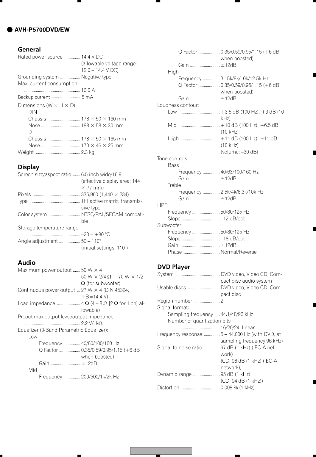
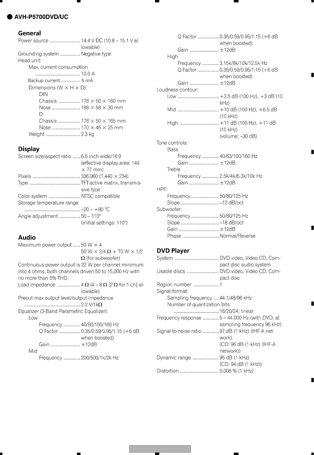
1. SPECIFICATIONS
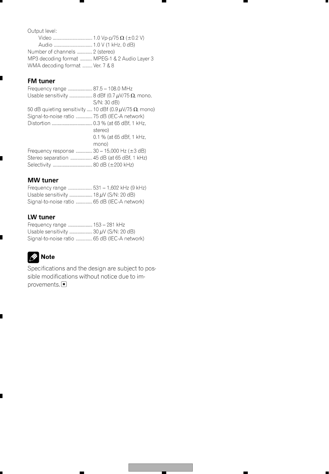
AVH-P5700DVD/EW
8
1234
1234
C
D
F
A
B
E
AVH-P5700DVD/EW 9
5678
5678
C
D
F
A
B
E

AVH-P5700DVD/EW
10
1234
1234
C
D
F
A
B
E

AVH-P5700DVD/EW 11
5678
5678
C
D
F
A
B
E
AVH-P5700DVD/EW
12
1234
1234
C
D
F
A
B
E
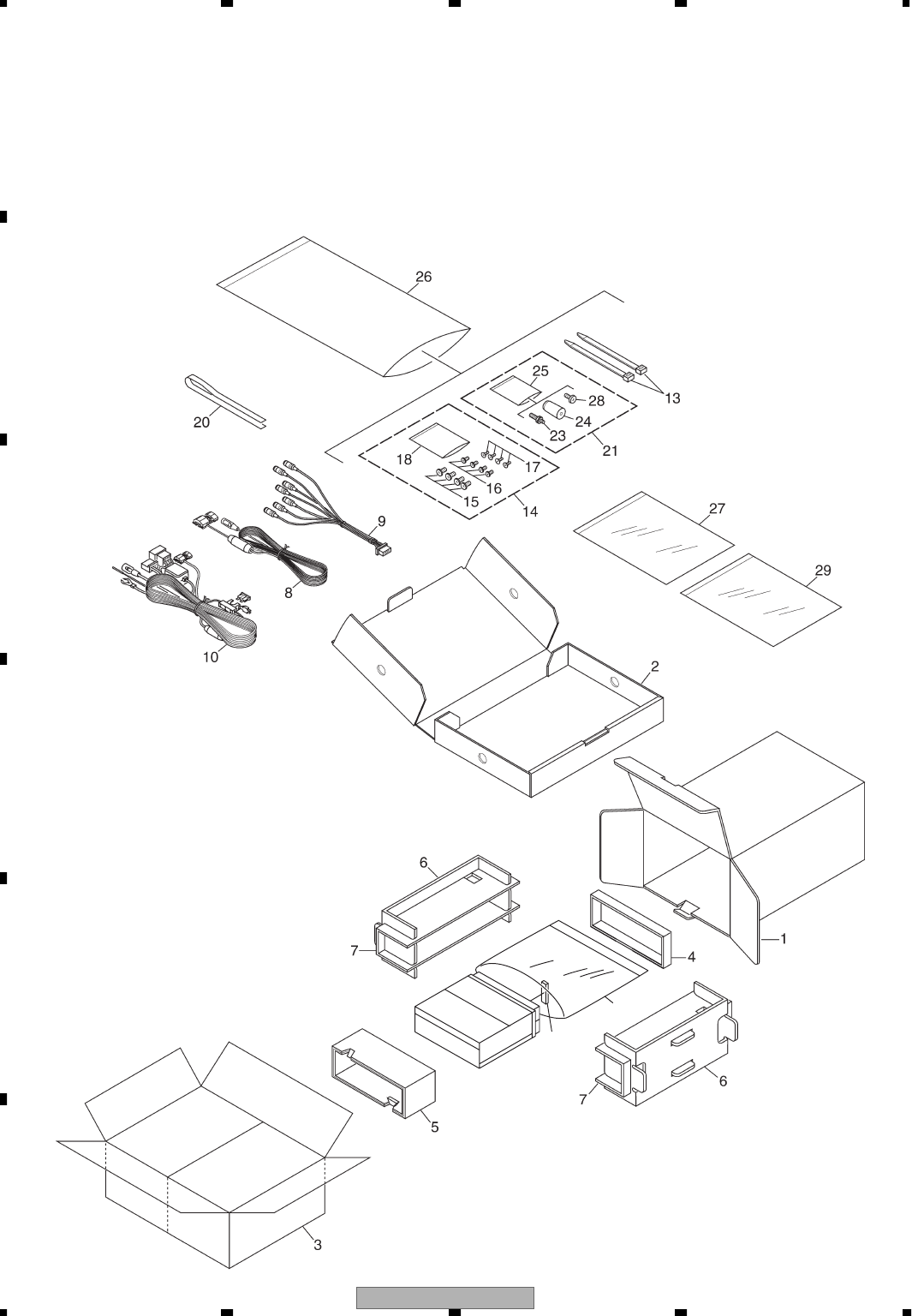
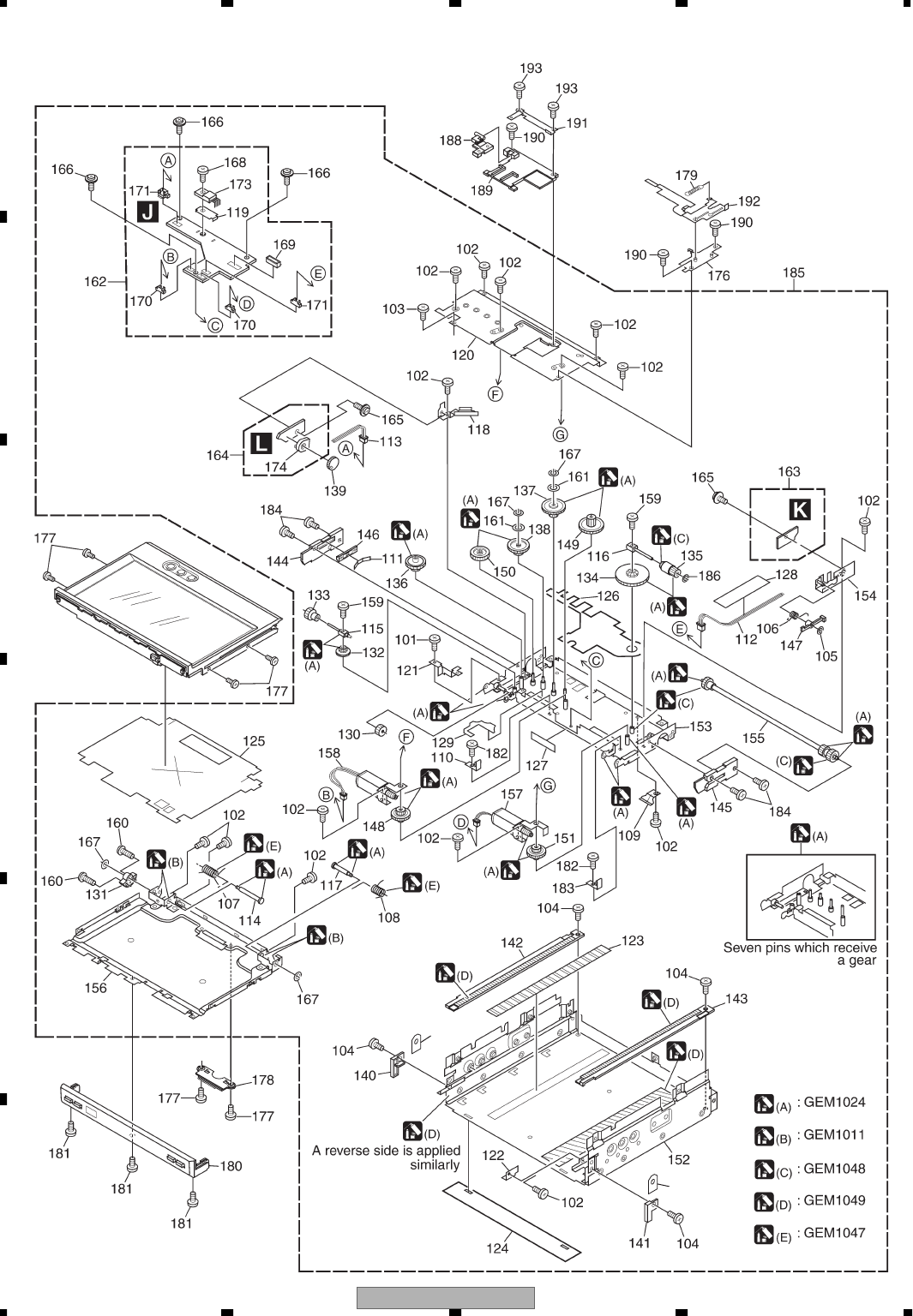
2. EXPLODED VIEWS AND PARTS LIST
2.1 PACKING(AVH-P5700DVD/EW)
N
OTES : • Parts marked by " * " are generally unavailable because they are not in our Master Spare Parts List.
• The > mark found on some component parts indicatesthe importance of the safety factor of the part.
Therefore, when replacing, be sure to use parts of identical designation.
• Screw adjacent to mark on the product are used for disassembly.
• For the applying amount of lobricants or glue, follow the instructions in this manual.
(In the case of no amount instructions,apply as you think it appropriate.)
"
11
12
AVH-P5700DVD/EW 13
5678
5678
C
D
F
A
B
E
PACKING(AVH-P5700DVD/EW) SECTION PARTS LIST
Owner's Manual,Installation Manual
Mark No. Description Part No.
1 Carton CHG5493
2 Sub Carton CHG5270
3 Contain Box CHL5493
4 Protector CHP2387
5 Protector CHP2708
6 Protector CHP2706
7 Protector CHP2707
8 Cord Assy CDE7321
9 Cord Assy CDE7801
10 Cord Assy CDE7792
11 Spacer CNM9773
12 Polyethylene Bag CEG1088
* 13 Lock Tie CNV-754
14 Screw Assy CEA5144
15 Screw BMZ50P060FTC
16 Screw(M4x3) CBA1870
17 Screw CMZ50P060FTC
* 18 Polyethylene Sheet CNM4338
20 Sheet CNM8603
21 Accessory Assy CEA4771
23 Screw CBA1650
24 Bush CNV1917
* 25 Polyethylene Bag E36-615
* 26 Polyethylene Bag CEG-158
27-1 Polyethylene Bag CEG1116
27-2 Owner's Manual CRB2047
27-3 Owner's Manual CRB2048
27-4 Owner's Manual CRB2049
27-5 Owner's Manual CRB2050
* 27-6 Warranty Card CRY1157
* 27-7 Passport CRY1013
28 Screw CBA1875
29-1 Polyethylene Bag CEG1116
29-2 Owner's Manual CRB2051
29-3 Owner's Manual CRB2052
29-4 Installation Manual CRD3965
Mark No. Description Part No.
Part No. Language
CRB2047 English
CRB2048 Spanish
CRB2049 German
CRB2050 French
CRB2051 Italian
CRB2052 Dutch
CRD3965 English, Spanish, German, French, Italian, Dutch
AVH-P5700DVD/EW
14
1234
1234
C
D
F
A
B
E
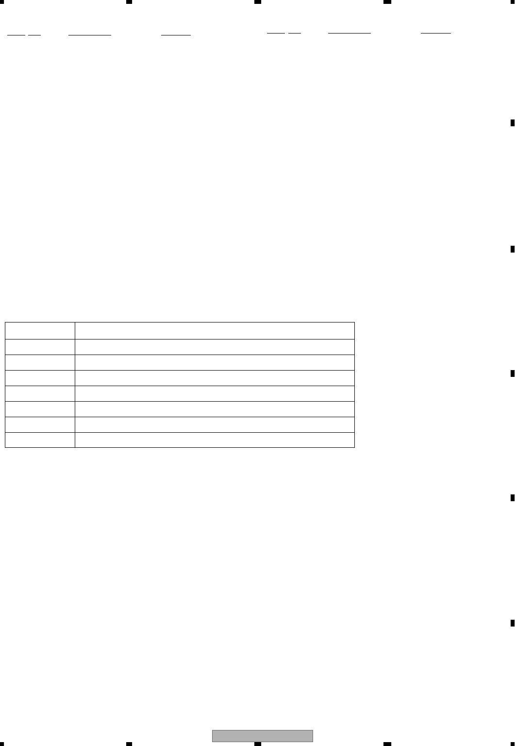
2.2 PACKING(AVH-P5700DVD/UC)
11
12

AVH-P5700DVD/EW 15
5678
5678
C
D
F
A
B
E
PACKING(AVH-P5700DVD/UC) SECTION PARTS LIST
Owner's Manual,Installation Manual
Mark No. Description Part No.
1 Carton CHG5494
2 Sub Carton CHG5270
3 Contain Box CHL5494
4 Protector CHP2387
5 Protector CHP2708
6 Protector CHP2706
7 Protector CHP2707
8 Cord Assy CDE7321
9 Cord Assy CDE7815
10 Cord Assy CDE7790
11 Spacer CNM9773
12 Polyethylene Bag CEG1185
13 •••••
14 Screw Assy CEA5144
15 Screw BMZ50P060FTC
16 Screw(M4x3) CBA1870
17 Screw CMZ50P060FTC
* 18 Polyethylene Sheet CNM4338
20 Sheet CNM8603
21 Accessory Assy CEA4771
23 Screw CBA1650
24 Bush CNV1917
* 25 Polyethylene Bag E36-615
26 •••••
27-1 Polyethylene Bag CEG1116
27-2 Owner's Manual CRB2053
27-3 Owner's Manual CRB2054
27-4 Installation Manual CRD3966
* 27-5 Registration Card CRY1229
27-6 Caution Card CRP1310
28 Screw CBA1875
Mark No. Description Part No.
Part No. Language
CRB2053 English
CRB2054 French
CRD3966 English, French
AVH-P5700DVD/EW
16
1234
1234
C
D
F
A
B
E
2.3 EXTERIOR(1)(AVH-P5700DVD/EW)
28
88
89
L
G
97

AVH-P5700DVD/EW 17
5678
5678
C
D
F
A
B
E
EXTERIOR(1)(AVH-P5700DVD/EW) SECTION PARTS LIST
Mark No. Description Part No.
1 Screw BMZ20P030FTB
2 Screw BMZ20P160FTC
3 Screw BMZ26P030FTC
4 Screw(M2x8) CBA1752
5 Screw BPZ20P060FTB
6 Screw(M2x2) CBA1872
7 Button(EJECT) CAC9051
8 Button(A-BM) CAC9052
9 Button(CROSS) CAC9053
10 Cord Assy CDE7176
11 Cord CDE7715
12 Cord Assy CDE7797
13 Flat Cable CDE7805
14 Cord Assy CDE7796
15 Panel CNB3101
16 Case CNB3104
17 Bracket CND1438
18 Holder CND1441
19 Button(VOL) CAC9050
20 Bracket CND2626
21 Bracket CND2627
22 Holder CND2628
23 Lever Unit CXC4211
24 Insulator CNM8495
25 Insulator CNM8864
26 Insulator CNM9398
27 Sheet CNM9517
28 Insulator CNM9750
29 Flexible PCB CNP8806
30 FFC CDE7807
31 Connector(CN5501) CKS4511
32 Guide CNV8415
33 Mother Unit CWM9808
34 Screw BMZ26P160FTC
35 Screw BSZ26P080FTC
36 Spring CBH2863
37 Flat Cable CDE7806
38 Antenna Cable CDH1348
39 FM/AM Tuner Unit CWE1650
40 Connector(CN101,102) CKS4653
41 Cushion CNM8671
42 Holder CND1432
43 Connector(CN154) CKS4823
44 Cord CDE7809
45 Terminal(CN731) CKF1064
46 Connector(CN701) CKM1332
47 Socket(CN261) CKM1457
48 Connector(CN171) CKS3751
49 •••••
50 Connector(CN151) CKS4052
51 Connector(CN181) CKS4052
52 Connector(CN175) CKS4068
53 Connector(CN152) CKS4282
54 Connector(CN101) CKS4511
55 Connector(CN771) CKS4822
56 Connector(CN561) CKS4824
57 Connector(CN121) CKS4830
58 Connector(CN131) CKS4832
59 Connector(CN781) CKS4977
60 Holder CND2629
61 Holder CND2630
62 Shield CND2631
63 Holder CND2633
64 Insulator CNM9400
65 Insulator CNM9521
66 Spacer CNM9522
67 Spacer CNM9523
68 Heat Sink CNR1703
69 Heat Sink CNR1784
70 RGB Unit CWM9815
71 Connector(CN951) CKS4497
72 Connector(CN952) CKS4978
73 Jack(CN981) CKN1022
74 Connector(CN954) CKS4052
75 Detach Grille Assy CXC4192
76 Bracket CND1482
77 Holder CND2634
78 Button(SRC/-,+) CAC9054
79 Button(ATT,EQ/BAND) CAC9056
80
DVD Mechanism Module(MS-3V1)
CXK6418
81 Fan Motor(M771) CXM1262
82 Fan Motor(M781) CXM1276
83 Screw IMS26P040FTC
84 Cover CNS8177
85 Grille CNS8173
86 Screw IPS20P060FTB
87 Grille Unit CXC4206
88 Transistor(Q892) 2SD2396
89 IC(IC871) NJM2388F84
90 IC(IC241) PAL007A
91 IC(IC5501) TSOP4840SB1
92 Cap CNV6727
93 Screw CMZ50P060FTC
94 Holder CNC9510
95 Panel CNS7797
96 Label VRW1860
97 Grille Assy CXC4187
Mark No. Description Part No.

AVH-P5700DVD/EW
18
1234
1234
C
D
F
A
B
E
2.4 EXTERIOR(1)(AVH-P5700DVD/UC)
28
88
89
L
G
97

AVH-P5700DVD/EW 19
5678
5678
C
D
F
A
B
E
EXTERIOR(1)(AVH-P5700DVD/UC) SECTION PARTS LIST
Mark No. Description Part No.
1 Screw BMZ20P030FTB
2 Screw BMZ20P160FTC
3 Screw BMZ26P030FTC
4 Screw(M2x8) CBA1752
5 Screw BPZ20P060FTB
6 Screw(M2x2) CBA1872
7 Button(EJECT) CAC9051
8 Button(A-BM) CAC9052
9 Button(CROSS) CAC9053
10 Cord Assy CDE7176
11 Cord CDE7715
12 Cord Assy CDE7798
13 Flat Cable CDE7805
14 Cord Assy CDE7796
15 Panel CNB3102
16 Case CNB3104
17 Bracket CND1438
18 Holder CND1441
19 Button(VOL) CAC9050
20 Bracket CND2626
21 Bracket CND2627
22 Holder CND2628
23 Lever Unit CXC4211
24 Insulator CNM8495
25 Insulator CNM8864
26 Insulator CNM9398
27 Sheet CNM9517
28 Insulator CNM9750
29 Flexible PCB CNP8806
30 FFC CDE7807
31 Connector(CN5501) CKS4511
32 Guide CNV8415
33 Mother Unit CWM9809
34 Screw BMZ26P160FTC
35 Screw BSZ26P080FTC
36 Spring CBH2863
37 Flat Cable CDE7806
38 Antenna Cable CDH1348
39 FM/AM Tuner Unit CWE1651
40 Connector(CN101,102) CKS4653
41 Cushion CNM8671
42 Holder CND1432
43 Connector(CN154) CKS4823
44 Cord CDE7809
45 Terminal(CN731) CKF1064
46 Connector(CN701) CKM1332
47 Socket(CN261) CKM1457
48 Connector(CN171) CKS3751
49 •••••
50 Connector(CN151) CKS4052
51 Connector(CN181) CKS4052
52 Connector(CN175) CKS4068
53 Connector(CN152) CKS4282
54 Connector(CN101) CKS4511
55 Connector(CN771) CKS4822
56 Connector(CN561) CKS4824
57 Connector(CN121) CKS4830
58 Connector(CN131) CKS4832
59 Connector(CN781) CKS4977
60 Holder CND2629
61 Holder CND2630
62 Shield CND2631
63 Holder CND2633
64 Insulator CNM9400
65 Insulator CNM9521
66 Spacer CNM9522
67 Spacer CNM9523
68 Heat Sink CNR1703
69 Heat Sink CNR1784
70 RGB Unit CWM9816
71 Connector(CN951) CKS4497
72 Connector(CN952) CKS4978
73 Jack(CN981) CKN1022
74 Connector(CN954) CKS4052
75 Detach Grille Assy CXC4193
76 Bracket CND1482
77 Holder CND2634
78 Button(SRC/-,+) CAC9054
79 Button(BOOST,EQ/BAND) CAC9055
80
DVD Mechanism Module(MS-3V1)
CXK6418
81 Fan Motor(M771) CXM1262
82 Fan Motor(M781) CXM1276
83 Screw IMS26P040FTC
84 Cover CNS8177
85 Grille CNS8174
86 Screw IPS20P060FTB
87 Grille Unit CXC4206
88 Transistor(Q892) 2SD2396
89 IC(IC871) NJM2388F84
90 IC(IC241) PAL007A
91 IC(IC5501) TSOP4840SB1
92 Cap CNV6727
93 Screw CMZ50P060FTC
94 Holder CNC9510
95 Panel CNS7797
96 •••••
97 Grille Assy CXC4188
Mark No. Description Part No.
AVH-P5700DVD/EW
20
1234
1234
C
D
F
A
B
E
2.5 EXTERIOR(2)
172
172

AVH-P5700DVD/EW 21
5678
5678
C
D
F
A
B
E
EXTERIOR(2) SECTION PARTS LIST
Mark No. Description Part No.
101 Screw(M2x3) CBA1082
102 Screw(M2x2.5) CBA1250
103 Screw(M2x4) CBA1277
104 Screw(M2x1.5) CBA1615
105 Washer CBF1038
106 Spring CBH2645
107 Spring CBH2646
108 Spring CBH2647
109 Spring CBL1585
110 Spring CBL1586
111 Spring CBL1587
112 Cord Assy CDE7047
113 Cord Assy CDE7213
114 Shaft CLA4270
115 Shaft CLA4305
116 Shaft CLA4306
117 Shaft CLA4309
118 Bracket CND1221
119 Heat Sink CND1228
120 Case CND1229
121 Holder CND1318
122 Holder CND1449
123 Sheet CNM8522
124 Sheet CNM8037
125 Insulator CNM8048
126 Insulator CNM8158
127 Sheet CNM8159
128 Tape CNM8160
129 Insulator CNM8294
130 Gear CNR1664
131 Gear CNR1665
132 Gear CNR1677
133 Gear CNR1678
134 Gear CNR1679
135 Gear CNR1680
136 Gear CNR1688
137 Gear CNR1802
138 Gear CNR1708
139 Gear CNV7383
140 Holder CNV7384
141 Holder CNV7385
142 Rack CNV7386
143 Rack CNV7387
144 Slider CNV7388
145 Slider CNV7389
146 Holder CNV7390
147 Arm CNV7391
148 Gear CNV7522
149 Gear CNV7523
150 Gear CNR1709
151 Gear CNV7529
152 Chassis Unit CXB9509
153 Frame Unit CXB9511
154 Holder Unit CXB9512
155 Shaft Unit CXB9513
156 Holder Unit CXB9514
157 Motor Unit(M3001)(Position) CXB9515
158 Motor Unit(M3002)(Angle) CXB9516
159 Screw CZB3082
160 Screw CZB3083
161 Washer CZB3084
162 Main Unit CZW3087
163 SW Unit CZW3088
164 Volume Unit CZW3089
165 Screw IMS20P020FTC
166 Screw IMS20P030FZK
167 Washer YE15S
168 Screw BMZ26P050FTC
169 Connector(CN3801) CKS4068
170 Connector(CN3802,CN3803) CKS4732
171 Connector(CN3807,3809) CKS4733
172 Spacer CNM9837
173 IC(IC3801) BA00AST
174 Volume(VR3841) CCW1025
175 •••••
176 Bracket Unit CXC3048
177 Screw(M2x2) CBA1872
178 Holder CND2890
179 Spring CBH2750
180 Cover Unit(EW) CXC5117
Cover Unit(UC) CXC5118
181 Screw(M2x2) CBA1872
182 Screw(M2x1.8) CZB3085
183 Spring CBL1642
184 Screw(M2x4) CZB3088
185 Drive Unit CXC5111
186 Washer CZB3089
187 Sheet •••••
188 Arm CNV8065
189 Holder CNV8066
190 Screw(M2x3) CBA1876
191 Spring CBL1679
192 Lever CND2202
193 Screw CBA1797
Mark No. Description Part No.
AVH-P5700DVD/EW
22
1234
1234
C
D
F
A
B
E
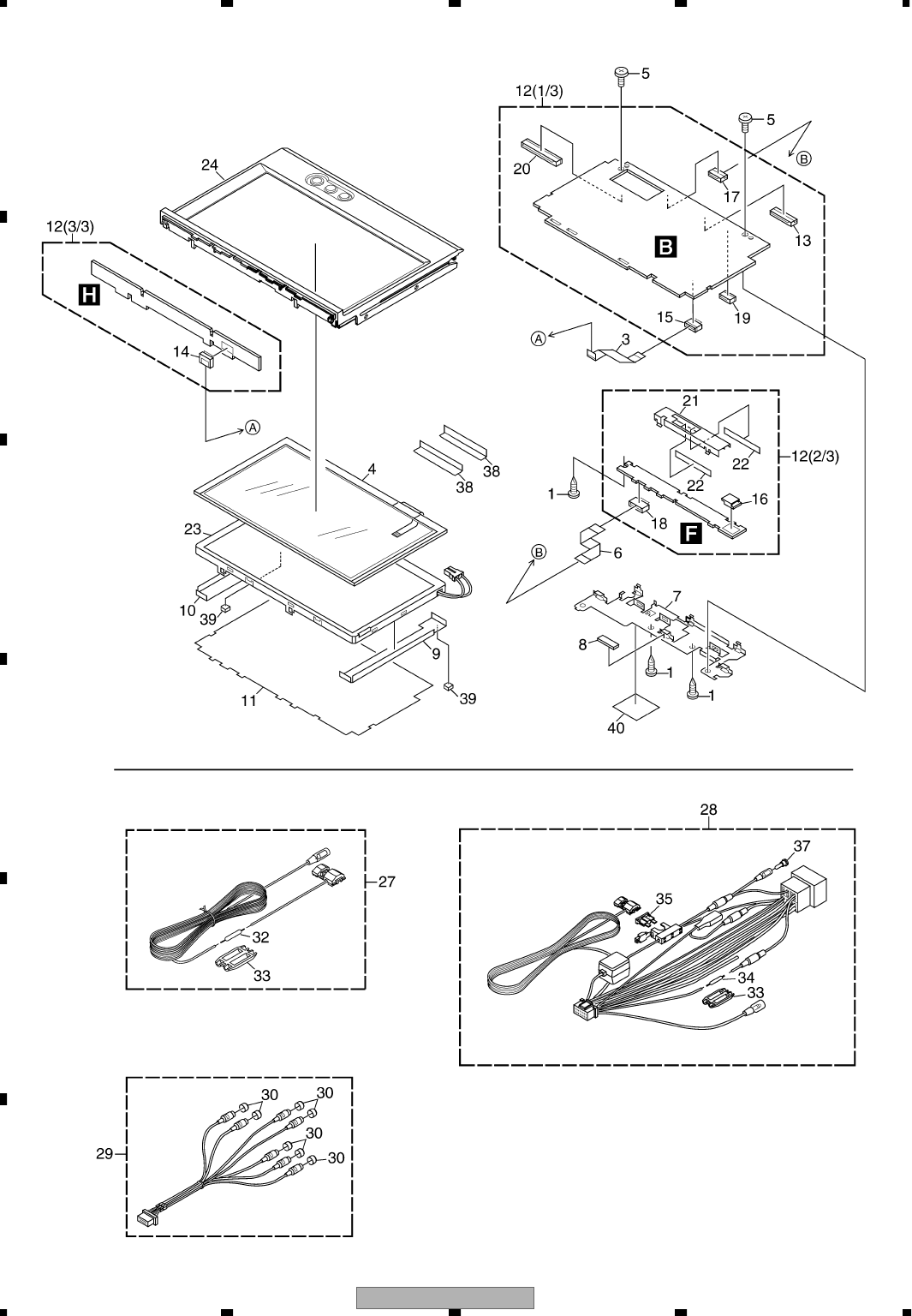
2.6 EXTERIOR(3)(AVH-P5700DVD/EW)

AVH-P5700DVD/EW 23
5678
5678
C
D
F
A
B
E
EXTERIOR(3)(AVH-P5700DVD/EW) SECTION PARTS LIST
Mark No. Description Part No.
1 Screw BPZ20P060FTC
2 •••••
3 FFC CDE7195
4 Touch Panel CSX1087
5 Screw(M2x2) CBA1872
6 FFC CDE7814
7 Holder CND2610
8 Gasket CNM8600
9 Sheet CNM8265
10 Sheet CNM7784
11 Insulator CNM9390
12 Monitor Unit CWM9820
13 Connector(CN4541) CKS3968
14 Connector(CN4301) CKS4054
15 Connector(CN4591) CKS4054
16 Connector(CN5342) CKS4428
17 Connector(CN4521) CKS4595
18 Connector(CN5001) CKS4595
19 Connector(CN4501) CKS4675
20 Connector(CN4007) CKS4872
21 Shield CND2737
22 Insulator CNM9251
23 LCD Module CWX3151
24 Grille Unit CXC4198
25 •••••
26 •••••
27 Cord Assy CDE7321
28 Cord Assy CDE7792
29 Cord Assy CDE7801
30 Cap CNV6727
31 •••••
32 Resistor RSV2PMF102J
33 Cap CNS1472
34 Resistor RS1/2PMF102J
>
35 Fuse(10A) CEK1136
36 •••••
37 Terminal Cover CKX-003
38 Sheet CNM9742
39 Spacer CNM9840
40 Sheet CNM9744
AVH-P5700DVD/EW
24
1234
1234
C
D
F
A
B
E
2.7 EXTERIOR(3)(AVH-P5700DVD/UC)

AVH-P5700DVD/EW 25
5678
5678
C
D
F
A
B
E
EXTERIOR(3)(AVH-P5700DVD/UC) SECTION PARTS LIST
Mark No. Description Part No.
1 Screw BPZ20P060FTC
2 •••••
3 FFC CDE7195
4 Touch Panel CSX1087
5 Screw(M2x2) CBA1872
6 FFC CDE7814
7 Holder CND2610
8 Gasket CNM8600
9 Sheet CNM8265
10 Sheet CNM7784
11 Insulator CNM9391
12 Monitor Unit CWM9821
13 Connector(CN4541) CKS3968
14 Connector(CN4301) CKS4054
15 Connector(CN4591) CKS4054
16 Connector(CN5342) CKS4428
17 Connector(CN4521) CKS4595
18 Connector(CN5001) CKS4595
19 Connector(CN4501) CKS4675
20 Connector(CN4007) CKS4872
21 Shield CND2737
22 Insulator CNM9251
23 LCD Module CWX3151
24 Grille Unit CXC4201
25 •••••
26 •••••
27 Cord Assy CDE7321
28 Cord Assy CDE7790
29 Cord Assy CDE7815
30 Cap CNV6727
31 •••••
32 Resistor RSV2PMF102J
33 Cap CNS1472
34 Resistor RS1/2PMF102J
>
35 Fuse(10A) CEK1136
36 •••••
37 •••••
38 Sheet CNM9742
39 Spacer CNM9840
40 Sheet CNM9744

AVH-P5700DVD/EW
26
1234
1234
C
D
F
A
B
E
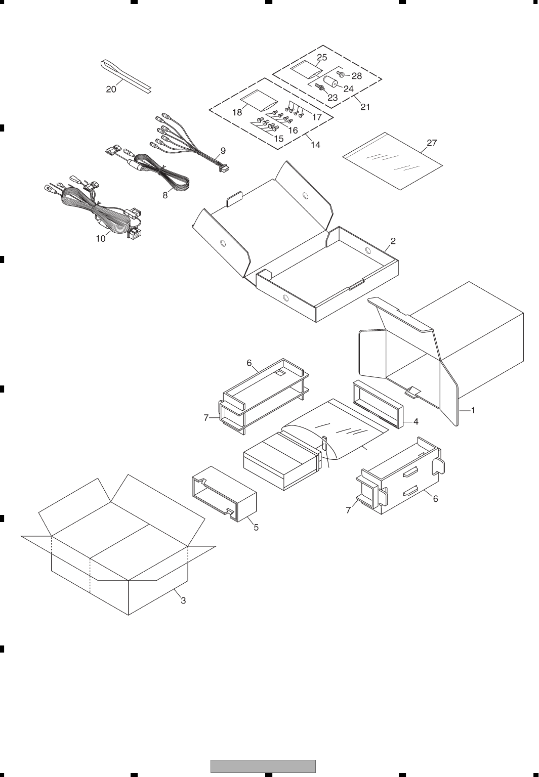
2.8 DVD MECHANISM MODULE(MS-3V1)
M

AVH-P5700DVD/EW 27
5678
5678
C
D
F
A
B
E
DVD MECHANISM MODULE (MS-3V1) SECTION PARTS LIST
Mark No. Description Part No.
1 DVD Core Unit CWX3170
2 •••••
3 Connector(CN1201) CKS4067
4 Connector(CN1551) CKS4817
5 Connector(CN1231) CKS4624
6 Connector(CN1903) CKS4374
7 Connector(CN1101) CKS4625
8 Connector(CN1901) CKS3971
9 Screw BMZ20P020FTC
10 Screw(M2 x 3.5) CBA1571
11 Screw(M2 x 2.5) CBA1623
12 Washer CBF1038
13 Washer CBF1064
14 Spring CBH2586
15 Spring CBH2587
16 Spring CBH2588
17 Spring CBH2589
18 Spring CBH2590
19 Spring CBH2591
20 Spring CBH2592
21 Spring CBH2593
22 Spring CBH2594
23 Spring CBH2595
24 Spring CBH2596
25 Spring CBH2597
26 Spring CBH2598
27 Spring CBH2599
28 Spring CBH2600
29 Spring CBH2601
30 Spring CBH2602
31 Spring CBH2603
32 Spring CBH2604
33 Spring CBH2605
34 Spring CBH2711
35 Spring CBL1564
36 Pickup Unit(Service) CXX1770
37 Shaft CLA3881
38 Shaft CLA4206
39 Shaft CLA4207
40 Lever CNC9933
41 Holder CNC9939
42 Holder CND2251
43 Holder CNC9941
44 Frame CND2250
45 Sheet CNM6883
46 Sheet CNM8283
47 Sheet CNM8643
48 Lever CNV8076
49 Lever CNV7155
50 Cam CNV7156
51 Rack CNV7157
52 Clamper CNV7158
53 Arm CNV7159
54 Arm CNV7160
55 Arm CNV7161
56 Arm CNV7162
* 57 Arm CNV7163
58 Arm CNV7164
59 Roller CNV7165
60 Arm CNV7166
61 Guide CNV8093
62 Gear CNV7169
63 Gear CNV7170
64 Gear CNV7171
65 Gear(Black) CNV7172
66 Gear CNV7173
67 Gear CNV7174
68 Rack CNV7175
69 Gear CNV7176
70 Arm CNV8077
71 Lever CNV7178
72 Lever CNV7179
73 Screw IMS20P030FTC
74 Gear CNV7181
75 Holder CNV7183
76 Holder CNV7184
77 Guide CNV7745
78 Roller CNV7344
79 Damper CNV7470
80 Damper CNV7471
81 Collar CNV7645
82 Compound Unit(A) CWX3154
83 Screw(M2x2) CBA1817
84 Compound Unit(B) CWX3156
85 Washer YE20FTC
86 Chassis Unit CXC3629
87 Arm Unit CXB8681
88 Frame Unit CXB8683
89 Arm Unit CXC4701
90 Bracket Unit CXB8685
91 Motor Unit(LOADING)(M1) CXC4659
92 Motor Unit(CARRIAGE)(M2) CXC4314
93 Screw Unit CXB8689
94 Roller Unit CXB8690
95 Motor(SPINDLE)(M3) CXM1272
96 Screw JFZ20P018FTC
97 Photo-transistor(Q1299) CPT231SCTD
98 Switch(S1201,S1202,S1203) CSN1069
99 Spring Switch(S1204,S1205) CSN1070
100 Resistor(R1298,R1299) RS1/16S0R0J
101 Gathering PCB CNX4320
102 Holder CNV8186
103 Arm CNV7742
104 Arm CNV7743
105 Spring CBH2710
106 Spring CBL1643
107 Spring CBH2712
108 Pickup Unit(Service)(Screw) GXX1242
109 Screw Assy CXX1750
110 Screw(M1.4xM1.4) CBA1787
111 Cover CNC9943
112 Screw JFZ20P018FTC
Mark No. Description Part No.
AVH-P5700DVD/EW
28
1234
1234
C
D
F
A
B
E
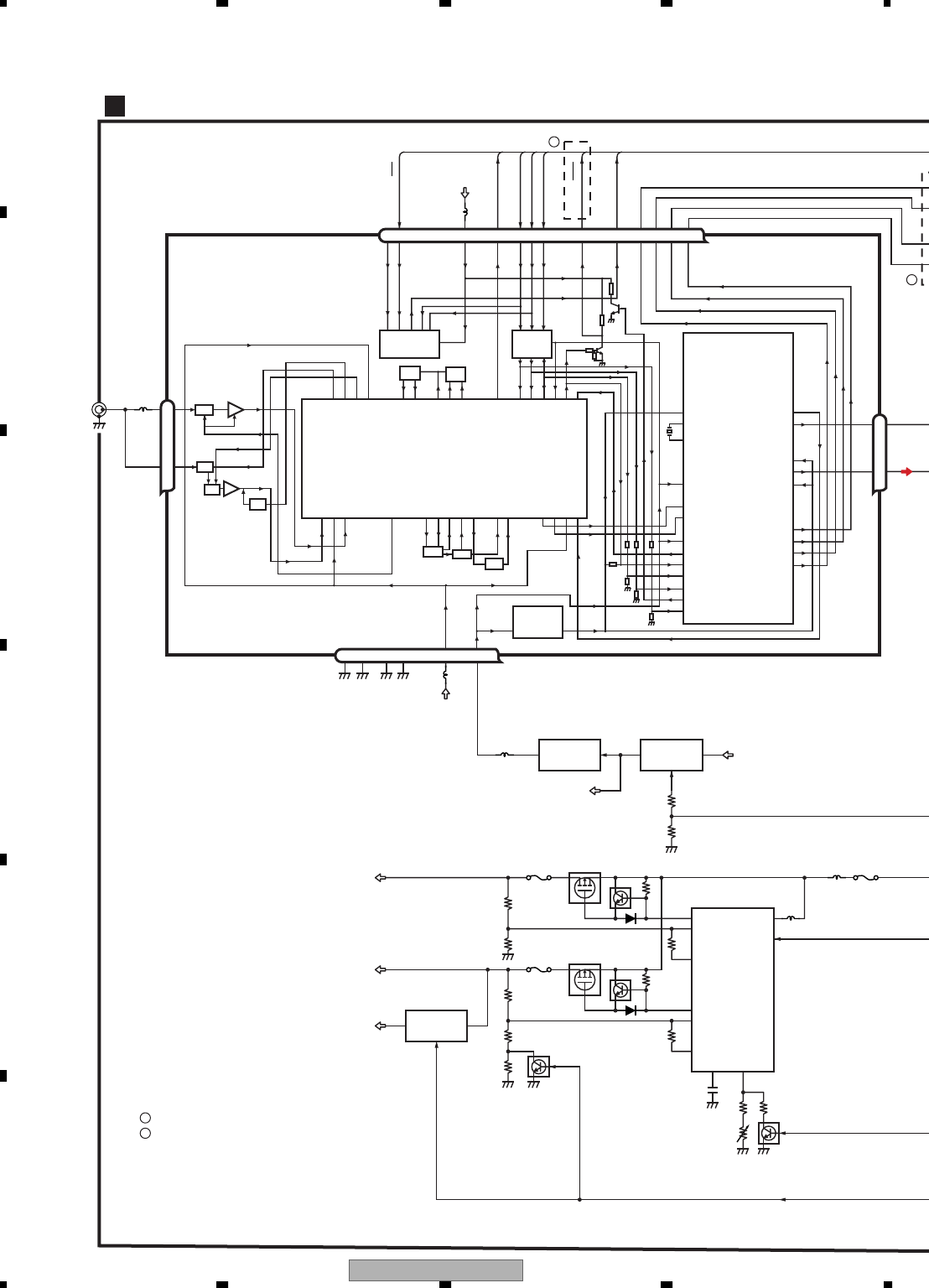
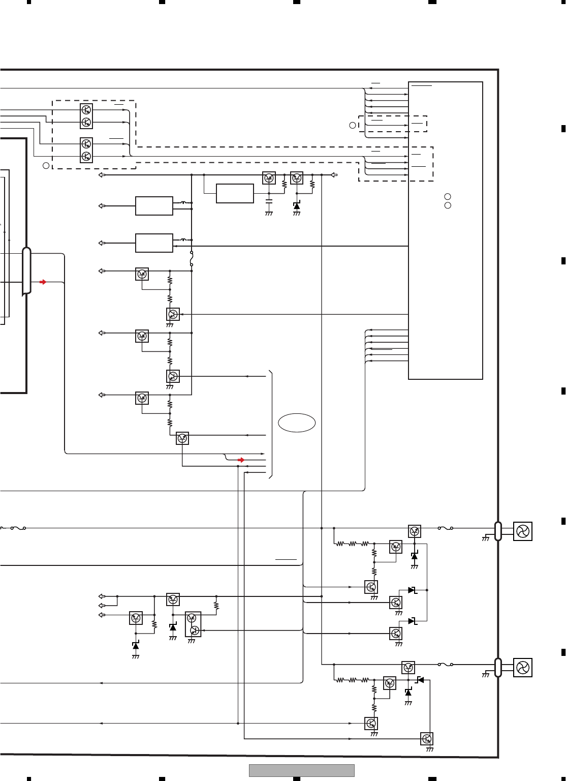
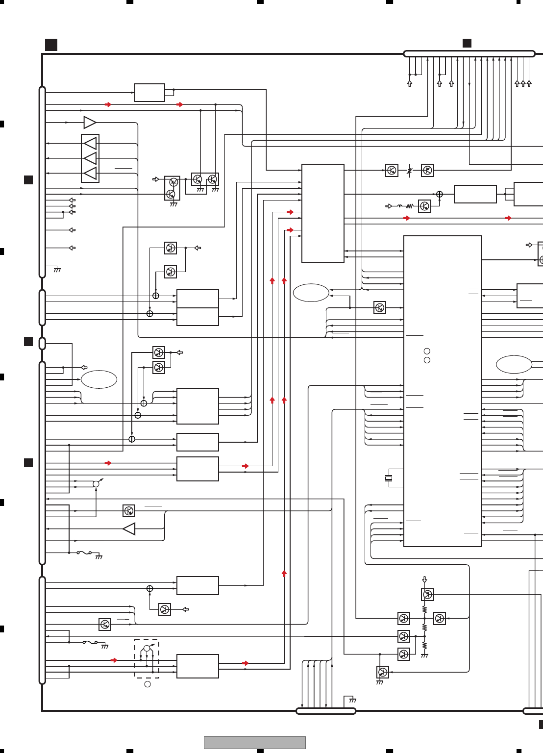
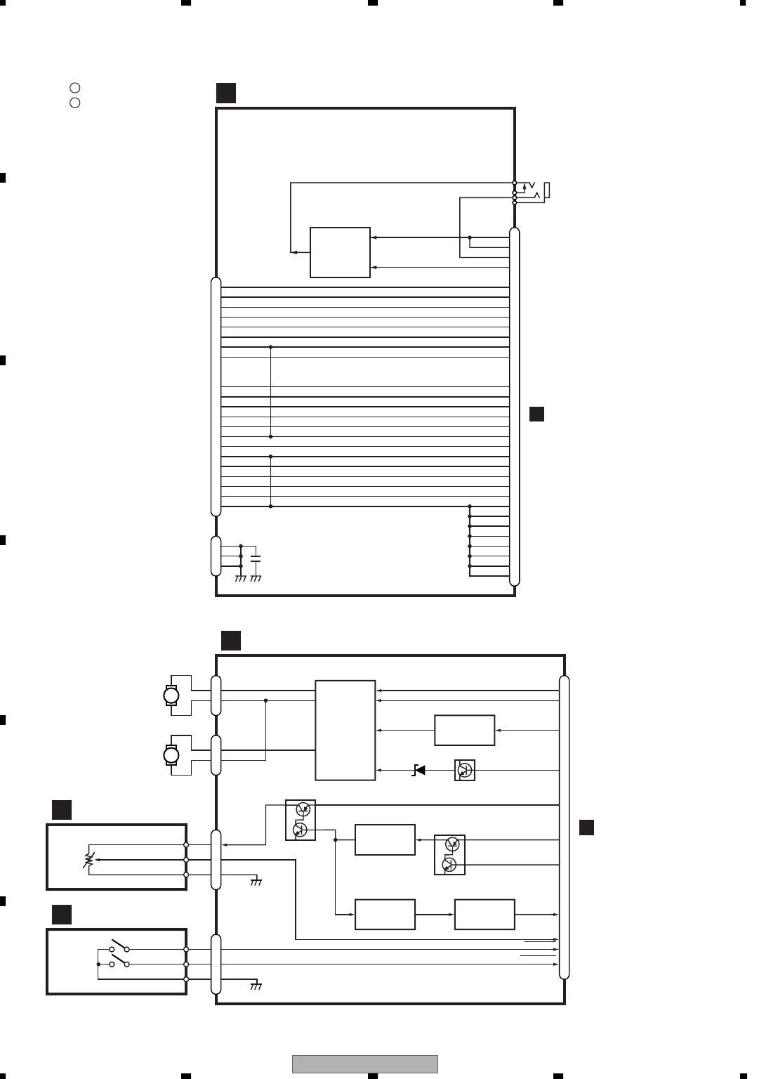
3. BLOCK DIAGRAM AND SCHEMATIC DIAGRAM
3.1 BLOCK DIAGRAM
VDD5
IC831
BA00BC0WFP
3.3V REG.
9
CN401
FM/AM
ANT
AVH-P5700DVD/EW
IC801
AN8011S
D/D CONVERTER
VCC
3
12
ON/OFF
10 OUT1
13 IN-1
12 FB1
2
1
4VDD VC VIN
FU803
VD8
SYS+B
VCC33
SYS+B
B.UP
FMRF
ANT adj RF adj
FM ANT
T51 CF52
CF51
RFGND
OSCGND
DGND
AUDIOGND
NC
VCC
VDD_3.3
3.3V 2.5V
IC 4
3.3V 2.5V
←
IC 2
2.5V
WC
CE2
ROM_VDD
SL
DI
CK
CE1
LDET
DO
SL
DI
CK
CE
DO
RDS_CK
RDS_DATA
RDS_LOCK
RDS_HSLK
76 13 5 1098 11 14 18192021
1
3
212 1522 16 4 17
IC 1
3.3V
AM ANT FMRF
ATT
LPF
OSC
IC 3 EEPROM
5.0V
IC 5
5V 3.3V
←
ATT
MIXER, IF AMP DET, FM MPX,
RDS DECODER
24
23
Rch
Lch
TU
N
TU
N
IC881
NJM2391DL1-33
3.3V REG.
13 OUT IN
IC871
NJM2388F84
8.4V REG.
12
4
VOUT
CONT VIN
Q803
Q801
7OUT2
Q804
Q805
Q806
Q802
FU801
4IN-2
5FB2
CT RT
VCC15 FU802
CE2
LDET
A
A
A
AVH-P5700DVD/UC
B
MOTHER UNIT (1/2)
FM/AM TUNER UNIT
A
AVH-P5700DVD/EW 29
5678
5678
C
D
F
A
B
E
CN771
2
1
FAN MOTOR
(REAR)
CN781
2
1
Q842Q841
Q402
Q401
B.UPVDD5
VIDEO5V REG.
VIDEO9V REG.
ACC5V REG.
SWVDD5V REG.
OPT5V REG.
REAR FAN6V REG.
CENTER FAN6V REG.
FU803 FU771
IC841
S-812C50AUA-C3E
5V REG.
SYSTEM CONTROLLER
23 VOUT
103 CONTVDD
46 TUNPDI
45
100 TUNPCE
48 TUNPCK
47 TUNPDO
135 TUNSL
101
DO
CE
CK
DI
SL
29 ACCPW
VIN
IC851
S-818A35AUC-BGP
3.5V REG.
5
1VOUT VIN 4
ON/OFF
SRVDD
24
23
Rch
Lch
TUNR
TUNL
TUNR
TUNL
IC856
S-814A33AMC-BCX
3.3V REG.
1
5VOUT VIN 3 CONTVDD
ACCPW
SWVDD
HSEN
FU861
ON/OFF
VDD33
SWVDD5
Q861
(1/2)
Q861
(2/2)
OPT5
Q864
(1/2)
Q864
(2/2)
VPW
SYSPW
DDCONTL
VPW
CCONT1
CCONT2
CONTB
MFLPW
SW9
VIDEO9
Q892
Q893
Q773
(1/2)
Q773
(2/2)
Q772
VIDEO5
Q891
ACC5
Q867
(1/2)
Q867
(2/2)
Q772
Q771
Q774
FU781
Q782
(1/2)
Q782
(2/2)
Q781
Q783
CE2 TUNPCE2
LDET
RDT
RCK
RDSHSLK
RDSLK
RDT
RCK
RDSHSLK
RDSLK RDT
RCK
RDS57K
RDSLK
LDET
24
25
23
57
VPW
CCONT1
CONTVDB
VPW
COOLCNT1
77
104
32
CCONT2 COOLCNT2
78
SYSPW SYSPW
31
DDCONTL DDCONTL
CONTVDB
33
CONTB
MFLPW
TO
MOTHER UNIT
(2/2)
CONTVDB
A
A
: PE5484A
A
: PE5485A
B
IC601(1/2)
FAN MOTOR
(CENTER)
AVH-P5700DVD/EW
30
1234
1234
C
D
F
A
B
E
MOTHER UNIT (2/2)
A
ANR1
CN171
ANG1
ANB1
MONVBS
CSYNC
ANR1
ANG1
ANB1
CSYNC
YS
HRX
HTX
RXMON
TXMON
MFLPW
PWRVI
SELFRSTSELFRST
MON5PWSWVDD
MOREM
PWRFL
MONI5V
ILMC
VBILM
ILMA
VRILM
ILMGB
31
30
32
35
27
25
19
20
21
16
15
13
18
23
5
3
1
2
39
37
36
VGILM
SWVDD5
PWFL
PWVI
VD8
OPT5
VCC15
VCC33
SRVDD VIDEO9
VDD33
B.UP
IPPW
ASENBO
PRGRST
TXMON
SWVDD
RXMON
FRONTMUTE
VDT
VCK
VST
SYSTEM CONTROLLER
IC601(2/2)
40
VOUT1
33
39
41
27
26
84
86
62
108
107
109
CONTBIN
81
RXMS3
111
TXMS3
112
IRQPWR
RXMS3
TXMS3
IRQPWR 113
114
119
TXNAV
TXNAV
RXNAV
RXNAV
118
117
VOUT2
LOUT1
ROUT1
SDA
SCL
SDA
SCL
47 TV
1V1
8V2
15 V3
23 V4
16 LV3
18 RV3
2LV1
4RV1
IC501
CXA2089Q
AV SELECTOR
TU
N
TU
N
DIN1
1
2DOUT
8
91
90
88
87
TX
RX
IPPW
B
U
B
U
IC121
HA12240
F
1
2
8
3
4
9
13
10
11
12
14
19
15
17
18
20
21
24
25
27
26
28
30
31
32
|
39
CN151
CCR
CCG
HSEN
OPT OUT
OPT OUT
OPT5
OPT5
CCB
CCR
CCG
CCB
CCSYNC
GNDSIG
DVDVBS
GNDDVD
YS
CCAUL
CCAUR
GNDAU
ONSEI+
ONSEI−
GNDRAU
CCREM
DSEN
TVON
GION GUIDEON
HTXD 4 1,2
HRXD
TXNAV
RXNAV
GNDD FU151
39
37
35
29
27
28
26
1
23
22
20
21
19
18
17
|
14
12
|
10
8
|
2
4
3
1
CN181
VIDEO INAV-BUS
CN954
CN561
1
CN152
ANALOG ROUT
VIDEO OUT
ANALOG LOUT
MS3 Rch
MS3 Lch
VDD33
AMUTE
VCONTB CONTB
XRESET
IRQPWR
HSTCMD
SLVSTS
IRQPWR
TXMS3
RXMS3
VIN VF
VOUT
3
6
8
1
16
7
1
4
9
4
SRVDD
VCC33
VCC15(33)
VD
VCRV
G
BCAM
G
CN131
AV−
AV+
VSEL1
VSEL2
AVON
AVG
REMIN
AVG
VCRINL
VCRGND
VCRINR
1
2
3
4
5
6
7
8
9
10
11
12 VCRGND
XRESET
XRESET
RGBARI
RGBARI
RGBARI
53AVON AVON IN
XRESET
IC182
TC7SET08FUS1
3V→5V
IC541
SM5304AV
VIDEO AMP
D_OUT
C_OUT
B_OUT
A_OUT
IC461
NJM2138V
RGB VIDEO ISOLATOR
OUT1
OUT2
IN1B/2B
IN1A
IN2A
IC441
TA2050F
NAVI DVD(A)
IC151
TC4S81F
+
−
+
−
6
2
3
2
36
VCR IN(V)
B.CAMERA(V)
IC551
NJM2136V
IC561
NJM2136V
IC181
TC74VHC08FTS1
5V→3V
+
−
6
2
3
13
12
10,15
NAVI DVD(V)
IC571
NJM2136V
+63
4
2
3
BUFFER
IC521
NJM2136V
IC522
BA7623F
VIDEO AM
Q181 Q182
H
I
VSELIN1
VSELIN2
AVON
CCR
CCG
CCB
10
Q461
Q151
5
3
12
1
7
8
14
2,6,9,13
8
1
OUT1
OUT2
IN1A
IN1B/2B
IN2A
IC451
TA2050F
AV-BUS(A)
−
+
6
3
2
10,15
12
13
AV-BUS(V)
IC581
NJM2136V
8
1
ANB1
ANR1
CSYNC
ANG1
CN665
TXNAV
RXNAV
TXNAV
RXNAV
PRGON
PRGSW
VPPON
VPP
PRGON
PRGSW
VPPON
VPP
10
9
8
7
6
5
4
|
1
FU131
VIDEO5
Q571
VIDEO5
Q581
VIDEO5
Q561
Q551
Q131
G
I
CN4541
B
CN101
1
6
2
ILMA
REM
RESET
DFLED
DSENS
MOREM REMUTE
DREM
REMIN
CCREM
ACC5
Q691
Q693Q692
Q695
Q694
Q696
ASENBO
SELFRST
RXMON
TXMON
SWVDDSWVDD
CONTB
CONTB
ANGLE
LIFTPUL
MTRS
MTRPW
MTR2
MTR1
MTRSEL
SNSPW
PUSHSW
DEG0SW
ANGLE IN
LIFTPUL
MTRS
MTRPW
MTR2
MTR1
MTRSEL
SNSPW
PUSHSW
DEG0SW
RESET RESET
ASENS
BSENS
VSELIN1
VSELIN1
VSELIN2
VSELIN2
51
52
PRGSW
PRGSW 61 PRGON
PRGON 58
VPPON
VPPON 59
VPP
VPP 41
X2
74
X1
73
REMUTE
106
DREM
105
96
PBSENS129
69
BGSENS130
TELIN127
CILM66
CGILM35
CRILM
ASENS
BSENS
PBSENS
68
BEEP
AMPPW30
AMPPW
AMPMUTE124
AMPMUTE
RCAMUTE50
RCAMUTE
SYSMUTE122
MUTE
BGSENS
TELIN
CILM
ILMGRN
ILMRED 67
18
19
20
14
16
17
13
15
21
137
40
REMUTE
DREM
83
142KDT2
141
140
KDT1
KDT0
DSENS
KEYDT2
KEYDT1
KEYDT0 34
DLED
B.UP
Q512
Q521
Q601
VR511Q511
IN2
IN3
IN1
OU
T
STBY
TO
MOTHER UNIT
(1/2)
TO
MOTHER UNIT
(1/2)
TO
MOTHER UNIT
(1/2)
IETX
IERX
11
12
9
10
NMIXCNT 121
X601
18.874368MHz
:PE5484A
A
:PE5485A
B
A
CN1901
C
CN1551
C

AVH-P5700DVD/EW 31
5678
5678
C
D
F
A
B
E
ANR1
CN121
IP-BUS
ANG1
ANB1
MONVBS
ANR1
ANG1
ANB1
ILMC
VBILM
ILMA
VRILM
ILMGB
31
30
32
35
39
37
36
IPL−
BUS+
IPR−
IPR+
ASENBO
IPL+
BUS−
BUS+
ASENBO
BUS−
7
6
1
4
10
9
8
VGILM
B.UP
43
35
10
IN4+L
IN4+R34
IN4−R44
IN4−L
FRONTOUT_L
24
3
2
5
1
7
6
FRONTOUT_R
12
PREOUT_L
22
PREOUT_R
41 IN2_L
37
MS3 Lch
MS3 Rch IN2_R
IN1_L
IN1_R
11
REAROUT_L
23
REAROUT_R
A+IN
A−IN
B+IN
AOUT
BOUT
5
23
3
4
7
19
9
17
21
B−IN
IC201
PML009A
ELECTRIC VOLUME
40
38
1
IN−1OUT1
2
3IN+1
IC301
NJM4558V
IN+2
5
3
TUNL
TUNR
7
1
IN+1
OUT2
OUT1
IC421
NJM4558MD
TUNER AUDIO AMP
DIN1
16
5
BUS+
BUS−
2DOUT
8
TX
RX
IPPW
BUS+
BUS−
IC121
HA12240FP
IC303
NJM4580V
IC241
PAL007B
POWER AMP
7
IN+2OUT2
5
6IN−2
7
IN+2OUT2
6
5
Q302
Q303
Q301
IN−2
ONSEI+
ONSEI−
GUIDEON
RCA OUTPOWER SUPPLY
OUT VDD
12
IC681
S-80841CNUA-B82
RESET GEN.
63 8
REARV
4
2
V
IC522
BA7623F
VIDEO AMP
H
1
2
3
CN154
FU152
CN3801
J
CN5501
I
5
41
CN101
13
12
11
10
8
9
1
7
6
2
KEY0
KEY1
KEY2
KDT0
KDT1
KDT2
ILMG
ILMA
REM
RESET
DFLED
ACC5
VGILM
VRILM
DSENSDSENS
VDD5
Q101
(1/2)
Q101
(2/2)
ASENBO
ASENBO
CN175
ANGLEIN ANGLE
BUP
15
14
16
17
13
12
11
10
3
1
2
20
19
18
B.UP
LIFTPUL
MTRS
MTRPW
MTR2
MTR1
MTRSEL
LIFTPUL
MTRS
MTRPW
MTR2
MTR1
MTRSEL
ANGL0SW
PUSHSW
SENSPW SNSPW
VDD
FU175
FU176 VDD5
PUSHSW
DEG0SW
ANGLE
LIFTPUL
MTRS
MTRPW
MTR2
MTR1
MTRSEL
SNSPW
PUSHSW
DEG0SW
RESET
Q754
VRILM
CRILM
Q753
B.UP
ASENS
BSENS
CN701
ACC
15
14
16
13
12
11
4
3
1
2
8
7
10
9
5
6
B.REM
B.G.
MUTE
B.UP
PWVI
PWFL
RR+
FR+
RR−
FR−
RL+
FL+
RL−
FL−
P.B .
BGSENS
TELIN
MFLPW
PBSENS
RR+
FR+
RR−
FR−
RL+
FL+
RL−
FL−
VGND
FU703
Q703
Q705
Q704
FU701
RR+
FR+
RR−
FR−
RL+
FL+
RL−
FL−
AMPPW
12
FL
11
FR
14
15
RR+
FR+
RR−
FR−
RL+
FL+
RL−
FL−
25
22
B.REMOTE
MUTE
FRIN
FLIN
RRIN
RLIN
Q706
Q701
Q702
Q756
FU702
VBILM
CILM
Q755
Q752
VGILM
CGILM
ASENS
BSENS
Q751
CN261
RL
VCRINL
VCRINR
FL
FR
6
4
8
10
12
14
13
11
3
1
7
9
5
RR
VCRGND
SYSMUTE
RCAMUTE
AMPMUTE
Q281
Q245
Q244
Q242Q241
REARV
SWR
FL
FR
FU261
B.UP
IN3_L
IN3_R
42
36
SWL
PBSENS
9
BGSENS
0
TELIN
7
CILM
CGILM
CRILM
AMPPW
AMPMUTE
4
RCAMUTE
SYSMUTE
2
7
Q261
Q262
I
B.UP
SYS+B
Q243
RBU14
Q121
B.UP
1
IN−1OUT1
2
3IN+1
IC302
NJM4558V
NAVI GUIDE MIXING
IN2
IN3
IN1
OUT1
STBY
NMIXCNT
TO
MOTHER UNIT
(1/2)
MFLPW
TO
MOTHER UNIT
(1/2)
BZ601
20 MUTE
19 STB
18 DATA
17
1
CLK
STBY
VDD5
SWVDD
AVH-P5700DVD/EW
A
AVH-P5700DVD/UC
B
B
B
A
AVH-P5700DVD/EW
32
1234
1234
C
D
F
A
B
E
1,2,5,6
1,2,5,6
MONITOR PCB
B
26
25
27
29
23
21
20
19
17
16
15
13
14
4
2
3
1
ANR1 73
CN4541
CN4501
ANG1 74
ANB1 75
MONVBS
CSYNC 86
YS
GNDSIG
MON5VPW
MFLPW
KYDT
DPDT
PWRVI
11 SELFRST
4MOREM
ILMGB
ILMA
ILMC
VILLGB
VILLA
VILLC
3PWRFL
30
1
2
31
32
12
MONI5V
KST1
KST2
KDT4
KDT3
KDT2
KDT1
KD1 72
KD2 71
KD3 70
KD4 69
KS1 68
KS2 67
LSEN 94
XTAL-IN
XTAL-OUT
DAC OUT
PLL IN
X4001
42MHz
Q4001
52
53
PNLADY
92
PNLVD
91
PNLYV
PNLADX
90
93
PNLXV
80
Q4503
Q4502
(1/2)
Q4502
(2/2)
Q4501
(1/2)
VSW3V2
Q4501
(2/2)
V33
Q4441
YSSTP
TOPOSD
BLNK
Q4602 Q4661
Q4603
Q4440
VSW3V1
VACC5
FU4541
VFL
V14A1
60
56
VLSEN
V33
VSW3V2
MONITOR u-COM
IC4601
PEG087A
41
2
IC4604
TC7SET08FUS1 IC4605
TC7SH08FUS1
TEMP.Sens
TH4301
4
2
1
IC4451(1/2)
TC7WH08FU
7
2
1
IC4451(2/2)
TC7WH08FU
IC4453
TC7SH32FUS1
IC4452
TC7SH02FUS1
3
5
6
2
14
4
VSW5V
VSW3V2
2
1
RADIN1
GADIN1 ROUT2-7
GOUT2-7
BOUT2-7
BADIN1
RGBSYNC1
STH
47 OVERLAY
101 OSDBLANKHin
66
139
LOAD 138
CPH 137
GOE 136
CPV 135
STV 134
SADIN1
(2/2)CN171
A
PICTURE SPLIT IC
IC4001
TC90A96AFG
4
3
1
DO
DI
CS 2
38
39
41
42
SK
EPRDI
EPRDO
EPRCS
EPRCK
XOUT
XIN
28
SCL
EEPROM Block
IC4691
S-93C56BD0I-J8
6
7
8
DI
CLK
LD
A02
A01
5
6
4
DI
CLK
LD
24
DIMDTY
26
INVPUL
INVBST
IC4105
M62343FP
IC4171
TC7S04FU
7
89
10 VDDSENS YSSTOP
OSDTOP
OSDBLNK
YSSTP
TOPOSD
BLNK
MFLPW
KYDT
DPDT
STEST2
RGBSYNC2
SELFRST
REMIN
TEMPSEN
19
20
21
OSDR 32
OSDG 33
OSDB 34
81
35
36
75
77
Q4662
Q4663
78 RADIN2
79 GADIN2
80 BADIN2
104 SCL
31
SDA 105 SDA
11
5060IN 106 ACK
27
ICRES 107 RESET
23
MUTE 111 MUTE
17 4 2
OSDCLK 91
88 OSDCKout
62
HSYNC 93 OSDC/HSYNCout
64
VSYNC 92 OSDVSYNCout
IC4102
TC7SET04FUS1
IC4122
TC7SET04FUS1
133 42
VCOM 41
9,11
2
-
+7
5
6
-
+
1
2
3
1
2
IC4101
NJM2100V
IC4103
TC7S66FU IC4104
NJM082BV
-
+1
3
2
-
+7
521
4
6
DIMDT2
INVPUL
INVBST
V14A1
V5
3
4
3
4
D/D CONVERTER
IC4181
BD6171KV
3.3V REG.
11
6PVCC1
PVCC2
3232 EN1MVIPW
OUT2 7
VS2 4
PVCC3
PVCC4
PVCC5
23
48
37
OUT1 10
OUT5 38
OUT4 47
V8
V8
Q4101
(1/2)
Q4102
(1/2)
VM12
V33
V31
V18
OUT3 22 V5
VM12
Q4182
8V REG.
Q4181
42 VCC
V8
Q4301
IC4531
TC7SET08FUS1
4
2
1
3
5
2.5V REG.
VCOM AMP
V33 IC4182
S-1131B25UC
-N4K
5
1.5V REG.
IC4183
S-1131B15UC
-N4A
4
51
VACC5
IC4606
S-818A33AUC
-BGN
VSW3V2
VS1 13
TOUCH PANEL
X4601
10MHz 13
15
RESET
12
12 IC4602
S-80827CNNB-B8M
RESET
AVH-P5700DVD/EW 33
5678
5678
C
D
F
A
B
E
V0-10
DC0-5
DB0-5
DA0-5
1
3
2
4
6
5
7
8
9
10
CN4591
INVERTER PCB
F
1
2
|
30
35
|
36
41
|
42
47
59
29
9
20
8
6
28
17
16
26
|
24
13
4
58
|
48
16
2
1
3
4
5
7
6
8
9
10
14
15
1
15
16
14
13
12
10
11
9
8
7
3
2
CN5001
CN4521
CN4007
V33
STH1
LOAD
CPH
OE
CPV
STV1
L/R
VDD1
V5 VDD2
V18 VGH
VM12 VGL
VCOM
VCOM
VDD1
IC4121
TC74VHC04FTS1
FUS1
IC4122
TC7SET04FUS1
4 4 1,3,5
9,11,13
2
1
CN5342
513PWRFL
VILMA
VILMG
DIMDTY
INVPUL
INVBST
DIMDT2
INVPUL
INVBST
KST1
KDT2
KST2
LSEN
KDT1KDT1
VILLC
VACC5
VILLA
VILLGB
VILLC
VILLA
VILLGB
KDT2
KST1
KST2
VILLA
VILLGB
VILLA
VILLGB
KST1
KST2
KST1
KST2
GNDILM
KS1
KS2
DIMDTY
INVPUL
INVBST
KD3
KD4
ILMGND
20
14
15 5
4
3
6
7
2
LCT
3ENA
7V2500
9FB
DIM
VDDA NDRV_B
19
PDRV_A
11
NDRV_D
12
PDRV_C
2
OVP
Q5371
FU5341
S5102
WIDE
(POS)
Q5372
Q5342
D5251
D5252
D5253
D5201
D5202
D5203
Q5343
Q5344
5V REG.
IC5373
TA78L05F
LCD DRIVE
IC5341
OZ961ISN
PWRFL
18 CT
Q5003
Q5002
T5341
FL1
FL2
1
2
Q5005
(1/2)
Q5005
(2/2)
IC5345
TC7SET08FUS1
1,2 4
A
S5101
ENT
(NAVI MENU)
S5103
V.ADJ
(NAVI/AV)
KDT3
KDT4
KDT3
KDT4
V
8
Q4101
(2/2)
Q4101
(1/2)
Q4102
(1/2) Q4102
(2/2)
VFL
1
2
51
2.5V REG.
V25
IC4182
S-1131B25UC
-N4K
51
1.5V REG.
V15
IC4183
S-1131B15UC
-N4A
1VLSEN
VSW5V
C
4606
S
-818A33AUC
B
GN
AVH-P5700DVD/EW
A
AVH-P5700DVD/UC
B
VSW3V2
11
9
10
8
6
7
5
4
3
2
CN4301
Button Illumination (Green)
Button Illumination (Red)
S4392
Center Illumination (Blue)
GILL
KDT1
VILLC(VILLB)
VILLA
VILLGB
KDT2
KST1
KST2
VSW5
LSEN
S4393
FLIP DOWN
S4391
INFO
S4394
OPEN/CLOSE
A
B
PGM
TA/NEWS A
+
-
+
-
715
6
3
2
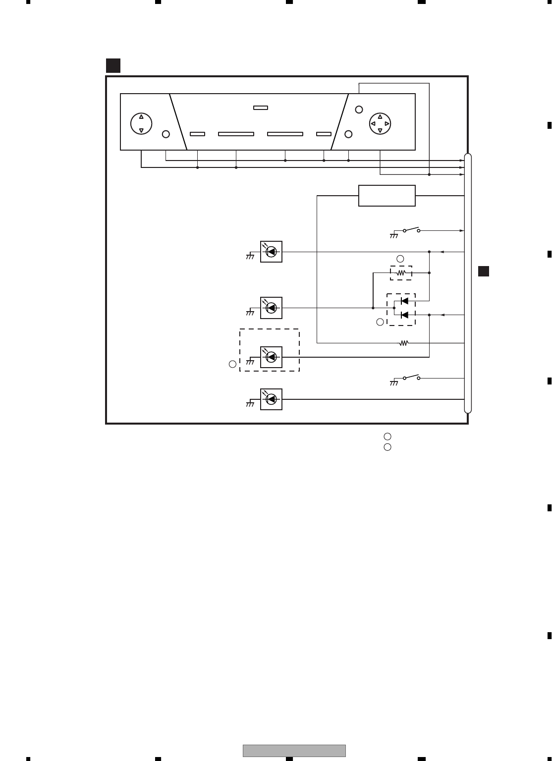
UPPER PCB
H
IC4311
NJM062V
LCD
LCD
BACK LIGHT
LCD MODULE
AVH-P5700DVD/EW
34
1234
1234
C
D
F
A
B
E
40
39
33
38
37
32
28
31
30
29
27
22
26
24
23
21
2
20
17
16
14
15
13
11
10
9
8
7
6
5
4
3
CN954
CN981
CCR
CCG
HSEN
OPT OUT
OPT5
2
1
OPT5
4
CCB
CCSYNC
GNDSIG
DVDVBS
GNDDVD
YS
CCAUL
CCAUR
GNDAU
ONSEI+
ONSEI−
GNDRAU
CCREM
DSEN
TVON
GION
HTXD
HRXD
GNDD
GNDD
GNDD
GNDD
GNDD
GNDD
GNDD
GNDD
OPTICAL OUT
IC981
TC7SET08FUS1
(2/2)CN151
DIGITAL
OUTPUT
A
INA
INB
OUTY
RGB UNIT
G
1
2
6
3
4
5
7
12
8
10
11
13
19
14
17
18
20
26
21
24
25
CN951
1
2
3
CN952
CCR
CCG
CCB
CCSYNC
GNDSIG
DVDVBS
GNDDVD
YS
CCAUL
CCAUR
GNDAU
ONSEI+
ONSEI−
GNDRAU
CCREM
DSEN
TVON
GION
HTXD
HRXD
GNDD
TO
NAVI
NAVI
RGB SHIELD
CN3802
MO1
MOB
1
2
CN3809
CN3843
CN3842
CN3841
CN3833
CN3831
CN3832
ANGLV
ANGLIN0
1
2
ANGLG
3
IC 3802
BA6247FP
Q3804
VR3841
CN3801
5
MTR2
4
MTRPW
3
MTRS
11
VDD
18
19
20
VBU
10
SNSPW
2
LIFTPUL
1
ANGLEIN
9
8
6
MTR1
REGULATOR FOR DRIVER
MOTOR DRIVER
41
1
18
22
16
14
6
5
IC 3801
BA00AST
Q3801
CN3803
MO2
MOB
2
1
M
M
POSITION
MOTOR
ANGLE
MOTOR
13
IC 3803
TA78L05F
Q3802
Q3803
13
IC 3805
GP2L24B
24
IC 3804
TC7S14FU
CN3807
LIFT
ANGLE0
1
3
GNDSNS
2
VOLUME UNIT
SW UNIT
S3832
LIFTSW
S3831
ANGLE0SW
ANGL0SW
PUSHSW
MAIN UNIT
J
L
K
(2/2)CN175
A
AVH-P5700DVD/EW
A
AVH-P5700DVD/UC
B
AVH-P5700DVD/EW 35
5678
5678
C
D
F
A
B
E
CN5501
KEY0
KEY1
KEY2
SWVDD
DSENS
ILMG
ILMA
REM
3
S5517
DSENS
D5510,D5512,D5514
D5516,D5518,D5520
D5522,D5524,D5526
1
13
12
11
10
8
9
1
7
6
2
KEYBOARD UNIT
I
S5504
S5505
VOL S5506
EJECT S5510
BOOK.M
S5515
A.MENU
S5501
SOURCE
S5512
S5513
S5514 S5511
SLOT ILM
S5507 S5508
BOOST
ATT EQ
S5509
BAND
S5503 S5502
ANGLE
−+
IC5501
TSOP4840SB1
RESET
DFLED
S5516
RESET
A
A
D5511,D5513,D5515
D5517,D5519,D5521
D5523,D5525,D5527
D5528
D5502-D5508
(2/2)CN101
A
AVH-P5700DVD/EW
A
AVH-P5700DVD/UC
B
B
AVH-P5700DVD/EW
36
1234
1234
C
D
F
A
B
E
26
24
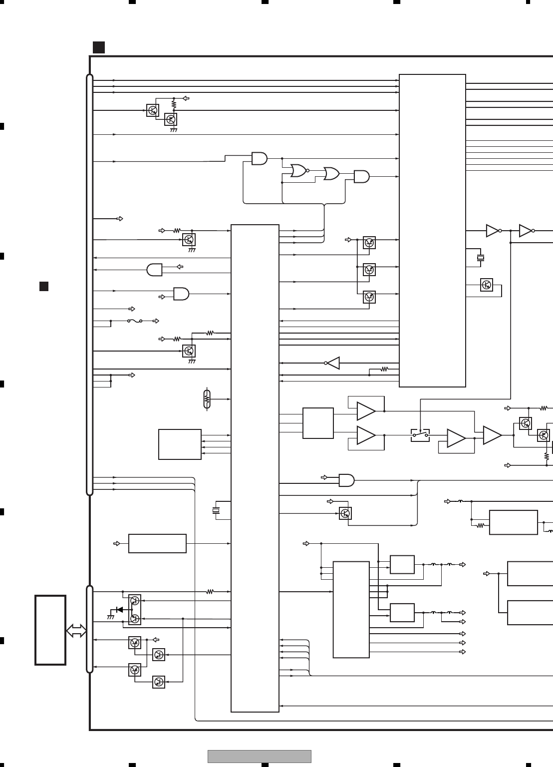
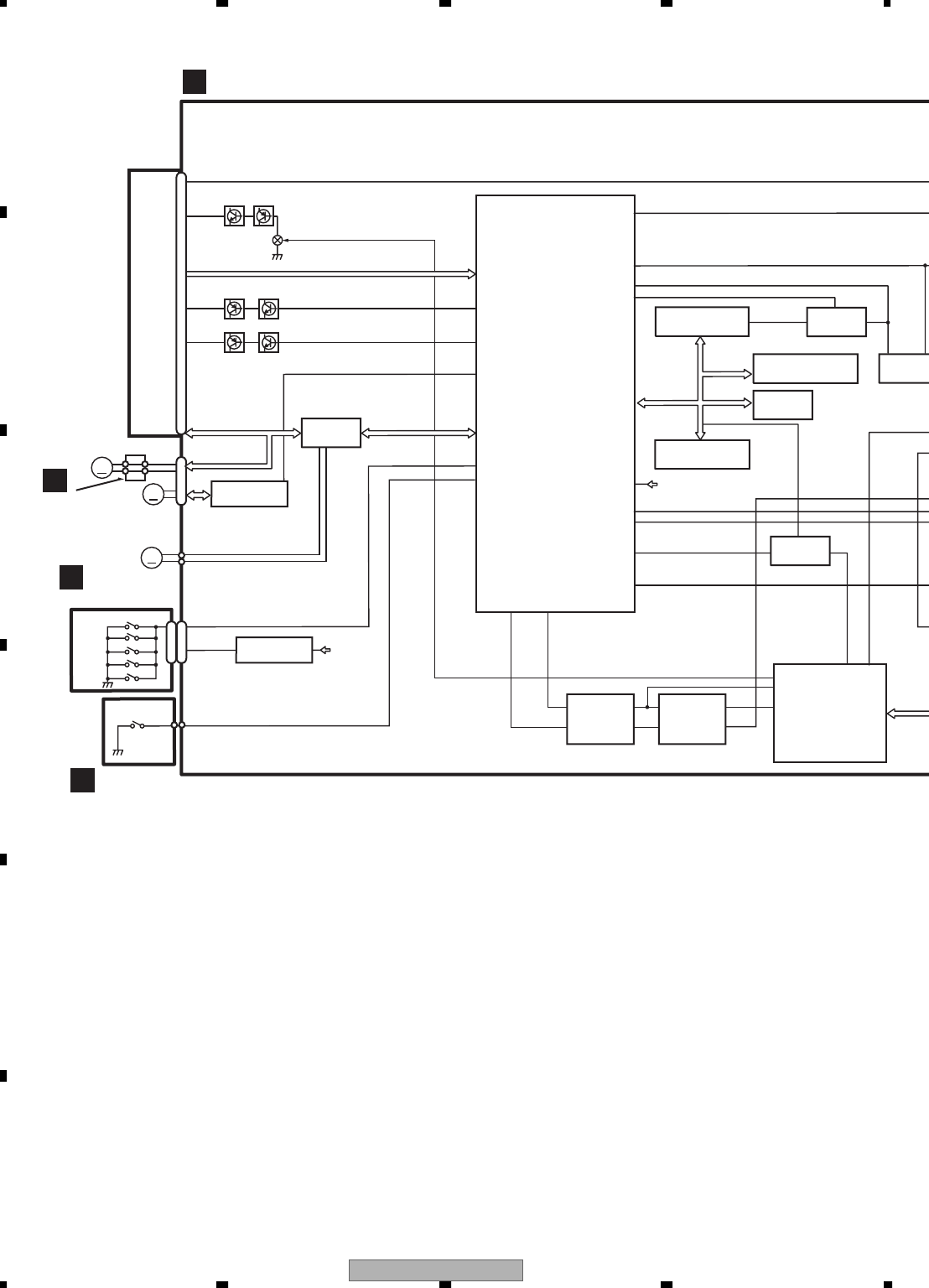
DVD CORE UNIT
Q1101 Q1106
Q1102
Q1104
Q1103
Q1105
Q1107
65LD
78LD
133
135
VSHF
CN1101
CN1201
CN1231
IC 1201
AN8471SAT1
IC1231
TC7SZ125FU
CPU
IC1501
MN35104UB
62,66
148
174
LRCK 175
SRCK
163
163
DAC4OUT
BECLK
AD1
76 DRY6
DSCSNS
CLNP
181
IECOUT
47
XCSSR 33
XCSFM
68
NRST
39 1
EXADR18
IC1251
BA5985FM
IC1601
PD6516A
IC1672
TC7SZ08FU
IC1652
TC7SZ126
F
IC1671
TC74LCX16373AFT
IC1651
M5M5V216ATP-70HI
IC1602
TC7SH86FU
IC1570
K4S283232E-TC75
23
9
18
PICKUP UNIT(SERVICE)
A,B1-4,C,RF+,RF-
M
SPINDLE
MOTOR
M
CARRIGE
MOTOR
M
LOADING
MOTOR
FOP,FOM,TOP,TOM
COP,COM
DRIVER
9
LOM
10
LOP
10
14
IC1051
PE5401A
VCC15
C
FD,TD,MD,CRGDRV
FG
LPCO2
LPCO1
AMU
T
S1206
S1202
S1203
S1204
S1201
S1205
CLAMP SW
12cm
8cm
8cm
Disc sens
Disc sens
COMPOUND UNIT(B)
E
COMPOUND UNIT(A)
D
RELAY PCB
M
A0-20,
ADT0-15
A20
CD/DVD
39 REV
21
XRES_M
25
2
4
25,48 4 1
2
2
VDD33
FSSW2
42
FSSW1
43
6
5
1143
92
OSCI
213
15 IC1802
TC7WH157FU
IC1801
SM8707LV
ELERGENCY LOAD
SDRAM
SDRAM
LATCH
CLOCK GENERATOR
FLASH MEMORY
AVH-P5700DVD/EW 37
5678
5678
C
D
F
A
B
E
37
39
1
10
3,5
8
3
7
1,2
3
5
6
1
5
2
1
2
1,2
1
3
16
IECOUT
Lch OUT
IC1851
PCM1742KE
IC1852
NJM2140R
VIDEO OUT
25
VCONTA
CN1551
CN1901
6
72
Z
08FU
IC1652
TC7SZ126FU
0HI
5
1
1A
21
VDD33
VCC15
(2/2)CN181
A
(2/2)CN152
A
IC1853
NJM2100V
AMUTE,XRES_S,IRQPWR,STSCOMN,CMDCOMN
1
CN1903
Q1551
R
EV
21
XRES_M
25
1
2
21
23
VCONTB
10
VD
6,7
11
12
VD
Q1002
IC1003
LTC3411EMS
IC1001
S-L2980A50MC-C7J
IC1002
R1130H501B
XRES_M 9
DC-DC CONVERTER
ADAC
S
H MEMORY


AVH-P5700DVD/EW
40
1234
1234
C
D
F
A
B
E
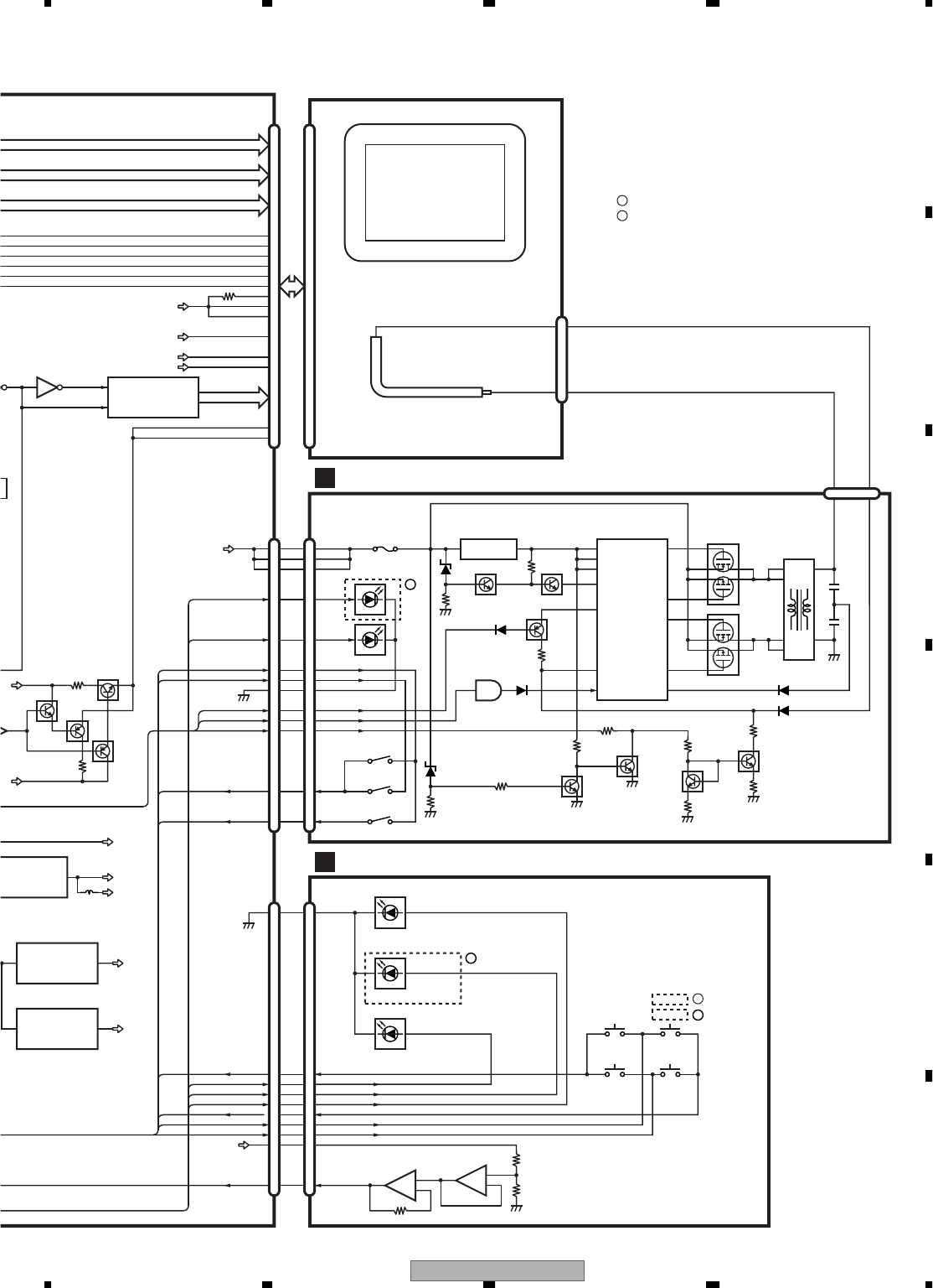
3.3 MOTHER UNIT(SYSTEM)(GUIDE PAGE)
1/2
A
A-a 1/2
A-a A-b
A-a A-b
A-b
A-a
Large size
SCH diagram
Guide page
Detailed page
Note: When ordering service parts, be sure to refer to " EXPLODED VIEWS AND PARTS LIST" or
"ELECTRICAL PARTS LIST".
>
>
>
2/2
A
?
GCN954
ICN5501
BCN4541
REAR VIDEO
ISOLATOR
VIDEO FILTER
TVW
ISOLATOR
AUDIO
ISOLATOR
VIDEO ISOLATOR
AUDIO
ISOLATOR
VIDEO
ISOLATOR
VIDEO
ISOLATOR
VIDEO
ISOLATOR
IP-BUS
DRIVER
RGB VIDEO
ISOLATOR
5V
5.0V
EW
CN1901
2/2
C
CN1551
1/2
C
1
2
3
5
8
9
10
11
6
7
1234
5
8 9 10 11
67
GCN952
DVD/CD:+2.6dBs
NAVI:+2.2dBs
VCR(UC):+8.2dBs
IP-BUS:+2.2dBs
FM(100%):-20.0dBs
AM(30%):-30.0dBs
FM(100%):-16.0dBs
AM(30%):-26.0dBs
NAVI:+2.2dBs
VCR:+8.2dBs
VCR:+4.3dBs
NAVI:+4.3dBs
UC
EW
AVH-P5700DVD/EW 41
5678
5678
C
D
F
A
B
E
1/2
A
A-b 1/2
A-a A-b
A-a A-b
A-b
A-a
PAL007B
: The power supply is shown with the marked box.
>>
>
>
>
>
Decimal points for resistor
and capacitor fixed values
are expressed as :
2.2 2R2
0.022 R022
←
←
The > mark found on some component parts indicates
the importance of the safety factor of the part.
Therefore, when replacing, be sure to use parts of
identical designation.
Symbol indicates a resistor.
No differentiation is made between chip resistors and
discrete resistors.
NOTE :
Symbol indicates a capacitor.
No differentiation is made between chip capacitors and
discrete capacitors.
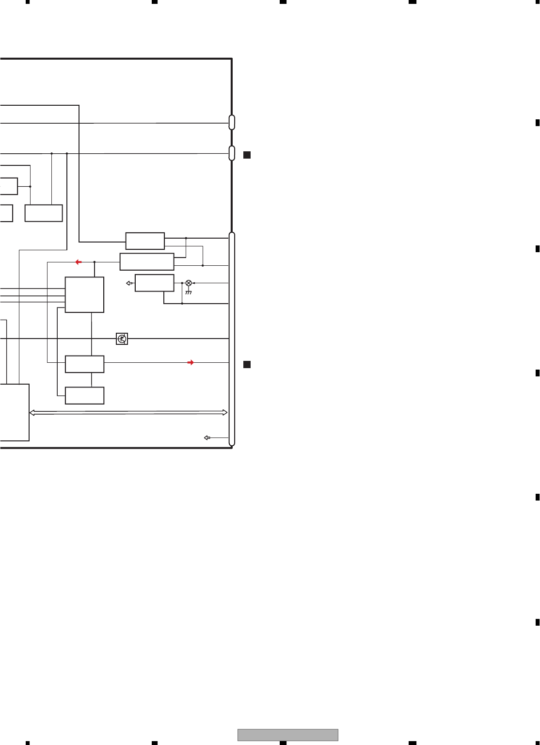
MOTHER UNIT (SYSTEM)
1/2
A
41
E-VOL
RGB VIDEO
ISOLATOR
POWER AMP
8.4V
8.4V
EW
UC
UC
EW
EW
EW
EW
JCN3801
IP-BUS:+9.3dBs
VCR:+9.3dBs
NAVI:+9.3dBs
DVD/CD:+9.7dBs
IP-BUS:+8.54dBs
VCR:+8.54dBs
NAVI:+8.54dBs
DVD/CD:+8.94dBs
IP-BUS:+35.3dBs
VCR:+35.3dBs
NAVI:+35.3dBs
DVD/CD:+35.7dBs
FM:+5.1dBs
AM: -4.9dBs
FM:+7.1dBs
AM: -0.9dBs
(UC)
(EW)
FM:+4.34dBs
AM: -5.66dBs
FM:+6.34dBs
AM: -1.66dBs
(UC)
(EW)
FM:+31.1dBs
AM:+21.1dBs
FM:+33.1dBs
AM:+25.1dBs
(UC)
(EW)
VCR IN:+8.2dBs(EW)
VIDEO OUTPUT
FL OUTPUT
FR OUTPUT
SUBWOOFER
L OUTPUT
SUBWOOFER
R OUTPUT
L INPUT(EW)
RL OUTPUT(UC)
FR INPUT(EW)
RR OUTPUT(UC)
SYSTEM CONTROLLER
>
CEK1136
10A
1K(1/2W)
UC
RR
+
RR
-
FR
+
FR
-
FL
+
FL
-
RL
+
RL
-
ACC
GND
BACK
UP
B.
REM
EW


AVH-P5700DVD/EW
44
1234
1234
C
D
F
A
B
E
A-a A-b
A-b
1/2
12
PAL007B
>>
>
Decimal points for resistor
and capacitor fixed values
are expressed as :
2.2 2R2
0.022 R022
←
←
Symbol indicates a resistor.
No differentiation is made between chip resistors and
discrete resistors.
NOTE :
Symbol indicates a capacitor.
No differentiation is made between chip capacitors and
discrete capacitors.
MOTHER UNIT (SYSTEM)
1/2
A
E-VOL
POWER AMP
8.4V
8.4V
EW
UC
UC
J
CN3801
IP-BUS:+9.3dBs
VCR:+9.3dBs
NAVI:+9.3dBs
DVD/CD:+9 7dBs
IP-BUS:+8.54dBs
VCR:+8.54dBs
NAVI:+8.54dBs
DVD/CD:+8.94dBs
FM:+5.1dBs
AM: -4.9dBs
FM:+7.1dBs
AM: -0.9dBs
(UC)
(EW)
FM:+4.34dBs
AM: -5.66dBs
FM:+6.34dBs
AM: -1.66dBs
(UC)
(EW)
FM:+31.1dBs(UC)
VCR IN:+8.2dBs(EW)
VIDEO OUTPUT
FL OUTPUT
FR OUTPUT
SUBWOOFER
L OUTPUT
SUBWOOFER
R OUTPUT
L INPUT(EW)
RL OUTPUT(UC)
FR INPUT(EW)
RR OUTPUT(UC)
AVH-P5700DVD/EW 45
5678
5678
C
D
F
A
B
E
A-a A-b
A-b
1/2
3
: The power supply is shown with the marked box.
>
>
>
The > mark found on some component parts indicates
the importance of the safety factor of the part.
Therefore, when replacing, be sure to use parts of
identical designation.
EW
EW
EW
IP-BUS:+9.3dBs
VCR:+9.3dBs
NAVI:+9.3dBs
DVD/CD:+9.7dBs
IP-BUS:+35.3dBs
VCR:+35.3dBs
NAVI:+35.3dBs
DVD/CD:+35.7dBs
FM:+5.1dBs
AM: -4.9dBs
FM:+7.1dBs
AM: -0.9dBs
(UC)
(EW)
FM:+31.1dBs
AM:+21.1dBs
FM:+33.1dBs
AM:+25.1dBs
(UC)
(EW)
SYSTEM CONTROLLER
>
CEK1136
10A
1K(1/2W)
UC
RR
+
RR
-
FR
+
FR
-
FL
+
FL
-
RL
+
RL
-
ACC
GND
BACK
UP
B.
REM
EW


AVH-P5700DVD/EW
62
1234
1234
C
D
F
A
B
E
1ANAMONI1 0.2V/div. 0.1µs/div.
0.2V/div. 100µs/div.
0.2V/div. 0.1µs/div.
CDRF
Interval
1ANAMONI1 0.5V/div. 100µs/div.
1ANAMONI1
DVDRF DVDRF(BD1mm)
2TD1 0.5V/div. 100µs/div.
Interval FWD
2TD1 0.5V/div. 100µs/div.
Interval REV
2TD1
2CH1: TD1
3CH2: COP1-COM1 2.0V/div.5ms/div.
Traverse501FWD
0.5V/div.5ms/div. 2CH1: TD1
3CH2: COP1-COM1 2.0V/div.5ms/div.
Traverse501REV
0.5V/div.5ms/div. 2CH1: TD1
3CH2: COP1-COM1 2.0V/div.5ms/div.
Traverse5000FWD
0.5V/div.5ms/div.
-Waveforms Note:1. The encircled number denote measuring pointes in the circuit diagram.
2. Reference voltage VHALF : 1.65V(TD1,FD1,CRGDRV)
: 2V Center(ANAMONI1)
In this waveform, it is seeing on the GND standard.
Offset of 1.65V or 2V is put in.
VHALF→
VHALF→VHALF→
VHALF→
VHALF→VHALF→
VHALF→
VHALF→
VHALF→
VHALF→
VHALF→
VHALF→

AVH-P5700DVD/EW 63
5678
5678
C
D
F
A
B
E
2TD1
Play TD 5FD1 0.5V/div. 1ms/div.
Focus close
VHALF→VHALF→VHALF→
VHALF→
VHALF→
VHALF→
VHALF→
VHALF→
VHALF→
VHALF→
0.5V/div. 100µs/div.
ID search Insaide → Outside
4CRGPRV
2CH1: TD1
3CH2: COP1-COM1 2.0V/div.5ms/div.
Traverse5000REV
0.5V/div.5ms/div.
0.5V/div.20ms/div.
5FD1
Focus jamp L 0 → L1
0.5V/div.500µs/div.
2TD1
Multi 32REV
0.5V/div.500µs/div.
2TD1
Multi 32FWD
0.5V/div.500µs/div.
5FD1
Focus jamp L1 → L 0
0.5V/div.500µs/div. 5FD1
Play TD
0.5V/div.20ms/div.
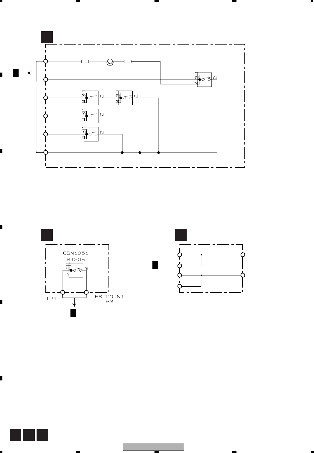
AVH-P5700DVD/EW
64
1234
1234
C
D
F
A
B
E
3.8 COMPOUND UNIT(A), COMPOUND UNIT(B) AND RELAY PCB
D E M
ECOMPOUND UNIT(B) MRELAY PCB
DCOMPOUND UNIT(A)
CLAMP
C1/2
C1/2
S1201
Q1299
S1202 S1204
S1203
R1298
0R0
1
2
3
4
5
6
S1205
R1299
0R0
CPT231SCTD
CSN1069
CSN1069
CSN1069
CSN1070
CSN1070
12cm
8cm
DISC SENS DISC SENS
8cm
CN1231
CN1201
M2
CARRIAGE MOTOR
CXC4314
C1/2
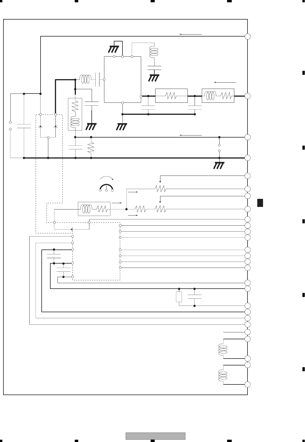
AVH-P5700DVD/EW 65
5678
5678
C
D
F
A
B
E
3.9 PU UNIT(REFERENCE)
24
Iop78
L2
LC
Vcc
GND
GND
IC1
L4
C2C3
C6
C7
L3
1715
C1
16
65LD78LD
LDGND
R1C5
Short round
Short round
L1 C4
78LD
65LD
65MD
65MDGVR2/ 65Rmd
VR1/ 78RmdVmda
1
2
3
4
6
5
7
R2
L6
MDA
Top View
up
MDA
A
SW
Vcc
C8
C9
12
GND
13
V r
14
MDC
98
78MD
78MDG
MDG
B1
B1
B2
RF-
B3
RF+
B4
C
Vref : 2.5V
GND
C10TH1
TEMP
Vcc
SW
A
NC
T-
T+
F-
F+
B2
RF-
B3
RF+
B4
C
LDGND
23
26
25
07
08
05
06
22
21
20
19
18
17
27
02
01
03
04
09
16
15
14
13
12
11
10
Iop65
Im/ 2
Im
Im/ 2
Ishf
Vshf : 4V
CN1101
C1/2


AVH-P5700DVD/EW
74
1234
1234
C
D
F
A
B
E
3.14 MAIN UNIT, SW UNIT AND VOLUME UNIT
J K L
JMAIN UNIT
L
VOLUME
UNIT
K
SW UNIT
CN175
1/2
A
(High speed:L,
Low speed:H)
Short round
(Open)
Photo pulse output
Photo pulse driver
5V regulator for sense
Angle sense volume power supply switch
Position motor
Angle motor
Regulator output
Voltage adj. input
Regulator for driver
Position motor
Position motor:H
Angle motor
Angle motor:H
Motor driver
Angle operation
Horizon operation
Note:It comes out lower about 1.5v than Vcc.
Position motor
Angle motor
LIFT SW ANGLE SW
CXB9515
CXB9516
Angle sense
(Deg.0:L)
(EJECT:L)
(Deg.0:L)
(EJECT:L)
3
6
2
5
1
8
7
4
M3001
M3002
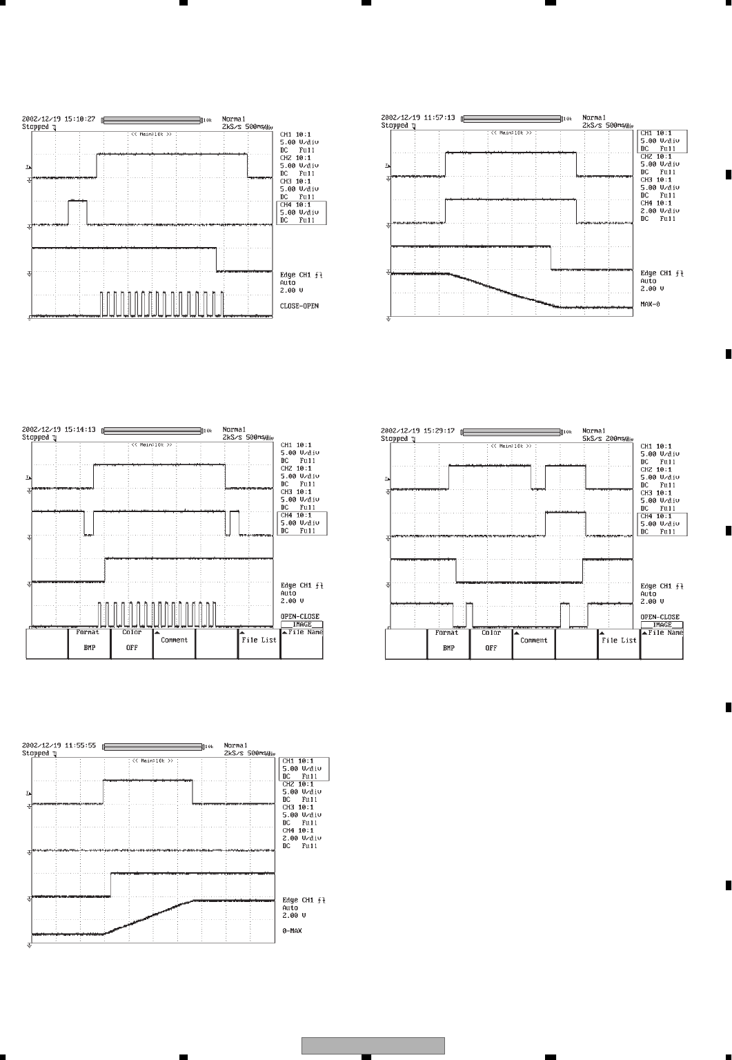
AVH-P5700DVD/EW 75
5678
5678
C
D
F
A
B
E
- Waveforms The encircled number denote measuring pointes in the circuit diagram.
• CLOSE -> OPEN
• OPEN -> CLOSE
5 CH1:MTR1
6 CH3:ANGLSW
• 0->MAX
2 CH2:MTRSEL
7 CH4:ANGLIN
• MAX -> Deg.0 DOWN
1 CH1:MTR2
3 CH3:LIFTSW
2 CH2:MTRSEL
4 CH4:LFTPLS
1 CH1:MTR2
3 CH3:LIFTSW
2 CH2:MTRSEL
4 CH4:LFTPLS
5 CH1:MTR1
6 CH3:ANGLSW
2 CH2:MTRSEL
7 CH4:ANGLIN
• Set back open -> Set
1 CH1:MTR2
3 CH3:LIFTSW
8 CH2:MTRS
4 CH4:LFTPLS
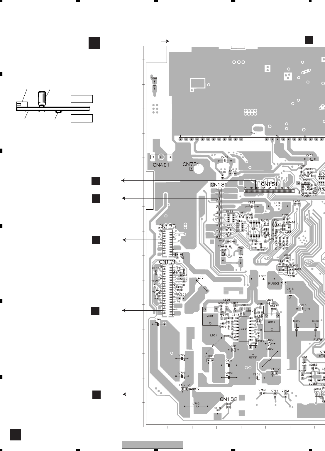
AVH-P5700DVD/EW
76
1234
1234
C
D
F
A
B
E
4. PCB CONNECTION DIAGRAM
4.1 MOTHER UNIT
Capacitor
Connector
P.C.Board Chip Part
A
AMOTHER UNIT
SIDE B
SIDE A
NOTE FOR PCB DIAGRAMS
1.The parts mounted on this PCB
include all necessary parts for
several destination.
For further information for
respective destinations, be sure
to check with the schematic dia-
gram.
2.Viewpoint of PCB diagrams
10 20 30 40 50 60 70
X
10
20
30
40
50
60
70
80
90
100
110
120
130
0
Y
140
150
F
CN954
BCN4541
CCN1551
CCN1901
ANTENNA CABLE
JCN3801
FM/AM TUNER UNIT
G
CN
9
G


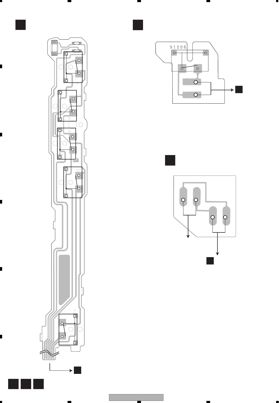
AVH-P5700DVD/EW
88
1234
1234
C
D
F
A
B
E
4.4 COMPOUND UNIT(A), COMPOUND UNIT(B) AND RELAY PCB
D E M
E
D
C
C
CLAMP
M2
12cm
S1201
R1298
R1299
Q1299
CN1231
CCN1201
16
DISC SENS
S1204
DISC SENS
S1203
8cm
S1202
8cm
S1205
M
COMPOUND UNIT(B)
RELAY PCB
COMPOUND UNIT(A)
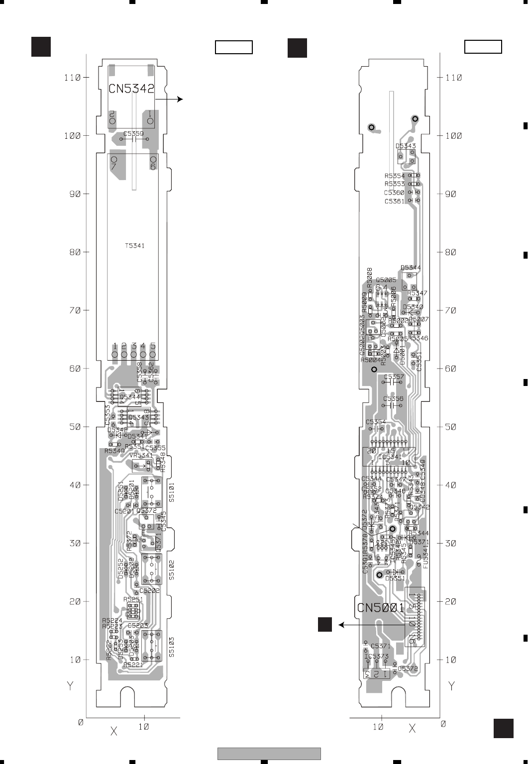
AVH-P5700DVD/EW 89
5678
5678
C
D
F
A
B
E
4.5 INVERTER PCB
F
FINVERTER PCB FINVERTER PCB
SIDE A SIDE B
B
CN4521
LCD MODULE
FL1
FL2
GNDF2
INVPUL
DIMDTY
ENTWIDEV.ADJ
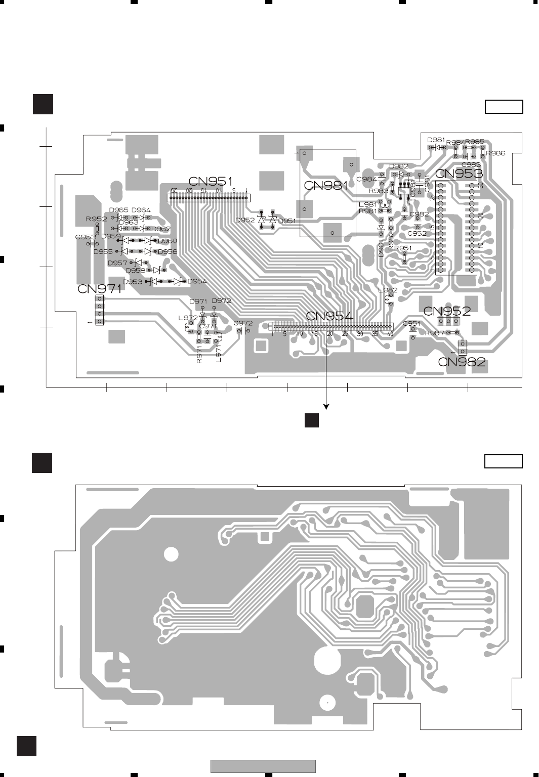
AVH-P5700DVD/EW
90
1234
1234
C
D
F
A
B
E
4.6 RGB UNIT
G
GRGB UNIT SIDE A
SIDE B
GRGB UNIT
010 20 30 40 50 60 70
10
20
30
40
Y
X
ACN151
DIGITAL OUTPUT
RGB INPUT
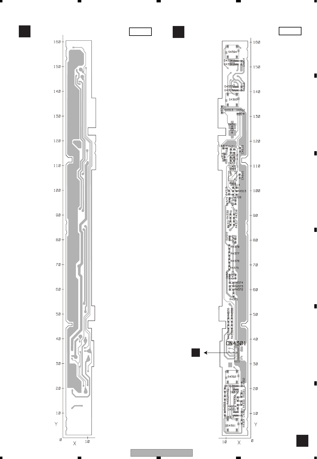
AVH-P5700DVD/EW 91
5678
5678
C
D
F
A
B
E
4.7 UPPER PCB
H
HUPPER PCB HUPPER PCB
SIDE A SIDE B
B
CN4591
INFO TA/NEWS(EW)
PGM(UC) OPEN/CLOSEFLIP DOWN

AVH-P5700DVD/EW
92
1234
1234
C
D
F
A
B
E
4.8 KEYBOARD UNIT
I
IKEYBOARD UNIT IKEYBOARD UNIT
SIDE A SIDE B
10 20 30 40 50 60 70 80 90 100 110 120 130 140 150
X
10
20
0
Y
160
1020304050607080
90100110120130140150
X
10
20
0
Y
160
A
CN101
VOL+
SRCEJECTVOL- ANGLE- ATTANGLE+ EQ BOOK.MBAND DOWN
RESET
A.MENU
UP
DSENSE
RIGHT
LEFT

AVH-P5700DVD/EW 93
5678
5678
C
D
F
A
B
E
4.9 SW UNIT AND VOLUME UNIT
VOLUME UNIT
L
SW UNIT
K
L
K
ANGLE SW
LIFT SW
ANGLE SENSE
JCN3807
JCN3809
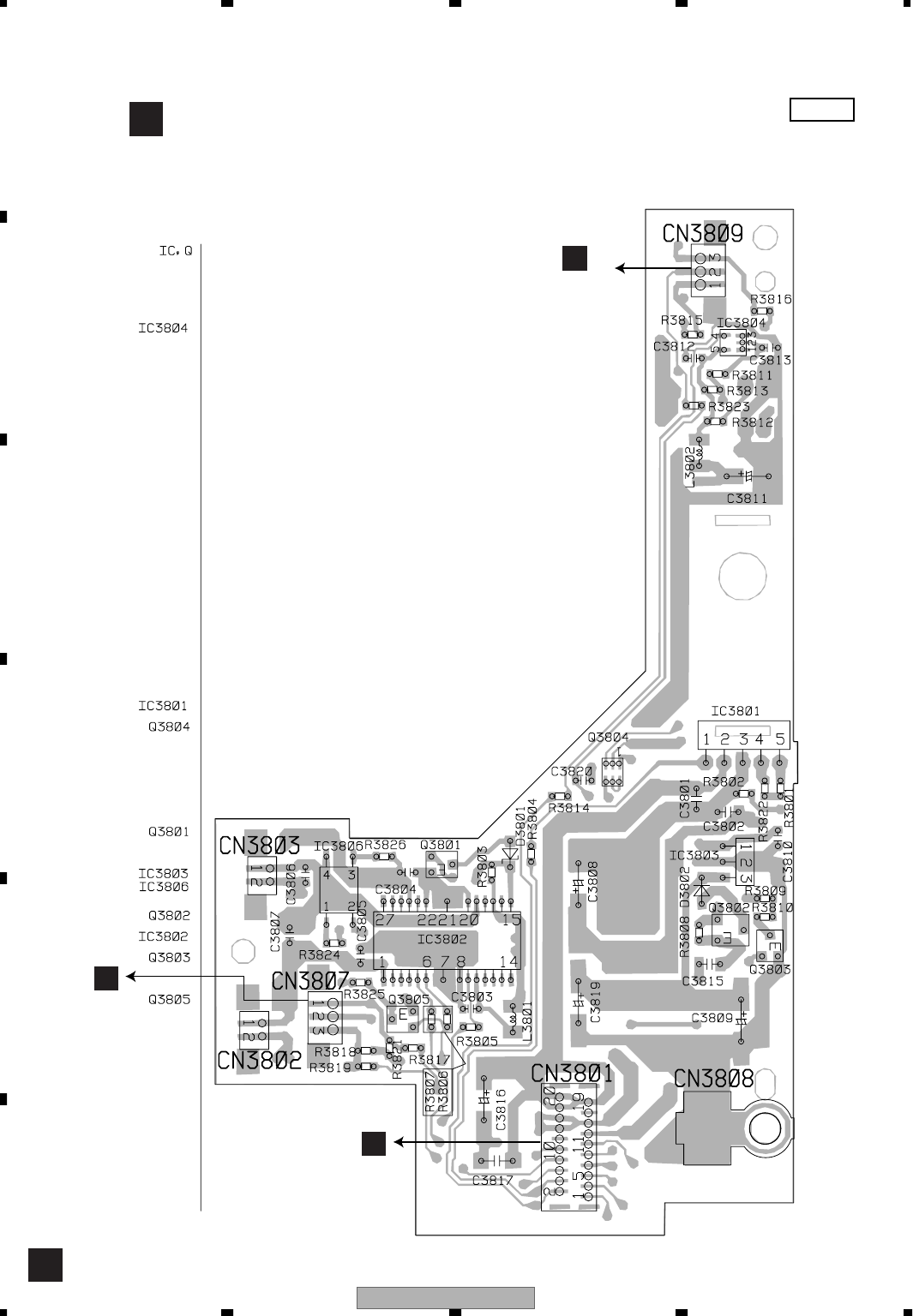
AVH-P5700DVD/EW
94
1234
1234
C
D
F
A
B
E
4.10 MAIN UNIT
J
J
MAIN UNIT SIDE A
L
CN3841
CN3842
CN3843
A
CN175
K
CN3831
CN3832
CN3833
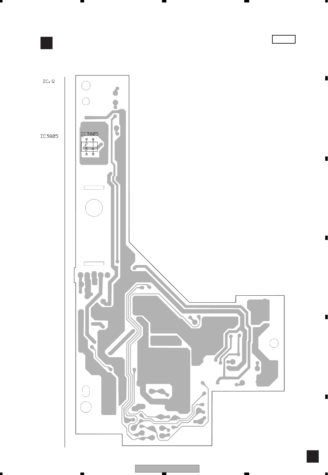
AVH-P5700DVD/EW 95
5678
5678
C
D
F
A
B
E
J
J
MAIN UNIT SIDE B

AVH-P5700DVD/EW
96
1234
1234
C
D
F
A
B
E
5. ELECTRICAL PARTS LIST
NOTE:
• Parts whose parts numbers are omitted are subject to being not supplied.
• The part numbers shown below indicate chip components.
Chip Resistor
RS1/_S___J,RS1/__S___J
Chip Capacitor (except for CQS.....)
CKS....., CCS....., CSZS.....
• The > mark found on some component parts indicatesthe importance of the safety factor of the part.
Therefore, when replacing, be sure to use parts of identical designation.
• Meaning of the figures and others in the parentheses in the parts list.
Example) IC 301 is on the point (face A, 91 of x-axis, and 111 of y-axis) of the corresponding
PC board.
IC 301 (A, 91, 111) IC NJM2068V
Circuit Symbol and No. Part No.
AVH-P5700DVD/EW
Mother Unit : CWM9808
RGB Unit : CWM9815
Monitor Unit : CWM9820
Monitor PCB : NSP
Inverter PCB : NSP
Upper PCB : NSP
Keyboard Unit : NSP
DVD Core Unit : CWX3170
Compound Unit(A) : CWX3154
Compound Unit(B) : CWX3156
Main Unit : CZW3087
SW Unit : CZW3088
Volume Unit : CZW3089
AVH-P5700DVD/UC
Mother Unit : CWM9809
RGB Unit : CWM9816
Monitor Unit : CWM9821
Monitor PCB : NSP
Inverter PCB : NSP
Upper PCB : NSP
Keyboard Unit : NSP
DVD Core Unit : CWX3170
Compound Unit(A) : CWX3154
Compound Unit(B) : CWX3156
Main Unit : CZW3087
SW Unit : CZW3088
Volume Unit : CZW3089
A
Unit Number:CWM9809(UC)
Unit Number:CWM9808(EW)
Unit Name:Mother Unit
MISCELLANEOUS
IC 121 (B,115,96) IC HA12240FP
IC 151 (B,42,94) IC TC4S81F
IC 181 (A,46,81) IC TC74VHC08FTS1
IC 182 (A,50,82) IC TC7SET08FUS1
IC 201 (B,145,63) IC PML009A
IC 241 (A,155,128) IC PAL007B
IC 301 (B,127,91) IC NJM4558V
IC 302 (B,138,84) IC NJM4558V
IC 303 (B,136,97) IC NJM4580V
IC 421 (B,126,51) IC NJM4558MD
IC 441 (A,147,46) IC TA2050F
IC 451 (A,132,46) IC TA2050F
IC 461 (B,59,86) IC NJM2138V
IC 501 (B,145,14) IC CXA2089Q
IC 521 (A,162,17) IC NJM2136V
IC 522 (A,160,29) IC BA7623F
IC 541 (B,36,72) IC SM5304AV
IC 551 (B,127,17) IC NJM2136V
IC 561 (B,124,31) IC NJM2136V
IC 571 (B,135,31) IC NJM2136V
IC 581 (B,146,31) IC NJM2136V
IC 601 (B,87,81) IC (UC) PE5485A
(B,87,81) IC (EW) PE5484A
IC 681 (B,94,43) IC S-80841CNUA-B82
IC 801 (A,41,40) IC AN8011S
IC 831 (B,19,92) IC BA00BC0WFP
IC 841 (B,112,24) IC S-812C50AUA-C3E
IC 851 (A,70,21) IC S-818A35AUC-BGP
IC 856 (A,57,64) IC S-814A33AMC-BCX
IC 871 (A,168,100) IC NJM2388F84
IC 881 (B,25,146) IC NJM2391DL1-33
Q 101 (B,97,29) Transistor UMF23N
Q 121 (B,123,107) Transistor UMF23N
Q 131 (A,83,109) Transistor 2SC4081
Q 151 (B,49,102) Transistor 2SC4081
Q 181 (B,47,76) Transistor IMD2A
Q 182 (B,47,73) Transistor IMX9
Q 241 (B,146,88) Transistor DTC124EU
Q 242 (B,146,93) Transistor DTC144EU
Circuit Symbol and No. Part No.

AVH-P5700DVD/EW 97
5678
5678
C
D
F
A
B
E
Q 243 (B,150,84) Transistor IMD2A
Q 244 (A,147,84) Transistor 2SC4081
Q 245 (B,152,77) Transistor IMD2A
Q 261 (A,116,106) Transistor IMX9
Q 262 (A,109,106) Transistor IMX9
Q 281 (A,102,106) Transistor (UC) IMX9
Q 301 (B,133,83) Transistor IMD2A
Q 302 (B,132,86) Transistor DTC323TU
Q 303 (B,126,81) Transistor DTC124EU
Q 401 (B,73,110) Transistor (EW) IMH2A
Q 402 (B,72,106) Transistor (EW) IMH2A
Q 461 (A,59,82) Transistor 2SC4081
Q 511 (A,135,5) Transistor 2SC4081
Q 512 (A,125,8) Transistor 2SA1577
Q 521 (B,161,19) Transistor 2SC4081
Q 551 (A,125,14) Transistor 2SC4081
Q 561 (A,124,28) Transistor 2SC4081
Q 571 (A,134,28) Transistor 2SC4081
Q 581 (A,145,28) Transistor 2SC4081
Q 601 (B,104,83) Transistor DTC124EU
Q 691 (A,107,55) Transistor DTA114EU
Q 692 (A,112,52) Transistor DTC144EU
Q 693 (A,112,55) Transistor DTC114EU
Q 694 (B,109,49) Transistor 2SC4081
Q 695 (B,112,49) Transistor 2SC4081
Q 696 (B,106,50) Transistor 2SC4081
Q 701 (B,12,19) Transistor 2SA1615-Z
Q 702 (B,9,29) Transistor DTC114EU
Q 703 (A,142,104) Transistor 2SA1576
Q 704 (A,138,105) Transistor 2SC4081
Q 705 (A,133,102) Transistor IMX1
Q 706 (A,142,109) Transistor 2SA1576
Q 751 (B,50,11) Transistor 2SA1577
Q 752 (B,50,9) Transistor DTC144EU
Q 753 (B,58,11) Transistor (EW) 2SA1577
Q 754 (B,58,9) Transistor (EW) DTC144EU
Q 755 (B,44,11) Transistor 2SA1577
Q 756 (B,44,9) Transistor DTC144EU
Q 771 (B,72,146) Transistor 2SD1760F5
Q 772 (B,67,139) Transistor DTC144EU
Q 773 (B,61,148) Transistor UMF5N
Q 774 (B,62,141) Transistor DTC144EU
Q 781 (B,67,45) Transistor 2SD1760F5
Q 782 (B,73,46) Transistor UMF5N
Q 783 (B,72,37) Transistor DTC114EU
Q 801 (A,27,44) Transistor 2SJ529S
Q 802 (A,53,41) Transistor 2SJ529S
Q 803 (A,33,43) Transistor 2SC4097
Q 804 (A,48,48) Transistor 2SC4097
Q 805 (B,44,37) Transistor DTC124EU
Q 806 (B,51,39) Transistor DTC114EU
Q 841 (B,108,34) Transistor 2SB1184F5
Q 842 (A,156,56) Transistor 2SD1767
Q 861 (A,72,14) Transistor UMF5N
Q 864 (A,66,98) Transistor UMF5N
Q 867 (A,99,25) Transistor UMF5N
Q 891 (B,163,80) Transistor 2SD1767
Q 892 (A,167,115) Transistor 2SD2396
Q 893 (B,155,107) Transistor IMD2A
D 101 (A,98,22) Diode UDZS5R6(B)
Circuit Symbol and No. Part No.
D 107 (B,94,26) Diode UDZS5R6(B)
D 151 (B,46,93) Diode Network DA204U
D 152 (B,42,97) Diode Network DA204U
D 241 (B,144,85) Diode DAN202U
D 242 (B,156,79) Diode RSX201L-30
D 243 (B,144,82) Diode DAN202U
D 244 (A,146,89) Diode 1SS355
D 245 (A,159,71) Diode UDZS8R2(B)
D 246 (B,149,81) Diode DAN202U
D 421 (B,123,57) Diode UDZS3R9(B)
D 681 (B,100,44) Diode 1SS355
D 691 (B,109,53) Diode 1SS355
D 692 (B,113,53) Diode 1SS355
D 701 (B,130,152) Diode S1G-6904G2P
D 702 (B,124,152) Diode S1G-6904G2P
D 703 (A,139,102) Diode DAN202U
D 704 (B,132,108) Diode UDZS6R8(B)
D 705 (A,136,108) Diode HZU7L(A1)
D 706 (B,126,111) Diode HZU7L(C3)
D 707 (B,139,105) Diode DAN202U
D 708 (A,103,138) Diode 5KP24A
D 771 (B,70,141) Diode HZU9R1(B2)
D 772 (B,65,142) Diode HZU6R8(B3)
D 773 (B,62,145) Diode HZU8R2(B2)
D 781 (B,73,42) Diode HZU7R5(B2)
D 782 (B,69,37) Diode HZU6R8(B3)
D 801 (A,37,32) Diode RSX201L-30
D 802 (A,52,34) Diode RSX201L-30
D 803 (A,33,46) Diode MA111
D 804 (A,47,45) Diode MA111
D 805 (A,111,132) Diode RSX201L-30
D 806 (A,107,129) Diode RSX201L-30
D 831 (B,26,60) Diode S2G-6600
D 841 (A,139,56) Diode 1SR154-400
D 842 (A,157,52) Diode UDZS18(B)
D 851 (A,66,26) Diode SC802-06
D 881 (B,40,143) Diode 1SR154-400
D 882 (B,45,141) Diode 1SR154-400
D 883 (B,48,146) Diode 1SR154-400
D 891 (B,165,73) Diode UDZS5R6(B)
D 892 (B,152,104) Diode HZU9R1(B3)
ZNR401 (B,9,99) Surge Protector RCCA-201Q31UA-PI
L 101 (A,99,19) Inductor CTF1399
L 121 (B,117,91) Inductor LCTC2R2K1608
L 151 (A,65,96) Inductor CTF1473
L 171 (A,14,63) Inductor CTF1383
L 172 (A,6,55) Inductor CTF1473
L 181 (A,35,79) Inductor CTF1473
L 182 (A,35,81) Inductor CTF1473
L 183 (B,31,88) Inductor CTF1399
L 184 (A,43,86) Inductor CTF1305
L 185 (A,50,77) Inductor CTF1305
L 187 (A,40,86) Inductor CTF1473
L 201 (A,135,69) Inductor LCTAW2R2J2520
L 301 (A,130,90) Inductor CTF1399
L 302 (B,135,79) Inductor CTF1399
L 303 (A,133,92) Inductor CTF1399
L 401 (B,63,128) Chip Coil LCTAW1R0J2520
L 402 (A,37,104) Chip Coil LCTAW1R0J2520
L 403 (B,9,102) Chip Coil LCTAW4R7J2520
Circuit Symbol and No. Part No.

AVH-P5700DVD/EW
98
1234
1234
C
D
F
A
B
E
L 404 (A,68,103) Inductor CTF1473
L 405 (B,59,109) Inductor CTF1473
L 421 (B,130,58) Inductor CTF1399
L 441 (A,153,51) Inductor CTF1399
L 451 (A,139,51) Inductor CTF1399
L 461 (A,63,91) Inductor CTF1399
L 501 (B,160,12) Chip Coil LCTAW100J2520
L 511 (A,133,11) Inductor CTF1399
L 521 (A,167,21) Inductor CTF1399
L 522 (A,167,29) Inductor LCTAW150J2520
L 523 (B,118,115) Inductor CTF1383
L 541 (B,43,68) Inductor CTF1399
L 551 (B,125,11) Inductor CTF1399
L 561 (B,123,24) Inductor CTF1399
L 571 (B,135,23) Inductor CTF1399
L 581 (B,145,25) Inductor CTF1399
L 601 (B,82,95) Inductor CTF1306
L 602 (B,84,95) Inductor CTF1306
L 603 (B,94,62) Inductor LCTAW2R2J2520
L 604 (B,77,97) Inductor CTF1473
L 701 (A,24,58) Coil CTH1267
L 702 (A,22,8) Inductor CTH1262
L 703 (B,143,101) Inductor LCTC2R2K1608
L 704 (B,132,110) Inductor CTF1295
L 705 (B,138,108) Inductor LCTC2R2K1608
L 801 (A,29,33) Coil CTH1303
L 802 (A,52,28) Coil CTH1303
L 803 (A,49,61) Inductor CTH1253
L 804 (A,38,49) Inductor LCTAW100J2520
L 851 (A,75,22) Inductor CTF1383
L 856 (A,59,66) Inductor CTF1383
X 601 (B,103,91)Radiator 18.874368MHz CSS1622
VR511 (A,130,13)Semi-fixed 1.5kΩ(B) CCP1391
VR801 (A,45,31)Semi-fixed 10kΩ(B) CCP1396
FU131 (B,94,115) Fuse 3A CEK1286
FU151 (B,41,102) Fuse 3A CEK1286
FU152 (A,95,132) Fuse 3A CEK1286
FU175 (A,15,71) Fuse 1.75A CEK1283
FU176 (B,62,68) Fuse 1A CEK1280
FU261 (B,104,127) Fuse 3A CEK1286
FU701 (A,16,53) Fuse 1.25A CEK1281
FU702 (A,17,16) Fuse 1.75A CEK1283
FU703 (B,126,149) Fuse 3A CEK1286
FU771 (B,64,147) Fuse 1A CEK1280
FU781 (A,76,36) Fuse 1A CEK1280
FU801 (A,27,27) Fuse 2.5A CEK1285
FU802 (A,54,22) Fuse 2.5A CEK1285
FU803 (A,57,59) Fuse 2.5A CEK1285
FU861 (A,101,31) Fuse 1A CEK1280
BZ601 (A,83,10) Buzzer CPV1063
RESISTORS
R 101 (B,72,26) RS1/16S472J
R 102 (B,72,27) RS1/16S472J
R 103 (B,70,29) RS1/16S472J
R 104 (B,75,30) RAB4C222J
R 105 (B,89,42) RS1/16S102J
R 106 (B,91,42) RS1/16S102J
R 107 (B,95,35) RS1/16S222J
Circuit Symbol and No. Part No.
R 108 (B,98,26) RS1/16S332J
R 109 (B,100,28) RS1/16S332J
R 121 (B,114,93) RS1/16S102J
R 122 (B,120,96) RS1/16S101J
R 123 (B,123,98) RS1/16S150J
R 124 (B,125,98) RS1/16S470J
R 125 (B,125,99) RS1/16S101J
R 126 (B,122,110) RS1/16S222J
R 127 (B,126,107) RS1/16S332J
R 128 (B,124,104) RS1/16S562J
R 131 (A,86,111) RS1/16S473J
R 132 (A,83,112) RS1/16S473J
R 133 (A,86,108) RS1/16S473J
R 151 (B,52,98) RS1/16S750J
R 152 (B,65,98) RS1/16S750J
R 153 (B,60,98) RS1/16S750J
R 154 (B,56,98) RS1/16S750J
R 155 (B,44,102) RS1/16S681J
R 156 (B,48,96) RS1/16S473J
R 157 (B,46,102) RS1/16S473J
R 158 (B,45,97) RS1/16S681J
R 159 (B,48,92) RS1/16S473J
R 160 (B,43,99) RS1/16S473J
R 171 (B,5,52) RS1/16S0R0J
R 172 (A,5,58) RS1/16S0R0J
R 174 (A,15,56) RS1/16S102J
R 175 (B,13,55) RS1/16S0R0J
R 176 (B,11,54) RS1/16S0R0J
R 177 (B,9,59) RS1/16S0R0J
R 178 (A,5,53) RS1/16S0R0J
R 179 (A,5,63) RS1/16S0R0J
R 181 (A,40,82) RAB4C102J
R 182 (A,36,85) RAB4C102J
R 184 (A,46,74) RS1/16S103J
R 185 (A,48,74) RS1/16S103J
R 187 (B,43,71) RS1/16S0R0J
R 188 (B,51,72) RS1/16S0R0J
R 201 (B,137,53) RS1/16S181J
R 202 (B,148,52) RS1/16S181J
R 203 (B,135,55) RS1/16S223J
R 204 (B,151,52) RS1/16S223J
R 205 (B,135,56) RS1/16S102J
R 206 (B,155,51) RS1/16S102J
R 207 (B,140,51) RS1/16S0R0J
R 208 (B,147,49) RS1/16S0R0J
R 209 (B,136,60) RS1/16S0R0J
R 210 (A,148,57) RS1/16S0R0J
R 211 (B,130,71) RS1/16S0R0J
R 212 (B,149,72) RS1/16S0R0J
R 213 (B,134,67) RS1/16S0R0J
R 214 (B,154,71) RS1/16S0R0J
R 215 (B,135,68) RS1/16S0R0J
R 216 (B,156,69) RS1/16S0R0J
R 217 (B,145,110) RS1/16S471J
R 218 (B,150,113) RS1/16S471J
R 241 (B,150,93) RS1/16S103J
R 242 (B,146,90) RS1/16S103J
R 243 (B,151,90) RS1/16S221J
R 244 (B,141,108) RS1/16S103J
R 245 (B,146,101) RS1/16S473J
Circuit Symbol and No. Part No.
>
>
>
>
>
>
>
>
>
>
>
>
>
>
>

AVH-P5700DVD/EW 99
5678
5678
C
D
F
A
B
E
R 246 (B,149,90) RS1/16S101J
R 247 (B,153,83) RS1/16S222J
R 248 (A,148,87) RS1/16S103J
R 249 (A,144,81) RS1/16S104J
R 250 (A,143,84) RS1/16S473J
R 251 (A,146,87) RS1/16S101J
R 252 (B,155,74) RS1/16S222J
R 261 (B,107,112) RS1/16S821J
R 262 (B,103,112) RS1/16S821J
R 263 (B,115,112) RS1/16S821J
R 264 (B,111,109) RS1/16S821J
R 265 (A,108,103) RS1/16S103J
R 266 (A,111,103) RS1/16S103J
R 267 (A,114,103) RS1/16S103J
R 268 (A,118,103) RS1/16S103J
R 269 (B,106,114) RS1/16S223J
R 270 (B,103,114) RS1/16S223J
R 271 (B,115,114) RS1/16S223J
R 272 (B,111,114) RS1/16S223J
R 281 (B,100,114) (UC) RS1/16S821J
R 282 (B,97,114) (UC) RS1/16S821J
R 283 (A,101,103) (UC) RS1/16S103J
R 284 (A,104,103) (UC) RS1/16S103J
R 285 (B,100,115) (UC) RS1/16S223J
R 286 (B,97,115) (UC) RS1/16S223J
R 287 (B,102,105) (EW) RS1/16S0R0J
R 288 (B,97,105) (EW) RS1/16S0R0J
R 289 (A,92,131) (EW) RS1/16S0R0J
R 293 (B,104,130) (UC) RS1/16S0R0J
R 301 (B,121,90) RS1/16S101J
R 302 (B,124,90) RS1/16S473J
R 303 (B,124,93) RS1/16S473J
R 304 (B,131,94) RS1/16S472J
R 305 (B,127,95) RS1/16S472J
R 306 (B,136,89) RS1/16S473J
R 307 (B,137,89) RS1/16S103J
R 308 (B,134,89) RS1/16S103J
R 309 (B,131,89) RS1/16S821J
R 310 (B,130,88) RS1/16S473J
R 311 (A,136,97) RS1/16S103J
R 312 (A,134,97) RS1/16S103J
R 313 (B,145,96) RS1/16S103J
R 314 (B,142,96) RS1/16S103J
R 315 (B,141,83) RS1/16S103J
R 316 (B,133,94) RS1/16S103J
R 317 (A,138,97) RS1/16S103J
R 318 (A,132,100) RS1/16S103J
R 319 (B,143,110) RS1/16S471J
R 320 (B,146,110) RS1/16S471J
R 321 (B,139,90) RS1/16S104J
R 322 (B,124,87) RS1/16S473J
R 323 (B,127,85) RS1/16S473J
R 324 (A,130,81) RS1/16S473J
R 325 (B,125,84) RS1/16S102J
R 401 (B,54,106) RS1/16S681J
R 402 (B,40,109) (EW) RS1/16S681J
R 403 (B,38,109) RS1/16S681J
R 404 (B,37,109) RS1/16S681J
R 405 (B,35,109) RS1/16S681J
R 406 (B,34,109) RS1/16S681J
Circuit Symbol and No. Part No.
R 407 (B,32,109) RS1/16S681J
R 408 (A,73,101) (EW) RAB4C223J
R 410 (A,30,6) RS1/16S0R0J
R 421 (B,116,58) RS1/16S103J
R 422 (B,117,58) RS1/16S103J
R 423 (B,120,56) RS1/16S103J
R 424 (B,120,57) RS1/16S103J
R 427 (B,121,51) RS1/16S103J
R 428 (B,131,51) RS1/16S103J
R 429 (B,120,49) RS1/16S103J
R 430 (B,133,49) RS1/16S103J
R 431 (B,128,59) RS1/16S681J
R 441 (B,151,39) RS1/16S102J
R 442 (B,141,42) RS1/16S102J
R 443 (B,148,41) RS1/16S181J
R 444 (B,146,41) RS1/16S181J
R 445 (B,150,41) RS1/16S223J
R 446 (B,143,41) RS1/16S223J
R 447 (A,141,24) RS1/16S562J
R 448 (A,141,23) RS1/16S562J
R 451 (B,137,41) RS1/16S123J
R 452 (B,127,40) RS1/16S123J
R 453 (B,133,41) RS1/16S123J
R 454 (B,131,41) RS1/16S123J
R 455 (B,134,41) RS1/16S223J
R 456 (B,130,41) RS1/16S223J
R 457 (B,136,41) RS1/16S223J
R 458 (B,127,42) RS1/16S223J
R 459 (B,120,44) RS1/16S562J
R 460 (B,120,42) RS1/16S562J
R 461 (B,51,91) RS1/16S472J
R 462 (B,54,84) RS1/16S472J
R 463 (B,53,91) RS1/16S472J
R 464 (B,57,81) RS1/16S472J
R 465 (B,55,91) RS1/16S472J
R 466 (B,54,88) RS1/16S472J
R 467 (B,57,91) RS1/16S472J
R 468 (B,59,81) RS1/16S472J
R 469 (B,66,91) RS1/16S472J
R 470 (B,64,84) RS1/16S472J
R 471 (B,64,91) RS1/16S472J
R 472 (B,62,81) RS1/16S472J
R 473 (B,62,91) RS1/16S472J
R 474 (B,64,88) RS1/16S472J
R 475 (B,60,91) RS1/16S472J
R 476 (B,60,81) RS1/16S472J
R 477 (A,54,77) RS1/16S101J
R 478 (A,56,77) RS1/16S101J
R 479 (A,59,77) RS1/16S101J
R 480 (A,57,77) RS1/16S101J
R 481 (A,54,79) RS1/16S102J
R 482 (A,58,84) RS1/16S272J
R 483 (A,54,82) RS1/16S472J
R 491 (B,70,127) RS1/16S0R0J
R 501 (B,155,8) RS1/16S0R0J
R 502 (B,149,28) RS1/16S272J
R 503 (B,127,28) RS1/16S272J
R 504 (B,130,13) RS1/16S272J
R 511 (A,136,8) RS1/16S222J
R 512 (A,137,10) RS1/16S222J
Circuit Symbol and No. Part No.

AVH-P5700DVD/EW
100
1234
1234
C
D
F
A
B
E
R 513 (A,132,8) RS1/16S681J
R 514 (A,132,6) RS1/16S681J
R 515 (A,130,9) RS1/16S331J
R 516 (A,128,9) RS1/16S272J
R 517 (A,129,6) RS1/16S0R0J
R 518 (A,17,64) RS1/16S0R0J
R 521 (A,160,12) RS1/16S472J
R 522 (A,158,14) RS1/16S472J
R 523 (B,162,21) RS1/16S272J
R 524 (B,164,19) RS1/16S392J
R 526 (A,162,20) RS1/16S101J
R 527 (B,159,16) RS1/16S472J
R 528 (B,158,19) RS1/16S102J
R 529 (B,164,14) RS1/16S472J
R 530 (B,166,15) RS1/16S101J
R 531 (A,164,29) RS1/16S473J
R 532 (A,164,32) RS1/16S333J
R 533 (B,162,27) RS1/16S560J
R 534 (B,162,29) RS1/16S150J
R 543 (B,33,72) RS1/16S332J
R 546 (B,38,66) RS1/16S101J
R 547 (B,33,66) RS1/16S102J
R 548 (B,139,5) RS1/16S0R0J
R 551 (A,127,24) RS1/16S750J
R 552 (A,126,21) RS1/16S472J
R 553 (A,128,21) RS1/16S472J
R 554 (B,130,11) RS1/16S101J
R 555 (A,128,17) RS1/16S472J
R 556 (B,124,17) RS1/16S472J
R 557 (A,122,13) RS1/16S102J
R 558 (A,125,18) RS1/16S272J
R 559 (A,123,19) RS1/16S472J
R 560 (B,133,9) RS1/16S0R0J
R 561 (A,124,38) RS1/16S750J
R 562 (A,124,35) RS1/16S472J
R 563 (A,125,35) RS1/16S472J
R 564 (B,128,24) RS1/16S101J
R 565 (A,126,31) RS1/16S472J
R 566 (B,121,31) RS1/16S472J
R 567 (A,119,27) RS1/16S102J
R 568 (B,135,16) RS1/16S0R0J
R 569 (A,123,31) RS1/16S272J
R 570 (A,119,30) RS1/16S472J
R 571 (A,134,38) RS1/16S750J
R 572 (A,134,35) RS1/16S472J
R 573 (A,135,35) RS1/16S472J
R 574 (B,137,25) RS1/16S101J
R 575 (A,137,31) RS1/16S472J
R 576 (B,132,31) RS1/16S472J
R 577 (A,130,28) RS1/16S102J
R 578 (A,134,31) RS1/16S272J
R 579 (A,130,31) RS1/16S472J
R 580 (B,141,24) RS1/16S0R0J
R 581 (A,145,38) RS1/16S750J
R 582 (A,144,35) RS1/16S472J
R 583 (A,145,35) RS1/16S472J
R 584 (B,148,25) RS1/16S101J
R 585 (A,146,31) RS1/16S472J
R 586 (B,143,31) RS1/16S472J
R 587 (A,141,28) RS1/16S102J
Circuit Symbol and No. Part No.
R 588 (A,145,31) RS1/16S272J
R 589 (A,141,31) RS1/16S472J
R 590 (B,148,24) RS1/16S0R0J
R 601 (B,72,70) RS1/16S102J
R 602 (B,72,68) RS1/16S102J
R 603 (B,72,66) RS1/16S102J
R 604 (A,109,65) RAB4C102J
R 605 (B,112,68) RS1/16S473J
R 606 (B,69,75) RAB4C102J
R 607 (B,71,79) RAB4C102J
R 608 (B,68,80) RS1/16S102J
R 609 (B,71,84) (EW) RAB4C101J
R 610 (B,98,57) RS1/16S473J
R 612 (B,98,46) RS1/16S102J
R 613 (B,92,18) RS1/16S473J
R 614 (B,93,16) RS1/16S0R0J
R 615 (A,73,98) (EW) RS1/16S681J
R 616 (A,77,100) RS1/16S221J
R 617 (B,88,112) RS1/16S102J
R 618 (B,88,115) RS1/16S473J
R 619 (B,90,112) RS1/16S102J
R 620 (B,90,115) RS1/16S473J
R 621 (B,96,99) RS1/16S473J
R 622 (B,96,97) RS1/16S102J
R 623 (B,96,17) RAB4C102J
R 624 (B,97,14) RS1/16S473J
R 625 (B,92,15) RS1/16S473J
R 626 (B,98,96) (EW) RS1/16S473J
R 627 (B,103,54) RS1/16S102J
R 628 (A,110,59) RS1/16S102J
R 629 (B,111,71) RS1/16S104J
R 630 (B,103,87) RS1/16S151J
R 631 (B,109,69) RS1/16S104J
R 632 (B,158,39) RS1/16S472J
R 633 (B,158,38) RS1/16S472J
R 634 (B,108,64) RAB4C102J
R 635 (B,103,80) RS1/16S473J
R 636 (B,108,84) RS1/16S472J
R 637 (B,109,71) RS1/16S104J
R 639 (B,108,72) RS1/16S681J
R 641 (B,105,72) RS1/16S681J
R 642 (B,101,73) RS1/16S102J
R 643 (B,101,70) RS1/16S102J
R 644 (B,104,64) RS1/16S473J
R 645 (B,101,64) RAB4C681J
R 646 (B,98,58) RS1/16S104J
R 647 (A,100,61) RS1/16S681J
R 648 (A,100,58) RS1/16S681J
R 649 (A,101,53) RS1/16S473J
R 651 (B,92,66) RS1/16S473J
R 652 (B,77,57) RS1/16S681J
R 653 (B,75,59) RS1/16S101J
R 654 (B,76,63) RS1/16S473J
R 661 (A,96,55) RS1/16S473J
R 663 (A,94,55) RS1/16S473J
R 671 (A,84,53) RS1/16S103J
R 672 (A,88,55) RS1/16S473J
R 673 (A,92,55) RS1/16S473J
R 681 (B,98,43) RS1/16S104J
R 691 (A,110,55) RS1/16S103J
Circuit Symbol and No. Part No.

AVH-P5700DVD/EW 101
5678
5678
C
D
F
A
B
E
R 692 (A,109,50) RS1/16S223J
R 693 (A,106,51) RS1/16S473J
R 694 (B,109,56) RS1/16S472J
R 695 (B,112,56) RS1/16S472J
R 696 (B,106,48) RS1/16S473J
R 697 (B,105,54) RS1/16S473J
R 702 (B,16,24) RS1/16S153J
R 703 (B,13,24) RS1/10S301J
R 704 (B,9,24) RS1/10S301J
R 705 (A,144,101) RS1/16S102J
R 706 (A,143,101) RS1/16S473J
R 707 (A,144,105) RS1/16S473J
R 708 (B,143,100) RS1/16S103J
R 709 (A,142,107) RS1/16S473J
R 710 (B,134,103) RS1/16S103J
R 711 (B,134,106) RS1/16S103J
R 712 (B,129,109) RS1/16S103J
R 713 (B,131,103) RS1/16S103J
R 714 (A,134,105) RS1/16S473J
R 715 (A,132,107) RS1/16S472J
R 716 (B,128,105) RS1/16S104J
R 717 (B,124,111) RS1/16S473J
R 718 (A,143,112) RS1/16S102J
R 719 (A,140,109) RS1/16S472J
R 720 (A,138,108) RS1/16S472J
R 721 (B,138,109) RS1/16S153J
R 751 (B,48,9) RS1/16S472J
R 752 (B,48,11) RS1/16S223J
R 753 (B,55,9) (EW) RS1/16S472J
R 754 (B,56,11) (EW) RS1/16S223J
R 755 (B,41,9) RS1/16S472J
R 756 (B,41,11) RS1/16S223J
R 771 (B,71,150) RS1/16S271J
R 772 (B,69,150) RS1/16S271J
R 773 (B,66,150) RS1/16S271J
R 774 (B,58,147) RS1/16S103J
R 775 (B,58,150) RS1/16S103J
R 776 (B,73,90) RS1/16S0R0J
R 781 (A,76,39) RS1/16S0R0J
R 782 (B,69,55) RS1/16S271J
R 783 (B,69,54) RS1/16S271J
R 784 (B,69,52) RS1/16S271J
R 785 (B,72,52) RS1/16S103J
R 786 (B,73,50) RS1/16S103J
R 788 (B,66,56) RS1/16S0R0J
R 801 (B,34,34) RS1/16S3901D
R 802 (B,37,34) RS1/16S4701D
R 803 (B,35,31) RS1/16S2202D
R 804 (B,35,34) RS1/16S2202D
R 805 (B,47,33) RS1/16S6801D
R 806 (B,48,38) RS1/16S8200D
R 807 (B,48,30) RS1/16S3900D
R 808 (B,48,33) RS1/16S3301D
R 809 (A,32,49) RS1/16S560J
R 810 (A,53,48) RS1/16S560J
R 811 (A,35,44) RS1/16S272J
R 812 (A,46,47) RS1/16S272J
R 813 (A,36,44) RS1/16S221J
R 814 (A,47,43) RS1/16S221J
Circuit Symbol and No. Part No.
R 815 (B,38,38) RS1/16S6801D
R 816 (A,36,37) RS1/16S1502D
R 817 (A,46,35) RS1/16S6801D
R 818 (A,47,38) RS1/16S6802D
R 819 (B,34,39) RS1/16S3901D
R 820 (B,48,40) RS1/16S7501D
R 821 (B,38,40) RS1/16S2203D
R 822 (B,44,40) RS1/16S4702D
R 823 (B,38,43) RS1/16S3302D
R 824 (B,43,43) RS1/16S3302D
R 825 (A,103,130) RS1/16S0R0J
R 826 (A,100,130) RS1/16S0R0J
R 829 (B,54,39) RS1/16S1200D
R 830 (B,51,43) RS1/16S102J
R 831 (B,14,90) RS1/16S6802D
R 832 (B,14,93) RS1/16S1202D
R 833 (B,15,84) RS1/16S1203D
R 834 (B,14,87) RS1/16S1502D
R 835 (B,23,84) RS1/16S102J
R 841 (B,112,18) RS1/16S471J
R 842 (A,167,68) RS1/16S2R2J
R 843 (A,167,65) RS1/16S2R2J
R 844 (A,165,68) RS1/16S2R2J
R 845 (A,165,65) RS1/16S2R2J
R 846 (A,152,54) RS1/16S222J
R 856 (A,61,64) RS1/16S473J
R 861 (A,75,14) RS1/16S103J
R 862 (A,74,16) RS1/16S332J
R 864 (A,69,98) RS1/16S103J
R 865 (A,67,100) RS1/16S332J
R 867 (A,99,29) RS1/16S103J
R 868 (A,97,28) RS1/16S332J
R 871 (B,158,83) RS1/16S102J
R 872 (B,156,84) RS1/16S473J
R 891 (B,164,76) RS1/16S391J
R 892 (A,159,90) RS1/16S0R0J
R 893 (B,158,110) RS1/16S101J
R 894 (B,156,110) RS1/16S101J
R 895 (B,156,104) RS1/16S101J
CAPACITORS
C 121 (B,106,98) CKSRYB102K50
C 122 (B,108,98) CKSRYB102K50
C 123 (B,121,118) CKSRYB104K50
C 124 (B,109,98) CKSRYB104K50
C 153 (B,42,92) CKSRYB104K50
C 171 (B,5,54) CCSRCH101J50
C 181 (B,45,83) CKSRYB104K50
C 182 (A,50,79) CKSRYB104K50
C 184 (B,28,99) CKSRYB104K50
C 186 (B,28,79) CCSRCH101J50
C 187 (B,26,79) CKSRYB104K50
C 188 (B,32,62) CKSRYB104K50
C 201 (B,137,55) CKSRYB105K6R3
C 202 (B,151,53) CKSRYB105K6R3
C 203 (B,137,56) CKSRYB105K6R3
C 204 (B,154,54) CKSRYB105K6R3
C 205 (B,140,53) CKSRYB224K16
C 206 (B,147,54) CKSRYB224K16
C 207 (B,137,51) CKSRYB105K6R3
Circuit Symbol and No. Part No.

AVH-P5700DVD/EW
102
1234
1234
C
D
F
A
B
E
C 208 (B,150,49) CKSRYB105K6R3
C 211 (B,143,51) CKSRYB105K6R3
C 212 (B,145,51) CKSRYB105K6R3
C 213 (A,139,59) CKSYB475K16
C 214 (A,152,59) CKSYB475K16
C 217 (A,138,61) CKSYB475K16
C 218 (A,152,61) CKSYB475K16
C 219 (A,137,63) CKSYB475K16
C 220 (A,152,63) CKSYB475K16
C 221 (A,137,65) CKSYB475K16
C 222 (A,152,65) CKSYB475K16
C 223 (B,137,66) CCSRCH100D50
C 224 (B,153,66) CCSRCH100D50
C 225 (B,139,70) CCSRCH100D50
C 226 (B,153,71) CCSRCH100D50
C 227 (B,139,72) CCSRCH100D50
C 228 (B,150,70) CCSRCH100D50
C 229 (A,152,69) CEVLW100M16
C 230 (B,143,71) CKSRYB104K50
C 231 (B,143,72) CKSRYB104K50
C 232 (A,136,71) CKSRYB102K50
C 233 (A,145,63) CEVLW470M16
C 234 (A,138,68) CKSRYB104K50
C 241 (B,143,113) CKSRYB105K10
C 242 (B,146,113) CKSRYB105K10
C 243 (B,143,115) CKSRYB105K10
C 244 (B,146,115) CKSRYB105K10
C 245 (B,145,113) CKSRYB105K10
C 246 (B,152,115) CKSRYB105K10
C 247 (B,145,115) CKSRYB105K10
C 248 (B,155,115) CKSRYB105K10
C 249 (A,153,85) CEVLW330M25
C 250 (B,124,114) 10µF CCG1138
C 251 (A,119,127) 1000µF/16V CCH1428
C 252 (B,145,105) 10µF CCG1182
C 253 (A,160,117) CKSYB475K16
C 254 (A,157,117) CKSYB475K16
C 255 (B,157,115) CKSRYB473K50
C 256 (A,156,77) CEVLW470M16
C 257 (A,142,71) CEVW101M16
C 258 (A,143,86) 10µF CCG1182
C 261 (B,107,109) 10µF CCG1182
C 262 (B,104,109) 10µF CCG1182
C 263 (B,117,106) 10µF CCG1182
C 264 (B,113,106) 10µF CCG1182
C 265 (B,106,115) CCSRCH101J50
C 266 (B,103,115) CCSRCH101J50
C 267 (B,115,115) CCSRCH101J50
C 268 (B,111,115) CCSRCH101J50
C 269 (A,110,141) CKSRYB102K50
C 281 (B,100,111) 10µF (UC) CCG1182
C 282 (B,97,110) 10µF (UC) CCG1182
C 283 (B,100,117) (UC) CCSRCH101J50
C 284 (B,97,117) (UC) CCSRCH101J50
C 301 (B,121,89) CKSRYB105K6R3
C 302 (B,121,92) CKSRYB105K6R3
C 305 (A,150,76) CEVLW100M16
C 306 (B,133,81) CKSRYB104K50
C 307 (B,121,86) 10µF CCG1171
C 308 (A,131,94) CKSRYB104K50
Circuit Symbol and No. Part No.
C 309 (B,133,89) CKSRYB104K50
C 310 (B,139,91) CKSRYB104K50
C 313 (A,136,94) CKSRYB104K50
C 402 (B,59,128) CKSYB475K16
C 403 (B,59,130) CKSRYB103K50
C 404 (A,68,110) CEVLW470M6R3
C 405 (B,57,111) CKSRYB103K50
C 406 (A,32,102) CKSRYB103K50
C 407 (A,33,109) CEVLW101M10
C 408 (B,84,116) CKSRYB102K50
C 409 (B,19,140) CKSRYB102K50
C 410 (B,75,137) CKSRYB102K50
C 411 (B,3,57) CCSRCH101J50
C 413 (A,68,104) CKSRYB104K50
C 417 (B,16,32) CKSRYB104K50
C 418 (B,28,7) CKSRYB102K50
C 419 (B,54,109) CKSRYB104K50
C 421 (B,77,110) CKSRYB474K10
C 422 (B,79,110) CKSRYB474K10
C 423 (B,120,54) CCSRCH470J50
C 424 (B,120,59) CCSRCH470J50
C 425 (B,126,58) CKSYB475K16
C 426 (B,124,58) CKSRYB103K50
C 427 (B,119,51) CCSRCH470J50
C 428 (B,133,51) CCSRCH470J50
C 429 (B,120,48) CKSRYB474K10
C 430 (B,133,47) CKSRYB474K10
C 431 (B,126,48) CKSRYB105K10
C 441 (B,151,42) CKSRYB105K6R3
C 442 (B,143,43) CKSRYB105K6R3
C 443 (B,149,43) CKSRYB105K6R3
C 444 (B,146,43) CKSRYB105K6R3
C 445 (A,139,25) CKSRYB105K6R3
C 446 (A,138,23) CKSRYB105K6R3
C 447 (A,145,41) CKSYB475K16
C 448 (A,155,46) CEVLW100M16
C 449 (A,149,41) CKSRYB104K50
C 451 (B,136,43) CKSRYB105K6R3
C 452 (B,127,43) CKSRYB105K6R3
C 453 (B,133,43) CKSRYB105K6R3
C 454 (B,130,43) CKSRYB105K6R3
C 455 (B,123,44) CKSRYB105K6R3
C 456 (B,123,42) CKSRYB105K6R3
C 457 (A,129,41) CKSYB475K16
C 458 (A,139,46) CEVLW100M16
C 459 (A,134,41) CKSRYB104K50
C 461 (B,55,95) CKSYB106K6R3
C 462 (B,57,95) CKSYB106K6R3
C 463 (B,53,95) CKSYB106K6R3
C 464 (B,51,95) CKSYB106K6R3
C 465 (B,64,95) CKSYB106K6R3
C 466 (B,66,95) CKSYB106K6R3
C 467 (B,60,95) CKSYB106K6R3
C 468 (B,62,95) CKSYB106K6R3
C 469 (B,52,84) CCSRCH6R0D50
C 470 (B,52,88) CCSRCH6R0D50
C 471 (B,65,84) CCSRCH6R0D50
C 472 (B,65,88) CCSRCH6R0D50
C 473 (A,54,81) CKSRYB104K50
C 474 (A,54,84) CKSRYB102K50
Circuit Symbol and No. Part No.

AVH-P5700DVD/EW 103
5678
5678
C
D
F
A
B
E
C 475 (A,58,85) CKSRYB104K50
C 481 (B,65,64) CKSRYB102K50
C 482 (B,61,64) CKSRYB102K50
C 483 (B,154,59) CKSRYB102K50
C 484 (B,70,131) CCSRCH101J50
C 487 (B,48,128) CKSRYB103K50
C 488 (B,42,65) CKSRYB104K50
C 501 (A,151,5) 10µF CCG1171
C 502 (A,150,10) CEVLW100M16
C 503 (A,155,8) CKSRYB104K50
C 511 (A,135,10) CKSRYB105K6R3
C 512 (A,142,8) CEVLW101M10
C 521 (A,156,6) 47µF CCG1181
C 522 (A,157,10) 47µF CCG1181
C 523 (A,153,25) CEVLW101M10
C 524 (A,162,22) 10µF CCG1171
C 525 (B,162,17) CKSRYB104K50
C 526 (B,165,17) CKSRYB104K50
C 527 (B,164,13) CCSRCH4R0D50
C 529 (A,153,33) CEVLW101M10
C 530 (A,165,26) 10µF CCG1171
C 531 (A,138,17) CEVLW221M4
C 532 (A,145,17) CEVLW221M4
C 533 (A,153,17) CEVLW221M4
C 535 (B,155,5) 22µF CCG1178
C 536 (B,156,15) 22µF CCG1178
C 541 (A,36,76) CKSYB106K6R3
C 543 (B,40,70) CKSYB475K16
C 544 (B,33,70) CKSRYB103K50
C 545 (A,33,70) CEVLW220M6R3
C 546 (A,40,70) CEVLW101M10
C 547 (B,136,5) CKSRYB105K6R3
C 551 (A,124,22) CKSYB106K6R3
C 552 (A,130,22) CKSYB106K6R3
C 554 (A,131,17) CCSRCH6R0D50
C 555 (A,122,15) CKSRYB104K50
C 556 (A,123,17) 10µF CCG1171
C 557 (B,124,14) CKSRYB104K50
C 558 (B,130,9) CKSRYB104K50
C 561 (A,122,36) CKSYB106K6R3
C 562 (A,127,36) CKSYB106K6R3
C 564 (A,125,31) CCSRCH6R0D50
C 565 (A,119,29) CKSRYB104K50
C 566 (B,135,19) CKSRYB104K50
C 567 (A,119,32) 10µF CCG1171
C 568 (B,123,26) CKSRYB104K50
C 571 (A,132,36) CKSYB106K6R3
C 572 (A,137,36) CKSYB106K6R3
C 574 (A,135,31) CCSRCH6R0D50
C 575 (A,130,29) CKSRYB104K50
C 576 (A,130,33) 10µF CCG1171
C 577 (B,134,25) CKSRYB104K50
C 578 (B,138,24) CKSRYB104K50
C 581 (A,142,36) CKSYB106K6R3
C 582 (A,147,36) CKSYB106K6R3
C 584 (A,148,31) CCSRCH6R0D50
C 585 (A,141,29) CKSRYB104K50
C 586 (A,141,33) 10µF CCG1171
C 587 (B,145,26) CKSRYB104K50
C 588 (B,151,24) CKSRYB104K50
Circuit Symbol and No. Part No.
C 601 (B,76,95) CKSRYB105K6R3
C 604 (B,106,94) CCSRCH7R0D50
C 605 (B,106,89) CCSRCH7R0D50
C 606 (B,91,64) CKSRYB105K6R3
C 608 (B,75,61) CCSRCH101J50
C 609 (B,74,67) CKSRYB104K50
C 611 (B,95,56) CKSRYB103K50
C 612 (B,77,100) CKSRYB103K50
C 671 (B,88,50) CKSRYB105K6R3
C 681 (A,98,42) CEVLW2R2M50
C 691 (A,105,51) CKSRYB103K50
C 692 (B,112,58) CKSRYB103K50
C 701 (B,8,34) CKSRYB104K50
C 704 (A,6,42) 2200µF/16V CCH1405
C 705 (B,132,149) CKSRYB104K50
C 706 (B,143,103) CKSRYB103K50
C 707 (B,139,103) CKSRYB104K50
C 708 (B,133,103) CKSRYB104K50
C 709 (A,132,109) CKSRYB104K50
C 710 (B,109,129) CKSRYB103K50
C 711 (B,140,108) CKSRYB104K50
C 712 (B,124,118) CKSRYB104K50
C 751 (A,54,13) CKSRYB104K50
C 752 (A,58,13) (EW) CKSRYB104K50
C 753 (A,49,14) CKSRYB104K50
C 771 (B,63,150) CKSRYB103K50
C 772 (A,86,149) CEVLW100M16
C 773 (B,70,139) CKSRYB103K50
C 781 (B,70,35) CKSRYB103K50
C 782 (A,74,29) CEVLW100M16
C 783 (B,73,40) CKSRYB103K50
C 801 (B,34,31) CKSRYB153K50
C 802 (B,47,30) CKSRYB223K50
C 803 (A,35,20) 220µF/10V CCH1409
C 804 (A,46,20) 470µF/6.3V CCH1437
C 805 (A,52,51) CKSYB225K16
C 806 (A,34,50) CKSYB225K16
C 807 (B,38,36) CKSYB475K16
C 808 (B,42,34) CCSRCH101J50
C 809 (B,34,41) CKSRYB223K50
C 810 (B,48,41) CKSRYB683K50
C 811 (B,38,44) CKSRYB104K50
C 812 (B,43,44) CKSRYB104K50
C 813 (A,41,46) CKSRYB104K50
C 814 (A,42,48) CKSYB475K16
C 815 (A,65,48) 100µF/16V CCH1565
C 816 (A,60,54) CKSYB225K16
C 817 (A,89,125) 2200µF/16V CCH1405
C 818 (A,70,40) 100µF/16V CCH1565
C 819 (A,63,40) 100µF/16V CCH1565
C 820 (B,51,42) CKSRYB474K10
C 821 (A,35,25) 220µF/10V CCH1409
C 831 (B,18,84) CCSRCH102J50
C 832 (A,44,90) CEVLW470M16
C 833 (B,19,82) CKSRYB474K10
C 841 (B,101,34) CKSYB475K16
C 842 (B,101,32) CKSRYB102K50
C 843 (A,105,19) CEVLW101M10
C 845 (B,110,21) CKSRYB103K50
C 846 (B,113,21) CKSRYB103K50
Circuit Symbol and No. Part No.

AVH-P5700DVD/EW
104
1234
1234
C
D
F
A
B
E
C 847 (A,108,29) CEVW101M16
C 848 (A,165,61) 2200µF/16V CCH1405
C 849 (A,157,50) CKSRYB104K50
C 851 (A,84,24) 0.22µF CCL1058
C 852 (A,65,21) CKSQYB225K10
C 853 (A,70,24) CKSRYB105K10
C 854 (A,75,20) CKSRYB102K50
C 856 (A,61,63) CKSRYB105K6R3
C 857 (A,57,67) CKSRYB105K10
C 858 (A,59,69) CKSRYB103K50
C 864 (A,70,98) CKSRYB104K50
C 871 (A,154,101) CEVLW101M10
C 872 (A,158,110) CKSRYB103K50
C 873 (A,152,116) CEVW101M16
C 881 (A,5,140) CEVLW220M6R3
C 882 (B,32,139) CKSRYB103K50
C 883 (B,33,145) CKSYB475K16
C 884 (B,34,142) CKSRYB104K50
C 891 (B,161,75) CKSRYB104K50
C 892 (A,163,76) CEVLW470M6R3
C 893 (B,164,74) CKSRYB103K50
C 894 (A,166,71) 10µF CCG1182
C 895 (B,152,101) CKSRYB104K50
G
Unit Number:CWM9816(UC)
Unit Number:CWM9815(EW)
Unit Name:RGB Unit
MISCELLANEOUS
IC 981 (A,59,33) IC TC7SET08FUS1
D 951 (A,38,28) Diode HZU2R7(B1)
D 952 (A,36,28) Diode HZU2R7(B1)
D 953 (A,18,18) Diode HZU2R7(B1)
D 954 (A,22,18) Diode HZU2R7(B1)
D 955 (A,13,23) Diode HZU2R7(B1)
D 956 (A,17,23) Diode HZU2R7(B1)
D 957 (A,15,21) Diode HZU2R7(B1)
D 958 (A,18,19) Diode HZU2R7(B1)
D 959 (A,13,24) Diode HZU2R7(B1)
D 960 (A,17,24) Diode HZU2R7(B1)
D 961 (A,56,27) Diode UDZS5R6(B)
D 962 (A,16,26) Diode UDZS5R6(B)
D 963 (A,12,26) Diode UDZS5R6(B)
D 964 (A,16,28) Diode UDZS5R6(B)
D 965 (A,12,28) Diode UDZS5R6(B)
D 981 (A,65,40) Diode UDZS5R6(B)
D 982 (A,59,35) Diode UDZS5R6(B)
L 981 (A,56,31) Inductor CTF1389
L 982 (A,57,15) Inductor CTF1379
RESISTORS
R 982 (A,57,27) RS1/16S0R0J
R 983 (A,57,33) RS1/16S121J
R 984 (A,68,39) RS1/16S473J
R 985 (A,70,40) RS1/16S621J
R 986 (A,72,39) RS1/16S221J
R 987 (A,67,9) RS1/16S0R0J
Circuit Symbol and No. Part No.
CAPACITORS
C 951 (A,61,9) CKSRYB102K50
C 952 (A,62,27) CCSRCH471J50
C 953 (A,8,24) CKSRYB104K50
C 981 (A,62,34) CKSYB106K6R3
C 982 (A,59,29) CKSRYB104K50
C 983 (A,70,38) CCSRCH150J50
C 984 (A,56,35) CKSRYB104K50
Monitor Unit
Consists of
Monitor PCB
Inverter PCB
Upper PCB
BFH
Unit Number:CWM9821(UC)
Unit Number:CWM9820(EW)
Unit Name:Monitor Unit
MISCELLANEOUS
IC 4001 (A,119,33) IC TC90A96AFG
IC 4101 (A,100,67) IC NJM2100V
IC 4102 (A,142,49) IC TC7SET04FUS1
IC 4103 (A,144,41) IC TC7S66FU
IC 4104 (A,147,32) IC NJM082BV
IC 4105 (A,95,66) IC M62343FP
IC 4121 (A,96,57) IC TC74VHC04FTS1
IC 4122 (A,91,60) IC TC7SET04FUS1
IC 4171 (A,150,13) IC TC7S04FU
IC 4181 (A,21,43) IC BD6171KV
IC 4182 (A,74,16) IC S-1131B25UC-N4K
IC 4183 (A,80,27) IC S-1131B15UC-N4A
IC 4311 (B,7,106) IC NJM062V
IC 4451 (A,144,21) IC TC7WH08FU
IC 4452 (A,141,27) IC TC7SH02FUS1
IC 4453 (A,144,28) TC7SH32FUS1
IC 4531 (A,57,43) IC TC7SET08FUS1
IC 4601 (A,68,60) IC PEG087A
IC 4602 (A,49,66) IC S-80827CNNB-B8M
IC 4604 (A,62,44) IC TC7SET08FUS1
IC 4605 (A,64,43) IC TC7SH08FUS1
IC 4606 (A,49,70) IC S-818A33AUC-BGN
IC 4691 (A,40,16) IC S-93C56BD0I-J8
IC 5341 (B,9,45) IC OZ961ISN
IC 5345 (B,10,28) IC TC7SET08FUS1
IC 5373 (B,11,8) IC TA78L05F
Q 4001 (A,114,14) Transistor 2SC4617
Q 4101 (A,149,41) Transistor UMX2N
Q 4102 (A,148,48) Transistor UMT2N
Q 4181 (A,31,38) FET RSQ035P03
Q 4182 (A,33,49) FET RSQ035P03
Q 4301 (A,30,9) Transistor 2SC4617
Q 4440 (A,84,10) Transistor 2SC4081
Q 4441 (A,91,10) Transistor 2SA1576
Q 4501 (A,19,76) Transistor UMF5N
Q 4502 (A,23,76) Transistor UMF5N
Circuit Symbol and No. Part No.

AVH-P5700DVD/EW 105
5678
5678
C
D
F
A
B
E
Q 4503 (A,28,75) Transistor FMG12
Q 4602 (A,43,68) Transistor 2SC4617
Q 4603 (A,55,71) Transistor DTC114EE
Q 4661 (A,66,11) Transistor 2SC4617
Q 4662 (A,66,15) Transistor 2SC4617
Q 4663 (A,62,12) Transistor 2SC4617
Q 5002 (B,12,65) Transistor 2SC4617
Q 5003 (B,11,67) Transistor 2SC4617
Q 5005 (B,10,72) Transistor UMX2N
Q 5342 (B,5,34) Transistor 2SA1774
Q 5343 (A,9,52) FET SI6544DQ
Q 5344 (A,7,55) FET SI6544DQ
Q 5371 (A,11,30) Transistor 2SC4617
Q 5372 (A,10,34) Transistor 2SC4617
D 4181 (A,33,35) Diode RB160M-30
D 4182 (A,38,49) Diode U2FWJ44N
D 4183 (A,30,33) Diode RB548W
D 4184 (A,28,33) Diode RB548W
D 4185 (A,16,29) Diode RB548W
D 4186 (A,12,33) Diode RB548W
D 4187 (A,12,37) Diode RB548W
D 4241 (A,75,28) Diode RB500V-40
D 4242 (A,70,11) Diode RB500V-40
D 4311 (B,8,125) Photo Diode AM-30-21
D 4312 (B,4,131) Diode UDZS5R6(B)
D 4313 (B,12,133) Diode UDZS5R6(B)
D 4331 (B,6,11) Diode (EW) CL-195SR-CD
D 4332 (B,6,20) Diode (EW) CL-195SR-CD
D 4333 (B,6,142) Diode (EW) CL-195SR-CD
D 4334 (B,6,151) Diode (EW) CL-195SR-CD
D 4351 (B,6,9) LED CL-195PG-CD
D 4352 (B,6,21) LED CL-195PG-CD
D 4353 (B,6,141) LED CL-195PG-CD
D 4354 (B,6,152) LED CL-195PG-CD
D 4371 (B,9,65) LED CL-190UB2-X
D 4372 (B,9,81) LED CL-190UB2-X
D 4373 (B,9,96) LED CL-190UB2-X
D 4501 (A,37,81) Diode UDZS5R6(B)
D 4502 (A,35,84) Diode UDZS5R6(B)
D 4503 (A,36,77) Diode UDZS5R6(B)
D 4504 (A,39,76) Diode UDZS5R6(B)
D 4505 (A,27,78) Diode MA111
D 4591 (A,21,16) Diode UDZS5R6(B)
D 4592 (A,21,14) Diode UDZS5R6(B)
D 4593 (A,21,13) Diode UDZS5R6(B)
D 4594 (A,11,16) Diode UDZS5R6(B)
D 5001 (B,7,63) Diode UDZS8R2(B)
D 5201 (A,9,39) LED CL-195PG-CD
D 5202 (A,9,26) LED CL-195PG-CD
D 5203 (A,9,12) LED CL-195PG-CD
D 5251 (A,7,39) Diode (EW) CL-195SR-CD
D 5252 (A,7,26) Diode (EW) CL-195SR-CD
D 5253 (A,7,12) Diode (EW) CL-195SR-CD
D 5340 (B,5,70) Diode HZU6R2(B3)
D 5341 (A,11,49) Diode HZU6R2(B3)
D 5342 (A,6,49) Diode HZU6R2(B3)
D 5343 (B,6,96) Diode MA143
D 5344 (B,5,75) Diode MA143
D 5351 (B,8,25) Diode 1SS355
D 5371 (B,6,31) Diode UDZS6R2(B)
Circuit Symbol and No. Part No.
D 5372 (B,12,33) Diode RB751V40
L 4001 (A,103,41) Inductor CTF1306
L 4002 (A,100,35) Inductor CTF1306
L 4003 (A,103,36) Inductor CTF1306
L 4004 (A,101,32) Inductor CTF1306
L 4005 (A,103,29) Inductor CTF1306
L 4006 (A,101,28) Inductor CTF1306
L 4007 (A,102,25) Inductor CTF1306
L 4008 (A,102,23) Inductor CTF1306
L 4009 (A,104,19) Inductor CTF1306
L 4010 (A,104,18) Inductor CTF1306
L 4011 (A,102,15) Inductor CTF1306
L 4012 (A,102,14) Inductor CTF1306
L 4013 (A,111,11) Inductor CTF1306
L 4018 (A,114,12) Inductor CTF1306
L 4025 (A,119,16) Inductor CTF1306
L 4030 (A,121,16) Inductor CTF1306
L 4034 (A,125,16) Inductor CTF1306
L 4036 (A,129,16) Inductor CTF1306
L 4038 (A,131,19) Inductor CTF1306
L 4039 (A,135,20) Inductor CTF1306
L 4040 (A,135,21) Inductor CTF1306
L 4041 (A,138,20) Inductor CTF1306
L 4042 (A,139,21) Inductor CTF1306
L 4043 (A,138,23) Inductor CTF1306
L 4044 (A,135,24) Inductor CTF1306
L 4048 (A,135,26) Inductor CTF1306
L 4049 (A,136,27) Inductor CTF1306
L 4050 (A,135,28) Inductor CTF1306
L 4051 (A,136,30) Inductor CTF1306
L 4052 (A,136,31) Inductor CTF1306
L 4053 (A,135,34) Inductor CTF1306
L 4054 (A,135,36) Inductor CTF1306
L 4055 (A,135,37) Inductor CTF1306
L 4056 (A,135,38) Inductor CTF1306
L 4057 (A,136,40) Inductor CTF1306
L 4058 (A,138,41) Inductor CTF1306
L 4059 (A,136,43) Inductor CTF1306
L 4060 (A,135,44) Inductor CTF1306
L 4061 (A,132,47) Ferrite Bead CTF1528
L 4062 (A,132,48) Ferrite Bead CTF1528
L 4063 (A,130,48) Ferrite Bead CTF1528
L 4064 (A,130,48) Ferrite Bead CTF1528
L 4065 (A,129,48) Ferrite Bead CTF1528
L 4066 (A,128,48) Ferrite Bead CTF1528
L 4067 (A,127,48) Ferrite Bead CTF1528
L 4068 (A,126,50) Inductor CTF1306
L 4069 (A,124,50) Inductor CTF1306
L 4070 (A,123,49) Ferrite Bead CTF1528
L 4071 (A,123,51) Ferrite Bead CTF1528
L 4072 (A,122,49) Ferrite Bead CTF1528
L 4073 (A,121,51) Ferrite Bead CTF1528
L 4074 (A,121,49) Ferrite Bead CTF1528
L 4075 (A,120,51) Ferrite Bead CTF1528
L 4076 (A,119,49) Inductor CTF1306
L 4077 (A,118,49) Ferrite Bead CTF1528
L 4078 (A,118,51) Ferrite Bead CTF1528
L 4079 (A,117,49) Ferrite Bead CTF1528
L 4080 (A,116,51) Ferrite Bead CTF1528
L 4081 (A,116,49) Ferrite Bead CTF1528
Circuit Symbol and No. Part No.

AVH-P5700DVD/EW
106
1234
1234
C
D
F
A
B
E
L 4082 (A,115,51) Ferrite Bead CTF1528
L 4083 (A,114,50) Inductor CTF1306
L 4084 (A,112,52) Inductor CTF1306
L 4085 (A,112,49) Inductor CTF1306
L 4086 (A,111,50) Ferrite Bead CTF1528
L 4087 (A,110,50) Ferrite Bead CTF1528
L 4088 (A,109,50) Ferrite Bead CTF1528
L 4089 (A,108,50) Ferrite Bead CTF1528
L 4090 (A,107,50) Ferrite Bead CTF1528
L 4091 (A,106,50) Ferrite Bead CTF1528
L 4092 (A,106,48) Inductor CTF1306
L 4093 (A,105,46) Inductor CTF1306
L 4094 (A,99,14) Inductor CTF1635
L 4095 (A,136,15) Inductor CTF1635
L 4096 (A,95,17) Inductor CTF1635
L 4097 (A,139,44) Inductor CTF1635
L 4098 (A,101,38) Inductor CTF1635
L 4099 (A,99,18) Inductor CTF1635
L 4100 (A,46,53) Choke Coil 18µH CTH1250
L 4101 (A,141,33) Inductor LCKAW101J2520
L 4102 (A,150,27) Inductor LCKAW101J2520
L 4105 (A,146,45) Inductor CTF1306
L 4121 (A,96,49) Inductor CTF1635
L 4122 (A,97,61) Inductor CTF1306
L 4123 (A,92,55) Inductor CTF1306
L 4151 (A,133,53) Chip Inductor DTL1096
L 4152 (A,128,53) Inductor CTF1635
L 4153 (A,136,54) Inductor CTF1635
L 4161 (A,144,55) Chip Inductor DTL1096
L 4171 (A,142,15) Inductor LCKAW101J2520
L 4172 (A,150,16) Inductor CTF1306
L 4173 (A,146,12) Inductor CTF1379
L 4181 (A,23,25) Chip Inductor DTL1096
L 4185 (A,42,60) Choke Coil 10µH CTH1249
L 4186 (A,10,47) Inductor CTF1635
L 4195 (A,26,26) Inductor CTF1635
L 4203 (A,36,30) Choke Coil 68µH CTH1318
L 4207 (A,12,27) Inductor CTF1635
L 4214 (A,36,55) Choke Coil 18µH CTH1250
L 4311 (B,11,114) Inductor LCKBW100K2520
L 4423 (A,79,15) Inductor LCKAW101J2520
L 4424 (A,88,15) Inductor LCTAW220J2520
L 4425 (A,91,15) Chip Coil LCTAW270J2520
L 4451 (A,145,15) Inductor LCKAW101J2520
L 4521 (A,88,81) Coil CTH1338
L 4531 (A,54,43) Inductor CTF1306
L 4541 (A,24,70) Inductor CTF1488
L 4601 (A,51,79) Inductor LCKBW100K2520
L 4602 (A,43,72) Inductor LCKBW100K2520
T 5341 (A,8,79) Transformer CTT1126
TH4301 (A,32,11) Thermistor CCX1051
X 4001 (A,107,13)Crystal Resonator 42MHz CSS1604
X 4601 (A,66,49) Radiator 10.0MHz CSS1577
S 4391 (B,8,5) Push Switch CSG1126
S 4392 (B,8,25) Push Switch CSG1126
S 4393 (B,8,137) Push Switch CSG1126
S 4394 (B,8,156) Push Switch CSG1126
S 5101 (A,11,39) Push Switch CSG1155
S 5102 (A,11,26) Push Switch CSG1155
S 5103 (A,11,12) Push Switch CSG1155
Circuit Symbol and No. Part No.
VR5341 (A,10,43) Semi-fixed 15kΩ(B) CCP1424
FU4541 (A,29,70) Fuse 500mA CEK1251
FU5341 (B,4,27) Fuse 1.25A CEK1281
EF4401 (A,88,39) EMI Filter CCG1082
EF4402 (A,88,35) EMI Filter CCG1082
EF4403 (A,89,32) EMI Filter CCG1082
RESISTORS
R 4001 (A,111,17) RS1/16SS105J
R 4002 (A,110,14) RS1/16SS391J
R 4003 (A,114,16) RS1/16SS152J
R 4004 (A,116,16) RS1/16SS331J
R 4005 (A,120,10) RS1/16S0R0J
R 4061 (A,138,34) RS1/16SS333J
R 4062 (A,134,48) RAB4CQ221J
R 4063 (A,128,50) RAB4CQ221J
R 4064 (A,122,53) RAB4CQ221J
R 4065 (A,119,53) RAB4CQ221J
R 4066 (A,134,33) RS1/16S102J
R 4067 (A,116,53) RAB4CQ221J
R 4068 (A,110,52) RAB4CQ221J
R 4069 (A,107,52) RAB4CQ221J
R 4070 (A,135,18) RS1/16S0R0J
R 4101 (A,104,63) RS1/16S101J
R 4102 (A,104,67) RS1/16S101J
R 4103 (A,151,36) RS1/16SS472J
R 4104 (A,151,31) RS1/16SS223J
R 4106 (A,145,34) RS1/16S3302F
R 4107 (A,144,32) RS1/16S5602F
R 4108 (A,148,39) RS1/16S101J
R 4111 (A,150,43) RS1/16S153J
R 4112 (A,151,45) RS1/16SS153J
R 4113 (A,148,44) RS1/16SS0R0J
R 4114 (A,150,45) RS1/16SS0R0J
R 4115 (A,150,39) RS1/16SS100J
R 4116 (A,151,47) RS1/16SS100J
R 4117 (A,143,46) RS1/16SS681J
R 4118 (A,90,65) RAB4CQ221J
R 4122 (A,101,61) RS1/16S27R0D
R 4124 (A,101,59) RS1/16S10R0D
R 4125 (A,105,61) RS1/16S6800D
R 4126 (A,103,60) RS1/16S1000D
R 4128 (A,104,58) RS1/16S82R0F
R 4132 (A,104,57) RS1/16S56R0D
R 4134 (A,102,54) RS1/16S47R0D
R 4136 (A,102,53) RS1/16S36R0D
R 4138 (A,102,51) RS1/16S33R0F
R 4142 (A,100,53) RS1/16S27R0D
R 4144 (A,101,55) RS1/16S1800D
R 4146 (A,101,57) RS1/16S82R0F
R 4148 (A,101,58) RS1/16S12R0F
R 4151 (A,132,56) RS1/16S102J
R 4171 (A,148,15) RS1/16SS102J
R 4173 (A,140,15) RS1/16SS102J
R 4174 (A,140,17) RS1/16SS101J
R 4175 (A,140,19) RS1/16SS101J
R 4181 (A,26,31) RS1/16S3303D
R 4182 (A,25,35) RS1/16S1802D
R 4183 (A,24,35) RS1/16S4300D
Circuit Symbol and No. Part No.
>
>

AVH-P5700DVD/EW 107
5678
5678
C
D
F
A
B
E
R 4184 (A,22,35) RS1/16S5102D
R 4185 (A,14,43) RS1/16S2202F
R 4186 (A,13,45) RS1/16S1802F
R 4187 (A,15,45) RS1/16S1002F
R 4188 (A,30,42) RS1/16S563J
R 4191 (A,29,44) RS1/16S150J
R 4192 (A,27,49) RS1/16S150J
R 4193 (A,30,50) RS1/16S273J
R 4194 (A,27,53) RS1/16S1600D
R 4195 (A,28,55) RS1/16S1001D
R 4196 (A,28,52) RS1/16S2700D
R 4201 (A,24,59) RS1/16S682J
R 4203 (A,15,53) RS1/16S5100F
R 4204 (A,21,51) RS1/16S2001F
R 4216 (A,25,50) RS1/16S333J
R 4217 (A,26,56) RS1/16S102J
R 4218 (A,24,56) RS1/16S684J
R 4219 (A,23,62) RS1/16S6801F
R 4220 (A,20,61) RS1/16S1001D
R 4221 (A,23,61) RS1/16S201J
R 4222 (A,23,54) RS1/16S123J
R 4241 (A,76,28) RS1/16SS684J
R 4242 (A,74,22) RS1/16SS474J
R 4251 (A,137,28) RS1/16SS470J
R 4252 (A,139,31) RS1/16SS470J
R 4253 (A,139,32) RS1/16SS471J
R 4305 (A,33,14) RS1/16SS153J
R 4308 (A,28,8) RS1/16SS104J
R 4309 (A,31,6) RS1/16S103J
R 4311 (B,7,112) RS1/16S155J
R 4312 (B,7,117) RS1/16S105J
R 4313 (B,7,100) RS1/16S393J
R 4314 (B,7,101) RS1/16S103J
R 4315 (B,9,99) RS1/16S203J
R 4316 (B,7,98) RS1/16S393J
R 4331 (B,4,17) (EW) RS1/16S271J
R 4332 (B,5,16) (EW) RS1/16S271J
R 4333 (B,4,14) (EW) RS1/16S181J
R 4334 (B,5,13) (EW) RS1/16S181J
R 4335 (B,9,45) (EW) RS1/16S271J
R 4336 (B,9,48) (EW) RS1/16S271J
R 4337 (B,8,87) (EW) RS1/16S181J
R 4338 (B,8,90) (EW) RS1/16S181J
R 4351 (B,11,19) RS1/16S271J
R 4352 (B,11,16) RS1/16S271J
R 4353 (B,11,10) RS1/16S331J
R 4354 (B,4,7) RS1/16S331J
R 4355 (B,8,45) RS1/16S271J
R 4356 (B,8,48) RS1/16S271J
R 4357 (B,7,87) RS1/16S331J
R 4358 (B,7,90) RS1/16S331J
R 4371 (B,7,58) RS1/16S101J
R 4372 (B,8,60) RS1/16S101J
R 4373 (B,8,61) RS1/16S101J
R 4374 (B,8,63) RS1/16S221J
R 4375 (B,9,69) RS1/16S221J
R 4376 (B,9,72) RS1/16S221J
R 4377 (B,9,74) RS1/16S221J
R 4378 (B,9,77) RS1/16S221J
R 4426 (A,77,76) RS1/16SS0R0J
Circuit Symbol and No. Part No.
R 4439 (A,88,8) RS1/16S391J
R 4440 (A,92,29) RS1/16SS0R0J
R 4442 (A,87,12) RS1/16SS104J
R 4444 (A,92,18) RS1/16SS272J
R 4445 (A,88,9) RS1/16S471J
R 4446 (A,87,11) RS1/16SS681J
R 4448 (A,85,19) RS1/16S472J
R 4449 (A,86,19) RS1/16SS104J
R 4450 (A,84,13) RS1/16SS153J
R 4451 (A,150,20) RAB4CQ101J
R 4452 (A,151,23) RS1/16SS473J
R 4454 (A,145,18) RS1/16SS473J
R 4455 (A,147,22) RS1/16SS473J
R 4456 (A,149,22) RS1/16SS101J
R 4501 (A,20,79) RS1/16SS105J
R 4502 (A,23,79) RS1/16SS105J
R 4503 (A,18,74) RS1/16SS103J
R 4504 (A,20,74) RS1/16SS103J
R 4505 (A,22,74) RS1/16SS103J
R 4506 (A,24,74) RS1/16SS103J
R 4507 (A,33,76) RS1/16SS102J
R 4508 (A,31,77) RS1/16SS102J
R 4521 (A,97,72) RS1/16SS101J
R 4522 (A,96,74) RS1/16SS101J
R 4523 (A,102,74) RS1/16SS101J
R 4524 (A,101,74) RS1/16SS101J
R 4525 (A,99,75) RS1/16SS101J
R 4526 (A,98,75) RS1/16SS101J
R 4531 (A,59,41) RS1/16SS101J
R 4532 (A,55,44) RS1/16SS103J
R 4541 (A,74,77) RS1/16SS471J
R 4563 (A,65,74) RS1/16S0R0J
R 4564 (A,61,75) RS1/16S0R0J
R 4565 (A,67,45) RS1/16S0R0J
R 4566 (A,69,46) RS1/16S0R0J
R 4591 (A,12,16) RS1/16SS101J
R 4592 (A,24,11) RS1/16SS101J
R 4593 (A,24,13) RS1/16SS101J
R 4594 (A,21,18) RS1/16SS101J
R 4601 (A,50,73) RS1/16SS103J
R 4602 (A,55,54) RS1/16SS473J
R 4603 (A,55,46) RS1/16SS103J
R 4604 (A,39,67) RS1/16SS473J
R 4605 (A,41,68) RS1/16SS473J
R 4606 (A,45,69) RS1/16SS473J
R 4607 (A,63,48) RS1/16SS101J
R 4608 (A,47,66) RS1/16SS103J
R 4609 (A,71,49) RS1/16SS101J
R 4611 (A,76,42) RS1/16SS272J
R 4612 (A,75,41) RS1/16SS272J
R 4613 (A,66,45) RS1/16SS471J
R 4614 (A,64,47) RS1/16SS471J
R 4616 (A,82,50) RAB4CQ102J
R 4617 (A,82,61) RS1/16SS473J
R 4619 (A,72,70) RS1/16SS0R0J
R 4620 (A,70,71) RS1/16SS0R0J
R 4621 (A,57,70) RS1/16SS473J
R 4622 (A,56,69) RS1/16SS473J
R 4625 (A,31,24) RS1/16SS473J
R 4626 (A,53,62) RAB4CQ473J
Circuit Symbol and No. Part No.

AVH-P5700DVD/EW
108
1234
1234
C
D
F
A
B
E
R 4627 (A,53,59) RS1/16SS471J
R 4628 (A,54,66) RS1/16SS471J
R 4630 (A,58,49) RAB4CQ473J
R 4635 (A,76,70) RS1/16SS102J
R 4636 (A,75,70) RS1/16SS472J
R 4665 (A,64,11) RS1/16SS1002D
R 4666 (A,65,14) RS1/16SS1002D
R 4667 (A,60,12) RS1/16SS1002D
R 4668 (A,65,12) RS1/16SS5602F
R 4669 (A,64,15) RS1/16SS5602F
R 4670 (A,62,14) RS1/16SS5602F
R 4671 (A,63,9) RS1/16SS5602F
R 4672 (A,67,14) RS1/16SS5602F
R 4673 (A,60,10) RS1/16SS5602F
R 4674 (A,65,9) RS1/16SS102J
R 4675 (A,67,12) RS1/16SS102J
R 4676 (A,62,10) RS1/16SS102J
R 4692 (A,41,12) RS1/16S103J
R 4701 (A,88,47) RS1/10S103J
R 4708 (A,99,30) RS1/16S0R0J
R 5002 (B,7,67) RS1/16S621J
R 5003 (B,9,63) RS1/16S103J
R 5004 (B,11,63) RS1/16S104J
R 5005 (B,7,66) RS1/16S473J
R 5006 (B,8,70) RS1/16S621J
R 5007 (B,4,68) RS1/16S821J
R 5008 (B,12,73) RS1/16S101J
R 5009 (B,12,70) RS1/16S101J
R 5221 (A,8,10) RS1/16SS151J
R 5222 (A,5,12) RS1/16SS151J
R 5223 (A,5,14) RS1/16SS101J
R 5224 (A,5,15) RS1/16SS101J
R 5251 (A,8,18) (EW) RAB4CQ181J
R 5342 (B,9,31) RS1/16S103J
R 5343 (B,5,37) RS1/16S333J
R 5344 (B,5,33) RS1/16S473J
R 5345 (B,5,29) RS1/16S472J
R 5346 (B,4,66) RS1/16S513J
R 5347 (B,4,72) RS1/16S105J
R 5348 (A,12,44) RS1/16S563J
R 5349 (A,5,47) RS1/16S103J
R 5351 (A,9,47) RS1/16S103J
R 5353 (B,4,92) RS1/16S511J
R 5371 (B,7,35) RS1/16S103J
R 5372 (A,8,30) RS1/16S104J
R 5373 (B,8,36) RS1/16S473J
R 5374 (B,11,37) RS1/16S105J
R 5378 (B,12,30) RS1/16S102J
CAPACITORS
C 4001 (A,104,43) CKSSYF104Z16
C 4002 (A,104,39) CKSSYF104Z16
C 4003 (A,104,37) CKSSYF104Z16
C 4004 (A,104,33) CKSSYF104Z16
C 4005 (A,104,31) CKSSYF104Z16
C 4006 (A,104,27) CKSSYF104Z16
C 4007 (A,104,25) CKSSYF104Z16
C 4008 (A,104,22) CKSSYF104Z16
C 4009 (A,107,18) CKSSYF104Z16
C 4011 (A,109,18) CKSSYF104Z16
Circuit Symbol and No. Part No.
C 4012 (A,111,18) CKSSYF104Z16
C 4013 (A,114,18) CKSSYF104Z16
C 4014 (A,105,14) CCSSCH9R0D50
C 4015 (A,110,12) CCSSCH9R0D50
C 4016 (A,113,16) CKSSYB103K16
C 4017 (A,112,14) CCSSCH181J25
C 4018 (A,116,18) CKSSYF104Z16
C 4019 (A,115,16) CCSSCH4R0C50
C 4020 (A,113,14) CKSSYF104Z16
C 4022 (A,116,14) CKSSYB104K10
C 4023 (A,117,15) CKSSYB104K10
C 4024 (A,117,17) CKSSYB104K10
C 4025 (A,119,18) CKSSYF104Z16
C 4026 (A,121,12) CKSSYB104K10
C 4027 (A,122,13) CKSSYB104K10
C 4028 (A,120,14) CKSSYB104K10
C 4030 (A,121,18) CKSSYF104Z16
C 4031 (A,123,15) CKSSYB104K10
C 4032 (A,122,17) CKSSYB104K10
C 4033 (A,123,17) CKSSYB104K10
C 4034 (A,124,17) CKSSYB104K10
C 4035 (A,125,18) CKSSYF104Z16
C 4036 (A,125,12) CKSSYB104K10
C 4037 (A,126,12) CKSSYB104K10
C 4038 (A,127,12) CKSSYB104K10
C 4039 (A,127,16) CKSSYB104K10
C 4040 (A,128,16) CKSSYB104K10
C 4041 (A,128,18) CKSSYF104Z16
C 4043 (A,133,11) CKSRYB104K50
C 4044 (A,129,18) CKSSYF104Z16
C 4045 (A,133,21) CKSSYF104Z16
C 4046 (A,134,23) CKSSYF104Z16
C 4047 (A,133,25) CKSSYF104Z16
C 4049 (A,134,27) CKSSYF104Z16
C 4053 (A,133,31) CKSSYF104Z16
C 4054 (A,133,35) CKSSYF104Z16
C 4055 (A,133,37) CKSSYF104Z16
C 4056 (A,133,38) CKSSYF104Z16
C 4057 (A,134,40) CKSSYF104Z16
C 4058 (A,135,41) CKSSYF104Z16
C 4059 (A,134,42) CKSSYF104Z16
C 4060 (A,133,45) CKSRYF105Z10
C 4062 (A,137,33) CKSSYF104Z16
C 4068 (A,126,47) CKSSYF104Z16
C 4069 (A,124,48) CKSSYF104Z16
C 4076 (A,120,47) CKSSYF104Z16
C 4083 (A,115,47) CKSSYF104Z16
C 4085 (A,113,47) CKSSYF104Z16
C 4089 (A,101,48) CSZSR330M10
C 4090 (A,113,48) CKSSYF104Z16
C 4091 (A,49,58) CKSRYB104K50
C 4092 (A,109,47) CKSSYF104Z16
C 4093 (A,106,46) CKSSYF104Z16
C 4094 (A,115,10) CKSYF105Z16
C 4095 (A,133,15) CSZSR330M10
C 4096 (A,97,14) CKSYF105Z16
C 4097 (A,141,43) CSZS100M16
C 4098 (A,100,41) CSZSR220M10
C 4099 (A,100,20) CSZSR220M10
C 4100 (A,101,45) CSZSR330M10
Circuit Symbol and No. Part No.

AVH-P5700DVD/EW 109
5678
5678
C
D
F
A
B
E
C 4101 (A,144,47) CKSSYF104Z16
C 4102 (A,99,71) CKSSYF104Z16
C 4103 (A,144,44) CKSRYB105K6R3
C 4104 (A,145,39) CKSRYB104K50
C 4105 (A,144,37) CKSSYF104Z16
C 4106 (A,145,25) CKSRYB104K50
C 4107 (A,141,38) CSZSR220M16
C 4108 (A,147,25) 4.7µF CCG1111
C 4109 (A,96,70) CSZS100M16
C 4111 (A,149,37) CKSRYB105K6R3
C 4112 (A,151,33) CKSRYB104K50
C 4121 (A,91,57) CKSRYF104Z16
C 4122 (A,98,53) CKSSYF104Z16
C 4123 (A,97,51) CSZS100M16
C 4151 (A,134,51) CKSSYF104Z16
C 4152 (A,128,58) CKSSYF104Z16
C 4153 (A,136,52) CKSRYB104K50
C 4154 (A,135,56) CKSRYB104K50
C 4155 (A,134,55) CKSSYF104Z16
C 4156 (A,128,56) CSZSR330M10
C 4157 (A,138,56) CKSQYF334Z25
C 4158 (A,132,52) CSZS100M16
C 4161 (A,130,51) CKSSYF104Z16
C 4162 (A,146,53) CKSRYB104K50
C 4163 (A,140,53) 4.7µF CCG1111
C 4164 (A,141,56) CKSRYB104K50
C 4172 (A,144,12) CKSRYB104K50
C 4181 (A,20,27) CKSQYF105Z25
C 4182 (A,30,27) CKSQYF105Z25
C 4183 (A,29,29) CKSRYB104K50
C 4184 (A,24,33) CKSQYF105Z25
C 4188 (A,13,31) CKSQYF105Z25
C 4190 (A,11,41) CKSQYF225Z16
C 4191 (A,11,40) CKSQYF225Z16
C 4192 (A,11,43) CKSQYF105Z25
C 4193 (A,15,35) CKSRYF474Z16
C 4194 (A,16,31) CKSRYF474Z16
C 4195 (A,20,31) CKSYF475Z16
C 4196 (A,26,35) CKSRYB472K50
C 4197 (A,29,35) CKSRYB472K50
C 4198 (A,26,23) CKSQYF105Z25
C 4199 (A,15,37) CKSRYF474Z16
C 4200 (A,11,35) CKSQYF105Z25
C 4201 (A,43,30) 33µF/10V CCH1586
C 4202 (A,40,29) CKSRYB104K50
C 4203 (A,33,39) CKSRYB103K50
C 4204 (A,36,38) 10µF CCG1138
C 4205 (A,27,38) CKSRYB103K50
C 4206 (A,28,38) CKSRYB105K6R3
C 4207 (A,10,27) CKSQYF105Z25
C 4208 (A,30,45) CKSRYB102K50
C 4209 (A,29,42) CKSRYB104K50
C 4210 (A,46,62) CKSQYF105Z25
C 4211 (A,30,47) CKSRYB105K6R3
C 4212 (A,36,45) 10µF CCG1138
C 4213 (A,30,48) CKSRYB104K50
C 4214 (A,39,45) 10µF CCG1138
C 4215 (A,38,51) CKSRYB104K50
C 4216 (A,41,53) 68µF/6.3V CCH1440
C 4217 (A,25,53) CCSRCH101J50
Circuit Symbol and No. Part No.
C 4219 (A,26,49) CKSRYB103K50
C 4221 (A,26,55) CCSRCH331J50
C 4223 (A,26,57) CKSRYB393K16
C 4224 (A,22,56) CKSRYB103K50
C 4226 (A,22,59) CKSRYB473K50
C 4228 (A,17,53) CKSRYB393K16
C 4229 (A,14,47) CKSRYB393K16
C 4230 (A,32,62) CKSRYB102K50
C 4231 (A,17,50) CKSRYB104K50
C 4232 (A,19,51) CSZS100M16
C 4233 (A,14,48) CKSRYB105K6R3
C 4234 (A,10,50) CKSRYB104K50
C 4235 (A,21,31) CKSRYB103K50
C 4236 (A,81,24) CKSRYF105Z10
C 4237 (A,80,31) CKSSYB104K10
C 4238 (A,77,31) CSZS100M10
C 4239 (A,17,38) CKSSYF104Z16
C 4240 (A,33,45) CKSRYB103K50
C 4241 (A,75,20) CKSRYF105Z10
C 4242 (A,74,13) CKSSYB104K10
C 4243 (A,71,15) CSZS100M10
C 4244 (A,77,24) CSZS100M16
C 4245 (A,75,12) CKSSYF104Z16
C 4248 (A,77,28) CKSSYB104K10
C 4261 (A,41,10) CKSRYB104K50
C 4301 (A,30,6) CKSRYB105K6R3
C 4302 (A,33,10) CKSRYB104K50
C 4311 (B,7,114) CKSRYB474K10
C 4312 (B,7,115) CKSRYB104K50
C 4313 (B,4,117) CKSRYB104K50
C 4314 (B,10,117) CKSRYB104K50
C 4315 (B,5,106) CKSRYB104K50
C 4371 (B,6,65) CKSRYB104K50
C 4372 (B,6,80) CKSRYB104K50
C 4373 (B,6,95) CKSRYB104K50
C 4430 (A,91,18) CCSSCH470J50
C 4431 (A,90,18) CCSSCH680J50
C 4432 (A,89,18) CCSSCH470J50
C 4433 (A,85,15) 10µF CCG1171
C 4438 (A,81,13) CKSSYF104Z16
C 4439 (A,90,12) CCSSCH5R0C50
C 4440 (A,82,16) CSZSR330M10
C 4452 (A,141,30) CKSSYB104K10
C 4453 (A,143,19) CKSSYB104K10
C 4454 (A,144,30) CKSSYB104K10
C 4455 (A,149,18) CSZS100M10
C 4501 (A,38,81) CKSSYB102K10
C 4502 (A,37,85) CKSSYB102K10
C 4503 (A,37,78) CKSSYB102K10
C 4504 (A,38,75) CKSSYB102K10
C 4506 (A,34,76) CKSSYB102K10
C 4507 (A,33,78) CKSSYB102K10
C 4508 (A,33,75) CKSRYB105K6R3
C 4521 (A,82,80) 10µF CCG1138
C 4522 (A,78,80) 10µF CCG1138
C 4531 (A,57,41) CKSSYB104K10
C 4541 (A,21,68) CKSQYF224Z25
C 4601 (A,49,75) CSZSR330M10
C 4602 (A,47,73) CKSSYB104K10
C 4603 (A,45,72) CKSQYB225K10
Circuit Symbol and No. Part No.

AVH-P5700DVD/EW
110
1234
1234
C
D
F
A
B
E
C 4604 (A,36,70) CSZS330M6R3
C 4608 (A,70,50) CKSSYB104K10
C 4609 (A,64,41) CKSSYB104K10
C 4610 (A,62,41) CKSSYB104K10
C 4611 (A,45,66) CKSSYB104K10
C 4668 (A,76,40) 2.2µF CCG1179
C 4669 (A,75,49) 2.2µF CCG1179
C 4670 (A,77,40) 2.2µF CCG1179
C 4691 (A,35,16) CKSSYB104K10
C 5002 (B,10,69) CKSRYB104K50
C 5343 (B,10,34) CKSRYB104K50
C 5344 (B,12,40) CKSRYB105K10
C 5345 (A,13,34) CKSQYB474K16
C 5346 (B,8,38) CKSRYF105Z10
C 5347 (B,8,40) CKSRYF104Z50
C 5348 (B,4,38) CKSRYB332K50
C 5349 (B,4,41) CKSRYB152K50
C 5352 (B,12,39) CKSRYB103K50
C 5353 (A,5,51) CKSRYB473K50
C 5354 (B,11,50) CFHXSQ221J50
C 5355 (A,12,47) CKSRYB473K50
C 5356 (B,8,54) 10µF CCG1138
C 5357 (B,8,58) 10µF CCG1138
C 5358 (A,10,59) CKSQYB105K10
C 5359 (A,8,99) 22pF CCG1140
C 5361 (B,4,89) CKSRYB223K50
C 5362 (A,12,59) CKSQYB105K10
C 5371 (B,13,12) CKSRYF104Z50
C 5372 (B,8,9) CKSRYF105Z10
C 5391 (B,12,27) CKSRYF104Z50
I
Unit Number:
Unit Name:Keyboard Unit
MISCELLANEOUS
IC 5501 (A,19,11) IC TSOP4840SB1
D 5501 (B,58,9) LED (EW) CL-195SR-CD
D 5502 (A,58,5) LED CL-190UB2-X
D 5503 (A,121,5) LED CL-190UB2-X
D 5504 (A,95,5) LED CL-190UB2-X
D 5505 (A,71,5) LED CL-190UB2-X
D 5506 (A,44,5) LED CL-190UB2-X
D 5507 (A,108,5) LED CL-190UB2-X
D 5508 (A,84,12) LED CL-190UB2-X
D 5509 (B,24,12) Diode UDZS6R8(B)
D 5510 (A,27,4) LED CL-195PG-CD
D 5511 (A,29,4) LED (EW) CL-195SR-CD
D 5512 (A,154,5) LED CL-195PG-CD
D 5513 (A,154,7) LED (EW) CL-195SR-CD
D 5514 (A,139,12) LED CL-195PG-CD
D 5515 (A,138,12) LED (EW) CL-195SR-CD
D 5516 (A,11,14) LED CL-195PG-CD
D 5517 (A,9,14) LED (EW) CL-195SR-CD
D 5518 (A,159,10) LED CL-195PG-CD
D 5519 (A,158,10) LED (EW) CL-195SR-CD
D 5520 (A,138,4) LED CL-195PG-CD
D 5521 (A,137,4) LED (EW) CL-195SR-CD
D 5522 (A,11,6) LED CL-195PG-CD
Circuit Symbol and No. Part No.
D 5523 (A,9,7) LED (EW) CL-195SR-CD
D 5524 (A,154,14) LED CL-195PG-CD
D 5525 (A,154,13) LED (EW) CL-195SR-CD
D 5526 (A,150,9) LED CL-195PG-CD
D 5527 (A,151,10) LED (EW) CL-195SR-CD
D 5528 (A,100,11) LED CL-195SR-CD
S 5501 (A,44,3) Push Switch CSG1155
S 5502 (A,75,3) Push Switch CSG1155
S 5503 (A,54,3) Push Switch CSG1155
S 5504 (A,9,17) Push Switch CSG1155
S 5505 (A,9,3) Push Switch CSG1155
S 5506 (A,24,4) Push Switch CSG1155
S 5507 (A,91,3) Push Switch CSG1155
S 5508 (A,112,3) Push Switch CSG1155
S 5509 (A,121,3) Push Switch CSG1155
S 5510 (A,142,4) Push Switch CSG1155
S 5511 (A,162,10) Push Switch CSG1155
S 5512 (A,154,17) Push Switch CSG1155
S 5513 (A,154,3) Push Switch CSG1155
S 5514 (A,147,10) Push Switch CSG1155
S 5515 (A,143,14) Push Switch CSG1155
S 5516 (A,162,20) Push Switch CSG1155
S 5517 (A,83,8) Switch CSN1057
RESISTORS
R 5501 (B,63,6) RS1/16S122J
R 5502 (A,63,4) RS1/16S202J
R 5503 (B,24,5) RS1/16S392J
R 5504 (B,7,9) RS1/16S123J
R 5505 (B,60,9) (EW) RS1/16S220J
R 5506 (A,83,4) RS1/16S122J
R 5507 (B,112,6) RS1/16S202J
R 5508 (B,116,6) RS1/16S392J
R 5509 (B,142,6) RS1/16S123J
R 5510 (B,156,6) RS1/16S122J
R 5511 (B,160,12) RS1/16S202J
R 5512 (B,159,10) RS1/16S392J
R 5513 (B,146,8) RS1/16S123J
R 5515 (B,44,6) RS1/16S221J
R 5516 (B,106,4) RS1/16S221J
R 5517 (B,94,9) RS1/16S221J
R 5518 (B,70,5) RS1/16S391J
R 5519 (B,47,6) RS1/16S221J
R 5520 (B,109,4) RS1/16S221J
R 5521 (B,96,9) RS1/16S221J
R 5522 (B,73,5) RS1/16S391J
R 5523 (B,50,6) RS1/16S221J
R 5524 (B,112,4) RS1/16S221J
R 5525 (B,97,9) RS1/16S221J
R 5526 (B,73,4) RS1/16S331J
R 5527 (B,40,5) RS1/16S151J
R 5528 (B,156,14) RS1/16S151J
R 5529 (B,136,12) RS1/16S151J
R 5530 (B,38,5) RS1/16S121J
R 5531 (B,157,12) RS1/16S121J
R 5532 (B,138,12) RS1/16S121J
R 5533 (B,36,5) RS1/16S121J
R 5534 (B,157,10) RS1/16S121J
R 5535 (B,139,12) RS1/16S121J
Circuit Symbol and No. Part No.

AVH-P5700DVD/EW 111
5678
5678
C
D
F
A
B
E
R 5536 (B,32,10) RS1/16S103J
R 5537 (B,33,12) RS1/16S101J
R 5538 (B,34,5) RS1/16S121J
R 5539 (B,157,8) RS1/16S121J
R 5540 (B,137,9) RS1/16S121J
R 5541 (B,29,9) RS1/16S101J
R 5542 (B,105,10) RS1/16S101J
R 5543 (B,105,11) RS1/16S101J
R 5544 (A,9,8) (EW) RS1/16S750J
R 5545 (B,151,10) (EW) RS1/16S750J
R 5546 (B,149,11) (EW) RS1/16S750J
CAPACITORS
C 5501 (A,59,4) CKSRYB104K50
C 5502 (A,121,7) CKSRYB104K50
C 5503 (A,96,4) CKSRYB104K50
C 5504 (A,70,4) CKSRYB104K50
C 5505 (A,44,7) CKSRYB104K50
C 5506 (A,106,4) CKSRYB104K50
C 5507 (A,86,11) CKSRYB104K50
C 5508 (B,26,10) CKSYB475K16
C
Unit Number:CWX3170
Unit Name:DVD Core Unit
MISCELLANEOUS
IC 1001 IC S-L2980A50MC-C7J
IC 1002 IC R1130H501B
IC 1003 IC LTC3411EMS
IC 1051 IC PE5401A
IC 1201 IC AN8471SAT1
IC 1231 IC TC7SZ125FU
IC 1251 IC BA5985FM
IC 1501 IC MN35104UB
IC 1570 IC K4S283232E-TC75
IC 1601 IC PD6516A
IC 1602 IC TC7SH86FU
IC 1651 IC M5M5V216ATP-70HI
IC 1652 IC TC7SZ126FU
IC 1671 IC TC74LCX16373AFT
IC 1672 IC TC7SZ08FU
IC 1801 IC SM8707LV
IC 1802 IC TC7WH157FU
IC 1851 IC PCM1742KE
IC 1852 IC NJM2140R
IC 1853 IC NJM2100V
Q 1002 Transistor DTC114EU
Q 1101 Transistor 2SB1260
Q 1102 Transistor 2SB1260
Q 1103 Transistor DTC114EU
Q 1104 Transistor 2SA1576A
Q 1105 Transistor 2SC4081
Q 1106 Transistor 2SC4081
Q 1107 Transistor 2SC4081
Q 1551 Transistor 2SA1576
D 1001 Diode 1SR154-400
D 1101 Diode 1SS355
Circuit Symbol and No. Part No.
D 1102 Diode 1SS355
D 1241 Chip LED CL205IRXTU
L 1001 Inductor CTF1623
L 1002 Inductor CTF1624
L 1003 Inductor CTF1558
L 1004 Inductor CTF1558
L 1051 Inductor CTF1473
L 1101 Inductor CTF1305
L 1501 Inductor CTF1378
L 1502 Inductor CTF1487
L 1503 Inductor CTF1488
L 1554 Inductor CTF1473
L 1555 Inductor CTF1473
L 1556 Inductor CTF1400
L 1557 Inductor CTF1395
L 1558 Inductor CTF1473
L 1561 Inductor CTF1473
L 1601 Inductor CTF1464
L 1651 Inductor CTF1464
L 1671 Inductor CTF1473
L 1801 Inductor CTF1558
L 1802 Inductor CTF1558
L 1803 Inductor CTF1464
L 1804 Inductor CTF1468
L 1851 Inductor CTF1471
L 1852 Inductor CTF1473
L 1901 Inductor CTF1487
L 1902 Inductor CTF1558
L 1903 Inductor CTF1558
L 1904 Inductor CTF1468
L 1905 Inductor CTF1468
X 1051 Resonator 4.91MHz CSS1668
X 1801 Resonator 27.0000MHz CSS1661
VR1551 Semi-fixed 10kΩ(B) CCP1448
EF1801 Chp EMI Filter DTL1106
EF1802 Chp EMI Filter DTL1106
EF1803 Chp EMI Filter DTL1106
EF1901 Chp EMI Filter DTL1106
EF1902 Chp EMI Filter DTL1106
EF1903 Chp EMI Filter DTL1106
EF1904 Chp EMI Filter DTL1106
EF1905 Chp EMI Filter DTF1106
RESISTORS
R 1001 RS1/10S0R0J
R 1003 RS1/16SS1003D
R 1004 RS1/10S0R0J
R 1005 RS1/16SS1501D
R 1006 RS1/16SS8202D
R 1007 RS1/16SS1502D
R 1008 RS1/16SS101J
R 1010 RS1/16SS105J
R 1011 RS1/16SS105J
R 1013 RS1/16SS103J
R 1014 RS1/16SS1203D
R 1015 RS1/16SS2402D
R 1016 RS1/16SS0R0J
R 1017 RS1/16SS0R0J
R 1018 RS1/16SS105J
Circuit Symbol and No. Part No.

AVH-P5700DVD/EW
112
1234
1234
C
D
F
A
B
E
R 1021 RS1/16SS122J
R 1051 RS1/16SS104J
R 1052 RS1/16SS104J
R 1053 RS1/16SS104J
R 1054 RS1/16SS104J
R 1055 RS1/16SS222J
R 1057 RS1/16SS104J
R 1058 RS1/16SS0R0J
R 1059 RS1/16SS104J
R 1060 RS1/16SS104J
R 1061 RS1/16SS221J
R 1062 RS1/16SS104J
R 1063 RS1/16SS104J
R 1064 RS1/16SS104J
R 1065 RS1/16SS104J
R 1066 RS1/16SS104J
R 1067 RS1/16SS104J
R 1068 RS1/16SS221J
R 1069 RS1/16SS221J
R 1070 RS1/16SS221J
R 1071 RS1/16SS221J
R 1072 RS1/16SS104J
R 1073 RS1/16SS104J
R 1074 RS1/16SS104J
R 1075 RS1/16SS472J
R 1076 RS1/16SS104J
R 1080 RS1/16SS0R0J
R 1081 RS1/16SS221J
R 1082 RS1/16SS473J
R 1083 RS1/16S153J
R 1084 RS1/16SS104J
R 1085 RS1/16S823J
R 1087 RS1/16S104J
R 1088 RS1/16SS104J
R 1089 RS1/16SS104J
R 1090 RAB4CQ104J
R 1101 RS1/16S6R8J
R 1102 RS1/16SS3R9J
R 1103 RS1/16SS3R9J
R 1104 RS1/16SS3R9J
R 1105 RS1/16SS3R9J
R 1106 RS1/16S6R8J
R 1107 RS1/16SS3R9J
R 1108 RS1/16SS3R9J
R 1109 RS1/16SS3R9J
R 1110 RS1/16SS3R9J
R 1111 RS1/16SS272J
R 1112 RS1/16SS472J
R 1113 RS1/16SS102J
R 1114 RS1/16SS221J
R 1115 RS1/16SS221J
R 1116 RS1/16SS331J
R 1117 RS1/16SS221J
R 1118 RS1/16SS0R0J
R 1119 RS1/16SS0R0J
R 1120 RS1/16SS0R0J
R 1121 RS1/16SS0R0J
R 1128 RS1/16S0R0J
R 1129 RS1/16S0R0J
R 1130 RS1/16S0R0J
Circuit Symbol and No. Part No.
R 1131 RS1/16S0R0J
R 1201 RS1/16SS181J
R 1202 RS1/16SS181J
R 1203 RS1/16SS513J
R 1204 RS1/16SS221J
R 1206 RS1/16SS513J
R 1207 RS1/16S0R0J
R 1208 RS1/16S0R0J
R 1211 RS1/16SS1R0J
R 1212 RS1/16SS1R0J
R 1213 RS1/16SS1R0J
R 1214 RS1/16SS1R0J
R 1215 RS1/16SS1R0J
R 1216 RS1/16SS1R0J
R 1231 RS1/16SS822J
R 1232 RS1/16SS822J
R 1233 RS1/16SS822J
R 1234 RS1/16SS822J
R 1235 RS1/16SS563J
R 1236 RS1/16SS243J
R 1237 RS1/16SS683J
R 1238 RS1/16SS243J
R 1240 RS1/16S471J
R 1241 RS1/16S391J
R 1246 RS1/16SS104J
R 1248 RS1/16SS0R0J
R 1251 RS1/16SS221J
R 1252 RS1/16SS221J
R 1253 RS1/16SS393J
R 1254 RS1/16SS223J
R 1256 RS1/16SS102J
R 1257 RS1/16SS0R0J
R 1258 RS1/16SS393J
R 1259 RS1/16SS393J
R 1260 RS1/16SS393J
R 1261 RS1/16SS393J
R 1262 RS1/16SS221J
R 1263 RS1/16S0R0J
R 1269 RS1/16SS102J
R 1270 RS1/16SS102J
R 1501 RS1/16SS0R0J
R 1502 RS1/16SS0R0J
R 1503 RAB4CQ101J
R 1504 RS1/16SS0R0J
R 1505 RS1/16SS0R0J
R 1506 RAB4CQ101J
R 1507 RS1/16SS0R0J
R 1508 RAB4CQ101J
R 1509 RS1/16SS0R0J
R 1511 RAB4CQ101J
R 1512 RS1/16SS0R0J
R 1513 RS1/16SS473J
R 1514 RS1/16SS104J
R 1515 RS1/16SS222J
R 1518 RS1/16SS104J
R 1519 RS1/16SS104J
R 1522 RS1/16SS103J
R 1523 RS1/16SS104J
R 1525 RS1/16SS102J
R 1530 RS1/16SS104J
Circuit Symbol and No. Part No.

AVH-P5700DVD/EW 113
5678
5678
C
D
F
A
B
E
R 1531 RS1/16S221J
R 1532 RS1/16SS104J
R 1536 RS1/16SS104J
R 1537 RS1/16SS104J
R 1540 RS1/16SS221J
R 1541 RS1/16SS473J
R 1543 RS1/16SS104J
R 1544 RS1/16SS102J
R 1545 RS1/16SS102J
R 1546 RS1/16SS104J
R 1547 RS1/16SS330J
R 1548 RS1/16SS104J
R 1551 Inductor CTF1387
R 1552 RS1/16S101J
R 1555 RS1/16S101J
R 1556 RS1/16S101J
R 1558 RS1/16SS750J
R 1561 RS1/16SS153J
R 1562 RS1/16SS471J
R 1563 RS1/16SS471J
R 1565 RS1/16S68R0D
R 1566 RS1/16S4R7J
R 1567 RS1/16SS273J
R 1568 RS1/16SS183J
R 1569 RS1/16SS153J
R 1571 RAB4CQ101J
R 1572 RAB4CQ101J
R 1573 RAB4CQ101J
R 1574 RAB4CQ101J
R 1575 RS1/16SS560J
R 1576 RS1/16SS560J
R 1577 RAB4CQ560J
R 1578 RAB4CQ560J
R 1579 RS1/16SS220J
R 1580 RAB4CQ560J
R 1581 RS1/16SS560J
R 1582 RS1/16SS560J
R 1583 RS1/16SS560J
R 1584 RAB4CQ560J
R 1585 RS1/16SS560J
R 1586 RS1/16SS560J
R 1587 RAB4CQ101J
R 1588 RAB4CQ101J
R 1589 RAB4CQ101J
R 1590 RAB4CQ101J
R 1593 RS1/16SS104J
R 1594 RS1/16S0R0J
R 1599 RS1/16S221J
R 1604 RS1/16SS0R0J
R 1608 RS1/16SS104J
R 1613 RS1/16SS0R0J
R 1652 RS1/16SS104J
R 1653 RS1/16SS510J
R 1671 RAB4CQ101J
R 1672 RAB4CQ101J
R 1673 RAB4CQ101J
R 1674 RAB4CQ101J
R 1675 RS1/16SS331J
R 1701 RS1/16SS103J
R 1702 RS1/16SS103J
Circuit Symbol and No. Part No.
R 1703 RS1/16SS0R0J
R 1704 RS1/16SS105J
R 1705 RN1/16SE1002D
R 1706 RS1/16SS222J
R 1708 RS1/16SS223J
R 1709 RS1/16S1502D
R 1710 RS1/16SS102J
R 1711 RS1/16SS683J
R 1712 RS1/16SS103J
R 1713 RS1/16SS103J
R 1714 RS1/16SS0R0J
R 1715 RS1/16SS0R0J
R 1716 RS1/16SS0R0J
R 1717 RS1/16SS0R0J
R 1718 RS1/16SS103J
R 1719 RS1/16SS103J
R 1720 RS1/16SS103J
R 1721 RS1/16SS103J
R 1723 RN1/16SE3901D
R 1724 RS1/16SS0R0J
R 1729 RAB4CQ220J
R 1730 RAB4CQ220J
R 1801 RS1/16S0R0J
R 1802 RS1/16S151J
R 1803 RS1/16S151J
R 1804 RS1/16S221J
R 1805 RS1/16S271J
R 1806 RS1/16SS104J
R 1807 RS1/16S560J
R 1809 RS1/16SS0R0J
R 1821 RS1/16SS222J
R 1823 RS1/16SS101J
R 1851 RS1/16SS0R0J
R 1856 RS1/16SS102J
R 1857 RS1/16SS102J
R 1858 RS1/16SS222J
R 1859 RS1/16SS222J
R 1860 RS1/16SS472J
R 1861 RS1/16SS472J
R 1862 RS1/16SS472J
R 1863 RS1/16SS472J
R 1864 RS1/16SS103J
R 1865 RS1/16SS103J
R 1866 RS1/16SS472J
R 1867 RS1/16SS472J
R 1868 RS1/16SS821J
R 1869 RS1/16SS821J
R 1870 RS1/16SS104J
R 1871 RS1/16SS104J
R 1872 RS1/16SS0R0J
R 1873 RS1/16SS0R0J
R 1874 RS1/16SS0R0J
R 1876 RS1/16SS0R0J
R 1877 RS1/16SS0R0J
R 1885 RS1/16SS0R0J
R 1897 RS1/16SS0R0J
R 1899 RS1/16SS0R0J
R 1901 RS1/16SS221J
R 1903 RS1/16SS221J
R 1908 RS1/16SS102J
Circuit Symbol and No. Part No.

AVH-P5700DVD/EW
114
1234
1234
C
D
F
A
B
E
R 1913 RS1/16S0R0J
R 1922 RS1/16SS0R0J
R 1923 RS1/16SS221J
R 1925 RS1/16S0R0J
R 1927 RS1/16SS0R0J
R 1928 RS1/16SS221J
R 1954 RS1/16SS221J
R 1955 RS1/16SS221J
R 1961 RS1/16S0R0J
CAPACITORS
C 1001 CKSRYB105K10
C 1002 CKSRYB104K25
C 1003 CKSRYB104K25
C 1004 CKSRYB104K25
C 1005 CKSRYB105K10
C 1006 CKSRYB104K25
C 1007 22µF CCG1178
C 1008 22µF CCG1178
C 1009 CCSSCH220J50
C 1010 CKSSYB102K16
C 1012 22µF CCG1178
C 1013 22µF CCG1178
C 1016 CKSRYB104K25
C 1051 CKSYB106K6R3
C 1052 CKSSYB104K10
C 1053 CKSSYB104K10
C 1054 CKSSYB103K16
C 1055 CKSSYB103K16
C 1058 CKSSYB471K50
C 1059 CKSSYB104K10
C 1060 CKSRYB105K10
C 1101 CSZSR220M16
C 1102 CSZSR101M6R3
C 1103 CKSSYB104K10
C 1104 CKSSYB103K16
C 1105 CSZSR101M6R3
C 1106 CKSSYB104K10
C 1107 CKSSYB103K16
C 1108 CKSRYB104K25
C 1109 CKSSYB473K10
C 1110 CKSSYB473K10
C 1111 CKSSYB103K16
C 1112 CKSRYB105K10
C 1113 CKSRYB105K10
C 1114 CKSSYB103K16
C 1115 CSZSR220M16
C 1201 CEVW101M16
C 1202 CKSRYB104K25
C 1203 CSZSR220M16
C 1204 CKSRYB104K25
C 1205 CKSRYB104K25
C 1206 CKSRYB104K25
C 1207 CSZSR220M16
C 1231 CKSRYB104K25
C 1232 CKSSYB104K10
C 1251 CKSRYB104K25
C 1254 CKSRYB103K50
C 1255 CKSRYB103K50
C 1256 CEVW101M16
Circuit Symbol and No. Part No.
C 1257 CKSRYB104K25
C 1258 CCSSCH470J50
C 1259 CCSSCH5R0C50
C 1501 CSZSR470M10
C 1502 CSZSR101M6R3
C 1503 CSZSR101M6R3
C 1504 CKSSYB104K10
C 1505 CKSSYB104K10
C 1506 CKSSYB104K10
C 1507 CKSSYB104K10
C 1508 CKSSYB104K10
C 1509 CKSSYB104K10
C 1510 CKSSYB104K10
C 1511 CKSSYB104K10
C 1512 CKSSYB104K10
C 1513 CKSSYB104K10
C 1514 CKSSYB104K10
C 1515 CKSSYB104K10
C 1516 CKSSYB104K10
C 1517 CKSSYB104K10
C 1518 CKSSYB104K10
C 1519 CKSSYB104K10
C 1520 CKSSYB104K10
C 1521 CKSSYB104K10
C 1522 CKSSYB104K10
C 1523 CKSSYB104K10
C 1524 CKSSYB104K10
C 1525 CKSSYB104K10
C 1526 CKSSYB104K10
C 1527 CKSSYB104K10
C 1528 CKSSYB104K10
C 1529 CKSSYB104K10
C 1530 CKSSYB104K10
C 1531 CKSSYB471K50
C 1532 CKSSYB103K16
C 1533 CKSSYB103K16
C 1552 CKSSYB104K10
C 1553 CKSRYB104K25
C 1554 CKSSYB104K10
C 1555 CKSRYB105K10
C 1556 CSZSR470M10
C 1557 CKSSYB104K10
C 1558 CSZS4R7M16
C 1559 CKSRYB105K10
C 1561 CKSSYB102K50
C 1570 CSZSR470M10
C 1571 CKSSYB104K10
C 1572 CKSSYB104K10
C 1573 CKSSYB104K10
C 1574 CKSSYB104K10
C 1575 CKSSYB104K10
C 1576 CKSSYB104K10
C 1577 CKSSYB104K10
C 1578 CKSSYB104K10
C 1579 CKSSYB104K10
C 1580 CKSSYB104K10
C 1581 CKSSYB104K10
C 1582 CKSSYB104K10
C 1583 CSZSR470M10
C 1601 CSZSR470M10
Circuit Symbol and No. Part No.

AVH-P5700DVD/EW 115
5678
5678
C
D
F
A
B
E
C 1603 CKSSYB104K10
C 1651 CSZSR470M10
C 1653 CKSSYB104K10
C 1654 CKSRYB104K25
C 1655 CKSSYB104K10
C 1671 CKSSYB104K10
C 1672 CKSSYB104K10
C 1673 CKSSYB104K10
C 1674 CKSSYB104K10
C 1675 CKSRYB104K25
C 1676 CKSYB106K6R3
C 1701 CKSRYB104K25
C 1702 CKSRYB104K25
C 1703 CKSSYB104K10
C 1704 CKSSYB103K16
C 1705 CKSSYB103K16
C 1706 CKSSYB104K10
C 1707 CKSSYB104K10
C 1708 CKSSYB103K16
C 1709 CCSRCH221J50
C 1710 CKSSYB152K50
C 1711 CKSRYB105K10
C 1712 CKSRYB105K10
C 1713 CKSRYB105K10
C 1715 CKSSYB104K10
C 1716 CKSSYB104K10
C 1717 CKSSYB104K10
C 1718 CKSSYB104K10
C 1719 CKSSYB562K25
C 1720 CCSSCH101J50
C 1721 CCSSCH470J50
C 1722 CKSSYB103K16
C 1723 CKSSYB104K10
C 1724 CKSSYB104K10
C 1725 CKSSYB104K10
C 1726 CCSSCH330J50
C 1727 CKSSYB333K16
C 1728 CKSSYB104K10
C 1733 CKSSYB103K16
C 1801 CKSSYB104K10
C 1802 CKSSYB104K10
C 1804 CKSSYB104K10
C 1805 CCSSCH100D50
C 1809 CCSSCJ3R0C50
C 1810 CCSSCK2R0C50
C 1811 CKSSYB104K10
C 1851 CKSSYB104K10
C 1852 CKSSYB104K10
C 1853 CKSYB106K6R3
C 1854 CKSYB106K6R3
C 1855 CKSRYB104K25
C 1856 CKSRYB104K25
C 1857 CCSRCH471J50
C 1858 CCSRCH471J50
C 1859 CCSRCH471J50
C 1860 CCSRCH471J50
C 1861 CKSQYB225K10
C 1862 CKSSYB471K50
C 1863 CKSSYB471K50
C 1864 CKSYB475K10
Circuit Symbol and No. Part No.
C 1865 CKSYB475K10
C 1870 CKSSYB104K10
C 1903 CKSRYB102K50
D
Unit Number:CWX3154
Unit Name:Compound Unit(A)
Q 1299 Photo-taransistor CPT231SCTD
S 1201 Spring Switch(12cm) CSN1069
S 1202 Spring Switch(8cm) CSN1069
S 1203 Spring Switch(DISC SENS) CSN1069
S 1204 Spring Switch(DISC SENS) CSN1070
S 1205 Spring Switch(8cm) CSN1070
R 1298 RS1/16S0R0J
R 1299 RS1/16S0R0J
E
Unit Number:CWX3156
Unit Name:Compound Unit(B)
S 1206 Switch(CLAMP) CSN1051
J
Unit Number:CZW3087
Unit Name:Main Unit
MISCELLANEOUS
IC 3801 IC BA00AST
IC 3802 IC BA6247FP
IC 3803 IC TA78L05F
IC 3804 IC TC7S14FU
IC 3805 Photo-interrupter GP2L24B
Q 3801 Transistor DTC124EU
Q 3802 Transistor 2SA1037K
Q 3803 Transistor DTC124EU
Q 3804 Transistor UMD2N
D 3801 Diode UDZS5R6(B)
D 3802 Diode 1SS355
L 3801 Inductor LCTA150J2520
L 3802 Inductor LCTA150J2520
RESISTORS
R 3801 RS1/16S103J
R 3802 RS1/16S222J
R 3803 RS1/16S471J
R 3804 RS1/16S102J
R 3805 RS1/16S102J
R 3806 RS1/16S102J
R 3807 RS1/16S102J
R 3808 RS1/16S103J
R 3809 RS1/16S222J
R 3810 RS1/16S222J
R 3811 RS1/16S102J
R 3812 RS1/16S102J
R 3813 RS1/16S472J
R 3814 RS1/16S102J
R 3815 RS1/16S0R0J
Circuit Symbol and No. Part No.

AVH-P5700DVD/EW
116
1234
1234
C
D
F
A
B
E
R 3816 RS1/16S0R0J
R 3817 RS1/16S0R0J
R 3818 RS1/16S473J
R 3819 RS1/16S0R0J
R 3821 RS1/16S473J
R 3822 RS1/16S512J
R 3823 RS1/16S0R0J
CAPACITORS
C 3801 CKSQYB105K16
C 3802 CKSQYB105K16
C 3803 CKSRYB104K16
C 3804 CKSRYB104K16
C 3805 CKSRYB104K16
C 3806 CKSRYB223K50
C 3807 CKSRYB223K50
C 3808 CEVW101M16
C 3809 CEVW101M16
C 3810 CKSRYB104K16
C 3811 CEVW100M16
C 3812 CKSRYB104K16
C 3813 CKSRYB102K50
C 3815 CKSQYB104K50
C 3819 CEVW101M16
K
Unit Number:CZW3088
Unit Name:SW Unit
S 3831 Spring Switch(ANGLE) CSN1052
S 3832 Spring Switch(LIFT) CSN1052
L
Unit Number:CZW3089
Unit Name:Volume Unit
VR3841 Volume (ANGLE SENSE) CCW1025
Miscellaneous Parts List
Pickup Unit(Service) CXX1770
M 1 Motor Unit(LOADING) CXC4659
M 2 Motor Unit(CARRIAGE) CXC4134
M 3 Motor(SPINDLE) CXM1272
M 771 Fan Motor(REAR) CXM1262
M 781 Fan Motor(CENTER) CXM1276
M 3001 Motor Unit(POSITION) CXB9515
M 3002 Motor Unit(ANGLE) CXB9516
Circuit Symbol and No. Part No.
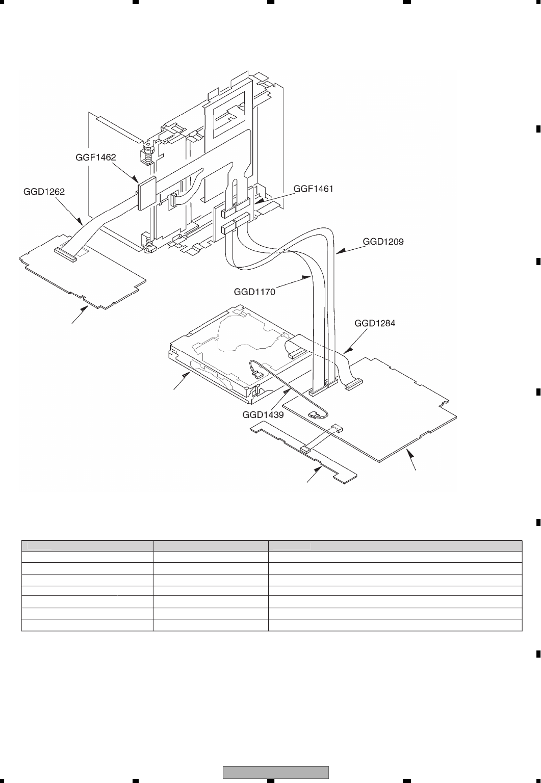
AVH-P5700DVD/EW 117
5678
5678
C
D
F
A
B
E
6. ADJUSTMENT
6.1 JIG CONNECTION DIAGRAM
DVD MECHANISM MODULE
(MS-3V1)
MOTHER UNIT
MONITOR PCB
KEYBOARD UNIT
-
J
i
gs L
i
st
N
ame
33
pi
n extens
i
on ca
ble
Rela
y
P
C
B
Rela
y
P
C
B
20
pi
n extens
i
on ca
ble
p
40
pi
n extens
i
on ca
ble
40
pi
n extens
i
on ca
ble
2
pi
n extens
i
on ca
ble
Jig
No
.
GG
D12
6
2
GG
F14
6
2
GG
F1461
GG
D1209
GG
D117
0
GG
D12
8
4
GG
D1439
R
emarks
C
onnectin
g
the monitor P
C
B to rela
y
P
C
B
(GG
F1462
)
gy()
C
onnectin
g
the monitor P
C
B extension cable to flexible P
C
B
C
onnectin
g
the monitor P
C
B extension cable to flexible P
C
B
Connecting the mother unit to relay PCB(GGF1461)
gy()
C
onnectin
g
the mother unit to relay P
C
B(
GG
F1461)
C
onnectin
g
the mother unit to DVD mechanism modul
e
C
onnectin
g
the mother unit to DVD mechanism modul
e

AVH-P5700DVD/EW
118
1234
1234
C
D
F
A
B
E
6.2 DVD ADJUSTMENT
1) Precautions
This product uses 5V and 3.3V as standard voltages.
The electrical potential that is the reference for signals,
is not GND, but VREF (approximately 2.2V) and VHALF
(approximately 1.65V).
During product adjustments, if the reference voltage is
mistakenly taken as GND, and a grounding contact is
made, not only would it be impossible to measure the
accurate electrical potential, but also the servo motor
would malfunction, resulting in the application of a
strong impact on the pick up. The following precaution-
ary measures should be strictly adhered to, in order to
avoid such problems.
The reference voltage and GND should not be confused
when using the minus probe of a measurement device.
When an oscilloscope is being used special care should
be taken to make sure that the reference voltage is not
connected to the probe of ch1 (on the minus side),
while the probe of ch2 (on the minus side), is connected
to GND. Further, since the body frame of most mea-
surement devices have the same electrical potential as
the minus side of the probe, the body frame of the mea-
surement device should be set to floating ground.
If the reference voltage is connected to GND by mis-
take, turn the regulator OFF immediately, or turn the
power OFF.
• Remove the filters and wires used for measurements
only after the regulator has been turned OFF.
• After the power supply is turned on, regulator ON the
following adjustment and measurement are promptly
done.
• Whenever the product is in the test mode, the software
will not take any protective action. For this reason,
special care should be taken to make sure that no
mechanical or electrical shock could be applied to the
product when taking measurements in the test mode.
• Whenever the EJECT key is pressed to eject the disk,
no other keys, other than the EJECT key, should be
pressed until the disk eject action has been complet-
ed.
• Press the EJECT key only after the disk has stopped
completely.
• If the product hangs up turn the power OFF immedi-
ately.
•
Laser didoes may be damaged, if the volume switch for
the laser power adjustment of the pick up unit, is turned.
Attention)
• Test mode starting procedure
Reset start while pressing the BAND and ANGLE- keys
together.
• Test mode stopping procedure
ACC and Backup OFF.
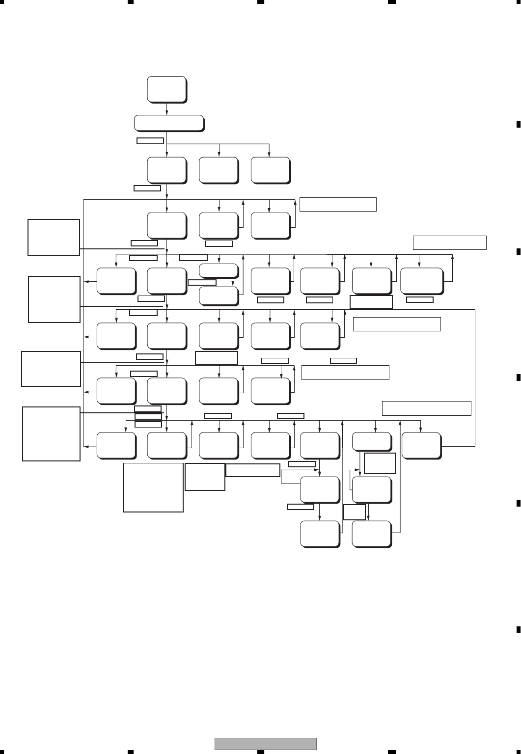
AVH-P5700DVD/EW 119
5678
5678
C
D
F
A
B
E
Test mode In
Set source to DVD
Start test mode
FE
test mode
Power On
Power Off CRG + CRG – LD_ON
Focus close
adjustment
Focus Search
Power Off CRG + CRG –
T.Bal and
other
adjustments
Focus Jump
Power Off
Focus Jump ID Search
Tracking
Open
T. Jump
+/–
ID
specification Track number
specification
Error Rate
measurement
(Note 2)
Reproduction
speed switching
(Note 3)
Power Off CRG –
Tracking close
adjustment
CRG +
Disc Type
(Note 1) Eject
EDC1
mode EDC2
mode
A.MENU
A.MENU
A.MENU
A.MENU
Focus Search
Stop
CRG_HOME
ATT
ATT
EQ
EQ
A.MENU
ATT ATT
ANGLE-
LEFT~ATT EJECT
RIGHT LEFT
LEFT
LEFT
LEFT
LEFT
RIGHT
RIGHT
RIGHT
RIGHT
RIGHT
Power off condition
Power on condition
Focus close condition 2
Focus close condition 1
Tracking close condition
ID
Search Start Jump start
0X00 0000
0FFF 00000FFF 0000
1X00 0000
2X00 0000
1FFF 0000
0000 0000
1A00 0000
1100 0000
TEST
FE offset coefficient
TE offset coefficient
AS offset coefficient
ENV offset coefficient
TG offset coefficient
DBALt coefficient
FE MAX level
FE MIN level
AS MAX level
ENV MAX level
FE normalization feature
Spindle gain coefficient
TEMAX level
TEMIN level
TBAL Coefficient(Layer 0)
TBAL Coefficient(Layer 1)
TE normalization feature
(Layer0)
TE normalization feature
(Layer1)
FBAL Coefficient(Layer0)
FBAL Coefficient(Layer1)
Focus Gain Coefficient(Layer0)
Focus Gain Coefficient(Layer1)
Tracking Gain Coefficient(Layer0)
Tracking Gain Coefficient(Layer1)
AS normalization adjustment feature
(Layer0)
AS normalization adjustment feature
(Layer1)
2FFF 0000
Layer L0:2000 0000
Layer L1:2100 0000
Layer L0:4X00 0000
Layer L1:4X00 0000
3000 0000
3FFF 0000
3B00 0000
DVD x 1.3
~
1.6CAV
CD x 4CLV:
4X00 0000
3C00 0000
4A00 0000
Jump+:
4B00 0000
Jump-:
4C00 0000
ID displayTrack
number
display
4000 0000
4X00 0000
Error Rate
Focus Gain Coefficient(Layer0)
Focus Gain Coefficient(Layer1)
Tracking Gain Coefficient(Layer0)
Tracking Gain Coefficient(Layer1)
AS normalization adjustment feature
(Layer0)
AS normalization adjustment feature
(Layer1)
Operation while key is being pushed.Operation while key is being pushed.
Operation while key is being pushed.
Operation while key is being pushed.
2B00 0000 2C00 0000
Note 1: At this stage select the media type. Various settings are carried out
according to the media selection made here.
Note 2: While measurements are being taken, only the operation, for which
the measurement is being taken, is allowed.
Note 3: Reproduction (play) speed is selectable from
Note 4: Gain change: Normal gain -> OEIC=H -> OEIC=H and FEP x 4 AMP ON
DVD : x1.3 1.6CAV,CD : x 4CLV Fixation
LEFT : DVD, single-layer
ANGLE- : DVD, dual-layer
ANGLE+ : CD
ATT : CD-RW
-Front-End test mode flow chart
1B00 0000 1C00 0000 1D00 0000
LD_ON :1100 0000
LD_OFF:1000 0000
RIGHT
ANGLE+
~
ANGLE-
ANGLE-,
ANGLE+
ANGLE+
ANGLE- ANGLE+
ANGLE- ANGLE+
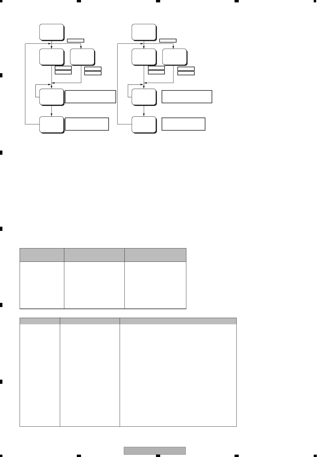
AVH-P5700DVD/EW
120
1234
1234
C
D
F
A
B
E
Layer 0
selected Layer 1
selected
EDC1
mode
ID
designation
EDC1 start
ATT
Layer 0
selected Layer 1
selected
EDC2
mode
ID
designation
EDC2 start
ATT
F-close and F-search cannot be executed, unless LD-ON is set.
0000 0000 0000 0000
0100 0000
1103 0000
Layer0:10** ****
Layer1:11** ****
** ****: ID specification value
Layer0:20** ****
Layer1:21** ****
** ****: Present ID value
0000 0000
1003 0000
0100 0000
1103 0000
0000 0000
1003 0000
Layer0:10** ****
Layer1:11** ****
** ****: ID specification value
Layer0:20** ****
Layer1:21** ****
** ****: Present ID value
The track number designation is selected from the track numbers already prepared for selection.
Switching to cyclic operation is made at step ANGLE-, and the decision is finalized (entered) in step ATT.
For CD: Tracks 1, 4, 10, 11 and 32.
For DVD: Tracks 1, 4, 10, 11, 32, 64 and 100.
Method for designating an ID address:
•
A number of digits are determined through commands RIGHT
and LEFT. Numerical UP/DOWN operations are performed
through commands ANGLE- and ANGLE+. The decision is finalized (entered) with command ATT.
Error status from
DVD microcomputer Contents Display
0X50 Mecha. error No display
0X40 No disc No display
0X30 The temperature is abnormal Thermal Protection in Motion
0X20 Read error Error-02-XX
0XE2 Non-playable disc NON-PLAYABLE DISC
0X90
Different region disc
DIFFERENT REGION DISC
0XFF Undefined error Error-FF
Error code of read error(Part of XX)
Error Code Contents Display
0X99 Data cannot read Please confirm the disc
0X80 The address cannot be found Please confirm the disc
0X90 Focus error Please confirm the disc
0X91 Spindle lock NG DVD is stopping because mechanism detected abnormality
0X92 Carriage home NG DVD is stopping because mechanism detected abnormality
0X93 FOK error Please confirm the disc
0X94 ID/Subcode cannot be read Please confirm the disc
0X95 High spindle rotation
0X96 Row spindle rotation DVD is stopping because mechanism detected abnormality
DVD is stopping because mechanism detected abnormality
0X98 TOC cannot be found Please confirm the disc
0X9A AV chip error DVD is stopping because mechanism detected abnormality
0X9B RecaveryNG(BE)
Play state error
Disc data error
DVD is stopping because mechanism detected abnormality
Display
Error Code List
RIGHT
ANGLE+
~
RIGHT
ANGLE-
~
[If F-close isn't executed within 9 seconds after LD-ON, it switches to LD-OFF automatically.
And even if F-search is executed within 9 seconds after LD-ON, it also switches to LD-OFF.]
Please carry out F-close after carrying out power-off at once and carrying out power-on again,
when carrying out F-close after performing F-search.
RIGHT RIGHT LEFTLEFT
0X9C
0X9D
0X9E Serface error
(Disc distinction is improper)

AVH-P5700DVD/EW 121
5678
5678
C
D
F
A
B
E
Oscilloscope
ANAMONI
AGND
If any of the following replacements have been performed on the system, adjustments for pick up,
must be conducted:
1. Pick up unit replacement
2. Spindle motor replacement
3. Carriage chassis replacement
4. Pick up unit main shaft replacement
5. Pick up unit sub-shaft replacement
Measurement device and tools
Disk used
Measurement reference
Measurement point
Connection diagram
DVD core unit
: Oscilloscope
Allen key wrench
40-pin flexible extension (GGD1284)
2-pin extension cable(GGD1439)
Screw lock (GYL1001)
: GGV1018
: AGND3
: ANAMONI
Skew Adjustment
The skew adjustment is to adjust the pickup and the flatness of the disc so that the beam from the pickup
continues to go to the disc vertically. In MS3 mecha, the pickup shaft on the inner track near the carriage
motor is fixed, so the fixed position is regarded as the standard and the flatness is adjusted. Observing the
RF waveform on the oscilloscope, repeat the adjustment on the inner track position and the outer track position,
and narrow the adjusted value.
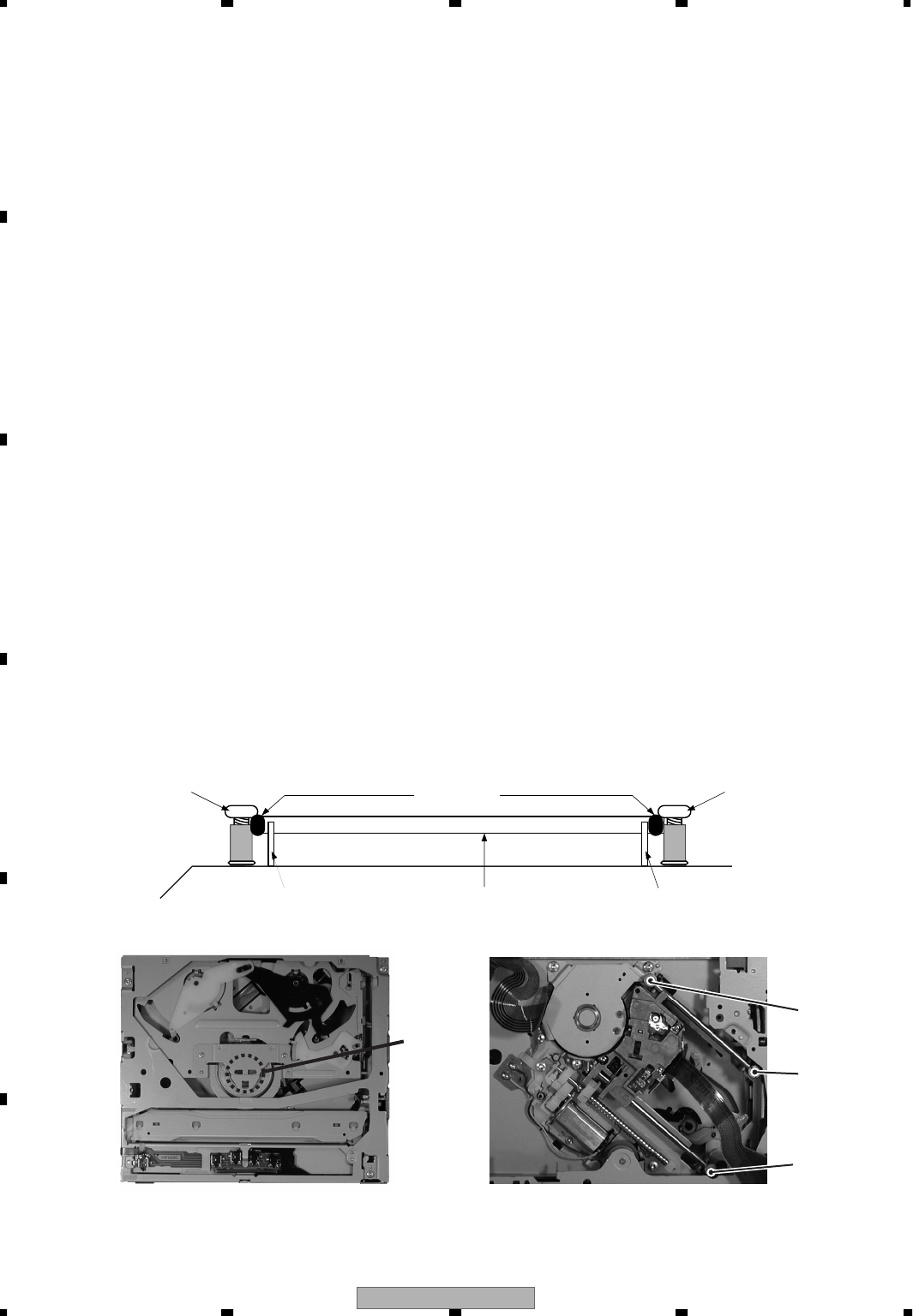
AVH-P5700DVD/EW
122
1234
1234
C
D
F
A
B
E
Apply glue
Shaft
Skew adj. screw Skew adj. screw
Prevent applied glue
from extending beyond this position.
Prevent applied glue
from extending beyond this position.
B
A
C
1
Symptoms in case of poor adjustment:
Caution: Avoid exposing your eyes to laser beams for a long time.
Preparation for adjustment: Clean both ends of the shafts.
Use brand new skew screws supplied with the service kit GXX1242.
Procedures:
1. Place the DVD mechanism module upside down.
To avoid the disc from being robbed when it is turned upside down, first put a coin of about 1.5 mm on the table,
then turn the disc upside down and set it so that the 1 in the figure comes to the point immediately above
the coin.
2. After replacing the pickup (by referring to the procedures of "Removing the Pickup."), roughly adjust the three
skew screws through visual check so that the pickup is mounted in parallel to the CRG chassis around the inner
and outer tacks.
3. Connect an oscilloscope as shown in the connecting diagram.
4. Turn on the power of the product. Load the test disc (GGV1018).
5. In the front-end test mode, set the disc type to DVD layer 1. Then, turn on the power. Move the pickup toward
the inner tracks.
6. Turn on the laser diodes.
7. With the focus servo closed, complete all automatic adjustments. Close the tracking servo, and then complete all
automatic adjustments.
8 Follow the next procedures, from 8-1 to 8-5, and adjust the (three) skew screws.
8-1 Move the pickup toward the inner track and turn the skew adjustment screw C so that the RF level of
oscilloscope becomes the maximum.
(Tangential adjustment at the inner track position: Adjust the flatness of the disc at the inner track position with
the adjustment screw C)
8-2 Move the pickup toward the outer track and turn the skew adjustment screw B so that the RF level becomes
the maximum.
(Tangential adjustment at the outer track position: Adjust the flatness of the disc at the outer track position with
the adjustment screw B)
8-3 Leave the pickup at the outer track position and turn the skew adjustment screws A and B in the same direction
alternately one quarter at a time (A•B•A•B •••) so that the RF level becomes the maximum.
(Radial adjustment at the outer track position: Keeping the flatness at the outer track position, adjust the flatness
of the whole disk with the adjustment screws A and B)
8-4 Move the pickup toward the inner track and turn the skew adjustment screw C so that the RF level becomes
the maximum.
(Tangential adjustment at the inner track position: Adjust the flatness of the disc at the inner track position with
the djustment screw C)
8-5 Repeat the steps from 8-2 to 8-4 three times, and adjust at the position where the RF level becomes the
maximum.
9. Turn off the power in the test mode. After confirming that the disc has stopped, eject the disc.
10. Adjust with a screw rock the shaft and skew adjustment screw to the same state as initial one.
Error efficiency deteriorated: 10
(Optimum value: 10
or lower)
High jitter of the RF signal RF waveform deformed
Unstable operation in tracking closing and servo control
-3 -4
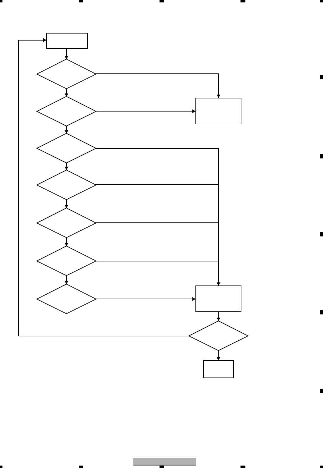
AVH-P5700DVD/EW 123
5678
5678
C
D
F
A
B
E
Are all
power supply voltages?
Execute Check 1
Are all clocks
operating normally?
Execute Check 2
Is the
audio circuit
operating normally?
Execute Check
3
Is the
video circuit
operating normally?
Execute Check
4
Are all
reproduced images
and sounds
normal?
Start
Is SDRAM I/F
operating normally?
Execute Check 5
Repair or replace
any defective unit
All checks normal?
Check
completed
Is the F.E. section
normal?
Go to the F.E.
section check
YES
YES
OK
OK
OK
OK
NO
NO
NG
NG
NG
NG
NG
YES
NO
Back end section check flow chart
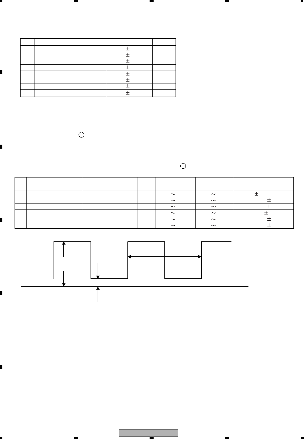
AVH-P5700DVD/EW
124
1234
1234
C
D
F
A
B
E
Reproduce DVD-REF-A1 Title 1.
Verify the voltage of the sensing pin.
Check 1 : Are all power supply voltages?
No.
1
2
3
4
5
6
7
8
Verification location
VD8_1/2
-
PGND_1/2
VDD33
-
DGND1/2/3
SRVDD
-
DGND1/2/3
VCC5_1
-
AGND1
AVCC5_1
-
AGND1
VCC33_1/2
-
DGND1/2/3
VCC33_3/4/5
-
DGND1/2/3
VCC15_1/2
-
DGND1/2/3
Rated value
8.0 0.4
3.3 0.15
3.3 0.15
5.0 0.1
5.0 0.1
3.3 0.15
3.3 0.3
1.5 0.1
Unit
V
V
V
V
V
V
V
V
Check 2 : Are all clock operating normally?
Reproduce DVD-REF-A1 Title 1
Check Circuit Diagram .
Checks are to conducted with a GND reference.
If locations listed under "verification location 2", can be verified, there will be no need to perform verifications
for the locations listed under "verification location 1."
If the result is not satisfactory, check to see if there are any problems with the resin flux cored solder and other
defects in the applicable line, vicinity of IC 1802 (Circuit Diagram ) and peripheral components.
GND
Rated Value 1 Rated value 3
Rated Value 2
Clock rated values
1
1
No.
1
2
3
4
5
6
Verification location 1
(Sensing pin)
BECLK
EXTCK
EXTCK
MCK33
DACCLK
DACCLK
Verification location 2
IC1501
IC1501
IC1501
IC1501
IC1851
IC1881
170pin
172pin
172pin
92pin
16pin
3pin
Media
ALL
DVD
CD
ALL
DVD
DVD
Rated value 1
2.3V VCC33
2.3V VCC33
2.3V VCC33
2.2V VCC33
2.0V VCC33
2.3V VCC33
Rated value 2
GND 0.8V
GND 0.8V
GND 0.8V
GND 0.8V
GND 0.8V
GND 0.99V
Rated value 3
27MHz 50ppm
36.8640MHz 300ppm
33.8688MHz 300ppm
33.898MHz 300ppm
33.8688MHz 300ppm
33.8689MHz 300ppm

AVH-P5700DVD/EW 125
5678
5678
C
D
F
A
B
E
Circuit Diagram
1
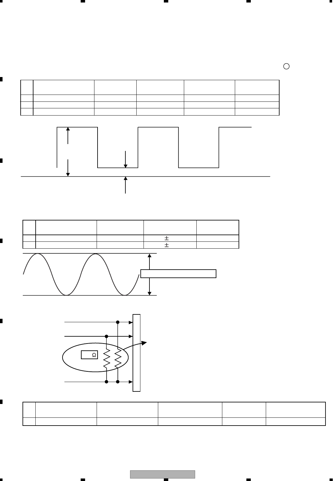
AVH-P5700DVD/EW
126
1234
1234
C
D
F
A
B
E
Check 3 : Is the audio circuit operating normally?
Reproduce DVD-REF-A1 Title 2 Chapter (48k/16-bit 1 kHz/0dB).
Checks are to be conducted using GNDAU1 (sensing pins) as a reference.
If the locations, listed under "verification location 2", can be verified, there is no need to conduct verifications for
the locations listed under "verification location 1."
If the result is not satisfactory, check to see if there are any problems with resin flux cored solder and other
defects in the applicable line, vicinity of major parts stated in the above diagram (Circuit Diagram ) and
peripheral components.
GND
Rated value 1
Rated value 2
Three serial output rated values
No.
1
2
3
Verification location 1
(Sensing pin)
AOUT0
SRCK
LRCK
Verification
location 2
IC1851 2pin
IC1851 1pin
IC1851 3pin
Rated value 1
2.0V and over
2.0V and over
2.0V and over
Rated value 2
0.8V and lower
0.8V and lower
0.8V and lower
Reference
waveform
Waveform 1
Waveform 1
Waveform 1
2
Checks are conducted with the measurement circuit below.
Analog audio outputs (LO and RO) rated values
LO
RO
GNDAU
HOST I/F
Rated value is effective value (rms)
22k
These resistors are inserted.
LO and RO output measurement circuit
No.
6
Verification location 1
(Sensing pin)
IEC958
Verification location 2
CN1551 1pin
Rated value 1
VCC33V
-
0.6V and over
Rated value 2
0.4Vand lower
Reference waveform
Waveform 3
No.
4
5
Verification location 1
(Sensing pin)
LO
RO
Verification
location 2
CN1901 37pin
CN1901 35pin
Reference
waveform
Waveform 2
Waveform 2
Rated value (rms)
1100 150mV
1100 150mV
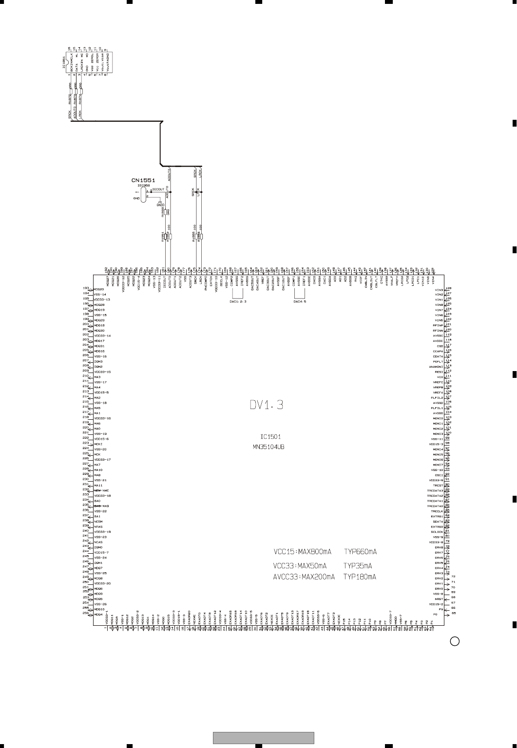
AVH-P5700DVD/EW 127
5678
5678
C
D
F
A
B
E
Circuit Diagram
2
AVH-P5700DVD/EW
128
1234
1234
C
D
F
A
B
E
Check 4 : Is the video circuit operated normally?
Reproduce DVD-REF-A1 Title 2 Chapters (White 1000IRE)
Monitor the output with the oscilloscope, by setting the COMPO signal to a GND reference.
Set the Trigger mode to the TV trigger, and the Trigger line to line-150.
Composite signal white 100% output waveform
If the result is not satisfactory, check to see if there are any problems with resin flux cored solder and other
defects in the applicable line, vicinity of major parts stated in the above diagram (Circuit Diagram ) and
peripheral components.
COMPO Signal
< Method of Readjusting Video Levels >
If the video composite output is not within the range of rated value, the video level is readjusted in the following
method.
Turn the video level adjustment volume (VR1551) to adjust its level to 1.0 0.02Vpp.
Pedestal Level
Rated value
Color brust
Horizontal periodic signal
PEAK
BOTTOM
When the result is not satisfactory,
adjust the level to 1.0 0.02Vpp.
No.
1
Verification location 1
(Sensing pin)
COMPO
Reference waveform
Waveform 4
Rated value
1.0 0.02Vpp
3
Check 5 : Is SDRAM I/F operated normally?
Reproduce DVD-REF-A1 Title 1.
Check Circuit Diagram
Common to all DVD-V adapted modules
Check the conductivity of both the "Verification location 1"and the "Verification location 2."
If the result is not satisfactory, check to see if there are any problems with the resin flux cored solder, parts and
components, in areas where as problem occurs, for the overall sequence of "output" "input" of the checked
location.
3
No.
1
2
3
4
5
6
7
8
9
10
11
12
Verification location 1
IC1570
IC1570
IC1570
IC1570
IC1570
IC1570
IC1570
IC1570
IC1570
IC1570
IC1570
IC1570
25pin
26pin
27pin
60pin
61pin
62pin
63pin
64pin
65pin
66pin
24pin
21pin
Signal name
MA0
MA1
MA2
MA3
MA4
MA5
MA6
MA7
MA8
MA9
MA10
MA11
220pin
217pin
214pin
210pin
212pin
216pin
219pin
227pin
229pin
235pin
228pin
231pin
Verification location 2
IC1501
IC1501
IC1501
IC1501
IC1501
IC1501
IC1501
IC1501
IC1501
IC1501
IC1501
IC1501
Rated value
56 5%
56 5%
56 5%
56 5%
56 5%
56 5%
56 5%
56 5%
56 5%
56 5%
56 5%
56 5%
AVH-P5700DVD/EW 129
5678
5678
C
D
F
A
B
E
No.
13
14
15
16
17
18
19
20
21
22
23
24
25
26
27
28
29
30
31
32
33
34
35
36
37
38
39
40
41
42
43
44
45
46
47
48
49
50
51
52
53
54
55
Verification location 1
IC1570
IC1570
IC1570
IC1570
IC1570
IC1570
IC1570
IC1570
IC1570
IC1570
IC1570
IC1570
IC1570
IC1570
IC1570
IC1570
IC1570
IC1570
IC1570
IC1570
IC1570
IC1570
IC1570
IC1570
IC1570
IC1570
IC1570
IC1570
IC1570
IC1570
IC1570
IC1570
IC1570
IC1570
IC1570
IC1570
IC1570
IC1570
IC1570
IC1570
IC1570
IC1570
IC1570
2pin
4pin
5pin
7pin
8pin
10pin
11pin
13pin
74pin
76pin
77pin
79pin
80pin
82pin
83pin
85pin
31pin
33pin
34pin
36pin
37pin
39pin
40pin
42pin
45pin
47pin
48pin
50pin
51pin
53pin
54pin
56pin
68pin
17pin
18pin
19pin
20pin
16pin
71pin
28pin
59pin
22pin
23pin
Signal name
MDQ0
MDQ1
MDQ2
MDQ3
MDQ4
MDQ5
MDQ6
MDQ7
MDQ8
MDQ9
MDQ10
MDQ11
MDQ12
MDQ13
MDQ14
MDQ15
MDQ16
MDQ17
MDQ18
MDQ19
MDQ20
MDQ21
MDQ22
MDQ23
MDQ24
MDQ25
MDQ26
MDQ27
MDQ28
MDQ29
MDQ30
MDQ31
MCK
XWE
XCAS
XRAS
XCSM
DQM0
DQM1
DQM2
DQM3
BA0
BA1
12pin
9pin
6pin
3pin
256pin
253pin
251pin
247pin
249pin
252pin
255pin
2pin
5pin
8pin
10pin
13pin
205pin
203pin
200pin
197pin
193pin
191pin
187pin
185pin
184pin
188pin
190pin
192pin
196pin
199pin
201pin
204pin
225pin
232pin
242pin
239pin
238pin
243pin
246pin
208pin
207pin
234pin
237pin
Verification location 2
IC1501
IC1501
IC1501
IC1501
IC1501
IC1501
IC1501
IC1501
IC1501
IC1501
IC1501
IC1501
IC1501
IC1501
IC1501
IC1501
IC1501
IC1501
IC1501
IC1501
IC1501
IC1501
IC1501
IC1501
IC1501
IC1501
IC1501
IC1501
IC1501
IC1501
IC1501
IC1501
IC1501
IC1501
IC1501
IC1501
IC1501
IC1501
IC1501
IC1501
IC1501
IC1501
IC1501
Rated value
100 5%
100 5%
100 5%
100 5%
100 5%
100 5%
100 5%
100 5%
100 5%
100 5%
100 5%
100 5%
100 5%
100 5%
100 5%
100 5%
100 5%
100 5%
100 5%
100 5%
100 5%
100 5%
100 5%
100 5%
100 5%
100 5%
100 5%
100 5%
100 5%
100 5%
100 5%
56 5%
22 5%
56 5%
56 5%
56 5%
56 5%
56 5%
56 5%
56 5%
56 5%
56 5%
56 5%
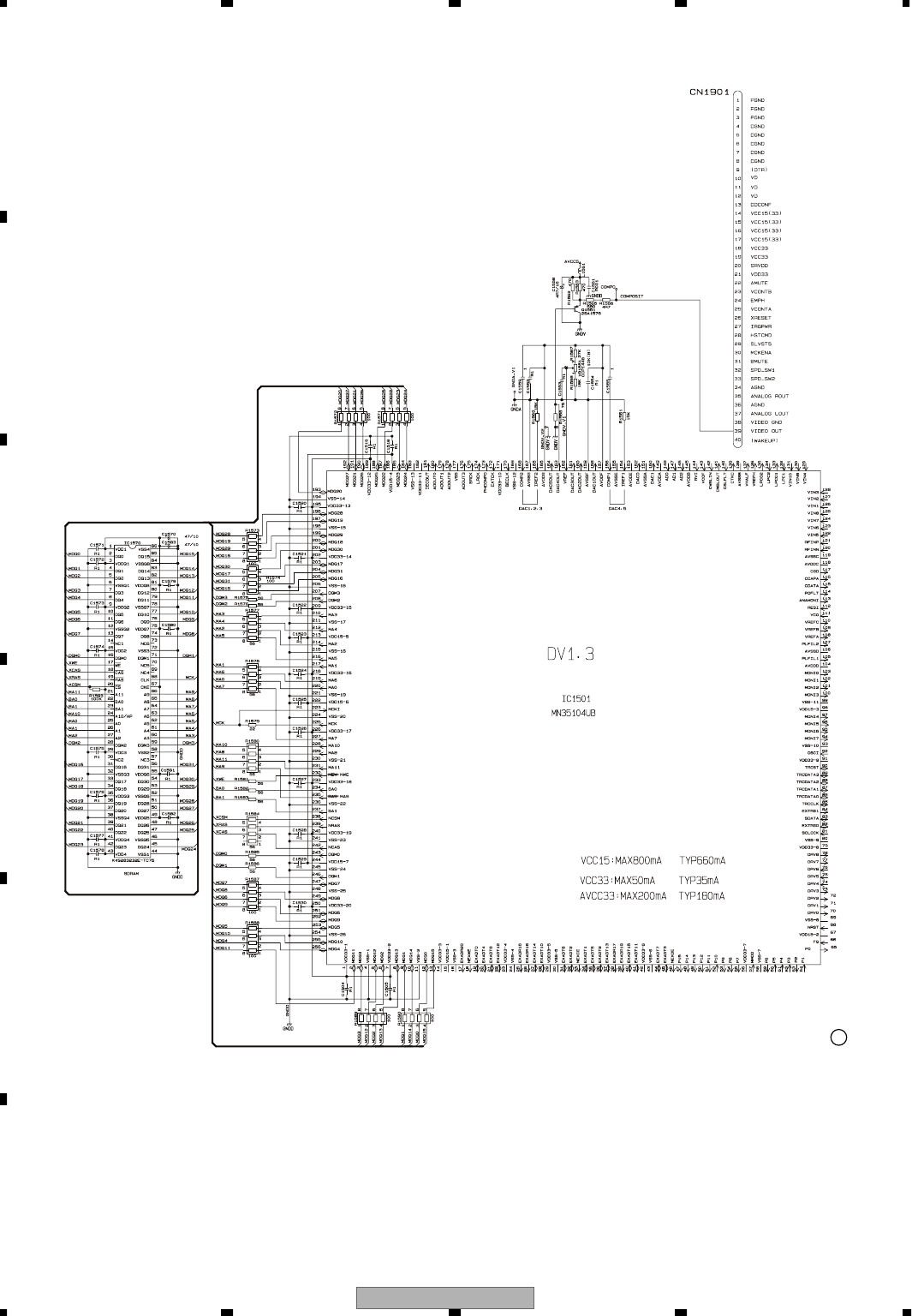
AVH-P5700DVD/EW
130
1234
1234
C
D
F
A
B
E
Circuit Diagram
3
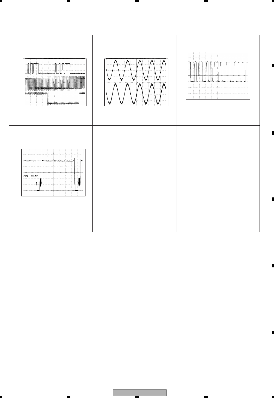
AVH-P5700DVD/EW 131
5678
5678
C
D
F
A
B
E
CH1: AOUT0
CH2: SRCKAV
CH3: LRCKAV
G→
2V/div. 2µs/div.
G→
G→←T
CH1: IEC958 1V/div. 500ns/div.
G→
←T
CH1: LO
CH2: RO
G→
1V/div. 500µs/div.
G→
←T
CH1: COMPO 200mV/div. 10µs/div.
[White 100% output]
G→
Waveform1 Waveform2
Waveform3
Waveform4
Note: Reference voltage VHALF : 1.65V
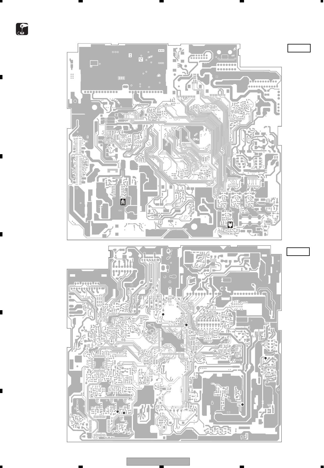
AVH-P5700DVD/EW
132
1234
1234
C
D
F
A
B
E
6.3 MOTHER UNIT ADJUSTMENT
VR511
TP614
PCL
VCRVG
VCRV
TP803
TP190
VR801
- Adjustment Point SIDE A
SIDE B
AVH-P5700DVD/EW 133
5678
5678
C
D
F
A
B
E
Step
1Main video level
Input test pin:
VCRV....100 IRE
(white 100%),
1.0Vp-p,
(input via 75ohms)
VCRVG....
(GND VIDEO GND)
Mother PCB
adjustment Mode
AV
Measuring
instruments Specs Adjusting
point
Input signsl
(input test pin,specs,
other conditions)
Output signsl
(measuring point,
waveform)
Measuring point:
TP190
Oscilloscope
1.4V ± 0.05Vp-p
Measure between the
sync tip and 100 IRE
(top wave).
Symptoms with
poor adjustment.
Over level :
Luminance is too high.
Under level :
Luminance is too low.
2Clock frequency
Check IC601 pin56(TP614)
to 5V
Playback the DVD
IC601 pin36(PCL) Frequency
Counter 18.874368MHz±754Hz
3DC-DC converter
frequency
Adjustment
Test point TP803 Frequency
Counter 370kHz±5Hz
VR511
VR801
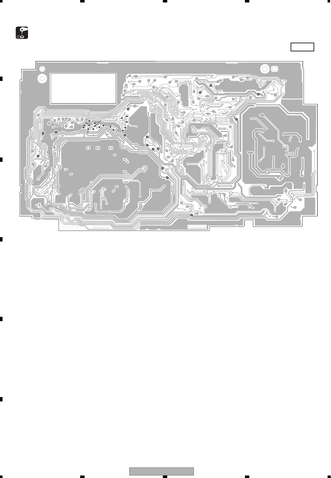
AVH-P5700DVD/EW
134
1234
1234
C
D
F
A
B
E
6.4 MONITOR PCB ADJUSTMENT
RO4
RO3
RO5
RO2
BO5
GO2
GO3 GO04
GO5
BO3
BO2
BO4
COM
VM12 V18
COMDC
VO1
VO3 VO9
VO5
VO7
V5 ANG1
ANB1
ANR1
CSYNC
CVBS1
YSIN V14
V33
V8
V25
V15
- Adjustment Point SIDE B

AVH-P5700DVD/EW 135
5678
5678
C
D
F
A
B
E
1
No. Adjustment item Input signal Measurement point
Check 3.3V power
supply voltage TP:14.4V
to14V C210 hot side
(TP:V33) —
NOTE : When shutting off the power supply of TC90A64AFG, be careful not to energize each IC terminal. However, IIC lines (SDA and SCL) is not included in
this case and it is possible to energize them with up to 5V.
Note
Adjustment point Adjustment
V33 = 3.3 ± 0.25V
2 Check 2.5V power
supply voltage TP:14.4V
to14V IC4182
1-pin
(TP:V25)
—V25 = 2.5 ± 0.15V
3 Check 1.5V power
supply voltage TP:14.4V
to14V IC4183
1-pin
(TP:V15)
—V15 = 1.5 ± 0.08V
4 Check 5V power
supply voltage TP:14.4V
to14V C4234 hot side
(TP:V5) —V5 = 4.9 ± 0.3 V
5 Check 8V power
supply voltage TP:14.4V
to14V C4198 hot side
(TP:V8) —V8 = 8.0 ± 0.5 V
6 Check 18.5V power
supply voltage TP:14.4V
to14V C4181 hot side
(TP:V18) —V18 = 18.5 ± 0.5 V
Check -12V power
supply voltage TP:14.4V
to14V C4207 hot side
(TP:VM12) —VM12 = -12.0 ± 0.6 V7
Vcom amplifier
output amplitude
check
No definition CN4007
1-pin
(TP:COM)
—4.70 ± 0.10 V
4.20 ± 0.30 V
1.80 ± 0.10 V
9Tone voltage
amplitude
check V1
No definition CN4007
57-pin
(TP:VO1)
Connect LCD panel for measurement
Connect LCD panel for measurement
—
10 Tone voltage
amplitude
check V3
No definition CN4007
55-pin
(TP:VO3)
Connect LCD panel for measurement
—
8
AVH-P5700DVD/EW
136
1234
1234
C
D
F
A
B
E
Make sure that each output is “Hi”
continuously during displaying image.
15.734kHz
0.3V
3.3V 50µS
No. Adjustment item Input signal Measurement point
NOTE : When shutting off the power supply of TC90A64AFG, be careful not to energize each IC terminal. However, IIC lines (SDA and SCL) is not included in
this case and it is possible to energize them with up to 5V.
Note
Adjustment point Adjustment
Tone voltage
amplitude
adjustment V7
No definition CN4007
51-pin
(TP:VO7)
—
13 Tone voltage
amplitude
adjustment V9
No definition CN4007
49-pin
(TP:VO9)
Connect LCD panel for measurement
Connect LCD panel for measurement
—
14 Preparation for
image check Input synchroniz-
ed signal to
TP CSYNC
—Input 0.3V (75Ω)—
15 Check RGB digital
output Input white 100%
signal to
TP ANR1,
ANG1, ANB1
(0.70Vpp±1%)
TP BO2 ∼ BO5
TP GO2 ∼ GO5
TP RO2 ∼ RO5
When OSD is displayed in EEPROM
adjustment mode, LOW output is mixed to
the parts where there is a character.
—
12
11 Tone voltage
amplitude
adjustment V5
No definition CN4007
53-pin
(TP:VO5)
Connect LCD panel for measurement—0.35 ± 0.10 V
0.60 ± 0.10 V
3.30 ± 0.20 V
16 Composite level
adjustment Input composite
image 10STEP
signal to
TP CVBS1
(1.4Vpp±1%)
Verify YS performs.
17 YS performance
check Input signal to
TP YSIN
For abroad:
0-3.3V
For J spec:
0.4-1.4V(75Ω)
TP GO1
TP GO2 ∼ GO5
Using EEPROM adjustment mode,
set CMP CONTRAST on 30 and
decrease value one by one.
Decrease value by one when "L"
starts to appear on output
while displaying GO1 image.
Check that "H" always appears on
each output while displaying image.
Using EEPROM adjustment mode, check
that CONTRAST is being 168 to make
adjustment.
When OSD is displayed on EEPROM
adjustment mode, ignore "L" output shown
among lettered part.
Resistor setting
of SA13h D5-0
AVH-P5700DVD/EW 137
5678
5678
C
D
F
A
B
E
SA**h in this chart means the sub-address of TC90A64AFG.
No. Adjustment item Input signal Measurement point
NOTE : When shutting off the power supply of TC90A64AFG, be careful not to energize each IC terminal. However, IIC line (SDA and SCL) is not included in
this case and it is possible to energize it with up to 5V.
Note
Adjustment point Adjustment
YS-OFFSET
setting, check No definition —Register setting
of SA2Fh D3-0
Adjust the flicker level to minimum
from all directions.
20 Image check Input composite
image lamp signal
(monochrome)
to TP CVBS1
Screen Execute to verify that 2-display IC
digital-out is not bridged or “OPEN”ed.
Check EEP-ROM setting value after writing.
—
21 Aging No definition ——
22 Flicker adjustment Input black-white
reverse signal
per 1 line to TP
ANR1, ANG1,
ANB1
Screen Black-white reverse signal can be the input to
TP CVBS1 (however, adjustment in RGB
comes first).
Brightness level of reverse signal should be 50%.
Adjustment point can be COM DC of flicker
adjustment mode.
IC4101-3pin
(TP COMDC)
DC output
19
18 YS, RGB sampling
phase setting,
check
No definition —Check EEP-ROM setting value after writing.Register setting
for SA2Dh
D15 ∼ 12 : YS
D11 ∼ 8 : B
D7 ∼ 4 : G
D3 ∼ 0 : R
(Line writing): 0100
(Service): [YS (R, G, B) SAMPL]
should be 12 in EEPROM test mode
(Line writing): 1111
(Service): [YS DELAY] should be
7 in EEPROM test mode
Make sure that tone changes
smoothly, and there is no colored
area in the entire display.
Leave for more than 30 minutes in
operation mode.
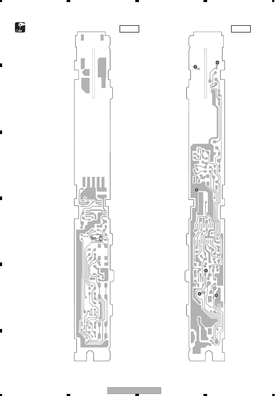
AVH-P5700DVD/EW
138
1234
1234
C
D
F
A
B
E
6.5 INVERTER PCB ADJUSTMENT
FL1
FL2
GNDF2
INVPUL
DIMDTY
VPFL1
VR5341
- Adjustment Point SIDE A SIDE B
AVH-P5700DVD/EW 139
5678
5678
C
D
F
A
B
E
No. Adjustment item Input signal Measurement point Note
Adjustment point Adjustment
Check frequency
switching Input 98.0 ± 1kHz waveform
below to TP INVPUL.
10 ± 2%
5V
0V
TP FL1
TP FL2 —
3Check frequency
switching Input 104.0 ± 1kHz waveform
below to TP INVPUL. TP FL1
TP FL2 Verify that the frequency of waveform
measured in No.1 is 52kHz.
Verify that the frequency of waveform
measured in No.1 is 49kHz.
—
2
1Basic drive
Frequency
adjustment
14.4 ± 0.2V to TP VPFL1
TP DIMDTY : GND
TP GNDFL : GND
TP INVPUL : GND
TP FL1
TP FL2 Connect 100kΩ between TP FL1 and FL2.
Monitor the waveform after voltage division or
TP FL2. Do not monitor TP FL1 directly
(measurement meter may be damaged
because of high voltage).
VR5341 48.0 ± 0.1kHz
49.0 ± 0.5kHz
52.0 ± 0.5kHz
10 ± 2%
5V
0V
AVH-P5700DVD/EW
140
1234
1234
C
D
F
A
B
E
6.6 MONITOR TEST MODE
1. Start-up
• Reset and start-up the monitor microcomputer while EPRTEST terminal is in the Low.
• Press EQ key + SOURCE key together to Reset Start.
2. Operation
Switching setting mode
Press [MENU] key of remote control unit to go to the next mode.
Selecting an adjustment item to be changed
Press [ ↑ ↓ ] key of remote control unit.
Changing value of the selected item
Press [← →] key of remote control unit.
3. Setting mode
(1) Flicker adjustment mode (start-up mode)
(2) Line adjustment 1 mode
(3) Line adjustment 2 mode
(4) Line adjustment 3 mode
(5) Line adjustment 4 mode
(6) Line adjustment 5 mode
(7) Line adjustment 6 mode
(8) Line adjustment 7 mode
(9) Line adjustment 8 mode
(10) Line adjustment 9 mode
(11) Line adjustment 10 mode
(12) Parameter setting mode for dimmer
4. Operation key
(If pressing a monitor key in this adjustment mode, there is no affection in operation of the main unit.)
* Please note that there is a model by which the remote control signal is not connected to the monitor
microcomputer (in that case, operation should be done only by key).
* After writing a setting value to EEPROM, read and display it.
Writing and reading should be done in 16-bit unit. The bit number of settings varies in each item.
* After changing the value of CS (CHECKSUM), take exclusive OR (XOR) with 8-bit and execute writing.
After writing this CS value to EEPROM, read and display it, too.
If the written value and the read value are different, change the color of the read value.
- EEPROM Setting Mode
[Remote control code] head unit code
Main unit key
Key Code
MENU AD19AF63
↑AD40
↓AD41
←AD42
→AD43
AVH-P5700DVD/EW 141
5678
5678
C
D
F
A
B
E
EEPROM memory alignment chart (S-93C56BD0I-JS)
ADDRESS
Bit15 Bit14 Bit13 Bit12 Bit11 Bit10 Bit9 Bit8 Bit7 Bit6 Bit5 Bit4 Bit3 Bit2 Bit1 Bit0
00h Outside light of dimmer adjustment coordinates (high) Backlight of dimmer adjustment coordinates (high)
01h Outside light of dimmer adjustment coordinates (middle) Backlight of dimmer adjustment coordinates (middle)
02h
03h
04h
05h
06h
07h
08h
RELATED PIP
(
including
operation settings
)
RELATED PIP
(
excluding
operation settings
)
RELATED
DIMMER
09h
0Ah
0Bh
0Ch
0Dh
0Eh
0Fh
10h
11h
12h
13h
14h
15h
16h
17h
18h
19h
1Ah
1Bh
1Ch
1Dh
1Eh
1Fh
20h
21h
22h
Common reference output DC center value Common reverse output amplitude adjustment value
Brightness G
Brightness B
Main horizontal enhancer
Don't care
Don't care
Gain Limiter Gain Replicate Coringfo
Don't care RGB simultaneous slope A
γ γ
γγ
R output DC offset
SA24h UPPER
SA25h UPPER
SA26h UPPER TV
SA26h UPPER
SA27h UPPER TV
SA27h UPPER
SA46h UPPER
SA47h UPPER
SA48h UPPER
SA49h UPPER
SA4Ah UPPER
SA4Bh UPPER
SA4Ch UPPER
SA4Dh UPPER
SA4Eh UPPER
SA4Fh UPPER
Dot search threshold
Phase search threshold
SA4Dh LOWER
SA4Eh LOWER
SA4Fh LOWER
YS search threshold
Xdisp (display difference permissible level)
Don't care
Don't care
Checksum
EEPROM address:0AH-28H
YS disp (display difference permissible level)
Common reverse output DC center value reference
Touch panel X coordinate 1 Touch panel Y coordinate 1
Touch panel X coordinate 2 Touch panel Y coordinate 2
Touch panel X coordinate 3 Touch panel Y coordinate 3
Touch panel X coordinate 4 Touch panel Y coordinate 4
Touch panel X coordinate 5 Touch panel Y coordinate 5
Touch panel X coordinate 6 Touch panel Y coordinate 6
Touch panel X coordinate 7 Touch panel Y coordinate 7
Touch panel X coordinate 8 Touch panel Y coordinate 8
SA46h LOWER
SA47h LOWER
SA48h LOWER
SA49h LOWER
SA4Ah LOWER
SA4Bh LOWER
SA4Ch LOWER
SA24h LOWER
SA25h LOWER
SA26h LOWER TV
SA26h LOWER
SA27h LOWER TV
SA27h LOWER
Don't care
Don't care
Don't care
RGB simultaneous slope C RGB simultaneous 3 inflection pointRGB simultaneous slope B RGB simultaneous 2 inflection point
Don't care
G output DC offset
B output DC offset
Don't care
Don't care
Don't care
Don't care
Don't care
Main Y contrast
Sub Y contrast
Sub vertical enhancer
Don't care
Don't care
Don't care
Don't care Don't care
Main horizontal enhancer
Gain Limiter Gain Replicate Coring
RGB simultaneous 1 inflection point
fo
Sub vertical enhancer
Don't care Don't care
Brightness R
Don't care YS internal delay adjustment value
Gch sampling phase
RELATED
TOUCH PANEL
23h
24h
25h
26h
27h
28h
29h
2AH
2Bh
2Ch
2Dh
2Eh
2Fh
30h
31h
32h
Touch panel X coordinate 9 Touch panel Y coordinate 933h
Outside light of dimmer adjustment coordinates (low)
Rch sampling phase
Backlight of dimmer adjustment coordinates (low)
Outside light threshold for dimmer (high) Outside light threshold for dimmer (low)
Maximum value of backlight output
RGB &YS horizontal positioning
YS sampling phase Bch sampling phase
Minimum value of backlight output
Checksum
EEPROM address:03h-04h
Checksum
EEPROM address:06h-08h
5. Memory item list and EEPROM
γγ

AVH-P5700DVD/EW
142
1234
1234
C
D
F
A
B
E
ADDRESS
Bit15 Bit14 Bit13 Bit12 Bit11 Bit10 Bit9 Bit8 Bit7 Bit6 Bit5 Bit4 Bit3 Bit2 Bit1 Bit0
Touch panel calibration adjustment result Touch panel outermost circumference adjustment result
Checksum
EEPROM address:2BH-3DH
Flicker adjustment completion
(writing of microcomputer) *AEEPROM adjustment completion
(writing of production engineering jig) *BEJECT lock value
RELATED
TOUCH PANEL
Others
Addition
To be
determined
3Dh
3Eh
3FH
40H
41H
∼
7FH
* The order of RELATED DIMMER, RELATED PIP, RELATED TOUCH PANEL and others is determined according to frequency of changing.
* When a writing & reading error or data check (checksum, magnitude relation) error occurs, initialization is done with data belonging to the software at the error time, and initialization is performed
per divided section described above.
However, RELATED DIMMER should be further divided into sections such as address 00H∼02H and 03H∼04H, then initialized.
* The user changeable parts (address 00H∼02H) in the segment RELATED DIMMER is not a target of checksum.
* Concerning the segment RELATED DIMMER, considering PIP register configuration, data obtained from PIP can be stored without software processing.
And the alignment is designed to send data obtained from EEPROM to PIP without processing it. (same as NN629)
Each area is divided according as whether it is changed during operation or not. (Checksum division is carried out to each.)
* Address 2H, remote control reverse output DC center value reference is not a target of checksum because it maintains default settings, and basically it is READ ONLY and is not shipped.
* Address 40H, sampling phase reference is not a target of checksum because it maintains default settings, and basically it is READ ONLY and is not shipped.
* At the time of EEPROM reset, the address above (excluding 2AH, 40H) is initialized with data belonging to the software.
*A : Microcomputer writes the result whether flicker adjustment is performed or not (direct mode, EEPROM adjustment screen).
*B : Production engineering jig: After completing EEPROM adjustment, the value is written (this value is displayed on the confirmation screen).
Touch panel X coordinate 10 Touch panel Y coordinate 10
Touch panel X coordinate 11 Touch panel Y coordinate 11
Touch panel X coordinate 12 Touch panel Y coordinate 12
Touch panel X coordinate 13 Touch panel Y coordinate 13
Touch panel X coordinate 14 Touch panel Y coordinate 14
Touch panel X coordinate 15 Touch panel Y coordinate 15
Touch panel X coordinate 16 Touch panel Y coordinate 16
Outermost circumference X min Outermost circumference Y min
34h
35h
36h
37h
38h
39h
3Ah
3Bh
Outermost circumference X max Outermost circumference Y max3Ch
Ch sampling phase reference Ch sampling phase reference Ch sampling phase referenceDon't care
Don't care
Don't care
Don't care
AVH-P5700DVD/EW 143
5678
5678
C
D
F
A
B
E
■Flicker adjustment mode
* ■Note1 : The contents of [COM DC, clock phase] should be reflected to the reverse output center reference value.
6. Screen specification of each mode
Actual OSD screen samples are showed inside of the thick frame in the chart below.
The numbers in the chart are the changed parts during adjustment in each screen (maximum value is showed in the sample)
.
The items are for design review and line adjustment.
Common reverse output center value [0-255] COM_DC 255
Setting item Adjustment
range Display item Adjustment value
Write value
(DEC)
■Line adjustment 1 mode
• Adjust common reverse output amplitude by line in order to cancel the variation of hardware quality.
• [COM AMPAJ] is a default value set by line and stored in EEPROM.
• In the normal operation, [BRIGHT] is determined based on COM AMPAJ (common reverse output amplitude adjustment)
and the attached “Image quality table” according to user setting steps, and this value controls monitor microcomputer
[COM_AC] output.
• User’s adjustment of “Black density (=bright)” on this product is done by controlling common reverse output amplitude only,
not done by brightness of 2-display IC.
• User’s adjustment of “Black density” is not reflected to [BRIGHT] in the test mode of single monitor.
When adjusting [COM AMPAJ], [BRIGHT] changes accordingly. (Memorized [COM AMPAJ] is the same as the [BRIGHT]
value of step0.)
• When entering test mode in product condition, “Black density” by user’s adjustment is reflected to [BRIGHT] value.
If changing [BRIGHT] value in the test mode, it is not reflected to the user setting value.
* ■Note1 : The contents of [BRIGHT] and [CONTRAST] are the reference value for adjusting the other items,
and not stored in EEPROM.
* ■Note2 : Be careful about the contents of [R, G, B OUT BIAS] and [RGB, CMP CONTRST] since their indicated value /
EEPROM written value and their registered value of 2-display IC (TC90A96AFG) are different.
(Software conversion is running because correlation between registered value of 2-display IC and display output is not linear.)
Setting item Adjustment
range Display item Adjustment value
Write value
(DEC)
LINE1
Bright [0-255] BRIGHT 150 NOT EEPROM
RGB simultaneous contrast (SA0C [D0-7])
[0-255] CONTRAST 168 NOT EEPROM
Common reverse output amplitude [0-255] COM AMP AJ 150
adjustment value
R output DC offset (SA1A [D11-8]) [0-15] ROUT BIAS 8
G output DC offset (SA1C[D11-8])
[0-15] GOUT BIAS 8
B output DC offset (SA1E[D11-8]) [0-15] BOUT BIAS 8
Main Y contrast (SA0F[D5-0])
[0-63] RGB CNTRST 34
Sub Y contrast (SA13[D5-0]) [0-63] CMP CNTRST 26
CS FFFF
AVH-P5700DVD/EW
144
1234
1234
C
D
F
A
B
E
■Line adjustment 2 mode
* ■Note : Be careful about the contents of [YS,R,G,B SAMPL] and [YS DELAY] since their indicated value / EEPROM
written value and their registered value of 2-display IC (TC90A96AFG) are different.
(Software conversion is running because correlation between registered value of 2-display IC and display output is not linear.)
[RGB, CMP, CNTRST]
[R, G, BOUT BIAS]
15 15 0111 (MAX)
14 14 0110
: : :
9 9 0001
8 8 0000 (TYP)
7 7 1111
: : :
1 1 1001
0 0 1000 (MIN)
Indicated value
(=adjustment value)
(DEC)
EEPROM written
value (DEC) Registered value of
2- display IC (BIN)
63 63 011111 (MAX)
62 62 011110
: : :
33 33 000001
32 32 000000 (TYP)
31 31 111111
: : :
1 1 100001
0 0 100000 (MIN)
Indicated value
(=adjustment value)
(DEC)
EEPROM written
value (DEC) Registered value of
2- display IC (BIN)
15 15 0111 (MAX)
14 14 0110
: : :
9 9 0001
8 8 0000 (TYP)
7 7 1111
: : :
1 1 1001
0 0 1000 (MIN)
Indicated value
(=adjustment value)
(DEC)
EEPROM written
value (DEC) Registered value of
2- display IC (BIN)
Setting item Adjustment
range Display item Adjustment value
Write value
(DEC)
RGB & YS horizontal alignment (SA2B [D15-8])
[0-255] DOT H POSIT 63 LINE2
YS sampling phase 1 (SA2D [D15-12]) [0-15] YS SAMPL 8
AD sampling phase B (SA2D [D11-8]) [0-15] B SAMPL 8
AD sampling phase G (SA2D [D7-4]) [0-15] G SAMPL 8
AD sampling phase R (SA2D [D3-0]) [0-15] R SAMPL 8
YS internal delay adjustment phase (SA2F [D3-0])
[0-15] YS DELAY 8
CS FFFF
AVH-P5700DVD/EW 145
5678
5678
C
D
F
A
B
E
■Line adjustment 3 mode
■Line adjustment 4 mode
Setting item Adjustment
range Display item Adjustment value
Write value
(DEC)
Dot search threshold [0-255] TH DOT 112 LINE3
YS search threshold [0-4] TH YS 3
Phase search threshold [0-255] TH PHASE 112
Xdisp [0-63] X DISP 32
Ydisp [0-4] YS DISP 2
CS FFFF
Setting item Adjustment
range Display item Adjustment value
Write value
(DEC)
Main horizontal enhancer gain (SA10 [D13-12])
[0-3] MH GAIN 0 LINE4
Main horizontal enhancer limiter (SA10 [D11-10])
[0-3] MH LIMIT 0
Main horizontal enhancer f0 (SA10 [D8]) [0-1] MH F0 0
Main vertical enhancer gain (SA10 [D7-6])
[0-3] MV GAIN 0
Main vertical enhancer replicable (SA10 [D5-4])
[0-3] MV ORI 0
Main vertical enhancer coring (SA10 [D3-2])
[0-3] MV CORE 0
CS FFFF
AVH-P5700DVD/EW
146
1234
1234
C
D
F
A
B
E
■Line adjustment 5 mode
■Line adjustment 6 mode
* ■Note : Be careful about the contents of [BRIGHTNESS R, G, B] since their indicated value / EEPROM written value
and their registered value of 2-display IC (TC90A96AFG) are different.
(Software conversion is running because correlation between registered value of 2-display IC and display output is not linear.)
[BRIGHTNESS R, G, B]
63 63 011111 (MAX)
62 62 011110
: : :
33 33 000001
32 32 000000 (TYP)
31 31 111111
: : :
1 1 100001
0 0 100000 (MIN)
Indicated value
(=adjustment value)
(DEC)
EEPROM written
value (DEC) Registered value of
2- display IC (BIN)
Setting item Adjustment
range Display item Adjustment value
Write value
(DEC)
Sub horizontal enhancer gain (SA14 [D13-12])
[0-3] SH GAIN 1 LINE5
Sub horizontal enhancer limiter (SA14 [D11-10])
[0-3] SH LIMIT 1
Sub horizontal enhancer f0 (SA14 [D8]) [0-1] SH F0 1
Sub vertical enhancer gain (SA14 [D7-6])
[0-3] SV GAIN 2
Sub vertical enhancer replicable (SA14 [D5-4])
[0-3] SV ORI 1
Sub vertical enhancer coring (SA14 [D3-2])
[0-3] SV CORE 2
CS FFFF
Setting item Adjustment
range Display item Adjustment value
Write value
(DEC)
Brightness R (SA0C [D13-8]) [0-63] BRIGHT R 16 LINE6
Brightness G (SA0D [D13-8]) [0-63] BRIGHT G 16
Brightness B (SA0E [D13-8]) [0-63] BRIGHT B 16
control ON/OFF (SA1A [D15]) GAMMA OFF
RGB simultaneous 1 inflection point (SA1A [D5-D0])
[0-63] GAMMA 1 0
RGB simultaneous 2 inflection point (SA1B [D12-8])
[0-31] GAMMA 2 4
RGB simultaneous 3 inflection point (SA1B[D4-D0])
[0-31] GAMMA 3 1
RGB simultaneous slope A (SA1A [D14-12])
[0-7] GAMMASLP A 4
RGB simultaneous slope B (SA1B [D15-13])
[0-7] GAMMASLP B 1
RGB simultaneous slope C (SA1B [D7-5])
[0-7] GAMMASLP C 1 CS FFFF
γ
γ
γ
γ
γ
γ
γ
AVH-P5700DVD/EW 147
5678
5678
C
D
F
A
B
E
■Line adjustment 7 mode
■Line adjustment 8 mode
■Line adjustment 9 mode
Setting item Adjustment
range Display item Adjustment value
Write value
(DEC)
LINE7
Main PLL0 (SA24 [D15-D8]) [0-255] MAIN PLL0 158
Main PLL1 (SA24 [D7-D0]) [0-255] MAIN PLL1 13
Main PLL2 (SA25 [D15-D8]) [0-255] MAIN PLL2 204
Main PLL3 (SA25 [D7-D0]) [0-255] MAIN PLL3 4
CS FFFF
Setting item Adjustment
range Display item Adjustment value
Write value
(DEC)
LINE8
TV sub PLL0 (SA26 [D15-8]) [0-255] SUB PLL0 TV 140
TV sub PLL1 (SA26 [D7-D0]) [0-255] SUB PLL1 TV 136
Other sub PLL0 (SA27 [D15-D8]) [0-255] SUB PLL0 140
Other sub PLL1 (SA27 [D7-D0]) [0-255] SUB PLL1 141
TV sub PLL2 (SA28 [D15-8]) [0-255] SUB PLL2 TV 100
TV sub PLL3 (SA28 [D7-D0]) [0-255] SUB PLL3 TV 68
Other sub PLL0 (SA29 [D15-D8]) [0-255] SUB PLL2 152
Other sub PLL1 (SA29 [D7-D0]) [0-255] SUB PLL3 135
CS FFFF
Setting item Adjustment
range Display item Adjustment value
Write value
(DEC)
SA46[D15-8] [0-255] SA46H UPPER 0 LINE9
SA46[D7-D0] [0-255] SA46H LOWER 0
SA47[D15-8] [0-255] SA47H UPPER 0
SA47[D7-D0] [0-255] SA47H LOWER 0
SA48[D15-8] [0-255] SA48H UPPER 0
SA48[D7-D0] [0-255] SA48H LOWER 0
SA49[D15-D8] [0-255] SA49H UPPER 0
SA49[D7-D0] [0-255] SA49H LOWER 0
SA4A[D15-8] [0-255] SA4AH UPPER 0
SA4A[D7-D0] [0-255] SA4AH LOWER 0 CS FFFF
AVH-P5700DVD/EW
148
1234
1234
C
D
F
A
B
E
■Line adjustment 10 mode
■Parameter setting mode for dimmer
* Data of point for dimmer (coordinates) is stored in EEPROM but is not a target of CS since that is changeable
by user's operation.
Setting item Adjustment
range Display item Adjustment value
Write value
(DEC)
SA4B[D15-D8] [0-255] SA4BH UPPER 0 LINE10
SA4B[D7-D0] [0-255] SA4BH LOWER 0
SA4C[D15-D8] [0-255] SA4CH UPPER 0
SA4C[D7-D0] [0-255] SA4CH LOWER 0
SA4D[D15-D8] [0-255] SA4DH UPPER 0
SA4D[D7-D0] [0-255] SA4DH LOWER 0
SA4E[D15-D8] [0-255] SA4EH UPPER 0
SA4E[D7-D0] [0-255] SA4EH LOWER 0
SA4F[D15-D8] [0-255] SA4FH UPPER 0
SA4F[D7-D0] [0-255] SA4FH LOWER 0 CS FFFF
Setting item Adjustment
range Display item Adjustment value
Write value
(DEC)
Maximum Backlight power [0-255] BL MAX C4 DIMMER
Minimum Backlight power [0-255] BL MIN 59
Dimmer threshold (high) [0-255] REF H C0
Dimmer threshold (low) [0-255] REF L 60
Outside light point (high) [0-255] LUM H E2
Outside light point (middle) [0-255] LUM M 87
Outside light point (low) [0-255] LUM L 52
Backlight point (high) [0-255] BL H C4
Backlight point (middle) [0-255] BL M C4
Backlight point (low) [0-255] BL L 68 CS FFFF
Item
Upper limit of backlight output
Lower limit of backlight output
Threshold value (high) of outer light for DIMMER
Threshold value (low) of outer light for DIMMER
Outer light value on DIMMER-adjusted coordinate (high)
Outer light value on DIMMER-adjusted coordinate (middle)
Outer light value on DIMMER-adjusted coordinate (low)
Backlight value on DIMMER-adjusted coordinate (high)
Backlight value on DIMMER-adjusted coordinate (middle)
Backlight value on DIMMER-adjusted coordinate (low)
DIMMER relation
Touch panel relation
C4
59
C0
60
E2
87
52
C4
C4
68
E2PROM initial value (HEX)
Item
X coordinate (1-16) of touch panel
Y coordinate (1-16) of touch panel
Ultimate perimeter (Xmin) of touch panel
Ultimate perimeter (Xmax) of touch panel
Ultimate perimeter (Ymin) of touch panel
Ultimate perimeter (Ymax) of touch panel
Result of adjusting calibration of touch panel
Result of adjusting ultimate perimeter of touch panel
00
00
3A
F8
40
F1
00
00
E2PROM initial value (HEX) 00
00
58
248
64
241
00
00
E2PROM initial value (DEC)
■List of EEPROM write values
AVH-P5700DVD/EW 149
5678
5678
C
D
F
A
B
E
IC relation on Screen 2
Item
COM_DC
COM_AMP_AJ
ROUT_BIAS
GOUT_BIAS
BOUT_BIAS
RGB_CNTRST
CMP_CNTRST
DOT_H_POSIT
YS_SAMPL
B_SAMPL
G_SAMPL
R_SAMPL
YS_DELAY
TH_DOT
TH_YS
TH_PHASE
X_DISP
YS_DISP
M_H_GAIN
M_H_LIMIT
M_H_F0
M_V_GAIN
M_V_ORI
M_V_CORE
S_H_GAIN
S_H_LIMIT
S_H_F0
S_V_GAIN
S_V_ORI
S_V_CORE
BRIGHT_R
BRIGHT_G
BRIGHT_B
GAMMA_1
GAMMA_2
GAMMA_3
GAMMASLP_A
GAMMASLP_B
GAMMASLP_C
SA24H_UPPER
SA24H_LOWER
SA25H_UPPER
SA25H_LOWER
SA26H_UPPER_TV
SA26H_LOWER_TV
SA26H_UPPER
SA26H_LOWER
SA27H_UPPER_TV
SA27H_LOWER_TV
SA27H_UPPER
SA27H_LOWER
SA46H_UPPER
SA46H_LOWER
SA47H_UPPER
SA47H_LOWER
SA48H_UPPER
SA48H_LOWER
SA49H_UPPER
SA49H_LOWER
SA4AH_UPPER
SA4AH_LOWER
SA4BH_UPPER
SA4BH_LOWER
SA4CH_UPPER
SA4CH_LOWER
SA4DH_UPPER
SA4DH_LOWER
SA4EH_UPPER
SA4EH_LOWER
SA4FH_UPPER
SA4FH_LOWER
*The value shown on the left is initial value
which is adjusted based on No. 22 Flicker
Adjustment in 6.4 Monitor PCB Adjustment.
*The value shown on the left is initial value
which is adjusted based on No. 16 Composite
Level Adjustment in 6.4 Monitor PCB Adjustme
-nt.
(5C)
96
08
08
08
22
1A
3F
0C
0C
0C
0C
07
70
03
70
20
02
00
00
00
00
00
00
00
01
01
00
01
02
10
10
10
00
04
01
04
01
01
9E
0D
CC
04
8C
88
8C
8D
64
44
98
6B
02
00
00
00
00
00
00
00
00
00
00
00
00
00
00
00
00
00
00
00
E2PROM initial value (HEX)
(92)
150
8
8
8
34
26
63
12
12
12
12
7
112
3
112
32
2
0
0
0
0
0
0
0
1
1
0
1
2
16
16
16
0
4
1
4
1
1
158
13
204
4
140
136
140
141
100
68
152
107
2
0
0
0
0
0
0
0
0
0
0
0
0
0
0
0
0
0
0
0
E2PROM initial value (DEC)
AVH-P5700DVD/EW
150
1234
1234
C
D
F
A
B
E
6.7 TOUCH PANEL TEST MODE
# # # C a l i b r a t i o n / T P - t e s t # # #
1 . S e t u p T P e f f e c t i v e r a n g e
2 . S e t u p c a l i b r a t i o n
3 . T o u c h - p a n e l t e s t
4 . C a l i b r a t i o n t e s t
5 . D a t a i n i t i a l i z e
[ U P / D U W N ] C u r s o r m o v e m e n t
[ E N T E R ] M e n u s e l e c t i o n
[ A C C O F F ] E n d o f t e s t
0 1 2 3 4 5 6 7 8 9 0 1 2 3 4 5 6 7 8 9 0 1 2 3 4 5 6 7 8 9
0
1
2
3
4
5
6
7
8
9
0
1
2
3
4
5
6
7
8
9
1.2 Operation specification
1.3 Processing detail
Currently selected item is displayed in blue (default : 1).
*Background : black
Characters : white
Selected characters : blue
Confirmation indication of conditioned item : red
Non-selectable items : gray
1 TOP MENU
1.1 Screen configuration
The mark meaning “conditioned item” is indicated under following condition:
1
When outermost circumference is adjusted, it is indicated.
2
When 16-point adjustment is done, it is indicated.
The mark meaning “conditioned item” is not indicated under following condition:
No calibration is done after product completion.
Adjusted value initialization is done.
EEPROM initialization is done.
Confirmation indication of conditioned EEPROM Newly available with this product
See “Production engineering test : result feedback specification document” for more detail.
There is no condition in MENU selection.
1.4 Screen detail
Reset Start by pressing ATT and ANGLE+ to go to touch panel calibration mode.
Select each item with up and down keys and go to each setting screen with A.MENU key.
Key
[Remote control code]
Code
ENTER AD19AF63
↑AD40
↓AD41
Select each item of touch panel test mode.
Key
[Main unit key]
ENTER
↑
↓

AVH-P5700DVD/EW 151
5678
5678
C
D
F
A
B
E
#
#
S
e
t
u
p
T
P
e
f
f
e
c
t
i
v
e
r
a
n
g
e
#
#
e f f e c t r a n g e ( b e f o r e , a f t e r )
T h
r
t
o
u
c
h -
p
a n
e
l
P l e a s e t o u c h a r o u n d p a n e l
<
C A U T I O N
>
[ E N T E R ] C h e c k t h e V a l u e
X m i n
Y m i n
X m a x
Y m a x
: ( 5 6 , 1 2 0 )
: ( 6 3 , 1 2 0 )
: ( 2 4 3 , 1 8 0 )
: ( 2 3 4 , 1 8 0 )
O . K
[ E N T E R ] R e t u r n t o M e n u
0
1 2
3
4
5
6
7
8
9
0
1 2
3
4
5
6
7
8
9
0
1 2
3
4
5
6
7
8
9
0
1
2
3
4
5
6
7
8
9
0
1
2
3
4
5
6
7
8
9
0
1 2
3
4
5
6
7
8
9
0
1 2
3
4
5
6
7
8
9
0
1 2
3
4
5
6
7
8
9
0
1
2
3
4
5
6
7
8
9
0
1
2
3
4
5
6
7
8
9
N . G
[
E
N
T
E
R
]
R
e
t
u
r n t o M e n u
0
1 2
3
4
5
6
7
8
9
0
1 2
3
4
5
6
7
8
9
0
1 2
3
4
5
6
7
8
9
0
1
2
3
4
5
6
7
8
9
0
1
2
3
4
5
6
7
8
9
Audit
r
esult
co
n
fi
rm
atio
n
sc
r
ee
n : n
o
rm
al
case
Audit
r
esult
co
n
fi
rm
atio
n
sc
r
ee
n:
ab
n
o
rm
al
case
*
[
before
]
is the data stored alread
y
in EEPR
O
M
.
[
a
f
ter
]
i
s t
h
e
d
ata
g
o
i
n
g
to
b
e store
d
now
.
2
OU
TERM
OS
T
C
IR
CU
MFEREN
C
E
2.1
Screen confi
g
uratio
n
G
o over the outermost circumference of touch
p
anel to store the set value to EEPR
O
M
.
N
G
co
n
d
i
t
i
o
n inf
o
rm
at
i
o
n
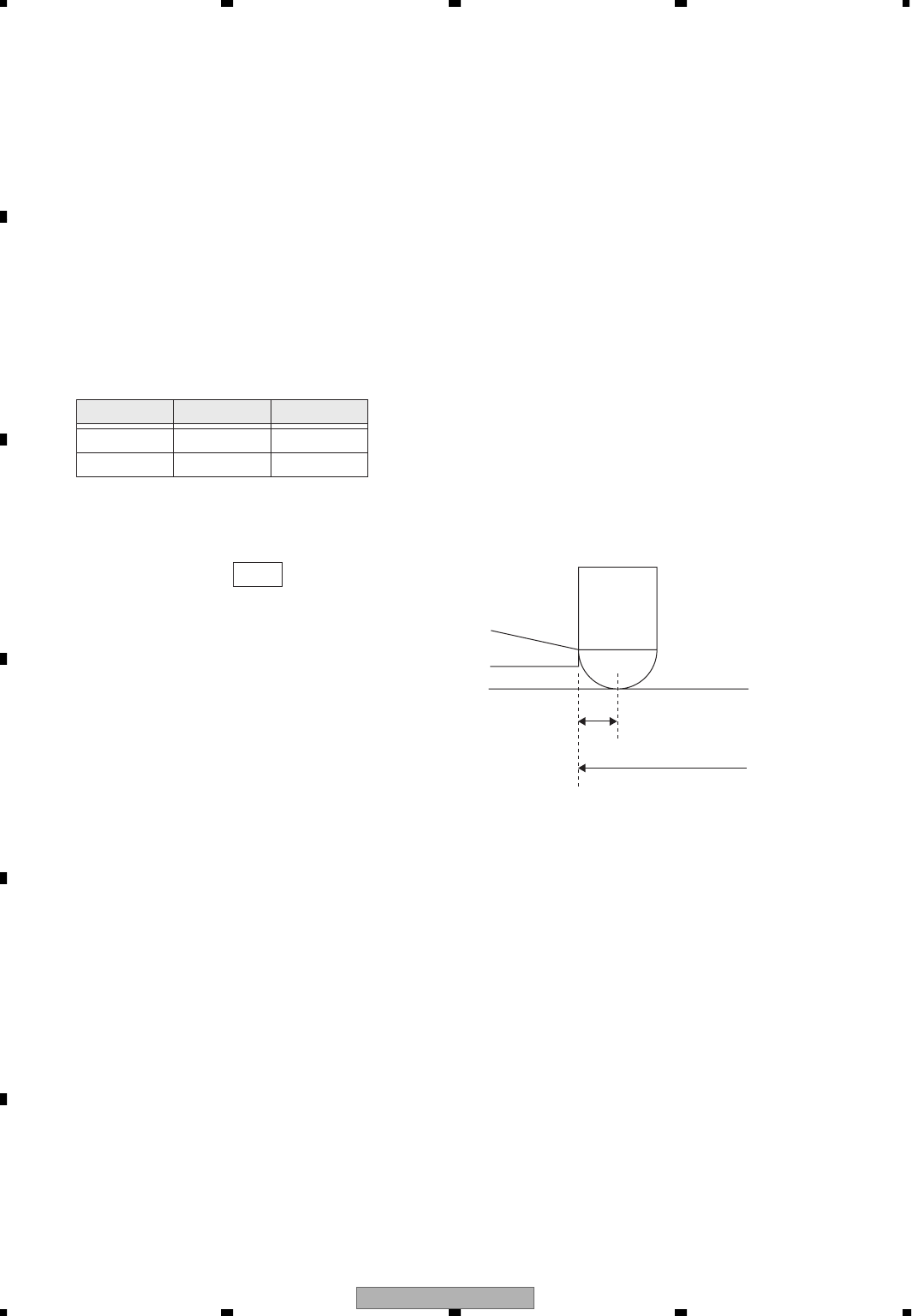
AVH-P5700DVD/EW
152
1234
1234
C
D
F
A
B
E
Coordinates Minimum Maximum
X
Y
pen tip for adjustment (zoom in)
out-of-alignment length
permissible screen area
58
64
248
241
Default is showed below.
2.2 Operation specification
2.3 Processing detail
Press [ENT] key of main unit or remote control unit to finish adjustment and store setting value (maximum and minimum
value) to EEPROM only when the taken value is within permissible zone.
Receive confirmation screen TP and display OK or NG after fulfilling the following conditions:
[O.K] is displayed after storing a taken value to EEPROM.
[NG] is displayed when a taken value is determined to be outside permissible zone.
2.4 Additional information
Consider diameter of the top of jig (pen tip) before adjusting outermost circumference.
Out-of-alignment length 0.8 mm
Perform calibration data operation with the size calculated
by subtracting out-of-alignment length from
permissible screen area.
Touch the outermost circumference of screen, and take outermost circumference value of X, Y.
Press [ENT] key of main unit or remote control unit to finish adjustment.
After finishing adjustment, if a taken value is within permissible zone, enter [O.K] at the center, and if it is outside
permissible zone, enter [NG] at the center.
Then, press [ENT] key of main unit or remote control unit to return to TOP MENU.
AVH-P5700DVD/EW 153
5678
5678
C
D
F
A
B
E
+
1
3
+14
+15
+16
F I N I S H E D
+17
+
12
+11
+10
+ 9
+
5
+ 6
+ 7
+ 8 + 1
+4
+ 3
+ 2
[ E N T E R ] R e t u r n t o M e n u
0
1 2
3
4
5
6
7
8
9
0
1 2
3
4
5
6
7
8
9
0
1 2
3
4
5
6
7
8
9
0
1
2
3
4
5
6
7
8
9
0
1
2
3
4
5
6
7
8
9
0 1 2 3 4 5 6 7 8 9 0 1 2 3 4 5 6 7 8 9 0 1 2 3 4 5 6 7 8 9
0
1
2
3
4
5
6
7
8
9
0
1
2
3
4
5
6
7
8
9
*It is invalid if the distant point from displayed block is pressed.
*
*
[
FINI
S
H
E
D
]
a
b
ove
i
s
di
s
pl
a
y
e
d
w
h
en t
h
e num
b
er 17
i
s
p
resse
d.
3
C
ALIBRATI
ON
3
.
1
O
vervie
w
P
r
ess
cu
r
so
r
[
+
]
o
n
t
h
e
sc
r
ee
n in
tu
rn
to
ca
li
b
r
ate
a
n
d
sto
r
e
t
h
e
set
v
a
l
ue
to
EEPR
O
M
.
The taken settin
g
value is stored in EEPR
O
M only when pressin
g
the 17th point, and
[
FINI
S
H
E
D
]
i
s
di
s
pl
a
y
e
d
a
f
ter
stor
i
n
g.
See
“
t
” about the area for storin
g
EEPR
O
M settin
g
s
.
See
“
”
See
“
3
.
3
Processin
g
detail
E
xecute ca
lib
rat
i
on
b
y press
i
n
g
cursor
di
sp
l
aye
d
at 16 po
i
nts on t
h
e screen
i
n turn an
d
press one po
i
nt to
fi
n
i
s
h
at t
h
e
end
(
total 17
p
oints
).
Af
ter t
h
e 17t
h
p
o
i
nt
i
s
di
s
pl
a
y
e
d,
[
FINI
S
H
E
D
]
i
s
i
n
di
cate
d
at t
h
e center o
f
t
h
e screen
.
C
ursor is always showin
g
one point only and the next cursor is displayed after pressin
g
one correctly
.
P
r
ess
[
EN
T
]
ke
y
of main unit or remote control unit to return to T
O
P MENU.
Wh
en press
i
n
g
[
E
S
C
] durin
g
ad
j
ustment, the ad
j
usted value is not stored and T
O
P MENU screen is displayed
.
3
.
2
O
p
eration s
p
ecificatio
n
AVH-P5700DVD/EW
154
1234
1234
C
D
F
A
B
E
# # # T P c o o r d i n a t e s t e s t # # #
P o s i t i o n ( 7 9 , 8 0 )+ A D
B e f o r e
A f t e r
( 0 , 0 )
( 0 , 0 )
( 0 , 0 )
[ E N T E R ] R e t u r n t o M e n u
0 1 2 3 4 5 6 7 8 9 0 1 2 3 4 5 6 7 8 9 0 1 2 3 4 5 6 7 8 9
0
1
2
3
4
5
6
7
8
9
0
1
2
3
4
5
6
7
8
9
4.2 Operation specification
4 TOUCH PANEL COORDINATES AUDIT
4.1 Screen configuration
*Explanation about displayed coordinates (from up to down)
(79, 80) : Drawing system coordinates of the cross point of horizontal and vertical lines (X direction, Y direction [0-500,
0-240]).
(0,0) : AD data value of the coordinates of pressed point (X direction, Y direction).
(0,0) : The coordinates of normalized AD data of pressed point within permissible zone (X direction, Y direction).
(0,0) : The coordinates corrected by calibration of the normalized coordinates (X direction, Y direction).
Specification correction
Rounding was done within the setting range with outermost circumference adjustment in the conventional product
(AVH-P9DVA).
When value more than outermost circumference value was entered, the outermost circumference value was used.
From this time, considering that audit may be performed without outermost circumference adjustment, no limit is set.
4.3 Processing detail
Move [ + ] mark by up and down, right and left keys and display its OSD coordinates.
Press [ ENT ] key of main unit or remote control unit to return to TOP MENU.
M152 : The + mark is not displayed at 16 points on the screen.
Check displayed coordinates before and after correction when pressing touch panel and perform operation check.
Key
[Remote control unit code]
Operatable with main unit key
Operatable only with remote control unit
Code
ENTER AD19AF63
↑AD40
↓AD41
←AD42
→AD43
AVH-P5700DVD/EW 155
5678
5678
C
D
F
A
B
E
# # # C a l i b r a t i o n t e s t # # #
X _ b e f o r e
y _ b e f o r e
X _ A f t e r
y _ A f t e r
+
++
+
+
+
+O K
+
+
+
+
+
+
+
+
+
= 3 5
= 4 0
= 3 8
= 4 5
[ E N T E R ] R e t u r n t o M e n u
0 1 2 3 4 5 6 7 8 9 0 1 2 3 4 5 6 7 8 9 0 1 2 3 4 5 6 7 8 9
0
1
2
3
4
5
6
7
8
9
4.5 Judgment processing
4.4 Screen processing (additional)
OK, NG judgment indication
According to the length between + indication and touched coordinates (the point where the cursor is pointed), OK or NG
is indicated.
OK condition the length between + position and cursor indication is within ±6 mm at the center
NG condition except OK condition
The + mark at the point touched on screen is displayed.
When a finger etc. is detached, the + mark at the point pressed at the last moment is displayed continuously.
The + mark displayed when being pressed is showed at the under layer of the fixed red + mark.
The value displayed at that time is still being displayed.
AVH-P5700DVD/EW
156
1234
1234
C
D
F
A
B
E
0 1 2 3 4 5 6 7 8 9 0 1 2 3 4 5 6 7 8 9 0 1 2 3 4 5 6 7 8 9
# # # C a l i b r a t i o n t e s t # # #
X _ b e f o r e
y _ b e f o r e
X _ A f t e r
y _ A f t e r
+
+
+
+
+
+
+
+
+
+
+
+
+
+
+
+
= 3 5
= 4 0
= 3 8
= 4 5
+
[ E N T E R ] R e t u r n t o M e n u
Coordinates after data A
33 ∼ 95 Right corner correction
data of correction area
96 ∼ 160
161 ∼ 224
B
Left corner correction data
of correction area
C
Left corner coordinates of
correction area
0
1
2
3
4
5
6
7
8
9
5 TOUCH PANEL CONFIRMATION
5.1 Screen configuration
Displayed items
panel x_before = * normalized data before calibration (0-255)
panel y_before = * normalized data before calibration (0-255)
panel x_after = * normalized data after calibration (0-255)
panel y_after = * normalized data after calibration (0-255)
Follow the steps below to convert AD value entered from touch panel to the corrected coordinates.
(Follow 1 → 2 in turn. Execute them during regular operation.)
1 Data expansion of raw coordinates
Coordinates after data expansion = (raw coordinates − minimum value ) × 255 ÷ (maximum value − minimum value)
*If raw coordinates are 0, the coordinates after data expansion should be 0.
2 Coordinates correction after data expansion
(1) If the coordinates are under 224 after data expansion;
Coordinates after correction = coordinates after data expansion + correction value × (1 − (coordinates after data
expansion − 224) ÷ 31)
*31: Because there are 31 points of coordinates position from the value 225 to 255.
*The effect of correction value declines as the value is going to 255.
(2) If the coordinates are less than or equal to 32 after data expansion;
Coordinates after correction = coordinates after data expansion + (correction value × coordinates after data
expansion ÷ 32)
*32 : Because there are 32 points of coordinates position from the value 0 to 32 (coordinates 0 is not included).
*The effect of correction value declines as the value is going to 0.
(3) If the coordinates are 33 ∼ 224 after data expansion;
Coordinates after correction = coordinates after data expansion + B + (A − B) × (coordinates after data expansion
− C) ÷ 64)
*64 : Because there are 64 points of coordinates position in each area.
*Add the correction value at the left corner first. Then, the effect of correction value is increasing as going to right.
5.3 Processing detail
5.2 Operation specification
Check the coordinates before and after correction by touching the touch panel.
Press [ ENT ] key of main unit or remote control unit to return to TOP MENU.
Check displayed coordinates before and after correction when pressing touch panel and perform operation check.
AVH-P5700DVD/EW 157
5678
5678
C
D
F
A
B
E
0
1 2
3
4
5
6
7
8
9
0
1 2
3
4
5
6
7
8
9
0
1 2
3
4
5
6
7
8
9
#
#
#
T P
d
a
t
a
i
n
i
t
i
a
li
z
e
#
#
#
[ ▲ ] R a n g e i n i t
[ ▼ ] C a l i b r a t i o n i n i t
[ E N T E R ] R e t u r n t o M e n u
0
1
2
3
4
5
6
7
8
9
0
1
2
3
4
5
6
7
8
9
6.2
6
INITIALIZATI
O
N
O
F T
OUC
H PANEL
C
ALIBRATI
O
N DATA
6
.
1
Screen confi
g
uratio
n
The mark indicates that adjustment is finished.
Deleted after initialization.
(initialization = default inside microcomputer)
[
I
n
i
t
i
a
li
zat
i
on
p
rocess
i
n
g
]
I
t
i
n
i
t
i
a
li
zes outermost c
i
rcum
f
erence va
l
ue an
d
16-
p
o
i
nt va
l
ue
.
It writes default of initialized items to EEPR
O
M and clears conditioned fla
g.
6
.
3
Processin
g
detai
l
[
]
C
learin
g
outermost circumference ad
j
ustment value and return it to default
[
▼
]
C
learin
g
16-point calibration value and return it to default
.
P
r
ess
[
EN
T
]
ke
y
of main unit or remote control unit to return to T
O
P MENU
.
R
eturn t
h
e outermost c
i
rcum
f
erence, 16-
p
o
i
nt ca
lib
rat
i
on
d
ata to
d
e
f
au
l
t
.

AVH-P5700DVD/EW
158
1234
1234
C
D
F
A
B
E
- Information About Permissible Error Settings For TPS Touch Panel Audit
Outermost circumference settings
Permissible error of outermost circumference should be 10% of valid zone.
*10% is calculated by the value determined by the outermost circumference zone as 100.
Outermost circumference default
min
X Voltage (V)
digital (AD)
dot (OSD)
NAVI
Voltage (V)
digital (AD)
dot (OSD)
NAVI
ref
0.75
58
0
0
0.83
64
0
0
3.3
3.21
248
240
255
3.12
241
232
255
(V)
Y
*Default above is measured with to the very limit of frame during measuring outermost circumference value.
max
Settings valid zone (OK)
Settings invalid zone (NG)
10%
10%
Outermost circumference adjustment OK zone
min
X Minimum permissible value
Maximum permissible value
Minimum permissible value
Maximum permissible value
0
77
0
82
229
255
223
255
Y
max
Outermost circumference permissible error value
X Voltage (V)
digital (AD)
dot (OSD)
NAVI
Voltage (V)
digital (AD)
dot (OSD)
NAVI
10%
19
0.25
24
26
0.23
18
23
26
Y

AVH-P5700DVD/EW 159
5678
5678
C
D
F
A
B
E
Calibration
Permissible error of point calibration should be 10%
Settings valid zone (OK)
Settings invalid zone (NG)
10%
10%
+
Outermost circumference permissible error value
X Voltage (V)
digital (AD)
dot (OSD)
NAVI
Voltage (V)
digital (AD)
dot (OSD)
NAVI
3.3 (V)
10%
19
0.25
24
26
0.23
18
23
26
Y
ref
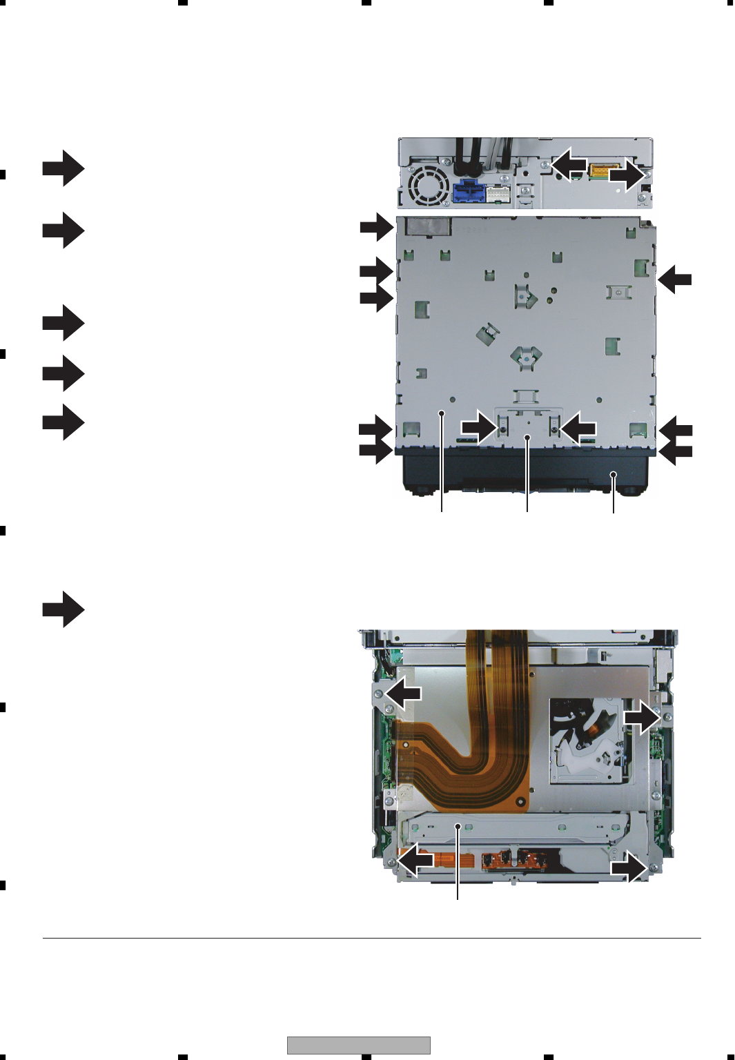
AVH-P5700DVD/EW
160
1234
1234
C
D
F
A
B
E
7. GENERAL INFORMATION
7.1 DIAGNOSIS
7.1.1 DISASSEMBLY
Fig.1
- Removing the Grille Assy (Fig.1)
Fig.2
- Removing the Case
5
22
Grille Assy
1
1
1
5
Case
3
3
3
3
3
1Remove the two screws and then remove
the Holder.
Disconnect the connector.
11
Holder
2Remove the two screws and then remove
the Grille Assy.
3Remove the five screws.(Fig.1)
4Remove the screw.(Fig.1)
Note) Inside the product there is a flexible substrate
that connects the Case and the Bracket.
Be very careful and do not give it a strong pull
when removing the Case, otherwise it may
be torn.
5Remove the two screws and then remove
the Case.(Fig.1)
4
1
- Removing the DVD Mechanism Module (Fig.2)
Remove the four screws.
Disconnect the connector and then remove the
DVD Mechanism Module.
1
DVD Mechanism Module
Monitor section is drawn out forward.

AVH-P5700DVD/EW 161
5678
5678
C
D
F
A
B
E
- Removing the Mother Unit (Fig.3)
5
5
4
Fig.3
6
6
3
6
6
7
Mother Unit
5
1
4
Panel
Holder
1Straighten the tabs at two locations
indicated.
2Remove the two screws and then remove
the Holder.
4Remove the two screws.
6Straighten the tabs at five locations
indicated.
7Remove the screw and then remove
the Mother Unit.
5Remove the five screws and then remove
the Panel.
1
3
5
2
3Remove the two screws.
Disconnect the connector and then remove the
Fan Motor.
Fan Motor
2
5
6
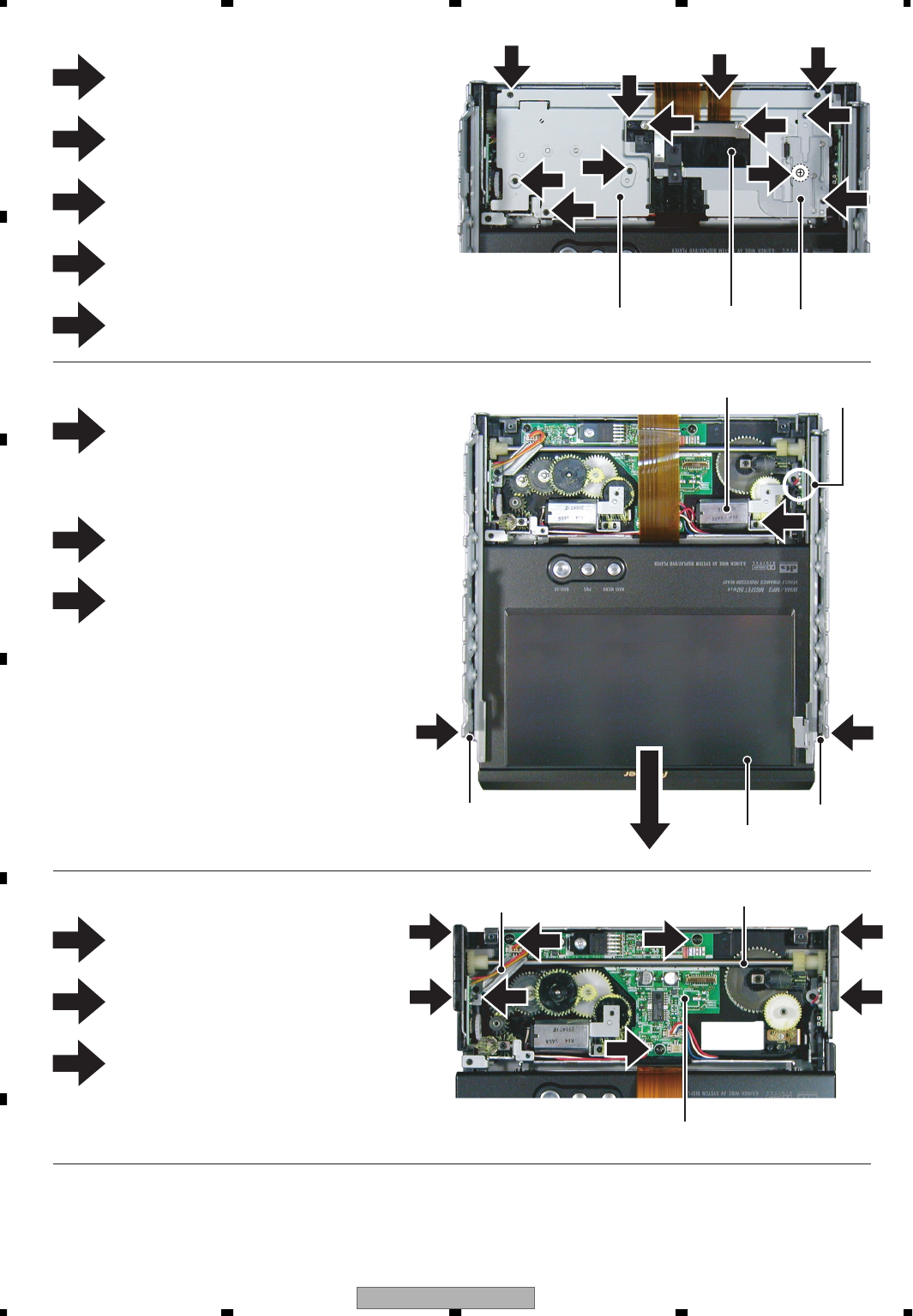
AVH-P5700DVD/EW
162
1234
1234
C
D
F
A
B
E
Fig.4
- Removing the Case (Fig.4)
Remove the two screws and then remove
the Lever.
1
4
Holder
1
Fig.5
1
Motor Unit
- Removing the Display Assy (Fig.5)
1
55
2
Case
Remove the three screws and then remove
the Holder.
2
Holder Holder
Display Assy
2
2
Remove the two screws and then remove
the two Holders.
2
Pull out the Display Assy in the arrow
indicated direction.
Note) When reassembling, hold the switch down
with tweezers or the like and put the Display Assy
back to the Chassis. Otherwise, the switch may be
damaged and not function properly.
3
Fig.6
1
Bracket Shaft Unit
2
2
2
2
Main Unit
33
3
- Removing the Main Unit (Fig.6)
Remove the screw and then remove
the Bracket.
1
Remove the four screws and then
remove the Shaft Unit.
2
3
1
Remove the screw.
Disconnect the connector and then remove
the Motor Unit.
Remove the three screws.
Disconnect the connector and then remove
the Main Unit.
3
Switch
5
53
2
2
5
Lever
Remove the screw.
4
Disconnect the connector.
3
Remove the five screws and then remove
the Case.
5

AVH-P5700DVD/EW 163
5678
5678
C
D
F
A
B
E
Fig.7
- Removing the Display Assy (Fig.7)
1
2
11
2
Display Assy
2
Fig.8
1
Monitor PCB
2
2
1
- Removing the Monitor PCB (Fig.8)
Straighten the tabs at two locations indicated.
1
2
Cover Unit
Holder
4
4
4
4
2
Remove the two screws and then remove
the Holder.
Remove the three screws and then remove
the Cover Unit.
3Remove the four screws.
Disconnect the connector and then remove
the Display Assy.
Remove the three screws.
Disconnect the connector and then remove
the Monitor PCB.
2
Note:
Tighten the screws with the panel in warped state as shown in the photograph below.
Otherwise, it will be difficult to install Detach Grille Assy to Panel Assy.
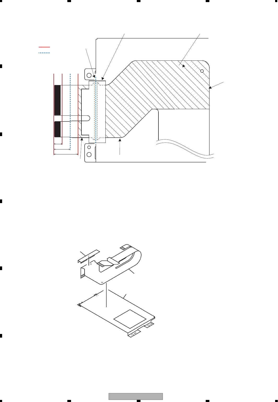
AVH-P5700DVD/EW
164
1234
1234
C
D
F
A
B
E
A
C
B
6614
(mm)
: Valley fold
: Mountain fold
1. When exchanging a flexible PCB (CNP8806), fold the PCB as indicated in the upper figure.
2. Connect the mother unit side of the flexible PCB to the connecter of the mother unit.
3. Remove release B part of coated paper of the flexible PCB.
4. Paste A part of the flexible PCB along the corner of the bracket (CND2627).
3. Paste C part of the flexible PCB on the bracket.
5. Paste the sheet (CNM9517) according to A part of the flexible PCB.
If the flexible PCB and the sheet are not contacted at this time, a monitor part will get damaged or a shutter
mechanism will get hung up. Make sure that the flexible PCB and the sheet contact a bracket.
In addition, since adhesive strength becomes weak, do not use again the sheet removed once.
Release coated paper 1
Mother unit side
Bracket (CND2627)
Sheet (CNM9517)
- Exchanging Flexible PCB (CNP8806)
Flexible PCB (CNP8806)
Flexible PCB (CNP8806)
Sheet (CNM9517)
Bracket (CND2627)

AVH-P5700DVD/EW 165
5678
5678
C
D
F
A
B
E
- Precautions on handling the mechanism module
1. Hold the upper and main frames.
2. Do not hold the front portion of the upper frame. It is a delicate part.
3. Do not touch the switches on the top panel.
4. Be careful not to catch the flexible cables.
Do not touch here. Do not touch here.
Do not hold this delicate portion.
- Removing the module pc board
Load motor
leads and clamp SW leads
Connector
(for 8/12 detection flexible cable)
Connector
(for pickup flexible cable)
Connector
(for CRG flexible cable)
Short here.
A
BC
Module pc board
1. Set the mechanism to the lock position (disc load standby position).
2. Place the mechanism module upside down.
3. Short the two lands on the pickup flexible cable as shown below.
4. Be sure to disconnect the pickup flexible cable and the CRG flexible cable from the connectors
to protect them from damages.
5. Remove solder from the load motor leads and clamp SW leads.
6. Loosen the two fixing screws. Lift the position A of the module pc board lightly and move it
in the direction B to remove it. Be careful not to damage the flexible cable C.
7. Disconnect the 8/12 detection flexible-cable from the connector.
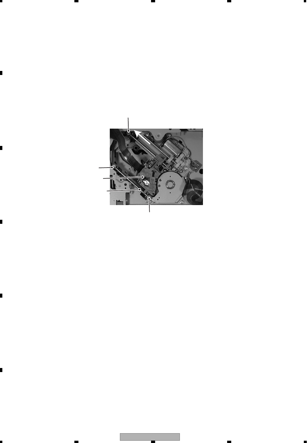
AVH-P5700DVD/EW
166
1234
1234
C
D
F
A
B
E
-Removing the pickup unit
1. Remove the module pc board in accordance with the procedure of "Removing the module pc board.”
2. While holding the pickup case, remove the skew screw (main).
3. Lifting the end of the pickup rack, slide the main shaft, and remove the pickup unit.
Notes:
Replacing the pickup unit requires the skew adjustment.
Remove glue from both ends of the main and sub shafts, and skew stud.
Do not reuse the old skew screw. Be sure to use a brand-new skew screw supplied with a new pickup unit.
Fix the skew screw with glue (GYL1001) after adjustment.
Sub shaft
Pickup unit
Skew screw
Skew screw (main)
Skew screw

AVH-P5700DVD/EW 167
5678
5678
C
D
F
A
B
E
- How to install the Volume Unit fo the Drive Unit
When install the Volume Unit, adjust the positioning of the rotating angle of the gear.
1. Set the Monitor Unit horizontally with the Main Unit of the Drive Unit.
2. When install the gear unit, rotate the gear by hand until the square box of the gear keeps in a horizontal
position like the figure below.
*Gap of one teeth is acceptable.
Square box
AVH-P5700DVD/EW
168
1234
1234
C
D
F
A
B
E
7.1.2 PCB LOCATIONS
COMPOUND UINT(B)
COMPOUND UINT(A)
DVD CORE UNIT
RELAY PCB
D
C
M
MOTHER UNIT
A
VOLUME UNIT
L
E
RGB UNIT
G
MONITOR PCB
B
KEYBOARD UNIT
I
UPPER PCB
H
INVERTER PCB
F
MAIN UNIT
J
SW UNIT
K
AVH-P5700DVD/EW 169
5678
5678
C
D
F
A
B
E
7.1.3 CONNECTOR FUNCTION DESCRIPTION
16
15
2
1
1 : FL-
2 : RL-
3 : FL+
4 : RL+
5 : FR-
6 : RR-
7 : FR+
8 : RR+
9 : P.B.
10 : VGND
11 : ACC
12 : B.REM
13 : B.G
14 : MUTE
15 : B.UP
16 : GND
1 : REAR V
2 : VGN D
3 : FL
4 : FLGND
5 : FR
6 : FRGND
7 : SWL
8 : SWLGND
9 : SWR
10 : SWRGND
11 : VCRINL(EW)
: RL(UC)
12 : VCRGND(EW)
: RLGND(UC)
13 : VCRINR(EW)
: RR(UC)
14 : VCRGND(EW)
: RRGND(UC)
1 : CCR
2 : CCG
3 : CCB
4 : CCSYNC
5 : GNDSIG
6 : DVDVBS
7 : GNDDVD
8 : YS
9 : NC
10 : CCAUL
11 : CCAUR
12 : GNDAU
13 : ONSEI+
14 : ONSEI-
15 : REAUR
16 : REAUL
17 : GNDRAU
18 : CCREM
19 : DSEN
20 : TVON
21 : GION
22 : MONON
23 : VSW5
24 : HTXD
25 : HRXD
26 : GNDD
M4x6MAX M5x6MAX
1
2
13
14
1
2
25
26
FM/AM ANTENNA INPUT
1. BUS+
2. GND
3. GND
4. NC
5. BUS-
6. GND
7. BUS L+ OUTPUT
8. ASENB
9. BUS R+ OUTPUT
10. BUS R- OUTPUT
11. BUS L- OUT PUT
1. COMP GND
2. COMP
5. IP_SEL1
4. IP_SEL2
12. AV_ON
6. LED_V
7. GND
10. REMIN
11. NEW AV SENS
REAR VIEW CAMERA INPUT(BROWN)
VIDEO INPUT(YELLOW)
RIGHT AUDIO INPUT(RED)
LEFT AUDIO INPUT(WHITE)
UC
RGB VIDEO INPUTPOWER SUPPLY,
SPEAKER OUTPUT RCA OUTPUT
IP-BUS INPUT
AV-BUS INPUT
AVH-P5700DVD/EW
170
1234
1234
C
D
F
A
B
E
7.2 IC
1 IN B
2 IN A
3 GND 4 OUT Y
5 VCC
123
VOUT VSS NC
VREF
45
VIN ON/OFF
ON/OFF
+
-
1
2
3
4
8
7
6
5
+INPUT
V-
-INPUT
BAL
ONTPUT
NC
V+
BAL
*TC7SET08FUS1,TC7SH08FUS1
TC7SET08FUS1
TC7SH08FUS1
NJM2136V
S-818A35AUC-BGP
NJM2388F84
TC74VHC08FTS1
PE5484A
PE5485A
TC90A96AFG
TC7SET04FUS1
TC74VHC04FTS1
BD6171KV
S-1131B25UC-N4K
S-1131B15UC-N4A
TC7SH02FUS1
TC7SH32FUS1
S-93C56BD0I-J8
OZ961ISN
PEG087A
K4S283232E-TC75
NJM2140R
TC7WH157FU
R1130H501B
SM8707LV
TC74LCX16373AFT
SM8707LV
TC74LCK16373AFT
PE5401A
PD6516A
S-L2980A50MC-C7J
LTC3411EMS
TC7SZ125FU
MN35104UB
*NJM2136V S-818A35AUC-BGP
IC's marked by * are MOS type.
Be careful in handling them because they are very
liable to be damaged by electrostatic induction.

AVH-P5700DVD/EW 171
5678
5678
C
D
F
A
B
E
1
2
3
4
VIN
Bandgap
Reference
VOUT
GND
CONT
ON/OFF
control
Over Voltage
Protection
Thermal
Protection
Over Current
Protection
+
-
14 VCC
13 4B
12 4A
11 4Y
10 3B
9 3A
8 3Y
1 1A
2 1B
3 1Y
4 2A
5 2B
6 2Y
7 GND
TC74VHC08FTS1
NJM2388F84

AVH-P5700DVD/EW
172
1234
1234
C
D
F
A
B
E
NC
MODEL0,1
NC
PORTGND0
ROMCS
ROMCLK
ROMDATA
VDT
VCK
FRONTMUTE
VST
MTRPW
MTRSEL
MTRS
MTR1
MTR2
SNSPW
PUSHSW
DEGOSW
LIFTPUL
PORTVDD0
RDT
rds%&k
rdslk
RECIVE
NC
ACCPW
AMPPW
SYSPW
VPW
DDCCNTL
DLED
ILMGRN
PCL
GND0
CPUREG
VDD0
reset
VPP
TSI
NC
TCK
ldet
TUNPDI
TUNPDO
TUNPCK
NC
RCAMUTE
VSELIN1,2
AVONIN
NC
TESTIN
rck
PRGON
VPPON
PORTVDD1
Pin Name
-Pin Functions(PE5484A(EW),PE5485A(UC))
1
2,3
4
5
6
7
8
9
10
11
12
13
14
15
16
17
18
19
20
21
22
23
24
25
26
27,28
29
30
31
32
33
34
35
36
37
38
39
40
41
42
43
44
45
46
47
48
49
50
51,52
53
54,55
56
57
58
59
60
Pin No.
I
O
O
I/O
O
O
O
O
O
O
O
O
O
O
I
I
I
I
I
I
O
O
O
O
O
O
O
O
I
I
I
I
I
I/O
I/O
O
I
I
I
I
I
O
I/O
Not used
Model select input
Not used
Port GND
ROM Chip select output
ROM Clock output
ROM Data Input/output
Electronic volume:Data output
Electronic volume:Clock output
Front Mute output
Electronic volume:Strobe output
FLAP Motor power supply control output
FLAP motor control output
FLAP Motor speed contorl output
FLAP angle motor control signal output
FLAP position motor control signal
FLAP sense power supply output
FLAP LIFE sense switch input
FLAP monitor angle 0 sense input
FLAP lift pulse input
Port power supply
RDS data input (EW model)
RDS 57kHz input (EW model)
RDS signal input (EW model)
Not used
Not used
ACC power control output
Amp power control output
Video power control output
DC/DC converter control output
Anti-theft LED output
Green illumination output
System clock ouptut
GND
Filter capacitor connected
Power supply
System reset input
Power supply for frash ROM
Test data input
Not used
Test data clock input
RDS PLL signal (EW model)
TUNER PLL data input
TUNER PLL data input/output
TUNER PLL clock input/output
Not used
RCA REAR mute output
VSEL input
AV-BUS AV video sense input
Not used
Test mode input
RDS data clock (EW model)
System microcomputer program mode input
VPP ON/OFF output
Port power supply
Function and operation

AVH-P5700DVD/EW 173
5678
5678
C
D
F
A
B
E
61
62
63-65
66
67
68
69
70,71
72
73,74
75,76
77,78
79,80
81
82
83
84
85
86
87
88
89
90
91
92
93-95
96
97-99
100
101
102
103
104
105
106
107
108
109
110
111
112
113
114
115,116
117
118
119
120
121
122
123
124
125,126
127
128
129
130
PRGSW
PRGRST
NC
CILM
ILMRED
BEEP
bsens
XT2,1
GND2
X1,2
NC
COOLCNT1,2
NC
CONTBIN
NC
dsens
SDA
NC
SCL
ASENBO
IPPW
NC
ierx
ietx
PORTGND1
NC
asens
NC
TUNPCE
tunpce@
PORTVDD2
CONTVDD
CONTVD8
DREM
REMUTE
RXMOM
TXMON
SWVDD
NC
RXMS3
TXMS3
IRQPWR
xreset
NC
RXNAV
TXNAV
rgbari
NC
NMIXCNT
MUTE
NC
AMPMUTE
NC
TELIN
VDD1
PBSENS
BGSENS
I
O
O
O
O
I
O
I
I
I/O
O
O
O
I
O
I
O
O
O
O
O
O
I
O
O
I
O
O
O
I
O
I
O
O
O
I
I
I
System microcomputer programing mode input
Display microcomputer programing mode reset output
Not used
Flap illumination output
Red illumination output (EW model)
BEEP output
Backup sense input
Sub clock oscillator connect
GND
Main clock oscillator connect
Not used
Fan control output1,2
Not used
Backup off intput
Notused
Detach sense intput
AVselector data input/output
Not used
AV selector clock output
Slave ACC sense output
IPBUS driver power supply contorl output
Not used
IPBUS data input
IPBUS data output
Port GND
Not used
ACC sense input
Not used
TUNER PLL chip enable output
TUNER PLL chip enable output 2
Port power supply
DVD Mechanism modul digital power control output
DVD Mechanism modul motor power control output
NAVI Reboot remote control output
NAVI remote control mute output
Display microcomputer data input
Display microcomputer data output
Display microcomputer power supply output
Not used
DVD Mechanism modul data input
DVD Mechanism modul data output
DVD Mechanism modul backup power output
DVD Mechanism modul mechanism CPU reset output
Not used
NAVI data input
NAVI command output
RGB navigation ON sense input
Not used
Voice guide mute output
Mute output
Not used
AMP mute output
Not used
TEL mute input
Power supply
Packing brake sense input
Back gear sense input
Pin No. Pin Name I/O Function and operation
AVH-P5700DVD/EW
174
1234
1234
C
D
F
A
B
E
144 109
37
1
36
108
73
72
*PE5484A (EW),PE5485A (UC)
Pin Name I/O Function and operation
GND1
NC
TUNSL
NC
ANGLEIN
NC
KEYDTA0-2
ADCVDD
ADCGND
I
I
I
GND
Not used
TUNER signal level input
Not used
Mechanism volume for angle sense input
Not used
Key data input0-2
A/D Power supply
A/D GND
131
132-134
135
136
137
138,139
140-142
143
144
Pin No.

AVH-P5700DVD/EW 175
5678
5678
C
D
F
A
B
E
11
22
33
44
55
66
77
88
99
1010
1111
1212
1313
1414
1515
1616
1717
1818
1919
2020
2121
2222
2323
2424
2525
2626
2727
2828
2929
3030
3131
3232
3333
3434
3535
3636
3737
3838
3939
4040
4141
4242
4343
4444
132132
131131
130130
129129
128128
127127
126126
125125
124124
123123
122122
121121
120120
119119
118118
117117
116116
115115
114114
113113
112112
111111
110110
109109
108108
107107
106106
105105
104104
103103
102102
101101
100100
9999
9898
9797
9696
9595
9494
9393
9292
9191
9090
8989
VSS-D1VSS-D1
VDD-D1VDD-D1
R7 D.INR7 D.IN
R6 D.INR6 D.IN
R5 D.INR5 D.IN
R4 D.INR4 D.IN
R3 D.INR3 D.IN
R2 D.INR2 D.IN
VSS-IO1VSS-IO1
VDD-IO1VDD-IO1
R1 D.INR1 D.IN
R0 D.INR0 D.IN
VSS-D2VSS-D2
VDD-D2VDD-D2
G7 D.ING7 D.IN
G6 D.ING6 D.IN
G5 D.ING5 D.IN
G4 D.ING4 D.IN
G3 D.ING3 D.IN
G2 D.ING2 D.IN
VSS-IO2VSS-IO2
VDD-IO2VDD-IO2
G1 D. ING1 D. IN
G0 D.ING0 D.IN
VSS-D3VSS-D3
VDD-D3VDD-D3
B7 D.INB7 D.IN
B6 D.INB6 D.IN
B5 D.INB5 D.IN
B4 D.INB4 D.IN
B3 D.INB3 D.IN
B2 D.INB2 D.IN
VSS-IO3VSS-IO3
VDD-IO3VDD-IO3
B1 D.INB1 D.IN
B0 D.INB0 D.IN
VSS-D4VSS-D4
VDD-D4VDD-D4
D-RGB V.Sync IND-RGB V.Sync IN
D-RGB H/C.Sync IND-RGB H/C.Sync IN
D-RGB Clock IND-RGB Clock IN
Test(DTNB)Test(DTNB)
VDD-D5VDD-D5
VSS-D5VSS-D5
888887878686
8585
8484
8383
82828181
808079797878
7777
7676
75757474
7373
7272
7171
7070
69696868
6767
6666
6565646463636262616160605959
5858
57575656
5555
54545353525251515050494948484747
4646
4545
133133134134135135
136136
137137
138138
139139140140
141141142142143143
144144
145145
146146147147
148148
149149
150150
151151
152152153153
154154
155155
156156157157158158159159160160161161162162
163163
164164165165
166166
167167168168169169170170171171172172173173174174
175175
176176
VSS25-DRAMVSS25-DRAM
VDD15-DRAM3VDD15-DRAM3
VSS15-DRAM3VSS15-DRAM3
VDD-IO7VDD-IO7
VSS-IO7VSS-IO7
VDD-D11VDD-D11
VSS-D11VSS-D11
VDD15-DRAM2VDD15-DRAM2
VSS15-DRAM2VSS15-DRAM2
Test mode1Test mode1
Test mode0Test mode0
VDD15-DRAM1VDD15-DRAM1
VSS15-DRAM1VSS15-DRAM1
VDD-D10VDD-D10
VSS-D10VSS-D10
Test(Scan)Test(Scan)
Test(MBST)Test(MBST)
Main Clock SetMain Clock Set
Dispaly MuteDispaly Mute
VDD-D9VDD-D9
VSS-D9VSS-D9
Rest INRest IN
Bus ACK OutBus ACK Out
Bus Data I/OBus Data I/O
Bus Clock INBus Clock IN
VDD-IO6VDD-IO6
OSD BLK.H INOSD BLK.H IN
OSD BLK.L INOSD BLK.L IN
OSD R INOSD R IN
OSD G INOSD G IN
OSD B INOSD B IN
VDD-D8VDD-D8
VSS-IO5VSS-IO5
VDD-IO5VDD-IO5
OSD H/C.Sync OutOSD H/C.Sync Out
OSD V.Sync Out OSD V.Sync Out
OSD Clock Out OSD Clock Out
VDD-D7VDD-D7
VDD25-DRAMVDD25-DRAM
Test mode3Test mode3
Test mode2Test mode2
VSS-IO5VSS-IO5
VSS-IO6VSS-IO6
VSS-D7VSS-D7
VSS-D6VSS-D6
VDD-D6VDD-D6
R7 D.INR7 D.IN
R6 D.INR6 D.IN
VSS-D6VSS-D6
VDD-D6VDD-D6
VDD-X'talVDD-X'tal
X'tal INX'tal IN
X'tal OutX'tal Out
VSS-X'talVSS-X'tal
VDD-PLLVDD-PLL
PLL INPLL IN
PLL FilterPLL Filter
VSS-PLLVSS-PLL
DVDDDVDD
DAC OutDAC Out
DVSSDVSS
DAC BiasDAC Bias
Sub ADC BiasSub ADC Bias
Sub ADC Vref.TSub ADC Vref.T
VDD Sub ADCVDD Sub ADC
Sub C.Video IN.1Sub C.Video IN.1
VSS Sub ADCVSS Sub ADC
Sub C.Video IN.2Sub C.Video IN.2
Sub ADC Vref BSub ADC Vref B
VSS Main ADC 1VSS Main ADC 1
VDD Main ADC 1VDD Main ADC 1
Main ADC Vref BMain ADC Vref B
R IN 1R IN 1
G IN 1G IN 1
B IN 1B IN 1
VSS Main ADC 2VSS Main ADC 2
VDD Main ADC 2VDD Main ADC 2
R IN 2R IN 2
G IN 2G IN 2
B IN 2B IN 2
Main ADC Vref TMain ADC Vref T
Main ADC BiasMain ADC Bias
VSS Main ADC 3VSS Main ADC 3
VDD Main ADC 3VDD Main ADC 3
D-VSSD-VSS
Main RGB Sync IN 1Main RGB Sync IN 1
D-VDDD-VDD
Main RGB Sync
IN 2
Main RGB Sync
IN 2
VSS-IO11VSS-IO11
VDD-IO11VDD-IO11
VDD-D14VDD-D14
B0 D.OutB0 D.Out
B1 D.OutB1 D.Out
B2 D.OutB2 D.Out
B3 D.OutB3 D.Out
B4 D.OutB4 D.Out
B5 D.OutB5 D.Out
B6 D.OutB6 D.Out
B7 D.OutB7 D.Out
VDD-D13VDD-D13
VSS-D13VSS-D13
VDD-IO10VDD-IO10
VDD15-DAM4VDD15-DAM4
VSS15-DAM4VSS15-DAM4
G0 D.OutG0 D.Out
G1 D.OutG1 D.Out
G2 D.OutG2 D.Out
G3 D.OutG3 D.Out
G4 D.OutG4 D.Out
G5 D.OutG5 D.Out
G6 D.OutG6 D.Out
G7 D.OutG7 D.Out
VDD-IO9VDD-IO9
VSS-IO9VSS-IO9
R0 D.OutR0 D.Out
R1 D.OutR1 D.Out
R2 D.OutR2 D.Out
R3 D.OutR3 D.Out
R4 D.OutR4 D.Out
R5 D.OutR5 D.Out
R6 D.OutR6 D.Out
R7 D.OutR7 D.Out
VDD-D12VDD-D12
VDD-IO8VDD-IO8
VSS-IO8VSS-IO8
STHSTH
LoadLoad
CPHCPH
GOEGOE
CPVCPV
STVSTV
VcomVcom
TC90A96AFG
- Pin Layout

AVH-P5700DVD/EW
176
1234
1234
C
D
F
A
B
E
39 40 41 47 99 98 97
RGB
101 100
104 105 6053 56 86 8857
73
OSD
VDD(I/O) : 3.3V
OSD
H/C Sync
V Sync
Clock
VDD(Analog & DRAM) : 2.5V
VDD(Logic & DRAM) : 1.5V
Blanking High
(Charactor)
Blanking Low
(Back Ground)
C.Video1
C.Video2
R1(Cr1)
B1(Cb1)
G1(Y1)/
NTSC Gamera
R2(Cr2)
B2(Cb2)
G2(Y2)/
NTSC Camera
Reset Clock Data
(ACK)
ACK
Monitor
Sub C.Sync Main Rate
Low(GVGA)/High(VGA)
Digital PLL
Sync
Clock
LCD Controller
STH/STH/HD
Load/CX/Enable
CPH/CPH/Ck
GOE/DA Ck/Low
CPV/CPV/Low
STV/STV/VD
Vcom/Vcom/Vcom
ClockH/V
OSD
Timing
Generator
Side
Panel
Blue
Back
Frame
DAC(6bit)
7.2/8.3M
Main Sync
XO
40pin : O. Sync or H. Sync Data
RGB
OSD(Palelte mode)
RGB Palette Set
HD/VD
/Clock
39pin : V. Sync
Digital I/F
YCbCr 4:4:4
Through/Ovarlay/input A.OSD(OVGA) (VGA)Ys
BLK.H
H/V Enhanser
Y Conlrast
Y Brightness
Y Mute
Main/Sub
picture
Control
CbCr Level
CbCr Offset
CTI
C Mute
Panel Sync D.OSD
Panel Sync A.OSD OSD I/F
BLK.H
BLK.L
Panel Sync
Palette OSD
Clamp
DC SW
ADC
8bit
28.8 / 33M
Dot
Phase
Adj.
RGB
u
YCbCr
YCbCr
u
RGB
Digital
Ouut
RGB 3ch
6bit
or 8bit
Display
mute
RGB
Picture Control
Mute
Bus/111pin
Contrast
Brightness
Gamma
DC Offset
Main
H/V
Comp.
H/V
Expand
PinP
D.RAM
6M bit
Sub
H/V Comp
Y : Cb : Cr=4 : 2 : 2
Multi
Color Decoder
ACC, Killer.
Decode Phase Adj
Sub Sync
Double Scan Conv.
(Off/ON)
Wide Aspect Conv.
A.RGB
mode
only
NTSC(Cammra)
Color Decoder
Y/C Sep.
3Line Comb
(MTSC / PAL)
LPF / BPF(DLher)
Distinetion
System Det.
Dot Det.
Sync
Sep
Clamp
DC SW
Sub.(C.Video) Signal System
Main(RGB) Signal System
ADC
8bit
28.8 / 33M
ADC
8bit
28.8 / 33M
Clamp
Clamp
IIC - Bus
ADC
8bit
28.8 / 33M
Input Sync mode
A. OSD(BLK.H)
/Over lay(Ys)
Priority
Ext. /
Int.
74
75
78
79
80
66
68
136
135
134
133
139
111
138
137
93
92
91
107 106 48 112 52
TC90A96AFG
- Block Diagram
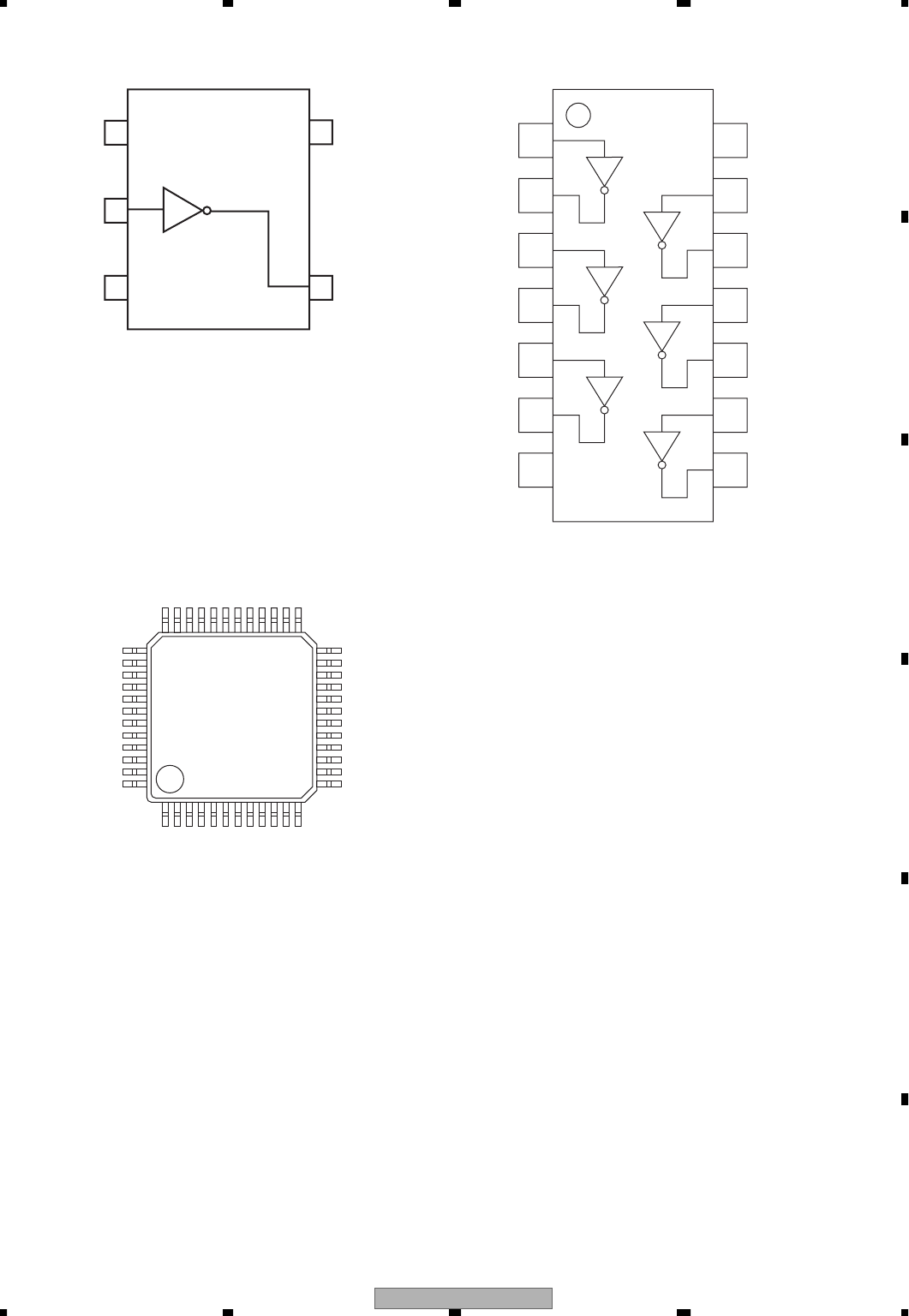
AVH-P5700DVD/EW 177
5678
5678
C
D
F
A
B
E
112
36 25
13
24
48
37
1
5
7
6
4
3
2
1A
3A
GND
3Y
2Y
2A
1Y
VCC
5Y
4Y
4A
5A
6Y
6A
14
10
8
9
11
12
13
1
2
34
5
GND
VCC
TC7SET04FUS1
BD6171KV
TC74VHC04FTS1
- Pin Layout
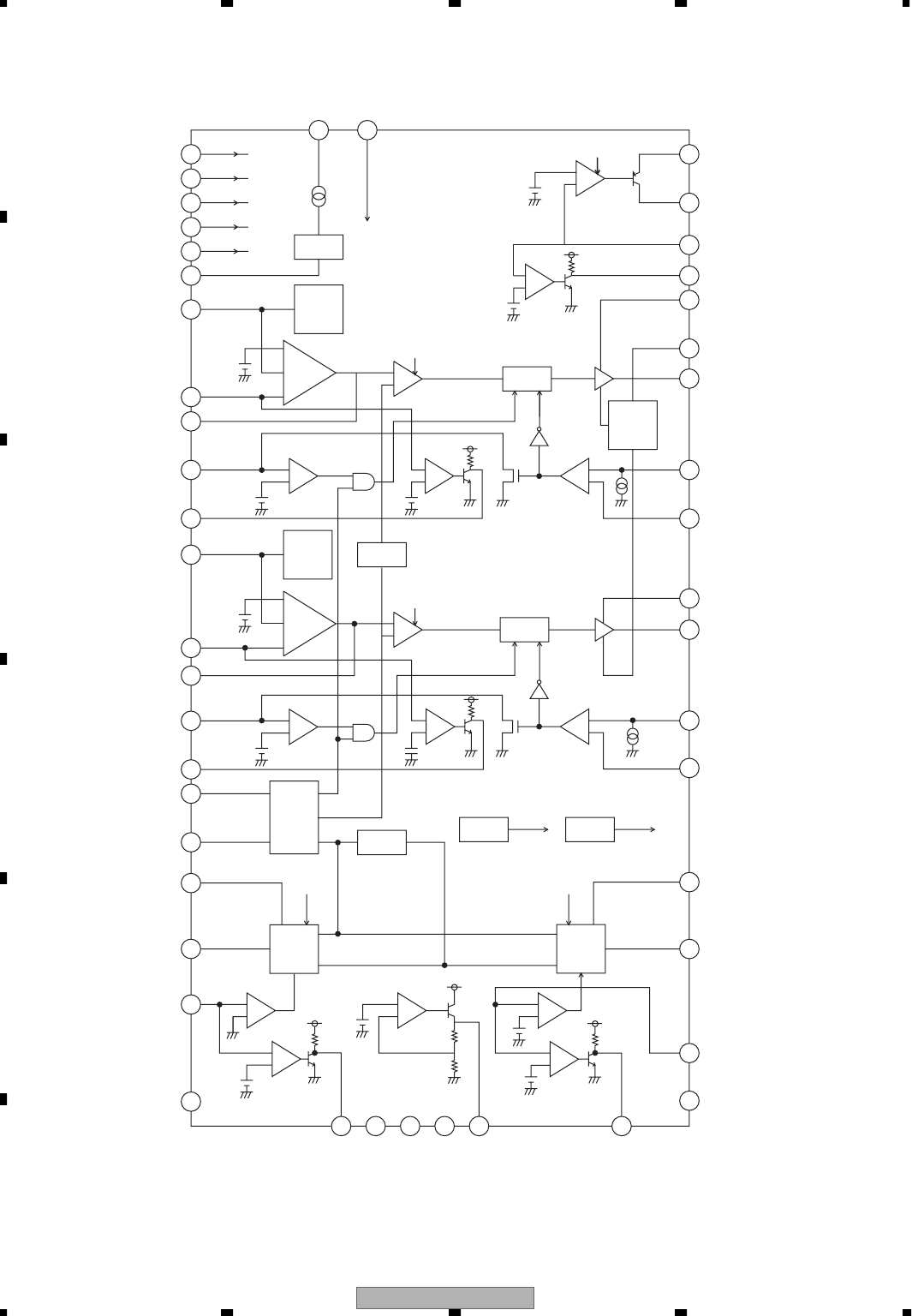
AVH-P5700DVD/EW
178
1234
1234
C
D
F
A
B
E
EN1 32
42 41
33
34
35
36
21
17
16
15
14
26
20
19
18
2
27
44
1
37
38
39
40
29 30 43 31 3 28
45
46
47
48
4
5
7
6
13
12
10
9
11
25
24
22
23
EN2
EN5
1V
3V
VCC
VREF
VREF
SS1 SOFT
START
SOFT
START INVERT
DELAY
GATE
CRAMP
LATCH
LATCH
UVLO
CP
POS
CP
NEG
TSD
OSC
FET
DRIVER
ERROR AMP
FET
DRIVER
ERROR AMP
PWM
DVCC PVCC3
0.6
VREGA
EN3
EN4 OUT3
OUT1
RESET
RESET
VREGA
VREGA
0.6V
0.6V
OUT2
OUT4
FB4
PGND4
VO4DETVREGAVO5DET GNDDGNDSGND
0.6V0.6V
PGND5
FB5 DVCC5VREG
OUT5
PVCC5
SYNC
RT
FB2
INV2
SS2
VO1DET
OCPC1
2V
2V
FB1
INV1
1V
VO2DET
OCPC2
1V
VREGAVREGA
VREF
OUTOUT
CL2
VS2
PVCC4
EN4EN5
CL1
VS1
PVCC2
FB3
VO3DET
PVCC1
VREGB
EN1
PWM
OSCILLATOR
EN2
EN3
+
+
-
+
-
-
+
-
+
+
+
-
+
-
-
+
-
+
-
+
-
+
-
+
-
+
+
-+
-
+
-
-
+
-
+
BD6171KV
- Block Diagram

AVH-P5700DVD/EW 179
5678
5678
C
D
F
A
B
E
1 2 3
VOUT VSS NC
VREF
45
VIN ON/OFF
ON/OFF
Over Current
Protector
IN B
IN A
GND OUT Y
VCC
5
4
1 IN B
2 IN A
3 GND 4 OUT Y
5 VCC
CS
SK
DI
NC
TEST
DO GND
VCC
1
2
3
4
8
7
6
5
NC
VCC
CS
SK
DI
DO
GND
TEST
:Not used
:Power supply
:Chip select input
:Clock input
:Data input
:Data output
:Ground
:Test
1
2
3
S-1131B25UC-N4K
S-1131B15UC-N4A
TC7SH02FUS1
S-93C56BD0I-J8TC7SH32FUS1

AVH-P5700DVD/EW
180
1234
1234
C
D
F
A
B
E
1
2
3
4
5
6
7
8
9
10
20
19
18
17
16
15
14
13
12
11
CTIMR
OVP
ENA
SST
VCCA
GNDA
REF
RT1
FB
CMP
NDR_B
PDR_A
CT
RT
PGND
LCT
DIM
LPWM
PDR_C
NDR_D
Protection
NDR_B
PDR_A
ZVS
Phase-Shift
Controller
HF
OSC
PDR_C
NDR_D
Burst-
Mode
Control
OVP
ENA
hys.
COMP
hys.
COMP
1.5V 2V
+
-
+
-
Reference
OPLAMP
-
+
EA
-
+
1.25V
3V
2.50V
sub.
POFF
POFF
I=3uA
I=6uA
Soft
Start
ACTIVE
"HIGH"
VCCA
SST2
+
-
SST/2.5
OZ961ISN

AVH-P5700DVD/EW 181
5678
5678
C
D
F
A
B
E
- Pin Functions (PEG087A)
1
2
3
4
5
6
7
8
9
10
11
12
13
14
15
16
17
18
19
20
21
22
23
24
25
26
27
28
29,30
31
32
33
34
35
36
37
38
39
40
41
42
43
44-50
51
52
53
54-61
62
63
64
65,66
67,68
69-72
73,74
75
I
I
O
O
O
O
I
I
I
I
I
I
O
I
I
O
O
O
O
O
O
O
O
I/O
O
O
O
O
I
I
I
O
O
O
I
I
I
I
I
I
I/O
I
I
VHOLD1
HLF1
INVBST
LD
DI
REMIN
REMIN
BYTE
CNVSS
VDDSENS
5060IN
RESET
XOUT
VSS
XIN
VCC
OSDCLK
NC
YSSTOP
OSDTOP
OSDBLNK
NC
MUTE
DIMMER
NC
INVPUL
ICRES
SCL
NC
SDA
OSDR
OSDG
OSDB
KYDT
DPDT
TSCK
EPRDI
EPRDO
NC
EPRCS
EPRCK
TESTIN
NC
FSCWIDE
LCD76
EPRCV
NC
HSYNC
NC
VSYNC
NC
KS2,1
KD4-1
NC
STEST2
Not used
Not used
Inverter boost output
COMAC,COMDC latch signal output
COMAC,COMDC data output
COMAC,COMDC clock output
Remote control signal input
GND connection
GND connection
VDD power supply sense input
50/60Hz input
Reset input
Clock output
GND
Clock input
Power supply
Clock input for OSD
Not used
NAVI over write enable output
OSD/NAVI over write enable output
OSD blanking output
Not used
2 screens IC mute output
Dimmer pulse output
Not used
Inverter pulse output
IC reset output
2 screens IC clock output
Not used
2 screens IC data input/output
OSD analog R signal output
OSD analog G signal output
OSD analog B signal output
Key data output
Display data input
Test mode clock input
EEPROM data input for adjustment memory
EEPROM data output for adjustment memory
Not used
EEPROM chip select output for adjustment memory
EEPROM clock output for adjustment memory
Chip test input
Not used
Not used
LCD size select (H:7inch, L:6.5inch) input
EEPROM adjustment input
Not used
HSYNC signal input for OSD
Not used
VSYNC signal input for OSD
Not used
Key strobe input/output
Key data input
Not used
Touch panel test mode input
Pin No. Pin Name I/O Format Function and Operation
C
C
C
C
C
C
C
C
C
C
C
C
C
C
C
C
C
C
C
C
C
C
C
AVH-P5700DVD/EW
182
1234
1234
C
D
F
A
B
E
10081
80
51
50 31 30
1
*PEG087A
Format Meaning
CC MOS
76
77
78,79
80
81
82
83
84
85
86
87
88
89
90
91
92
93
94
95
96
97
98
99
100
NC
SELFRST
NC
PNLXV
MFLPW
MVIPW
ROMCS
ROMCK
ROMDATA
EPRPST
STEST1
EPRTEST
TEMPSEN
PNLYV
PNLVD
PNLADY
PNLADX
LSEN
VHOLD2
HLF2
CVIN2
TVSETB
VCCE
CVIN1
Not used
Self write reset input
Not used
Touch panel:X direction sense output
Back light power supply control output
Video power supply control output
EEPROM chip select output
EEPROM clock output
EEPROM data input
EEPROM initalize input for memory adjustment
Monitor mode input
EEPROM set mode input for memory adjustment
Temperature sense input for inverter boost
Touch panel:Y direction sense output
Touch panel:sense output
Touch panel:X data input
Touch panel:Y data input
Brightness on the outside sense input
Not used
Not used
Not used
Test mode input
Power supply
Not used
Pin No. Pin Name I/O Format Function and Operation
I
O
O
O
O
O
I
I
I
I
I
O
O
I
I
I
I
I
I
I
I
C
C
C
C
C
C
C
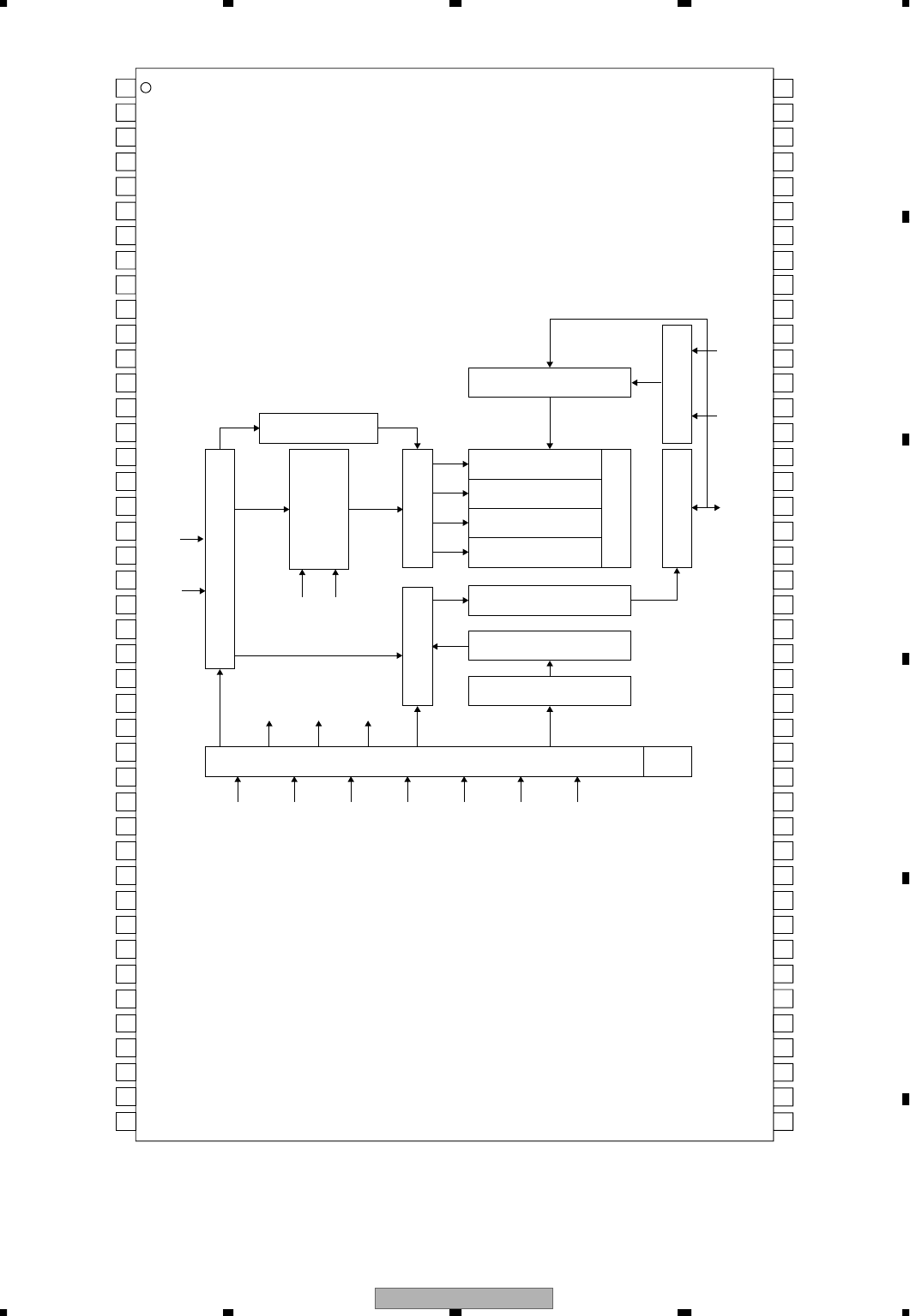
AVH-P5700DVD/EW 183
5678
5678
C
D
F
A
B
E
25
28
32
29
30
31
26
27
DQ16
A0
DQM2
V
SSQ
V
DD
N.C
DQ16
A1
A2
DQ17
DQ18
V
DDQ
DQ20
V
SSQ
DQ23
DQ21
DQ22
V
DDQ
V
DD
36
34
35
37
38
42
39
40
41
43
51
62
59
55
58
57
56
61
60
54
53
52
DQ28
A5
DQM3
V
DDQ
V
SS
N.C
DQ31
A4
A3
DQ30
DQ29
V
SSQ
DQ27
V
DDQ
DQ24
DQ26
DQ25
V
CCQ
V
SS
49
45
48
47
46
44
50
1
2
5
9
6
7
8
3
4
DQ7
V
DD
DQ0
DQ2
V
DDQ
V
SSQ
DQ3
DQ4
V
DDQ
DQ1
DQ5
DQ6
V
SSQ
N.C
BA1
V
DD
ras
DQM0
we
cas
cs
A11
BA0
A10/AP
13
11
12
14
23
15
19
16
17
18
20
21
22
24
74
86
85
82
78
81
80
79
84
83
77
76
75
DQ8
V
SS
DQ15
DQ13
V
SSQ
V
DDQ
DQ12
DQ11
V
SSQ
DQ14
DQ10
DQ9
V
DDQ
N.C
A7
V
SS
CLK
DQM1
N.C
N.C
CKE
A9
A8
A6
64
72
68
71
70
69
67
66
65
63
73
33
10
Programming Register
Latency & Burst Length
Column Decoder
Timing Register
Row Decoder
LRAS
LCBR
Sense AMP
Output BufferI/O Control
Bank Select
CLK
ADD
LCKE
LRAS
CLK CKE cs ras cas we DQM
LCBR LWE LCAS LWCBR
Data Input Register
1M x 32
LWE
LDQM
DQi
1M x 32
1M x 32
1M x 32
Address Register
Col Buffer
Row Buffer
Refresh Counter
*K4S283232E-TC75
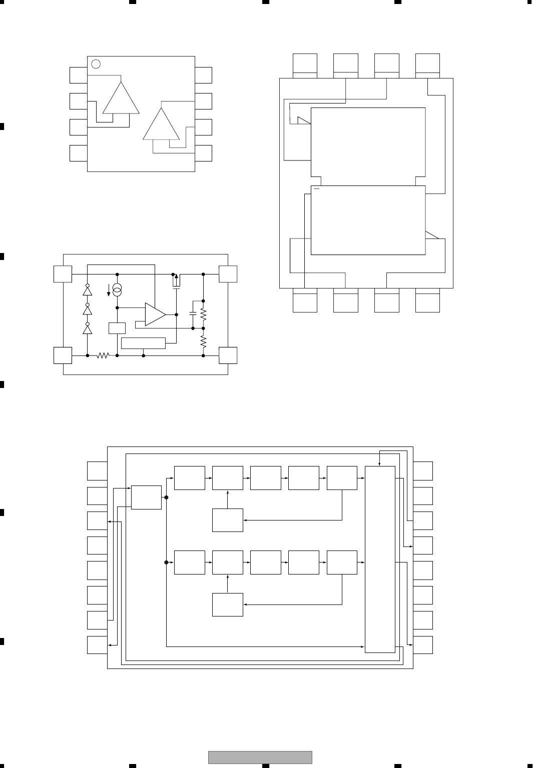
AVH-P5700DVD/EW
184
1234
1234
C
D
F
A
B
E
1OUT A
-IN A
+IN A
V+
V+
OUT B
-IN B
+IN B
2
3
4
8
7
6
5
A
-+
B
+-
NJM2140R
1234
8765
VCC st SELECT Y
AByGND
EN
1 MUX
1
G1
*TC7WH157FU
1
2
5
6
7
8
3
4
YDD1
VSS1
VDD2
VSS2
XT1
XT0
MO1,NC1
MO2,NC1,SO1
48
47
44
43
42
41
46
45
NC2
SO4,SO3,SO2,NC1
VDD3
VSS3
AO1,SO2
SO2,SO1,AO1
FSEL,NC2
SO3,SO2,SO1
X’tal
OSC
Reference
Divider 0 Phase
Divider 0
Loop
Divider 0
Charge
Pump 0 LPF 0 VCO 0
Reference
Divider 1 Phase
Divider 1
Loop
Divider 1
Charge
Pump 1 LPF 1 VCO 1
Control
Logic
*SM8707LV
Current Limit
Vref
VDD
ce
Vout
GND
+
-
2
5
1
3
*R1130H501B

AVH-P5700DVD/EW 185
5678
5678
C
D
F
A
B
E
10
1
2
5
9
6
7
8
3
4
2Q1
1oe
1Q1
1Q3
1Q6
1Q4
V
CC
1Q5
1Q2
GND
GND
1Q7
1Q8
2Q2
2Q8
GND
2Q5
2Q3
2Q4
V
CC
2Q6
GND
2Q7
1oe
13
11
12
14
23
15
19
16
17
18
20
21
22
24
36
48
47
44
40
43
42
41
46
45
39
38
37
2D1
1LE
1D1
1D3
1D6
1D4
V
CC
1D5
1D2
GND
GND
1D7
1D8
2D2
2D8
GND
2D5
2D3
2D4
V
CC
2D6
GND
2D7
2LE
26
34
30
33
32
31
29
28
27
25
35
1LE
1oe
48
47
D
LE Q
1D1
46
D
LE Q
1D2
45
D
LE Q
1D3
44
D
LE Q
1D4
43
D
LE Q
1D5
42
D
LE Q
1D6
41
D
LE Q
1D7
40
D
LE Q
1D8
2
1Q1
3
1Q2
5
1Q3
6
1Q4
8
1Q5
9
1Q6
10
1Q7
11
1Q8
1
2LE
2oe
25
36
D
LE Q
2D1
35
D
LE Q
2D2
33
D
LE Q
2D3
32
D
LE Q
2D4
30
D
LE Q
2D5
29
D
LE Q
2D6
27
D
LE Q
2D7
26
D
LE Q
2D8
13
2Q1
14
2Q2
16
2Q3
17
2Q4
19
2Q5
20
2Q6
22
2Q7
23
2Q8
24
*TC74LCX16373AFT
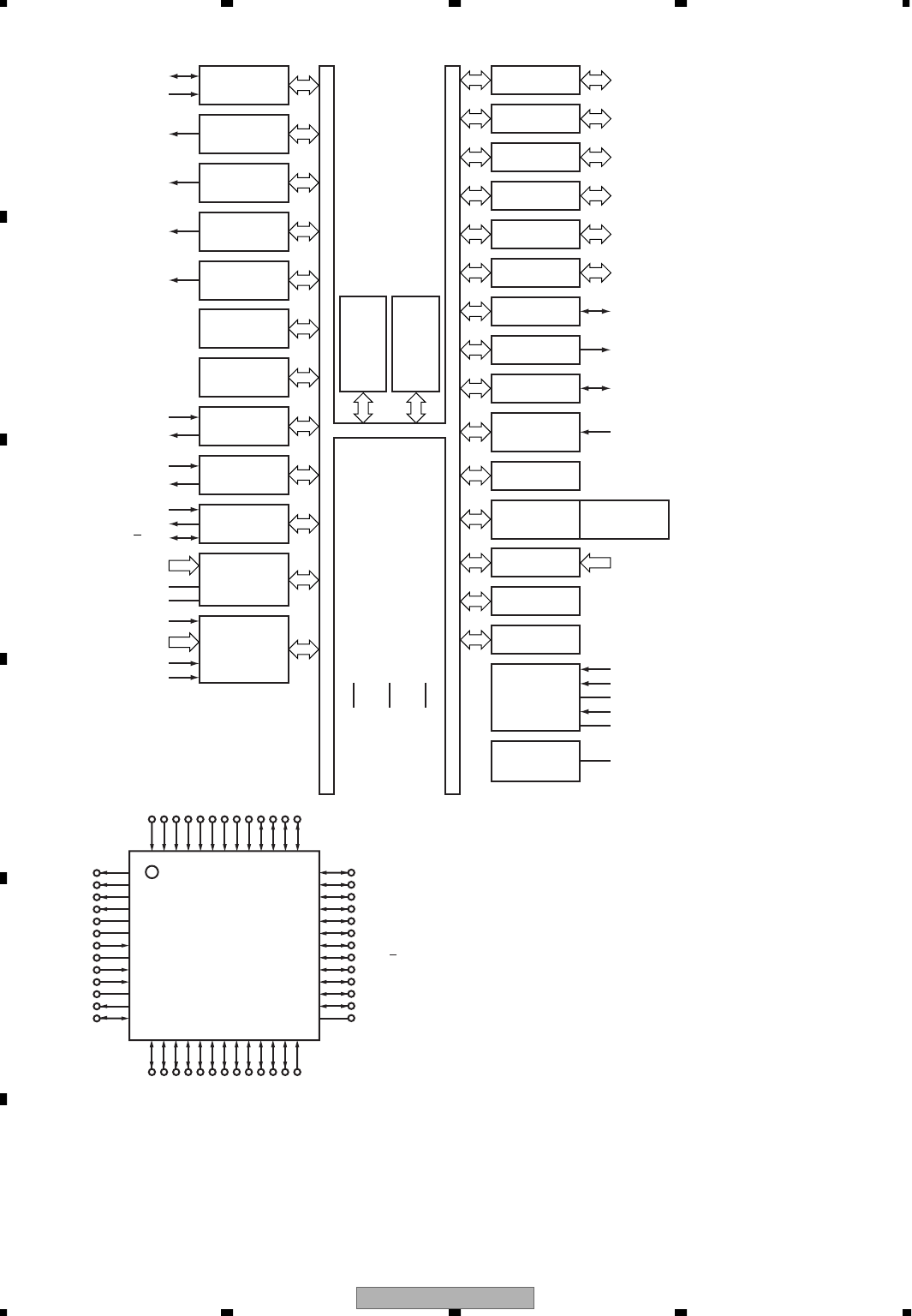
AVH-P5700DVD/EW
186
1234
1234
C
D
F
A
B
E
16-bit TIMER/
EVENT COUNTER 00
8-bit TIMER/
EVENT COUNTER 50
TO00/TI10/P01
RxD0/P11
TxD0/P10
8-bit TIMER H0TOH0/P15
8-bit TIMER H1
WATCH TIMER
WATCHDOG TIMER
78K/0
CPU
CORE
ROM
(FLASH
MEMORY)
TOH0/P16
TI50/TO50/P17
8-bit TIMER/
EVENT COUNTER 51
SERIAL
INTERFACE UART0
TI51/TO51/P33
RxD0/P14
TxD0/P13
SERIAL
INTERFACE UART6
SERIAL
INTERFACE CSI10
SI10/P11
SO10/P12
TI000/P00
sck10/P10
ANI0/P20 8
ANI7/P27 A/D CONVERTER
AVSS
AVREF
INTP0/P120
4
INTP1/P30
INTP6/P140
INTP5/P16
INTP4/P33 INTERRUPT
CONTROL
PORT 1 P10-P17
PORT 0 4
8
PORT 2 P20-P27
8
PORT 3 P30-P33
4
PORT 6 P60-P63
4
PORT 7 P70-P77
8
PORT 12
P00-P03
CLOCK OUTPUT
CONTROL PCL/P140
KR0/P70-
KR7/P77
VOLTAGE
REGULATOR REGC
P120
PORT 13 P130
PORT 14 P140
CLOCK MONITOR
KEY RETURN
RESET CONTROL
Ring-OSC
POWER ON CLEAR/
LOW VOLTAGE
INDICATOR
POC/LVI
CONTROL
8
reset
X1
XT2
X2
SYSTEM
CONTROL
VDD,
EVDD
VSS,
EVSS
IC
(VPP)
XT1
AVREF
AVSS
VPP/IC
VDD
REGC
VSS
X1
X2
reset
XT1
XT2
P130
P120/INTP0
P75/KR5
P76/KR6
P77/KR7
P00/TI000
P01/TI010/TO00
P02
P03
P10/sck10/RXD0
P11/SI10/RXD0
P12/SO10
P13/TXD6
P14/RXD6
EVDD
P33/TI51/TO51/INTP4
P32/INTP3
P31/INTP2
P30/INTP1
P140/PCL/INTP6
P17/TI50/TO50
P16/TOH1/INTP5
P15/TOH0
P60
P61
P62
P63
EVSS
P20/ANI0
P21/ANI1
P22/ANI2
P23/ANI3
P24/ANI4
P25/ANI5
P26/ANI6
P27/ANI7
P70/KR0
P71/KR1
P72/KR2
P73/KR3
P74/KR4
1
14 15 16 17 18 19 20 21 22 23 24 25 26
52 51 50 49 48 47 46 45 44 43 42 41 40
2
3
4
5
6
7
8
9
10
11
12
13
39
38
37
36
35
34
33
32
31
30
29
28
27
*PE5401A
AVH-P5700DVD/EW 187
5678
5678
C
D
F
A
B
E
2
10
11
12
13
14
15
16
17
18
19
20
21
22
39
38
37
36
35
34
33
32
31
30
29
28
27
43
42
41
40
47
46
45
44
48
A15
A14
A13
A12
A11
A10
A9
A8
A19
A20
we
reset
NC
ACC
RY/by
A18
A17
A7
A6
A5
A4
A3
A16
byte
VSS
DQ15/A-1
DQ7
DQ14
DQ6
DQ13
DQ5
DQ12
DQ4
VCC
DQ11
DQ3
DQ10
DQ2
DQ9
DQ1
DQ8
DQ0
oe
VSS
23
24
26
25
A2
A1
ce
A0
A-1
A0-A20
DQ0-D15
byte
ce
oe
RY/by
reset
ACC
VCC
VSS
8
9
4
5
6
7
3
1
:Data output/Address input
:Address input
:Data input output
:Mode select
:Chip enable input
:Output enable input
:Ready/Busy output
:Reset
:Acc
:Power supply
:GND
*PD6516A
ON/OFF
VSS
VIN
NC
VOUT
123
54
+
-
ON/OFF
*S-L2980A50MC-C7J
VOLTAGE
REFERENCE

AVH-P5700DVD/EW
188
1234
1234
C
D
F
A
B
E
1
2
3
4
5
SHDN/RT
SYNC/MODE
SGND
SW
PGND
ITH
VFB
PGOOD
SVIN
PVIN
10
9
8
7
6
VOLTAGE
REFERENCE VOLTAGE
REFERENCE
OSCILLATOR
LOGIC
-
+
+
-
B
+
-
+
-
+
-
SLOPE
COMPENSATION
NMOS
COMPARATOR
PMOS CURRENT
COMPARATOR
BURST
COMPARATOR
ERROR
AMPLIFIER
0.74V
0.8V
0.86V
VB
REVERSE
COMPARATOR
+
-
+
-
*LTC3411EMS
*MN35104UB
*TC7SZ125FU
64
65
128
1
29
1
92
193
256
1
1
g
2
IN A
3
GND
5
4
VCC
OUT Y
AVH-P5700DVD/EW 189
5678
5678
C
D
F
A
B
E
1
2,3
4
5,6
7
8-10
11
12,13
14
15
16
17
18
19-22
23
24
25,26
27,28
29
30
31,32
33
34-37
38,39
40,41
42
43
44,45
46
47
48
49
50
51
52
53
54
55
56
57
58
59
VDD33
MDQ
VSS
MDQ
VDD33
MDQ
VSS
MDQ
VDD33
VDD15
VSS
EXADR
NEXWE
EXADT
VDD33
VSS
EXADR
EXADT
VDD33
VSS
EXADT
NEXCE
EXADT
EXADR
EXADT
VD33
VSS
EXADT
NEXOE
P15
P14
P13
P12
P11
P10
P9
P8
P7
VDD3
MMOD
VSS
P6
I / O
I / O
I / O
I / O
I / O
O
I / O
I / O
I / O
I / O
O
I / O
I / O
I / O
I / O
O
I / O
I / O
I / O
I / O
I / O
I / O
I / O
I / O
I / O
I
I / O
IO power supply
SDRAM data
GND
SDRAM data
IO power supply
SDRAM data
GND
SDRAM data
IO power supply
Power supply
GND
Memory address
Memory write enable
Memory address data
IO power supply
GND
Memory address
Memory address data
IO power supply
GND
Memory address data
Memory chip select
Memory address data
Memory address
Memory address data
IO power supply
GND
Memory address data
Memory output(Read) enable
Memory address bus
The flag of transmitting end
The flag of transmitting start
Serial clock
Serial output data
Serial input data
Serial clock
Serial output data
Serial input data
IO power supply
Test mode setting
GND
Serial clock
-Pin Functions(MN35104UB)
Pin No. Pin Name I/O Function and Operation

AVH-P5700DVD/EW
190
1234
1234
C
D
F
A
B
E
60
61
62
63
64
65
66
67
68
69
70-77
78
79
80
81
82
83
84
85
86-89
90
91
92
93
94-97
98
99
100-103
104
105
106
107
108-110
111
112
113
114
115
116
117
118
119
P5
P4
P3
P2
P1
P0
FG
VDD15
NRST
VSS
DRV
DRV8
VDD33
VSS
SCLOCK
EXTRG
SDATA
EXTRG
TRCCLK
TRCDATA
TRCST
VDD33
OSCI
VSS
MONI
VDD15
VSS
MONI
AVDDD
PLFIL1
AVSSD
PLFIL2
VREF
VC0
RESI
ANAMONI
POFLT
CDATA
CCAPA
CGD
AVDDC
AVSSC
I / O
I / O
I / O
I / O
I / O
I / O
I
I
I / O
I / O
I / O
I / O
I / O
I / O
I / O
I / O
I / O
I
I / O
I / O
O
O
O
I
I
O
O
O
O
O
I
Serial output data
Serial input data
Serial clock
Serial output data
Serial input data
Serial clock
Motor FG
Power supply
Master reset
GND
Servo port
Servo port
IO power supply
GND
Input clock for debug
I/O trigger for debug
I/O data for debug
I/O trigger for debug
Output trace clock for debug
I/O trace data for debug
Output trace status for debug
Power supply
Front end clock input
GND
Inside monitor
Power supply
GND
Inside monitor
Power supply
DRC VCO
GND
DRC VCO
Reference voltage
gm-cEQ
gm-cEQ
Inside analog monitor
DPDOFTR
Inline data
Inline capacitor
Reference voltage
Analog current
Analog GND
Pin No. Pin Name I/O Function and Operation
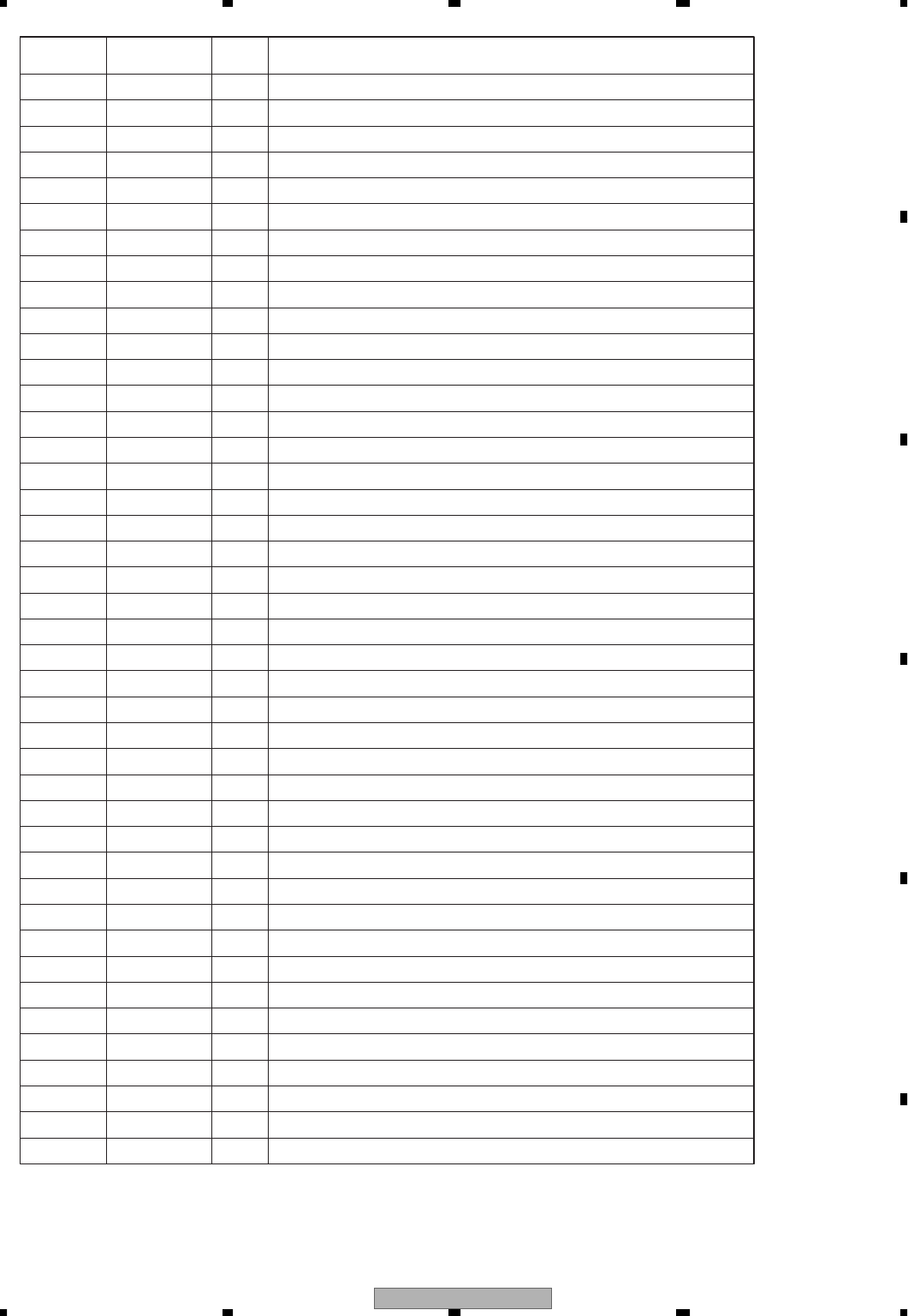
AVH-P5700DVD/EW 191
5678
5678
C
D
F
A
B
E
120
121
122-131
132
133
134
135
136
137
138
139
140
141
142
143
144
145
146-148
149
150
151
152
153
154
155
156
157
158
159
160
161
162
163
164
165
166
167
168
169
170
171
172
RFINN
RFINP
VIN
LPC1
LPCO1
LPC2
LPCO2
VREFH
VHALF
AVSSB
CTKC
CSLFLT
CWBLOUT
CWBLIN
VCOF
RVI
AVDDB
AD
AVDDA
DAC1
AVSSA
DAC0
AVDDE
IREF1
AVSSE
COMP1
AVDDF
DAC1OUT
AVSSF
DAC2OUT
DAC3OUT
VREF
DAC4OUT
DAC5OUT
AVDDG
IREF2
VSSG
COMP2
VSS
BECLK
VDD33
EXTCK
I
I
I
O
I
O
O
O
O
I
O
I
I
I
I
O
O
I
I
O
O
O
I
O
O
I
I
I
I
RF input
RF input
Head input
DVDLPC input
DVDLPC output
CDLPC input
CDLPC output
Reference voltage
Reference voltage
Analog GND
TC
Capasitor
DC cut for wobble
DC cut for wobble
JFVCO control voltage
VREFH reference current
Analog current
AD input
Analog current
Tracking drive output
Analog GND
Focus drive output
Analog current
Inside DAC bias current
Analog GND
Inside DAC
Analog current
Analog signal
Analog GND
Analog signal
Analog signal
Reference voltage
Analog signal
Analog signal
Analog power suplly
Inside DAC bias current
Analog GND
Inside DAC
GND
Backend clock input
IO power supply
Exterior audio clock
Pin No. Pin Name I/O Function and Operation

AVH-P5700DVD/EW
192
1234
1234
C
D
F
A
B
E
173
174
175
176
177
178-180
181
182
183
184,185
186
187,188
189
190-193
194
195
196,197
198
199-201
202
203-205
206
207,208
209
210
211
212
213
214
215
216,217
218
219,220
221
222
223
224
225
226
227-229
230
231
PHCOMPO
LRCK
SRCK
ADOUT3
VSS
ADOUT
IECOUT
VDD33
VSS
MDQ
VDD15
MDQ
VDD33
MDQ
VSS
VDD33
MDQ
VSS
MDQ
VDD33
MDQ
VSS
DQM
VDD33
MA
VSS
MA4
VDD15
MA2
VSS
MA
VDD33
MA
VSS
VDD15
MCKI
VSS
MCK
VDD33
MA
VSS
MA
O
O
O
O
O
O
I / O
I / O
I / O
I / O
I / O
I / O
O
O
O
O
O
O
I
O
O
O
Composite audio clock
LR chanel clock output
Bit clock output
Audio down mixing
GND
Audio data
IEC958 digital audio output
IO power supply
GND
SDRAM data
Power supply
SDRAM data
IO power supply
SDRAM data
GND
IO power supply
SDRAM data
GND
SDRAM data
GND
SDRAM data
GND
SDRAM data mask
Power supply
SDRAM address
GND
SDRAM address
Power supply
SDRAM address
GND
SDRAM address
Power supply
SDRAM address
GND
Power supply
SDRAM output clock
GND
SDRAM input clock
IO power supply
SDRAM address
GND
SDRAM address
Pin No. Pin Name I/O Function and Operation

AVH-P5700DVD/EW 193
5678
5678
C
D
F
A
B
E
232
233
234
235
236
237
238
239
240
241
242
243
244
245
246
247
248
249
250
251-253
254
255,256
NWE
VDD33
BA0
MA
VSS
BA1
NCSM
NRAS
VDD33
VSS
NCAS
DQM0
VDD15
VSS
DQM
MDQ
VSS
MDQ
VDD33
MDQ
VSS
MDQ
O
O
O
O
O
O
O
O
O
I / O
I / O
I / O
I / O
SDRAM writte enable
IO power supply
SDRAM bank address
SDRAM address
GND
SDRAM bank address
SDRAM chip select
SDRAM low address strobe
IO power supply
GND
SDRAM column address strobe
SDRAM data mask
Power supply
GND
SDRAM data mask
SDRAM data
GND
SDRAM data
IO power supply
SDRAM data
GND
SDRAM data
Pin No. Pin Name I/O Function and Operation
AVH-P5700DVD/EW
194
1234
1234
C
D
F
A
B
E
No. Symbol I/O Explain
1 AMANT I AM antenna input AM antenna input high impedance AMANT pin is connected with
an all antenna by way of 4.7µH. (LAU type inductor) A series circuit
including an inductor and a resistor is connected with RF ground for
the countermeasure against the hum of power transmission line.
2 RFGND RF ground Ground of antenna block
3 FMANT I FM antenna input Input of FM antenna 75ΩSurge absorber(DSP-201M-S00B) is necessary.
4 VCC power supply The power supply for analog block. D.C 8.4V ±0.3V
5 SL O signal level Output of FM/AM signals level
6 CE2 I chip enable-2 Chip enable for EEPROM ”Low” active
7 WC I write control You can write EEPROM, when EEPROM write control is “Low”.
Ordinary non connection
8 CE1 I chip enable-1 Chip enable for AF•RF ”High” active
9 CK I clock Clock
10 DI I data in Data input
11 LDET O lock detector “Low” active
12 OSCGND osc ground Ground of oscillator block
13 ROM_VDD power supply Power supply for EEPROM pin 13 is connected with a power supply of
micro computer.
14 DO O data out Data output
15 DGND digital ground Ground of digital block
16 NC non connection Not used
17 VDD_3.3 power supply The power supply for digital block. 3.3V ±0.2V
18 RDS_CK O RDS clock Output of RDS clock(2.5V)
19 RDS_DATA O RDS data Output of RDS data(2.5V)
20 RDS_LOCK O RDS lock Output unit “High” active(2.5V) (RDS_LOCK turns over by the
external transistor. “Low” active)
21 RDS_HSLK O RDS high speed Output unit “High” active(2.5V)(RDS_HSLK turns over by the
lock external transistor. “Low” active)
22 AUDIOGND audio ground Ground of audio block
23 L ch O L channel output FM stereo “L-ch” signal output or AM audio output
24 R ch O R channel output FM stereo “R-ch” signal output or AM audio output
FMRF
ANT adj RF adj
FM ANT
T51 CF52
CF51
RFGND
OSCGND
DGND
AUDIOGND
NC
VCC
VDD_3.3
3.3V 2.5V
IC 4
3.3V 2.5V
←
IC 2
2.5V
WC
CE2
ROM_VDD
SL
DI
CK
CE1
LDET
DO
RDS_CK
RDS_DATA
RDS_LOCK
RDS_HSLK
76 13 5 1098 11 14 18192021
1
3
212 1522 16 4 17
IC 1
3.3V
AM ANT FMRF
ATT
LPF
OSC
IC 3 EEPROM
5.0V
IC 5
5V 3.3V
←
ATT
MIXER, IF AMP DET, FM MPX,
RDS DECODER
24
23
Rch
Lch
- FM/AM Tuner Unit(AVH-P5700DVD/EW)
AVH-P5700DVD/EW 195
5678
5678
C
D
F
A
B
E
No. Symbol I/O Explain
1 AMANT I AM antenna input AM antenna input high impedance AMANT pin is connected with
an all antenna by way of 4.7µH. (LAU type inductor) A series circuit
including an inductor and a resistor is connected with RF ground for
the countermeasure against the hum of power transmission line.
2 RFGND RF ground Ground of antenna block
3 FMANT I FM antenna input Input of FM antenna 75ΩSurge absorber(DSP-201M-S00B) is necessary.
4 VCC power supply The power supply for analog block. D.C 8.4V ±0.3V
5 SL O signal level Output of FM/AM signals level
6 CE2 I chip enable-2 Chip enable for EEPROM ”Low” active
7 WC I write control You can write EEPROM, when EEPROM write control is “Low”.
Ordinary non connection
8 CE1 I chip enable-1 Chip enable for AF•RF ”High” active
9 CK I clock Clock
10 DI I data in Data input
11 NC non connection Not used
12 OSCGND osc ground Ground of oscillator block
13 ROM_VDD power supply Power supply for EEPROM pin 13 is connected with a power supply of
micro computer.
14 DO O data out Data output
15 DGND digital ground Ground of digital block
16 NC non connection Not used
17 VDD_3.3 power supply The power supply for digital block. 3.3V ±0.2V
18 NC non connection Not used
19 NC non connection Not used
20 NC non connection Not used
21 NC non connection Not used
22 AUDIOGND audio ground Ground of audio block
23 L ch O L channel output FM stereo “L-ch” signal output or AM audio output
24 R ch O R channel output FM stereo “R-ch” signal output or AM audio output
FMRF
ANT adj RF adj
FM ANT
T51 CF52
CF51
RFGND
OSCGND
DGND
AUDIOGND
NC
VCC
VDD_3.3
3.3V 2.5V
IC 4
3.3V 2.5V
←
IC 2
2.5V
WC
CE2
ROM_VDD
SL
DI
CK
CE1
NC
DO
NC
NC
NC
NC
76 13 5 1098 11 14 18192021
1
3
212 1522 16 4 17
IC 1
3.3V
AM ANT FMRF
ATT
LPF
OSC
IC 3 EEPROM
5.0V
IC 5
5V 3.3V
←
ATT
MIXER, IF AMP DET, FM MPX
24
23
Rch
Lch
- FM/AM Tuner Unit(AVH-P5700DVD/UC)

AVH-P5700DVD/EW
196
1234
1234
C
D
F
A
B
E
7.3 EXPLANATION
7.3.1 MECHANISM DESCRIPTIONS
- Outline of the FLAP motion
1. The motion is actuated made by two motors, the forward/backward driving motor (CXB9515) and the angle
driving motor (CXB9516).
2. Analog electric potential generated by the angle encoder is detected to detect angle motion status and motion
position.
3. Memory function for the angle last position is accomplished by the micro processor using the 256 resolution
steps of the VDD.
4. A pulse is detected by the photo interrupter to detect the horizontal motion status.
5. In the case of reset start, the monitor will be in a stored position first, and ejection motion will take place, which
puts the system in the booted up state.
6. Angle adjustment is made by the angle key (+/-).
7. OPEN/CLOSE key makes the monitor stored or ejected, and temporary folding key folds the monitor
temporarily.
8. Setting of the monitor auto storage/ejection ON/OFF and set back ON/OFF at the time of ACC ON/OFF is made
on the navigation menu screen.
9. A backlight is switched-off during forward/backward and storage.
- Explanation on the FLAP ejection motion
1. When the OPEN key is pressed or ACC is set to ON while the auto OPEN/CLOSE is being set to ON, angle
driving motor rotates in the 0° direction for 500ms. (Pressed down.)
2. After 500ms, the angle driving motor is stopped, and the forward/backward driving motor rotates in the
ejection direction.
3. For a period of 600ms from the time when LIFTSW is switched from H to L, the forward/backward driving
motor keeps rotating in the ejection direction.
4. After 600ms, the forward/backward driving motor is stopped, and the angle driving motor rotates in the UP
direction.
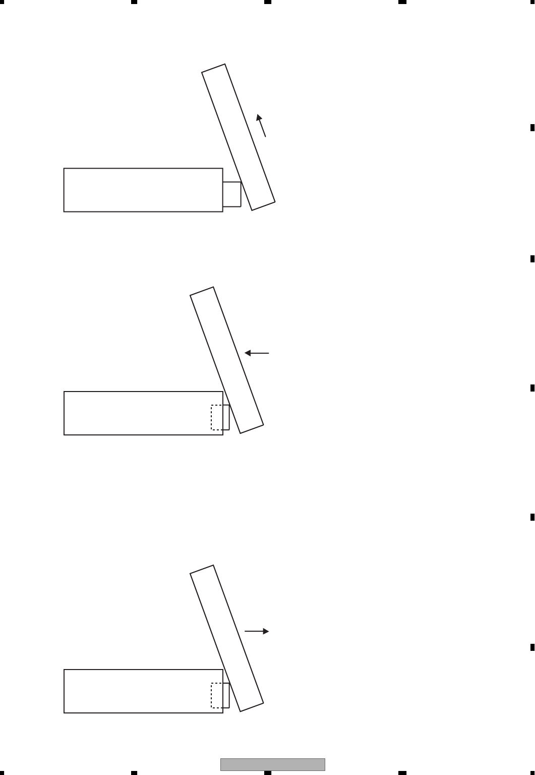
AVH-P5700DVD/EW 197
5678
5678
C
D
F
A
B
E
5. When the angle voltage reaches the voltage for 110°, brake is applied to the angle driving motor, and the
ejection is completed. (In case the previous angle is stored in the memory, the motion continues to that angle.)
6. When the setback is set to ON, after the monitor angle voltage has reached the previously memorized voltage,
brake is applied to the angle driving motor, then the forward/backward driving motor is rotated in slow speed
in the storage direction. After that, when LIFTSW has switched from L to H, the forward/backward driving
motor is stopped.
110° voltage position or the last memory position.
- Explanation of the FLAP storage motion
1. When CLOSE key is pressed, or after 6 seconds from ACC OFF when auto OPEN/CLOSE is being set to ON, the
angle driving motor is rotated in the 0° direction. In case the setback setting is ON, the forward/backward
driving motor is rotated in high speed in the ejection direction and the motor continues to rotate for 600ms
from the time when LIFTSW is switched from H to L, then the angle driving motor is rotated in the 0° direction.
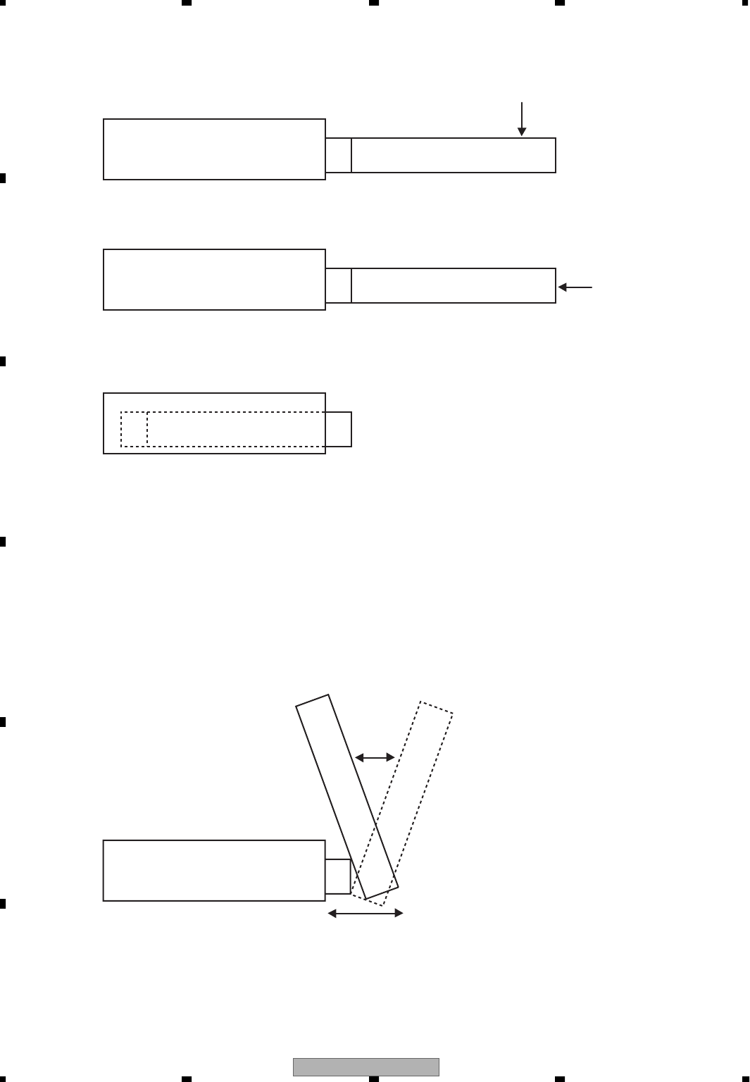
AVH-P5700DVD/EW
198
1234
1234
C
D
F
A
B
E
2. For a period of 500ms from the time when DIGOSW is switched from H to L, the angle driving motor is rotated
in the 0° direction for the “pressed down” motion.
3. After 500ms, brake is applied to the angle driving motor, and then the forward/backward driving motor is
rotated in the storage direction.
4. When the horizontal motion detection pulse is no longer detected for 200ms, brake is applied and the monitor
storage motion is completed.
- Explanation on the FLAP angle adjustment
1. The angle driving motor is rotated in UP direction by the “+” key and in DOWN direction by the “–” key from
the monitor stop position. If the key is kept pressed, the monitor will keep changing the angle without steps
within the range of 50 to 110 degrees. When the setback is being set to ON, the forward/backward driving
motor is rotated in the horizontal ejection direction while the key is being pressed, and angle adjustment is
made by changing the angle voltage to the extent the angle adjustment key is effective after 600ms has
elapsed from the time when LIFTSW has switched from H to L. When 3 seconds have elapsed from the time
of angle adjustment completion, the forward/backward driving motor is rotated in slow speed in the horizontal
storage direction, and brake is applied when LIFTSW has switched from L to H.
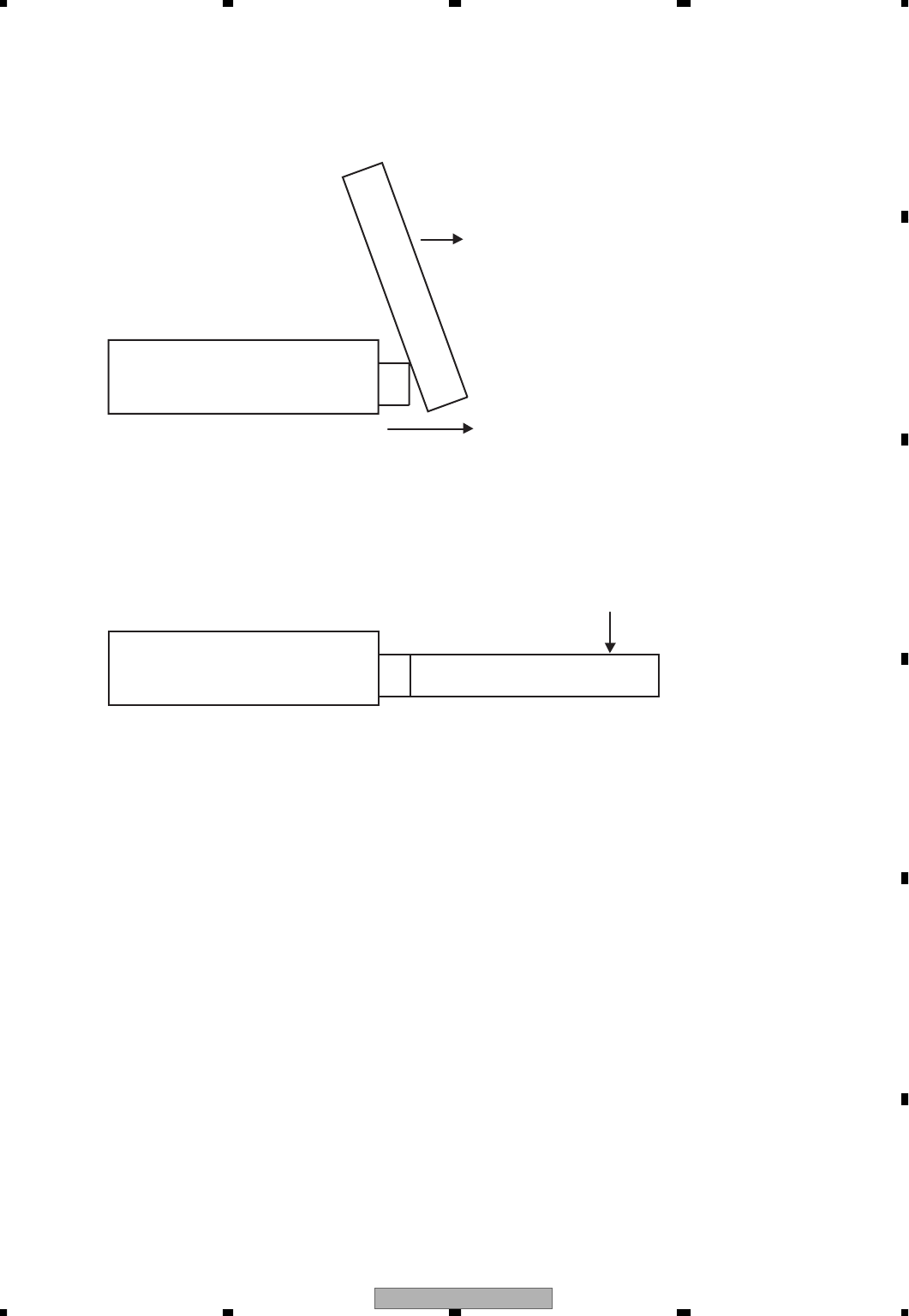
AVH-P5700DVD/EW 199
5678
5678
C
D
F
A
B
E
- Explanation on the FLAP temporary folding operation
1. By pressing the temporary folding key, the angle driving motor is rotated from the monitor stop position
toward 0° direction. When the setback is being set to ON, the forward/backward driving motor is rotated when
the key is pressed, brake is applied after 600ms has elapsed from the time when LIFTSW has switched from H
to L, and the angle driving motor is rotated in 0° direction.
2. For a period of 500ms after DEGOSW has switched from H to L, the angle driving motor is rotated, and the
monitor stops at its horizontal position by the brake. After 7 seconds, navigator operation sound is heard three
times in 1 second interval. After 10 seconds, the angle driving motor is rotated in UP direction, and then the
brake is applied to stop the motor at the last memory position. When the setback is being set to ON, after the
angle driving motor stops at the last memory position, the forward/backward driving motor is rotated in slow
speed in the horizontal storage direction, and the motor stops after LIFTSW has switched from L to H.
- Notes related to the FLAP motion
1. Regarding the angle position, angle voltage is always checked, and the last memory is stored by addition or
subtraction of the voltage. It should be noted, however, that the last memory will not be stored when the
monitor is manually moved by force.
2. If the expected pulse is not detected during horizontal motion, the monitor will stop at that position.
AVH-P5700DVD/EW
200
1234
1234
C
D
F
A
B
E
Bup ON
(Reset start)
Bup OFF
Bup OFF ON
ACC ON
ACC OFF ON
ACC OFF
Last memory
Bup ON
(Reset start)
Bup OFF
Bup OFF ON
ACC ON
ACC OFF ON
ACC OFF
Last memory
OPEN state
CLOSE state
CLOSE
OPEN state
Last angle
To stand-by
No state change
No state change
No state change
6 sec from ACC OFF
Advance
CLOSE motion
CLOSE
OPEN
To stand-by
No state change
No state change
No state change
No state change
OPEN
In OPEN motion In CLOSE motion CLOSE state
Continue OPEN motion
Last angle
Return
To stand-by To stand-by To stand-by
Continue OPEN motion
Last angle
Return
Continue OPEN motion
Last angle
Return
6 sec from ACC OFF
Advance
CLOSE motion
CLOSE
OPEN CLOSE CLOSE
To stand-by To stand-by To stand-by
Continue OPEN motion
Last angle
Return
Continue OPEN motion
Last angle
Return
Continue OPEN motion
Last angle
Return
OPEN CLOSE CLOSE
Continue CLOSE motion
CLOSE
Continue CLOSE motion
CLOSE
Continue CLOSE motion
CLOSE
Continue CLOSE motion
CLOSE
Continue CLOSE motion
CLOSE
Continue CLOSE motion
CLOSE
Continue OPEN motion
Last angle
No state change
OPEN motion
Last angle
Return
No state change
No state change
No state change
No state change
No state change
No state change
- Table of driving unit operations by different preset modes
* When the setback is being set to OFF, there will be no advance/return motion.
After ACC OFF, if ACC is switched ON again during the 6 seconds counting, standby will be passed and the FLAP
status will not change.
Auto OPEN/CLOSE setting ONAuto OPEN/CLOSE setting OFF
AVH-P5700DVD/EW 201
5678
5678
C
D
F
A
B
E
- Table of temporary folding control
* When the setback is being set to OFF, there will be no advance/return motion.
Bup ON
Bup OFF
ACC ON
Bup OFF ON
ACC OFF ON
ACC OFF
Last memory
Bup ON
Bup OFF
ACC ON
Bup OFF ON
ACC OFF ON
ACC OFF
Last memory
To stand-by To stand-by To stand-by
Continue temporary
folding motion
Continue OPEN motion
Last angle
Return
Continue temporary
folding motion
Temporary folding
OPEN motion
Last angle
Return
Continue OPEN motion
Last angle
Return
Continue temporary
folding motion
Temporary folding
6 sec from ACC OFF
CLOSE motion
CLOSE
Continue OPEN motion
Last angle
Return
6 sec from ACC OFF
Advance
CLOSE motion
CLOSE
Continue temporary
folding motion
Temporary folding
6 sec from ACC OFF
CLOSE motion
CLOSE
OPEN OPEN OPEN
To stand-by To stand-by To stand-by
Continue temporary
folding motion
Temporary
folding reset
Temporary
folding in motion
OPEN motion
Last angle
Return
Continue OPEN motion
Last angle
Return
OPEN motion
Last angle
Return
OPEN motion
Last angle
Return
Continue OPEN motion
Last angle
Return
OPEN motion
Last angle
Return
OPEN OPEN OPEN
Temporary folding state
(horizontal position) Temporary folding reset
(horizontal position last angle) Temporary folding in motion
(last angle horizontal position)
Auto OPEN/CLOSE setting ONAuto OPEN/CLOSE setting OFF
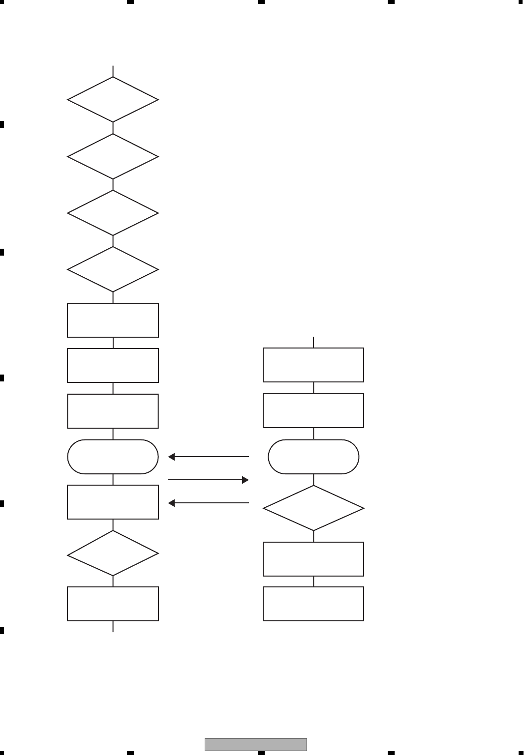
AVH-P5700DVD/EW
202
1234
1234
C
D
F
A
B
E
7.3.2 OPERATIONAL FLOW CHART
VDD0=5V
Pin 39
Power ON
bsens=L
asens=L
dsens=L
bsens
Pin 69
asens
Pin 96
dsens
Pin 83
SWVDD←H
Pin 109
ASENBO←H
Pin 87
Source keys
operative
Completes power-on operation.
(After that, proceed to each source operation)
SYSPW←H
Pin 31
Starts
communication
with Display
microcomputer.
Source ON
Starts
communication
with System
microcomputer
ACCPW←H
Pin 29
DISPLAY MICROCOMPUTER
SWVDD ON
Microcomputer
Initialization
SYS resending
dimand
Display processing
Initialization Key
Response Connection
formation
Resending dimand
Comunication
formation
Key Scan
(Sys control)

AVH-P5700DVD/EW 203
5678
5678
C
D
F
A
B
E
7.4 CLEANING
Before shipping out the product, be sure to clean the following portions by using the prescribed cleaning tools:
Portions to be cleaned Cleaning tools
DVD pickup lenses Cleaning liquid : GEM1004
Cleaning paper : GED-008
Portions to be cleaned Cleaning tools
Fans Cleaning paper : GED-008
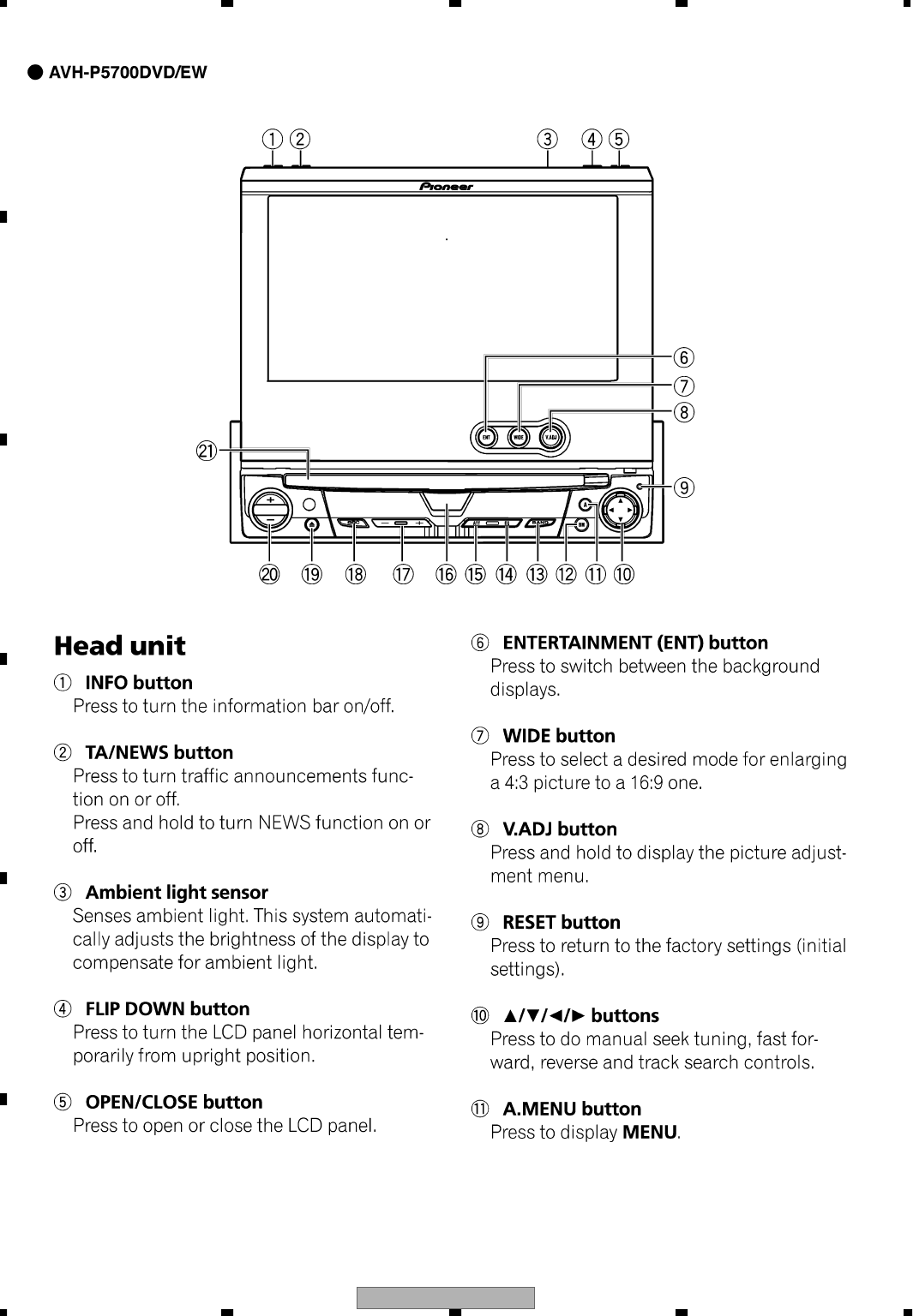
AVH-P5700DVD/EW
204
1234
1234
C
D
F
A
B
E
8. OPERATIONS
AVH-P5700DVD/EW 205
5678
5678
C
D
F
A
B
E
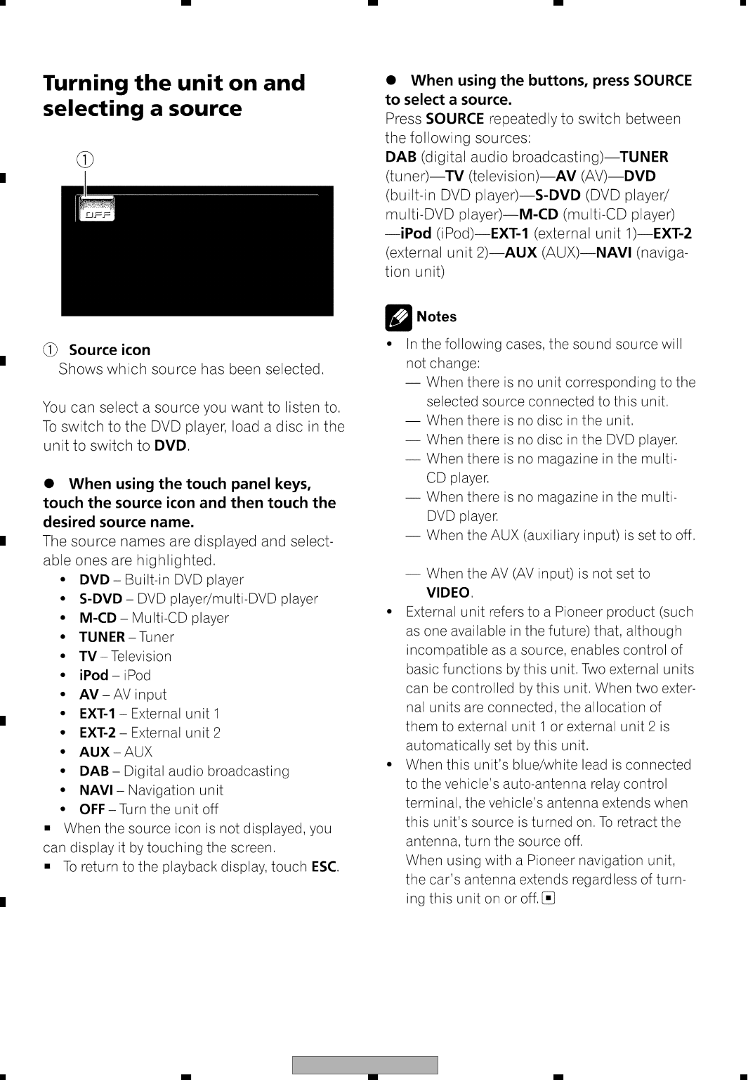
AVH-P5700DVD/EW
206
1234
1234
C
D
F
A
B
E
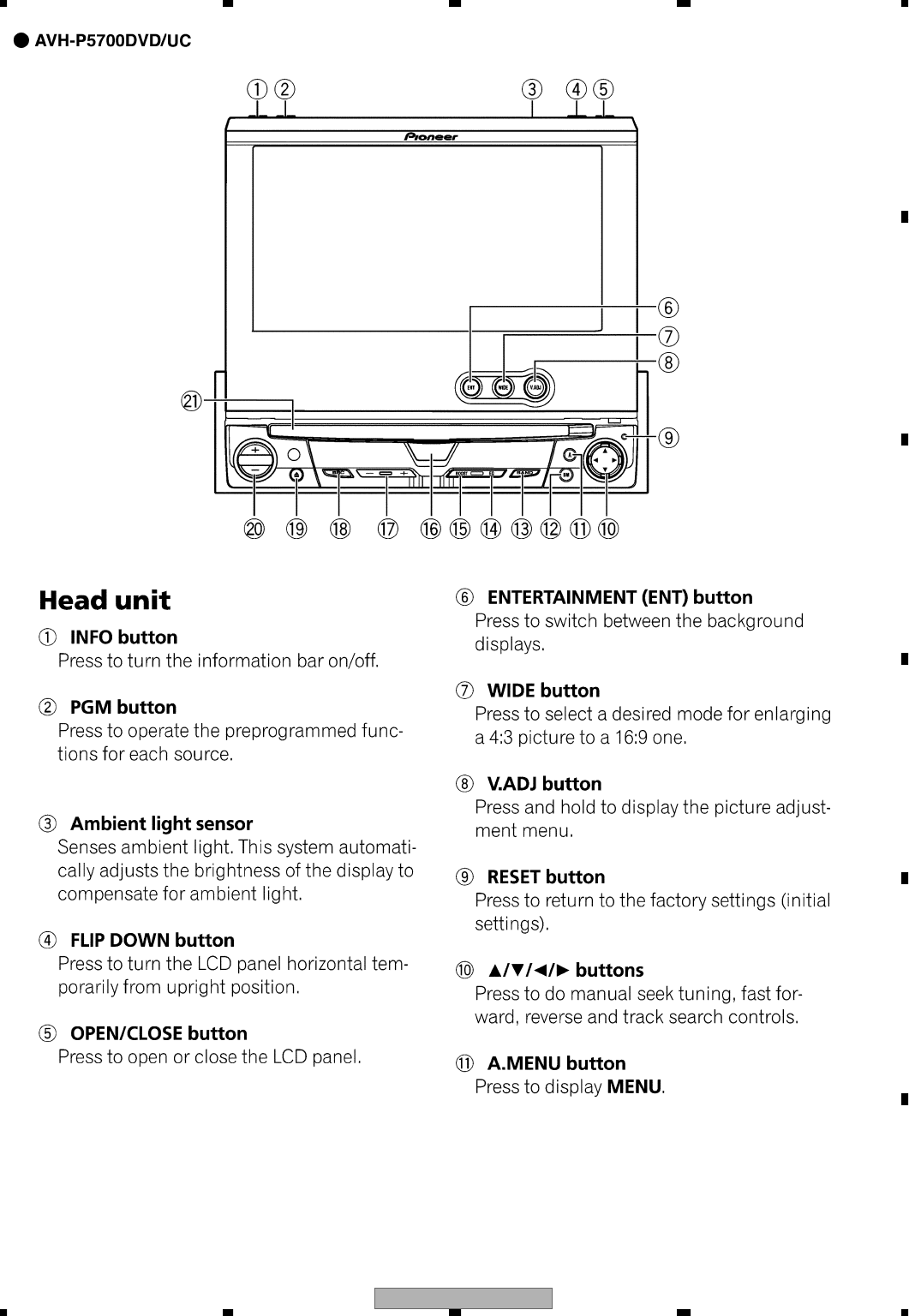
AVH-P5700DVD/EW 207
5678
5678
C
D
F
A
B
E
AVH-P5700DVD/EW
208
1234
1234
C
D
F
A
B
E

AVH-P5700DVD/EW 209
5678
5678
C
D
F
A
B
E
AVH-P5700DVD/EW
210
1234
1234
C
D
F
A
B
E

AVH-P5700DVD/EW 211
5678
5678
C
D
F
A
B
E

AVH-P5700DVD/EW
212
1234
1234
C
D
F
A
B
E

AVH-P5700DVD/EW 213
5678
5678
C
D
F
A
B
E
AVH-P5700DVD/EW
214
1234
1234
C
D
F
A
B
E

AVH-P5700DVD/EW 215
5678
5678
C
D
F
A
B
E
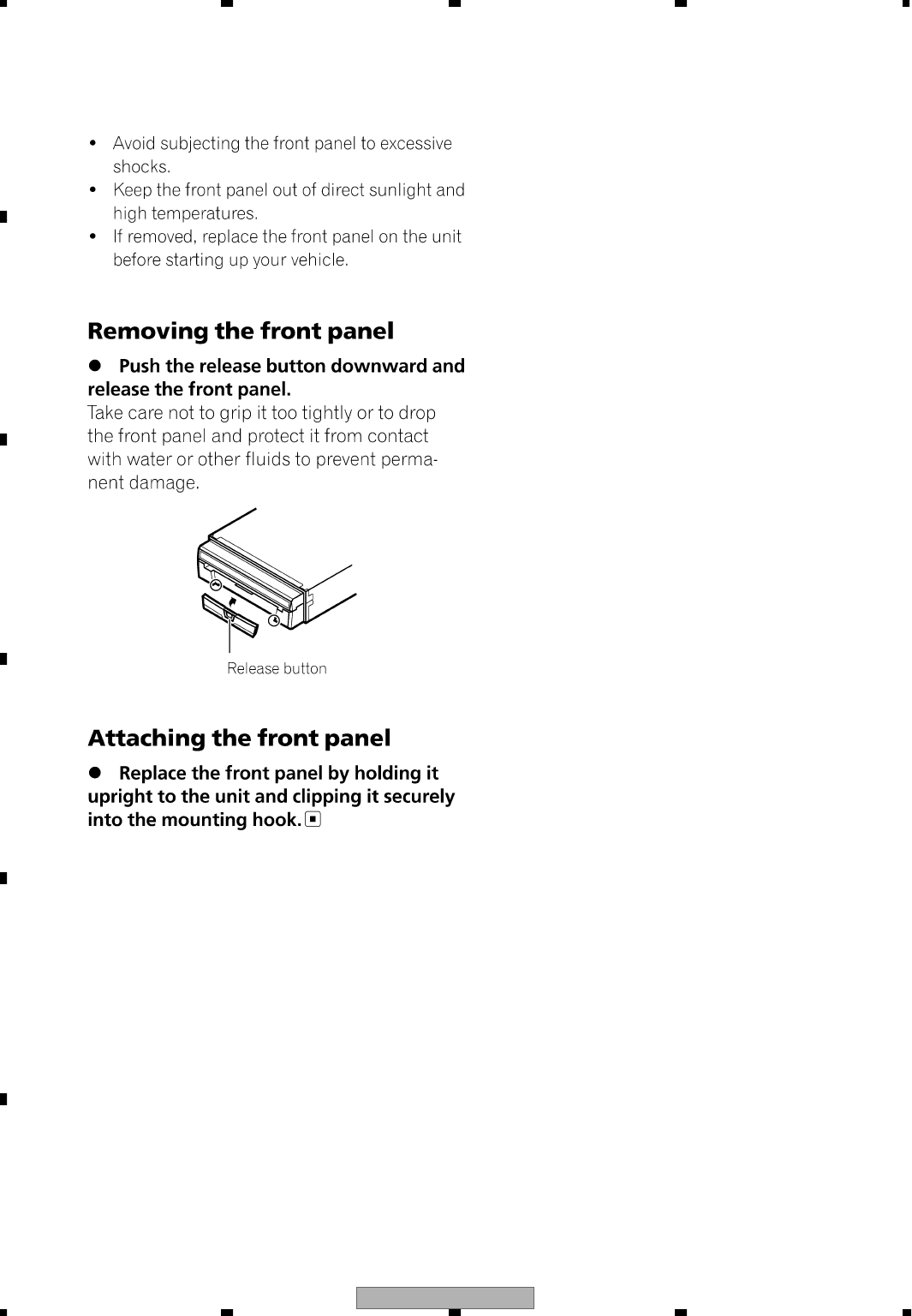
AVH-P5700DVD/EW
216
1234
1234
C
D
F
A
B
E

AVH-P5700DVD/EW 217
5678
5678
C
D
F
A
B
E
AVH-P5700DVD/EW
218
1234
1234
C
D
F
A
B
E
AVH-P5700DVD/EW 219
5678
5678
C
D
F
A
B
E
AVH-P5700DVD/EW
220
1234
1234
C
D
F
A
B
E
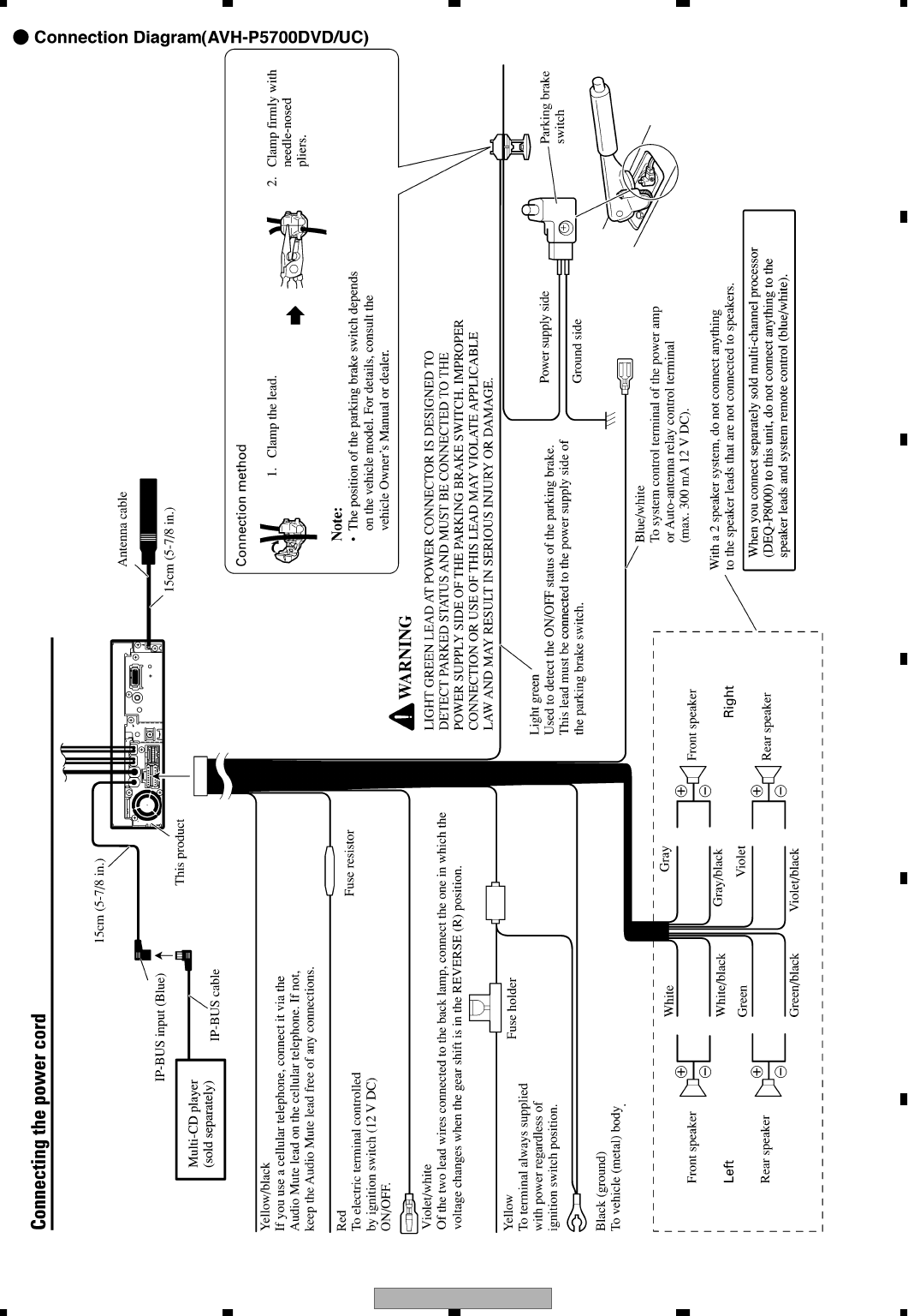
AVH-P5700DVD/EW 221
5678
5678
C
D
F
A
B
E
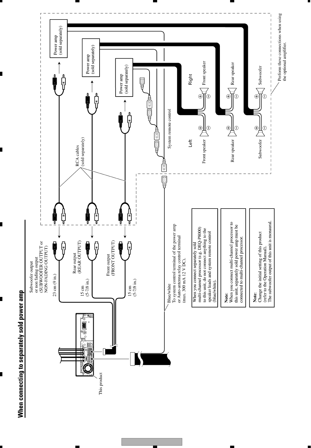
AVH-P5700DVD/EW
222
1234
1234
C
D
F
A
B
E
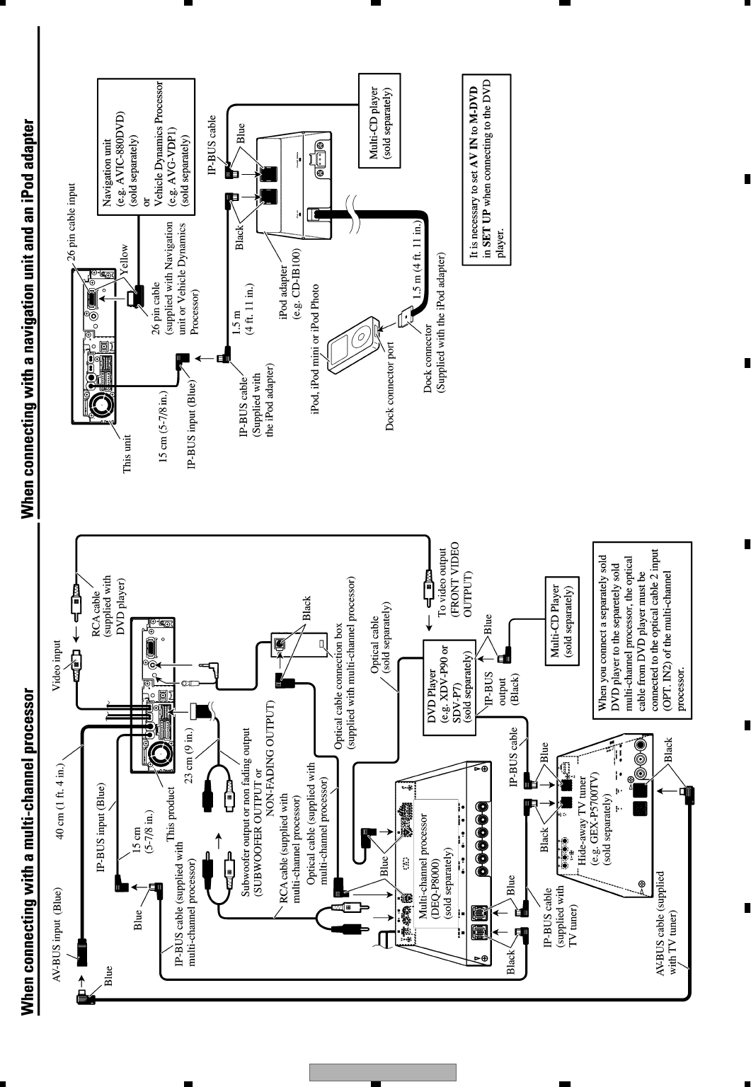
AVH-P5700DVD/EW 223
5678
5678
C
D
F
A
B
E

AVH-P5700DVD/EW
224
1234
1234
C
D
F
A
B
E
-
J
ig
s L
i
st
N
ame
Test
Disc
Sc
r
e
w l
ock
33
pi
n extens
i
on ca
ble
Rela
y
P
C
B
y
Rela
y
P
C
B
20
pi
n extens
i
on ca
ble
40
pi
n extens
i
on ca
ble
40
pi
n extens
i
on ca
ble
2
pi
n extens
i
on ca
ble
Ji
g No
.
GG
V1
0
1
8
G
YL1
00
1
GG
D12
6
2
GG
F1462
GG
F1461
GG
D12
09
GG
D117
0
GG
D1284
GG
D1439
R
emark
s
Adj
ust
i
n
g
t
h
e s
k
e
w
jg
Adj
ust
i
n
g
t
h
e s
k
e
w
C
onnectin
g
the monitor P
C
B to rela
y
P
C
B(
GG
F1462)
Connecting the monitor
g
P
C
B
e
x
te
n
s
i
o
n
cab
l
e
to
fl
e
xi
b
l
e
P
C
B
C
onnectin
g
the monitor P
C
B
e
x
te
n
s
i
o
n
cab
l
e
to
fl
e
xi
b
l
e
P
C
B
C
onnectin
g
the mother unit to rela
y
P
C
B(
GG
F1461)
C
onnectin
g
the mother unit to rela
y
P
C
B(
GG
F1461)
C
onnectin
g
the mother unit to DVD mechanism modul
e
C
onnectin
g
the mother unit to DVD mechanism modul
e
