CRT3193 AVHP6600DVD
User Manual: AVHP6600DVD
Open the PDF directly: View PDF ![]() .
.
Page Count: 228 [warning: Documents this large are best viewed by clicking the View PDF Link!]
- SAFETY INFORMATION
- CONTENTS
- 1. SPECIFICATIONS
- 2. EXPLODED VIEWS AND PARTS LIST
- 2.1 PACKING
- 2.2 EXTERIOR(1)
- 2.3 EXTERIOR(2)
- 2.4 EXTERIOR(3)
- 2.5 DVD MECHANISM MODULE
- 3. BLOCK DIAGRAM AND SCHEMATIC DIAGRAM
- 3.1 BLOCK DIAGRAM
- 3.2 OVERALL CONNECTION DIAGRAM
- 3.3 MOTHER(1/3) PCB(GUIDE PAGE)
- 3.4 MOTHER(2/3) PCB
- 3.5 MOTHER(3/3) PCB(GUIDE PAGE)
- 3.6 RELAY PCB
- 3.7 DVD CORE UNIT(MS-3V1)(SODC)(GUIDE PAGE)
- 3.8 DVD CORE UNIT(MS-3V1)(CPU)
- 3.9 COMPOUND UNIT(A) , COMPOUND UNIT(B) AND RELAY PCB
- 3.10 PU UNIT(REFERENCE)
- 3.11 TUNER UNIT
- 3.12 INVERTER PCB
- 3.13 MONITOR PCB(GUIDE PAGE)
- 3.14 GRILLE PCB
- 3.15 PANEL PCB
- 3.16 MAIN UNIT, SW UNIT AND VOLUME UNIT
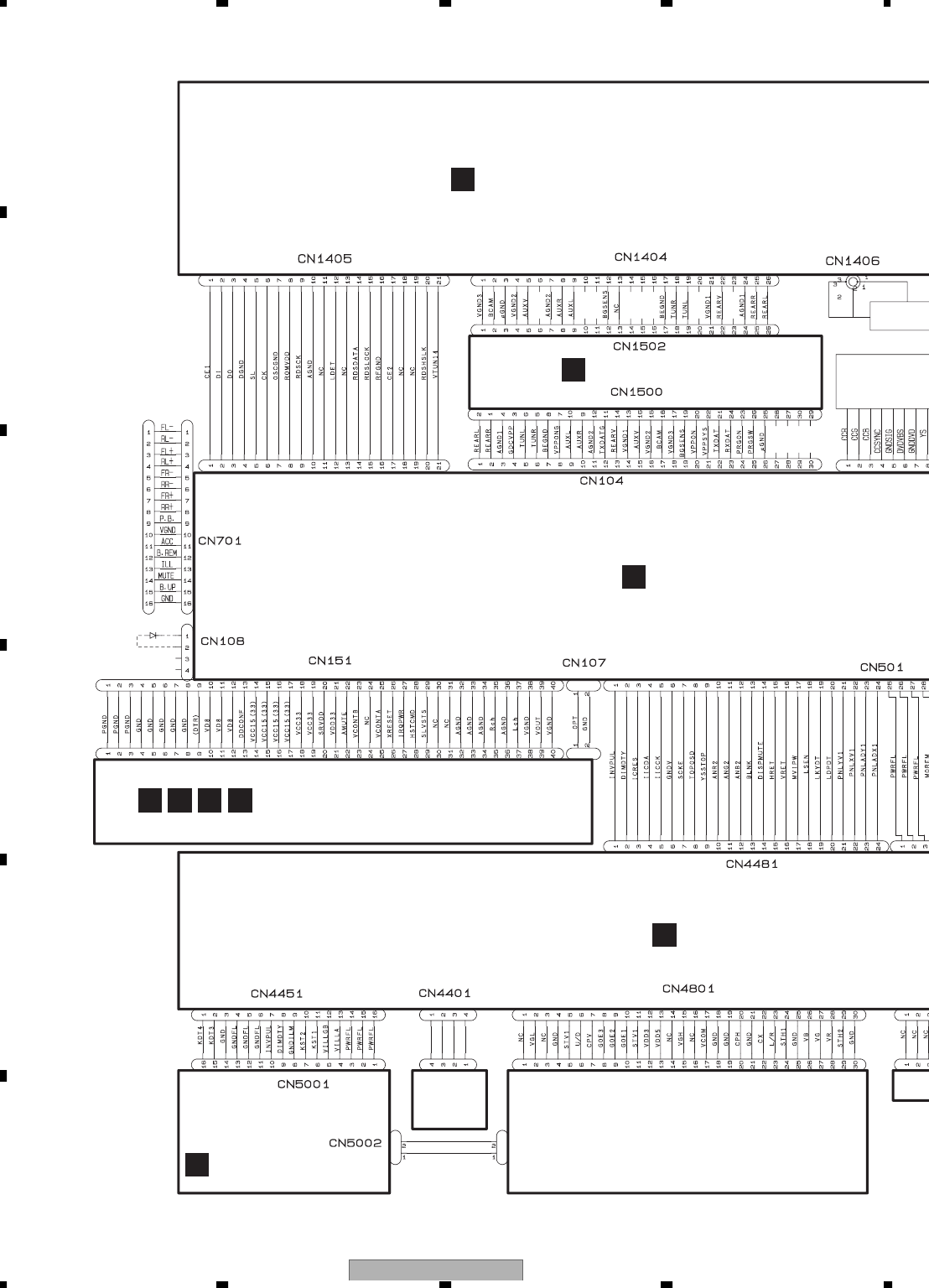
- 4. PCB CONNECTION DIAGRAM
- 4.1 MOTHER PCB
- 4.2 RELAY PCB
- 4.3 DVD CORE UNIT(MS-3V1)
- 4.4 COMPOUND UNIT(A), COMPOUND UNIT(B) AND RELAY PCB
- 4.5 TUNER UNIT
- 4.6 MONITOR PCB
- 4.7 INVERTER PCB
- 4.8 UPPER PCB
- 4.9 SENSE PCB
- 4.10 GRILLE PCB
- 4.11 KEYBOARD PCB
- 4.12 SW UNIT AND VOLUME UNIT
- 4.13 MAIN UNIT
- 5. ELECTRICAL PARTS LIST
- 6. ADJUSTMENT
- 6.1 JIG CONNECTION DIAGRAM
- 6.2 DVD ADJUSTMENT
- 6.3 MOTHER PCB ADJUSTMENT
- 6.4 MONITOR PCB ADJUSTMENT
- 6.5 INVERTER PCB ADJUSTMENT
- 6.6 MONITOR TEST MODE
- 6.7 DOT CLOCK ADJUSTMENT
- 6.8 TOUCH PANEL TEST MODE
- 6.9 FREQUENCY CHECK FOR CLOCK
- 7. GENERAL INFORMATION
- 7.1 DIAGNOSIS
- 7.1.1 DISASSEMBLY
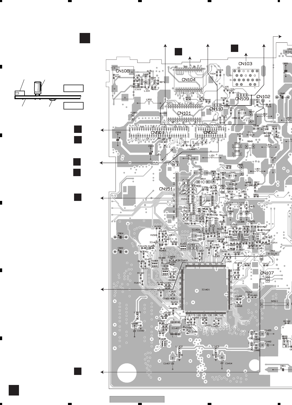
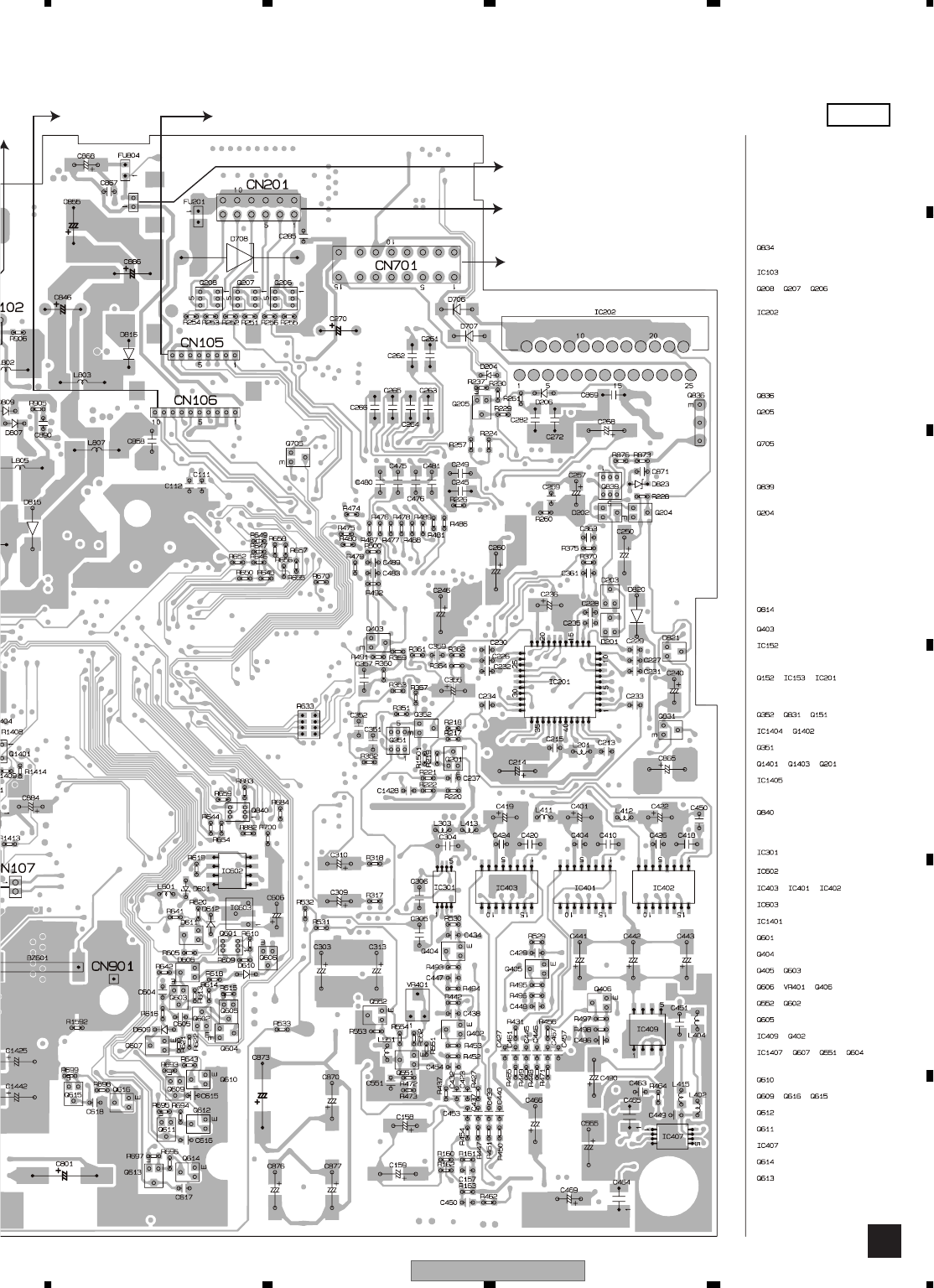
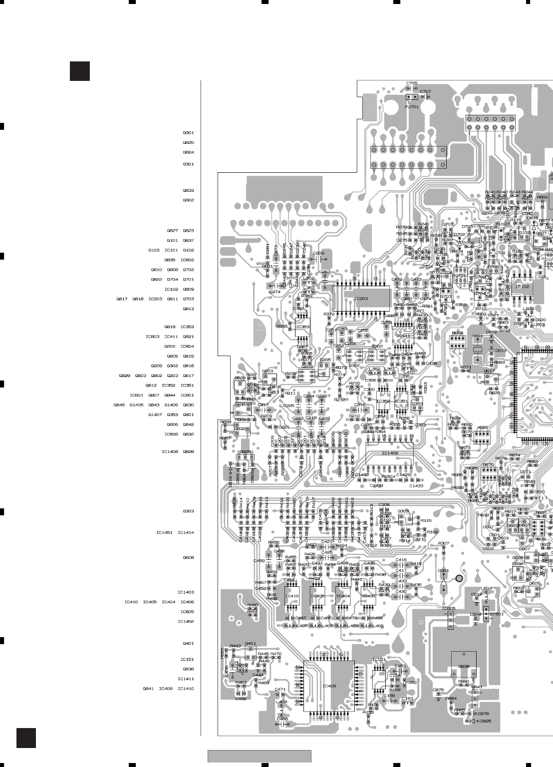
- 7.1.2 PCB LOCATIONS
- 7.1.3 CONNECTOR FUNCTION DESCRIPTION
- 7.2 PARTS
- 7.2.1 IC
- 7.2.2 DISPLAY
- 7.3 EXPLANATION
- 7.3.1 MECHANISM DESCRIPTIONS
- 7.3.2 OPERATIONAL FLOW CHART
- 7.4 CLEANING
- 8. OPERATIONS
ORDER NO.
PIONEER CORPORATION 4-1, Meguro 1-chome, Meguro-ku, Tokyo 153-8654, Japan
PIONEER ELECTRONICS (USA) INC. P.O. Box 1760, Long Beach, CA 90801-1760, U.S.A.
PIONEER EUROPE NV Haven 1087, Keetberglaan 1, 9120 Melsele, Belgium
PIONEER ELECTRONICS ASIACENTRE PTE. LTD. 253 Alexandra Road, #04-01, Singapore 159936
PIONEER CORPORATION 2004
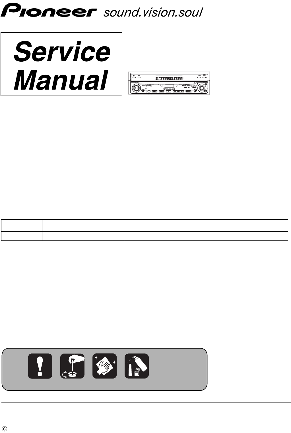
AVH-P6600DVD/UC
CRT3193
AV RECEIVER/DVD PLAYER WITH 6.5 INCH WIDE DISPLAY
AVH-P6600DVD
/UC
AVH-P6600DVD
/EW
AVH-P6650DVD
/RC
AVH-P6650DVD
/RD
This service manual should be used together with the following manual(s):
Manufactured under license from Dolby Laboratories. "Dolby" and the double-D sysmbol are trademarks
of Dolby Laboratories.
Model No. Order No. Mech.Module Remarks
CX-3078 CRT3257 MS-3V1 DVD Mech. Module:Circuit Description, Mech. Description, Disassembly
For details, refer to "Important symbols for good services".
K-ZZU.MAR. 2004 printed in Japan
AVH-P6600DVD/UC
2
1234
1234
C
D
F
A
B
E
SAFETY INFORMATION
UC
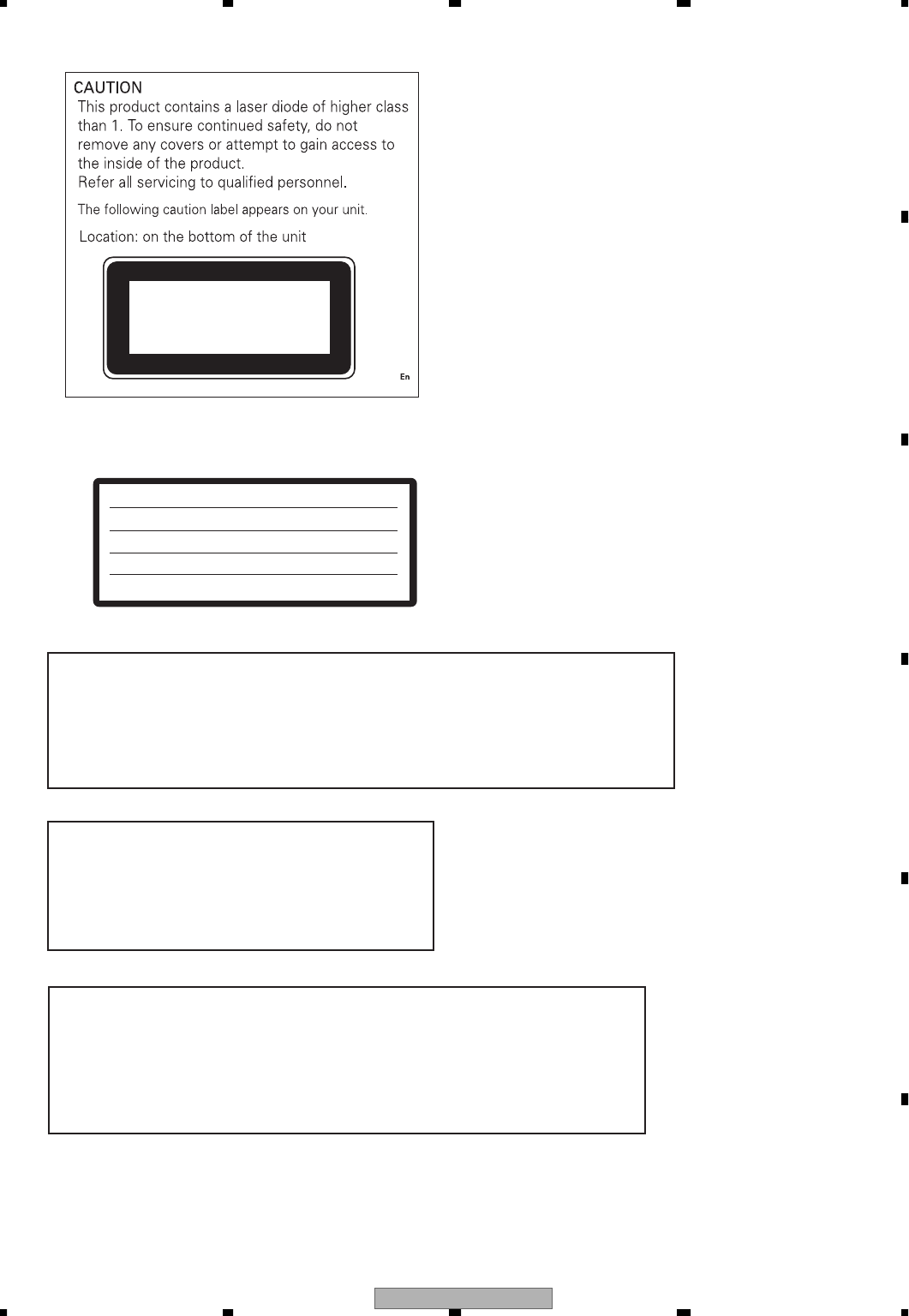
CAUTION
This service manual is intended for qualified service technicians; it is not meant for the casual do-it-yourselfer.
Qualified technicians have the necessary test equipment and tools, and have been trained to properly and safely repair
complex products such as those covered by this manual.
Improperly performed repairs can adversely affect the safety and reliability of the product and may void the warranty.
If you are not qualified to perform the repair of this product properly and safely, you should not risk trying to do so
and refer the repair to a qualified service technician.
WARNING
This product contains lead in solder and certain electrical parts contain chemicals which are known to the state of
California to cause cancer, birth defects or other reproductive harm.
Health & Safety Code Section 25249.6 - Proposition 65
EW
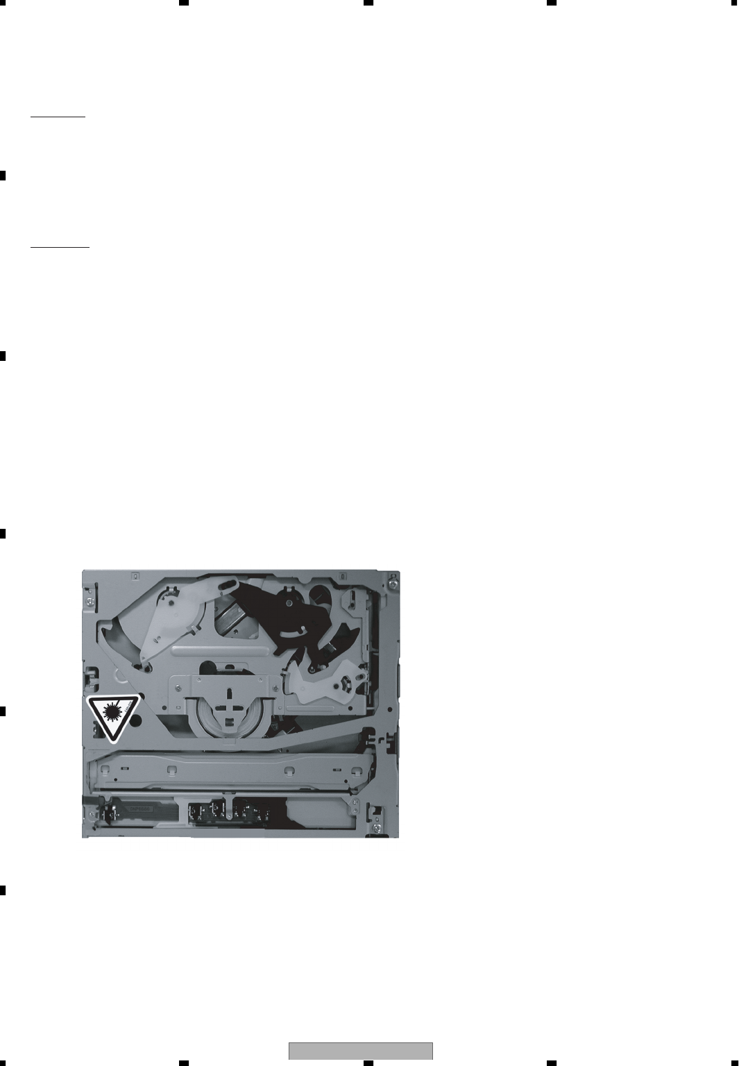
1. Safety Precautions for those who Service this Unit.
• Follow the adjustment steps (see pages 143 through 156)in the service manual when servicing this unit. When check-
ing or adjusting the emitting power of the laser diode exercise caution in order to get safe, reliable results.
Caution:
1. During repair or tests, minimum distance of 13cm from the focus lens must be kept.
2. During repair or tests, do not view laser beam for 10 seconds or longer.
2. The triangular label is attached to the mechanism
unit frame.
This product contains mercury. Disposal of this material may be regulated due to
environmental considerations. For disposal or recycling information, please contact
your local authorities or the Electronics Industries Alliance: www.eiae.org.
AVH-P6600DVD/UC 3
5678
5678
C
D
F
A
B
E
On the top of the player.
CAUTION :
VORSICHT :
ADVARSEL :
VARNING :
VARO! :
VISIBLE AND INVISIBLE LASER RADIATION WHEN OPEN.
AVOID EXPOSURE TO BEAM.
SICHTBARE UND UNSICHTBARE LASERSTRAHLUNG, WENN
ABDECKUNG GEÖFFNET NICHT DEM STRAHL AUSSETZEN!
SYNLIG OG USYNLIG LASERSTRÅLING VED ÅBNING
UNDGÅ UDSÆTTELSE FOR STRÀLING.
SYNLIG OCH OSYNLIG LASERSTRÅLNING NÄR DENNA
DEL ÄR ÖPPNAD BETRAKTA EJ STRÅLEN.
AVATTAESSA ALTISTUT NÄKYVÄ JA NÄKYMÄTTÖMÄLLE
LASERSATEIL YLLE. ÄLÄ KATSO SÄTEESEN. VRW1860
CLASS 1
LASER PRODUCT
WARNING!
The AEL (accessible emission level )of the laser power output is less than CLASS 1
but the laser component is capable of emitting radiation exceeding the limit for
CLASS 1.
A specially instructed person should do servicing operation of the apparatus.
Laser diode characteristics
Wave length:
DVD:640~660nm
CD:770~810nm
DVD : 2.48mw(Emitting period :9sec. )
CD : 705µw(Emitting period : unlimited)
Additionla Laser Caution
Transistors Q1101 and Q1102 in PCB drive the laser diodes for DVD and CD
respectively. When Q1101 or Q1102 is shorted between their terminals,
the laser diodes for DVD or CD will radiate beam. If the top cover is removed
with no disc loaded while such short-circuit is continued, the naked eyes may
be exposed to the laser beam.
AVH-P6600DVD/UC
4
1234
1234
C
D
F
A
B
E
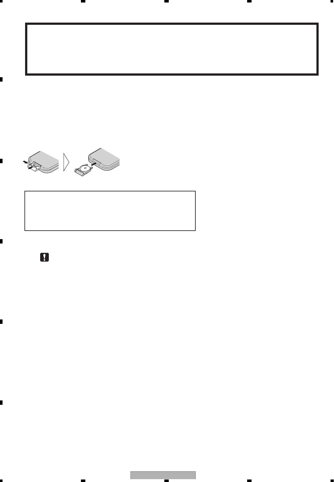
CAUTION
Danger of explosion if battery is incorrectly replaced.
Replaced only with the same or equivalent type recommended by the manufacture.
Discord used batteries according to the manufacture's instructions.
RC,RD
CAUTION
Danger of explosion if battery is incorrectly replaced.
Replaced only with the same or equivalent type.
Battery
Slide the tray out on the back of the
remote controller and insert the battery
with the (+) and (–) poles pointing in
the proper direction.
Note :
• Use a CR2025 (3V) lithium battery
only. Never use other types of battery
with this unit.
1. In the state of FAN being attached to the mother unit, the voltage of about 6 to 8 V is impressed between TEST
point (FAN1) on surface A of the base plate and adequate GND to confirm its operation by visual observation.
2. After product assembly, a waveform observation is conducted using oscilloscope while playing DVD on TEST
point (TEST1) in front of chassis hole on lower face and adequate GND to confirm the existence of operation
noise (pulse) shape.
- Method of FAN Operation Confirmation
- Inverter for LCD back light becomes a high voltage.
NOTE:
AVH-P6600DVD/UC 5
5678
5678
C
D
F
A
B
E
[ Important symbols for good services ]
In this manual, the symbols shown-below indicate that adjustments, settings or cleaning should be made securely.
When you find the procedures bearing any of the symbols, be sure to fulfill them:
2. Adjustments
To keep the original performances of the product, optimum adjustments or specification confirmation is indispensable.
In accordance with the procedures or instructions described in this manual, adjustments should be performed.
3. Cleaning
For optical pickups, tape-deck heads, lenses and mirrors used in projection monitors, and other parts requiring cleaning,
proper cleaning should be performed to restore their performances.
5. Lubricants, glues, and replacement parts
Appropriately applying grease or glue can maintain the product performances. But improper lubrication or applying
glue may lead to failures or troubles in the product. By following the instructions in this manual, be sure to apply the
prescribed grease or glue to proper portions by the appropriate amount.For replacement parts or tools, the prescribed
ones should be used.
4. Shipping mode and shipping screws
To protect the product from damages or failures that may be caused during transit, the shipping mode should be set or
the shipping screws should be installed before shipping out in accordance with this manual, if necessary.
1. Product safety
You should conform to the regulations governing the product (safety, radio and noise, and other regulations), and
should keep the safety during servicing by following the safety instructions described in this manual.

AVH-P6600DVD/UC
6
1234
1234
C
D
F
A
B
E
CONTENTS
SAFETY INFORMATION..................................................................................................................................... 2
1. SPECIFICATIONS ............................................................................................................................................ 7
2. EXPLODED VIEWS AND PARTS LIST .......................................................................................................... 14
2.1 PACKING ................................................................................................................................................. 14
2.2 EXTERIOR(1) .......................................................................................................................................... 18
2.3 EXTERIOR(2) .......................................................................................................................................... 22
2.4 EXTERIOR(3) .......................................................................................................................................... 24
2.5 DVD MECHANISM MODULE .................................................................................................................. 27
3. BLOCK DIAGRAM AND SCHEMATIC DIAGRAM..........................................................................................30
3.1 BLOCK DIAGRAM ................................................................................................................................... 30
3.2 OVERALL CONNECTION DIAGRAM...................................................................................................... 36
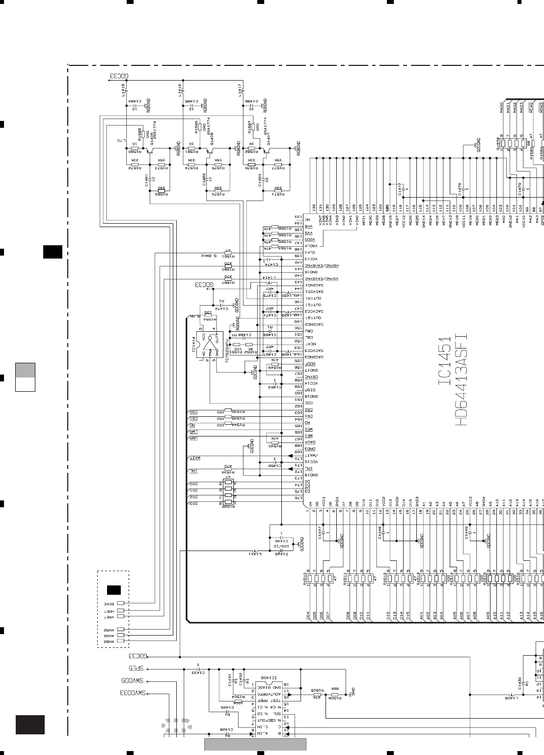
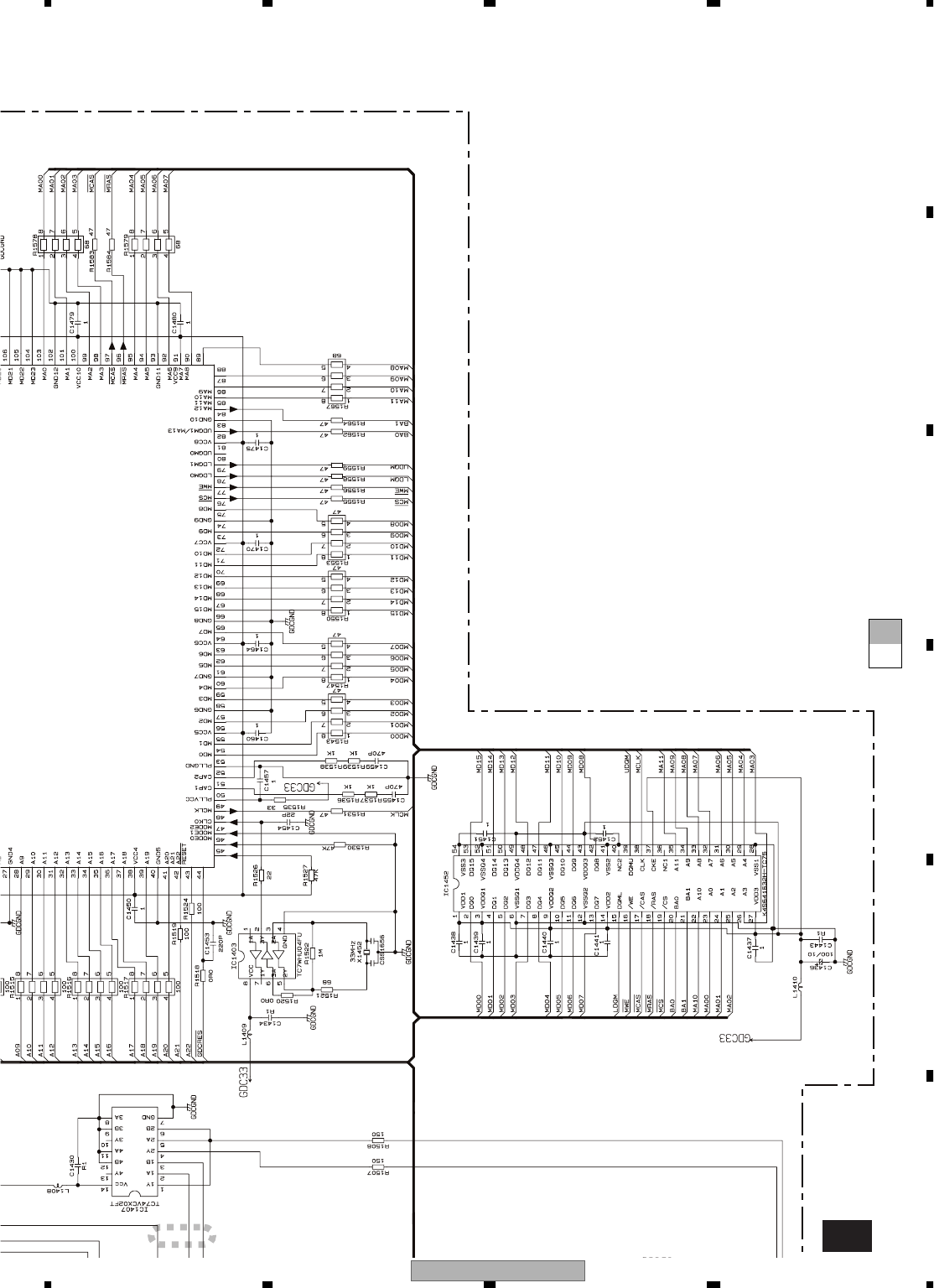
3.3 MOTHER(1/3) PCB(GUIDE PAGE).......................................................................................................... 38
3.4 MOTHER(2/3) PCB.................................................................................................................................. 44
3.5 MOTHER(3/3) PCB(GUIDE PAGE).......................................................................................................... 46
3.6 RELAY PCB ............................................................................................................................................. 52
3.7 DVD CORE UNIT(MS-3V1)(SODC)(GUIDE PAGE)................................................................................. 54
3.8 DVD CORE UNIT(MS-3V1)(CPU)............................................................................................................ 60
3.9 COMPOUND UNIT(A) , COMPOUND UNIT(B) AND RELAY PCB ......................................................... 64
3.10 PU UNIT(REFERENCE) ........................................................................................................................ 65
3.11 TUNER UNIT ......................................................................................................................................... 66
3.12 INVERTER PCB..................................................................................................................................... 68
3.13 MONITOR PCB(GUIDE PAGE).............................................................................................................. 70
3.14 GRILLE PCB.......................................................................................................................................... 76
3.15 PANEL PCB ........................................................................................................................................... 78
3.16 MAIN UNIT, SW UNIT AND VOLUME UNIT .......................................................................................... 79
4. PCB CONNECTION DIAGRAM ..................................................................................................................... 82
4.1 MOTHER PCB ......................................................................................................................................... 82
4.2 RELAY PCB ............................................................................................................................................. 86
4.3 DVD CORE UNIT(MS-3V1)...................................................................................................................... 88
4.4 COMPOUND UNIT(A), COMPOUND UNIT(B) AND RELAY PCB .......................................................... 92
4.5 TUNER UNIT ........................................................................................................................................... 94
4.6 MONITOR PCB........................................................................................................................................ 96
4.7 INVERTER PCB..................................................................................................................................... 100
4.8 UPPER PCB .......................................................................................................................................... 101
4.9 SENSE PCB .......................................................................................................................................... 102
4.10 GRILLE PCB........................................................................................................................................ 103
4.11 KEYBOARD PCB................................................................................................................................. 104
4.12 SW UNIT AND VOLUME UNIT............................................................................................................ 105
4.13 MAIN UNIT........................................................................................................................................... 106
5. ELECTRICAL PARTS LIST .......................................................................................................................... 108
6. ADJUSTMENT ............................................................................................................................................. 142
6.1 JIG CONNECTION DIAGRAM............................................................................................................... 142
6.2 DVD ADJUSTMENT............................................................................................................................... 143
6.3 MOTHER PCB ADJUSTMENT.............................................................................................................. 157
6.4 MONITOR PCB ADJUSTMENT............................................................................................................. 160
6.5 INVERTER PCB ADJUSTMENT ........................................................................................................... 162
6.6 MONITOR TEST MODE ........................................................................................................................ 163
6.7 DOT CLOCK ADJUSTMENT................................................................................................................. 167
6.8 TOUCH PANEL TEST MODE ................................................................................................................ 168
6.9 FREQUENCY CHECK FOR CLOCK..................................................................................................... 173
7. GENERAL INFORMATION........................................................................................................................... 174
7.1 DIAGNOSIS ........................................................................................................................................... 174
7.1.1 DISASSEMBLY ................................................................................................................................... 174
7.1.2 PCB LOCATIONS ............................................................................................................................... 181
7.1.3 CONNECTOR FUNCTION DESCRIPTION........................................................................................ 183
7.2 PARTS.................................................................................................................................................... 185
7.2.1 IC ........................................................................................................................................................ 185
7.2.2 DISPLAY ............................................................................................................................................. 213
7.3 EXPLANATION ...................................................................................................................................... 214
7.3.1 MECHANISM DESCRIPTIONS .......................................................................................................... 214
7.3.2 OPERATIONAL FLOW CHART .......................................................................................................... 220
7.4 CLEANING............................................................................................................................................. 221
8. OPERATIONS .............................................................................................................................................. 222
AVH-P6600DVD/UC 7
5678
5678
C
D
F
A
B
E
1. SPECIFICATIONS
AVH-P6600DVD/UC
8
1234
1234
C
D
F
A
B
E
AVH-P6600DVD/UC 9
5678
5678
C
D
F
A
B
E
AVH-P6600DVD/UC
10
1234
1234
C
D
F
A
B
E
AVH-P6600DVD/UC 11
5678
5678
C
D
F
A
B
E
AVH-P6600DVD/UC
12
1234
1234
C
D
F
A
B
E

AVH-P6600DVD/UC 13
5678
5678
C
D
F
A
B
E
AVH-P6600DVD/UC
14
1234
1234
C
D
F
A
B
E
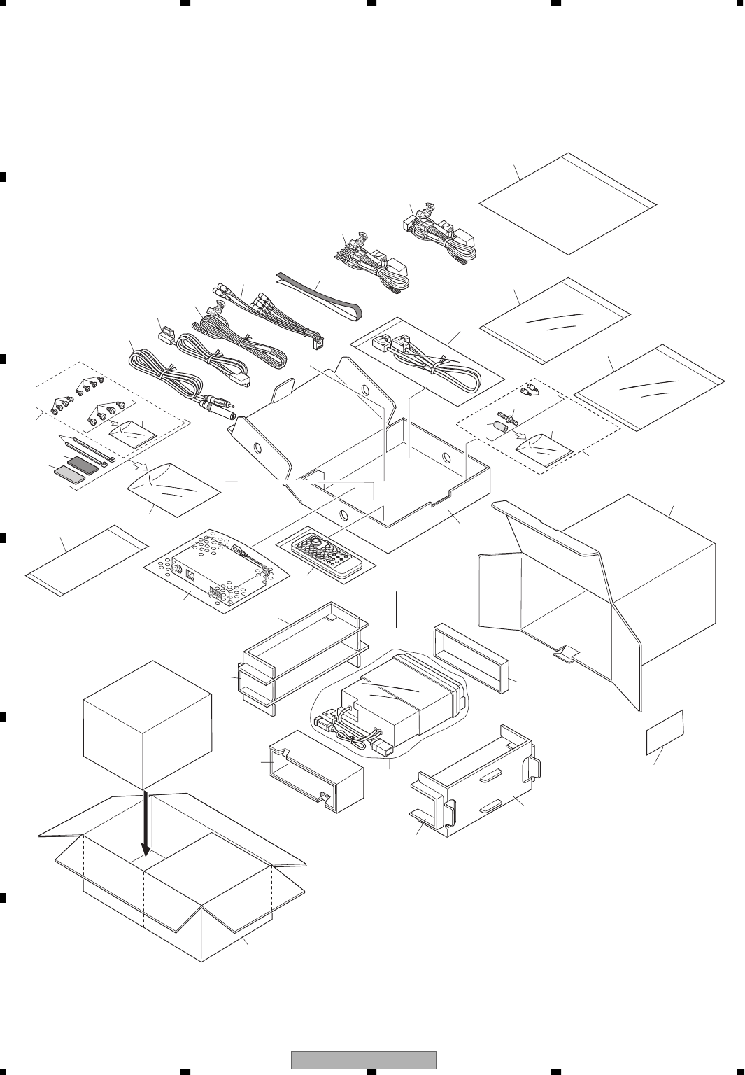
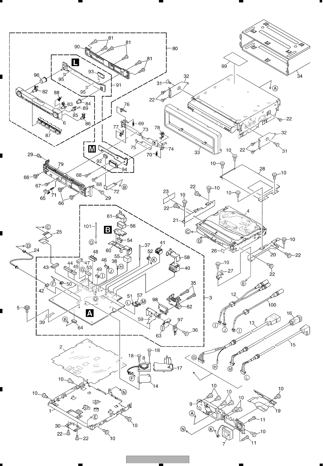
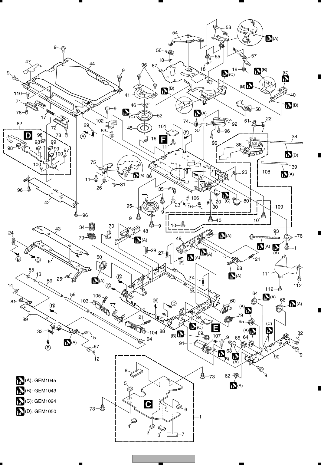
2. EXPLODED VIEWS AND PARTS LIST
2.1 PACKING
N
OTES : • Parts marked by " * " are generally unavailable because they are not in our Master Spare Parts List.
• Screw adjacent to mark on the product are used for disassembly.
• For the applying amount of lobricants or glue, follow the instructions in this manual.
(In the case of no amount instructions,apply as you think it appropriate.)
"
20
34
15
16
17
18
19 14
11
32
33
12
13
1
36
37
35
38 21
2
3
7
6
5
8
9
6
7
10
4
24
23
27
25
29
3130
22
28

AVH-P6600DVD/UC 15
5678
5678
C
D
F
A
B
E
PACKING SECTION PARTS LIST
Mark NO Description P6600DVD/UC P6600DVD/EW P6650DVD/RC P6650DVD/RD
1-1 Polyethylene Bag CEG1116 CEG1116 CEG1116 CEG1116
1-2 Owner's Manual CRB1927 CRB1921 CRB1929 CRB1929
1-3 Owner's Manual CRB1928 CRB1922 CRB1930 CRB1931
1-4 Owner's Manual Not used Not used Not used CRB1932
1-5 Installation Manual CRD3858 CRD3897 CRD3859 CRD3860
* 1-6 Card ARY1048 Not used Not used Not used
1-7 Caution Card CRP1310 Not used CRP1310 CRP1310
2 Carton CHG5221 CHG5220 CHG5222 CHG5222
3 Contain Box CHL5221 CHL5220 CHL5222 CHL5223
4 Air Cushioned Bag CEG1089 CEG1089 CEG1089 CEG1089
5 Polyethylene Bag CEG1185 CEG1088 CEG1088 CEG1088
6 Protector CHP2707 CHP2707 CHP2707 CHP2707
7 Protector CHP2706 CHP2706 CHP2706 CHP2706
8 Protector CHP2708 CHP2708 CHP2708 CHP2708
9 Protector CHP2387 CHP2387 CHP2387 CHP2387
10 Remote Control Unit CXC3074 CXC3075 CXC3075 CXC3075
* 11 Polyethylene Bag E36-615 E36-615 E36-615 E36-615
12 Screw CBA1650 CBA1650 CBA1650 CBA1650
13 Bush CNV1917 CNV1917 CNV1917 CNV1917
14 Cord Assy CDE7445 CDE7445 CDE7445 CDE7445
15 Cord Assy CDE7609 Not used CDE7609 CDE7609
16 Cord Assy CDE7194 CDE7194 CDE7194 CDE7194
17 Cord Assy CDE7321 CDE7321 CDE7321 CDE7321
18 Cord Assy CDE7187 CDE7187 CDE7187 CDE7187
19 Antenna Cable CDH1281 CDH1281 CDH1281 CDH1281
20 Sheet CNM8603 CNM8603 CNM8603 CNM8603
21 Sub Craton CHG5080 CHG5080 CHG5080 CHG5080
* 22 Polyethylene Bag CEG-158 CEG-158 CEG-158 CEG-158
23 Screw Assy CEA3686 CEA3686 CEA3686 CEA3686
24 Screw(M4x3) CBA1468 CBA1468 CBA1468 CBA1468
25 Screw CMZ50P060FTC CMZ50P060FTC CMZ50P060FTC CMZ50P060FTC
26 •••••
27 Screw BMZ50P060FTC BMZ50P060FTC BMZ50P060FTC BMZ50P060FTC
* 28 Polyethylene Sheet CNM4338 CNM4338 CNM4338 CNM4338
* 29 Lock Tie Not used CNV-754 CNV-754 CNV-754
* 30 Fastener CNM6544 CNM6544 CNM6544 CNM6544
* 31 Fastener CNM6545 CNM6545 CNM6545 CNM6545
32 Accessory Assy CEA3685 CEA3685 CEA3743 CEA3743
33 Fixing Screw JGZ20P070FTC JGZ20P070FTC Not used Not used
34 Cord Assy Not used CDE7608 Not used Not used
35-1 Polyethylene Bag Not used CEG1116 Not used Not used
35-2 Owner's Manual Not used CRB1923 Not used Not used
35-3 Owner's Manual Not used CRB1924 Not used Not used
35-4 Owner's Manual Not used CRB1925 Not used Not used
35-5 Owner's Manual Not used CRB1926 Not used Not used
* 35-6 Passport Not used CRY1013 Not used Not used
* 35-7 Warranty Card Not used CRY1157 Not used Not used
36 Cleaning Cloth Assy CEA3952 CEA3952 CEA3952 CEA3952
37 Seal Not used Not used Not used CAN4722
38 Opt Terminal Change Not used Not used CXC3584 CXC3584
AVH-P6600DVD/UC
16
1234
1234
C
D
F
A
B
E
Owner's Manual,Installation Manual
Part No. Language
CRB1921 English
CRB1922 Spanish
CRB1923 German
CRB1924 French
CRB1925 Italian
CRB1926 Dutch
CRD3897 English,Spanish,German,French,Italian,Dutch
CRB1927 English
CRB1928 French
CRD3858 English,French
CRB1929 English
CRB1930 Traditional Chinese
CRD3859 English,Traditional Chinese
CRB1931 Spanish
CRB1932 Portuguese(B)
CRD3860 English,Spanish,Portuguese(B)

AVH-P6600DVD/UC 17
5678
5678
C
D
F
A
B
E
AVH-P6600DVD/UC
18
1234
1234
C
D
F
A
B
E
2.2 EXTERIOR(1)

AVH-P6600DVD/UC 19
5678
5678
C
D
F
A
B
E
(1)EXTERIOR(1) SECTION PARTS LIST
Mark No. Description Part No.
1 Case CNB2948
2 Insulator CNM8646
3 Mother Unit See Contrast table(2)
4 DVD Mechanism Mdule(MS-3V1)CXK6410
5 Screw IMS26P040FTC
6 Grille Unit(Service) See Contrast table(2)
7 Fan Motor(M1001) CXM1262
8 Fan Motor(M1002) CXM1276
9 Panel See Contrast table(2)
10 Screw BMZ26P030FTC
11 Screw BMZ20P160FTC
12 Cord Assy See Contrast table(2)
13 Cord Assy See Contrast table(2)
14 Insulator CNM8864
15 Cord Assy CDE7450
16 Cord Assy CDE7449
17 Guide CNV7973
18 Screw(M2x8) CBA1752
19 Holder CND2034
20 Bracket CND1438
21 Bracket CND1439
22 Screw BMZ20P030FZK
23 Insulator CNM8495
24 Cord CDE7715
25 Cable CDE7452
26 Spacer CNM9272
27 Earth CBL1660
28 Bracket CND1603
29 Screw(M2x2) CBA1753
30 Holder CND1441
31 Screw CMZ50P060FTC
32 Bracket CND1482
33 Panel See Contrast table(2)
34 Holder CNC9510
35 Screw BMZ26P160FTC
36 Screw BSZ26P100FTC
37 Clamper CEF1036
38 Terminal(CN102) See Contrast table(2)
39 Terminal(CN901) CKF1064
40 Connector(CN701) CKM1332
41 Connector(CN201) CKM1389
42 Connector(CN107) CKS4282
43 Connector(CN151) CKS4052
44 Connector(CN501) CKS3930
45 Connector(CN502) VKN1533
46 Connector(CN109) See Contrast table(2)
47 Jack(CN108) CKN1022
48 Connector(CN104) CKS4800
49 Connector(CN110) CKS3125
50 Connector(CN802) CKS2191
51 Connector(CN106) CKS3132
52 Connector(CN801) CKS3124
53 Connector(CN101) See Contrast table(2)
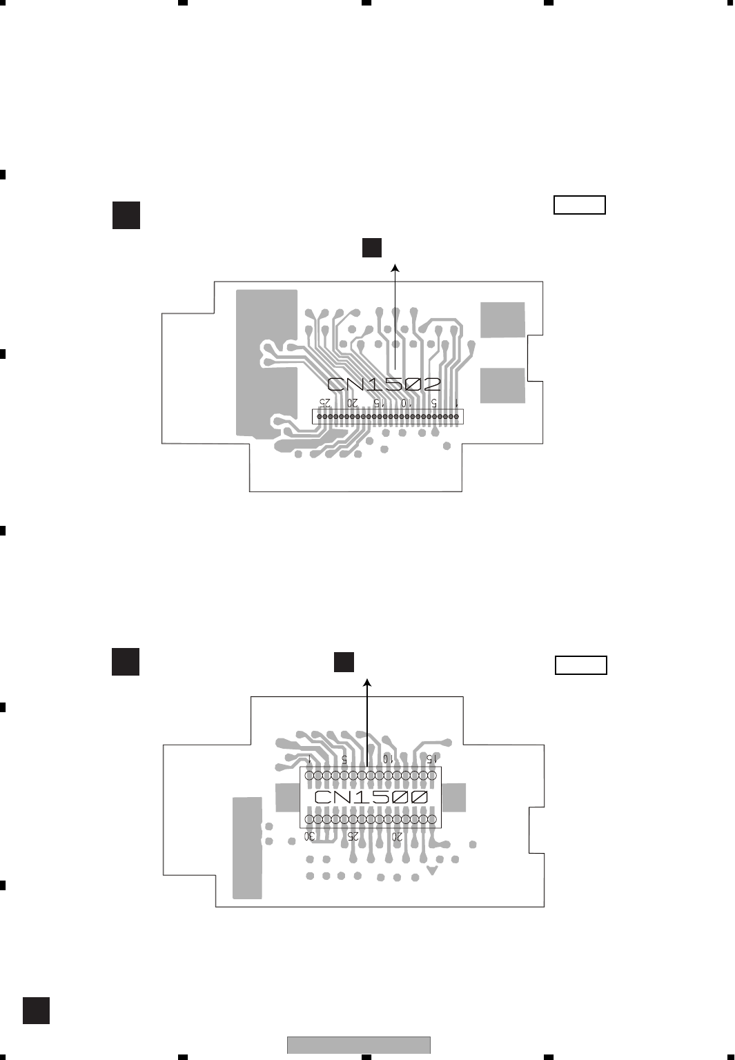
54 Connector(CN1500) CKS4799
55 Connector(CN103) CKS4663
56 Connector(CN1502) CKS4467
57 Connector(CN105) CKS3130
58 Holder CND1433
59 Holder CND1434
60 Holder CND2035
61 Holder CND2036
62 Heat Sink CNR1684
63 Heat Sink CNR1703
64 Connector(CN601) CKS3986
65 Button CAC7953
66 Screw(M2x4) CBA1734
67 Screw(M2.6x2.5) CBA1777
68 Screw(M2x4) CBA1778
69 Spring CBH2681
70 Spring CBH2682
71 Spring CBH2683
72 Flat Cable CDE7179
73 Holder CND1840
74 Holder CND1841
75 Insulator CNM8510
76 Arm CNV7567
77 Arm CNV7568
78 Arm CNV7569
79 Panel Unit See Contrast table(2)
80 Grille Assy See Contrast table(2)
81 Screw BPZ20P080FZK
82 Button(SRC) CAC7946
83 Button(EQ) CAC7947
84 Button CAC8149
85 Button(Detach Eject) See Contrast table(2)
86 Button(Disc Eject) See Contrast table(2)
87 Button See Contrast table(2)
88 Button(Reset) See Contrast table(2)
89 Spring CBH2680
90 Cover CNS7441
91 Keyboard Unit See Contrast table(2)
92 Connector(CN5901) CKS3986
93 Connector(CN5501) CKS4657
94 Connector(CN5902) CKS4658
95 Insulator CNM8521
96 Knob Unit CXC2034
97 Transistor(Q836) 2SD1275
98 IC(IC202) PAL007A
99 Label See Contrast table(2)
100 Cord Assy See Contrast table(2)
101 Clamper See Contrast table(2)
Mark No. Description Part No.

AVH-P6600DVD/UC
20
1234
1234
C
D
F
A
B
E
(2) CONTRAST TABLE
AVH-P6600DVD/UC , AVH-P6600DVD/EW , AVH-P6650DVD/RC and AVH-P6650DVD/RD are constructed the
same except for the following:
Mark NO Description P6600DVD/UC P6600DVD/EW P6650DVD/RC P6650DVD/RD
3 Mother Unit CWM9143 CWM9142 CWM9144 CWM9145
6 Grille Unit(Service) CXX1801 CXX1800 CXX1802 CXX1802
9 Panel CNB2946 CNB2946 CNB2947 CNB2947
12 Cord Assy CDE7456 CDE7456 Not used Not used
13 Cord Assy CDE7451 CDE7451 Not used Not used
33 Panel CNS7785 CNS7785 CNS7481 CNS7481
38 Terminal(CN102) CKF-047 CKF-047 Not used Not used
46 Connector(CN109) CKS3126 CKS3126 Not used Not used
53 Connector(CN101) CKS4454 CKS4454 Not used Not used
79 Panel Unit CXC2662 CXC2662 CXC3277 CXC3277
80 Grille Assy GXC1007 GXC1009 GXC1008 GXC1008
85 Button(Detach Eject) CAC8452 CAC8452 CAC7951 CAC7951
86 Button(Disc Eject) CAC8453 CAC8453 CAC7950 CAC7950
87 Button CAC8454 CAC8454 CAC8922 CAC8922
88 Button(Reset) CAC8456 CAC8456 CAC8054 CAC8054
91 Keyboard Unit CWM8766 CWM8765 CWM8766 CWM8766
99 Label Not used VRW1860 Not used Not used
100 Cord Assy Not used Not used CDE7457 CDE7457
101 Clamper CEF1036 CEF1036 Not used Not used

AVH-P6600DVD/UC 21
5678
5678
C
D
F
A
B
E
AVH-P6600DVD/UC
22
1234
1234
C
D
F
A
B
E
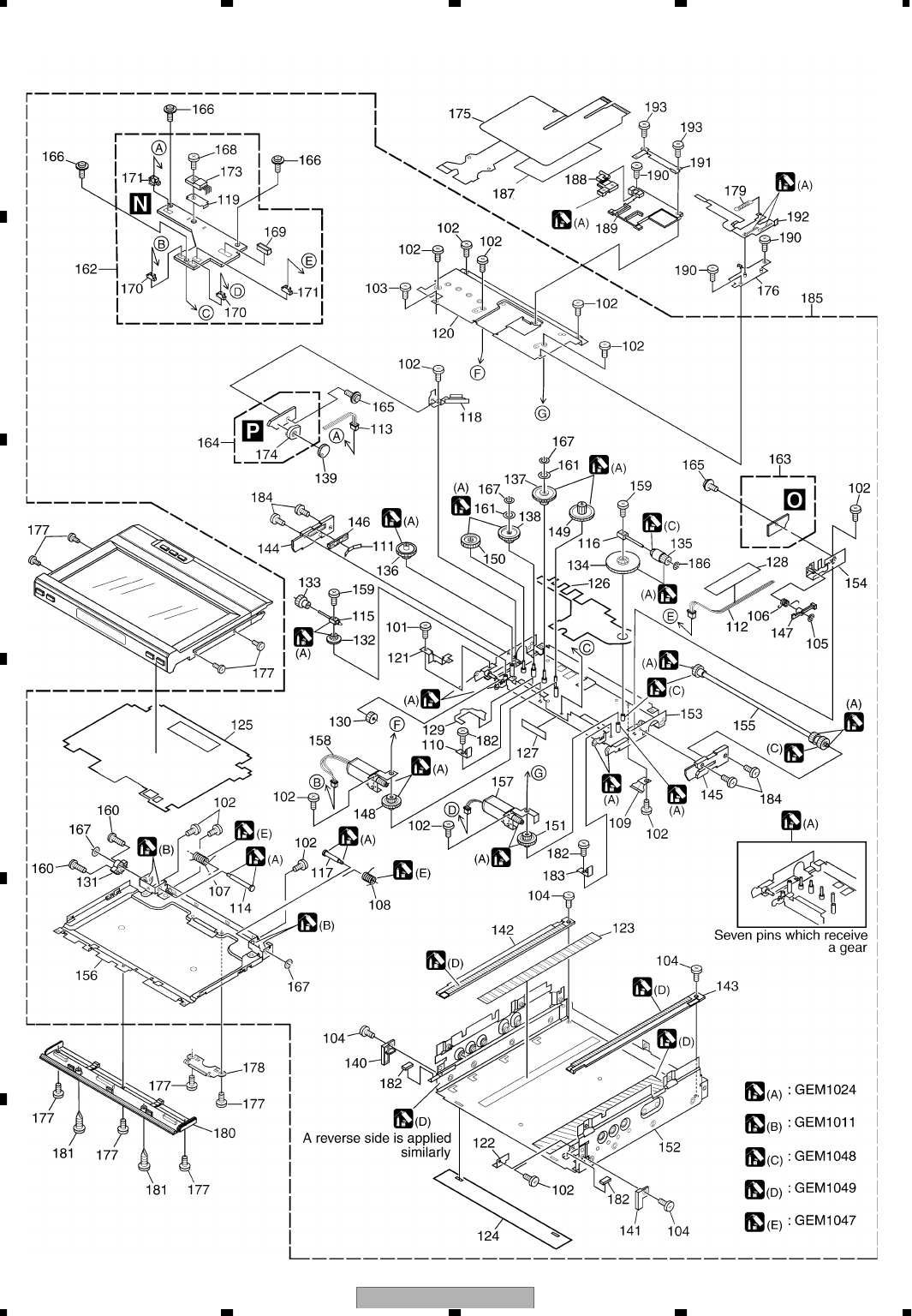
2.3 EXTERIOR(2)

AVH-P6600DVD/UC 23
5678
5678
C
D
F
A
B
E
EXTERIOR(2) SECTION PARTS LIST
Mark No. Description Part No.
101 Screw(M2x3) CBA1082
102 Screw(M2x2.5) CBA1250
103 Screw(M2x4) CBA1277
104 Screw(M2x1.5) CBA1615
105 Washer CBF1038
106 Spring CBH2645
107 Spring CBH2646
108 Spring CBH2647
109 Spring CBL1585
110 Spring CBL1586
111 Spring CBL1587
112 Cord Assy CDE7047
113 Cord Assy CDE7213
114 Shaft CLA4270
115 Shaft CLA4305
116 Shaft CLA4306
117 Shaft CLA4309
118 Bracket CND1221
119 Heat Sink CND1228
120 Case CND1229
121 Holder CND1318
122 Holder CND1449
123 Sheet CNM8522
124 Sheet CNM8037
125 Insulator CNM8048
126 Insulator CNM8158
127 Sheet CNM8159
128 Tape CNM8160
129 Insulator CNM8294
130 Gear CNR1664
131 Gear CNR1665
132 Gear CNR1677
133 Gear CNR1678
134 Gear CNR1679
135 Gear CNR1680
136 Gear CNR1688
137 Gear CNR1708
138 Gear CNR1709
139 Gear CNV7383
140 Holder CNV7384
141 Holder CNV7385
142 Rack CNV7386
143 Rack CNV7387
144 Slider CNV7388
145 Slider CNV7389
146 Holder CNV7390
147 Arm CNV7391
148 Gear CNV7522
149 Gear CNV7523
150 Gear CNV7524
151 Gear CNV7529
152 Chassis Unit CXB9509
153 Frame Unit CXB9511
154 Holder Unit CXB9512
155 Shaft Unit CXB9513
156 Holder Unit CXB9514
157 Motor Unit(M3001)(Position) CXB9515
158 Motor Unit(M3002)(Angle) CXB9516
159 Screw CZB3082
160 Screw CZB3083
161 Washer CZB3084
162 Main Unit CZW3087
163 SW Unit CZW3088
164 Volume Unit CZW3089
165 Screw IMS20P020FTC
166 Screw IMS20P030FZK
167 Washer YE15S
168 Screw BMZ26P050FTC
169 Connector(CN3801) CKS4068
170 Connector(CN3802,CN3803) CKS3124
171 Connector(CN3807,3809) CKS3125
172 •••••
173 IC(IC3801) BA00AST
174 Volume(VR3841) CCW1025
175 Flexible PCB CNP7682
176 Bracket Unit CXC3048
177 Screw(M2x2) CBA1753
178 Holder CND2243
179 Spring CBH2750
180 Cover CNS7438
181 Screw BPZ20P080FZK
182 Screw(M2x1.8) CZB3085
183 Spring CBL1642
184 Screw(M2x4) CZB3088
185 Drive Unit CXB9508
186 Washer CZB3089
187 Sheet CNM8952
188 Arm CNV8065
189 Holder CNV8066
190 Screw(M2x3) CBA1780
191 Spring CBL1679
192 Lever CND2202
193 Screw(M2x3) CBA1797
Mark No. Description Part No.
AVH-P6600DVD/UC
24
1234
1234
C
D
F
A
B
E
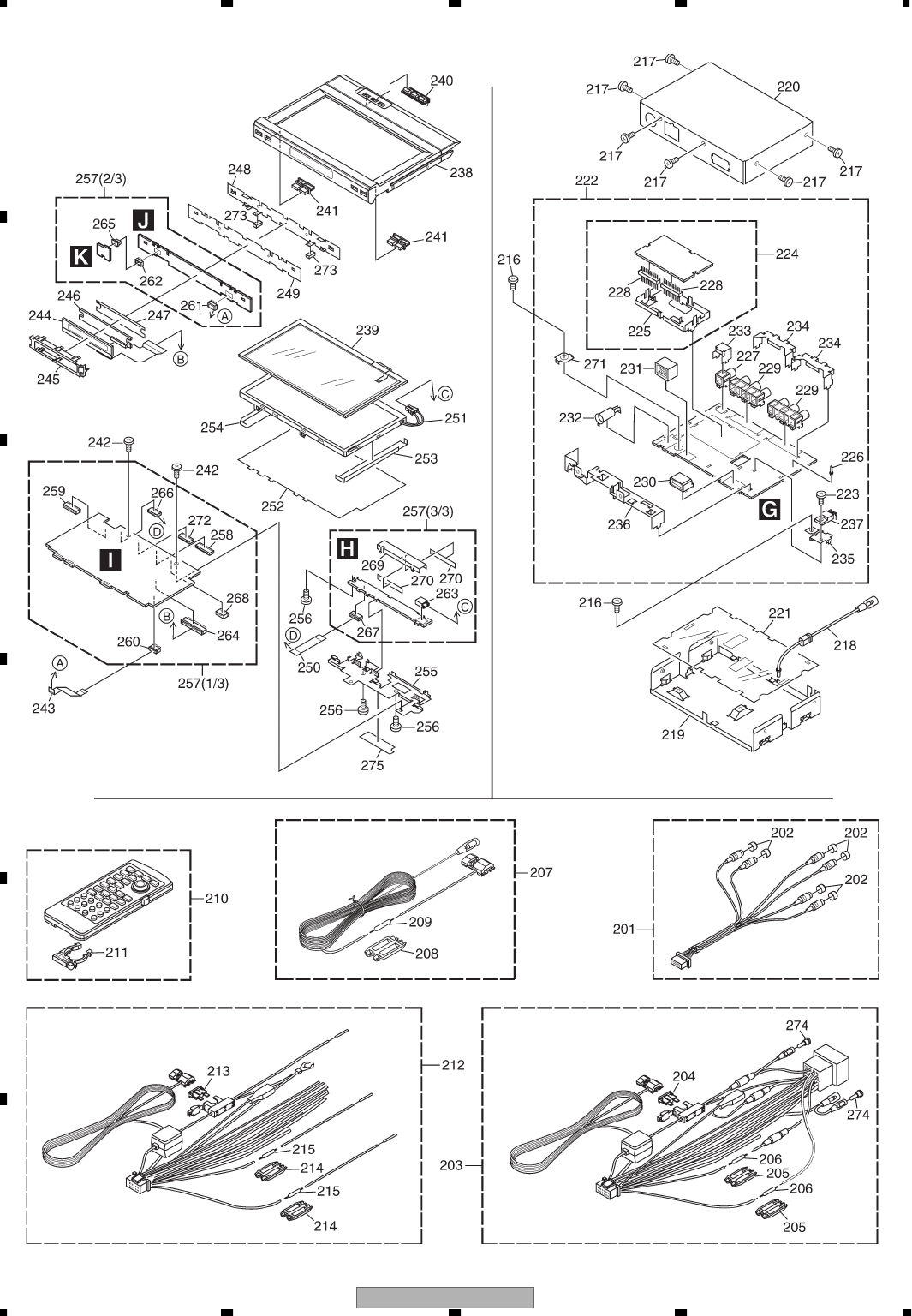
2.4 EXTERIOR(3)
(1)

AVH-P6600DVD/UC 25
5678
5678
C
D
F
A
B
E
(1)EXTERIOR(3) SECTION PARTS LIST
Mark No. Description Part No.
201 Cord Assy CDE7194
202 Cap CNV6727
203 Cord Assy See Contrast table(2)
204 Fuse(10A) See Contrast table(2)
205 Cap See Contrast table(2)
206 Resistor See Contrast table(2)
207 Cord Assy CDE7321
208 Cap CNS1472
209 Resistor RS1/2PMF102J
210 Remote Control Unit See Contrast table(2)
211 Cover CZN5357
212 Cord Assy See Contrast table(2)
213 Fuse(10A) See Contrast table(2)
214 Cap See Contrast table(2)
215 Resistor See Contrast table(2)
216 Screw ISS26P055FTC
217 Screw BSZ30P060FZK
218 Cord Assy CDE7280
219 Chassis CNA2774
220 Case See Contrast table(2)
221 Insulator CNM9193
222 Tuner Unit See Contrast table(2)
223 Screw BMZ30P050FTC
224 FM/AM Tuner Unit See Contrast table(2)
225 Holder CND1432
226 Terminal(CN1412) CKF-047
227 Pin Jack(CN1403) CKS1065
228 Connector(CN101,CN102) CKS4653
229 Pin Jack(CN1401,CN1402) CKS2918
230 Connector(CN1404) CKS4467
231 Connector(CN1405) CKS4663
232 Antenna Jack(CN1406) CKX1056
233 Holder CNC6746
234 Holder CNC7205
235 Holder CNC9888
236 Holder CND1451
237 Transistor(Q1404) 2SD2375
238 Grille Unit See Contrast table(2)
239 Touch Panel CSX1064
240 Button(ENT,WIDE,MENU) See Contrast table(2)
241 Button CAC7936
242 Screw(M2x2.2) CBA1753
243 FFC CDE7195
244 LCD CAW1805
245 Holder CND1468
246 Lighting Conductor CNV7564
247 Sheet CNM8488
248 Holder CND1469
249 Insulator CNM8131
250 FFC CDE7196
251 LCD Panel CWX3056
252 Insulator CNM8930
253 Sheet CNM8265
254 Sheet CNM7784
255 Holder CND2037
256 Screw BPZ20P060FTC
257 Monitor Unit See Contrast table(2)
258 Connector(CN4461) CKS3968
259 Connector(CN4801) CKS3991
260 Connector(CN4201) CKS4054
261 Connector(CN4301) CKS4054
262 Connector(CN4311) CKS4374
263 Connector(CN5002) CKS4428
264 Connector(CN4701) CKS4495
265 Connector(CN4312) CKS4496
266 Connector(CN4451) CKS4595
267 Connector(CN5001) CKS4595
268 Connector(CN4401) CKS4675
269 Holder CND1677
270 Insulator CNM9251
271 Holder(CN1407) CNC5399
272 Connector(CN4481) CKS4319
273 Cushion CNM8440
274 Cap See Contrast table(2)
275 Insulator CNM9216
Mark No. Description Part No.

AVH-P6600DVD/UC
26
1234
1234
C
D
F
A
B
E
(2) CONTRAST TABLE
AVH-P6600DVD/UC , AVH-P6600DVD/EW , AVH-P6650DVD/RC and AVH-P6650DVD/RD are constructed the
same except for the following:
Mark NO Description P6600DVD/UC P6600DVD/EW P6650DVD/RC P6650DVD/RD
203 Cord Assy Not used CDE7608 Not used Not used
204 Fuse(10A) Not used CEK1136 Not used Not used
205 Cap Not used CNS1472 Not used Not used
206 Resistor Not used RS1/2PMF102J Not used Not used
210 Remote Control Unit CXC3074 CXC3075 CXC3075 CXC3075
212 Cord Assy CDE7609 Not used CDE7609 CDE7609
213 Fuse(10A) CEK1136 Not used CEK1136 CEK1136
214 Cap CNS1472 Not used CNS1472 CNS1472
215 Resistor RS1/2PMF102J Not used RS1/2PMF102J RS1/2PMF102J
220 Case CNB2963 CNB2963 CNB2964 CNB2964
222 Tuner Unit CWM9203 CWM9202 CWM9203 CWM9203
224 FM/AM Tuner Unit CWE1651 CWE1650 CWE1651 CWE1651
238 Grille Unit CXC2660 CXC2659 CXC2661 CXC2661
240 Button
(ENT,WIDE,MENU) CAC8451 CAC8451 CAC8688 CAC8688
257 Monitor Unit CWM9148 CWM9147 CWM9149 CWM9149
274 Cap Not used CKX-003 Not used Not used
AVH-P6600DVD/UC 27
5678
5678
C
D
F
A
B
E
2.5 DVD MECHANISM MODULE

AVH-P6600DVD/UC
28
1234
1234
C
D
F
A
B
E
DVD MECHANISM MODULE SECTION PARTS LIST
Mark No. Description Part No.
1 DVD Core Unit(MS-3V1) CWX2883
2 Connector(CN1902) CKS4374
3 Connector(CN1201) CKS4067
4 Connector(CN1551) CKS4817
5 Connector(CN1231) CKS4624
6 Connector(CN1903) CKS4374
7 Connector(CN1101) CKS4625
8 Connector(CN1901) CKS3971
9 Screw BMZ20P020FTC
10 Screw(M2 x 3.5) CBA1571
11 Screw(M2 x 2.5) CBA1623
12 Washer CBF1038
13 Washer CBF1064
14 Spring CBH2586
15 Spring CBH2587
16 Spring CBH2588
17 Spring CBH2589
18 Spring CBH2590
19 Spring CBH2591
20 Spring CBH2592
21 Spring CBH2593
22 Spring CBH2594
23 Spring CBH2595
24 Spring CBH2596
25 Spring CBH2597
26 Spring CBH2598
27 Spring CBH2599
28 Spring CBH2600
29 Spring CBH2601
30 Spring CBH2602
31 Spring CBH2603
32 Spring CBH2604
33 Spring CBH2605
34 Spring CBH2711
35 Spring CBL1564
36 Pickup Unit(Service) CXX1770
37 Shaft CLA3881
38 Shaft CLA4206
39 Shaft CLA4207
40 Lever CNC9933
41 Holder CNC9939
42 Holder CND2251
43 Holder CNC9941
44 Frame CND2250
45 Sheet CNM6883
46 Sheet CNM8283
47 Sheet CNM8643
48 Lever CNV8076
49 Lever CNV7155
50 Cam CNV7156
51 Rack CNV7157
52 Clamper CNV7158
53 Arm CNV7159
54 Arm CNV7160
55 Arm CNV7161
56 Arm CNV7162
* 57 Arm CNV7163
58 Arm CNV7164
59 Roller CNV7165
60 Arm CNV7166
61 Guide CNV8093
62 Gear CNV7169
63 Gear CNV7170
64 Gear CNV7171
65 Gear(Black) CNV7172
66 Gear CNV7173
67 Gear CNV7174
68 Rack CNV7175
69 Gear CNV7176
70 Arm CNV8077
71 Lever CNV7178
72 Lever CNV7179
73 Screw IMS20P030FTC
74 Gear CNV7181
75 Holder CNV7183
76 Holder CNV7184
77 Guide CNV7745
78 Roller CNV7344
79 Damper CNV7470
80 Damper CNV7471
81 Collar CNV7645
82 Compound(A) CWX3024
83 Screw(M2x2) CBA1802
84 Compound(B) CWX2753
85 Washer YE20FTC
86 Chassis Unit CXC3629
87 Arm Unit CXB8681
88 Frame Unit CXB8683
89 Arm Unit CXC2988
90 Bracket Unit CXB8685
91 Motor Unit(LOADING)(M1) CXB8687
92 Motor Unit(CARRIAGE)(M2) CXB8688
93 Screw Unit CXB8689
94 Roller Unit CXB8690
95 Motor(SPINDLE)(M3) CXM1272
96 Screw JFZ20P018FTC
97 Photo-transistor(Q1299) CPT231SCTD
98 Switch(S1201,S1202,S1203) CSN1051
99 Spring Switch(S1204,S1205) CSN1052
100 Resistor(R1298,R1299) RS1/16S0R0J
101 Gathering PCB CNX4320
102 Holder CNV8186
103 Arm CNV7742
104 Arm CNV7743
105 Spring CBH2710
106 Spring CBL1643
107 Spring CBH2712
108 Pickup Unit(Service)(Screw) GXX1242
109 Screw Assy CXX1750
110 Screw(M1.4xM1.4) CBA1787
111 Cover CNC9943
112 Screw JFZ20P018FTC
Mark No. Description Part No.

AVH-P6600DVD/UC 29
5678
5678
C
D
F
A
B
E
AVH-P6600DVD/UC
30
1234
1234
C
D
F
A
B
E
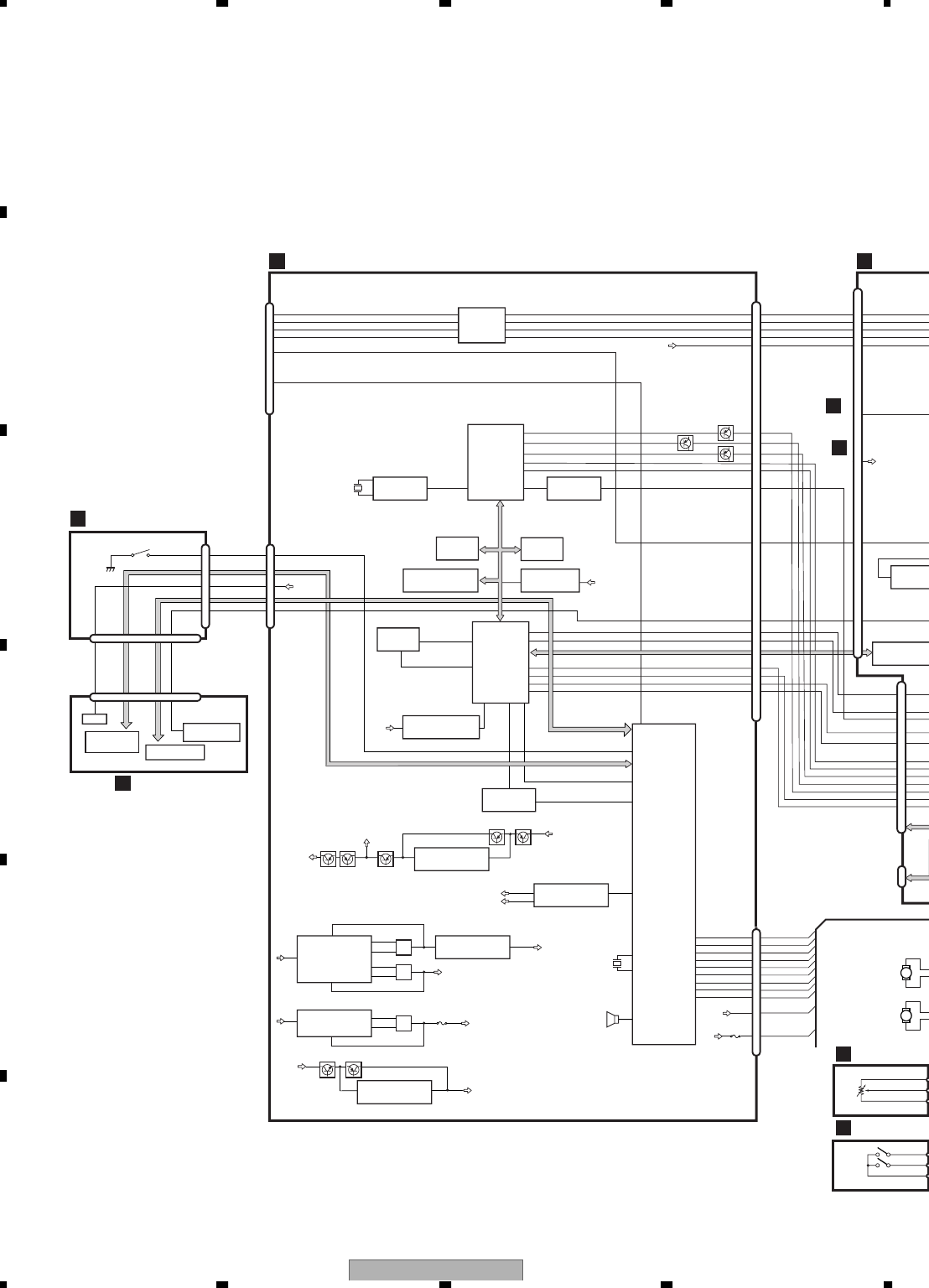
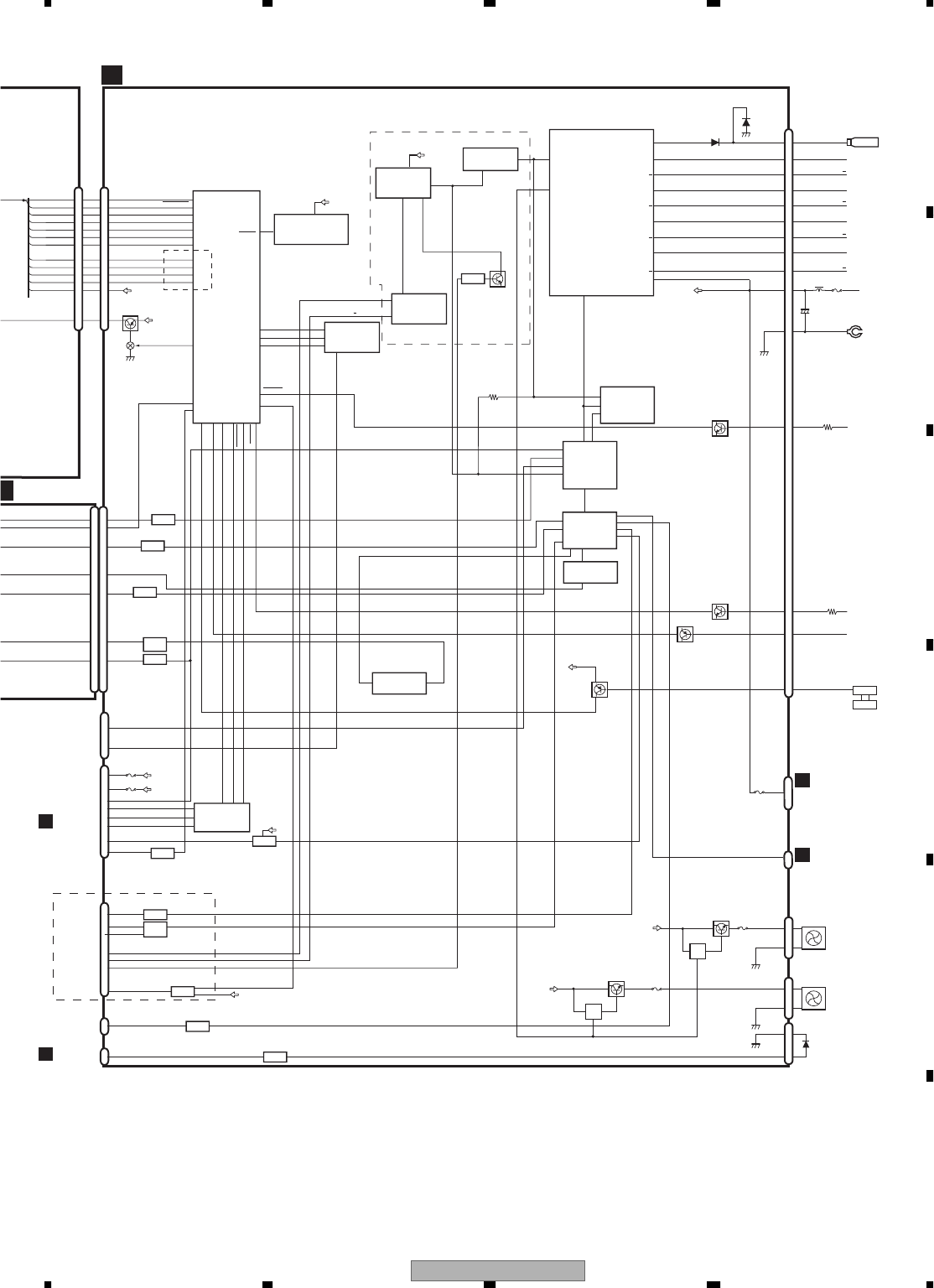
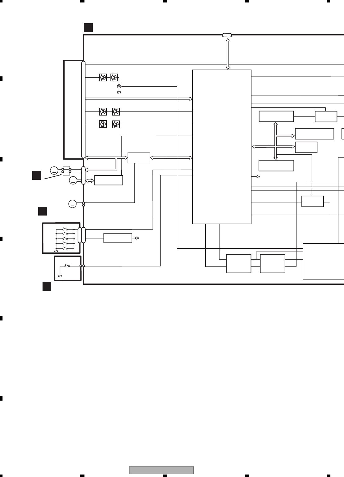
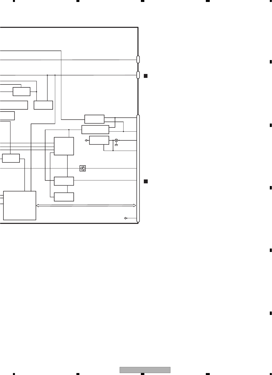
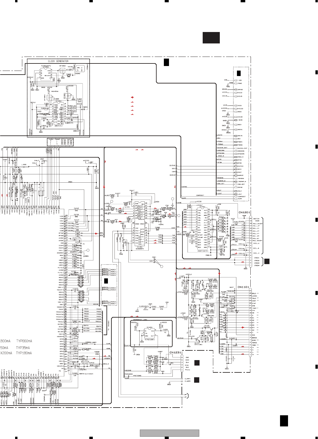
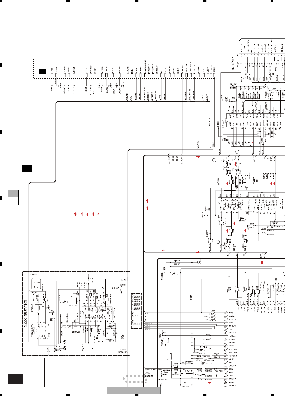
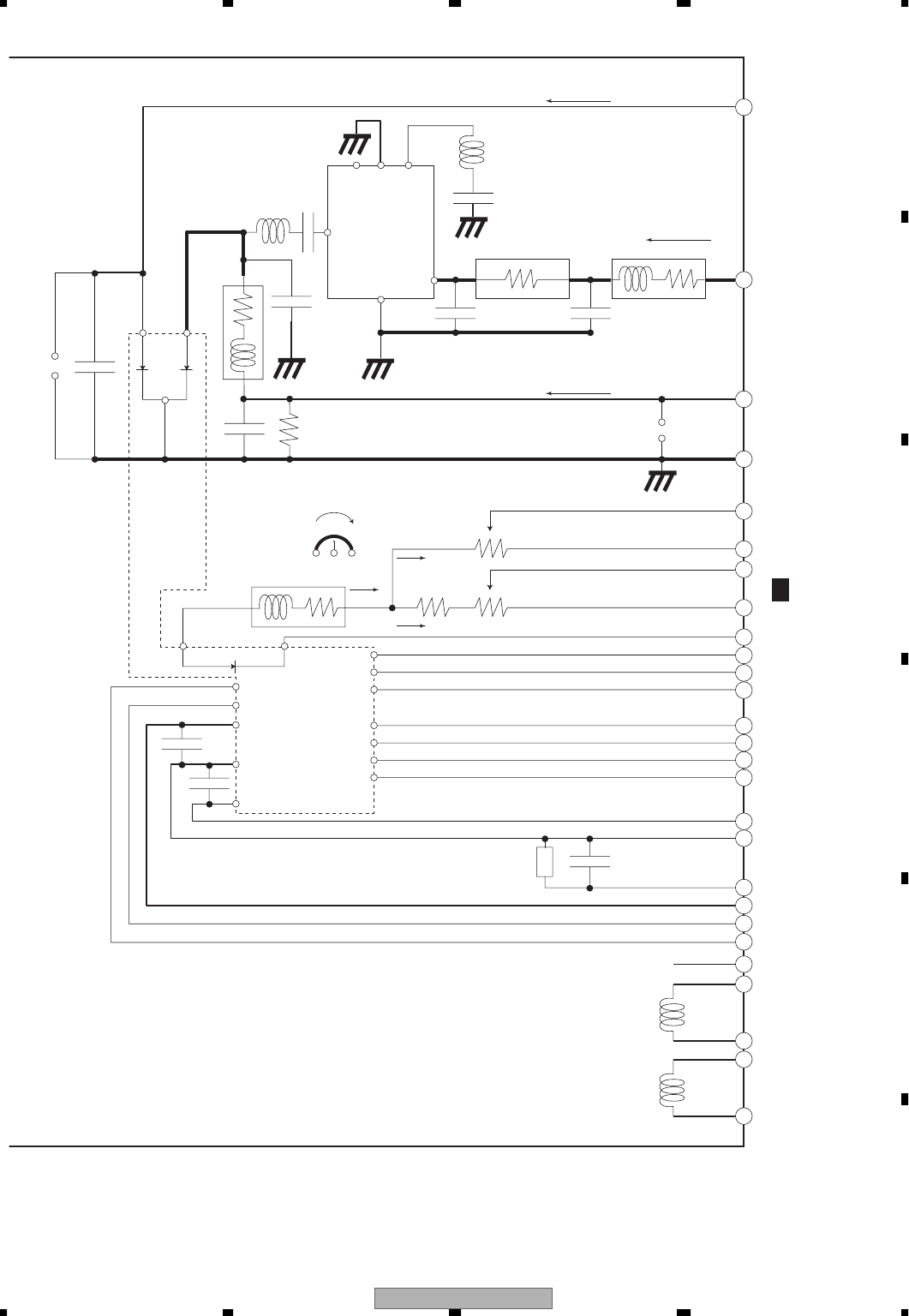
3. BLOCK DIAGRAM AND SCHEMATIC DIAGRAM
3.1 BLOCK DIAGRAM
CN3843
CN3842
CN3841
CN3833
CN3831
CN3832
VR3841
M
M
POSITION
MOTOR
ANGLE
MOTOR
VOLUME UNIT
SW UNIT
S3832
LIFTSW
S3831
ANGLE0SW
CN4461
CN4481
ANR1
ANG1
ANB1
CSYNC
MONI5V
ANR1
ANG1
ANB1
CSYNC
MONI5V
YS
22
REMCON
IC 4691
S-93C46BR0I-J
1
2
3
4
8
25
LSEN
MONITOR
I
(1/2)MOTHER PCB
A
NAVI
P
O
40
117
66
21
33
83,84,85
10,11,12
67
3
A20
47 162
142
140
146
147
149
2
14
137
21
14
13
17
16
20
19
18
SYSTEM
CONTROLLER
IC601
PE5416A
(UC,RC,RD)
PE5415A
(EW)
(1/2)
CN502
reset
RXNAV
VDD
BU
BU
BU
SWVDD33V
GDC33
VDD33
VDD5
CN101(1/2) CN501(1/2)
ANGLE
LIFTPUL
MTRSEL
MTRPW
MTR2
MTR1
deg)sw
pushsw
SENPW
ANGLEIN
LIFTPUL
MTRS
MTRPW
MTR2
MTR1
angl)sw
pushsw
SNSPW
VDD
VBU
25
26
27
23
14
21
CVBS
29
43
13
15
10
11
12
16
1
2
3
28
20
19
17
2
1
18
4
24
23
22
21
20
19
17
16
15
14
6
7
8
IC4061
TC7SZ02
2
EEP-RO
M
M
KEY
MATRIX ILLUMINATION
GRILLE PCB
PANEL PCB
ILMG,DSENSOUT
IC5501
RS-140
IC1401
PE5417A
CN5902
CN5501
CN5901
KEY0-2
KEY0-2
REMCOM
RESET
CN601
RESET
MONI5V
L
BUZZER
73
74
68
PWRFL
VDD5 GDC33
SWVDD
FU453
7
15
7
15
16
9
2
9
117
S5511
47
48
49
45
37
IC411
NJM2138V
1
1
1
3
3
13
3
4
LDPDT
20
LKYDT
BNLK
EPRSK,EPRCS,EPRPRO,EPRDO,EPRDI
19
13
HRET
VRET
ANR2
ANG2
ANB2
DIMIDT
Y
INVPUL
15
16
10
11
12
2
1
LDPDT
LKYDT
DPDTRESET
SPEANA
SP
CN4401
TOUCH PANEL
A
CN501
(2/2)
18
MVIPW
MVIPW
DMMER
43
INVPUL
80
LSEN
17
A
CN502
(2/2)
IC1405
TC7SET08FU
IC1404
S-80827CNUA-B8M
IC1408
BA3834F
IC1410
PD8125A
IC1407
TC74VCX02FT
IC1452
K4S641632H-TC75
IC1411
PD8126A
IC1451
HD64413ASFI
IC1403
TC7WHU04FU 4
2
IC1414
TC7SZ04FU
107 RXMON
103 CONTVDD
106 TXMON
4
IC801
S-812C33AUA-C2N
32
IC805
S-812C50AUA-C3E
32
IC806
S-814A33AMC-BCX
35
1
216
2
7059
16
77
12
KYDT
69
A0-A22,D00-D15,
MA00-MA11,MD00-MD15
25,26,
27pin
1pin
Q1407
Q1406
Q1405
Q807
Q805 Q803
Q815 Q816
Q823
VCC33
421
VD8
VDD5
IC804
BA00BC0WFP
IC802
LTC3728EG
419
14
2
227
Q822
1
423
24
BU IC803
LTC3728EG
24 DD33
14
216
Q821
1
419
FU802
BU
Q838
Q841
AVH-P6600DVD/UC 31
5678
5678
C
D
F
A
B
E
CN3802
MO1
MOB
1
2
CN3809
CN3843
CN3842
CN3841
CN3833
CN3831
CN3832
ANGLV
ANGLIN0
1
2
ANGLG
3
IC 3802
BA6247FP
Q3804
VR3841
CN3801
5
MTR2
4
MTRPW
3
MTRS
11
VDD
18
19
20
VBU
10
SNSPW
2
LIFTPUL
1
ANGLEIN
9
pushsw
8
angl)sw
6
MTR1
Regulator for driver
Motor driver
41
1
18
22
16
14
6
5
IC 3801
BA00AST
Q3801
CN3803
MO2
MOB
2
1
M
M
POSITION
MOTOR
ANGLE
MOTOR
13
IC 3803
TA78L05F
Q3802
Q3803
13
IC 3805
GP2L24B
24
IC 3804
TC7S14FU
CN3807
LIFT
ANGLE0
1
3
GNDSNS
2
VOLUME UNIT
SW UNIT
S3832
LIFTSW
S3831
ANGLE0SW
MAIN UNIT
Q4156
8.0V
CN4801
Q4153
734
Q4152
1
VR
Q4155
VG
Q4154
VB
VCOM
36 4
Q4151
1438
Q4182
Q4183
8.0V
IC 4151
NJM2138V
RGB AMP
28
27
26
CN4461
CN4481
ANR1
ANG1
ANB1
CSYNC
MONI5V
YS
22
REMCON
17
X4001
42MHz
IC4001
TC90A64AF-P
(1/2)
LCD MICROCOMPUTER
82
83
ROUT
RIN
52
GIN
53
HDIN
18
CVI1
65
GOUT
BOUT
X0
X1
IC4181
NJM082BV
VCOM AMP
6
17 19 20
28
POLC
1
KEY
MATRIX
KEY
MATRIX
IC 4691
S-93C46BR0I-J8T1
Q4131 Q4133 Q4132
Q4121 Q4123 Q4122
BIN
54
Q4111 Q4113 Q4112
FNAVI
93
Q4101 Q4103 Q4102
IC 4142
TK15404MI 23 IC4141
TC7SH08FU
1,2 4
IC4065
TC7SZ08FU
2
1
4
LSEN
VSW5
LSEN
LCD
LCD
BACK LIGHT
LCD MODULE
DIMDTY
DIMDTY
PWRFL
102
100
57
58
59
MONITOR PCB
I
CN5002
FL1
FL2
IC 5003
OZ961IS
20
11
10
T5001
Q5005
Q5004
UPPER PCB
INVERTER PCB
H
N
P
O
Q5003
PWRFL
CN5001
CN4451
3 1 5,14,15
7
IC5001
TA78L05F
1,2
4
18
IC 5002
TC7SET08FU
CN4201
CN4701
SUB DISPLAY
CN4301
CN4311
CN4312
1
2
3
9
14
15
16
8
9
10
3
2IC 4311
NJM062V 3
16
7
1
25
26
27
23
14
21
CVBS
29
1
2
3
4
2
19 20
120
J
SENSE PCB
K
OUT OF LIGHT SENSOR
INVERTER FOR
BACK LIGHT
TWO PICTURES
CONTROL IC
IC 4851
LT1376CS8
IC 4701
PD6340A
2
IC 4841
R1130H251B
22.5V
B.UP
IC 4861
MAX1748EUE
418V
3.3V
Q4832
Q4831
3.3V
3.3V
14.4V 3
1
78V
-12V
15
8
8.0V
Q4835
5V
KST1,2,KDT1,2,3,4
KST1,2,KDT2
SEG
KST1,2,KDT3,4
FILTER
SYMC AMP 5->3 CHANGE
5->3V CHANGE
BLNK
92
IC4064
TC7SZ08FU
24
IC4063
TC7SZ32FU
24
IC4061
TC7SZ02FU
24
IC4731
TC7SET08FU
24
IC4732
TC7SH08FU
42
POWER SUPPLY
EEP-ROM
VILLA,VILLGB
IC 4451
TC7SET08FU
1
4
7
10
NDSH
NDSV
RIN
GIN
BIN
PWRFL
LDPDT
20
LKYDT
BNLK
19
13
HRET
VRET
ANR2
ANG2
ANB2
DIMIDTY
INVPUL
15
16
10
11
12
2
1
CN4401
TOUCH PANEL PNLADV1,PNLADX1,
PNLXV1,PNLYV1
A
CN501
(2/2)
IC4001
TC90A64AF-P
(2/2)
18
MVIPW
17
A
CN502
(2/2) UC,EW model
EW,RC,RD model
25,26,
27pin
1pin
AVH-P6600DVD/UC
32
1234
1234
C
D
F
A
B
E
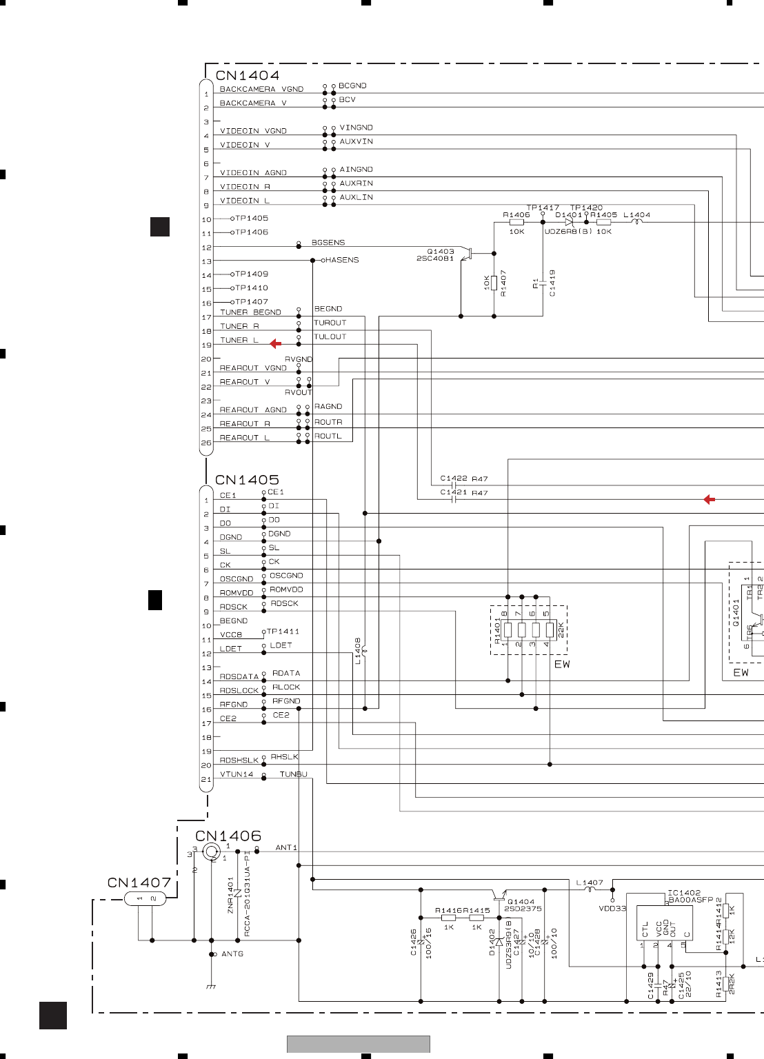
MAIN ANT
CN1405
SL
DO
DI
CK
CE1
RDSHSLK
RDSLOCK
RDSDATA
RDSCK
ROMVDD
TUNL
12
17
5
3
2
6
1
20
15
14
9
8
21
CN1404
CN1502 CN1500
19
BGSENS
BCAM
AUXV
AUXL
REARV
REARL
CE2
LDET
CN1412
REVERSE GEAR SENSE
IP-BU
S
COR
D
CN101(2
/
NAVI
AV BUS
Q1404
RER VIEW CAMERA IN
L VIDEO IN
CN1402
V VIDEO IN
L REAR VIDEO OUT
CN1401
V REAR VIDEO OUT
19
22
1
12 12
1
55
1
99
22 22
1
26 26
CN1
0
CN1
0
FMRF
ANT adj
RF adj
FM ANT
T51
CF52 CF51
VCC
VDD_3.3
3.3V 2.5V
IC 4
3.3V 2.5V
←
IC 2
2.5V
CE2
ROM_VDD
SL
DI
CK
CE1
LDET
DO
RDS_CK
RDS_DATA
RDS_LOCK
RDS_HSLK
6 13 5 10 9 8 11 14 18 19 20 21
1
3
IC 1
3.3V
AM ANT FMRF
ATT
LPF
OSC
IC 3 EEPROM
5.0V IC 5
5V 3.3V
←
ATT MIXER, IF AMP DET, FM MPX,
RDS DECODER
23
Lch
FM/AM TUNER UNIT
TUNER UNIT
G
RELAY PCB
B
CN1901
C
CN1551
C
CN1406
(EW model)
4
4 1,2
17
IC 1402
BA00ASFP
EW model
AVH-P6600DVD/UC 33
5678
5678
C
D
F
A
B
E
SYSTEM
CONTROLLER
IC 601
PE5416A
(UC,RC,RD)
PE5415A
(EW)
(2/2)
CN1405
SL
DO
DI
CK
CE1
RDSHSLK
RDSLOCK
RDSDATA
RDSCK
ROMVDD
12
17
5
3
2
6
1
20
15
14
9
8
21
C
N1502 CN1500
CN104
TUNSL
TUNPDI
TUNPDO
TUNPCK
TUNPCE
rds%&k
rdslk
RDT
rck
45
101
135
46
47
48
100
24
25
23
57
CN103
12
17
5
3
2
6
1
20
15
14
9
8
21
TUNL
BGSENS
BCAM
AUXV
AUXL
REARV
REARL
CE2
ldet
TUNPCE2
RESET
LDET
POWERFL
SYS+B
RC,RD
R373
BUP
ACC
ILL
40
12
11
39
B.REM
PARKING
IC351
NJM4558V
IC352
NJM4558V
GUIDE VOICE
INPUT
3
2
1
34
3
6,7
1,5
7
41
42
43
10
2
129
PBSENS
127
TELIN
112
TXMS3
113
IRQPWR
114
XRESET
126
ILSENS
ONSEI+
ONSEI
96
118
ASENS
88 8
IPPW
1
IC 353
NJM4580V
GUIDE MIX
UC,EW
21
POWER AMP
IC202
PAL007A
RL+
12 FLIN
4SYSPW
14
RLIN
23
RL
17
RR+
19
RR
5
FL+
3
FL
9
FR+
7
6,20
FR
25
R.REM
GND
+BACK UP
ACC5
Q703
Q704
Q352
Q351
Q702
Q706
Q833
BUP
VD8
Q837
Q844
Q845
REAR
FAN
FU804
CN701
4
2
6
3
11
13
1
7
5
12
8
9
14
15
16
CN801
CN501
(2/2)
CN108
2
1
CENTER
FAN
CN802
2
1
RL+
RL
RR+
RR
FL+
FL
FR+
TEL MUTE
FR
VDD5
VDD5
B.up
CN106
CN151
6
1
37
26
27
28
29
ONSEI +
ONSEI-
GDIN
HTXD
AVCOMP
OPT
IPL+
MS3L
SLVSTS
39
21
VIDEO OUT
IP-BUS
CORD
CN101(2/2)
10
13
14
21
24
11
NAVI
AV BUS
IC203
(2/2)
PA2028A
IC201
PML009A
VIDEO/AUDIO
SELECTOR
IC408
(2/2)
CXA2089Q
7
11
9
IC102
HA12240FP
IC603
S-80841CNUA-B82
6
90 2
2
RX
91
49 1
1
40
TX
TXNAV
SYSPW
130
BGSENS
111
RXMS3
7
1
33
2
8
16 47
15
23
40
3
63
IC406
NJM2136V
IC407
NJM2136V
IC402
TA2050F
98
36
IC403
TA2050F
12 8
8 2,3,4
14
941
Q824
Q825
5
17
19
15
9
13
1
5
17
19
15
9
13
1
IC401
TA2050F
IC101
TC4S81F
12
13
8
6
CN105
2
CN107
1
IC405
NJM2136V
36
IC410
NJM2136V
36
45
1.2
IC153
TC7SET08FU
1
8
6
3
4
IC151
SM5304AV
IC152
TC74VHC08FT
12,4 6
VDD
3V -> 5V
CHANGE
VIDEO5V
IC103
TC7SET08FU
24
1
2
RELAY PCB
B
CN1901
C
CN1551
C
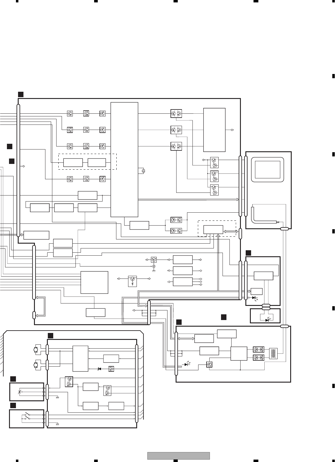
MOTHER PCB(2/2)
A
UC,EW
IC409
BA7623F
IC301
NJM4558V
IC404
NJM2136V
(EW model)
1,2,3pin
25
26
27
CN4461
I
CN502
(2/2)
29pin
1
CN4461
I
FU805
FU902
FU155 VDD33
10
11
12
FU151 VD8
AVH-P6600DVD/UC
34
1234
1234
C
D
F
A
B
E
26
24
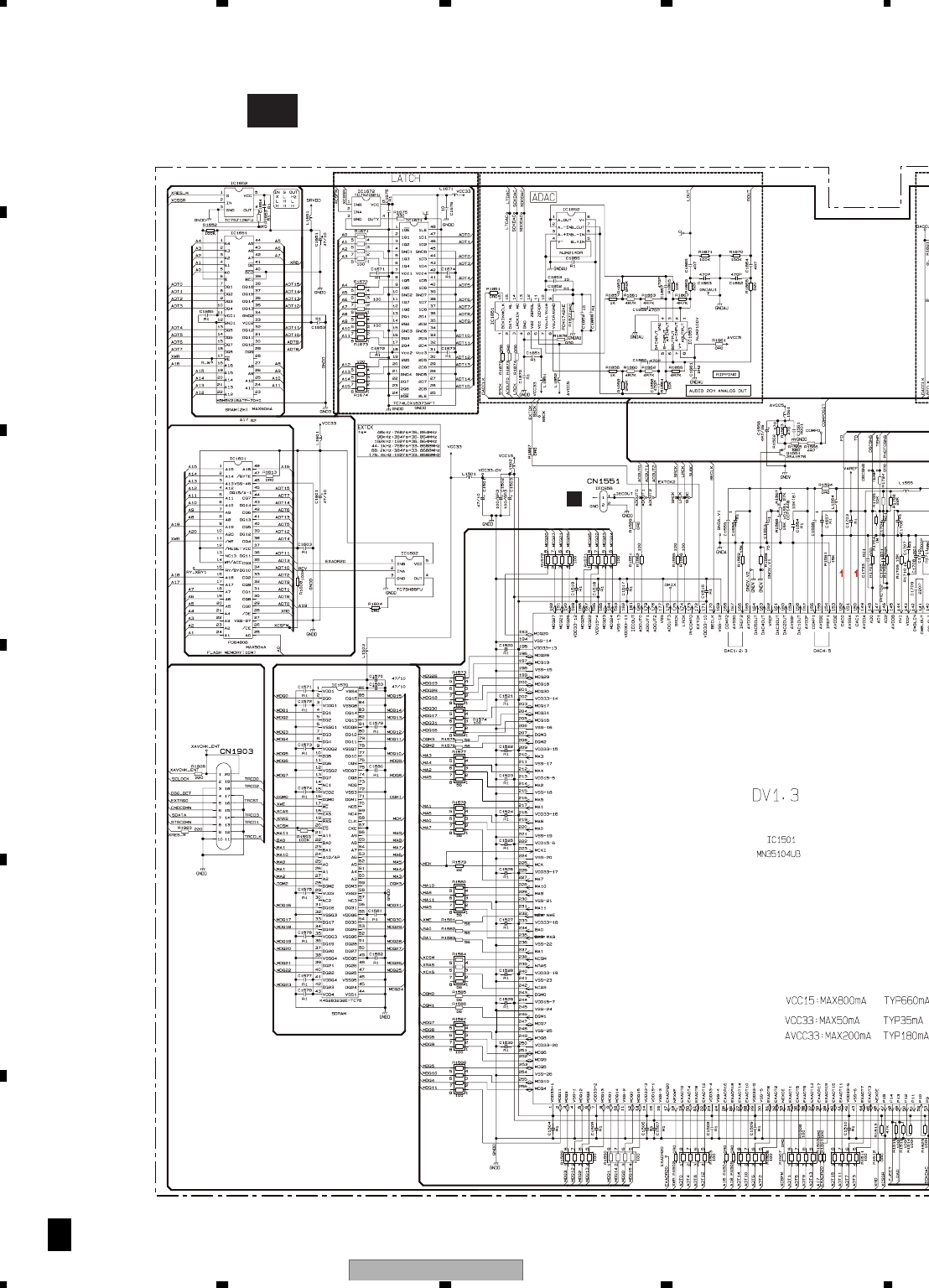
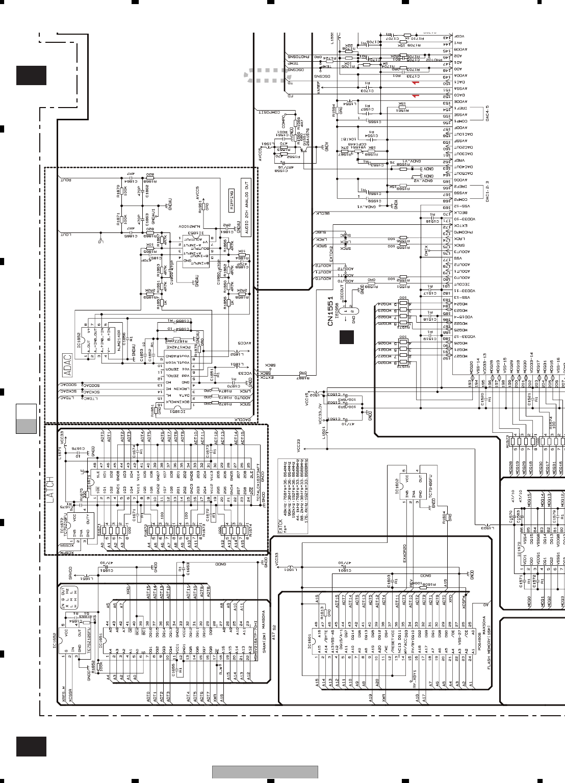
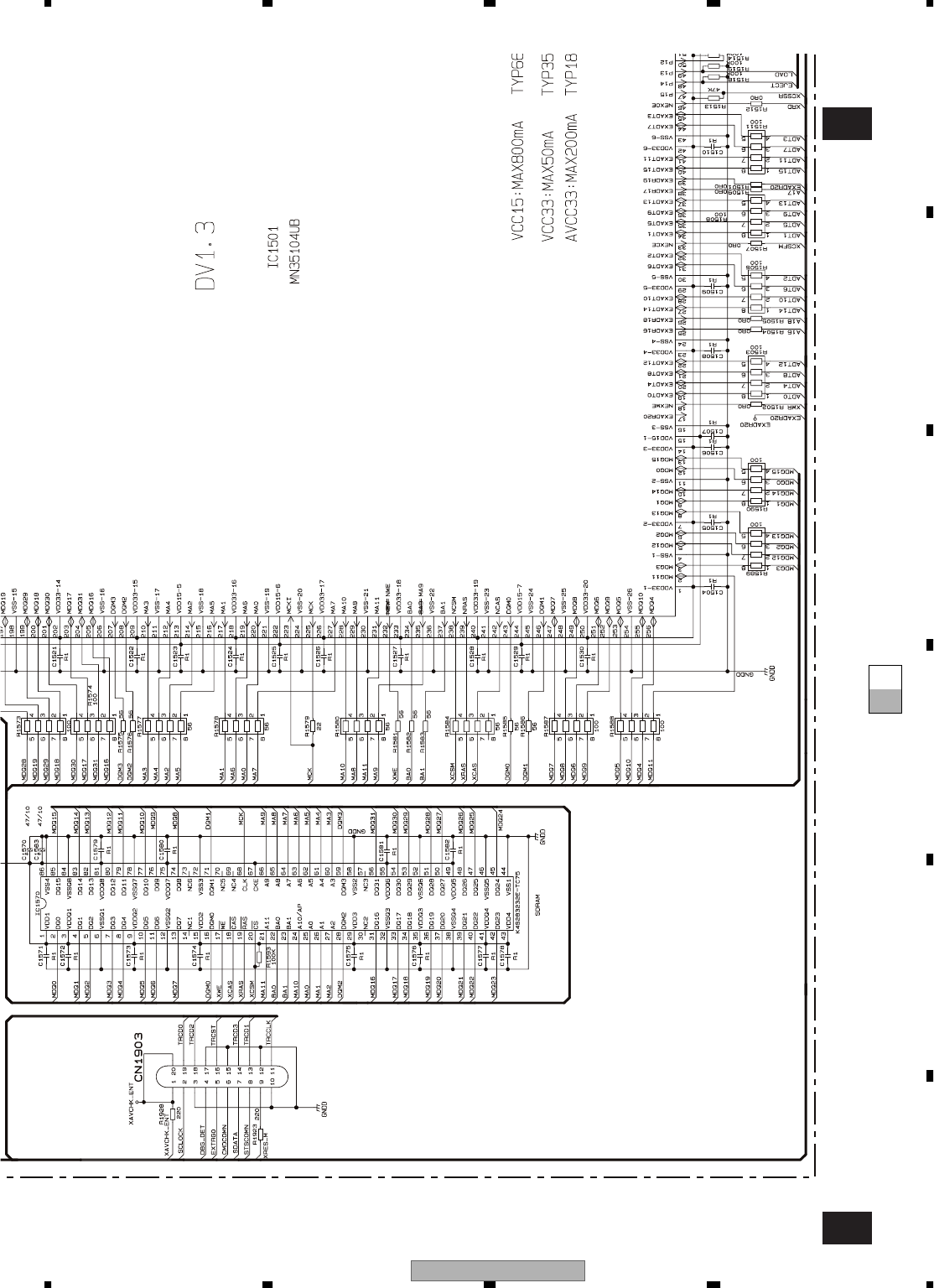
DVD CORE UNIT (MS-3V1)
Q1101 Q1106
Q1102
Q1104
Q1103
Q1105
Q1107
65LD
78LD
133
135
VSHF
CN1101
CN1201
CN1231
IC 1201
AN8471SAT1
IC1231
TC7SZ125FU
CPU
IC1501
MN35104UB
62,66
148
174
LRCK 175
SRCK
163
163
DAC4OUT
BECLK
AD1
76 DRY6
DSCSNS
CLNP
181
IECOUT
47
XCSSR 33
XCSFM
68
NRST
39 1
EXADR18
IC1251
BA5985FM
IC1601
PD6480B
IC1672
TC7SZ08FU
T
IC1671
TC74LCX16373AFT
IC1651
M5M5V216ATP-70HI
IC1602
TC7SH86FU
IC1570
K4S283232E-TC75
23
9
18
PICKUP UNIT(SERVICE)
A,B1-4,C,RF+,RF-
M
SPINDLE
MOTOR
M
CARRIGE
MOTOR
M
LOADING
MOTOR
FOP,FOM,TOP,TOM
COP,COM
DRIVER
9
LOM
10
LOP
10
14
IC1051
PE5401A
VCC15
C
FD,TD,MD,CRGDRV
FG
LPCO2
LPCO1
S1206
S1202
S1203
S1204
S1201
S1205
CLAMP SW
12cm
8cm
8cm
Disc sens
Disc sens
COMPOUND UNIT(B)
E
COMPOUND UNIT(A)
D
RELAY PCB
F
A0-20,
ADT0-15
A20
CD/DVD
39 REV
21
XRES_M
25
2
4
25,48 4 1
2
VDD33
FSSW2
42
FSSW1
43
6
5
1143
92
OSCI
213
15 IC1802
TC7WH157FU
IC1801
SM8707LV
ELERGENCY LOAD
SDRAM
SDRAM
LATCH
CLOCK GENERATOR
FLASH MEMOR
Y
MONI
CN1902
AVH-P6600DVD/UC 35
5678
5678
C
D
F
A
B
E
37
39
1
10
3,5
8
3
7
1,2
3
5
6
1
5
2
1
2
1,2
1
3
16
IECOUT
Lch OUT
IC1851
PCM1742KE
IC1852
NJM2140R
VIDEO OUT
25
VCONTA
CN1551
CN1901
IC1601
P
D6480B
IC1672
TC7SZ08FU
IC1652
TC7SZ126FU
IC1651
M
5M5V216ATP-70HI
IC1602
TC7SH86FU
IC1051
PE5401A
21
VDD33
VCC15
CN151
A
CN107
A
IC1853
NJM2100V
AMUTE,XRES_S,IRQPWR,STSCOMN,CMDCOMN
1
CN1903
Q1551
CD/DVD
3
9REV
21
XRES_M
25
2
4
4
84 1
2
21
FSSW2
4
2
FSSW1
4
3
23
VCONTB
10
VD
6,7
11
12
VD
Q1002
IC1003
LTC3411EMS
IC1001
S-L2980A50MC-C7J
IC1002
R1130H501B
XRES_M 9
DC-DC CONVERTER
SDRAM
ADAC
FLASH MEMORY

AVH-P6600DVD/UC
38
1234
1234
C
D
F
A
B
E
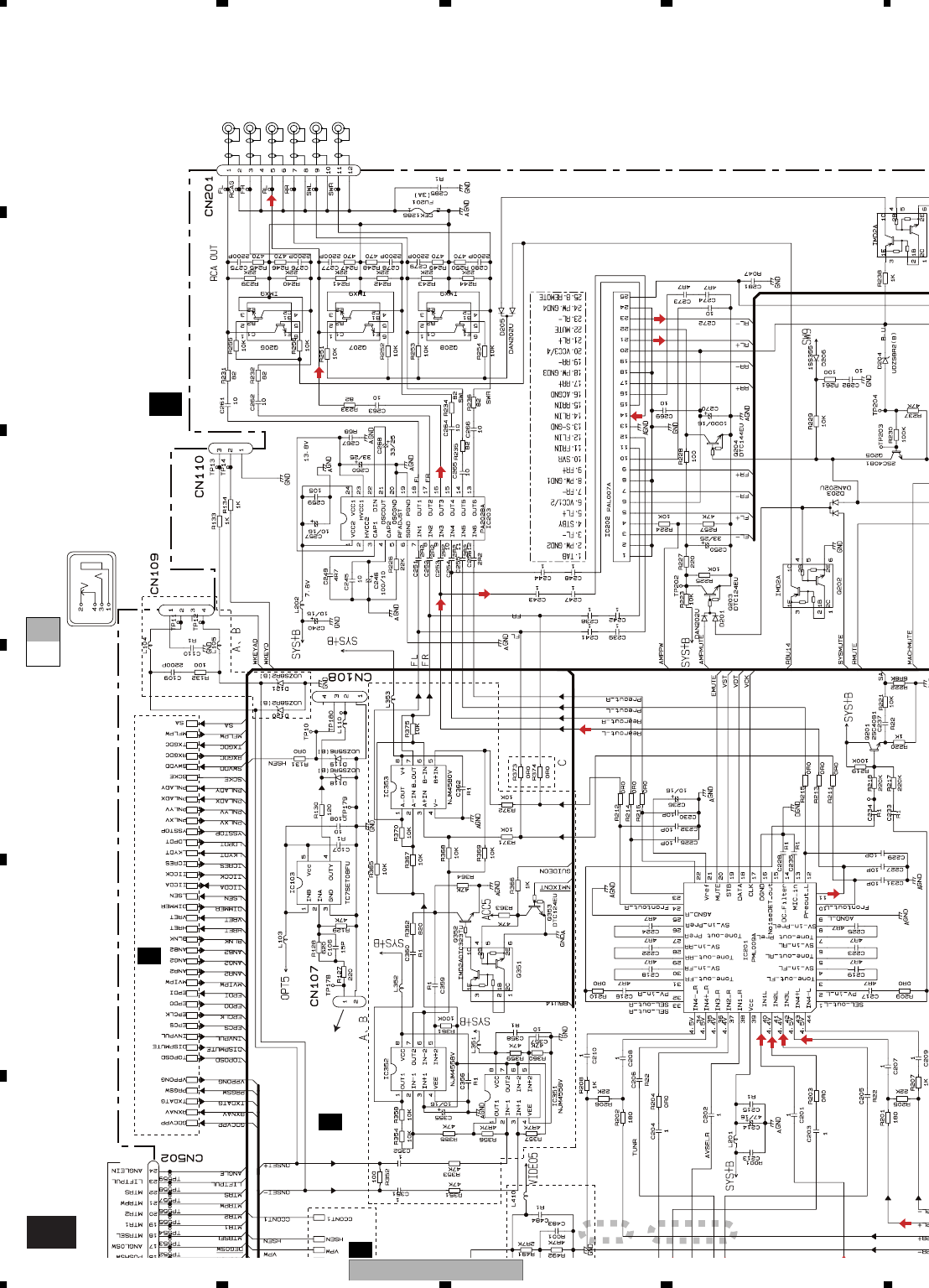
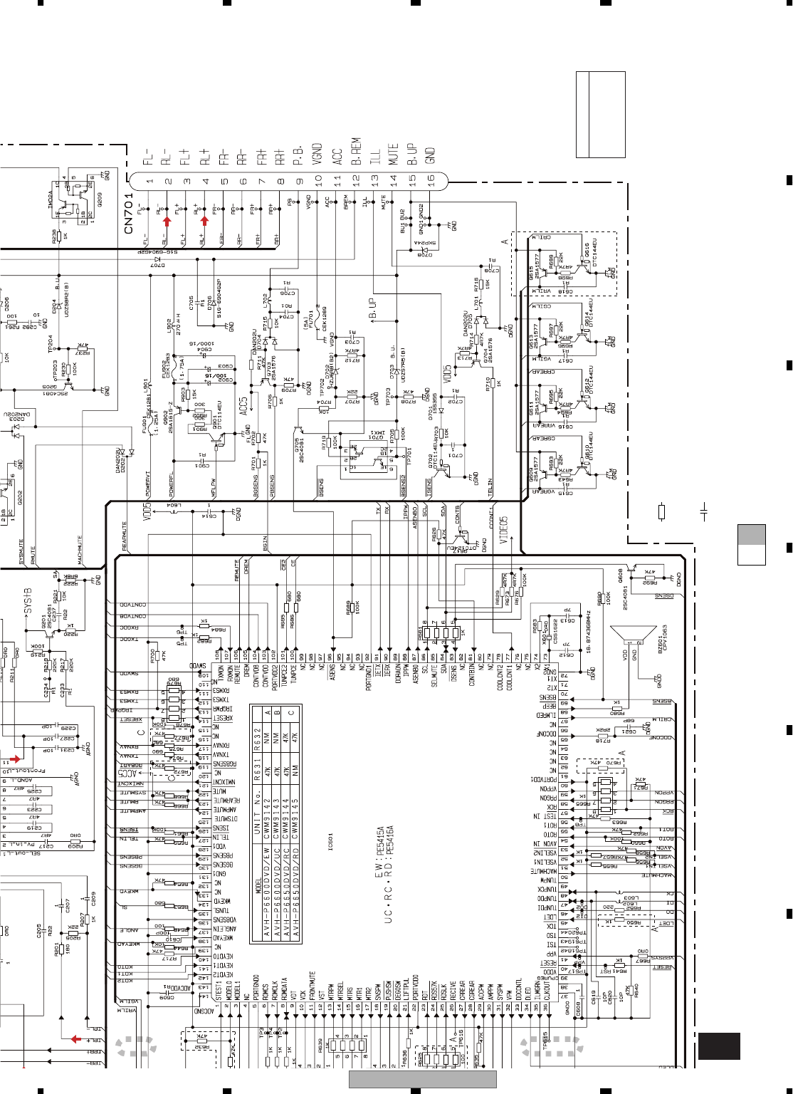
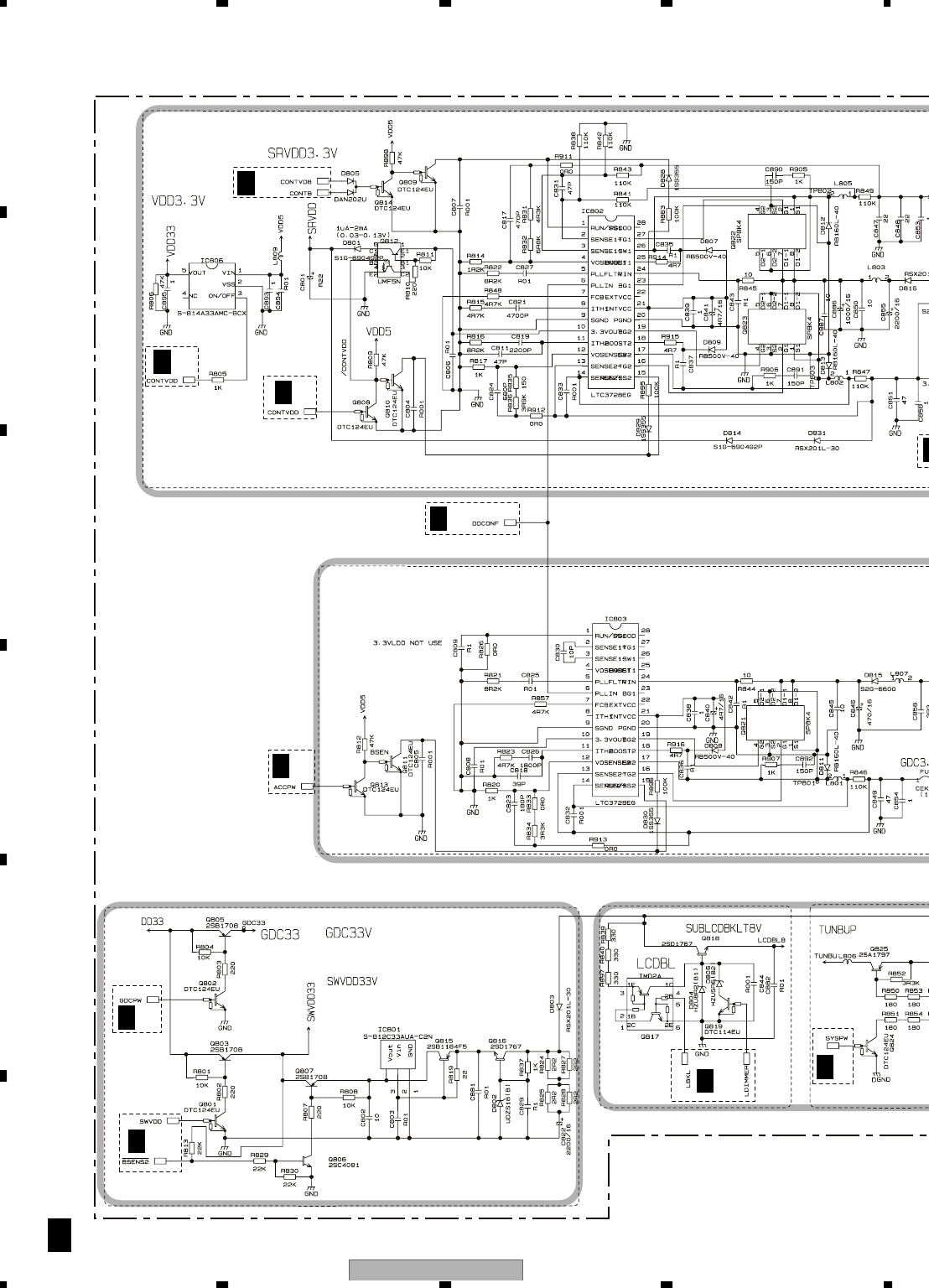
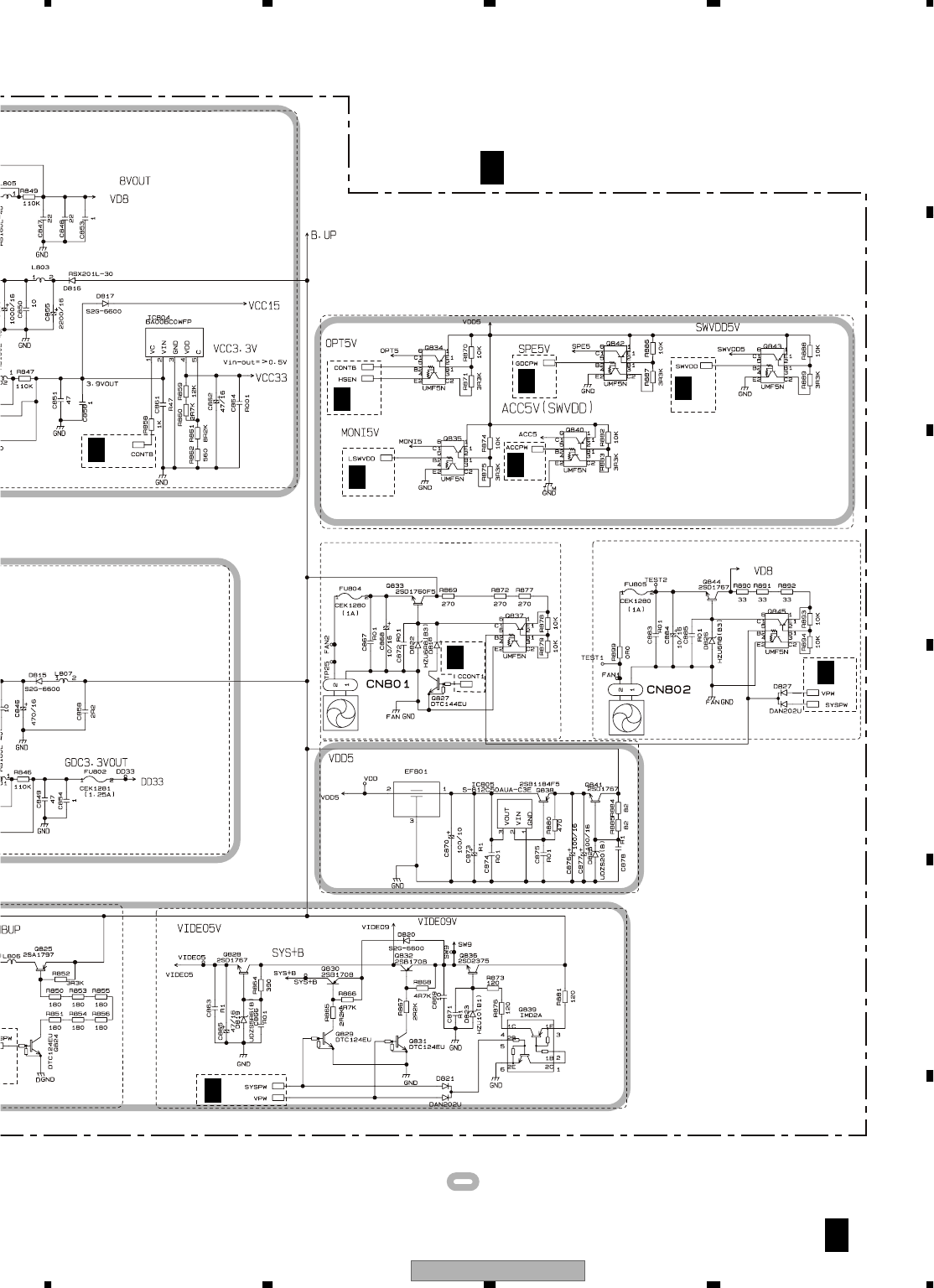
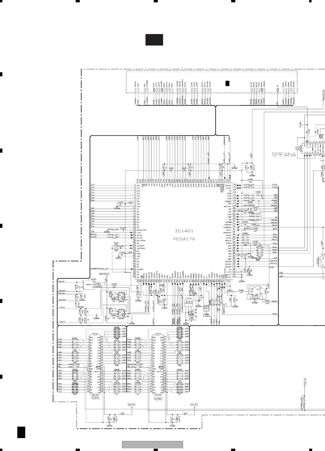
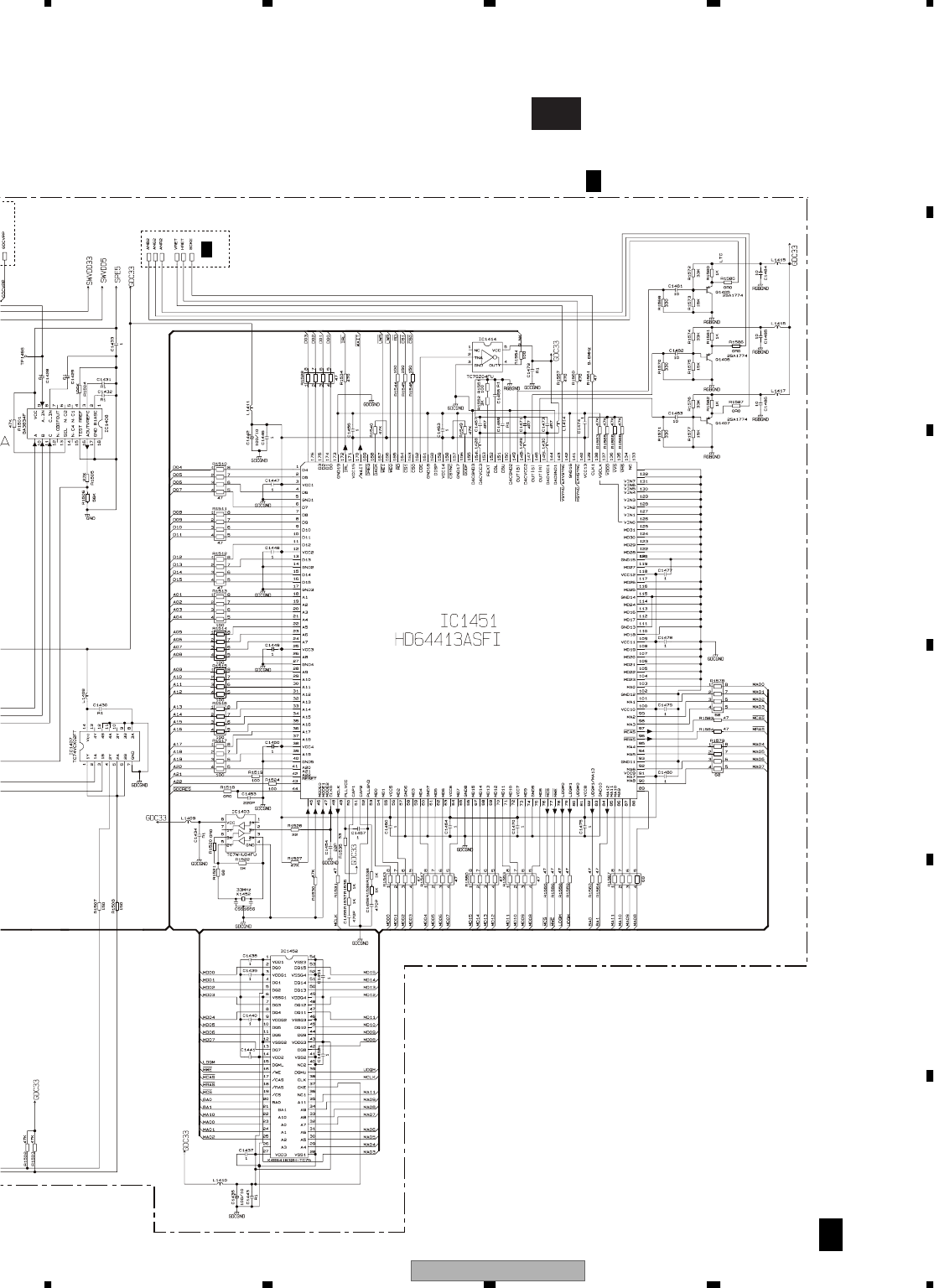
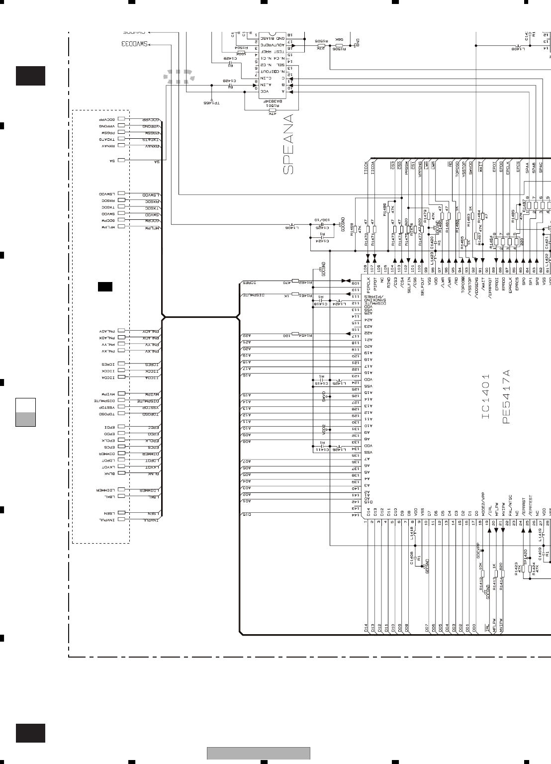
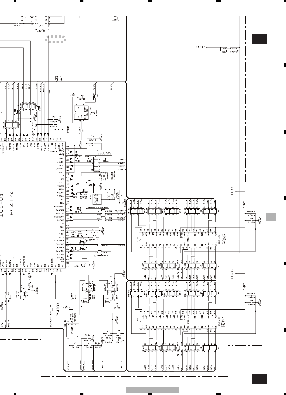
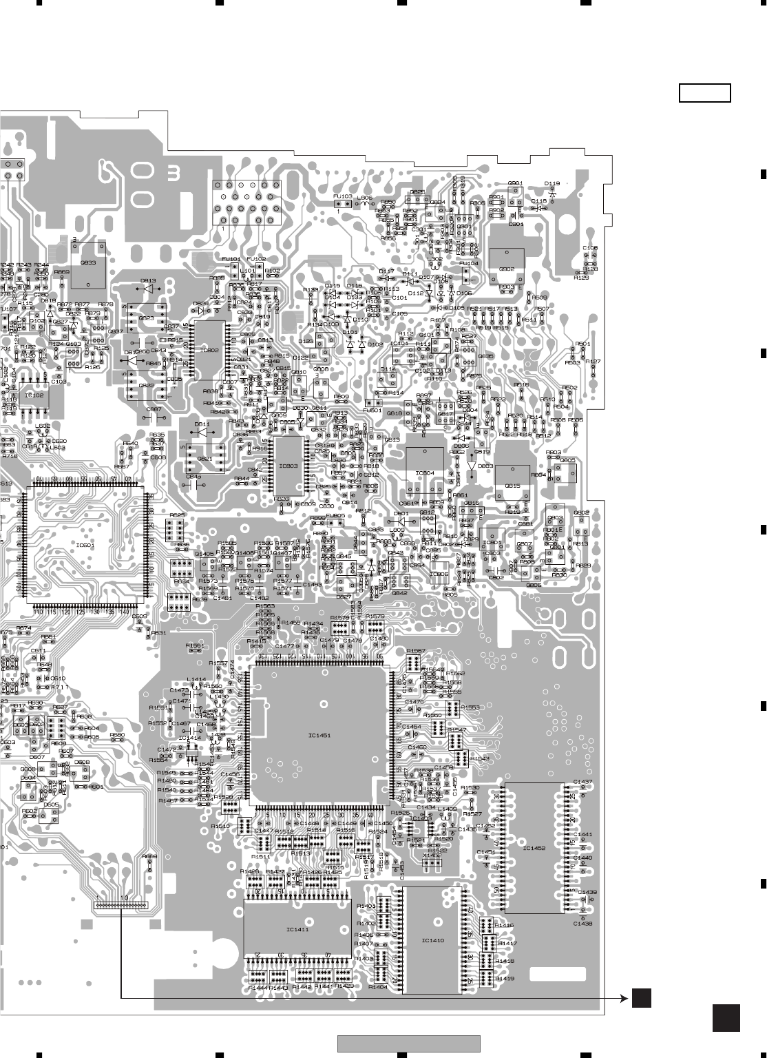
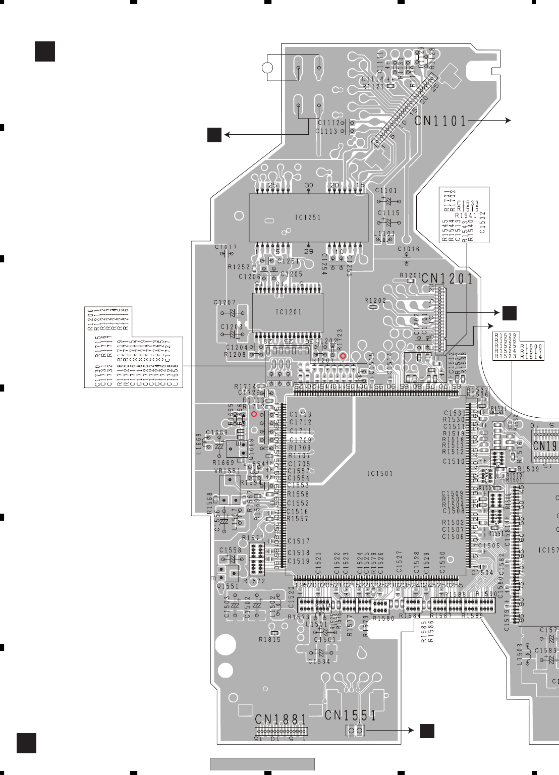
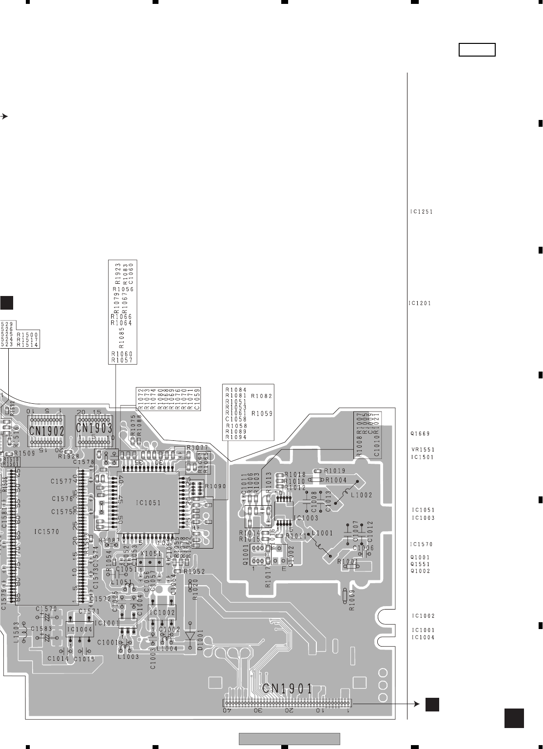
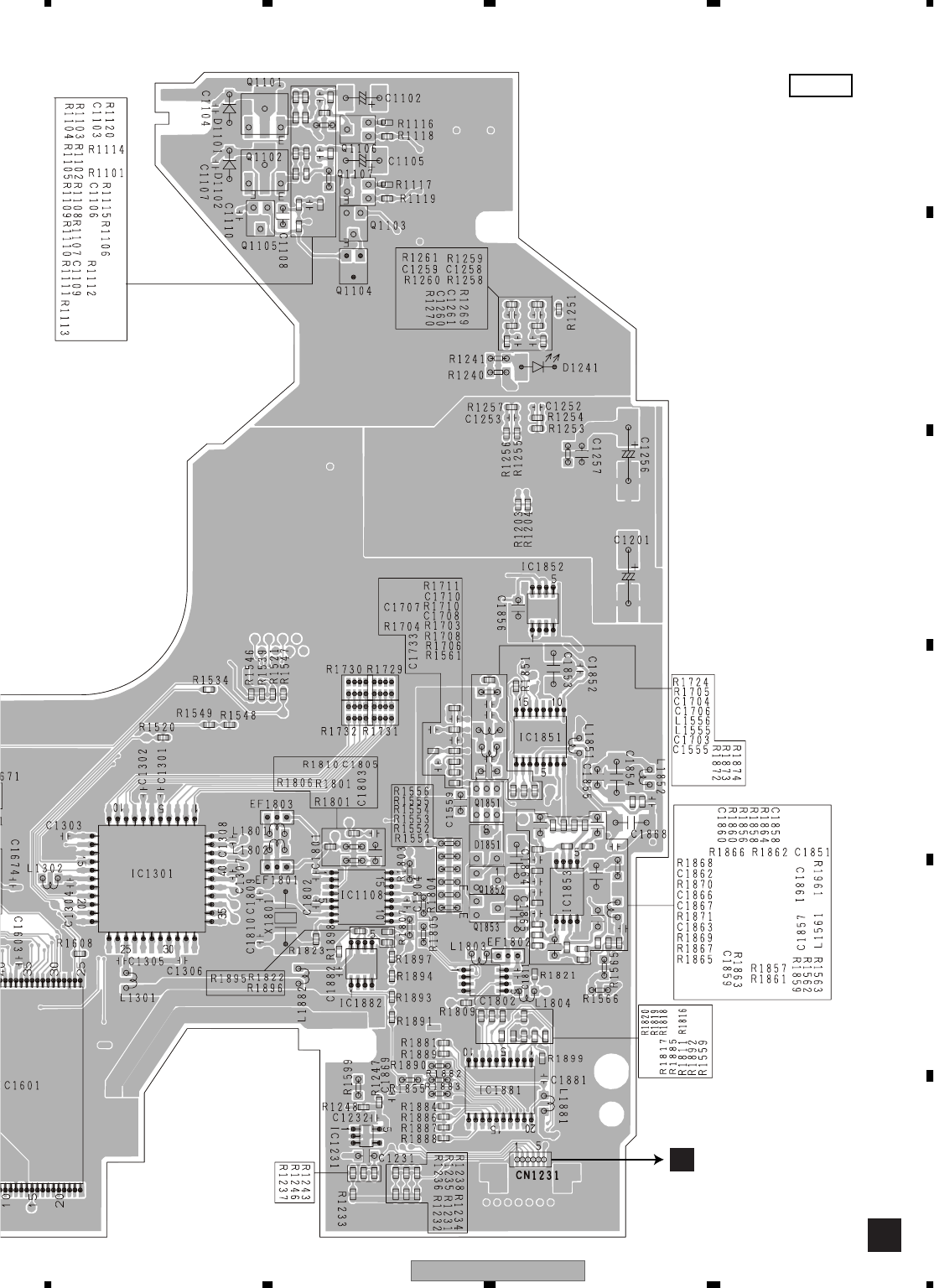
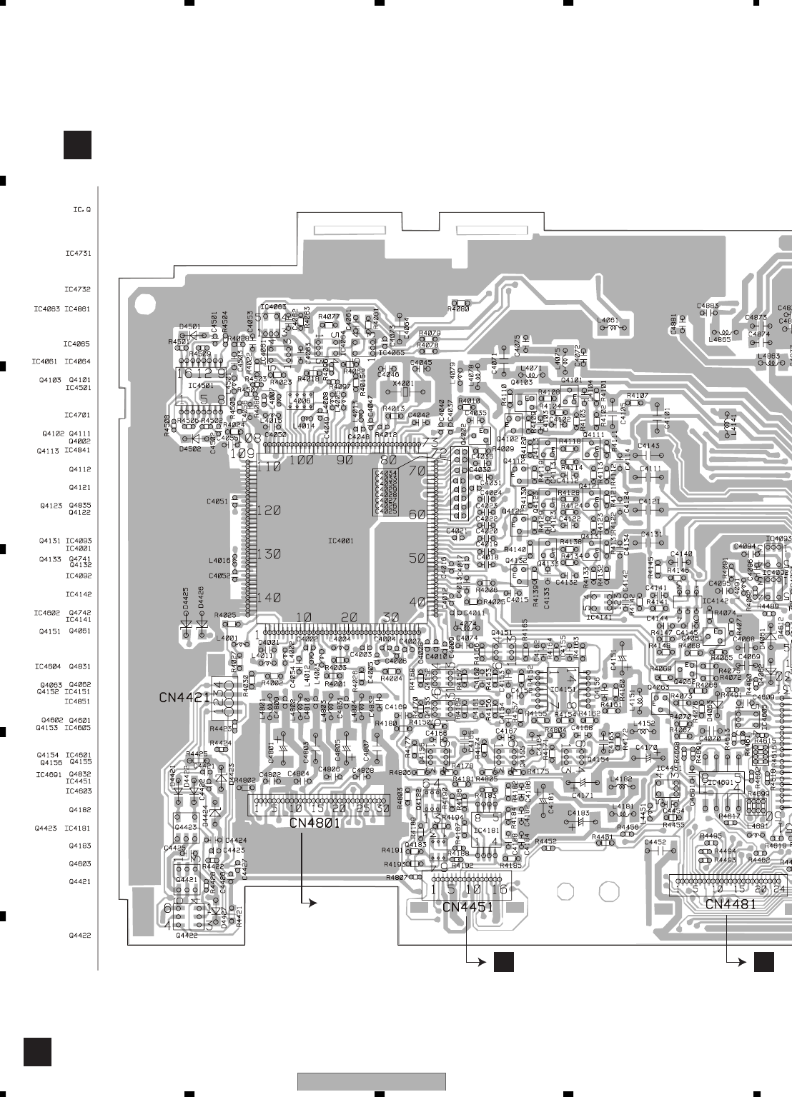
3.3 MOTHER(1/3) PCB(GUIDE PAGE)
A-a A-b
A-a A-b
A-b
A-a
Large size
SCH diagram
Guide page
Detailed page
Note: When ordering service parts, be sure to refer to " EXPLODED VIEWS AND PARTS LIST" or
"ELECTRICAL PARTS LIST".
A-a 1/3
A1/3
VIDEO ISOLATOR
PDH085A
N
CN3801
2/3
A
I
CN4481
I
CN4461
M
CN5901
B
CN1500
G
CN1405
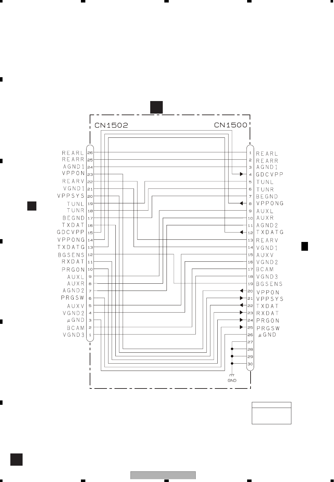
CN1901
C2/2
CONNECTOR (NAVI)
>
>
>
>
>
>
>
>
>
>
AVH-P6600DVD/UC 39
5678
5678
C
D
F
A
B
E
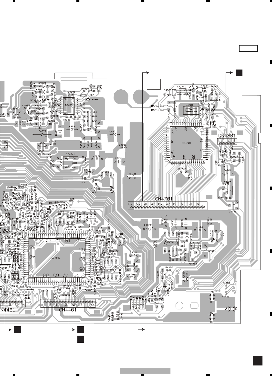
A-a A-b
A-a A-b
A-b
A-a
A-b 1/3
A1/3
VIDEO ISOLATOR
NAVI GUIDE MIX
OPT. OUTPUT
NAVI GUIDE OUTPUT
WIRED REMOTE CONTROL
3/3
A1/3
A
MOTHER PCB
N
CN3801
2/3
A
CN1551
C1/2
FRONT
L CH
FRONT
R CH
REAR
L CH
REAR
R CH
SUBWOOFER
L CH
SUBWOOFER
R CH
Decimal points for resistor
and capacitor fixed values
are expressed as :
2.2 2R2
0.022 R022
←
←
Symbol indicates a resistor.
No differentiation is made between chip resistors and
discrete resistors.
NOTE :
Symbol indicates a capacitor.
No differentiation is made between chip capacitors and
discrete capacitors.
The > mark found on some component parts indicates
the importance of the safety factor of the part.
Therefore, when replacing, be sure to use parts of
identical designation.
>
>
>
>
MOTHER UNIT
Consists of
MOTHER PCB
RELAY PCB
AVH-P6600DVD/UC
42
1234
1234
C
D
F
A
B
E
A-a A-b
A-b 1/3
12
S
OLATOR
NAVI GUIDE MIX
OPT. OUTPUT
NAVI GUIDE OUTPUT
WIRED REMOTE CONTROL
3/3
A1/3
A
MOTHER PCB
2/3
A
CN1551
C1/2
FRONT
L CH
FRONT
R CH
REAR
L CH
REAR
R CH
SUBWOOFER
L CH
SUBWOOFER
R CH
The > mark found on some component parts indicates
the importance of the safety factor of the part.
Therefore, when replacing, be sure to use parts of
identical designation.
>
AVH-P6600DVD/UC 43
5678
5678
C
D
F
A
B
E
A-a A-b
A-b 1/3
3 4
Decimal points for resistor
and capacitor fixed values
are expressed as :
2.2 2R2
0.022 R022
←
←
Symbol indicates a resistor.
No differentiation is made between chip resistors and
discrete resistors.
NOTE :
Symbol indicates a capacitor.
No differentiation is made between chip capacitors and
discrete capacitors.
>
>
>
MOTHER UNIT
Consists of
MOTHER PCB
RELAY PCB
AVH-P6600DVD/UC
52
1234
1234
C
D
F
A
B
E
3.6 RELAY PCB
B
BRELAY PCB
CN104
1/3
A
CN1404
G
MOTHER UNIT
Consists of
MOTHER PCB
RELAY PCB

AVH-P6600DVD/UC 53
5678
5678
C
D
F
A
B
E
AVH-P6600DVD/UC 55
5678
5678
C
D
F
A
B
E
C1/2
C-b 1/2
PICKUP UNIT(SERVICE) M3 SPINDLE MOTOR
CXM1280
RF SIGNAL
FOCUS SERVO LINE
TRACKING SERVO LINE
CARRIAGE SERVO LINE
SPINDLE SERVO LINE
SS
M1
LOADINGMOTOR
CXB8687
sense
2/2
C
2/2
C
1/2
C
DVD CORE UNIT (MS-3V1)(SODC)
F
D
E
FF
SS
SSCC
SS
SS
CC
CC
CC
SS
SS
SS
TT
FF
FF
FF
TT
TT
FF
TT
FF
TT
CC
SS
SS
TT
FF
TT
CC
1
4
3
2
5
AVH-P6600DVD/UC
62
1234
1234
C
D
F
A
B
E
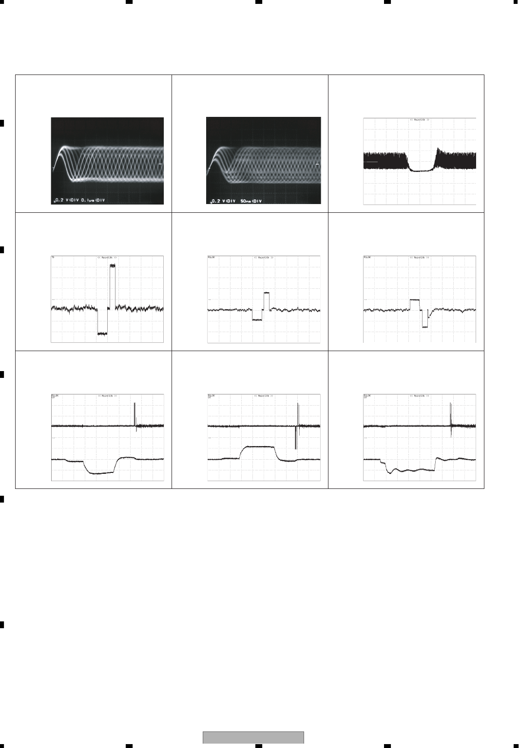
1ANAMONI1 0.2V/div. 0.1µs/div.
0.2V/div. 100µs/div.
0.2V/div. 0.1µs/div.
CDRF
Interval
1ANAMONI1 0.5V/div. 100µs/div.
1ANAMONI1
DVDRF DVDRF(BD1mm)
2TD1 0.5V/div. 100µs/div.
Interval FWD
2TD1 0.5V/div. 100µs/div.
Interval REV
2TD1
2CH1: TD1
3CH2: COP1-COM1 2.0V/div.5ms/div.
Traverse501FWD
0.5V/div.5ms/div. 2CH1: TD1
3CH2: COP1-COM1 2.0V/div.5ms/div.
Traverse501REV
0.5V/div.5ms/div. 2CH1: TD1
3CH2: COP1-COM1 2.0V/div.5ms/div.
Traverse5000FWD
0.5V/div.5ms/div.
-Waveforms Note:1. The encircled number denote measuring pointes in the circuit diagram.
2. Reference voltage VHALF : 1.65V(TD1,FD1,CRGDRV)
: 2V Center(ANAMONI1)
In this waveform, it is seeing on the GND standard.
Offset of 1.65V or 2V is put in.
VHALF→
VHALF→VHALF→
VHALF→
VHALF→VHALF→
VHALF→
VHALF→
VHALF→
VHALF→
VHALF→
VHALF→
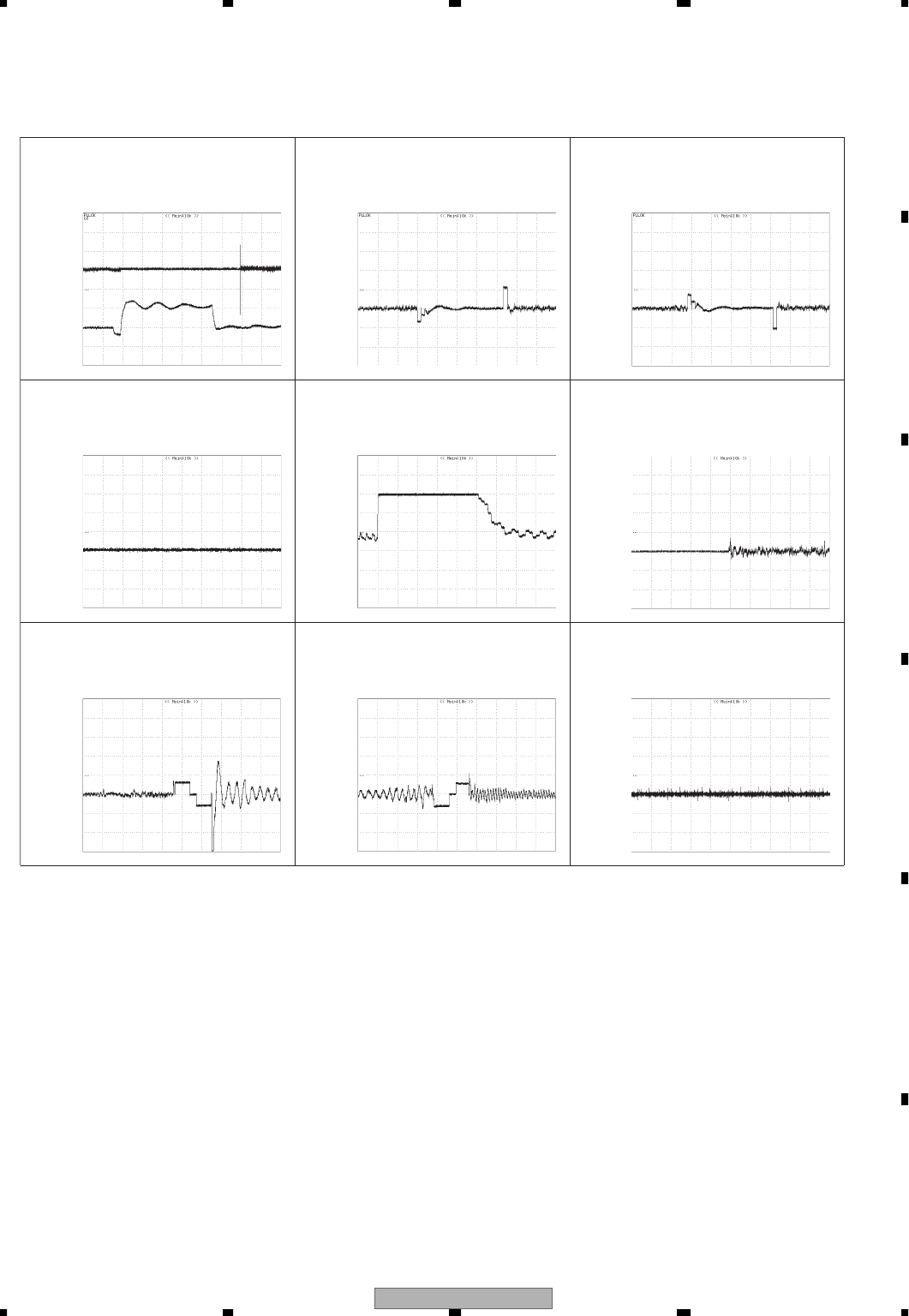
AVH-P6600DVD/UC 63
5678
5678
C
D
F
A
B
E
2TD1
Play TD 5FD1 0.5V/div. 1ms/div.
Focus close
-Waveforms Note:1. The encircled number denote measuring pointes in the circuit diagram.
2. Reference voltage VHALF : 1.65V(TD1,FD1,CRGDRV)
: 2V Center(ANAMONI1)
In this waveform, it is seeing on the GND standard.
Offset of 1.65V or 2V is put in.
VHALF→VHALF→VHALF→
VHALF→
VHALF→
VHALF→
VHALF→
VHALF→
VHALF→
VHALF→
0.5V/div. 100µs/div.
ID search Insaide → Outside
4CRGPRV
2CH1: TD1
3CH2: COP1-COM1 2.0V/div.5ms/div.
Traverse5000REV
0.5V/div.5ms/div.
0.5V/div.20ms/div.
5FD1
Focus jamp L 0 → L1
0.5V/div.500µs/div.
2TD1
Multi 32REV
0.5V/div.500µs/div.
2TD1
Multi 32FWD
0.5V/div.500µs/div.
5FD1
Focus jamp L1 → L 0
0.5V/div.500µs/div. 5FD1
Play TD
0.5V/div.20ms/div.
AVH-P6600DVD/UC
64
1234
1234
C
D
F
A
B
E
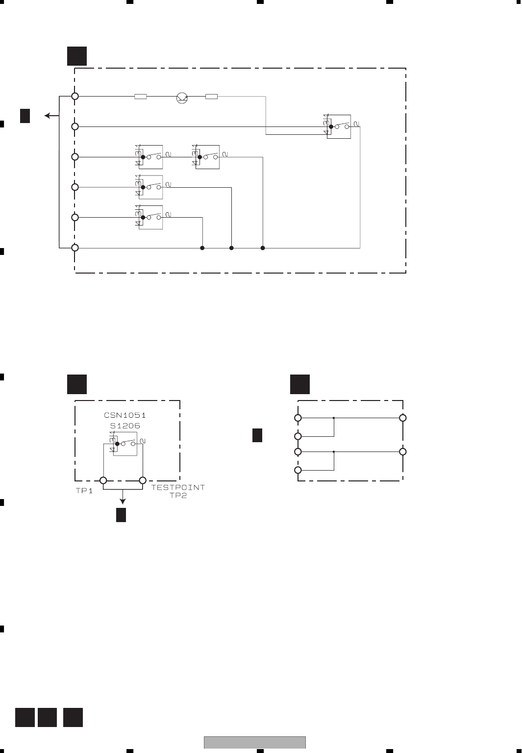
3.9 COMPOUND UNIT(A) , COMPOUND UNIT(B) AND RELAY PCB
D E F
ECOMPOUND UNIT(B) FRELAY PCB
DCOMPOUND UNIT(A)
CLAMP
C1/2
C1/2
S1201
Q1299
S1202 S1204
S1203
R1298
0R0
1
2
3
4
5
6
S1205
R1299
0R0
CPT231SCTD
CSN1069
CSN1069
CSN1069
CSN1070
CSN1070
12cm
8cm
DISC SENS DISC SENS
8cm
CN1231
CN1201
M2
CARRIAGE MOTOR
CXB8688
C1/2
AVH-P6600DVD/UC 65
5678
5678
C
D
F
A
B
E
3.10 PU UNIT(REFERENCE)
24
Iop78
L2
LC
Vcc
GND
GND
IC1
L4
C2C3
C6
C7
L3
1715
C1
16
65LD78LD
LDGND
R1C5
Short round
Short round
L1 C4
78LD
65LD
65MD
65MDGVR2/ 65Rmd
VR1/ 78RmdVmda
1
2
3
4
6
5
7
R2
L6
MDA
Top View
up
MDA
A
SW
Vcc
C8
C9
12
GND
13
V r
14
MDC
98
78MD
78MDG
MDG
B1
B1
B2
RF-
B3
RF+
B4
C
Vref : 2.5V
GND
C10TH1
TEMP
Vcc
SW
A
NC
T-
T+
F-
F+
B2
RF-
B3
RF+
B4
C
LDGND
23
26
25
07
08
05
06
22
21
20
19
18
17
27
02
01
03
04
09
16
15
14
13
12
11
10
Iop65
Im/ 2
Im
Im/ 2
Ishf
Vshf : 4V
CN1101
C
1/2
AVH-P6600DVD/UC
68
1234
1234
C
D
F
A
B
E
3.12 INVERTER PCB
H
ICN4451
HINVERTER PCB
LCD MODULE
MONITOR UNIT
Consists of
MONITOR PCB
UPPER PCB
SENSE PCB
INVERTER PCB
EW
EW

AVH-P6600DVD/UC 69
5678
5678
C
D
F
A
B
E
AVH-P6600DVD/UC
78
1234
1234
C
D
F
A
B
E
3.15 PANEL PCB
M
MPANEL PCB
ACN601
LCN5501
RESET
KEYBOARD UNIT
Consists of
Grille PCB
Panel PCB
AVH-P6600DVD/UC 79
5678
5678
C
D
F
A
B
E
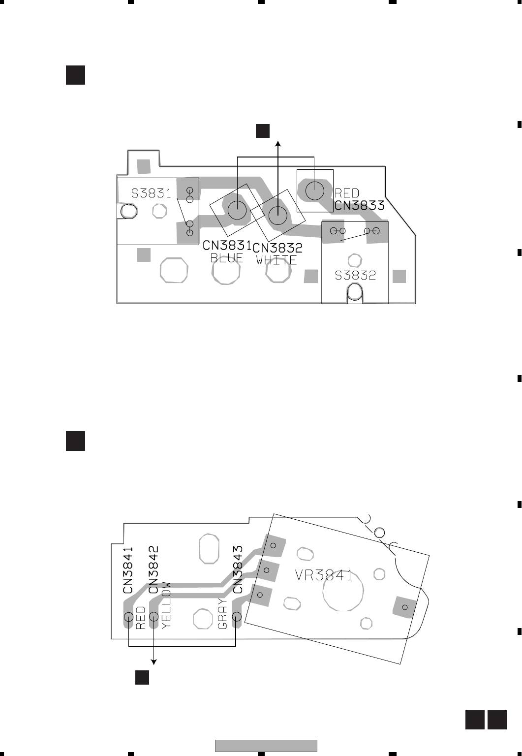
3.16 MAIN UNIT, SW UNIT AND VOLUME UNIT
N
A
N
O
O
P
P
(High speed:L,
Low speed:H)
Short round
(Open)
Photo pulse output
Photo pulse driver
5V regulator for sense
Angle sense volume power supply switch
Position motor
Angle motor
Regulator output
Voltage adj. input
Regulator for driver
Position motor
Position motor:H
Angle motor
Angle motor:H
Motor driver
Angle operation
Horizon operation
Note:It comes out lower about 1.5v than Vcc.
MAIN UNIT
Position motor
Angle motor
LIFT SW ANGLE SW
CXB9515
CXB9516
VOLUME
UNIT SW UNIT
Angle sense
CN502
(Deg.0:L)
(EJECT:L)
(Deg.0:L)
(EJECT:L)
3
6
2
5
1
8
7
4
M3001
M3002
AVH-P6600DVD/UC
80
1234
1234
C
D
F
A
B
E
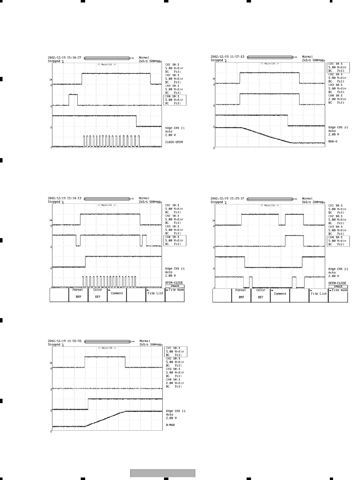
- Waveforms The encircled number denote measuring pointes in the circuit diagram.
• CLOSE -> OPEN
• OPEN -> CLOSE
5 CH1:MTR1
6 CH3:ANGLSW
• 0->MAX
2 CH2:MTRSEL
7 CH4:ANGLIN
• MAX -> Deg.0 DOWN
1 CH1:MTR2
3 CH3:LIFTSW
2 CH2:MTRSEL
4 CH4:LFTPLS
1 CH1:MTR2
3 CH3:LIFTSW
2 CH2:MTRSEL
4 CH4:LFTPLS
5 CH1:MTR1
6 CH3:ANGLSW
2 CH2:MTRSEL
7 CH4:ANGLIN
• Set back open -> Set
1 CH1:MTR2
3 CH3:LIFTSW
8 CH2:MTRS
4 CH4:LFTPLS

AVH-P6600DVD/UC 81
5678
5678
C
D
F
A
B
E
AVH-P6600DVD/UC
82
1234
1234
C
D
F
A
B
E
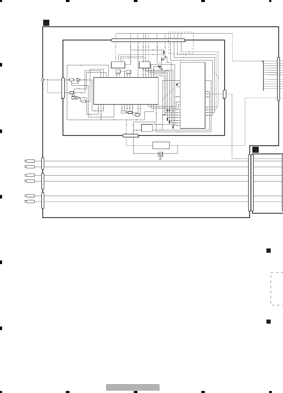
4. PCB CONNECTION DIAGRAM
4.1 MOTHER PCB
Capacitor
Connector
P.C.Board Chip Part
A
AMOTHER PCB
SIDE B
SIDE A
NOTE FOR PCB DIAGRAMS
1.The parts mounted on this PCB
include all necessary parts for
several destination.
For further information for
respective destinations, be sure
to check with the schematic dia-
gram.
2.Viewpoint of PCB diagrams
FRON
T
CN802
ICN4461
ICN4461
ICN4481
NCN3801
CCN1901
CCN1551
FAN MOTOR
GCN1405
BCN1500
CORD ASSY
(RC,RD only) CORD ASSY
(UC,EW only)
CORD ASSY
(UC,EW only) IP
B
AVH-P6600DVD/UC
86
1234
1234
C
D
F
A
B
E
4.2 RELAY PCB
B
BRELAY PCB
SIDE A
SIDE B
BRELAY PCB
GCN1404
ACN104

AVH-P6600DVD/UC 87
5678
5678
C
D
F
A
B
E

AVH-P6600DVD/UC
92
1234
1234
C
D
F
A
B
E
4.4 COMPOUND UNIT(A), COMPOUND UNIT(B) AND RELAY PCB
D E F
E
D
C
C
CLAMP
M2
12cm
S1201
R1298
R1299
Q1299
CN1231
CCN1201
16
DISC SENS
S1204
DISC SENS
S1203
8cm
S1202
8cm
S1205
F
COMPOUND UNIT(B)
RELAY PCB
COMPOUND UNIT(A)

AVH-P6600DVD/UC 93
5678
5678
C
D
F
A
B
E
AVH-P6600DVD/UC
94
1234
1234
C
D
F
A
B
E
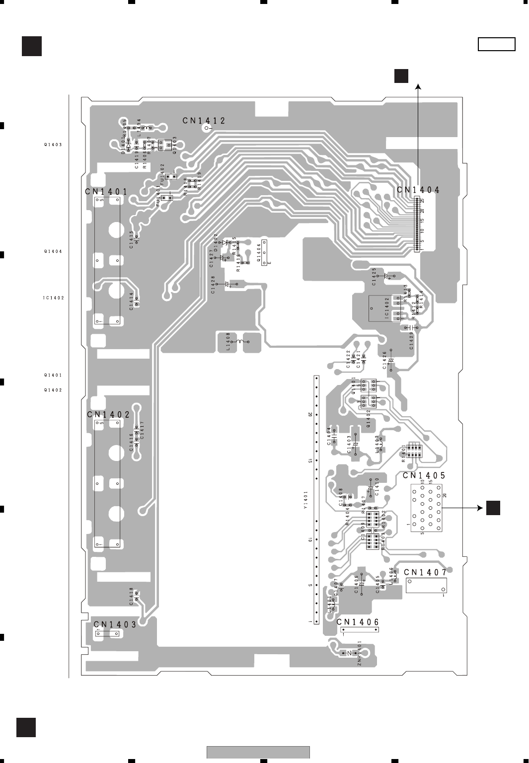
4.5 TUNER UNIT
G
GTUNER UNIT SIDE A
IC,Q
BCN1502
A
CN103
??
IP-BUS
FM/AM TUNER UNIT
AVH-P6600DVD/UC 95
5678
5678
C
D
F
A
B
E
G
GTUNER UNIT SIDE B
AVH-P6600DVD/UC
100
1234
1234
C
D
F
A
B
E
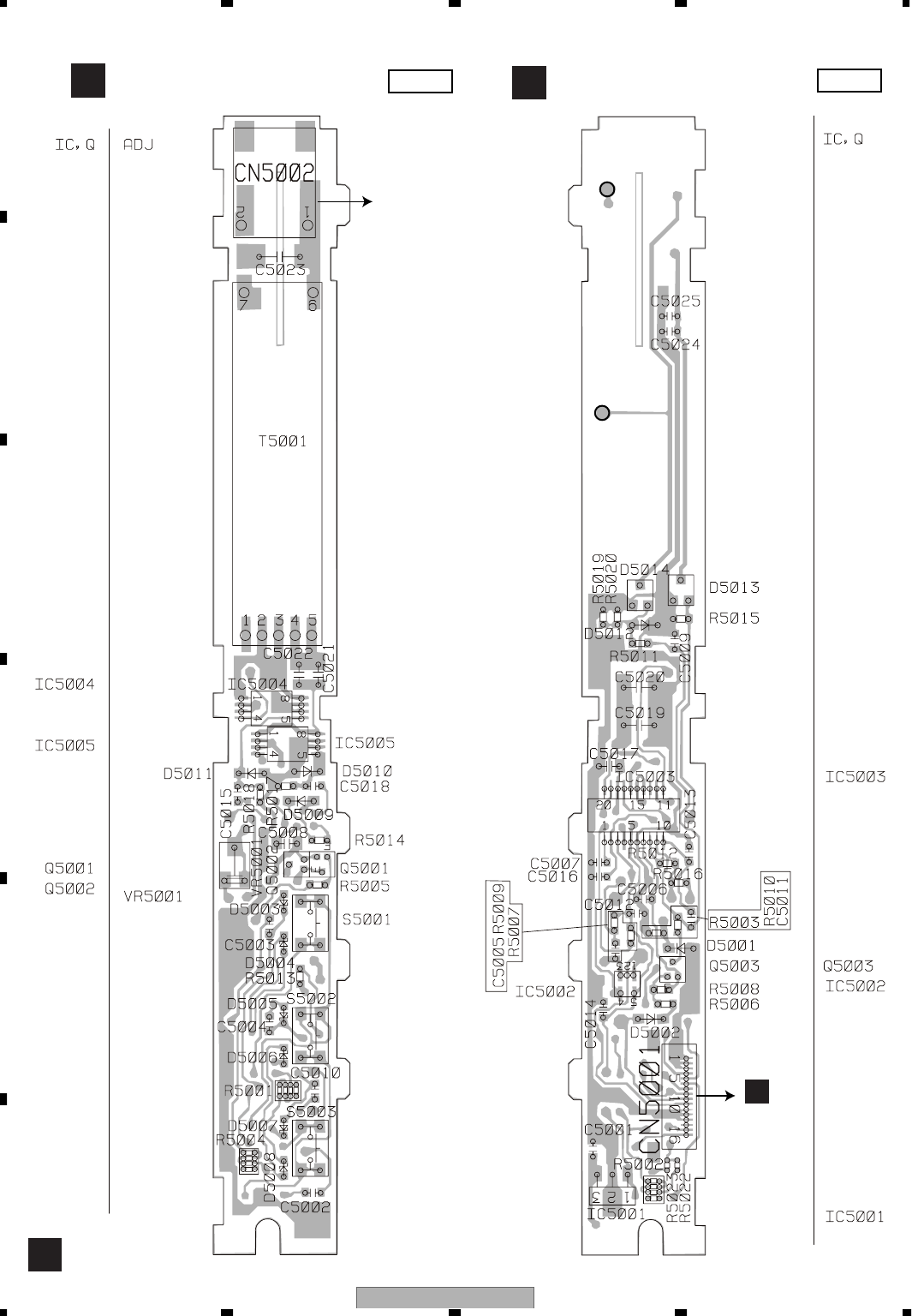
4.7 INVERTER PCB
H
HINVERTER PCB HINVERTER PCB
SIDE A SIDE B
I
CN4451
LCD PANEL
FL2
FL1
AVH-P6600DVD/UC 101
5678
5678
C
D
F
A
B
E
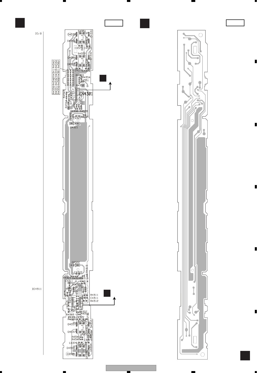
4.8 UPPER PCB
J
JUPPER PCB JUPPER PCB
SIDE A SIDE B
ICN4201
KCN4312
AVH-P6600DVD/UC
102
1234
1234
C
D
F
A
B
E
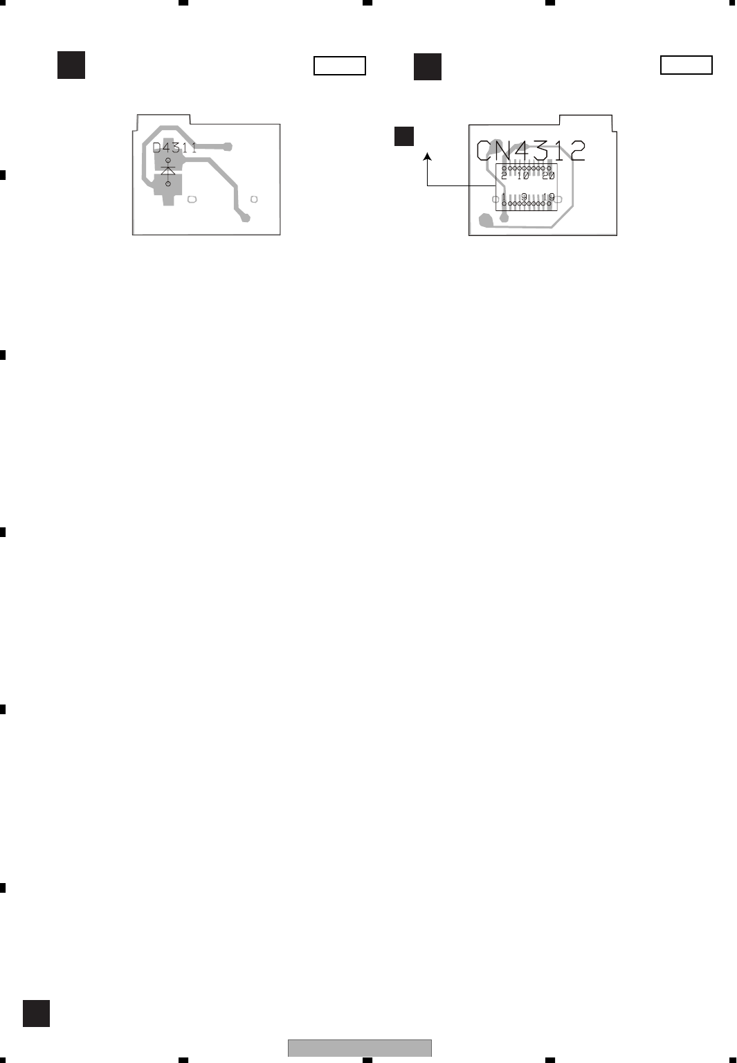
4.9 SENSE PCB
K
KSENSE PCB KSENSE PCB
SIDE A SIDE B
JCN4311

AVH-P6600DVD/UC 103
5678
5678
C
D
F
A
B
E
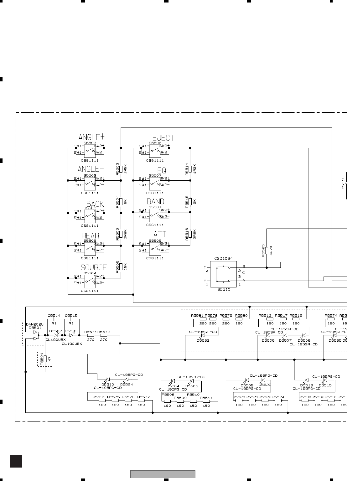
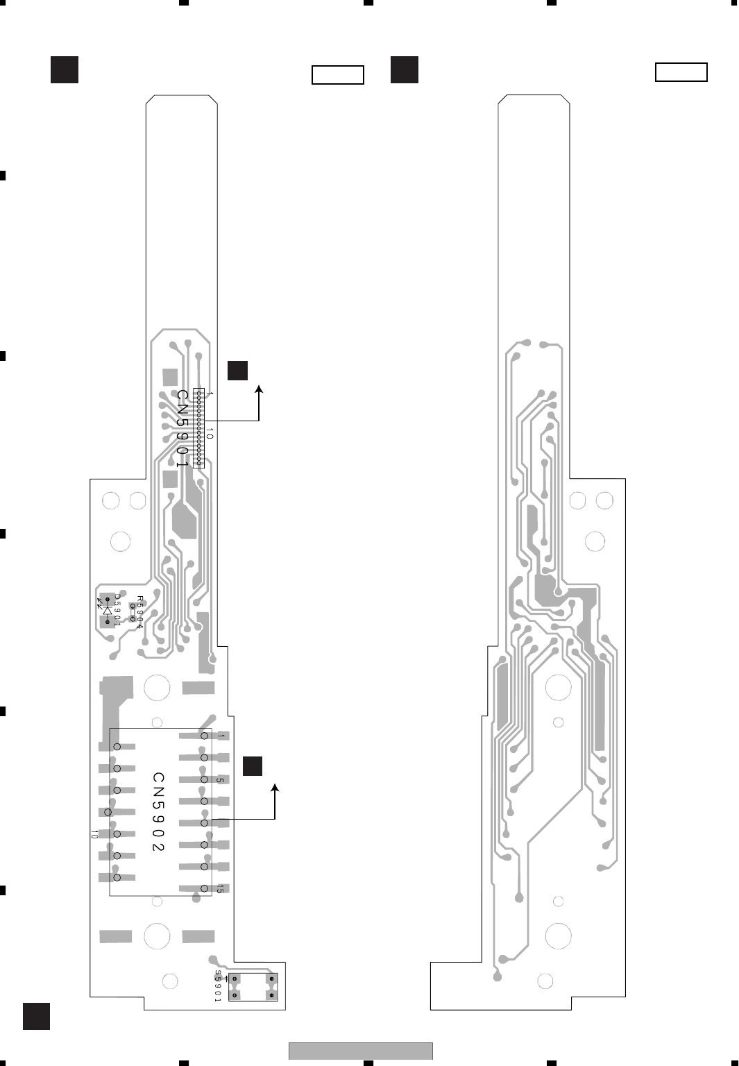
4.10 GRILLE PCB
L
LGRILLE PCB SIDE A SIDE B
LGRILLE PCB
MCN5902
SOURCE REAR BACK ATT ANGLE- ANGLE+ BAND EQ EJECT
VOLUME
JOYSTICK
AVH-P6600DVD/UC
104
1234
1234
C
D
F
A
B
E
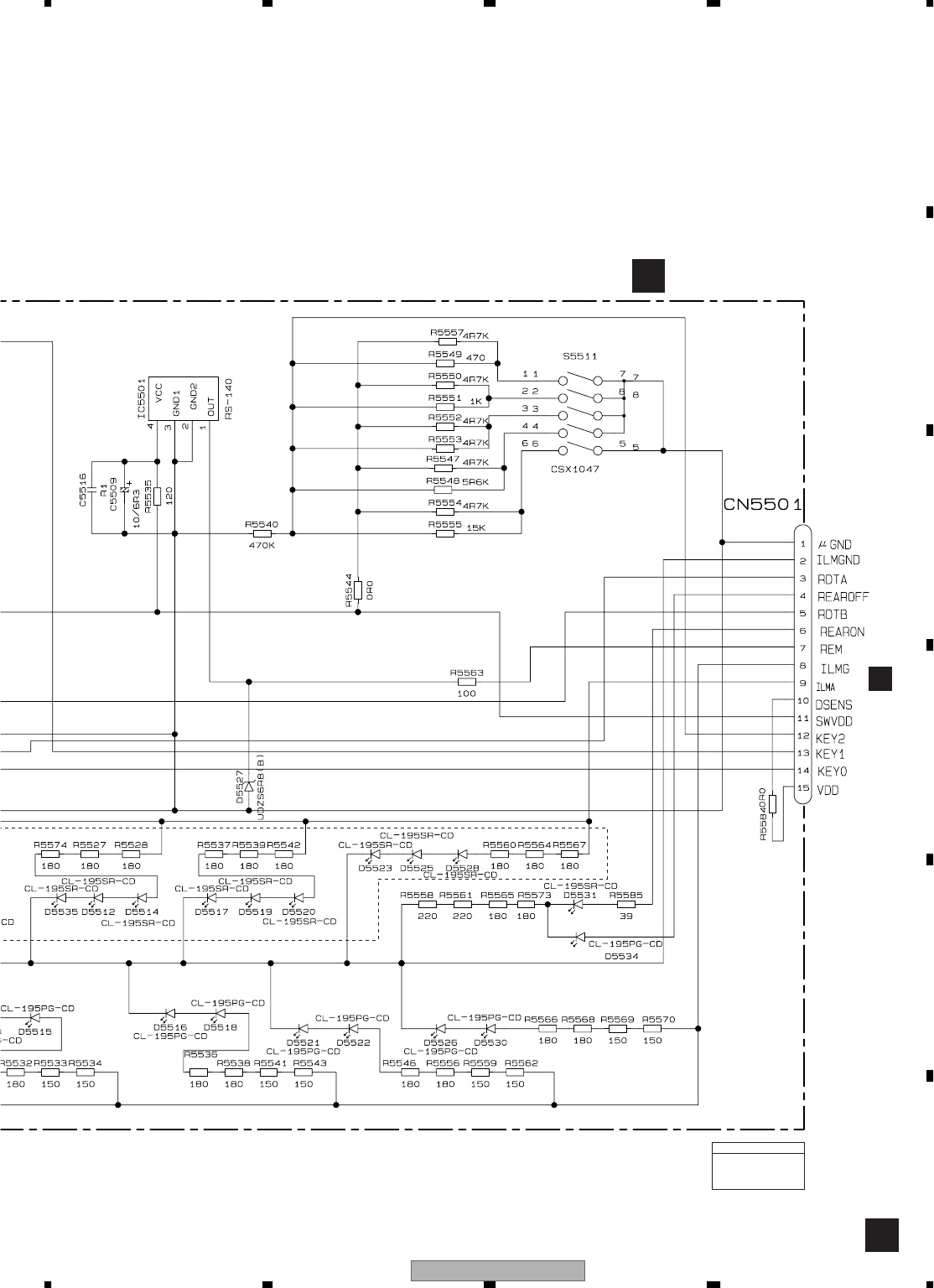
4.11 KEYBOARD PCB
M
MPANEL PCB SIDE A SIDE B
MPANEL PCB
LCN5501
RESET
ACN601
AVH-P6600DVD/UC 105
5678
5678
C
D
F
A
B
E
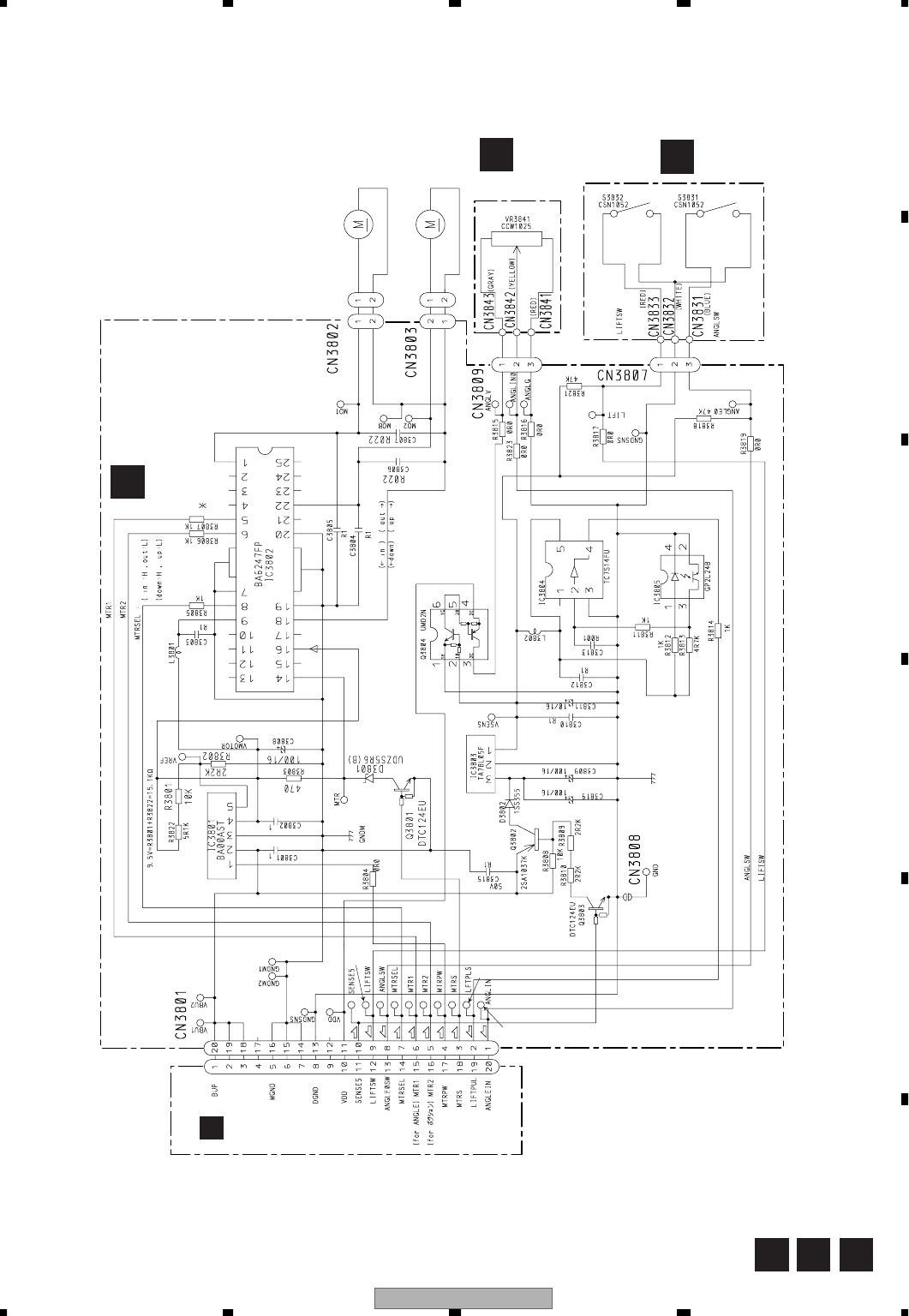
4.12 SW UNIT AND VOLUME UNIT
VOLUME UNIT
P
SW UNIT
O
P
O
ANGLE SW
LIFT SW
ANGLE SENSE
NCN3807
NCN3809
AVH-P6600DVD/UC
106
1234
1234
C
D
F
A
B
E
4.13 MAIN UNIT
N
N
MAIN UNIT SIDE A
P
CN3841
CN3842
CN3843
A
CN502
O
CN3831
CN3832
CN3833
AVH-P6600DVD/UC 107
5678
5678
C
D
F
A
B
E
N
N
MAIN UNIT SIDE B

AVH-P6600DVD/UC
108
1234
1234
C
D
F
A
B
E
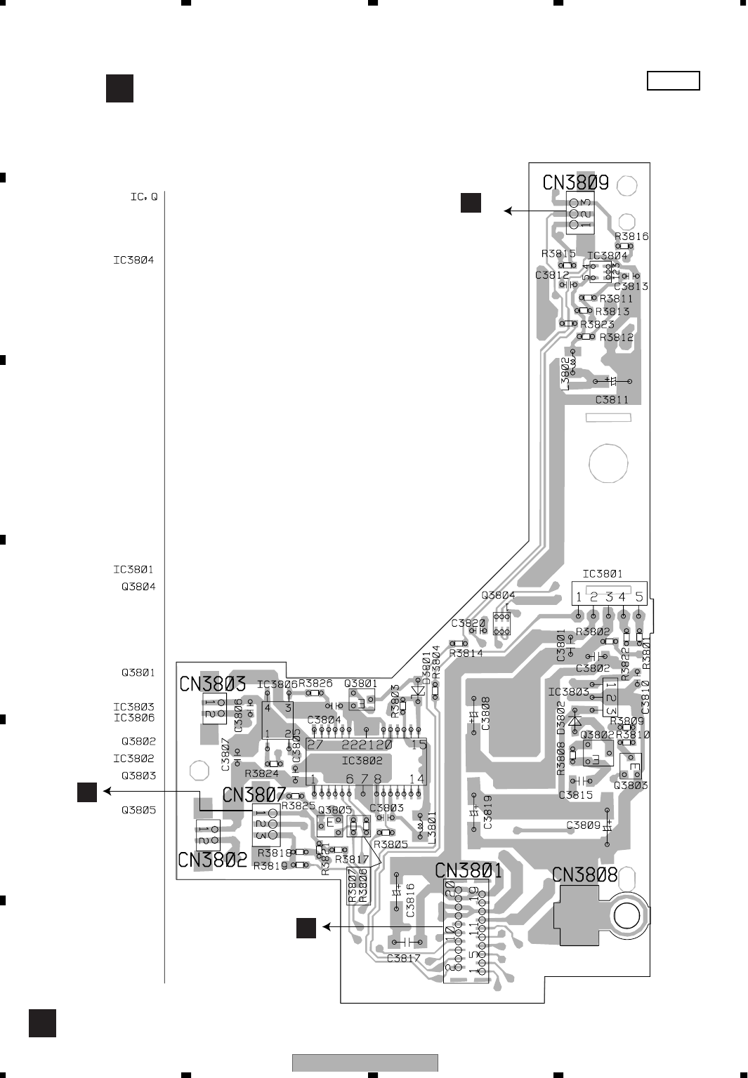
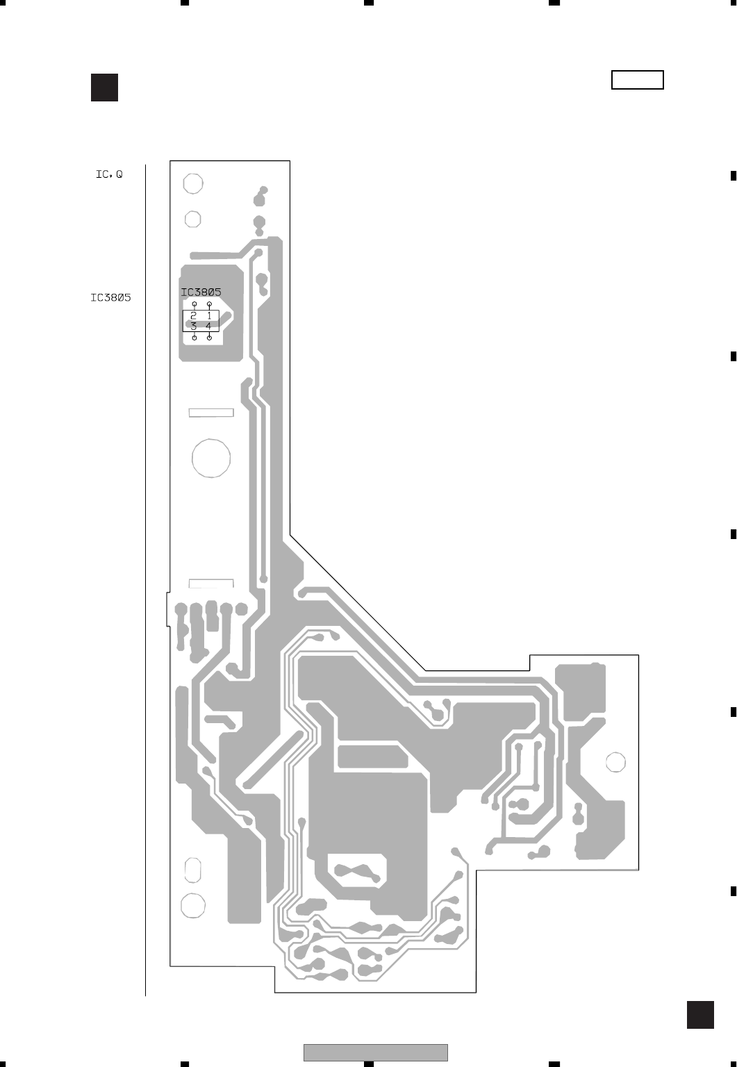
5. ELECTRICAL PARTS LIST
NOTE:
• Parts whose parts numbers are omitted are subject to being not supplied.
• The part numbers shown below indicate chip components.
Chip Resistor
RS1/_S___J,RS1/__S___J
Chip Capacitor (except for CQS.....)
CKS....., CCS....., CSZS.....
Circuit Symbol and No. Part No.
Mother Unit
Consists of
Mother PCB
Relay PCB
AB
Unit Number:CWM9143(UC model)
Unit Number:CWM9142(EW model)
Unit Name:Mother Unit
MISCELLANEOUS
IC 101 IC TC4S81F
IC 102 IC HA12240FP
IC 103 IC TC7SET08FU
IC 151 IC SM5304AV
IC 152 IC TC74VHC08FT
IC 153 IC TC7SET08FU
IC 201 IC PML009A
IC 202 IC PAL007A
IC 203 IC PA2028A
IC 301 IC NJM4558V
IC 351 IC NJM4558V
IC 352 IC NJM4558V
IC 353 IC NJM4580V
IC 401 IC TA2050F
IC 402 IC TA2050F
IC 403 IC TA2050F
IC 404 IC NJM2136V
IC 405 IC NJM2136V
IC 406 IC NJM2136V
IC 407 IC NJM2136V
IC 408 IC CXA2089Q
IC 409 IC BA7623F
IC 410 IC NJM2136V
IC 411 IC NJM2138V
IC 601 IC(UC model) PE5416A
IC 601 IC(EW model) PE5415A
IC 602 IC PDH089A
IC 603 IC S-80841CNUA-B82
IC 801 IC S-812C33AUA-C2N
IC 802 IC LTC3728EG
IC 803 IC LTC3728EG
IC 804 IC BA00BC0WFP
IC 805 IC S-812C50AUA-C3E
IC 806 IC S-814A33AMC-BCX
IC 1401 IC PE5417A
IC 1403 IC TC7WHU04FU
IC 1404 IC S-80827CNUA-B8M
IC 1405 IC TC7SET08FU
IC 1407 IC TC74VCX02FT
IC 1408 IC BA3834F
IC 1410 IC PD8125A
IC 1411 IC PD8126A
IC 1414 IC TC7SZ04FU
IC 1451 IC HD64413ASFI
IC 1452 IC K4S641632H-TC75
Q 101 Transistor 2SC4081
Q 102 Transistor 2SC4081
Q 103 Transistor UMF23N
Q 151 Transistor IMD2A
Q 152 Transistor IMX9
Q 201 Transistor 2SC4081
Q 202 Transistor IMD2A
Q 203 Transistor DTC124EU
Q 204 Transistor DTC144EU
Q 205 Transistor 2SC4081
Q 206 Transistor IMX9
Q 207 Transistor IMX9
Q 208 Transistor IMX9
Q 209 Transistor IMD2A
Q 301 Transistor IMX9
Q 302 Transistor IMD2A
Q 303 Transistor 2SC4081
Q 351 Transistor IMD2A
Q 352 Transistor DTC323TU
Q 353 Transistor DTC124EU
Q 401 Transistor 2SC4081
Q 402 Transistor 2SC4081
Q 403 Transistor 2SC4081
Q 404 Transistor 2SC4081
Q 405 Transistor 2SC4081
Q 406 Transistor 2SC4081
Q 551 Transistor 2SC4081
Q 552 Transistor 2SA1577
Q 601 Transistor UMF23N
Q 602 Transistor DTC114EU
Q 603 Transistor DTA114EU
Q 604 Transistor DTC144EU
Q 605 Transistor 2SC4081
Q 606 Transistor 2SC4081
Q 607 Transistor 2SC4081
Q 608 Transistor 2SC4081
Q 609 Transistor 2SA1577
Circuit Symbol and No. Part No.

AVH-P6600DVD/UC 109
5678
5678
C
D
F
A
B
E
Q 610 Transistor DTC144EU
Q 611 Transistor 2SA1577
Q 612 Transistor DTC144EU
Q 613 Transistor 2SA1577
Q 614 Transistor DTC144EU
Q 615 Transistor(EW model) 2SA1577
Q 616 Transistor(EW model) DTC144EU
Q 617 Transistor DTC124EU
Q 701 Transistor IMX1
Q 702 Transistor DTC114EU
Q 703 Transistor 2SA1576
Q 704 Transistor 2SA1576
Q 705 Transistor 2SC4081
Q 801 Transistor DTC124EU
Q 802 Transistor DTC124EU
Q 803 Transistor 2SB1708
Q 805 Transistor 2SB1708
Q 806 Transistor 2SC4081
Q 807 Transistor 2SB1708
Q 808 Transistor DTC124EU
Q 809 Transistor DTC124EU
Q 810 Transistor DTC124EU
Q 811 Transistor DTC124EU
Q 812 Transistor UMF5N
Q 813 Transistor DTC124EU
Q 814 Transistor DTC124EU
Q 815 Transistor 2SB1184F5
Q 816 Transistor 2SD1767
Q 817 Transistor IMD2A
Q 818 Transistor 2SD1767
Q 819 Transistor DTC114EU
Q 821 FET SP8K4
Q 822 FET SP8K4
Q 823 FET SP8K4
Q 824 Transistor DTC124EU
Q 825 Transistor 2SA1797
Q 827 Transistor DTC144EU
Q 828 Transistor 2SD1767
Q 829 Transistor DTC124EU
Q 830 Transistor 2SB1708
Q 831 Transistor DTC124EU
Q 832 Transistor 2SB1708
Q 833 Transistor 2SD1760F5
Q 834 Transistor UMF5N
Q 835 Transistor UMF5N
Q 836 Transistor 2SD2375
Q 837 Transistor UMF5N
Q 838 Transistor 2SB1184F5
Q 839 Transistor IMD2A
Q 840 Transistor UMF5N
Q 841 Transistor 2SD1767
Q 842 Transistor UMF5N
Q 843 Transistor UMF5N
Q 844 Transistor 2SD1767
Q 845 Transistor UMF5N
Q 901 Transistor DTC114EU
Q 902 Transistor 2SA1615-Z
Q 1401 Transistor FMG12
Q 1402 Transistor UMF5N
Q 1403 Transistor UMF5N
Circuit Symbol and No. Part No.
Q 1405 Transistor 2SA1774
Q 1406 Transistor 2SA1774
Q 1407 Transistor 2SA1774
D 101 Diode HZU2R7(B1)
D 102 Diode HZU2R7(B1)
D 103 Diode HZU2R7(B1)
D 104 Diode HZU2R7(B1)
D 105 Diode UDZS5R6(B)
D 106 Diode UDZS5R6(B)
D 107 Diode UDZS5R6(B)
D 108 Diode UDZS5R6(B)
D 109 Diode HZU2R7(B1)
D 110 Diode HZU2R7(B1)
D 111 Diode HZU2R7(B1)
D 112 Diode HZU2R7(B1)
D 113 Diode Network DA204U
D 114 Diode Network DA204U
D 115 Diode HZU2R7(B1)
D 116 Diode HZU2R7(B1)
D 117 Diode UDZS5R6(B)
D 118 Diode UDZS5R6(B)
D 119 Diode UDZS5R6(B)
D 120 Diode UDZS8R2(B)
D 121 Diode UDZS8R2(B)
D 201 Diode DAN202U
D 202 Diode DAN202U
D 203 Diode DAN202U
D 204 Diode UDZS8R2(B)
D 205 Diode DAN202U
D 206 Diode 1SS355
D 301 Diode RSX201L-30
D 601 Diode UDZS5R6(B)
D 602 Diode Network DA204U
D 603 Diode Network DA204U
D 604 Diode Network DA204U
D 605 Diode Network DA204U
D 606 Diode Network DA204U
D 607 Diode Network DA204U
D 608 Diode Network DA204U
D 609 Diode 1SS355
D 610 Diode 1SS355
D 611 Diode DAN202U
D 612 Diode 1SS355
D 701 Diode 1SS355
D 702 Diode HZU6R8(B2)
D 703 Diode UDZS7R5(B)
D 704 Diode DAN202U
D 705 Diode DAN202U
D 706 Diode S1G-6904G2P
D 707 Diode S1G-6904G2P
D 708 Diode 5KP24A
D 801 Diode S1G-6904G2P
D 802 Diode UDZS18(B)
D 803 Diode RSX201L-30
D 804 Diode HZU8R2(B1)
D 805 Diode DAN202U
D 806 Diode HZU5R6(B2)
D 807 Diode RB500V-40
D 808 Diode RB500V-40
D 809 Diode RB500V-40
Circuit Symbol and No. Part No.

AVH-P6600DVD/UC
110
1234
1234
C
D
F
A
B
E
D 811 Diode RB160L-40
D 812 Diode RB160L-40
D 813 Diode RB160L-40
D 814 Diode S1G-6904G2P
D 815 Diode S2G-6600
D 816 Diode RSX201L-30
D 817 Diode S2G-6600
D 819 Diode UDZS5R6(B)
D 820 Diode S2G-6600
D 821 Diode DAN202U
D 822 Diode HZU6R8(B3)
D 823 Diode HZU10(B1)
D 825 Diode UDZS20(B)
D 826 Diode HZU6R8(B3)
D 827 Diode DAN202U
D 828 Diode 1SS355
D 829 Diode 1SS355
D 830 Diode 1SS355
D 831 Diode RSX201L-30
D 1401 Diode 1SS355
D 1402 Diode 1SS355
L 101 Inductor CTF1379
L 102 Inductor LCTC2R2K1608
L 103 Inductor CTF1379
L 104 Inductor CTF1558
L 105 Inductor CTF1558
L 110 Inductor CTF1389
L 151 Coil CTH1295
L 152 Inductor CTF1399
L 153 Inductor CTF1399
L 154 Inductor CTF1305
L 155 Inductor CTF1305
L 157 Inductor CTF1473
L 158 Inductor CTF1473
L 201 Inductor LCTA2R2J2520
L 202 Inductor LCTA101J2520
L 301 Inductor CTF1379
L 302 Inductor CTF1379
L 303 Inductor CTF1399
L 351 Inductor CTF1399
L 352 Inductor CTF1399
L 353 Inductor CTF1399
L 401 Inductor CTF1383
L 403 Inductor CTF1399
L 404 Inductor LCTA150J2520
L 405 Inductor CTF1399
L 406 Inductor CTF1399
L 407 Inductor CTF1399
L 408 Inductor LCTA100J2520
L 409 Inductor CTF1383
L 410 Inductor CTF1399
L 411 Inductor CTF1399
L 412 Inductor CTF1399
L 413 Inductor CTF1399
L 415 Inductor CTF1399
L 551 Inductor CTF1399
L 601 Inductor CTF1399
L 602 Inductor CTF1306
L 603 Inductor CTF1306
L 604 Inductor LCTA2R2J2520
Circuit Symbol and No. Part No.
L 701 Inductor LCTC2R2K1608
L 702 Inductor LCTC2R2K1608
L 801 Coil CTH1308
L 802 Coil CTH1308
L 803 Coil CTH1308
L 805 Coil CTH1308
L 806 Inductor LCTA1R0J3225
L 807 Coil CTH1308
L 809 Inductor CTF1383
L 901 Coil CTH1267
L 902 Choke Coil 270µH CTH1263
L 1401 Inductor CTF1379
L 1402 Inductor CTF1399
L 1403 Inductor CTF1399
L 1404 Inductor CTF1379
L 1406 Inductor CTF1399
L 1407 Inductor CTF1379
L 1408 Inductor CTF1379
L 1409 Inductor CTF1379
L 1410 Inductor CTF1399
L 1411 Inductor CTF1396
L 1414 Inductor CTF1379
L 1415 Inductor LCTC2R2K1608
L 1416 Inductor LCTC2R2K1608
L 1417 Inductor LCTC2R2K1608
L 1418 Inductor CTF1379
L 1419 Inductor CTF1379
L 1420 Inductor CTF1379
L 1421 Inductor CTF1379
L 1422 Inductor CTF1379
L 1423 Inductor CTF1379
L 1424 Inductor CTF1379
L 1425 Inductor CTF1379
L 1426 Inductor CTF1379
L 1427 Inductor CTF1379
L 1428 Inductor CTF1389
L 1429 Inductor CTF1389
L 1430 Inductor CTF1389
X 601 Resonator 18.874368MHz CSS1622
X 1401 Ceramic Resonator 4.97MHz CSS1575
X 1452 Resonator 33.0MHz CSS1656
VR401 Semi-fixed 1.5kΩ(OB) CCP1391
FU101 Fuse 5A CEK1289
FU102 Fuse 1A CEK1280
FU103 Fuse 1A CEK1280
FU104 Fuse 5A CEK1289
FU107 Fuse 5A CEK1289
FU151 Fuse 2.5A CEK1285
FU152 Fuse 1A CEK1280
FU153 Fuse 2A CEK1284
FU154 Fuse 250mA CEK1276
FU155 Fuse 250mA CEK1276
FU201 Fuse 3A CEK1286
FU501 Fuse 250mA CEK1276
FU502 Fuse 1.75A CEK1283
FU701 Fuse 5A CEK1289
FU802 Fuse 1.25A CEK1281
FU804 Fuse 1A CEK1280
FU805 Fuse 1A CEK1280
FU901 Fuse 1.25A CEK1281
Circuit Symbol and No. Part No.

AVH-P6600DVD/UC 111
5678
5678
C
D
F
A
B
E
FU902 Fuse 1.75A CEK1283
EF801 EMI Filter CCG1142
BZ601 Buzzer CPV1063
RESISTORS
R 101 RS1/16S750J
R 103 RS1/16S681J
R 104 RS1/16S681J
R 105 RS1/16S0R0J
R 106 RS1/16S750J
R 107 RS1/16S473J
R 108 RS1/16S681J
R 109 RS1/16S750J
R 110 RS1/16S473J
R 111 RS1/16S473J
R 112 RS1/16S681J
R 113 RS1/16S750J
R 114 RS1/16S473J
R 115 RS1/16S473J
R 116 RS1/16S473J
R 117 RS1/16S473J
R 118 RS1/16S472J
R 119 RS1/16S102J
R 120 RS1/16S101J
R 121 RS1/16S150J
R 122 RS1/16S470J
R 123 RS1/16S101J
R 124 RS1/16S222J
R 125 RS1/16S332J
R 126 RS1/16S562J
R 127 RS1/16S221J
R 128 RS1/16S621J
R 129 RS1/16S473J
R 130 RS1/16S121J
R 131 RS1/16S0R0J
R 132 RS1/16S101J
R 133 RS1/16S102J
R 134 RS1/16S102J
R 151 RAB4C102J
R 153 RAB4C102J
R 157 RS1/16S0R0J
R 158 RS1/16S0R0J
R 159 RS1/16S472J
R 162 RS1/16S101J
R 163 RS1/16S102J
R 164 RS1/16S103J
R 165 RS1/16S103J
R 201 RS1/16S181J
R 202 RS1/16S181J
R 203 RS1/16S0R0J
R 204 RS1/16S0R0J
R 205 RS1/16S223J
R 206 RS1/16S223J
R 207 RS1/16S102J
R 208 RS1/16S102J
R 209 RS1/16S0R0J
R 210 RS1/16S0R0J
R 211 RS1/16S0R0J
R 212 RS1/16S0R0J
R 213 RS1/16S0R0J
Circuit Symbol and No. Part No.
R 214 RS1/16S0R0J
R 215 RS1/16S0R0J
R 216 RS1/16S0R0J
R 217 RS1/16S224J
R 218 RS1/16S224J
R 219 RS1/16S104J
R 220 RS1/16S102J
R 221 RS1/16S103J
R 222 RS1/16S682J
R 223 RS1/16S103J
R 224 RS1/16S103J
R 225 RS1/16S103J
R 226 RS1/16S223J
R 227 RS1/16S221J
R 228 RS1/16S101J
R 229 RS1/16S103J
R 230 RS1/16S104J
R 231 RS1/16S820J
R 232 RS1/16S820J
R 233 RS1/16S820J
R 234 RS1/16S820J
R 235 RS1/16S820J
R 236 RS1/16S820J
R 237 RS1/16S473J
R 238 RS1/16S102J
R 239 RS1/16S223J
R 240 RS1/16S223J
R 241 RS1/16S223J
R 242 RS1/16S223J
R 243 RS1/16S223J
R 244 RS1/16S223J
R 245 RS1/16S471J
R 246 RS1/16S471J
R 247 RS1/16S471J
R 248 RS1/16S471J
R 249 RS1/16S471J
R 250 RS1/16S471J
R 251 RS1/16S103J
R 252 RS1/16S103J
R 253 RS1/16S103J
R 254 RS1/16S103J
R 255 RS1/16S103J
R 256 RS1/16S103J
R 257 RS1/16S473J
R 261 RS1/16S101J
R 301 RS1/16S0R0J
R 302 RS1/16S0R0J
R 303 RS1/16S223J
R 304 RS1/16S223J
R 305 RS1/16S821J
R 306 RS1/16S821J
R 307 RS1/16S222J
R 308 RS1/16S472J
R 309 RS1/16S472J
R 312 RS1/16S473J
R 313 RS1/16S473J
R 314 RS1/16S102J
R 315 RS1/16S272J
R 316 RS1/16S472J
R 317 RS1/16S222J
Circuit Symbol and No. Part No.

AVH-P6600DVD/UC
112
1234
1234
C
D
F
A
B
E
R 318 RS1/16S222J
R 319 RS1/16S103J
R 320 RS1/16S103J
R 351 RS1/16S473J
R 352 RS1/16S101J
R 353 RS1/16S473J
R 354 RS1/16S103J
R 355 RS1/16S473J
R 356 RS1/16S472J
R 357 RS1/16S472J
R 358 RS1/16S103J
R 359 RS1/16S473J
R 360 RS1/16S473J
R 361 RS1/16S104J
R 362 RS1/16S821J
R 363 RS1/16S473J
R 364 RS1/16S473J
R 365 RS1/16S103J
R 366 RS1/16S102J
R 367 RS1/16S103J
R 368 RS1/16S103J
R 369 RS1/16S103J
R 370 RS1/16S103J
R 371 RS1/16S103J
R 372 RS1/16S103J
R 375 RS1/16S103J
R 401 RS1/16S123J
R 402 RS1/16S123J
R 403 RS1/16S123J
R 404 RS1/16S223J
R 405 RS1/16S123J
R 406 RS1/16S223J
R 407 RS1/16S223J
R 408 RS1/16S102J
R 409 RS1/16S181J
R 410 RS1/16S181J
R 411 RS1/16S223J
R 412 RS1/16S102J
R 413 RS1/16S102J
R 414 RS1/16S223J
R 415 RS1/16S223J
R 416 RS1/16S223J
R 417 RS1/16S102J
R 418 RS1/16S750J
R 419 RS1/16S223J
R 420 RS1/16S181J
R 421 RS1/16S181J
R 422 RS1/16S472J
R 423 RS1/16S472J
R 424 RS1/16S750J
R 425 RS1/16S472J
R 426 RS1/16S472J
R 427 RS1/16S101J
R 428 RS1/16S472J
R 429 RS1/16S472J
R 430 RS1/16S152J
R 431 RS1/16S101J
R 432 RS1/16S472J
R 433 RS1/16S472J
R 434 RS1/16S472J
Circuit Symbol and No. Part No.
R 435 RS1/16S152J
R 436 RS1/16S750J
R 437 RS1/16S101J
R 438 RS1/16S472J
R 439 RS1/16S472J
R 440 RS1/16S270J
R 441 RS1/16S472J
R 442 RS1/16S102J
R 443 RS1/16S272J
R 444 RS1/16S392J
R 445 RS1/16S472J
R 446 RS1/16S102J
R 447 RS1/16S0R0J
R 448 RS1/16S562J
R 449 RS1/16S562J
R 450 RS1/16S562J
R 451 RS1/16S562J
R 452 RS1/16S272J
R 453 RS1/16S472J
R 454 RS1/16S0R0J
R 455 RS1/16S472J
R 456 RS1/16S101J
R 457 RS1/16S472J
R 458 RS1/16S750J
R 459 RS1/16S472J
R 460 RS1/16S473J
R 461 RS1/16S333J
R 462 RS1/16S0R0J
R 463 RS1/16S472J
R 464 RS1/16S101J
R 465 RS1/16S0R0J
R 467 RS1/16S472J
R 468 RS1/16S102J
R 469 RS1/16S472J
R 470 RS1/16S472J
R 471 RS1/16S0R0J
R 472 RS1/16S222J
R 473 RS1/16S222J
R 474 RS1/16S101J
R 475 RS1/16S101J
R 476 RS1/16S152J
R 477 RS1/16S152J
R 478 RS1/16S152J
R 479 RS1/16S101J
R 480 RS1/16S101J
R 481 RS1/16S152J
R 482 RS1/16S152J
R 483 RS1/16S152J
R 484 RS1/16S152J
R 485 RS1/16S152J
R 486 RS1/16S152J
R 487 RS1/16S152J
R 488 RS1/16S152J
R 489 RS1/16S152J
R 490 RS1/16S152J
R 491 RS1/16S272J
R 492 RS1/16S472J
R 493 RS1/16S272J
R 494 RS1/16S472J
R 495 RS1/16S272J
Circuit Symbol and No. Part No.

AVH-P6600DVD/UC 113
5678
5678
C
D
F
A
B
E
R 496 RS1/16S472J
R 497 RS1/16S272J
R 498 RS1/16S472J
R 499 RS1/16S152J
R 500 RS1/16S102J
R 501 RS1/16S471J
R 502 RS1/16S102J
R 503 RS1/16S471J
R 504 RS1/16S0R0J
R 505 RS1/16S0R0J
R 507 RS1/16S102J
R 508 RS1/16S102J
R 509 RS1/16S0R0J
R 510 RS1/16S0R0J
R 511 RS1/16S0R0J
R 512 RS1/16S0R0J
R 513 RS1/16S102J
R 514 RS1/16S0R0J
R 515 RS1/16S0R0J
R 516 RS1/16S471J
R 517 RS1/16S0R0J
R 518 RS1/16S102J
R 519 RS1/16S102J
R 520 RS1/16S0R0J
R 521 RS1/16S0R0J
R 522 RS1/16S0R0J
R 523 RS1/16S0R0J
R 524 RS1/16S0R0J
R 525 RS1/16S221J
R 526 RS1/16S221J
R 527 RS1/16S221J
R 528 RS1/16S221J
R 529 RS1/16S102J
R 530 RS1/16S102J
R 531 RS1/16S0R0J
R 532 RS1/16S0R0J
R 551 RS1/16S681J
R 552 RS1/16S331J
R 553 RS1/16S272J
R 554 RS1/16S681J
R 555 RS1/16S101J
R 601 RS1/16S102J
R 602 RS1/16S102J
R 603 RS1/16S102J
R 604 RS1/16S822J
R 605 RS1/16S222J
R 606 RS1/16S472J
R 607 RS1/16S472J
R 608 RAB4C222J
R 609 RS1/16S332J
R 610 RS1/16S332J
R 611 RS1/16S102J
R 612 RS1/16S102J
R 613 RS1/16S103J
R 614 RS1/16S223J
R 615 RS1/16S473J
R 616 RS1/16S472J
R 617 RS1/16S473J
R 618 RS1/16S472J
R 619 RS1/16S103J
Circuit Symbol and No. Part No.
R 620 RS1/16S104J
R 621 RS1/16S473J
R 622 RS1/16S473J
R 623 RS1/16S473J
R 624 RS1/16S473J
R 625 (EW model) RAB4C101J
R 626 RS1/16S473J
R 627 RS1/16S102J
R 629 RS1/16S472J
R 630 RS1/16S102J
R 631 RS1/16S473J
R 633 RAB4C102J
R 634 RAB4C102J
R 635 RS1/16S473J
R 636 RS1/16S102J
R 638 RS1/16S102J
R 639 RAB4C102J
R 640 RS1/16S473J
R 641 RS1/16S102J
R 642 RS1/16S102J
R 643 RS1/16S472J
R 644 RS1/16S103J
R 648 RS1/16S101J
R 650 (EW model) RS1/16S102J
R 652 RS1/16S221J
R 653 RS1/16S681J
R 654 RS1/16S473J
R 655 RS1/16S102J
R 656 RS1/16S473J
R 657 RS1/16S102J
R 658 RS1/16S473J
R 659 RS1/16S473J
R 660 RS1/16S104J
R 661 RS1/16S104J
R 662 RS1/16S473J
R 663 RS1/16S473J
R 665 RAB4C102J
R 666 RS1/16S473J
R 667 RS1/16S0R0J
R 668 RS1/16S473J
R 669 RS1/16S473J
R 670 (EW model) RS1/16S473J
R 671 RS1/16S473J
R 673 RS1/16S472J
R 674 RS1/16S681J
R 675 RS1/16S681J
R 676 RS1/16S104J
R 678 RS1/16S104J
R 679 RAB4C681J
R 680 RS1/16S102J
R 681 RAB4C102J
R 682 RS1/16S102J
R 683 RS1/16S0R0J
R 684 RS1/16S102J
R 685 RS1/16S681J
R 686 RS1/16S681J
R 689 RS1/16S104J
R 690 RS1/16S104J
R 692 RS1/16S473J
R 693 RS1/16S223J
Circuit Symbol and No. Part No.

AVH-P6600DVD/UC
114
1234
1234
C
D
F
A
B
E
R 694 RS1/16S472J
R 695 RS1/16S223J
R 696 RS1/16S472J
R 697 RS1/16S223J
R 698 (EW model) RS1/16S472J
R 699 (EW model) RS1/16S223J
R 700 RS1/16S473J
R 701 RS1/16S102J
R 702 RS1/16S473J
R 703 RS1/16S103J
R 704 RS1/16S103J
R 705 RS1/16S104J
R 706 RS1/16S102J
R 707 RS1/16S223J
R 708 RS1/16S473J
R 709 RS1/16S473J
R 710 RS1/16S102J
R 711 RS1/16S473J
R 712 RS1/16S472J
R 713 RS1/16S472J
R 714 RS1/16S472J
R 715 RS1/16S103J
R 716 RS1/16S153J
R 717 RS1/16S473J
R 718 RS1/16S222J
R 719 RS1/16S104J
R 801 RS1/16S103J
R 802 RS1/16S221J
R 803 RS1/16S221J
R 804 RS1/16S103J
R 805 RS1/16S102J
R 806 RS1/16S473J
R 807 RS1/16S221J
R 808 RS1/16S103J
R 809 RS1/16S473J
R 810 RS1/16S221J
R 811 RS1/16S103J
R 812 RS1/16S473J
R 813 RS1/16S223J
R 814 RS1/16S1201D
R 815 RS1/16S4701D
R 816 RS1/16S8201D
R 817 RS1/16S1001D
R 819 RS1/16S220J
R 820 RS1/16S1001D
R 821 RS1/16S822J
R 822 RS1/16S822J
R 823 RS1/16S4701D
R 824 RS1/16S2R2J
R 825 RS1/16S2R2J
R 826 RS1/16S0R0J
R 827 RS1/16S2R2J
R 828 RS1/16S2R2J
R 829 RS1/16S223J
R 830 RS1/16S223J
R 831 RS1/16S4301D
R 832 RS1/16S6801D
R 833 RS1/16S0R0J
R 834 RS1/16S3301D
R 835 RS1/16S1500D
Circuit Symbol and No. Part No.
R 836 RS1/16S3901D
R 837 RS1/16S102J
R 838 2.7kΩCCN1143
R 839 RS1/16S331J
R 840 RS1/16S331J
R 841 2.7kΩCCN1143
R 842 2.7kΩCCN1143
R 843 2.7kΩCCN1143
R 844 RS1/16S100J
R 845 RS1/16S100J
R 846 10ΩCCN1148
R 847 10ΩCCN1148
R 848 RS1/16S472J
R 849 10ΩCCN1148
R 850 RS1/16S181J
R 851 RS1/16S181J
R 852 RS1/16S332J
R 853 RS1/16S181J
R 854 RS1/16S181J
R 855 RS1/16S181J
R 856 RS1/16S181J
R 857 RS1/16S472J
R 858 RS1/16S102J
R 859 RS1/16S1202D
R 860 RS1/16S2701D
R 861 RS1/16S8201D
R 862 RS1/16S5600D
R 863 RS1/16S104J
R 864 RS1/16S391J
R 865 RS1/16S222J
R 866 RS1/16S472J
R 867 RS1/16S222J
R 868 RS1/16S472J
R 869 RS1/16S271J
R 870 RS1/16S103J
R 871 RS1/16S332J
R 872 RS1/16S271J
R 873 RS1/16S121J
R 874 RS1/16S103J
R 875 RS1/16S332J
R 876 RS1/16S121J
R 877 RS1/16S271J
R 878 RS1/16S103J
R 879 RS1/16S103J
R 880 RS1/16S471J
R 881 RS1/16S121J
R 882 RS1/16S103J
R 883 RS1/16S332J
R 884 RS1/16S820J
R 885 RS1/16S820J
R 886 RS1/16S103J
R 887 RS1/16S332J
R 888 RS1/16S103J
R 889 RS1/16S332J
R 890 RS1/16S330J
R 891 RS1/16S330J
R 892 RS1/16S330J
R 893 RS1/16S103J
R 894 RS1/16S103J
R 895 RS1/16S104J
Circuit Symbol and No. Part No.

AVH-P6600DVD/UC 115
5678
5678
C
D
F
A
B
E
R 896 RS1/16S104J
R 897 RS1/16S331J
R 898 RS1/16S473J
R 899 RS1/16S0R0J
R 901 RS1/10S301J
R 902 RS1/10S301J
R 903 RS1/16S153J
R 905 RS1/16S102J
R 906 RS1/16S102J
R 907 RS1/16S102J
R 911 RS1/16S0R0J
R 912 RS1/16S0R0J
R 913 RS1/16S0R0J
R 914 RS1/16SS4R7J
R 915 RS1/16SS4R7J
R 916 RS1/16S4R7J
R 1401 RAB4CQ101J
R 1402 RAB4CQ101J
R 1403 RAB4CQ470J
R 1404 RAB4CQ470J
R 1405 RAB4CQ101J
R 1406 RS1/16S101J
R 1407 RS1/16S101J
R 1408 RS1/16S102J
R 1409 RS1/16S102J
R 1410 RS1/16S105J
R 1411 RS1/16S105J
R 1412 RS1/16S103J
R 1413 RS1/16S102J
R 1414 RS1/16S821J
R 1415 RS1/16S102J
R 1416 RAB4CQ101J
R 1417 RAB4CQ101J
R 1418 RAB4CQ470J
R 1419 RAB4CQ470J
R 1420 RS1/16S0R0J
R 1423 RS1/16S473J
R 1424 RS1/16S473J
R 1425 RAB4CQ101J
R 1426 RAB4CQ101J
R 1427 RAB4CQ470J
R 1428 RAB4CQ470J
R 1429 RAB4CQ101J
R 1430 RS1/16S101J
R 1431 RS1/16S101J
R 1432 RS1/16S471J
R 1433 RS1/16S471J
R 1434 RS1/16S473J
R 1435 RS1/16S471J
R 1436 RS1/16S473J
R 1439 RS1/16S102J
R 1440 RS1/16S821J
R 1441 RAB4CQ101J
R 1442 RAB4CQ101J
R 1443 RAB4CQ470J
R 1444 RAB4CQ470J
R 1445 RS1/16S821J
R 1446 RS1/16S471J
R 1449 RS1/16S821J
R 1450 RS1/16S102J
Circuit Symbol and No. Part No.
R 1451 RS1/16S124J
R 1452 RS1/16S473J
R 1453 RS1/16S0R0J
R 1454 RS1/16S101J
R 1455 RS1/16S473J
R 1456 RAB4CQ102J
R 1460 RS1/16S102J
R 1461 RS1/16S102J
R 1462 RS1/16S471J
R 1463 RS1/16S102J
R 1464 RAB4CQ221J
R 1465 RS1/16S102J
R 1467 RS1/16S473J
R 1469 RS1/16S473J
R 1470 RS1/16S470J
R 1471 RS1/16S470J
R 1473 RS1/16S470J
R 1474 RS1/16S470J
R 1475 RS1/16S821J
R 1476 RS1/16S470J
R 1477 RS1/16S821J
R 1479 RS1/16S473J
R 1480 RS1/16S470J
R 1481 RS1/16S470J
R 1482 RS1/16S102J
R 1483 RS1/16S102J
R 1484 RS1/16S470J
R 1485 RS1/16S473J
R 1486 RS1/16S473J
R 1487 RAB4CQ102J
R 1488 RS1/16S222J
R 1497 RS1/16S0R0J
R 1501 RS1/16S473J
R 1502 RS1/16S473J
R 1503 RS1/16S473J
R 1504 RS1/16S104J
R 1505 RS1/16S273J
R 1506 RS1/16S563J
R 1507 RS1/16S151J
R 1508 RS1/16S151J
R 1510 RAB4CQ470J
R 1511 RAB4CQ470J
R 1512 RAB4CQ470J
R 1513 RAB4CQ101J
R 1514 RAB4CQ101J
R 1515 RAB4CQ101J
R 1516 RAB4CQ101J
R 1517 RAB4CQ101J
R 1518 RS1/16S0R0J
R 1519 RS1/16S101J
R 1520 RS1/16S0R0J
R 1521 RS1/16S680J
R 1522 RS1/16S105J
R 1524 RS1/16S101J
R 1526 RS1/16S220J
R 1527 RS1/16S473J
R 1528 RAB4CQ470J
R 1530 RS1/16S473J
R 1531 RS1/16S470J
R 1534 RS1/16S471J
Circuit Symbol and No. Part No.

AVH-P6600DVD/UC
116
1234
1234
C
D
F
A
B
E
R 1535 RS1/16S330J
R 1536 RS1/16S102J
R 1537 RS1/16S102J
R 1538 RS1/16S102J
R 1539 RS1/16S102J
R 1540 RS1/16S473J
R 1543 RAB4CQ470J
R 1544 RS1/16S101J
R 1545 RS1/16S151J
R 1546 RS1/16S151J
R 1547 RAB4CQ470J
R 1549 RS1/16S473J
R 1550 RAB4CQ470J
R 1551 RS1/16S101J
R 1552 RS1/16S302J
R 1553 RAB4CQ470J
R 1554 RS1/16S101J
R 1555 RS1/16S470J
R 1556 RS1/16S470J
R 1557 RS1/16S471J
R 1558 RS1/16S470J
R 1559 RS1/16S470J
R 1560 RS1/16S471J
R 1561 RS1/16S470J
R 1562 RS1/16S470J
R 1563 RS1/16S473J
R 1564 RS1/16S470J
R 1565 RS1/16S473J
R 1566 RS1/16S473J
R 1567 RAB4CQ680J
R 1568 RS1/16S473J
R 1569 RS1/16S331J
R 1570 RS1/16S331J
R 1571 RS1/16S331J
R 1572 RS1/16S333J
R 1573 RS1/16S153J
R 1574 RS1/16S333J
R 1575 RS1/16S153J
R 1576 RS1/16S333J
R 1577 RS1/16S153J
R 1578 RAB4CQ680J
R 1579 RAB4CQ680J
R 1580 RS1/16S102J
R 1581 RS1/16S102J
R 1582 RS1/16S102J
R 1583 RS1/16S470J
R 1584 RS1/16S470J
R 1585 RS1/16S0R0J
R 1586 RS1/16S0R0J
R 1587 RS1/16S0R0J
R 1588 RS1/16S103J
R 1589 RS1/16S103J
R 1590 RS1/16S103J
R 1591 RS1/16S103J
CAPACITORS
C 101 CCSRCH471J50
C 102 CKSRYB104K16
C 103 CKSRYB104K16
Circuit Symbol and No. Part No.
C 104 CKSRYB104K16
C 105 CKSRYB102K50
C 106 CCSRCH150J50
C 107 CKSRYB104K16
C 108 CKSYB106K6R3
C 109 CKSRYB222K50
C 110 CKSRYB104K16
C 111 CKSRYB102K50
C 112 CKSRYB102K50
C 153 CKSYB106K6R3
C 155 CKSRYB102K50
C 156 CKSYB475K10
C 157 CKSRYB103K50
C 158 CEVLW220M6R3
C 159 CEVLW101M10
C 160 CKSRYB102K50
C 201 CKSRYB105K6R3
C 202 CKSRYB105K6R3
C 203 CKSRYB105K6R3
C 204 CKSRYB105K6R3
C 205 CKSRYB224K10
C 206 CKSRYB224K10
C 207 CKSRYB105K6R3
C 208 CKSRYB105K6R3
C 209 CKSRYB105K6R3
C 210 CKSRYB105K6R3
C 213 CKSRYB102K50
C 214 CEVLW470M16
C 215 CKSRYB104K16
C 216 CKSYB475K10
C 217 CKSYB475K10
C 218 CKSYB475K10
C 219 CKSYB475K10
C 222 CKSYB475K10
C 223 CKSYB475K10
C 224 CKSYB475K10
C 225 CKSYB475K10
C 226 CCSRCH100D50
C 227 CCSRCH100D50
C 228 CKSRYB104K16
C 229 CCSRCH100D50
C 230 CCSRCH100D50
C 231 CCSRCH100D50
C 232 CCSRCH100D50
C 233 CKSRYB104K16
C 234 CKSRYB104K16
C 235 CKSRYB104K16
C 236 CEVLW100M16
C 237 CKSRYB224K10
C 238 CKSRYB105K10
C 239 CKSRYB105K10
C 240 CEVLW100M16
C 241 CKSRYB105K10
C 242 CKSRYB105K10
C 243 CKSRYB105K10
C 244 CKSRYB105K10
C 245 10µF CCG1182
C 246 CEVLW101M10
C 247 CKSRYB105K10
C 248 CKSRYB105K10
Circuit Symbol and No. Part No.

AVH-P6600DVD/UC 117
5678
5678
C
D
F
A
B
E
C 249 CKSYB475K10
C 250 CEVLW330M25
C 251 CKSQYB225K10
C 252 CKSQYB225K10
C 253 CKSQYB225K10
C 254 CKSQYB225K10
C 255 CKSQYB225K10
C 256 CKSQYB225K10
C 257 CEVLW100M16
C 259 CKSRYB105K10
C 260 CEVLW330M25
C 261 10µF CCG1182
C 262 10µF CCG1182
C 263 10µF CCG1182
C 264 10µF CCG1182
C 265 10µF CCG1182
C 266 10µF CCG1182
C 267 CKSYB684K16
C 268 CEVLW330M25
C 269 10µF CCG1138
C 270 1000µF/16V CCH1428
C 272 10µF CCG1182
C 273 CKSYB475K16
C 274 CKSYB475K16
C 275 CKSRYB222K50
C 276 CKSRYB222K50
C 277 CKSRYB222K50
C 278 CKSRYB222K50
C 279 CKSRYB222K50
C 280 CKSRYB222K50
C 281 CKSRYB473K50
C 282 10µF CCG1182
C 285 CKSRYB104K16
C 303 CEVW101M16
C 304 CKSYB475K10
C 305 CKSYB475K16
C 306 CKSYB475K16
C 307 CCSRCH220J50
C 308 CCSRCH220J50
C 309 CEVLW100M16
C 310 CEVLW100M16
C 311 CKSRYB102K50
C 312 CKSRYB105K10
C 313 CEVLW470M16
C 351 CKSQYB105K16
C 352 CKSQYB105K16
C 355 CEVLW100M16
C 356 CKSRYB104K16
C 357 CKSYB106K6R3
C 358 CKSRYB104K16
C 359 CKSRYB104K16
C 360 CKSRYB104K16
C 362 CKSRYB104K16
C 401 CEVLW100M16
C 402 CKSRYB105K6R3
C 403 CKSRYB105K6R3
C 404 CKSRYB104K16
C 405 CKSRYB105K6R3
C 406 CKSRYB105K6R3
C 407 CKSRYB104K16
Circuit Symbol and No. Part No.
C 408 CKSRYB105K6R3
C 409 CKSRYB105K6R3
C 410 CKSYB475K16
C 411 CKSRYB104K16
C 412 CKSRYB104K16
C 413 CKSRYB105K6R3
C 414 CKSRYB104K16
C 415 CKSRYB105K6R3
C 416 CKSYB106K6R3
C 417 CKSYB106K6R3
C 418 CKSYB475K16
C 419 CEVLW100M16
C 420 CKSYB475K16
C 421 CKSYB106K6R3
C 422 CEVLW100M16
C 424 CKSRYB104K16
C 425 CKSYB106K6R3
C 426 CKSRYB104K16
C 428 CCSRCH6R0D50
C 429 CKSRYB104K16
C 430 CKSYB106K6R3
C 431 CCSRCH6R0D50
C 433 CKSYB106K6R3
C 434 CKSRYB104K16
C 435 CCSRCH6R0D50
C 436 CKSYB106K6R3
C 437 CKSRYB105K6R3
C 438 CKSRYB104K16
C 439 CKSRYB105K6R3
C 440 CKSRYB105K6R3
C 441 CEVLW221M4
C 442 CEVLW221M4
C 443 CEVLW221M4
C 444 CKSRYB104K16
C 445 CKSRYB105K6R3
C 446 CKSRYB105K6R3
C 447 CKSRYB102K50
C 448 CKSRYB102K50
C 449 CKSRYB104K16
C 450 CKSQYB225K10
C 451 CKSYB106K6R3
C 452 CKSRYB104K16
C 453 CKSRYB105K6R3
C 454 CKSRYB102K50
C 455 CKSRYB104K16
C 456 CKSYB106K6R3
C 458 CCSRCH6R0D50
C 459 CKSYB106K6R3
C 460 CKSRYB105K6R3
C 461 CKSRYB105K6R3
C 462 CCSRCH6R0D50
C 464 47µF CCG1181
C 465 47µF CCG1181
C 466 CEVLW101M10
C 467 CKSRYB105K6R3
C 468 CKSYB106K6R3
C 469 CEVLW100M16
C 470 CKSRYB104K16
C 471 CKSRYB104K16
C 472 CKSYB106K6R3
Circuit Symbol and No. Part No.

AVH-P6600DVD/UC
118
1234
1234
C
D
F
A
B
E
C 473 CKSYB106K6R3
C 474 CKSYB106K6R3
C 475 CKSYB106K6R3
C 476 CKSYB106K6R3
C 477 CCSRCH6R0D50
C 478 CCSRCH6R0D50
C 479 CCSRCH6R0D50
C 480 CKSYB106K6R3
C 481 CKSYB106K6R3
C 482 CKSYB106K6R3
C 483 CKSRYB102K50
C 484 CKSRYB104K16
C 485 CKSRYB104K16
C 486 CKSRYB102K50
C 487 CKSRYB104K16
C 488 CCSRCH6R0D50
C 489 CKSRYB104K16
C 490 CEVLW101M10
C 551 CKSRYB105K6R3
C 555 CEVLW101M10
C 604 CKSRYB103K50
C 605 CKSRYB103K50
C 606 CEVLW2R2M50
C 607 CKSRYB105K6R3
C 608 CKSRYB105K6R3
C 609 CKSRYB104K16
C 610 CCSRCH101J50
C 612 CCSRCH7R0D50
C 613 CCSRCH7R0D50
C 614 CKSRYB105K6R3
C 615 CKSRYB104K25
C 616 CKSRYB104K25
C 617 CKSRYB104K25
C 618 (EW model) CKSRYB104K25
C 619 CCSRCH100D50
C 620 CCSRCH100D50
C 621 CCSRCH680J50
C 701 CKSRYB105K10
C 702 CKSRYB104K16
C 703 CKSRYB104K16
C 704 CKSRYB103K50
C 705 CKSQYB104K16
C 706 CKSRYB104K16
C 708 CKSRYB104K16
C 801 0.22µF CCL1058
C 802 CKSYB106K6R3
C 803 CKSRYB103K50
C 804 CCSRCH102J50
C 805 CCSRCH102J50
C 806 CKSRYB103K50
C 807 CCSRCH102J50
C 808 CKSRYB103K50
C 809 CKSRYB104K16
C 811 CCSRCH470J50
C 817 CCSRCH471J50
C 818 CCSRCH390J50
C 819 CKSRYB222K50
C 821 CKSRYB472K50
C 822 2200µF/16V CCH1405
C 823 CCSRCH181J50
Circuit Symbol and No. Part No.
C 824 CCSRCH681J50
C 825 CKSRYB103K50
C 826 CKSRYB182K50
C 827 CKSRYB103K50
C 829 CKSRYB104K16
C 830 CCSRCH100D50
C 831 CCSRCH470J50
C 832 CCSRCH102J50
C 833 CCSRCH102J50
C 835 CKSSYB104K10
C 836 CKSRYB104K16
C 837 CKSSYB104K10
C 838 CKSQYB105K16
C 839 CKSQYB105K16
C 840 CSZS4R7M16
C 841 CSZS4R7M16
C 842 CKSRYB104K16
C 843 CKSRYB104K16
C 844 CKSRYB102K50
C 845 10µF CCG1138
C 846 CEHAZL471M16
C 847 22µF CCG1183
C 848 22µF CCG1183
C 849 47µF CCG1181
C 850 10µF CCG1138
C 851 47µF CCG1181
C 853 CKSRYB105K10
C 854 CKSRYB105K10
C 855 2200µF/16V CCH1405
C 856 CKSRYB105K10
C 858 CKSYB225K16
C 861 CKSRYB474K10
C 862 CEVLW470M16
C 863 CKSRYB104K16
C 864 CCSRCH102J50
C 865 CEVLW470M16
C 866 CKSRYB103K50
C 867 CKSRYB103K50
C 868 CEVLW100M16
C 869 10µF CCG1182
C 870 CEVLW101M10
C 871 CKSRYB104K16
C 872 CKSRYB103K50
C 873 0.1µF CCL1059
C 874 CKSRYB103K50
C 875 CKSRYB103K50
C 876 CEVW101M16
C 877 CEVW101M16
C 878 CKSRYB104K16
C 881 CKSRYB103K50
C 882 CKSRYB103K50
C 883 CKSRYB103K50
C 884 CEVLW100M16
C 885 CKSRYB103K50
C 886 1000µF/16V CCH1428
C 887 10µF CCG1138
C 890 CCSRCH151J50
C 891 CCSRCH151J50
C 892 CCSRCH151J50
C 893 CKSRYB105K6R3
Circuit Symbol and No. Part No.

AVH-P6600DVD/UC 119
5678
5678
C
D
F
A
B
E
C 894 CKSRYB103K50
C 895 CKSRYB105K6R3
C 901 CKSRYB104K16
C 902 100µF/16V CCH1228
C 903 100µF/16V CCH1228
C 904 1000µF/16V CCH1428
C 1401 CKSRYB102K50
C 1402 CKSRYB102K50
C 1403 CKSRYB102K50
C 1404 CKSRYB102K50
C 1405 CKSRYB104K16
C 1406 CKSRYB104K16
C 1407 CSZSC101M10
C 1408 CKSRYB104K16
C 1409 CKSRYB104K16
C 1410 CKSRYB104K16
C 1411 CKSRYB104K16
C 1412 CKSRYB104K16
C 1413 CKSRYB104K16
C 1414 CSZSC101M10
C 1415 CKSRYB104K16
C 1416 CKSRYB105K6R3
C 1417 CKSRYB104K16
C 1418 CKSRYB104K16
C 1419 CKSRYB104K16
C 1420 CKSRYB104K16
C 1421 CKSRYB104K16
C 1422 CKSRYB103K50
C 1424 CKSRYB104K16
C 1425 CSZSC101M10
C 1426 CKSRYB103K50
C 1427 CKSRYB104K16
C 1428 CKSRYB104K16
C 1429 CKSRYB104K16
C 1430 CKSRYB104K16
C 1431 CKSRYB104K16
C 1432 CKSRYB104K16
C 1433 CKSRYB105K6R3
C 1434 CKSRYB104K16
C 1436 CSZSC101M10
C 1437 CKSRYB105K6R3
C 1438 CKSRYB105K6R3
C 1439 CKSRYB105K6R3
C 1440 CKSRYB105K6R3
C 1441 CKSRYB105K6R3
C 1442 CSZSC101M10
C 1443 CKSRYB104K16
C 1446 CKSRYB105K6R3
C 1447 CKSRYB105K6R3
C 1448 CKSRYB105K6R3
C 1449 CKSRYB105K6R3
C 1450 CKSRYB105K6R3
C 1451 CKSRYB105K6R3
C 1452 CKSRYB105K6R3
C 1453 CCSRCH221J50
C 1454 CCSRCH220J50
C 1455 CCSRCH471J50
C 1456 CKSRYB105K6R3
C 1457 CKSRYB105K6R3
C 1459 CCSRCH471J50
Circuit Symbol and No. Part No.
C 1460 CKSRYB105K6R3
C 1463 CKSRYB105K6R3
C 1464 CKSRYB105K6R3
C 1467 CKSYB475K10
C 1468 CKSRYB104K16
C 1469 CKSRYB104K16
C 1470 CKSRYB105K6R3
C 1471 CKSYB475K10
C 1472 CKSRYB104K16
C 1473 CKSYB475K10
C 1474 CKSRYB105K6R3
C 1475 CKSRYB105K6R3
C 1477 CKSRYB105K6R3
C 1478 CKSRYB105K6R3
C 1479 CKSRYB105K6R3
C 1480 CKSRYB105K6R3
C 1481 CKSYB106K6R3
C 1482 CKSYB106K6R3
C 1483 CKSYB106K6R3
C 1484 CKSYB106K6R3
C 1485 CKSYB106K6R3
C 1486 CKSYB106K6R3
Mother Unit
Consists of
Mother PCB
Relay PCB
AB
Unit Number:CWM9144(RC model)
Unit Number:CWM9145(RD model)
Unit Name:Mother Unit
MISCELLANEOUS
IC 102 IC HA12240FP
IC 103 IC TC7SET08FU
IC 151 IC SM5304AV
IC 152 IC TC74VHC08FT
IC 153 IC TC7SET08FU
IC 201 IC PML009A
IC 202 IC PAL007A
IC 203 IC PA2028A
IC 301 IC NJM4558V
IC 402 IC TA2050F
IC 403 IC TA2050F
IC 404 IC NJM2136V
IC 406 IC NJM2136V
IC 407 IC NJM2136V
IC 408 IC CXA2089Q
IC 409 IC BA7623F
IC 410 IC NJM2136V
IC 601 IC PE5416A
IC 602 IC PDH089A
IC 603 IC S-80841CNUA-B82
IC 801 IC S-812C33AUA-C2N
IC 802 IC LTC3728EG
IC 803 IC LTC3728EG
IC 804 IC BA00BC0WFP
Circuit Symbol and No. Part No.

AVH-P6600DVD/UC
120
1234
1234
C
D
F
A
B
E
IC 805 IC S-812C50AUA-C3E
IC 806 IC S-814A33AMC-BCX
IC 1401 IC PE5417A
IC 1403 IC TC7WHU04FU
IC 1404 IC S-80827CNUA-B8M
IC 1405 IC TC7SET08FU
IC 1407 IC TC74VCX02FT
IC 1408 IC BA3834F
IC 1410 IC PD8125A
IC 1411 IC PD8126A
IC 1414 IC TC7SZ04FU
IC 1451 IC HD64413ASFI
IC 1452 IC K4S641632H-TC75
Q 102 Transistor 2SC4081
Q 103 Transistor UMF23N
Q 151 Transistor IMD2A
Q 152 Transistor IMX9
Q 201 Transistor 2SC4081
Q 202 Transistor IMD2A
Q 203 Transistor DTC124EU
Q 204 Transistor DTC144EU
Q 205 Transistor 2SC4081
Q 206 Transistor IMX9
Q 207 Transistor IMX9
Q 208 Transistor IMX9
Q 209 Transistor IMD2A
Q 301 Transistor IMX9
Q 302 Transistor IMD2A
Q 303 Transistor 2SC4081
Q 401 Transistor 2SC4081
Q 402 Transistor 2SC4081
Q 404 Transistor 2SC4081
Q 406 Transistor 2SC4081
Q 551 Transistor 2SC4081
Q 552 Transistor 2SA1577
Q 601 Transistor UMF23N
Q 603 Transistor DTA114EU
Q 604 Transistor DTC144EU
Q 605 Transistor 2SC4081
Q 606 Transistor 2SC4081
Q 608 Transistor 2SC4081
Q 609 Transistor 2SA1577
Q 610 Transistor DTC144EU
Q 611 Transistor 2SA1577
Q 612 Transistor DTC144EU
Q 613 Transistor 2SA1577
Q 614 Transistor DTC144EU
Q 617 Transistor DTC124EU
Q 701 Transistor IMX1
Q 702 Transistor DTC114EU
Q 703 Transistor 2SA1576
Q 704 Transistor 2SA1576
Q 705 Transistor 2SC4081
Q 801 Transistor DTC124EU
Q 802 Transistor DTC124EU
Q 803 Transistor 2SB1708
Q 805 Transistor 2SB1708
Q 806 Transistor 2SC4081
Q 807 Transistor 2SB1708
Q 808 Transistor DTC124EU
Circuit Symbol and No. Part No.
Q 809 Transistor DTC124EU
Q 810 Transistor DTC124EU
Q 811 Transistor DTC124EU
Q 812 Transistor UMF5N
Q 813 Transistor DTC124EU
Q 814 Transistor DTC124EU
Q 815 Transistor 2SB1184F5
Q 816 Transistor 2SD1767
Q 817 Transistor IMD2A
Q 818 Transistor 2SD1767
Q 819 Transistor DTC114EU
Q 821 FET SP8K4
Q 822 FET SP8K4
Q 823 FET SP8K4
Q 824 Transistor DTC124EU
Q 825 Transistor 2SA1797
Q 827 Transistor DTC144EU
Q 828 Transistor 2SD1767
Q 829 Transistor DTC124EU
Q 830 Transistor 2SB1708
Q 831 Transistor DTC124EU
Q 832 Transistor 2SB1708
Q 833 Transistor 2SD1760F5
Q 834 Transistor UMF5N
Q 835 Transistor UMF5N
Q 836 Transistor 2SD2375
Q 837 Transistor UMF5N
Q 838 Transistor 2SB1184F5
Q 839 Transistor IMD2A
Q 840 Transistor UMF5N
Q 841 Transistor 2SD1767
Q 842 Transistor UMF5N
Q 843 Transistor UMF5N
Q 844 Transistor 2SD1767
Q 845 Transistor UMF5N
Q 901 Transistor DTC114EU
Q 902 Transistor 2SA1615-Z
Q 1401 Transistor FMG12
Q 1402 Transistor UMF5N
Q 1403 Transistor UMF5N
Q 1405 Transistor 2SA1774
Q 1406 Transistor 2SA1774
Q 1407 Transistor 2SA1774
D 118 Diode UDZS5R6(B)
D 119 Diode UDZS5R6(B)
D 201 Diode DAN202U
D 202 Diode DAN202U
D 203 Diode DAN202U
D 204 Diode UDZS8R2(B)
D 205 Diode DAN202U
D 206 Diode 1SS355
D 301 Diode RSX201L-30
D 601 Diode UDZS5R6(B)
D 602 Diode Network DA204U
D 603 Diode Network DA204U
D 604 Diode Network DA204U
D 605 Diode Network DA204U
D 606 Diode Network DA204U
D 607 Diode Network DA204U
D 608 Diode Network DA204U
Circuit Symbol and No. Part No.

AVH-P6600DVD/UC 121
5678
5678
C
D
F
A
B
E
D 609 Diode 1SS355
D 610 Diode 1SS355
D 611 Diode DAN202U
D 612 Diode 1SS355
D 701 Diode 1SS355
D 702 Diode HZU6R8(B2)
D 703 Diode UDZS7R5(B)
D 704 Diode DAN202U
D 705 Diode DAN202U
D 706 Diode S1G-6904G2P
D 707 Diode S1G-6904G2P
D 708 Diode 5KP24A
D 801 Diode S1G-6904G2P
D 802 Diode UDZS18(B)
D 803 Diode RSX201L-30
D 804 Diode HZU8R2(B1)
D 805 Diode DAN202U
D 806 Diode HZU5R6(B2)
D 807 Diode RB500V-40
D 808 Diode RB500V-40
D 809 Diode RB500V-40
D 811 Diode RB160L-40
D 812 Diode RB160L-40
D 813 Diode RB160L-40
D 814 Diode S1G-6904G2P
D 815 Diode S2G-6600
D 816 Diode RSX201L-30
D 817 Diode S2G-6600
D 819 Diode UDZS5R6(B)
D 820 Diode S2G-6600
D 821 Diode DAN202U
D 822 Diode HZU6R8(B3)
D 823 Diode HZU10(B1)
D 825 Diode UDZS20(B)
D 826 Diode HZU6R8(B3)
D 827 Diode DAN202U
D 828 Diode 1SS355
D 829 Diode 1SS355
D 830 Diode 1SS355
D 831 Diode RSX201L-30
D 1401 Diode 1SS355
D 1402 Diode 1SS355
L 101 Inductor CTF1379
L 102 Inductor LCTC2R2K1608
L 103 Inductor CTF1379
L 110 Inductor CTF1389
L 151 Coil CTH1295
L 152 Inductor CTF1399
L 153 Inductor CTF1399
L 154 Inductor CTF1305
L 155 Inductor CTF1305
L 157 Inductor CTF1473
L 158 Inductor CTF1473
L 201 Inductor LCTA2R2J2520
L 202 Inductor LCTA101J2520
L 301 Inductor CTF1379
L 302 Inductor CTF1379
L 303 Inductor CTF1399
L 401 Inductor CTF1383
L 403 Inductor CTF1399
Circuit Symbol and No. Part No.
L 404 Inductor LCTA150J2520
L 406 Inductor CTF1399
L 407 Inductor CTF1399
L 408 Inductor LCTA100J2520
L 409 Inductor CTF1383
L 412 Inductor CTF1399
L 413 Inductor CTF1399
L 415 Inductor CTF1399
L 551 Inductor CTF1399
L 601 Inductor CTF1399
L 602 Inductor CTF1306
L 603 Inductor CTF1306
L 604 Inductor LCTA2R2J2520
L 701 Inductor LCTC2R2K1608
L 702 Inductor LCTC2R2K1608
L 801 Coil CTH1308
L 802 Coil CTH1308
L 803 Coil CTH1308
L 805 Coil CTH1308
L 806 Inductor LCTA1R0J3225
L 807 Coil CTH1308
L 809 Inductor CTF1383
L 901 Coil CTH1267
L 902 Choke Coill 270µH CTH1263
L 1401 Inductor CTF1379
L 1402 Inductor CTF1399
L 1403 Inductor CTF1399
L 1404 Inductor CTF1379
L 1406 Inductor CTF1399
L 1407 Inductor CTF1379
L 1408 Inductor CTF1379
L 1409 Inductor CTF1379
L 1410 Inductor CTF1399
L 1411 Inductor CTF1396
L 1414 Inductor CTF1379
L 1415 Inductor LCTC2R2K1608
L 1416 Inductor LCTC2R2K1608
L 1417 Inductor LCTC2R2K1608
L 1418 Inductor CTF1379
L 1419 Inductor CTF1379
L 1420 Inductor CTF1379
L 1421 Inductor CTF1379
L 1422 Inductor CTF1379
L 1423 Inductor CTF1379
L 1424 Inductor CTF1379
L 1425 Inductor CTF1379
L 1426 Inductor CTF1379
L 1427 Inductor CTF1379
L 1428 Inductor CTF1389
L 1429 Inductor CTF1389
L 1430 Inductor CTF1389
X 601 Resonator 18.874368MHz CSS1622
X 1401 Ceramic Resonator 4.97MHz CSS1575
X 1452 Resonator 33.0MHz CSS1656
VR401 Semi-fixed 1.5kΩ(OB) CCP1391
FU102 Fuse 1A CEK1280
FU103 Fuse 1A CEK1280
FU107 Fuse 5A CEK1289
FU151 Fuse 2.5A CEK1285
FU152 Fuse 1A CEK1280
Circuit Symbol and No. Part No.

AVH-P6600DVD/UC
122
1234
1234
C
D
F
A
B
E
FU153 Fuse 2A CEK1284
FU154 Fuse 250mA CEK1276
FU155 Fuse 250mA CEK1276
FU201 Fuse 3A CEK1286
FU501 Fuse 250mA CEK1276
FU502 Fuse 1.75A CEK1283
FU701 Fuse 5A CEK1289
FU802 Fuse 1.25A CEK1281
FU804 Fuse 1A CEK1280
FU805 Fuse 1A CEK1280
FU901 Fuse 1.25A CEK1281
FU902 Fuse 1.75A CEK1283
EF801 EMI Filter CCG1142
BZ601 Buzzer CPV1063
RESISTORS
R 103 RS1/16S681J
R 104 RS1/16S681J
R 105 RS1/16S0R0J
R 115 RS1/16S473J
R 116 RS1/16S473J
R 117 RS1/16S473J
R 118 RS1/16S472J
R 119 RS1/16S102J
R 120 RS1/16S101J
R 121 RS1/16S150J
R 122 RS1/16S470J
R 123 RS1/16S101J
R 124 RS1/16S222J
R 125 RS1/16S332J
R 126 RS1/16S562J
R 127 RS1/16S221J
R 128 RS1/16S621J
R 129 RS1/16S473J
R 130 RS1/16S121J
R 131 RS1/16S0R0J
R 133 RS1/16S102J
R 134 RS1/16S102J
R 151 RAB4C102J
R 153 RAB4C102J
R 157 RS1/16S0R0J
R 158 RS1/16S0R0J
R 159 RS1/16S472J
R 162 RS1/16S101J
R 163 RS1/16S102J
R 164 RS1/16S103J
R 165 RS1/16S103J
R 201 RS1/16S181J
R 202 RS1/16S181J
R 203 RS1/16S0R0J
R 204 RS1/16S0R0J
R 205 RS1/16S223J
R 206 RS1/16S223J
R 207 RS1/16S102J
R 208 RS1/16S102J
R 209 RS1/16S0R0J
R 210 RS1/16S0R0J
R 211 RS1/16S0R0J
R 212 RS1/16S0R0J
Circuit Symbol and No. Part No.
R 213 RS1/16S0R0J
R 214 RS1/16S0R0J
R 215 RS1/16S0R0J
R 216 RS1/16S0R0J
R 217 RS1/16S224J
R 218 RS1/16S224J
R 219 RS1/16S104J
R 220 RS1/16S102J
R 221 RS1/16S103J
R 222 RS1/16S682J
R 223 RS1/16S103J
R 224 RS1/16S103J
R 225 RS1/16S103J
R 226 RS1/16S223J
R 227 RS1/16S221J
R 228 RS1/16S101J
R 229 RS1/16S103J
R 230 RS1/16S104J
R 231 RS1/16S820J
R 232 RS1/16S820J
R 233 RS1/16S820J
R 234 RS1/16S820J
R 235 RS1/16S820J
R 236 RS1/16S820J
R 237 RS1/16S473J
R 238 RS1/16S102J
R 239 RS1/16S223J
R 240 RS1/16S223J
R 241 RS1/16S223J
R 242 RS1/16S223J
R 243 RS1/16S223J
R 244 RS1/16S223J
R 245 RS1/16S471J
R 246 RS1/16S471J
R 247 RS1/16S471J
R 248 RS1/16S471J
R 249 RS1/16S471J
R 250 RS1/16S471J
R 251 RS1/16S103J
R 252 RS1/16S103J
R 253 RS1/16S103J
R 254 RS1/16S103J
R 255 RS1/16S103J
R 256 RS1/16S103J
R 257 RS1/16S473J
R 261 RS1/16S101J
R 301 RS1/16S0R0J
R 302 RS1/16S0R0J
R 303 RS1/16S223J
R 304 RS1/16S223J
R 305 RS1/16S821J
R 306 RS1/16S821J
R 307 RS1/16S222J
R 308 RS1/16S472J
R 309 RS1/16S472J
R 312 RS1/16S473J
R 313 RS1/16S473J
R 314 RS1/16S102J
R 315 RS1/16S272J
R 316 RS1/16S472J
Circuit Symbol and No. Part No.

AVH-P6600DVD/UC 123
5678
5678
C
D
F
A
B
E
R 317 RS1/16S222J
R 318 RS1/16S222J
R 319 RS1/16S103J
R 320 RS1/16S103J
R 373 RS1/16S0R0J
R 374 RS1/16S0R0J
R 401 RS1/16S123J
R 402 RS1/16S123J
R 403 RS1/16S123J
R 404 RS1/16S223J
R 405 RS1/16S123J
R 406 RS1/16S223J
R 407 RS1/16S223J
R 408 RS1/16S102J
R 409 RS1/16S181J
R 410 RS1/16S181J
R 411 RS1/16S223J
R 413 RS1/16S102J
R 414 RS1/16S223J
R 415 RS1/16S223J
R 418 RS1/16S750J
R 422 RS1/16S472J
R 425 RS1/16S472J
R 427 RS1/16S101J
R 428 RS1/16S472J
R 433 RS1/16S472J
R 434 RS1/16S472J
R 436 RS1/16S750J
R 437 RS1/16S101J
R 438 RS1/16S472J
R 439 RS1/16S472J
R 440 RS1/16S270J
R 441 RS1/16S472J
R 442 RS1/16S102J
R 443 RS1/16S272J
R 444 RS1/16S392J
R 445 RS1/16S472J
R 446 RS1/16S102J
R 447 RS1/16S0R0J
R 450 RS1/16S562J
R 451 RS1/16S562J
R 452 RS1/16S272J
R 453 RS1/16S472J
R 454 RS1/16S0R0J
R 455 RS1/16S472J
R 456 RS1/16S101J
R 457 RS1/16S472J
R 458 RS1/16S750J
R 459 RS1/16S472J
R 460 RS1/16S473J
R 461 RS1/16S333J
R 462 RS1/16S0R0J
R 463 RS1/16S472J
R 464 RS1/16S101J
R 467 RS1/16S472J
R 468 RS1/16S102J
R 469 RS1/16S472J
R 470 RS1/16S472J
R 471 RS1/16S0R0J
R 472 RS1/16S222J
Circuit Symbol and No. Part No.
R 473 RS1/16S222J
R 493 RS1/16S272J
R 494 RS1/16S472J
R 497 RS1/16S272J
R 498 RS1/16S472J
R 501 RS1/16S471J
R 502 RS1/16S102J
R 503 RS1/16S471J
R 504 RS1/16S0R0J
R 505 RS1/16S0R0J
R 507 RS1/16S102J
R 508 RS1/16S102J
R 509 RS1/16S0R0J
R 510 RS1/16S0R0J
R 511 RS1/16S0R0J
R 512 RS1/16S0R0J
R 513 RS1/16S102J
R 514 RS1/16S0R0J
R 515 RS1/16S0R0J
R 516 RS1/16S471J
R 517 RS1/16S0R0J
R 518 RS1/16S102J
R 519 RS1/16S102J
R 520 RS1/16S0R0J
R 521 RS1/16S0R0J
R 522 RS1/16S0R0J
R 523 RS1/16S0R0J
R 524 RS1/16S0R0J
R 525 RS1/16S221J
R 526 RS1/16S221J
R 527 RS1/16S221J
R 528 RS1/16S221J
R 530 RS1/16S102J
R 531 RS1/16S0R0J
R 532 RS1/16S0R0J
R 551 RS1/16S681J
R 552 RS1/16S331J
R 553 RS1/16S272J
R 554 RS1/16S681J
R 555 RS1/16S101J
R 601 RS1/16S102J
R 602 RS1/16S102J
R 603 RS1/16S102J
R 604 RS1/16S822J
R 605 RS1/16S222J
R 606 RS1/16S472J
R 607 RS1/16S472J
R 608 RAB4C222J
R 609 RS1/16S332J
R 610 RS1/16S332J
R 611 RS1/16S102J
R 612 RS1/16S102J
R 613 RS1/16S103J
R 614 RS1/16S223J
R 615 RS1/16S473J
R 616 RS1/16S472J
R 617 RS1/16S473J
R 618 RS1/16S472J
R 619 RS1/16S103J
R 620 RS1/16S104J
Circuit Symbol and No. Part No.

AVH-P6600DVD/UC
124
1234
1234
C
D
F
A
B
E
R 623 RS1/16S473J
R 624 RS1/16S473J
R 626 RS1/16S473J
R 627 RS1/16S102J
R 629 RS1/16S472J
R 630 RS1/16S102J
R 631 (RC model) RS1/16S473J
R 632 RS1/16S473J
R 633 RAB4C102J
R 634 RAB4C102J
R 635 RS1/16S473J
R 636 RS1/16S102J
R 638 RS1/16S102J
R 639 RAB4C102J
R 640 RS1/16S473J
R 641 RS1/16S102J
R 642 RS1/16S102J
R 643 RS1/16S472J
R 644 RS1/16S103J
R 648 RS1/16S101J
R 652 RS1/16S221J
R 653 RS1/16S681J
R 654 RS1/16S473J
R 655 RS1/16S102J
R 656 RS1/16S473J
R 657 RS1/16S102J
R 658 RS1/16S473J
R 659 RS1/16S473J
R 660 RS1/16S104J
R 661 RS1/16S104J
R 662 RS1/16S473J
R 663 RS1/16S473J
R 665 RAB4C102J
R 666 RS1/16S473J
R 667 RS1/16S0R0J
R 668 RS1/16S473J
R 669 RS1/16S473J
R 671 RS1/16S473J
R 672 RS1/16S473J
R 673 RS1/16S472J
R 674 RS1/16S681J
R 675 RS1/16S681J
R 676 RS1/16S104J
R 677 RS1/16S473J
R 678 RS1/16S104J
R 679 RAB4C681J
R 680 RS1/16S102J
R 681 RAB4C102J
R 682 RS1/16S102J
R 683 RS1/16S0R0J
R 684 RS1/16S102J
R 685 RS1/16S681J
R 686 RS1/16S681J
R 689 RS1/16S104J
R 690 RS1/16S104J
R 692 RS1/16S473J
R 693 RS1/16S223J
R 694 RS1/16S472J
R 695 RS1/16S223J
R 696 RS1/16S472J
Circuit Symbol and No. Part No.
R 697 RS1/16S223J
R 700 RS1/16S473J
R 701 RS1/16S102J
R 702 RS1/16S473J
R 703 RS1/16S103J
R 704 RS1/16S103J
R 705 RS1/16S104J
R 706 RS1/16S102J
R 707 RS1/16S223J
R 708 RS1/16S473J
R 709 RS1/16S473J
R 710 RS1/16S102J
R 711 RS1/16S473J
R 712 RS1/16S472J
R 713 RS1/16S472J
R 714 RS1/16S472J
R 715 RS1/16S103J
R 716 RS1/16S153J
R 717 RS1/16S473J
R 718 RS1/16S222J
R 719 RS1/16S104J
R 801 RS1/16S103J
R 802 RS1/16S221J
R 803 RS1/16S221J
R 804 RS1/16S103J
R 805 RS1/16S102J
R 806 RS1/16S473J
R 807 RS1/16S221J
R 808 RS1/16S103J
R 809 RS1/16S473J
R 810 RS1/16S221J
R 811 RS1/16S103J
R 812 RS1/16S473J
R 813 RS1/16S223J
R 814 RS1/16S1201D
R 815 RS1/16S4701D
R 816 RS1/16S8201D
R 817 RS1/16S1001D
R 819 RS1/16S220J
R 820 RS1/16S1001D
R 821 RS1/16S822J
R 822 RS1/16S822J
R 823 RS1/16S4701D
R 824 RS1/16S2R2J
R 825 RS1/16S2R2J
R 826 RS1/16S0R0J
R 827 RS1/16S2R2J
R 828 RS1/16S2R2J
R 829 RS1/16S223J
R 830 RS1/16S223J
R 831 RS1/16S4301D
R 832 RS1/16S6801D
R 833 RS1/16S0R0J
R 834 RS1/16S3301D
R 835 RS1/16S1500D
R 836 RS1/16S3901D
R 837 RS1/16S102J
R 838 2.7kΩCCN1143
R 839 RS1/16S331J
R 840 RS1/16S331J
Circuit Symbol and No. Part No.

AVH-P6600DVD/UC 125
5678
5678
C
D
F
A
B
E
R 841 2.7kΩCCN1143
R 842 2.7kΩCCN1143
R 843 2.7kΩCCN1143
R 844 RS1/16S100J
R 845 RS1/16S100J
R 846 10ΩCCN1148
R 847 10ΩCCN1148
R 848 RS1/16S472J
R 849 10ΩCCN1148
R 850 RS1/16S181J
R 851 RS1/16S181J
R 852 RS1/16S332J
R 853 RS1/16S181J
R 854 RS1/16S181J
R 855 RS1/16S181J
R 856 RS1/16S181J
R 857 RS1/16S472J
R 858 RS1/16S102J
R 859 RS1/16S1202D
R 860 RS1/16S2701D
R 861 RS1/16S8201D
R 862 RS1/16S5600D
R 863 RS1/16S104J
R 864 RS1/16S391J
R 865 RS1/16S222J
R 866 RS1/16S472J
R 867 RS1/16S222J
R 868 RS1/16S472J
R 869 RS1/16S271J
R 870 RS1/16S103J
R 871 RS1/16S332J
R 872 RS1/16S271J
R 873 RS1/16S121J
R 874 RS1/16S103J
R 875 RS1/16S332J
R 876 RS1/16S121J
R 877 RS1/16S271J
R 878 RS1/16S103J
R 879 RS1/16S103J
R 880 RS1/16S471J
R 881 RS1/16S121J
R 882 RS1/16S103J
R 883 RS1/16S332J
R 884 RS1/16S820J
R 885 RS1/16S820J
R 886 RS1/16S103J
R 887 RS1/16S332J
R 888 RS1/16S103J
R 889 RS1/16S332J
R 890 RS1/16S330J
R 891 RS1/16S330J
R 892 RS1/16S330J
R 893 RS1/16S103J
R 894 RS1/16S103J
R 895 RS1/16S104J
R 896 RS1/16S104J
R 897 RS1/16S331J
R 898 RS1/16S473J
R 899 RS1/16S0R0J
R 901 RS1/10S301J
Circuit Symbol and No. Part No.
R 902 RS1/10S301J
R 903 RS1/16S153J
R 905 RS1/16S102J
R 906 RS1/16S102J
R 907 RS1/16S102J
R 911 RS1/16S0R0J
R 912 RS1/16S0R0J
R 913 RS1/16S0R0J
R 914 RS1/16SS4R7J
R 915 RS1/16SS4R7J
R 916 RS1/16S4R7J
R 1401 RAB4CQ101J
R 1402 RAB4CQ101J
R 1403 RAB4CQ470J
R 1404 RAB4CQ470J
R 1405 RAB4CQ101J
R 1406 RS1/16S101J
R 1407 RS1/16S101J
R 1408 RS1/16S102J
R 1409 RS1/16S102J
R 1410 RS1/16S105J
R 1411 RS1/16S105J
R 1412 RS1/16S103J
R 1413 RS1/16S102J
R 1414 RS1/16S821J
R 1415 RS1/16S102J
R 1416 RAB4CQ101J
R 1417 RAB4CQ101J
R 1418 RAB4CQ470J
R 1419 RAB4CQ470J
R 1420 RS1/16S0R0J
R 1423 RS1/16S473J
R 1424 RS1/16S473J
R 1425 RAB4CQ101J
R 1426 RAB4CQ101J
R 1427 RAB4CQ470J
R 1428 RAB4CQ470J
R 1429 RAB4CQ101J
R 1430 RS1/16S101J
R 1431 RS1/16S101J
R 1432 RS1/16S471J
R 1433 RS1/16S471J
R 1434 RS1/16S473J
R 1435 RS1/16S471J
R 1436 RS1/16S473J
R 1439 RS1/16S102J
R 1440 RS1/16S821J
R 1441 RAB4CQ101J
R 1442 RAB4CQ101J
R 1443 RAB4CQ470J
R 1444 RAB4CQ470J
R 1445 RS1/16S821J
R 1446 RS1/16S471J
R 1449 RS1/16S821J
R 1450 RS1/16S102J
R 1451 RS1/16S124J
R 1452 RS1/16S473J
R 1453 RS1/16S0R0J
R 1454 RS1/16S101J
R 1455 RS1/16S473J
Circuit Symbol and No. Part No.

AVH-P6600DVD/UC
126
1234
1234
C
D
F
A
B
E
R 1456 RAB4CQ102J
R 1460 RS1/16S102J
R 1461 RS1/16S102J
R 1462 RS1/16S471J
R 1463 RS1/16S102J
R 1464 RAB4CQ221J
R 1465 RS1/16S102J
R 1467 RS1/16S473J
R 1469 RS1/16S473J
R 1470 RS1/16S470J
R 1471 RS1/16S470J
R 1473 RS1/16S470J
R 1474 RS1/16S470J
R 1475 RS1/16S821J
R 1476 RS1/16S470J
R 1477 RS1/16S821J
R 1479 RS1/16S473J
R 1480 RS1/16S470J
R 1481 RS1/16S470J
R 1482 RS1/16S102J
R 1483 RS1/16S102J
R 1484 RS1/16S470J
R 1485 RS1/16S473J
R 1486 RS1/16S473J
R 1487 RAB4CQ102J
R 1488 RS1/16S222J
R 1497 RS1/16S0R0J
R 1501 RS1/16S473J
R 1502 RS1/16S473J
R 1503 RS1/16S473J
R 1504 RS1/16S104J
R 1505 RS1/16S273J
R 1506 RS1/16S563J
R 1507 RS1/16S151J
R 1508 RS1/16S151J
R 1510 RAB4CQ470J
R 1511 RAB4CQ470J
R 1512 RAB4CQ470J
R 1513 RAB4CQ101J
R 1514 RAB4CQ101J
R 1515 RAB4CQ101J
R 1516 RAB4CQ101J
R 1517 RAB4CQ101J
R 1518 RS1/16S0R0J
R 1519 RS1/16S101J
R 1520 RS1/16S0R0J
R 1521 RS1/16S680J
R 1522 RS1/16S105J
R 1524 RS1/16S101J
R 1526 RS1/16S220J
R 1527 RS1/16S473J
R 1528 RAB4CQ470J
R 1530 RS1/16S473J
R 1531 RS1/16S470J
R 1534 RS1/16S471J
R 1535 RS1/16S330J
R 1536 RS1/16S102J
R 1537 RS1/16S102J
R 1538 RS1/16S102J
R 1539 RS1/16S102J
Circuit Symbol and No. Part No.
R 1540 RS1/16S473J
R 1543 RAB4CQ470J
R 1544 RS1/16S101J
R 1545 RS1/16S151J
R 1546 RS1/16S151J
R 1547 RAB4CQ470J
R 1549 RS1/16S473J
R 1550 RAB4CQ470J
R 1551 RS1/16S101J
R 1552 RS1/16S302J
R 1553 RAB4CQ470J
R 1554 RS1/16S101J
R 1555 RS1/16S470J
R 1556 RS1/16S470J
R 1557 RS1/16S471J
R 1558 RS1/16S470J
R 1559 RS1/16S470J
R 1560 RS1/16S471J
R 1561 RS1/16S470J
R 1562 RS1/16S470J
R 1563 RS1/16S473J
R 1564 RS1/16S470J
R 1565 RS1/16S473J
R 1566 RS1/16S473J
R 1567 RAB4CQ680J
R 1568 RS1/16S473J
R 1569 RS1/16S331J
R 1570 RS1/16S331J
R 1571 RS1/16S331J
R 1572 RS1/16S333J
R 1573 RS1/16S153J
R 1574 RS1/16S333J
R 1575 RS1/16S153J
R 1576 RS1/16S333J
R 1577 RS1/16S153J
R 1578 RAB4CQ680J
R 1579 RAB4CQ680J
R 1580 RS1/16S102J
R 1581 RS1/16S102J
R 1582 RS1/16S102J
R 1583 RS1/16S470J
R 1584 RS1/16S470J
R 1585 RS1/16S0R0J
R 1586 RS1/16S0R0J
R 1587 RS1/16S0R0J
R 1588 RS1/16S103J
R 1589 RS1/16S103J
R 1590 RS1/16S103J
R 1591 RS1/16S103J
CAPACITORS
C 103 CKSRYB104K16
C 104 CKSRYB104K16
C 106 CCSRCH150J50
C 107 CKSRYB104K16
C 108 CKSYB106K6R3
C 111 CKSRYB102K50
C 112 CKSRYB102K50
C 153 CKSYB106K6R3
Circuit Symbol and No. Part No.

AVH-P6600DVD/UC 127
5678
5678
C
D
F
A
B
E
C 155 CKSRYB102K50
C 156 CKSYB475K10
C 157 CKSRYB103K50
C 158 CEVLW220M6R3
C 159 CEVLW101M10
C 160 CKSRYB102K50
C 201 CKSRYB105K6R3
C 202 CKSRYB105K6R3
C 203 CKSRYB105K6R3
C 204 CKSRYB105K6R3
C 205 CKSRYB224K10
C 206 CKSRYB224K10
C 207 CKSRYB105K6R3
C 208 CKSRYB105K6R3
C 209 CKSRYB105K6R3
C 210 CKSRYB105K6R3
C 213 CKSRYB102K50
C 214 CEVLW470M16
C 215 CKSRYB104K16
C 216 CKSYB475K10
C 217 CKSYB475K10
C 218 CKSYB475K10
C 219 CKSYB475K10
C 222 CKSYB475K10
C 223 CKSYB475K10
C 224 CKSYB475K10
C 225 CKSYB475K10
C 226 CCSRCH100D50
C 227 CCSRCH100D50
C 228 CKSRYB104K16
C 229 CCSRCH100D50
C 230 CCSRCH100D50
C 231 CCSRCH100D50
C 232 CCSRCH100D50
C 233 CKSRYB104K16
C 234 CKSRYB104K16
C 235 CKSRYB104K16
C 236 CEVLW100M16
C 237 CKSRYB224K10
C 238 CKSRYB105K10
C 239 CKSRYB105K10
C 240 CEVLW100M16
C 241 CKSRYB105K10
C 242 CKSRYB105K10
C 243 CKSRYB105K10
C 244 CKSRYB105K10
C 245 10µF CCG1182
C 246 CEVLW101M10
C 247 CKSRYB105K10
C 248 CKSRYB105K10
C 249 CKSYB475K10
C 250 CEVLW330M25
C 251 CKSQYB225K10
C 252 CKSQYB225K10
C 253 CKSQYB225K10
C 254 CKSQYB225K10
C 255 CKSQYB225K10
C 256 CKSQYB225K10
C 257 CEVLW100M16
C 259 CKSRYB105K10
Circuit Symbol and No. Part No.
C 260 CEVLW330M25
C 261 10µF CCG1182
C 262 10µF CCG1182
C 263 10µF CCG1182
C 264 10µF CCG1182
C 265 10µF CCG1182
C 266 10µF CCG1182
C 267 CKSYB684K16
C 268 CEVLW330M25
C 269 10µF CCG1138
C 270 1000µF/16V CCH1428
C 272 10µF CCG1182
C 273 CKSYB475K16
C 274 CKSYB475K16
C 275 CKSRYB222K50
C 276 CKSRYB222K50
C 277 CKSRYB222K50
C 278 CKSRYB222K50
C 279 CKSRYB222K50
C 280 CKSRYB222K50
C 281 CKSRYB473K50
C 282 10µF CCG1182
C 285 CKSRYB104K16
C 303 CEVW101M16
C 304 CKSYB475K10
C 305 CKSYB475K16
C 306 CKSYB475K16
C 307 CCSRCH220J50
C 308 CCSRCH220J50
C 309 CEVLW100M16
C 310 CEVLW100M16
C 311 CKSRYB102K50
C 312 CKSRYB105K10
C 313 CEVLW470M16
C 403 CKSRYB105K6R3
C 405 CKSRYB105K6R3
C 407 CKSRYB104K16
C 408 CKSRYB105K6R3
C 409 CKSRYB105K6R3
C 411 CKSRYB104K16
C 412 CKSRYB104K16
C 414 CKSRYB104K16
C 416 CKSYB106K6R3
C 417 CKSYB106K6R3
C 418 CKSYB475K16
C 419 CEVLW100M16
C 420 CKSYB475K16
C 422 CEVLW100M16
C 424 CKSRYB104K16
C 426 CKSRYB104K16
C 428 CCSRCH6R0D50
C 430 CKSYB106K6R3
C 433 CKSYB106K6R3
C 434 CKSRYB104K16
C 435 CCSRCH6R0D50
C 436 CKSYB106K6R3
C 437 CKSRYB105K6R3
C 438 CKSRYB104K16
C 439 CKSRYB105K6R3
C 440 CKSRYB105K6R3
Circuit Symbol and No. Part No.

AVH-P6600DVD/UC
128
1234
1234
C
D
F
A
B
E
C 441 CEVLW221M4
C 442 CEVLW221M4
C 443 CEVLW221M4
C 444 CKSRYB104K16
C 447 CKSRYB102K50
C 449 CKSRYB104K16
C 450 CKSQYB225K10
C 451 CKSYB106K6R3
C 452 CKSRYB104K16
C 453 CKSRYB105K6R3
C 454 CKSRYB102K50
C 455 CKSRYB104K16
C 456 CKSYB106K6R3
C 458 CCSRCH6R0D50
C 459 CKSYB106K6R3
C 460 CKSRYB105K6R3
C 462 CCSRCH6R0D50
C 464 47µF CCG1181
C 465 47µF CCG1181
C 466 CEVLW101M10
C 467 CKSRYB105K6R3
C 468 CKSYB106K6R3
C 469 CEVLW100M16
C 470 CKSRYB104K16
C 471 CKSRYB104K16
C 486 CKSRYB102K50
C 487 CKSRYB104K16
C 490 CEVLW101M10
C 551 CKSRYB105K6R3
C 555 CEVLW101M10
C 604 CKSRYB103K50
C 605 CKSRYB103K50
C 606 CEVLW2R2M50
C 607 CKSRYB105K6R3
C 608 CKSRYB105K6R3
C 609 CKSRYB104K16
C 610 CCSRCH101J50
C 612 CCSRCH7R0D50
C 613 CCSRCH7R0D50
C 614 CKSRYB105K6R3
C 615 CKSRYB104K25
C 616 CKSRYB104K25
C 617 CKSRYB104K25
C 619 CCSRCH100D50
C 620 CCSRCH100D50
C 621 CCSRCH680J50
C 701 CKSRYB105K10
C 702 CKSRYB104K16
C 703 CKSRYB104K16
C 704 CKSRYB103K50
C 705 CKSQYB104K16
C 706 CKSRYB104K16
C 708 CKSRYB104K16
C 801 0.22µF CCL1058
C 802 CKSYB106K6R3
C 803 CKSRYB103K50
C 804 CCSRCH102J50
C 805 CCSRCH102J50
C 806 CKSRYB103K50
C 807 CCSRCH102J50
Circuit Symbol and No. Part No.
C 808 CKSRYB103K50
C 809 CKSRYB104K16
C 811 CCSRCH470J50
C 817 CCSRCH471J50
C 818 CCSRCH390J50
C 819 CKSRYB222K50
C 821 CKSRYB472K50
C 822 2200µF/16V CCH1405
C 823 CCSRCH181J50
C 824 CCSRCH681J50
C 825 CKSRYB103K50
C 826 CKSRYB182K50
C 827 CKSRYB103K50
C 829 CKSRYB104K16
C 830 CCSRCH100D50
C 831 CCSRCH470J50
C 832 CCSRCH102J50
C 833 CCSRCH102J50
C 835 CKSSYB104K10
C 836 CKSRYB104K16
C 837 CKSSYB104K10
C 838 CKSQYB105K16
C 839 CKSQYB105K16
C 840 CSZS4R7M16
C 841 CSZS4R7M16
C 842 CKSRYB104K16
C 843 CKSRYB104K16
C 844 CKSRYB102K50
C 845 10µF CCG1138
C 846 CEHAZL471M16
C 847 10µF CCG1183
C 848 10µF CCG1183
C 849 47µF CCG1181
C 850 10µF CCG1138
C 851 47µF CCG1181
C 853 CKSRYB105K10
C 854 CKSRYB105K10
C 855 2200µF/16V CCH1405
C 856 CKSRYB105K10
C 858 CKSYB225K16
C 861 CKSRYB474K10
C 862 CEVLW470M16
C 863 CKSRYB104K16
C 864 CCSRCH102J50
C 865 CEVLW470M16
C 866 CKSRYB103K50
C 867 CKSRYB103K50
C 868 CEVLW100M16
C 869 10µF CCG1182
C 870 CEVLW101M10
C 871 CKSRYB104K16
C 872 CKSRYB103K50
C 873 0.1µF CCL1059
C 874 CKSRYB103K50
C 875 CKSRYB103K50
C 876 CEVW101M16
C 877 CEVW101M16
C 878 CKSRYB104K16
C 881 CKSRYB103K50
C 882 CKSRYB103K50
Circuit Symbol and No. Part No.

AVH-P6600DVD/UC 129
5678
5678
C
D
F
A
B
E
C 883 CKSRYB103K50
C 884 CEVLW100M16
C 885 CKSRYB103K50
C 886 1000µF/16V CCH1428
C 887 10µF CCG1138
C 890 CCSRCH151J50
C 891 CCSRCH151J50
C 892 CCSRCH151J50
C 893 CKSRYB105K6R3
C 894 CKSRYB103K50
C 895 CKSRYB105K6R3
C 901 CKSRYB104K16
C 902 100µF/16V CCH1228
C 903 100µF/16V CCH1228
C 904 1000µF/16V CCH1428
C 1401 CKSRYB102K50
C 1402 CKSRYB102K50
C 1403 CKSRYB102K50
C 1404 CKSRYB102K50
C 1405 CKSRYB104K16
C 1406 CKSRYB104K16
C 1407 CSZSC101M10
C 1408 CKSRYB104K16
C 1409 CKSRYB104K16
C 1410 CKSRYB104K16
C 1411 CKSRYB104K16
C 1412 CKSRYB104K16
C 1413 CKSRYB104K16
C 1414 CSZSC101M10
C 1415 CKSRYB104K16
C 1416 CKSRYB105K6R3
C 1417 CKSRYB104K16
C 1418 CKSRYB104K16
C 1419 CKSRYB104K16
C 1420 CKSRYB104K16
C 1421 CKSRYB104K16
C 1422 CKSRYB103K50
C 1424 CKSRYB104K16
C 1425 CSZSC101M10
C 1426 CKSRYB103K50
C 1427 CKSRYB104K16
C 1428 CKSRYB104K16
C 1429 CKSRYB104K16
C 1430 CKSRYB104K16
C 1431 CKSRYB104K16
C 1432 CKSRYB104K16
C 1433 CKSRYB105K6R3
C 1434 CKSRYB104K16
C 1436 CSZSC101M10
C 1437 CKSRYB105K6R3
C 1438 CKSRYB105K6R3
C 1439 CKSRYB105K6R3
C 1440 CKSRYB105K6R3
C 1441 CKSRYB105K6R3
C 1442 CSZSC101M10
C 1443 CKSRYB104K16
C 1446 CKSRYB105K6R3
C 1447 CKSRYB105K6R3
C 1448 CKSRYB105K6R3
C 1449 CKSRYB105K6R3
Circuit Symbol and No. Part No.
C 1450 CKSRYB105K6R3
C 1451 CKSRYB105K6R3
C 1452 CKSRYB105K6R3
C 1453 CCSRCH221J50
C 1454 CCSRCH220J50
C 1455 CCSRCH471J50
C 1456 CKSRYB105K6R3
C 1457 CKSRYB105K6R3
C 1459 CCSRCH471J50
C 1460 CKSRYB105K6R3
C 1463 CKSRYB105K6R3
C 1464 CKSRYB105K6R3
C 1467 CKSYB475K10
C 1468 CKSRYB104K16
C 1469 CKSRYB104K16
C 1470 CKSRYB105K6R3
C 1471 CKSYB475K10
C 1472 CKSRYB104K16
C 1473 CKSYB475K10
C 1474 CKSRYB105K6R3
C 1475 CKSRYB105K6R3
C 1477 CKSRYB105K6R3
C 1478 CKSRYB105K6R3
C 1479 CKSRYB105K6R3
C 1480 CKSRYB105K6R3
C 1481 CKSYB106K6R3
C 1482 CKSYB106K6R3
C 1483 CKSYB106K6R3
C 1484 CKSYB106K6R3
C 1485 CKSYB106K6R3
C 1486 CKSYB106K6R3
C
Unit Number:CWX2883
Unit Name:DVD Core Unit(MS-3V1)
MISCELLANEOUS
IC 1001 IC S-L2980A50MC-C7J
IC 1002 IC R1130H501B
IC 1003 IC LTC3411EMS
IC 1051 IC PE5401A
IC 1201 IC AN8471SAT1
IC 1231 IC TC7SZ125FU
IC 1251 IC BA5985FM
IC 1501 IC MN35104UB
IC 1570 IC K4S283232E-TC75
IC 1601 IC PD6480B
IC 1602 IC TC7SH86FU
IC 1651 IC M5M5V216ATP-70HI
IC 1652 IC TC7SZ126FU
IC 1671 IC TC74LCX16373AFT
IC 1672 IC TC7SZ08FU
IC 1801 IC SM8707LV
IC 1802 IC TC7WH157FU
IC 1851 IC PCM1742KE
IC 1852 IC NJM2140R
IC 1853 IC NJM2100V
Q 1002 Transistor DTC114EU
Q 1101 Transistor 2SB1260
Circuit Symbol and No. Part No.

AVH-P6600DVD/UC
130
1234
1234
C
D
F
A
B
E
Q 1102 Transistor 2SB1260
Q 1103 Transistor DTC114EU
Q 1104 Transistor 2SA1576A
Q 1105 Transistor 2SC4081
Q 1106 Transistor 2SC4081
Q 1107 Transistor 2SC4081
Q 1551 Transistor 2SA1576
D 1001 Diode 1SR154-400
D 1101 Diode 1SS355
D 1102 Diode 1SS355
D 1241 Chip LED CL205IRXTU
L 1001 Inductor CTF1623
L 1002 Inductor CTF1624
L 1003 Inductor CTF1558
L 1004 Inductor CTF1558
L 1051 Inductor CTF1473
L 1101 Inductor CTF1305
L 1501 Inductor CTF1378
L 1502 Inductor CTF1487
L 1503 Inductor CTF1488
L 1554 Inductor CTF1473
L 1555 Inductor CTF1473
L 1556 Inductor CTF1400
L 1557 Inductor CTF1395
L 1558 Inductor CTF1473
L 1561 Inductor CTF1473
L 1601 Inductor CTF1464
L 1651 Inductor CTF1464
L 1671 Inductor CTF1473
L 1801 Inductor CTF1558
L 1802 Inductor CTF1558
L 1803 Inductor CTF1464
L 1804 Inductor CTF1468
L 1851 Inductor CTF1464
L 1852 Inductor CTF1473
L 1901 Inductor CTF1487
L 1902 Inductor CTF1558
L 1903 Inductor CTF1558
L 1904 Inductor CTF1468
L 1905 Inductor CTF1468
X 1051 Resonator 4.91MHz CSS1668
X 1801 Resonator 27.0000MHz CSS1661
VR1551 Semi-fixed 10kΩ(B) CCP1448
EF1801 DTL1106
EF1802 DTL1106
EF1803 DTL1106
EF1901 DTL1106
EF1902 DTL1106
EF1903 DTL1106
EF1904 DTL1106
EF1905 DTF1106
RESISTORS
R 1001 RS1/10S0R0J
R 1003 RS1/16SS1003D
R 1004 RS1/10S0R0J
R 1005 RS1/16SS1501D
R 1006 RS1/16SS8202D
R 1007 RS1/16SS1502D
Circuit Symbol and No. Part No.
R 1008 RS1/16SS101J
R 1010 RS1/16SS105J
R 1011 RS1/16SS105J
R 1013 RS1/16SS103J
R 1014 RS1/16SS1203D
R 1015 RS1/16SS2402D
R 1016 RS1/16SS0R0J
R 1017 RS1/16SS0R0J
R 1018 RS1/16SS105J
R 1021 RS1/16SS122J
R 1051 RS1/16SS104J
R 1052 RS1/16SS104J
R 1053 RS1/16SS104J
R 1054 RS1/16SS104J
R 1055 RS1/16SS222J
R 1057 RS1/16SS104J
R 1058 RS1/16SS0R0J
R 1059 RS1/16SS104J
R 1060 RS1/16SS104J
R 1061 RS1/16SS221J
R 1062 RS1/16SS104J
R 1063 RS1/16SS104J
R 1064 RS1/16SS104J
R 1065 RS1/16SS104J
R 1066 RS1/16SS104J
R 1067 RS1/16SS104J
R 1068 RS1/16SS221J
R 1069 RS1/16SS221J
R 1070 RS1/16SS221J
R 1071 RS1/16SS221J
R 1072 RS1/16SS104J
R 1073 RS1/16SS104J
R 1074 RS1/16SS104J
R 1075 RS1/16SS472J
R 1076 RS1/16SS104J
R 1080 RS1/16SS0R0J
R 1081 RS1/16SS221J
R 1082 RS1/16SS473J
R 1083 RS1/16S153J
R 1084 RS1/16SS104J
R 1085 RS1/16S823J
R 1087 RS1/16S104J
R 1088 RS1/16SS104J
R 1089 RS1/16SS104J
R 1090 RAB4CQ104J
R 1101 RS1/16S6R8J
R 1102 RS1/16SS3R9J
R 1103 RS1/16SS3R9J
R 1104 RS1/16SS3R9J
R 1105 RS1/16SS3R9J
R 1106 RS1/16S6R8J
R 1107 RS1/16SS3R9J
R 1108 RS1/16SS3R9J
R 1109 RS1/16SS3R9J
R 1110 RS1/16SS3R9J
R 1111 RS1/16SS272J
R 1112 RS1/16SS472J
R 1113 RS1/16SS102J
R 1114 RS1/16SS221J
R 1115 RS1/16SS221J
Circuit Symbol and No. Part No.

AVH-P6600DVD/UC 131
5678
5678
C
D
F
A
B
E
R 1116 RS1/16SS331J
R 1117 RS1/16SS221J
R 1118 RS1/16SS0R0J
R 1119 RS1/16SS0R0J
R 1120 RS1/16SS0R0J
R 1121 RS1/16SS0R0J
R 1128 RS1/16S0R0J
R 1129 RS1/16S0R0J
R 1130 RS1/16S0R0J
R 1131 RS1/16S0R0J
R 1201 RS1/16SS181J
R 1202 RS1/16SS181J
R 1203 RS1/16SS513J
R 1204 RS1/16SS221J
R 1206 RS1/16SS513J
R 1207 RS1/16S0R0J
R 1208 RS1/16S0R0J
R 1211 RS1/16SS1R0J
R 1212 RS1/16SS1R0J
R 1213 RS1/16SS1R0J
R 1214 RS1/16SS1R0J
R 1215 RS1/16SS1R0J
R 1216 RS1/16SS1R0J
R 1231 RS1/16SS822J
R 1232 RS1/16SS822J
R 1233 RS1/16SS822J
R 1234 RS1/16SS822J
R 1235 RS1/16SS563J
R 1236 RS1/16SS243J
R 1237 RS1/16SS683J
R 1238 RS1/16SS243J
R 1240 RS1/16S471J
R 1241 RS1/16S391J
R 1246 RS1/16SS104J
R 1248 RS1/16SS0R0J
R 1251 RS1/16SS221J
R 1252 RS1/16SS221J
R 1253 RS1/16SS393J
R 1254 RS1/16SS223J
R 1256 RS1/16SS102J
R 1257 RS1/16SS0R0J
R 1258 RS1/16SS393J
R 1259 RS1/16SS393J
R 1260 RS1/16SS393J
R 1261 RS1/16SS393J
R 1262 RS1/16SS221J
R 1263 RS1/16S0R0J
R 1269 RS1/16SS102J
R 1270 RS1/16SS102J
R 1501 RS1/16SS0R0J
R 1502 RS1/16SS0R0J
R 1503 RAB4CQ101J
R 1504 RS1/16SS0R0J
R 1505 RS1/16SS0R0J
R 1506 RAB4CQ101J
R 1507 RS1/16SS0R0J
R 1508 RAB4CQ101J
R 1509 RS1/16SS0R0J
R 1511 RAB4CQ101J
R 1512 RS1/16SS0R0J
Circuit Symbol and No. Part No.
R 1513 RS1/16SS473J
R 1514 RS1/16SS104J
R 1515 RS1/16SS222J
R 1518 RS1/16SS104J
R 1519 RS1/16SS104J
R 1522 RS1/16SS103J
R 1523 RS1/16SS104J
R 1525 RS1/16SS102J
R 1530 RS1/16SS104J
R 1531 RS1/16S221J
R 1532 RS1/16SS104J
R 1536 RS1/16SS104J
R 1537 RS1/16SS104J
R 1540 RS1/16SS221J
R 1541 RS1/16SS473J
R 1543 RS1/16SS104J
R 1544 RS1/16SS102J
R 1545 RS1/16SS102J
R 1546 RS1/16SS104J
R 1547 RS1/16SS330J
R 1548 RS1/16SS104J
R 1551 Inductor CTF1387
R 1552 RS1/16S101J
R 1555 RS1/16S101J
R 1556 RS1/16S101J
R 1558 RS1/16SS750J
R 1561 RS1/16SS153J
R 1562 RS1/16SS471J
R 1563 RS1/16SS471J
R 1565 RS1/16S68R0D
R 1566 RS1/16S4R7J
R 1567 RS1/16SS273J
R 1568 RS1/16SS183J
R 1569 RS1/16SS153J
R 1571 RAB4CQ101J
R 1572 RAB4CQ101J
R 1573 RAB4CQ101J
R 1574 RAB4CQ101J
R 1575 RS1/16SS560J
R 1576 RS1/16SS560J
R 1577 RAB4CQ560J
R 1578 RAB4CQ560J
R 1579 RS1/16SS220J
R 1580 RAB4CQ560J
R 1581 RS1/16SS560J
R 1582 RS1/16SS560J
R 1583 RS1/16SS560J
R 1584 RAB4CQ560J
R 1585 RS1/16SS560J
R 1586 RS1/16SS560J
R 1587 RAB4CQ101J
R 1588 RAB4CQ101J
R 1589 RAB4CQ101J
R 1590 RAB4CQ101J
R 1593 RS1/16SS104J
R 1594 RS1/16S0R0J
R 1599 RS1/16S221J
R 1604 RS1/16SS0R0J
R 1608 RS1/16SS104J
R 1613 RS1/16SS0R0J
Circuit Symbol and No. Part No.

AVH-P6600DVD/UC
132
1234
1234
C
D
F
A
B
E
R 1652 RS1/16SS104J
R 1653 RS1/16SS510J
R 1671 RAB4CQ101J
R 1672 RAB4CQ101J
R 1673 RAB4CQ101J
R 1674 RAB4CQ101J
R 1675 RS1/16SS331J
R 1701 RS1/16SS103J
R 1702 RS1/16SS103J
R 1703 RS1/16SS0R0J
R 1704 RS1/16SS105J
R 1705 RN1/16SE1002D
R 1706 RS1/16SS222J
R 1708 RS1/16SS223J
R 1709 RS1/16S1502D
R 1710 RS1/16SS102J
R 1711 RS1/16SS683J
R 1712 RS1/16SS103J
R 1713 RS1/16SS103J
R 1714 RS1/16SS0R0J
R 1715 RS1/16SS0R0J
R 1716 RS1/16SS0R0J
R 1717 RS1/16SS0R0J
R 1718 RS1/16SS103J
R 1719 RS1/16SS103J
R 1720 RS1/16SS103J
R 1721 RS1/16SS103J
R 1723 RN1/16SE3901D
R 1724 RS1/16SS0R0J
R 1729 RAB4CQ220J
R 1730 RAB4CQ220J
R 1801 RS1/16S0R0J
R 1802 RS1/16S151J
R 1803 RS1/16S151J
R 1804 RS1/16S221J
R 1805 RS1/16S271J
R 1806 RS1/16SS104J
R 1807 RS1/16S560J
R 1809 RS1/16SS0R0J
R 1821 RS1/16SS222J
R 1823 RS1/16SS101J
R 1851 RS1/16SS0R0J
R 1856 RS1/16SS102J
R 1857 RS1/16SS102J
R 1858 RS1/16SS222J
R 1859 RS1/16SS222J
R 1860 RS1/16SS472J
R 1861 RS1/16SS472J
R 1862 RS1/16SS472J
R 1863 RS1/16SS472J
R 1864 RS1/16SS103J
R 1865 RS1/16SS103J
R 1866 RS1/16SS472J
R 1867 RS1/16SS472J
R 1868 RS1/16SS821J
R 1869 RS1/16SS821J
R 1870 RS1/16SS104J
R 1871 RS1/16SS104J
R 1872 RS1/16SS0R0J
R 1873 RS1/16SS0R0J
Circuit Symbol and No. Part No.
R 1874 RS1/16SS0R0J
R 1876 RS1/16SS0R0J
R 1877 RS1/16SS0R0J
R 1885 RS1/16SS0R0J
R 1897 RS1/16SS0R0J
R 1899 RS1/16SS0R0J
R 1901 RS1/16SS221J
R 1903 RS1/16SS221J
R 1908 RS1/16SS102J
R 1913 RS1/16S0R0J
R 1922 RS1/16SS0R0J
R 1923 RS1/16SS221J
R 1925 RS1/16S0R0J
R 1927 RS1/16SS0R0J
R 1928 RS1/16SS221J
R 1954 RS1/16SS221J
R 1955 RS1/16SS221J
R 1961 RS1/16S0R0J
CAPACITORS
C 1001 CKSRYB474K16
C 1002 CKSRYB104K25
C 1003 CKSRYB104K25
C 1004 CKSRYB104K25
C 1005 CKSRYB105K10
C 1006 CKSRYB104K25
C 1007 22µF CCG1178
C 1008 22µF CCG1178
C 1009 CCSSCH220J50
C 1010 CKSSYB102K16
C 1012 22µF CCG1178
C 1013 22µF CCG1178
C 1016 CKSRYB104K25
C 1051 CKSYB106K6R3
C 1052 CKSSYB104K10
C 1053 CKSSYB104K10
C 1054 CKSSYB103K16
C 1055 CKSSYB103K16
C 1058 CKSSYB471K50
C 1059 CKSSYB104K10
C 1060 CKSRYB105K10
C 1101 CSZSR220M16
C 1102 CSZSR101M6R3
C 1103 CKSSYB104K10
C 1104 CKSSYB103K16
C 1105 CSZSR101M6R3
C 1106 CKSSYB104K10
C 1107 CKSSYB103K16
C 1108 CKSRYB104K25
C 1109 CKSSYB473K10
C 1110 CKSSYB473K10
C 1111 CKSSYB103K16
C 1112 CKSRYB105K10
C 1113 CKSRYB105K10
C 1114 CKSSYB103K16
C 1115 CSZSR220M16
C 1201 CEV101M16
C 1202 CKSRYB104K25
C 1203 CSZSR220M16
C 1204 CKSRYB104K25
Circuit Symbol and No. Part No.

AVH-P6600DVD/UC 133
5678
5678
C
D
F
A
B
E
C 1205 CKSRYB104K25
C 1206 CKSRYB104K25
C 1207 CSZSR220M16
C 1231 CKSRYB104K25
C 1232 CKSSYB104K10
C 1251 CKSRYB104K25
C 1254 CKSRYB103K50
C 1255 CKSRYB103K50
C 1256 CEV101M16
C 1257 CKSRYB104K25
C 1258 CCSSCH470J50
C 1259 CCSSCH5R0C50
C 1501 CSZSR470M10
C 1502 CSZSR101M6R3
C 1503 CSZSR101M6R3
C 1504 CKSSYB104K10
C 1505 CKSSYB104K10
C 1506 CKSSYB104K10
C 1507 CKSSYB104K10
C 1508 CKSSYB104K10
C 1509 CKSSYB104K10
C 1510 CKSSYB104K10
C 1511 CKSSYB104K10
C 1512 CKSSYB104K10
C 1513 CKSSYB104K10
C 1514 CKSSYB104K10
C 1515 CKSSYB104K10
C 1516 CKSSYB104K10
C 1517 CKSSYB104K10
C 1518 CKSSYB104K10
C 1519 CKSSYB104K10
C 1520 CKSSYB104K10
C 1521 CKSSYB104K10
C 1522 CKSSYB104K10
C 1523 CKSSYB104K10
C 1524 CKSSYB104K10
C 1525 CKSSYB104K10
C 1526 CKSSYB104K10
C 1527 CKSSYB104K10
C 1528 CKSSYB104K10
C 1529 CKSSYB104K10
C 1530 CKSSYB104K10
C 1531 CKSSYB471K50
C 1532 CKSSYB103K16
C 1533 CKSSYB103K16
C 1552 CKSSYB104K10
C 1553 CKSRYB104K25
C 1554 CKSSYB104K10
C 1555 CKSRYB105K10
C 1556 CSZSR470M10
C 1557 CKSSYB104K10
C 1558 CSZS4R7M16
C 1559 CKSRYB105K10
C 1561 CKSSYB102K50
C 1570 CSZSR470M10
C 1571 CKSSYB104K10
C 1572 CKSSYB104K10
C 1573 CKSSYB104K10
C 1574 CKSSYB104K10
C 1575 CKSSYB104K10
Circuit Symbol and No. Part No.
C 1576 CKSSYB104K10
C 1577 CKSSYB104K10
C 1578 CKSSYB104K10
C 1579 CKSSYB104K10
C 1580 CKSSYB104K10
C 1581 CKSSYB104K10
C 1582 CKSSYB104K10
C 1583 CSZSR470M10
C 1601 CSZSR470M10
C 1603 CKSSYB104K10
C 1651 CSZSR470M10
C 1653 CKSSYB104K10
C 1654 CKSRYB104K25
C 1655 CKSSYB104K10
C 1671 CKSSYB104K10
C 1672 CKSSYB104K10
C 1673 CKSSYB104K10
C 1674 CKSSYB104K10
C 1675 CKSRYB104K25
C 1676 CKSYB106K6R3
C 1701 CKSRYB104K25
C 1702 CKSRYB104K25
C 1703 CKSSYB104K10
C 1704 CKSSYB103K16
C 1705 CKSSYB103K16
C 1706 CKSSYB104K10
C 1707 CKSSYB104K10
C 1708 CKSSYB103K16
C 1709 CCSRCH221J50
C 1710 CKSSYB152K50
C 1711 CKSRYB105K10
C 1712 CKSRYB105K10
C 1713 CKSRYB105K10
C 1715 CKSSYB104K10
C 1716 CKSSYB104K10
C 1717 CKSSYB104K10
C 1718 CKSSYB104K10
C 1719 CKSSYB562K25
C 1720 CCSSCH101J50
C 1721 CCSSCH470J50
C 1722 CKSSYB103K16
C 1723 CKSSYB104K10
C 1724 CKSSYB104K10
C 1725 CKSSYB104K10
C 1726 CCSSCH330J50
C 1727 CKSSYB333K16
C 1728 CKSSYB104K10
C 1733 CKSSYB103K16
C 1801 CKSSYB104K10
C 1802 CKSSYB104K10
C 1804 CKSSYB104K10
C 1805 CCSSCH100D50
C 1809 CCSSCJ3R0C50
C 1810 CCSSCK2R0C50
C 1811 CKSSYB104K10
C 1851 CKSSYB104K10
C 1852 CKSSYB104K10
C 1853 CKSYB106K6R3
C 1854 CKSYB106K6R3
C 1855 CKSRYB104K25
Circuit Symbol and No. Part No.

AVH-P6600DVD/UC
134
1234
1234
C
D
F
A
B
E
C 1856 CKSRYB104K25
C 1857 CCSRCH471J50
C 1858 CCSRCH471J50
C 1859 CCSRCH471J50
C 1860 CCSRCH471J50
C 1861 CKSQYB225K10
C 1862 CKSSYB471K50
C 1863 CKSSYB471K50
C 1864 CKSYB475K10
C 1865 CKSYB475K10
C 1870 CKSSYB104K10
C 1903 CKSRYB102K50
D
Unit Number:CWX3024
Unit Name:Compound Unit(A)
Q 1299 Photo-taransistor CPT231SCTD
S 1201 Spring Switch(12cm) CSN1069
S 1202 Spring Switch(8cm) CSN1069
S 1203 Spring Switch(DISC SENS) CSN1069
S 1204 Spring Switch(DISC SENS) CSN1070
S 1205 Spring Switch(8cm) CSN1070
R 1298 RS1/16S0R0J
R 1299 RS1/16S0R0J
E
Unit Number:CWX2753
Unit Name:Compound Unit(B)
S 1206 Switch(CLAMP) CSN1051
G
Unit Number:CWM9203(UC,RC,RD
model)
Unit Number:CWM9202(EW model)
Unit Name:Tuner Unit
MISCELLANEOUS
IC 1402 IC BA00ASFP
Q 1401 Transistor(EW model) IMH2A
Q 1402 Transistor(EW model) IMH2A
Q 1403 Transistor 2SC4081
Q 1404 Transistor 2SD2375
D 1401 Diode UDZ6R8(B)
D 1402 Diode UDZS3R9(B)
ZNR1401 Surge Protector RCCA-201Q31UA-PI
L 1401 Inductor LCTA4R7J2520
L 1404 Inductor CTF1295
L 1406 Inductor LCTA1R0J2520
L 1407 Inductor LCTA1R0J3225
L 1408 Inductor LCTA680J4532
FU1401 Fuse 5A CEK1289
FU1402 Fuse 5A CEK1289
RESISTORS
Circuit Symbol and No. Part No.
R 1401 (EW model) RAB4C223J
R 1402 RAB4C471J
R 1403 RAB4C471J
R 1404 RS1/16S0R0J
R 1405 RS1/16S103J
R 1406 RS1/16S103J
R 1407 RS1/16S103J
R 1412 RS1/16S1001D
R 1413 RS1/16S2201D
R 1414 RS1/16S1202D
R 1415 RS1/16S102J
R 1416 RS1/16S102J
R 1417 RS1/16S101J
R 1418 RS1/16S820J
R 1419 RS1/16S820J
CAPACITORS
C 1403 100µF/6.3V CCH1496
C 1404 CKSYB475K10
C 1405 CKSRYB103K50
C 1406 56µF/10V CCH1497
C 1408 CKSRYB103K50
C 1414 CCSRCH221J50
C 1415 CCSRCH221J50
C 1416 CCSRCH221J50
C 1417 CCSRCH221J50
C 1418 CCSRCH221J50
C 1419 CKSRYB104K16
C 1421 CKSRYB474K10
C 1422 CKSRYB474K10
C 1425 CEVW220M10
C 1426 CEVW101M16
C 1427 CEVW100M10
C 1428 CEVW101M10
C 1429 CKSYB474K16
Monitor Unit
Consists of
Inverter PCB
Monitor PCB
Upper PCB
Sense PCB
HIJK
Unit Number:CWM9148(UC model)
Unit Number:CWM9147(EW model)
Unit Number:CWM9149(RC,RD model)
Unit Name:Monitor Unit
MISCELLANEOUS
IC 4001 IC TC90A64AF-P
IC 4061 L-MOS(NOR) TC7SZ02FU
IC 4063 IC TC7SZ32FU
IC 4064 IC TC7SZ08FU
IC 4065 IC TC7SZ08FU
IC 4141 IC(UC,EW model) TC7SH08FU
IC 4142 IC(UC,EW model) TK15404AMI
IC 4151 IC NJM2138V
Circuit Symbol and No. Part No.

AVH-P6600DVD/UC 135
5678
5678
C
D
F
A
B
E
IC 4181 IC NJM082BV
IC 4311 IC NJM062V
IC 4451 IC TC7SET08FU
IC 4691 IC S-93C46BR0I-J8T1
IC 4701 IC(UC model) PD6340A
IC 4701 IC(EW,RC,RD model) PD6347A
IC 4731 IC TC7SET08FU
IC 4732 IC TC7SH08FU
IC 4841 IC R1130H251B
IC 4851 IC LT1376CS8
IC 4861 IC MAX1748EUE
IC 5001 IC TA78L05F
IC 5002 IC TC7SET08FU
IC 5003 IC OZ961IS
IC 5004 FET SI6544DQ
IC 5005 FET SI6544DQ
Q 4002 Transistor 2SC4617
Q 4061 Transistor 2SC4617
Q 4062 Transistor 2SC4617
Q 4063 Transistor 2SC4617
Q 4101 Transistor 2SC4617
Q 4102 Transistor 2SA1774
Q 4103 Transistor 2SC4617
Q 4111 Transistor(UC,EW model) 2SC4617
Q 4112 Transistor(UC,EW model) 2SA1774
Q 4113 Transistor(UC,EW model) 2SC4617
Q 4121 Transistor(UC,EW model) 2SC4617
Q 4122 Transistor(UC,EW model) 2SA1774
Q 4123 Transistor(UC,EW model) 2SC4617
Q 4131 Transistor(UC,EW model) 2SC4617
Q 4132 Transistor(UC,EW model) 2SA1774
Q 4133 Transistor(UC,EW model) 2SC4617
Q 4151 Transistor UMZ1N
Q 4152 Transistor UMZ1N
Q 4153 Transistor UMZ1N
Q 4154 Transistor UMZ1N
Q 4155 Transistor UMZ1N
Q 4156 Transistor UMZ1N
Q 4182 Transistor UMX2N
Q 4183 Transistor UMT2N
Q 4831 Transistor 2SB1260
Q 4832 Transistor DTC114EK
Q 4835 Transistor 2SD1664
Q 5001 Transistor 2SC4617
Q 5002 Transistor 2SC4617
Q 5003 Transistor 2SA1774
D 4061 Diode UDZS5R6(B)
D 4062 Diode UDZS5R6(B)
D 4063 Diode UDZS5R6(B)
D 4311 AM-30-21
D 4321 LED NSSW440-9159
D 4322 LED NSSW440-9159
D 4331 LED(EW model) CL-195SR-CD
D 4332 LED(EW model) CL-195SR-CD
D 4333 LED(EW model) CL-195SR-CD
D 4334 LED(EW model) CL-195SR-CD
D 4335 LED(EW model) CL-195SR-CD
D 4336 LED(EW model) CL-195SR-CD
D 4337 LED(EW model) CL-195SR-CD
D 4338 LED(EW model) CL-195SR-CD
Circuit Symbol and No. Part No.
D 4351 LED CL-195PG-CD
D 4352 LED CL-195PG-CD
D 4353 LED CL-195PG-CD
D 4354 LED CL-195PG-CD
D 4355 LED CL-195PG-CD
D 4356 LED CL-195PG-CD
D 4357 LED CL-195PG-CD
D 4358 LED CL-195PG-CD
D 4401 Diode UDZS5R6(B)
D 4402 Diode UDZS5R6(B)
D 4403 Diode UDZS5R6(B)
D 4404 Diode UDZS5R6(B)
D 4481 Diode UDZS3R9(B)
D 4482 Diode UDZS3R9(B)
D 4701 Diode HZU5R6(B2)
D 4702 Diode HZU5R6(B2)
D 4703 Diode HZU5R6(B2)
D 4704 Diode HZU5R6(B2)
D 4705 Diode HZU5R6(B2)
D 4706 Diode HZU5R6(B2)
D 4835 Diode HZU5R6(B2)
D 4851 Diode RB500V-40
D 4852 Diode U2FWJ44N
D 4861 Diode RB160M-30
D 4862 Diode RB500V-40
D 4863 Diode RB500V-40
D 4864 Diode RB500V-40
D 4865 Diode RB500V-40
D 4866 Diode RB500V-40
D 4867 Diode RB500V-40
D 4868 Diode RB500V-40
D 4869 Diode RB500V-40
D 5001 Diode UDZS6R2(B)
D 5002 Diode 1SS355
D 5003 LED CL-195PG-CD
D 5004 LED(EW model) CL-195SR-CD
D 5005 LED CL-195PG-CD
D 5006 LED(EW model) CL-195SR-CD
D 5007 LED CL-195PG-CD
D 5008 LED(EW model) CL-195SR-CD
D 5009 Diode RB751V40
D 5010 Diode HZU6R2(B3)
D 5011 Diode HZU6R2(B3)
D 5012 Diode HZU6R2(B3)
D 5013 Diode MA143
D 5014 Diode MA143
L 4001 Inductor CTF1306
L 4002 Inductor CTF1306
L 4003 Inductor CTF1306
L 4004 Inductor CTF1306
L 4005 Inductor CTF1306
L 4006 Inductor-Array CTF1421
L 4007 Ferrite Bead CTF1528
L 4008 Inductor CTF1306
L 4011 Inductor CTF1306
L 4012 Ferrite Bead CTF1528
L 4013 Ferrite Bead CTF1528
L 4014 Ferrite Bead CTF1528
L 4015 Inductor CTF1306
L 4016 Ferrite Bead CTF1528
Circuit Symbol and No. Part No.

AVH-P6600DVD/UC
136
1234
1234
C
D
F
A
B
E
L 4061 Inductor LCKAW101J2520
L 4071 Inductor LCKBW100K2520
L 4074 Inductor LCKBW100K2520
L 4075 Inductor LCKBW100K2520
L 4078 Inductor LCKBW100K2520
L 4079 Inductor CTF1306
L 4092 Inductor CTF1306
L 4094 Inductor CTF1306
L 4101 Inductor LCKBW100K2520
L 4141 Inductor LCKBW100K2520
L 4151 Inductor LCKBW100K2520
L 4152 Inductor LCKBW100K2520
L 4181 Inductor LCKAW101J2520
L 4182 Inductor LCKAW101J2520
L 4311 Inductor LCKBW100K2520
L 4451 Inductor CTF1306
L 4691 Inductor CTF1306
L 4701 Inductor LCKBW100K2520
L 4732 Inductor CTF1306
L 4801 Inductor LCKBW100K2520
L 4802 Inductor LCKBW100K2520
L 4803 Inductor LCKBW100K2520
L 4804 Inductor LCKBW100K2520
L 4841 Choke Coil 10µH CTH1249
L 4851 Choke Coil 10µH CTH1259
L 4852 Choke Coil 18µH CTH1250
L 4861 Choke Coil 10µH CTH1249
L 4862 Choke Coil 6.8µH CTH1248
L 4863 Inductor LCKBW100K2520
L 4864 Inductor LCKBW100K2520
L 4865 Inductor LCKBW100K2520
T 5001 Transformer CTT1103
X 4001 Crystal Resonator 42MHz CSS1541
X 4701 Ceramic Resonator 4.97MHz CSS1573
S 4351 Push Switch CSG1111
S 4352 Push Switch CSG1111
S 4353 Push Switch CSG1111
S 4354 Push Switch CSG1111
S 5001 Push Switch CSG1111
S 5002 Push Switch CSG1111
S 5003 Push Switch CSG1111
VR5001 Semi-fixed 15kΩ(B) CCP1397
FU4831 Fuse 630mA CEK1252
RESISTORS
R 3 RS1/16S0R0J
R 8 RS1/16S0R0J
R 9 RS1/16S0R0J
R 4001 RS1/16S101J
R 4002 RS1/16S470J
R 4003 RS1/16S101J
R 4004 RS1/16S101J
R 4005 RS1/16S473J
R 4006 RS1/16S392J
R 4009 RS1/16S152J
R 4010 RS1/16S331J
R 4012 RS1/16SS105J
R 4013 RS1/16S391J
R 4015 RS1/16S473J
Circuit Symbol and No. Part No.
R 4018 RS1/16S101J
R 4022 RS1/16S0R0J
R 4024 RS1/16S333J
R 4025 RS1/16S101J
R 4026 (UC,EW model) RS1/16S101J
R 4027 RS1/16S101J
R 4030 RS1/16S101J
R 4061 RS1/16S473J
R 4062 RS1/16S473J
R 4065 RS1/16S1002D
R 4066 RS1/16S1002D
R 4067 RS1/16S1002D
R 4068 RS1/16S5602F
R 4069 RS1/16S5602F
R 4070 RS1/16S5602F
R 4071 RS1/16S5602F
R 4072 RS1/16S5602F
R 4073 RS1/16S5602F
R 4074 RS1/16S102J
R 4075 RS1/16S102J
R 4076 RS1/16S102J
R 4077 RS1/16S0R0J
R 4078 RS1/16S0R0J
R 4079 RS1/16S0R0J
R 4080 RS1/16S0R0J
R 4083 RS1/16SS470J
R 4084 RS1/16S470J
R 4085 RS1/16SS471J
R 4086 RS1/16SS101J
R 4093 RS1/16S471J
R 4095 RS1/16S471J
R 4096 RS1/16SS222J
R 4097 RS1/16SS152J
R 4101 RS1/16S1502F
R 4102 RS1/16S1003F
R 4103 RS1/16S681J
R 4104 RS1/16S331J
R 4107 RS1/16S1002F
R 4108 RS1/16S331J
R 4109 RS1/16S391J
R 4110 RS1/16S391J
R 4111 (UC,EW model) RS1/16S153J
R 4112 (UC,EW model) RS1/16S104J
R 4113 (UC,EW model) RS1/16S681J
R 4114 (UC,EW model) RS1/16S331J
R 4118 (UC,EW model) RS1/16S331J
R 4119 (UC,EW model) RS1/16S391J
R 4120 RS1/16S391J
R 4121 (UC,EW model) RS1/16S153J
R 4122 (UC,EW model) RS1/16S104J
R 4123 (UC,EW model) RS1/16S681J
R 4124 (UC,EW model) RS1/16S331J
R 4128 (UC,EW model) RS1/16S331J
R 4129 (UC,EW model) RS1/16S391J
R 4130 RS1/16S391J
R 4131 (UC,EW model) RS1/16S153J
R 4132 (UC,EW model) RS1/16S104J
R 4133 (UC,EW model) RS1/16S681J
R 4134 (UC,EW model) RS1/16S331J
R 4138 (UC,EW model) RS1/16S331J
Circuit Symbol and No. Part No.

AVH-P6600DVD/UC 137
5678
5678
C
D
F
A
B
E
R 4139 (UC,EW model) RS1/16S391J
R 4140 RS1/16S391J
R 4141 (UC,EW model) RS1/16S105J
R 4142 (UC,EW model) RS1/16S224J
R 4145 (UC,EW model) RS1/16S1501F
R 4146 (UC,EW model) RS1/16S5602F
R 4147 (UC,EW model) RS1/16S3302F
R 4148 (UC,EW model) RS1/16S1002F
R 4150 RS1/16S183J
R 4152 RS1/16S3901F
R 4153 RS1/16S1501F
R 4154 RS1/16S102J
R 4155 RS1/16S102J
R 4156 RS1/16S1501F
R 4157 RS1/16S3901F
R 4160 RS1/16S1002F
R 4161 RS1/16S1802F
R 4162 RS1/16S102J
R 4163 RS1/16S3901F
R 4164 RS1/16S1501F
R 4165 RS1/16S102J
R 4166 RS1/16S272J
R 4167 RS1/16S102J
R 4168 RS1/16S272J
R 4169 RS1/16S102J
R 4170 RS1/16S272J
R 4171 RS1/16S331J
R 4172 RS1/16S103J
R 4174 RS1/16S331J
R 4175 RS1/16S103J
R 4177 RS1/16S331J
R 4178 RS1/16S103J
R 4180 RS1/16S243J
R 4181 RS1/16S3002F
R 4182 RS1/16S223J
R 4183 RS1/16S1203F
R 4184 RS1/16S1602F
R 4185 RS1/16S1502F
R 4186 RS1/16S1002F
R 4187 RS1/16S1002F
R 4188 RS1/16SS101J
R 4189 RS1/16S153J
R 4190 RS1/16S100J
R 4191 RS1/16S153J
R 4192 RS1/16SS100J
R 4193 RS1/16S0R0J
R 4194 RS1/16S0R0J
R 4208 RS1/16SS101J
R 4209 RS1/16SS101J
R 4311 RS1/16S395J
R 4312 RS1/16S105J
R 4313 RS1/16SS393J
R 4314 RS1/16SS103J
R 4315 RS1/16SS203J
R 4316 RS1/16SS393J
R 4321 RS1/16SS121J
R 4322 RS1/16SS181J
R 4323 RS1/16SS121J
R 4324 RS1/16SS181J
R 4331 (EW model) RS1/16SS151J
Circuit Symbol and No. Part No.
R 4332 (EW model) RS1/16SS151J
R 4333 (EW model) RS1/16SS181J
R 4334 (EW model) RS1/16SS181J
R 4335 (EW model) RS1/16SS151J
R 4336 (EW model) RS1/16SS151J
R 4337 (EW model) RS1/16SS181J
R 4338 (EW model) RS1/16SS181J
R 4339 (EW model) RS1/16SS151J
R 4340 (EW model) RS1/16SS151J
R 4341 (EW model) RS1/16SS181J
R 4342 (EW model) RS1/16SS181J
R 4343 (EW model) RS1/16SS151J
R 4344 (EW model) RS1/16SS151J
R 4345 (EW model) RS1/16SS181J
R 4346 (EW model) RS1/16SS181J
R 4351 RS1/16SS151J
R 4352 RS1/16SS151J
R 4353 RS1/16SS121J
R 4354 RS1/16SS121J
R 4355 RS1/16SS151J
R 4356 RS1/16SS151J
R 4357 RS1/16SS121J
R 4358 RS1/16SS121J
R 4359 RS1/16SS151J
R 4360 RS1/16SS151J
R 4361 RS1/16SS181J
R 4362 RS1/16SS181J
R 4363 RS1/16SS151J
R 4364 RS1/16SS151J
R 4365 RS1/16SS181J
R 4366 RS1/16SS181J
R 4451 RS1/16S101J
R 4452 RS1/16SS101J
R 4453 RS1/16SS101J
R 4454 RS1/16SS101J
R 4455 RS1/16S101J
R 4456 RS1/16SS103J
R 4483 RS1/16SS0R0J
R 4484 RS1/16SS0R0J
R 4485 RS1/16SS0R0J
R 4487 RS1/16SS0R0J
R 4488 RS1/16SS0R0J
R 4489 RS1/16SS0R0J
R 4490 RS1/16SS0R0J
R 4491 RS1/16SS0R0J
R 4492 RS1/16SS0R0J
R 4493 RS1/16SS0R0J
R 4495 RS1/16SS0R0J
R 4496 RS1/16SS471J
R 4497 RS1/16SS101J
R 4498 RS1/16S0R0J
R 4507 RS1/16SS0R0J
R 4692 RS1/16SS103J
R 4698 RS1/16SS102J
R 4699 RAB4CQ102J
R 4701 RS1/16SS101J
R 4702 RS1/16SS101J
R 4703 RS1/16SS101J
R 4704 RS1/16SS101J
R 4705 RS1/16SS471J
Circuit Symbol and No. Part No.

AVH-P6600DVD/UC
138
1234
1234
C
D
F
A
B
E
R 4706 RS1/16SS471J
R 4707 RS1/16SS0R0J
R 4709 RS1/16SS102J
R 4710 RS1/16SS472J
R 4731 RS1/16S0R0J
R 4802 RS1/16S0R0J
R 4803 RS1/16S333J
R 4804 RS1/16S0R0J
R 4805 RS1/16S0R0J
R 4806 RS1/16S0R0J
R 4831 RS1/16S153J
R 4832 RS1/16S472J
R 4833 RS1/16S472J
R 4835 RS1/16S121J
R 4851 RS1/16S182J
R 4852 RS1/16S512J
R 4861 RS1/16S104J
R 4862 RS1/16S102J
R 4863 RS1/16S1102F
R 4864 RS1/16S2001F
R 4865 RS1/16S3302F
R 4866 RS1/16S2401F
R 4867 RS1/16S5602F
R 4868 RS1/16S2703F
R 4869 RS1/16S5602F
R 5001 (EW model) RAB4CQ181J
R 5002 RAB4CQ151J
R 5003 RS1/16S473J
R 5004 RAB4CQ181J
R 5005 RS1/16S104J
R 5006 RS1/16S472J
R 5007 RS1/16S473J
R 5008 RS1/16S473J
R 5009 RS1/16S105J
R 5010 RS1/16S333J
R 5011 RS1/16S513J
R 5014 RS1/16S102J
R 5015 RS1/16S105J
R 5016 RS1/16S563J
R 5017 RS1/16S103J
R 5018 RS1/16S103J
R 5019 RS1/16S561J
R 5022 RS1/16SS181J
R 5023 RS1/16SS221J
CAPACITORS
C 4001 CKSRYB105K6R3
C 4002 CKSSYB104K10
C 4003 CKSSYB104K10
C 4004 CKSSYB104K10
C 4005 CKSSYB104K10
C 4006 CKSSYB104K10
C 4007 CKSSYB104K10
C 4008 CKSSYB104K10
C 4009 CKSSYB104K10
C 4010 CKSSYB104K10
C 4011 CKSSYB104K10
C 4012 CKSSYB104K10
C 4013 CKSRYB392K50
Circuit Symbol and No. Part No.
C 4015 CKSRYB105K6R3
C 4016 CKSSYB104K10
C 4017 CKSSYB104K10
C 4018 CKSRYB104K16
C 4019 CKSRYB104K16
C 4020 CKSRYB104K16
C 4021 CKSSYB104K10
C 4022 CKSRYB104K16
C 4023 CKSRYB104K16
C 4024 CKSRYB104K16
C 4025 CKSSYB104K10
C 4026 CKSSYB104K10
C 4027 CKSSYB104K10
C 4028 CKSSYB104K10
C 4029 CKSSYB104K10
C 4030 CKSRYB104K16
C 4031 CKSSYB104K10
C 4032 CKSSYB104K10
C 4033 CKSSYB104K10
C 4034 CKSSYB104K10
C 4035 CKSRYB103K50
C 4036 CCSRCH4R0C50
C 4037 CKSSYB104K10
C 4040 CKSSYB104K10
C 4042 CCSRCH181J50
C 4045 CCSRCH8R0D50
C 4046 CCSRCH8R0D50
C 4047 CKSSYB104K10
C 4048 CKSSYB104K10
C 4049 CKSSYB104K10
C 4050 CKSRYB105K6R3
C 4051 CKSSYB104K10
C 4052 CKSSYB104K10
C 4053 CCSRCH101J50
C 4054 CCSRCH101J50
C 4055 CKSRYB104K16
C 4061 CKSRYB104K16
C 4062 CKSRYB104K16
C 4063 CKSRYB104K16
C 4064 CSZS100M10
C 4068 CKSQYB225K10
C 4069 CKSQYB225K10
C 4070 CKSQYB225K10
C 4071 CSZS100M10
C 4073 (UC,EW model) CCSSCH151J50
C 4074 CKSRYB105K6R3
C 4075 CKSRYB105K6R3
C 4101 CKSYB106K6R3
C 4102 CCSRCH470J50
C 4103 CCSRCH470J50
C 4104 CKSRYB104K16
C 4105 CSZS100M10
C 4111 (UC,EW model) CKSYB106K6R3
C 4112 (UC,EW model) CCSRCH470J50
C 4113 (UC,EW model) CCSRCH470J50
C 4114 (UC,EW model) CKSRYB104K16
C 4121 (UC,EW model) CKSYB106K6R3
C 4122 (UC,EW model) CCSRCH470J50
C 4123 (UC,EW model) CCSRCH470J50
C 4124 (UC,EW model) CKSRYB104K16
Circuit Symbol and No. Part No.

AVH-P6600DVD/UC 139
5678
5678
C
D
F
A
B
E
C 4131 (UC,EW model) CKSYB106K6R3
C 4132 (UC,EW model) CCSRCH470J50
C 4133 (UC,EW model) CCSRCH470J50
C 4134 (UC,EW model) CKSRYB104K16
C 4140 (UC,EW model) CKSQYB225K10
C 4141 (UC,EW model) CKSRYB105K6R3
C 4142 (UC,EW model) CKSRYB104K16
C 4143 (UC,EW model) CSZS100M10
C 4144 (UC,EW model) CKSRYB104K16
C 4145 (UC,EW model) CKSRYB104K16
C 4151 CSZSR220M16
C 4152 CKSRYB103K50
C 4153 CCSRCH4R0C50
C 4154 CCSRCH4R0C50
C 4155 CCSRCH4R0C50
C 4156 CKSRYB104K16
C 4160 CKSRYB104K16
C 4161 CKSRYB104K16
C 4162 CKSRYB104K16
C 4163 CKSQYB225K10
C 4164 CKSQYB225K10
C 4165 CKSQYB225K10
C 4166 CKSRYB104K16
C 4167 CKSRYB104K16
C 4168 CKSRYB104K16
C 4169 CKSRYB103K50
C 4170 CSZSR220M16
C 4171 CSZSR220M16
C 4181 CSZSR220M16
C 4182 CKSRYB104K16
C 4183 CSZSR4R7M16
C 4184 CKSRYB104K16
C 4186 CKSRYB104K16
C 4188 CKSRYB104K16
C 4311 CKSRYB224K10
C 4312 CKSRYB104K16
C 4313 CKSRYB104K16
C 4314 CKSRYB104K16
C 4315 CKSRYB104K16
C 4321 CKSRYB104K16
C 4322 CKSRYB104K16
C 4401 CKSSYB102K50
C 4402 CKSSYB102K50
C 4403 CKSSYB102K50
C 4404 CKSSYB102K50
C 4451 10µF CCG1138
C 4452 10µF CCG1138
C 4454 CKSRYB104K16
C 4691 CKSRYB104K16
C 4701 CSZSR330M10
C 4702 CKSRYB104K16
C 4731 CKSRYB104K16
C 4732 CKSRYB104K16
C 4801 CSZSR4R7M16
C 4802 CKSRYB104K16
C 4803 CSZS100M10
C 4804 CKSRYB104K16
C 4805 CSZSR330M10
C 4806 CKSRYB104K16
C 4807 CSZSR33M25
Circuit Symbol and No. Part No.
C 4808 CKSRYB104K25
C 4809 CKSSYB104K10
C 4810 CKSSYB104K10
C 4831 CKSSYB104K10
C 4832 CKSRYB104K25
C 4835 CKSRYB104K16
C 4836 CKSRYB104K16
C 4841 CKSRYB105K6R3
C 4843 CSZS100M10
C 4844 CKSRYB104K16
C 4851 CKSRYB104K16
C 4852 68µF/6.3V CCH1440
C 4853 CKSRYB104K16
C 4854 CKSRYB104K16
C 4855 10µF CCG1138
C 4856 CKSRYB332K50
C 4858 10µF CCG1138
C 4859 CKSRYB104K16
C 4860 CKSYB106K6R3
C 4861 CKSYB106K6R3
C 4862 CCSRCH100D50
C 4863 CKSRYB683K16
C 4864 CKSRYB104K16
C 4865 CKSRYB471K50
C 4866 CKSRYB224K16
C 4867 CKSRYB104K16
C 4868 CKSRYB104K16
C 4869 CKSRYB104K16
C 4870 CKSRYB224K16
C 4871 CKSRYB224K16
C 4872 CKSRYB104K16
C 4873 CKSQYB105K16
C 4874 CKSQYB474K25
C 4875 CKSRYB104K16
C 4876 CKSQYB474K25
C 4877 CKSQYB105K16
C 4878 CKSRYB104K16
C 4879 22µF/12V CCH1359
C 4881 CKSRYB104K25
C 4882 CKSRYB104K16
C 4883 CKSRYB104K16
C 4884 CKSRYB104K16
C 4885 68µF/6.3V CCH1440
C 4886 CKSRYB104K16
C 4887 CKSRYB104K16
C 5001 CKSRYB104K16
C 5002 CKSRYB105K6R3
C 5005 CKSRYB105K6R3
C 5006 CKSRYB104K16
C 5007 CKSRYB105K6R3
C 5008 CKSQYB335K6R3
C 5011 CKSRYB332K50
C 5012 CKSRYB105K6R3
C 5013 CKSRYB152K50
C 5014 CKSRYB104K16
C 5015 CKSRYB473K50
C 5016 CKSRYB103K50
C 5017 CFHSQ221J50
C 5018 CKSRYB473K50
C 5019 10µF CCG1138
Circuit Symbol and No. Part No.

AVH-P6600DVD/UC
140
1234
1234
C
D
F
A
B
E
C 5020 10µF CCG1138
C 5021 CKSQYB105K16
C 5022 CKSQYB105K16
C 5023 22pF CCG1140
C 5024 CKSRYB223K50
Keyboard Unit
Consists of
Grille PCB
Panel PCB
LM
Unit Number:CWM8766
(UC,RC,RD model)
Unit Number:CWM8765(EW model)
Unit Name:Keyboard Unit
MISCELLANEOUS
IC 5501 HIC RS-140
D 5501 Diode(EW model) DAN202U
D 5502 LED CL190UBX
D 5503 LED CL190UBX
D 5504 LED CL-195PG-CD
D 5505 LED CL-195PG-CD
D 5506 LED(EW model) CL-195SR-CD
D 5507 LED(EW model) CL-195SR-CD
D 5508 LED(EW model) CL-195SR-CD
D 5509 LED CL-195PG-CD
D 5510 LED CL-195PG-CD
D 5512 LED(EW model) CL-195SR-CD
D 5513 LED CL-195PG-CD
D 5514 LED(EW model) CL-195SR-CD
D 5515 LED CL-195PG-CD
D 5516 LED CL-195PG-CD
D 5517 LED(EW model) CL-195SR-CD
D 5518 LED CL-195PG-CD
D 5519 LED(EW model) CL-195SR-CD
D 5520 LED(EW model) CL-195SR-CD
D 5521 LED CL-195PG-CD
D 5522 LED CL-195PG-CD
D 5523 LED(EW model) CL-195SR-CD
D 5524 LED CL-195PG-CD
D 5525 LED(EW model) CL-195SR-CD
D 5526 LED CL-195PG-CD
D 5527 Diode UDZS6R8(B)
D 5528 LED(EW model) CL-195SR-CD
D 5529 LED CL-195PG-CD
D 5530 LED CL-195PG-CD
D 5531 LED CL-195SR-CD
D 5532 LED(EW model) CL-195SR-CD
D 5534 LED CL-195PG-CD
D 5535 LED(EW model) CL-195SR-CD
D 5901 LED SML-010VT
S 5501 Push Switch CSG1111
S 5502 Push Switch CSG1111
S 5503 Push Switch CSG1111
S 5504 Push Switch CSG1111
S 5505 Push Switch CSG1111
Circuit Symbol and No. Part No.
S 5506 Push Switch CSG1111
S 5507 Push Switch CSG1111
S 5508 Push Switch CSG1111
S 5509 Push Switch CSG1111
S 5510 Encoder(Volume) CSD1094
S 5511 Switch(Joystick) CSX1047
S 5901 Push Switch CSG1111
RESISTORS
R 5501 (UC,RC,RD model) RS1/16S470J
R 5503 RS1/16S122J
R 5504 RS1/16S202J
R 5505 RS1/16S392J
R 5506 RS1/16S123J
R 5508 RS1/16S181J
R 5509 RS1/16S181J
R 5510 RS1/16S151J
R 5511 RS1/16S151J
R 5512 (EW model) RS1/16S181J
R 5514 RS1/16S122J
R 5515 RS1/16S202J
R 5516 RS1/16S392J
R 5517 (EW model) RS1/16S181J
R 5519 (EW model) RS1/16S181J
R 5520 RS1/16S181J
R 5521 RS1/16S181J
R 5522 RS1/16S151J
R 5524 RS1/16S151J
R 5525 RS1/16S472J
R 5527 (EW model) RS1/16S181J
R 5528 (EW model) RS1/16S181J
R 5530 RS1/16S181J
R 5531 RS1/16S181J
R 5532 RS1/16S181J
R 5533 RS1/16S151J
R 5534 RS1/16S151J
R 5535 RS1/16S121J
R 5536 RS1/16S181J
R 5537 (EW model) RS1/16S181J
R 5538 RS1/16S181J
R 5539 (EW model) RS1/16S181J
R 5540 RS1/16SS474J
R 5541 RS1/16S151J
R 5542 (EW model) RS1/16S181J
R 5543 RS1/16S151J
R 5544 RS1/16S0R0J
R 5546 RS1/16S181J
R 5547 RS1/16SS472J
R 5548 RS1/16SS562J
R 5549 RS1/16SS471J
R 5550 RS1/16SS472J
R 5551 RS1/16SS102J
R 5552 RS1/16SS472J
R 5553 RS1/16SS472J
R 5554 RS1/16SS472J
R 5555 RS1/16SS153J
R 5556 RS1/16S181J
R 5557 RS1/16SS472J
R 5558 RS1/16S221J
Circuit Symbol and No. Part No.

AVH-P6600DVD/UC 141
5678
5678
C
D
F
A
B
E
R5559 RS1/16S151J
R5560 (EW model) RS1/16S181J
R5561 RS1/16S221J
R5562 RS1/16S151J
R5563 RS1/16S101J
R5564 (EW model) RS1/16S181J
R5565 RS1/16S181J
R5566 RS1/16S181J
R5567 (EW model) RS1/16S181J
R5568 RS1/16S181J
R5569 RS1/16S151J
R5570 RS1/16S151J
R5571 RS1/16S271J
R5572 RS1/16S271J
R5573 RS1/16S181J
R5574 (EW model) RS1/16S181J
R5575 RS1/16S181J
R5576 RS1/16S151J
R5577 RS1/16S151J
R5578 (EW model) RS1/16S221J
R5579 (EW model) RS1/16S221J
R5580 (EW model) RS1/16S181J
R5581 (EW model) RS1/16S221J
R5584 RS1/16SS0R0J
R5585 RS1/16S390J
R5904 RS1/16S151J
CAPACITORS
C5509 CSZSQ100M6R3
C5514 CKSRYB104K16
C5515 CKSRYB104K16
C5516 CKSRYB104K16
N
Unit Number:CZW3087
Unit Name:Main Unit
MISCELLANEOUS
IC 3801 IC BA00AST
IC 3802 IC BA6247FP
IC 3803 IC TA78L05F
IC 3804 IC TC7S14FU
IC 3805 Photo-interrupter GP2L24B
Q3801 Transistor DTC124EU
Q3802 Transistor 2SA1037K
Q3803 Transistor DTC124EU
Q3804 Transistor UMD2N
D3801 Diode UDZS5R6(B)
D3802 Diode 1SS355
L3801 Inductor LCTA150J2520
L3802 Inductor LCTA150J2520
RESISTORS
R3801 RS1/16S103J
R3802 RS1/16S222J
R3803 RS1/16S471J
R3804 RS1/16S102J
R3805 RS1/16S102J
Circuit Symbol and No. Part No.
R3806 RS1/16S102J
R3807 RS1/16S102J
R3808 RS1/16S103J
R3809 RS1/16S222J
R3810 RS1/16S222J
R3811 RS1/16S102J
R3812 RS1/16S102J
R3813 RS1/16S472J
R3814 RS1/16S102J
R3815 RS1/16S0R0J
R3816 RS1/16S0R0J
R3817 RS1/16S0R0J
R3818 RS1/16S473J
R3819 RS1/16S0R0J
R3821 RS1/16S473J
R3822 RS1/16S512J
R3823 RS1/16S0R0J
CAPACITORS
C3801 CKSQYB105K16
C3802 CKSQYB105K16
C3803 CKSRYB104K16
C3804 CKSRYB104K16
C3805 CKSRYB104K16
C3806 CKSRYB223K50
C3807 CKSRYB223K50
C3808 CEVW101M16
C3809 CEVW101M16
C3810 CKSRYB104K16
C3811 CEVW100M16
C3812 CKSRYB104K16
C3813 CKSRYB102K50
C3815 CKSQYB104K50
C3819 CEVW101M16
O
Unit Number:CZW3088
Unit Name:SW Unit
S3831 Spring Switch(ANGLE) CSN1052
S3832 Spring Switch(LIFT) CSN1052
P
Unit Number:CZW3089
Unit Name:Volume Unit
VR3841 Volume(Angle sense) CCW1025
Miscellaneous Parts List
Pickup Unit(Service) CXX1770
M1 Motor Unit(LOADING) CXB8687
M2 Motor Unit(CARRIAGE) CXB8688
M3 Motor(SPINDLE) CXM1272
M1001 Fan Motor(REAR) CXM1262
M1002 Fan Motor(CENTER) CXM1276
M3001 Motor Unit(Position) CXB9515
M3002 Motor Unit(Angle) CXB9516
Circuit Symbol and No. Part No.
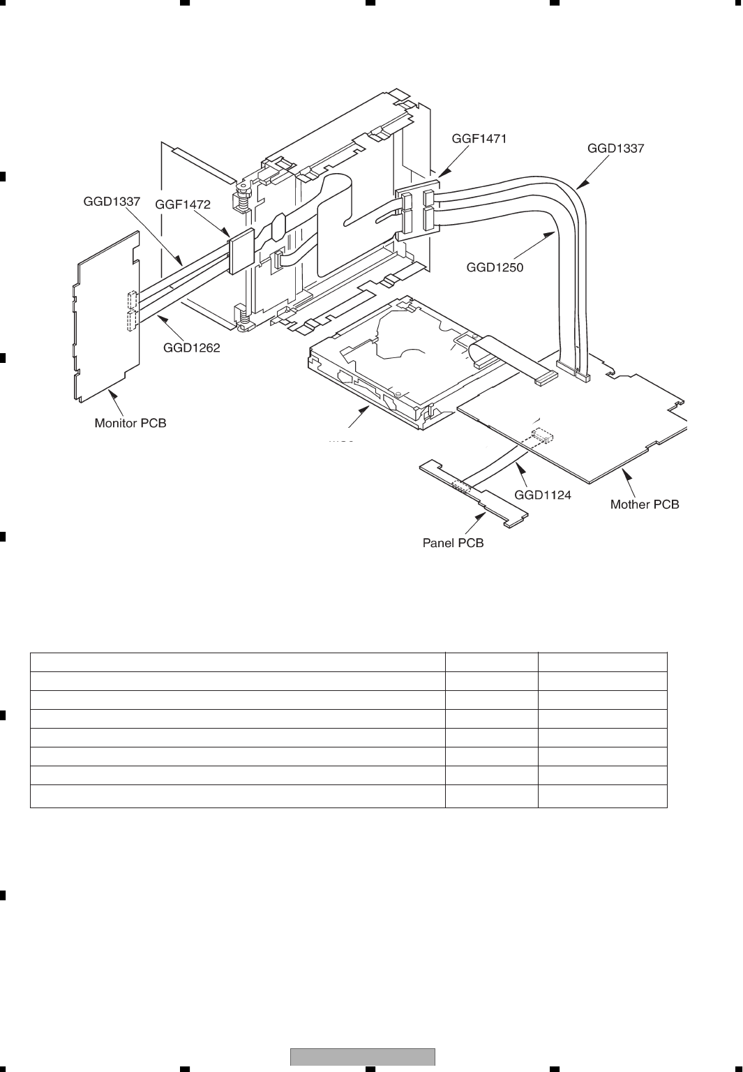
AVH-P6600DVD/UC
142
1234
1234
C
D
F
A
B
E
6. ADJUSTMENT
6.1 JIG CONNECTION DIAGRAM
DVD Mechanism Module(MS-3V1)
Function Name Jig No.
Mother PCB(CN501) <-> Main Unit(CN3801) PCB GGF1471
Mother PCB(CN501) <-> GGF1471 50P FFC GGD1250
Mother PCB(CN502) <-> GGF1471 24P FFC GGD1337
Mother PCB(CN501,CN502) <-> Monitor PCB(CN4461,CN4481) PCB GGF1472
Monitor PCB(CN4461) <-> GGF1472 33P FFC GGD1262
Monitor PCB(CN4481) <-> GGF1472 24P FFC GGD1337
Mother PCB(CN601) <-> Panel PCB(CN5901) 17PFFC GGD1124

AVH-P6600DVD/UC 143
5678
5678
C
D
F
A
B
E
6.2 DVD ADJUSTMENT
1) Precautions
This product uses 5V and 3.3V as standard voltages.
The electrical potential that is the reference for signals,
is not GND, but VREF (approximately 2.2V) and VHALF
(approximately 1.65V).
During product adjustments, if the reference voltage is
mistakenly taken as GND, and a grounding contact is
made, not only would it be impossible to measure the
accurate electrical potential, but also the servo motor
would malfunction, resulting in the application of a
strong impact on the pick up. The following precaution-
ary measures should be strictly adhered to, in order to
avoid such problems.
The reference voltage and GND should not be confused
when using the minus probe of a measurement device.
When an oscilloscope is being used special care should
be taken to make sure that the reference voltage is not
connected to the probe of ch1 (on the minus side),
while the probe of ch2 (on the minus side), is connected
to GND. Further, since the body frame of most mea-
surement devices have the same electrical potential as
the minus side of the probe, the body frame of the mea-
surement device should be set to floating ground.
If the reference voltage is connected to GND by mis-
take, turn the regulator OFF immediately, or turn the
power OFF.
• Remove the filters and wires used for measurements
only after the regulator has been turned OFF.
• After the power supply is turned on, regulator ON the
following adjustment and measurement are promptly
done.
• Whenever the product is in the test mode, the software
will not take any protective action. For this reason,
special care should be taken to make sure that no
mechanical or electrical shock could be applied to the
product when taking measurements in the test mode.
• Whenever the EJECT key is pressed to eject the disk,
no other keys, other than the EJECT key, should be
pressed until the disk eject action has been complet-
ed.
• Press the EJECT key only after the disk has stopped
completely.
• If the product hangs up turn the power OFF immedi-
ately.
•
Laser didoes may be damaged, if the volume switch for
the laser power adjustment of the pick up unit, is turned.
Attention)
• Test mode starting procedure
ACC ON while pressing the BAND/ESC
and ANGLE- keys together.
• Test mode stopping procedure
ACC and Backup OFF.
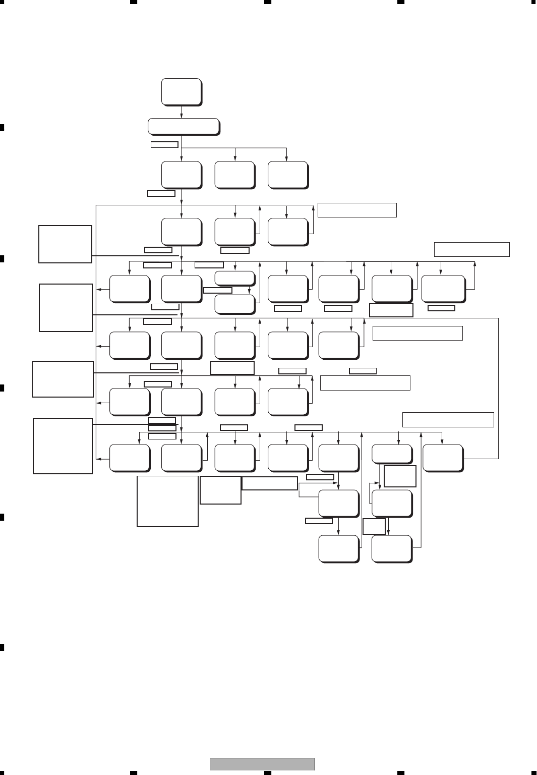
AVH-P6600DVD/UC
144
1234
1234
C
D
F
A
B
E
Test mode In
Set source to DVD
Start test mode
FE
test mode
Power On
Power Off CRG + CRG – LD_ON
Focus close
adjustment
Focus Search
Power Off CRG + CRG –
T.Bal and
other
adjustments
Focus Jump
Power Off
Focus Jump ID Search
Tracking
Open
T. Jump
+/–
ID
specification Track number
specification
Error Rate
measurement
(Note 2)
Reproduction
speed switching
(Note 3)
Power Off CRG –
Tracking close
adjustment
CRG +
Disc Type
(Note 1) Eject
EDC1
mode EDC2
mode
Focus Search
Stop
CRG_HOME
LEFT~ATT EJECT Power off condition
Power on condition
Focus close condition 2
Focus close condition 1
Tracking close condition
ID
Search Start Jump start
0X00 0000
0FFF 00000FFF 0000
1X00 0000
2X00 0000
1FFF 0000
0000 0000
1A00 0000
1100 0000
TEST
FE offset coefficient
TE offset coefficient
AS offset coefficient
ENV offset coefficient
TG offset coefficient
DBALt coefficient
FE MAX level
FE MIN level
AS MAX level
ENV MAX level
FE normalization feature
Spindle gain coefficient
TEMAX level
TEMIN level
TBAL Coefficient(Layer 0)
TBAL Coefficient(Layer 1)
TE normalization feature
(Layer0)
TE normalization feature
(Layer1)
FBAL Coefficient(Layer0)
FBAL Coefficient(Layer1)
Focus Gain Coefficient(Layer0)
Focus Gain Coefficient(Layer1)
Tracking Gain Coefficient(Layer0)
Tracking Gain Coefficient(Layer1)
AS normalization adjustment feature
(Layer0)
AS normalization adjustment feature
(Layer1)
2FFF 0000
Layer L0:2000 0000
Layer L1:2100 0000
Layer L0:4X00 0000
Layer L1:4X00 0000
3000 0000
3FFF 0000
3B00 0000
DVD x 1.3
~
1.6CAV
CD x 4CLV:
4X00 0000
3C00 0000
4A00 0000
Jump+:
4B00 0000
Jump-:
4C00 0000
ID display Track
number
display
4000 0000
4X00 0000
Error Rate
Focus Gain Coefficient(Layer0)
Focus Gain Coefficient(Layer1)
Tracking Gain Coefficient(Layer0)
Tracking Gain Coefficient(Layer1)
AS normalization adjustment feature
(Layer0)
AS normalization adjustment feature
(Layer1)
Operation while key is being pushed.Operation while key is being pushed.
Operation while key is being pushed.Operation while key is being pushed.
2B00 0000 2C00 0000
Note 1: At this stage select the media type. Various settings are carried out
according to the media selection made here.
Note 2: While measurements are being taken, only the operation, for which
the measurement is being taken, is allowed.
Note 3: Reproduction (play) speed is selectable from
Note 4: Gain change: Normal gain -> OEIC=H -> OEIC=H and FEP x 4 AMP ON
DVD : x1.3 1.6CAV,CD : x 4CLV Fixation
: DVD, single-layer
: DVD, dual-layer
: CD
: CD-RW
-Front-End test mode flow chart
1B00 0000 1C00 0000 1D00 0000
LD_ON :1100 0000
LD_OFF:1000 0000
RIGHT
BACK/TEXT
~
RIGHT LEFT
LEFT
REAR
BACK/TEXT
ATT
REAR
REAR
REAR
REAR
REAR,
BACK/TEXT
ATT ANGLE-
ANGLE- ANGLE+
ATT
ATTATT
BACK/TEXT
BACK/TEXT
LEFT
LEFT
LEFT
LEFT
EQ
EQ
EQ
EQ
RIGHT
RIGHT
RIGHT
RIGHT
RIGHT
REAR
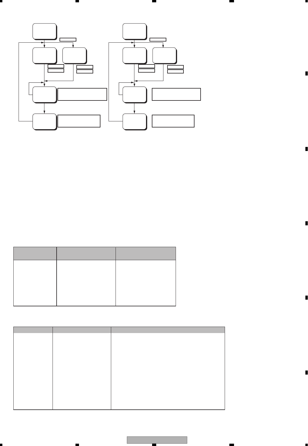
AVH-P6600DVD/UC 145
5678
5678
C
D
F
A
B
E
Layer 0
selected Layer 1
selected
EDC1
mode
ID
designation
RIGHT
ATT ATT
RIGHT,LEFT,
REAR,
BACK/TEXT
RIGHT,LEFT,
REAR,
BACK/TEXT
LEFT LEFT
RIGHT
EDC1 start
Layer 0
selected Layer 1
selected
EDC2
mode
ID
designation
EDC2 start
F-close and F-search cannot be executed, unless LD-ON is set.
0000 0000 0000 0000
0100 0000
1103 0000
Layer0:10** ****
Layer1:11** ****
** ****: ID specification value
Layer0:20** ****
Layer1:21** ****
** ****: Present ID value
0000 0000
1003 0000
0100 0000
1103 0000
0000 0000
1003 0000
Layer0:10** ****
Layer1:11** ****
** ****: ID specification value
Layer0:20** ****
Layer1:21** ****
** ****: Present ID value
The track number designation is selected from the track numbers already prepared for selection.
Switching to cyclic operation is made at step REAR, and the decision is finalized (entered) in step ATT.
For CD: Tracks 1, 4, 10, 11 and 32.
For DVD: Tracks 1, 4, 10, 11, 32, 64 and 100.
Method for designating an ID address:
•
A number of digits are determined through commands RIGHT
and LEFT. Numerical UP/DOWN operations are
performed
through commands REAR and BACK/TEXT. The decision is finalized (entered) with command ATT.
Error status from
DVD micurocomputer Contents Display
0X50 Mecha. error No dislay
0X40 No disc No dislay
0X30 The temperature is abnormal Thermal Protection in Motion
0X20 Read error Error-02-XX
0XE2 Non-playable disc NON-PLAYABLE DISC
0X90
Different region disc
DIFFERENT REGION DISC
0XFF Undefined error Error-FF
Error code of read error(Part of XX)
Error Code Contents Display
0X99 Data cannot read Please confirm the disc
0X80 The address cannot be found Please confirm the disc
0X90 Focus error Please confirm the disc
0X91 Spindle lock NG DVD is stopping because mechanism detected abnormality
0X92 Carrige home NG DVD is stopping because mechanism detected abnormality
0X93 FOK error Please confirm the disc
0X94 ID/Subcode cannot be read Please confirm the disc
0X95 High spindle rotation Please confirm the disc
0X96 Row spindle rotation DVD is stopping because mechanism detected abnormality
0X98 TOC cannot be found Please confirm the disc
0X9A AV chip error DVD is stopping because mechanism detected abnormality
0X9B RecaveryNG(BE) DVD is stopping because mechanism detected abnormality
Display
Error Code List
[If F-close isn't executed within 9 seconds after LD-ON, it switches to LD-OFF automatically.
And even if F-search is executed within 9 seconds after LD-ON, it also switches to LD-OFF.]
Please carry out F-close after carrying out power-off at once and carrying out power-on again,
when carrying out F-close after performing F-search.
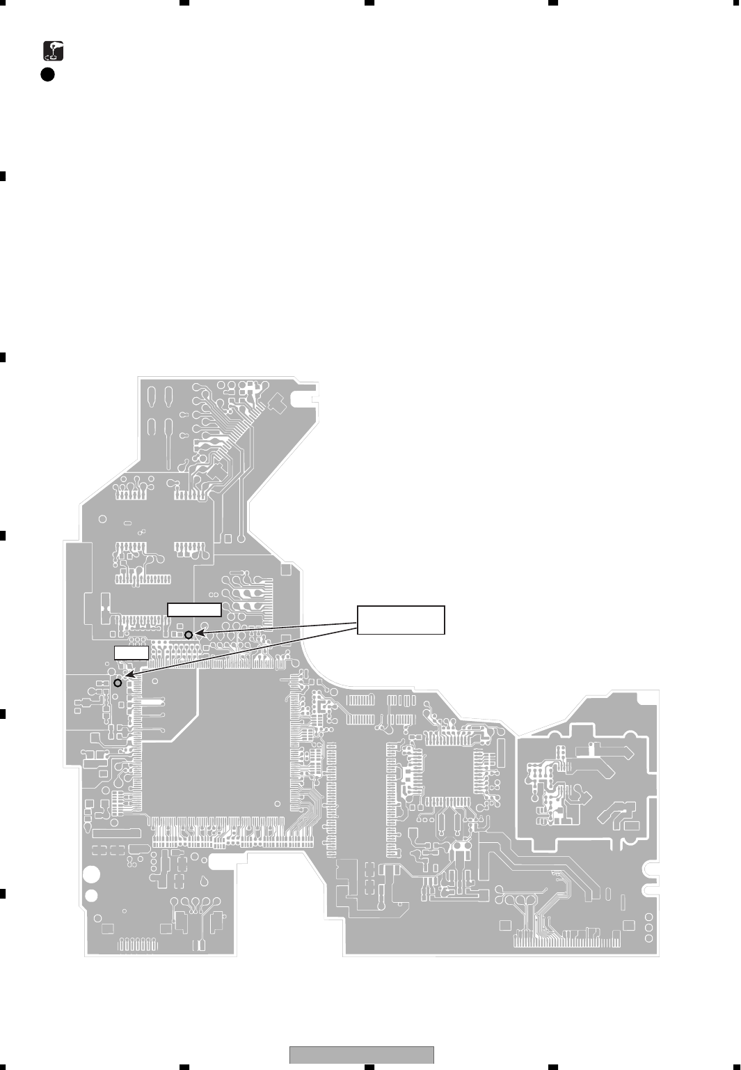
AVH-P6600DVD/UC
146
1234
1234
C
D
F
A
B
E
Oscilloscope
ANAMONI
AGND
If any of the following replacements have been performed on the system, adjustments for pick up,
must be conducted:
1. Pick up unit replacement
2. Spindle motor replacement
3. Carriage chassis replacement
4. Pick up unit main shaft replacement
5. Pick up unit sub-shaft replacement
Measurement device and tools
Disk used
Measurement reference
Measurement point
Connection diagram
DVD core unit
: Oscilloscope
Allen key wrench
40-pin flexible extension (GGD1170)
: GGV1018
: AGND3
: ANAMONI
Skew adjustment
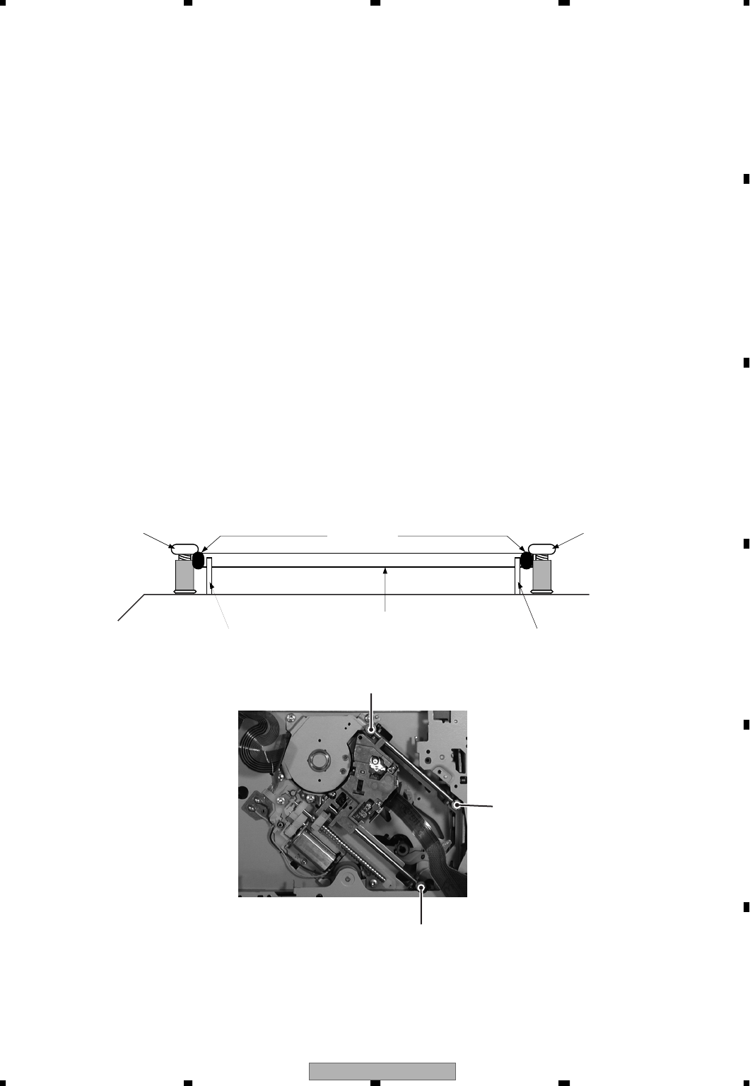
AVH-P6600DVD/UC 147
5678
5678
C
D
F
A
B
E
Apply glue
Shaft
Skew adj. screw Skew adj. screw
Prevent applied glue
from extending beyond this position.
Prevent applied glue
from extending beyond this position.
A
B
C
Symptoms in case of poor adjustment:
Caution: Avoid exposing your eyes to laser beams for a long time.
Preparation for adjustment: Clean both ends of the shafts.
Use brand new skew screws supplied with the service kit CXX1639.
Procedures:
1. Place the DVD mechanism module upside down.
2. After replacing the pickup (by referring to the procedures of "Removing the Pickup."), roughly adjust the three
skew screws through visual check so that the pickup is mounted in parallel to the CRG chassis around the inner
and outer tacks.
3. Connect an oscilloscope as shown in the connecting diagram.
4. Turn on the power of the product. Load the test disc (GGV1018).
5. In the front-end test mode, set the disc type to DVD layer 1. Then, turn on the power. Move the pickup toward
the inner tracks.
6. Turn on the laser diodes.
7. With the focus servo closed, complete all automatic adjustments. Close the tracking servo, and then complete
all automatic adjustments.
8. Observing the RF waveform on the oscilloscope, slightly turn the skew adj. screw C to maximize the RF level.
Next, move the pickup toward the outer track. Slightly turn the skew adj. B to maximize the RF level.
Furthermore, turn the skew adj. screws A and B in the same direction keeping their rotating angles the same
until the RF level becomes the maximum. Lastly, move the pickup toward the inner tracks. Turn the skew
adj. screw C so that the RF level becomes the maximum.Repeat the step 8 three times.
9. Turn off the power in the test mode. After confirming that the disc has stopped, eject the disc.
10. Adjust with a screw rock the shaft and skew adjustment screw to the same state as initial one.
Error efficiency deteriorated: 10
(Optimum value: 10
or lower)
High jitter of the RF signal RF waveform deformed
Unstable operation in tracking closing and servo control
-3 -4
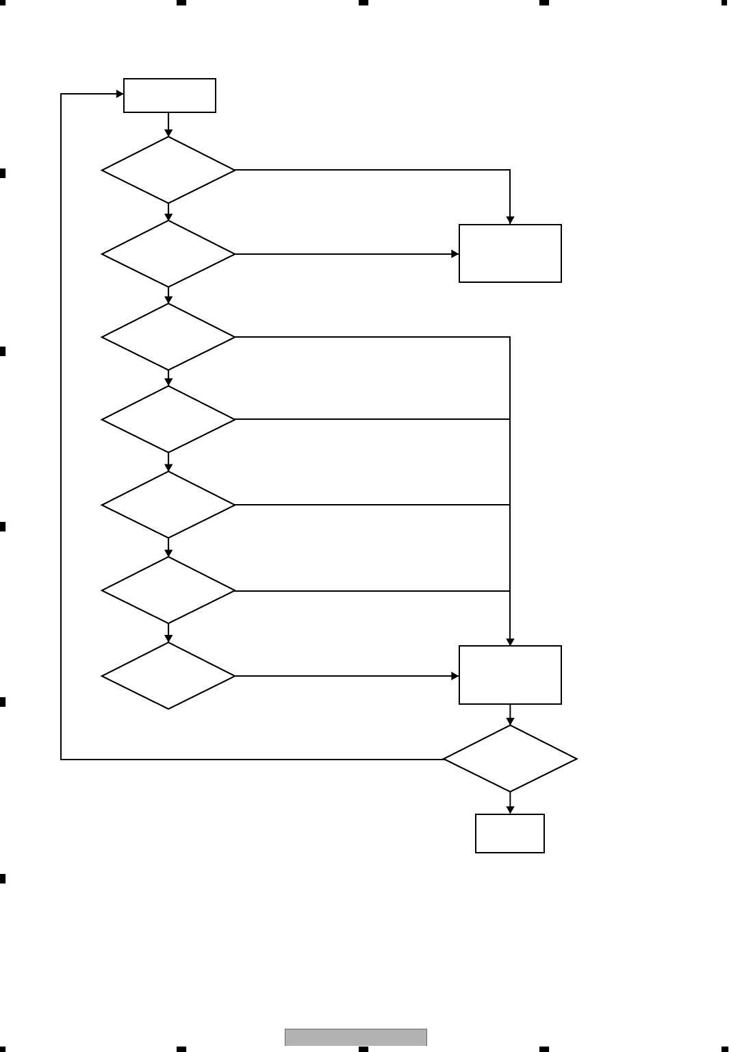
AVH-P6600DVD/UC
148
1234
1234
C
D
F
A
B
E
Are all
power supply voltages?
Execute Check 1
Are all clocks
operating normally?
Execute Check 2
Is the
audio circuit
operating normally?
Execute Check
3
Is the
video circuit
operating normally?
Execute Check
4
Are all
reproduced images
and sounds
normal?
Start
Is SDRAM I/F
operating normally?
Execute Check 5
Repair or replace
any defective unit
All checks normal?
Check
completed
Is the F.E. section
normal?
Go to the F.E.
section check
YES
YES
OK
OK
OK
OK
NO
NO
NG
NG
NG
NG
NG
YES
NO
Back end section check flow chart
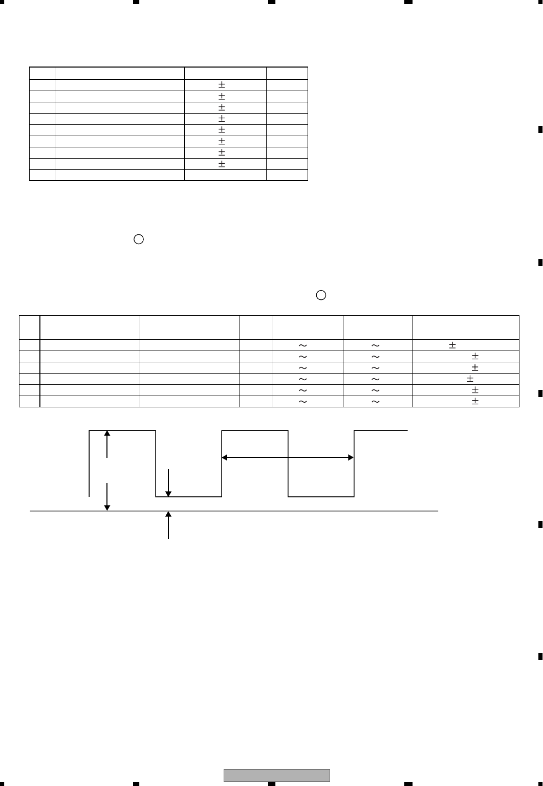
AVH-P6600DVD/UC 149
5678
5678
C
D
F
A
B
E
Reproduce DVD-REF-A1 Title 1.
Verify the voltage of the sensing pin.
Check 1 : Are all power supply voltages?
No.
1
2
3
4
5
6
7
8
9
Verification location
VD8_1/2
-
PGND_1/2
VDD33
-
DGND1/2/3
SRVDD
-
DGND1/2/3
VCC5_1
-
AGND1
AVCC5_1
-
AGND1
VCC33_1/2
-
DGND1/2/3
VCC33_3/4/5
-
DGND1/2/3
VCC15_1/2
-
DGND1/2/3
VCC18
-
DGND1/2/3
Rated value
8.0 0.4
3.3 0.15
3.3 0.15
5.0 0.1
5.0 0.1
3.3 0.15
3.3 0.3
1.5 0.1
****
Unit
V
V
V
V
V
V
V
V
V
Check 2 : Are all clock operating normally?
Reproduce DVD-REF-A1 Title 1
Check Circuit Diagram .
Checks are to conducted with a GND reference.
If locations listed under "verification location 2", can be verified, there will be no need to perform verifications
for the locations listed under "verification location 1."
If the result is not satisfactory, check to see if there are any problems with the resin flux cored solder and other
defects in the applicable line, vicinity of IC 1802 (Circuit Diagram ) and peripheral components.
GND
Rated Value 1 Rated value 3
Rated Value 2
Clock rated values
1
1
No.
1
2
3
4
5
6
Verification location 1
(Sensing pin)
BECLK
EXTCK
EXTCK
MCK33
DACCLK
DACCLK
Verification location 2
IC1501
IC1501
IC1501
IC1501
IC1851
IC1881
170pin
172pin
172pin
92pin
16pin
3pin
Media
ALL
DVD
CD
ALL
DVD
DVD
Rated value 1
2.3V VCC33
2.3V VCC33
2.3V VCC33
2.2V VCC33
2.0V VCC33
2.3V VCC33
Rated value 2
GND 0.8V
GND 0.8V
GND 0.8V
GND 0.8V
GND 0.8V
GND 0.99V
Rated value 3
27MHz 50ppm
36.8640MHz 300ppm
33.8688MHz 300ppm
33.898MHz 300ppm
33.8688MHz 300ppm
33.8689MHz 300ppm
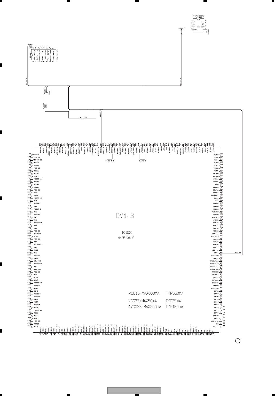
AVH-P6600DVD/UC
150
1234
1234
C
D
F
A
B
E
Circuit Diagram
1
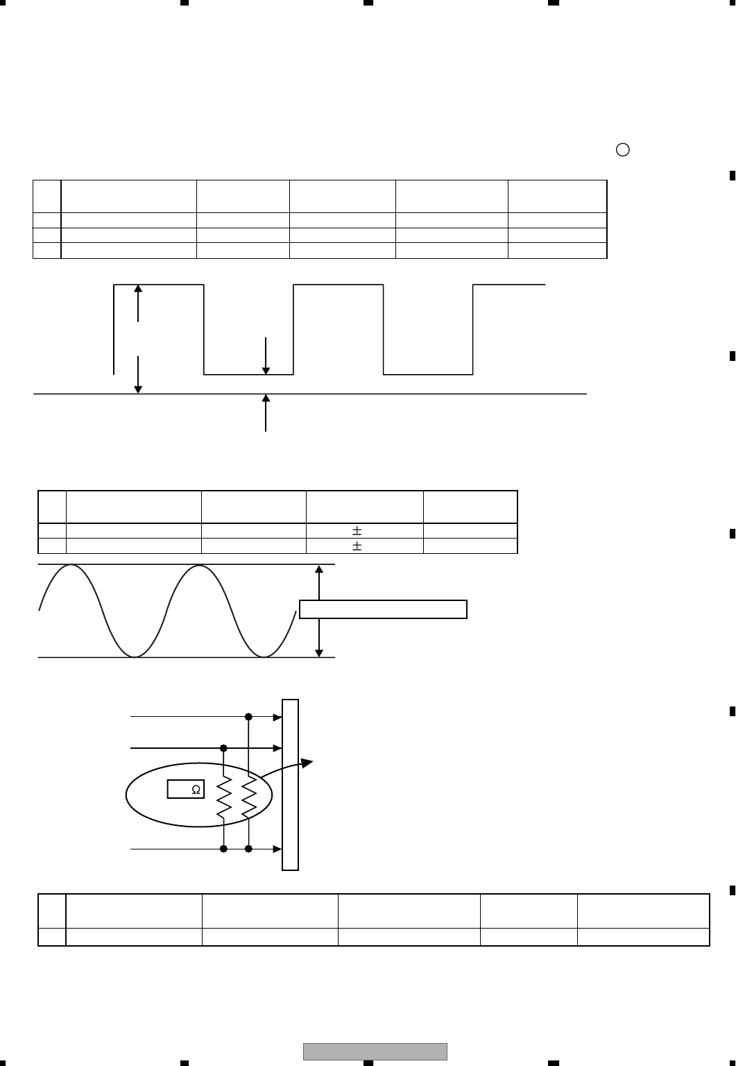
AVH-P6600DVD/UC 151
5678
5678
C
D
F
A
B
E
Check 3 : Is the audio circuit operating normally?
Reproduce DVD-REF-A1 Title 2 Chapter (48k/16-bit 1 kHz/0dB).
Checks are to be conducted using GNDAU1 (sensing pins) as a reference.
If the locations, listed under "verification location 2", can be verified, there is no need to conduct verifications for
the locations listed under "verification location 1."
If the result is not satisfactory, check to see if there are any problems with resin flux cored solder and other
defects in the applicable line, vicinity of major parts stated in the above diagram (Circuit Diagram ) and
peripheral components.
GND
Rated value 1
Rated value 2
Three serial output rated values
No.
1
2
3
Verification location 1
(Sensing pin)
AOUT0
SRCK
LRCK
Verification
location 2
IC1851 2pin
IC1851 1pin
IC1851 3pin
Rated value 1
2.0V and over
2.0V and over
2.0V and over
Rated value 2
0.8V and lower
0.8V and lower
0.8V and lower
Reference
waveform
Waveform 1
Waveform 1
Waveform 1
2
Checks are conducted with the measurement circuit below.
Analog audio outputs (LO and RO) rated values
LO
RO
GNDAU
HOST I/F
Rated value is effective value (rms)
22k
These resistors are inserted.
LO and RO output measurement circuit
No.
6
Verification location 1
(Sensing pin)
IEC958
Verification location 2
CN1551 1pin
Rated value 1
VCC33V
-
0.6V and over
Rated value 2
0.4Vand lower
Reference waveform
Waveform 3
No.
4
5
Verification location 1
(Sensing pin)
LO
RO
Verification
location 2
CN1901 37pin
CN1901 35pin
Reference
waveform
Waveform 2
Waveform 2
Rated value (rms)
1100 150mV
1100 150mV
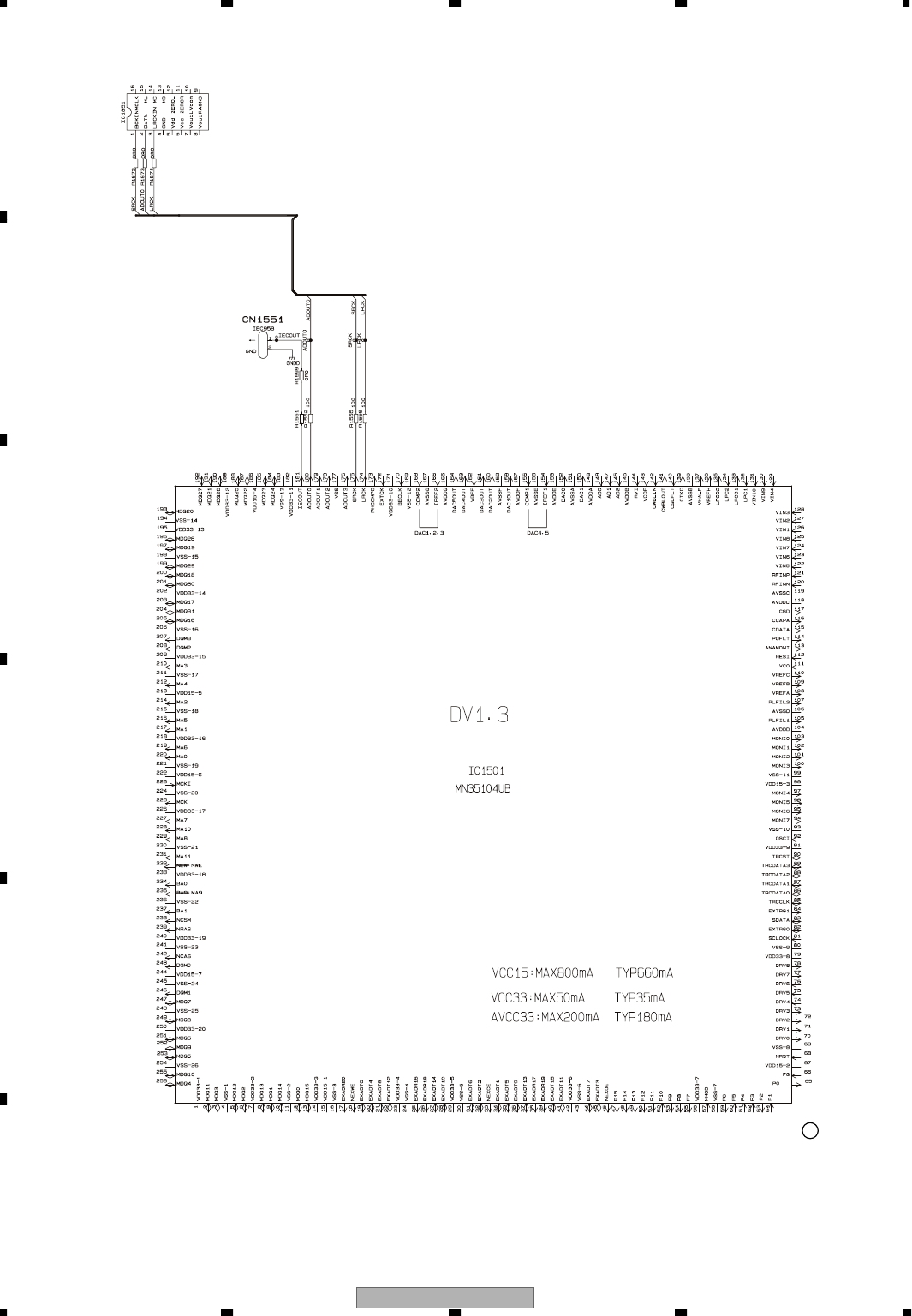
AVH-P6600DVD/UC
152
1234
1234
C
D
F
A
B
E
Circuit Diagram
2
AVH-P6600DVD/UC 153
5678
5678
C
D
F
A
B
E
Check 4 : Is the video circuit operated normally?
Reproduce DVD-REF-A1 Title 2 Chapters (White 1000IRE)
Monitor the output with the oscilloscope, by setting the COMPO signal to a GND reference.
Set the Trigger mode to the TV trigger, and the Trigger line to line-150.
Composite signal white 100% output waveform
If the result is not satisfactory, check to see if there are any problems with resin flux cored solder and other
defects in the applicable line, vicinity of major parts stated in the above diagram (Circuit Diagram ) and
peripheral components.
COMPO Signal
< Method of Readjusting Video Levels >
If the video composite output is not within the range of rated value, the video level is readjusted in the following
method.
Turn the video level adjustment volume (VR1551) to adjust its level to 1.0 0.02Vpp.
Pedestal Level
Rated value
Color brust
Horizontal periodic signal
PEAK
BOTTOM
When the result is not satisfactory,
adjust the level to 1.0 0.02Vpp.
No.
1
Verification location 1
(Sensing pin)
COMPO
Reference waveform
Waveform 4
Rated value
1.0 0.02Vpp
3
Check 5 : Is SDRAM I/F operated normally?
Reproduce DVD-REF-A1 Title 1.
Check Circuit Diagram
Common to all DVD-V adapted modules
Check the conductivity of both the "Verification location 1"and the "Verification location 2."
If the result is not satisfactory, check to see if there are any problems with the resin flux cored solder, parts and
components, in areas where as problem occurs, for the overall sequence of "output" "input" of the checked
location.
3
No.
1
2
3
4
5
6
7
8
9
10
11
12
Verification location 1
IC1570
IC1570
IC1570
IC1570
IC1570
IC1570
IC1570
IC1570
IC1570
IC1570
IC1570
IC1570
25pin
26pin
27pin
60pin
61pin
62pin
63pin
64pin
65pin
66pin
24pin
21pin
Signal name
MA0
MA1
MA2
MA3
MA4
MA5
MA6
MA7
MA8
MA9
MA10
MA11
220pin
217pin
214pin
210pin
212pin
216pin
219pin
227pin
229pin
235pin
228pin
231pin
Verification location 2
IC1501
IC1501
IC1501
IC1501
IC1501
IC1501
IC1501
IC1501
IC1501
IC1501
IC1501
IC1501
Rated value
56 5%
56 5%
56 5%
56 5%
56 5%
56 5%
56 5%
56 5%
56 5%
56 5%
56 5%
56 5%
AVH-P6600DVD/UC
154
1234
1234
C
D
F
A
B
E
No.
13
14
15
16
17
18
19
20
21
22
23
24
25
26
27
28
29
30
31
32
33
34
35
36
37
38
39
40
41
42
43
44
45
46
47
48
49
50
51
52
53
54
55
Verification location 1
IC1570
IC1570
IC1570
IC1570
IC1570
IC1570
IC1570
IC1570
IC1570
IC1570
IC1570
IC1570
IC1570
IC1570
IC1570
IC1570
IC1570
IC1570
IC1570
IC1570
IC1570
IC1570
IC1570
IC1570
IC1570
IC1570
IC1570
IC1570
IC1570
IC1570
IC1570
IC1570
IC1570
IC1570
IC1570
IC1570
IC1570
IC1570
IC1570
IC1570
IC1570
IC1570
IC1570
2pin
4pin
5pin
7pin
8pin
10pin
11pin
13pin
74pin
76pin
77pin
79pin
80pin
82pin
83pin
85pin
31pin
33pin
34pin
36pin
37pin
39pin
40pin
42pin
45pin
47pin
48pin
50pin
51pin
53pin
54pin
56pin
68pin
17pin
18pin
19pin
20pin
16pin
71pin
28pin
59pin
22pin
23pin
Signal name
MDQ0
MDQ1
MDQ2
MDQ3
MDQ4
MDQ5
MDQ6
MDQ7
MDQ8
MDQ9
MDQ10
MDQ11
MDQ12
MDQ13
MDQ14
MDQ15
MDQ16
MDQ17
MDQ18
MDQ19
MDQ20
MDQ21
MDQ22
MDQ23
MDQ24
MDQ25
MDQ26
MDQ27
MDQ28
MDQ29
MDQ30
MDQ31
MCK
XWE
XCAS
XRAS
XCSM
DQM0
DQM1
DQM2
DQM3
BA0
BA1
12pin
9pin
6pin
3pin
256pin
253pin
251pin
247pin
249pin
252pin
255pin
2pin
5pin
8pin
10pin
13pin
205pin
203pin
200pin
197pin
193pin
191pin
187pin
185pin
184pin
188pin
190pin
192pin
196pin
199pin
201pin
204pin
225pin
232pin
242pin
239pin
238pin
243pin
246pin
208pin
207pin
234pin
237pin
Verification location 2
IC1501
IC1501
IC1501
IC1501
IC1501
IC1501
IC1501
IC1501
IC1501
IC1501
IC1501
IC1501
IC1501
IC1501
IC1501
IC1501
IC1501
IC1501
IC1501
IC1501
IC1501
IC1501
IC1501
IC1501
IC1501
IC1501
IC1501
IC1501
IC1501
IC1501
IC1501
IC1501
IC1501
IC1501
IC1501
IC1501
IC1501
IC1501
IC1501
IC1501
IC1501
IC1501
IC1501
Rated value
100 5%
100 5%
100 5%
100 5%
100 5%
100 5%
100 5%
100 5%
100 5%
100 5%
100 5%
100 5%
100 5%
100 5%
100 5%
100 5%
100 5%
100 5%
100 5%
100 5%
100 5%
100 5%
100 5%
100 5%
100 5%
100 5%
100 5%
100 5%
100 5%
100 5%
100 5%
56 5%
22 5%
56 5%
56 5%
56 5%
56 5%
56 5%
56 5%
56 5%
56 5%
56 5%
56 5%
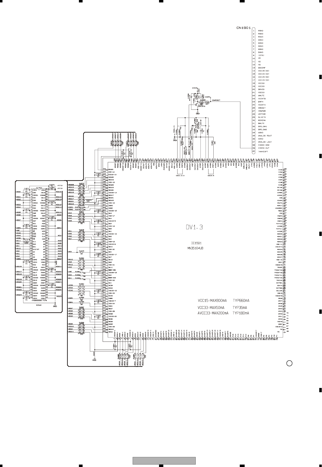
AVH-P6600DVD/UC 155
5678
5678
C
D
F
A
B
E
Circuit Diagram
3
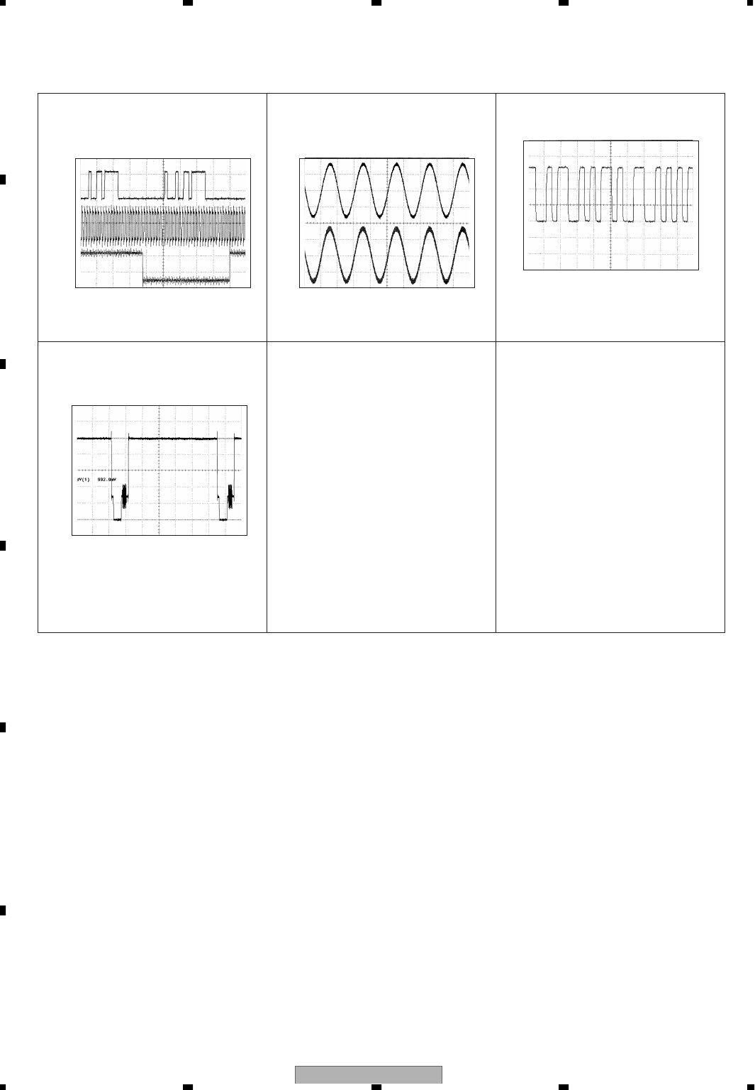
AVH-P6600DVD/UC
156
1234
1234
C
D
F
A
B
E
CH1: AOUT0
CH2: SRCKAV
CH3: LRCKAV
G→
2V/div. 2µs/div.
G→
G→←T
CH1: IEC958 1V/div. 500ns/div.
G→
←T
CH1: LO
CH2: RO
G→
1V/div. 500µs/div.
G→
←T
CH1: COMPO 200mV/div. 10µs/div.
[White 100% output]
G→
Waveform1 Waveform2
Waveform3
Waveform4
Note: Reference voltage VHALF : 1.65V
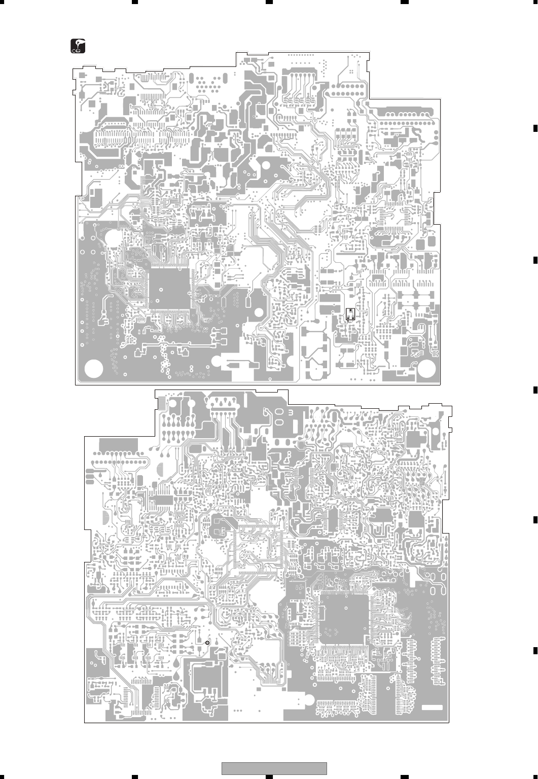
AVH-P6600DVD/UC 157
5678
5678
C
D
F
A
B
E
6.3 MOTHER PCB ADJUSTMENT
VOUT
VR401

AVH-P6600DVD/UC
158
1234
1234
C
D
F
A
B
E
Notes:
1) When the power supply for TC90A64AF-P (IC4001) is OFF, be careful not to apply any voltage to its terminals
except for IIC lines(SDA and SCL). The IIC lines can accept a maximum of 5V.
No Adjustment item Measuring
point
1
2
3
4
5
6
3.3V power supply
verification
2.5V power supply
verification
C4852 hot side
(TP V33) V33 = 3.3V 0.3V
V25 = 2.5V 0.2V
(TP V25)
(TP V5)
(TP V8)
(TP V18)
(TP VM12)
Input
Apply 14.4V
to TP PWRV1
and TP PWRV2.
Apply 14.4V
to TP VVI.
5V power supply
verification V5 = 5.0V 0.3V
Apply 14.4V
to TP VVI.
8V power supply
verification V8 = 8.0V 0.6V
Apply 14.4V
to TP VVI.
18.5V power supply
verification V18 = 18.5V 0.8V
Apply 14.4V
to TP VVI.
-12V power supply
verification VM12 = -12.0V 0.6V
Apply 14.4V
to TP VVI.
Adjusting
point Measuring method
and specs. Remarks
AVH-P6600DVD/UC 159
5678
5678
C
D
F
A
B
E
Step
7Main video level
Input test pin: MS-3V1
....100 IRE
(white 100%),
1.0Vp-p,
(input via 75ohms)
TP20....VIDEO GND
Note : A monitor is the
connected state.
Mother PCB
adjustment Mode
AV
Measuring
instruments Specs Adjusting
point
Input
(input test pin,specs,
other conditions)
Output
(measuring point,
waveform)
Measuring point:
VOUT or V2
Oscilloscope
1.35V ± 0.05Vp-p
Measure between the
sync tip and 100 IRE
(top wave).
Symptoms with
poor adjustment.
Over lever :
Luminance is too high.
Under level :
Luminance is too low.
VR401
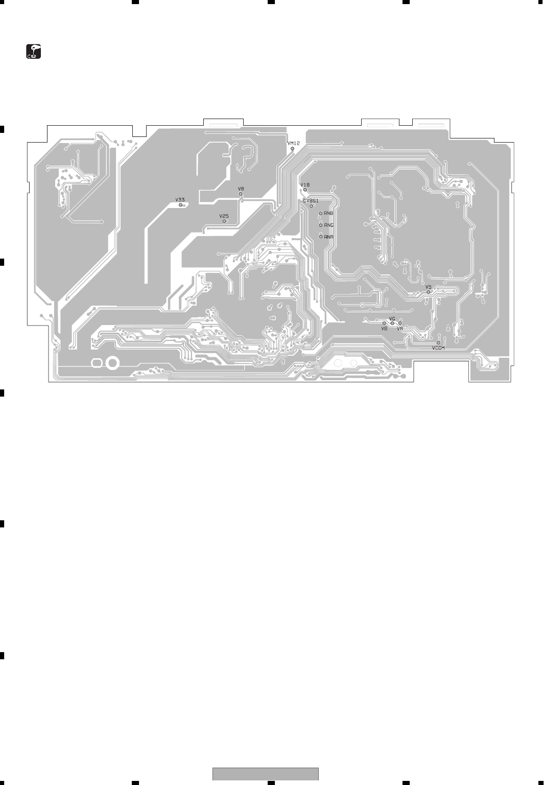
AVH-P6600DVD/UC
160
1234
1234
C
D
F
A
B
E
6.4 MONITOR PCB ADJUSTMENT
Notes: Flicker adjustment is needed when monitor PCB is exchanged.
Monitor PCB (Side B)
- Adjustment Point

AVH-P6600DVD/UC 161
5678
5678
C
D
F
A
B
E
No Adjustment item Input Adjusting
point Measuring method
and specs. Remarks
Measuring
point
Register
setting of
SA22h
D15 - 8
Keep the unit in the
operation mode for
30 minutes or longer.
Adjust so that the flickers
become minimum in all
1Aging Any input
signal
2Flicker
Input a signal for
alternate white
and black lines
to TP ANR,
TP ANG and
TP ANB.
Screen
Notes:
1) When the power supply for TC90A64AF-P is OFF, be careful not to apply any voltage to its terminals except for IIC
lines(SDA and SCL). The IIC lines can accept a maximum of 5V.
2) In the following table, SA**h is a sub-address of TC90A64AF-P.
•Flicker adjustment has been deviated The images flicker.
•Signal for flicker adjustment
EEPROM setting mode
[Operations]
To enter the setting mode, while keeping the TP1420 terminal(IC1401 pin25) at "Low",
turn reset the micro computer. To switch between the adjustment modes, click the joystick.
Flicker adjustment mode
Line adjustment 1 mode
Line adjustment 2 mode
Dimmer parameter setting mode
[ ] button: Used to select a desired adjustment item in each mode
[ ] button: Used to adjust the selected item
[ ] button: Flicker adjustment mode
[ BAND/ESC ] button: alternate white and black lines
[ ] button: Adjust so that the flickers become minimum in all
If it input a signal for alternate
white into TP CVBS1, it is possible.
The luminance level of the input
signal: 50%. In the flicker
adjustment mode, COM DC can be
used as the adjusting point.
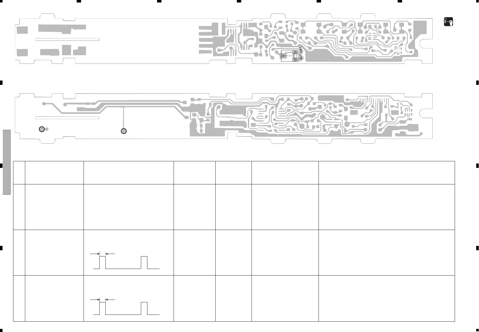
AVH-P6600DVD/UC
162
1234
1234
C
D
F
A
B
E
6.5 INVERTER PCB ADJUSTMENT
FL2
FL1
No
1
2
3
Adjustment item Input signal Measuring method
and specs. Remarks
Measuring
point Adjusting
point
BACK LIGHT
DRIVE
FREQUENCY
FREQUENCY
CHANGE CHECK
FREQUENCY
CHANGE CHECK
Apply 14.4V ± 0.2V
to TP VPPFL1
Apply 5.0V to TP DIMDTY
TP GNDFL1 and TP INVPUL
: GND
Apply wave of 98.0V ± 1kHz to
TP INVPUL
TP:FL1,FL2 VR 5001 48.0 ± 0.1kHz
TP:FL1,FL2
TP:FL1,FL2
49.0 ± 0.5kHz
52.0 ± 0.5kHz
10 ± 2% 5V
0V
Apply wave of 104.0V ± 1kHz to
TP INVPUL
10 ± 2% 5V
0V
100k ohms is connected between TP FL1 and
TP FL2. It acts as the monitor of the waveform
after potential. Don't acts as the monitor of the
TP FL2 directly. (there is a possibility that a
measuring instrument may be destroyed, for
high voltage.) Out of spec., when frequency
change of following may become impossible.
It checks that the waveform after potential is set
to 49 kHz
It checks that the waveform after potential is set
to 52 kHz
AVH-P6600DVD/UC 163
5678
5678
C
D
F
A
B
E
6.6 MONITOR TEST MODE
-EEPROM setting mode
[Operations]
To enter the setting mode, while keeping the EPRTEST terminal(probe land EPRTSTA) at "Low",
turn reset the monitor micro computer. To switch between the adjustment modes, click the joystick.
Flicker adjustment mode
Line adjustment 1 mode
Line adjustment 2 mode
Dimmer parameter setting mode
[ ↑ ↓ ] button: Used to select a desired adjustment item in each mode
[ ←→ ] button: Used to adjust the selected item
Notes:
1) The setting values are written in the EEPROM,and then the read-out data is displayed on the screen.
WRITE and READ operations are processed by the block data of 16 bits.
The total bits for the settings depend on adjusting items.
2) For CS (Check Sum) items, when the settings are changed, the CS value is written in 8 bits by applying
the exclusive OR (XOR). The CS value is first written in the EEPROM, and then the read-out data is displayed.
If the written data is different from the read-out data, the letter color for the read-out data is changed.
Common reverse output center(Reference)
Clock phase adjustment initial value
Don'tcare
Don'tcare
Don'tcare
- Memory items and addresses on the EEPROM(S-93C46BR01-J8T1)
Memory
array
EEPROM
address Bit15 Bit14 Bit13 Bit12 Bit11 Bit10 Bit9 Bit8 Bit7 Bit6 Bit5 Bit4 Bit3 Bit2 Bit1 Bit0
00H Dimmer external light threshold (low)
01H Backlight output (upper limit)
Common reverse output center (COM DC)
γ 3 inflection point (GAMMA 3)
PIP
SA:24h[B15-12]
Output sub contrast R (SUB CON R)
PIP
SA:26h[B15-9]
γ 2 inflection point (GAMMA 2)
PIP
SA:24h[B11-8]
Output clamp DC (RGB BIAS)
PIP
SA:23h[B13-8]
Don'tcare
Dimmer external light threshold (high)
Backlight output (lower limit)
02H Common reserve output amplitude (COM AMP)
PIP
SA:22h[B7-2]
γ 0 inflection point (GAMMA 0)
PIP
SA:23h[B3-0]
γ 1 inflection point (GAMMA 1)
PIP
SA:24h[B7-3]
Output sub contrast B (SUB CON B)
PIP
SA:26h[B7-1]
03H
04H
05H
06H
07H
08H
Bank 1
09H
0AH
0BH
0CH
0DH
0EH
0FH
10H
11H
12H
13H
14H
15H
16H
17H
18H
19H
1AH
1BH
1CH
1DH
1EH
1FH
Don'tcare
Clock phase adjustment (DOT CLK)
PIP SA:2Ah[B3-0]
Sharpness (SHARPNESS)
PIP SA:05h[B2-1]
Don'tcare Don'tcare
Don'tcare Don'tcare
Don'tcare
Don'tcare
Don'tcare
Don'tcare Don'tcare
Sub brightness R after γ circuit (SUB BRI R)
PIP SA:39h[B15-12] Sub brightness B after g circuit (SUB BRI B)
PIP SA:39h[B11-8]
Check sum address
Touch panel X coordinates 1 Touch panel Y coordinates 1
Touch panel X coordinates 2 Touch panel Y coordinates 2
Touch panel X coordinates 3 Touch panel Y coordinates 3
Touch panel X coordinates 4 Touch panel Y coordinates 4
Touch panel X coordinates 5 Touch panel Y coordinates 5
Touch panel X coordinates 6 Touch panel Y coordinates 6
Touch panel X coordinates 7 Touch panel Y coordinates 7
Touch panel X coordinates 8 Touch panel Y coordinates 8
Touch panel X coordinates 9 Touch panel Y coordinates 9
Touch panel X coordinates 10 Touch panel Y coordinates 10
Touch panel X coordinates 11 Touch panel Y coordinates 11
Touch panel X coordinates 12 Touch panel Y coordinates 12
Touch panel X coordinates 13 Touch panel Y coordinates 13
Touch panel X coordinates 14 Touch panel Y coordinates 14
Touch panel X coordinates 15 Touch panel Y coordinates 15
Touch panel X coordinates 16 Touch panel Y coordinates 16
Touch panel X coordinates 17 (Not used) Touch panel Y coordinates 17 (Not used)
Outer most Xmin Outer most Ymin
Outer most Xmax Outer most Ymax
AVH-P6600DVD/UC
164
1234
1234
C
D
F
A
B
E
- EEPROM initial value
Item Meaning initial value(DEC) initial value(hex)
COM_DC Common reverse output center 140 8C
COM_AMP Common reverse output amplitude 30 1E
RGB_BIAS Out clamp DC 00 00
GAMMA0 γ 0 02 02
GAMMA3 γ 3 04 04
GAMMA2 γ 2 04 04
GAMMA1 γ 1 19 13
SUB_CON_R Output sub contrast R 64 40
SUB_CON_B Output sub contrast B 64 40
SUB_BRI_R Sub brightness R after γ circuit 08 08
SUB_BRI_B Sub brightness B after γ circuit 08 08
DOT_CLK Clock phase adjustment 07 07
SHARPNESS Sharpness 03 03
BL_MAX Back light output (Max.) 196 C4
BL_MIN Back light output (Min.) 91 5B
REF_HIGH Dimmer (H) 192 C0
REF_LOW Dimmer (L) 96 60
LUM_HIGH External light (H) 226 E2
LUM_MID External light (M) 135 87
LUM_LOW External light (L) 82 52
BL_HIGH Back light (H) 196 C4
BL_MID Back light (M) 196 C4
BL_LOW Back light (L) 104 68
Touch panel initial value(Before a calibration)
TOUCH_X01-TOUCH_X17 Touch panel compensation (X) 00 00
TOUCH_Y01-TOUCH_Y17 Touch panel compensation (Y) 00 00
GAISYU_MIN_X Outermost X (Min.) 56 38
GAISYU_MAX_X Outermost X (Max.) 243 F3
GAISYU_MIN_Y Outermost Y (Min.) 63 3F
GAISYU_MAX_Y Outermost Y (Max.) 234 EA
Bank 2
External light of dimmer adjustment(H) Back light of dimmer adjustment(H)
External light of dimmer adjustment(M) Back light of dimmer adjustment(M)
External light of dimmer adjustment(L) Back light of dimmer adjustment(L)
Memory
array
EEPROM
address Bit15 Bit14 Bit13 Bit12 Bit11 Bit10 Bit9 Bit8 Bit7 Bit6 Bit5 Bit4 Bit3 Bit2 Bit1 Bit0
20H
21H
22H
23H
-
3FH
Don'tcare
AVH-P6600DVD/UC 165
5678
5678
C
D
F
A
B
E
(1) Flicker adjustment mode
(2) Line adjustment 1 mode
[0 - 255] 140COM DC
Adjustment item
Common reverse output center
Adjustable name
Adjustment
range
Settings or
written data
(DEC)
Adjustment item
Bright (SA22: B7-2)
Contrast (SA25: B7-1)
Common reverse output center
Common reverse output amplitude
Output clamp DC
γ 0 inflection point
γ 3 inflection point
γ 2 inflection point
γ 1 inflection point
Adjustable range
Adjustment
item
Settings or
written data
(DEC)
[0 - 63]
[0 - 127]
[0-255]
[0-63]
[0-63]
[0-15]
[0-15]
[0-15]
[0-31]
30
88
140
30
0
2
4
4
19
BRIGHT
CONTRAST
COM DC
COM AMP
RGB BIAS
GAMMA0
GAMMA3
GAMMA2
GAMMA1
LINE1
AFC3CS
[Displays in each mode]
In the following figures, the letters and numbers surrounded by a large square are for OSD examples.
On the screen, the adjustment names and the settings (or written data) are listed.
The settings (or written data) will change when some adjustments are made in each mode.
(The following examples show the maximum values.)
Notes:
1) CONTRAST data
The CONTRAST data is adjustable, and used as reference data for other adjustment items,
which is not memorized in the EEPROM.
2) BRIGHT and COM AMP data
The BRIGHT and COM AMP adjustments are made by using the same 2-screen IC register
(SA22h B7-2: common reverse output amplitude).
Therefore, adjusting one of the data will change the other one.
Notes: The CONTRAST data is [88], and used as refference data for other adjustment items.
AVH-P6600DVD/UC
166
1234
1234
C
D
F
A
B
E
(3) Line adjustment 2 mode
(4) Dimmer parameter setting mode
[0 - 63]
[0 - 127]
[0 - 127]
[0 - 127]
[0 - 15]
[0 - 15]
[0 - 15]
[0 - 3]
30
88
64
64
8
8
7
BRIGHT
CONTRAST
SUB CON R
SUB CON B
SUB BRI R
SUB BRI B
DOT CLK
SHARPNESS
Adjustment item
Bright (SA22: B7-2)
Contrast (SA25: B7-1)
Output sub contrast R
Output sub contrast B
Sub brightness R after γ circuit
Sub brightness B after γ circuit
Clock phase adjustment
Sharpness
Adjustable name
Adjustment
range
Settings or
written data
(DEC)
Adjustment item
Backlight output (MAX)
Backlight output(MIN)
Dimmer threshold (high)
Dimmer threshold (low)
External light point (high)
External light point (middle)
External light point (low)
Backlight point (high)
Backlight point (middle)
Backlight point (low)
Adjustable range
Adjustment
item
Settings or
written data
(DEC)
[0 - 255]
[0 - 255]
[0 - 255]
[0 - 255]
[0 - 255]
[0 - 255]
[0 - 255]
[0 - 255]
[0 - 255]
[0 - 255]
196
91
192
96
226
135
82
196
196
104
BL MAX
BL MIN
REF H
REF L
LUM H
LUM M
LUM L
BL H
BL M
BL L
DIMMER
LINE2
AFC3CS
AFC3CS
Notes:
1) CONTRAST data
The CONTRAST data is adjustable, and used as reference data for other adjustment items,
which is not memorized in the EEPROM.
2) SUB BRI R and SUB BRI B data
The displayed value or EEPROM written data is different from the setting value for the 2-screen
IC register (TC90A64AF : IC1).
(Before displayed on the screen, the setting value is converted via some software.)
Note: The dimmer point data is memorized in the EEPROM, but not treated as a CS item.
It's because the settings are adjustable by the user.
(MAX)
(TIP)
(MIN)
Displayed value
(adjusting value) (DEC)
15
14
9
8
7
1
0
15
14
9
8
7
1
0
0111
0110
0001
0000
1111
1001
1000
E2PROM written value.
(DEC) 2-screen IC register
setting (BIN)
Notes: The CONTRAST data is [88], and used as refference data for other adjustment items,

AVH-P6600DVD/UC 167
5678
5678
C
D
F
A
B
E
6.7 DOT CLOCK ADJUSTMENT
- Dot Clock Adjustment Mode
[Operations]
. [Dot Clock adjustment mode] starting procedure
Reset start while pressing the [ATT] and [SOURCE] Keys together.
. [Dot Clock adjustment mode] cancellation Monitor's microcomputer OFF.
. The operation after this should use remote control.
. [ u i ] button : Used to select a desired adjustment item in each mode.
. [ r t ] button : Used to adjust the selected item.
[EEPROM : S-93C46BR01-J8T1]
The setting values are written in the EEPROM,and then the read-out data is displayed on the screen.
WRITE and READ operations are processed by the block data of 16 bits.
[Display]
In the following figures,a large square are for OSD examples.
Adjustment item
Clock phase adjustment
''(initial)
Common reverse
output center
Common reverse
output center adjustment
initial
Adjustment range
[0-15]
[0-15]
[0-255]
[0-255]
Display
DOT CLK 15
[FACTORY
7 ]
COM DC
255
[FACTORY 140 ]
* CS(Check Sum)display is not performed.
Dot Clock adjustment mode
Setting or written data
(DEC)

AVH-P6600DVD/UC
168
1234
1234
C
D
F
A
B
E
6.8 TOUCH PANEL TEST MODE
1. Touch panel calibration
1.1 To enter the touch panel calibration mode
While pressing the ATT and BACK keys on the main unit, reset and start the unit.
1.2 Adjustment outline
1) Touch panel effective range check
2) Touch panel 16-point calibration
The touch panel calibration consists of the above two checks.
When finishing the above checks, exit from the calibration mode by turning off the ACC.
1.3 Adjustment screen menu
Top menu
1) Setup TP effective range
The effective range (outer limit) of the touch panel is obtained.
2) Setup calibration
By touching the 16 points on the screen (excluding the last one for finalization), whole screen calibration will be per-
formed.
* Pressing any screen points far from the (+) marks will not allow you to proceed to the next (+) point.
* To stop the calibration, press the ESC key .
3) TP coordinates test (Not used)
For each (+) mark, the OSD coordinates, AD values, and coordinates before and after correction are displayed.
4) Calibration test
For touched points, coordinates before and after correction are displayed.
5) Data initialize
The range and the calibration data are returned to an initial value.
1.4 Cautions on adjustment
At the TP effective range check, never use a pointed thing like nails to trace the edge of the screen. Use a round-
headed thing (R1.6 or more) and push the screen softly to prevent the screen from being damaged.
1.5 Detailed adjustment procedures
On the main unit or the remote control, use the UP/DOWN keys to select the check item from the menu,
and then press the ENTER key.
When finishing both checks, turn off the ACC to exit from the calibration mode.
0 1 2 3 4 5 6 7 8 9 0 1 2 3 4 5 6 7 8 9 0 1 2 3 4 5 6 7 8 9 0
0
1
2
3
4
5
6
7
8
9
0
1
2
3
4
5
6
7
8
9
# # # TOUCH-PANEL TEST # # #
[ / ]
[ENTER]
[ACC OFF] Cursor movement
Menu selection
End of test
1. Setup TP effective range
2. Setup calibration
3. TP coordinates test
4. Calibration test
5. Data initialize
AVH-P6600DVD/UC 169
5678
5678
C
D
F
A
B
E
(1) Setup TP effective range
The checking data for the edge of the TP screen is memorized in the EEPROM.
[Display]
* The range (before) is the data that has been stored in the EEPROM before calibration.
* The range (after) is the data that will be stored after calibration. (Default: min 120, max 180)
Checking result - OK
Checking result - NG
0 1 2 3 4 5 6 7 8 9 0 1 2 3 4 5 6 7 8 9 0 1 2 3 4 5 6 7 8 9 0
0
1
2
3
4
5
6
7
8
9
0
1
2
3
4
5
6
7
8
9
# # Setup TP effective range # #
The present of touch - panel
effect range (before,after)
X min : ( . )
Y min : ( . )
X max : ( . )
Y max : ( . )
< CAUTION >
Please touch around panel.
[ENTER] Check the Value
0 1 2 3 4 5 6 7 8 9 0 1 2 3 4 5 6 7 8 9 0 1 2 3 4 5 6 7 8 9 0
0
1
2
3
4
5
6
7
8
9
0
1
2
3
4
5
6
7
8
9
[ENTER] Return to Menu
O K
0 1 2 3 4 5 6 7 8 9 0 1 2 3 4 5 6 7 8 9 0 1 2 3 4 5 6 7 8 9 0
0
1
2
3
4
5
6
7
8
9
0
1
2
3
4
5
6
7
8
9
[ENTER] Return to Menu
N G

AVH-P6600DVD/UC
170
1234
1234
C
D
F
A
B
E
[Adjustment steps]
1) Trace the edge of the screen along the monitor resin frame with a round-headed thing (R1 or more) to obtain the
coordinates (as shown by a white line in the right figure).
Caution:
Never use a pointed thing like nails when tracing the edge of the screen. Use a round-headed thing (R1 or more) and
push the screen softly to prevent the screen from being damaged
2) Press the ENTER key on the main unit or remote control.
If the checking result is within the allowable range, "OK" will be displayed in the center of the screen. If not, "NG" will
be displayed.
* When the checking result exceeds the default values by 10% or more, "NG" is displayed on the screen.
3) To return to the top menu, press the ENTER key on the main unit or remote control.
Default data list
Coordinates Min. Max.
X 56 243
Y 63 234
* The black frame is the outer resin frame of the monitor.
AVH-P6600DVD/UC 171
5678
5678
C
D
F
A
B
E
(2) Setup calibration
By touching the (+) marks on the screen one by one, their calibration results are memorized in the EEPROM.
[Display]
* Pressing any screen points far from the (+) marks is ignored.
* In the above figure, the numbers after (+) (from 1 to 17) shows the order where the cursor moves.
* When the 17th (+) mark is pressed, "FINISHED" will be displayed.
[Adjustment steps]
1) Push the 16 (+) marks one by one by following the cursor's movement. (The plus marks appear in turn on the
screen. When you push one properly, the next mark will be displayed.)
2) Lastly, push the 17th (+) mark. "FINISHED" will be displayed in the center of the screen.
3) To return to the top menu, press the ENTER key on the main unit or remote control.
* If you press the ESC key during adjustment, the screen mode will return to the top menu without any adjust-
ment results stored.
0 1 2 3 4 5 6 7 8 9 0 1 2 3 4 5 6 7 8 9 0 1 2 3 4 5 6 7 8 9 0
0
1
2
3
4
5
6
7
8
9
0
1
2
3
4
5
6
7
8
9
+13
+14
+15
+16
+12
+11
+10
+9
+5
+6
+7
+8
+17
+4
+3
+2
+1
0 1 2 3 4 5 6 7 8 9 0 1 2 3 4 5 6 7 8 9 0 1 2 3 4 5 6 7 8 9 0
0
1
2
3
4
5
6
7
8
9
0
1
2
3
4
5
6
7
8
9
[ENTER] Return to Menu
FINISHED

AVH-P6600DVD/UC
172
1234
1234
C
D
F
A
B
E
(3) Calibration test
For touched points, coordinates before and after correction are displayed.
[Display]
* The 16 (+) marks are displayed on a screen.
[Adjustment steps]
1) For touched points, coordinates before and after correction are displayed.
2) To return to the top menu, press the ENTER key on the main unit or remote control.
0 1 2 3 4 5 6 7 8 9 0 1 2 3 4 5 6 7 8 9 0 1 2 3 4 5 6 7 8 9 0
0
1
2
3
4
5
6
7
8
9
0
1
2
3
4
5
6
7
8
9
# # Calibration test # #
panel X_before =
panel Y_before =
panel X_after =
panel Y_after =
[ENTER] Return to Menu +
(4) TP data initialize
The range and the calibration data are returned to an initial value.
[Display]
: Setup complete.
The mark will disappear when initialization is complete.
[Adjustment steps]
1) [ ] : The range data initialize.
2) To return to the top menu, press the ENTER key on the main unit or remote control.
0 1 2 3 4 5 6 7 8 9 0 1 2 3 4 5 6 7 8 9 0 1 2 3 4 5 6 7 8 9 0
0
1
2
3
4
5
6
7
8
9
0
1
2
3
4
5
6
7
8
9
# # TP data initialize # #
[ ] Range init
[ ] Calibration init
[ENTER] Memu selection
[ ] : The calibration data initialize.

AVH-P6600DVD/UC 173
5678
5678
C
D
F
A
B
E
6.9 FREQUENCY CHECK FOR CLOCK
1. PCL output
In the normal operation mode (with the detachable panel installed, the ACC switched ON, the standby mode can-
celled), shift the TESTIN terminal (Pin56) to H. The clock signal is output from the CLKOUT terminal (Pin 36).
The frequency of the clock signal is 18.874368MHz±754Hz that is the fundamental frequency..
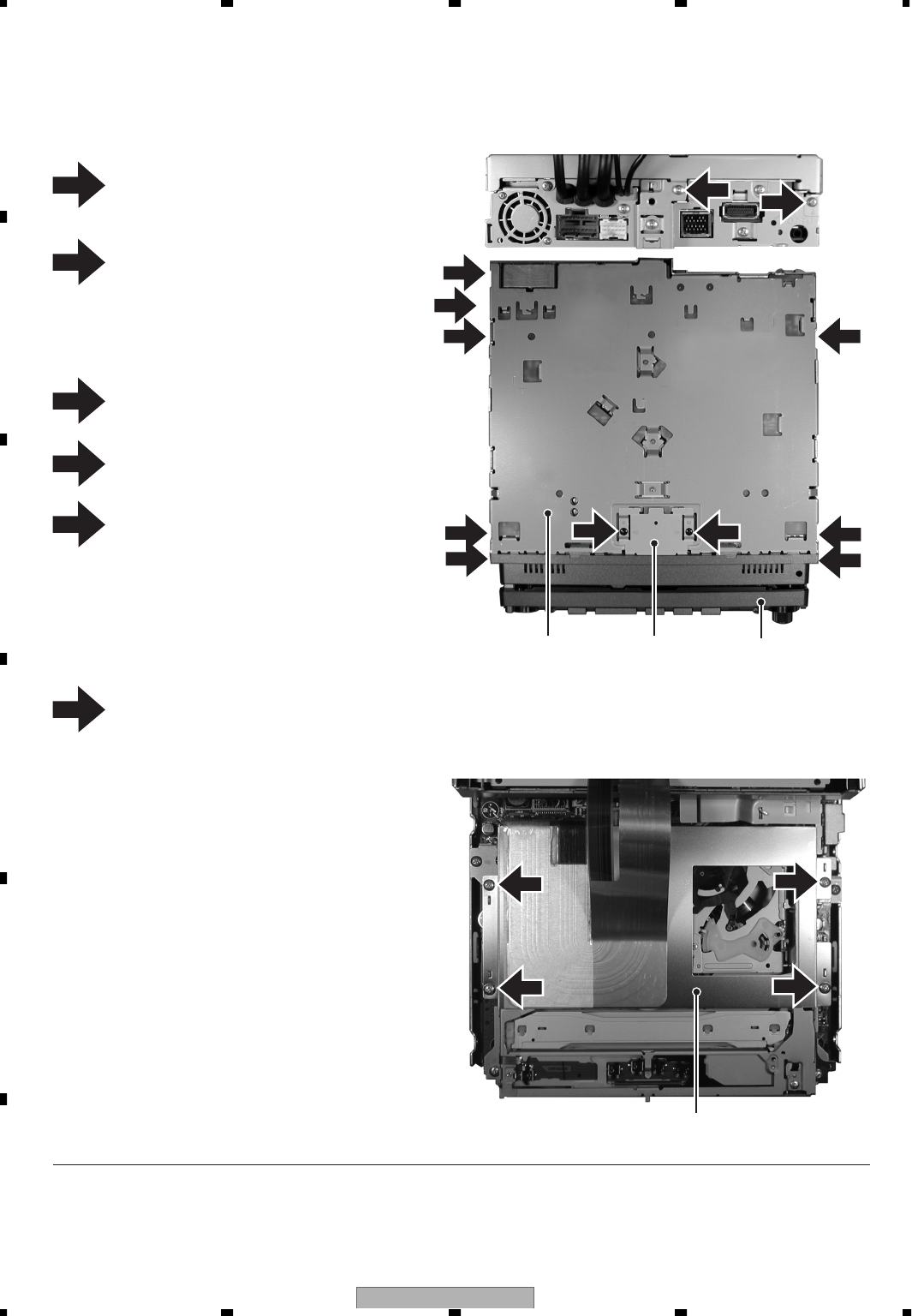
AVH-P6600DVD/UC
174
1234
1234
C
D
F
A
B
E
7. GENERAL INFORMATION
7.1 DIAGNOSIS
7.1.1 DISASSEMBLY
Fig.1
- Removing the Grille Assy (Fig.1)
Fig.2
- Removing the Case
5
22
Grille Assy
6
66
6
Bracket
5
Case
3
3
3
3
3
1Remove the two screws and then remove
the Holder.
Disconnect the connector.
11
Holder
2Remove the two screws and then remove
the Grille Assy.
3Remove the five screws.(Fig.1)
4Remove the screw.(Fig.1)
6Remove the four screws. (Fig.2)
Disconnect the connector and then remove the
Bracket. (Fig.2)
Remove the Case.(Fig.1)
Note) Inside the product there is a flexible substrate
that connects the Case and the Bracket.
Be very careful and do not give it a strong pull
when removing the Case, otherwise it may
be torn.
5Remove the two screws and then remove
the Case.(Fig.1)
4
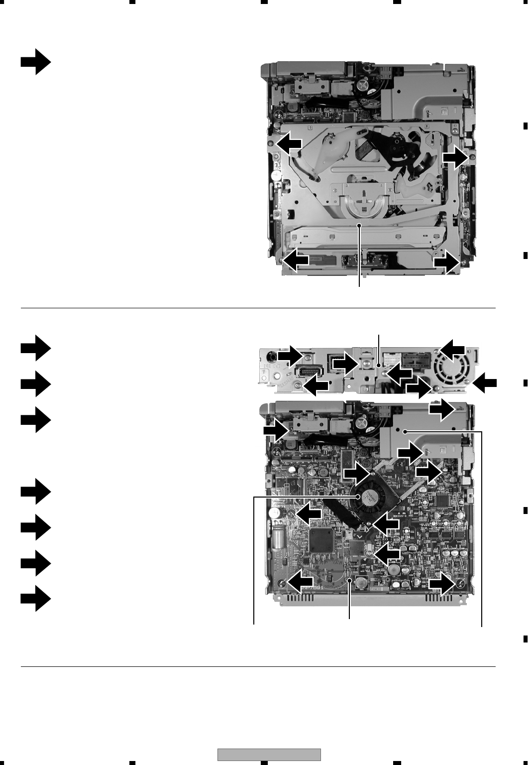
AVH-P6600DVD/UC 175
5678
5678
C
D
F
A
B
E
Fig.3
- Removing the Tuner Unit (Fig.4)
1
1
DVD Mechanism Module
1
1
5
5
4
Fig.4
6
6
3
7
6
6
6
Tuner Unit
1
- Removing the DVD Mechanism Module (Fig.3)
Remove the four screws.
Disconnect the connector and then remove the
DVD Mechanism Module.
5
1
4
Bracket
Holder
1Straighten the tabs at two locations
indicated.
2Remove the screw and then remove
the Holder.
4Remove the two screws.
6Straighten the tabs at five locations
indicated.
7Remove the screw and then remove
the Tuner Unit
5Remove the four screws and then remove
the Bracket.
1
3
5
2
3Remove the two screws.
Disconnect the connector and then remove the
Fan Motor.
Fan Motor
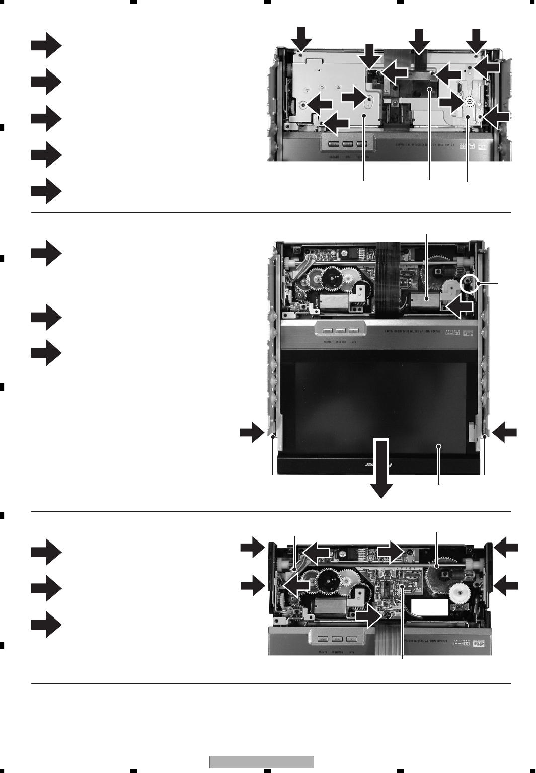
AVH-P6600DVD/UC
176
1234
1234
C
D
F
A
B
E
Fig.5
- Removing the Case (Fig.5)
Remove the two screws and then remove
the Lever.
1
4
Holder
1
Fig.6
1
Motor Unit
- Removing the Display Assy (Fig.6)
1
55
2
Case
Remove the three screws and then remove
the Holder.
2
Holder Holder
Display Assy
22
Remove the two screws and then remove
the two Holders.
2
Pull out the Display Assy in the arrow
indicated direction.
Note) When reassembling, hold the switch down
with tweezers or the like and put the Display Assy
back to the Chassis. Otherwise, the switch may be
damaged and not function properly.
3
Fig.7
1
Bracket Shaft Unit
2
2
2
2
Main Unit
33
3
- Removing the Main Unit (Fig.7)
Remove the screw and then remove
the Bracket.
1
Remove the four screws and then
remove the Shaft Unit.
2
3
1
Remove the screw.
Disconnect the connector and then remove
the Motor Unit.
Remove the three screws.
Disconnect the connector and then remove
the Main Unit.
3
Swit
c
5
53
2
2
5
Lever
Remove the screw.
4
Disconnect the connector.
3
Remove the five screws and then remove
the Case.
5
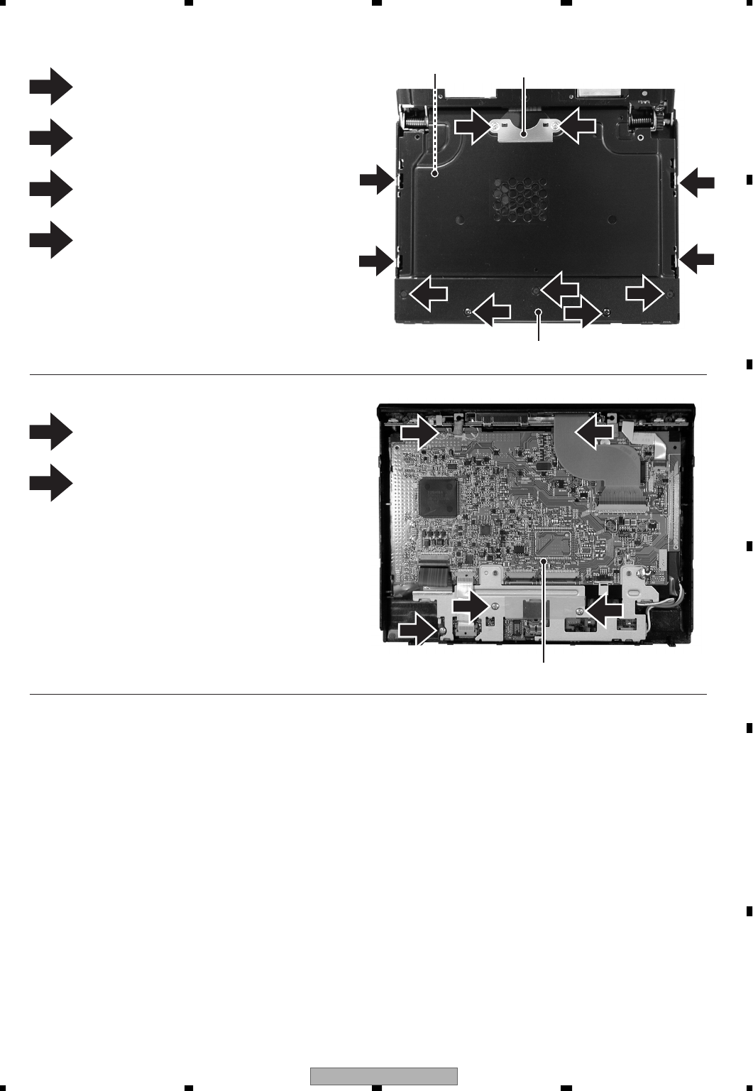
AVH-P6600DVD/UC 177
5678
5678
C
D
F
A
B
E
Fig.8
- Removing the Display Assy (Fig.8)
1
2
11
2
Display Assy
2
4
Fig.9
1
Monitor PCB
2
2
1
- Removing the Monitor PCB (Fig.9)
Straighten the tabs at two locations indicated.
1
2
Cover Unit
Holder
4
4
4
4
2
Remove the two screws and then remove
the Holder.
Remove the three screws.
Remove the four screws.
33
3Remove the two screws and then remove
the Cover Unit.
Disconnect the connector and then remove
the Display Assy.
Remove the three screws.
Disconnect the connector and then remove
the Monitor PCB.
2
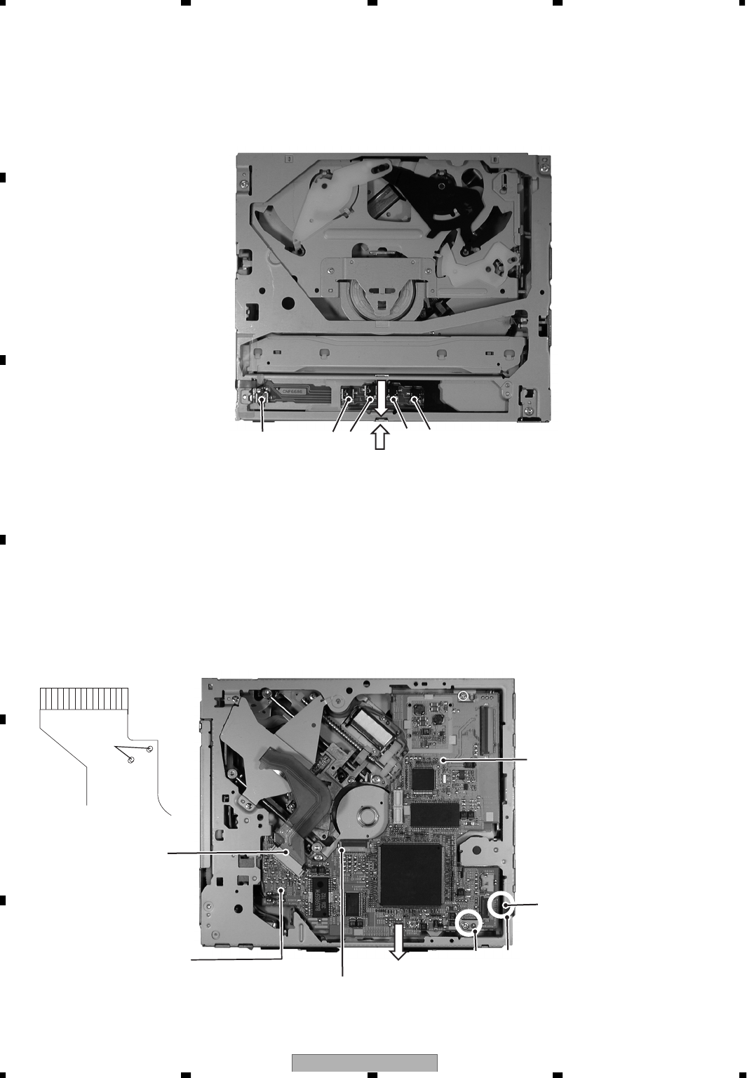
AVH-P6600DVD/UC
178
1234
1234
C
D
F
A
B
E
- Precautions on handling the mechanism module
1. Hold the upper and main frames.
2. Do not hold the front portion of the upper frame. It is a delicate part.
3. Do not touch the switches on the top panel.
4. Be careful not to catch the flexible cables.
Do not touch here. Do not touch here.
Do not hold this delicate portion.
- Removing the module pc board
Load motor
leads and clamp SW leads
Connector
(for 8/12 detection flexible cable)
Connector
(for pickup flexible cable)
Connector
(for CRG flexible cable)
Short here.
A
BC
Module pc board
1. Set the mechanism to the lock position (disc load standby position).
2. Place the mechanism module upside down.
3. Short the two lands on the pickup flexible cable as shown below.
4. Be sure to disconnect the pickup flexible cable and the CRG flexible cable from the connectors
to protect them from damages.
5. Remove solder from the load motor leads and clamp SW leads.
6. Loosen the two fixing screws. Lift the position A of the module pc board lightly and move it
in the direction B to remove it. Be careful not to damage the flexible cable C.
7. Disconnect the 8/12 detection flexible-cable from the connector.
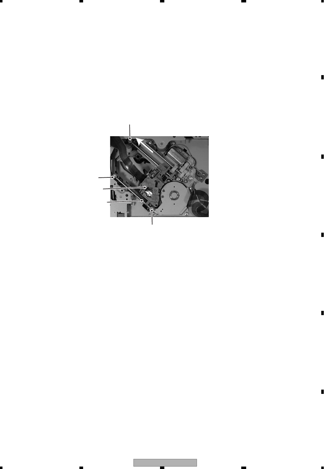
AVH-P6600DVD/UC 179
5678
5678
C
D
F
A
B
E
-Removing the pickup unit
1. Remove the module pc board in accordance with the procedure of "Removing the module pc board.”
2. While holding the pickup case, remove the skew screw (main).
3. Lifting the end of the pickup rack, slide the main shaft, and remove the pickup unit.
Notes:
Replacing the pickup unit requires the skew adjustment.
Remove glue from both ends of the main and sub shafts, and skew stud.
Do not reuse the old skew screw. Be sure to use a brand-new skew screw supplied with a new pickup unit.
Fix the skew screw with glue (GYL1001) after adjustment.
Sub shaft
Pickup unit
Skew screw
Skew screw (main)
Skew screw
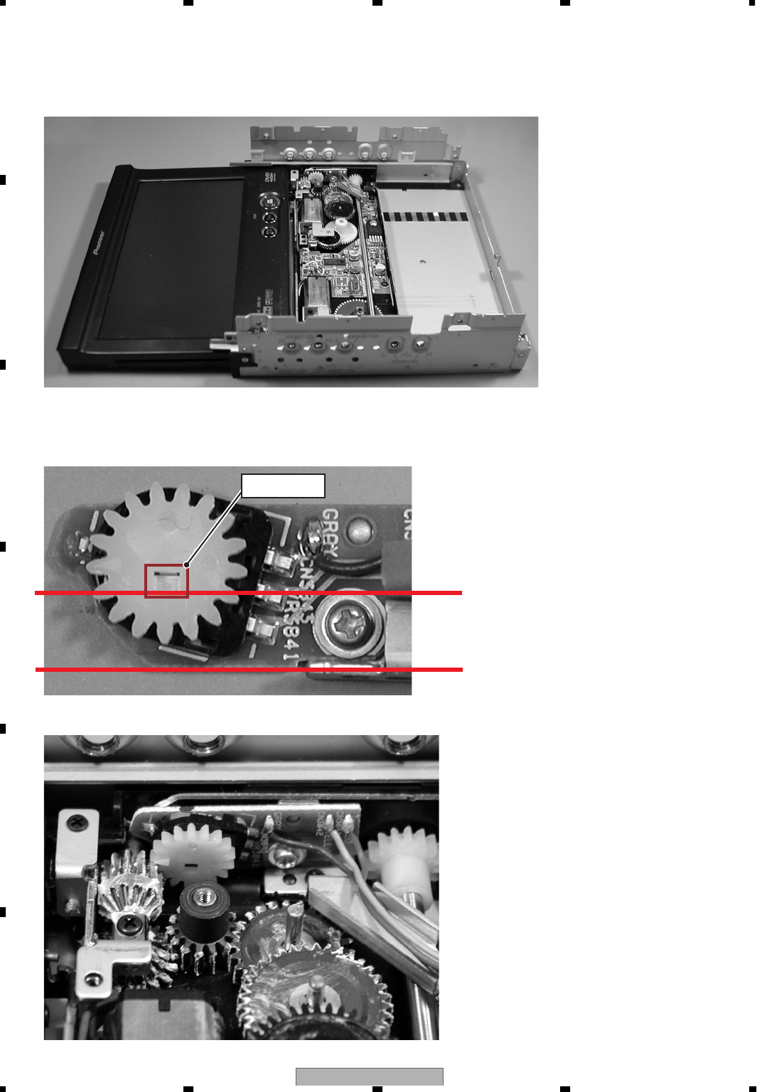
AVH-P6600DVD/UC
180
1234
1234
C
D
F
A
B
E
- How to install the Volume Unit fo the Drive Unit
When install the Volume Unit, adjust the positioning of the rotating angle of the gear.
1. Set the Monitor Unit horizontally with the Main Unit of the Drive Unit.
2. When install the gear unit, rotate the gear by hand until the square box of the gear keeps in a horizontal
position like the figure below.
*Gap of one teeth is acceptable.
Square box
AVH-P6600DVD/UC 181
5678
5678
C
D
F
A
B
E
7.1.2 PCB LOCATIONS
COMPOUND UNIT(A)
COMPOUND UNIT(B)
AVH-P6600DVD/UC
182
1234
1234
C
D
F
A
B
E
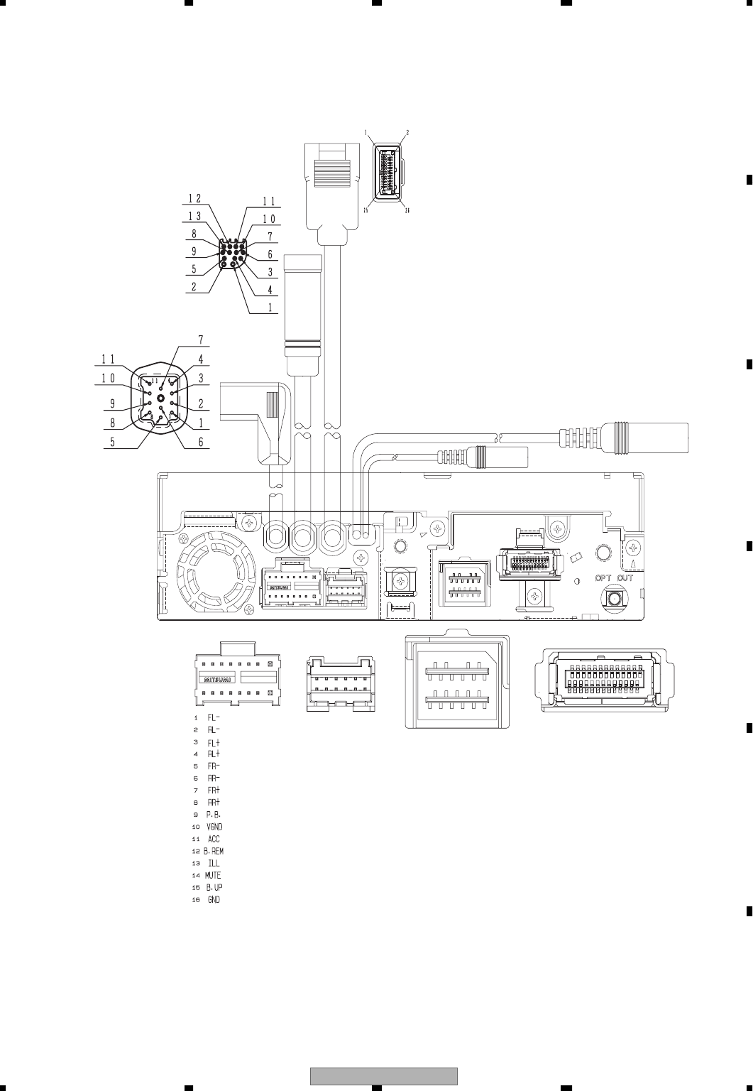
AVH-P6600DVD/UC 183
5678
5678
C
D
F
A
B
E
7.1.3 CONNECTOR FUNCTION DESCRIPTION
M5x6MAX
M4x6MAX
AVH-P6600DVD/UC
AVH-P6600DVD/EW
OPT-OUT
WIRED REMOTE INPUT
GUIDE SP OUTPUT
2
1
1
4
10 5
15 11
16
21
26
25
1
2
1
2
11
12
15
16
1 : FL
2 : FLGND
3 : FR
4 : FRGND
5 : RL
6 : RLGND
7 : RR
8 : RRGND
9 : SWL
10 : SWLGND
11 : SWR
12 : SWRGND
1 : CE1
2 : D1
3 : D0
4 : DGND
5 : SL
6 : CK
7 : OSCGND
8 : ROMVDD
9 : RDSCK
10 : AGND
11 : NC
12 : LDET
13 : NC
14 : RDSDATA
15 : RDSLOCK
16 : RFGND
17 : CE2
18 : NC
19 : NC
20 : RDSLO
21 : BU14
1. BUS+
2. GND
3. GND
4. NC
5. BUS-
6. GND
7. BUS L+ OUTPUT
8. ASENB
9. BUS R+ OUTPUT
10. BUS R- OUTPUT
11. BUS L- OUT PUT
1. COMP GND
2. COMP
5. IP_SEL1
4. IP_SEL2
12. AV_ON
6. LED_V
7. GND
10. REMIN
11. NEW AV SENS
1 : CCR
2 : CCG
3 : CCB
4 : CCSYNC
5 : GNDSIG
6 : DVDVBS
7 : GNDDVD
8 : YS
9 : NC
10 : CCAUL
11 : CCAUR
12 : GNDAU
13 : ONSEI+
14 : ONSEI-
15 : REAUR
16 : REAUL
17 : GNDRAU
18 : CCREM
19 : DSEN
20 : TVON
21 : GION
22 : MONON
23 : VSW5
24 : HTXD
25 : HRXD
26 : GNDD
1 : VGND3
2 : BCAM
3 : µGND
4 : VGND2
5 : AUXV
6 : PRGSW
7 : AGND2
8 : AUXR
9 : AUXL
10 : NC
11 : NC
12 : BGSENS
13 : NC
14 : NC
15 : NC
16 : NC
17 : BEGND
18 : TUNR
19 : TUNL
20 : NC
21 : VGND1
22 : REARV
23 : NC
24 : AGND1
25 : REARR
26 : REARL
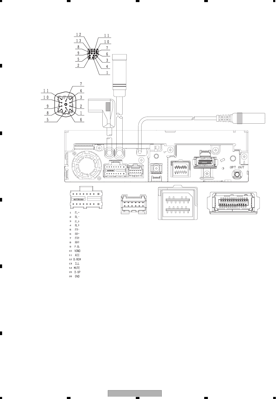
AVH-P6600DVD/UC
184
1234
1234
C
D
F
A
B
E
M5x6MAX
M4x6MAX
AVH-P6650DVD/RC
AVH-P6650DVD/RD
OPT-OUT
WIRED REMOTE INPUT
2
1
1
4
10 5
15 11
16
21
26
25
1
2
11
12
1 : FL
2 : FLGND
3 : FR
4 : FRGND
5 : RL
6 : RLGND
7 : RR
8 : RRGND
9 : SWL
10 : SWLGND
11 : SWR
12 : SWRGND
1. BUS+
2. GND
3. GND
4. NC
5. BUS-
6. GND
7. BUS L+ OUTPUT
8. ASENB
9. BUS R+ OUTPUT
10. BUS R- OUTPUT
11. BUS L- OUT PUT
1. COMP GND
2. COMP
5. IP_SEL1
4. IP_SEL2
12. AV_ON
6. LED_V
7. GND
10. REMIN
11. NEW AV SENS
1
2
15
16
1 : VGND3
2 : BCAM
3 : µGND
4 : VGND2
5 : AUXV
6 : PRGSW
7 : AGND2
8 : AUXR
9 : AUXL
10 : NC
11 : NC
12 : BGSENS
13 : NC
14 : NC
15 : NC
16 : NC
17 : BEGND
18 : TUNR
19 : TUNL
20 : NC
21 : VGND1
22 : REARV
23 : NC
24 : AGND1
25 : REARR
26 : REARL
1 : CE1
2 : D1
3 : D0
4 : DGND
5 : SL
6 : CK
7 : OSCGND
8 : ROMVDD
9 : RDSCK
10 : AGND
11 : NC
12 : LDET
13 : NC
14 : RDSDATA
15 : RDSLOCK
16 : RFGND
17 : CE2
18 : NC
19 : NC
20 : RDSLO
21 : BU14
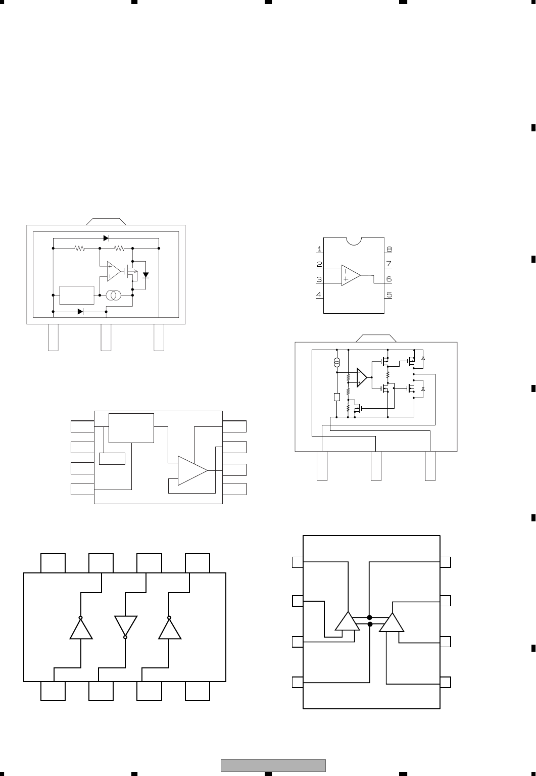
AVH-P6600DVD/UC 185
5678
5678
C
D
F
A
B
E
7.2 PARTS
7.2.1 IC
123
VIN
VOUT
GND
Reference
Voltage
*S-812C33AUA-C2N
IC's marked by * are MOS type.
Be careful in handling them because they are very
liable to be damaged by electrostatic induction.
BAL
Input-
Input+
V-
BAL
V+
OUTPUT
NC
NJM2136V
V
REF
123
VDD
VSS
OUT
*S-80841CNUA-B82
Vcc
8
1Y
7
3A
6
2Y
5
1A
1
3Y
2
2A
3
GND
4
*TC7WHU04FU
8
7
6
5
V+
B OUT
B-IN-
B+IN
1
2
3
4
A OUT
A-IN
A+IN
V-
AB
NJM4580V
S-812C33AUA-C2N
NJM2136V
SM5304AV
S-80841CNUA-B82
TC7WHU04FU
NJM4580V
PE5415A : EW
PE5416A : UC,RC,RD
HA12240FP
PE5417A
S-812C50AUA-C3E
PD8125A
PD8126A
K4S641632H-TC75
TC7SZ04FU
TC7SZ02FU
LTC3728EG
TK15404AMI
SI6544DQ
S-93C46BR0I-J8T1
TC7SZ32FU
S-80827CNUA-B8M
TC74VCX02FT
PD6340A
K4S283232E-TC75
NJM2140R
TC7WH157FU
R1130H501B
SM8707LV
TC74LCK16373AFT
GSEL
VF
VOUT
GND
VIN
ENABLE
RFC
VCC
8th Order
LPF
1
2
3
4
8
7
6
5
Buffer
Clamp
SM5304AV
PE5401A
PD6480B
S-L2980A50MC-C7J
LTC3411EMS
TC7SZ125FU
MN35104UB

AVH-P6600DVD/UC
186
1234
1234
C
D
F
A
B
E
Pin Function(PE5415A:EW,PE5416A:UC,RC,RD)
Pin No. Pin Name I/O Function and operation
1
2
3
4
STEST1
MODEL1
MODEL2
NC
I
I
I
Test input
Model select input
Model select input
Not used
5 PORTGND0 Port GND
6 ROMCS O ROM Chip select output
7 ROMCLK O ROM Clock output
8 ROMDATA I/O ROM Data Input output
9 VDT O EVOL Data output
10 VCK O EVOL Clock output
11 FRONTMUTE O Front Mute output
12 VST O EVOL Strobe output
13 MTRPW O FLAP Motor power supply control output
14 MTRSEL O FLAP motor control output
15 MTRS O FLAP Motor speed contorl output
16 MTR1 O FLAP angle motor control signal output
17 MTR2 O FLAP position motor control signal
18 SNSPW O FLAP sense power supply output
19 pushsw I FLAP push switch input
20 deg)sw I FLAP monitor angle 0 sense input
21 LIFTPUL I FLAP lift pulse input
22 PORTVDD0 Port power supply
23 RDT I RDS data input (EW model)
24 rds%&k
rdslk
I RDS 57kHz input (EW model)
25 I
I
RDS signal input (EW model)
26 RECIVE O RDS receive
27 CRREAR O Rear key output
28 CGREAR O Rear output
29 ACCPW O ACC power control output
30 SRCPW O Source power control output
31 AMPPW O Amp power control output
32 VPW O Video power control output
33 DDCCNTL O DD converter output
34 DLED O LED output
35 ILMGRN O Illumination output
36 CLKOUT O System clock ouptut
37 GND0 GND
38 CPUREG Regulator output
39 VDD0 Power supply(/RESET)
40 reset
Reset input
41 VPP Vpp
42 TSI I Test data input
43 TSO O Test data output
44 TCK I Test data clock input
45 ldet
I RDS PLL signal (EW model)
46 TUNPDI I TUNER PLL data input
47 TUNPDO I/O TUNER PLL data input/output
48 TUNPCK I/O TUNER PLL clock input/output
49 TUNPW O Tuner power control output
50 MACHMUTE O RCA REAR/SW mute output
51 VSELIN1 I VSEL input
52 VSELIN2 I VSEL input
53 AVONIN I AV-BUS AV video input sense
54 ROT0 I Rotary encoder input
55 ROT1 I Rotary encoder input
56 TESTIN I Test mode input
57 rck I RDS data clock (EW model)
58 PRGON I System microcomputer program mode
59 VPPON O VPP ON/OFF
60 PORTVDD1 O Port power supply
-

AVH-P6600DVD/UC 187
5678
5678
C
D
F
A
B
E
Pin No. Pin Name I/O Function and operation
61-64 NC Not used
65 DDCONF O DD converter control output
66 NC Not used
67 ILMRED O Illumination output (EW model)
68 BEEP O BEEP output
69 bsens
I Back up sense input
70 XT2 Sub clock oscillator connect
71 XT1 Sub clock oscillator connect
72 GND2 GND
73 X1 Main clock oscillator connect
74
77
78
81
82
83
X2 Main clock oscillator connect
75,76
79,80
NC
COOLCNT1
COOLCNT2
NC
CONTBIN
NC
dsens
Not used
Fan control output
Fan control output
Not used
Back up off intput
Notused
Detach sense intput
84 SDA I/O AV selector data input/output
85 SELMUTE O
O
O
I
I
AV selector sound mute output
86 SCL O AV selector clock output
87 ASENBO O Slave ACC sense output
88 IPPW O IPBUS driver power supply contorl output
89 NC Not used
90 ierx
ietx
I IPBUS data input
91
O IPBUS data output
92 PORTGND1 Port GND
93-95 NC O Not used
96 asens I ACC sense input
97-99 NC Not used
100 TUNPCE O TUNER PLL chip enable output
101 tunpce 2
O TUNER PLL chip enable output 2
102 PORTVDD2 Port power supply
103 CONTVDD O MS3 digital power control output
104 CONTVD8 O MS3 motor power control output
105 DREM O NAVI Reboot remote control output
106 REMUTE O NAVI remote control mute output
107 RXMOM I Display microcomputer data input
108 TXMON O Display microcomputer data output
109 SWVDD O Display microcomputer power supply output
110 NC Not used
111 RXMS3 I MS3 data input
112 TXMS3 O MS3 data output
113 IRQPWR O MS3 backup power output
114 xreset
O MS3 mechanism CPU reset output
115-116 NC Not used
117 RXNAV I NAVI data input
118 TXNAV O NAVI command output
119 rgbsens I RGB navigation ON sense input
120 NC Not used
121 NMIXCNT O Voice guide mute output
122 MUTE O Mute output
123 REARMUTE O Rear monitor mute output
124 AMPMUTE O AMP mute output
125 NC Not used

AVH-P6600DVD/UC
188
1234
1234
C
D
F
A
B
E
144 109
37
1
36
108
73
72
Pin No. Pin Name I/O Function and operation
131 GND1 GND
132,133 NC
WKYD
Not used
Remote control intput
135
134
TUNSL I
I
TUNER signal level input
136 VD8SENS I VD8 sense input
137 ANGLEIN I Mechanism volume for angle sense input
138 WKYAD I Remote control input(Analog)
139 NC I Not used
140-142 KEYDTA0-2 I Key data input
143 ADCVDD A/D Power supply
144 ADCGND A/D GND
*PE5415A : EW,PE5416A : UC,RC,RD
126 isens
I Illumination sense input
127 TELIN I TEL mute input
128 VDD1 Power supply
129 PBSENS I Packing brake sense input
130 BGSENS I Back gear sense input
132
S1 R S2 GND
BUS-BUS+VCCSTB
4
56
78
BIAS
DRIVER
OUTPUT
+
-
-
+
COM
RECEIVER
OUTPUT
HA12240FP

AVH-P6600DVD/UC 189
5678
5678
C
D
F
A
B
E
- Pin Function(PE5417A)
Pin No. Pin Name I/O Function and operation
1-7
8
9
10-17
D14-8
VDD
VSS
D7-0
I/O
I/O
Exterior ROM/RAM data bus input/output
Power supply
GND
Exterior ROM/RAM data bus
18
19
20
21
22,23
24
25
26
27
28
29-32
33
34-36
37
38
39
40
41
42
43
44
45
46
47
48
49
50
51
52
53
54
55,56
57,58
59
60
61
62,63
64
65
66
67
68
69
70
71
72
73-76
77
78
79
80
81
82
83-85
86
87
MODE2 Operation mode select
irl
MFLPW
MVIPW
NC
eprst
eprtest
NC
VDD
VSS
NC
DIMMER
NC
VDD
VSS
PNLVD
PNLXV
PNLYV2
stest
INVPUL
stest@
STEST
nm!
VDD
VSS
NC
GDCPW
gdcres
SELFRX
SELFTX
LDIMMER
NC
MODE1,0
RESET
CKSEL
CVDD
X2,1
CVSS
LSWVDD
LKYDT
LDPDT
LBKL
DPDT
KYDT
AVDD
AVSS
NC
SPEANA
PNLADY
PNLADXLSEN
LSEN
VDD
VSS
SP2-0
EPRCS
EPRCLK
I GDC interruption demand input
O
O
TFT backlight output
Video power supply output
Not used
I EEPROM data reset mode input
EEPROM data test mode input
Not used
Power supply
GND
Not used
Dimmer output
Not used
Power supply
GND
Pouch panel push sense output
Hi output is carried out when X directions is detected output
Hi output is carried out when Y directions is detected output
Monitor operation mode input
Inverter pulse output
Touch panel test mode input
Test input
Not used
Power supply
GND
Not used
GDC IC power supply output
GDC IC reset output
Data input for self writting
Data output for self writting
LCD dimmer output
Not used
Operation mode pin
Reset pin
Clock generator select
Clock generator power supply
Oscillation pin
Clock generator GND
LCD micro computer power supply control output
Data input from LCD micro computer
Data output from LCD micro computer
LCD micro computer backlight power supply control output
Data input for test mode/data input from system micro computer
Data output for test mode/data output from system micro computer
A/D power supply
A/D GND
Not used
Spectrumanalyzer level input
Y directions analog input
X directions analog input
Lens sense input
Power supply
GND
Spectrumanalyzer band select output
Memory for adjustment chip select output
Memory for adjustment clock output
I
O
O
O
O
I
O
I
I
O
O
I
O
O
O
I
O
O
I
O
I
I
I
I
O
O
O
AVH-P6600DVD/UC
190
1234
1234
C
D
F
A
B
E
144 109
37
1
36
108
73
72
Pin No. Pin Name I/O Function and operation
*PE5417A
88
89
90
91
92
93
94
95
96
97
98
99
100
101
102
103
104
105
106
107
108
109
110
111
112
113
114-116
117-123
124
125
126-133
134
135
136-143
144
EPRDO
EPRDI
eprprot
wait
vddsens
ysstop
TOPGDC
rd
uwr
lwr
VDD
VSS
SELFOUT
cs^
SELFIN
cs$
cs#
RIND
NC
PIPDT
PIPCLK
pipres
SYNCKIND
DISPMUTE
VDD
VSS
NC
A22-16
VDD
VSS
A15-A8
VDD
VSS
A7-0
D15
O
I
O
I
O
O
O
O
O
O
I
I
O
O
O
O
O
I
O
O
O
O
I/O
Memory for adjustment data output
Memory for adjustment data input
Memoty for adjustment protect output
GDC wait input
EEPROM power supply
YS stop output
NAVI/GDC select output
Read output
RAM write output
RAM write output
Power supply
GND
Self write output
Exterior RAM chip select input
Self write input
Exterior RAM chip select output
Exterior ROM chip select output
Not used
Not used
Pin P IC data input output
Pin P IC clock output
Pin P IC reset output
RGB signal input
Video mute output
Power supply
GND
Not used
Exterior ROM/RAM address output
Power supply
GND
Exterior ROM/RAM address output
Power supply
GND
Exterior ROM/RAM address output
Exterior ROM/RAM data bus input/output
123
VIN
VOUT
GND
Reference
Voltage
*S-812C50AUA-C3E
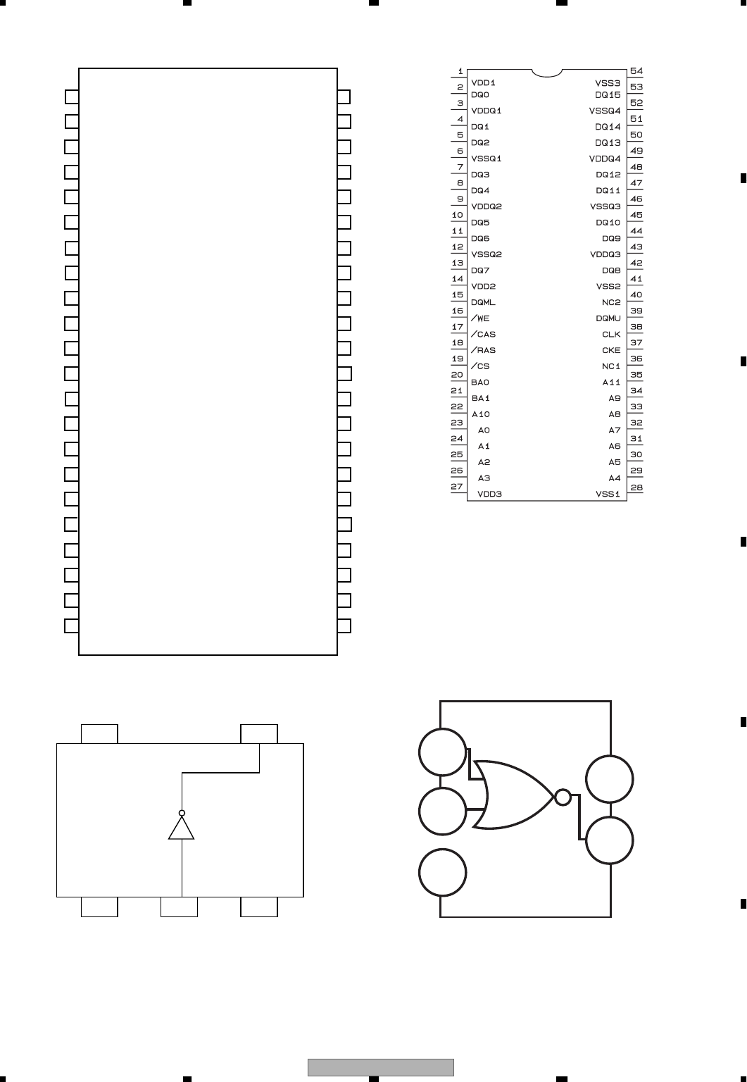
AVH-P6600DVD/UC 191
5678
5678
C
D
F
A
B
E
2
10
11
12
13
14
15
16
17
18
19
20
21
22
35
34
33
32
31
30
29
28
27
26
25
24
23
39
38
37
36
43
42
41
40
44
NC
A18
A17
A7
A6
A5
A4
A3
A2
A1
A0
ce
VSS
oe
D0
D8
D1
D9
D2
D10
D3
D11
A20
A19
A8
A9
A10
A11
A12
A13
A14
A15
A16
byte
VSS
D15/A-1
D7
D14
D6
D13
D5
D12
D4
VCC
A15/A-1
A0-A20
D0-D19
byte
ce
oe
VCC
VSS
8
9
4
5
6
7
3
1
:Data output/Address input
:Address input
:Data output
:Mode select
:Chip enable input
:Output enable input
:Power supply
:GND
*PD8125A,
*PD8126A
VCC
NC IN A
OUT Y
GND
54
132
*TC7SZ04FU
A0-A11
DQ0-DQ19
VDD
VSS
BA
/CS
/RAS
/CAS
/WE
DQML
DQMU
CLK
CKE
:Address input
:Data request output
:Power supply
:GND
:Memory address input
:Chip enable
:Row address strobe
:Column address strobe
:Write enable
:Low byte DQ mask
:Upper byte DQ mask
:Clock output
:Clock enable
*K4S641632H-TC75
15
4
2
3
VCC
Output
Input1
Input2
GND
*TC7SZ02FU
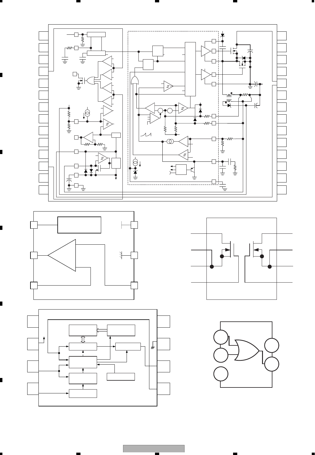
AVH-P6600DVD/UC
192
1234
1234
C
D
F
A
B
E
1
2
5
9
6
7
8
3
4
SENSE2-
RUN/SS1
SENSE1+
PLLFLTR
SGND
PLLIN
FCB
I
TH1
SENSE1-
V
OSENSE1
3.3V
OUT
I
TH2
V
OSENSE2
SENSE2+
13
11
12
14
16
28
27
24
20
23
22
21
26
25
19
18
17
TG2
PGOOD
TG1
V
IN
PGND
BG1
EXTV
CC
INTV
CC
SW1
BOOST1
BG2
BOOST2
SW2
RUN/SS2
15
10
+
-
-
+
+
-
+
-
+
-
+
-
+
-
+
-
+
-
-
+
+
-
+
-
+
-
+
+
+
+
+-
VV
-+
CIN
COUT
RSENSE
CSECDSEC
SENSE+
PGND
BG
INTVCC
SWITCH
LOGIC
SHDN
BOT
DUPLICATE FOR SECOND
CONTROLLER CHANNEL
PHASE DET
OSCILLATOR
CLK1
CLK2
0.86V
0.86V
0.74V
0.74V
BINH
fcb
VREF
5V
LDO
REG
4.8V
0.8V
FIN
RLP
CLP
PLLIN
PGOOD
FCB
R6
R5
3.3VOUT
VIN
EXTVCC
INTVCC
SGND INTERNAL
SUPPLY
5V
3V
0.18 A
VSEC
4.5V
PLLFLTR
50k
0.55V
I1I2
B
DROP
OUT
DET
S
R
Q
q
TOP ON
fcb
SW
TG
TOP
BOT
BOOST DB
CB
INTVCC
30k
INTVCC
SENSE-
30k
45k
3mV
45k
1.2 A
6V
SLOPE
COMP
0.86V
4(VFB)
2.4V VFB
0.80V
EA
OV
0.86V
SHDN
RST
ITH
VOSENSE
R1
R2
CC
RCCC2
CSS
RUN/SS
4(VFB)
RUN
SOFT
START
VOUT
D1
*LTC3728EG
Reference
Standby Logic
75Ω
DRIVER
+
-
1
2
3
6
5
4
Vcc
VREF
OUT
IN- IN+
GND
VCC
*TK15404AMI
NC
VCC
CS
SK
TEST
GND
DO
DI
1
2
3
4
8
7
6
5
Memory
Aray Address
Decoder
Mode Decode
Logic
Data Resistor Output Buffer
Clock Pulse
Counter Voltage Ditector
Clock Oscillater
*S-93C46BR0I-J8T1
1
2
3
4
8
7
6
5
*SI6544DQ
*TC7SZ32FU
15
4
2
3Output
VCC
Input1
Input2
GND
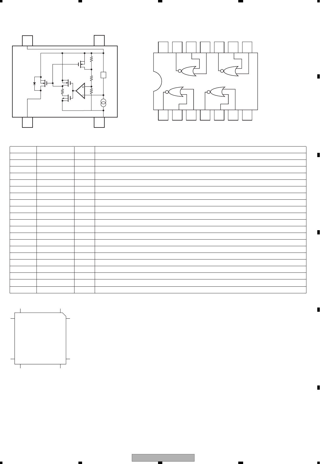
AVH-P6600DVD/UC 193
5678
5678
C
D
F
A
B
E
- Pin Functions (PD6340A)
Pin No. Pin Name I/O Function and Operation
1,2 SEG1,0 O LCD
3-5 NC Not used
segment signal output
LCD segment signal output
6-9 COM3-0 O
O
LCD common signal output
10 VLCD LCD driver power supply
11-14 KST3-0 Key strobe output
15,16 KDT0,1 Key data intput(Analog)
17 REM I Remote control data input
18 DPDT I
I
I
Display data input
19 NC Not used
20 KYDT O Key data output
21 MODA GND
22 X0 Crystal oscillating element connection pin
Crystal oscillating element connection pin
23 X1
24 VSS GND
25,26 KDT2,3 Key data input
27 NC Not used
28 KST4 O Key strobe output
29-33 NC Not used
34-55 SEG31-10 O LCD segment signal output
56 VDD Power suplly
57-64 SEG9-2 O
116
17
32
33 48 49
64
*PD6340A
1 2
4
1
OUT VDD
VSS
3
NC
VREF
*S-80827CNUA-B8M
1
2
3
4
5
6
7
1Y
1A
1B
2Y
2A
2B
GND
VCC
4Y
4B
4A
3Y
3B
3A
14
13
12
11
10
9
8
*TC74VCX02FT

AVH-P6600DVD/UC
194
1234
1234
C
D
F
A
B
E
25
28
32
29
30
31
26
27
DQ16
A0
DQM2
V
SSQ
V
DD
N.C
DQ16
A1
A2
DQ17
DQ18
V
DDQ
DQ20
V
SSQ
DQ23
DQ21
DQ22
V
DDQ
V
DD
36
34
35
37
38
42
39
40
41
43
51
62
59
55
58
57
56
61
60
54
53
52
DQ28
A5
DQM3
V
DDQ
V
SS
N.C
DQ31
A4
A3
DQ30
DQ29
V
SSQ
DQ27
V
DDQ
DQ24
DQ26
DQ25
V
CCQ
V
SS
49
45
48
47
46
44
50
1
2
5
9
6
7
8
3
4
DQ7
V
DD
DQ0
DQ2
V
DDQ
V
SSQ
DQ3
DQ4
V
DDQ
DQ1
DQ5
DQ6
V
SSQ
N.C
BA1
V
DD
ras
DQM0
we
cas
cs
A11
BA0
A10/AP
13
11
12
14
23
15
19
16
17
18
20
21
22
24
74
86
85
82
78
81
80
79
84
83
77
76
75
DQ8
V
SS
DQ15
DQ13
V
SSQ
V
DDQ
DQ12
DQ11
V
SSQ
DQ14
DQ10
DQ9
V
DDQ
N.C
A7
V
SS
CLK
DQM1
N.C
N.C
CKE
A9
A8
A6
64
72
68
71
70
69
67
66
65
63
73
33
10
Programming Register
Latency & Burst Length
Column Decoder
Timing Register
Row Decoder
LRAS
LCBR
Sense AMP
OutPut BufferI/O Contral
Bank Select
CLK
ADD
LCKE
LRAS
CLK CKE cs ras cas we DQM
LCBR LWE LCAS LWCBR
Data Input Register
1M x 32
LWE
LDQM
DQi
1M x 32
1M x 32
1M x 32
Address Register
Col Buffer
Row Buffer
Refresh Counter
*K4S283232E-TC75
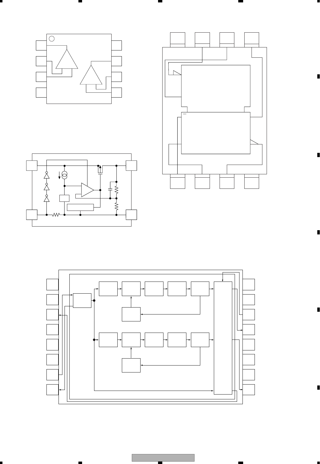
AVH-P6600DVD/UC 195
5678
5678
C
D
F
A
B
E
1OUT A
-IN A
+IN A
V+
V+
OUT B
-IN B
+IN B
2
3
4
8
7
6
5
A
-+
B
+-
NJM2140R
1234
8765
VCC st SELECT Y
AByGND
EN
1 MUX
1
G1
*TC7WH157FU
1
2
5
6
7
8
3
4
YDD1
VSS1
VDD2
VSS2
XT1
XT0
MO1,NC1
MO2,NC1,SO1
48
47
44
43
42
41
46
45
NC2
SO4,SO3,SO2,NC1
VDD3
VSS3
AO1,SO2
SO2,SO1,AO1
FSEL,NC2
SO3,SO2,SO1
X’tal
OSC
Reference
Divider 0 Phase
Divider 0
Loop
Divider 0
Charge
Pump 0 LPF 0 VCO 0
Reference
Divider 1 Phase
Divider 1
Loop
Divider 1
Charge
Pump 1 LPF 1 VCO 1
Control
Logic
*SM8707LV
Current Limit
Vref
VDD
ce
Vout
GND
+
-
2
5
1
3
*R1130H501B
AVH-P6600DVD/UC
196
1234
1234
C
D
F
A
B
E
10
1
2
5
9
6
7
8
3
4
2Q1
1oe
1Q1
1Q3
1Q6
1Q4
V
CC
1Q5
1Q2
GND
GND
1Q7
1Q8
2Q2
2Q8
GND
2Q5
2Q3
2Q4
V
CC
2Q6
GND
2Q7
1oe
13
11
12
14
23
15
19
16
17
18
20
21
22
24
36
48
47
44
40
43
42
41
46
45
39
38
37
2D1
1LE
1D1
1D3
1D6
1D4
V
CC
1D5
1D2
GND
GND
1D7
1D8
2D2
2D8
GND
2D5
2D3
2D4
V
CC
2D6
GND
2D7
2LE
26
34
30
33
32
31
29
28
27
25
35
1LE
1oe
48
47
D
LE Q
1D1
46
D
LE Q
1D2
45
D
LE Q
1D3
44
D
LE Q
1D4
43
D
LE Q
1D5
42
D
LE Q
1D6
41
D
LE Q
1D7
40
D
LE Q
1D8
2
1Q1
3
1Q2
5
1Q3
6
1Q4
8
1Q5
9
1Q6
10
1Q7
11
1Q8
1
2LE
2oe
25
36
D
LE Q
2D1
35
D
LE Q
2D2
33
D
LE Q
2D3
32
D
LE Q
2D4
30
D
LE Q
2D5
29
D
LE Q
2D6
27
D
LE Q
2D7
26
D
LE Q
2D8
13
2Q1
14
2Q2
16
2Q3
17
2Q4
19
2Q5
20
2Q6
22
2Q7
23
2Q8
24
*TC74LCX16373AFT
AVH-P6600DVD/UC 197
5678
5678
C
D
F
A
B
E
16-bit TIMER/
EVENT COUNTER 00
8-bit TIMER/
EVENT COUNTER 50
TO00/TI10/P01
RxD0/P11
TxD0/P10
8-bit TIMER H0TOH0/P15
8-bit TIMER H1
WATCH TIMER
WATCHDOG TIMER
78K/0
CPU
CORE
ROM
(FLASH
MEMORY)
TOH0/P16
TI50/TO50/P17
8-bit TIMER/
EVENT COUNTER 51
SERIAL
INTERFACE UART0
TI51/TO51/P33
RxD0/P14
TxD0/P13
SERIAL
INTERFACE UART6
SERIAL
INTERFACE CSI10
SI10/P11
SO10/P12
TI000/P00
sck10/P10
ANI0/P20 8
ANI7/P27 A/D CONVERTER
AVSS
AVREF
INTP0/P120
4
INTP1/P30
INTP6/P140
INTP5/P16
INTP4/P33 INTERRUPT
CONTROL
PORT 1 P10-P17
PORT 0 4
8
PORT 2 P20-P27
8
PORT 3 P30-P33
4
PORT 6 P60-P63
4
PORT 7 P70-P77
8
PORT 12
P00-P03
CLOCK OUTPUT
CONTROL PCL/P140
KR0/P70-
KR7/P77
VOLTAGE
REGULATOR REGC
P120
PORT 13 P130
PORT 14 P140
CLOCK MONITOR
KEY RETURN
RESET CONTROL
Ring-OSC
POWER ON CLEAR/
LOW VOLTAGE
INDICATOR
POC/LVI
CONTROL
8
reset
X1
XT2
X2
SYSTEM
CONTROL
VDD,
EVDD
VSS,
EVSS
IC
(VPP)
XT1
AVREF
AVSS
VPP/IC
VDD
REGC
VSS
X1
X2
reset
XT1
XT2
P130
P120/INTP0
P75/KR5
P76/KR6
P77/KR7
P00/TI000
P01/TI010/TO00
P02
P03
P10/sck10/RXD0
P11/SI10/RXD0
P12/SO10
P13/TXD6
P14/RXD6
EVDD
P33/TI51/TO51/INTP4
P32/INTP3
P31/INTP2
P30/INTP1
P140/PCL/INTP6
P17/TI50/TO50
P16/TOH1/INTP5
P15/TOH0
P60
P61
P62
P63
EVSS
P20/ANI0
P21/ANI1
P22/ANI2
P23/ANI3
P24/ANI4
P25/ANI5
P26/ANI6
P27/ANI7
P70/KR0
P71/KR1
P72/KR2
P73/KR3
P74/KR4
1
14 15 16 17 18 19 20 21 22 23 24 25 26
52 51 50 49 48 47 46 45 44 43 42 41 40
2
3
4
5
6
7
8
9
10
11
12
13
39
38
37
36
35
34
33
32
31
30
29
28
27
*PE5401A

AVH-P6600DVD/UC
198
1234
1234
C
D
F
A
B
E
2
10
11
12
13
14
15
16
17
18
19
20
21
22
39
38
37
36
35
34
33
32
31
30
29
28
27
43
42
41
40
47
46
45
44
48
A15
A14
A13
A12
A11
A10
A9
A8
A19
A20
we
reset
NC
ACC
RY/by
A18
A17
A7
A6
A5
A4
A3
A16
byte
VSS
DQ15/A-1
DQ7
DQ14
DQ6
DQ13
DQ5
DQ12
DQ4
VCC
DQ11
DQ3
DQ10
DQ2
DQ9
DQ1
DQ8
DQ0
oe
VSS
23
24
26
25
A2
A1
ce
A0
A-1
A0-A20
DQ0-D15
byte
ce
oe
RY/by
reset
ACC
VCC
VSS
8
9
4
5
6
7
3
1
:Data output/Address input
:Address input
:Data input output
:Mode select
:Chip enable input
:Output enable input
:Ready/Busy output
:Reset
:Acc
:Power supply
:GND
*PD6480B
ON/OFF
VSS
VIN
NC*1
VOUT
123
54
+
-
ON/OFF
*S-L2980A50MC-C7J
VOLTAGE
REFERENCE
AVH-P6600DVD/UC 199
5678
5678
C
D
F
A
B
E
1
2
3
4
5
SHDN/RT
SYNC/MODE
SGND
SW
PGND
ITH
VFB
PGOOD
SVIN
PVIN
10
9
8
7
6
VOLTAGE
REFERENCE VOLTAGE
REFERENCE
OSCILLATOR
LOGIC
-
+
+
-
B
+
-
+
-
+
-
SLOPE
COMPENSATION
NMOS
COMPARATOR
PMOS CURRENT
COMPARATOR
BURST
COMPARATOR
ERROR
AMPLIFIER
0.74V
0.8V
0.86V
VB
REVERSE
COMPARATOR
+
-
+
-
*LTC3411EMS
*MN35104UB
*TC7SZ125FU
64
65
128
1
29
1
92
193
256
1
1
g
2
IN A
3
GND
5
4
VCC
OUT Y

AVH-P6600DVD/UC
200
1234
1234
C
D
F
A
B
E
1
2,3
4
5,6
7
8,10
11
12,13
14
15
16
17
18
19-22
23
24
25,26
27,28
29
30
31,32
33
34-37
38,39
40,41
42
43
44,45
46
47
48
49
50
51
52
53
54
55
56
57
58
59
VDD33
MDQ
VSS
MDQ
VDD33
MDQ
VSS
MDQ
VDD33
VDD15
VSS
EXADR
NEXWE
EXADT
VDD33
VSS
EXADR
EXADT
VDD33
VSS
EXADT
NEXCE
EXADT
EXADR
EXADT
VD33
VSS
EXADT
NEXOE
P15
P14
P13
P12
P11
P10
P9
P8
P7
VDD3
MMOD
VSS
P6
I / O
I / O
I / O
I / O
I / O
O
I / O
I / O
I / O
I / O
O
I / O
I / O
I / O
I / O
O
I / O
I / O
I / O
I / O
I / O
I / O
I / O
I / O
I / O
I
I / O
IO power supply
SDRAM data
GND
SDRAM data
IO power supply
SDRAM data
GND
SDRAM data
IO power supply
Power supply
GND
Memory address
Memory write enable
Memory address data
IO power supply
GND
Memory address
Memory address data
IO power supply
GND
Memory address data
Memory chip select
Memory address data
Memory address
Memory address data
IO power supply
GND
Memory address data
Memory output(Read) enable
Memory address bus
The flag of transmitting end
The flag of transmitting start
Serial clock
Serial output data
Serial input data
Serial clock
Serial output data
Serial input data
IO power supply
Test mode setting
GND
Serial clock
-Pin Functions(MN35104UB)
Pin No. Pin Name I/O Function and Operation
AVH-P6600DVD/UC 201
5678
5678
C
D
F
A
B
E
60
61
62
63
64
65
66
67
68
69
70-77
78
79
80
81
82
83
84
85
86-89
90
91
92
93
94-97
98
99
100-103
104
105
106
107
108-110
111
112
113
114
115
116
117
118
119
P5
P4
P3
P2
P1
P0
FG
VDD15
NRST
VSS
DRV
DRV8
VDD33
VSS
SCLOCK
EXTRG
SDATA
EXTRG
TRCCLK
TRCDATA
TRCST
VDD33
OSCI
VSS
MONI
VDD15
VSS
MONI
AVDDD
PLFIL1
AVSSD
PLFIL2
VREF
VC0
RESI
ANAMONI
POFLT
CDATA
CCAPA
CGD
AVDDC
AVSSC
I / O
I / O
I / O
I / O
I / O
I / O
I
I
I / O
I / O
I / O
I / O
I / O
I / O
I / O
I / O
I / O
I
I / O
I / O
O
O
O
I
I
O
O
O
O
O
I
Serial output data
Serial input data
Serial clock
Serial output data
Serial input data
Serial clock
Motor FG
Power supply
Master reset
GND
Servo port
Servo port
IO power supply
GND
Input clock for debug
I/O trigger for debug
I/O data for debug
I/O trigger for debug
Output trace clock for debug
I/O trace data for debug
Output trace status for debug
Power supply
Front end clock input
GND
Inside monitor
Power supply
GND
Inside monitor
Power supply
DRC VCO
GND
DRC VCO
Reference voltage
gm-cEQ
gm-cEQ
Inside analog monitor
DPDOFTR
Inline data
Inline capacitor
Reference voltage
Analog current
Analog GND
Pin No. Pin Name I/O Function and Operation

AVH-P6600DVD/UC
202
1234
1234
C
D
F
A
B
E
120
121
122-131
132
133
134
135
136
137
138
139
140
141
142
143
144
145
146-148
149
150
151
152
153
154
155
156
157
158
159
160
161
162
163
164
165
166
167
168
169
170
171
172
RFINN
RFINP
VIN
LPC1
LPCO1
LPC2
LPCO2
VREFH
VHALF
AVSSB
CTKC
CSLFLT
CWBLOUT
CWBLIN
VCOF
RVI
AVDDB
AD
AVDDA
DAC1
AVSSA
DAC0
AVDDE
IREF1
AVSSE
COMP1
AVDDF
DAC1OUT
AVSSF
DAC2OUT
DAC3OUT
VREF
DAC4OUT
DAC5OUT
AVDDG
IREF2
VSSG
COMP2
VSS
BECLK
VDD33
EXTCK
I
I
I
O
I
O
O
O
O
I
O
I
I
I
I
O
O
I
I
O
O
O
I
O
O
I
I
I
I
RF input
RF input
Head input
DVDLPC input
DVDLPC output
CDLPC input
CDLPC output
Reference voltage
Reference voltage
Analog GND
TC
Capasitor
DC cut for wobble
DC cut for wobble
JFVCO control voltage
VREFH reference current
Analog current
AD input
Analog current
Tracking drive output
Analog GND
Focus drive output
Analog current
Inside DAC bias current
Analog GND
Inside DAC
Analog current
Analog signal
Analog GND
Analog signal
Analog signal
Reference voltage
Analog signal
Analog signal
Analog power suplly
Inside DAC bias current
Analog GND
Inside DAC
GND
Backend clock input
IO power supply
Exterior audio clock
Pin No. Pin Name I/O Function and Operation

AVH-P6600DVD/UC 203
5678
5678
C
D
F
A
B
E
173
174
175
176
177
178-180
181
182
183
184,185
186
187,188
189
190-193
194
195
196,197
198
199,201
202
203-205
206
207,208
209
210
211
212
213
214
215
216,217
218
219-220
221
222
223
224
225
226
227-229
230
231
PHCOMPO
LRCK
SRCK
ADOUT3
VSS
ADOUT
IECOUT
VDD33
VSS
MDQ
VDD15
MDQ
VDD33
MDQ
VSS
VDD33
MDQ
VSS
MDQ
VDD33
MDQ
VSS
DQM
VDD33
MA
VSS
MA4
VDD15
MA2
VSS
MA
VDD33
MA
VSS
VDD15
MCKI
VSS
MCK
VDD33
MA
VSS
MA
O
O
O
O
O
O
I / O
I / O
I / O
I / O
I / O
I / O
O
O
O
O
O
O
I
O
O
O
Composite audio clock
LR chanel clock output
Bit clock output
Audio down mixing
GND
Audio data
IEC958 digital audio output
IO power supply
GND
SDRAM data
Power supply
SDRAM data
IO power supply
SDRAM data
GND
IO power supply
SDRAM data
GND
SDRAM data
GND
SDRAM data
GND
SDRAM data mask
Power supply
SDRAM address
GND
SDRAM address
Power supply
SDRAM address
GND
SDRAM address
Power supply
SDRAM address
GND
Power supply
SDRAM output clock
GND
SDRAM input clock
IO power supply
SDRAM address
GND
SDRAM address
Pin No. Pin Name I/O Function and Operation
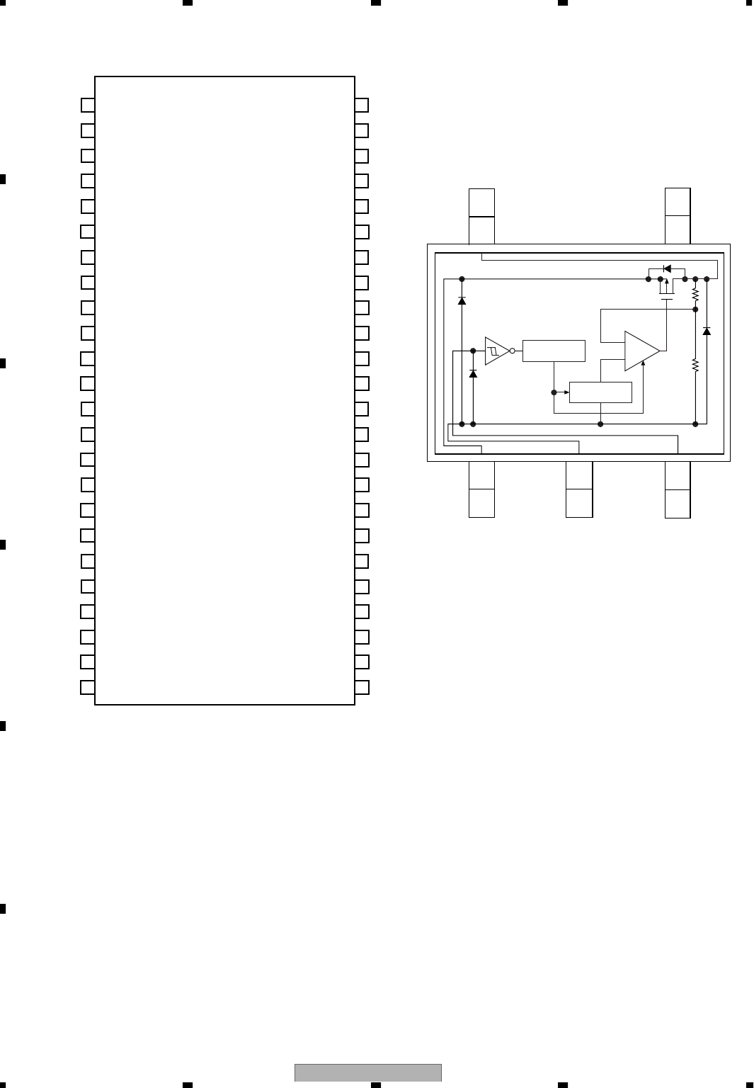
AVH-P6600DVD/UC
204
1234
1234
C
D
F
A
B
E
2
10
11
12
13
14
15
16
17
18
19
20
21
22
39
38
37
36
35
34
33
32
31
30
29
28
27
43
42
41
40
47
46
45
44
48
A15
A14
A13
A12
A11
A10
A9
A8
A19
A20
we
reset
NC
ACC
RY/by
A18
A17
A7
A6
A5
A4
A3
A16
byte
VSS
DQ15/A-1
DQ7
DQ14
DQ6
DQ13
DQ5
DQ12
DQ4
VCC
DQ11
DQ3
DQ10
DQ2
DQ9
DQ1
DQ8
DQ0
oe
VSS
23
24
26
25
A2
A1
ce
A0
A-1
A0-A20
DQ0-D15
byte
ce
oe
RY/by
reset
ACC
VCC
VSS
8
9
4
5
6
7
3
1
:Data output/Address input
:Address input
:Data input output
:Mode select
:Chip enable input
:Output enable input
:Ready/Busy output
:Reset
:Acc
:Power supply
:GND
*PD6480B
ON/OFF
VSS
VIN
NC*1
VOUT
123
54
+
-
ON/OFF
*S-L2980A50MC-C7J
VOLTAGE
REFERENCE

AVH-P6600DVD/UC 205
5678
5678
C
D
F
A
B
E
1
2
3
4
5
SHDN/RT
SYNC/MODE
SGND
SW
PGND
ITH
VFB
PGOOD
SVIN
PVIN
10
9
8
7
6
VOLTAGE
REFERENCE VOLTAGE
REFERENCE
OSCILLATOR
LOGIC
-
+
+
-
B
+
-
+
-
+
-
SLOPE
COMPENSATION
NMOS
COMPARATOR
PMOS CURRENT
COMPARATOR
BURST
COMPARATOR
ERROR
AMPLIFIER
0.74V
0.8V
0.86V
VB
REVERSE
COMPARATOR
+
-
+
-
*LTC3411EMS
*MN35104UB
*TC7SZ125FU
64
65
128
1
29
1
92
193
256
1
1
g
2
IN A
3
GND
5
4
VCC
OUT Y

AVH-P6600DVD/UC
206
1234
1234
C
D
F
A
B
E
1
2,3
4
5,6
7
8,10
11
12,13
14
15
16
17
18
19-22
23
24
25,26
27,28
29
30
31,32
33
34-37
38,39
40,41
42
43
44,45
46
47
48
49
50
51
52
53
54
55
56
57
58
59
VDD33
MDQ
VSS
MDQ
VDD33
MDQ
VSS
MDQ
VDD33
VDD15
VSS
EXADR
NEXWE
EXADT
VDD33
VSS
EXADR
EXADT
VDD33
VSS
EXADT
NEXCE
EXADT
EXADR
EXADT
VD33
VSS
EXADT
NEXOE
P15
P14
P13
P12
P11
P10
P9
P8
P7
VDD3
MMOD
VSS
P6
I / O
I / O
I / O
I / O
I / O
O
I / O
I / O
I / O
I / O
O
I / O
I / O
I / O
I / O
O
I / O
I / O
I / O
I / O
I / O
I / O
I / O
I / O
I / O
I
I / O
IO power supply
SDRAM data
GND
SDRAM data
IO power supply
SDRAM data
GND
SDRAM data
IO power supply
Power supply
GND
Memory address
Memory write enable
Memory address data
IO power supply
GND
Memory address
Memory address data
IO power supply
GND
Memory address data
Memory chip select
Memory address data
Memory address
Memory address data
IO power supply
GND
Memory address data
Memory output(Read) enable
Memory address bus
The flag of transmitting end
The flag of transmitting start
Serial clock
Serial output data
Serial input data
Serial clock
Serial output data
Serial input data
IO power supply
Test mode setting
GND
Serial clock
-Pin Functions(MN35104UB)
Pin No. Pin Name I/O Function and Operation

AVH-P6600DVD/UC 207
5678
5678
C
D
F
A
B
E
60
61
62
63
64
65
66
67
68
69
70-77
78
79
80
81
82
83
84
85
86-89
90
91
92
93
94-97
98
99
100-103
104
105
106
107
108-110
111
112
113
114
115
116
117
118
119
P5
P4
P3
P2
P1
P0
FG
VDD15
NRST
VSS
DRV
DRV8
VDD33
VSS
SCLOCK
EXTRG
SDATA
EXTRG
TRCCLK
TRCDATA
TRCST
VDD33
OSCI
VSS
MONI
VDD15
VSS
MONI
AVDDD
PLFIL1
AVSSD
PLFIL2
VREF
VC0
RESI
ANAMONI
POFLT
CDATA
CCAPA
CGD
AVDDC
AVSSC
I / O
I / O
I / O
I / O
I / O
I / O
I
I
I / O
I / O
I / O
I / O
I / O
I / O
I / O
I / O
I / O
I
I / O
I / O
O
O
O
I
I
O
O
O
O
O
I
Serial output data
Serial input data
Serial clock
Serial output data
Serial input data
Serial clock
Motor FG
Power supply
Master reset
GND
Servo port
Servo port
IO power supply
GND
Input clock for debug
I/O trigger for debug
I/O data for debug
I/O trigger for debug
Output trace clock for debug
I/O trace data for debug
Output trace status for debug
Power supply
Front end clock input
GND
Inside monitor
Power supply
GND
Inside monitor
Power supply
DRC VCO
GND
DRC VCO
Reference voltage
gm-cEQ
gm-cEQ
Inside analog monitor
DPDOFTR
Inline data
Inline capacitor
Reference voltage
Analog current
Analog GND
Pin No. Pin Name I/O Function and Operation

AVH-P6600DVD/UC
208
1234
1234
C
D
F
A
B
E
120
121
122-131
132
133
134
135
136
137
138
139
140
141
142
143
144
145
146-148
149
150
151
152
153
154
155
156
157
158
159
160
161
162
163
164
165
166
167
168
169
170
171
172
RFINN
RFINP
VIN
LPC1
LPCO1
LPC2
LPCO2
VREFH
VHALF
AVSSB
CTKC
CSLFLT
CWBLOUT
CWBLIN
VCOF
RVI
AVDDB
AD
AVDDA
DAC1
AVSSA
DAC0
AVDDE
IREF1
AVSSE
COMP1
AVDDF
DAC1OUT
AVSSF
DAC2OUT
DAC3OUT
VREF
DAC4OUT
DAC5OUT
AVDDG
IREF2
VSSG
COMP2
VSS
BECLK
VDD33
EXTCK
I
I
I
O
I
O
O
O
O
I
O
I
I
I
I
O
O
I
I
O
O
O
I
O
O
I
I
I
I
RF input
RF input
Head input
DVDLPC input
DVDLPC output
CDLPC input
CDLPC output
Reference voltage
Reference voltage
Analog GND
TC
Capasitor
DC cut for wobble
DC cut for wobble
JFVCO control voltage
VREFH reference current
Analog current
AD input
Analog current
Tracking drive output
Analog GND
Focus drive output
Analog current
Inside DAC bias current
Analog GND
Inside DAC
Analog current
Analog signal
Analog GND
Analog signal
Analog signal
Reference voltage
Analog signal
Analog signal
Analog power suplly
Inside DAC bias current
Analog GND
Inside DAC
GND
Backend clock input
IO power supply
Exterior audio clock
Pin No. Pin Name I/O Function and Operation

AVH-P6600DVD/UC 209
5678
5678
C
D
F
A
B
E
173
174
175
176
177
178-180
181
182
183
184,185
186
187,188
189
190-193
194
195
196,197
198
199,201
202
203-205
206
207,208
209
210
211
212
213
214
215
216,217
218
219-220
221
222
223
224
225
226
227-229
230
231
PHCOMPO
LRCK
SRCK
ADOUT3
VSS
ADOUT
IECOUT
VDD33
VSS
MDQ
VDD15
MDQ
VDD33
MDQ
VSS
VDD33
MDQ
VSS
MDQ
VDD33
MDQ
VSS
DQM
VDD33
MA
VSS
MA4
VDD15
MA2
VSS
MA
VDD33
MA
VSS
VDD15
MCKI
VSS
MCK
VDD33
MA
VSS
MA
O
O
O
O
O
O
I / O
I / O
I / O
I / O
I / O
I / O
O
O
O
O
O
O
I
O
O
O
Composite audio clock
LR chanel clock output
Bit clock output
Audio down mixing
GND
Audio data
IEC958 digital audio output
IO power supply
GND
SDRAM data
Power supply
SDRAM data
IO power supply
SDRAM data
GND
IO power supply
SDRAM data
GND
SDRAM data
GND
SDRAM data
GND
SDRAM data mask
Power supply
SDRAM address
GND
SDRAM address
Power supply
SDRAM address
GND
SDRAM address
Power supply
SDRAM address
GND
Power supply
SDRAM output clock
GND
SDRAM input clock
IO power supply
SDRAM address
GND
SDRAM address
Pin No. Pin Name I/O Function and Operation
AVH-P6600DVD/UC
210
1234
1234
C
D
F
A
B
E
232
233
234
235
236
237
238
239
240
241
242
243
244
245
246
247
248
249
250
251-253
254
255,256
NWE
VDD33
BA0
MA
VSS
BA1
NCSM
NRAS
VDD33
VSS
NCAS
DQM0
VDD15
VSS
DQM
MDQ
VSS
MDQ
VDD33
MDQ
VSS
MDQ
O
O
O
O
O
O
O
O
O
I / O
I / O
I / O
I / O
SDRAM writte enable
IO power supply
SDRAM bank address
SDRAM address
GND
SDRAM bank address
SDRAM chip select
SDRAM low address strobe
IO power supply
GND
SDRAM column address strobe
SDRAM data mask
Power supply
GND
SDRAM data mask
SDRAM data
GND
SDRAM data
IO power supply
SDRAM data
GND
SDRAM data
Pin No. Pin Name I/O Function and Operation
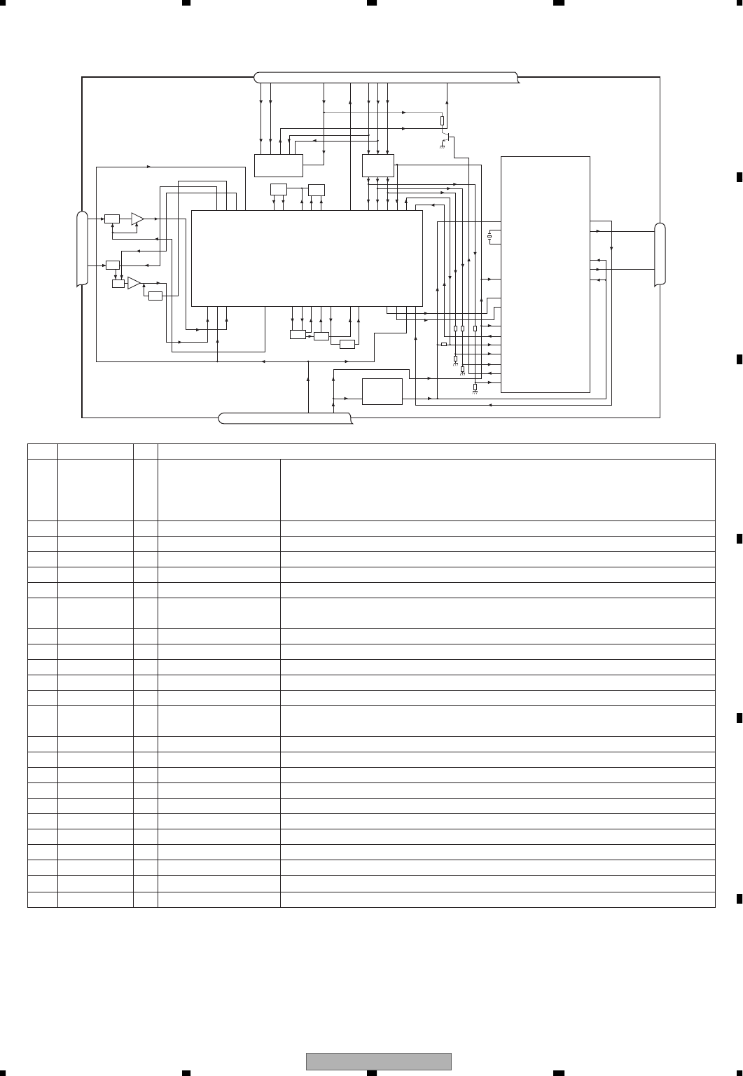
AVH-P6600DVD/UC 211
5678
5678
C
D
F
A
B
E
UC ,RC,RDmodel
No. Symbol I/O Explain
1 AMANT I AM antenna input AM antenna input high impedance AMANT pin is connected with
an all antenna by way of 4.7µH. (LAU type inductor) A series circuit
including an inductor and a resistor is connected with RF ground for
the countermeasure against the ham of power transmission line.
2 RFGND RF ground Ground of antenna block
3 FMANT I FM antenna input Input of FM antenna 75ΩSurge absorber(DSP-201M-S00B) is necessary.
4 VCC power supply The power supply for analog block. D.C 8.4V ±0.3V
5 SL O signal level Output of FM/AM signals level
6 CE2 I chip enable-2 Chip enable for EEPROM ”Low” active
7 WC I write control You can write EEPROM, when EEPROM write control is “Low”.
Ordinary non connection
8 CE1 I chip enable-1 Chip enable for AF•RF ”High” active
9 CK I clock Clock
10 DI I data in Data input
11 NC non connection Not used
12 OSCGND osc ground Ground of oscillator block
13 ROM_VDD power supply Power supply for EEPROM pin 13 is connected with a power supply of
micro computer.
14 DO O data out Data output
15 DGND digital ground Ground of digital block
16 NC non connection Not used
17 VDD_3.3 power supply The power supply for digital block. 3.3V ±0.2V
18 NC non connection Not used
19 NC non connection Not used
20 NC non connection Not used
21 NC non connection Not used
22 AUDIOGND audio ground Ground of audio block
23 L ch O L channel output FM stereo “L-ch” signal output or AM audio output
24 R ch O R channel output FM stereo “R-ch” signal output or AM audio output
FMRF
ANT adj RF adj
FM ANT
T51 CF52
CF51
RFGND
OSCGND
DGND
AUDIOGND
NC
VCC
VDD_3.3
3.3V 2.5V
IC 4
3.3V 2.5V
←
IC 2
2.5V
WC
CE2
ROM_VDD
SL
DI
CK
CE1
NC
DO
NC
NC
NC
NC
7 6 13 5 10 9 8 11 14 18 19 20 21
1
3
212 1522 16 4 17
IC 1
3.3V
AM ANT FMRF
ATT
LPF
OSC
IC 3 EEPROM
5.0V
IC 5
5V 3.3V
←
ATT
MIXER, IF AMP DET, FM MPX
24
23
Rch
Lch
- FM/AM Tuner Unit
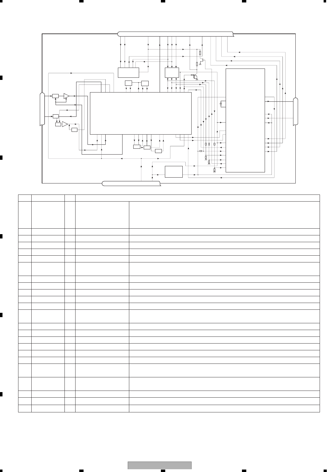
AVH-P6600DVD/UC
212
1234
1234
C
D
F
A
B
E
EW model
No. Symbol I/O Explain
1 AMANT I AM antenna input AM antenna input high impedance AMANT pin is connected with
an all antenna by way of 4.7µH. (LAU type inductor) A series circuit
including an inductor and a resistor is connected with RF ground for
the countermeasure against the ham of power transmission line.
2 RFGND RF ground Ground of antenna block
3 FMANT I FM antenna input Input of FM antenna 75ΩSurge absorber(DSP-201M-S00B) is necessary.
4 VCC power supply The power supply for analog block. D.C 8.4V ±0.3V
5 SL O signal level Output of FM/AM signals level
6 CE2 I chip enable-2 Chip enable for EEPROM ”Low” active
7 WC I write control You can write EEPROM, when EEPROM write control is “Low”.
Ordinary non connection
8 CE1 I chip enable-1 Chip enable for AF•RF ”High” active
9 CK I clock Clock
10 DI I data in Data input
11 LDET O lock detector “Low” active
12 OSCGND osc ground Ground of oscillator block
13 ROM_VDD power supply Power supply for EEPROM pin 13 is connected with a power supply of
micro computer.
14 DO O data out Data output
15 DGND digital ground Ground of digital block
16 NC non connection Not used
17 VDD_3.3 power supply The power supply for digital block. 3.3V ±0.2V
18 RDS_CK O RDS clock Output of RDS clock(2.5V)
19 RDS_DATA O RDS data Output of RDS data(2.5V)
20 RDS_LOCK O RDS lock Output unit “High” active(2.5V) (RDS_LOCK turns over by the
external transistor. “Low” active)
21 RDS_HSLK O RDS high speed Output unit “High” active(2.5V)(RDS_HSLK turns over by the
lock external transistor. “Low” active)
22 AUDIOGND audio ground Ground of audio block
23 L ch O L channel output FM stereo “L-ch” signal output or AM audio output
24 R ch O R channel output FM stereo “R-ch” signal output or AM audio output
FMRF
ANT adj RF adj
FM ANT
T51 CF52
CF51
RFGND
OSCGND
DGND
AUDIOGND
NC
VCC
VDD_3.3
3.3V 2.5V
IC 4
3.3V 2.5V
←
IC 2
2.5V
WC
CE2
ROM_VDD
SL
DI
CK
CE1
LDET
DO
RDS_CK
RDS_DATA
RDS_LOCK
RDS_HSLK
7 6 13 5 10 9 8 11 14 18 19 20 21
1
3
212 1522 16 4 17
IC 1
3.3V
AM ANT FMRF
ATT
LPF
OSC
IC 3 EEPROM
5.0V
IC 5
5V 3.3V
←
ATT
MIXER, IF AMP DET, FM MPX,
RDS DECODER
24
23
Rch
Lch
- FM/AM Tuner Unit
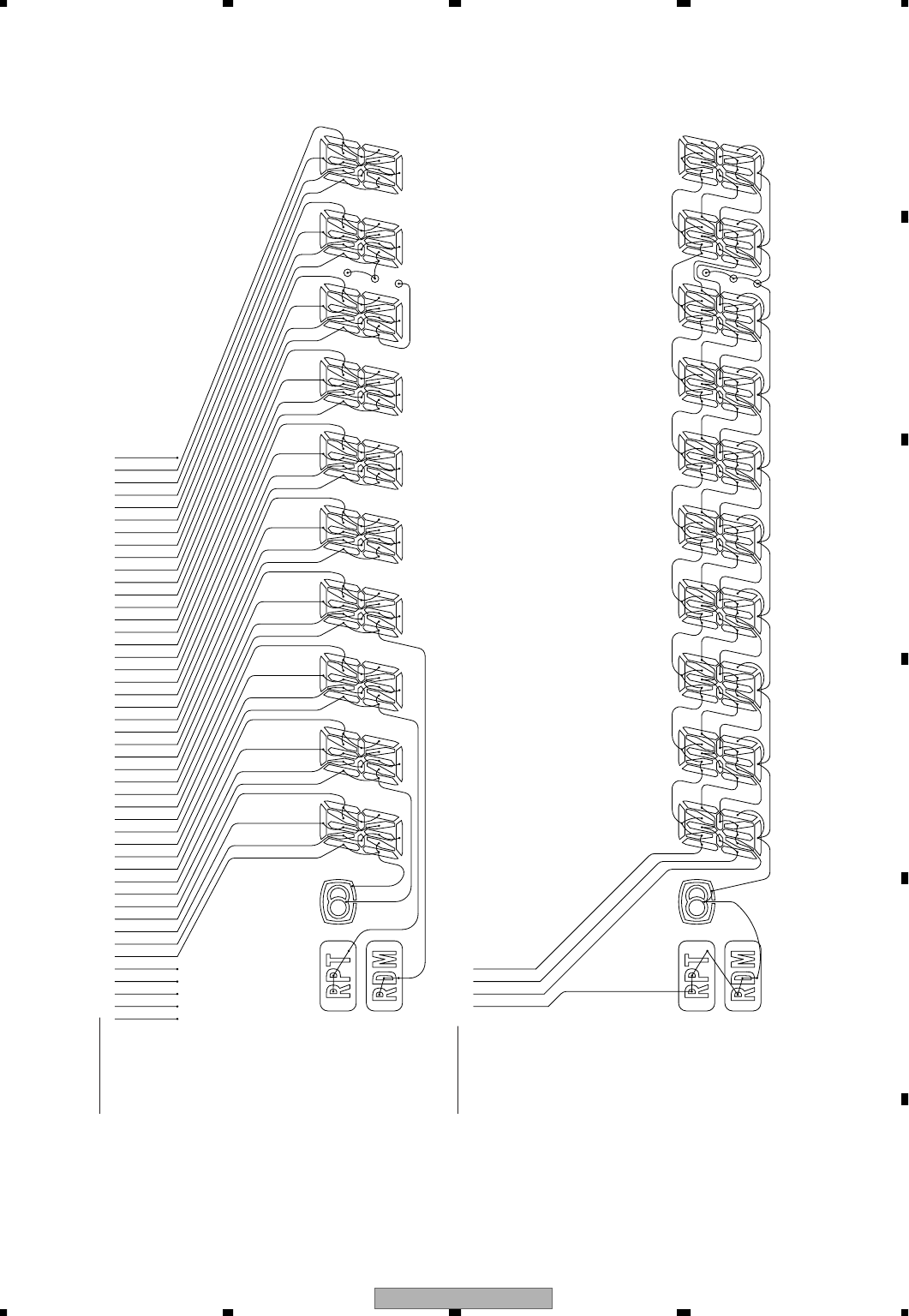
AVH-P6600DVD/UC 213
5678
5678
C
D
F
A
B
E
7.2.2 DISPLAY
NC
SEG1
SEG2
SEG3
SEG4
SEG5
SEG6
SEG7
SEG8
SEG9
SEG10
SEG11
SEG12
SEG13
SEG14
SEG15
SEG16
SEG17
SEG18
SEG19
SEG20
SEG21
SEG22
SEG23
SEG24
SEG25
SEG26
SEG27
SEG28
SEG29
SEG30
SEG31
SEG32
SEG33
SEG34
SEG35
SEG36
SEG37
SEG38
SEG39
SEG40
NC
COM1
COM2
COM3
COM4
SEGMENT
COMMON
COM1
COM2
COM3
COM4
- LCD(CAW1805)
AVH-P6600DVD/UC
214
1234
1234
C
D
F
A
B
E
7.3 EXPLANATION
7.3.1 MECHANISM DESCRIPTIONS
- Outline of the FLAP motion
1. The motion is actuated made by two motors, the forward/backward driving motor (CXB9515) and the angle
driving motor (CXB9516).
2. Analog electric potential generated by the angle encoder is detected to detect angle motion status and motion
position.
3. Memory function for the angle last position is accomplished by the micro processor using the 256 resolution
steps of the VDD.
4. A pulse is detected by the photo interrupter to detect the horizontal motion status.
5. In the case of reset start, the monitor will be in a stored position first, and ejection motion will take place, which
puts the system in the booted up state.
6. Angle adjustment is made by the angle key (+/-).
7. OPEN/CLOSE key makes the monitor stored or ejected, and temporary folding key folds the monitor
temporarily.
8. Setting of the monitor auto storage/ejection ON/OFF and set back ON/OFF at the time of ACC ON/OFF is made
on the navigation menu screen.
9. A backlight is switched-off during forward/backward and storage.
- Explanation on the FLAP ejection motion
1. When the OPEN key is pressed or ACC is set to ON while the auto OPEN/CLOSE is being set to ON, angle
driving motor rotates in the 0° direction for 500ms. (Pressed down.)
2. After 500ms, the angle driving motor is stopped, and the forward/backward driving motor rotates in the
ejection direction.
3. For a period of 600ms from the time when LIFTSW is switched from H to L, the forward/backward driving
motor keeps rotating in the ejection direction.
4. After 600ms, the forward/backward driving motor is stopped, and the angle driving motor rotates in the UP
direction.
AVH-P6600DVD/UC 215
5678
5678
C
D
F
A
B
E
5. When the angle voltage reaches the voltage for 110°, brake is applied to the angle driving motor, and the
ejection is completed. (In case the previous angle is stored in the memory, the motion continues to that angle.)
6. When the setback is set to ON, after the monitor angle voltage has reached the previously memorized voltage,
brake is applied to the angle driving motor, then the forward/backward driving motor is rotated in slow speed
in the storage direction. After that, when LIFTSW has switched from L to H, the forward/backward driving
motor is stopped.
110° voltage position or the last memory position.
- Explanation of the FLAP storage motion
1. When CLOSE key is pressed, or after 6 seconds from ACC OFF when auto OPEN/CLOSE is being set to ON, the
angle driving motor is rotated in the 0° direction. In case the setback setting is ON, the forward/backward
driving motor is rotated in high speed in the ejection direction and the motor continues to rotate for 600ms
from the time when LIFTSW is switched from H to L, then the angle driving motor is rotated in the 0° direction.
AVH-P6600DVD/UC
216
1234
1234
C
D
F
A
B
E
2. For a period of 500ms from the time when DIGOSW is switched from H to L, the angle driving motor is rotated
in the 0° direction for the “pressed down” motion.
3. After 500ms, brake is applied to the angle driving motor, and then the forward/backward driving motor is
rotated in the storage direction.
4. When the horizontal motion detection pulse is no longer detected for 200ms, brake is applied and the monitor
storage motion is completed.
- Explanation on the FLAP angle adjustment
1. The angle driving motor is rotated in UP direction by the “+” key and in DOWN direction by the “–” key from
the monitor stop position. If the key is kept pressed, the monitor will keep changing the angle without steps
within the range of 50 to 110 degrees. When the setback is being set to ON, the forward/backward driving
motor is rotated in the horizontal ejection direction while the key is being pressed, and angle adjustment is
made by changing the angle voltage to the extent the angle adjustment key is effective after 600ms has
elapsed from the time when LIFTSW has switched from H to L. When 3 seconds have elapsed from the time
of angle adjustment completion, the forward/backward driving motor is rotated in slow speed in the horizontal
storage direction, and brake is applied when LIFTSW has switched from L to H.
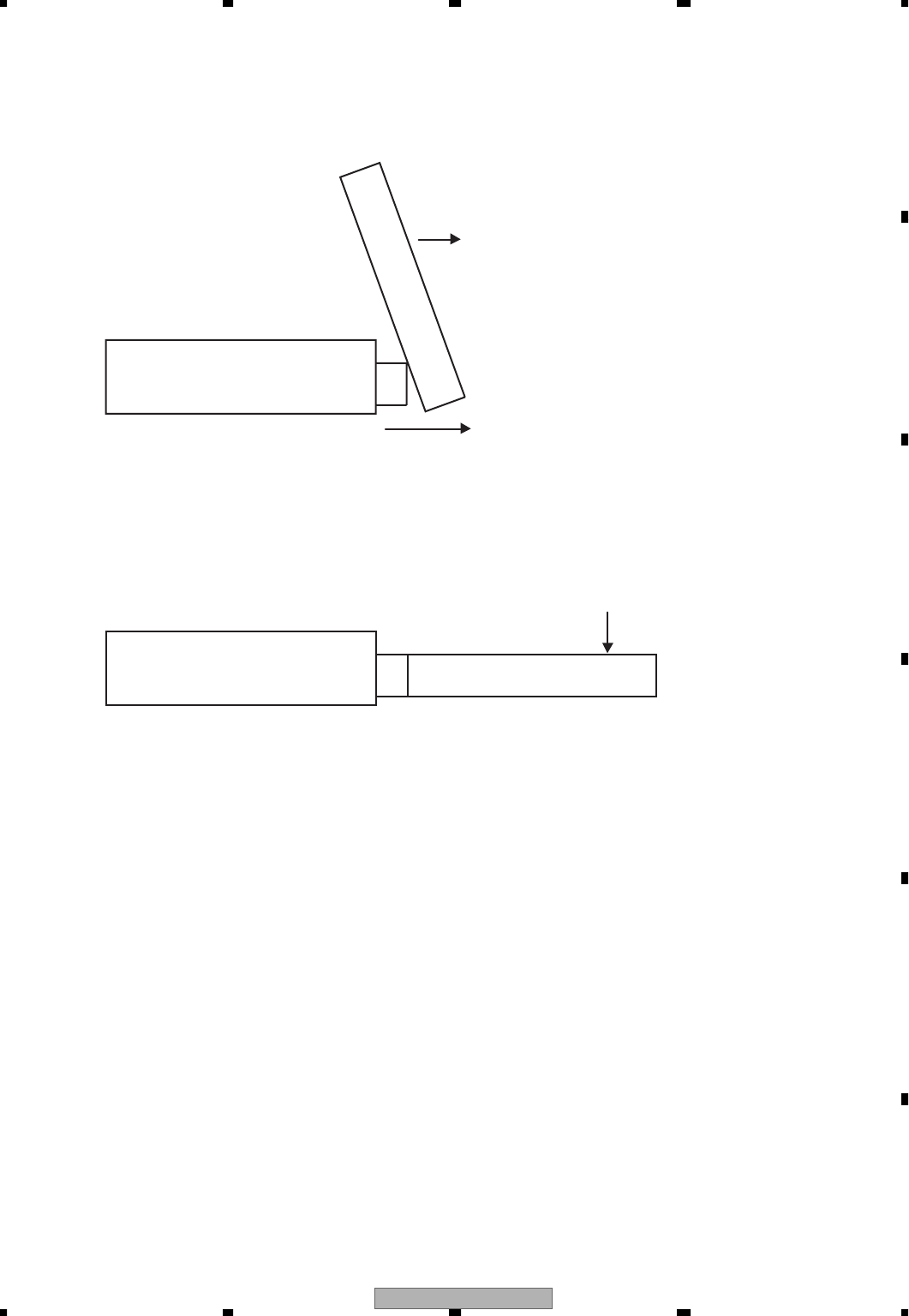
AVH-P6600DVD/UC 217
5678
5678
C
D
F
A
B
E
- Explanation on the FLAP temporary folding operation
1. By pressing the temporary folding key, the angle driving motor is rotated from the monitor stop position
toward 0° direction. When the setback is being set to ON, the forward/backward driving motor is rotated when
the key is pressed, brake is applied after 600ms has elapsed from the time when LIFTSW has switched from H
to L, and the angle driving motor is rotated in 0° direction.
2. For a period of 500ms after DEGOSW has switched from H to L, the angle driving motor is rotated, and the
monitor stops at its horizontal position by the brake. After 7 seconds, navigator operation sound is heard three
times in 1 second interval. After 10 seconds, the angle driving motor is rotated in UP direction, and then the
brake is applied to stop the motor at the last memory position. When the setback is being set to ON, after the
angle driving motor stops at the last memory position, the forward/backward driving motor is rotated in slow
speed in the horizontal storage direction, and the motor stops after LIFTSW has switched from L to H.
- Notes related to the FLAP motion
1. Regarding the angle position, angle voltage is always checked, and the last memory is stored by addition or
subtraction of the voltage. It should be noted, however, that the last memory will not be stored when the
monitor is manually moved by force.
2. If the expected pulse is not detected during horizontal motion, the monitor will stop at that position.
AVH-P6600DVD/UC
218
1234
1234
C
D
F
A
B
E
Bup ON
(Reset start)
Bup OFF
Bup OFF ON
ACC ON
ACC OFF ON
ACC OFF
Last memory
Bup ON
(Reset start)
Bup OFF
Bup OFF ON
ACC ON
ACC OFF ON
ACC OFF
Last memory
OPEN state
CLOSE state
CLOSE
OPEN state
Last angle
To stand-by
No state change
No state change
No state change
6 sec from ACC OFF
Advance
CLOSE motion
CLOSE
OPEN
To stand-by
No state change
No state change
No state change
No state change
OPEN
In OPEN motion In CLOSE motion CLOSE state
Continue OPEN motion
Last angle
Return
To stand-by To stand-by To stand-by
Continue OPEN motion
Last angle
Return
Continue OPEN motion
Last angle
Return
6 sec from ACC OFF
Advance
CLOSE motion
CLOSE
OPEN CLOSE CLOSE
To stand-by To stand-by To stand-by
Continue OPEN motion
Last angle
Return
Continue OPEN motion
Last angle
Return
Continue OPEN motion
Last angle
Return
OPEN CLOSE CLOSE
Continue CLOSE motion
CLOSE
Continue CLOSE motion
CLOSE
Continue CLOSE motion
CLOSE
Continue CLOSE motion
CLOSE
Continue CLOSE motion
CLOSE
Continue CLOSE motion
CLOSE
Continue OPEN motion
Last angle
No state change
OPEN motion
Last angle
Return
No state change
No state change
No state change
No state change
No state change
No state change
- Table of driving unit operations by different preset modes
* When the setback is being set to OFF, there will be no advance/return motion.
After ACC OFF, if ACC is switched ON again during the 6 seconds counting, standby will be passed and the FLAP
status will not change.
Auto OPEN/CLOSE setting ONAuto OPEN/CLOSE setting OFF
AVH-P6600DVD/UC 219
5678
5678
C
D
F
A
B
E
- Table of temporary folding control
* When the setback is being set to OFF, there will be no advance/return motion.
Bup ON
Bup OFF
ACC ON
Bup OFF ON
ACC OFF ON
ACC OFF
Last memory
Bup ON
Bup OFF
ACC ON
Bup OFF ON
ACC OFF ON
ACC OFF
Last memory
To stand-by To stand-by To stand-by
Continue temporary
folding motion
Continue OPEN motion
Last angle
Return
Continue temporary
folding motion
Temporary folding
OPEN motion
Last angle
Return
Continue OPEN motion
Last angle
Return
Continue temporary
folding motion
Temporary folding
6 sec from ACC OFF
CLOSE motion
CLOSE
Continue OPEN motion
Last angle
Return
6 sec from ACC OFF
Advance
CLOSE motion
CLOSE
Continue temporary
folding motion
Temporary folding
6 sec from ACC OFF
CLOSE motion
CLOSE
OPEN OPEN OPEN
To stand-by To stand-by To stand-by
Continue temporary
folding motion
Temporary
folding reset
Temporary
folding in motion
OPEN motion
Last angle
Return
Continue OPEN motion
Last angle
Return
OPEN motion
Last angle
Return
OPEN motion
Last angle
Return
Continue OPEN motion
Last angle
Return
OPEN motion
Last angle
Return
OPEN OPEN OPEN
Temporary folding state
(horizontal position) Temporary folding reset
(horizontal position last angle) Temporary folding in motion
(last angle horizontal position)
Auto OPEN/CLOSE setting ONAuto OPEN/CLOSE setting OFF
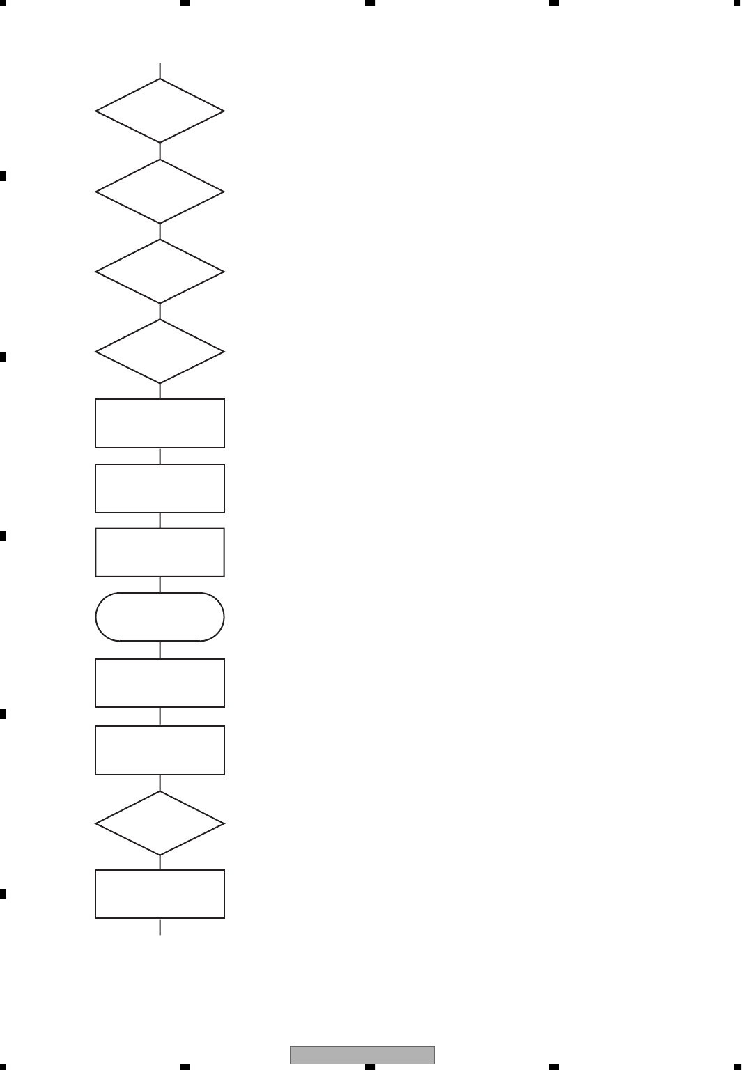
AVH-P6600DVD/UC
220
1234
1234
C
D
F
A
B
E
7.3.2 OPERATIONAL FLOW CHART
VDD0=5V
Pin 39
Power ON
bsens=L
asens=L
dsens=L
bsens
Pin 69
asens
Pin 96
dsens
Pin 83
SWVDD←H
Pin 109
ASENBO←H
Pin 87
SWVDD←H
Pin 109
Source keys
operative
Completes power-on operation.
(After that, proceed to each source operation)
SYSPW←H
Pin 31
Starts
communication
with Display
microcomputer.
Source ON
ACCPW←H
Pin 29

AVH-P6600DVD/UC 221
5678
5678
C
D
F
A
B
E
7.4 CLEANING
Before shipping out the product, be sure to clean the following portions by using the prescribed cleaning tools:
Portions to be cleaned Cleaning tools
DVD pickup lenses Cleaning liquid : GEM1004
Cleaning paper : GED-008
Portions to be cleaned Cleaning tools
Fans Cleaning paper : GED-008
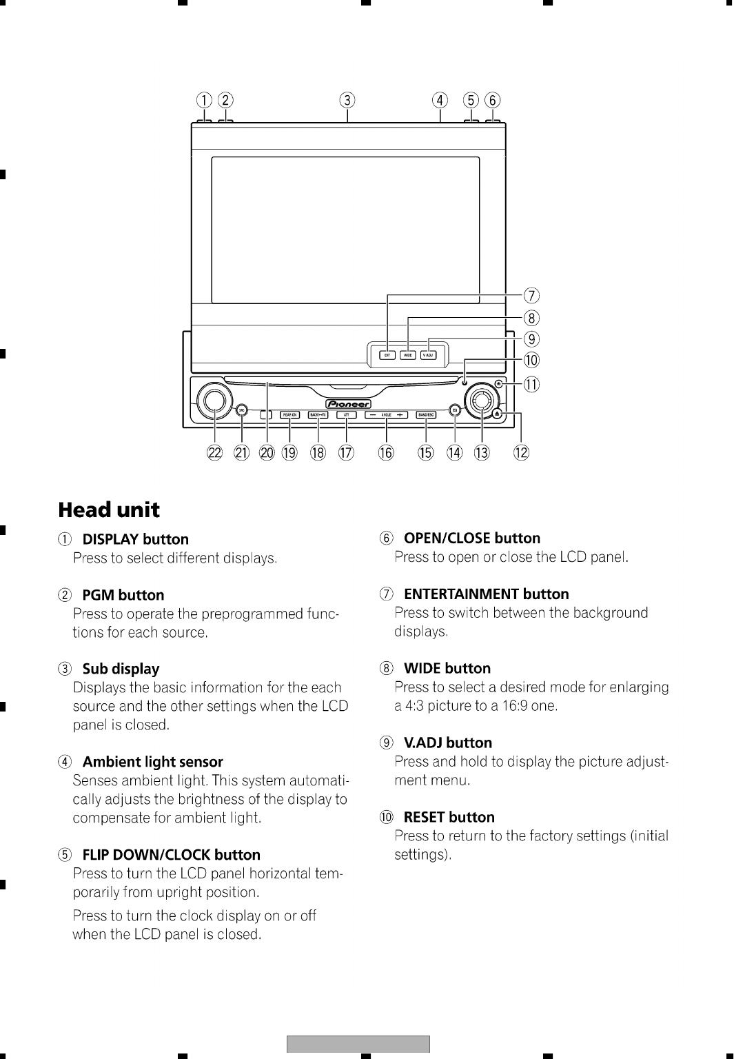
AVH-P6600DVD/UC
222
1234
1234
C
D
F
A
B
E
8. OPERATIONS
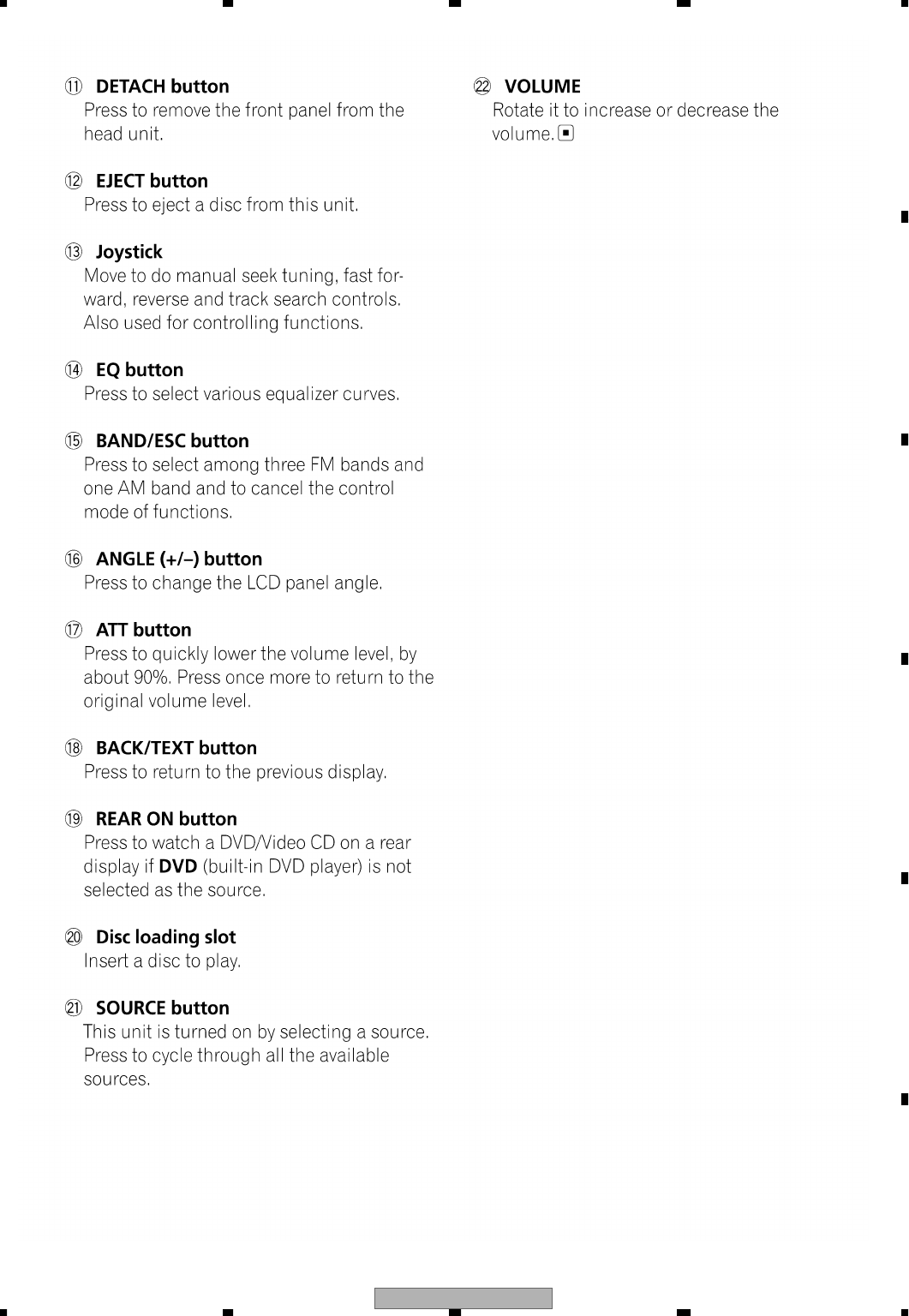
AVH-P6600DVD/UC 223
5678
5678
C
D
F
A
B
E
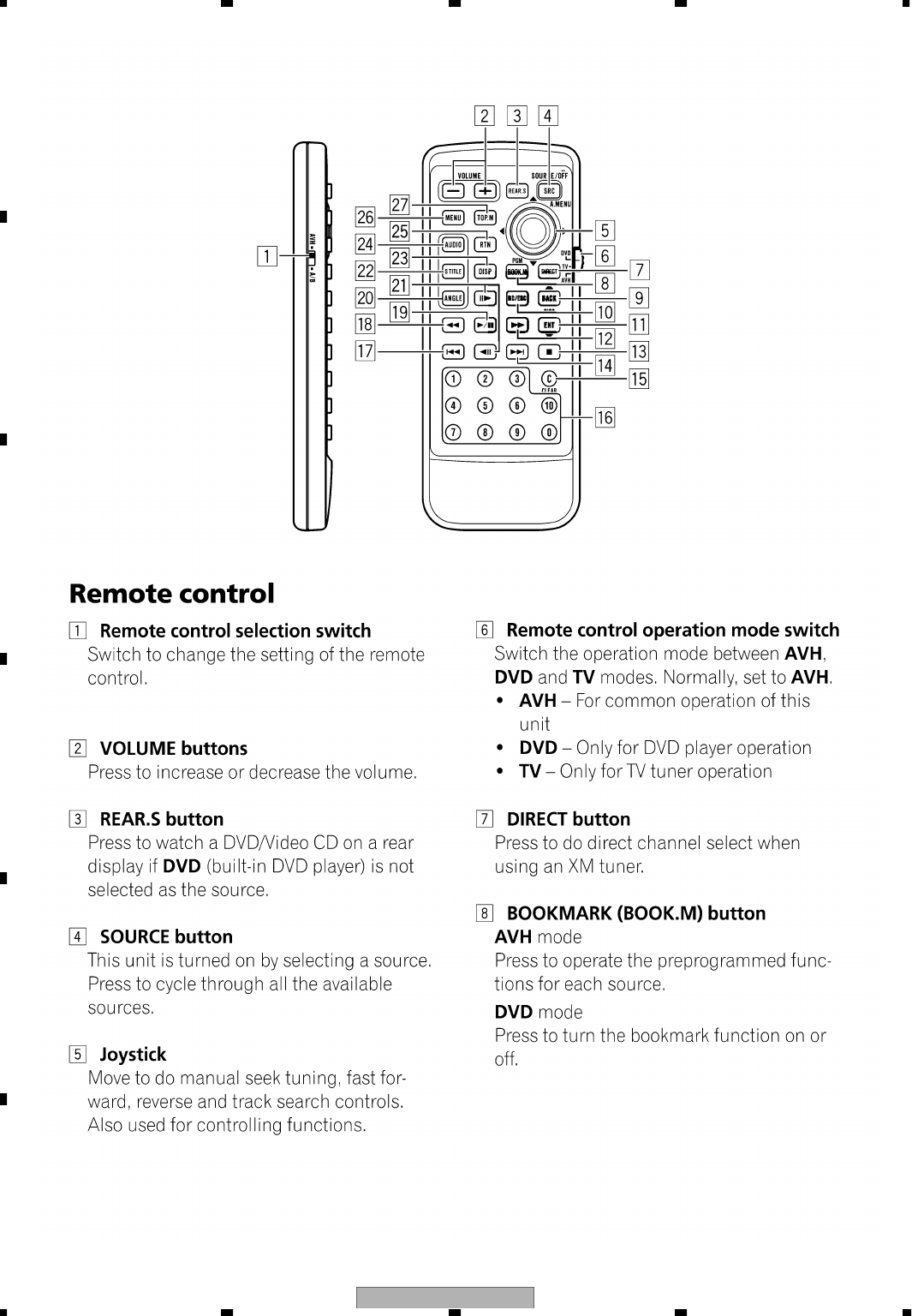
AVH-P6600DVD/UC
224
1234
1234
C
D
F
A
B
E
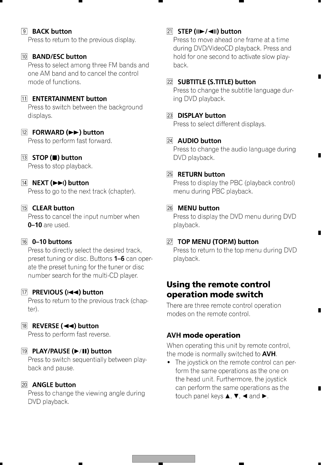
AVH-P6600DVD/UC 225
5678
5678
C
D
F
A
B
E
AVH-P6600DVD/UC
226
1234
1234
C
D
F
A
B
E
When you connect separately sold multi-channel processor
(DEQ-P8000) to this unit, do not connect anything to the
speaker leads and system remote control (blue/white).
Note:
•The position of the parking brake switch depends
on the vehicle model. For details, consult the
vehicle Owner’s Manual or dealer.
Connection method
Clamp the lead.1. 2. Clamp firmly with
needle-nosed
pliers.
Blue/white
To system control terminal of the power amp
or Auto-antenna relay control terminal
(max. 300 mA 12 V DC).
With a 2 speaker system, do not connect anything
to the speaker leads that are not connected to speakers.
Parking brake
switch
Power supply side
Ground side
Light green
Used to detect the ON/OFF status of the parking brake.
This lead must be connected to the power supply side of the parking
brake switch.
Antenna jack Violet
Black
1.5 m
(4 ft. 11 in.)
Antenna cable (supplied)
2 m
(6 ft. 7 in.)
26 pin cable (supplied)
21 pin cable (supplied)
Yellow
To terminal always supplied
with power regardless of
ignition switch position.
Fuse holder
Fuse resistor
Red
To electric terminal controlled
by ignition switch (12 V DC)
ON/OFF.
Black (ground)
To vehicle (metal) body.
Orange/white
To lighting switch terminal.
White
White/black
Gray
Gray/black
Green
Green/black
Violet
Violet/black
Front speaker
Rear speaker
Front speaker
Rear speaker
Fuse resistor
Multi-CD player
(sold separately) IP-BUS cable Violet
15 cm
(5-7/8 in.)
IP-BUS input (Blue)
Left Right
+
≠
+
≠
+
≠
+
≠
Hide-away unit
Yellow/black
If you use a cellular telephone, connect it via the
Audio Mute lead on the cellular telephone. If not,
keep the Audio Mute lead free of any connections.
Black
This product
Jack for Wired Remote Control
Please see the Instruction Manual for the
Wired Remote Control (sold separately).
- CONNECTION DIAGRAM
AVH-P6600DVD/UC 227
5678
5678
C
D
F
A
B
E
Note:
Change the initial setting of this product
(refer to the Operation Manual).
The subwoofer output of this unit is monaura
l
Note:
When you connect multi-channel processor to
this unit, separately sold power amp must be
connected to multi-channel processor.
When you connect separately sold
multi-channel processor (e.g. DEQ-P8000)
to this unit, do not connect anything to the
speaker leads and system remote control
(blue/white).
Blue/white
To system control terminal of the power amp
or Auto-antenna relay control terminal
(max. 300 mA 12 V DC).
This product
Front output
(FRONT OUTPUT)
Subwoofer output
or non fading output
(SUBWOOFER OUTPUT or
NON-FADING OUTPUT)
Rear output
(REAR OUTPUT)
Power amp
(sold separately)
Power amp
(sold separately)
Power amp
(sold separately)
+
≠
+
≠
+
≠
+
≠
+
≠
+
≠
System remote control
RCA cables
(sold separately)
Front speaker
Rear speaker
Subwoofer
Front speaker
Rear speaker
Subwoofer
Left Right
15 cm
(5-7/8 in.)
23 cm (9 in.)
15 cm
(5-7/8 in.)
- CONNECTION DIAGRAM

AVH-P6600DVD/UC
228
1234
1234
C
D
F
A
B
E
- Jigs list
Disc : GGV1018
Cleaning liquid : GEM1004
Cleaning paper : GED-008
Function Name Jig No.
Mother PCB(CN501) <-> Main Unit(CN3801) PCB GGF1471
Mother PCB(CN501) <-> GGF1471 50P FFC GGD1250
Mother PCB(CN502) <-> GGF1471 24P FFC GGD1337
Mother PCB(CN501,CN502) <-> Monitor PCB(CN4461,CN4481) PCB GGF1472
Monitor PCB(CN4461) <-> GGF1472 33P FFC GGD1262
Monitor PCB(CN4481) <-> GGF1472 24P FFC GGD1337
Mother PCB(CN601) <-> Panel PCB(CN5901) 17PFFC GGD1124
