CRT3879 AVICD3
User Manual: AVICD3
Open the PDF directly: View PDF ![]() .
.
Page Count: 306 [warning: Documents this large are best viewed by clicking the View PDF Link!]
- SAFETY INFORMATION
- CONTENTS
- 1. SPECIFICATIONS
- 2. EXPLODED VIEWS AND PARTS LIST
- 2.1 PACKING (UC)
- 2.2 PACKING (EW5)
- 2.3 EXTERIOR (1)
- 2.4 EXTERIOR (2)
- 2.5 EXTERIOR (3)
- 2.6 DVD MECHANISM MODULE
- 3. BLOCK DIAGRAM AND SCHEMATIC DIAGRAM
- 3.1 BLOCK DIAGRAM
- 3.2 OVERALL CONNECTION DIAGRAM
- 3.3 NAVI MOTHER UNIT (CPU, ASIC, SDRAM)(GUIDE PAGE)
- 3.4 NAVI MOTHER UNIT (ROM, SRAM, BUS-BUFFER)
- 3.5 NAVI MOTHER UNIT (GRAPHIC)(GUIDE PAGE)
- 3.6 NAVI MOTHER UNIT (MAIN, CC I/F)
- 3.7 NAVI MOTHER UNIT (SYSTEM uCOM)(GUIDE PAGE)
- 3.8 NAVI MOTHER UNIT (I/F)(GUIDE PAGE)
- 3.9 NAVI MOTHER UNIT (PS)(GUIDE PAGE)
- 3.10 GPS UNIT(GUIDE PAGE)
- 3.11 AV UNIT (PS, I/F)
- 3.12 AV UNIT (A/V)(GUIDE PAGE)
- 3.13 AV UNIT (TUNER)
- 3.14 DVD CORE UNIT (1/2)(GUIDE PAGE)
- 3.15 DVD CORE UNIT (2/2)
- 3.16 COMPOUND UNIT(A), COMPOUND UNIT(B)
- 3.17 MONITOR UNIT (VIDEO)(GUIDE PAGE)
- 3.18 MONITOR UNIT (INVERTER)
- 3.19 KEY PCB
- 3.20 AV MINI JACK PCB
- 4. PCB CONNECTION DIAGRAM
- 4.1 NAVI MOTHER UNIT
- 4.2 AV UNIT
- 4.3 DVD CORE UNIT
- 4.4 COMPOUND UNIT(A), COMPOUND UNIT(B)
- 4.5 GPS UNIT
- 4.6 MONITOR UNIT
- 4.7 KEY PCB
- 4.8 AV MINI JACK PCB
- 5. ELECTRICAL PARTS LIST
- 6. ADJUSTMENT
- 6.1 JIG CONNECTION DIAGRAM
- 6.2 DVD ADJUSTMENT
- 6.3 MONITOR UNIT ADJUSTMENT
- 6.4 SERVICE ADJUSTMENT
- 6.5 EEPROM ADJUSTMENT
- 6.6 PHASE ADJUSTMENT
- 6.7 RGB ILLUMINATION ADJUSTMENT
- 6.8 TOUCH PANEL TEST MODE
- 6.9 NAVIGATION TEST MODE
- 6.10 USING THE TEST DISC
- 7. GENERAL INFORMATION
- 7.1 DIAGNOSIS
- 7.1.1 DISASSEMBLY
- 7.1.2 CONNECTOR FUNCTION DESCRIPTION
- 7.2 IC
- 7.3 EXPLANATION
- 7.3.1 CIRCUIT DESCRIPTIONS
- 7.3.2 OPERATIONAL FLOW CHART
- 8. OPERATIONS
ORDER NO.
PIONEER CORPORATION 4-1, Meguro 1-chome, Meguro-ku, Tokyo 153-8654, Japan
PIONEER ELECTRONICS (USA) INC. P.O. Box 1760, Long Beach, CA 90801-1760, U.S.A.
PIONEER EUROPE NV Haven 1087, Keetberglaan 1, 9120 Melsele, Belgium
PIONEER ELECTRONICS ASIACENTRE PTE. LTD. 253 Alexandra Road, #04-01, Singapore 159936
PIONEER CORPORATION 2007
AVIC-D3/XU/UC
CRT3879
DVD MULTIMEDIA AV NAVIGATION SERVER
AVIC-D3
/XU/UC
AVIC-D3
/XU/EW5
This service manual should be used together with the following manual(s):
Model No. Order No. Mech.Module Remarks
CX-3212 CRT3896 MS5 DVD Mech. Module : Circuit Descriptions, Mech. Descriptions, Disassembly
For details, refer to "Important Check Points for Good Servicing".
K-ZZW. FEB. 2007 Printed in Japan
AVIC-D3/XU/UC
2
1234
1234
C
D
F
A
B
E
SAFETY INFORMATION
1. Safety Precautions for those who Service this Unit.
•Follow the adjustment steps in the service manual when servicing this unit. When check -
ing or adjusting the emitting power of the laser diode exercise caution in order to get safe, reliable results.
Caution:
1. During repair or tests, minimum distance of 13cm from the focus lens must be kept.
2. During repair or tests, do not view laser beam for 10 seconds or longer.
CAUTION
This service manual is intended for qualified service technicians; it is not meant for the casual do-it-yourselfer.
Qualified technicians have the necessary test equipment and tools, and have been trained to properly and safely repair
complex products such as those covered by this manual.
and refer the repair to a qualified service technician.
WARNING
This product contains lead in solder and certain electrical parts contain chemicals which are known to the state of
California to cause cancer, birth defects or other reproductive harm.
Health & Safety Code Section 25249.6 - Proposition 65
This product contains mercury. Disposal of this material may be regulated due to environmental considerations.
For disposal or recycling information, please contact your local authorities or the Electronics Industries
Alliance: www.eiae.org.
Improperly performed repairs can adversely affect the safety and reliability of the product and may void the warranty.
If you are not qualified to perform the repair of this product properly and safely, you should not risk trying to do so
2.The trianglar label is attached to the mechanism unit frame.
On the top of the player.
WARNING!
The AEL (accessible emission level )of the laser power output is less than CLASS 1
but the laser component is capable of emitting radiation exceeding the limit for
CLASS 1.
A specially instructed person should do servicing operation of the apparatus.
Laser diode characteristics
Wave length:
DVD:660 nm to 670 nm
CD:780 nm to 800 nm
DVD : 1.27 mW(Emitting period :9 sec.)
CD : 6.26 mW(Emitting period : unlimited)
Maximum output:
AVIC-D3/XU/UC 3
5678
56
78
C
D
F
A
B
E
Additional Laser Caution
Transistors Q1103 and Q1104 in PCB drive the laser diodes for DVD and CD
respectively. When Q1103 or Q1104 is shorted between their terminals,
the laser diodes for DVD or CD will radiate beam. If the top cover is removed
with no disc loaded while such short-circuit is continued, the naked eyes may
be exposed to the laser beam.
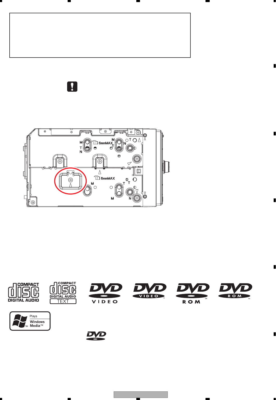
DVD MECHANISM MODULE section precaution
1. Before disassembling the unit, be sure to turn off the power. Unplugging and plugging the connectors
during power-on mode may damage the ICs inside the unit.
2. To protect the pickup unit from electrostatic discharge during servicing, take an appropriate treatment
(shorting-solder) by referring to "the DISASSEMBLY" .
3. After replacing the pickup unit, be sure to skew adjustment.
4. During disassembly, be sure to turn the power off since an internal IC might be destroyed when a
connector is plugged or unplugged.
- Service Precautions
1. You should conform to the regulations governing the product (safety, radio and noise, and other regulations),
and should keep the safety during servicing by following the safety instructions described in this manual.
2. Be careful in handling ICs. Some ICs such as MOS type are so fragile that they can be damaged by electrostatic
induction.
3. Because a part to show in figure below becomes hot, take care upon its operation.
is a trademark of DVD Format/Logo Licensing Corporation.
AVIC-D3/XU/UC
4
1234
1234
C
D
F
A
B
E
[Important Check Points for Good Servicing]
In this manual, procedures that must be performed during repairs are marked with the below symbol.
Please be sure to confirm and follow these procedures.
1. Product safety
Please conform to product regulations (such as safety and radiation regulations), and maintain a safe servicing environment by
following the safety instructions described in this manual.
1 Use specified parts for repair.
Use genuine parts. Be sure to use important parts for safety.
2 Do not perform modifications without proper instructions.
Please follow the specified safety methods when modification(addition/change of parts) is required due to interferences such as
radio/TV interference and foreign noise.
3 Make sure the soldering of repaired locations is properly performed.
When you solder while repairing, please be sure that there are no cold solder and other debris.
Soldering should be finished with the proper quantity. (Refer to the example)
4 Make sure the screws are tightly fastened.
Please be sure that all screws are fastened, and that there are no loose screws.
5 Make sure each connectors are correctly inserted.
Please be sure that all connectors are inserted, and that there are no imperfect insertion.
6 Make sure the wiring cables are set to their original state.
Please replace the wiring and cables to the original state after repairs.
In addition, be sure that there are no pinched wires, etc.
7 Make sure screws and soldering scraps do not remain inside the product.
Please check that neither solder debris nor screws remain inside the product.
8 There should be no semi-broken wires, scratches, melting, etc. on the coating of the power cord.
Damaged power cords may lead to fire accidents, so please be sure that there are no damages.
If you find a damaged power cord, please exchange it with a suitable one.
9 There should be no spark traces or similar marks on the power plug.
When spark traces or similar marks are found on the power supply plug, please check the connection and advise on secure
connections and suitable usage. Please exchange the power cord if necessary.
0 Safe environment should be secured during servicing.
When you perform repairs, please pay attention to static electricity, furniture, household articles, etc. in order to prevent injuries.
Please pay attention to your surroundings and repair safely.
2. Adjustments
To keep the original performance of the products, optimum adjustments and confirmation of characteristics within specification.
Adjustments should be performed in accordance with the procedures/instructions described in this manual.
4. Cleaning
For parts that require cleaning, such as optical pickups, tape deck heads, lenses and mirrors used in projection monitors, proper
cleaning should be performed to restore their performances.
3. Lubricants, Glues, and Replacement parts
Use grease and adhesives that are equal to the specified substance.
Make sure the proper amount is applied.
5. Shipping mode and Shipping screws
To protect products from damages or failures during transit, the shipping mode should be set or the shipping screws should be
installed before shipment. Please be sure to follow this method especially if it is specified in this manual.

AVIC-D3/XU/UC 5
5678
56
78
C
D
F
A
B
E
CONTENTS
SAFETY INFORMATION......................................................................................................................................2
1. SPECIFICATIONS .............................................................................................................................................6
2. EXPLODED VIEWS AND PARTS LIST...........................................................................................................10
2.1 PACKING (UC) .........................................................................................................................................10
2.2 PACKING (EW5).......................................................................................................................................12
2.3 EXTERIOR (1) ..........................................................................................................................................14
2.4 EXTERIOR (2) ..........................................................................................................................................16
2.5 EXTERIOR (3) ..........................................................................................................................................18
2.6 DVD MECHANISM MODULE ...................................................................................................................20
3. BLOCK DIAGRAM AND SCHEMATIC DIAGRAM ..........................................................................................22
3.1 BLOCK DIAGRAM....................................................................................................................................22
3.2 OVERALL CONNECTION DIAGRAM ......................................................................................................40
3.3 NAVI MOTHER UNIT (CPU, ASIC, SDRAM)(GUIDE PAGE) ...................................................................42
3.4 NAVI MOTHER UNIT (ROM, SRAM, BUS-BUFFER)...............................................................................48
3.5 NAVI MOTHER UNIT (GRAPHIC)(GUIDE PAGE)....................................................................................50
3.6 NAVI MOTHER UNIT (MAIN, CC I/F) .......................................................................................................56
3.7 NAVI MOTHER UNIT (SYSTEM uCOM)(GUIDE PAGE)..........................................................................58
3.8 NAVI MOTHER UNIT (I/F)(GUIDE PAGE)................................................................................................64
3.9 NAVI MOTHER UNIT (PS)(GUIDE PAGE) ...............................................................................................70
3.10 GPS UNIT(GUIDE PAGE) ......................................................................................................................76
3.11 AV UNIT (PS, I/F) ...................................................................................................................................82
3.12 AV UNIT (A/V)(GUIDE PAGE) ................................................................................................................84
3.13 AV UNIT (TUNER) ..................................................................................................................................90
3.14 DVD CORE UNIT (1/2)(GUIDE PAGE)...................................................................................................92
3.15 DVD CORE UNIT (2/2) ...........................................................................................................................98
3.16 COMPOUND UNIT(A), COMPOUND UNIT(B).....................................................................................102
3.17 MONITOR UNIT (VIDEO)(GUIDE PAGE).............................................................................................104
3.18 MONITOR UNIT (INVERTER) ..............................................................................................................110
3.19 KEY PCB ..............................................................................................................................................114
3.20 AV MINI JACK PCB ..............................................................................................................................116
4. PCB CONNECTION DIAGRAM ....................................................................................................................118
4.1 NAVI MOTHER UNIT..............................................................................................................................118
4.2 AV UNIT..................................................................................................................................................122
4.3 DVD CORE UNIT....................................................................................................................................126
4.4 COMPOUND UNIT(A), COMPOUND UNIT(B).......................................................................................130
4.5 GPS UNIT...............................................................................................................................................131
4.6 MONITOR UNIT .....................................................................................................................................132
4.7 KEY PCB ................................................................................................................................................136
4.8 AV MINI JACK PCB ................................................................................................................................137
5. ELECTRICAL PARTS LIST ...........................................................................................................................138
6. ADJUSTMENT ..............................................................................................................................................164
6.1 JIG CONNECTION DIAGRAM ...............................................................................................................164
6.2 DVD ADJUSTMENT ...............................................................................................................................165
6.3 MONITOR UNIT ADJUSTMENT ............................................................................................................196
6.4 SERVICE ADJUSTMENT .......................................................................................................................205
6.5 EEPROM ADJUSTMENT .......................................................................................................................207
6.6 PHASE ADJUSTMENT ..........................................................................................................................213
6.7 RGB ILLUMINATION ADJUSTMENT .....................................................................................................215
6.8 TOUCH PANEL TEST MODE .................................................................................................................217
6.9 NAVIGATION TEST MODE ....................................................................................................................223
6.10 USING THE TEST DISC.......................................................................................................................242
7. GENERAL INFORMATION ...........................................................................................................................254
7.1 DIAGNOSIS............................................................................................................................................254
7.1.1 DISASSEMBLY....................................................................................................................................254
7.1.2 CONNECTOR FUNCTION DESCRIPTION ........................................................................................260
7.2 IC ............................................................................................................................................................261
7.3 EXPLANATION .......................................................................................................................................293
7.3.1 CIRCUIT DESCRIPTIONS ..................................................................................................................293
7.3.2 OPERATIONAL FLOW CHART ...........................................................................................................294
8. OPERATIONS ...............................................................................................................................................296
AVIC-D3/XU/UC
6
1234
1234
C
D
F
A
B
E
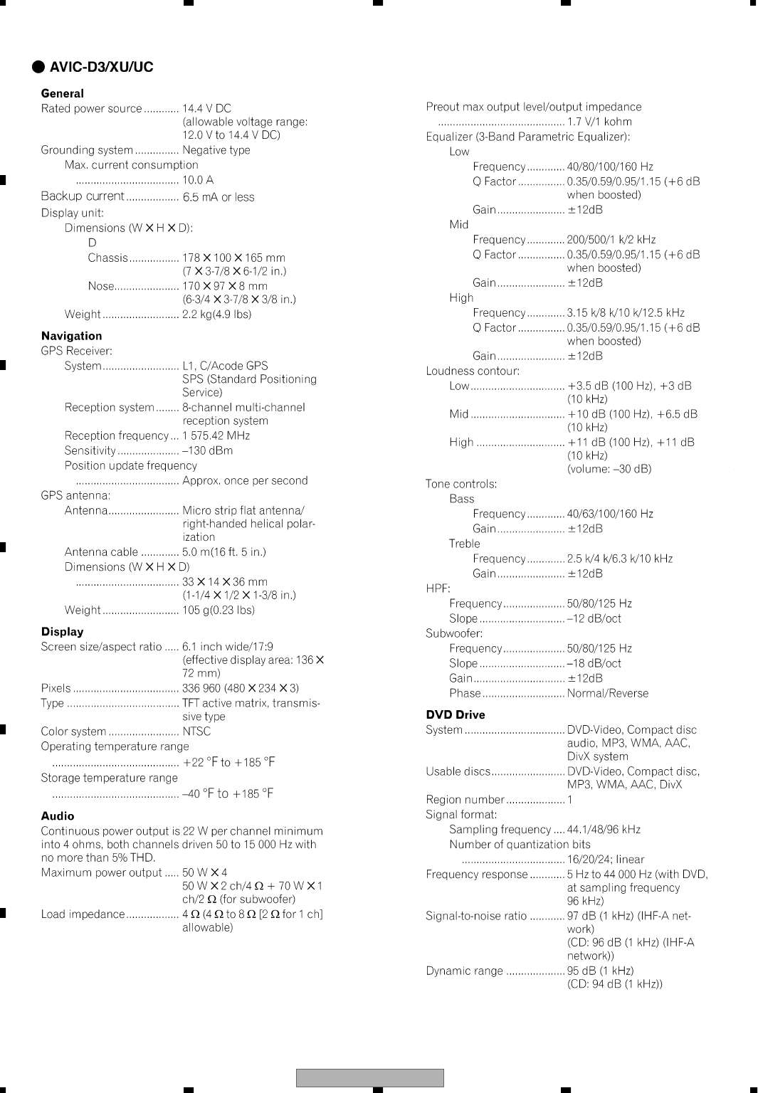
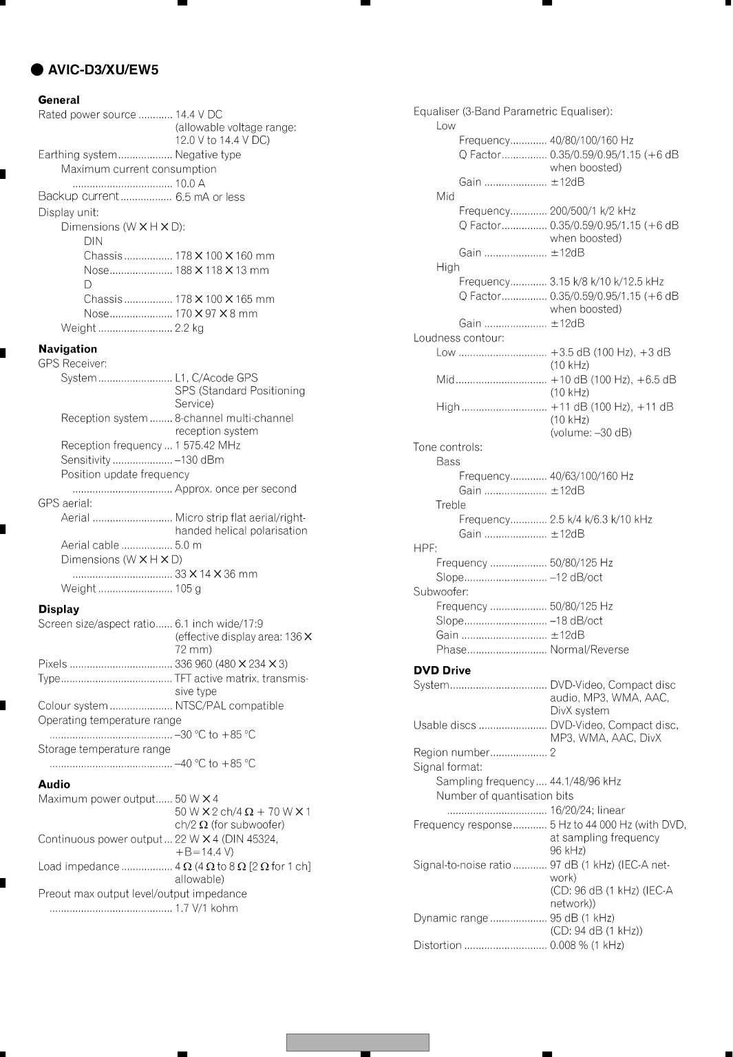
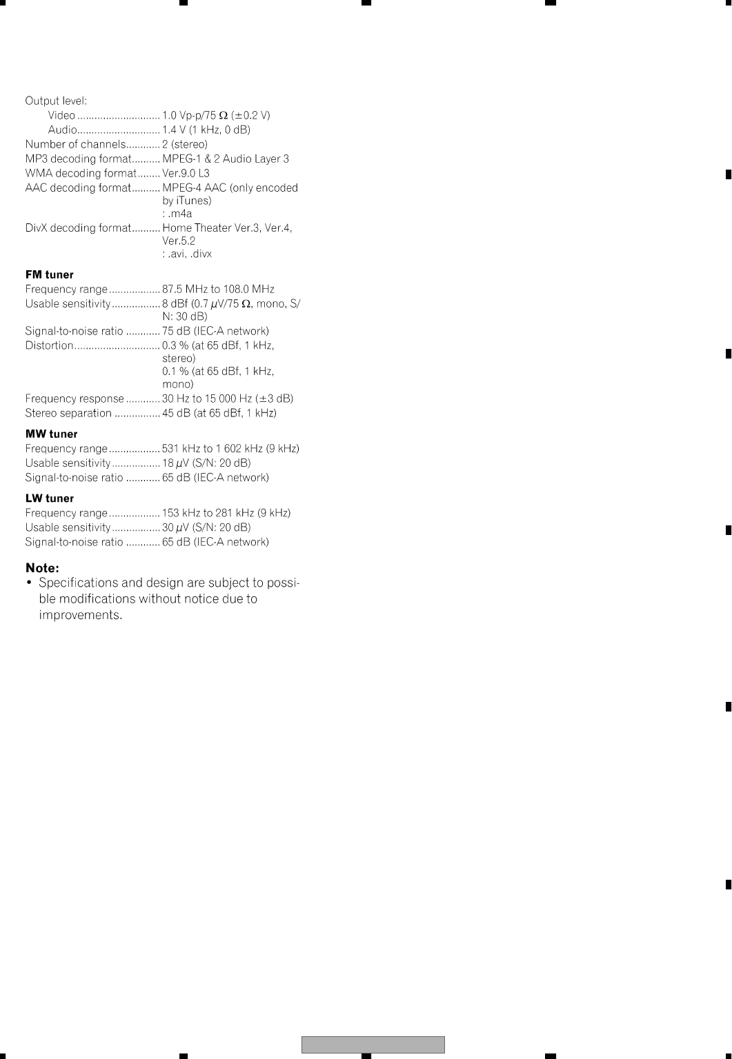
1. SPECIFICATIONS
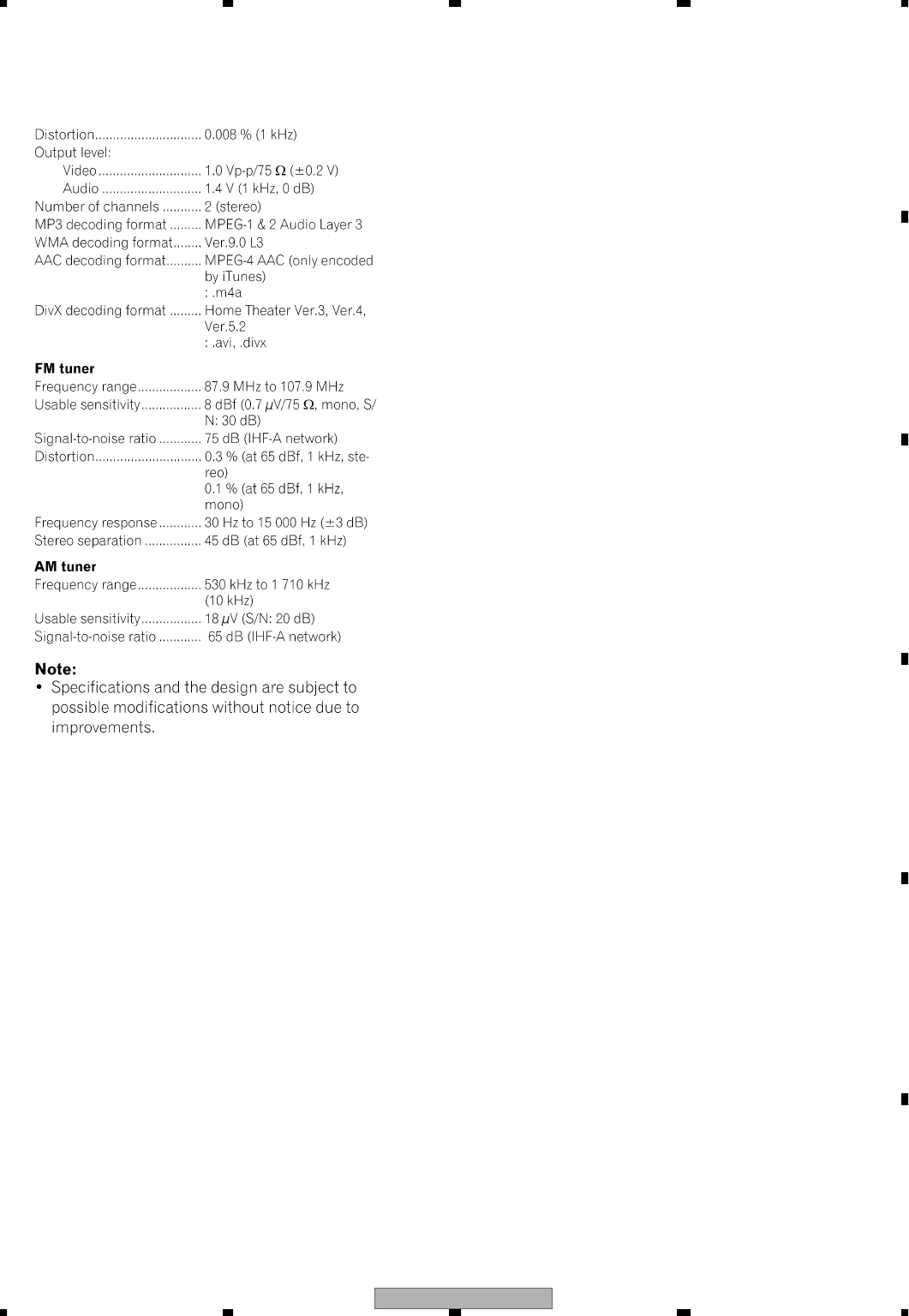
AVIC-D3/XU/UC 7
5678
56
78
C
D
F
A
B
E
AVIC-D3/XU/UC
8
1234
1234
C
D
F
A
B
E
AVIC-D3/XU/UC 9
5678
56
78
C
D
F
A
B
E
AVIC-D3/XU/UC
10
1234
1234
C
D
F
A
B
E
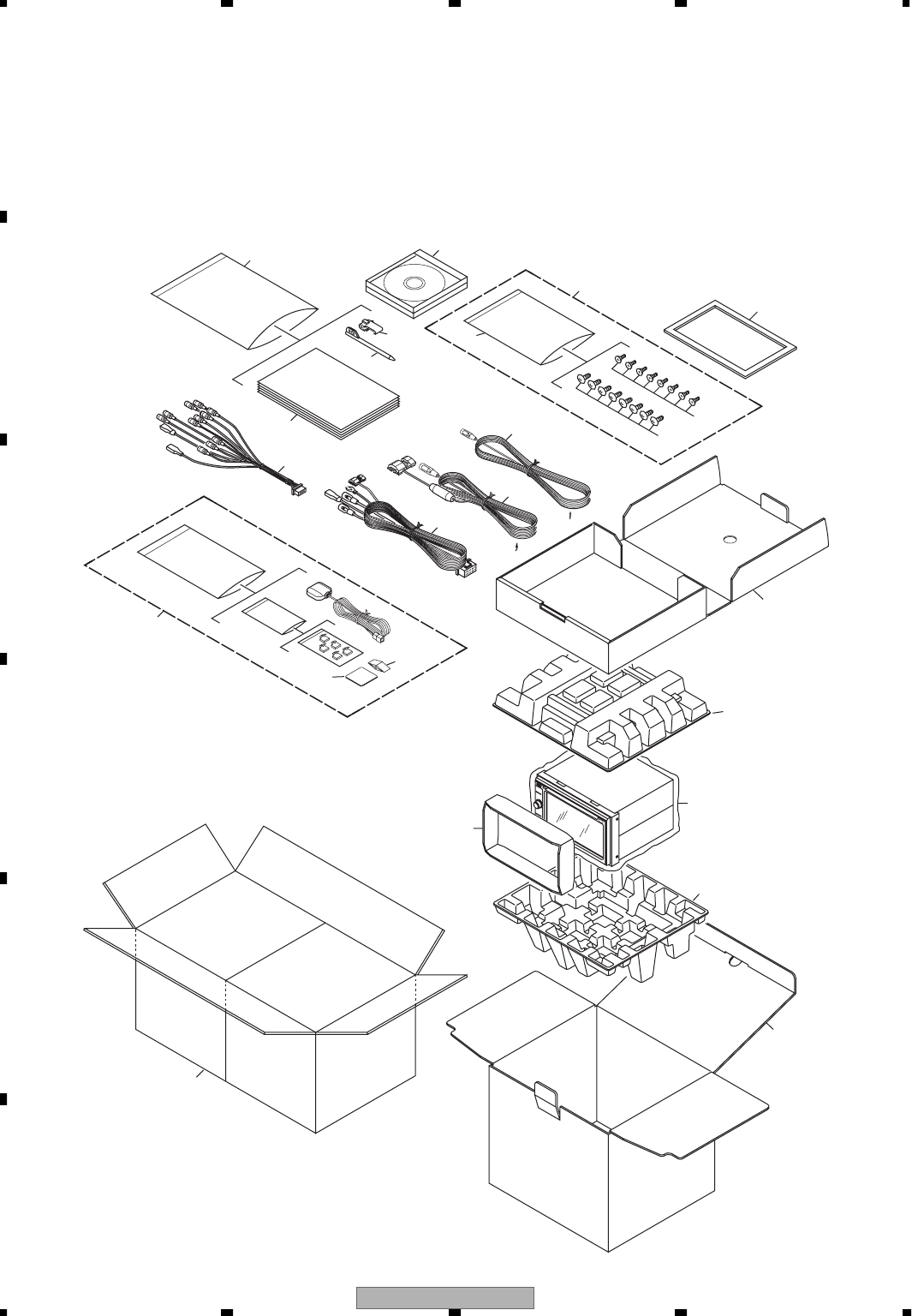
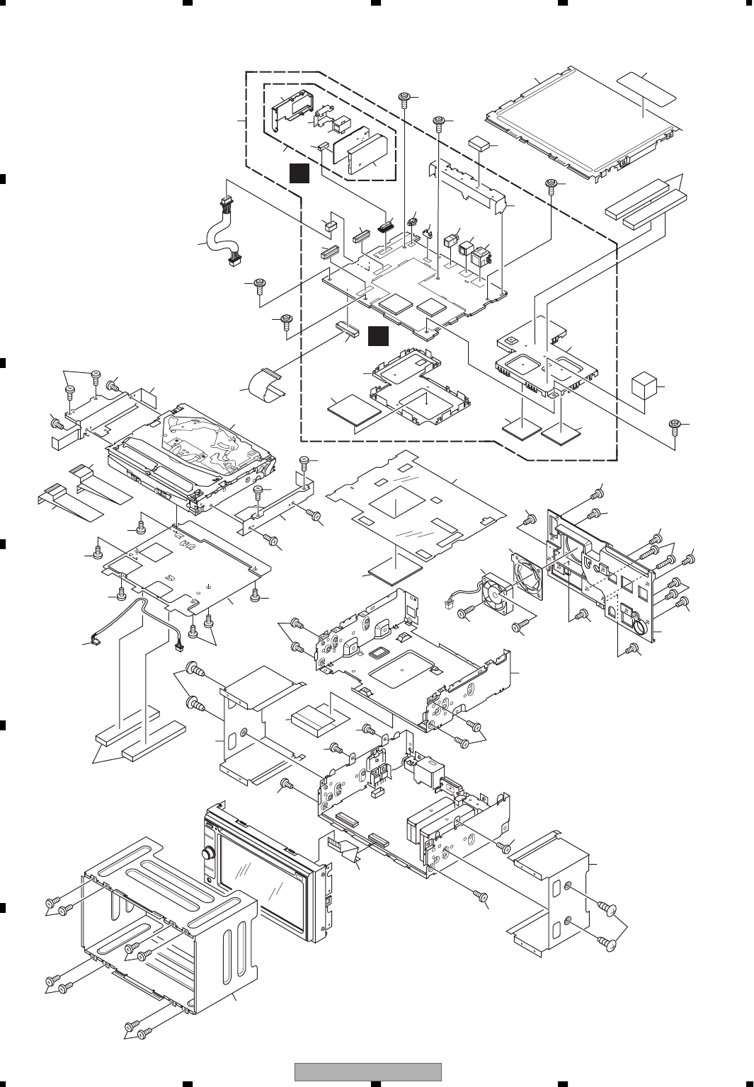
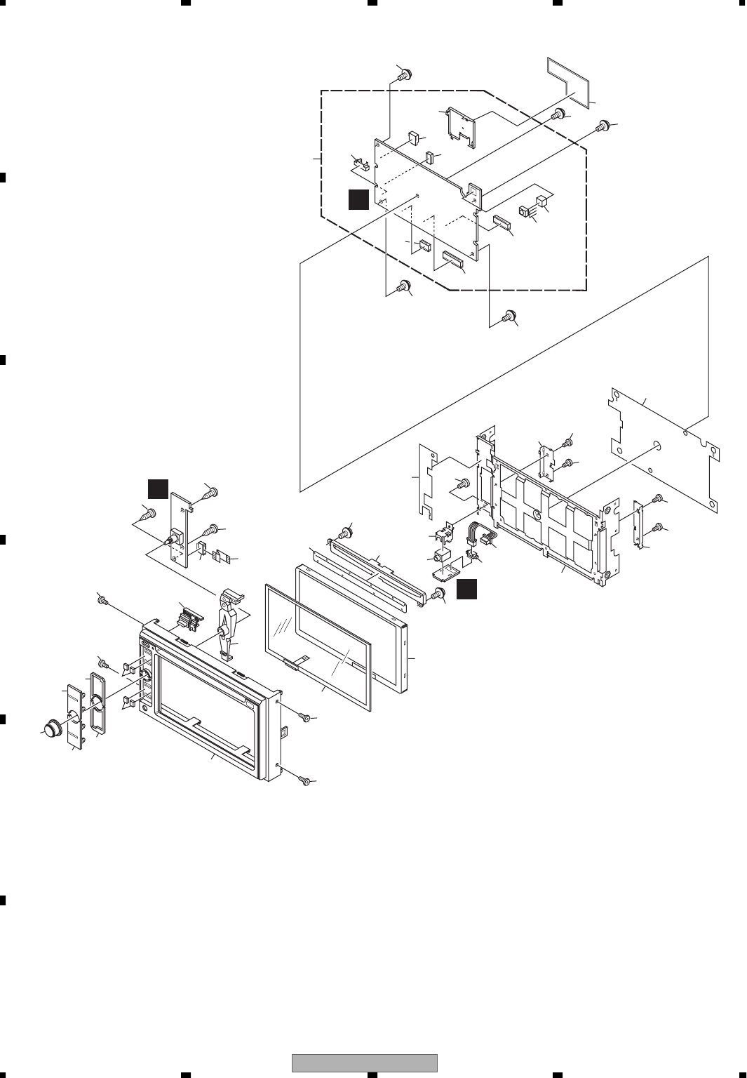
2. EXPLODED VIEWS AND PARTS LIST
2.1 PACKING (UC)
N
OTES : • Parts marked by " * " are generally unavailable because they are not in our Master Spare Parts List.
• The > mark found on some component parts indicates the importance of the safety factor of the part.
Therefore, when replacing, be sure to use parts of identical designation.
• Screw adjacent to mark on the product are used for disassembly.
• For the applying amount of lubricants or glue, follow the instructions in this manual.
(In the case of no amount instructions,apply as you think it appropriate.)
"
19
7
8
9
10
21
23
22
12
13
11
14
17
16
6
1
5
4
2
3
15
20
24
18
AVIC-D3/XU/UC 11
5678
56
78
C
D
F
A
B
E
PACKING (UC) SECTION PARTS LIST
Owner's Manual,Installation Manual
Mark No. Description Part No.
1 Polyethylene Bag CEG1383
2 Unit Box CHG6065
3 Contain Box CHL6065
4 Protector CHP3376
5 Protector CHP3315
6 Protector CHP3316
7 Cord CDE5044
8 Cord CDE6825
9 Cord Assy CDP1063
10 Cord Assy CDP1064
11 Screw Assy CEA3797
12 Screw BMZ50P060FTC
* 13 Polyethylene Bag CEG-127
14 Screw CMZ50P060FTC
15 Polyethylene Bag CEG1116
16 Sub Unit Box CHG6064
17 Panel CNS9008
18 Pen CNV8969
19 DVD-ROM CPJ1183
20-1 Owner's Manual CRB2325
20-2 Owner's Manual/POC/FRE CRB2326
20-3 Owner's Manual CRB2327
20-4 Owner's Manual/POC/FRE CRB2328
20-5 Installation Manual CRD4167
20-6 Caution Card CRP1310
* 20-7 Warranty Card CRY1246
* 20-8 Registration Card CRY1263
21 GPS Antenna Assy CXC4864
22 Water Proof Pad CZN5442
23 Sheet CZN7008
24 Connector CKX1049
Mark No. Description Part No.
Part No. Language
CRB2325,
CRB2327
English
CRB2326,
CRB2328
French
CRD4167 English, French
AVIC-D3/XU/UC
12
1234
1234
C
D
F
A
B
E
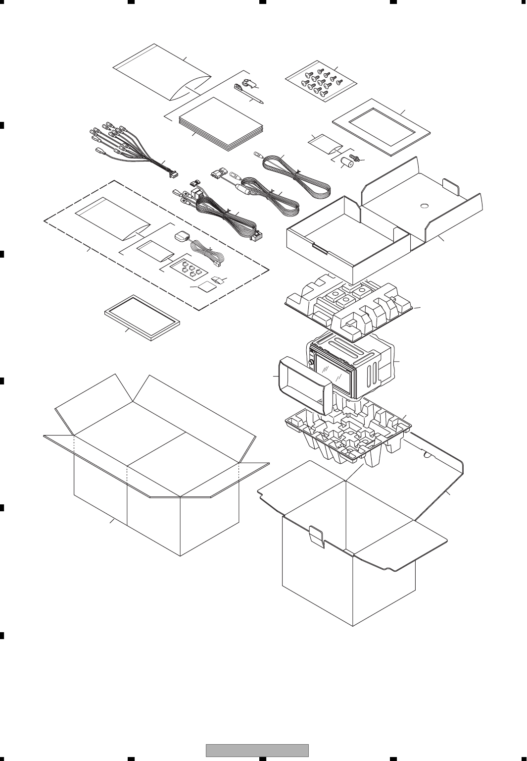
2.2 PACKING (EW5)
11
18
14
12
13
7
8
9
10
21
22
23
16
6
1
5
2
3
4
15
20
24
19
17
AVIC-D3/XU/UC 13
5678
56
78
C
D
F
A
B
E
PACKING (EW5) SECTION PARTS LIST
Owner's Manual,Installation Manual
Mark No. Description Part No.
1 Polyethylene Bag CEG1382
2 Unit Box CHG6066
3 Contain Box CHL6066
4 Protector CHP3376
5 Protector CHP3317
6 Protector CHP3318
7 Cord CDE5044
8 Cord CDE6825
9 Cord Assy CDP1062
10 Cord Assy CDP1064
11 Screw Assy CEA7395
12 Screw CBA2081
13 Bush CNV3930
* 14 Polyethylene Bag E36-615
15 Polyethylene Bag CEG1116
16 Sub Unit Box CHG6064
17 Panel CNS8665
18 Panel CNS9007
19 Pen CNV8969
20-1 Owner's Manual/PEE/ENG CRB2329
20-2 Owner's Manual/PEE/SPE CRB2330
20-3 Owner's Manual/PEE/GER CRB2331
20-4 Owner's Manual/PEE/FRE CRB2332
20-5 Owner's Manual/PEE/ITA CRB2333
20-6 Owner's Manual/PEE/DUT CRB2334
20-7 Owner's Manual/PEE/ENG CRB2335
20-8 Owner's Manual/PEE/SPE CRB2336
20-9 Owner's Manual/PEE/GER CRB2337
20-10 Owner's Manual/PEE/FRE CRB2338
20-11 Owner's Manual/PEE/ITA CRB2339
20-12 Owner's Manual/PEE/DUT CRB2340
20-13 Installation Manual CRD4169
20-14 Caution Card CRP1310
* 20-15 Warranty Card CRY1157
21 GPS Antenna Assy CXC4864
22 Water Proof Pad CZN5442
23 Sheet CZN7008
24 Connector CKX1049
Mark No. Description Part No.
Part No. Language
CRB2329,
CRB2335
English
CRB2330,
CRB2336
Spanish
CRB2331,
CRB2337
German
CRB2332,
CRB2338
French
CRB2333,
CRB2339
Italian
CRB2334,
CRB2340
Dutch
CRD4169 English, Spanish, German, French, Italian, Dutch
AVIC-D3/XU/UC
14
1234
1234
C
D
F
A
B
E
2.3 EXTERIOR (1)
53
18
13
1
1
40
31
39
30
34
33
38
36
32
35
43
29
46
48 44
45
47
7
1
1
37
50
42
1
14
1
2
2
2
22
32
2
2
28
2
2
6
24
52
6
17
2
2
20
16
2
2
2
20
16
10
5
5
5
9
8
5
2522
51
27
2
5
26
5
5
23
21
5
2
2
11
4
19
4
4
4
41
49
25
41
54
15
15
A
B
AVIC-D3/XU/UC 15
5678
56
78
C
D
F
A
B
E
(1) EXTERIOR (1) SECTION PARTS LIST
(2) CONTRAST TABLE
AVIC-D3/XU/UC and AVIC-D3/XU/EW5 are constructed the same except for the following:
Mark No. Description Part No.
1 Screw ASZ26P050FTC
2 Screw BMZ26P050FTC
3 Screw BMZ26P160FTB
4 Screw See Contrast table(2)
5 Screw(M2 x 3) CBA2096
6 Screw(M3 x 10) CBA2097
7 Cord Assy CDE8156
8 FFC CDE8312
9 FFC CDE8313
10 Cord Assy CDE8339
11 FFC CDE8340
12 •••••
13 Gasket CNN1805
14 Gasket CNN1804
15 Cushion CNN1807
16 Screw See Contrast table(2)
17 Chassis CNA2964
18 Case CNB3357
19 Holder See Contrast table(2)
20 Holder See Contrast table(2)
21 Shield CND3692
22 Bracket CND3697
23 Bracket CND3698
24 Cover CND3917
25 Insulator CNN1404
26 Sheet CNN1449
27 Flexible PCB CNP8272
28 Heat Sink CNR1888
29 Navi Mother Unit See Contrast table(2)
30 Jack(CN2063) CKN1043
31 Connector(CN2065) CKS3408
32 Connector(CN2068) CKS4674
33 Connector(CN2059) CKS4822
34 Connector(CN2061) CKS4823
35 Connector(CN2) CKS5075
36 Connector(CN2057) CKS5075
37 Connector(CN2055) CKS5110
38 Connector(CN2060) CKS5205
39 Connector(CN2066) CKS5598
40 Holder CND3696
41 Sheet CNM9933
42 Sheet CNN1449
43 GPS Unit See Contrast table(2)
44 Connector(CN504) CKS4432
45 Connector(CN461) CKS5204
46 Shield CNC9191
47 Shield CNC9192
48 Holder CND1535
49 Shield Assy CXC7020
50 Shield Assy CXC7021
51 DVD Mechanism Module(MS5) CXK6601
52 Fan Motor CXM1320
53 Label See Contrast table(2)
54 Shield CNN1806
Mark No. Description Part No.
Mark No. Description AVIC-D3/XU/UC AVIC-D3/XU/EW5
4 Screw Not used BMZ30P060FTC
16 Screw Not used CMZ50P060FTC
19 Holder Not used CND3430
20 Holder Not used CND3431
29 Navi Mother Unit CWN2189 CWN2089
43 GPS Unit CWX3446 CWX3447
53 Label Not used CAN5448
AVIC-D3/XU/UC
16
1234
1234
C
D
F
A
B
E
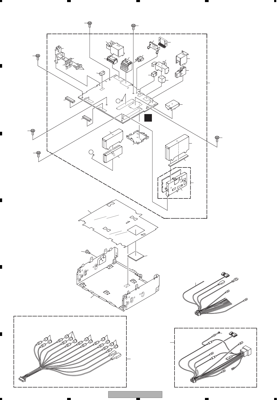
2.4 EXTERIOR (2)
A
A
11
23
12
1
25
33
10 14
11 24
17
21
18
26
13
15
16
22
31
30
1
1
1
20
27
28
29
8
34
6
7
2
3
4
5
5
5
5
5
9
33
19 32
35
36
C
AVIC-D3/XU/UC 17
5678
56
78
C
D
F
A
B
E
(1) EXTERIOR (2) SECTION PARTS LIST
(2) CONTRAST TABLE
AVIC-D3/XU/UC and AVIC-D3/XU/EW5 are constructed the same except for the following:
Mark No. Description Part No.
1 Screw ASZ26P050FTC
2 Cord Assy See Contrast table(2)
3 Cap See Contrast table(2)
4 Cord Assy CDP1064
5 Cap CNV6727
6 Chassis See Contrast table(2)
7 Sheet CNM9933
8 Insulator CNN1403
9 AV Unit See Contrast table(2)
10 Screw BMZ26P060FTC
11 Plug(CN1651) CKM1376
12 Connector(CN1701) CKM1460
13 Jack(CN1721) CKN1042
14 Connector(CN1652) CKS4674
15 Connector(CN1711) CKS5110
16 Connector(CN1661) CKS5486
17 Connector(CN1621) CKS5683
18 Antenna Jack(CN1401) CKX1060
19 Holder CNC9921
20 Shield CND3004
21 Holder CND3181
22 Shield See Contrast table(2)
23 Holder CND3693
24 Holder CND3694
25 Holder CND3695
26 Shield See Contrast table(2)
27 Sheet CNM9805
28 FM/AM Tuner Unit(Y1431) See Contrast table(2)
29 Holder CND1054
30 Tuner Unit(Y1452) See Contrast table(2)
31 Shield Assy CXC7172
32 IC(IC1201) PAL007C
33 IC(IC1821,1841) BA00C0WCP-V5
34 Screw BMZ26P050FTC
>
35 Fuse(10A) CEK1208
36 Cord Assy See Contrast table(2)
Mark No. Description Part No.
Mark No. Description AVIC-D3/XU/UC AVIC-D3/XU/EW5
2 Cord Assy Not used CDP1062
3 Cap Not used CKX-003
6 Chassis CNA2971 CNA2963
9 AV Unit CWN2190 CWN2090
22 Shield Not used CND3188
26 Shield Not used CND3769
28 FM/AM Tuner Unit(Y1431) CWE1952 CWE1951
30 Tuner Unit(Y1452) Not used CWE2023
36 Cord Assy CDP1063 Not used
AVIC-D3/XU/UC
18
1234
1234
C
D
F
A
B
E
2.5 EXTERIOR (3)
33
26
24
25
28
33 33
31
37
29
30
27
33
33
21 18
18
18
18
20
19
8
15
17
14
12
36
10
13
6
6
34
35
5
9
49
6
6
2
2
2
16 7
32
36
23
22 1
3
11
38
38
39
40
G
H
I
AVIC-D3/XU/UC 19
5678
56
78
C
D
F
A
B
E
(1) EXTERIOR (3) SECTION PARTS LIST
(2) CONTRAST TABLE
AVIC-D3/XU/UC and AVIC-D3/XU/EW5 are constructed the same except for the following:
Mark No. Description Part No.
1 Screw BMZ26P030FTC
2 Screw BPZ20P080FTC
3 Button CAC9994
4 Button CAC9995
5 Button CAC9996
6 Screw(M2 x 3) CBA1797
7 FFC CDE8341
8 Cord Assy CDE8343
9 Cushion CNN1429
10 Cover CNN1432
11 Lighting Conductor CNV9371
12 Holder CNV9375
13 Touch Panel CSX1114
14 Jack(CN5552) CKN1046
15 Connector(CN4825) CKS4825
16 Connector(CN5503) CKS5037
17 Holder CND3755
18 Screw(M2 x 2) CBA1771
19 Holder CND3757
20 Holder CND3758
21 Holder CND3759
22 Insulator CNN1431
23 Insulator CNN1444
24 Monitor Unit See Contrast table(2)
25 Connector(CN5006) CKS4428
26 Connector(CN5004) CKS4825
27 Connector(CN5002) CKS5033
28 Connector(CN5003) CKS5037
29 Connector(CN5007) CKS5050
30 Connector(CN5001) CKS5054
31 Cushion CNN1445
32 LCD Module CWX3435
33 Screw PMB20P040FTC
34 Grille Assy See Contrast table(2)
35 Knob Assy CXC7160
36 Screw IMS26P040FTC
37 REMOTE IC(IC5307) GP1UX51RK
38 Cushion CNN1704
39 Shield CNN1731
40 Shield CND3932
Mark No. Description Part No.
Mark No. Description AVIC-D3/XU/UC AVIC-D3/XU/EW5
24 Monitor Unit CWN2188 CWN2091
34 Grille Assy CXC7159 CXC7158
AVIC-D3/XU/UC
20
1234
1234
C
D
F
A
B
E
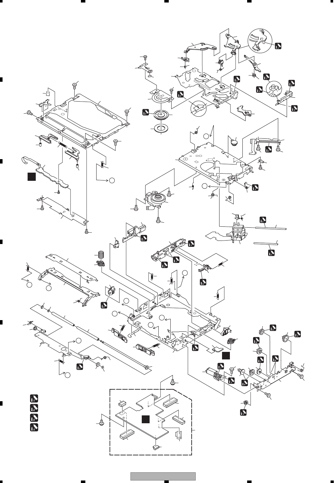
2.6 DVD MECHANISM MODULE
:(A) GEM1045
:(B) GEM1043
:(C) GEM1024
:(D) GEM1050
(C)
(A)
B
B
CD
E
(A)
D
E
C
F
F
(A)
(A)
(A) (A)
(C)
(B)
(C)
(B)
(B)
(B)
(C)
(A)
(B)
(B)
(A)
(A)
(A)
(C)
(A)
(A)
(A)
(C)
F
A
(D)
D
55
56
58
16 59
17
37
51
57
16
60
78
87
33
45
47
42
30
50
41
20
8812
48
48
85
34
11
67
28
84
52
13
73
21
14
81
32
31
8
86
8
8
71
72
46
29
74
75 19 79
24
23
53
49
19
14 18
26
35
36
54
89
23
61
50
77
82
8
63
65
65
64
66
27
8
80
8
62
1
6
5
3
2
7
4
90
90
64
38
83
9
9
87
22
(A)
(B)
87
A
8
25
8
43 39
8
8
68
70 15
69
70
87
40
87
E
76
10
(A)
44(1/2)
44(2/2)

AVIC-D3/XU/UC 21
5678
56
78
C
D
F
A
B
E
DVD MECHANISM MODULE SECTION PARTS LIST
Mark No. Description Part No.
1 DVD Core Unit CWX3401
2 Connector(CN1852) CKS4817
3 Connector(CN1101) CKS4841
4 Connector(CN1301) CKS5017
5 Connector(CN1201) CKS5043
6 Connector(CN1901) CKS5054
7 Connector(CN2001) CKS5054
8 Screw BMZ20P020FTC
9 Screw BMZ20P025FNI
10 Screw CBA1787
11 Washer CBF1038
12 Washer CBF1064
13 Spring CBH2586
14 Spring CBH2588
15 Spring CBH2589
16 Spring CBH2590
17 Spring CBH2591
18 Spring CBH2592
19 Spring CBH2593
20 Spring CBH2596
21 Spring CBH2597
22 Spring CBL1726
23 Spring CBH2599
24 Spring CBH2600
25 Spring CBH2601
26 Spring CBH2926
27 Spring CBH2604
28 Spring CBH2605
29 Spring CBH2710
30 Spring CBH2711
31 Spring CBH2935
32 Spring CBH2890
33 Spring CBL1689
34 Spring CBH2898
35 Shaft CLA4206
36 Shaft CLA4701
37 Lever CNC9933
38 Holder CND2643
39 Frame CND2250
40 Holder CND2251
41 Holder CND2642
42 Sheet CNM6883
43 Sheet CNM8697
44 Sheet CNM9658
45 Sheet CNM9407
46 Cam CNV7156
47 Clamper CNV7158
48 Roller CNV7165
49 Rack CNV7175
50 Damper CNV9061
51 Damper CNV9062
52 Collar CNV8845
53 Lever CNV8865
54 Rack CNV9063
55 Arm CNV8867
56 Arm CNV8868
57 Arm CNV9577
58 Arm CNV8870
59 Arm CNV8871
60 Arm CNV8872
61 Arm CNV8873
62 Gear CNV8874
63 Gear CNV8875
64 Gear CNV8876
65 Gear CNV8877
66 Gear CNV8878
67 Gear CNV8879
68 Lever CNV8903
69 Lever CNV8904
70 Roller CNV8905
71 Lever CNV8908
72 Arm CNV8909
73 Guide CNV8910
74 Arm CNV9116
75 Arm CNV9117
76 Compound Unit(A) CWX3154
77 Compound Unit(B) CWX3394
* 78 Arm Unit CXC7872
79 Frame Unit CXC6442
80 Bracket Unit CXB8685
81 Chassis Unit CXC6443
82 Motor Unit(LOAD)(M1) CXC4912
83 Motor(STEPPING)(M2) CXM1364
84 Arm Unit CXC5486
85 Roller Unit CXC5708
86 Motor(SPDL)(M3) CXM1362
87 Screw JFZ20P018FTC
88 Washer YE20FTC
89 Pickup Unit(Service) CXX2118
90 Screw IMS20P030FTC
Mark No. Description Part No.
AVIC-D3/XU/UC
22
1234
1234
C
D
F
A
B
E
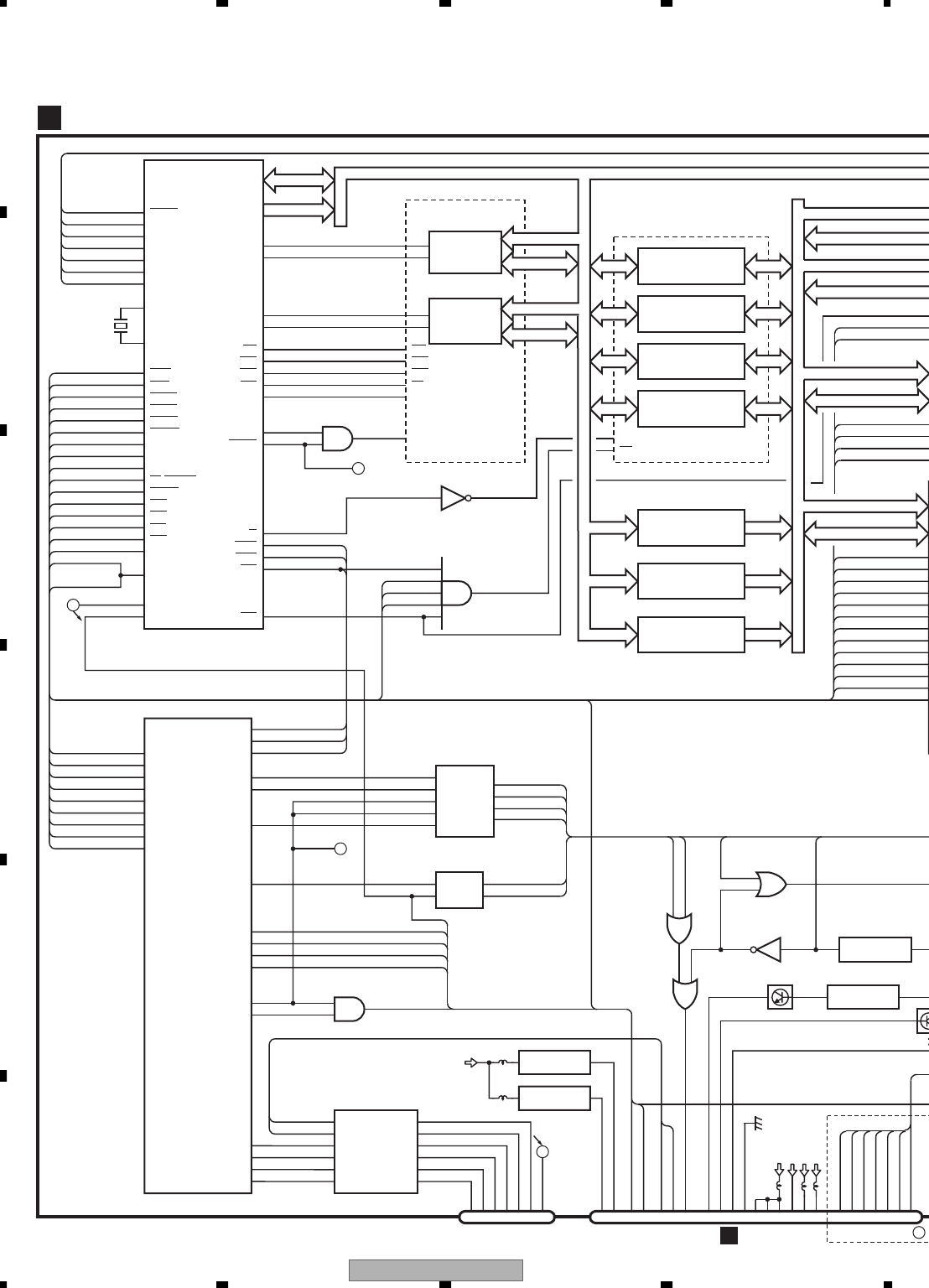
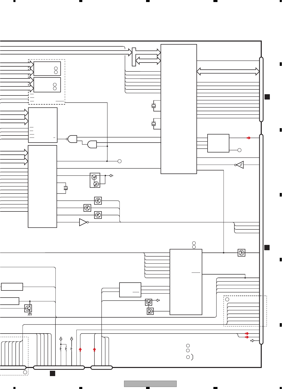
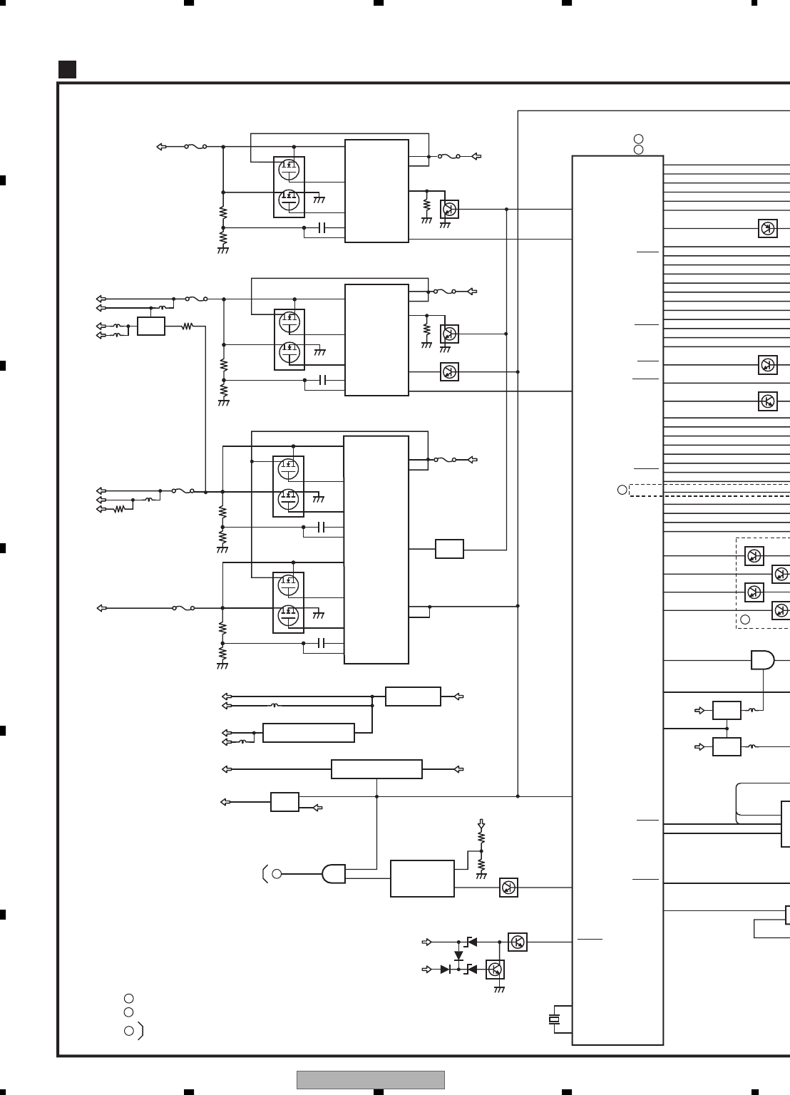
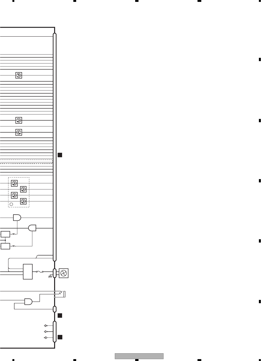
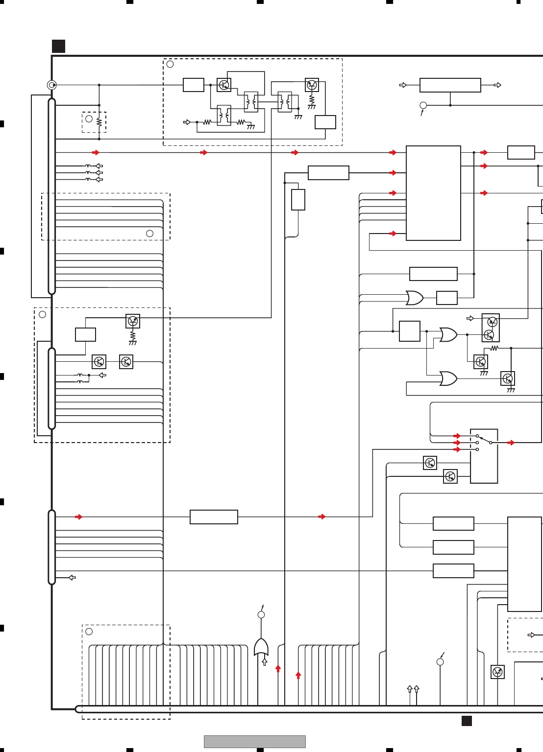
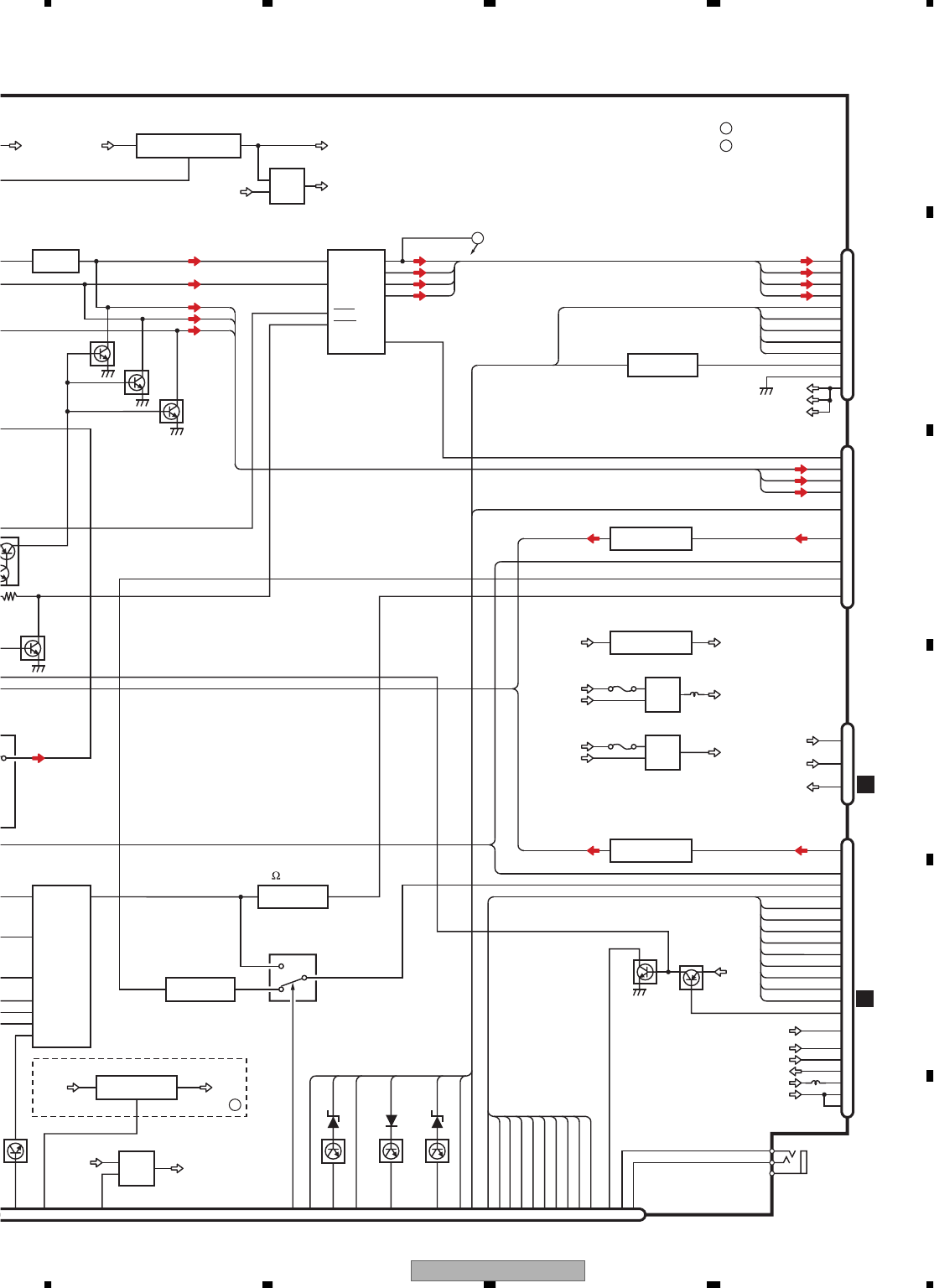
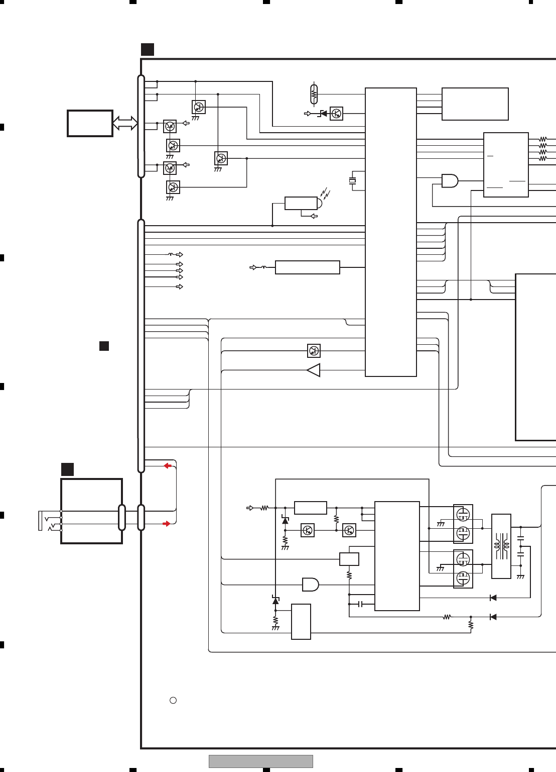
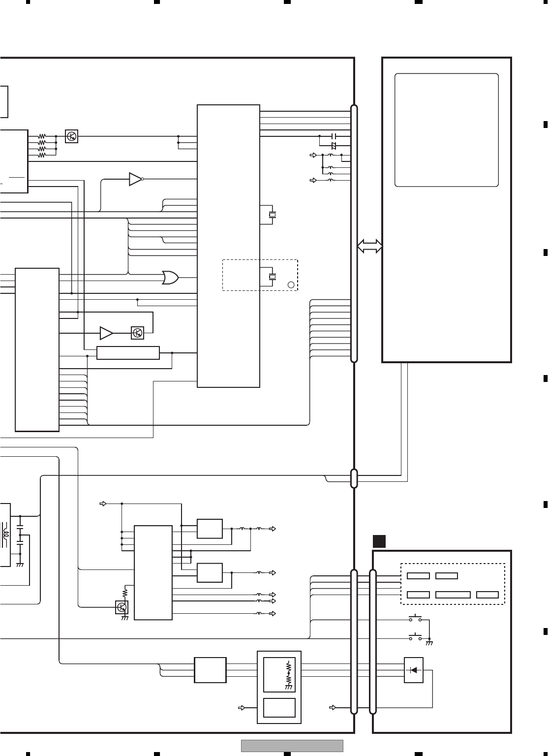
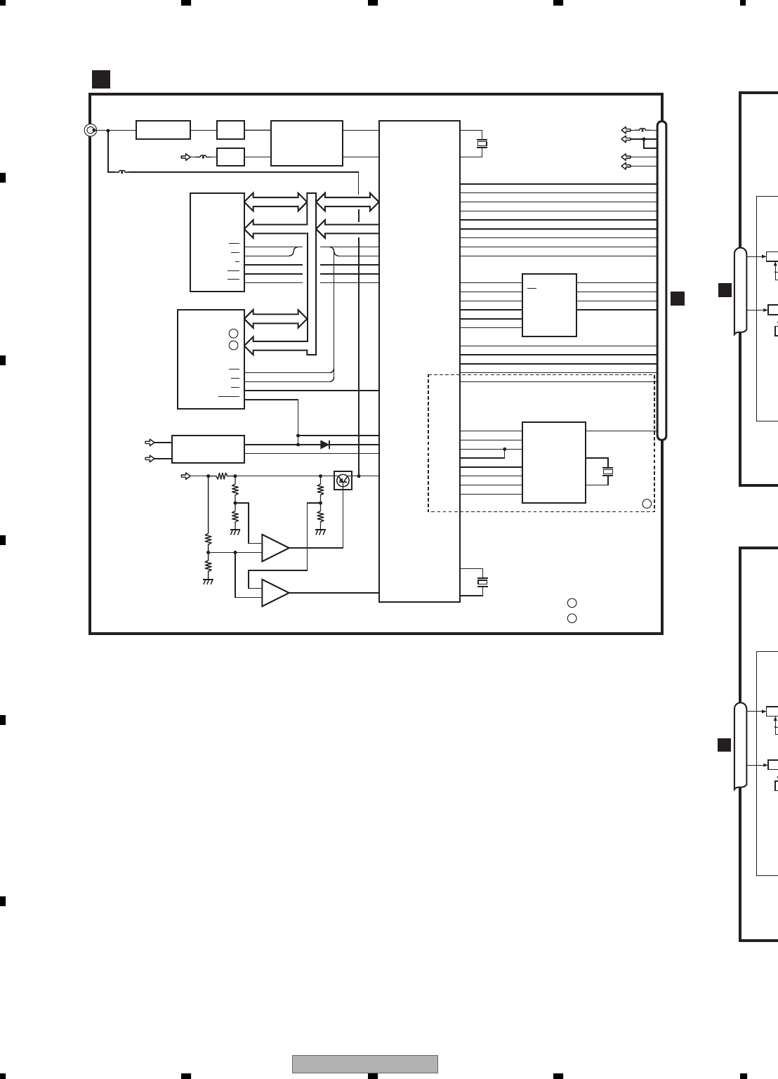
3. BLOCK DIAGRAM AND SCHEMATIC DIAGRAM
3.1 BLOCK DIAGRAM
D0-15
D16-31
D0-7
D8-15
D16-23
D24-31
BD0-7
BD8-15
BD16-23
BD24-31
A1-23
D0-31
CPU
IC2
UPD705103
GM-180S1
411XCS5
56
57 X2
X1
78
84 PORTB0/TI
PORTB6/INTP02
PORTA6/DMARQ3
X1
30.000MHz
SDRAM
IC1
K4S561632H-UL75 BUS BUFFER
IC103
TC74LCX245FTS1
IC104
TC74LCX245FTS1
IC3
HY57V561620FLTP-H
13XCS6
95 5XCS7
108
109
105
96
2XCS4
CKE 13
1XCS2
IC4
TC7SZ08FU
IC102
TC7SH04FUS1
IC105
TC74LCX245FTS1
BUS BUFFER
BUS BUFFER
BUS BUFFER
IC106
TC74LCX245FTS1
IC107
TC74LCX541FTS1
IC108
TC74LCX541FTS1
IC109
TC74LCX541FTS1
1
2
R/W
IC101
TC74LCX08FTS1
24
4
D
D
C
DIR
99GDC_INT
1
19
XBCYST
XCS4
XMRD
XMWR
XLLBEN
XLUBEN
XULBEN
XUUBEN
GDC_DMARQ
GDC_DMAACK
XTC
115
114
116
179
117
118
119
120
98
107
108
ASIC
IC5(2/2)
PD6336C
33CPU_CLKASIC CPU_CLK
169 XBCYST
238 XCS5
171 XCS3
170 XCS2
88 XMRD
XMWR
163
164 XLLBEN
231
90
XIOWR 165
XIORD
XLUBEN
29
30
27
110
26
107
127
UART2_TX
UART2_RX
UART3_TX
UART3_RX
UART4_TX
UART4_RX
PIO13
CPU_CLKGDC 113
97
XCS6
XIORD
XIOWR
XCS6
IOWR
R/W
CS6
IORD
89
88
DREQ0
DREQ1 PORTA2/DMARQ1
87DREQ2 PORTA4/DMARQ2
PORTA0/DMARQ0
82
77
INT2
INT3 PORTB3/INTP13
PORTB2/INTP00
106
85
XREADY
INT0 PORTB7/INTP03
READY
HYOKA
IRQPWR
PORTA7/DMAAK3
90
86
GDC_DMAACK
GDC_DMARQ
94
XTC
98
XCS4
107
XBCYST
115
XMRD
114
XMWR
113
XLLBEN
112
XLUBEN
111
XULBEN
110
XUUBEN
CLKOUT
46
CPU_CLKGDC
CPU_CLKASIC
TC/STOPAK
CS4
CS7
5 XRAS
3XCS0
12 SDCKOUT
14 XCAS
4 XWE
WE
915
LLDQM LDQM
839
LUDQM UDQM
715
ULDQM LDQM
639
16
17
18
19
38
37
UUDQM UDQM
CAS
RAS
CS0
SDCLKOUT
WE
CAS
RAS
CS
CLK
CKE
63
RST3
RESET
MWR
MRD
OE
BCYST
LLBEN
LUBEN
ULBEN
UUBEN
83
100
97
99
GDC_INT PORTB4/INTP01
XCS2 CS2
XCS5 CS5
XCS3 CS3
BD0-31
A1-8
A9-16
A17-23
BA1-8
BA9-16
BA17-23
39
XLLBEN
40
XLUBEN
41XMRD
17XMWR
28
XMRD
XMWR 11
BD0-15
BD16-31
BD0-15
XCS7 26
ANAVI MOTHER UNIT(1/2)
CTOGPS
GPSTOC
MTOC
CTOM
XMSRS
CPUWDT5
CTOSYS5
CCRST5
CPUWDT5
CTOSYS
CPUWDT
SYSTOC
IRQPWR
SYSTOC5
IRQPW5
1
3
5
6
7
8
13
11
12
16
15
17
18
20
19
21
22
GSENS
CTOGPSCTG
GPSREV
GPSRQ
GPSTOCGTC
RXDD
TXDD
PULSE
POUT
GYRO
GSNS
IRQPW5
MUTE
CN2060
5V→3V
IC2084
TC7SH04FUS1
IC2052
TC7S32FU
5V→3V
IC2051
TC7WH32FU
5V→3V
IC2053
TC7WH08FU
GYRO
GY1
3V→5V
IC2050
TC74VHCT08AFTS1
3
5
VCC5
6
8
3
4,5
1,27
5,63
9,10
1,2
42
3
56
7
12
TMCDET
TMCSD
TMCCE
GTOTMC
TMCCK
TMCTOG
TMCSL
30
27
29
CCD3
10
28
26
SWBUP
BUP3
VCC5
BCN461
4
8G Sensor
GY4
Q2052
IC2058
NJM2904M
SPEED SENSE
51
IC2055
BD5335FVE
RESET
31
1
RESET
24
PIO29 2
2
1
IC309
TC7SH08FUS1
XRSTMS3
RST3
4
108
XRESET
C
23
105
21
104
UART6_TX
UART6_RX
UART7_TX
UART7_RX CTOETC
ETCTOC
CTOEX
EXTOC
EXTOD
DTOEX
12
9
13
10
11
8
19
22
18
21
20
23
1
4
2
5
8
6
7
CN2066
RS232C DRIVER
IC2078
UPD4723GSS1
GTOEX
CTOEX
EXTOG
EXTOC
HYOKA
CTOETC
ETCTOC
Rout2
Din2
Rout3
Din3
Rout1
Din1
Rin2
Dout2
Rin3
Dout3
Rin1
Dout1
TO EXTENSION A
48
MS5STBY1 PIO12
XBCYST
XCS5
XCS3
XCS2
XMRD
XMWR
XLLBEN
XLUBEN
XIOWR
XIORD
XCS6
49
PIO14 MSCCSTBY 13
12 2A,2B
3A,3B
1A,1B
4B
4A OFFOK
11
3Y
1Y
2Y
4Y
MS5STBY1
A2-16
A2-16
14
PDO
PDI
BA2-23
BA1-17
BA2-23
BA2-23
TO 2/2
TO 2/2
EXTOD
DTOEX
AVIC-D3/XU/UC 23
5678
56
78
C
D
F
A
B
E
X202
14.31818MHz
124
128
1
3
|
18
21
23
25
27
29
31
33
35
36
37
38
ATA_XRESET114 RESET
ATA_DMARQ182 DMARQ
ATA_XDIOW109 DIOWB
ATA_XDIOR246 DIORB
ATA_IORDY181 IORDY
ATA_XDMACK180 DMACKB
ATA_INT179 INTRQ
ATA_DA1178 DA1
ATA_DA0177 DA0
ATA_DA2191 DA2
ATA_ XCS 0257 CS1FXB
ATA_ XCS 1192 CS3FXB
RST3
1
CCD3C
XRST 44
S
XINT
XRDY
XBS
XCS
129
AOUTR 152
AOUTG 147
AOUTB 143
56
DAC_LRCK
97
99GDC_INT
AOUTBLUE
CSYNC 204 NVSYNC
AOUTGREEN
AOUTRED
NVBLUE
NVGREN
NVRED
GDC_WT
XBCYST
XCS4
XMRD
XMWR
XLLBEN
XLUBEN
XULBEN
XUUBEN
GDC_DMARQ
GDC_DMAACK
XTC
115
114
XRD
116 A24
179
XWE0
117
XWE1
118
XWE2
119
XWE3
120
DREQ
98
DRACK
107
DTACK
108
ASIC
IC5(1/2)
PD6336C
GDC_WT
101
134
55
135
126
PIO11
14
129
PIO17 GUIDEMUTE
PBSNS
REM_IN
IR_RX
CN2
CPU_CLKGDC BCLKI
OSCOUT
CLK
113
1 DACOUTL GUIDE11
2
DAC_MCLK
DAC_DATA
DAC_BCLK
176
175
94
172
173
240
174
XREADY
INT0
INT2
INT3
DREQ0
DREQ1
DREQ2
DAC
IC304
AK4388VT
MCLK AOUTL
BICK
3SDTI
4LRCK
ATA_DMARQ
ATA_DD0-15
ATA_XRESET
ATA_XDIOW
ATA_XDIOR
ATA_IORDY
ATA_XDMACK
ATA_INT
ATA_DA1
ATA_DA0
ATA_DA2
ATA_XCS0
ATA_XCS1
ATA_ DD 0-15
D0-31
BD0-31 C
18
16 XTAL0
EXTAL0
X2
33.000MHz
60
58 XTAL1
EXTAL1
X3
33.8688MHz
IC114
TC7SH08FUS1
SCARLET
IC201
MB86291
APFVS-G-DL
WE
CE
FLASH ROM
IC110
IC111
SRAM
IC113
M5M5V216
ATP-70HI
39
XLLBEN
40
XLUBEN
41XMRD
17XMWR
28 12
XMRD RST3
XMWR 11
OE RESET
IC112
TC7SH00FUS1
4
4
2
6
2 SRAM_CSE
1
11 XCS_SRAM
44 PIO4
S
BD0-15
BD16-31
BD0-15
C
S7 26
Q201
RSTIN
SRCMUTE
SPEED
GPSREV
SPEED
CN2055
(1/2)
1
3
5
6
7
8
13
32
29
24
23
21
22
20
4
CN2057
8
1
5
7
CN2065
MVDD5
CVBS DVDV
SLVSTS
CTOM
HSTCMD
MTOC
IRQPWR
XRES XMSRS
TMCDET
TMCSD
TMCCE
GTOTMC
TMCCK
TMCTOG
TMCSL
ANALOUT DVDL
AMUTE
ASENBO
IPBUS+
IPBUS-
IPL+ IPL
ASENB
47
IRQPWR
SYSTOC
CPUWDT
RST3
CTOSYS
ASENBO
130
88
BKSNS
89IPPW IPPW
90IPTOSYS RX
91
113
118
SYSTOIPBUS TX
BUS-
BUS+
98 MUTE
40 RESET
1
DIN1 2
ROUT 8
STBY
IC2068
HA12241FP
SYSTEM-uCOM
IC2056(1/2)
IPBUS+
IPBUS-
6
5
103
106
SYSTOC5
CCRST5
117CTOSYS5
CPUWDT5
IRQPW5
REVSNS
SYSREV
GPSREV 51
75
RESETRSTIN
65
SRCMUTE
IP-BUS IN
CCN1711
VDD5
ASENB Q2091
Q2054
IC2058
N
JM2904M
P
EED SENSE
5
IC2055
BD5335FVE
RESET
3
AMUTE 54
32
PDI
TMCTOG 24
PCK
TMCCK 26
PDO
GTOTMC 34
PCE
TMCCE 36
SD
TMCSD 30
DETOUTTMCDET
28
SL
TMCSL
56
IPL
48
DVDL
73
DVDV
I
17
15
VD8
VDD8(DRY)
VDD8(REG)
I
3
1
21
70
64
REMIN
PKB
5V→3V
IC2083
TC7SH14FUS1
PARKING SENSE
Q2055
Q2068
Q2069
Q2070
49
NVSYNC 13
NVBLUE 7
NVGREN 9
NVRED 11
PBSNS 129
24
PBSNS
79
VDD5
A
A
A2-12,23
PDO
PDI
25 STANBY MS5STBY1
BA2-23
BA1-17
BA2-23
BA2-23
A
B
PEH078B
PEH104B
A
B
PEH077B
PEH103B
DCN1901
XREADY
INT0
INT2
INT3
DREQ0
DREQ1
DREQ2
MUTE
RESET
105 XCCSTBY
OFFOK
Q2089
KBUP
AAVIC-D3/XU/EW5
BAVIC-D3/XU/UC
TO 2/2
C
TO 2/2
5CTO 2/2
RSTIN
DCN2001
A
B
PE5581A
PE5580A
OE
WE
BC1
BC2
IC2065
TC7SH04FUS1
42
AVIC-D3/XU/UC
24
1234
1234
C
D
F
A
B
E
A
Q2099
132
OPTSNS
120
OPTON
DRAMPW
78
FCONT
67
DD8CONT
34
84
VSEL2 85
VSEL1 86
BCVSW 53
NOSELL 109
SWACPW 62
SYSPWR
58
TELIN
64
ANTON 126
11
MUTEVO 76
ACONTA 9
VDT 77
ACONTB 10
VCK 61
SREMOTE 12
VST 29
137
WREMIN 124
PPW
116
125
123
PID
135
TUNSL 101
TUNCE2 107
MTOSYS 100
TUNCE1 108
SYSTOM 48
TUNCLK 133
47
TUNDO 45
LDET 46
TUNDI 13
ROT1 14
ROT0 65
XVMUTE
57
RCK
23
RDT
25
RDSLK
24
RDS57K
112
TXIPOD
111
RXIPOD
SYSTEM-uCOM
IC2056(2/2)
RSTOUT
104
CCON
79
69BSENS
BSENS
BLSENS
Q2088
Q2090
BUP
KBUP
NAVI MOTHER UNIT(2/2)
73
74 X2
X1
X2050
Q2059
Q2053
Q2051
Q209
8
Q2097
Q209
6
A
SYSRST
CCON
RST3 2
5
6
CCD3C
RESET GEN.
IC301
M51957BFP
Q301
Cd
IN1
RSTOUT
IC302
TC7SH08FUS1
TO 1/2 2
1
4
C
63
FANCONT
ILLSNS
WCONT
IC2
TC7SE
T
OPTSNS
96
ASENS ASENS
FANUP
1
2
IC2061
TC7SH08FUS
1,2 4
5TC
7
DALMON 33
Q2102
Q2104
Q2103
Q2105
Q
Q
Q
Q
BUP3
UVDD5
Q2093
BUP
VD8
SRVDD
FU1931
KBUP
FU1913
FU2060
SD3VC FU1908
FCONT
Q2094
CCON
Q2092
FCONT
8.0V D/D CONVERTER
IC1931
TPS5103IDB
3.3V D/D CONVERTER
IC1903
TPS5103IDB
KBUP
KBUP
FU1903
CCON
FCONT
5.0V / 2.5V D/D CONVERTER
IC1901
TPS5120DBT
CCD3C Q2071
Q2072
Q1935
Q2101
VDD5
UVDD5
MVDD5
CCD5
CCD5C FU1901
CCD25C FU1902
CCD3
BUP3
BUP3C
1
4
5
IC2070
S-814A50AUC-BDO
VCC5 VD8
VCC5 REG.
51
IC2076
BD3931HFP
VDD5 REG.
5 1,3
IC2075
S-L2980A33MC-C6S
BUP3 REG.
PSENS
PSENSG
DVEJKY
AAVIC-D3/XU/EW5
13
VCC
14
VCC-SENSE
5
RT
10
STBY
Q1931
19
18
17
LL
OUT_U
OUT_D
3FB
2INV
Q1934
19
18
17
LL
OUT_U
OUT_D
3FB
2INV 10
STBY
9
RWMSKIP
5
RT
13
VCC
14
VCC-SENSE
Q1903
17
19
LL2
OUT2_U
OUT2_D
14 FB2
15 INV2
Q1902
29
28
27
LL1
OUT1_U
OUT1_D
2FB1
1INV1
24
VCC
6
5V-STBY
5
CT
10
STBY2
9
STBY1
18
Q2095
Q2100
SWBUP REG.
BUP
SWBUP
BAVIC-D3/XU/UC
TO 1/2
C
A
B
PE5581A
PE5580A
A
AVIC-D3/XU/UC 25
5678
56
78
C
D
F
A
B
E
Q2099
FU2051
78
VSEL2
46
CCON
76
VSEL1
74
BCVSW
71
GMUTEL
63
SWACPW
61
SYSPWR
59
MUTEIN
TELMUTE
55
ANTON
53
ILMSNS
44
MUTEVO
43
ACONTA
42
VDT
41
ACONTB
40
VCK
39
SREMOT
38
VST
37
WCONT
35
WREMIN
33
PPW
27
ACCPW
25
ACCDET
23
ACCID
22
FMSL
20
FMCE2
19
MTOSYS
18
FMCE1
17
SYSTOM
16
FMCLK
15
DVEJKY
14
STOFM
12
HLDET
10
FMTOS
5
ROT1
3
ROT0
1
XVMUTE
2
HRHSLK
4
HRLK
6
HRDT
8
HRCK
31
SYSTOI
29
68
45
ITOSYS
CN2059
2
1
FAN
CCN1711
Q2059
Q2053
Q2051
Q2098
Q2097
Q2096
A
CN2063
IC2067
TC7SET08FUS1
CN2061
DIGITAL
OUT
OPTSNS
ASENS
FANUP
FANUP
ASENS
DIN
FNV
1
24
1
IC2061
TC7SH08FUS1
1,2 4
5IC2062
TC7SET08FUS1
4
5
1,2
Q2102
Q2104
Q2103
Q2105
Q2056
|
Q2058
Q2060
|
Q2062
CN2055 (2/2)
KBUP
VD8
CN2068
BUP
I
10
9
I
8
5
I
4
1
3
2
1
CCN1652 DCN1852
AVIC-D3/XU/UC
26
1234
1234
C
D
F
A
B
E
42
10
18
17
11
AUXL
CLK
FLOUT
DATA
IN3L
RLOUT
20
19
VDT
VCK
MUTEVO
VST STB
MUTE
41FML IN2L
PREOUTL
43
IPL
POMUTE
RSTMUTE
IN4+L 12
C
8
GUIDE MIX
IC1131
NJM2060V
Lch MUTE
ISOLATOR, LPF AMP
CAPTAIN
IC1061
PML009A
FL
13FL
RL
SWL
37
IC1111
BA4558RFVM
GUIDE
GMUTEL
GMUTE
3AV1VIN 1 AV1V
IC1301
NJM2137V
ISOLATOR
2
KBUP
NBUP
CN1401
FM/AM TUNER UNIT Y1431
VDD_3.3
VCC
ROM_VDD
DI
DO
CE1
CK
SL
CE2
STOFM
FMTOS
FMCE1
FMCLK
FMSL
FMCE2
Lch FML
AM_ANT
FM_ANT
RDS-LOCK
RDS-HSLK
RDS-CK
RDS-DATA
LDET
HRLK
HRHSLK
HRCK
HRDT
HLDET
1
3
23
5
6
8
9
10
14
11
18
19
20
21
4
13
17
AV8
VDD5
TMC8
TU3
GUIDE
GUIDEMUTE GMUTE
GMUTEL
FM TUNER UNIT Y1452
STUNB
SPLL
SCMP
SBSL
SBDI
SBCE
SBDO
SBCK
SFMANT
SBSD
TMCDET
TXiPod SYSTOI
RXiPod ITOSYS
ACCID
ACCPW
ACCDET
TMCSL
TMCTOG
TMCCE
GTOTMC
TMCCK
TMCSD
1
6
13
14
15
16
7
9
10
11
ANTENA
IN
SREMOTE
SRCMUTE
DVDV
VSEL2
VSEL1
XVMUTE
SYSPWR
CCON
SWACPW
SWACPW
VDD5
F/W PWR
ACONTA
CN1711
VST
VDT
MUTEVO
VCK
FANUP
ACONTB
IPL
DETOUT TMCDET
SL
SD TMCSD
PCK
PDO
PCE
PDI
HRCK
HRDT
HLDET
HRLK
HRHSLK
TMCSL
TMCCK
GTOTMC
TMCCE
CTL
TMCTOG
4
38
12
39
2
79
37
40
42
36
24
48
46
54
44
56
50
52
78
76
74
72
68
17
19
34
1
Q1331
CN2055
A
AV UNIT
B
Q1402
AV8
D
A
A
A
A
Q1401
T1403T1402
T1401
Q1403
Q1451 Q1452
FL
Q109
2
Q1205
Q1206
31
DVD LPF
IC1001
NJM4558V
5
2
1
10
VTR2L
iPodL
VTR1L
AUDIO SELECTOR
IC1051
TC4052BFT
3AUXL
ACONTA
Q1052
9
ACONTB
Q1051
13
ISOLATOR
IC1021(1/2)
BA4558RFVM
C
FL
Q1112
Q1114
Q1204
Q1001
Q1002
Q1201
|
Q1203
40DVDL1
DVDLS
AMUTE
IN1L
1
1
VIDEO SELEC
T
IC1331
BA7649AF
IN1
8IN3
3AV2VIN 6 AV2V
IC1316
NJM2136V
ISOLATOR
10 IN4
VSEL1 3CTLA
VSEL2 4CTLB
5CTLC
4IPODVS 1
IC1381
NJM2505F
ISOLATOR
6IN2
VOUT
DVDV
7
STOFM
FMTOS
FMCE1
FMCLK
FMSL
FMCE2
58
60
62
64
66
70 SYSTOI
49 ITOSYS
51 ACCID
57 ACCPW
53 ACCDET
55
DVDL
32 AMUTE
26
LOUT IPODLS
CN1621
3
5
VOUT IPODVS
7
11
2
10
4
6
16
10
9SREMOT
SRCMUTE
41
15
NBU
P
TU3 REG.
24
1
NBUP TU3
IC1841
BA00CC0WCP-V5
CTL
C
FM DISTRIBUTION
TO iPod
SREMOTE
B
A
NBUP
IPODV
AVIC-D3/XU/UC 27
5678
56
78
C
D
F
A
B
E
14
5
12
3
21
23
FL
22
4SREMOTE
MUT
POWER AMP
IC1201
PAL007C
IN2 OUT2+
OUT2-
IN4 OUT4+
OUT4-
B-REMOTE 25
MUTE
STBY
VTR1L
POMUTE
8
GUIDE MIX
IC1131
NJM2060V
RL+
FANUP
RL-
FL+
FL-
Q1093
13FL
RL
SWL SWL
BREMOTE
Q1711
(1/2)
Q1711
(2/2)
TMC8 REG.
FireWire PWR
V
1V
13,4
IC1876
NJM2125F
AV8 AU5
AU5 REG.
2
1
4
KBUP TMC8
F/W PWR
NBUP
IC1891
BA00CC0WFP
42,3
7
3
1
2
SELECTOR
IC1351
NJM2235M
75 DRIVER
IC1361
TK15405BMI
CN1701
BREM
SWL 13
12
1
19
17
23
21
BCVBCVIN
AV2V
AV2L
AV2VIN
AV2LS
REARVOUTRVOUT
WCONT
WREMIN
TELMUTE
VTR1V
AV1VIN
VTR1LAV1LS
9
5
FL
RL
PFL
PRL
CN1651
FL-
RL-
RL+ 6
8
5
7
13
9
11
14
10
12
15
16
KBUP
NBUP
AANTANTON
FL+
PULSESPEED
PKB
REV
ILM
BUP
ACC
16 IC1601
TPD1018F
AUTO ANT
PWRVI
VIDEO5
MFLPW
SWACPW
HDRST
MONVBS
MONVBS
BCVIN
V
DV
ROT0
CN1661
CN1721
WIRED
REMOTE
(BLACK)
MTOSYS
MOREM
NVR
DISCEJ
SYSTOM
MTOS
STOM
NVB
ROT1
NVG
36
37
34
30
15
16
19
5
1
17
21
18
22
23
31
28
32
33
14
ILMB
VDD5
RSTMUTE
RVOUT
NVGREN NVG
NVRED
BCVSW
REMIN MOREM
MTOSYS
SYSTOM
MTOS
STOM
ROT1
NVSYNC
NVBLUE
NVR
NVB
XVMUTE
SPEED
REVSNS REV
PKB
DVEJKY
CCON
ANTON
RESET RSTIN
MUTEIN TELM
WCONT
WREMIN
75
63
61
59
69
71
73
79
67
31
29
33
34
25
21
6
43
5
65
45
ILMSNS
ILM SENS
Q1603
ASENS
Q1602
ASENS
ILM
ACC
27
35
REV SENS Q1601
Q1331
D
0
55
CN5001
G
14 IC1341
NJM2505F
ISOLATOR
A
KBUP
ILMB
CN1652
NBUP BUP
CN2068
A
I
10
9
I
8
5
I
4
1
PRL
PFL
Q1092
Q1091
2
05
VTR2L
L
ECTOR
5
1
2
BFT
3AUXL
31
ISOLATOR
IC1031(1/2)
BA4558RFVM
31
ISOLATOR
IC1041(1/2)
BA4558RFVM
AAVIC-D3/XU/EW5
BAVIC-D3/XU/UC
PWRFL
PWRFL
NBUP
MFLPW
FU1864
Q1861
Q1862
PWRVI
PWRVI
NBUP
SWACPW
FU1865
Q1851
Q1852
Q1204
Q1801
|
Q1805
ACC5V
PWRFL
I
12
10
1
14
VIDEO SELECTOR
IC1331
BA7649AF
IN1
8IN3
V
2V 10 IN4
S
EL1 3CTLA
S
EL2 4CTLB
5CTLC
6IN2
VOUT
PPW
47
AV8 REG.
24
1
NBUP AV8
SWACPW VIDEO5
IC1821
BA00CC0WCP-V5
CTL Q1831
|
Q1833
TU3
O
DV
VIDEO5 REG.
RL
BUP
Vehicle I/F
TELM
DVEJKY
NVSYNC 25
2
3
1
ROT0
77
AVIC-D3/XU/UC
28
1234
1234
C
D
F
A
B
E
Q5300
MONITOR CPU
IC5300
PE5584A
TH5300
TEMP. SENSOR
80
76
62
8
9
30
5
CN5001
PWRVI
ACC5V
MTOSYS
SYSTOM
MOREM REMCON
NVR
NVG
NVB
AV2V
AV2L
AV2V
AV2L
AV2V
AV2L
ANR
ANG
ANB
4
5
7
26
27
22
36
40
13
25
24
23
9
8
11
10
18
19
20
2
1
DIMDTY
INVBST
Q5301
V14
MONVBS
ROT1
ROT0
HDRST
DISCEJ
VACC5
SWACPW
ILMB
TEMPSEN
KDT0
61 REMIN
32
MFLPW MFLPW
77 KDT1
VDDSENS
RXD/TSI
TXD/TSO
INVBST
DIMMER
MVIPW
X1
X2
11
X5300
12.58MHz 70
69
MONITOR UNIT
G
SWACPW
44 INVPUL
VACC5 RESET
601
EPRCS 49 1
EPRCK 48 2
EPRDO 47 3
EPRDI 46 4
2
EEP-ROM
IC5303
S-93C46BD0I-J8
IC5304
S-80835CNNB-B8U
IC5681
NJM2903V
POWER ON RESET
YV
XV
CN5002
ADX
ADY
7
5
6
4
3
2
9
8
24
25
3
2
PNLXV
PNLYV
PNLADY
PNLADX
TOUCH
PANEL
Q5364
Q5362
26 PNLVD
Q5360
(2/2)
Q5360
(1/2)
VACC5
VACC5
Q5363
Q5361
VACC5
FL1
FL2
531
DIMDTY
INVPUL
INVBST
11
14
15
5
37
LCT
3ENA
7V2500
9FB
18 CT
DIM
VDDA NDRV_D
12
PDRV_C
20
NDRV_B
19
PDRV_A
2
OVP
Q5900 Q5901
Q5904
Q5902
Q5908
Q5905
|
Q5907
Q5903
5V REG.
IC5900
TA78L05F
LCD DRIVE
IC5902
OZ961ISN
10 COMP
6
T5900
PWRFL
I
29
31 PWRFL
I
OSDDT
OSDCK
OSDCS
HSY
17
18
19
OSDDISP 31
25
12
24
26
IC5650
PD6567A
LCDDT 12
LCDCK 13
LCDCS 14
MODS 34 16
MODW 35
MODN 36
MDS
MDW
MDN
FREQSW 43
20
21
LEDDT 52
LEDCK 53
LEDCS 54
BLKDRV 15
RGBSEL 27
PSAVE 28
COLSYS 29
SIN
SCLK
DISP
OSDTRE 16 23 TRE
ROUT(C1)
GOUT(C2)
DOCKI
VOB1
IOUT(C3)
BOUT(C0)
8
16
20
18
19
17
CS
HSYNC
13 VSYNC
IC5100
LZ9FE30
MDW
MDN
VSYNC 64 12 VSY
MDS
VS
C
SPI
O
SP
S
CL
S
V
R
MOD
2
MOD
1
CT
R
CL
D
H
R
SPO
PD
P
SYN
FRP
T
NTP
C
HS
Y
AV MINI
JACK PCB
I
IC5901
TC7SH08FUS1
4
1,2
CN1661
C
IC5651
TC7SH08FUS1
2
1414
OSC
OSC
O
REMOTE
IC5307
GP1UX51RK
1
3
REM
AAVIC-D3/XU/EW5
CN5552 CN5004CN4825
5
2
5
2
NVSYNC
16
1
2
4
3
DI
SK
DO
CS
AVIC-D3/XU/UC 29
5678
56
78
C
D
F
A
B
E
CN5003
KDT0
X5010
4.43MHz
IC5011
RB5P0090M
35
34
33
KDT1
CN5007
REDLCDR
GREEN
V53
CS
VGL
COM
BLUE 21
29
30
31
32
12
19
15
1
17
26
28
23
24
9
10
7
8
6
25
20
LCDG
LCDB
VCOM
COMS
30
29
ROUT
RIN1
GIN1
BIN1
GOUT
VCO_OUT(PAL)
VCO_IN(PAL)
X5011
3.58MHz
27
26
VCO_OUT(NTSC)
VCO_IN(NTSC)
BOUT 37
COM_DC 39
COMOUT
ANR
ANG
ANB
15
14
13 LCD MODULE
MVIPW
Q5650
J
8
IC5101
NJM2107F
9
4IC5060
TC74VHC221AFTS1
CN5006
FL1
FL2
FL1
FL2
1
2
1,2,5,6
1,2,5,6
V14
FREQSW
3
4
3
4
D/D CONVERTER
IC5181
BD6171KV
5V REG.
11
6PVCC1
PVCC2
32 EN1
OUT2 7
VS2 4
PVCC3
PVCC4
PVCC5
23
48
37
OUT1 10
OUT5 38
OUT4 47
V8
V5
V15
OUT3 22 V53
VM10
Q5210
8V REG.
Q5200
41 PVCC
42 VCC
VS1 13
7
6
9
00
14
7
8
2
3
6
5
11
10
9
VSHA2
VSHA1
VCC
SPIO
SPS
CLS
VRV
MODE2
MODE1
CTR
CLD
HRVHR
SPOI
RIN2
GIN2
BIN2
SW2
OSDOVR
18
17
16
11
12
C
5650
D
6567A
16
20
21
4
6
1
41
42
BLK_IN
PSAVE
NTSC/PAL_OUT
BLKDRV
COLSYS
434
10
45
COLSYS
210 MASK
111
DI
CLK
CS
SYNC_SW
LCDDT
LCDCK
LCDCS
RGBSEL
47
46
48
6
ROUT(C1)
GOUT(C2)
DOCKI
VOB1
IOUT(C3)
BOUT(C0)
8
16
20
18
19
17 OSDRGB
IC5700
M62343FP
6DI A01 1
7CLK A02 2
8LD A03 3
HSYNC
C
IC5100
LZ9FE30
MDW
MDN
12 VSY
MDS
VSC
37 1
SPIO
58
SPS 57
CLS 59
VR 32
MOD2 60
MOD1 36
CTR 47
CLD 33
HR 28
SPOI
38
PDP
7
SYNI
FRPT
NTPC
HSY
FRP
2SYNCCT SYNC_OUT
4SYNC_IN1
COM_FRP
HSY_IN
D5501
RESET
S5506
EJECT
S5505
Q5703
|
Q5705
Q5700
|
Q5702
CN5503
KEY PCB
H
KEY MATRIX
ROT0
KDT1
LEDR
S5501
RIGHT
S5502
LEFT
S5503
MAP
S5504
MENU
S5507
SOURCE(enter)
ROT1
KDT0
ROT0
ROT1
12
1
4
5
6
9
10
8
7
13
LEDG
LEDB
LEDR
LEDG
LEDB
RED
GREEN
BLUE
ILMB
HDRST
DISCEJ
HDRST
DISCEJ
Q5180
44 RT
IC5010
TC7SH32FUS1
44
OSCI
43
OSCO
+
ILMB
LEDDT
LEDCK
LEDCS
A
V15 VGH
4
2
IC5012
TC7SH04FUS1
SYNC_IN2
3
NVSYNC
PSAVE SW1
12
Q5100
4
1
VR
MOD2
MOD1
ILMB
AVIC-D3/XU/UC
30
1234
1234
C
D
F
A
B
E
D0-15
A1-18
D0-15
A1-18
D0-15
A1-17
GPS UNIT
B
22
IC402
UPB1027GS
RF_MIXin 2ndIFout
19 17
REFin LOOUT
IC503
M5M5V216ATP-70HI
530
26
27
29
28
22
18
21
20
19
17
15
12
13
11
10
16
8
7
6
5
3
1
TXDD
RXDD
GPSTOC
CTOGPS
REVSNS
RQ
5
SPEED9
6
7
8
133
132
CN461
CN504
ANTVCC
AD5V
VCC3
BUP3
BUP3
11
86
WE
12
1 RESETB
6
28
87
26
OE
WE
OE
CERAM 97
17
41
6
WE
OE
120
140
DRAGON
IC501
PD3390A
WRLB
RDB
CS1B
CEROM 89 CS0B
RESETB
BOWWOWB
RTCVCC
110 CRCK
PIN0
IF
PIN2
PIN3
RXD0
TXD0
RXD1
TXD1
SPEED
GSNSIN
13
ADRXD
GYROIN
10
ADCSB
VSNS
12
ADTXD 11
19
18
20
21
3
2
4
ADSCK
XRTCIN
XRTCOUT
143
GPS
ANTENNA
X401
F401
POWER ON RESET
IC504
MAX6364PUT29
Q441 130
PIN1
131
ANTVCC
41 IC401
UPC2749T 4
2
7
1
3
2
5
6
IC441
NJM2100V
OE
WE
CE
OE
64HBS40 A0
BC2 85LBS39 WRHB
BC1
WE
S
RESET
IC461
ADC12H034CIMSAS1
CS
DI
DO
SCLK
15 22
ADIO0 CCLK
14 16
ADSRX EOC
CH2
CH1
CH3
X501
102
103
X532
15
16
PSWOUT17
ADIO2
14
FLASHWE112
PC0
PDI25
PLRX
PCK23
PLSCK
PDO24
PLTX
SD28
PLIO2
PCE22
PLCE
SL
1
CH0
35
DDIO1 29
DDINT 33
DDRX
24
22
25
BCLOCK
DINT
DDO
IC532
LC72720YVSS1
DO
RDS-ID
SYNC
31
DDSCK 30
DDCE 32
DDTX
26
29
28
DCL
DCE
DDI DI
CL
CE
36
DDIO2
34
DDIO0 30
DSTB
DRST SYR
XOUT
XIN
DETIN
2
MPXIN
CN2060
A
+
-
+
-
VCC3
104
5
A
AAVIC-D3/XU/EW5
XAUXIN
XAUXOUT
X502
20.0MHz
128
129
A
N
FM ANT
1
3
AM ANT
AT
T
A
T
A
N
FM ANT
1
3
AM ANT
AT
T
A
T
C
C
FM/A
M
FM/A
M
BAVIC-D3/XU/UC
IC502
PEH101A8
PEH100A8
A
B
VCC3 4
34
AVIC-D3/XU/UC 31
5678
56
78
C
D
F
A
B
E
FMRF
ANT adj RF adj
FM ANT
T51 CF52
RFGND
OSCGND
DGND
AUDIOGND
NC
VCC
VDD_3.3
3.3V 2.5V
IC 4
3.3V 2.5V
←
IC 2
2.5V
NC
CE2
ROM_VDD
SL
DI
CK
CE1
NC
DO
NC
NC
NC
NC
76 13 5 1098 11 14 18192021
1
3
212 1522 16 4 17
IC 1
3.3V
AM ANT FMRF
ATT
LPF
OSC
IC 3 EEPROM
5.0V
IC 5
5V 3.3V
←
ATT
MIXER, IF AMP DET, FM MPX
24
23
Rch
Lch
FMRF
ANT adj RF adj
FM ANT
T51 CF52
RFGND
OSCGND
DGND
AUDIOGND
NC
VCC
VDD_3.3
3.3V 2.5V
IC 4
3.3V 2.5V
←
IC 2
2.5V
NC
CE2
ROM_VDD
SL
DI
CK
CE1
LDET
DO
RDS_CK
RDS_DATA
RDS_LOCK
RDS_HSLK
76 13 5 1098 11 14 18192021
1
3
212 1522 16 4 17
IC 1
3.3V
AM ANT FMRF
ATT
LPF
OSC
IC 3 EEPROM
5.0V
IC 5
5V 3.3V
←
ATT
MIXER, IF AMP DET, FM MPX,
RDS DECODER
24
23
Rch
Lch
C
C
C
C
C
C
C
C
FM/AM TUNER UNIT(AVIC-D3/XU/UC)
FM/AM TUNER UNIT(AVIC-D3/XU/EW5)
AVIC-D3/XU/UC
32
1234
1234
C
D
F
A
B
E
MA0-11
MDQ0-31
DQM0-3
HDD0-15
A16-19
AD0-15
VIDEO+AUDIO
IC1501
MN2DS0016AAUB
A
SRCK
LRCK
ADOUT3
SDODAC
LTDAC
SCKDAC
DACCK
174
173
175
91
74
90
172 DACCLK
SRCK
ADOUT3
SDODAC
LRCK
LTDAC
SCKDAC
DACCLK
DRV3 95
CONT1
MD
CONT2 84
97
85
LOADIN 93
FD 150
TD 149
LDIN
FG
HOME
TEMP
VIN1RF
VIN3RF
VIN4RF
VIN2RF
VIN5
VIN6
DVDMPD
RFINN
F+H_G+H
CDMPD
E+G_E+F
LPCO2
LPCO1
99
98
145
123
121
120
122
VIN2 142
136
137
A
C
D
B
FE1
FE2
128
116
134
130
135
131
129
RF
Cr
Cb
Y
Comp
152
153
154
161
STANDBY 78
HOSTCMD 80
SLVSTS 79
IRQPWR 89
AMUTE 87
DSCSNS 147
PHOTOSNS 144
(CR)
(CB)
(Y)
(COMPOSIT)
CR
CB
Y
COMPOSIT
DRV2 96
NRES
OSCO
OSCI
X1501
169
170
STANBY
CMDCOMN
STSCOMN
IECOUT 179
A16-19
A0-15
A0-15
AD0-15
AD0-15
XRDNRES 28 50 NEXOE
101 NRST
77 XCSSR
51 NEXCE
62 NEXWE
XCSSR
26
12
XWR111
48
CE
OE
WE
RESET
2 1 VSENS
VOLTAGE DETECT
IC1003
S-80859CNNB-B9K
VD8 OUTVDD 88 VSENCE
SDRAM
IC1481
EDS1232AATA-75
20
68
CS
CLK
XWE17 3 NWE
XCAS18 4 NCAS
XRAS19 5 NRAS
XCSM 6 NCSM
22 8BA0
23 10 BA1
BA0
BA1
MCK 234 MCK
232 MCKI
194 NRESET
216 DMARQ
217 NIOWR
218 NIORD
219 IORDY
193 MASTER
222 NDMACK
223 INTRQ
224 DA1
225 NPDIAG
226 DA0
227 DA2
228 NCS1FX
229 NCS3FX
230 NDASP
CAS
RAS
WE
92 P0
VIN1 143
VIN3 140
VIN4 141
FLASH 16M
IC1401
CWW1428
LATCH
IC1352
TC74LCX16373FT
IC1351
TC7SZ08FU
IC1403
TC7SZ32FU
XCSFM26
11 XWR2
CE
WE
IC1402
CWW1429
41
2
41
2
XCSFM
1LE 25
2LE
CN2001
1HRST
21
23
25
27
29
31
33
35
36
37
38
DMARQ
NIOWR
NIORD
IORDY
NDMACK
INTRQ
DA1
DA0
DA2
NCS0
NCS1
34 NPDIAG
28 MASTER
39 DASP
HRST
NCS0
NCS1
DASP
DVD CORE UNIT
D
VREF
132
VREFH
VHALF
133
VHALF
CLAMP 94
VDD5 VCC
18
STB
19
SEL1
1
PVC
C
12
PVC
C
8
DC/DC
C
I
C
BD9
8
CN2
A
AVIC-D3/XU/UC 33
5678
56
78
C
D
F
A
B
E
AVCC5
VOUTL 7
BCK
LRCK
DATA
MD
1
3
2
13
AUDIO 2CH ANALOG OUT
IC1801
PCM1753DBQ
LOUT
ML
MC
SCK
15
14
16
SRCK
ADOUT3
SDODAC
LRCK
LTDAC
SCKDAC
DACCLK
20 18
CTL2
3
ACO2+4
MOTOR DRIVER
IC1201
BD7996EFV
2
1
TOM
TOP
FOM
FOP
ACO1+
21 CTL1
25 SLIN2
26
29 SPIN
10 LDIN
13 FG
DISC DET
IC1301
TC7SZ125FU
VDD5
CN1201
17
SLO2+
16
15
SLO1+42
VCOILV
39
WCOILW
44
UCOILU
36
HB HBM
30 HWM
31
HW+ HWP
32 HVM
33
HV+ HVP
34 HUM
35
HU+ HUP
20
18
15
14
17
1
2
3
4
9
10
7
12
11
8
13
16
5
6
Q1104Q1102
VREF
VCC5
CN1101
LD(CD)
F+
T+
FOM
THTEMP
B
FOP
TOM
TOP
LPCO2
25
20
19
1
2
3
4
10
11
8
14
12
9
15
21
17
22
24
5
7
Q1103Q1101
LD(DVD)
VCC
LPCO1
4DSCSNS 2,3
51 ACTIN1
50 ACTIN2
51
3
VIN
VOUT ON/OFF
AVCC5 REG.
IC1005
S-L2980A50MC-C7J
VCC5
VDD5
VD8
45
1
VIN
VOUT CONT
VCC5 REG.
IC1004
NJM2880U1-05
A
C
D
FE1
FE2
78MD
CDMPD
65MDDVDMPD
RF
F+H/G+HF+H_G+H
E+G/E+FE+G_E+F
1
DRV3
SLIN1
DRV2
CONT1
CONT2
MD
FD
TD
CR
IECOUT
CB
Y
COMPOSIT
STANBY
SLVSTS
HSTCMD
STSCOMN
CMDCOMN
IRQPWR
AMUTE
VD8
XRESETNRES
WAKE UP
B+
COIL_V
COIL_W
COIL_U
ANALOG LOUT
DiscDetect
8cm
12cm
8cm
PhotoPHOTOSNS
CN1901
40
21
4
29
38
36
23
22
25
20
24
15
|
17
3
|
1
34
32
CN1852
1
CN1301
3
4
1
5
2
A+
SWITCHHOME
HALL_W+
HALL_V+
HALL_U+
HALL_BIAS+
4
COMPOUND UNIT(A)
E
S1203 S1204
DISC SENS
3
S1202
8cm
S1201
212cm
5S1205
8cm
6Q1299
CLAMP1 TP1
COMPOUND UNIT(B)
F
S1206
CLAMP
Q1003
VCC12
VCC33
5
VCC INV2
FB2
11
18
STB
19 6
16
INV1
FB1 15
SEL1
1
PVCC1
12
PVCC2
8OUT1
Q1001
9
OUT2
DC/DC CONVERTER
IC1001
BD9851EFV
VAREF
CN2057
A
CN2061
A
PICKUP UNIT(SERVICE)
AVIC-D3/XU/UC
34
1234
1234
C
D
F
A
B
E
+B
TUNER
REG
AUDIO
REG
FM/AM TUNER
UNIT
TU3V = 3.3 V
AV8V = 8.3 V FM
DISTRIBUTOR
TMC8
REG TMC TUNER UNIT
(UC NM)
ZENER
DIODE
TMC8 = 8.2 V
VCC3V = 3.3 V
CAPTAIN4
PML009A
AV2 AUDIO
ISORATOR
BA4558RFV
AUDIO MUTE
IMD3A
GUIDE
ISOLATOR
BA4558RFV
VIDEO5
REG
AV1 AUDIO
ISOLATOR
BA4558RFV
IPOD AUDIO
ISOLATOR
BA4558RFV
GUIDE MUTE
IMD3A
GUIDE MIX
NJM2060V
VIDEO
SELECTOR
BA7649AF
IPOD VIDEO
ISOLATOR
NJM2505F
AUTO ANT
TPD1018F
SRC MUTE
FW PWR SW
PWR VI SW
PWR FL SW
POWER AMP
PAL007C
INVERTER
OZ961ISN
BACK LIGHT DC/DC
CONVERTER
BD6171KV
V5 = 5 V
V15 = 15 V
VM10 = -10 V
V53V = 5.3 V
5V REG
TA78L05F
INV PUL
TC7SH08FUS1
CCON
SWACPW
OR
SYSPWR
SWACPW
OR
SYSPWR
SWACPW
AV UNIT
SREMOTE
PPW
SWACPW
MFLPWR
V8V = 8 V
AB C
- Power supply system figure
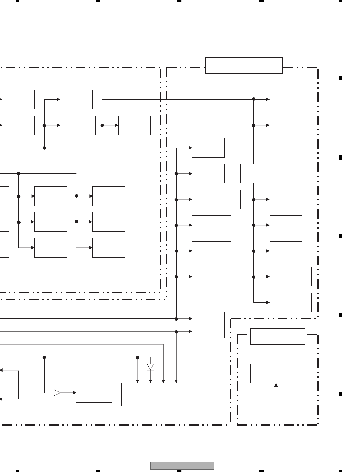
AVIC-D3/XU/UC 35
5678
56
78
C
D
F
A
B
E
O
O
R
F
V
R
F
V
U
TE
IX
0
V
AUDIO
SELECTOR
TC4052BFT
GUIDE
ISOLATOR
BA4558RFV
DVD AUDIO
LPF
NJM4558V
AU5 REF
NJM2125F
AV1 VIDEO
ISOLATOR
NJM2137V
AV2 VIDEO
ISOLATOR
NJM2136V
VIDEO
SELECTOR
BA7649AF
IPOD VIDEO
ISOLATOR
NJM2505F
B CAMERA
ISOLATOR
NJM2505F
75 Ω DRIVER
TK154058BMI
VIDEO
SELECTOR
NJM2235
VSW5V
MONITOR
UCOM
PE5584A
RESET IC
S-80835
EEPROM
UCOM MEMORY
S-93C46BD0I
EEPROM
ROM COLLECT
S-93C56BDOI
THERMISTOR
CCX1051
TIMING
ADJUSTMENT
TC74VHC221AFTS1
OR
TC7SH32FUS1
OSD SW
AND
TC7SH08FUS1
LED DRIVER
M62343
DIMMER OSC
NJM2903V
VIDEO I/F IC
RB5P0090M
REMCON
GP1UX51RK
TOUCH
PAN EL
CSX1114
6.1 inch LCD
TIMING
CONTROL IC
LZ9FE30
V5 = 5 V
V15 = 15 V
VM10 = -10 V
V53V = 5.3 V
OSD IC
PD6567
MULTI COLOR LED
NSSM025
MONITOR UNIT
KEY UNIT
V8V = 8 V
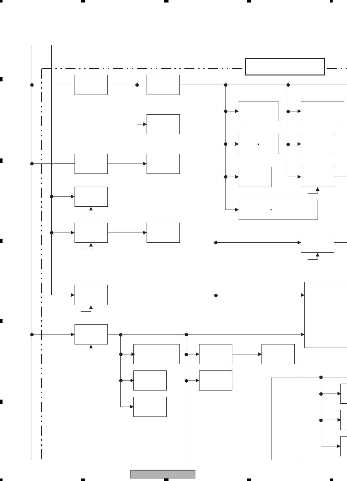
AVIC-D3/XU/UC
36
1234
1234
C
D
F
A
B
E
VDD5
REG
IPBUS
DRIVER
HA12241FP
SYSTEM
UCOM
uPD703089YGJ
RST INV
5 3
TC7SH04FUS1
MUTE
OR
TC7S32FU
ROM
COLLECTION
S-93C568DOI-J8
RESET IC
BD5335FVE
TR SW
CTOSYS WDT OFFOK RST
3 5 AND
TC74VHCT08AFTS1
LC FILTER
UVDD5
DC/DC
8 V
TPS5103IDB
VCC5
REG
SWBUP
SW
FAN CNT
DC/DC
5 V
TPS5120BT
MS5
ASENS IPBUS
POWER
W
T
C
S
Y
A
OPTON
TC7SET08FUS1
SPEED
PULSE
NJM2904M
LC FILTER RGB
BUFFER
K MODE
(EW NM)
PB SNS
T
NAVI MOTHER UNIT
ASENBO
VDD5 = 5 V
ASENS
FANCONT
FANUP
CCON
VD8 = 8.2 V
VCC5V
UVDD5 = 5 V
CCON
DD8CONT
CCON
DALMON
FAN
7.5 V to 10.5 V
T
C
AB C
DEEF
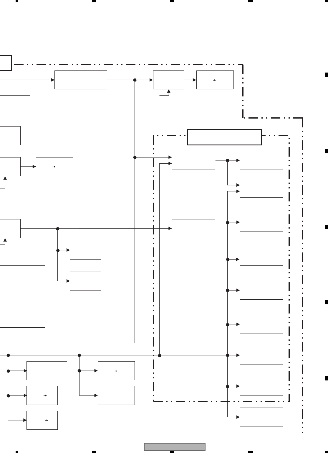
AVIC-D3/XU/UC 37
5678
56
78
C
D
F
A
B
E
ROM
O
LLECTION
C568DOI-J8
E
SET IC
5
335FVE
T
R SW
IPOD TO SYS
3 5
TC7SET08FUS1
BUP3
S-L2980A33MC-C6S
SYS TO IPOD
5 3
TC7SH08FUS1
TR SW
V
CC5
REG
GYRO
CSX1122
G SENSOR
CSX1118
MS5
RST IC
MAX6364PUT29
GPS 2M SRAM
M5M5V216ATP
DRAGON
PD3390A
4Mbit
FLASH
ADC
ADC12H034CIMSA
DIAGNOSIS
NJM2100V
TCXO
CWX2381
RF AMP
UPC2749T
GPS
ANNTENA
RDS DECODER
LC72720YVS
(UC/NM)
WDT IRQ
OR 5 3
TC7WH32FU
SYSTOC IRQ
AND 5 3
RS232C
DRIVER
UPD4723GSS1
REM INV
5 3
TC7SH14FUS1
SYNC
INV
TC7SH04FUS1
GPS UNIT
BUP3 = 3.3 V
RF IC
UPB1027GS
DALMON
TC7WH08FU
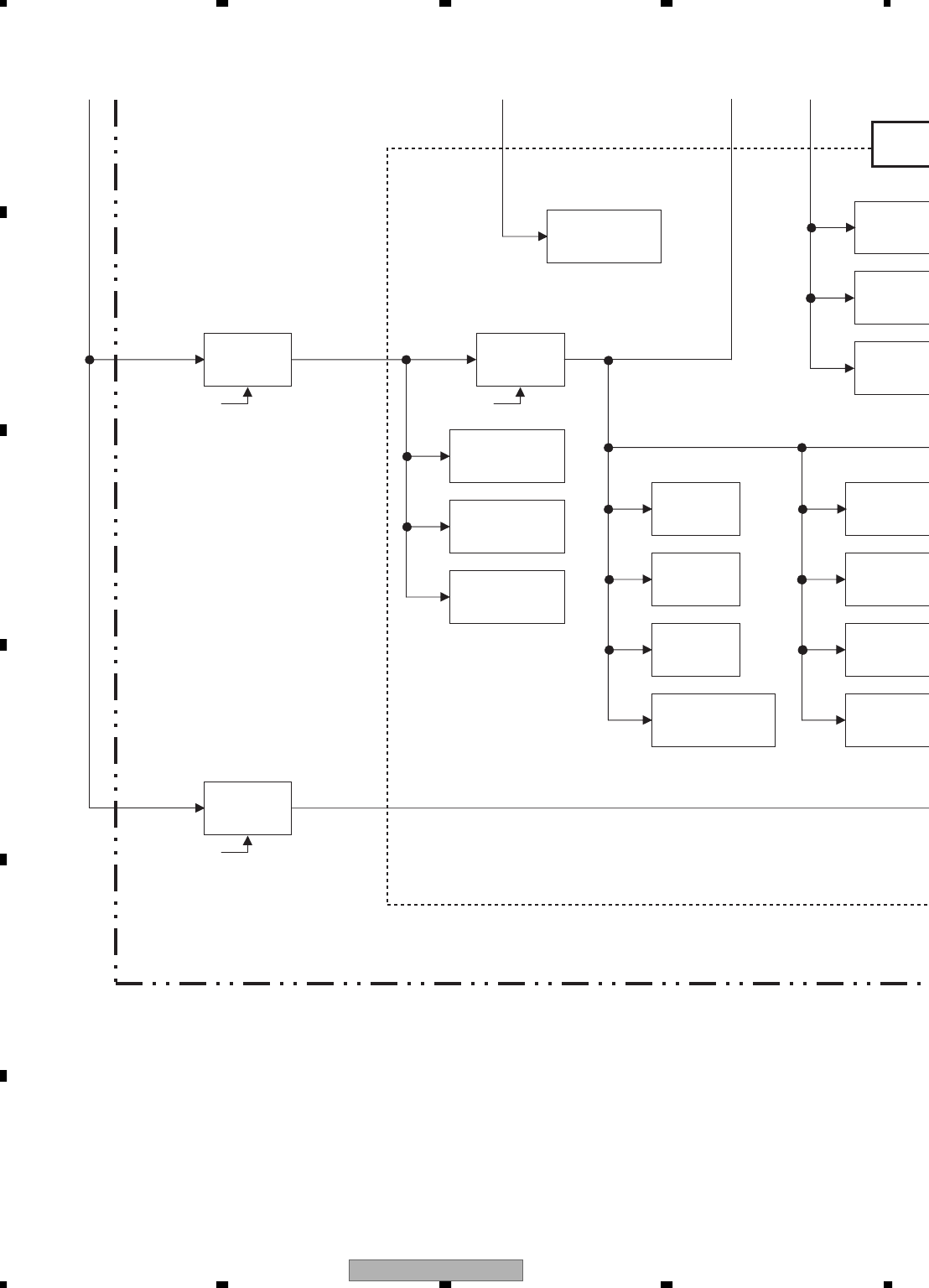
AVIC-D3/XU/UC
38
1234
1234
C
D
F
A
B
E
DC/DC
3.3 V
TPS5103IDB
TR SW
RST3
AND
TC7WH08FUS1
CKE SDRAM
AND
TC7SZ08FU
SDRAM*2
K4S561632E
HY57V561620
ASIC
PD6336B
DATA
BUFFER
*
TC74LCX24
Xtal
CWX2795
CHIP SE
AND
TC74LCX08
F
ADDRESS
BUFFER*3
TC74LCX541FTS1
64MBIT
FLASH*2
R/W
INV
TC7SH04F
U
RST3
M51957BF
P
DC/DC
2.5 V
TPS5120BT
DRAMPW
&
CCON
CCD5
CCON
CCD3 = 3.3 V
CCD25 = 2.5 V
SRAM
M5M5V21
6
XCS SR
A
NAND
TC7SH00
F
RST SRA
M
AND
TC7SH08
F
DAC
AK4388VT
C
DEEF
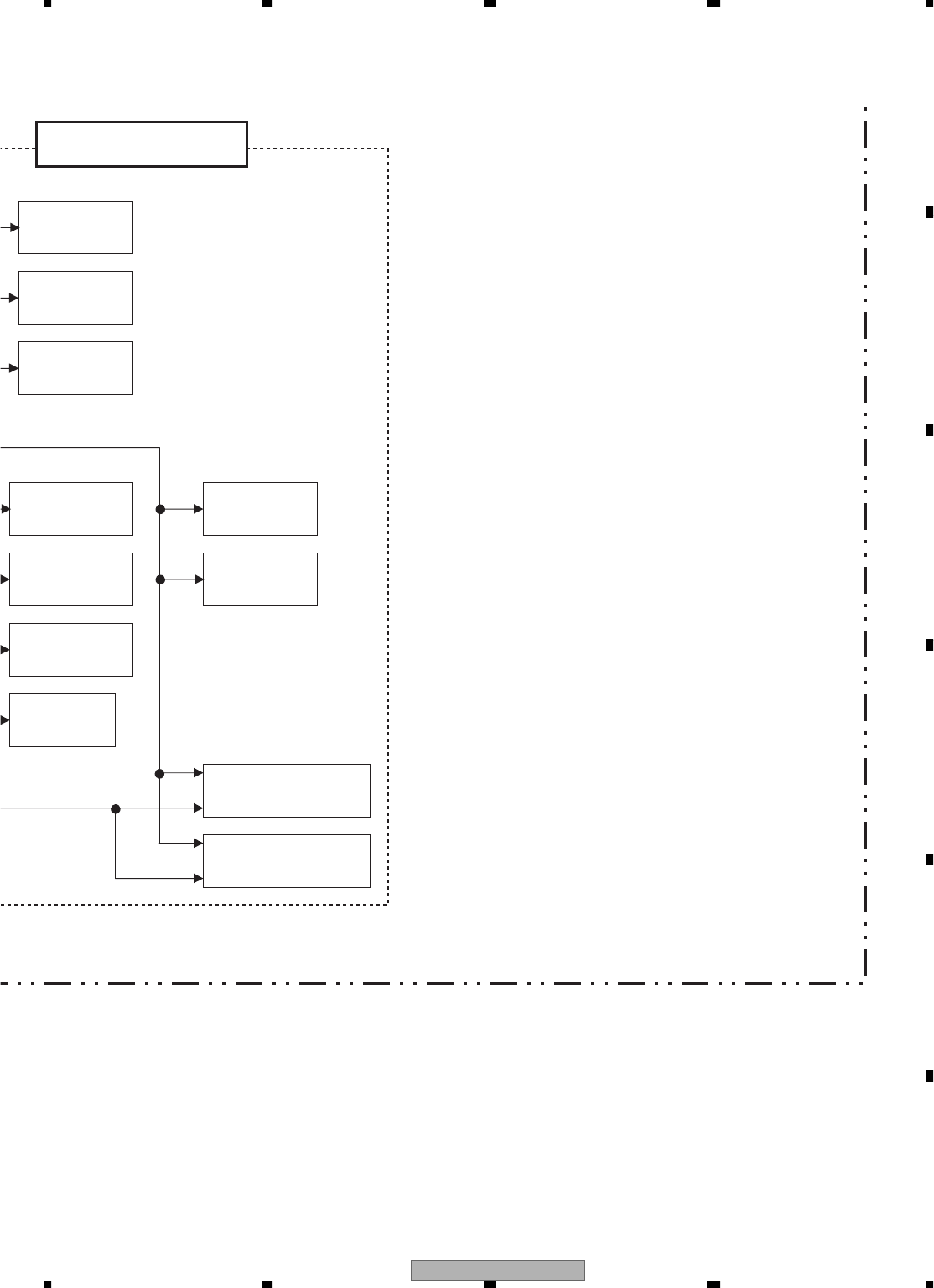
AVIC-D3/XU/UC 39
5678
56
78
C
D
F
A
B
E
DATA
BUFFER*4
TC74LCX245FT
CHIP SEL
AND
TC74LCX08FTS1
R/W
INV
TC7SH04FUS1
RST3
M51957BFP
MS5 RESET
AND
TC7SH08FUS1
BUFFER
TC74LVX4245
SCARLET
MB86291APFVS
CPU
UPD705103GM180S1
SRAM
M5M5V216ATP
XCS SRAM
NAND
TC7SH00FUS1
RST SRAM CS
AND
TC7SH08FUS1
CC SECTION
AVIC-D3/XU/UC
40
1234
1234
C
D
F
A
B
E
3.2 OVERALL CONNECTION DIAGRAM
NAVI MOTHER UNIT
A
1/7
A
CPU,ASIC,SDRAM
2/7
A
ROM,SRAM,BUS-BUFFER
3/7
A
GRAPHIC
4/7
A
MAIN,CC I/F
5/7
A
SYSTEM uCOM
6/7
A
I/F
7/7
A
PS
AV UNIT
C
1/3
C
PS,I/F
2/3
C
A/V
3/3
C
TUNER
KEY PCB
H
AV MINI JACK
P
I
DVD MECHANISM
MODULE(MS5)
D E F
TOUCH PANEL
AVIC-D3/XU/EW5
AVIC-D3/XU/UC
Note: When ordering service parts, be sure to refer to " EXPLODED VIEWS AND PARTS LIST" or
"ELECTRICAL PARTS LIST".
CN2001CN1901CN1852
AVIC-D3/XU/UC 41
5678
56
78
C
D
F
A
B
E
GPS UNIT
B
U
NIT
P
S,I/F
A
/V
T
UNER
MONITOR UNIT
G
1/2
G
VIDEO
2/2
G
INVERTER
KEY PCB
H
MINI JACK PCB
LCD
MODULE
T
OUCH PANEL
TUNER UNIT
(AVIC-D3/XU/EW5)
FM/AM TUNER UNIT
GPS ANTENNA
FAN MOTOR
AVIC-D3/XU/UC
42
1234
1234
C
D
F
A
B
E
3.3 NAVI MOTHER UNIT (CPU, ASIC, SDRAM)(GUIDE PAGE)
A-a
1/7
A
1/7
A-a A-b
A-a A-b
A-b
A-a
Large size
SCH diagram
Guide page
Detailed page
4/7
A
3/7
A2/7
A
Decimal points for resistor
and capacitor fixed values
are expressed as :
2.2 2R2
0.022 R022
←
←
The > mark found on some component parts indicates
the importance of the safety factor of the part.
Therefore, when replacing, be sure to use parts of
identical designation.
Symbol indicates a resistor.
No differentiation is made between chip resistors and
discrete resistors.
NOTE :
Symbol indicates a capacitor.
No differentiation is made between chip capacitors and
discrete capacitors.
3.3V
3.3V
3.3V
3.3V
2.5V
2.5V
2.5V
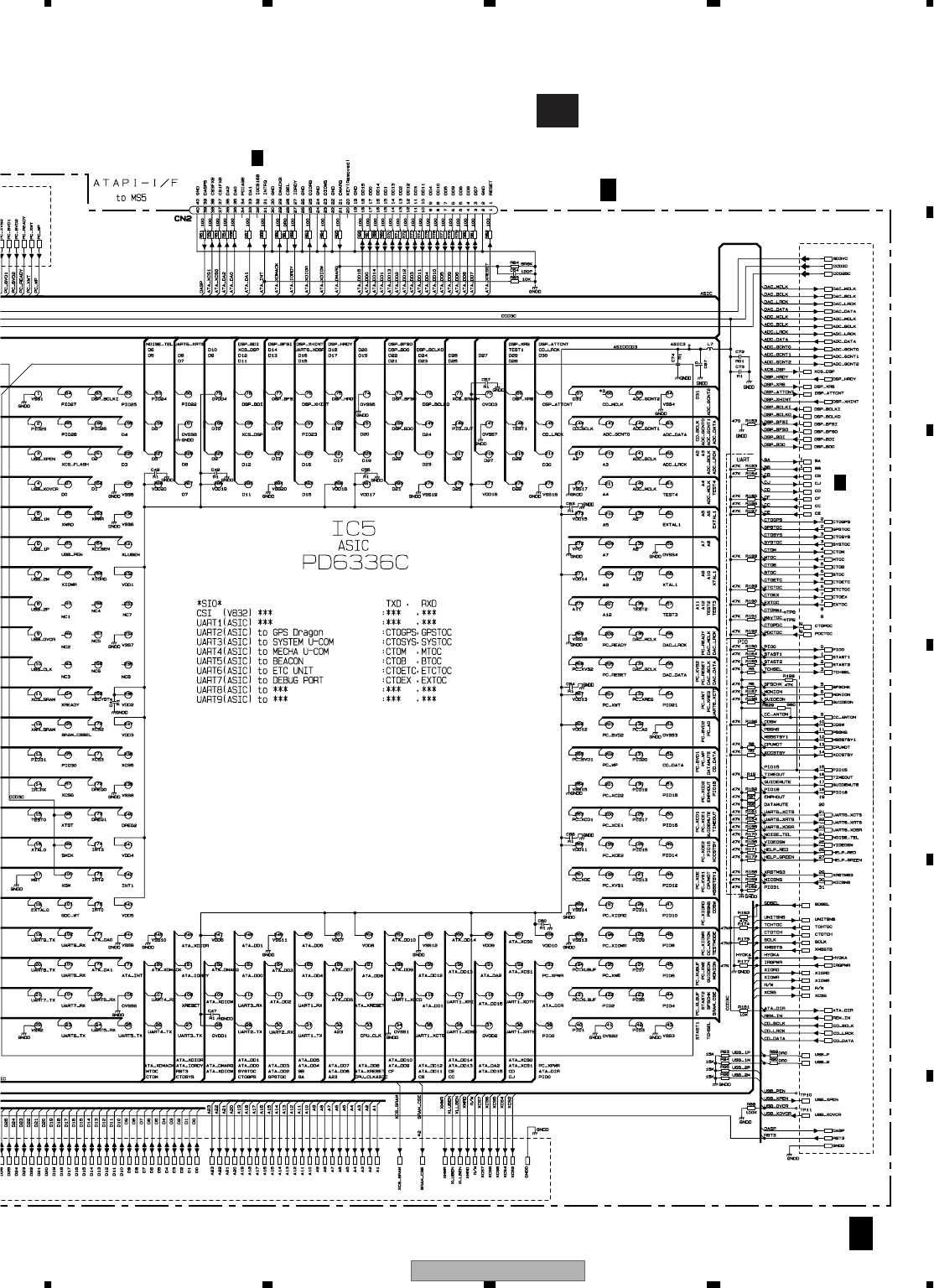
AVIC-D3/XU/UC 43
5678
56
78
C
D
F
A
B
E
A-b
1/7
A
1/7
A-a A-b
A-a A-b
A-b
A-a
CN2001
2/2
D
4/7
A
NAVI MOTHER UNIT (CPU, ASIC, SDRAM)
1/7
A
3.3V
2.5V
3.3V
3.3V
3.3V
3.3V
2.5V
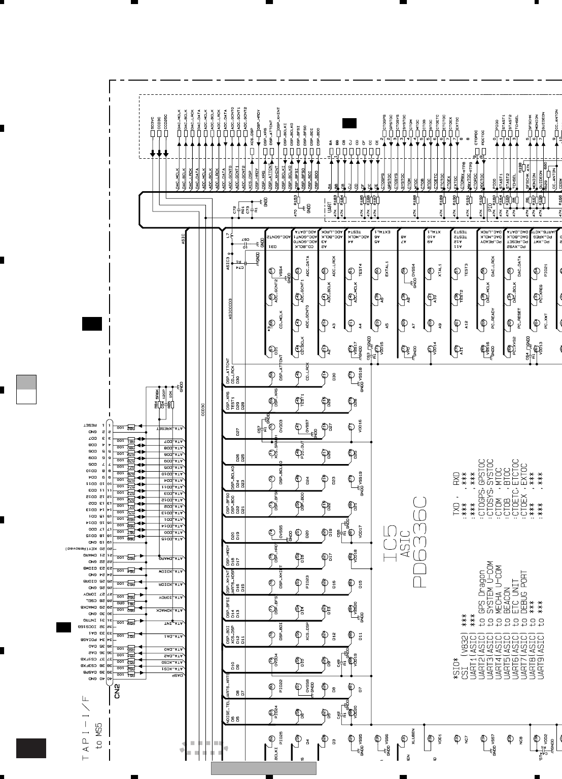
AVIC-D3/XU/UC
44
1234
1234
C
D
F
A
B
E
A-a A-b
A-b 1/7
1
CN2001
2/2
D
4/7
A
NAVI MOTHER UNIT (CPU, ASIC, SDRAM)
1/7
A
3.3V
3.3V
3.3V
2.5V
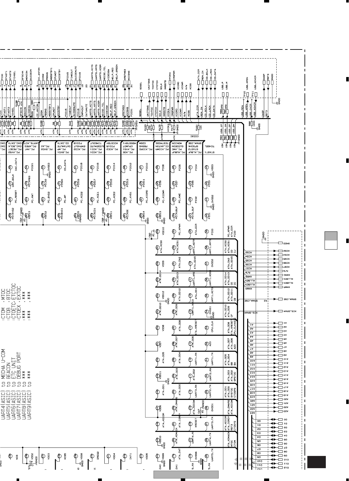
AVIC-D3/XU/UC 45
5678
56
78
C
D
F
A
B
E
A-a A-b
A-b 1/7
2
3.3V
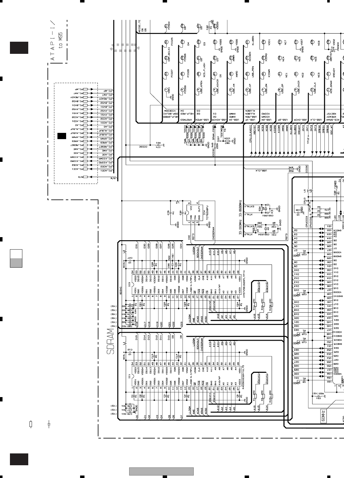
AVIC-D3/XU/UC
46
1234
1234
C
D
F
A
B
E
A-bA-a
A-a 1/7
A-b 1/7
1
4/7
A
Decimal points for resistor
and capacitor fixed values
are expressed as :
2.2 2R2
0.022 R022
←
←
The > mark found on some component parts indicates
the importance of the safety factor of the part.
Therefore, when replacing, be sure to use parts of
identical designation.
Symbol indicates a resistor.
No differentiation is made between chip resistors and
discrete resistors.
NOTE :
Symbol indicates a capacitor.
No differentiation is made between chip capacitors and
discrete capacitors.
3.3V
3.3V
3.3V
3.3V
2.5V
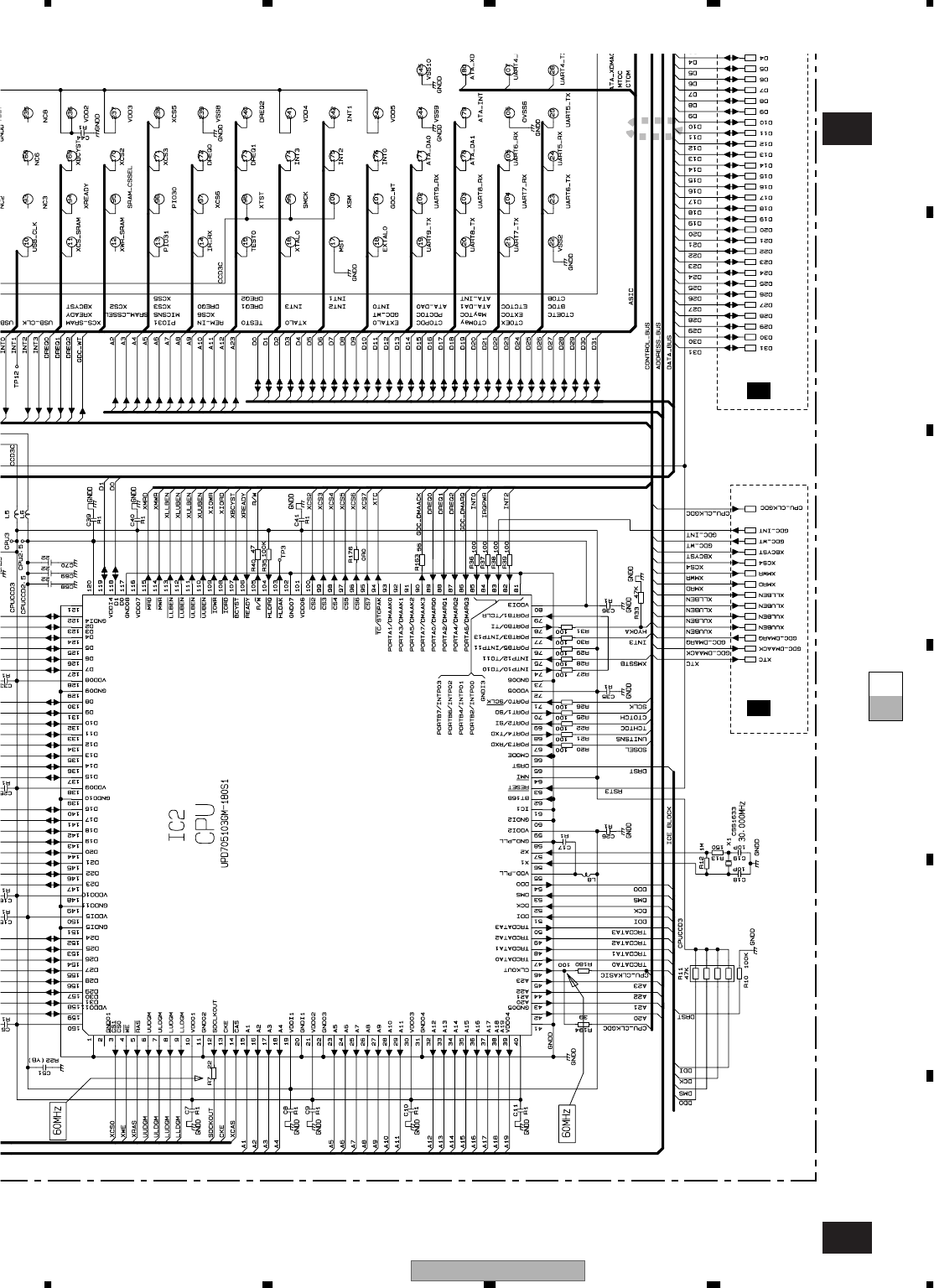
AVIC-D3/XU/UC 47
5678
56
78
C
D
F
A
B
E
A-bA-a
A-a 1/7
A-b 1/7
2
3/7
A2/7
A
2.5V
2.5V
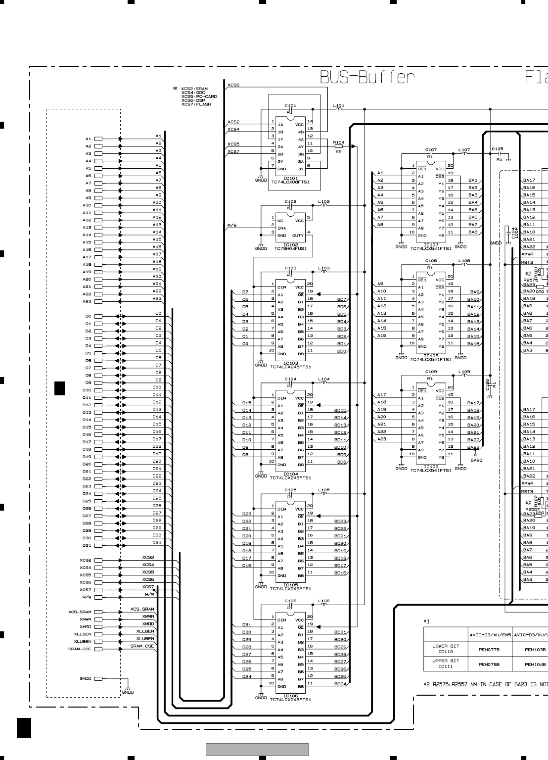
AVIC-D3/XU/UC
48
1234
1234
C
D
F
A
B
E
3.4 NAVI MOTHER UNIT (ROM, SRAM, BUS-BUFFER)
2/7
A
1/7
A
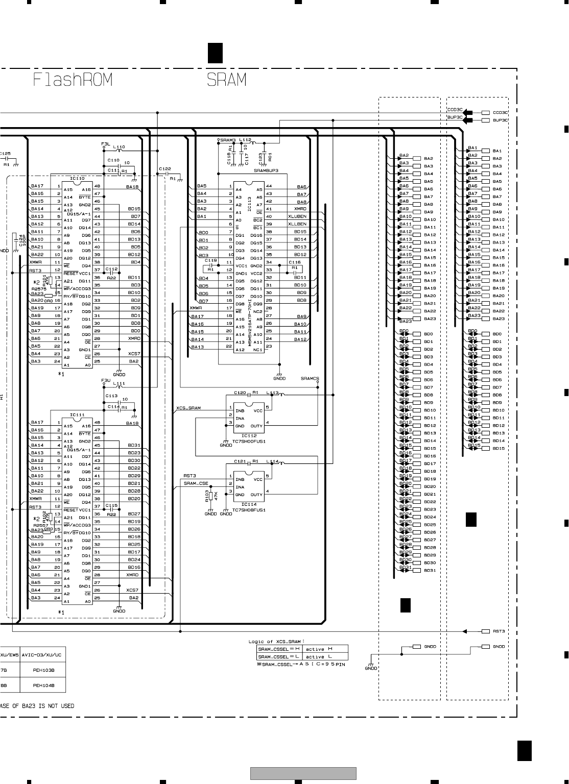
AVIC-D3/XU/UC 49
5678
56
78
C
D
F
A
B
E
2/7
A
NAVI MOTHER UNIT (ROM, SRAM, BUS-BUFFER)
2/7
A
3/7
A
4/7
A
3.3V 3.3V
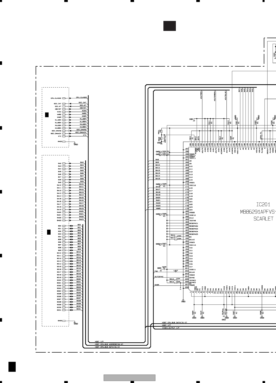
AVIC-D3/XU/UC
50
1234
1234
C
D
F
A
B
E
3.5 NAVI MOTHER UNIT (GRAPHIC)(GUIDE PAGE)
A-a
3/7
A
3/7
2/7
A
1/7
A
2.5V
2.5V
3.3V
3.3V
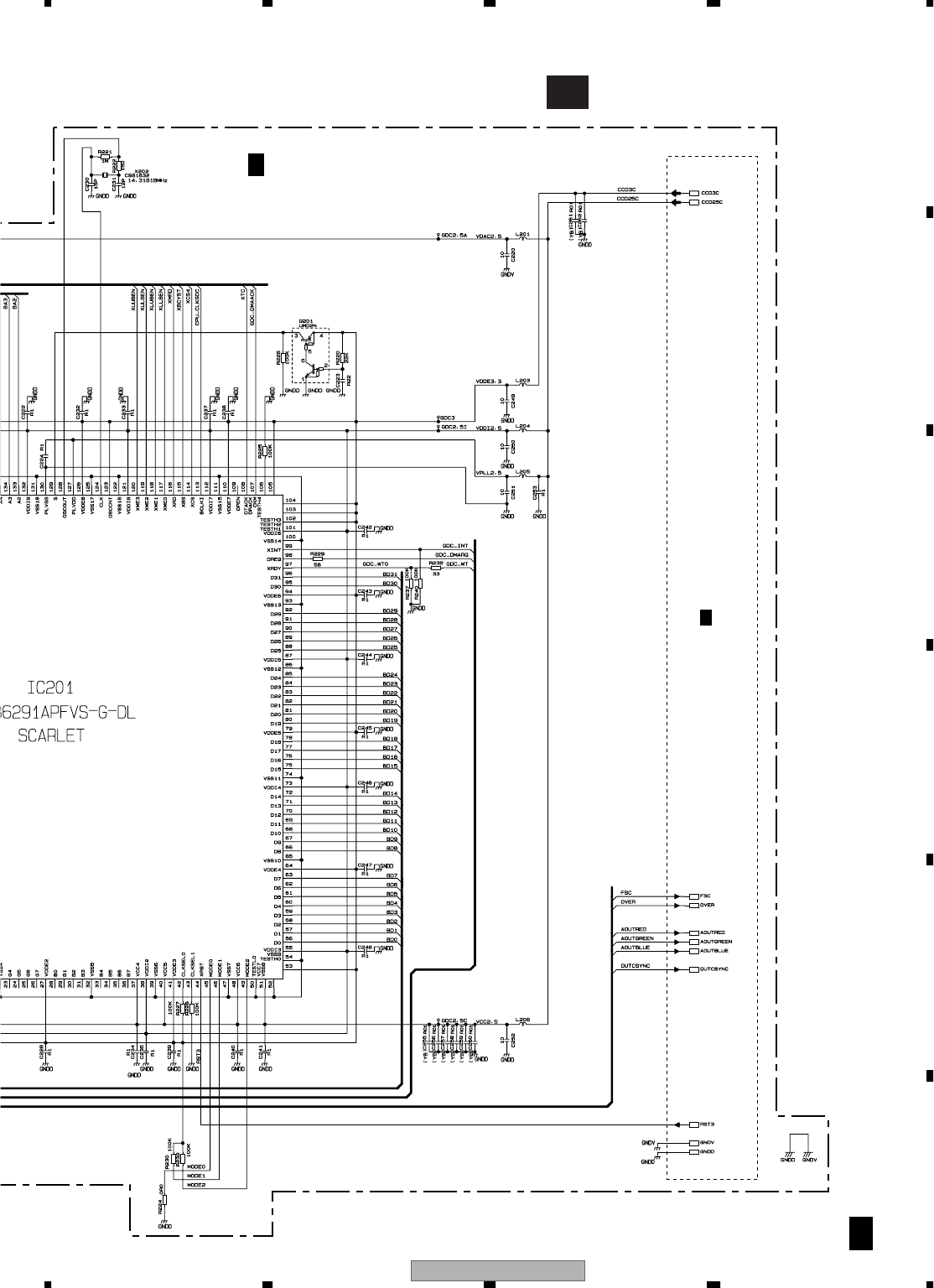
AVIC-D3/XU/UC 51
5678
56
78
C
D
F
A
B
E
A-b
3/7
A
3/7
NAVI MOTHER UNIT (GRAPHIC)
3/7
A
4/7
A
2.5V
2.5V
2.5V
2.5V
3.3V
3.3V
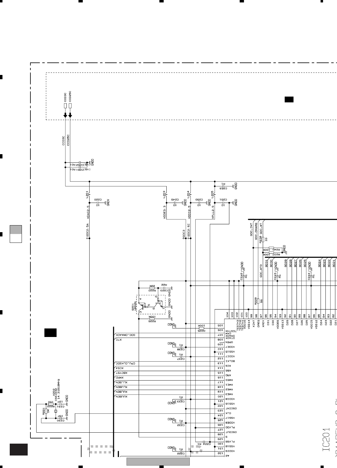
AVIC-D3/XU/UC
52
1234
1234
C
D
F
A
B
E
A-a A-b
A-b 3/7
1 2
NAVI MOTHER UNIT (GRAPHIC)
3/7
A
4/7
A
2.5V
2.5V
3.3V
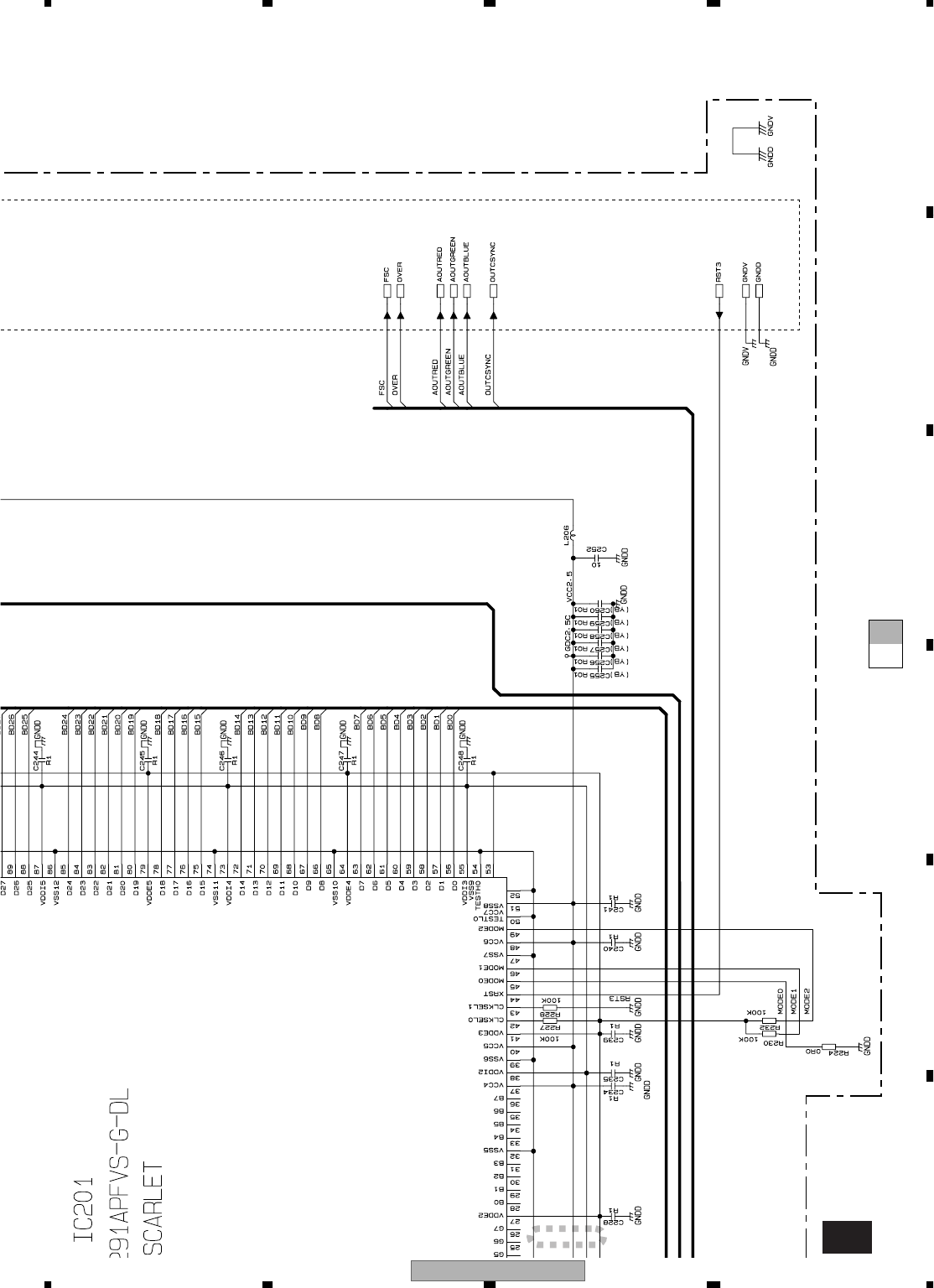
AVIC-D3/XU/UC 53
5678
56
78
C
D
F
A
B
E
A-a A-b
A-b 3/7
3
2.5V
2.5V
3.3V
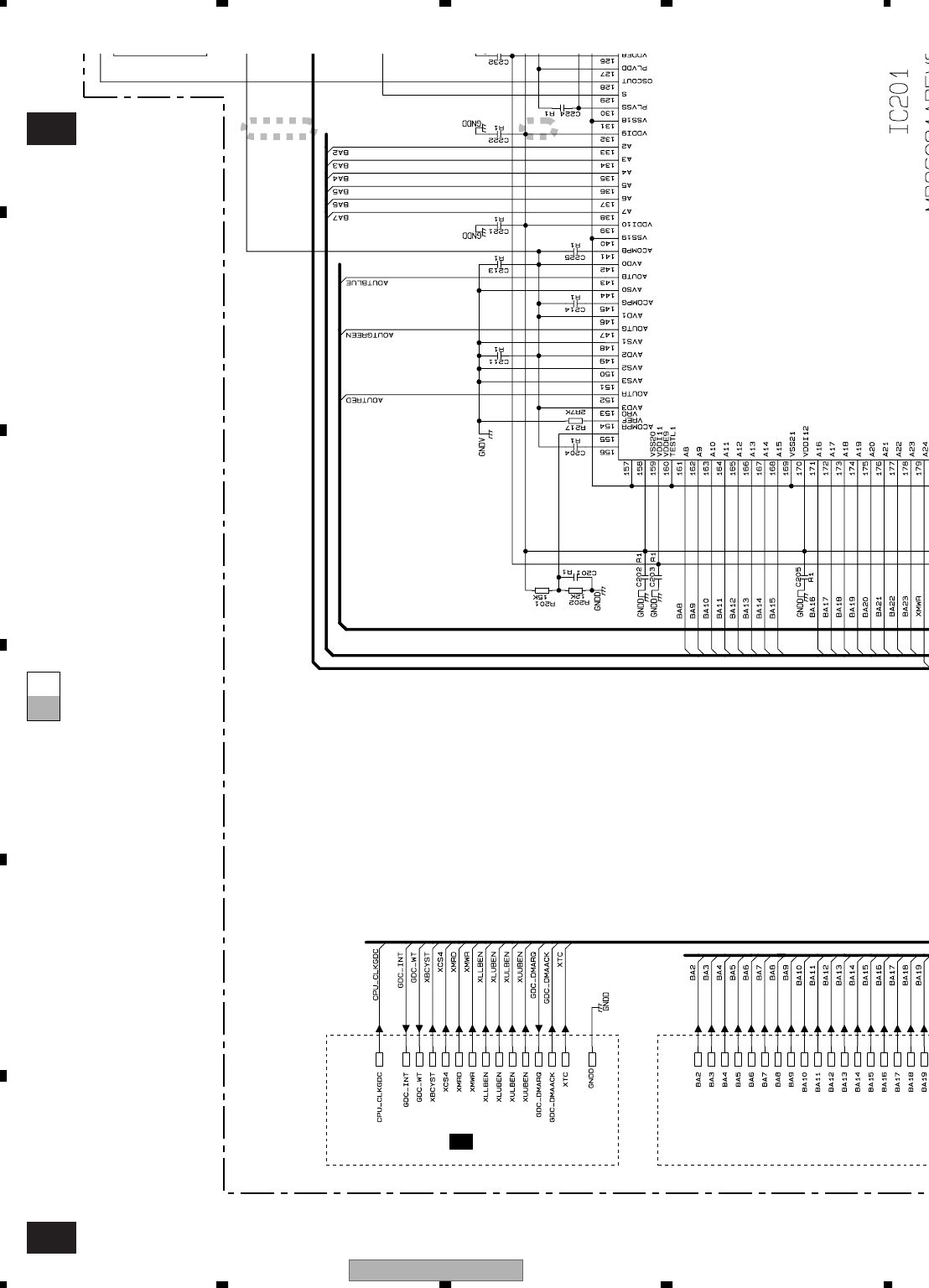
AVIC-D3/XU/UC
54
1234
1234
C
D
F
A
B
E
A-bA-a
A-a 3/7
A-b 3/7
1 2
1/7
A
2.5V
3.3V
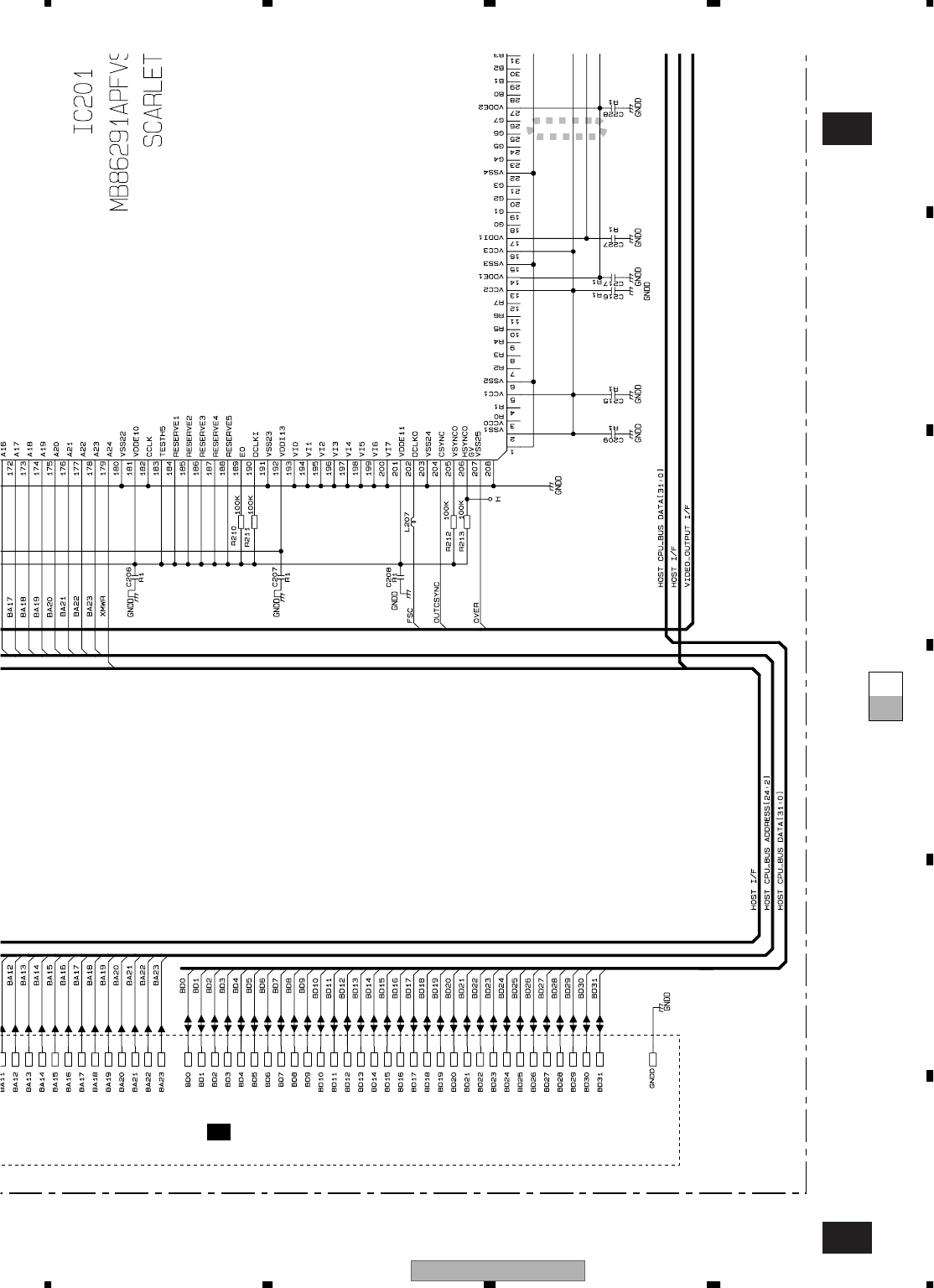
AVIC-D3/XU/UC 55
5678
56
78
C
D
F
A
B
E
A-bA-a
A-a 3/7
A-b 3/7
3
2/7
A
2.5V
3.3V
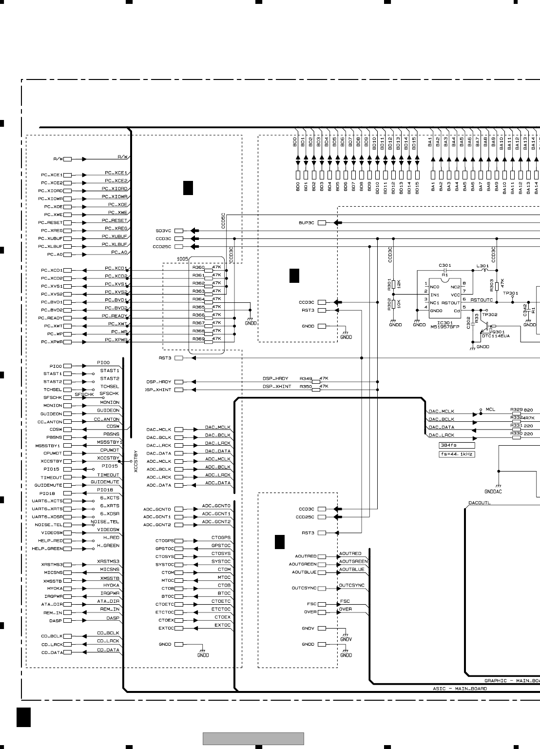
AVIC-D3/XU/UC
56
1234
1234
C
D
F
A
B
E
3.6 NAVI MOTHER UNIT (MAIN, CC I/F)
4/7
A
1/7
A
2/7
A
3/7
A
5.1V
3.3V
2.5V
3.3V
3.3V
2.5V
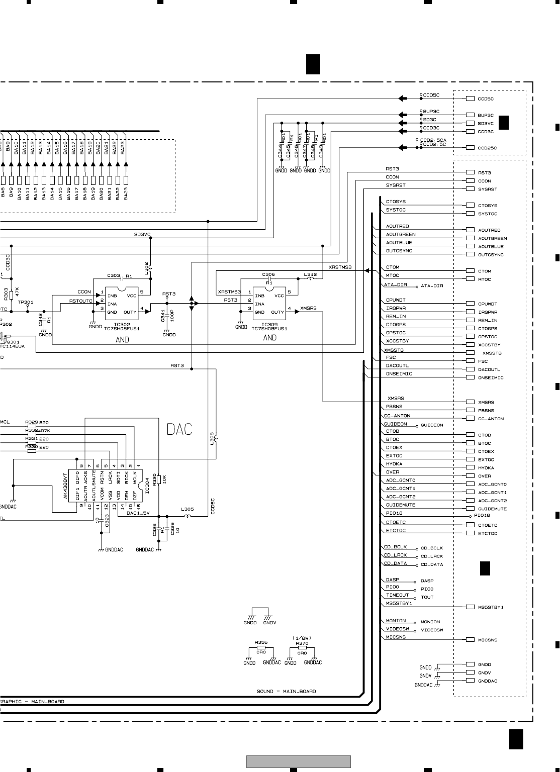
AVIC-D3/XU/UC 57
5678
56
78
C
D
F
A
B
E
4/7
A
NAVI MOTHER UNIT (MAIN, CC I/F)
4/7
A
7/7
A
6/7
A
3.3V
2.5V
3.3V
3.3V
5.1V
5.1V
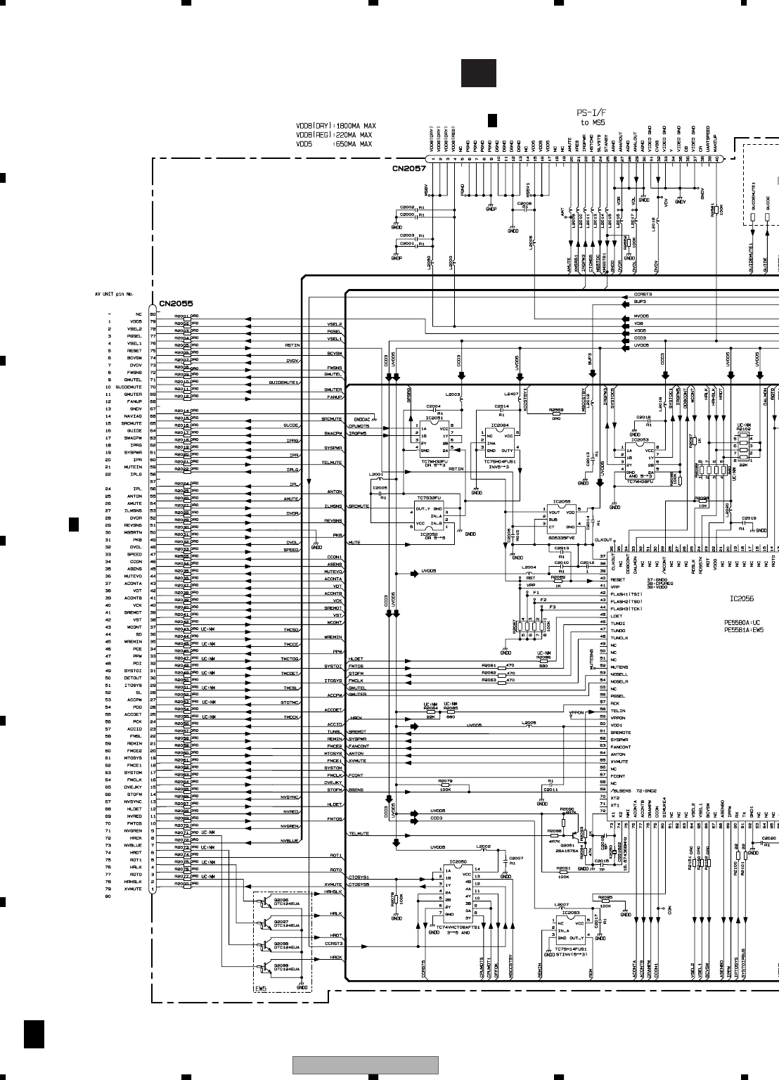
AVIC-D3/XU/UC
58
1234
1234
C
D
F
A
B
E
3.7 NAVI MOTHER UNIT (SYSTEM uCOM)(GUIDE PAGE)
A-a
5/7
A
5/7
CN1901
2/2
D
CN1711
2/3
C
SYSTEM CONTROLL
5.1V
8.1V
3.3V
5.0V
5.0V
3.3V
5.0V
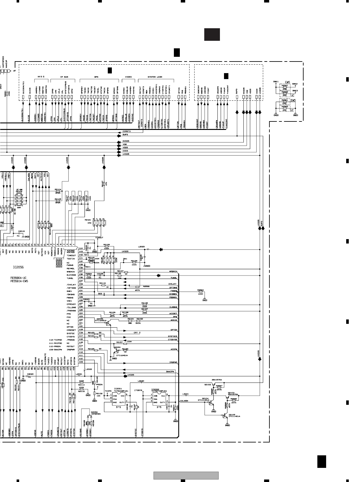
AVIC-D3/XU/UC 59
5678
56
78
C
D
F
A
B
E
A-b
5/7
A
5/7
NAVI MOTHER UNIT (SYSTEM uCOM)
5/7
A
6/7
A
7/7
A
Y
STEM CONTROLLER
3.3V
5.1V
8.1V
5.0V
3.3V
5.0V
3.3V
5.0V
5.0V
3.3V
5.0V
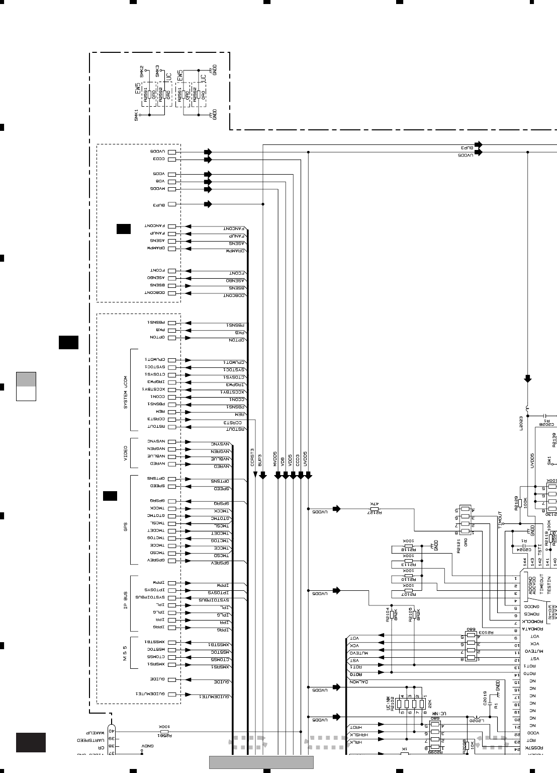
AVIC-D3/XU/UC
60
1234
1234
C
D
F
A
B
E
A-a A-b
A-b 5/7
1 2 3
NAVI MOTHER UNIT (SYSTEM uCOM)
5/7
A
6/7
A
7/7
A
3.3V
5.1V
8.1V
5.0V
3.3V
5.0V
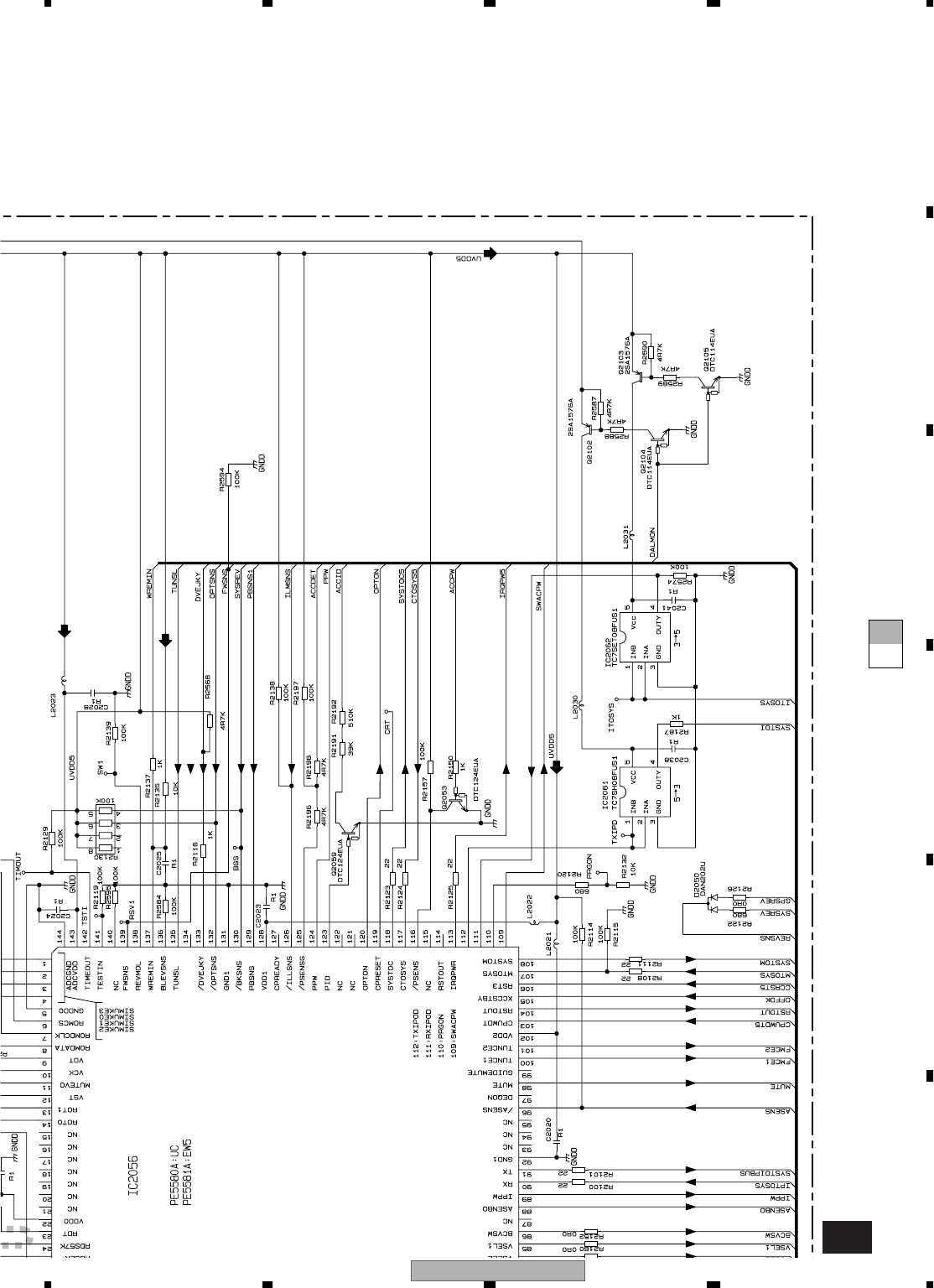
AVIC-D3/XU/UC 61
5678
56
78
C
D
F
A
B
E
A-a A-b
A-b 5/7
SYSTEM CONTROLLER
3.3V
5.0V
5.0V
3.3V
5.0V
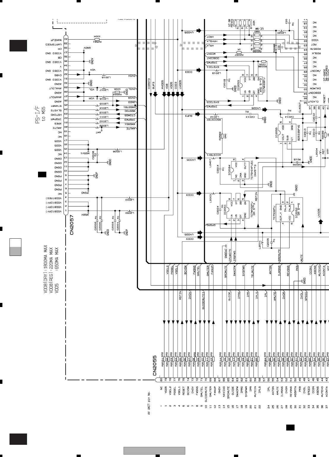
AVIC-D3/XU/UC
62
1234
1234
C
D
F
A
B
E
A-bA-a
A-a 5/7
A-b 5/7
1 2 3
CN1901
2/2
D
CN1711
2/3
C
5.1V
8.1V
3.3V
5.0V
3.3V
5.0V
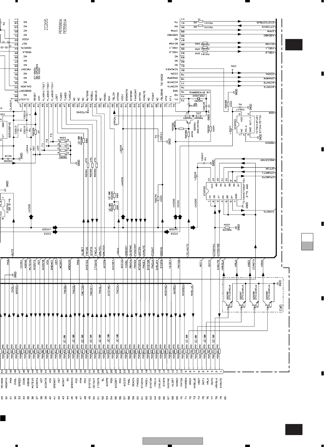
AVIC-D3/XU/UC 63
5678
56
78
C
D
F
A
B
E
A-bA-a
A-a 5/7
A-b 5/7
CN1711
2/3
C
SYSTEM CO
N
5.0V
3.3V
5.0V
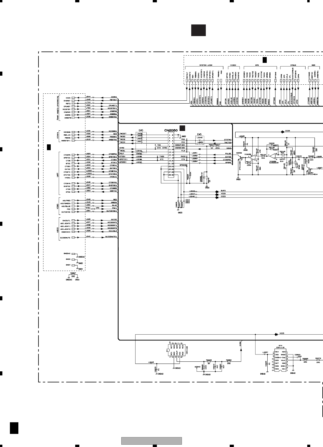
AVIC-D3/XU/UC
64
1234
1234
C
D
F
A
B
E
3.8 NAVI MOTHER UNIT (I/F)(GUIDE PAGE)
A-a
6/7
A
6/7
BCN461
5/7
A
4/7
A
5.1V
3.3V
3.3V
5.0V
5.0V
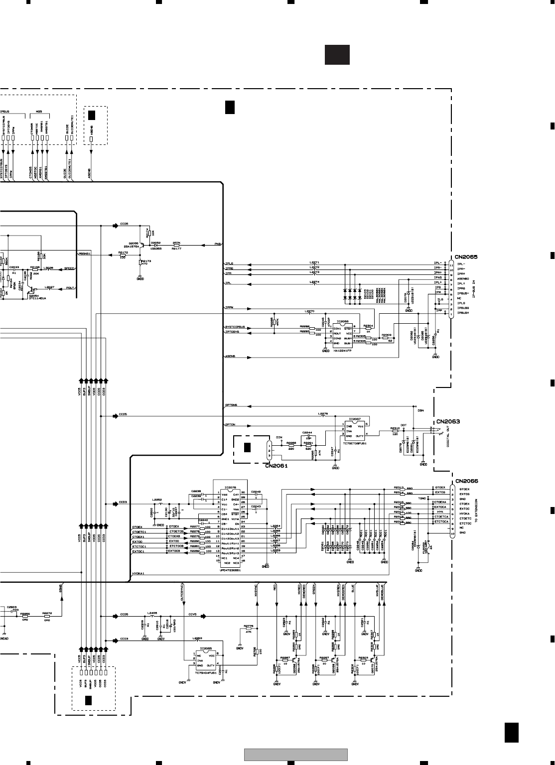
AVIC-D3/XU/UC 65
5678
56
78
C
D
F
A
B
E
A-b
6/7
A
6/7
NAVI MOTHER UNIT (I/F)
6/7
A
>
CN1852
2/2
D
7/7
A
7/7
A
5.1V
5.0V
5.1V
3.3V
3.3V
5.1V
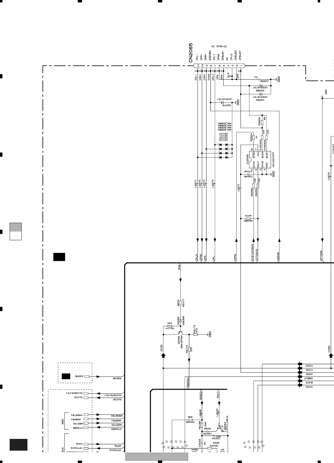
AVIC-D3/XU/UC
66
1234
1234
C
D
F
A
B
E
A-a A-b
A-b 6/7
1 2
NAVI MOTHER UNIT (I/F)
6/7
A
7/7
A
5.1V
5.1V
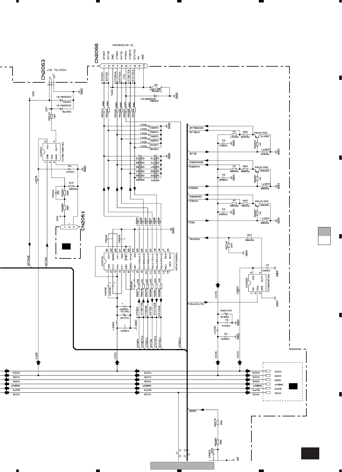
AVIC-D3/XU/UC 67
5678
56
78
C
D
F
A
B
E
A-a A-b
A-b 6/7
3
>
CN1852
2/2
D
7/7
A
5.0V
5.1V
3.3V
3.3V
5.1V
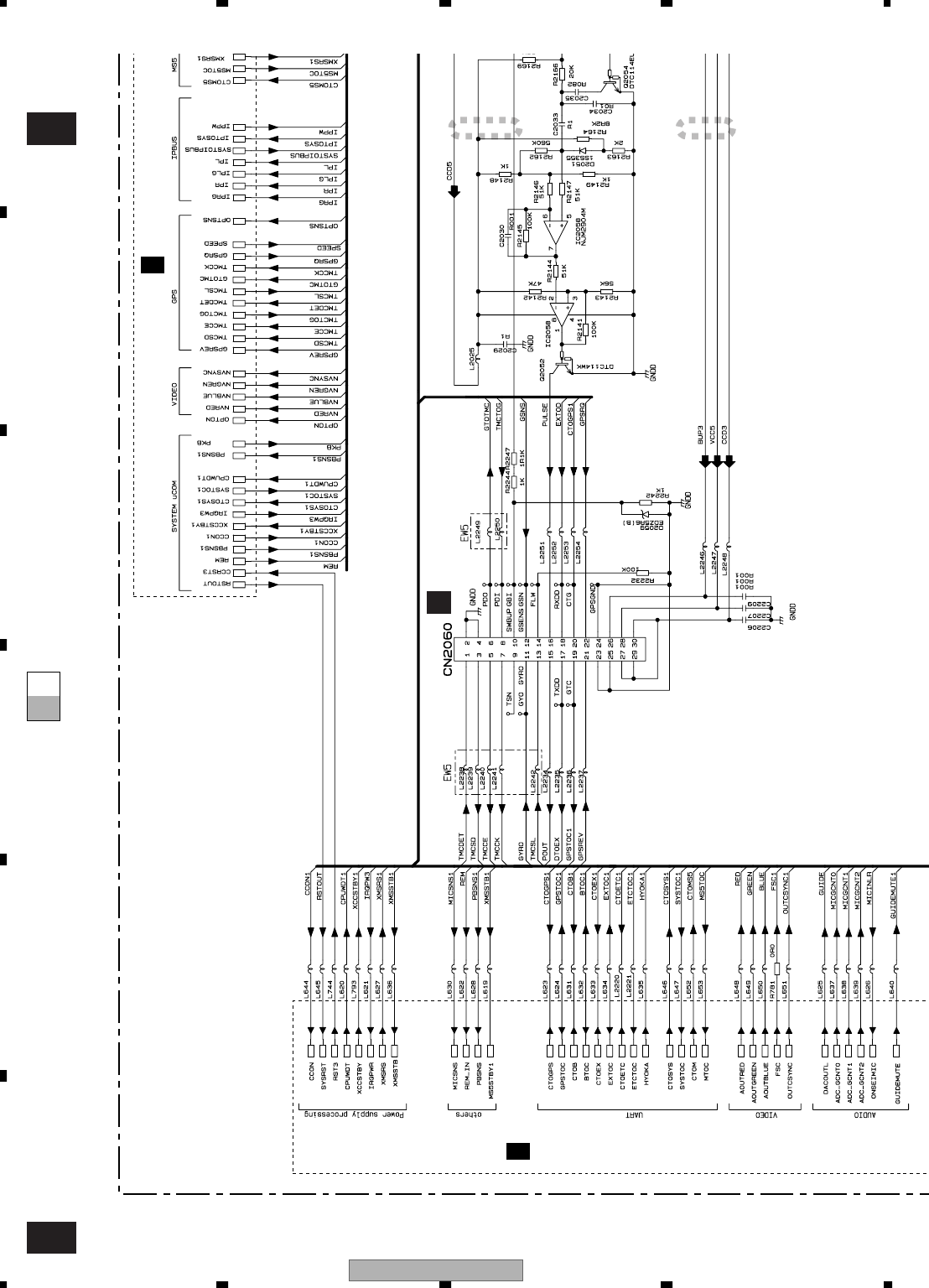
AVIC-D3/XU/UC
68
1234
1234
C
D
F
A
B
E
A-bA-a
A-a 6/7
A-b 6/7
1 2
B
CN461
5/7
A
4/7
A
5
3.3V
3.3V
5.0V
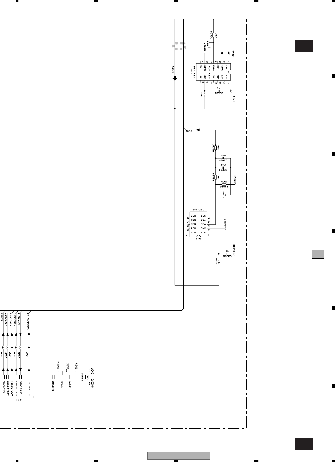
AVIC-D3/XU/UC 69
5678
56
78
C
D
F
A
B
E
A-bA-a
A-a 6/7
A-b 6/7
3
5.0V
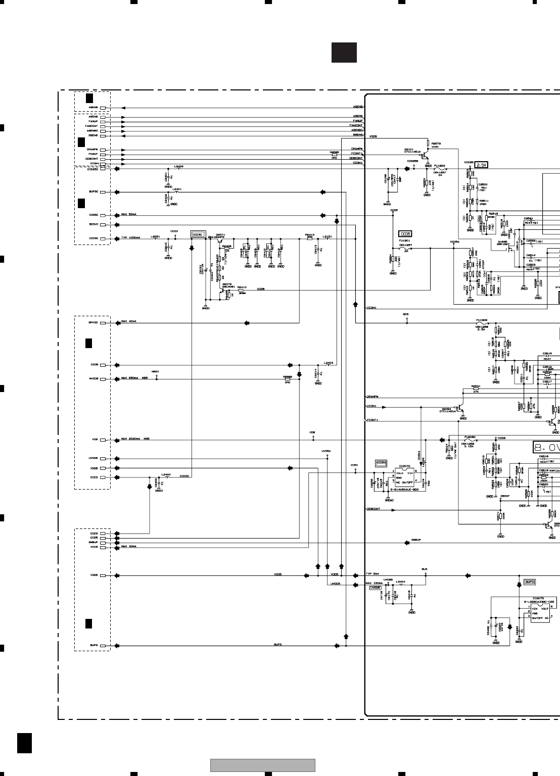
AVIC-D3/XU/UC
70
1234
1234
C
D
F
A
B
E
3.9 NAVI MOTHER UNIT (PS)(GUIDE PAGE)
A-a
7/7
A
7/7
>
>
>
>
6/7
A
5/7
A
4/7
A
5/7
A
6/7
A
2.5V
3.3V
5.1V
3.3V
3.3V
5.1V
5.1V
8.1V
5.0V
5.0V
3.3V
5.1V
5.0V
5.0V
3.3V
2.5V
5.1V
3.3V
5.1V
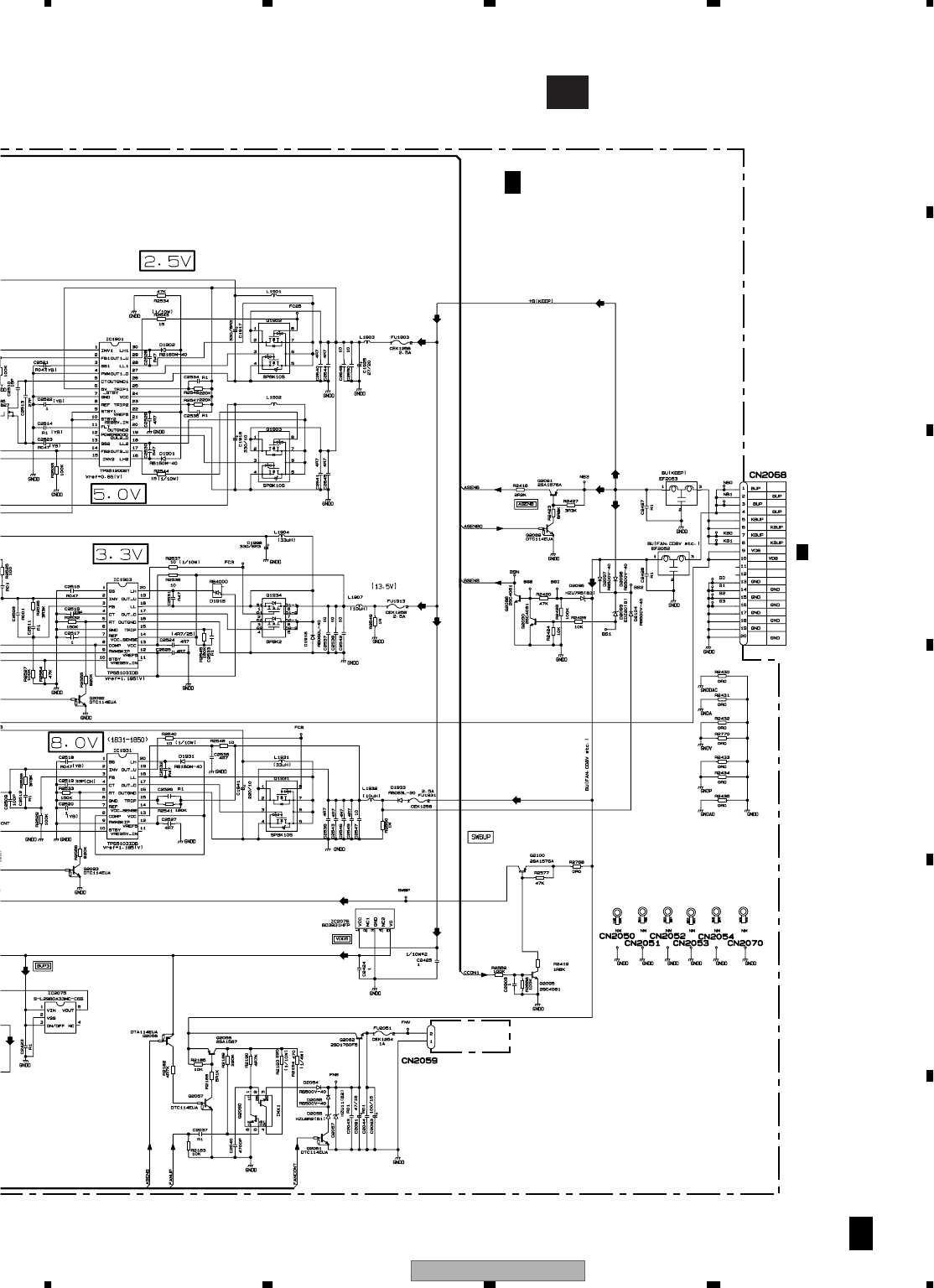
AVIC-D3/XU/UC 71
5678
56
78
C
D
F
A
B
E
A-b
7/7
A
7/7
>
>
>
>
CN1652
1/3
C
NAVI MOTHER UNIT (PS)
7/7
A
FAN MOTOR
CXM1320
5.0V
5.1V
8.1V
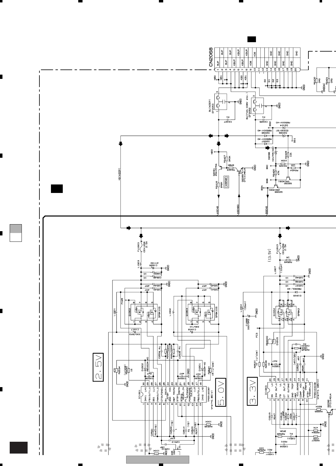
AVIC-D3/XU/UC
72
1234
1234
C
D
F
A
B
E
A-a A-b
A-b 7/7
1 2 3
4
>
>
CN1652
1/3
C
NAVI MOTHER UNIT (PS)
7/7
A
5.1V
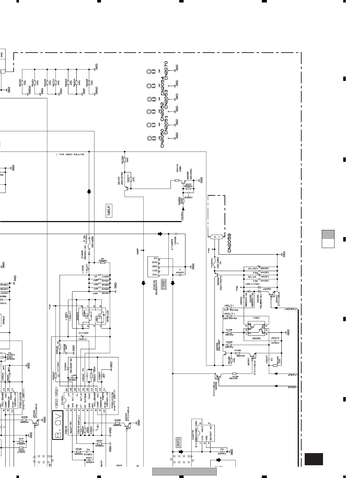
AVIC-D3/XU/UC 73
5678
56
78
C
D
F
A
B
E
A-a A-b
A-b 7/7
4 5
>
>
FAN MOTOR
CXM1320
5.0V
8.1V
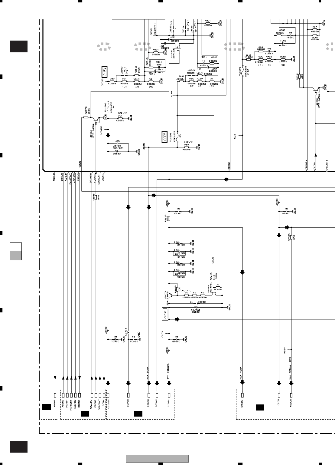
AVIC-D3/XU/UC
74
1234
1234
C
D
F
A
B
E
A-bA-a
A-a 7/7
A-b 7/7
1 2 3
4
>
>
>
6/7
A
5/7
A
4/7
A
5/7
A
2.5V
3.3V
5.1V
3.3V
3.3V
5.1V
5.1V
2.5V
5.1V
5.1V
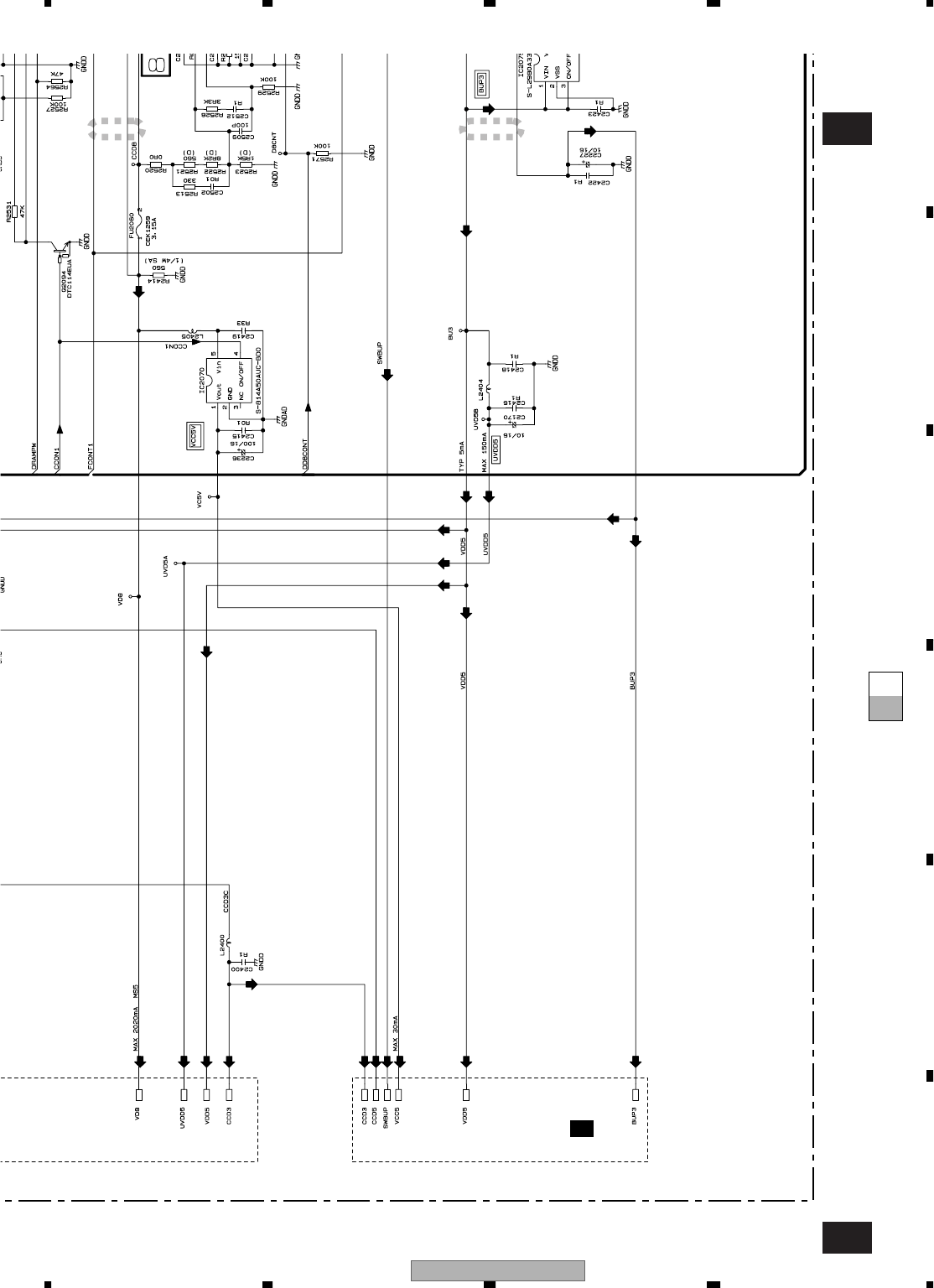
AVIC-D3/XU/UC 75
5678
56
78
C
D
F
A
B
E
A-bA-a
A-a 7/7
A-b 7/7
4 5
>
6/7
A
5
.
1V
8.1V
5.0V
5.0V
3.3V
5.1V
5.0V
5.0V
3.3V 3.3V
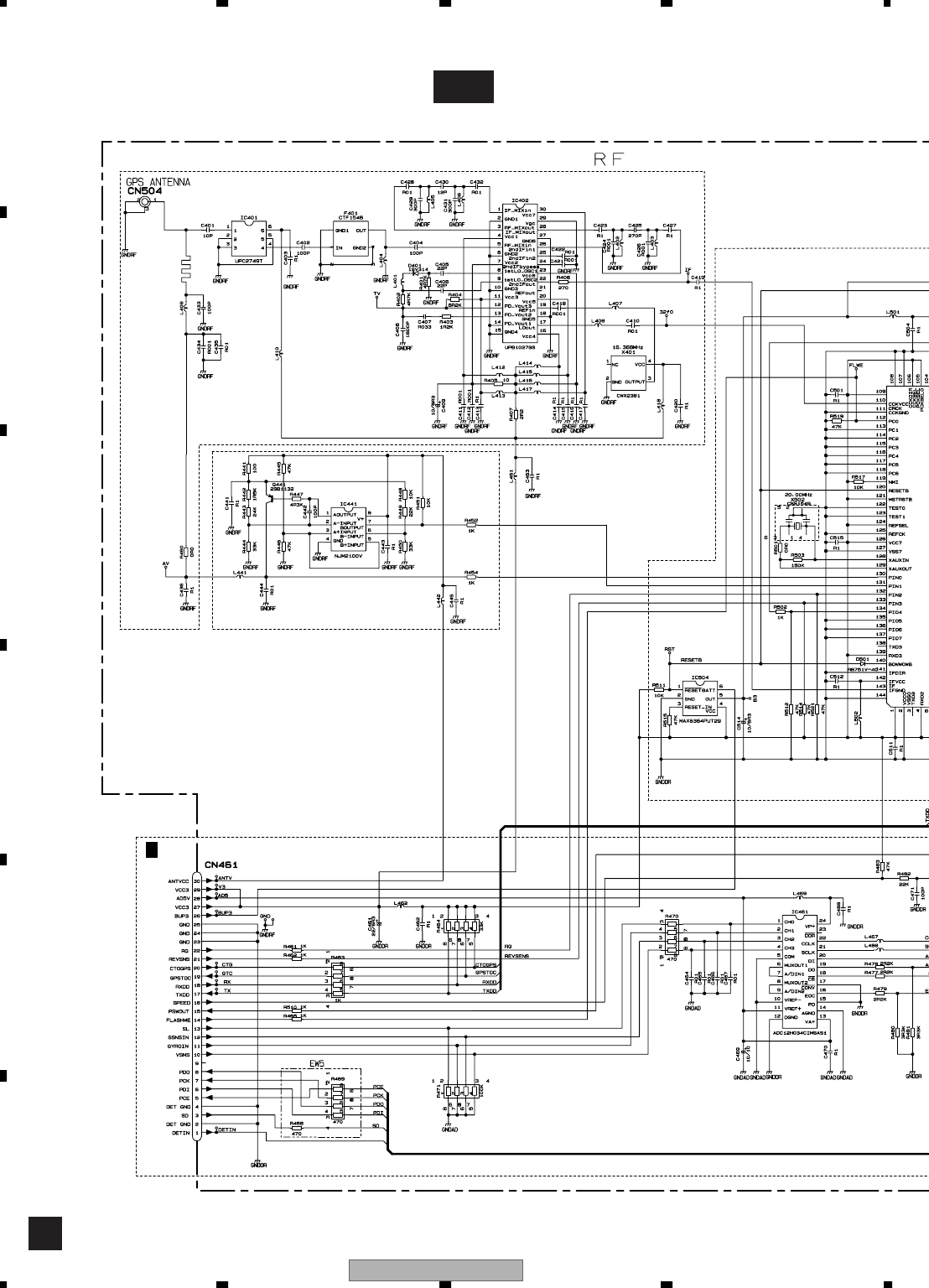
AVIC-D3/XU/UC
76
1234
1234
C
D
F
A
B
E
3.10 GPS UNIT(GUIDE PAGE)
B-a
B
CN2060
6/7
A
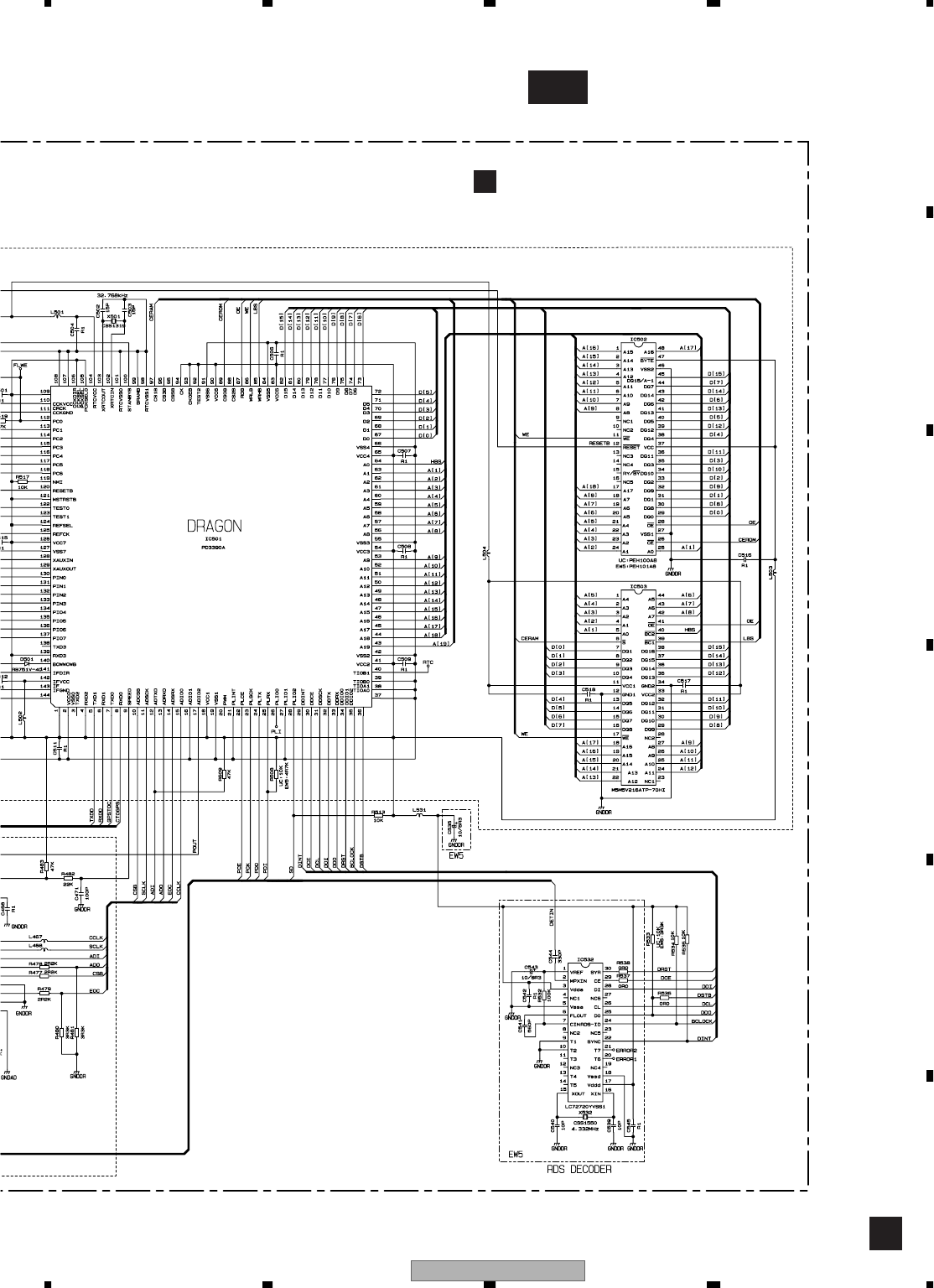
AVIC-D3/XU/UC 77
5678
56
78
C
D
F
A
B
E
B-b
B
BGPS UNIT
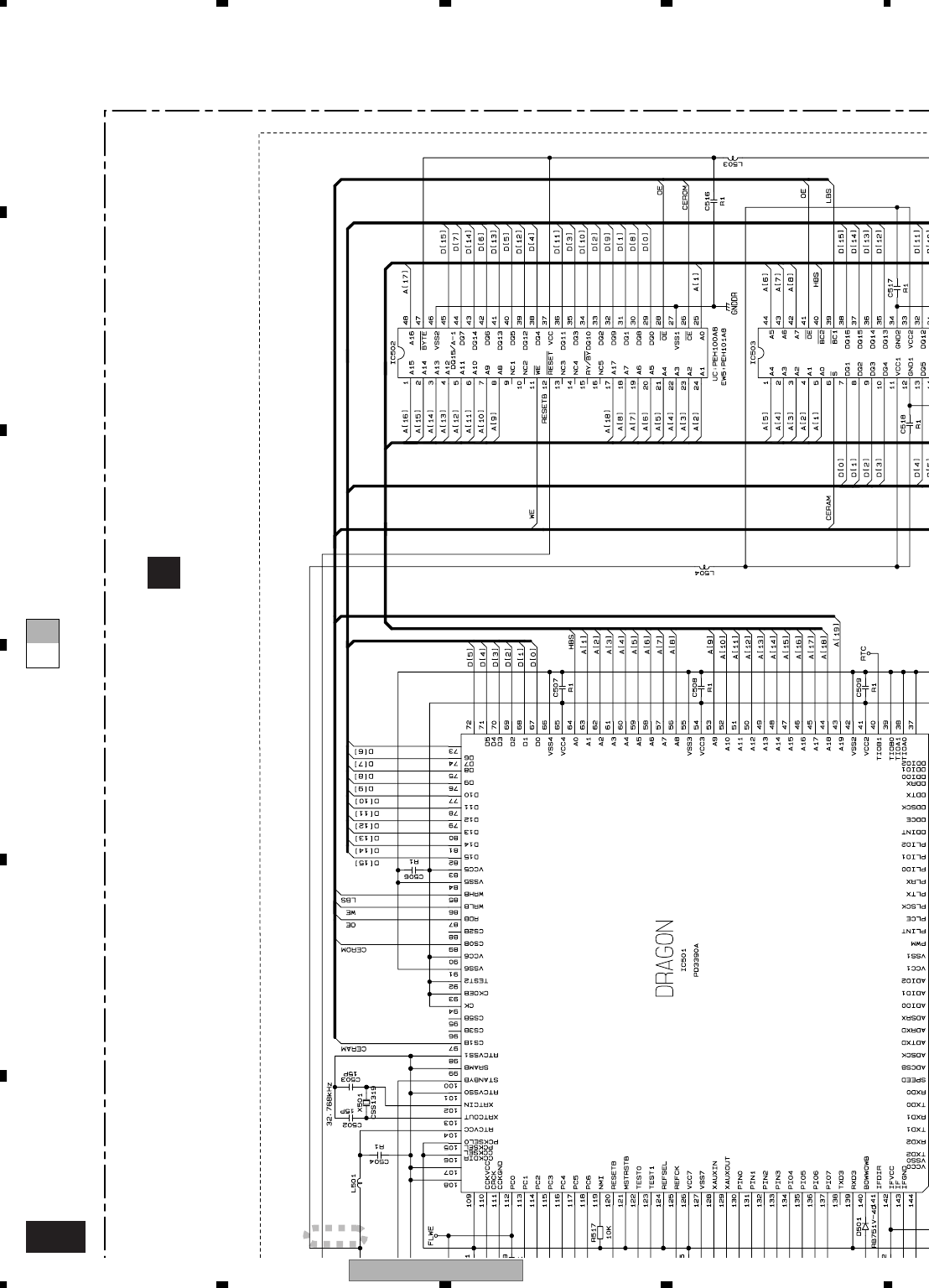
AVIC-D3/XU/UC
78
1234
1234
C
D
F
A
B
E
B-a B-b
B-b 1
BGPS UNIT
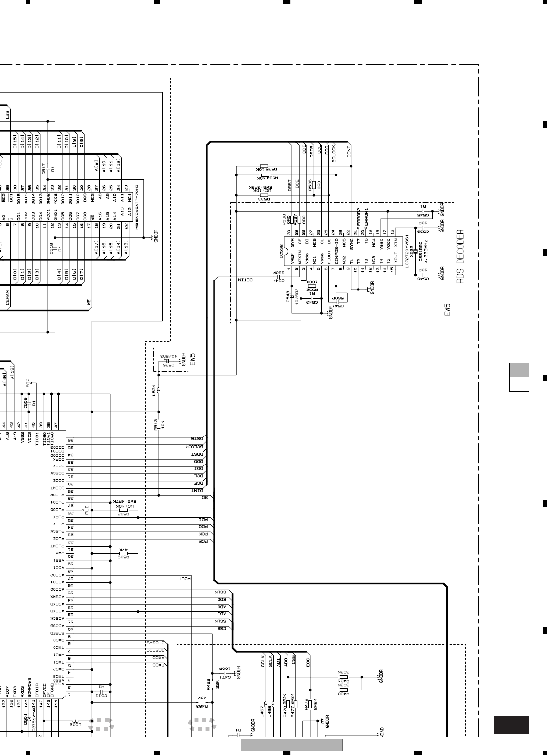
AVIC-D3/XU/UC 79
5678
56
78
C
D
F
A
B
E
B-a B-b
B-b
2 3
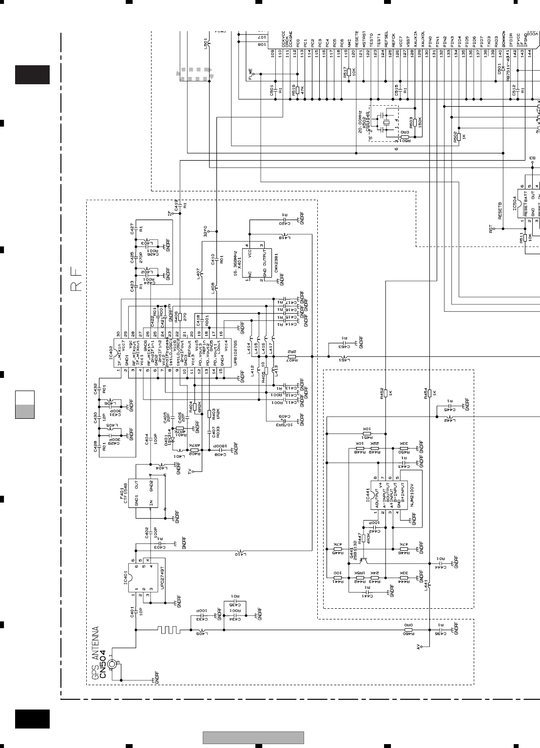
AVIC-D3/XU/UC
80
1234
1234
C
D
F
A
B
E
B-bB-a
B-a
B-b 1
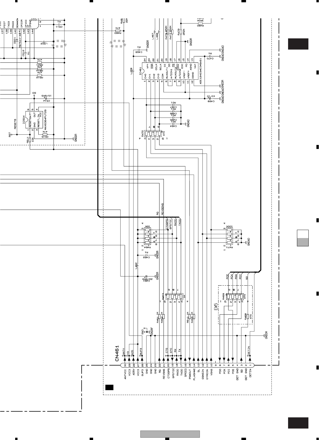
AVIC-D3/XU/UC 81
5678
56
78
C
D
F
A
B
E
B-a
B-b
B-bB-a
2 3
CN2060
6/7
A
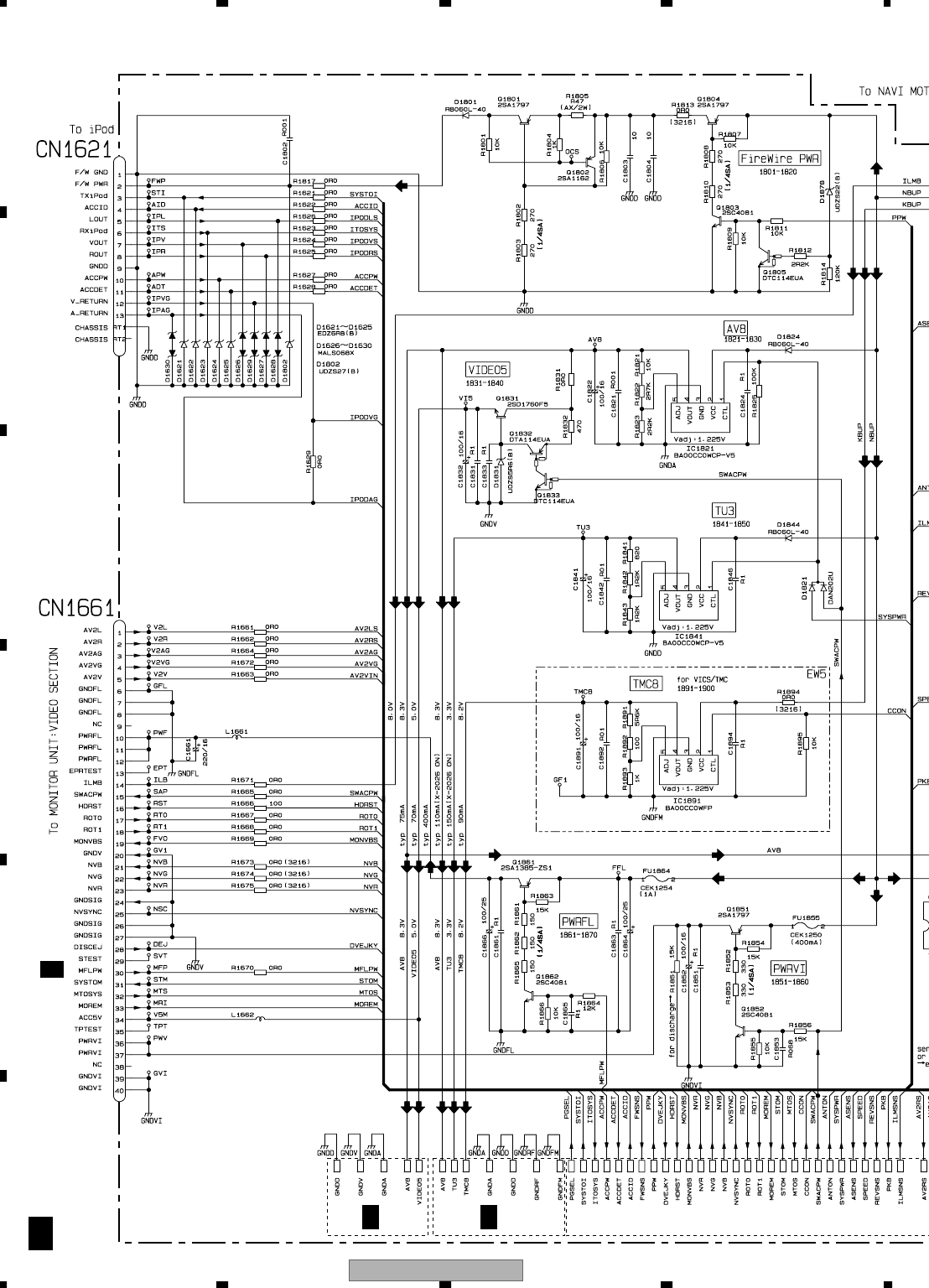
AVIC-D3/XU/UC
82
1234
1234
C
D
F
A
B
E
3.11 AV UNIT (PS, I/F)
1/3
C
>>
3/3
C
2/3
C
CN5001
1/2
G
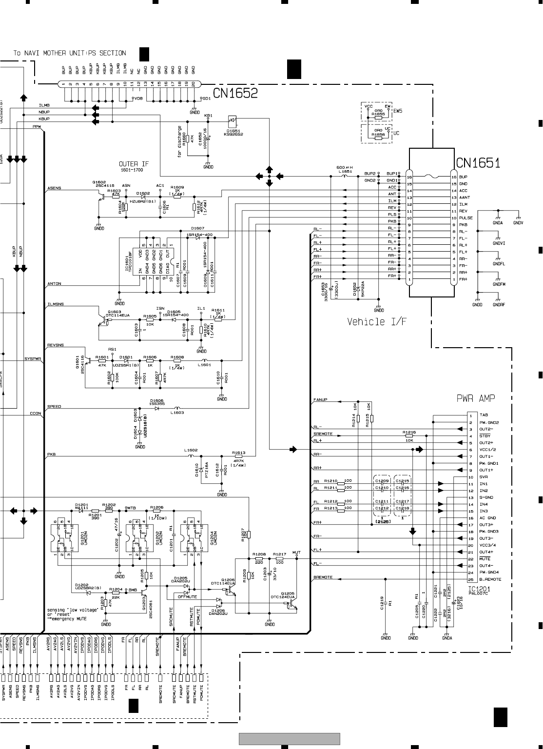
AVIC-D3/XU/UC 83
5678
56
78
C
D
F
A
B
E
1/3
C
>
FUSE
CEK1208(10A)
AV UNIT (PS, I/F)
1/3
C
2/3
C
CN2068
7/7
A
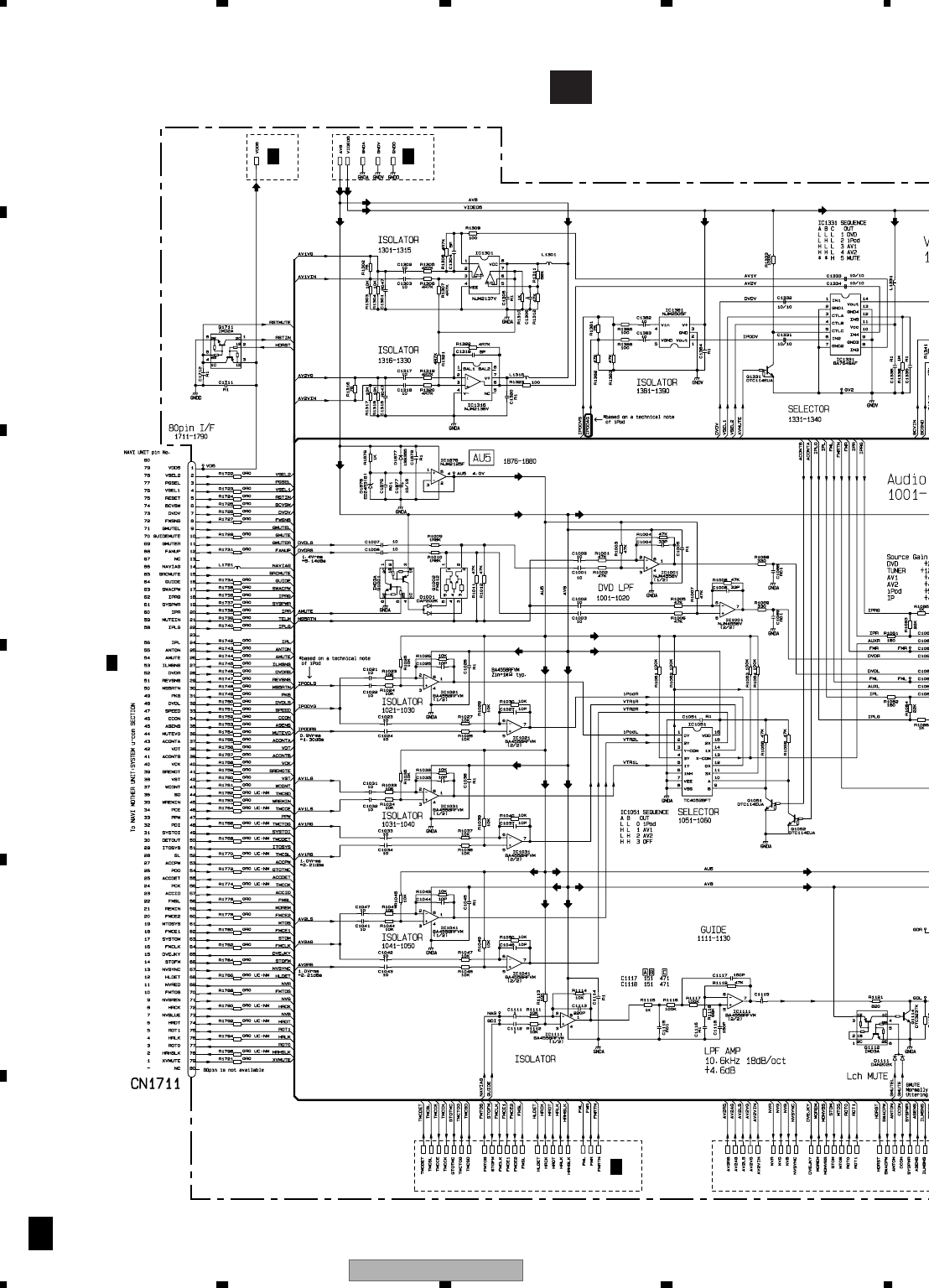
AVIC-D3/XU/UC
84
1234
1234
C
D
F
A
B
E
3.12 AV UNIT (A/V)(GUIDE PAGE)
C-a
2/3
C
2/3
3/3
C1/3
C
3/3
C
CN2055
5/7
A
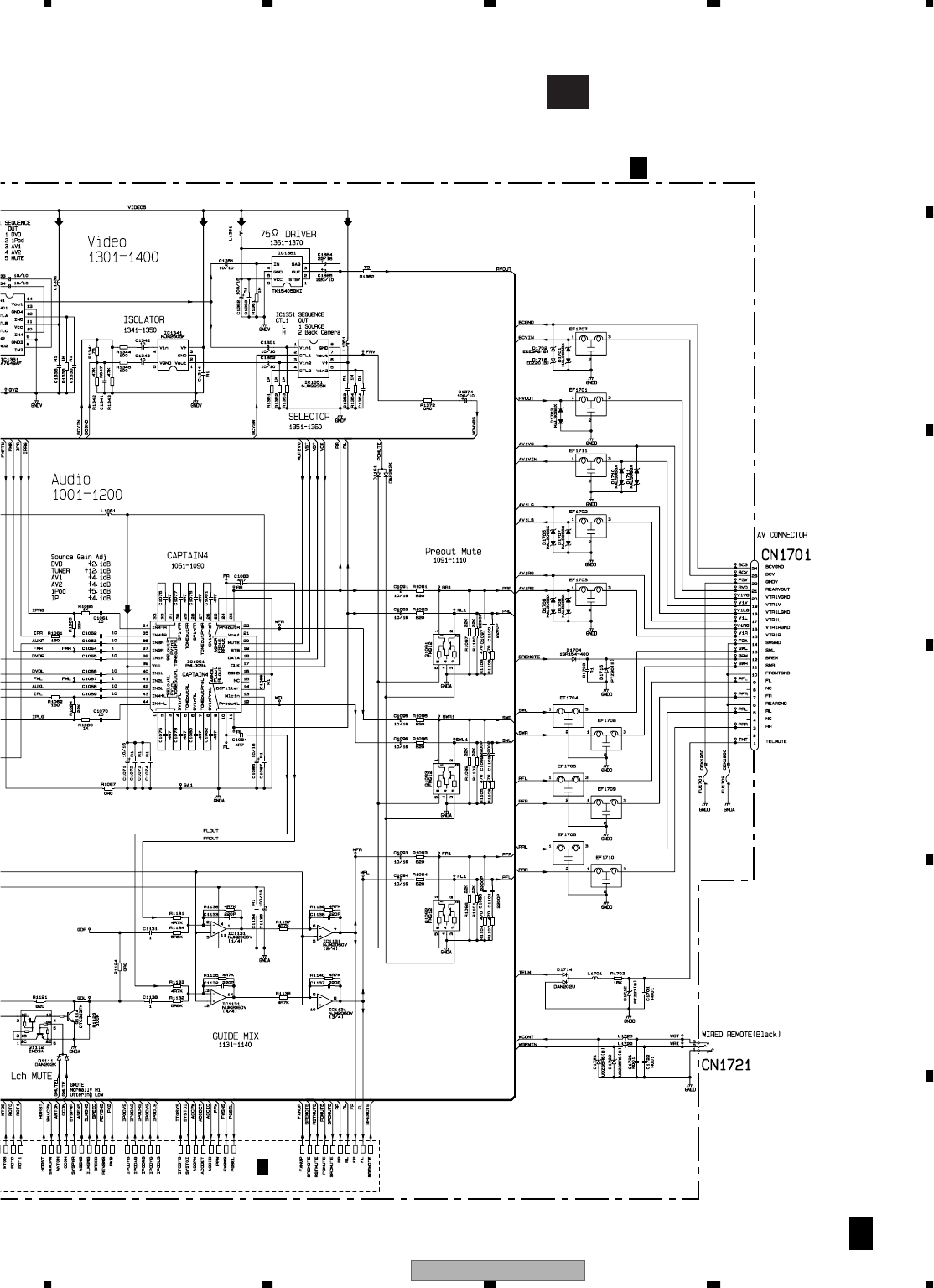
AVIC-D3/XU/UC 85
5678
56
78
C
D
F
A
B
E
C-b
2/3
C
2/3
(4A)
(4A)
NC(Reserved?)
>>
1/3
C
AV UNIT (A/V)
2/3
C
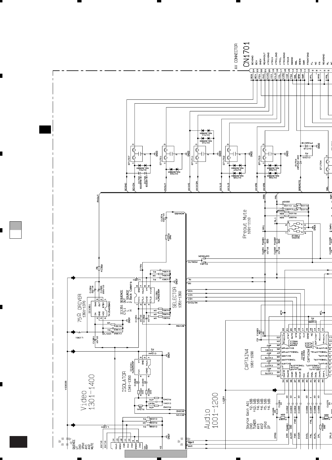
AVIC-D3/XU/UC
86
1234
1234
C
D
F
A
B
E
C-a C-b
C-b 2/3
1 2
AV UNIT (A/V)
2/3
C
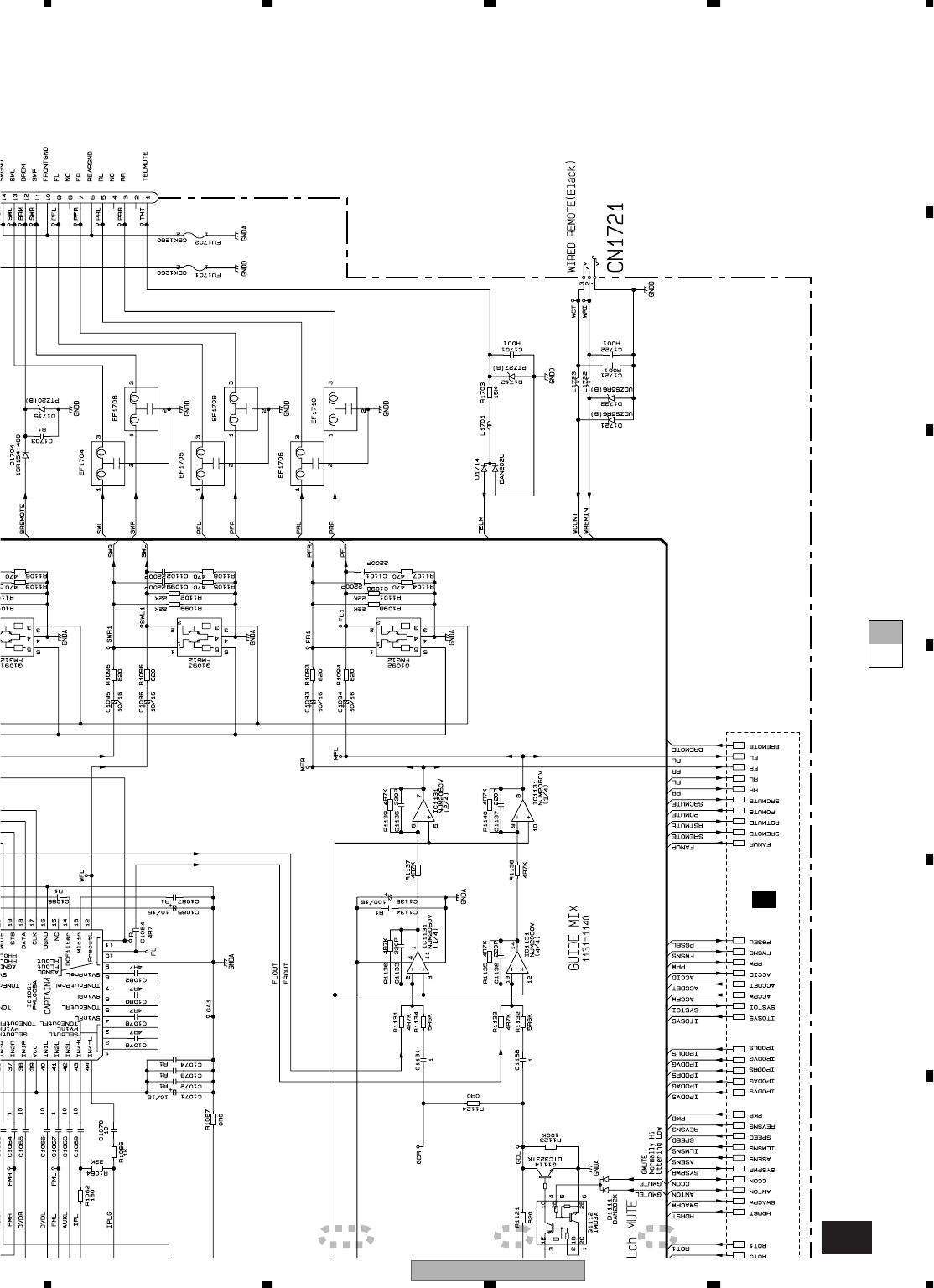
AVIC-D3/XU/UC 87
5678
56
78
C
D
F
A
B
E
C-a C-b
C-b 2/3
3 4 5
(4A)
(4A)
NC(Reserved?)
>>
1/3
C
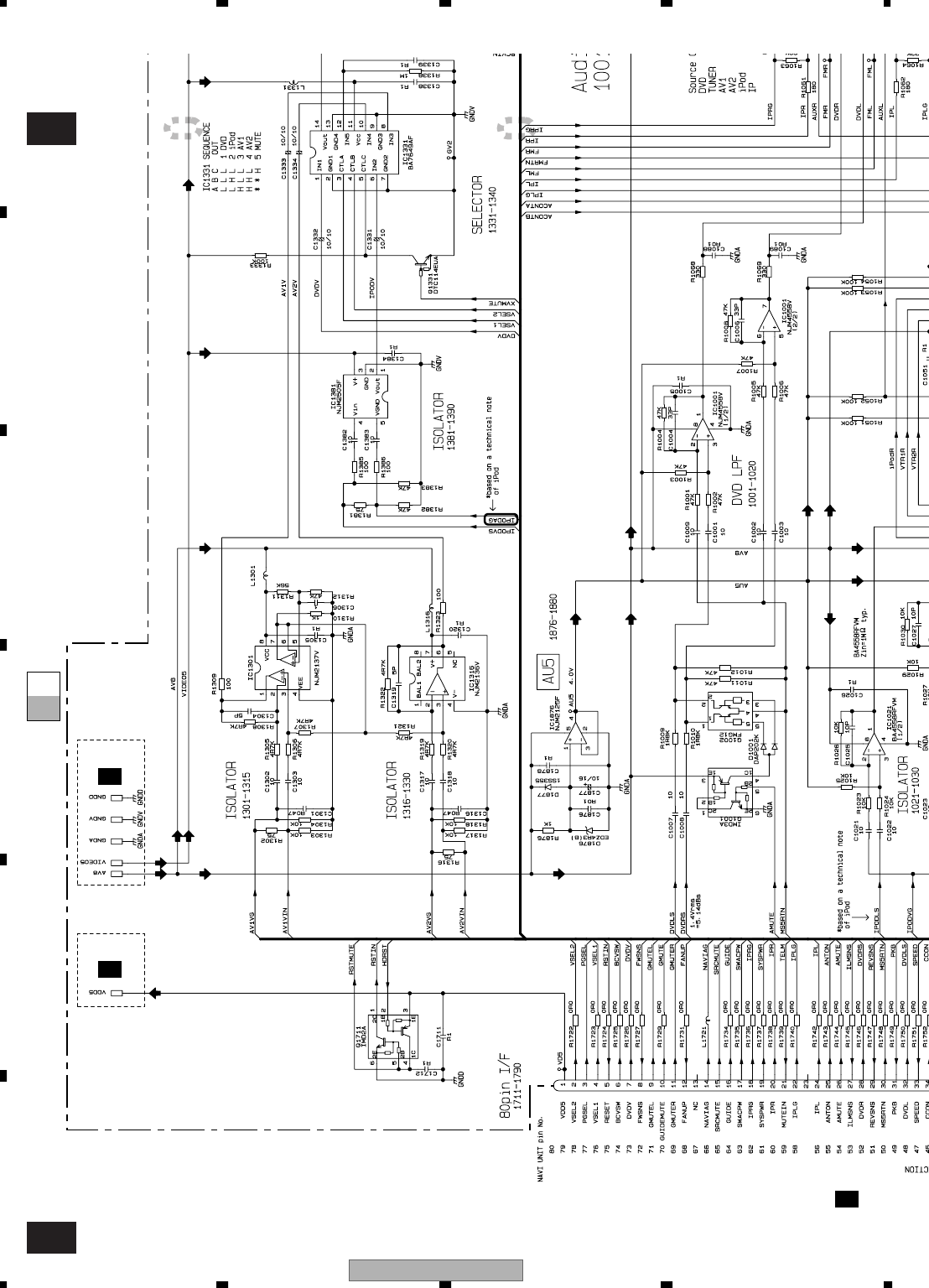
AVIC-D3/XU/UC
88
1234
1234
C
D
F
A
B
E
C-bC-a
C-a 2/3
C-b 2/3
1 2
3/3
C1/3
C
CN2055
5/7
A
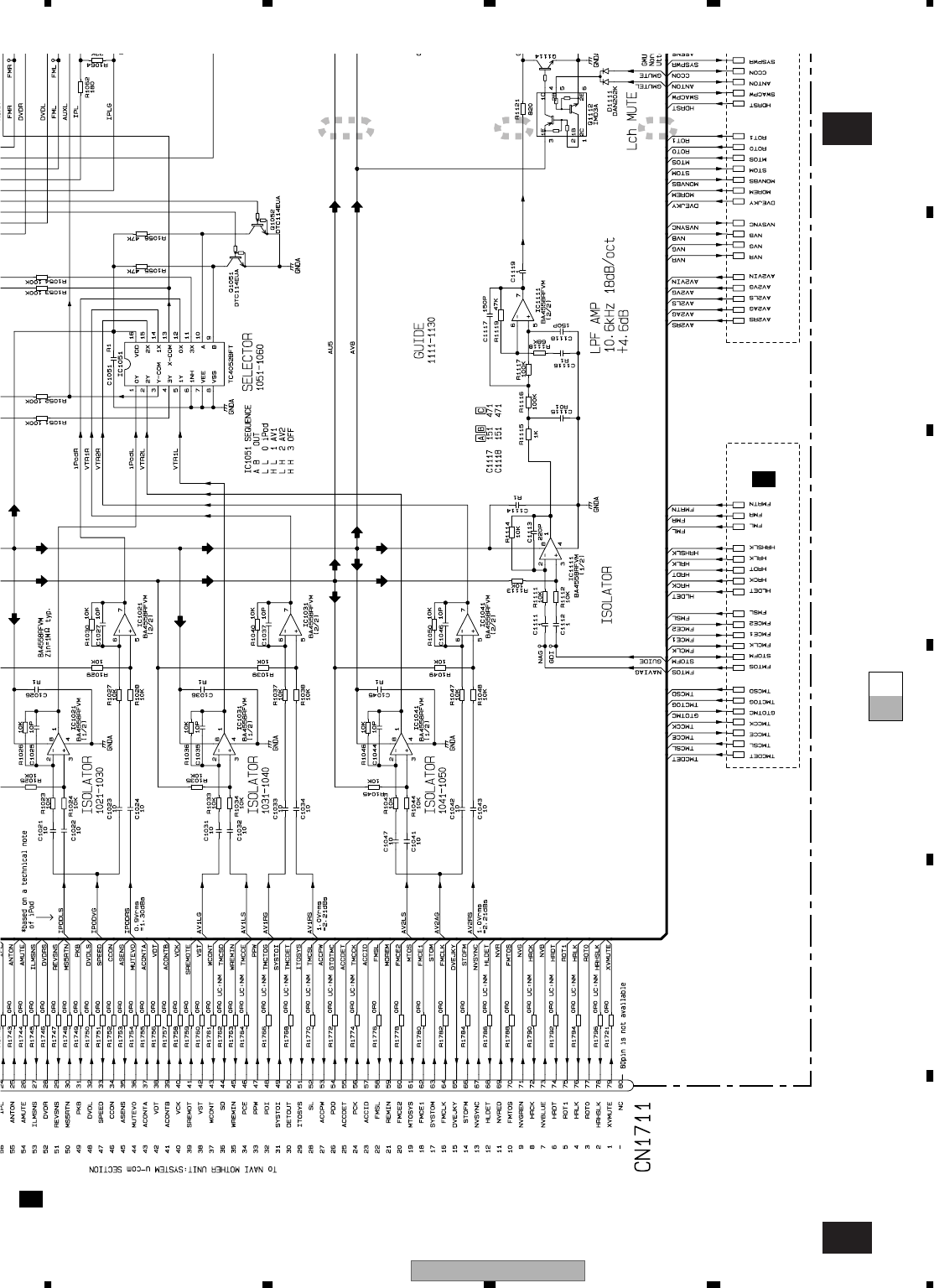
AVIC-D3/XU/UC 89
5678
56
78
C
D
F
A
B
E
C-bC-a
C-a 2/3
C-b 2/3
3 4 5
3/3
C
CN2055
5/7
A
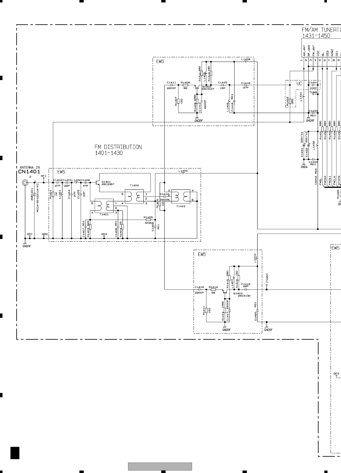
AVIC-D3/XU/UC
90
1234
1234
C
D
F
A
B
E
3.13 AV UNIT (TUNER)
3/3
C
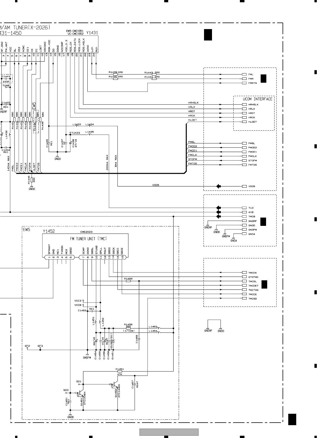
AVIC-D3/XU/UC 91
5678
56
78
C
D
F
A
B
E
3/3
C
2/3
C
1/3
C
2/3
C
AV UNIT (TUNER)
3/3
C
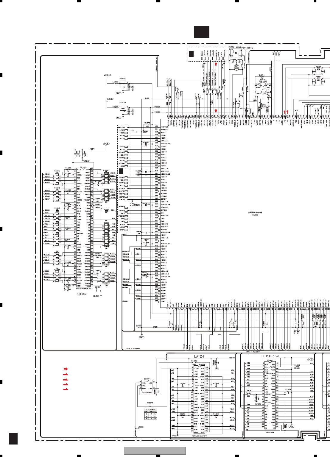
AVIC-D3/XU/UC
92
1234
1234
C
D
F
A
B
E
3.14 DVD CORE UNIT (1/2)(GUIDE PAGE)
D-a
1/2
D
1/2
2/2
D
2/2
D
F
RF SIGNAL
FOCUS SERVO LINE
TRACKING SERVO LINE
CARRIAGE SERVO LINE
SPINDLE SERVO LINE
T
C
S
F
T
RF
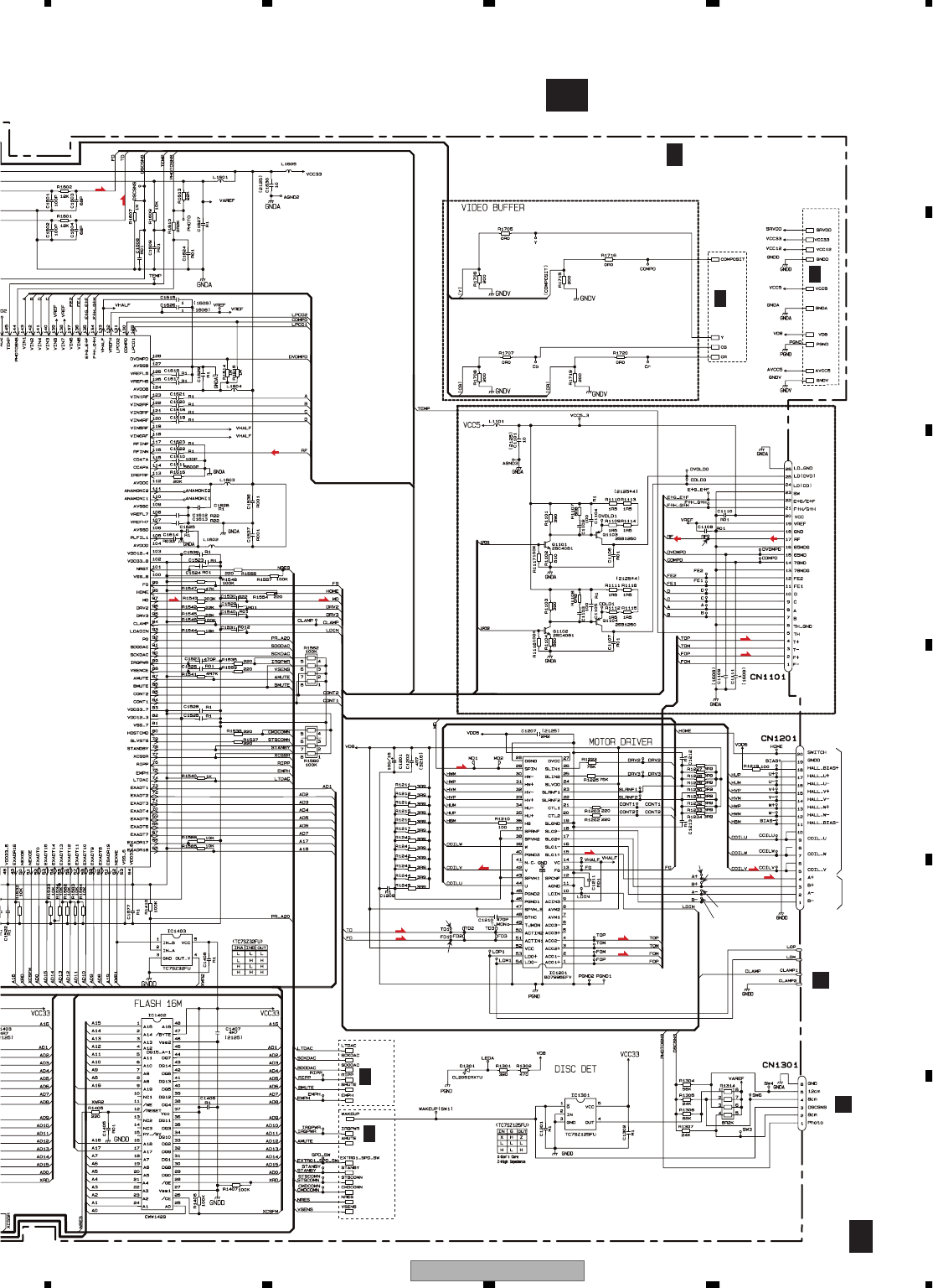
AVIC-D3/XU/UC 93
5678
56
78
C
D
F
A
B
E
D-b
1/2
D
1/2
DVD CORE UNIT (1/2)
2/2
D
1/2
D
2/2
D
2/2
D
2/2
D
PICKUP UNIT(SERVICE)
STEPPING MOTOR
M2:CXM1364
M1:CXC4912
F
E
SPINDLE
MOTOR
M3:CXM1362
F
T
F
T
T
F
T
F
C
S
C
S
S
S S
RF
RF RF
1
2
5
34
3
4
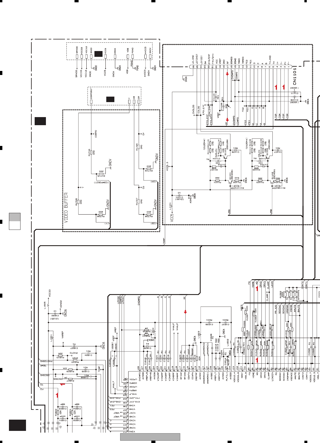
AVIC-D3/XU/UC
94
1234
1234
C
D
F
A
B
E
D-a D-b
D-b 1/2
12
DVD CORE UNIT (1/2)
2/2
D
1/2
D
2/2
D
PICKUP UNIT(SERVICE)
F
T
T
F
S S
RF
RF RF
1
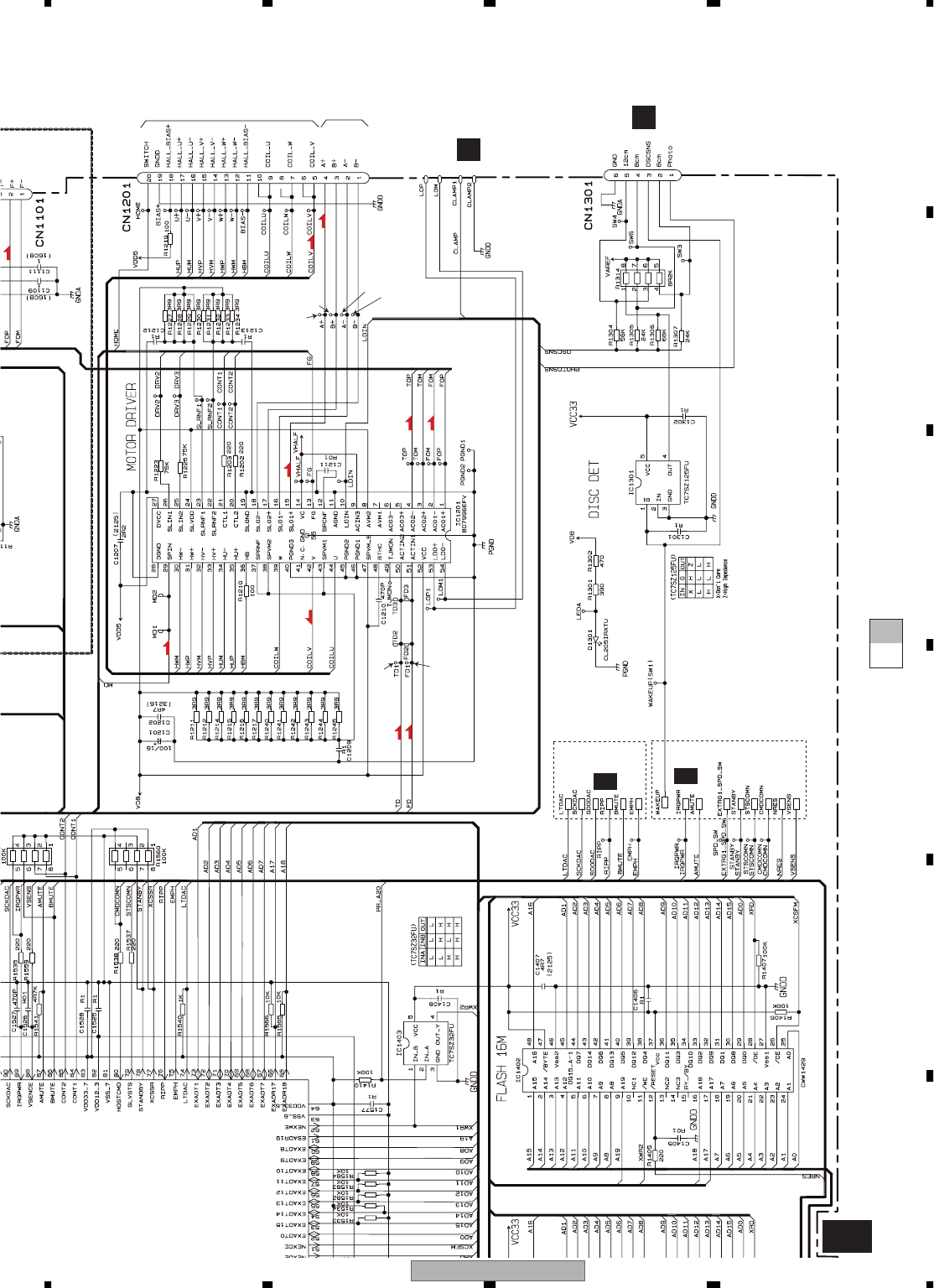
AVIC-D3/XU/UC 95
5678
56
78
C
D
F
A
B
E
D-a D-b
D-b 1/2
2/2
D
2/2
D
STEPPING MOTOR
M2:CXM1364
M1:CXC4912
F
E
SPINDLE
MOTOR
M3:CXM1362
F
T
T
F
F
C
S
C
S
S
2
5
34
3
4
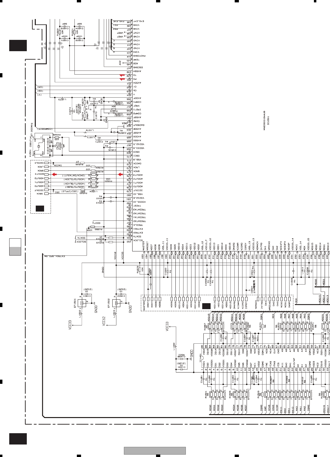
AVIC-D3/XU/UC
96
1234
1234
C
D
F
A
B
E
D-bD-a
D-a 1/2
D-b 1/2
12
2/2
D
2/2
D
F
T
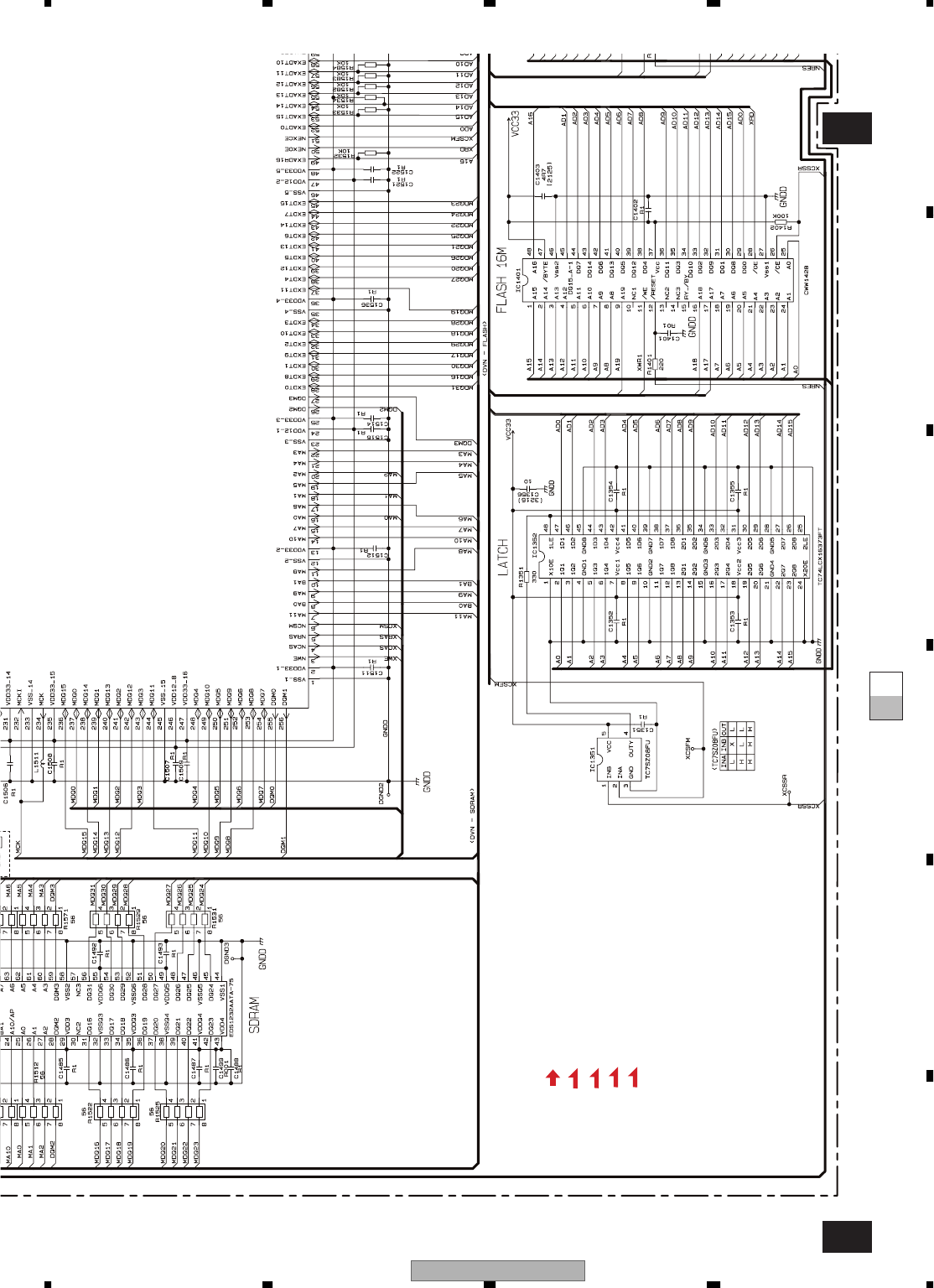
AVIC-D3/XU/UC 97
5678
56
78
C
D
F
A
B
E
D-bD-a
D-a 1/2
D-b 1/2
F
RF SIGNAL
FOCUS SERVO LINE
TRACKING SERVO LINE
CARRIAGE SERVO LINE
SPINDLE SERVO LINE
T
C
S
RF
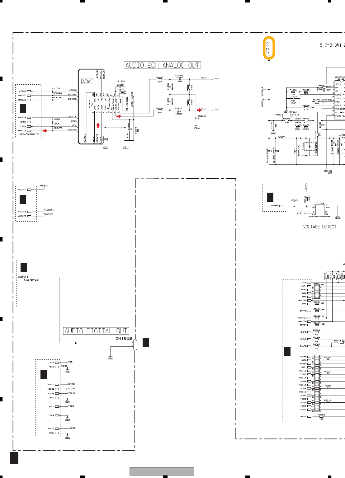
AVIC-D3/XU/UC
98
1234
1234
C
D
F
A
B
E
3.15 DVD CORE UNIT (2/2)
2/2
D
1/2
D
1/2
D
1/2
D
1/2
D
1/2
D
1/2
D
CN2061
6/7
A
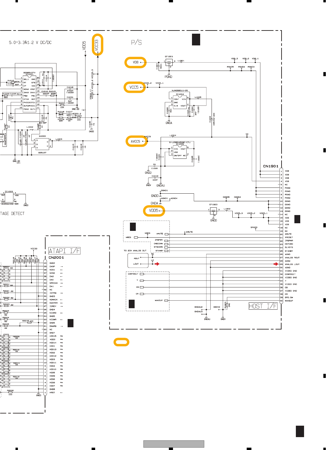
AVIC-D3/XU/UC 99
5678
56
78
C
D
F
A
B
E
2/2
D
DVD CORE UNIT(2/2)
2/2
D
1/2
D
1/2
D
CN2
1/7
A
CN2057
5/7
A
: The power supply is shown with the marked box.
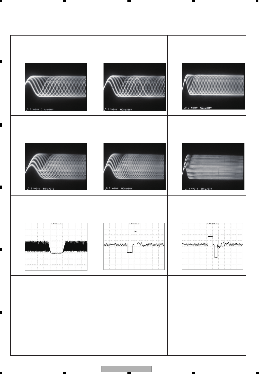
AVIC-D3/XU/UC
100
1234
1234
C
D
F
A
B
E
1 RF
2 TD1
3 A+, A-
4 B+, B-
5 FD1
1RF 0.2 V/div(AC) 1RF 0.2 V/div(AC) 50 ns/div 1
RF 0.2 V/div(AC) 50 ns/div
CDRF(x 4 CLV) CDRF(x 20 CAV Inner peripheral)
CDRF(x 20 CAV
Peripheral)
1
RF 0.2 V/div(AC) 50 ns/div
1
RF 0.2 V/div(AC) 50 ns/div
1
RF 0.2 V/div(AC) 50 ns/div
DVDRF(x 1.3 ZCAV) DVDRF(x 5 CAV
Inner peripheral)
DVDRF(x 5 CAV
Peripheral)
1
RF 0.5 V/div
2
TD1 0.1 V/div
2
TD1 0.1 V/div
DVDRF(BD1 mm) Interval FWD Interval REV
VHALF VHALF2.2 V
t
- Waveforms
Note:1. The encircled number denote measuring points in the circuit diagram.
2. Reference voltage: 1.65 V(TD1,FD1)(=VHALF)
2.2 V(RF)(=VREF)
In the waveform, it is seeing on the GND standard.
Offset of 1.65 V or 2.2 V is put in.
100 µs/div 100 µs/div 100 µs/div
0.1 µs/div
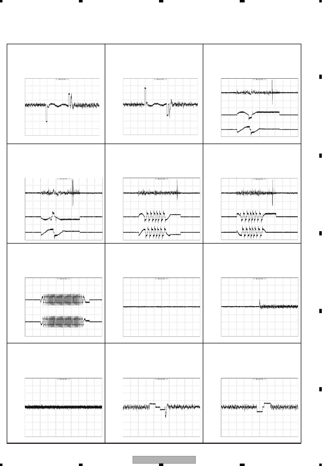
AVIC-D3/XU/UC 101
5678
56
78
C
D
F
A
B
E
2TD1 0.1 V/div 2TD1 0.1 V/div 2
CH1 : TD1 0.5 V/div 10 ms/div
Multi
32 FWD Multi
32 REV 3
CH2 : A+-A-10.0 V/div 10 ms/div
4
CH3 : B+-B-10.0 V/div 10 ms/div
Traverse 900 FWD(Short)
VHALF
0
t
VHALF VHALF
0
t
2
CH1 : TD1 0.5 V/div 10 ms/div
2
CH1 : TD1 0.5 V/div 20 ms/div
2
CH1 : TD1 0.5 V/div 20 ms/div
3
CH2 : A+-A-10.0 V/div 10 ms/div
3
CH2 : A+-A-10.0 V/div 20 ms/div
3
CH2 : A+-A-10.0 V/div 20 ms/div
4
CH3 : B+-B-10.0 V/div 10 ms/div
4
CH3 : B+-B-10.0 V/div 20 ms/div
4
CH3 : B+-B-10.0 V/div 20 ms/div
Traverse 900 REV(Short) Traverse 5 000 FWD(Long) Traverse 5 000 REV(Long)
VHALFVHALF VHALF
0
t
0
t
0
t
0
t
0
t
0
t
3
CH
:
A+-A-10 V/div 50 ms/div
2
TD1 0.5 Vdiv 20 ms/div
5
FD1 0.5 V/div 1 ms/div
4
CH2
:
B+-B-Play
TD Focus Close
ID search Inside
t
Outside
VHALFVHALF
0
t
0
t
(LPF of the oscilloscope is set to 10 kHz)
(LPF of the oscilloscope is set to 10 kHz)
(LPF of the oscilloscope is set to 10 kHz)
(LPF of the oscilloscope is set to 10 kHz)
(LPF of the oscilloscope is set to 10 kHz)
(LPF of the oscilloscope is set to 10 kHz)
(LPF of the oscilloscope is set to 10 kHz)
(LPF of the oscilloscope is set to 10 kHz)
5FD1 0.5 V/div 20 ms/div 5FD1 0.5 V/div
Play FD Focus Jump L0
t
L1
VHALF VHALFVHALF
5FD1 0.5 V/div
Focus Jump L1
t
L0
500 µs/div 500 µs/div
500 µs/div500 µs/div
AVIC-D3/XU/UC
102
1234
1234
C
D
F
A
B
E
3.16 COMPOUND UNIT(A), COMPOUND UNIT(B)
E F
F
E
COMPOUND UNIT(B)
COMPOUND UNIT(A)
CLAMP
D1/2
S1201
Q1299
S1202 S1204
S1203
R1298
0R0
1
2
3
4
5
6
S1205
R1299
0R0
CPT231SCTD
CSN1069
CSN1069
CSN1069
CSN1067
CSN1070
CSN1070
12cm
8cm
DISC SENS DISC SENS
8cm
CN1301
D1/2

AVIC-D3/XU/UC 103
5678
56
78
C
D
F
A
B
E
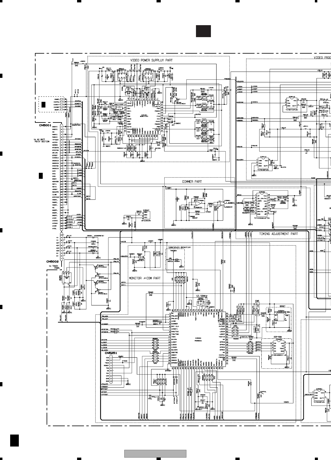
AVIC-D3/XU/UC
104
1234
1234
C
D
F
A
B
E
3.17 MONITOR UNIT (VIDEO)(GUIDE PAGE)
G-a
1/2
G
1/2
68/10
CN1661
TOUCH
PANEL
1/3
C
2/2
G
5.3V
5.0V
5.0V
5.0V
5.0V
5.0V
15.0V
5.0V
330P
1
¤
⁄
)(
!
5
‹
6
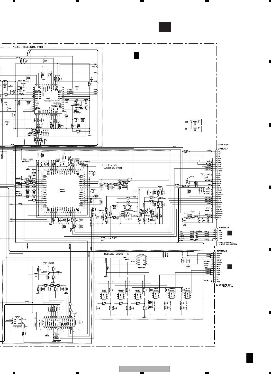
AVIC-D3/XU/UC 105
5678
56
78
C
D
F
A
B
E
G-b
1/2
G
1/2
H
CN5503
I
CN4825
LCD
MODULE
MONITOR UNIT (VIDEO)
1/2
G
5.0V
5.0V
8.0V
5.0V
-10.0V
5.3V
15.0V
RGB
(NAVI)
RGB
(OSD)
330P
7
$
^
6
%
#
*
@
8
2
3
4
0
&
9
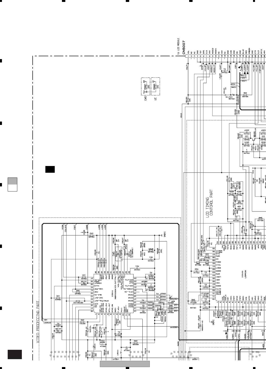
AVIC-D3/XU/UC
106
1234
1234
C
D
F
A
B
E
G-a G-b
G-b 1/2
1 2 3 4
LCD
MODULE
MONITOR UNIT (VIDEO)
1/2
G
-10.0V
5.3V
15.0V
RGB
(NAVI)
RGB
(OSD)
330P
7
$
^
6
@
8
2
3
4
0
&
9
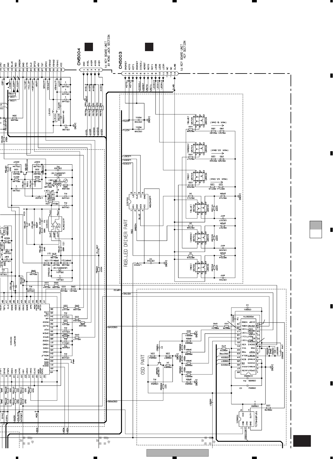
AVIC-D3/XU/UC 107
5678
56
78
C
D
F
A
B
E
G-a G-b
G-b 1/2
4 65
H
CN5503
I
CN4825
LCD
MODULE
5.0V
5.0V
8.0V
5.0V
%
#
*
2
3
4
0
&
9
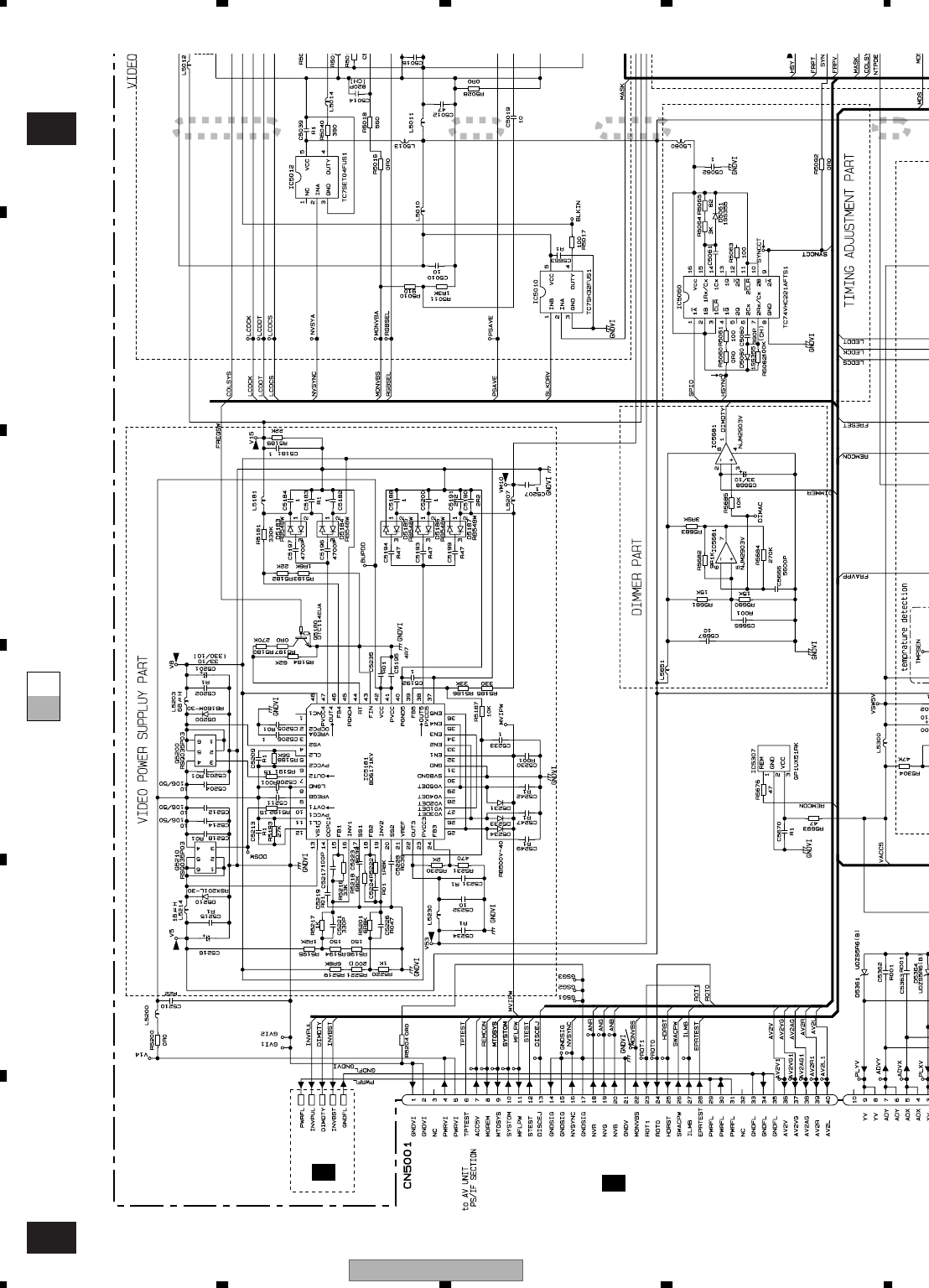
AVIC-D3/XU/UC
108
1234
1234
C
D
F
A
B
E
G-bG-a
G-a 1/2
G-b 1/2
1 2 3 4
68/10
CN1661
TOUCH
PANEL
1/3
C
2/2
G
5.3V
5.0V
5.0V
15.0V
5.0V
330P
1
¤
⁄
)(
!
5
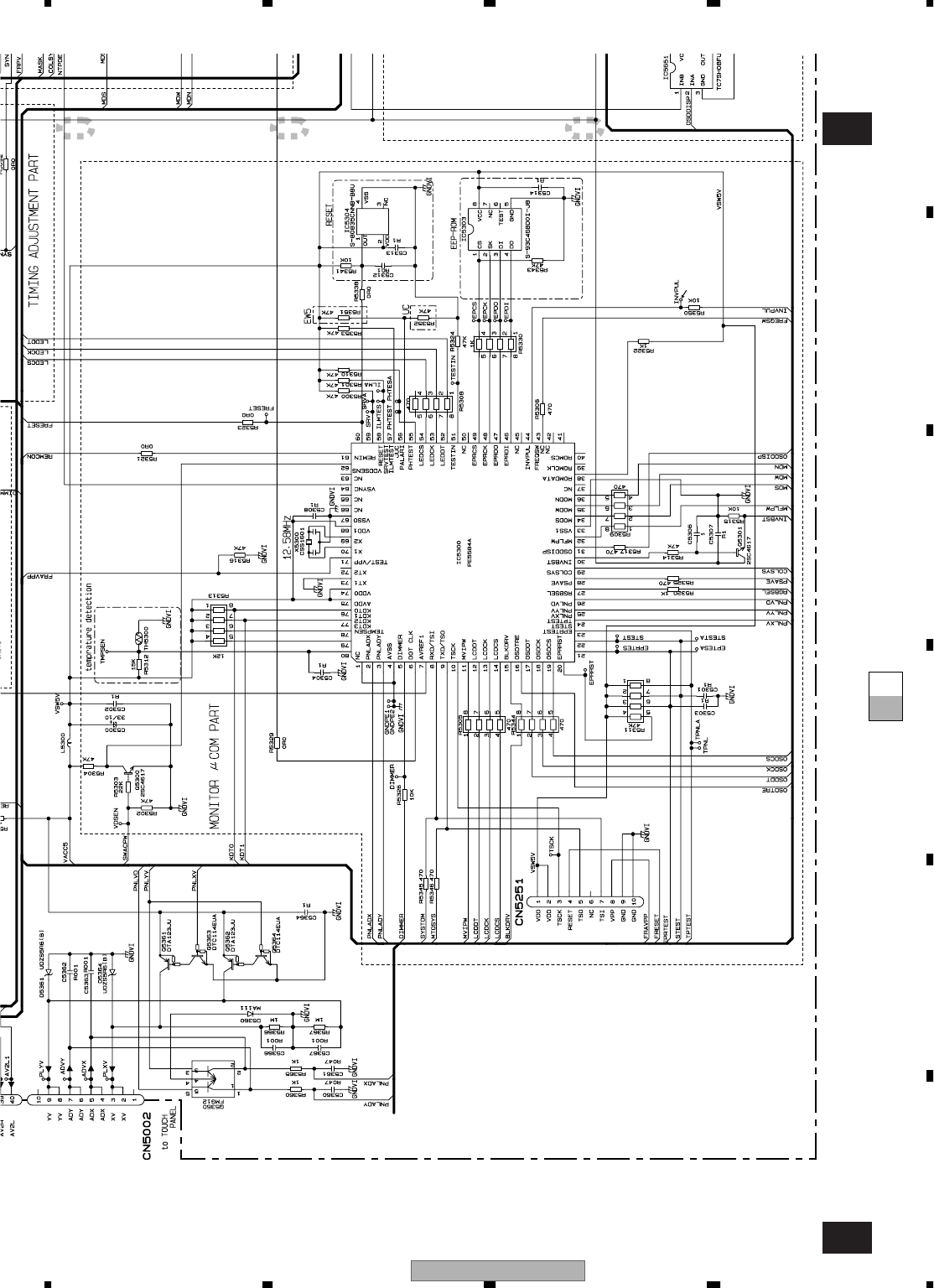
AVIC-D3/XU/UC 109
5678
56
78
C
D
F
A
B
E
G-bG-a
G-a 1/2
G-b 1/2
4 65
TOUCH
PANEL
5.0V
5.0V
5.0V
5.0V
‹
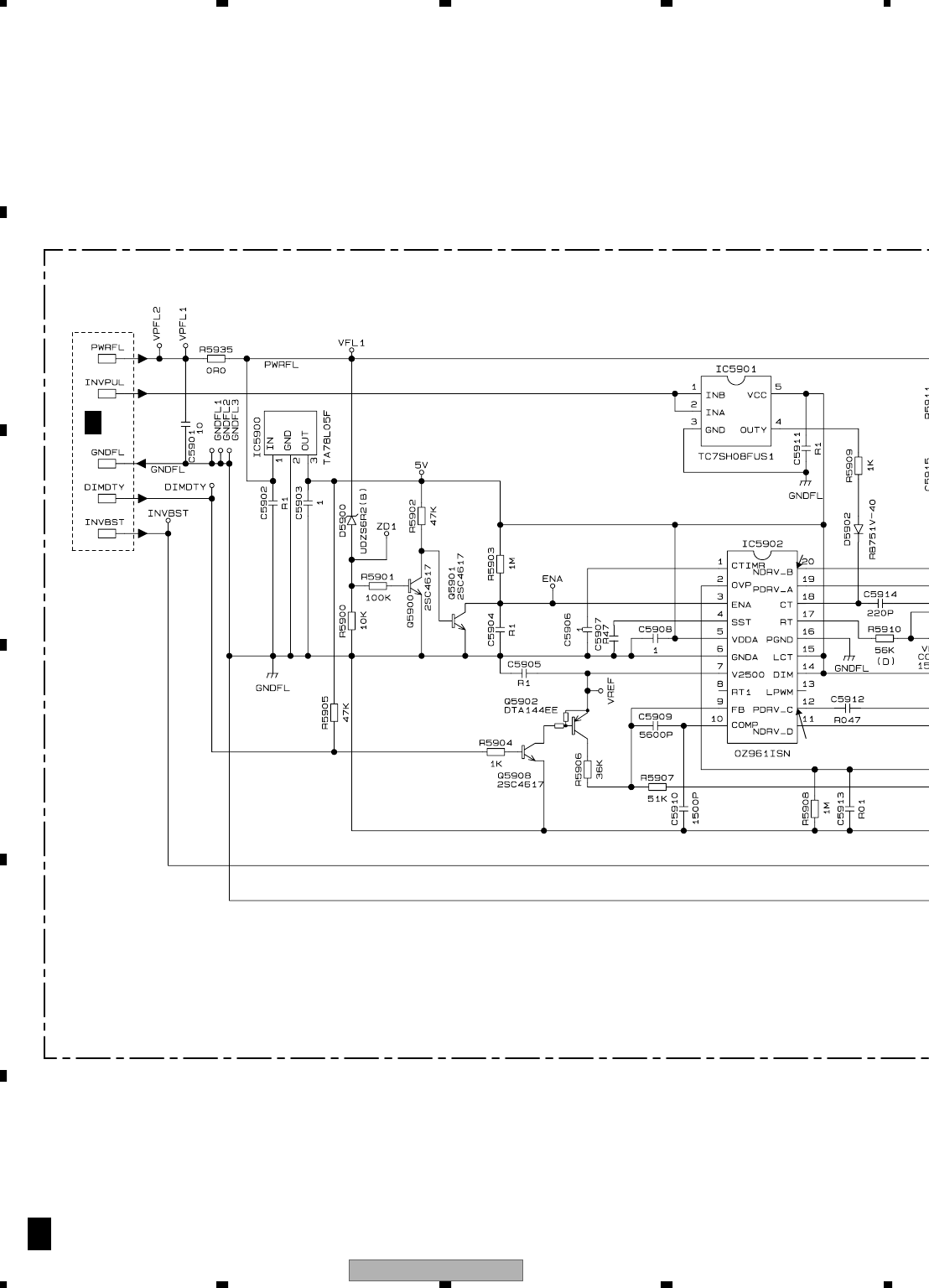
AVIC-D3/XU/UC
110
1234
1234
C
D
F
A
B
E
3.18 MONITOR UNIT (INVERTER)
2/2
G
1/2
G
›
fi
5.0V
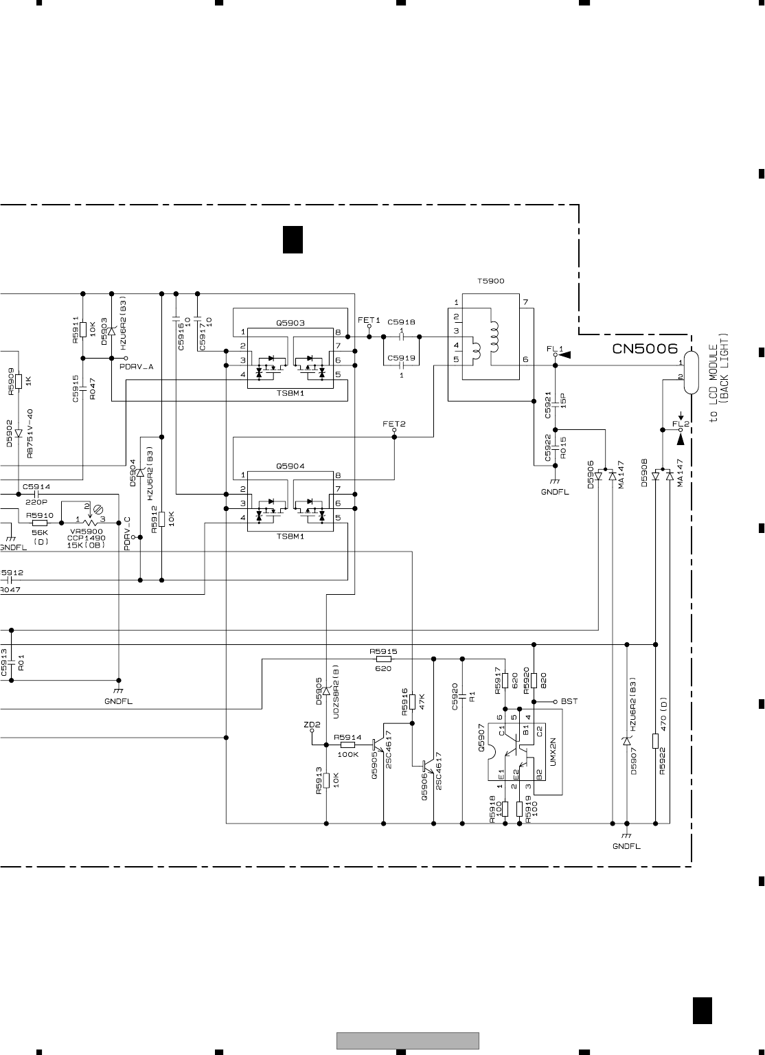
AVIC-D3/XU/UC 111
5678
56
78
C
D
F
A
B
E
2/2
G
MONITOR UNIT (INVERTER)
2/2
G
LCD
MODULE
fl
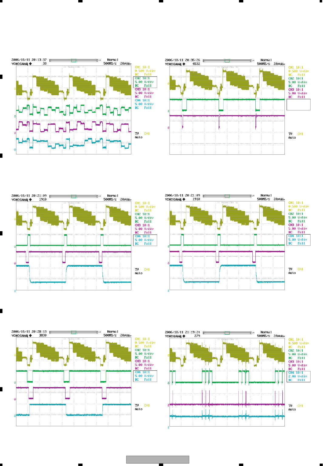
AVIC-D3/XU/UC
112
1234
1234
C
D
F
A
B
E
DVD TEST DISC : State of color bar display
1 CH1 : MONVBS 3 CH3 : LCDR
2 CH2 : LCDB 4 CH4 : LCDG
DVD TEST DISC : State of color bar display
1 CH1 : MONVBS 6 CH3 : HSY
5 CH2 : SYNCCT 7 CH4 : COMS
DVD TEST DISC : State of color bar display
1 CH1 : MONVBS 9 CH3 : SPIO
8 CH2 : CLS 0 CH4 : CTR
DVD TEST DISC : State of color bar display
1 CH1 : MONVBS ! CH3 : HSYNC
9 CH2 : SPIO
DVD TEST DISC : State of color bar display
1 CH1 : MONVBS # CH3 : VSYNC
@ CH2 : SPS
DVD TEST DISC : State of color bar display
1 CH1 : MONVBS % CH3 : IOUT(C3)
$ CH2 : OSDOVR ^ CH4 : OSD RGB
- Waveforms The encircled number denote measuring pointes in the circuit diagram.
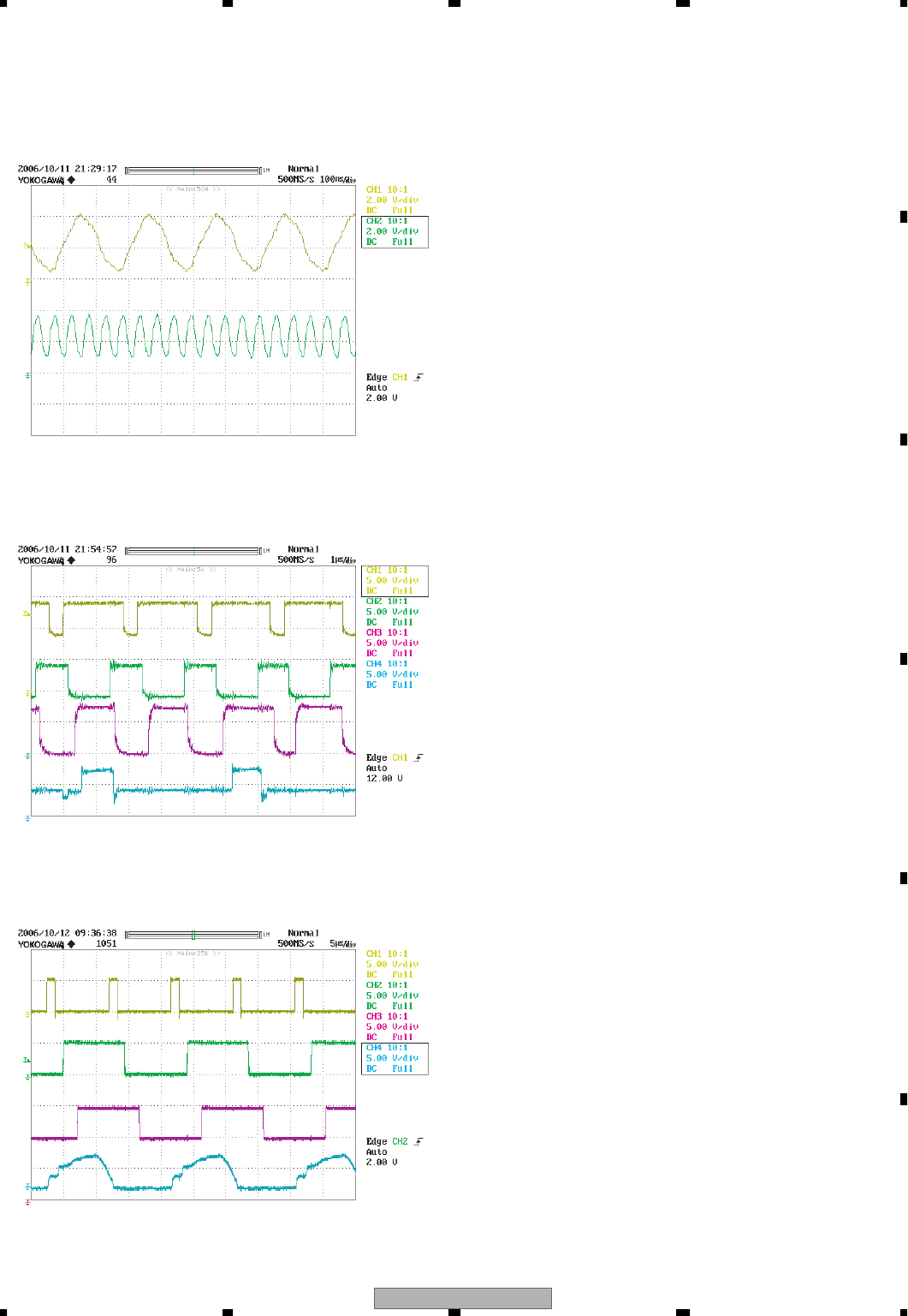
AVIC-D3/XU/UC 113
5678
56
78
C
D
F
A
B
E
DVD TEST DISC : State of color bar display
& CH1 : CLD
* CH2 : DOCKI
( CH1 : OUT1 ⁄ CH3 : OUT4
) CH2 : OUT2 ¤ CH4 : OUT5
‹ CH1 : INVPUL fi CH3 : PDRV_C
› CH2 : NDRV_B fl CH4 : FL2
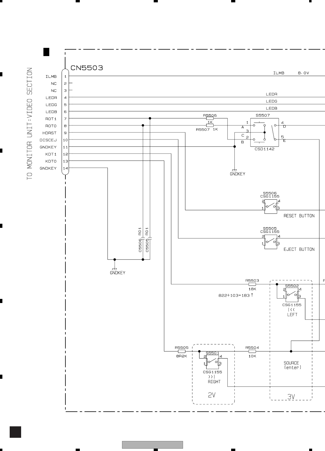
AVIC-D3/XU/UC
114
1234
1234
C
D
F
A
B
E
3.19 KEY PCB
H
CN5003
1/2
G
VOLUME
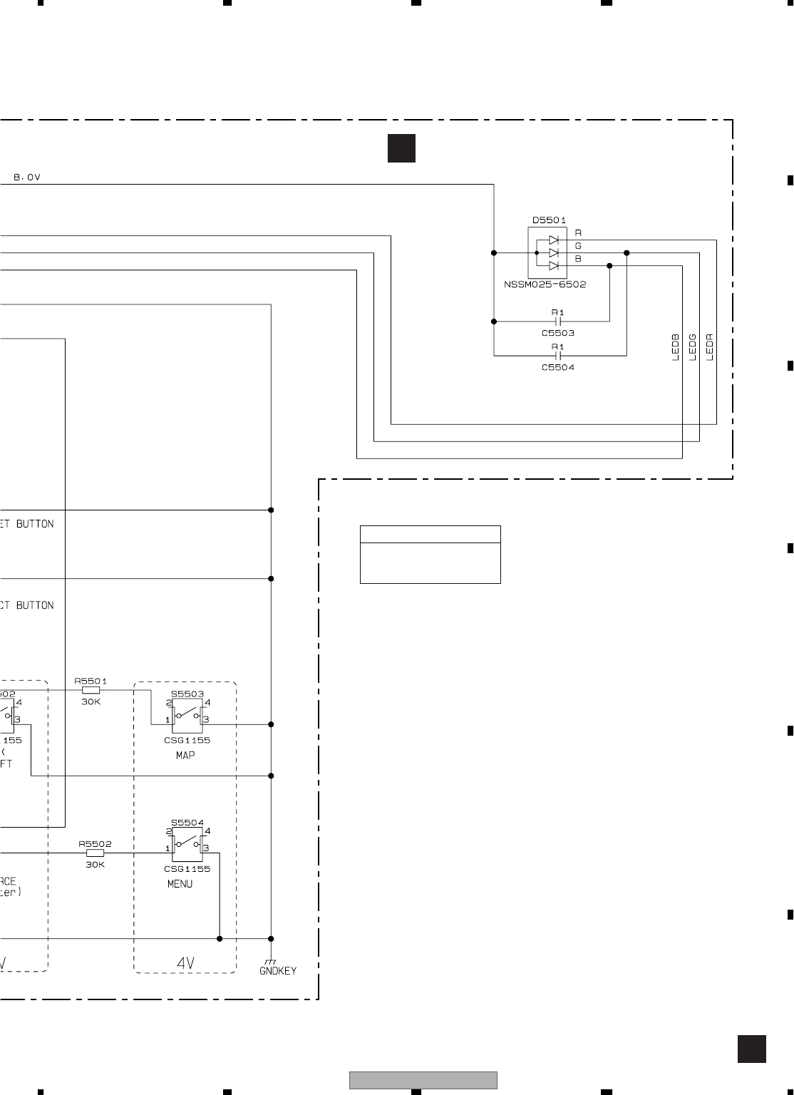
AVIC-D3/XU/UC 115
5678
56
78
C
D
F
A
B
E
H
HKEY PCB
KEYBOARD UNIT
Consists of
KEY PCB
AV MINI JACK PCB
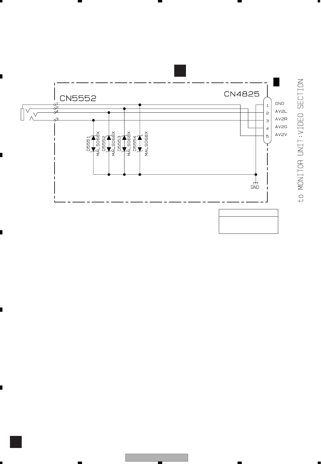
AVIC-D3/XU/UC
116
1234
1234
C
D
F
A
B
E
3.20 AV MINI JACK PCB
I
CN5004
1/2
G
IAV MINI JACK PCB
KEYBOARD UNIT
Consists of
KEY PCB
AV MINI JACK PCB
MINI JACK

AVIC-D3/XU/UC 117
5678
56
78
C
D
F
A
B
E
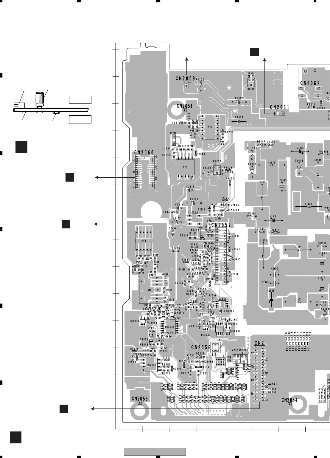
AVIC-D3/XU/UC
118
1234
1234
C
D
F
A
B
E
4. PCB CONNECTION DIAGRAM
4.1 NAVI MOTHER UNIT
A
ANAVI MOTHER UNIT
Capacitor
Connector
P.C.Board Chip Part SIDE B
SIDE A
NOTE FOR PCB DIAGRAMS
1.The parts mounted on this PCB
include all necessary parts for
several destination.
For further information for
respective destinations, be sure
to check with the schematic dia-
gram.
2.Viewpoint of PCB diagrams
10 20 30 40 50 60 70
8
X
140
130
120
110
100
90
80
70
60
50
40
30
20
10
0
Y
DCN1852
DCN1901
BCN461
DCN2001
FAN MOTOR
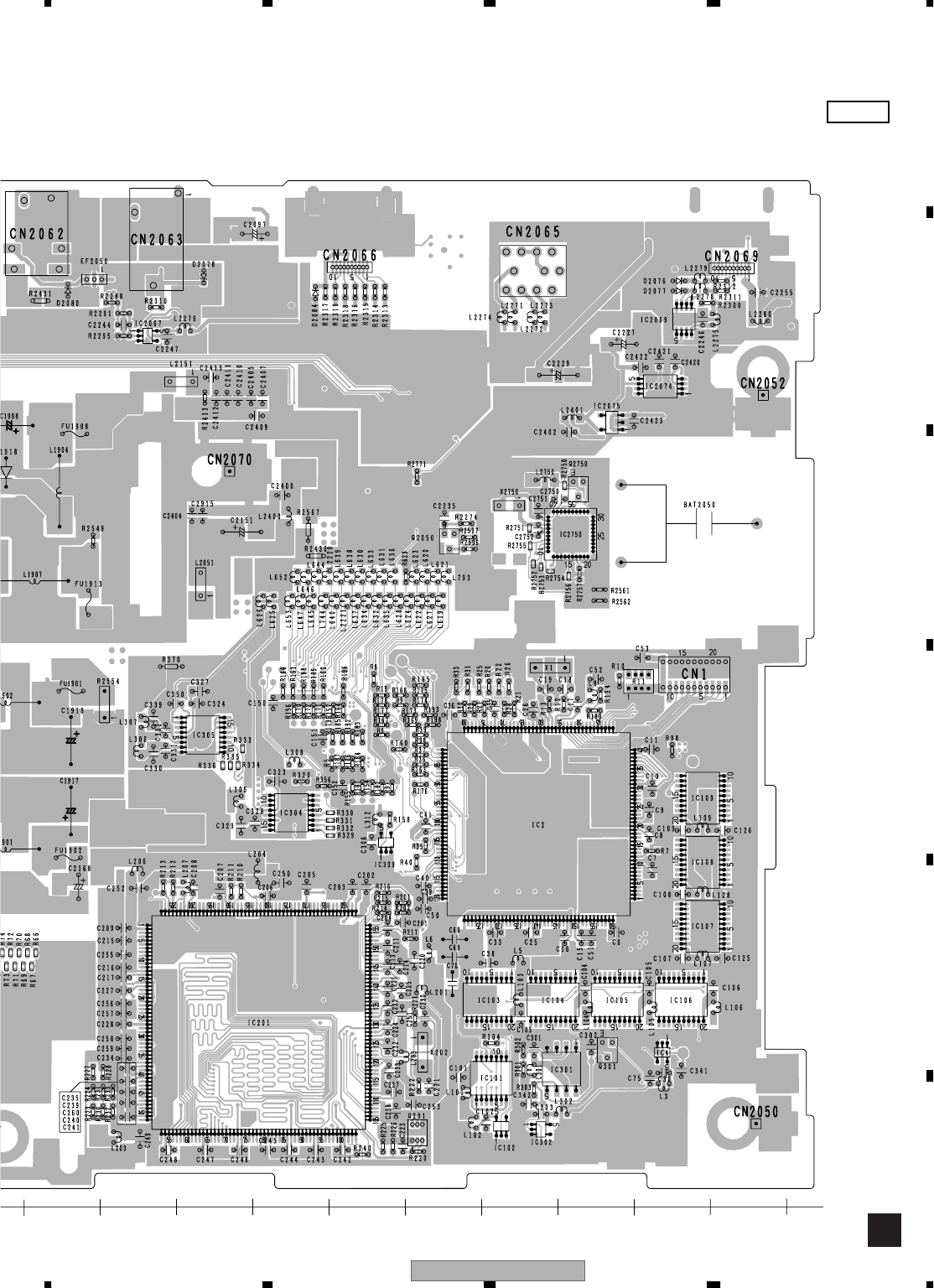
AVIC-D3/XU/UC 119
5678
56
78
C
D
F
A
B
E
A
SIDE A
70 80 90 100 110 120 130 140 150 160 170
FRONT
DIGITAL OUT
EXTENSION
IP-BUS
1234
567
891011
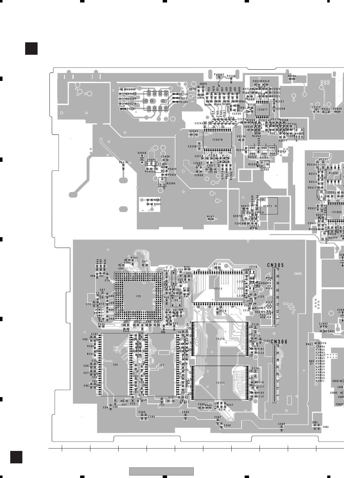
AVIC-D3/XU/UC
120
1234
1234
C
D
F
A
B
E
A
ANAVI MOTHER UNIT
7
8090100110120130140150160170
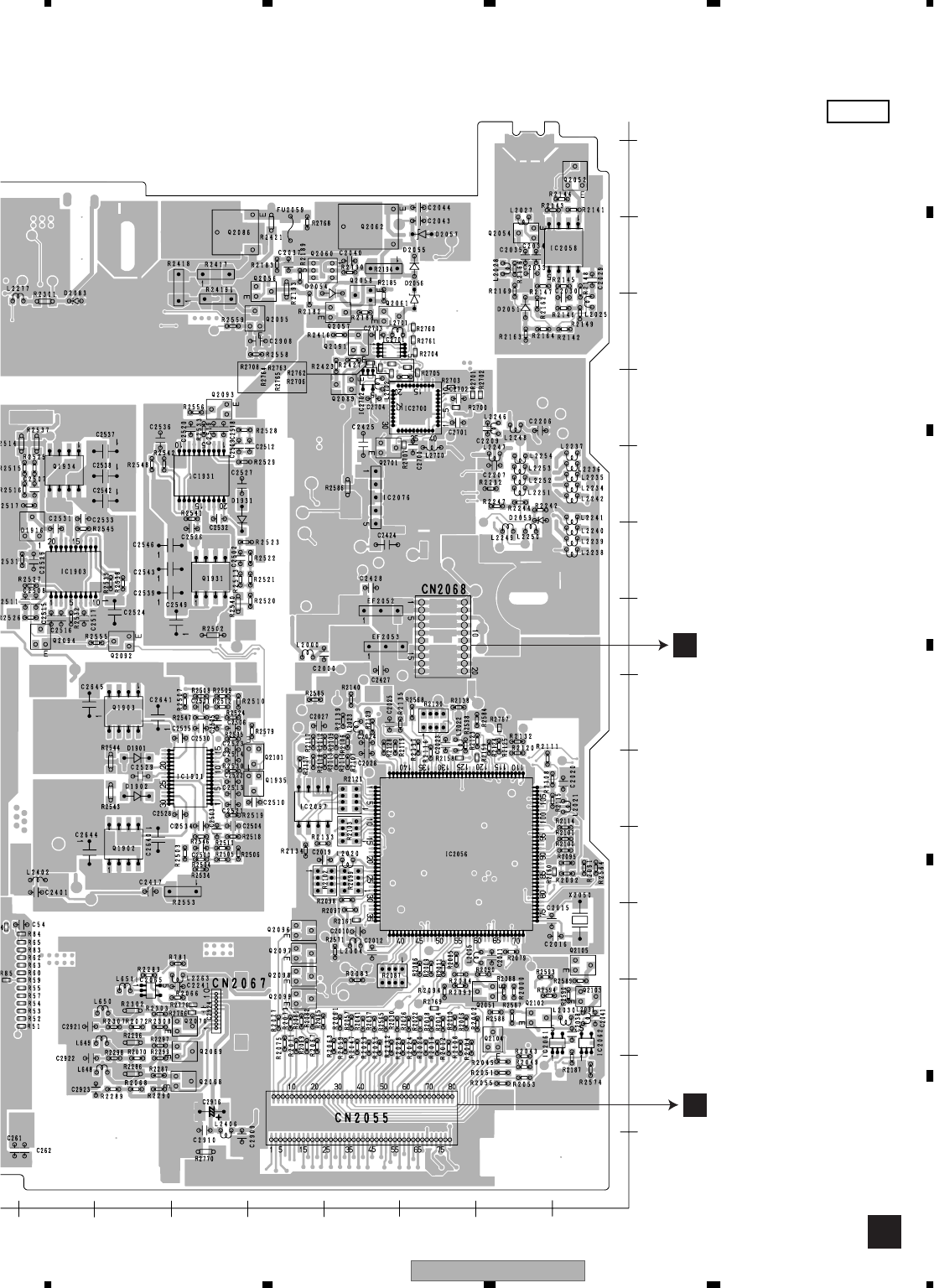
AVIC-D3/XU/UC 121
5678
56
78
C
D
F
A
B
E
A
SIDE B
1020304050607080 X
140
130
120
110
100
90
80
70
60
50
40
30
20
10
0
Y
CCN1652
CCN1711
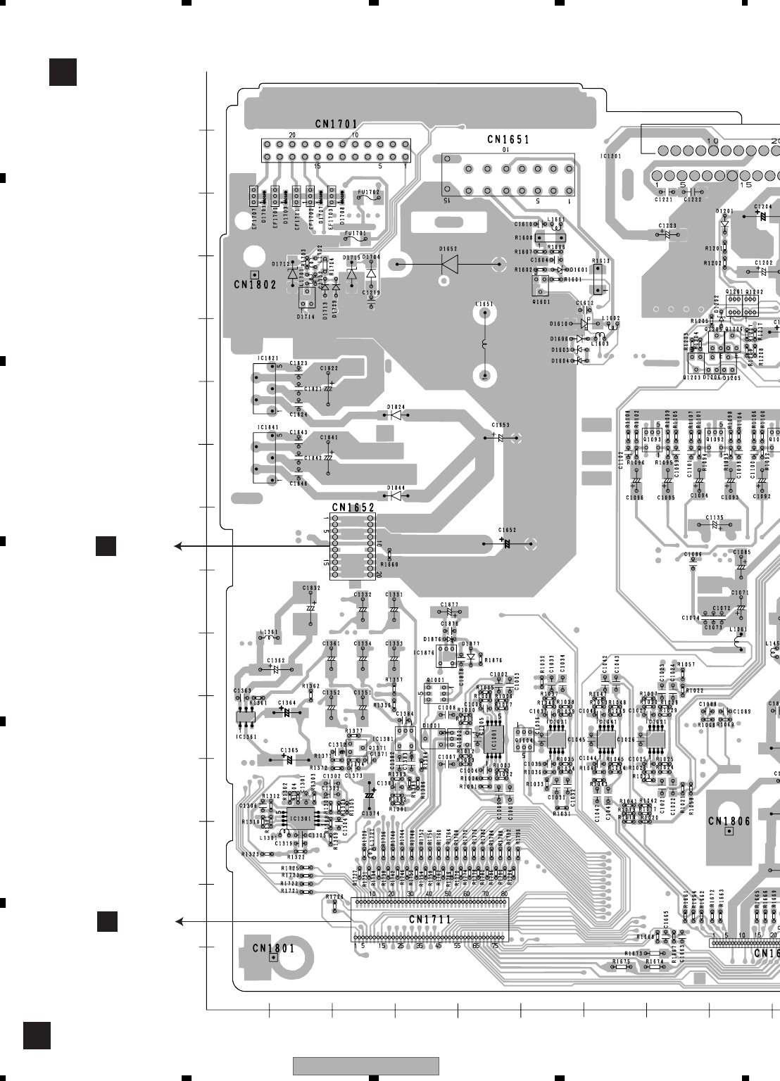
AVIC-D3/XU/UC
122
1234
1234
C
D
F
A
B
E
4.2 AV UNIT
C
CAV UNIT
10 20 30 40 50 60 70 80 90
X
0
140
130
120
110
100
90
80
70
60
50
40
30
20
10
Y
ACN2068
ACN2055
CORD ASSY
CORD ASSY

AVIC-D3/XU/UC 123
5678
56
78
C
D
F
A
B
E
C
SIDE A
80 90 100 110 120 130 140 150 160 170
GCN5001
WIRED REMOTE
CONTROLLER
iPod
12
95436
1381271110
ANTENNA
FM/AM TUNER UNIT
TUNER UNIT(EW5)
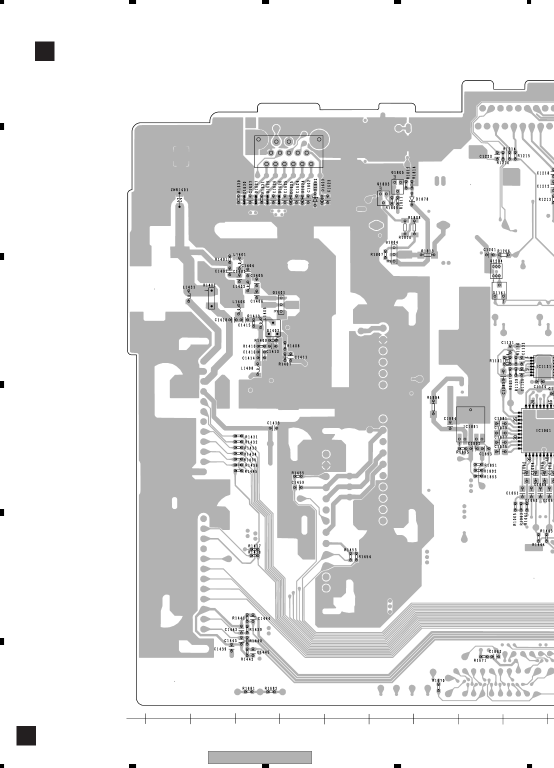
AVIC-D3/XU/UC
124
1234
1234
C
D
F
A
B
E
C
CAV UNIT
8090100110120130140150160170
1
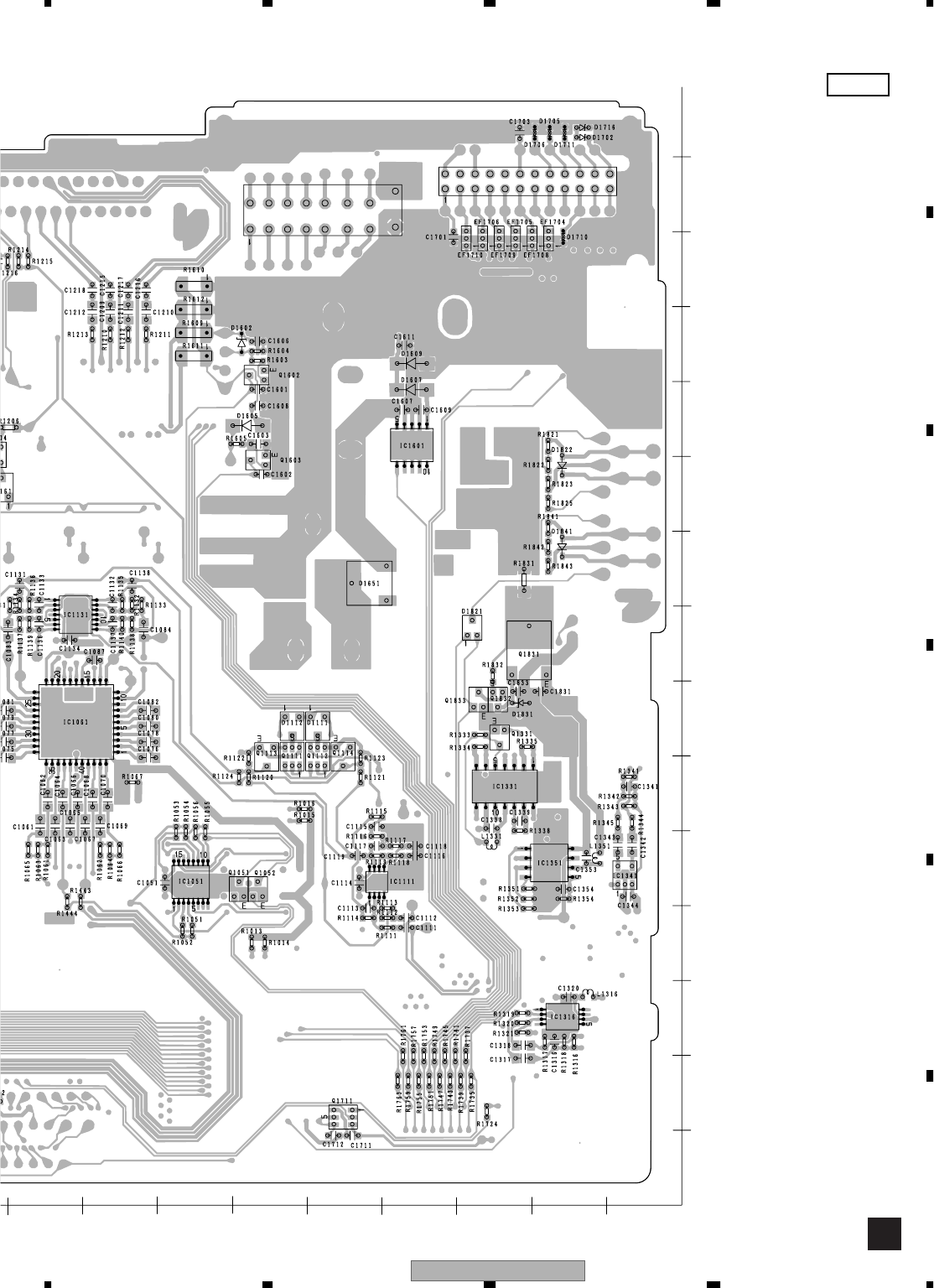
AVIC-D3/XU/UC 125
5678
56
78
C
D
F
A
B
E
C
SIDE B
140
130
120
110
100
90
80
70
60
50
40
30
20
10
Y
1020304050607080
9
0X0
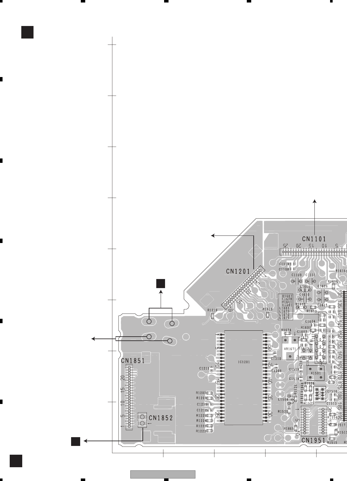
AVIC-D3/XU/UC
126
1234
1234
C
D
F
A
B
E
4.3 DVD CORE UNIT
D
DDVD CORE UNIT
10 20 30 40
10
20
30
40
50
60
70
80
0X
Y
A
CN2061
PICKUP UNIT(SERVICE)
M2,M3
M1
F
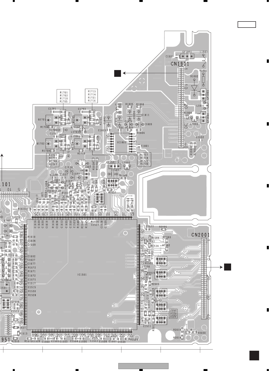
AVIC-D3/XU/UC 127
5678
56
78
C
D
F
A
B
E
D
SIDE A
40 50 60 70 80 90
N
IT(SERVICE)
A
CN2057
A
CN2
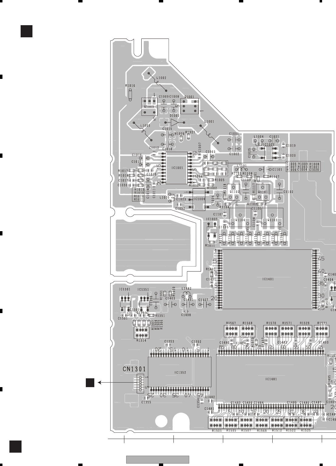
AVIC-D3/XU/UC
128
1234
1234
C
D
F
A
B
E
D
DDVD CORE UNIT
5060708090
E
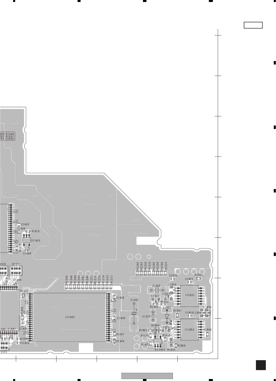
AVIC-D3/XU/UC 129
5678
56
78
C
D
F
A
B
E
D
SIDE B
1020304050
10
20
30
40
50
60
70
80
0X
Y
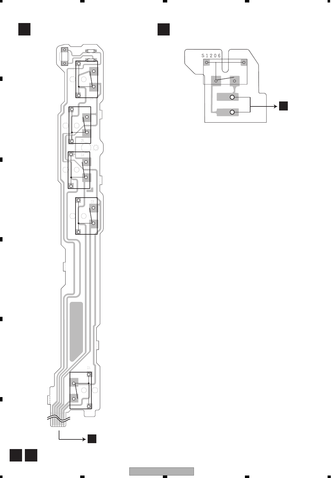
AVIC-D3/XU/UC
130
1234
1234
C
D
F
A
B
E
4.4 COMPOUND UNIT(A), COMPOUND UNIT(B)
FE
F
E
D
D
CLAMP
12cm
S1201
R1298
R1299
Q1299
CN1301
16
DISC SENS
S1204
DISC SENS
S1203
8cm
S1202
8cm
S1205
COMPOUND UNIT(B)COMPOUND UNIT(A)
AVIC-D3/XU/UC 131
5678
56
78
C
D
F
A
B
E
4.5 GPS UNIT
B
SIDE A
BGPS UNIT
SIDE B
BGPS UNIT
10 20 30 40 50 60
X
30
20
10
0
Y
10 20 30 40 50 60
X
10
20
30
0
Y
ACN2060
GPS ANTENNA
AVIC-D3/XU/UC
132
1234
1234
C
D
F
A
B
E
4.6 MONITOR UNIT
G
GMONITOR UNIT
10 20 30 40 50 60 70
X
90
80
70
60
50
40
30
20
10
0
Y
LCD MODULE
AVIC-D3/XU/UC 133
5678
56
78
C
D
F
A
B
E
G
SIDE A
70 80 90 100 110 120 130 140
CCN1661 ICN4825 HCN5503
LCD MODULE
TOUCH PANEL
AVIC-D3/XU/UC
134
1234
1234
C
D
F
A
B
E
G
GMONITOR UNIT
708090100110120130140
FL1
FL2
AVIC-D3/XU/UC 135
5678
56
78
C
D
F
A
B
E
G
SIDE B
10203040506070 X
90
80
70
60
50
40
30
20
10
0
Y
COM
V5
V53
VM10
V15
V8
LCDG
LCDR
LCDB
HSY
AVIC-D3/XU/UC
136
1234
1234
C
D
F
A
B
E
4.7 KEY PCB
H
SIDE BSIDE A
HKEY PCB HKEY PCB
10 20
X
80
70
60
50
40
30
20
10
0
Y
1020 X
80
70
60
50
40
30
20
10
0
Y
GCN5003
RESET
EJECT
MENU
MAP
VOLUME
AVIC-D3/XU/UC 137
5678
56
78
C
D
F
A
B
E
4.8 AV MINI JACK PCB
I
SIDE BSIDE A
IAV MINI JACK PCB IAV MINI JACK PCB
10
X
20
10
0
Y
10 X
20
10
0
Y
GCN5004
MINI JACK

AVIC-D3/XU/UC
138
1234
1234
C
D
F
A
B
E
5. ELECTRICAL PARTS LIST
N
OTE:
• Parts whose parts numbers are omitted are subject to being not supplied.
• The part numbers shown below indicate chip components.
Chip Resistor
RS1/_S___J,RS1/__S___J
Chip Capacitor (except for CQS.....)
CKS....., CCS....., CSZS.....
• The > mark found on some component parts indicates the importance of the safety factor of the part.
Therefore, when replacing, be sure to use parts of identical designation.
• Meaning of the figures and others in the parentheses in the parts list.
Example) IC 301 is on the point (face A, 91 of x-axis, and 111 of y-axis) of the corresponding
PC board.
IC 301 (A, 91, 111) IC NJM2068V
Circuit Symbol and No. Part No.
Unit Number : CWN2189(UC)
Unit Number : CWN2089(EW5)
Unit Name : Navi Mother Unit
Unit Number : CWX3446(UC)
Unit Number : CWX3447(EW5)
Unit Name : GPS Unit
Unit Number : CWN2190(UC)
Unit Number : CWN2090(EW5)
Unit Name : AV Unit
Unit Number : CWN2188(UC)
Unit Number : CWN2091(EW5)
Unit Name : Monitor Unit
Unit Number :
Unit Name : Keyboard Unit
Unit Number : CWX3401
Unit Name : DVD Core Unit
Unit Number : CWX3154
Unit Name : Compound Unit(A)
Unit Number : CWX3394
Unit Name : Compound Unit(B)
A
Unit Number : CWN2189(UC)
Unit Number : CWN2089(EW5)
Unit Name : Navi Mother Unit
MISCELLANEOUS
IC 1 (B,135,30) IC K4S561632H-UL75
IC 2 (A,138,50) IC UPD705103GM-180S1
IC 3 (B,151,30) IC HY57V561620FLTP-H
IC 4 (A,154,20) IC TC7SZ08FU
IC 5 (B,143,54) IC PD6336C
IC 101 (A,131,17) IC TC74LCX08FTS1
IC 102 (A,133,11) IC TC7SH04FUS1
IC 103 (A,131,27) IC TC74LCX245FTS1
IC 104 (A,139,27) IC TC74LCX245FTS1
IC 105 (A,148,27) IC TC74LCX245FTS1
IC 106 (A,156,27) IC TC74LCX245FTS1
IC 107 (A,159,37) IC TC74LCX541FTS1
IC 108 (A,159,45) IC TC74LCX541FTS1
IC 109 (A,159,54) IC TC74LCX541FTS1
IC 110 (B,114,39) IC(UC) PEH103B
(B,114,39) IC(EW5) PEH077B
IC 111 (B,114,23) IC(UC) PEH104B
(B,114,23) IC(EW5) PEH078B
IC 112 (B,103,61) IC TC7SH00FUS1
IC 113 (B,115,57) IC M5M5V216ATP-70HI
IC 114 (B,103,58) IC TC7SH08FUS1
IC 201 (A,101,24) IC MB86291APFVS-G-DL
IC 301 (A,141,18) IC M51957BFP
IC 302 (A,138,10) IC TC7SH08FUS1
IC 304 (A,105,52) IC AK4388VT
IC 309 (A,118,48) IC TC7SH08FUS1
IC 1901 (B,57,57) IC TPS5120DBT
IC 1903 (B,73,83) IC TPS5103IDB
IC 1931 (B,56,96) IC TPS5103IDB
IC 2050 (A,20,38) IC TC74VHCT08AFTS1
IC 2051 (A,38,37) IC TC7WH32FU
IC 2052 (A,10,40) IC TC7S32FU
IC 2053 (A,39,46) IC TC7WH08FU
IC 2055 (A,13,34) IC BD5335FVE
IC 2056 (B,23,46) IC(UC) PE5580A
(B,23,46) IC(EW5) PE5581A
IC 2058 (B,9,126) IC NJM2904M
IC 2061 (B,9,22) IC TC7SH08FUS1
IC 2062 (B,6,22) L-MOS AND Gate TC7SET08FUS1
IC 2065 (B,63,29) IC TC7SH04FUS1
IC 2067 (A,86,114) L-MOS AND Gate TC7SET08FUS1
IC 2068 (A,13,24) IC HA12241FP
IC 2070 (A,29,77) IC S-814A50AUC-BDO
Circuit Symbol and No. Part No.

AVIC-D3/XU/UC 139
5678
56
78
C
D
F
A
B
E
IC 2075 (A,147,103) IC S-L2980A33MC-C6S
IC 2076 (B,28,93) IC BD3931HFP
IC 2078 (B,115,109) IC UPD4723GSS1
IC 2083 (A,33,38) IC TC7SH14FUS1
IC 2084 (A,41,36) IC TC7SH04FUS1
Q 201 (A,122,10) Transistor UMD2N
Q 301 (A,147,21) Transistor DTC114EUA
Q 1902 (B,66,48) FET SP8K10S
Q 1903 (B,66,65) FET SP8K10S
Q 1931 (B,55,83) FET SP8K10S
Q 1934 (B,74,97) FET SP8K2
Q 1935 (B,49,56) FET 2SK1827
Q 2050 (A,126,87) Transistor 2SA1576A
Q 2051 (B,19,28) Transistor 2SA1576A
Q 2052 (B,7,135) Transistor DTC114WK
Q 2053 (A,47,26) Transistor DTC124EUA
Q 2054 (B,13,128) Transistor DTC114EUA
Q 2055 (A,28,24) Transistor 2SA1576A
Q 2056 (B,48,120) Transistor DTA114EUA
Q 2057 (B,38,117) Transistor DTC114EUA
Q 2058 (B,35,120) Transistor 2SA1587
Q 2059 (A,45,26) Transistor DTC124EUA
Q 2060 (B,40,123) Transistor IMX1
Q 2061 (B,31,117) Transistor DTC114EUA
Q 2062 (B,36,129) Transistor 2SD1760F5
Q 2068 (B,58,17) Transistor 2SA1576A
Q 2069 (B,58,21) Transistor 2SA1576A
Q 2070 (B,58,24) Transistor 2SA1576A
Q 2071 (B,94,86) Transistor 2SA1834F5
Q 2072 (B,105,82) Transistor 2SC4081
Q 2088 (A,33,94) Transistor 2SC4081
Q 2089 (B,37,108) Transistor DTC114EUA
Q 2090 (A,37,95) Transistor 2SC4081
Q 2091 (B,35,113) Transistor 2SA1576A
Q 2092 (B,67,74) Transistor DTC114EUA
Q 2093 (B,54,105) Transistor DTC114EUA
Q 2094 (B,77,75) Transistor DTC114EUA
Q 2095 (B,49,117) Transistor 2SC4081
Q 2096 (B,43,36) Transistor(EW5) DTC124EUA
Q 2097 (B,43,33) Transistor(EW5) DTC124EUA
Q 2098 (B,43,30) Transistor(EW5) DTC124EUA
Q 2099 (B,43,27) Transistor(EW5) DTC124EUA
Q 2100 (A,50,128) Transistor 2SA1576A
Q 2101 (B,49,59) Transistor DTC114EUA
Q 2102 (B,12,25) Transistor 2SA1576A
Q 2103 (B,5,28) Transistor 2SA1576A
Q 2104 (B,18,22) Transistor DTC114EUA
Q 2105 (B,6,32) Transistor DTC114EUA
D 1901 (B,65,59) Diode RB160M-40
D 1902 (B,65,54) Diode RB160M-40
D 1916 (B,78,89) Diode RB400D
D 1918 (A,68,96) Diode RB060L-40
D 1931 (B,51,90) Diode RB160M-40
D 1933 (A,50,95) Diode RB083L-20
D 2050 (A,28,53) Diode DAN202U
D 2051 (B,14,118) Diode 1SS355
D 2052 (A,31,25) Diode 1SS355
D 2054 (B,39,120) Diode RB500V-40
D 2055 (B,28,123) Diode RB500V-40
D 2056 (B,28,119) Diode HZU8R2(B1)
Circuit Symbol and No. Part No.
D 2057 (B,27,128) Diode HZU11(B2)
D 2059 (B,12,90) Diode EDZ5R6(B)
D 2060 (B,110,120) Diode EDZ13(B)
D 2061 (B,108,121) Diode EDZ13(B)
D 2062 (B,109,123) Diode EDZ13(B)
D 2063 (B,108,125) Diode EDZ13(B)
D 2064 (B,112,123) Diode EDZ13(B)
D 2065 (B,111,125) Diode EDZ13(B)
D 2066 (B,115,123) Diode EDZ13(B)
D 2067 (B,114,125) Diode EDZ13(B)
D 2069 (B,118,123) Diode EDZ13(B)
D 2070 (B,117,125) Diode EDZ13(B)
D 2072 (B,121,125) Diode EDZ13(B)
D 2073 (B,120,127) Diode EDZ13(B)
D 2078 (A,94,122) Diode EDZ5R6(B)
D 2079 (B,148,122) Diode UDZS18(B)
D 2081 (B,89,131) Diode EDZ5R6(B)
D 2082 (B,148,125) Diode UDZS18(B)
D 2084 (A,108,120) Diode EDZ6R8(B)
D 2085 (B,148,124) Diode UDZS18(B)
D 2096 (A,40,83) Diode HZU7R5(B3)
D 2097 (A,40,81) Diode RB500V-40
D 2098 (A,38,79) Diode RB500V-40
D 2099 (A,36,81) Diode EDZ20(B)
D 2100 (B,130,125) Diode MALS068X
D 2101 (B,148,120) Diode MALS068X
D 2102 (B,130,124) Diode MALS068X
D 2103 (B,130,122) Diode MALS068X
D 2104 (A,54,105) Diode RB500V-40
L 1 (B,127,16) Inductor CTF1558
L 2 (B,142,17) Inductor CTF1558
L 3 (A,154,16) Inductor CTF1410
L 5 (A,135,32) Inductor CTF1556
L 6 (A,123,33) Inductor CTF1295
L 7 (B,157,53) Inductor CTF1558
L 8 (A,144,67) Inductor CTF1556
L 101 (A,128,15) Chip Ferrite Bead CTF1557
L 102 (A,129,11) Chip Ferrite Bead CTF1557
L 103 (A,135,27) Chip Ferrite Bead CTF1557
L 104 (A,144,26) Chip Ferrite Bead CTF1557
L 105 (A,152,26) Chip Ferrite Bead CTF1557
L 106 (A,160,26) Chip Ferrite Bead CTF1557
L 107 (A,159,33) Chip Ferrite Bead CTF1557
L 108 (A,159,41) Chip Ferrite Bead CTF1557
L 109 (A,159,49) Chip Ferrite Bead CTF1557
L 110 (B,102,37) Inductor CTF1556
L 111 (B,102,21) Inductor CTF1556
L 112 (B,103,54) Inductor CTF1556
L 113 (B,105,59) Chip Ferrite Bead CTF1557
L 114 (B,105,54) Chip Ferrite Bead CTF1557
L 201 (A,122,28) Inductor CTF1556
L 203 (A,82,9) Inductor CTF1556
L 204 (A,101,44) Inductor CTF1488
L 205 (A,120,20) Inductor CTF1556
L 206 (A,85,44) Inductor CTF1556
L 207 (A,91,42) Inductor CTF1379
L 301 (A,137,18) Chip Ferrite Bead CTF1557
L 302 (A,141,12) Chip Ferrite Bead CTF1557
L 305 (A,99,53) Inductor CTF1556
L 308 (A,106,58) Inductor CTF1334
Circuit Symbol and No. Part No.

AVIC-D3/XU/UC
140
1234
1234
C
D
F
A
B
E
L 312 (A,117,51) Inductor CTF1410
L 619 (A,125,79) Inductor CTF1306
L 620 (A,123,83) Inductor CTF1306
L 621 (A,124,83) Inductor CTF1306
L 622 (A,122,79) Inductor CTF1334
L 623 (A,122,83) Inductor CTF1387
L 624 (A,121,79) Inductor CTF1334
L 625 (A,103,79) Inductor CTF1306
L 626 (A,101,79) Inductor CTF1306
L 627 (A,124,79) Inductor CTF1306
L 628 (A,119,79) Inductor CTF1306
L 630 (A,114,83) Inductor CTF1306
L 631 (A,117,83) Inductor CTF1334
L 632 (A,117,79) Inductor CTF1334
L 633 (A,116,83) Inductor CTF1334
L 634 (A,115,79) Inductor CTF1334
L 635 (A,118,79) Inductor CTF1306
L 636 (A,119,83) Inductor CTF1334
L 637 (A,114,79) Inductor CTF1306
L 638 (A,113,83) Inductor CTF1306
L 639 (A,112,83) Inductor CTF1306
L 640 (A,111,79) Inductor CTF1306
L 644 (A,109,83) Inductor CTF1306
L 645 (A,108,79) Inductor CTF1306
L 646 (A,107,83) Inductor CTF1334
L 647 (A,107,79) Inductor CTF1334
L 648 (B,69,18) Inductor CTF1378
L 649 (B,69,22) Inductor CTF1378
L 650 (B,69,26) Inductor CTF1378
L 651 (B,66,29) Inductor CTF1378
L 652 (A,106,83) Inductor CTF1334
L 653 (A,105,79) Inductor CTF1467
L 744 (A,110,79) Inductor CTF1334
L 793 (A,126,83) Inductor CTF1334
L 1901 (A,67,47) Inductor CTH1257
L 1902 (A,67,66) Inductor CTH1257
L 1903 (A,55,64) Inductor CTH1253
L 1904 (A,75,94) Inductor CTH1255
L 1907 (A,71,82) Inductor CTH1257
L 1931 (A,54,86) Inductor CTH1255
L 1932 (A,58,97) Inductor CTH1257
L 2000 (B,42,72) Inductor CTF1357
L 2001 (A,13,42) Inductor CTF1410
L 2002 (A,16,34) Inductor CTF1410
L 2003 (A,36,42) Inductor CTF1410
L 2004 (B,36,34) Inductor CTF1410
L 2005 (B,19,33) Inductor CTF1410
L 2006 (A,35,66) Inductor CTF1463
L 2007 (A,31,41) Inductor CTF1410
L 2009 (A,32,64) Inductor CTF1306
L 2010 (A,35,63) Inductor CTF1306
L 2011 (A,32,62) Inductor CTF1306
L 2012 (A,33,48) Inductor CTF1410
L 2013 (A,35,62) Inductor CTF1306
L 2014 (A,42,63) Inductor CTF1306
L 2015 (A,32,61) Inductor CTF1306
L 2016 (A,33,59) Inductor CTF1306
L 2017 (A,33,57) Inductor CTF1306
L 2018 (A,42,57) Inductor CTF1306
L 2019 (A,35,45) Inductor CTF1410
Circuit Symbol and No. Part No.
L 2020 (B,37,46) Inductor CTF1410
L 2021 (B,9,53) Inductor CTF1410
L 2022 (B,23,61) Inductor CTF1410
L 2023 (B,35,63) Inductor CTF1410
L 2025 (B,5,119) Inductor CTF1334
L 2027 (B,14,130) Inductor CTF1334
L 2028 (B,17,123) Inductor CTF1334
L 2030 (B,8,25) Inductor CTF1410
L 2031 (B,6,25) Inductor CTF1410
L 2050 (A,32,73) Inductor CTF1453
L 2051 (A,93,82) Inductor CTF1453
L 2151 (A,91,108) Inductor CTF1453
L 2220 (A,110,83) Inductor CTF1334
L 2221 (A,112,79) Inductor CTF1334
L 2234 (B,7,95) Inductor CTF1334
L 2235 (B,7,96) Inductor CTF1334
L 2236 (B,7,98) Inductor CTF1334
L 2237 (B,7,99) Inductor CTF1334
L 2238 (B,7,86) Inductor(EW5) CTF1334
L 2239 (B,7,88) Inductor(EW5) CTF1334
L 2240 (B,7,89) Inductor(EW5) CTF1334
L 2241 (B,7,91) Inductor(EW5) CTF1334
L 2242 (B,7,93) Inductor(EW5) CTF1334
L 2245 (A,14,63) Inductor CTF1334
L 2246 (B,17,102) Inductor CTF1334
L 2247 (B,18,99) Inductor CTF1334
L 2248 (B,15,103) Inductor CTF1463
L 2249 (B,16,89) Inductor(EW5) CTF1334
L 2250 (B,13,89) Inductor(EW5) CTF1334
L 2251 (B,14,94) Inductor CTF1334
L 2252 (B,14,96) Inductor CTF1334
L 2253 (B,14,97) Inductor CTF1334
L 2254 (B,14,99) Inductor CTF1334
L 2257 (A,40,107) Inductor CTF1334
L 2262 (B,122,99) Inductor CTF1410
L 2263 (B,59,31) Inductor CTF1410
L 2264 (B,116,115) Inductor CTF1334
L 2265 (B,115,115) Inductor CTF1334
L 2266 (B,113,115) Inductor CTF1334
L 2267 (B,112,115) Inductor CTF1334
L 2268 (B,111,115) Inductor CTF1334
L 2269 (B,109,115) Inductor CTF1334
L 2270 (A,14,29) Inductor LCYC2R2K1608
L 2271 (A,134,117) Inductor CTF1334
L 2272 (A,137,117) Inductor CTF1334
L 2273 (A,138,117) Inductor CTF1334
L 2274 (A,133,117) Inductor CTF1334
L 2276 (A,91,115) Inductor CTF1379
L 2400 (A,105,91) Inductor CTF1393
L 2401 (A,142,103) Chip Ferrite Bead CTF1399
L 2402 (B,77,43) Inductor CTF1393
L 2403 (B,102,78) Inductor CTF1393
L 2404 (A,22,80) Inductor CTF1393
L 2405 (A,35,78) Inductor CTF1357
L 2406 (B,53,10) Inductor CTF1410
L 2407 (A,41,41) Inductor CTF1410
X 1 (A,139,71) Radiator 30.000 MHz CSS1633
X 2 (B,131,60) Radiator 33.000 MHz CSS1634
X 3 (B,157,48) Radiator 33.868 8 MHz CSS1551
X 202 (A,122,20) Radiator 14.318 18 MHz CSS1632
Circuit Symbol and No. Part No.

AVIC-D3/XU/UC 141
5678
56
78
C
D
F
A
B
E
X 2050 (B,6,38) Radiator 18.874 368 MHz CSS1622
>FU1901 (A,76,68) Fuse 2 A CEK1257
>FU1902 (A,76,46) Fuse 2 A CEK1257
>FU1903 (A,53,73) Fuse 2.5 A CEK1258
>FU1908 (A,77,101) Fuse 2.5 A CEK1258
>FU1913 (A,79,79) Fuse 2.5 A CEK1258
>FU1931 (A,50,101) Fuse 2.5 A CEK1258
>FU2051 (A,31,126) Fuse 1 A CEK1254
>FU2052 (B,114,130) Fuse 2 A CEK1257
>FU2060 (A,50,79) Fuse 3.15 A CEK1259
GY1 (A,10,69) Sensor CSX1122
GY4 (A,35,111) Sensor CSX1118
EF2052 (B,33,78) EMI Filter CCG1172
EF2053 (B,32,74) EMI Filter CCG1172
RESISTORS
R 1 (B,127,33) RS1/16S0R0J
R 3 (B,127,36) RS1/16S0R0J
R 5 (A,110,58) RS1/16S473J
R 6 (A,117,62) RS1/16S473J
R 7 (A,152,47) RS1/16S220J
R 8 (A,116,69) RS1/16S473J
R 9 (A,119,66) RS1/16S473J
R 10 (A,148,69) RS1/16S104J
R 11 (A,151,69) RAB4C473J
R 12 (A,141,66) RS1/16S105J
R 13 (A,139,66) RS1/16S151J
R 14 (B,143,33) RS1/16S0R0J
R 16 (B,143,36) RS1/16S0R0J
R 19 (A,117,67) RS1/16S473J
R 20 (A,131,68) RS1/16S101J
R 21 (A,134,65) RS1/16S101J
R 22 (A,132,68) RS1/16S101J
R 23 (B,133,58) RS1/16S105J
R 24 (B,133,61) RS1/16S151J
R 25 (A,130,68) RS1/16S101J
R 26 (A,134,68) RS1/16S101J
R 27 (A,130,65) RS1/16S101J
R 28 (A,133,65) RS1/16S101J
R 29 (A,129,65) RS1/16S101J
R 30 (A,128,65) RS1/16S101J
R 31 (A,128,68) RS1/16S101J
R 32 (B,133,52) RS1/16S473J
R 33 (A,127,68) RS1/16S473J
R 34 (B,154,49) RS1/16S105J
R 35 (A,123,47) RS1/16S104J
R 36 (A,122,58) RS1/16S101J
R 37 (A,122,59) RS1/16S101J
R 38 (A,122,61) RS1/16S101J
R 39 (A,122,62) RS1/16S101J
R 40 (A,122,45) RS1/16S470J
R 45 (B,126,54) RS1/16S104J
R 46 (B,126,60) RS1/16S104J
R 47 (B,156,46) RS1/16S104J
R 48 (B,155,64) RS1/16S104J
R 49 (B,156,64) RS1/16S104J
R 50 (B,158,64) RS1/16S104J
R 51 (B,80,24) RS1/16SS101J
R 52 (B,80,25) RS1/16SS101J
R 53 (B,80,26) RS1/16SS101J
Circuit Symbol and No. Part No.
R 54 (B,80,27) RS1/16SS101J
R 55 (B,80,29) RS1/16SS101J
R 57 (B,80,28) RS1/16SS101J
R 59 (B,80,30) RS1/16SS101J
R 60 (B,80,31) RS1/16SS101J
R 61 (A,57,17) RS1/16SS0R0J
R 62 (B,80,33) RS1/16SS101J
R 63 (B,80,32) RS1/16SS101J
R 64 (B,82,37) RS1/16SS101J
R 65 (B,80,35) RS1/16SS101J
R 66 (A,72,33) RS1/16SS101J
R 67 (A,71,32) RS1/16SS101J
R 68 (A,71,33) RS1/16SS101J
R 69 (A,70,32) RS1/16SS101J
R 70 (A,69,33) RS1/16SS101J
R 71 (A,69,32) RS1/16SS101J
R 72 (A,68,33) RS1/16SS101J
R 73 (A,68,32) RS1/16SS101J
R 74 (A,67,33) RS1/16SS101J
R 75 (A,67,32) RS1/16SS101J
R 76 (A,66,33) RS1/16SS101J
R 77 (A,66,32) RS1/16SS101J
R 78 (A,65,33) RS1/16SS101J
R 79 (A,64,32) RS1/16SS101J
R 80 (A,64,33) RS1/16SS101J
R 81 (A,63,32) RS1/16SS101J
R 82 (A,63,33) RS1/16SS101J
R 84 (B,80,36) RS1/16SS562J
R 85 (B,82,30) RS1/16SS103J
R 87 (B,156,62) RS1/16S104J
R 88 (B,128,47) RS1/16S104J
R 89 (B,132,45) RS1/16S0R0J
R 90 (B,132,44) RS1/16S0R0J
R 93 (B,130,43) RS1/16S153J
R 94 (B,134,43) RS1/16S153J
R 95 (B,130,48) RS1/16S153J
R 96 (B,130,47) RS1/16S153J
R 97 (A,118,55) RS1/16S473J
R 98 (A,155,60) RS1/16S473J
R 101 (B,102,35) RS1/16S473J
R 102 (B,102,20) RS1/16S473J
R 103 (B,101,58) RS1/16S473J
R 104 (A,131,21) RS1/16S220J
R 151 (B,127,31) RS1/16S0R0J
R 152 (B,158,34) RS1/16S0R0J
R 153 (B,142,43) RS1/16S471J
R 154 (A,116,55) RS1/16S473J
R 155 (A,113,55) RS1/16S473J
R 156 (A,105,65) RS1/16S473J
R 158 (A,118,51) RS1/16S473J
R 159 (B,126,56) RS1/16S473J
R 160 (A,119,60) RS1/16S473J
R 161 (A,105,68) RS1/16S103J
R 162 (B,131,56) RS1/16S473J
R 163 (A,122,57) RS1/16S560J
R 164 (A,112,65) RS1/16S473J
R 165 (A,122,68) RS1/16S473J
R 166 (A,104,68) RS1/16S473J
R 167 (A,117,63) RS1/16S473J
R 170 (A,107,65) RS1/16S473J
Circuit Symbol and No. Part No.

AVIC-D3/XU/UC
142
1234
1234
C
D
F
A
B
E
R 171 (A,109,65) RS1/16S473J
R 172 (A,108,65) RS1/16S473J
R 174 (A,122,66) RS1/16S473J
R 175 (A,122,67) RS1/16S473J
R 176 (A,122,55) RS1/16S0R0J
R 177 (A,117,64) RS1/16S473J
R 180 (A,145,65) RS1/16S101J
R 181 (A,114,55) RS1/16S473J
R 182 (A,117,55) RS1/16S473J
R 183 (A,114,62) RS1/16S473J
R 184 (A,114,58) RS1/16S473J
R 185 (A,112,62) RS1/16S473J
R 186 (A,113,58) RS1/16S473J
R 187 (A,112,58) RS1/16S473J
R 188 (A,107,68) RS1/16S473J
R 189 (A,108,68) RS1/16S473J
R 190 (A,109,68) RS1/16S473J
R 191 (B,126,63) RS1/16S473J
R 192 (A,113,62) RS1/16S473J
R 193 (A,123,64) RS1/16S473J
R 194 (A,146,67) RS1/16S390J
R 196 (A,112,68) RS1/16S473J
R 198 (A,124,63) RS1/16S473J
R 201 (A,120,40) RN1/16SE1502D
R 202 (A,120,39) RN1/16SE1202D
R 210 (A,99,41) RS1/16S104J
R 211 (A,97,41) RS1/16S104J
R 212 (A,90,42) RS1/16S104J
R 213 (A,88,42) RS1/16S104J
R 217 (A,121,35) RS1/16S272J
R 220 (A,122,7) RS1/16S223J
R 221 (A,121,25) RS1/16S105J
R 222 (A,122,16) RS1/16S151J
R 224 (A,79,15) RS1/16S0R0J
R 225 (A,117,8) RS1/16S104J
R 226 (A,118,8) RS1/16S104J
R 227 (A,79,18) RS1/16S104J
R 228 (A,80,18) RS1/16S104J
R 229 (B,115,15) RS1/16S560J
R 230 (A,80,12) RS1/16S104J
R 232 (A,82,12) RS1/16S104J
R 237 (B,112,15) RS1/16S104J
R 238 (B,114,15) RS1/16S330J
R 240 (A,114,7) RS1/16S104J
R 301 (A,136,18) RS1/16S123J
R 302 (A,136,21) RS1/16S103J
R 303 (A,137,15) RS1/16S473J
R 320 (A,106,56) RS1/16S103J
R 329 (A,110,49) RS1/16SS821J
R 330 (A,110,52) RS1/16SS221J
R 331 (A,110,51) RS1/16SS221J
R 332 (A,110,50) RS1/16SS472J
R 349 (B,156,43) RS1/16S473J
R 350 (B,147,42) RS1/16S473J
R 356 (A,109,55) RS1/16S0R0J
R 360 (B,97,59) RS1/16SS473J
R 361 (B,97,46) RS1/16SS473J
R 362 (B,97,58) RS1/16SS473J
R 363 (B,97,47) RS1/16SS473J
R 364 (B,97,51) RS1/16SS473J
Circuit Symbol and No. Part No.
R 365 (B,97,50) RS1/16SS473J
R 366 (B,97,49) RS1/16SS473J
R 367 (B,99,48) RS1/16SS473J
R 368 (B,99,50) RS1/16SS473J
R 369 (B,97,57) RS1/16SS473J
R 370 (A,89,71) RS1/8S0R0J
R 629 (A,120,83) RS1/16S681J
R 781 (B,59,32) RS1/16S0R0J
R 2000 (B,15,28) RS1/16S0R0J
R 2001 (A,19,16) RS1/16S0R0J
R 2002 (B,20,24) RS1/16S0R0J
R 2003 (A,20,11) RS1/16S0R0J
R 2004 (B,21,21) RS1/16S0R0J
R 2005 (A,21,16) RS1/16S0R0J
R 2006 (B,21,24) RS1/16S0R0J
R 2007 (A,22,11) RS1/16S0R0J
R 2008 (B,22,21) RS1/16S0R0J
R 2009 (B,26,31) RS1/16S0R0J
R 2010 (B,23,24) RS1/16S0R0J
R 2011 (B,24,31) RS1/16S0R0J
R 2012 (B,24,21) RS1/16S0R0J
R 2014 (B,24,24) RS1/16S0R0J
R 2015 (A,25,11) RS1/16S0R0J
R 2016 (B,25,21) RS1/16S0R0J
R 2017 (A,25,16) RS1/16S0R0J
R 2018 (B,26,24) RS1/16S0R0J
R 2019 (A,26,11) RS1/16S0R0J
R 2020 (B,27,21) RS1/16S0R0J
R 2021 (A,27,16) RS1/16S0R0J
R 2022 (B,27,24) RS1/16S0R0J
R 2023 (A,28,11) RS1/16S0R0J
R 2024 (B,28,21) RS1/16S0R0J
R 2025 (A,28,16) RS1/16S0R0J
R 2026 (B,29,24) RS1/16S0R0J
R 2027 (A,29,11) RS1/16S0R0J
R 2028 (B,30,21) RS1/16S0R0J
R 2029 (A,30,16) RS1/16S0R0J
R 2030 (B,30,24) RS1/16S0R0J
R 2031 (A,31,11) RS1/16S0R0J
R 2032 (B,31,21) RS1/16S0R0J
R 2033 (A,18,16) RS1/16S0R0J
R 2034 (A,32,11) RS1/16S0R0J
R 2035 (B,33,21) RS1/16S0R0J
R 2036 (A,33,16) RS1/16S0R0J
R 2037 (B,33,24) RS1/16S0R0J
R 2038 (A,34,11) RS1/16S0R0J
R 2039 (B,34,21) RS1/16S0R0J
R 2040 (A,34,16) RS1/16S0R0J
R 2041 (B,35,24) RS1/16S0R0J
R 2042 (A,35,11) RS1/16S0R0J
R 2043 (B,14,20) (EW5) RS1/16S0R0J
R 2044 (A,36,16) RS1/16S0R0J
R 2045 (B,17,19) (EW5) RS1/16S0R0J
R 2046 (A,37,11) RS1/16S0R0J
R 2047 (B,36,21) (EW5) RS1/16S0R0J
R 2048 (A,37,16) RS1/16S0R0J
R 2049 (B,14,19) (EW5) RS1/16S0R0J
R 2050 (A,38,11) RS1/16S0R0J
R 2051 (B,17,18) (EW5) RS1/16S0R0J
R 2052 (A,39,16) RS1/16S0R0J
Circuit Symbol and No. Part No.

AVIC-D3/XU/UC 143
5678
56
78
C
D
F
A
B
E
R 2053 (B,14,17) (EW5) RS1/16S0R0J
R 2054 (A,40,11) RS1/16S0R0J
R 2055 (B,17,16) (EW5) RS1/16S0R0J
R 2056 (A,40,16) RS1/16S0R0J
R 2057 (B,36,24) RS1/16S0R0J
R 2058 (A,41,11) RS1/16S0R0J
R 2059 (B,37,21) RS1/16S0R0J
R 2060 (A,42,16) RS1/16S0R0J
R 2061 (B,38,24) RS1/16S0R0J
R 2062 (A,43,11) RS1/16S0R0J
R 2063 (B,39,21) RS1/16S0R0J
R 2064 (A,43,16) RS1/16S0R0J
R 2065 (B,40,25) RS1/16S0R0J
R 2066 (B,59,28) RS1/16S0R0J
R 2067 (B,41,21) RS1/16S0R0J
R 2068 (B,65,16) RS1/16S0R0J
R 2069 (B,42,21) RS1/16S0R0J
R 2070 (B,64,20) RS1/16S0R0J
R 2071 (B,44,21) (EW5) RS1/16S0R0J
R 2072 (B,65,24) RS1/16S0R0J
R 2073 (B,44,24) (EW5) RS1/16S0R0J
R 2074 (A,47,11) RS1/16S0R0J
R 2075 (B,45,22) (EW5) RS1/16S0R0J
R 2076 (A,48,16) RS1/16S0R0J
R 2077 (B,46,24) (EW5) RS1/16S0R0J
R 2078 (A,29,65) RS1/16S104J
R 2079 (B,15,34) RS1/16S104J
R 2081 (B,43,25) RS1/16S471J
R 2082 (B,41,25) RS1/16S471J
R 2083 (B,36,30) RS1/16S471J
R 2084 (B,22,31) (EW5) RS1/16S223J
R 2085 (B,23,33) (EW5) RS1/16S681J
R 2086 (B,27,31) (EW5) RS1/16S681J
R 2087 (B,31,30) RAB4C104J
R 2088 (B,16,28) RS1/16S472J
R 2089 (A,13,31) RS1/16S102J
R 2090 (B,19,31) RS1/16S472J
R 2091 (B,6,45) RS1/16S104J
R 2093 (B,22,29) RS1/16S102J
R 2094 (B,24,28) RS1/16S473J
R 2095 (B,8,45) RS1/16S104J
R 2096 (A,36,48) RS1/16S104J
R 2097 (B,37,39) RS1/16S102J
R 2098 (B,37,40) RS1/16S103J
R 2099 (B,36,43) (EW5) RAB4C681J
R 2100 (B,8,47) RS1/16S220J
R 2101 (B,8,48) RS1/16S220J
R 2102 (B,40,43) (EW5) RAB4C223J
R 2103 (B,37,49) RAB4C681J
R 2104 (A,45,16) RS1/16S822J
R 2105 (A,46,11) RS1/16S822J
R 2107 (B,37,59) RS1/16S104J
R 2108 (B,10,56) RS1/16S220J
R 2110 (B,38,59) RS1/16S104J
R 2111 (B,11,59) RS1/16S220J
R 2113 (B,40,59) RS1/16S104J
R 2114 (B,8,50) RS1/16S104J
R 2115 (B,10,53) RS1/16S104J
R 2116 (B,26,60) RS1/16S102J
R 2118 (B,41,59) RS1/16S104J
Circuit Symbol and No. Part No.
R 2119 (B,31,60) RS1/16S104J
R 2120 (B,15,60) RS1/16S681J
R 2121 (B,37,54) RAB4C0R0J
R 2122 (A,26,54) RS1/16S681J
R 2123 (B,20,61) RS1/16S220J
R 2124 (B,18,60) RS1/16S220J
R 2125 (B,17,61) RS1/16S220J
R 2126 (A,28,56) RS1/16S0R0J
R 2127 (B,43,58) RS1/16S473J
R 2129 (B,34,63) RS1/16S104J
R 2130 (B,26,64) RAB4C104J
R 2132 (B,15,61) RS1/16S103J
R 2135 (B,30,63) RS1/16S103J
R 2137 (B,28,60) RS1/16S102J
R 2138 (B,22,66) RS1/16S104J
R 2139 (B,37,64) RS1/16S104J
R 2141 (B,7,131) RS1/16S104J
R 2142 (B,8,115) RS1/16S473J
R 2143 (B,10,131) RS1/16S563J
R 2144 (B,9,132) RS1/16S513J
R 2145 (B,9,121) RS1/16S104J
R 2146 (B,9,118) RS1/16S513J
R 2147 (B,11,121) RS1/16S513J
R 2148 (B,6,120) RS1/16S102J
R 2149 (B,6,117) RS1/16S102J
R 2150 (A,49,23) RS1/16S102J
R 2151 (A,18,42) RS1/16SS0R0J
R 2152 (A,20,44) RS1/16SS0R0J
R 2157 (A,47,23) RS1/16S104J
R 2160 (B,10,44) RS1/16SS0R0J
R 2162 (B,12,119) RS1/16S564J
R 2163 (B,14,115) RS1/16S202J
R 2164 (B,11,115) RS1/16S822J
R 2166 (B,15,123) RS1/16S203J
R 2169 (B,15,120) RS1/16S333J
R 2172 (A,25,24) RS1/16S101J
R 2173 (A,28,21) RS1/16S471J
R 2174 (A,30,23) RS1/16S103J
R 2177 (A,31,21) RS1/16S272J
R 2182 (B,42,119) RS1/16S472J
R 2183 (B,46,124) RS1/16S103J
R 2185 (B,32,120) RS1/16S103J
R 2187 (B,7,20) RS1/16S102J
R 2188 (B,35,117) RS1/16S512J
R 2189 (B,43,122) RS1/16S224J
R 2190 (B,37,123) RS1/16S472J
R 2191 (A,45,23) RS1/16S393J
R 2192 (A,45,20) RS1/16S514J
R 2193 (B,45,120) RS1/10S221J
R 2194 (B,32,123) RS1/4S471J
R 2196 (A,43,21) RS1/16S472J
R 2197 (A,41,21) RS1/16S104J
R 2198 (A,40,20) RS1/16S472J
R 2228 (A,9,63) RS1/16S104J
R 2229 (A,9,61) RS1/16S202J
R 2232 (B,18,94) RS1/16S104J
R 2242 (B,12,92) RS1/16S1001D
R 2244 (B,14,93) RS1/16S1001D
R 2247 (B,17,92) RS1/16S1101D
R 2266 (A,29,113) RS1/16S0R0J
Circuit Symbol and No. Part No.

AVIC-D3/XU/UC
144
1234
1234
C
D
F
A
B
E
R 2272 (A,29,111) RS1/16S0R0J
R 2274 (A,128,90) RS1/16S103J
R 2277 (B,114,102) RS1/16S101J
R 2278 (B,113,99) RS1/16S101J
R 2279 (B,113,102) RS1/16S101J
R 2280 (B,112,99) RS1/16S101J
R 2281 (B,111,102) RS1/16S101J
R 2282 (B,110,99) RS1/16S101J
R 2285 (A,7,29) RS1/16S472J
R 2286 (B,65,18) RS1/10S1000F
R 2287 (B,62,17) RS1/16S100J
R 2288 (A,82,119) RS1/16S221J
R 2289 (B,68,16) RS1/16S102J
R 2290 (B,62,16) RS1/16S0R0J
R 2291 (A,83,117) RS1/16S621J
R 2292 (A,8,26) RS1/16S101J
R 2293 (A,6,26) RS1/16S101J
R 2295 (A,83,114) RS1/16S473J
R 2296 (B,65,22) RS1/10S1000F
R 2297 (B,61,21) RS1/16S100J
R 2298 (B,67,20) RS1/16S102J
R 2299 (B,61,20) RS1/16S0R0J
R 2302 (B,65,26) RS1/10S1000F
R 2303 (B,61,25) RS1/16S100J
R 2304 (A,19,26) RS1/16S102J
R 2305 (A,19,23) RS1/16S101J
R 2306 (A,19,22) RS1/16S101J
R 2307 (B,68,24) RS1/16S102J
R 2308 (B,62,24) RS1/16S0R0J
R 2309 (A,21,22) RS1/16S620J
R 2310 (A,87,118) RS1/16S121J
R 2313 (A,117,120) RS1/16S681J
R 2314 (A,116,120) RS1/16S681J
R 2315 (A,115,120) RS1/16S681J
R 2316 (A,113,120) RS1/16S681J
R 2317 (A,110,120) RS1/16S101J
R 2318 (A,112,120) RS1/16S681J
R 2319 (A,111,120) RS1/16S681J
R 2400 (B,103,85) RS1/10S330J
R 2401 (B,102,82) RS1/16S330J
R 2402 (B,102,81) RS1/16S330J
R 2405 (B,105,85) RS1/16S102J
R 2406 (B,101,85) RS1/16S103J
R 2410 (B,102,79) RS1/16S392J
R 2413 (A,94,106) RS1/16S0R0J
R 2414 (A,59,73) RS1/4SA561J
R 2416 (B,38,114) RS1/16S222J
R 2419 (B,54,119) RS1/4S182J
R 2420 (A,42,91) RS1/16S473J
R 2423 (B,38,110) RS1/16S682J
R 2424 (A,39,95) RS1/16S103J
R 2426 (A,40,84) RS1/16S104J
R 2427 (B,36,111) RS1/16S332J
R 2428 (A,42,96) RS1/16S103J
R 2430 (A,108,85) RS1/10S0R0J
R 2431 (A,72,119) RS1/10S0R0J
R 2432 (A,29,67) RS1/10S0R0J
R 2433 (A,29,71) RS1/10S0R0J
R 2434 (A,27,71) RS1/10S0R0J
R 2435 (A,22,66) RS1/10S0R0J
Circuit Symbol and No. Part No.
R 2503 (B,58,47) RS1/16S0R0J
R 2504 (B,56,46) RS1/16S1800D
R 2505 (B,53,46) RS1/16S1801D
R 2506 (B,51,47) RS1/16S1001D
R 2507 (B,58,66) RS1/16S0R0J
R 2508 (B,56,67) RS1/16S3900D
R 2509 (B,53,67) RS1/16S4701D
R 2510 (B,51,66) RS1/16S1001D
R 2511 (B,53,47) RS1/16S122J
R 2512 (B,53,66) RS1/16S132J
R 2513 (B,51,82) RS1/16S331J
R 2514 (B,80,100) RS1/10S0R0J
R 2515 (B,79,97) RS1/16S5600D
R 2516 (B,79,94) RS1/16S2401D
R 2517 (B,79,92) RS1/16S1601D
R 2518 (B,52,49) RS1/16S332J
R 2519 (B,52,52) RS1/16S104J
R 2520 (B,50,80) RS1/16S0R0J
R 2521 (B,50,82) RS1/16S5600D
R 2522 (B,50,85) RS1/16S8201D
R 2523 (B,50,87) RS1/16S1501D
R 2524 (B,52,64) RS1/16S332J
R 2525 (B,78,97) RS1/16S101J
R 2526 (B,78,77) RS1/16S332J
R 2527 (B,78,82) RS1/16S104J
R 2528 (B,50,102) RS1/16S332J
R 2529 (B,50,98) RS1/16S104J
R 2531 (B,80,85) RS1/16S473J
R 2532 (B,73,77) RS1/16S1503D
R 2533 (B,56,102) RS1/16S1503D
R 2534 (B,56,44) RS1/16S473J
R 2535 (B,52,62) RS1/16S104J
R 2537 (B,78,100) RS1/10S100J
R 2538 (B,66,82) RS1/16S100J
R 2540 (B,51,79) RS1/10S100J
R 2541 (B,57,90) RS1/16S184J
R 2543 (B,68,55) RS1/10S150J
R 2544 (B,68,59) RS1/10S150J
R 2545 (B,72,89) RS1/16S184J
R 2546 (B,56,49) RS1/16S224J
R 2547 (B,56,64) RS1/16S224J
R 2548 (B,63,98) RS1/16S100J
R 2549 (A,79,87) RS1/16S105J
R 2550 (A,57,105) RS1/16S105J
R 2552 (A,26,62) RS1/16S104J
R 2553 (B,58,42) RS1/4S101J
R 2554 (A,81,66) RS1/4S221J
R 2555 (B,70,74) RS1/16S8203D
R 2556 (B,57,104) RS1/16S8203D
R 2557 (B,125,23) RS1/16SS0R0J
R 2558 (B,49,112) RS1/16S104J
R 2559 (B,52,116) RS1/16S104J
R 2560 (A,7,59) RS1/16S0R0J
R 2561 (A,146,81) (EW5) RS1/16S0R0J
R 2562 (A,146,79) (UC) RS1/16S0R0J
R 2564 (B,4,45) RS1/16S473J
R 2565 (B,32,24) RS1/16S0R0J
R 2567 (A,107,89) RS1/8S0R0J
R 2568 (B,28,65) RS1/16S472J
R 2569 (A,27,46) RS1/16S0R0J
Circuit Symbol and No. Part No.

AVIC-D3/XU/UC 145
5678
56
78
C
D
F
A
B
E
R 2571 (B,39,34) RS1/16S104J
R 2574 (B,5,18) RS1/16S104J
R 2575 (B,126,38) RS1/16SS0R0J
R 2577 (A,50,130) RS1/16S473J
R 2579 (B,49,63) RS1/16S104J
R 2581 (A,35,54) RS1/16S104J
R 2584 (B,20,64) RS1/16S104J
R 2585 (B,41,67) RS1/16S0R0J
R 2586 (B,37,95) RS1/10S0R0J
R 2587 (B,15,25) RS1/16S472J
R 2588 (B,17,26) RS1/16S472J
R 2589 (B,6,30) RS1/16S472J
R 2590 (B,8,28) RS1/16S472J
R 2591 (B,139,86) (EW5) RS1/16S0R0J
R 2592 (B,139,88) (UC) RS1/16S0R0J
R 2594 (B,10,28) RS1/16S104J
R 2595 (A,28,59) RS1/16S104J
R 2596 (A,128,86) RS1/16S471J
R 2597 (A,128,88) RS1/16S101J
R 2766 (B,57,26) RS1/16SS101J
R 2768 (B,42,129) RS1/16S0R0J
R 2770 (B,55,7) RS1/10S0R0J
R 2776 (B,57,27) RS1/16SS473J
CAPACITORS
C 1 (B,128,18) CKSRYB104K16
C 2 (B,127,21) CKSRYB104K16
C 3 (B,127,24) CKSRYB104K16
C 4 (B,127,29) CKSRYB104K16
C 5 (B,127,41) CKSRYB104K16
C 6 (A,148,36) CKSRYB104K16
C 7 (A,152,44) CKSRYB104K16
C 8 (A,152,49) CKSRYB104K16
C 9 (A,152,52) CKSRYB104K16
C 10 (A,152,55) CKSRYB104K16
C 11 (A,152,60) CKSRYB104K16
C 12 (B,132,17) CKSQYB106K6R3
C 13 (B,142,25) CKSRYB104K16
C 14 (B,142,28) CKSRYB104K16
C 15 (A,143,35) CKSRYB104K16
C 16 (A,141,35) CKSRYB104K16
C 17 (A,143,66) CKSRYB104K16
C 18 (A,141,68) CCSRCH100D50
C 19 (A,138,68) CCSRCH100D50
C 20 (B,145,17) CKSRYB104K16
C 21 (B,144,21) CKSRYB104K16
C 22 (B,144,24) CKSRYB104K16
C 23 (B,144,29) CKSRYB104K16
C 24 (B,143,40) CKSRYB104K16
C 25 (A,137,36) CKSRYB104K16
C 26 (A,137,65) CKSRYB104K16
C 27 (B,148,17) CKSQYB106K6R3
C 28 (B,153,15) CKSRYB104K16
C 29 (B,158,27) CKSRYB104K16
C 30 (A,154,18) CKSRYF104Z25
C 31 (B,128,58) CCSRCH9R0D50
C 32 (B,128,62) CCSRCH9R0D50
C 33 (A,132,36) CKSRYB104K16
C 35 (A,132,65) CKSRYB104K16
C 36 (A,126,64) CKSRYB104K16
Circuit Symbol and No. Part No.
C 38 (A,131,32) CKSQYB106K6R3
C 39 (A,123,40) CKSRYB104K16
C 40 (A,122,42) CKSRYB104K16
C 41 (A,123,50) CKSRYB104K16
C 42 (B,137,44) CKSRYB104K16
C 44 (B,133,56) CKSRYB104K16
C 47 (B,141,65) CKSRYB104K16
C 49 (B,139,44) CKSRYB104K16
C 51 (A,144,35) CKSRYB224K10
C 54 (B,80,37) CCSRCH121J50
C 55 (B,144,44) CKSRYB104K16
C 57 (B,147,44) CKSRYB104K16
C 60 (B,149,65) CKSRYB104K16
C 63 (B,154,46) CKSRYB104K16
C 64 (B,154,51) CKSRYB104K16
C 66 (B,154,54) CKSRYB104K16
C 67 (B,156,54) CKSQYB106K6R3
C 68 (A,127,35) 22 µF CCG1178
C 69 (A,127,33) 22 µF CCG1178
C 70 (A,126,29) 22 µF CCG1178
C 71 (B,125,60) CKSRYF103Z50
C 72 (B,159,51) CKSRYF103Z50
C 73 (B,157,51) CKSRYF104Z25
C 74 (B,154,61) CKSRYF104Z25
C 75 (A,152,17) CKSRYF104Z25
C 76 (B,127,27) CKSRYB103K16
C 77 (B,135,17) CKSRYB103K16
C 78 (B,142,20) CKSRYB103K16
C 79 (B,158,29) CKSRYB103K50
C 80 (B,151,16) CKSRYB103K50
C 81 (B,143,39) CKSRYB224K10
C 82 (B,158,22) CKSRYB103K50
C 96 (B,160,22) CKSRYB224K10
C 97 (B,160,27) CKSRYB224K10
C 98 (B,160,29) CKSRYB224K10
C 101 (A,127,17) CKSRYB104K16
C 102 (A,131,11) CKSRYB104K16
C 103 (A,135,25) CKSRYB104K16
C 104 (A,144,29) CKSRYB104K16
C 105 (A,152,29) CKSRYB104K16
C 106 (A,160,29) CKSRYB104K16
C 107 (A,156,33) CKSRYB104K16
C 108 (A,156,41) CKSRYB104K16
C 109 (A,156,49) CKSRYB104K16
C 110 (B,102,42) CKSQYB106K6R3
C 111 (B,102,39) CKSRYB104K16
C 112 (B,102,34) CKSRYF224Z16
C 113 (B,102,26) CKSQYB106K6R3
C 114 (B,102,23) CKSRYB104K16
C 115 (B,102,18) CKSRYF224Z16
C 116 (B,115,64) CKSRYF104Z25
C 117 (B,103,51) CKSQYB106K6R3
C 118 (B,103,49) CKSRYB104K16
C 119 (B,115,49) CKSRYF104Z25
C 120 (B,105,61) CKSRYF104Z25
C 121 (B,105,56) CKSRYF104Z25
C 122 (B,100,38) CKSRYF104Z25
C 123 (B,102,54) CKSRYF103Z50
C 124 (B,126,41) CCSRCH101J50
C 125 (A,162,33) CKSRYF104Z25
Circuit Symbol and No. Part No.

AVIC-D3/XU/UC
146
1234
1234
C
D
F
A
B
E
C 126 (A,162,49) CKSRYF104Z25
C 201 (A,120,37) CKSRYB104K16
C 202 (A,115,42) CKSRYB104K16
C 203 (A,113,42) CKSRYB104K16
C 204 (A,118,37) CKSRYB104K16
C 205 (A,107,42) CKSRYB104K16
C 206 (A,102,41) CKSRYB104K16
C 207 (A,96,41) CKSRYB104K16
C 208 (A,92,42) CKSRYB104K16
C 209 (A,83,37) CKSRYB104K16
C 211 (A,118,34) CKSRYB104K16
C 213 (A,118,31) CKSRYB104K16
C 214 (A,119,32) CKSRYB104K16
C 215 (A,83,35) CKSRYB104K16
C 216 (A,83,31) CKSRYB104K16
C 217 (A,83,30) CKSRYB104K16
C 220 (A,121,32) CKSQYB106K6R3
C 221 (A,118,29) CKSRYB104K16
C 222 (A,118,26) CKSRYB104K16
C 223 (A,120,8) CKSRYB224K10
C 224 (A,118,24) CKSRYB104K16
C 225 (A,120,28) CKSRYB104K16
C 227 (A,83,28) CKSRYB104K16
C 228 (A,83,24) CKSRYB104K16
C 230 (A,123,25) CCSRCH150J50
C 231 (A,123,16) CCSRCH120J50
C 232 (A,118,21) CKSRYB104K16
C 233 (A,118,18) CKSRYB104K16
C 234 (A,83,19) CKSRYB104K16
C 235 (A,84,18) CKSRYB104K16
C 237 (A,119,15) CKSRYB104K16
C 238 (A,119,13) CKSRYB104K16
C 239 (A,84,16) CKSRYB104K16
C 240 (A,84,14) CKSRYB104K16
C 241 (A,84,12) CKSRYB104K16
C 242 (A,112,7) CKSRYB104K16
C 243 (A,108,7) CKSRYB104K16
C 244 (A,105,7) CKSRYB104K16
C 245 (A,102,7) CKSRYB104K16
C 246 (A,98,7) CKSRYB104K16
C 247 (A,94,7) CKSRYB104K16
C 248 (A,89,7) CKSRYB104K16
C 249 (A,85,9) CKSQYB106K6R3
C 250 (A,104,42) CKSQYB106K6R3
C 251 (A,120,25) CKSQYB106K6R3
C 252 (A,85,42) CKSQYB106K6R3
C 253 (A,121,13) CKSRYF104Z25
C 255 (A,83,33) CKSRYB103K50
C 256 (A,83,27) CKSRYB103K50
C 257 (A,83,25) CKSRYB103K50
C 258 (A,83,22) CKSRYB103K50
C 259 (A,83,21) CKSRYB103K50
C 260 (A,84,15) CKSRYB103K50
C 261 (B,81,8) CKSRYB103K50
C 262 (B,79,8) CKSRYB103K50
C 301 (A,137,21) CKSRYF104Z25
C 302 (A,144,21) CKSRYB334K10
C 303 (A,138,12) CKSRYF104Z25
C 306 (A,116,48) CKSRYF104Z25
C 323 (A,103,56) CKSQYB106K6R3
Circuit Symbol and No. Part No.
C 328 (A,100,50) CKSRYB104K16
C 329 (A,99,50) 10 µF CCG1203
C 341 (A,156,18) CCSRCH101J50
C 342 (A,136,13) CKSRYF104Z25
C 344 (B,142,11) CKSRYF103Z50
C 345 (B,140,11) CKSRYF104Z25
C 346 (B,126,11) CKSRYF103Z50
C 347 (B,115,9) CKSRYF103Z50
C 348 (B,114,8) CKSRYF104Z25
C 349 (B,92,7) CKSRYF103Z50
C 1917 (A,76,52) 330 µF/6.3 V CCH1366
C 1918 (A,76,61) 330 µF/10 V CCH1623
C 1925 (A,58,48) 27 µF/20 V CCH1744
C 1941 (A,58,77) 220 µF/10 V CCH1409
C 1998 (A,68,102) 330 µF/6.3 V CCH1366
C 2000 (B,40,73) CKSRYB104K25
C 2001 (A,36,72) CKSRYB104K25
C 2002 (A,42,71) CKSRYF104Z25
C 2003 (A,34,72) CKSRYF104Z25
C 2004 (A,36,39) CKSRYB104K16
C 2005 (A,12,40) CKSRYB104K16
C 2006 (A,16,31) CKSRYB153K50
C 2007 (A,20,34) CKSRYB104K16
C 2008 (A,36,68) CKSRYF104Z25
C 2010 (B,36,36) CKSRYB104K16
C 2011 (B,18,33) CKSRYB104K50
C 2012 (B,34,34) CKSRYB105K10
C 2013 (A,31,46) CKSRYB104K16
C 2014 (A,13,36) CKSRYB104K16
C 2015 (B,10,38) CCSRCH7R0D50
C 2016 (B,10,36) CCSRCH6R0D50
C 2017 (A,31,38) CKSRYB104K50
C 2018 (A,39,44) CKSRYB104K16
C 2019 (B,40,46) CKSRYB104K16
C 2020 (B,9,56) CKSRYB104K16
C 2023 (B,24,61) CKSRYB104K16
C 2024 (B,34,61) CKSRYB104K16
C 2025 (B,31,63) CKSRYB104K16
C 2028 (B,34,60) CKSRYB104K16
C 2029 (B,5,122) CKSRYB104K50
C 2030 (B,9,119) CKSRYB102K50
C 2033 (B,13,123) CKSRYB104K50
C 2034 (B,12,125) CKSRYB103K50
C 2035 (B,14,125) CKSRYB823K16
C 2037 (B,45,124) CKSRYB104K50
C 2038 (B,7,23) CKSRYB104K50
C 2040 (B,37,124) CKSRYB472K50
C 2041 (B,4,25) CKSRYB104K50
C 2043 (B,28,129) CKSRYB103K50
C 2044 (B,28,131) CKSRYB103K50
C 2091 (A,46,113) CEVW470M16
C 2093 (A,46,121) CEVW101M16
C 2130 (B,117,99) CSZSR330M10
C 2151 (A,99,88) CEVW101M16
C 2168 (A,77,42) CSZSR101M6R3
C 2170 (A,23,76) CEVW100M16
C 2205 (A,12,62) CKSRYB104K50
C 2206 (B,12,102) CKSRYB102K50
C 2207 (B,18,97) CKSRYB102K50
C 2209 (B,19,102) CKSRYB102K50
Circuit Symbol and No. Part No.

AVIC-D3/XU/UC 147
5678
56
78
C
D
F
A
B
E
C 2210 (A,11,60) CKSRYB474K16
C 2225 (A,40,109) CKSRYB104K50
C 2227 (A,149,113) CEVW100M16
C 2235 (A,125,90) CKSRYB104K50
C 2236 (A,29,83) CEVW101M16
C 2237 (B,118,101) CKSRYB105K6R3
C 2238 (B,121,107) CKSQYB105K16
C 2239 (B,120,102) CKSQYB105K16
C 2240 (B,116,102) CKSQYB105K16
C 2241 (B,59,29) CKSRYB104K16
C 2242 (B,119,115) CKSQYB105K16
C 2243 (B,123,111) CKSQYB105K16
C 2244 (A,83,116) CCSRCH150J50
C 2245 (A,14,27) CKSRYB472K50
C 2247 (A,89,114) CKSRYB104K16
C 2248 (B,108,119) CKSRYB102K50
C 2249 (B,110,125) CKSRYB102K50
C 2250 (B,113,125) CKSRYB102K50
C 2251 (B,116,125) CKSRYB102K50
C 2252 (B,119,125) CKSRYB102K50
C 2253 (B,122,127) CKSRYB102K50
C 2256 (B,148,127) CKSRYB104K50
C 2400 (A,104,93) CKSRYB104K50
C 2401 (B,78,41) CKSRYB104K50
C 2402 (A,142,102) CKSRYB104K50
C 2404 (A,92,91) CKSRYB104K16
C 2405 (A,100,106) CKSRYF104Z25
C 2407 (A,101,106) CKSRYF103Z50
C 2409 (A,101,104) CKSRYF103Z50
C 2410 (A,98,106) CKSRYF104Z25
C 2411 (A,97,106) CKSRYF103Z50
C 2412 (A,95,106) CKSRYF103Z50
C 2413 (A,95,109) CKSRYB104K50
C 2414 (B,105,79) CKSRYB104K50
C 2415 (A,28,88) CKSRYB103K50
C 2416 (A,21,72) CKSRYB104K16
C 2417 (B,63,42) CCSRCH680J50
C 2418 (A,24,82) CKSRYB104K16
C 2419 (A,35,81) CKSRYB334K10
C 2422 (A,151,110) CKSRYB104K16
C 2423 (A,150,103) CKSRYB104K16
C 2424 (B,32,87) CKSYB105K16
C 2425 (B,35,100) CKSYB105K25
C 2427 (B,33,71) CKSRYB104K50
C 2428 (B,34,81) CKSRYB104K50
C 2500 (B,56,47) CKSRYB103K50
C 2501 (B,56,66) CKSRYB472K50
C 2502 (B,51,85) CKSRYB103K25
C 2503 (B,54,49) CCSRCH101J50
C 2504 (B,52,50) CKSRYB224K16
C 2505 (B,54,64) CCSRCH221J50
C 2506 (B,52,63) CKSRYB104K50
C 2507 (B,78,94) CKSRYB103K25
C 2508 (B,78,80) CCSRCH102J50
C 2509 (B,51,100) CCSRCH101J50
C 2510 (B,49,53) 15 pF CCG1240
C 2511 (B,79,80) CKSRYB104K16
C 2512 (B,50,100) CKSRYB104K50
C 2513 (B,52,54) 27 pF CCG1241
C 2514 (B,52,59) CKSRYB104K50
Circuit Symbol and No. Part No.
C 2515 (B,76,77) CKSRYB473K50
C 2516 (B,74,77) 30 pF CCG1252
C 2517 (B,71,77) CKSRYB105K10
C 2518 (B,53,102) CKSRYB473K50
C 2519 (B,54,102) 30 pF CCG1252
C 2520 (B,57,102) CKSRYB105K10
C 2521 (B,52,53) CKSRYB473K50
C 2522 (B,52,56) CKSRYB105K10
C 2523 (B,52,60) CKSRYB473K50
C 2524 (B,67,78) 4.7 µF CCG1111
C 2525 (B,78,85) CKSQYB475K10
C 2526 (B,57,89) CKSRYF104Z25
C 2527 (B,51,95) 4.7 µF CCG1222
C 2528 (B,59,52) CKSRYF474Z16
C 2529 (B,64,57) 4.7 µF CCG1222
C 2530 (B,59,62) CKSRYF474Z16
C 2531 (B,75,89) CKSRYF474Z16
C 2532 (B,54,90) CKSRYF474Z16
C 2533 (B,72,90) CKSRYB104K16
C 2534 (B,56,50) CKSRYF104Z25
C 2535 (B,56,63) CKSRYF104Z25
C 2536 (B,61,101) 4.7 µF CCG1222
C 2537 (B,69,99) 10 µF CCG1223
C 2538 (B,69,96) 10 µF CCG1223
C 2539 (B,60,81) 4.7 µF CCG1111
C 2542 (B,69,93) 10 µF CCG1223
C 2543 (B,60,84) 4.7 µF CCG1111
C 2546 (B,60,87) 4.7 µF CCG1111
C 2547 (A,61,89) 10 µF CCG1223
C 2549 (B,59,77) 4.7 µF CCG1111
C 2640 (B,62,48) 4.7 µF CCG1111
C 2641 (B,62,64) 4.7 µF CCG1111
C 2644 (B,71,47) 4.7 µF CCG1111
C 2645 (B,71,66) 4.7 µF CCG1111
C 2648 (A,59,54) 10 µF CCG1223
C 2650 (A,59,57) 10 µF CCG1223
C 2900 (B,122,98) CKSRYB105K6R3
C 2903 (A,30,111) CKSRYB334K10
C 2908 (B,49,114) CKSQYB105K10
C 2909 (B,51,9) CKSRYB104K50
C 2910 (B,56,10) CKSRYB104K50
C 2913 (A,18,30) CKSRYB104K25
C 2914 (A,41,39) CKSRYB104K50
C 2915 (A,93,91) CKSRYB104K50
C 2916 (B,55,13) 100 µF/6.3 V DCH1164
C 2920 (A,9,59) CKSRYB474K16
C 2921 (B,71,24) CKSRYB104K16
C 2922 (B,71,20) CKSRYB104K16
C 2923 (B,70,16) CKSRYB104K16
B
Unit Number : CWX3446(UC)
Unit Number : CWX3447(EW5)
Unit Name : GPS Unit
MISCELLANEOUS
IC 401 (A,25,16) IC UPC2749T
IC 402 (B,20,27) IC UPB1027GS
Circuit Symbol and No. Part No.

AVIC-D3/XU/UC
148
1234
1234
C
D
F
A
B
E
IC 441 (A,33,30) IC NJM2100V
IC 461 (B,29,10) IC ADC12H034CIMSAS1
IC 501 (B,50,25) IC PD3390A
IC 502 (B,48,9) IC(UC) PEH100A8
(B,48,9) IC(EW5) PEH101A8
IC 503 (A,50,29) IC M5M5V216ATP-70HI
IC 504 (A,31,14) IC MAX6364PUT29
IC 532 (A,47,15) IC(EW5) LC72720YVSS1
Q 441 (A,32,22) Transistor 2SB1132
D 401 (B,11,27) Diode 1SV314
D 501 (B,35,30) Diode RB751V-40
L 401 (B,12,29) Inductor CTF1549
L 402 (B,26,22) Inductor LCYC1R2K1608
L 403 (B,27,26) Inductor LCYC1R2K1608
L 404 (A,21,22) Inductor LCSA3N3R1608
L 405 (B,13,24) Inductor LCYB22NJ1608
L 406 (B,15,20) Inductor LCYB22NJ1608
L 407 (A,19,32) Inductor CTF1410
L 408 (B,26,31) Inductor(UC) CTF1556
(B,26,31) Inductor(EW5) CTF1410
L 409 (B,19,12) Inductor LCYC1R0K2125
L 410 (B,26,17) Inductor CTF1547
L 412 (A,25,27) Inductor CTF1547
L 413 (A,25,26) Inductor CTF1547
L 414 (A,25,32) Inductor CTF1547
L 415 (A,26,29) Inductor CTF1547
L 416 (A,27,28) Inductor CTF1547
L 417 (B,25,20) Inductor CTF1547
L 418 (A,14,33) Inductor CTF1410
L 441 (B,32,20) Inductor CTF1410
L 442 (A,29,25) Inductor CTF1410
L 461 (A,29,9) Inductor CTF1410
L 462 (A,31,8) Inductor CTF1410
L 467 (B,33,17) Inductor CTF1547
L 468 (B,32,17) Inductor CTF1547
L 469 (A,32,11) Inductor CTF1410
L 501 (B,38,17) Inductor CTF1410
L 502 (B,36,32) Inductor CTF1410
L 503 (B,59,6) Inductor CTF1410
L 504 (A,38,33) Inductor CTF1410
L 531 (A,53,17) Inductor CTF1410
X 401 (A,14,27) TCXO 16.368 MHz CWX2381
X 501 (A,38,26) Radiator 32.768 kHz CSS1319
X 502 (B,36,26) Radiator 20.00 MHz CSS1549
X 532 (A,58,15) Radiator 4.332 MHz(EW5) CSS1550
F 401 (A,23,23) Filter CTF1548
RESISTORS
R 401 (B,11,26) RS1/16SS472J
R 402 (B,12,30) RS1/16SS472J
R 403 (B,14,32) RS1/16SS122J
R 404 (B,14,30) RS1/16SS622J
R 405 (A,23,26) RS1/16SS100J
R 406 (B,27,29) RS1/16S271J
R 407 (B,25,18) RS1/16S2R2J
R 441 (A,30,27) RN1/16SC10R0D
R 442 (B,33,24) RN1/16SE1501D
R 443 (B,31,24) RN1/16SE2402D
R 444 (B,31,26) RN1/16SE3302D
Circuit Symbol and No. Part No.
R 445 (B,32,33) RN1/16SE4702D
R 446 (B,30,32) RN1/16SE4702D
R 447 (A,33,25) RS1/16S432J
R 448 (B,32,30) RN1/16SE1002D
R 449 (B,33,32) RN1/16SE2202D
R 450 (B,32,32) RN1/16SE3302D
R 451 (A,29,32) RS1/16S103J
R 452 (B,34,27) RS1/16SS102J
R 454 (B,34,26) RS1/16SS102J
R 460 (B,22,13) RS1/16S0R0J
R 461 (A,37,5) RS1/16SS102J
R 462 (A,38,9) RS1/16SS102J
R 463 (B,36,12) RAB4CQ102J
R 464 (A,35,12) RAB4CQ333J
R 465 (A,39,8) RS1/16SS102J
R 468 (A,58,8) (EW5) RS1/16SS471J
R 469 (A,58,6) (EW5) RAB4CQ471J
R 470 (B,35,7) RAB4CQ471J
R 471 (B,35,4) RAB4CQ104J
R 477 (B,31,17) RS1/16SS222J
R 478 (B,30,16) RS1/16SS222J
R 479 (B,28,15) RS1/16SS222J
R 480 (B,29,17) RS1/16SS332J
R 481 (B,30,17) RS1/16SS332J
R 482 (A,38,6) RS1/16SS223J
R 483 (A,38,5) RS1/16SS473J
R 501 (B,39,27) RS1/16SS0R0J
R 502 (B,38,29) RS1/16SS102J
R 503 (B,39,26) RS1/16SS154J
R 508 (B,60,14) (UC) RS1/16SS103J
(B,60,14) (EW5) RS1/16SS472J
R 509 (B,34,15) RS1/16SS473J
R 510 (A,38,7) RS1/16SS102J
R 511 (A,34,19) RS1/16SS103J
R 512 (B,39,30) RS1/16SS473J
R 513 (B,60,16) RS1/16SS103J
R 514 (B,39,29) RS1/16SS473J
R 515 (A,30,12) RS1/16SS473J
R 517 (B,39,22) RS1/16SS103J
R 519 (B,39,21) RS1/16SS473J
R 521 (B,37,29) RS1/16SS473J
R 532 (A,43,10) (EW5) RS1/16SS104J
R 533 (A,40,18) (UC) RS1/16SS103J
(A,40,18) (EW5) RS1/16SS332J
R 534 (A,41,19) RS1/16SS103J
R 535 (A,38,13) RS1/16SS103J
R 536 (A,39,18) RS1/16SS0R0J
R 537 (A,38,15) (EW5) RS1/16S0R0J
R 538 (A,38,17) (EW5) RS1/16SS0R0J
CAPACITORS
C 401 (A,25,13) CCSRCH100D50
C 402 (A,24,20) CCSSCH101J50
C 403 (A,27,16) CKSSYB104K10
C 404 (A,20,24) CCSSCH101J50
C 405 (B,14,27) CCSRUJ220J50
C 406 (B,14,29) CCSRUJ220J50
C 407 (B,13,32) CKSSYB333K16
C 408 (B,12,32) CKSSYB182K50
C 409 (A,21,29) CSZS100M6R3
Circuit Symbol and No. Part No.

AVIC-D3/XU/UC 149
5678
56
78
C
D
F
A
B
E
C 410 (B,28,32) CKSSYB103K16
C 411 (A,21,27) CKSSYB102K50
C 412 (A,21,28) CKSSYB102K50
C 413 (A,20,31) CKSSYB104K10
C 414 (A,24,32) CKSSYB104K10
C 415 (A,25,30) CKSSYB104K10
C 416 (A,24,28) CKSSYB104K10
C 417 (B,25,22) CKSSYB104K10
C 418 (A,21,32) CKSSYB102K50
C 419 (B,39,32) CKSSYB104K10
C 420 (A,14,32) CKSSYB104K10
C 421 (B,26,27) CKSSYB102K50
C 422 (B,25,26) CKSSYB103K16
C 423 (B,26,24) CKSSYB104K10
C 424 (B,27,22) CCSRCH102J50
C 425 (B,29,23) CCSRCH271J50
C 426 (B,28,26) CCSRCH102J50
C 427 (B,25,25) CKSSYB104K10
C 428 (B,15,24) CKSSYB103K16
C 429 (B,12,24) CCSRCH301J50
C 430 (B,13,22) CCSSCH120J50
C 431 (B,14,20) CCSRCH301J50
C 432 (B,16,22) CKSSYB103K16
C 433 (B,19,9) CCSRCH101J50
C 434 (B,19,14) CKSSYB102K50
C 435 (B,20,14) CKSSYB103K16
C 436 (B,31,22) CKSSYB104K10
C 441 (B,31,28) CKSRYB104K16
C 442 (A,30,29) CCSRCH101J50
C 443 (A,30,32) CKSRYB104K16
C 444 (B,33,22) CKSSYB103K16
C 445 (A,29,30) CKSSYB104K10
C 461 (A,28,5) 22 µF/6.3 V CCH1408
C 462 (A,31,9) CKSRYB104K16
C 463 (A,27,9) CKSRYB104K16
C 464 (B,31,5) CKSSYB103K16
C 465 (B,31,4) CKSSYB103K16
C 466 (B,32,4) CKSSYB103K16
C 467 (B,33,4) CKSSYB103K16
C 468 (A,30,11) CKSSYB104K10
C 469 (B,27,4) CSZS100M10
C 470 (B,26,15) CKSSYB104K10
C 471 (B,37,6) CCSSCH101J50
C 501 (B,39,19) CKSSYB104K10
C 502 (B,37,22) CCSRCH150J50
C 503 (B,38,22) CCSRCH150J50
C 504 (B,40,17) CKSSYB104K10
C 506 (B,60,19) CKSSYB104K10
C 507 (B,60,21) CKSSYB104K10
C 508 (B,60,26) CKSSYB104K10
C 509 (B,60,30) CKSSYB104K10
C 511 (B,41,34) CKSSYB104K10
C 512 (B,38,31) CKSSYB104K10
C 514 (A,31,17) CSZS100M6R3
C 515 (B,39,24) CKSSYB104K10
C 516 (B,59,11) CKSSYB104K10
C 517 (A,51,21) CKSSYB104K10
C 518 (A,39,32) CKSSYB104K10
C 535 (A,55,15) (EW5) CSZS100M6R3
C 539 (A,55,19) (EW5) CCSRCH100D50
Circuit Symbol and No. Part No.
C 540 (A,53,12) (EW5) CCSRCH100D50
C 541 (A,47,10) (EW5) CCSRCH561J50
C 542 (A,45,10) (EW5) CKSSYB104K10
C 543 (A,40,12) (EW5) CSZS100M6R3
C 544 (A,50,10) (EW5) CCSRCH331J50
C 545 (A,53,15) (EW5) CKSSYB104K10
C
Unit Number : CWN2190(UC)
Unit Number : CWN2090(EW5)
Unit Name : AV Unit
MISCELLANEOUS
IC 1001 (A,46,43) IC NJM4558V
IC 1021 (A,72,43) IC BA4558RFVM
IC 1031 (A,56,43) IC BA4558RFVM
IC 1041 (A,64,43) IC BA4558RFVM
IC 1051 (B,66,43) IC TC4052BFT
IC 1061 (B,81,65) IC PML009A
IC 1111 (B,41,43) IC BA4558RFVM
IC 1131 (B,81,79) IC NJM2060V
IC 1201 (A,84,139) IC PAL007C
IC 1301 (A,15,30) IC NJM2137V
IC 1316 (B,16,25) IC NJM2136V
IC 1331 (B,24,56) IC BA7649AF
IC 1341 (B,8,44) IC NJM2505F
IC 1351 (B,18,46) IC NJM2235M
IC 1361 (A,6,47) IC TK15405BMI
IC 1381 (A,32,43) IC NJM2505F
IC 1601 (B,36,102) IC TPD1018F
IC 1821 (A,9,99) IC BA00CC0WCP-V5
IC 1841 (A,9,88) IC BA00CC0WCP-V5
IC 1876 (A,38,56) IC NJM2125F
IC 1891 (B,97,67) Regulator(EW5) BA00CC0WFP
Q 1001 (A,37,50) Transistor IMD3A
Q 1002 (A,40,43) Transistor FMG12
Q 1051 (B,59,42) Transistor DTC114EUA
Q 1052 (B,57,42) Transistor DTC114EUA
Q 1091 (A,91,91) Transistor FMG12
Q 1092 (A,81,91) Transistor FMG12
Q 1093 (A,71,91) Transistor FMG12
Q 1112 (B,49,60) Transistor IMD3A
Q 1114 (B,45,60) Transistor DTC323TK
Q 1201 (A,84,112) Transistor UMD2N
Q 1202 (A,87,112) Transistor UMD2N
Q 1203 (A,78,103) Transistor 2SC4081
Q 1204 (B,92,100) Transistor UMD2N
Q 1205 (A,81,106) Transistor DTC124EUA
Q 1206 (A,84,106) Transistor DTC114EUA
Q 1331 (B,24,62) Transistor DTC114EUA
Q 1401 (B,138,93) Transistor(EW5) 2SC3357
Q 1402 (B,142,87) Transistor(EW5) 2SC3127
Q 1403 (A,135,75) Transistor(EW5) 2SC3130
Q 1451 (A,105,74) Transistor(EW5) DTC144EK
Q 1452 (A,105,77) Transistor(EW5) DTC144EK
Q 1601 (A,53,115) Transistor 2SC4116
Q 1602 (B,57,111) Transistor 2SC4116
Q 1603 (B,57,100) Transistor DTC114EUA
Circuit Symbol and No. Part No.

AVIC-D3/XU/UC
150
1234
1234
C
D
F
A
B
E
Q 1711 (B,45,12) Transistor IMD2A
Q 1801 (A,123,117) Transistor 2SA1797
Q 1802 (A,117,117) Transistor 2SA1162
Q 1803 (B,117,117) Transistor 2SC4081
Q 1804 (B,113,104) Transistor 2SA1797
Q 1805 (B,114,119) Transistor DTC114EUA
Q 1831 (B,20,76) Transistor 2SD1760F5
Q 1832 (B,25,68) Transistor DTA114EUA
Q 1833 (B,27,68) Transistor DTC114EUA
Q 1851 (A,109,24) Transistor 2SA1797
Q 1852 (A,118,32) Transistor 2SC4081
Q 1861 (A,102,34) Transistor 2SA1385-ZS1
Q 1862 (A,102,49) Transistor 2SC4081
D 1001 (A,36,43) Diode DAP202K
D 1111 (B,49,64) Diode DAN202K
D 1161 (B,91,96) Diode DAP202K
D 1201 (A,82,125) Diode MA111
D 1202 (A,82,110) Diode UDZS8R2(B)
D 1205 (A,83,103) Diode DAN202U
D 1206 (A,81,103) Diode DAN202U
D 1451 (A,96,57) Diode(EW5) HZU3R3(B1)
D 1601 (A,56,118) Diode UDZS5R1(B)
D 1602 (B,59,115) Diode HZU8R2(B1)
D 1603 (A,59,105) Diode UDZS18(B)
D 1604 (A,59,103) Diode UDZS18(B)
D 1605 (B,58,104) Diode 1SR154-400
D 1606 (A,59,107) Diode 1SS355
D 1607 (B,36,109) Diode 1SR154-400
D 1609 (B,36,112) Diode 1SR154-400
D 1610 (A,60,109) Diode PTZ18A
D 1621 (A,128,126) Diode EDZ6R8(B)
D 1622 (A,128,129) Diode EDZ6R8(B)
D 1623 (B,131,116) Diode EDZ6R8(B)
D 1624 (B,135,116) Diode EDZ6R8(B)
D 1625 (B,138,116) Diode EDZ6R8(B)
D 1626 (B,140,116) Diode MALS068X
D 1627 (B,145,116) Diode MALS068X
D 1628 (A,147,126) Diode MALS068X
D 1629 (B,143,116) Diode MALS068X
D 1630 (B,148,116) Diode MALS068X
D 1651 (B,44,83) Diode KS926S2
D 1652 (A,38,119) Diode 5KP22A
D 1701 (A,9,129) Diode MALS068X
D 1702 (B,13,143) Diode EDZ6R8(B)
D 1703 (A,13,129) Diode MALS068X
D 1704 (A,26,117) Diode 1SR154-400
D 1705 (B,18,143) Diode MALS068X
D 1706 (B,20,143) Diode MALS068X
D 1707 (A,18,129) Diode MALS068X
D 1708 (A,22,129) Diode MALS068X
D 1709 (A,21,115) Diode 1SS355
D 1710 (B,16,129) Diode MALS068X
D 1711 (B,16,143) Diode MALS068X
D 1712 (A,14,117) Diode PTZ27(B)
D 1713 (A,19,115) Diode 1SS355
D 1714 (A,16,113) Diode DAN202U
D 1715 (A,23,117) Diode PTZ20(B)
D 1716 (B,13,144) Diode EDZ20(B)
D 1721 (A,121,131) Diode UDZS5R6(B)
D 1722 (A,121,128) Diode UDZS5R6(B)
Circuit Symbol and No. Part No.
D 1801 (A,123,111) Diode RB060L-40
D 1802 (B,132,116) Diode UDZS27(B)
D 1821 (B,28,77) Diode DAN202U
D 1824 (A,30,95) Diode RB060L-40
D 1831 (B,22,67) Diode UDZS5R6(B)
D 1844 (A,30,82) Diode RB060L-40
D 1876 (A,39,59) Diode EDZ4R3(B)
D 1877 (A,42,56) Diode 1SS355
D 1878 (B,110,116) Diode UDZS22(B)
ZNR1401 (B,163,116) Surge Protector RCCA-201Q31UA-PI
L 1061 (A,85,59) Inductor LCYA2R2J2520
L 1301 (A,12,28) Inductor CTF1410
L 1316 (B,13,28) Inductor CTF1410
L 1331 (B,25,49) Inductor CTF1410
L 1351 (B,11,46) Inductor CTF1410
L 1361 (A,10,59) Inductor LCTAW100J3225
L 1401 (B,149,102) Inductor(EW5) LCTAWR12J2520
L 1402 (B,147,97) Inductor(EW5) LCYCR10K2125
L 1404 (A,145,78) Inductor(EW5) LCTAW101J2520
L 1405 (B,144,89) Inductor(EW5) LCTCR22K2125
L 1406 (B,149,92) Inductor(EW5) LCTCR10K2125
L 1407 (A,139,74) Inductor(EW5) LCTCR15K2125
L 1408 (B,145,78) Inductor(EW5) LCTAW101J2520
L 1410 (A,145,72) Chip Coil(EW5) LCTAW1R0J2520
L 1431 (B,160,95) Chip Coil LCTAW4R7J2520
L 1432 (A,143,43) Inductor LCTAW2R2J3225
L 1433 (A,146,36) Inductor LCTAW2R2J2520
L 1434 (A,143,35) Chip Ferrite Bead CTF1399
L 1435 (A,145,19) Inductor LCTAW2R2J3225
L 1451 (A,106,64) Chip Coil(EW5) LCTAW1R0J2520
L 1452 (A,106,58) Inductor(EW5) LCTAW2R2J2520
L 1453 (A,91,57) Chip Ferrite Bead(EW5) CTF1557
L 1454 (A,95,67) Chip Ferrite Bead(EW5) CTF1557
L 1601 (A,56,125) Inductor CTF1410
L 1602 (A,65,109) Inductor CTF1410
L 1603 (A,63,107) Inductor CTF1410
L 1651 (A,44,106) Choke Coil 600 µH CTH1347
L 1661 (A,102,24) Inductor CTH1256
L 1662 (A,94,14) Inductor CTF1306
L 1701 (A,16,116) Inductor LCTC2R2K1608
L 1702 (A,17,119) Inductor CTF1556
L 1721 (A,27,25) Inductor CTF1379
L 1722 (A,119,126) Inductor CTF1334
L 1723 (A,119,133) Inductor CTF1334
T 1401 (A,140,93) Coil(EW5) CTC1194
T 1402 (A,142,84) Coil(EW5) CTC1193
T 1403 (A,132,84) Coil(EW5) CTC1192
>FU1701 (A,24,123) Fuse 4 A CEK1260
>FU1702 (A,26,129) Fuse 4 A CEK1260
>FU1855 (A,108,31) Fuse 400 mA CEK1250
>FU1864 (A,95,48) Fuse 1 A CEK1254
Y 1452 (A,115,67) Tuner Unit(EW5) CWE2023
Y 1431 (A,157,80) FM/AM Tuner Unit(UC) CWE1952
(A,157,80) FM/AM Tuner Unit(EW5) CWE1951
EF1701 (A,11,130) EMI Filter CCG1067
EF1702 (A,17,130) EMI Filter CCG1067
EF1703 (A,20,130) EMI Filter CCG1067
EF1704 (B,18,129) EMI Filter CCG1067
EF1705 (B,22,129) EMI Filter CCG1067
EF1706 (B,27,129) EMI Filter CCG1067
EF1707 (A,8,130) EMI Filter CCG1067
Circuit Symbol and No. Part No.

AVIC-D3/XU/UC 151
5678
56
78
C
D
F
A
B
E
EF1708 (B,20,129) EMI Filter CCG1067
EF1709 (B,24,129) EMI Filter CCG1067
EF1710 (B,29,129) EMI Filter CCG1067
EF1711 (A,14,130) EMI Filter CCG1067
>Fuse 10 A CEK1208
RESISTORS
R 1001 (A,44,36) RS1/16S473J
R 1002 (A,47,37) RS1/16S473J
R 1003 (A,47,38) RS1/16S473J
R 1004 (A,44,37) RS1/16S473J
R 1005 (A,44,51) RS1/16S473J
R 1006 (A,47,49) RS1/16S473J
R 1007 (A,47,48) RS1/16S473J
R 1008 (A,44,49) RS1/16S473J
R 1009 (A,41,39) RS1/16S182J
R 1010 (A,41,47) RS1/16S182J
R 1011 (A,41,46) RS1/16S473J
R 1012 (A,41,40) RS1/16S473J
R 1023 (A,70,37) RS1/16S103J
R 1024 (A,73,38) RS1/16S103J
R 1025 (A,73,39) RS1/16S103J
R 1026 (A,70,38) RS1/16S103J
R 1027 (A,70,50) RS1/16S103J
R 1028 (A,73,48) RS1/16S103J
R 1029 (A,73,47) RS1/16S103J
R 1030 (A,70,48) RS1/16S103J
R 1033 (A,54,36) RS1/16S103J
R 1034 (A,57,38) RS1/16S103J
R 1035 (A,57,39) RS1/16S103J
R 1036 (A,55,38) RS1/16S103J
R 1037 (A,55,50) RS1/16S103J
R 1038 (A,57,48) RS1/16S103J
R 1039 (A,57,47) RS1/16S103J
R 1040 (A,55,48) RS1/16S103J
R 1043 (A,62,37) RS1/16S103J
R 1044 (A,65,38) RS1/16S103J
R 1045 (A,65,39) RS1/16S103J
R 1046 (A,62,38) RS1/16S103J
R 1047 (A,62,50) RS1/16S103J
R 1048 (A,65,48) RS1/16S103J
R 1049 (A,65,47) RS1/16S103J
R 1050 (A,62,48) RS1/16S103J
R 1051 (B,65,37) RS1/16S104J
R 1052 (B,67,37) RS1/16S104J
R 1053 (B,68,50) RS1/16S104J
R 1054 (B,66,50) RS1/16S104J
R 1055 (B,64,50) RS1/16S473J
R 1056 (B,65,50) RS1/16S473J
R 1061 (B,85,47) RS1/16S181J
R 1062 (B,78,47) RS1/16S181J
R 1063 (B,86,47) RS1/16S223J
R 1064 (B,76,47) RS1/16S223J
R 1065 (B,87,47) RS1/16S102J
R 1066 (B,75,47) RS1/16S102J
R 1067 (B,73,56) RS1/16S0R0J
R 1068 (A,80,46) RS1/16S331J
R 1069 (A,83,46) RS1/16S331J
R 1091 (A,93,89) RS1/16S821J
Circuit Symbol and No. Part No.
R 1092 (A,88,89) RS1/16S821J
R 1093 (A,83,89) RS1/16S821J
R 1094 (A,78,89) RS1/16S821J
R 1095 (A,73,89) RS1/16S821J
R 1096 (A,68,89) RS1/16S821J
R 1097 (A,93,91) RS1/16S223J
R 1098 (A,83,91) RS1/16S223J
R 1099 (A,73,91) RS1/16S223J
R 1100 (A,88,91) RS1/16S223J
R 1101 (A,78,91) RS1/16S223J
R 1102 (A,68,91) RS1/16S223J
R 1103 (A,95,91) RS1/16S471J
R 1104 (A,85,91) RS1/16S471J
R 1105 (A,75,91) RS1/16S471J
R 1106 (A,87,91) RS1/16S471J
R 1107 (A,77,91) RS1/16S471J
R 1108 (A,67,91) RS1/16S471J
R 1111 (B,39,37) RS1/16S103J
R 1112 (B,39,38) RS1/16S103J
R 1113 (B,39,40) RS1/16S103J
R 1114 (B,42,38) RS1/16S103J
R 1115 (B,41,52) RS1/16S102J
R 1116 (B,41,49) RS1/16S104J
R 1117 (B,38,48) RS1/16S104J
R 1118 (B,38,47) RS1/16S683J
R 1119 (B,41,47) RS1/16S473J
R 1121 (B,43,57) RS1/16S821J
R 1123 (B,43,60) RS1/16S104J
R 1124 (B,59,57) RS1/16S0R0J
R 1131 (B,90,80) RS1/16S472J
R 1132 (B,73,80) RS1/16S562J
R 1133 (B,72,80) RS1/16S472J
R 1134 (B,88,80) RS1/16S562J
R 1135 (B,75,80) RS1/16S472J
R 1136 (B,87,80) RS1/16S472J
R 1137 (B,88,78) RS1/16S472J
R 1138 (B,73,78) RS1/16S472J
R 1139 (B,87,78) RS1/16S472J
R 1140 (B,75,78) RS1/16S472J
R 1201 (A,82,121) RS1/16S391J
R 1202 (A,82,119) RS1/16S391J
R 1203 (A,77,106) RS1/16S473J
R 1204 (A,79,106) RS1/16S223J
R 1205 (A,80,110) RS1/16S103J
R 1206 (B,90,104) RS1/10S102J
R 1207 (A,86,107) RS1/16S103J
R 1208 (A,87,105) RS1/16S221J
R 1209 (A,86,105) RS1/16S103J
R 1210 (B,76,116) RS1/16S101J
R 1211 (B,72,116) RS1/16S101J
R 1212 (B,74,116) RS1/16S101J
R 1213 (B,79,116) RS1/16S101J
R 1214 (B,89,126) RS1/16S103J
R 1215 (B,87,126) RS1/16S103J
R 1216 (B,90,126) RS1/16S103J
R 1217 (A,87,107) RS1/16S101J
R 1302 (A,13,34) RS1/16S750J
R 1303 (A,17,34) RS1/16S103J
R 1304 (A,15,34) RS1/16S103J
R 1305 (A,22,32) RS1/16S4701D
Circuit Symbol and No. Part No.

AVIC-D3/XU/UC
152
1234
1234
C
D
F
A
B
E
R 1306 (A,21,32) RS1/16S4701D
R 1307 (A,20,32) RS1/16S4701D
R 1308 (A,20,30) RS1/16S4701D
R 1309 (A,20,27) RS1/16S101J
R 1310 (A,9,30) RS1/16S102J
R 1311 (A,10,30) RS1/16S563J
R 1312 (A,10,33) RS1/16S473J
R 1316 (B,14,22) RS1/16S750J
R 1317 (B,18,22) RS1/16S103J
R 1318 (B,16,22) RS1/16S103J
R 1319 (B,21,26) RS1/16S4701D
R 1320 (B,21,24) RS1/16S4701D
R 1321 (B,21,23) RS1/16S4701D
R 1322 (A,15,25) RS1/16S4701D
R 1323 (A,10,25) RS1/16S101J
R 1333 (B,27,63) RS1/16S104J
R 1338 (B,22,50) RS1/16S105J
R 1341 (B,7,57) RS1/16S750J
R 1342 (B,7,55) RS1/16S473J
R 1343 (B,7,53) RS1/16S473J
R 1344 (B,7,51) RS1/16S101J
R 1345 (B,9,51) RS1/16S101J
R 1351 (B,20,42) RS1/16S105J
R 1352 (B,20,41) RS1/16S105J
R 1353 (B,20,40) RS1/16S105J
R 1354 (B,16,41) RS1/16S105J
R 1361 (A,8,50) RS1/16S105J
R 1362 (A,17,50) RS1/16S750J
R 1372 (A,21,38) RS1/16S0R0J
R 1381 (A,30,33) RS1/16S750J
R 1382 (A,30,34) RS1/16S473J
R 1383 (A,30,37) RS1/16S473J
R 1385 (A,32,36) RS1/16S101J
R 1386 (A,34,36) RS1/16S101J
R 1401 (B,151,103) (EW5) RS1/16S105J
R 1402 (B,155,94) (UC) RS1/4S0R0J
R 1403 (A,135,94) (EW5) RS1/16S821J
R 1404 (A,135,97) (EW5) RS1/16S330J
R 1405 (A,142,78) (EW5) RS1/16S332J
R 1406 (A,132,80) (EW5) RS1/16S101J
R 1407 (B,139,81) (EW5) RS1/16S151J
R 1408 (B,139,84) (EW5) RS1/16S680J
R 1409 (B,142,85) (EW5) RS1/16S152J
R 1410 (B,144,83) (EW5) RS1/16S681J
R 1411 (A,131,73) (EW5) RS1/16S151J
R 1412 (A,133,76) (EW5) RS1/16S680J
R 1413 (B,146,89) (EW5) RS1/16S181J
R 1414 (A,139,76) (EW5) RS1/16S152J
R 1415 (A,141,74) (EW5) RS1/16S681J
R 1416 (A,140,71) (EW5) RS1/16S151J
R 1431 (B,149,63) RS1/16S681J
R 1432 (B,149,62) RS1/16S681J
R 1433 (B,149,61) RS1/16S681J
R 1434 (B,149,59) RS1/16S681J
R 1435 (B,149,58) RS1/16S681J
R 1436 (B,149,57) (EW5) RS1/16S681J
R 1438 (B,146,37) RS1/16S681J
R 1439 (B,147,20) RS1/16S0R0J
R 1440 (B,147,17) RS1/16S0R0J
R 1443 (B,80,41) RS1/16S0R0J
Circuit Symbol and No. Part No.
R 1444 (B,82,41) RS1/16S0R0J
R 1445 (B,149,56) RS1/16S223J
R 1451 (A,107,71) (EW5) RS1/16S473J
R 1455 (B,136,54) (EW5) RS1/16S221J
R 1456 (A,93,55) (EW5) RS1/10S391J
R 1601 (A,56,116) RS1/16S473J
R 1602 (A,53,118) RS1/16S104J
R 1603 (B,57,113) RS1/16S473J
R 1604 (B,57,114) RS1/16S104J
R 1605 (B,60,102) RS1/16S103J
R 1606 (A,56,121) RS1/16S102J
R 1607 (A,53,121) RS1/16S472J
R 1608 (A,55,123) RS1/4S102J
R 1609 (B,65,117) RS1/4S102J
R 1610 (B,65,123) RS1/4S472J
R 1611 (B,65,113) RS1/4S102J
R 1612 (B,65,120) RS1/4S472J
R 1613 (A,62,116) RS1/4S472J
R 1621 (A,139,119) RS1/16S0R0J
R 1622 (A,138,116) RS1/16S0R0J
R 1623 (A,140,116) RS1/16S0R0J
R 1624 (A,142,119) RS1/16S0R0J
R 1625 (A,144,115) RS1/16S0R0J
R 1626 (A,148,115) RS1/16S0R0J
R 1627 (A,140,119) RS1/16S0R0J
R 1628 (A,141,116) RS1/16S0R0J
R 1629 (A,144,121) RS1/16S0R0J
R 1655 (A,107,8) (EW5) RS1/10S0R0J
R 1656 (A,110,8) (UC) RS1/10S0R0J
R 1660 (A,29,72) RS1/16S473J
R 1661 (A,76,15) RS1/16S0R0J
R 1662 (A,79,15) RS1/16S0R0J
R 1663 (A,82,15) RS1/16S0R0J
R 1664 (A,77,15) RS1/16S0R0J
R 1665 (A,88,15) RS1/16S0R0J
R 1666 (A,89,15) RS1/16S101J
R 1667 (A,74,12) RS1/16S0R0J
R 1668 (A,72,12) RS1/16S0R0J
R 1669 (A,90,15) RS1/16S0R0J
R 1670 (B,105,7) RS1/16S0R0J
R 1671 (B,94,14) RS1/16S0R0J
R 1672 (A,80,15) RS1/16S0R0J
R 1673 (A,71,9) RS1/8S0R0J
R 1674 (A,71,7) RS1/8S0R0J
R 1675 (A,66,7) RS1/8S0R0J
R 1703 (A,16,119) RS1/16S153J
R 1704 (A,19,119) RS1/10S103J
R 1721 (A,16,19) RS1/16S0R0J
R 1722 (A,16,20) RS1/16S0R0J
R 1723 (A,16,21) RS1/16S0R0J
R 1724 (B,26,13) RS1/16S0R0J
R 1725 (A,16,23) RS1/16S0R0J
R 1726 (A,20,17) RS1/16S0R0J
R 1727 (A,24,22) RS1/16S0R0J
R 1729 (A,25,25) RS1/16S0R0J
R 1731 (A,26,22) RS1/16S0R0J
R 1734 (A,27,22) RS1/16S0R0J
R 1735 (B,28,17) RS1/16S0R0J
R 1736 (A,28,25) RS1/16S0R0J
R 1737 (B,29,20) RS1/16S0R0J
Circuit Symbol and No. Part No.

AVIC-D3/XU/UC 153
5678
56
78
C
D
F
A
B
E
R 1738 (A,29,22) RS1/16S0R0J
R 1739 (B,30,17) RS1/16S0R0J
R 1740 (A,30,25) RS1/16S0R0J
R 1741 (B,30,20) RS1/16S0R0J
R 1742 (A,30,22) RS1/16S0R0J
R 1743 (B,31,17) RS1/16S0R0J
R 1744 (A,31,25) RS1/16S0R0J
R 1745 (B,32,20) RS1/16S0R0J
R 1746 (A,32,22) RS1/16S0R0J
R 1747 (B,32,17) RS1/16S0R0J
R 1748 (A,33,25) RS1/16S0R0J
R 1749 (B,33,20) RS1/16S0R0J
R 1750 (A,33,22) RS1/16S0R0J
R 1751 (B,34,17) RS1/16S0R0J
R 1752 (A,34,25) RS1/16S0R0J
R 1753 (B,34,20) RS1/16S0R0J
R 1754 (A,35,22) RS1/16S0R0J
R 1755 (B,35,17) RS1/16S0R0J
R 1756 (A,36,25) RS1/16S0R0J
R 1757 (B,36,20) RS1/16S0R0J
R 1758 (A,36,22) RS1/16S0R0J
R 1759 (B,37,17) RS1/16S0R0J
R 1760 (A,37,25) RS1/16S0R0J
R 1761 (B,37,20) RS1/16S0R0J
R 1762 (A,38,22) (EW5) RS1/16S0R0J
R 1763 (B,38,17) RS1/16S0R0J
R 1764 (A,38,25) (EW5) RS1/16S0R0J
R 1766 (A,39,22) (EW5) RS1/16S0R0J
R 1768 (A,40,25) (EW5) RS1/16S0R0J
R 1770 (A,40,22) (EW5) RS1/16S0R0J
R 1772 (A,41,25) (EW5) RS1/16S0R0J
R 1774 (A,42,22) (EW5) RS1/16S0R0J
R 1776 (A,43,25) RS1/16S0R0J
R 1778 (A,43,22) RS1/16S0R0J
R 1780 (A,44,25) RS1/16S0R0J
R 1782 (A,45,22) RS1/16S0R0J
R 1784 (A,45,25) RS1/16S0R0J
R 1786 (A,46,22) (EW5) RS1/16S0R0J
R 1788 (A,47,25) RS1/16S0R0J
R 1790 (A,47,22) (EW5) RS1/16S0R0J
R 1792 (A,48,25) (EW5) RS1/16S0R0J
R 1794 (A,49,22) (EW5) RS1/16S0R0J
R 1796 (A,50,25) (EW5) RS1/16S0R0J
R 1801 (A,120,118) RS1/16S103J
R 1802 (A,114,117) RS1/4SA271J
R 1803 (A,112,117) RS1/4SA271J
R 1804 (A,120,116) RS1/16S102J
R 1805 (A,111,111) RS2PMFR47J
R 1806 (A,117,114) RS1/16S103J
R 1807 (B,116,104) RS1/16S103J
R 1808 (B,110,110) RS1/4SA271J
R 1809 (B,115,116) RS1/16S103J
R 1810 (B,112,110) RS1/4SA271J
R 1811 (B,114,116) RS1/16S103J
R 1812 (B,112,120) RS1/16S222J
R 1813 (B,107,104) RS1/8S0R0J
R 1814 (B,110,120) RS1/16S124J
R 1817 (A,132,115) RS1/8S0R0J
R 1821 (B,18,101) RN1/16SE1002D
R 1822 (B,18,99) RN1/16SE2701D
Circuit Symbol and No. Part No.
R 1823 (B,18,96) RN1/16SE2201D
R 1825 (B,18,94) RS1/16S104J
R 1831 (B,21,84) RS1/8S0R0J
R 1832 (B,25,71) RS1/16S471J
R 1841 (B,18,90) RS1/16S8200D
R 1842 (B,18,88) RS1/16S1201D
R 1843 (B,18,85) RS1/16S1201D
R 1851 (A,99,13) RS1/16S153J
R 1852 (A,112,24) RS1/4SA331J
R 1853 (A,112,29) RS1/4SA331J
R 1854 (A,108,28) RS1/16S153J
R 1855 (A,118,30) RS1/16S103J
R 1856 (A,115,29) RS1/16S153J
R 1861 (A,102,43) RS1/4SA151J
R 1862 (A,102,45) RS1/4SA151J
R 1863 (A,102,41) RS1/16S153J
R 1864 (A,107,49) RS1/16S123J
R 1865 (A,102,47) RS1/4SA151J
R 1866 (A,104,49) RS1/16S103J
R 1876 (A,44,56) RS1/16S102J
R 1891 (B,96,57) (EW5) RS1/16S5601D
R 1892 (B,96,56) (EW5) RS1/16S1000D
R 1893 (B,96,54) (EW5) RS1/16S1001D
R 1894 (B,106,70) (EW5) RS1/8S0R0J
R 1895 (B,99,60) (EW5) RS1/16S103J
CAPACITORS
C 1001 (A,48,34) 10 µF CCG1203
C 1002 (A,47,52) 10 µF CCG1203
C 1003 (A,48,52) 10 µF CCG1203
C 1004 (A,44,38) CCSRCH330J50
C 1005 (A,43,43) CKSRYB104K50
C 1006 (A,44,48) CCSRCH330J50
C 1007 (A,38,39) 10 µF CCG1203
C 1008 (A,38,47) 10 µF CCG1203
C 1009 (A,47,34) 10 µF CCG1203
C 1021 (A,72,35) 10 µF CCG1203
C 1022 (A,74,35) 10 µF CCG1203
C 1023 (A,72,51) 10 µF CCG1203
C 1024 (A,74,51) 10 µF CCG1203
C 1025 (A,70,39) CCSRCH100D50
C 1026 (A,69,43) CKSRYB104K50
C 1027 (A,70,47) CCSRCH100D50
C 1031 (A,56,36) 10 µF CCG1203
C 1032 (A,57,36) 10 µF CCG1203
C 1033 (A,55,52) 10 µF CCG1203
C 1034 (A,57,52) 10 µF CCG1203
C 1035 (A,55,39) CCSRCH100D50
C 1036 (A,53,43) CKSRYB104K50
C 1037 (A,55,47) CCSRCH100D50
C 1041 (A,64,34) 10 µF CCG1203
C 1042 (A,63,52) 10 µF CCG1203
C 1043 (A,65,52) 10 µF CCG1203
C 1044 (A,62,39) CCSRCH100D50
C 1045 (A,61,43) CKSRYB104K50
C 1046 (A,62,47) CCSRCH100D50
C 1047 (A,62,34) 10 µF CCG1203
C 1051 (B,69,43) CKSRYB104K50
C 1061 (B,86,51) 10 µF CCG1203
C 1062 (B,85,54) 10 µF CCG1203
Circuit Symbol and No. Part No.

AVIC-D3/XU/UC
154
1234
1234
C
D
F
A
B
E
C 1063 (B,84,51) 10 µF CCG1203
C 1064 (B,83,54) CKSQYB105K16
C 1065 (B,82,51) 10 µF CCG1203
C 1066 (B,81,54) 10 µF CCG1203
C 1067 (B,80,51) CKSQYB105K16
C 1068 (B,79,54) 10 µF CCG1203
C 1069 (B,78,51) 10 µF CCG1203
C 1070 (B,77,54) 10 µF CCG1203
C 1071 (A,85,64) CEVW100M16
C 1072 (A,82,62) CKSRYB104K25
C 1073 (A,81,62) CKSRYB104K25
C 1074 (A,79,62) CKSRYB104K25
C 1075 (B,91,60) CKSQYB475K10
C 1076 (B,71,60) CKSQYB475K10
C 1077 (B,91,62) CKSQYB475K10
C 1078 (B,71,62) CKSQYB475K10
C 1079 (B,91,64) CKSQYB475K10
C 1080 (B,71,64) CKSQYB475K10
C 1081 (B,91,66) CKSQYB475K10
C 1082 (B,71,66) CKSQYB475K10
C 1083 (B,90,77) CKSQYB475K10
C 1084 (B,72,77) CKSQYB475K10
C 1085 (A,85,70) CEVW100M16
C 1086 (A,77,71) CKSRYB104K25
C 1087 (B,78,73) CKSRYB104K25
C 1088 (A,80,48) CKSRYB103K50
C 1089 (A,83,48) CKSRYB103K50
C 1091 (A,93,84) CEVW100M16
C 1092 (A,88,84) CEVW100M16
C 1093 (A,83,84) CEVW100M16
C 1094 (A,78,84) CEVW100M16
C 1095 (A,73,84) CEVW100M16
C 1096 (A,68,84) CEVW100M16
C 1097 (A,95,89) CKSRYB222K50
C 1098 (A,85,89) CKSRYB222K50
C 1099 (A,75,89) CKSRYB222K50
C 1100 (A,87,89) CKSRYB222K50
C 1101 (A,77,89) CKSRYB222K50
C 1102 (A,67,89) CKSRYB222K50
C 1111 (B,37,37) CKSRYB105K10
C 1112 (B,37,38) CKSRYB105K10
C 1113 (B,42,40) CCSRCH221J50
C 1114 (B,43,43) CKSRYB104K25
C 1115 (B,41,51) CKSRYB103K50
C 1116 (B,36,47) CKSRYB104K50
C 1117 (B,41,48) CCSRCH151J50
C 1118 (B,36,48) CCSRCH151J50
C 1119 (B,43,47) CKSRYB105K10
C 1131 (B,88,83) CKSRYB105K10
C 1132 (B,76,80) CCSRCH221J50
C 1133 (B,86,80) CCSRCH221J50
C 1134 (B,82,75) CKSRYB104K25
C 1135 (A,81,77) CEVW101M16
C 1136 (B,86,78) CCSRCH221J50
C 1137 (B,76,78) CCSRCH221J50
C 1138 (B,73,83) CKSRYB105K10
C 1201 (B,93,104) CKSRYB104K50
C 1202 (A,89,117) CEVW470M16
C 1203 (A,92,108) CEVW330M10
C 1205 (A,96,130) CKSRYB104K50
Circuit Symbol and No. Part No.
C 1209 (B,76,119) CKSQYB105K16
C 1210 (B,72,119) CKSQYB105K16
C 1211 (B,74,119) CKSQYB105K16
C 1212 (B,79,119) CKSQYB105K16
C 1215 (B,76,122) CKSRYB105K10
C 1216 (B,72,122) CKSRYB105K10
C 1217 (B,74,122) CKSRYB105K10
C 1218 (B,79,122) CKSRYB105K10
C 1219 (A,26,113) CKSRYB104K50
C 1220 (B,91,126) CKSRYB105K10
C 1221 (A,73,130) CKSQYB225K10
C 1222 (A,77,130) CKSYB225K16
C 1223 (A,73,123) CEVW100M16
C 1301 (A,16,34) CKSRYB473K50
C 1302 (A,20,36) 10 µF CCG1203
C 1303 (A,20,34) 10 µF CCG1203
C 1304 (A,21,30) CCSRCH5R0C50
C 1305 (A,15,28) CKSRYB104K16
C 1306 (A,9,33) CKSRYB105K10
C 1316 (B,17,22) CKSRYB473K50
C 1317 (B,21,20) 10 µF CCG1203
C 1318 (B,21,21) 10 µF CCG1203
C 1319 (A,15,27) CCSRCH5R0C50
C 1320 (B,15,28) CKSRYB104K16
C 1331 (A,30,64) CEVWNP100M10
C 1332 (A,25,64) CEVWNP100M10
C 1333 (A,30,56) CEVWNP100M10
C 1334 (A,25,56) CEVWNP100M10
C 1338 (B,25,50) CKSRYB104K25
C 1339 (B,22,51) CKSRYB104K25
C 1341 (B,7,56) CKSRYB473K50
C 1342 (B,7,48) 10 µF CCG1203
C 1343 (B,9,48) 10 µF CCG1203
C 1344 (B,7,41) CKSRYB104K25
C 1351 (A,25,48) CEVWNP100M10
C 1352 (A,20,48) CEVWNP100M10
C 1353 (B,13,46) CKSRYB104K25
C 1354 (B,16,42) CKSRYB104K25
C 1361 (A,20,56) CEVWNP100M10
C 1362 (A,11,54) CEVW101M16
C 1363 (A,6,50) CKSRYB104K25
C 1364 (A,13,47) CEVW220M16
C 1365 (A,13,40) CEVW221M10
C 1374 (A,26,34) CEVQW101M10
C 1382 (A,31,39) 10 µF CCG1203
C 1383 (A,33,39) 10 µF CCG1203
C 1384 (A,31,46) CKSRYB104K25
C 1402 (B,151,100) (EW5) CCSRCH270J50
C 1403 (B,149,99) (EW5) CCSRCH220J50
C 1404 (B,147,100) (EW5) CCSRCH270J50
C 1405 (B,145,98) (EW5) CCSRCH330J50
C 1406 (B,145,95) (EW5) CCSRCH470J50
C 1407 (A,135,93) (EW5) CKSRYB103K50
C 1408 (A,135,95) (EW5) CKSRYB103K50
C 1409 (A,143,78) (EW5) CKSRYB103K50
C 1410 (A,137,83) (EW5) CKSRYB222K50
C 1411 (B,138,81) (EW5) CKSRYB222K50
C 1412 (A,131,76) (EW5) CKSRYB222K50
C 1413 (B,142,83) (EW5) CKSRYB222K50
C 1415 (B,148,89) (EW5) CCSRCH150J50
Circuit Symbol and No. Part No.

AVIC-D3/XU/UC 155
5678
56
78
C
D
F
A
B
E
C 1416 (B,144,82) (EW5) CKSRYB103K50
C 1417 (A,138,76) (EW5) CKSRYB222K50
C 1418 (B,151,89) (EW5) CCSRCH270J50
C 1419 (A,137,71) (EW5) CCSRCH220J50
C 1420 (A,143,73) (EW5) CKSRYB103K50
C 1431 (A,144,61) CEVW221M10
C 1432 (A,144,50) CEVW221M10
C 1433 (B,141,65) CKSRYB103K50
C 1434 (A,147,43) CKSRYB103K50
C 1435 (A,148,33) CKSRYB103K50
C 1437 (A,147,31) 10 µF CCG1203
C 1438 (A,145,25) CEVW470M16
C 1441 (A,162,73) (UC) CCSRCH101J50
C 1451 (A,107,74) (EW5) CKSRYB103K50
C 1453 (A,108,58) (EW5) CKSRYB103K50
C 1454 (A,102,65) (EW5) CEVW220M16
C 1455 (A,98,65) (EW5) CKSRYB103K50
C 1456 (A,102,57) (EW5) CEVW100M16
C 1457 (A,102,77) (EW5) CKSRYB473K50
C 1458 (A,97,56) (EW5) CKSRYB473K50
C 1459 (B,136,52) (EW5) CCSRCH221J50
C 1603 (B,57,102) CKSQYB105K16
C 1604 (A,56,119) CKSRYB102K50
C 1606 (B,57,115) CKSRYB104K50
C 1607 (B,37,106) CKSRYB104K50
C 1608 (B,57,107) CKSRYB102K50
C 1609 (B,35,106) CKSRYB102K50
C 1610 (A,53,125) CKSRYB102K50
C 1611 (B,37,115) CKSRYB102K50
C 1612 (A,60,111) CKSRYB102K50
C 1652 (A,48,74) CEAT103M16
C 1653 (A,47,91) 3 300 µF/16 V CCH1018
C 1661 (A,93,22) CEVW221M16
C 1701 (B,31,129) CKSRYB102K50
C 1702 (A,17,116) CKSRYF103Z50
C 1703 (B,22,143) CKSRYB104K25
C 1711 (B,44,9) CKSRYB104K25
C 1712 (B,47,9) CKSRYB104K25
C 1721 (A,119,131) CKSRYB102K50
C 1722 (A,119,128) CKSRYB102K50
C 1802 (B,134,116) CKSRYB102K50
C 1803 (A,103,116) 10 µF CCG1223
C 1804 (A,103,105) 10 µF CCG1223
C 1821 (A,15,99) CCSRCH102J50
C 1822 (A,19,99) 100 µF/16 V CCH1565
C 1824 (A,15,96) CKSRYB104K50
C 1831 (B,19,69) CKSRYB104K50
C 1832 (A,17,64) CEVW101M16
C 1833 (B,22,69) CKSRYB104K50
C 1841 (A,19,88) 100 µF/16 V CCH1565
C 1842 (A,15,88) CKSRYB103K50
C 1846 (A,15,85) CKSRYB104K50
C 1851 (A,99,14) CKSRYB104K50
C 1852 (A,110,18) CEVW101M16
C 1853 (A,118,29) CKSRYB683K50
C 1861 (A,95,36) CKSRYB104K50
C 1863 (A,91,48) CKSRYB104K50
C 1864 (A,93,42) CEVW101M25
C 1865 (A,105,49) CKSRYB104K50
C 1866 (A,93,31) CEVW101M25
Circuit Symbol and No. Part No.
C 1876 (A,39,60) CKSRYB103K50
C 1877 (A,39,63) CEVW100M16
C 1878 (A,41,56) CKSRYB104K50
C 1891 (A,94,62) (EW5) CEVW101M16
C 1892 (B,97,60) (EW5) CKSRYB103K50
C 1894 (B,102,66) (EW5) CKSRYB104K50
G
Unit Number : CWN2188(UC)
Unit Number : CWN2091(EW5)
Unit Name : Monitor Unit
MISCELLANEOUS
IC 5010 (A,20,42) 1 Chip or Gate TC7SH32FUS1
IC 5011 (A,27,51) IC RB5P0090M
IC 5012 (A,28,35) IC TC7SET04FUS1
IC 5060 (A,77,33) IC TC74VHC221AFTS1
IC 5100 (A,54,36) IC LZ9FE30
IC 5101 (B,65,32) IC NJM2107F
IC 5181 (A,31,15) IC BD6171KV
IC 5300 (A,111,34) IC PE5584A
IC 5303 (A,124,23) IC S-93C46BD0I-J8
IC 5304 (B,121,46) IC S-80835CNNB-B8U
IC 5307 (B,12,86) Remote IC GP1UX51RK
IC 5650 (A,57,57) IC PD6567A
IC 5651 (A,68,52) IC TC7SH08FUS1
IC 5681 (A,71,72) IC NJM2903V
IC 5700 (A,132,32) IC M62343FP
IC 5900 (B,103,51) IC TA78L05F
IC 5901 (B,77,67) IC TC7SH08FUS1
IC 5902 (A,80,65) IC OZ961ISN
Q 5100 (A,70,34) Transistor 2SC2411K
Q 5180 (B,47,15) Transistor DTC114EUA
Q 5200 (A,29,25) FET RSQ035P03
Q 5210 (A,24,21) FET RSQ035P03
Q 5300 (A,95,17) Transistor 2SC4617
Q 5301 (B,112,25) Transistor 2SC4617
Q 5360 (A,110,18) Transistor FMG12
Q 5361 (A,107,18) Transistor DTA123JU
Q 5362 (A,113,18) Transistor DTA123JU
Q 5363 (B,108,18) Transistor DTC114EUA
Q 5364 (B,113,17) Transistor DTC114EUA
Q 5650 (B,55,70) Transistor 2SC4617
Q 5700 (B,133,51) Transistor UMX1N
Q 5701 (B,127,49) Transistor UMX1N
Q 5702 (B,129,30) Transistor UMX1N
Q 5703 (B,128,42) Transistor UMX1N
Q 5704 (B,121,34) Transistor UMX1N
Q 5705 (B,135,30) Transistor UMX1N
Q 5900 (B,94,56) Transistor 2SC4617
Q 5901 (B,92,56) Transistor 2SC4617
Q 5902 (B,83,62) Transistor DTA144EE
Q 5903 (A,89,68) FET TS8M1
Q 5904 (A,89,61) FET TS8M1
Q 5905 (A,111,73) Transistor 2SC4617
Q 5906 (A,114,73) Transistor 2SC4617
Q 5907 (A,119,76) Transistor UMX2N
Q 5908 (B,85,60) Transistor 2SC4617
Circuit Symbol and No. Part No.

AVIC-D3/XU/UC
156
1234
1234
C
D
F
A
B
E
D 5060 (A,75,28) Diode 1SS355
D 5061 (A,73,39) Diode 1SS355
D 5100 (A,47,28) Diode RB500V-40
D 5101 (A,61,29) Diode UDZS5R1(B)
D 5102 (A,67,38) Diode RB548W
D 5103 (A,64,29) Diode MA335
D 5104 (B,70,27) Diode UDZS5R1(B)
D 5105 (B,67,19) Diode RB500V-40
D 5183 (A,41,18) Diode RB548W
D 5184 (A,38,19) Diode RB548W
D 5185 (A,41,14) Diode RB548W
D 5186 (A,41,12) Diode RB548W
D 5187 (A,41,9) Diode RB548W
D 5200 (A,33,27) Diode RB160M-30
D 5210 (A,20,26) Diode RSX201L-30
D 5231 (A,32,8) Diode RB500V-40
D 5233 (A,32,6) Diode RB500V-40
D 5234 (A,28,7) Diode RB500V-40
D 5360 (B,109,16) Diode MA111
D 5361 (B,116,13) Diode UDZS5R6(B)
D 5364 (B,114,13) Diode UDZS5R6(B)
D 5650 (A,53,48) Diode 1SS355
D 5900 (B,98,56) Diode UDZS6R2(B)
D 5902 (B,78,60) Diode RB751V-40
D 5903 (B,93,66) Diode HZU6R2(B3)
D 5904 (B,93,61) Diode HZU6R2(B3)
D 5905 (A,109,75) Diode UDZS8R2(B)
D 5906 (A,132,55) Diode MA147
D 5907 (A,122,54) Diode HZU6R2(B3)
D 5908 (A,128,55) Diode MA147
L 5010 (A,11,59) Chip Coil LCTAW100J2520
L 5011 (A,17,34) Chip Coil LCTAW100J2520
L 5012 (A,13,44) Chip Coil LCTAW100J2520
L 5013 (A,22,33) Chip Coil LCTAW100J2520
L 5014 (A,24,37) Inductor CTF1334
L 5060 (A,75,22) Chip Coil LCTAW100J2520
L 5100 (A,44,27) Chip Coil LCTAW100J2520
L 5101 (A,63,41) Inductor LCTAW150J2520
L 5102 (A,70,28) Inductor LCTAW2R7J2520
L 5103 (B,65,20) Chip Inductor(10U) DTL1096
L 5104 (B,65,22) Chip Inductor(10U) DTL1096
L 5105 (B,65,18) Inductor LCTC120K2125
L 5106 (B,52,18) Inductor LCTC120K2125
L 5181 (A,42,16) Chip Inductor(10U) DTL1096
L 5200 (A,68,6) Inductor CTF1488
L 5203 (A,37,25) Choke Coil 68 µH CTH1318
L 5207 (A,44,9) Inductor CTF1635
L 5214 (A,19,19) Choke Coil 18 µH CTH1250
L 5230 (A,24,11) Inductor CTF1635
L 5300 (A,85,19) Inductor CTF1635
L 5650 (A,42,45) Chip Coil LCTAW100J2520
L 5651 (A,58,73) Inductor LCKBW100K2520
L 5700 (A,129,27) Chip Coil LCTAW100J2520
T 5900 (A,116,64) Transformer CTT1130
TH5300 (B,107,40) Thermistor CCX1051
X 5010 (A,22,68) Radiator 4.43 MHz(EW5) CSS1726
X 5011 (A,36,66) Radiator 3.58 MHz CSS1725
X 5300 (A,111,45) Radiator 12.58 MHz CSS1601
VR5101 (A,68,25) Semi-fixed 2.2 kΩ(OB) CCP1485
VR5900 (A,79,57) Semi-fixed 15 kΩ(OB) CCP1490
Circuit Symbol and No. Part No.
RESISTORS
R 5010 (A,32,41) RS1/16S9100D
R 5011 (A,32,40) RS1/16S1301D
R 5013 (B,23,49) RS1/16S102J
R 5014 (B,24,45) RS1/16S103J
R 5015 (B,25,49) RS1/16S474J
R 5016 (A,28,40) RS1/16S0R0J
R 5017 (A,19,46) RS1/16S101J
R 5018 (A,26,40) RS1/16S561J
R 5019 (B,43,47) RS1/16S1501D
R 5020 (B,41,47) RS1/16S1501D
R 5021 (B,43,50) RS1/16S1501D
R 5023 (B,23,51) RS1/16S103J
R 5026 (B,24,54) RS1/16S0R0J
R 5027 (B,27,45) RS1/16S1802F
R 5028 (B,26,52) RS1/16S0R0J
R 5029 (B,28,50) RS1/16S0R0J
R 5030 (A,14,58) RS1/16S103J
R 5031 (A,23,61) RS1/16S101J
R 5032 (A,24,61) RS1/16S101J
R 5033 (A,26,61) RS1/16S101J
R 5034 (A,38,52) RS1/16S105J
R 5035 (A,38,57) RS1/16S105J
R 5036 (A,26,64) RS1/16S681J
R 5037 (A,30,62) RS1/16S222J
R 5038 (B,29,55) RS1/16S822J
R 5039 (B,30,58) RS1/16S562J
R 5040 (A,24,35) RS1/16S391J
R 5042 (B,49,47) RS1/16S6200D
R 5043 (B,46,48) RS1/16S6200D
R 5044 (B,49,49) RS1/16S6200D
R 5045 (B,42,43) RS1/16S0R0J
R 5060 (A,80,39) RS1/16S0R0J
R 5061 (A,80,36) RS1/16S101J
R 5062 (A,75,26) RS1/16S104J
R 5063 (A,77,38) RS1/16S101J
R 5064 (A,74,37) RS1/16S3001D
R 5065 (A,71,37) RS1/16S82R0F
R 5092 (A,77,44) RS1/16S0R0J
R 5100 (A,42,39) RS1/16S0R0J
R 5101 (B,42,39) RS1/16S0R0J
R 5102 (A,42,38) RS1/16S0R0J
R 5103 (B,42,38) RS1/16S0R0J
R 5104 (A,42,36) RS1/16S0R0J
R 5106 (A,46,40) RS1/16S1003F
R 5107 (A,45,39) RS1/16S101J
R 5108 (B,45,39) RS1/16S101J
R 5109 (A,45,38) RS1/16S101J
R 5110 (B,45,38) RS1/16S101J
R 5111 (A,44,36) RS1/16S101J
R 5112 (B,48,34) RS1/16S0R0J
R 5113 (A,50,44) RS1/16S5101D
R 5114 (A,47,47) RS1/16S0R0J
R 5115 (B,59,37) RS1/16S224J
R 5116 (A,54,28) RS1/16S101J
R 5117 (A,54,27) RS1/16S0R0J
R 5118 (B,51,38) RS1/16S0R0J
R 5119 (B,51,40) RS1/16S101J
R 5120 (B,52,40) RS1/16S101J
Circuit Symbol and No. Part No.

AVIC-D3/XU/UC 157
5678
56
78
C
D
F
A
B
E
R 5121 (A,56,28) RS1/16S101J
R 5122 (A,57,26) RS1/16S0R0J
R 5123 (B,54,40) RS1/16S101J
R 5124 (A,58,28) RS1/16S101J
R 5125 (B,54,38) RS1/16S0R0J
R 5126 (B,55,40) RS1/16S101J
R 5127 (B,59,28) RS1/16S101J
R 5128 (B,59,26) RS1/16S0R0J
R 5129 (B,55,38) RS1/16S0R0J
R 5130 (B,58,30) RS1/16S101J
R 5131 (B,58,27) RS1/16S0R0J
R 5132 (A,63,34) RS1/16S105J
R 5133 (B,60,32) RS1/16S0R0J
R 5134 (A,62,39) RS1/16S391J
R 5136 (B,61,24) RS1/16S103J
R 5137 (A,61,26) RS1/16S3901D
R 5138 (B,61,30) RS1/16S3901D
R 5139 (A,62,33) RS1/16S4702D
R 5140 (A,62,32) RS1/16S243J
R 5141 (A,65,32) RS1/16S6802D
R 5142 (A,67,37) RS1/16S564J
R 5143 (A,67,42) RS1/16S564J
R 5144 (A,69,32) RS1/16S683J
R 5145 (B,70,30) RS1/16S105J
R 5146 (A,69,41) RS1/16S0R0J
R 5147 (A,67,29) RS1/16S103J
R 5148 (B,66,26) RS1/16S272J
R 5149 (B,65,34) RS1/16S272J
R 5150 (B,70,33) RS1/16S332J
R 5151 (B,65,35) RS1/16S101J
R 5152 (B,70,35) RS1/16S331J
R 5153 (A,46,13) RS1/16S103J
R 5154 (A,44,6) RS1/16S273J
R 5155 (B,57,20) RS1/16S333J
R 5156 (B,69,24) RS1/16S152J
R 5157 (B,61,37) RS1/16S101J
R 5158 (B,62,39) RS1/16S0R0J
R 5159 (A,71,26) RS1/16S0R0J
R 5160 (A,65,34) RS1/16S0R0J
R 5180 (B,39,16) RS1/16S2703D
R 5181 (B,40,19) RS1/16S3303D
R 5182 (B,38,20) RS1/16S2202F
R 5183 (B,38,18) RS1/16S1601F
R 5184 (B,37,16) RS1/16S6202D
R 5185 (A,38,7) RS1/16S3300F
R 5186 (A,38,9) RS1/16S3302F
R 5187 (A,36,9) RS1/16S1002F
R 5188 (B,29,20) RS1/16S563J
R 5189 (B,42,17) RS1/16S223J
R 5191 (B,31,24) RS1/16S150J
R 5192 (A,28,23) RS1/16S150J
R 5193 (B,27,20) RS1/16S273J
R 5194 (A,20,14) RS1/16S1500F
R 5195 (A,18,14) RS1/16S1201F
R 5196 (A,20,12) RS1/16S1500F
R 5197 (B,43,15) RS1/16S0R0J
R 5200 (A,70,4) RS1/16S0R0J
R 5201 (B,24,16) RS1/16S682J
R 5204 (A,135,19) RS1/16S0R0J
R 5216 (A,24,17) RS1/16S333J
Circuit Symbol and No. Part No.
R 5217 (A,22,14) RS1/16S102J
R 5218 (B,23,12) RS1/16S684J
R 5219 (B,35,30) RS1/16S6801F
R 5220 (B,21,16) RS1/16S1001F
R 5221 (B,24,19) RS1/16S2000D
R 5222 (B,22,13) RS1/16S182J
R 5230 (A,26,9) RS1/16S2001F
R 5231 (A,24,7) RS1/16S4700F
R 5300 (A,128,50) RS1/16S473J
R 5301 (A,128,49) RS1/16S473J
R 5302 (A,92,16) RS1/16S473J
R 5303 (A,92,18) RS1/16S223J
R 5304 (A,104,18) RS1/16S473J
R 5305 (A,100,33) RAB4C471J
R 5306 (A,122,28) RS1/16S471J
R 5308 (A,123,36) RAB4C471J
R 5309 (A,115,23) RAB4C471J
R 5310 (A,124,41) RS1/16S473J
R 5311 (B,100,25) RAB4C473J
R 5312 (B,107,42) RS1/16S153J
R 5313 (A,107,46) RAB4C123J
R 5314 (A,111,23) RS1/16S473J
R 5315 (B,112,23) RS1/16S103J
R 5316 (B,112,40) RS1/16S473J
R 5317 (A,112,23) RS1/16S471J
R 5320 (B,109,23) RS1/16S102J
R 5321 (A,118,45) RS1/16S0R0J
R 5322 (A,123,15) RS1/16S102J
R 5323 (A,120,46) RS1/16S0R0J
R 5324 (B,116,35) RS1/16S473J
R 5325 (A,109,23) RS1/16S471J
R 5326 (A,101,39) RS1/16S103J
R 5329 (B,101,33) RS1/16S0R0J
R 5330 (A,123,33) RAB4C102J
R 5331 (B,63,29) RS1/16S104J
R 5338 (B,119,49) RS1/16S0R0J
R 5341 (B,121,49) RS1/16S103J
R 5343 (A,120,22) RS1/16S473J
R 5344 (A,100,29) RAB4C471J
R 5345 (A,99,39) RS1/16S471J
R 5346 (A,98,38) RS1/16S471J
R 5350 (A,122,30) RS1/16S103J
R 5351 (A,127,46) (EW5) RS1/16S473J
R 5352 (A,128,46) (UC) RS1/16S473J
R 5353 (A,131,46) RS1/16S473J
R 5360 (A,104,10) RS1/16S102J
R 5365 (A,103,10) RS1/16S102J
R 5366 (B,108,13) RS1/16S105J
R 5367 (B,112,13) RS1/16S105J
R 5650 (B,56,67) RS1/16S362J
R 5651 (B,59,66) RS1/16S362J
R 5652 (B,57,67) RS1/16S182J
R 5653 (B,51,71) RS1/16S102J
R 5654 (B,55,72) RS1/16S103J
R 5655 (B,60,66) RS1/16S362J
R 5656 (B,59,68) RS1/16S182J
R 5657 (B,57,69) RS1/16S103J
R 5658 (B,61,66) RS1/16S362J
R 5659 (B,62,68) RS1/16S182J
R 5660 (B,63,66) RS1/16S362J
Circuit Symbol and No. Part No.

AVIC-D3/XU/UC
158
1234
1234
C
D
F
A
B
E
R 5661 (B,64,70) RS1/16S301J
R 5662 (B,47,67) RS1/16S101J
R 5665 (A,53,50) RS1/16S474J
R 5672 (B,57,60) RS1/16S471J
R 5674 (B,61,60) RS1/16S0R0J
R 5675 (B,63,60) RS1/16S101J
R 5676 (A,14,75) RS1/16S470J
R 5678 (A,66,49) RS1/16S101J
R 5680 (A,66,72) RS1/16S153J
R 5681 (A,64,74) RS1/16S153J
R 5682 (A,66,76) RS1/16S912J
R 5683 (A,64,76) RS1/16S392J
R 5684 (A,67,76) RS1/16S2703F
R 5685 (A,74,72) RS1/16S103J
R 5693 (A,15,75) RS1/16S470J
R 5702 (B,136,50) RS1/16S224J
R 5703 (B,125,39) RS1/16S102J
R 5704 (B,138,50) RS1/16S222J
R 5705 (B,129,49) RS1/16S224J
R 5706 (B,123,38) RS1/16S102J
R 5707 (B,131,49) RS1/16S222J
R 5709 (B,130,46) RS1/16S101J
R 5710 (B,127,30) RS1/16S224J
R 5711 (B,129,32) RS1/16S102J
R 5712 (B,126,30) RS1/16S222J
R 5713 (B,130,37) RS1/10S121J
R 5714 (B,128,35) RS1/10S101J
R 5717 (B,119,37) RS1/16S101J
R 5720 (B,21,49) RS1/16S101J
R 5721 (B,23,45) RS1/16S0R0J
R 5724 (B,120,32) RS1/10S121J
R 5725 (B,124,32) RS1/10S151J
R 5728 (B,132,30) RS1/16S101J
R 5730 (B,133,29) RS1/10S151J
R 5731 (B,131,27) RS1/10S181J
R 5751 (B,132,12) RS1/16S0R0J
R 5752 (B,134,14) RS1/16S0R0J
R 5753 (B,131,14) RS1/16S0R0J
R 5754 (B,131,16) RS1/16S0R0J
R 5755 (A,128,10) RS1/16S0R0J
R 5900 (B,96,56) RS1/16S103J
R 5901 (B,95,54) RS1/16S104J
R 5902 (B,97,54) RS1/16S473J
R 5903 (B,90,56) RS1/16S105J
R 5904 (B,85,58) RS1/16S102J
R 5905 (B,86,56) RS1/16S473J
R 5906 (B,83,65) RS1/16S363J
R 5907 (B,84,70) RS1/16S513J
R 5908 (B,132,55) RS1/16S105J
R 5909 (B,77,63) RS1/16S102J
R 5910 (A,83,57) RS1/16S5602D
R 5911 (B,93,68) RS1/16S103J
R 5912 (B,92,63) RS1/16S103J
R 5913 (A,108,73) RS1/16S103J
R 5914 (A,109,73) RS1/16S104J
R 5915 (A,113,76) RS1/16S621J
R 5916 (A,109,77) RS1/16S473J
R 5917 (A,116,75) RS1/16S621J
R 5918 (A,120,73) RS1/16S101J
R 5919 (A,118,73) RS1/16S101J
Circuit Symbol and No. Part No.
R 5920 (A,120,54) RS1/16S821J
R 5922 (A,124,55) RS1/16S4700D
R 5935 (A,98,55) RS1/16S0R0J
R 5997 (A,43,75) (EW5) RS1/10S0R0J
R 5998 (A,48,75) (UC) RS1/10S0R0J
CAPACITORS
C 5010 (A,17,58) 10 µF CCG1203
C 5012 (A,21,37) 47 µF CCG1233
C 5014 (B,26,45) CCSRCH821J50
C 5015 (A,25,42) CKSRYB105K10
C 5016 (B,29,45) CKSRYB104K50
C 5019 (A,33,43) 10 µF CCG1203
C 5020 (A,15,48) CEVW100M25
C 5021 (B,21,54) CKSRYB104K50
C 5022 (A,37,47) CKSRYB104K16
C 5023 (B,37,48) CKSRYB104K16
C 5024 (A,37,49) CKSRYB104K16
C 5025 (B,37,50) CKSRYB104K50
C 5026 (A,37,50) CKSRYB104K50
C 5027 (B,37,51) CKSRYB104K50
C 5028 (A,15,54) CEVW100M25
C 5029 (A,38,53) CKSRYB105K10
C 5030 (A,38,54) CKSRYB682K25
C 5031 (A,38,56) CKSRYB104K50
C 5032 (A,32,60) CKSRYB103K50
C 5033 (B,28,58) CKSRYB103K50
C 5034 (B,29,58) CKSRYB474K16
C 5035 (B,24,57) CKSRYB104K50
C 5036 (A,24,64) CCSRCH8R0D50
C 5037 (A,33,62) CCSRCH8R0D50
C 5039 (A,26,33) CKSRYB104K50
C 5060 (A,78,27) CCSRCH391J50
C 5061 (A,76,38) 330 pF CCG1247
C 5062 (A,75,25) CKSRYB105K10
C 5100 (B,50,42) CKSRYB104K50
C 5101 (B,48,40) CKSRYB104K50
C 5103 (A,45,43) CKSRYB222K50
C 5104 (A,44,34) 10 µF CCG1203
C 5105 (A,47,44) CKSRYB104K50
C 5106 (A,54,46) 330 pF CCG1247
C 5107 (B,51,43) CKSRYB104K50
C 5108 (B,54,28) CKSRYB104K50
C 5109 (B,53,31) CKSRYB104K50
C 5110 (A,54,44) CKSRYB104K50
C 5111 (B,54,34) CKSRYB104K50
C 5112 (B,57,39) CKSRYB224K16
C 5113 (B,56,29) CKSRYB104K50
C 5114 (B,55,31) CKSRYB104K50
C 5115 (B,57,42) CKSRYB104K50
C 5116 (B,59,42) CKSRYB104K50
C 5117 (B,59,41) CKSRYB104K50
C 5118 (B,59,39) CKSRYB104K50
C 5119 (B,57,36) CKSRYB104K50
C 5120 (B,57,34) CKSRYB104K50
C 5121 (A,59,28) CKSRYB105K10
C 5122 (A,63,36) CKSRYB104K50
C 5123 (A,63,39) CCSRCH330J50
C 5124 (A,65,39) CCSRCH330J50
Circuit Symbol and No. Part No.

AVIC-D3/XU/UC 159
5678
56
78
C
D
F
A
B
E
C 5125 (A,68,43) CCSRCH102J50
C 5126 (B,69,30) CCSRCH561J50
C 5127 (A,69,30) CKSRYB104K50
C 5128 (B,62,32) CKSRYB104K50
C 5129 (B,66,28) CKSRYB104K50
C 5130 (B,59,35) CKSRYB105K10
C 5131 (A,71,31) CCSRCH102J50
C 5132 (A,73,31) CCSRCH101J50
C 5133 (B,67,26) CKSRYB104K50
C 5134 (A,67,34) CCSRCH221J50
C 5135 (B,70,34) CCSRCH331J50
C 5136 (B,69,18) 10 µF CCG1203
C 5137 (A,16,38) 10 µF CCG1223
C 5138 (A,11,38) CEVW101M16
C 5139 (A,64,27) CCSRCK2R0C50
C 5142 (B,61,20) CKSRYB105K10
C 5143 (B,61,22) CKSRYB105K10
C 5144 (B,54,20) CKSRYB104K50
C 5145 (B,61,18) CKSRYB105K10
C 5181 (B,43,18) CKSQYF105Z25
C 5182 (B,35,18) CKSQYF105Z25
C 5183 (A,38,17) CKSRYB104K25
C 5184 (A,38,16) CKSQYF105Z25
C 5188 (B,50,12) CKSQYB105K16
C 5190 (B,54,12) CKSQYF225Z16
C 5191 (A,43,13) CKSQYF225Z16
C 5192 (B,35,13) CKSQYF105Z25
C 5193 (A,38,12) CKSRYF474Z16
C 5194 (A,38,13) CKSRYF474Z16
C 5195 (B,31,14) CKSYF475Z16
C 5196 (A,40,20) CKSRYB472K50
C 5197 (A,41,20) CKSRYB472K50
C 5199 (A,38,10) CKSRYF474Z16
C 5200 (B,52,12) CKSQYB105K16
C 5201 (A,36,30) 33 µF/10 V CCH1586
C 5202 (A,36,33) CKSRYB104K25
C 5203 (B,29,29) CKSRYB103K50
C 5204 (A,29,29) 10 µF CCG1223
C 5205 (B,33,19) CKSRYB103K50
C 5206 (B,32,19) CKSRYB105K10
C 5207 (A,41,6) CKSQYF105Z25
C 5208 (B,30,17) CCSRCH102J50
C 5209 (B,30,20) CKSRYB104K25
C 5210 (A,70,7) CKSQYF224Z25
C 5211 (B,31,22) CKSRYB105K10
C 5212 (A,24,28) 10 µF CCG1223
C 5213 (B,26,20) CKSRYB104K25
C 5214 (A,24,24) 10 µF CCG1223
C 5215 (A,14,25) CKSRYB104K25
C 5216 (A,16,27) 68 µF/10 V CCH1635
C 5217 (A,23,17) CCSRCH101J50
C 5218 (B,24,26) CKSRYB103K50
C 5219 (B,26,18) CKSRYB103K50
C 5221 (A,21,14) CCSRCH331J50
C 5223 (B,28,17) CKSRYB393K16
C 5224 (B,22,10) CKSRYB103K50
C 5226 (B,22,16) CKSRYB473K50
C 5228 (B,26,16) CKSRYB393K16
C 5230 (B,32,12) CCSRCH102J50
C 5231 (A,21,10) CKSRYB104K25
Circuit Symbol and No. Part No.
C 5232 (A,22,11) 10 µF CCG1203
C 5233 (B,26,14) CKSRYB105K10
C 5234 (A,23,9) CKSRYB104K25
C 5235 (B,31,16) CKSRYB103K50
C 5242 (B,30,12) CKSRYB104K25
C 5247 (B,28,12) CKSRYB104K25
C 5249 (B,27,12) CKSRYB104K25
C 5300 (A,87,28) CEVW330M10
C 5301 (B,107,25) CKSRYF104Z16
C 5302 (B,95,24) CKSRYF104Z16
C 5303 (B,105,25) CKSRYF104Z16
C 5304 (B,107,39) CKSRYB104K25
C 5306 (B,112,22) CKSRYB105K6R3
C 5307 (B,112,27) CKSRYF104Z50
C 5308 (A,114,45) CKSRYF104Z16
C 5312 (B,119,46) CKSRYB103K50
C 5313 (B,123,46) CKSRYF104Z16
C 5314 (B,121,21) CKSRYF104Z16
C 5360 (A,104,12) CKSRYB473K50
C 5361 (A,103,12) CKSRYB473K50
C 5362 (B,117,13) CKSRYB102K50
C 5363 (B,119,13) CKSRYB102K50
C 5364 (B,105,18) CKSRYB104K10
C 5366 (B,110,13) CKSRYB102K50
C 5367 (B,111,13) CKSRYB102K50
C 5651 (B,61,70) 10 µF CCG1203
C 5652 (B,53,71) CKSRYB104K16
C 5654 (A,43,56) 10 µF CCG1203
C 5655 (A,47,54) CKSRYB104K50
C 5659 (A,55,50) CKSRYB474K10
C 5660 (B,59,62) CKSRYB104K50
C 5661 (A,43,48) 10 µF CCG1203
C 5663 (B,19,42) CKSRYB104K50
C 5665 (A,67,72) CCSRCH102J50
C 5666 (B,68,71) CFHXSQ562J16
C 5667 (A,60,73) 10 µF CCG1203
C 5668 (A,62,67) CEVW330M10
C 5669 (A,68,55) CKSRYB105K10
C 5670 (A,17,75) CKSRYB104K16
C 5700 (B,137,52) CKSQYB475K6R3
C 5702 (A,132,29) 10 µF CCG1203
C 5705 (B,130,51) CKSQYB475K6R3
C 5707 (B,126,28) CKSQYB475K6R3
C 5708 (B,134,22) CKSRYB102K50
C 5709 (B,134,20) CKSRYB102K50
C 5901 (A,94,52) 10 µF CCG1223
C 5902 (B,100,54) CKSRYB104K25
C 5903 (B,99,49) CKSRYB105K10
C 5904 (B,88,59) CKSRYB104K25
C 5905 (A,73,64) CKSRYB104K25
C 5906 (A,75,69) CKSRYB105K10
C 5907 (A,73,67) CKSRYB474K10
C 5908 (A,73,66) CKSRYB105K10
C 5909 (A,75,62) CKSRYB562K50
C 5910 (A,76,60) CKSRYB152K50
C 5911 (B,79,67) CKSRYB104K25
C 5912 (B,88,64) CKSRYB473K50
C 5913 (B,134,55) CKSRYB103K50
C 5914 (A,80,59) CKSRYB221K50
C 5915 (B,89,69) CKSRYB473K50
Circuit Symbol and No. Part No.

AVIC-D3/XU/UC
160
1234
1234
C
D
F
A
B
E
C 5916 (A,89,57) 10 µF CCG1223
C 5917 (A,89,64) 10 µF CCG1223
C 5918 (A,95,70) CKSQYB105K16
C 5919 (A,95,72) CKSQYB105K16
C 5920 (A,116,73) CKSRYB104K25
C 5921 (A,137,58) 15 pF CCG1194
C 5922 (B,137,55) CKSRYB153K50
Keyboard Unit
Consists of
Key PCB
AV Mini Jack PCB
HI
Unit Number :
Unit Name : Keyboard Unit
MISCELLANEOUS
D 5501 (A,12,60) LED NSSM025-6502
D 5551 (B,5,6) Diode MALS068X
D 5552 (B,8,18) Diode MALS068X
D 5553 (B,11,6) Diode MALS068X
D 5554 (B,8,6) Diode MALS068X
S 5501 (A,11,26) Push Switch CSG1155
S 5502 (A,12,6) Push Switch CSG1155
S 5503 (A,12,47) Push Switch CSG1155
S 5504 (A,11,68) Push Switch CSG1155
S 5505 (A,12,74) Push Switch CSG1155
S 5506 (A,23,76) Push Switch CSG1155
S 5507 (A,12,37) Rotary Switch(VOLUME) CSD1142
RESISTORS
R 5501 (A,16,46) RS1/16S303J
R 5502 (A,14,66) RS1/16S303J
R 5503 (A,11,8) RS1/16S183J
R 5504 (A,12,20) RS1/16S103J
R 5505 (A,12,18) RS1/16S822J
R 5506 (B,10,50) RS1/16S102J
R 5507 (B,14,50) RS1/16S102J
CAPACITORS
C 5503 (A,11,54) CKSRYB104K25
C 5504 (A,12,56) CKSRYB104K25
C 5505 (B,11,50) CKSRYB103K50
C 5506 (B,13,50) CKSRYB103K50
D
Unit Number : CWX3401
Unit Name : DVD Core Unit
MISCELLANEOUS
IC 1001 (B,79,55) IC BD9851EFV
IC 1003 (B,72,42) IC S-80859CNNB-B9K
IC 1004 (B,75,48) Regulator IC NJM2880U1-05
IC 1005 (B,61,58) IC S-L2980A50MC-C7J
IC 1201 (A,26,15) IC BD7996EFV
Circuit Symbol and No. Part No.
IC 1301 (B,90,27) IC TC7SZ125FU
IC 1351 (B,86,27) IC TC7SZ08FU
IC 1352 (B,79,14) IC TC74LCX16373FT
IC 1401 (B,61,32) Flash ROM Unit CWW1428
IC 1402 (B,37,10) Flash ROM Unit CWW1429
IC 1403 (B,47,29) IC TC7SZ32FU
IC 1481 (B,60,12) IC EDS1232AATA-75
IC 1501 (A,60,19) IC MN2DS0016AAUB
IC 1801 (A,70,53) D/A Converter PCM1753DBQ
Q 1001 (B,77,67) FET RSQ030P03
Q 1003 (B,85,67) FET QS5U27
Q 1101 (B,62,50) Transistor 2SC4081
Q 1102 (B,68,50) Transistor 2SC4081
Q 1103 (B,60,45) Transistor 2SB1260
Q 1104 (B,67,45) Transistor 2SB1260
D 1001 (B,80,64) Chip Diode RB050L-40
D 1002 (A,89,67) Diode 1SR154-400
D 1301 (B,13,10) Chip LED CL205IRXTU
L 1001 (B,73,62) Inductor CTF1678
L 1002 (B,83,72) Inductor CTF1677
L 1003 (B,86,62) Inductor CTF1681
L 1004 (B,63,60) Inductor CTF1558
L 1005 (B,81,49) Inductor CTF1558
L 1101 (B,66,54) Inductor CTF1305
L 1482 (B,77,29) Inductor CTF1473
L 1502 (A,71,47) Inductor CTF1378
L 1503 (A,60,47) Inductor CTF1487
L 1504 (A,35,10) Inductor CTF1387
L 1511 (A,63,3) Inductor CTF1680
L 1601 (A,41,23) Inductor CTF1473
L 1602 (A,55,42) Inductor CTF1473
L 1603 (A,54,42) Inductor CTF1473
L 1604 (A,52,42) Inductor CTF1473
L 1605 (A,38,32) Inductor CTF1395
L 1671 (A,41,19) Inductor CTF1473
L 1672 (A,41,20) Inductor CTF1473
L 1673 (A,41,21) Inductor CTF1473
L 1801 (A,70,61) Inductor CTF1473
L 1901 (A,91,73) Inductor CTF1487
L 1902 (A,91,62) Inductor CTF1558
X 1501 (A,40,16) Clystal 27.000 MHz CSS1714
VR1671 (A,35,20) Semi-fixed 10 kΩ(B) CCP1448
EF1501 (A,68,47) Chip EMI Filter DTL1106
EF1502 (A,61,45) Chip EMI Filter DTL1106
EF1901 (A,87,74) Chip EMI Filter DTF1106
EF1903 (A,91,65) Chip EMI Filter DTL1106
RESISTORS
R 1001 (B,70,55) RS1/16SS101J
R 1002 (B,72,51) RS1/16SS103J
R 1003 (B,72,55) RS1/16SS122J
R 1005 (B,72,52) RS1/16SS153J
R 1006 (B,73,54) RS1/16SS471J
R 1007 (B,73,55) RS1/16SS8201D
R 1008 (B,70,56) RS1/16SS4702D
R 1009 (B,72,56) RS1/16SS561J
R 1010 (B,74,51) RS1/16SS472J
R 1011 (B,72,40) RS1/16SS104J
R 1013 (B,87,54) RS1/16SS682J
Circuit Symbol and No. Part No.

AVIC-D3/XU/UC 161
5678
56
78
C
D
F
A
B
E
R 1017 (B,88,54) RS1/16SS1002D
R 1018 (B,88,53) RS1/16SS472J
R 1019 (B,87,53) RS1/16SS2202D
R 1020 (B,87,52) RS1/16SS102J
R 1021 (B,87,51) RS1/16SS101J
R 1026 (B,78,61) RS1/16SS100J
R 1027 (B,77,61) RS1/16SS100J
R 1101 (B,63,53) RS1/16SS391J
R 1102 (B,63,47) RS1/16SS511J
R 1103 (B,67,53) RS1/16SS391J
R 1104 (B,69,47) RS1/16SS561J
R 1107 (B,61,53) RS1/16SS6R8J
R 1108 (B,65,53) RS1/16SS6R8J
R 1109 (B,58,41) RS1/10S1R5J
R 1110 (B,63,41) RS1/10S1R5J
R 1111 (B,70,41) RS1/10S1R5J
R 1112 (B,65,41) RS1/10S1R5J
R 1113 (B,61,41) RS1/10S1R5J
R 1114 (B,59,41) RS1/10S1R5J
R 1115 (B,66,41) RS1/10S1R5J
R 1116 (B,68,41) RS1/10S1R5J
R 1117 (B,64,49) RS1/16SS104J
R 1118 (B,70,49) RS1/16SS104J
R 1202 (A,19,12) RS1/16SS221J
R 1203 (A,19,11) RS1/16SS221J
R 1210 (A,30,27) RS1/16SS101J
R 1211 (B,26,18) RS1/16SS3R9J
R 1212 (B,27,18) RS1/16SS3R9J
R 1214 (B,28,18) RS1/16SS3R9J
R 1215 (B,29,18) RS1/16SS3R9J
R 1216 (B,30,18) RS1/16SS3R9J
R 1217 (B,31,18) RS1/16SS3R9J
R 1219 (A,20,27) RS1/16SS101J
R 1223 (A,19,4) RS1/16SS753J
R 1225 (A,19,7) RS1/16SS753J
R 1227 (B,13,21) RS1/16SS3R9J
R 1228 (B,14,21) RS1/16SS3R9J
R 1229 (B,15,21) RS1/16SS3R9J
R 1230 (B,16,21) RS1/16SS3R9J
R 1231 (B,17,21) RS1/16SS3R9J
R 1232 (B,18,21) RS1/16SS3R9J
R 1233 (B,19,21) RS1/16SS3R9J
R 1234 (B,20,21) RS1/16SS3R9J
R 1240 (B,32,18) RS1/16SS3R9J
R 1241 (B,33,18) RS1/16SS3R9J
R 1242 (B,34,18) RS1/16SS3R9J
R 1243 (B,38,18) RS1/16SS3R9J
R 1244 (B,36,18) RS1/16SS3R9J
R 1245 (B,35,18) RS1/16SS3R9J
R 1301 (B,14,14) RS1/16SS391J
R 1302 (B,16,14) RS1/16SS471J
R 1304 (B,87,23) RS1/16SS563J
R 1305 (B,86,23) RS1/16SS243J
R 1306 (B,85,23) RS1/16SS683J
R 1307 (B,88,23) RS1/16SS243J
R 1314 (B,86,21) RAB4CQ822J
R 1351 (B,84,25) RS1/16SS331J
R 1401 (B,72,33) RS1/16SS221J
R 1402 (B,50,27) RS1/16SS104J
R 1405 (B,48,10) RS1/16SS221J
Circuit Symbol and No. Part No.
R 1406 (B,26,4) RS1/16SS104J
R 1407 (B,26,6) RS1/16SS104J
R 1410 (B,47,32) RS1/16SS104J
R 1501 (B,71,3) RAB4CQ560J
R 1503 (A,72,3) RS1/16SS560J
R 1505 (B,68,3) RAB4CQ560J
R 1507 (B,65,3) RAB4CQ560J
R 1512 (B,59,3) RAB4CQ560J
R 1513 (A,44,4) RS1/16SS102J
R 1515 (A,43,3) RS1/16SS102J
R 1520 (A,35,8) RS1/16SS221J
R 1521 (A,41,12) RAB4CQ101J
R 1522 (B,56,3) RAB4CQ560J
R 1523 (A,39,11) RS1/16SS101J
R 1524 (A,39,13) RS1/16SS101J
R 1525 (B,53,3) RAB4CQ560J
R 1526 (A,36,11) RS1/16SS270J
R 1528 (A,43,14) RS1/16SS101J
R 1529 (B,54,22) RAB4CQ560J
R 1530 (A,43,15) RS1/16SS105J
R 1531 (B,50,22) RAB4CQ560J
R 1532 (A,77,23) RS1/16SS103J
R 1533 (A,76,27) RS1/16SS103J
R 1534 (A,77,26) RS1/16SS103J
R 1535 (A,63,36) RS1/16SS221J
R 1537 (A,67,41) RS1/16SS221J
R 1538 (A,66,41) RS1/16SS221J
R 1540 (A,71,44) RS1/16SS102J
R 1541 (A,64,41) RS1/16SS472J
R 1542 (A,60,36) RS1/16SS223J
R 1543 (A,59,38) RS1/16SS332J
R 1544 (A,57,41) RS1/16SS183J
R 1545 (A,61,36) RS1/16SS223J
R 1546 (A,59,42) RS1/16SS104J
R 1547 (A,59,41) RS1/16SS473J
R 1548 (A,59,36) RS1/16SS104J
R 1554 (A,60,40) RS1/16SS221J
R 1555 (A,58,38) RS1/16SS221J
R 1556 (A,43,8) RS1/16SS104J
R 1557 (A,57,40) RS1/16SS104J
R 1559 (A,63,41) RS1/16SS221J
R 1560 (A,68,42) RAB4CQ104J
R 1562 (A,64,38) RAB4CQ104J
R 1565 (A,73,36) RS1/16SS103J
R 1566 (A,72,36) RS1/16SS103J
R 1567 (B,68,22) RAB4CQ560J
R 1568 (B,65,22) RAB4CQ560J
R 1569 (B,62,3) RAB4CQ560J
R 1570 (B,60,22) RAB4CQ560J
R 1571 (B,57,22) RAB4CQ560J
R 1572 (A,47,3) RS1/16SS103J
R 1573 (B,63,20) RS1/16SS560J
R 1582 (A,82,26) RS1/16SS103J
R 1583 (A,82,28) RS1/16SS103J
R 1584 (A,77,28) RS1/16SS103J
R 1601 (A,41,25) RS1/16SS123J
R 1602 (A,39,24) RS1/16SS123J
R 1607 (A,41,27) RS1/16SS105J
R 1609 (A,37,29) RN1/16SE1002D
R 1610 (A,43,29) RS1/16SS222J
Circuit Symbol and No. Part No.

AVIC-D3/XU/UC
162
1234
1234
C
D
F
A
B
E
R 1613 (A,39,29) RS1/16SS223J
R 1614 (A,46,36) RS1/16SS105J
R 1615 (A,43,33) RS1/16SS105J
R 1616 (A,53,36) RS1/16SS2002D
R 1672 (A,43,21) RS1/16SS303J
R 1673 (A,38,22) RS1/16SS183J
R 1674 (A,34,23) RS1/16SS562J
R 1705 (A,55,57) RS1/16SS0R0J
R 1706 (A,52,57) RS1/16SS201J
R 1707 (A,55,51) RS1/16SS0R0J
R 1708 (A,52,50) RS1/16SS201J
R 1715 (A,60,56) RS1/16SS201J
R 1716 (A,63,57) RS1/16SS0R0J
R 1719 (A,60,50) RS1/16SS201J
R 1720 (A,63,51) RS1/16SS0R0J
R 1803 (A,72,56) RS1/16SS821J
R 1804 (A,74,56) RS1/16SS821J
R 1805 (A,72,62) RS1/16SS104J
R 1806 (A,74,62) RS1/16SS104J
R 1903 (A,89,52) RS1/16SS0R0J
R 2001 (A,77,8) RS1/16SS820J
R 2003 (A,78,12) RS1/16SS820J
R 2004 (A,77,14) RS1/16SS820J
R 2005 (A,77,17) RS1/16SS220J
R 2006 (A,81,31) RS1/16SS101J
R 2007 (A,80,7) RAB4CQ820J
R 2009 (A,80,11) RAB4CQ330J
R 2010 (A,80,14) RAB4CQ330J
R 2011 (A,80,19) RAB4CQ330J
R 2012 (A,80,22) RAB4CQ330J
R 2014 (A,85,3) RS1/16SS103J
R 2015 (A,77,19) RS1/16SS103J
R 2017 (A,78,7) RS1/16SS103J
R 2018 (A,87,4) RS1/16SS103J
R 2019 (A,85,5) RS1/16SS103J
R 2020 (A,89,4) RS1/16SS103J
R 2021 (A,76,9) RS1/16SS220J
R 2022 (A,77,9) RS1/16SS820J
R 2023 (A,78,9) RS1/16SS220J
CAPACITORS
C 1001 (B,68,60) 10 µF CCG1171
C 1002 (B,68,59) 10 µF CCG1171
C 1003 (B,73,57) CKSRYB103K50
C 1004 (B,72,54) CKSSYB681K50
C 1005 (B,73,56) CKSSYB103K16
C 1006 (B,74,52) CCSSCH820J50
C 1007 (B,75,57) CKSSYB104K10
C 1008 (B,80,67) 10 µF CCG1192
C 1009 (B,82,67) 10 µF CCG1192
C 1010 (B,85,54) CKSSYB222K50
C 1011 (B,84,51) CKSSYB104K10
C 1012 (B,84,58) CKSSYB104K10
C 1014 (B,85,52) CKSRYB105K10
C 1015 (B,81,61) 10 µF CCG1171
C 1016 (B,86,57) CKSRYB472K50
C 1017 (B,88,52) CKSSYB681K50
C 1018 (B,81,60) 10 µF CCG1171
C 1019 (B,58,59) CCSSCH101J50
C 1020 (B,58,57) CKSSYB104K10
Circuit Symbol and No. Part No.
C 1021 (B,60,60) CKSRYB105K10
C 1022 (B,79,47) CKSSYB103K16
C 1023 (B,79,49) CKSSYB104K10
C 1024 (B,71,48) CKSQYB475K10
C 1025 (B,64,58) CKSRYB105K10
C 1029 (B,70,54) CKSSYB104K10
C 1030 (B,88,51) CKSSYB104K10
C 1031 (B,86,55) CKSRYB474K10
C 1101 (B,61,54) 10 µF CCG1192
C 1102 (B,59,50) 100 µF CCG1232
C 1103 (B,65,50) 100 µF CCG1232
C 1104 (B,63,44) CKSSYB104K10
C 1105 (B,70,44) CKSSYB104K10
C 1106 (B,63,46) CKSSYB103K16
C 1107 (B,70,45) CKSSYB103K16
C 1108 (A,35,36) CKSSYB103K16
C 1109 (A,36,34) CKSRYB105K10
C 1110 (A,35,37) CKSSYB103K16
C 1111 (A,39,34) CKSRYB105K10
C 1201 (B,21,11) CEVW101M16
C 1202 (B,15,17) CKSYB475K16
C 1207 (B,16,11) CKSQYB225K10
C 1209 (A,32,17) CKSSYB104K10
C 1210 (A,32,19) CKSSYB471K50
C 1211 (A,19,17) CKSSYB103K16
C 1212 (A,19,8) CKSSYB104K10
C 1213 (A,19,10) CKSSYB104K10
C 1301 (B,90,25) CKSSYB104K10
C 1302 (B,88,25) CKSSYB104K10
C 1351 (B,86,25) CKSSYB104K10
C 1352 (B,76,19) CKSSYB104K10
C 1353 (B,81,19) CKSSYB104K10
C 1354 (B,74,8) CKSSYB104K10
C 1355 (B,86,8) CKSSYB104K10
C 1356 (B,84,28) CKSYB106K6R3
C 1401 (B,72,31) CKSSYB103K16
C 1402 (B,49,33) CKSSYB104K10
C 1403 (B,81,27) CKSQYB475K6R3
C 1405 (B,48,8) CKSSYB103K16
C 1406 (B,26,15) CKSSYB104K10
C 1407 (B,74,27) CKSQYB475K6R3
C 1408 (B,47,27) CKSSYB104K10
C 1481 (B,73,5) CKSSYB104K10
C 1482 (B,73,8) CKSSYB104K10
C 1483 (B,67,5) CKSSYB104K10
C 1484 (B,63,5) CKSSYB104K10
C 1485 (B,56,5) CKSSYB104K10
C 1486 (B,53,5) CKSSYB104K10
C 1487 (B,51,5) CKSSYB104K10
C 1488 (B,49,5) CKSSYB104K10
C 1490 (B,68,20) CKSSYB104K10
C 1491 (B,77,27) CKSQYB106K6R3
C 1492 (B,55,20) CKSSYB104K10
C 1493 (B,52,20) CKSSYB104K10
C 1494 (B,65,20) CKSSYB104K10
C 1496 (B,65,5) CKSSYB102K50
C 1497 (B,61,20) CKSSYB102K50
C 1498 (B,77,26) CKSSYB102K50
C 1499 (B,49,4) CKSSYB102K50
C 1501 (A,68,45) CKSQYB106K6R3
Circuit Symbol and No. Part No.

AVIC-D3/XU/UC 163
5678
56
78
C
D
F
A
B
E
C 1502 (A,58,44) CKSQYB106K6R3
C 1503 (A,55,3) CKSSYB104K10
C 1504 (A,58,3) CKSSYB104K10
C 1505 (A,53,3) CKSSYB104K10
C 1506 (A,60,3) CKSSYB104K10
C 1507 (A,68,3) CKSSYB104K10
C 1508 (A,65,3) CKSSYB104K10
C 1509 (A,70,3) CKSSYB104K10
C 1510 (A,43,11) CKSSYB104K10
C 1511 (A,77,7) CKSSYB104K10
C 1512 (A,76,11) CKSSYB104K10
C 1513 (A,43,10) CKSSYB104K10
C 1514 (A,76,17) CKSSYB104K10
C 1515 (A,43,16) CKSSYB104K10
C 1516 (A,76,15) CKSSYB104K10
C 1517 (A,43,17) CKSSYB104K10
C 1518 (A,37,15) CCSSCH8R0D50
C 1519 (A,37,16) CCSSCH8R0D50
C 1520 (A,49,3) CCSSCH181J25
C 1521 (A,76,24) CKSSYB104K10
C 1522 (A,77,24) CKSSYB104K10
C 1523 (A,58,36) CKSSYB104K10
C 1524 (A,58,37) CKSSYB103K16
C 1525 (A,66,36) CKSSYB104K10
C 1526 (A,62,40) CKSSYB103K16
C 1527 (A,63,35) CKSSYB471K50
C 1528 (A,65,36) CKSSYB104K10
C 1529 (A,60,38) CKSSYB103K16
C 1530 (A,59,40) CKSSYB224K6R3
C 1531 (A,57,42) CKSSYB123K16
C 1536 (A,76,20) CKSSYB104K10
C 1537 (A,55,44) CKSSYB102K50
C 1538 (A,53,44) CKSSYB102K50
C 1539 (A,57,36) CKSSYB104K10
C 1540 (A,61,38) CKSSYB103K16
C 1560 (A,51,3) CKSSYB104K10
C 1577 (A,77,31) CKSSYB104K10
C 1601 (A,41,24) CCSSCH101J50
C 1602 (A,43,24) CCSSCH101J50
C 1603 (A,38,23) CCSSCH680J50
C 1604 (A,39,25) CCSSCH680J50
C 1608 (A,41,26) CKSSYB103K16
C 1609 (A,43,27) CKSSYB103K16
C 1610 (A,53,39) CCSSCH101J50
C 1611 (A,54,38) CKSSYB562K25
C 1612 (A,55,36) CKSSYB224K6R3
C 1613 (A,55,38) CKSSYB224K6R3
C 1614 (A,56,38) CKSSYB333K16
C 1615 (A,41,30) CKSRYB105K10
C 1616 (A,48,36) CKSSYB104K10
C 1617 (A,49,38) CKSSYB104K10
C 1618 (A,51,38) CKSSYB104K10
C 1619 (A,51,36) CKSSYB104K10
C 1620 (A,50,36) CKSSYB104K10
C 1621 (A,50,38) CKSSYB104K10
C 1622 (A,53,38) CKSSYB104K10
C 1623 (A,52,39) CKSSYB104K10
C 1624 (A,43,28) CKSSYB103K16
C 1625 (A,56,36) CKSSYB104K10
C 1626 (A,41,31) CKSRYB105K10
Circuit Symbol and No. Part No.
C 1627 (A,43,23) CKSSYB104K10
C 1628 (A,54,36) CKSSYB104K10
C 1629 (A,49,36) CKSSYB104K10
C 1630 (A,38,30) CKSQYB106K6R3
C 1671 (A,43,18) CKSSYB104K10
C 1672 (A,43,19) CKSSYB104K10
C 1673 (A,38,21) CKSSYB104K10
C 1674 (A,39,22) CKSSYB104K10
C 1675 (A,39,19) CKSRYB105K10
C 1676 (A,38,19) CKSRYB105K10
C 1677 (A,43,22) CKSSYB104K10
C 1801 (A,75,52) CKSSYB104K10
C 1802 (A,67,58) 10 µF CCG1192
C 1803 (A,67,56) CKSSYB104K10
C 1804 (A,70,58) 10 µF CCG1192
C 1805 (A,70,56) CKSSYB104K10
C 1808 (A,72,57) CCSRCH182J50
C 1809 (A,75,57) CCSRCH182J50
C 1810 (A,72,59) CKSQYB475K6R3
C 1811 (A,74,59) CKSQYB475K6R3
C 1901 (A,84,74) CKSSYB102K50
E
Unit Number : CWX3154
Unit Name : Compound Unit(A)
Q 1299 Photo-taransistor CPT231SCTD
S 1201 Spring Switch(12cm) CSN1069
S 1202 Spring Switch(8cm) CSN1069
S 1203 Spring Switch(DISC SENS) CSN1069
S 1204 Spring Switch(DISC SENS) CSN1070
S 1205 Spring Switch(8cm) CSN1070
R 1298 RS1/16S0R0J
R 1299 RS1/16S0R0J
F
Unit Number : CWX3394
Unit Name : Compound Unit(B)
S 1206 Switch(CLAMP) CSN1067
Miscellaneous Parts List
Pickup Unit(Service) CXX2118
M 1 Motor Unit(LOADING) CXC4912
M 2 Motor(STEPPING) CXM1364
M 3 Motor(SPINDLE) CXM1362
Circuit Symbol and No. Part No.
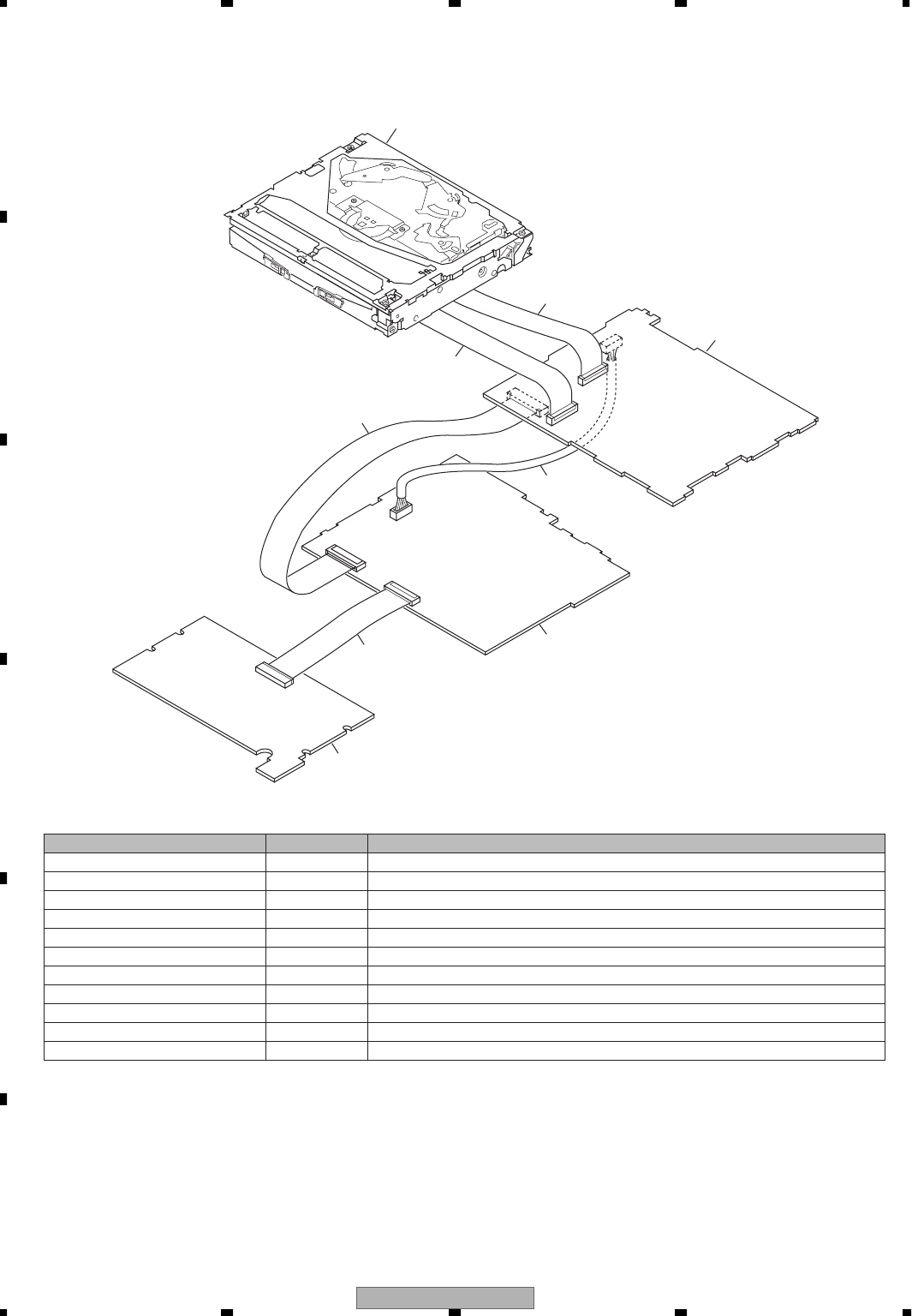
AVIC-D3/XU/UC
164
1234
1234
C
D
F
A
B
E
6. ADJUSTMENT
6.1 JIG CONNECTION DIAGRAM
DVD Mechanism Module(MS5)
Navi Mother Unit
GGD1284
GGD1284
GGD1327
GGD1406
GGD1170
Monitor Unit
AV Unit
- Jigs List
Name
40P FFC BBR
40P FFC BBR
20P Extension Cable
80P FPC
40P FFC BB
TEST DISC
Remote Control Uint
TORX driver (T2)
Bond
Bond (Produced by THREE BOND)
TEST DISC
Jig No.
GGD1284
GGD1284
GGD1327
GGD1406
GGD1170
GGV1303
CXC6317
GGK1095
GEM1033
1401M
GGV1018
Remarks
DVD Core Unit (CN2001) <---> Navi Mother Unit (CN2)
DVD Core Unit (CN1901) <---> Navi Mother Unit (CN2057)
Navi Mother Unit (CN2068) <---> AV Unit (CN1652)
Navi Mother Unit (CN2055) <---> AV Unit (CN1711)
Monitor Unit (CN5001) <---> AV Unit (CN1661)
Operation check
Operation for adjustment
SKEW adjustment (DVD)
SKEW adjustment (DVD)
SKEW adjustment (DVD)
SKEW adjustment (DVD)

AVIC-D3/XU/UC 165
5678
56
78
C
D
F
A
B
E
6.2 DVD ADJUSTMENT
1) Precautions
This product uses 5 V and 3.3 V as standard voltages.
The electrical potential that is the reference for signals,
is not GND, but VREF (approximately 2.2 V) and VHALF
(approximately 1.65 V).
During product adjustments, if the reference voltage is
mistakenly taken as GND, and a grounding contact is
made, not only would it be impossible to measure the
accurate electrical potential, but also the servo motor
would malfunction, resulting in the application of a
strong impact on the pick up. The following precaution-
ary measures should be strictly adhered to, in order to
avoid such problems.
The reference voltage and GND should not be confused
when using the minus probe of a measurement device.
When an oscilloscope is being used special care should
be taken to make sure that the reference voltage is not
connected to the probe of ch1 (on the minus side),
while the probe of ch2 (on the minus side), is connected
to GND. Further, since the body frame of most mea-
surement devices have the same electrical potential as
the minus side of the probe, the body frame of the mea-
surement device should be set to floating ground.
If the reference voltage is connected to GND by mis-
take, turn the regulator OFF immediately, or turn the
power OFF.
• Remove the filters and wires used for measurements
only after the regulator has been turned OFF.
•
• Whenever the product is in the test mode, the software
will not take any protective action. For this reason,
special care should be taken to make sure that no
mechanical or electrical shock could be applied to the
product when taking measurements in the test mode.
• Whenever the EJECT key is pressed to eject the disk,
no other keys, other than the EJECT key, should be
pressed until the disk eject action has been complet-
ed.
• If the product hangs up turn the power OFF immedi-
ately.
•
Laser didoes may be damaged, if the volume switch for
the laser power adjustment of the pick up unit, is turned.
Attention)
• Test mode starting procedure
Please select "MS5 check" to start test mode.
• Test mode stopping procedure
ACC and Backup OFF.
For stable circuit operation, keep the mechanism
operating for about one minute or more after the
regulator is turned on.
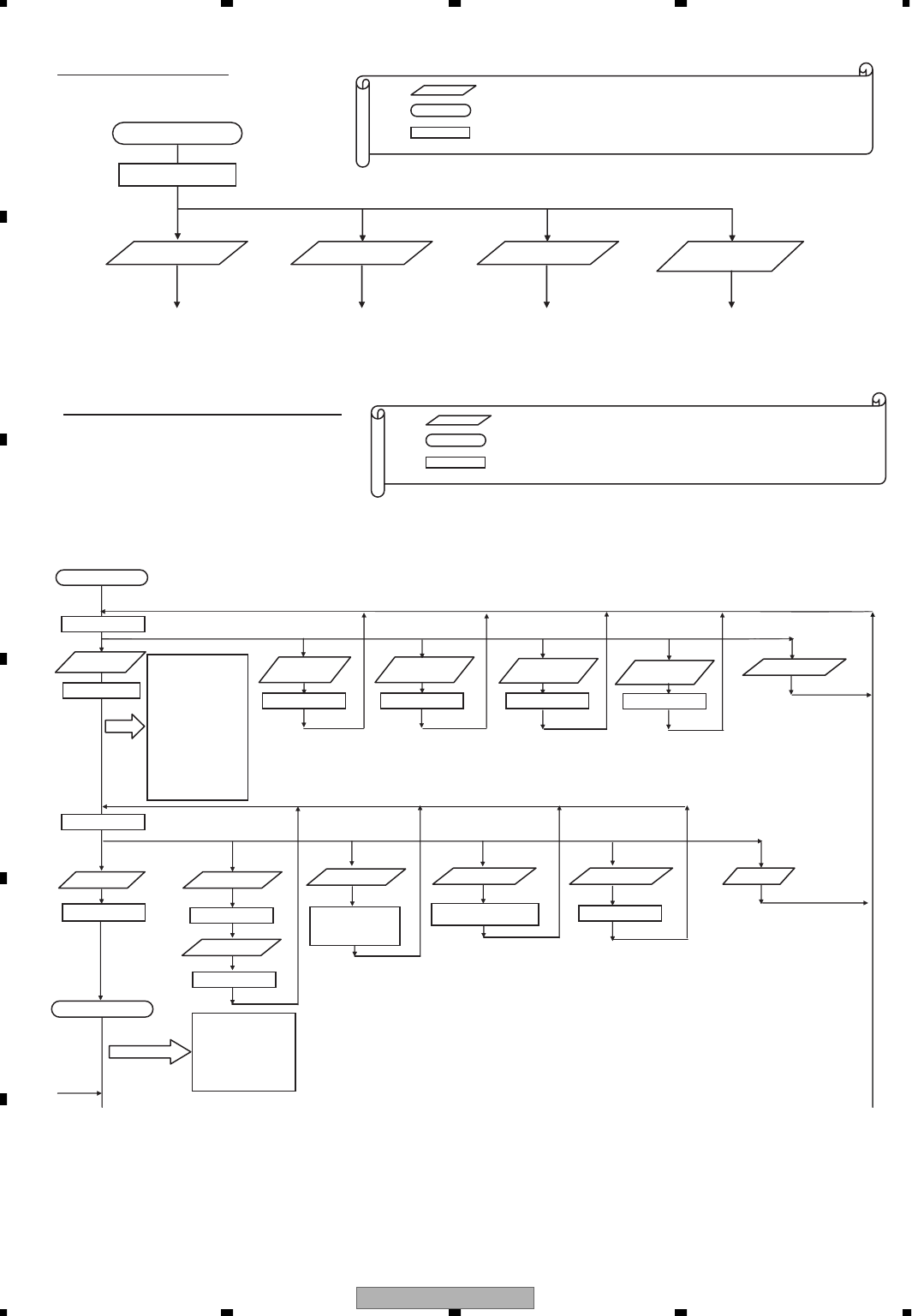
AVIC-D3/XU/UC
166
1234
1234
C
D
F
A
B
E
Image of the test mode.
[Note] Higher level 4 characters only. Lower level 4 characters are spaces.
(1) (2)
Start of the test mode.
TEST
FE test selection EDC1 test selection
Hereafter, to FE test
mode image. Hereafter, to EDC1
test mode image.
[Note] In order to move on to another test after selecting a test (FE/EDC1/EDC2), it is necessary to restart the DVD mechanism in the test mode.
(3)
EDC2 test selection
Hereafter, to EDC2
test mode image.
(4)
LD power on time
mode selection
Hereafter, to LD power on
time mode image.
Legend: ··· Key operation
··· Operation state
··· The content displayed on the DVD mechanism (video only)
8 characters data is sent to the product side (HOST) by UART communication.
Image of the front end test mode.
(2)
FE test mode
Disc type DVD1
layer
FE offset coefficient
TE offset coefficient
AS offset coefficient
ENV offset coefficient
TG offset coefficient
DBAL coefficient
VIN1 offset cancel value
VIN2 offset cancel value
VIN3 offset cancel value
VIN4 offset cancel value
VIN5 offset cancel value
VIN6 offset cancel value
VIN7 offset cancel value
VIN8 offset cancel value
VIN9 offset cancel value
VIN10 offset cancel value
Power on
0000 0000
0FFF 0000
0 x 00 0000
Legend: ··· Key operation
··· Operation state
··· The content displayed on the DVD mechanism (video only)
8 characters data is sent to the product side (HOST) by UART communication.
(4) (5)
Disc type DVD2
layer Disc type CD
0100 0000 0200 0000
Disc type CD-RW
0300 0000
EJECT
EJECT
[Note] If no action is taken for approximately 10 seconds after LD-ON, it will become LO-OFF automatically.
If F close is selected during LD-OFF, it will become an error.
During focus search (S character measurement mode), too, safety regulation applies if LD_OFF is not selected
within 10 seconds. Therefore, even if focus search is selected after LD-ON, it will become LD-OFF after 9 seconds.
In order to F close after focus search (S character measurement mode), set to Power_OFF first then power on again
before F close.
FEMAX level
FEMIN level
ASMAX level
ENVMAX level
FE normalization coefficient
Spindle gain coefficient
TEMAX level indication
TEMIN level indication
(2)
Focus close state
(1) (2)
S curve
measurement
(2)
F close F search
1A00 0000
F search
1100 0000
1FFF 0000
(3),(4)
CRG+/-
Activates while the key
is being pressed.
1B00 0000 : CRG+
1C00 0000 : CRG-
(5) (6)
LD-ON/OFF
When LO-ON: 1100 0000
When LD-OFF: 1000 000
CRG_HOME
1D00 0000
(8)
Power_OFF
(1) (3)
a b
1 x 00 0000
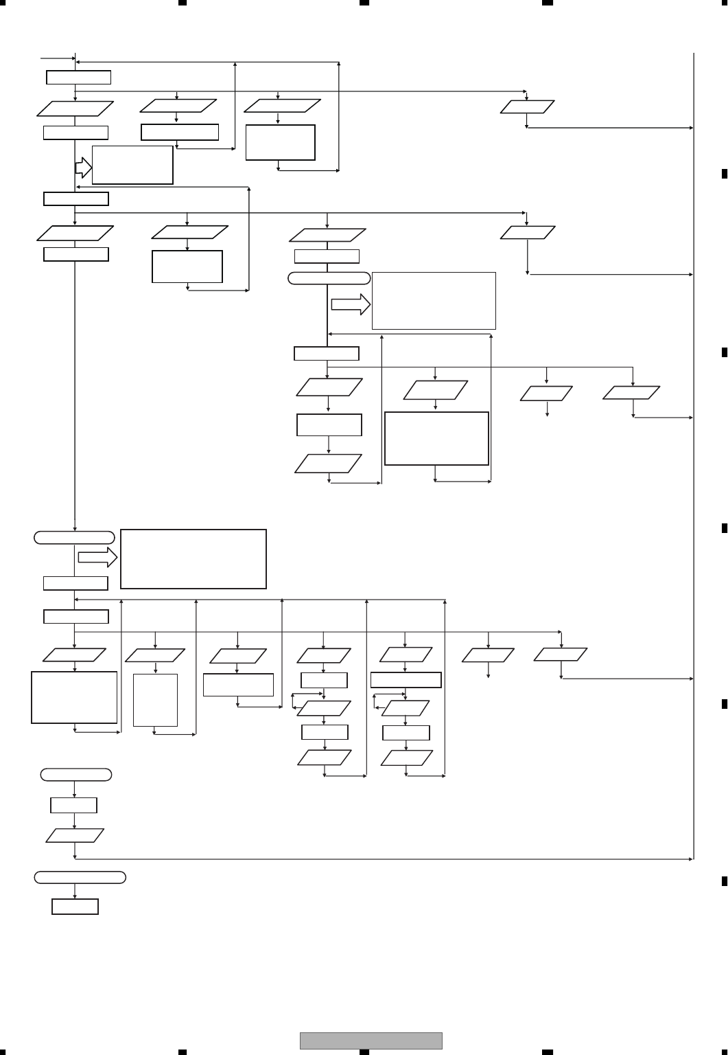
AVIC-D3/XU/UC 167
5678
56
78
C
D
F
A
B
E
(2)
(1) (2)
Tracking balance
TBAL coefficient (layer 0)
TBAL coefficient (layer 1)
TE normalization coefficient (layer 0)
TE normalization coefficient (layer 1)
Off track adjustment result
Focus Jump
When L0 layer: 2000 0000
When L1 layer: 2100 0000
2 x 00 0000
2FFF 0000
(3),(4)
CRG +/-
It operates while the key
is being pressed.
2B00 0000 : CRG+
2C00 0000 : CRG-
3000 0000
(8)
Power_OFF
(8)
Power_OFF
(5)
Performed including the tracking close processing.
FBAL coefficient (layer 0)
FBAL coefficient (layer 1)
Focus gain coefficient (layer 0)
Focus gain coefficient (layer 1)
Tracking gain coefficient (layer 0)
Tracking gain coefficient (layer 1)
AS normalization adjustment value (layer 0)
AS normalization adjustment value (layer 1)
RF level value
3FFF 0000
Tracking close state
(1) (2)
(1)
Error rate
measurement
Error rate
Focus gain coefficient (layer 0)
Focus gain coefficient (layer 1)
Tracking gain coefficient (layer 0)
Tracking gain coefficient (layer 1)
AS normalization adjustment value (layer 0)
AS normalization adjustment value (layer 1)
RF level value
indication start
5000 0000
RF level is informed
every 500msec.
RF level value
indication end
(7) (8)
To (2)
T.O PEN Power_OFF
(1) (3),(4)
Tracking close CRG +/-
It operates while the key
is being pressed.
3B00 0000 : CRG+
3C00 0000 : CRG-
3FFF 0000
a b
(1) (2)
Tracking close state
Error rate
measurement
FBAL coefficient (layer 0)
FBAL coefficient (layer 1)
Focus gain coefficient (layer 0)
Focus gain coefficient (layer 1)
Tracking gain coefficient (layer 0)
Tracking gain coefficient (layer 1)
AS normalization adjustment value (layer 0)
AS normalization adjustment value (layer 1)
Playback speed
switching
4000 0000
4 x 00 0000
(5)
Error rate
Focus gain coefficient (layer 0)
Focus gain coefficient (layer 1)
Tracking gain coefficient (layer 0)
Tracking gain coefficient (layer 1)
AS normalization adjustment value (layer 0)
AS normalization adjustment value (layer 1)
Focus Jump
DVDX1.3~
1.6CAV
CDX4CLV:
4x00 0000
When L0 layer: 4x00 0000
When L1 layer: 4x00 0000
(8)
Error display
Power_OFF
Error occurrence
L0 layer DVD X 1.3~1.6CAV, CD X 4CLV :4000 0000
L1 layer DVD X 1.3~1.6CAV :4100 0000
[Note] If an error occurs at Power_OFF, reset cannot be made. In such a case, it is necessary to turn the power off and start the test mode once again.
Error occurrence at Power_OFF
Error display
The number for designation of the track number shall be selected from the track numbers previously prepared.
Switch to cyclic by (3). Fix by (4).
For CD: Tracks 1, 4, 10, 11 and 32
For DVD: Tracks 1, 4, 10, 11, 32, 64 and 100
Change the method for ID address designation.
Designation of digit by command (1) and (2). UP/DOWN of numbers by command (3) and (4). Fix by command (5).
The higher 2 digits of the designated ID are the value showing the test state.
The lower 6 digits show the ID.
Example) If 300000 is desired to be designated as the ID, designated ID: 4A03 0000.
(7) (8)
To (2)
T.OPEN Power_OFF
(6) (3),(4)
(1)-(4) (3)
(5) (5)
ID Search T.Jump+/-
4A00 0000 Jump+ : 4B00 0000
Jump- : 4C00 0000
ID designation
ID display
Track number
designation
Track number
indication
Search start Jump start
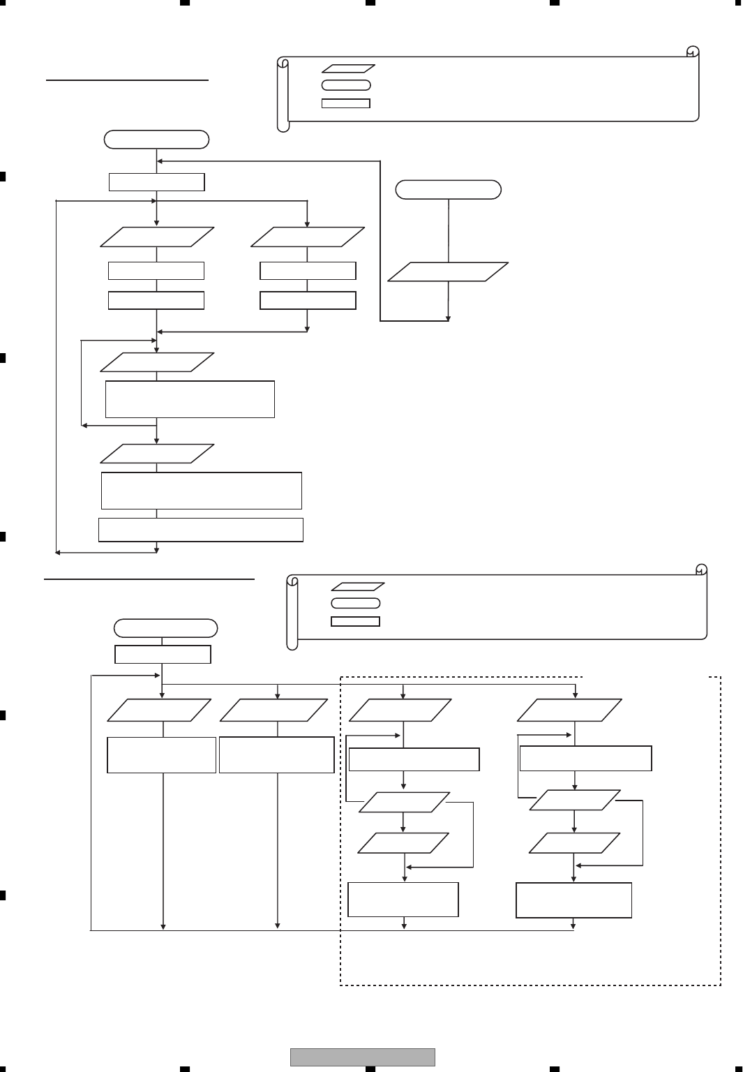
AVIC-D3/XU/UC
168
1234
1234
C
D
F
A
B
E
EDC. Image of the test mode
[Note] Image is the same for both EDC1 and EDC2.
(1) (2)
EDC1/2 test mode
0000 0000
Layer 0 selection Layer 1 selection
0000 0000 0100 0000
1003 0000 1103 0000
(5)
[Note] The display is updated at 0.5 seconds interval until 0/1 layer is selected or Eject is effected.
(1)-(4)
ID designation
EDC1/2 start
Layer 0: 10** ****
Layer 1: 11** ****
[Note] ** **** is the ID designation value
Layer 0: 20** ****
Layer 1: 21** ****
[Note] ** **** is the present ID designation value
**** ****
[Note] **** **** is the present ID designation value
Legend: ··· Key operation
··· Operational state
··· The content displayed on the DVD mechanism (video only)
8 characters data is sent to the product side (HOST) by UART communication.
[Note] Eject can be effected any time during the EDC test mode.
However, disc exist/non-exist bit of BD of UART communication
is not fixed.
Eject
After completion of EJECT operation
EJECT operation
Test mode Eject
Image of the LD power on time mode.
LD power on time mode
0000 0000
CD LD power on
time indication
DVD LD power on
time indication
10** ****
[Note] ** **** is the CD LD
power on time.
20** ****
[Note] ** **** is the DVD LD
power on time.
(1) (2)
CD LD power on
time setting
Setting time
designation
30** ****
[Note] ** **** is the setting time.
Setting time
registration
DVD LD power on
time setting
Setting time
designation
40** ****
[Note] ** **** is the setting time.
(5) (6)
(1)-(4) (1)-(4)
(5) (5)
(8)
10** ****
[Note] ** **** is the CD LD
power on time.
Setting time
registration
(8)
20** ****
[Note] ** **** is the DVD LD
power on time.
[Note] If the power on time is 999999 hours or more, it is always reported as 999999 hours.
[Note] If the power on time is " *E** **** ", the value may not be correct due to the life of the flash memory.
[Method of setting time designation]
Designate the digit by command (1) and (2). UP/DOWN of numbers by command (3) and (4).
Fix by command (5). Cancel by command (8).
Legend: ··· Key operation
··· Operational state
··· The content displayed on the DVD mechanism (video only)
8 characters data is sent to the product side (HOST) by UART communication.
Not for service use
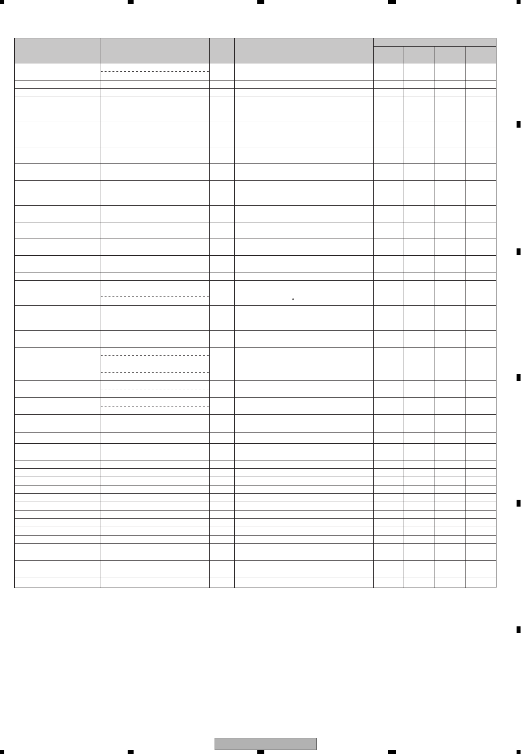
AVIC-D3/XU/UC 169
5678
56
78
C
D
F
A
B
E
Error status
Open
Read Error
Focus Error(Focus Error
in mechanism set up)
Surface Error
Address not found
(Invalid Track)
Spindle Lock
Carriage HOME
ID/SUBCODE Read Error
AV CHIP decode Error
AV CHIP Recovery NG
Error of PLAY BACK Mode
Status
Disc Data Error
No Disc
(including Disc loading
and ejecting)
Media Error
Temp Error
(In Case of High
Temperature)
OSD *1
It is a disc unable to be played back.
NON-PLAYABLE DISC
(No display)
ERROR-02-99
ERROR-02-90
ERROR-02-9E
ERROR-02-80
ERROR-02-91
ERROR-02-92
ERROR-02-94
ERROR-02-9A
ERROR-02-9B
ERROR-02-9C
Temperature protection circuit is
being activated.
THERMAL PROTECTION IN MOTION
(No display)
(No display)
UART
*2
10h
20h
21h
22h
23h
24h
25h
26h
2Ah
2Bh
2Ch
2Dh
40h
00h
30h
Meaning
Door open error
Transfer start error
Focus error
Focus error during set up
(A focus has never been achieved with that
disc.)
Address not found.
Spindle lock NG
(the disc cannot rotate)
Carriage home NG
(The pick up tries to return to carriage
home, but it cannot go back and stopped.)
ID/SUBCODE Read Error (ID/SUBCODE
cannot be read due to scratch or stain.)
AV CHIP decode NG
(AV chip cannot be decoded.)
AV CHIP recovery NG
Playback state error
(An error due to software bug.)
Disc Data NG
Disc has not been inserted.
(Including Load in process or Eject in process.)
Loading mechanism error
(The disc cannot be clamped.)
A disc containing the unplayable Format only.
High temperature
(Playback is stopped because the pick up
temperature is 89 C or higher.)
ACC
Off/On
Source
Off/On
Eject
Play Key
****
XXXX
XXXX
XXXX
X
X
X
X
X
X
X
X
*
X
X-XX
X
-
-
Method of reset
--
X
X
X
X
X
X
X
X
*
-
-
-
-
X
X
X
X
X
X
X
X
*
X
X
-
X
X
X
X
X
X
X
X
X
X
*
-
-
-
-
-
ERROR-02-9D
Loading_Mecha Error 50h
REQUEST error
Failure in issuing read
command (chip dependent)
Adjustment of L0 is NG.
Adjustment of L1 is NG.
LD system NG
Gain adjustment system NG.
Gain determining system NG.
Servo initial setting related items NG.
Disc is not clamped yet.
Tracking system NG.
Media setting system NG.
Focus Error
Error of PLAY BACK
Mode Status
Error of PLAY BACK
Mode Status
Undefined Error
DRM Error
Region code Error NG
CPPM*3 Key Error *4
AWM*5 Error *4
It is a protected disc.
PROTECTED DISC
Region code is incorrect.
DIFFERENT REGION DISC
It is a disc unable to be played back.
NON-PLAYABLE DISC
ERROR-02-A0
ERROR-02-A1
ERROR-02-A2
ERROR-02-A3
ERROR-02-A4
ERROR-02-A5
ERROR-02-A6
ERROR-02-A7
ERROR-02-A8
ERROR-02-A9
ERROR-02-AA
ERROR-02-AB
ERROR-02-B0
ERROR-02-B1
ERROR-FF-FF
A0h
A1h
A2h
A3h
A4h
A5h
A6h
A7h
A8h
A9h
AAh
ABh
B0h
B1h
FFh
70h
90h
91h
*6
REQUEST error
Failure in issuing the read command
L0 adjustment is NG.
L1 adjustment is NG
LD system NG
Gain adjustment system NG.
Gain determining system NG.
Servo initial setting related items NG.
Disc is not clamped yet.
Tracking system NG
Media setting system NG
JUMP over layers NG
Navigation command error
Retry over
Undefined error
DRM error
(All music cannot be played back due to DRM.)
Region code NG (Unable to be played back
due to incorrect mechanism region.)
Playback the illegally copied disc by DVD-A
(Mute the sound on the mechanism side.)
Key Error for playback
--X-CPRM Key Error *7
NON-PLAYABLE DISC
93h Key Error for playback
X
X
X
X
X
X
X
X
X
X
X
X
X
X
X
XXX -
X
X
X
X
X
X
X
X
X
X
X
X
X
X
X
X
X
X
X
X
X
X
X
X
X
X
X
X
X
X
X
X
X
X
X
X
X
X
X
X
X
X
X
X
X
X: Cancel the error by operation. -: Error is not cancelled by operation. *: No setting
*1 A content displayed on OSD. As for the items having multiple display patterns, the upper row is for the Japanese version Full GUI, and the lower row is for
the Touch Panel model and Full GUI (English version).
*2 A parameter of UART command, such as "receipt error notice", that the DVD mechanism transmits.
*3 CPPM(Content Protection for Prerecorded Media) : A copyright protection technique used in DVD-A. The protection is realized by using the keys recorded
on the media and the device key held by the player.
*4 DVD-A compatible model only.
When an error has occurred, only the audio output will be muted but playback operation will continue. Furthermore, acceptance of the user operation will be
the same as usual.
*5 AWM (Audio WaterMark): Electronic watermark. Information on the copyright owner or CCI (copy control information) are recorded so that illegally copied
discs can be identified.
*6 Notice as an error status will not be given
*7 CPRM(Content Protection for Recordable Media) : A copyright protection technique for digital contents used for re-writable DVD or memory card.
(DVD-VR model only)
(No display)
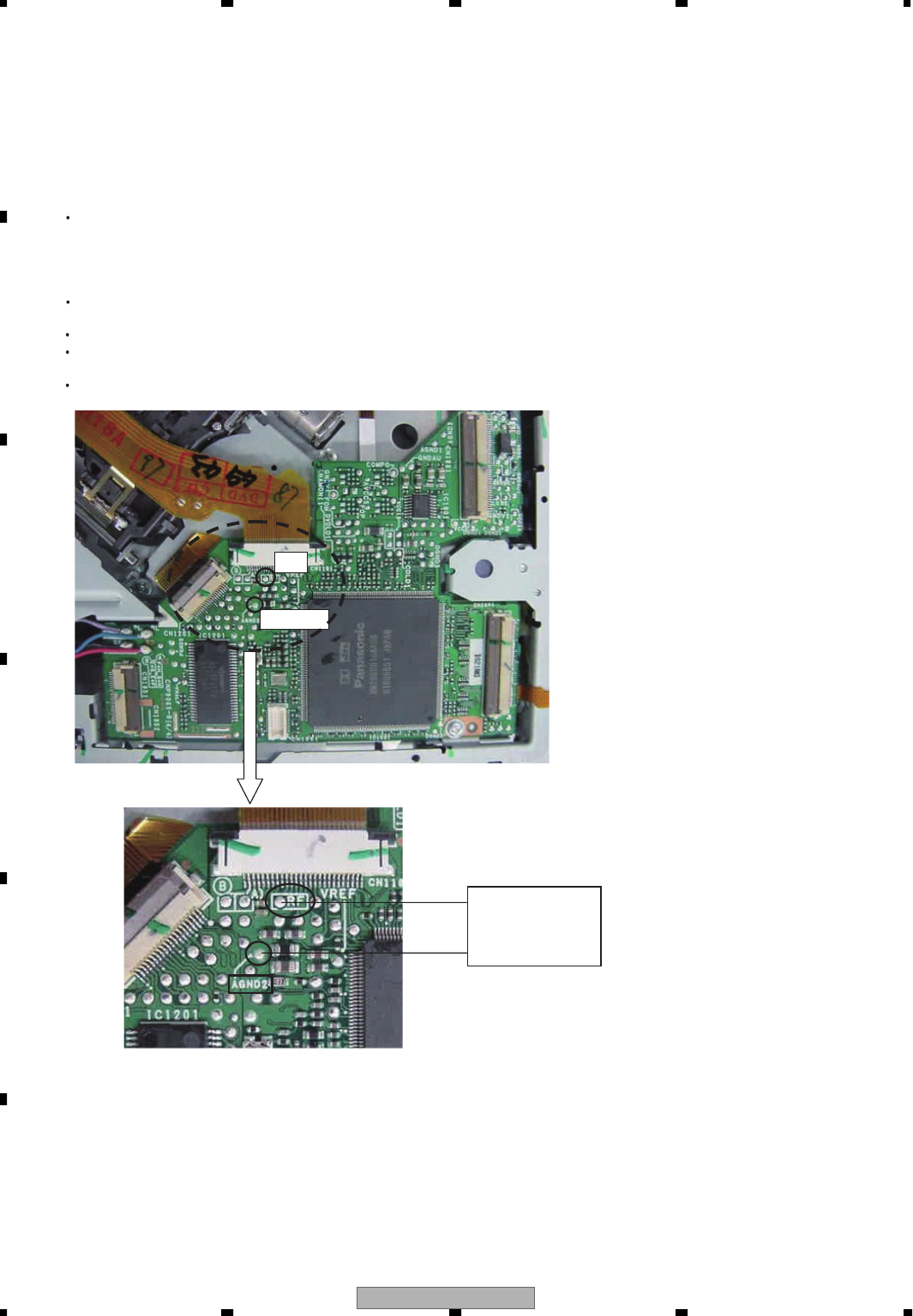
AVIC-D3/XU/UC
170
1234
1234
C
D
F
A
B
E
- SKEW adjustment
When one of the following replacements has taken place, SKEW adjustment for the pick up will be required.
(1) Replacement of the pick up unit
(2) Replacement of the spindle motor
(3) Replacement of the carriage chassis
(4) Replacement of the main shaft of the pick up unit
(5) Replacement of the sub shaft of the pick up unit
Measurement equipment and tools/jigs: Oscilloscope
Driver for SKEW adjustment t TORX driver (T2) (GGK1095)
Bond for fixing the SKEW (GEM1033)
Bond for locking the screw (Locking agents (1401M : produced by THREE BOND))
Disc used: GGV1018
Measurement reference: AGND2
Measurement point: RF
Connection drawing
DVD core unit
Enlargement
Symptom in case the adjustment is not adequate: Worsening of the error rate 10-3
(Normally 10-4 or less.)
Large RF jitter
RF waveform distortion
Tracking drawing/Unstable servo
* Caution: Do not look into the laser light during adjustment.
Oscilloscope
RF
AGND2

AVIC-D3/XU/UC 171
5678
56
78
C
D
F
A
B
E
There are two methods for adjustment, a method whereby the adjustment is made while monitoring the RF waveform
using the oscilloscope (method 1) and a method whereby the adjustment is made while checking the RF level in
value by OSD (method 2).
The adjustment procedure is shown below. Refer to the paragraph for the service test mode regarding entering of the
test mode and the operation procedure.
Adjustment procedure:
1. Turn the DVD mechanism module upside down so that the pick up can be adjusted.
When the module is turned upside down, there is a possibility that the disc is rubbed.
So, first place a coin with the thickness of approximately 1.5mm on a desk, and set the module upside down in a
way that section 1 in the illustration below comes right above the coin.
2. Install the pick up. (Refer to the section regarding removal of the pick up from the mechanism unit.)
As for the precautions in handling the pick up, refer to the precautions in handling the PU as described below.
3. Method 1:
Connect the oscilloscope by referring to the connection drawing so that the RF signal can be monitored with
AGND2 as the reference.
Method 2:
There is no need for setting of any equipment. Proceed to step 4.
4. Turn the power ON, and load the disc for adjustment.(GGV1018)
5. After setting the disc type to DVD layer 1 in the front end test mode, turn the power ON, and move the pick up to
the inner periphery. (CRG - Home)
6. Turn the LD ON.
7. Set to focus close, and make auto adjustment for all items under that state, then set to tracking close.
And make auto adjustment for all items under that state as well.
8. Make an intermediate periphery (ID: 100 000) search, and move the PU to intermediate periphery.
9. Method 1:
Proceed to step 10.
Method 2:
After setting to Tracking Open, make all auto adjustments, and set to Tracking Close this time with a command that
can be RF displayed. Make auto adjustment for all items under that state as well.
10. Use TORX driver (T2) (GGK1095) for the following.
Method 1:
While monitoring the RF waveform on the oscilloscope, turn SKEW adjustment screw A just a little bit in a way that
the level will reach the maximum.
While the pick up is at the intermediate periphery, turn SKEW adjustment screw B just a little bit in a way that the
level will reach the maximum.
While the pick up is at the intermediate periphery, turn SKEW adjustment screw A just a little bit in a way that the
level will reach the maximum.
(Make adjustment in the order of A -> B -> A, Please end the each adjustment by turning screw clockwise. )
Method 2:
While monitoring the RF level value on the OSD display, turn the SKEW adjustment screw A just a little bit in a way
that the level will reach the maximum.
While the pick up is at the intermediate periphery, turn SKEW adjustment screw B just a little bit in a way that the
level will reach the maximum.
While the pick up is at the intermediate periphery, turn SKEW adjustment screw A just a little bit in a way that the
level will reach the maximum.
(Make adjustment in the order of A -> B -> A, Please end the each adjustment by turning screw clockwise. )
If the error rate is not good, please perform Method again.
11. Turn the power OFF in the test mode, and after confirming that the disc has stopped, eject the disc.
12. Apply adhesive for fixing the SKEW and lock the screw.
Refer to the illustration below for the adhesion points.
1
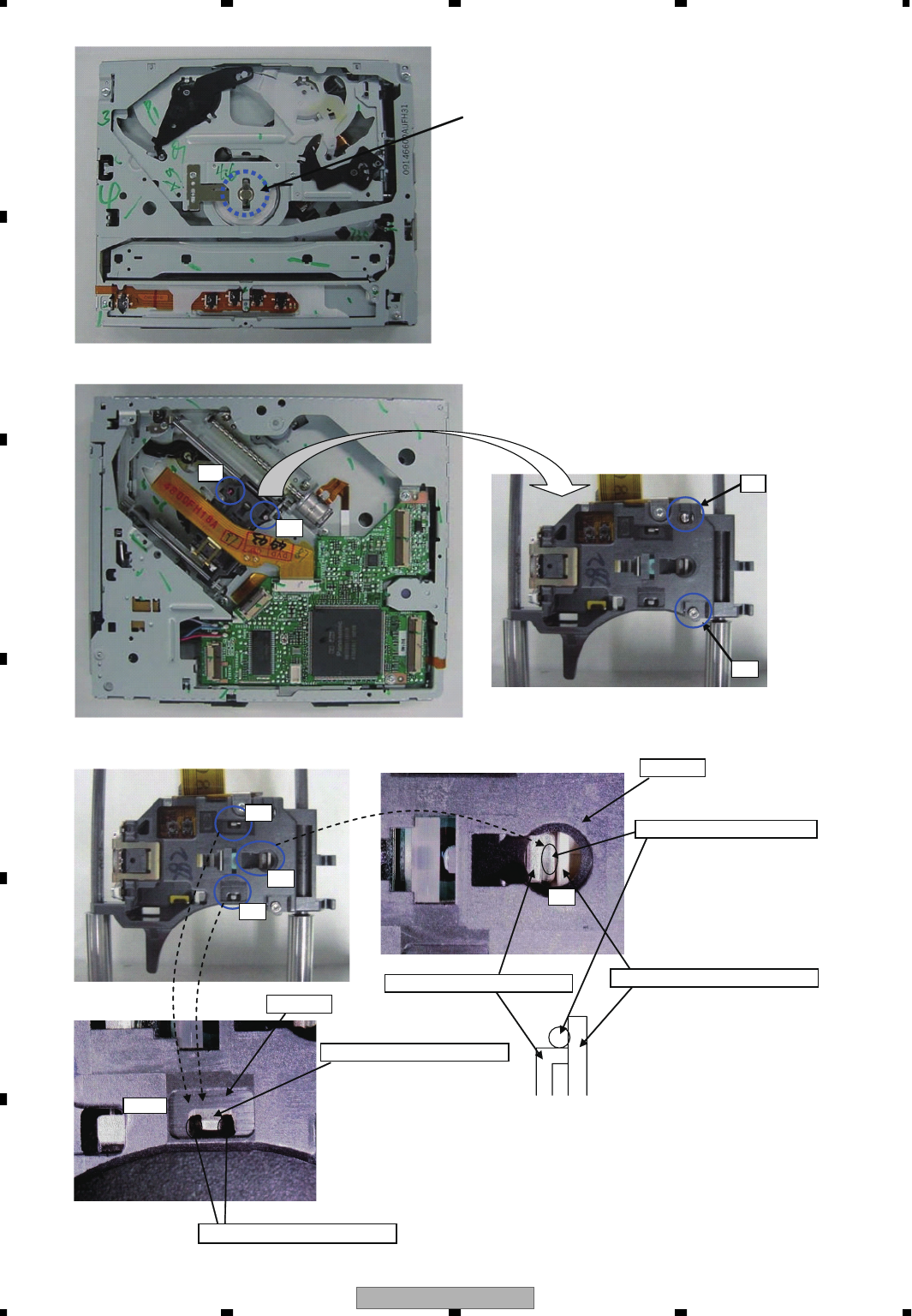
AVIC-D3/XU/UC
172
1234
1234
C
D
F
A
B
E
SKEW adjustment locations.
A
B
A
B
SKEW adhesive locations (GEM1033) RAD-SKEW adhesive locations
Cross section of R-SKEW adhesive locations.
* Caution: Make a cross link to both the resin section
and the sheet metal section.
C
Adhesive application locations
Sheet metal (yoke base) section Resin (suspension support) section
PU case
Sheet metal (yoke base) section
* Caution: Make a cross link to both the case section and the sheet metal section.
Adhesive application locations
TAN-SKEW adhesive locations
D & E
PU case
C
D
E
1
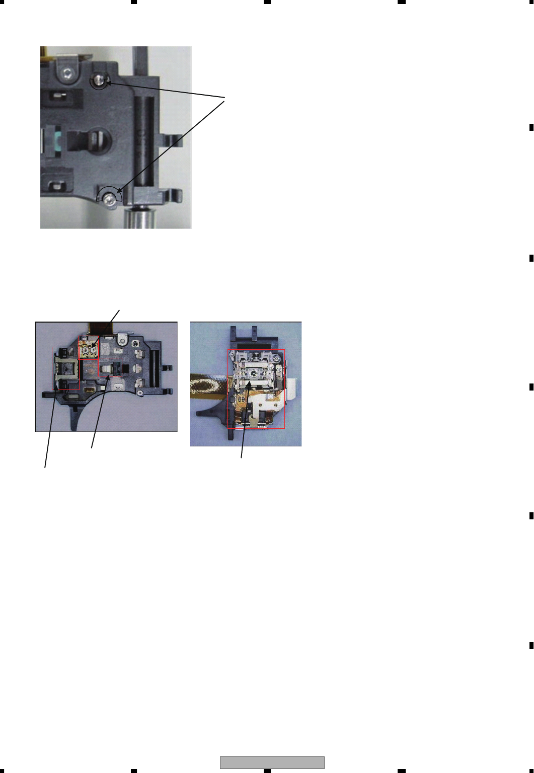
AVIC-D3/XU/UC 173
5678
56
78
C
D
F
A
B
E
Screw locking adhesive location (1401M : produced by THREE BOND)
Screw locking adhesive location
Apply the locking agent for more than half of the screw head
circumference.
* Caution: The locking agent shall not overflow to outside of
the PU case.
Precautions in handling the PU.
* Caution: Do not touch the shaded section in the drawing below.
RF level adjustment section
Do not touch the optical parts.
Hologram (be careful for the static electricity)
GRT adjustment section
Do not touch the springs.
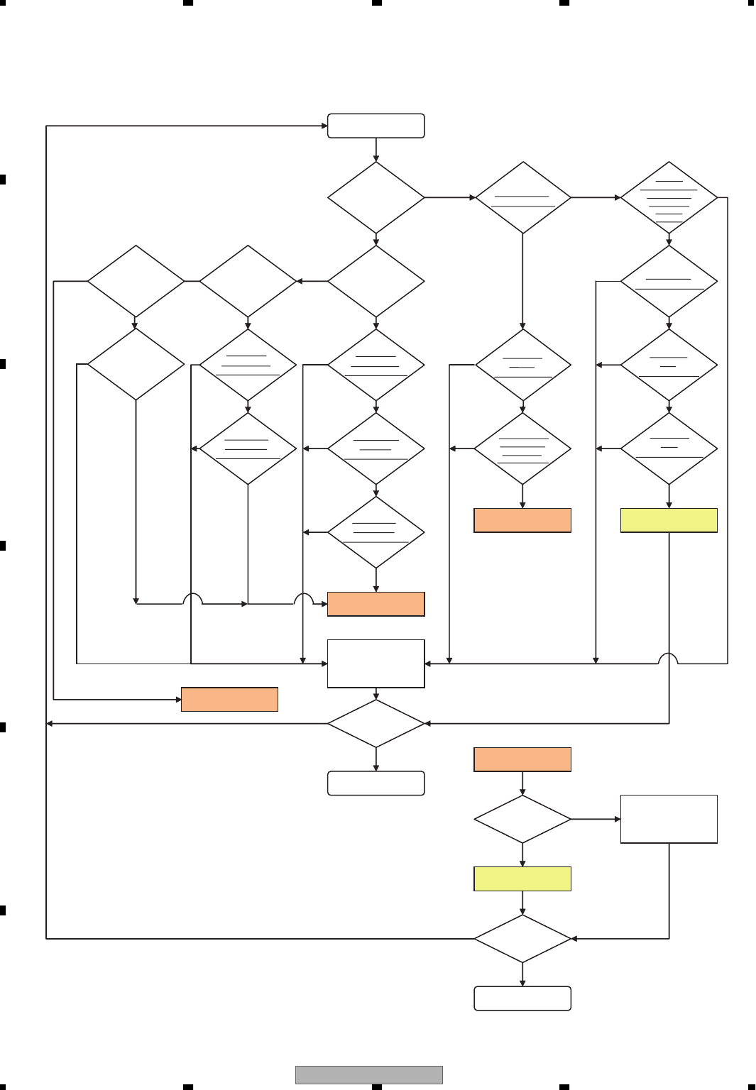
AVIC-D3/XU/UC
174
1234
1234
C
D
F
A
B
E
Is the image
in error?
Go to FE related
repair process.
Is FE section
normal?
BACK END section flow
Can the
playback
start?
Is the sound
in error?
Repair the
defective part.
Normal?
NO
YES
NO
YES
YES
YES
YES
YES
YES
Go to FE
section check.
YES
YES
NO
NO
NO
NO
NO
NO
NO
FE section check.
Go to FE
section check.
NO
NO
NO
Replace the unit.
YES
YES
Go to FE
section check.
NO
YES
YES
NO
START
END
NO
NO
NO
NO
Replace the unit.
YES
Normal?
YES
NO
END
NO
YES
YES
YES
YES
YES
Does the
operation
take time?
Is the life of flash
memory OK?
Conduct check item 12.
Standby OK?
Execute check 1.
Is VDD5
(VCC33, VCC12)
power supply
voltage OK?
Execute
check 2.
Reset OK?
Execute check 3.
Is VD8, VCC5
power supply
voltage OK?
Execute check 7.
Is SDRAM
IF OK?
Execute check 6.
Is VSENS
OK?
Execute check 4.
Is 27 MHz
OK?
Execute check 5.
Is AVCC5
voltage OK?
Execute check 8.
Is DACCLK
normal?
Execute check 9.
Is the audio
circuit OK?
Execute check 10.
Is the video
circuit OK?
Execute check 11.
Is AVCC5
voltage OK?
Execute check 8.
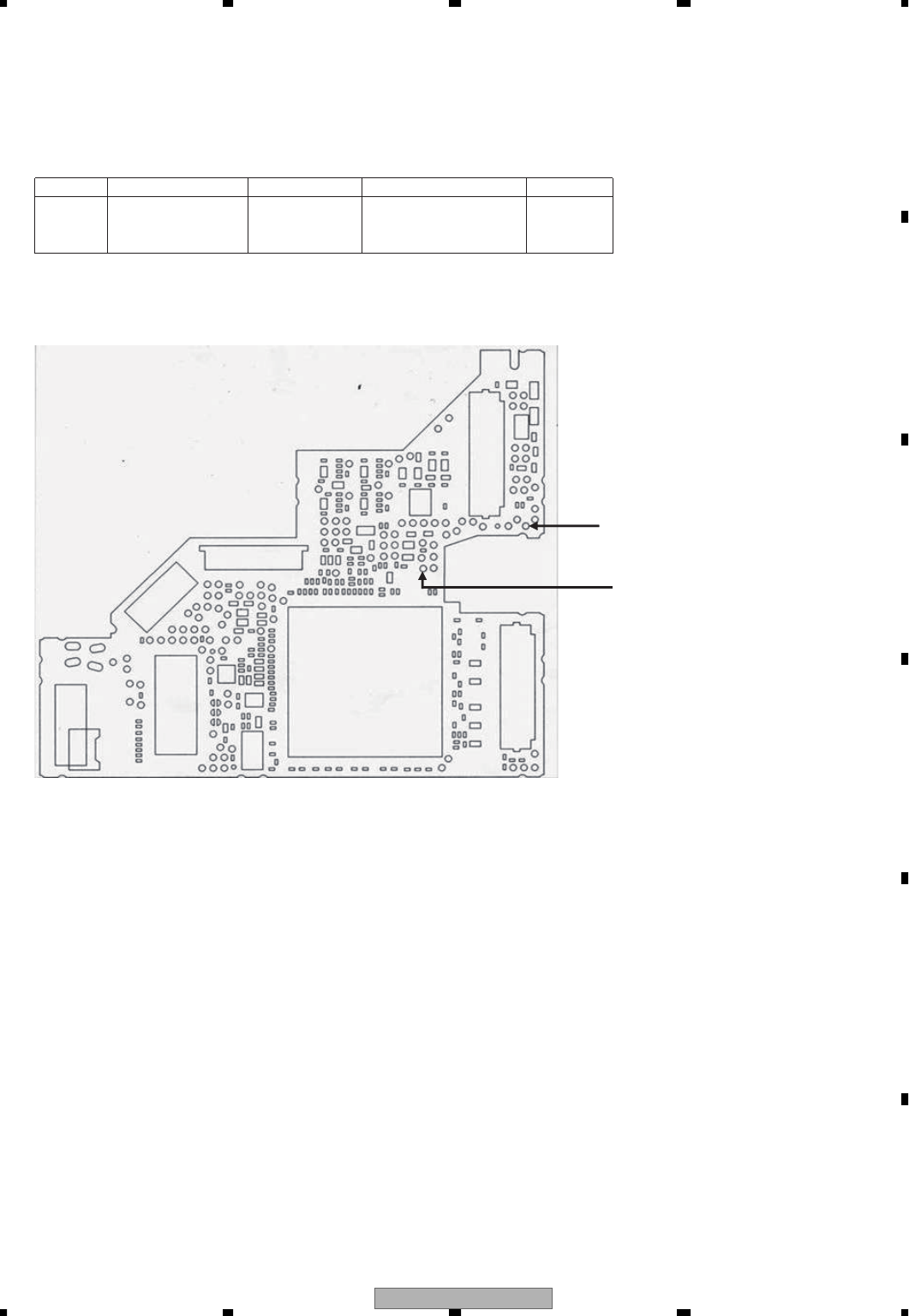
AVIC-D3/XU/UC 175
5678
56
78
C
D
F
A
B
E
Check 1: Standby OK?
<Check> Check the voltage at the "STANBY" test point while the power is on.
Use the "DGND1" test point at the reference.
NO. Check point Module No. Specification value Unit
STANBY-DGND1 ALL VCC33 V-
0.6 V or more
V
Fig 1.1: STANBY check point
STANBY
DGND1
Side A
1
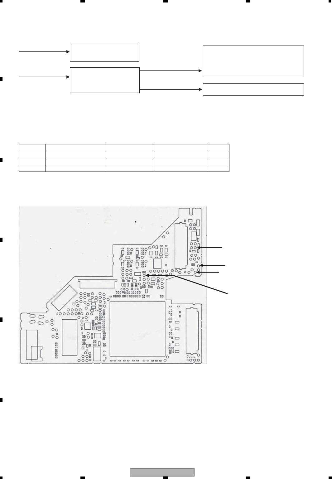
AVIC-D3/XU/UC
176
1234
1234
C
D
F
A
B
E
Check 2: Is VDD5 (VCC33, VCC12) power supply voltage OK?
VDD5
VCC33 (= 3.3 V )
VDD5
VCC12 (= 1.2 V )
IC1401 FLASH power supply (Data)
IC1402 FLASH power supply (Program)
IC1481 SDRAM power supply
IC1501 DVD-LSI power supply
IC1501 DVD-LSI power supply
IC1001 DC/DC
converter
VCC 3.3 V/1.2 V output
F.E. driver control system
NO. Check point Module No. Specification value Unit
1
2
3
VDD5_3 - DGND1
VCC33_3 - DGND1
VCC12_1 - DGND1
ALL
ALL
ALL
5.0 ± 0.4
3.3 ± 0.15
1.2 ± 0.12
V
V
V
Side A
VCC33_3
VDD5_3
VCC12_1
DGND1
Fig 2.2: VDD5, VCC33, VCC12 voltage check points
Fig 2.1: Power supply configuration
<Check> Check the voltage at the "VDD5_3, VCC33_3 and VCC12_1" test point while the power is on.
Use the "DGND1" test point at the reference.
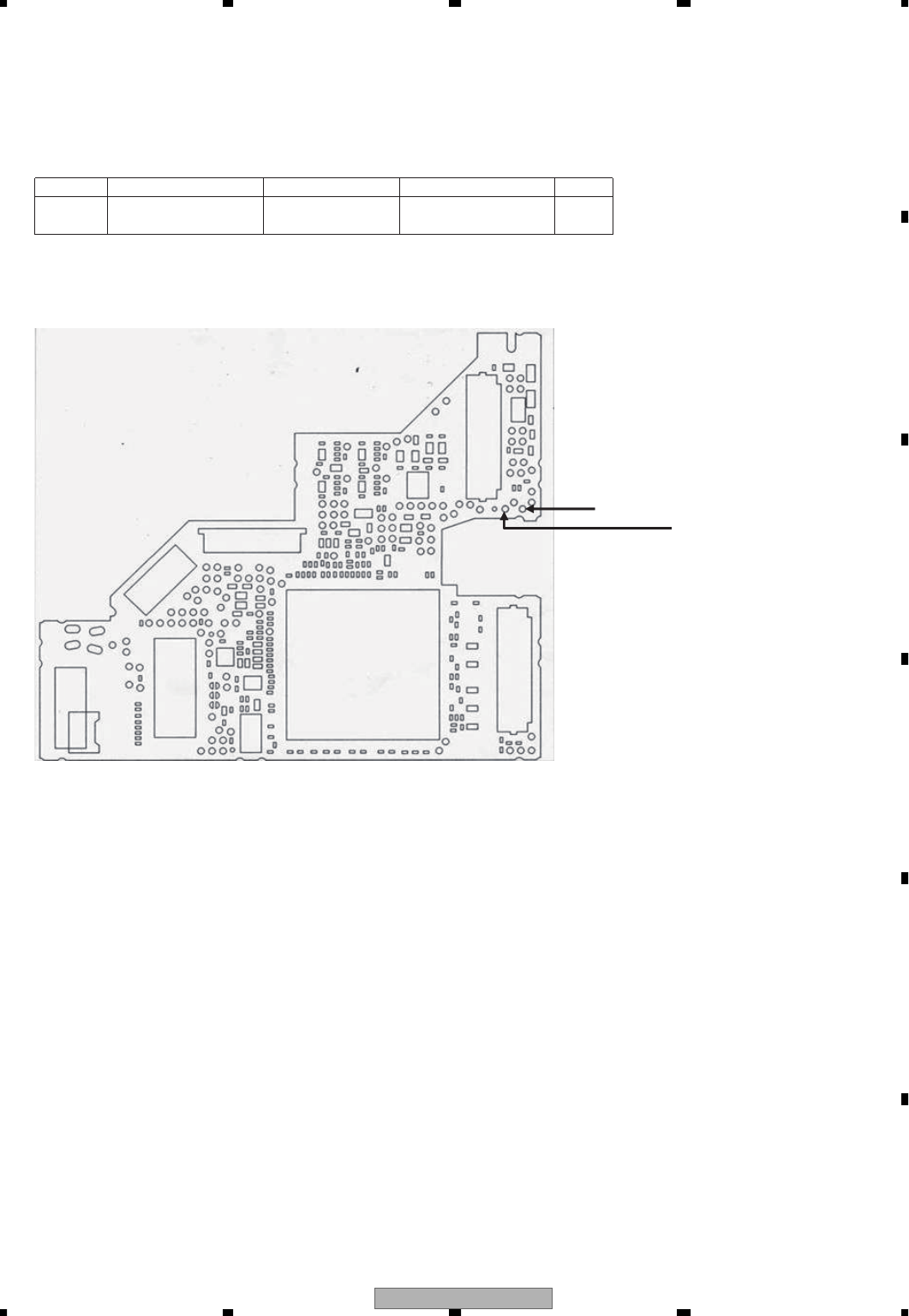
AVIC-D3/XU/UC 177
5678
56
78
C
D
F
A
B
E
Check 3: Reset OK?
NO. Check point Module No. Specification value Unit
1 XRES-DGND1 ALL VCC33 x
0.7 or more
V
Side A
Fig 3.1: RESET check point
XRES
DGND1
<Check> Check the voltage at the "XRES" test point while the power is on.
Use the "DGND1" test point at the reference.
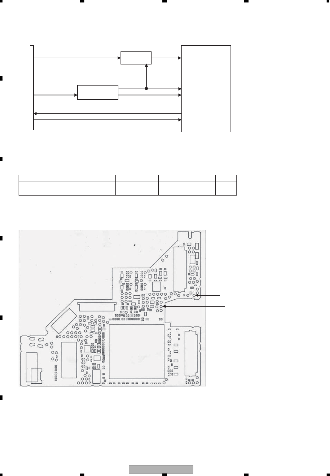
AVIC-D3/XU/UC
178
1234
1234
C
D
F
A
B
E
Check 4: Is VSENS OK?
CN1901
HOST I/F
VD8 VSENS
VCC33
VDD5 VCC12
STANBY
XRES
Fig 4.1: Power supply configuration and VSENS
NO. Check point
IC1501
DVD-LSI
IC1001
DC/DC converter
IC1003
detection IC
Side A
Fig 4.2: VSENS check point
VSENS
DGND1
Module No. Specification value Unit
VSENS - DGND1 ALL VCC33 x 0.7
or more V1
<Check> Check the voltage at the "VSENS" test point while the power is on.
Use the "DGND1" test point at the reference.
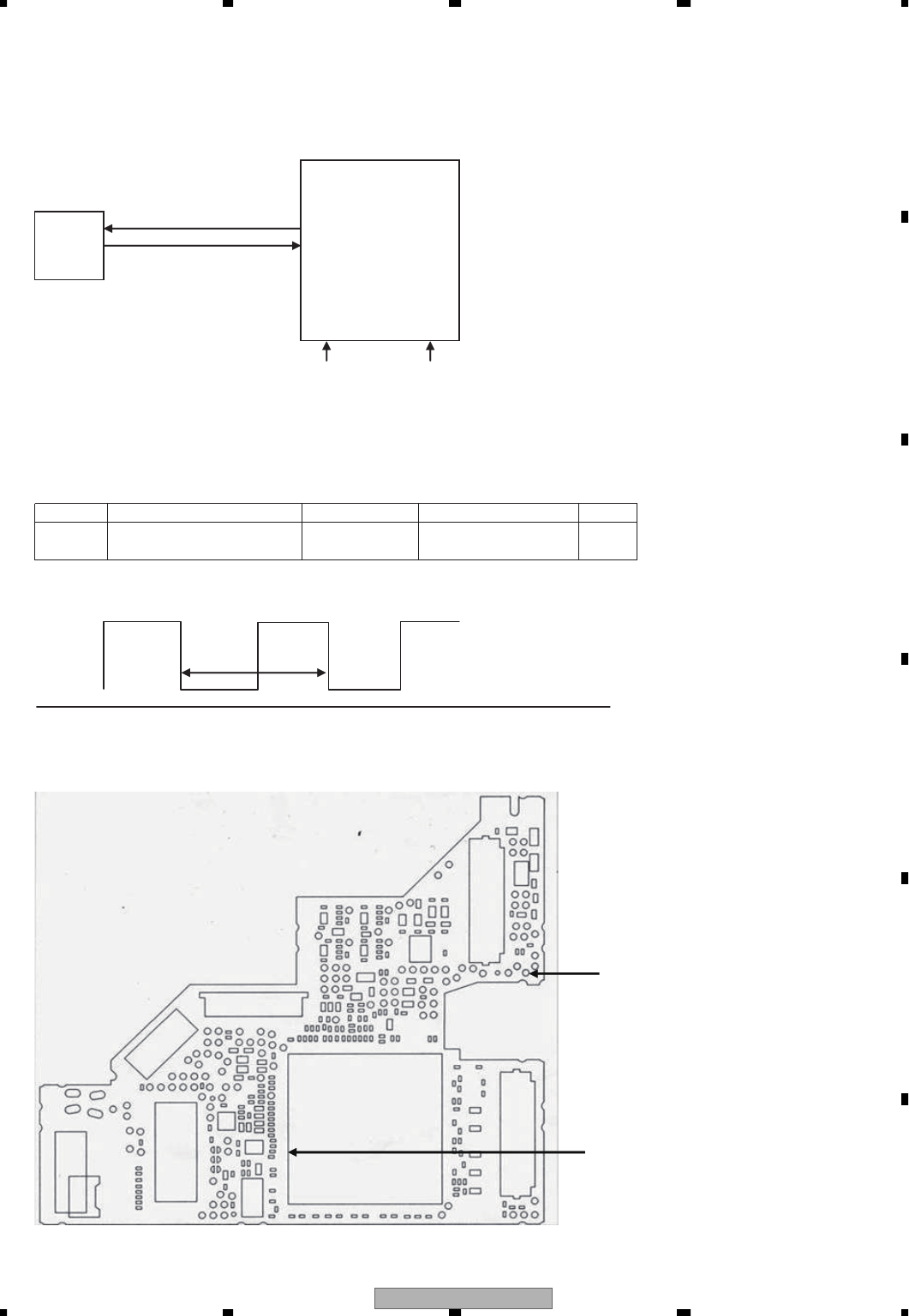
AVIC-D3/XU/UC 179
5678
56
78
C
D
F
A
B
E
Check 5: 27 MHz Normal?
<Outline> Each clock is created inside the IC1501 using the 27 MHz master crystal oscillator (X1501).
OSCO
OSCI
Fig 5.1: Clock configuration
IC1501
DVD-LSI
X1501
27 MHz
crystal
VCC33 VCC12
<Check method> Turn the power on, and check with DGND being the reference.
In case of NG, check the applicable line, periphery of IC1501,
soldering of the peripheral components and defective components.
NO. Check point Module No. Specification value Unit
2 IC1501 169pin ALL 27 MHz
± 50 ppm ppm
GND Fig 5.2: Clock specification value
Side A
Fig 5.3: 27 MHz check point
Specification
value
DGND1
IC1501 169pin
AVIC-D3/XU/UC
180
1234
1234
C
D
F
A
B
E
Check 6: Is SDRAM I/F OK?
<Outline> In order to secure the MPEG stream data as the buffer,
the capacity of communication I/F SDRAM between the LSI and the memory is 128Mbit.
Be careful as XCSM, XWE, XCAS, XRAS and XSCM of IC1481 are called differently in IC1501,
namely NCSM, NWE, NCAS, NRAS, NCSM.
MA0~11
MDQ0~31
MCK
XWE (NWE)
XCAS (NCAS)
XRAS (NRAS)
XCSM (NCSM)
DQM0
DQM1
DQM2
DQM3
BA0
BA1
Fig 6.1: SDRAM I/F
IC
1481
SDRAM
IC1501
DVD-LSI

AVIC-D3/XU/UC 181
5678
56
78
C
D
F
A
B
E
1
2
3
4
5
6
7
8
9
10
11
12
13
14
15
16
17
18
19
20
21
22
23
24
25
26
27
28
29
30
31
32
33
34
35
36
37
38
39
40
41
42
43
44
45
46
47
48
49
50
51
52
53
54
55
MA0
MA1
MA2
MA3
MA4
MA5
MA6
MA7
MA8
MA9
MA10
MA11
MDQ0
MDQ1
MDQ2
MDQ3
MDQ4
MDQ5
MDQ6
MDQ7
MDQ8
MDQ9
MDQ10
MDQ11
MDQ12
MDQ13
MDQ14
MDQ15
MDQ16
MDQ17
MDQ18
MDQ19
MDQ20
MDQ21
MDQ22
MDQ23
MDQ24
MDQ25
MDQ26
MDQ27
MDQ28
MDQ29
MDQ30
MDQ31
MCK
XWE
XCAS
XRAS
XCSM
DQM0
DQM1
DQM2
DQM3
BA0
BA1
56 Ω± 5 %
56 Ω± 5 %
56 Ω± 5 %
56 Ω± 5 %
56 Ω± 5 %
56 Ω± 5 %
56 Ω± 5 %
56 Ω± 5 %
56 Ω± 5 %
56 Ω± 5 %
56 Ω± 5 %
56 Ω± 5 %
56 Ω± 5 %
56 Ω± 5 %
56 Ω± 5 %
56 Ω± 5 %
56 Ω± 5 %
56 Ω± 5 %
56 Ω± 5 %
56 Ω± 5 %
56 Ω± 5 %
56 Ω± 5 %
56 Ω± 5 %
56 Ω± 5 %
56 Ω± 5 %
56 Ω± 5 %
56 Ω± 5 %
56 Ω± 5 %
56 Ω± 5 %
56 Ω± 5 %
56 Ω± 5 %
56 Ω± 5 %
56 Ω± 5 %
56 Ω± 5 %
56 Ω± 5 %
56 Ω± 5 %
56 Ω± 5 %
56 Ω± 5 %
56 Ω± 5 %
56 Ω± 5 %
56 Ω± 5 %
56 Ω± 5 %
56 Ω± 5 %
56 Ω± 5 %
0.17 Ω± or lower
56 Ω± 5 %
56 Ω± 5 %
56 Ω± 5 %
56 Ω± 5 %
56 Ω± 5 %
56 Ω± 5 %
56 Ω± 5 %
56 Ω± 5 %
56 Ω± 5 %
56 Ω± 5 %
IC1481 25pin
IC1481 26pin
IC1481 27pin
IC1481 60pin
IC1481 61pin
IC1481 62pin
IC1481 63pin
IC1481 64pin
IC1481 65pin
IC1481 66pin
IC1481 24pin
IC1481 21pin
IC1481 2pin
IC1481 4pin
IC1481 5pin
IC1481 7pin
IC1481 8pin
IC1481 10pin
IC1481 11pin
IC1481 13pin
IC1481 74pin
IC1481 76pin
IC1481 77pin
IC1481 79pin
IC1481 80pin
IC1481 82pin
IC1481 83pin
IC1481 85pin
IC1481 31pin
IC1481 33pin
IC1481 34pin
IC1481 36pin
IC1481 37pin
IC1481 39pin
IC1481 40pin
IC1481 42pin
IC1481 45pin
IC1481 47pin
IC1481 48pin
IC1481 50pin
IC1481 51pin
IC1481 53pin
IC1481 54pin
IC1481 56pin
IC1481 68pin
IC1481 17pin
IC1481 18pin
IC1481 19pin
IC1481 20pin
IC1481 16pin
IC1481 71pin
IC1481 28pin
IC1481 59pin
IC1481 22pin
IC1481 23pin
IC1501 16pin
IC1501 18pin
IC1501 20pin
IC1501 22pin
IC1501 21pin
IC1501 19pin
IC1501 17pin
IC1501 15pin
IC1501 11pin
IC1501 9pin
IC1501 14pin
IC1501 7pin
IC1501 237pin
IC1501 239pin
IC1501 241pin
IC1501 243pin
IC1501 248pin
IC1501 250pin
IC1501 252pin
IC1501 254pin
IC1501 253pin
IC1501 251pin
IC1501 249pin
IC1501 244pin
IC1501 242pin
IC1501 240pin
IC1501 238pin
IC1501 236pin
IC1501 29pin
IC1501 31pin
IC1501 33pin
IC1501 37pin
IC1501 39pin
IC1501 41pin
IC1501 43pin
IC1501 45pin
IC1501 44pin
IC1501 42pin
IC1501 40pin
IC1501 38pin
IC1501 34pin
IC1501 32pin
IC1501 30pin
IC1501 28pin
IC1501 234pin
IC1501 3pin
IC1501 4pin
IC1501 5pin
IC1501 6pin
IC1501 255pin
IC1501 256pin
IC1501 26pin
IC1501 27pin
IC1501 8pin
IC1501 10pin
<Check> Check the conductivity at "check point 1" and "check point 2" without power.
In case of NG, check the soldering and defective components throughout the
"output t input" of the applicable section.
NO. Signal name Check point 1 Check point 2 Specification value
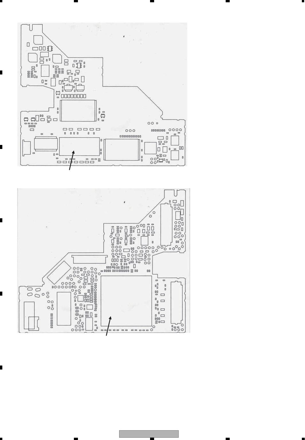
AVIC-D3/XU/UC
182
1234
1234
C
D
F
A
B
E
Side B
Check point 1 (IC1481)
Side A
Check point 2 (IC1501)
Fig 6.2: SDRAM I/F check point
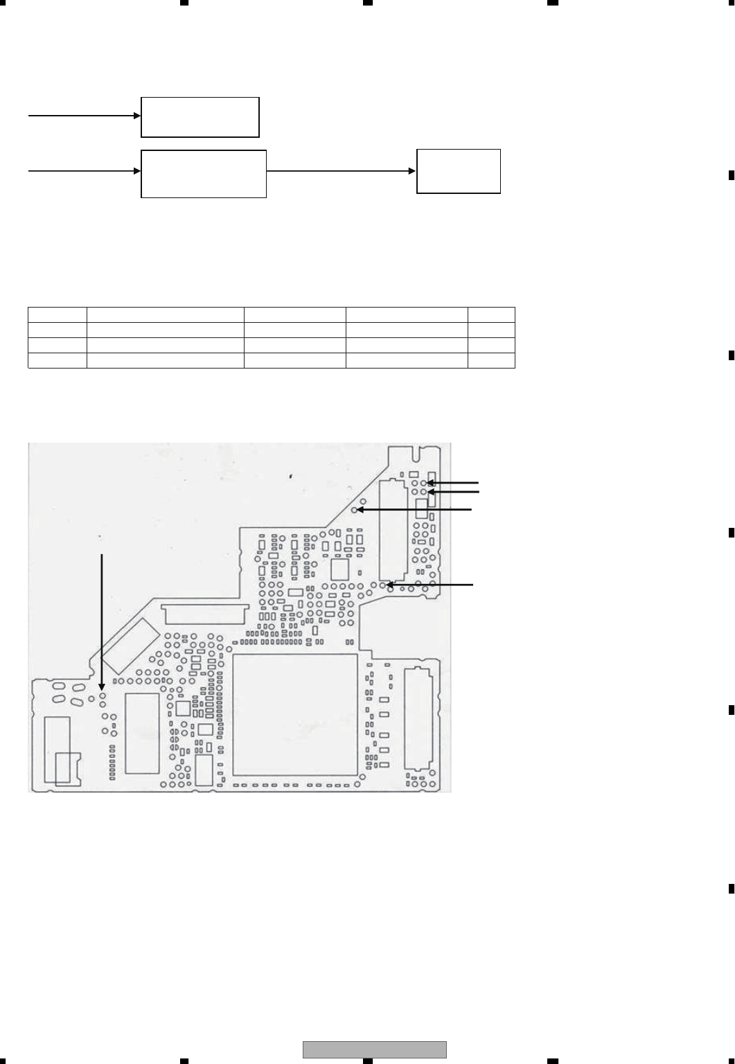
AVIC-D3/XU/UC 183
5678
56
78
C
D
F
A
B
E
Check 7: Is VD8, VCC5 power supply voltage OK?
VD8_1
VD VCC5 (= 5.0V )
Fig 7.1: Power supply configuration
F.E. driver system
DISC detection LED
Power supply
for PU
IC1004
REG IC
for VCC 5V.
NO. Check point Module No. Specification value Unit
1
2
3
VD8_1 - PGND3
VD - PGND3
VCC5_1- AGND1
ALL
ALL
ALL
8.0 ± 0.4
8.0 ± 0.4
5.0 ± 0.1
V
V
V
Side A
VD8_1
PGND3
VCC5_1
AGND1
VD
Fig 7.2: VD8, VCC5 voltage check points
<Check> Check the voltage at the "VD8_1, VD and VCC5_1" test point while the power is on.
Use the "PGND3 and AGND1" test point at the reference.
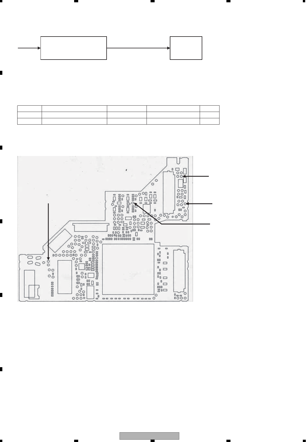
AVIC-D3/XU/UC
184
1234
1234
C
D
F
A
B
E
Check 8: Is AVCC5 voltage OK?
VD AVCC5 (= 5.0 V )
Fig 8.1: Power supply configuration
<Check> Playback DVD-REF-A1 TITLE 1 and check the voltage at the stylus.
Check with PGND and GNDAU being the reference.
NO. Check point
VD - PGND_3
AVCC5 - GNDAU1
IC1801
Audio-DAC
IC1005
REG IC
for AVCC 5 V.
Module No. Specification value Unit
1
2
ALL
ALL
8.0 ± 0.4
5.0 ± 0.1
V
V
Side A
Fig 8.2: VD8, AVCC5 voltage check points
GNDAU
AVCC5
VD
PGND3
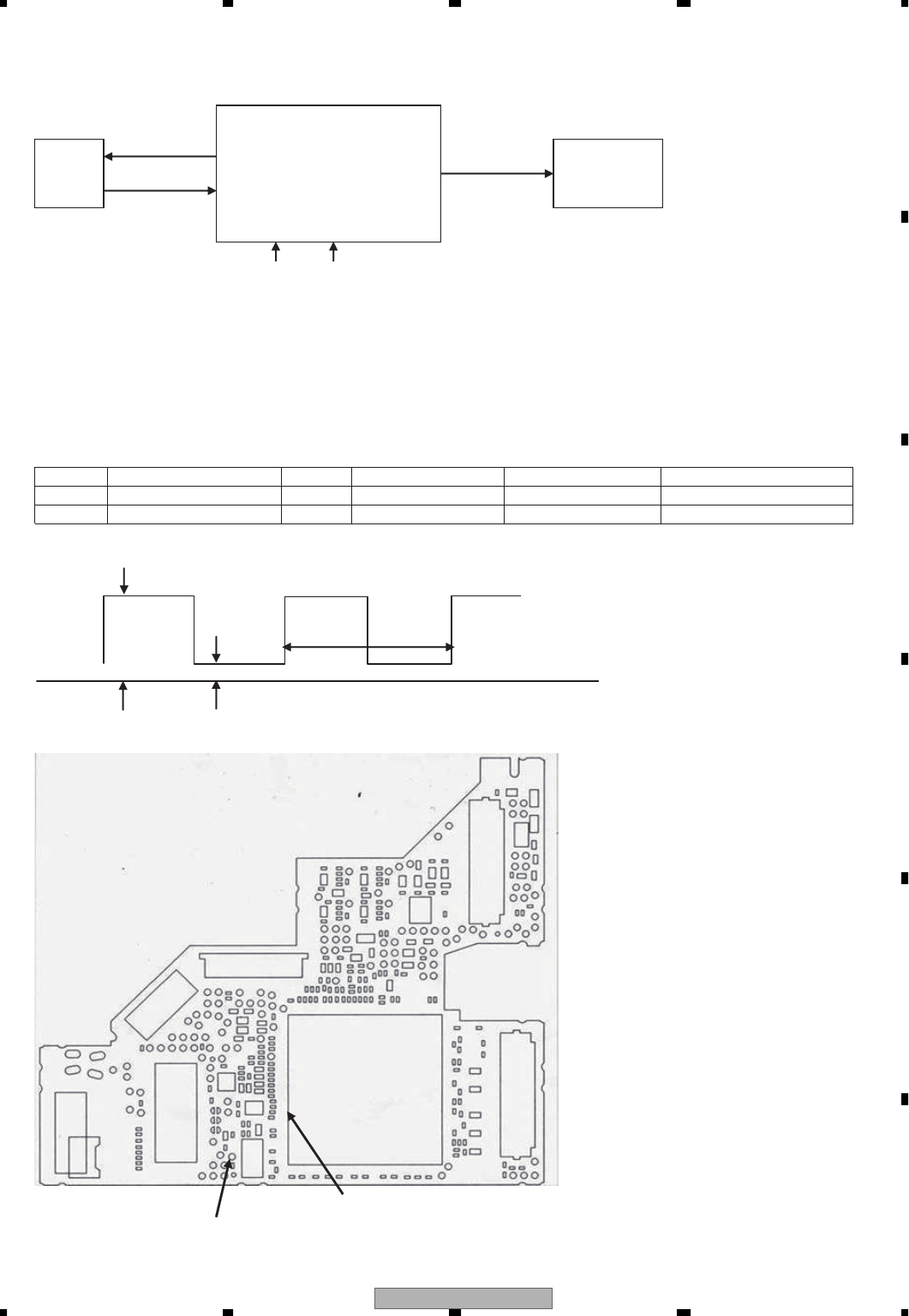
AVIC-D3/XU/UC 185
5678
56
78
C
D
F
A
B
E
Fig 9.1: Clock configuration
Check 9: Is DACCLK normal?
<Outline> DACCLK for Audio-DAC is created by IC1501 using the 27 MHz master crystal oscillator (X1501).
DACCLK
<Check method>
DVD: DVD-REF-A1 TITLE 1
CD: Playback a normal CDDA.
Common to all DVD-V compatible modules.
Check with DGND being the reference.
In case of NG, check the applicable line, the periphery of IC1501, soldering of the peripheral components and
defective components.
IC1501
DVD-LSIX1501
27 MHz
crystal
IC1801
Audio-DAC
VCC33 VCC12
GND
Fig 9.2: Clock specification value
Side A
Check point 2 (IC1501 172 pin)
Check point 1 (stylus)
Fig 9.3: 27 MHz, DACCLK check point
Specification
value 1
Specification
value 2
Specification
value 3
NO. Check point 1 (stylus) Media Specification value 1 Specification value 2 Specification value 3
1
2
DACCK
DACCK
DVD
CD
2.0 V~VCC33 V
2.0 V~VCC33 V
DGND~0.8 V
DGND~0.8 V
36.864 0 MHz ± 300 ppm
33.868 8 MHz ± 300 ppm
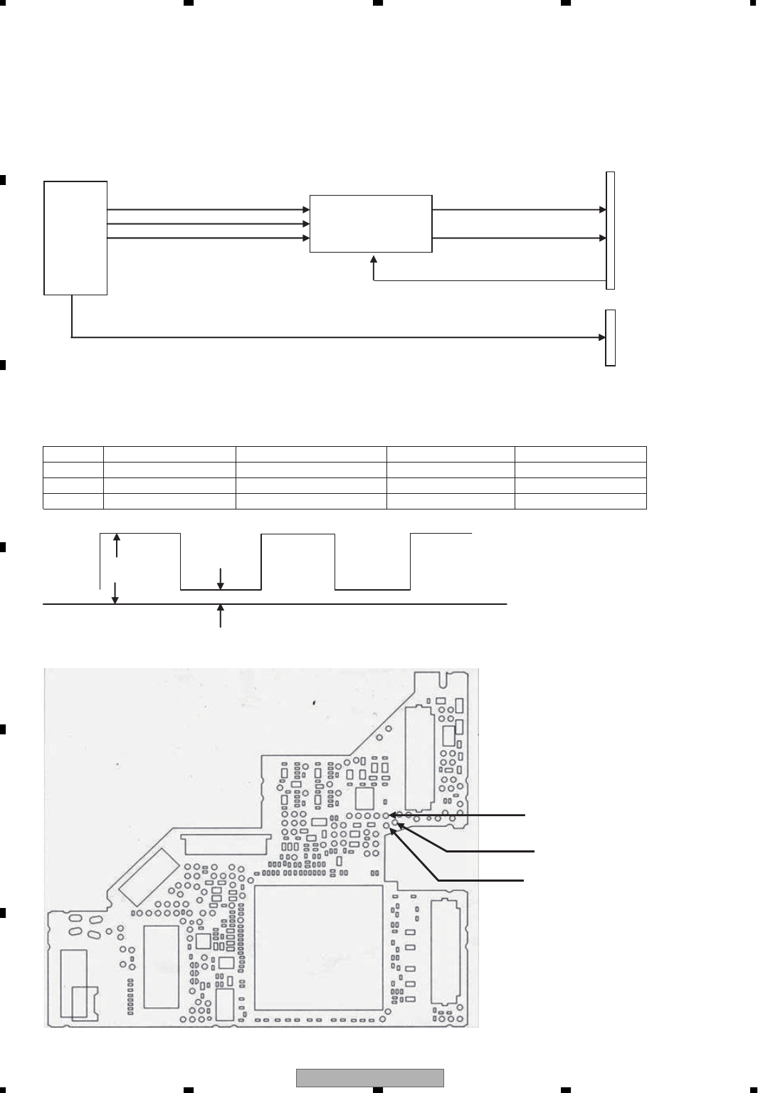
AVIC-D3/XU/UC
186
1234
1234
C
D
F
A
B
E
Check 10: Is the audio circuit OK?
<Outline> The serial 3 lines digital output + DACCLK, output from DVD-LSI (IC1501), are converted to analog audio
signal at Audio-DAC (IC1801) and are output from the HOST I/F (CN1901).
Simultaneously, the analog MUTE signal is also output from DVD-LSI (IC1501) via the HOST I/F.
The digital audio signal (IECOUT), output from DVD-LSI (IC1501), is output via CN1852.
CN1901
HOST I/F
LRCK LO
ADOUT3
SRCK RO
GNDAU
CN1852
IC1801
Audio-DAC
IC1501
DVD-LSI
IEC
Fig 10.1: Audio circuit
<Check method> Playback DVD-REF-A1 TITLE 2 CHAPTER 1 (48 k/16 bit 1 kHz 0 dB),
and check with DGND being the reference.
In case of NG, check the applicable line, periphery of major components as described in the above drawing,
soldering of the peripheral components and defective components.
NO. Check point 1 (stylus)
1
2
3
Specification value 1 Specification value 2 Reference waveform
ADOUT3
SRCK
LRCK
VCC33 V-0.6 V or higher
VCC33 V-0.6 V or higher
VCC33 V-0.6 V or higher
0.4 V or lower
0.4 V or lower
0.4 V or lower
Waveform 1
Waveform 2
Waveform 3
GND
Fig 10.2: Serial 3 lines specification value
Side A
Specification
value 1
Specification
value 2
Fig 10.3: Serial 3 lines check points
ADOUT3
SRCK
LRCK
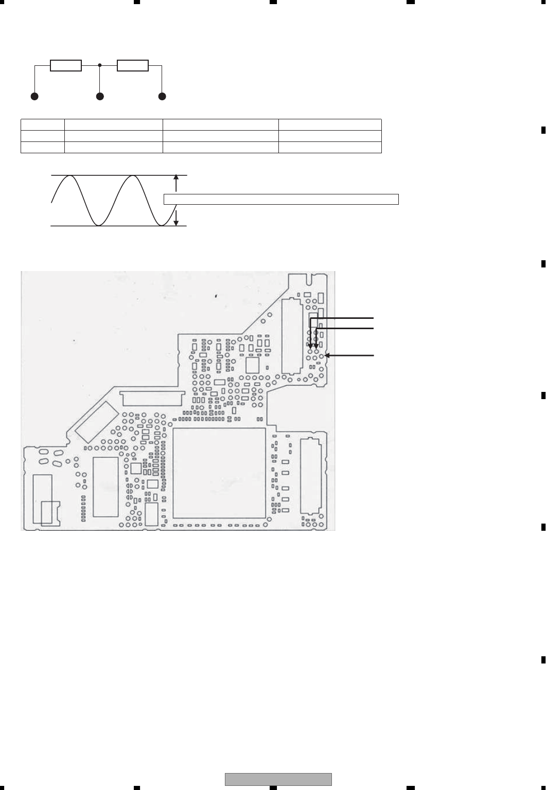
AVIC-D3/XU/UC 187
5678
56
78
C
D
F
A
B
E
The following checks shall be conducted using the following measurement circuits with GNDAU1 being the reference.
NO.
4
5
Fig 10.4: Analog audio out (LO, RO) specification value.
Side A
Fig 10.5: Analog audio out check point
Specification value is the root-mean-square value (rms).
LO
RO
GNDAU1
Check point 1 (stylus)
1 400 ± 150 mV
1 400 ± 150 mV
Specification value (rms) Reference waveform
Waveform 4
Waveform 4
LO
RO
LO GNDAU1 RO
47 kΩ47 kΩ
AVIC-D3/XU/UC
188
1234
1234
C
D
F
A
B
E
Check with DGND being the reference.
Check 2pin cord after connecting it to a jig, etc.
NO. Check point 1 (stylus) Specification value 1 Specification value 2 Reference waveform
6 IEC VCC33 V-0.6 V or higher 0.4 V or lower Waveform 5
Side A
Fig 10.6: Digital audio signal (IECOUT) check point
IEC
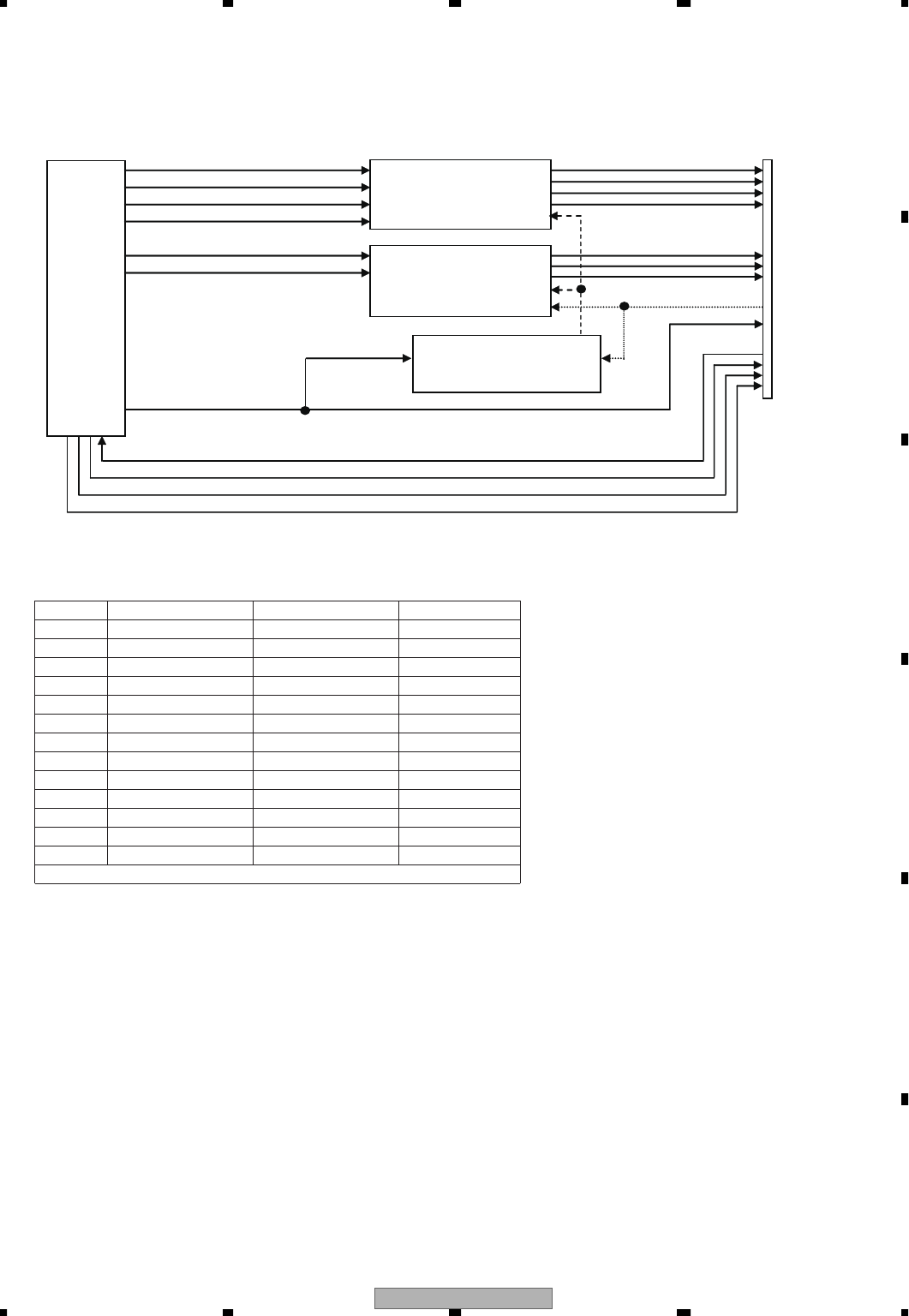
AVIC-D3/XU/UC 189
5678
56
78
C
D
F
A
B
E
IN IN
OUT
<Outline> At the time of 6ch digital out, the serial 6 lines output from DVD-LSI (IC1501) is output via CN1581.
Furthermore, at the time of ripping, the serial 3 lines digital output + SUBC, output from DVD-LSI (IC1501),
is output in 4 times speed via CN1851.
CN1851
ADOUT0/SUBC
ADOUT1/BLKCK
ADOUT2/CLDCK
SRCK
LRCK
DATA
MCKENA
RIPP
IC1501
LSI IC1851 buffer SW,
ripping or 6ch digital out.
IC1852 buffer SW,
ripping or 6ch digital out.
IC1853 buffer SW,
ripping or 6ch digital out.
SBCK
BMUTE
EMPH
IEC/IPFLG
The signal at CN1851 for 6ch digital out/Ripping.
Pin No. Pin name
2
4
6
8
10
12
14
16
18
20
21
22
23
SRCK
LRCK
AD0/SUBC
AD1/BLK
AD2/CLD
AD3/DATA
IEC/IPFLG
-
SBCK
BMUTE
MCKENA
RIPP
EMPH
Pins 1, 3, 5, 7, 9, 11, 13, 15, 17, 19 and 24 are GNDD.
Fig 10.7: 6ch digital out/Ripping circuit
6ch digital out Ripping
SRCK
LRCK
ADOUT0
ADOUT1
ADOUT2
ADOUT3
IEC
-
-
BMUTE
Low
High
EMPH
SRCK
LRCK
SUBC
BLKCK
CLDCK
DATA
IPFLG
-
SBCK
-
High
Low
EMPH
AVIC-D3/XU/UC
190
1234
1234
C
D
F
A
B
E
Playback DVD-REF-A1 TITLE22 CHAPTER 1, and check with GNDD being the reference.
In case of NG, check the applicable line, the periphery of the major components in the drawing above,
soldering of the peripheral components and defective components.
Check 24pin FFC after connecting it to a jig, etc.
NO. Check point 1 (stylus)
7
8
9
10
11
12
13
SRCK
LRCK
ADOUT0
ADOUT1
ADOUT2
IEC
MCKENA
Specification value 2
0.4 V or lower
0.4 V or lower
0.4 V or lower
0.4 V or lower
0.4 V or lower
0.4 V or lower
VCC33 V x 0.3 V or lower
0.4 V or lower
0.4 V or lower
0.4 V or lower
0.4 V or lower
0.4 V or lower
0.4 V or lower
0.4 V or lower
VCC33 V x 0.3 V or lower
Rip common CDDA, and check with GNDD being the reference.
In case of NG, check the applicable line, the periphery of the major components in the drawing above,
soldering of the peripheral components and defective components.
Check 24pin FFC after connecting it to a jig, etc.
NO. Check point 1 (stylus)
14
15
16
17
18
19
20
21
SRCK
LRCK
SUBC
BLKCK
CLDCK
DATA
SBCK
RIPP
Specification value 1 Specification value 2
VCC33 V-0.6 V or higher
VCC33 V-0.6 V or higher
VCC33 V-0.6 V or higher
VCC33 V-0.6 V or higher
VCC33 V-0.6 V or higher
VCC33 V-0.6 V or higher
VCC33 V-0.6 V or higher
-
Specification
value 1
GND Specification value 2
Fig 10.8: 6ch digital out/Ripping specification value
VCC33 V-0.6 V or higher
VCC33 V-0.6 V or higher
VCC33 V-0.6 V or higher
VCC33 V-0.6 V or higher
VCC33 V-0.6 V or higher
VCC33 V-0.6 V or higher
-
Specification value 1
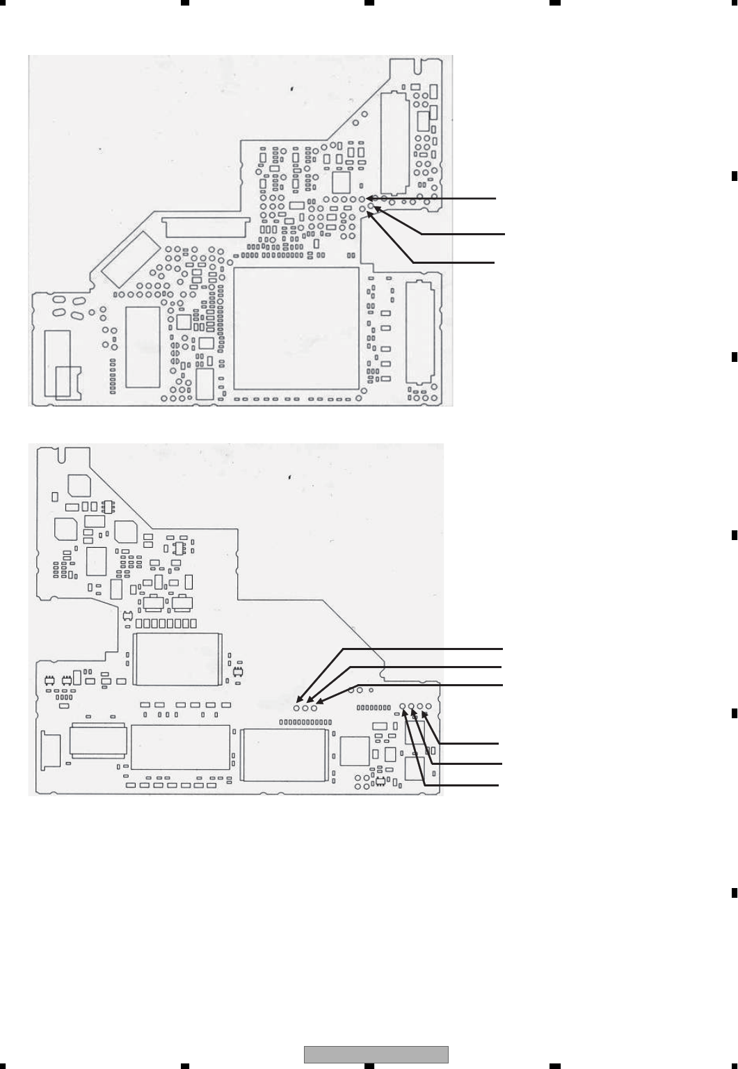
AVIC-D3/XU/UC 191
5678
56
78
C
D
F
A
B
E
Side A
Side B
Fig 10.9: 6ch digital out/Ripping check point
ADOUT3
SRCK
LRCK
ADOUT2
ADOUT1
ADOUT0
MCKENA
SBCK
RIPP
AVIC-D3/XU/UC
192
1234
1234
C
D
F
A
B
E
Check 11: Is the video circuit OK?
<Outline> Composite signal and component signal are output from DVD-LSI (IC1501), and are output from the
HOST I/F (CN1901) via a buffer circuit.
CN1901
HOST I/F
AVCC5
Composite
Component Y
Component Cb
Component Cr COMPO
Fig 11.1: Video circuit
<Checking method> Playback DVD-REF-A1 TITLE2 CHAPTER5 (WHITE 100%), and monitor COMPO signal with
an oscilloscope with GNDV1 (stylus) being the reference. Set the trigger mode to "TV trigger" and
the trigger line to "150 line".
Video buffer circuit
NoMount
IC1501
DVD_LSI
Video
DAC
section
NO.
Check point 1 (stylus)
Specification value Reference waveform
1 COMPO 1 000 mVpp ± 5 % Waveform 6
In case of NG, check the applicable line, the periphery of the major components in the drawing above, soldering of the
peripheral components and defective components. PEAK
COMPO signal Reference
value
Color burst
Pedestal level
BOTTOM
Horizontal sync signal
Fig 11.2: Waveform for the case of composite white 100% output
<Video level readjustment method>
In case the video composite output is outside of the specification value, readjust the level according to the method
described below.
Turn the volume (VR1671) to adjust the video level within the range of 1.0 ± 0.02 Vpp.
The adjustment specification is 1.0 ± 0.02 Vpp.
Adjust this level within the
range of 1.0 ± 0.02 Vpp.
AVCC5
Fig 11.3: Video circuit (component)
Q1702(NoMount)
Video buffer circuit
Q1701(NoMount)
Video buffer circuit
Q1704(NoMount)
Video buffer circuit
CN1901
HOST I/F
YY
Cb Cb
Cr Cr
IC1501
LSI
Video
DAC
section
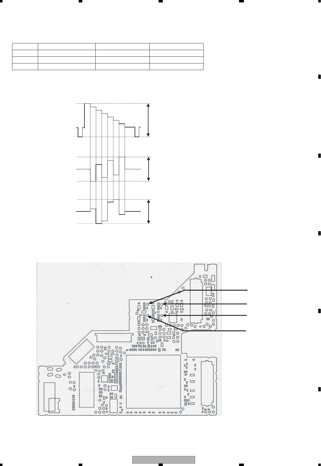
AVIC-D3/XU/UC 193
5678
56
78
C
D
F
A
B
E
<Checking method> Playback DVD-REF-A1 TITLE2 CHAPTER19 (100% Color Bars), and monitor Y, Cb, and Cr
signal with an oscilloscope with GNDV1 (stylus) being the reference. Set the trigger mode to
"TV trigger" and the trigger line to "150 line".
NO. Check point 1 (stylus) Specification value Reference waveform
1 000 mVpp ± 5%
700 mVpp ± 5%
700 mVpp ± 5%
Waveform 7
Waveform 7
Waveform 7
2
3
4
Y
Cb
Cr
In case of NG, check the applicable line, the periphery of the major components in the drawing above, soldering of
the peripheral components and defective components.
PEAK
Y signal Specification value
BOTTOM
PEAK
Cb signal Specification value
BOTTOM
PEAK
Cr signal Specification value
BOTTOM
100% Color Bars signal
Fig 11.4 Waveform for the case of component 100% Color Bars output
Side A
COMPO
Cr
Cb
Y
Fig 11.5: VIDEO signal check point

AVIC-D3/XU/UC
194
1234
1234
C
D
F
A
B
E
Check 12:How to judge whether the flash memory has reached its life or not.
If the reaction to user operation is slow or operation is slow in general, there is a possibility that the flash memory
has reached its life.
Make judgment regarding the flash memory life by looking at the display of the LD energizing time.
1.Let the LD energizing time displayed.
(Refer to the FE test mode for the method of displaying the LD energizing time.)
2.If the second digit from the left of the energizing time display is showing E,
such as " E ", it means that the flash memory has reached its life.
Example:
0E000BB8
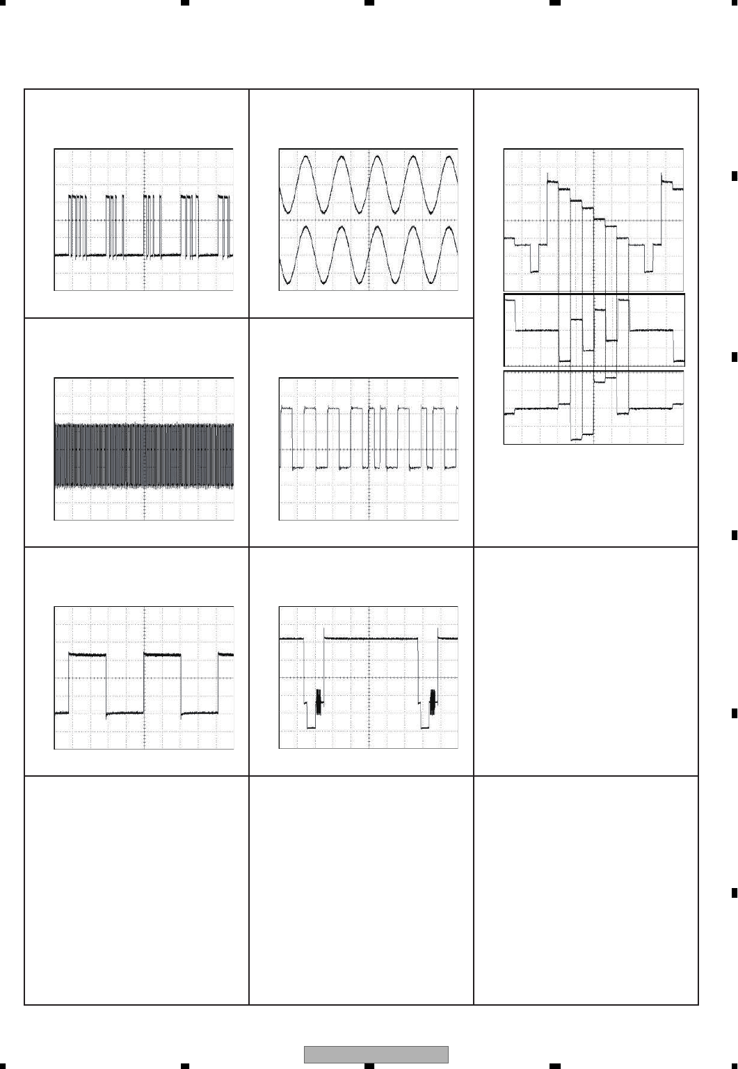
AVIC-D3/XU/UC 195
5678
56
78
C
D
F
A
B
E
CH1 LO
CH1 ADOUT3 CH2 RO
Reference voltage: DGND2 1 V/div. 5 µsec/div
Reference voltage: GNDAU2 1 V/div. 500 µsec/div
Waveform 1 Waveform 4
CH1 SRCK CH1 IECOUT
Reference voltage: DGND2 1 V/div. 5 µsec/div Reference voltage: DGND2 1 V/div. 500 nsec/div
Waveform 2 Waveform 5
CH1 LRCK
Reference voltage: DGND2 1 V/div. 5 µsec/div
Waveform 3
AUDIO VIDEO
G->
G->
G-> G->
G->
G->
CH1 COMPO
Reference voltage: GNDV1 200 mV/div. 10 µsec/div
Waveform 6
Waveform 7
[WHITE 100IRE]
[100% Color Bars]
CH1 Y
CH2 Cb
CH3 Cr
Reference voltage: GNDV1 200 mV/div. 5 µsec/div
:
:
:
:
:
:
::
::
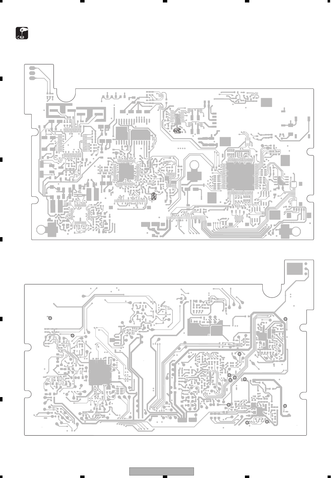
AVIC-D3/XU/UC
196
1234
1234
C
D
F
A
B
E
6.3 MONITOR UNIT ADJUSTMENT
FL1
FL2
COM
V5
V53
VM10
V15
V8
LCDG
LCDR
LCDB
HSY
VR5900
VR5101
- Adjustment point
MONITOR UNIT(SIDE A)
MONITOR UNIT(SIDE B)
AVIC-D3/XU/UC 197
5678
56
78
C
D
F
A
B
E
- Power supply check
Adjustment item Measuring
point Adjusting point Measuring method and specs. Remarks
1
5 V power supply verification
TP_V5 5.0 V ± 0.3 V DC
2
8 V power supply verification
TP_V8 8.0 V ± 0.5 V DC
3
5.3 V power supply verification
TP_V53 5.3 V ± 0.5 V DC
4
15 V power supply verification
TP_V15 15.0 V ± 0.7 V DC
5
-10 V power supply verification
TP_VM10 -10.0 V ± 0.8 V DC
Adjustment item Measuring
point Adjusting point Measuring method and specs. Remarks
6 PLL free run
adjustment
TP_HSY VR5101 f = 15.820 kHz to 15.830 kHz Set TP_SYNI to Low.
(Release it after PLL free run adjustment.)
[Effect of deviation from the adjusted value]
• No sync on the screen.
• Displayed position on the screen shifts
substantially to the left or to the right.
7 Register
temporary setting
IC5011 IC5011 register
8 COM AMP level
verification
TP_COM [Effect of deviation from the adjusted value]
• Dark screen (large amplitude)
• Bright screen (small amplitude)
7.7 V ± 0.4 V
- Image related adjustment
COM DC :
BRIGHT :
CONT-RGB1 :
RGB AMPLITUDE :
COM AMPLITUDE :
GAMMA 1 :
GAMMA 2 :
SUB-BRIGHT R :
SUB-BRIGHT B :
CONT-VIDEO :
COLOR :
PICTURE :
TINT :
PALTINT :
PHASE :
CONT-RGB2 :
INPUT MODE/SW :
84
128
255
255
188
255
255
128
128
221
100
16
141
150
42
221
00000000
(NTSC)
(PAL)
When you replaced EEPROM(IC5303), set
it after executing reset of EEPROM.
Procedure of reset
1. IC5300_pin20(EPRRST) is connected
with GND.
2. Power-on of the product.
3. Power-off of the product.
4. IC5300_pin20(EPRRST) is opened.
AVIC-D3/XU/UC
198
1234
1234
C
D
F
A
B
E
Adjustment item Measuring
point Adjusting point Measuring method and specs. Remarks
9 RGB AMP
adjustment
TP_LCDG IC5011 register
RGB AMPLITUDE
(10h)
10 STEP signal (RGB 525 lines / 60 Hz) input
3.80 V ± 0.02 V (clamp level ~ clamp level of the next line)
10 Bright adjustment TP_LCDG IC5011 register
BRIGHT (11h)
10 STEP signal (RGB 525 lines / 60 Hz) input
2.00 V ± 0.02 V (10% white ~ 10% white of the next line)
11 Gamma 1
adjustment
TP_LCDG IC5011 register
GAMMA 1 (08h)
10 STEP signal (RGB 525 lines / 60 Hz) input
2.00 V ± 0.02 V (clamp level ~ 30% white) If there are the black section and the white
30% section during 1 horizontal scanning,
it is OK even if it is not a 10 STEP signal.
[Effect of deviation from the adjusted value]
• The screen is whitish (high voltage)
• The screen is dark (low voltage)
4.9 (
µ
Sec)
4.9 (
µ
Sec)
: section is the clamp level period.
The signal inverting timing being the reference,
the following periods are indicated.
Forward rotation side…4.9 (µsec)
Backward rotation side…4.9 (µsec)
It is different from the black level during the image
display period.
[Effect of deviation from the adjusted value]
The side panel brightness at the time of screen
mode (normal) is affected.
• Floating white (small amplitude)
• Sinking black (large amplitude)
[Effect of deviation from the adjusted value]
• The screen is whitish (small amplitude)
• The screen is dark (large amplitude)
: section is the clamp level period.
AVIC-D3/XU/UC 199
5678
56
78
C
D
F
A
B
E
Adjustment item Measuring
point Adjusting point Measuring method and specs. Remarks
12 Gamma 2
adjustment
TP_LCDG IC5011 register
GAMMA 2 (09h)
10 STEP signal (RGB 525 lines / 60 Hz) input
4.00 V ± 0.03 V (clamp level ~ 100% white) If there are the black section and the white
100% section during 1 horizontal scanning,
it is OK even if it is not a 10 STEP signal.
[Effect of deviation from the adjusted value]
• The bright section is scattered white
(high voltage)
• The screen is dark (low voltage)
13 Register setting IC5011 IC5011 register CONT-RGB1(06h) : DDh ····· *1 *1 : A value set to IC5011 when the user
contrast adjustment step is 00.
14 Sub bright R
adjustment
TP_LCDG
TP_LCDR
IC5011 register
SUB-BRIGHT R
(12h)
10 STEP signal (RGB 525 lines / 60 Hz) input
Adjust SUB-BRIGHT R in a way that the difference of the
following two will be within ± 0.02 V.
• The clamp level to 90% white level of TP_LCDG.
• The clamp level to 90% white level of TP_LCDR.
If there are the clamp level and the white
90% section during 1 horizontal scanning,
it is OK even if it is not a 10 STEP signal.
[Effect of deviation from the adjusted value]
• The screen is reddish
(high voltage on the LCDR side)
• The screen is bluish
(low voltage on the LCDR side)
: section is the clamp level period.
AVIC-D3/XU/UC
200
1234
1234
C
D
F
A
B
E
Adjustment item Measuring
point Adjusting point Measuring method and specs. Remarks
15 Sub-bright B
adjustment
TP_LCDG
TP_LCDB
IC5011 register
SUB-BRIGHT B
(13h)
10 STEP signal (RGB 525 lines / 60 Hz) input
Adjust SUB-BRIGHT B in a way that the difference of the
following two will be within ± 0.02 V.
• The clamp level to 90% white level of TP_LCDG.
• The clamp level to 90% white level of TP_LCDB.
If there are the clamp level and the white
90% section during 1 horizontal scanning,
it is OK even if it is not a 10 STEP signal.
[Effect of deviation from the adjusted value]
• The screen is bluish
(high voltage on the LCDR side)
• The screen is yellowish
(low voltage on the LCDR side)
16
PAL demodulation
adjustment
(COLOR preliminary
adjustment)
TP_LCDR IC5011 register
COLOR (02h)
100% color bar signal (PAL) input
Execute step 1 “Method of color adjustment (RB5P0090M)”
after entering “PHASE ADJUSTMENT”.
AVIC-D3/XU/EW5 only
100% color bar signal…
A color bar of which the brightness level of the
white section is 100% and the color carrier
amplitude is 100% modulation.
(EIA color bar, BBC color bar)
An adjustment with the rise up edge of the FRPV
signal being the trigger is recommended.
The result of color adjustment is not saved in the
EEPROM.
[Effect of deviation from the adjusted value]
PALTINT and PHASE adjustment can no longer
be made appropriately.
17 PAL demodulation
adjustment
(PALTINT)
TP_LCDR IC5011 register
TINT (03h)
100% color bar signal (PAL) input
Execute step 2 “Method of color adjustment (RB5P0090M)”
after entering “PHASE ADJUSTMENT”.
AVIC-D3/XU/EW5
only
An adjustment with the rise up edge of the
FRPV signal being the trigger is
recommended.
[Effect of deviation from the adjusted value]
Color flickering or horizontal stripes are
observed during PAL image display.
AVIC-D3/XU/UC 201
5678
56
78
C
D
F
A
B
E
Adjustment item Measuring
point Adjusting point Measuring method and specs. Remarks
18 PAL demodulation
adjustment
(PHASE)
TP_LCDB IC5011 register
PHASE (04h)
100% color bar signal (PAL) input
Execute step 3 “Method of color adjustment (RB5P0090M)”
after entering “PHASE ADJUSTMENT”.
AVIC-D3/XU/EW5 only
An adjustment with the rise up edge of the
FRPV signal being the trigger is
recommended.
[Effect of deviation from the adjusted value]
Color flickering or horizontal stripes are
observed during PAL image display.
*) Because step signal of the test disc (GGV1303) is interval in each step is not even, use the step which is near to the designated level referring to "Step signal level table".
10 step
32
step
White level
(%)
10 31 100.0%
30 96.9%
29 93.8%
9 28 90.6%
27 87.5%
26 84.4%
8 25 81.3%
24 78.1%
23 75.0%
7 22 71.9%
21 68.8%
20 65.7%
6 19 62.5%
18 59.4%
17 56.3%
5 16 53.2%
15 50.1%
14 46.9%
4 13 43.8%
12 40.7%
11 37.6%
3 10 34.4%
9 31.3%
8 28.2%
2 7 25.1%
6 22.0%
5 18.8%
1 4 15.7%
3 12.2%
29.2%
1 6.2%
00
0.0%
Step signal level table
AVIC-D3/XU/UC
202
1234
1234
C
D
F
A
B
E
Adjustment item Measuring
point Adjusting point Measuring method and specs. Remarks
22 Aging Input the entire screen white signal (or the moving image).
Leave the equipment in the operational state for 30 minutes or
more.
23 Flicker adjustment Screen IC5011 register
COM DC (15h)
Input a signal for flicker adjustment (RGB 525 line / 60 Hz).
Make adjustment in a way that the screen flickering will become
minimum.
A signal for flicker adjustment…
An image where white 50% and black is
displayed alternately for each horizontal
scanning line.
- Flicker adjustment
Adjustment item Measuring
point Adjusting point Measuring method and specs. Remarks
19 Backlight inverter
basic driving
frequency
adjustment
TP_FL1
TP_FL2
VR5900 Set to IC5300 pin44 (INVPUL) = Low. Connect a cold cathode tube equivalent to
CWX3454-A between TP_FL1 and FL2.
Measure at the waveform of TP_FL1 output
after the voltage division or at TP_FL2.
Do not measure TP_FL1 directly.
(The measuring equipment may be damaged
due to high voltage.)
20 Backlight inverter
frequency
switching check 1
TP_FL1
TP_FL2
Set to IC5300 pin44 (INVPUL) = High impedance.
Input the following waveform of 98.0 kHz ± 1.0 kHz to TP_INVPUL.
The output frequency of TP_FL1/FL2 shall be 49.0 kHz ± 0.5 kHz.
Connect a cold cathode tube equivalent to
CWX3454-A between TP_FL1 and FL2.
Measure at the waveform of TP_FL1 output
after the voltage division or at TP_FL2.
Do not measure TP_FL1 directly.
(The measuring equipment may be damaged
due to high voltage.)
10% ± 2%
21 Backlight inverter
frequency
switching check 2
TP_FL1
TP_FL2
Set to IC5300 pin44 (INVPUL) = High impedance.
Input the following waveform of 104.0 kH ± 1.0 kHz to TP_INVPUL.
The output frequency of TP_FL1/FL2 shall be 52.0 kHz ± 0.5 kHz.
Connect a cold cathode tube equivalent to
CWX3454-A between TP_FL1 and FL2.
Measure at the waveform of TP_FL1 output
after the voltage division or at TP_FL2.
Do not measure TP_FL1 directly.
(The measuring equipment may be damaged
due to high voltage.)
5 V
0 V
10% ± 2% 5 V
0 V
- Inverter adjustment
Please refer to the "6.4 SERVICE ADJUSTMENT".
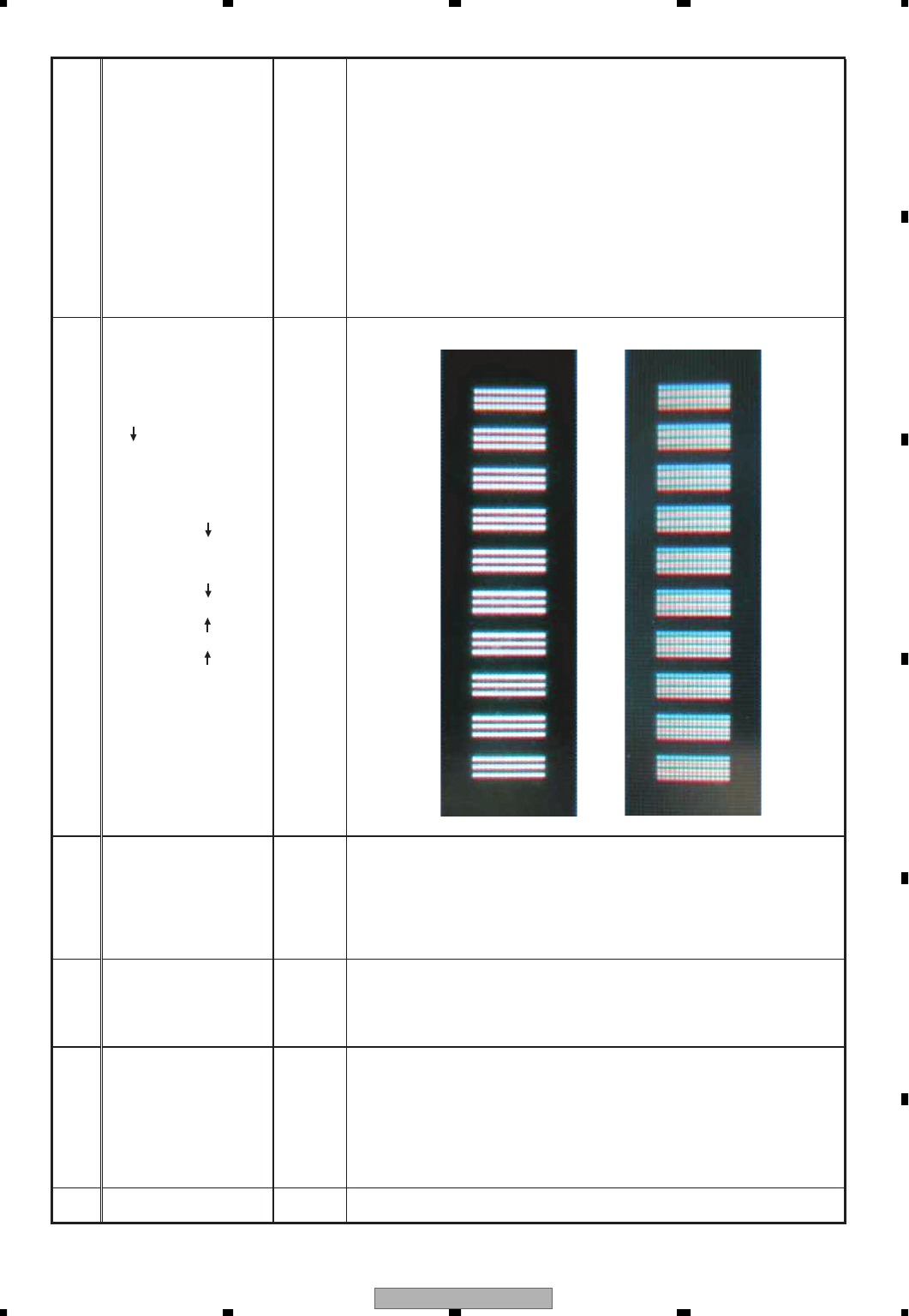
AVIC-D3/XU/UC 203
5678
56
78
C
D
F
A
B
E
26 Dot clock
adjustment
Test
pattern on
the screen
Touch key [-],
[+], STEP 0~7.
• In case of vertical stripe display
The vertical stripes of the test pattern shall be displayed clearly without
rolling.
OK
NG
Pressing "Back" or "ESC" key, setting value is stored in EEPROM.
Then turn off the unit.
Adjustment item Measuring
point Adjusting point Measuring method and specs. Remarks
24 Calling out of line
adjustment mode
Make the following operation.
1) Reset while pushing the two buttons, [SOURCE] and [ ].
(BUP and ACC on while pushing the buttons will also do.)
2) Release the key when “PLEASE PUSH THE [RESET]” is displayed on
the screen.
3) Push in the order of [ ], [ ], [ ] and [ ].
4) Make sure that “PLEASE PUSH THE [RESET]” goes away.
If “PLEASE PUSH THE [RESET]” is not
displayed in 2), it means a failure of
succession. So, repeat from 1).
If “PLEASE PUSH THE [RESET]” did
not go away in 4), it means a failure of
succession. So, repeat from 1).
25 Calling out of
Dot clock
adjustment mode
Enter the Initial setting menu, and call out the (Dot clock) adjustment
screen.
Succession is not possible in the
state of parking off.
- Dot clock adjustment
AVIC-D3/XU/UC
204
1234
1234
C
D
F
A
B
E
- Color adjustment method (RB5P0090M) (for PAL mode)
Step 1 (Fig.1)
1. Input the EIA color bar signal.
2. Monitor the ROUT terminal using an oscilloscope.
3. Adjust the COLOR register value in a way that the average
level of white, yellow, magenta and red will be almost the same.
Step 2 (Fig.2)
4. Adjust the TINT register value in a way that the level being
shifted for each horizontal period will match.
Step 3 (Fig.3)
5. Next, monitor the BOUT terminal.
6. Adjust the PHASE register value in a way that the shifting of
cyan, green and magenta region for each horizontal period
will match.
Reference value after adjustment
COLOR : 90
TINT : 152
PHASE : 40
: The points easier to be used for adjustment
ROUT...TP_LCDR
BOUT...TP_LCDB
*) Because the result of adjustment will vary depending on the product, the value will not necessarily be close to
the “Reference value after adjustment”.
Fig. 1
Fig.2
Fig.3
The level differs for each horizontal period.
Match Adjust
The level differs for each horizontal period.
Match Adjust
ROUT
ROUT
BOUT
White
Yellow
Cyan
Green
Magenta
Red
Blue
Black
AVIC-D3/XU/UC 205
5678
56
78
C
D
F
A
B
E
6.4 SERVICE ADJUSTMENT
[Operational specifications]
• After replacing the LCD Module or Monitor Unit, this "SERVICE ADJUSTMENT" must be performed.
• Method1
If the monitor microcomputer is reset by double pressing of the SOURCE key + the [|<<] key, the following screen will
be displayed on the OSD.
At this time, if the keys are pressed in the order of MENU |<< >>| MAP, the system will proceed to
the [Adjustment mode for service].
• Method2
If the monitor microcomputer is reset with the [SRVTEST] terminal set to Low, the system will proceed to
the [Adjustment mode for service].
(You can get the same result by resetting, but it is not recommended as you will lose the user data.)
*) When the succession is made by the terminal, the OSD display screen below will not be displayed.
• The key operations under this test mode are as follows.
(1): Main body key
(2): Remote controller key (CXC6317 SW1 : AVH, SW2 : AVH)
• A method to cancel [Adjustment mode for service] is described below.
ACC OFF ON. (BUP OFF ON will do too.)
*) The preset value is first written in the EEPROM, then read out and displayed.
Writing and reading are made in 16 bits. Depending on the setting item, the number of bit may be different.
031
0
P L E A S E P U S H T HE [ R E S E T ]
8
Key Operation Remarks
|<<
Adjustment value DOWN on the selected item
>>|
Adjustment value UP on the selected item
Key Operation Remarks
Adjustment value UP on the selected item
Adjustment value DOWN on the selected item
AVIC-D3/XU/UC
206
1234
1234
C
D
F
A
B
E
- Adjustment mode for service
[Picture source preparation]
After entering "Adjustment mode", insert TEST DISC (GGV1303) to the unit and select "11. Horizontal Line1"
in the "19. Picture check MENU 2/2".
The specifications of the item adjusted on this page are as follows.
The actual image of the OSD display screen is as follows.
*) The above characters are displayed in black with white rim.
*) " " mark indicates the selected item (cursor).
*) There is no CS (check sum) display.
Note 1: The content of [FACTORY] is the default setting value for adjustment for each product adjusted in the line.
(Rewriting can be done in EEPROM adjustment mode only.)
Common inverted output center value
[ 0 to 255 ] COM DC 84
Common inverted output center
setting value (FACTORY preset value)
[ 0 to 255 ] FACTORY 84
01234567891011
12 13 14 15 16 17 18 19 20 21 22 23 24 25 26 27 28 29 30 31
0S E R VICE MODE
1
2COMDC 84
3[FACTORY]84
4
5
6
7
8
Adjustment item Adjustment range Adjustable name
Settings or written
data (DEC)
AVIC-D3/XU/UC 207
5678
56
78
C
D
F
A
B
E
6.5 EEPROM ADJUSTMENT
[Operational specifications]
• Method1
If the monitor microcomputer is reset by double pressing of the SOURCE key + the [|<<] key, the following screen will
be displayed on the OSD.
At this time, if the keys are pressed in the order of |<< MENU >>| MAP, the system will proceed to
the [Flicker adjustment mode].
• Method2
If the monitor microcomputer is reset while the [EPRTEST] terminal is set to Low, the system will proceed
to [Flicker adjustment mode].
(You can get the same result by resetting, but it is not recommended as you will lose the user data.)
*) When the succession is made by the terminal, the OSD display screen below will not be displayed.
• The key operations under this test mode are as follows.
(1): Main body key
(2): Remote controller key (CXC6317 SW1 : AVH, SW2 : AVH)
• A method to cancel [E2PROM adjust mode] is described below.
ACC OFF ON. (BUP OFF ON will do too.)
*) The preset value is first written in the EEPROM, then read out and displayed.
Writing and reading are made in 16 bits. Depending on the setting item, the number of bit may be different.
*) When a value subject to CS (check sum) computation is changed, it takes the exclusive (XOR) in 8 bit,
and conducts writing.
This CS value, too, is read out after being written into the EEPROM, and that read out value is displayed.
Key Operation Remarks
SOURCE Page turning
The screen succeeds in the order of [Flicker adjustment mode] [Line adjustment mode1]
[Line adjustment mode2] [Flicker adjustment mode].
MENU
Upward search of selection item
If pressed when the cursor is pointing the top item in a page, the cursor will move to the lowest item.
MAP
Downward search of selection item
If pressed when the cursor is pointing the lowest item in a page, the cursor will move to the top item.
|<<
Adjustment value DOWN on the selected item
>>|
Adjustment value UP on the selected item
Key Operation Remarks
MENU Page turning
The screen succeeds in the order of [Flicker adjustment mode] [Line adjustment mode1]
[Line adjustment mode2] [Flicker adjustment mode].
Downward search of selection item
If pressed when the cursor is pointing the lowest item in a page, the cursor will move to the top item.
Upward search of selection item
If pressed when the cursor is pointing the top item in a page, the cursor will move to the lowest item.
Adjustment value UP on the selected item
Adjustment value DOWN on the selected item
031
0
P L E A S E P U S H T HE [ R E S E T ]
8
AVIC-D3/XU/UC
208
1234
1234
C
D
F
A
B
E
- Flicker adjustment mode
The specifications of the item adjusted on this page are as follows.
The actual image of the OSD display screen is as follows.
*) The above characters are displayed in black with white rim.
*) " " mark indicates the selected item (cursor).
• Note 1: The content of [COM DC] is also reflected to the common inverted output center reference
value (Refer to 07-2: EEPROM memory arrangement.xls.).
(The common inverted output center reference value is treated as the initial value set in the line.)
Adjustment item Adjustment range Adjustable name
Settings or written
data (DEC)
Common inverted output center value
[ 0 to 255 ] *
COM DC 84
“*” is indicated if a value is
adjusted regardless of the
magnitude.
012345678910111213141516171819202122232425262728293031
0
1
2
3
4
5
6FL I CKER
7
8COMDC 84
- Line 1 adjustment mode
The specifications of the item adjusted on this page are as follows.
The actual image of the OSD display screen is as follows.
Bright [ 0 to 255 ] BRIGHT 62
RGB1 contrast [ 0 to 255 ] CONT-RGB1 168
Black amplitude [ 0 to 255 ] RGB AMP AJ 232
Output amplitude [ 0 to 255 ] COM AMP AJ 150
GAMMA 1 [ 0 to 255 ] GAMMA 1 157
GAMMA 2 [ 0 to 255 ] GAMMA 2 116
Sub brightness R [ 0 to 255 ] SUB BRI R 128
Sub brightness B [ 0 to 255 ] SUB BRI B 128
012345678910 11 12 13 14 15 16 17 18 19 20 21 22 23 24 25 26 27 28 29 30 31
0BRI GHT6
2
1CONT - RGB1 1 6 8 NOT EEPROM
2RGB AMP AJ 2 3 2
3COM AMPAJ150N
OTEEP
ROM
4GAMMA 115
7
5GAMMA2116
6SUB BR I R 128
7SUB BRI B 128
8CS FFFF
Adjustment item Adjustment range Adjustable name
Settings or written
data (DEC)
AVIC-D3/XU/UC 209
5678
56
78
C
D
F
A
B
E
*) The above characters are displayed in black with white rim.
*) " " mark indicates the selected item (cursor).
*) CS: Check Sum
• Note 1: The content of [CONT-RGB1] and [COM AMP AJ] are the reference value (adjustable) for adjusting
other items, and they are not saved in the EEPROM.
(It is so expressed by displaying “NOT EEPROM” as shown in the above OSD display screen image.)
- Line 2 adjustment mode
The specifications of the item adjusted on this page are as follows.
The actual image of the OSD display screen is as follows.
(1) When a mode other than the “operational mode” is selected.
(2) When the “operational mode” is selected.
*) The above characters are displayed in black with white rim.
*) " " mark indicates the selected item (cursor).
*) CS: Check Sum
• Note 1: The content of the following items are the reference value (adjustable) for adjusting other items, and they are
not saved in the EEPROM.
(It is so expressed by displaying “NOT EEPROM” as shown in the above OSD display screen image.)
· CONT-VIDEO
· COLOR
· TINT
VIDEO contrast [ 0 to 255 ] CONT-VIDEO 150
VIDEO color density [ 0 to 255 ] COLOR 168
VIDEO coloring (NTSC) [ 0 to 255 ] TINT 100
VIDEO coloring (PAL) [ 0 to 255 ] PALTINT 150
VIDEO sharpness [ 0 to 31 ] PICTURE 16
VIDEO PAL demodulation [ 0 to 63 ] PHASE 42
OSD contrast [ 0 to 255 ] CONT-RGB2 221
Operational mode Note 2 INPUT MODE 00000000
01234567 8 91011121314 15 16 17 18 19 20 21 22 23 24 25 26 27 28 29 30 31
0CONT - VIDEO 150 NOT EEPROM
1COLOR 168 NOT EEPROM
2TINT 100 NOT EEPRO
O
M
3PALTINT 150
4PICTURE 16
5PHASE 42
6CONT - RGB2 2 2 1
7INPUT MODE 00000000
8CS FFFF
012345678 9 10 11 12 13 14 15 16 17 18 19 20 21 22 23 24 25 26 27 28 29 30 31
0CONT - VID
EO 150 N
OTEEPROM
1COLOR168NOTEEPROM
2TINT 100 N
OT EEPROM
3PALT INT 150
4PICTURE
5PHASE
6CONT - RGB2
7INPUT MODE
8CS FFFF
Adjustment item Adjustment range Adjustable name
Settings or written
data (DEC)
16
42
221
00000000
AVIC-D3/XU/UC
210
1234
1234
C
D
F
A
B
E
• Note 2: Adjustment of the operational mode
The precautions for adjustment of the operational mode are as follows.
· Indicated in binary notation, and adjustable by bit only. (no carrying)
· Not subject to CS computation.
While the basic operation is as described in the operational specifications sheet, the cursor movement is made
according to the operation/succession shown below.
(The following descriptions are for the cases when the main body keys are operated.)
6CONT - RGB2 1 0 0
7INPUT MODE 11111111
8
7INP
UT MODE1
1111111
8
7INPUT MODE 11111111
8
7INP
UT MODE 11111111
8
1CONT - VID
EO 150 NOT EEPROM
MAP key MENU key
MAP key MENU key
MAP key MENU key
MAP key MENU key
MAP key MENU key
AVIC-D3/XU/UC 211
5678
56
78
C
D
F
A
B
E
Touch panel outermost circumference adjustment result
(0x00)
Calibration adjustment result
(0x00)
Line touch panel confirmation result
(0x00)
COM DC (Factory value)
(0x01)
EEPROM memory alignment chart (S-93C46BD0I-J8)
ADDRESS
Bit15 Bit14 Bit13 Bit12 Bit11 Bit10 Bit9 Bit8 Bit7 Bit6 Bit5 Bit4 Bit3 Bit2 Bit1 Bit0
0COM DC
(0x54) PICTURE
(0x54)
1Don't care
(0x00) GAMMA 1
(0x9D)
2
3
4
5
6
7
8
Adjustment
value of LCD
9
A
B
C
D
E
F
10
15
16
17
18
19
1A
1B
1C
1D
1E
1F
20
21
22
23
24
Outermost circumference X max
(0xF7)
Touch panel X coordinate 1
(0x00)
Outermost circumference Y min
(0x33)
Outermost circumference Y max
(0xEE)
Outermost circumference X min
(0x2A)
25
26
27
28
29
2A
2B
2C
2D
2E
GAMMA 2
(0x74)
SUB BRIGHT R
(0x80)
BRIGHT
(0x3E)
Checksum (LCD)
- Memory item list and EEPROM
Adjustment
value of
Touch panel
(USER)
Adjustment
value of
Touch panel
11
12
13
14
RGB AMPLITUDE
(0xE8)
SUB BRIGHT B
(0x80)
CONT RGB 2
(0xDD)
PALTINT
(0x96)
Don't care
(0x00)
*1
(0x00)
PHASE
(0x2A)
*3
(0x00)
*2
(0x00)
Checksum (Touch panel)
Touch panel X coordinate 2
(0x00)
Touch panel X coordinate 3
(0xFF)
Touch panel X coordinate 4
(0x00)
Touch panel X coordinate 5
(0x01)
Touch panel X coordinate 6
(0x01)
Touch panel X coordinate 7
(0x01)
Touch panel X coordinate 8
(0x01)
Touch panel X coordinate 9
(0x01)
Touch panel X coordinate 10
(0x01)
Touch panel X coordinate 11
(0x01)
Touch panel X coordinate 12
(0x01)
Touch panel X coordinate 13
(0x02)
Touch panel X coordinate 14
(0x02)
Touch panel X coordinate 15
(0x02)
Touch panel X coordinate 16
(0x02)
Touch panel Y coordinate 1
(0x04)
Touch panel Y coordinate 2
(0x02)
Touch panel Y coordinate 3
(0x01)
Touch panel Y coordinate 4
(0xFF)
Touch panel Y coordinate 5
(0xFD)
Touch panel Y coordinate 6
(0x00)
Touch panel Y coordinate 7
(0x01)
Touch panel Y coordinate 8
(0x04)
Touch panel Y coordinate 9
(0x05)
Touch panel Y coordinate 10
(0x02)
Touch panel Y coordinate 11
(0x00)
Touch panel Y coordinate 12
(0xFD)
Touch panel Y coordinate 13
(0xFD)
Touch panel Y coordinate 14
(0x00)
Touch panel Y coordinate 15
(0x01)
Touch panel Y coordinate 16
(0x04)
INPUT MODE (LCD IC)
(0x00)
Touch panel outermost circumference adjustment result [USER]
(0x00)
Calibration adjustment result [USER]
(0x00)
Outermost circumference X max [USER]
(0x00)
Touch panel X coordinate 1 [USER]
(0x00)
Outermost circumference Y min [USER]
(0x00)
Outermost circumference Y max [USER]
(0x00)
Outermost circumference X min [USER]
(0x00)
Touch panel X coordinate 2 [USER]
(0x00)
Touch panel X coordinate 3 [USER]
(0x00)
Touch panel X coordinate 4 [USER]
(0x00)
Touch panel X coordinate 5 [USER]
(0x00)
Touch panel X coordinate 6 [USER]
(0x00)
Touch panel X coordinate 7 [USER]
(0x00)
Touch panel X coordinate 8 [USER]
(0x00)
Touch panel X coordinate 9 [USER]
(0x00)
Touch panel X coordinate 10 [USER]
(0x00)
Touch panel X coordinate 11 [USER]
(0x00)
Touch panel X coordinate 12 [USER]
(0x00)
Touch panel X coordinate 13 [USER]
(0x00)
Touch panel X coordinate 14 [USER]
(0x00)
Touch panel X coordinate 15 [USER]
(0x00)
Touch panel X coordinate 16 [USER]
(0x00)
Touch panel Y coordinate 1 [USER]
(0x00)
Touch panel Y coordinate 2 [USER]
(0x00)
Touch panel Y coordinate 3 [USER]
(0x00)
Touch panel Y coordinate 4 [USER]
(0x00)
Touch panel Y coordinate 5 [USER]
(0x00)
Touch panel Y coordinate 6 [USER]
(0x00)
Touch panel Y coordinate 7 [USER]
(0x00)
Touch panel Y coordinate 8 [USER]
(0x00)
Touch panel Y coordinate 9 [USER]
(0x00)
Touch panel Y coordinate 10 [USER]
(0x00)
Touch panel Y coordinate 11 [USER]
(0x00)
Touch panel Y coordinate 12 [USER]
(0x00)
Touch panel Y coordinate 13 [USER]
(0x00)
Touch panel Y coordinate 14 [USER]
(0x00)
Touch panel Y coordinate 15 [USER]
(0x00)
Touch panel Y coordinate 16 [USER]
(0x00)
AVIC-D3/XU/UC
212
1234
1234
C
D
F
A
B
E
RGB preset
Adjustment
of DOTCLK
ADDRESS
Bit15 Bit14 Bit13 Bit12 Bit11 Bit10 Bit9 Bit8 Bit7 Bit6 Bit5 Bit4 Bit3 Bit2 Bit1 Bit0
2F
30
31
32
33
34
35
36
37
38
39
3A
3B
3C
3D
3E
3F
RGB user
preset
ACT
1
ACT
1
ACT
1
ACT
1
ACT
1
ACT
1
ACT
1
ACT
1
ACT
1
ACT
1
ACT
1
ACT
0
ACT
0
ACT
0
ACT
0
RED
11111
GREEN
00000
BLUE
00000
RED
00000
GREEN
11111
BLUE
00000
RED
00000
GREEN
00000
BLUE
11111
RED
11101
GREEN
11101
BLUE
11111
RED
00110
GREEN
11100
BLUE
00100
RED
00100
GREEN
11111
BLUE
00010
RED
00110
GREEN
00110
BLUE
11111
RED
00000
GREEN
00010
BLUE
11111
RED
11111
GREEN
11110
BLUE
00000
RED
11111
GREEN
00100
BLUE
00000
RED
11111
GREEN
00001
BLUE
00000
RED
11111
GREEN
11111
BLUE
11111
RED
11111
GREEN
11111
BLUE
11111
RED
11111
GREEN
11111
BLUE
11111
RED
11111
GREEN
11111
BLUE
11111
USER1
USER2
USER3
PRESET1 (Honda/White)
PRESET2 (Volvo/Light Green)
PRESET3 (Ford/Green)
PRESET4 (VW/Violet)
PRESET5 (Toyota/Blue)
PRESET6 (Nissan/Yellow)
PRESET7 (Peugeot/Orange)
PRESET8 (Audi/Red)
Reservation 1
Reservation 2
Reservation 3
Reservation 4
Checksum (RGB Illumination)
Don't care
(0x00) *4
(0x00) Step value when DOTCLK is high temperature
(0x00) Step value when DOTCLK is low temperature
(0x00)
The value of ( ) is different according to the adjustment result of an individual product.
*1 : Flicker adjustment
*2 : PHASE adjustment
*3 : PALTINT adjustment
*4 : DOTCLK adjustment
AVIC-D3/XU/UC 213
5678
56
78
C
D
F
A
B
E
6.6 PHASE ADJUSTMENT
[Operational specifications]
• If the monitor microcomputer is reset while the [PHTEST] terminal is set to Low, the system will proceed to
[PHASE adjustment mode]. (You can get the same result by resetting, but it is not recommended as you will
lose the user data.)
• The key operations under this test mode are as follows.
(1): Main body key
(2): Remote controller key (CXC6317 SW1 : AVH, SW2 : AVH)
• A method to cancel [PHASE adjustment mode] is described below.
ACC OFF ON. (BUP OFF ON will do too.)
* The preset value is first written in the EEPROM, then read out and displayed.
Writing and reading are made in 16 bits. Depending on the setting item, the number of bit may be different.
Key Operation Remarks
MENU Upward search of selection item
If pressed when the cursor is pointing the top item in a page, the cursor will move to the lowest item.
MAP
Downward search of selection item
If pressed when the cursor is pointing the lowest item in a page, the cursor will move to the top item.
|<<
Adjustment value DOWN on the selected item
>>|
Adjustment value UP on the selected item
Key Operation Remarks
Downward search of selection item
If pressed when the cursor is pointing the lowest item in a page, the cursor will move to the top item.
Upward search of selection item
If pressed when the cursor is pointing the top item in a page, the cursor will move to the lowest item.
Adjustment value UP on the selected item
Adjustment value DOWN on the selected item
AVIC-D3/XU/UC
214
1234
1234
C
D
F
A
B
E
- PHASE adjustment mode
The specifications of the item adjusted on this page are as follows.
The actual image of the OSD display screen is as follows.
*) The above characters are displayed in black with white rim.
*) " " mark indicates the selected item (cursor).
*) There is no CS (check sum) display.
0 1 2 3 4 5 6 7 8 910111213141516171819202122232425262728293031
0P H A S E MOD E
1
2PHASE 42
3COLOR 9 0
4PALT I NT 150
5
6
7
8
VIDEO PAL demodulation [ 0 to 63 ] * PHASE 42
VIDEO color density [ 0 to 255 ] COLOR 90
V
VIDEO coloring (PAL) [ 0 to 255 ] * PALTINT 150
O
OSD color total display
“*” is indicated if a value is
adjusted regardless of the
magnitude.
“*” is indicated if a value is
adjusted regardless of the
magnitude.
Adjustment item Adjustment range Adjustable name
Settings or written
data (DEC)
AVIC-D3/XU/UC 215
5678
56
78
C
D
F
A
B
E
6.7 RGB ILLUMINATION ADJUSTMENT
[Operational specifications]
• Method1
If the monitor microcomputer is reset by double pressing of the SOURCE key + the [|<<] key, the following screen will
be displayed on the OSD.
At this time, if the keys are pressed in the order of SOURCE >>| MENU |<<, the system will proceed to
the [RGB illumination test mode].
• Method2
If the monitor microcomputer is reset with the [ILMTEST] terminal set to Low, the system will proceed to
the [RGB illumination test mode].
(You can get the same result by resetting, but it is not recommended as you will lose the user data.)
*) When the succession is made by the terminal, the OSD display screen below will not be displayed.
• The key operations under this test mode are as follows.
(1): Main body key
(2): Remote controller key (CXC6317 SW1 : AVH, SW2 : AVH)
• A method to cancel [RGB illumination test mode] is described below.
ACC OFF ON. (BUP OFF ON will do too.)
*) The preset value is first written in the EEPROM, then read out and displayed.
In the case of ON/OFF setting item, set to OFF.
In the case of ON/OFF setting item, set to ON.
In the case of ON/OFF setting item, set to OFF.
In the case of ON/OFF setting item, set to ON.
Key Operation Remarks
SOURCE Page turning
The screen succeeds in the order of [RGB preset 1 setting mode] [RGB preset 2 setting mode]
[RGB preset 11 setting mode] [RGB preset 12 setting mode] [RGB preset 1 setting mode].
MENU
Upward search of selection item
If pressed when the cursor is pointing the top item in a page, the cursor will move to the lowest item.
MAP
Downward search of selection item
If pressed when the cursor is pointing the lowest item in a page, the cursor will move to the top item.
|<<
Adjustment value DOWN on the selected item
>>|
Adjustment value UP on the selected item
Key Operation Remarks
MENU Page turning
The screen succeeds in the order of [RGB preset 1 setting mode] [RGB preset 2 setting mode]
[RGB preset 11 setting mode] [RGB preset 12 setting mode] [RGB preset 1 setting mode].
Downward search of selection item
If pressed when the cursor is pointing the lowest item in a page, the cursor will move to the top item.
Upward search of selection item
If pressed when the cursor is pointing the top item in a page, the cursor will move to the lowest item.
Adjustment value UP on the selected item
Adjustment value DOWN on the selected item
031
0
P L E A S E P U S H T HE [ R E S E T ]
8
AVIC-D3/XU/UC
216
1234
1234
C
D
F
A
B
E
- RGB illumination test mode
The specifications of the items adjustable on each preset page are as follows.
The actual image of the OSD display screen is as follows. (Preset 1 display screen is shown as an example.)
*) The above characters are displayed in black with white rim.
*) " " mark indicates the selected item (cursor).
*) The above display screen is common to all preset screens except that the preset number changes.
Note 1: When changed, writing into the E2PROM is done for each preset unit.
Setting of USED/UNUSED ON/OFF ACTIVITY ON
RED adjustment value [ 0 to 31 ] RED 29
GREEN adjustment value [ 0 to 31 ] GREEN 29
BLUE adjustment value [ 0 to 31 ] BLUE 31
012345678910111213141516171819202122232425262728293031
0RGB I LM MODE
1
2PRESET
_01
3
4A
CTIVITYON
5RED 29
6GREEN 29
7BLUE 1
8
Adjustment item Adjustment range Adjustable name
Settings or written
data (DEC)
3
Default setting value
PRESET Number
PRESET_01
PRESET_02
PRESET_03
PRESET_04
PRESET_05
PRESET_06
PRESET_07
PRESET_08
PRESET_09
PRESET_10
PRESET_11
PRESET_12
ACTIVITY
ON
ON
ON
ON
ON
ON
ON
ON
OFF
OFF
OFF
OFF
RED
29
6
4
6
0
31
31
31
31
31
31
31
GREEN
29
28
31
6
2
30
4
1
31
31
31
31
BLUE
31
4
2
31
31
0
0
0
31
31
31
31
Remarks
White
Light Green
Green
Violet
Blue
Yellow
Orange
Red
N/A
N/A
N/A
N/A
AVIC-D3/XU/UC 217
5678
56
78
C
D
F
A
B
E
6.8 TOUCH PANEL TEST MODE
[Operational specifications]
• After replacing the LCD Module or Monitor Unit.
"1. TP EFFECTIVE RANGE" and "4. LINE TOUCH PANEL" must be performed.
If "4. LINE TOUCH PANEL" is failed, "2. CALIBRATION" must be performed.
• Method1
If the monitor microcomputer is reset by double pressing of the SOURCE key + the [|<<] key, the following screen will be
displayed on the OSD.
At this time, if the keys are pressed in the order of MAP SOURCE >>| MENU, the system will proceed to
the [touch panel test mode].
• Method2
If the monitor microcomputer is reset with the [TPTEST] terminal set to Low, the system will proceed to the [touch
panel test mode]. (You can get the same result by resetting, but it is not recommended as you will lose the user data.)
*) When the succession is made by the terminal, the OSD display screen below will not be displayed.
031
0
P L E A S E P U S H T HE [ R E S E T ]
8
Main body key Remote controller key Operation
MENUSOURCE
MENU
MAP
Select item
Upward the cursor
Downward the cursor
• Key Operation
*) Remote controller : CXC6317 (SW1:AVH, SW2: AVH)

AVIC-D3/XU/UC
218
1234
1234
C
D
F
A
B
E
- MAIN MENU
Screen configuration
Select each item of the touch panel test mode.
• Conditions for the adjusted mark ( ) to light on.
1. TP EFFECTIVE RANGE
When the outermost circumference adjustment has been completed correctly.
2. CALIBRATION
When the calibration has been completed correctly.
When the line touch panel test has been completed correctly.
*) If one of the above conditions is met, the light will turn on.
4. LINE TOUCH TEST
When the line touch panel test has been completed correctly.
• Conditions for the adjusted mark ( ) to go out.
1. TP EFFECTIVE RANGE
If the outermost circumference adjustment has never been made.
When the EEPROM initialization is made.
When the outermost circumference adjustment value initialization is made in the initialization menu.
When the outermost circumference adjustment has failed.
2. CALIBRATION
If the calibration adjustment has never been conducted.
When the EEPROM initialization is made.
When the calibration adjustment value initialization is made in the initialization menu.
When the calibration adjustment has failed.
When the line touch panel verification has failed.
4. LINE TOUCH TEST
If the line touch panel verification has never been conducted.
When the EEPROM initialization is made.
When the calibration adjustment value initialization is made in the initialization menu.
When the line touch panel verification has failed.
1234567891011121314151617181920212223242526272829303132
1TOUCH- PANEL TEST
21TPEFFECTIVERANGE
32CAL I BRAT I ON
43TOUCH TEST
54LINE TOUCH TEST
65DATA I N I T I A L I ZE
7[ENTER] MENU SELECTION
8[UP DOWN] MOVE CURSOR
9[ACC OFF] END OF TES
T
AVIC-D3/XU/UC 219
5678
56
78
C
D
F
A
B
E
TP EFFECT I VE RANGE
[BEFOR
EAFTER]
MIN- X[999 999]
MA X - X[999999]
MIN- Y[999999]
MA X - Y[999999]
[CAUTION]
PLEASE TOUCH AROUND PANEL
1234567891011121314151617181920212223242526272829303132
1
2
3
4
5
6
7
8
9
[The list of AFTER initial value]
Coordinate Minimum value Maximum value
X126 161
Y126 161
[The list of initial setting value at the time of EEPROM reset]
Coordinate Minimum value Maximum value
X42 247
Y51 238
[The list of AFTER setting allowable range]
Coordinate Minimum value Maximum value
X0 to 125 162 to 255
Y0 to 125 162 to 255
- TP EFFECTIVE RANGE
Screen configuration
Trace the white line displayed on the each four corner of touch panel with a soft stick(ex. wooden toothpick), and the
setting values are saved in the EEPROM.
Operational specifications
Touch on the touch panel, and check the outermost circumference.
OK (NG) is displayed in the screen center by the SOURCE key, and 2 seconds later, the screen will return to the
top MENU.
Details of the process
After pressing the SOURCE key, the setting values are judged.
If the value is within the allowable range, the upper limit and the lower limit of the setting value and the normal
ending information are saved in the EEPROM and OK is displayed. After 2 seconds, the screen will return to the
top MENU.
If the setting value is outside of the range, the upper limit and the lower limit values are not saved in the EEPROM,
NG ending information is saved and NG is displayed. After 2 seconds, the screen will return to the top MENU.
The initial values and the setting value allowable range are as shown below.

AVIC-D3/XU/UC
220
1234
1234
C
D
F
A
B
E
- CALIBRATION
Outline
Press “+” cursors on the screen one by one for calibration, and the setting values are saved in the EEPROM.
*) The numbers above indicate the order of the cursors being displayed.
Operational specifications
Press the cursors displayed at 16 locations on the screen one by one for calibration, and the process will be
completed by pressing the last cursor (total 17 locations).
After the 17th location has been displayed, “FINISHED” will be displayed in the center of the screen. After 2
seconds, the screen will return to the top MENU.
The cursor is displayed only one at a time, and the next cursor will be displayed when the previous one has been
pressed correctly.
If the SOURCE key is pressed before pressing 17 locations, NG will be displayed, and after 2 seconds, the screen
will return to the top MENU.
Details of the process
When the 17th location is pressed, the setting values and normal ending information are saved in the EEPROM,
and “FINISHED” will be displayed.
If the SOURCE key is pressed during the process and the inspection is finished, the EEPROM will save the NG
ending information, and “NG” is displayed.
+13 +12 +5 +4
+14 +11 +6+3
+15 + 10 + 7+2
+16 +17 +9+8+1
1234567891011121314151617181920212223242526272829303132
1
2
3
4
5
6
7
8
9

AVIC-D3/XU/UC 221
5678
56
78
C
D
F
A
B
E
- TOUCH TEST
Screen configuration
The coordinate before correction and after correction at the time of the touch panel pressing are displayed to verify
the operation.
Operational specifications
Touch the touch panel to display the coordinate. Verify the coordinate before correction and the coordinate after
correction by the factory setting. Return to the top MENU by pressing the SOURCE key.
TOUCH TEST
[BFRAFT1AFT2]
X[999999999]
Y[999999999]
1234567891011121314151617181920212223242526272829303132
1
2
3
4
5
6
7
8
9
Coordinate before calibration
Coordinate after correction by the factory setting
Coordinate after correction by the user setting
- LINE TOUCH TEST
Outline
Press the “+” cursors on the screen one by one to judge OK/NG of the touch panel.
*) The above numbers indicate the order that the cursors are displayed.
Operational specifications
Press the cursors displayed at 16 locations on the screen one by one for inspection.
After the 16th location has been displayed, “OK” will be displayed in the center of the screen. After 2 seconds, the
screen will return to the top MENU.
The cursor is displayed only one at a time, and the next cursor will be displayed when the previous one has been
pressed correctly.
If not pressed correctly (if not within the OK range), “OUTSIDE OF THE RANGE” will be displayed.
If the SOURCE key is pressed before pressing 16 locations, NG will be displayed, and after 2 seconds, the screen will
return to the top MENU.
+13 +12 +5 +4
+14 +11 +6+3
+15 + 10 + 7+2
+16 +9+8+1
1234567891011121314151617181920212223242526272829303132
1
2
3
4
5
6
7
8
9

AVIC-D3/XU/UC
222
1234
1234
C
D
F
A
B
E
- TP DATA INITIALIZE
Screen configuration
Outermost circumference and 16 point calibration data are returned to the initial value.
The functions by the items selected are as follows.
RANGE INIT The factory preset outermost circumference setting is initialized.
CALIB INIT The factory preset calibration is initialized.
USER RANGE INIT The user preset outermost circumference setting is initialized.
By this action, the factory preset outermost circumference setting is used.
USER CALIB INIT The user preset calibration setting is initialized.
By this action, the factory preset outermost circumference setting is used.
• Conditions for the adjusted mark ( ) to light on.
RANGE INIT
The same condition as the item for outermost circumference adjustment in the top MENU.
CALIB INIT
The same condition as the item for line touch panel verification in the top MENU.
USER RANGE INIT
In case the user outermost circumference adjustment made a normal ending.
USER CALIB INIT
In case the user calibration made a normal ending.
• Conditions for the adjusted mark ( ) to go out.
RANGE INIT
The same condition as the item for outermost circumference adjustment in the top MENU.
CALIB INIT
The same condition as the item for line touch panel verification in the top MENU.
USER RANGE INIT
In case the user outermost circumference adjustment has never been conducted.
When the EEPROM initialization is made.
In case the user outermost circumference adjustment value initialization was conducted in the initialization menu.
In case the outermost circumference adjustment made a normal ending.
In case the calibration adjustment made a normal ending.
USER CALIB INIT
In case the user calibration adjustment has never been conducted.
When the EEPROM initialization is made.
In case the user calibration adjustment value initialization was conducted in the initialization menu.
In case the outermost circumference adjustment made a normal ending.
In case the calibration adjustment made a normal ending.
Operational specifications
Select each item by the MENU key and the MAP key.
The function of the item selected by the SOURCE key is executed.
When “RETURN TO MENU” is executed, the screen will return to the top MENU.
TP DATA INITIALIZE
RANGE I NI T
CAL I B I N I T
USER RANGE I N I T
USER CAL I B I N I T
RETURN TO MENU
[ENTER] USE FUNCTION
[UP DOWN ] MOVE CURSOR
12345678910111213141516
17 18 19 20 21 22 23 24 25 26 27 28 29 30 31 32
1
2
3
4
5
6
7
8
9
If already set, " " will be displayed in front of each item. It goes away upon clearing of the setting.

AVIC-D3/XU/UC 223
5678
56
78
C
D
F
A
B
E
6.9 NAVIGATION TEST MODE
2. How to start the test mode
1. When +Battery and ACC are ON, push RESET and EJECT buttons simultaneously.
2. Release RESET button only.
3. When “password entry screen” is displayed, release EJECT button.
4. Enter the password.
5. When the password has been entered, press [ENTER] key.
6. If the correct password has been entered, the test mode menu will be displayed.
* The password entry screen, as the one used in the previous model, is no longer displayed.
<< Password for the service >>
[ 8 ] [ 1 ] [ 8 ] [ 3 ] [ 7 ] [ 2 ] [ 0 ] [ 8 ].
If 8 digits or more are entered and [ENTER] key is pressed, it will be treated as a password error.
• Password entry screen
• Password OK : After 2 seconds or so, the screen will automatically move on to the menu screen.
• Password NG : Nothing will be displayed, and reboot action will be taken.
Please push the [RESET] button.
<Attention> This is a specal service application
Not for customer use.
Please input the whole password,then push the [OK] button.
A B C D E F G H I J K L M N O P Q R S T U V W X Y Z
Password right.
Go to next page.
1. Key operation
Use the remote controller for operation. (Part No. : CXC6317 (Operation mode switch : SW1 : AVH, SW2 : DVD))
Basic operation method in the remote controller.
• [ ] (The cursor is moved up) ....................
• [ ] (The cursor is moved down) ...............
• [ ] (The cursor is moved left) ...................
• [ ] (The cursor is moved right) .................
[ 2 ] key
[ 8 ] key
[ 4 ] key
[ 6 ] key
• [ OK ], [ ENTER ] .......................................
• [ BACK ] .....................................................
• [ NAVI ] ......................................................
• [ MENU ] ....................................................
[ 5 ] key
[
C
] key
[ 7 ] key
[ 0 ] key

AVIC-D3/XU/UC
224
1234
1234
C
D
F
A
B
E
2. Error log
3. Format FLASH drive
1. Version check
5. Clear backup memory
6. GPS backup data clear
7. GYRO SENSOR INFO data clear
8. Port status information
==> next page
SYSTEM Ver. : [BOOT] 0.14 [OS] 0.14
TESTMODE MENU [SERVICE_MENU(THCHNICAL)]
Content if inspection
Display of various version information.
(system software, GPS, system
microprocessor, microprocessor for
mechanism control, microprocessor for timer).
The screen will return to “menu” by BACK key.
History of system software errors stored in
SRAM is displayed.
Maximum 8 events from the error last occurred
can be displayed.
The screen will return to “menu” by BACK key.
FLASH domain used by the system soft is
initialized.
When the job is done, the screen will return
to “menu”.
Application file inside FLASH is clear.
*(Except voice data and SRAM backup
variable)
When the job is done, the screen will return
to “menu”.
SRAM domain used by the system software
is initialized.
When the job is done, reboot action will be
taken.
SRAM domain used by GPS is initialized.
When the job is done, the screen will return
to “menu”.
Learned data inside gyro sensor is cleared.
When the job is done, the screen will return
to “menu”.
Port status is displayed. (reverse, parking,
pulse, SDRAM capacity.)
No.
1
2
3
4
5
6
7
8
Inspection item
Version check
ERROR log
Format FLASH drive
Erase APL-file in
FLASH
Clear backup memory
GPS backup data clear
GYRO SENSOR INFO
data clear
Port status information
Outline of inspection
Version information check
Error history entry
FLASH format
Application file inside
FLASH is clear
Back up variables
initialization
GPS back up data clear
Learned data inside gyro
sensor is clear
Port status display
3. Test mode menu
4. Erase APL-file in FLASH
AVIC-D3/XU/UC 225
5678
56
78
C
D
F
A
B
E
1. Change to display error [Message]
3. Program loading
4. GPS assessment
2. Start within debug shell [Disc & Card]
[On]
5. File maintenance
6. Program forced write
<== back page ==> next page
SYSTEM Ver. : [BOOT] 0.14 [OS] 0.14
TESTMODE MENU [SERVICE_MENU(THCHNICAL)]
Content if inspection
Display setting for error cases. (for debugging)
Message/Information (error information) selectable.
Setting for debug shell start. (for debugging)
Off (no initial start)/On (initial start) selectable.
Recognition method for boot up program write is changed.
Disc
(default)
Disc & Card
(for debug)
GPS assessment system can be used. The system will return
to “menu” by BACK key.
File maintenance operations are made. Formatting of SRAM
drive and PC card (ATA Flash Card) are made.
SRAM data is retrieved and copied to PC card. Data retrieved
from SRAM is copied to SRAM from PC card.
Rewriting of SYS (system), GPS (GPS) and APL (application)
software are done by force.
(Joystick is used) The system will return to “menu” by BACK key.
No.
1
2
3
4
5
6
Inspection item
Change to display
error
Start within debug
shell
Program
loading
GPS
assessment
File maintenance
Program forced
write
Outline of inspection
Switching of error
information display
Switching of debug shell
start
Switching of program
loading
GPS assessment system
start
File maintenance function
Program forced write
Write when the version
No. in the disc is
higher.
Write when the version
No. in the disc is
higher.
Write when the version
No. in the disc is
higher.
Write when the version
information is different
from the one in disc.
Write when the version
No. in disc or card is
higher.
Write when the version
No. in disc or card is
higher.
Write when the version
No. in disc or card is
higher.
Write when the version
No. in disc or card is
higher.
System
program
System data
GPS program
Application
program
System
program
System data
GPS program
Application
program
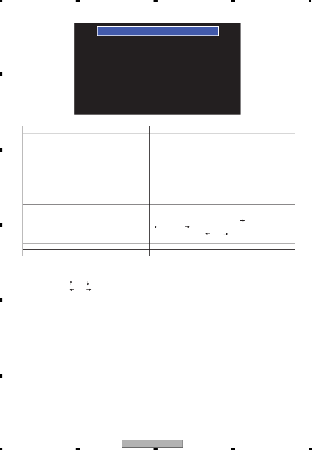
AVIC-D3/XU/UC
226
1234
1234
C
D
F
A
B
E
1. SRAM / SDRAM test
3. RGB test
2. SENSOR test
4. MS5 check
5. Region code
<== back page ==> next page
SYSTEM Ver. : [BOOT] 0.14 [OS] 0.14
TESTMODE MENU [SERVICE_MENU(THCHNICAL)]
Content if inspection
SRAM : Device inspection and bus inspection are performed against all
SRAM domains.
Data will be protected. (applicable to both 32M and 64M)
SDRAM : Device inspection and bus inspection are performed against all
SDRAM domains.
Data will be protected for both BIOS domain and USER domain.
The function for SDRAM all domain inspection will activate by
the built-in instruction RAM.
G sensor, gyro, power supply voltage and installation condition are
displayed.
The system will return to “menu” by BACK key.
RGB inspection
(Upper half, 8 colors. Black/blue/red/pink/green/light blue/yellow/white
display. Lower half, 3 colors. Red/green/blue.) red (FULL)
green (FULL) blue (FULL)
Switching can be made by [ ] and [ ] keys.
The system will return to “menu” by BACK key.
MS5 mechanism test mode inspection.
Region code display.
No.
1
2
3
4
5
Inspection item
SRAM/SDRAM test
SENSOR test
RGB test
MS5 check
Region code
Outline of inspection
Memory inspection
Sensor inspection
Image RGB inspection
MS5 check
Region code display
4. How to select test mode menu
Select a desired menu by [ ] and [ ] keys, and execute by pressing [ENTER] key.
Pages can be changed by [ ] and [ ] keys.
5. Version information
Version No. for BOOT section = X.XX System software does not exist in SDRAM.
Version No. for BOOT section = X.XX Version No. for SDRAM = Y.YY
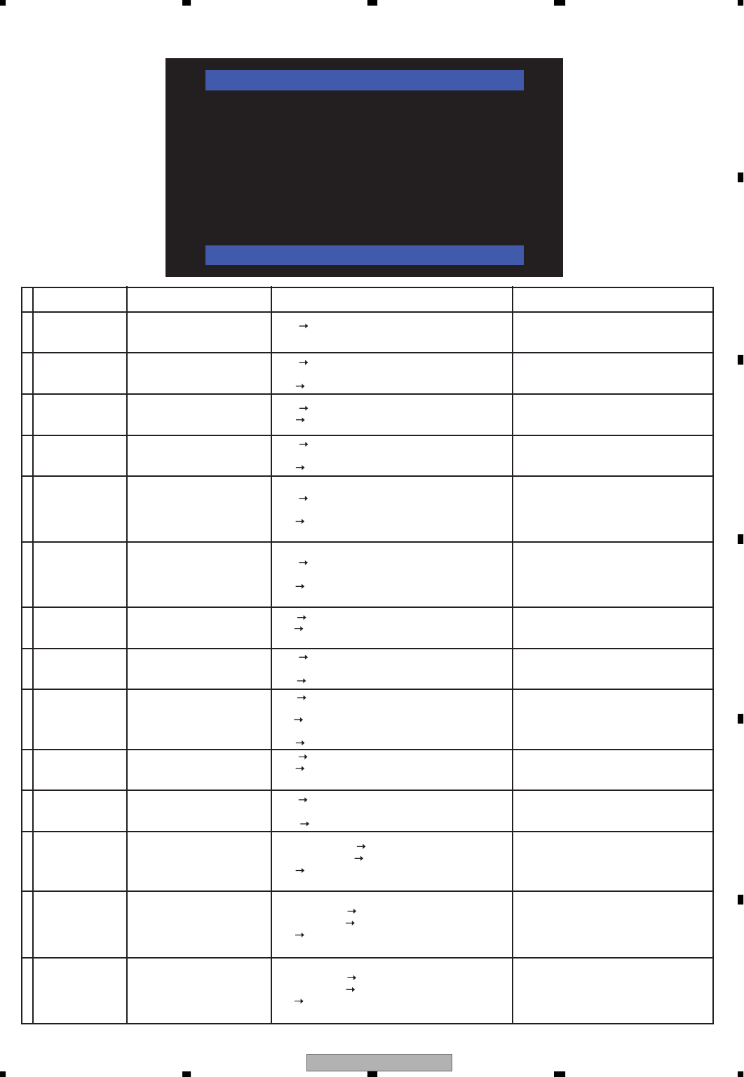
AVIC-D3/XU/UC 227
5678
56
78
C
D
F
A
B
E
- Version check
VERSION INFORMATION
2. System OS version
4. Application version
6. Sound data version
7. Syscom version
8. Syscom romc version
9. Drive version
10. Monitor ucom version
1. System boot version [ 0.20 ]
[ 1.20 ]
[ 0.000700 ]
[ 1.000000 ]
[ 1.000000 ]
[ 6.08 ]
[ - - - - - - ]
[ 1.0.07.04 ]
[ 6.05 ]
[ 0.20 ]
Return = [ BACK ]
+
3. GPS program version
5. Language data version
1
2
3
4
5
6
7
8
9
10
11
12
13
14
Item Content Information display File name
System boot
version
System OS
version
GPS program
version
Application
version
Language data
version
Sound data
version
Syscom version
Syscom romc
version
Drive version
Monitor ucom
version
Monitor ucom
romc version
System program
Application
language
Sound data
language
The sound data file by
language is displayed
The version information of the
system software boot section
(FLASH) is displayed.
The version information of the
system software OS section
(FLASH) is displayed.
The version information of the
GPS program (DRAGON) is
displayed.
The version information of the
application program (FLASH)
is displayed.
The version information of the
data by language (FLASH) is
displayed.
The version information of the
system microcomputer is
displayed.
The ROM Correction version
information of the system
microcomputer is displayed.
The core version information of
the mechanism microcomputer
is displayed.
The version information of
the monitor microcomputer
is displayed.
The ROM Correction version
information of the monitor
microcomputer is displayed.
The system software
file is displayed.
The data file by language
is displayed.
EW070SDF.xxx
(xxx: Extension is determined for each language.
GBR, DEU, FRA, ITA, NLD, ESP, SWE, DNK. BEL)
UC070SDF.yyy
(yyy: Extension is determined for each language.
USA, FRA, ESP.)
[**.**] The version information of the system
software boot section.
[**.**] The version information of the system
software OS section.
[NG] There is no system program.
[**.**] The version information of the GPS program.
[NG] There is no GPS program.
[**.**] The version information of the application
program.
[NG]
There is no application program.
[**.**] The version information of the data by
language.
[NG] There is no data by language.
[**.**] The version information of the sound data
by language.
[NG] There is no sound data by language.
[**.**]
The version information of the system microcomputer.
[NG]
The communication with the system microcomputer
is not established.
[**.**] The ROM Correction version information
of the system microcomputer.
[-----] There is no ROM Correction attached.
[**.**] The core version information of the mechanism
microcomputer.
[NG] The communication with the mechanism
microcomputer is not established.
[-----] The region of the mechanism is different.
[**.**]
The version information of the monitor microcomputer.
[NG] The communication with the monitor
microcomputer is not established.
[**.**] The ROM Correction version information of
the monitor microcomputer.
[------] There is no ROM Correction attached.
[EW070SYS.PRG] System software file for EW.
[UC070SYS.PRG] System software file for UC.
[NG] There is no system software file.
[EW070DAT.xxx] Data file by language for EW.
[UC070DAT.yyy] Data file by language for UC.
[NG] There is no data by language.
[EW070SDF.xxx]
Sound data file by language for EW.
[UC070SDF.yyy]
Sound data file by language for UC.
[NG] There is no sound data by language.
EW070BOT.PRG
UC070BOT.PRG
EW070SYS.PRG
UC070SYS.PRG
EW070GPS.PRG
UC070GPS.PRG
EU070APL.PRG
EW070DAT.xxx
(xxx: Extension is determined for each language.
GBR, DEU, FRA, ITA, NLD, ESP, SWE, DNK.)
UC070DAT.yyy
(yyy: Extension is determined for each language.
USA, FRA, ESP.)
EW070SDF.xxx
(xxx: Extension is determined for each language.
GBR, DEU, FRA, ITA, NLD, ESP, SWE, DNK BEL.)
UC070SDF.yyy
(yyy: Extension is determined for each language.
USA, FRA, ESP.)
EW070DAT.xxx
(xxx: Extension is determined for each language.
GBR, DEU, FRA, ITA, NLD, ESP, SWE, DNK.)
UC070DAT.yyy
(yyy: Extension is determined for each language.
USA, FRA, ESP.)
The version information of the
sound data by language
(FLASH) is displayed.
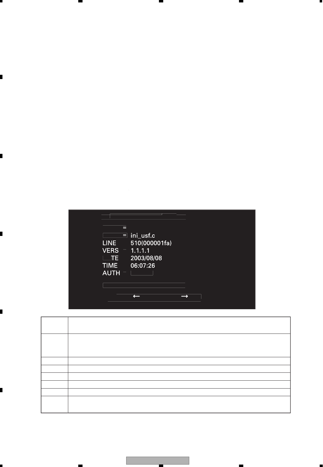
AVIC-D3/XU/UC
228
1234
1234
C
D
F
A
B
E
1. Err
o
r Inf
o
rm
at
i
o
n
Descriptions of error information, for errors arisin
g
from system software problems, will be provided in thi
s
sect
i
o
n
.
Up to ei
g
ht sets of information, related to the system softwar
e
’
s errors
,
will be stored in the SRAM
.
By executin
g
hi_sysdwn( ) the line number (on which the error occurred), the error code and detailed informatio
n
of the error
, will be stored in the error log.
r
Hi_sysdwn( ) will be executed in the followin
g
two circumstances
:
1. hi_s
y
sdwn( ) will be intentionall
y
stored if fatal errors occur with each BIOS
.
2. If multiple exceptions, fatal exceptions, ille
g
al command codes and trap command errors occur.
2. Error Lo
g
's Entry Functio
n
Up to twenty-four sets of information, related to errors starting with the latest error, will be displayed by the
error log entry function
.
There are two types o
f
error log displays
.
The display will vary when the argument provided to hi_sysdwn( ), depending on whether detailed in
f
ormatio
n
(such as program name, version number
,
creat
i
on
d
ate, creat
i
on t
i
me an
d
creator name
)
ex
i
sts or no
t
r
, creation date, creation time and creator name) exists or not
.
1. When detailed in
f
ormation exists
:
-
Err
o
r Inf
o
rm
a
ti
on
ERROR INFORMA
TION
A
TION
A
** **
ERROR
INFORMA
TION
A
ERCD
FILE
DA
ERR
O
R-TIME ffff-ff-ff ff:ff:f
f
No.4 ERROR No.3 No.
2
Sto
p
when
p
ush [DEST] button
.
00000028
(
40
)
da
i
su
k
e
=
=
=
=
=
=
=
=
ER
CD
FILE
LINE
VERS
DATE
TIME
AUTH
ERROR -
TIME
Error
C
ode (If the FILE column is "int_wdt.c", ID of the task in o
p
eration is dis
p
la
y
ed when
the last 4 digits are reset)
Name of the program where the error occurred (In case of “int_wdt.c”, it shows that reset
is activated by the Watch Dog Timer. In this case, ERCD shows other information than
error information).
Program line number where the error occurred
Version number of the program where the error occurred
Date of creation of the program where the error occurred
Time of creation of the program where the error occurred
Creator of the program where the error occurred
Time of error occurrence
3. Reset activated by the Watch Do
g
Timer function. This occurs when the pro
g
ram ceases to function
p
ro
p
erl
y.

AVIC-D3/XU/UC 229
5678
56
78
C
D
F
A
B
E
2. Wh
e
n
deta
il
ed
inf
o
rm
at
i
o
n
does
n
ot
e
xi
st
:
t
yp
e
E
rror occurr
i
n
g
pro
g
ram
li
ne num
b
e
r
gg
.
erc
d
E
rror co
d
e
.
in
f
Sy
stem down in
f
ormation
.
ERR
O
R-TI
M
EE
rror occurrence
d
ate an
d
t
i
me
.
3
. Err
o
r Inf
o
rm
at
i
o
n
S
wi
tch
The product (with default settin
g
s) will display error messa
g
es to the user if an error occurs
.
Error information can be displayed if an error occurs by switchin
g
the error information in the test mod
e
.
In either case, the error lo
g
entry display will be the same.
1) Error messa
g
e display (default settin
g
s
)
:
•
Settin
g
in the test mod
e
:
ERROR INFORMA
TION
A
TION
A
** **
ERROR
INFORMA
TION
A
t
yp
e = 000000b7(183
)
ercd = ffffc002
(
-16382
)
inf = ffb7ac18
(
-4740072
)
ERR
O
R-TIME ffff-ff-ff ff:ff:f
f
No.2 ERROR No.1 No.24
Sto
p
when
p
ush [DEST] button
.
1. Change to display error [Message]
3. Program loading
4. GPS assessment
2. Start within debug shell [Disc & Card]
[On]
5. File maintenance
6. Program forced write
<== back page ==> next page
SYSTEM Ver. : [BOOT] 0.14 [OS] 0.14
TE
S
TM
O
DE MENU
[S
ERVI
C
E_MENU
(
TH
C
HNI
C
AL
)]

AVIC-D3/XU/UC
230
1234
1234
C
D
F
A
B
E
•
Dis
p
la
y
when an error occurs
:
2) Error information dis
p
la
y
•
Settin
g
s in the test mod
e
:
Dis
p
la
y
when an error occurs
:
•
If
e
rr
o
r inf
o
rm
at
i
o
n
e
xi
sts:
ERROR INFORMA
TIO
A
TIO
A
N
** **
ERROR
INFORMA
TIO
A
N
ERCD
FILE
DA
ERR
O
R-TIME ffff-ff-ff ff:ff:f
f
f f f f f f f f
(
-1
)
tsk
_
ini.
c
152
(
00000098
)
1.11
=
=
=
=
=
=
1. Change to display error [Information]
3. Program loading
4. GPS assessment
2. Start within debug shell [Disc]
[Off]
5. File maintenance
6. Program forced write
<== back page ==> next page
SYSTEM Ver. : [BOOT] 0.14 [OS] 0.14
TE
S
TM
O
DE MENU
[S
ERVI
C
E_MENU
(
TH
C
HNI
C
AL
)]
An error has occured.
Please turn power off and on again.
Une erreur a ete decelee.
Veuillez eteindre puis rallumer le systeme.
Fehler.
Bitte System aus- und wieder einschalten.

AVIC-D3/XU/UC 231
5678
56
78
C
D
F
A
B
E
•
If
e
rr
o
r inf
o
rm
at
i
o
n
does
n
ot
e
xi
st
:
ERROR INFORMA
TION
A
TION
A
** **
ERROR
INFORMA
TION
A
t
yp
e = 00000109
(
265
)
ercd = 00000001
(
1
)
inf = ffe83230
(
-1560016
)
ERR
O
R-TIME ffff-ff-ff ff:ff:ff
4. Watch dog timer
This product has a built-in mechanism to monitor at a certain interval whether the software is correctly
operating or not.
Once this mechanism becomes inoperable, “reset request” will be sent to the power supply microprocessor
when a preset time (approximately 4 seconds) has elapsed.
In order to record operational situation of such an occasion, a special code which is not an error code is recorded
in the ERCD.
AVIC-D3/XU/UC
232
1234
1234
C
D
F
A
B
E
- Port status information
Port status information
Parking
Pulse
Reverse Low
0
Low
[ NAVI ] information renewal.
[ BACK ] go to testmode menu.
How to operate.
[BACK] : Return to the test mode menu.
[NAVI] : Update of the port status.
Display
Reverse
Parking
Pulse
Content of inspection
Reverse port status
Parking port status
Pulse status
- GPS assessment
GPS TEST
GPS
SENSOR
FLASH :Ver. 3. 09
:Ver. 5. 56
:Ver. 0. 10 02 / 03 / 12
02 / 05 / 10
Press [ BACK ] to return
Display of DRAGON FLASH ROM version information.
Display of GPS version information.
Display of sensor version information.
FLASH
GPS
SENSOR
The pulse number of vehicle speed is indicated at 1/5 value of input frequency for vehicle speed signal.
For example, when vehicle speed signal is 100Hz, the value becomes 20.
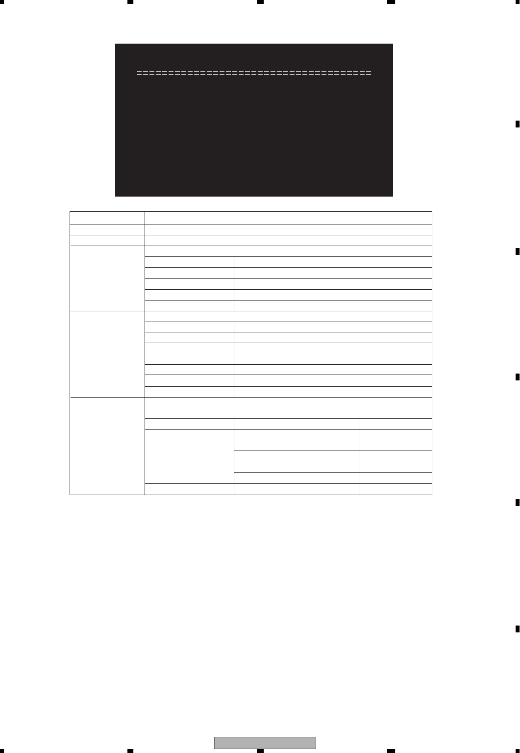
AVIC-D3/XU/UC 233
5678
56
78
C
D
F
A
B
E
SENSOR TEST
GYRO
POWER
G-SENSOR :
:
:2.4804 [V]
1.9875 [V]
FIT UP
DISTANCE :
:OK(Best)
14.9453 [V]
LOW SPEED : OK
SPEED PULSE
Press [ BACK ] to return
- SENSOR test
Display of G sensor voltage
Display of gyro voltage
Display of power supply voltage
Display of installation status
Display
• NG
• OK
• OK (Better)
• OK (Best)
Display of distance calculation status.
Display
• INITIALIZE
• GPS
• G-SENSOR
• ND-PG1
• SPEED PULSE
Display of minimum output speed of a low speed NG vehicle.
(Depends on DISTANCE status.)
DISTANCE status
SPEED PULSE
Others
G-SENSOR
GYRO
POWER
FIT UP
DISTANCE
LOW SPEED
Status
Installation position is NG.
Installation position is OK. (3rd best)
Installation position is OK. (2nd best)
Installation position is OK. (Best)
Status
Sensor initial learning is under way.
GPS distance. (Model without G sensor.
No pulse connection.)
G sensor distance. (simple hybrid.)
ND-PG1 distance.
Vehicle speed pulse distance.
SPEED PULSE status
Low vehicle speed pulse
learning is under way.
Low vehicle speed pulse is
OK.
Low vehicle speed is NG.
Display
CHECK
OK
NG xx[km/h]
- - - - -
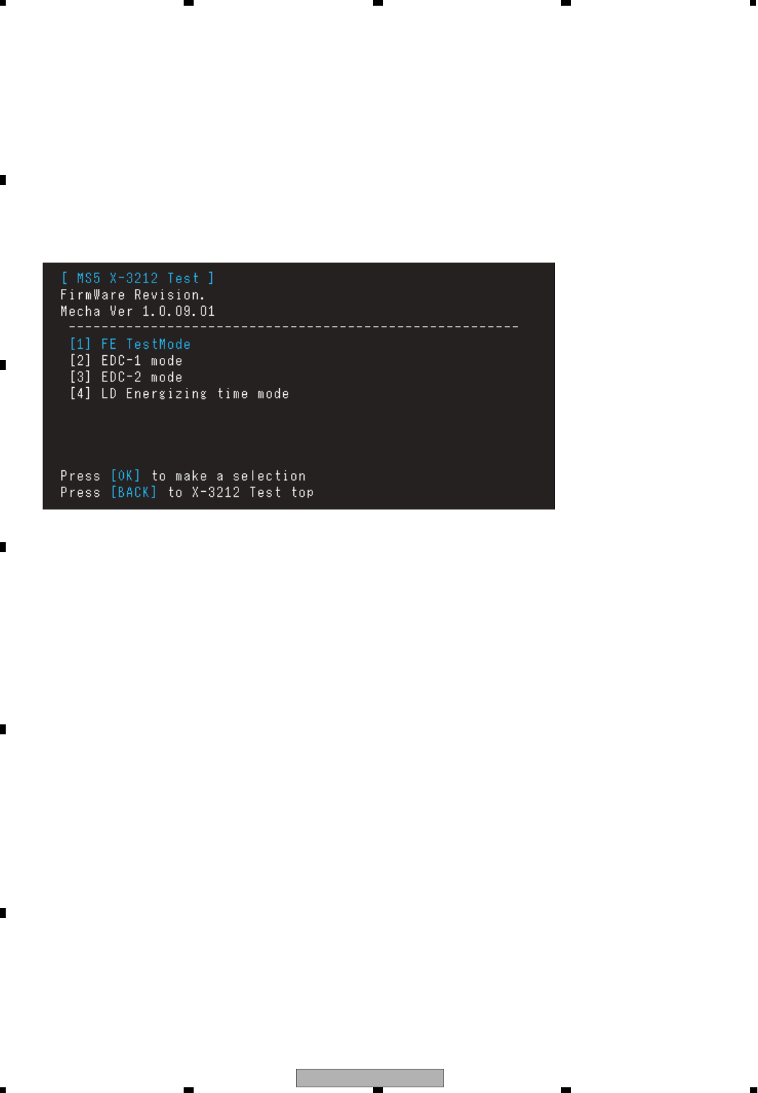
AVIC-D3/XU/UC
234
1234
1234
C
D
F
A
B
E
- MS5 check (DVD Mechanism Module test mode)
*) Caution
During the servo test, the protection against runaway of the mechanism will not be effective. If the runaway
state is left as it is, it may cause a critical damage. When a strange sound is heard during test, turn the power
OFF immediately.
The keys used
[OK] decision key
[BACK] return key
[Direction key] up, down, left and right of the joystick
[MS5 X-3212 Test] Initial screen of the test mode
Mecha Ver: Software version of the MS5 mechanism.
[1] Start of FE test
[2] Start of EDC-1 test
[3] Start of EDC-2 test
[4] Start of LD energizing time mode
[OK] Execute
[BACK] Exit from X-3212 test mode
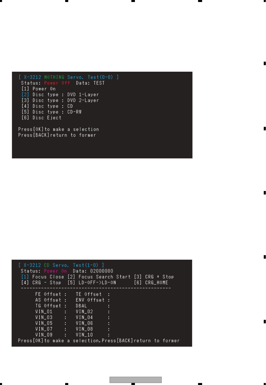
AVIC-D3/XU/UC 235
5678
56
78
C
D
F
A
B
E
FE test operational specifications
*) Caution
During the servo test, the protection against runaway of the mechanism will not be effective. If the runaway
state is left as it is, it may cause a critical damage. When a strange sound is heard during test, turn the power
OFF immediately.
When E is displayed at the head digit of the data, operation other than [BACK] is not possible.
1. [X-3212 Servo Test]: The screen in the power off state.
• NOTHING is changed by selecting [2] to [5] below.
• Each display is changed to the compatible media type.
• Status is unchanged at Power Off.
• The value of the data changes according to the executed command.
Note) [1] cannot be selected for execution unless one of the commands among [2] to [5] is executed once.
[1] Succeeds to Power On state.
[2] Specify DVD layer 1
[3] Specify DVD layer 2
[4] Specify CD
[5] Specify CD-RW
[6] Eject Disc
[OK] Execute
[BACK] Exit from X-3212 test mode
2. [X-3121 Servo Test(1-0)]: The screen in the power on state.
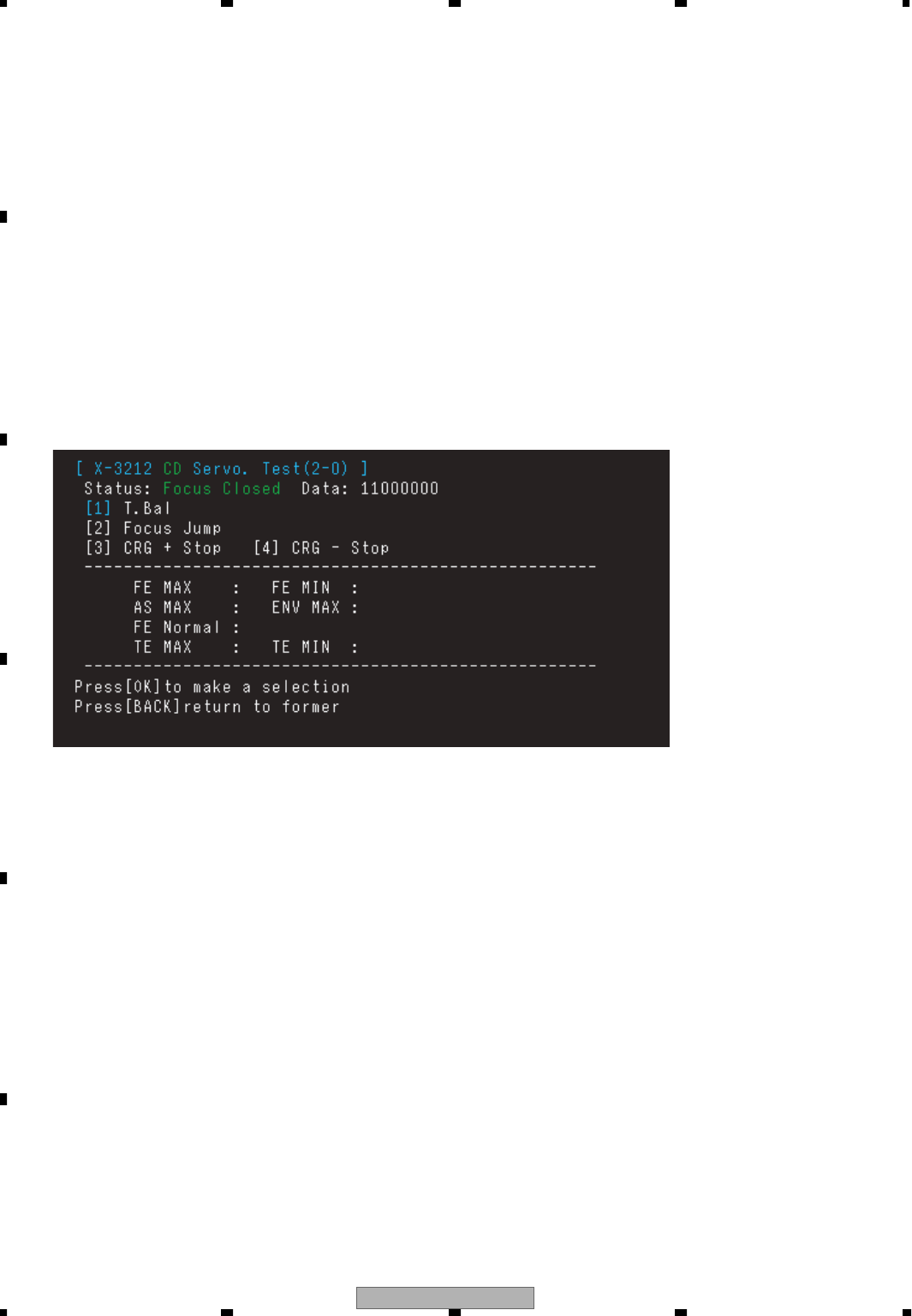
AVIC-D3/XU/UC
236
1234
1234
C
D
F
A
B
E
Note) If no action is taken for approximately 10 seconds after LD-ON, it will be switched to LD-OFF automatically.
If F close is selected in LD-OFF state, it will become an error.
Because it will be in conflict with the safety regulation if LD_OFF is not selected within 10 seconds during
focus search (S character measurement mode), too, it will switch to LD-OFF after 9 seconds even if the focus
search is conducted after LD-ON.
If F close is to be selected after focus search (S character measurement mode), select Power_OFF once then
power on again before F close.
Operation cannot be made until completion of displaying the value from FE Offset to VIN_10.
[1] cannot be executed unless [5] command is executed once.
[1] Succeed to Focus Close 1 state.
[2] Execution and stop of Focus Search
[3] Execution and stop of CRG+
[4] Execution and stop of CRG-
[5] On/Off of LD
[6] Execution of CRG_HOME
[OK] Execution/stop
[BACK] 1, [X-3212 Servo Test]: Return to Power Off state screen.
3. [x-3212 Servo Test (2-0)]: Focus Close 1 state screen
Note) Value of the data will change upon execution of the command.
Operation cannot be made until completion of displaying the value from FE MAX to TE MIN.
[1] Succeed to Focus Close 2 state.
[2] Execution of Focus Jump
[3] Execution and stop of CRG+
[4] Execution and stop of CRG-
[OK] Execution/stop
[BACK] 1, [X-3212 Servo Test]: Return to Power Off state screen.
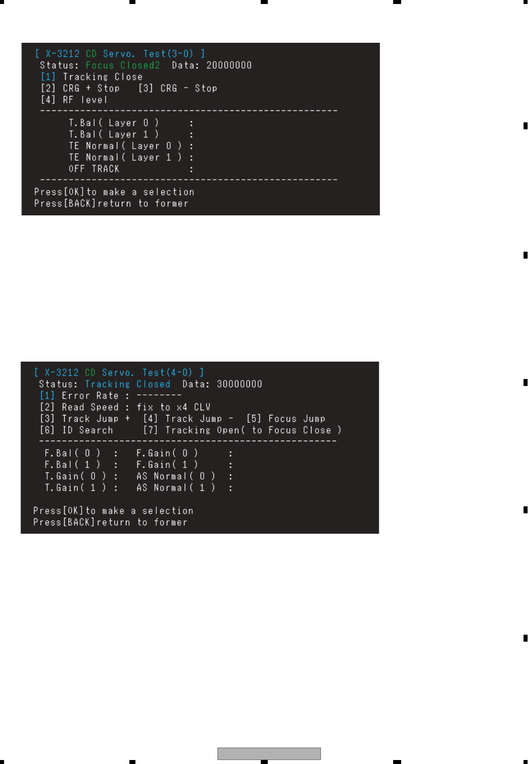
AVIC-D3/XU/UC 237
5678
56
78
C
D
F
A
B
E
4. [X-3212 Servo Test (3-0)]: Focus Close 2 state screen
Note) Value of the data will change upon execution of the command.
Operation cannot be made until completion of displaying the value from T. Bal to OFF TRACK.
[1] Succeed to Tracking Close state.
[2] Execution and stop of CRG+
[3] Execution and stop of CRG-
[4] Succeed to RF Level display state.
[OK] Execution/stop
[BACK] 1, [X-3212 Servo Test]: Return to Power Off state screen.
5. [X-3212 Servo Test (4-0)]: Tracking Close state screen
Note) Value of the data will change upon execution of the command.
Operation cannot be made until completion of displaying the value from F. Bal(0) to AS Normal(1).
[1] Error Rate display (Operation cannot be made for approximately 10 seconds after execution.)
[2] Read speed change (Fixed speed for CD.)
[3] Go to Track Jump + screen.
[4] Go to Track Jump – screen.
[5] Execution of Focus Jump
[6] Go to ID Search screen.
[7] 3, [x-3212 Servo Test (2-0):] Succeed to Focus Close 1 state screen
[OK] Execution/stop
[BACK] 1, [X-3212 Servo Test]: Return to Power Off state screen.
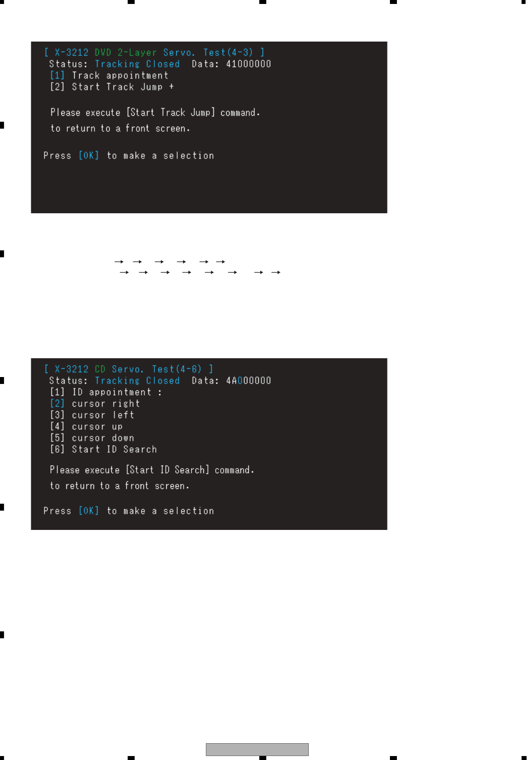
AVIC-D3/XU/UC
238
1234
1234
C
D
F
A
B
E
6. [X-3212 Servo Test (4-3)]: Track Jump +/- screen
Note) Value of the data will change upon execution of the command.
[1] The value of the data is switched to cyclic for each execution.
For CD: 1 4 10 11 32 1 … [track]
For DVD: 1 4 10 11 32 64 100 1 … [track]
[2] Execution of Track Jump +/-.
[OK] Execution
[BACK] 5, [X-3212 Servo Test (4-0): Return to Tracking Close state screen
(Selectable only after execution of Track Jump.)
7. [X-3212 Servo Test (4-5)]: ID Search screen
Note) Value of the data will change upon execution of the command.
[1] Display of ID
[2] Blue digit of the Data is shifted to the right by one digit.
[3] Blue digit of the Data is shifted to the left by one digit.
(Shifting can be made only up to the 3rd digit from the left.)
[4] The number of the blue digit of the data is increased by 1.
[5] The number of the blue digit of the data is decreased by 1.
[6] Start of ID Search
[OK] Execution
[BACK] 5, [X-3212 Servo Test (4-0): Return to Tracking Close state screen
(Selectable only after execution of ID Search.)
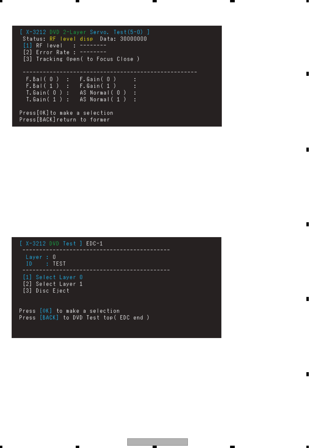
AVIC-D3/XU/UC 239
5678
56
78
C
D
F
A
B
E
8. [X-3212 Servo Test (5-0)]: RF level display state screen
Note) Value of the data will change upon execution of the command.
Operation cannot be made until completion of displaying the value from F. Bal (0) to AS Normal (1).
[1] Display of RF level
[2] Display of Error rate
[3] Succeed to Focus Close 1 state screen
[OK] Execution/stop
[BACK] 5, [X-3212 Servo Test (4-0)]: Return to Tracking Close state screen.
EDC test operational specifications
Note) The operational method is common to both EDC-1 and EDC-2 tests.
1. [X-3212 EDC-1/2 TEST]: Initial screen
Note) Value of the ID will change upon execution of the command.
[1] Go to setting screen of 2, [X-3212 EDC-1/2 Test Layer 0]
[2] Go to setting screen of 3, [X-3212 EDC-1/2 Test Layer 1]
[3] Ejection of the disc
[OK] Execution
[BACK] Exit from MS5 check.
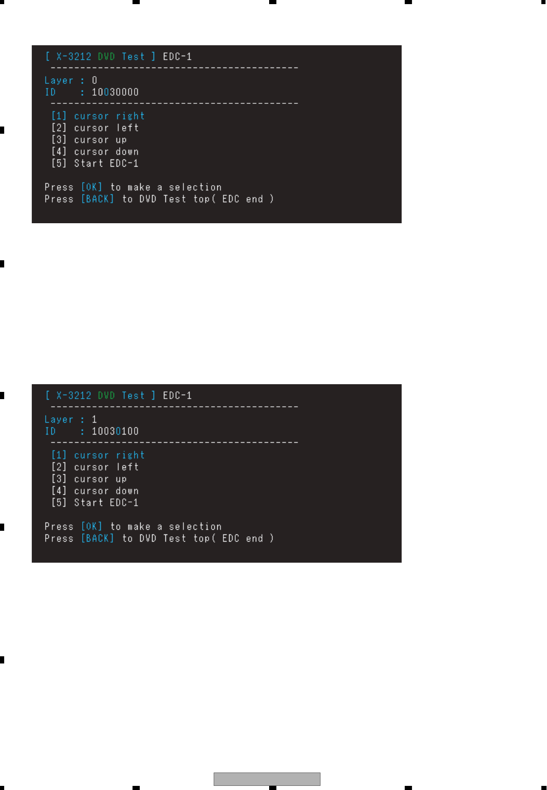
AVIC-D3/XU/UC
240
1234
1234
C
D
F
A
B
E
2. [X-3212 EDC-1/2 Test Layer 0]
Note) Value of the ID will change upon execution of the command.
[1] Shift the blue digit of the ID to the right by one digit.
[2] Shift the blue digit of the ID to the left by one digit.
(Shifting can be made up to the 3rd digit from the left.)
[3] The number of the blue digit of the ID is increased by 1.
[4] The number of the blue digit of the ID is decreased by 1.
[5] Start of EDC test
[OK] Execution
[BACK] Exit from MS5 check.
3. X-3212 EDC-1/2 Test Layer 1]
Note) Value of the ID will change upon execution of the command.
[1] Shift the blue digit of the ID to the right by one digit.
[2] Shift the blue digit of the ID to the left by one digit.
(Shifting can be made up to the 3rd digit from the left.)
[3] The number of the blue digit of the ID is increased by 1.
[4] The number of the blue digit of the ID is decreased by 1.
[5] Start of EDC test
[OK] Execution
[BACK] Exit from MS5 check.
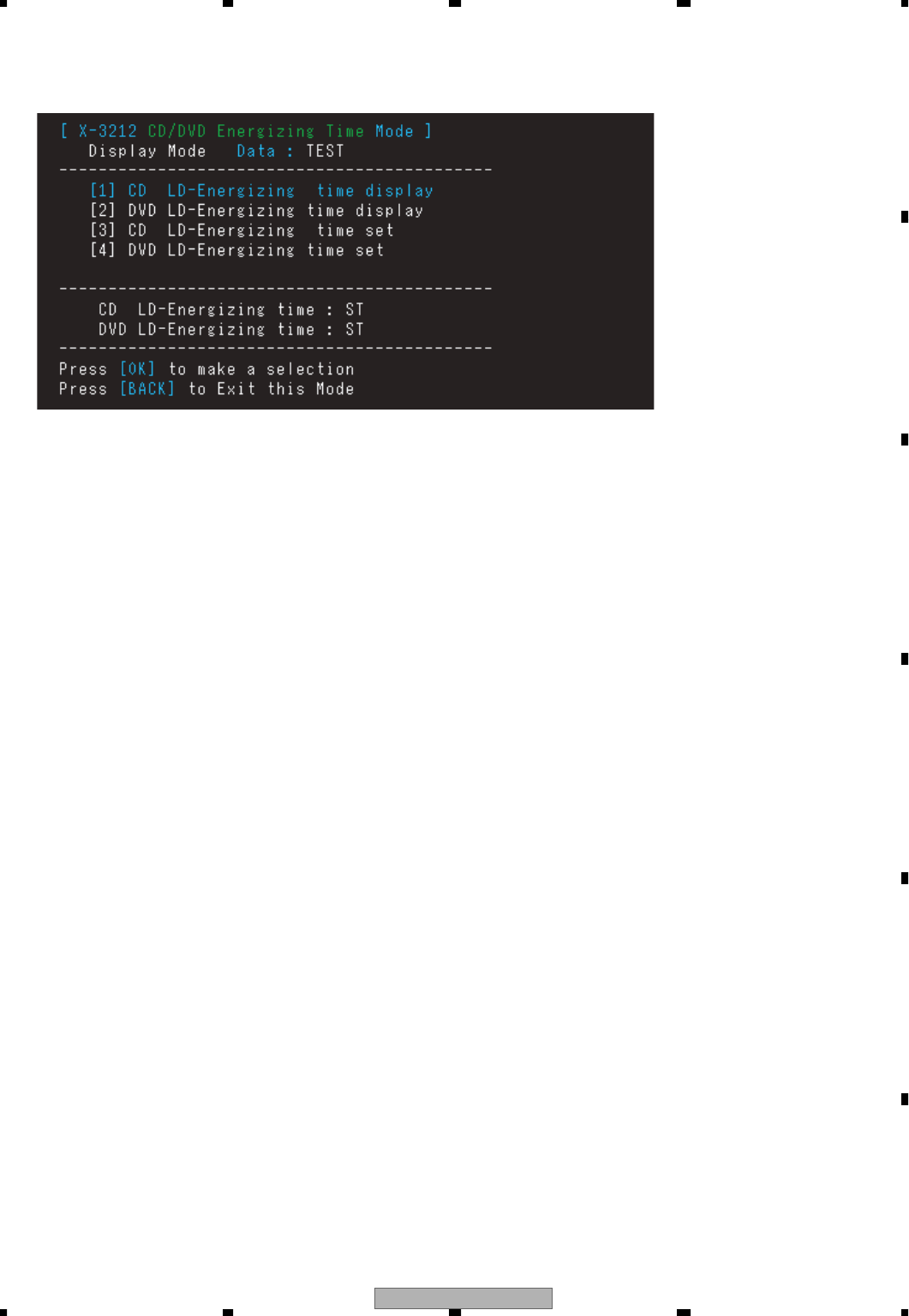
AVIC-D3/XU/UC 241
5678
56
78
C
D
F
A
B
E
Operational specifications for the LD energizing time setting
1. [x-3212 CD/DVD Energizing Time Mode]: LD initial screen
Note) Value of the data will change upon execution of the command.
[1] The current CD energizing preset time is displayed.
[2] The current DVD energizing preset time is displayed.
[3] Go to CD energizing time setting screen. (Not for service use)
[4] Go to DVD energizing time setting screen. (Not for service use)
[OK] Execution
[BACK] Exit from MS5 check.

AVIC-D3/XU/UC
242
1234
1234
C
D
F
A
B
E
6.10 USING THE TEST DISC
1. Start / Termination
1-1. Start
After insertion of test disk, the title “NN700 TEST DISC” is displayed.
(If CD-ROM is the media for TESTDISC, background of the title will be red.)
If the [
C
] key on the remote controller is pressed while the title is being displayed, the menu screen appears.
If no key is pressed during the period, the first screen of test screens for line appears.
Title screen
1-2. Termination
No action is taken.
2. Key operation
Use the remote controller for operation.
Basic operation method in the remote controller.
• (The cursor is moved up) ......................
• (The cursor is moved down) ..................
• (The cursor is moved left) ......................
• (The cursor is moved right) ....................
• Decision (Enter) .........................................
• Return and cancellation (Cancel) ..............
• Inspection execution and re-inspection ......
1. Use [ 4 ] and [ 6 ] keys to select the menu screen.
2. Use [ 2 ] and [ 8 ] keys to select the test items and select [ 5 ] key and move to the testing screen.
3. Use [
C
] key to return to the menu screen.
* Please refer to explanation on each screen for details.
TEST DISC Part No. : GGV1303
Remote Control Uint Part No. : CXC6317 (Operation mode switch : SW1 : AVH, SW2 : DVD)
NN700 TEST DISC
[ 2 ] key
[ 8 ] key
[ 4 ] key
[ 6 ] key
[ 5 ] key
[
C
] key
[ 0 ] key

AVIC-D3/XU/UC 243
5678
56
78
C
D
F
A
B
E
Menu screens
Self Test Menu
1. External Connection
2. Data Communication (Short Circuit) Check
3. Data Communication (Open Circuit) Check
4. Natural Drawing
5. Back Camera check
[ 2 / 8 ] : Change cursol , [ 4 / 6 ] : Change page
[ 5 ] : Select item
Self Test Menu
6. VTR1 In check
10. Monitor adjustment check
11. Language Flag setup mode
[ 2 / 8 ] : Change cursol , [ 4 / 6 ] : Change page
[ 5 ] : Select item
Self Test Menu
14. Picture RGB check
20. Device check(Design engineer only)
21. Memory all clear (for Service)
22. BackUp Memory clear
[ 2 / 8 ] : Change cursol , [ 4 / 6 ] : Change page
[ 5 ] : Select item
8. FM Multiplex Tuner Error Rate
9. GPS Self check
16. GPS sensitivity measurement
19. Picture check
15. GPS information
17. Sound play
18. File Maintenance mode
7. VTR2 In check
13. Software version display
12. Memory all cleay

AVIC-D3/XU/UC
244
1234
1234
C
D
F
A
B
E
1. Connection check
• The status of above items is updated approximately every single second.
• Set ANTON port to H when starting the inspection and set to L when ending.
• When the gyro is in operation, a BEEP sound will be made when the G sensor is activated.
Right: 500 Hz, Left: 700 Hz, Up: 800 Hz, Down: 600 Hz
• Conditions for moving on to the next inspection
Illumination status is changing between ON and OFF.
Parking brake status is changing between ON and OFF.
Reverse status is changing between NOR and REV.
Pulse is changing to a value other than 0/0.
K-mode status is changing between ON and OFF.
Standard value for other items
• GYRO voltage
OK: 2.5 ± 0.15
USABLE: 2.5 ± 0.30
• GYRO variation
OK: Less than 30
• G sensor voltage
OK: 2.5 ± 0.15
USABLE: 2.5 ± 0.30
• G sensor variation
OK: Less than 60
• Only when all the conditions are met, you can move on to the next inspection by the [ 8 ] key on the remote
controller. It should be noted, however, that you will not be able to move on to the next inspection if there is
an error (background color is red) even if the conditions are met.
3. Inspection screen
1. Connection check
Illumination signal
Parking brake signal
Car speed signal
Reverse gear signal
Gyro voltage / sigma
GSENS voltage / sigma
Heading
OFF
ON
NOR
0
2.450V OK / 1.1 OK
2.050V OK / 1.1 OK
CONST
CONST
DOWN
[ 8 ] It progresses to the next inspection.
Key check
Pitch
K-MODE ON
Details of the error
An error that is generated when data cannot be received from the AD converter.
The possible cause is the device error in the AD converter.
This error is also generated when the car speed pulse cannot be measured.
(rare case)
An error that is generated when communication is not established with DRAGON.
The possible cause is the hardware error causing interruption of communication.
It is highly likely that this results from the hardware error of DRAGON.
A response timeout error for BIOS call.
The possible cause is the hardware error causing interruption of communication.
It is highly likely that this results from the hardware error of DRAGON.
Error of unknown causes.
Displayed message
Structure data error
DRAGON unconnected
Command error
Unknown error
<Supplemental explanation regarding error display>
• Checking of “K-MODE” is available only on the UC model.
“K-MODE” will not be displayed on the EW model.

AVIC-D3/XU/UC 245
5678
56
78
C
D
F
A
B
E
2. Data Communication (Short Circuit) check (Not for service)
• Short circuit in SIO connection is checked.
• Loopback in 6CH and 7 CH is checked.
• A “wait” screen is displayed until the check is completed.
• While the test result screen is being displayed, press the [ 0 ] key to perform retesting.
• Only when “OK” is displayed, you can go on to the next test with the [ 8 ] key.
3. Data Communication (Open Circuit) check (Not for service)
• Open circuit in SIO connection is checked.
• 6CH and 7CH are checked.
• Do not connect anything to the terminal. In the released state, ”OK” will be displayed.
• A “wait” screen is displayed until the check is completed.
• While the test result screen is being displayed, press the [ 0 ] key to perform retesting.
• Only when “OK” is displayed, go on to the next test with the [ 8 ] key.
2. Data Communication (Short Circuit) check
Serial I/O #6
Serial I/O #7(for Debug) OK
OK
[ 8 ] It progresses to the next inspection.
3. Data Communication (Open Circuit) check
Serial I/O #6
Serial I/O #7(for Debug) OK
OK
[ 8 ] It progresses to the next inspection.

AVIC-D3/XU/UC
246
1234
1234
C
D
F
A
B
E
4. Natural Drawing
• Nature images with 256 colors are drawn on the BG surface.
• The ADPCM 1 kHz sine wave, which sampling rate is 19 kHz, is output for 30 seconds.
• With the [NAVI] key, GUIDEON terminal can be switched between “H” / “L” with a toggle.
• With the [ 4 ] key or the [ 6 ] key, the volume can be changed.
[JPEG file name: ZHITO1.JPEG]
[Audio file name: A19K01KS.WAV]
• Press the [ 8 ] key to go on to the next test.
5. Back Camera check
Images in the back camera
In this test, check with eyes that images in the back camera is being displayed.
• Images in the back camera are displayed.
• Press the [ 8 ] key to go on to the next test.

AVIC-D3/XU/UC 247
5678
56
78
C
D
F
A
B
E
6. VTR1 In check
External input image
• On the screen, external input video (Front VTR image) is displayed.
• Press the [ 8 ] key to go on to the next test.
7. VTR2 In check
External input image
• On the screen, external input video (Rear VTR image) is displayed.
• Press the [ 8 ] key to go on to the next test.

AVIC-D3/XU/UC
248
1234
1234
C
D
F
A
B
E
8. FM multiplex tuner error rate measurement
• FM multiplexing error is measured.
• In the case of UC model, this inspection is not performed and the system will move on to the next inspection.
• Default frequency is 87.5 MHz.
• When entering this mode for the first time, the result of measurement at the time of test disc boot up will be
displayed.
• After the measurement is taken, the frequency can be changed by the [ 4 ] and [ 6 ] keys.
• 500 blocks will be measured, and if there are 450 or more blocks without error, then it will be determined as OK.
• Only when “OK” is displayed, you can go on to the next test with the [ 8 ] key.
• Use the [ 0 ] key to start re-inspection.
9. GPS Self check
• The GPS reception state is displayed.
• Conditions to go on to the next test
- The antenna connection is “OK”.
- Data is obtained from one or more satellites.
- Time is being displayed.
• When all of the above conditions are satisfied, the background color changes into blue.
• Only when all of the above conditions are satisfied, go on to the next test with the [ 8 ] key.
However, in case of error occurs (background: red), you cannot go on to the next test even if all conditions are
satisfied.
• In case a command error has occurred during GPS signal receiving inspection, the detailed screen of the command
error will be displayed.
• There are two screens for the command error detailed screen, a screen that displays the state of BIOS call used in
GPS signal receiving in real-time and a screen which displays the history from the time of command error occurrence
up to 40 times, and the screen can be switched between these two by [ 5 ] key.
To save the error information, it is so designed that you cannot return from the command error detailed screen to the
normal inspection screen. If you desire to resume the inspection, eject the disc once, and insert the test disc once again.
8. FM multiplex tuner error rate measurement
Push 0 key to go to re-check.
FM Frequency
Frequency to check
Blocks Received Correctly
Blocks with one bit corrected
Blocks with two bits corrected
Blocks Received with error
[ 4 / 6 ] to adjust FM frequency
87.50
87.50
0500
0000
0000
0000
[ 8 ] It progresses to the next inspection.
9. GPS Self check
Using satellites No.
01 02 03 04 05 06 07 08
Antenna connection
Receiving signal level
Latitude
Longitude
2005/03/22 15:00:00
OK
13.5
3D 35 55 47.1
139 28 30.0
[ 8 ] It progresses to the next inspection.

AVIC-D3/XU/UC 249
5678
56
78
C
D
F
A
B
E
<Supplemental explanation regarding error display>
10. Monitor adjustment check
• Each state of “PHASE adjusted flag”, “PALTINT adjusted flag”, “Flicker adjusted flag” and “dotclock adjusted flag”
is obtained from the microcomputer, and the result of whether the monitor has been adjusted or not will be
displayed.
• While there is no difference between the EW model and the UC model in terms of the screen specifications,
the monitor is judged to be adjusted if all adjusted flags are ON for the EW model and if “PHASE adjusted flag”
and “PALTINT adjusted flag” are OFF but “Flicker adjusted flag” is ON for the UC model, and you can proceed
to the next inspection by pressing the [ 8 ] key.
• If the above conditions for the EW and the UC models are not met, the monitor is judged to be unadjusted and
NG screen will be displayed.
11. Language Flag setup mode
• When the system enters into this inspection, language selection will be set to the original setting made at
the time of shipment (i.e. no setting).
* The setting is made to display the screen for selecting the language to be used at the initial boot up after
the shipment out of the factory.
• The setting is made when the system enters into this inspection.
• Press the [ 8 ] key to go on to the next test.
Details of the error
This is an error when communication with DRAGON is not established.
Communication error due to a hardware problem could be the cause.
It is highly possible that the hardware on the DRAGON side is defective.
Time out error for response to BIOS call.
Communication error due to a hardware problem could be the cause.
It is highly possible that the hardware on the DRAGON side is defective.
This is an error when request is made while the data for response is not
prepared (not obtained from DRAGON).
Communication error due to a hardware problem could be the cause.
It is highly possible that the hardware on the DRAGON side is defective.
Displayed message
No connection to DRAGON
Command error
Invalid data
10. Monitor adjustment check
monitor unit process(PALTINT)
display module process
monitor unit process(PHASE)
11. Language selection flag initialize
[ 8 ] It progresses to the next inspection.
Language selection flag is initialized.
monitor dotclock process

AVIC-D3/XU/UC
250
1234
1234
C
D
F
A
B
E
13. Software version display
• The software versions are displayed.
• As for the GPS model, it will be considered OK if "07 EW (0x37)" is displayed in the case of EW model and
if "07 UC (0x38)" is displayed for UC model.
14. Picture RGB check
• Bridge tests are performed for RGB.
• Pressing the [ 4 ] key or the [ 6 ] key switches the screens.
• RGB is plotted in the following pattern: R100% -> R50% -> G100% -> G50% -> B100% -> B50%
• 6 screens are displayed in total.
13. Software version
System boot / OS version
Syscom version
GPS program version
GPS model
0.17 / 0.17
0.010200
2.01
7.01
10.20 05/03/22 0.60
07 EW (0x37)
1.00
[
C
] It returns to a screen.
Mecha micom version
Monitor micom version
Application version
12. Memory all clear (Not for service)
• SRAM (application domain) is cleared.
• FLASH (application domain) is cleared.
• Sensor learning level is cleared.
• If SRAM clear is not successful, FLASH will not be cleared.
• After displaying the test screen, press the [ 0 ] key to execute the above processing.
• The execution results are displayed.
• Only when all is “OK”, press the [ 8 ] key to end the production engineering test and return to the menu screen.
12. All memory clear
The clearance of SRAM (application domain)
The clearance of Flash (application domain)
Elimination of a sensor study value
[ 0 ] Inspection is performed.

AVIC-D3/XU/UC 251
5678
56
78
C
D
F
A
B
E
15. GPS information
• The information displayed switches with the [ 4 ] key and the [ 6 ] key.
• Pressing the [ 5 ] key while the cursor is placed at “Position” displays the “position information”.
• Pressing the [ 5 ] key while the cursor is placed at “Sv Stat” displays the “status information”.
• Pressing the [ 5 ] key while the cursor is placed at “Ver&Diag” displays the “diagnostic information”.
• Pressing the [ 5 ] key while the cursor is placed at “Err Info” displays the “error information”.
• In the test, “status information” (above screen) is displayed first.
16. GPS sensitivity measurement
• Press the [ 4 ] key or the [ 6 ] key to change GPS.
• The GPS sensitivity selected with the [ 5 ] key is displayed.
• If communication with the GPS unit fails, an error screen is displayed.
<Supplemental explanation regarding error display>
15. GPS information
0D T2 H25.5 V25.5 05/03/22 15:00:00
Position Sv Stat Ver & Diag Err Info
SV
10
26
18
23
17
9
Azi
119
25
310
305
317
196
Ev
39
60
25
33
49
56
SNR
3.0
4.9
0.0
0.0
0.0
0.0
Flag
UY--
UYC-
---m
---m
---m
---m
Acc
3
2
f
f
f
f
SV
3
14
4
12
15
6
Azi
119
25
310
305
317
196
Ev
39
60
25
33
49
56
SNR
3.0
4.9
0.0
0.0
0.0
0.0
Flag
UY--
UYC-
---m
---m
---m
---m
Acc
3
2
f
f
f
f
16. GPS sensitivity measurement
Satellite No. 3 [ < LEFT / RIGHT > to select satellite ]
CH. Lock SNR(AMU) SNR(dB)
1 OK 12.3 23.4
2 OK 12.3 23.4
3 OK 12.3 23.4
4 OK 12.3 23.4
5 OK 12.3 23.4
6 OK 12.3 23.4
ALL OK Sensitivity: 22.8(db)
DoppRMS: 1.51(Hz)
CH. Lock SNR(AMU) SNR(dB)
7 OK 12.3 23.4
8 OK 12.3 23.4
9 OK 12.3 23.4
10 OK 12.3 23.4
11 OK 12.3 23.4
12 OK 12.3 23.4
Details of the error
This is an error when communication with DRAGON is not established.
Communication error due to a hardware problem could be the cause.
It is highly possible that the hardware on the DRAGON side is defective.
Time out error for response to BIOS call.
Communication error due to a hardware problem could be the cause.
It is highly possible that the hardware on the DRAGON side is defective.
Displayed message
No connection to DRAGON
Command error

AVIC-D3/XU/UC
252
1234
1234
C
D
F
A
B
E
17. Sound play
• Audio files (in WAVE format) are played back.
• When entering the screen, set the GUIDEON terminal to “H”, and reset to “L” when exiting it.
• Press the [ 5 ] key to play back the selected audio.
• Press the [ 4 ] key or the [ 6 ] key to change the volume.
18. File Maintenance mode
• Files can be copied, deleted, or dumped.
See HELP for usage of each function.
19. Picture check
• Select a pattern with the [ 2 / 8 ] key and press the [ 5 ] key to display the image.
17. Sound play
ADPCM fixation 11K 1K L
ADPCM fixation 11K 1K mono
ADPCM fixation 11K 1K R
ADPCM fixation 11K 1K ste
ADPCM fixation 19K 1K L
ADPCM fixation 19K 1K mono
ADPCM fixation 19K 1K R
Guidance Vol.[0-15](level) 10
[ 4 / 6 ] Vol up/down
[
C
] It returns to a menu screen.
18. File maintenance
Totale Capacity : 216.5K Remain : 185.5K
Media:SRAM Path:
NATURE1.JPG 20
MAP.JPG 20 12.5K 05 / 03 / 22 00:00
17.7K 05 / 03 / 22 00:00
[ 1 ] Media [ 3 ] Operate [ 0 ] Help
19. Picture check MENU 1/2
1. Plane
2. Color Bar
3. Cross Hatch
4. Sweep
5. Step
6. Ramp
7. Window
8. Mono Scope
9. Vertical Resolution Column
[ 5 ] It selects a item.
[
C
] It returns to a menu screen.

AVIC-D3/XU/UC 253
5678
56
78
C
D
F
A
B
E
20. Device Check(Design engineer only)
• The above devices will be inspected for engineering purpose.
• A device is selected by the [ 2 ] and [ 8 ] keys on the remote controller, and cleared by the [ 5 ] key.
• On each device screen, a pattern is selected by the [ 2 ] and [ 8 ] keys, and inspection is started by the [ 5 ] key.
21. Memory all clear (for Service)
• SRAM (application region) is cleared.
• FLASH (application region) is cleared.
• If SRAM clear is not successful, FLASH will not be cleared.
• After displaying the test screen, press the [ 0 ] key to execute the above processing.
• The execution results are displayed.
22. BackUp Memory clear
• Press the [ 0 ] key to initialize the backup variables and to reset the system.
• Press the [
C
] key to return to the menu screen.
20. Device Check
1. SDRAM (0X48000000 - 0X4BFFFFFF)
2. SRAM (0X42000000 - 0X4203FFFF)
3. ASIC (0X43000270 - 0X43000274)
4. All Device
[
C
] It returns to a menu screen.
21. All memory clear (for Service)
The clearance of SRAM (application domain)
The clearance of FLASH (application domain)
[ 0 ] Inspection is performed.
[
C
] It returns to a menu screen.
22. Initialization of a backup variable
A backup variable is initialized.
Cautions
System reset is carried out after initialization.
[ 0 ] A backup variable is initialized.
[
C
] It returns to a menu screen.
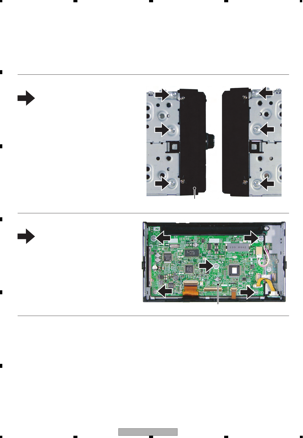
AVIC-D3/XU/UC
254
1234
1234
C
D
F
A
B
E
7. GENERAL INFORMATION
7.1 DIAGNOSIS
7.1.1 DISASSEMBLY
- Removing the Grille Assy (Fig.1)
1
Fig.1
- Removing the Case (not shown)
Grille Assy
1. Remove the Case.
1
1
1
Remove the six screws.
Disconnect the connector and then remove the
Grille Assy.
1
1
1
- Removing the Monitor Unit (Fig.2)
Remove the five screws.
1
11
1
Monitor Unit Fig.2
Disconnect the connector and then remove the
Monitor Unit.
1
1
*) When attaching the Grille Assy onto the main
body, make the Grille Assy stick to the main
body by hand (there shall be no gap), and fix
them using the screws.
*) Be sure to place the remote controller with the
optical receiver facing up. Otherwise the leads
of the optical receiver may be bent.
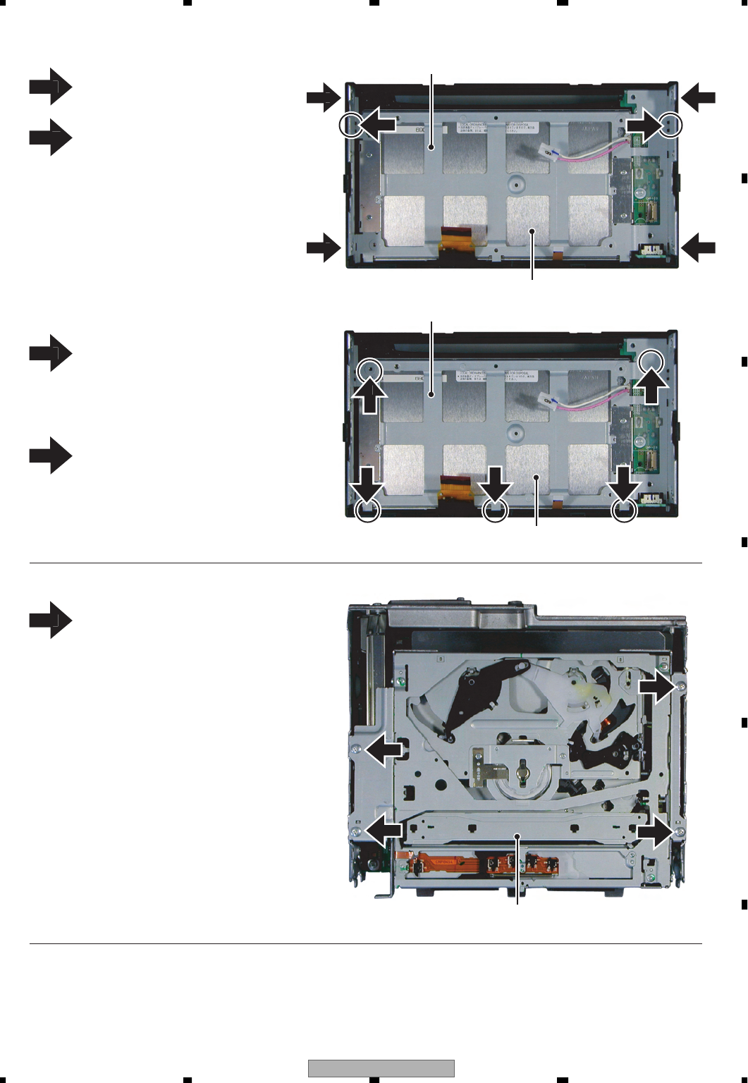
AVIC-D3/XU/UC 255
5678
56
78
C
D
F
A
B
E
1
-
Removin
g
the LCD Assy (Fi
g
.3)
Fig.5
DVD Mechanism Module
Re
m
o
v
e
the
fou
r
sc
r
e
w
s.
Th
ere
i
s a
g
ap
b
etween t
h
e
H
o
ld
er
a
nd the
G
rille. Put
y
our fin
g
er in the
g
ap and push out the
G
rille toward
outside
to
r
elease
the
fi
x
ed
sectio
n
of the
G
rille and the Holder.
(
both
le
f
t and ri
g
ht)
2
LCD Aaay
Fig.4
1
1
1
-
Removin
g
the DVD Mechanism Module (Fi
g
.5
)
Re
m
o
v
e
the
fou
r
sc
r
e
w
s.
1
Disco
nn
ect
the
co
nn
ecto
r
a
n
d
the
n r
e
m
o
v
e
the
DVD
Mecha
n
is
m
Module.
1
1
1
1
1
2
2
Fig.3
1
-
Installation of the LCD Assy (Fi
g
.4
)
Match
the
th
r
ee
cla
w
s
as
sho
wn
o
n
the
d
raw
i
n
g
to t
h
e correspon
di
n
g
sect
i
ons o
f
the
G
rille. When doin
g
so, put the Holder
onto the
G
rille in a wa
y
that the broken-out
sect
i
on o
f
t
h
e
H
o
ld
er w
ill
b
e tota
lly
hidd
en
.
Push
the
t
w
o
locatio
n
s
as
sho
wn
o
n
the
d
raw
i
n
g
, an
d
pus
h
a
ll
t
h
e wa
y
to t
h
e
b
ac
k
so
that
the
cla
w
s
of
the
Holde
r
a
n
d
the
G
rille sna
p
s in
.
2
1
11
2
2
Holder
LCD Aaay
*)
Do not bend the Holder
.
Holder
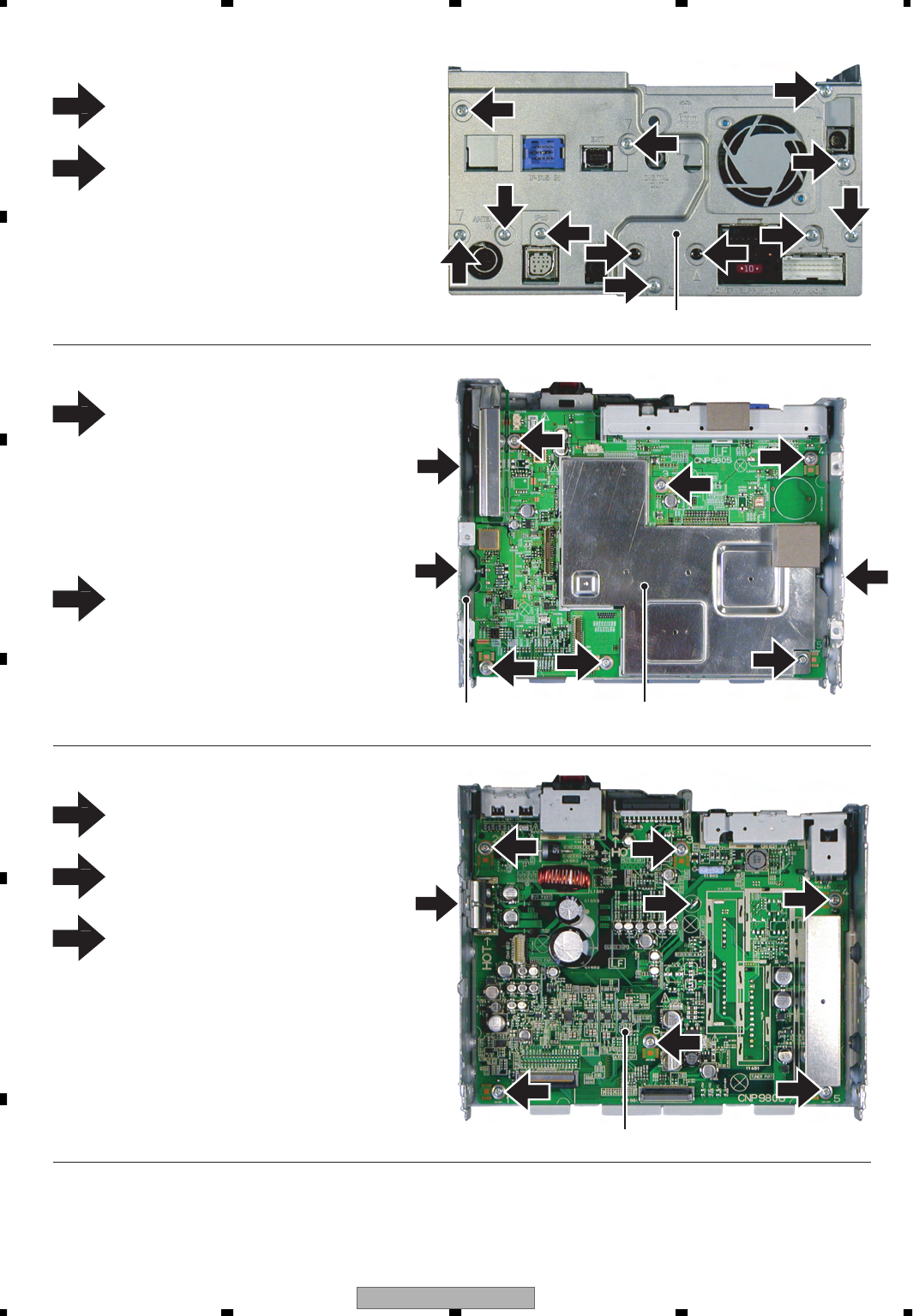
AVIC-D3/XU/UC
256
1234
1234
C
D
F
A
B
E
Fig.6
Heat Sink
2
-
Removin
g
the Heat Sink (Fi
g
.6)
Re
m
o
v
e
the
t
w
o
sc
r
e
w
s.
1
2
1
2
2
1
Re
m
o
v
e
the
te
n
sc
r
e
w
s
a
n
d
the
n
re
m
o
v
e
t
h
e
H
eat
S
ink
.
2
-
Removin
g
the Chassis (Fi
g
.7
)
Fig.7
Re
m
o
v
e
the
th
r
ee
sc
r
e
w
s.
1
Navi Mother Unit
2
2
2
2
2
2
2
-
Removin
g
the Navi Mother Unit (Fi
g
.7)
Re
m
o
v
e
the
si
x
sc
r
e
w
s
a
n
d
the
n
re
m
o
v
e
the
Na
v
i
Mothe
r
U
n
it.
2
Chassis
2
22
2
11
12
Disco
nn
ect
the
co
nn
ecto
r
a
n
d
the
n r
e
m
o
v
e
t
h
e
C
h
ass
i
s.
Fig.8
-
Removin
g
the AV Unit (Fi
g
.8
)
3
3
3
3
AV Unit
Re
m
o
v
e
the
sc
r
e
w
.
1
3
S
trai
g
hten the tab at location indicated
.
2
Re
m
o
v
e
the
si
x
sc
r
e
w
s
a
n
d
the
n
re
m
o
v
e
the
AV
U
n
it.
3
23
1
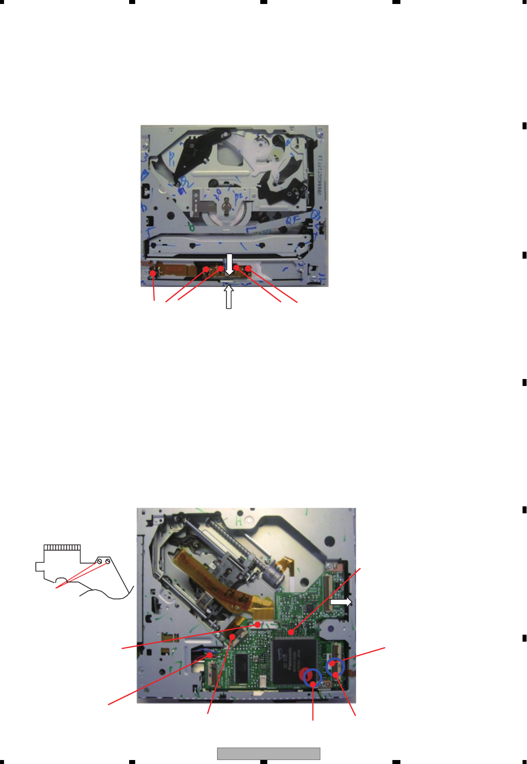
AVIC-D3/XU/UC 257
5678
56
78
C
D
F
A
B
E
- How to hold the mechanism section (Fig.9)
1. Hold the main frame and the top frame.
2. As the mechanical strength of the front part of the top frame is not strong, do not hold this part.
3. Do not touch the switches provided on the top face of the mechanism section.
4. Be careful not to pull the flexible PCB on the side face.
Fig.9
Do not touch this part. Do not touch this part.
Do not touch this part.
- How to remove the module PCB (Fig.10, Fig.11)
1. Put the mechanism section in locked state (disc load standby position).
2. Hold the mechanism module with its top face down.
3. Make the lands at 2 locations on the pick up flexible PCB short.
4. Disconnect the connectors of the pick up flexible PCB and the SPDL flexible PCB.
(Be sure to disconnect the connectors as the flexible PCB will be damaged if the PCB is removed without removing
the flexible PCB.)
5. Remove the solder joint of the lead wire of the load motor and the clamp SW.
6. Remove the two screws, and then remove the module PCB.
(Lift up point A slightly and remove it toward B direction. Be careful as the point C is connected with a flexible PCB.)
7. Disconnect the connector of the 8-12 detection flexible PCB from the PCB.
Solder land
(load motor, lead wire of the clamp SW.)
Connector
(8-12 detection flexible)
Module PCB
Fig.11
Connector (SPDL flexible)
Connector
(pick up flexible)
C
B
A
Fig.10
Short
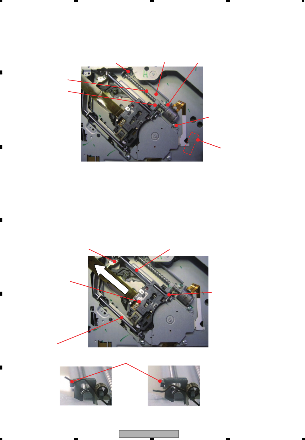
AVIC-D3/XU/UC
258
1234
1234
C
D
F
A
B
E
- How to remove the CRG motor assy (Fig.12)
1. Remove the module PCB according to the instructions in ìHow to remove the module PCBî.
2. Remove the Mylar tape.
3. Remove the flexible PCB of the CRG motor from the connector of the spindle motor.
4. Remove the two screws, and then remove the CRG motor assy.
Set screw (spindle)
Feeding screw
PU rack
Set screw (CRG) Set screw (CRG)
CRG motor assy
Mylar tape
Fig.12
- How to remove the PU unit (Fig.13)
1. Remove the module PCB according to the instructions in "How to remove the module PCB".
2. Hang the main shaft holding spring to the CRG chassis temporary hanger.
3. Remove the CRG motor assy according to the instructions in "How to remove the CRG motor assy".
4. Remove the holding plate spring of the main shaft.
5. While lifting up the tip of the pick up rack, slide the main shaft, and remove the PU unit.
(Note) When mounting the PU unit again, make sure to do the adjustments of the devices mounted thereon
according to the descriptions of the service manual. Furthermore, make sure to hang the main shaft
holding spring permanently.
PU unit
Sub shaft
Main shaft
Fig.13
Permanent hanging
Temporary hanging
CRG chassis temporary hanging section
Main shaft holding spring
Holding plate spring
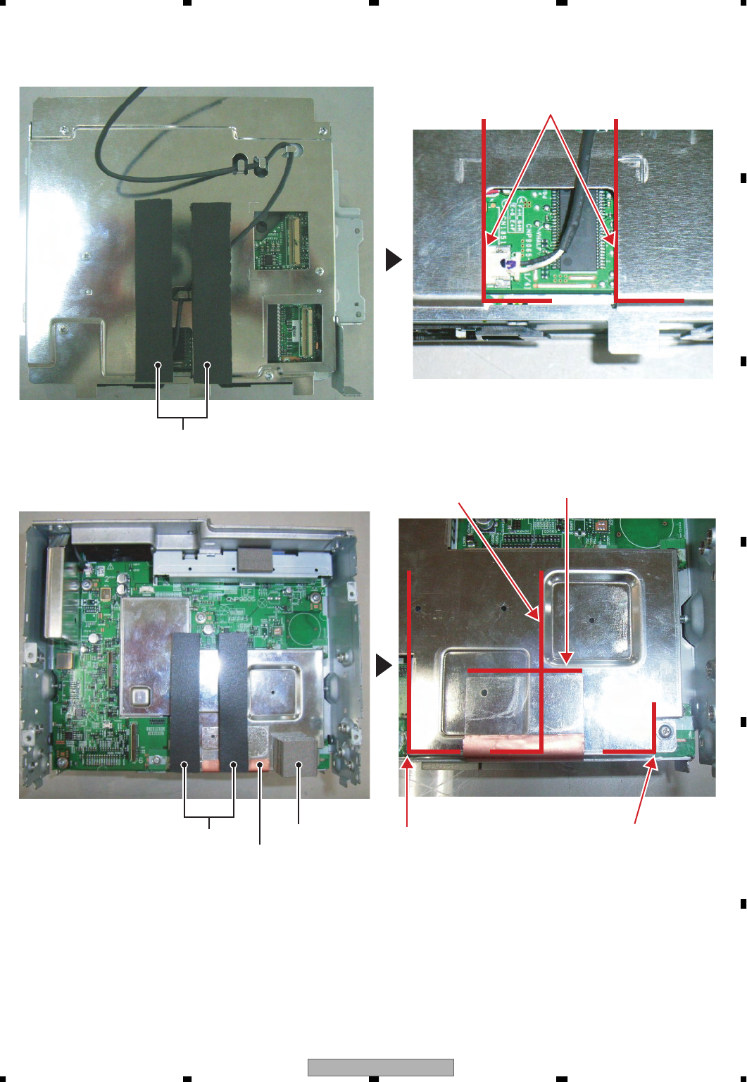
AVIC-D3/XU/UC 259
5678
56
78
C
D
F
A
B
E
CNN1807
· Position to put :
Set it to the position
of the corner.
CNN1804
· Position to put :
Set it to the position
of the corner.
CNN1807
CNN1807
CNN1804
CNN1806
CNN1807
· Position to put :
Edge of dent
CNN1807
· Position to put :
Edge of slit
CNN1806
· Position to put(Right and left) :
During CNN1804 and CNN1807
· Position to put(Depth) :
Edge of dent
* Caution
CNN1806 : Recycling is not possible, use the new shield.
Put it not to slack.
CNN1807 : When the adhesive strength is weak, use the new cushion.
- How to install the gasket, cushion and shield
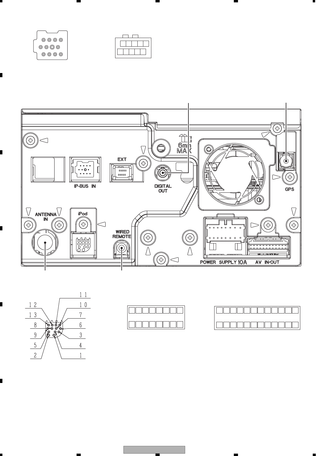
AVIC-D3/XU/UC
260
1234
1234
C
D
F
A
B
E
7.1.2 CONNECTOR FUNCTION DESCRIPTION
1. FR+
2. RR+
3. FR-
4. RR-
5. FL+
6. RL+
7. FL-
8. RL-
1. TELMUTE
2. NC(Reserved?)
3. RR
4. NC
5. RL
6. REARGND
7. FR
8. NC
9. FL
10. FRONTGND
11. SWR
12. BREM
13. SWL
14. SWGND
15. VTR1R
16. VTR1RGND
17. VTR1L
18. VTR1LGND
19. VTR1V
20. VTR1VGND
21. REARVOUT
22. GNDV
23. BCV
24. BCVGND
9. PKB
10. PULSE
11. REV
12. ILM
13. AANT
14. ACC
15. GND
16. BUP
POWER SUPPLY
1 3 5 7 9 11 13 15
2 4 6 8 10 12 14 16
AV IN/OUT
20181614121086
1917151311975
42
31
2422
2321
1. IPBUS+
2. IPBUSG
3. IPLG
4. NC
5. IPBUS-
6. IPRG
1234
56 7
8 9 10 11
7. IPL+
8. ASENBO
9. IPR+
10. IPR-
11. IPL-
IP-BUS IN
108642
97531
EXTENSION
1. GTOEX
2. EXTOG
3. GND
4. CTOEX
5. EXTOC
6. HYOKA
7. CTOETC
8. ETCTOC
9. NC
10. GND
GPS ANTENNADIGITAL OUT
FM/AM ANTENNA WIRED REMOTE CONTROLLER
1. F/W GND
2. F/W PWR
3. TXiPod
4. ACCID
5. LOUT
6. RXiPod
7. VOUT
8. ROUT
9. GNDD
10. ACCPW
11. ACCDET
12. V_RETURN
13. A_RETURN
iPod
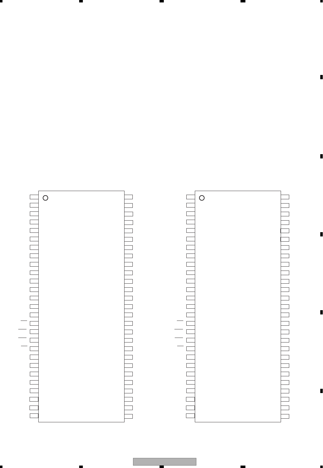
AVIC-D3/XU/UC 261
5678
56
78
C
D
F
A
B
E
7.2 IC
K4S561632H-UL75
DQ0 2
VDDQ 3
DQ1 4
DQ2 5
VSSQ 6
DQ3 7
DQ4 8
VDDQ 9
DQ5 10
DQ6 11
VSSQ 12
DQ7 13
VDD 14
WE
15
CAS
16
RAS
17
CS
18
BA1
19
A10/AP
20
A0
21
A1
22
A2
23
A3
24
48
DQ14
47
VSSQ
46
DQ13
45
DQ12
44
VDDQ
43
DQ11
42
DQ10
41
VSSQ
40
DQ9
39
DQ8
38
37
VSS
36
UDQM
35
CLK
34
CKE
33
NC
32
A9
31
A8
30
A7
29
A6
28
A5
54
A4
53
VSS
VDD 1
VDD
25
49
DQ15
50
VSS
26
27
52
51
LDQM
BA0 A11
NC
VDDQ
A0-A11 : Address input
BA0-BA1 : Bank select address
DQ0-DQ15 : Data input/output
CLK : Clock input
CKE : Clock enable
cs : Chip select
ras : Row address strobe
cas : Column address strobe
we : Write enable
LDQM : Lower DQ mask enable
UDQM : Upper DQ mask enable
VDD : Power supply
VSS : GND
VDDQ : Data output power supply
VSSQ : Data output GND
NC : Not used
DQ0 2
VDDQ 3
DQ1 4
DQ2 5
VSSQ 6
DQ3 7
DQ4 8
VDDQ 9
DQ5 10
DQ6 11
VSSQ 12
DQ7 13
VDD2 14
WE
15
CAS
16
RAS
17
CS
18
BA1
19
A10/AP
20
A0
21
A1
22
A2
23
A3
24
48
DQ14
47
VSSQ
46
DQ13
45
DQ12
44
VDDQ
43
DQ11
42
DQ10
41
VSSQ
40
DQ9
39
DQ8
38
37
VSS
36
UDQM
35
CLK
34
CKE
33
NC
32
A9
31
A8
30
A7
29
A6
28
A5
54
A4
53
VSS
VDD 1
VDD
25
49
DQ15
50
VSS
26
27
52
51
LDQM
BA0 A11
NC
VDDQ
A0-A11 : Address input
BA0-BA1 : Bank select address
DQ0-DQ15 : Data input/output
CLK : Clock input
CKE : Clock enable
cs : Chip select
ras : Row address strobe
cas : Column address strobe
we : Write enable
LDQM : Lower DQ mask enable
UDQM : Upper DQ mask enable
VDD : Power supply
VSS : GND
VDDQ : Data output power supply
VSSQ : Data output GND
NC : Not used
HY57V561620FLTP-H
K4S561632H-UL75
HY57V561620FLTP-H
UPD705103GM-180S1
TC74LCX08FTS1
TC7SH04FUS1
PD6336C
PEH103A
PEH077A
PEH104A
PEH078A
AK4388VT
MB86291APFVS-G-DL
TC7WH32FU
BD5335FVE
PE5580A
PE5581A
BD3931HFP
PE5584A
S-93C46BR0I-J8
PD6567A
LZ9FE30
S-80859CNNB-B9K
BD9851EFV
EDS1232AATA-75
PCM1753DBQ
NJM2880U1-05
TC74LCX16373FT
CWW1423
CWW1424
MN2DS0016
BD7996EFV
S-814A50AUC-BDO
UPD4723GSS1
TPS5120DBT
UPB1027GS
PEH100A8
PEH101A8
PD3390A
LC72720YVSS1
ADC12H034CIMSAS1
BA00CCWCP-V5
BA00CCWFP
NJM2505F
BA4558RFVM
PAL007C
RB5P0090M
TC74VHC221AFTS1
GP1UX51RK
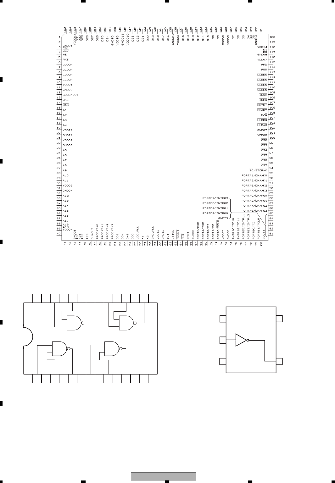
AVIC-D3/XU/UC
262
1234
1234
C
D
F
A
B
E
A1-A23 : Address Bus
bcyst : Bus Cycle Start
BT16B : Boot Bus Size 16-bit
cas : Column Address Strobe
CKE : Clock Enable
CLKOUT : Clock Out
CMODE : Clock Mode
cs)-cs& : Chip Select
D0-D31 : Data Bus
DCK : Debug Clock
DDI : Debug Data Input
DDO : Debug Data Output
DMAAK0-DMAAK3 : DMA Acknowledge
DMARQ0-DMARQ3 DMA Request
DMS : Debug Mode Select
drst : Debug Reset
GND_I : Ground
GND_O : Ground
GND_PLL : Ground
hldak : Hold Acknowledge
hldrq : Hold Request
IC1 : Internally Connected
INTP00-INTP03,INTP10-INTP13 :
Interrupt Request From Peripheral
iord : I/O Read
iowr : I/O Write
llben : Lower Lower Byte Enable
LLDQM : Lower Lower DQ Mask Enable
luben : Lower Upper Byte Enable
LUDQM : Lower Upper DQ Mask Enable
mrd : Memory Read
mwr : Memory Write Strobe
nmi : Non-Maskable Interrupt Request
PORT0-PORT4,PORTA0-PORTA7 : Port
R/w : Bus Read or Write Status
ras : Row Address Strobe
ready : Ready
reset : Reset
RXD : Receive Data
sclk : Serial Clock
SDCLKOUT : SDRAM CLKOUT
SI : Serial Input
SO : Serial Output
stopak : Stop Acknowledge
tc : Terminal Count
TCLR : Timer Clear
TI : Timer Input
TO10,TO11 : Timer Output
TRCDATA0-TRCDATA3 : Trace Data
TXD : Transmit Data
ulben : Upper Lower Byte Enable
ULDQM : Upper Lower DQ Mask Enable
uuben : Upper Lower Byte Enable
UUDQM : Upper Upper DQ Mask Enable
VDD_I : Power Supply
VDD_O : Power Supply
VDD_PLL : PLL Power Supply
we : Write Enable
X1,X2 : Crystal Oscillator
UPD705103GM-180S1
6413275
9
1114 1213 8
10
VCC
4B
4A
3B
3A
3Y
1A
1B
1Y
2A
2B
2Y
GND
4Y
TC74LCX08FTS1
TC7SH04FUS1
1 NC
2 IN A
3 GND
4 OUT Y
5 VCC
AVIC-D3/XU/UC 263
5678
56
78
C
D
F
A
B
E
1
2
3
4
5
6
7
8
9
10
11
12
13
14
15
16
17
18
19
20
21
22
84
85
86
87
88
89
90
91
92
93
94
95
96
97
98
99
100
101
102
103
104
23
83
160
161
162
163
164
165
166
167
168
169
170
171
172
173
174
175
176
177
178
105
24
82
159
228
229
230
231
232
233
234
235
236
237
238
239
240
241
242
243
244
179
106
25
81
158
227
288
245
180
107
26
80
157
226
287
246
181
108
27
79
156
225
286
247
182
109
28
78
155
224
285
248
183
110
29
77
154
223
284
249
184
111
30
76
153
222
283
250
185
112
31
75
152
221
282
251
186
113
32
74
151
220
281
252
187
114
33
73
150
219
280
253
188
115
34
72
149
218
279
254
189
116
35
71
148
217
278
255
190
117
36
70
147
216
277
256
191
118
37
69
146
215
276
257
192
119
38
68
145
214
275
258
193
120
39
67
144
213
274
273
272
271
270
269
268
267
266
265
264
263
262
261
260
259
194
121
40
66
143
212
211
210
209
208
207
206
205
204
203
202
201
200
199
198
197
196
195
122
41
65
142
141
140
139
138
137
136
135
134
133
132
131
130
129
128
127
126
125
124
123
42
64
63
62
61
60
59
58
57
56
55
54
53
52
51
50
49
48
47
46
45
44
43
VSS
PIO29
USBXPWREN
USBXOVRCUR
UVD1M
UVD1P
UVD2M
UVD2P
USBOVRCUR
USB_CLK
XCS_SRAM
XWR_SRAM
PIO31
IR_RX
TEST0
XTAL0
MST
EXTAL0
UART9_TXD
UART8_TXD
UART7_TXD
VSS
PIO27
PIO28
XCS_FLASH
D0
XMRD
USBPWREN
XIOWR
NC
NC
NC
XREADY
SRAM_CSSEL
PIO30
XCS6
XTST
SMCK
XSM
GDC_WT
UART9_RXD
UART8_RXD
UART7_RXD
UART6_TXD
DSP_BCLKI
PIO26
D2
D1
XMWR
XLLBEN
XIORD
NC
NC
NC
XBCYST
XCS2
XCS3
DREQ0
DREQ1
INT3
INT2
INT0
ATA_DA0
ATA_DA1
UART6_RXD
UART5_RXD
PIO25
D4
D3
VSS
VSS
XLUBEN
VDD
NC
VSS
NC
VDD
VDD
XCS5
VSS
DREQ2
VDD
INT1
VDD
VSS
ATA_INT
OVSS0
UART5_TXD
PIO24
D6
D5
VDD
VSS
ATA_XDMACK
UART4_RXD
UART4_TXD
PIO22
OVSS7
D8
D7
ATA_XDIOR
ATA_IORDY
XRESET
UART3_TXD
OVDD3
D10
D9
VDD
VDD
ATA_DMARQ
ATA_XDIOW
OVDD0
DSP_BDI
XCS_DSP
D12
D11
ATA_DD1
ATA_DD0
UART3_RXD
UART2_TXD
DSP_XHINT
PIO23
D16
D15
VSS
ATA_DD3
ATA_DD2
UART2_RXD
DSP_HRDY
D18
D17
VDD
ATA_DD5
ATA_DD4
UART1_RXD
UART1_TXD
OVSS6
D20
D19
VDD
VDD
ATA_DD7
ATA_DD6
A23
DSP_BFSO
DSP_BDO
D22
D21
VDD
ATA_DD8
ATA_XRESET
CPU_CLK
DSP_BCLKO
D24
D23
VSS
ATA_DD10
ATA_DD9
UART_XDCD
OVSS1
XCS_SRAMH
PIO_OUT
D26
D25
VSS
ATA_DD12
ATA_DD11
UART1_XCTS
OVDD2
OVSS5
D27
VDD
ATA_DD14
ATA_DD13
UART_XRI
UART_XDSR
DSP_BFSI
D14
D13
VSS
VDD
ATA_DA2
ATA_DD15
OVDD1
DSP_XRS
TEST1
D29
D28
ATA_XCS0
ATA_XCS1
UART1_XDTR
UART1_XRTS
DSP_ATTCNT
CD_LRCLK
D30
VSS
VDD
PC_XPWR
ATA_DIR
PIO0
D31
CD_BLK
A2
VSS
VDD
VPDP
VDD
A11
VSS
PC_XVS2
VDD
VDD
PC_BVD1
VSS
PC_XCD1
VDD
PC_XOE
VSS
VSS
PC_XUBUF
PC_XLBUF
PIO1
CD_MCLK
ADC_GCNT0
A3
A4
A5
A7
A9
A12
PC_READY
PC_RESET
PC_WXT
PC_BVD2
PC_WP
PC_XCD2
PC_XCE1
PC_XCE2
PC_XVS1
PC_XIORD
PC_XIOWR
PC_XWE
PIO2
OVSS2
ADC_GCNT2
ADC_GCNT1
ADC_BCLK
ADC_MCLK
A6
A8
A10
TEST2
DAC_MCLK
DAC_BCLK
PC_XREG
PC_A0
PIO20
PIO19
PIO17
PIO15
PIO13
PIO11
PIO9
PIO7
PIO5
PIO3
VSS
ADC_DATA
ADC_LRCLK
TEST4
EXTAL1
OVSS4
XTAL1
TEST3
DAC_LRCLK
DAC_DATA
PIO21
OVSS3
CD_DATA
PIO18
PIO16
PIO14
PIO12
PIO10
PIO8
PIO6
PIO4
VSS
TOP VEIW
TOP VEIW
PD6336C
- Pin Arrangement Chart
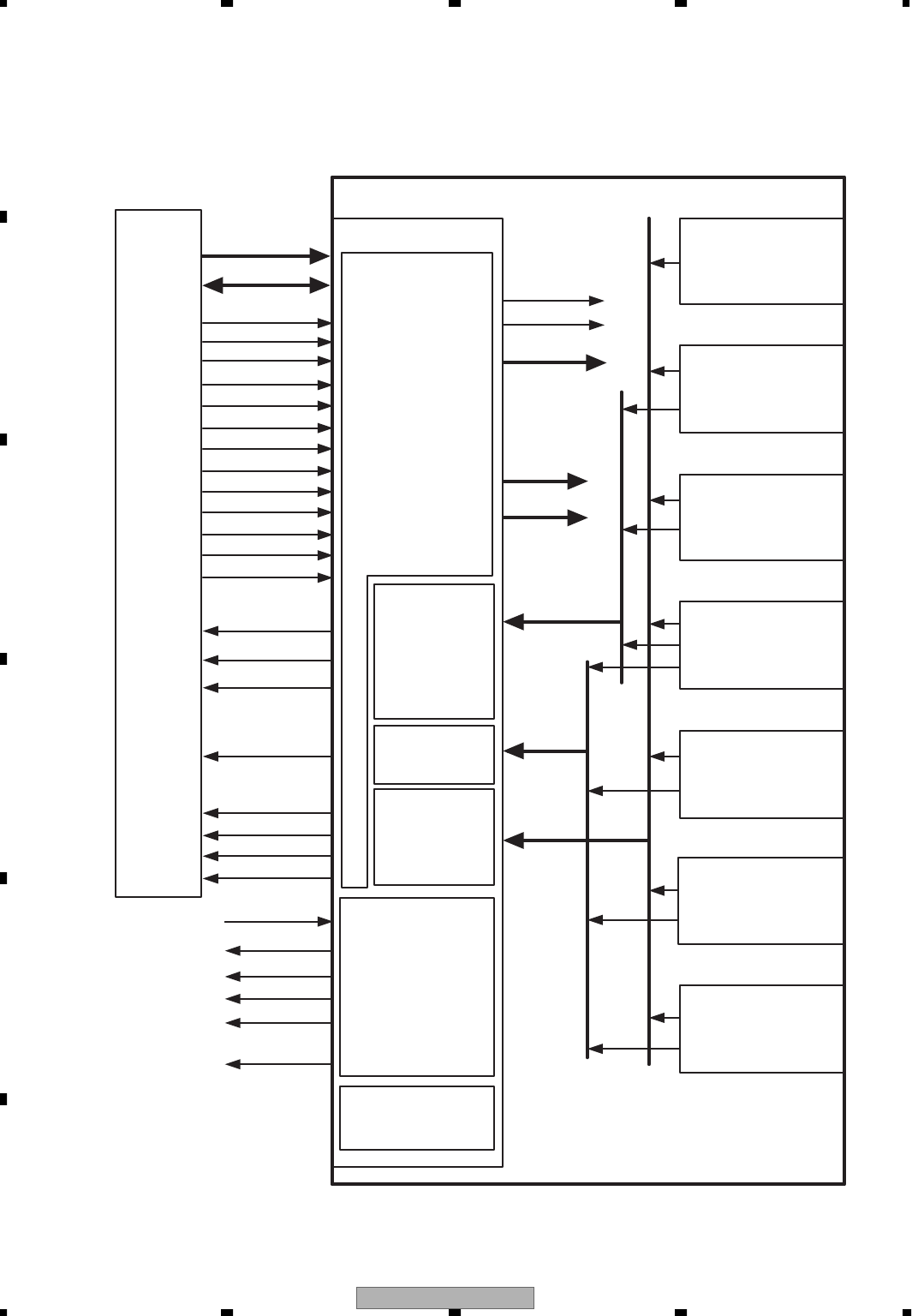
AVIC-D3/XU/UC
264
1234
1234
C
D
F
A
B
E
A2-A11,A23
D0-D31
CPU_CLK
XBCYST
XRESET
XCS2(SRAM)
XCS3(ASIC)
XCS5(PCCARD)
XCS6(DSP)
XIOWR
XIORD
XMWR
XMRD
XLLBEN
XLUBEN
DMARQ0
DMARQ1
DMARQ2
INTP0
INTP1
XREADY
INTP2
INTP3
SRAM_CSSEL
XCS_SRAM
XCS_SRAMH
XCS_FLASH
XCS_DSP
XWR_SRAM
CPU I/F BLOCK
TOP SECTION
DMA CHANNEL
SELECT SECTION
WAIT CONTROL
SECTION
INTERRUPT
CONTROL
SECTION
PROTECT
and
CHIP SELECT
GENERATOR
SECTION
TIMER SECTION
ASIC
ASIC_CLK
XRESET
A7-A2
WExx
RExx
DMAxx
WAIT
WTxx
INTxx
DMA
INT
AUDIO BLOCK
CD-ROM BLOCK
PERI BLOCK
(SIO,PIO,
REMOTE CONTROL)
ATAPI BLOCK
PC-CARD BLOCK
SOUND BLOCK
USB BLOCK
CPU
- Block Diagram Chart
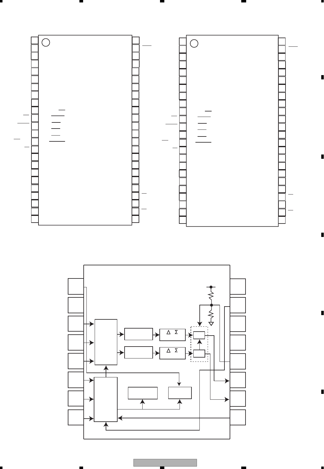
AVIC-D3/XU/UC 265
5678
56
78
C
D
F
A
B
E
1
A15
2
A14
3
A13
4
A12
5
A11
6
A10
7
A9
8
A8
11
WE
12
RESET
13
A21
14
WP/ACC
15
16
RY/BY
A18
A0-A18,A-1
RY/BY
BYTE
OE
DQ0-DQ15
:Address input
:Ready/busy output
:8bit,16bit mode select
:Output enable
:Data input/output
WE :Write enable
CE :Chip enable
RESET :Reset
9
A19
10
A20
17
A17
18
A7
19
A6
20
A5
21
A4
22
A3
23
A2
24
A1
A16
BYTE
VSS
DQ15/A-1
DQ7
DQ14
DQ6
DQ13
38 DQ4
37 VCC
36 DQ11
35 DQ3
34
33
DQ10
DQ2
DQ5
39 DQ12
32 DQ9
31 DQ1
30 DQ8
29 DQ0
28 OE
27 VSS
26 CE
25 A0
47
46
45
44
43
42
48
41
40
PEH103A (UC)
PEH077A (EW5)
1
A15
2
A14
3
A13
4
A12
5
A11
6
A10
7
A9
8
A8
11
WE
12
RESET
13
A21
14
15
16
RY/BY
A18
A0-A18,A-1
RY/BY
BYTE
OE
DQ0-DQ15
:Address input
:Ready/busy output
:8bit,16bit mode select
:Output enable
:Data input/output
WE :Write enable
CE :Chip enable
RESET :Reset
9
A19
10
A20
17
A17
18
A7
19
A6
20
A5
21
A4
22
A3
23
A2
24
A1
A16
BYTE
VSS
DQ15/A-1
DQ7
DQ14
DQ6
DQ13
38 DQ4
37 VCC
36 DQ11
35 DQ3
34
33
DQ10
DQ2
DQ5
39 DQ12
32 DQ9
31 DQ1
30 DQ8
29 DQ0
28 OE
27 VSS
26 CE
25 A0
47
46
45
44
43
42
48
41
40
PEH104A (UC)
PEH078A (EW5)
wp/ACC : Write protect/
Acceleration
wp/ACC : Write protect/
Acceleration
WP/ACC
1
3
2
AOUTL
LRCK 4
8
7
6
5
SMUTE
RSTN VCOM
16
15
14
13
DEM
MCLK
12
11
10
9
BICK
SDTI
DIF1
VDD
ACKS
DIF0
AOUTR
VSS
DZF
Control
Port
Audio
Data
Interface
De-emphasis
Control
Clock
Divider
8X
Interpolator Modulator LPF
8X
Interpolator Modulator LPF
AK4388VT
AVIC-D3/XU/UC
266
1234
1234
C
D
F
A
B
E
Host
Interface
Memory
Interface
Controller
External Video
Interface Controller
Display Controller
DAC
Set-up
Engine
2D/3D
Rendering
Engine
Embedded SDRAM
(64bit x 256K word)
64bit
D0-32
A2-24
ARGB
DRGB
RBT656
MB86291APFVS-G-DL
8 VCC
7 1Y
6 2B
5 2A
1A 1
1B 2
2Y 3
GND 4
TC7WH32FU
1 2 31
VOUT SUB CT
45
VDD GND
Vref
BD5335FVE

AVIC-D3/XU/UC 267
5678
56
78
C
D
F
A
B
E
-
Pin F
u
n
c
ti
o
n
s
(
UC : PE5580A, EW5 : PE5581A
)
Pi
n
No
.
Pi
n
Na
m
e
I
/O
Function and
Op
eration
1
S
IM
U
KE
3
I
Typ
e
i
n
p
ut
2
S
IM
U
KE
0
I
Typ
e
i
n
p
ut
3 SIMUKE1 I Type input
4 SIMUKE2 I Type input
5 GND0 GND
6 ROMCS O ROM collection chip select output
7 ROMCLK O ROM collection clock output
8 ROMDATA I/O ROM collection data input/output
9 VDT O E. volume data output
10 VCK O E. volume data clock output
11 MUTEVO O E. volume mute output
12 VST O E. volume strobe output
13 ROT1 I Rotary encoder input
14 ROT2 I Rotary encoder input
15-21 NC Not used
22 VDD0 Power supply
23 RDT I RDS : Data input (EW model)
24 RDS57K I RDS : 57 kHz pulse count input (EW model)
25 RDSLK I RDS : Lock signal input (EW model)
26-28 NC Not used
29 wcont I Wired remote control SEL input
30-32 NC Not used
33 DALMON O For consumption current reduction output
34 DD8CONT O MS5 power supply control output
35 NC Not used
36 CLKOUT O System clock output
37 GND0 GND
38 CPUREG CPU regulator connection
39 VDD0 Power supply
40 RESET I System reset input
41 VPP Flash ROM writing voltage supply
42 FLASH1 I Flash ROM writing data input
43 FLASH2 O Flash ROM writing data output
44 FLASH3 O Flash ROM writing clock output
45 LDET I RDS : PLL lock signal input (EW model)
46 TUNDI I FM/AM tuner data input
47 TUNDO O FM/AM tuner data output
48 TUNCLK O FM/AM tuner clock output
49-51 NC Not used
52 MUTENS Not used
53 NOSELL O L ch guide mute control output
54 NOSELR O R ch guide mute control output
55 NC Not used
56 PGSEL Not used
57 RCK I RDS : Data clock input (EW model)
58 TELIN I Mobile phone mute input
59 VPPON O Voltage supply control output
60 VDD1 Power supply
61 SREMOT O Control output for system remote
62 SYSPWR O System power supply control output
63 FANCONT O Fan output control output
64 ANTON O Control output for auto antenna
65 XVMUTE O Composition mute output
66 NC Not used
67 FCONT O Control output for DD converter
68 NC Not used
69 blsens I B. up power supply sense input
70 XT2 Not used
71 XT1 Not used
72 GND2 GND
73 X1 Crystal oscillating element connection
74 X2 Crystal oscillating element connection
75 NMI Not used

AVIC-D3/XU/UC
268
1234
1234
C
D
F
A
B
E
Pi
n
No
.
Pi
n
Na
m
e
I
/O
Function and
Op
eration
76
A
CO
NTA
O
A
u
di
o sw
i
tc
h
contro
l
out
p
ut
77
A
CO
NTB
O
A
u
di
o sw
i
tc
h
contro
l
out
p
ut
78 DRAMPW O DRAM power supply control output
79 CCON O Navigation power supply control output
80 SIMUKE4 I Type input
81-83 NC Not used
84 VSEL1 O Picture selector control output 1
85 VSEL2 O Picture selector control output 2
86 BCVSW O Picture selector control output (Back camera)
87 NC Not used
88 ASENBO O ASENBO output for IP-BUS output
89 IPPW O IP-BUS driver power supply control output
90 RX I IP-BUS data input
91 TX O IP-BUS data output
92 GND1 GND
93-95 NC Not used
96 asens I ACC power supply sense input
97 DEQON O DEQ connect enable output
98 MUTE O Mute output
99 GUIDEMUTE Not used
100 TUNCE1 O Chip enable output for FM/AM tuner
101 TUNCE2 O Chip enable output for FM/AM tuner
102 VDD2 Power supply
103 CPUWDT I Watch dog timer input
104 RSTOUT O RSTOUT output
105 XCCSTBY I OFF processing completion input
106 RST3 Not used
107 MTOSYS I Monitor microcomputer UART communication (Reception) input
108 SYSTOM O Monitor microcomputer UART communication (Transmission) output
109 SWACPW O Monitor microcomputer power supply control output
110 PRGON I System microcomputer self programing mode ON input
111 RXIPOD I iPod : UART communication input
112 TXIPOD O iPod : UART communication output
113 IRQPWR O B. up OFF output
114 RSTOUT NC
115 NC NC
116 psens I iPod : Connect sense input (communication)
117 CTOSYS I Navigation UART communication (Reception) input
118 SYSTOC O Navigation UART communication (Transmission) output
119 CPRESET Not used
120 OPTON O Optical digital output
121,122 NC Not used
123 PID O iPod : Communication mode notification output
124 PPW O iPod : Power supply control output
125 psensg I iPod : Connect sense input (connector)
126 illsns I Illumination sense input
127 CPREADY Not used
128 VDD1 Power supply
129 PBSNS I Parking brake sense input
130 bksns I Back gear sense input
131 GND1 GND
132 optsns I Optical cable detection input
133 dvejky I MS3 eject key input
134 NC Not used
135 TUNSL I Signal level inptut for FM/AM tuner
136 BLEVSNS Not used
137 WREMIN I Wired remote control AD input
138 REVMDL I Model type reversing switch input
139 FWSNS I iPod : Control input
140 NC Not used
141 TESTIN I Testmode input
142 TIMEOUT I Time out input
143 ADCVDD A/D converter power supply
AVIC-D3/XU/UC 269
5678
56
78
C
D
F
A
B
E
Pi
n
No
.
Pi
n
Na
m
e
I
/O
Function and
Op
eration
144
AD
CG
ND A
/
D converter GN
D
36
37
72
73
108
109
144
1
PE5580A
(
U
C)
PE5581A (EW5)
1
2
34
5
ON/OFF
CIRCUIT
REFERENCE
VOLTAGE
SHORT-
CIRCUIT
PROTECT
VIN
NC
VSS
VOUT
ON/OFF
S-814A50AUC-BDO
12345
VO
NC
GND
NC
VCC
Reference
voltage
BD3931HFP
AVIC-D3/XU/UC
270
1234
1234
C
D
F
A
B
E
1
2
3
4
5
6
7
8
9
10
11
12
13
14
15
30
29
28
27
26
25
24
23
22
21
20
19
18
17
16
INV1
FB1
SOFTSTART1
PWM/SKIP
CT
5V_STBY
GND
REF
STBY1
STBY2
FLT
POWERGOOD
SOFTSTART2
FB2
INV2
LH1
OUT1_u
LL1
OUT1_d
OUTGND1
TRIP1
VCC
TRIP2
VREF5
REG5V_IN
OUTGND2
OUT2_d
LL2
OUT2_u
LH2
TPS5120DBT
- Pin Arrangement Chart
15
14
13
12
11
10
9
8
7
6
5
4
3
2
1
16
17
18
19
20
21
22
23
24
25
26
27
28
29
30
NC
NC
ROUT3
ROUT2
ROUT1
DIN3
DIN2
DIN1
C5-
GND
C5+
C1-
VCC
C1+
VDD
NC
NC
RIN3
RIN2
RIN1
DOUT3
DOUT2
DOUT1
EN
VCHA
stby
VSS
C4-
GND
C4+
UPD4723GSS1
AVIC-D3/XU/UC 271
5678
56
78
C
D
F
A
B
E
SOFTSTART1
DLY
DLY
OSC
Timer
SOFTSTART2
DLY
DLY
Phase
Vref 5 VREG
Current
Protection
Trigger
Skip Comp.
PWM Comp.
Err Amp.
0.85 V
STBY1
UVLO
SIGNAL
STBY2
OVP1
OVP2
UVP1
UVP2
0.85 V+12%
Err Amp.
Skip Comp.
0.85 V UVLO
SIGNAL
UVLO
Comp.
0.85 V
INV2 INV1
PGcomp4 PGcomp3 INV2
PGcomp2
INV1
0.85 V –7% PGcomp1
4.5 V
5.0 V
PWM Comp.
Current Comp.
VCC
SOFTSTART1
FB1
INV1
CT
FLT
FB2
INV2
PWM/SKIP
SOFTSTART2
STBY1
STBY2
REF
5V_STBY
GND
POWERGOOD
REG5V_IN
VREF5
LH2
OUT2_u
LL2
OUT2_d
OUTGND2
TRIP2
TRIP1
VCC
OUTGND1
OUT1_d
LL1
OUT1_u
LH1
SFT1 SFT2
Inverter
0.85 V+12%
0.85 V –19.4%
0.85 V –19.4%
0.85 V –7%
0.85 V +7%
0.85 V +7%
_
+
_
+
_
+
_
+
_
+
_
+
_
+
+
_
+
_
+
+
_
+
_
+
_
+
_
+
_
+
_
+
_
+
_
+_
+
_
+
–(VCC –VTRIP1)
VCC –VTRIP1
LSD Trip
HSD Trip
_
+
HSD Trip
LSD Trip
VCC –VTRIP2
–(VCC –VTRIP2)
- Block Diagram Chart
AVIC-D3/XU/UC
272
1234
1234
C
D
F
A
B
E
1
2
3
4
5
6
7
8
9
10
11
12
13
14
15
PD
25
2
4
2
30
29
28
27
26
25
24
23
22
21
20
19
18
17
16
IF-MIXin
GND (IF-MIX)
RF-MIXout
VCC (RF-MIX)
RF-MIXin
VCC (1stLO-OSC)
1stLO-OSC1
1stLO-OSC2
GND (1stLO-OSC)
VCC (phase detector)
PD-Vout3
PD-Vout2
PD-Vout1
GND (phase detector)
GND (RF-MIX)
VCC (IF-MIX)
VGC (IF-MIX)
IF-MIXout
GND (2ndIF-AMP)
2ndIFin1
2ndIFin2
2ndIFbypass
VCC (2ndIF-AMP)
2ndIFout
REFout
VCC (reference block)
REFin
GND (divider block)
LOout
VCC (divider block)
UPB1027GS
2
10
11
12
13
14
15
16
17
18
19
20
21
22
39
38
37
36
35
34
33
32
31
30
29
28
27
43
42
41
40
47
46
45
44
48
A15
A14
A13
A12
A11
A10
A9
A8
NC
NC
we
reset
NC
NC
RY/by
NC
A17
A7
A6
A5
A4
A3
A16
byte
VSS
DQ15/A-1
DQ7
DQ14
DQ6
DQ13
DQ5
DQ12
DQ4
VCC
DQ11
DQ3
DQ10
DQ2
DQ9
DQ1
DQ8
DQ0
oe
VSS
23
24
26
25
A2
A1
ce
A0
A-1
A0-A17
DQ0-D15
byte
ce
oe
RY/by
reset
NC
VCC
VSS
we
8
9
4
5
6
7
3
1
:Data output/Address input
:Address input
:Data input output
:Mode select
:Chip enable input
:Output enable input
:Ready/Busy output
:Reset
:Not used
:Power supply
:GND
:Write enable
PEH100A8 (UC)
PEH101A8 (EW5)
AVIC-D3/XU/UC 273
5678
56
78
C
D
F
A
B
E
Pin No. Pin Name I/O Format Function and Operation
1 VCC0 Power supply (3.3V)
2 VSS0 GND
3 TXD2 l/O SIO2 Transmission data input / output
4 RXD2 l/O SIO2 Reception data input / output
5 TXD1 O C SIO1 Transmission data output
6 RXD1 l SIO1 Reception data input
7 TXD0 O C SIO0 Transmission data output
8 RXD0 l SIO0 Reception data input
9 SPEED l SP I/F input
10 ADCSB O C AD I/F output
11 ADSCK O C AD I/F output
12 ADTXD O C AD I/F output
13 ADRXD l AD I/F input
14 ADSRX l AD I/F input
15 ADIO0 l/O AD I/F input / output
16 ADIO1 l/O AD I/F input / output
17 ADIO2 l/O AD I/F input / output
18 VCC1 Power supply (3.3V)
19 VSS1 GND
20 PWM O PWM signal output
21 PLINT l PLL I/F input
22 PLCE O C PLL I/F output
23 PLSCK O C PLL I/F output
24 PLTX O C PLL I/F output
25 PLRX l PLL I/F input
26 PLIO0 l/O PLL I/F input / output
27 PLIO1 l/O PLL I/F input / output
28 PLIO2 l/O PLL I/F input / output
29 DDINT l DARC I/F input
30 DDCE O C DARC I/F output
31 DDSCK O C DARC I/F output
32 DDTX O C DARC I/F output
33 DDRX l DARC I/F input
34 DDIO0 l/O DARC I/F input / output
35 DDIO1 l/O DARC I/F input / output
36 DDIO2 l/O DARC I/F input / output
37 TIOA0 l/O ParaIIeI input / output
38 TIOA1 l/O ParaIIeI input / output
39 TIOB0 l/O ParaIIeI input / output
40 TIOB1 l/O ParaIIeI input / output
41 VCC2 Power supply (3.3V)
42 VSS2 GND
43-53 A19-9 l/O Address bus input / output
54 VCC3 Power supply (3.3V)
55 VSS3 GND
56-64 A8-0 l/O Address bus input / output
65 VCC4 Power supply (3.3V)
66 VSS4 GND
67-82 D0-15 l/O Address bus input / output
83 VCC5 Power supply (3.3V)
84 VSS5 GND
85 WRHB l/O Upper data write strobe input / output
86 WRLB l/O Lower data write strobe input / output
87 RDB l/O Read data strobe input / output
88 CS2B l/O Chip select aria 1 for external storage input / output
89
90
CS0B l/O Chip select aria 0 for ROM input / output
VCC6 Power supply (3.3V)
-Pin Functions(PD3390A)
AVIC-D3/XU/UC
274
1234
1234
C
D
F
A
B
E
Pin No. Pin Name I/O Format Function and Operation
91 VSS6 GND
92 TEST2 Test mode
93 CKOEB l CK output enable input
94 CK O CPU clock output
95 CS5B O C DRAM low address strobe output
96 CS3B O
O
DRAM column address strobe output
97 CS1B C DRAM column address upper byte strobe output
98 RTCVSS1
l
Power supply (3.3V)
99 SRAMB
l
Backup memory select input
100 STANBYB Stand by signal input
101 RTCVSS0 GND
102 XRTCIN l
C
C
C
Sub crystal oscillator input (RTC)
103 XRTCOUT O Sub crystal oscillator output (RTC)
104 RTCVCC Power supply (3.3V)
105 PCKSEL0 l Processor clock select input
106 PCKSEL1 l Processor clock select input
107 CCKSEL l
l/O
CRCK signal select input
108 CCKDIR Carrier clock direct input / inverter amp output
Power supply (3.3V)109 CCKVCC
110 CRCK l Carrier clock input
111 CCKGND GND
112-118 PC0-6 l/O Parallel input / output
119 NMI Connect to VCC
120 RESETB l System reset input
121 MSTRSTB l Test reset input
122 TEST0 l Test mode input
123 TEST1 l Test mode input
124 REFSEL l GPS reference clock select input
125 REFCK l Reference clock input
126 VCC7 Power supply (3.3V)
127 VSS7 GND
128 XAUXIN l
C
C
Sub crystal oscillator output input (AUX)
129 XAUXOUT O Sub crystal oscillator output (AUX)
130-133 PIN0-3 l Parallel input
134-137 PIO4-7 l/O Parallel input / output
138 TXD3 l/O SIO3 Transmission data input / output
139 RXD3 l/O SIO3 Reception data input / output
140 BOWWOWB O Watch dog timer output
141 IFDIR l/O IF direct input / IF inverter amp output
142 IFVCC
l
l
Power supply (3.3V)
143 IF IF input
IF amp GND input
Format
C
Meaning
CMOS
144
PD3390A
72
37
109
144
36
1
73
108
IFGND
AVIC-D3/XU/UC 275
5678
56
78
C
D
F
A
B
E
Pin No. Pin Name I/O
O
l
Function and Operation
1 VREF Reference voltage output
2 MPXIN Base band (multiplexed) signal input
3 Vdda Analog system power supply (+ 5 V)
4 NC Not used
5 Vssa Analog system GND
6 FLOUT O Sub carrier output (filter output)
7 CIN l Sub carrier input (comparator input)
8 NC Not used
9 T1 l Test input (connect to GND)
10 T2 l Test input (stand-by control)
11 T3 O RDS clock output
12 NC Not used
13 T4 O RDS data output
14 T5 O Soft-decision control data output
15 XOUT O Crystal oscillator output
16 XIN l Crystal oscillator input
17 Vddd Digital system power supply (+ 5 V)
18 Vssd Digital system GND
19 NC Not used
20 T6 O Error status,regenerated carrier and error block count outputs
21 T7 O Error correction status, SK detection and error block count outputs
22 SYNC O Block synchronization detection output
23 NC Not used
24 RDS-ID O RDS detection output
25 DO O Data output
26 CL l Clock input
27 NC Not used
28 DI l Data input
29 CE l Chip enable input
30 SYR l Synchronization and RAM address reset input
- Pin Functions(LC72720YVSS1 : EW5)
LC72720YVSS1 (EW5)
1
15
30
16
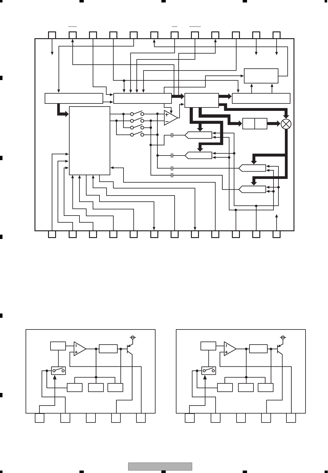
AVIC-D3/XU/UC
276
1234
1234
C
D
F
A
B
E
ADC12H034CIMSAS1
Address Latch and Decoder Control Timing
Analog
Input
Multiplexer
SAR
+Main DAC
-Main DAC
-Correction
DAC
+Correction
DAC
Output Shift Register
ALU RAM
Output Select
Logic and Buffer
1
CH0
2
CH1
3
CH2
4
CH3
5
COM
6
MUX
OUT1
7
A/DIN1
8
MUX
OUT2
9
A/DIN2
10
VREF-
11
VREF+
12
DGND
24
VD+
23
DOR
22
CCLK
21
SCLK
20
DI
19
DO
18
CS
17
CONV
16
EOC
15
PD
14
AGND
13
VA+
OVP TSD OCP
Vref Driver
GND
VCC
CTL
2
1
VOUT 4
C5
3
BA00CCWCP-V5
OVP TSD OCP
Vref Driver
NC
VCC
CTL
2
1
VOUT 4
C5
3
BA00CCWFP (EW5)
AVIC-D3/XU/UC 277
5678
56
78
C
D
F
A
B
E
1
TAB
2
P-GND2
3
OUT2-
4
STBY
5
OUT2+
6
VCC
7
OUT1-
8
P-GND1
9
OUT1+
10
SVR
11
IN1
12
IN2
13
S-GND
14
IN4
15
IN3
16
AC-GND
17
OUT3+
18
P-GND3
19
OUT3-
20
VCC
21
OUT4+
22
MUTE
23
OUT4-
24
P-GND4
SWITCH
25
+-+
-
Offset
Detection
+-+
-
Offset
Detection
+-+
-
Offset
Detection
+-+
-
Offset
Detection
Protector;
Over current limit
sw_vcc
stby
Protector;
Short circuit
Mute circuit
amp_vcc
Stand-by
Circuit
Protector;
Over voltage
sw_vcc
Protector;
Thermal
Reference
amp_vcc
PAL007C
132
OUT1
-IN1
+IN1
VEE +IN2
-IN2
OUT2
VCC
4
567
8
+
+
BA4558RFVM
1
2
3
5
4
VOUT
GND
V+ VIN
VGND
NJM2505F
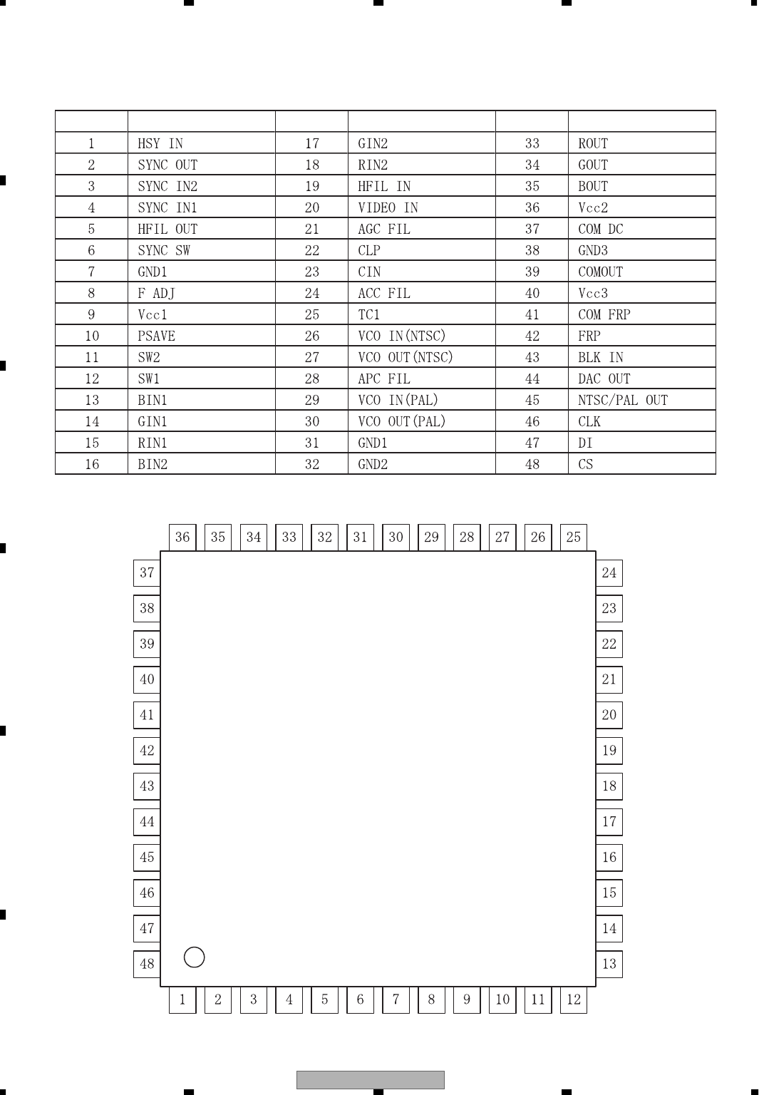
AVIC-D3/XU/UC
278
1234
1234
C
D
F
A
B
E
Pi
n
No.
Pi
n
Na
m
e
Pi
n
No.
Pi
n
Na
m
e
Pi
n
No
.
Pi
n
Na
m
e
RB5P0090M
-
Pin Arran
g
ement Char
t
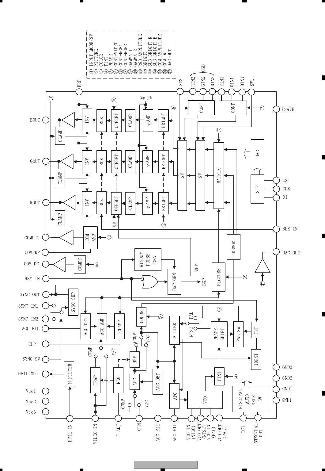
AVIC-D3/XU/UC 279
5678
56
78
C
D
F
A
B
E
- Block Diagram Chart
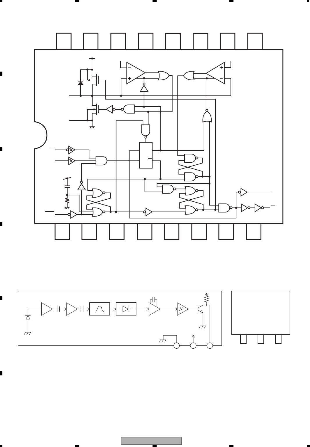
AVIC-D3/XU/UC
280
1234
1234
C
D
F
A
B
E
Rx/Cx
Cx
A
B
CLR
Q
Q
C2 H
Vref
Vref
C1
L
VCC
QP
QN
F/F
R
DQ
CK Q
16 15 14 13 12 11 9
12345678
1a1clr 1q
2a2clr2qVCC 1Rx/Cx 1Cx 1Q 2B
1B 2Q 2Cx 2Rx/Cx GND
10
TC74VHC221AFTS1
vout GND VCC
123
Amp Limiter B.P.F Demodulato Integrator Comparator
GND VCC vout
1
32
RL
GP1UX51RK
- Pin Arrangement Chart- Block Diagram Chart

AVIC-D3/XU/UC 281
5678
56
78
C
D
F
A
B
E
51 TESTIN I Chip test input
- Pin Functions (PE5584A)
Pin No. Pin Name I/O Function and Operation
1
PNLADX Touch panel X directions A/D input
2
NC Not used
3 PNLADY Touch panel Y directions A/D input
4 AVSS A/D converter GND
DIMMER O Dimmer analog output
7 AVREF1 D/A converter standard voltage
8 RXD I Data input from system microcomputer
9 TXD O Data output from system microcomputer
10
MFLPW O Back light power supply control output
17 OSDDT O OSD data output
18 OSDCK O OSD clock output
19 OSDCS O OSD chip select output
16 OSDTRE Not used
TSCK I Test mode clock input
20 EPRRST I EEPROM data initialization mode input
21 EPRTEST I EEPROM data setting mode input
22 STEST I The monitor independent mode input for aging
30 INVBST O CCFL current boost output
32
33 VSS1 GND
41,42 NC Not used
43 FREQSW DC convertor select output
44 INVPUL Inverter pulse output
45 NC Not used
5
49 EPRCS O EEPROM chip select output
48 EPRCK O EEPROM serial clock output
47 EPRDO O EEPROM serial data output
46 EPRDI I EEPROM serial data input
59 SRVTEST I Adjustment mode input for service
60 RESET I Reset input
61 REMIN I Remote control data input
I
I
23
24 PNLXV O Touch panel X directions power supply control output
25 PNLYV O Touch panel Y directions power supply control output
TPTEST I Touch panel test mode input
11 MVIPW O Video power control output
26 PNLVD O Touch panel power supply control output
31 OSDDIPS OSD display control output
12 LCDDT I/O LCD data input/output
13 LCDCK O LCD clock output
14 LCDCS O LCD chip select output
15 BLKDRV O Mute output
27 RGBSEL O RGB/ C. Video select output
28 PSAVE O LCD IC power save output
29 COLSYS O NTSC/PAL detect output
O
34 MODS O Screen mode select output
35 MODW O Screen mode select output
36 MODN O Screen mode select output
37 NC Not used
38 ROMDATA I/O ROM collection data input/output
39 ROMCLK O ROM collection clock output
40 ROMCS O ROM collection chip select output
O
O
50 NC Not used
52 LEDDT I/O LED data input/output
53 LEDCK O LED clock output
54 LEDCS O LED chip select output
55 PHTEST I PHASE adjustment mode input
56 PALARI I Model type detect input
57 JUC I Model type detect input
58 ILMTEST I RGB illumination test mode input
DOTCLK Pixel align
6
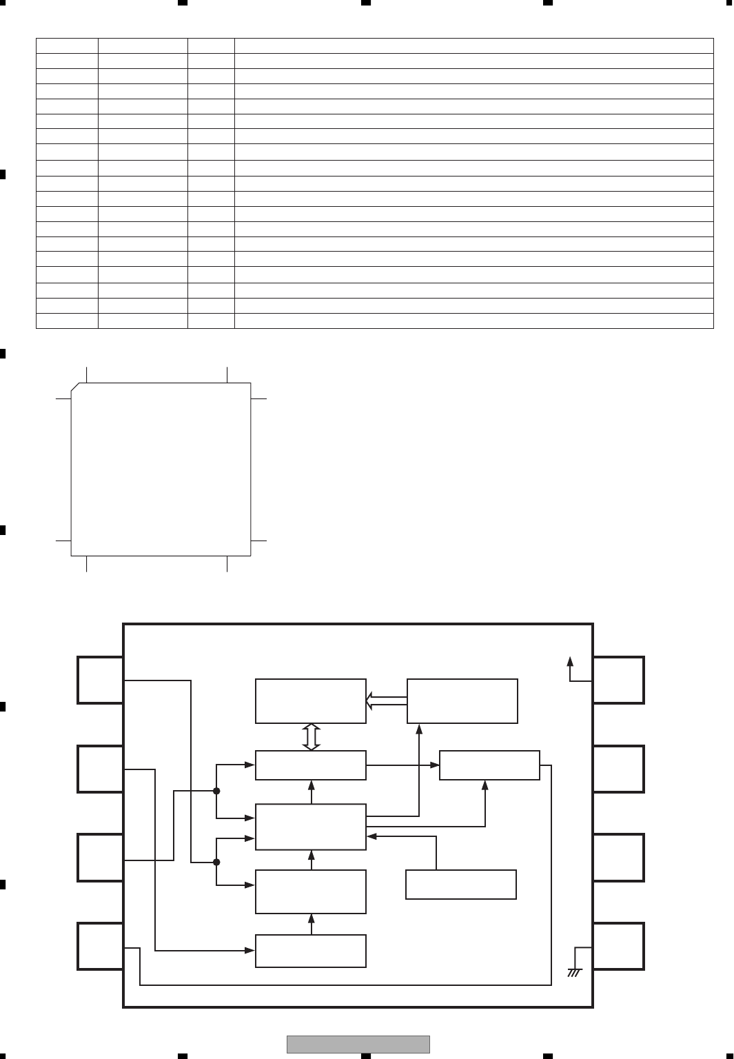
AVIC-D3/XU/UC
282
1234
1234
C
D
F
A
B
E
Pin No. Pin Name I/O Function and Operation
76 KDT0 I Analog key data intput
77 KDT1 I Analog key data intput
78 KDT2 I Analog key data intput
79 KDT3 I Analog key data intput
80 TEMPSEN I Temperature detection input
1
20
21 40
41
60
6180
PE5584A
74 VDD0 Power supply
75 AVDD A/D converter power supply
62 VDDSENS I EEPROM power supply sense input
68 VDD1 Power supply
69 X2 Crystal oscillating element connection
70 X1 Crystal oscillating element connection
71 VPP I Flash writing input
72 XT2 Not used
73 XT1 GND
67 VSS0 GND
63 NC Not used
64 VSYNC I Vertical synchronizing signal input
65,66 NC Not used
CS
SK
DI
DO
VCC
NC
TEST
GND
1
2
3
4
8
7
6
5
Memory
Aray
Address
Decoder
Mode Decode
Logic
Data Resistor Output Buffer
Clock Pulse
Counter
Voltage Ditector
Clock Oscillater
S-93C46BR0I-J8
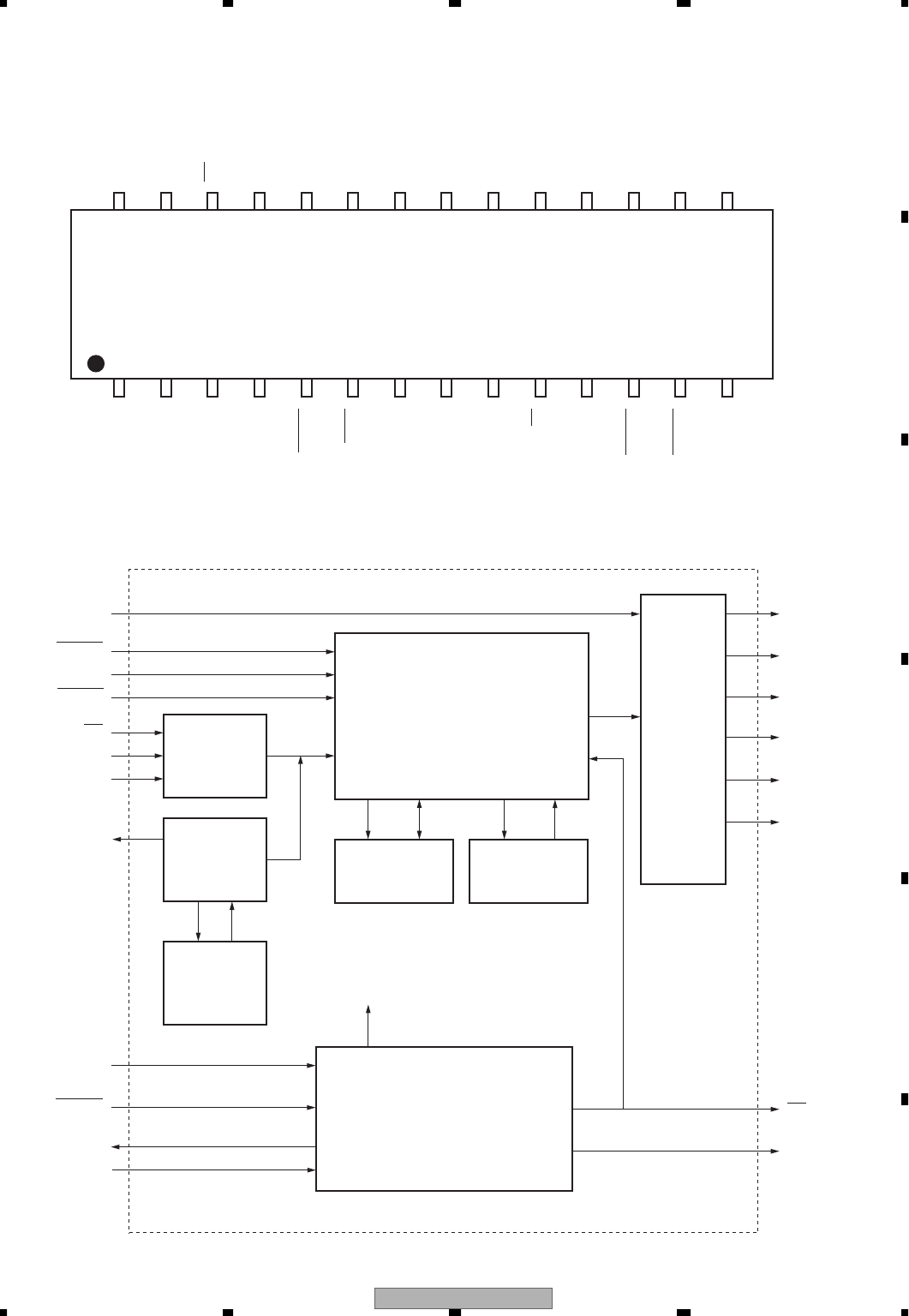
AVIC-D3/XU/UC 283
5678
56
78
C
D
F
A
B
E
CPOUT
AVSS
VCOIN
AVSS
RESET
TEST
VSS
DOCKI
DOCKO
FH
EVEN
HSYNC
VSYNC
DISP
AV3V
AVCC
CS
SIN
SCLK
TRE
VCC
V3V
BOUT (C0)
ROUT (C1)
GOUT (C2)
IOUT (C3)
VOB1
VOB2
1
2
3
4
5
6
7
8
9
10
11
12
13
14
28
27
26
25
24
23
22
21
20
19
18
17
16
15
DISP BOUT
ROUT
GOUT
IOUT
VOB1
VOB2
FH
DOCKO
DOCKI
HSYNC
CPOUT
VCOIN
VSYNC
EVEN
RESET
CS
SIN
SCLK
TRE
Serial input
control
Display control Display
output
control
Command
table ROM
Command
table ROM
control Display memory
VRAM Font ROM
Dot clock generator circuit
Dot clock
(16 KByte)
(PLL circuit)
(512 char.)(32 char. x 16 line)
- Pin Arrangement Chart
- Block Diagram Chart
PD6567A

AVIC-D3/XU/UC
284
1234
1234
C
D
F
A
B
E
-
Pin F
u
n
c
ti
o
n
s
(
LZ9FE30
)
Pi
n
No.
Pi
n
Na
m
e
I
/O
Function and
Op
eration
1
VIN
I
V
ert
i
ca
l
s
y
nc
h
ron
i
z
i
n
g
s
ig
na
l
i
nput
2
C
V
O
P
O
V
ert
i
ca
l
s
y
nc
h
ronous separat
i
on s
ig
na
l
output
3 HON_E O Test setting output
4 HSY I/O Horizontal synchronizing signal input/output
5 VDD1 Power supply
6 FRPT O Polarity reversing signal output (common electrode)
7 SYNI I Compound synchronous signal input
8 FRPV O Polarity reversing signal output (video signal)
9 GND1 GND
10 VCS O Normal mode mask signal output
11 NTPC I NTSC/PAL setting input
12 VSY I/O Vertical synchronizing signal input/output
13 HRVC I Horizontal scanning direction setting input
14 VRVC I Vertical scanning direction setting input
15 CLKC I Clock synchronous signal I/O setting input
16 MDS I Display mode setting input
17 GND2 GND
18 EXCL I/O Clock input/output
19 GND3 GND
20 MDW I Display mode setting input
21 MDN I Display mode setting input
22 PWM O Backlight control signal output
23 MON_F O Test setting output
24 VSWC I VSWO output control input
25 VSWI I Video system switch input
26 VSWO O Video system switch output
27 VDD2 Power supply
28 SPOI I/O Start signal input/output for source driver
29 GND4 GND
30 PCP O Test setting output
31 CLOC I EXCL port output mode switch input
32 MOD2 O Control signal output for gate driver
33 HR O Horizontal scanning setting output for source driver
34 IVR O Vertical scanning setting output for gate driver
35 PS O Control signal output for source driver
36 CTR O Control signal output for source driver
37 SPIO I/O Start signal input/output for source driver
38 PDP O Phase comparison output
39 PAIR I Pairing setting siganl input
40 MON O Test setting output
41 APN I Horizontal display position setting input
42 GND5 GND
43 OSCO O Clock oscillation circuit output
44 OSCI I Clock oscillation circuit input
45 VDD3 Power supply
46 GND6 GND
47 CLD O Clock signal output for source driver
48 TST1 I Test setting input
49 RESH I Horizontal counter reset input
50 RESV I Vertical counter reset input
51 TST2 I Test setting input
52 TEST I Test setting input
53 MON_A O Test setting output
54 TPC O Touch panel control signal output
55 MON_C O Test setting output
56 MON_D O Test setting output
57 CLS O Clock signal output for gate driver
58 SPS O Reset signal output for gate driver
59 VR O Scanning setting output for gate driver
60 MOD1 O Control signal output for gate driver
61 TCLK I Test setting input
62 GND7 GND
63 GND8 GND
AVIC-D3/XU/UC 285
5678
56
78
C
D
F
A
B
E
Pi
n
No.
Pi
n
Na
m
e
I
/O
Function and
Op
eration
6
4
G
P
S
O
S
i
g
nal output for
g
ate power suppl
y
65
L
O
WI
I
C
ontrol si
g
nal in
p
ut for
g
ate driver
66 ABC I Output setting input
67 VDC Power supply
68 GND9 GND
69 DVTC O Test setting output
70 BLKI I Screen position adjustment input
71 BLKO O Screen position adjustment output
72 SYNO O Compound synchronous signal output
18
19
36
37
54
55
72
1
LZ9FE30
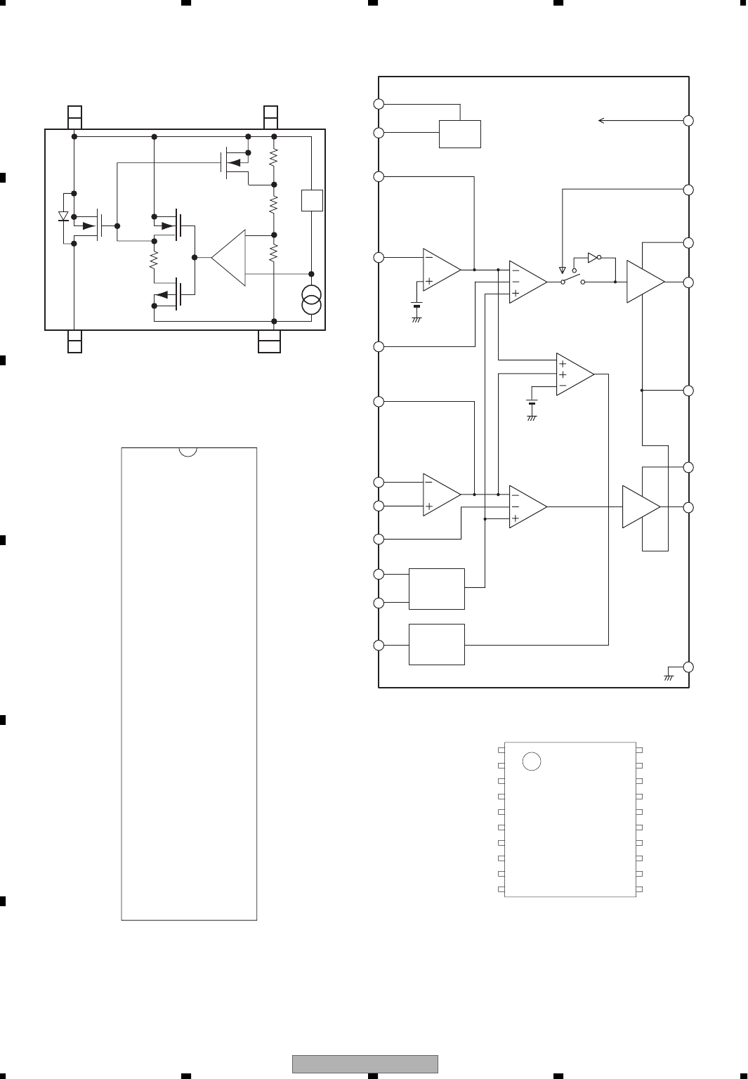
AVIC-D3/XU/UC
286
1234
1234
C
D
F
A
B
E
- Pin Layout
20
19
18
17
16
15
14
13
12
11
GND
STB
VCC
VREF
INV1
FB1
SCP
DTC1
PVCC1
OUT1
1
2
3
4
5
6
7
8
9
10
SEL1
RT
CT
NON2
INV2
FB2
DTC2
PVCC2
OUT2
PGND
- Block Diagram
VREF
VCC
VREF
FB1
INV1
DTC1
FB2
INV2
NON2
RT
CT OSC
STB
Both CH
ON/OFF
PVCC2
PVCC1
SEL1
PGND
OUT1
OUT2
SCP Timer
Latch GND
DTC2
18
17
15
16
13
6
5
4
7
2
3
14
20
9
8
10
11
12
1
19
(2.5 V)
1 V
2.3 V
S-80859CNNB-B9K
12
43
OUT VDD
VSS NC
VREF
-
+
BD9851EFV
VSS
DQ15
VSSQ
DQ14
DQ13
VDDQ
DQ12
DQ11
VSSQ
DQ10
DQ9
VDDQ
DQ8
NC
VSS
DQM1
NC
NC
CLK
CKE
A9
A8
A7
A6
A5
A4
A3
DQM3
VSS
NC
DQ31
VDDQ
DQ30
DQ29
VSSQ
DQ28
DQ27
VDDQ
DQ26
DQ25
VSSQ
DQ24
VSS
86
85
84
83
82
81
80
79
78
77
76
75
74
73
72
71
70
69
68
67
66
65
64
63
62
61
60
59
58
57
56
55
54
53
52
51
50
49
48
47
46
45
44
1
2
3
4
5
6
7
8
9
10
11
12
13
14
15
16
17
18
19
20
21
22
23
24
25
26
27
28
29
30
31
32
33
34
35
36
37
38
39
40
41
42
43
VDD
DQ0
VDDQ
DQ1
DQ2
VSSQ
DQ3
DQ4
VDDQ
DQ5
DQ6
VSSQ
DQ7
NC
VDD
DQM0
/WE
/CAS
/RAS
/CS
A11
BA0
BA1
A10(AP)
A0
A1
A2
DQM2
VDD
NC
DQ16
VSSQ
DQ17
DQ18
VDDQ
DQ19
DQ20
VSSQ
DQ21
DQ22
VDDQ
DQ23
VDD
EDS1232AATA-75
A0 to A11
BA0,BA1
DQ0 to DQ31
/CS
/RAS
/CAS
/WE
Address Inputs
Bank select
Data Input/output
Chip select
Row address atrobe
Column address strobe
Write enable
DQM0 to DQM3
CKE
CLK
VDD
VSS
VDDQ
VSSQ
NC
DQ mask enable
Clock enable
Clock Input
Supply voltage
Ground
Supply voltage for DQ
Ground for DQ
No connection
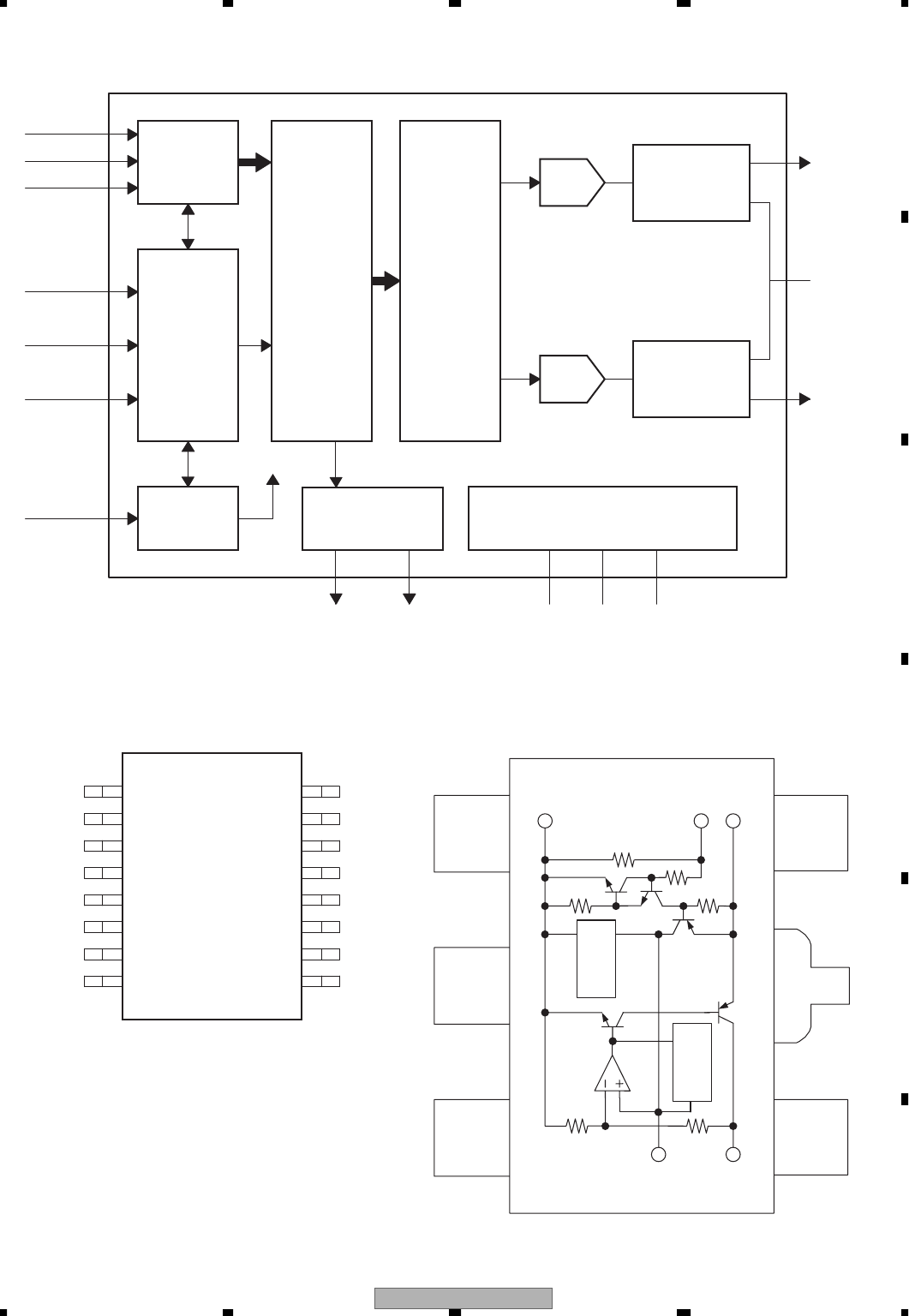
AVIC-D3/XU/UC 287
5678
56
78
C
D
F
A
B
E
- Pin Layout
SCK
ML
MC
MD
ZEROL/NA
ZEROR/ZEROA
VCOM
AGND
16
15
14
13
12
11
10
9
BCK
DATA
LRCK
DGND
NC
VCC
VOUTL
VOUTR
1
2
3
4
5
6
7
8
- Block Diagram
Power Supply
DGND
Enhanced
Multi-level
Delta-Sigma
Modulator
VOUTL
Audio
Serial
Port
BCK
LRCK
DATA
Serial
Control
Port
Zero Detect
SCK System
Clock
Manager
MC
ML
Output Amp
and
Low-Pass Filter
MD
DAC
VCOM
System Clock
AGND
VCC
ZEROR/ZEROA
ZEROL/NA
Output Amp
and
Low-Pass Filter
DAC
VOUTR
4× / 8×
Oversampling
Digital
Filter
with
Function
Controller
PCM1753DBQ
V
OUT
GND
V
IN
Thermal
Protection
Bandgap
Reference
Noise
Bypass
Cont
123
452
CONTROL GND NOISE BYPASS
VOUTVIN GND
NJM2880U1-05
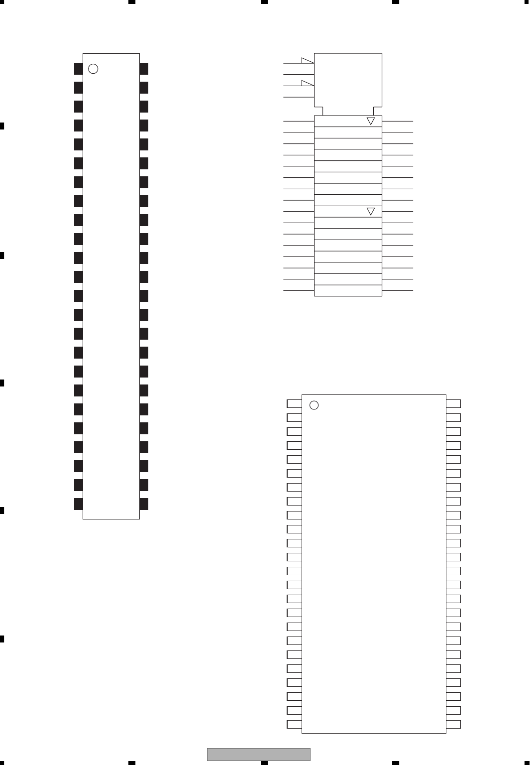
AVIC-D3/XU/UC
288
1234
1234
C
D
F
A
B
E
A15
A14
A13
A12
A11
A10
A9
A8
NC
NC
we
reset
NC
NC
RY/by
NC
A17
A7
A6
A5
A4
A3
A2
A1
A16
byte
VSS2
DQ15/A-1
DQ7
DQ14
DQ6
DQ13
DQ5
DQ12
DQ4
VCC
DQ11
DQ3
DQ10
DQ2
DQ9
DQ1
DQ8
DQ0
oe
VSS1
ce
A0
1
2
3
4
5
6
7
8
9
10
11
12
13
14
15
16
17
18
19
20
21
22
23
24
48
47
46
45
44
43
42
41
40
39
38
37
36
35
34
33
32
31
30
29
28
27
26
25
A0 to A17 : 18 address inputs
DQ0 to DQ14 : 15 data inputs/outputs
DQ15/A-1 : DQ15 (data input/output,
word mode),
A-1 (LSB address input,
byte mode)
byte : Selects 8-bit or 16-bit mode
ce : Chip enable input
oe : Output enable input
we : Write enable input
reset : Hardware reset pin input
RY/by : Ready/busy output
VCC : 3.0 volt-only single power supply
VSS : Device ground
NC : Pin not connected internally
CWW1423
CWW1424
11oe 48 1LE
47 1D1
46 1D2
45 GND
44 1D3
43 1D4
42 VCC
41 1D5
40 1D6
39 GND
38 1D7
37 1D8
36 2D1
35 2D2
34 GND
33 2D3
32 2D4
31 VCC
30 2D5
29 2D6
28 GND
27 2D7
26 2D8
25 2LE
21Q1
31Q2
4GND
51Q3
61Q4
7VCC
81Q5
91Q6
10GND
111Q7
121Q8
132Q1
142Q2
15GND
162Q3
172Q4
18VCC
192Q5
202Q6
21GND
222Q7
232Q8
242oe
47 2
1D1 1Q1
46 3
1D2 1Q2
44 5
1D3 1Q3
43 6
1D4
1
1oe 48
1LE 24
2oe 25
2LE C4
3D 1
24D
2EN
C3
1EN
1Q4
41 8
1D5 1Q5
40 9
1D6 1Q6
38 11
1D7 1Q7
37 12
1D8 1Q8
36 13
2D1 2Q1
35 14
2D2 2Q2
33 16
2D3 2Q3
32 17
2D4 2Q4
30 19
2D5 2Q5
29 20
2D6 2Q6
27 22
2D7 2Q7
26 23
2D8 2Q8
TC74LCX16373FT
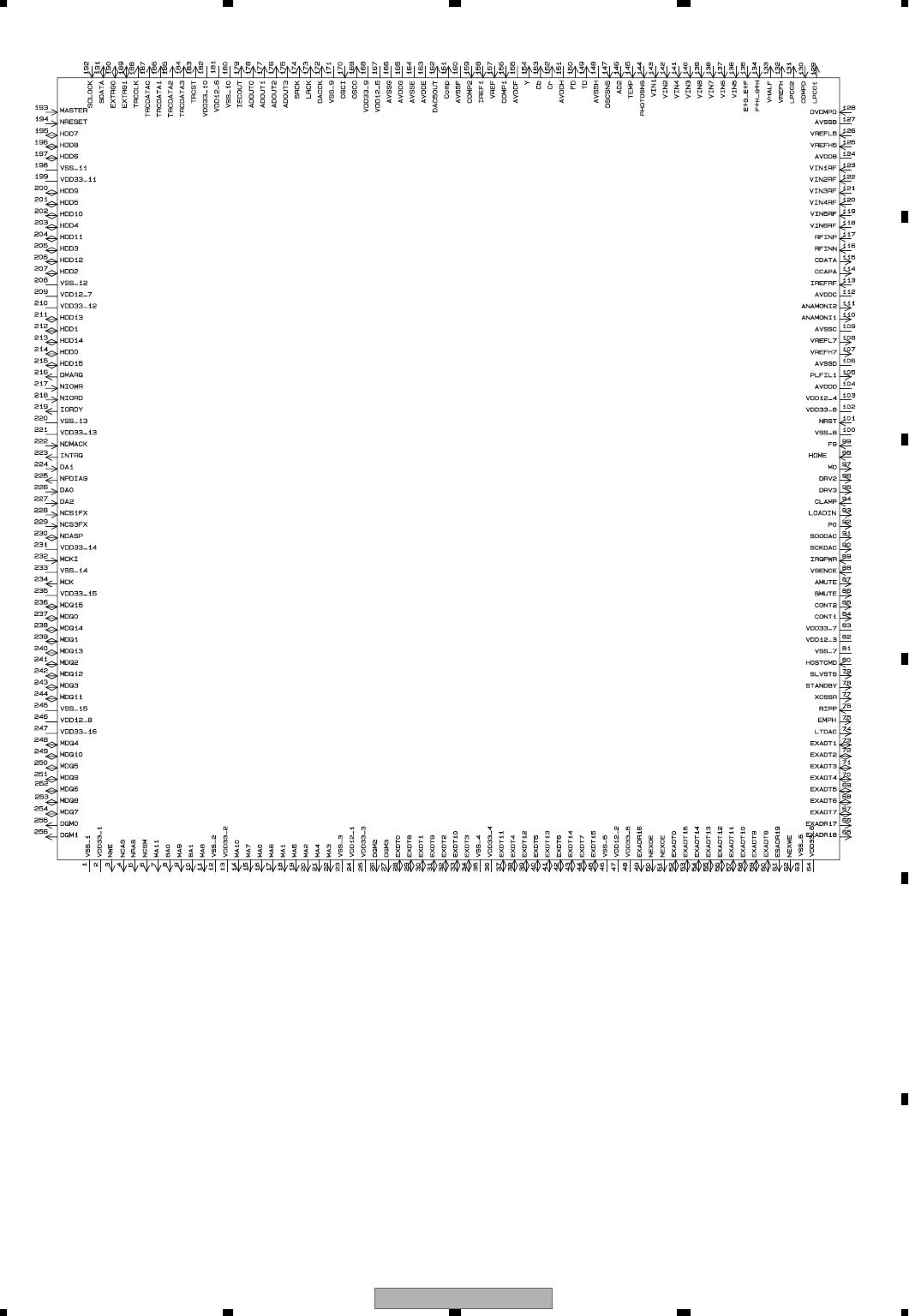
AVIC-D3/XU/UC 289
5678
56
78
C
D
F
A
B
E
VSS GND
VDD Power supply
NWE SDRAM write enable O
NCAS SDRAM Column address strobe O
NRAS SDRAM low address strobe O
NCSM SDRAM chip select O
MA SDRAM address I/O
BA SDRAM bank address O
DQM SDRAM data mask I/O
EXDT External memory data I/O
EXADR External memory address I/O
NEXOE External memory output chip enable O
NEXCE External memory chip select O
EXADT External memory address I/O
NEXWE External memory write enable O
P General port I/O
DRV Servo port I/O
FG Motor FG I/O
NRST Master reset I
AVDD Analog power supply
PLFIL Connect for DRC-VCO O
AVSS Analog GND
VREFH ADC reference voltage for DRC(TOP) O
VREFL ADC reference voltage for DRC(BTM) O
ANAMONI Analog monitor O
IREFRF Reference voltage I
CCAPA Inline capa connect O
CDATA Inline data connect O
RFINN External RF input I
RFINP External RF input I
VINRF RF input I
LPC DVD/CD LPC input I
LPCO DVD/CD LPC output O
VHALF Reference voltage O
MN2DS0016
AD Servo AD input I
PWM Tracking (Focus) drive output O
DACOUT RGB analog signal O
COMP DAC stabilization connect pin I
VREF DAC reference input I
IREF DAC bias current setting pin I
OSCO Resonator output O
OSCI Resonator input I
DACCK Audio clock I/O
LRCK LR chann clock output O
SRCK Bit clock output O
ADOUT Audio down mix output I/O
IECOUT Digital audio output I/O
TRCST Output trace status for debugging I/O
TRCDATA Output trace data for debugging I/O
TRCCLK Output trace clock for debugging I/O
EXTRG I/O trigger for debugging I/O
SDATA Data for debugging I/O
SCLOCK Input clock for debugging I
MASTER ATAPI master slave signal input I/O
NRESET ATAPI reset input signal I
HDD ATAPI I/O data I/O
DMARQ ATAPI host DMA request output I/O
NIOWR ATAPI host write signal I/O
NIORD ATAPI host read signal I/O
IORDY ATAPI host ready output I/O
NDAMCK ATAPI host DMA acnorigge input I
INTRQ ATAPI host interrupt output I/O
DA ATAPI host address I/O
NPDIAG ATAPI diagnosis signal I/O
NCSFX ATAPI host chip select input I
MCKI SDRAM input clock I
MCK SDRAM clock O
MDQ SDRAM data I/O
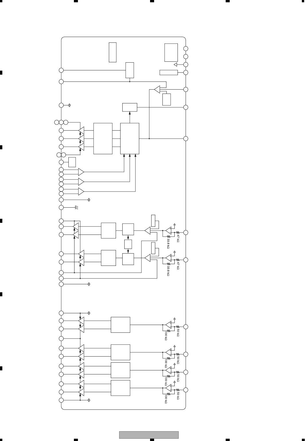
AVIC-D3/XU/UC
290
1234
1234
C
D
F
A
B
E
20 CTL2
BD7996EFV
21 CTL1
14 VC
49 TJMON
29 SPIN
13 FG
12 SPCNF
25 SLIN2
26 SLIN1
10 LDIN
9 ACTIN3
50 ACTIN2
51 ACTIN1
LINTLINT
LEVEL
SHIFT
54LDO-
53LDO+
PRE
logo
FF
16SLO1-
42V
39W
40 45 46PGND1,2,3
44U
38 43SPVM1,2
15SLO1+
PRE
logo
FF ORC
18SLO2-
34HU-
35HU+
32HV-
33HV+
30HW-
36HB
HB
BOTTOM
HOLD
STBY/
BRANCE
CONTROL X
LIMIT
T.R.D.
FD
T
31HW+
17SLO2+
LEVEL
SHIFT
6ACO3-
5ACO3+
LEVEL
SHIFT
4ACO2-
3ACO2+
LEVEL
SHIFT
2ACO1-
1ACO1+
8AVM
52VCC
24SLVOO
27DVOC
47SPVM_S
48BTHC
37SPRNF
28DGND
19SLGND
22SLRNF2
23SLRNF1
11AGND
HALL
MATRICC
PWM
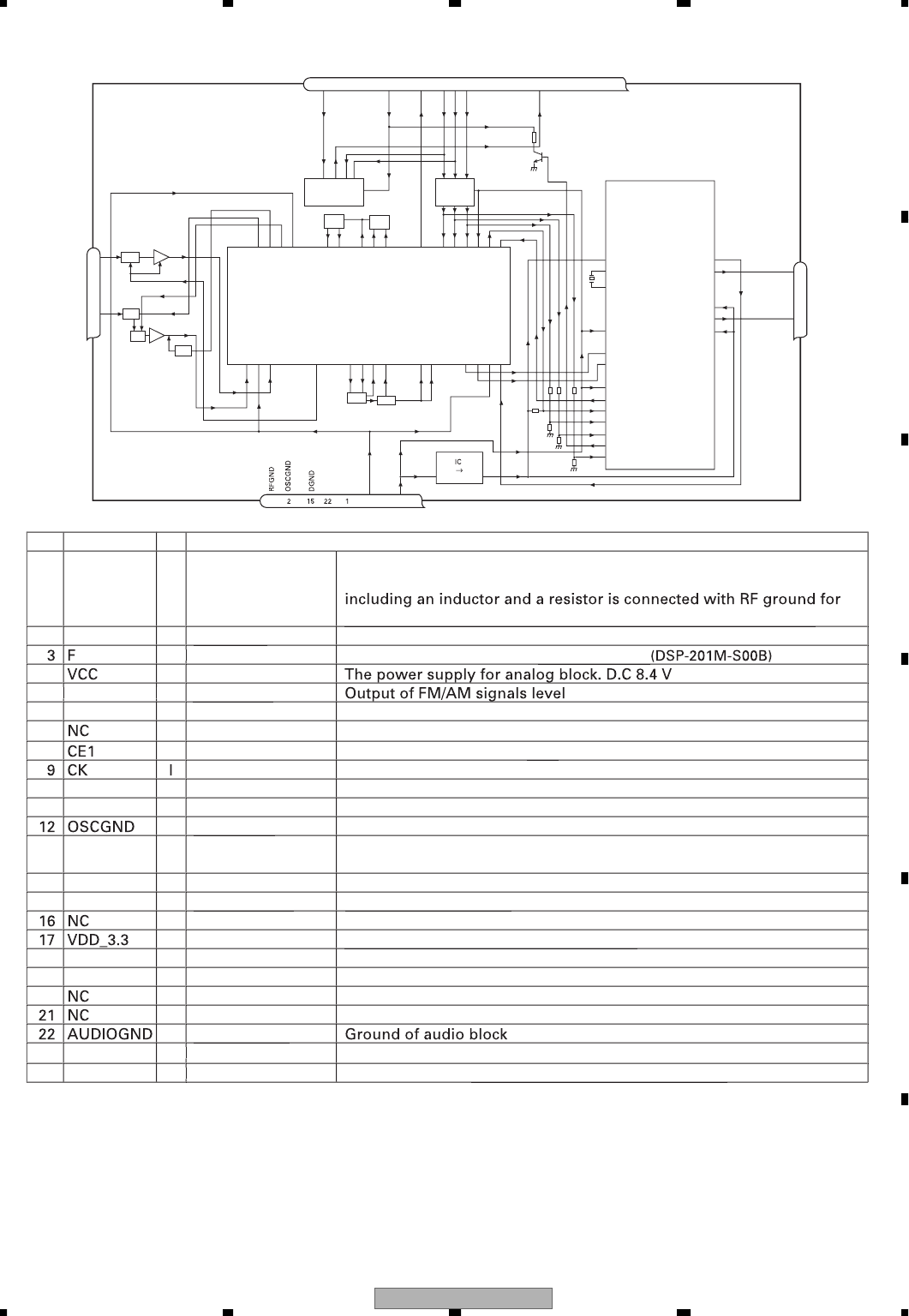
AVIC-D3/XU/UC 291
5678
56
78
C
D
F
A
B
E
N
o.
S
y
mbo
l
I
/O
Ex
p
lai
n
1
AMANT
I
AM antenna in
p
u
t
AM antenna input hi
g
h impedance AMANT pin is connected wit
h
an all antenna b
y
wa
y
of 4.7
µ
H. (LAU t
yp
e inductor
)
A
se
ri
es
c
ir
cu
i
t
the countermeasure a
g
ainst the hum of power transmission line
.
g
2
RF
G
N
D
RF
g
roun
d
g
G
r
ou
n
d
o
f
a
n
te
nn
a
b
l
ock
MANT
IF
M antenna in
p
u
t
In
p
ut of FM antenna 7
5
Ω
Sur
g
e absorbe
r
g
i
s
n
ecessar
y.
4
p
ower su
pply
±
0
.
3
V
5S
LO
si
g
nal leve
l
g
6
C
E
2
I
chi
p
enable-
2
Chi
p
enable for EEPROM
”
L
ow
”
act
i
v
e
7
n
o
n
co
nn
ect
i
on
N
ot
used
8
I
c
hip
ena
bl
e-
1
Chi
p
enable for A
F
•
RF
”
High
g
”
activ
e
c
l
ock
C
l
ock
1
0
DI
I
data
in Data in
p
ut
11
N
C
n
o
n
co
nn
ect
i
on
N
ot
used
osc
g
round
g
G
r
ou
n
d
o
f
osc
ill
ato
r
b
l
oc
k
1
3
ROM
_
VD
D
p
ower su
pp
l
y
Power su
pp
l
y
for EEPROM
p
in 13 is connected with a
p
ower su
pp
l
y
o
f
micro com
p
uter
.
14
D
O
O
data
out
Data out
p
ut
1
5
D
G
N
D
di
g
ital
g
roun
d
gg
Ground of di
g
ital bloc
k
g
n
o
n
co
nn
ection
Not
used
p
ower su
pp
l
y
The power supply for di
g
ital block. 3.3 V
g
±
0
.2
V
1
8
N
C
n
o
n
co
nn
ect
i
on
N
ot
used
1
9
N
C
n
o
n
co
nn
ect
i
on
N
ot
used
2
0
n
o
n
co
nn
ect
i
on
N
ot
used
n
o
n
co
nn
ect
i
on
N
ot
used
audio
g
roun
d
g
2
3
L
ch
OL
channel out
p
u
t
FM
ste
r
eo
“
L
-
c
h
”
si
g
nal output or AM audio outpu
t
24
R
ch
OR
channel out
p
u
t
FM
ste
r
eo
“
R
-
c
h
”
si
g
nal output or AM audio outpu
t
g
FMRF
ANT adj RF adj
FM ANT
T51 CF52
RFGND
AU
DI
OG
N
D
NC
VCC
V
DD
_
3.
3
3
.
3
V
2.
5
V
4
3
.
3
V
2.
5
V
IC 2
2.5 V
NC
CE2
ROM_VDD
SL
DI
CK
CE1
NC
DO
NC
NC
NC
NC
7 6 13 5 10 9 8 11 14 18 19 20 21
1
3
21
64
17
IC 1
3.3 V
AM ANT FMRF
ATT
LPF
OSC
IC 3 EEPROM
5.0 V
IC 5
5 V 3.3 V
←
ATT
MIXER, IF AMP DET, FM MPX
24
23
Rch
Lch
-
FM/AM Tuner Unit
(
UC
)
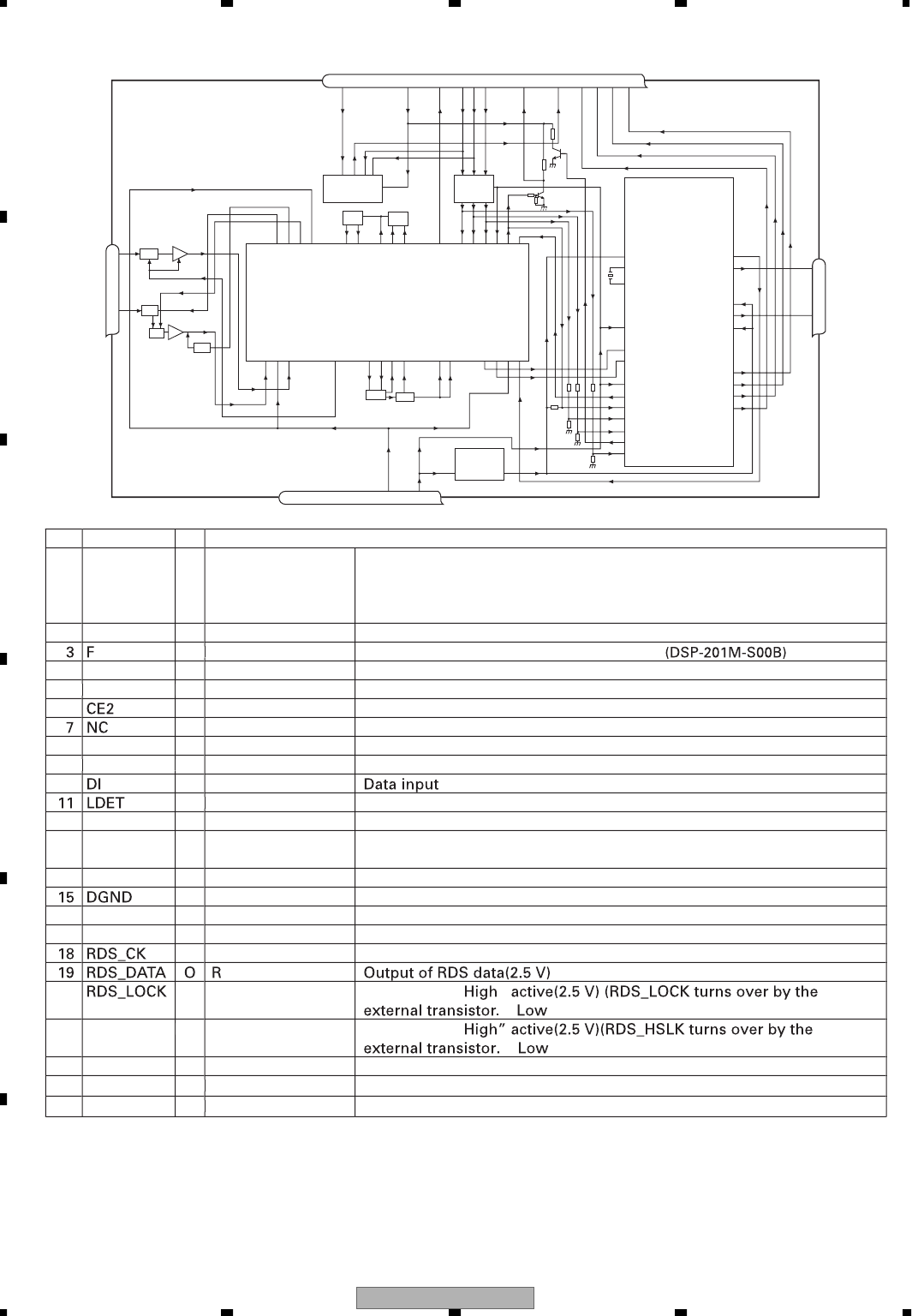
AVIC-D3/XU/UC
292
1234
1234
C
D
F
A
B
E
N
o.
S
y
mbo
l
I
/O
Ex
p
lai
n
1
AMANT
I
AM antenna in
p
u
t
AM antenna input hi
g
h impedance AMANT pin is connected wit
h
an all antenna b
y
wa
y
of 4.7
µ
H. (LAU t
yp
e inductor) A series circuit
includin
g
an inductor and a resistor is connected with RF
g
round for
the countermeasure a
g
ainst the hum of power transmission line
.
g
2
RF
G
N
D
RF
g
roun
d
g
G
r
ou
n
d
o
f
a
n
te
nn
a
b
l
ock
MANT
IF
M antenna in
p
u
t
In
p
ut of FM antenna 7
5
Ω
Sur
g
e absorbe
r
g
is necessar
y.
4
V
CC
p
ower su
pp
l
y
The power supply for analo
g
block. D.C 8.4 V
g
±
0
.
3
V
5S
LO
si
g
nal leve
l
g
Output of FM/AM si
g
nals leve
l
g
6
I
chi
p
enable-
2
Chi
p
enable for EEPROM
”
L
ow
”
act
iv
e
n
o
n
co
nn
ect
i
on
N
ot
used
8
C
E
1
I
chi
p
enable-
1
Chi
p
enable for A
F
•
RF
”
Hi
gh
g
”
act
iv
e
9C
KI
c
l
ock
C
l
ock
1
0
I
data
in
Ol
oc
k
detector
“
L
ow
”
act
iv
e
12
OSCG
N
D
osc
g
round
g
G
r
ou
n
d
o
f
osc
ill
ato
r
b
l
ock
1
3
ROM
_
VD
D
p
ower su
pp
l
y
Power su
pp
l
y
for EEPROM
p
in 13 is connected with a
p
ower su
pp
l
y
o
f
micro com
p
uter
.
14
D
O
O
data
out
Data out
p
u
t
di
g
ital
g
roun
d
gg
Ground of di
g
ital bloc
k
g
1
6
N
C
n
o
n
co
nn
ect
i
on
N
ot
used
17
VDD
_
3.
3
p
ower su
pp
l
y
The power supply for di
g
ital block. 3.3
V
g
±
0
.2 V
O
RD
S
c
l
ock
Out
p
ut of RDS clock(2.5 V
)
D
S
data
2
0
O
RD
S
l
ock
Out
p
ut unit
“
”
“
”
active
)
21
RDS
_
HS
L
KO
RDS hi
g
h spee
d
Out
p
ut unit
“
l
ock
“
”
active
)
22
A
U
DI
OG
N
D
audio
g
roun
d
g
G
r
ou
n
d
o
f
aud
i
o
b
l
ock
2
3
L
ch
OL
channel out
p
u
t
FM
ste
r
eo
“
L-
ch
”
si
g
nal output or AM audio outpu
t
24
R
ch
OR
channel out
p
u
t
FM
ste
r
eo
“
R-
ch
”
si
g
nal output or AM audio outpu
t
FMRF
ANT adj RF adj
FM ANT
T51 CF52
RFGND
OSCGND
DGND
AUDIOGND
NC
VCC
VDD_3.3
3.3V 2.5V
IC 4
3.3V 2.5V
←
IC 2
2.5V
NC
CE2
ROM_VDD
SL
DI
CK
CE1
LDET
DO
RDS_CK
RDS_DATA
RDS_LOCK
RDS_HSLK
7 6 13 5 10 9 8 11 14 18 19 20 21
1
3
21
21
52
21
64
17
IC 1
3.3V
AM ANT FMRF
ATT
LPF
OSC
IC 3 EEPROM
5.0V
IC 5
5V 3.3V
←
ATT
MIXER, IF AMP DET, FM MPX,
RDS DECODER
24
23
Rch
Lch
-
FM/AM Tuner Unit
(
EW5
)
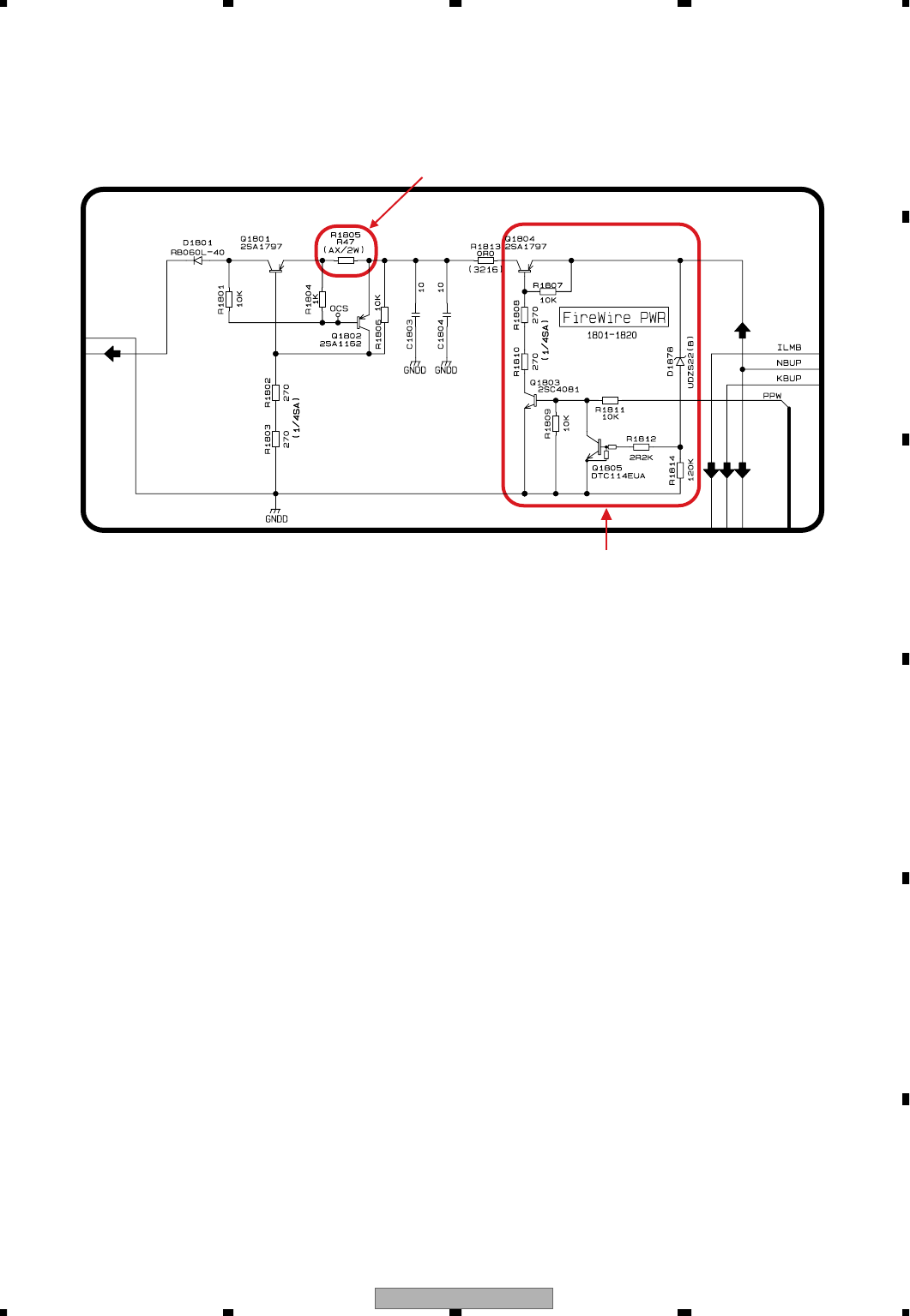
AVIC-D3/XU/UC 293
5678
56
78
C
D
F
A
B
E
7.3 EXPLANATION
7.3.1 CIRCUIT DESCRIPTIONS
Overcurrent detection mechanism
1. The current exceeding the allowable range flows to the load side (=iPod).
2. The difference of electrical potential at both ends of R1805 becomes large exceeding approximately 0.6 V.
3. As a result of the difference of potential between the emitter and the base of Q1802, the current starts to flow from
the emitter to the base, and the difference of potential between the emitter and the collector becomes almost zero.
4. The difference of potential between the emitter and the base of Q1801 no longer exists, and Q1801 will close.
5. It is designed in a way that, if the output is grounded, the current will start flowing to Q1802 even before that and
that Q1801 will close.
- FireWire PWR
FireWire : Power supply circuit to supply electricity to iPod.
Overcurrent detection resistor 0.47 Ω
A popular switch circuit.
When there is an overvoltage, D1878 will be ON
and PPW will be dropped down to Low level by
force so that the overvoltage will not be applied to
the iPod side.
Page 82 Address 4A
AVIC-D3/XU/UC
294
1234
1234
C
D
F
A
B
E
7.3.2 OPERATIONAL FLOW CHART
/BSENS
/ASENS
Status
MUTE
MUTEVO
ASENBO
SREMOTE
DEQON
SYSPWR
ANTON
SWACPW
CCON
RSTOUT
IRQPWR
CPUWDT
OFFOK
RST3(Not used)
VDCONT
DRAMPW
FANCONT
XVMUTE
BCVSW
500 ms
200 ms 1 sec to 2 sec 250 ms to 300 ms
500 ms or more
8
1
Power supply mask (200 ms)
Power supply mask (200 ms)
Power supply mask (200 ms)
Oscillation stop
Standby loop Main loop
IP-BUS pretreatment
IP-BUS slave connection check
Slave waiting for a pwr. mask
DRAMPW(At the tim
e
It is
IP-BUS slave connection check time (IP-BUS spec)
• The number of connection slaves is 0 last time.(1 sec)
• The number of connection slaves is one or more last time.
-When a connection slave is able to be altogether checked within 1 sec last time. ····· 1 sec
-When at least one connection slave is not able to be checked within 1 sec last time. ····· 2 sec
With slave connection : 250 ms to 300 ms
Sense system
Sound Mute
Control
IP-BUS
AUX Out
Audio Control
Power Supply
Control
Monitor Control
NAVI Control
MS5 Control
DRAM
Power Supply
Control
FAN Motor
Control
Video Mute
Control
ANTON(Source interlocking
movement, forced OFF)
- Acc ON(Normal Acc ON)(Reference)
AVIC-D3/XU/UC 295
5678
56
78
C
D
F
A
B
E
8 ms to 16 ms or more
16 ms
16 ms to 24 ms
48 ms
48 ms or more
16 ms
u
pply mask (200 ms)
u
pply mask (200 ms)
u
pply mask (200 ms)
M
ain loop
After mute(200 ms)(After SYSPWR ON, at least 200 ms. MUTE time is extended to OFFOK Hi henceforth.)
After mute(200 ms)(After SYSPWR ON, at least 200 ms. MUTE time is extended henceforth according to other factors.)
D
RAMPW(At the time of a reset start)
It is a low speed until it receives temperature information from NAVI.
FANCONT(At the time of high temperature)
XVMUTE(At the time of source without a picture)
It is MUTE continuation because of source without a picture.
It is video MUTE OFF at the time of video sauce ON.
o
300 ms
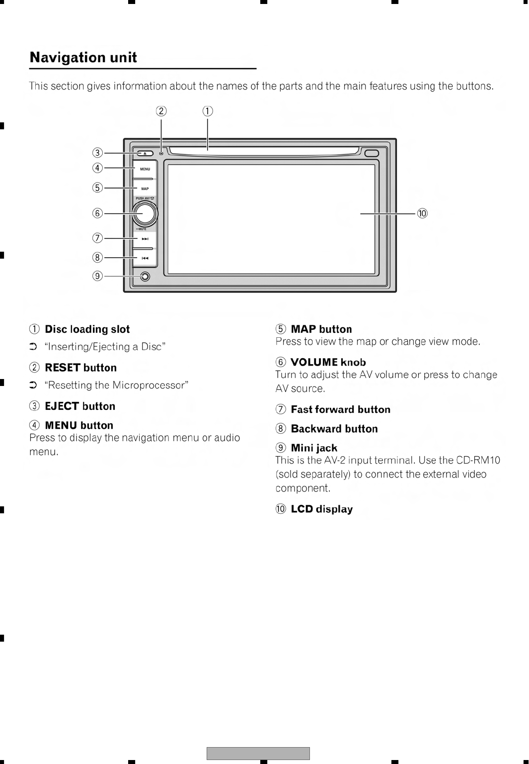
AVIC-D3/XU/UC
296
1234
1234
C
D
F
A
B
E
8. OPERATIONS
AVIC-D3/XU/UC 297
5678
56
78
C
D
F
A
B
E
AVIC-D3/XU/UC
298
1234
1234
C
D
F
A
B
E
- AVIC-D3/XU/UC
AVIC-D3/XU/UC 299
5678
56
78
C
D
F
A
B
E
AVIC-D3/XU/UC
300
1234
1234
C
D
F
A
B
E
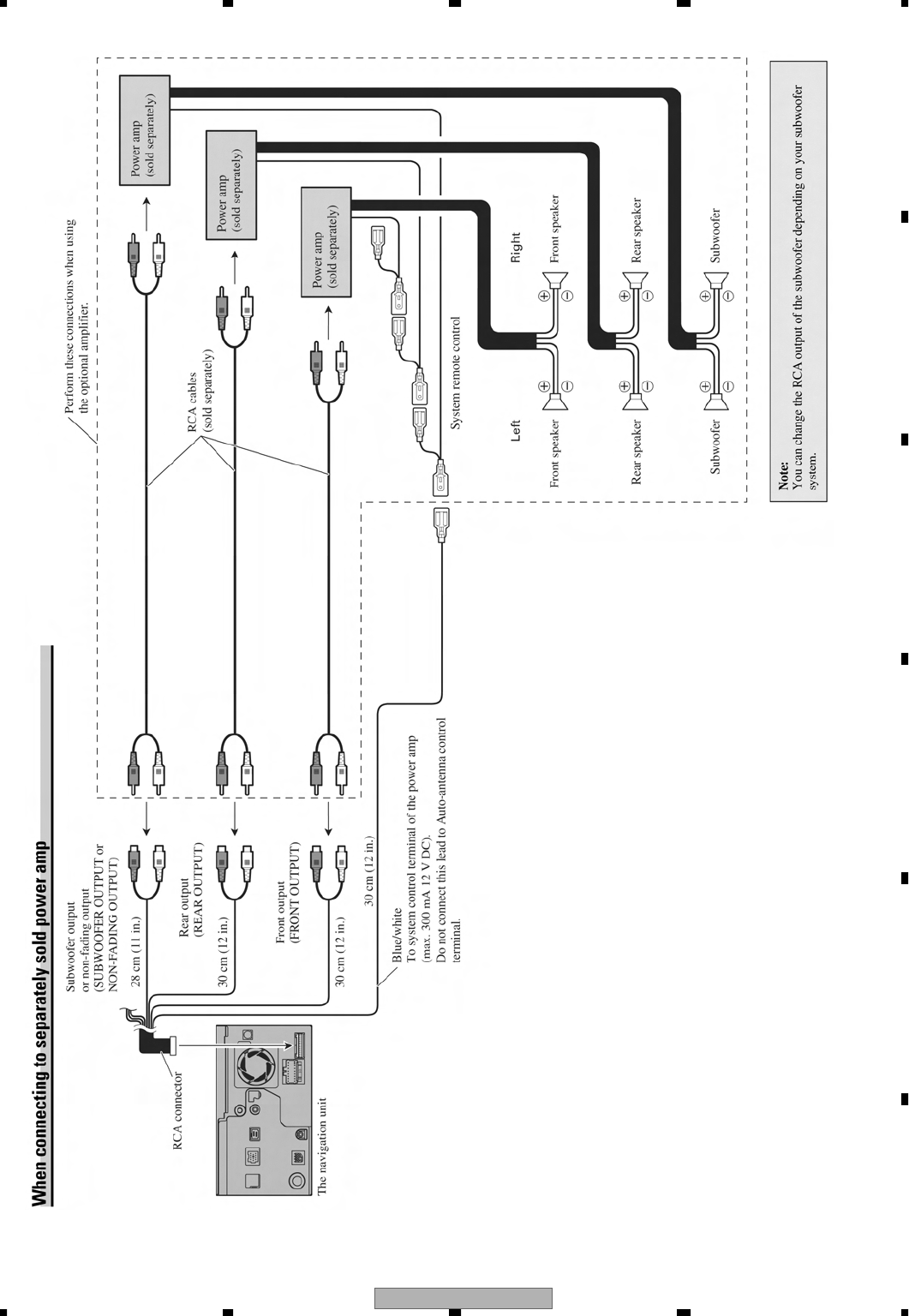
AVIC-D3/XU/UC 301
5678
56
78
C
D
F
A
B
E
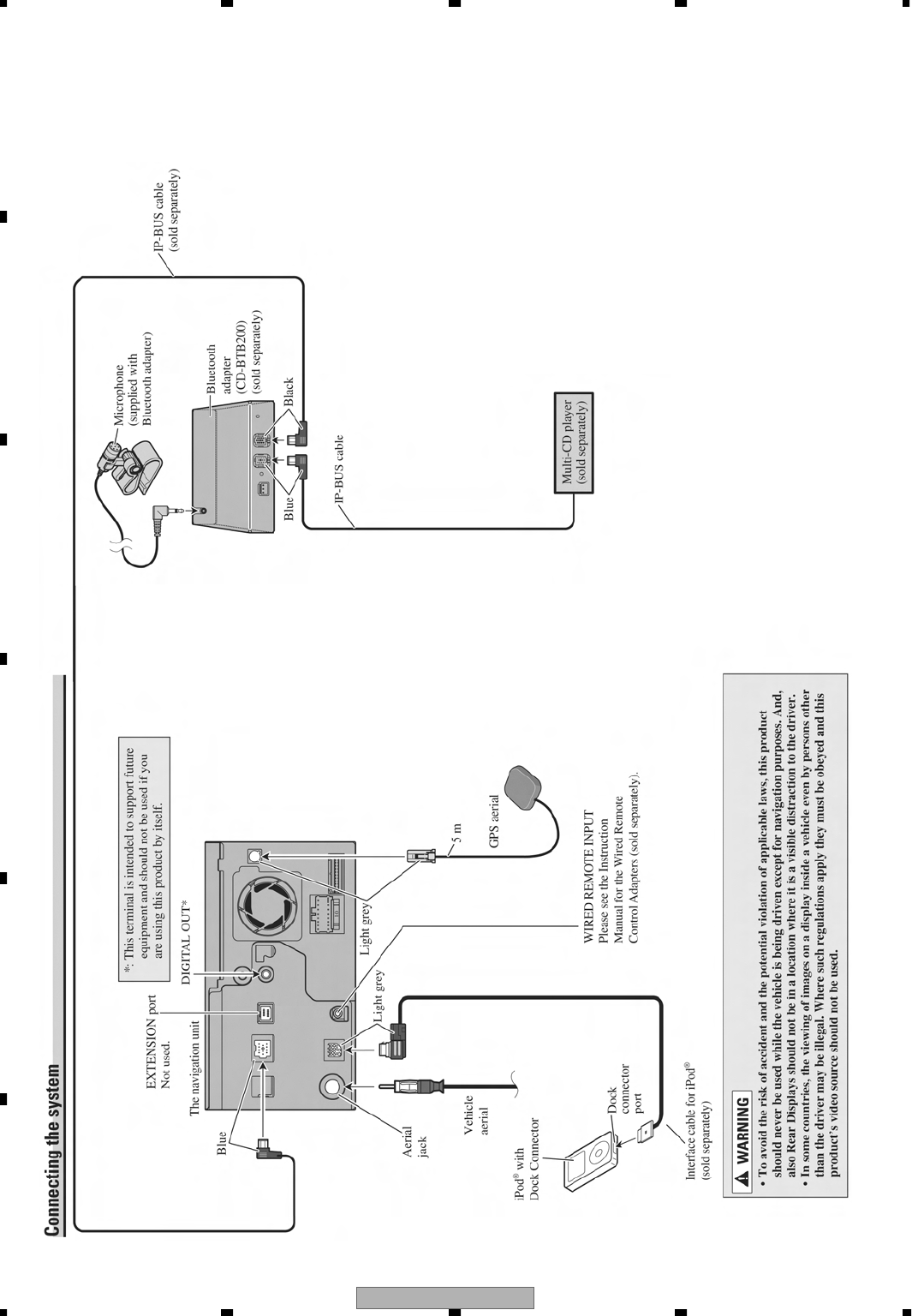
AVIC-D3/XU/UC
302
1234
1234
C
D
F
A
B
E
- AVIC-D3/XU/EW5
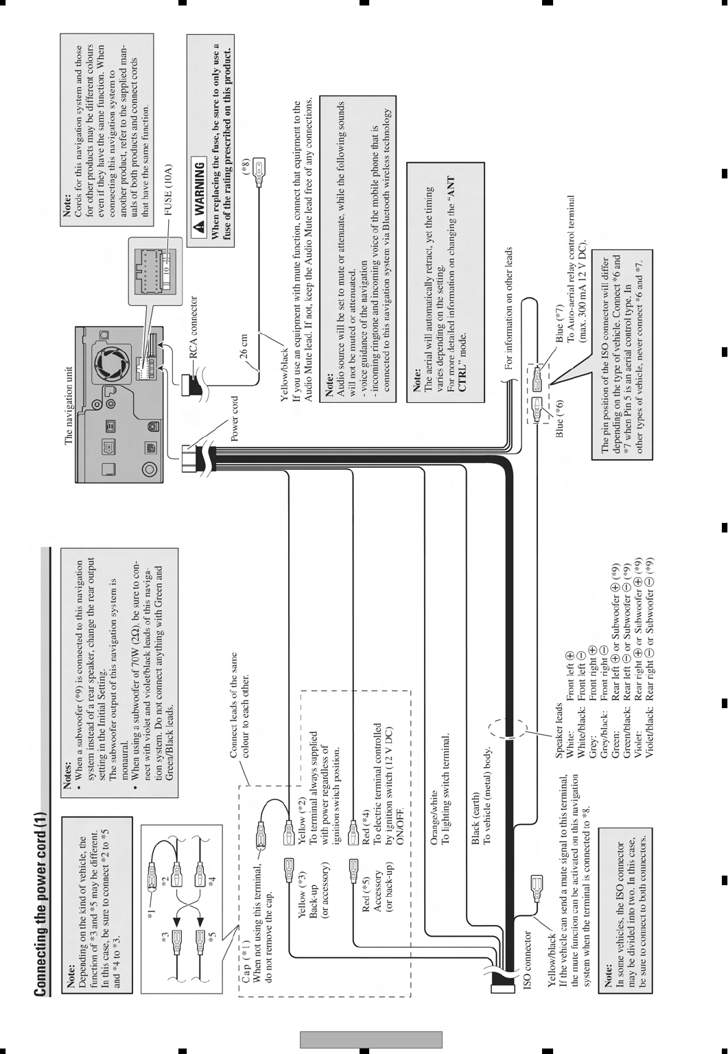
AVIC-D3/XU/UC 303
5678
56
78
C
D
F
A
B
E
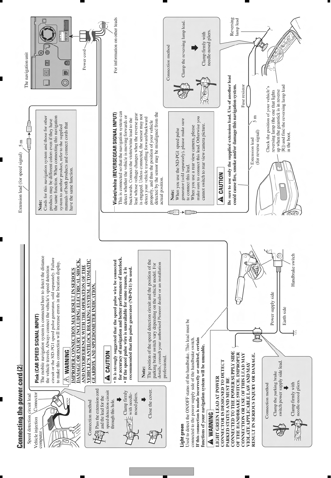
AVIC-D3/XU/UC
304
1234
1234
C
D
F
A
B
E
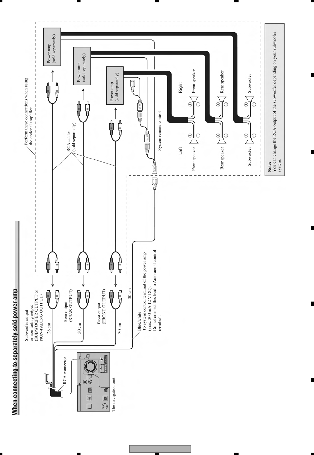
AVIC-D3/XU/UC 305
5678
56
78
C
D
F
A
B
E
AVIC-D3/XU/UC
306
1234
1234
C
D
F
A
B
E
Before shipping out the product, be sure to clean the following portions by using the prescribed cleaning tools:
Portions to be cleaned Cleaning tools
DVD pickup lenses Cleaning liquid : GEM1004
Cleaning paper : GED-008
Portions to be cleaned Cleaning tools
Fans Cleaning paper : GED-008
-
G
rease List
G
r
ease
G
r
ease
G
r
ease
G
r
ease
G
EM1
0
24
G
EM1
0
4
3
G
EM1
0
4
5
G
EM1
050
DVD
Mecha
n
is
m
Module
DVD
Mecha
n
is
m
Module
DVD
Mecha
n
is
m
Module
DVD
Mecha
n
is
m
Module
N
a
m
e
G
rease No
.
R
e
m
a
rk
s
-
Ji
g
s Lis
t
N
a
m
e
4
0
P FF
C
BBR
4
0
P FF
C
BBR
2
0
P Ex
te
n
s
i
o
n
Cab
l
e
80
P FP
C
4
0
P FF
C
BB
TE
S
T DI
SC
R
e
m
ote
Co
n
t
r
o
l
U
in
t
T
O
RX driver
(
T2
)
Bo
n
d
Bond (Produced b
y
THREE B
O
ND)
TE
S
T DI
SC
Ji
g
No
.
GG
D12
8
4
GG
D12
8
4
GG
D1
3
27
GG
D14
06
GG
D117
0
GG
V1
303
C
X
C63
17
GG
K1
095
G
EM1
033
14
0
1
M
GG
V1
0
1
8
R
e
m
a
rk
s
DVD
C
ore Unit
(C
N2001
)
<---> Navi Mother Unit
(C
N2
)
() ()
DVD
C
ore Unit
(C
N1901
)
<---> Navi Mother Unit
(C
N2057
)
Navi Mother Unit
(C
N2068
)
<---> AV Unit
(C
N1652
)
Navi Mother Unit
(C
N2055
)
<---> AV Unit
(C
N1711
)
Monitor Unit
(C
N5001
)
<---> AV Unit
(C
N1661
)
Op
eration chec
k
Op
eration for ad
j
ustment
S
KEW ad
j
ustment
(
DVD
)
S
KEW ad
j
ustment
(
DVD
)
S
KEW ad
j
ustment
(
DVD
)
S
KEW ad
j
ustment
(
DVD
)
() ()
() ()
() ()
() ()
p
pj
j()
j()
j()
j()
