CRT4321 001 AVICX910BT
User Manual: AVICX910BT
Open the PDF directly: View PDF ![]() .
.
Page Count: 244 [warning: Documents this large are best viewed by clicking the View PDF Link!]
- SAFETY INFORMATION
- CONTENTS
- 1. SERVICE PRECAUTIONS
- 1.1 SERVICE PRECAUTIONS
- 1.2 NOTES ON SOLDERING
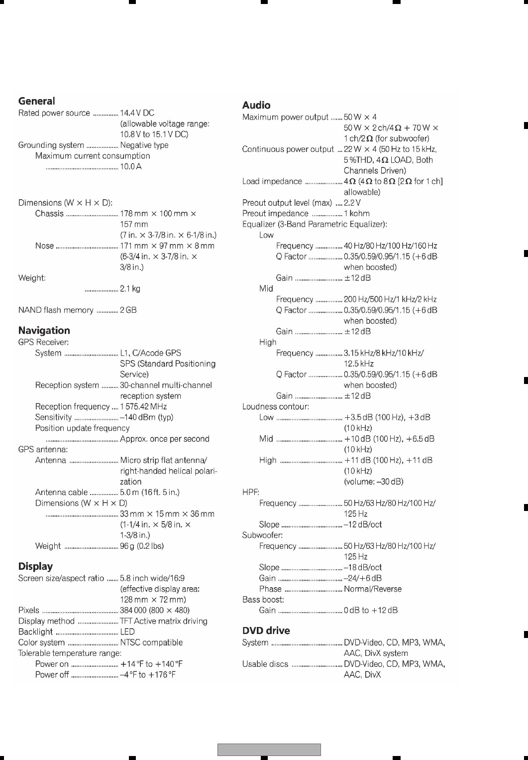
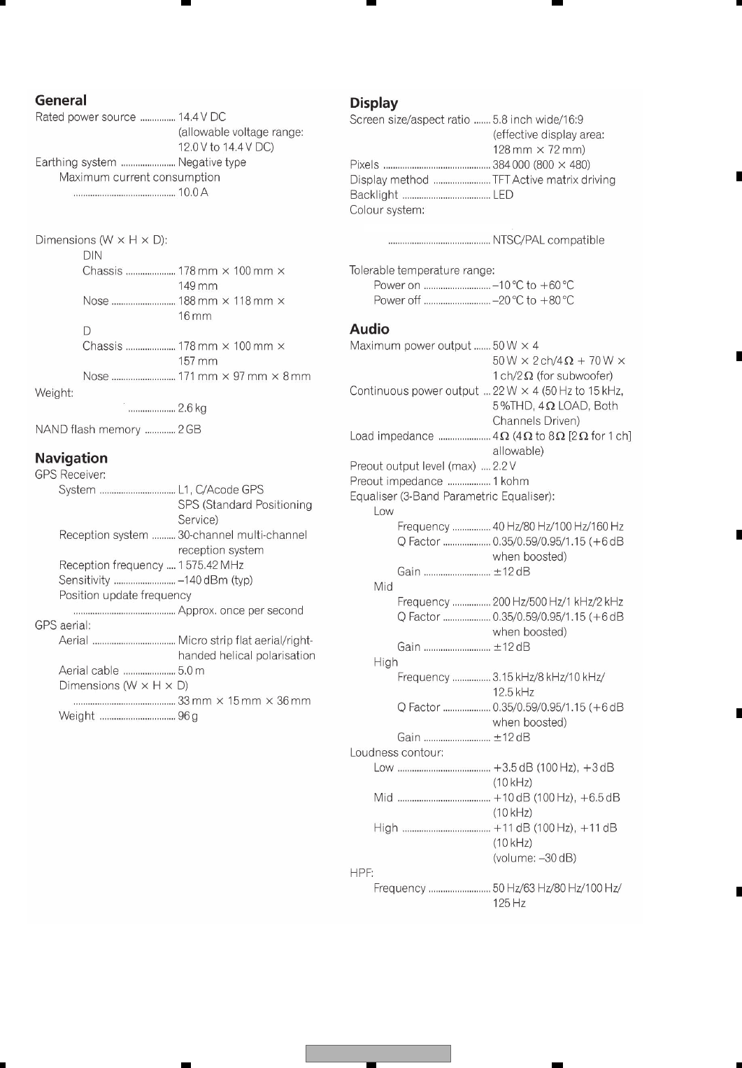
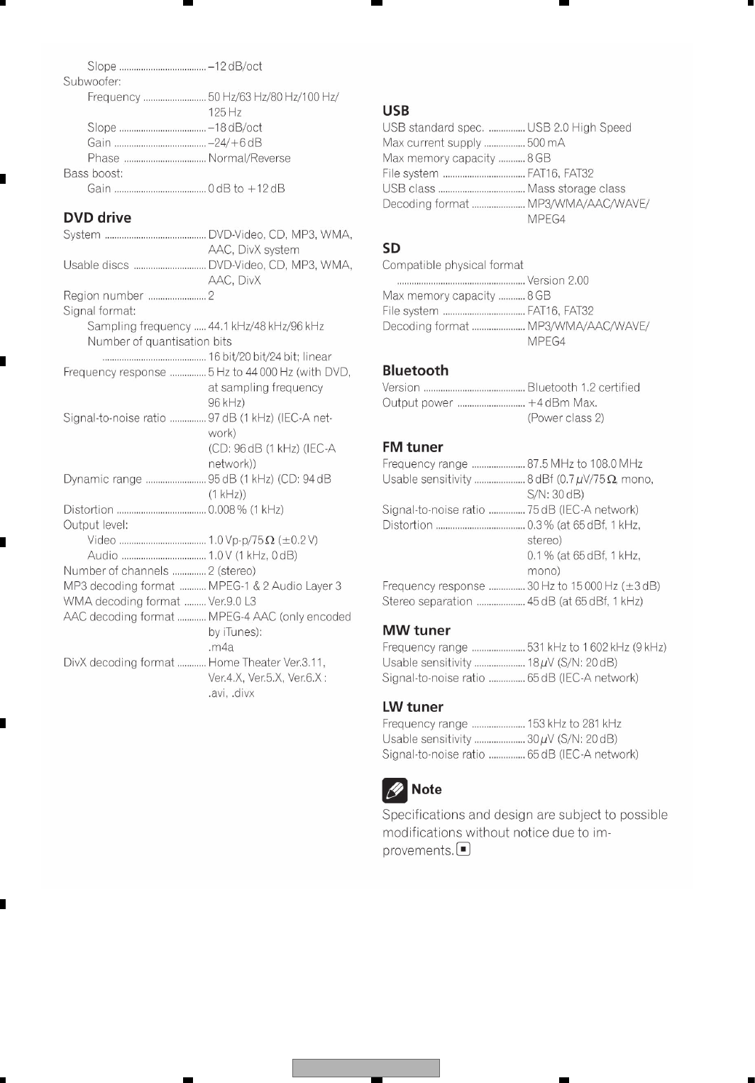
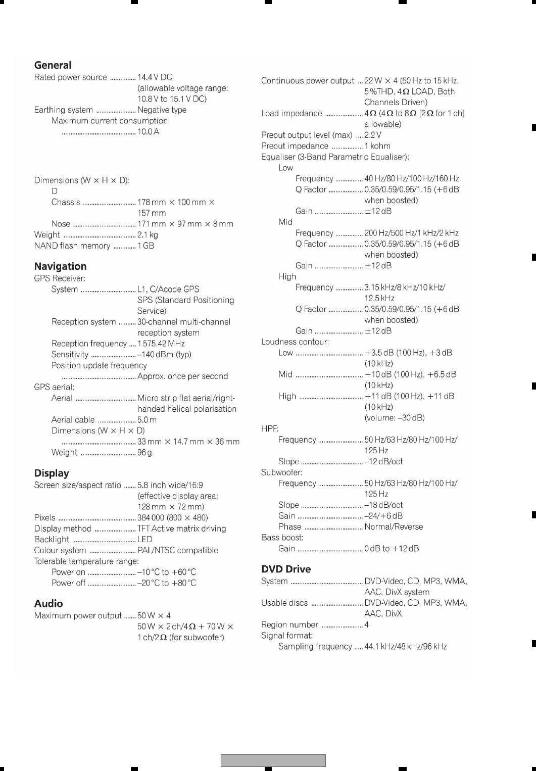
- 2. SPECIFICATIONS
- 2.1 SPECIFICATIONS
- 2.2 DISC/CONTENT FORMAT
- 2.3 PANEL FACILITIES
- 2.4 CONNECTION DIAGRAM
- 3. BASIC ITEMS FOR SERVICE
- 3.1 CHECK POINTS AFTER SERVICING
- 3.2 PCB LOCATIONS
- 3.3 JIGS LIST
- 3.4 CLEANING
- 4. BLOCK DIAGRAM
- 4.1 OVERALL CONNECTION DIAGRAM
- 4.2 BLOCK DIAGRAM
- 4.3 POWER SUPPLY SYSTEM FIGURE
- 5. DIAGNOSIS
- 5.1 OPERATIONAL FLOWCHART
- 5.2 INSPECTION METHOD OF PICKUP UNIT
- 5.3 DIAGNOSIS FLOWCHART
- 5.4 ERROR CODE LIST
- 5.5 CONNECTOR FUNCTION DESCRIPTION
- 5.6 TROUBLESHOOTING
- 6. SERVICE MODE
- 6.1 TEST MODE
- 6.2 DVD TEST MODE
- 6.3 uBOOT MENU
- 6.4 USING THE TEST DISC
- 7. DISASSEMBLY
- 8. EACH SETTING AND ADJUSTMENT
- 8.1 DVD ADJUSTMENT
- 8.2 AV UNIT ADJUSTMENT
- 8.3 FLICKER ADJUSTMENT
- 10. SCHEMATIC DIAGRAM
- 10.1 AV UNIT(PS/IF SECTION)(GUIDE PAGE)
- 10.2 AV UNIT(A/V SECTION)(GUIDE PAGE)
- 10.3 AV UNIT(TUNER SECTION)
- 10.4 AV UNIT(SYSTEM uCOM SECTION)(GUIDE PAGE)
- 10.5 AV UNIT(RGB LED DRIVER SECTION)
- 10.6 AV UNIT(IF SECTION)(GUIDE PAGE)
- 10.7 CK UNIT
- 10.8 DVD CORE UNIT(GUIDE PAGE)
- 10.9 CONNECT PCB
- 10.10 KEYBOARD UNIT
- 10.11 WAVEFORMS
- 11. PCB CONNECTION DIAGRAM
- 11.1 AV UNIT
- 11.2 CK UNIT
- 11.3 DVD CORE UNIT
- 11.4 CONNECT PCB
- 11.5 KEYBOARD UNIT
- 12. ELECTRICAL PARTS LIST
- CRT4300
ORDER NO.
PIONEER CORPORATION 4-1, Meguro 1-chome, Meguro-ku, Tokyo 153-8654, Japan
PIONEER ELECTRONICS (USA) INC. P.O. Box 1760, Long Beach, CA 90801-1760, U.S.A.
PIONEER EUROPE NV Haven 1087, Keetberglaan 1, 9120 Melsele, Belgium
PIONEER ELECTRONICS ASIACENTRE PTE. LTD. 253 Alexandra Road, #04-01, Singapore 159936
PIONEER CORPORATION 2009
AVIC-X910BT/XS/UC
CRT4321
FLASH MEMORY MULTIMEDIA AV NAVIGATION RECEIVER
AVIC-X910BT
/XS/UC
NAVIGATION AV SYSTEM
AVIC-F910BT
/XS/EU5
AVIC-F910BT
/XS/AU
This service manual should be used together with the following manual(s):
Model No. Order No. Mech.Module Remarks
CX-3250 CRT4300 LS1 DVD Mech. Module : Circuit Descriptions, Mech. Descriptions, Disassembly
For details, refer to "Important Check Points for Good Servicing".
K-ZZZ.-001 APR. 2009 Printed in Japan

AVIC-X910BT/XS/UC
2
1234
1234
C
D
F
A
B
E
SAFETY INFORMATION
Where in a manufacturer’s service documentation, for example in circuit diagrams or lists
of components, a symbol is used to indicate that a specific component shall be replaced only
by the component specified in that documentation for safety reasons, the following symbol shall
be used:
CAUTION:
USE OF CONTROLS OR ADJUSTMENTS OR PERFORMANCE OF PROCEDURES OTHER THAN THOSE
SPECIFIED HEREIN MAY RESULT IN HAZARDOUS RADIATION EXPOSURE.
- Safety Precautions for those who Service this Unit.
When checking or adjusting the emitting power of the laser diode exercise caution in order to get safe, reliable
results.
Caution:
1. During repair or tests, minimum distance of 13 cm from the focus lens must be kept.
CAUTION
CLASS 1M INVISIBLE LASER RADIATION WHEN OPEN. DO NOT VIEW DIRECTLY WITH OPTICAL INSTRUMENTS
2. During repair or tests, do not view laser beam for 10 seconds or longer.
CAUTION
This service manual is intended for qualified service technicians; it is not meant for the casual do-it-yourselfer.
Qualified technicians have the necessary test equipment and tools, and have been trained to properly and safely repair
complex products such as those covered by this manual.
Improperly performed repairs can adversely affect the safety and reliability of the product and may void the warranty.
If you are not qualified to perform the repair of this product properly and safely, you should not risk trying to do so
and refer the repair to a qualified service technician.
WARNING
This product may contain a chemical known to the State of California to cause cancer, or birth defects or
other reproductive harm.
Health & Safety Code Section 25249.6 - Proposition 65
AVIC-X910BT/XS/UC 3
5678
5678
C
D
F
A
B
E
WARNING!
The AEL (accessible emission level )of the laser power output is less than CLASS 1
but the laser component is capable of emitting radiation exceeding the limit for
CLASS 1.
A specially instructed person should do servicing operation of the apparatus.
Laser diode characteristics
Wave length:
DVD:660 nm to 670 nm
CD:780 nm to 800 nm
Focus lens on Maximum output:
CD:6.26 mW(Emitting period :9 sec.)
DVD:1.27 mW (Emitting period : unlimited)
Additional Laser Caution
Transistors Q1103 and Q1104 in PCB drive the laser diodes for DVD and CD
respectively. When Q1103 or Q1104 is shorted between their terminals,
the laser diodes for DVD or CD will radiate beam. If the top cover is removed
with no disc loaded while such short-circuit is continued, the naked eyes may
be exposed to the laser beam.
AVIC-X910BT/XS/UC
4
1234
1234
C
D
F
A
B
E
[Important Check Points for Good Servicing]
In this manual, procedures that must be performed during repairs are marked with the below symbol.
Please be sure to confirm and follow these procedures.
1. Product safety
Please conform to product regulations (such as safety and radiation regulations), and maintain a safe servicing environment by
following the safety instructions described in this manual.
1 Use specified parts for repair.
Use genuine parts. Be sure to use important parts for safety.
2 Do not perform modifications without proper instructions.
Please follow the specified safety methods when modification(addition/change of parts) is required due to interferences such as
radio/TV interference and foreign noise.
3 Make sure the soldering of repaired locations is properly performed.
When you solder while repairing, please be sure that there are no cold solder and other debris.
Soldering should be finished with the proper quantity. (Refer to the example)
4 Make sure the screws are tightly fastened.
Please be sure that all screws are fastened, and that there are no loose screws.
5 Make sure each connectors are correctly inserted.
Please be sure that all connectors are inserted, and that there are no imperfect insertion.
6 Make sure the wiring cables are set to their original state.
Please replace the wiring and cables to the original state after repairs.
In addition, be sure that there are no pinched wires, etc.
7 Make sure screws and soldering scraps do not remain inside the product.
Please check that neither solder debris nor screws remain inside the product.
8 There should be no semi-broken wires, scratches, melting, etc. on the coating of the power cord.
Damaged power cords may lead to fire accidents, so please be sure that there are no damages.
If you find a damaged power cord, please exchange it with a suitable one.
9 There should be no spark traces or similar marks on the power plug.
When spark traces or similar marks are found on the power supply plug, please check the connection and advise on secure
connections and suitable usage. Please exchange the power cord if necessary.
a Safe environment should be secured during servicing.
When you perform repairs, please pay attention to static electricity, furniture, household articles, etc. in order to prevent injuries.
Please pay attention to your surroundings and repair safely.
2. Adjustments
To keep the original performance of the products, optimum adjustments and confirmation of characteristics within specification.
Adjustments should be performed in accordance with the procedures/instructions described in this manual.
4. Cleaning
For parts that require cleaning, such as optical pickups, tape deck heads, lenses and mirrors used in projection monitors, proper
cleaning should be performed to restore their performances.
3. Lubricants, Glues, and Replacement parts
Use grease and adhesives that are equal to the specified substance.
Make sure the proper amount is applied.
5. Shipping mode and Shipping screws
To protect products from damages or failures during transit, the shipping mode should be set or the shipping screws should be
installed before shipment. Please be sure to follow this method especially if it is specified in this manual.

AVIC-X910BT/XS/UC 5
5678
5678
C
D
F
A
B
E
CONTENTS
SAFETY INFORMATION .....................................................................................................................................2
1. SERVICE PRECAUTIONS................................................................................................................................6
1.1 SERVICE PRECAUTIONS .........................................................................................................................6
1.2 NOTES ON SOLDERING...........................................................................................................................6
2. SPECIFICATIONS.............................................................................................................................................7
2.1 SPECIFICATIONS ......................................................................................................................................7
2.2 DISC/CONTENT FORMAT.......................................................................................................................13
2.3 PANEL FACILITIES...................................................................................................................................14
2.4 CONNECTION DIAGRAM........................................................................................................................17
3. BASIC ITEMS FOR SERVICE ........................................................................................................................19
3.1 CHECK POINTS AFTER SERVICING .....................................................................................................19
3.2 PCB LOCATIONS.....................................................................................................................................20
3.3 JIGS LIST .................................................................................................................................................21
3.4 CLEANING ...............................................................................................................................................22
4. BLOCK DIAGRAM ..........................................................................................................................................24
4.1 OVERALL CONNECTION DIAGRAM ......................................................................................................24
4.2 BLOCK DIAGRAM....................................................................................................................................28
4.3 POWER SUPPLY SYSTEM FIGURE .......................................................................................................36
5. DIAGNOSIS ....................................................................................................................................................40
5.1 OPERATIONAL FLOWCHART .................................................................................................................40
5.2 INSPECTION METHOD OF PICKUP UNIT .............................................................................................42
5.3 DIAGNOSIS FLOWCHART ......................................................................................................................45
5.4 ERROR CODE LIST.................................................................................................................................72
5.5 CONNECTOR FUNCTION DESCRIPTION .............................................................................................74
5.6 TROUBLESHOOTING..............................................................................................................................75
6. SERVICE MODE.............................................................................................................................................79
6.1 TEST MODE.............................................................................................................................................79
6.2 DVD TEST MODE ....................................................................................................................................91
6.3 uBOOT MENU..........................................................................................................................................97
6.4 USING THE TEST DISC ..........................................................................................................................98
7. DISASSEMBLY .............................................................................................................................................104
8. EACH SETTING AND ADJUSTMENT..........................................................................................................118
8.1 DVD ADJUSTMENT ...............................................................................................................................118
8.2 AV UNIT ADJUSTMENT.........................................................................................................................126
8.3 FLICKER ADJUSTMENT .......................................................................................................................128
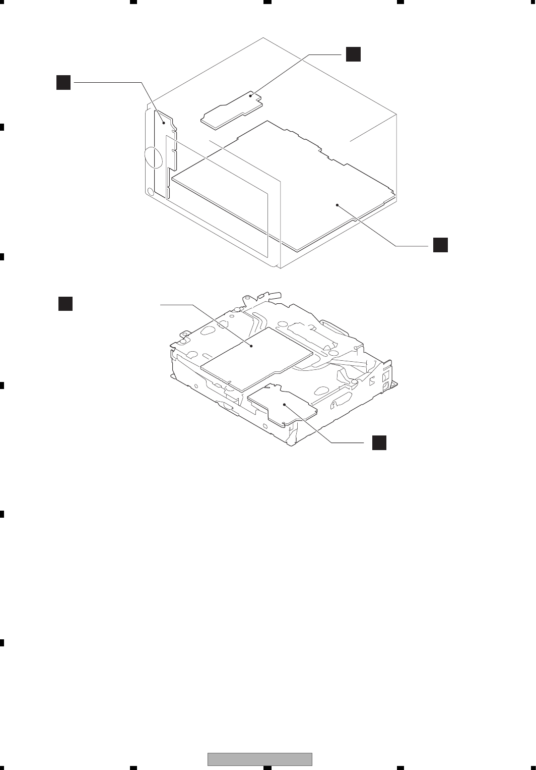
9. EXPLODED VIEWS AND PARTS LIST ........................................................................................................130
9.1 PACKING ................................................................................................................................................130
9.2 EXTERIOR(1).........................................................................................................................................134
9.3 EXTERIOR(2).........................................................................................................................................136
9.4 EXTERIOR(3).........................................................................................................................................138
9.5 DVD MECHANISM MODULE.................................................................................................................140
10. SCHEMATIC DIAGRAM..............................................................................................................................144
10.1 AV UNIT(PS/IF SECTION)(GUIDE PAGE) ...........................................................................................144
10.2 AV UNIT(A/V SECTION)(GUIDE PAGE) ..............................................................................................150
10.3 AV UNIT(TUNER SECTION)................................................................................................................156
10.4 AV UNIT(SYSTEM uCOM SECTION)(GUIDE PAGE)..........................................................................158
10.5 AV UNIT(RGB LED DRIVER SECTION)..............................................................................................164
10.6 AV UNIT(IF SECTION)(GUIDE PAGE).................................................................................................166
10.7 CK UNIT ...............................................................................................................................................172
10.8 DVD CORE UNIT(GUIDE PAGE) .........................................................................................................174
10.9 CONNECT PCB....................................................................................................................................180
10.10 KEYBOARD UNIT ..............................................................................................................................182
10.11 WAVEFORMS.....................................................................................................................................184
11. PCB CONNECTION DIAGRAM..................................................................................................................186
11.1 AV UNIT................................................................................................................................................186
11.2 CK UNIT ...............................................................................................................................................190
11.3 DVD CORE UNIT..................................................................................................................................192
11.4 CONNECT PCB....................................................................................................................................194
11.5 KEYBOARD UNIT ................................................................................................................................196
12. ELECTRICAL PARTS LIST .........................................................................................................................197
AVIC-X910BT/XS/UC
6
1234
1234
C
D
F
A
B
E
1. SERVICE PRECAUTIONS
1.1 SERVICE PRECAUTIONS
1.2 NOTES ON SOLDERING
1. You should conform to the regulations governing the product (safety, radio and noise, and other regulations),
and should keep the safety during servicing by following the safety instructions described in this manual.
2. Be careful in handling ICs. Some ICs such as MOS type are so fragile that they can be damaged by electrostatic
induction.
3. Before disassembling the unit, be sure to turn off the power. Unplugging and plugging the connectors during
power-on mode may damage the ICs inside the unit.
4. To protect the pickup unit from electrostatic discharge during servicing, take an appropriate treatment
(shorting-solder) by referring to "the DISASSEMBLY" .
5. After replacing the pickup unit, be sure to skew adjustment.
6. During disassembly, be sure to turn the power off since an internal IC might be destroyed when a connector
is plugged or unplugged.
7. Gasket(CNN2533) must not come in contact with the terminal(Panel Unit).
EJECT LOCK MODE for DVD mechanism
In order to change the EJECT LOCK/UNLOCK status of the mechanism, please perform following procedure.
< Procedure >
Top Menu -> AV Source -> Source OFF
Short push area "A" -> Short push area "B" -> Long push area "C" on above screen.
(In order to change the status, follow the same operation.)
The current status can be confirmed by "OFF" character color.
AB
C
Eject Lock: ON
Eject Lock: OFF
(White) (Blue)
For environmental protection, lead-free solder is used on the printed circuit boards mounted in this unit.
Be sure to use lead-free solder and a soldering iron that can meet specifications for use with lead-free solders for repairs
accompanied by reworking of soldering.
Compared with conventional eutectic solders, lead-free solders have higher melting points, by approximately 40 C.
Therefore, for lead-free soldering, the tip temperature of a soldering iron must be set to around 373 C in general, although
the temperature depends on the heat capacity of the PC board on which reworking is required and the weight of the tip of
the soldering iron.
Compared with eutectic solders, lead-free solders have higher bond strengths but slower wetting times and higher melting
temperatures (hard to melt/easy to harden).
The following lead-free solders are available as service parts:
Parts numbers of lead-free solder:
GYP1006 1.0 in dia.
GYP1007 0.6 in dia.
GYP1008 0.3 in dia.
AVIC-X910BT/XS/UC 7
5678
5678
C
D
F
A
B
E
2. SPECIFICATIONS
2.1 SPECIFICATIONS
Backup current ............... 6.5 mA or less
UC model

AVIC-X910BT/XS/UC
8
1234
1234
C
D
F
A
B
E
AVIC-X910BT/XS/UC 9
5678
5678
C
D
F
A
B
E
Backup current ............... 6.5 mA or less
EU5 model
AVIC-X910BT/XS/UC
10
1234
1234
C
D
F
A
B
E
AVIC-X910BT/XS/UC 11
5678
5678
C
D
F
A
B
E
Backup current ............... 6.5 mA or less
AU model
AVIC-X910BT/XS/UC
12
1234
1234
C
D
F
A
B
E
AVIC-X910BT/XS/UC 13
5678
5678
C
D
F
A
B
E
2.2 DISC/CONTENT FORMAT
AVIC-X910BT/XS/UC
14
1234
1234
C
D
F
A
B
E
2.3 PANEL FACILITIES
AVIC-X910BT/XS/UC 15
5678
5678
C
D
F
A
B
E

AVIC-X910BT/XS/UC
16
1234
1234
C
D
F
A
B
E
AVIC-X910BT/XS/UC 17
5678
5678
C
D
F
A
B
E
2.4 CONNECTION DIAGRAM
AVIC-X910BT/XS/UC
18
1234
1234
C
D
F
A
B
E
AVIC-X910BT/XS/UC 19
5678
5678
C
D
F
A
B
E
3. BASIC ITEMS FOR SERVICE
3.1 CHECK POINTS AFTER SERVICING
To keep the product quality after servicing, please confirm following check points.
demrifnocebotmetIserudecorP.oN
1 Confirm whether the customer complain has
been solved.
If the customer complain occurs with the
specific media, use it for the operation check.
The customer complain must not be
reappeared.
Display, video, audio and operations must be
normal.
2 DVD Measure playback error rates at the
innermost and outermost tracks by using the
test mode with the following disc.
DVD test disc (GGV1025)
Deterioration of mecha-drive can be
checked.
3 DVD Play back a DVD.
(Menu operation; Title/chapter search)
Display, video, audio and operations must be
normal.
4 CD Play back a CD.
(Track search)
Display, audio and operations must be
normal.
5 FM/AM tuner Check FM/AM tuner action.
(Seek, Preset)
Switch band to check both FM and AM.
Display, audio and operations must be
normal.
6 GPS positioning Connect GPS antenna to the product, and
check whether the current location is correct.
Current location must be correct.
Display and operations must be normal.
7 Map display
Touch-panel
operation
Remote-control
operation
Check functions of map scale change and
map scroll.
Display and operations must be normal.
8 Delete data added during the operating
check.
Check whether no media (CD etc.) is inside
the product.
Make sure to delete data added during the
operating check.
The media used for the operating check must
be ejected.
retfaecnaraeppastinotridrosehct
arcsoNkcehcecnaraeppA9
receiving it for service.
See the table below for the items to be checked regarding video and audio:
Item to be checked regarding video Item to be checked regarding audio
noitrotsiDesion-kcolB
esioNesionlatnoziroH
wolootemuloVesiontoD
Disturbed image (video jumpiness) Volume too high
gnitautculfemuloVkradooT
detpurretnidnuoSthgirbooT
Mottled color
The error rate must be less than the
threshold value.
(Refer to the chapter of DIAGNOSIS
for the threshold value.)
AVIC-X910BT/XS/UC
20
1234
1234
C
D
F
A
B
E
3.2 PCB LOCATIONS
E
AV Unit
A
Keyboard Unit
CDVD Core Unit
DConnect PCB
CK Unit
B
Unit Number : CWN4237(UC)
Unit Number : CWN4238(EU5)
Unit Number : CWN4239(AU)
Unit Name : AV Unit
Unit Number : CWN4251
Unit Name : CK Unit
Unit Number : YWX5009
Unit Name : DVD Core Unit
Unit Number :
Unit Name : Connect PCB
Unit Number :
Unit Name : Keyboard Unit
AVIC-X910BT/XS/UC 21
5678
5678
C
D
F
A
B
E
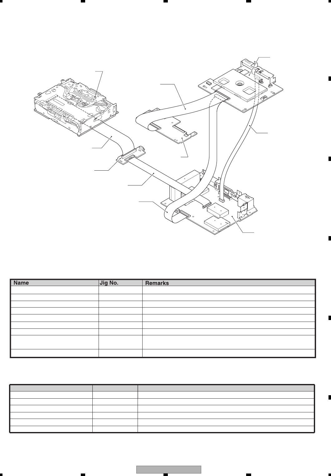
3.3 JIGS LIST
15P FFC GGD1123 Navi Unit <---> SD Unit
74P FFC GGD1560 Navi Unit <---> Panel Unit
50P FFC GGD1250 Navi Unit <---> AV Unit
20P Extension Cable GGD1327 Navi Unit <---> AV Unit
TORX screwdriver GGK1068 T8 (For top cover)
40P FFC GGD1170 AV Unit <---> CK Unit
30P FFC BBR GGD1635 CK Unit <---> DVD Mechanism Module
Disc TDV-582 Skew adjustment, Check points after servicing,
Inspection method of Pickup Unit
Disc TCD-782 Inspection method of Pickup Unit
- Jigs List
- Grease List
Name
Grease
Grease
Grease
Locking agents
Bond
Bond
Jig No.
GEM1024
GEM1038
GEM1045
1401M
GEM1033
1530
Remarks
DVD Mechanism Module
DVD Mechanism Module
DVD Mechanism Module
Skew adjustment (1401M:produced by THREE BOND)
Skew adjustment
Skew adjustment (1530:produced by THREE BOND)
GGD1327
Navi Unit
GGD1250
GGD1560
DVD Mechanism Module
(LS1)
GGD1170
Panel Unit
AV Unit
GGD1635
CK Unit

AVIC-X910BT/XS/UC
22
1234
1234
C
D
F
A
B
E
3.4 CLEANING
Before shipping out the product, be sure to clean the following portions by using the prescribed cleaning tools:
Portions to be cleaned Cleaning tools
DVD pickup lenses Cleaning liquid : GEM1004
Cleaning paper : GED-008
Portions to be cleaned Cleaning tools
Fans Cleaning paper : GED-008

AVIC-X910BT/XS/UC 23
5678
5678
C
D
F
A
B
E
AVIC-X910BT/XS/UC
24
1234
1234
C
D
F
A
B
E
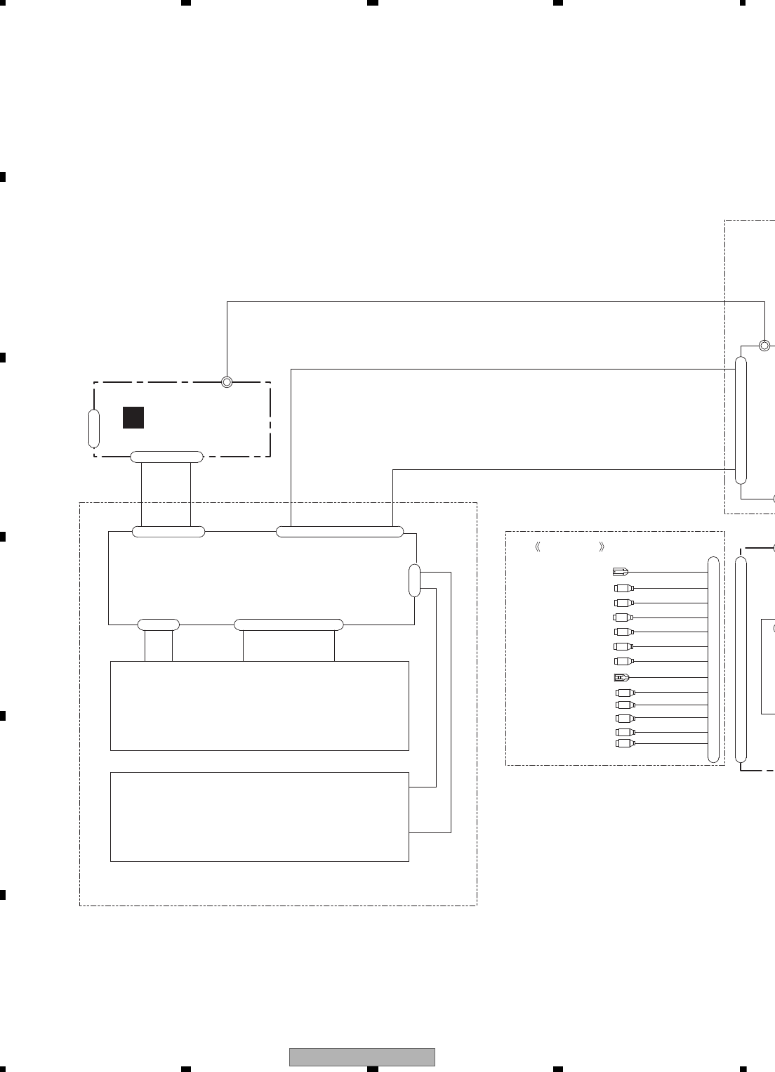
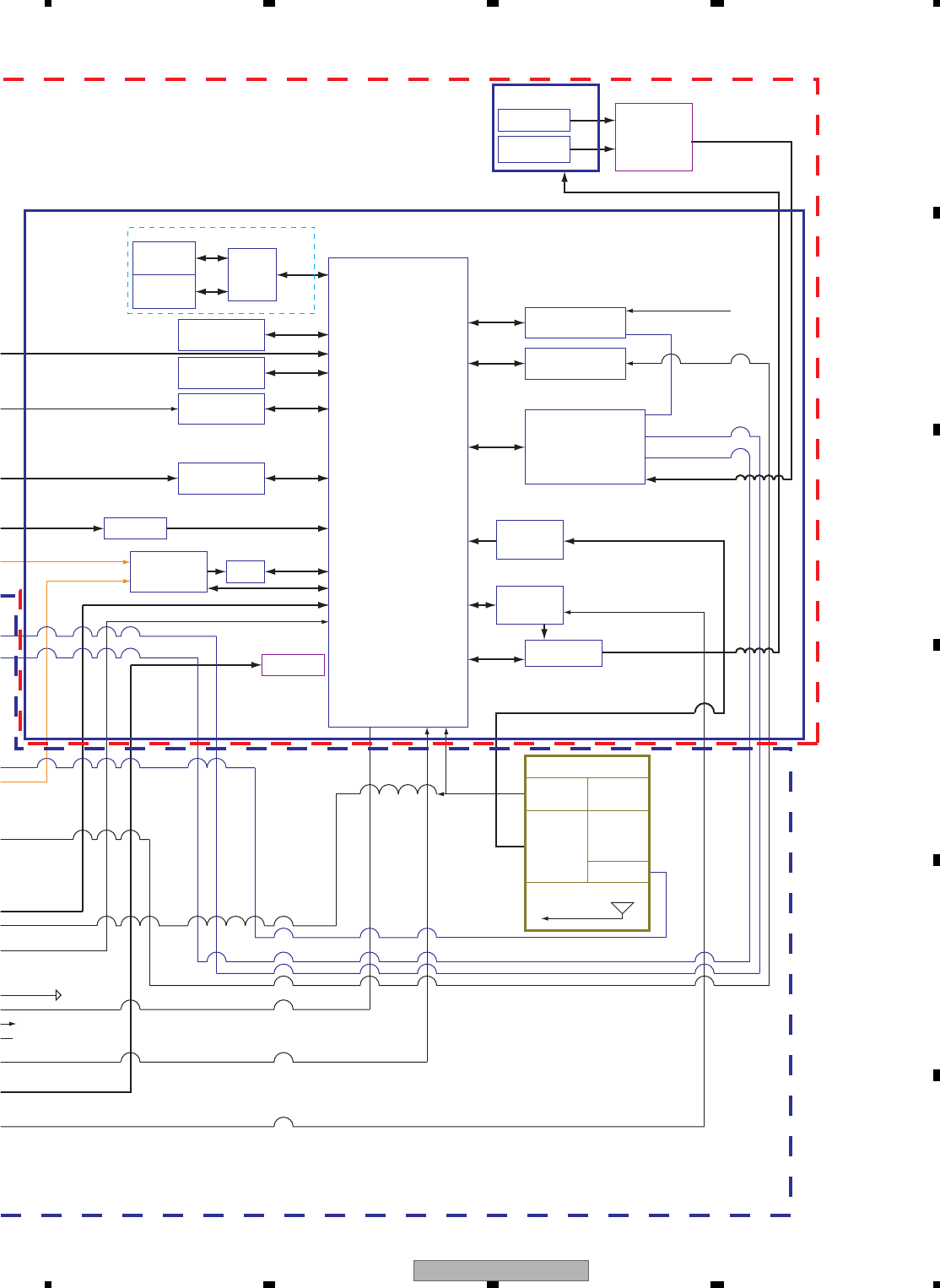
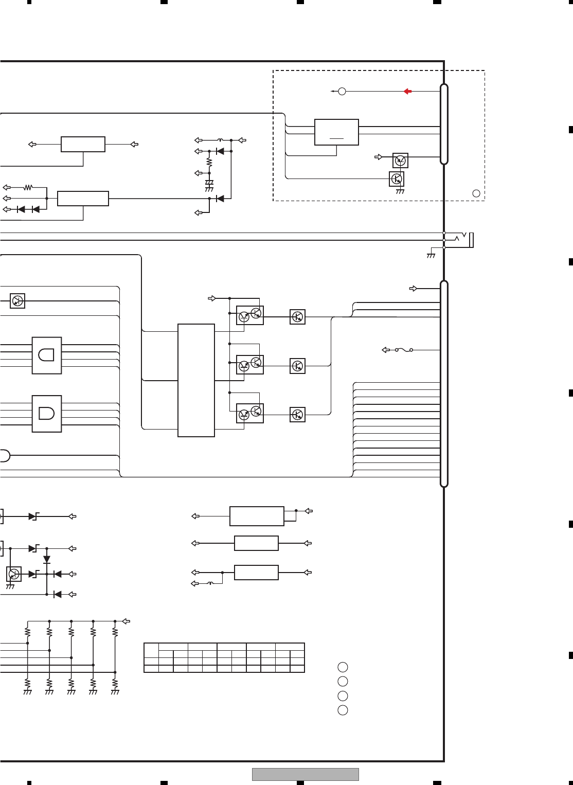
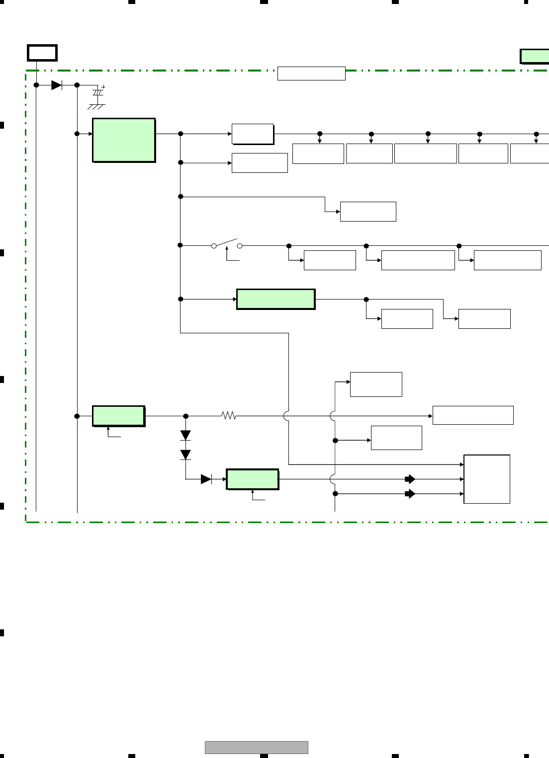
4. BLOCK DIAGRAM
4.1 OVERALL CONNECTION DIAGRAM
}
}
}
}
60
LCJ3
1
REAR CAMERA INPUT
REAR MONITOR OUTPUT
U
E
MUTE
REAR OUTPUT
FRONT OUTPUT
1
24
AUDIO INPUT
VIDEO INPUT1
SUBWOOFER OUTPUT
SYSTEM REMOTE CONTROL
CODE ASS'Y
CN801
122
1
74
LCJ1
F
1
24
CN803
OTJ2
122 1 74
OTJ1
110
1 4
LCJ6
LCJ1
A
LCD MODULE
PANEL UNIT
TOUCH PANEL
CWX3850-
CWX3785-
CSX1136-
CDP1241-
AVIC-X910BT/XS/UC
AVIC-F910BT/XS/AU
AVIC-F910BT/XS/EU5
1
4
LCD MODULE ASS'Y CXE2153-
BTJ2
CN802
F
CN1016
(AV MINI
JACK IN)
T
EKEYBOARD UNIT
AVIC-X910BT/XS/UC 25
5678
5678
C
D
F
A
B
E
FAN
GND
10A
POWER SUPPLY
TERMINALS
ACC
PKB
ILM
RR-
FL-
RR+
FL+
RL-
FR-
FR+
RL+
CN1005
150
OTJ1
MIC ASS'Y
GPS ANTENNA ASS'Y
CXC8574-
UC:CPM1064-
EU5,AU:CPM1083-
1
16
1
30
CN1901
AANT
1
24
REV
PULSE
5
1
CODE ASS'Y
SPJ2
21
1
74
LCJ1
SPJ1
120
OTJ5
16
MIC
BLACK 2.5
115
24 1
FM/AM TUNER UNIT
GPJ1
31
CN1001
20
11
CN1000
50
140
CN702
1
24
115
ANT1401
CN1441
NAVI UNIT
DVD MECHA MODULE
SD UNIT
CWX3652-
CXM1320-
115
USB
CXK6801-
UC,AU:CDP1095-
EU5:CDP1097-
EU5:CWE2127-
OTJ6OTJ11BTJ2
FM/AM ANTENNA IN
UC:CDE9102-
EU5,AU:CDE8913-
BUP
CN701
CN1016
OTJ2
TMJ1
1
16
111
CN1021
IP BUS
UC,AU:CWE2128-
40
CN882
1
30
CN883
1
AAV UNIT
PS/IF SECTION
1/6
A
A/V SECTION
2/6
A
SYSTEM uCOM SECTION
3/6
A
IF SECTION
4/6
A
TUNER SECTION
5/6
A
RGB LED DRIVER SECTION
6/6
A
BCK UNIT
CD
AVIC-X910BT/XS/UC
26
1234
1234
C
D
F
A
B
E
to Titan
(NAVIBD)
to CPLD(NAV
GPS Antenna CONN
USB 2.0 Slot
RS232CONN*1
Rear Camera CONN
Speaker CONN Speaker Out
Composite In
Composite In (1)
USB 2.0
GPS Antenna
GPS
Antenna
Radio
Antenna
Composite
Composite
R-sound In
L-sound In
Phone Mute Input
Wire Remote Input
Acc/Bup/ILM
Speed Pulse Input
Parking Signal Input
Reverse Signal Input
Reset GND
Reset Signal
UART(2)
TMC (EW only)
Composite In (2)
GUIDANCE (Audio Signal)
Source Audio Signal
CPU Watchdog
An Information of Power off
An Answer of Power off
Reverse Signal
VCC 5 V
Speed Pulse
Control Signal
Video Out CONN
Radio Antenna CONN
Phone Mute CONN
Parking Signal CONN
Wire Remote Input
Reverse Signal Input
Power Supply CONN
Speed Pulse CONN
RF Splitter
I2C
AMP E-vol
DVD(LS1)
SD/MMC Slot SDIO(1)
U
G
AV
Selector IC
FM/AM
Tuner
Arrange
Waveform
Arrange
Waveform
Voltage
Detecting IC
Voltage
Detecting IC
Arrange
Waveform
Arrange
Waveform
LPF
DC/DC Switch
CK Unit
System
u-COM
Sense
3RCA CONN
IP-BUS CONN
(UC only)
SubWoofer CONN
SD Board
AV Unit
Rear
Pannel
AVIC-X910BT/XS/UC 27
5678
5678
C
D
F
A
B
E
to CPLD(NAVI BD)
Composite In (1)
Composite In (2)
GND
y)
(2)
og
al
Transmitter
Switch
5 V In Jack
USB 2.0
H & D Gyro
ADC I2C(1)
ROM 16-bit
SDIO(1)
133 MHz
USB 2.0
AC97
UART(0)
USP(0)
USB 2.0
GPS Antenna
RS232
I2C(0)
UART(2)
VCC 5 V
Reset Signal
ITU-R BT
601/656
8-bit
Dead Reckoning
G Sensor
GPS Front end
Bluetooth Module
TMC/FM6 Module
BT Antenna
TMC
(EW only)
Mono Out
Speed Pulse
16-bit
Color-TFT
Touch Panel
4-wire
Headphone Out
LED Driver
LVDS RX
5.8” TFT LCD
with
Touch Panel
LVDS TX
Xilinx CPLD
Timing
Control
ADC
Volume
Controller
AuX-in
BT Antenna
Buttons
1. Eject
2. Menu
3. Map
4. Mute
DDR1*2
(16Meg*32)
SLC Flash 256 MB
Video Decoder
Front Panel
Key Pad
Board
600 MHz
LCD Board
Navigation Unit
CPU
Audio Codec
UP to 400 MHz DDR or 166 MHz SDRAM
Enhanced 32 channel GPS base band
24-bit Color-TFT LCD panel interface
8/16-bit HAND flash interface
CMOS/CCD sensor interface
USB OTG 2.0 high-speed interface
ATA-4 interface (UDMA33)
2 slots SD/SDIO/MMC/MMC4.0/CE-ATA
2 CANBus ports
AC97 & I2C Audio CODEC interface
3 Universal Serial Ports (USP) &
3 UARTs
2 SPI interface
2 I2C interface
PWM interface
AVIC-X910BT/XS/UC
28
1234
1234
C
D
F
A
B
E
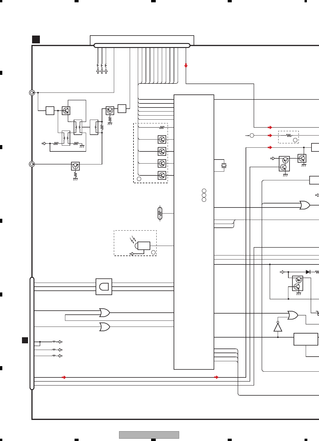
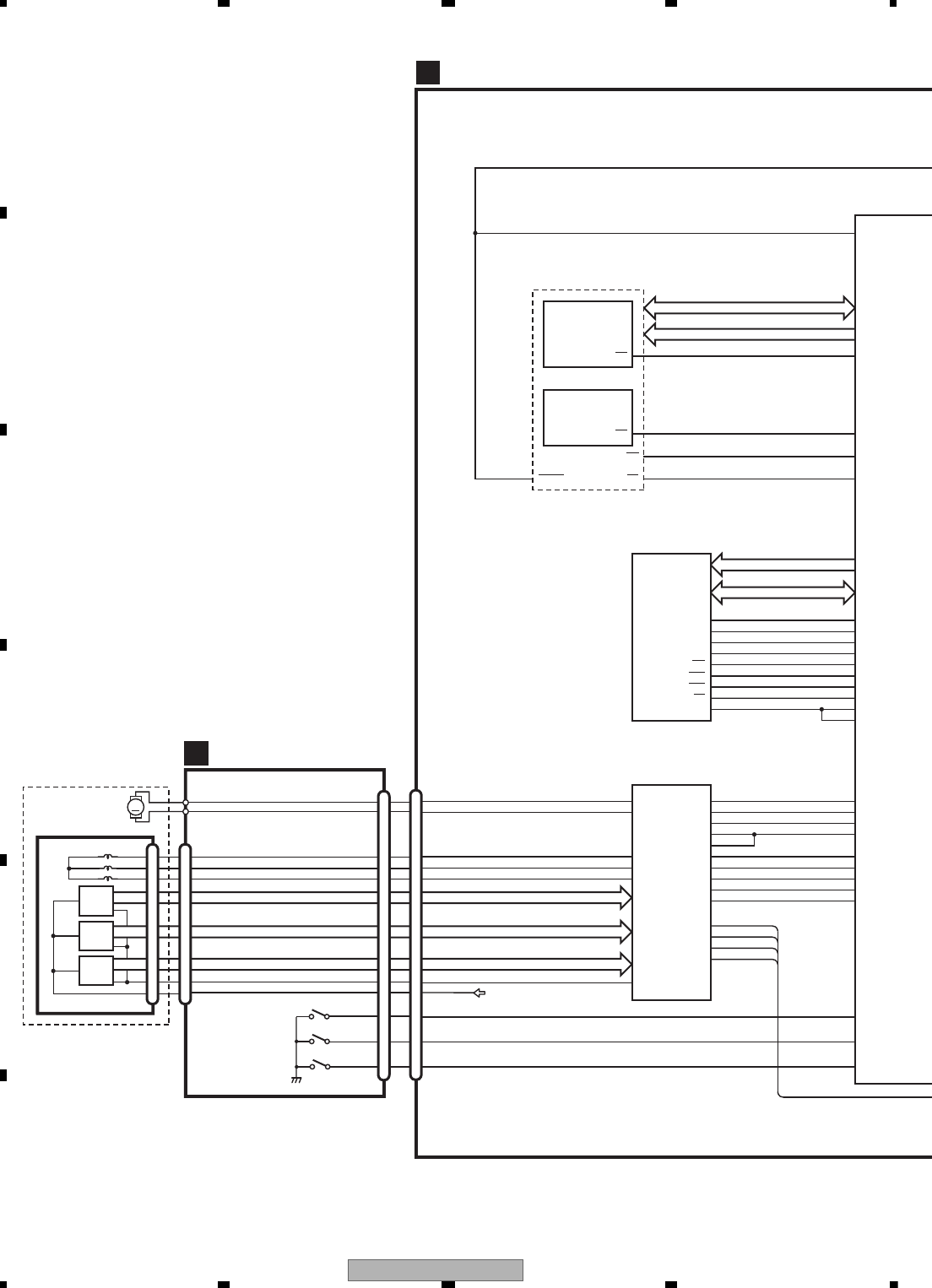
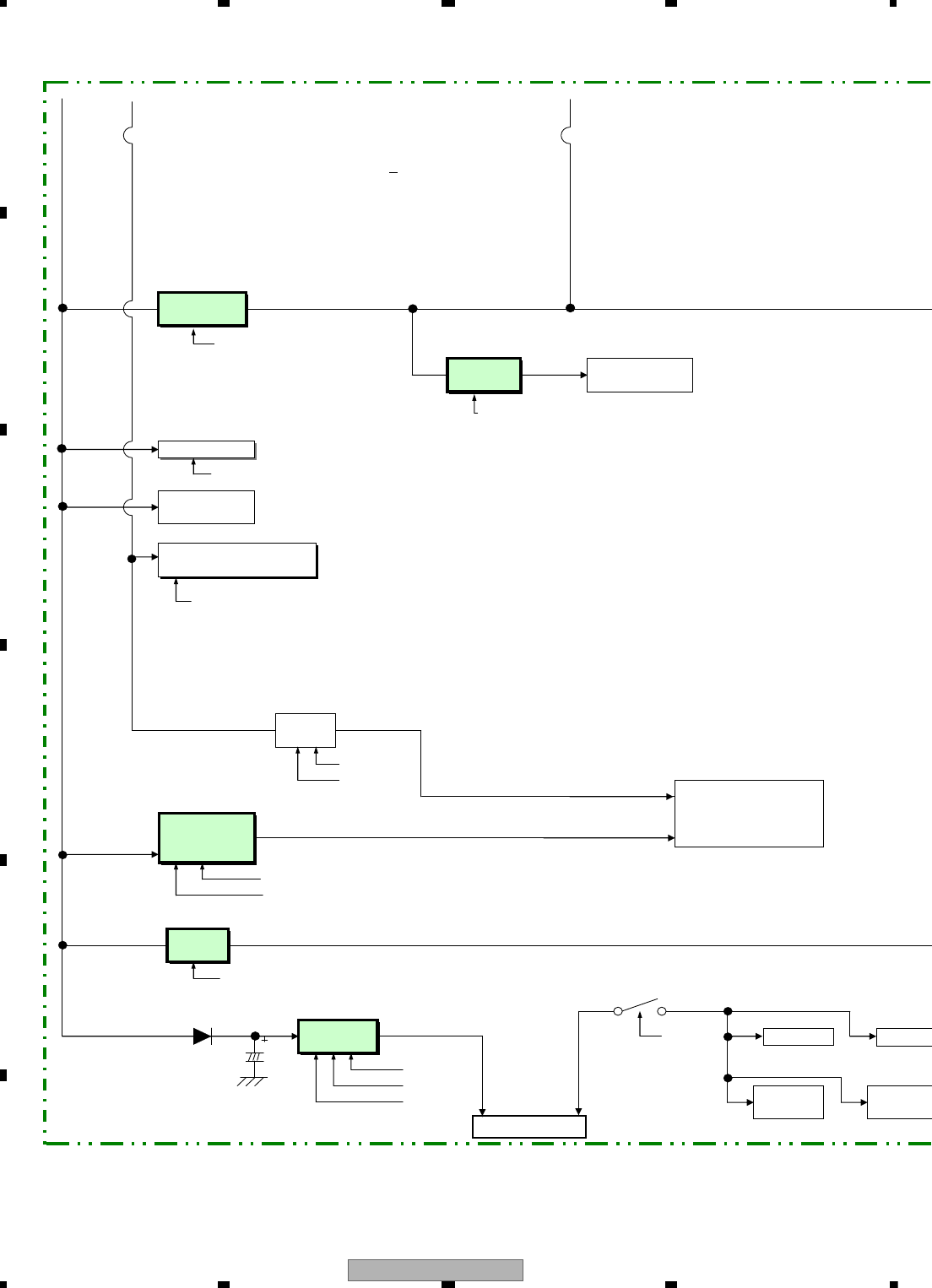
4.2 BLOCK DIAGRAM
AV UNIT(1/2)
A
FL
ANT1401
FM/AM
ANTENNA
Q1421
AV8
FL
Q1401
T1403T1402
T1401
CN1441 VICS/TMC AMP
Q1441
FM/AM TUNER UNIT
6
17
8
9
3
5
4
FM_ANT
1
AM_ANT
B
VCC
AV8
13
VDD5 VDD_3.3
TU3
SL
CE2
CE1
CK
10
14
DI
DO
TUNSL
23
LchFML
TUNCE2
TUNCE1
TUNCLK
TUNDO
TUNDI
11
18
LDET
RDS_CK
19
20
RDS_DATA
RDS_LOCK
21
RDS_HSLK
HRCK
HRDT
HRLK
HRHSLK
Q752
Q753
Q754
Q751
HRCK
HLDET
HRDT
HRLK
HRHSLK
VD8
VD8
MVDD5
IRQPWR
XRES
HSTCMD
IRQPW3
XRES3
SYSTOMS53
IRQPW5
XRES5
SYSTOMS55
64,5
31,2
MS5TOSYS5
11 12,13
ROM_VDD
24
25
20
1
2
VDD8(DRY)
3
VDD5
AMUTE
SLVSTS MS5TOSYS3
21
22
23
STANBY MS5_STANDBY3
32 CVBS DVDV
29 ANALOUT
VDD8(REG) 134
ILLSNS
72
TEIN
78
SELSDA
79
SELSCL
FML
IC
BA45
3
GUIDE ISOL
GUIDE
ILMSNS
CN702
IC
NJM
3
DVDL
DV
Q3042
AMUTE
Q3041
A
D
TO 2/2
IPL
MS5_STANDBY5
9,10
56
CNVSS 4
8
I
17
14
SREMOTE 66
TUNSL
141
TUNCE2
9
TUNCE1
8
TUNCLK
7
TUNDO
5
TUNDI
6
LDET
26
RCK
25
RDT
17
RDSLK
14
RDS57K
18
XOUT
XIN
X601
20MHz
20
22
XRES
64
IRQPW
63
HSTCMD
38
SLVSTS
40
CNVSS
16
MS5_STANDBY
61
TMPIN
137
REMOCON
3
TEMP SENSOR
TH601
C
103
ASENS
84
NFCONT
73
FANCONT
CN882
B
77
NOSELR
95
VST
96
VDT
97
VCK
GUIDEMUTE
NOSELR
AV8
SWVDD5
U695 1
RESET 19
MUTE 85
1
3
IC608
BD5335FVE
IC603
TC7SH04FUS1
IC604
TC7S32FU
VOUT
CT
VDD
SRCMUT
2
4
4
1
2
FM DISTRIBUTION
NAVI UNIT
TMJ1
IR REMOTE
DVDL
5V→3V
IC607
TC74VHC08FTS1
3V→5V
IC612
TC74VHCT32AFT
AV8
AMUTE
Q2860
BUP
HLDET
SYSTEM-uCOM
IC610(1/2)
A
B
PEG562A8:
PEG561A8:
PEG563A8: C
3
AMUTE
AVIC-X910BT/XS/UC 29
5678
5678
C
D
F
A
B
E
32
30
VOUT2
39DVDV
15
AV SELECTOR
IC4171
AN15887A
36
35
6
IN2_L
IC1016
BA4558RFVM
73
2IN5+_L
3IN4+_L
EVOL
IC4271
PML018A
GUIDE ISOLATOR/LPF AMP
10
5
Frout_L
IN3_L
11
FL
RL
Rear_L
12
Pre/SW_L
Q4232
VR4231
Q4231
VIDEO BUFFER
Vout 1
Vin
4BCVIN
BACK CAMERA ISOLATOR
IC4251
NJM2505AF
43
V4-1
19
L4-1
23
L5-1
34
VOUT1
37
V1-1
14
5
12
3
21
23
4
22
SREMOTE
PWR AMP
IC1007
PAL007C
IN2 OUT2+
OUT2-
IN4 OUT4+
OUT4-
25
B_REMOTE
STBY
MUTE
CN1005
8
12
14
5
7
ILMILMSNS
ACC
6
ASENS
FANUP
FANCONT
CN1016
BCV
12
BREM
13
ASENS
11
REVREVSNS
10
PULSESPEED
9
PKB
PKBOUT
Q2880
Q2900
PFL
PRL
RL+
RL-
FL+
CN1000
(1/2)
POWER SUPPLY TERMINALSCODE ASSYNAVI UNIT
OTJ1 NAVI UNIT
SPJ1
27
FRV
FL-
9
5
13
SWL
FL
RL
PFL
PRL
ANTB
16
BUP
Q2870
Q4751
IC1015
NJM4558V
13
DVD LPF
7IN1-L
Q3042 Q4333
Q4331
Q4332
Q3041
A
SWL
POMUTE
29
AANT
GUIDEMUTE 30
GUIDE 32
SPEED
PCHNG 49
PULSE 50
PKBPKBOUT 42
NFCONT 25
KMODEKMODEOUT 43
REVREVSNS 44
AUX-LAV2LS 12
AUX-VAV2VIN 15
VTR1LAV1LS 17
VTR1VAV1VIN 19
TELMUTE 1
TEIN
BCV 23
REARVOUT 21
NaviAL 23
8
KMODE
KMODEOUT Q4752
Q2840
SPEED PULSE
IC1002
NJM2904M
15
Q2841
Q601
MUT
FANV
AV8V
CN1001
2
20
Q4771
I
Q4776
AV8
4
6
8
10
12
14
16
18
NAVI5V
FU4771
Q4314
Q4312
VCK
VDT
20 CLK
19 DATA
VST 21 STB
AV8
FAN DRIVE
POMUTE
RESET 4
SREMOTE
HDRST
RSTMUTE
RSTIN
15
3
IC608
BD5335FVE
S1
IC604
C7S32FU
VOUT
CT
VDD UVDD5
SRCMUTE
MUT
4Q2864
Q2865
Q2862
AV8
NFCONT
AAVIC-X910BT/XS/UC
BAVIC-F910BT/XS/EU5
CAVIC-F910BT/XS/AU
MUTE
MUTE
Q2863
Q2860 Q2861
LOUT2
V2-1
SCL
SDA
MUTE
MUTE
PARKING SENS
REVSNS
ILMSNS
ASENS
TELMUTE
KMODE
NAVIAL
DTO 2/2
Q1016(2/2)
Q1016(1/2)
VDD5
3.3V
RST
VOUT2
L3-1
V4-1
3.3V
IN+ OUT
AVIC-X910BT/XS/UC
30
1234
1234
C
D
F
A
B
E
NAVI5V
IC4601
TPS5103IDB
9
14
Q4661
VCC_SENSE
RWMSKIP
10
STBY
Q4602
19
18
17
LL 48 NAVICON
49
DCSKIP
88
104
FCONT
BSENS
OUT_U
OUT_D
3FB
NKBUP
NAVI5V
2INV
FU4601
FU4602
DVD8V
IC4641
TPS5103IDB
10
STBY
Q4642
19
18
17
LL 58 VDCONT
OUT_U
OUT_D
3FB
VD8
2INV
FU4641
DVD5V
IC4661
TPS5103IDB
10
STBY
Q4663
19
18
17
LL 60
92
VDD5CONT
69 SYSPW
67 SWACPW
ANTON
OUT_U
OUT_D
3FB
MVDD5
2INV
FU4661
ANTB 1
5
Q4601
RT
5
Q4641
RT
5
Q4662
RT
SWVDD5 VDD5
Q2881
Q2882
SYSPW
3.3V NAVI3V
Q4753
Q4754
SYSPW
FU4631
ILMV
Q4631
Q4632
BU
50
DCSKIPCD
Q2811
Q2812
42
AV8
VIDEO5
Q2810
BUP
SWACPW
AV8
IC2801
BA00CC0WCP-V5
42
TU3 VT6
TU3
IC2830
BA00BC0WFP
1
1
SYSPW
SWACPW
36
RX 70
IPPW 71
ASENBO
37
TX
Q4733
Q4731
86
BSENSN
SYSPW
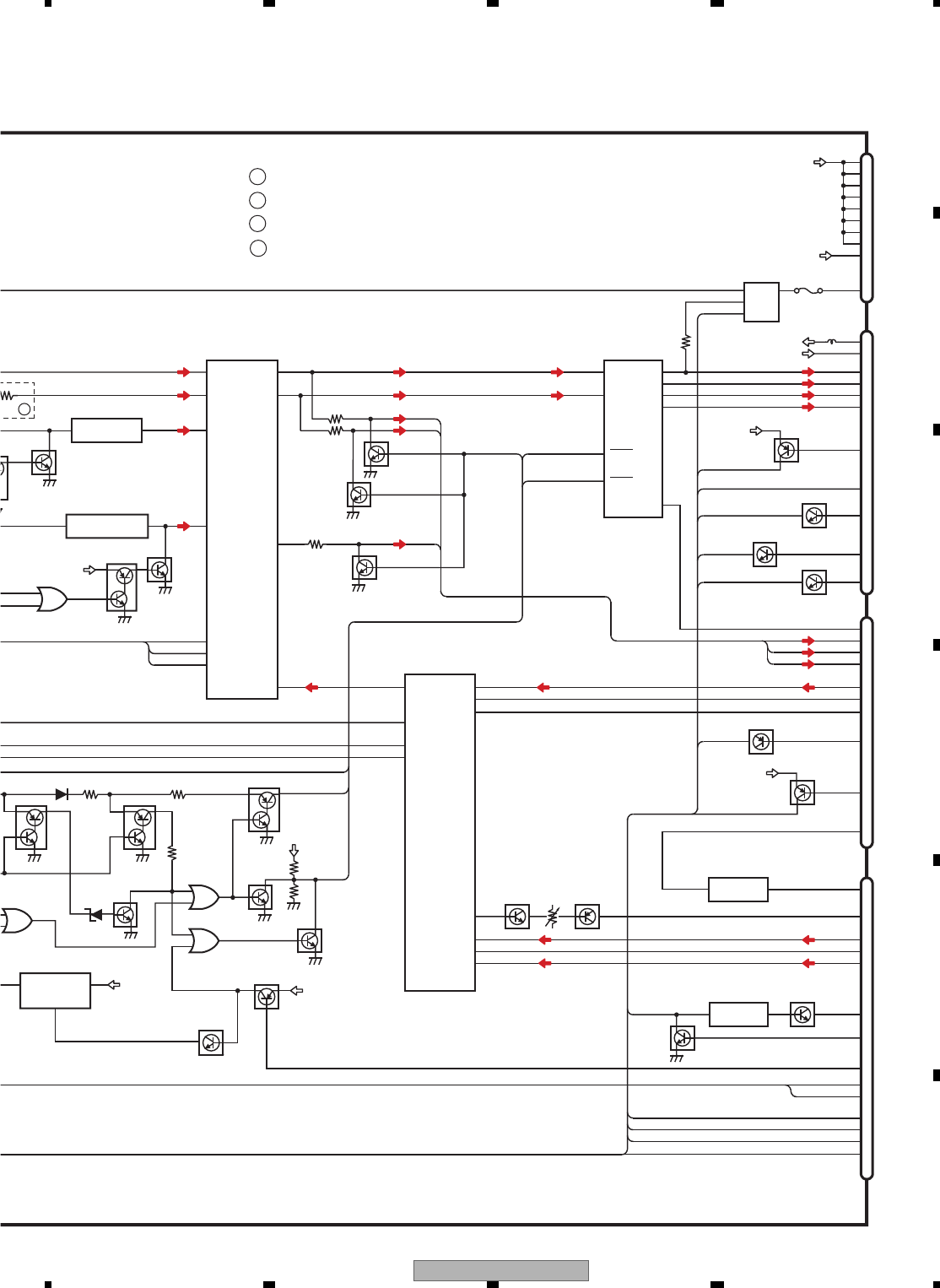
AV UNIT(2/2)
A
56
55
51
SIMUKE0
SIMUKE1
SIMUKE4
53
52
SIMUKE2
SIMUKE3
R658 R
R657 R
VT8 4
B
VT6
VICS8
13
VCC
14
VCC_SENSE
VCC 13
BU
FU4642
14
VCC_SENSE
VCC 13
KBUP
FU4662
VIDEO5
ILMV
SWVDD5
PARKING SENS/
KMODE 3.3V
NAVIC
Q4738
90
OPTSNS
139
WREMIN
133
WCONT
89
OPTON
121
RSTOUT
119
OFFINFO
126
SYSTOC
131
SYSTOCV
117
BATFAULT
120
CPUWDT
118
OFFANS
125
CTOSYS
128
CTOSYSV
124
DVEJKY
112
ROT1
111
ROT0
CTOSYS5
CTOSYSV5
OFFANS5
CPUWDT5
3
3V
→
5V
IC605
TC74VHCT08
6
8
11
SYSTOCV5
BATFAULT5
SYSTOC5
OFFINFO5
9,10
5V
→
3V
IC609
TC74VHC08
1,2
4,5
12,13
Q661
Q662
1,2 4
LEDCS
105
106
107
LEDDT
LEDCK
RESET
IC601
TC7SH08FUS1
SYSTEM-uCOM
IC610(2/2)
A
B
PEG562A8:
PEG561A8:
PEG563A8: C
VOUT VCC
CTL
VDD VIN
VC
BSENS
AVIC-X910BT/XS/UC 31
5678
5678
C
D
F
A
B
E
BUP3 5
1VDD5
BUP3
IC4703
S-L2980A33MC-C6S
AU4 1
IC1008
NJM2125F AV8
AU4
ANTB 15
6
BUP
AANT
IC2890
TPD1018F
VDD5 51
IC4701
BD3931HFP KBUP
VDD5
A
D
KBUP
Q4732
Q4734
ASENBO
BU BUP
NKBUP
KBUP
NAVIC +
BU
KBUP
Q4733
31
NAVIC
CN1021
IPBUS-
IPL+IPL
IPBUS+
7
1
5
IP-BUS DRIVER
IC4721
HA12241FP
6
5
DIN1
ROUT
BUS+
BUS-
ASENBO 8
1
2
TX
RX
8
IPPW
STBY
IP BUS
A,B
C
R643
104
104
R644
NM
NM
SIMUKE4
R646
104
104
R647
NM
NM
SIMUKE3
R650
104
104
R651
NM
NM
SIMUKE2
R654
104
NM
R655
NM
104
SIMUKE1
R657
104
104
R658
NM
NM
SIMUKE0
R658 R655 R651 R647 R644
R657 R654 R650 R646 R643
UVDD5
TO 1/2
42
1
VT8
IC2820
BA00CC0WCP-V5
NKBUP
IC
38
3,4
UVDD5
A
BAVIC-F910BT/XS/EU5
AVIC-X910BT/XS/UC
C
DTO 1/2
AVIC-F910BT/XS/AU
WCONT
WIREIN
CN1015
WIRED REMOTE
(Black)
YS5
YSV5
NS5
WDT5
3 1,2
3V
→
5V
IC605
TC74VHCT08AFTS1
6 4,5
8 9,10
11 12,13
CTOSYSV3
CTOSYS3
SYSTOCV3
SYSTOC3
OFFANS3
CPUWDT3
BATFAULT3
OFFINFO3
OCV5
AULT5
OC5
FO5
ROT1
ROT0
RESETB
9,10 8
5V
→
3V
IC609
TC74VHC08FTS1
1,2 3
4,5 6
12,13 11
Q661
4
CN1000
(2/2)
9
ILMR 7
ILMG 6
ILMB 5
EJECTDVEJKY 3
ROT1 17
ROT0 18
RESETB 48
OPTON 40
OPTSNS 41
NAVI33V 24
CTOSYSV3 34
CTOSYS3 37
OFFANS 45
WDOG
OFFANS3
CPUWDT3 47
BATTERY-FAULTBATFAULT3 16
SYSTOCV3 35
SYSTOC3 38
OFFINFOOFFINFO3 46
NAVI3V
FU2900
NAVI UNIT
OTJ1
ESET
C601
H08FUS1
ILMR
ILMG
ILMB
ILMV
61
DI AO1
72
CLK AO2
83
LD AO3
Q3604
Q3605
LEDDT
LEDCK
LEDCS
Q3606
Q3601
Q3602
Q3603
RED
GREEN
BLUE
IC3601
M62343FP
RGB LED DRIVER ILMV
3
2
1
OUT VDD
IN
VOUT VCC
CTL
BSENS
VOUT VIN
ON/OFF 3
AVIC-X910BT/XS/UC
32
1234
1234
C
D
F
A
B
E
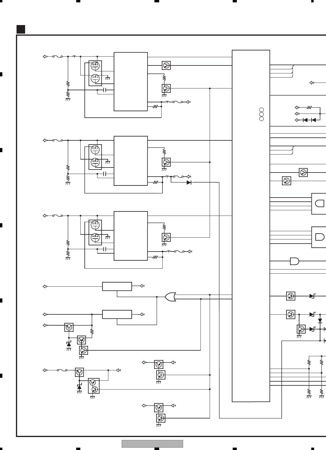
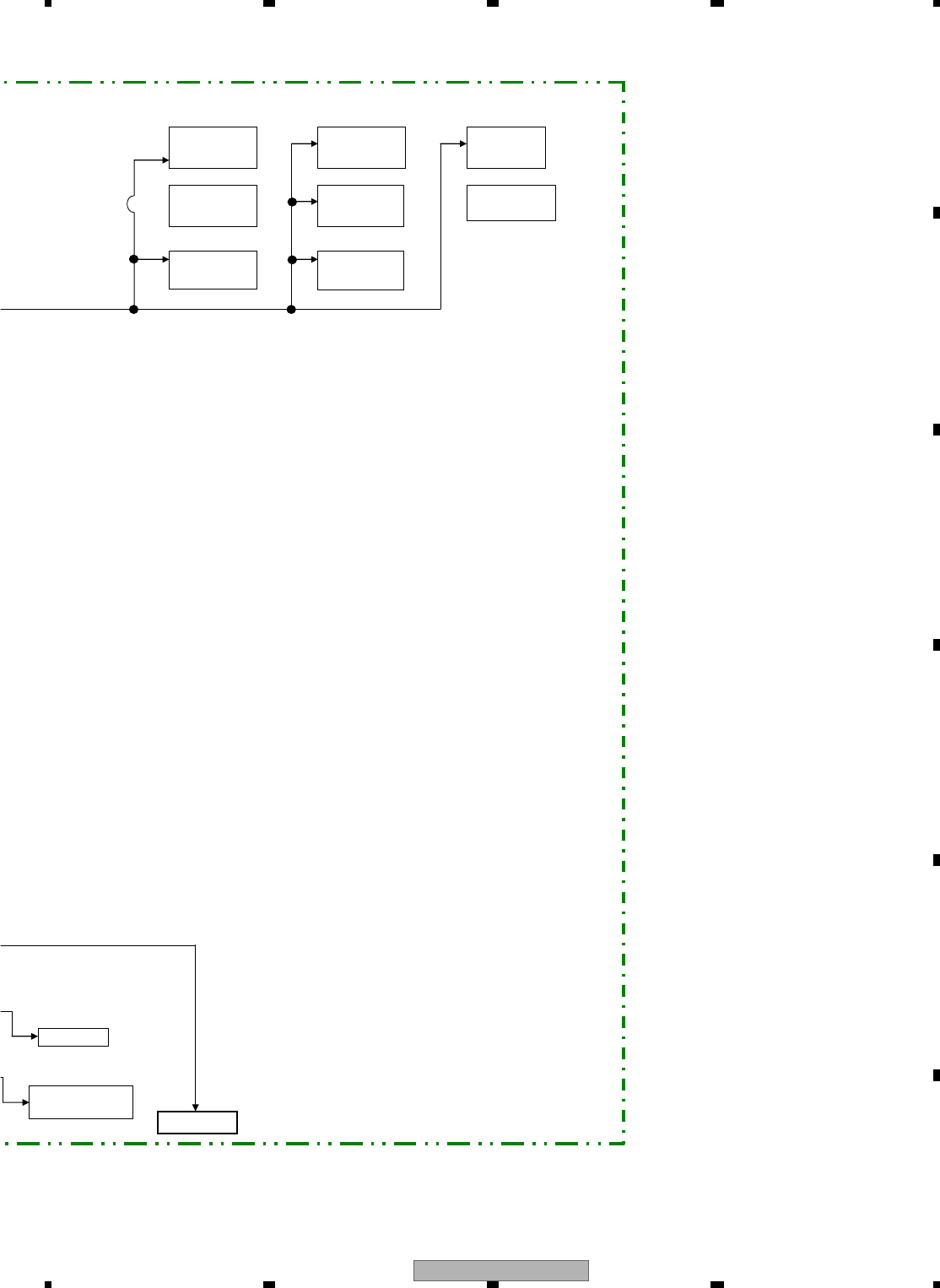
MA0-11
MDQ0-15
D0-15
VIDEO+AUD
IC1501
MN2DS0018M
S
S
TRC
TRC
TRC
T
S
E
F+
E+
D
COM
ST
CMD
ST
IR
E
TRC
NRES
A0-19
HWP(HW+),HWM(HW-)
HVP(HV+),HVM(HV-)
HUP(HU+),HUM(HU-)
HWP(HW+),HWM(HW-)
HVP(HV+),HVM(HV-)
HUP(HU+),HUM(HU-)
XRDNRES 28 214 NEXOE
NEXWE
70 NRES
59 XCSSR
213
31
NEXCE
26
12
CE
OE
RESET
SDRAM
IC1480
K4S641632N-LC75
19
38
CS
CLK
XWE16 181 NWE
XCAS
DQM0
DQM1
17 188 NCAS
XRAS18 189 NRAS
XCSM 190 NCSM
20 193 BA0
21 197 BA1
BA0
BA1
15 179 DQM0
39
8
9
12
5
6
7
3
4
1
2
32
31
27
26
28
14
180 DQM1
LDQM
UDQM
MCK
VHALF
TD
FD
CRGDRV
MD
CONT1
CONT2
FOP
FOM
TOP
TOM
183 MCK
185 MCKI
V
CAS
RAS
WE
MOTOR DRIVER
IC1201
BD8231EFV
CTL1
CTL2
FG
FCO+
FCO-
TKO-
TKO+
FCIN
SLIN
VC
TKIN
LDIN
SPIN
W
HB
SL/LDO-
SL/LDO+
V
U
SLOPOUT
CN1201
CN101
CN701
CRG/LE+
COIL_U
17
18
16
6
3
4
5
9
8
7
HALL_BIAS-
HALL_BIAS+
COIL_V
COIL_W
67
127
126
66
71
64
63
FG
CONT2
CONT1
12EJ
08EJ
HOME
62
MD
LDIN
CRGDRV
FD
TD
34
36
35
33
55
49
65
CRG/LE- 110 VHALF
FLASH 16M
IC1401
CWW1825
XCFS2
XCFS1
26
11 XWR1
CE
WE
IC1402
CWW1826
DVD CORE UNIT
C
VCC5
BR
GY
CRG-
CRG+
V COIL V
U COIL U
W COIL W
V
U
W
H- HALL BIAS-
H+
H-
H+ HALL BIAS+
HOME
8SNS
DSCSNS
HOME
8cm
12cm(DSCSNS)
CONNECT PCB
SPINDLE MOTOR
LS1 MECHA UNIT
D
2
1
3
13
16
15
14
10
11
12
1
2
3
4
10
1
2
3
4
10
M
LOADING/CARRIAGE
MOTOR
HOME
S101
8cm
S102
12cm
S103
H3
H2
H1
AVIC-X910BT/XS/UC 33
5678
5678
C
D
F
A
B
E
VIDEO+AUDIO
IC1501
MN2DS0018MAUB
AVCC5
VOUTL 7
BCK
LRCK
DATA
MD
1
3
2
13
AUDIO 2CH ANALOG OUT
IC1801
PCM1753DBQ
LOUT
ML
MC
SCK
SRCK
LRCK
ADOUT
SDODAC
LTDAC
SCKDAC
DACCK
15
14
16
149
150
151
57
56
58
148
SRCK
ADOUT
SDODAC
LRCK
LTDAC
SCKDAC
DACCK
TRCST
TRCDATA3
TRCDATA2
TRCDATA1
TRCDATA0
TRCCLK
EXTRG0
1
2
3
4
9
7
12
8
13
5
6
Q1104Q1102
VREF
VCC5
CN1101
CN1951
78LD
F+H_G+H
E+G_E+F
F+H/G+H
E+G/E+F
LPCO2
8
2
3
4
14
15
12
18
17
13
20
22
7
5
11
Q1103Q1101
65LD
VCC
Vref
LPCO1
TRCDATA2 79
TRCDATA3
TRCDATA0
TRCST 80
77
81
TRCCLK 76
SDATA
SCLOCK
SDATA 73
SCLOCK 72
EXTRG0
F+H_G+H
E+G_E+F
VIN4RF
VIN2RF
VIN1RF
VIN3RF
VIN8
DVDMPD
TEMP
RFINP
CDMPD
LPCO2
LPCO1
74
112
111
99
98
97
100
116
105
A
C
D
B
FE1
FE2
RF
122
96
103
106
104
51
3
VIN
VOUT ON/OFF
AVCC5 REG.
IC1003
S-1200B50-M5
VCC5
VD8
54
3
VIN
VOUT ON/OFF
VCC5 REG.
IC1002
S-1133850-U5
A10
B
C
D
FE1
FE2
78MDCDMPD
65MDDVDMPD
TEMP
RF
COMPOSITE 138
STANDBY 191
CMDCOMN 53
STSCOMN 54
IRQPWR 48
EXTRG1 75 AMUTE
24
25
23
26
F-
F+
FOM
FOP
TOP
TOM
T+
T-
TRCDATA1 78
COMPOSIT
STANBY
SLVSTS
HSTCMD
STSCOMN
CMDCOMN
COMPOSITE
STANDBY
IRQPWR
AMUTE
VD8
XRESETNRES
OSCO
OSCI
X1501
156
155
ANALOG LOUT
CN1901
9
3
17
11
10
13
8
7
12
1
.
2
19
CN882
20
38
12
18
19
16
21
17
39
.
40
9
VREF
214 NEXOE
NEXWE
70 NRES
59 XCSSR
213
31
NEXCE
181 NWE
188 NCAS
189 NRAS
190 NCSM
193 BA0
197 BA1
179 DQM0
180 DQM1
183 MCK
185
121
MCKI
VDSENS
67
127
126
66
71
64
63
FG
CONT2
CONT1
12EJ
08EJ
HOME
62
MD
LDIN
CRGDRV
FD
TD
120
VIN1
109
VREFH
119
VIN2 118
VIN4 117
VIN3 114
VIN6 113
VIN5
55
49
65
110 VHALF
VIN7 115
13
VCC33 VDD5
VCC33
3.3V REG.
IC1004
NJM2885DL1-33
INOUT
2
8VDD5
VCC12
1.2V REG.
IC1005
R1232D121B
VIN
VDD
CE
LX
5VOUT
VDD5 VD5
PU (DP10)
DEBUG
CN702
A
CK UNIT
B
3
4
CN883
9
3
17
11
10
13
8
7
12
1
.
2
19
XRES
ANA LOUT
CVBS
STANDBY
SLVSTS
HSTCMD
IRQPWR
AMUTE
VDD5
VDD8(DRV)
VDD8(REG)
I
27
24
AVIC-X910BT/XS/UC
34
1234
1234
C
D
F
A
B
E
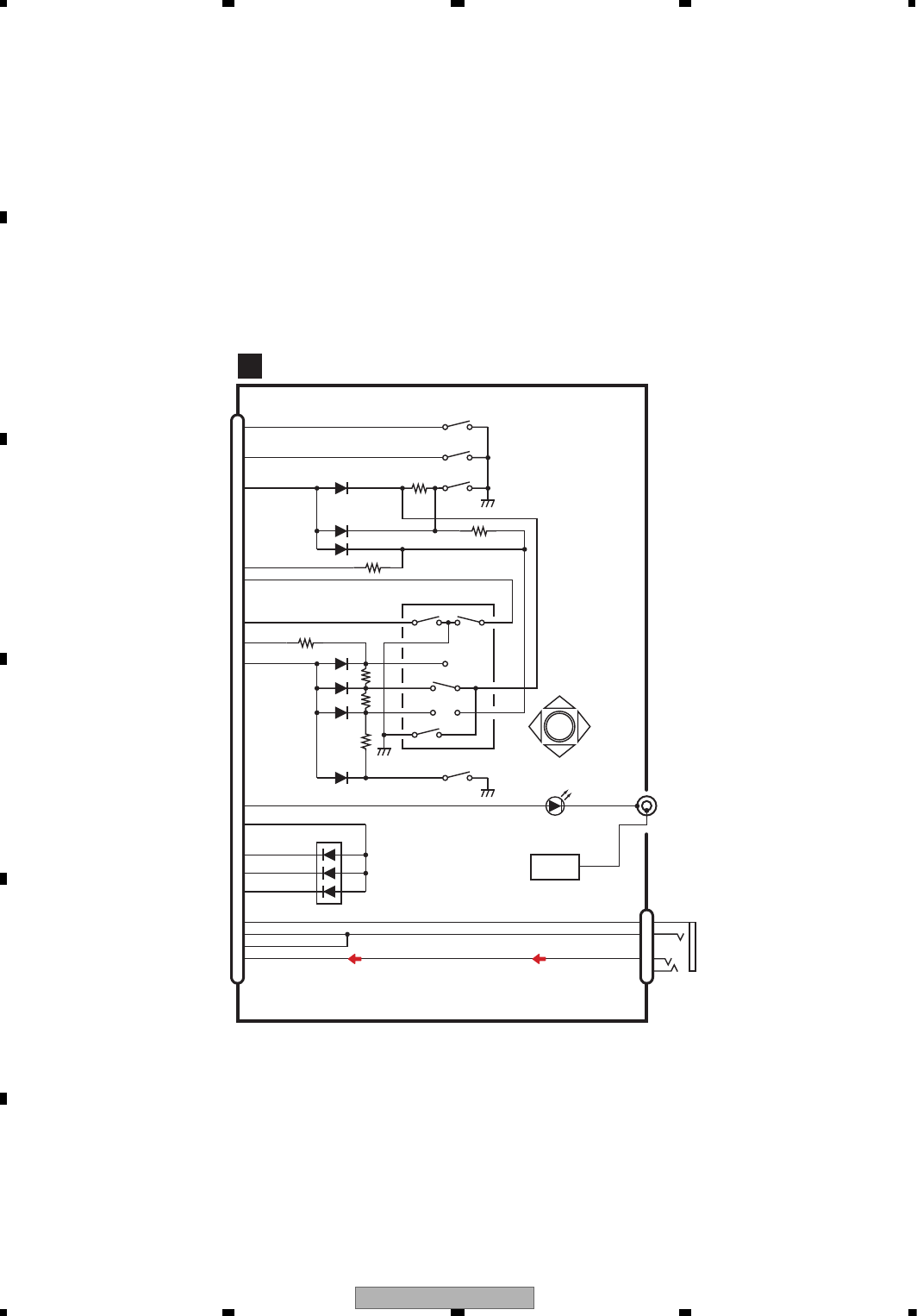
KEYBOARD UNIT
E
RESET
CN801
2
RESET
S801
EJECT
3
EJECT
S804
INT_KEY0
4
ROT1
14 1
2
3A
B
C
Com
Enc-Com
4
7
10
9
PUSH
D8
5
MENU
S802
MAP
S805
KEY0
5
INT_KEY1
6
ROT0 Phase-B
Phase-A
13
ROTARY COMMANDER
S803
KEY1
7
BL-LED
8
AUX-V
21 AUX-AG
20 AUX-VG VG
AG
22 AUX-L
19
ILMV
9
ILMR
D801
10
ILMG
11
ILMB
R
G
B
12
PUSH
A
C
BD
CN803
3
D815
1
CN802
AV MINI JACK
NAVI UNIT
BTJ2
PANEL UNIT
OTJ2
R4
L
2
AUX-G 1
V
2,3
1
BT-ANT
ANT801
RF_I/O

AVIC-X910BT/XS/UC 35
5678
5678
C
D
F
A
B
E
AVIC-X910BT/XS/UC
36
1234
1234
C
D
F
A
B
E
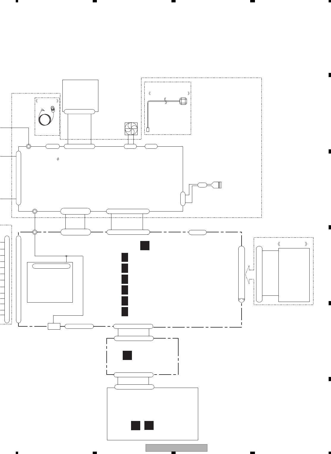
4.3 POWER SUPPLY SYSTEM FIGURE
+BPOWE
AV UNIT
SYS u-com
M30878FJBGP
VDD5
REGULAR
POWER SUPPLY
5 V
BD3931HFP HA12241FP
IP-BUS DRIVER
RESET IC
BD5335FVE
NAVI -> SYS
TC74VHCT08T
UVDD5
ROM COLLECTION
S-93C568DOI
BUP 3 V
S-L2980A33MC-C6C
SYS -> MS
TC74VHC08FT
SPEED I/F
NJM2904M
ATT CONTROL
UMD3N*3
+
DCSKIPCD
FM/AM
TUNER
UNIT
X-2026
VT8(8 V)
BA00CC0WFP
typ 103 mA
max 140 mA
typ 172 mA
max 200 m
A
DISTRIBUTOR
MACHINE
+
TU3
BA00CC0WFP
SYSPW or
SWACPW
SYSPWIR REMOTE
RPMS2401-H19E4AV
2 mA
2 mA2 mA2 mA
2 mA
SWVDD5
DARC -> SY
TC74VHCT0
10 mA
SYS -> DARC
TC74VHC08FT
2 mA
1 mA
MAX 45 mA
TYP 32 mA
2 mA
FM/AM Tuner
Front step
am
p
lifie
r
TMC/VICS/MSN/Direct
Tuner Front step amplifier
63 m
A
4 m
A
11 m
A
81 m
A
172 m
A
25.4 mA
25.4 mA
27.3 mA
427 mA
RGB_LED DRIVER
M62343&UMX1N
3 mA
A
B C
AVIC-X910BT/XS/UC 37
5678
5678
C
D
F
A
B
E
POWER SUPPLY
RQ(WDT,IRQ)
TC7WH32FU
YS
T08T
3 -> 5AND IPD
TC7SET08FU
RST INV
TC74SH04
2 mA
OR MUTE CIRCUIT
TC7S32FU
2 mA
M
R
6
AV SELECTOR
2 mA
2 mA
DARC -> SYS
TC74VHCT08T
MS5 ->SYS
TC74VHCT32T
2 m
A
2 mA
RC
08FT
TEMPERATURE CIRCUIT
ect
mplifier
LED DRIVER
43&UMX1N
3 mA
AVIC-X910BT/XS/UC
38
1234
1234
C
D
F
A
B
E
D/D
DVD 8 V(LS1)
IP_BUS POWER SUPPLY
SW
ASENBO
POWER , AMP
PAL007B
SW FOR ANT +
ANTON
SYSPWR or
SWACPW
AUTO ANTENNA
AV8(8.3 V)
BA00CCOWCP
SWACP
VIDEO ISOLATOR
NJM2505F
typ 19 mA
max 29.0 mA
VIDEO 5 V
VDCONT
D/D
NAVI 5 V
NAVICO
max2.5A
FCONT
FCONT
SYSPW
ILMV 9 V
KMOD TR PKB SNS
SYSPW
SYS->NAVI
TC7SH08FU
SYS->NAVI
TC74VHCT0
NAVI 3.3 V
ILMV
DCSKIP
121.6 mA
181.1 mA
24 mA
326.7 mA
30 mA
A
BC
D/D
DVD 5 V
VDCONT
FCONT
LS1(DVD)
MAX 500 mA
TYP 220 mA
MAX 2 350 mA
TYP 390 mA
NAVI, LCD BORD
AVIC-X910BT/XS/UC 39
5678
5678
C
D
F
A
B
E
GUIDE MIX
NJM2060V
MUTE CIRCUIT
AU4
NJM2125
CAPTAIN6
VIDEO
LEVELSHIFT
AV SELECTOR
AN15887A
DVD LPF
NJM4558V
PKB SNS
SYS->NAVI
TC74VHCT08FTS1
50 mA
1 mA
5.7 mA
VIDEO BUFFER
10.5 mA
37 mA
KEY BORD
AVIC-X910BT/XS/UC
40
1234
1234
C
D
F
A
B
E
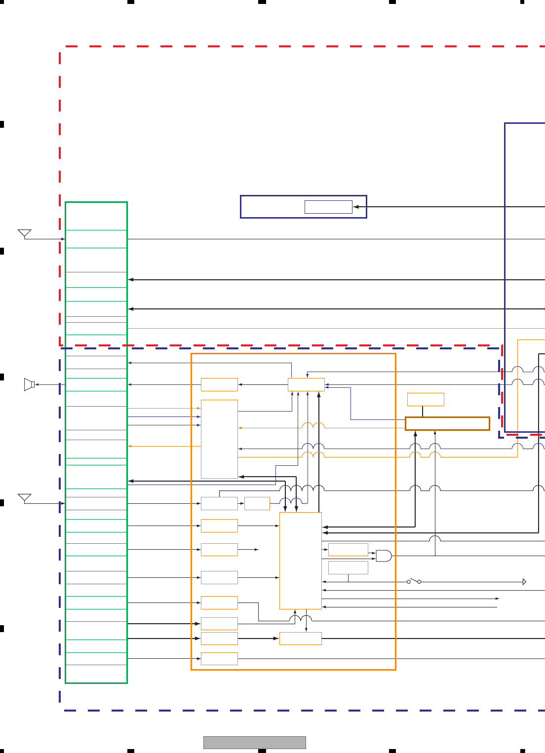
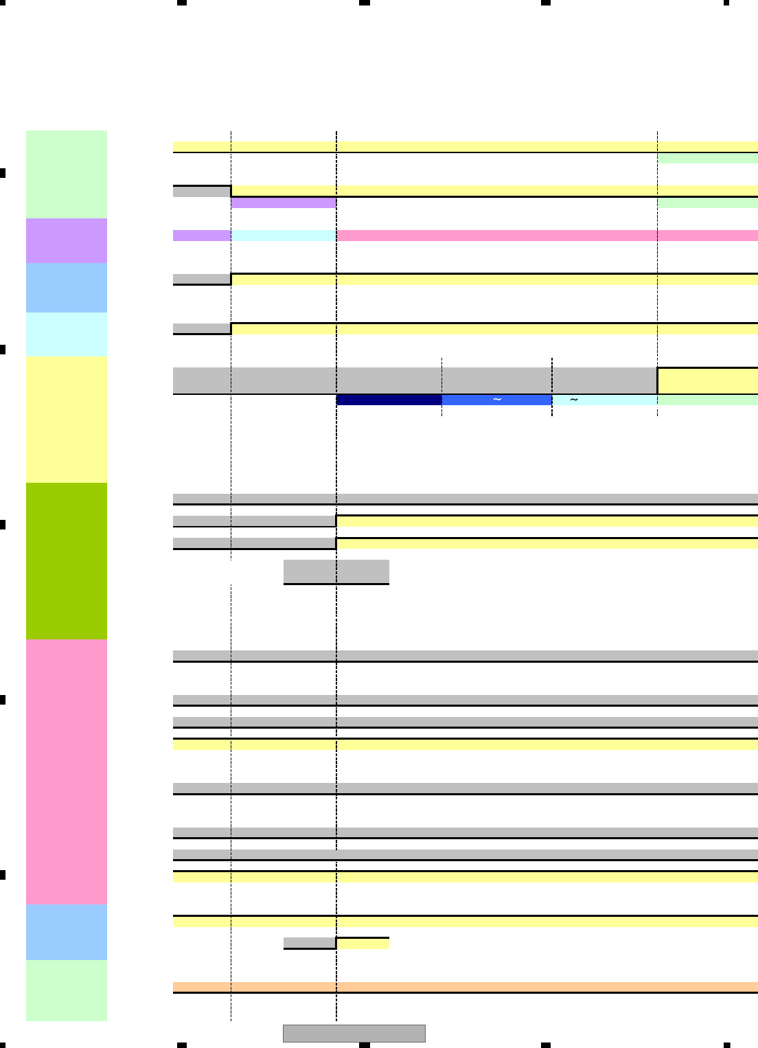
5. DIAGNOSIS
5.1 OPERATIONAL FLOWCHART
Acc on (USUALLY Acc ON)
/BSENS
/ASENS
STATUS
MUTE
ASENBO
SREMOTE
SYSPW
DCSKIPCD
ANTON
SWACPW
DCSKIP
BSENSN
RSTOUT
BATFAULT
CPUWDT
OFFINFO
OFFANS
NAVICON
FANCONT
FAN CONTROL
200 ms
EXTERNAL
OUTPUT
AUDIO
CONTROL
NAVI POWER
SUPPLY
CONTROL
NAVI CONTROL
ANTON (Source interlocking
movement, forced OFF)
250 300 ms(SURVEY)POWER SUPPLY MASK(200 ms
1 sec 2 sec
IP-BUS
PRETREATMENT
IP-BUS SLAVE
CONNECTION CHECK
SOUND MUTE
CONTROL
POWER SUPPLY MASK(200 ms
SENSE SYSTEM
POWER
SUPPLY
CONTROL
IP-BUS
SYSTEM
POWER SUPPLY MASK(200 ms
WAITING FOR SLAVE
POWER SUPPLY
OSCILLATION STOP STANDBY LOOP
500 ms
(At the time of a reset start)
AVIC-X910BT/XS/UC 41
5678
5678
C
D
F
A
B
E
8 ms to 16 ms or mor
e
FANCONT
(
At the time of hi
g
h tem
p
erature
)
R SUPPLY MASK(200 ms)
16 ms
MAIN LOOP
After mute (300 ms)
(After SYSPWR ON, at least 300 ms. MUTE time is extended to OFFANS Low henceforth.)
R SUPPLY MASK(200 ms)
R SUPPLY MASK(200 ms)
AVIC-X910BT/XS/UC
42
1234
1234
C
D
F
A
B
E
5.2 INSPECTION METHOD OF PICKUP UNIT
Disc to be used
CD-DA: TCD-782
DVD-Video: GGV1025
Execution method
START
Is it OK?
Is it OK?
Ckeck parts
other than PICK UP
PICK UP
cleaned?
Perform lens
cleaning
SKEW ADJ.
Is it OK?
LD current check
RF level check
RF level check
Yes
Error rate check
Finished
LD turned on? Check parts
No
Is it OK? PICK UP
cleaned?
Perform lens
cleaning
Error rate check
Is it OK?
Replace the PICK UP
Replace the PICK UP
Replace the PICK UP
Replace the PICK UP
Check point:
AS MAX check
Check point:
LD current check
Check point:
Error rate check
Yes
No
Yes
No
Yes
No
Yes
No
Yes
No
Yes
No
Yes
No
Check point:
AS MAX check
Check point:
Error rate check

AVIC-X910BT/XS/UC 43
5678
5678
C
D
F
A
B
E
LD current check
Check
Status: [Foucs closed] of TEST MODE
Notes: Please pay attention to the laser diode damage by static electricity.
Threshold
2 TCD-782 CDLD1-VCC5_3 60 - 360 (mV) 10 - 60 (mA)
NO. Disc Check Point
Check Point
DVDLD1-VCC5_3
NO.
1
Disc
GGV1025
Remarks: LD current
10 - 65 (mA)
Threshold
60 - 390 (mV)
Expansion
Expansion
Remarks: LD current
AVIC-X910BT/XS/UC
44
1234
1234
C
D
F
A
B
E
ASMAX check
ASMAX value shows the value of RF level.
Status: [Foucs closed] of TEST MODE
No. Disc Check Point Threshold Remarks:
8 digits value of
ASMAX more than
on display 0000 0B00
8 digits value of
ASMAX more than
on display 0000 0C00
Error rate check
Status: [Tracking Closed] of TEST MODE
No. Disc Check Point Threshold Remarks:
less than
1.000E-03
less than
1.000E-03
less than
2.500E-03
3 TCD-782 ID: HOME Position
2
GGV1025
ID: 200000
1
GGV1025
ID: 40000
1
GGV1025
Only four last digits are
displayed according to
the product.
2 TCD-782
Only four last digits is
displayed according to
the product.
In this case, the value is displayed for a split second.
When you tried to perform [FOCS CLOSE],
the display will charge automatically in the following order.
[1FFF0000]->[FEMAX]->[FE MIN]->[AS MAX]->
[ENV MAX]->[FE normal]->[Spindle gain]->
[TEMAX]->[TEMIN] ->[20000000]
Watch carefully the value of ASMAX.
Test mode display will not appear on the display of this product. Connect the rear monitor output to a monitor.
Test mode display will not appear on the display of this product. Connect the rear monitor output to a monitor.
AVIC-X910BT/XS/UC 45
5678
5678
C
D
F
A
B
E
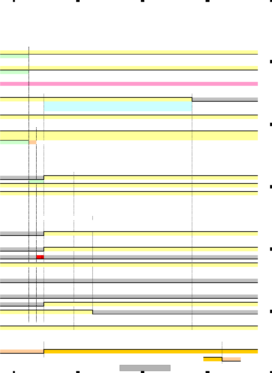
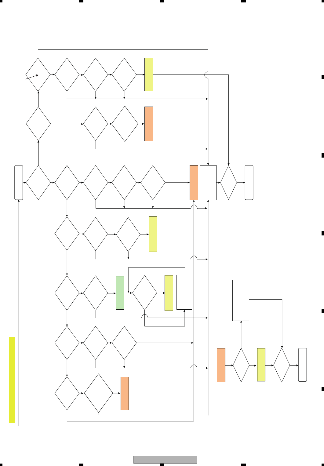
5.3 DIAGNOSIS FLOWCHART
BACK END section flow
Standby
OK?
Execute
check 1.
Can the
playback
start?
NO
YES
YES
YES
YES
YES YES
YESYES
YE
S
YES
YES
YES
NO
NO
NO
NO
NO
YES
YES
YES
NO
YESYES
NO
START
END
END
YES
NO
NO
NO
NO
NO
YES
YES
NO
NO
NO
The product
is normal?(iPod
attestation IC)
YES
Product repair
YES
NO
NO
NO
NO
YES
NO
YES
YES
YES
NO
NO
YES
Does the
operation
take time?
Go to FE
section check.
Go to FE
section check.
Is the life of flash
memory OK?
Conduct check item 12.
Is the image
in error?
Is the video
circuit OK?
Execute check 11.
Is AVCC5
voltage OK?
Execute check 8.
Replace the unit.
Is VDD5(VCC33, VCC12)
power supply voltage OK?
Execute check 2.
Reset OK?
Execute check 3.
Is VSENS
OK?
Execute check 4.
Is 27 MHz
OK?
Execute check 5.
Is 48 MHz OK?
Execute check 13.
Replace the unit.
Replace the unit.
Replace the unit.
Go to FE
section check.
Go to the
product check.
Go to FE
section check.
Is VD8, VCC5
power supply
voltage OK?
Execute check 7.
Is SDRAM
IF OK?
Execute check 6.
Is the sound
in error?
Is the iPod play
in error?
Is the USB play
in error?
Is AVCC5
voltage OK?
Execute check 8.
Is DACCLK
normal?
Execute check 9.
Is the audio
circuit OK?
Execute check 10.
Repair the
defective part.
Normal?
Normal?
Is FE section
normal?
Go to FE related
repair process.
Is the iPod
circuit OK?
Execute check 14.
Is the USB
circuit OK?
Execute check 14.
AVIC-X910BT/XS/UC
46
1234
1234
C
D
F
A
B
E
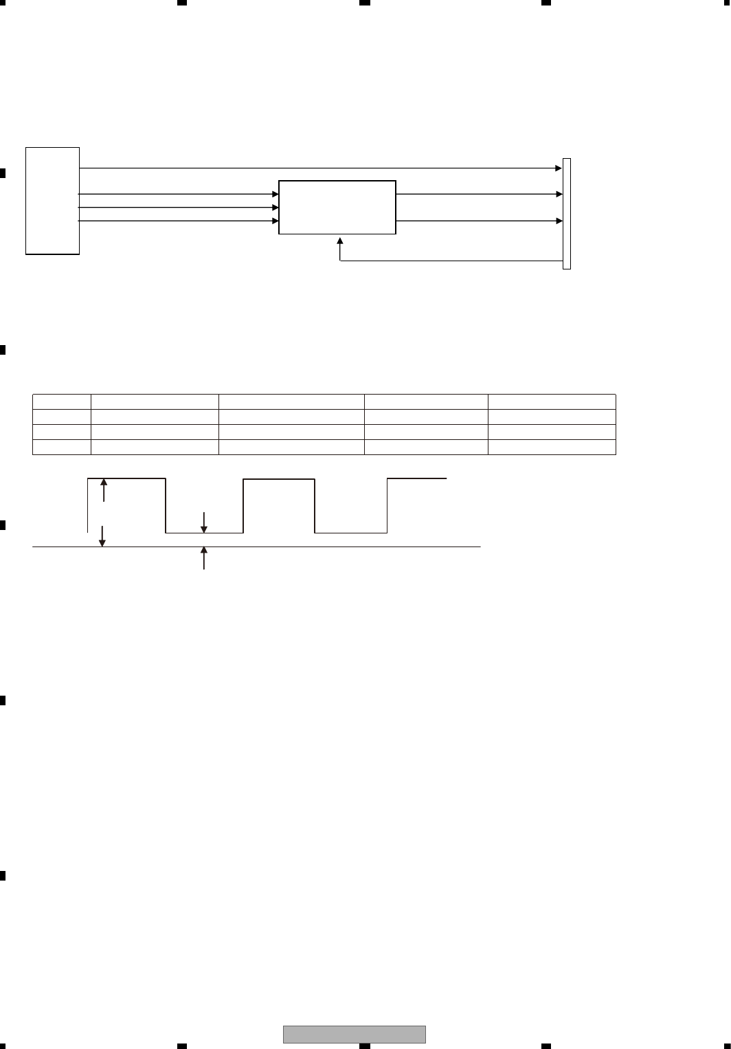
Check 1: Standby OK?
<Check> Check the voltage at the “STANBY” test point while the power is on.
Use the “DGND1” test point at the reference.
NO. Check point Module No. Specification value Unit
STANBY-DGND1 ALL VCC33 V-
0.6 V or more
V
Side A
1
Fig 1.1: STANBY check point
STANBY
AVIC-X910BT/XS/UC 47
5678
5678
C
D
F
A
B
E
VCC33 (= 3.3 V)
5DDV
VCC12 (= 1.2 V)
1VDD5_1 - DGND1
2VCC33_1 - DGND1
3VCC12_1 - DGND1
VDD5_1
DGND1
VCC12_1
VCC33_1
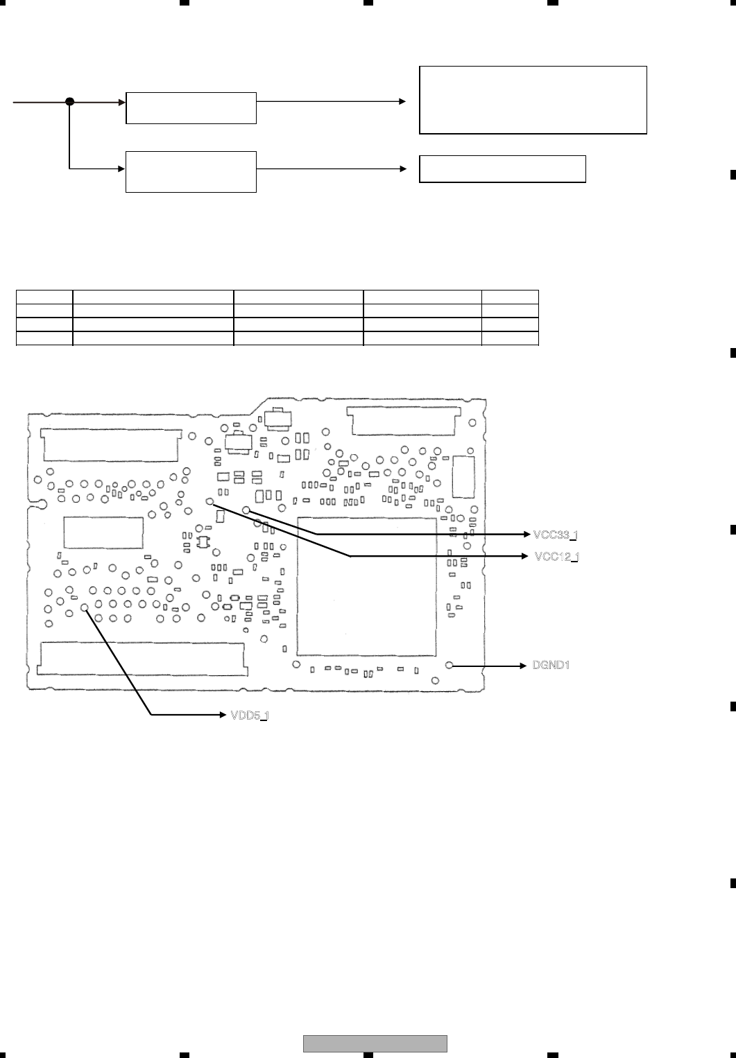
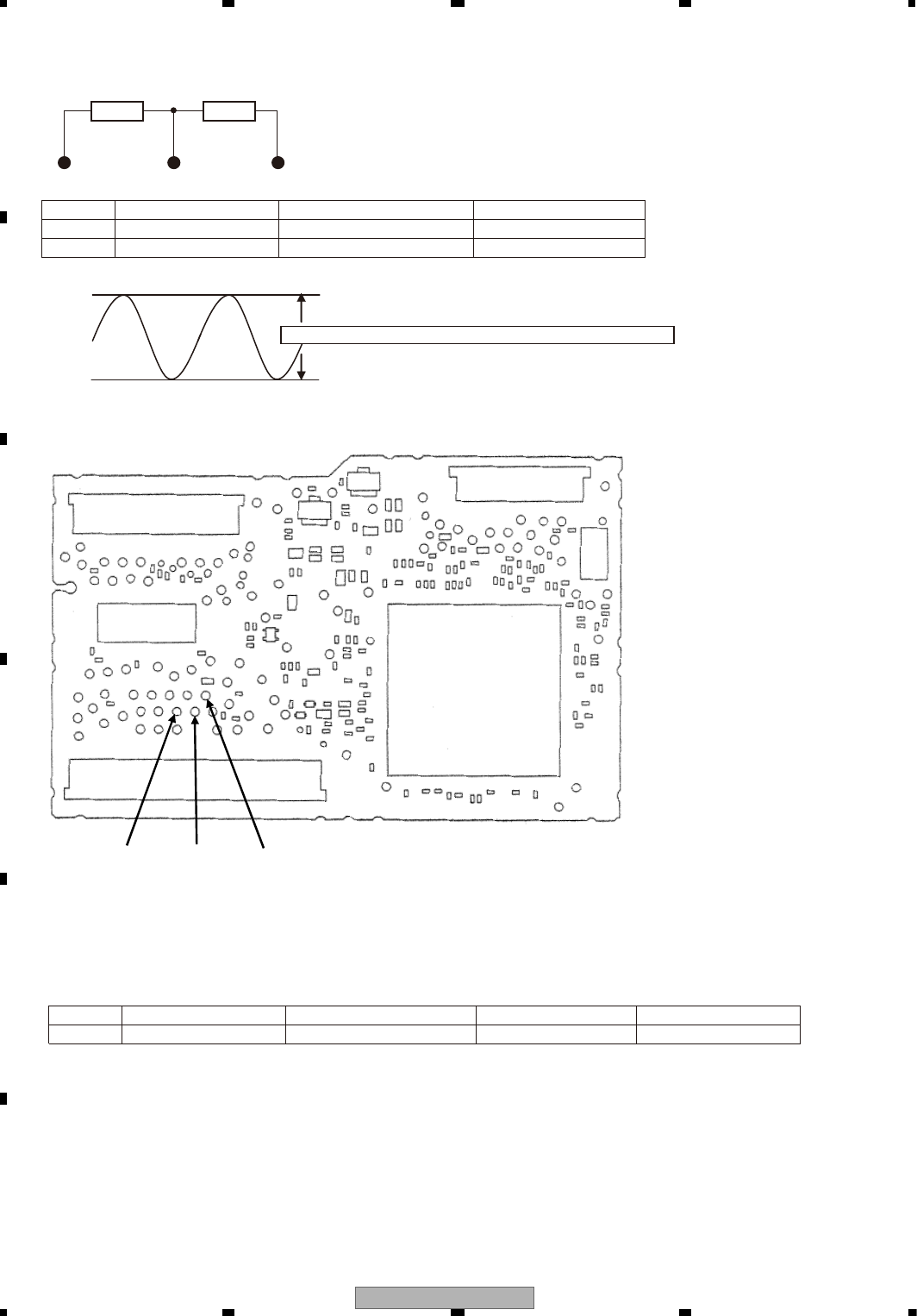
Check 2: Is VDD5 (VCC33, VCC12) power supply voltage OK?
Fig 2.1: Power supply configuration
IC1004
3.3 V output regulator
IC1005
DC/DC converter
1.2 V output
IC1501 DV5U power supply
IC1401 FLASH power supply (Data)
IC1402 FLASH power supply (Program)
IC1481 SDRAM power supply
IC1501 DV5U power supply
<Check> Check the voltage at the “VDD5_1, VCC33_1 and VCC12_1” test point while the power is on.
Use the “DGND1” test point at the reference.
Side A
NO. Check point Module No. Specification value Unit
Fig 2.2: VDD5, VCC33, VCC12 voltage check points
ALL
ALL
ALL
5.0 ± 0.4
3.3 ± 0.15
1.2 ± 0.12
V
V
V
AVIC-X910BT/XS/UC
48
1234
1234
C
D
F
A
B
E
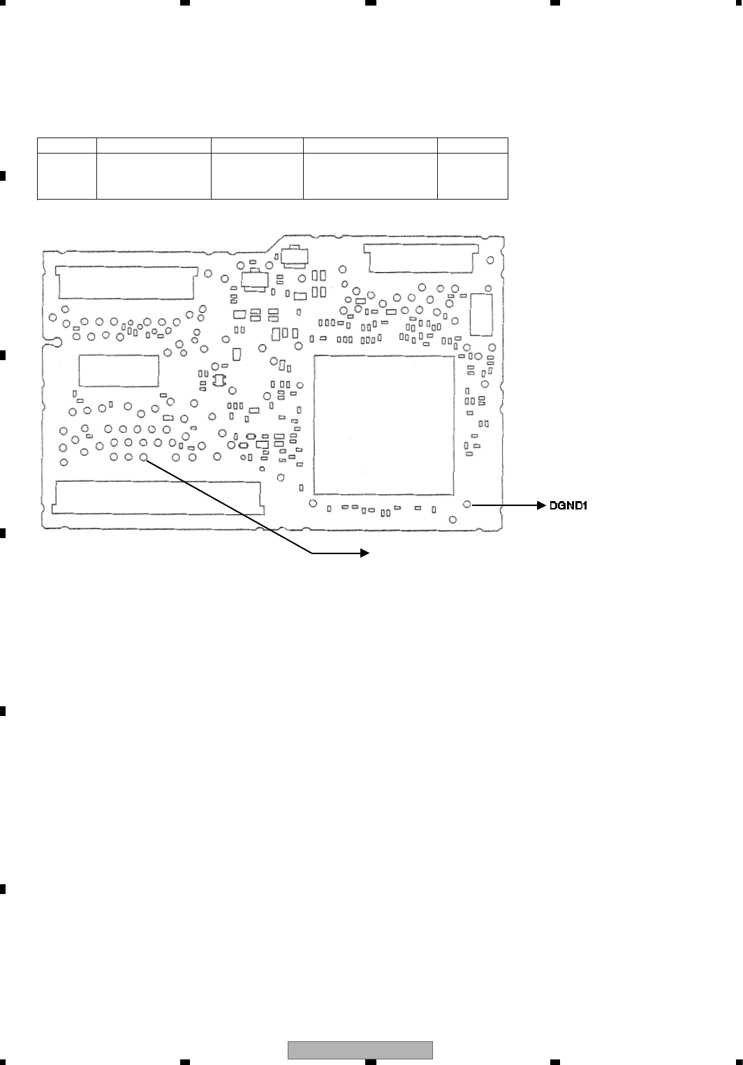
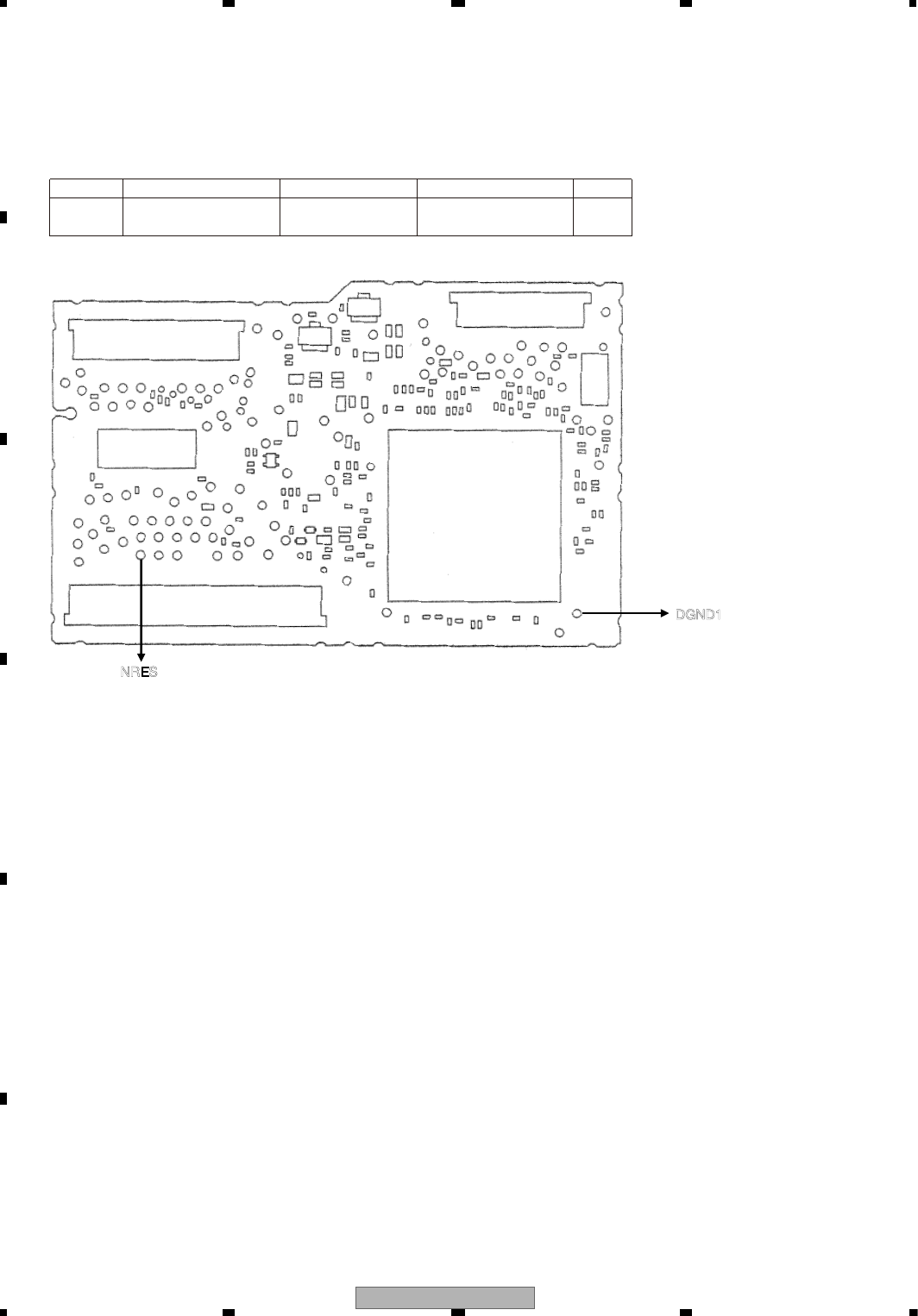
NRES
DGND1
Check 3: Reset OK?
NO. Check point Module No. Specification value Unit
1 XRES-DGND1 ALL VCC33 ×
0.7 or more
V
Side A
<Check> Check the voltage at the “XRES” test point while the power is on.
Use the “DGND1” test point at the reference.
Fig 3.1: RESET check point
AVIC-X910BT/XS/UC 49
5678
5678
C
D
F
A
B
E
CN1901
HOST I/F
SNESV8DV
33CCV5DDV
VCC12
STANBY
XRES
1 VSENS - DGND1 ALL 0.95 - 1.07 V
VD8 = 8.0 ± 0.4 V
IC1501
DV5U
IC1004
Regulator
IC1005
DC/DC
converter
VSENS
DGND1
Check 4: Is VSENS OK?
Fig 4.1: Power supply configuration and VSENS
<Check> Check the voltage at the “VSENS” test point while the power is on.
Use the “DGND1” test point at the reference.
NO. Check point
Side A
Module No. Specification value Unit
Fig 4.2: VSENS check point
R1004,
R1007
AVIC-X910BT/XS/UC
50
1234
1234
C
D
F
A
B
E
IC1501
DVD-LSI
X1501
27 MHz
crystal
VCC33 VCC12
Check 5: 27 MHz Normal?
<Outline> Each clock is created inside the IC1501 using the 27 MHz master crystal oscillator (X1501).
Fig 5.1: Clock configuration
<Check method> Turn the power on, and check with DGND being the reference.
In case of NG, check the applicable line, periphery of IC1501,
soldering of the peripheral components and defective components.
NO. Check point Module No. Specification value Unit
2 IC1501 169pin ALL 27 MHz
± 50 ppm ppm
GND
Fig 5.2: Clock specification value
Side A
Specification
value
Fig 5.3: 27 MHz check point
IC1501 158pin
DGND1
OSCO
OSCI
AVIC-X910BT/XS/UC 51
5678
5678
C
D
F
A
B
E
MA0 - 11
MDQ0 - 15
MCK
XWE(NWE)
XCAS(NCAS)
XRAS(NRAS)
XCSM(NCSM)
DQM0
DQM1
BA0
BA1
IC
1480
SDRAM
IC1501
DV5U
Fig 6.1: SDRAM I/F
Check 6: Is SDRAM I/F OK?
<Outline> In order to secure the MPEG stream data as the buffer,
the capacity of communication I/F SDRAM between the LSI and the memory is 64Mbit.
Be careful as XCSM, XWE, XCAS and XRAS of IC1480 are called differently in IC1501,
namely NCSM, NWE, NCAS, NRAS.

AVIC-X910BT/XS/UC
52
1234
1234
C
D
F
A
B
E
1
2
3
4
5
6
7
8
9
10
11
12
13
14
15
16
17
18
19
20
21
22
23
24
25
26
27
28
29
30
31
32
33
34
35
36
37
MA0
MA1
MA2
MA3
MA4
MA5
MA6
MA7
MA8
MA9
MA10
MA11
MDQ0
MDQ1
MDQ2
MDQ3
MDQ4
MDQ5
MDQ6
MDQ7
MDQ8
MDQ9
MDQ10
MDQ11
MDQ12
MDQ13
MDQ14
MDQ15
MCK
XWE
XCAS
XRAS
XCSM
DQM0
DQM1
BA0
BA1
56 ohm ± 5 %
56 ohm ± 5 %
56 ohm ± 5 %
56 ohm ± 5 %
56 ohm ± 5 %
56 ohm ± 5 %
56 ohm ± 5 %
56 ohm ± 5 %
56 ohm ± 5 %
56 ohm ± 5 %
56 ohm ± 5 %
56 ohm ± 5 %
56 ohm ± 5 %
56 ohm ± 5 %
56 ohm ± 5 %
56 ohm ± 5 %
56 ohm ± 5 %
56 ohm ± 5 %
56 ohm ± 5 %
56 ohm ± 5 %
56 ohm ± 5 %
56 ohm ± 5 %
56 ohm ± 5 %
56 ohm ± 5 %
56 ohm ± 5 %
56 ohm ± 5 %
56 ohm ± 5 %
56 ohm ± 5 %
0.17 ohm or lower
56 ohm ± 5 %
56 ohm ± 5 %
56 ohm ± 5 %
56 ohm ± 5 %
56 ohm ± 5 %
56 ohm ± 5 %
56 ohm ± 5 %
56 ohm ± 5 %
IC1480 23pin
IC1480 24pin
IC1480 25pin
IC1480 29pin
IC1480 30pin
IC1480 31pin
IC1480 32pin
IC1480 33pin
IC1480 34pin
IC1480 33pin
IC1480 22pin
IC1480 35pin
IC1480 2pin
IC1480 4pin
IC1480 5pin
IC1480 7pin
IC1480 8pin
IC1480 10pin
IC1480 11pin
IC1480 13pin
IC1480 42pin
IC1480 44pin
IC1480 45pin
IC1480 47pin
IC1480 48pin
IC1480 50pin
IC1480 51pin
IC1480 53pin
IC1480 38pin
IC1480 16pin
IC1480 17pin
IC1480 18pin
IC1480 19pin
IC1480 15pin
IC1480 39pin
IC1480 20pin
IC1480 21pin
IC1501 201pin
IC1501 203pin
IC1501 207pin
IC1501 209pin
IC1501 208pin
IC1501 206pin
IC1501 202pin
IC1501 200pin
IC1501 198pin
IC1501 194pin
IC1501 199pin
IC1501 192pin
IC1501 160pin
IC1501 162pin
IC1501 164pin
IC1501 168pin
IC1501 170pin
IC1501 172pin
IC1501 176pin
IC1501 178pin
IC1501 177pin
IC1501 175pin
IC1501 171pin
IC1501 169pin
IC1501 167pin
IC1501 163pin
IC1501 161pin
IC1501 159pin
IC1501 183pin
IC1501 181pin
IC1501 188pin
IC1501 189pin
IC1501 190pin
IC1501 179pin
IC1501 180pin
IC1501 193pin
IC1501 197pin
<Check> Check the conductivity at “check point 1” and “check point 2” without power.
In case of NG, check the soldering and defective components throughout the
“output t input” of the applicable section.
NO. Signal name Check point 1 Check point 2 Specification value
AVIC-X910BT/XS/UC 53
5678
5678
C
D
F
A
B
E
Side B
Side A
Check point 1 (IC1480)
Check point 2 (IC1501)
Fig 6.2: SDRAM I/F check point
AVIC-X910BT/XS/UC
54
1234
1234
C
D
F
A
B
E
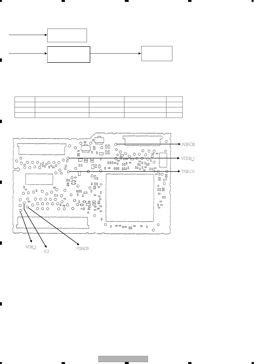
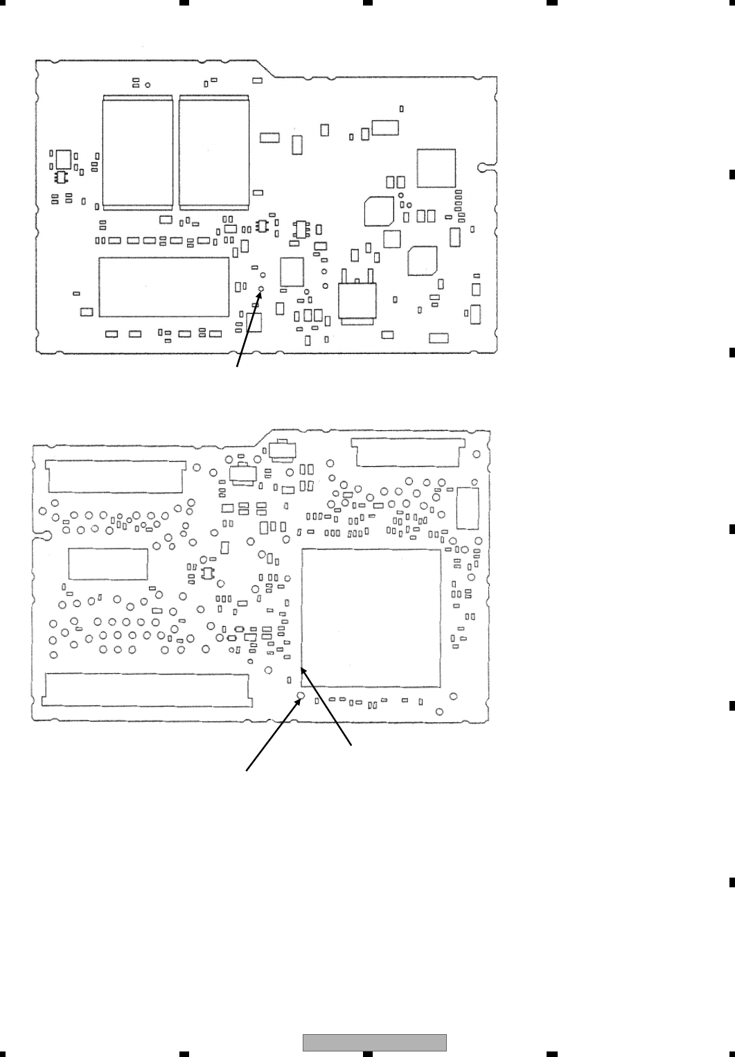
VD8_1
PGND3
VD
VD8_1
PGND1
VCC5_1
AGND3
Check 7: Is VD8, VCC5 power supply voltage OK?
F.E. driver system
IC1002
REG IC
for VCC 5 V.
Fig 7.1: Power supply configuration
Power supply
for PU
NO. Check point Module No. Specification value Unit
1
2
3
VD8_1 - PGND3
VD - PGND3
VCC5_1- AGND1
ALL
ALL
ALL
8.0 ± 0.4
8.0 ± 0.4
5.0 ± 0.1
V
V
V
Side A
<Check> Check the voltage at the “VD8_1, VD and VCC5_1” test point while the power is on.
Use the “PGND3 and AGND1” test point at the reference.
Fig 7.2: VD8, VCC5 voltage check points
VD8_2 VCC5 (= 5.0 V)
AVIC-X910BT/XS/UC 55
5678
5678
C
D
F
A
B
E
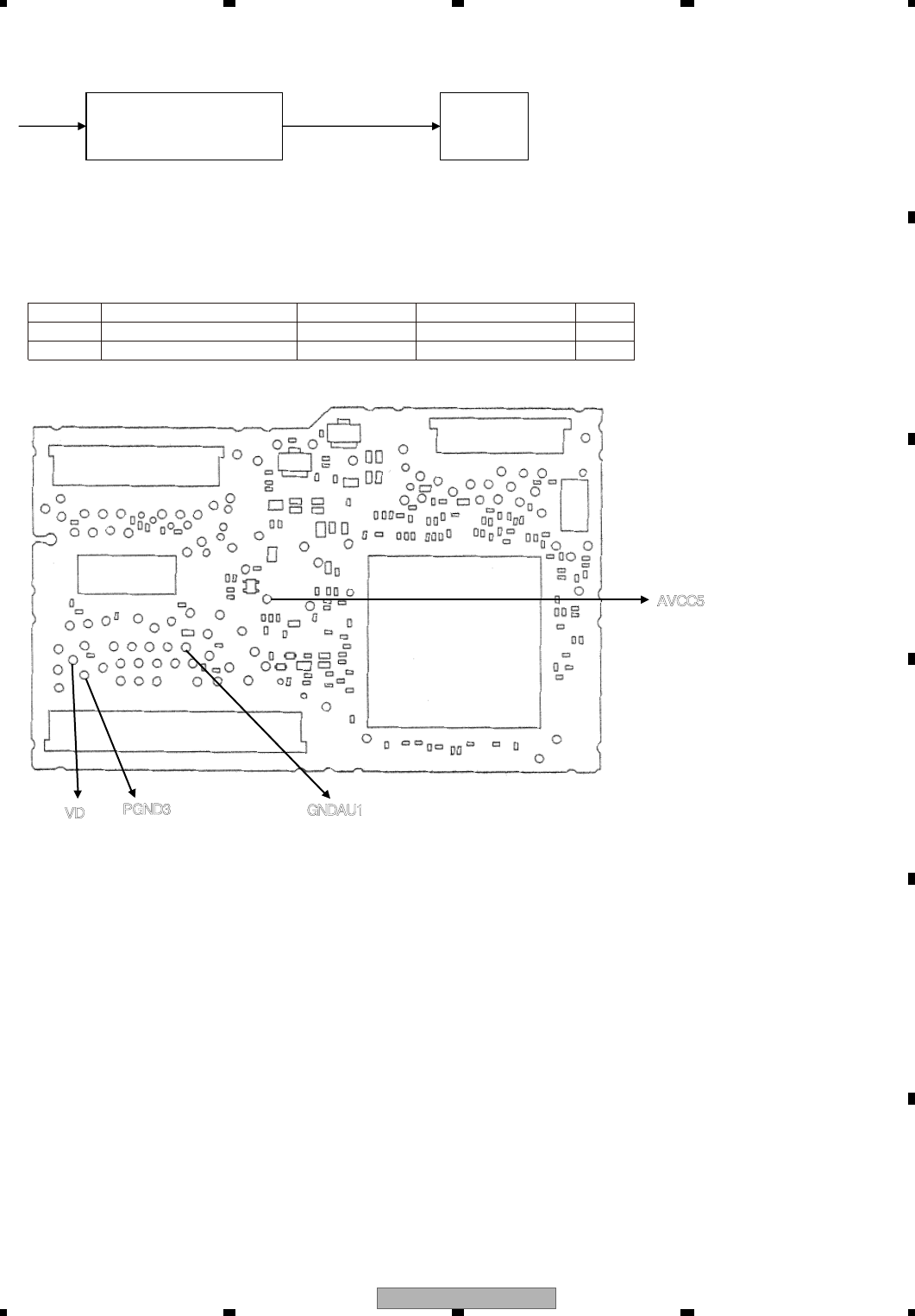
DV IC1801
Audio-DAC
GNDAU1
PGND3
VD
AVCC5
Fig 8.2: VD8, AVCC5 voltage check points
Side A
Check 8: Is AVCC5 voltage OK?
Fig 8.1: Power supply configuration
IC1003
REG IC
for AVCC 5 V.
<Check> Playback DVD-REF-A1 TITLE 1 and check the voltage at the stylus.
Check with PGND and GNDAU being the reference.
NO. Check point
VD - PGND_3
AVCC5 - GNDAU1
Module No. Specification value Unit
1
2
ALL
ALL
8.0 ± 0.4
5.0 ± 0.1
V
V
AVCC5 (= 5.0 V)
AVIC-X910BT/XS/UC
56
1234
1234
C
D
F
A
B
E
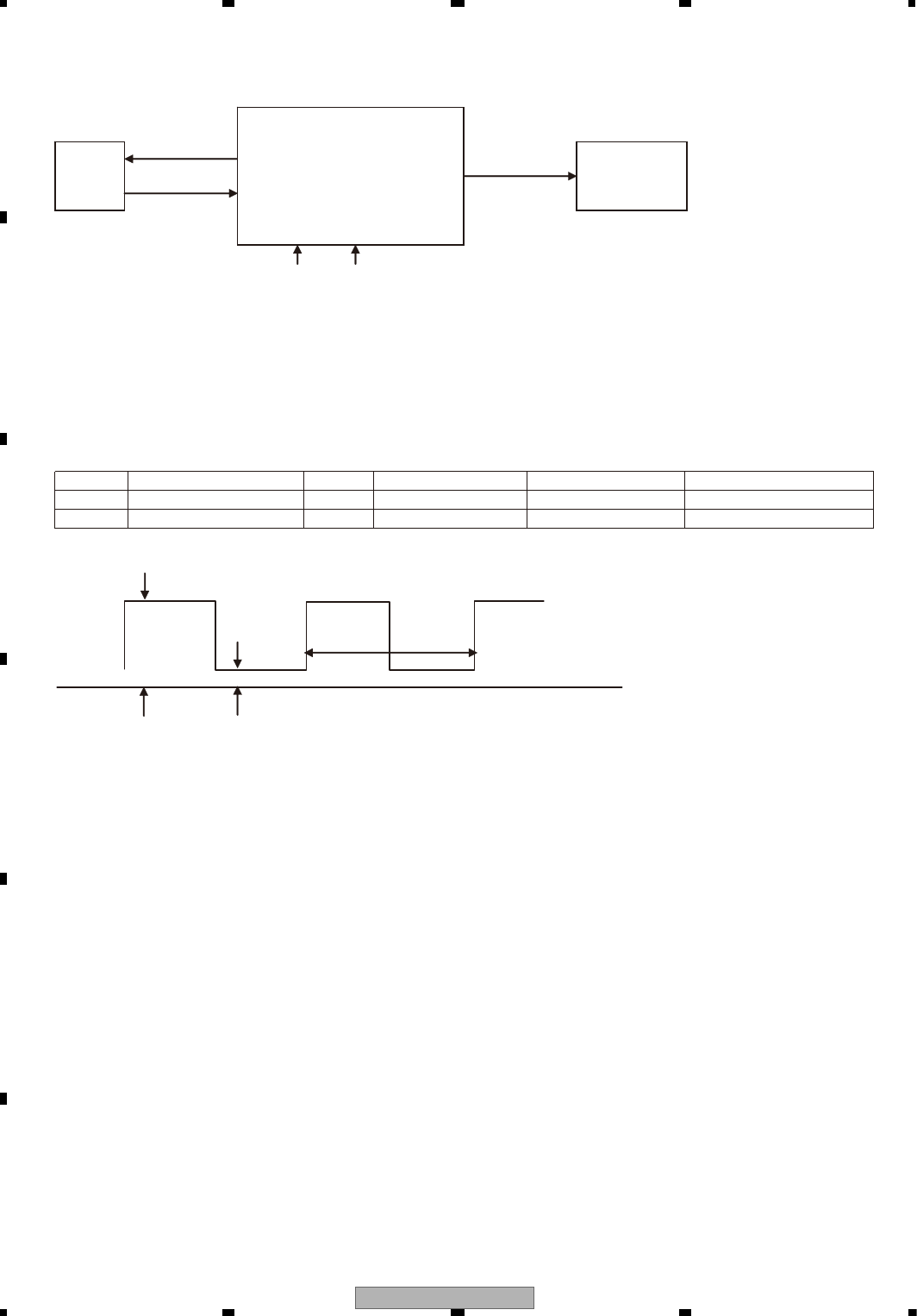
Fig 9.1: Clock configuration
Check 9: Is DACCLK normal?
<Outline> DACCLK for Audio-DAC is created by IC1501 using the 27 MHz master crystal oscillator (X1501).
DACCLK
<Check method>
DVD: DVD-REF-A1 TITLE 1
CD: Playback a normal CDDA.
Common to all DVD-V compatible modules.
Check with DGND being the reference.
In case of NG, check the applicable line, the periphery of IC1501, soldering of the peripheral components and
defective components.
IC1501
DVD-LSIX1501
27 MHz
crystal
IC1801
Audio-DAC
VCC33 VCC12
GND
Fig 9.2: Clock specification value
Specification
value 1
Specification
value 2
Specification
value 3
NO. Check point 1 (stylus) Media Specification value 1 Specification value 2 Specification value 3
1
2
DACCK
DACCK
DVD
CD
2.0 V~VCC33 V
2.0 V~VCC33 V
DGND~0.8 V
DGND~0.8 V
36.864 0 MHz ± 300 ppm
33.868 8 MHz ± 300 ppm
AVIC-X910BT/XS/UC 57
5678
5678
C
D
F
A
B
E
DGND2
Side B
Side A
Fig 9.3: 27 MHz, DACCLK check point
Check point 1 (DACCK stylus)
Check point 2 (IC1501 148 pin)
AVIC-X910BT/XS/UC
58
1234
1234
C
D
F
A
B
E
CN1901
HOST I/F
IECOUT
OLKCRL
ADOUT
ORKCRS
GNDAU
IC1801
Audio-DAC
IC1501
DVD-LSI
Fig 10.1: Audio circuit
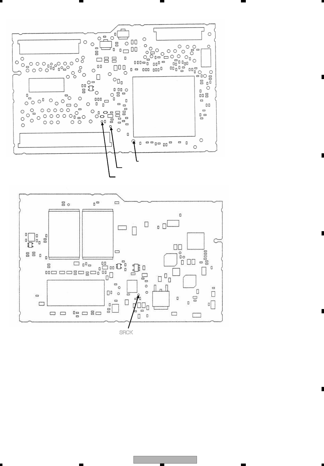
Check 10: Is the audio circuit OK?
<Outline> The serial 3 lines digital output + DACCLK, output from DVD-LSI (IC1501), are converted to analog audio
signal at Audio-DAC (IC1801) and are output from the HOST I/F (CN1901).
Simultaneously, the analog MUTE signal is also output from DVD-LSI (IC1501) via the HOST I/F.
The digital audio signal (IECOUT), output from DVD-LSI (IC1501).
<Check method> Playback DVD-REF-A1 TITLE 2 CHAPTER 1 (48 k/16 bit 1 kHz 0 dB),
and check with DGND being the reference.
In case of NG, check the applicable line, periphery of major components as described in the above drawing,
soldering of the peripheral components and defective components.
NO. Check point 1 (stylus)
1
2
3
Specification value 1 Specification value 2 Reference waveform
ADOUT3
SRCK
LRCK
VCC33 V-0.6 V or higher
VCC33 V-0.6 V or higher
VCC33 V-0.6 V or higher
0.4 V or lower
0.4 V or lower
0.4 V or lower
Waveform 1
Waveform 2
Waveform 3
GND
Fig 10.2: Serial 3 lines specification value
Specification
value 1
Specification
value 2
AVIC-X910BT/XS/UC 59
5678
5678
C
D
F
A
B
E
SRCK
LRCK
ADOUT
DGND2
Fig 10.3: Serial 3 lines check points
Side A
Side B
AVIC-X910BT/XS/UC
60
1234
1234
C
D
F
A
B
E
LO
RO GNDAU1
The following checks shall be conducted using the following measurement circuits with GNDAU1 being the reference.
NO.
4
5
Fig 10.4: Analog audio out (LO, RO) specification value.
Side A
Specification value is the root-mean-square value (rms).
Check point 1 (stylus)
1 400 ± 150 mV
1 400 ± 150 mV
Specification value (rms) Reference waveform
Waveform 4
Waveform 4
LO
RO
LO GNDAU1 RO
47 kohm 47 kohm
Fig 10.5: Analog audio out check point
Check with DGND being the reference.
NO. Check point 1 (stylus) Specification value 1 Specification value 2 Reference waveform
6 IEC VCC33 V-0.6 V or higher 0.4 V or lower Waveform 5
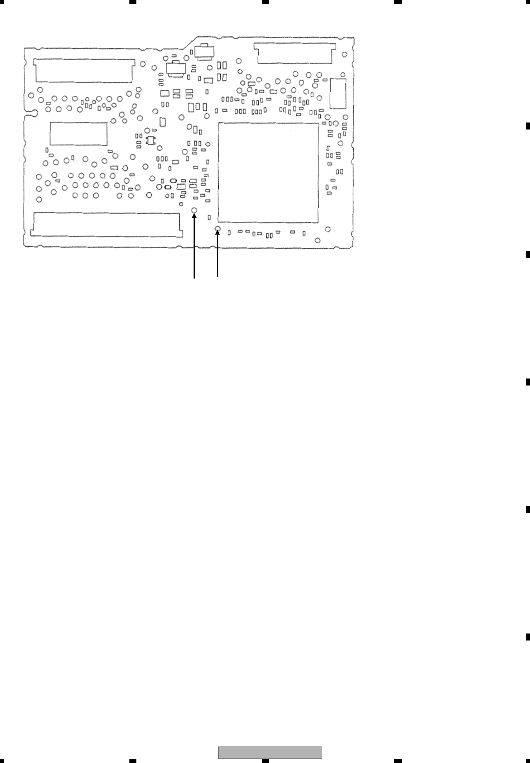
AVIC-X910BT/XS/UC 61
5678
5678
C
D
F
A
B
E
IEC DGND2
Fig 10.6: Digital audio signal (IECOUT) check point
Side A
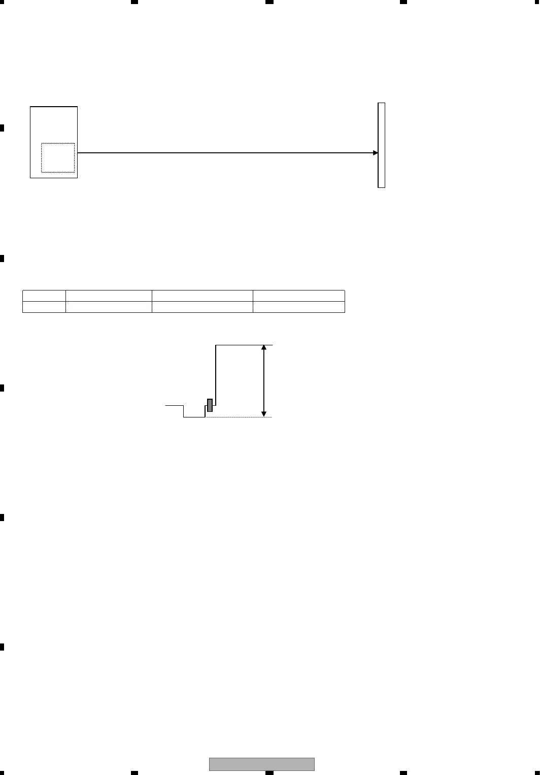
AVIC-X910BT/XS/UC
62
1234
1234
C
D
F
A
B
E
Check 11: Is the video circuit OK?
<Outline> Composite signal and component signal are output from DVD-LSI (IC1501), and are output from the
HOST I/F (CN1901) via a buffer circuit.
CN1901
HOST I/F
Composite COMPOSITE
Fig 11.1: Video circuit
<Checking method> Playback DVD-REF-A1 TITLE2 CHAPTER5 (WHITE 100%), and monitor COMPOSITE signal with
an oscilloscope with GNDV1 (stylus) being the reference. Set the trigger mode to “TV trigger” and
the trigger line to “150 line”.
IC1501
DVD_LSI
Video
DAC
section
NO.
Check point 1 (stylus)
Specification value Reference waveform
1 COMPOSITE 1 000 mVpp ± 5 % Waveform 6
In case of NG, check the applicable line, the periphery of the major components in the drawing above, soldering of the
peripheral components and defective components.
PEAK
COMPOSITE signal Reference
value
Color burst
Pedestal level
BOTTOM
Horizontal sync signal
Fig 11.2: Waveform for the case of composite white 100% output
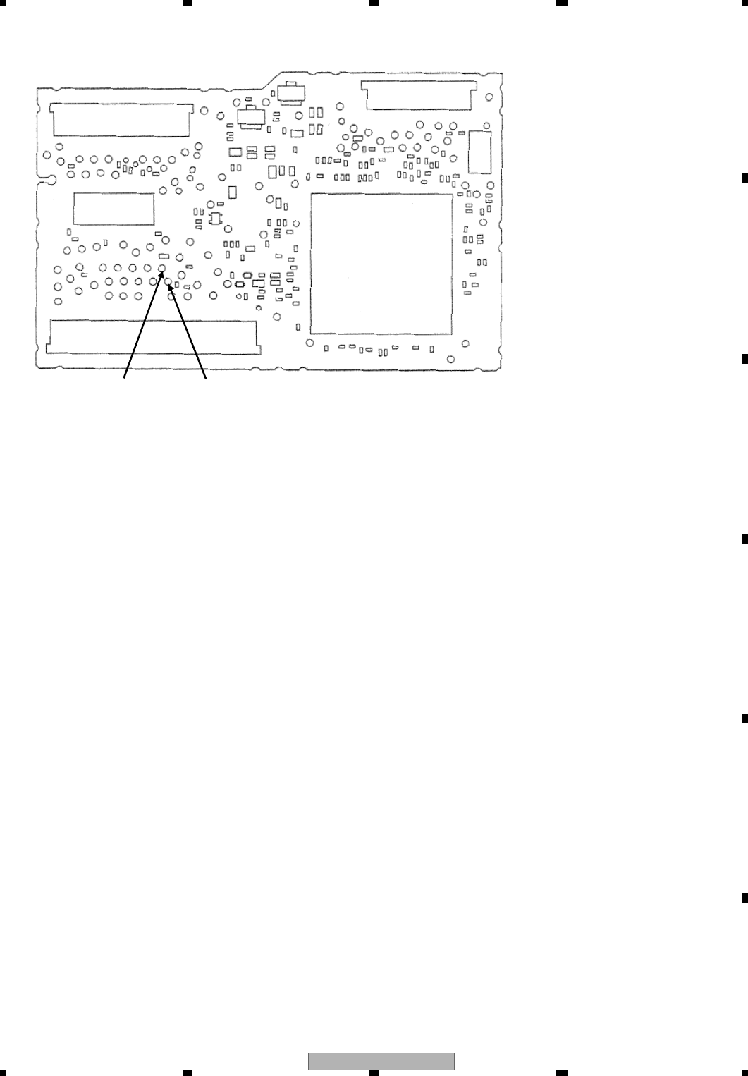
AVIC-X910BT/XS/UC 63
5678
5678
C
D
F
A
B
E
Side A
COMPOSITE GNDV
Fig 11.3: VIDEO signal check point

AVIC-X910BT/XS/UC
64
1234
1234
C
D
F
A
B
E
Check 12:How to judge whether the flash memory has reached its life or not.
If the reaction to user operation is slow or operation is slow in general, there is a possibility that the flash memory
has reached its life.
Make judgment regarding the flash memory life by looking at the display of the LD energizing time.
1.Let the LD energizing time displayed.
(Refer to the FE test mode for the method of displaying the LD energizing time.)
2.If the second digit from the left of the energizing time display is showing E,
such as “ E ”, it means that the flash memory has reached its life.
Example:
0E000BB8
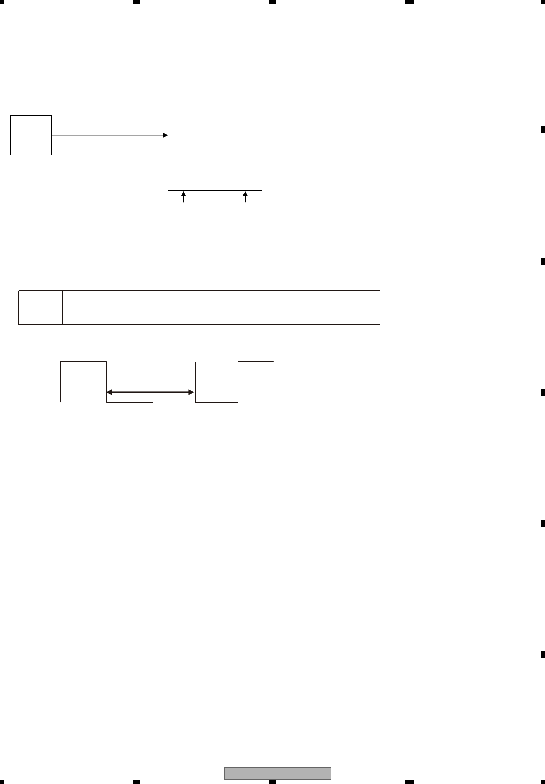
AVIC-X910BT/XS/UC 65
5678
5678
C
D
F
A
B
E
USB_CLOCK
IC1501
DVD-LSI
X1950
48 MHz
VCC33 VCC12
Check 13: 48 MHz Normal?
<Outline> Each clock is created inside the IC1501 using the 48 MHz master crystal oscillator (X1501).
Fig 13.1: Clock configuration
crystal
Fig 13.2: Clock specification value
<Check method> Turn the power on, and check with DGND1 being the reference.
In case of NG, check the applicable line, periphery of IC1501,
soldering of the peripheral components and defective components.
NO. Check point Module No. Specification value Unit
2 IC1501 50pin-DGND1 ALL 48 MHz
± 50 ppm ppm
GND
Specification
value
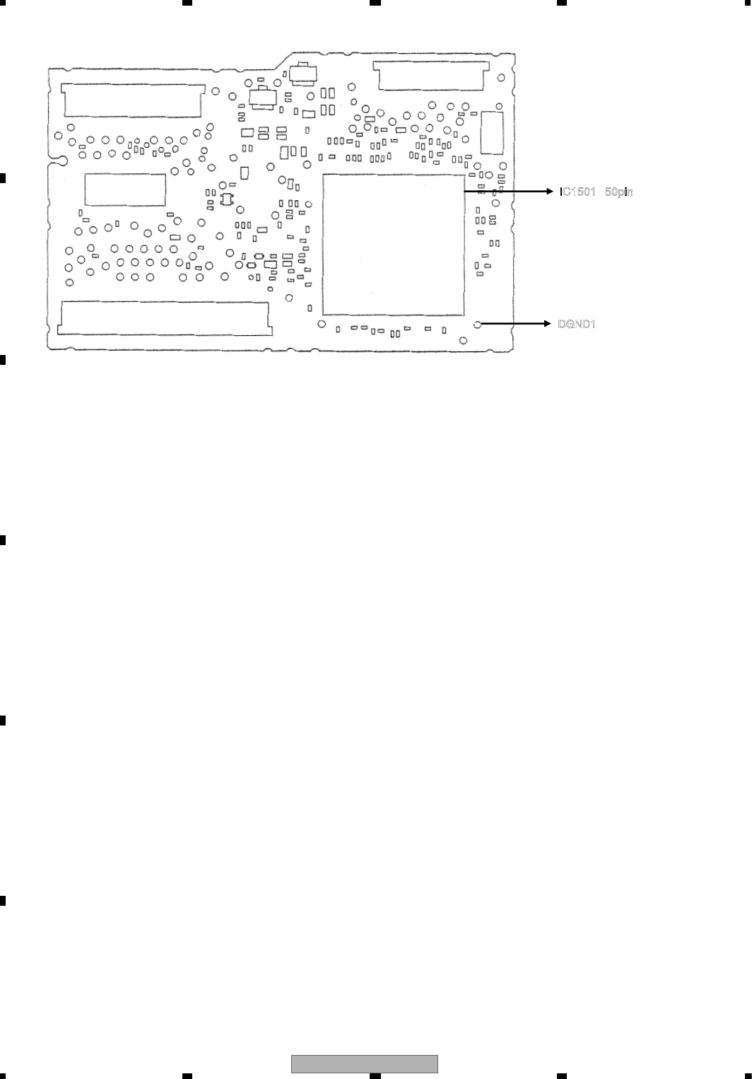
AVIC-X910BT/XS/UC
66
1234
1234
C
D
F
A
B
E
Side A
DGND1
IC1501 50pin
Fig 13.3: 48 MHz check point
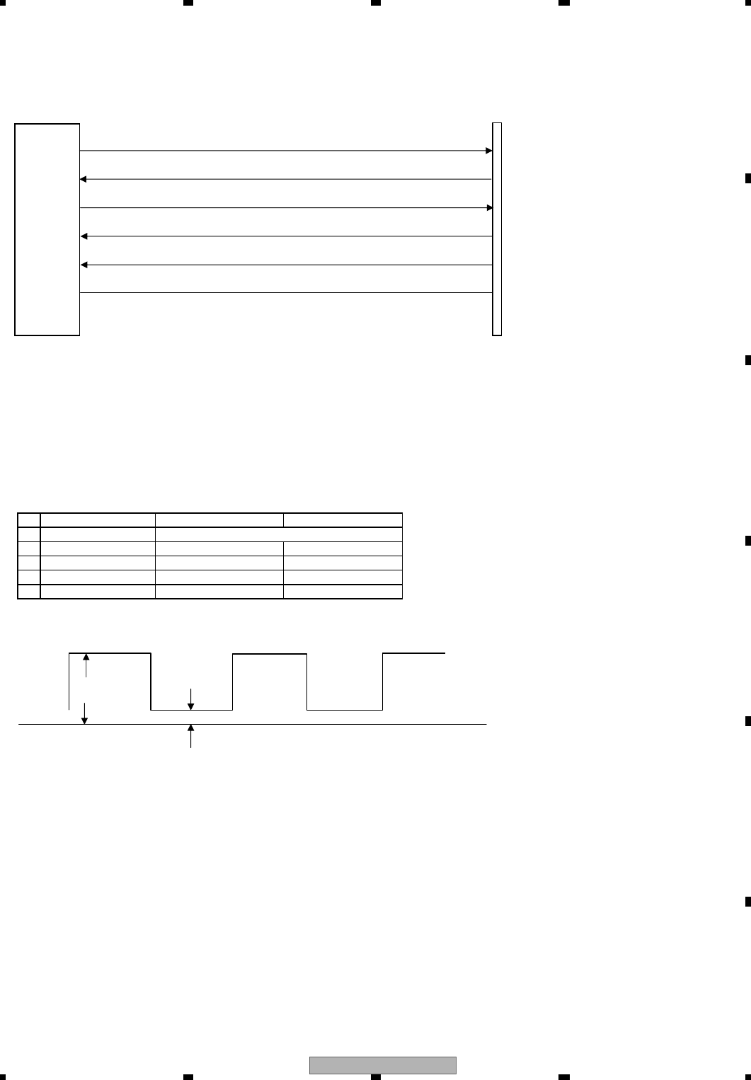
AVIC-X910BT/XS/UC 67
5678
5678
C
D
F
A
B
E
CN1901
HOST I/F
No.
1 CP_RESET
2 SDATA VCC33*0.7or more VCC33*0.2 or less
VCC33*0.7or more VCC33*0.2 or less
VCC33*0.7or more VCC33*0.3 or less
VCC33*0.7or more VCC33*0.3 or less
3 SCLOCK
4 D+
5 D-
Fig. 14.2: USB Circuit Communication Wave
VCC33*0.7or more
IC1501
DVD-LSI
D-
D+
I2C_SCL
I2C_SDA
CP_RESE
Standard value 1
Standard value 1
Standard value 2
Standard value 2
DGND
Check 14: Is USB Circuit OK?
<Outline>
The data is transmitted through D+, D- and SDA of HOST I/F while playing USB/IPOD.
USB memory uses only D+ and D-, but IPOD uses SDA (DATA) and SCL (CLOCK)
in addition to D+ and D-.
Fig. 14-1: USB Circuit
<Check Method>
1.USB Memory: Play a song from USB memory and check D+ and D- with the DGND standards.
2.iPod: Connect iPod and check CP_RESET, SDA and SCL with the DGND standards until the pioneer log appears.
Play a song from iPod and check D+/D- with the DGND standards.
When it does not conform to the standards, check appropriate line, main parts shown in the above figure,
soldering of peripheral parts and malfunctions in parts.
Checking spot (stylus)
*Until the pioneer log appears after connecting the iPod
*Until the pioneer log appears after connecting the iPod
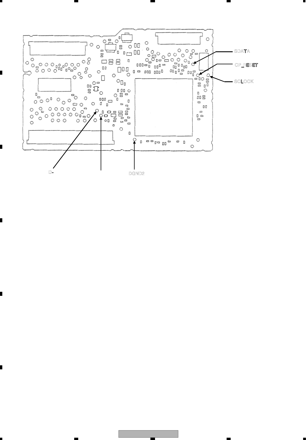
AVIC-X910BT/XS/UC
68
1234
1234
C
D
F
A
B
E
Side A
SCLOCK
SDATA
D-
CP_RESET
D+ DGND2
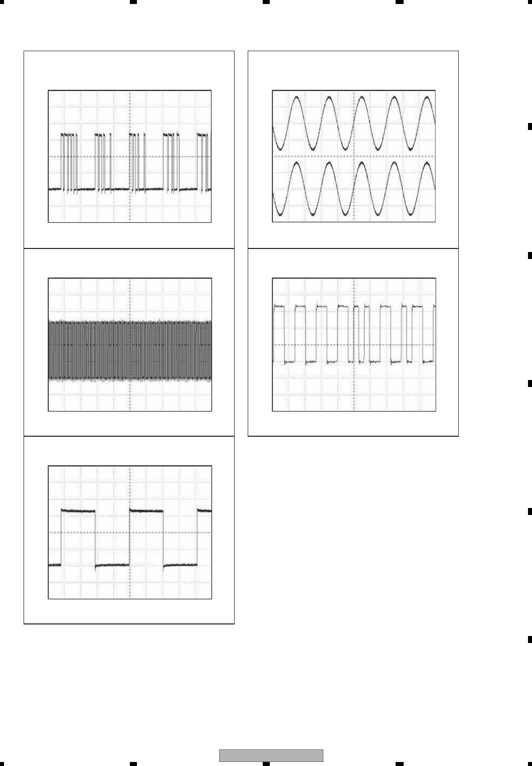
AVIC-X910BT/XS/UC 69
5678
5678
C
D
F
A
B
E
AUDIO
Reference voltage: DGND2 1 V/div. 5 usec/div Reference voltage: GNDAU2 1 V/div. 500 usec/div
Reference voltage: DGND2 1 V/div. 5 usec/div Reference voltage: DGND2 1 V/div. 500 nsec/div
CH1:LRCK
CH1:SRCK
CH1:ADOUT3
CH1:LO
CH2:RO
CH1:IECOUT
Reference voltage: DGND2 1 V/div. 5 usec/div
G->
G->
->G->G
G->
G->
Waveform 1 Waveform 4
Waveform 2
Waveform 3
Waveform 5
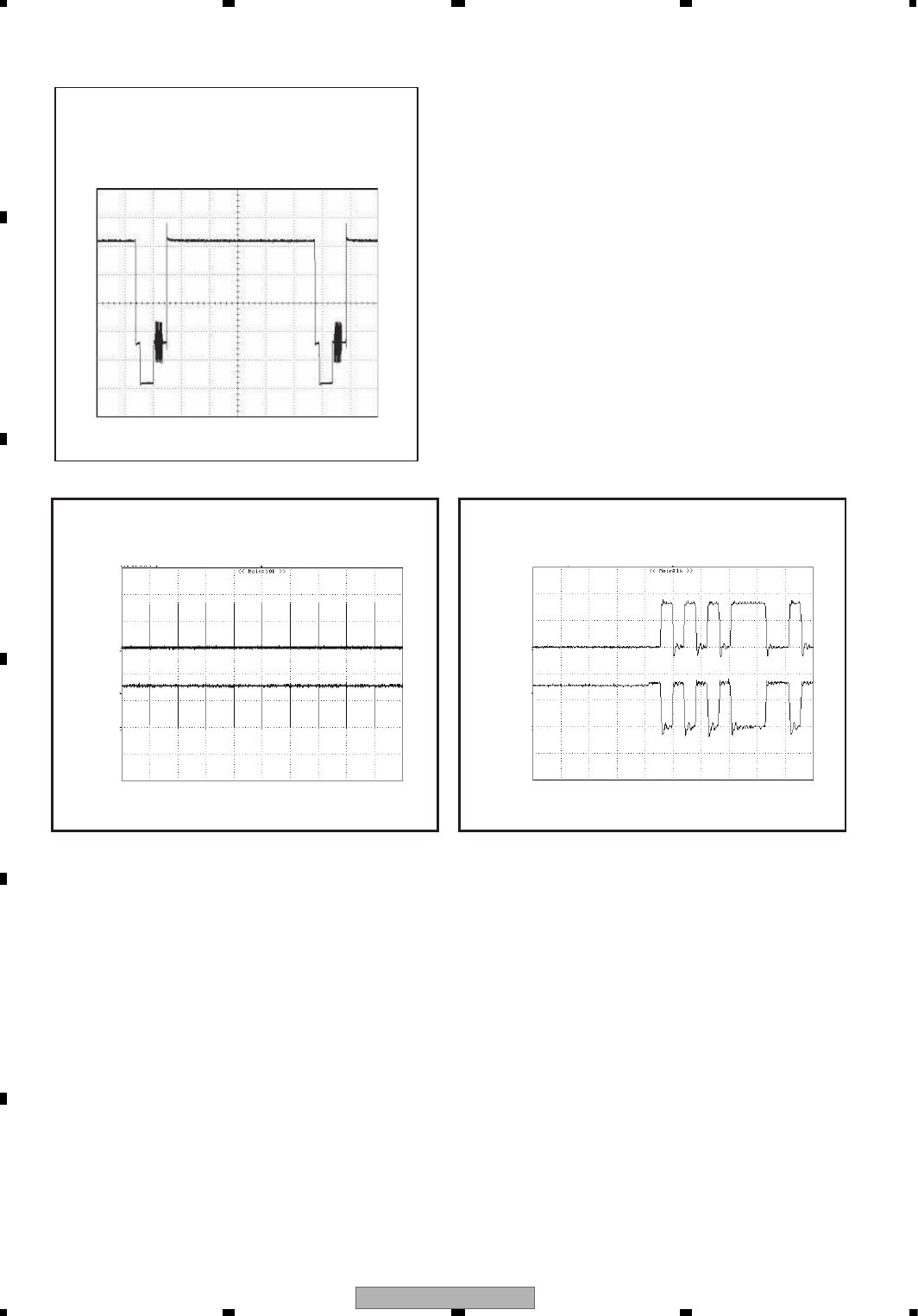
AVIC-X910BT/XS/UC
70
1234
1234
C
D
F
A
B
E
VIDEO
USB memory
USB memory USB memory
[WHITE 100IRE]
CH1:COMPO
Reference voltage: GNDV1 200 mV/div. 10 usec/div
-D-D
DNGDDNGD
+D+D
Waveform 6
Waveform 7 Waveform 8
Reference voltage:DGND 1 ms/div 2 V/div Reference voltage:DGND 200 ns/div 2 V/div
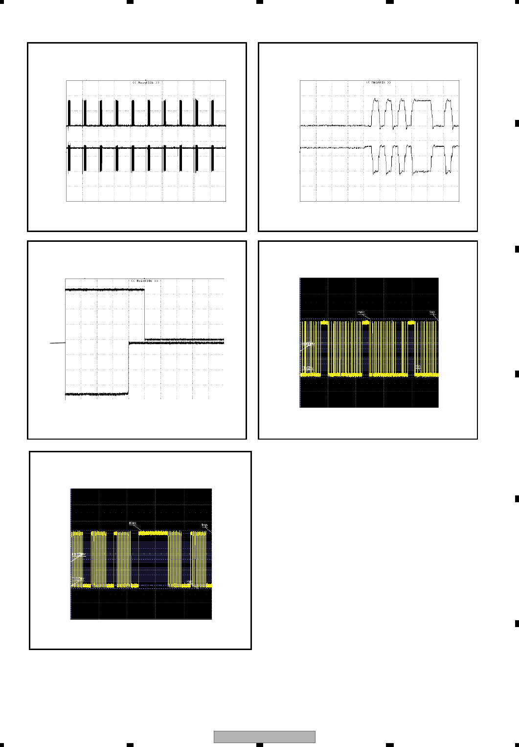
AVIC-X910BT/XS/UC 71
5678
5678
C
D
F
A
B
E
iPod
-D-D
DNGDDNGD
+D+D
CP_RESET
DGND
SDA
NRES
iPod
SCL
iPod
iPodiPod
iPod
Waveform 9
Waveform 11
Waveform 13
Waveform 12
Waveform 10
Reference voltage:DGND 1 ms/div 2 V/div
Reference voltage:DGND 20 ms/div 1 V/div
Reference voltage:DGND 500 us/div 1 V/div
Reference voltage:DGND 2 ms/div 1 V/div
Reference voltage:DGND 200 ns/div 2 V/div
AVIC-X910BT/XS/UC
72
1234
1234
C
D
F
A
B
E
5.4 ERROR CODE LIST
Error status OSD *1 Disc
USB
(MSC)
USB
(iPod)
ACC
Off/On
Source
Off/On
Eject Play Key
NON-PLAYABLE DISC
INCOMPATIBLE DEVICE
UNPLAYABLE FILE
O
p
en 10h
X
-- ****
Read Error 0h299-20-RORRE
X
--
Focus Error(Focus Error
in mechanism set u
p)
h1209-20-RORRE X- - XXXX
XXXX
Surface Error h22E9-20-RORRE X- - XXXX
Address no
t
found(Invalid Track) ERROR-02-80 23h X- - XXXX
Spindle Lock ERROR-02-91 24h X- - XXXX
Carriage HOME ERROR-02-92 25h X- - XXXX
ID/SUBCODE Read Error ERROR-02-94 26h X- - XXXX
AV CHIP decode Error ERROR-02-9A 2Ah XX - XXXX
AV CHIP Recovery NG ERROR-02-9B 2Bh XXX XXXX
Error of PLAY BAC
K
Mode Status ERROR-02-9C 2Ch XX - XXXX
Disc Data Error ERROR-02-9D 2Dh X- - XXXX
THERMAL
PROTECTION IN MOTION
No Disc
(including Disc loading
and e
j
ectin
g)
40h X- - ****
Loading_Mecha Error 50h XXX X-X-
Communication fault attesting iPod
Communication fault attesting iPodh0606-20-RORRE
X
-
X
h1616-20-RORRE
X
-
X
iPod attestation retrying failure
iPod attestation time out
h2626-20-RORRE iPod attestation retrying failure
X
-
X
h3636-20-RORRE X-X --X-
--X-
--X-
--X-
h4646-20-RORRE --X --X-
--X-
Error setting iPod h5656-20-RORRE --
X
h6666-20-RORRE --X --X-
h7676-20-RORRE --X --X-
h8686-20-RORRE --X --X-
No songs error h96 --X --X-
iPod control forwarding/
Intarapta forwarding error hA6A6-20-RORRE --X --X-
Demand timeout
iPod's reproducing hB6B6-20-RORRE --X --X-
--X-
ERROR-02-6C --
X
Remote switch demand
timeout ERROR-02-6D --X --X-
--X-
--X-
PROTECTED DISC
NO ACCESSIBLE
DATA AVAILABL
DIFFERENT REGION DISC
NON-PLAYABLE DISC
ERROR-02-A0
X
--
XXXX
h1A1A-20-RORRE X- -
ERROR-02-A2
A
2h
X
--
XXXX
ERROR-02-A3
A
3h
X
--
XXXX
ERROR-02-A4
A
4h
X
--
XXXX
ERROR-02-A5
A
5h
X
--
XXXX
ERROR-02-A6
A
6h
X
--
XXXX
ERROR-02-A7
A
7h
X
--
XXXX
ERROR-02-A8
A
8h
X
--
XXXX
ERROR-02-A9
A
9h
X
--
XXXX
ERROR-02-AA
A
Ah
X
--
XXXX
Focus Error ERROR-02-AB
A
Bh
X
--
XXXX
Error of PLAY BAC
K
Mode Status h0B0B-20-RORRE X- - XXXX
Error of PLAY BAC
K
Mode Status h1B
C0h
1B-20-RORRE X- - XXXX
A
udio Propert
y
Timeou
t
Error *9 ERROR-02-C0 Audio property timeout error X- - XX X -
ERROR-02-D0 -X- --X-
CBW and CSW forwarding error
ERROR-02-D1 -
X
---
X
-
Audio class band securing failure
ERROR-02-D8 --
X
--
X
-
Audio class FS setting failure
ERROR-02-D9 --
X
--
X
-
Undefined Error ERROR-FF-FF
X
--
XXXX
--
--
00h USB device of format alone that
cannot be reproduced XX
30h X
70h --
X--
90h --X
Method of reset
Temp Error
(In Case of High
Tem
p
erature )
Region code Error NG
--
--
8*rorrEyeK7*MRPC Key Error for playback X--
X-
--
-- --
X-
Generation source
-
--
XX
h00rorrEaideM XXX X -
00h USB device that doesn't correspond XX-
X-
h07rorrEMRD X
(No display)
(No display)
(No display)
(No display)
A disc containing the unplayable
Format only
Door open error
Transfer start error
Focus error
Focus error during set up
(A focus has never been achieved
with that disc.)
Address not found.
Spindle lock NG
(the disc cannot rotate)
Carriage home NG
(The pick up tries to return to carriage
home, but it cannot go back and stopped.)
ID/SUBCODE Read Error (ID/SUBCODE
cannot be read due to scratch or stain.)
UART
*2 Meaning
AV CHIP decode NG
(AV chip cannot be decoded.)
AV CHIP recovery NG
Playback state error
(An error due to software bug.)
Disc Data NG
Disc has not been inserted.
(Including Load in process or
Eject in process.)
High temperature
(Playback is stopped because the pick up
temperature is 89 C or higher.)
Loading mechanism error
(The disc cannot be clamped.)
6Ch
6Dh
A0h
h39
D0h
FFh
D9h
D8h
D1h
DRM error (All music cannot be played
back due to DRM.)
DRM error (All music cannot be played
back due to DRM.)
Undefined error
iPod authentication data is abnormal
iPod authentication data is abnormal
REQUEST error
Failure in issuing the read command
L0 adjustment is NG.
L1 adjustment is NG
LD system NG
Gain adjustment system NG.
Gain determining system NG.
Servo initial setting related items NG.
Disc is not clamped yet.
Tracking system NG
Media setting system NG
JUMP over layers NG
Navigation command error
Retry over
REQUEST error
Failure in issuing read
command (chip dependent)
Adjustment of L0 is NG.
Adjustment of L1 is NG.
LD system NG
Gain adjustment system NG.
Gain determining system NG.
Servo initial setting related items NG.
Disc is not clamped yet.
Tracking system NG.
Media setting system NG.
XXXX
Error when iPod is connected/
It is generated STALL by the USB
communication
Demand timeout when
initial is communicated
Protocol version
non-correspondence
Timeout when protocol
version is judged
Remote switch error
iPod attestation time out
Error setting iPod
No songs error
iPod control forwarding/
Intarapta forwarding error
Demand timeout
iPod's reproducing
Remote switch demand
timeout
Error when iPod is connected/
It is generated STALL by the USB
communication
Demand timeout when
initial is communicated
Protocol version
non-correspondence
Timeout when protocol
version is judged
Remote switch error
Error when MCS is connected/
It is generated STALL by the USB
communication
CBW and CSW forwarding error
Audio class band securing failure
Audio class FS setting failure
Error when MCS is connected/
It is generated STALL by the USB
communication
Region code NG (Unable to be played back
due to incorrect mechanism region.)

AVIC-X910BT/XS/UC 73
5678
5678
C
D
F
A
B
E
X: Cancel the error by operation. -: Error is not cancelled by operation. *: No setting
*1 A content displayed on OSD. As for the items having multiple display patterns, the upper row is for the Japanese version Full GUI, and the lower row is for
the Touch Panel model and Full GUI (English version).
*2 A parameter of UART command, such as “receipt error notice”, that the DVD mechanism transmits.
*3 CPPM(Content Protection for Prerecorded Media) : A copyright protection technique used in DVD-A. The protection is realized by using the keys recorded
on the media and the device key held by the player.
*4 DVD-A compatible model only.
When an error has occurred, only the audio output will be muted but playback operation will continue. Furthermore, acceptance of the user operation will be
the same as usual.
*5 AWM (Audio WaterMark): Electronic watermark. Information on the copyright owner or CCI (copy control information) are recorded so that illegally copied
discs can be identified.
*6 Notice as an error status will not be given
*7 CPRM(Content Protection for Recordable Media) : A copyright protection technique for digital contents used for re-writable DVD or memory card.
(DVD-VR model only)
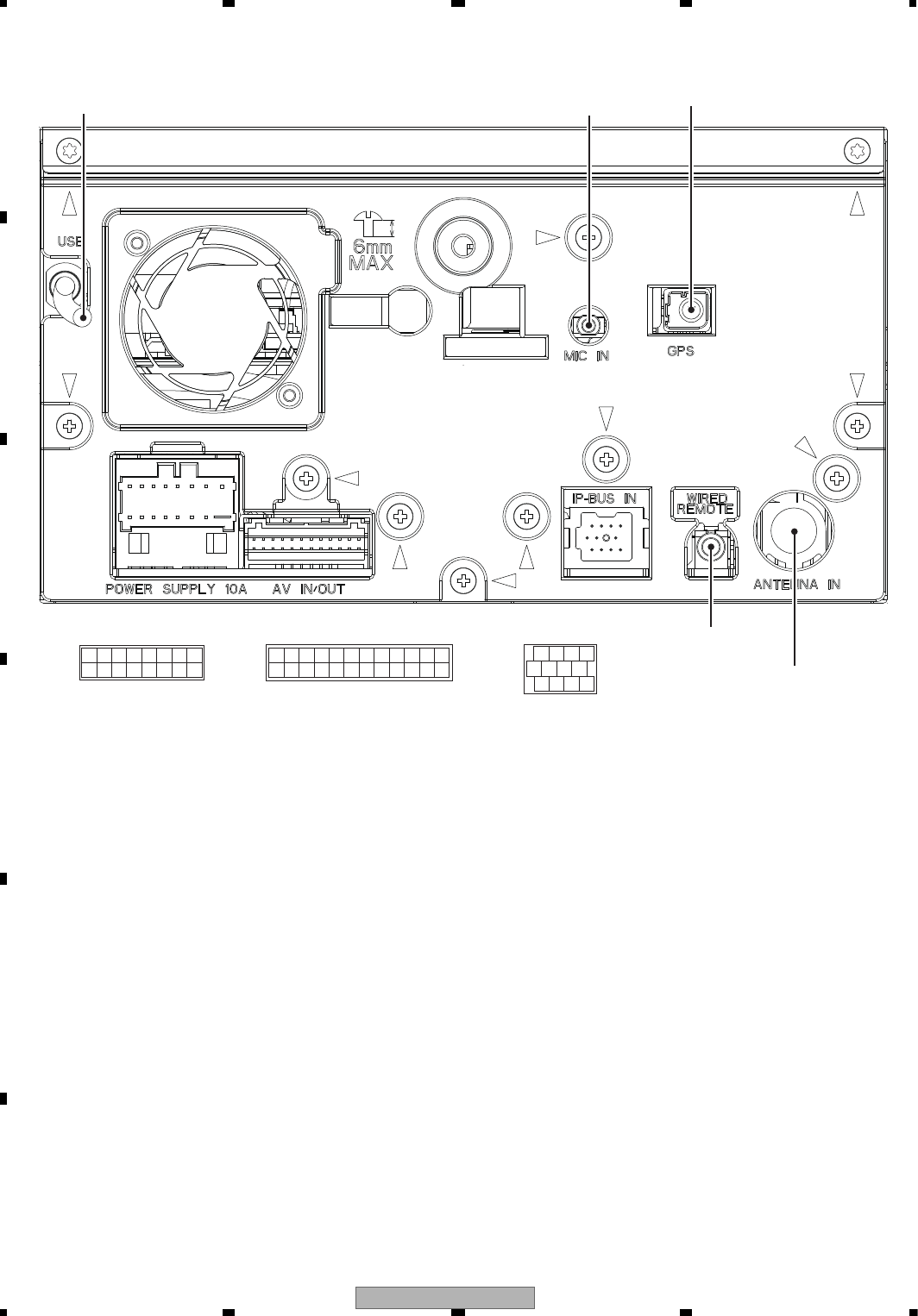
AVIC-X910BT/XS/UC
74
1234
1234
C
D
F
A
B
E
5.5 CONNECTOR FUNCTION DESCRIPTION
1. TELMUTE
2. DTVVGND
3. RR
4. DTVV
5. RL
6. REARGND
7. FR
8. KMODE
9. FL
10. FRONTGND
11. SWR
12. BREM
13. SWL
14. SWGND
15. VTR1R
16. VTR1RGND
17. VTR1L
18. VTR1LGND
19. VTR1V
20. VTR1VGND
21. REARVOUT
22. GNDV
23. BCV
24. BCVGND
1. FR+
2. RR+
3. FR-
4. RR-
5. FL+
6. RL+
7. FL-
8. RL-
9. PKB
10. PULSE
11. REV
12. ILM
13. AANT
14. ACC
15. GND
16. BUP
1. IPBUS+
2. IPBUSG
3. IPLG
4. NC
5. IPBUS-
6. IPRG
7. IPL+
8. ASENBO
9. IPR+
10. IPR-
11. IPL-
13579111315
246810121416
POWER SUPPLY
1 3 5 7 9 11 13 15 17 19 21 23
2 4 6 8 10 12 14 16 18 20 22 24
AV IN/OUT
1234
56 7
8 9 10 11
IP-BUS IN (UC)
USB MIC IN GPS ANTENNA
WIRED REMOTE
FM/AM ANTENNA

AVIC-X910BT/XS/UC 75
5678
5678
C
D
F
A
B
E
5.6 TROUBLESHOOTING
No Power
Key illumination is
lighted?
Check the following signal in the
AV unit.
(BSEN/ASEN/ILM, 8 V Power
supply)
Key illumination is
lighted more than 20
seconds?
LCD backlight is OK?
NAVI5V is OK?
Check the Power supply (D/D
converter) block and Control signal
(48pin NAVICON) of the System
u-com in the AV unit.
LCD unit failure.
Power supply
block for "LCD Panel
unit" is OK?
LCD Panel unit failure.NAVI unit failure.
NAVI3V from the
NAVI unit is OK?
NAVI unit failure.
(NAVI3V is supplied from NAVI
unit and also NAVI3V is
generated from NAVI5V)
NO
YES
NO
YES
NO
(No output)
YES
NO
Key illumination
go off after 20
seconds.
Initial communication error
between NAVI and AV unit.
- Confirm communication line
between 2 unit. (*1)
- Change the NAVI unit
(*1)
Normal operation after ACC ON
- RESETB: High
- OFFINFO: L -> H
- OFFANS: H -> L
- CTOSYS: UART
- SYSTOC: UART
- CPUWDT: L
- BATFAULT: L
Notes:
All siganl mentioned above are control
key signal from System u-com (AV
unit) to NAVI unit.
The "H" voltage is different depends on
the location.
- Port of system u-com: 5 V
- Connector of AV unit: 3 V
YES
No Display
(White or Gray screen)
YES
NO
(No output)
NO
YES
-FLOWCHART

AVIC-X910BT/XS/UC
76
1234
1234
C
D
F
A
B
E
LCD BD Side ANAVI BD Side BNAVI BD Side A
Case 1 System can not wake-up.
ACC ON ACC OFF
Pin27: NAVI33V High High This power supply is from NAVI BD to AV BD.
Pin5: OFFINFO High Low This signal is from AV BD(system-ucom) to NAVI BD.
Pin6: OFFANS Low High This signal is from NAVI BD to AV BD(system-ucom).
(High = 3.3 V)
Pin13: SYSTOC Communication line (Sys u-com to NAVI unit)
Pin14: CTOSYS Communication line (NABI unit to Sys u-com)
Pin3,5,7,9,11,13,15,17,19 ACC ON ACC OFF
NAVI 5V 5V 5V power supply is from AV BD to NAVI BD.
Case 2 Navi image can not be displayed on LCD.
Pin1: TFT_ANODE
Pin36: LVDSN Video signal (LVDS) from NAVI to LCD BD. Pin2: TFT_ANODE2
Pin37: LVDSP Video signal (LVDS) from NAVI to LCD BD. Pin6: TFT_CATHODE
Pin7: TFT_CATHODE
Power supply
from LCD BD to
LCD unit
05niP1niP
Pin1
Pin2
Pin19
Pin20
Pin1 Pin74
Chip resistor (0 ohm)
AB
CD
E
B
C
D
F
Pin1 Pin10
- DIAGNOSIS POINT
F
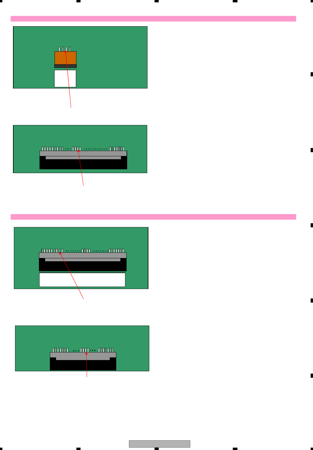
AVIC-X910BT/XS/UC 77
5678
5678
C
D
F
A
B
E
Case 3 Touch panel operation doesn't work
Pin1: nYPON
Pin2: nXPON
Pin3: YMON
Pin4: XMON
Pin29: nYPON
Pin30: nXPON
Pin31: YMON
Pin32: XMON
Case 4 Hard Key doesn't work
Pin8: KEY0 KEY (Push, Menu, Right) signal from KEY BD to LCD BD (DC Voltage)
Pin9: KEY1 KEY (MAP, Left, Down ,Up) signal from KEY BD to LCD BD (DC Voltage)
Pin11: ROT0 KEY (Rotary) signal from KEY BD to LCD BD (Pulse waveform)
Pin12: ROT1 KEY (Rotary) signal from KEY BD to LCD BD (Pulse waveform)
Pin33: ROT0 KEY (Rotary) signal from KEY BD to LCD BD (Pulse waveform)
Pin34: ROT1 KEY (Rotary) signal from KEY BD to LCD BD (Pulse waveform)
The signal from touch-panel to LCD BD
(Wavefrom pulse can be mintored while operating touch-
panel.)
The signal from LCD BD to NAVI BD
(Wavefrom pulse can be mintored while operating touch-
panel.)
Pin1 Pin4
Pin1 Pin74
Pin1 Pin74
05niP1niP
E
A
D
B

AVIC-X910BT/XS/UC
78
1234
1234
C
D
F
A
B
E
Case 5 Audio (NAVI SOURCE) or Guide voice (BEEP sound) is NG.
Pin19: GUI_P Guidance or BEEP sound
Pin28: NAVI L Audio Lch
Pin30: NAVI R Audio Rch
Pin29,31: GND
05niP1niP B
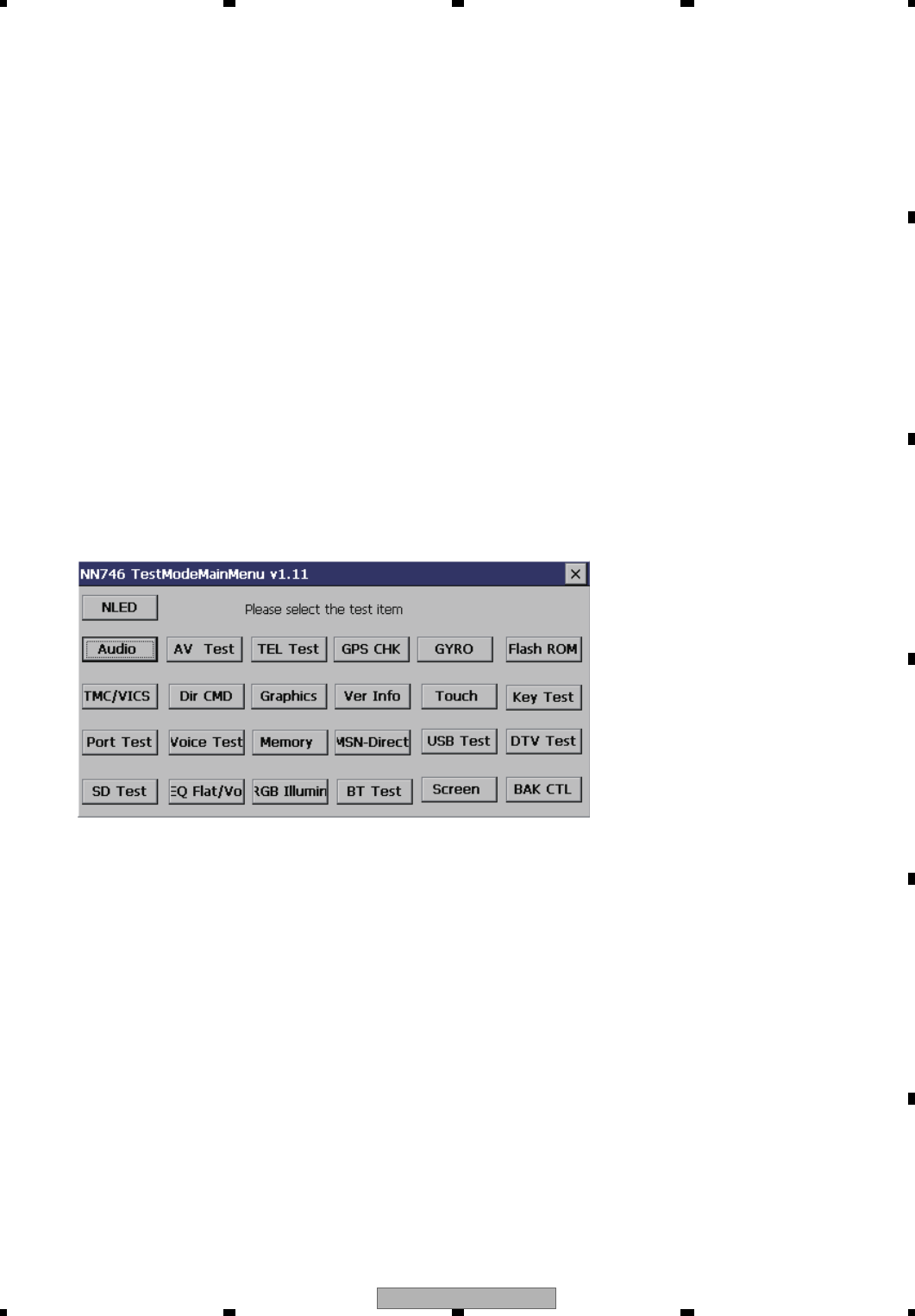
AVIC-X910BT/XS/UC 79
5678
5678
C
D
F
A
B
E
6. SERVICE MODE
6.1 TEST MODE
1. Test mode menu selection method
The main keyboard cannot be used for this operation.
Double-click the touch panel directly.
2. Test mode activation method
1. Copy a "TestMode" folder under “TestMode” folder on GGV1322 to a SD card.
Note: "TestMode" folder must be on the SD card root.
2. Download a ID file from the Service Site and copy the file to the "TestMode" folder on the SD card.
3. Insert the SD card into the main unit.
4. Turn ACC ON.
5. The test mode menu is displayed.
<< Enter the test mode in the set procedure. >>
When the set procedure is followed (Procedure OK)
Start screen
Jig No : GGV1322
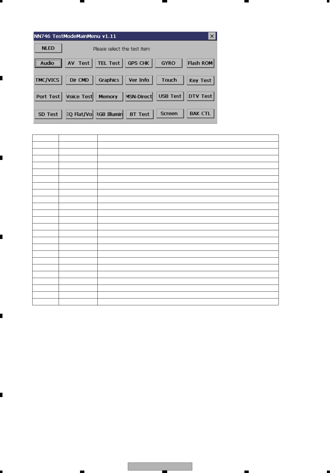
AVIC-X910BT/XS/UC
80
1234
1234
C
D
F
A
B
E
3. Test mode menu
No. Test Item Test Content
1 Audio Playback of audio
2 AV Test Not for service
3 TEL Test Not for service
4 GPS CHK GPS receiver test
5 GYRO Gyro test
6 Flash ROM Flash ROM read/write test
7 TMC/VICS FM multiplex error test
8 Dir CMD Not for service
9 Graphics Graphics test
10 Ver Info Display version information of software, mecha, and microcomputers.
11 Touch Correction and test of Touch Panel
12 Key Test Not for service
13 Port Test Display states such as parking and reverse.
14 Voice Test Not for service
15 Memory Not for service
16 MSN-Direct Not for service
17 USB Test Not for service
18 DTV Test Not for service
19 SD Test SD card test
20 EQ Flat/Vo Not for service
21 RGB Illumin Not for service
22 BT Test Not for service
23 Screen Not for service
24 BAK CTL Not for service
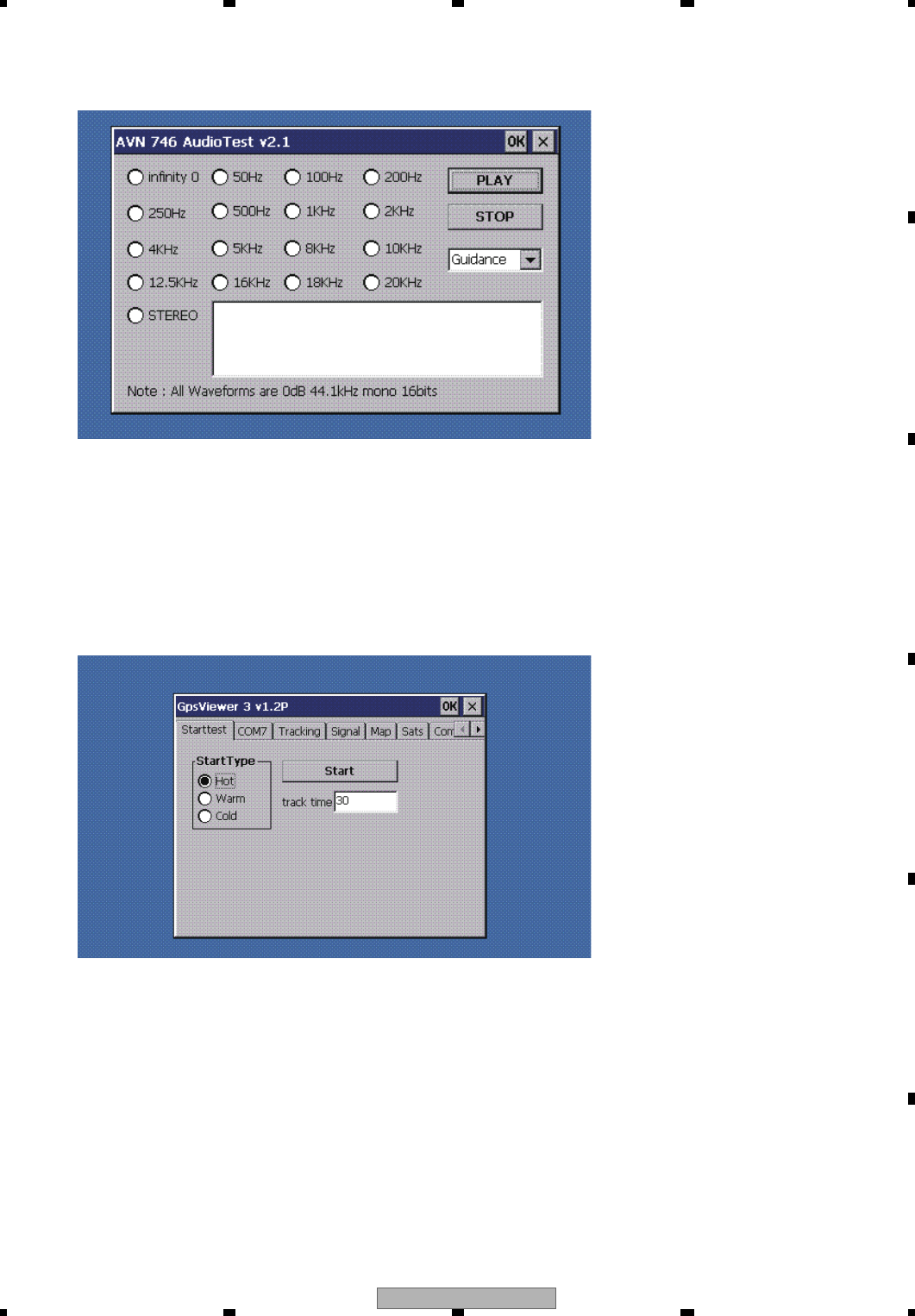
AVIC-X910BT/XS/UC 81
5678
5678
C
D
F
A
B
E
Audio Test Screen
Gps Viewer Execution Screen
Audio Test Mode
Starttest
<< Key Operation >>
[Play] • • • Play
[Stop] • • • Stop
[Guidance] • • • Output of guidance
[Stereo] • • • Output of stereo
[OK] • • • Terminate Audio Test.
Note : Big sound (0 dB signal) is output
<< Operation method >>
1. Select ‘Start Type’. Normally, ‘Hot’.
2. Press ‘Start’ to start the test.
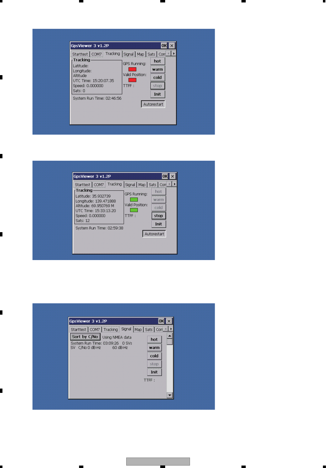
AVIC-X910BT/XS/UC
82
1234
1234
C
D
F
A
B
E
Tracking
Signal
<< Operation method >>
1. When GPS Running is red, press ‘hot’.
<< Operation method >>
1. When GPS Running is green, the test is started.
2. When Valid Position is green, the measurement is successfully conducted.
<< Operation method >>
1. The screen will be in this state if the test is not started.
2. To start the test, press ‘hot’.
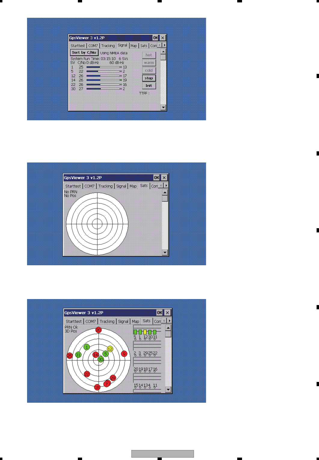
AVIC-X910BT/XS/UC 83
5678
5678
C
D
F
A
B
E
Sats
<< Operation method >>
1. The screen will be in this state if the test starts.
2. When the blue color bar appears, GPS signal is locked.
<< Operation method >>
1. The screen will be in this state if the test is not started.
2. To start the test, refer to ‘Start test’ tab.
<< Operation method >>
1. When the test starts and a satellite is started to be acquired, the screen will be in this state.
Red • • • Not acquired. Yellow • • • Already acquired. Green • • • Acquired and data obtained.
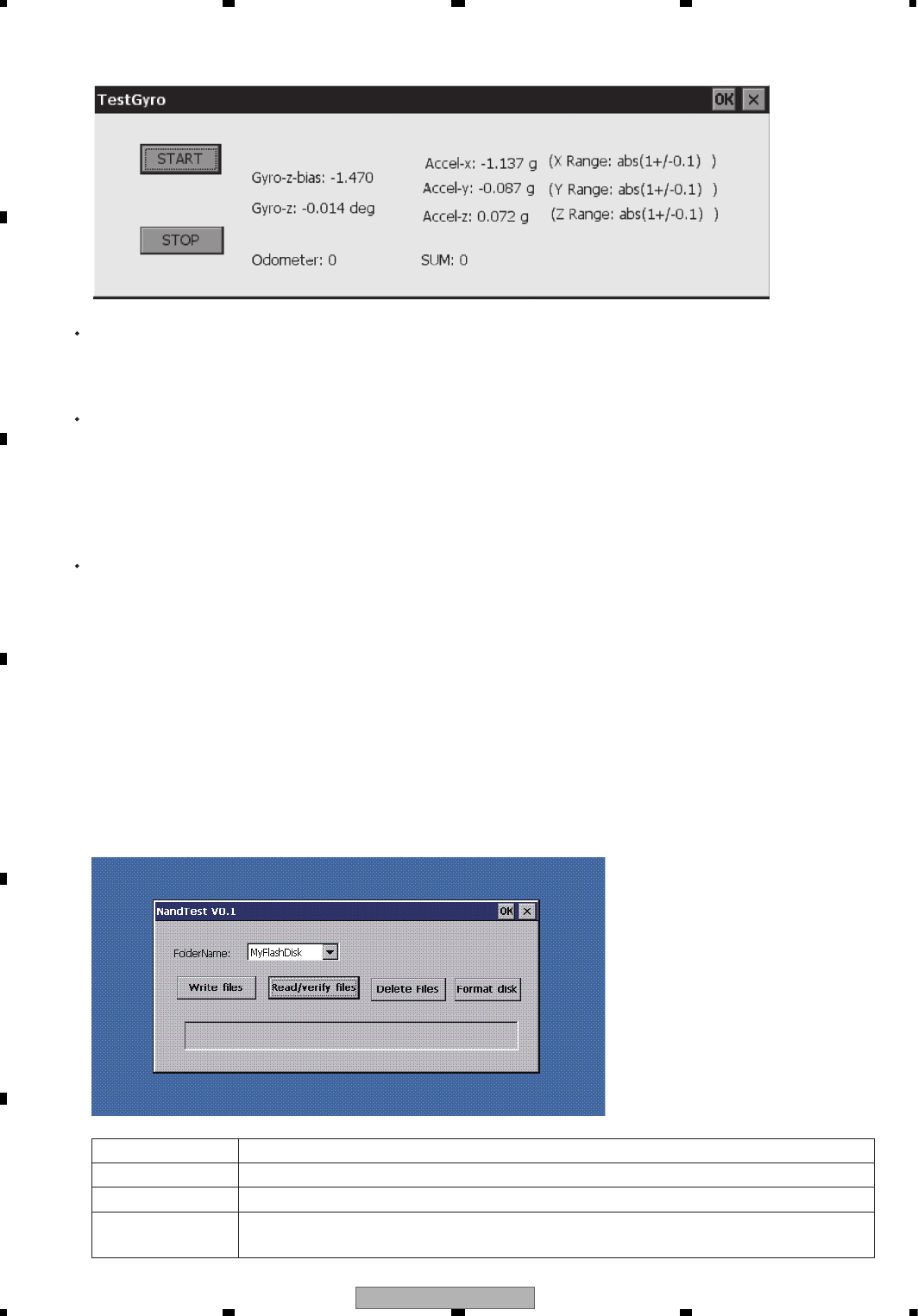
AVIC-X910BT/XS/UC
84
1234
1234
C
D
F
A
B
E
TestGyro Screen
NAND Flash test mode start screen
Write files Conduct a write test to NAND Flash disc.
Read/verify files Conduct a read test to NAND Flash disc. Notes) It will take time by test completion.
Delete Files Conduct a deletion test to NAND Flash disc.
Format disc Conduct a formatting test to NAND Flash disc. Notes) After performing “Format disc”,
all data is deleted include APL and MAP data.
Gyro-z-bias test
1. Press “Start” and wait 2 seconds, then the “Gyro-z-bias” result will be displayed.
The result should be within the range between - 2 and 2 degrees.
Gyro-z test
1. Rotate the unit 360 degrees. (or 180 degrees)
The “Gyro-z” result should be within the range of 360 +/- 14.4 degrees. (or 180 +/- 7.2 degrees)
2. Press “Stop” and then press “Start” again.
3. Rotate the unit -360 degrees. (or 180 degrees)
The “Gyro-z” result should be within the range of -360 +/- 14.4 degrees. (or 180 +/- 7.2 degrees)
Accelerometer Testing
1. Set the unit "Face Down" position to +1 g (pointing up). You will then get an “Accel-x” result
2. Set the unit "Face Up" position to -1 g (pointing up). You will then get an “Accel-x” result
3. Calculate the difference of the two results. The difference should be within the range of 2 +/- 0.1 g.
For example, the result of step 1 is "1.045 g" and step 2 is "-0.902 g", the difference is 1.045+0.902=1.947 g.
4. Set the unit "Right side up" position to +1 g (pointing up). You will get an “Accel-y” result.
5. Set the unit "Right side down" position to -1 g (pointing up). You will get an “Accel-y” result.
6. Calculate the difference of the two results. The difference should be within the range of 2 +/- 0.2 g.
7. Set the unit "Up side down" position to +1 g (pointing up). You will get an “Accel-z” result.
8. Set the unit "Normal" position to -1 g (pointing up). You will get an “Accel-z” result.
9. Calculate the difference of the two results. The difference should be within the range of 2 +/- 0.2 g.

AVIC-X910BT/XS/UC 85
5678
5678
C
D
F
A
B
E
GpsTmcDemo
TMC measurement selection screen
Graphics Test start screen
<< Test Content >>
The TMC error rate can be measured.
The frequency can be changed by tapping ‘<’ or ‘>’.
The test can be terminated by tapping the left ‘x’ mark.
Start screen
<< Operation method >>
1. The screen will be in this state after started.
2. Press ‘Test’ to start the test.

AVIC-X910BT/XS/UC
86
1234
1234
C
D
F
A
B
E
<< Operation method >>
1. The menu appears when ‘Test’ is pressed. Select the item to test.
<< Operation method >>
1. To terminate the test, press ‘File’ and then ‘Exit’.
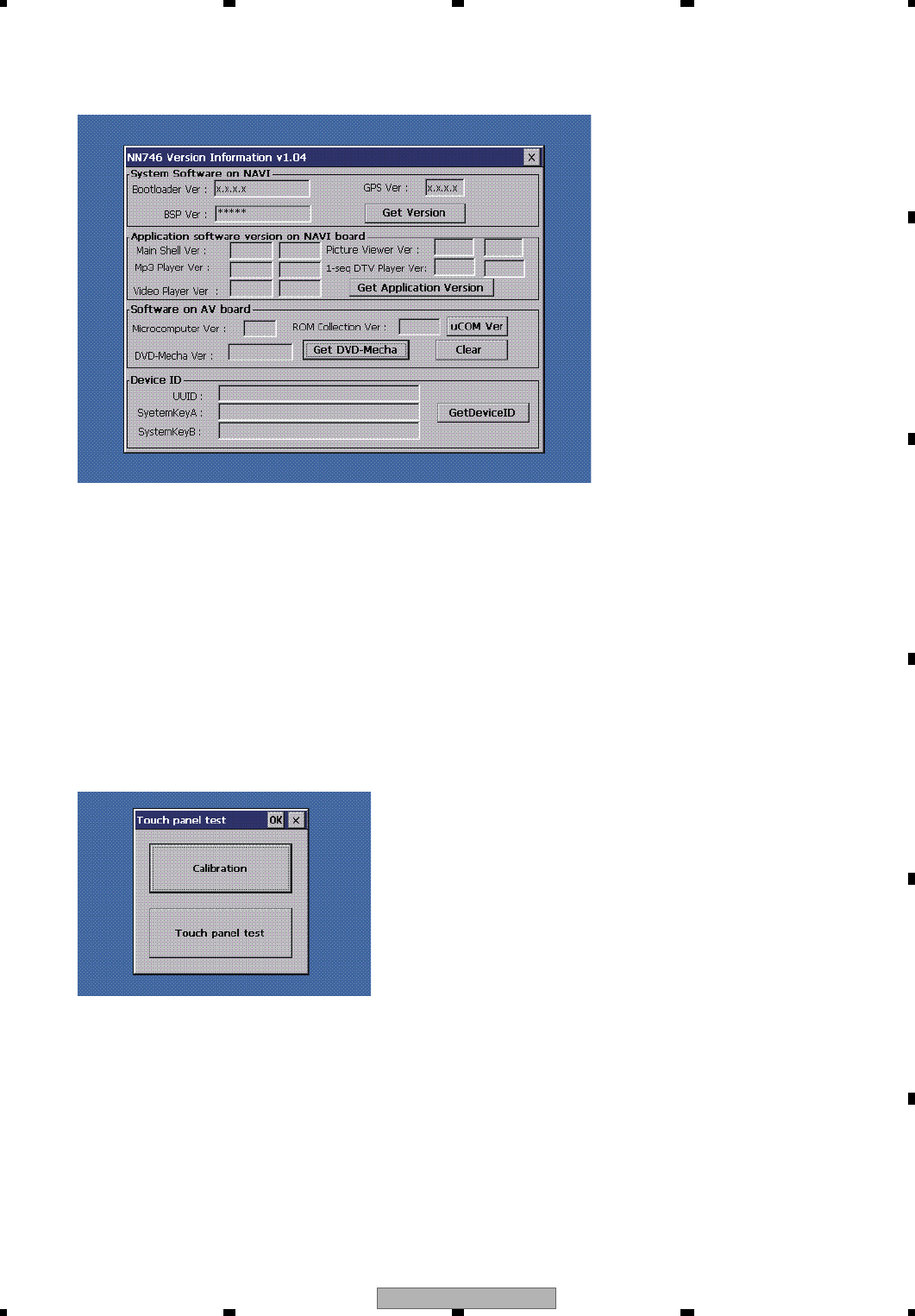
AVIC-X910BT/XS/UC 87
5678
5678
C
D
F
A
B
E
Version Information screen
Touch Panel Test screen
Start screen
Start screen
<< Key operation >>
[Get Version] • • • Display the version of Bootloader, GPS, and BSP.
[Get Application Version] • • • Display the version of each application.
[uCOM Ver] • • • Display the microcomputer version and ROM Collection version.
[Get DVD-Mecha] • • • Display the DVD and CD mecha version.
[Clear] • • • Clear the display of the version of microcomputer, ROM, and mecha.
[GetDeviceID] • • • Display the device ID.
<< Key operation >>
[Calibration] • • • Conduct calibration.
[Touch panel test] • • • Conduct touch panel test.
AVIC-X910BT/XS/UC
88
1234
1234
C
D
F
A
B
E
Calibration
Touch Panel Test
<< Key operation >>
Touch panel calibration can be conducted by tapping five ‘+’ marks.
<< Key operation >>
A line appears when a line is drawn by a finger on the touch panel.
The test can be terminated by pressing the top right ‘x’ mark.
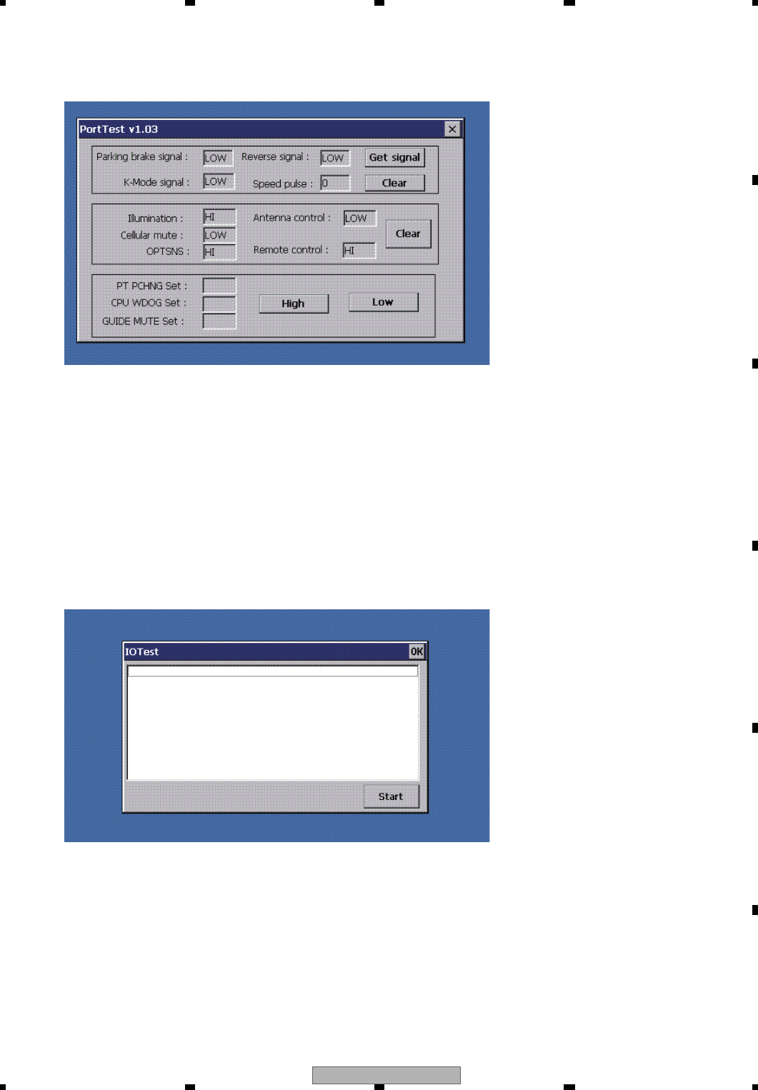
AVIC-X910BT/XS/UC 89
5678
5678
C
D
F
A
B
E
Port Test screen
SD Card Test screen
Start screen
Start screen
<< Key operation >>
[Start] • • • Start the test.
<< Key operation >>
[Get signal] • • • Display the states of Parking brake, Reverse, K-Mode, and Speed Pulse.
The states of Illumination, Cellular mute, OPTSNS, Antenna control, and Remote control are displayed
automatically.
[Clear] • • • Clear the display.
[High] • • • Not for service
[Low] • • • Not for service

AVIC-X910BT/XS/UC
90
1234
1234
C
D
F
A
B
E
Error screen
This is the state when an error occurred in the test.
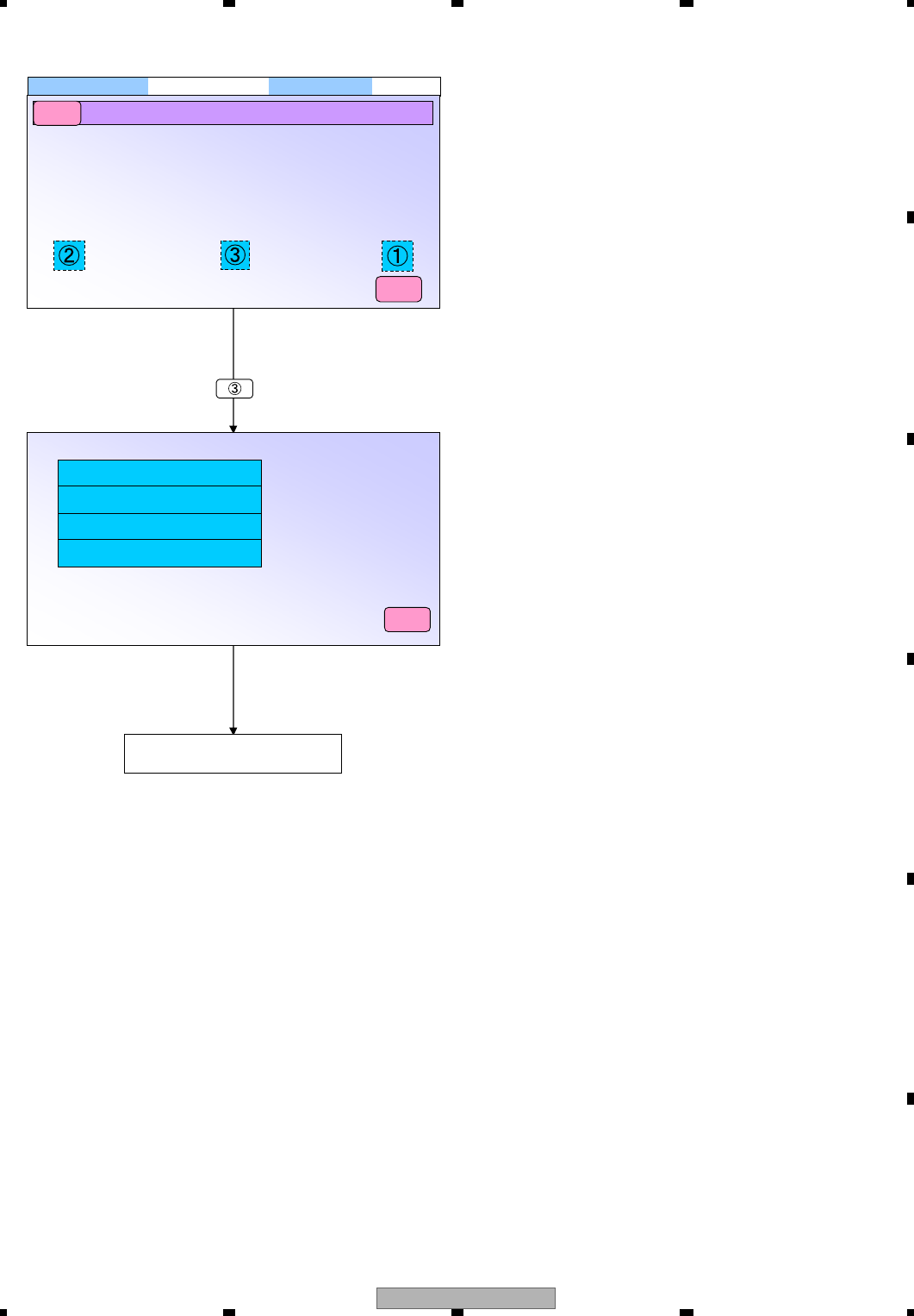
AVIC-X910BT/XS/UC 91
5678
5678
C
D
F
A
B
E
6.2 DVD TEST MODE
W
MM-14-23-01
EREUCAUJ
CN
PKB
(1), (2) and (3) are invisible buttons
In this screen, press long the areas (1), (2) and (3) that
display the test mode selection screen
by implementing the operations below in order
.
Detailed procedur
e
Step1 change the screen to source OFF screen
Step2 press the area of (1) lon
g
Step3 press the area of (2) lon
g
Step4 press the area of (3) lon
g
* When the operation above is normally implemented,
BEEP sound 1 is output.
If the operation is completed successfully,
the screen shifts to test mode screen after (3) is pressed long
The test mode is released by ACC-OFF operation
.
Source PlateOFF
SlaveTestMode
DVD(CD) region display
DVD(CD) debug display
DVD(CD) touch direct display
Back
Shift to selected test mode.
Map
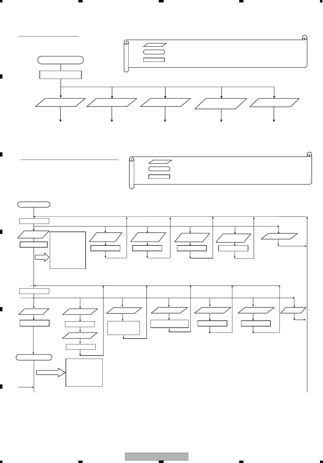
AVIC-X910BT/XS/UC
92
1234
1234
C
D
F
A
B
E
Image of the test mode.
[Note] Higher level 4 characters only. Lower level 4 characters are spaces.
)2()1(
Start of the test mode.
TEST
FE test selection EDC1 test selection
Hereafter, to FE test
mode image.
Hereafter, to EDC1
test mode image.
[Note] In order to move on to another test after selecting a test (FE/EDC1/EDC2), it is necessary to restart the DVD mechanism in the test mode.
(3)
EDC2 test selection
Hereafter, to EDC2
test mode image.
(4)
LD power on time
mode selection
Hereafter, to LD power on
time mode image.
(5)
Simple FE test mode
Hereafter, to simple
FE test mode.
Legend: … Key operation
… Operation state
… The content displayed on the DVD mechanism (video only)
8 characters data is sent to the product side (HOST) by UART communication.
Image of the front end test mode.
(2)
FE test mode
Disc type DVD1
layer
FE offset coefficient
TE offset coefficient
AS offset coefficient
ENV offset coefficient
TG offset coefficient
DBAL coefficient
VIN1 offset cancel value
VIN2 offset cancel value
VIN3 offset cancel value
VIN4 offset cancel value
VIN5 offset cancel value
Power on
0000 0000
0FFF 0000
0 x 00 0000
Legend: … Key operation
… Operation state
… The content displayed on the DVD mechanism (video only)
8 characters data is sent to the product side (HOST) by UART communication.
)5()4(
Disc type DVD2
layer Disc type CD
0000002000000010
Disc type CD-RW
0300 0000
EJECT
EJECT
[Note] If no action is taken for approximately 10 seconds after LD-ON, it will become LO-OFF automatically.
If F close is selected during LD-OFF, it will become an error.
During focus search (S character measurement mode), too, safety regulation applies if LD_OFF is not selected
within 10 seconds. Therefore, even if focus search is selected after LD-ON, it will become LD-OFF after 9 seconds.
In order to F close after focus search (S character measurement mode), set to Power_OFF first then power on again
before F close.
FEMAX level
FEMIN level
ASMAX level
ENVMAX level
FE normalization coefficient
Spindle gain coefficient
TEMAX level indication
TEMIN level indication
(2)
Focus close state
)2()1(
S curve
measurement
(2)
hcraesFesolcF
1A00 0000
F search
1100 0000
1FFF 0000
(3),(4)
CRG+/-
Activates while the key
is being pressed.
1B00 0000 : CRG+
1C00 0000 : CRG-
(5) (6)
LD-ON/OFF
When LO-ON: 1100 0000
When LD-OFF: 1000 000
CRG_HOME
1D00 0000
(8)
Power_OFF
(1) (3)
a b
1 x 00 0000
(7)
CRG_OUTSIDER
1E00 0000
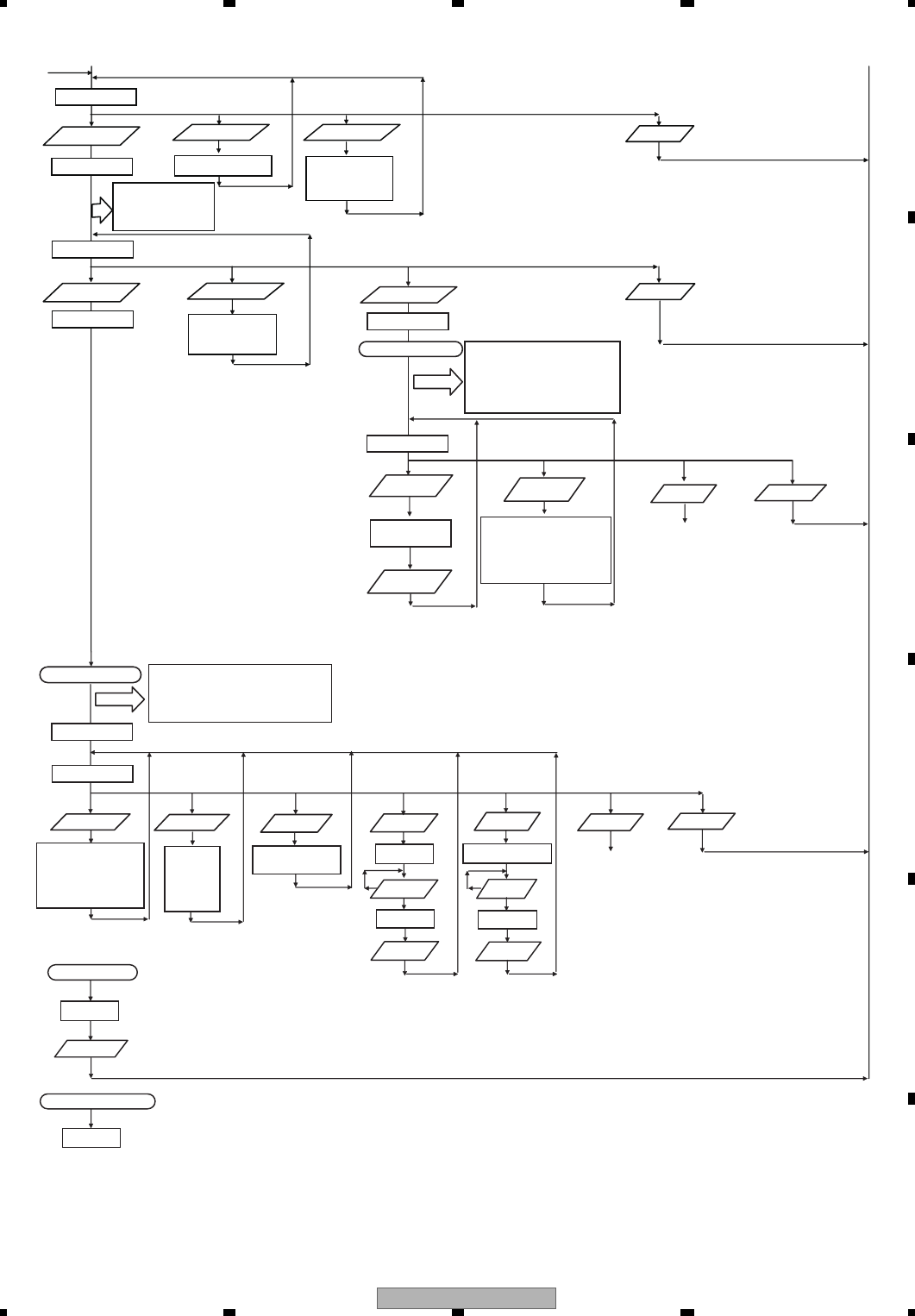
AVIC-X910BT/XS/UC 93
5678
5678
C
D
F
A
B
E
(2)
(1) (2)
Tracking balance
TBAL coefficient (layer 0)
TBAL coefficient (layer 1)
TE normalization coefficient (layer 0)
TE normalization coefficient (layer 1)
Off track adjustment result
Focus Jump
When L0 layer: 2000 0000
When L1 layer: 2100 0000
2 x 00 0000
2FFF 0000
(3),(4)
CRG +/-
It operates while the key
is being pressed.
2B00 0000 : CRG+
2C00 0000 : CRG-
3000 0000
(8)
Power_OFF
(8)
Power_OFF
(5)
Performed including the tracking close processing.
FBAL coefficient (layer 0)
FBAL coefficient (layer 1)
Focus gain coefficient (layer 0)
Focus gain coefficient (layer 1)
Tracking gain coefficient (layer 0)
Tracking gain coefficient (layer 1)
AS normalization adjustment value (layer 0)
RF level value
3FFF 0000
Tracking close state
)2()1(
(1)
Error rate
measurement
Error rate
Focus gain coefficient (layer 0)
Focus gain coefficient (layer 1)
Tracking gain coefficient (layer 0)
Tracking gain coefficient (layer 1)
AS normalization adjustment value (layer 0)
RF level value
indication start
5000 0000
RF level is informed
every 500msec.
RF level value
indication end
)8()7(
To (2)
T.OPEN Power_OFF
)4(,)3()1(
Tracking close CRG +/-
It operates while the key
is being pressed.
3B00 0000 : CRG+
3C00 0000 : CRG-
3FFF 0000
a b
)2()1(
Tracking close state
Error rate
measurement
FBAL coefficient (layer 0)
FBAL coefficient (layer 1)
Focus gain coefficient (layer 0)
Focus gain coefficient (layer 1)
Tracking gain coefficient (layer 0)
Tracking gain coefficient (layer 1)
Playback speed
switching
4000 0000
4 x 00 0000
(5)
Error rate
Focus gain coefficient (layer 0)
Focus gain coefficient (layer 1)
Tracking gain coefficient (layer 0)
Tracking gain coefficient (layer 1)
AS normalization adjustment value (layer 0)
Focus Jump
DVDX1.3~
1.6CAV
CDX4CLV:
4x00 0000
When L0 layer: 4x00 0000
When L1 layer: 4x00 0000
(8)
Error display
Power_OFF
Error occurrence
L0 layer DVD X 1.3~1.6CAV, CD X 4CLV :4000 0000
L1 layer DVD X 1.3~1.6CAV :4100 0000
[Note] If an error occurs at Power_OFF, reset cannot be made. In such a case, it is necessary to turn the power off and start the test mode once again.
Error occurrence at Power_OFF
Error display
The number for designation of the track number shall be selected from the track numbers previously prepared.
Switch to cyclic by (3). Fix by (4).
For CD: Tracks 1, 4, 10, 11 and 32
For DVD: Tracks 1, 4, 10, 11, 32, 64 and 100
Change the method for ID address designation.
Designation of digit by command (1) and (2). UP/DOWN of numbers by command (3) and (4). Fix by command (5).
The higher 2 digits of the designated ID are the value showing the test state.
The lower 6 digits show the ID.
Example) If 300000 is desired to be designated as the ID, designated ID: 4A03 0000.
)8()7(
To (2)
T.OPEN Power_OFF
)4(,)3()6(
)3()4(-)1(
)5()5(
ID Search T.Jump+/-
4A00 0000 Jump+ : 4B00 0000
Jump- : 4C00 0000
ID designation
ID display
Track number
designation
Track number
indication
Search start Jump start
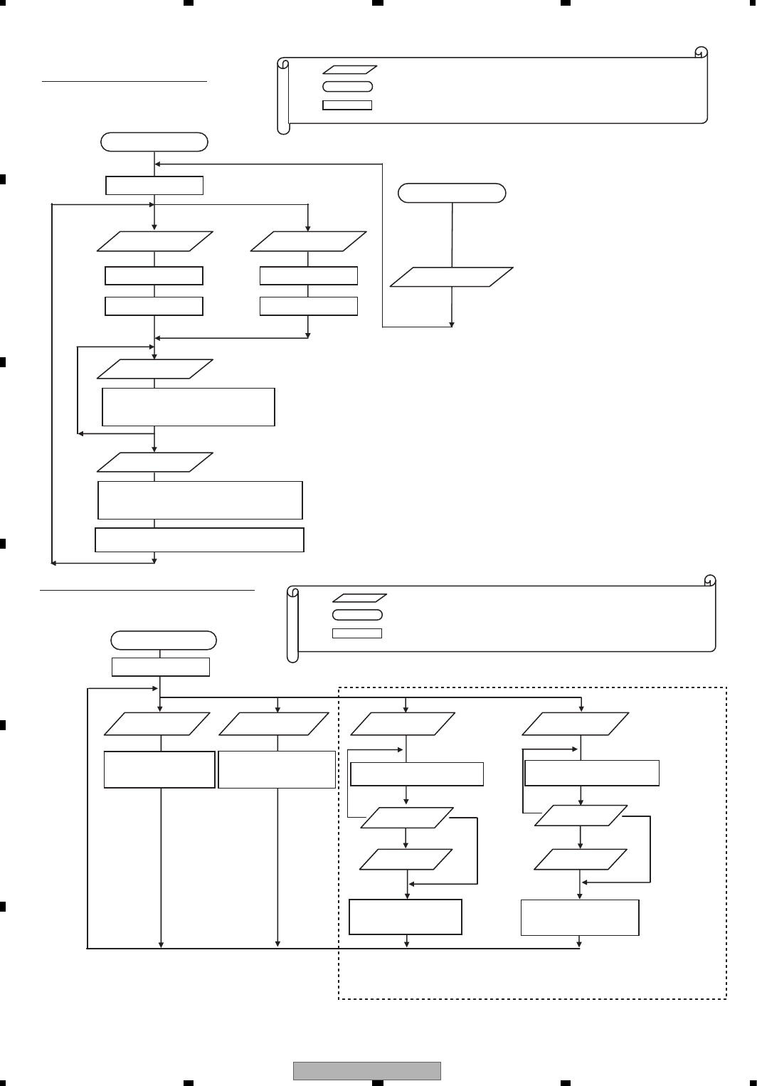
AVIC-X910BT/XS/UC
94
1234
1234
C
D
F
A
B
E
EDC. Image of the test mode
[Note] Image is the same for both EDC1 and EDC2.
(1) (2)
EDC1/2 test mode
0000 0000
Layer 0 selection Layer 1 selection
0000 0000 0100 0000
1003 0000 1103 0000
(5)
[Note] The display is updated at 0.5 seconds interval until 0/1 layer is selected or Eject is effected.
(1)-(4)
ID designation
EDC1/2 start
Layer 0: 10** ****
Layer 1: 11** ****
[Note] ** **** is the ID designation value
Layer 0: 20** ****
Layer 1: 21** ****
[Note] ** **** is the present ID designation value
**** ****
[Note] **** **** is the present ID designation value
Legend: … Key operation
… Operational state
… The content displayed on the DVD mechanism (video only)
8 characters data is sent to the product side (HOST) by UART communication.
[Note] Eject can be effected any time during the EDC test mode.
Eject
After completion of EJECT operation
EJECT operation
Test mode Eject
Image of the LD power on time mode.
LD power on time mode
0000 0000
CD LD power on
time indication
DVD LD power on
time indication
10** ****
[Note] ** **** is the CD LD
power on time.
20** ****
[Note] ** **** is the DVD LD
power on time.
(1) (2)
CD LD power on
time setting
Setting time
designation
30** ****
[Note] ** **** is the setting time.
Setting time
registration
DVD LD power on
time setting
Setting time
designation
40** ****
[Note] ** **** is the setting time.
(5) (6)
(1)-(4) (1)-(4)
(5) (5)
(8)
10** ****
[Note] ** **** is the CD LD
power on time.
Setting time
registration
(8)
20** ****
[Note] ** **** is the DVD LD
power on time.
[Note] If the power on time is 999999 hours or more, it is always reported as 999999 hours.
[Note] If the power on time is “*E** ****”, the value may not be correct due to the life of the flash memory.
[Method of setting time designation]
Designate the digit by command (1) and (2). UP/DOWN of numbers by command (3) and (4).
Fix by command (5). Cancel by command (8).
Legend: … Key operation
… Operational state
… The content displayed on the DVD mechanism (video only)
8 characters data is sent to the product side (HOST) by UART communication.
Not for service use
AVIC-X910BT/XS/UC 95
5678
5678
C
D
F
A
B
E
Side A
COMPOSITE GNDV
The selection of the figure of each screen can be selected by "Key command for the test".
To display following screen, connect the “COMPOSITE” and “GND” line of the LS1 mecha module to a monitor.
Simple test mode
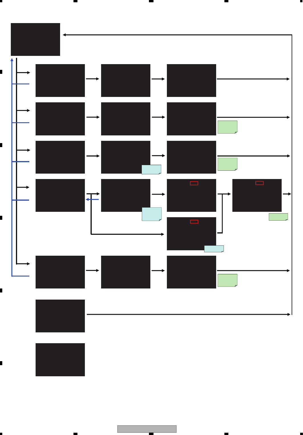
AVIC-X910BT/XS/UC
96
1234
1234
C
D
F
A
B
E
TEST MODE
1: LD ON
2: ASMAX
3: Skew Adjustment
4: Error Rate
5: CRG Move Outer
6: Eject
Please Input Number
NODLNODLNODL
1: DVD Single Layer 1: Power OFF
2: DVD Dual Layer
3: CD
4: CD-RW
5: Return
rebmuNtupnIesaelPgninnuRwoNrebmuNtupnIesaelP
XAMSAXAMSAXAMSA
1: DVD Single Layer 1: Power OFF
2: DVD Dual Layer
3: CD
4: CD-RW
5: Return ASMAX Level : 000000
rebmuNtupnI
esaelPgninnuRwoNrebmuNtupnIesaelP
tnemtsujdAwekStnemtsujdAwekStnemtsujdAwekS
1: DVD Single Layer 1: Power OFF
5: Return RF Level : 000000
rebmuNtupnIesaelPgninnuRwoNrebmuNtupnIesaelP
rennI-etaRrorrErennI-etaRrorrEetaRrorrEetaRrorrE
tnemerusaeMrennI:1reyaLelgniSDVD:1 1: Power OFF
2: Outer Measurement
tneme
rusaeM
elddiM:3DC:3
nruteR:5nruteR:5 Error Rate : 000000
NtupnI
es
aelPgninnuRwoNreb
m
uNtupnIesaelPrebmuNtupnIesaelP umber
*1 : The position in which
select was done is
displayed.
Error Rate
-
CD
DVD Inner
DVD Outer
DVD Middle
CD CD
Now Running
retuOevoMGRCretuOevoMGRCretuOevoMGRC
1: DVD Single Layer 1: Power OFF
2: DVD Dual Layer
3: CD
4: CD-RW
5: Return
rebmuNtupnIesaelPgninnuRwoNrebmuNtupnIesaelP
ERROR
1: Power OFF
Code : 00000000
Please Input Number
ERROR
Code : 00000000
Please Reset
1 select
2 select
3 select
4 select
select LD ON
Completion
select
ASMAX
value set
value set
select
RF Level
DVD select select
Error Rate
set select
select
select
select
select
ASMAX
Level display
Error Rate
display
RF Level
display
Update 500 msec.
*1
CD select
*1
*1
Search ID
0x00100000
Search ID
inner :
0x00040000
outer :
Search CRG
home position
5 Return select
5 Return select
5 Return select
5 Return select
5 Return
select
5 select
select select
CRG moves
to the most
outer
5 Return select
CRG Move
Completion
0 0020000
0
<Flow chart>
<Error>
<Error : Power OFF>
AVIC-X910BT/XS/UC 97
5678
5678
C
D
F
A
B
E
6.3 uBOOT MENU
UBOOT Upgrade
1. Copy the Uboot files named as “uboot.bin” and “uboot.cks” to the SD/MMC card
2. Inset SD/MMC card to the Main Unit at first, then enter the Uboot interface.
3. Select ““3=UBOOT Upgrade” item in Uboot menu, then select ““1=UBOOT by SD/MMC” item
in “UBOOT Upgrade” menu and execute.
UBOOT Upgrade
0=WINCE Upgrade 0=UBOOT by USB
1=GPS Tools 1=UBOOT by SD/MMC
2=BT Tools 2=Exit
3=UBOOT Upgrade Choice: 1
4=Memory Tools
5=Other Tools
Coice: 0
<Uboot Menu> <UBOOT Upgrade Menu>
UBOOT Upgrade UBOOT Upgrade
0=UBOOT by USB 0=UBOOT by USB
1=UBOOT by SD/MMC 1=UBOOT by SD/MMC
2=Exit 2=Exit
Choice: 1 Choice: 1
Star Erase & Write UT!!
UT Upgrade O
K
Star Erase & Write UT!! Please restart your device!!
Read Progress : 31% Read process 100%
<UBOOT Upgrade Menu:Progress Screen> <UBOOT Upgrade Menu:Finish Screen>
4. After the menu of “UBOOT Upgrade” show “UT Upgrade OK”, restart the device.
WINCE Image Upgrade
1. Copy the image files named as “winceimg.bin” and “winceimg.cks” to the SD/MMC card.
2. Inset SD/MMC card to the Main Unit at first, then enter the Uboot interface.
3. Select “0=WINCE Upgrade” item in Uboot menu, then select “1=WINCE b
y
SD
/
MMC” item
in “WINCE Upgrade” menu and execute.
WINCE Upgrade
0=WINCE Upgrade 0=WINCE by SD/MMC (Format)
1=GPS Tools 1=WINCE by SD/MMC
2=BT Tools 2=WINCE by USB (Format)
3=UBOOT Upgrade 3=WINCE by USB
4=Memory Tools 4=Exit
5=Other Tools Coice: 1
Coice: 0
<Uboot Menu> <WINCE Upgrade Menu>
WINCE Upgrade WINCE Upgrade
0=WINCE by SD/MMC (Format) 0=WINCE by SD/MMC (Format)
1=WINCE by SD/MMC 1=WINCE by SD/MMC
2=WINCE by USB (Format) 2=WINCE by USB (Format)
3=WINCE by USB 3=WINCE by USB
4=Exit 4=Exit
Coice: 1 Coice: 1
Image Region
Checksum = 0x64463447
Read Progress : 31% CE Upgrade OK
Please restart your device!!
<WINCE Upgrade Menu:Progress Screen> <WINCE Upgrade Menu:Finish Screen>
4. After the menu of “WINCE Upgrade” show “CE Upgrade OK”, restart the device.
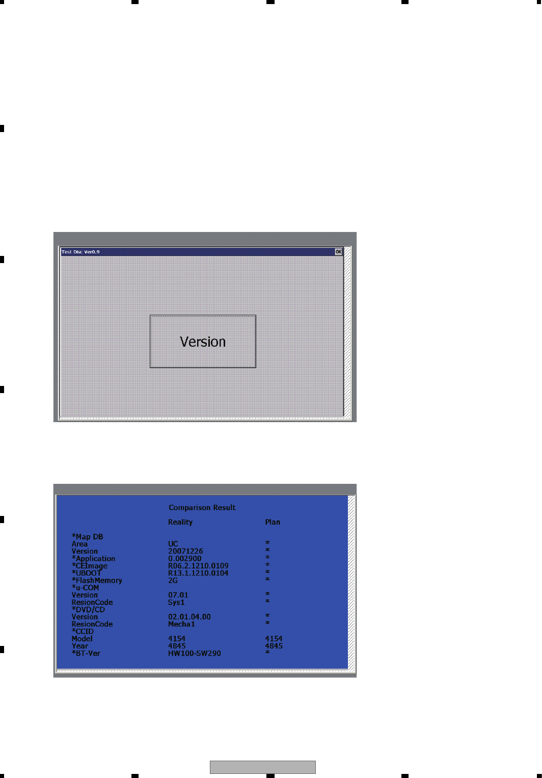
AVIC-X910BT/XS/UC
98
1234
1234
C
D
F
A
B
E
6.4 USING THE TEST DISC
Test Disc 1 Start Screen Specification
Test Disc 1 Start
1. Copy all files under “Test Disc1” folder on GGV1322 to a SD card.
2. Download a ID file from the Service Site and copy the file to the SD card.
3. Insert the SD card into the Main Unit and turn ACC OFF ON. Then, the test disc starts.
The test can be terminated by turning ACC OFF. After turning ACC OFF, remove the SD card.
Test Disc 1 Start Screen
Jig No : GGV1322
Version Check
<< Operation method >>
1. This screen appears when the Test Disc is activated.
2. When ‘Version’ is tapped, the test starts.
If the "Reality" corresponds to "Plan", the result becomes "OK".
<< Operation method >>
If the test result is "OK", the blue screen is displayed.
"Reality" is each version on actual machine and the "Plan" is the version information
described in "Information.txt" of SD card.
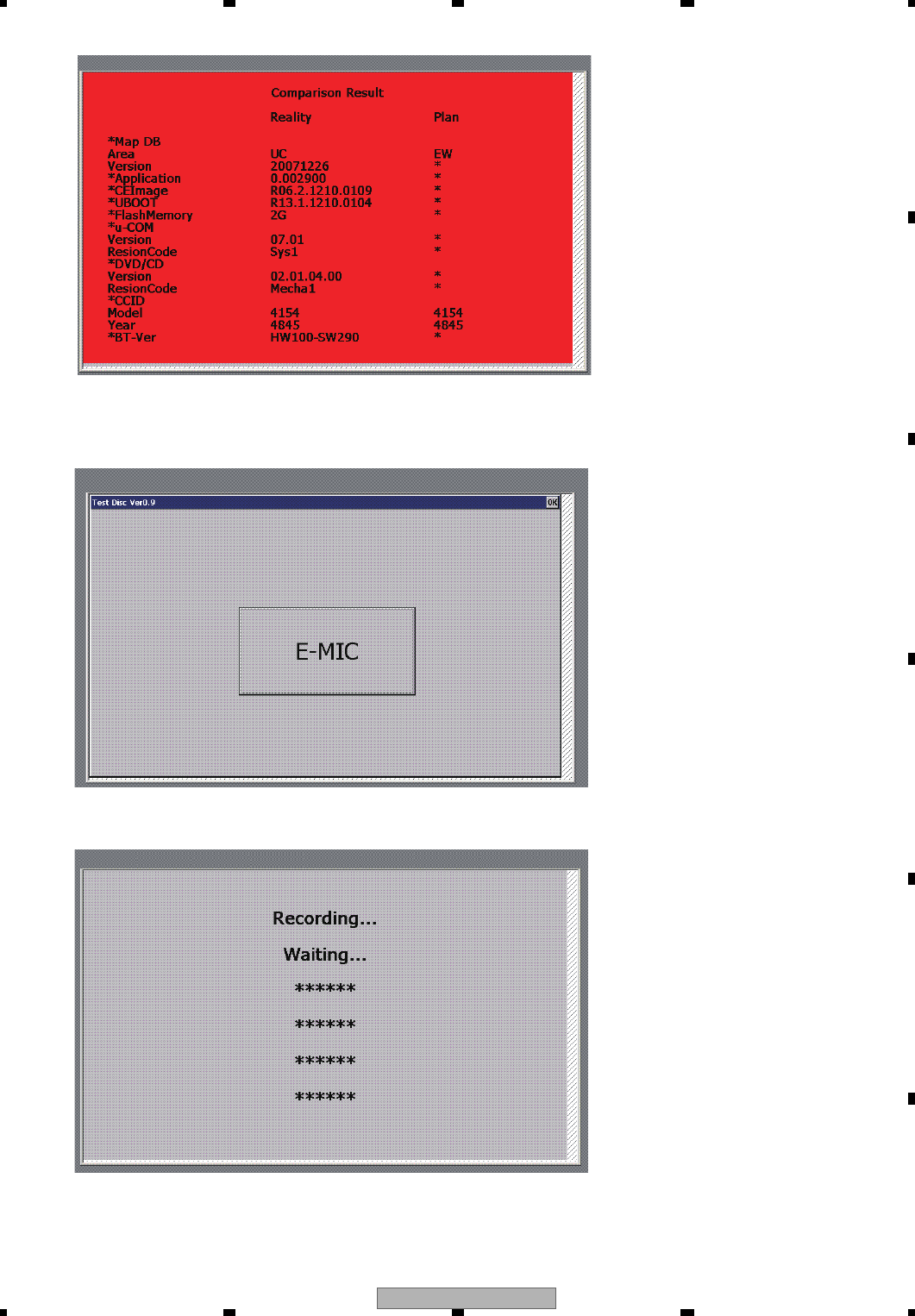
AVIC-X910BT/XS/UC 99
5678
5678
C
D
F
A
B
E
<< Operation method >>
If the test result is "NG", the red screen is displayed.
<< Operation method >>
1. This screen appears when the Test Disc is activated.
2. Tap ‘E-MIC’ to start the test.
<< Operation method >>
1. This screen appears when the test is started.
2. Put a sound into the microphone while this screen is shown. The sound is recorded.
MIC Test
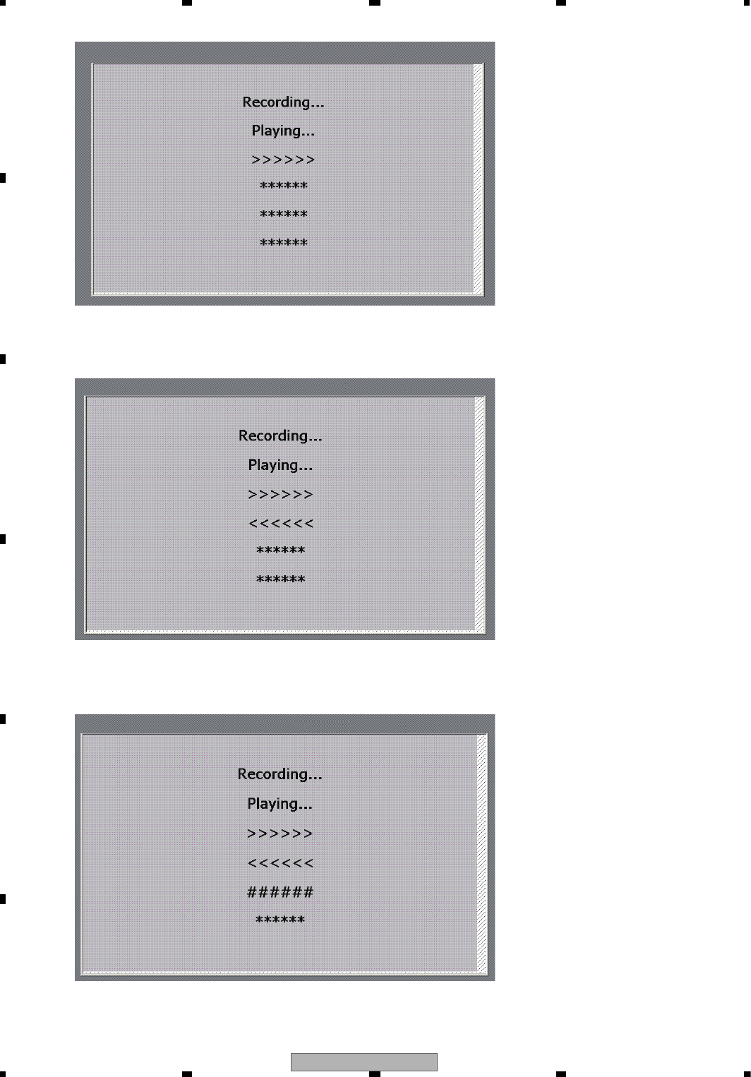
AVIC-X910BT/XS/UC
100
1234
1234
C
D
F
A
B
E
<< Operation method >>
1. When this screen appears, the recorded sound is played ‘loudly’.
Notes) The sound volume cannot be adjusted.
<< Operation method >>
1. When this screen appears, the recorded sound is played ‘quietly’.
Notes) The sound volume cannot be adjusted.
<< Operation method >>
1. When this screen appears, the recorded sound is muted.
Notes) The sound volume cannot be adjusted.

AVIC-X910BT/XS/UC 101
5678
5678
C
D
F
A
B
E
<< Operation method >>
1. When the test finishes, this screen appears.
2. To proceed to the next test, tap ‘OK’. To conduct MIC Test again, tap ‘Retry’.
<< Operation method>>
1. This screen appears when the Test Disc is activated.
If you tap "GPS_TTFF", the test is started.
GPS Test
<< Operation method >>
1. When the test is started, this screen is displayed.
When you terminate the test in the way, tap the "Exit".

AVIC-X910BT/XS/UC
102
1234
1234
C
D
F
A
B
E
<< Operation method >>
When the positioning is terminated within one minute, the test is completed successfully,
and this screen is displayed.
If you implement the test again, tap the "Retry".
If you go to next step, tap "OK".
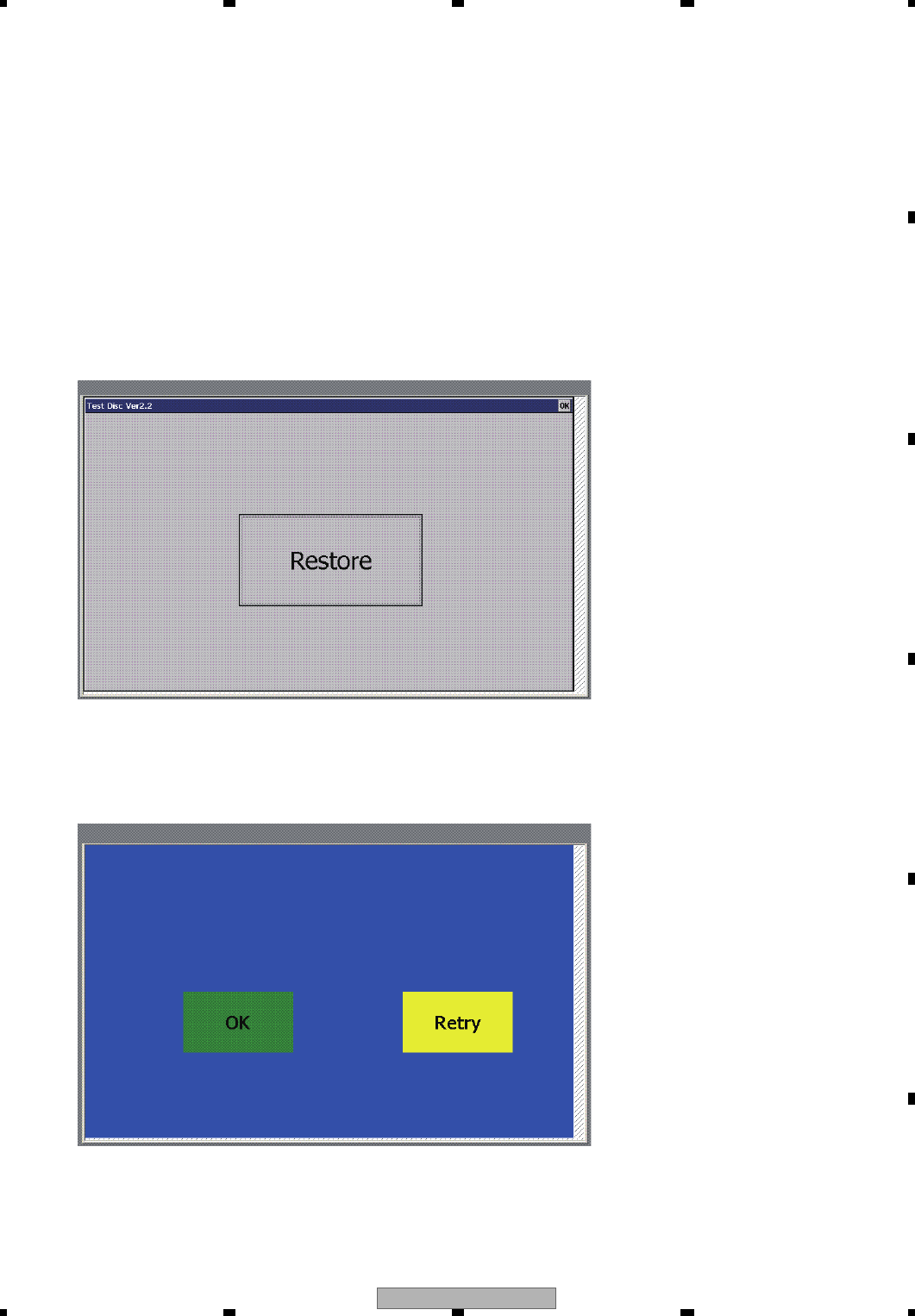
AVIC-X910BT/XS/UC 103
5678
5678
C
D
F
A
B
E
Test Disc 2 Start Screen Specification
Test Disc 2 Start
1. Copy all files under “Test Disc 2” folder on GGV1322 to a SD card.
2. Download a ID file from the Service Site and copy the file to the SD card.
3. Insert the SD card into the Main Unit and turn ACC OFF ON. Then, the test disc starts.
The test can be terminated by turning ACC OFF. After turning ACC OFF, remove the SD card.
Test Disc 2 Start Screen
The user data is deleted
<< Operation method >>
1. This screen appears when the Test Disc is activated.
2. If you tap the "Restore", the user data is deleted.
<< Operation method >>
If the deletion is terminated, this screen is displayed.
Jig No : GGV1322
Notes:) "Splash screen setting" is not back to default after performing this function.
Please set the "Splash screen setting", before performing this function.
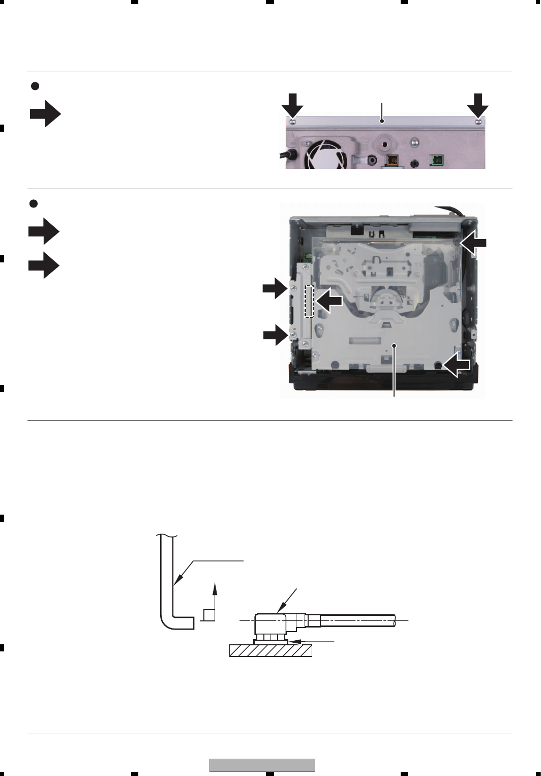
AVIC-X910BT/XS/UC
104
1234
1234
C
D
F
A
B
E
7. DISASSEMBLY
11 1
Fig.1
Removing the Case (Fig.1)
Remove the two screws and then remove
the Case.
Note)
To remove the screws, use jig No. GGK1068.
Case
NOTE) While the photograph shown is slightly different from this model in shape, the disassembly
procedure is the same.
1
2
1
1
1
1
2
Fig.2
Remove the four screws.
Disconnect the connector and then
remove the DVD Mechanism Module.
Removing the DVD Mechanism Module (Fig.2)
DVD Mechanism Module
When unplugging the cord assy, make sure to use jig GGF1539.
If the antenna cable is directly unplugged without using jig GGF1539, you might damage your fingertip or fingernail.
- How to Remove the Cord Assy
When unplugging cord assy, hook the point of jig GGF1539 on the lid of cord assy and vertically draw out
along with the engagement axis of connector.
- How to Attach the Cord Assy
For inserting cord assy, adjust cord assy with the engagement axis of connector and insert it as vertically
as possible.
Do not insert the cord assy in extreme slant, as the connector might suffer damage.
Connector
Cord Assy
GGF1539
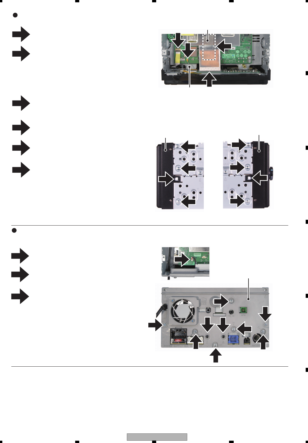
AVIC-X910BT/XS/UC 105
5678
5678
C
D
F
A
B
E
1
2
Fig.4
Disconnect the FAN Cord.
Remove the two screws.
Remove the seven screws
and then remove the Heat sink.
Removing the Heat sink (Fig.4)
1
2
3
(Right side)
6
5
5
5
6
5
5
5
(Top side)
(Left side)
Fig.3
Removing the Monitor Assy (Fig.3)
Peel off the Mylay tape.
Disconnect the FFC.
Attention when assembling:
Please fix the FFC (CDE9039) with
the Mylar tape (GYH1031) as shown in figure.
Disconnect the Cord Assy using GGF1539.
Disconnect the FFC.
Remove the six screws.
Release the two latches
and then remove the Monitor Assy.
Monitor Assy
Monitor Assy
Mylay tape
1
2
4
3
Cord Assy
4
3
1
22
3
3
33
3
3
5
6
Heat sink
3
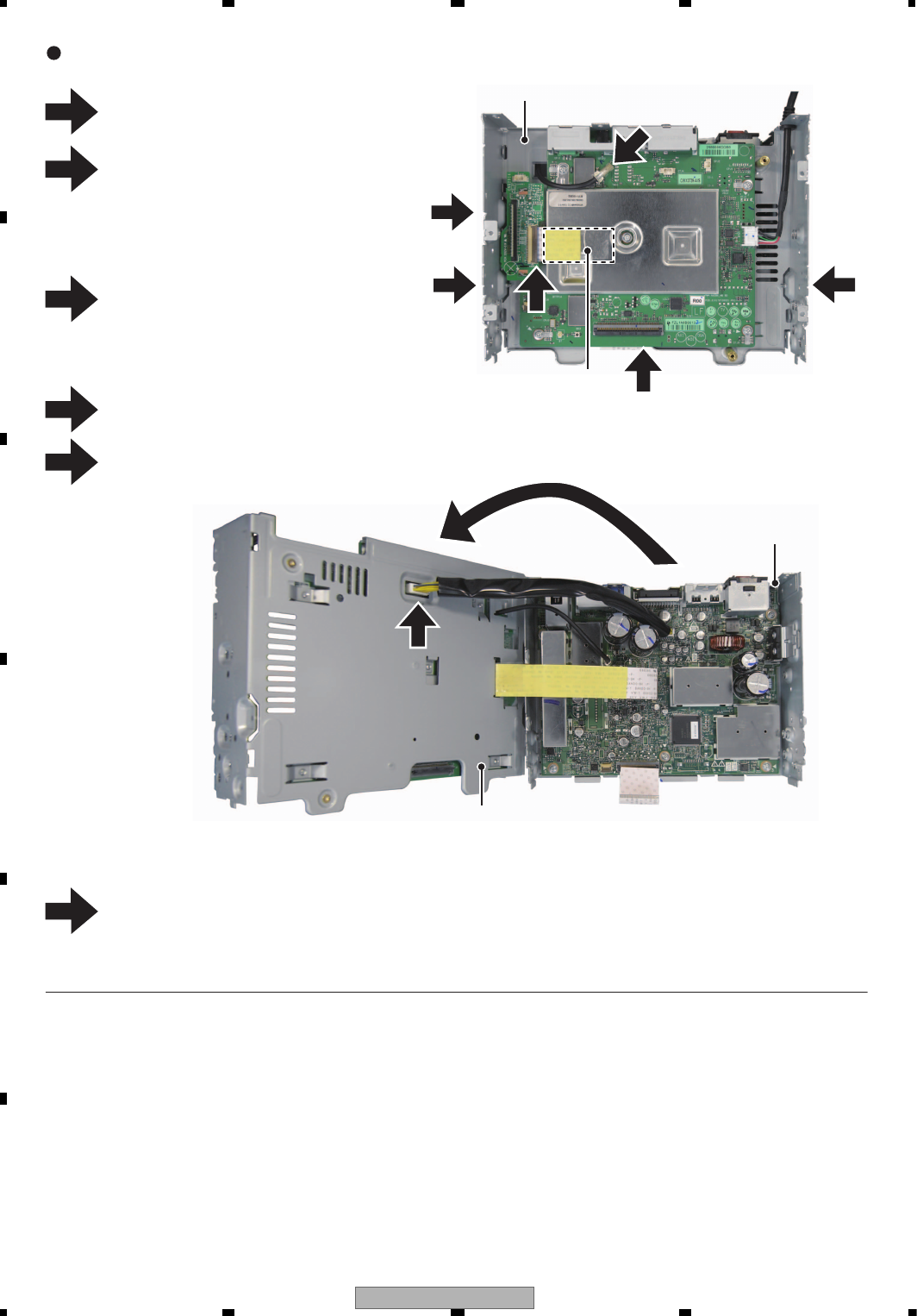
AVIC-X910BT/XS/UC
106
1234
1234
C
D
F
A
B
E
1
2
3
6
4
5
Fig.5
Peel off the Mylay tape.
Disconnect the FFC.
Attention when assembling:
Please fix the FFC (CDE8912) with
the Mylar tape (GYH1031) as shown in figure.
Disconnect the Cord.
Attention when assembling:
The connector is inserted in the direction of figure.
The cable is not loosened and pushed below.
Remove the FFC.
Remove the three screws and then
left the Chassis(Upper) from right side.
Separating the upper and lower chassis. (Fig.5)
Chassis(upper)
Chassis(Upper)
Chassis(lower)
Mylar tape
3
2
4
5
55
6
Disconnect the Cord Assy
and then remove the Chassis(Upper).
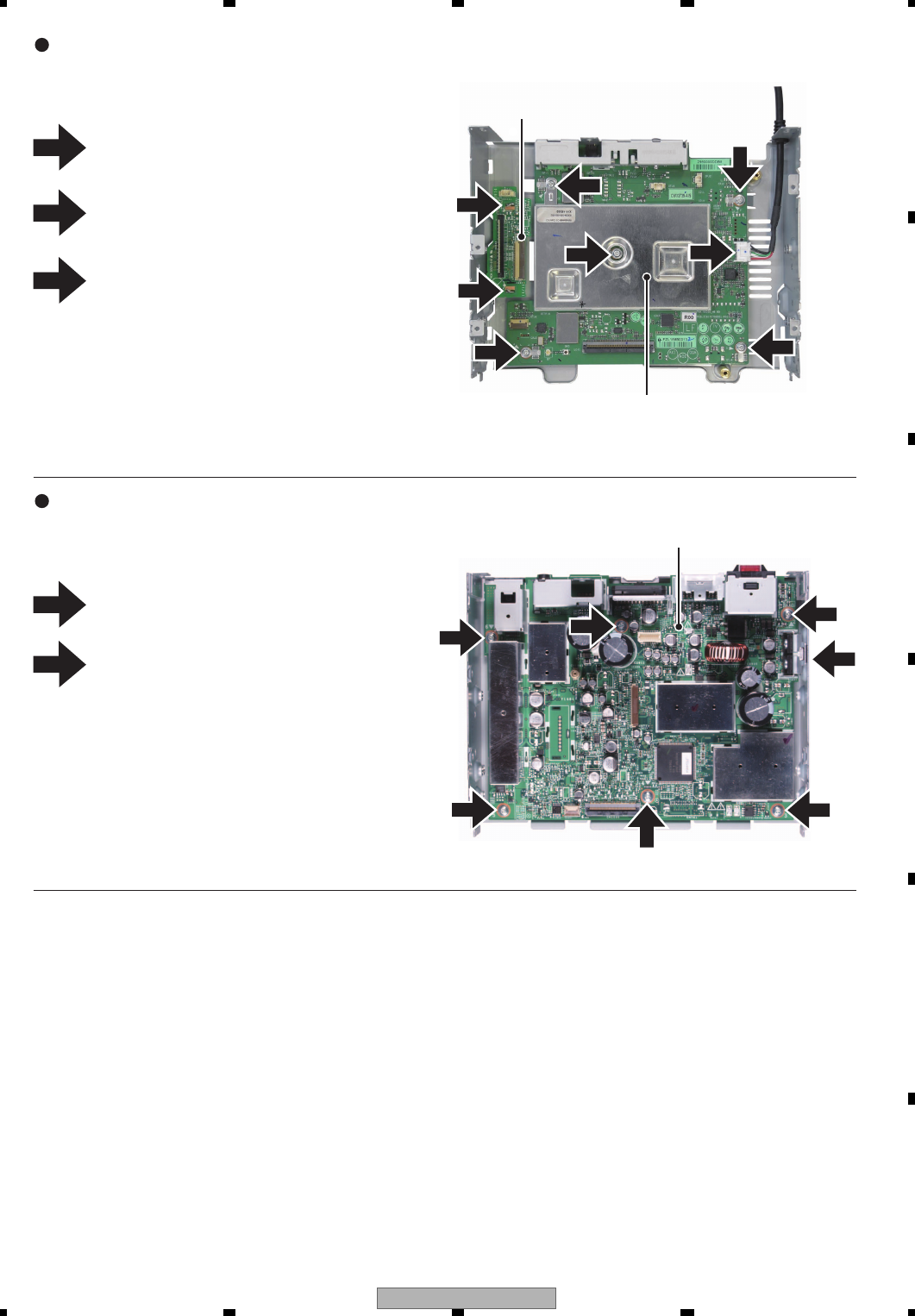
AVIC-X910BT/XS/UC 107
5678
5678
C
D
F
A
B
E
1
2
3
Remove the six screws.
Fig.6
Straighten the tabs at two locations indicated
and then remove the CK Unit.
Disconnect the Cable.
Remove the five screws and then
remove the Navi Unit.
Removing the CK Unit and the Navi Unit (Fig.6)
AV Unit
Navi Unit
CK Unit
Removing the AV Unit (Fig.7)
1
Remove the screw and then remove
the AV Unit.
2
Fig.7
1
1
2
3
3
3
3
3
1
1
1
1
2
1
1
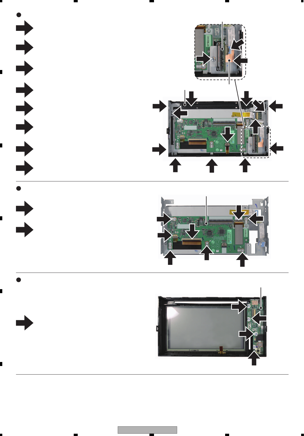
AVIC-X910BT/XS/UC
108
1234
1234
C
D
F
A
B
E
1
2
3
1
2
1
Fig.8
Fig.10
Removing the SD Unit and LCD Module Assy (Fig.8)
Removing the Panel Unit (Fig.9) Panel Unit
Disconnect the three cables.
Remove the five screws and then remove
the Panel Unit.
Peel off the Insulator.
Disconnect the FFC.
Remove the screw and then remove
the SD Unit.
Disconnect the two cables.
Remove the two screws and the Holder and
Cover.
Remove the four screws.
Release the two latches using Tweezers.
Release the three latches and then remove
the LCD Module Assy.
SD Unit
Insulator
1
2
3
6
6
6
6
7
7
888
4
5
6
4
55
7
8
Removing the Keyboard Unit (Fig.10)
Fig.9
Keyboard Unit
Remove the four screws and then remove
the Keyboard Unit.
1
1
2
2
2
2
1
2
1
1
1
1
4
Holder and Cover
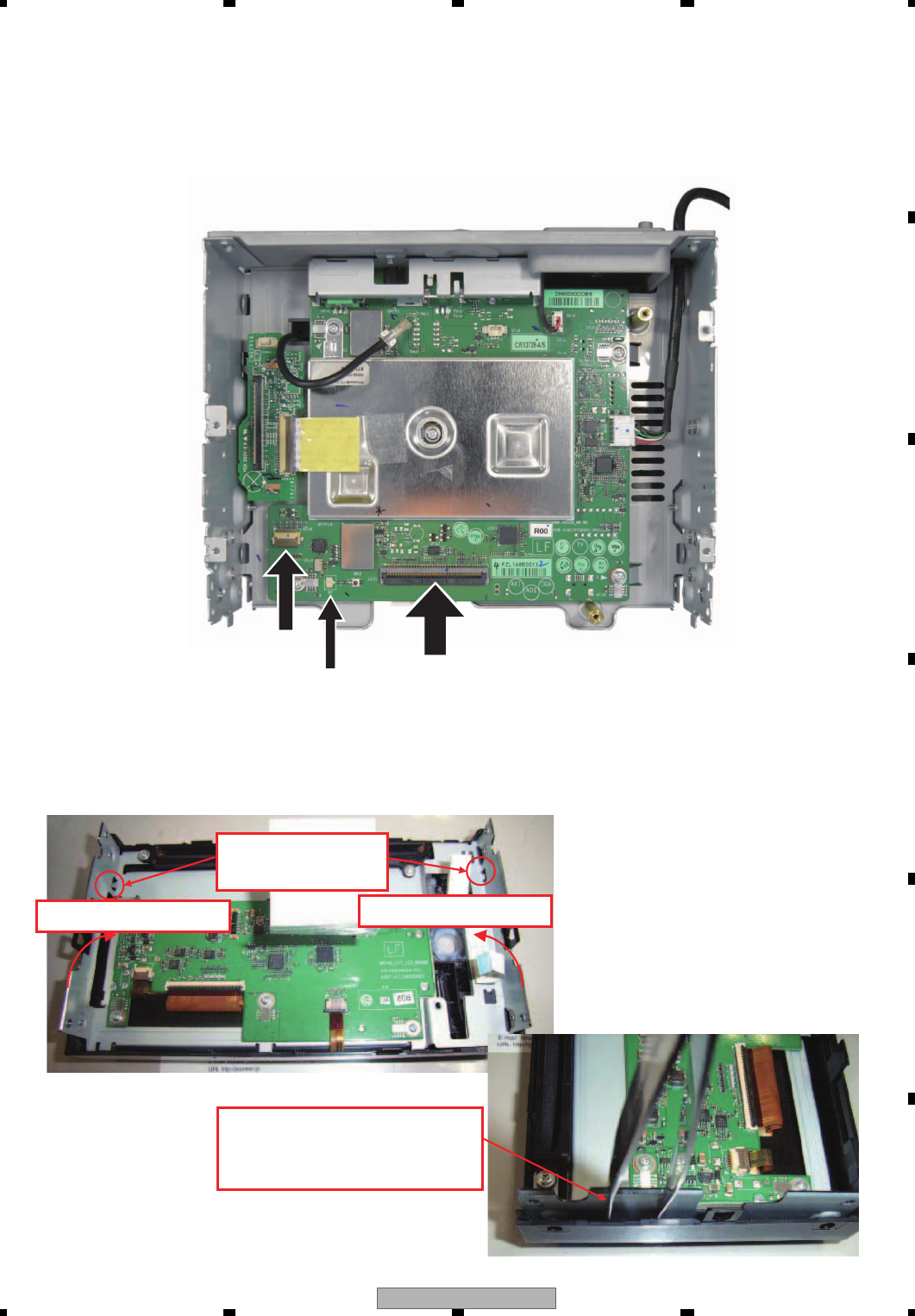
AVIC-X910BT/XS/UC 109
5678
5678
C
D
F
A
B
E
• Notes on disassembly
• When separating the MONITOR ASSY from the MAIN UNIT ASSY, do so slowly.
Two FFCs (CDE9037, CDE9039) and one CODE ASSY (CDE8559) are connected. The strength of the joint part
of the code and terminals of CDE8559 (CODE ASSY for Bluetooth to connect the keyboard unit and navi unit)
is weak, it may break or the code may extend.
Remove after peeling off the tape of CDE9039 and the shield.
• When demounting LCD PANEL ASSY from the grille, be careful not to bend LCD plate (CND4319) as there are
snap fits on the right and left. Demount LCD PANEL ASSY by extending snap fits on the grille side.
CDE8559
Snap fit
2 place
Do not bend CND4319
Remove snap fits by extending
them on the grille side using
tweezers or bamboo tweezers.
Do not bend CND4319
Actually does the CODE ASSY (CDE8559) to a left connector of a round inclosing.
*
CDE9037
CDE9039
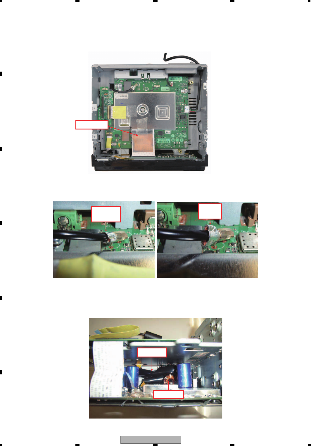
AVIC-X910BT/XS/UC
110
1234
1234
C
D
F
A
B
E
• Be sure to remove the MONITOR ASSY after removing the DVD mecha.
If the procedure is done oppositely, the FFC (CDE9039) connecting the MONITOR ASSY and the MAIN UNIT
ASSY will be damaged. At assembly, be sure to fix the MONITOR ASSY first and then fix the DVD mecha. If it is
done oppositely, the FFC (CDE9039) cannot be folded as intended under the DVD mecha.
• When connecting the code assy connecting 1F AV UNIT and 2F NAVI UNIT (CDH1381) on NAVI UNIT side, do
so as shown below.
• The code assy connecting 1F AV UNIT and 2F NAVI UNIT (CDE8393) shall be fitted on the back side of the
choke coil (CTH1347) after 1F Chassis Unit and 2F Chassis Unit are fixed, as shown below.
CDE9039
OK
Horizontal
NG
Vertical
CDE8393
CTH1347
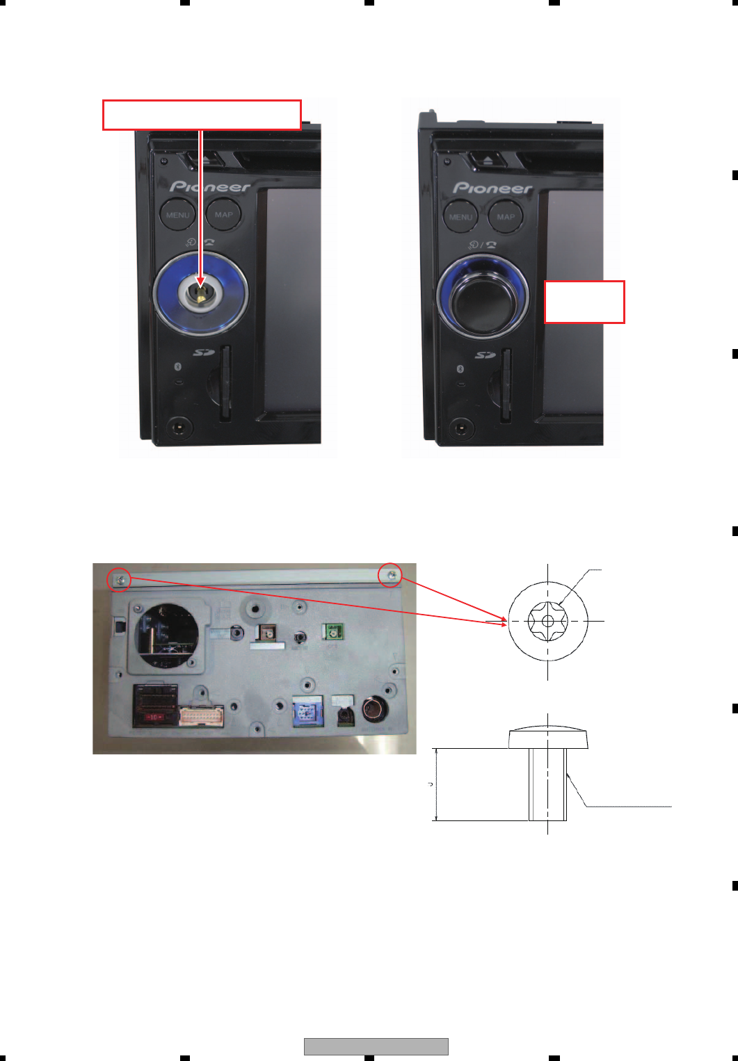
AVIC-X910BT/XS/UC 111
5678
5678
C
D
F
A
B
E
• When mounting KNOB ASSY (CXE1633) in the MONITOR ASSY, be careful to don't destroy
encoder part.
• Since two case (CNB3472) fixing screws are ‘TORX tamper’ (tamper-proof screws with a projection in
TORX), a special tool is required.
TORX screwdriver(T8) : GGK1068
CSX1135 shaft of an encoder
CXE1633
Mark 1 (T8 size)
M2.6 thread
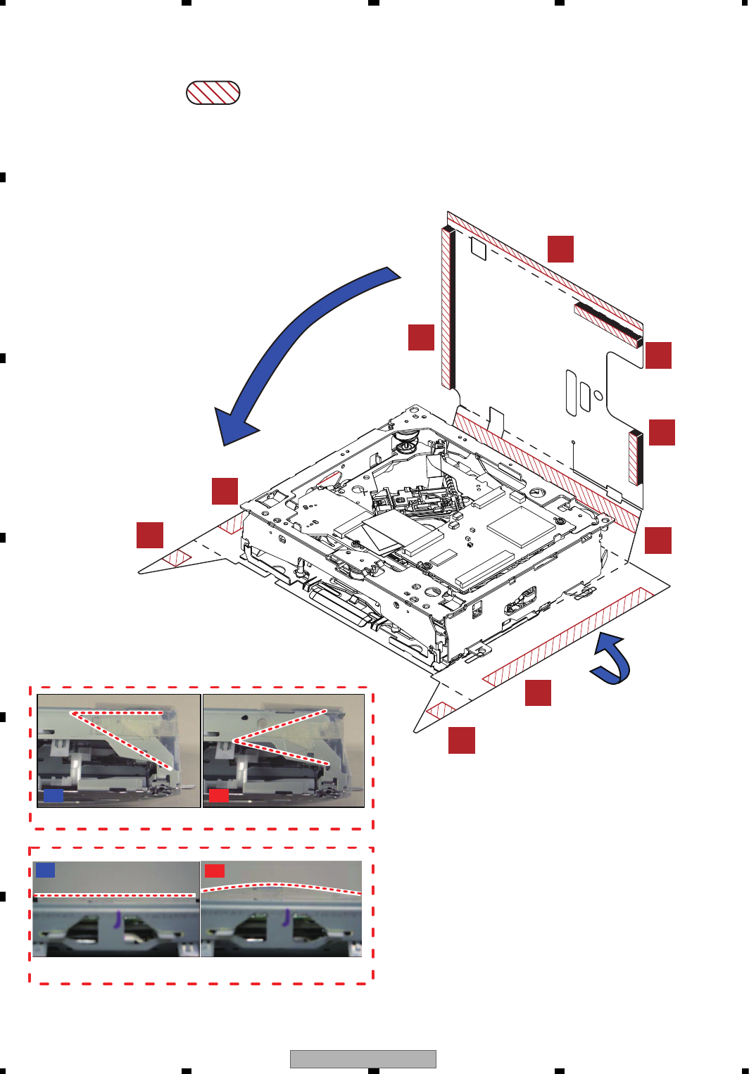
AVIC-X910BT/XS/UC
112
1234
1234
C
D
F
A
B
E
Peel off release liners at areas.
Sticking procedure of the insulator
1: Fit the 2 hooks on the LS1 mech temporarily to the insulator.
2: Peel off 9 release liners.
3: Stick A to F in this order.
(Stick both sides at once except for B and D.)
B: Sick one by one.
D: Stick the left side first and then stick the right side
as pulling the insulator to the right.
- How to install the Insulator to LS1 Mechanism Module.
A
A
B
BC
D
D
E
F
Left side
Right side
Keep the insulator off the slot at point B.
OK NG
Stick the insulator fast at point D.
OK NG
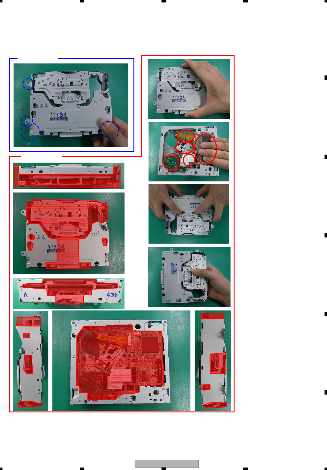
AVIC-X910BT/XS/UC 113
5678
5678
C
D
F
A
B
E
1.Have a specified part.
Handling OK
Handling NG
How to have it
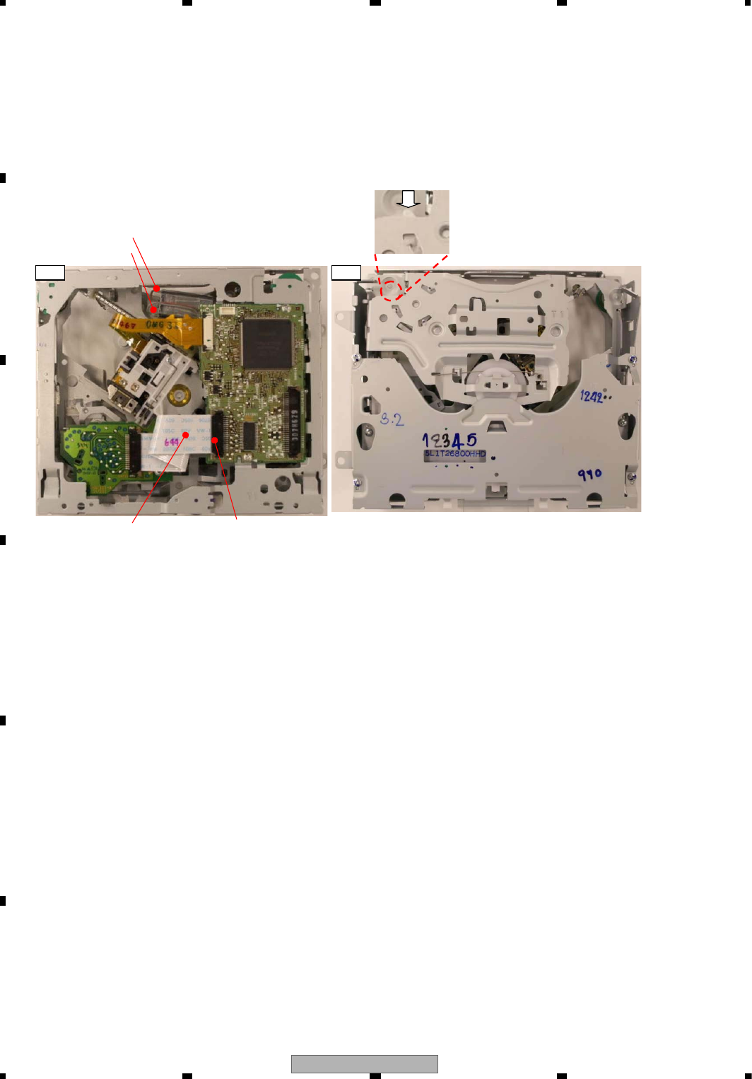
AVIC-X910BT/XS/UC
114
1234
1234
C
D
F
A
B
E
Connector (relay FFC)
Relay FFC
Fig. 1 Fig. 2
GND the brown line
4V to the gray line
Mecha Module_Bringing into the Clamp State with No Disc Loaded
1. Remove the relay FFC from the connector on the module PCB side (Fig. 1).
(Precaution) When it is difficult to apply 4V to the motor in procedure 2 below, remove the connector on the relay
PCB side, then remove the FFC, and remove the solder of the CRG motor lead and apply voltage to the lead.
2. Push the Disc detection arm while applying 4V to the CRG motor (Fig. 2)
By this action, the mecha moves to the clamp state and the PU moves to the outer periphery.
3. Stop the motor when the PU comes to the vicinity of the intermediate periphery.
(Precaution) If the PU goes to the outer most periphery, it idles.
It is not a problem, but please try not to let it idle as much as possible.
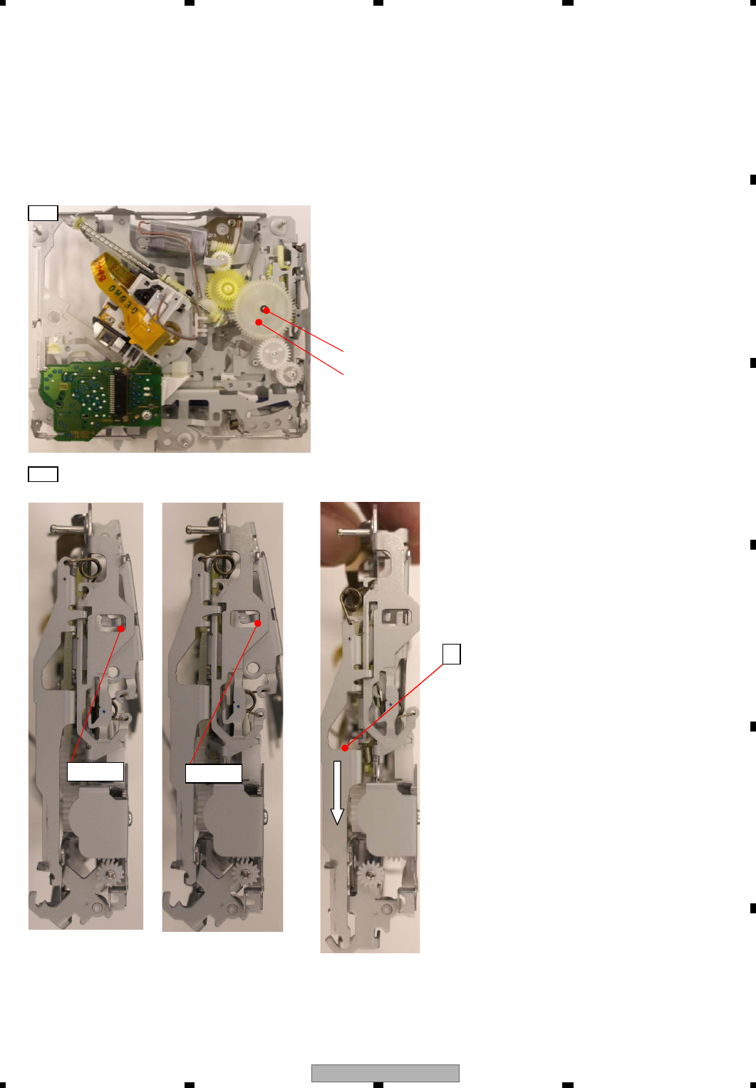
AVIC-X910BT/XS/UC 115
5678
5678
C
D
F
A
B
E
T-case washer
Drive gear
Fig. 1
Fig. 2
b.Open-lock state
There is a
space There is
no space
c.Clamp state with no disc loaded
A
CRG Mecha_Bringing into the Clamp State with No Disc Loaded
1.Remove the T-case washer and then remove the drive gear. (Fig. 1)
2.Lift the clamp arm assy until it is in the state shown in Fig. 2_b (open-lock state).
3.Put your finger on the area A of Fig. 2_c and then slide it to the direction of the arrow (the direction of the playing state).
4.Push down the clamp arm.
(Precaution) When bringing the CRG mecha into the ejecting state again, install the drive gear after sliding the drive
lever and bringing it to the ejecting state, in order to prevent the cog of the pinion in the drive gear from chipping at the
time of its installation.
a.Ejecting state
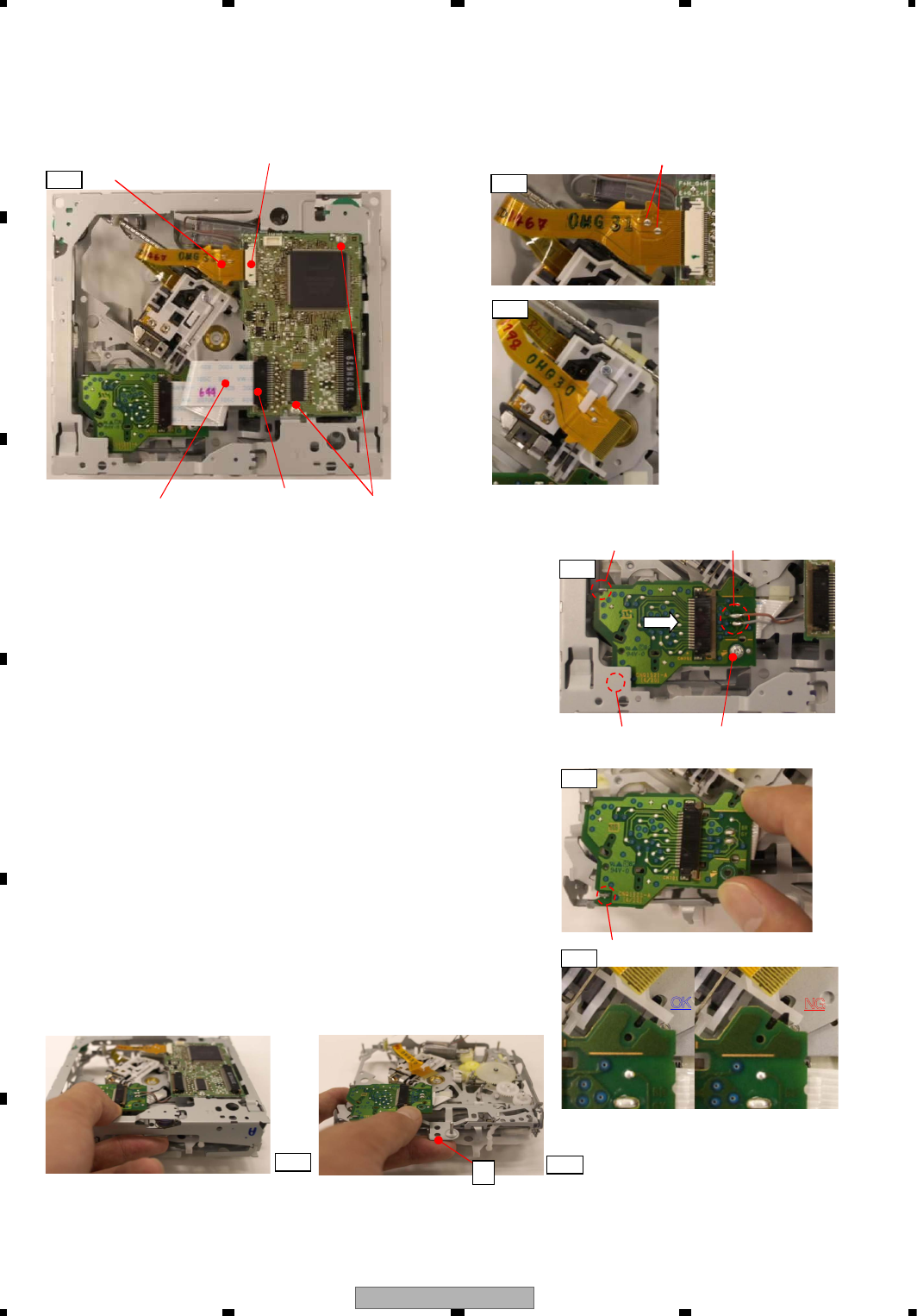
AVIC-X910BT/XS/UC
116
1234
1234
C
D
F
A
B
E
Connector (pick up FPC)
Connector
(Relay FFC)PCB clinch screw
Short-circuit
Fig.1
Fig. 2
Fig.3
Pick up FPC
Relay FFC
Fig. 4
Solder on the lead
Relay PCB clinch screw
Hook A
Hook B
Fig. 5
Hook B
Fig. 6
OK NG
Fig. 7 Fig. 8
A
Removing the Module PCB
1.Short-circuit two spots on the land of the pick up FPC. (Fig. 1)
2.Remove the pick up FPC and the relay FFC from the connector. (Fig. 2)
3.Temporarily attach the pick up FPC to the pick up rack. (Fig. 3)
(in order to prevent the damage to the pick up FPC)
4.Remove the two PCB clinch screws and then remove the module PCB. (Fig. 2)
Removing/Installing the Relay PCB
Removing)
1.Remove the relay FFC from the connector
(remove both sides so that the entire FFC will be removed). (Fig. 2)
2.Remove the solder on the lead for the CRG motor. (Fig. 4)
3.Remove the one relay PCB clinch screw. (Fig. 4)
4.Slide the relay PCB to the direction of the arrow and then remove
the relay PCB from the hook A and the hook B. (Fig. 4)
5.Turn the relay PCB over and then remove the SPDL motor FFC
from the connector.
Installing)
1.Check the mecha is in the ejecting state (disc-load suspended state).
When it is not in the ejecting state, apply 4V to the lead (motor) and then
bring it to the ejecting state (4V to the brown line and GND the gray line).
2.Fit the SPDL motor FFC to the connector (back of the relay PCB).
3.Hold the relay PCB so that it does not touch the SW knob as in Fig. 5.
4.Insert it into the hook B as it is a little off to the clockwise direction.
(Precaution) This is to prevent the SW knob from getting into the NG
position as in Fig. 6.
5.Push down the relay PCB lightly and then rotate it to the
counterclockwise direction.
It sets the relay PCB in the hook A and the positioning dowel.
(Precaution) Pay attention so the SW knob will not get onto the PU rack.
(Fig. 6)
6.As in the Figures, while supporting the location A with your fingers,
screw the relay PCB. (Fig. 7 / Fig. 8)
7.Solder the lead for the CRG motor.
8.Fit the relay FFC to the connector.
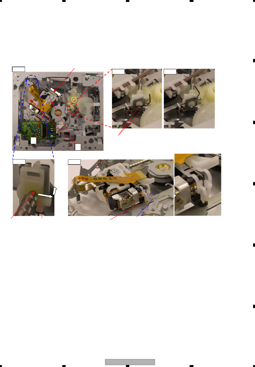
AVIC-X910BT/XS/UC 117
5678
5678
C
D
F
A
B
E
Fig. 2a
Permanently hooked position Temporary hooked position
Fig. 2b
A
Slide to the direction of inner periphery
Fig. 1
Fig. 3
B
Fig.4
Regularly installed position Install avoiding the
area with blue broken
line (the connected
metal plate part)
The spring is installed under the resin flange and inside
the bended metal plate.
Outside holder
Back end of
the feed screw
Removing the PU Unit
1.Hook the feed screw biasing spring on the temporary hook (Fig. 2b). Be careful not to get injured by the tip of the spring.
2.Hold the PU at the location A in Fig. 1 and slide and scoot it to the direction of the inner periphery.
3.As in Fig. 3, shift the back end of the feed screw to the side and then to above and remove it from the outside holder.
4.Remove the tucking joint for the chassis at the location B and the PU unit by lifting them up without changing their
position and then remove the PU unit.
(Precaution) When installing the PU again, make sure to tuck the chassis in B and the PU unit (Fig. 4) first.
Moreover, do not forget to permanently hook the feed screw biasing spring (Fig. 2a).
Adjustments to the PU after its installation should be made according to the service manual.
Sending the PU to the outer periphery
1.Bring to the clamp state with no disc loaded according to the “Mecha Module_Bringing into the Clamp State with
No Disc Loaded” manual.
(Precaution) The relay FFC must be removed for certainty in order to prevent the IC damage.
2.Apply 1.5V to the CRG motor and then transfer the PU to the outer periphery.
(Precaution) Do not forget to reinstall the relay FFC after sending the PU to the outer periphery and take the
necessary measures.
[Installation NG]
The chassis is not tucked
between the PU case and the
PU rack.

AVIC-X910BT/XS/UC
118
1234
1234
C
D
F
A
B
E
8. EACH SETTING AND ADJUSTMENT
8.1 DVD ADJUSTMENT
1) Precautions
This product uses 5 V and 3.3 V as standard voltages.
The electrical potential that is the reference for signals,
is not GND, but VREF (approximately 2.2 V) and VHALF
(approximately 1.65 V) .
During product adjustments, if the reference voltage is
mistakenly taken as GND, and a grounding contact is
made, not only would it be impossible to measure the
accurate electrical potential, but also the servo motor
would malfunction, resulting in the application of a
strong impact on the pick up. The following precautionary
measures should be strictly adhered to, in order to
avoid such problems.
The reference voltage and GND should not be confused
when using the minus probe of a measurement device.
When an oscilloscope is being used special care should
be taken to make sure that the reference voltage is not
connected to the probe of ch1 (on the minus side),
while the probe of ch2 (on the minus side), is connected
to GND. Further, since the body frame of most measurement
devices have the same electrical potential as
the minus side of the probe, the body frame of the
measurement device should be set to floating ground.
If the reference voltage is connected to GND by
mistake, turn the regulator OFF immediately, or
turn the power OFF.
Remove the filters and wires used for measurements
only after the regulator has been turned OFF.
After the power supply is turned on, regulator ON the
following adjustment and measurement are promptly
done.
Whenever the product is in the test mode, the software
will not take any protective action. For this reason,
special care should be taken to make sure that no
mechanical or electrical shock could be applied to the
product when taking measurements in the test mode.
Whenever the EJECT key is pressed to eject the disk,
no other keys, other than the EJECT key, should be
pressed until the disk eject action has been completed.
Press the EJECT key only after the disk has stopped
completely.
If the product hangs up turn the power OFF immediately.
Laser didoes may be damaged, if the volume switch for
the laser power adjustment of the pick up unit, is turned.
AVIC-X910BT/XS/UC 119
5678
5678
C
D
F
A
B
E
Disc used:GGV1025
Measurement reference: AGND3
Measurement point: RF
Expansion
Oscilloscope
RF
AGND3
- SKEW adjustment
When one of the following replacements has taken place, SKEW adjustment for the pick up will be required.
(1) Replacement of the pick up unit
(2) Replacement of the spindle motor
(3) Replacement of the carriage chassis
(4) Replacement of the main shaft of the pick up unit
Measurement equipment and tools/jigs: Oscilloscope
Driver for SKEW adjustment -> Driver
Bond for fixing the SKEW -> GEM1033
Bond for resonance -> 1530 (1530 : produced by THREE BOND)
Bond for locking the screw -> 1401M (1401M : produced by THREE BOND)
Connection drawing
DVD core unit
Symptom in case the adjustment is not adequate: Worsening of the error rate 10
(Normally 10 or less.)
Large RF jitter
RF waveform distortion
Tracking drawing/Unstable servo
* Caution: Do not look into the laser light during adjustment.
-3
-4
RF
AGND3

AVIC-X910BT/XS/UC
120
1234
1234
C
D
F
A
B
E
TEST MODE
1: LD ON
2: ASMAX
3: Skew Adjustment
4: Error Rate
5: CRG Move Outer
6: Eject
Please Input Number
7. Skew Adjustment
Select “1: DVD Single Layer.”
Skew Adjustment
1: DVD Single Layer
5: Return
Please Input Number
There are two methods of making adjustment: a method of making adjustment through monitoring RF waves by the
oscilloscope (method 1) and a method of making adjustment through checking the numerical value of the RF level by
OSD (method 2).
Adjusting procedure is shown below, but regarding how to start the test mode and the operating procedure, please refer
to the clause on the service test mode.
Adjusting Procedure:
1. Install the pickup
(Refer to the removal of the pickup from the mecha unit.)
When handling the pickup, refer to the precautions on how to handle the PU listed below.
2. Method 1:
Connect the oscilloscope according to the AGND3 standards with reference to the connection diagram so that the RF
signals can be monitored.
Method 2:
The device does not need to be set. Proceed to the procedure 3.
3. Turn ON the power of the product.
4. Start the simplified FE test mode.
(Regarding how to start the test mode and the operating procedure, refer to the clause on the service test mode.)
5. Load the disc for adjustment (GGV1025).
6. TEST MODE
Select “3: Skew Adjustment.”
8. Adjust the Skew using a driver while checking the RF value.
Refer to the following pages concerning the locations to make SKEW adjustment.
Method 1:
Slightly turn the skew adjusting screw A while checking the RF wave level by the oscilloscope and make
adjustment so the wave level would reach its maximum.
Next, slightly turn the skew adjusting screw B so the wave level would reach its maximum.
Slightly turn the skew adjusting screw A again so the wave level would reach its maximum.
(Make adjustment in the order of A->B->A and in the end complete adjustment by turning each screw
in the clockwise direction.)
Method 2:
Slightly turn the skew adjusting screw A while checking the value of the RF level through the OSD display so the wave
level would reach its maximum.
Next, slightly turn the skew adjusting screw B so the level would reach its maximum.
Slightly turn the skew adjusting screw A again so the level would reach its maximum.
(Make adjustment in the order of A->B->A and in the end complete adjustment by turning each screw in the
clockwise direction.)
AVIC-X910BT/XS/UC 121
5678
5678
C
D
F
A
B
E
Skew Adjustment
1: Power OFF
RF Level : 000000
Please Input Number
Skew Adjustment
1: Power OFF
RF Level : 000000
Please Input Number
TEST MODE
1: LD ON
2: ASMAX
3: Skew Adjustment
4: Error Rate
5: CRG Move Outer
6: Eject
Please Input Number
TEST MODE
1: LD ON
2: ASMAX
3: Skew Adjustment
4: Error Rate
5: CRG Move Outer
6: Eject
Please Input Number
Switch arms
9. Skew Adjustment
Select “1: Power OFF.”
10. TEST MODE
Select “6: Eject.”
11. TEST MODE
Select “5: CRG Move Outer.”
12. In order to produce the clamping state with no disc loaded, slightly move the disc detection arm in the
counterclockwise direction while moving the switch arms outward.
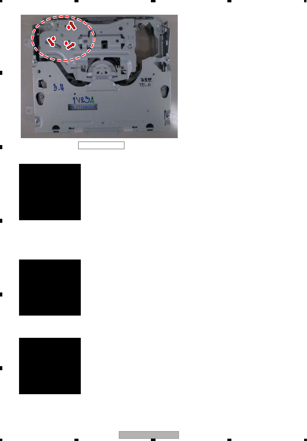
AVIC-X910BT/XS/UC
122
1234
1234
C
D
F
A
B
E
CRG Move Outer
1: DVD Single Layer
2: DVD Dual Layer
3: CD
4: CD-RW
5: Return
Please Input Number
CRG Move Outer
1: Power OFF
Please Input Number
TEST MODE
1: LD ON
2: ASMAX
3: Skew Adjustment
4: Error Rate
5: CRG Move Outer
6: Eject
Please Input Number
Disc Detection Arm
13. CRG Move Outer
Select “1: DVD Single Layer.”
The pickup moves to the outer periphery.
Apply the adhesive to fix the skew, the resonance adhesive and the screw lock.
Refer to the next page regarding the locations of adhesive joining.
14. CRG Move Outer
1: Power OFF
15. TEST MODE
Select “6: Eject.”
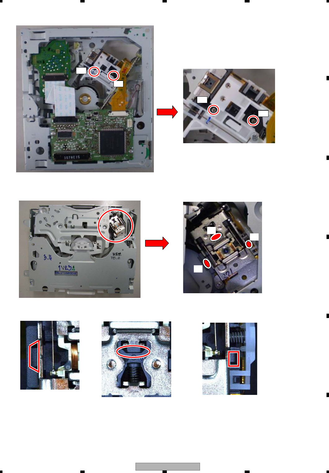
AVIC-X910BT/XS/UC 123
5678
5678
C
D
F
A
B
E
A
B
A
B
1
12 3
Locations to make SKEW adjustment
Locations to adhere the SKEW 1,2,3: GEM1033
2
3
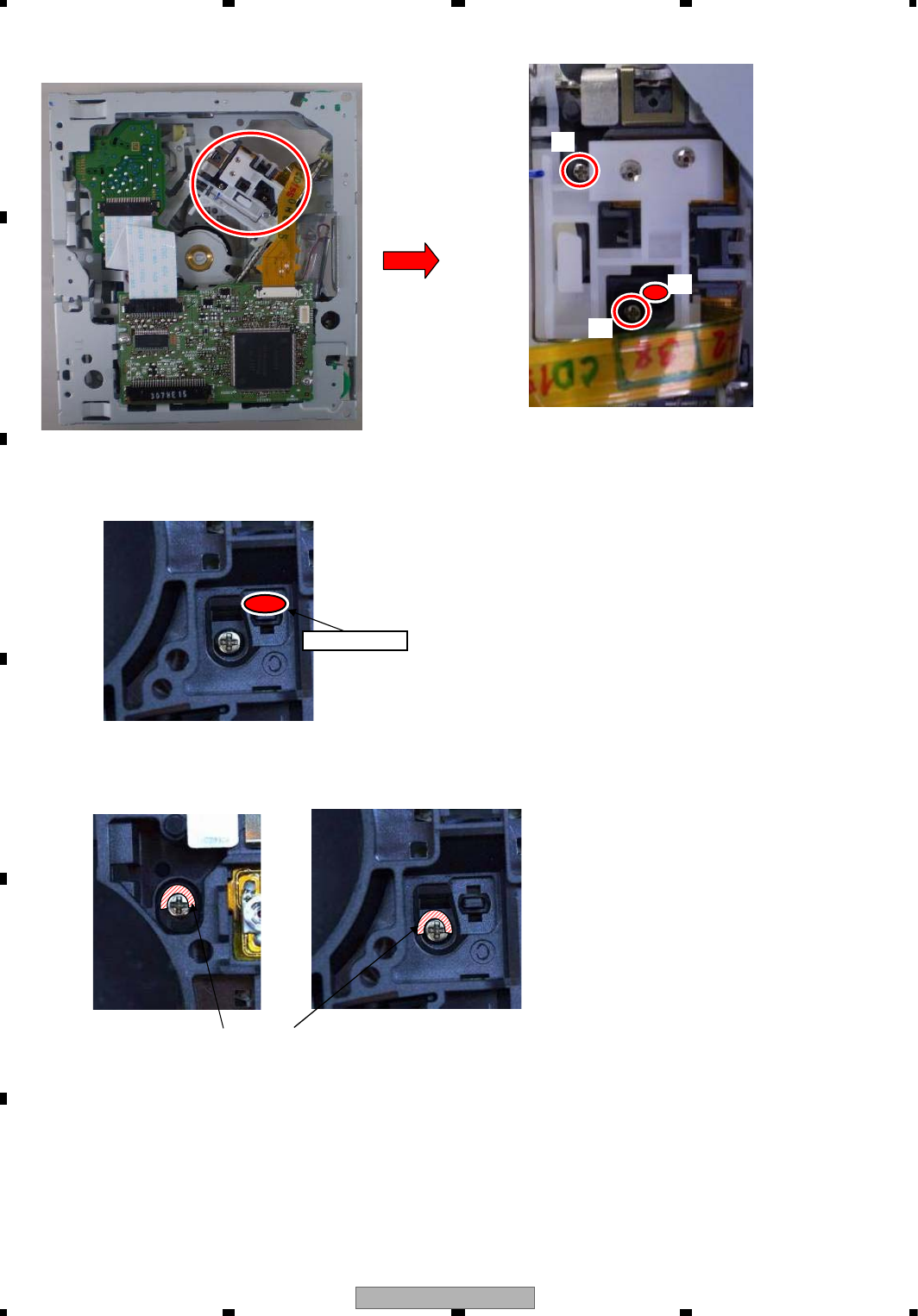
AVIC-X910BT/XS/UC
124
1234
1234
C
D
F
A
B
E
adhesive
Bond for resonance 4:Three Bond 1530
4
5
6
4
56
Bond for locking the screw 5,6 : Three Bond 1401M
Bond for locking the screw

AVIC-X910BT/XS/UC 125
5678
5678
C
D
F
A
B
E
Hologram (Beware of the static)
Do not touch the optical part
RF level adjusting part
Do not touch the spring
Precautions on handling the PU
*Precaution: Do not touch those shaded areas in the following figures.
.
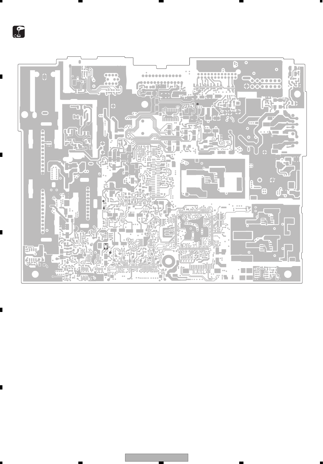
AVIC-X910BT/XS/UC
126
1234
1234
C
D
F
A
B
E
8.2 AV UNIT ADJUSTMENT
- Adjustment point
AV UNIT(SIDE A)
VR4231
AV1VG
AV1VIN
FRV2
GNDV
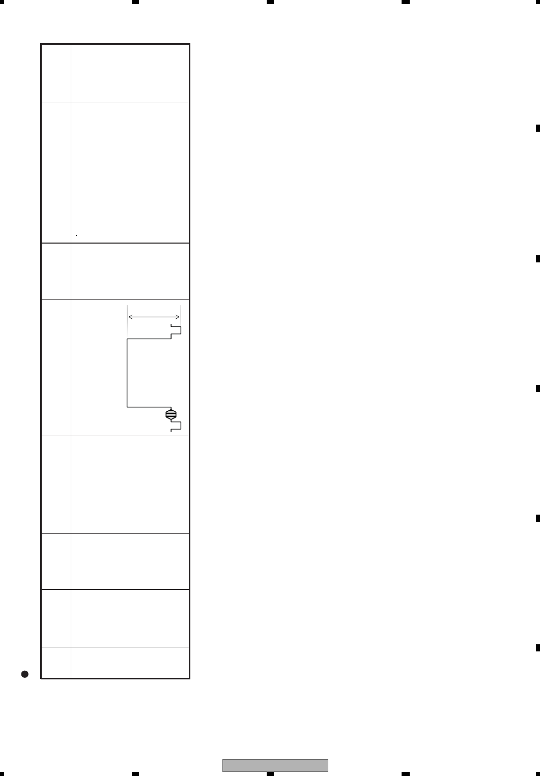
AVIC-X910BT/XS/UC 127
5678
5678
C
D
F
A
B
E
AV UNIT ADJUSTMENT
StepAdjustment
item
Mode Input signal
(Input testpin,specs,
other conditions)
Output signal
(Measurement point,wave pattern)
Masuring
instruments
SpecsAdjusting
point
1 Video level
adjustment
AV selector
VTR1
GGV1025
Title3 chap3 play
(white 100%)
1,0 Vp-p
To perform AV unit only
TP AV1VIN (input)
TP AV1VG (GND)
100IRE (white 100%)
1,0 Vp-p
(input via 75 ohm)
Measurement point:
FRV2 GNDV (GND)
(To measure the AV Unit only, connect
1.4 kohm between TP FRV2 and GNDV.)
Oscilloscope 1.00 V ±0.02 Vp-p
Measure between the sync tip and 100
IRE(wave top).
Symptoms with poor adjustment.
Over level:
Luminance is too high.
Under level:
Luminance is too low.
VR4231
AVIC-X910BT/XS/UC
128
1234
1234
C
D
F
A
B
E
8.3 FLICKER ADJUSTMENT
FLICKER ADJUSTMENT
Adjustment item Measurement point Adjustment point The contentsofadjustment Remarks
.langis%001etihwtupnIgnigA1
Leave for more than 30 minutes in operation
mode.
2Flicker adjustment Screen LCVR1 Adjust the flicker level to minimum from all
directions.
Signal for Flicker adjustment…
Select “Graphics” “Flicer Adjustment”
in the Test Mode.
(Input a signal for alternate white and black line.
The luminance level of the input signal : 50%)

AVIC-X910BT/XS/UC 129
5678
5678
C
D
F
A
B
E
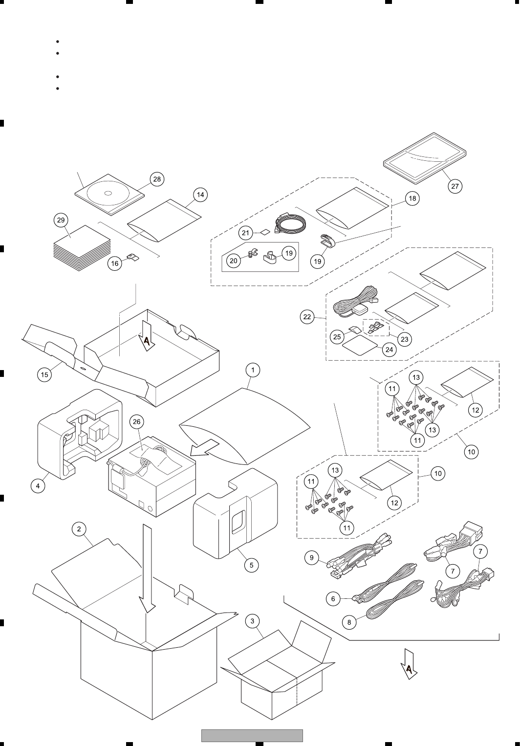
AVIC-X910BT/XS/UC
130
1234
1234
C
D
F
A
B
E
9. EXPLODED VIEWS AND PARTS LIST
9.1 PACKING
NOTES : Parts marked by " * " are generally unavailable because they are not in our Master Spare Parts List.
The > mark found on some component parts indicates the importance of the safety factor of the part.
Therefore, when replacing, be sure to use parts of identical designation.
Screw adjacent to mark on the product are used for disassembly.
For the applying amount of lubricants or glue, follow the instructions in this manual.
(In the case of no amount instructions,apply as you think it appropriate.)
""
AVIC-X910BT/XS/UC
AVIC-F910BT/XS/AU
AVIC-F910BT/XS/EU5
AVIC-X910BT/XS/UC
AVIC-F910BT/XS/AU
AVIC-F910BT/XS/AU
AVIC-F910BT/XS/EU5
AVIC-F910BT/XS/AU
AVIC-F910BT/XS/EU5
AVIC-F910BT/XS/EU5
AVIC-X910BT/XS/UC
AVIC-F910BT/XS/EU5

AVIC-X910BT/XS/UC 131
5678
5678
C
D
F
A
B
E
PACKING SECTION PARTS LIST
Mark No. Description AVIC-X910BT/XS/UC AVIC-F910BT/XS/EU5 AVIC-F910BT/XS/AU
1 Polyethylene Bag CEG1402 CEG1401 CEG1401
2 Unit Box CHG6774 CHG6772 CHG6775
3 Contain Box CHL6774 CHL6772 CHL6775
4 Protector CHP3552 CHP3550 CHP3552
5 Protector CHP3553 CHP3551 CHP3553
6 Cord CDE6825 CDE6825 CDE6825
7 Cord Assy CDP1095 CDP1097 CDP1095
8 Cord CDP1157 CDP1157 CDP1157
9 Cord Assy CDP1241 CDP1241 CDP1241
10 Screw Assy CEA3797 CEA7395 CEA3797
11 Screw BMZ50P060FTC BMZ50P060FTC BMZ50P060FTC
* 12 Polyethylene Bag CEG-127 CEG-127/CNM4388 CEG-127
13 Screw CMZ50P060FTC CMZ50P060FTC CMZ50P060FTC
14 Polyethylene Bag CEG1116 CEG1116 CEG1116
15 Sub Unit Box CHG6491 CHG6491 CHG6491
16 Connector CKX1049 CKX1049 CKX1049
17 •••••
18 Microphone Assy CPM1064 CPM1083 CPM1083
19 Clip Holder CZN5471 *CZN7912 *CZN7912
20 Microphone Holder CZN5472 Not used Not used
21 Cushion CZN5473 *CZN7913 *CZN7913
22 GPS Antenna Assy CXC8574 CXC8574 CXC8574
* 23 Clamper Assy CZE3090 CZE3090 CZE3090
24 Water Proof Pad CZN5442 CZN5442 CZN5442
25 Sheet CZN7151 CZN7151 CZN7151
26 Seal CNN2515 CNN2515 CNN2515
27 Panel Not used CNS8665 Not used
* 28 IM CD-ROM/PEE Not used CPJ1273 CPJ1273
29-1 Owner's Manual CRB2985 Not used Not used
29-2 Owner's Manual CRB2986 Not used Not used
29-3 Installation Manual CRD4409 CRD4411 CRB3008
29-4 Quick Start Guide CRB2987 CRB2995 CRB3006
29-5 Quick Start Guide CRB2988 CRB2996 Not used
29-6 Quick Start Guide Not used CRB2997 Not used
29-7 Quick Start Guide Not used CRB2998 Not used
29-8 Quick Start Guide Not used CRB2999 Not used
29-9 Quick Start Guide Not used CRB3000 Not used
29-10 Important Information Not used CRD4410 CRB3007
* 29-11 Caution Card CRP1310 Not used CRP1310
* 29-12 Warranty Card CRY1246 CRY1265 Not used
* 29-13 Registration Card CRY1271 Not used Not used
* 29-14 Passport Not used CRY1268 Not used

AVIC-X910BT/XS/UC
132
1234
1234
C
D
F
A
B
E
Owner's Manual,Installation Manual
CONTENTS OF CD-ROM (Operation Manual), CPJ1274
All operation manuals are supplied in PDF files by the CD-ROM.
Regarding the availability of paper manual, contact Pioneer Service representative in your region.
Part No. Language
CRB2985 English
CRB2986 French
CRB2987 English
CRB2988 French
CRD4409 English, French
CRB2995 English
CRB2996 Spanish(Espanol)
CRB2997 German
CRB2998 French
CRB2999 Italian
CRB3000 Dutch
CRD4410 English, Spanish(Espanol), German, French, Italian, Dutch
CRD4411 English, Spanish(Espanol), German, French, Italian, Dutch
CRB3006 English
CRB3007 English
CRB3008 English
Part No. Language
* CRB2989 English
* CRB2990 Spanish(Espanol)
* CRB2991 German
* CRB2992 French
* CRB2993 Italian
* CRB2994 Dutch
* CRB3005 English

AVIC-X910BT/XS/UC 133
5678
5678
C
D
F
A
B
E
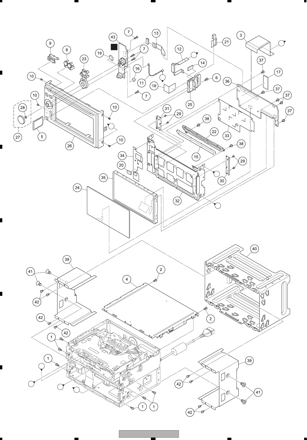
AVIC-X910BT/XS/UC
134
1234
1234
C
D
F
A
B
E
9.2 EXTERIOR(1)
C
A
E
B
B
C
D
DE
E
A
AVIC-X910BT/XS/UC 135
5678
5678
C
D
F
A
B
E
(1) EXTERIOR(1) SECTION PARTS LIST
(2) CONTRAST TABLE
AVIC-X910BT/XS/UC, AVIC-F910BT/XS/EU5 and AVIC-F910BT/XS/AU are constructed the same except for the
following:
Mark No. Description Part No.
1 Screw BMZ26P050FTC
2 Screw(M2.6 x 5) CBA2145
3 FFC CDE9039
4 Case CNB3472
5 Card CNW1231
6 Screw BMZ26P050FTC
7 Screw BPZ20P080FTC
8 Button(MENU, MAP) CAI1705
9 Button(RESET, EJECT) CAI2435
10 Screw(M2 x 3) CBA1797
11 Cord Assy CDE8559
12 FFC CDE9037
13 FFC CDE9038
14 Spacer
See Contrast table (2)
15 Cover CNN2046
16 Gasket CNN2501
17 Gasket CNN2533
18 Insulator CNN2534
19 Cushion
See Contrast table (2)
20 Gasket
See Contrast table (2)
21 Insulator
See Contrast table (2)
22 Holder CNV9903
23 Lighting Conductor CNW1561
24 Touch Panel CSX1136
25 SD Unit CWX3652
26 Grille Unit
See Contrast table (2)
27 Knob Unit CXE1633
* 28 Spring YBL5013
29 Screw(M2 x 2) CBA1771
30 Holder CND3758
31 Holder CND3759
32 Holder CND4319
33 Insulator CNN2044
34 Insulator CNN2045
35 LCD Module CWX3850
36 Panel Unit CWX3785
37 Screw PMB20P040FTC
38 Screw IMS26P040FTC
39 Holder
See Contrast table (2)
40 Holder
See Contrast table (2)
41 Screw
See Contrast table (2)
42 Screw
See Contrast table (2)
43 Keyboard Unit CWN4250
Mark No. Description Part No.
Mark No. Description AVIC-X910BT/XS/UC AVIC-F910BT/XS/EU5 AVIC-F910BT/XS/AU
14 Spacer CNM9246 Not used CNM9246
19 Cushion CNN2723 Not used CNN2723
20 Gasket CNN2724 Not used CNN2724
21 Insulator CNN2725 Not used CNN2725
26 Grille Unit CXE1623 CXE1624 CXE1625
39 Holder Not used CND3431 Not used
40 Holder Not used CND3430 Not used
41 Screw Not used CMZ50P060FTC Not used
42 Screw Not used BMZ30P060FTC Not used
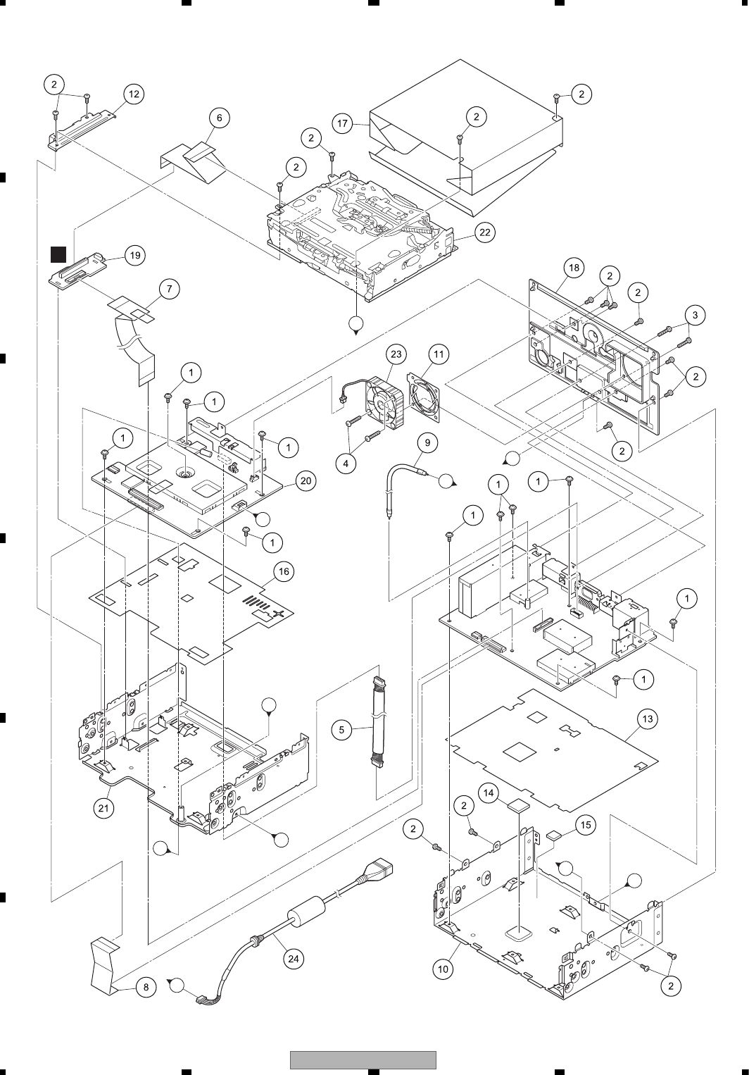
AVIC-X910BT/XS/UC
136
1234
1234
C
D
F
A
B
E
9.3 EXTERIOR(2)
(A)
(A)
E
E
B
C
D
D
A
C
A
B
B
(A) GYH1031(Mylar tape)
* Hold the flexible cable to the shield on the Navi Unit.

AVIC-X910BT/XS/UC 137
5678
5678
C
D
F
A
B
E
EXTERIOR(2) SECTION PARTS LIST
Mark No. Description Part No.
1 Screw ASZ26P050FTC
2 Screw BMZ26P050FTC
3 Screw BMZ26P160FTB
4 Screw(M2.6 x 12) CBA2102
5 Cord Assy CDE8393
6 FFC CDE8911
7 FFC CDE8912
8 FFC CDE9036
9 Cord Assy CDH1381
10 Chassis CNA3114
11 Cover CND3917
12 Bracket CND4564
13 Insulator CNN2042
14 Sheet CNN2294
15 Gasket CNN2529
16 Insulator CNN2807
17 Sheet CNN2808
18 Heat Sink CNR1944
19 CK Unit CWN4251
20 Navi Unit(UC) CWX3739
Navi Unit(EU5) CWX3740
Navi Unit(AU) CWX3741
21 Chassis Unit CXE1631
22 DVD Mechanism Module(LS1) CXK6801
23 Fan Motor CXM1320
24 Cord Assy(UC) CDE9102
Cord Assy(EU5) CDE8913
Cord Assy(AU) CDE8913
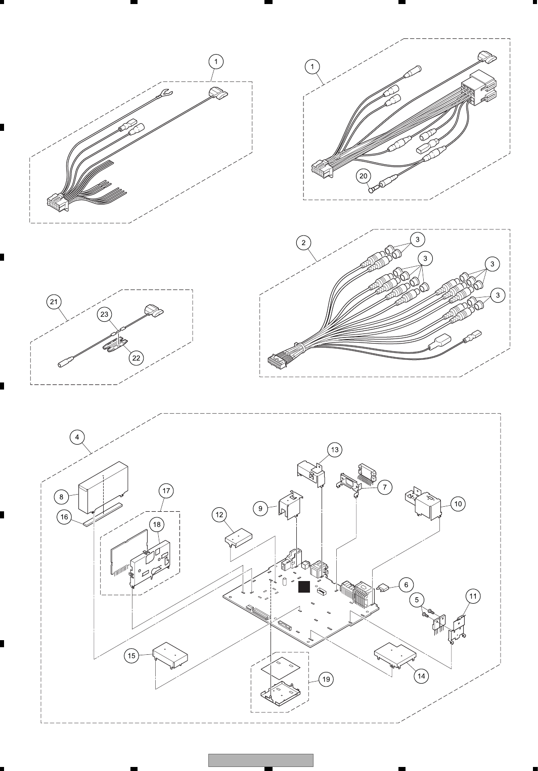
AVIC-X910BT/XS/UC
138
1234
1234
C
D
F
A
B
E
9.4 EXTERIOR(3)
A
AVIC-X910BT/XS/UC
AVIC-F910BT/XS/AU
AVIC-F910BT/XS/EU5

AVIC-X910BT/XS/UC 139
5678
5678
C
D
F
A
B
E
(1) EXTERIOR(3) SECTION PARTS LIST
(2) CONTRAST TABLE
AVIC-X910BT/XS/UC, AVIC-F910BT/XS/EU5 and AVIC-F910BT/XS/AU are constructed the same except for the
following:
Mark No. Description Part No.
1 Cord Assy
See Contrast table (2)
2 Cord Assy CDP1241
3 Cap CNW1490
4AV Unit
See Contrast table (2)
5 Screw BMZ26P060FTC
>6 Fuse(10 A) CEK1208
7 Holder CNC9921
8 Shield CND3004
9 Holder CND3181
10 Holder CND3693
11 Holder CND3695
12 Shield CND3769
13 Holder
See Contrast table (2)
14 Shield CND4320
15 Shield CND4563
16 Sheet CNM9805
17 FM/AM Tuner Unit(Y1461)
See Contrast table (2)
18 Holder CND4324
19 Shield Unit CXC8983
20 Terminal Cover
See Contrast table (2)
21 Cord CDE6825
22 Cap CNS1472
23 Resistor RS1/2PMF102J
Mark No. Description Part No.
Mark No. Description AVIC-X910BT/XS/UC AVIC-F910BT/XS/EU5 AVIC-F910BT/XS/AU
1 Cord Assy CDP1095 CDP1097 CDP1095
4 AV Unit CWN4237 CWN4238 CWN4239
13 Holder CND4314 CND4315 CND4315
17
FM/AM Tuner Unit(Y1461)
CWE2128 CWE2127 CWE2128
20 Terminal Cover Not used CKX-003 Not used
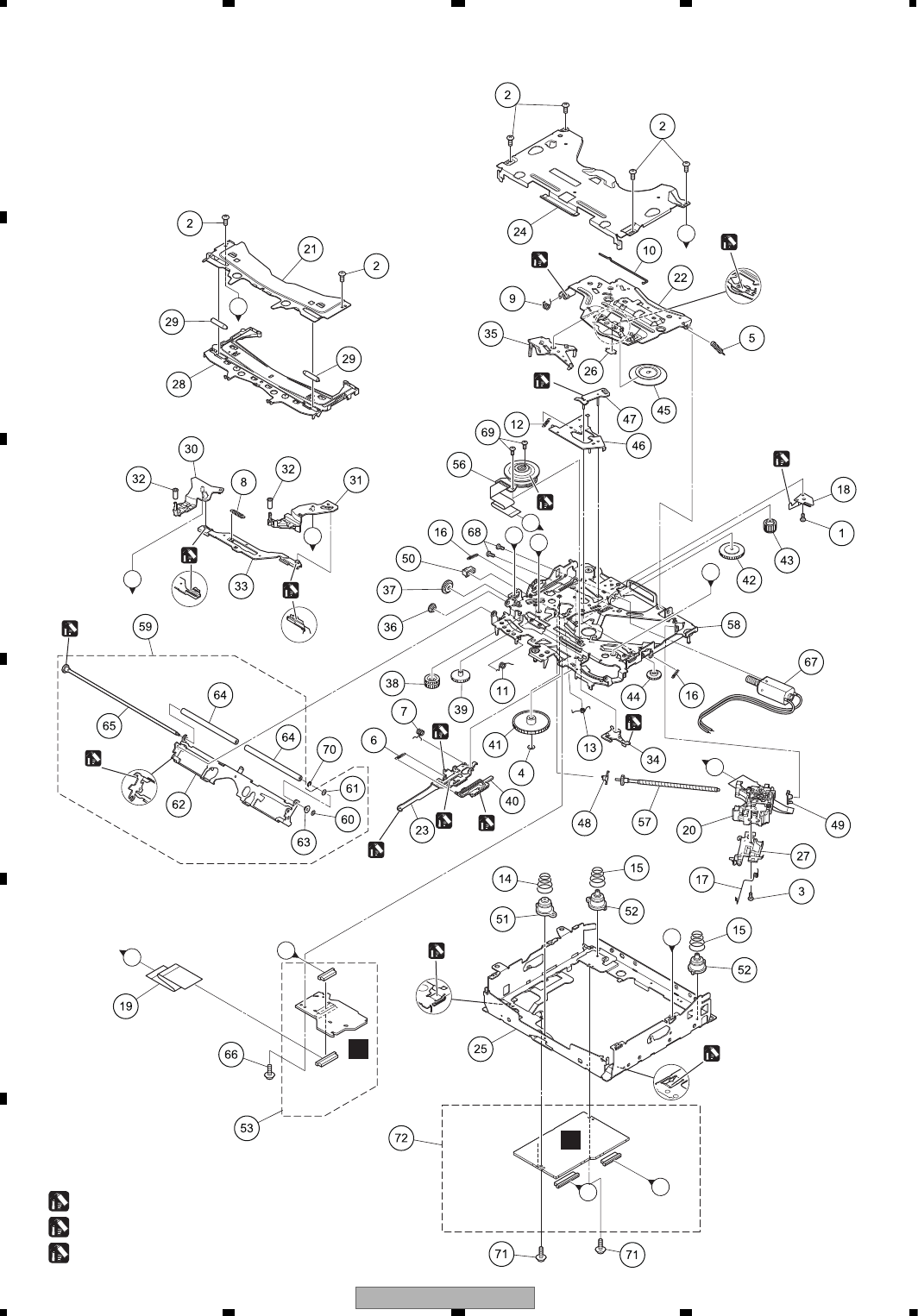
AVIC-X910BT/XS/UC
140
1234
1234
C
D
F
A
B
E
9.5 DVD MECHANISM MODULE
A
C
D
D
F
E
C
B
A
B
E
G
F
G
C
D
(A) : GEM1045
(B) : GEM1038
(C) : GEM1024
(C)
(C)
(A)
(A)
(A)
(A)
(C)
(A)
(A)
(C)
(C)
(C)
(C)
(B)
(C)
(C)

AVIC-X910BT/XS/UC 141
5678
5678
C
D
F
A
B
E
DVD MECHANISM MODULE SECTION PARTS LIST
Mark No. Description Part No.
1 Screw BMZ20P020FTC
2 Screw BSZ20P040FTC
3 Screw(M2 x 4) CBA1835
4 Washer CBF1038
5 Spring CBH2860
6 Spring CBH3010
7 Spring CBH3011
8 Spring CBH3012
9 Spring CBH3013
10 Spring CBH3014
11 Spring CBH3015
12 Spring CBH3016
13 Spring CBH3017
14 Spring CBH3018
15 Spring CBH3019
16 Spring CBH3020
17 Spring CBH3030
18 Plate Spring CBL1797
19 Cable CDE8631
20 Service PU Unit CXX2398
21 Bracket CND4553
22 Arm CND4555
23 Lever CND4556
24 Frame CND4557
25 Frame CND4558
26 Sheet CNN2280
27 Rack CNW1170
28 Guide CNW1171
29 Roller CNW1172
30 Arm CNW1173
31 Arm CNW1174
32 Roller CNW1175
33 Lever CNW1176
34 Arm CNW1177
35 Arm CNW1178
36 Gear CNW1180
37 Gear CNW1181
38 Gear CNW1182
39 Gear CNW1183
40 Rack CNW1184
41 Gear CNW1185
42 Gear CNW1186
43 Gear CNW1187
44 Gear CNW1188
45 Clamper CNW1190
46 Arm CNW1191
47 Arm CNW1192
48 Holder CNW1193
49 Holder CNW1194
50 Holder CNW1195
51 Damper CNW1197
52 Damper CNW1198
* 53 Connect PCB Unit CWX3618
54 •••••
55 •••••
56 Motor Unit CXC4026
57 Screw Unit CXC8894
58 Chassis Unit CXC8895
59 Arm Assy CXC8896
60 Washer CBF1037
61 Washer CBF1038
62 Arm CND4554
63 Collar CNV6906
64 Roller CNW1196
65 Gear Unit CXC8893
66 Screw(M2 x 5) EBA1028
67 Motor EXM1050
68 Screw JFZ20P025FTC
69 Screw JGZ17P022FTC
70 Washer YE15FTC
71 Screw IMS20P030FTC
72 DVD Core Unit YWX5009
Mark No. Description Part No.
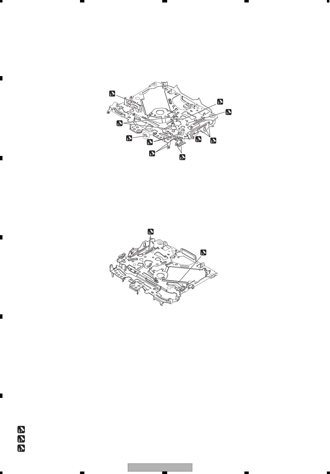
AVIC-X910BT/XS/UC
142
1234
1234
C
D
F
A
B
E
(A) : GEM1045
(B) : GEM1038
(C) : GEM1024
(A)
(C)
(C)
(A)
(A)
(C)
(C)
(C)
(C)
(C)
(A)
(A)

AVIC-X910BT/XS/UC 143
5678
5678
C
D
F
A
B
E
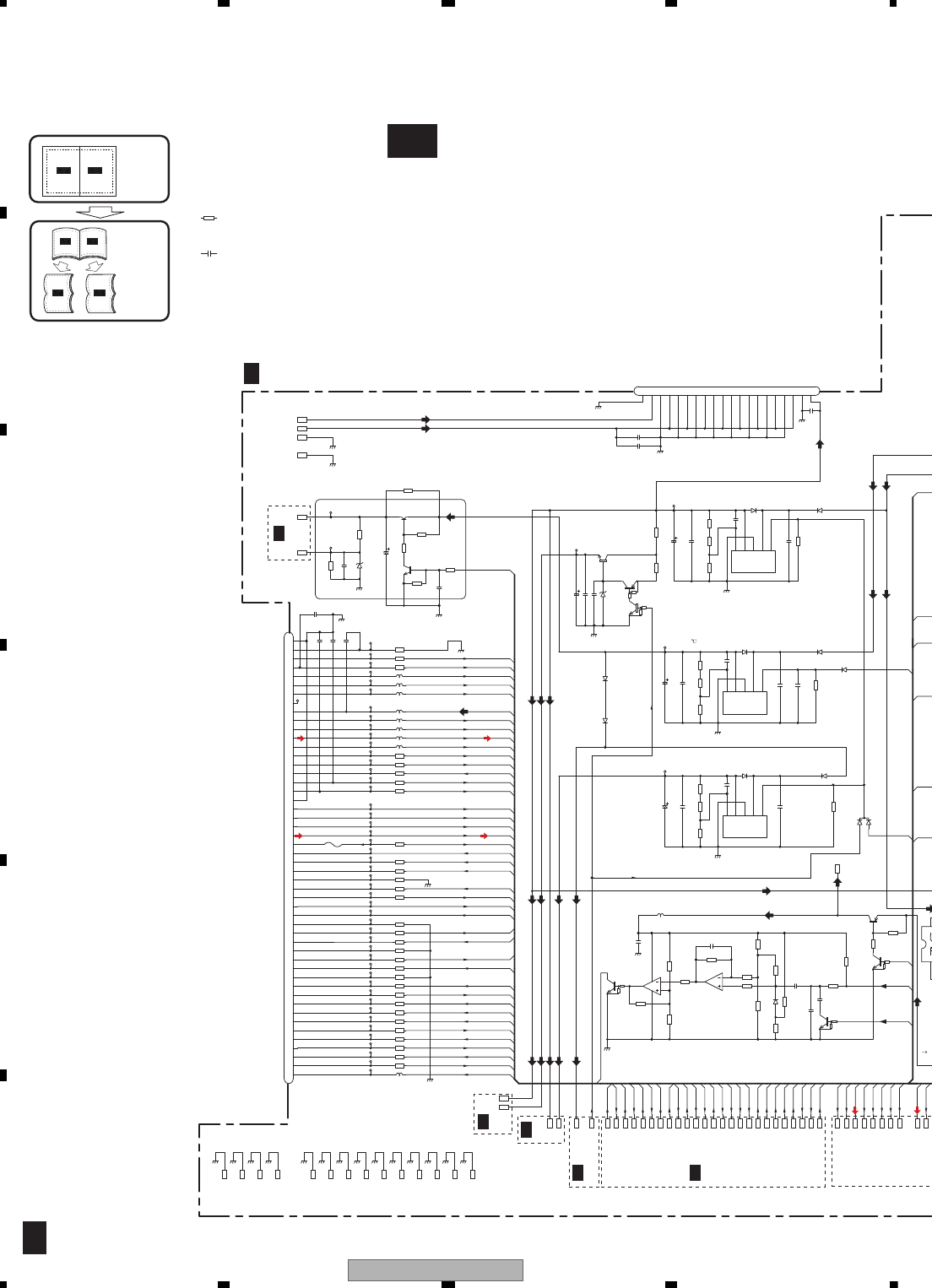
AVIC-X910BT/XS/UC
144
1234
1234
C
D
F
A
B
E
10. SCHEMATIC DIAGRAM
10.1 AV UNIT(PS/IF SECTION)(GUIDE PAGE)
A-a A-b
A-a A-b
A-b
A-a
Large size
SCH diagram
Guide page
Detailed page
Note: When ordering service parts, be sure to refer to " EXPLODED VIEWS AND PARTS LIST" or
"ELECTRICAL PARTS LIST".
1/6
A
A-a 1/6
GUIDE
PKB
CPUWDT3
SYSTOC3
ROT1
ASENS
OPTSNS
ILMSN
ANTON
OPTON
OFFINFO3
SYSTOCV3
OFFANS3
ROT1
RESETB
HDRST
REVSN
DVEJKY
ROT0
BATFAULT3
AV2RG
AV2RS
RESETB
NAVIAR
HDRST
AV2LS
DVEJKY
SPEED
CTOSYS3
OFFANS3
OPTSNS
KMODEOUT
OFFINFO3
CPUWDT3
REVSNS
OPTON
CTOSYSV3
PULSE
PKBOUT
SPEED
PCHNG
PULSE
ILMR
ILMG
ILMB
ILMV
FRV
ROT0
AV2VIN
AV2VG
AV2LG
NAVIAL
MONVBS
GUIDEMUTE
VICSON
SREMOTE
SYSPW
AV2RS
CTOSYSV3
SYSTOCV3
SYSTOC3
CTOSYS3
ASENS
ANTON
PCHNG
NAVIRG
NAVILG
FRVGND
GUIDEG
ILMSNS
SRCMUTE
MONVBS
NAVILG
AV2RG
NAVIRG
AV2LG
AV2VG
AV2LS
AV2VIN
NAVIAR
NAVIAL
SYSPW
TU3
VIDEO5
FANV
NAVI3V
BATFAULT3
KBUP
VT6
VICSON
SYSPW
DCSKIPCD
DCSKIPCD
NAVI3V
VT8
NAVI5V
AV8
AV8
AV8
AV8
SWACPW
NFCONT
NFCONT
BUP
R2801
10k
R2940 0
R2804 100k
R2811
470
R2803
2.2k
R2802
2.7k
R2810
0
R2834
100k
R2832
2.2k
R2822
2.2k
R2951 0
R2952 0
R2953 0
R2954 0
R2960 0
R2961 0
R2962 0
R2963 0
R2964 0
R2967 0
R2968 0
R2969 0
R2970 0
R2971 0
R2972 0
R2973 0
R2974 0
R2975 0
R2976 0
R2977 0
R2978 0
R2979 0
R2980 0
R2981 0
R2982 0
R2983 0
R2959 0
R2941 100
R2942 100
R1016 0
R2841
47k
R2840
100k
R2842
56k
R2843
51k
R2844
100k
R2845
51k
R2846
51k
R2848
1k R2847
1k
R2849
560k
R2850
2k
R2851
8.2k
R2852
20k
R2853
33k
R2884
4.7k
R2883
4.7k
R2820
2.2k
R2821
10k
R2830
3.6k
R2831
10
R2838
NM
R2836
NM
R2837
NM
R2839
NM
R2835
NM
R2823
1M
R2833 0
R2829
NM
C2804
0.1u/50
C2811 0.1u/50
SYSPW
TU3
BATFAULT3
C2844
0.082u/16
NAVI5GND
IC1002
NJM2904M
5
6
7
C1022
0.1u/50
100u/16
C2810
ILMGND
GNDV
CTOSYSV3
GNDD
Q2810
2SD1760F5(R)
D2802
RB060L-40
C2842
0.1u/50
GNDD
GNDA
AV2LS
C2841
1000p/50
GNDFM
NAVIRG
GUIDEG
ROT0
C2803
NM
DTC114WK
Q2840
SYSTOC3
C2840
0.1u/50
NAVILG ILMGND
GNDRF
FANGND
C1021
1000p/50
C1020
1000p/50
NAVIRG
ROT1
GNDFM
NAVIRG
OPTSNS
AV2LG
2E
16
2C
TU3
CCH1565-A
C2820
HDRST
100u/16
C2830
DTC114EUA
Q2841
L1004
CTF1334-A
SRCMUTE
FANGND
NAVIAL
AV8
ASENS
NAVIAR
FANGND
DTC114EU
Q2812
MONVBS
C2821 0.01u/50
GNDD
BA00CC0WCP-V5
IC2801
Vadj:1.225V
1
CTL
2
VCC
3
GND
4
VOUT
5
ADJ
D2810
UDZS5R6(B)
AV2VG
D2821
RB060L-40
NAVILG
SREMOTE
GNDV
SWACPW
GNDA
C2812 0.1u/50
GNDRF
SYSTOCV3
AV2RG
GNDV
NAVI5GND
GNDD
AV2RS
NAVI5V
ANTON
GNDD
FANGND
C2831 0.01u/50
OFFANS3
D2840
1SS355
FANGND
IC1002
NJM2904M
3
4
2
18
NAVILG
C2832
NM
AV2VIN
OPTON
D2820
NM
VICSON
DVEJKY
D2801
NM
FRVGND
GNDA
CPUWDT3
NAVI5GND
C2802 1000p/50
C2822
NM
GNDA
NAVI3GND
VI5
CKS5732-A
CN1000
1
2
3
4
5
6
7
8
9
10
11
12
13
14
15
16
17
18
19
20
21
22
23
24
25
26
27
28
29
30
31
32
33
34
35
36
37
38
39
40
41
42
43
44
45
46
47
48
49
50 L2940
CTF1334-A
CKS4674-A
CN1001
1
2
3
4
5
6
7
8
9
10
11
12
13
14
15
16
17
18
19
20
C2833
0.1u/50
FRVGND
CTOSYS3
GNDV
GNDD
GUIDEG
ILMGND
AV8
RESETB
C2843
0.01u/50
GNDD
NAVI3GND
C2823
0.1u/50
GNDD
GNDA
DTA114EU
Q2811
ILMSNS
VT6
OFFINFO3
VT8
GNDD
DTC114EU
Q2881
D2830
NM
FANV
ILG
EJT
RES
ILMB
ILMG
ILMR
ILMV
AUR
AURG
AUL
AULG
AUVG
AUV
ROT1
ROTO
NARG
NAR
NALG
NAL
N33V
FRG
FRV
BCGN
BCVN
GMUTE
GUIG
GUI
GSY1
CTSV
STCV
GSY2
CTN
STC
GSY3
OPON
OPSN
PKN
KMB
RVN
OFAN
OFIN
WDOG
RESB
PCHG
PLN
NC1
NFC
SWVDD5
BFA
D2822
DAN202U
BA00BC0WFP
IC2830
1
VC
2
VIN
3
GND
4
VDD
5
C
D2831
RR264M-400
GNDD
Q2831
NM
Q2832
NM
VICS8
D2835
NM
C2835
NM
VICS5
NM
C2836
VISC8
GNDD
GNDD
DCSKIPCD
D2824
1SR154-400
D2823
1SR154-400
C2837
NM
C2824
NM
D2825
1SS400G
NAVI3V
GNDA
C2805 0.1u/50
C2800
1000p/50
NFCONT
C1023
NM
C2806
NM
VISC5
FU2900
CEK1276-A 250mA
12
2SA1576A(QR)
Q2882
BA00CC0WCP-V5
IC2820
Vadj:1.225V
1
CTL
2
VCC
3
GND
4
VOUT
5
ADJ
CCH1565-A
C2801
L2943 CTF1556-A
L2944 CTF1556-A
L2945 CTF1556-A
L2946 CTF1556-A
L2947 CTF1675-A
L2948 CTF1675-A
L2949 CTF1675-A
L2950 CTF1675-A
8.3V
2820-2829
GND
ILMGND
EJECT
RESET
ILMB
CCH1565
100u/16V
105
ILMGILMG
ILMR
ILMV
NC
AUX-R
AUX-RG
AUX-L
ROT1
AUX-VG
AUX-LG
AUX-V
GND
NaviARG
ROT0
BATTERY_FAULT
BCVGND
OPTSNS
GNDSYS
GNDSYS
GUIDE
PKB
GNDSYS
CTOSYSV3
FRVGND
SYSTOCV3
GUIDEMUTE
OPTON
GUIDEG
BCV
FRV
PULSE
OFFINFO
OFFANS
KMODE
WDOG
RESETB
PCHNG
REV
NaviAR
NaviALG
NaviAL
NFCONT
NAVI33V
5.0V
SYSTOC3
CTOSYS3
NAVI5V
NAVI5V
NAVGND
NAVGND
FANV
FANGND
8.3V
3.3V
AV8
2801-2809
sens
or "re
em
NAVI5V
NAVI5V
NAVGND
NAVGND
AV8V GND
AV8V
NAVI5V
NAVI5V
NAVI5V
NAVI5V
NAVGND
NAVGND
NAVGND
NAVGND
NM
NAVI UNIT OTJ1
NAVI UNIT SPJ1
8.3V
8.0V 8.0V
6.5V
6.5V 6.5V
3.3V
8.0V
8.3V
5.0
5.0V
5.0V5.0V
5.0V
8.3V 8.3V
8.3V
5.0V 5.0V 5.0V
5.0V
5.0V
5.0V
5.0V
5.0V
5.0V
5.0V
5.0V
8.3V
5.0V
8.3V 8.3V
8.3V
5.0V
8.5V
2829-2833
1000-1001
2800
1016
2805-2806
2810-2819
2900
1021-1025
2900-2
2940-2985
VIDEO5
TU3
to NAVI
1002-1004
ASE
SPEED PULSE
2840-2865
2830-2834
2881-2884
2835-2839
VICS8 SWICTH
VT8
2900
1021-1025
2940-2985
to NAVI
1000-1001
2800
1016
2805-2806
AV8
VIDEO5
>
3/6
A
4/6
A
6/6
A
2/6
A3/6
A
AV UNIT (PS/IF SECTION)
1/6
A
The > mark found on some component parts indicates
the importance of the safety factor of the part.
Therefore, when replacing, be sure to use parts of
identical designation.
Symbol indicates a resistor.
No differentiation is made between chip resistors and
discrete resistors.
NOTE :
Symbol indicates a capacitor.
No differentiation is made between chip capacitors and
discrete capacitors.
NM : No Mount
Navi Audio:-2.68 dBs
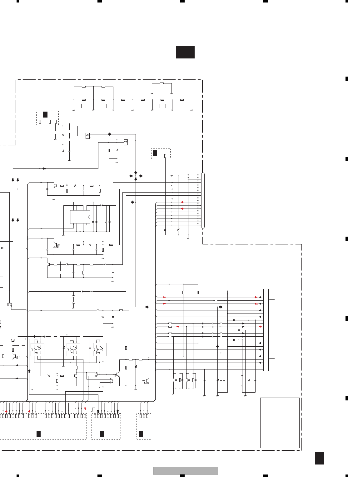
AVIC-X910BT/XS/UC 145
5678
5678
C
D
F
A
B
E
1/6
A
A-b 1/6
RR
RR+
PKB
FL+
ASENS
FR-
ILMSNS
ANTON
SRCMUTE
FR+
SREMOTE
REVSNS
FANUP
SREMOTE
OFFMUTE
SPEED
RL-
FR
FL-
FL
BREMOTE
RL+
RL
RR-
SPEED
PCHNG
GUIDEMUTE
MONVBS
NAVILG
AV2RG
NAVIRG
AV2LG
AV2VG
AV2LS
AV2VIN
NAVIAR
NAVIAL
GUIDE
GUIDEG
FRV
FRVGND
RSTMUTE
KMODEOUT
FANUP
PKBOUT
PKB
ANTON
ILMB
ILMR
ILMG
POMUTE
BREMOTE
FR
FL
RR
RL
ILMV
RL+
FL+
FR+
FL-
RL-
SYSPW
FR-
RR+
RR-
KBUP
SYSPW
DCSKIPCD
BUP
R2873
4.7k
R2901
100k
R2910
47k
R2900
47k
R2870
47k
R2880
10k
R2872
1k
R2871
100k
R2925 10k
R2924 10k
R2926
10k
100k
R2912
4.7
R2913
4.7
R2911
47k
R2860
390
R2861
390
R2863
22k
R2862
47k
R2864
10k
R2868
220
R2866
10k
R2867
10k
R2869
100
R2853
33k
R2884
4.7k
R2883
4.7k
R2920 1k
R2921 1k
R2922 1k
R2923 1k
R4779 NM
R4780 NM
R4781 NM
R4782 NM
R4812
0
R4811
NM
R4802
NM
R4801
NM
R4816
NM
R4815
NM
R4814
NM
R4813
NM
R4821
NM
R2865
1k
(1/10W)
R2902
1k
(1/4W)
R2882
1k
(1/4W)
R2874
1k
(1/4W)
R2875
4.7k
(1/4W)
R2903
4.7k
(1/4W)R2881
4.7k
(1/4W)
GNDA
BUP2
FR
Q2863
UMD2N
2E
1
2B
2
1C
31E 4
5
1B
6
2C
GNDD
ILMG
GNDD
GND1
ANTON
DTC114EU
Q2880
GNDD
GNDD
AV2LS
GUIDEMUTE
D2862
DAN202U
NAVIRG
GNDD
GNDD
D2871
UDZS18(B)
GNDD
C2926
1u/10
FRVGND
DTC114EU
Q2864
33u/10
C2862
IC2890
TPD1018F
1
OUT 2
GND1 3
GND2 4
GND3 5
VDD
6IN
7GND4
8GND5
9GND6
10 DIAG
D2873
1SS355
ILMR
L2871
CTF1410-A
C2882
1000p/50
C2861 0.1u/50
C2931 1u/10
Q2861
UMD2N
2E
1
2B
2
1C
31E 4
5
1B
6
2C
GNDD
BUP
KMODEOUT
GNDD
C2925
1u/10
AV2LG
Q2860
UMD2N
2E
1
2B
2
1C
31E 4
5
1B
6
2C
D2860
MA111
GNDD
FANUP
GNDD
47u/16
C2860
4EUA
KB1
IL1
GNDD
L2930
CTH1347-A
KBUP
L2870
CTF1410-A
C2901
0.1u/50
NAVIAL
VDD5
NAVIAR
C2872
1000p/50
C2890 0.1u/50
RSTMUTE
ILMV
MONVBS
FRV
C2924
0.1u/50
DTC124EUA
Q2865
5
GNDD
AV2VG
L2872
CTF1410-A
D2863
DAN202U
NAVILG
ILMB
C2871
1000p/50
D2900
HZU8R2(B1)
MUT
GUIDE
ISN
GNDD
BREMOTE
PKB
PKBOUT
D2910
KS926S2
FL
AV2RG
Q2870
2SC4116(GRBL)
Q2862
2SC4081(QRS)
C2881
1u/16
C2892 1000p/50
AV2RS
D2861
UDZS8R2(B)
GNDD
AV2VIN
C2891 1000p/50
D2890
1SR154-400
C2927
1u/10
D2891 1SR154-400
C2929 NM
RR
D2872
UDZS18(B)
POMUTE
S4674-A
N1001
RL
D2880
1SR154-400
GUIDEG
D2870
UDZS5R1(B)
C2870
1000p/50
BUP1
GND2
C2930 0.1u/50
10u/16
C2934
C2880
NM
C2900
NM
Q2900
2SC4116(GRBL)
D2930
ST70-27F
DTC114EU
Q2881
D2911
RB060L-40
D2912
KS926S2
GNDD
NKBUP
GNDD
AC2
KB2
RV2
MUB
ACC
AANT
ILM
REV
PLS
PKB
RL-
FL-
RL+
FL+
RR-
FR-
RR+
FR+
SWVDD5
GNDA
D2822
DAN202U
NAVIC
D2825
S400G
MTB
GNDRF
GNDRF
GNDRF GNDRF GNDRF GNDRF GNDRF GNDRF
GNDRF
CN1005
CKM1376-A
1
2
3
4
5
6
7
8
9
10
11
12
13
14
15
16
10000u/16
C2911
10000u/16
C2912
D2874
PTZ18A
2SA1576A(QR)
Q2882
IC1007
PAL007C
1
2
3
4
5
6
7
8
9
10
11
12
13
14
15
16
17
18
19
20
21
22
23
24
25
CCH1018-A
C2935
(3300u)
C2933
2.2u/16
(3216)
C2932
2.2u/10
(2125)
C2921
1u/16
C2928
1u/10
C2922
1u/16
C2920
1u/16
C2923
1u/16
(2125)
10000u/16
C2910
(10000u)
C2936
NM
CTF1689-A-T
CTF1689-A-T
CTF1689-A-T
CTF1689-A-T C2937
NM
C2938
NM
C2940 NM
C2941 NM
C2942 NM
C2943 NM
L2932
L2933
L2934
L2931
C2939
NM
ILM
AANT
ACC
GND
IN4
S-GND
REV
IN2
PKB
PW.GND1
IN1
PW.GND2
TAB
PW.GND4
PW.GND3
VCC1/2
OUT2+
STBY
OUT2-
OUT4-
MUTE
OUT4+
VCC3/4
OUT3-
OUT3+
SVR
OUT1+
OUT1-
PULSE
B_REMOTE
AC GND
IN3
BUP
sensing "low voltage"
or "reset"
emergency MUTE
for discharge
1/4W1/4W
RL+
FL+
RR-
FR-
RL-
RR+
FL-
FR+
2910-2919
V
14.4V
14.4V
14.4V
5.0V
5.0V
5.0V
8.3V 8.3V
(Reserve) (Reserve)
(Reserve)
AUUCEU
AVIC-X910BT/XS/UC
AVIC-F910BT/XS/EU5
AVIC-F910BT/XS/AU
MODEL
to NAVI
VICS8 SWICTH
VIDEO5
TU3
SPEED PULSE
2910-2919
2900-2909
2890-2899
2880-2882
SPEED/REVSNS/PKB 2862-2869
4779-4782
Vehicle I/F 2930
1016
2940-2985
1000-1001
2900
1021-1025
NKBUP
ASENS
AANT
2835-2839
2829-2833
2805-2806
2800
ILMSNS
2810-2819
2870-2875
2830-2834
2935
PWR AMP 2920-2934
AV SECTION
2840-2865
2881-2884
1002-1004
4801-4821SHIMUKE
2880-2882
2920-2934
2890-2899
2930
4779-4782
PWR AMP
2900-2909
4801-4821
SHIMUKE
AV SECTION
2862-2869
ASENS
Vehicle I/F
AANT
2935
NKBUP
2870-2875
SPEED/REVSNS/PKB
VT8 2820-2829
00
21-1025
40-2985
o NAVI
00-1001
00
16
05-2806
ILMSNS
1007
1007
1005
1005
2/6
A6/6
A5/6
A
6/6
A
6/6
A
FM(EU):+32.6 dBs
AM(EU):+23.1 dBs
FM:+28.6 dBs
AM:+19.1 dBs
LS1:+34.9 dBs
IP-BUS/AV:+35.3 dBs
Navi Audio:+30.4 dBs
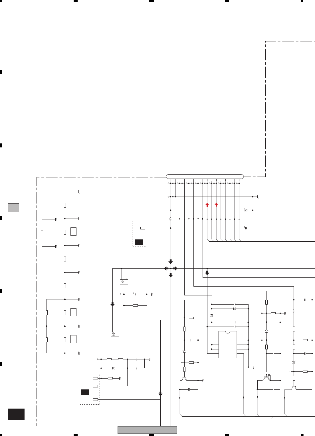
AVIC-X910BT/XS/UC
146
1234
1234
C
D
F
A
B
E
A-a A-b
A-b 1/6
ASENS
ILMSNS
ANTON
REVSNS
RL+
FL+
FR+
FL-
RL-
FR-
RR+
RR-
PCD
R2873
4.7k
R2901
100k
R2910
47k
R2900
47k
R2870
47k
R2880
10k
R2872
1k
R2871
100k
R2912
4.7
R2913
4.7
R2911
47k
R4812
0
R4811
NM
R4802
NM
R4801
NM
R4816
NM
R4815
NM
R4814
NM
R4813
NM
R4821
NM
R2902
1k
(1/4W)
R2882
1k
(1/4W)
R2874
1k
(1/4W)
R2903
4.7k
(1/4W)R2881
4.7k
(1/4W)
BUP2
GND1
DTC114EU
Q2880
GNDD
IC2890
TPD1018F
1
OUT 2
GND1 3
GND2 4
GND3 5
VDD
6IN
7GND4
8GND5
9GND6
10 DIAG
C2882
1000p/50
GNDD
BUP
GNDD
KB1
IL1
L2930
CTH1347-A
KBUP
C2901
0.1u/50
C2890 0.1u/50
L2872
CTF1410-A
C2871
1000p/50
D2900
HZU8R2(B1)
ISN
GNDD
D2910
KS926S2
Q2870
2SC4116(GRBL)
C2881
1u/16
C2892 1000p/50
GNDD
C2891 1000p/50
D2890
1SR154-400
D2891 1SR154-400
D2880
1SR154-400
D2870
UDZS5R1(B)
C2870
1000p/50
BUP1
GND2
C2880
NM
C2900
NM
Q2900
2SC4116(GRBL)
D2930
ST70-27F
D2911
RB060L-40
D2912
KS926S2
GNDD
NKBUP
GNDD
AC2
KB2
RV2
ACC
AANT
ILM
REV
PLS
PKB
RL-
FL-
RL+
FL+
RR-
FR-
RR+
FR+
NAVIC
GNDRF
GNDRF
GNDRF GNDRF GNDRF GNDRF GNDRF GNDRF
GNDRF
CN1005
CKM1376-A
1
2
3
4
5
6
7
8
9
10
11
12
13
14
15
16
10000u/16
C2911
10000u/16
C2912
CCH1018-A
C2935
(3300u)
10000u/16
C2910
(10000u)
ILM
AANT
ACC
GND
REV
PKB
PULSE
BUP
for discharge
1/4W1/4W
RL+
FL+
RR-
FR-
RL-
RR+
FL-
FR+
2910-2919
14.4V
(Reserve) (Reserve)
(Reserve)
AUUCEU
AVIC-X910BT/XS/UC
AVIC-F910BT/XS/EU5
AVIC-F910BT/XS/AU
MODEL
2880-2882
2920-2934
2890-2899
2930
PWR AMP
2900-2909
4801-4821
SHIMUKE
ASENS
Vehicle I/F
AANT
2935
NKBUP
ILMSNS
1007
1005
6/6
A
6/6
A
FM(EU):+32.6 dBs
AM(EU):+23.1 dBs
FM:+28.6 dBs
AM:+19.1 dBs
LS1:+34.9 dBs
IP-BUS/AV:+35.3 dBs
Navi Audio:+30.4 dBs
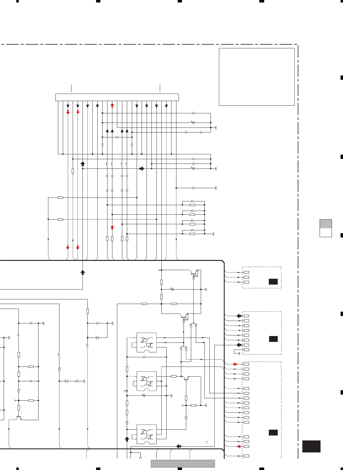
AVIC-X910BT/XS/UC 147
5678
5678
C
D
F
A
B
E
A-a A-b
A-b 1/6
RR
RR+
PKB
FL+
FR-
SRCMUTE
FR+
SREMOTE
REVSNS
FANUP
SREMOTE
OFFMUTE
SPEED
RL-
FR
FL-
FL
BREMOTE
RL+
RL
RR-
PEED
CHNG
GUIDEMUTE
MONVBS
NAVILG
NAVIRG
NAVIAL
GUIDE
GUIDEG
FRV
FRVGND
RSTMUTE
KMODEOUT
FANUP
PKBOUT
PKB
ANTON
ILMB
ILMR
ILMG
POMUTE
BREMOTE
FR
FL
RR
RL
ILMV
YSPW
YSPW
R2873
4.7k
R2870
47k
R2872
1k
R2871
100k
R2925 10k
R2924 10k
R2926
10k
R2860
390
R2861
390
R2863
22k
R2862
47k
R2864
10k
R2868
220
R2866
10k
R2867
10k
R2869
100
84
k
R2920 1k
R2921 1k
R2922 1k
R2923 1k
R4779 NM
R4780 NM
R4781 NM
R4782 NM
R2865
1k
(1/10W)
R2874
1k
(1/4W)
R2875
4.7k
(1/4W)
R
(1/
GNDA
FR
Q2863
UMD2N
2E
1
2B
2
1C
31E 4
5
1B
6
2C
GNDD
ILMG
GNDD
ANTON
GNDD
GNDD
GUIDEMUTE
D2862
DAN202U
NAVIRG
GNDD
D2871
UDZS18(B)
GNDD
C2926
1u/10
FRVGND
DTC114EU
Q2864
33u/10
C2862
D2873
1SS355
ILMR
L2871
CTF1410-A
C
100
C2861 0.1u/50
C2931 1u/10
Q2861
UMD2N
2E
1
2B
2
1C
31E 4
5
1B
6
2C
KMODEOUT
GNDD
C2925
1u/10
Q2860
UMD2N
2E
1
2B
2
1C
31E 4
5
1B
6
2C
D2860
MA111
FANUP
GNDD
47u/16
C2860
GNDD
L2870
CTF1410-A
NAVIAL
VDD5
C2872
1000p/50
RSTMUTE
ILMV
MONVBS
FRV
C2924
0.1u/50
DTC124EUA
Q2865
GNDD
L2872
CTF1410-A
D2863
DAN202U
NAVILG
ILMB
C2871
1000p/50
MUT
GUIDE
GNDD
BREMOTE
PKB
PKBOUT
FL
Q2870
2SC4116(GRBL)
Q2862
2SC4081(QRS)
C
1
D2861
UDZS8R2(B)
C2927
1u/10
C2929 NM
RR
D2872
UDZS18(B)
POMUTE
RL
GUIDEG
D2870
UDZS5R1(B)
C2870
1000p/50
C2930 0.1u/50
10u/16
C2934
C
EU
RV2
MUB
GNDA
MTB
D2874
PTZ18A
)
IC1007
PAL007C
1
2
3
4
5
6
7
8
9
10
11
12
13
14
15
16
17
18
19
20
21
22
23
24
25
C2933
2.2u/16
(3216)
C2932
2.2u/10
(2125)
C2921
1u/16
C2928
1u/10
C2922
1u/16
C2920
1u/16
C2923
1u/16
(2125)
C2936
NM
CTF1689-A-T
CTF1689-A-T
CTF1689-A-T
CTF1689-A-T C2937
NM
C2938
NM
C2940 NM
C2941 NM
C2942 NM
C2943 NM
L2932
L2933
L2934
L2931
C2939
NM
IN4
S-GND
IN2
PW.GND1
IN1
PW.GND2
TAB
PW.GND4
PW.GND3
VCC1/2
OUT2+
STBY
OUT2-
OUT4-
MUTE
OUT4+
VCC3/4
OUT3-
OUT3+
SVR
OUT1+
OUT1-
B_REMOTE
AC GND
IN3
sensing "low voltage"
or "reset"
emergency MUTE
14.4V
14.4V
5.0V
5.0V
5.0V
8.3V
to NAVI
VICS8 SWICTH
VIDEO5
TU3
SPEED PULSE
2910-2919
2900-2909
2890-2899
2880-2882
SPEED/REVSNS/PKB 2862-2869
4779-4782
Vehicle I/F 2930
1016
2940-2985
1000-1001
2900
1021-1025
NKBUP
ASENS
AANT
2835-2839
2829-2833
2805-2806
2800
ILMSNS
2810-2819
2870-2875
2830-2834
2935
PWR AMP 2920-2934
AV SECTION
2840-2865
2881-2884
1002-1004
4801-4821SHIMUKE
2920-2934
4779-4782
PWR AMP
AV SECTION
2862-2869
2870-2875
SPEED/REVSNS/PKB
VT8 2820-2829
1007
1007
1005
2/6
A
6/6
A
5/6
A
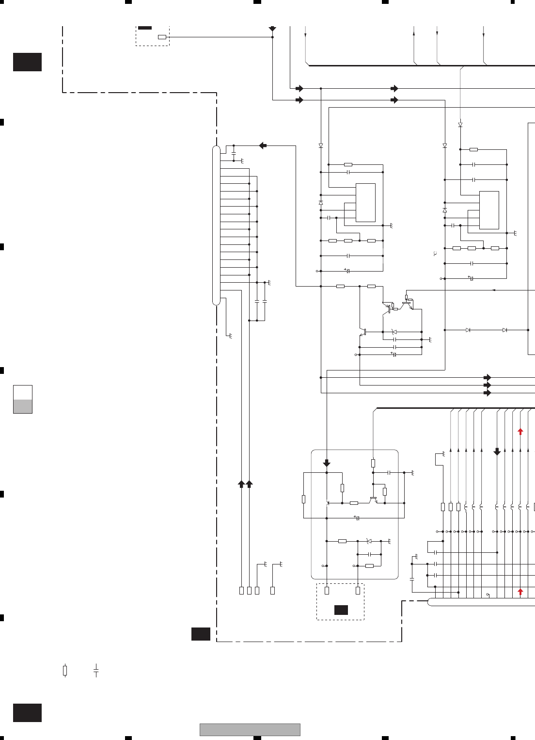
AVIC-X910BT/XS/UC
148
1234
1234
C
D
F
A
B
E
A-bA-a
A-a 1/6
A-b 1/6
ASENS
ILMSNS
ANTON
REVSNS
AV2RG
AV2RS
HDRST
AV2LS
DVEJKY
ILMR
ILMG
ILMB
ILMV
AV2VG
AV2LG
FANV
KBUP
VICSON
DCSKIPCD
VT8
NAVI5V
AV8
BUP
R2801
10k
R2940 0
R2804 100k
R2811
470
R2803
2.2k
R2802
2.7k
R2810
0
R2822
2.2k
R2951 0
R2941 100
R2942 100
R2820
2.2k
R2821
10k
R2838
NM
R2836
NM
R2837
NM
R2839
NM
R2835
NM
R2823
1M
R2833 0
R2829
NM
C2804
0.1u/50
C2811 0.1u/50
NAVI5GND
C1022
0.1u/50
100u/16
C2810
ILMGND
Q2810
2SD1760F5(R)
D2802
RB060L-40
GNDD
C2803
NM
FANGND
C1021
1000p/50
C1020
1000p/50
CCH1565-A
C2820
KBUP
FANGND
AV8
DTC114EU
Q2812
C2821 0.01u/50
BA00CC0WCP-V5
IC2801
Vadj:1.225V
1
CTL
2
VCC
3
GND
4
VOUT
5
ADJ
D2810
UDZS5R6(B)
D2821
RB060L-40
GNDV
C2812 0.1u/50
Q2870
2SC4116(GRBL)
NAVI5GND
NAVI5V
FANGND
D2820
NM
D2801
NM
GNDA
NAVI5GND
C2802 1000p/50
C2822
NM
VI5
CKS5732-A
CN1000
1
2
3
4
5
6
7
8
9
10
11
12
13
14
CKS4674-A
CN1001
1
2
3
4
5
6
7
8
9
10
11
12
13
14
15
16
17
18
19
20
C2823
0.1u/50
DTA114EU
Q2811
VT8
GNDD
FANV
ILG
EJT
RES
ILMB
ILMG
ILMR
ILMV
AUR
AURG
AUL
AULG
AUVG
NC1
Q2831
NM
Q2832
NM
VICS8
D2835
NM
C2835
NM
VICS5
NM
C2836
VISC8
GNDD
GNDD
D2824
1SR154-400
D2823
1SR154-400
C2837
NM
C2824
NM
D2825
1SS400G
GNDA
C2805 0.1u/50
C2800
1000p/50
C1023
NM
C2806
NM
VISC5
BA00CC0WCP-V5
IC2820
Vadj:1.225V
1
CTL
2
VCC
3
GND
4
VOUT
5
ADJ
CCH1565-A
C2801
L2943 CTF1556-A
L2944 CTF1556-A
L2945 CTF1556-A
L2946 CTF1556-A
L2947 CTF1675-A
L2948 CTF1675-A
L2949 CTF1675-A
L2950 CTF1675-A
2820-2829
GND
ILMGND
EJECT
RESET
ILMB
CCH1565
100u/16V
105
ILMGILMG
ILMR
ILMV
NC
AUX-R
AUX-RG
AUX-L
AUX VG
AUX-LG
NAVI5V
NAVI5V
NAVGND
NAVGND
FANV
FANGND
AV8
2801-2809
NAVI5V
NAVI5V
NAVGND
NAVGND
AV8V GND
AV8V
NAVI5V
NAVI5V
NAVI5V
NAVI5V
NAVGND
NAVGND
NAVGND
NAVGND
NM
NAVI UNIT SPJ1
8.3V
8.0V 8.0V
6.5V 6.5V
8.0V
8.3V
8.3V
5.0V 5.0V 5.0V
5.0V
5.0V
5.0V
5.0V
5.0V
5.0V
5.0V
5.0V
8.3V
8.3V
5.0V
8.5V
2829-2833
1000-1001
2800
1016
2880-28
289
2805-2806
2810-2819
2900
1021-1025
2900-2909
2940-2985
VIDEO5
to NAVI
ASENS
AA
2835-2839
VICS8 SWICTH
VT8
2900
1021-1025
2940-2985
to NAVI
1000-1001
2800
1016
2805-2806
ILMS
3/6
A
A
AV UNIT (PS/IF SECTION)
1/6
A
The > mark found on some component parts indicates
the importance of the safety factor of the part.
Therefore, when replacing, be sure to use parts of
identical designation.
Symbol indicates a resistor.
No differentiation is made between chip resistors and
discrete resistors.
NOTE :
Symbol indicates a capacitor.
No differentiation is made between chip capacitors and
discrete capacitors.
NM : No Mount
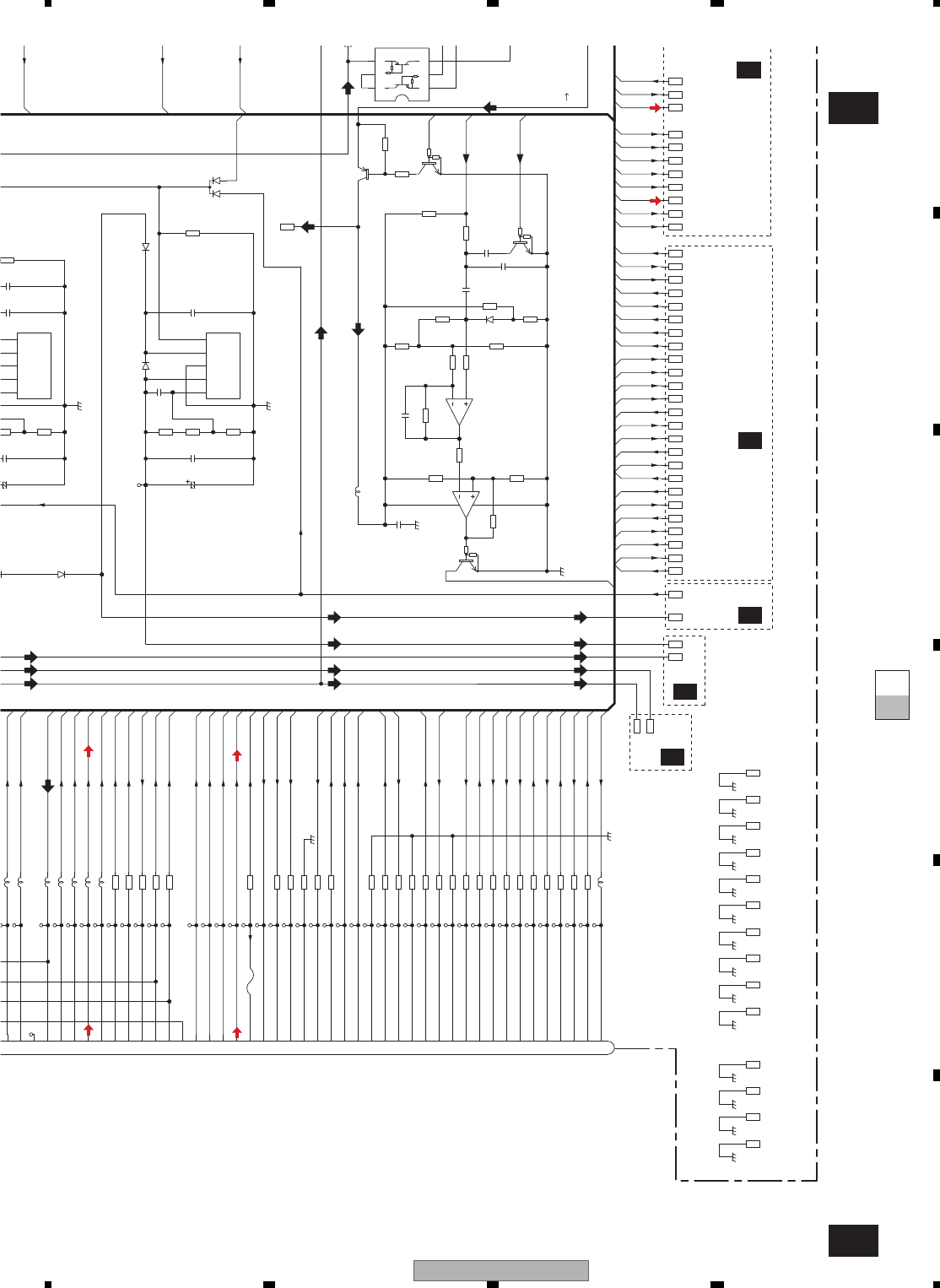
AVIC-X910BT/XS/UC 149
5678
5678
C
D
F
A
B
E
A-bA-a
A-a 1/6
A-b 1/6
GUIDE
PKB
CPUWDT3
SYSTOC3
ROT1
OPTSNS
OPTON
OFFINFO3
SYSTOCV3
OFFANS3
ROT1
RESETB
HDRST
REVSNS
DVEJKY
ROT0
BATFAULT3
AV2RG
AV2RS
RESETB
NAVIAR
AV2LS
SPEED
CTOSYS3
OFFANS3
OPTSNS
KMODEOUT
OFFINFO3
CPUWDT3
REVSNS
OPTON
CTOSYSV3
PULSE
PKBOUT
SPEED
PCHNG
PULSE
ILMR
ILMG
ILMV
FRV
ROT0
AV2VIN
AV2VG
AV2LG
NAVIAL
MONVBS
GUIDEMUTE
VICSON
SREMOTE
SYSPW
AV2RS
CTOSYSV3
SYSTOCV3
SYSTOC3
CTOSYS3
ASENS
ANTON
PCHNG
NAVIRG
NAVILG
FRVGND
GUIDEG
ILMSNS
SRCMUTE
MONVBS
NAVILG
AV2RG
NAVIRG
AV2LG
AV2VG
AV2LS
AV2VIN
NAVIAR
NAVIAL
GUIDE
SYSPW
TU3
VIDEO5
NAVI3V
BATFAULT3
VT6
SYSPW
DCSKIPCD
NAVI3V
AV8
AV8
AV8
SWACPW
NFCONT
NFCONT
R2834
100k
R2832
2.2k
R2822
2.2k
R2951 0
R2952 0
R2953 0
R2954 0
R2960 0
R2961 0
R2962 0
R2963 0
R2964 0
R2967 0
R2968 0
R2969 0
R2970 0
R2971 0
R2972 0
R2973 0
R2974 0
R2975 0
R2976 0
R2977 0
R2978 0
R2979 0
R2980 0
R2981 0
R2982 0
R2983 0
R2959 0
R1016 0
R2841
47k
R2840
100k
R2842
56k
R2843
51k
R2844
100k
R2845
51k
R2846
51k
R2848
1k R2847
1k
R2849
560k
R2850
2k
R2851
8.2k
R2852
20k
R2853
33k
R2884
4.7k
R2883
4.7k
R2821
10k
R2830
3.6k
R2831
10
R2823
1M
SYSPW
TU3
BATFAULT3
C2844
0.082u/16
IC1002
NJM2904M
5
6
7
GNDV
CTOSYSV3
GNDD
C2842
0.1u/50
GNDD
GNDA
AV2LS
C2841
1000p/50
GNDFM
NAVIRG
GUIDEG
ROT0
DTC114WK
Q2840
SYSTOC3
C2840
0.1u/50
NAVILG ILMGND
GNDRF
NAVIRG
ROT1
GNDFM
NAVIRG
OPTSNS
AV2LG
2E
1
2B
2
1C
31E 4
5
1B
6
2C
TU3
CCH1565
C282
D2
MA
HDRST
100u/16
C2830
DTC114EUA
Q2841
L1004
CTF1334-A
SRCMUTE
NAVIAL
ASENS
NAVIAR
FANGND
MONVBS
C2821
GNDD
AV2VG
NAVILG
SREMOTE
SWACPW
GUIDE
GNDA
GNDRF
SYSTOCV3
AV2RG
GNDV
Q2870
2SC4116(GRBL)
GNDD
AV2RS
D2
UD
ANTON
GNDD
FANGND
C2831 0.01u/50
OFFANS3
D2840
1SS355
IC1002
NJM2904M
3
4
2
18
NAVILG
C2832
NM
AV2VIN
OPTON
VICSON
DVEJKY
FRVGND
CPUWDT3
GNDA
NAVI3GND
6
7
8
9
10
11
12
13
14
15
16
17
18
19
20
21
22
23
24
25
26
27
28
29
30
31
32
33
34
35
36
37
38
39
40
41
42
43
44
45
46
47
48
49
50 L2940
CTF1334-A
C2833
0.1u/50
FRVGND
CTOSYS3
GNDV
GNDD
GUIDEG
ILMGND
AV8
RESETB
C2843
0.01u/50
GNDD
NAVI3GND
C2823
0.1u/50
GNDD
GNDA
ILMSNS
VT6
OFFINFO3
DTC114EU
Q2881
D2830
NM
ILMG
ILMR
ILMV
AUR
AURG
AUL
AULG
AUVG
AUV
ROT1
ROTO
NARG
NAR
NALG
NAL
N33V
FRG
FRV
BCGN
BCVN
GMUTE
GUIG
GUI
GSY1
CTSV
STCV
GSY2
CTN
STC
GSY3
OPON
OPSN
PKN
KMB
RVN
OFAN
OFIN
WDOG
RESB
PCHG
PLN
NC1
NFC
SWVDD5
BFA
D2822
DAN202U
BA00BC0WFP
IC2830
1
VC
2
VIN
3
GND
4
VDD
5
C
D2831
RR264M-400
GNDD
DCSKIPCD
D28
1SR154
D2823
1SR154-400
C2824
NM
NAVI3V
NFCONT
FU2900
CEK1276-A 250mA
12
2SA1576A(QR)
Q2882
BA00CC0WCP-V5
IC2820
Vadj:1.225V
1
CTL
2
VCC
3
GND
4
VOUT
5
ADJ
L2944 CTF1556-A
L2945 CTF1556-A
L2946 CTF1556-A
L2947 CTF1675-A
L2948 CTF1675-A
L2949 CTF1675-A
L2950 CTF1675-A
8.3V
ILMGILMG
ILMR
ILMV
NC
AUX-R
AUX-RG
AUX-L
ROT1
AUX-VG
AUX-LG
AUX-V
GND
NaviARG
ROT0
BATTERY_FAULT
BCVGND
OPTSNS
GNDSYS
GNDSYS
GUIDE
PKB
GNDSYS
CTOSYSV3
FRVGND
SYSTOCV3
GUIDEMUTE
OPTON
GUIDEG
BCV
FRV
PULSE
OFFINFO
OFFANS
KMODE
WDOG
RESETB
PCHNG
REV
NaviAR
NaviALG
NaviAL
NFCONT
NAVI33V
5.0V
SYSTOC3
CTOSYS3
8.3V
3.3V
sensing "low volta
or "reset"
emergency MU
NAVI UNIT OTJ1
6.5V
6.5V 6.5V
3.3V
5.0V
5.0V
5.0V5.0V
5.0V
8.3V 8.3V
8.3V
5.0V
8.3V
8.5V
2900
2940-2985
TU3
1002-1004
SPEED PULSE
2840-2865
2830-2834
2881-2884
AV8
VIDEO5
>
2/6
A
4/6
A
6/6
A
2/6
A
3/6
A
Navi Audio:-2.68 dBs
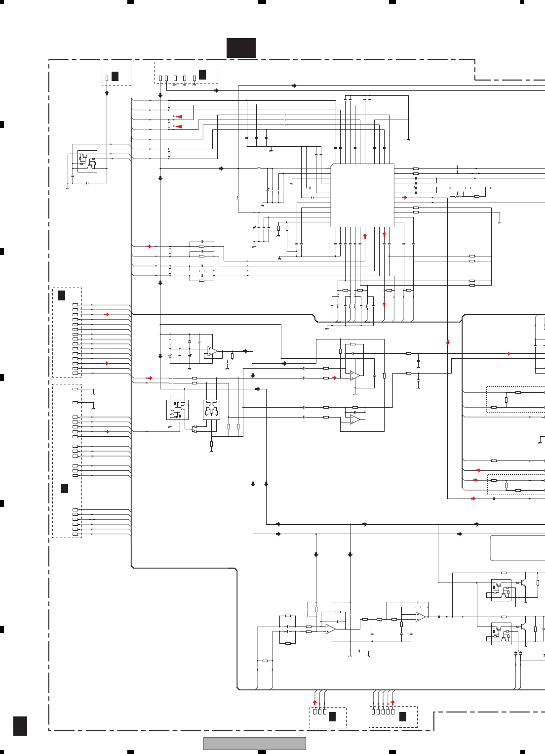
AVIC-X910BT/XS/UC
150
1234
1234
C
D
F
A
B
E
10.2 AV UNIT(A/V SECTION)(GUIDE PAGE)
2/6
A
A-a 2/6
DVDV
GUIDEG
MONVBS
AV2RS
DVDL
VCK
FRV
AMUTE
VDT
NAVIAL
NAVIAL
IPL
NAVIAR
FML
IPLG
AV2LG
NOSELR
NAVIRG
GUIDE
CDR
FMRTN
FML
AV2VIN
FMRTN
AV2LS
NAVIAR
AMUTE
NOSELL
GUIDEMUTE
AV2RG
NOSELR
TELMUTE
NAVIRG
IPLG
FMR
RSTMUTE
AV2LG
SELSDA
AV2VG
IPR
SELSCL
AV2VIN
GUIDEG
AV2RG
DVDR1
DVDV
VST
AV3VIN
GUIDEMUTE
IPL
AV2RS
DVDR
RSTIN
AV2LS
DVDL
IPRG
CDL
IPR
FMR
CDR
IPRG
CDL
AV1LS
NAVILG
GUIDE
HDRST
KMOD
WCONT
DVDR
WIREIN
NAVILG
AU4
RSTIN
AV3VG
AV2VG
AV1VG
AV1VIN
AV1LG
AV1RS
AV1RG
AV8AV8
AV8
AV8
AV8
AV8
R4071
47k
R4165 NM
R4314
NM
R4274
22k
R4176
0
R4174
22k
R4079
33
R4160
NM
R3041
1.8k
R4168 NM
R4195 220
R4188 NM
R4072
47k
R4187 NM
R4164 NM
R4075
47k
R4198 NM
R4167 NM R4278 NM
R4159 47k
R4156
100k
R4077
47k
R4155
1k
R4078 47k
R4076
47k
R4272
180
R4271
0
R4163
NM
R304447k
R4194 220
R4173
NM
R4073
47k
R3042
1.8k
R4157
100k
R4275
1k
R4166
NM
R4061
1k
R4041
75
R4313
100k
R4153
10k
R4021
75
R4171
22k
R4279 NM
R4277
1k
R4080
33
R4074
47k
R4001
75
R4161
NM
R4151
10k
R4273
180
R4154
10k
R4170
22k
R4199 NM
R4152
10k
R304347k
R4162
NM
R4276
22k
R4175
22k
R4311
NM
R4312
820
R751
0
R4158
68k
R4062
NM
C4072
CCG1203-A
GNDD
AV2VIN
C4202 1u/10
MONVBS
GNDA
GNDA
NAVIRG
C3042 CCG1203-A
C4188
1u/10
C4200 1u/10
C4182 0.1u/50
C42
1u/6.
DVDR
VST
IPRG
C4215 1u/10
FMRTN
WCONT
GNDV
10u/16
C4062
AV2VG
D4311
DAN202K
GNDV
GNDV
FML
GNDA
C4191
1u/10
C4070
CCG1203-A
C4192
1u/10
GNDA
GUIDEMUTE
22u/6.3
C4183
AV8
AV2RS
GNDV
L4172
10u
C1077
0.1u/25
C4181 0.1u/50
VDD5
C1078
0.1u/25
C4080
0.01u/50
IPLG
FRV
C4073
CCG1203-A
D4062
1SS355
GNDA
NOSELL
VIDEO5
GNDA
C4071
CCG1203-A
CCG1203-A
C4151
22u/6.3
C4174
C4221
1u/10
GNDD
C4063
0.1u/50
WIREIN
GNDD
47u/16
C4171
C4075
33p/50
C4194
1u/10
SSCL
GNDA
C4189 1u/10
C4206 1u/10
SELSDA
D4061
EDZ4R3(B)
Q3042
FMG12
1
1
5
5
4
4
2
2
3
3
CDR
C4061
0.01u/50
VCK
GNDA
C4190
1u/10
C4222
1u/10
CCG1203-A
C4152
22u/10
C4218
DVDL
DVDV
C4193 1u/10
AMUTE
VDT
C42
CCG12
C4172 0.1u/50
NOSELR
C42
1u/6.
GNDV
AV2LG
C4198 1u/10
GNDA
GUIDE
IPR
CDL
NAVIAL
NAVILG
330u/10
C4219
IC1008
NJM2125F
32
14
5
FMR
GNDA
AN15887A
IC4171
VCC1
1
BIAS1
2
GND1
3
L1-1
4
L1-2
5
R1-1
6
R1-2
7
L2-1
8
L2-2
9
VCC2
10
BIAS2
11 GND2
12
R2-1
13
R2-2
14
L3-1
15
L3-2
16
R3-1
17
R3-2
18
L4-1
19
L4-2
20
R4-1
21
R4-2
22
L5-1
23 L5-2
24
R5-1
25
R5-2 26
ROUT1 27
LOUT1 28
ROUT2 29
LOUT2 30
FB2 31
VOUT2 32
FB1 33
VOUT1 34
SDA
35
SCL
36
V1-1
37
V1-2 38
V2-1 39
V2-2 40
V3-1 41
V3-2 42
V4-1 43
V4-2 44
V5-1 45
V5-2 46
V6-1
47
V6-2
48
C4078
33p/50
Q4312
IMD3A
2E 6
2B
5
1C
4
1E
3
21B
12C
IC1016
BA4558RFVM
(2/2)
5
67
IC1015
NJM4558V
(2/2)
5
67
C3041 CCG1203-A
AV2RG
GNDV
DTC323TK
Q4314
Q3041
IMD3A
E2
6
B2
5
C1
4
E1
3
2
B1
1
C2
22u/10
C4220
SSDA
GNDV
C42
1u/6.
IC1015
NJM4558V
(1/2)
34
21
8
Q4311
NM
2E 6
2B
5
1C
4
1E
3
21B
12C
GUIDEG
GNDA
Q1016
IMD2A
2E
6
2B
5
1C
4
1E
3
2
1B
1
2C
GNDA
C4076
0.1u/50
C42
1u/6.
47u/16
C4173
TELMUTE
GNDV
SELSCL
C4217 1u/10
GNDA
C42
CCG12
C4204 1u/10
Q4313
NM
GNDV
L4171
10u
IPL
D3041
DAP202K
IC1016
BA4558RFVM
(1/2)
34
21
8
C42
1u/6.
GNDD
C4281
1u/6.3
C4079
0.01u/50
GNDA
AV2LS
KMOD
GNDV
NAVIAR
22u/10
C4232
C4159
2.2u/10
C4279
C4278
NM
GNDA
(DVD)
C4197 4.7u/10
C4195 4.7u/10
C4203 4.7u/10
C4211 4.7u/10
C4216 4.7u/10
C4210 1u/10
C4208 1u/10
C4212 1u/10
C4213 1u/10
C4186 4.7u/10
C4187 4.7u/10
C4185 4.7u/10
C4199
1u/10
C4207
1u/10
C4224
1u/10
C4201
1u/10
C4156
0.1u/16
C4157
150p/25
C4158
150p/25
C4155
0.01u/25
C4154
0.1u/16
C4160
220p/50
C4153
220p/50
C4719
C4161
NM
GNDD
C4064
NM
GNDA
RSTIN
C4184 0.1u/50
C4176
NM
C4177
NM
C4175
NM
R4201
NM
NM
VR4200
13
2
AV1VG
AV1VIN
R4200
75
GNDA
C4227 NM
C4228 NM
C4225 NM
C4226 NM
L4176
CTF1689-A-T
L4175
CTF1689-A-T
L4174
CTF1689-A-T
L4173
CTF1689-A-T
4.0V
Lch MUTE
AV SELECTOR
Rch MUTE
VTR2L
GMUTE
Normally Hi
Uttering Low
ISOLATOR LPF AMP
10.6kHz 18dB/oct
+4.6dB
VTR3
1016
NAVI L
VTR2R
VTR1R
1008
VTR1L
EVOL
NAVI R
DVD R
DVD L
VTR2
VTR1
DVD
1.0Vrms
=2.21dBs
GUIDE
4719
8.3V8.3V
8.3V
8.3V
8.3V 8.3V
8.3V
8.3V
8.3V
4.0V
4.0V
4.0V
4.0V
4.0V
8.3V
8.3V
8.3V
8.3V
4.0V 4.0V
8.3V
5.0V
5.0V
8.3V
8.3V 8.3V 8.3V
8.3V
8.3V
8.3V
4.0V4.0V
4.0V
8.3V
8.3V
5.0V
5.0V 5.0V 5.0V
(100)
1077-1078
RST
1046
AU4
4061-4069
AMUTE
3041-3045
751
4070-4089
DVD LPF
1015
4271-4289
4794
4291
4296-4299
4232
4000-4049
4163-4199
4200-4229
4278-4279
4150-4162
GUIDE MUTE
4311-4314
GUIDE MIX
4295
1020 4311-4329
4367
4288 4364-4365
4292-4293
UC
UC
1/6
A
6/6
A
1/6
A
4/6
A
3/6
A6/6
A
FM(EU): -9.5 dBs
AM(EU): -20 dBs
FM: -13.5 dBs
AM: -24 dBs
LS1:+4.804 dBs
IP-BUS/AV: +2.2 dBs
Navi Audio: -2.68 dBs
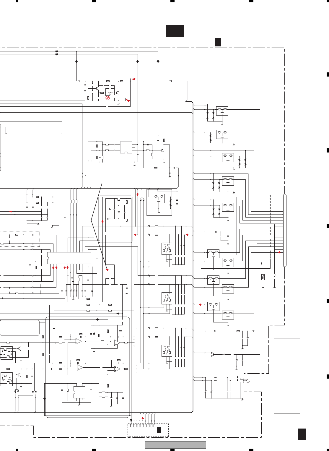
AVIC-X910BT/XS/UC 151
5678
5678
C
D
F
A
B
E
2/6
A
A-b 2/6
WIREIN
TELMUTE
BCVIN
RSTMUTE
RVOUT
AV1LG
POMUTE
PRL
NOSELR
VCK
PRR
PFR
CDR
BCGND
NOSELL
KMOD
PFL
BREMOTE
PFR
HDRST
SWR
GUIDEMUTE
SWR
RR
VST
WCONT
RL
POMUTE
SELSCL
VDT
BCGND
SELSDA
RR
HIVOL15
MONVBS
BCVIN
RL
PFL
AV3VG
SWL
CDL
SWL
AV3VIN
FRV
PRL BREMOTE
PRR
AU4
RVOUT
AV8
AV8
AV8
AV1VG
AV1VIN
AV1LS
AV1RG
AV1RS
R4347 470 R4346 470
R4345 470
R4282
NM
R4321
NM
R4794
NM
R4314
NM
R4235 680
R4274
22k
R4251
75
R4232
30k
R4252 47k
R4284
R4343 470
R4352
10k
(1/10W)
R4367
NM
R4348 470
R4328
NM
R4326
NM
R4337 22k
R4240
0
R4364
NM
R4327 NM
R4233
680
R4362
NM
R4365
NM
R4280
NM
R4341 22k
R4231
22k
R4238
NM
R4325
NM
R4366
NM
R4272
180
R4271
0
R4261
NM
R4320
NM
R4285
R4264
NM
R4301
NM
R4342 22k
R4253 47k
R4338 22k
R4275
1k
R4281
NM
R4324
NM
R4313
100k
R4339 22k
R4262
NM
R4263
0
R4322 NM
R4277
1k
R4254
100
R4323 NM
R4351
15k
R4283
R4273
180
R4255
100
R4286
R4363
NM
R4234
1k
R4329
NM
R4237
0
R4236
1.5k
R4344 470
R4239 NM
R4340 22k
R4276
22k
R4293 0
R4288
NM
R4290 NM R4295 0
R4318
NM
R4319
NM
R4287 1k
R4289 1k
R4291 1k
R4317
0
R4316
0
R4361
NM
R4311
NM
R4312
820
R4241
NM
R4296
0
R4292
NM
EF4357 CCG1067-A
3
2
1
C4264
CEVQW101M10
GNDA
C4312
NM
C4339 2200p/50
C4371 1000p/50
AG
C4362
NM
V1RG
V1R
C4284
1u/6.3
GNDD
C4293 0.1u/16
C4291 0.1u/16
C4252
CCG1203-A
L4371 CTF1334-A
NM
C4316
RL
GNDA
C4280
1u/6.3
IC1020
NM
(4/4)
5
67
RL
FL
C4340 2200p/50
D4365
PTZ27(B)
GNDD
EF4360
CCG1067-A
3
2
1
47u/16
C4289
D4362
1SR154-400
EF4351
CCG1067-A
3
2
1
C4363
NM
D4311
DAN202K
C4282
NM
FRV2
C4342 2200p/50
C4337 2200p/50
C4318
NM
C4361
NM
L4352
CTF1556-A
RR
GNDA
D4355
DAN202U
EF4352
CCG1067-A
3
2
1
C4262
NM
GNDA
10u/16
C4294
IC1020
NM
(1/4)
311
21
4
GNDA
SWL
C4263
NM
GNDA
C4251 0.047u/50
GNDA
D4371
UDZS5R6(B)
GNDV
EF4356 CCG1067-A
3
2
1
MN
2034C
Q4261
NM
IC1020
NM
(2/4)
10
98
C4351
0.1u/25
C4364
NM
IC4271
PML018A
IN5-_L
1
IN5+_L
2
IN4+_L
3
IN4-_L
4
5IN3_L
6IN2_L
7IN1_L
8Vref
9Vcc
10 Front_L
11 Rear_L
12 Pre/SW_L
13 Vp
14 Pref 15
PGND
16
Pre/SW_R
17
Rear_R
18
Front_R
19
DATA
20
CLK
21
STB
22
GND
23
IN1_R
24
IN2_R
25
IN3_R
26
IN4-_R
27
IN4+_R
28
IN5+_R
Q4331
FMG12
1
1
5
5
4
4
2
2
3
3
FU4352 CEK1259-A
12
D4312
NM
EF4353
CCG1067-A
3
2
1
C4287
1u/6.3
GNDD
EF4355 CCG1067-A
3
2
1
C4314 NM
C4283
NM
V2V
V1L
HIVOL
CN1015
CKN1042-A
2
3
1
GNDD
C4303 NM
GNDA
TELM
C4231
1u/10
C4315 NM
GNDA
10u/16
C4288
GNDD
GNV
D4361
1SS355
C4254
0.1u/25
Q4333
FMG12
1
1
5
5
4
4
2
2
3
3
C4285
1u/6.3
EF4359
CCG1067-A
3
2
1
L4372 CTF1334-A
C4296
0.1u/16
POMUTE
GNDA
IC1020
NM
(3/4)
12
13 14
C4253
CCG1203-A
EF4361
CCG1067-A
3
2
1
EF4733 NM
3
2
1
EF4358
CCG1067-A
3
2
1
BREMOTE
RR
GNDD
C4271
CCG1203-A
C4353
1000p/50
C4304 NM
V1LG
C4276
1u/6.3
BCG
L4271
2.2u
C4372 1000p/50
V2G
GNDA
C4313 NM
C4261
NM
GNDA
GNDD
C4317 NM
2SA1576A(RS)
Q4232
SWR
RVO
GNDV
C4341 2200p/50
V1V
GNDA
GNDV
GNDD
GNDA
Q4312
IMD3A
2E 6
2B
5
1C
4
1E
1B
2C
D4331
DAP202K
C4286
1u/6.3
IC1021
NM
CONT
1
GND
2
NB
3VOUT 4
5
VIN
Q4231
2SC4081(QRS)
Q4332
FMG12
1
1
5
5
4
4
2
2
3
3
FL
KMD
DTC323TK
Q4314
D4357
MALS068X
D4360
1SR154-400
GNDD
V1VG
FR
D4301
NM
C4275
1u/6.3
WCT
Q4311
NM
2E 6
2B
5
1C
4
1E
1B
2C
GNDD
D4372
UDZS5R6(B)
GNDA
D4356
MALS068X
FR
D4363
MALS068X
D4368
NM
BCV
C4273
1u/6.3
C4233
CEVQW101M10
GNDD
C4301
NM
D4359
MALS068X
BREM
GNDV
GNDA
C4277
CCG1203-A
RSTMUTE
Q4313
NM
C4338 2200p/50
C4352
0.01u/50
GNDD
C4274
1u/6.3
WRI
GNDD
L4231
CTF1473-A
D4358
MALS068X
EF4354 CCG1067-A
3
2
1
GNDD
4.7u/16
C4295
C4281
u/6.3
Q4301 NM
CN1016
CKM1460-A
1
2
3
4
5
6
7
8
9
10
11
12
14
15
16
17
18
19
20
21
22
23
24
13
L4351
2.2u
D4364
PTZ27(B)
HDRST
C4311
NM
CCP1483-A
VR4231
13
2
miniSMDC075F/24
FU4351
12
BCISO
C4290
NM
C4292
NM
C4279
NM
C4278
NM
C4241
NM
IC4251
NJM2505AF
Vout 1
GND 2
V+ 3
Vin
4
5VGND
C4719
NM
C4297
1u/10
GNDA
R4331
820
R4332
820
R4333
820
R4334
820
R4335
820
R4336
8204.7u/16
C4336
4.7u/16
C4335
4.7u/16
C4334
4.7u/16
C4333
4.7u/16
C4332
4.7u/16
C4331
D4351
MALS180X
D4353
MALS180X
D4366
MALS180X
D4354
MALS180X
D4776
NM
D4775
MALS180X
C4298
10p/50
C4299
1000p/50
GNDV
C4300
100p/50
R4298
NM
R4297
0
C4305
0.01u/50
BACK CAMERA
BCVGND
VTR2V
TELMUTE
RR
VTR1L
GNDV
FR
VTR1V
SWL
3.15A
4351-4363
GMUTE
Normally Hi
Uttering Low
VTR2GND
BREM
FM
KMODE
FM
FM
FRONTGND
IP BUS
VTR1LGND
IP BUS
REARVOUT
IP BUS
SWGND
IP BUS
VTR1VGND
VTR1RGND
GUIDE
SWR
FL
RL
SELOUT IN
BCV
SELOUT IN
REARGND
DVD R
DVD L
CD/DVD
CD/DVD
VIDEO to NAVI
4231-4249
LEVEL SHIFT
VTR1R
4261-4269
4251-4259
NM
NM
4292
TELMUTE
4371-4374
MUTE
4.0V 4.0V
8.3V
8.3V
8.3V
8.3V
8.3V
8.3V
8.3V
8.3V
8.3V8.3V
8.3V
4.0V
5.0V 5.0V
5.0V5.0V5.0V
18V18V
18V
18V
18V 18V 18V 18V 18V
NM
0R0
0R0
E MUTE
4
HIVOL15
1021
4361-4364
4366
4368
GUIDE MIX
4295
1020 4311-4329
4367
4288 4364-4365
4292-4293
4331-4349
WIRED REMOTE
4355
4353
4351
4365
4352
4364
4361
KMOD
AV CONNECTOR
4366
4733
4775-4776
1016
VIDEO BUFFER
HIVOL12
4301-4309
HIVOL15
4271-4289
AU4 1008
3041-3045
1016
4351-4363
EVOL
4301-4309
4070-4089
751
4371-4374
AMUTE
4150-4162
4292-4293
4288
4292
LEVEL SHIFT
DVD LPF
VODEO BUFFER
4794
1021
4368
4364
1020
4261-4269
GUIDE MIX
4291
BACK CAMERA
4361
4775-4776
WIRED REMOTE
4232
4231-4249
1015
4353
4061-4069
MUTE
TELMUTE 4331-4349
4200-4229
4351
4366
AV SELECTOR
4295
4364-4365
4251-4259
4000-4049
4367
RST
1016
1077-1078
KMOD
HIVOL12
4355
4733
GUIDE
4366
4296-4299
4163-4199
4311-4329
4352
AV CONNECTOR
4361-4364
4278-4279
4311-4314
4365
4719
1046
GUIDE MUTE
NM
NM
>
1/6
A
AV UNIT (A/V SECTION)
2/6
A
FM(EU):+5.8 dBs
AM(EU): -3.7 dBs
FM:+1.8 dBs
AM: -7.7 dBs
LS1:+8.1 dBs
IP-BUS/AV:+8.5 dBs
Navi Audio:+3.7 dBs
FM(EU): -9.5 dBs
AM(EU): -20 dBs
FM: -13.5 dBs
AM: -24 dBs
LS1:+4.804 dBs
IP-BUS/AV: +2.2 dBs
Navi Audio: -2.68 dBs
FM(EU): +6.6 dBs
AM(EU): -2.9 dBs
FM: +2.6 dBs
AM: -6.9 dBs
LS1:+8.904 dBs
IP-BUS/AV: +9.3 dBs
Navi Audio: +4.42 dBs
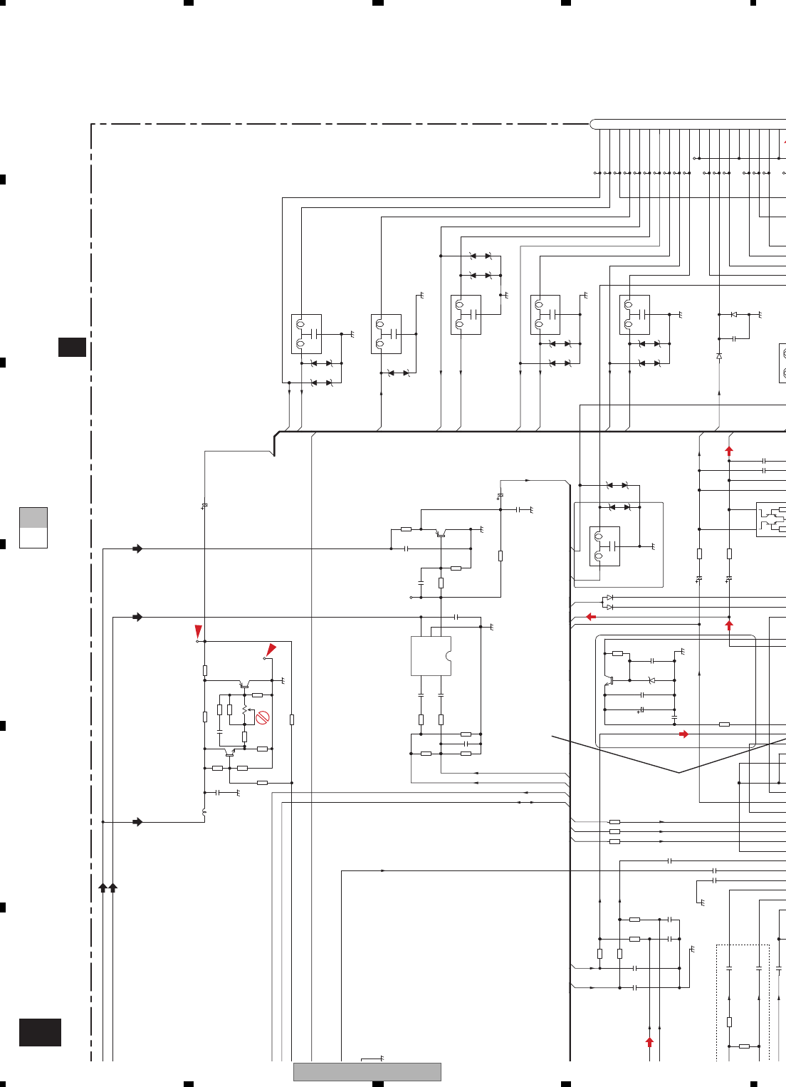
AVIC-X910BT/XS/UC
152
1234
1234
C
D
F
A
B
E
A-a A-b
A-b 2/6
BCVIN
RVOUT
AV1LG
POMUTE
VCK
PRR
CDR
BCGND
VST
SELSCL
VDT
BCGND
SELSDA
RR
MONVBS
BCVIN
RL
AV3VG
CDL
SWL
AV3VIN
FRV
PRL BREMOTE
RVOUT
AV8
AV1VG
AV1VIN
AV1LS
AV1RG
AV1RS
R4235 680
R4274
22k
R4251
75
R4232
30k
R4252 47k
R4284
k
R4240
0
R4233
680
R4231
22k
R4238
NM
R4261
NM
R4285
R4264
NM
R4301
NM
R4253 47k
R4275
1k
R4262
NM
R4263
0
R4254
100
R4283
R4255
100
R4286
R4234
1k
R4237
0
R4236
1.5k
R4239 NM
k
R4287 1k
R4289 1k
R4291 1k
R4241
NM
R4292
NM
EF4357 CCG1067-A
3
2
1
C4264
CEVQW101M10
AG
V1RG
V1R
C4284
1u/6.3
C4252
CCG1203-A
RL
C4340 2200p/50
D4362
1SR154-400
EF4351
CCG1067-A
31
C4282
NM
FRV2
C4337 2200p/50
C4262
NM
GNDA
SWL
C4263
NM
GNDA
C4251 0.047u/50
GNDV
EF4356 CCG1067-A
3
2
1
MN
2034C
Q4261
NM
C4351
0.1u/25
15
16
17
18
19
20
21
22
23
24
25
26
27
28
Q4331
FMG12
1
1
2
2
EF4355 CCG1067-A
3
2
1
C4283
NM
V1L
C4303 NM
NDA
C4231
1u/10
GNDD
GNV
C4254
0.1u/25
C4253
CCG1203-A
EF4733 NM
3
2
1
EF4358
CCG1067-A
3
2
1
GNDD
C4271
CCG1203-A
C4304 NM
V1LG
BCG
C4261
NM
GNDA
2SA1576A(RS)
Q4232
SWR
RVO
GNDV
V1V
GNDV
GNDD
D4331
DAP202K
C4286
1u/6.3
Q4231
2SC4081(QRS)
FL
KMD
D4357
MALS068X
D4360
1SR154-400
V1VG
FR
D4301
NM
GNDD
D4356
MALS068X
D4363
MALS068X
BCV
C4273
1u/6.3
C4233
CEVQW101M10
C4301
NM
D4359
MALS068X
BREM
GNDV
GNDD
C4274
1u/6.3
GNDD
L4231
CTF1473-A
D4358
MALS068X
EF4354 CCG1067-A
3
2
1
GNDD
Q4301 NM
CN1016
CKM1460-A
6
7
8
9
10
11
12
14
15
16
17
18
19
20
21
22
23
24
13
CCP1483-A
VR4231
13
2
BCISO
C4279
NM
C4278
NM
C4241
NM
IC4251
NJM2505AF
Vout 1
GND 2
V+ 3
Vin
4
5VGND
C4297
1u/10
GNDA
R4331
820
R4332
8204.7u/16
C4332
4.7u/16
C4331
D4351
MALS180X
D4353
MALS180X
D4366
MALS180X
D4354
MALS180X
D4776
NM
D4775
MALS180X
GNDV
BACK CAMERA
BCVGND
VTR1L
GNDV
FR
VTR1V
SWL
4351-4363
BREM
FM
KMODE
FRONTGND
VTR1LGND
IP BUS
REARVOUT
SWGND
IP BUS
VTR1VGND
VTR1RGND
SWR
FL
RL
SELOUT IN
BCV
REARGND
R
L
CD/DVD
VIDEO to NAVI
4231-4249
LEVEL SHIFT
VTR1R
4261-4269
4251-4259
NM
4292
8.3V
8.3V
8.3V
8.3V
8.3V8.3V
5.0V 5.0V
5.0V5.0V5.0V
18V
NM
0R0
0R0
AV CONNECTOR
4366
4733
4775-4776
1016
VIDEO BUFFER
HIVOL12
4301-4309
NM
NM
AV UNIT (A/V SECTION)
2/6
A
FM(EU): +6.6 dBs
AM(EU): -2.9 dBs
FM: +2.6 dBs
AM: -6.9 dBs
LS1:+8.904 dBs
IP-BUS/AV: +9.3 dBs
Navi Audio: +4.42 dBs
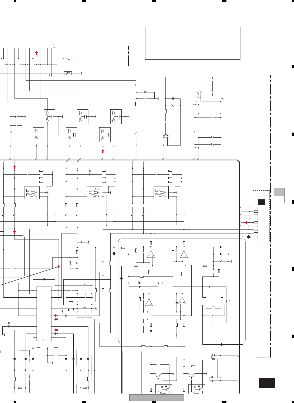
AVIC-X910BT/XS/UC 153
5678
5678
C
D
F
A
B
E
A-a A-b
A-b 2/6
WIREIN
TELMUTE
RSTMUTE
PRL
NOSELR
PRR
PFR
NOSELL
KMOD
PFL
BREMOTE
PFR
HDRST
SWR
GUIDEMUTE
SWR
RR
WCONT
RL
POMUTE
HIVOL15
PFL
SWL
SWL
PRL BREMOTE
PRR
AU4
AV8
AV8
R4347 470 R4346 470
R4345 470
R4282
NM
R4321
NM
R4794
NM
R4314
NM
R4274
22k
R4343 470
R4352
10k
(1/10W)
R4367
NM
R4348 470
R4328
NM
R4326
NM
R4337 22k
R4364
NM
R4327 NM
R4362
NM
R4365
NM
R4280
NM
R4341 22k
R4325
NM
R4366
NM
R4320
NM
R4342 22k
R4338 22k
R4275
1k
R4281
NM
R4324
NM
R4313
100k
R4339 22k
R4322 NM
R4277
1k
R4323 NM
R4351
15k
R4363
NM
R4329
NM
R4344 470
R4340 22k
R4276
22k
R4293 0
R4288
NM
R4290 NM R4295 0
R4318
NM
R4319
NM
R4317
0
R4316
0
R4361
NM
R4311
NM
R4312
820
R4296
0
R4292
NM
GNDA
C4312
NM
C4339 2200p/50
C4371 1000p/50
AG
C4362
NM
C4284
1u/6.3
GNDD
C4293 0.1u/16
C4291 0.1u/16
L4371 CTF1334-A
NM
C4316
RL
GNDA
C4280
1u/6.3
IC1020
NM
(4/4)
5
67
RL
FL
C4340 2200p/50
D4365
PTZ27(B)
GNDD
EF4360
CCG1067-A
3
2
1
47u/16
C4289
D4362
1SR154-400
EF4351
CCG1067-A
3
2
1
C4363
NM
D4311
DAN202K
C4342 2200p/50
C4337 2200p/50
C4318
NM
C4361
NM
L4352
CTF1556-A
RR
GNDA
D4355
DAN202U
EF4352
CCG1067-A
3
2
1
GNDA
10u/16
C4294
IC1020
NM
(1/4)
311
21
4
SWL
GNDA
GNDA
D4371
UDZS5R6(B)
IC1020
NM
(2/4)
10
98
C4351
0.1u/25
C4364
NM
IC4271
PML018A
IN5-_L
1
IN5+_L
2
IN4+_L
3
IN4-_L
4
5IN3_L
6IN2_L
7IN1_L
8Vref
9Vcc
10 Front_L
11 Rear_L
12 Pre/SW_L
13 Vp
14 Pref 15
PGND
16
Pre/SW_R
17
Rear_R
18
Front_R
19
DATA
20
CLK
21
STB
22
GND
23
IN1_R
24
IN2_R
25
IN3_R
26
IN4-_R
27
IN4+_R
28
IN5+_R
Q4331
FMG12
1
1
5
5
4
4
2
2
3
3
FU4352 CEK1259-A
12
D4312
NM
EF4353
CCG1067-A
3
2
1
C4287
1u/6.3
GNDD
C4314 NM
V2V
HIVOL
CN1015
CKN1042-A
2
3
1
GNDD
TELM
C4315 NM
GNDA
10u/16
C4288
D4361
1SS355
Q4333
FMG12
1
1
5
5
4
4
2
2
3
3
C4285
1u/6.3
EF4359
CCG1067-A
3
2
1
L4372 CTF1334-A
C4296
0.1u/16
POMUTE
GNDA
IC1020
NM
(3/4)
12
13 14
EF4361
CCG1067-A
3
2
1
BREMOTE
RR
C4271
CCG1203-A
C4353
1000p/50
C4276
1u/6.3 L4271
2.2u
C4372 1000p/50
V2G
GNDA
C4313 NM
GNDD
C4317 NM
SWR
C4341 2200p/50
GNDA
GNDA
4312
MD3A
2E 6
2B
5
1C
4
IC1021
NM
CONT
1
GND
2
NB
3VOUT 4
5
VIN
Q4332
FMG12
1
1
5
5
4
4
2
2
3
3
FL
KMD
DTC323TK
Q4314
D4360
1SR154-400
GNDD
FR
C4275
1u/6.3
WCT
4311
NM
2E 6
2B
5
1C
4
GNDD
D4372
UDZS5R6(B)
GNDA
FR
D4368
NM
C4273
1u/6.3
GNDD
BREM
GNDA
C4277
CCG1203-A
RSTMUTE
Q4313
NM
C4338 2200p/50
C4352
0.01u/50
C4274
1u/6.3
WRI
4.7u/16
C4295
1
2
3
4
5
6
7
8
9
10
11
12
14
15
13
L4351
2.2u
D4364
PTZ27(B)
HDRST
C4311
NM
miniSMDC075F/24
FU4351
12
C4290
NM
C4292
NM
C4719
NM
C4297
1u/10
GNDA
R4331
820
R4332
820
R4333
820
R4334
820
R4335
820
R4336
8204.7u/16
C4336
4.7u/16
C4335
4.7u/16
C4334
4.7u/16
C4333
4.7u/16
C4332
4.7u/16
C4331
C4298
10p/50
C4299
1000p/50
C4300
100p/50
R4298
NM
R4297
0
C4305
0.01u/50
VTR2V
TELMUTE
RR
FR
SWL
3.15A
GMUTE
Normally Hi
Uttering Low
VTR2GND
BREM
FM
KMODE
FM
FM
FRONTGND
IP BUS
IP BUS
IP BUS
SWGND
IP BUS
GUIDE
SWR
FL
RL
SELOUT IN
SELOUT IN
REARGND
CD/DVD
CD/DVD
NM
4292
TELMUTE
4371-4374
MUTE
4.0V 4.0V
8.3V
8.3V
8.3V
8.3V
8.3V
4.0V
18V18V
18V
18V
18V 18V 18V 18V
UTE HIVOL15
1021
4361-4364
4366
4368
UIDE MIX
5
4311-4329
4367
8 4364-4365
2-4293
4331-4349
WIRED REMOTE
4355
4353
4351
4365
4352
4364
4361
KMOD
HIVOL12
4301-4309
HIVOL15
4271-4289
AU4 1008
3041-3045
1016
4351-4363
EVOL
4301-4309
4070-4089
751
4371-4374
AMUTE
4150-4162
4292-4293
4288
4292
LEVEL SHIFT
DVD LPF
VODEO BUFFER
4794
1021
4368
4364
1020
4261-4269
GUIDE MIX
4291
BACK CAMERA
4361
4775-4776
WIRED REMOTE
4232
4231-4249
1015
4353
4061-4069
MUTE
TELMUTE 4331-4349
4200-4229
4351
4366
AV SELECTOR
4295
4364-4365
4251-4259
4000-4049
4367
RST
1016
1077-1078
KMOD
HIVOL12
4355
4733
GUIDE
4366
4296-4299
4163-4199
4311-4329
4352
AV CONNECTOR
4361-4364
4278-4279
4311-4314
4365
4719
1046
GUIDE MUTE
>
1/6
A
FM(EU):+5.8 dBs
AM(EU): -3.7 dBs
FM:+1.8 dBs
AM: -7.7 dBs
LS1:+8.1 dBs
IP-BUS/AV:+8.5 dBs
Navi Audio:+3.7 dBs
FM(EU): -9.5 dBs
AM(EU): -20 dBs
FM: -13.5 dBs
AM: -24 dBs
LS1:+4.804 dBs
BUS/AV: +2.2 dBs
avi Audio: -2.68 dBs
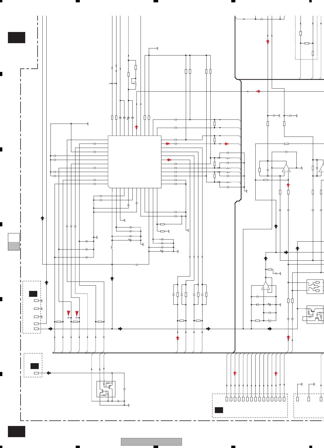
AVIC-X910BT/XS/UC
154
1234
1234
C
D
F
A
B
E
A-bA-a
A-a 2/6
A-b 2/6
MONVBS
AV2RS
DVDL
FRV
NAVIAL
NAVIAL
NAVIAR
AV2LG
NAVIRG
GUIDE
CDR
AV2VIN
AV2LS
NAVIAR
AV2RG
NAVIRG
FMR
RSTMUTE
AV2LG
AV2VG
IPR
AV2VIN
GUIDEG
AV2RG
DVDR1
DVDV
AV3VIN
GUIDEMUTE
AV2RS
RSTIN
AV2LS
IPRG
CDL
CDR
AV1LS
NAVILG
HDRST
DVDR
NAVILG
AV3VG
AV2VG
AV1VG
AV1VIN
AV1LG
AV1RS
AV1RG
AV8
AV8
AV8
R4071
47k
R4165 NM
R4274
22k
R4176
0
R4174
22k
R4079
33
R3041
1.8k
R4168 NM
R4195 220
R4188 NM
R4072
47k
R4187 NM
R4164 NM
R4075
47k
R4198 NM
R4167 NM R4278 NM
R4077
47k
R4078 47k
R4076
47k
R4272
180
R4163
NM
k
R4194 220
R4173
NM
R4073
47k
R3042
1.8k R4275
1k
R4166
NM
R4061
1k
R4041
75 R4021
75
R4171
22k
R4279 NM
R4080
33
R4074
47k
R4001
75
R4170
22k
R4199 NM
k
R4175
22k
R4062
NM
C4072
CCG1203-A
GNDD
AV2VIN
C4202 1u/10
MONVBS
GNDA
NAVIRG
C3042 CCG1203-A
C4188
1u/10
C4200 1u/10
C4182 0.1u/50
C4215 1u/10
GNDV
10u/16
C4062
AV2VG
GNDV
GNDV
GNDA
C4191
1u/10
C4070
CCG1203-A
C4192
1u/10
GNDA
GUIDEMUTE
22u/6.3
C4183
AV8
AV2RS
GNDV
L4172
10u
C1077
0.1u/25
C4181 0.1u/50
VDD5
C1078
0.1u/25
C4080
0.01u/50
FRV
C4073
CCG1203-A
D4062
1SS355
GNDA
VIDEO5
GNDA
C4071
CCG1203-A
22u/6.3
C4174
C4221
1u/10
GNDD
C4063
0.1u/50
GNDD
47u/16
C4171
C4075
33p/50
C4194
1u/10
SSCL
GNDA
C4189 1u/10
C4206 1u/10
D4061
EDZ4R3(B)
Q3042
FMG12
1
1
5
4
2
2
3
C4061
0.01u/50
C4190
1u/10
C4222
1u/10
22u/10
C4218
C4193 1u/10
CC
C4172 0.1u/50
GNDV
AV2LG
C4198 1u/10
GNDA
GUIDE
CDL
NAVIAL
NAVILG
330u/10
C4219
IC1008
NJM2125F
32
14
5
GNDA
AN15887A
IC4171
VCC1
1
BIAS1
2
GND1
3
L1-1
4
L1-2
5
R1-1
6
R1-2
7
L2-1
8
L2-2
9
VCC2
10
BIAS2
11 GND2
12
R2-1
13
R2-2
14
L3-1
15
L3-2
16
R3-1
17
R3-2
18
L4-1
19
L4-2
20
R4-1
21
R4-2
22
L5-1
23 L5-2
24
R5-1
25
R5-2 26
ROUT1 27
LOUT1 28
ROUT2 29
LOUT2 30
FB2 31
VOUT2 32
FB1 33
VOUT1 34
SDA
35
SCL
36
V1-1
37
V1-2 38
V2-1 39
V2-2 40
V3-1 41
V3-2 42
V4-1 43
V4-2 44
V5-1 45
V5-2 46
V6-1
47
V6-2
48
C4078
33p/50
67
C3041 CCG1203-A
AV2RG
GNDV
Q3041
IMD3A
E2
B2
C1 E1
3
2
B1
1
C2
22u/10
C4220
SSDA
GNDV
IC1015
NJM4558V
(1/2)
34
21
8
GUIDEG
Q1016
IMD2A
2E
6
2B
5
1C
4
1E
3
2
1B
1
2C
C4076
0.1u/50
47u/16
C4173
GNDV
C4217 1u/10
C4204 1u/10
GNDV
L4171
10u
GNDD
C4079
0.01u/50
GNDA
AV2LS
GNDV
NAVIAR
22u/10
C4232
C4278
NM
C4197 4.7u/10
C4195 4.7u/10
C4203 4.7u/10
C4211 4.7u/10
C4216 4.7u/10
C4210 1u/10
C4208 1u/10
C4212 1u/10
C4213 1u/10
C4186 4.7u/10
C4187 4.7u/10
C4185 4.7u/10
C4199
1u/10
C4207
1u/10
C4224
1u/10
C4201
1u/10
C4064
NM
GNDA
C4184 0.1u/50
C4176
NM
C4177
NM
C4175
NM
R4201
NM
NM
VR4200
13
2
AV1VG
AV1VIN
R4200
75
GNDA
C4227 NM
C4228 NM
C4225 NM
C4226 NM
L4176
CTF1689-A-T
L4175
CTF1689-A-T
L4174
CTF1689-A-T
L4173
CTF1689-A-T
4.0V
AV SELECTOR
VTR2L
VTR3
NAVI L
VTR2R
VTR1R
1008
VTR1L
EVOL
NAVI R
DVD R
DVD L
VTR2
VTR1
DVD
1.0Vrms
=2.21dBs
8.3V8.3V
8.3V
8.3V
8.3V 8.3V
8.3V
4.0V
4.0V
5.0V
5.0V
8.3V
8.3V 8.3V 8.3V
8.3V
8.3V
8.3V
4.0V4.0V
4.0V
8.3V
8.3V
5.0V
5.0V 5.0V 5.0V
(100)
1077-1078
RST
1046
AU4
4061-4069
4070-4089
DVD LPF
1015
4271-4289
4794
4291
4296-4299
4232
4000-4049
4163-4199
4200-4229
4278-4279
UC
1/6
A
6/6
A
1/6
A
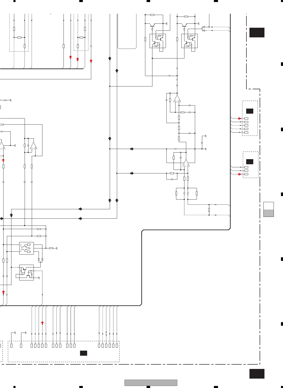
AVIC-X910BT/XS/UC 155
5678
5678
C
D
F
A
B
E
A-bA-a
A-a 2/6
A-b 2/6
DVDV
GUIDEG
DVDL
VCK
AMUTE
VDT
IPL
FML
IPLG
NOSELR
FMRTN
FML
FMRTN
AMUTE
NOSELL
GUIDEMUTE
NOSELR
TELMUTE
IPLG
FMR
SELSDA
IPR
SELSCL
VST
IPL
DVDR
DVDL
IPRG
CDL
IPR
FMR
CDR
IPRG
GUIDE
KMOD
WCONT
DVDR
WIREIN
AU4
RSTIN
AV8AV8
AV8
R4314
R4274
22k
R4160
NM
R3041
1.8k R4072
47k
R4159 47k
R4156
100k
R4077
47k
R4155
1k
R4078 47k
R4076
47k
R4272
180
R4271
0
R304447k
R4073
47k
R3042
1.8k
R4157
100k
R4275
1k
R4313
100k
R4153
10k
R4277
1k
R4161
NM
R4151
10k
R4273
180
R4154
10k
R4152
10k
R304347k
R4162
NM
R4276
22k
R4311
NM
R4312
820
R751
0
R4158
68k
C4072
CCG1203-A
MONVBS
GNDA
C3042 CCG1203-A
DVDR
VST
IPRG
FMRTN
WCONT
GNDV
D4311
DAN202K
GNDV
FML
C4070
CCG1203-A
GNDA
C4080
0.01u/50
IPLG
C4073
CCG1203-A
NOSELL
GNDA
CCG1203-A
C4151
WIREIN
SELSDA
Q3042
FMG12
1
1
5
5
4
4
2
2
3
3
CDR
VCK
G
CCG1203-A
C4152
DVDL
DVDV
AMUTE
VDT
CC
NOSELR
IPR
CDL
FMR
C4078
33p/50
Q4312
IMD3A
2E 6
2B
5
1C
4
1E
3
21B
12C
IC1016
BA4558RFVM
(2/2)
5
67
IC1015
NJM4558V
(2/2)
5
67
C3041 CCG1203-A
DTC323TK
Q4314
Q3041
IMD3A
E2
6
B2
5
C1
4
E1
3
2
B1
1
C2
GNDV
IC1015
NJM4558V
(1/2)
34
1
Q4311
NM
2E 6
2B
5
1C
4
1E
3
21B
12C
GNDA
GNDA
C40
0.1u/
TELMUTE
SELSCL
GNDA
CC
Q4313
NM
IPL
D3041
DAP202K
IC1016
BA4558RFVM
(1/2)
34
21
8
C4281
1u/6.3
KMOD
GNDV
C4159
2.2u/10
GNDA
(DVD)
C4156
0.1u/16
C4157
150p/25
C4158
150p/25
C4155
0.01u/25
C4154
0.1u/16
C4160
220p/50
C4153
220p/50
C4161
NM
GNDD
RSTIN
Lch MUTE
Rch MUTE
GMUTE
Normally Hi
Uttering Low
ISOLATOR LPF AMP
10.6kHz 18dB/oct
+4.6dB
1016
GUIDE
4719
8.3V 8.3V
8.3V
8.3V
8.3V
4.0V4.0V
4.0V
4.0V
8.3V
8.3V
8.3V
8.3V
4.0V 4.0V
8.3V
AMUTE
3041-3045
751
4070-4089
DVD LPF
1015
4150-4162
GUIDE MUTE
4311-4314
GUIDE MIX
4295
1020 4311-4329
4367
4288 4364-4365
4292-4293
UC
UC
4/6
A
3/6
A
6/6
A
FM(EU): -9.5 dBs
AM(EU): -20 dBs
FM: -13.5 dBs
AM: -24 dBs
LS1:+4.804 dBs
IP-BUS/AV: +2.2 dBs
Navi Audio: -2.68 dBs
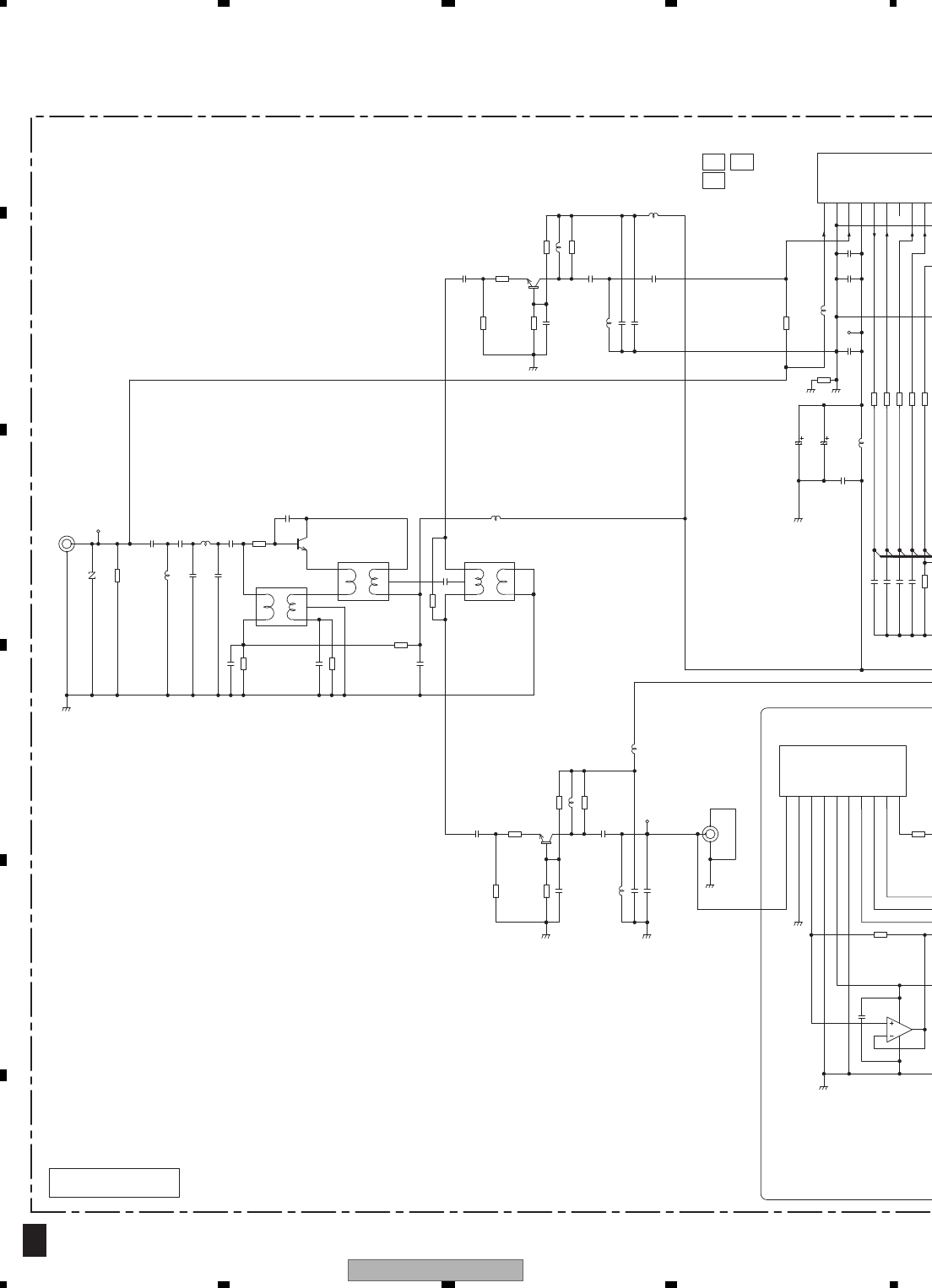
AVIC-X910BT/XS/UC
156
1234
1234
C
D
F
A
B
E
10.3 AV UNIT(TUNER SECTION)
3/6
A
TUNSL
TUNCE2
TUNCE1
TUNCLK
TUNDO
R1442
68
R1421
150
R1426
NM
R1443 1.5k
R1441
150
R1413
100
R1411 33
R1482
NM
R1410 820
R1412
3.3k
R1481
NM
R1409
1M
R1424 680
R1444 680
R1425 180
R1445 150
R1422
68
R1423 1.5k
R1461 680
R1462 680
R1463 680
R1464 680
R1465 680
R1466
22k
R1434
NM
C1421
2200p/50
C1463
NM
TMC
G
GNDRF
Y1461
1
AM_ANT
2
RF_GND
3
FM_ANT
4
VCC
5
SL
6
CE2
NC
7
WC
8
CE1
9
CK
10
L1401
0.12u
GNDRF
C1464
100p/50
C1422
2200p/50
TUVCC
T1403
CTC1192-A
1
2
34
5
L1423
0.1m
GNDRF
L1403
0.1m
C1465
0.01u/50
GNDRF
CN1441
CKX1046-A
1
2
3
RFIN
C1405
47p/50
L1443
1u
GNDA
C1445 NM
C1409
2200p/50
L1421 0.22u
C1423
15p/50
C1443
22p/50
C1425 NM
NM
Y1481
1
ANT
2
GND1
3
DETOUT
4
GND2
5
VCC
6
GND3
7
SCL
8
S-METER
9
SDA
10
SD/DO
C1441
2200p/50
T1402
CTC1193-A
1
2
34
5
C1481
NM
L1441 0.15u
GNDRF
C1402
22p/50
C1424 0.01u/50
L1462
2.2u
C1406 0.01u/50
C1401
27p/50
C1408
0.01u/50
L1422 0.1u
C1444 0.01u/50
Q1401
2SC3357(RE)
T1401
CTC1194-A
1
2
34
5
C1403
27p/50
GNDRF
GNDRF
C1407
0.01u/50
C1426
27p/50
IC1000
NM
32
1
4
5
ZNR1401
RCCA-201Q31UA-PI
GNDRF
Q1421
2SC3127
C1404
33p/50
C1442
2200p/50
L1402
0.1u
L1442 NM
L1461
4.7u
ANT1401
CKX1060-A
1
1
22
220u/10
C1461
220u/10
C1462
C1451
NM
C1453
NM
C1454
NM
C1455
NM
C1466
0.01u/50
ILMGND
C1452
1000p/50
Q1441
2SC3130(PQ)
C1410
NM
R1401
CTF1689-A
ANTENNA IN
140mA MAX
NM
EU5
UC AU
1441-1449
VICS/TMC AMP
8.3V
8.3V 8.3V
8.3V
8.3V
8.0V
8.3V
8.0V
CWE2127-
CWE2128-
1481-1499
VICS TUNER
1431-1479
1000
FM DISTRIBUTION 1401-1430
FM/AM TUNER 1000
VICS TUNER
1401-1430
1481-1499
FM/AM
FM DISTRIBUTION
E
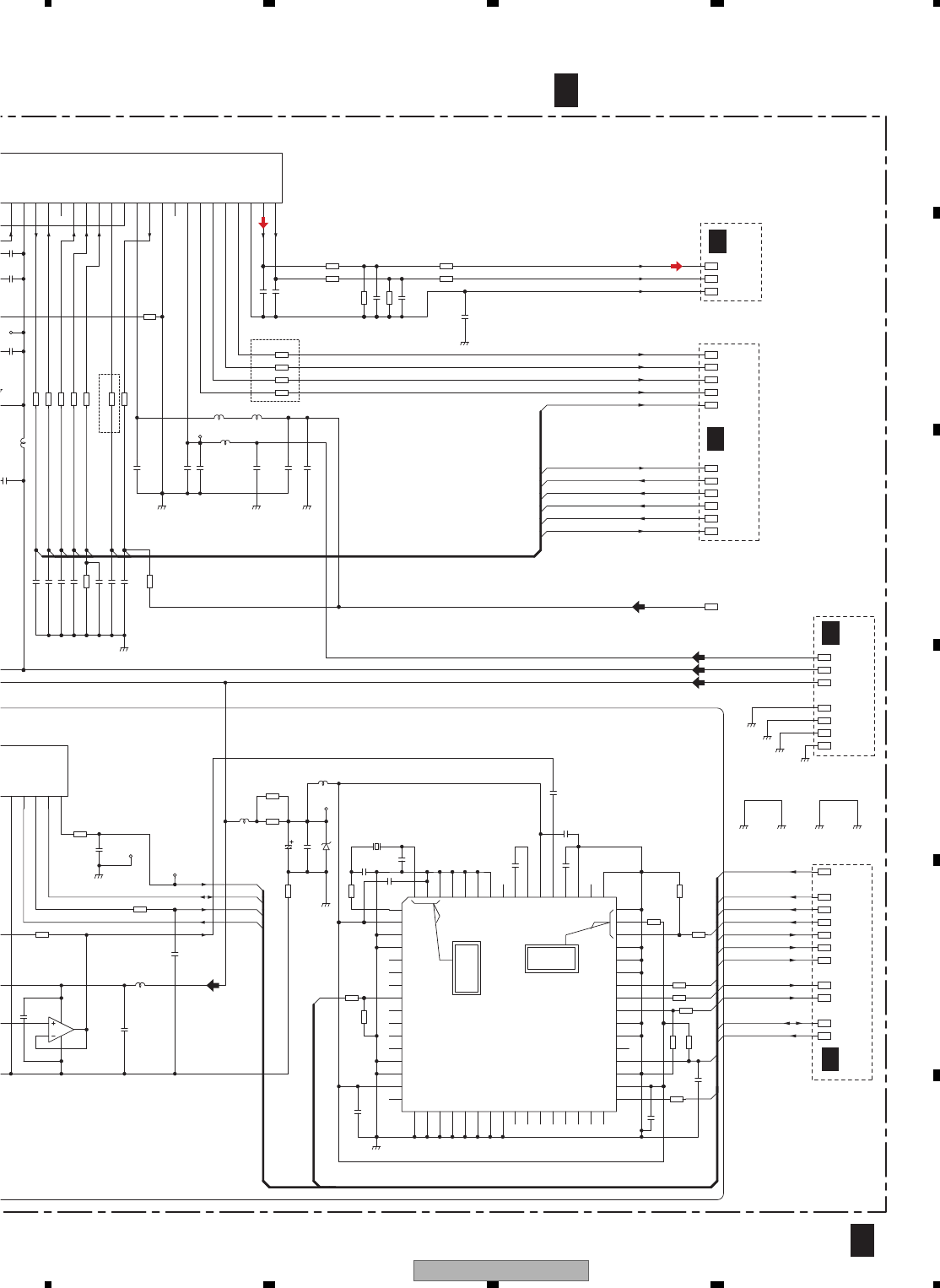
AVIC-X910BT/XS/UC 157
5678
5678
C
D
F
A
B
E
3/6
A
TUNDI
TUNCE1
TUNSL
TUNDO
TUNCLK
TUNCE2
HLDET
HRHSLK
HRLK
HRCK
DCE3
DCL3
DRST3
SDA
DDI3
DCE3
SCL
DDO3
BCLOCK3
DINT3
DDO3
SD/DO
S-meter
SD/DO
SDA
S-meter
SCL
DCL3
DDI3VICS8
VICS8
DARC33
DARC33
HRDT
AV8
TUNSL
TUNCE2
TUNCE1
TUNCLK
TUNDO
TUNDI
HLDET
DINT3
BCLOCK3
DRST3
VDD5
TU3
R1488
NM
R1489
NM
R1485
NM
R1482
NM
R1469
NM
R1481
NM
R1483
NM
R1491
NM
R1487
NM
R1494
NM
R1490
NM
R1495
NM
R1484
NM
R1472 NM
R1473 NM
R1470 0
R1471 0
R1474 0
R1475 0
R1461 680
R1462 680
R1463 680
R1464 680
R1465 680
R1467 680
R1468 680
R1466
22k
R1492
NM
R1493
NM
R1486
NM
R1476
0
R1477
0
R1478
0
R1479
0
R1497
NM
R1496
NM
R1498
NM
R1433
NM
GNDRF
GNDD
C1482
NM
TUNSL
DINT3
C1463
NM
GNDD
GNDD
HRLK
461
RF_GND
3
FM_ANT
4
VCC
5
SL
6
CE2
NC
7
WC
8
CE1
9
CK
10
DI
11
LDET
12
OSCGND
13
ROM_VDD
14
DO
15
DGND
NC
16
COMP
17
VDD_3.3
18
RDS_CK
19
RDS_DATA
20
RDS_LOCK
21
RDS_HSLK
AGND
22
BEGND
23
Lch
24
Rch
TUNDO
SDA
L1463
2.2u
HRHSLK
C1464
100p/50
TUVCC
DDO3
TUNDI
C1468
CCG1203-A
AV8
C1492
NM
465
u/50 TUNCE1
GNDRF
C1489
NM
HLDET
BCLOCK3
GNDA
S-meter
HRDT
VICS8
L1465
2.2u
NM
VCC
6
GND3
7
SCL
8
S-METER
9
SDA
10
SD/DO
GNDD
SD
C1481
NM
VICSG
FMR
C1467
NM
GNDA
HRCK
L1462
2.2u
L1481
NM
FML
L1483
NM
C1494
NM
TU3
C1483 NM
C1486 NM
GNDA
DCE3
FMRTN
GNDD
D1481
NM
DRF
C1484
NM
DRST3
IC1000
NM
32
1
4
5
SCL
GNDD
TUNCE2
NM
C1485
L1464
CTF1399-A
TUNCLK
VDD5
C1472
NM
VDD33
GNDD
DCL3
SD/DO
L1482
NM
DDI3
X1481
NM
IC1481
NM
XOUT
1
Vddd1
2
IOCNT1
3
IOCNT2
4
CLK16
5
DATA
6
FLOCK
7
BLOCK
8
FCK
9
BCK
10
CRC4
11
DREQ
12
DACK
13
14
Vddd2
15
RDY
16
D4
21
D5
22
D6
23
D7
24
D8
25
D9
26
D10
27
D11
28
D12
29
D13
30
D14
31 D15
32
INT 33
Vddd3 34
35
DO 36
NC1 37
WR 38
RD 39
A0/C 40
A1/C 41
A2/D 42
A3 43
CS 44
STNBY 45
46
47
48
Vref 52
MPXI 53
Vdda 54
FLOUT 55
CIN 56
NC3 57
TPC1 58
TPC2 59
TEST 60
TOSEL1 61
62
63
64
D3
20
D2
19 D1
18 D0
17
Vssa 51
NC2 50
TIN 49
C1495
NM
C1493
NM
C1497
NM
C1498
NM
C1488
NM
C1471
NM
C1470 NM
C1473 NM
C1474 NM
C1475 NM
C1487 NM
C1491
NM
GNDRFGNDRF GNDDGNDA
DEC3
C1451
NM
C1453
NM
C1454
NM
C1455
NM
C1456
NM
C1457
NM
C1466
0.01u/50
ILMGND
ILMGND
C1469
0.01u/50
C1458
0.01u/50
GNDRF
C1452
1000p/50
C1476
0.01u/25
GNDRF
8mA MAX
140mA MAX
200mA MAX
7.20MHz
64 XIN
63 Vssd1
62 TOSEL2
Vssd2 Vssd3
48 BUSWD
47 SP
48 RST
10Uf/10V
5.0V
8.3V
3.3V
5.0V5.0V
5.0V
3.3V
3.3V
3.3V
8.3V
8.3V
8.3V
8.0V8.0V8.0V8.0V
8.0V8.0V
8.0V
8.0V
TUNER
9
FM/AM TUNER UNIT
EU5
EU5
4/6
A
1/6
A
4/6
A
AV UNIT (TUNER SECTION)
3/6
A
FM(EU): -9.5 dBs
AM(EU): -20 dBs
FM:-13.5 dBs
AM: -24 dBs
2/6
A
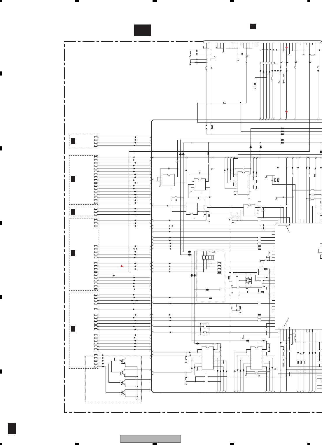
AVIC-X910BT/XS/UC
158
1234
1234
C
D
F
A
B
E
10.4 AV UNIT(SYSTEM uCOM SECTION)(GUIDE PAGE)
4/6
A
A-a 4/6
CTOSYSV5
CPUWDT5
MS5TOSYS3
DVDV
DVDL
DVDR
TX
CTOSYSV3
OFFANS3
RDSLK
RDT
RCK
RDS57K
SRCMUTE
TEMPIN
TUNSL
RX
TX
DCE5
BCLOCK5
DRST5
VICSON
NAVICON
OFFANS5
SYSTOC5
SYSTOC3
SYSTOCV3
SYSTOCV5
OFFINFO3
OFFINFO5
BATFAULT5
WIREIN
TUNDO
TUNDI
TUNCLK
TUNCE1
TUNCE2
HLDET
DVEJKY
DDO3
DDI3
RSTIN
DCE3
DCL3
BCLOCK3
DRST3
TUNDO
TUNDI
TUNCLK
TUNCE1
TUNCE2
HLDET
S-meter
DINT3
SDA
SCL
SD/DO
WIREIN
WCONT
CDR
CDL
DVDR
DVDL
DVDV
TUNSL
VST
SELSCL
SELSDA
VDT
VCK
SRCMUTE
LEDDT
ROT0
ROT1
RESETB
RESETB
RSTOUT
CTOSYS3
CTOSYSV3
SYSTOCV3
SYSTOC3
BATFAULT3
OFFINFO3
CPUWDT3
ASENBO
IPPW
RX
SYSTOMS53
XRES3
OPTON
OPTSNS
S-meter
CTOSYS5
CTOSYS3
DCSKIP
DCL5
AMUTE
NOSELL
NOSELR
IRQPW3
XRES3
XRES5
WAKEUP
SYSTOMS55
SYSTOMS53
AMUTE
BDATABDATA
CPUWDT3
MUTE
SYSTOCV5
REM
DCSKIPCD
DDI5
DDO5
IRQPW3
RCK
RDS57K
RDT
RDSLK
TELMUTE
LEDCK
LEDCS
OFFANS3
BATFAULT3
MS5TOSYS5
SYSTOMS55
BSCK
RSTIN
NFCONT
IRQPW5
MS5_STANDBY3
WCONT
ILMSNS
R637
NM
R601
100k
R635
NM
R602
100k
R632
0
R714
0
R628
22k
2
1
4
3
6
5
8
7
R638
NM
R608
680
2
1
4
36
5
8
7
R715
0
R722
100k
R614
470
R615
2.2k
R613
470
R617
0
R616
0
R619
100k
R612
100k
R627
100k
R607
680
R622 NM
R623 NM
R625
NM
R634
100k
R618 100k
R643
100k
R646
R647
R644
NM
R641
10k
R640
10k
R639
1k
R633
1k
R636
100k
R688 100k
R689 100k
R624 NM
R603
22
R642
22
R645
R611
NM
R609
100k
R610
1k
R604
22
R712
NM
R605
100k
R631
NM
R629
NM
R717
0
R620
100
R718
220
R626
220
R697
100k
R698
100k
R732
NM
R731
0
R630
0
OPTSNS
RX
DCL3
GNDA
RESETB
GNDV
DRST3
SYSTES
CPUWDT3
L612
CTF1410 A
L705
CTF1463-A
DDO3
TX
C604
0.1u/50
DCE3
C705 0.1u/25
L601
CTF1410-A
DTC124EUA
Q752
NOSELL
ROT0
GNDD
TUNCE1
DVDR
L711 CTF1306-A
DTC124EUA
Q751
VDT
SD/DO
SRCMUTE
C613
0.1u/16
C708 0.1u/25
GNDD
SCL
TUNCLK
HRDT
IPPW
HRLK
DTC124EUA
Q753
1
2
3
4
5
6
7
8
9
10
11
12
13
14
15
16
17
18
19
20
21
22
23
24
25
26
27
28
29
30
31
32
33
34
35
36
37
38
39
40
41
42
43
44
45
46
47
48
49
50
51
52 129
130
131
132
133
134
135
136
137
138
139
140
141
142
143
144
L609
CTF1410-A
WCONT
L610
CTF1410-A
WIREIN
C616
NM
SELSDA
DTC124EUA
Q754
GNDD
C619
0.1u/16
BCLOCK3
DVDL
GNDD
L707 CTF1306-A
C614
0.1u/16
C615
0.1u/16
FB701
CTF1453-A
C602
0.1u/50
GNDP
GNDD
GNDD
IC603
TC7SH04FUS1
NC
1
INA
2
GND
3OUTY 4
5
VCC
HLDET
L708 CTF1306-A
DVDV
DDI3
IC604
TC7S32FU
IN_B 1
IN_A 2
GND 3
OUT_Y
4
5VCC
GNDD
C617
0.1u/16
ROT1
L713
CTF1306-A
L605 CTF1410-A
AMUTE
C709
0.1u/25
BATFAULT3
GNDD
IC608
BD5335FVE
VOUT
1
SUB
2
CT
3GND 4
5
VDD
GND
L608 CTF1410-A
L704
CTF1357-A
VCK
DINT3
LEDDT
TUNDO
SYSTOC3
SYSTOCV3
GNDD
OFFANS3
GNDD
L602
CTF1410-A
CTOSYS3
GNDA
C609 0.1u/16
L714
CTF1306-A
RSTIN
OPTON
L611
CTF1410-A
OFFINFO3
DVEJKY
TUNCE2
C601
0.1u/16
HRHSLK
GNDD
NOSELR
TUNDI
TUNSL
SDA
L710 CTF1306-A
LEDCS
L709 CTF1306-A
C607
0.015u/50
CDL
GNDV
SELSCL
C706 0.1u/25
GNDD
GNDD
C605
0.1u/16
VST GNDD
C707 0.1u/25
CKS5075-A
CN702
1
2
3
4
5
6
7
8
9
10
11
12
13
14
15
16
17
18
19
20
21
22
23
24
25
26
27
28
29
30
31
32
33
34
35
36
37
38
39
40
CDR
HRCK
CTOSYSV3
GNDP
ASENBO
L706 CTF1306-A
LEDCK
IC605
TC74VHCT08AFTS1
1A
1
1B
2
1Y
3
2A
4
52B
62Y
7GND 8
3Y
9
3A
10
3B
11
4Y
12
4A
13
4B
14
VCC
GNDA
L712
CTF1306-A
L604
CTF1410-A
S-meter
C618
0 1 /16
GNDD
L607
CTF1410-A
C606
0.1u/50
GNDD
IC609
TC74VHC08FTS1
1A
1
1B
2
1Y
3
2A
4
52B
62Y
7GND 8
3Y
9
3A
10
3B
11
4Y
12
4A
13
4B
14
VCC
IC607
TC74VHC08FTS1
1A
1
1B
2
1Y
3
2A
4
52B
62Y
7GND 8
3Y
9
3A
10
3B
11
4Y
12
4A
13
4B
14
VCC
GNDD
GNDD
X601
VSS1186-A
1
1
22
3
3
C610
NM
C611
NM
VD5
AMUT
XRES
IRPQ
HST
SLV
STBY
DVR DVL DVV
W
DVVG
DAG
GNDD
C623 0.01u/16
C711
0.01u/16
GNDD
IC601
TC7SH08FUS1
INB
1
INA
2
GND
3OUTY 4
5
Vcc
TELMUTE
GNDD
GNDD
MS8V
MS8VR
BSCK
BSO
PGND
VCC1
GNDD
GNDD
GNDD
L731
NM
C608
0.1u/16
C635
NM
C636
0.1u/16
NFCONT
L715
NM
CTF1306-A-T
GNDD
DGND
UVDD5
ANAROUT
NC
MVDD5
PGND
AGND
DGND
VIDEO GND
VIDEO GND
NAVI3
DGND
VDD8(DRY)
OR 5 5
PGND
UVDD5
IRQPWR
AGND
UVDD5
VDD5
NC
Y
PGND
CVBS
UARTSPEED
VIDEO GND
VDD8(REG)
3 5 AND
ANALOUT
VDD5
XRES
AGND
VIDEO GND
DGND
BUP3
CR
WAKEUP
NC
CB
AMUTE
VDD8(DRY)
VD8
NC
HSTCMD
SLVSTS
VDD5
STANBY
UVDD5
UVDD5
UVDD5
NAVI3
NAVI3
NAVI3
UVDD5
UVDD5
INV5 5
20MHz
BSO/TSO
BSCK/TSCK
REMOCON
NC
TUNDO
TUNDI
TUNCLK
TUNCE1
TUNCE2
NC
NC
NC
SYSTEST
RDSLK
BYTE
CNVSS
RDT
RDS57K
RESET
XOUT
VSS
XIN
VCC1
NMI
RCK
LDET
NC
DCE
DDO
DCL
DDI
BCLOCK
VICSON
FREQSW
RX
TX
VSS
SYSTOCV
VCC1
DCSKIPCD
NC
CLK1
SIMUKE4
NAVICON
NC
DCSKIP
SIMUKE3
HSTCMD(SYSTOMS5)
SLVSTS(MS5TOSYS)
NC
VREF
ILLSNS
S-Meter
TUNSL
BSI/TSI
WCONT
AVSS
VCC1
AVCC
VSS
WREMIN
NC
NC
TMPIN
5 3 AND
NAVI3
UVDD5
NC
NC
NC
AND 5 3
AND 5 3
DGND
VDD5
DRST
DARC LEVEL SHIFT
A
U
EU
701-722
DVD
607(L,IC)
C606,626
601-602
HR
3.3V
3.3V
3.3V
3.3V
3.3V
3.3V
5.0V
5.0V
5.0V
5.0V
5.0V
5.0V5.0V
5.0V5.0V
5.0V
5.0V5.0V5.0V
5.0V
5.0V
5.0V
5.0V
5.0V
5.0V
5.0V
5.0V
5.0V
5.0V
5.0V
5.0V
8.0V
8.0V8.0V
3.3V
3.3V3.3V3.3V
3.3V3.3V3.3V
3.3V
3.3V
3.3V
3.3V 3.3V
3.3V
3.3V
761- 767
612
602- 603
606
621
615
NAVI LEVEL SHIFT
688-689
623
618
609-610
605
601-602
751-754
CD/DVD
603-605
601
613-614
635
SRCMUTE
607-609
RESET
603-604
627-666
680-684
608-625
687
616
668-678
NAVI UART(VICS)
NAVI UART
UC
AU
EU5
EU5
UC,EU5
EU5
1/6
A
1/6
A
5/6
A
2/6
A
3/6
A
B
CN882
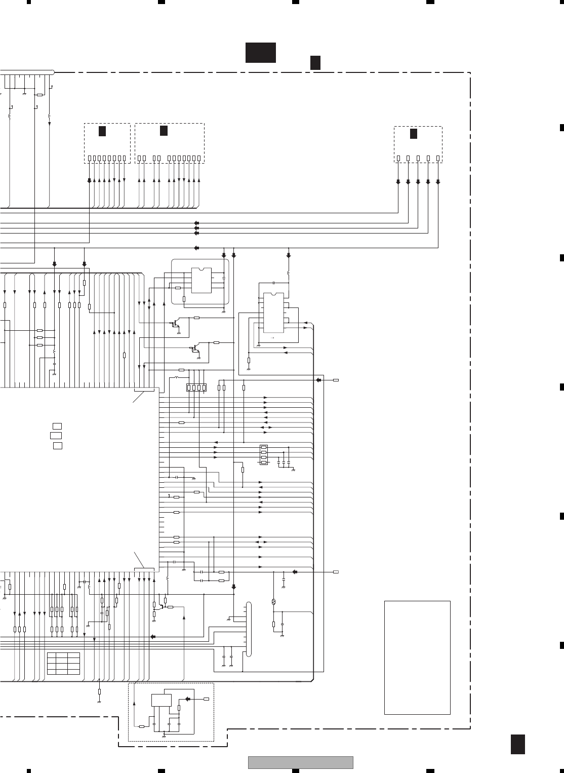
AVIC-X910BT/XS/UC 159
5678
5678
C
D
F
A
B
E
4/6
A
A-b 4/6
DVDV
FANCONT
SREMOTE
SYSPW
IPPW
ASENBO
NOSELR
NOSELL
MUTE
FCONT
OPTON
ANTON
LEDDT
LEDCK
LEDCS
CDRESET
BSRQ
BRST
BRXEM
TEMPIN
NAVICON
TELMUTE
WIREIN
VCK
VDT
VST
BSENS
VICSON
FANCONT
BSENS
VDCONT
VDD5CONT
DCSKIP
SWACPW
VDCONT
VDD5CONT
OFFINFO5
XRES5
OFFANS5
RSTOUT
CPUWDT5
DCL5
TEMPIN
ASENS
IRQPW5
WAKEUP
MS5_STANDBY5
MS5_STANDBY3
MS5TOSYS5
SELSCL
OPTSNS
DVEJKY
SYSTOCV5
SYSTOC5
CTOSYS5
CTOSYSV5
BSENSN
SDA
SCL
BSENSN
MS5TOSYS3
REM
DCSKIPCD
DDI5
DDO5
ROT1
ROT0
SD/DO
SWACPW
SREMOTE
ILMSNS
ANTON
FCONT
NAVICON
SYSPW
SYSPW
DCSKIPCD
DCSKIP
MS5TOSYS5
SYSTOMS55
MS5_STANDBY5
DINT5
NFCONT
ASENS
ASENS
BATFAULT5
WCONT
ILMSNS
WAKEUP
CNVSS
CNVSS
SELSDA
UVDD5
R684
680
2
1
4
36
5
8
7
R637
NM
R662
100k
R635
NM
R683
100k
2
1
4
36
5
8
7
R677 0
R676 0
R638
NM
R682
0
R660
100k
R648
100k
R659
22
R685
1k
R634
100k
R657
100k
R643
100k
R650
100k
R654
100k
R646
100k
R647
NM
R651
NM
R655
NM
R644
NM
R658
NM
R670
100k
R641
10k
R640
10k
R639
1k
R633
1k
R636
100k
R653 1k
R661
NM
R690
4.7k
R656
NM
R4783
3.3k
R4784
3.3k
R691 NM
R692
NM
R696
47
R663
1k
R664
47k
R680
4.7k
R668
4.7k
R687
100k R686
100k
R679
NM
R667
NM
R665
100k
R642
22
R645
22
R649 22
R652 22
R695
47
R666
100k
R681 47k
R693
NM
R717
0
R699
100k
R694
NM
R768
NM
R671
1k
R733
NM
NAVI3V
NDA
VICSON
L612
CTF1410-A
SREMOTE
CD3.3
VDD5CONT
VDCONT
GNDD
C633 NM
M30878FJBGP
IC610
42
43
44
45
46
47
48
49
50
51
52
53
54
55
56
57
58
59
60
61
62
63
64
65
66
67
68
69
70
71
72
73
74
75
76
77
78
79
80
81
82
83
84
85
86
87
88
89
90
91
92
93
94
95
96
97
98
99
100
101
102
103
104
105
106
107
108
109
110
111
112
113
114
115
116
117
118
119
120
121
122
123
124
125
126
127
128
129
130
131
132
133
134
135
136
137
138
139
GNDD
SWACPW
FANCONT
C634
NM
VD8
C631 NM
C622
0.1u/16
C621
0.1u/16
0.1u/16
GNDD
GNDD
C620
0.1u/16
GNDD
L613
CTF1410-A
BSENS
L714
CTF1306-A
L611
CTF1410-A
NM
IC611
CS
1
SK
2
DI
3
DO
45
GND
6
TEST
7
NC
8
VCC
L615
CTF1410-A
MVDD5
L614
CTF1410-A
GNDD
2SA1576A(QR)
Q601
CCX1051-A
TH601
GNDV
UVDD5
30
31
32
33
34
35
36
37
38
39
40
GNDD
C632
0.1u/16
C618
0.1u/16
IC612
TC74VHCT32AFT
1A
1
1B
2
1Y
3
2A
4
52B
62Y
7GND 8
3Y
9
3A
10
3B
11
4Y
12
4A
13
4B
14
VCC
BUP3
L617
CTF1410-A
GNDD
C630
0.1u/50
NM
CN601
1
2
3
4
5
6
7
8
9
10
GNDD
C4786
NM
VICS5
BSENSN
C695
NM
C697
NM
CCG1171-A
C696
C4784
47p/50
C4785
47p/50
L DVV
WAKE
DVVG
SWVDD5
SWVDD5
GNDD
U695
1
4
2
3
DTC114EUA
Q662
DTC114EUA
Q661
GNDD
GNDD
ILMSNS
ANTON
DCSKIPCD
FCONT
NAVICON
DCSKIP
SYSPW
SYSPW
GNDD
TSIN
GNDD
C685
0.1u/16
GNDD
C671
0.1u/16
C629
NM
ASENS
ASENS
C672
0.1u/16
GNDRF
L715
NM
CTF1306-A-T
GNDD
GNDD
GNDD
GNDD
D5
VIDEO GND
VIDEO GND
3
D5
Y
CVBS
UARTSPEED
VIDEO GND
VIDEO GND
3
CR
WAKEUP
CB
MVDD5
VD8
UVDD5
UVDD5
UVDD5
UVDD5
FANCONT
DDO
DCL
DDI
ROT0
ROMDATA
ROT1
CDRESET
VSS
CTOSYSV
SYSTOCV
VCC1
NC
SREMOTE
P50
SWACPW
RSTOUT
VSS
CPUWDT
BATFAULT
OFFINFO
VCC2
OFFANS
DCSKIPCD
NC
CLK1
SIMUKE4
NAVICON
CTOSYS
NC
DCSKIP
SYSTOC
NC
ROMCLK
SIMUKE3
SIMUKE2
SIMUKE1
SIMUKE0
/HOLD
VCC2
NOSELL
VSS
NOSELR
SELSDA
SELSCL
NC
NC
NFCONT
MUTE
NC
NC
VST
OPTON
VDT
BSENSN
OPTSNS
VCC2
MUTEVO
ANTON
VCK
VSS
TESTIN
FCONT
SD/DO
NC
SDA
LEDDT
LEDCS
BSENS
DINT
ASENS
SCL
LEDCK
ROMCS
BSRQ
BRST
VDCONT
BRXEN
WAKEUP
MS5_STANDBY
VDD5CONT
SLVSTS(MS5TOSYS)
NC
XRES
NC
DVEJKY
IRQPW
VREF
ILLSNS
S-Meter
TUNSL
WCONT
AVSS
VCC1
VSS
WREMIN
NC
NC
TMPIN
IPPW
SYSPW
ASENBO
TEIN
NC
UVDD5
3 5 OR
BUP3
S-93C56BD0I-J8
VDD8(REG):220MA MAX
VDD8(DRY):1800MA MAX
VDD5 :650MA MAX
EL SHIFT
RPMS2401-H19E4AV
PEG563A8
AU
UC PEG562A8
EU5 PEG561A8
630
ROM
IC611,C629,
667,679
TEMPIN
TH601,R685,
C632,C685
601
3.3V
3.3V
3.3V
3.3V
3.3V
3.3V
3.3V
3.3V
3.3V
3.3V
3.3V
3.3V
5.0V5.0V
8.0V8.0V
5.0V5.0V
5.0V
8.0V
5.0V
5.0V
8.0V
5.0V
5.0V
5.0V
5.0V
5.0V
5.0V
5.0V
5.0V
5.0V5.0V5.0V5.0V
5.0V
5.0V
5.0V
5.0V
5.0V5.0V 5.0V
5.0V
5.0V
5.0V
5.0V
5.0V
5.0V
5.0V
5.0V
5.0V
8.0V
8.0V
3.3V3.3V3.3V
3.3V3.3V
5.0V 5.0V
5.0V 5.0V 5.0V 5.0V
5.0V
NM
CKS3752-A
1M
10k
606
602-603
DARC LEVEL SHIFT
761-767
612
621
IR REMOTE
695-696
697
697
IR REMOTE 695-696
NAVI LEVEL SHIFT 601-602
688-689
605
609-610
615
618
623
CD/DVD 701-722
613-614
SRCMUTE 603-605
607-609
635
RESET 601-602
CNVSS
612
617
686
CNVSS 617
612
630
686
603-604
608-625
627-666
668-678
690-694
680-684
687
731
697-699
733
768
4783-4786
603-604
690-694
627-666
697-699
680-684
768
4783-4786
608-625 731
687
733
616
668-678
uCOM
R655
100k NM
R654
NM 100k
NM
100k
UC
AU
EU5
AU
1/6
A6/6
A6/6
A
AV UNIT (SYSTEM uCOM SECTION)
4/6
A
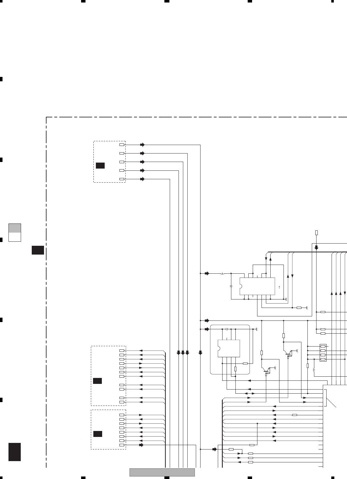
AVIC-X910BT/XS/UC
160
1234
1234
C
D
F
A
B
E
A-a A-b
A-b 4/6
LEDDT
LEDCK
LEDCS
CDRESET
BSRQ
BRST
BRXEM
BSENS
VICSON
FANCONT
BSENS
VDCONT
VDD5CONT
OFFINFO5
OFFANS5
RSTOUT
CPUWDT5
ASENS
MS5_STANDBY5
MS5_STANDBY3
MS5TOSYS5
DVEJKY
SYSTOC5
CTOSYS5
BSENSN
MS5TOSYS3
ROT1
ROT0
SWACPW
SREMOTE
ILMSNS
ANTON
FCONT
NAVICON
SYSPW
SYSPW
DCSKIPCD
DCSKIP
ASENS
ASENS
BATFAULT5
CNVSS
R683
100k
2
1
4
36
5
8
7
R653 1k
R690
4.7k
R691 NM
R692
NM
R686
100k
R679
NM
R667
NM
R665
100k
22
R649 22
R652 22
R666
100k
R681 47k
R693
NM
R694
NM
R733
NM
NAVI3V
VICSON
SREMOTE
CD3.3
VDD5CONT
VDCONT
103
104
105
106
107
108
109
110
111
112
113
114
115
116
117
118
119
120
121
122
123
124
125
126
127
SWACPW
FANCONT
VD8
BSENS
NM
IC611
CS
1
SK
2
DI
3
DO
45
GND
6
TEST
7
NC
8
VCC
L615
CTF1410-A
MVDD5
UVDD5
GNDD
IC612
TC74VHCT32AFT
1A
1
1B
2
1Y
3
2A
4
52B
62Y
7GND 8
3Y
9
3A
10
3B
11
4Y
12
4A
13
4B
14
VCC
BUP3
L617
CTF1410-A
GNDD
C630
0.1u/50
GNDD
VICS5
BSENSN
DTC114EUA
Q662
DTC114EUA
Q661
GNDD
GNDD
ILMSNS
ANTON
DCSKIPCD
FCONT
NAVICON
DCSKIP
SYSPW
SYSPW
C629
NM
ASENS
ASENS
MVDD5
VD8
UVDD5
UVDD5
UVDD5
ROT0
OMDATA
ROT1
DRESET
NC
RSTOUT
CPUWDT
BATFAULT
OFFINFO
OFFANS
CTOSYS
SYSTOC
NC
ROMCLK
LEDDT
LEDCS
BSENS
LEDCK
ROMCS
BSRQ
BRST
BRXEN
NC
DVEJKY
UVDD5
3 5 OR
BUP3
S-93C56BD0I-J8
VDD8(REG):220MA MAX
VDD8(DRY):1800MA MAX
VDD5 :650MA MAX
630
ROM
IC611,C629,
667,679
3.3V
3.3V
3.3V
3.3V
3.3V
3.3V
3.3V
3.3V
3.3V
3.3V
5.0V5.0V
8.0V8.0V
5.0V5.0V
5.0V
8.0V
5.0V
5.0V
8.0V
5.0V
5.0V
5.0V
5.0V
5.0V
5.0V
5.0V
5.0V
5.0V
5.0V
5.0V
5.0V
5.0V
5.0V
5.0V
8.0V
3.3V3.3V3.3V
3.3V
5.0V 5.0V 5.0V 5.0V
NM
1M
10k
CNVSS
612
617
686
1/6
A
6/6
A
6/6
A
AV UNIT (SYSTEM uCOM SECTION)
4/6
A
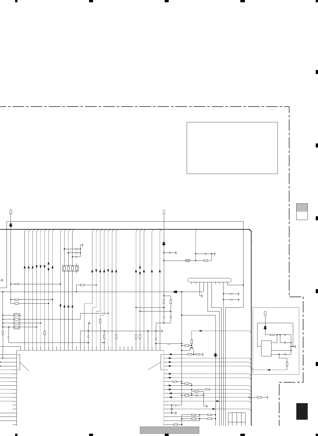
AVIC-X910BT/XS/UC 161
5678
5678
C
D
F
A
B
E
A-a A-b
A-b 4/6
FANCONT
SREMOTE
SYSPW
IPPW
ASENBO
NOSELR
NOSELL
MUTE
FCONT
OPTON
ANTON
LEDDT
LEDCK
LEDCS
TELMUTE
VCK
VDT
VST
BSENS
SWACPW
VDCONT
VDD5CONT
XRES5
TEMPIN
ASENS
IRQPW5
SELSCL
OPTSNS
BSENSN
SDA
SCL
REM
SD/DO
MS5TOSYS5
SYSTOMS55
MS5_STANDBY5
DINT5
NFCONT
WAKEUP
CNVSS
SELSDA
UVDD5
R684
680
2
1
4
36
5
8
7
R662
100k
R683
100k
2
1
4
36
5
8
7
R677 0
R676 0
R682
0
R660
100k
R648
100k
R659
22
R685
1k
R657
100k
100k
R654
100k
NM
R655
NM
R658
NM
R670
100k
R661
NM
R656
NM
R4783
3.3k
R4784
3.3k
R691 NM
R692
NM
R696
47
R663
1k
R664
47k
R680
4.7k
R668
4.7k
R687
100k
R695
47
R681 47k
R693
NM
R699
100k
R768
NM
R671
1k
C633 NM
M30878FJBGP
IC610
54
55
56
57
58
59
60
61
62
63
64
65
66
67
68
69
70
71
72
73
74
75
76
77
78
79
80
81
82
83
84
85
86
87
88
89
90
91
92
93
94
95
96
97
98
99
100
101
102
103
104
105
106
107
108
109
110
111
112
113
114
115
116
117
118
119
120
121
122
123
124
125
126
127
GNDD
C634
NM
C631 NM
C622
0.1u/16
C621
0.1u/16
GNDD
C620
0.1u/16
GNDD
L613
CTF1410-A
L615
CTF1410-A
L614
CTF1410-A
GNDD
2SA1576A(QR)
Q601
CCX1051-A
TH601
C632
0.1u/16
NM
CN601
1
2
3
4
5
6
7
8
9
10
GNDD
C4786
NM
VICS5
C695
NM
C697
NM
CCG1171-A
C696
C4784
47p/50
C4785
47p/50
SWVDD5
SWVDD5
GNDD
U695
1
4
2
3
GNDD
TSIN
GNDD
C685
0.1u/16
GNDD
C671
0.1u/16
C672
0.1u/16
GNDRF
GNDD
GNDD
GNDD
GNDD
FANCONT
ROT0
ROMDATA
ROT1
CDRESET
NC
SREMOTE
P50
SWACPW
RSTOUT
VSS
CPUWDT
BATFAULT
OFFINFO
VCC2
OFFANS
CTOSYS
SYSTOC
NC
ROMCLK
SIMUKE1
SIMUKE0
/HOLD
VCC2
NOSELL
VSS
NOSELR
SELSDA
SELSCL
NC
NC
NFCONT
MUTE
NC
NC
VST
OPTON
VDT
BSENSN
OPTSNS
VCC2
MUTEVO
ANTON
VCK
VSS
TESTIN
FCONT
SD/DO
NC
SDA
LEDDT
LEDCS
BSENS
DINT
ASENS
SCL
LEDCK
ROMCS
BSRQ
BRST
VDCONT
BRXEN
WAKEUP
MS5_STANDBY
VDD5CONT
XRES
NC
DVEJKY
IRQPW
IPPW
SYSPW
ASENBO
TEIN
NC
UVDD5
RPMS2401-H19E4AV
PEG563A8
PEG562A8
PEG561A8
TEMPIN
TH601,R685,
C632,C685
601
5.0V
5.0V5.0V5.0V
5.0V
5.0V
5.0V
5.0V
5.0V5.0V
5.0V
5.0V
5.0V 5.0V
5.0V 5.0V 5.0V 5.0V
5.0V
CKS3752-A
606
602-603
DARC LEVEL SHIFT
761-767
612
621
IR REMOTE
695-696
697
697
IR REMOTE 695-696
NAVI LEVEL SHIFT 601-602
688-689
605
609-610
615
618
623
CD/DVD 701-722
613-614
SRCMUTE 603-605
607-609
635
RESET 601-602
CNVSS 617
612
630
686
603-604
608-625
627-666
668-678
690-694
680-684
687
731
697-699
733
768
4783-4786
690-694
697-699
768
4783-4786
731
733
uCOM
R655
0k NM
54
M 100k
NM
0k
AU
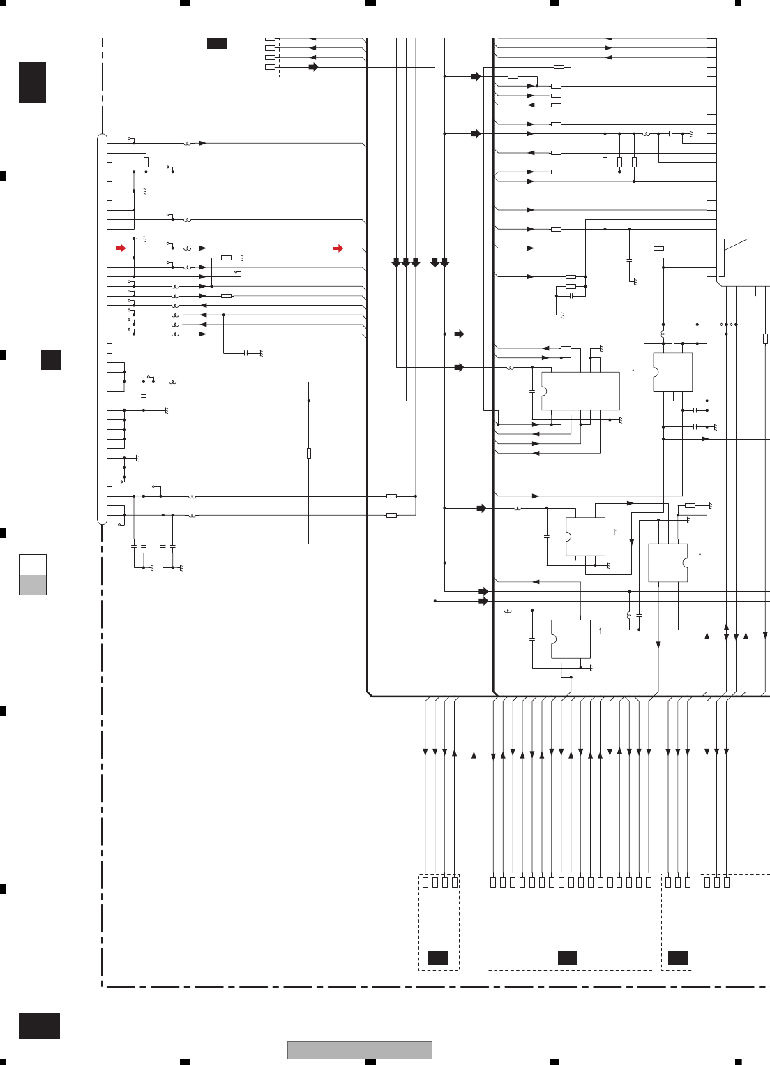
AVIC-X910BT/XS/UC
162
1234
1234
C
D
F
A
B
E
A-bA-a
A-a 4/6
A-b 4/6
MS5TOSYS3
DVDV
DVDL
DVDR
TX
OFFANS3
SRCMUTE
TEMPIN
TUNSL
WIREIN
TUNDO
DVEJKY
RSTIN
VST
VDT
VCK
SRCMUTE
LEDDT
ROT0
ROT1
RESETB
RESETB
RSTOUT
CTOSYS3
CTOSYSV3
SYSTOCV3
SYSTOC3
BATFAULT3
OFFINFO3
CPUWDT3
ASENBO
IPPW
RX
SYSTOMS53
XRES3
VICSON
OPTON
OPTSNS
S-meter
OFFINFO5
RSTOUT
CPUWDT5
IRQPW3
XRES3
XRES5
WAKEUP
SYSTOMS55
SYSTOMS53
AMUTE
BDATABDATA
DVEJKY
MUTE
SYSTOCV5
SYSTOC5
CTOSYS5
CTOSYSV5
REM
IRQPW3
SWACPW
SREMOTE
LEDCK
LEDCS
BSCK
RSTIN
NFCONT
IRQPW5
MS5_STANDBY3
WCONT
ILMSNS
R632
0
R714
0
R715
0
R722
100k
R614
R613
470
R641
10k
R640
10k
R639
1k
R633
1k
R636
100k
R653 1k
R690
4.7k
R642
22
R645
22
R649 22
R652 22
R712
NM
R605
100k
R631
NM
R629
NM
R717
0
R718
220
R626
220
R733
NM
OPTSNS
NAVI3V
RX
GNDA
RESETB
VICSON
CPUWDT3
L612
CTF1410-A
L705
CTF1463-A
SREMOTE
TX
C604
0.1u/50
C705 0.1u/25
L601
CTF1410-A
ROT0
L711 CTF1306-A
VDT
SRCMUTE
C613
0.1u/16
C708 0.1u/25
IPPW
1
2
3
4
5
6
119
120
121
122
123
124
125
126
127
128
129
130
131
132
133
134
135
136
137
138
139
140
141
142
143
144
L609
CTF1410-A
SWACPW
C616
NM
GNDD
C619
0.1u/16
L707 CTF1306-A
C614
0.1u/16
FB701
CTF1453-A
C602
0.1u/50
GNDP
GNDD
GNDD
IC603
TC7SH04FUS1
NC
1
INA
2
GND
3OUTY 4
5
VCC
L708 CTF1306-A
IC604
TC7S32FU
IN_B 1
IN_A 2
GND 3
OUT_Y
4
5VCC
ROT1
L713
CTF1306-A
C709
0.1u/25
BATFAULT3
GNDD
IC608
BD5335FVE
VOUT
1
SUB
2
CT
3GND 4
5
VDD
GNDD
L704
CTF1357-A
VCK
LEDDT
SYSTOC3
SYSTOCV3
OFFANS3
GNDD
L602
CTF1410-A
CTOSYS3
L714
CTF1306-A
RSTIN
OPTON
OFFINFO3
DVEJKY
C601
0.1u/16
L710 CTF1306-A
LEDCS
L709 CTF1306-A
C607
0.015u/50
GNDV
C706 0.1u/25
GNDD
VST GNDD
C707 0.1u/25
CKS5075-A
CN702
1
2
3
4
5
6
7
8
9
10
11
12
13
14
15
16
17
18
19
20
21
22
23
24
25
26
27
28
29
30
31
32
33
34
35
36
37
38
39
40
CTOSYSV3
GNDP
ASENBO
L706 CTF1306-A
LEDCK
L712
CTF1306-A
L604
CTF1410-A
C618
0.1u/16
GNDD
L607
CTF1410-A
C606
0.1u/50
GNDD
IC607
TC74VHC08FTS1
1A
1
1B
2
1Y
3
2A
4
52B
62Y
7GND 8
3Y
9
3A
10
3B
11
4Y
12
4A
13
4B
14
VCC
GNDD
VD5
AMUT
XRES
IRPQ
HST
SLV
STBY
DVR DVL DVV
WAKE
DVVG
DAG
GNDD
C711
0.01u/16
GNDD
IC601
TC7SH08FUS1
INB
1
INA
2
GND
3OUTY 4
5
Vcc
MS8V
MS8VR
BSCK
BSO
PGND
C635
NM
NFCONT
L715
NM
CTF1306-A-T
GNDD
DGND
UVDD5
ANAROUT
NC
MVDD5
PGND
AGND
DGND
VIDEO GND
VIDEO GND
NAVI3
DGND
VDD8(DRY)
OR 5 5
PGND
IRQPWR
AGND
UVDD5
VDD5
NC
Y
PGND
CVBS
UARTSPEED
VIDEO GND
VDD8(REG)
ANALOUT
VDD5
XRES
AGND
VIDEO GND
DGND
BUP3
CR
WAKEUP
NC
CB
AMUTE
VDD8(DRY)
VD8
NC
HSTCMD
SLVSTS
VDD5
STANBY
UVDD5
UVDD5
NAVI3
UVDD5
INV5 5
BSO/TSO
BSCK/TSCK
REMOCON
NC
TUNDO
CTOSYSV
SYSTOCV
NC
RSTOUT
CPUWDT
OFFINFO
CTOSYS
SYSTOC
NC
NC
NC
DVEJKY
VREF
ILLSNS
S-Meter
TUNSL
SI/TSI
WCONT
AVSS
VCC1
AVCC
VSS
WREMIN
NC
NC
TMPIN
UVDD5
AND 5 3
AND 5 3
DGND
VDD5
VDD8(REG):220M
VDD8(DRY):1800M
VDD5 :650MA M
701-722
DVD
607(L,IC)
C606,626
601-602
3.3V
3.3V
3.3V
3.3V
3.3V
3.3V
3.3V
3.3V
5.0V
5.0V
5.0V
5.0V
5.0V
5.0V
5.0V5.0V
5.0V5.0V
5.0V
5.0V5.0V5.0V
5.0V
5.0V
5.0V
5.0V
5.0V
5.0V
8.0V
8.0V
8.0V8.0V
3.3V3.3V3.3V
3.3V3.3V
3.3V3.3V3.3V
3.3V3.3V3.3V
3.3V
3.3V
CD/DVD
603-605
601
613-614
635
SRCMUTE
607-609
RESET
A
1/6
A
1/6
A
5/6
A
BCN882
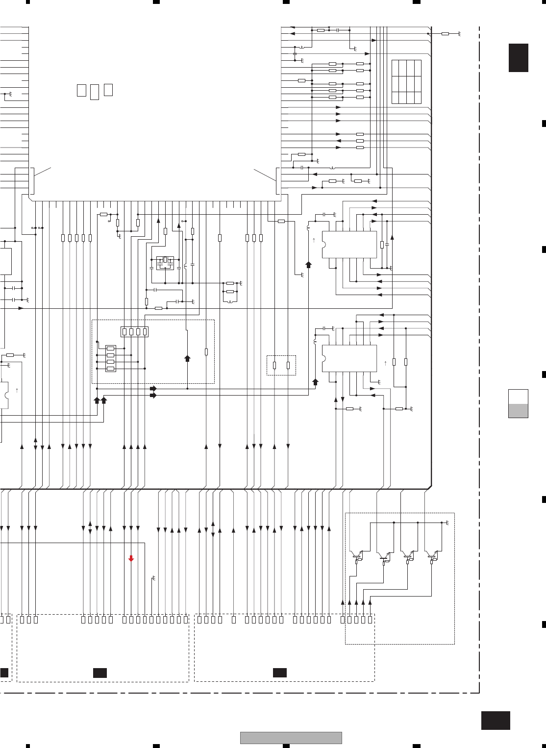
AVIC-X910BT/XS/UC 163
5678
5678
C
D
F
A
B
E
A-bA-a
A-a 4/6
A-b 4/6
CTOSYSV5
CPUWDT5
CTOSYSV3
RDSLK
RDT
RCK
RDS57K
RX
TX
DCE5
BCLOCK5
DRST5
VICSON
NAVICON
OFFANS5
SYSTOC5
SYSTOC3
SYSTOCV3
SYSTOCV5
OFFINFO3
OFFINFO5
BATFAULT5
TUNDO
TUNDI
TUNCLK
TUNCE1
TUNCE2
HLDET
DDO3
DDI3
DCE3
DCL3
BCLOCK3
DRST3
TUNDO
TUNDI
TUNCLK
TUNCE1
TUNCE2
HLDET
S-meter
DINT3
SDA
SCL
SD/DO
WIREIN
WCONT
CDR
CDL
DVDR
DVDL
DVDV
TUNSL
VST
SELSCL
SELSDA
VDT
VCK
LEDDT
CTOSYS5
CTOSYS3
DCSKIP
VDCONT
VDD5CONT
DCL5
AMUTE
NOSELL
NOSELR
BDATABDATA
CPUWDT3
MUTE
REM
DCSKIPCD
DDI5
DDO5
RCK
RDS57K
RDT
RDSLK
TELMUTE
LEDCK
OFFANS3
BATFAULT3
MS5TOSYS5
SYSTOMS55
MS5_STANDBY5
BSCK
WAKEUP
R637
NM
R601
100k
R635
NM
R602
100k
R628
22k
2
1
4
3
6
5
8
7
R638
NM
R608
680
2
1
4
36
5
8
7
R648
100k
R659
R614
470
R615
2.2k
R613
470
R617
0
R616
0
R619
100k
R612
100k
R627
100k
R607
680
R622 NM
R623 NM
R625
NM
R634
100k
R618 100k
R657
100k
R643
100k
R650
100k
R654
100k
R646
100k
R647
NM
R651
NM
R655
NM
R644
NM
R658
NM
R661
NM
R688 100k
R689 100k
R624 NM
R603
22
R611
NM
R609
100k
R610
1k
R604
22
R605
100k
R620
100
R697
100k
R698
100k
R699
100k
R732
NM
R731
0
R630
0
DCL3
GNDV
DRST3
SYSTES
DDO3
DCE3
DTC124EUA
Q752
NOSELL
GNDD
TUNCE1
DVDR
DTC124EUA
Q751
VDT
SD/DO
C
0.1u/16
GNDD
SCL
TUNCLK
HRDT
HRLK
DTC124EUA
Q753
M30878FJBGP
IC610
1
2
3
4
5
6
7
8
9
10
11
12
13
14
15
16
17
18
19
20
21
22
23
24
25
26
27
28
29
30
31
32
33
34
35
36
37
38
39
40
41
42
43
44
45
46
47
48
49
50
51
52
53
54
55
56
57
58
59
60
61
62 119
120
121
122
123
124
125
126
127
128
129
130
131
132
133
134
135
136
137
138
139
140
141
142
143
144
WCONT
L610
CTF1410-A
WIREIN
SELSDA
DTC124EUA
Q754
GNDD
BCLOCK3
DVDL
GNDD
C
0.1u/1
C615
0.1u/16
HLDET
DVDV
DDI3
IC604
IN_B 15 VCC
GNDD
C617
0.1u/16
L605 CTF1410-A
AMUTE
BD5335FVE
CT
3GND 4
GNDD
L608 CTF1410-A
VCK
DINT3
C620
0.1u/16
LEDDT
TUNDO
L613
CTF1410-A
GNDD
GNDA
C609 0.1u/16
L611
CTF1410-A
TUNCE2
HRHSLK
GNDD
NOSELR
TUNDI
TUNSL
SDA
C607
0.015u/50
CDL
SELSCL
GNDD
C605
0.1u/16
VST GNDD
CDR
HRCK
LEDCK
IC605
TC74VHCT08AFTS1
1A
1
1B
2
1Y
3
2A
4
52B
62Y
7GND 8
3Y
9
3A
10
3B
11
4Y
12
4A
13
4B
14
VCC
GNDA
S-meter
C
0.1u
IC609
TC74VHC08FTS1
1A
1
1B
2
1Y
3
2A
4
52B
62Y
7GND 8
3Y
9
3A
10
3B
11
4Y
12
4A
13
4B
14
VCC
GNDD
C4786
NM
X601
VSS1186-A
1
1
22
3
3
C610
NM
C611
NM
GNDD
C623 0.01u/16
TELMUTE
GNDD
GNDD
GNDD
BSCK
BSO
VCC1
GNDD
GNDD
GNDD
L731
NM
C608
0.1u/16
C635
NM
C636
0.1u/16
GNDD
GNDD
OR 5 5
UVDD5
3 5 AND
UVDD5
UVDD5
NAVI3
NAVI3
UVDD5
20MHz
BSO/TSO
BSCK/TSCK
REMOCON
NC
TUNDO
TUNDI
TUNCLK
TUNCE1
TUNCE2
NC
NC
NC
SYSTEST
RDSLK
BYTE
CNVSS
RDT
RDS57K
RESET
XOUT
VSS
XIN
VCC1
NMI
RCK
LDET
NC
DCE
DDO
DCL
DDI
BCLOCK
VICSON
FREQSW
RX
TX
VSS
CTOSYSV
SYSTOCV
VCC1
NC
RSTOUT
VSS
CPUWDT
OFFINFO
VCC2
DCSKIPCD
NC
CLK1
SIMUKE4
NAVICON
CTOSYS
NC
DCSKIP
SYSTOC
NC
SIMUKE3
SIMUKE2
SIMUKE1
SIMUKE0
/HOLD
VDCONT
WAKEUP
MS5_STANDBY
VDD5CONT
HSTCMD(SYSTOMS5)
SLVSTS(MS5TOSYS)
NC
NC
DVEJKY
VREF
ILLSNS
S-Meter
TUNSL
BSI/TSI
WCONT
AVSS
VCC1
AVCC
VSS
WREMIN
NC
NC
TMPIN
5 3 AND
NAVI3
NC
NC
NC
DRST
DARC LEVEL SHIFT
PEG563A8
AU
UC PEG562A8
EU5 PEG561A8
HR
5.0V 5.0V
5.0V
5.0V
5.0V
5.0V
5.0V
5.0V
5.0V
5.0V
3.3V
3.3V
3.3V3.3V
3.3V 3.3V
761- 767
612
602- 603
606
621
615
NAVI LEVEL SHIFT
688-689
623
618
609-610
605
601-602
751-754
635
603-604
690-694
627-666
697-699
680-684
768
4783-4786
608-625 731
687
733
616
668-678
NAVI UART(VICS)
NAVI UART
R655
100k NM
R654
NM 100k
NM
100k
UC
AU
EU5
EU5
UC,EU5
EU5
5/6
A
2/6
A
3/6
A
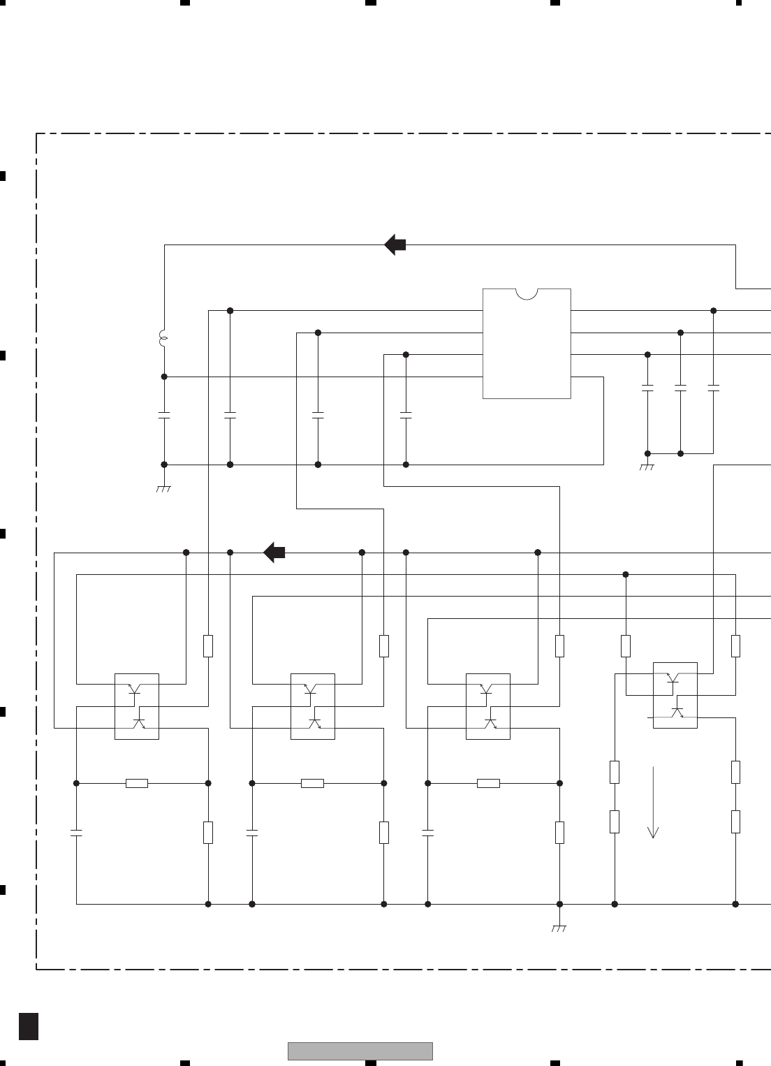
AVIC-X910BT/XS/UC
164
1234
1234
C
D
F
A
B
E
10.5 AV UNIT(RGB LED DRIVER SECTION)
5/6
A
BLUE
RED
GREEN
R3605
1k
R3612
100
R3608
1k
R3601
220k
R3603
2.2k
R3609
2.2k
R3606
2.2k
R3602
1k
R3604
220k
R3613
NM
R3607
220k
R3610
120
R3611
100
(1/16W)
R3614
NM
R3615
NM
R3616R3617
C3602
CCG1203-A
C3603
NM
UMX1N
Q3603
E1
1
B1
2
C2
3
E2
4
5
B2
6
C1
M62343FP
IC3601
A01
1
A02
2
A03
3
VCC
45
GND
6
DI
7
CLK
8
LD
C3607
4.7u/6.3
C3601
4.7u/6.3
C3605
NM
ILMGND
ILMGND
UMX1N
Q3604
E1
1
B1
2
C2
3
E2
4
5
B2
6
C1
C3604
4.7u/6.3
UMX1N
Q3602
E1
1
B1
2
C2
3
E2
4
5
B2
6
C1
C3606
NM
L3601
10u
UMX1N
Q3601
E1
1
B1
2
C2
3
E2
4
5
B2
6
C1
C3611
1000p/50
C3612
1000p/50
C3613
1000p/50
GNDD
(RED) (GREEN)
(MAX 12.0mA)
(BLUE)
(RED)
5.0V
5.0
5.0V
5.0V
8.5V8.5V
RGB_LED DRIVER
3601-3630
AVIC-X910BT/XS/UC 165
5678
5678
C
D
F
A
B
E
5/6
A
R3624
100
R3627
NM
R3618
100
R3621
NM
R3613
NM
R3614
NM
R3615
NM
R3619
NM
R3620
NM
R3626
NM
R3625
NM
R3616
120
R3617
150
(1/16w)
R3622
150
(1/16w)
R3623
180
R3628
NM
R3629
0
LEDCS
UMX1N
Q3605
E1
1
B1
2
C2
3
E2
4
5
B2
6
C1
UMX1N
Q3606
E1
1
B1
2
C2
3
E2
4
5
B2
6
C1
LEDDT
ILG2
GNDD
ILMGND
LEDCK
ILMG
ILMV
C3608
CCG1203-A
ILMGND
ILMB
E2
4
5
B2
6
C1
ILMGND
GNDD
ILMR
ILR2
ILB2
ILV2
SWVDD5
GNDD
p
C3613
1000p/50
(BLUE)
(MAX 10.8mA)
(MAX 9.0mA)
(GREEN)
5.0V5.0V
8.5V
8.5V
3601-3630RGB_LED DRIVER
4/6
A
1/6
A
AV UNIT (RGB LED DRIVER SECTION)
5/6
A
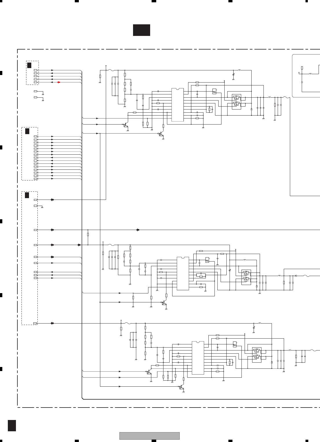
AVIC-X910BT/XS/UC
166
1234
1234
C
D
F
A
B
E
10.6 AV UNIT(IF SECTION)(GUIDE PAGE)
6/6
A
A-a 6/6
NAVICON
FCONT
FCONT
FCONT
FANV
KMODEOUT
PKBOUT
DCSKIP
VDCONT
VDD5CONT
DCSKIPCD
DCSKIPCD
TX
RX
IPPW
ASENBO
VDCONT
DCSKIP
NAVICON
FCONT
FANCONT
ASENS
BSENS
VDD5CONT
IPR
IPRG
IPLG
IPL
KMOD
FANUP
SYSPW
PKB
BSENSN
VD8
BK
R4642
NM
R4650
100k
R4677
1M
R4612
10
R4646
8.2k
R4609
150k
R4645
560
R4671
150k
R4654 180k
R4648
100k
R4676
180k
R4641
560
(1/4W SA)
R4601
0
R4606
3.3k
R4652
820k
R4672
820k
R4614
180k
R4655
NM
R4605
100
R4608
47k
R4644
0
R4610
820k
R4647
1.5k
R4674
10
R4673
10 (1/10W)
R4649
3.3k
R4668
3.3k
R4613
NM
R4615
1M
R4607
100k
R4651
150k
R4662
0
R4675
NM
R4670
47k
R4656
10
R4643
330
R4657
1M
R4666
47k
R4669 100k
R4667
100
R4653
10
R4611 10 (1/10W)
R4602
220
R4603
4.7k
R4604
1.5k
R4663
180
R4664
4.7k
R4665
1.5k
R4678
220
R4628
NM
R4679
NM
R4680
0
C4669
0.47u/16
GNDD
C4670
0.1u/16
PKBOUT
C4674 CCG1223-A
C4613 CCG1223-A
C4646
1u/10
DVD5
C4642
100p/50
C4605 33p/50
CCH1366-A_Po
C4611
L4641
CTH1255-A
(33uH)
C4614 CCG1223-A
FU4662
CEK1258
2.5A
12
C4609
0.47u/16
L4662
CTH1257-A
(10uH)
DTC114EU
Q4661
C4665 33p/50
FU4641
CEK1259-A
12
GNDD
GNDD
GNDD
GNDD
D4661
RB400D
C4672 CCG1223-A
GNDD
C4647 0.1u/25
GNDD
GNDD
GNDD
GNDD
NAVI5V
GNDD
NAVI5
CCH1366-A_Po
C4671
GNDD
GNDD
C4602
1000p/50
GNDD
L4661
CTH1255-A
(33uH)
GNDD
C4608
4.7u/10
GNDD
D4662
RB060L-40
GNDD
C4666
1u/10
C4603
0.1u/16
FU4642
CEK1258
12
SP8K2
Q4602
S1
1
G1
2
S2
3
G2
45
D2-2
6
D2-1
7
D1-2
8
D1-1
C4644
0.047u/50
C4641
0.01u/25
MVDD5
C4604
0.047u/50
C4664
0.047u/50
C4661
0.01u/25
C4610
0.1u/16
GNDD
FC8
C4643
0.1u/50
DTC114EU
Q4601
GNDD
GNDD
C4649
0.47u/16
GNDD
D4602
RB060L-40
C4668
4.7u/10
FU4661
CEK1258
2.5A
12
GNDD
C4606
1u/10
VD8
IC4661
TPS5103IDB
Vref=1.185(V)
SS
1
INV
2
FB
3
CT
4
5RT
6GND
7REF
8COMP
9RWMSKIP
10 STBY 11
VREG5V_IN
12
VREF5
13
VCC
14
VCC_SENSE
15
TRIP
16
OUTGND
17
OUT_D
18
LL
19
OUT_U
20
LH
D4601
RB400D
GNDD
NAVI5GND
NAVI5GND
IC4601
TPS5103IDB
Vref=1.185(V)
SS
1
INV
2
FB
3
CT
4
5RT
6GND
7REF
8COMP
9RWMSKIP
10 STBY 11
VREG5V_IN
12
VREF5
13
VCC
14
VCC_SENSE
15
TRIP
16
OUTGND
17
OUT_D
18
LL
19
OUT_U
20
LH
C4673 CCG1223-A
IC4641
TPS5103IDB
SS
1
INV
2
FB
3
CT
4
5RT
6GND
7REF
8COMP
9RWMSKIP
10 STBY 11
VREG5V_IN
12
VREF5
13
VCC
14
VCC_SENSE
15
TRIP
16
OUTGND
17
OUT_D
18
LL
19
OUT_U
20
LH
DTC114EU
Q4641
L4642
CTH1257-A
(10uH)
KMODEOUT
C4663
0.1u/16
FANV
SP8K2
Q4663
S1
1
G1
2
S2
3
G2
45
D2-2
6
D2-1
7
D1-2
8
D1-1
C4601
0.01u/25
GNDD
C4645 33p/50
GNDD
C4662
1000p/50
C4612 CCG1223-A
DTC114EU
Q4662
D4643
RB083L-20
CCH1409-A_Po
C4651
(220u/10)
C4653
CCG1223-A
C4652
CCG1223-A
SP8K2
Q4642
S1
1
G1
2
S2
3
G2
45
D2-2
6
D2-1
7
D1-2
8
D1-1
D4642
RB060L-40
C4654
CCG1223-A
(10uF/50V)
D4641
RB400D
C4650
CCG1222-A
(4R7/25)
L4681
NM
C4681
NM
HIVOL
GNDD
L4601
L4602
HI18
DV8
GNDD
GNDD
ILMV
FU4602
CEK1261-A
12
Q4664
GNDD
C4607
CCG1222-A
(4R7/25)
C4667
CCG1222-A
(4R7/25)
C4648
4.7u/10
VDCONT
RX
FCONT
ASENS
TX
BSENSN
BSENS
FANCONT
DCSKIPCD
VDD5CONT
ASENBO
DCSKIP
NAVICON
IPPW
IPRG
IPLG
IPL
IPR
KMOD
FANUP
SYSPW
PKB
GNDA
GNDA
FC5N
FC5D
C4617
0.1u/50
C4618
CCG1223-A
C4619
0.1u/50
C4600
1000p/50
C4655
CCG1223-A
C4657
1000p/50
C4656
0.1u/50
C4676
0.1u/50
C4677
1000p/50
C4675
CCG1223-A
GNDD
C4659
0.1u/50
C4616
1000p/50
C4658
1000p/50
C4679
0.1u/50
C4678
1000p/50
FU4601
CEK1261-A
12
R4616
2.2k
(D)
(106/50)
(D)
(1/8W)
(1/10W)
(D)
(106/50)
(D)
(106/50)
Vref=1.185(V)
(106/50)
(D)
(D)
(D)
(POSCAP)
(106/50)
(YB) (D) (D)
(D)
(D)
2.5A
(D)
(D)
(D)
(4R7/25)
(D)
(106/50)
(13.5V)
(YB)
(YB)
CCG1252
LCTAW4R7J2520
475
10uH
27uH
NM
N
CDRH127NP-270MC
CDRH127NP-100MC
5.0V
H:10.6V/L:7.4V
8.5V
8.0V
8.5V
8.0V
8.0V
8.5V 8.5V
5.0V
5.0V 5.0V
5.0V 5.0V
5.0V
5.0V
(POSCAP)
(POSCAP)
4641-4660
DVD8V
HIVOL18
4661-4680
4681-4690
DVD5V
4600-4620
4666
NAVI5V
5A
5A
3.15A
>
>
>
>
>
2/6
A
4/6
A
1/6
A
>
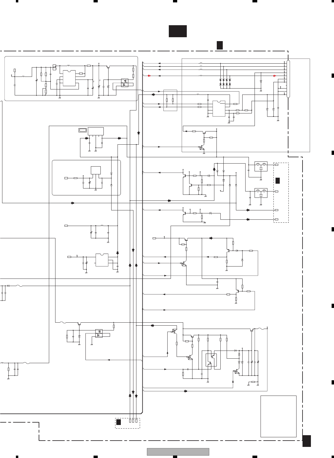
AVIC-X910BT/XS/UC 167
5678
5678
C
D
F
A
B
E
6/6
A
A-b 6/6
IPRG
IPPW
IPLG
IPR
IPL
RX
BSENS
FANUP
FANCONT
ASENS
FANV
KMODEOUT
PKBOUT
KMOD
PKB
ASENB
SYSPW
SYSPW
BSENSN
SYSPW
TX
VT6
NKBUP
BU
BU
BU
ASENBO
VDD5
VDD5
BKEEP
BKEEP
R4677
1M
R4733
6.8k
R4732
47k
R4751
100
R4778 470
(1/4W)
R4723
100
R4724
1k
R4777 220
(1/10W)
R4731
2.2k
R4721
4.7k
R4722
100
R4727
62
R4726
100
R4734
10k
R4756
10k
R4735
100k
R4758
2.7k
R4736
3.3k
R4754
10k
R4752
100
R4737
10k
R4725
100
R4687
NM
R4688
NM
R4684
NM
R4683
NM
R4685
NM
R4686
NM
R4681 NM
R4682 NM
R4757
0
R4749
4.7k
R4750
4.7k
R4755
1M
R4753
1M
R4738
47k
R4739
100k
R4701
NM
R4773
10k
R4771
4.7k
R4774
5.1k
R4775
220k
R4776
4.7k
R4772
4.7k
R4728
4.7k
R4785
NM
R4632
NM
R4633
820
D4772
RB500V-40
BU
GNDD
DTA114EU
Q4771
FANGND
C4751
0.1u/50
VDD5
GNDD
IPR+
D4731
HZU7R5(B3)
47u/16
C4774
C4721
4700p/16
BSI
FU4662
CEK1258
2.5A
12
GNDD
D4752
1SS355
D4726
UDZS18(B)
IPL-
GNDD
IPR-
L4701
CTF1393-A
2SA1576(QR)
Q4734
KBUP
EF4732
CCG1172-A
3
2
1
DTC114EUA
Q4772
4662
257-A
0uH)
NS3
C4731
0.1u/50
C4710
0.1u/16
C4707
0.1u/16
D4771
RB500V-40
FNV
Q4731
2SC4081(QRS)
FANGND
D4733
RB500V-40
EF4731 CCG1172-A
3
2
1
IPL+
L4721
2.2u
100u/16
C4776
10u/16
C4705
Q4733
2SC4081(QRS)
GNDD
C4775 0.01u/50
GNDD
FU4771
CEK1254
12
L4723 CTF1334-A
2SA1576A(QR)
Q4751
CN1021
CKS3408
1
2
3
4
5
6
7
8
9
10
11
IPBUS
D4735
RB500V-40
10u/16
C4704
C4773 0.01u/50
2SA1576A(QR)
Q4752
GNDD
BUP
GNDD
D4724
MALS068X
GNDD
GNDD
IPBUS-
L4725 CTF1334-A
FU4642
CEK1258
12
IPRG
L4724 CTF1334-A
D4732
RB500V-40
DTC114EUA
Q4775
Q4774
IMX1
1E
6
1B
5
2C
42E 3
2
2B
1
1C
DD
C4709
0.1u/16
D4773
HZU8R2(B1)
BSB
C4732
0.1u/50
C4724
0.1u/50
HA12241FP
IC4721
DIN1
1
ROUT
2
DIN2
3
GND
45
BUS-
6
BUS+
7
VCC
8
STBY
IPAS
GNDD
C4771
0.1u/50
D4723
MALS068X
D4727
UDZS18(B)
D4734
EDZ20(B)
GNDD
D4725
UDZS18(B)
UVDD5
GNDD
IC4703
S-L2980A33MC-C6S
VIN 1
VSS 2
ON/OFF 3
NC
4
5VOUT
GNDD
D4774
HZU11(B2)
NAVI3V
C4772
4700p/50
2SA1587(GRBL)
Q4773
D4751
1SS355
C4702
0.1u/16
GNDD
L4722 CTF1334-A
FNB
BUP3
Q4776
2SD1760F5(R)
D4643
RB083L-20
C4723
NM
C4722
NM
GNDD
L4681
NM
D4681
NM
GNDA
L4682
NM
GNDA
C4685 NM
C4688 NM
NM
Q4682
1
2
34
5
6
C4681
NM
95V
NM
IC4681
CS
1
ES
2
CT
3
GND
45
INV
6
VCC
7
SI
8
CD
C4684
NM
C4683 NM
HIVOL
Q4681
NM
D4682
NM
NM
C4687
NM
C4682
DTC114EU
Q4753
2SA1576A(QR)
Q4754
NM
C4686
D4736
RB500V-40
Q4738
2SC4081(QRS)
D4737
HZU7R5(B3)
NBSINBSB
GNDD
C4706
1u/25
C4701
1u/16
CD3.3
GNDD
CD3
GNDD
C4711
NM
BUP3
HI18
NA3B
BSN
NBSN
TP4736
TP4735
IPLG
GNDD
C4631
0.1u/50
D4631
UDZ9R1(B)
GNDD
UMD2N
Q4632
GND1 1
IN1 2
OUT1 3GND2
4
5IN2
6OUT2
Q4631
2SD1767(QR)
A
2
BD3931HFP
IC4701
1VCC
2NC1
3GND
4NC2
5VO
NM
IC4702
1IN
2GND
3OUT
NM
C4708
D4701
NM
D4702
NM
VT6
NKBUP
NAVIC
C4703
NM
FU4631
CEK1247-A
200mA
12
GNDD
C4659
0.1u/50
1000p/50
C4679
0.1u/50
C4678
1000p/50
GNDD
DTC114EU
Q4732
D4721
MALS180X
D4722
MALS180X
IP-BUS IN
IPL+
IPL-
IPBUSG
IPR-
IPBUS-
NC
ASENBO
IPBUS+
IPRG
IPR+
IPLG
2.5A
(13.5V)
BUP3
IC4703,C4702
C4704,C4710
MAX 150mA
NM
18.0V
LCTAW4R7J2520
9.5V
(1/4W)
105
(1/4W)
475
105
VDD5
NM
NM
6.5V
6.5V
6.5V6.5V6.5V6.5V6.5V6.5V
5.0V 5.0V 5.0V 5.0V 5.0V 5.0V 5.0V 5.0V 5.0V
5.0V
5.0V
5.0V
5.0V
5.0V5.0V5.0V5.0V
5.0V
5.0V
5.0V
3.3V3.3V
3.3V3.3V
3.3V
3.3V
3.3V
H:10.6V/L:7.4V H:10.6V/L:7.4V
H:10.6V/L:7.4V
8.5V
8.5V
5.0V
NAVI5V 4600-4620
4666
4641-4660DVD8V
DVD5V 4661-4680
HIVOL18 4681-4690
VDD5
CD3.3
UVDD5
BUP3
ILMV
BUP
NAVIC
4749-4759
4701
4712
4706
4701
4707
4705
4709
4702-4703
4710
4701-4703
4708
4711
4631-4635
4737
4738-4739
IP-BUS
4721-4729
1021
4731-4737
FAN DRIVER 4771-4778
4785
PARKING SENS/KMODE
4737
HIVOL18
4771-4778
NAVIC
4701
UVDD5
4701
IP-BUS
4681-4690
4711
BUP
PARKING SENS/KMODE
4738-4739
4707
4708
4705
4785
4710
4701-4703
CD3.3
4721-4729
BUP3
4712
4631-4635
4731-4737
FAN DRIVER
ILMV
4702-4703
4749-4759
1021
4709
VDD5
4706
1A
UC,EU5
UC
>
>
>
1/6
A
1/6
A
>
AV UNIT (IF SECTION)
6/6
A
IP-BUS:+2.2 dBs
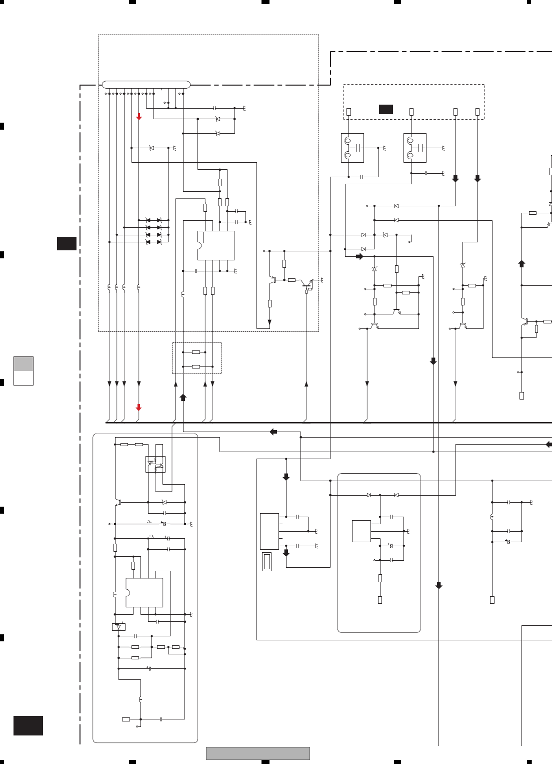
AVIC-X910BT/XS/UC
168
1234
1234
C
D
F
A
B
E
A-a A-b
A-b 6/6
IPRG
IPPW
IPLG
IPR
IPL
RX
BSENS
ASENB
SYSPW
BSENSN
TX
VT6
NKBUP
BU
BU
ASENBO
BKEEP
R4733
6.8k
R4732
47k
R4723
100
R4724
1k
R4731
2.2k
R4721
4.7k
R4722
100
R4727
62
R4726
100
R4734
10k R4735
100k
2.7k
R4736
3.3k
R4754
10k
R4737
10k
R4725
100
R4687
NM
R4688
NM
R4684
NM
R4683
NM
R4685
NM
R4686
NM
R4681 NM
R4682 NM
R4749
4.7k
R4750
4.7k
R4738
47k
R4739
100k
R4701
NM
R4728
4.7k
IPR+
D4731
HZU7R5(B3)
C4721
4700p/16
BSI
GNDD
D4726
UDZS18(B)
IPL-
GNDD
IPR-
L4701
CTF1393-A
2SA1576(QR)
Q4734
KBUP
EF4732
CCG1172-A
3
2
1
NS3
C4731
0.1u/50
C4707
0.1u/16
Q4731
2SC4081(QRS)
D4733
RB500V-40
EF4731 CCG1172-A
3
2
1
IPL+
L4721
2.2u
10u/16
C4705
Q4733
2SC4081(QRS)
GNDD
L4723 CTF1334-A
2SA1576A(QR)
Q4751
CN1021
CKS3408
1
2
3
4
5
6
7
8
9
10
11
IPBUS
D4735
RB500V-40
BUP
GNDD
D4724
MALS068X
GNDD
GNDD
IPBUS-
L4725 CTF1334-A
IPRG
L4724 CTF1334-A
D4732
RB500V-40
C4709
0.1u/16
BSB
C4732
0.1u/50
C4724
0.1u/50
HA12241FP
IC4721
DIN1
1
ROUT
2
DIN2
3
GND
45
BUS-
6
BUS+
7
VCC
8
STBY
IPAS
D4723
MALS068X
D4727
UDZS18(B)
D4734
EDZ20(B)
GNDD
D4725
UDZS18(B)
UVDD5
GNDD
IC4703
GNDD
NAVI3V
D4751
L4722 CTF1334-A
C4723
NM
C4722
NM
GNDD
L4681
NM
D4681
NM
GNDA
L4682
NM
GNDA
C4685 NM
C4688 NM
NM
Q4682
1
2
34
5
6
C4681
NM
95V
NM
IC4681
CS
1
ES
2
CT
3
GND
45
INV
6
VCC
7
SI
8
CD
C4684
NM
C4683 NM
HIVOL
Q4681
NM
D4682
NM
NM
C4687
NM
C4682
2SA1576A(QR)
Q4754
NM
C4686
D4736
RB500V-40
Q4738
2SC4081(QRS)
D4737
HZU7R5(B3)
NBSINBSB
GNDD
C4706
1u/25
C4701
1u/16
CD3.3
GNDD
CD3
GNDD
C4711
NM
HI18
NA3B
BSN
NBSN
TP4736
TP4735
IPLG
BD3931HFP
IC4701
1VCC
2NC1
3GND
4NC2
5VO
NM
IC4702
1IN
2GND
3OUT
NM
C4708
D4701
NM
D4702
NM
NKBUP
NAVIC
C4703
NM
GNDD
DTC114EU
Q4732
D4721
MALS180X
D4722
MALS180X
IP-BUS IN
IPL+
IPL-
IPBUSG
IPR-
IPBUS-
NC
ASENBO
IPBUS+
IPRG
IPR+
IPLG
MAX 150mA
18.0V
LCTAW4R7J2520
9.5V
(1/4W)
105
(1/4W)
475
105
VDD5
NM
NM
6.5V
6.5V
6.5V
5.0V 5.0V 5.0V 5.0V
5.0V
5.0V
5.0V
5.0V
5.0V5.0V5.0V5.0V
5.0V
3.3V3.3V
3.3V
3.3V
8.5V
5.0V
4737
HIVOL18
NAVIC
4701
UVDD5
4701
IP-BUS
4681-4690
4711
PARKING SENS/KMODE
4738-4739
4707
4708
4705
4710
4701-4703
CD3.3
4721-4729
BUP3
4712
4702-4703
4749-4759
1021
4709
VDD5
4706
UC,EU5
UC
1/6
A
AV UNIT (IF SECTION)
6/6
A
IP-BUS:+2.2 dBs
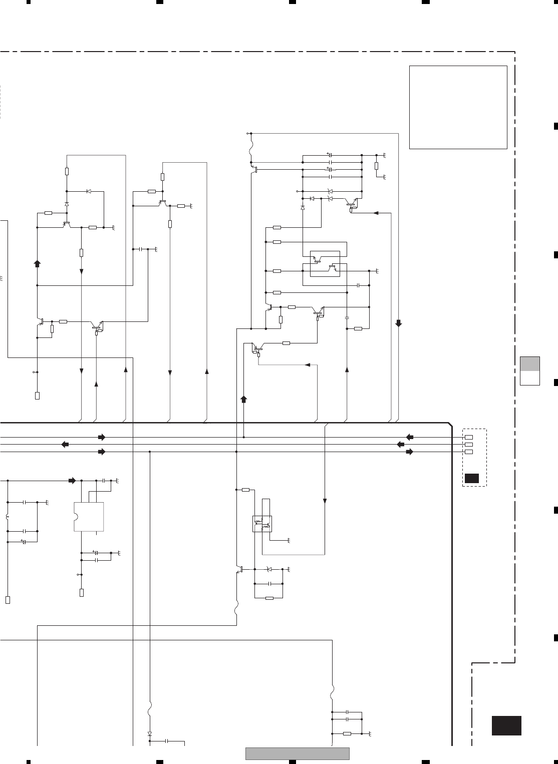
AVIC-X910BT/XS/UC 169
5678
5678
C
D
F
A
B
E
A-a A-b
A-b 6/6
FANUP
FANCONT
ASENS
FANV
KMODEOUT
PKBOUT
KMOD
PKB
SYSPW
SYSPW
VT6
BU
VDD5
VDD5
BKEEP
R4677
1M
R4751
100
R4778 470
(1/4W)
R4777 220
(1/10W)
R4756
10k
R4758
2.7k
R4754
10k
R4752
100
R4757
0
R4749
4.7k
R4750
4.7k
R4755
1M
R4753
1M
R4773
10k
R4771
4.7k
R4774
5.1k
R4775
220k
R4776
4.7k
R4772
4.7k
R4785
NM
R4632
NM
R4633
820
D4772
RB500V-40
BU
GNDD
DTA114EU
Q4771
FANGND
C4751
0.1u/50
VDD5
GNDD
47u/16
C4774
FU4662
CEK1258
2.5A
12
D4752
1SS355
L4701
CTF1393-A
DTC114EUA
Q4772
2
-A
C4710
0.1u/16
C4707
0.1u/16
D4771
RB500V-40
FNV
FANGND
100u/16
C4776
10u/16
C4705
GNDD
C4775 0.01u/50
FU4771
CEK1254
12
2SA1576A(QR)
Q4751
10u/16
C4704
C4773 0.01u/50
2SA1576A(QR)
Q4752
GNDD
FU4642
CEK1258
12
DTC114EUA
Q4775
Q4774
IMX1
1E
6
1B
5
2C
42E 3
2
2B
1
1C
C4709
0.1u/16
D4773
HZU8R2(B1)
GNDD
C4771
0.1u/50
UVDD5
IC4703
S-L2980A33MC-C6S
VIN 1
VSS 2
ON/OFF 3
NC
4
5VOUT
GNDD
D4774
HZU11(B2)
NAVI3V
C4772
4700p/50
2SA1587(GRBL)
Q4773
D4751
1SS355
C4702
0.1u/16
GNDD
FNB
BUP3
Q4776
2SD1760F5(R)
D4643
RB083L-20
DTC114EU
Q4753
2SA1576A(QR)
Q4754
2SC
GNDD
BUP3
NA3B
GNDD
C4631
0.1u/50
D4631
UDZ9R1(B)
GNDD
UMD2N
Q4632
GND1 1
IN1 2
OUT1 3GND2
4
5IN2
6OUT2
Q4631
2SD1767(QR)
VT6
FU4631
CEK1247-A
200mA
12
C4659
0.1u/50
C4679
0.1u/50
C4678
1000p/50
GNDD
2.5A
(13.5V)
BUP3
IC4703,C4702
C4704,C4710
MAX 150mA
NM
6.5V6.5V6.5V6.5V6.5V
5.0V 5.0V 5.0V 5.0V 5.0V 5.0V
5.0V
5.0V
5.0V
5.0V
3.3V3.3V
3.3V3.3V
3.3V
3.3V
3.3V
H:10.6V/L:7.4V H:10.6V/L:7.4V
H:10.6V/L:7.4V
8.5V
8.5V
NAVI5V 4600-4620
4666
4641-4660DVD8V
DVD5V 4661-4680
HIVOL18 4681-4690
VDD5
CD3.3
UVDD5
BUP3
ILMV
BUP
NAVIC
4749-4759
4701
4712
4706
4701
4707
4705
4709
4702-4703
4710
4701-4703
4708
4711
4631-4635
4737
4738-4739
IP-BUS
4721-4729
1021
4731-4737
FAN DRIVER 4771-4778
4785
PARKING SENS/KMODE
4771-4778
4701
UVDD5
BUP
PARKING SENS/KMODE
4707
4705
4785
4631-4635
4731-4737
FAN DRIVER
ILMV
4749-4759
4709
1A
>
>
>
1/6
A
>
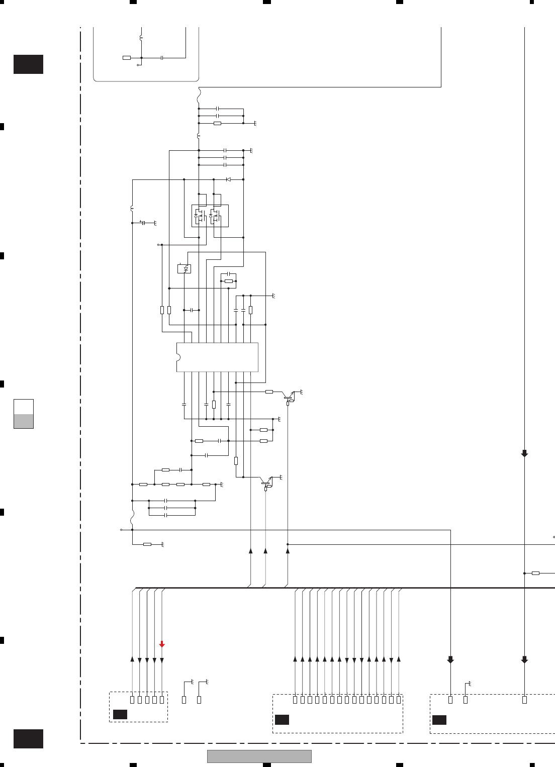
AVIC-X910BT/XS/UC
170
1234
1234
C
D
F
A
B
E
A-bA-a
A-a 6/6
A-b 6/6
NAVICON
FCONT
DCSKIP
DCSKIPCD
TX
RX
IPPW
ASENBO
VDCONT
DCSKIP
NAVICON
FCONT
FANCONT
ASENS
BSENS
VDD5CONT
IPR
IPRG
IPLG
IPL
KMOD
SYSPW
BSENSN
R4612
10
R4609
150k
R4601
0
R4606
3.3k
R4614
180k
R4605
100
R4608
47k
R4610
820k
R4613
NM
R4615
1M
R4607
100k
R4666
47k
R4611 10 (1/10W)
R4602
220
R4603
4.7k
R4604
1.5k
R4628
NM
C4613 CCG1223-A
C4605 33p/50
CCH1366-A_Po
C4611
C4614 CCG1223-A
C4609
0.47u/16
DTC114EU
Q4661
GNDD
GNDD
GNDD
GNDD
GNDD
NAVI5V
GNDD
NAVI5
GNDD
C4602
1000p/50
C4608
4.7u/10
GNDD
GNDD
C4603
0.1u/16
SP8K2
Q4602
S1
1
G1
2
S2
3
G2
45
D2-2
6
D2-1
7
D1-2
8
D1-1
C4604
0.047u/50
C4610
0.1u/16
DTC114EU
Q4601
D4602
RB060L-40
C4606
1u/10
D4601
RB400D
NAVI5GND
NAVI5GND
IC4601
TPS5103IDB
Vref=1.185(V)
SS
1
INV
2
FB
3
CT
4
5RT
6GND
7REF
8COMP
9RWMSKIP
10 STBY 11
VREG5V_IN
12
VREF5
13
VCC
14
VCC_SENSE
15
TRIP
16
OUTGND
17
OUT_D
18
LL
19
OUT_U
20
LH
C4601
0.01u/25
C4612 CCG1223-A
L4681
NM
C4681
NM
HIVOL
GNDD
L4601
L4602
HI18
DV8
GNDD
ILMV
FU4602
CEK1261-A
12
C4607
CCG1222-A
(4R7/25)
VDCONT
RX
FCONT
ASENS
TX
BSENSN
BSENS
FANCONT
DCSKIPCD
VDD5CONT
ASENBO
DCSKIP
NAVICON
IPPW
IPRG
IPLG
IPL
IPR
KMOD
SYSPW
GNDA
GNDA
FC5N
C4617
0.1u/50
C4618
CCG1223-A
C4619
0.1u/50
C4600
1000p/50
C4616
1000p/50
FU4601
CEK1261-A
12
R4616
2.2k
(106/50)
(D)
(106/50)
(106/50)
(D) (D)
(D)
(D)
LCTAW4R7J2520
475
10uH
27uH
CDRH127NP-270MC
CDRH127NP-100MC
8.5V 8.5V
0V
8.5V 8.5V
5.0V
5.0V 5.0V
5.0V 5.0V
5.0V
(POSCAP)
4641-4660
DVD8V
HIVOL18
4681-4690
4600-4620
4666
NAVI5V
5A
5A
>
>
>
2/6
A
4/6
A
1/6
A
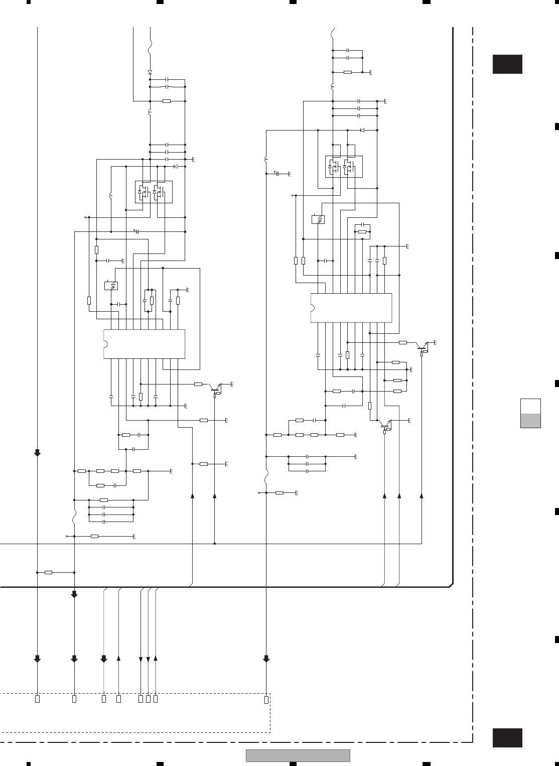
AVIC-X910BT/XS/UC 171
5678
5678
C
D
F
A
B
E
A-bA-a
A-a 6/6
A-b 6/6
FCONT
FCONT
FANV
KMODEOUT
PKBOUT
VDCONT
VDD5CONT
DCSKIPCD
FANUP
PKB
VD8
R4642
NM
R4650
100k
R4677
1M
R4646
8.2k
R4645
560
R4671
150k
R4654 180k
R4648
100k
R4676
180k
R4641
560
(1/4W SA)
R4652
820k
R4672
820k
R4655
NM
R4644
0
R4647
1.5k
R4674
10
R4673
10 (1/10W)
R4649
3.3k
R4668
3.3k
R4651
150k
R4662
0
R4675
NM
R4670
47k
R4656
10
R4643
330
R4657
1M
R4669 100k
R4667
100
R4653
10
R4663
180
R4664
4.7k
R4665
1.5k
R4678
220
R4628
NM
R4679
NM
R4680
0
C4669
0.47u/16
GNDD
C4670
0.1u/16
PKBOUT
C4674 CCG1223-A
C4646
1u/10
DVD5
C4642
100p/50
L4641
CTH1255-A
(33uH)
FU4662
CEK125
2.5A
1
L4662
CTH1257-A
(10uH)
C4665 33p/50
FU4641
CEK1259-A
12
GNDD
GNDD
GNDD
D4661
RB400D
C4672 CCG1223-A
C4647 0.1u/25
GNDD
CCH1366-A_Po
C4671
GNDD
GNDD
L4661
CTH1255-A
(33uH)
GNDD
D4662
RB060L-40
C4666
1u/10
FU4642
CEK1258
12
C4644
0.047u/50
C4641
0.01u/25
MVDD5
C4664
0.047u/50
C4661
0.01u/25
GNDD
FC8
C4643
0.1u/50
GNDD
GNDD
C4649
0.47u/16
GNDD
C4668
4.7u/10
FU4661
CEK1258
2.5A
12
GNDD
VD8
IC4661
TPS5103IDB
Vref=1.185(V)
SS
1
INV
2
FB
3
CT
4
5RT
6GND
7REF
8COMP
9RWMSKIP
10 STBY 11
VREG5V_IN
12
VREF5
13
VCC
14
VCC_SENSE
15
TRIP
16
OUTGND
17
OUT_D
18
LL
19
OUT_U
20
LH
GNDD
C4673 CCG1223-A
IC4641
TPS5103IDB
SS
1
INV
2
FB
3
CT
4
5RT
6GND
7REF
8COMP
9RWMSKIP
10 STBY 11
VREG5V_IN
12
VREF5
13
VCC
14
VCC_SENSE
15
TRIP
16
OUTGND
17
OUT_D
18
LL
19
OUT_U
20
LH
DTC114EU
Q4641
L4642
CTH1257-A
(10uH)
KMODEOUT
C4663
0.1u/16
FANV
SP8K2
Q4663
S1
1
G1
2
S2
3
G2
45
D2-2
6
D2-1
7
D1-2
8
D1-1
GNDD
C4645 33p/50
GNDD
C4662
1000p/50
DTC114EU
Q4662
D4643
RB083L-20
CCH1409-A_Po
C4651
(220u/10)
C4653
CCG1223-A
C4652
CCG1223-A
SP8K2
Q4642
S1
1
G1
2
S2
3
G2
45
D2-2
6
D2-1
7
D1-2
8
D1-1
D4642
RB060L-40
C4654
CCG1223-A
(10uF/50V)
D4641
RB400D
C4650
CCG1222-A
(4R7/25)
DV8
GNDD
ILMV
Q4664
GNDD
C4667
CCG1222-A
(4R7/25)
C4648
4.7u/10
FANUP
PKB
FC5D
C4655
CCG1223-A
C4657
1000p/50
C4656
0.1u/50
C4676
0.1u/50
C4677
1000p/50
C4675
CCG1223-A
GNDD
C4659
0.1u/50
C4658
1000p/50
C4679
0.1u/50
C4678
1000p/50
(D)
(D)
(1/8W)
(1/10W)
(106/50)
(D)
Vref=1.185(V)
(D)
(D)
(D)
(POSCAP)
(106/50)
(YB)
(D)
2.5A
(D)
(D)
(4R7/25)
(D)
(106/50)
(13.5V)
(YB)
(YB)
CCG1252
NM
5.0V
H:10.6V/L:7.4V
8.5V
8.0V
8.5V
8.0V
8.0V
8.5V 8.5V
5.0V
(POSCAP)
4641-4660
DVD8V
4661-4680
DVD5V
3.15A
>
>
>
>
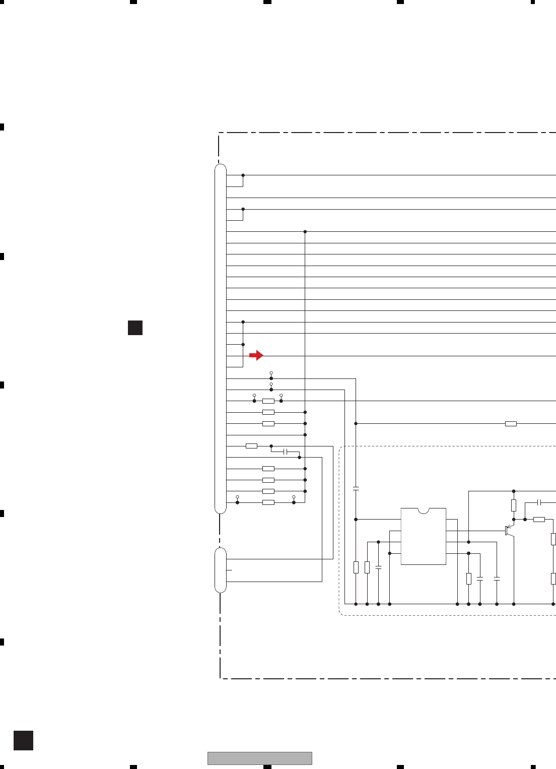
AVIC-X910BT/XS/UC
172
1234
1234
C
D
F
A
B
E
10.7 CK UNIT
B
NM
CN881
1
2
3
CKS6115-A
CN883
1
2
3
4
5
6
7
8
9
10
11
12
13
14
15
16
17
18
19
20
21
22
23
24
25
26
27
28
29
30
C892
NM
C891
NM
C890
NM
C887
NM
C893
NM
NM
IC890
VIN1
1
SW1
2
VIN2
3
SW2
45
VIN3
6
V+
7
VOUT
8
GND
NM
Q890
R887
NM
R
R890 NM
R892 NM
R891 NM
R896
R894
NM
R893
NM
TP883
TP882TP881
TP884
NM
VR890
1
R881 NM
R888
NM
R882 NM
R883 NM
R884 NM
R885 NM
R886 NM
R898
0
C896
NM
TP894
TP895
VDD8(DRV)
VDD8(DRV)
VDD8(REG)
PGND
PGND
DGND
VDD5
AMUTE
XRES
IRQPWR
HSTCMD
SLVSTS
STANDBY
AGND
AGND
AGND
ANA ROUT
ANA LOUT
CVBS
VIDEO GND
WAKEUP
USB D+
USB D-
DGND
IEC OUT
DGND
I2C SCL
I2C SDA
CP RESET
CP LADY
IEC OUT
DGND
(NC)
6dB
NM
CKS4823-A
2V ->
C
CN1901
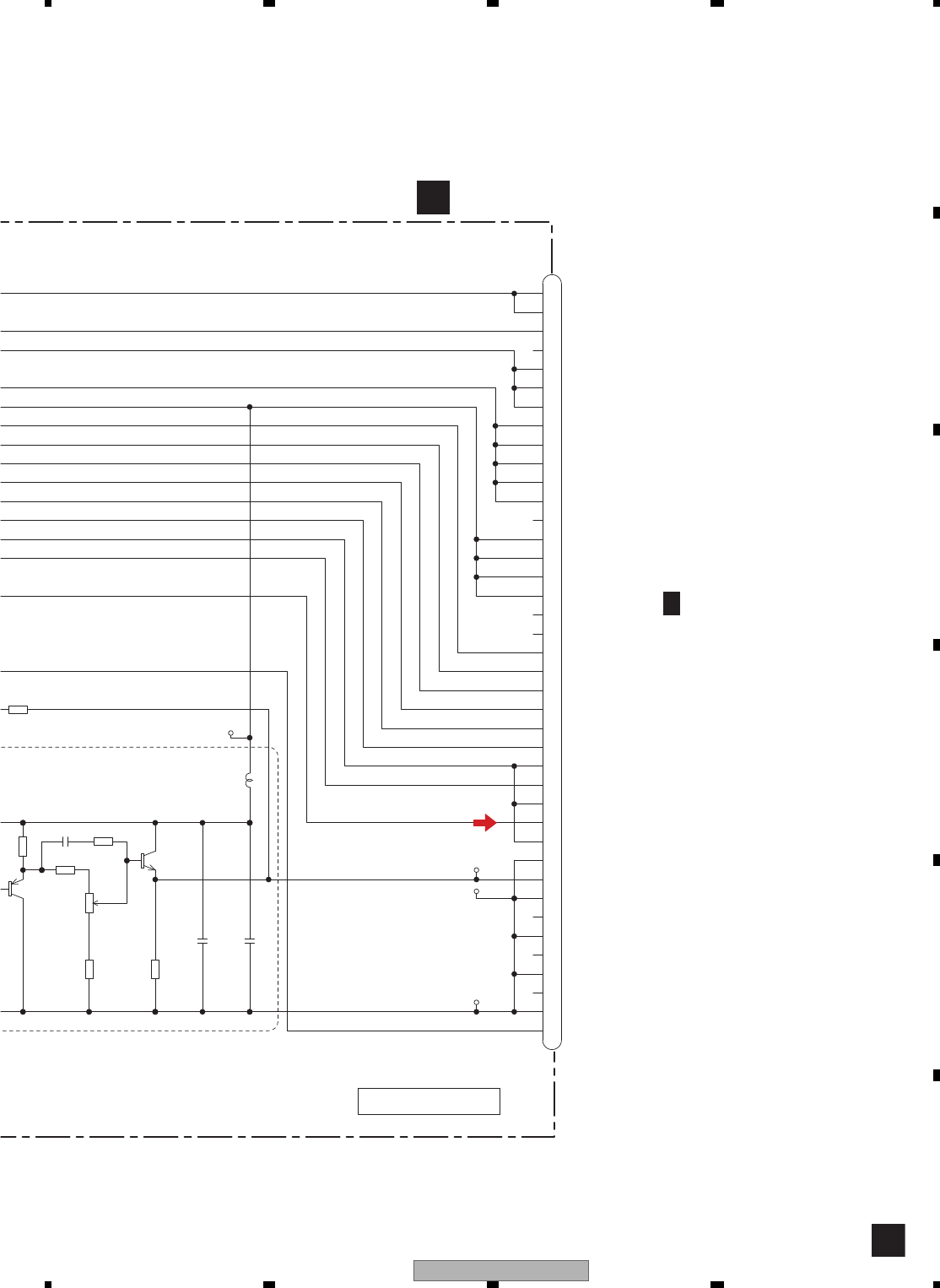
AVIC-X910BT/XS/UC 173
5678
5678
C
D
F
A
B
E
B
1
2
3
4
5
6
7
8
9
10
11
12
13
14
15
16
17
18
19
20
21
22
23
24
25
26
27
28
29
30
31
32
33
34
35
36
37
38
39
40
C895
NM
C893
NM
L890
NM
Q891
NM
NM
Q890
R895
NM
R896
NM
R897
NM
R894
NM
R893
NM
NM
VR890
1
3
2
R898
0
NM
C897
NM
TP890
TP891
TP892
TP893
AMUTE
VDD8(DRV)
AGND
AGND
PGND
PGND
VDD8(DRV)
VDD8(REG)
IRQPWR
HSTCMD
DGND
VDD5
SLVSTS
XRES
STANDBY
AGND
ANA ROUT
ANA LOUT
CVBS
VIDEO GND
WAKEUP
(NC)
(NC)
(NC)
(NC)
PGND
DGND
DGND
DGND
DGND
VDD5
VDD5
VDD5
VIDEO GND
Y
CB
CR
VIDEO GND
VIDEO GND
UARTSPEED
(1k)
Connector 881-887
890-898Video
CKS5100-A
CN882
2V -> 1V
BCK UNIT
CN702
4/6
A
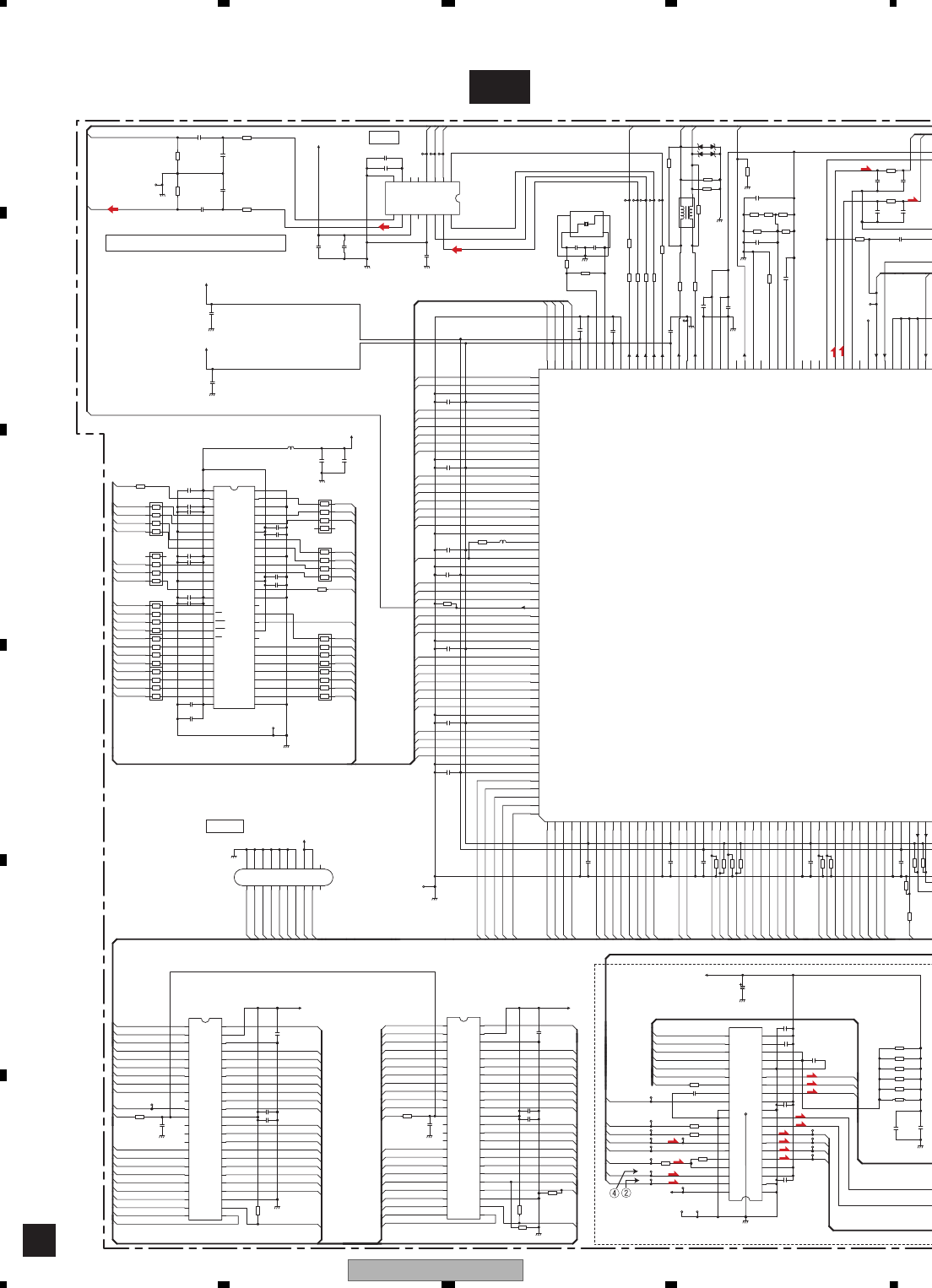
AVIC-X910BT/XS/UC
174
1234
1234
C
D
F
A
B
E
10.8 DVD CORE UNIT(GUIDE PAGE)
C
C-a
A9
A4
A10
A5
A11
A6
A12
A7
A13
A8
A14
A15
D15
D7
D14
D6
D13
D5
D12
D4
D11
D3
D10
D2
D9
D1
D8
A3
A2
A1
XRD
A16
A5
A10
A4
A9
A1
A2
A3
A16A15
A14
A8
A13
A7
A12
A6
XRD
A11
A19
XWR1
A18
A17 A17
A19
A18
MDQ7
MDQ6
MDQ5
MDQ15
MDQ14
MA9
MA8
MA7
MA6
MA5
MA4
DQM0
XWE
XCAS
XRAS
XCSM
BA1
MA10
BA0
MA0
MA1
MA2
MA3
MCK
MA11
MDQ15
MDQ0
MDQ14
MDQ1
MDQ13
MDQ2
MDQ12
MDQ3
MDQ11
MDQ4
MDQ10
MDQ5
MDQ7
MDQ6
DQM1
DQM0
MDQ9
MDQ8
XWE
MA9
XRAS
BA0
XCAS
XCSM
MA7
MA0
MA1
MA10
MA8
BA1
MA6
MA3
MA5
MA4
MA2
A0
XCSF2
XRD
A16
XWR1
A19
A1
A17
A6
A3
A5
A2
A4
A7
FD
TD
XCSF1
D0
D8
D1
D9
D10
D2
D3
D4
D5
D11
D14
D13
D12
D7
D15
D4
D12
D5
D13
D6
D14
D7
D15
D10
D3
D11
D0
D8
D1
D9
D2
D6
A10
A8
A11
A9
LOUT
ROUT
SDODAC
SCKDAC
LTDAC
A12
IECOUT
A0
MA11
TRCDATA3
SCLOCK
TRCDATA0
TRCCLK
TRCDATA1
TRCST
TRCDATA2
SDATA
A0
MCK
COMPOSITE
XCSF2
FE1
FE2
EXTRG0
A15
A14
A13
A18
TEMP
DQM1
COILU
COILV
COILW
MD
LDIN TOM
FOP
FOM
TOP
CONT1
CONT2
FG
CRGDRV
HWP
HVM
HVP
HUM
HUP
HWM
HBM
XWR1
NRES
NRES
TD
FD
STANDBY
MDQ13
MDQ9
MDQ10
MDQ11
MDQ12
MDQ8
MDQ1
MDQ3
MDQ2
MDQ4
MDQ0
A20
A20
D+
D-
D0
DGND3
DGND2
IEC
GNDD
GNDD
GNDA
GNDA
GNDD
GNDD
GNDD
GNDD
GNDD
R1405
100K
R1503
1M
R1406
100K
R1402
100K
C1671
R1
C1672
R1
C1487
R1
C1481 R1
C1674
R1
C1480 R1
C1603
100P
C1482 R1
C1484 R1
C1509
R1
C1488
R1
C1602
100P
C1408
R1
C1403
R1
C1407
NM
C1402
NM
C1502
10
C1404
4R7
C1409
4R7
C1676
1
C1503 R1
VCC33
VCC12
VCC33
C1485
R1
C1504
R1
C1505
R1
C1506
R1
C1507
R1
C1508
R1
C1518 R1
C1519 R1
C1514
R1
C1511
R1
C1513 R1
C1516 R1
C1517 R1
C1515
R1
C1805
R1
PCM1753DBQ
IC1801
BCK
1
DATA
2
LRCK
3
DGND
4
5
NC
6
VCC
7
VOUTL
8
VOUTR
9
AGND
10
VCOM
11
ZEROR/ZEROA
12
ZEROL/NA
13
MD
14
MC
15
ML
16
SCK
2081C
7R4
GNDAU1
R1804
820
R1803
820
C1801
4R7
R1802
100K
C1804
1800P
R1801
100K
C1803
1800P
GNDAU
C1809
R1
GNDD
AVCC5
GNDAU
VCC33
C1501
10
GNDD
CN1951
1
2
3
4
5
6
7
8
9
1011
12
13
14
15
16
17
18
19
20
GNDD
NM
VCC33
TEMP
PGND
GNDV
GNDD
R1954
NM
R1955
NM
C1601
R01
R1603
10K
R1517
10K
R1518
10K
C1673
R1
C1491 NM
C1492 NM
C1493 NM
C1494 NM
R1528
10K
R1529
10K
R1530
10K
R1531
10K
C1807
NM
R1217
1
R1218
1
R1213
1
R1214
1
R1215
1
R1216
1
PGND
PGND1PGND2
VHALF VHALF
VD8
PGND
100/16
C1201
FG
R1202 220
R1201 220
L1901
NM
11
2
2
3
344
D1902
NM
D1901
NM
GNDD
C1489
10
R1538
100K
R1602
12K
R1601
12K
C1604
68P
C1605
68P
GNDD
VCC33
C1483 NM
C1486
NM
C1405
NM
R1212
270
AD2
ADOUT
CONT2
CONT1
CRGDRV
DACCK
FD1
LDIN
LRCK
LTDAC
MD1 MD2
SCKDAC
SDODAC
SRCK
TD1
XWR1
C1204
2200P
GNDD5
R1403
NM
R1203
10K
R1204
15K
FOM2
FOP2
TOM2
TOP2
R1539
100K
R1501
1R2K
R1679
NM R1675
NM
R1673
NM
GNDD
R1505 100
R1506 100
R1507 100
L1904
C1490
R001
C1211
4R7
R1401
220
C1401
R01
R1950
NM
R1951
NM
C1512
10P
C1510
12P
C1203
NM
C1205
R1
C1207
R1
C1210
R1
C1209
R1
R1508
220
R1512
100
C1208
R01
R1483
56
2
1
4
3
6
5
8
7
R1487
56
2
1
4
3
6
5
8
7
R1486
56
2
1
4
3
6
5
8
7
R1488
56
2
1
4
3
6
5
8
7
R1481
56
2
1
4
3
6
5
8
7
R1480
56
2
1
4
3
6
5
8
7
R1484
56
2
1
4
3
6
5
8
7
R1482
56
2
1
4
3
6
5
8
7
R1485
56
2
1
4
3
6
5
8
7
R1490
56
R1489
56
C1806
10
R1527
6R8K
R1546
6R8K
R1956
NM
R1957
NM
R1547
NM
R1409
NM
IC1201
BD8231EFV
1VC
2TKIN
3FCIN
4SLIN
5
SLOPOUT
6LDIN
7SPIN
8CTL1
9CTL2
10 GND1
11 TEST
12 FG
13 SPCNF
14 HB
15 HW-
16 HW+
17 HV-
18 HV+
19 HU-
20 HU+ 21
VM_S
22
BH
23
SPRNF
24
SPVM
25
SPGND
26
U
27
V
28
W
29
SLVM
30
PGND
31
SL/LDO+
32
SL/LDO-
33
FCO+
34
FCO-
35
TKO+
36
TKO- 37
AVM
38
PREVcc 39
PREGND 40
SUBGND
41
GND2
MN2DS0018MAUB
IC1501
EXDT1
1
EXDT9
2
EXDT2
3
EXDT10
4
VSS_1
5
VDD33_1
6
EXDT3
7
EXDT11
8
EXDT4
9
EXDT12
10
EXDT5
11
EXDT13
12
EXDT6
13
EXDT14
14
VSS_2
15
VDD33_2
16
EXDT7
17
EXDT15
18
VSS_3
19
VDD12_1
20
EXADR16
21
EXADT15
22
EXADT14
23
EXADT13
24
EXADT12
25
EXADT11
26
EXADT10
27
EXADT9
28
EXADT8
29
EXADR19
30
NEXWE
31
VSS_4
32
VDD33_3
33
EXADR18
34
EXADR17
35
EXADT7
36
EXADT6
37
EXADT5
38
EXADT4
39
EXADT3
40
EXADT2
41
EXADT1
42
VSS_5
43
VDD12_2
44
45
46
47
48 115
116
VIN3 117
VIN4 118
VIN2 119
VIN1 120
VDSENS 121
TEMP 122
AD2 123
AD4 124
AVSSH 125
TD 126
FD 127
AVDDH 128
DAC3OUT 129
DAC2OUT 130
DAC1OUT 131
AVDDF 132
COMP1 133
VREF 134
IREF1 135
COMP2 136
AVSSF 137
COMPOSITE 138
DAC5OUT 139
AVSSE 140
AVDDE 141
AVDDG 142
AVSSG 143
LOUT 144
145
AVSSI
146
ROUT
147
AVDDI
148
DACCK
149
SRCK
150
LRCK
151
ADOUT
152
IECOUT
153
VSS_9
154
VDD33_6
155
OSCI
156
OSCO
157
VSS_10
158
VDD12_4
159
MDQ15
160
MDQ0
161
MDQ14
162
MDQ1
163
MDQ13
164
MDQ2
165
VSS_11
166 VDD33_7
167 MDQ12
168 MDQ3
169 MDQ11
170 MDQ4
171 MDQ10
172 MDQ5
173 VSS_12
174 VDD33_8
175 MDQ9
176 MDQ6
177 MDQ8
178 MDQ7
179 DQM0
180 DQM1
181 NWE
182 VSS_13
183 MCK
184 VDD33_9
185 MCKI
186 VSS_14
187 VDD12_5
188 NCAS
189 NRAS
190 NCSM
191
192 DQM3
193 BA0
194 MA9
195 VSS_15
196 VDD33_10
197 BA1
198 MA8
199 MA10
200 MA7
201 MA0
202 MA6
203 MA1
204 VSS_16
205 VDD33_11
206 MA5
207 MA2
208 MA4
209 MA3
210 VSS_17
211 VDD12_6
212 EXADT0
213 NEXCE
214 NEXOE
215 EXDT0
216
EXDT8
X1501
CSS1768
X1
1GND1 2
GND2
4X2 3
L1512
IC1480
K4S641632N-LC75
VDD1
1
DQ0
2
VDDQ1
3
DQ1
4
5DQ2
6VSSQ1
7DQ3
8DQ4
9VDDQ2
10 DQ5
11 DQ6
12 VSSQ2
13 DQ7
14 VDD2
15 LDQM
16 WE
17 CAS
18 RAS
19 CS
20 BA0
21 BA1
22 A10/AP
23 A0
24 A1
25 A2
26 A3
27 VDD3 28
VSS1
29
A4
30
A5
31
A6
32
A7
33
A8
34
A9
35
A11
36
N.C
37
CKE
38
CLK
39
UDQM
40
N.C/RFU
41
VSS2
42
DQ8
43
VDDQ3
44
DQ9
45
DQ10
46
VSSQ3
47
DQ11
48
DQ12
49
VDDQ4
50
DQ13
51
DQ14
52
VSSQ4
53
DQ15
54
VSS3
R1504
12
C1808
NM
IC1401
CWW1825
A15
1
A14
2
A13
3
A12
4
5A11
6A10
7A9
8A8
9A19
10 NC1
11 /WE
12 /RESET
13 NC2
14 NC3
15 RY_/BY
16 A18
17 A17
18 A7
19 A6
20 A5
21 A4
22 A3
23 A2
24 A1 25
A0
26
/CE
27
Vss1
28
/OE
29
DQ0
30
DQ8
31
DQ1
32
DQ9
33
DQ2
34
DQ10
35
DQ3
36
DQ11
37
Vcc
38
DQ4
39
DQ12
40
DQ5
41
DQ13
42
DQ6
43
DQ14
44
DQ7
45
DQ15_A-1
46
Vss2
47
/BYTE
48
A16
IC1402
CWW1826
A15
1
A14
2
A13
3
A12
4
5A11
6A10
7A9
8A8
9A19
10 NC1
11 /WE
12 /RESET
13 NC2
14 NC3
15 RY_/BY
16 A18
17 A17
18 A7
19 A6
20 A5
21 A4
22 A3
23 A2
24 A1 25
A0
26
/CE
27
Vss1
28
/OE
29
DQ0
30
DQ8
31
DQ1
32
DQ9
33
DQ2
34
DQ10
35
DQ3
36
DQ11
37
Vcc
38
DQ4
39
DQ12
40
DQ5
41
DQ13
42
DQ6
43
DQ14
44
DQ7
45
DQ15_A-1
46
Vss2
47
/BYTE
48
A16
R1511 0R0
R1670
10K
R1672
200
R1671
24K
R1674
30K
FLASH 16M
(2125)
(2125)
(2125)
FLASH 16M
(IEC/IPFLG)
SDRAM
(1608)
(2125)
(2125)
AUDIO 2CH ANALOG OUT
ADAC
(2125)
DEBUG
(2125)
CP_READY
I2C_SDA
I2C_SCL
STANDBY
VIN8
(3216)
27.000MHz
T
T
F
F
F
T
T
F
T
F
S
C
C
C
S
S
S
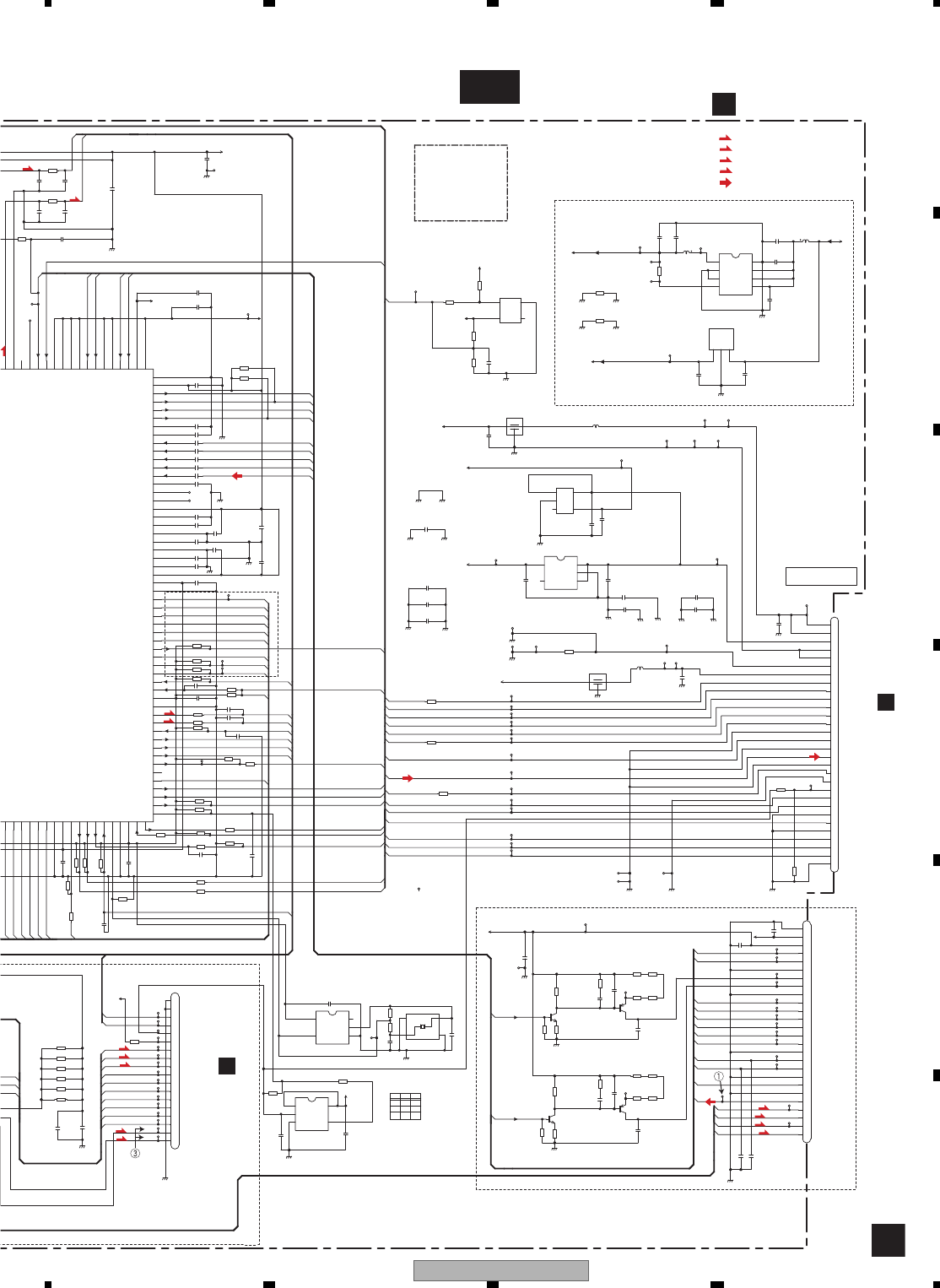
AVIC-X910BT/XS/UC 175
5678
5678
C
D
F
A
B
E
C
C-b
DVDMPD
FE1
A1
A6
A3
A5
A2
A4
SCLOCK
SDATA
TRCCLK
TRCDATA0
TRCDATA1
TRCDATA2
TRCDATA3
B
C
A
D
LPCO1
LPCO2
FD
TD
CDMPD
STANDBY
STSCOMN
SCKDAC
COILV
COILU
COILW
HVM
HVP
HWM
HUP
HUM
HBM
XCSF1
E+G_E+F
F+H_G+H
B
A
FE2
TEMP
RF
F+H_G+H
E+G_E+F
RF
CDMPD
CRGDRV
MD
FG
FE1
FE2
NRES
NRES
LTDAC
SDODAC
TOP
EXTRG0
TEMP
AMUTE
C
D
LDIN
CONT2
CONT1
CMDCOMN
VDSENS
VDSENS
HWP
FOM
FOP
COILU
COILV
COILW
HOME
NRES
IRQPWR
CMDCOMN
STSCOMN
ROUT
D-
D+
IECOUT
LOUT
AMUTE
08EJ
TRCST
TOM
I2C_SCL
I2C_SDA
CP_Reset
I2C_SCL
I2C_SDA
IRQPWR
COMPOSITE
HOME
08EJ
A20
CP_Reset
DVDMPD
DVDLD1
AGND3
VCC5_3
GNDA
GNDD
GNDA
GNDA
GNDA
GNDA
R1103
390
R1104
510
R1101 100K
C1106
R01
C1603
100P
C1606
R1
C1602
100P
VCC33
VCC5
Q1101
2SC4081
C1519 R1
C1520
R1
R1509 1K
R1510 1K
SDATA
SCLOCK
C1521 R1
C1622 R033
GNDA
C1620 R22
GNDA
C1624
R1
C1625
R1
C1621 R22
ANAMONI1
ANAMONI2
C1619 5600P
C1618 100P
C1616 R1
C1617 R1
GNDA
C1612 R1
C1614 R1
C1615 R1
C1613 R1
C1611 R1
C1610 R1
GNDA
C1609 R1
VREF
VREF
C1623
1
C1608
1
VHALF
R1232D121B
IC1005
PGND 1
VIN 2
VDD 3
CE 45 VOUT
6TEST
7AGND
8LX
L1004
FB12A
VCC12
C1010
2R2
C1011
1
R1002
100
VCC33-1
VCC33
VDD5
VCC12-1
FB12B
DDF
VCC33
IC1001
NM
OUT
1
VDD
2
NC
3
VSS
4
VSENS
VD8
GNDA
DGND1
PGND
PGND4
GNDV
NRES
VDD5
VD8_1
C1004
4R7
R1015
NM
AGND4
VCC5_1
EF1002
3
2
1
EF1001
3
2
1
PGND3
AGND1
VDD5_1
GNDAU GNDD
VDD5_2
GNDA
VCC5
GNDD
C1001
1
DGND4
PGND5
GNDD
AVCC5
RO
LO
VD8
AVCC5
C1522 R1
DVDLD0
CDLD0
R1604 1M
TEMP
PGND
GNDD
GNDD
CKS6003
VCC33
U-
HB+
HB-
W-
COM
COILU
V-
COP
U+
W+
V+
COILV
COILW
C1007
NM
C1006
NM
HOME
GNDD
R1017
NM
GND_DD
C1110
R01
VREF
C1108 R01
E+G_E+F
F+H_G+H
R1102 100K
GNDA
C1105 R1
R1106
560
Q1102
2SC4081
R1105
390
C1107
R01
CDLD1
DVDMPD
RF
C1601
R01
R1603
10K
CDMPD
C1523
R1
R1513 10K
08EJ
12EJ
IRQPWR
CMDCOMN
STSCOMN
STANBY
COMPOSITE
D+
D-
VD
C1526 R01
R1523 220
R1522 100K
R1519 1K
IC1006
NM
G
1
IN
2
GND
3OUT 4
5
VCC
VD8
GNDAU
GNDAU3
GNDV
GNDAU2
GNDD
C1015
R001
PGND
R1536
100K
R1537
100K
R1004
47K
R1007
6R8K
GNDD
VD8_2
R1011
NM
GND_DD
GND_DD
GND_DCON
GND_DCON
B
A
C
D
FE1
FE2
R1217
1
R1218
1
R1213
1
R1214
1
R1215
1
R1216
1
L1003
R1534
220
GNDD
C1016
R001
R1540 220
AGND2
GNDA
C1607
10
C1003 R1
AMUTE
R1525 10K
GNDD
NM
1M
IC1951
NM
NC 1
IN_A 2
GND 3
OUT_Y
4
5VCC
C1950
NM
R1542
10K
R1524 4R7K
48MHz
C1104
R1
R1602
12K
R1601
12K
C1604
68P
C1605
68P
R1514 18K
R1541 220
C1017
NM
R1526 10K
C1005
1
R1222
270
AD2
TRCST
R1026
NM
R1516 10K
R1300
0R0
VCC5
C1524
R047
C1302
NM
R1021
0R0
TOP1
FOP1
R1535
100K
CP_RESET
RESET
SDA
SCL
R1539
100K
NJM2885DL1-33
IC1004
1IN
2GND
3OUT
2SB1132
Q1104
2SB1132
Q1103
C1626
NM
C1627
NM
C1018
R1
L1902
L1903
C1211
4R7
GNDDPGND
C1019
R1
R1953
NM
C1210
R1
C1528
470P
WAKEUP
R1019
100
R1025
100
R1027
100
C1529
NM
GNDAU
C1952
NM
NM
10P
C1525
NM
C1527
NM
R1110
3R3
R1109
3R3
C1111
R22
C1109
R22
R1008
NM
R1001
NM
C1953
NM
C1954
47P
10
C1101
R1527
6R8K
R1546
6R8K
R1301
NM
R1547
NM
CN1901
1
2
3
4
5
6
7
8
9
10
11
12
13
14
15
16
17
18
19
20
21
22
23
24
25
26
27
28
29
30
CN1201
1
2
3
4
5
6
7
8
9
10
11
12
13
14
15
16
17
18
EXADT6
37
EXADT5
38
EXADT4
39
EXADT3
40
EXADT2
41
EXADT1
42
VSS_5
43
VDD12_2
44
45
46
47
IRQPWR
48
49
USB_CLOCK
50
VSS_6
51
VDD33_4
52
CMDCOMN
53 STSCOMN
54
12EJ
55
LTDAC 56
SDODAC 57
SCKDAC 58
XCSSR 59
P13 60
61
62
CONT1 63
CONT2 64
65
MD 66
CRGDRV 67
VSS_7 68
VDD33_5 69
NRES 70
FG 71
SCLOCK 72
SDATA 73
EXTRG0 74
EXTRG1 75
TRCCLK 76
TRCDATA0 77
TRCDATA1 78
TRCDATA2 79
TRCDATA3 80
TRCST 81
VSS_8 82
VDD12_3 83
AVDDD 84
PLFIL1 85
VREFH7 86
AVSSD 87
VREFL7 88
AVSSC 89
CCAPA 90
CDATA 91
AVDDC 92
ANAMONI1 93
ANAMONI2 94
RFINN 95
RFINP 96
VIN1RF 97
VIN2RF 98
VIN4RF 99
VIN3RF 100
VREFH5 101
VREFL5 102
DVDMPD 103
LPCO1 104
CDMPD 105
LPCO2
106
AVDDB
107
AVSSB
108
VREFH
109
VHALF 110
E+G_E+F 111
F+H_G+H 112
VIN5 113
VIN6 114
115
116
VIN3 117
VIN4 118
VIN2 119
VIN1 120
VDSENS 121
TEMP 122
AD2 123
AD4 124
AVSSH 125
TD 126
IC1003
S-1200B50-M5
VIN 1
VSS 2
ON/OFF 3
NC
4
5VOUT
X1950
NM
X1
1GND1 2
GND2
4X2 3
C1301
NM
CN1101
1
2
3
4
5
6
7
8
9
10
11
12
13
14
15
16
17
18
19
20
21
22
23
24
25
26
R1532
NM
C1014
10
C1009
10
C1013
10
C1008
10
C1012
NM
R1543 NM
R1544 NM
R1533
100K
C1112
22
C1113
22
IC1002
S-1133B50-U5
NC
1
VSS
2
ON/OFF
3
VIN
4
5
VOUT
CP_READY
R1114
1R5
R1111
1R5
R1112
1R5
R1115
1R5
R1116
1R5
R1117
1R5
R1113
1R5
R1118
1R5
R1605 1M
GNDDGNDD
LPCO1
LPCO2
PU(DP10)
(1608)
(1608)
(1608*4)
(1608*4)
(1608)
DEBUG
MOTOR DRIVER
12cm(DSCSNS)
8cm
5.0-3.3&1.2 V DC/DC
VOLTAGE DETECT
(1608)
VD5
HOST I/F
AMUTE
ANALOG ROUT
(2125)
STANBY
(1608)
PGND
COMPOSIT
(3216)
HSTCMD
SLVSTS
PGND
XRESET
AGND
VD8
DGND
ANALOG LOUT
IRQPWR
VD8
AGND
VIDEO GND
AGND
D-
D+
DGND
COIL_U
HALL_V+
HALL_V-
HALL_U-
HALL_W+
GNDD
HALL_U+
COIL_V
HALL_W-
HALL_BIAS+
HALL_BIAS-
COIL_W
HOME
CRG/LE+
CRG/LE-
X
L
H
L
Z
GOUT
H
L
<TC7SZ126FU>
H
IN
VD8
F+
T-
LD GND
F-
FE2
B
A
T+
78LD
C
RF
78MDG
SW
65LD
E+G/E+F
GND
D
F+H/G+H
VCC
65MDG
FE1
:PU
1200->1299
1100->1199
:FLASH
:SDRAM
1480->1499
1850->1899
1670->1699 :DVN(BE)
:DVN(SYS)
:VIDEO
1900->1950
1500->1599
:AUDIO (DIGITAL)
1400->1449
1000->1049
1800->1849
1700->1749
:ACT+SPDL
:POWER SUPPLY
:OUTSIDE I/F
:AUDIO (ANALOG)
1600->1669 :DVN(FE)
1950->1999
(2125)
Vref
78MD
65MD
TEMP
TEMP GND
IECOUT
DGND
(1608)
(1608)
H
(1608)
LDIN
HOME
:USB
GNDD
(2125)
CP_Reset
CP_READY
I2C_SDA
I2C_SCL
08EJ
VIN8
VIN7
RESET
SDA
SCL
(3216)
(1608)
(1005)
WAKEUP
DGND
USB
48.000MHz
X:Don’t Care
Z:High Impedance
GNDD
C1021
680P
C1022
680P CKS6025
GNDV
C1934
68P
CD
DVD
CKS5775
CDVD CORE UNIT
B
CN883
PICKUP UNIT (SERVICE)
D
CN701
FFOCUS SERVO LINE
TRACKING SERVO LINE
CARRIAGE SERVO LINE
SPINDLE SERVO LINE
RF SIGNAL
T
C
S
F
F
T
T
T
F
T
C
C
C
S
S
S
S
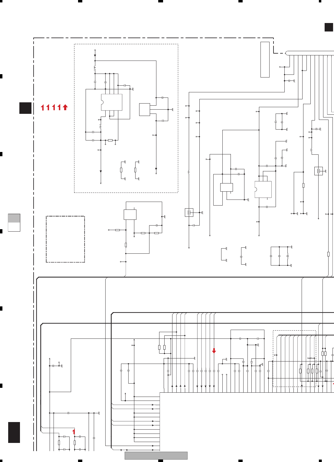
AVIC-X910BT/XS/UC
176
1234
1234
C
D
F
A
B
E
C-a C-b
C-b
SCLOCK
SDATA
TRCCLK
TRCDATA0
TRCDATA1
TRCDATA2
TRCDATA3
B
C
A
D
LPCO1
LPCO2
FD
TD
CDMPD
F+H_G+H
E+G_E+F
RF
CRGDRV
FG
FE1
FE2
NRES
NRES
EXTRG0
TEMP
AMUTE
VDSENS
VDSENS
NRES
AMUTE
TRCST
DVDMPD
GNDA
GNDD
GNDA
C1603
100P
C1606
R1
C1602
100P
VCC33
R1509 1K
R1510 1K
SDATA
SCLOCK
C1521 R1
C1622 R033
GNDA
C1620 R22
GNDA
C1624
R1
C1625
R1
C1621 R22
ANAMONI1
ANAMONI2
C1619 5600P
C1618 100P
C1616 R1
C1617 R1
GNDA
C1612 R1
C1614 R1
C1615 R1
C1613 R1
C1611 R1
C1610 R1
GNDA
C1609 R1
VREF
VREF
C1623
1
C1608
1
VHALF
R1232D121B
IC1005
PGND 1
VIN 2
VDD 3
CE 45 VOUT
6TEST
7AGND
8LX
L1004
FB12A
VCC12
C1010
2R2
C1011
1
R1002
100
VCC33-1
VCC33
VDD5
VCC12-1
FB12B
DDF
VCC33
IC1001
NM
OUT
1
VDD
2
NC
3
VSS
4
VSENS
VD8
GNDA
DGND1
PGND
PGND4
GNDV
NRES
VDD5
VD8_1
C1004
4R7
R1015
NM
AGND4
VCC5_1
EF1002
3
2
1
EF1001
3
2
1
PGND3
AGND1
VDD5_1
GNDAU GNDD
VDD5_2
GNDA
VCC5
GNDD
C1001
1
DGND4
PGND5
GNDD
AVCC5
VD8
AVCC5
C1522 R1
R1604 1M
C1007
NM
C1006
NM
GNDD
R1017
NM
GND_DD
C1601
R01
C1523
R1
R1513 10K
VD
C1526 R01
R1523 220
R1522 100K
VD8
C1015
R001
PGND
R1004
47K
R1007
6R8K
GNDD
VD8_2
R1011
NM
GND_DD
GND_DD
GND_DCON
GND_DCON
L1003
GNDD
C1016
R001
AGND2
GNDA
C1607
10
C1003 R1
AMUTE
R1524 4R7K
R1602
12K
R1601
12K
C1604
68P
C1605
68P
C1017
NM
C1005
1
TRCST
R1516 10K
NJM2885DL1-33
IC1004
1IN
2GND
3OUT
C1626
NM
C1627
NM
C1018
R1
L1902
L1903
GNDDPGND
C1019
R1
R1019
100
GNDAU
R1008
NM
R1001
NM
C1953
NM
C1954
47P
CN1901
1
2
3
4
5
6
7
8
9
10
11
67
VSS_7 68
VDD33_5 69
NRES 70
FG 71
SCLOCK 72
SDATA 73
EXTRG0 74
EXTRG1 75
TRCCLK 76
TRCDATA0 77
TRCDATA1 78
TRCDATA2 79
TRCDATA3 80
TRCST 81
VSS_8 82
VDD12_3 83
AVDDD 84
PLFIL1 85
VREFH7 86
AVSSD 87
VREFL7 88
AVSSC 89
CCAPA 90
CDATA 91
AVDDC 92
ANAMONI1 93
ANAMONI2 94
RFINN 95
RFINP 96
VIN1RF 97
VIN2RF 98
VIN4RF 99
VIN3RF 100
VREFH5 101
VREFL5 102
DVDMPD 103
LPCO1 104
CDMPD 105
LPCO2
106
AVDDB
107
AVSSB
108
VREFH
109
VHALF 110
E+G_E+F 111
F+H_G+H 112
VIN5 113
VIN6 114
115
116
VIN3 117
VIN4 118
VIN2 119
VIN1 120
VDSENS 121
TEMP 122
IC1003
S-1200B50-M5
VIN 1
VSS 2
ON/OFF 3
NC
4
5VOUT
C1014
10
C1009
10
C1013
10
C1008
10
C1012
NM
IC1002
S-1133B50-U5
NC
1
VSS
2
ON/OFF
3
VIN
4
5
VOUT
R1605 1M
GNDDGNDD
(1608)
DEBUG
5.0-3.3&1.2 V DC/DC
VOLTAGE DETECT
(1608)
VD5
HOST I/F
AMUTE
(2125)
(1608)
PGND
(3216)
HSTCMD
PGND
XRESET
VD8
DGND
IRQPWR
VD8
VD8
:PU
1200->1299
1100->1199
:FLASH
:SDRAM
1480->1499
1850->1899
1670->1699 :DVN(BE)
:DVN(SYS)
:VIDEO
1900->1950
1500->1599
:AUDIO (DIGITAL)
1400->1449
1000->1049
1800->1849
1700->1749
:ACT+SPDL
:POWER SUPPLY
:OUTSIDE I/F
:AUDIO (ANALOG)
1600->1669 :DVN(FE)
1950->1999
(2125)
(1608)
(1608)
(1608)
:USB
(2125)
VIN8
VIN7
(1608)
(1005)
USB
GNDD
C1021
680P
C1022
680P CKS6025
C1934
68P
C
DVD CORE UNIT
B
F
FOCUS SERVO LINE
TRACKING SERVO LINE
CARRIAGE SERVO LINE
SPINDLE SERVO LINE
RF SIGNAL
T
C
S
T
C
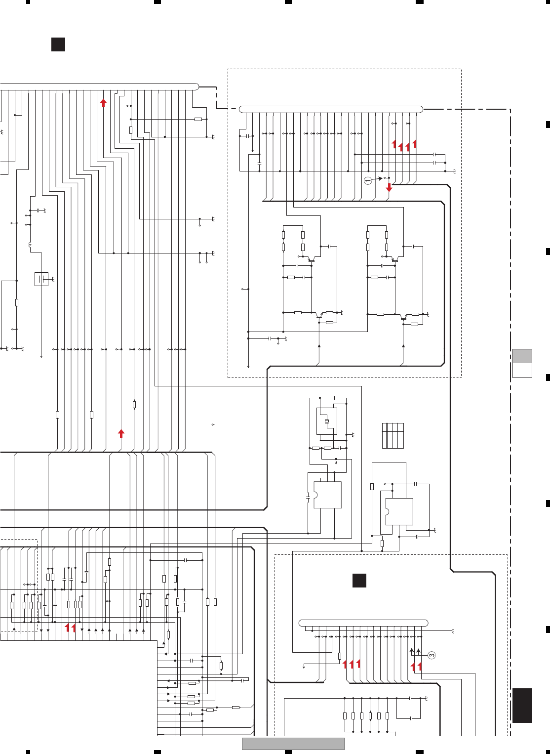
AVIC-X910BT/XS/UC 177
5678
5678
C
D
F
A
B
E
C-a C-b
C-b
DVDMPD
FE1
A1
A2
SCLOCK
SDATA
TRCCLK
STANDBY
STSCOMN
SCKDAC
COILV
COILU
COILW
HVM
HVP
HWM
HUP
HUM
HBM
XCSF1
E+G_E+F
F+H_G+H
B
A
FE2
TEMP
RF
CDMPD
CRGDRV
MD
FG
NRES
NRES
LTDAC
SDODAC
TOP
EXTRG0
AMUTE
C
D
LDIN
CONT2
CONT1
CMDCOMN
HWP
FOM
FOP
HOME
NRES
IRQPWR
CMDCOMN
STSCOMN
ROUT
D-
D+
IECOUT
LOUT
AMUTE
08EJ
TOM
I2C_SCL
I2C_SDA
CP_Reset
I2C_SCL
I2C_SDA
IRQPWR
COMPOSITE
HOME
08EJ
A20
CP_Reset
DVDLD1
AGND3
VCC5_3
GNDA
GNDD
GNDA
GNDA
GNDA
R1103
390
R1104
510
R1101 100K
C1106
R01
VCC5
Q1101
2SC4081
C1519 R1
C1520
R1
R1509 1K
R1510 1K
SDATA
SCLOCK
GNDA
NRES
VDD5
R1015
NM
AGND4
EF1002
3
2
1
AGND1
VDD5_1
VDD5_2
GNDD DGND4
GNDD
RO
LO
C1522 R1
DVDLD0
CDLD0
PGND
GNDD
GNDD
CKS6003
VCC33
U-
HB+
HB-
W-
COM
COILU
V-
COP
U+
W+
V+
COILV
COILW
HOME
C1110
R01
VREF
C1108 R01
E+G_E+F
F+H_G+H
R1102 100K
GNDA
C1105 R1
R1106
560
Q1102
2SC4081
R1105
390
C1107
R01
CDLD1
DVDMPD
RF
CDMPD
C1523
R1
R1513 10K
08EJ
12EJ
IRQPWR
CMDCOMN
STSCOMN
STANBY
COMPOSITE
D+
D-
C1526 R01
R1523 220
R1522 100K
R1519 1K
IC1006
NM
G
1
IN
2
GND
3OUT 4
5
VCC
GNDAU
GNDAU3
GNDV
GNDAU2
GNDD
PGND
R1536
100K
R1537
100K
B
A
C
D
FE1
FE2
R1217
1
R1218
1
R1213
1
R1214
1
R1215
1
R1216
1
R1534
220
GNDD
C1016
R001
R1540 220
AMUTE
R1525 10K
GNDD
NM
1M
IC1951
NM
NC 1
IN_A 2
GND 3
OUT_Y
4
5VCC
C1950
NM
R1542
10K
R1524 4R7K
48MHz
C1104
R1
R1514 18K
R1541 220
R1526 10K
R1222
270
R1026
NM
R1516 10K
R1300
0R0
VCC5
C1524
R047
C1302
NM
R1021
0R0
TOP1
FOP1
R1535
100K
CP_RESET
RESET
SDA
SCL
R1539
100K
2SB1132
Q1104
2SB1132
Q1103
L1903
C1211
4R7
R1953
NM
C1210
R1
C1528
470P
WAKEUP
R1019
100
R1025
100
R1027
100
C1529
NM
C1952
NM
NM
10P
C1525
NM
C1527
NM
R1110
3R3
R1109
3R3
C1111
R22
C1109
R22
10
C1101
R1527
6R8K
R1546
6R8K
R1301
NM
R1547
NM
2
3
4
5
6
7
8
9
10
11
12
13
14
15
16
17
18
19
20
21
22
23
24
25
26
27
28
29
30
CN1201
1
2
3
4
5
6
7
8
9
10
11
12
13
14
15
16
17
18
EXADT2
41
EXADT1
42
VSS_5
43
VDD12_2
44
45
46
47
IRQPWR
48
49
USB_CLOCK
50
VSS_6
51
VDD33_4
52
CMDCOMN
53 STSCOMN
54
12EJ
55
LTDAC 56
SDODAC 57
SCKDAC 58
XCSSR 59
P13 60
61
62
CONT1 63
CONT2 64
65
MD 66
CRGDRV 67
VSS_7 68
VDD33_5 69
NRES 70
FG 71
SCLOCK 72
SDATA 73
EXTRG0 74
EXTRG1 75
TRCCLK 76
TRCDATA0
X1950
NM
X1
1GND1 2
GND2
4X2 3
C1301
NM
CN1101
1
2
3
4
5
6
7
8
9
10
11
12
13
14
15
16
17
18
19
20
21
22
23
24
25
26
R1532
NM
R1543 NM
R1544 NM
R1533
100K
C1112
22
C1113
22
CP_READY
R1114
1R5
R1111
1R5
R1112
1R5
R1115
1R5
R1116
1R5
R1117
1R5
R1113
1R5
R1118
1R5
LPCO1
LPCO2
PU(DP10)
(1608)
(1608)
(1608*4)
(1608*4)
MOTOR DRIVER
12cm(DSCSNS)
8cm
VD5
AMUTE
ANALOG ROUT
STANBY
PGND
COMPOSIT
(3216)
HSTCMD
SLVSTS
PGND
XRESET
AGND
VD8
DGND
ANALOG LOUT
IRQPWR
AGND
VIDEO GND
AGND
D-
D+
DGND
COIL_U
HALL_V+
HALL_V-
HALL_U-
HALL_W+
GNDD
HALL_U+
COIL_V
HALL_W-
HALL_BIAS+
HALL_BIAS-
COIL_W
HOME
CRG/LE+
CRG/LE-
X
L
H
L
Z
G OUT
H
L
<TC7SZ126FU>
H
IN
VD8
F+
T-
LD GND
F-
FE2
B
A
T+
78LD
C
RF
78MDG
SW
65LD
E+G/E+F
GND
D
F+H/G+H
VCC
65MDG
FE1
Vref
78MD
65MD
TEMP
TEMP GND
IECOUT
DGND
H
LDIN
HOME
GNDD
CP_Reset
CP_READY
I2C_SDA
I2C_SCL
08EJ
RESET
SDA
SCL
(3216)
WAKEUP
DGND
48.000MHz
X:Don’t Care
Z:High Impedance
GNDV
CD
DVD
CKS5775
B
CN883
PICKUP UNIT (SERVICE)
D
CN701
F
F
T
T
C
C
C
S
S
S
S
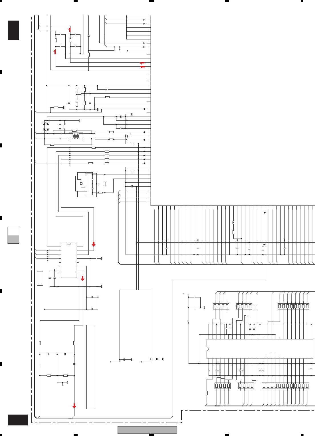
AVIC-X910BT/XS/UC
178
1234
1234
C
D
F
A
B
E
C-bC-a
C-a
C-b
MDQ7
MDQ6
MDQ5
MDQ15
MDQ14
MA9
MA8
MA7
MA6
MA5
MA4
DQM0
XWE
XCAS
XRAS
XCSM
BA1
MA10
BA0
MA0
MA1
MA2
MA3
MCK
MA11
MDQ15
MDQ0
MDQ14
MDQ1
MDQ13
MDQ2
MDQ12
MDQ3
MDQ11
MDQ4
MDQ10
MDQ5
MDQ7
MDQ6
DQM1
DQM0
MDQ9
MDQ8
XWE
MA9
XRAS
BA0
XCAS
XCSM
MA7
MA0
MA1
MA10
MA8
BA1
MA6
FD
TD
LOUT
ROUT
SDODAC
SCKDAC
LTDAC
IECOUT
MA11
MCK
COMPOSITE
FE1
FE2
TEMP
DQM1
STANDBY
MDQ13
MDQ9
MDQ10
MDQ11
MDQ12
MDQ8
MDQ1
MDQ3
MDQ2
MDQ4
MDQ0
D+
D-
IEC
GNDA
GNDA
GNDD
GNDD
R1503
1M
C1671
R1
C1672
R1
C1487
R1
C1481 R1
C1674
R1
C1480 R1
C1603
100P
C1482 R1
C1484 R1
C1488
R1
C1602
100P
C1502
10
C1676
1
C1503 R1
VCC33
VCC12
C1485
R1
C1504
R1
C1505
R1
C1506
R1
C1507
R1
C1514
R1
C1511
R1
C1515
R1
C1805
R1
PCM1753DBQ
IC1801
BCK
1
DATA
2
LRCK
3
DGND
4
5
NC
6
VCC
7
VOUTL
8
VOUTR
9
AGND
10
VCOM
11
ZEROR/ZEROA
12
ZEROL/NA
13
MD
14
MC
15
ML
16
SCK
2081C
7R4
GNDAU1
R1804
820
R1803
820
C1801
4R7
R1802
100K
C1804
1800P
R1801
100K
C1803
1800P
GNDAU
C1809
R1
GNDD
AVCC5
GNDAU
VCC33
C1501
10
GNDD
TEMP
GNDV
GNDD
R1954
NM
R1955
NM
C1601
R01
R1603
10K
C1673
R1
C1491 NM
C1492 NM
C1493 NM
C1494 NM
C1807
NM
L1901
NM
11
2
2
3
344
D1902
NM
D1901
NM
GNDD
C1489
10
R1538
100K
R1602
12K
R1601
12K
C1604
68P
C1605
68P
C1483 NM
AD2
ADOUT
DACCK
LRCK
LTDAC
SCKDAC
SDODAC
SRCK
GNDD5
R1501
1R2K
R1679
NM R1675
NM
R1673
NM
GNDD
R1505 100
R1506 100
R1507 100
L1904
C1490
R001
R1950
NM
R1951
NM
C1512
10P
C1510
12P
R1508
220
R1512
100
R1483
56
2
1
4
3
6
5
8
7
R1487
56
2
1
4
3
6
5
8
7
R1486
56
2
1
4
3
6
5
8
7
R1488
56
2
1
4
3
6
5
8
7
R1481
56
2
1
4
3
6
5
8
7
R1480
56
2
1
4
3
6
5
8
7
R1484
56
2
1
4
3
6
5
8
7
R1482
56
2
1
4
3
6
5
8
7
R1485
56
2
1
4
3
6
5
8
7
R1490
56
R1489
56
C1806
10
R1956
NM
R1957
NM
MN2DS0018MAUB
IC1501
VIN6 114
115
116
VIN3 117
VIN4 118
VIN2 119
VIN1 120
VDSENS 121
TEMP 122
AD2 123
AD4 124
AVSSH 125
TD 126
FD 127
AVDDH 128
DAC3OUT 129
DAC2OUT 130
DAC1OUT 131
AVDDF 132
COMP1 133
VREF 134
IREF1 135
COMP2 136
AVSSF 137
COMPOSITE 138
DAC5OUT 139
AVSSE 140
AVDDE 141
AVDDG 142
AVSSG 143
LOUT 144
145
AVSSI
146
ROUT
147
AVDDI
148
DACCK
149
SRCK
150
LRCK
151
ADOUT
152
IECOUT
153
VSS_9
154
VDD33_6
155
OSCI
156
OSCO
157
VSS_10
158
VDD12_4
159
MDQ15
160
MDQ0
161
MDQ14
162
MDQ1
163
MDQ13
164
MDQ2
165
VSS_11
166 VDD33_7
167 MDQ12
168 MDQ3
169 MDQ11
170 MDQ4
171 MDQ10
172 MDQ5
173 VSS_12
174 VDD33_8
175 MDQ9
176 MDQ6
177 MDQ8
178 MDQ7
179 DQM0
180 DQM1
181 NWE
182 VSS_13
183 MCK
184 VDD33_9
185 MCKI
186 VSS_14
187 VDD12_5
188 NCAS
189 NRAS
190 NCSM
191
192 DQM3
193 BA0
194 MA9
195 VSS_15
196 VDD33_10
197 BA1
198 MA8
199 MA10
200 MA7
201 MA0
202 MA6
203 MA1
204
X1501
CSS1768
X1
1GND1 2
GND2
4X2 3
L1512
IC1480
VDD1
1
DQ0
2
VDDQ1
3
DQ1
4
5DQ2
6VSSQ1
7DQ3
8DQ4
9VDDQ2
10 DQ5
11 DQ6
12 VSSQ2
13 DQ7
14 VDD2
15 LDQM
16 WE
17 CAS
18 RAS
19 CS
20 BA0
21 BA1
22 A10/AP
23 A0
24 A1
25 A2
26 A3
27 VDD3 28
VSS1
29
A4
30
A5
31
A6
32
A7
33
A8
34
A9
35
A11
36
N.C
37
CKE
38
CLK
39
UDQM
40
N.C/RFU
41
VSS2
42
DQ8
43
VDDQ3
44
DQ9
45
DQ10
46
VSSQ3
47
DQ11
48
DQ12
49
VDDQ4
50
DQ13
51
DQ14
52
VSSQ4
53
DQ15
54
VSS3
R1504
12
C1808
NM
R1511 0R0
R1670
10K
R1672
200
R1671
24K
R1674
30K
(2125)
(IEC/IPFLG)
(1608)
(2125)
(2125)
AUDIO 2CH ANALOG OUT
ADAC
(2125)
(2125)
STANDBY
VIN8
VIN7
27.000MHz
T
F
T
F
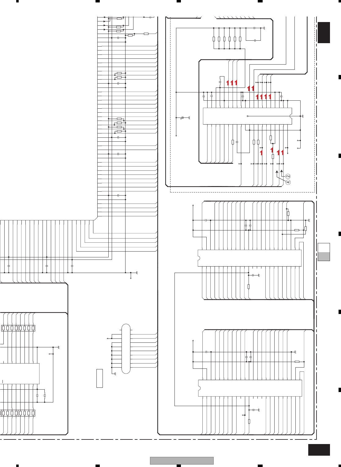
AVIC-X910BT/XS/UC 179
5678
5678
C
D
F
A
B
E
C-a
C-b
C-bC-a
A9
A4
A10
A5
A11
A6
A12
A7
A13
A8
A14
A15
D15
D7
D14
D6
D13
D5
D12
D4
D11
D3
D10
D2
D9
D1
D8
A3
A2
A1
XRD
A16
A5
A10
A4
A9
A1
A2
A3
A16A15
A14
A8
A13
A7
A12
A6
XRD
A11
A19
XWR1
A18
A17 A17
A19
A18
MA9
MA8
MA7
MA6
MA5
MA4
XCSM
BA1
MA10
BA0
MA0
MA1
MA2
MA3
MA11
MA7
MA0
MA1
MA10
MA8
BA1
MA6
MA3
MA5
MA4
MA2
A0
XCSF2
XRD
A16
XWR1
A19
A1
A17
A6
A3
A5
A2
A4
A7
XCSF1
D0
D8
D1
D9
D10
D2
D3
D4
D5
D11
D14
D13
D12
D7
D15
D4
D12
D5
D13
D6
D14
D7
D15
D10
D3
D11
D0
D8
D1
D9
D2
D6
A10
A8
A11
A9
A12
A0
TRCDATA3
SCLOCK
TRCDATA0
TRCCLK
TRCDATA1
TRCST
TRCDATA2
SDATA
A0
C
C
C
XCSF2
EXTRG0
A15
A14
A13
A18
DQM1
COILU
COILV
COILW
MD
LDIN TOM
FOP
FOM
TOP
CONT1
CONT2
FG
CRGDRV
HWP
HVM
HVP
HUM
HUP
HWM
HBM
XWR1
NRES
NRES
TD
FD
A20
A20
D0
DGND3
DGND2
GNDD
GNDD
GNDD
GNDD
GNDD
R1405
100K
R1406
100K
R1402
100K
C1509
R1
C1408
R1
C1403
R1
C1407
NM
C1402
NM
C1404
4R7
C1409
4R7
VCC33
C1485
R1
C1507
R1
C1508
R1
C1518 R1
C1519 R1
C1513 R1
C1516 R1
C1517 R1
CN1951
1
2
3
4
5
6
7
8
9
1011
12
13
14
15
16
17
18
19
20
GNDD
NM
VCC33
PGND
R1517
10K
R1518
10K
R1528
10K
R1529
10K
R1530
10K
R1531
10K
R1217
1
R1218
1
R1213
1
R1214
1
R1215
1
R1216
1
PGND
PGND1PGND2
VHALF
VHALF
VD8
PGND
100/16
C1201
FG
R1202 220
R1201 220
R1542
GNDD
VCC33
C1486
NM
C1405
NM
R1212
270
CONT2
CONT1
CRGDRV
FD1
LDIN
MD1 MD2
TD1
XWR1
C1204
2200P
R1403
NM
R1203
10K
R1204
15K
FOM2
FOP2
TOM2
TOP2
R1539
100K
C1211
4R7
R1401
220
C1401
R01
C1203
NM
C1205
R1
C1207
R1
C1210
R1
C1209
R1
C1208
R01
C1525
R1483
56
2
1
4
3
6
5
8
7
R1487
56
2
1
4
3
6
5
8
7
R1488
56
2
1
4
3
6
5
8
7
R1484
56
2
1
4
3
6
5
8
7
1
8
R1527
6R8K
R1546
6R8K
R1547
NM
R1409
NM
IC1201
BD8231EFV
1VC
2TKIN
3FCIN
4SLIN
5
SLOPOUT
6LDIN
7SPIN
8CTL1
9CTL2
10 GND1
11 TEST
12 FG
13 SPCNF
14 HB
15 HW-
16 HW+
17 HV-
18 HV+
19 HU-
20 HU+ 21
VM_S
22
BH
23
SPRNF
24
SPVM
25
SPGND
26
U
27
V
28
W
29
SLVM
30
PGND
31
SL/LDO+
32
SL/LDO-
33
FCO+
34
FCO-
35
TKO+
36
TKO- 37
AVM
38
PREVcc 39
PREGND 40
SUBGND
41
GND2
EXDT1
1
EXDT9
2
EXDT2
3
EXDT10
4
VSS_1
5
VDD33_1
6
EXDT3
7
EXDT11
8
EXDT4
9
EXDT12
10
EXDT5
11
EXDT13
12
EXDT6
13
EXDT14
14
VSS_2
15
VDD33_2
16
EXDT7
17
EXDT15
18
VSS_3
19
VDD12_1
20
EXADR16
21
EXADT15
22
EXADT14
23
EXADT13
24
EXADT12
25
EXADT11
26
EXADT10
27
EXADT9
28
EXADT8
29
EXADR19
30
NEXWE
31
VSS_4
32
VDD33_3
33
EXADR18
34
EXADR17
35
EXADT7
36
EXADT6
37
EXADT5
38
EXADT4
39
EXADT3
40
EXADT2
41
EXADT1
42
VSS_5
43
VDD12_2
44
45
46
47
IRQPWR
48
49
MA9
195 VSS_15
196 VDD33_10
197 BA1
198 MA8
199 MA10
200 MA7
201 MA0
202 MA6
203 MA1
204 VSS_16
205 VDD33_11
206 MA5
207 MA2
208 MA4
209 MA3
210 VSS_17
211 VDD12_6
212 EXADT0
213 NEXCE
214 NEXOE
215 EXDT0
216
EXDT8
K4S641632N-LC75
19 CS
20 BA0
21 BA1
22 A10/AP
23 A0
24 A1
25 A2
26 A3
27 VDD3 28
VSS1
29
A4
30
A5
31
A6
32
A7
33
A8
34
A9
35
A11
36
N.C
IC1401
CWW1825
A15
1
A14
2
A13
3
A12
4
5A11
6A10
7A9
8A8
9A19
10 NC1
11 /WE
12 /RESET
13 NC2
14 NC3
15 RY_/BY
16 A18
17 A17
18 A7
19 A6
20 A5
21 A4
22 A3
23 A2
24 A1 25
A0
26
/CE
27
Vss1
28
/OE
29
DQ0
30
DQ8
31
DQ1
32
DQ9
33
DQ2
34
DQ10
35
DQ3
36
DQ11
37
Vcc
38
DQ4
39
DQ12
40
DQ5
41
DQ13
42
DQ6
43
DQ14
44
DQ7
45
DQ15_A-1
46
Vss2
47
/BYTE
48
A16
IC1402
CWW1826
A15
1
A14
2
A13
3
A12
4
5A11
6A10
7A9
8A8
9A19
10 NC1
11 /WE
12 /RESET
13 NC2
14 NC3
15 RY_/BY
16 A18
17 A17
18 A7
19 A6
20 A5
21 A4
22 A3
23 A2
24 A1 25
A0
26
/CE
27
Vss1
28
/OE
29
DQ0
30
DQ8
31
DQ1
32
DQ9
33
DQ2
34
DQ10
35
DQ3
36
DQ11
37
Vcc
38
DQ4
39
DQ12
40
DQ5
41
DQ13
42
DQ6
43
DQ14
44
DQ7
45
DQ15_A-1
46
Vss2
47
/BYTE
48
A16
FLASH 16M
(2125)
(2125)
FLASH 16M
SDRAM
DEBUG
CP_READY
I2C_SDA
I2C_SCL
08EJ
(3216)
T
T
F
F
F
T
S
C
C
C
S
S
S
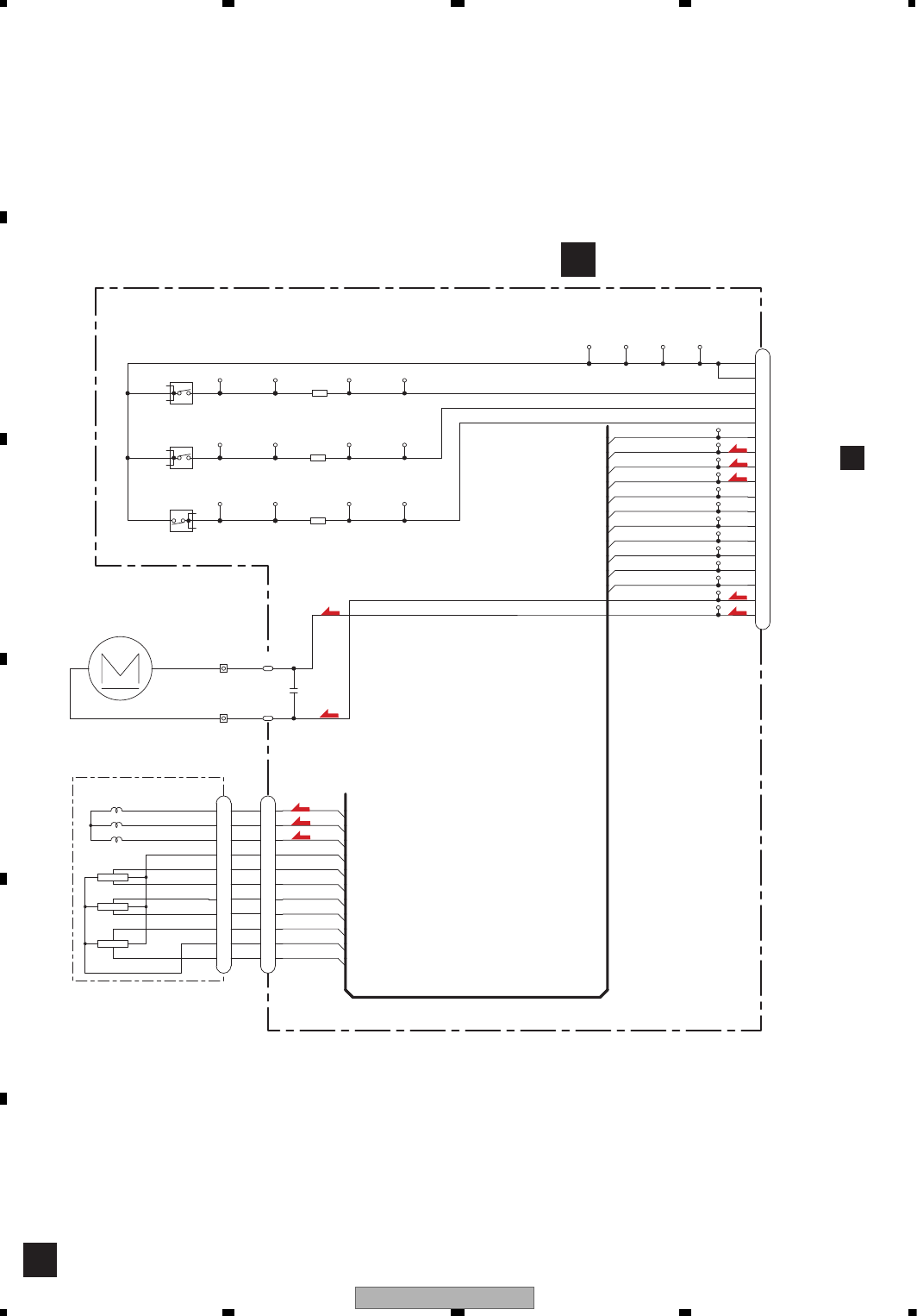
AVIC-X910BT/XS/UC
180
1234
1234
C
D
F
A
B
E
10.9 CONNECT PCB
D
H+,H-,HU+,HU-,HV+,HV-,HW+,HW-,U,V,W
H+
W
U
V
HW+
HW-
HV+
HV-
HU+
HU-
H-
HV-
H+
HV+
HU-
HU+
HW-
HW+
H-
W
U
V
CN701
1CRG-
2CRG+
3HALL BIAS-
4HALL U-
5HALL U+
6HALL V-
7HALL V+
8HALL W-
9HALL W+
10 COIL V
11 COIL U
12 COIL W
13 HALL BIAS+
14 DSCSNS
15 8SNS
16 HOME
17 GND
18 GND
CSN1068-A
S101
1
2
34
CSN1068-A
S102
1
2
34
12
11
HOME
8SNS0
DSCSNS0
GND3 GND2 GND1
CRGM
CRGP
HM
HUM
HUP
HVM
HVP
HWM
HWP
V
U
W
HP
CKS6003
BR
1
GY
1
DSCSNS0_B
8SNS0_B
HOME_B
C101
0.1u/50
R101
100
R102
100
R103
100
GND_B
HOME1_BHOME1
8SNS1 8SNS1_B
DSCSNS1 DSCSNS1_B
CN101
1
V
2
U
3
W
4
H-
5
HW+
6
HW-
7
HU+
8
HU-
9
HV+
10
H+
11
HV-
1
2
3
4
5
6
7
8
9
10
11
CSN1068-A
S103
1
2
34
H3
H1
H2
M2
SPINDLE MOTOR
EXM1050
M1
LOAD/CRG MOTOR
CXC4026
HOME
8SNS
DSCSNS
CKS6063
DCONNECT PCB
C
CN1201
C
C
C
C
S
S
S
S
S
S

AVIC-X910BT/XS/UC 181
5678
5678
C
D
F
A
B
E
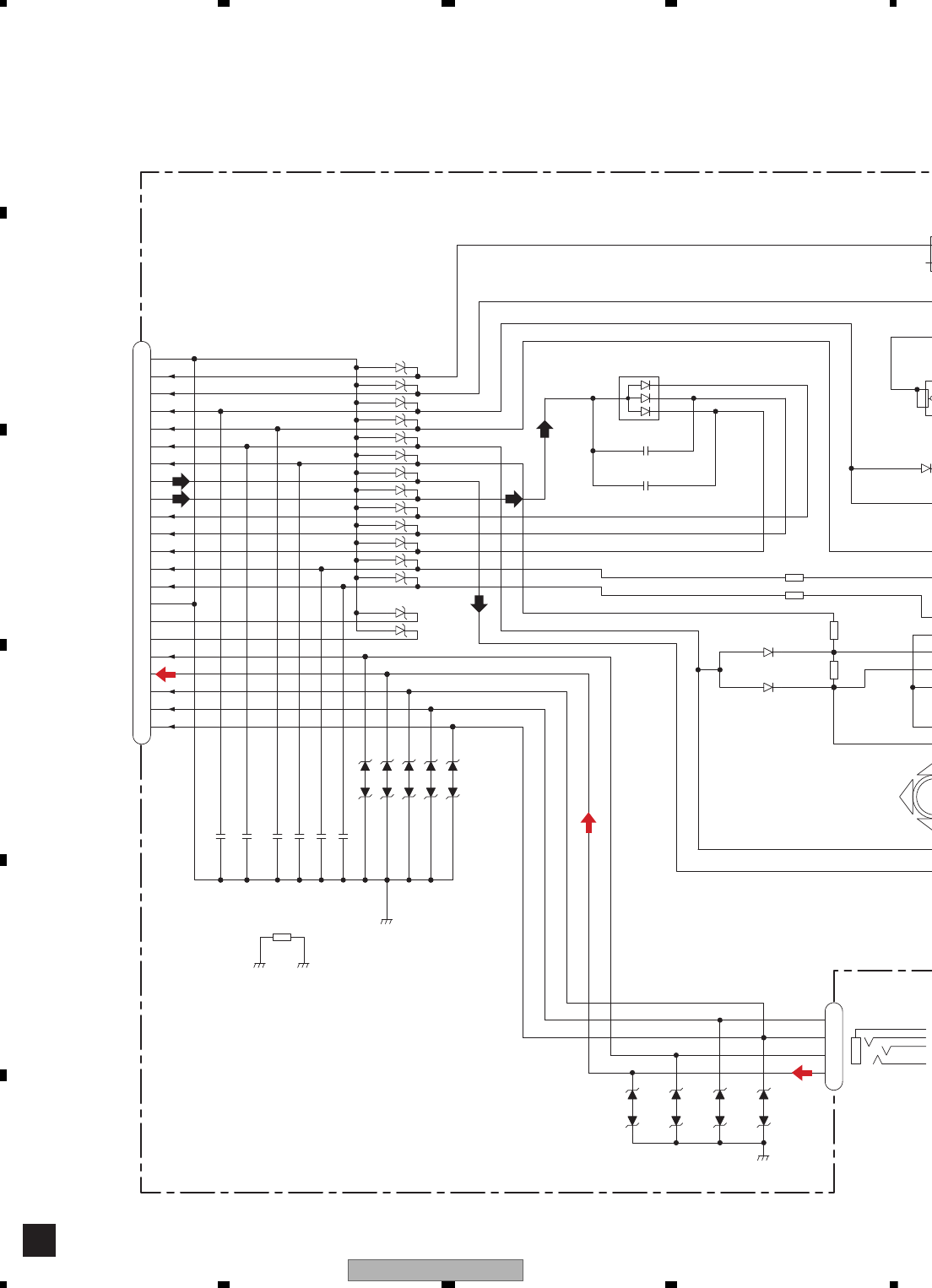
AVIC-X910BT/XS/UC
182
1234
1234
C
D
F
A
B
E
10.10 KEYBOARD UNIT
E
R803
1k
R804
1.6k
R802 0
R801 0
CSG1
S
1
2
CSG
1
2
D801
NSSM025-6502
CN802
CKN1049-A
1
2
3
4
D805
MALS068X
D802
MALS068X
D807
MALS068X
D806
MALS068X
C805
0.1u/25
C806
0.1u/25
GNDKEY
C803 0.01u/25
C804 0.01u/25
GNDKEY
D808
RB521S-3
D803
NM
D804
NM
CKS5862-A
CN801
1
2
3
4
5
6
7
8
9
10
11
12
13
14
15
16
17
18
19
20
21
22
C802 NM
C801 NM
D853
D854
D855
D856
D852
D857
D858
D863
D864
D866
D867
D868 NM
D869 NM
D870 NM
D871 MALS068X
D872 NM
C856 NM
C854 NM
D859
D860
D861
D862
Phase_A
Enc_Com
A
B
Com
R850 NM
GNDKEYGNDKEY
AUX-VG
AUX-V
AUX-AG
AUX-L
AUX-R
GNDKEY
ROT1
ROT0
ILMB
ILMG
ILMR
KEY1
KEY0
ILMV
EJECT
RESET
GNDKEY
to PANEL UNIT OTJ2
BT-LED
R
AV-IN
RGB ILM
A
BPU
2
3
4
1
R
G
B
M
INT_KEY0
INT_KEY1
NC
NC
8.5V
8.5V
8.5V
5V
5V
R
L
AG
V
VG
AG
V
VG
R
L
HZU5R6(B2)
HZU5R6(B2)
HZU5R6(B2)
HZU5R6(B2)
HZU5R6(B2)
HZU5R6(B2)
HZU5R6(B2)
HZU5R6(B2)
HZU5R6(B2)
HZU5R6(B2)
HZU5R6(B2)
HZU11(B2)
HZU11(B2)
HZU11(B2)
HZU11(B2)
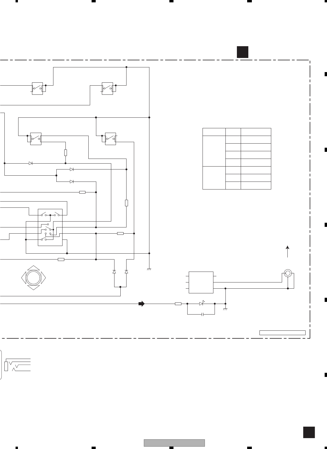
AVIC-X910BT/XS/UC 183
5678
5678
C
D
F
A
B
E
E
1k1.6k
R806
3k
R808
10k
R807
1.3k
R809
2.7k
R805
12k
CSG1155-A
S805
1
2
3
4
CSG1155-A
S804
1
2
3
4
CSG1155-A
S802
1
2
3
4
CSG1155-A
S801
1
2
3
4
CN802
CKN1049-A
GNDKEY
GNDKEY
CN803
CKS5749-A
12
3
D809
NM
D808
RB521S-30
D811
NM
D812
RB521S-30
D810
NM
ANT801
CTX1095
1
RF_I/O
2
GND
3
NC1
4
NC2
5
NC3
6
NC4
S803
CSX1135-A
Phase_A 1
Enc_Com 2
A3
B4
5
Com 6GND
7C
8D
9Push
10Phase_B
C807
NM
SMLE12BC7T(NP)
D815
R810
240
EJECTRESET
AV-IN
BT-ANT
ROTARY COMMANDER
A
B
C
DPUSH
2
3
4
1
BT-ILM
to NAVI UNIT
BTJ2
MAPMENU
SIGNAL
KEY1
KEY0
SW
MAP
C
B
A
PUSH
MENU
D
VOLTEGE[V]
2.63
1.93
1.30
0.66
2.64
1.65
0.81
5V
KEY 801-872
EKEYBOARD UNIT

AVIC-X910BT/XS/UC
184
1234
1234
C
D
F
A
B
E
10.11 WAVEFORMS
RF 0.2 V/div(AC) 100 ns/div
CDRF(x4CLV)
RF 0.2 V/div(AC) 50 ns/div
DVDRF(x1.3ZCAV)
RF 0.5 V/div 100 us/div
DVDRF(BD1mm)
TD1 0.2 V/div 100 us/div
Interval FWD(DVD)
TD1 0.2 V/div 100 us/div
Interval REV(DVD)
VHALF VHALF
2.2 V->
Traverse 1001FWD(short)(DVD)
VHALF
VHALF VHALF
0->
TD1 0.2 V/div 500 us/div
Multi 32FWD(DVD)
TD1 0.2 V/div 500 us/div
Multi 32REV(DVD)
CH1:TD1 0.5 V/div 10 ms/div
CH2:COP-COM 2.0 V/div 10 ms/div
- DVD CORE UNIT
Note:1. The encircled number denote measuring points in the circuit diagram.
2. Reference voltage: 1.65 V(TD1,FD1)(=VHALF)
2.2 V(RF)(=VREF)
In the waveform, it is seeing on the GND standard.
Offset of 1.65 V or 2.2 V is put in.
AVIC-X910BT/XS/UC 185
5678
5678
C
D
F
A
B
E
VHALF VHALF
VHALF
VHALF
VHALF VHALF
VHALF
VHALF
0->
0->
0->
0->
CH1:TD1 0.5 V/div 10 ms/div
CH2:COP-COM 2.0 V/div 10 ms/div
Traverse 1001REV(short)(DVD)
CH2:COP-COM 2.0 V/div 100 ms/div
ID search Inside -> Outside(DVD)
FD1 0.5 V/div 20 ms/div
Play FD(DVD)
FD1 0.5 V/div 500 us/div
Focus Jump L0 -> L1 FD1 0.5 V/div 500 us/div
Focus Jump L1 -> L0
TD1 0.5 V/div 100 ms/div
Play TD (DVD)
FD1 0.5 V/div 1 ms/div
Focus Close (DVD)
CH1:TD1 0.5 V/div 20 ms/div
CH2:COP-COM 2.0 V/div 20 ms/div
Traverse 5001FWD(long)(DVD)
CH1:TD1 0.5 V/div 20 ms/div
CH2:COP-COM 2.0 V/div 20 ms/div
Traverse 5001REV(long)(DVD)
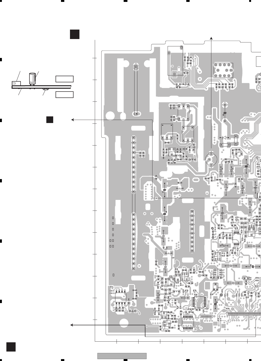
AVIC-X910BT/XS/UC
186
1234
1234
C
D
F
A
B
E
11. PCB CONNECTION DIAGRAM
11.1 AV UNIT
A
AAV UNIT
Capacitor
Connector
P.C.Board Chip Part SIDE B
SIDE A
NOTE FOR PCB DIAGRAMS
1.The parts mounted on this PCB
include all necessary parts for
several destination.
For further information for
respective destinations, be sure
to check with the schematic dia-
gram.
2.Viewpoint of PCB diagrams
1 10
15101520
1
0151
1 5
10
1 5
10
1 5 10 15 20 25 30
1
1
1
5
1
1
1
5
E
1
1
1
E
E
E
E
5
1
5
1
5
R601
D3041
L2947
L2948
L2949
R3041
R606
R3042
R3043
R3044
C4201
L2950
R3628
C4210
C4212
C4213
CN601
C4218
R621
C4219
C4220
R420
ANT1401
R638
C4232
C4233
L1403
C603
C605
TH601
R4021
R4801
R4802
C4061
C4062
C4063
C4064
R4811
R4812
R4813
R4814
R4238
R4815
R4239
R4816 C4070
C4071
C4072
C4073
C4075
C4076
C4078
R4821
C4079
L1441
Y1461
L1442
L1443
C4080
C2911
D4061
D4062
VR4231
R4061
R685
R4062
C4288
C4289
L4721
R4071
R4072
R4073
R4074
C4291
R4075
Y1481
R4076
L1462
C4293
R4077
R4078
C4294
L1465
C4295
R4079
C429
D2911
C2936
C2937
R4080
R2912
R2913
C672
L1481
L1482
L1483
IC602
C685
IC605
R4292
CN1000
L712
R4296
R4297
R4298
L4371
R2941
R2942
CN1015
CN1021
Q1016
C1406
C1407
C1408
C1409
C1023
R
IC1000
L3601
IC1008
C4300
C4302
C4305
IC1015
C4314
CN1441
C4316
R1410
R1411
R1412
R1413
C1441
C1442
C1443
C1444
C1445
Q1441
C4721
C4722
R1433
C4723
R1434
C1077
R4318
C1078
C1461
C1462
C1463
C1464
C1465
C1466
R4321
R1441
R1442
R1443
R432
R1444
R1445
R4326
R4328
T1401
T1402
T1403
C1476
R761
R762
R763
R764
R765
C1481
R4721
C1482
R4722
R4723
C1484
R4724
C1485
C4171
R4725
C1486
R4726
C4173
C4175
C4751
C4176
Q4751
Q4752
C4371
C4372
C1494
C1495
C1498
R4164
R
R4166
R4167
R4168
D1481
C2830
R1481
R1482
R1483
R1484
Q2831
C2835
D4751
C4199
C2836
Q2832
D4752
C2837
R4751
R4752
R4753
R4754
R4755
D4371
R4756
R4757
R4758
R1491
R1493
R1495
R1496
R1498
L603
L605
C3602
C3603
D2835
C3605
R2832
C3606
R2833
R2835
L4271
R2836
R2837
R2838
R2839
C3611
C3612
C3613
C3042
Q
Q3042
R4794
IC3601
10 20 30 40 50 60 70
X
130
120
110
100
90
80
70
60
50
40
30
20
10
0
Y
NAVI UNIT
OTJ1
ANTENNA
IP-BUS (UC)
FM/AM TUNER UNIT
BCN882
NAVI UNIT
TMJ1
FU 4631 (A,115,86) Fuse 200 mA CEK1247
FU 4641 (A,141,8) Fuse 3.15 A CEK1259
FU 4661 (A,137,8) Fuse 2.5 A CEK1258
FU 4771 (A,115,106) Fuse 1 A CEK1254
>
>
>
>
AV1VG
AV1VIN
FRV2
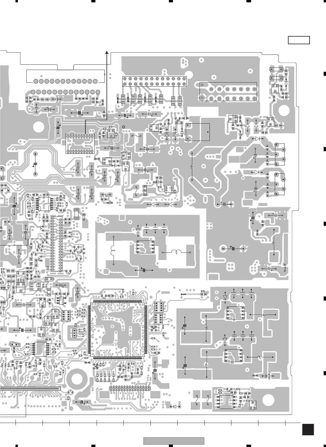
AVIC-X910BT/XS/UC 187
5678
5678
C
D
F
A
B
E
A
SIDE A
1
5
1
1
E
1
1
5
E
E
1
5
1 5
10
10 15 20 25 30 35 40 45 50
1 5
10
15
20
1
10
515
1 5 10 15 20 25 30 35
40 45 50 55 60 65 70
75
80859095100105
110115120125130135140
1
5
10
15
20
E
E
E
E
1
5
1 5
10
15
20
25
5
1 5 10 15
1 5 15 25 35
10 20 30 40
1 5
10
1
E
E
1 5
E
1 5
E
1
5
1
5
1
E
L2940
C2892
D2870
D3041
R603
R604
R2870
L2949
R3041
R2871
R3042
R3043
R607
R608
R3044
L2950
C4208
R613
R614
R2880
R615
R616
R617
C4210
C4212
C4213
R620
D2890
C4219
D2891
R622
R623 R624
L1004
Q4602
R627
C4220
C4225
R4200
C4228
FU4631
C4611
R4201
C4612 C4613
R634
C4614
R635
R638
2
TH601
FU4641
R643
R644
R646
D4602
R647
C610X601
C611
C612
R650
C4631
R651
C617
R653
C618
R654
VR4200
Q4631
R655
Q4632
R656
R657R658
R659
C620
C621
C622
R660
R661
FU4661
R662
R663
R664
Q4642
C4262
C4263
C4070
C4264
C2900
C4071
Q4261
C2901
C4072
C4073
R670
Q2900
75
R671
C4651
C4652C4653 C4654
D4631
R676
R677
R4632
R4633
C2910
C2912
R682
R683
R684
R685
D4642
D4643
Q4663
R690
C4288
C2924
D2900
C4671
R4262
C4672
R4263
C4673
R694
R4264
R2900
C4674
R4071
C2929
R2901
R4072
R2902
R4073
R2903
R4074
291
75
R4076
R4077
078
C2930
C2931
C2932
C4297
C2933
R4657
C2934
C2935
C4682
C2936
C2937 C2938
C4685
C2939
D4662
C4686
2913
C4687
R4279
L4351
L4352
L704
R2924
L705
R2925
L706
R2926
L707
L708
L709
L4174
D2930
C685
L4176
IC606
L710
CN1000
L711
CN1001
L712 L713
EF4353
7
L714
EF4354
L715
EF4355
CN1005
EF4356 EF4357
IC610
EF4358
R4686
EF4361
CN1016
Q751
FB701
Q752
Q753
Q754
R2962
R2963
R2964
IC1002
IC1007
C4302
R2978
C4305
R2979
R2980
R714
R2981
C1015
R2982
R717
R2983
R718
C4312
C4313
C4314
CN701
C4315
C4316
CN702
C4317
IC1020
C4318
C4702
R722
C4704
C4705
C4708
C4710
R732
C4331
C4332
C4333
C4334
C701
C4335
C4336
C705
C706
C707
C708
D4701
C709
R4318 R4319
R4320
R4321
R751
R4322
IC4703
R4323
R4324
R4325
R4326
R4327
R4328
R4329
C4352
C4353
C2801
C2802
C2803
R764
C2804
R765
L4601
R766
L4602
R767
C4363
C4364
C4171
C2810
FU4771
C2812
Q2811
Q2812
C2820
R4351
D4355
C2821
R4352
D4356
C2822
D4357
C2823
C2824
D4358
D4359
D2802
R4163
R4164
R4165
R4166
R4167
R4168
D4361
D4364
D4365
IC2801
D4368
D2810
C4774
C4776
R4367
R2811
C2840
C2842
C2843
C2844
Q2841
L4641
D2821
C4786
D2822
L4642
D2823 D2824
D2825
R2823
L606
IC2820
L611
L612
L613
L4271
L615
C2860
C2862
L4661 L4662
R2840
R2841
R2846
C2870
C3041
C3042
Q2870
Q3041
Q3042
R2852
R2853
R4794
C2880
L2930
C2881
Q2880
L4681
L4682
70 80 90 100 110 120 130 140 150 160 170
FRONT
C) CORD ASSY CORD ASSY
(POWER SUPPLY)
NAVI UNIT
SPJ1
GNDV
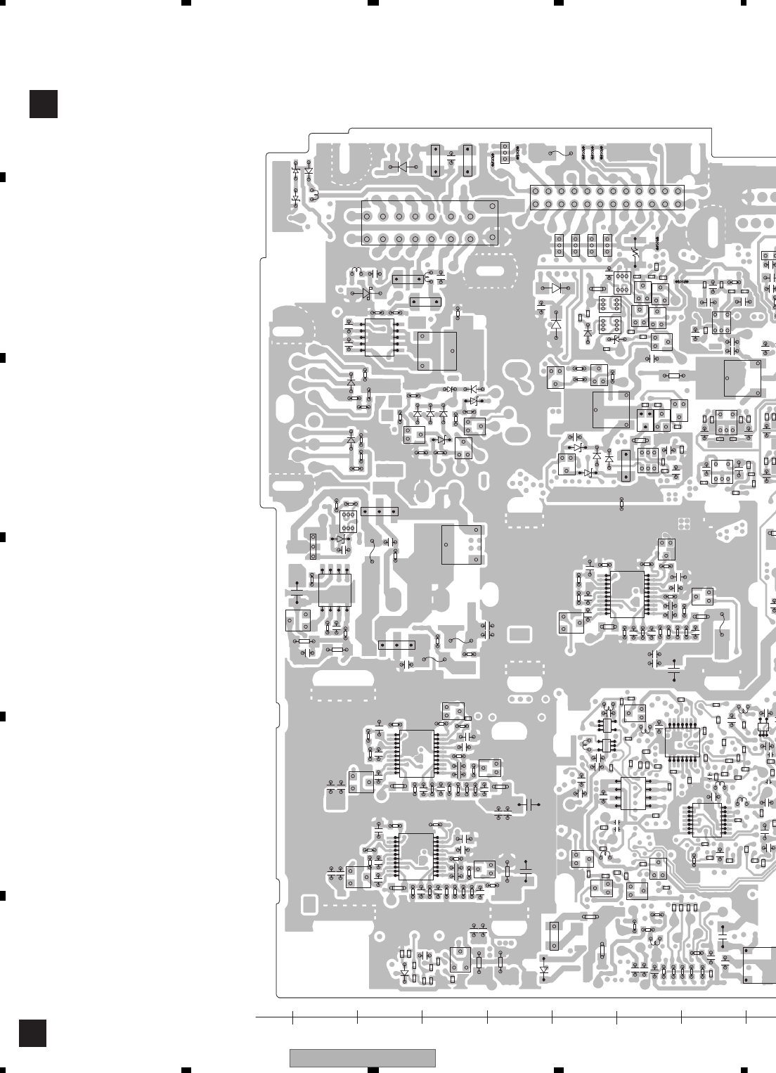
AVIC-X910BT/XS/UC
188
1234
1234
C
D
F
A
B
E
A
AAV UNIT
170 160 150 140 130 120 110 100
E
E
E
1 5
10
1 5 10
1520
E
E
E
E
1
5
1 5 10
1520
1
E
1
1 5 10
1520
1
5
1
5
1 5
10
1
1
5
1 5
10
1
5
1
1
5
1
E
E
E
E
E
E
E
E
E
E
1
5
E
E
E
1 1
E
1
EE
E
E
R2860
R2861
R2862
R2863
R2864
R2865
R2866
R2867R2868
C2890
R2869
C2891
Q661
D2871
FU4601
Q662
D2872
FU4602
D2873
D2874
R605
R2872
R2873
R2874
R609
R2875
D2880
R611
R612
R2881 R2882
R2883 R2884
R619
C4600
C4601
C4602
C4603
C4604
R625
C4605
Q4601
R626
C4606
C4607
C4608
R629
C4609
IC2890
R630
C4610
R631
R632
R633
C4616
R636
C4617
R637
C4618
C4619
R639
C601
C604
R640
R641
C606
R642
FU4642
C
R645
C609
D4601
R648
R649
R4601
R4602
R4603
R4604
R4605
R4606
C613
R4607
C614
R4608
R4609
IC4601
C616
R652
C619
R4610
C4251
R4611
C4252
R4612
C4253
R4613
C4254
R4614
R4615
C4641
C4642
FU4662
C4643
C4644
C629
R665
C4645
Q4641 R666
C4646
R667
C4647
R668
C4648
C4261
C4649
C630
C631
C632
C633
R4628
C634
C4650
C6
C4655
C4656
C4657
C4658
C4659
R679
R680
R681
R4251
C4661
R4252
C4662
R4253
C4663
R4254
C4664
R4255
C4665
Q4661
D4641
R686
C4666
Q4662
R687
C4667
Q4664
C4668
IC4251
C4669
R4641
R4642
R4643
R4644
R4645
R4646
C2923
R4647
C4670
R4648
R691
R4261
R4649
IC4641
R692
R693
C2928
C4675
R695
C4676
R
C4677
R697
C4678
R698
R4650
C4679
R699
R4651
R4652
R4653
R4654
R4655
R4656
D2910
C4681
D2912
C4683
C4684
R2910
R2911
D4661
Q4681
Q4682
C4688
R4662
R4663
R4664
C2940
R4665
R4666
R4667
R4668
R4669
IC4661
L701
L702
R
R4670
R4671
R4672
R4673
R4674
R4675
EF4731
R4676
EF4732
IC603
EF4733
R4677
R4678
IC604
R4679
IC607
IC
D4681
EF4351
D4682
EF4352
R4680
R4681
R4682
R4684
IC611
R4685
EF4359
IC612
R4687R4688
C695
IC4681
C696
EF4360
R701
R702
R703
R704
R705
R706
R707
R708
R709
R710
R711
R712
R713
R7
R716
L2870
IC1021
L2871 L2872
C4703
C4711
R733
FU4351
FU4352
Q4331
C702
C703
C4337
C704
C4338
C4339
D4702
C4340
R4701
C710
C71
C4731
IC4702
C4732
Q4731
Q4732
Q4733
Q4734
C4351
Q4738
R4331
R4332
R4333 R4335
C2806
R4337
R768
R4338
C4361
R4339
C4362 R4340
C2811
R4343
Q2810
R
R
D4731
R4346
D4732
D4733
D4734
D4735
R4731
D4736
R4732
D4737
R4733
R4734
D4351
R4735
R4736
D4353
R4737
R4738
D4354
R4739
D2801
R2801
R2802
R2803
D4360
R2804
D4362
D4363
R4361
C4771
R4362
C4772
D4366
R4363
C4773
R4364
Q601
Q4771
C4775
R4366
Q4772Q4773
R2810
Q4774
Q4775
Q4776
C2841
C4784
Q2840
D2820
C4785
R2820
L601
R2821
R2822
L604
L607
L608
R2829
L609
D4771
D4772
D4773
D4774
D4775
R4771
D4776
R4772
R4773
L614
R4774
R4775
R4776
L617
R4777
R4778
R4779
C2861
D2840
Q2860
Q2861
Q2862
Q2863
Q2864 Q2865
R2842
R4783
R2843
R4784
R2844
R4785
R2845 R2847
R2848
R2849
C2871
C2872
R2850
R2851
C2882
D2860
L2934
Q2881
D2861
Q2882
D2862 D2863
R4683
1
1
FU 2900 (B,72,8) Fuse 250 mA CEK1276
FU 4352 (B,129,133) Fuse 3.15 A CEK1259
FU 4601 (B,104,61) Fuse 5 A CEK1261
FU 4602 (B,144,58) Fuse 5 A CEK1261
FU 4642 (B,158,72) Fuse 2.5 A CEK1258
FU 4662 (B,148,55) Fuse 2.5 A CEK1258
>
>
>
>
>
>
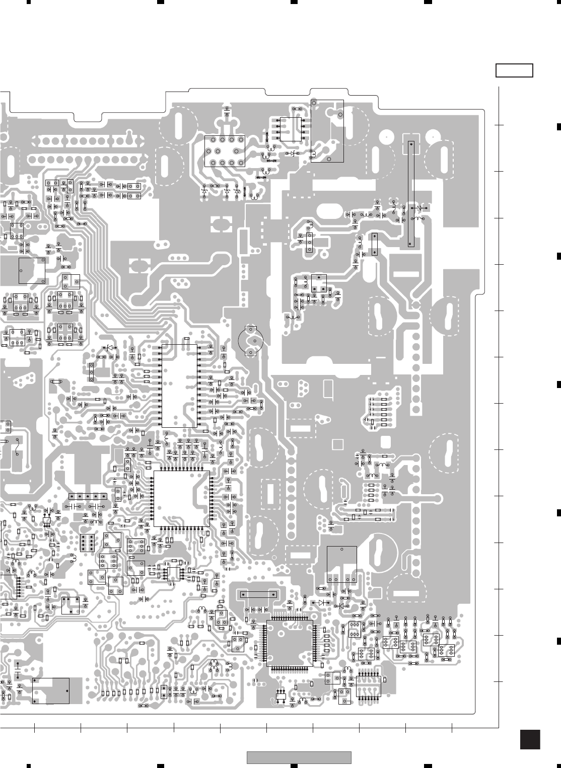
AVIC-X910BT/XS/UC 189
5678
5678
C
D
F
A
B
E
A
SIDE B
100 90 80 70 60 50 40 30
X
130
120
110
100
90
80
70
60
50
40
30
20
10
0
Y
20 10
E
E
E
1
1
1
5
1510
152025
1
5
10
1
1 5
10
E
E
E
1
1
5
1
5
E
E
1
1
5
1
5
1
5
1 5
1
1
5
E
E
E
1 5 10 15
20
25
30
354045
50
55
60
1 5 10
15 20
25 30 35
40 45
1
1
1
1
1
1
1
1
R3610
R3611
R3612
R3613
R3614 R3615
R3616
L2943
R3617
L2944
R3618
L2945
R3619
FU4601
L2946
R602
R3620
C4200
R609
R3621
R3622
C4202
C4203
R3623
R3624
C4204
R3625
R3626
C4206
R3627
C4207
R610
R3629
R611
R612
R618
C4211
C4215
C4216
C4217
601
R625
R4001
Q4601
R626
R628
R629
C4221
C4222
C4224
C4226
C4227
R630
R631
R632
R633
R636
R637
C4231
R639
L1401
L1402
Q4231
Q4232
C602
R640
R641
606
R642
C607
C608
R645
C609
8
C4241
R649
R4601
FU2900
C613
C614
C615
C616
R652
C619
L1421
C4251
L1422
C4252
L1423
C4253
C4254
R4616
C623
R4231
R4232
R4233
R4234
R4041
R4235
R4236
R4237
C632 R4240
R4241
C635
L4701
C636
X1481
C4271
C4273 C4274
C4275
C4276
C4277
C4278
C4279
R4251
R4252
R4253
R4254
R4255
R688
C4280
R689
C4281
IC4251
C4282
C4283 C4284
C2920
C4285
C2921
C4286
C2922
C4287
C2923
R4261
C2925
L4722
C2926
C2927
L4723
C2928 L4724
R695
L4725
R696
R697
R698
C4290
L1461
C4292
L1463
L1464
C4296
C4298
R4271
C4299
R4272
R4273
R4274
R4275
R4276 R4277
R4278
IC4271
C2940
C671
C2941
C2942
C2943
R4280
R4281
R4282
R4283
R4284
R2920
R4285
R2921
R4286
R2922
R4287
R2923
R4288
R4289
IC601
L4171
L4172
L4173
R4290
L4175
R4291
IC607
R4293
IC608
R4295
IC609
L4372
C695
C696
C697
R2940
L731
R2951
R2952
R2953
R2954
C1401
C1402
C1403
C1404
R2959
C1405
Q1401
C1020
C1021
C1022
R2960
R2961
C1410
R2967
R2968
R2969
R701
R2970
R2971
R2972
R2973
R2974
R708
R2975
C1421
C4301
C1422
R2976
R2977
C1423
C4303
C4304
C1424
Q1421
Q4301
C1425
C1426
R1016
R1401
R715
6
IC1016
R1409
C4311
Q4311
Q4312
Q4313
Q4314
IC1021
C4701
C4703
C4706
C4707
C4709
D4301
R731
C4711
R1421
R4301
R1422
R1423
R1424
R1425
R1426
C4719
C1451
C1452
C1453
C1454
C1455
D4311
Q4331
C1456
C702
D4312
Q4332
C1457
C4337
Q4333
C1458
C4338
R4311
C4339
R4312
R4313
R4314
C4724
R4316 R4317
C4340
C4341 C4342
C711
C4151
C4152
C4153
C1467
C1468
C4154
C1469
IC4701
C4155
C4156
IC4702
C4157
C4158
C4159
C1470
C1471
C1472
C1473
C4160
C1474
C4161
C1475
D4331
C2800
R4331
R4332
R4333
R4334
C2805
D4721
R4335
C2806
D4722
R4336
D4723
R4337
D4724
R4338
C4361
D4725
R4339
C4362
D4726
C1483
D4727
C4172
C1487
R4727
R4728
C4174
C1488
R4340
R1461
C1489
C2811
IC4721
R4341
R1462
R4342
C4177
R1463
R4343
R1464
Q2810
R4344
R4151
R1465
R4345
R4152
R1466
R4346
Q4753
R4153
R1467
R4347
Q4754
R4154
R1468
R4348
R1469
C1491
R4155
C1492
R4156
C1493
R4157
R4158
R4159
C4181
L4231
C4182
C4183
C1497
C4184
R1470
R1471
C4185
C4186
R1472
R1473
C4187
R4160
C4188
R1474
R4161
C4189
R1475
R1476
R4162
R1477
R1478
R1479
C4190
C4191
C4192
C4193
C4194
R4361
R4749
C4195
C2831
R4362
C2832
R4363
C4197
C2833
R4364
R4170 C4198
R4365
R4171
R1485
R4366
R1486
R1487
R4173
R4174
R4750
R1488
R4175
R1489
IC1481
ZNR1401
R4176
IC4171
D4372
R1490
R1492
R1494
R1497
L602
R4187
R4188
L607
L608
L609
D2830
D2831
U695
C3601
L610
C3604
R2830
R4194
R4195
R2831
Q3601
Q3602
Q3603
C3607
Q3604
R2834
R4198
C3608
R4199
Q3605
Q3606
IC2830
R4779
R4780
R4781
R4782
R3601
R3602
R3603
R3604
R3605
L2931
R3606
L2932
R3607
L2933
R3608
L2934
R3609
1
1
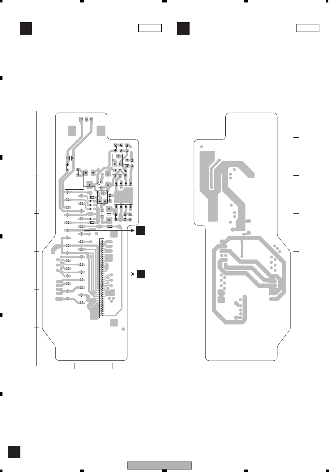
AVIC-X910BT/XS/UC
190
1234
1234
C
D
F
A
B
E
11.2 CK UNIT
B
SIDE BSIDE A
BCK UNIT BCK UNIT
1
1
E
1
5
E
1 5 25
15
1 5 10 15 20 25 30 35 40
Q890
Q891
L890
R881
R882
R883
R884
R885
R886
R887
R888
R890
R891
R892
R893
R894
R895
R896
R897
R898
CN881
CN882
CN883
C887
C890
C891
C892
C893
C895
C896
C897
VR890
IC890
20 30
10
10 20
X
60
50
40
30
20
10
0
Y
20 10
X
60
50
40
30
20
10
0
Y
A
CN702
C
CN1901

AVIC-X910BT/XS/UC 191
5678
5678
C
D
F
A
B
E
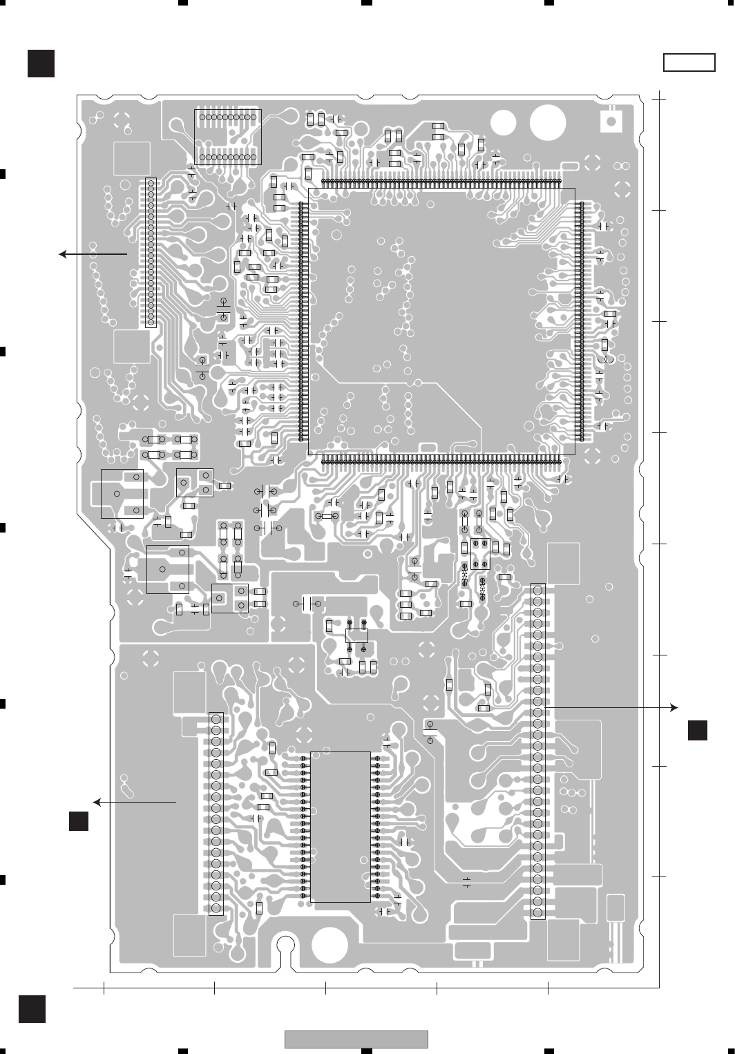
AVIC-X910BT/XS/UC
192
1234
1234
C
D
F
A
B
E
11.3 DVD CORE UNIT
C
SIDE A
CDVD CORE UNIT
1 5 10 15 20 25 30
1 5 10 15 20 25 30 35 40 45 50
65 70 75 80 85 90 95 100 105
130 135 140 145 150 155 160
195 200 205 210 215
6055
125120115110
190
185
180175170
165
1510
1520
1 5 10 15
1
1 5 10 15 20
25303540
1
1 5 10 15 20 25
E
E
E
E
C1502
C1503
C1504
C1505
C1506 C1507 C1509
CN1901
R1101
C1511
R1102
R1103
C1514
R1104
C1515
R1105
C1516
R1106
C1517
C1518
C1519
R1109
C1520
R1110
C1521
R1111
C1522
R1112
C1523
R1113
C1524
R1114
R1115
C1526
R1116
R1117
C1528
R1118
C1529
R1505
R1506
R1507
R1508
R1509
IC1501
R1510
R1512
R1513
R1514
D1901
D1902
R1516
R1517
R1518
R1519
R1522
R1523
R1524
R1525
R1526
R1528
R1529
R1530R1531
R1533
R1534
CN1951
R1536
R1537
R1538
R1539
R1540
R1541
R1542
C1953
R1547
R1950
R1951
R1954
R1955
R1956
R1957
CN1201
C1203
C1204
C1205
C1207
C1208
C1018
C1019
C1022
C1601
C1602
C1603
C1604
R1001
C1605
C1606
C1607
R1004
C1608
C1609
R1007
R1008
IC1001
C1610
R1201
C1611
R1202
C1612
R1203
C1613
R1204
C1614
C1615
C1616
C1617
C1618
IC1201
C1619
C1620
C1621
C1622
R1212
C1623
C1624
R1021
C1625
C1626
C1627
R1601
R1026
R1602
R1603
R1027
R1604
R1605
L1512
L1901 C1671
C1672
C1673
C1674
C1676
R1670
R1671 R1672
R1673
R1674
R1675
R1679
CN1101
C1104
C1105
Q1101
Q1102
C1106
Q1103
C1107
C1108
Q1104
C1109 C1110
C1111
C1508
10 20 30 40 50 60 70 80
X
50
40
30
20
10
0
Y
PICKUP UNIT (SERVICE)
BCN883
DCN701
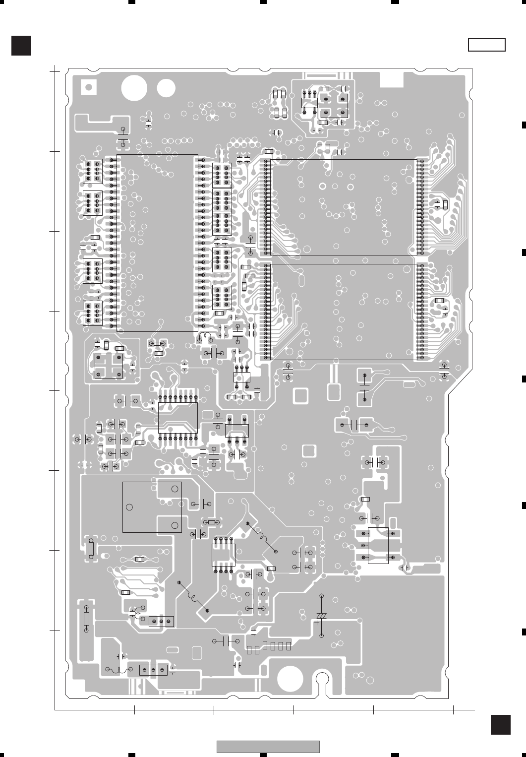
AVIC-X910BT/XS/UC 193
5678
5678
C
D
F
A
B
E
C
SIDE B
CDVD CORE UNIT
80 70 60 50 40 30 20 10
X
50
40
30
20
10
0
Y
1
1
1
5
1
1
1
1
1
5
1
5
10
15
20
25
30
35
40
45
1
5
10
15
20
25
30
35
40
45
1 5
1015
1
1 5 10 15 20 25
3035404550
C1501
C1510
C1512
C1513
R1300
R1301
C1525
C1527
R1501
R1503
R1504
L1003
L1004
R1511
EF1001
EF1002
C1934
R1527
R1532
R1535
C1950
C1951
C1952
R1543R1544
C1954
R1546
R1952 R1953
IC1951
C1001
C1003
C1004
C1005
C1006
C1007
C1008 C1009
C1201
C1010
C1011
C1012
C1013 C1014
C1209
C1015
C1016
C1017
C1401
C1402
C1403
C1404
C1210
C1405
C1211
C1407
C1408
C1409
C1021
X1501
R1002
C1802
IC1002
C1803
IC1003
C1804
IC1004
IC1005
C1805
C1806
IC1006
C1807
C1808
R1011
C1809
R1015
R1017
R1019
R1401
R1402
R1403
R1405
R1406
R1213
R1214
R1215
IC1401
R1409 R1216
IC1402
R1217
R1218
R1025
R1222
R1801 R1802
R1803
R1804
IC1801
L1902
L1903
L1904
X1950
C1480
C1481
C1482C1483
C1484
C1485
C1486
C1487
C1488
C1489
C1490
C1491
C1492
C1493
C1494
R1480
R1481
R1482
R1483R1484
R1485
R1486
R1487
R1488
IC1480
R1489
R1490
C1101
C1301
C1302
C1112 C1113
C1801
1

AVIC-X910BT/XS/UC
194
1234
1234
C
D
F
A
B
E
11.4 CONNECT PCB
D
SIDE A
DCONNECT PCB
1 5 10 15
CN701
10 20 30 40 50
X
40
30
20
10
0
Y
M
M1
LOAD/CRG
MOTOR
CCN1201

AVIC-X910BT/XS/UC 195
5678
5678
C
D
F
A
B
E
D
SIDE B
DCONNECT PCB
50 40 30 20 10
X
40
30
20
10
0
Y
1
1
1
1 5 10
R101
R102
R103
CN101
C101
S101
S102
S103
M2
SPINDLE MOTOR
HOME
8SNS
DSCSNS
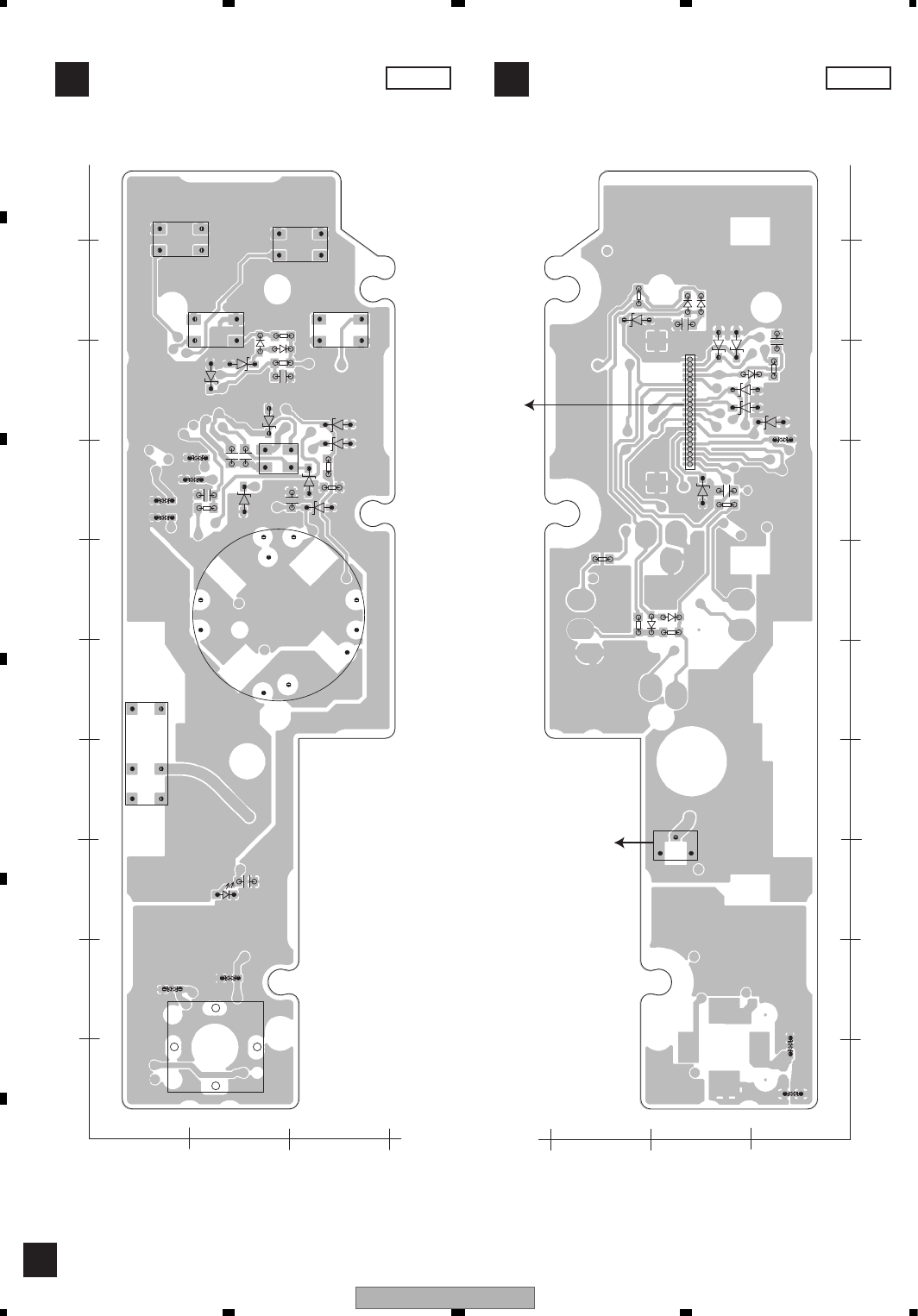
AVIC-X910BT/XS/UC
196
1234
1234
C
D
F
A
B
E
11.5 KEYBOARD UNIT
E
SIDE BSIDE A
EKEYBOARD UNIT EKEYBOARD UNIT
1
1
1
1
5
10
1
1
1
15
R802
R807
R809
R810
CN802
C801
C803C804
C805
C806
C807
R850
S801
S802
S803
S804
S805
D801
D802
D805
D809
D810
D815
D854
D855
D857
D858
D861
D862
D863
D866
D869
D870
D871
D872
ANT801
1 5 10 15 20
R801
R803
R804
R805
R806
R808
CN801
CN803
C802
C854
C856
D803
D804
D806
D807
D808
D811
D812
D852
D853
D856
D859
D860
D864
D867
D868
10 20 30
X
90
80
70
60
50
40
30
20
10
0
Y
30 20 10
X
90
80
70
60
50
40
30
20
10
0
Y
PANEL UNIT
OTJ2
NAVI UNIT
PTJ2
AV MINI
JACK
EJECT
RESET
MENU MAP
BT ANT
MULTI-CONTROL

AVIC-X910BT/XS/UC 197
5678
5678
C
D
F
A
B
E
12. ELECTRICAL PARTS LIST
NOTE:
Parts whose parts numbers are omitted are subject to being not supplied.
The part numbers shown below indicate chip components.
Chip Resistor
RS1/_S___J,RS1/__S___J
Chip Capacitor (except for CQS.....)
CKS....., CCS....., CSZS.....
The > mark found on some component parts indicates the importance of the safety factor of the part.
Therefore, when replacing, be sure to use parts of identical designation.
Meaning of the figures and others in the parentheses in the parts list.
Example) IC 301 is on the point (face A, 91 of x-axis, and 111 of y-axis) of the corresponding
PC board.
IC 301 (A, 91, 111) IC NJM2068V
Circuit Symbol and No. Part No.
Unit Number : CWN4237(UC)
Unit Number : CWN4238(EU5)
Unit Number : CWN4239(AU)
Unit Name : AV Unit
Unit Number : CWN4251
Unit Name : CK Unit
Unit Number : YWX5009
Unit Name : DVD Core Unit
Unit Number:
Unit Name : Connect PCB
Unit Number:
Unit Name : Keyboard Unit
A
Unit Number : CWN4237(UC)
Unit Number : CWN4238(EU5)
Unit Number : CWN4239(AU)
Unit Name : AV Unit
MISCELLANEOUS
IC 601 (B,47,7) IC TC7SH08FUS1
IC 603 (B,121,45) IC TC7SH04FUS1
IC 604 (B,122,42) IC TC7S32FU
IC 605 (A,43,9) IC TC74VHCT08AFTS1
IC 607 (B,106,30) IC TC74VHC08FTS1
IC 608 (B,97,45) IC BD5335FVE
IC 609 (B,28,9) IC TC74VHC08FTS1
IC 610 (A,108,35) IC(UC) PEG562A8
(A,108,35) IC(EU5) PEG561A8
(A,108,35) IC(AU) PEG563A8
IC 612 (B,110,42) Logic IC TC74VHCT32AFT
IC 1002 (A,148,8) IC NJM2904M
IC 1007 (A,89,128) IC PAL007C
IC 1008 (A,56,39) IC NJM2125F
IC 1015 (A,65,47) IC NJM4558V
IC 1016 (B,70,33) IC BA4558RFVM
IC 2801 (A,169,99) IC BA00CC0WCP-V5
IC 2820 (A,169,88) IC BA00CC0WCP-V5
IC 2830 (B,34,37) IC BA00BC0WFP
IC 2890 (B,157,105) IC TPD1018F
IC 3601 (A,12,20) IC M62343FP
IC 4171 (B,68,49) IC AN15887A
IC 4251 (B,104,107) IC NJM2505AF
IC 4271 (B,69,74) IC PML018A
IC 4601 (B,118,65) IC TPS5103IDB
IC 4641 (B,151,25) IC TPS5103IDB
IC 4661 (B,151,41) IC TPS5103IDB
IC 4701 (B,89,55) IC BD3931HFP
IC 4703 (A,87,45) IC S-L2980A33MC-C6S
IC 4721 (B,45,129) IC(UC) HA12241FP
Q 601 (B,117,20) Chip Transistor 2SA1576A
Q 661 (B,117,47) Chip Transistor DTC114EUA
Q 662 (B,114,23) Chip Transistor DTC114EUA
Q 751 (A,80,34) Chip Transistor(EU5) DTC124EUA
Q 752 (A,85,40) Chip Transistor(EU5) DTC124EUA
Q 753 (A,82,38) Chip Transistor(EU5) DTC124EUA
Q 754 (A,85,35) Chip Transistor(EU5) DTC124EUA
Q 1016 (A,56,32) Transistor IMD2A
Q 1401 (B,39,105) Transistor 2SC3357
Q 1421 (B,39,96) Transistor 2SC3127
Q 1441 (A,35,87) Transistor 2SC3130
Q 2810 (B,103,99) Transistor 2SD1760F5
Q 2811 (A,104,97) Chip Transistor DTA114EUA
Q 2812 (A,111,99) Chip Transistor DTC114EUA
Q 2840 (B,144,9) Transistor DTC114WK
Q 2841 (A,158,7) Chip Transistor DTC114EUA
Q 2860 (B,121,107) Transistor UMD2N
Q 2861 (B,121,110) Transistor UMD2N
Q 2862 (B,113,104) Transistor 2SC4081
Q 2863 (B,119,113) Transistor UMD2N
Q 2864 (B,116,112) Chip Transistor DTC114EUA
Q 2865 (B,113,112) Chip Transistor DTC124EUA
Q 2870 (A,151,113) Transistor 2SC4116
Q 2880 (A,165,112) Chip Transistor DTC114EUA
Circuit Symbol and No. Part No.

AVIC-X910BT/XS/UC
198
1234
1234
C
D
F
A
B
E
Q 2881 (B,125,24) Chip Transistor DTC114EUA
Q 2882 (B,122,20) Chip Transistor 2SA1576A
Q 2900 (A,166,124) Transistor 2SC4116
Q 3041 (A,77,51) Transistor IMD3A
Q 3042 (A,72,54) Transistor FMG12
Q 3601 (B,31,21) Transistor UMX1N
Q 3602 (B,23,19) Transistor UMX1N
Q 3603 (B,15,19) Transistor UMX1N
Q 3604 (B,29,16) Transistor UMX1N
Q 3605 (B,20,18) Transistor UMX1N
Q 3606 (B,11,17) Transistor UMX1N
Q 4231 (B,60,24) Transistor 2SC4081
Q 4232 (B,56,18) Chip Transistor 2SA1576A
Q 4312 (B,78,39) Transistor IMD3A
Q 4314 (B,78,35) Transistor DTC323TK
Q 4331 (B,103,92) Transistor FMG12
Q 4332 (B,93,85) Transistor FMG12
Q 4333 (B,93,92) Transistor FMG12
Q 4601 (B,107,65) Chip Transistor DTC114EUA
Q 4602 (A,118,65) FET SP8K2
Q 4631 (A,120,86) Transistor 2SD1767
Q 4632 (A,127,87) Transistor UMD2N
Q 4641 (B,140,23) Chip Transistor DTC114EUA
Q 4642 (A,151,25) FET SP8K2
Q 4661 (B,112,72) Chip Transistor DTC114EUA
Q 4662 (B,140,38) Chip Transistor DTC114EUA
Q 4663 (A,152,41) FET SP8K2
Q 4731 (B,144,88) Transistor 2SC4081
Q 4732 (B,129,99) Chip Transistor(UC) DTC114EUA
Q 4733 (B,151,90) Transistor 2SC4081
Q 4734 (B,123,99) Chip Transistor(UC) 2SA1576A
Q 4738 (B,142,91) Transistor 2SC4081
Q 4751 (A,32,12) Chip Transistor 2SA1576A
Q 4752 (A,33,8) Chip Transistor 2SA1576A
Q 4753 (B,36,11) Chip Transistor DTC114EUA
Q 4754 (B,33,7) Chip Transistor 2SA1576A
Q 4771 (B,110,94) Chip Transistor DTA114EUA
Q 4772 (B,113,92) Chip Transistor DTC114EUA
Q 4773 (B,116,92) Transistor 2SA1587
Q 4774 (B,115,86) Transistor IMX1
Q 4775 (B,128,85) Chip Transistor DTC114EUA
Q 4776 (B,123,94) Transistor 2SD1760F5
D 2802 (A,160,105) Diode RB060L-40
D 2810 (A,107,95) Diode UDZS5R6(B)
D 2821 (A,159,93) Diode RB060L-40
D 2822 (A,111,95) Diode DAN202U
D 2823 (A,121,81) Diode 1SR154-400
D 2824 (A,128,81) Diode 1SR154-400
D 2825 (A,132,48) Diode 1SS400G
D 2831 (B,38,27) Diode RR264M-400
D 2840 (B,153,7) Diode 1SS355
D 2860 (B,124,106) Diode MA111
D 2861 (B,120,105) Diode UDZS8R2(B)
D 2862 (B,116,108) Diode DAN202U
D 2863 (B,114,108) Diode DAN202U
D 2870 (A,153,107) Diode UDZS5R1(B)
D 2871 (B,170,131) Diode UDZS18(B)
D 2872 (B,170,126) Diode UDZS18(B)
D 2873 (B,168,131) Diode 1SS355
D 2874 (B,159,112) Diode PTZ18A
Circuit Symbol and No. Part No.
D 2880 (B,153,131) Diode 1SR154-400
D 2890 (A,156,110) Diode 1SR154-400
D 2891 (A,159,110) Diode 1SR154-400
D 2900 (A,170,126) Diode HZU8R2(B1)
D 2910 (B,146,73) Diode KS926S2
D 2911 (A,59,94) Diode RB060L-40
D 2912 (B,145,103) Diode KS926S2
D 2930 (A,141,108) Diode ST70-27F
D 3041 (A,72,50) Diode DAP202K
D 4061 (A,61,48) Diode EDZ4R3(B)
D 4062 (A,59,49) Diode 1SS355
D 4311 (B,83,31) Diode DAN202K
D 4312 (B,87,33) Diode DAN202K
D 4331 (B,92,96) Diode DAP202K
D 4351 (B,110,114) Diode MALS180X
D 4353 (B,124,133) Diode MALS180X
D 4354 (B,125,133) Diode MALS180X
D 4355 (A,121,109) Diode DAN202U
D 4356 (A,112,120) Diode MALS068X
D 4357 (A,108,120) Diode MALS068X
D 4358 (A,118,120) Diode MALS068X
D 4359 (A,122,120) Diode MALS068X
D 4360 (B,129,113) Diode 1SR154-400
D 4361 (A,132,108) Diode 1SS355
D 4362 (B,129,107) Diode 1SR154-400
D 4363 (B,114,119) Diode MALS068X
D 4364 (A,129,107) Diode PTZ27(B)
D 4365 (A,126,107) Diode PTZ27(B)
D 4366 (B,122,133) Diode MALS180X
D 4371 (A,42,118) Diode UDZS5R6(B)
D 4372 (B,44,124) Diode UDZS5R6(B)
D 4601 (B,127,61) Diode RB400D
D 4602 (A,115,71) Diode RB060L-40
D 4631 (A,123,89) Diode UDZS9R1(B)
D 4641 (B,160,22) Diode RB400D
D 4642 (A,148,31) Diode RB060L-40
D 4643 (A,164,17) Diode RB083L-20
D 4661 (B,159,36) Diode RB400D
D 4662 (A,148,46) Diode RB060L-40
D 4721 (B,49,122) Diode(UC) MALS180X
D 4722 (B,51,119) Diode(UC) MALS180X
D 4723 (B,55,116) Diode(UC) MALS068X
D 4724 (B,50,127) Diode(UC) MALS068X
D 4725 (B,56,116) Diode(UC) UDZS18(B)
D 4726 (B,63,116) Diode(UC) UDZS18(B)
D 4727 (B,59,116) Diode(UC) UDZS18(B)
D 4731 (B,147,89) Diode HZU7R5(B3)
D 4732 (B,147,93) Diode RB500V-40
D 4733 (B,151,93) Diode RB500V-40
D 4734 (B,146,97) Diode EDZ20(B)
D 4735 (B,149,93) Diode RB500V-40
D 4736 (B,142,97) Diode RB500V-40
D 4737 (B,142,95) Diode HZU7R5(B3)
D 4751 (A,29,14) Diode 1SS355
D 4752 (A,28,14) Diode 1SS355
D 4771 (B,121,86) Diode RB500V-40
D 4772 (B,123,87) Diode RB500V-40
D 4773 (B,124,84) Diode HZU8R2(B1)
D 4774 (B,126,88) Diode HZU11(B2)
D 4775 (B,139,132) Diode MALS180X
Circuit Symbol and No. Part No.

AVIC-X910BT/XS/UC 199
5678
5678
C
D
F
A
B
E
ZNR1401 (B,17,112) Surge Protector CSA30-201N
L 601 (B,124,42) Inductor CTF1410
L 602 (B,42,6) Inductor CTF1410
L 604 (B,121,48) Inductor CTF1410
L 605 (A,43,14) Inductor CTF1410
L 607 (B,104,35) Inductor CTF1410
L 608 (B,101,33) Inductor CTF1410
L 609 (B,100,48) Inductor CTF1410
L 610 (B,33,12) Inductor CTF1410
L 611 (A,99,21) Inductor CTF1410
L 612 (A,103,47) Inductor CTF1410
L 613 (A,110,20) Inductor CTF1410
L 614 (B,122,25) Inductor CTF1410
L 615 (A,121,34) Inductor CTF1410
L 617 (B,116,45) Inductor CTF1410
L 704 (A,80,72) Inductor CTF1357
L 705 (A,90,70) Inductor CTF1463
L 706 (A,95,64) Inductor CTF1306
L 707 (A,81,67) Inductor CTF1306
L 708 (A,93,65) Inductor CTF1306
L 709 (A,79,65) Inductor CTF1306
L 710 (A,91,64) Inductor CTF1306
L 711 (A,79,64) Inductor CTF1306
L 712 (A,77,62) Inductor CTF1306
L 713 (A,80,61) Inductor CTF1306
L 714 (A,93,61) Inductor CTF1306
L 1004 (A,149,13) Inductor CTF1334
L 1401 (B,23,112) Inductor LCTAWR12J2520
L 1402 (B,29,111) Inductor LCYCR10K2125
L 1403 (A,45,89) Inductor LCTAW101J2520
L 1421 (B,42,96) Inductor LCTCR22K2125
L 1422 (B,30,105) Inductor LCTCR10K2125
L 1423 (B,44,89) Inductor LCTAW101J2520
L 1441 (A,38,85) Inductor LCTCR15K2125
L 1443 (A,45,83) Chip Coil LCTAW1R0J2520
L 1461 (B,17,110) Chip Coil LCTAW4R7J2520
L 1462 (A,39,70) Inductor LCTAW2R2J3225
L 1463 (B,25,57) Inductor LCTAW2R2J2520
L 1464 (B,27,54) Chip Ferrite Bead CTF1399
L 1465 (A,34,41) Inductor LCTAW2R2J3225
L 2870 (B,167,127) Inductor CTF1410
L 2871 (B,160,115) Inductor CTF1410
L 2872 (B,149,114) Inductor CTF1410
L 2930 (A,135,95) Choke Coil 600 uH CTH1347
L 2931 (B,92,117) Inductor CTF1689
L 2932 (B,79,115) Inductor CTF1689
L 2933 (B,79,117) Inductor CTF1689
L 2934 (B,96,118) Inductor CTF1689
L 2940 (A,90,11) Inductor CTF1334
L 2943 (B,61,12) Inductor CTF1556
L 2944 (B,61,14) Inductor CTF1556
L 2945 (B,58,13) Inductor CTF1556
L 2946 (B,66,8) Inductor CTF1556
L 2947 (A,60,21) Inductor CTF1675
L 2948 (A,61,21) Inductor CTF1675
L 2949 (A,65,21) Inductor CTF1675
L 2950 (A,66,21) Inductor CTF1675
L 3601 (A,17,14) Chip Coil LCTAW100J2520
L 4171 (B,72,62) Chip Coil LCTAW100J2520
L 4172 (B,60,61) Chip Coil LCTAW100J2520
Circuit Symbol and No. Part No.
L 4173 (B,80,57) Inductor CTF1689
L 4174 (A,82,53) Inductor CTF1689
L 4175 (B,82,50) Inductor CTF1689
L 4176 (A,82,48) Inductor CTF1689
L 4231 (B,64,25) Inductor CTF1473
L 4271 (A,66,86) Inductor LCYA2R2J2520
L 4351 (A,125,111) Inductor LCTC2R2K1608
L 4352 (A,130,113) Inductor CTF1556
L 4371 (A,38,118) Inductor CTF1334
L 4372 (B,40,124) Inductor CTF1334
L 4601 (A,106,64) Choke Coil 27 uH CTH1402
L 4602 (A,130,63) Choke Coil 10 uH CTH1403
L 4641 (A,141,22) Inductor CTH1255
L 4642 (A,161,24) Inductor CTH1257
L 4661 (A,141,35) Inductor CTH1255
L 4662 (A,162,40) Inductor CTH1257
L 4701 (B,87,44) Inductor CTF1393
L 4721 (A,44,130) Inductor(UC) LCYC2R2K1608
L 4722 (B,50,124) Inductor(UC) CTF1334
L 4723 (B,50,120) Inductor(UC) CTF1334
L 4724 (B,53,115) Inductor(UC) CTF1334
L 4725 (B,49,125) Inductor(UC) CTF1334
T 1401 (A,41,105) Coil CTC1194
T 1402 (A,43,95) Coil CTC1193
T 1403 (A,33,96) Coil CTC1192
TH601 (A,70,29) Thermistor CCX1051
X 601 (A,92,33)
Ceramic Resonator 20.000 MHz
VSS1186
VR4231 (A,55,25) Semi-fixed 1 kohm(OB) CCP1483
>FU2900 (B,72,8) Fuse 250 mA CEK1276
FU4351 (B,117,118) Poly Switch MINISMDC075F/24
>FU4352 (B,129,133) Fuse 3.15 A CEK1259
>FU4601 (B,104,61) Fuse 5 A CEK1261
>FU4602 (B,144,58) Fuse 5 A CEK1261
>FU4631 (A,115,86) Fuse 200 mA CEK1247
>FU4641 (A,141,8) Fuse 3.15 A CEK1259
>FU4642 (B,158,72) Fuse 2.5 A CEK1258
>FU4661 (A,137,8) Fuse 2.5 A CEK1258
>FU4662 (B,148,55) Fuse 2.5 A CEK1258
>FU4771 (A,115,106) Fuse 1 A CEK1254
FB701 (A,93,77) Inductor CTF1453
EF4351 (B,121,119) EMI Filter CCG1067
EF4352 (B,126,119) EMI Filter CCG1067
EF4353 (A,128,119) EMI Filter CCG1067
EF4354 (A,110,120) EMI Filter CCG1067
EF4355 (A,114,120) EMI Filter CCG1067
EF4356 (A,116,120) EMI Filter CCG1067
EF4357 (A,120,120) EMI Filter CCG1067
EF4358 (A,124,120) EMI Filter CCG1067
EF4359 (B,124,119) EMI Filter CCG1067
EF4360 (B,129,119) EMI Filter CCG1067
EF4361 (A,131,119) EMI Filter CCG1067
EF4731 (B,157,78) EMI Filter CCG1172
EF4732 (B,154,57) EMI Filter CCG1172
ANT1401 (A,19,119) Antenna Jack CKX1060
Y 1461 (A,18,93) FM/AM Tuner Unit(UC,AU) CWE2128
(A,18,93) FM/AM Tuner Unit(EU5) CWE2127
U 695 (B,92,27) IR Remote(AU) RPMS2401-H19
CN702 (A,85,66) Connector CKS5627
CN1000 (A,74,9) Connector CKS5732
CN1001 (A,94,103) Connector CKS4674
Circuit Symbol and No. Part No.

AVIC-X910BT/XS/UC
200
1234
1234
C
D
F
A
B
E
CN1005 (A,149,129) Plug CKM1550
CN1015 (A,37,129) Jack CKN1042
CN1016 (A,122,132) Connector CKM1460
CN1021 (A,58,129) Connector(UC) CKS3408
CN1441 (A,53,84) Mini Pin Jack CKX1046
RESISTORS
R 601 (A,39,7) RS1/16S104J
R 602 (B,39,6) RS1/16S104J
R 603 (A,96,24) (UC,EU5) RS1/16SS220J
R 604 (A,97,22) (UC,EU5) RS1/16S220J
R 605 (B,121,39) RS1/16SS104J
R 607 (A,86,32) (EU5) RS1/16SS681J
R 608 (A,89,40) (EU5) RAB4C681J
R 609 (B,101,37) RS1/16SS104J
R 610 (B,96,38) RS1/16SS102J
R 612 (B,98,32) RS1/16SS104J
R 613 (A,95,42) RS1/16SS471J
R 614 (A,93,41) RS1/16SS471J
R 615 (A,95,41) RS1/16SS222J
R 616 (A,93,40) RS1/16SS0R0J
R 617 (A,95,39) RS1/16SS0R0J
R 618 (B,25,10) RS1/16SS104J
R 619 (B,111,38) RS1/16SS104J
R 620 (A,96,35) RS1/16SS101J
R 626 (B,101,30) RS1/16SS221J
R 627 (A,96,26) RS1/16SS104J
R 628 (B,89,40) (EU5) RAB4C223J
R 632 (B,100,45) RS1/16SS0R0J
R 633 (B,103,42) RS1/16SS102J
R 634 (A,102,22) RS1/16SS104J
R 636 (B,101,40) RS1/16SS104J
R 639 (B,106,40) RS1/16SS102J
R 640 (B,103,40) RS1/16SS103J
R 641 (B,100,41) RS1/16SS103J
R 642 (B,106,25) RS1/16SS220J
R 643 (A,100,18) RS1/16SS104J
R 646 (A,102,18) RS1/16SS104J
R 648 (B,108,24) RS1/16S104J
R 649 (B,104,46) RS1/16SS220J
R 650 (A,103,18) RS1/16SS104J
R 652 (B,106,44) RS1/16SS220J
R 653 (A,109,47) RS1/16SS102J
R 654 (A,105,18) RS1/16SS104J
R 657 (A,106,18) RS1/16SS104J
R 659 (A,112,21) RS1/16S220J
R 660 (A,115,19) RS1/16S104J
R 661 (A,109,17) RS1/16S104J
R 662 (A,113,18) RS1/16S104J
R 663 (A,117,20) RS1/16SS102J
R 664 (A,117,18) RS1/16SS473J
R 665 (B,118,49) RS1/16SS104J
R 666 (B,116,24) RS1/16SS104J
R 668 (B,119,22) RS1/16SS472J
R 670 (A,125,33) RS1/16SS104J
R 671 (A,121,31) RS1/16SS102J
R 676 (A,121,28) RS1/16SS0R0J
R 677 (A,121,27) RS1/16SS0R0J
R 680 (B,120,22) RS1/16SS472J
Circuit Symbol and No. Part No.
R 681 (B,119,49) RS1/16SS473J
R 682 (A,125,36) RS1/16SS0R0J
R 683 (A,123,43) RAB4C104J
R 684 (A,123,39) RAB4C681J
R 685 (A,69,27) RS1/16S102J
R 686 (B,109,37) RS1/16SS104J
R 687 (B,118,43) RS1/16SS104J
R 688 (B,44,9) RS1/16SS104J
R 689 (B,40,10) RS1/16SS104J
R 690 (A,110,49) RS1/16SS472J
R 695 (B,97,24) (AU) RS1/16SS470J
R 696 (B,96,30) (AU) RS1/16SS470J
R 697 (B,99,24) RS1/16SS104J
R 698 (B,106,27) RS1/16SS104J
R 699 (B,110,49) RS1/16SS104J
R 714 (A,95,76) RS1/10S0R0J
R 715 (B,95,75) RS1/10S0R0J
R 717 (A,82,57) RS1/16SS0R0J
R 718 (A,94,63) RS1/16SS221J
R 722 (A,82,69) RS1/16S104J
R 731 (B,95,35) RS1/16SS0R0J
R 751 (A,78,54) RS1/16S0R0J
R 1016 (B,70,16) RS1/16SS0R0J
R 1401 (B,41,109) Inductor CTF1742
R 1409 (B,20,112) RS1/16S105J
R 1410 (A,36,103) RS1/16S821J
R 1411 (A,35,108) RS1/16S330J
R 1412 (A,44,89) RS1/16S332J
R 1413 (A,33,91) RS1/16S101J
R 1421 (B,38,92) RS1/16S151J
R 1422 (B,36,94) RS1/16S680J
R 1423 (B,41,93) RS1/16S152J
R 1424 (B,43,93) RS1/16S681J
R 1425 (B,44,96) RS1/16S181J
R 1441 (A,32,85) RS1/16S151J
R 1442 (A,33,87) RS1/16S680J
R 1443 (A,39,88) RS1/16S152J
R 1444 (A,41,86) RS1/16S681J
R 1445 (A,39,84) RS1/16S151J
R 1461 (B,25,71) RS1/16SS681J
R 1462 (B,25,70) RS1/16SS681J
R 1463 (B,25,69) RS1/16SS681J
R 1464 (B,25,68) RS1/16SS681J
R 1465 (B,25,67) RS1/16SS681J
R 1466 (B,27,66) RS1/16SS223J
R 1467 (B,25,65) (EU5) RS1/16SS681J
R 1468 (B,25,59) RS1/16SS681J
R 1470 (B,26,47) RS1/16SS0R0J
R 1471 (B,26,45) RS1/16SS0R0J
R 1474 (B,30,47) RS1/16SS0R0J
R 1475 (B,33,45) RS1/16SS0R0J
R 1476 (B,28,49) (EU5) RS1/16SS0R0J
R 1477 (B,27,51) (EU5) RS1/16SS0R0J
R 1478 (B,28,50) (EU5) RS1/16SS0R0J
R 1479 (B,27,52) (EU5) RS1/16SS0R0J
R 2801 (B,160,96) RN1/16SE1002D
R 2802 (B,159,94) RN1/16SE2701D
R 2803 (B,158,96) RN1/16SE2201D
R 2804 (B,159,99) RS1/16S104J
R 2810 (B,111,99) RS1/8S0R0J
Circuit Symbol and No. Part No.

AVIC-X910BT/XS/UC 201
5678
5678
C
D
F
A
B
E
R 2811 (A,100,98) RS1/16S471J
R 2820 (B,160,85) RS1/16S2201D
R 2821 (B,159,87) RS1/16S1002D
R 2822 (B,159,89) RS1/16S2201D
R 2823 (A,139,49) RS1/16SS105J
R 2830 (B,33,28) RS1/16S3601D
R 2831 (B,31,24) RS1/16S10R0D
R 2832 (A,28,36) RS1/16S2201D
R 2833 (A,33,28) RS1/16S0R0J
R 2834 (B,38,30) RS1/16S104J
R 2840 (A,146,11) RS1/16SS104J
R 2841 (A,146,12) RS1/16SS473J
R 2842 (B,145,6) RS1/16SS563J
R 2843 (B,148,9) RS1/16SS513J
R 2844 (B,149,8) RS1/16SS104J
R 2845 (B,150,6) RS1/16SS513J
R 2846 (A,153,6) RS1/16SS513J
R 2847 (B,151,8) RS1/16SS102J
R 2848 (B,149,6) RS1/16SS102J
R 2849 (B,151,6) RS1/16SS564J
R 2850 (B,153,10) RS1/16SS202J
R 2851 (B,152,10) RS1/16SS822J
R 2852 (A,154,11) RS1/16SS203J
R 2853 (A,152,13) RS1/16SS333J
R 2860 (B,126,108) RS1/16SS391J
R 2861 (B,124,109) RS1/16SS391J
R 2862 (B,122,103) RS1/16SS473J
R 2863 (B,116,105) RS1/16SS223J
R 2864 (B,118,106) RS1/16SS103J
R 2865 (B,123,112) RS1/10S102J
R 2866 (B,114,116) RS1/16SS103J
R 2867 (B,117,114) RS1/16SS103J
R 2868 (B,115,114) RS1/16SS221J
R 2869 (B,113,114) RS1/16SS101J
R 2870 (A,153,110) RS1/16S473J
R 2871 (A,153,112) RS1/16S104J
R 2872 (B,154,109) RS1/16S102J
R 2873 (B,157,109) RS1/16S472J
R 2874 (B,150,110) RS1/4S102J
R 2875 (B,152,114) RS1/4S472J
R 2880 (A,166,120) RS1/16S103J
R 2881 (B,148,132) RS1/4S472J
R 2882 (B,143,132) RS1/4S102J
R 2883 (B,124,22) RS1/16SS472J
R 2884 (B,122,22) RS1/16SS472J
R 2900 (A,169,124) RS1/16S473J
R 2901 (A,170,122) RS1/16S104J
R 2902 (A,167,128) RS1/4S102J
R 2903 (A,167,131) RS1/4S472J
R 2910 (B,154,71) RS1/16S473J
R 2911 (B,145,109) RS1/16S473J
R 2912 (A,60,90) RS1/4S4R7J
R 2913 (A,65,92) RS1/4S4R7J
R 2920 (B,90,109) RS1/16S102J
R 2921 (B,89,113) RS1/16S102J
R 2922 (B,91,113) RS1/16S102J
R 2923 (B,95,108) RS1/16S102J
R 2924 (A,96,120) RS1/16S103J
R 2925 (A,93,120) RS1/16S103J
R 2926 (A,102,119) RS1/16S103J
Circuit Symbol and No. Part No.
R 2940 (B,61,7) RS1/16S0R0J
R 2941 (A,57,10) RS1/16SS101J
R 2942 (A,61,15) RS1/16SS101J
R 2951 (B,67,18) RS1/16SS0R0J
R 2952 (B,68,18) RS1/16SS0R0J
R 2953 (B,66,13) RS1/16SS0R0J
R 2954 (B,70,11) RS1/16SS0R0J
R 2959 (B,77,5) RS1/16S0R0J
R 2960 (B,74,8) RS1/16SS0R0J
R 2961 (B,75,8) RS1/16SS0R0J
R 2962 (A,77,18) RS1/16SS0R0J
R 2963 (A,79,18) RS1/16SS0R0J
R 2964 (A,81,21) RS1/16SS0R0J
R 2967 (B,77,18) RS1/16SS0R0J
R 2968 (B,76,8) RS1/16SS0R0J
R 2969 (B,78,8) RS1/16SS0R0J
R 2970 (B,80,15) RS1/16SS0R0J
R 2971 (B,79,8) RS1/16SS0R0J
R 2972 (B,81,8) RS1/16SS0R0J
R 2973 (B,82,15) RS1/16SS0R0J
R 2974 (B,82,8) RS1/16SS0R0J
R 2975 (B,83,8) RS1/16SS0R0J
R 2976 (B,84,8) RS1/16SS0R0J
R 2977 (B,85,8) RS1/16SS0R0J
R 2978 (A,85,21) RS1/16SS0R0J
R 2979 (A,87,18) RS1/16SS0R0J
R 2980 (A,88,19) RS1/16SS0R0J
R 2981 (A,87,22) RS1/16SS0R0J
R 2982 (A,90,9) RS1/16SS0R0J
R 2983 (A,156,8) RS1/16SS0R0J
R 3041 (A,75,56) RS1/16S182J
R 3042 (A,75,57) RS1/16S182J
R 3043 (A,76,54) RS1/16S473J
R 3044 (A,74,54) RS1/16S473J
R 3601 (B,29,22) RS1/16S224J
R 3602 (B,34,21) RS1/16S102J
R 3603 (B,27,24) RS1/16S222J
R 3604 (B,23,21) RS1/16S224J
R 3605 (B,18,14) RS1/16S102J
R 3606 (B,24,23) RS1/16S222J
R 3607 (B,16,21) RS1/16S224J
R 3608 (B,16,15) RS1/16S102J
R 3609 (B,15,24) RS1/16S222J
R 3610 (B,29,19) RS1/16S121J
R 3611 (B,27,21) RS1/16S101J
R 3612 (B,31,15) RS1/16S101J
R 3616 (B,20,20) RS1/16S121J
R 3617 (B,20,23) RS1/16S151J
R 3618 (B,21,16) RS1/16S101J
R 3622 (B,11,20) RS1/16S151J
R 3623 (B,12,23) RS1/16S181J
R 3624 (B,14,16) RS1/16S101J
R 3629 (B,71,8) RS1/16S0R0J
R 4001 (B,57,61) RS1/16S750J
R 4021 (A,54,50) RS1/16S750J
R 4041 (B,57,37) RS1/16S750J
R 4061 (A,57,48) RS1/16S102J
R 4071 (A,69,46) RS1/16SS473J
R 4072 (A,68,47) RS1/16SS473J
R 4073 (A,65,57) RS1/16SS473J
Circuit Symbol and No. Part No.

AVIC-X910BT/XS/UC
202
1234
1234
C
D
F
A
B
E
R 4074 (A,66,42) RS1/16SS473J
R 4075 (A,64,43) RS1/16SS473J
R 4076 (A,67,50) RS1/16SS473J
R 4077 (A,65,56) RS1/16SS473J
R 4078 (A,65,52) RS1/16SS473J
R 4079 (A,63,42) RS1/16SS330J
R 4080 (A,63,55) RS1/16SS330J
R 4151 (B,65,32) RS1/16SS103J
R 4152 (B,64,34) RS1/16SS103J
R 4153 (B,67,34) RS1/16SS103J
R 4154 (B,66,32) RS1/16SS103J
R 4155 (B,69,36) RS1/16SS102J
R 4156 (B,70,36) RS1/16SS104J
R 4157 (B,73,35) RS1/16SS104J
R 4158 (B,75,33) RS1/16SS683J
R 4159 (B,73,33) RS1/16SS473J
R 4170 (B,80,54) RS1/16SS223J
R 4171 (B,80,50) RS1/16SS223J
R 4174 (B,66,22) RS1/16SS223J
R 4175 (B,64,22) RS1/16SS223J
R 4176 (B,75,57) RS1/16SS0R0J
R 4194 (B,63,42) RS1/16SS221J
R 4195 (B,64,41) RS1/16SS221J
R 4200 (A,76,39) RS1/16S750J
R 4231 (B,60,26) RS1/16SS223J
R 4232 (B,60,22) RS1/16SS303J
R 4233 (B,58,22) RS1/16SS681J
R 4234 (B,57,24) RS1/16SS102J
R 4235 (B,62,22) RS1/16SS681J
R 4236 (B,54,19) RS1/16SS152J
R 4237 (B,58,18) RS1/16SS0R0J
R 4240 (B,60,27) RS1/16SS0R0J
R 4251 (B,102,113) RS1/16S750J
R 4252 (B,104,113) RS1/16SS473J
R 4253 (B,102,112) RS1/16SS473J
R 4254 (B,100,112) RS1/16SS101J
R 4255 (B,106,113) RS1/16SS101J
R 4263 (A,105,110) RS1/16SS0R0J
R 4271 (B,58,66) RS1/16S0R0J
R 4272 (B,86,65) (UC) RS1/16S181J
R 4273 (B,56,68) (UC) RS1/16S181J
R 4274 (B,87,67) (UC) RS1/16S223J
R 4275 (B,85,67) (UC) RS1/16S102J
R 4276 (B,53,69) (UC) RS1/16S223J
R 4277 (B,51,70) (UC) RS1/16S102J
R 4285 (B,59,73) RS1/16SS0R0J
R 4286 (B,85,71) RS1/16SS0R0J
R 4287 (B,76,75) RS1/16SS102J
R 4289 (B,76,76) RS1/16SS102J
R 4291 (B,76,77) RS1/16SS102J
R 4293 (B,77,80) RS1/16SS0R0J
R 4295 (B,59,77) RS1/16SS0R0J
R 4296 (A,54,75) RS1/16S0R0J
R 4297 (A,63,87) RS1/16S0R0J
R 4312 (B,78,32) RS1/16SS821J
R 4313 (B,79,37) RS1/16SS104J
R 4316 (B,84,44) RS1/16SS0R0J
R 4317 (B,80,45) RS1/16SS0R0J
R 4331 (B,106,92) RS1/16SS821J
R 4332 (B,100,92) RS1/16SS821J
Circuit Symbol and No. Part No.
R 4333 (B,97,86) RS1/16SS821J
R 4334 (B,90,86) RS1/16SS821J
R 4335 (B,97,93) RS1/16SS821J
R 4336 (B,90,93) RS1/16SS821J
R 4337 (B,105,92) RS1/16SS223J
R 4338 (B,96,86) RS1/16SS223J
R 4339 (B,96,93) RS1/16SS223J
R 4340 (B,101,92) RS1/16SS223J
R 4341 (B,91,86) RS1/16SS223J
R 4342 (B,91,93) RS1/16SS223J
R 4343 (B,104,89) RS1/16SS471J
R 4344 (B,94,83) RS1/16SS471J
R 4345 (B,94,90) RS1/16SS471J
R 4346 (B,102,89) RS1/16SS471J
R 4347 (B,93,83) RS1/16SS471J
R 4348 (B,93,90) RS1/16SS471J
R 4351 (A,127,112) RS1/16S153J
R 4352 (A,131,111) RS1/10S103J
R 4601 (B,107,62) RS1/10S0R0J
R 4602 (B,111,59) RS1/16S2200D
R 4603 (B,112,59) RS1/16S4701D
R 4604 (B,113,59) RS1/16S1501D
R 4605 (B,109,59) RS1/16S101J
R 4606 (B,116,59) RS1/16S332J
R 4607 (B,119,59) RS1/16S104J
R 4608 (B,115,70) RS1/16S473J
R 4609 (B,112,65) RS1/16S1503D
R 4610 (B,110,63) RS1/16S8203D
R 4611 (B,121,60) RS1/10S100J
R 4612 (B,126,68) RS1/16S100J
R 4614 (B,126,65) RS1/16S184J
R 4615 (B,143,56) RS1/16S105J
R 4616 (B,93,99) RS1/16S222J
R 4633 (A,129,86) RS1/16SS821J
R 4641 (B,141,8) RS1/4SA561J
R 4643 (B,142,19) RS1/16S331J
R 4644 (B,139,20) RS1/16S0R0J
R 4645 (B,144,19) RS1/16S5600D
R 4646 (B,145,19) RS1/16S8201D
R 4647 (B,146,19) RS1/16S1501D
R 4648 (B,148,30) RS1/16S473J
R 4649 (B,149,19) RS1/16S332J
R 4650 (B,151,19) RS1/16S104J
R 4651 (B,145,24) RS1/16S1503D
R 4652 (B,143,22) RS1/16S8203D
R 4653 (B,154,20) RS1/10S100J
R 4654 (B,158,24) RS1/16S184J
R 4656 (B,158,26) RS1/16S100J
R 4657 (A,159,18) RS1/16S105J
R 4662 (B,138,36) RS1/10S0R0J
R 4663 (B,143,35) RS1/16S1800D
R 4664 (B,144,35) RS1/16S4701D
R 4665 (B,146,35) RS1/16S1501D
R 4666 (B,112,70) RS1/16S473J
R 4667 (B,142,35) RS1/16S101J
R 4668 (B,148,35) RS1/16S332J
R 4669 (B,151,35) RS1/16S104J
R 4670 (B,147,45) RS1/16S473J
R 4671 (B,144,40) RS1/16S1503D
R 4672 (B,142,38) RS1/16S8203D
Circuit Symbol and No. Part No.

AVIC-X910BT/XS/UC 203
5678
5678
C
D
F
A
B
E
R 4673 (B,154,36) RS1/10S100J
R 4674 (B,158,43) RS1/16S100J
R 4676 (B,158,41) RS1/16S184J
R 4677 (B,148,58) RS1/16S105J
R 4678 (B,138,9) RS1/4SA221J
R 4680 (B,143,46) RS1/16SS0R0J
R 4721 (A,43,128) (UC,EU5) RS1/16S472J
R 4722 (A,41,130) (UC) RS1/16S101J
R 4723 (A,43,130) (UC) RS1/16S101J
R 4724 (A,56,117) (UC) RS1/16S102J
R 4725 (A,60,117) (UC) RS1/16S101J
R 4726 (A,63,117) (UC) RS1/16S101J
R 4727 (B,61,117) (UC) RS1/16S620J
R 4728 (B,43,134) (UC,EU5) RS1/16S472J
R 4731 (B,126,100) (UC) RS1/16S222J
R 4732 (B,147,87) RS1/16S473J
R 4733 (B,126,98) (UC) RS1/16S682J
R 4734 (B,153,93) RS1/16S103J
R 4735 (B,150,87) RS1/16S104J
R 4736 (B,121,99) (UC) RS1/16S332J
R 4737 (B,151,96) RS1/16S103J
R 4738 (B,143,93) RS1/16S473J
R 4739 (B,145,92) RS1/16S104J
R 4749 (B,35,7) RS1/16S472J
R 4750 (B,33,10) RS1/16S472J
R 4751 (A,34,13) RS1/16S101J
R 4752 (A,35,6) RS1/16S101J
R 4753 (A,36,12) RS1/16S105J
R 4754 (A,34,11) RS1/16S103J
R 4755 (A,37,9) RS1/16S105J
R 4756 (A,33,5) RS1/16S103J
R 4757 (A,30,6) RS1/16S0R0J
R 4758 (A,30,17) RS1/16S272J
R 4771 (B,111,91) RS1/16SS472J
R 4772 (B,110,88) RS1/16SS472J
R 4773 (B,116,95) RS1/16SS103J
R 4774 (B,114,95) RS1/16SS512J
R 4775 (B,113,86) RS1/16SS224J
R 4776 (B,113,84) RS1/16SS472J
R 4777 (B,116,89) RS1/10S221J
R 4778 (B,119,85) RS1/4S471J
R 4783 (B,122,29) RS1/16SS332J
R 4784 (B,122,26) RS1/16SS332J
R 4811 (A,8,44) (EU5) RS1/16SS0R0J
R 4812 (A,8,46) (UC) RS1/16SS0R0J
R 4815 (A,8,54) (AU) RS1/16SS0R0J
CAPACITORS
C 601 (B,123,40) CKSRYB104K16
C 602 (B,44,6) CKSRYB104K50
C 604 (B,121,47) CKSRYB104K50
C 605 (A,40,13) CKSRYB104K16
C 606 (B,105,34) CKSRYB104K50
C 607 (B,95,46) CKSRYB153K50
C 608 (B,97,36) CKSSYB104K16
C 609 (B,97,33) CKSRYB104K16
C 613 (B,97,47) CKSRYB104K16
C 614 (B,102,46) CKSRYB104K16
C 615 (B,32,10) CKSRYB104K16
Circuit Symbol and No. Part No.
C 617 (A,100,21) CKSRYB104K16
C 618 (A,105,47) CKSRYB104K16
C 619 (B,97,42) CKSRYB104K16
C 620 (A,109,20) CKSRYB104K16
C 621 (A,122,26) CKSRYB104K16
C 622 (A,121,36) CKSRYB104K16
C 623 (B,71,16) CKSRYB103K16
C 630 (B,113,45) CKSRYB104K50
C 632 (B,104,25) CKSRYB104K16
C 636 (B,95,40) CKSSYB104K16
C 671 (B,52,10) CKSSYB104K16
C 672 (A,48,33) CKSSYB104K16
C 685 (A,72,29) CKSSYB104K16
C 696 (B,97,29) (AU) CKSQYB106K6R3
C 705 (A,82,76) CKSRYB104K25
C 706 (A,90,75) CKSRYB104K25
C 707 (A,80,76) CKSRYF104Z25
C 708 (A,89,75) CKSRYF104Z25
C 709 (A,88,70) CKSRYF104Z25
C 711 (B,96,64) CKSRYB103K16
C 1020 (B,70,8) CKSRYB102K50
C 1021 (B,68,8) CKSRYB102K50
C 1022 (B,63,9) CKSRYB104K50
C 1077 (A,54,29) CKSRYB104K25
C 1078 (A,57,29) CKSRYB104K25
C 1401 (B,21,110) CCSRCH270J50
C 1402 (B,25,111) CCSRCH220J50
C 1403 (B,26,113) CCSRCH270J50
C 1404 (B,32,111) CCSRCH330J50
C 1405 (B,31,109) CCSRCH470J50
C 1406 (A,36,102) CKSRYB103K50
C 1407 (A,36,108) CKSRYB103K50
C 1408 (A,41,88) CKSRYB103K50
C 1409 (A,38,94) CKSRYB222K50
C 1421 (B,35,93) CKSRYB222K50
C 1422 (B,40,93) CKSRYB222K50
C 1423 (B,31,100) CCSRCH150J50
C 1424 (B,43,92) CKSRYB103K50
C 1426 (B,30,102) CCSRCH270J50
C 1441 (A,32,87) CKSRYB222K50
C 1442 (A,38,88) CKSRYB222K50
C 1443 (A,37,83) CCSRCH220J50
C 1444 (A,42,84) CKSRYB103K50
C 1452 (B,27,70) CKSSYB102K50
C 1458 (B,29,59) CKSRYB103K50
C 1461 (A,32,70) CEVW221M10
C 1462 (A,32,59) CEVW221M10
C 1464 (A,22,86) CCSRCH101J50
C 1465 (A,39,73) CKSRYB103K50
C 1466 (A,28,75) CKSRYB103K50
C 1468 (B,25,51) 10 uF CCG1203
C 1469 (B,23,51) CKSRYB103K50
C 1476 (A,36,38) CKSSYB103K25
C 2800 (B,95,104) CKSRYB102K50
C 2801 (A,159,99) 100 uF/16 V CCH1565
C 2802 (A,163,99) CCSRCH102J50
C 2804 (A,163,102) CKSRYB104K50
C 2805 (B,94,101) CKSRYB104K50
C 2810 (A,106,102) CEVW101M16
C 2811 (B,102,103) CKSRYB104K50
Circuit Symbol and No. Part No.

AVIC-X910BT/XS/UC
204
1234
1234
C
D
F
A
B
E
C 2812 (A,107,97) CKSRYB104K50
C 2820 (A,159,87) 100 uF/16 V CCH1565
C 2821 (A,163,88) CKSRYB103K50
C 2823 (A,163,91) CKSRYB104K50
C 2830 (A,32,34) CEVW101M16
C 2831 (B,33,30) CKSRYB103K50
C 2833 (B,36,29) CKSRYB104K50
C 2840 (A,151,11) CKSRYB104K50
C 2841 (B,150,10) CKSRYB102K50
C 2842 (A,153,9) CKSRYB104K50
C 2843 (A,156,11) CKSRYB103K50
C 2844 (A,156,10) CKSRYB823K16
C 2860 (A,120,114) CEVW470M16
C 2861 (B,121,115) CKSRYB104K50
C 2862 (A,111,114) CEVW330M10
C 2870 (A,151,110) CKSRYB102K50
C 2871 (B,147,114) CKSRYB102K50
C 2872 (B,157,115) CKSRYB102K50
C 2881 (A,167,110) CKSQYB105K16
C 2882 (B,146,133) CKSRYB102K50
C 2890 (B,161,104) CKSRYB104K50
C 2891 (B,161,107) CKSRYB102K50
C 2892 (A,162,111) CKSRYB102K50
C 2901 (A,170,130) CKSRYB104K50
C 2910 (A,151,65) CEAT103M16(P30)
C 2911 (A,60,105) CEAT103M16(P30)
C 2912 (A,77,96) CEAT103M16(P30)
C 2920 (B,93,114) CKSQYB105K16
C 2921 (B,85,115) CKSQYB105K16
C 2922 (B,85,117) CKSQYB105K16
C 2923 (B,96,114) CKSQYB105K16
C 2924 (A,100,120) CKSRYB104K50
C 2925 (B,94,117) CKSRYB105K10
C 2926 (B,81,115) CKSRYB105K10
C 2927 (B,81,117) CKSRYB105K10
C 2928 (B,96,116) CKSRYB105K10
C 2929 (A,94,115) CEVW101M25
C 2930 (A,103,115) CKSRYB104K50
C 2931 (A,100,119) CKSRYB105K10
C 2932 (A,81,120) CKSQYB225K10
C 2933 (A,85,120) CKSYB225K16
C 2934 (A,83,116) CEVW100M16
C 2935 (A,147,81) 3 300 uF/16 V CCH1018(P30)
C 3041 (A,78,59) 10 uF CCG1203
C 3042 (A,76,60) 10 uF CCG1203
C 3601 (B,27,23) CKSQYB475K6R3
C 3602 (A,16,18) 10 uF CCG1203
C 3604 (B,22,23) CKSQYB475K6R3
C 3607 (B,14,23) CKSQYB475K6R3
C 3611 (A,8,25) CKSSYB102K50
C 3612 (A,7,23) CKSSYB102K50
C 3613 (A,7,22) CKSSYB102K50
C 4061 (A,54,38) CKSRYB103K50
C 4062 (A,59,44) CEVW100M16
C 4063 (A,54,41) CKSRYB104K50
C 4070 (A,68,56) 10 uF CCG1203
C 4071 (A,69,49) 10 uF CCG1203
C 4072 (A,68,54) 10 uF CCG1203
C 4073 (A,68,52) 10 uF CCG1203
C 4075 (A,64,41) CCSRCH330J50
Circuit Symbol and No. Part No.
C 4076 (A,62,48) CKSRYB104K50
C 4078 (A,64,53) CCSRCH330J50
C 4079 (A,61,40) CKSRYB103K50
C 4080 (A,63,57) CKSRYB103K50
C 4151 (B,63,31) 10 uF CCG1203
C 4152 (B,61,32) 10 uF CCG1203
C 4153 (B,67,32) CCSSCH221J50
C 4154 (B,70,31) CKSSYB104K16
C 4155 (B,67,36) CKSSYB103K25
C 4156 (B,75,35) CKSSYB104K16
C 4157 (B,74,35) CCSSCH151J50
C 4158 (B,72,35) CCSSCH151J50
C 4159 (B,78,30) CKSQYB225K10
C 4160 (B,66,34) CCSSCH221J50
C 4171 (A,71,62) CEVLW470M16
C 4172 (B,73,61) CKSRYB104K50
C 4173 (A,59,59) CEVLW470M16
C 4174 (B,75,61) CKSYB226K6R3
C 4181 (B,62,58) CKSRYB104K50
C 4182 (B,77,59) CKSRYB104K50
C 4183 (B,63,60) CKSYB226K6R3
C 4184 (B,65,61) CKSRYB104K50
C 4185 (B,58,40) CKSQYB475K10
C 4186 (B,58,50) CKSQYB475K10
C 4187 (B,59,43) CKSQYB475K10
C 4188 (B,67,61) CKSRYB105K10
C 4189 (B,69,61) CKSRYB105K10
C 4190 (B,70,59) CKSRYB105K10
C 4191 (B,71,59) CKSRYB105K10
C 4192 (B,68,59) CKSRYB105K10
C 4193 (B,79,60) CKSRYB105K10
C 4194 (B,66,59) CKSRYB105K10
C 4195 (B,58,55) CKSQYB475K10
C 4197 (B,58,58) CKSQYB475K10
C 4198 (B,80,60) CKSRYB105K10
C 4199 (A,58,53) CKSRYB105K10
C 4200 (B,79,53) CKSRYB105K10
C 4201 (A,58,52) CKSRYB105K10
C 4202 (B,78,54) CKSRYB105K10
C 4203 (B,58,53) CKSQYB475K10
C 4204 (B,78,51) CKSRYB105K10
C 4206 (B,78,50) CKSRYB105K10
C 4207 (B,58,48) CKSRYB105K10
C 4208 (A,79,23) CKSRYB105K10
C 4210 (A,75,21) CKSRYB105K10
C 4211 (B,57,43) CKSQYB475K10
C 4212 (A,72,22) CKSRYB105K10
C 4213 (A,69,22) CKSRYB105K10
C 4215 (B,77,44) CKSRYB105K10
C 4216 (B,59,37) CKSQYB475K10
C 4217 (B,76,43) CKSRYB105K10
C 4219 (A,73,34) CEVW331M16
C 4220 (A,73,44) CEVWNP220M10
C 4221 (B,73,40) CKSRYB105K10
C 4222 (B,74,40) CKSRYB105K10
C 4224 (B,58,47) CKSRYB105K10
C 4231 (B,62,24) CKSRYB105K10
C 4232 (A,64,27) CEVWNP220M10
C 4233 (A,55,17) CEVQW101M10
C 4251 (B,105,113) CKSRYB473K50
Circuit Symbol and No. Part No.

AVIC-X910BT/XS/UC 205
5678
5678
C
D
F
A
B
E
C 4252 (B,100,110) 10 uF CCG1203
C 4253 (B,106,110) 10 uF CCG1203
C 4254 (B,102,104) CKSRYB104K25
C 4264 (A,86,109) CEVQW101M10
C 4271 (B,82,67) 10 uF(UC) CCG1203
C 4273 (B,85,66) (UC) CKSRYB105K6R3
C 4274 (B,79,64) CKSRYB105K6R3
C 4275 (B,60,64) CKSRYB105K6R3
C 4276 (B,59,67) CKSRYB105K6R3
C 4277 (B,54,71) 10 uF(UC) CCG1203
C 4280 (B,61,68) (UC) CKSRYB105K6R3
C 4281 (B,60,72) CKSRYB105K6R3
C 4284 (B,83,69) CKSRYB105K6R3
C 4285 (B,61,70) CKSRYB105K6R3
C 4286 (B,79,71) CKSRYB105K6R3
C 4287 (B,61,73) CKSRYB105K6R3
C 4288 (A,68,70) CEVW100M16
C 4289 (A,60,70) CEVW470M16
C 4291 (A,65,72) CKSRYB104K16
C 4293 (A,62,83) CKSRYB104K16
C 4294 (A,63,78) CEVW100M16
C 4295 (A,58,78) CEVW4R7M16
C 4296 (B,58,64) CKSRYB104K16
C 4297 (A,76,66) CKSRYB105K10
C 4298 (B,62,75) CCSRCH100D50
C 4299 (B,62,82) CKSRYB102K50
C 4300 (A,60,83) CCSRCH101J50
C 4305 (A,67,75) CKSRYB103K50
C 4331 (A,108,91) CEVW4R7M16
C 4332 (A,103,91) CEVW4R7M16
C 4333 (A,98,85) CEVW4R7M16
C 4334 (A,93,85) CEVW4R7M16
C 4335 (A,98,94) CEVW4R7M16
C 4336 (A,93,94) CEVW4R7M16
C 4337 (B,106,90) CKSRYB222K50
C 4338 (B,97,84) CKSRYB222K50
C 4339 (B,97,91) CKSRYB222K50
C 4340 (B,100,90) CKSRYB222K50
C 4341 (B,90,84) CKSRYB222K50
C 4342 (B,90,91) CKSRYB222K50
C 4351 (B,132,110) CKSRYB104K25
C 4352 (A,133,113) CKSRYF103Z50
C 4353 (A,124,108) CKSRYB102K50
C 4371 (A,38,117) CKSRYB102K50
C 4372 (A,42,123) CKSRYB102K50
C 4600 (B,114,55) CKSRYB102K50
C 4601 (B,108,59) CKSRYB103K25
C 4602 (B,115,59) CCSRCH102J50
C 4603 (B,117,59) CKSRYB104K16
C 4604 (B,112,62) CKSRYB473K50
C 4605 (B,112,63) 33 pF CCG1252
C 4606 (B,111,66) CKSRYB105K10
C 4607 (B,124,69) 4.7 uF CCG1222
C 4608 (B,110,68) CKSQYB475K10
C 4609 (B,124,62) CKSRYF474Z16
C 4610 (B,124,65) CKSRYB104K16
C 4611 (A,118,57) 330 uF/6.3 V CCH1366
C 4612 (A,119,72) 10 uF CCG1223
C 4613 (A,122,72) 10 uF CCG1223
C 4614 (A,125,72) 10 uF CCG1223
Circuit Symbol and No. Part No.
C 4616 (B,140,59) CKSRYB102K50
C 4617 (B,140,60) CKSRYB104K50
C 4618 (B,111,54) 10 uF CCG1223
C 4619 (B,114,56) CKSRYB104K50
C 4631 (A,123,91) CKSRYB104K50
C 4641 (B,141,19) CKSRYB103K25
C 4642 (B,148,19) CCSRCH101J50
C 4643 (B,150,19) CKSRYB104K50
C 4644 (B,145,22) CKSRYB473K50
C 4645 (B,145,23) 33 pF CCG1252
C 4646 (B,144,26) CKSRYB105K10
C 4647 (B,157,24) CKSRYF104Z25
C 4648 (B,144,28) CKSQYB475K10
C 4649 (B,157,21) CKSRYF474Z16
C 4650 (B,157,29) 4.7 uF CCG1222
C 4651 (A,133,21) 220 uF/10 V CCH1409
C 4652 (A,154,32) 10 uF CCG1223
C 4653 (A,151,32) 10 uF CCG1223
C 4654 (A,158,32) 10 uF CCG1223
C 4655 (B,134,23) 10 uF CCG1223
C 4656 (B,141,13) CKSRYB104K50
C 4657 (B,142,13) CKSRYB102K50
C 4658 (B,164,22) CKSRYB102K50
C 4659 (B,163,22) CKSRYB104K50
C 4661 (B,140,35) CKSRYB103K25
C 4662 (B,147,35) CCSRCH102J50
C 4663 (B,150,35) CKSRYB104K16
C 4664 (B,144,37) CKSRYB473K50
C 4665 (B,144,39) 33 pF CCG1252
C 4666 (B,144,42) CKSRYB105K10
C 4667 (B,157,45) 4.7 uF CCG1222
C 4668 (B,143,43) CKSQYB475K10
C 4669 (B,157,37) CKSRYF474Z16
C 4670 (B,157,41) CKSRYB104K16
C 4671 (A,133,36) 330 uF/6.3 V CCH1366
C 4672 (A,157,48) 10 uF CCG1223
C 4673 (A,151,48) 10 uF CCG1223
C 4674 (A,154,48) 10 uF CCG1223
C 4675 (B,134,33) 10 uF CCG1223
C 4676 (B,137,32) CKSRYB104K50
C 4677 (B,138,32) CKSRYB102K50
C 4678 (B,163,36) CKSRYB102K50
C 4679 (B,164,36) CKSRYB104K50
C 4701 (B,87,48) CKSYB105K16
C 4702 (A,89,48) CKSRYB104K16
C 4704 (A,87,51) CEVW100M16
C 4705 (A,93,48) CEVW100M16
C 4706 (B,92,48) CKSYB105K25
C 4707 (B,89,45) CKSRYB104K16
C 4709 (B,87,46) CKSRYB104K16
C 4710 (A,86,48) CKSRYB104K16
C 4721 (A,57,117) (UC) CKSRYB472K50
C 4724 (B,59,133) (UC) CKSRYB104K50
C 4731 (B,152,54) CKSRYB104K50
C 4732 (B,155,73) CKSRYB104K50
C 4751 (A,36,10) CKSRYB104K50
C 4771 (B,112,88) CKSRYB104K50
C 4772 (B,111,84) CKSRYB472K50
C 4773 (B,126,90) CKSRYB103K50
C 4774 (A,118,94) CEVW470M16
Circuit Symbol and No. Part No.

AVIC-X910BT/XS/UC
206
1234
1234
C
D
F
A
B
E
C 4775 (B,115,102) CKSRYB103K50
C 4776 (A,119,101) CEVW101M16
C 4784 (B,120,30) CCSSCH470J50
C 4785 (B,120,29) CCSSCH470J50
C 4786 (A,111,17) CKSRYB104K16
B
Unit Number : CWN4251
Unit Name : CK Unit
MISCELLANEOUS
CN882 (A,21,23) Connector CKS5660
CN883 (A,10,31) Connector CKS6115
RESISTORS
R 898 (A,17,40) RS1/16S0R0J
C
Unit Number : YWX5009
Unit Name : DVD Core Unit
MISCELLANEOUS
IC 1002 (B,21,41) Regulator IC S-1133B50-U5
IC 1003 (B,35,23) IC S-1200B50-M5
IC 1004 (B,25,11) IC NJM2885DL1-33
IC 1005 (B,19,21) IC R1232D121B
IC 1201 (A,15,29) IC BD8231EFV
*IC1401 (B,63,36) Flash ROM Unit CWW1825
*IC1402 (B,50,36) Flash ROM Unit CWW1826
IC 1480 (B,59,13) SDRAM(64M) K4S641632N-LC75
IC 1501 (A,60,20) IC MN2DS0018MAUB
IC 1801 (B,37,16) D/A Converter PCM1753DBQ
Q 1101 (A,35,39) Transistor 2SC4081
Q 1102 (A,46,42) Transistor 2SC4081
Q 1103 (A,38,45) Transistor 2SB1132
Q 1104 (A,45,49) Transistor 2SB1132
L 1003 (B,22,26) Inductor CTF1677
L 1004 (B,14,17) Inductor CTF1678
L 1512 (A,57,5) Inductor CTF1743
L 1902 (B,5,8) Inductor CTF1487
L 1903 (B,12,11) Inductor CTF1558
L 1904 (B,46,19) Inductor CTF1473
X 1501 (B,43,7) Oscillator 27.000 MHz CSS1768
EF1001 (B,5,12) Chip EMI Filter DTF1106
EF1002 (B,11,13) Chip EMI Filter DTL1106
CN1101 (A,66,49) Connector CKS5775
CN1201 (A,16,44) Connector CKS6003
CN1901 (A,21,7) Connector CKS6025
RESISTORS
R 1002 (B,18,27) RS1/16SS101J
R 1004 (A,29,27) RS1/16SS4702D
R 1007 (A,29,26) RS1/16SS6801D
R 1019 (B,15,9) RS1/16SS101J
R 1021 (A,27,15) RS1/16SS0R0J
Circuit Symbol and No. Part No.
R 1025 (B,19,11) RS1/16SS101J
R 1027 (A,27,19) RS1/16SS101J
R 1101 (A,35,36) RS1/16SS104J
R 1102 (A,43,42) RS1/16SS104J
R 1103 (A,34,41) RS1/16SS391J
R 1104 (A,36,36) RS1/16SS511J
R 1105 (A,42,44) RS1/16SS391J
R 1106 (A,45,39) RS1/16SS561J
R 1109 (A,34,43) RS1/16SS3R3J
R 1110 (A,41,43) RS1/16SS3R3J
R 1111 (A,38,39) RS1/10SR1R5J
R 1112 (A,38,38) RS1/10SR1R5J
R 1113 (A,49,46) RS1/10SR1R5J
R 1114 (A,48,46) RS1/10SR1R5J
R 1115 (A,41,38) RS1/10SR1R5J
R 1116 (A,41,39) RS1/10SR1R5J
R 1117 (A,48,43) RS1/10SR1R5J
R 1118 (A,49,43) RS1/10SR1R5J
R 1201 (A,16,36) RS1/16SS221J
R 1202 (A,17,35) RS1/16SS221J
R 1203 (A,22,35) RS1/16SS103J
R 1204 (A,19,35) RS1/16SS153J
R 1212 (A,7,36) RS1/16SS271J
R 1213 (B,8,29) RS1/16SS1R0J
R 1214 (B,8,27) RS1/16SS1R0J
R 1215 (B,8,28) RS1/16SS1R0J
R 1216 (B,8,24) RS1/16SS1R0J
R 1217 (B,8,25) RS1/16SS1R0J
R 1218 (B,8,26) RS1/16SS1R0J
R 1222 (B,26,39) RS1/16SS271J
R 1300 (B,39,24) RS1/16SS0R0J
R 1401 (B,63,49) RS1/16SS221J
R 1402 (B,70,27) RS1/16SS104J
R 1405 (B,56,24) RS1/16SS104J
R 1406 (B,54,25) RS1/16SS104J
R 1480 (B,52,21) RAB4CQ560J
R 1481 (B,56,21) RAB4CQ560J
R 1482 (B,61,21) RAB4CQ560J
R 1483 (B,64,21) RAB4CQ560J
R 1484 (B,67,21) RAB4CQ560J
R 1485 (B,50,5) RAB4CQ560J
R 1486 (B,55,5) RAB4CQ560J
R 1487 (B,64,5) RAB4CQ560J
R 1488 (B,68,5) RAB4CQ560J
R 1489 (B,59,5) RS1/16SS560J
R 1490 (B,50,21) RS1/16SS560J
R 1501 (B,46,7) RS1/16SS122J
R 1503 (B,45,8) RS1/16SS105J
R 1504 (B,45,13) RS1/16SS120J
R 1505 (A,43,13) RS1/16SS101J
R 1506 (A,37,14) RS1/16SS101J
R 1507 (A,44,14) RS1/16SS101J
R 1508 (A,43,15) RS1/16SS221J
R 1509 (A,63,35) RS1/16SS102J
R 1510 (A,64,35) RS1/16SS102J
R 1511 (B,46,13) RS1/16S0R0J
R 1512 (A,58,5) RS1/16SS101J
R 1513 (A,66,35) RS1/16SS103J
R 1514 (A,68,35) RS1/16SS183J
R 1516 (A,65,36) RS1/16SS103J
Circuit Symbol and No. Part No.

AVIC-X910BT/XS/UC 207
5678
5678
C
D
F
A
B
E
R 1517 (A,76,16) RS1/16SS103J
R 1518 (A,74,24) RS1/16SS103J
R 1519 (A,70,34) RS1/16SS102J
R 1522 (A,65,38) RS1/16SS104J
R 1523 (A,66,37) RS1/16SS221J
R 1524 (A,64,37) RS1/16SS472J
R 1525 (A,71,34) RS1/16SS103J
R 1526 (A,67,34) RS1/16SS103J
R 1527 (B,77,29) RS1/16SS682J
R 1528 (A,78,20) RS1/16SS103J
R 1529 (A,76,18) RS1/16SS103J
R 1530 (A,77,20) RS1/16SS103J
R 1531 (A,75,24) RS1/16SS103J
R 1533 (A,75,29) RS1/16SS104J
R 1534 (A,78,30) RS1/16SS221J
R 1535 (B,70,34) RS1/16SS104J
R 1536 (A,78,31) RS1/16SS104J
R 1537 (A,73,35) RS1/16SS104J
R 1538 (A,61,4) RS1/16SS104J
R 1539 (A,77,23) RS1/16SS104J
R 1540 (A,73,32) RS1/16SS221J
R 1541 (A,75,32) RS1/16SS221J
R 1542 (A,77,29) RS1/16SS103J
R 1546 (B,75,29) RS1/16SS682J
R 1601 (A,42,25) RS1/16SS123J
R 1602 (A,44,25) RS1/16SS123J
R 1603 (A,43,30) RN1/16SE1002D
R 1604 (A,50,35) RS1/16SS105J
R 1605 (A,49,37) RS1/16SS105J
R 1670 (A,34,21) RS1/16SS1002D
R 1671 (A,36,21) RS1/16SS2402D
R 1672 (A,45,19) RS1/16SS2000D
R 1674 (A,45,20) RS1/16SS3002D
R 1801 (B,35,6) RS1/16SS104J
R 1802 (B,33,6) RS1/16SS104J
R 1803 (B,35,11) RS1/16SS821J
R 1804 (B,34,11) RS1/16SS821J
CAPACITORS
C 1001 (B,36,21) CKSRYB105K10
C 1003 (B,18,44) CKSSYB104K16
C 1004 (B,24,40) CKSQYB475K10
C 1005 (B,32,23) CKSRYB105K16
C 1008 (B,20,31) 10 uF DCH1201
C 1009 (B,18,31) 10 uF DCH1201
C 1010 (B,26,18) CKSQYB225K10
C 1011 (B,22,18) CKSRYB105K10
C 1013 (B,15,25) 10 uF DCH1201
C 1014 (B,13,25) 10 uF DCH1201
C 1015 (B,7,8) CKSSYB102K50
C 1016 (B,12,10) CKSSYB102K50
C 1018 (A,28,28) CKSSYB104K10
C 1019 (A,10,17) CKSSYB104K10
C 1021 (B,34,4) CCSRCH681J50
C 1022 (A,23,21) CCSRCH681J50
C 1101 (B,31,40) 10 uF DCH1201
C 1104 (A,34,42) CKSSYB104K10
C 1105 (A,42,45) CKSSYB104K10
C 1106 (A,37,48) CKSSYB103K16
Circuit Symbol and No. Part No.
C 1107 (A,41,49) CKSSYB103K16
C 1108 (A,74,42) CKSSYB103K16
C 1109 (A,56,41) CKSRYB224K10
C 1110 (A,71,42) CKSSYB103K16
C 1111 (A,61,39) CKSRYB224K10
C 1112 (B,40,39) 22 uF CCG1178
C 1113 (B,36,38) 22 uF CCG1178
C 1201 (B,12,34) CEVW101M16
C 1204 (A,8,24) CKSSYB222K50
C 1205 (A,13,23) CKSSYB104K16
C 1207 (A,22,25) CKSSYB104K16
C 1208 (A,15,36) CKSSYB103K16
C 1209 (B,10,25) CKSSYB104K16
C 1210 (B,6,23) CKSSYB104K16
C 1211 (B,9,22) CKSYB475K16
C 1401 (B,63,48) CKSSYB103K16
C 1403 (B,69,23) CKSSYB104K10
C 1404 (B,58,25) CKSQYB475K6R3
C 1408 (B,47,25) CKSSYB104K10
C 1409 (B,47,23) CKSQYB475K6R3
C 1480 (B,47,21) CKSSYB104K10
C 1481 (B,49,23) CKSSYB104K10
C 1482 (B,54,21) CKSSYB104K10
C 1484 (B,59,20) CKSSYB104K10
C 1485 (B,69,21) CKSSYB104K10
C 1487 (B,58,4) CKSSYB104K10
C 1488 (B,52,5) CKSSYB104K10
C 1489 (B,45,20) CKSQYB106K6R3
C 1490 (B,45,23) CKSSYB102K50
C 1501 (B,72,9) CKSQYB106K6R3
C 1502 (A,35,32) CKSQYB106K6R3
C 1503 (A,60,4) CKSSYB104K10
C 1504 (A,51,5) CKSSYB104K10
C 1505 (A,53,5) CKSSYB104K10
C 1506 (A,55,5) CKSSYB104K10
C 1507 (A,62,5) CKSSYB104K10
C 1508 (A,66,5) CKSSYB104K10
C 1509 (A,69,5) CKSSYB104K10
C 1510 (B,46,5) CCSSCH120J50
C 1511 (A,46,9) CKSSYB104K10
C 1512 (B,43,10) CCSSCH100D50
C 1513 (B,74,12) CKSSYB104K10
C 1514 (A,46,13) CKSSYB104K10
C 1515 (A,45,15) CKSSYB104K10
C 1516 (A,75,15) CKSSYB104K10
C 1517 (A,74,16) CKSSYB104K10
C 1518 (A,75,22) CKSSYB104K10
C 1519 (A,74,26) CKSSYB104K10
C 1520 (A,75,30) CKSSYB104K10
C 1521 (A,60,37) CKSSYB104K10
C 1522 (A,65,34) CKSSYB104K10
C 1523 (A,68,37) CKSSYB104K10
C 1524 (A,69,37) CKSSYB473K10
C 1526 (A,68,37) CKSSYB103K16
C 1528 (A,78,29) CCSSCH471J16
C 1601 (A,44,29) CKSSYB103K16
C 1602 (A,42,24) CCSSCH101J50
C 1603 (A,44,27) CCSSCH101J50
C 1604 (A,41,27) CCSSCH680J50
C 1605 (A,43,27) CCSSCH680J50
Circuit Symbol and No. Part No.

AVIC-X910BT/XS/UC
208
1234
1234
C
D
F
A
B
E
C 1606 (A,41,23) CKSSYB104K10
C 1607 (A,41,35) CKSQYB106K6R3
C 1608 (A,43,36) CKSRYB105K10
C 1609 (A,48,35) CKSSYB104K10
C 1610 (A,50,37) CKSSYB104K10
C 1611 (A,51,37) CKSSYB104K10
C 1612 (A,52,34) CKSSYB104K10
C 1613 (A,52,37) CKSSYB104K10
C 1614 (A,53,34) CKSSYB104K10
C 1615 (A,54,34) CKSSYB104K10
C 1616 (A,54,37) CKSSYB104K10
C 1617 (A,54,38) CKSSYB104K10
C 1618 (A,56,34) CCSSCH101J50
C 1619 (A,57,34) CKSSYB562K25
C 1620 (A,58,34) CKSSYB224K6R3
C 1621 (A,57,37) CKSSYB224K6R3
C 1622 (A,59,35) CKSSYB333K16
C 1623 (A,45,35) CKSRYB105K10
C 1624 (A,58,37) CKSSYB104K10
C 1625 (A,56,37) CKSSYB104K10
C 1671 (A,44,17) CKSSYB104K10
C 1672 (A,45,18) CKSSYB104K10
C 1673 (A,45,22) CKSSYB104K10
C 1674 (A,43,21) CKSSYB104K10
C 1676 (A,38,22) CKSRYB105K10
C 1801 (B,34,8) CKSQYB475K6R3
C 1802 (B,32,8) CKSQYB475K6R3
C 1803 (B,36,8) CCSRCH182J50
C 1804 (B,31,7) CCSRCH182J50
C 1805 (B,32,19) CKSSYB104K10
C 1806 (B,39,9) 10 uF DCH1201
C 1809 (B,43,16) CKSSYB104K10
C 1934 (B,42,29) CCSRCH680J50
D
Unit Number :
Unit Name : Connect PCB
MISCELLANEOUS
S 101 (B,51,37) Switch(HOME) CSN1068
S 102 (B,12,23) Switch(DSCSNS) CSN1068
S 103 (B,22,10) Switch(8SNS) CSN1068
R 101 (B,52,27) RS1/16S101J
R 102 (B,15,29) RS1/16S101J
R 103 (B,16,11) RS1/16S101J
C 101 (B,51,23) CKSRYB104K50
E
Unit Number :
Unit Name : Keyboard Unit
MISCELLANEOUS
D 801 (A,19,68) LED NSSM025-6502
D 802 (A,14,16) Diode MALS068X
D 805 (A,8,15) Diode MALS068X
D 806 (B,6,9) Diode MALS068X
D 807 (B,6,5) Diode MALS068X
D 808 (B,10,77) Diode RB521S-30
Circuit Symbol and No. Part No.
D 812 (B,15,84) Diode RB521S-30
D 815 (A,14,24) LED SMLE12BC7T(NP)
D 852 (B,11,80) Diode HZU5R6(B2)
D 853 (B,13,80) Diode HZU5R6(B2)
D 854 (A,15,78) Diode HZU5R6(B2)
D 855 (A,12,76) Diode HZU5R6(B2)
D 856 (B,21,82) Diode HZU5R6(B2)
D 857 (A,25,70) Diode HZU5R6(B2)
D 858 (A,25,72) Diode HZU5R6(B2)
D 859 (B,11,75) Diode HZU11(B2)
D 860 (B,11,73) Diode HZU11(B2)
D 861 (A,18,72) Diode HZU11(B2)
D 862 (A,22,66) Diode HZU11(B2)
D 863 (A,23,63) Diode HZU5R6(B2)
D 864 (B,8,72) Diode HZU5R6(B2)
D 866 (A,16,64) Diode HZU5R6(B2)
D 867 (B,15,65) Diode HZU5R6(B2)
D 871 (A,11,68) Diode MALS068X
S 801 (A,9,90) Push Switch CSG1155
S 802 (A,13,81) Push Switch CSG1155
S 803 (A,19,52) Switch(MULTI-CONTROL) CSX1135
S 804 (A,21,90) Push Switch CSG1155
S 805 (A,25,81) Push Switch CSG1155
ANT801 (A,6,40) Antenna CTX1095
CN801 (B,19,73) Connector CKS5862
CN802 (A,13,9) Jack CKN1049
CN803 (B,18,29) Connector CKS5749
RESISTORS
R 801 (B,25,58) RS1/16S0R0J
R 802 (A,12,63) RS1/16S0R0J
R 803 (B,12,64) RS1/16S102J
R 804 (B,18,51) RS1/16S162J
R 805 (B,8,77) RS1/16S123J
R 806 (B,21,51) RS1/16S302J
R 807 (A,19,78) RS1/16S132J
R 808 (B,21,84) RS1/16S103J
R 809 (A,19,80) RS1/16S272J
R 810 (A,24,67) RS1/16S241J
CAPACITORS
C 803 (A,20,64) CKSRYB103K25
C 804 (A,12,64) CKSRYB103K25
C 805 (A,14,68) CKSRYB104K25
C 806 (A,16,68) CKSRYB104K25
Miscellaneous Parts List
Pickup Unit(Service) CXX2398
M 1 Motor Unit(LOAD/CRG) CXC4026
M 2 Motor(SPINDLE) EXM1050
Circuit Symbol and No. Part No.
ORDER NO.
PIONEER CORPORATION 4-1, Meguro 1-chome, Meguro-ku, Tokyo 153-8654, Japan
PIONEER ELECTRONICS (USA) INC. P.O. Box 1760, Long Beach, CA 90801-1760, U.S.A.
PIONEER EUROPE NV Haven 1087, Keetberglaan 1, 9120 Melsele, Belgium
PIONEER ELECTRONICS ASIACENTRE PTE. LTD. 253 Alexandra Road, #04-01, Singapore 159936
PIONEER CORPORATION 2009
CRT4300
DVD MECHANISM MODULE(LS1)
CX-3250
K-ZZU. JAN. 2009 Printed in Japan
CONTENTS
1. CIRCUIT DESCRIPTIONS ............................................................................................................................... 2
2. MECHANISM DESCRIPTIONS ...................................................................................................................... 17
3. DISASSEMBLY ............................................................................................................................................... 22
- This service manual describes the operation of the DVD mechanism module incorporated in models
listed in the table below.
- When performing repairs use this manual together with the specific manual for model under repair.
Model Service manual DVD Mechanism Module
DVH-P4100UB/XN/EW5 CRT4256 CXK6800
DVH-P4100UB/XN/UW5
DVH-P4150UB/XN/RC CRT4282 CXK6800
DVH-P4150UB/XN/RD
DVH-P4150UB/XN/RI
DVH-P4190UB/XN/ID

CX-3250
2
1234
1234
C
D
F
A
B
E
1. CIRCUIT DESCRIPTIONS
1. Front end section (MN2DS0018MAUB : IC1501)
MN2DS0018MAUB is a 1 chip LSI for DVD-Player. A DVD-Player system can be constructed by connecting this LSI,
driver IC, SDRAM, Flash-ROM, Audio-DAC, etc.
This LSI includes a front end (SODC/FE) which executes RF signal processing, servo processing and decode
processing, a AV decoder(back end/BE) which executes video decode processing such as MPEG1/MPEG2/JPEG
and audio decode processing such as DVD-Audio/Dolby Digital /DTS/MP3, and a system controller which controls
the system.
The front end section realizes optical head signal computation processing and RF signal processing, digital signal
processing (16-8 demodulation, error correction) for DVD-ROM playback according to the DVD specifications,
digital signal processing of CD-DA/CD-ROM (error correction), AV decoder transfer, servo control, spindle motor control
and seek control.
In the case of MN2DS0018MAUB, the front end servo system waveforms, such as FE, TE and AS, are not observed
as in the case of DVD mechanism module (MS5) CX-3212. Please pay attention.
1.1 Analog block (MN2DS0018MAUB : IC1501)
The functions of the analog block are as described below.
1. Reference power circuit
2. SERVO system/DPD system signal processing circuit
Gain switching amplifier and Low Pass Filter (LPF)
3. RF signal processing circuit
RF adding circuit, circuit to make inline, Variable Gain Amplifier (VGA) circuit
4. Laser power control (LPC) circuit
5. A/D converter for SERVO (10 bit, DPD system-4ch),DPD converter, PWM
1.1.1 APC circuit
The optical output of the laser diode (LD) has a large negative temperature characteristic.
Therefore, if the LD is driven by a constant current, a constant optical output cannot be obtained.
APC circuit is a circuit to control the current so that the output at the monitor diode (MD) will be constant.
MN2DS0016AAUB includes 2 types of APC circuit, one for DVD and the other for CD.
The LD current can be obtained by dividing the measured voltage between DVDLD1 (CDLD1) and 5 V by 6 Ω
(1.5 Ω x 4=6 Ω), in the case of DVD (CD). It will be approximately 50 mA (45 mA) in the case of DVD (CD).
The potential difference between DVDLD1(CDLD1) and 5 V is set to approx. 300 mV(270 mV).
DV5U Chip
(MN2DS0018MAUB : IC1501)
CDMPD 17
DVDMPD PU UNIT
2
106
105
104
103
7
8
18
CX-3250 3
5 678
5678
C
D
F
A
B
E
1.1.2 FE forming circuit
Focus error (FE) forming circuit
The signal from PU, FE1 and FE2, are AD converted inside IC1501 and captured. After that, a differential is obtained by taking the offset cancellation into consideration,
and FE is obtained.
FE = (FE1) - (FE2)
15
14
FE2
FE1
CN1101
115
116
VIN7
VIN8
Input AMP
Gain switching
-6 dB, 0 dB, 9.5 dB
LPF
50 k/100 kHz
LPF Buffer
LPF
50 k/100 kHz
G=0 dB
Buffer AMP
Selector
Selector
Gain switching
3 dB, 9 dB
DV5U Chip
ADC driving AMP
Gain switching
6/7.5/9/10.5/
12/13.5/15/
16.5/17/19.5 dB
ADC
ADC
After 10 bit ADC
FE signal forming circuit
1+Pfbal0,1/0x0100
1-Pfbal0,1/0x0100
Offset cancel Fbal coarse adjustment value FE
AMP
DV5U Chip
FE1
FE2
+
-

CX-3250
4
1234
1234
C
D
F
A
B
E
1.1.3 TE forming circuit
Tracking error (TE) forming circuit
In the case of a DVD, the phase difference method is used for TE forming, and the TE is formed from the phase difference among (A+C) and (B+D).
In the case of a CD, 3 beam method is used, and after entering the signal into a variable amplifier, it is AD converted,
and a TE is formed by the equation of TE=(F+H_G+H)-(E+G_E+F).
DVD (phase difference TE)
A
B
C
D
CN1101
0.1 μF
0.1 μF
0.1 μF
0.1 μF
10
11
12
13
98
99
VIN3RF
VIN1RF
97 VIN4RF
100
VIN2RF
Gain switching
–7.5 dB, 0 dB, 3.5 dB
LPF
11.3 M
/5.7 MHz
Input AMP LPF
LPF
11.3 M
/5.7 MHz
LPF
11.3 M
/5.7 MHz
LPF
11.3 M
/5.7 MHz
Buffer
Gain switching
G=0,3,6,9,12,15 dB
HPF
HPF
DAC control
Filter
1 MHz/25 MHz
/Through
HPF
1 MHz/25 MHz
/Through
HPF
1 MHz/25 MHz
/Through
HPF
1 MHz/25 MHz
/Through
G=-1 dB
ADCAMP
DV5 Chip
Phase comparator
Phase
comparator
LPF (integrator)
D
+
TE signal forming circuit
AMP
TE
+
DAC
DAC control
Filter
DAC
DAC control
Filter
DAC
DAC control
Filter
DAC
CX-3250 5
5 678
5678
C
D
F
A
B
E
CD (3 beam TE)
CN1101
F+H_G+ H
E+G_E+F
4
5111
112
VIN10
VIN9
Gain switching
-6 dB, 0 dB, 9.5 dB
Input AMP
LPF
50 kHz
LPF
G=0 dB
Buffer
LPF
50 kHz
Buffer AMP
Gain switching
3 dB, 9 dB
Gain switching
6/7.5/9/10.5/
12/13.5/15/
16.5/18/19.5 dB
ADCSelector
Selector ADC
AMP
DV5U Chip
After 10 bit ADC
F+H_G+H
E+G_E+F
TE signal forming circuit
+
-
1+Ptbal0,1/0x0100
1-Ptbal0,1/0x0100
Offset cancel Tbal adjustment value
DV5U Chip
TE
AMP
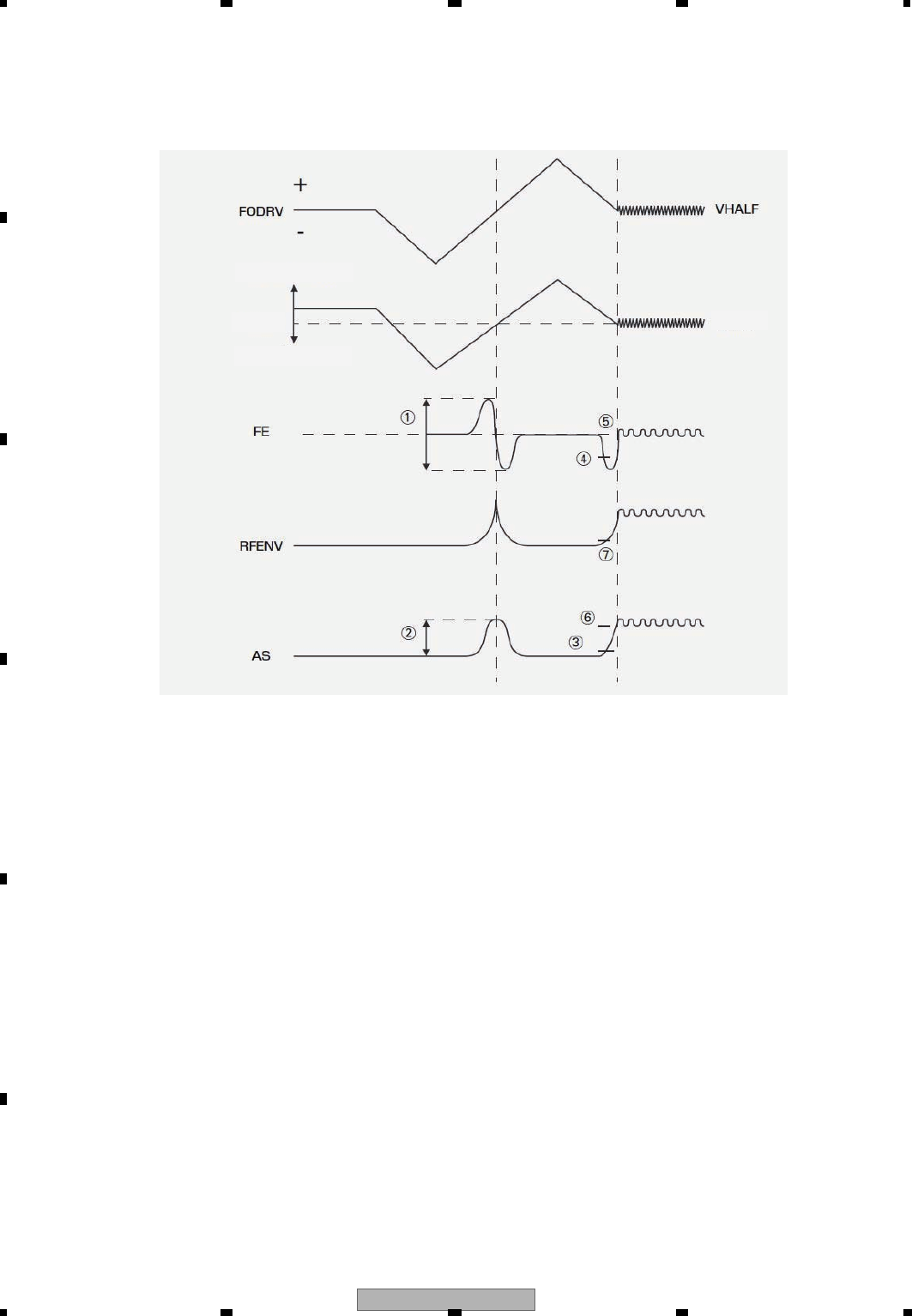
CX-3250
6
1234
1234
C
D
F
A
B
E
1.2 Servo block (MN2DS0018MAUB : IC1501)
At the servo block, focusing, tracking, servo control of traverse, spindle motor control and seek control are performed.
1.2.1 Focus close
After issuing the focus close command, both the DVD and the CD will perform the following processing.
1. Measurement and optimization of the signal level.
First the PU lens is driven in the direction getting away from the disc, then it is driven in the direction getting close
to the disc. At this time, each signal level of FE, AS and RFENV are measured at the focused focal point that the
lens passes, and the levels of FE and AS are optimized. (1 and 2 in the figure)
2. Focus adjustment
Next, after detecting the drawing level of FE and AS by driving the lens away from the disc, the focus loop filter is
activated and the focus is drawn. (3~6)
3. Confirmation of adjustment
Confirm the drawing at the signal level of AS and RFENV. (6, 7)
The signal levels of FE, AS and RFENV and the focus drive voltage can be checked by the focus search in the
test mode.
1.2.2 Tracking close
After issuing the tracking close command, both the DVD and the CD will perform the following processing.
1. Tracking brake
1/2 cycle of the track cross is measured and if the cycle is within the specified range, the brake pulse is output.
The output direction of the brake pulse is determined by the phase relationship of the OFTR and the TKC
(binary signal of TE) signals. When it is confirmed that the swinging of the lens against the disc has been controlled,
braking will be stopped and enters into drawing. If the drawing conditions are not met within 10 msec, after the brake
output, the brake will be ended and entered into drawing.
2. Tracking adjustment
Tracking drive hold processing by the OFTR signal will be performed.
3. Confirmation of adjustment
Checking is made that the number of track jumps within the specified period of time are at the designated numbers
or less. The time out for confirmation of adjustment is 8.4 msec. and retry is performed by the command from the
microcomputer.
Close to disc.
Lens
Late
Merging
point
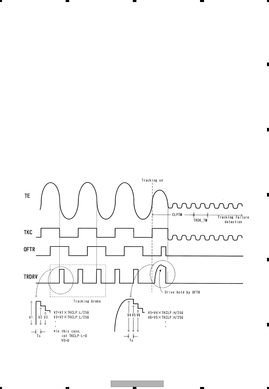
CX-3250 7
5 678
5678
C
D
F
A
B
E
Tracking-on process
1.2.3 Track jump
In this system, one of the three methods, interval jump, multi jump or traverse seek, is selected depending on the
number of target moving tracks.
1. Interval jump
Detailed seek can be performed to execute repeated track jump of 1 track, and it is used when the target track gets
close or at the time of seek operation to the adjacent track.
2. Multi jump
Both edges of the track cross signal TKC are counted, and track count move of the designated number is executed.
Furthermore, the CRG motor is driven according to the number of jumps.
3. Traverse seek
Track count by TKC is performed, and I control movement speed and seek it.
I minimize vibration of PU occurring for movement.
It indicates the setting for jump switching common to DVD and CD.
Types of target move number of jumps.
DVD
1~10 Interval jump
11~500 Multi jump
501~1000 Combination of multi jump and interval jump
1001~ Traverse seek (short)
CD
1~10 Interval jump
11~100 Multi jump
101~500 Combination of multi jump and interval jump
501~ Traverse seek (short)
The waveform of track jump is shown on the next page.
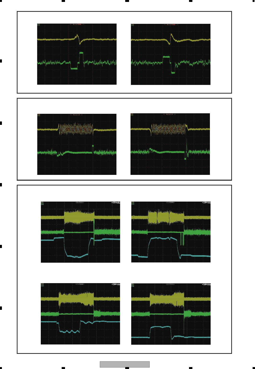
CX-3250
8
1234
1234
C
D
F
A
B
E
Interval jump (1 track) DVD
Outer peripheral jump Inner peripheral jump
Multi jump (32 track) DVD
Outer peripheral jump Inner peripheral jump
Traverse seek (1001 tracks) DVD
Outer peripheral jump Inner peripheral jump
Traverse seek (10 000 tracks)
Outer peripheral jump Inner peripheral jump
TE
TD
TE
TD
TE
TD
COP-COM
COP-COM
TE
TD
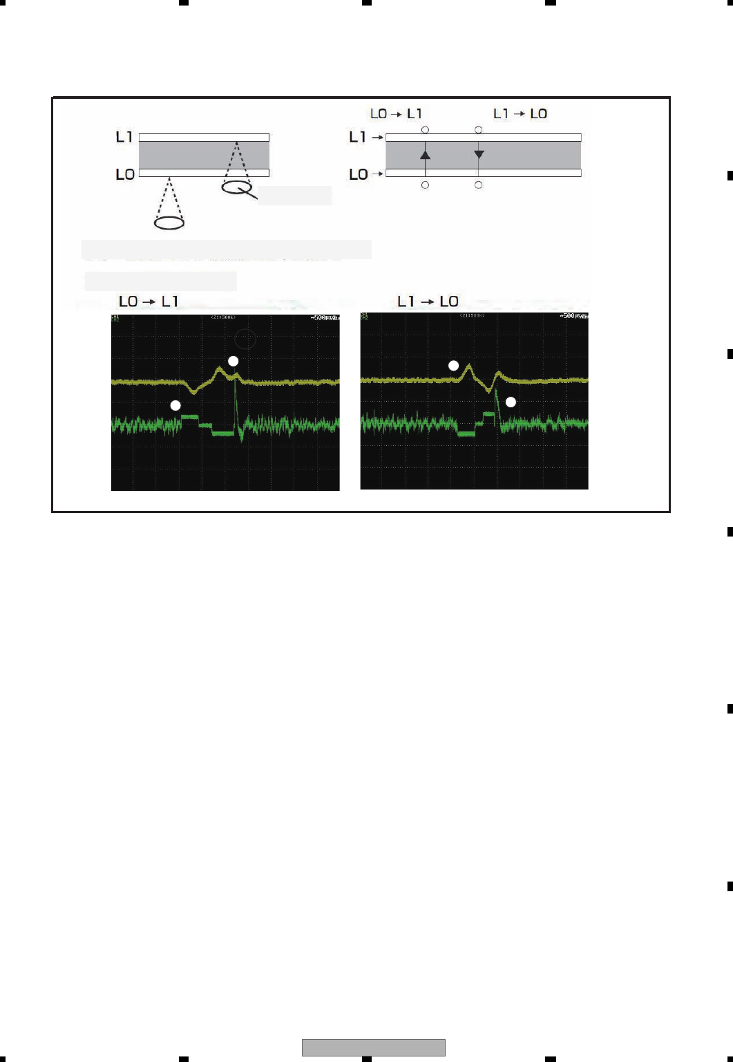
CX-3250 9
5 678
5678
C
D
F
A
B
E
1.2.4 Focus jump
Focus jump is a function compatible to 2 layers on one side or 2 layers on both sides. Looking from the object lens,
the layer close to the lens is called “layer 0” (L0) and the layer away from the lens is called “layer 1” (L1).
1.3 Auto adjustment function
All circuit adjustments are automated in this system.
Details of each auto adjustment are explained below.
1.3.1 VIN7, VIN8, VIN9, VIN10 offset cancel
Each signal from VIN7,8, 9 and 10 output by PU is converted to a digital signal by the AD converter in the servo block.
Offset cancel is a function to cancel input offset of the AD converter at the time of power ON.
1.3.2 VCO gain adjustment (VARI adjustment)
It has a function to absorb variation of VCO gain among individual LSI by learning so that auto adjustment is made to
maintain the VCO gain at a certain level. VCO is locked against the reference frequency for learning.
And, a frequency control value (FCNT) is read, and VARI register is adjusted so that the read value becomes the
same as the target FCNT value.
1.3.3 FE normalization adjustment
FE signal level measured at the time of focus close is adjusted so that it will become 190LSB at the digital equalizer
input stage.
FE
FD
Object lens
The waveform of the focus jump is shown below.
Focus jump waveform
The flow of the focus jump is shown below.
1. The tracking is opened by the layer being played back.
2. A command is issued to execute jump to the target layer.
3. The tracking is closed at the layer after the jump and the playback is resumed.
Incidentally, the process when the jump command is issued is as described below.
1. The lens is accelerated to the target layer until the FE signal detects the focus jump acceleration end level.
Acceleration will be ended by force, however, if the time for acceleration timeout has elapsed before detecting the
acceleration end level.
2. The drive voltage is not output until the FE signal detects the speed reduction start level, and the lens is moved by
inertia.
3. The lens speed is reduced from detection of the speed reduction start level until detection of the speed reduction
end level. Speed reduction will be ended by force, however, if the time for speed reduction timeout has elapsed
before detecting the speed reduction end level.
B
A
C
D
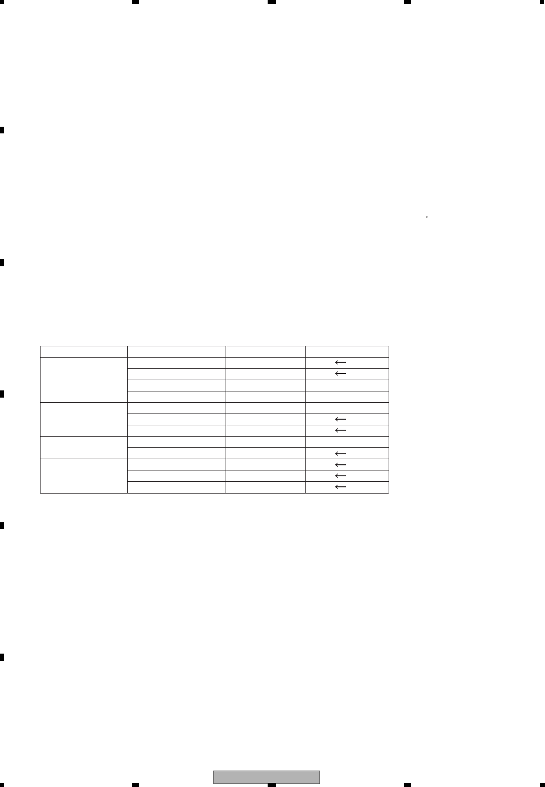
CX-3250
10
1234
1234
C
D
F
A
B
E
State
Power ON
F close
F close (after TBAL)
T close
Coefficient
VIN7 offset
VIN8 offset
VIN9 offset
VIN10 offset
FEPP(FEMAX-FEMIN)
AS MAX
FE normalization
TEPP(TEMAX-TEMIN)
TE normalization
F gain
T gain
AS normalization
DVD
05FB~0A17
05FB~0A17
-
-
1D84~6C08
No standard
No standard
2328~59D8
No standard
0100~0400
0100~0400
No standard
CD
0533~0B0C
0533~0B0C
2E18~A8CF
1E91~98D1
Note) Coefficient values are indicated in hexadecimals. In all cases, specifications
at the production line are described. For discs, TDV-582 is used for DVD and TCD-792 is used for CD.
1.4 CIRC block (MN2DS0018MAUB : IC1501)
The CIRC block includes the digital signal processing function (EFM modulation and error correction) of CD-DA and
CD-ROM and the digital servo processing function of the spindle motor.
1.5 DRC block (MN2DS0018MAUB : IC1501)
The digital read channel (DRC) is equipped with A/D converter, digital equalizer (DEQ), Adaptive filter, Viterbi
detector, digital PLL circuit, RISC interface and periphery circuits for reading of signal on optical disc.
The list of auto adjustment coefficient
1.3.4 Focus balance (FBAL) adjustment
The focus position is adjusted so that the RFENV will be the maximum at the time of focus close tracking open and
tracking close.
1.3.5 DPD amplitude adjustment
I perform the gain adjustment of the analog step so that the input signal of the DPD comparator of the TE generation
circuit of the DVD becomes constant.
1.3.6 Learning of tracking error amplitude
At the time of focus close and tracking open, the lens is oscillated in the track direction and adjusted so that the TE
amplitude level becomes 190 LSB at the digital equalizer input stage.
1.3.7 Tracking balance (TBAL) adjustment
At the time of focus close and tracking open, the lens is oscillated in the track direction and the balanced point where
the DC offset becomes zero is searched and adjusted by using the Newton-Raphson method.
1.3.8 OFTR adjustment
The binary threshold level is adjusted to make the OFTR signal into a binary digit.
1.3.9 AS normalization adjustment
The AS signal level is measured for the designated number of samples at the time of track closing, and after A/D
conversion at the ADSC, it is fine adjusted to become 64 LSB at the digital equalizer input stage.
1.3.10 Focus gain adjustment, tracking gain adjustment
At the time of tracking close, a disturbance is entered into the servo loop to adjust to the target gain intersection.
All auto adjustments can be confirmed by displaying the adjustment result in the test mode.
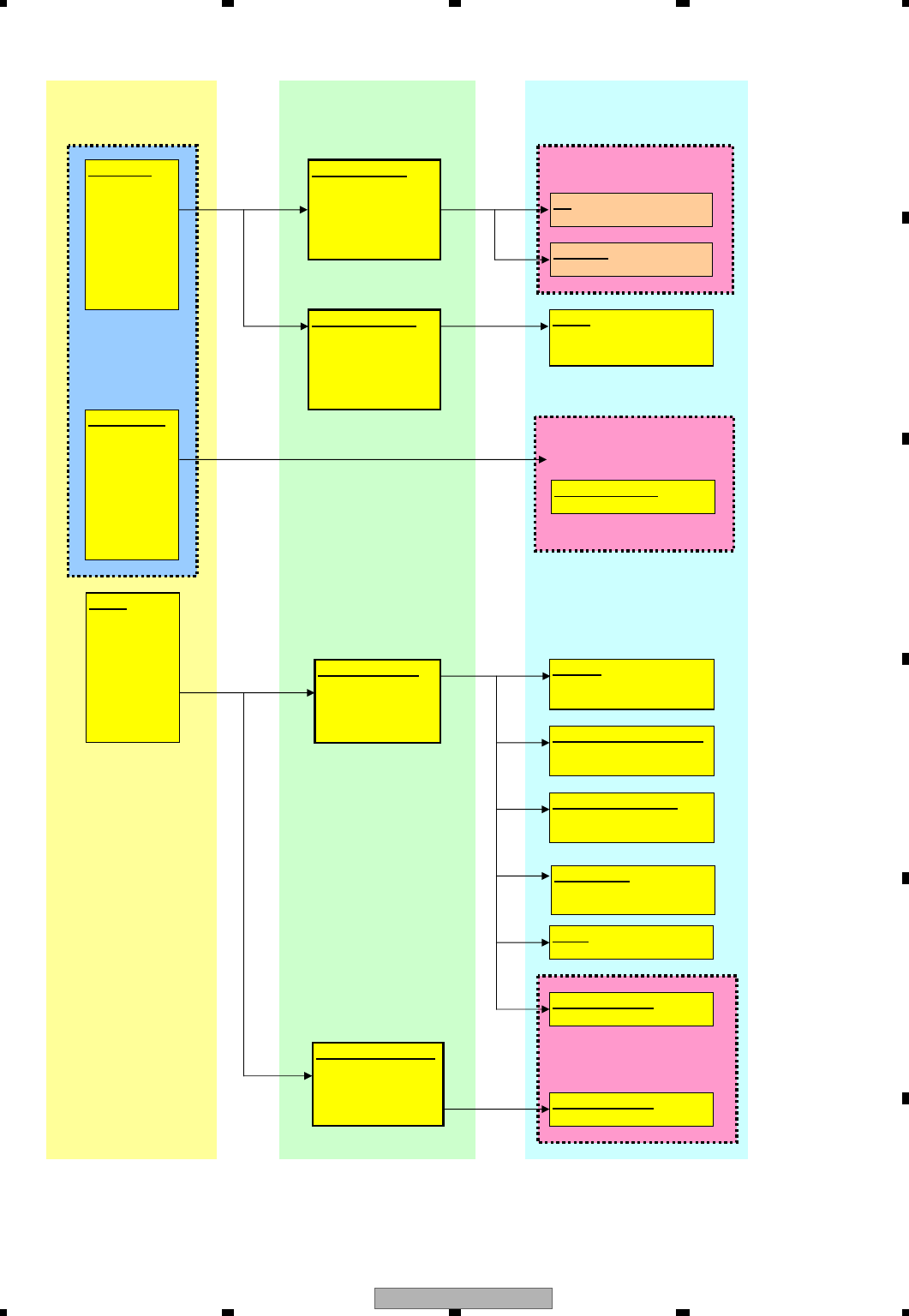
CX-3250 11
5 678
5678
C
D
F
A
B
E
1.6 LS1 Power Supply Map
VD8(Driver)
8 V+/-0.4 V
VD8(Reg)
8 V+/-0.4 V
VDD5
5 V+/-0.4 V
1chip Driver(8 V)
5 V Reg(VCC5)
5.0 V +/-0.1 V
IC1002
S-1133B50-U5
LD
Photo IC
5 V Reg(AVCC5)
5.0 V +/-0.1 V
IC1003
S-1200B50-M5
ADAC
IC1801
PCM1753DBQ
3.3 Reg(VCC33)
3.0 V<--->3.45 V
IC1004
NJM2885DL1-33
1.2 DC/DC(VCC12)
1.08 V<---> 1.32 V
IC1005
R1232D121B
DVD1chip(3.3 V)
SDRAM
IC1480
K4S641632N-LC75
Flash-ROM 1 (Program)
IC1402
S29AL016J70TFIC10H
Other
DVD1chip(1.2 V)
VD8V
HOST
Power Supply
Mecha inside
Power Supply
Pick Up Unit
CGY5000
1chip Driver
IC1201
BD8231EFV
DVD LSI
IC1501
MN2DS0018MAUB
Supply
IC
Flash-ROM 2 (Data)
IC1401
S29AL016J70TFIC10H
USB Circuit
IC1951
TC7SZU04FU
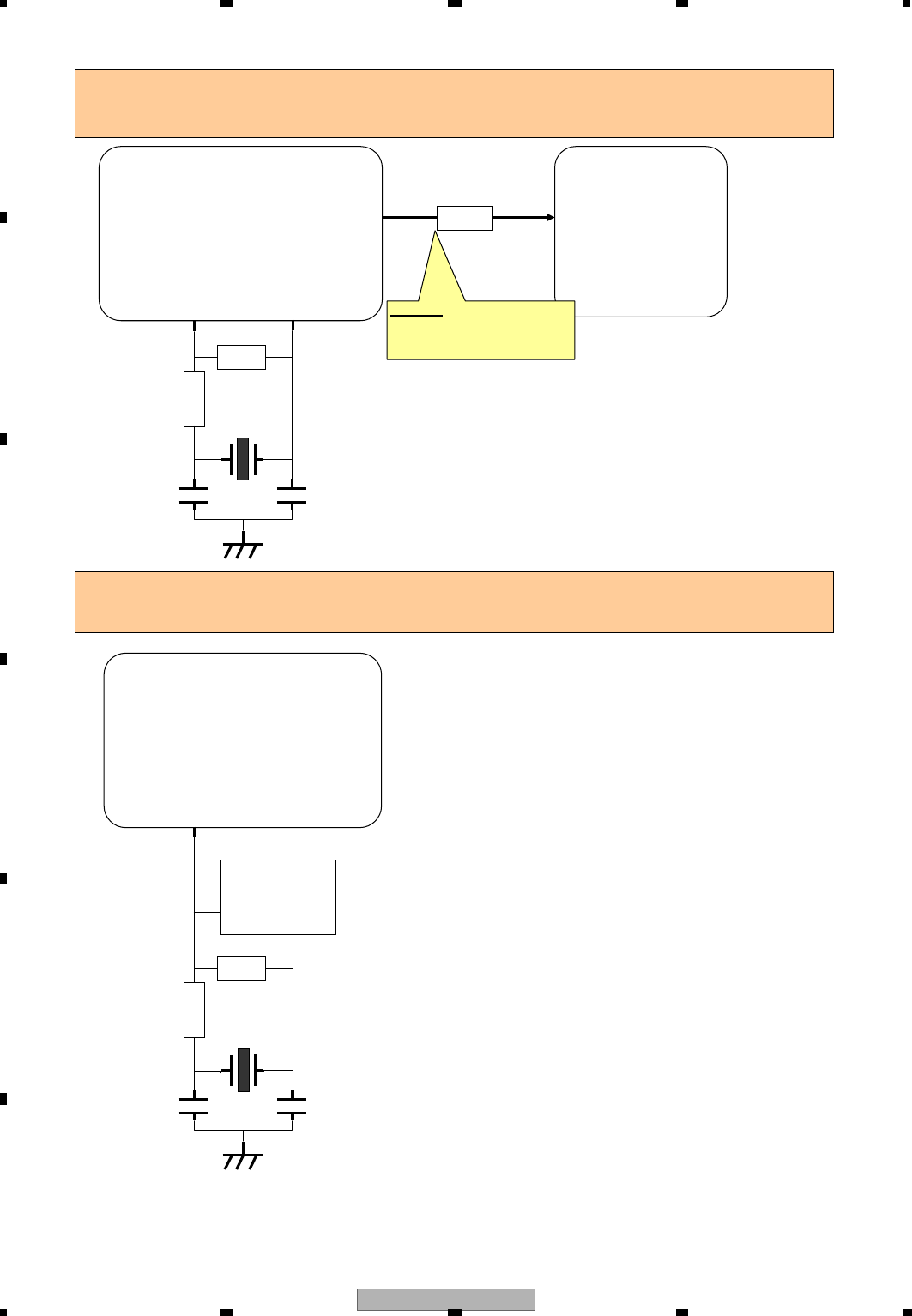
CX-3250
12
1234
1234
C
D
F
A
B
E
1.7 LS1 Clock circuit
R1503
C1510
12 pF
1Moh
m
X1501
CSS1768
27 MHz
R1501
C1512
10 pF
156pin 155pin
OSCO OSCI
IC1501
DVD-LSI
MN2DS0018MAUB
IC1801
Audio-DAC
PCM1753DBQ
DACCLK
or 36.864 MHz
220ohm
R1508
R1952
C1951
10 pF
1 Mohm
680 ohm
X1950
CSS1760
48 MHz
R1953
C1952
10 pF
50pin
USB_Clock
IC1501
DVD-LSI
MN2DS0018MAUB
IC951
TC7SZU04
2pin(IN_A)
4pin(OUT_Y)
1200ohm
FU
[Outline]
By connecting a 27 MHz crystal oscillator to DVD-LSI (IC1501), DACCLK for externally connected Audio-DAC
is formed and supplied by the clock generator inside the DVD-LSI in addition to the clock used inside the LSI.
[USB_Clock outline]
By connecting a 48 MHz crystal oscillator to DVD-LSI (IC1501), clock is formed and supplied by the clock
generator inside the DVD-LSI in addition to the clock used inside the USB circuit.
33.868 8 MHz
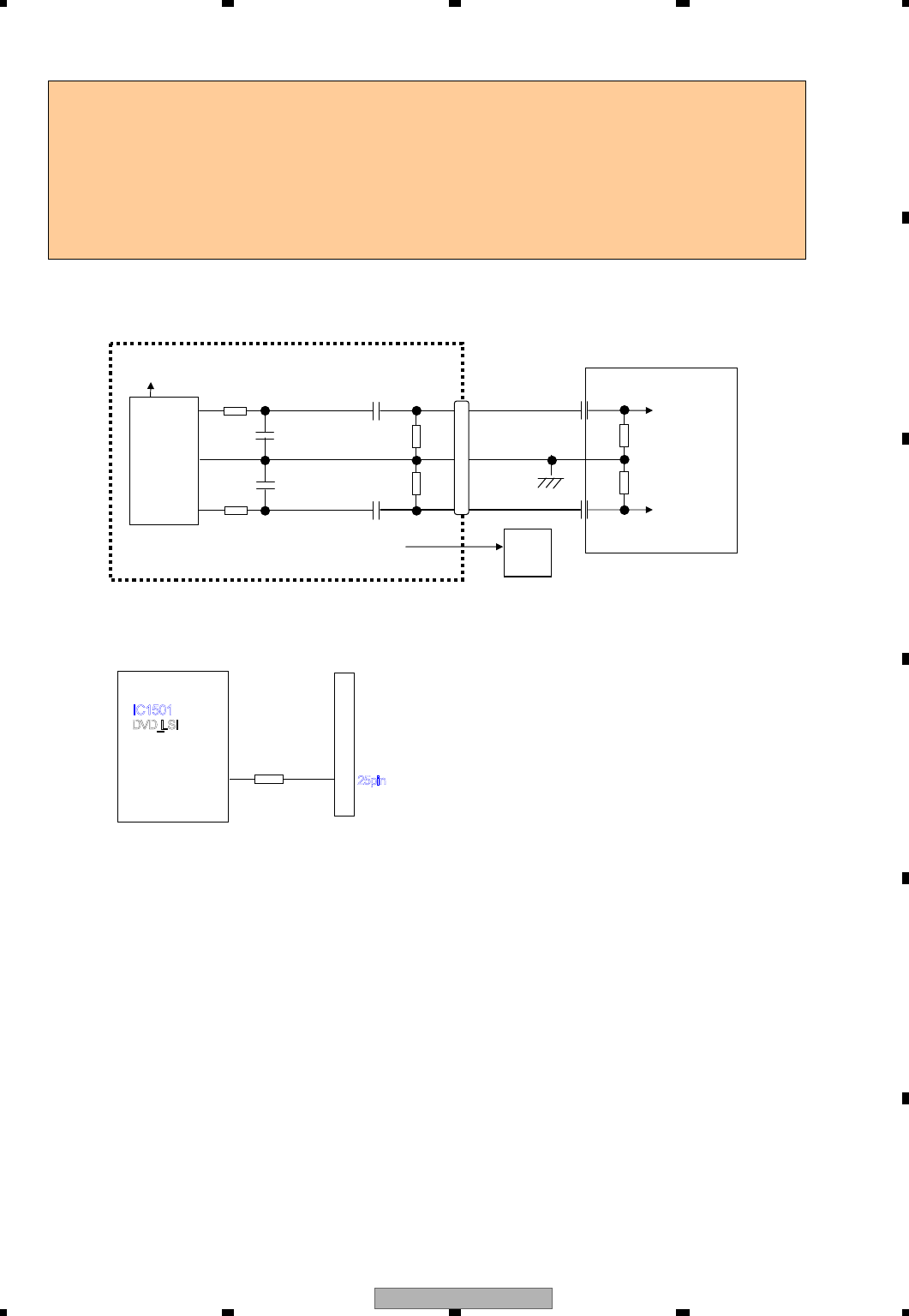
CX-3250 13
5 678
5678
C
D
F
A
B
E
1.8 LS1 Audio circuit
[Analog audio signal]
[Digital audio signal]
Zo=820 ohm
AVCC5
Radio audio circuit
17 pin
(Lch)
A
udio GND
LS1 Mechanism module
Audio DAC
(PCM1753)
15 pin
(Rch)
14,16,18 pin
(AudioGND)
fc=88 kHz
MUTE
Circuit
AMUTE 8 pin
47 kohm or more
47 kohm or more
IC1801 820 ohm
R1804
C1804
R1803
C1803
C1802
C1801
4.7 uF
4.7 uF
R1802R1801
100 kohm
100 kohm
CN1901
[Outline]
1 Analog audio signal
Serial 3 line digital output + DACCLK (audio clock) output from DVD-LSI (IC1501) are converted to
analog audio signal by Audio-DAC (IC1801), and are output from HOST IF connector (CN1901).
Furthermore, analog MUTE signal is also output from DVD-LSI (IC1501) via HOST IF connector
(CN1901) simultaneously.
2 Digital audio signal (IEC60958/IEC61937)
Digital audio signal (IEC60958/IEC61937), output from DVD-LSI (IC1501), is output via Multi-ch/Ripping
IF connector (CN1901).
25pin
(IECOUT)
IC1501
DVD_LSI
152pin
CN1901
R1504
12 ohm
820 ohm
1 800 pF 1 800 pF
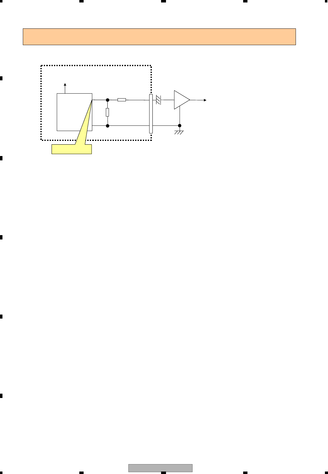
CX-3250
14
1234
1234
C
D
F
A
B
E
1.9 LS1 Video circuit
[Outline]
Composite signal is output from DVD-LSI (IC1501), and output from HOST IF (CN1901).
DVD LSI
(DV5U)
VCC33
Zo=300 ohm
LPF & 75 ohm Video
19 pin(CVBS)
20 pin
LS1 Mechanism module
(*1)
138pin:Comopsite
CN1901
IC1501 200 ohm
100 ohm
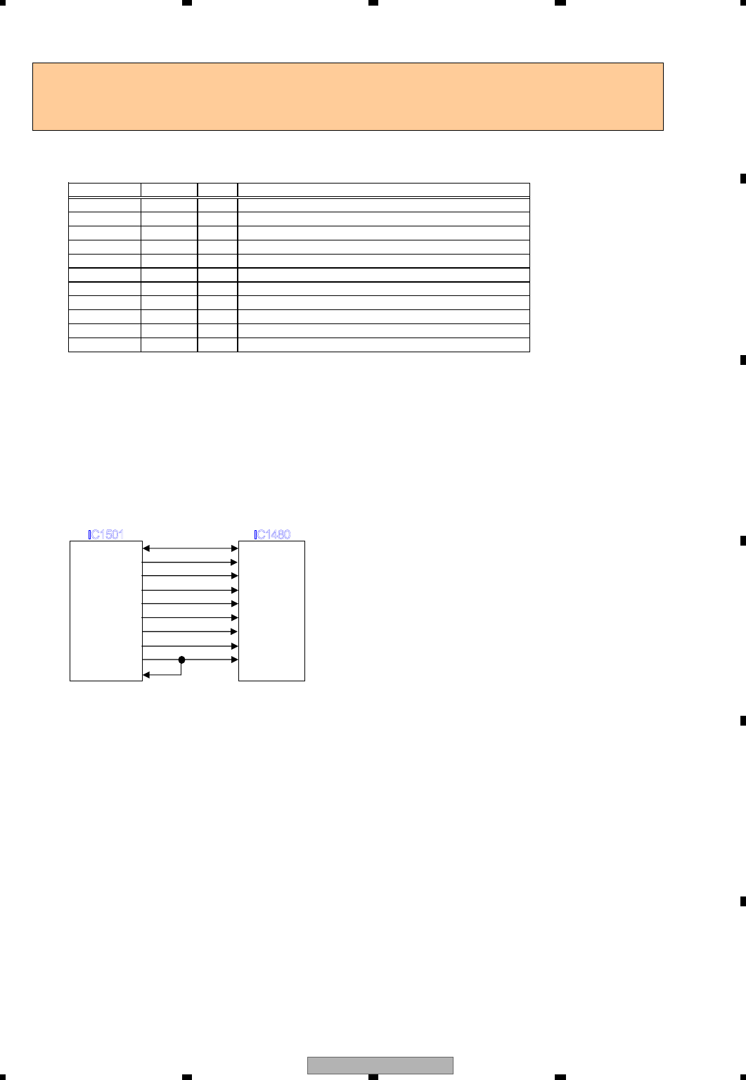
CX-3250 15
5 678
5678
C
D
F
A
B
E
1.10 LS1 SDRAM I/F
SDRAM interface
*When viewed from DVD-LSI
Signal Name Bits I/O
MDQ[15:0] 16 I/O
MA[11:0] 12 O
BA[1:0] 2 O
NRAS 1 O
NCAS 1 O
NEW 1 O
NCS 1 O
DQM[0] 1 O
DQM[1] 1 O
MCK 1 O
MCKI 1 I
SDRAM specifications
Data bus width: 32 bit
Operating frequency: 121.5 MHz
CAS latency=3
8 word burst transfer
Manual precharge
CAS before RAS refresh (Auto refresh)
SDRAM connection configuration
DVD-LSI SDRAM
IC1501 IC1480
MDQ[15:0] DQ[15:0]
MA[11:0] A[11:0]
BA[1:0] BA[1:0]
NRAS XRAS
NCAS XCAS
NEW XWE
DQM[1:0] DQM[1:0]
NCSM XCS
MCK CLK
MCKI
Description
Data bus of external SDRAM
SDRAM address
SDRAM bank address
RAS signal of SDRAM
CAS signal of SDRAM
Write enable signal of SDRAM
Chip select signal of SDRAM
SDRAM data mask 0
SDRAM data mask 1
Clock input to SDRAM
Clock input for data input from SDRAM
[Outline]
It is a memory for realizing the AV decoding function of DVD-LSI (IC1501). It is used for various purposes
such as buffering of stream data before decoding, working area for decoding, and storing of AV data or
output data after decoding.
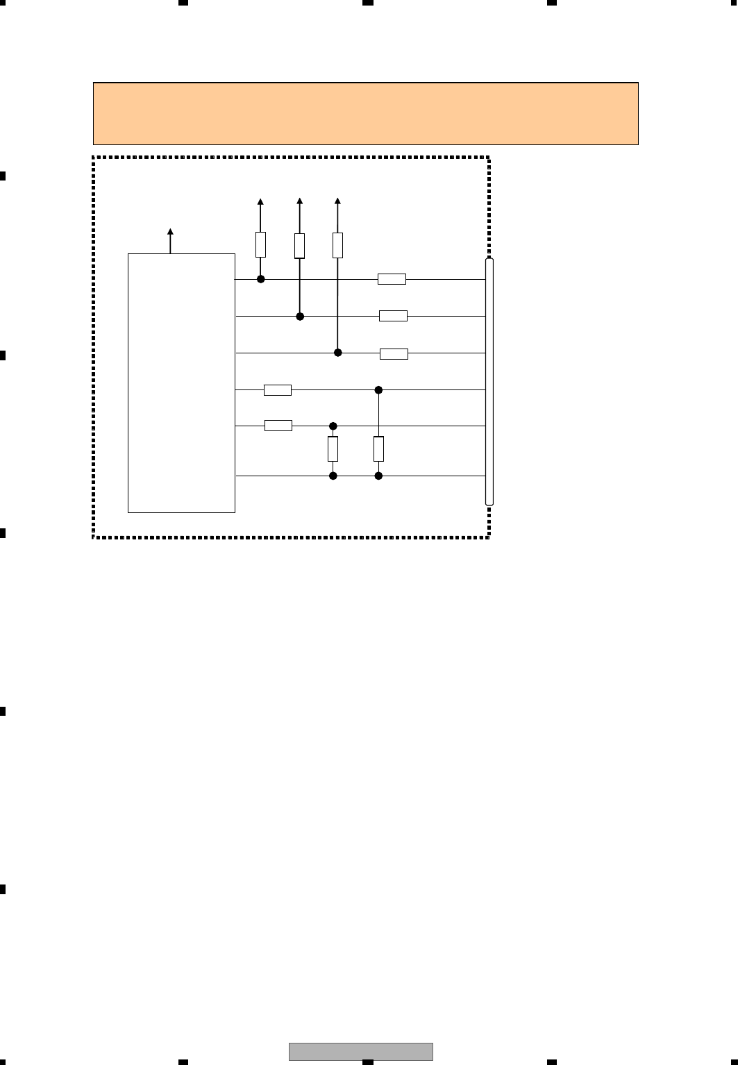
CX-3250
16
1234
1234
C
D
F
A
B
E
[Outline]
It inputs a D-/D+ signal into DVD - LSI (IC1501) than HOST IF (CN1901).
It uses CP_RESET, SDA, SCL by the iPod certification.
DVD LSI
(DV5U)
VCC33
CN1901
IC1501
R 1951
28pin(SDA)
29pin(RESET)
VCC33
VCC33
VCC33
1.11 LS1 USB(iPod)circuit
LS1 Mechanism module
6.8 kohm
10 kohm
24 ohm
15 kohm
24 ohm
15 kohm
180 ohm
180 ohm
100 ohm
22pin(D-)
23pin(D+)
24pin(DGND)
27pin(SCL)
R 1955
R 1954
R 1950
R 1543
R 1544
R 1532
144pin
(LOUT)
146pin
(ROUT)
47pin
(I2C_SC)
46pin
(I2C_SDA)
61pin
(CP_Reset)
R 1527
R 1546
R 1535
6.8 kohm
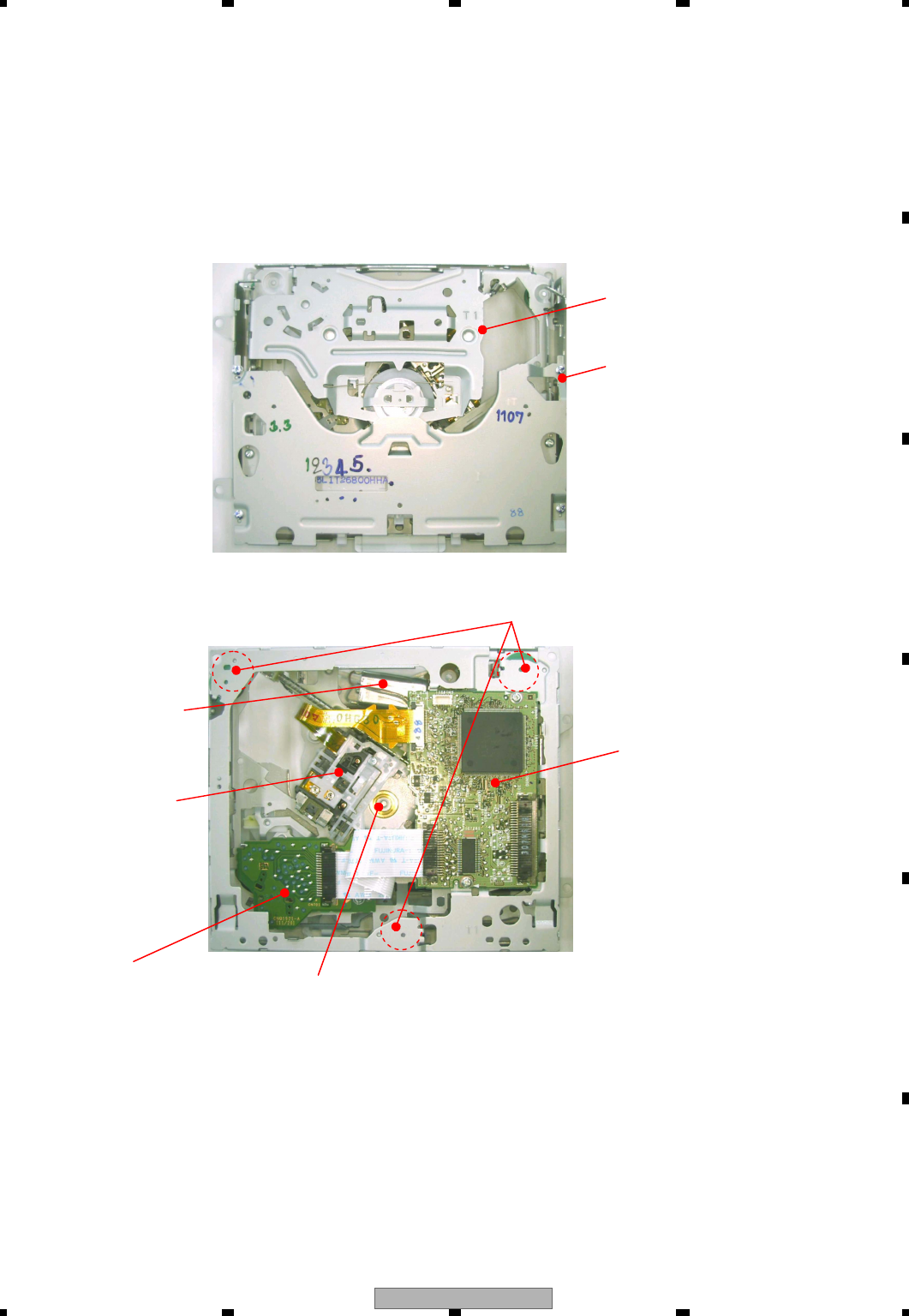
CX-3250 17
5 678
5678
C
D
F
A
B
E
2. MECHANISM DESCRIPTIONS
Construction
CRG motor
PU Unit
Spindle motor
Module PCB
Connector PCB
Damper
CRG mechanism
Upper/Under Frame
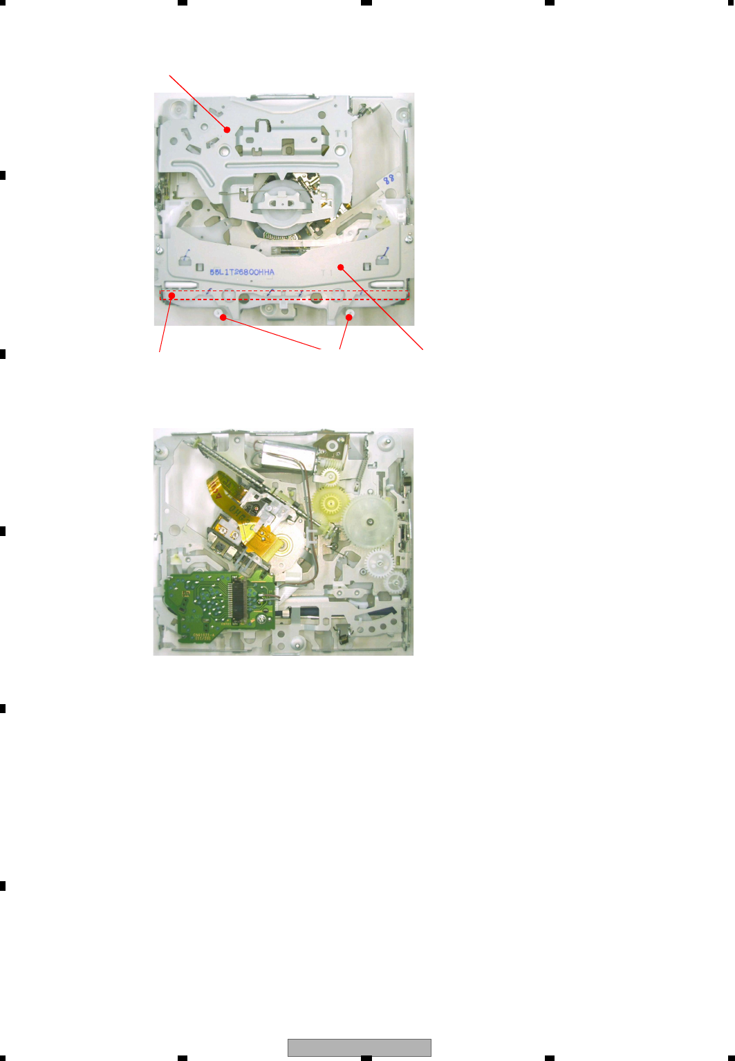
CX-3250
18
1234
1234
C
D
F
A
B
E
State of CRG mechanism
Disc guide assy
Clamper arm assy
SW armRoller arm assy
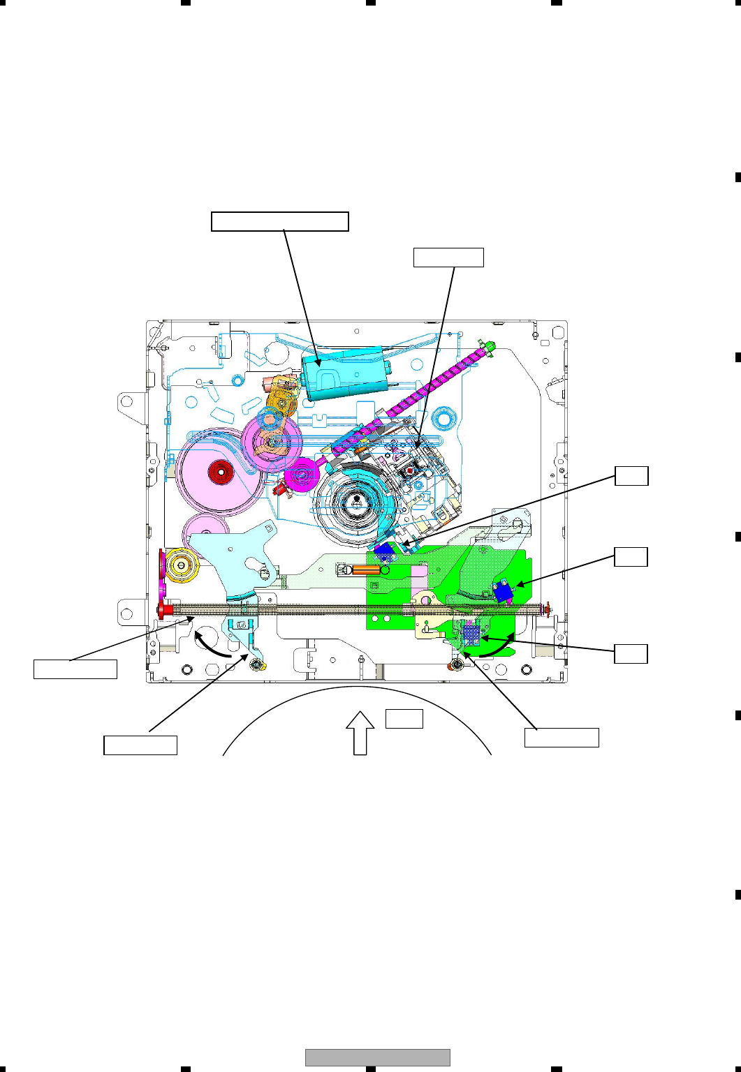
CX-3250 19
5 678
5678
C
D
F
A
B
E
Load carriage motor
PU unit
SW3
SW2
SW1
SW arm L SW arm R
Roller
DISC
Disc loading operation
1.When the disc is inserted, the SW arm L and R rotate and then SW1 turns ON from OFF.
By the SW1 turning ON from OFF, the load carriage motor starts and then the rubber roller rotates.
2.In the case for a 12cm disc, SW1 is turned OFF from ON by the SW arm being opened widely and then the
microcomputer determines that the disc is 12cm.
3.In the case for a 8cm disc, SW arm does not open widely, so SW1 is not turned OFF from ON but goes into the clamp
movement and then the microcomputer determines the disc to be 8cm.
(SW arms are jointed on both sides, and even if one side is pushed, the joint part is locked and the arms do not open
more than a fixed width. (SW1 is not turned OFF from ON.))
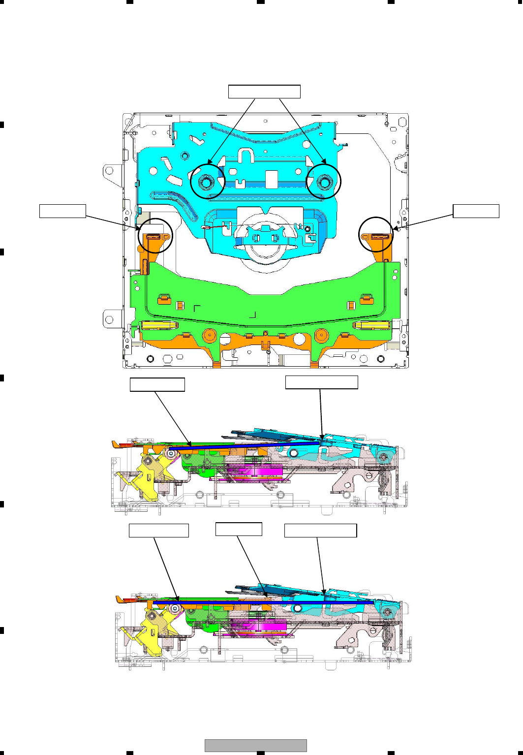
CX-3250
20
1234
1234
C
D
F
A
B
E
1. 8cm disk is centered with the guide pin and the centering pin.
2. 12cm disk passes under the guide pin and the centering pin, and is centered at the mechanism interior position.
Centering pin
8cm disc
Centering pin
Guide pin Guide pin
Guide pin Centering pin12cm disc
Disc centering mechanism
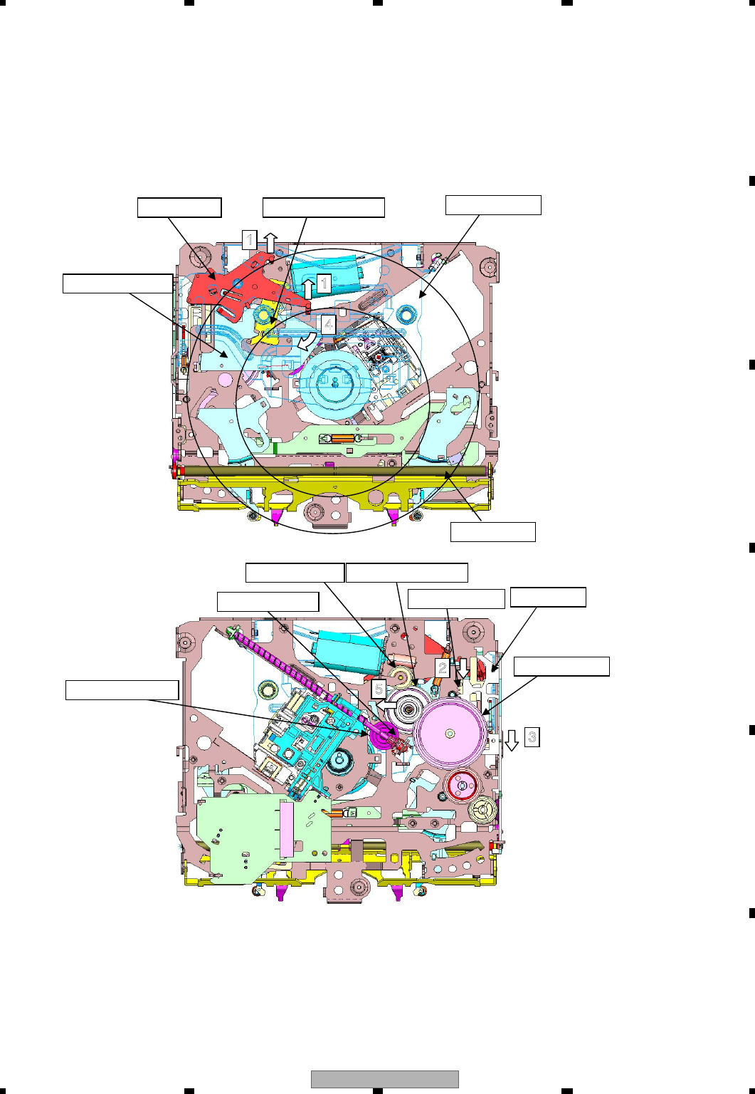
CX-3250 21
5 678
5678
C
D
F
A
B
E
1
Rubber roller
1
4
Clamp arm
Detection arm
Switching lock arm
Switching idler arm
3
2
5
Jumping rack
Worm wheel
Drive lever
Feed screw gear
Switching idler gear
Rack drive gear
Feed drive gear
Clamp Operation Structure
1.Drive the detection arm at the position where 8 or 12 cm disc is centered on the spindle.
2.Detection arm matches the jumping rack with the rack drive gear.
3.The drive lever that was jointed with the jumping rack slides and then lowers the clamp arm (it clamps the disc.).
At the same time, it rotates the roller arm and separates the rubber roller from the disc.
Moreover,rotation of the roller arm releases the upper and lower mecha locks and completes the clamp operation.
4.After the completion of the clamp operation, the control by the cam above the drive lever is released and then the
switching lock arm rotates.
When the same arm rotates, the switching idler gear is separated from the rack drive gear and meets with the feed screw
drive gear and then the carriage operation is executed.
Ejecting Operation
1.It starts the ejecting operation in the reverse order of above procedures when the load carriage motor rotates in the
reverse direction and the pick up is sent to the inner periphery with the home SW ON or more.
2.Ejection is completed when SW1 goes OFF->ON->OFF for 12cm disc.
3.Ejection is completed when SW1 goes ON->ON->OFF for 8cm disc.
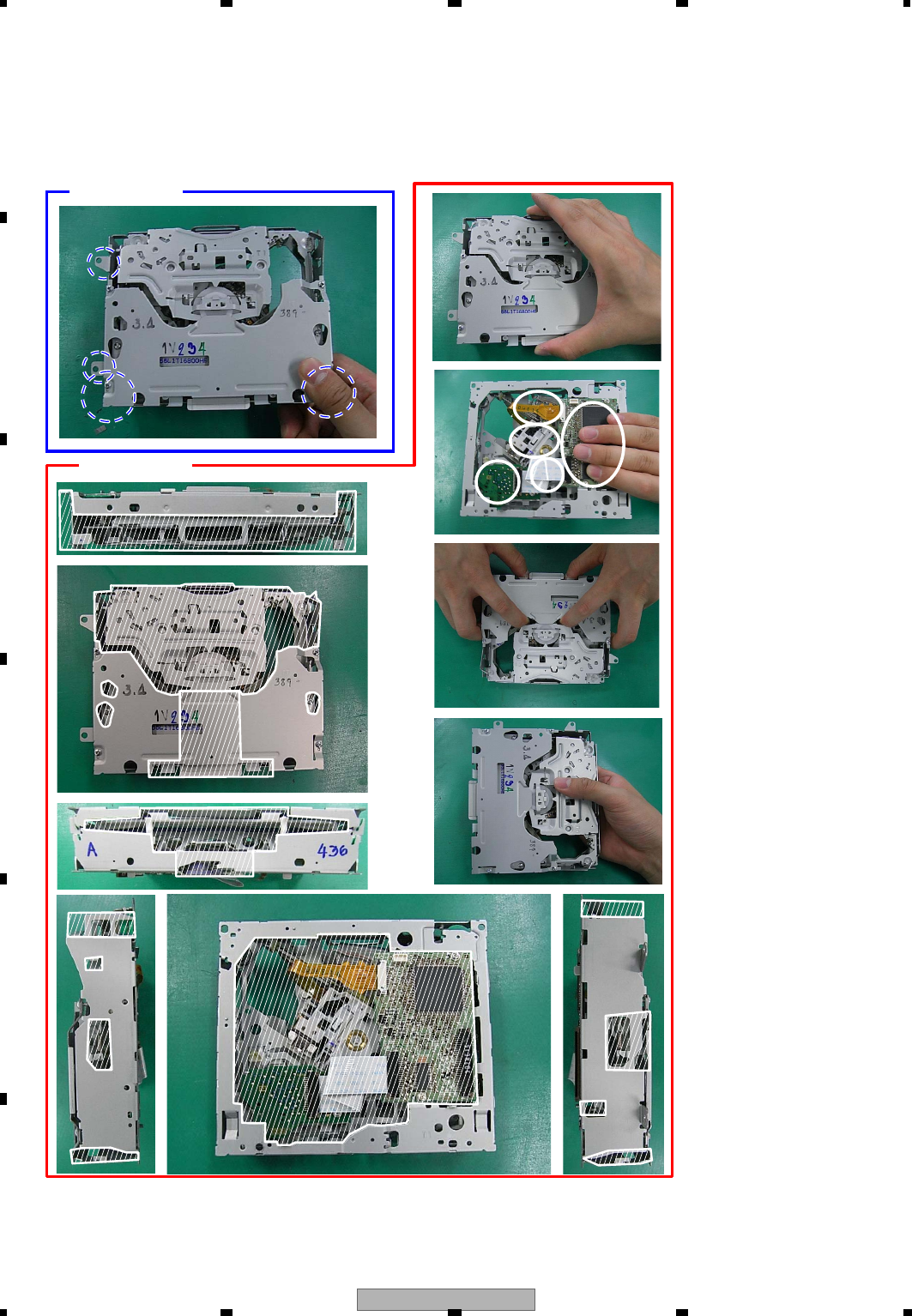
CX-3250
22
1234
1234
C
D
F
A
B
E
3. DISASSEMBLY
1.Have a specified part.
Please note that holding the front part of the upper frame or the CRG mechanical part,
or inserting a foreign substance could cause deformation.
Handling OK
Handling NG
How to have it
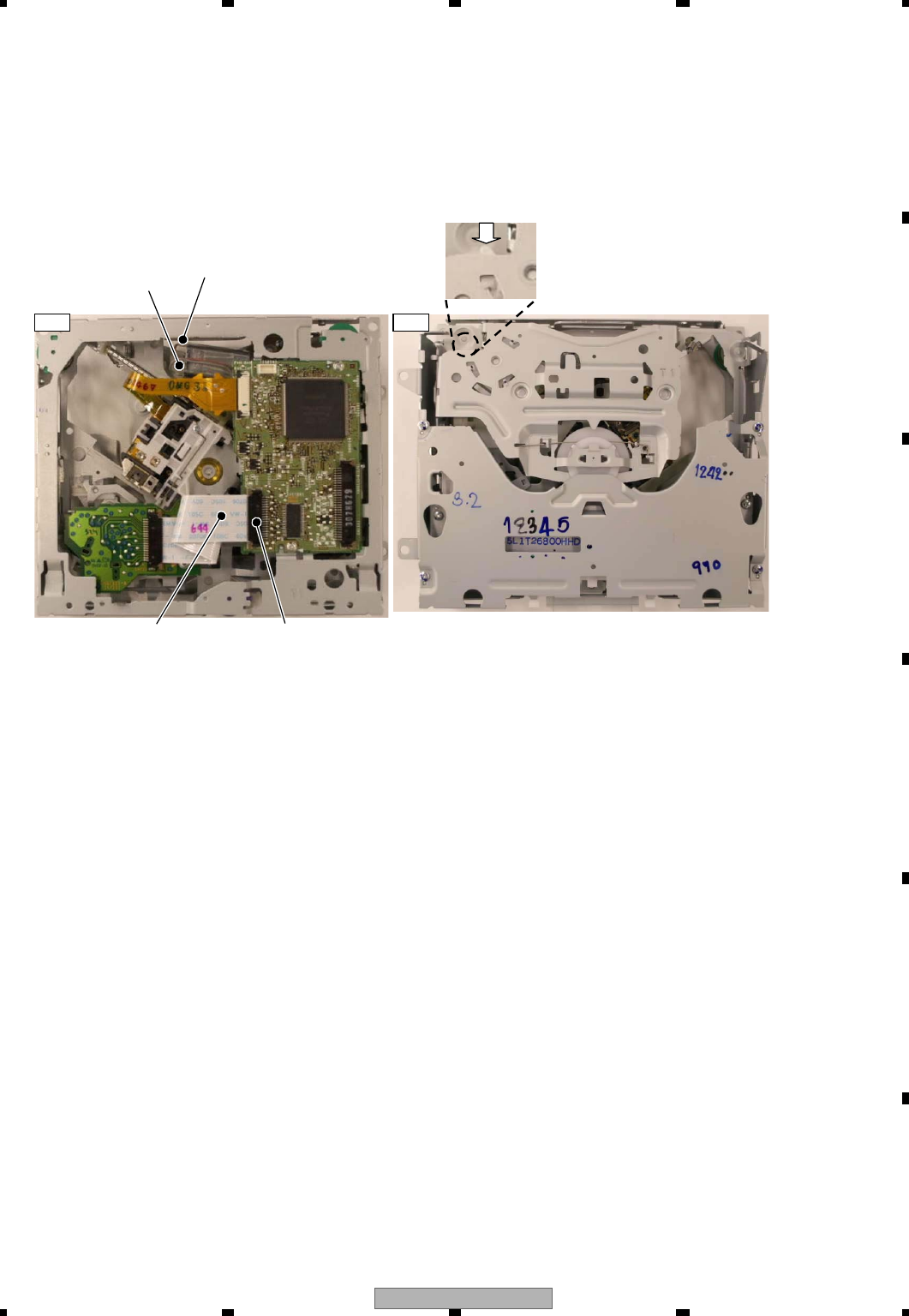
CX-3250 23
5 678
5678
C
D
F
A
B
E
Connector (relay FFC)
Relay FFC
Fig. 1 Fig. 2
GND the brown line
4V to the gray line
Mecha Module_Bringing into the Clamp State with No Disc Loaded
1. Remove the relay FFC from the connector on the module PCB side (Fig. 1).
(Precaution) When it is difficult to apply 4V to the motor in procedure 2 below, remove the connector on the relay
PCB side, then remove the FFC, and remove the solder of the CRG motor lead and apply voltage to the lead.
2. Push the Disc detection arm while applying 4V to the CRG motor (Fig. 2)
By this action, the mecha moves to the clamp state and the PU moves to the outer periphery.
3. Stop the motor when the PU comes to the vicinity of the intermediate periphery.
(Precaution) If the PU goes to the outer most periphery, it idles.
It is not a problem, but please try not to let it idle as much as possible.
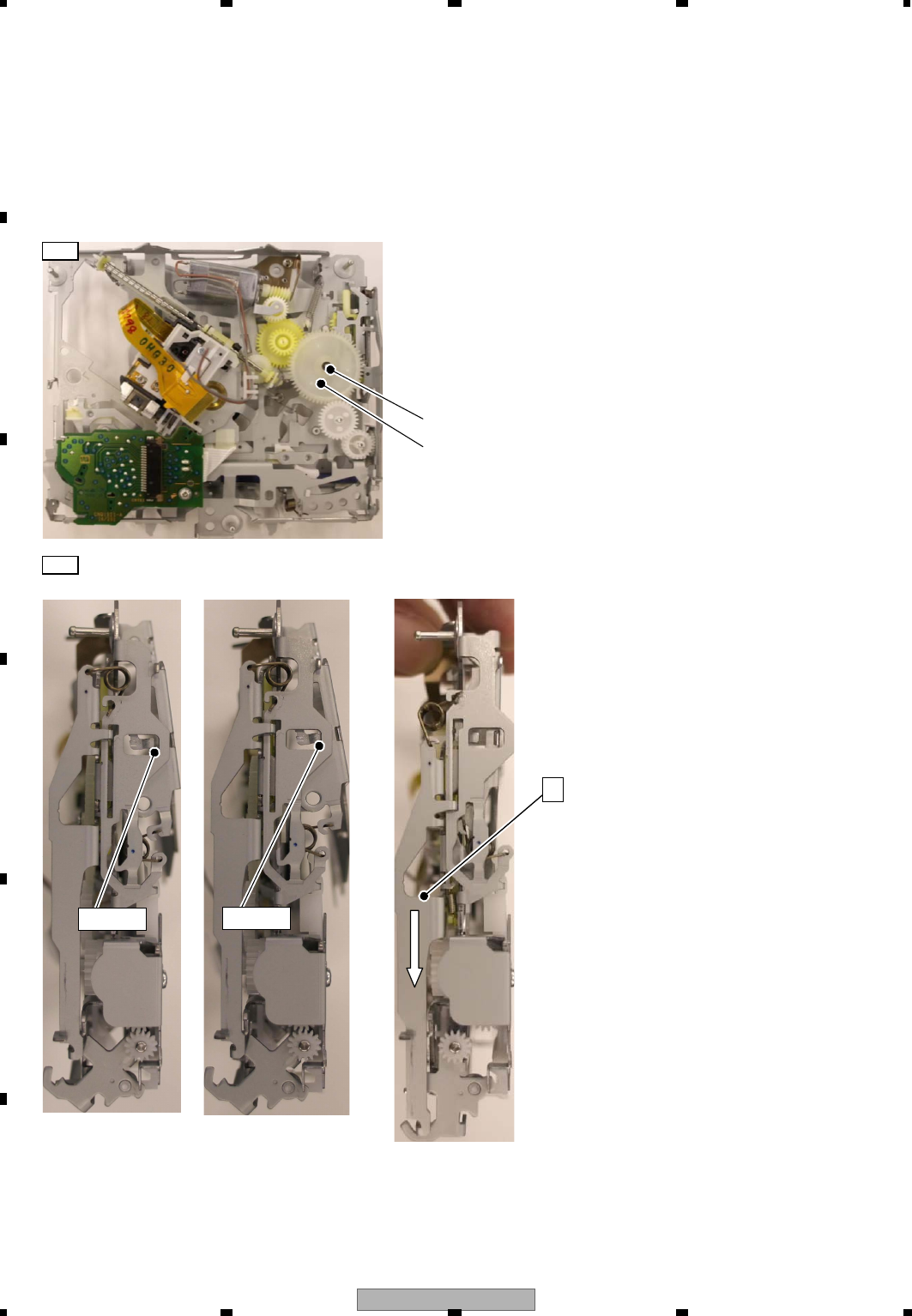
CX-3250
24
1234
1234
C
D
F
A
B
E
T-case washer
Drive gear
Fig. 1
Fig. 2
b.Open-lock state c.Clamp state with no disc loaded
CRG Mecha_Bringing into the Clamp State with No Disc Loaded
1.Remove the CRG mecha assy according to the “Removing the CRG Mecha assy” manual
(mecha is in the ejecting state).
2.Remove the T-case washer and then remove the drive gear. (Fig. 1)
3.Lift the clamp arm assy until it is in the state shown in Fig. 2_b (open-lock state).
4.Put your finger on the area A of Fig. 2_c and then slide it to the direction of the arrow (the direction of the playing state).
5.Push down the clamp arm.
(Precaution) When bringing the CRG mecha into the ejecting state again, install the drive gear after sliding the drive lever
and bringing it to the ejecting state, in order to prevent the cog of the pinion in the drive gear from chipping at the time of
its installation.
a.Ejecting state
There is a
space There is
no space
A
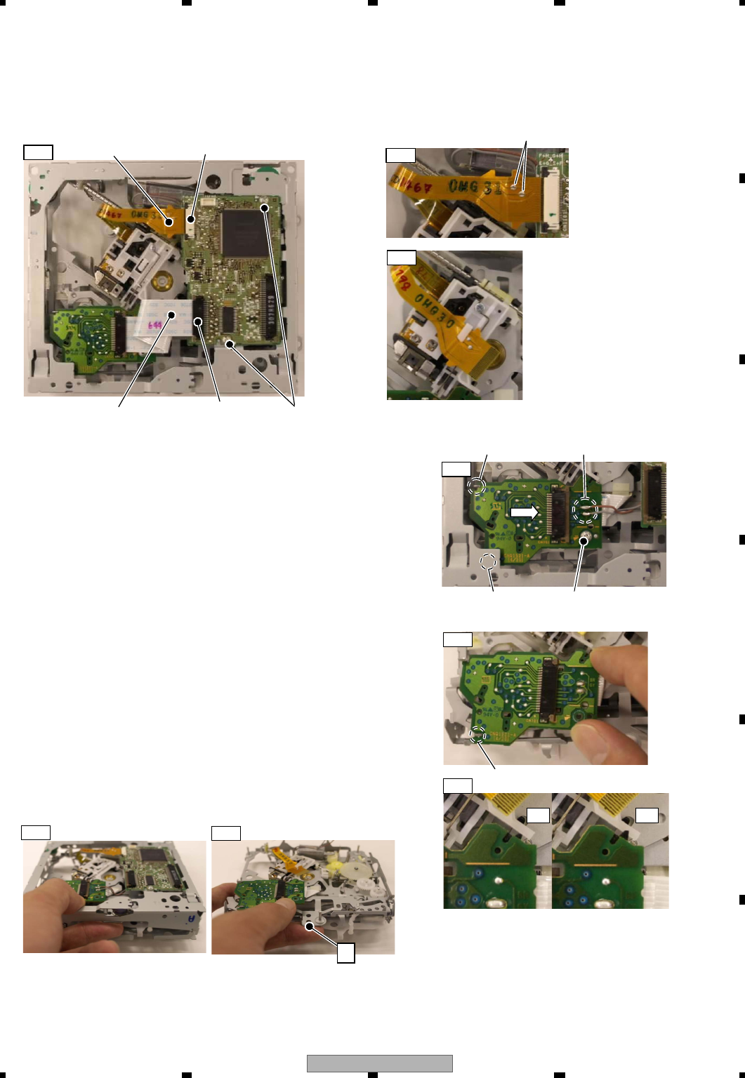
CX-3250 25
5 678
5678
C
D
F
A
B
E
Connector (pick up FPC)
Connector(Relay FFC) PCB clinch screw
Short-circuit
Fig.1
Fig. 2
Fig.3
Pick up FPC
Relay FFC
Fig. 4
Solder on the lead
Relay PCB clinch screw
Hook A
Hook B
Fig. 5
Hook B
Fig. 6
Fig. 7 Fig. 8
Removing the Module PCB
1.Short-circuit two spots on the land of the pick up FPC. (Fig. 1)
2.Remove the pick up FPC and the relay FFC from the connector. (Fig. 2)
3.Temporarily attach the pick up FPC to the pick up rack. (Fig. 3)
(in order to prevent the damage to the pick up FPC)
4.Remove the two PCB clinch screws and then remove the module PCB. (Fig. 2)
Removing/Installing the Relay PCB
Removing)
1.Remove the relay FFC from the connector
(remove both sides so that the entire FFC will be removed). (Fig. 2)
2.Remove the solder on the lead for the CRG motor. (Fig. 4)
3.Remove the one relay PCB clinch screw. (Fig. 4)
4.Slide the relay PCB to the direction of the arrow and then remove
the relay PCB from the hook A and the hook B. (Fig. 4)
5.Turn the relay PCB over and then remove the SPDL motor FFC
from the connector.
Installing)
1.Check the mecha is in the ejecting state (disc-load suspended state).
When it is not in the ejecting state, apply 4V to the lead (motor) and
then bring it to the ejecting state (4V to the brown line and GND the gray line).
2.Fit the SPDL motor FFC to the connector (back of the relay PCB).
3.Hold the relay PCB so that it does not touch the SW knob as in Fig. 5.
4.Insert it into the hook B as it is a little off to the clockwise direction.
(Precaution) This is to prevent the SW knob from getting into the NG
position as in Fig. 6.
5.Push down the relay PCB lightly and then rotate it to the
counterclockwise direction.
It sets the relay PCB in the hook A and the positioning dowel.
(Precaution) Pay attention so the SW knob will not get onto the PU rack.
(Fig. 6)
6.As in the Figures, while supporting the location A with your fingers,
screw the relay PCB. (Fig. 7 / Fig. 8)
7.Solder the lead for the CRG motor.
8.Fit the relay FFC to the connector.
NGOK
A
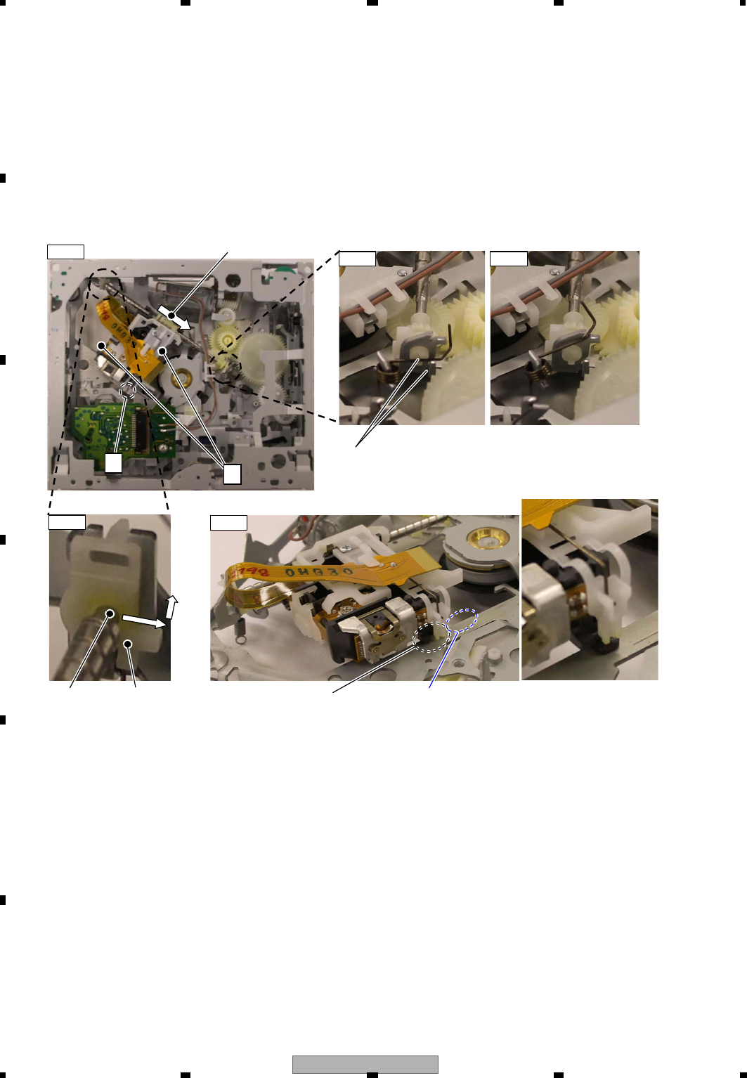
CX-3250
26
1234
1234
C
D
F
A
B
E
Fig. 2a
Permanently hooked position Temporary hooked position
Fig. 2b
Slide to the direction of inner periphery
Fig. 1
Fig. 3 Fig.4
Regularly installed position Install avoiding the
area with blue broken
line (the connected
metal plate part)
The spring is installed under the resin flange and inside
the bended metal plate.
Outside holder
Back end of
the feed screw
Removing the PU Unit
1.Bring to the clamp state with no disc loaded according to the “Bringing into the Clamp State with No Disc Loaded
(Motor Drive)” manual.
2.Remove the module PCB according to the “Removing the Module PCB” manual.
3.Hook the feed screw biasing spring on the temporary hook (Fig. 2b). Be careful not to get injured by the tip of the spring.
4.Hold the PU at the location A in Fig. 1 and slide and scoot it to the direction of the inner periphery.
5.As in Fig. 3, shift the back end of the feed screw to the side and then to above and remove it from the outside holder.
6.Remove the tucking joint for the chassis at the location B and the PU unit by lifting them up without changing their
position and then remove the PU unit.
(Precaution) When installing the PU again, make sure to tuck the chassis in B and the PU unit (Fig. 4) first.
Moreover, do not forget to permanently hook the feed screw biasing spring (Fig. 2a).
Adjustments to the PU after its installation should be made according to the service manual.
Sending the PU to the outer periphery
1.Bring to the clamp state with no disc loaded according to the “Mecha Module_Bringing into the Clamp State with
No Disc Loaded” manual.
(Precaution) The relay FFC must be removed for certainty in order to prevent the IC damage.
2.Apply 1.5V to the CRG motor and then transfer the PU to the outer periphery.
(Precaution) Do not forget to reinstall the relay FFC after sending the PU to the outer periphery and take the
necessary measures.
[Installation NG]
The chassis is not tucked
between the PU case and the
PU rack.
A
B
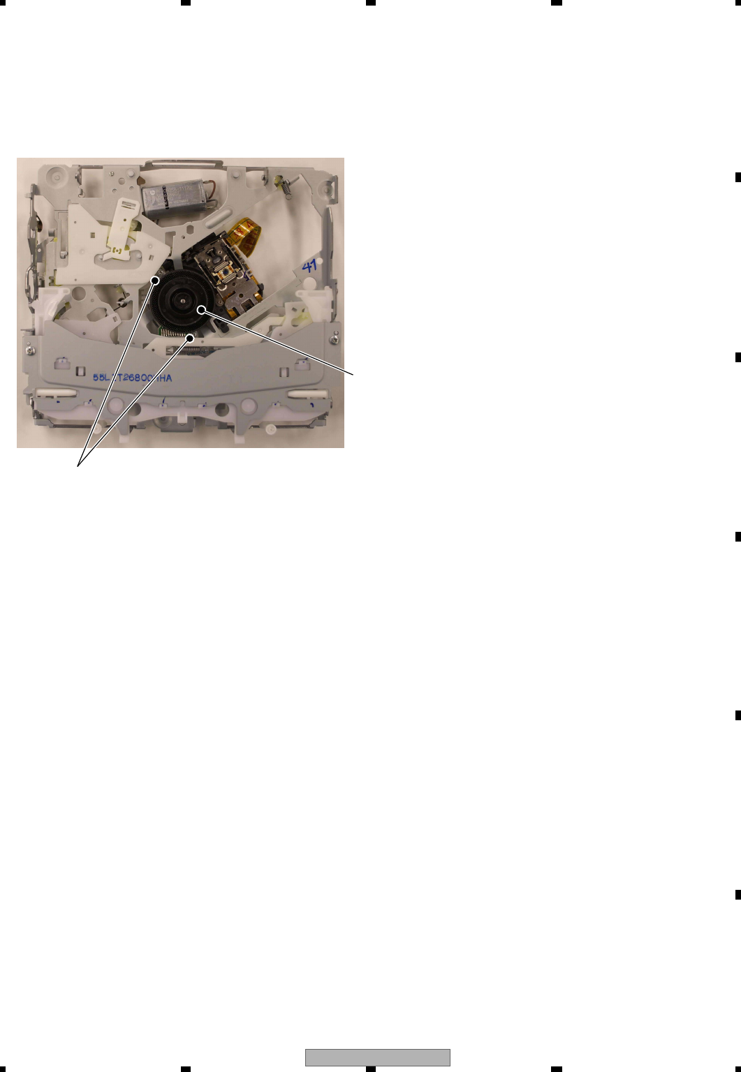
CX-3250 27
5 678
5678
C
D
F
A
B
E
Spindle motor
Spindle motor clinch screws
Removing the Spindle Motor
1.Remove the CRG mecha assy according to the “Removing the CRG Mecha assy” manual
(mecha is in the ejecting state).
2.Bring to the clamp state with no disc loaded according to the “Bringing into the Clamp State with No Disc Loaded
(Manual)” manual.
3.Remove the clamp arm according to the procedure 3 and after of the “Removing the Clamp Arm” manual.
4.Remove the relay PCB according to the “Removing the Relay PCB” manual.
5.Remove the two spindle motor clinch screws and then remove the spindle motor assy.
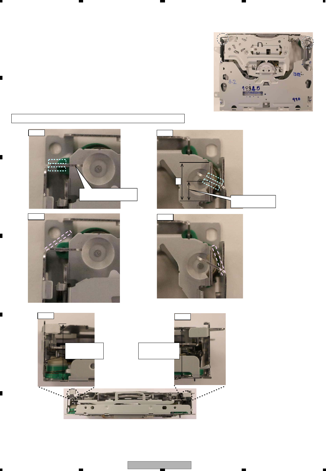
CX-3250
28
1234
1234
C
D
F
A
B
E
Fig. 1a Fig. 1b
Fig. 2a Fig. 2b
Clinch on the right side
It is bended orthogonally
in the initial condition It is in the L/2 position
in the initial condition
L
Fig. 3b
28.9+0.6/-0.3
(28.6 - 29.5)
25.45+0.6/-0.3
(25.15 - 26.05)
Removing the Clinch of the Bottom Frame
1.Use the needle-nose pliers when removing the clinch on the right side.
Nip the clinch at the location in Fig. 1a and then open it until it is in the position
circled by the red broken line in Fig. 2a.
2.Also to remove the clinch on the left side, use the needle-nose pliers,
nip the clinch at the location in Fig. 1b and then open it until it is in the position
circled by the red broken line in Fig. 2b.
(Precaution) When clinching again, use Fig. 2a and Fig. 2b as a guide.
It is okay as long as the tip of the clinch does not come off from the side a and
the side b by the vibration stroke (from front to back and from side to side).
Check Fig. 3a and Fig. 3b for the height of the clinch.
Correct the height with the needle-nose pliers when the height does not meet
the standard listed in those Figures.
In case of metal fatigue on the clinch part, exchange the lower frame.
Clinch on the left side
Fig. 3a
Caution: After repairing, make sure to clinch to the lower frame again.
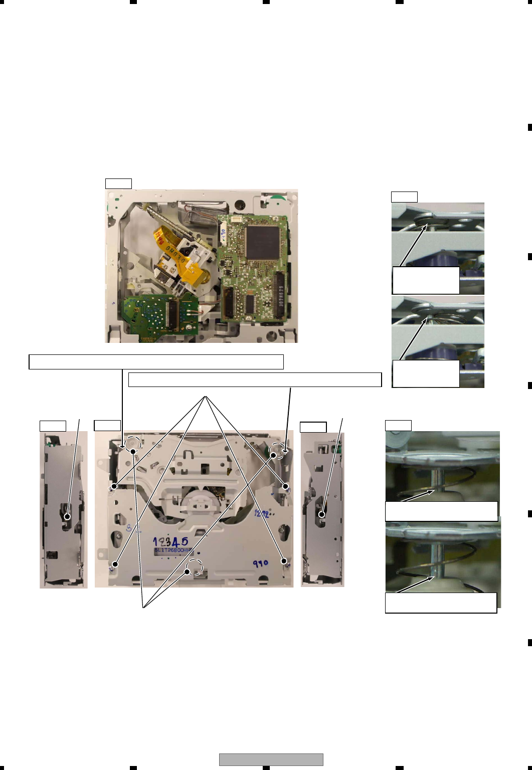
CX-3250 29
5 678
5678
C
D
F
A
B
E
Clinch screw of the top frame
Front-pulling spring
Front-pulling spring
Dampers
Fig. 1
Fig. 2a Fig. 3 Fig. 2b
Removing the CRG Mecha assy
1.Follow up to the procedure 3 of the “Removing the Module PCB” manual and then remove the PU FPC from the
connector.
2.Remove the relay FFC from the connector (both ends) and then remove the FFC. (Fig. 1)
3.Open the clinch of the bottom frame according to the “Removing the Clinch of the Bottom Frame” manual.
4.Remove the front-pulling springs on both sides. (Fig. 2a & Fig. 2b)
5.Remove four clinch screws of the top frame and then remove the top frame. (Fig. 3)
6.As lifting the carriage mecha, remove it from the dampers at three locations. (Fig. 3)
(Precaution) When assembling the CRG mecha assy again, apply alcohol on the dampers.
Make sure that the damper shafts are inside the three neutral springs (Fig. 4) and that the springs on both sides are hooked.
Before connecting to the module PCB after installing the CRG mecha, bring to the clamp state with no disc loaded
according to the “Mecha Module_Bringing into the Clamp State with No Disc Loaded” manual, push the upper part of the
damper of the CRG mecha by the finger and then make sure that the damper and the CRG mecha are jointed with certainty.
(Fig. 5)
Caution : After repairing, make sure to clinch to the lower frame again.
Fig. 4
Fig. 5
Caution : After repairing, make sure to clinch to the lower frame again.
OK:The end of the groove of the shaft
is hidden by the damper exterior.
NG:The end of the groove of the shaft
is found outside the damper exterior.
OK:A shaft is found
inside the spring.
NG:A shaft is found
outside the spring.
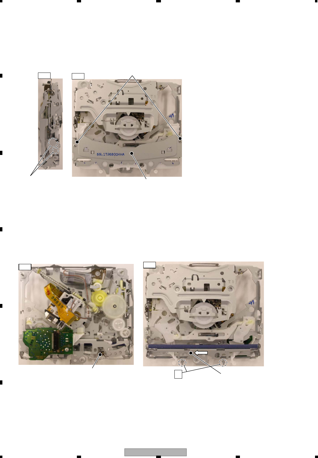
CX-3250
30
1234
1234
C
D
F
A
B
E
Guide bracket clinch screw
Roller transmission side gears
Fig. 1
Fig. 2
Roller assy biasing spring
Fig. 3
Disc guide assy
Roller Guide assy
Fig. 4
Removing the Disc Guide assy
(Removing the Roller Transmission Side Gear)
1.Remove the CRG mecha assy according to the “Removing the CRG Mecha assy” manual (mecha is in the ejecting state).
2.Remove the two guide bracket clinch screws and then remove the Disc guide assy. (Fig. 1)
3.Remove the two roller transmission side gears. (Fig. 2)
(Precaution) When assembling the Disc guide assy again, do not forget to install two gears on the side panel.
Removing the Roller assy
1.Remove the CRG mecha assy according to the “Removing the CRG Mecha assy” manual (mecha is in the ejecting state).
3.Remove the Roller assy biasing spring. (Fig. 3)
4.Remove the Disc guide assy according to the procedure 2 and after of the “Removing the Disc Guide assy” manual.
5.Hold the Roller assy at the locations A, slide it to the left and then remove it. (Fig.4)
(Precaution) When assembling the Disc guide assy again, do not forget to install two gears on the side panel.
A
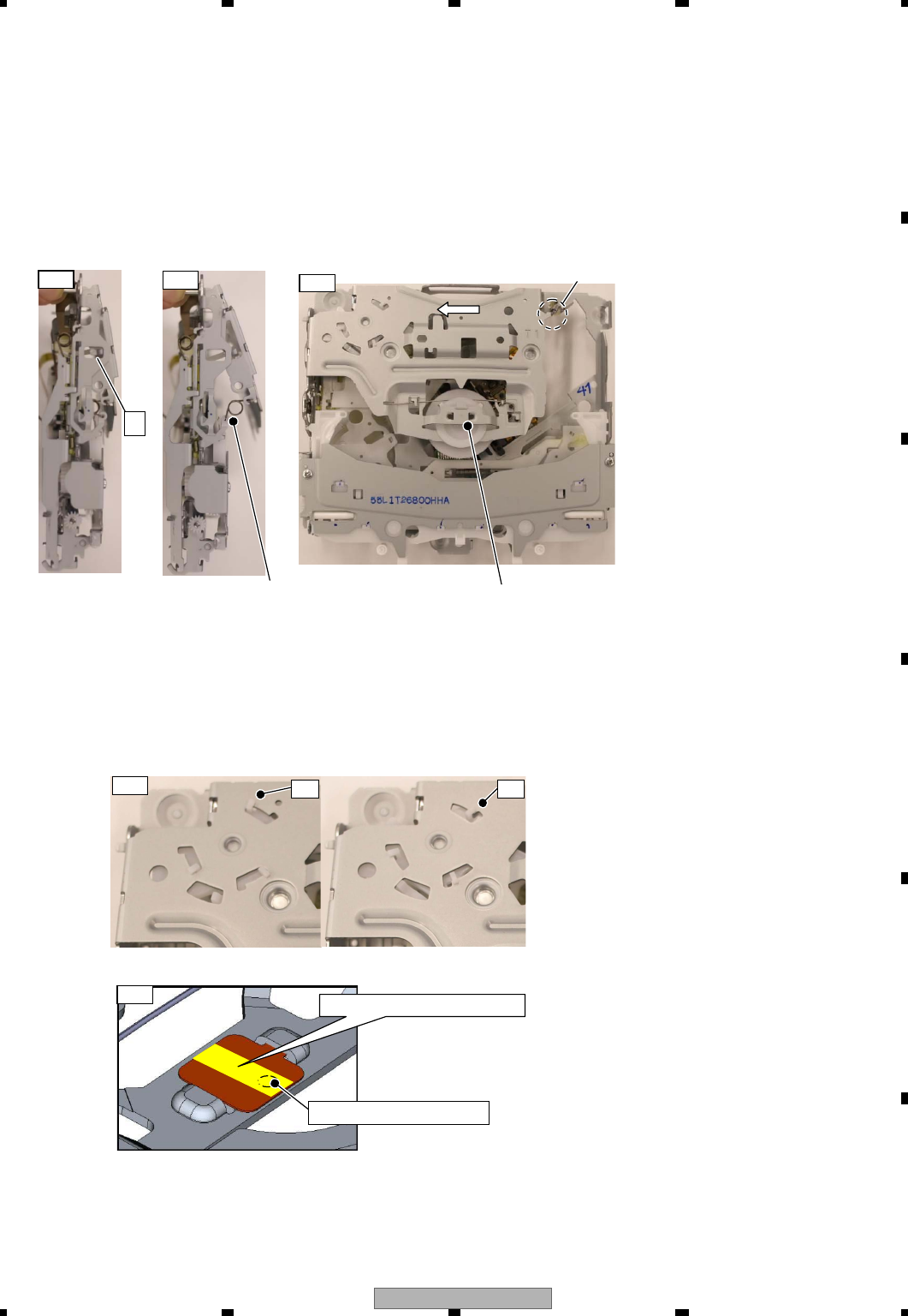
CX-3250 31
5 678
5678
C
D
F
A
B
E
Fig. 2 Fig. 1 Left biasing spring
Fig. 3
Right biasing spring
Fig. 3
Poly slider
Fig. 4 Apply the E paste on the yellow area.
Removing/Reassembling the Clamp Arm assy
1.Remove the CRG mecha assy according to the “Removing the CRG Mecha assy” manual
(mecha is in the ejecting state).
2.Bring to the clamp state with no disc loaded according to the “Bringing into the Clamp State with No Disc Loaded
(Manual)” manual.
3.Remove the right clamp arm biasing spring. (Just on the clamp-arm side. Do not remove on the chassis side.)
4.Lift the clamp arm assy until it is in the state shown in Fig. 2 (open-lock state).
5. Lightly push the part A and lift the clamp arm assy further to the position in Fig. 3.
6. Remove the left clamp arm biasing spring.
7. Lift the clamp arm assy further to 45-60 degrees, slide it to the left and then remove it. (Fig. 1)
Installing)
1.With the clamp arm assy tilted at 45-60 degrees, install it to the rotation fulcrum by sliding it from the left.
2.Bring down the clamp arm assy to the position in Fig. 3 (position where it meets the chassis and then stops).
3.Install the left clamp arm biasing spring.
4.Completely turn the detection arm to the position OK in Fig. 4 and then push the clamp arm assy to the bottom.
5.Install the right clamp arm biasing spring.
(Precaution) –When replacing the clamp arm assy, replace the poly slider with a new part as well.
Do not forget to apply the E paste on the poly slider (Fig. 4).
A
NGOK
Clamper convexity contact zone

CX-3250
32
1234
1234
C
D
F
A
B
E
Fig. 1
Remove the solder
Line clamper
Slide the spring
to remove it
CRG motor biasing spring Fig. 2a Fig. 2b
Correctly installed condition Joint removed condition
Fig. 4
Switching idler arm (Pull upward)
Fig. 3
Idler gear Worm wheel Switching idler arm biasing spring
CRG motor clinch screw
Fig. 5
Remove the joint
hook
Fig. 6a
Fig. 6c
Fig. 6b
A
Removing the CRG Motor assy
(Removing the Drive Transmission Gear)
1.Remove the CRG mecha assy according to the “Removing the CRG Mecha assy” manual (mecha is in the ejecting state).
2.Remove the clamp arm assy according to the “Removing the Clamp Arm assy” manual.
3.Remove the solder of the CRG motor lead and then remove the lead from the line clamper. (Fig. 1)
4.Remove the clinch screw of the CRG motor biasing spring and then slide the biasing spring to the direction of the arrow to remove it. (Fig. 1)
5.Nip the gear hook of the switching idler arm by the tips of your fingers and then push it below from the top of the gear. (Fig. 2a -> Fig. 2b)
6.Bend the hook on the chassis side of the switching idler arm to the direction of the arrow by tweezers and then remove the joint with the chassis.
(Fig. 3)
7.Pull off the switching idler arm from the top of the mecha (Fig. 4) and then remove the worm wheel and the idler gear. (Fig. 3)
8.Remove the switching idler lock arm biasing spring. (Fig. 3)
9.Remove two CRG motor clinch screws and then remove the CRG motor. (Fig. 3)
(Precaution) When installing the switching idler arm again, temporarily set the idler gear and the worm wheel as in Fig. 5, press the idler gear
from its top by your finger and then install the switching idler arm according to the steps in Fig. 6 from the opposite side of the chassis.
Do not forget to install the switching idler arm biasing spring.
Since the idler arm is in the snap fit structure, do not use them again.
When installing the CRG motor, scoot it to the center of the mecha in order to ensure that the gear engages.
Step 1: Insert the arm rotation fulcrum boss in the worm
wheel through the chassis hole.
Insert only the tip of the boss as in the figure.
Step 2: As pressing the idler gear from the opposite,
insert the gear fulcrum boss into the gear and joint them
until they are in the correctly installed condition in Fig. 2a.
When the idler arm is not installed correctly, there could be
an interference either in the location a or in the location b of
Fig. 4. Make a fine adjustment by moving it left and right.
Step 3: As matching the tip of the rotation fulcrum boss
with the metal plate hole by your finger (Fig. 6b), push the
area A in Fig. 6c to install the idler arm.
a: Match the fulcrum hole of the worm wheel
with the metal plate hole.
b: Engage the idler gear with the worm wheel.
c: Align the gear with the outer shape of the metal plate concavity as a guide.
Biasing spring cylind screw
Switching idler arm
a
b
c
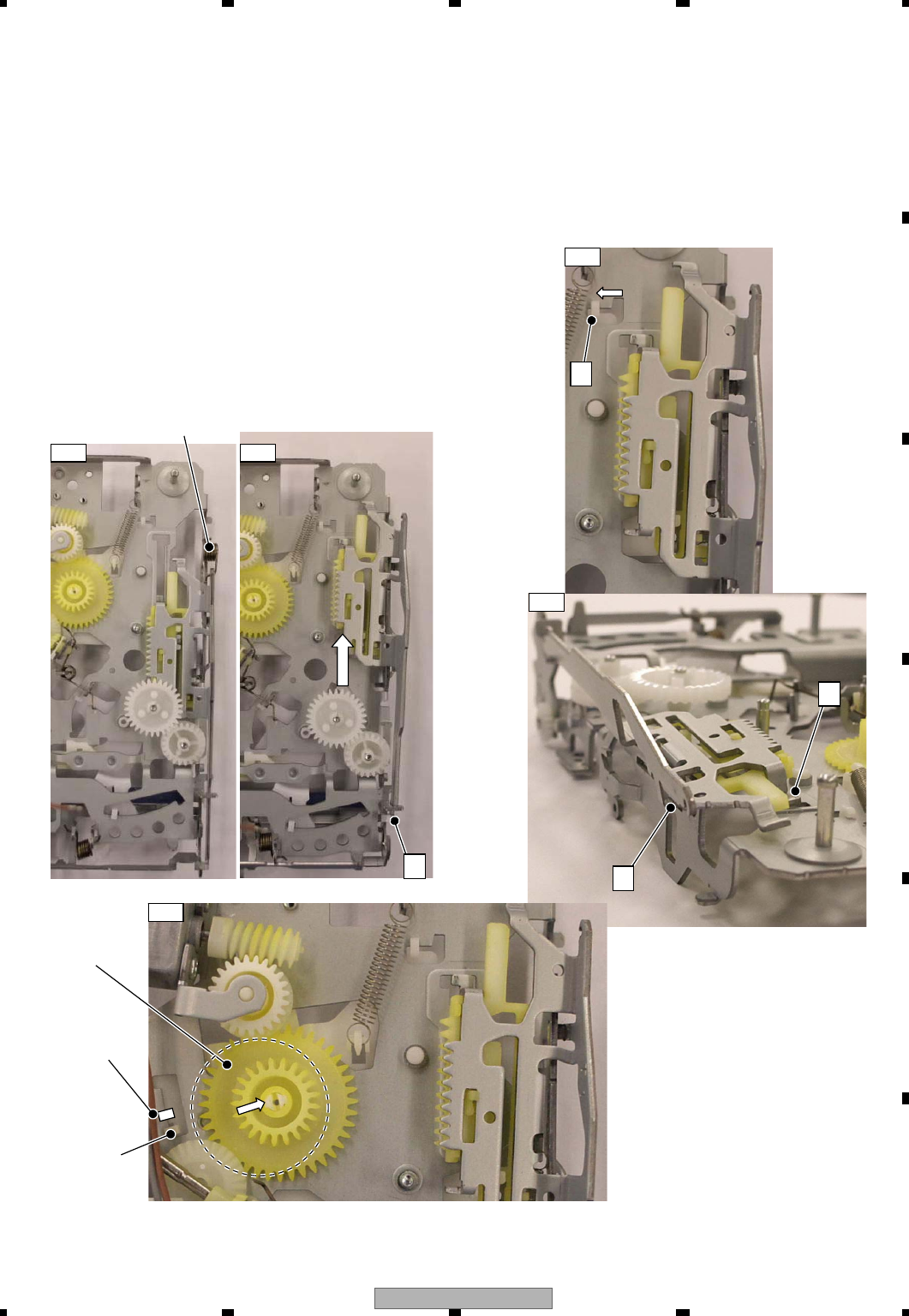
CX-3250 33
5 678
5678
C
D
F
A
B
E
Drive lever biasing spring
Fig. 1 Fig. 2
Fig. 4
Fig. 3
Removing the Drive Lever assy
1.Remove the CRG mecha assy according to the “Removing the CRG Mecha assy” manual (mecha is in the ejecting state).
2.Remove the clamp arm assy according to the “Removing the Clamp Arm assy” manual.
3.Remove the drive lever biasing spring. (Fig. 1)
4.Slide the drive lever to the direction of the arrow (the direction of ejecting), lift it to the direction of upper right and then
remove it. (Fig. 2)
(Precaution) When installing the drive lever assy again, install the part B (Fig. 2) first with the part A in Fig. 3 scooted to
the direction of the arrow(*1). Next, install the part C (Fig. 4) of the drive lever in the channel bending the side of the
chassis, and in the end, install the part D (Fig. 4) into the L-shaped channel of the chassis and then slide the drive lever to
the position in Fig. 1.
*1: If approach of Part A (Fig 3) is inadequate, the drive lever will not be
able to be well incorporated.
In this case, the idler gear might be located at the red dashed line (Fig 5).
Therefore, approach Part A (Fig 3) to the direction of the arrow as
approaching the idler gear to the direction of the arrow (Fig 5).
Determine, with the position of Part C in Fig 5, if the approach of
Part A is adequate.
B
A
C
D
Fig.5
Part C : NG
Position with
inadequate
approach
Part C : OK
Position with
adequate
approach
Idler gear
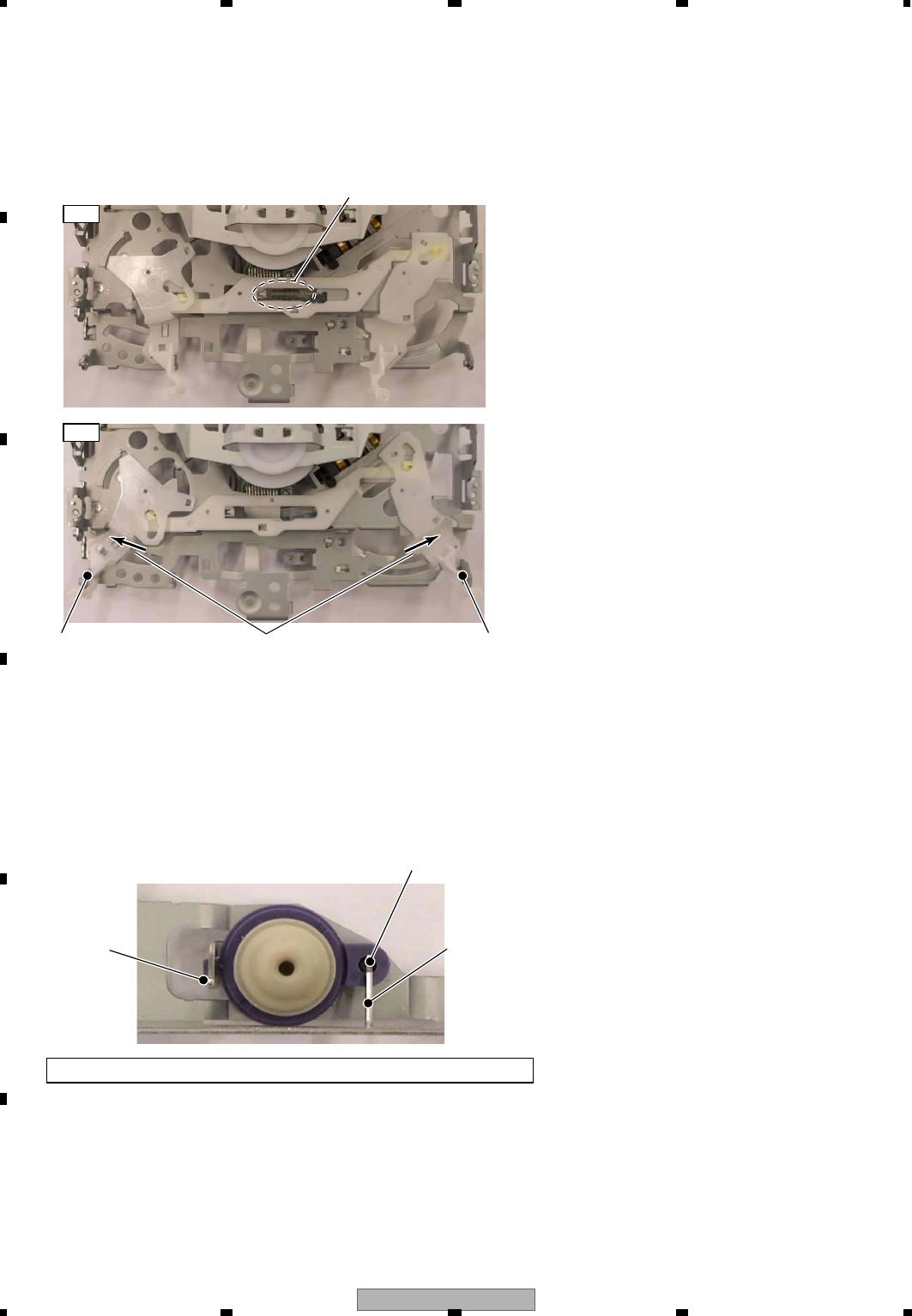
CX-3250
34
1234
1234
C
D
F
A
B
E
Connecting lever biasing spring
Fig. 1
Fig. 2
Removing the SW Arm
1.Remove the roller arm assy according to the “Removing the Roller Arm assy” manual.
2.Remove the SW arm connecting lever biasing spring. (Fig. 1)
3.Open the SW arms on both left and right sides until their tips touch the chassis. (Fig. 2)
4.Keep the SW arms open, lift them upward and then remove them.
Removing the Damper
1.Remove the CRG mecha according to the “Removing the CRG Mecha assy” manual
2.Insert the screwdriver under the part A of the metal plate configuration which joints the damper, lift the metal plate to
release the damper from being clinched by the part C.
3.Insert the screwdriver under the part D as well. Lift the metal plate, release the damper from being clinched to remove it.
A
C
D
Open the SW arms on both left and right side
Open the SW arm
on left sides until their tips
Open the SW arm
on right sides until their tips
Caution: After repairing, make sure to clinch to the lower frame again.
Caution: When mounting a damper, hold it tight with a clinch in order to avoid backlash.
In case of metal fatigue on the clinch part, exchange the frame.
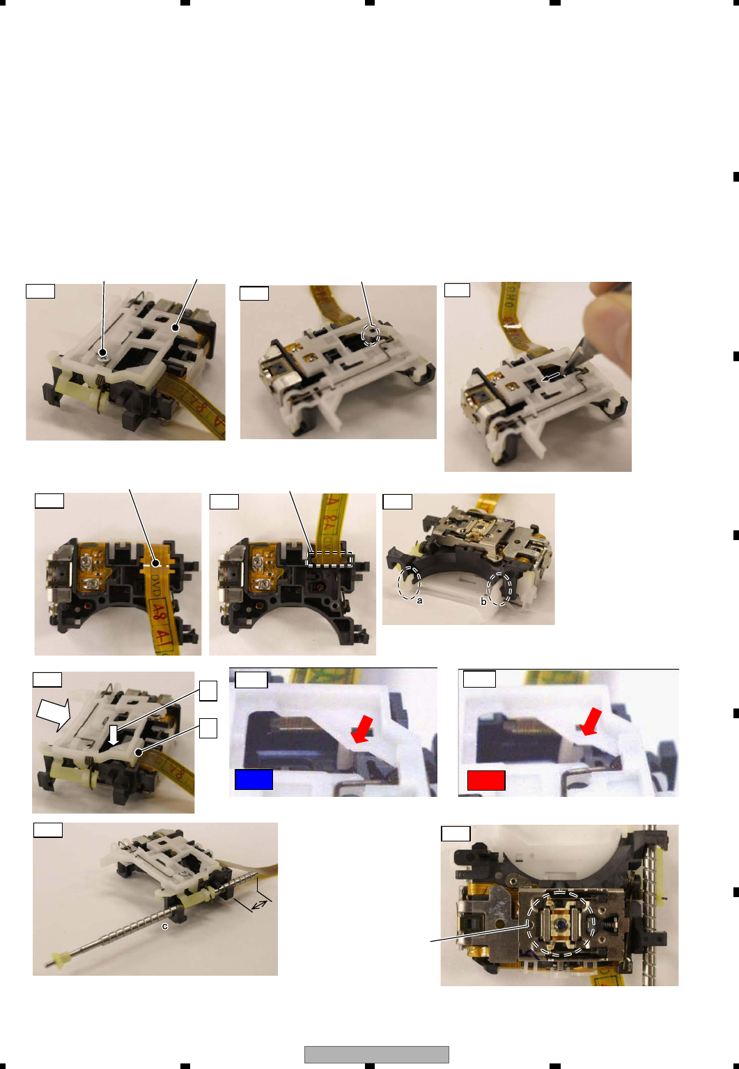
CX-3250 35
5 678
5678
C
D
F
A
B
E
Fig. 7
Fig. 2
Hook
PU rack
Fig. 1
PU rack clinch screw
Fig. 3
Fig. 6
Fig. 4
FFC folding line FFC folding back part
C
Fig. 8
Actuator
Removing the PU Rack
1.Remove the PU unit according to the “Removing the PU Unit” manual.
2.Remove the PU rack clinch screw. (Fig. 1)
3.Pick up the root of the hook on the PU rack (Fig. 2) with tweezers as in Fig. 3. While bending it so the tip of the hook
would open to the direction of the arrow (unhooked direction), pull out the PU rack upward.
(Precaution) When handling the PU unit, do not “touch the actuator in Fig. 9 or hit the desk with it during the operation.”
Handle the PU and the PU unit according to “Holding the PU” manual.
When installing the PU rack into the PU again, fold back the PU FPC as in Fig. 5 according to the folding line in Fig. 4
before installing the rack and settle it in the channel on the PU case. To install the PU rack, first install the part a and the
part b in Fig. 6 into the PU case, install the FPC folding back part in Fig. 5 so that it is held by the part A in Fig. 7, and push
the part B (top of the snap fit) to fit the PU rack.
When it is hard to fit the PU rack, try again as scooting it to the direction of the arrow C in Fig. 7.
After installing the PU rack, insert the feed screw from the side c in Fig. 8. Insert approximately 18mm on the part shown in
the figure.
Fig. 5
A
B
Fig. 7a
Fig. 7b
OK
NG
Fig. 9
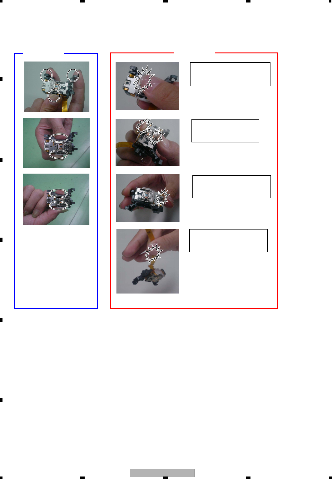
CX-3250
36
1234
1234
C
D
F
A
B
E
Handling OK Handling NG
Do not touch the object lens.
Do not touch the ACT.
Do not touch the Hologram.
Do not pull the FPC.
Holding the PU
1.Hold the “Handling OK” area of the PU indicated by the figure. Do not hold the “Handling NG” area.
