CRT3618 AVICZ1
User Manual: AVICZ1
Open the PDF directly: View PDF ![]() .
.
Page Count: 254 [warning: Documents this large are best viewed by clicking the View PDF Link!]
- SAFETY INFORMATION
- CONTENTS
- 1. SPECIFICATIONS
- 2. EXPLODED VIEWS AND PARTS LIST
- 2.1 PACKING
- 2.2 EXTERIOR(1)
- 2.3 EXTERIOR(2)
- 2.4 EXTERIOR(3)
- 2.5 DVD MECHANISM MODULE
- 3. BLOCK DIAGRAM AND SCHEMATIC DIAGRAM
- 3.1 BLOCK DIAGRAM
- 3.2 OVERALL CONNECTION DIAGRAM
- 3.3 GPS UNIT(GUIDE PAGE)
- 3.4 AUDIO UNIT(P/S•I/F)(GUIDE PAGE)
- 3.5 AUDIO UNIT(FM/AM•TMC TUNER)
- 3.6 DVD CORE UNIT(MS3)(SO-DC)(GUIDE PAGE)
- 3.7 DVD CORE UNIT(MS3)(CPU)(GUIDE PAGE)
- 3.8 COMPOUND UNIT(A) AND COMPOUND UNIT(B)
- 3.9 PU UNIT(REFERENCE)
- 3.10 NAVI MOTHER PCB(SYSCOM•P/S)(GUIDE PAGE)
- 3.11 NAVI MOTHER PCB(NAVI AV•EXTERNAL I/F)(GUIDE PAGE)
- 3.12 HDD PELAY PCB
- 3.13 PANEL UNIT
- 3.14 KEYBOARD UNIT
- 3.15 MONITOR UNIT(MONITOR)(GUIDE PAGE)
- 3.16 MONITOR UNIT(INVERTER)
- 3.17 MAIN PCB UNIT
- 4. PCB CONNECTION DIAGRAM
- 4.1 AUDIO UNIT
- 4.2 DVD CORE UNIT(MS3)
- 4.3 COMPOUND UNIT(A) AND COMPOUND UNIT(B)
- 4.4 GPS UNIT
- 4.5 NAVI MOTHER PCB
- 4.6 HDD RELAY PCB
- 4.7 PANEL UNIT
- 4.8 MONITOR UNIT
- 4.9 MAIN PCB UNIT
- 4.10 KEYBOARD UNIT
- 5. ELECTRICAL PARTS LIST
- 6. ADJUSTMENT
- 6.1 JIG CONNECTION DIAGRAM
- 6.2 DVD ADJUSTMENT
- 6.3 VIDEO LEVEL ADJUSTMENT
- 6.4 PLL ADJUSTMENT
- 6.5 MONITOR UNIT ADJUSTMENT
- 6.6 TEST MODE
- 6.7 TEST DISC
- 7. GENERAL INFORMATION
- 7.1 DIAGNOSIS
- 7.1.1 DISASSEMBLY
- 7.1.2 PCB LOCATIONS
- 7.1.3 CONNECTOR FUNCTION DESCRIPTION
- 7.2 IC
- 8. OPERATIONS
ORDER NO.
PIONEER CORPORATION 4-1, Meguro 1-chome, Meguro-ku, Tokyo 153-8654, Japan
PIONEER ELECTRONICS (USA) INC. P.O. Box 1760, Long Beach, CA 90801-1760, U.S.A.
PIONEER EUROPE NV Haven 1087, Keetberglaan 1, 9120 Melsele, Belgium
PIONEER ELECTRONICS ASIACENTRE PTE. LTD. 253 Alexandra Road, #04-01, Singapore 159936
PIONEER CORPORATION 2006
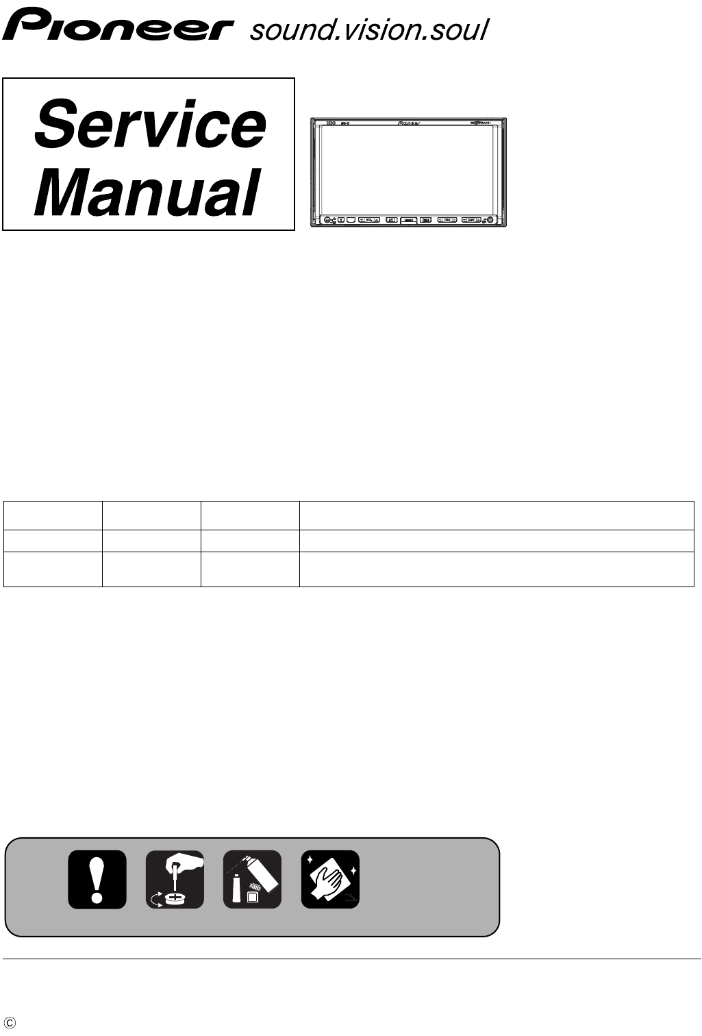
AVIC-Z1/UC
CRT3618
HDD MULTIMEDIA AV NAVIGATION SERVER
AVIC-Z1
/UC
AVIC-HD1BT
/EW5
This service manual should be used together with the following manual(s):
Model No. Order No. Mech.Module Remarks
CX-3016 CRT3056 MS3 DVD Mech. Module:Circuit Descriptions, Mech. Descriptions, Disassembly
ND-BT1/E5 CRT3684 Bluetooth unit
(ND-BT1/E is sold as packed unit of AVIC-HD/BT/EW5 in EW area.)
For details, refer to "Important Check Points for Good Servicing".
K-ZZU.MAR. 2006 Printed in Japan

AVIC-Z1/UC
2
1234
1234
C
D
F
A
B
E
SAFETY INFORMATION
C
A
U
TI
O
N
This service manual is intended for
q
ualified service technicians; it is not meant for the casual do-it-
y
ourself
e
r.
Qualified technicians have the necessar
y
test e
q
ui
p
ment and tools, and have been trained to
p
ro
p
erl
y
and safel
y
re
p
ai
r
com
p
lex
p
roducts such as those covered b
y
this manual
.
Im
p
ro
p
erl
y
p
erformed re
p
airs
ca
n adversel
y
a
ff
ect
t
h
e
safet
y
a
n
d
reliabilit
y
of
t
h
e
p
roduct
a
n
d
ma
y
v
o
i
d
t
h
e
.
If
y
ou
a
r
e
n
ot
q
ualified
to
t
h
e
re
p
air
of
t
hi
s
p
roduct
p
ro
p
erl
y
a
n
d
,
y
ou
s
h
ou
l
d
n
ot
ri
s
k
t
ryin
g
to
do
so
W
ARNING
W
ARNING
W
Thi
s
p
roduct
co
n
ta
in
s
l
ead
in
so
l
de
r
a
n
d
cer
ta
in
e
l
ect
ri
ca
l
p
arts
co
n
ta
in
c
h
e
mi
ca
l
s
whi
c
h
a
r
e
kn
o
wn
to
t
h
e
state
of
Health & Safet
y
Code Section 25249.6 - Pro
p
osition 6
5
This product contains mercury. Disposal of this material may be re
g
ulated due to environmental considerations.
For disposal or recyclin
g
information, please contact your local authorities or the Electronics Industries
Alliance: www.eiae.org.
UC
AVIC-Z1/UC 3
5678
5678
C
D
F
A
B
E
WARNING!
The AEL (accessible emission level )of the laser power output is less than CLASS 1
but the laser component is capable of emitting radiation exceeding the limit for
CLASS 1.
A specially instructed person should do servicing operation of the apparatus.
Laser diode characteristics
Wave length:
DVD:640~660nm
CD:770~810nm
DVD : 2.48mW(Emitting period :9sec.)
CD : 705 W(Emitting period : unlimited)
Additionla Laser Caution
Transistors Q1101 and Q1102 in PCB drive the laser diodes for DVD and CD
respectively. When Q1101 or Q1102 is shorted between their terminals,
the laser diodes for DVD or CD will radiate beam. If the top cover is removed
with no disc loaded while such short-circuit is continued, the naked eyes may
be exposed to the laser beam.
1. Safety Precautions for those who Service this Unit.
• Follow the adjustment steps in the service manual when servicing this unit. When check
ing or adjusting the emitting power of the laser diode exercise caution in order to get safe, reliable results.
Caution:
1. During repair or tests, minimum distance of 13cm from the focus lens must be kept.
2. During repair or tests, do not view laser beam for 10 seconds or longer.
.
EW5
On the top of the player
CAUTION :
VORSICHT :
ADVARSEL :
VARNING :
VARO! :
VISIBLE AND INVISIBLE LASER RADIATION WHEN OPEN.
AVOID EXPOSURE TO BEAM.
SICHTBARE UND UNSICHTBARE LASERSTRAHLUNG, WENN
ABDECKUNG GEÖFFNET NICHT DEM STRAHL AUSSETZEN!
SYNLIG OG USYNLIG LASERSTRÅLING VED ÅBNING
UNDGÅ UDSÆTTELSE FOR STRÀLING.
SYNLIG OCH OSYNLIG LASERSTRÅLNING NÄR DENNA
DEL ÄR ÖPPNAD BETRAKTA EJ STRÅLEN.
AVATTAESSA ALTISTUT NÄKYVÄ JA NÄKYMÄTTÖMÄLLE
LASERSATEIL YLLE. ÄLÄ KATSO SÄTEESEN. VRW1860
AVIC-Z1/UC
4
1234
1234
C
D
F
A
B
E
[Important Check Points for Good Servicing]
In this manual, procedures that must be performed during repairs are marked with the below symbol.
Please be sure to confirm and follow these procedures.
1. Product safety
Please conform to product regulations (such as safety and radiation regulations), and maintain a safe servicing environment by
following the safety instructions described in this manual.
1 Use specified parts for repair.
Use genuine parts. Be sure to use important parts for safety.
2 Do not perform modifications without proper instructions.
Please follow the specified safety methods when modification(addition/change of parts) is required due to interferences such as
radio/TV interference and foreign noise.
3 Make sure the soldering of repaired locations is properly performed.
When you solder while repairing, please be sure that there are no cold solder and other debris.
Soldering should be finished with the proper quantity. (Refer to the example)
4 Make sure the screws are tightly fastened.
Please be sure that all screws are fastened, and that there are no loose screws.
5 Make sure each connectors are correctly inserted.
Please be sure that all connectors are inserted, and that there are no imperfect insertion.
6 Make sure the wiring cables are set to their original state.
Please replace the wiring and cables to the original state after repairs.
In addition, be sure that there are no pinched wires, etc.
7 Make sure screws and soldering scraps do not remain inside the product.
Please check that neither solder debris nor screws remain inside the product.
8 There should be no semi-broken wires, scratches, melting, etc. on the coating of the power cord.
Damaged power cords may lead to fire accidents, so please be sure that there are no damages.
If you find a damaged power cord, please exchange it with a suitable one.
9 There should be no spark traces or similar marks on the power plug.
When spark traces or similar marks are found on the power supply plug, please check the connection and advise on secure
connections and suitable usage. Please exchange the power cord if necessary.
0 Safe environment should be secured during servicing.
When you perform repairs, please pay attention to static electricity, furniture, household articles, etc. in order to prevent injuries.
Please pay attention to your surroundings and repair safely.
2. Adjustments
To keep the original performance of the products, optimum adjustments and confirmation of characteristics within specification.
Adjustments should be performed in accordance with the procedures/instructions described in this manual.
4. Cleaning
For parts that require cleaning, such as optical pickups, tape deck heads, lenses and mirrors used in projection monitors, proper
cleaning should be performed to restore their performances.
3. Lubricants, Glues, and Replacement parts
Use grease and adhesives that are equal to the specified substance.
Make sure the proper amount is applied.
5. Shipping mode and Shipping screws
To protect products from damages or failures during transit, the shipping mode should be set or the shipping screws should be
installed before shipment. Please be sure to follow this method especially if it is specified in this manual.
AVIC-Z1/UC 5
5678
5678
C
D
F
A
B
E
- Service Precautions
• You should conform to the regulations governing the product (safety, radio and noise, and other regulations),
and should keep the safety during servicing by following the safety instructions described in this manual.
• Be careful in handling ICs. Some ICs such as MOS type are so fragile that they can be damaged by electrostatic
induction.
- DVD section precaution
1. EJECT LOCK MODE for DVD mechanism.
In order to enter "EJECT LOCK" mode, reset start while pressing "AV" and "V" keys together.
Pressing the "AV" and "V" keys until monitor back light is turned on.
In order to exit "EJECT LOCK" mode, follow the same steps to enter this mode.
2. Before disassembling the unit, be sure to turn off
the power. Unplugging and plugging the connectors
during power-on mode may damage the ICs inside
the unit.
3. To protect the pickup unit from electrostatic discharge
during servicing, take an appropriate treatment
(shorting-solder) by referring to "the DISASSEMBLY" .
4. After replacing the pickup unit, be sure to skew
adjustment.
5. During disassembly, be sure to turn the power off since
an internal IC might be destroyed when a connector
is plugged or unplugged.
is a trademark of DVD Format/Logo Licensing Corporation.

AVIC-Z1/UC
6
1234
1234
C
D
F
A
B
E
CONTENTS
SAFETY INFORMATION..................................................................................................................................... 2
1. SPECIFICATIONS ............................................................................................................................................ 7
2. EXPLODED VIEWS AND PARTS LIST ............................................................................................................ 9
2.1 PACKING ................................................................................................................................................. 10
2.2 EXTERIOR(1) .......................................................................................................................................... 12
2.3 EXTERIOR(2) .......................................................................................................................................... 14
2.4 EXTERIOR(3) .......................................................................................................................................... 16
2.5 DVD MECHANISM MODULE .................................................................................................................. 18
3. BLOCK DIAGRAM AND SCHEMATIC DIAGRAM..........................................................................................20
3.1 BLOCK DIAGRAM ................................................................................................................................... 20
3.2 OVERALL CONNECTION DIAGRAM...................................................................................................... 38
3.3 GPS UNIT(GUIDE PAGE)........................................................................................................................ 40
3.4 AUDIO UNIT(P/S•I/F)(GUIDE PAGE)....................................................................................................... 46
3.5 AUDIO UNIT(FM/AM•TMC TUNER) ........................................................................................................ 52
3.6 DVD CORE UNIT(MS3)(SO-DC)(GUIDE PAGE)..................................................................................... 54
3.7 DVD CORE UNIT(MS3)(CPU)(GUIDE PAGE).........................................................................................60
3.8 COMPOUND UNIT(A) AND COMPOUND UNIT(B) ................................................................................ 68
3.9 PU UNIT(REFERENCE) .......................................................................................................................... 69
3.10 NAVI MOTHER PCB(SYSCOM•P/S)(GUIDE PAGE)............................................................................. 70
3.11 NAVI MOTHER PCB(NAVI AV•EXTERNAL I/F)(GUIDE PAGE) ............................................................ 76
3.12 HDD PELAY PCB................................................................................................................................... 82
3.13 PANEL UNIT .......................................................................................................................................... 84
3.14 KEYBOARD UNIT.................................................................................................................................. 86
3.15 MONITOR UNIT(MONITOR)(GUIDE PAGE) ......................................................................................... 88
3.16 MONITOR UNIT(INVERTER) ................................................................................................................ 94
3.17 MAIN PCB UNIT .................................................................................................................................... 96
4. PCB CONNECTION DIAGRAM ..................................................................................................................... 98
4.1 AUDIO UNIT ............................................................................................................................................ 98
4.2 DVD CORE UNIT(MS3) ......................................................................................................................... 102
4.3 COMPOUND UNIT(A) AND COMPOUND UNIT(B) .............................................................................. 106
4.4 GPS UNIT .............................................................................................................................................. 107
4.5 NAVI MOTHER PCB .............................................................................................................................. 108
4.6 HDD RELAY PCB .................................................................................................................................. 112
4.7 PANEL UNIT .......................................................................................................................................... 113
4.8 MONITOR UNIT..................................................................................................................................... 114
4.9 MAIN PCB UNIT .................................................................................................................................... 118
4.10 KEYBOARD UNIT................................................................................................................................ 120
5. ELECTRICAL PARTS LIST .......................................................................................................................... 121
6. ADJUSTMENT ............................................................................................................................................. 148
6.1 JIG CONNECTION DIAGRAM............................................................................................................... 148
6.2 DVD ADJUSTMENT............................................................................................................................... 150
6.3 VIDEO LEVEL ADJUSTMENT............................................................................................................... 167
6.4 PLL ADJUSTMENT ............................................................................................................................... 169
6.5 MONITOR UNIT ADJUSTMENT............................................................................................................ 171
6.6 TEST MODE .......................................................................................................................................... 184
6.7 TEST DISC ............................................................................................................................................ 207
7. GENERAL INFORMATION........................................................................................................................... 224
7.1 DIAGNOSIS ........................................................................................................................................... 224
7.1.1 DISASSEMBLY ................................................................................................................................... 224
7.1.2 PCB LOCATIONS ............................................................................................................................... 232
7.1.3 CONNECTOR FUNCTION DESCRIPTION........................................................................................ 233
7.2 IC ........................................................................................................................................................... 234
8. OPERATIONS .............................................................................................................................................. 246
AVIC-Z1/UC 7
5678
5678
C
D
F
A
B
E
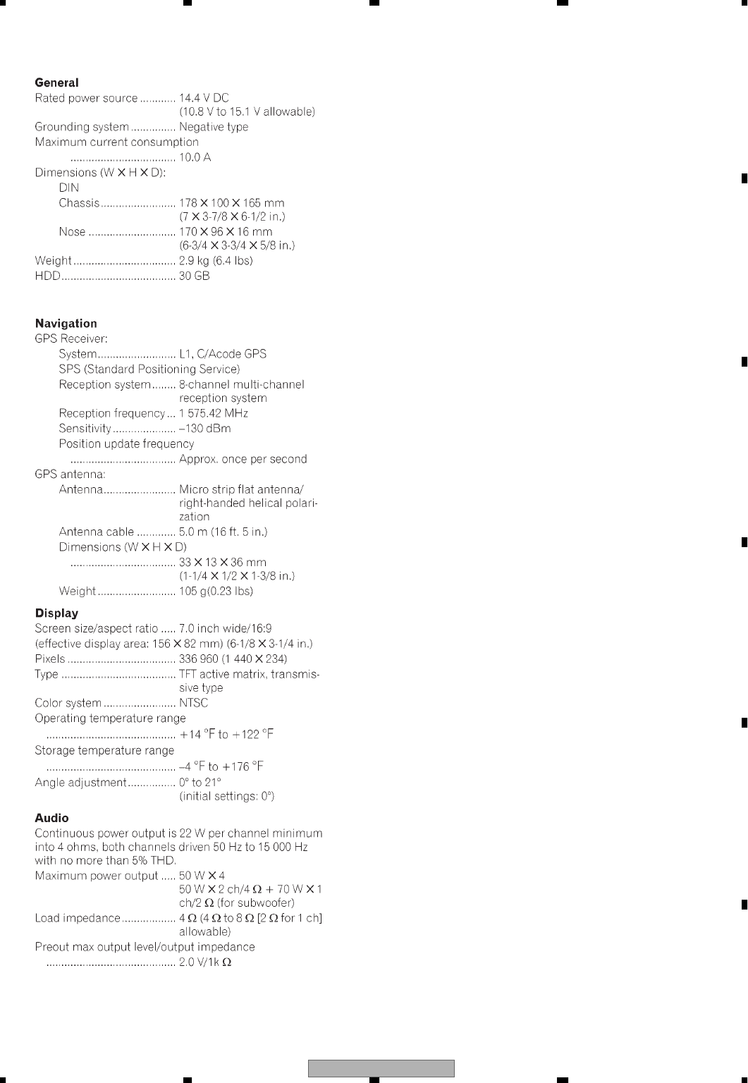
1. SPECIFICATIONS
Backup current ............... 2.25 mA or less
AVIC-Z1/UC
8
1234
1234
C
D
F
A
B
E

AVIC-Z1/UC 9
5678
5678
C
D
F
A
B
E
2. EXPLODED VIEWS AND PARTS LIST
N
OTES : • Parts marked by " * " are generally unavailable because they are not in our Master Spare Parts List.
• The > mark found on some component parts indicates the importance of the safety factor of the part.
Therefore, when replacing, be sure to use parts of identical designation.
• Screw adjacent to mark on the product are used for disassembly.
• For the applying amount of lubricants or glue, follow the instructions in this manual.
(In the case of no amount instructions,apply as you think it appropriate.)
"
AVIC-Z1/UC
10
1234
1234
C
D
F
A
B
E
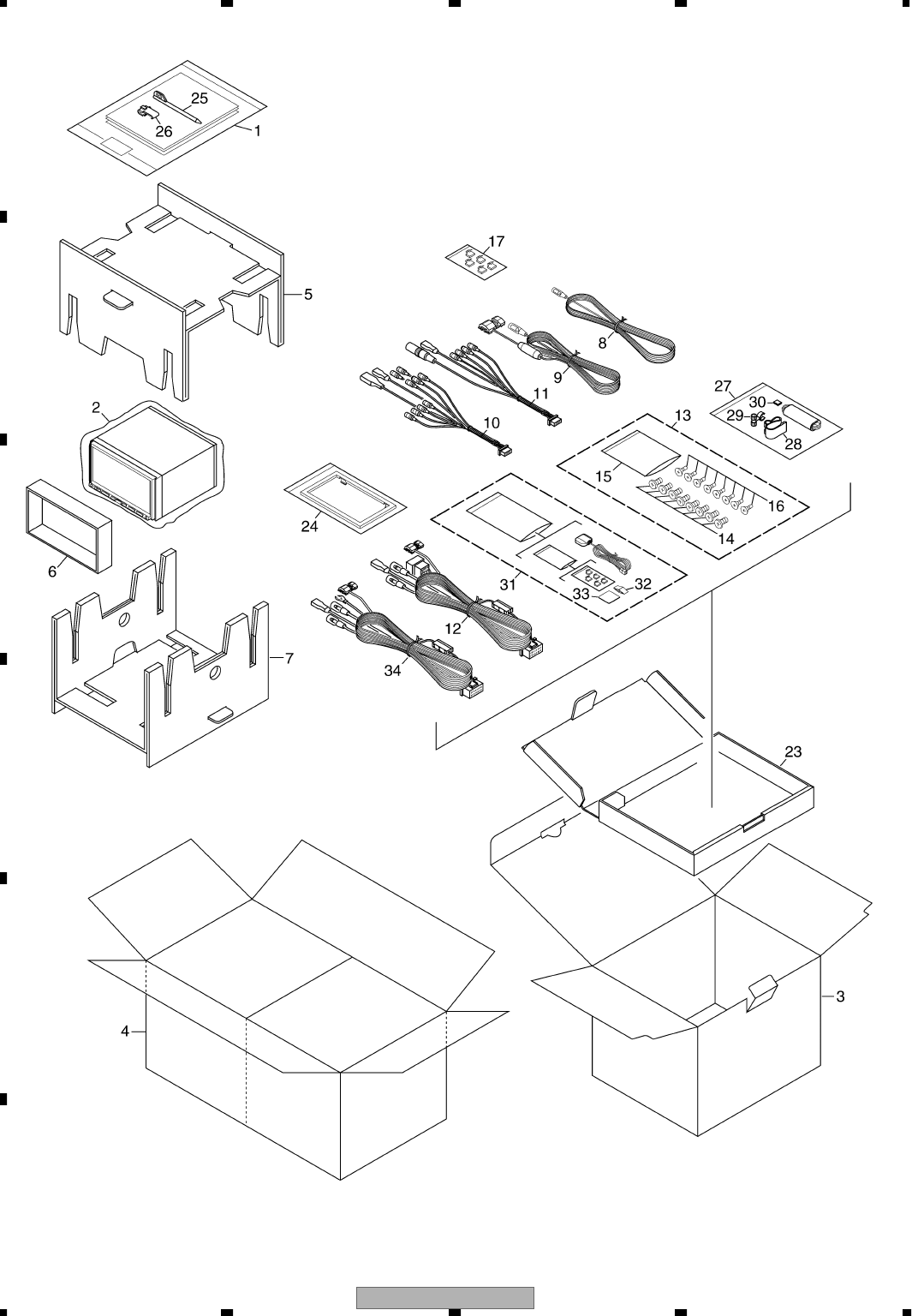
2.1 PACKING

AVIC-Z1/UC 11
5678
5678
C
D
F
A
B
E
PACKING SECTION PARTS LIST
Owner's Manual,Installation Manual
Mark No. Description Part No.
1-1 Owner's Manual(UC) CRB2183
Owner's Manual/PEE/ENG(EW) CRB2187
1-2 Owner's Manual(UC) CRB2184
Owner's Manual/PEE/ENG(EW) CRB2188
1-3 Owner's Manual/POC/FRE(UC) CRB2185
Owner's Manual/PEE/SPE(EW) CRB2189
1-4 Owner's Manual/POC/FRE(UC) CRB2186
Owner's Manual/PEE/SPE(EW) CRB2190
1-5 Owner's Manual/PEE/GER(EW) CRB2191
Owner's Manual(UC) CRB2258
1-6 Owner's Manual/PEE/GER(EW) CRB2192
Owner's Manual/POC/FRE(UC) CRB2259
1-7 Owner's Manual/PEE/FRE(EW) CRB2193
1-8 Owner's Manual/PEE/FRE(EW) CRB2194
1-9 Owner's Manual/PEE/ITA(EW) CRB2195
1-10 Owner's Manual/PEE/ITA(EW) CRB2196
1-11 Owner's Manual/PEE/DUT(EW) CRB2197
1-12 Owner's Manual/PEE/DUT(EW) CRB2198
1-13 Installation Manual(UC) CRD4100
Installation Manual(EW) CRD4101
* 1-14 Registration Card(UC) CRY1245
1-15 Caution Card(UC) CRP1310
* 1-16 Passport(EW) CRY1013
* 1-17 Warranty Card(EW) CRY1157
1-18 Owner's Manual/PEE/ENG(EW) CRB2260
1-19 Owner's Manual/PEE/SPE(EW) CRB2261
1-20 Owner's Manual/PEE/GER(EW) CRB2262
1-21 Owner's Manual/PEE/FRE(EW) CRB2263
1-22 Owner's Manual/PEE/ITA(EW) CRB2264
1-23 Owner's Manual/PEE/DUT(EW) CRB2265
1-24 Polyethylene Bag CEG1116
2 Cover(UC) CEG1177
Cover(EW) CEG1074
3 Carton(UC) CHG5732
Carton(EW) CHG5899
4 Contain Box(UC) CHL5732
Contain Box(EW) CHL5899
5 Protector(Upper) CHP2227
6 Protector CHP2242
7 Protector CHP2272
8 Cord CDE5044
9 Cord CDE6825
10 Cord Assy CDE8083
11 Cord Assy CDE8084
12 Cord Assy(EW) CDE8165
13 Screw Assy CEA3797
14 Screw BMZ50P060FTC
* 15 Polyethylene Bag CEG-127
16 Screw CMZ50P060FTC
17 Cord Clamper Assy CEA4636
18-22 •••••
23 Sub Carton CHA3298
24 Panel CNS8669
25 Pen CNV8969
26 Connector CKX1049
27 Microphone Assy CPM1064
28 Clip Holder CZN5471
29 Microphone Holder CZN5472
30 Cushion CZN5473
31 GPS Antenna Assy CXC4864
32 Water Proof Pad CZN5442
33 Sheet CZN7008
34 Cord Assy(UC) CDE8082
Mark No. Description Part No.
Part No. Language
CRB2183,CRB2184,CRB2187,CRB2188,CRB2258,CRB2260 English
CRB2185,CRB2186,CRB2193,CRB2194,CRB2259,CRB2263 French
CRB2189,CRB2190,CRB2261 Spanish
CRB2191,CRB2192,CRB2262 German
CRB2195,CRB2196,CRB2264 Italian
CRB2197,CRB2198,CRB2265 Dutch
CRD4100 English,French
CRD4101 English,Spanish,German,French,Italian,Dutch
AVIC-Z1/UC
12
1234
1234
C
D
F
A
B
E
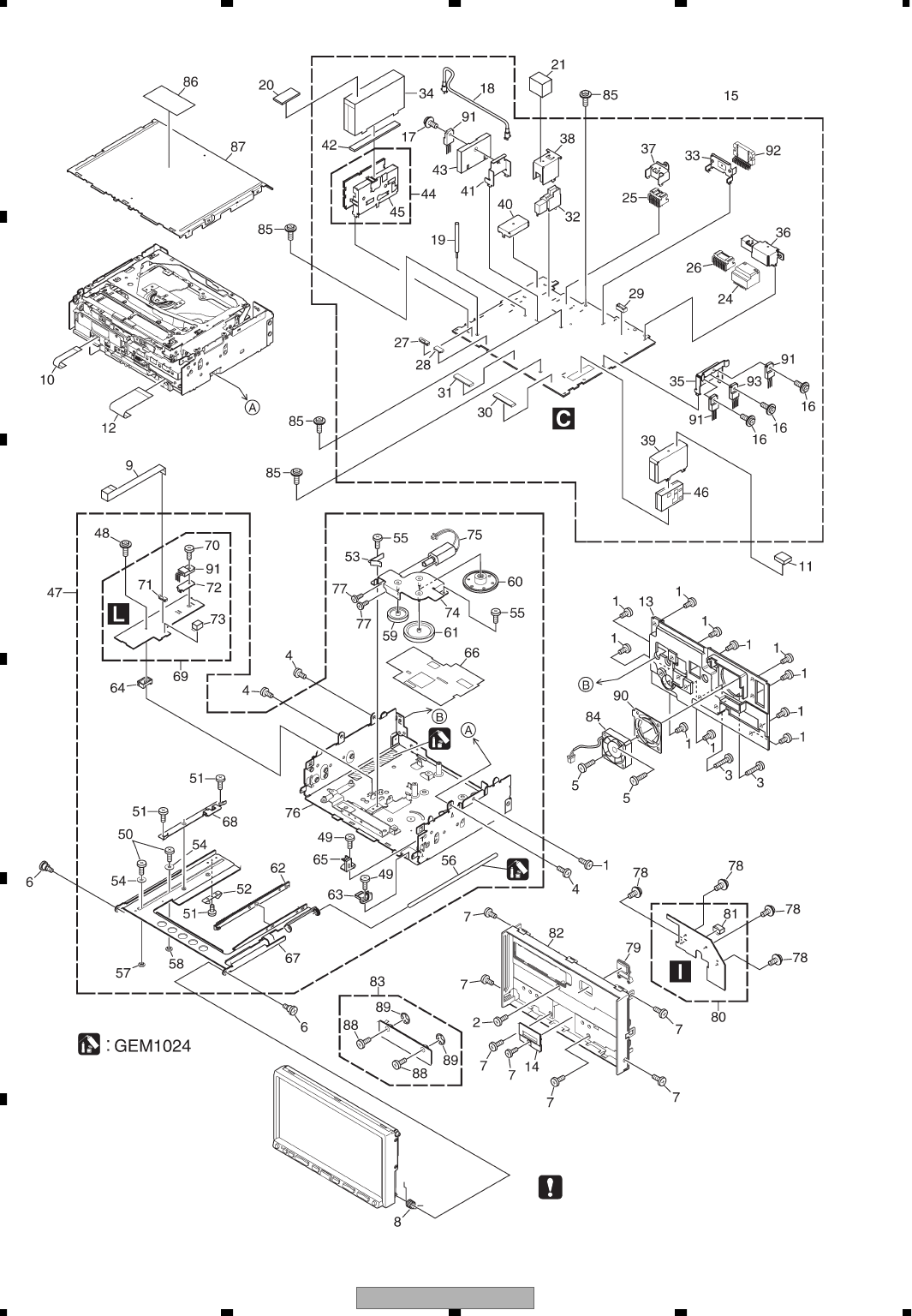
2.2 EXTERIOR(1)
To remove the 88 screw,
use a torques screwdriver (T8)(GGK1068).

AVIC-Z1/UC 13
5678
5678
C
D
F
A
B
E
EXTERIOR(1) SECTION PARTS LIST
Mark No. Description Part No.
1 Screw BMZ26P060FTC
2 Screw BMZ26P120FTB
3 Screw BMZ26P160FTB
4 Screw BSZ26P050FTB
5 Screw(M3 x 10) CBA1637
6 Screw CBA1735
7 Screw(M2 x 3) CBA1877
8 Spring CBH2932
9 FFC CDE7998
10 FFC CDE8204
11 Gasket(EW) CNN1296
12 Flexible PCB CNP8272
13 Heat Sink CNR1849
14 Cover CNS8525
15 Audio Unit(UC) CWN1583
Audio Unit(EW) CWN1633
16 Screw BMZ26P050FTB
17 Screw BMZ26P120FTC
18 Cord(EW) CDH1354
19 Clamper(EW) CEF1048
20 Gasket(EW) CNN1379
21 Gasket CNN1375
22 •••••
23 •••••
24 Plug(CN1001) CKM1278
25 Connector(CN1202) CKM1502
26 Connector(CN1201) CKM1506
27 Connector(CN1832) CKS5572
28 Connector(CN1003) CKS5644
29 Connector(CN1002) CKS4674
30 Connector(CN1831) CKS5110
31 Connector(CN1203) CKS5486
32 Antenna Jack(CN2501) CKX1060
33 Holder CNC9921
34 Shield CND3004
35 Holder CND3023
36 Holder CND3142
37 Holder CND3180
38 Holder CND3181
39 Shield(EW) CND3188
40 Shield(EW) CND3189
41 Holder CND3411
42 Sheet CNM9805
43 Heat Sink CNR1873
44 FM/AM Tuner Unit(UC) CWE1952
FM/AM Tuner Unit(EW) CWE1951
45 Holder CND1054
46 Tuner Unit(Y2600)(EW) CWE2023
47 Drive Mechanism Unit CXC6806
48 Screw(M2 x 6) CBA1399
49 Screw(M2 x 1.5) CBA1615
50 Screw(M2 x 2.5) CBA1881
51 Screw(M2 x 2) CBA1771
52 Spring CZB3092
53 Spring CZB3093
54 Washer CZB5004
55 Screw CZB5005
56 Shaft CZL3010
57 Roller CZL3011
58 Roller CZL3012
59 Gear CZN7011
60 Gear CZN7012
61 Gear CZN7013
62 Rack CZN7014
63 Holder CZN7015
64 Holder CZN7042
65 Holder CZN7043
66 Sheet CZN7044
67 Frame CZN7063
68 Plate CZN7064
69 Main PCB Unit CZW5026
70 Screw BMZ26P050FTC
71 Connector(CN2) CZK3075
72 Heat Sink CND1228
73 Connector(CN1) CZK3071
74 Bracket Unit CZX5101
75 Motor Unit(M1000) CZX5102
76 Chassis Unit CZX5169
77 Screw JFZ20P020FTC
78 Screw BPZ20P060FTC
79 Button(DISC) CAC9626
80 Panel Unit CWN1586
81 Connector(CN6901) CKS4487
82 Panel Unit(UC) CXC5925
Panel Unit(EW) CXC5984
83 Cover Unit CXC5989
84 Fan Motor CXM1320
85 Screw ASZ26P050FTC
86 Label(EW) VRW1860
87 Csse CNB3219
88 Screw CBA1981
89 Washer YE20FTC
90 Holder CND3484
91 Transistor(Q1207,1840,1850) 2SB1185
92 IC(IC1401) PAL007B
93 IC(IC1403) BA00CCOWT
Mark No. Description Part No.
AVIC-Z1/UC
14
1234
1234
C
D
F
A
B
E
2.3 EXTERIOR(2)

AVIC-Z1/UC 15
5678
5678
C
D
F
A
B
E
EXTERIOR(2) SECTION PARTS LIST
Mark No. Description Part No.
1 Screw AMZ26P040FTC
2 Screw BMZ26P060FTC
3 Screw BSZ26P050FTB
4 Screw(M2 x 3) CBA1527
5 Screw CBA1805
6 FFC CDE8077
7 FFC CDE8280
8 FFC CDE8286
9 Cord Assy CDE8081
10 Cord Assy CDE8156
11 Bracket CND1507
12 Bracket CND1831
13 Shield CND3001
14 Holder CND3002
15 Shield CND3010
16 Holder CND3182
17 Insulator CNM8452
18 Insulator CNM9815
19 Sheet CNM9933
20 Sheet CNM9947
21 Insulator CNN1376
22 Sheet CNN1215
23 Rail CNV7149
24 Rail CNV7150
25 Navi Mother Unit(UC) CWN1581
Navi Mother Unit(EW) CWN1631
26 •••••
27 •••••
28 •••••
29 •••••
30 •••••
31 •••••
32 Jack(CN5602) CKN1037
33 Connector(CN5571) CKS3408
34 Connector(CN5611) CKS3759
35 Connector(CN5671) CKS4473
36 Connector(CN6501) CKS4485
37 Connector(CN5531) CKS4499
38 Connector(CN5651) CKS4590
39 Connector(CN6801) CKS4602
40 Connector(CN5851) CKS4674
41 Connector(CN5621) CKS4752
42 Connector(CN6351) CKS4822
43 Connector(CN5601) CKS4823
44 Connector(CN5802) CKS5110
45 Connector(CN6401) CKS5205
46 Connector(CN5201) CKS5277
47 Connector(CN6101) CKS5486
48 Connector(CN6803) CKS5486
49 Connector(CN6802) CKS5522
50 Connector(CN5801) CKS5543
51 Holder CND3007
52 Holder CND3183
53 GPS Unit(UC) CWX3304
GPS Unit(EW) CWX3305
54 Connector(CN504) CKS4432
55 Connector(CN461) CKS5204
56 Shield CNC9191
57 Shield CNC9192
58 Holder CNC9252
59 Shield Assy CXC5867
60 Shield Assy CXC5868
61 CC Unit(UC) CWN1582
CC Unit(EW) CWN1632
62 Connector(CN4151) CKS5645
63 Connector(CN4001) CKS5229
64 Connector(CN4804) CKS5276
65 Shield Assy CXC5869
66 Shield Assy CXC5870
67 Screw PMH26P050FTC
68 Frame Assy CXC6022
69 Chassis Unit(UC) CXC5401
Chassis Unit(EW) CXC6523
70 DVD Mechanism Module(MS3) CXK6341
71 HDD Assy(Service)(UC) CXX2121
HDD Assy(Service)(EW) CXX2122
72 Screw IMS20P030FTC
73 Screw ASZ26P050FTC
74 Wire Clip(A) VEC1355
75 Washer CBF1037
76 Spring CBH2618
* 77 Shaft CLA4187
* 78 Lever CNV7151
* 79 Lever CNV7152
80 Gasket CNN1297
Mark No. Description Part No.
AVIC-Z1/UC
16
1234
1234
C
D
F
A
B
E
2.4 EXTERIOR(3)

AVIC-Z1/UC 17
5678
5678
C
D
F
A
B
E
EXTERIOR(3) SECTION PARTS LIST
Mark No. Description Part No.
1 Cord CDE6825
2 Cap CNS1472
3 Cord Assy CDE8083
4 Cap CNV6727
5 Cord Assy CDE8084
6 Cap CNV6727
7 Cord Assy(EW) CDE8165
>
8 Fuse(10 A) CEK1136
9 Cap(EW) CKX-003
10 Button CAC9622
11 Button(MENU) CAC9623
12 Button CAC9625
13 Screw(M2 x 5) CBA1875
14 Screw(M2 x 3) CBA1877
15 Shield CNM9656
16 Sheet CNN1102
17 Sheet CNN1103
18 Spacer CNN1220
19 Cover CNN1221
20 Cover CNN1223
21 Flexible PCB CNP8970
22 Grille(UC) CNS8523
Grille(EW) CNS8540
23 Guide CNV5169
24 Spacer CNV8730
25 Lighting Conductor CNV8732
26 Holder CNV8931
27 Touch Panel CSX1093
28 Case Unit CXC5408
29 Screw(M2 x 2) CBA1771
30 Holder CND3014
31 Holder CND3015
32 Holder CND3016
33 Insulator CNM9811
34 Insulator CNM9962
35 Monitor Unit(UC) CWN1584
Monitor Unit(EW) CWN1634
36 Terminal(CN971) CKF1064
37 Connector(CN842) CKS4428
38 Connector(CN3) CKS4675
39 Connector(CN5) CKS5037
40 Connector(CN4) CKS5041
41 Connector(CN1) CKS5095
42 Connector(CN7) CKS5111
43 Shield CND1177
44 Insulator CNM7876
45 Insulator CNM7877
46 Shield Assy CXC6514
47 LCD Module CWX3263
48 Screw PMB20P040FTC
49 Keyboard Unit(UC) CWN1585
Keyboard Unit(EW) CWN1635
50 Resistor RS1/2PMF102J
51 Cord Assy(UC) CDE8082
Mark No. Description Part No.
AVIC-Z1/UC
18
1234
1234
C
D
F
A
B
E
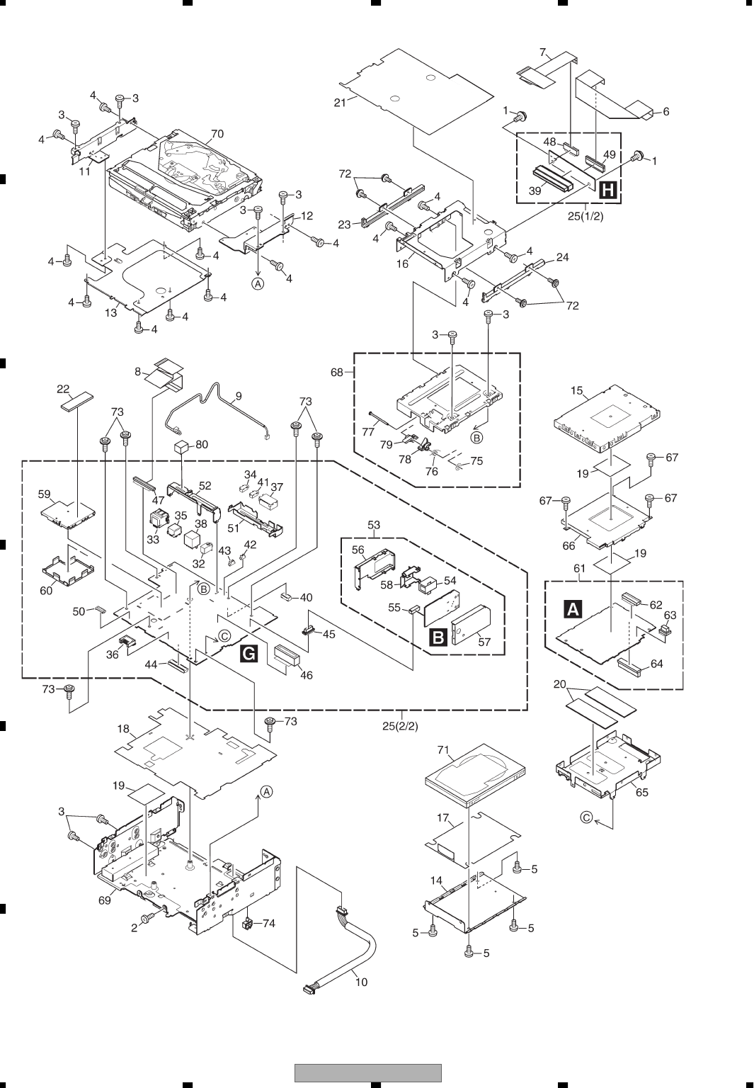
2.5 DVD MECHANISM MODULE

AVIC-Z1/UC 19
5678
5678
C
D
F
A
B
E
DVD MECHANISM MODULE SECTION PARTS LIST
Mark No. Description Part No.
1 DVD Core Unit CWX3301
2 Connector(CN1501) CKS4282
3 Connector(CN1401) CKS5100
4 Connector(CN1202) CKS5043
5 Connector(CN1611) CKS5100
6 Connector(CN1603) CKS4374
7 Connector(CN1101) CKS4842
8 Connector(CN1201) CKS5017
9 Screw BMZ20P020FTC
10 Screw(M2 x 3.5) CBA1571
11 Screw(M2 x 2.5) CBA1623
12 Washer CBF1038
13 Washer CBF1064
14 Spring CBH2586
15 Spring CBH2587
16 Spring CBH2588
17 Spring CBH2589
18 Spring CBH2590
19 Spring CBH2591
20 Spring CBH2592
21 Spring CBH2593
22 Spring CBH2594
23 Spring CBH2595
24 Spring CBH2596
25 Spring CBH2597
26 Spring CBH2598
27 Spring CBH2599
28 Spring CBH2600
29 Spring CBH2601
30 Spring CBH2602
31 Spring CBH2603
32 Spring CBH2604
33 Spring CBH2605
34 Spring CBH2711
35 Spring CBL1564
36 Pickup Unit(Service)(DP5) CXX1945
37 Shaft CLA3881
38 Shaft CLA4206
39 Shaft CLA4207
40 Lever CNC9933
41 Holder CNC9939
42 Holder CND2251
43 Holder CND2642
44 Frame CND2250
45 Sheet CNM6883
46 Sheet CNM8283
47 Sheet CNM8643
48 Lever CNV8502
49 Lever CNV8420
50 Cam CNV7156
51 Rack CNV7157
52 Clamper CNV7158
53 Arm CNV7159
54 Arm CNV7160
55 Arm CNV7161
56 Arm CNV7162
* 57 Arm CNV7163
58 Arm CNV7164
59 Roller CNV7165
60 Arm CNV7166
61 Guide CNV8093
62 Gear CNV7169
63 Gear CNV7170
64 Gear CNV7171
65 Gear(Black) CNV7172
66 Gear CNV7173
67 Gear CNV7174
68 Rack CNV7175
69 Gear CNV7176
70 Arm CNV8077
71 Lever CNV7178
72 Lever CNV7179
73 Screw IMS20P030FTC
74 Gear CNV7181
75 Holder CNV7183
76 Holder CNV7184
77 Guide CNV7745
78 Roller CNV7344
79 Damper CNV7470
80 Damper CNV7471
81 Collar CNV8845
82 Compound Unit(A) CWX3154
83 •••••
84 Compound Unit(B) CWX3394
85 Washer YE20FTC
86 Chassis Unit CXC3629
87 Arm Unit CXB8681
88 Frame Unit CXB8683
89 Arm Unit CXC4701
90 Bracket Unit CXB8685
91 Motor Unit(LOADING)(M1) CXC4315
92 Motor Unit(CARRIAGE)(M2) CXC4314
93 Screw Unit CXB8689
94 Roller Unit CXC5676
95 Motor(SPINDLE)(M3) CXM1308
96 Screw JFZ20P018FTC
97 Photo-transistor(Q1299) CPT231SCTD
98 Switch(S1201) CSN1069
99 Spring Switch(S1204) CSN1070
100 Resistor(R1298) RS1/16S0R0J
101 Guide CNV7615
102 Screw(M1.7 x 1.2) CBA1572
103 Arm CNV7742
104 Arm CNV7743
105 Spring CBH2710
106 Spring CBL1643
107 Spring CBH2712
108 Pickup Unit(Service)(Screw) GXX1259
109 Screw Assy CXX1750
110 Screw(M1.4 x 1.4) CBA1787
Mark No. Description Part No.
AVIC-Z1/UC
20
1234
1234
C
D
F
A
B
E
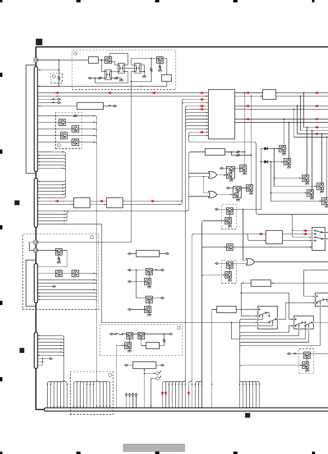
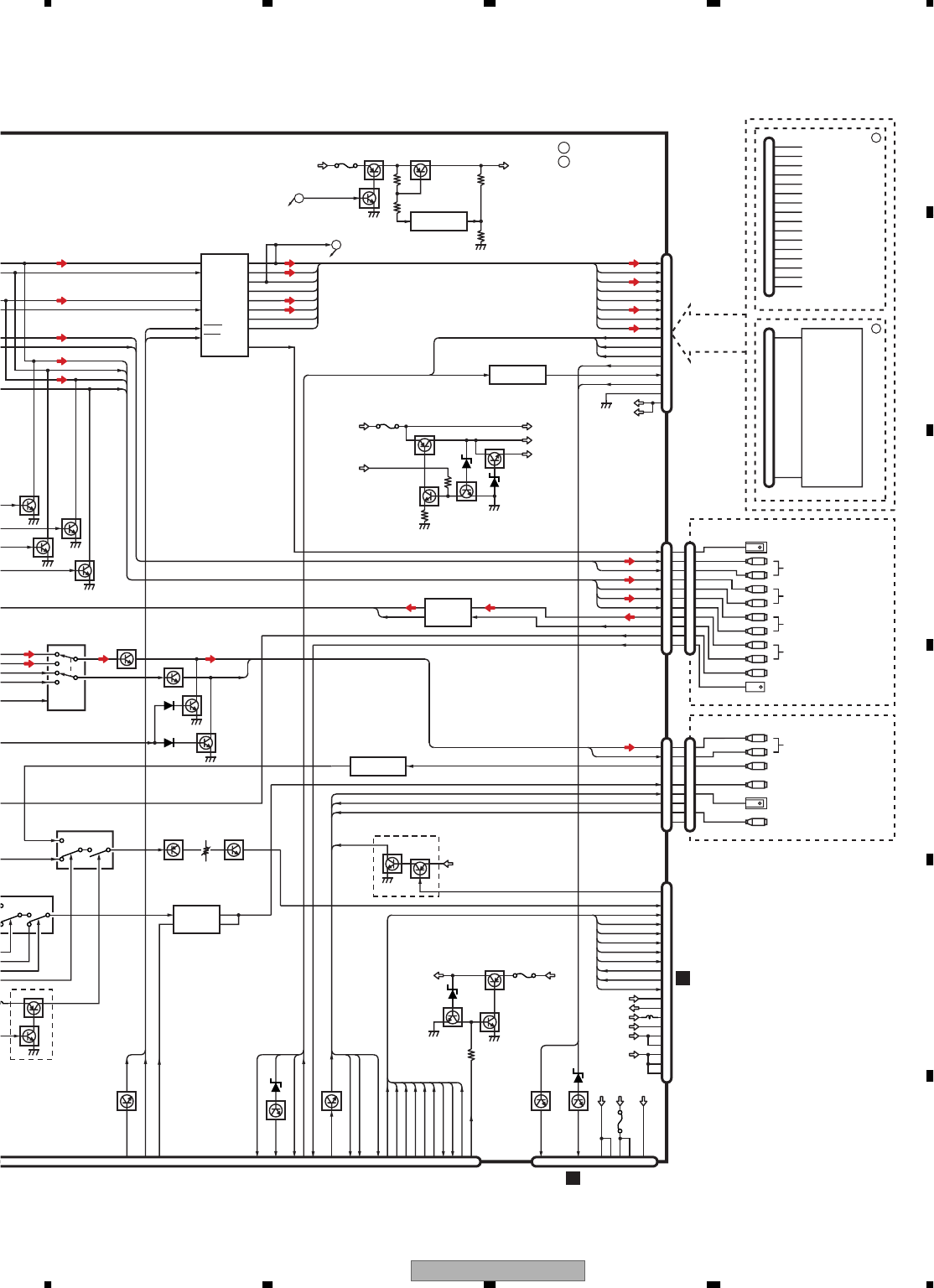
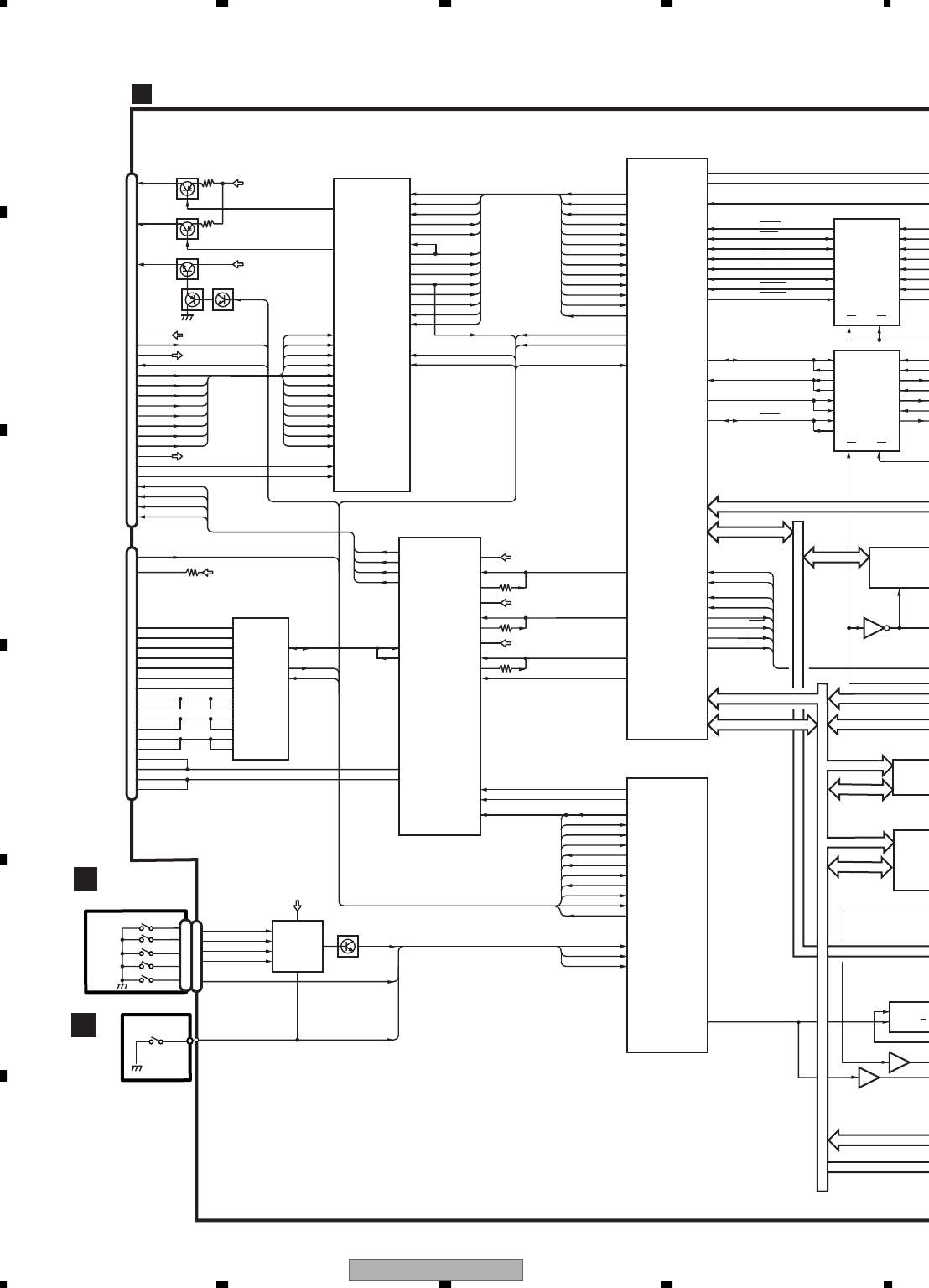
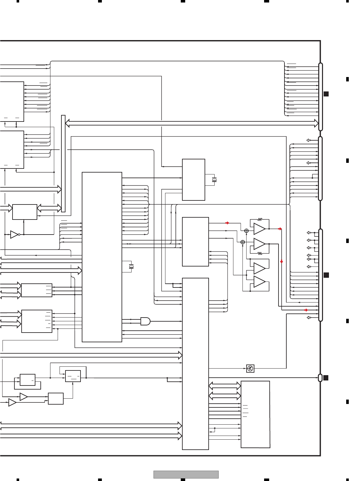
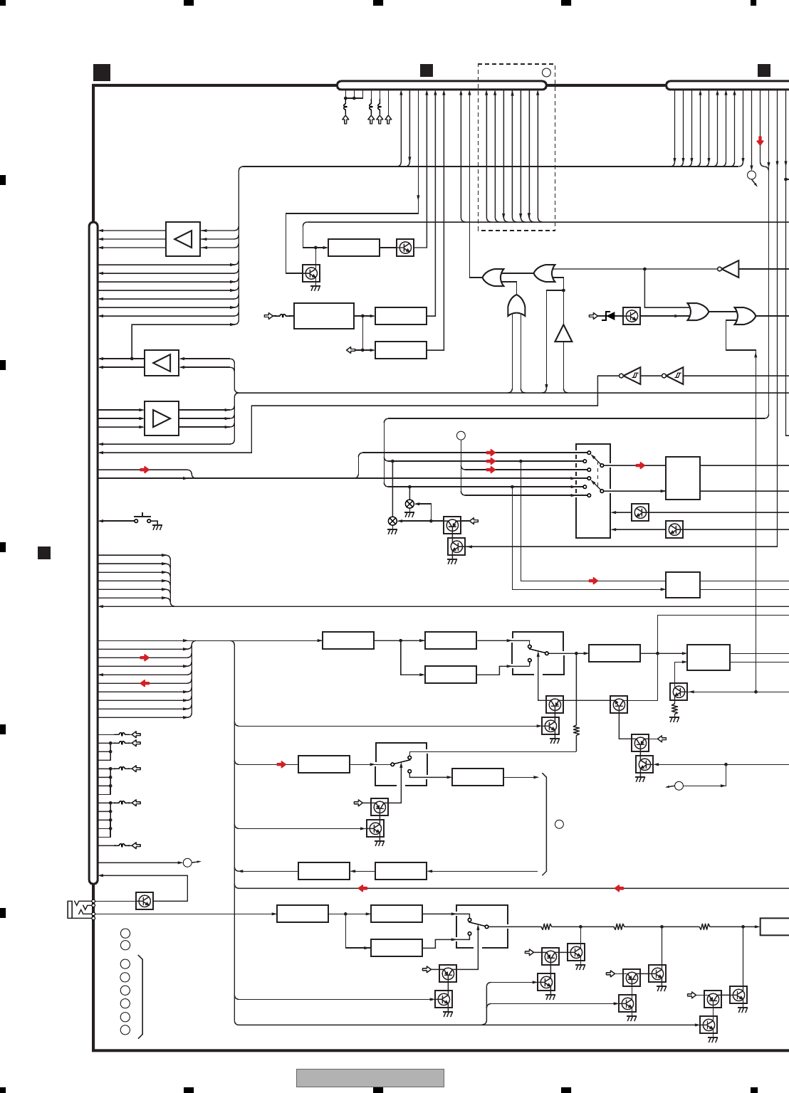
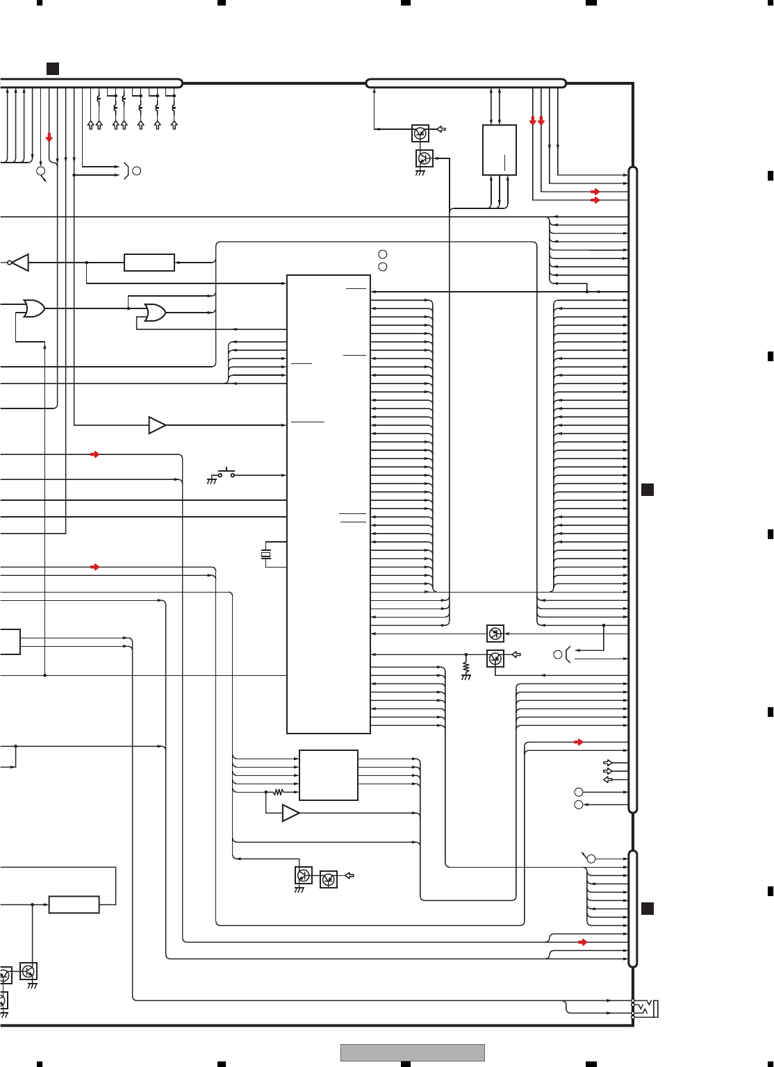
3. BLOCK DIAGRAM AND SCHEMATIC DIAGRAM
3.1 BLOCK DIAGRAM
IDED0-15
RESET
RESET(RESERVE)
DMARQ
DIOWB
DIORB
DMACKB
INTRQ
IORDY
DA1
DA0
DA2
CS1FXB
CS3FXB
BUSDIR
OE
1
20
23
46
50
|
47
|
3
18
21
33
27
25
29
31
36
35
37
38
44
45
CN4151
HDD5
CCD3
CORETDI
CORETDO
CORETCK
CORETMS
CORETRST
XASEBRK
RST3
TCK_AS
TMS_AS
TRST_AS
TDI_ASIC
TDO_SANYO
CN4001
CCD3
ZADA5
1
3
7
4
5
6
8
12
9
10
16
2
14
15
CC UNIT
A
H
CN6801
CN6802
TO HDD ASSY
5V(CCD5)
ATA_DIORB
ATA_IORDY
ATA_DMACKB
ATA_INT
ATA_DMARQ
LOGIC5
MOTOR5
ATA_RESETB
ATA_RESETB
MS_ATA_RESETB
MS_ATA_RESETB
ATA_DIOWB
2
4
27
29
37
38
39
41
42
43
44
47
7
48
9
24
|
31
33
35
ATA_DA0
ATA_DA2
ATA_CS0B
ATA_CS1B
IOCS16B
ATA_DA1
HDD RELAY PCB
ATA_DD0-15
CN6803
3.3V
MS_ATA_DD5
MS_ATA_DD4
MS_ATA_DD3
MS_ATA_DD2
MS_ATA_DD7
3.3V
5V(CCD5)
ATA_DD13
MS_ATA_DD6
1
3
5
13
15
17
4
6
8
10
14
12
16
28
18
21
27
31
23
29
25
32
33
36
35
37
38
7
9
11
ATA_DD11
ATA_DD14
ATA_DD15
ATA_DD12
ATA_DD8
ATA_DD9
ATA_DD10
MS_ATA_DD1
MS_ATA_DD0
MS_ATA_INT
ATA_DIOWB
ATA_DIORB
ATA_DMACKB
MS_ATA_DMARQ
MS_ATA_IORDY
ATA_INT
ATA_DMARQ
ATA_IORDY
ATA_DA0
ATA_DA2
ATA_CS0B
ATA_CS1B
IOCS16B
ATA_DA1
ATA_DIOWB
ATA_DIORB
ATA_DMACKB
ATA_INT
ATA_DMARQ
ATA_IORDY
BUSDIR
ATA_DA0
ATA_DA2
ATA_CS0B
ATA_CS1B
ATA_DA1
ATA_DD8-15
ATA_DD0-15
7
5
2
8
6
3
9
4ATA_DD5
ATA_DD4
ATA_DD3
ATA_DD2
ATA_DD7
ATA_DD6
ATA_DD1
ATA_DD0
15
18
12
14
17
11
1
19
13
17
15
13
5
7
3
19
16
IC6801
TC7MZ245FK
OE
OE
DIR
IC6802
TC7MBL3244AFK
2OE
1
20
23
46
50
|
47
|
3
18
21
33
27
25
29
31
36
35
37
38
44
45
CN1401
D
AVIC-Z1/UC 21
5678
5678
C
D
F
A
B
E
CCD3
ZADA5
CCD5
HDD5
BUP3
CN4804
DACOUT_L
DACOUT_R
ADCIN_L(MIC)
ADCIN_R(TEL)
DSPOUT_L
DSPOUT_R
1
3
15
19
26
28
30
32
34
35
36
37
38
40
41
7
9
BUSDIR(RESERVE)
PROGGAIN2
PROGGAIN1
PROGGAIN0
TELVC
XMS3RST
EMPH
42
CD_BCK
74
CD_DATA
76
CD_LRCK
78
NCLDCLK
90
SBCK
92
BLKCK
94
SUBC
2
ONSEIMUTE
FREQCNT
6
10
CPUWDT
14
GPSTOC
16
CTOGPS
18
IRQPW
24
CTOM
39
MTOC
45
46
48
REM
49
CTOP
55
PTOC
57
CC
60
TCHTOC
64
61
62
CTOB 59
BTOC
66
51
52
53
USB_XOVCR
68
75
CTOTCH
56
TELSEL
58
TCHSEL
70
UNITPWR
72
CLOCK
73
FRAME
77
PDCTOC
79
UNIT
80
CTOPDC
81
PCONT1
82
PCONT2
83
BB
84
CD
85
BA
86
CF
87
CJ
88
CE
CB
HYOKA
96
EXTOC
98
ETCTOC
CTOEX
100
CTOETC
102
OVER
104
CSYNC
FSC
43
B
63
G
22
R
105
109
111
115
117
107
113
112
114
116
118
122
120
HDDSENS
ASENRQ
MEMMUTE
OFFOK
B82RQ
CN5201
G
AVIC-Z1/UC
22
1234
1234
C
D
F
A
B
E
SL
SD 28
3
1
PLIO2
CN461
CN504
22
21
CTOGPS
SPEED
REVSNS
RQ
8
9
133
132
16
20
14
1
6
7
1
4
17
19
22
110
130
131
120
140
143
5
2
X401
IC 502
PEH026A:UC
PEH027A:EW5
FLASH ROM
IC 503
M5M5V216ATP-70HI
DRAM
CRCK
PIN0
PIN1
BOWWOWB
RESETB
IF
Q441
IC 461
ADC12H034CIMSAS1
RXD0
GPSTOC 7
19 TXD0
SPEED
PSWOUT 17
15 ADIO2
PIN2
PIN3
IC 401
UPC2749T F401
CTF1548
IC 402
UPB1027GS
IC 441
NJM2100V
IC 501
PD3390A
RESET
IC 504
MAX6364PUT29
BUP3V
128
129
X502
20.00MHz
16.368MHz
XAUXIN
XAUXOUT
102
103
X501
32.768kHz
XRTCIN
XRTCOUT
3
2
12
11 GSNSIN
GYROIN
GPS
ANTENNA
CPU
13
3PLIO2
DETIN
2
IC 532
LC72720YVSS1
RDS DECODER
X532
15
16
4.332MHz
GPS UNIT
B
G
CN6401
15
13
14
12
11
10
9
3
2
1
CN2
MOT0
MOT1
PULSE0
PULSE1
HALFSW
HOMESW
OPENSW
S1
OPEN SW
S2
HOME SW
S3
HALF SW
7
5
IC2
S-812C50AMC-C3E
IC1
BA6288FS
6
11
3
14
1
2
IC3
TC7W14FU
2
3
45
8
IC4
GP2L24B
2
3
IC5
GP2L24B
2
3
1
3
Q1
M
FLAP
MOTOR CN1
MAIN PCB UNIT
L
CN1003
C
AVIC-Z1/UC
AVIC-HD1BT/EW5
B
A
B
B
B
AVIC-Z1/UC 23
5678
5678
C
D
F
A
B
E
FMRF
ANT adj RF adj
FM ANT
T51 CF52
RFGND
OSCGND
DGND
AUDIOGND
NC
VCC
VDD_3.3
3.3V 2.5V
IC 4
3.3V 2.5V
←
IC 2
2.5V
NC
CE2
ROM_VDD
SL
DI
CK
CE1
LDET
DO
RDS_CK
RDS_DATA
RDS_LOCK
RDS_HSLK
76 13 5 1098 11 14 18192021
1
3
212 1522 16 4 17
IC 1
3.3V
AM ANT FMRF
ATT
LPF
OSC
IC 3 EEPROM
5.0V
IC 5
5V 3.3V
←
ATT
MIXER, IF AMP DET, FM MPX,
RDS DECODER
24
23
Rch
Lch
FMRF
ANT adj RF adj
FM ANT
T51 CF52
RFGND
OSCGND
DGND
AUDIOGND
NC
VCC
VDD_3.3
3.3V 2.5V
IC 4
3.3V 2.5V
←
IC 2
2.5V
NC
CE2
ROM_VDD
SL
DI
CK
CE1
NC
DO
NC
NC
NC
NC
76 13 5 1098 11 14 18192021
1
3
212 1522 16 4 17
IC 1
3.3V
AM ANT FMRF
ATT
LPF
OSC
IC 3 EEPROM
5.0V
IC 5
5V 3.3V
←
ATT
MIXER, IF AMP DET, FM MPX
24
23
Rch
Lch
FM/AM TUNER UNIT
(AVIC-HD1BT/EW5)
C
C
C
C
C
C
C
C
FM/AM TUNER UNIT
(AVIC-Z1/UC)
AVIC-Z1/UC
24
1234
1234
C
D
F
A
B
E
42
10
18
17
24
11
23
36
VTRL
VTRR
CLK
FRONTOUTL
DATA
FRONTOUTR
IN3L
REARTOUTL
REARTOUTR
IN1R
20
19
VDT
VCK
MUTEVO
VST STB
MUTE
41
37
FML
FMR IN2L
IN2R
40
38
AUDL
AUDR IN1L
IN3R
PREOUTL
PREOUTR
43
35
IPL+
IPR+
PREMUTE
IN4+L
IN4+R
12
22
C
14
1
GUIDE MIX
IC1621
NJM2060V
GUIDE L/R SW
GUIDE ISOLATOR
IC1402
PML009A
5
10
6,7
8,9
7
1
5
3
LPF
FL
Q1420
(1/2)
Q1420
(2/2)
Q1611
9
6
FL
FR
RL
RR
SWL
SWR
Q1432
BU1
RDVD
AUDIO8V
Q1613
Q1612
AUDIO8V
Q1614
31
IC1501(2/2)
NJM2060V
GUIDE
GMUTEL
OMUTE
GMUTER
AVV
2
1
4
IC1403
BA00CC0WT
BU1 AUDIO8V
AUDIO 8V REG.
41
IC1900
NJM2505F
AV-BUS
ISOLATOR
14
IC1530
NJM2125F
AUDIO8V A5S
A5S REG.
PWRFL
PWRFL
Q1200
Q1202
Q1203
PWRVI
PWRVI
BU1
SWACPW
Q1201
MFLPW
Q1822 Q1821
Q1823 13
BUV1 TMC8V
IC1821
M5237ML
IN ADJ
7
1
7
3
24
1
3
2
5
4
VIDEIN
VIDEIN
TVVTR
DVDV
DVDV
TVDVD
NVCOMP
RTVNV
TVBCR
1BCV
3
2
4
IC1200
NJM2235M
VIDEO ISOLATOR
AV(AVBUS/VTR/DVD-V)
IC12
0
NJM22
4
FRONT VIDEO
IC1202
NJM2235M
REAR VIDEO
SELECTOR
5
VMUTE
Q1242
ACC5V
CN2501
CN1832
FM/AM TUNER UNIT Y2501
3.3V REG.
VDD_3.3 3 1
VCC
ROM_VDD
DI
DO
CE1
CK
SL
CE2
D_STOFM
D_FMTOS
FMCE1
FMCLK
FMSL
FMCE2
Lch
Rch
FMLS
FMRS
AM_ANT
FM_ANT
RDS-LOCK
HDS-HSLK
RDS-CK
RDS-DATA
LDET
HRLK
HRHSLK
HRCK
HRDT
HLDET
1
3
23
24
5
6
8
9
10
14
11
18
19
20
21
4
13
17
VDORA85
ROMVDD5
TMC8V
VDORA85
D_STOFM
D_FMTOS
AUDIOL
DVDV
AUDIOR
AUDL
AUDR
GUIDE
ONSEI MUTE OMUTE
GMUTEL
GMUTER
CE1
FMCLK
FMSL
CE2
13
16
14
20
7
5
6
4
3
1
19
18
9
FM TUNER UNIT Y2600
STUNB
SCMP
SBSL
SBDI
SBCE
SBDO
SBCK
SFMANT
SBSD
TMCDET_O
TMCSL
TMCDI
TMCCE
TMCDO
TMCCK
TMCSD
1
6
13
14
15
16
7
9
10
IC2501
NJM2391DL1-33
ANTENA
34
44 IN4−L
IN4−R
IPR−
IPL−
31 IC1270
NJM2137V
DVD/TV TVDVD
TVBCR
TVVTR
RTVNV
NVCOMP
VMUTE
PULSE1
MOTPWR
OPENSW
PULSE0
HOMESW
MOT1
MOT0
VDD5
VACC5
SYSPWR
CCON
SWACPW
MOTB
ROMVDD5
ACC5V
ILMB
PREMUTE
RCONTA
RDVD
CN1831
CN1003
VST
VDT
MUTEVO
VCK
DVDL
DVDR
FANUP
RMUTE
IPL
IPRG
IPLG
IPR
IPL+
IPR−
IPL−
IPR+
TMCDET_O
TMCSL
TMCSD
TMCCK
TMCDO
TMCCE
TMCDI
HRCK
HRDT
HLDET
HRLK
HRHSLK
9
11
37
70
38
13
15
17
77
19
41
43
67
21
40
48
46
36
34
35
61
60
64
65
45
50
51
52
53
22
23
26
27
24
25
28
29
30
31
32
33
57
55
54
6
7
7
OPENSW
HOMESW
1
8
2
7
6
15
14
13
3
4
PULSE0
PULSE1
FLPPW
FLPBUP
MOTPWR
MOT0
MOT1
CN5801
G
CN5802
G
CN2
L
AUDIO UNIT
A
AUD ISOLAOR
IC1960
BA3121F IC1501(1/2)
NJM2060V
OUT1
OUT2
IN1
IN2
VDORA85
D
C
FU1820
B
B
B
B
BQ2550
Q2504
Q2503
Q2502
Q2501
L2558L2557
L2553
CN2050
CN2800 Q2800
Q2801 Q2802
Q2551
FL
P
Q1422
(1/2)
Q1422
(2/2)
Q1421
(1/2)
Q1421
(2/2)
RMUTE
Q1470
BU1
3
5
1
7
OUT1
IN1
IN2 OUT2
DVD ISOLATOR
IC1940
BA3121F 2
4
15
10
11DVDR
DVDL
DVDR
DVDL
VTRR
VTRL
AUDIO SELE
C
IC1520
TC4052BFT
3
1
3
RCONTA
Q1521
SOURCE SELECT
TMC 8V
FMCE1
FMCE2
AVIC-Z1/UC 25
5678
5678
C
D
F
A
B
E
14
17
9
12
11
19
7
21
5
23
3
15
GMIXL
GMIXR
22
4SREMOT
MUTE1
AMPMUTE MUTE1
POWER AMP
IC1401
PAL007B
RL RL+
RR
FR+
RL−
FR−
RR+
FL FL+
RR−
FL−
B-REMOTE
FR
25
MUTE
STBY
VTRL
VTRR
RLP
FANUP
FRP
RLM
FRM
RRP
FLP
RRM
FLM
4
20
/
2)
Q1431
POSWL
POSWR BREMOTE
Q1350
4
1
2
3
OUT
IN
STBY SAG
7
24
7
1BCV
3
24
IC1201
NJM2246M
FRONT VIDEO SELECTOR
IC1202
NJM2235M
R
EAR VIDEO
S
ELECTOR 75Ω DRIVER
IC1204
TK15405BMI
5
Q1242
Q1204VR1200Q1205
2V→1V
CN1201
BREM
POSWL
POSWR 1
3
19
20
13
15
17
CN1202
16
14
1
12
10
8
7
6
BCV
VOUT
GUIDEON
WREM SEL
WREM AN
WCONT
WREMIN
ROUT
LOUT
TEL MUTE
VIN
VTR_L
VTR_R
VTRL+
VTRR+
RR 7
9
11
5
FL
FR
RL
CN1001
FL−
RL−
FR−
RL+
FR+16
15
14
13
9
4
8
7
5
6
3
2
1
12
11
10
BU1
BUV1
ANTANTON
RR+
FL+
RR−
FLM
RLM
FRM
RLP
FRP
RRP
FLP
RRM
SPEED
PKB
REV
ILM
BUP
ACC
16 IC1802
TPD1018F
AUTO ANT
PWRFL
PWRVI
ACC5V
MFLPW
SWACPW
HDRESET
MONVBS
CN1203
MONT_FINVPUL
MTOSYS
MOREMREMIN
NVRED
SYSTOM
NVBLUE
NVGRNNVGREN
NVSYNC
YS
38
39
40
27
28
24
20
5
6
9
11
12
13
21
22
23
33
25
15
19
ILMB
ROMVDD5
RESET
VDOUT
NVGREENNVGREN
NVRED
REMIN
MTOSYS
SYSTOM
INVPUL
YS
NVSYNC
NVBLUE
SPEED
REVSNS REV
PKB
DD8CONT
ANTON
SREMOT
RVMUTE
GUIDEMT
RESET
MUTE2
MUTE2
Q1430
TELM
WCONT
WREMIN
12
2
4
8
69
71
73
79
75
42
44
14
59
72
62
39
56
63
10
20
16
18
74
BU1
BUV1
ILMSNS
ILM SENS
Q1006
ASENS
Q1004
ASENS
ILM
ACC
BUPV
BUP
CN1002
DVD8
DVD8/BUP
3
4
7
8
Q1841
(1/2)
Q1001
Q1841
(2/2)
Q1840
MS3 8V
DVD8 BU1
9
10
D
CN5851
G
CN1
K
ILMB
Q1207
FU1200
Q1830
(1/2)
Q1830
(2/2)
Q1206
ACC5V
BU1 MOTB
SWACPW
41 IC1901
NJM2505F
BCV ISOLATOR
FU1840
FU1001
I
14
11
VDORA85
BU1
13
IC1850
M5237ML
Q1852
Q1851 Q1850
VDORA85
FU1850
SYSPWR
PRE-RR
PRE-RL
PRE-FR
PRE-FL
Q1422
(1/2)
Q1422
(2/2)
Q1421
(1/2)
Q1421
(2/2)
2
4
15
10
11DVDR
DVDL
VTRR
VTRL Q1542
Q1541
Q1540
(1/2)
Q1540
(2/2)
AUDIO SELECT
IC1520
TC4052BFT
3
13
REARL
REARR
REARL
REARR
3
5
1
7OUT1 IN1
IN2OUT2
IC1486
BA3121F
19
1
3
9
15
17
13
20
11
5
7
CELLULAR MUTE
SYSTEM REMOTE CONTROL
AUDIO INPUT
VIDEO INPUT
REAR OUTPUT
FRONT OUTPUT
SUBWOOFER OUTPUT
<CODE ASSY> CDE8083
GUIDE ON
REAR OUTPUT L/R
WIRED REMOTE INPUT
REAR VIEW CANERA IN
REAR MONITOR OUTPUT
<CODE ASSY> CDE8084
12
10
7
6
1
16
14
8
C
AVIC-Z1/UC
AVIC-HD1BT/EW5
POWER
SUPPLY
TERMINALS
16
15
14
13
9
8
7
6
5
4
3
2
1
12
11
10
16
15
14
13
9
8
7
6
5
4
3
2
1
12
11
10
A
B
<CODE ASSY>
CDE8082
CDE8165
B
A
ACC 5V
PRE-RR
PRE-RL
PRE-FR
PRE-FL
VTR ISOLATOR
TELMUTE
AVIC-Z1/UC
26
1234
1234
C
D
F
A
B
E
DVD CORE UNIT
D
26
24
20
23
22
19
15
18
17
16
14
10
13
12
11
9
7
5
4
2
3
1
CN1101
CN1201
SW OEIC
VSHF
TEMP
CD/DVD
78LD
A
B1
B2
RF−
B3
RF+
B4
C
MDC
F+
F−
T−
T+
FOP
FOM
TOP
TOM
18
16
17
15
26
25
27
24
VO3(+)
VO3(−)
VO4(+)
VO4(−)
OPIN4(−)
OPIN4(+)
OPOUT4
OPIN3(+)
TOP
TOM
FOP
FOM
65LD VCC5
VCC5
VREF1
VCC5
VHALF
VHALF
VCC5
Q1102
Q1105
Q1104 Q1103
Q1101
50
VIN3
B3
VIN7
B3
59
51
B2 VIN6
VIN8
B4 52 VIN4
B4 60
VIN11
C62
RFINN
RF−48
RFINP
RF+47
LPC1
1
LPC2
3
20
15
18
17
16
14
10
13
12
11
9
7
5
4
2
3
1
HALL_BIAS+
SWITCH HOME
CONT
FG
HALL_U+
HALL_U−
HALL_V+
HALL_V−
HALL_W+
HALL_W−
HALL_BIAS−
COIL_U
8COIL_W
6
H2H
H1H
H1L
H2L
A12
H3H
H3L
VHB
A11
A31
A21
A32
A22
COIL_V
7
6
5
4
3
2
EC
START
FG1
8OPIN2(−)
6
OPOUT2
7
VO1(−)
13
VO1(+)
14
11
10
1
28
27
22
21
24
25
CRGD1
CRGD2
CRGD3
COM
COP
CRGD4
VCC5
CN1202
3
5
4
2
1
12cm
WAKEUP
8cm
DISC DETECT
8cm
PHOTOSNES
DSCSNS
FEOUT 22
DFL TON 30
DFL TOP 31
OFTR 39
BDO 40
RFENV 41
TESTSG
FEY
ARF−
ARF+
OFTR
OFTR
BDO
RFENV
TESTSG
46
SEN LTFEP
12
MONI0
DVDLOCK 127
MONI1
CDLOCK 128
FG
FG 69
DAC0
114
DAC1
115
SPDRV
68
TRSDRV
67
145
IORDY 140
NIOCS16
175
NRESET
VIN1
B1 57 VIN12
A63
LPCO1
2
LPCO2
4
VIN5
B1 49
VIN2
B2 58
FEP
IC1101
AN8703FH
DVD MOTOR CONTROL
IC1202
AN8471SAT1
SODC
IC1301
MNZS26EDCUB
BUFFER
IC1403
TC74LCX244FTS1
BUFFER
IC1405
TC74LCX244FTS1
DVD POWER CONTROL
IC1201
BA5985FM
CPU(2/2)
IC1701
PE5511A
IC1502
TC74VCX7
4
BUFFER
IC1505
TC7PA04FU
VDD33
Q1201
WAKEUP
DETECT
23
22
OPIN3(−)
OPOUT3
OPIN1(+)VHALF
3
FD
TD
CRGDRV
OPIN1(−)
MD
OPIN2(+)
OPOUT1
28
REV EJECT
1
FWD
92 EJECT
93 LOAD
LOAD
CLKOUT 90 1CK
31D
1Q
1Q
2
CLKOUT
21
MUTE OFTR
DVDLOCK
85
74
CONT 31
LTFEP 84
CDLOCK 77
CD/DVD 94
TEMP 80
OEIC 32
HOME 45
FG
OFTR
DVDLOCK
CONT
LTFEP
CDLOCK
CD/DVD
TEMP
OEIC
CRGSENS
FG
22
WAKEUP WAKEUP
51
PHOTOSNES PHOTOSNES
78
DSCSNS DISCSENS
79
16X
W
XSRAMWR
34 CL
K
OHRST
146
NIORD OIORD
139
DA1 ODA1
135
NCS1FX OCS1FX
134
NCS3FX OCS3FX
137
DA0 ODA0
142
NDMACK ODMACK
148
18
16
14
12
9
7
5
17
119
DMARQ
1Y1
1Y2
1Y3
1Y4
2Y1
2Y2
2Y3
2A4
1A1
1A2
1A3
1A4
2A1
2A2
2A3
ODMARQ
47
NRST XODCRES
36
NRD XRD
35
NWR XWR
34
NCS XCSODC
6
WAITODC WAITODC
5
NINT2 2
NINT1 INT1
INT2
1
NINT0 INT0
1OE 2OE
2
4
6
8
11
13
15
136
DA2 ODA2
175
MASTER OMASTER
79
OSCI1 MCK16
141
INTRQ OINTRQ
147
NIOWR OIOWR
2
3
5
16
6
13
8
9
1
19
19
1A1
2Y4
2Y3
1Y2
1A3
2A2
1A4
2Y1
1Y1
2A4
2A3
1A2
1Y3
2Y2
1OE 2OE
18
17
15
4
S
14
7
2A1 11
BUS BUFFE
R
IC1401
TC74LCX245F
T
IC1402
TC7SH04FUS1
FLASH M
I
C
P
D
A1-20
A1-17
DIR
1
XOE
24
SRA
IC
1
M5M5V21
OHDD8-15
OHDD8-15
A0-17
A
HDD0-7
VCC
65MD
78MD
PHOTO
SCKCOMN SCKCOMN
68
5
4
2
SCK SCKCOMN
13
STDI SOCOMN
44
OFTR
BDO
AD3
TESTSG
FBAL
JLINE
TBAL
AD2
AD1
AD0
NARF
ARF
SOCOMN
FBAL
JLINE
7
6
16
TBAL
ASOUT 20
TEOUT 18
FBAL
JLINE
TBAL
ASF
TEY
OFTR
BDO
RFENV
TESTSG
66
65
84
119
118
117
110
111
FBAL
JLINE
TBAL
ASF
TEY
FEY
ARF−
ARF+
51
52
120
82
SOCOMN 70
FEN 21
2Y4 3
D0-7 D
0
D0-15
D0-15
PICKUP UNIT(SERVICE) CARRIAGE MOTOR
SPINDLE MOTOR
S1206
S1202
S1203
S1204
S1201
S1205
CLAMP SW
12cm
8cm
8cm
Disc sens
Disc sens
COMPOUND
UNIT(B)
F
COMPOUND UNIT(A)
E
5
6
2
3
4
AVIC-Z1/UC 27
5678
5678
C
D
F
A
B
E
IORDY
IOCS16
IC1502
TC74VCX74FT
BUFFER
IC1505
TC7PA04FU
CPU(1/2)
IC1701
PE5511A
AV CHIP
IC1503
MN677531KAUB
XAVINT
XAVINT2
39 XAVINT
FS44/48 86 FSSW
1CK
31D
1Q
1Q
2
6
5
HCLK
41 XAVINT2
XAVRES 44 XAVRES
IC1504
TC74VCX74FT
11
13
2D
2Q
12
8 XHWR
2CK
2CLR
1 6 XWR1XSRAMWR
3 4 CLKOUT1
119
1Y1
1Y2
1Y3
1Y4
2Y1
2Y2
2Y3
2A4
1A1
1A2
1A3
1A4
2A1
2A2
2A3
40 XSODCINT2
XODCRES
19 XSODCINT1
XCSODC
20 XSODCINT0
WAITODC 91 NHDK/WAITODC
102 XCSODC
INT1
INT2
43 XODCRES
AMUTE
VCONTB
EMPH
VCONTA
XRESET
IRQPWR
BUSISO 111 DMIXON
INT0
88
117
114
116
59
49
HSTCMD 66
SLVSTS
AMUTE
VCONTB
EMPH
VCONTA
XRES
IRQPWR
HSTCMD
SLVSTS
XAVCHK_ENT 76 XAVCHK_ENT
SICOMN 69 SICOMN
TXPC 53 TXPC
RXPC 52 RXPC
DTR 50 DTR
VPP/MODE2 18 VPP
67
LTDAC 65
SCKCOMN 68
SOCOMN
LTDAC
SCKCOMN
SOCOMN
70
ML
15
MC
14
MD
13
DATA
2CH
VOUTL 7
SRCK
84
BCKIN
SRCK
LRCK
88
LRCKIN
LRCK
DMIX
87
MCLK
DACCLK
2CH
SRCK
LRCK
DACCKL
2
1
3
16
DACCK 86
VSTR-70
70
FSEL
14
VRQ
71
AUDSTR
STCLK
STENABLE
STVALIO 69
XHINT
17
XHINT2
18
XRST
13
1OE 2OE
2HRST
4IORD
6DA1
8CS1FX
11 CS3FX
13 DA0
15 DMACK
DMARQ
1
1
19
19
1A1
2Y4
2Y3
1Y2
1A3
2A2
1A4
2Y1
1Y1
2A4
2A3
1A2
1Y3
2Y2
1OE 2OE
18 STCLK
17 DA2
15 MASTER
4STENABLE
14 STVALIO
7INTRQ
2A1 11 IOWR
BUS BUFFER
IC1401
TC74LCX245FTS1
IC1402
TC7SH04FUS1
FLASH MEMORY(16M)
IC1705
PD6527A
A1-20
A1-17
DIR1
XOE
24
X1701
4.97MHz
62
X2
X1 63
X1501
27MHz
7
XTI
XTO 8
11
WE
CE
OE
26
28
97
106
95
XWR
XCSFM
XRD
XLWR
XCSFLSH
XRD
SRAM(2M)
IC1702
M5M5V216ATP-70HI
41
OE
BC2
BC1
40
39
108
109
XRD
XUBE
XLBE XUBE
XLBE
S
WE
6
17
107
105
XCSSR
XSRAMWR XCSSRAM
XSRAMWR
XCSAVR 101
XCSAVW 100
IC1706
TC7SH08FUS1
424
XCS
XCSAV
1
2
23 XRD
13 SO1
MCK16
10
EXTCK1 AO2
3MO1
100 EXTCK
96 CLK27
136 VCLK
CLOCK GEN.
IC1507
SM8707FV
IC1605
PCM1742KE
DQMLM
XCSE
DQMUE
DQMUM
MCK1
MCK
XWE
XCAS
XRAS
XCSM
22 XWR
XHWR
XHWR
21 XWRH
HCLK
26 HCLK
AUDIO 2CH ANALOG OUT
IC1602
NJM2100M
IC1604
NJM2100V
-
+
1 LOUT
2
3
-
+
1
2
3
VOUTR 8
VCOM 10
-
+
7 ROUT
5
6
-
+
7
5
6
VCBOUT
Q1501
126
VIDEO OUT
IECOUT 83 IECONT
CN1501
1
CN1401
1
23
21
25
35
36
38
37
29
31
27
28
33
32
HDMACK
HINTRQ
HIOCS16
HDA1
HDA0
HDA2
HCS0
HCS1
INTRQ
IOCS16
DA1
DA0
DA2
CSELMASTER
IORDY
DIORD
DIOWR
HDMARQ
HRST
18
|
3
CS3FX
CS1FX
DMACK
IORD
IOWR
DMARQ
HRST
CN1611
23
21
22
20
24
18
19
17
40
38
34
36
28
10
9
7
8
14
13
16
15
11
12
HSTCMD
IRQPWR
XRES XRESET
BUSDIR
VCONTA
EMPH
SLVSTS
VCONTB
AMUTE
VCC18
VD8
VCC33
SRVDD
VDD33
CN1603
19
17
18
16
14
15
13
6
5
1
4
9
12
11
7
8
DTR
RXPC
TXPC
SLVSTS
HSTCMD
XAVCHK_ENT
VCONTB
XRES
SCKCOMN
SOCOMN
SICOMN
VPP
VDD33
VDD33
AVCC5
VCC5
HDD8-15D8-15
A0-20
HDD0-7
HDD0-15 HDD0-15
STD0-7(OHDD8-15)
CN6101
G
CN5601
G
XRD
1CK
31D 1Q
25
2Y4 3
D0-15
D0-15
D0-15
SDRAM
IC1501
K4S641632
H-TC75
15
DQMLM
16
XWE
MDQ0-15
17
XCAS
18
XRAS
19
XCSM
35
XCSE
21
DQMUE
39
DQMUM
38
MCK
189
193
195
196
198
190
192
183
185
199
DQML
WE
CAS
RAS
A11
BA1
DQMU
CLK
CS
MA0-11
D0-15
A1-17
CLK27
SCKCOMN
SOCOMN
ANALOG L OUT
ANALOG R OUT
CN6803
H
VCONTA
AVIC-Z1/UC
28
1234
1234
C
D
F
A
B
E
PCE
PCK
PDO
SL
PDI
DET
SD
TMCCE
TMCCK
TMCDO
TMCSL
TMCDI
TMCDET_O
TMCSD
OUT+5
8
9
OUT−8
IN+
VC
2
4
GUIDE SP AMP
IC5481
TDA7052BT
IC5401(3/4)
NJM3403AV
MIX AMP
1
5
6
7
IC5421
TC4W53FU
GPSTOC
CTOGPS
RQ
GPSREV
PLS
CN6401
CCD3
GSN
GYO
POUT
CN461
BCN
1
D
VCC5A
SRVDD
15
16
30
26
29
27
28
22
21
20
19
12
11
13
1
3
5
7
6
8
10
SWBUP
AU8
Q5481
(1/2)
Q5482
Q5483
Q5481
(2/2)
12DACOUTR IC5401(1/4)
NJM3403AV
ISOLATOR
CN6101
VIDEO OUTDVDV
LRCK
SCKBCK
ADOUT0DATA
VCONTA
BUSDIR
SLVSTSMTOC
HSTCMDCTOM
IRQPWRIRQPW
XRESET
XMRST
ANALOG ROUTDVDR
ANALOG LOUTDVDL
EMPH
LRCKCD_LRCK
CD_BCK BCK
CD_DATA DATA
LRCK2
BCK2
DATA2
BUSDIR(RSV) BUSDIR
MTOC
CTOM
XMS3RST XMRST
EMPH
VCONTBCONTB
AMUTEMMUTE
OMUTE
MMUTE
1 2 FTELADCINR
ADCINL
IC5423(1/4)
NJM3403AV
AMP(Receiver)
14 13
IC5423(4/4)
NJM3403AV
LPF AMP
6,75DACOUTL IC5423(2/4)
NJM3403AV
LPF(10.5K)
8 TOTEL9IC5423(3/4)
NJM3403AV
AMP(Transmitter)
MUTE
CPUWDT5
1
IRQPW5
2
3
13
11
9
11
10
13
18
17
20
22
19
3
5
7
24
23
OUT_R
OUT_B
OUT_G
CSYNC
R
B
G
FSC
CSYNC
OVER
Q5902
Q5901
AU8 Q5421
(1/2)
Q5421
(2/2)
MEMMUTE
CF
Q5611
MICSNS
TELSEL
CH1
COM
CH0A
MICIN
TELVC
8
14
9
13
6
1,23
AMP(TEL)
ATT
IC5451
TC4W53FU
MIC HPF(100Hz)
IC5452(1/4)
NJM3403AV
6235
IC5452(3/4)
NJM3403AV LP
IC545
2
NJM3
4
5V→3V
IC6601
TC74VHC32FTS1
3V→5V
IC6603(1/2)
TC74VHCT125FTS1
5V→3V
IC6604
TC7WH14FU
IC6605
TC7S04FU
IC5452(4/4)
NJM3403AV
AMP(Speech recognition)
PROGGAIN0
PROGGAIN1
PROGGAIN2
Q5453
(2/2)
Q5453
(1/2)
AU8
Q5452
(2/2)
Q5452
(1/2) Q5455
Q5456
(1/2)
Q5456
(1/2)
AU8
Q5454
(2/2)
Q5454
(1/2)
AU8
Q5451
(2/2)
Q5451
(1/2)
HDD SENSE
S5901
AU8
CH0
7
6
5
COM 1
CH1 A
2
4
9
810
CTOSYS CTOSYS53
2
5V→3V
IC6609
TC7WH08FU
IC6610
TC74VHC125FTS1
B82RQ5B82RQ 7 1,2
IRQPW
IRQPW
IRQPW535,6
11 12
32
65
OFFOK OFFOK56
5
CPUWDT CPUWDT589
12
46
MUTE
5
1
23
IC6602(1/3)
TC74VHC32FTS1
GY6401
IC6402
S-812C50AUA
-C3E
VCC5A REG. G senser
GYRO
GY6402
AU8 1
3
1
6
3
2
IC5901
NJM2904M
SPEED SENSE
15
SPEED
CTOGPS
GPSTOC
CN5201
(1/2)
HDDSNS
PROGGAIN1
PROGGAIN0
PROGGAIN2
REM
DACOUT_L
DACOUT_R
DACOUTL
DACOUTR
TCHSEL
DSPOUT_R
DSPOUT_L
DSPOUTL
DSPOUTL
MEMMUTE
ADCIN_L
ADCIN_R
ADCINL
ADCINR
TELVC
SRVDD
CCD3
ASENRQ
ONSEIMUTE OMUTE
ASENRQ
ASENRQ5 ASENRQ
4,5
6
D
E
D
B
C
CCD5
CCD5
BUP3
HDD5
34
74
41
79
38
77
24
57
40
36
42
43
58
56
49
61
73
39
10
6
2
14
16
18
111
109
107
105
22
113
55
53
51
45
59
37
7
9
35
1
3
98
76
19
15
115
117
112
118
114
116
122
120
CCD5
ADA5
OFFMUTE
BUP
Q5961
AUDIO SELECT
IC5003
TC4052BFT BUFFER
IC5002
NJM2904V
1
2
4
12
3
13
3
5
1,2
6,7
10
9
ACONTA
ACONTB
15
11
DSPOUTL
DVDL
AVPL
DSPOUTR
DVDR
AVPR
Q5002
(1/2) Q5001
(1/2)
Q5001
(2/2)
Q5003
Q5004
Q5002
(2/2) AU8
BUFFER
IC5004
NJM2904V
5
3
6,7
1,2
MIC IN
CN5611
NAVI MOTHER PCB(1/2)
G
CN4804
A
LPF AMP
7
5IC5401(2/4)
NJM3403AV
1412 IC5401(4/4)
NJM3403AV
LPF(GUIDE)
1
5
6
7
IC5424
TC4W53FU
CH1
COM
CH0 A
TCHSEL
Q5401
(1/2)
Q5401
(2/2)
G
VCC5A
TO 2/2
AVIC-Z1/UC
AVIC-HD1BT/EW5
B
A
E
F
G
H
I
J
AVIC-Z1/UC 29
5678
5678
C
D
F
A
B
E
SYSTOM
TVVTR
MTOSYS
STOM
MTOS
RTVNV
RESETRSTIN
NVRED
TELMUTE
TVBCR
WCONT
VMUTE
NVBLUE
DVD/TVDVDTV
NVGREN
DD8CONT
NVCOMP
NVR
NVB
NVG
NVCMP
YS
WREMIN
RMUTE
HRLK
HLDET
RVMUTE
PKB
RCONTA
MUTEVO
MOT0
MOT1
REMIN
REMIN
GUIDEMT
PULSE0
OPENSW
SPEED
HOMESW
MOTPWR
PULSE1
SYSPWR
SWACPW
PREMUTE
SREMOT
ANTON
VDD5
CN5802
CN5801
SYSTOM 108
RTVNV
MTOSYS 87
107
DVDTV
TVBCR
TVVTR
84
86
85
RDVD
VMUTE
29
66
65
RCK
WREMIN
57
137
RDSLK
RDS57K 25
13
24
RVMUTE
RMUTE
CPUWDT
LDET
STOM
MTOS
WCONT
HRHSLK
HRLK
HRDT
HRCK
HLDET
35
56
45
117
103
105
113
MOT0
RCONTA
MUTEVO
15
55
11
MOT1
18
104
17
16
MOTPWR
PULSE1
PULSE0
14
20
19
SWACPW
GUIDEMUTE
SYSPWR 109
99
62
SREMOTE
ANTON
ACONTA
ASENBO 88
TX 91
RX 90
76
ACONTB
77
130
PBSNS 129
TELIN 58
NOSELR 54
NOSELL 53
135 FMSL
TUNCE1 100
TUNCE2 101
TUNDI 46
TUNDO 47
TUNCLK
MUTE
X1
X2
48
98
61
64
HOMESW
WCONT
BKSNS
MS3CONTB
OFFOK
OPENSW
HOMESW
OPENSW
SREMOT
GUIDEMT
TUNSL
INVPUL 122
DD8CONT 121
VST 12
VDT 9
VCK
B82RQ
IRQPWR
CTOSYS
10
RDT 23
SYSTEM-uCOM
IC6607(1/2)
INVPUL
NVSYNC
DVDL
DVDR
DVDL1
DVDR1
HRCK
HRHSLK
REVSNS
GPSREV
SYSREV
HRDT
76
78
64
60
62
51
49
50
48
42
41
47
46
45
44
43
69
71
68
65
67
63
61
59
28
39
40
35
37
29
30
73
74
27
25
23
52
21
17
18
55
53
57
7
54
56
19
20
15
16
58
9
11
8
13
70
66
26
10
38
3
5
72
1
6
32
34
36
24
AMPMUTE
GMUTER
GMUTEL
GUIDE
ONSEIMUTEOMUTE
DVDV
AUDIOR
AUDIOL
FMSL
FMCE1
FMCE2
D_STOFM
D_FMTOS
FMCLK
CCON
20
18
17
8
7
5
3
2
1
16
15
14
12
FMCE1
GMUTER
GMUTEL
FMCE2
D_STOFM
D_FMTOS
FMCLK
RDVD
VST
VDT
VCK
VACC5 75
ILMB
TMCCE
TMCCK
TMCDO
TMCDI
TMCDET_O
TMCSL
TMCSD
IPLG
IPL
IPRG
IPR
O
UT+5
O
UT−8
SPP
GUIDE
SPM
S
P AMP
4
81
0
52BT
CN1611
D
µVDD5
SRVDD
VCC33
VIDEO OUTDVDV
VCONTA
CONTA
CONTB
HSTCMDCTOM
IRQPWRIRQPW
XRESET
XMRST
ANALOG ROUTDVDR
ANALOG LOUTDVDL
EMPH
VCONTBCONTB
AMUTEMMUTE
OMUTE
E
MUTE
VD8
VCC18
VCC5
21
18
17
20
22
19
3
5
7
24
23
28
25
29
30
31
32
33
34
26
27
1
VCC5 AVCC5
IPPW 89
ROUT 23
BOUT
GOUT 21
22
VOUT 20
NVR
NVB
NVG
NVCMP
RIN
BIN
GIN
SYNCIN
SCIN
2
4
3
10
1,2 4
6
OUT_R
OUT_B
OUT_G
FSC
IC5104
BH7236AF
IC5103
TC7SET08FUS1
CSYNC
OVER
CF
NVSYNC
YS
SPP
SPM
67
ADCINL
LPF
IC5452(2/4)
NJM3403AV
3V→5V
IC6603(2/2)
TC74VHCT125FTS1
IC6605
T
C7S04FU
Q5456
(1/2)
3 RSTIN
RSTOUT
1
RESET(100msec)
IC6606
BD5335FVE
Q5454
(2/2)
5
454
1
/2)
2
4
CTOSYS5
IRQPW5
B82RQ5
114 ASENRQ
ASENRQ5
OFFOK5
CPUWDT5
CONTB CONTB51112
98 AMPMUTE
DEQON
10
46 PREMUTE
PREMUTE
MUTE
5
3
6
602(1/3)
V
HC32FTS1
IC6602(2/3)
TC74VHC32FTS1
97
RESET
40
REMIN
PARKING SENSE
Q5921
Q6601
82 DOORSNSIN
DOOR SENSE
S5902
DOORSNS
X6601
18.874368MHz 73
74
C F
PE5539A: A
PE5540A: B
C
GUIDE OUT
ASENB
ASENB
Q6302
Q6301
BUP
8
1
5
7
9
11
10
CN5571
ASENBO
IPBUS+
IPBUS−
IPL+
IPR+
IC5571
HA12241FP
6
5
1DIN1 BUS+
2
TX
ASENBO
RX
8BUS−
TO IP-BUS
IPPW
IPL−
IPR−
IPL
IPR
IPLG
IPRG
2
7
A
CONTA
A
CONTB
AUDIOR
AUDIOL
7
2
DVDL1
DVDR1
STBY
ROUT
CN5621
CN1831
C
CN1832
C
CCD3 VDD33
I
J
AVV
H
FANUP
CCD5
Q5201
(1/2)
Q5201
(2/2)
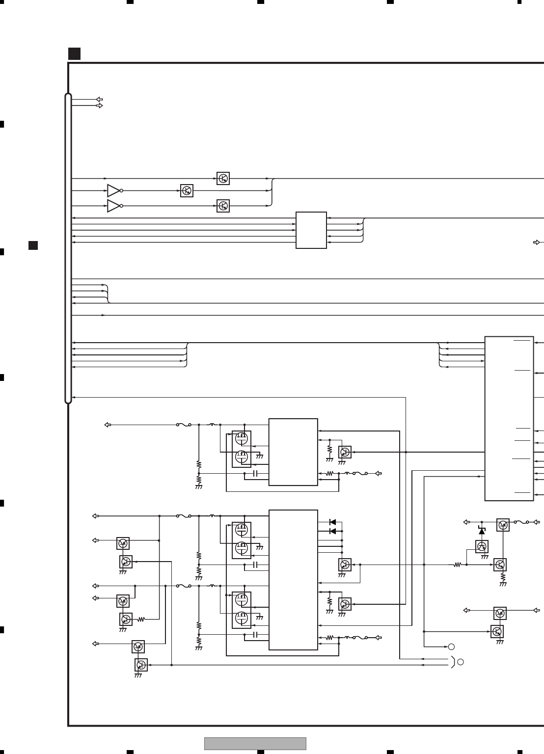
AVIC-Z1/UC
30
1234
1234
C
D
F
A
B
E
CN5201
(2/2)
IC5539
TC7SET04FUS1 BUFFER
IC5535
TC74VHC541FTS1
IC5537(2/2)
TC7W04FU
CCD3
CCD3
TCHTOC
CTOTCH
Q5531
UNIT
PCONT1
PCONT2
1
2
7
4
BB
CB
CJ
BA
CE
15
16
7
3
14
5
4
13
17
6
BB1
CB1
CJ1
BA1
CE1
UNIT1
CNT1
CNT2
Y4
A2
A4
Y2
Y5
A6
A5
Y6
Y3 A3
Q5532
Q5533
FREQCNT FCONT
CONTB
CONTA
CCON
4
16
6
9
CCON
DRAMPW
3.3V/5.0V D/D CONVERTER
IC6201
TPS5102IDBT AU8
SWBUP
1.8V D/D CONVERTER
IC6251
TPS5103IDB
VCC18
CCD5
SRVDD
PWM_SKIP
30
12
22
LH1
VREF5
COMP Q6204
Q6201
Q6203
FU6202
STBY1
LH2
RT
10
STBY2
17
18
19
LL2
OUT2_U
OUT2_D
14 FB2
FU6201
CCD5
Q6322
Q6321
CCD3
SRVDD
VCC
15 INV2
Q6202
29
28
27
LL1
OUT1_U
OUT1_D
2FB1
1INV1
5
13
FCONT
Q6251
VCC
RT
10
STBY
14
VCC-SENSE
24
VCC-CNTP
Q6252
19
18
17
LL
123 FCONT
78 DRAMPW
79 CCON
OUT_U
OUT_D
3FB BUP
VCC18
2INV
11 BUPV
Q6341
Q6342
VCC33
Q6331
Q6332
(1/2)
Q6332
(2/2)
CCON
CCON
Q6312
Q6371
AU8
Q6311
SWBUP
FU6251
FU6252
B
Q6370
VCC5
FU6203
B
FU6331
ILMSNS
DVEJKY
126
68
PILMPW
133
63
FANCONT
NAVI MOTHER PCB(2/2)
G
CN4804
A
69
BLSENS
F
I
SWD25ON
SDBUP
DDRBON
SDSELF
119
115
116
106
SW25ON
SW25ON
DDRBON
SDBUP5 SDBUP
SYSTOC
SDSELF5 SDSELF
SYSTOC
118
54
52
46
48
66
70
90
92
94
96
86
88
63
100
104
102
65
67
69
75
71
96
ASENS
87
85
83
81
64
78 CTOETC
ETCTOC
HYOKA
EXTPWR
CTOEX
EXTOC
BUP
OPTON
132
120
OPTSNS
31
VSELIN1 32
VSELIN2
30
AVONIN
SYSTEM-uCOM
IC6607(2/2) PE5539A:
PE5540A:
VCC55
CCD3
VCC33
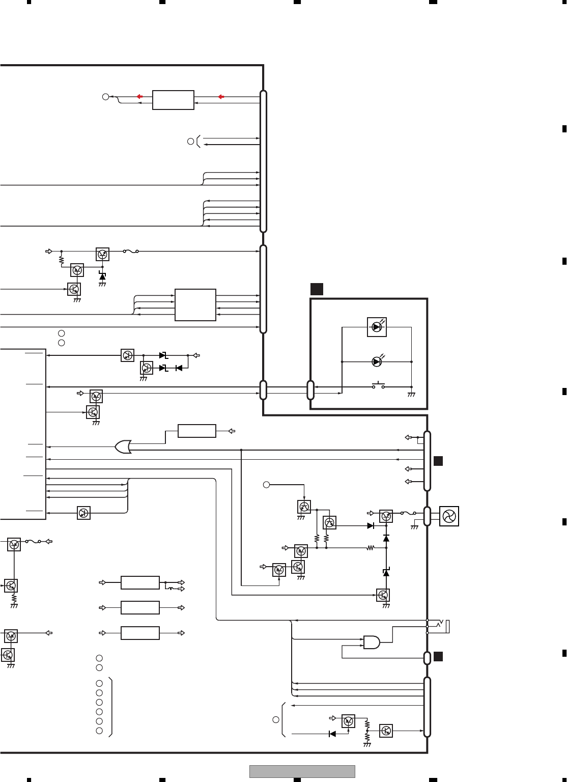
AVIC-Z1/UC 31
5678
5678
C
D
F
A
B
E
3
2
13
11
6
7
9
10
16
17
18
19
20
23
24
25
CN5531
BB1
CB1
CJ1
BA1
CE1
UNITUNIT1
CNT1
CNT2
/BA
/CB
/BB
/CE
/CJ
AU8
S
WBUP
F
CONT
D
RAMPW
C
CON
Q6331
Q6332
(1/2)
Q6312
Q6311
BUP
BUPV
FU6331
CN1002
C
BUP
Q6353
Q6352
ILMB Q6501
(1/2)
Q6501
(2/2)
VDD5
Q6351
BUP
Q6356 FU6351
Q6355
Q6354
(1/2)
Q6354
(2/2)
FANCONT
ASENS
ILMSNS
CN6351
2
1
CN5851
7
8
3
4
9
I
I
10
14
11
CN5651
4
5
12
2
10
FAN MOTOR
BUP
VD8
BUPV
CN6501
7
2
7
2
PNLILM PNLILM
DVEJKY DVEJKY
ILMSNS
DVEJKY
126
68
PILMPW
133
63
FANCONT
FANUP
PANEL UNIT
I
EJECT BUTTON(DVD/CD)
S6902
DVD/CD EJECT
D6905
DVD/CD IND
D6901,D6910
69
BLSENS BLSENS BUP
Q5941
Q5942
BL SENS
ISOLATOR
IC5531
BA3121F
AVPL
AVPR
7
1OUT2 IN2
OUT1 IN1
AVPL
AVPR
5
3
E
H
11ATSENS 13
12
ASENS
TSENS
J
S
WD25ON
S
DBUP
D
DRBON
S
DSELF
S
YSTOC
3,41 IC5422
NJM2125F
AU25 REG.
AUCCD5 AU25
3,41 IC5001
NJM2125F
AU5S REG.
AU8 AU5S
87 IC6611
LM56BIMM
Temperature sensor
µVDD5
96
ASENS
CN5671
CN6901
TO
EXTENSION
IC5671
UPD4721GSS1
8
9
10
7
13
12
11
14
CTOTA
CTOEX
TATOC
EXTOC
HYOKA
CTOETC
CTOEX
ETCTOC
EXTOC
DIN2 DOUT2
ROUT2 RIN2
DIN1 DOUT1
ROUT1 RIN1
VTA
7
6
4
8
5
9
BUP Q5671
(1/2)
Q5672
Q5671
(2/2)
FU5671
OPTON
132
120
OPTSNS OPTSNS
31
VSELIN1 32
VSELIN2
30
AVONIN AVONIN
CN5602
IC5601
TC7SET08FUS1
CN5601
DIGITAL OUT
AV-BUS
OPTSNS
OPTON
DIN
1
24
1
VSELIN1
VSELIN2
AVONIN
IP-SEL1
AVV COMP VIDEO
REMOUT
IP-SEL2
AV ON
CN1501
D
Q6602
VACC5
Q5651
Q5652
REMIN
E
F
G
H
I
J
AAVIC-Z1/UC
BAVIC-HD1BT/EW5
TO 1/2
IC6602(3/3)
TC74VHC32FTS1
M
-uCOM
0
7(2/2) PE5539A: A
PE5540A: B
51 IC6322
BD3931HFP
VDD5 REG.
BUPV VDD5
µVDD5
FAN
T-A
R-A
TOTEL
FTEL
G
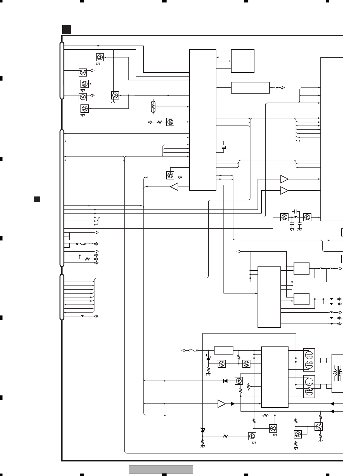
AVIC-Z1/UC
32
1234
1234
C
D
F
A
B
E
PWRFL
Q251
MONITOR CPU
IC301
PE5538A
TH301
TEMP. SENSOR
KDT2
KDT0
KDT3
80
76
78
79
62
8
9
32
30
44
28
27
25
24
5
22
23
6
21
20
19
15
13
12
11
9
CN1
MONT_F
PWRVI
ILMB
ACC5V
FU181
MTOSYS
SYSTOM
TXD
MOREM REMCON
RXD
MFLPW MFLPW
YS YS1N
NVSYNC
NVRED
NVGRN
NVBLUE
CSYNC
ANR
ANG
ANB
MONVBS CVBS
40
39
38
33
24DIMDTY
INVBST
Q301
IC305
TC7SH08FUS1
V14A1
SWACPW
VSWILL
VACC5
HDRESET HDRST
TEMPSEN
KDT0
REMCON 61 REMIN
KDT2
KDT3
VDDSEN
RXD/TSI
TXD/TSO
MFLPW
INVBST
DIMMER
COMAC
COMDC
RADIN1
GADIN1
BADIN1
OSDBIN
OSDGIN
OSDRIN
OSDBLANKHMIN
OSDC/HSYNCO
U
OSDCKOUT
OSDVSYNCOUT
SCL
SDA
RESET
SADIN1
OVERLAY
RGBSYNC1
X
OSDDT 17
OSDCK 18
OSDCS
SCL
SDA
PIPRES
COMAC
COMDC
MVIPWR
X1
X2
19
28 PIPCK
27 PIPDA
29 PIPRES
5 COMAC
6
13
COMDC
PIPCK
PIPDA
PIPRES
OSDB
ANR
ANG
ANB
OSDG
OSDR
BLNK
OSDH
OSDSCK
97
73
74
75
98
99
101
93
91
OSDV 92
104
105
107
66
47
86
YSREC
41,2
X301
12.58MHz
70
69
IC332
TC7SH08FUS1
IC41
TC7SH08FUS1
LPF
41,2
INVPUL
MVIPW
CN1203
C
SWACPW
V8
VACC5
RESET 60 1
EPRCS 46 3
EPRSK 47 4
EPRDO 48 5
EPRDI 49 6
2
EEP-ROM
IC252
BR93L56FJ-W DISPLAYS CO
N
IC1
TC90A96
A
IC251
S-80835CNNB-B8U
POWER ON RESET
CS
SK
DI
DO
PNLYV
PNLXV
CN3
ADX
ADY
4
3
2
1
24
25
3
2
PNLXV
PNLYV
PNLADY
PNLADX
PNLADY
PNLADX
PNLVD
Q681
(2/2)
Q681
(1/2)
26 PNLVD
Q683
(2/2)
Q683
(1/2)
VAC5
Q682
(2/2)
Q682
(1/2)
VAC5
Q352
Q351
1,2,5,6
1,2,5,6
V14A1
3
4
3
4
D/D CONVERTER
IC181
BD6171KV
3V REG.
11
6PVCC1
PVCC2
32 EN1
OUT2 7
VS2 4
PVCC3
PVCC4
PVCC5
23
48
37
OUT1 10
OUT5 38
OUT4 47
OUT3 22
Q182
8V REG.
Q181
41 DVCC
42 VCC
VS1 13
513
DIMDTY
INVPUL
INVBST
20
14
15 5
4
3
2
LCT
3ENA
7V2500
9FB
17 RT
DIM
VDDA NDRV_B
19
PDRV_A
11
NDRV_D
12
PDRV_C
2
OVP
Q871
FU841
Q872
Q842
VR841
Q843
Q844
5V REG.
IC873
TA78L05F
LCD DRIVE
IC841
OZ964ISN
18 CT
Q603
Q602
T841
Q605
(1/2)
Q605
(2/2)
IC845
TC7SH08FUS1
1,2 4
PWRFL
CN5
OSDH
SCKE
OSDV
3
4
2
8
5
6
7
9
10
11
1
BLK
OSDB
OSDG
OSDR
OSDH
OSDSCK
OSDV
BLNK
OSDDT
OSDCK
OSDCS
VCC V33
VAC5
MONITOR UNIT
K
TOUCH PANEL
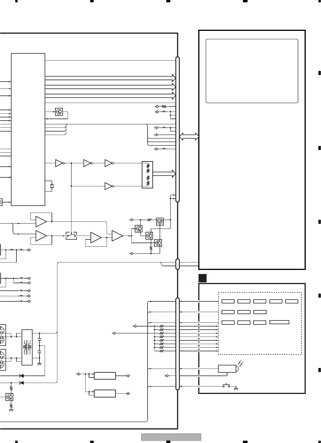
AVIC-Z1/UC 33
5678
5678
C
D
F
A
B
E
DA0-5
DB0-5
DC0-5
V0-10
CN4
RESET
REMOTEREMCON
KDT3
IC103
TC7S66FU
IC101
NJM2100V
IC102
TC7SET04FUS1
Q1
X1
42MHz
IC121
TC74VHC04FTS1
IC122
TC7SET04FUS1 REF.V
DEVIDE
60
134
135
136
137
138
139
STV
56
KDT2
KDT0
CN7
STH1
LOAD
L/R
V33
V5
V33
V18
VM12
42133
VCOM
VGL
STV1
STV
CPV
OE
CPH
30
29
28
26
25
24
20
17
16
13
9
8
6
4
2
1
59
48
I
I
I
I
58
47
42
41
36
35
COMAC
COMDC
42
8,10,129,11,13
2,4,61,3,5
52
53
STH
BOUT2-7
RADIN1
GADIN1
BADIN1
OSDBIN
OSDGIN
OSDRIN
OSDBLANKHMIN
OSDC/HSYNCOUT
OSDCKOUT
OSDVSYNCOUT
SCL
SDA
RESET
SADIN1
OVERLAY
RGBSYNC1
GOUT2-7
ROUT2-7
LOAD
XTAL-IN
XTAL-OUT
CPH
GOE
CPV
STV
DAC OUT
PLL IN
VCOM
S
R
G
B
C
K
97
73
74
75
98
99
101
93
91
92
104
105
107
66
47
86
C
REMOTE
IC3021
SBX3050-01
2.5V REG.
IC182
S-1132B25-U5
VIN
5
41
VOUT V25
V33
CE
1.5V REG.
IC183
S-1132B15-U5
VIN
51
VOUT V15
4CE
VGH
DISPLAYS CONTROL IC
IC1
TC90A96AFG-P
LCD MODULE
5
2
CN842
FL1
FL1
FL2
FL2
1
2
1,2,5,6
1,2,5,6 V8
V31
V18
V5
VM12
-
+7
5
6
-
+
1
2
3
IC104
NJM082BV
-
+1
3
2
-
+7
5
21
4
6
V8
Q101
(2/2)
Q101
(1/2)
Q102
(1/2) Q102
(2/2)
VM12
VACC5
VSWILL
5
4
3
6
7
2
8
43
8
44
T841
Q605
(1/2)
0
5
2
)
VSWILL
VCOM AMP
KEY MATRIX
KDT0
KDT2
KDT3
ILMB2
ILMB7
ILMB4
ILMSRC
ILMB1
ILMB5
ILMB3
ILMODK
ILMB2
ILMB7
ILMB4
ILMSRC
ILMB1
ILMB5
ILMB3
ILMODK
S3002
D3012
VOL+
S3008
D3001
TI
S3010
D3002
MAP
S3006
D3007
RIGHT
S3007
D3004
UP
S3009
D3003
MENU
S3011
D3009
LEFT
S3012
D3006
DOWN
S3001
D3015
AV
S3003
D3010
VOL−
S3004
D3014
P.ADJ
S3005
D3013
OPEN/CLOSE
RESET
VACC5
S3021
REMOTE 2
1
OUT
18
13
14
15
10
16
12
11
9
6
5
2
1
3
VDD2
VDD1
MDRST
CPV
OE
CPH
CPH
OE
CPV
V33 KEYBOARD UNIT
J
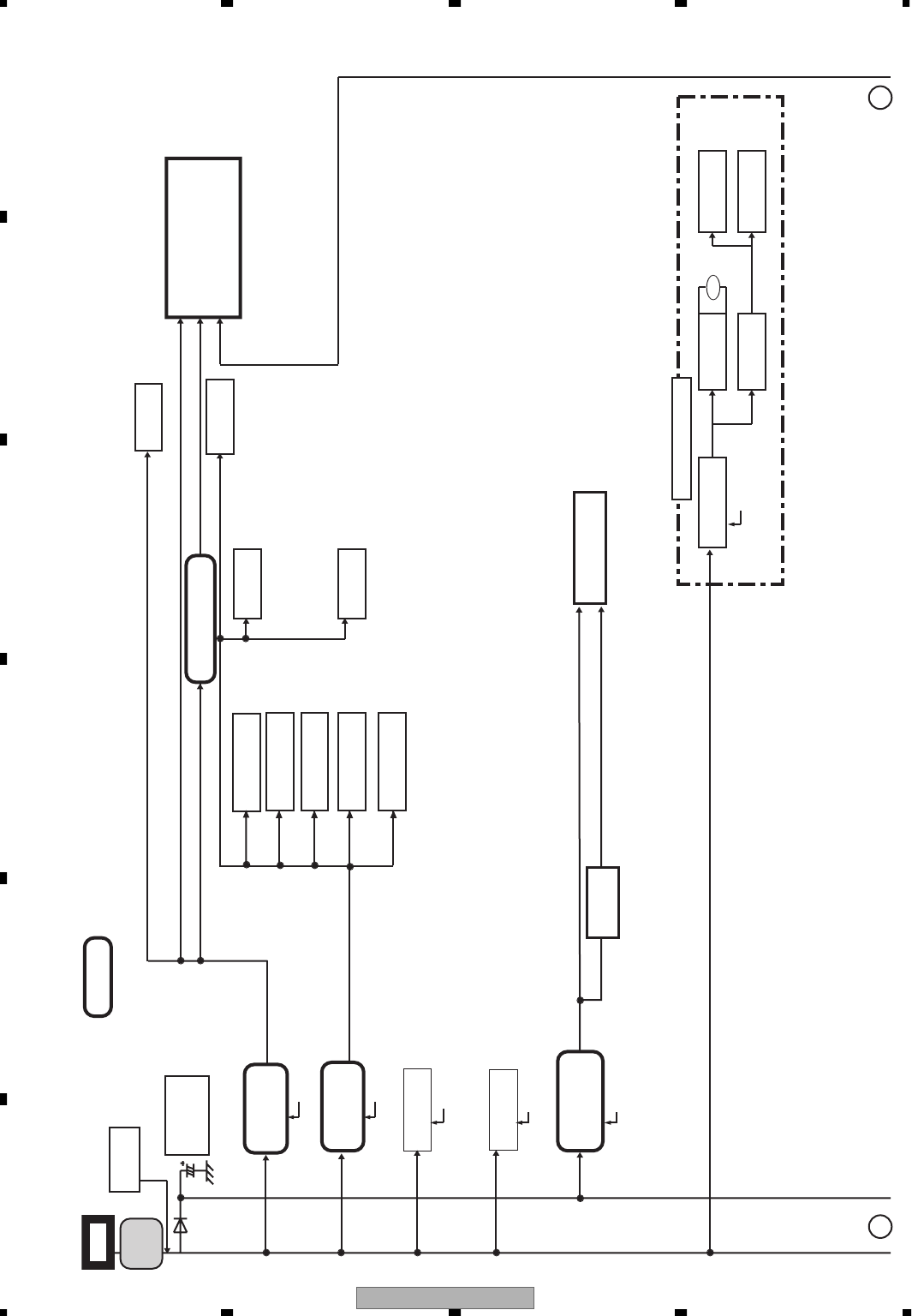
AVIC-Z1/UC
34
1234
1234
C
D
F
A
B
E
M
A B
POWER AMP
PAL007B
ANT+B SW
TPD1018F
AUDIO 8V
pwr.
BA00CC0WT
POWER SUPPLY MAP(Reference)
Guide sound ISO
NJM2060V
Gudie MIX IC
NJM2060V
10000µF/16V +
2200µF/16V
Maintenance
BUP
Rear DVD sound
ISO BA3121F
MUTE cir.
1/2VCC
A4R7(Zener)
FM/AM tuner
3.3REG
NJM2391DL1-33
Motor driver
MOTOR 0•1
Motor pwr. 7V
Motor 5V pwr.
Photo-Interrupter
GP1S94J*2
Schumitt trigger
TC7W14FU
Power Supply
CAPTAIN4
Audio
PCB
Ripple
Filter
NAVI Audio
BA3121F
VTR sound ISO
BA3121F
8.7V -> 3.3V
Zener
RDS-TMC tuner
Allotter
VDORA 8V
pwr.
2SB1185
TMC8V
pwr.
2SB1184F5
SYSPWR
SREMOT <- AMPSTBY
SYSPWR
AU8V=8.4V
+6.8V
ANTON
CCON
MOTPWR
Flap driver PCB
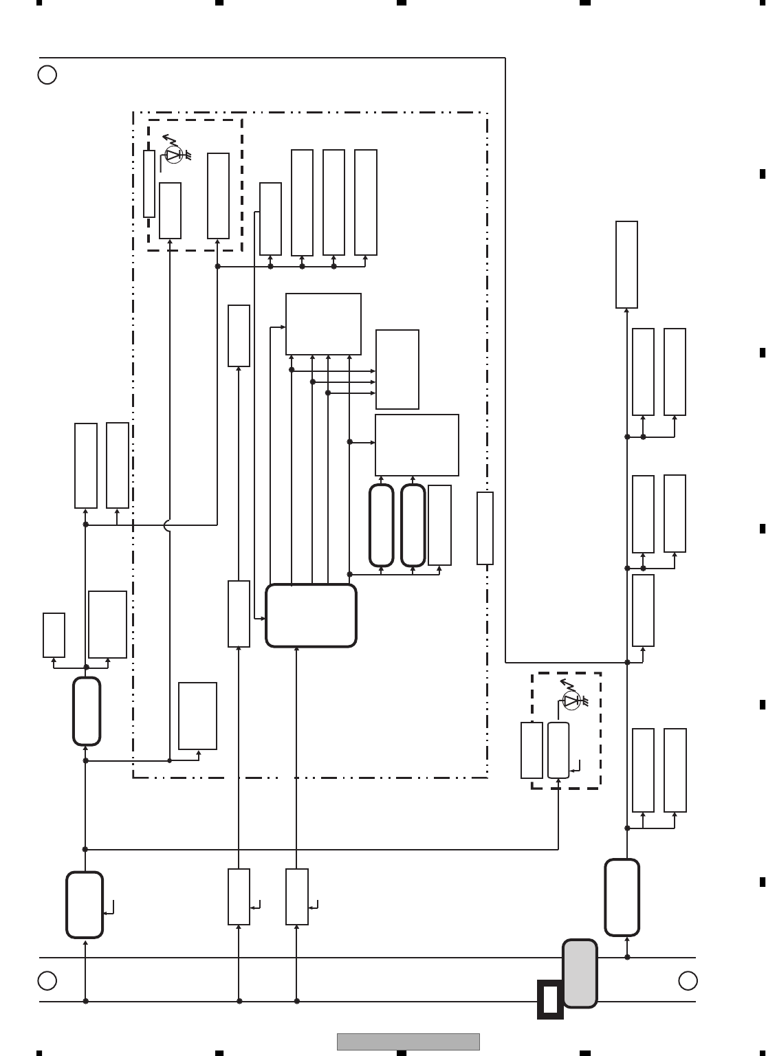
AVIC-Z1/UC 35
5678
5678
C
D
F
A
B
E
System microcom.
PE5539/5540A
ILL. pwr.
8.7V
2SB1185
SWACP
VDD5
Pwr. 5V
BD3931HFP RQ(GPS)
TC7SH04FU
HA12241FP
IP Bus driver
Reset IC
BD5335FVE
ACC5V
2SD1760F5
3 -> 5 Conversion
TC74VHC125FT
Backlight pwr.
OZ961SI
6.95 LCD
DD con.18V
-12V
BD6171KV
8V
5V
3.3V
REG 2.5V
S1132B25-U5T1
VCOM
TC7SET04FU
NJM2100V
NJM082BV
Video signal
processing
LCD control
TC90A96AFP
Backlight
Video LPF
Panel ill.SW
Video SW
NJM2235 *3
Rear moni. video SW
TK15405BMI
+B
BUP SW
PWFL
MFLPW
Monitor PCB
Grille ILL.
Monitor microcom.
PE5521A
Reset
S-80835CNNB-B8U
Remote con. euphotic
SBX3050-01
Keyboard PCB
Panel
BUP SW
PWVI
SWACPW
Mute control
TC74VHC32FT
Temperature sensor
LM56BIMM
PILMPW
Bluetooth
TC7SET04FUS1
ILMB
REG 1.5V
S1132B15-U5T1
AvBUS
VIDEO
Isolator *2
(BCV,AVBUS)
VIDEO
Isolator
(VTR)
EEPROM
S-29221BROI-J8T1
EEPROM
S-93C56BD0I-J8
VSWILL
VACC5
typ 0.85µA
max 2.55µA
(100mA)
MVIPW
NAVI. PCB
About 400mA(500)
119mA
A
C
B
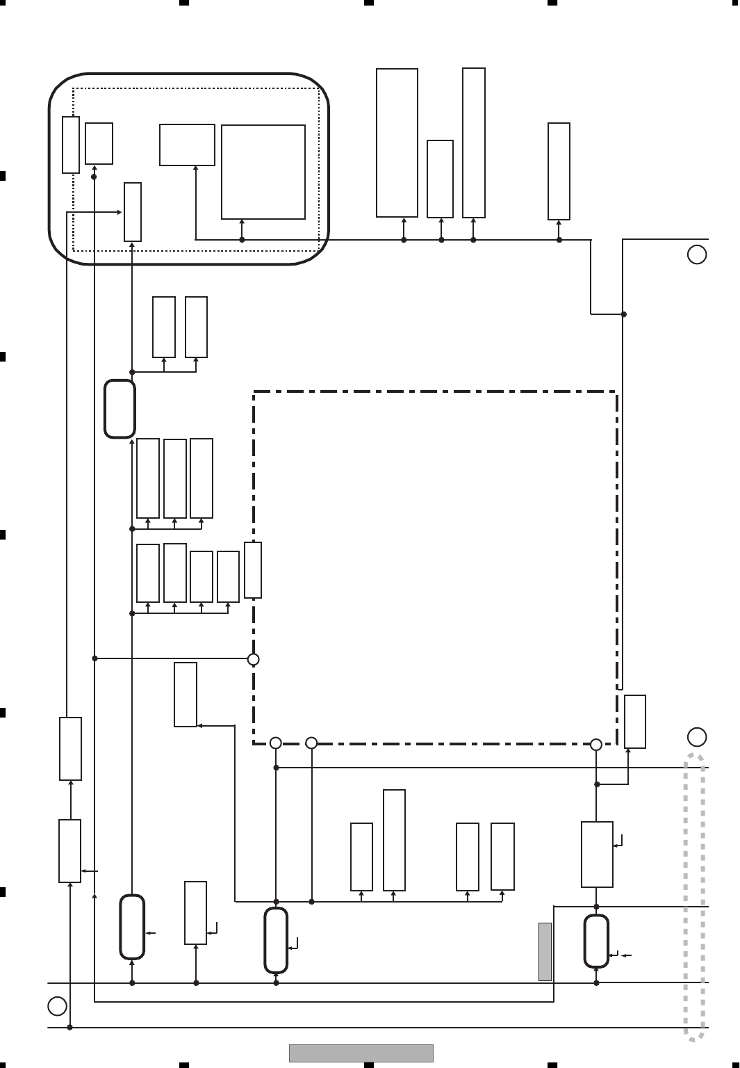
AVIC-Z1/UC
36
1234
1234
C
D
F
A
B
E
NAVI pwr.
CCD5V(D/D)
CCON
SRVDD
(D/D)
DRAMPW
AND YS,NVSYNC
TC7SH08FU x 2
RQ(GPS)
TC74VHC32FT
5->3V
TC7WH08FU,TC7SH08FUS1
VCC5A pwr.
S-812C50
GYRO
CSX1054
G sensor
CSX1055
OP AMP*1 GUIDE and sound
NJM3403AV*2,NJM2125F
SPEED I/F
NJM2904M
GPS
FLASH
ROM
Backup Voltage sense
CC
IP-BUS pwr.
SW
ASENBO
SRVDD
AU5S Standard vol.
NJM2125F
AU8V
2SB1184F OPAMP(Audio)
NJM3403V
CCON
buffer(Audio)
NJM2904V
RGB encoder
BH7236AF
AVP ISOLATOR
BA3121F
SP AMP
TDA7052BT
SWBUP
2SA1576
CCON
14.4V ->5.6V
Bluetooth
TC74VHC541FT,
TC7W04FU
Sound change
SWTC4W53FU
Analog SW
TC4052BFT
PKB SENSE
DIGITAL OUT
LOGIC of
RS232C
DRV
SKIP mode
CCD3
SW
2SA1834F5
CCD5
CCON
(SKIP mode)
DRAMPW
ED
C
SRAM
Zener
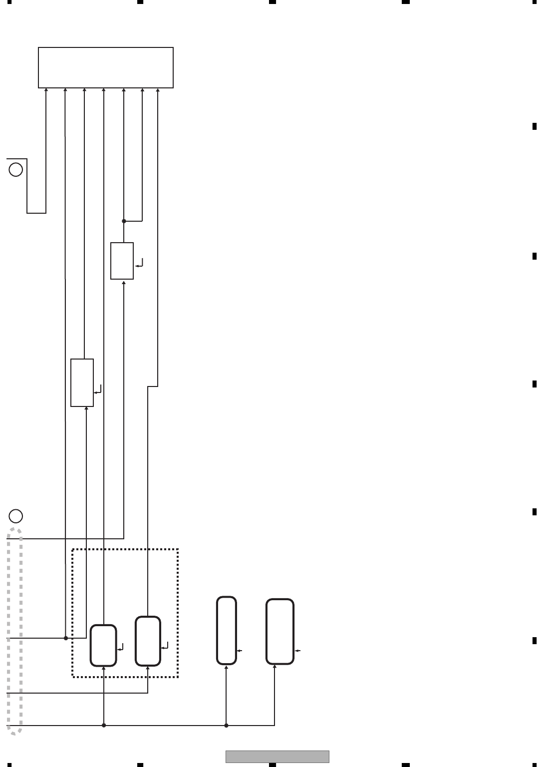
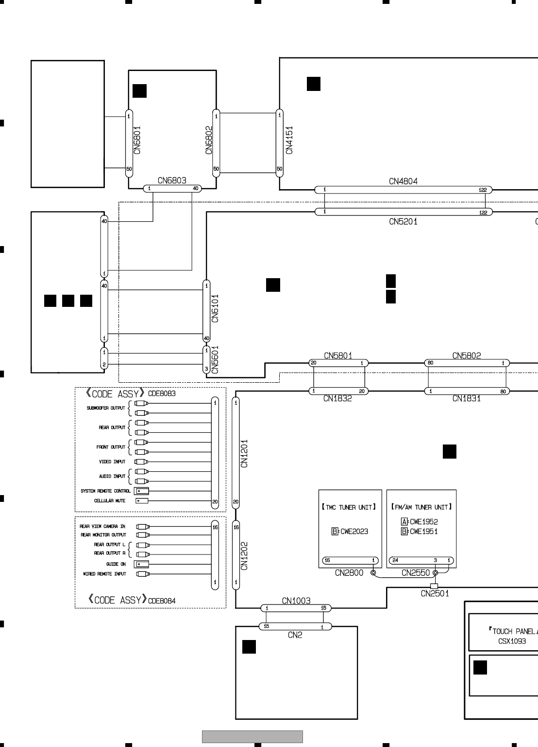
AVIC-Z1/UC
38
1234
1234
C
D
F
A
B
E
3.2 OVERALL CONNECTION DIAGRAM
D E F
ACC UNIT
HHDD RELAY
PCB
HDD ASSY
(SERVICE)
DVD
MECHANISM
MODULE
1/2
G
2/2
G
GNAVI MOTHER PCB
CAUDIO UNIT
L
MAIN PCB UNIT J
KEYBOARD U
N
SYSCOM • P/S Part
NAVI AV • EXTERNAL I/F P
a
Note: When ordering service parts, be sure to refer to " EXPLODED VIEWS AND PARTS LIST" or
"ELECTRICAL PARTS LIST".
CN1401CN1611
CN1501
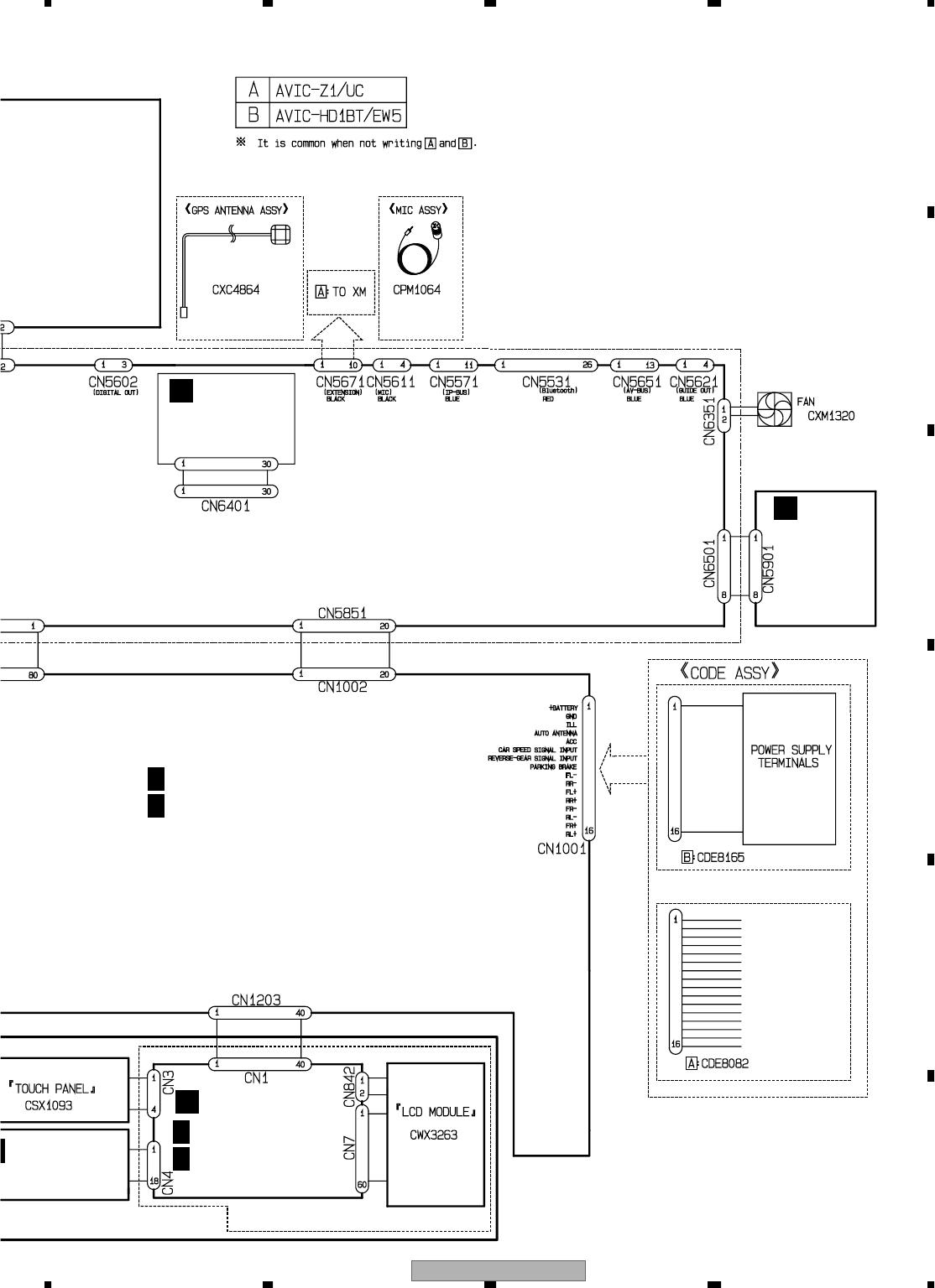
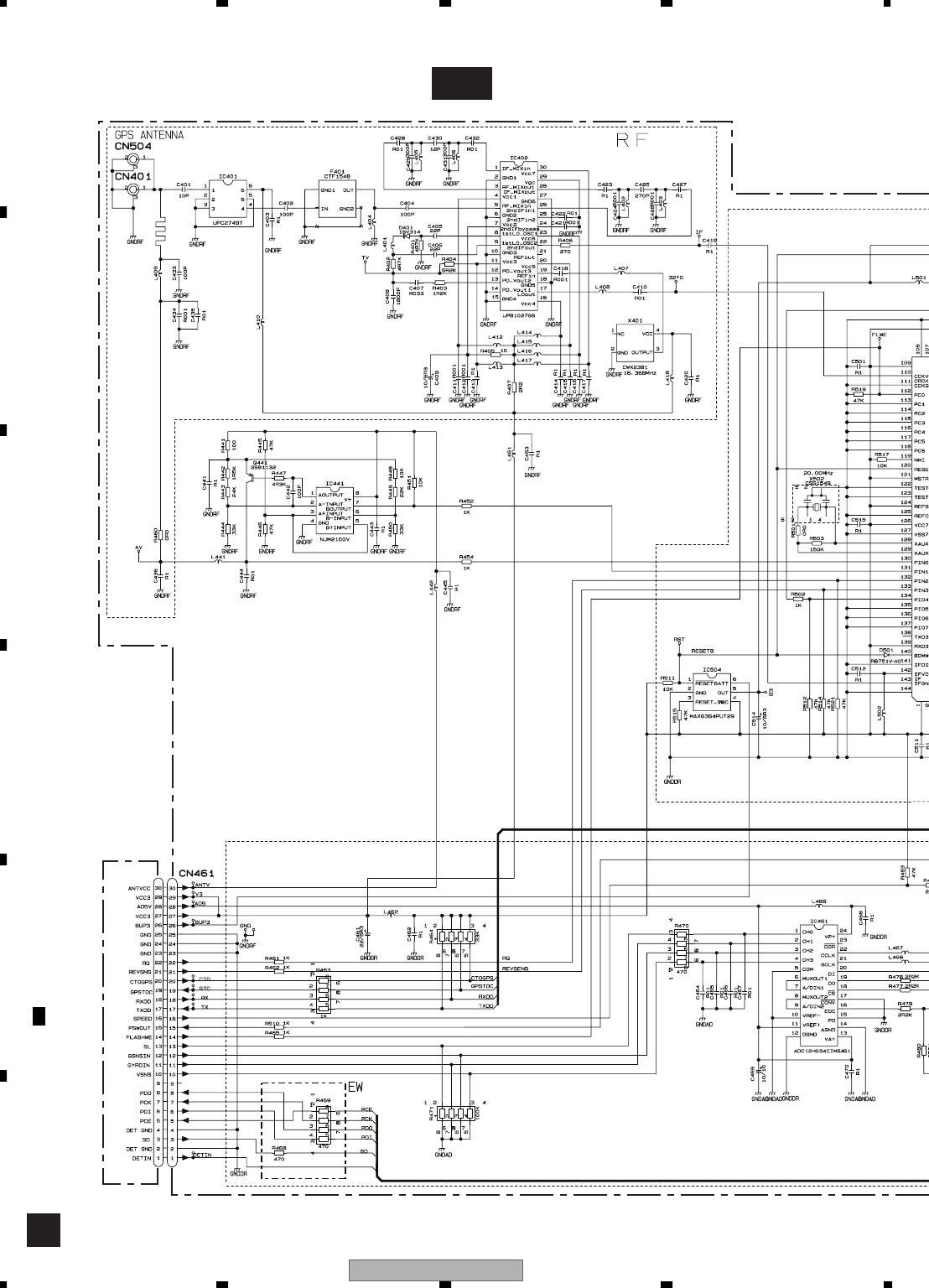
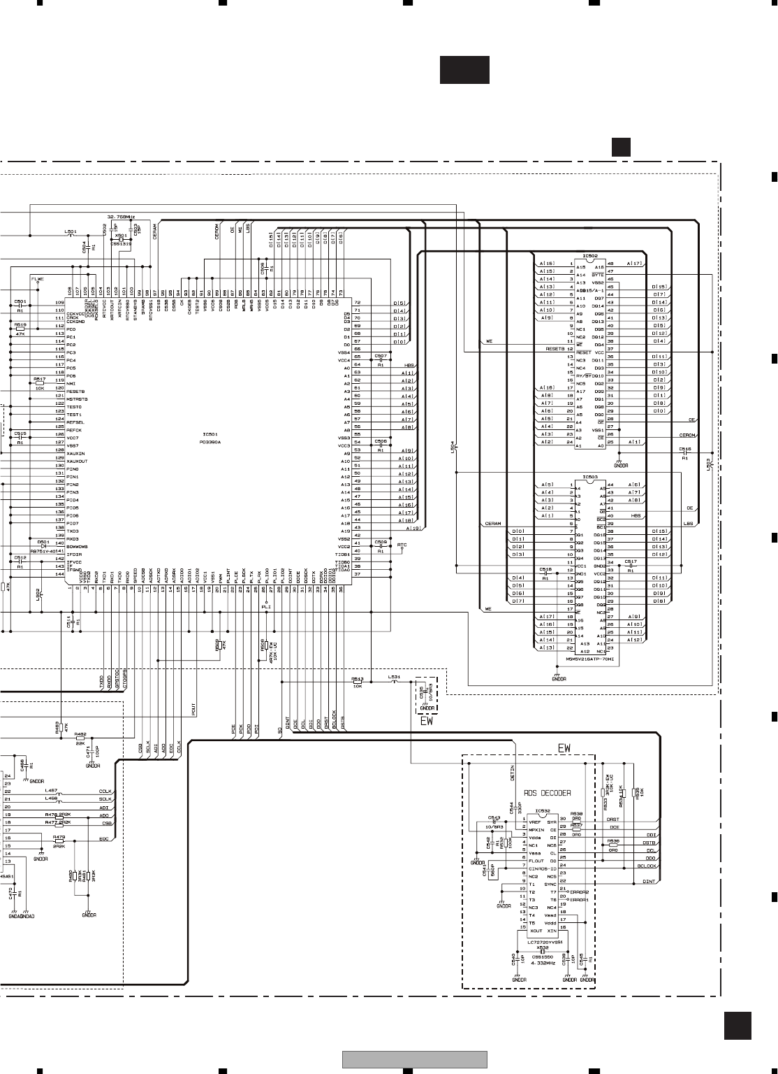
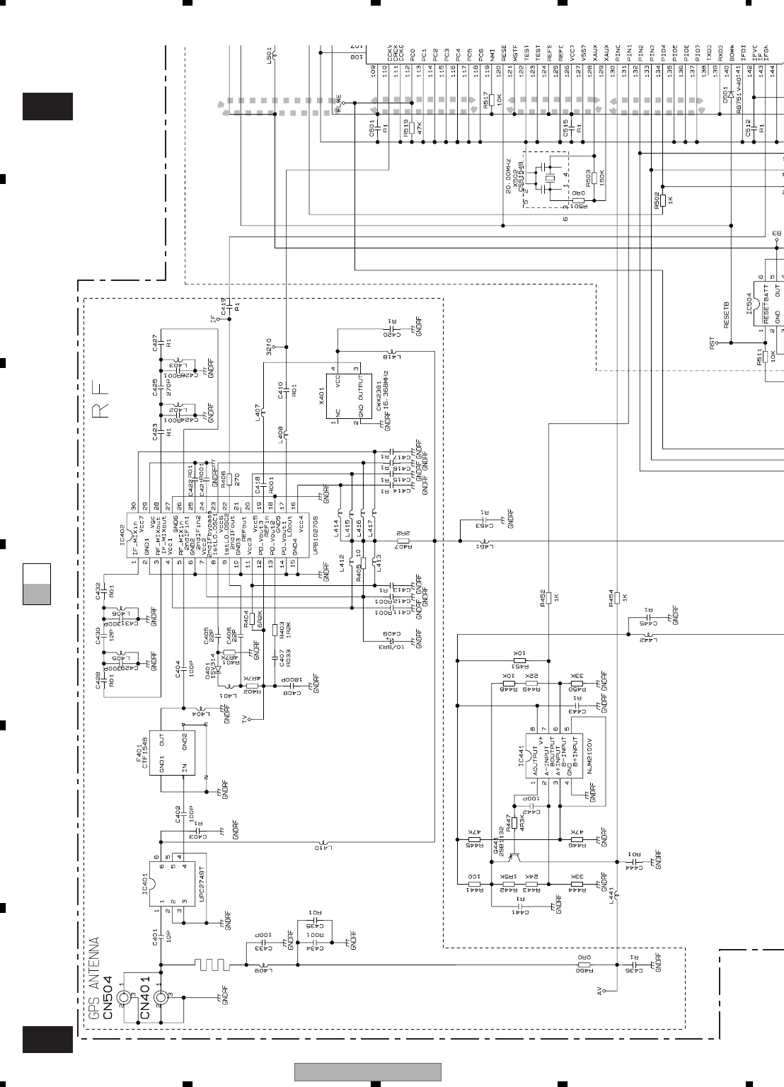
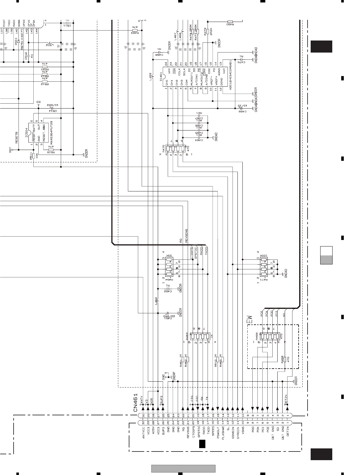
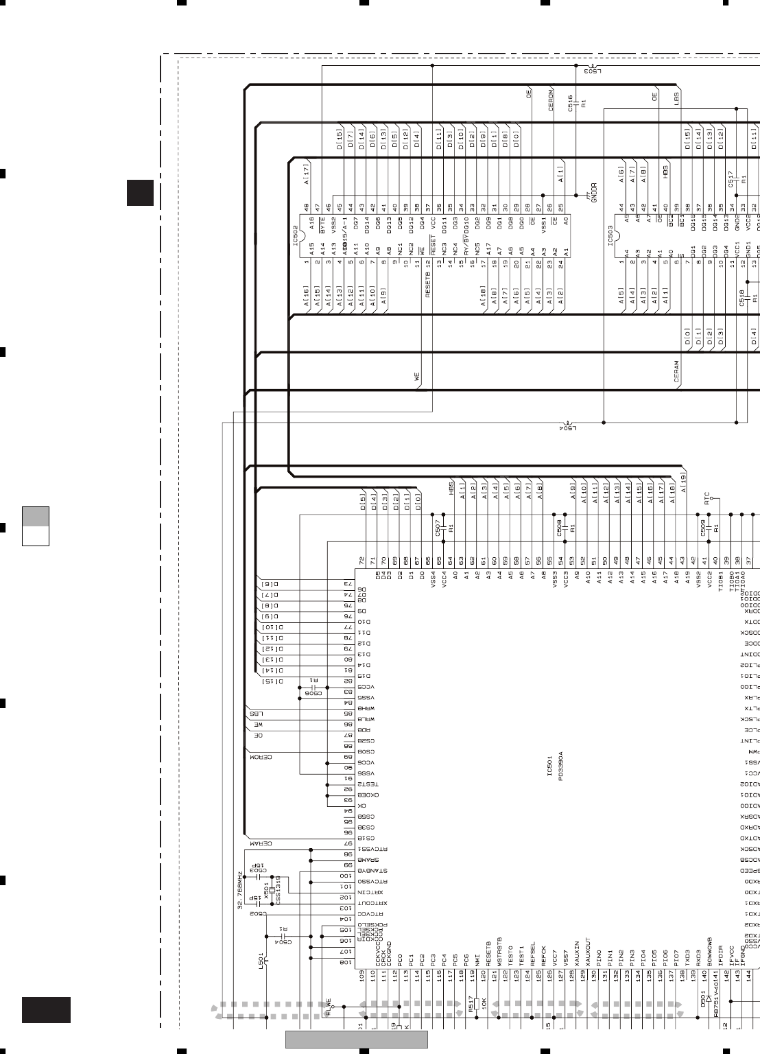
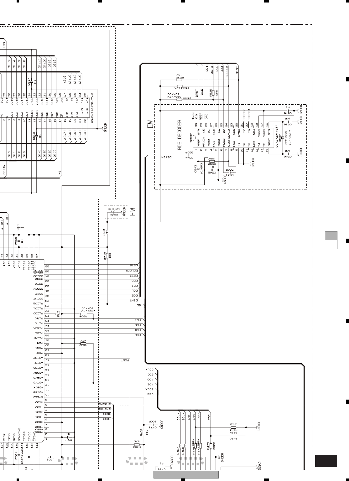
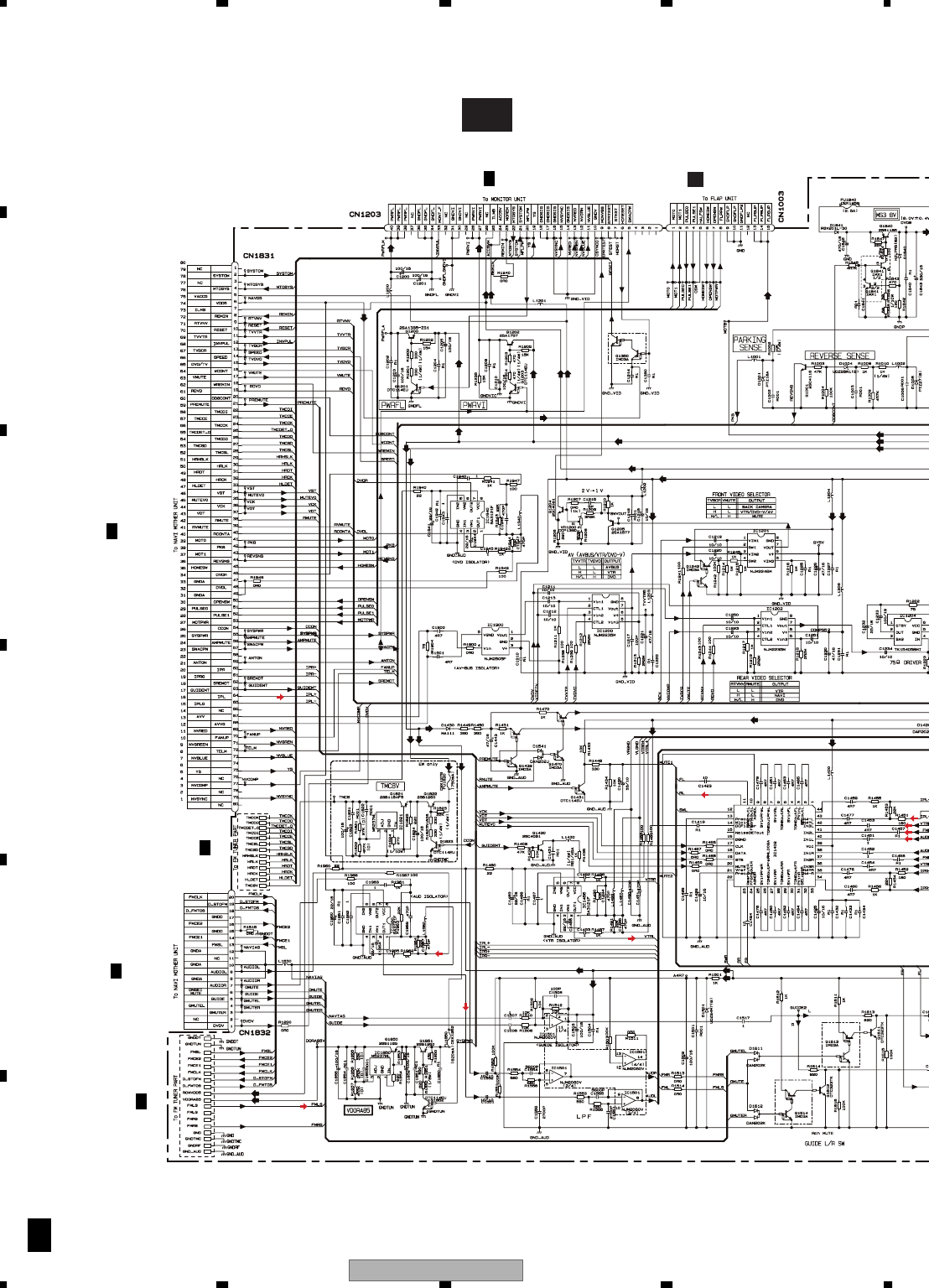
AVIC-Z1/UC
46
1234
1234
C
D
F
A
B
E
3.4 AUDIO UNIT(P/S•I/F)(GUIDE PAGE)
1/2
C
C-a 1/2
>
>
>
CN5802
CN5801
CN1 LCN2
2/2
C
1/2
G
2/2
C
1/2
G
Bluetooth,DVD,IP:9.31 dBs
VTR:10.31 dBs
FM:3.60 dBs(UC),7.60 dBs(EW)
AM:-6.90 dBs(UC),-2.90 dBs(EW)
*
*
1/2
K
FM:-13.5 dBs(U
-9.5 dBs(E
W
AM:-24.0 dBs(
U
-20.0 dBs(E
Bluetooth:2.21 dBs
DVD:2.21 dBs
IP:2.21 dBs
VTR:2.21 dBs
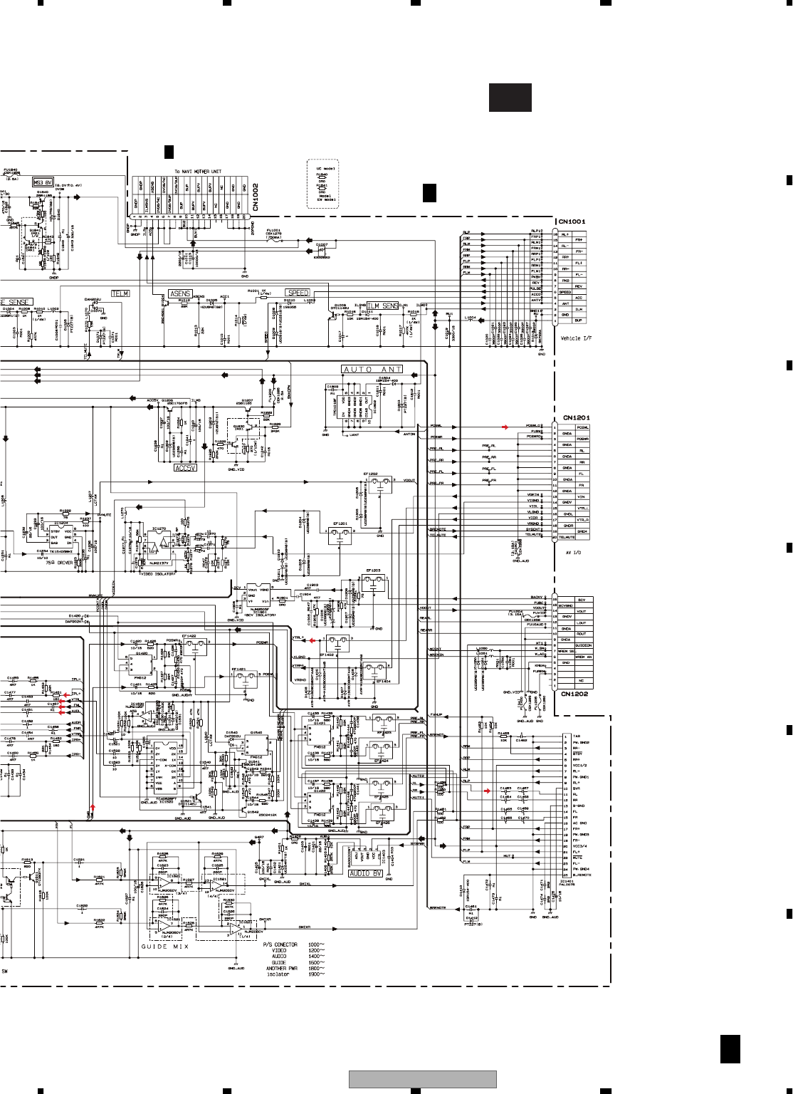
AVIC-Z1/UC 47
5678
5678
C
D
F
A
B
E
1/2
C
C-b 1/2
>
>
>
>
>
>
>
CN5851
CORD ASSY
CORD ASSY
CORD ASSY
AUDIO UNIT(P/S¥I/F)
1/2
C
Bluetooth,DVD,IP:35.31 dBs
VTR:36.31 dBs
FM:29.60 dBs(UC),33.60 dBs(EW)
AM:19.10 dBs(UC),23.10 dBs(EW)
1/2
G
Bluetooth,DVD,IP:9.31 dBs
VTR:10.31 dBs
FM:3.60 dBs(UC),7.60 dBs(EW)
AM:-6.90 dBs(UC),-2.90 dBs(EW)
VTR:2.21 dBs
(1.0 Vrms)
FM:-13.5 dBs(UC)
-9.5 dBs(EW)
AM:-24.0 dBs(UC)
-20.0 dBs(EW)
Bluetooth:2.21 dBs
DVD:2.21 dBs
IP:2.21 dBs
VTR:2.21 dBs
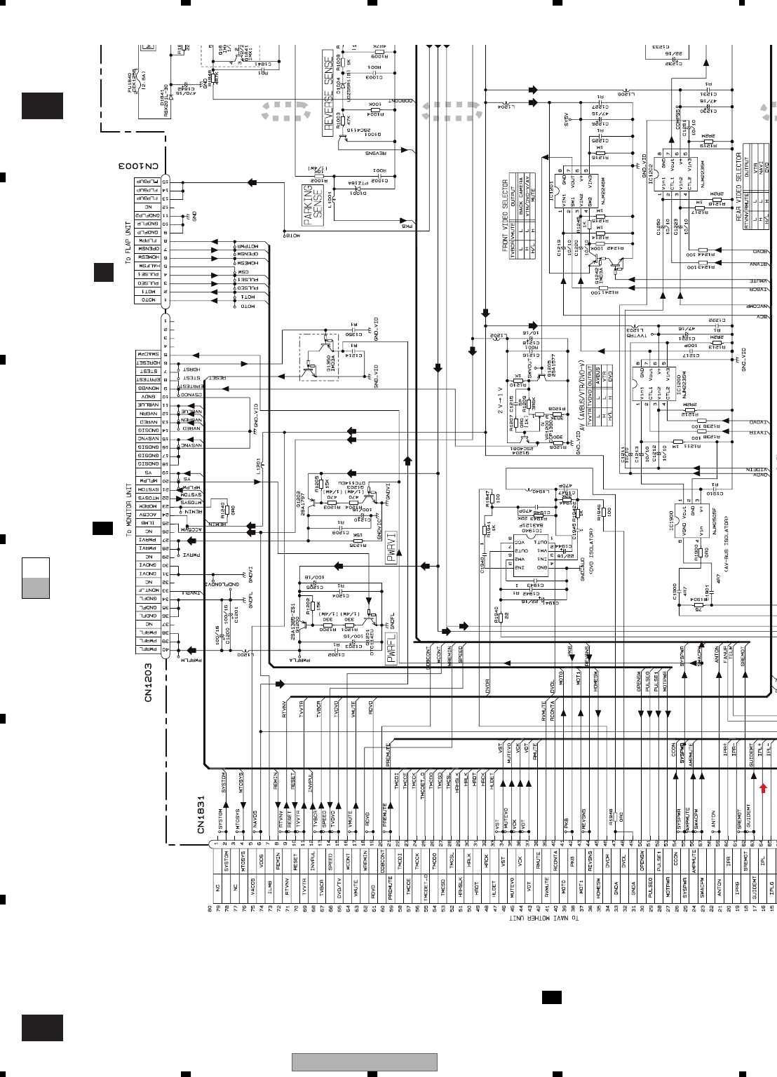
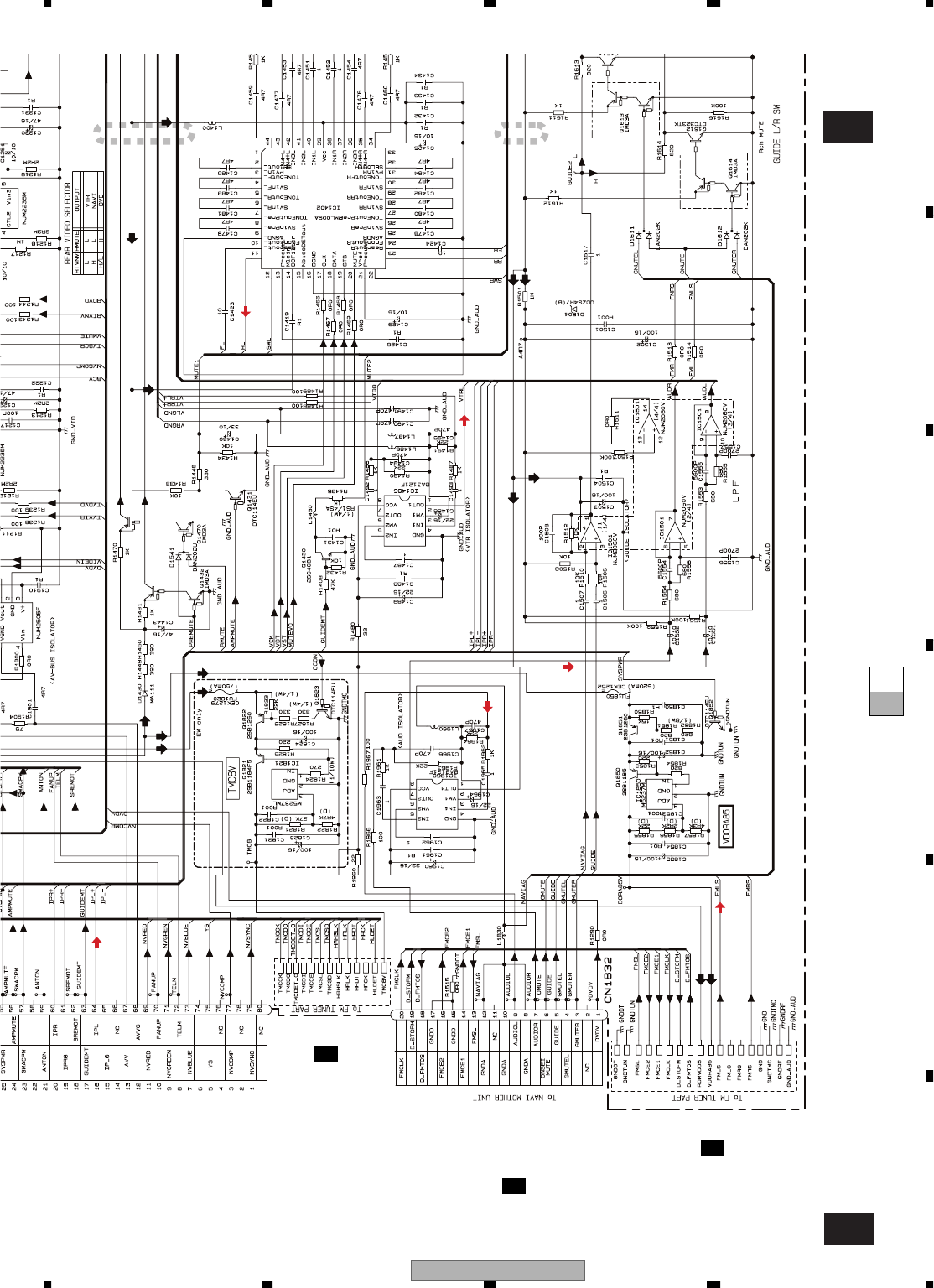
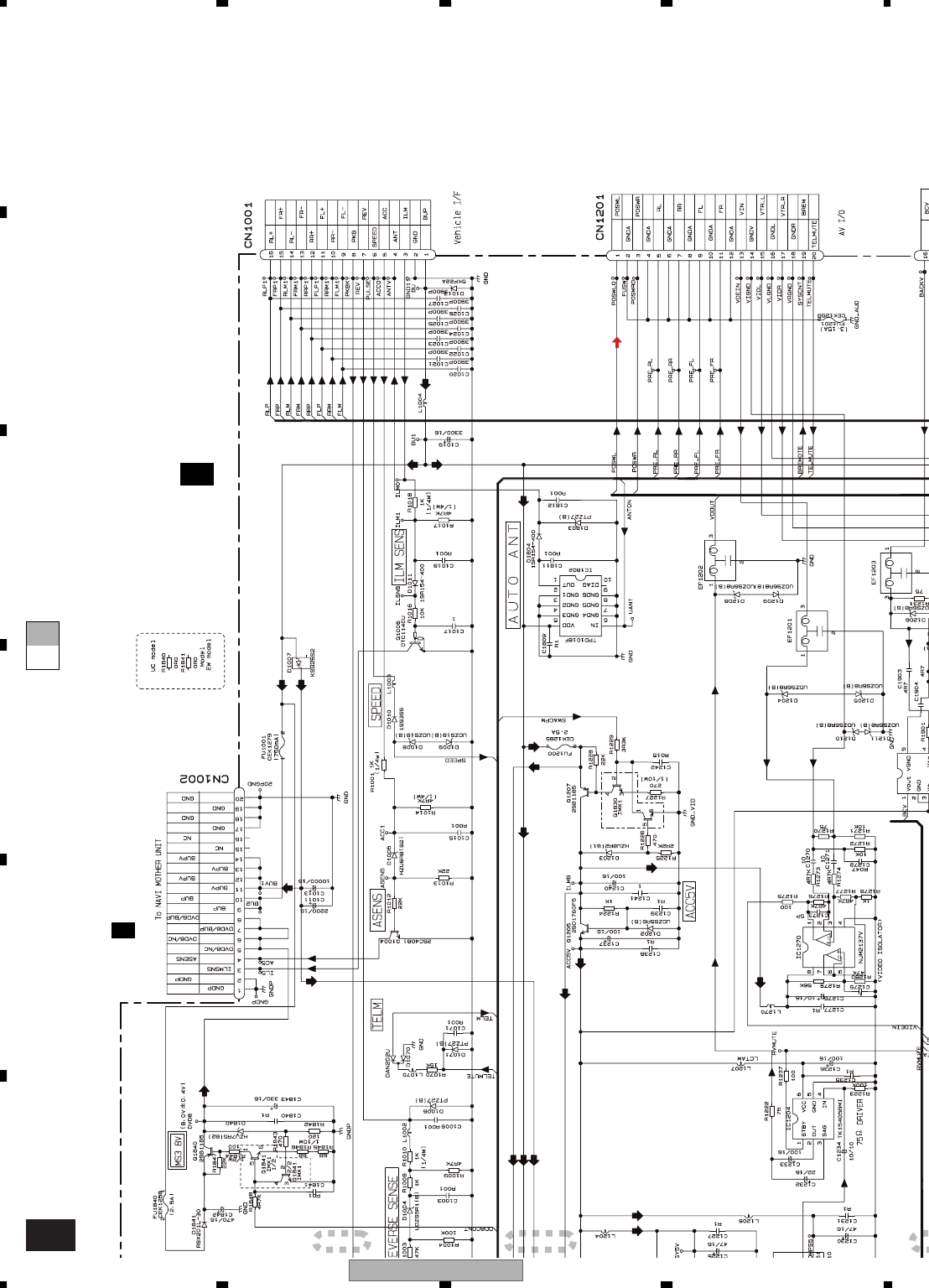
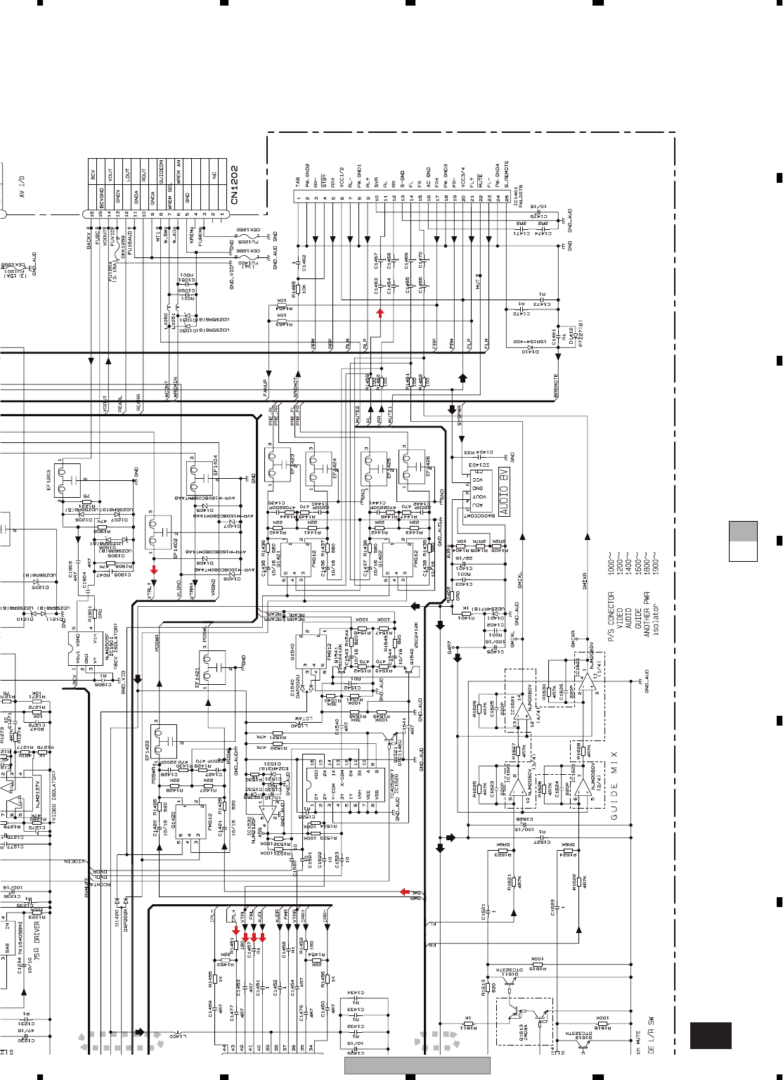
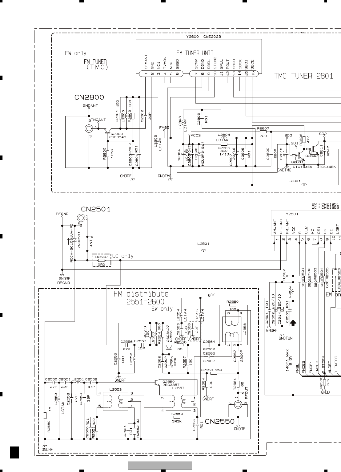
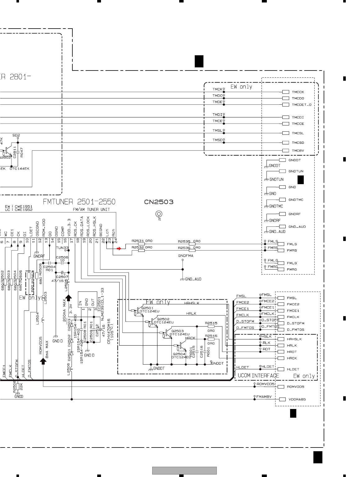
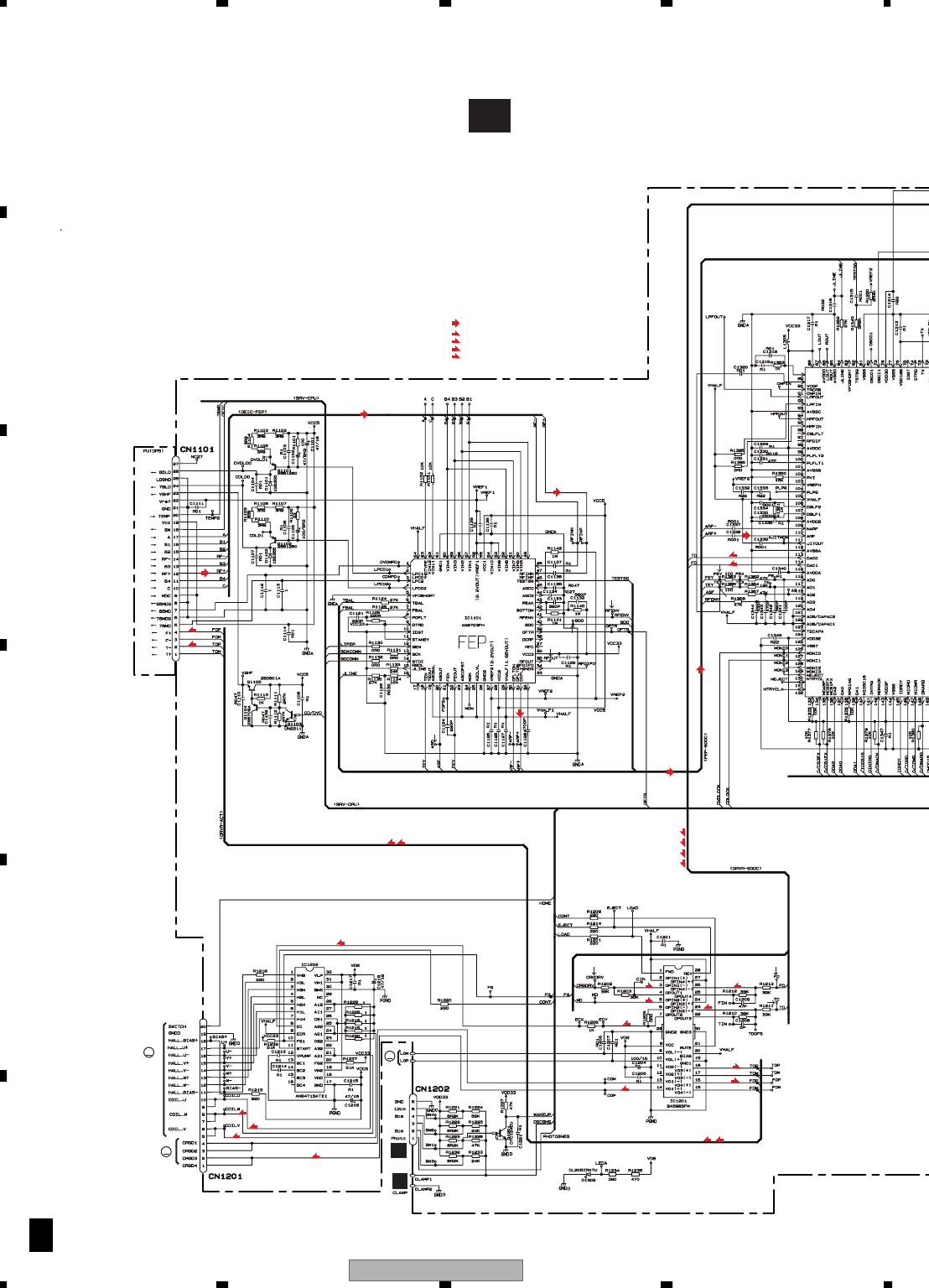
AVIC-Z1/UC
54
1234
1234
C
D
F
A
B
E
3.6 DVD CORE UNIT(MS3)(SO-DC)(GUIDE PAGE)
D-a
1/2
1/2
D
PICKUP UNIT(SERVICE)(DP5)
E
F
M
M2
CARRIAGE
MOTOR
CXC4314
M
M3
SPINDLE
MOTOR
CXM1308
M
M1
LOADING
MOTOR
CXC4315
disc sens
1
5
3
9
7
2
48
6
RF SIGNAL
FOCUS SERVO LINE
F
TRACKING SERVO LINE
T
CARRIAGE SERVO LINE
C
SPINDLE SERVO LINE
S
F
T
F
F
F
F T C S
T
C
S
T
T
S
S
C
S
S
T
S
C
F
TT
FF
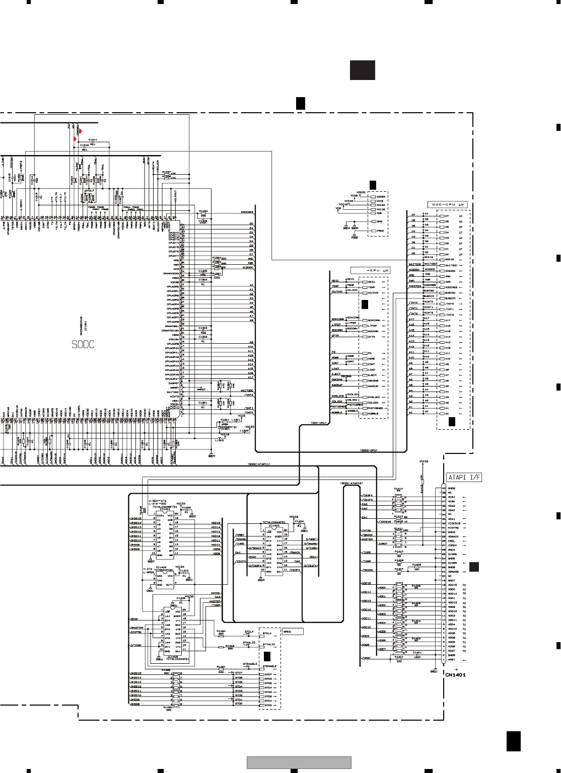
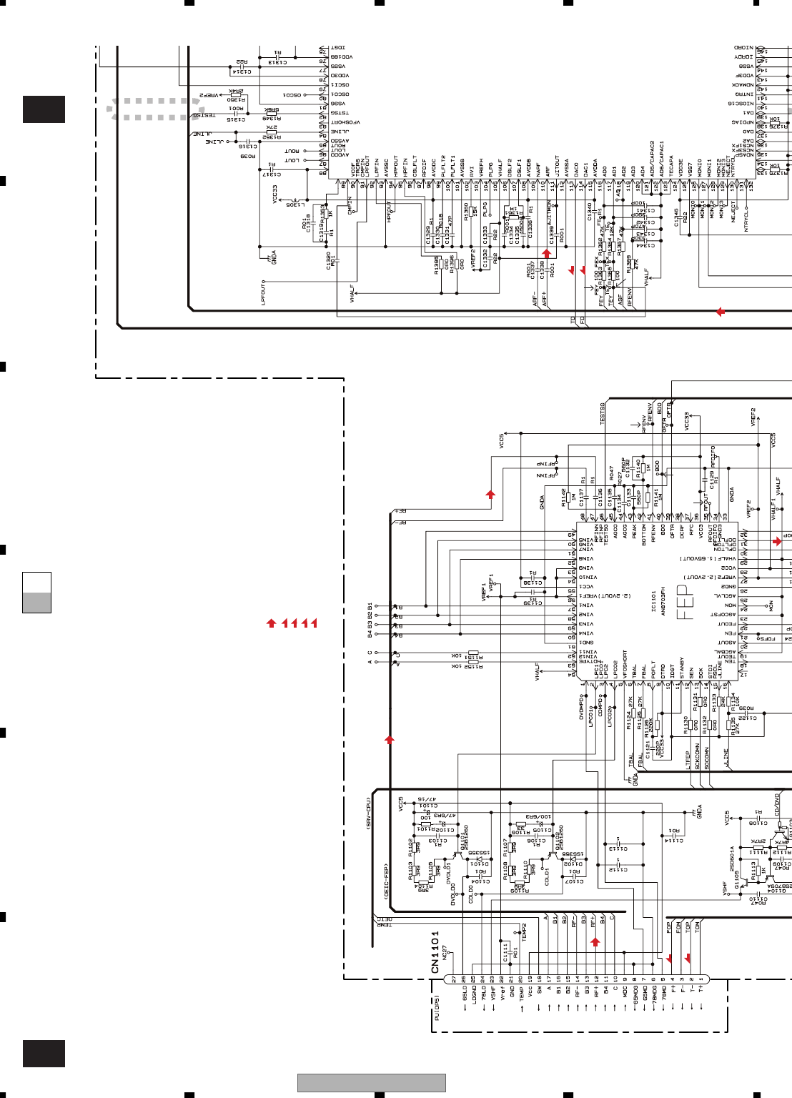
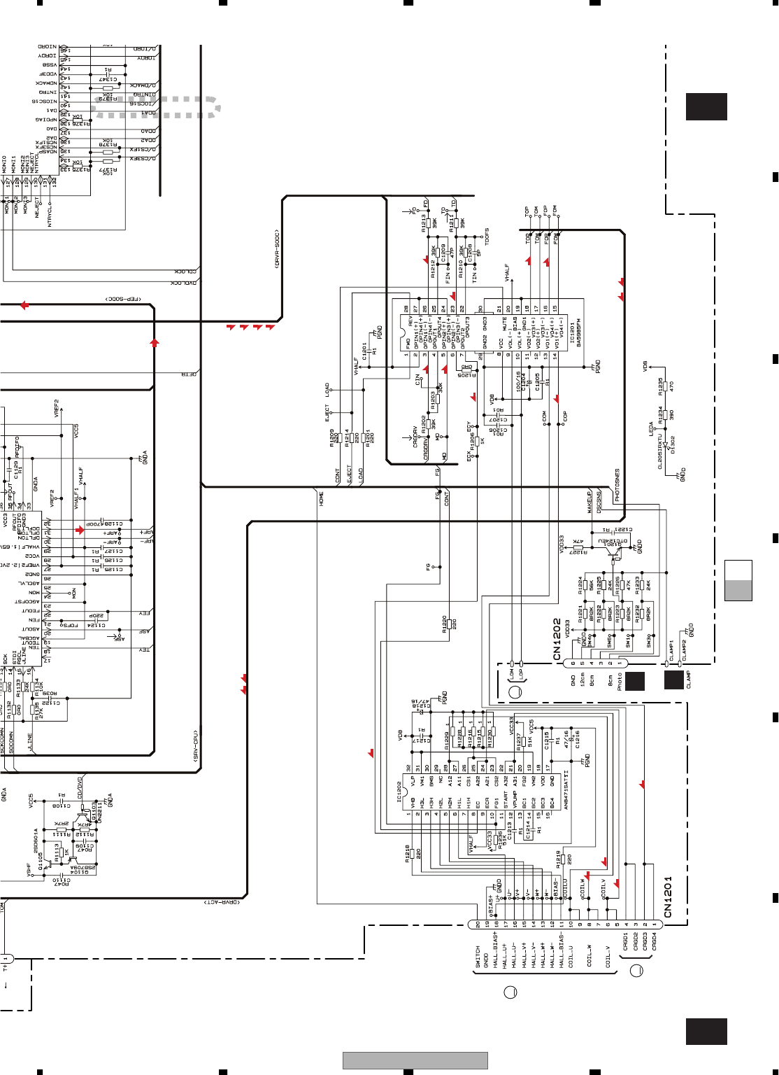
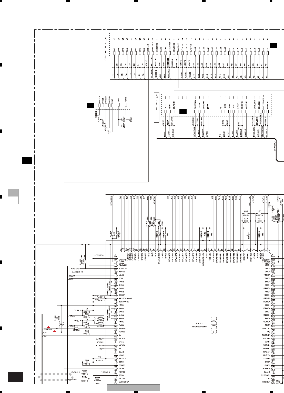
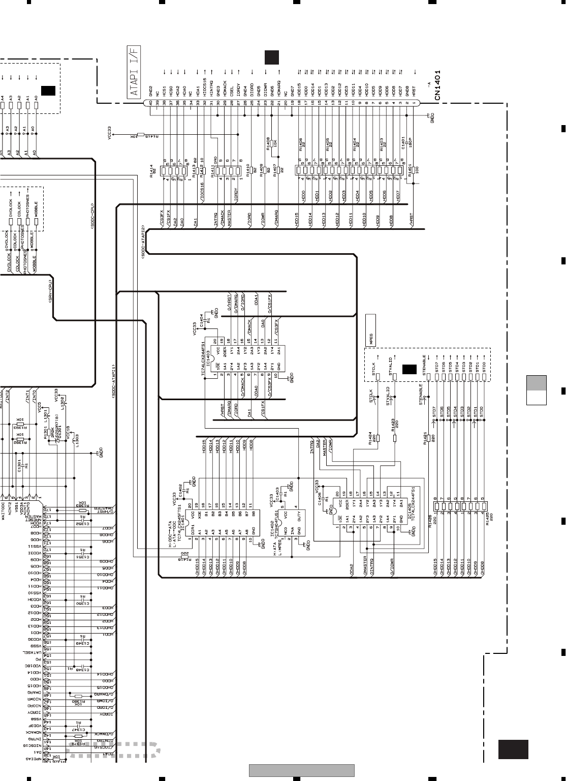
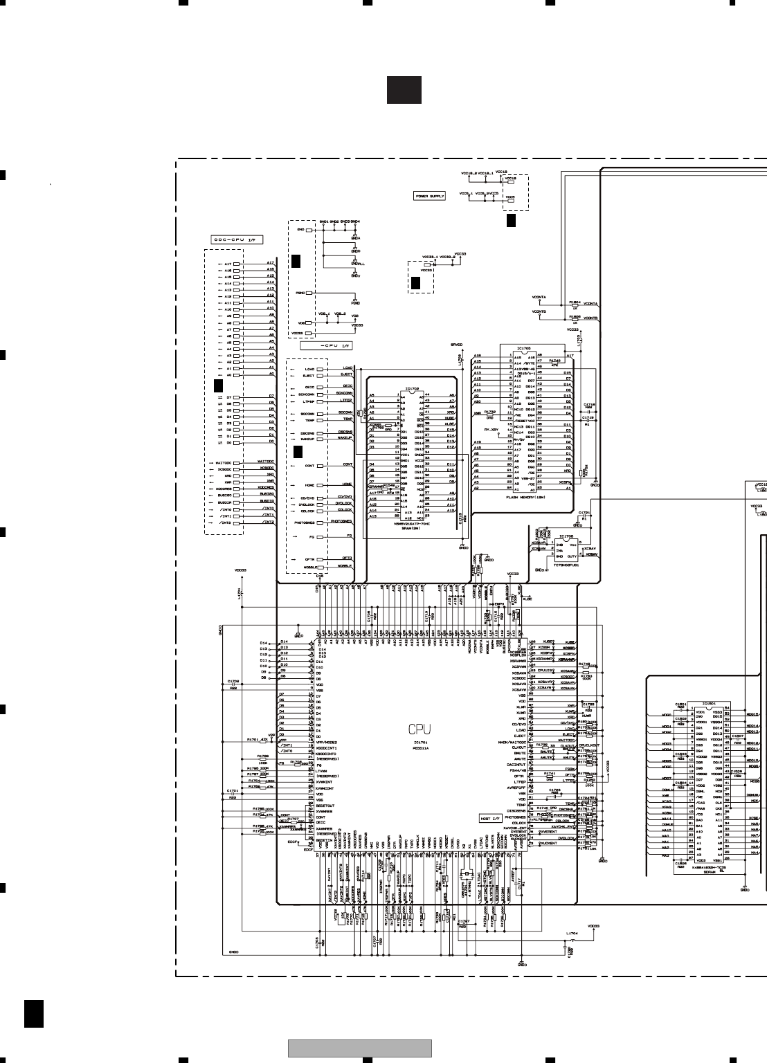
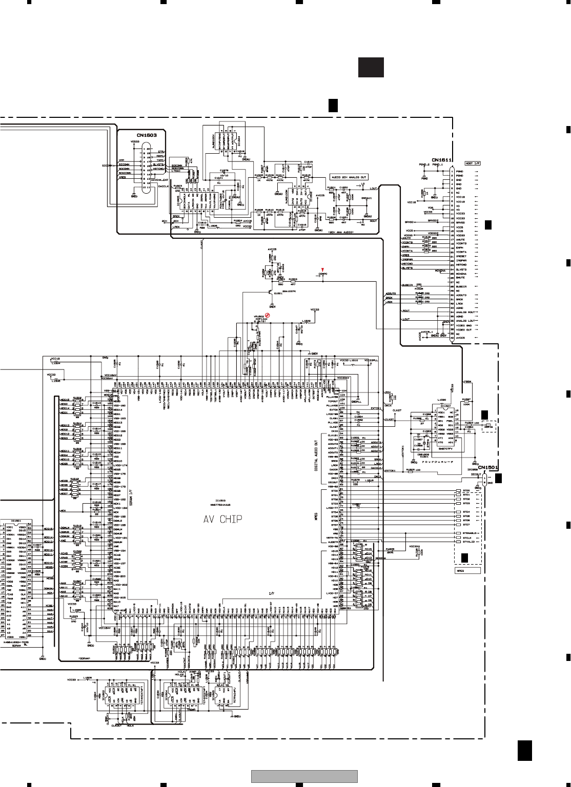
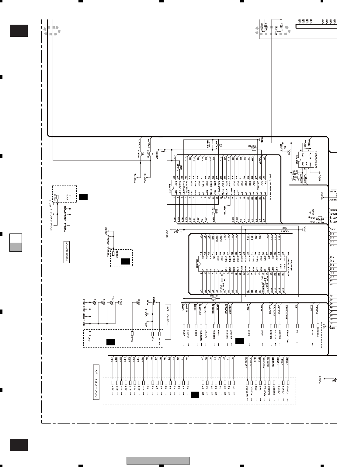
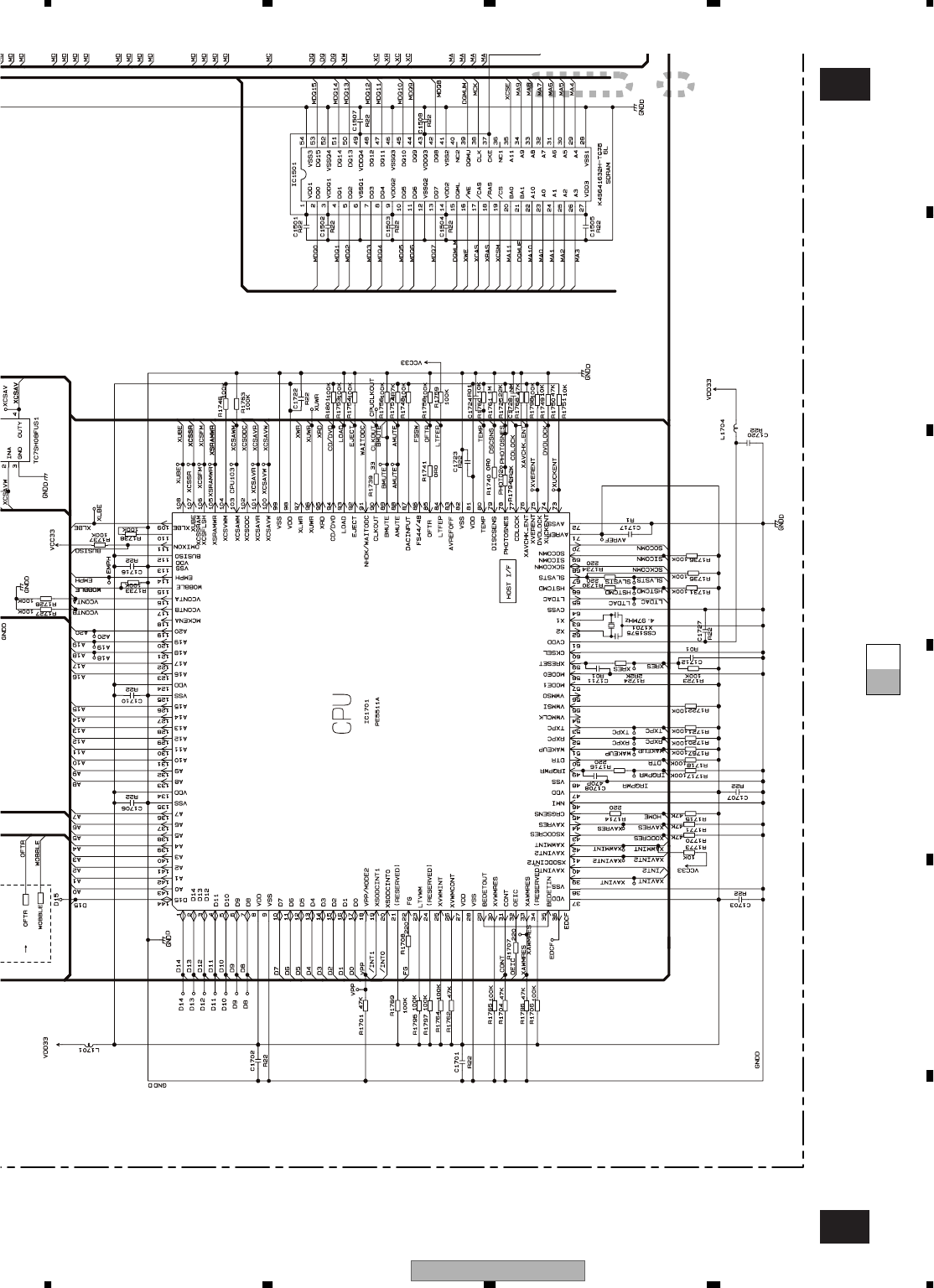
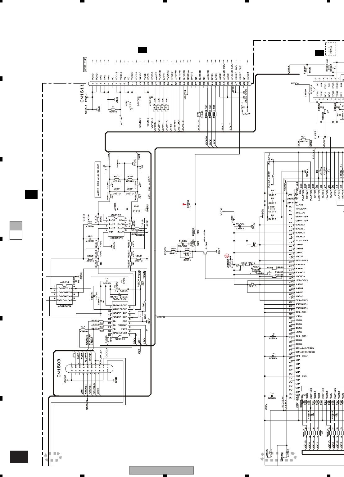
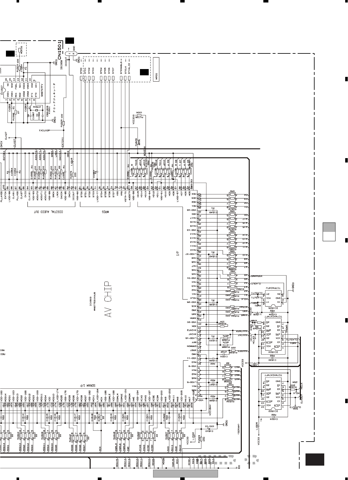
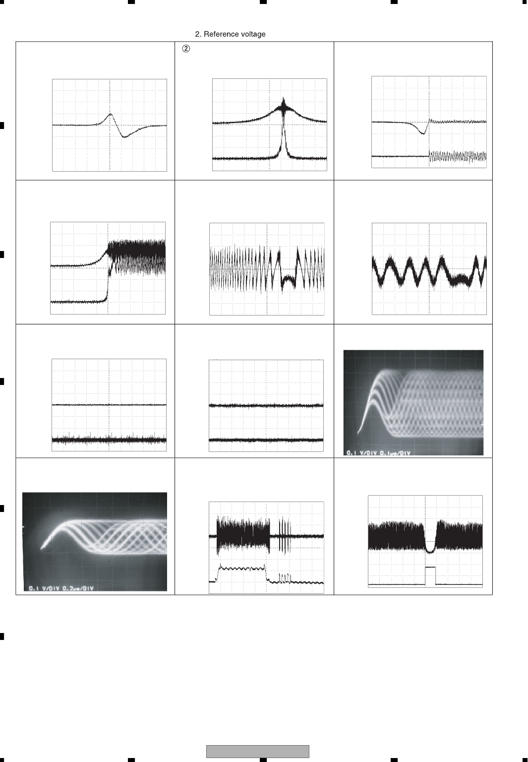
AVIC-Z1/UC
66
1234
1234
C
D
F
A
B
E
1
FEY
500 mV
/
div. 1 ms
/
div
.
F
ocus
sea
r
ch
C
H1: A
S
F
3
C
H2: RFEN
V
F
ocus
sea
r
ch
200 ms
/
div. 1 ms
/
div
.
1
C
H1: FE
Y
500 mV
/
div. 1 ms
/
div
.
4
C
H2: F
D
1 V
/
div. 1 ms
/
div.
F
ocus
c
l
ose
2
C
H1: A
SF
3
C
H1: RFEN
V
F
ocus
c
l
ose
5
C
H1: TE
Y
500 mV
/
div. 1 ms
/
div
.
Focus close
(
DVD
)
5
C
H1: TE
Y
500 mV
/
div. 1 ms
/
div
.
Focus close
(
CD
)
1
C
H1: FE
Y
4
C
H2: F
D
Pla
y
.
500 mV
/
div.20 ms
/
div
.
5
C
H1: TE
Y
6
C
H2: T
D
Pla
y
500 mV
/
div.20 ms
/
div
.
7
C
H1: RF
OUT
0.1 V
/
div. 0.1
µ
s
/
div
.
Play(DVD surroundin
g
s on inside
)
7
C
H1: RF
OUT
0.1 V
/
div. 0.2
µ
s
/
div
.
Pla
y
(CD
)
5
C
H1: TE
Y
8
C
H2:
C
R
G
DR
V
Surroundin
g
s on inside
-
>
surroundin
g
s on outsid
e
500 mV
/
div. 100 ms
/
div
.
VHALF
→
VHALF
→
VHALF
→
VHALF
→
VHALF
→
VHALF
→
VHALF
→
VHALF
→
200 mV
/
div. 2 ms
/
div
.
VHALF
→
VHALF
→
VHALF
→
VHALF
→
VHALF
→
VHALF
→
VHALF
→
7
C
H1: RF
OUT
20 0mV
/
div. 100
µ
s
/
div.
9
C
H2: BD
O
2 V
/
div. 100
µ
s
/
div
.
Bl
ac
k
dot
VHALF
→
VHAL
F
→
-
W
a
v
e
f
o
r
m
Note:1. The encircled numbers denote measurin
g
points in the circuit dia
g
ram.
VHALF : 1.
65
V
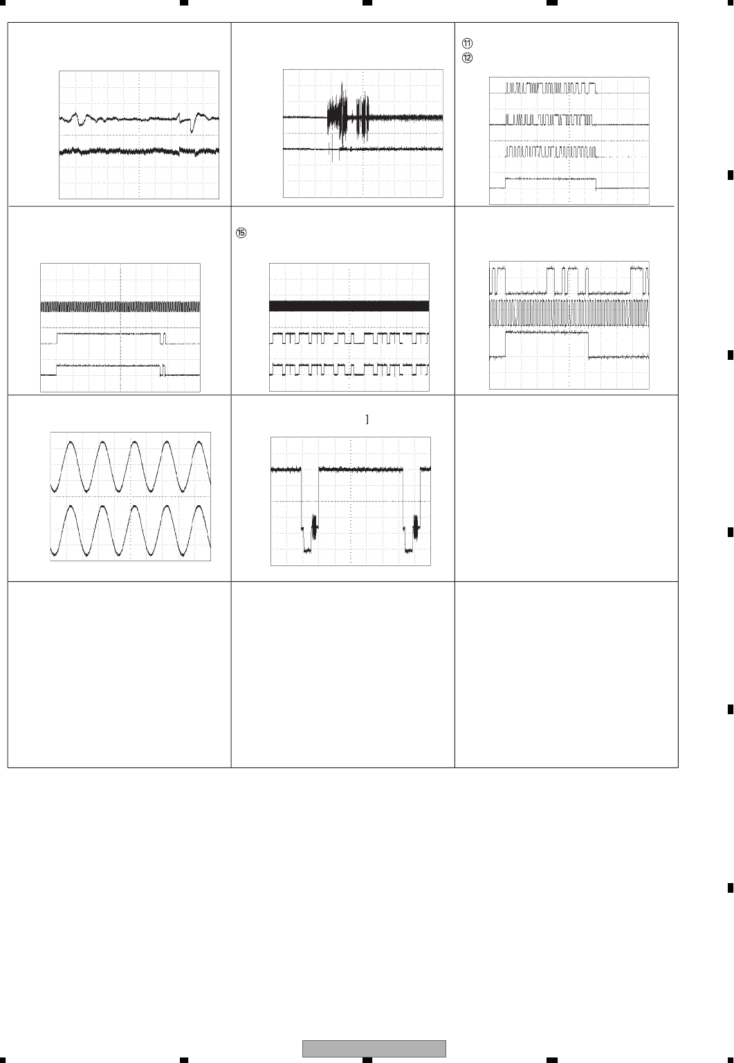
AVIC-Z1/UC 67
5678
5678
C
D
F
A
B
E
4
C
H1: F
D
1 V
/
div. 100
µ
s
/
div
.
6
C
H2: T
D
500 mV
/
div. 100
µ
s
/
div
.
Bl
ac
k
dot
5
C
H1: TE
Y
1
C
H2: FE
Y
EDC1 mode set up(DVD)
v.
500 mV
/
div.1 s
/
di
v
VHALF
→
VHALF
→
VHALF
→
VHALF
→
0
C
H1:
S
TD
1
C
H2:
S
TD
4
C
H
3
:
S
TD
7
#
C
H4:
S
TENAB
L
E
G
→
5 V
/
div. 2
µ
s
/
div
.
G
→
G
→
G
→
$
C
H1:
S
T
C
L
K
%
C
H2:
S
TVALI
D
#
C
H
3
:
S
TENABL
E
5 V
/
div. 2
µ
s
/
div
.
G
→
G
→
G
→
$
C
H1:
S
T
C
L
K
C
H2:
S
TVALI
D
#
C
H
3
:
S
TENABL
E
5 V
/
div. 50
µ
s
/
div
.
G
→
G
→
G
→
^
C
H1: AD
OU
T
0
&
C
H2:
S
R
CK
*
C
H
3
: LR
CK
G
→
2
V/di
v. 2
µ
s
/di
v
.
G
→
G
→
(
C
H1: L
O
)
C
H2: R
O
G
→
1 V
/
div. 500
µ
s
/
div
.
G
→
⁄
CH1: COMPO 200 mV
/
div. 10
µ
s
/
div
.
[White 100 % output
t
]
t
G
→
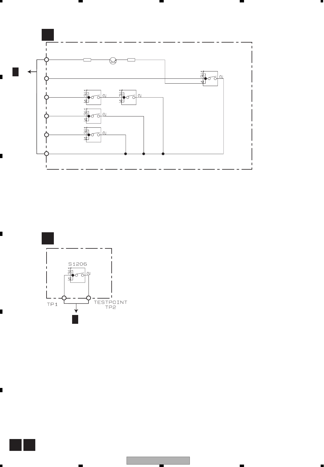
AVIC-Z1/UC
68
1234
1234
C
D
F
A
B
E
3.8 COMPOUND UNIT(A) AND COMPOUND UNIT(B)
E F
FCOMPOUND UNIT(B)
ECOMPOUND UNIT(A)
CLAMP
CSN1067
D1/2
S1201
Q1299
S1202 S1204
S1203
R1298
0R0
1
2
3
4
5
6
S1205
R1299
0R0
CPT231SCTD
12cm
8cm
DISC SENS DISC SENS
8cm
CN1202
D1/2
CSN1069
CSN1069
CSN1070
CSN1070
CSN1069
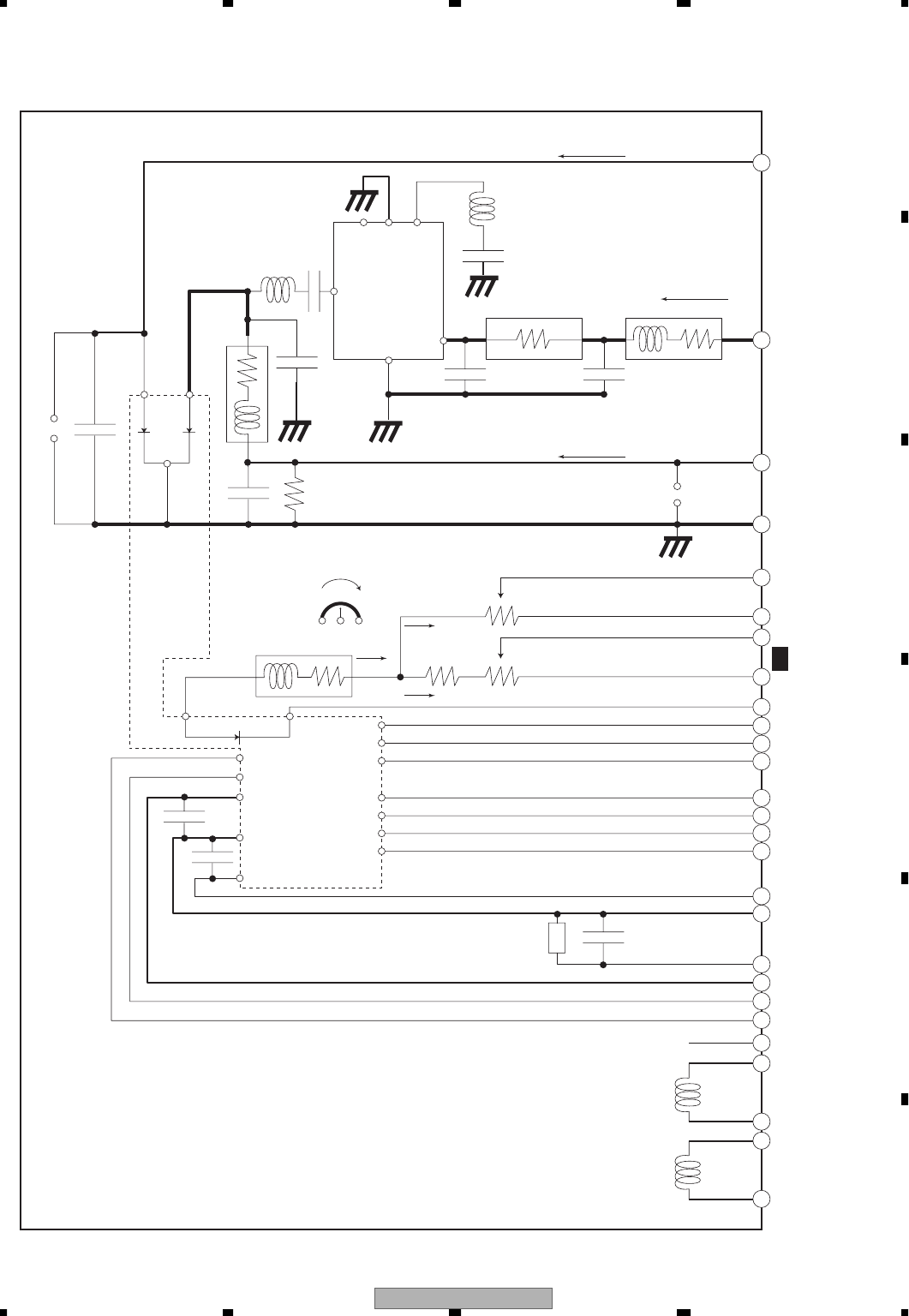
AVIC-Z1/UC 69
5678
5678
C
D
F
A
B
E
3.9 PU UNIT(REFERENCE)
24
Iop78
L2
LC
Vcc
GND
GND
IC1
L4
C2C3
C6
C7
L3
1715
C1
16
65LD78LD
LDGND
R1C5 Short round
L1 C4
78LD
65LD
65MD
65MDGVR2/ 65Rmd
VR1/ 78RmdVmda
1
2
3
4
6
5
7
R2
L6
MDA
Top View
up
MDA
A
SW
Vcc
C8
C9
12
GND
13
V r
14
MDC
98
78MD
78MDG
MDG
B1
B1
B2
RF-
B3
RF+
B4
C
Vref : 2.5V
GND
C10TH1
TEMP
Vcc
SW
A
NC
T-
T+
F-
F+
B2
RF-
B3
RF+
B4
C
LDGND
23
26
25
07
08
05
06
22
21
20
19
18
17
27
02
01
03
04
09
16
15
14
13
12
11
10
Iop65
Im/ 2
Im
Im/ 2
Ishf
Vshf : 4V
CN1101
Short round
D1/2
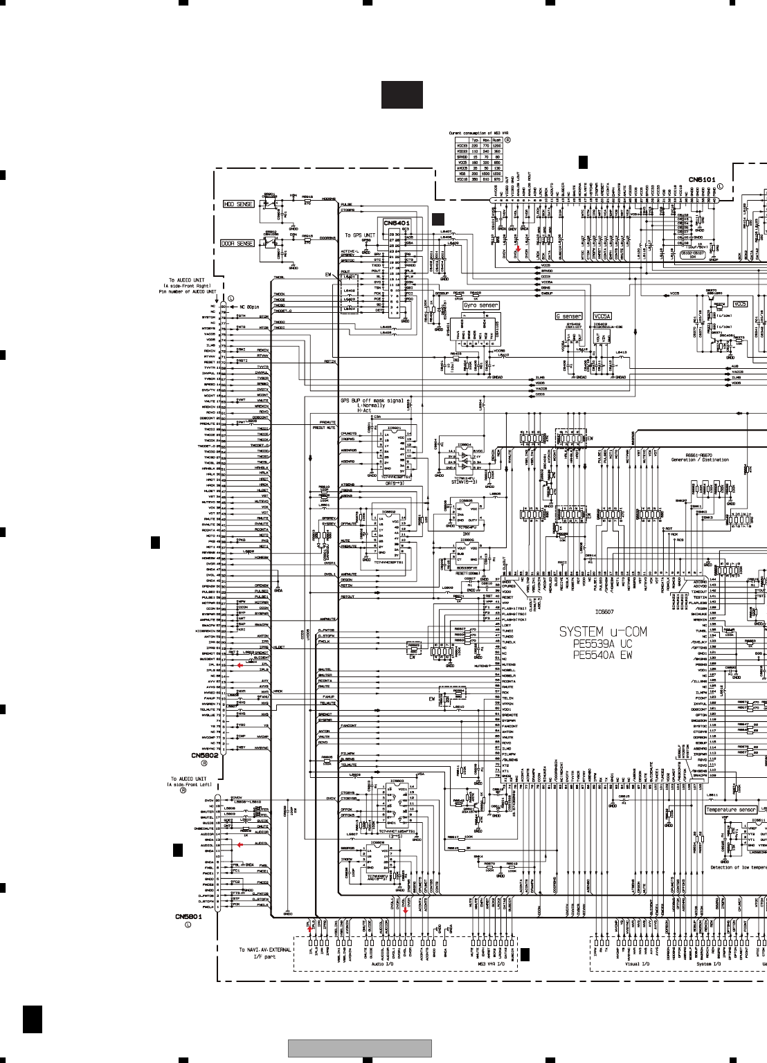
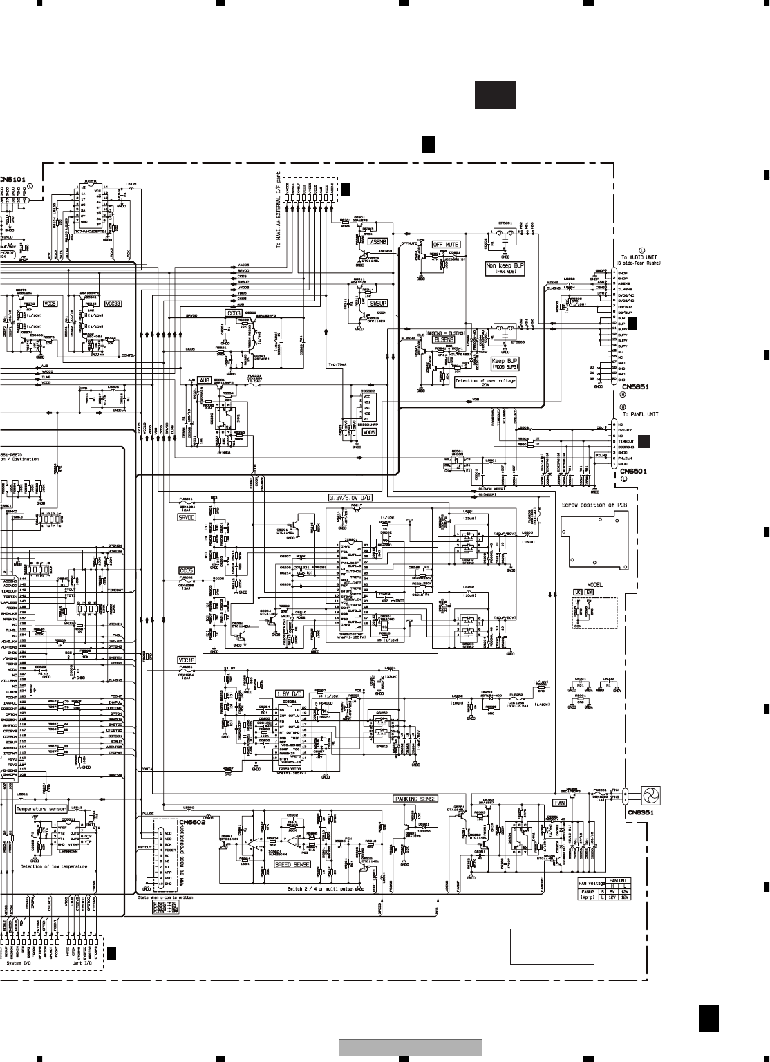
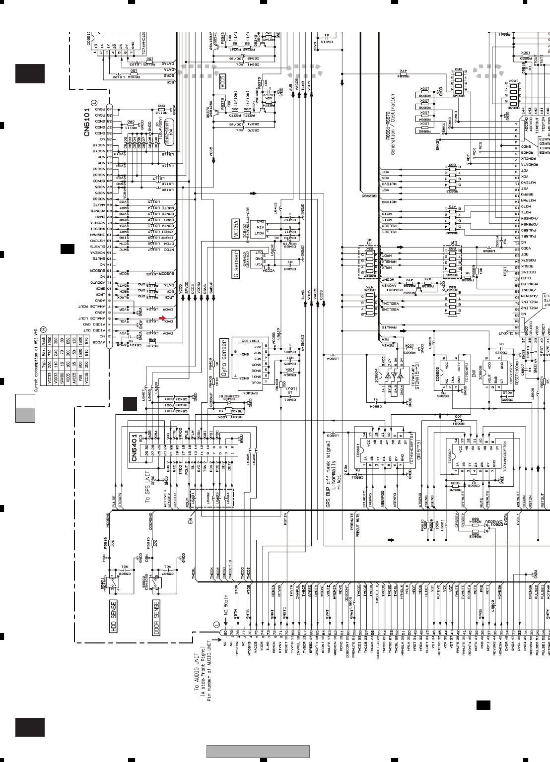
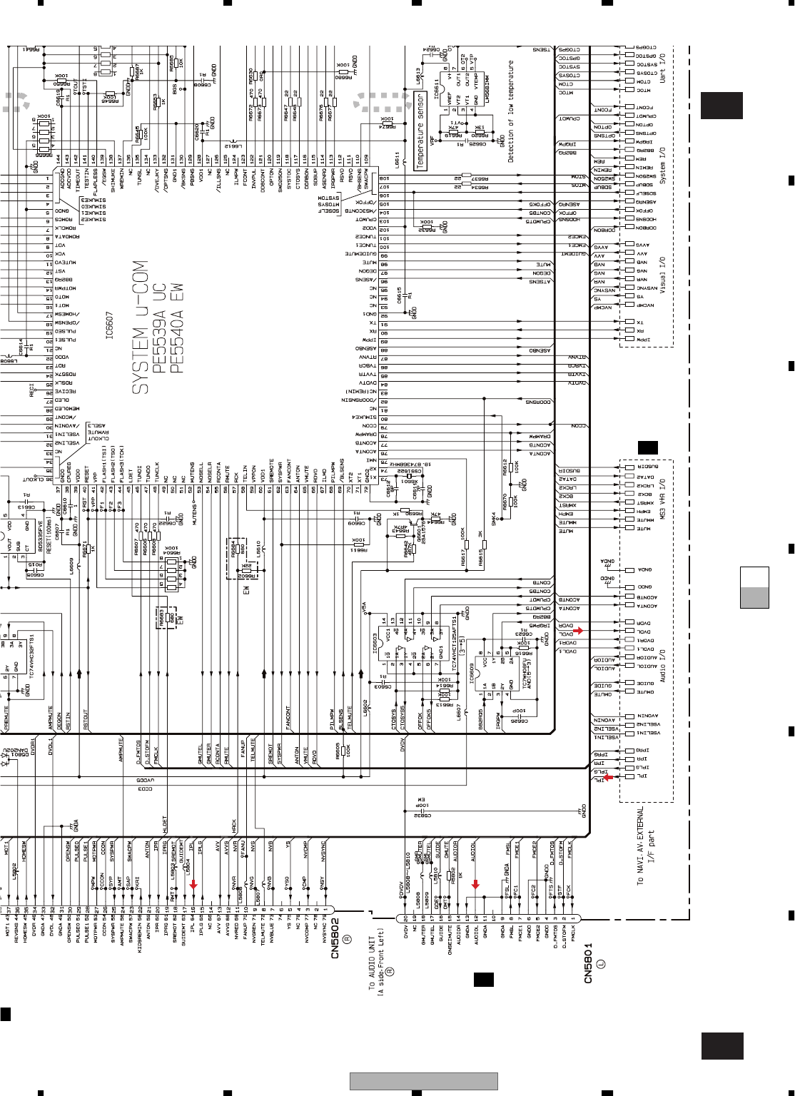
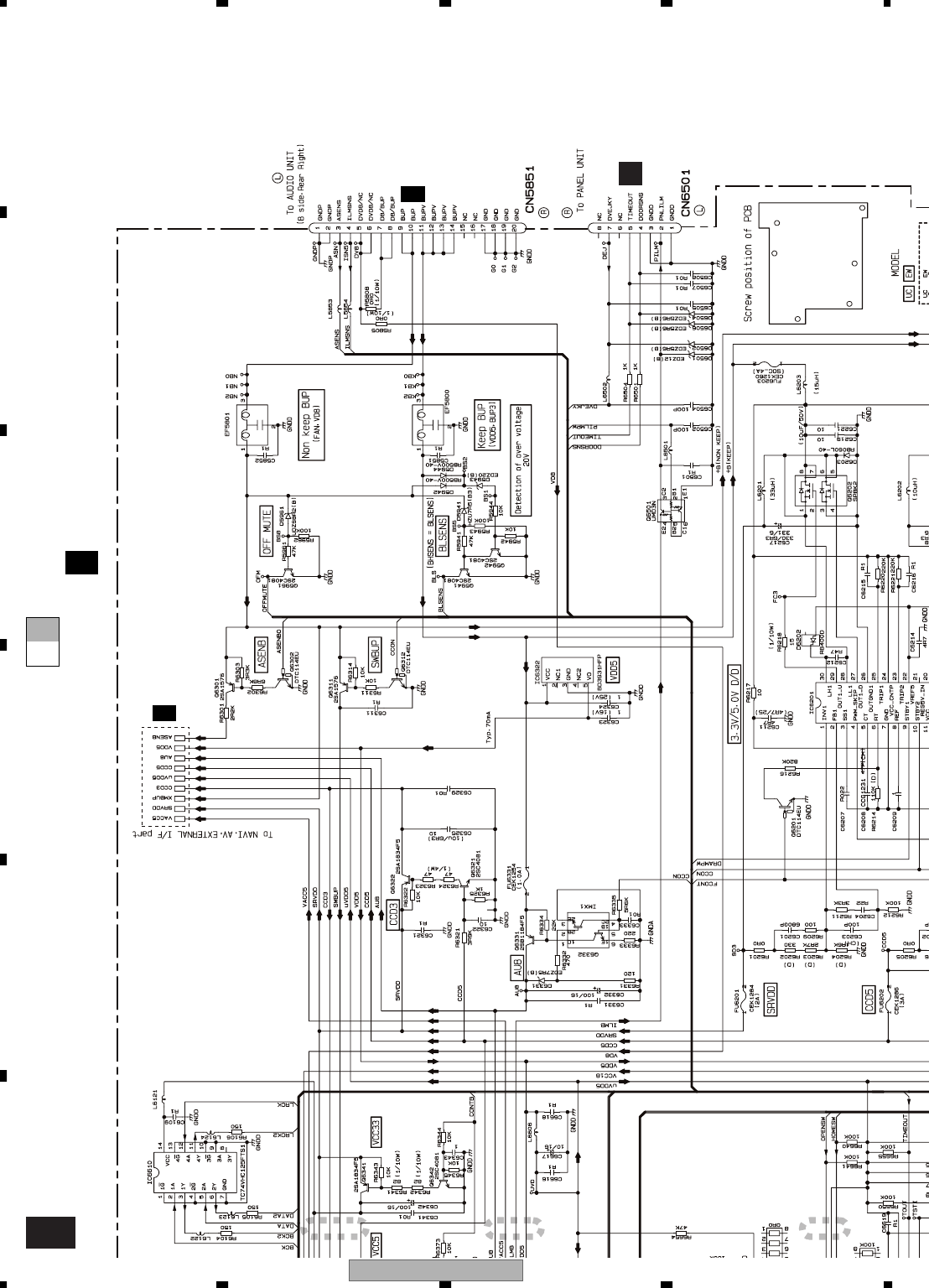
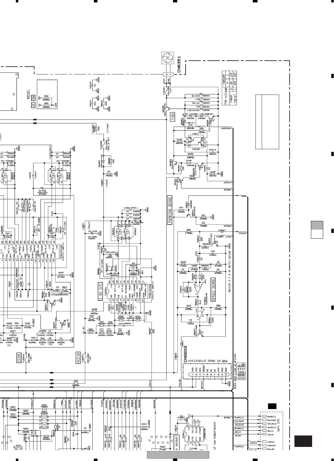
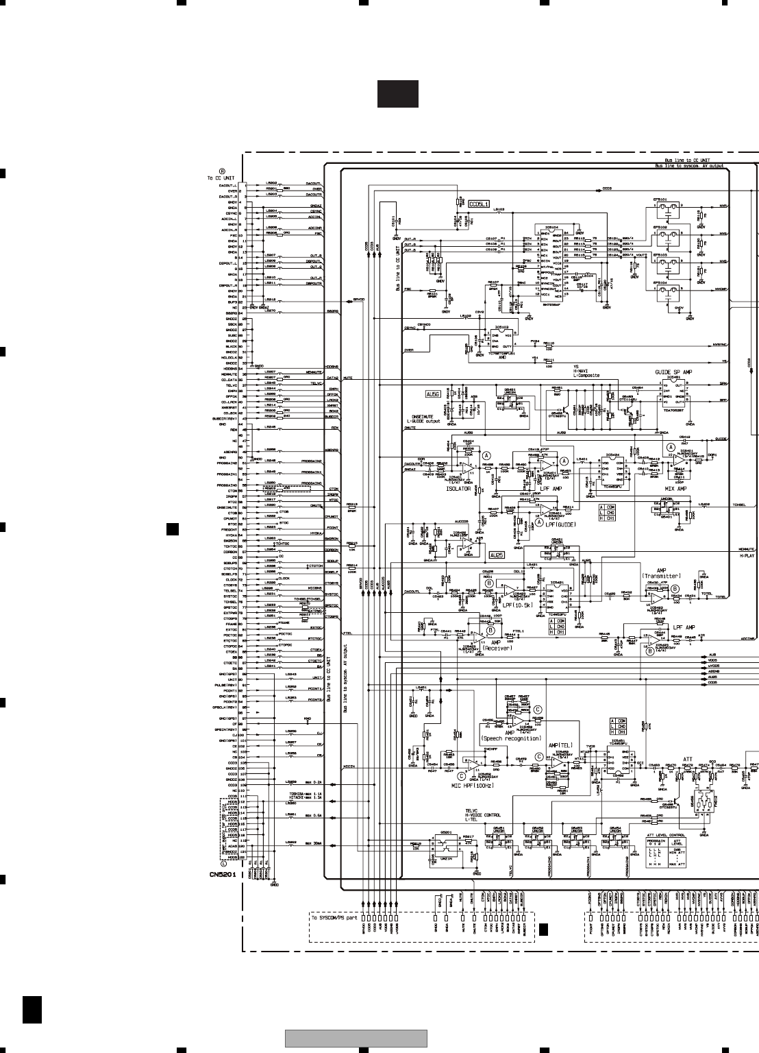
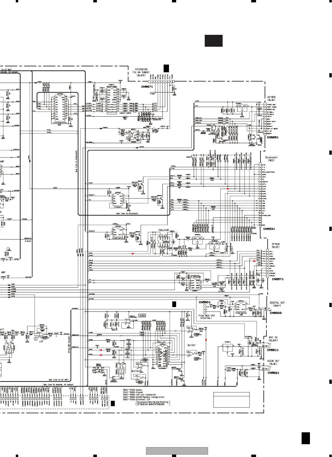
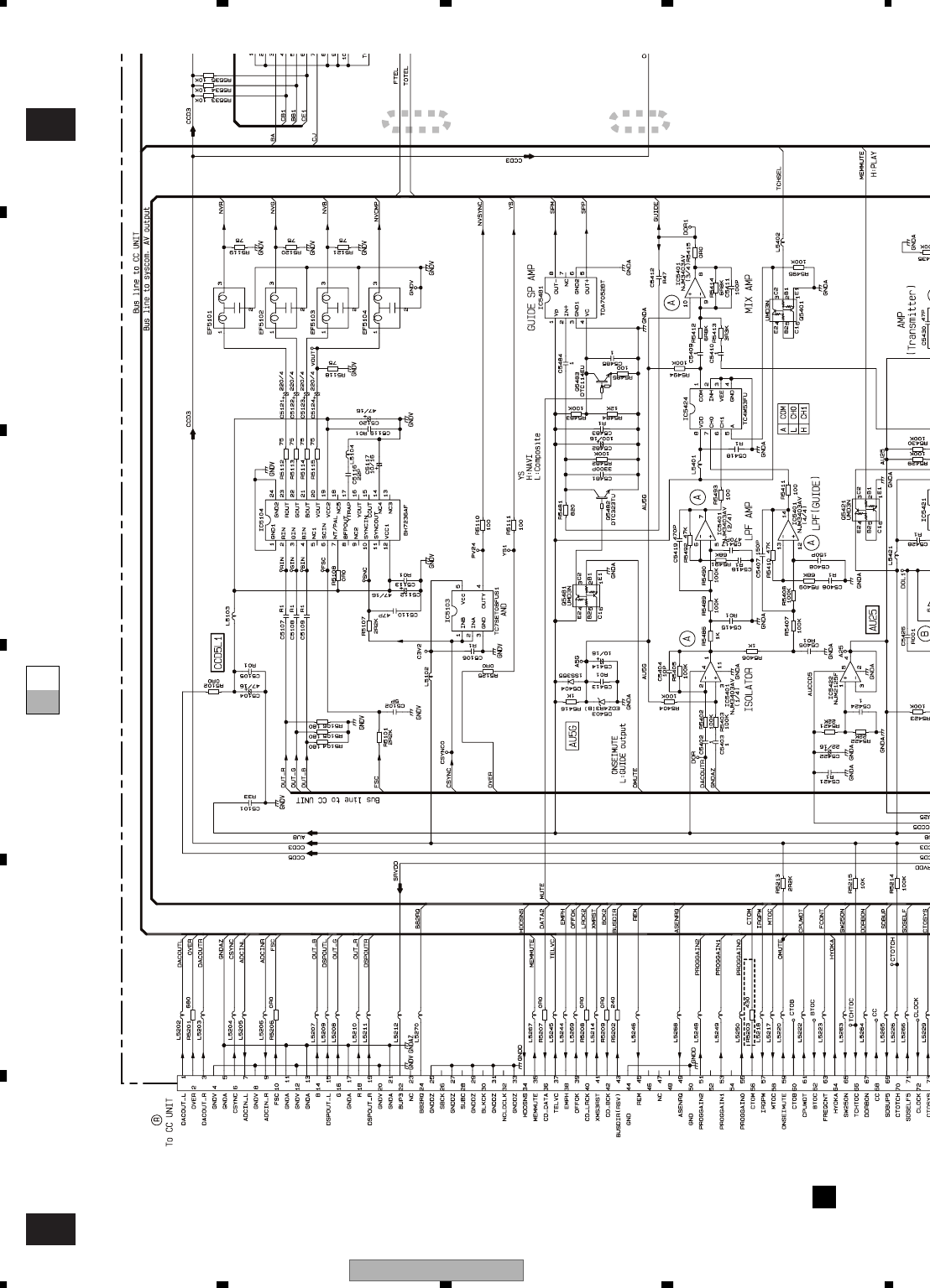
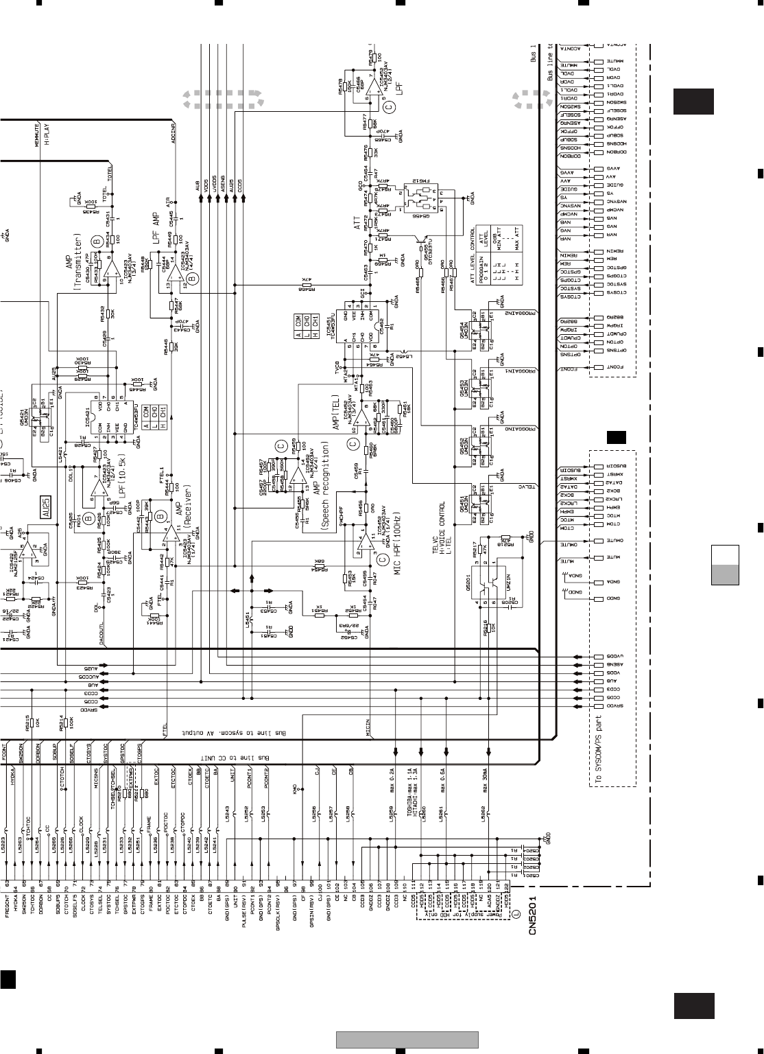
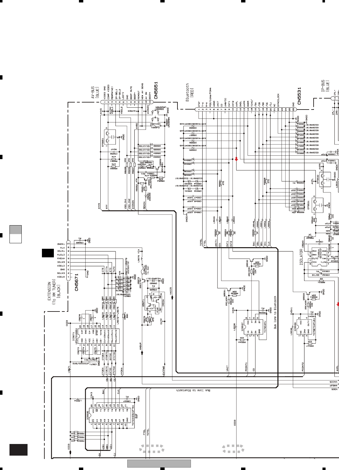
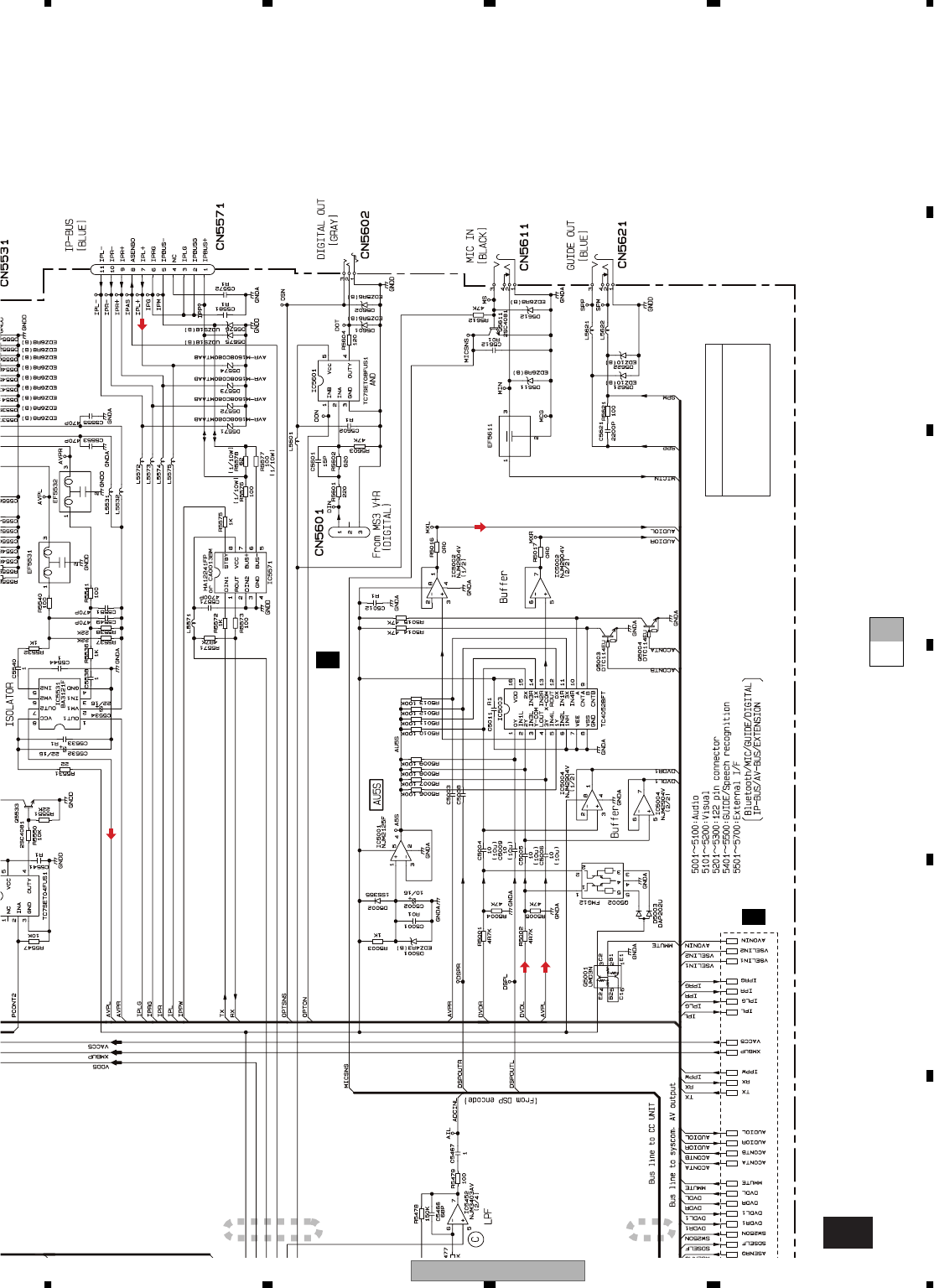
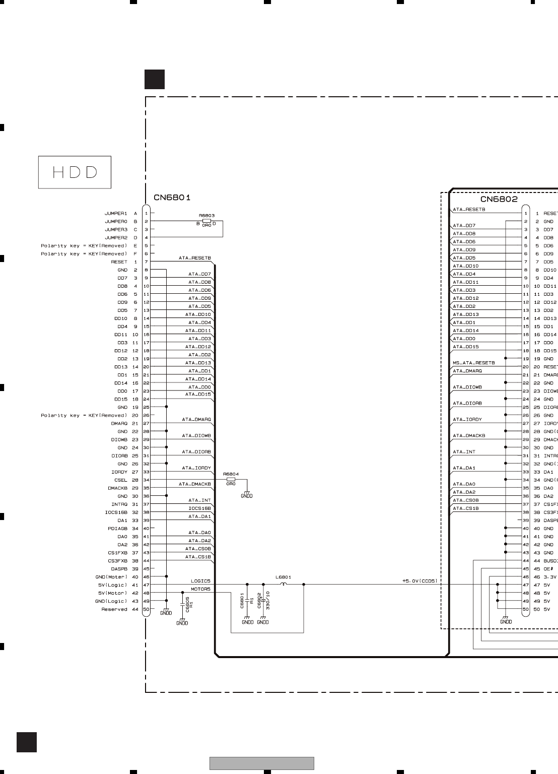
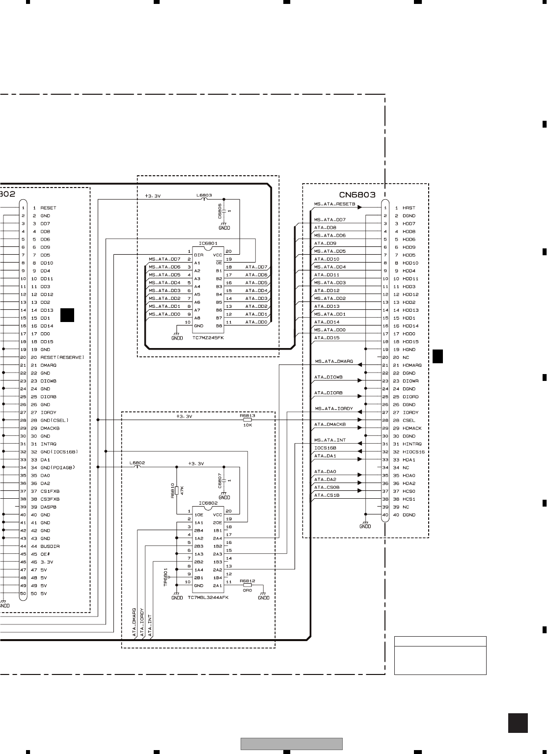
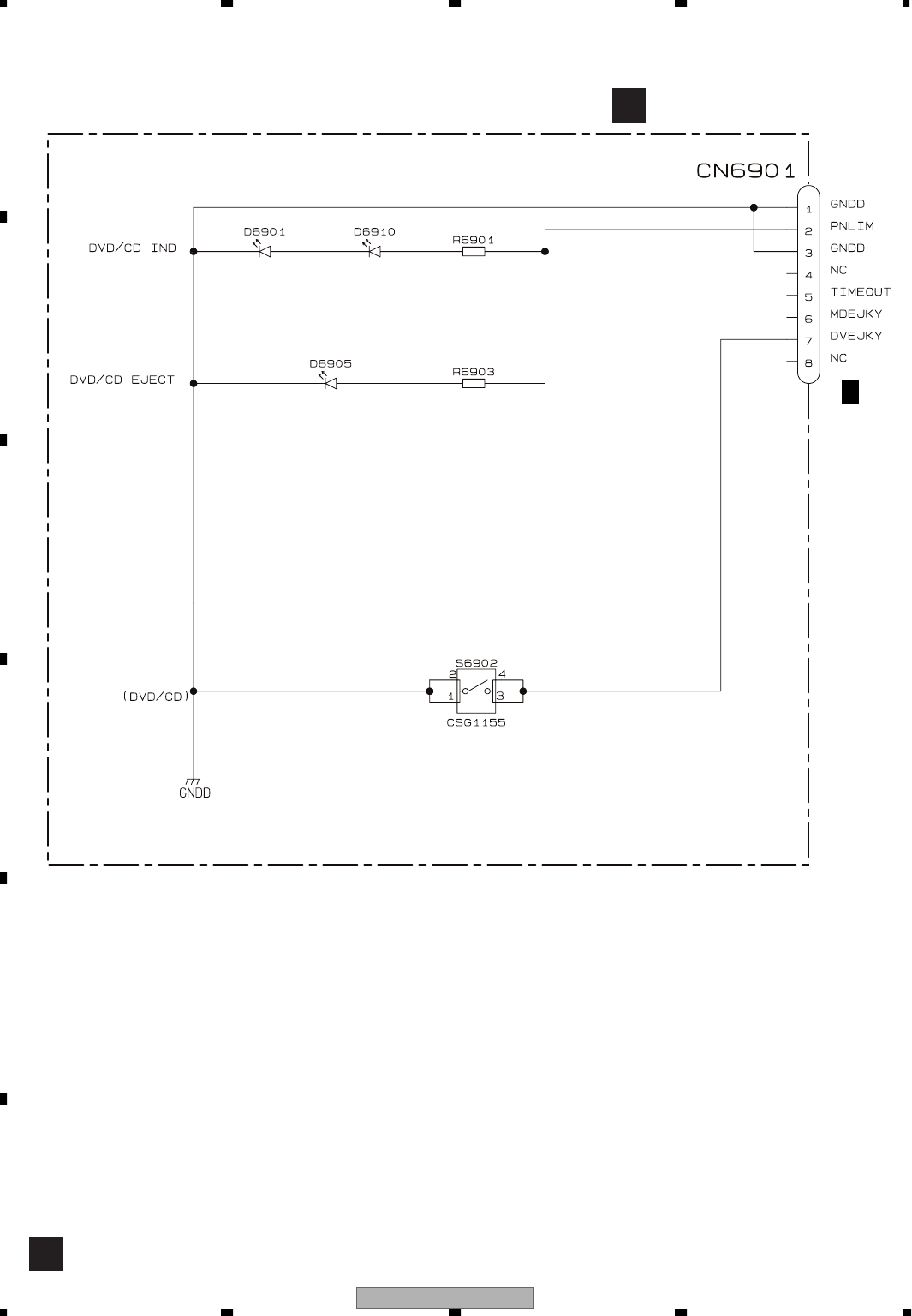
AVIC-Z1/UC
84
1234
1234
C
D
F
A
B
E
3.13 PANEL UNIT
I
240
2K
SDDB16001A(CA) SDDB16001A(CA)
SDDB16001A(CA)
PANEL UNIT
I
CN6501
1/2
G
8.7V
DISC
EJECT Button

AVIC-Z1/UC 85
5678
5678
C
D
F
A
B
E
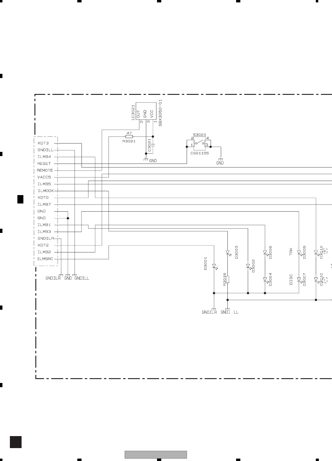
AVIC-Z1/UC
86
1234
1234
C
D
F
A
B
E
3.14 KEYBOARD UNIT
J
SDDB16001A(CA)
SDDB16001A(CA)
SDDB16001A(CA)
SDDB16001A(CA)
SDDB16001A(CA)
SDDB16001A(CA)
SDDB16001A(CA)
SDDB16001A(CA)
SDDB16001A1(CA)
CL-195SR-CD(AB)(EW)
SDDB16001A(CA)(UC)
CL-195SR-CD(AB)(EW)
SDDB16001A(UC)
R1
TA/NEWS
MENU
MAP
1/2
K
CN4
ILMB1~7 : 8 V
ILMODK, ILMSRC : 8 V
RESET
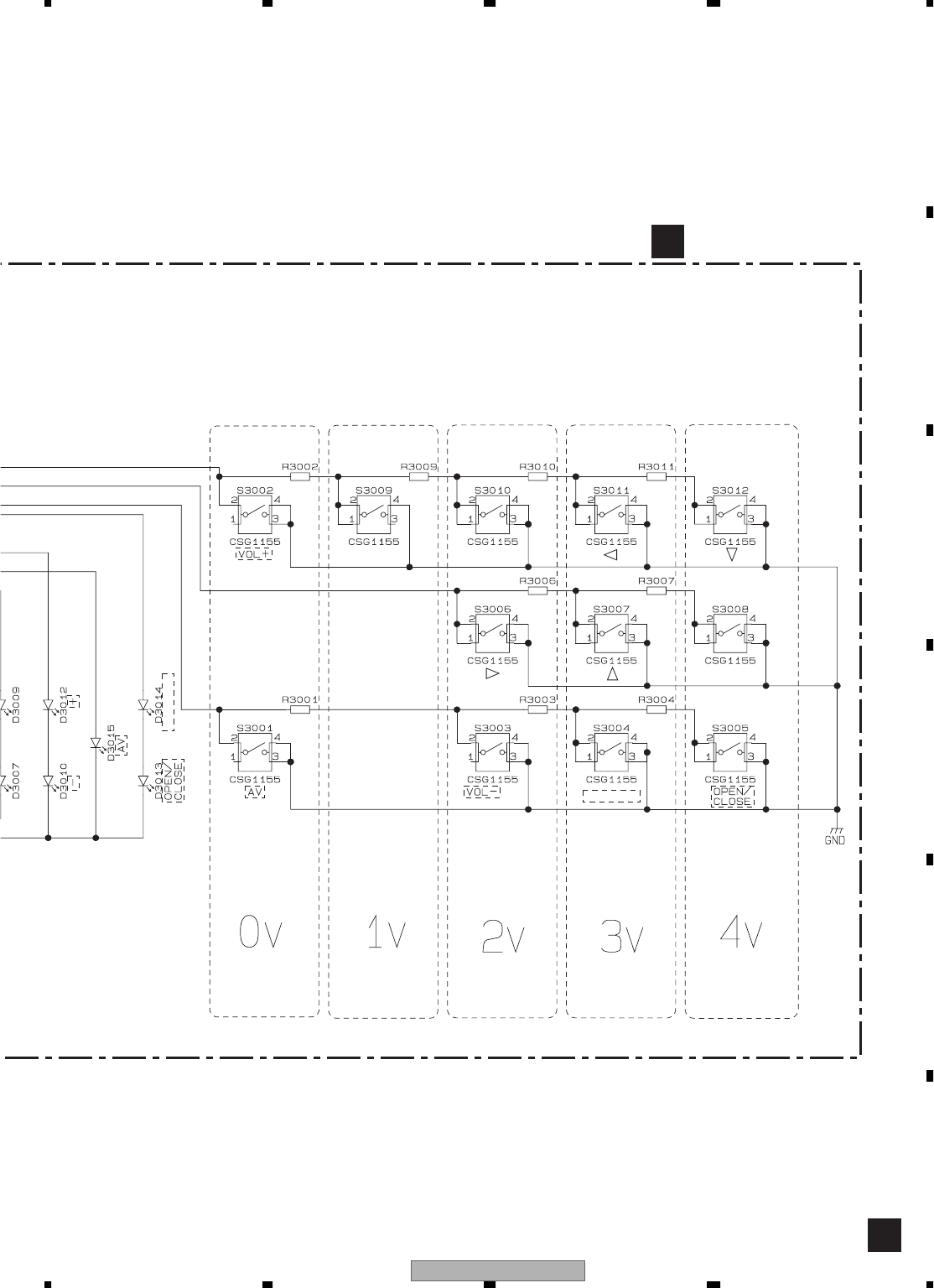
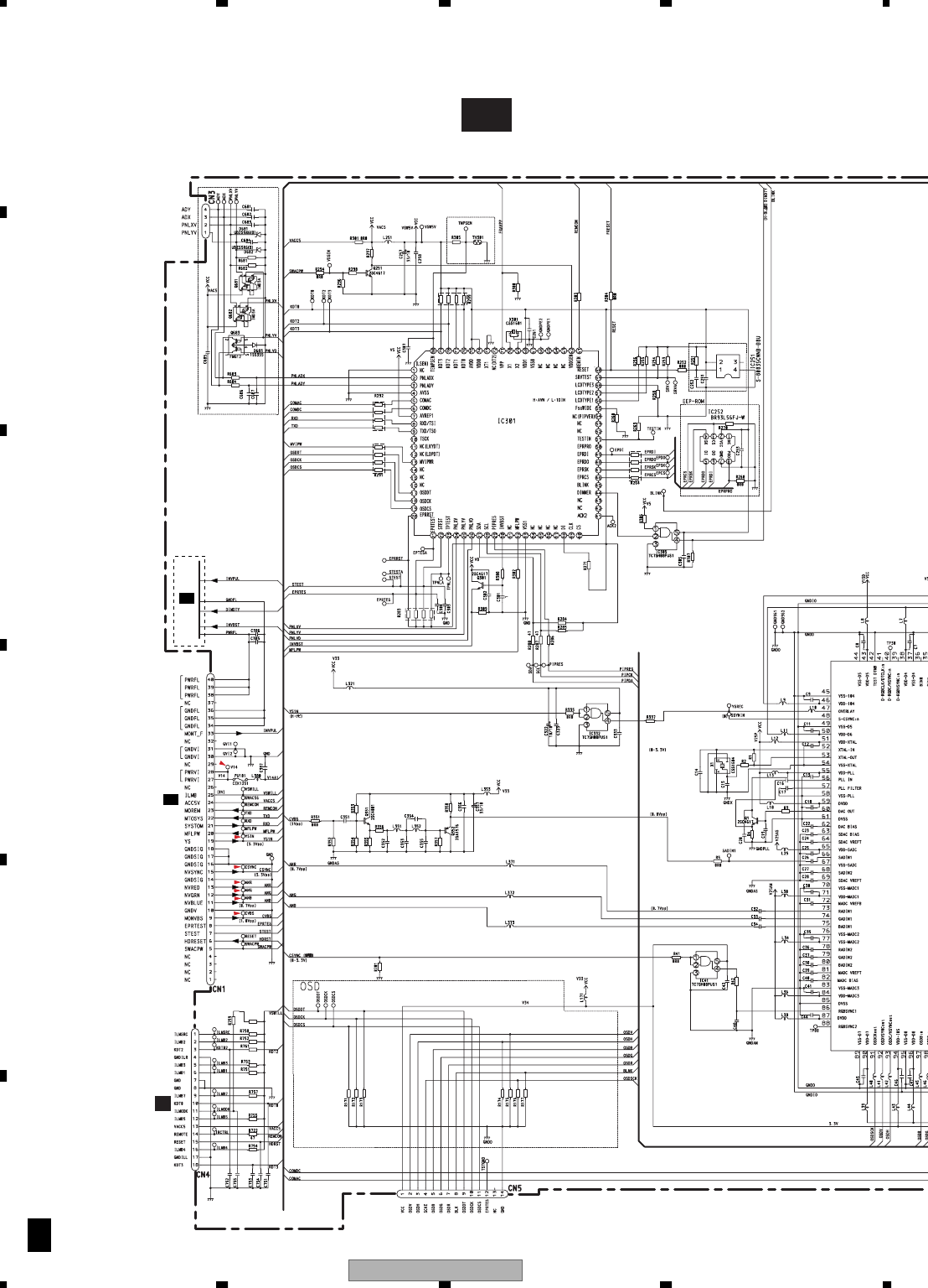
AVIC-Z1/UC
88
1234
1234
C
D
F
A
B
E
3.15 MONITOR UNIT(MONITOR)(GUIDE PAGE)
1/2
K
K-a 1/2
42MHz
12.58MHz
47K
22K
47K
15K
12K
47K
100
10K
47K
47K
47K(EW)
47K
47K
47K
47K
47K(UC)
47K
1K
470
470
1K
1K
47K
100K
470
1K
10K
2R7K
2R7K
470
10K
47K
100
1M
390
1R5K
330
390
2R7K
470
680
100K
100K
15K
500mA
100
10K
560(EW)
750(UC)
1R5K
750
8R2K
750
1R5K
0R0
R760
100K
100K
100K
47K
47K
47K
4R7K
1R5K
750
750
100K
100K
R001
R001
R001
R001
R1
R1
R1
R1
R01
R1
R1
R001
R001
R1
R1
R1
R1
R1
R1
10
10
R1
R1
R1
R1
R1
R1
R01
180P
9P
9P
R22
10
68P
100P
68P
2P
R1
R1
4P
R1
R1
R1
R1
R1
R1
R1
R1
R1
R1
R1
R1
R1
R1
R1
R1
R1
R1
R1
R1
R1
150P
R1
R1
R1
R1
R001
R1
AVR-M1608C080MTAAB
AVR-M1608C080MTAAB
AVR-M1608C080MTAAB
TMP SEN
TOUCH PANEL CN1203
1/2
C
2/2
K
>
J
OSD for service
PE5538A
Microcomputer
Reset
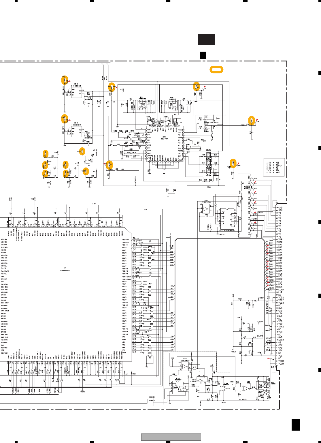
AVIC-Z1/UC 89
5678
5678
C
D
F
A
B
E
1/2
K
K-b 1/2
10 H
18 H 68 H
18 H
470K
56K
27K
680K
1K 160 270
1K 33K
6R8K 200
6R8K 1R8K
680k
1K
510 2K
51K
820
330K
18K
10K 18K 22K
220
220
220
220
220
220
220
680
100
100
15K 15K
100
56K
33K
22K
4R7K
33K
R1
R1
CCH1440
R1
R01
10
10
10
R01
R1
R1
R01 100P
330P R039
R01
R047
R039
R1
R1
R001
R1
R01
4700P
4700P
R1
R01
4R7
R1
R47
R47
R47
2R2
2R2
R1
R1
R1
R039
R001
R1
R1
R1
R1
R1
R1
R1
R1
R1
R1
R1
R1
R1
R1
R1
R1
R1
R1
R1
R1
R1
R1
R1
R1
R1
4R7
R1
R33
R1
R1
R1
R1
R1
R1
R1
R1
R1
R1
R1
R1
R1
R1
R1
R1
R1
4R7
R1
1K
CCH1586
LCD Module
MONITOR UNIT(MONITOR)
1/2
K
2 screen IC
Power Supply
: The power supply is shown with the marked box.
VCOM AMP
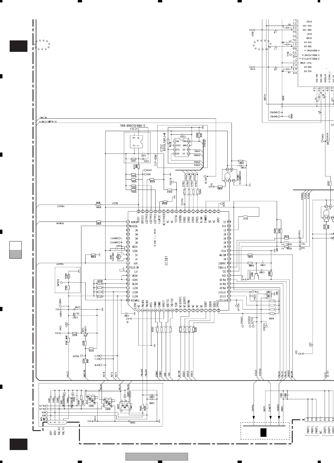
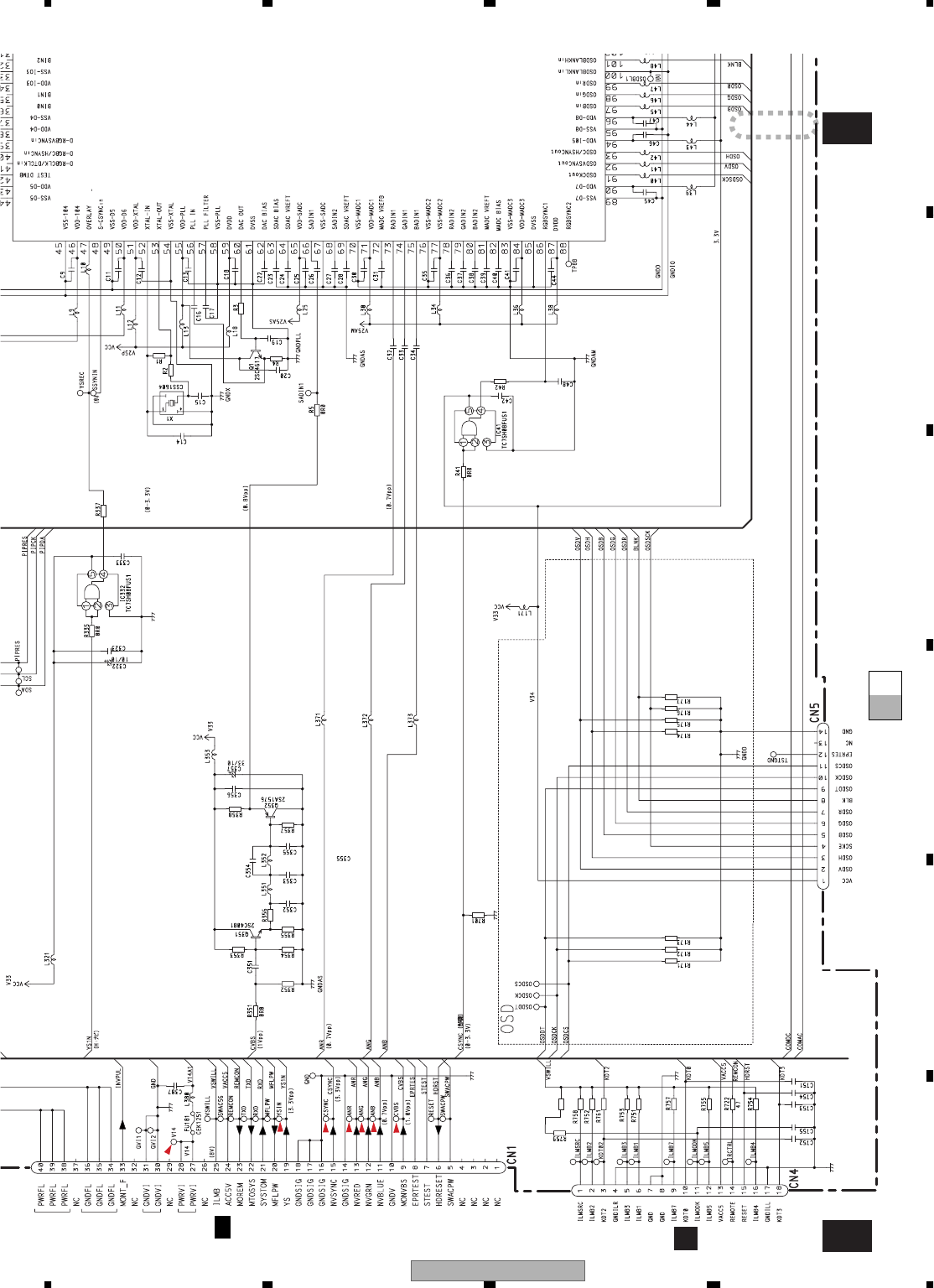
AVIC-Z1/UC 91
5678
5678
C
D
F
A
B
E
A-a K-b
K-a
K-a 1/2
K-b 1/2
3
42MHz
100
1M
390
1R5K
330
390
2R7K
470
680
100K
100K
15K
500mA
100
10K
560(EW)
750(UC)
1R5K
750
8R2K
750
1R5K
0R0
R760
100K
100K
100K
47K
47K
47K
4R7K
1R5K
750
750
R1
R1
R1
R1
R1
R1
R01
180P
9P
9P
R22
10
68P(UC)
47P(EW)
100P(UC)
68P(EW)
68P(UC)
47P(EW)
2P(UC)
5P(EW)
R1
R1
4P
R1
R1
R1
R1
R1
R1
R1
R1
R1
R1
R1
R1
R1
R1
R1
R1
R1
R1
R1
R1
R1
150P
R1
R1
R1
R1
R1
R001
R1
AVR-M1608C080MTAAB
AVR-M1608C080MTAAB
AVR-M1608C080MTAAB
CN1203
1/2
C
>
J
OSD for service
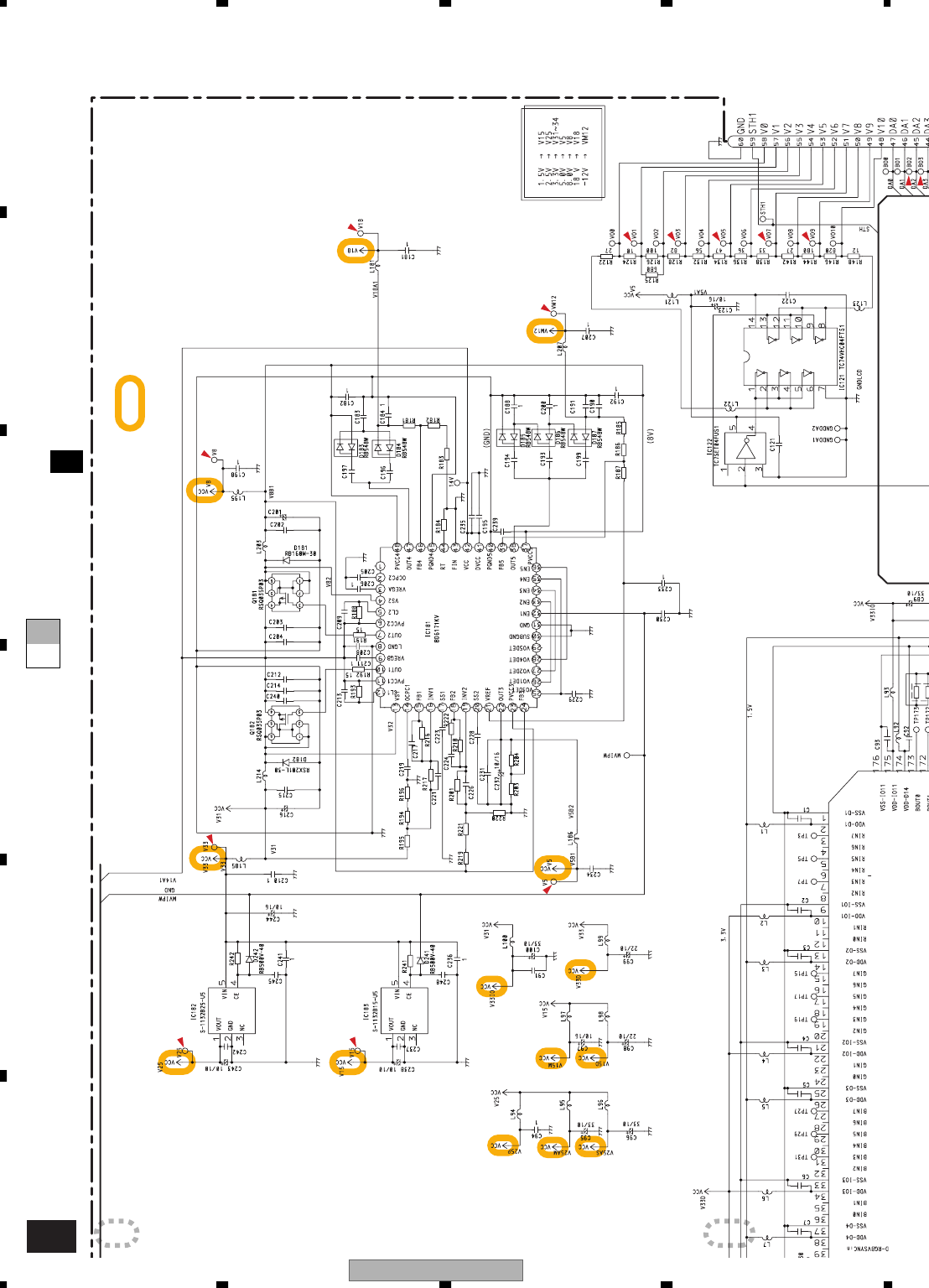
AVIC-Z1/UC
92
1234
1234
C
D
F
A
B
E
K-a K-b
K-b
1/2
12
10µH
18µH68µH
18µH
470K
56K
27K
680K
1K 160 270
1K 33K
6R8K 200
6R8K 1R8K
680k
1K
510 2K
51K
820
330K
18K
10K 18K 22K
R1
R1
CCH1440
R1
R01
10
10
10
R01
R1
R1
R01 100P
330P R039
R01
R047
R039
R1
R1
R001
R1
R01
4700P
4700P
R1
R01
4R7
R1
R47
R47
R47
2R2
2R2
R1
R1
R1
R039
R001
R1
R1
R1
R1
R1
R1
R1
R1
R1
R1
R1
CCH1586
MONITOR UNIT(MONITOR)
1/2
K
2 screen IC
Power Supply
: The power supply is shown with the marked box.
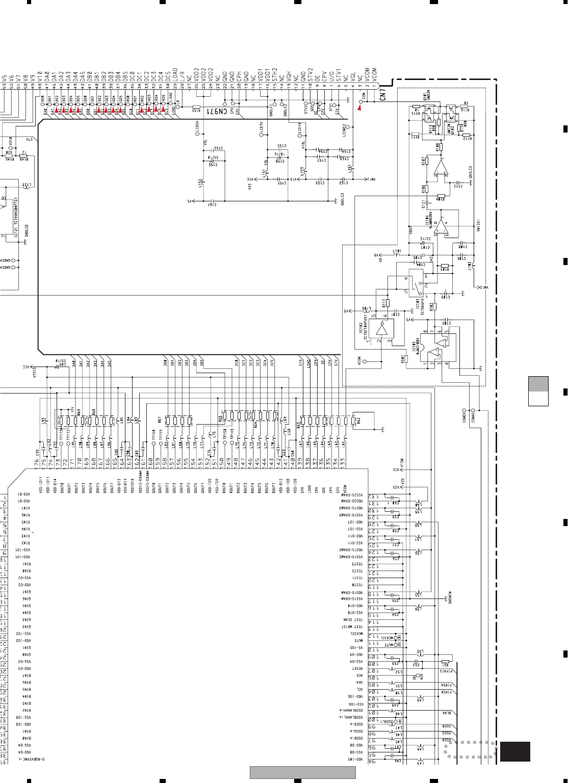
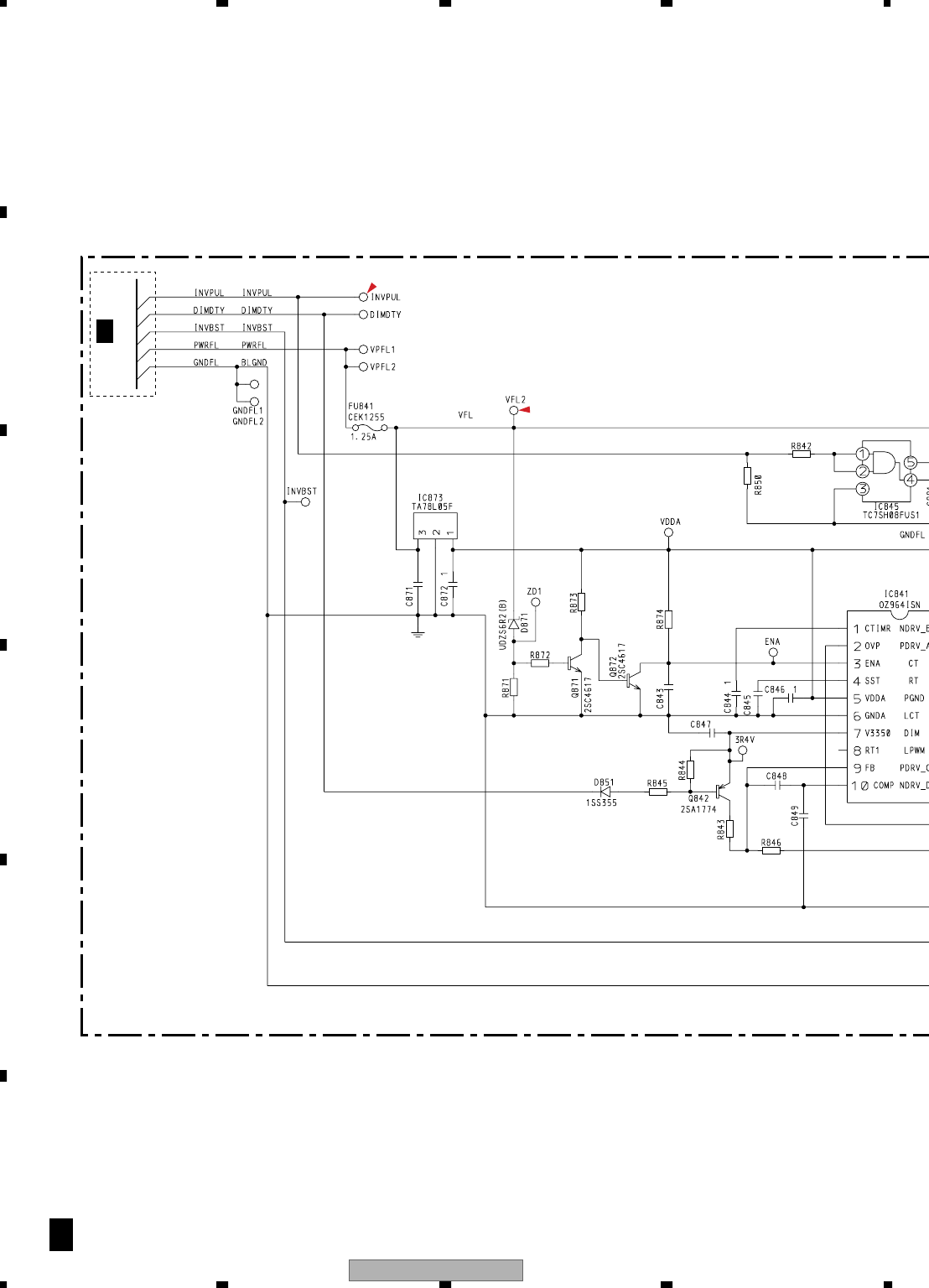
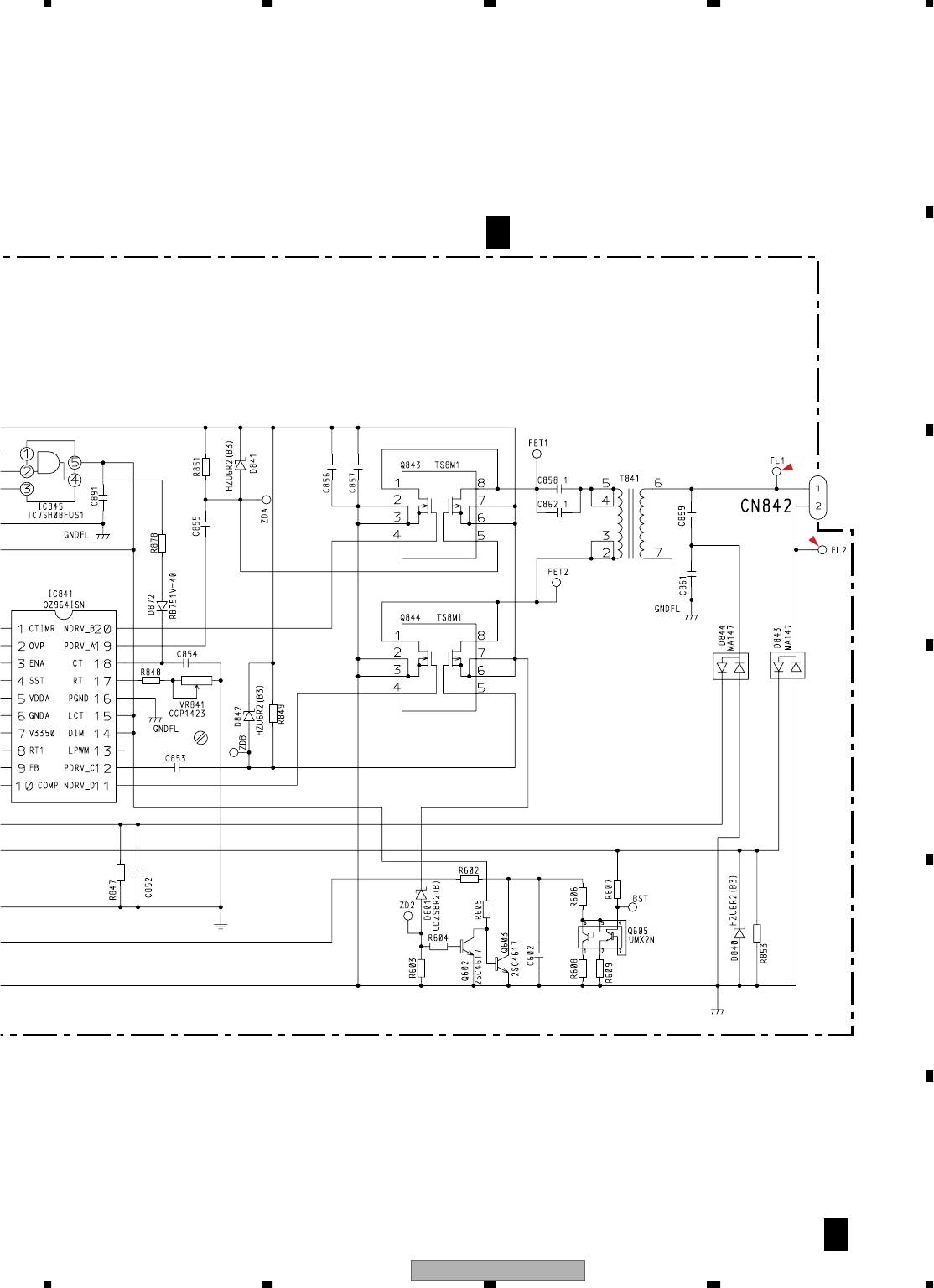
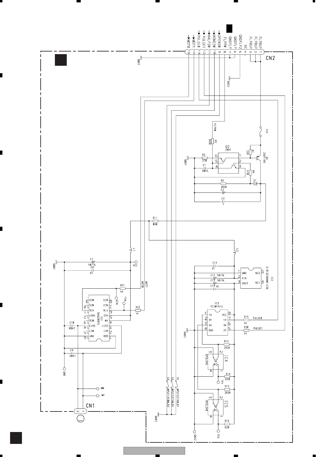
AVIC-Z1/UC
96
1234
1234
C
D
F
A
B
E
3.17 MAIN PCB UNIT
L
CEK1304
39/16
HZU6R2(B2)
M1000
CZX5102
(FLAP)
>
M
HOME SW
HARF SW
OPEN SW
(2A)
12
43 7 56
MAIN PCB UNIT
L
CN1003
1/2
C
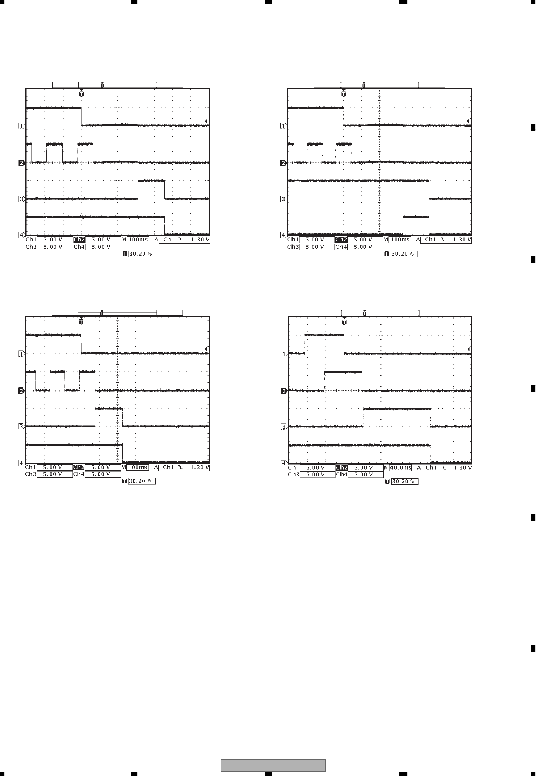
AVIC-Z1/UC 97
5678
5678
C
D
F
A
B
E
- Wave form Note:The encircled numbers denote measurin
g
points in the circuit dia
g
ram.
•
F
U
LL
O
PE
N
•
HALF
O
PE
N
•
C
L
OSE
1
C
H1 :
O
PEN
SW
2
C
H2 : P
U
L
S
E
1
3
C
H
3
: M
O
T
0
4
C
H4 : M
O
T
1
5
C
H1 : HALF
SW
2
C
H2 : P
U
L
S
E
1
3
C
H
3
: M
O
T
0
4
C
H4 : M
O
T
1
6
C
H1 : H
O
ME
SW
2
C
H2 : P
U
L
S
E
1
3
C
H
3
: M
O
T
0
4
C
H4 : M
O
T
1
•
AN
G
L
E
7
C
H1 : P
U
L
S
E
0
2
C
H2 : P
U
L
S
E
1
3
C
H
3
: M
O
T
0
4
C
H4 : M
O
T
1
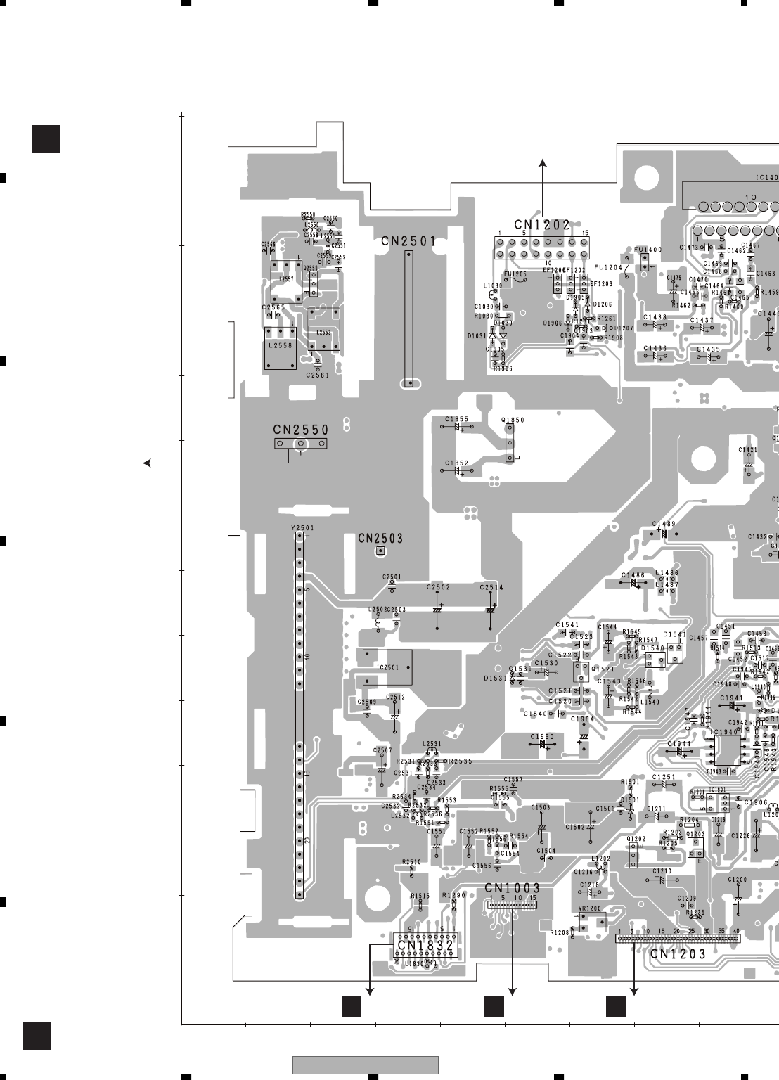
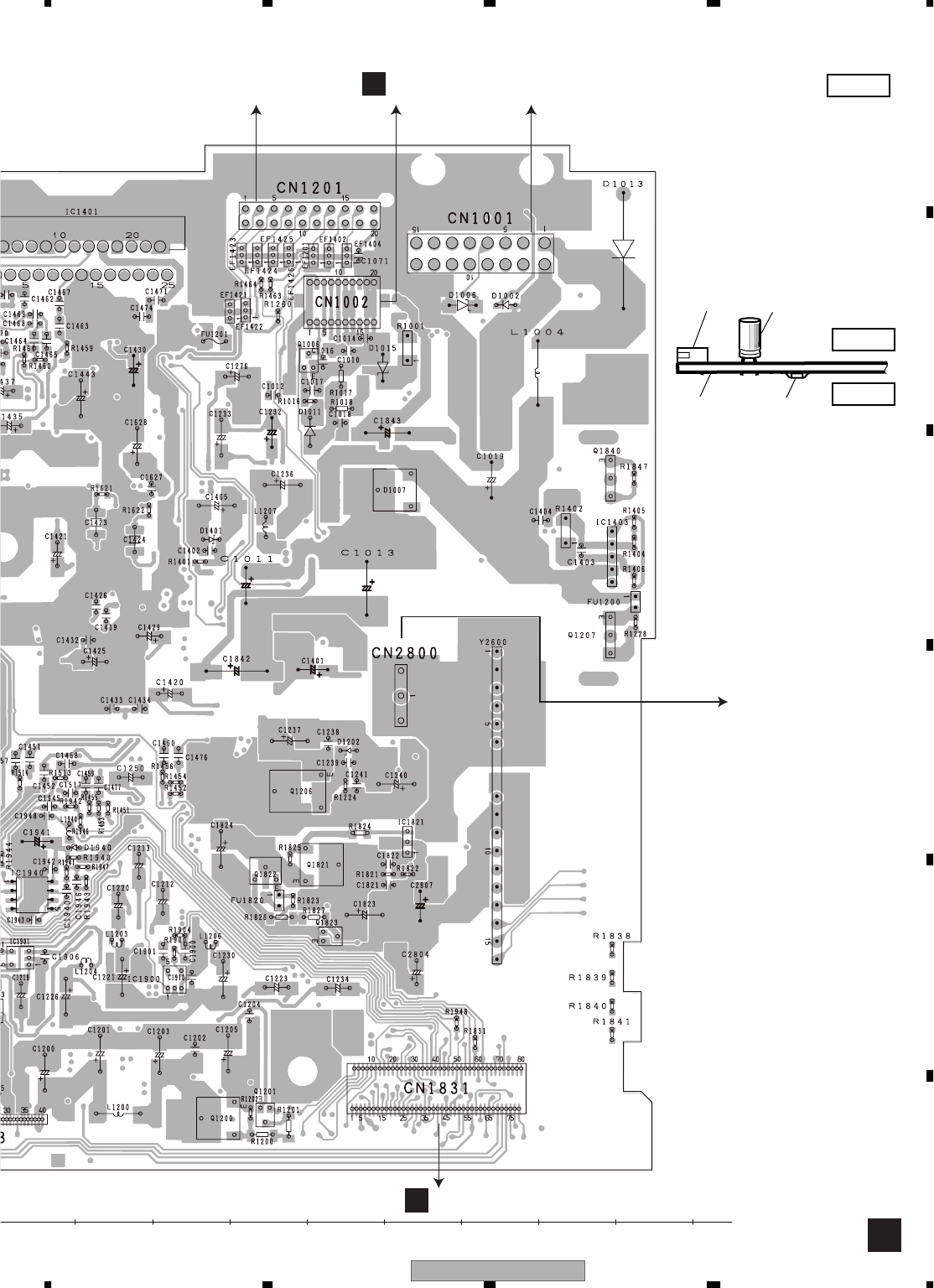
AVIC-Z1/UC 99
5678
5678
C
D
F
A
B
E
C
SIDE A
0
90 100 110 120 130 140 150 160 170
Cord Assy Cord Assy
GCN5802
TMC ANT
GCN5851 FU1200 (A,175,87) Fuse 2.5 A CEK1285
FU1201 (A,116,123) Fuse 3.15 A CEK1259
FU1204 (A,74,126) Fuse 3.15 A CEK1259
FU1400 (A,77,127) Fuse 3 A CEK1286
FU1820 (A,125,45) Fuse 750 mA(EW5) CEK1279
TUNER UNIT
Capacitor
Connector
P.C.Board Chip Part SIDE B
SIDE A
NOTE FOR PCB DIAGRAMS
1.The parts mounted on this PCB
include all necessary parts for
several destination.
For further information for
respective destinations, be sure
to check with the schematic dia-
gram.
2.Viewpoint of PCB diagrams
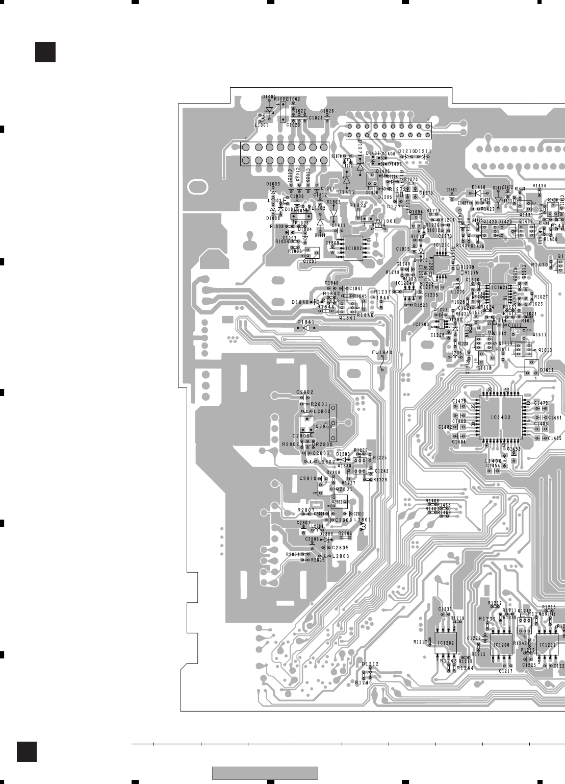
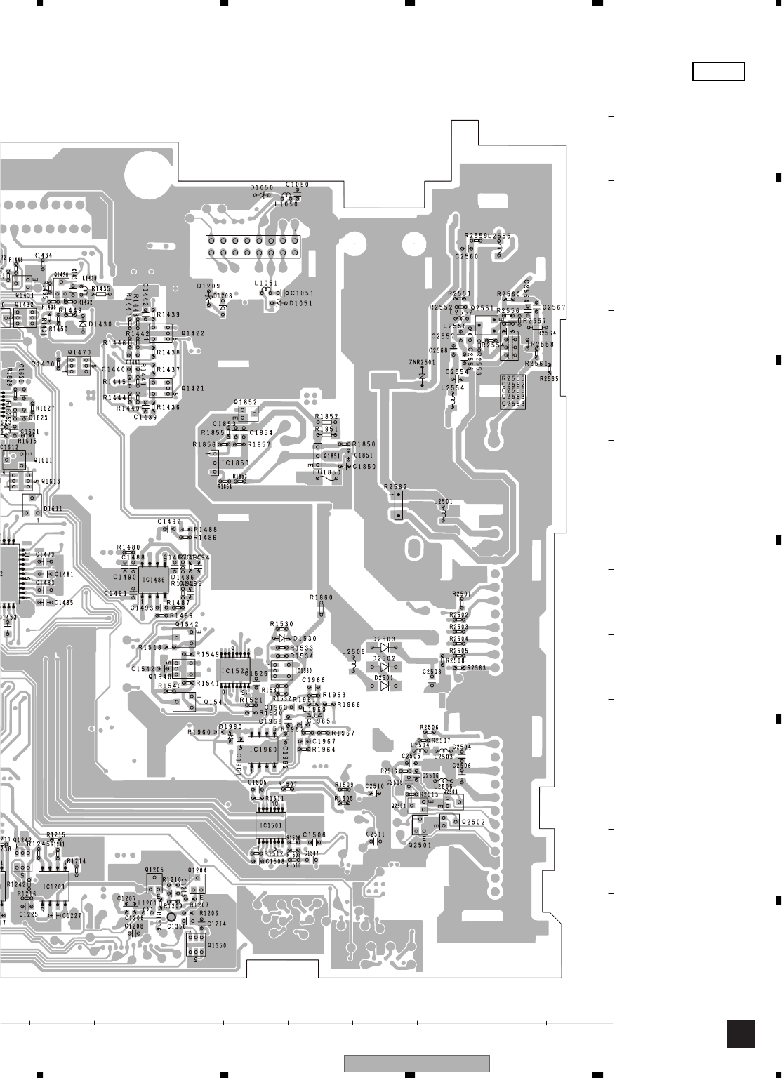
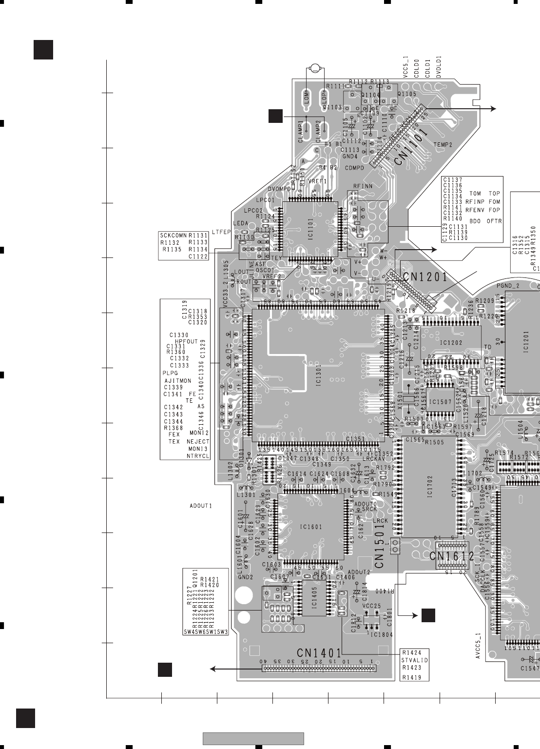
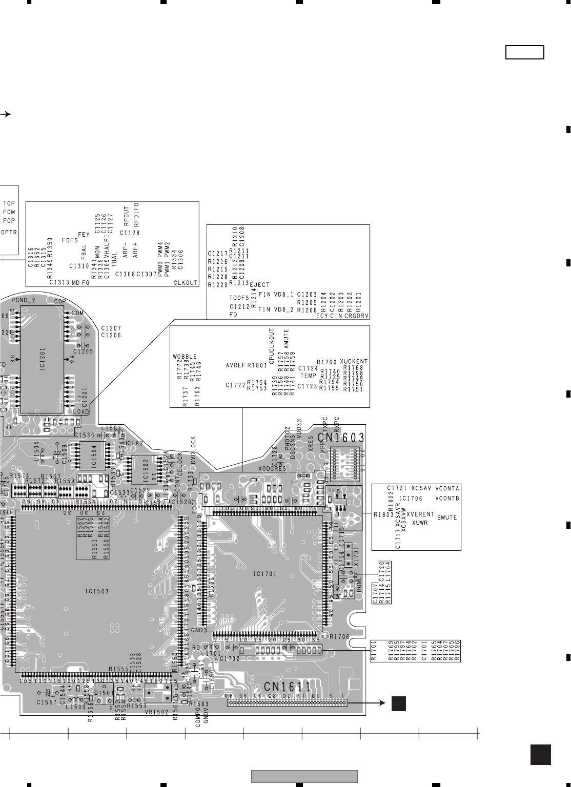
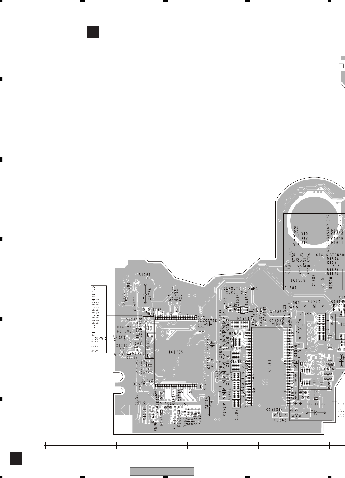
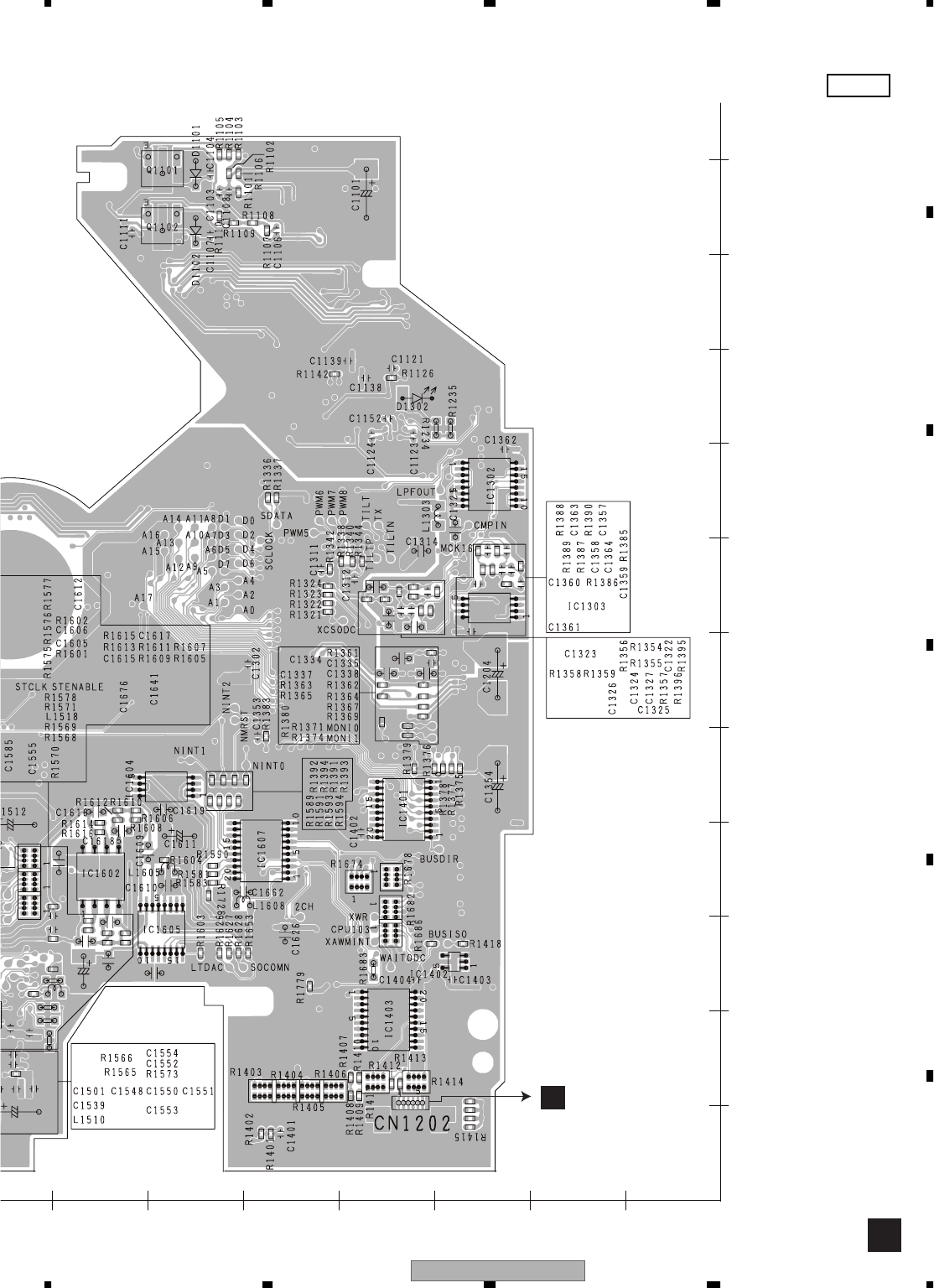
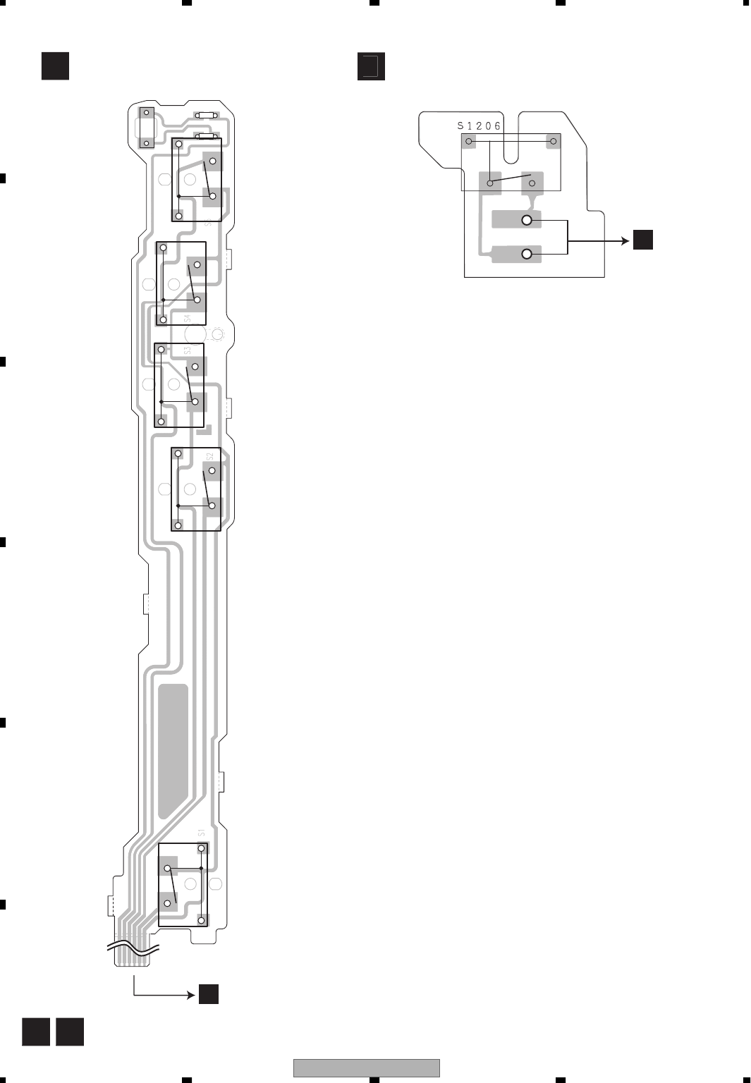
AVIC-Z1/UC
106
1234
1234
C
D
F
A
B
E
4.3 COMPOUND UNIT(A) AND COMPOUND UNIT(B)
E
F
F
E
COMPOUND UNIT
(
B
)
COMPOUND UNIT
(
A
)
D
D
CLAMP
12cm
S1201
R1298
R1299
Q
12
99
CN1202
1
6
DISC SENS
S1204
DISC SENS
S1203
8cm
S1202
8cm
S1205
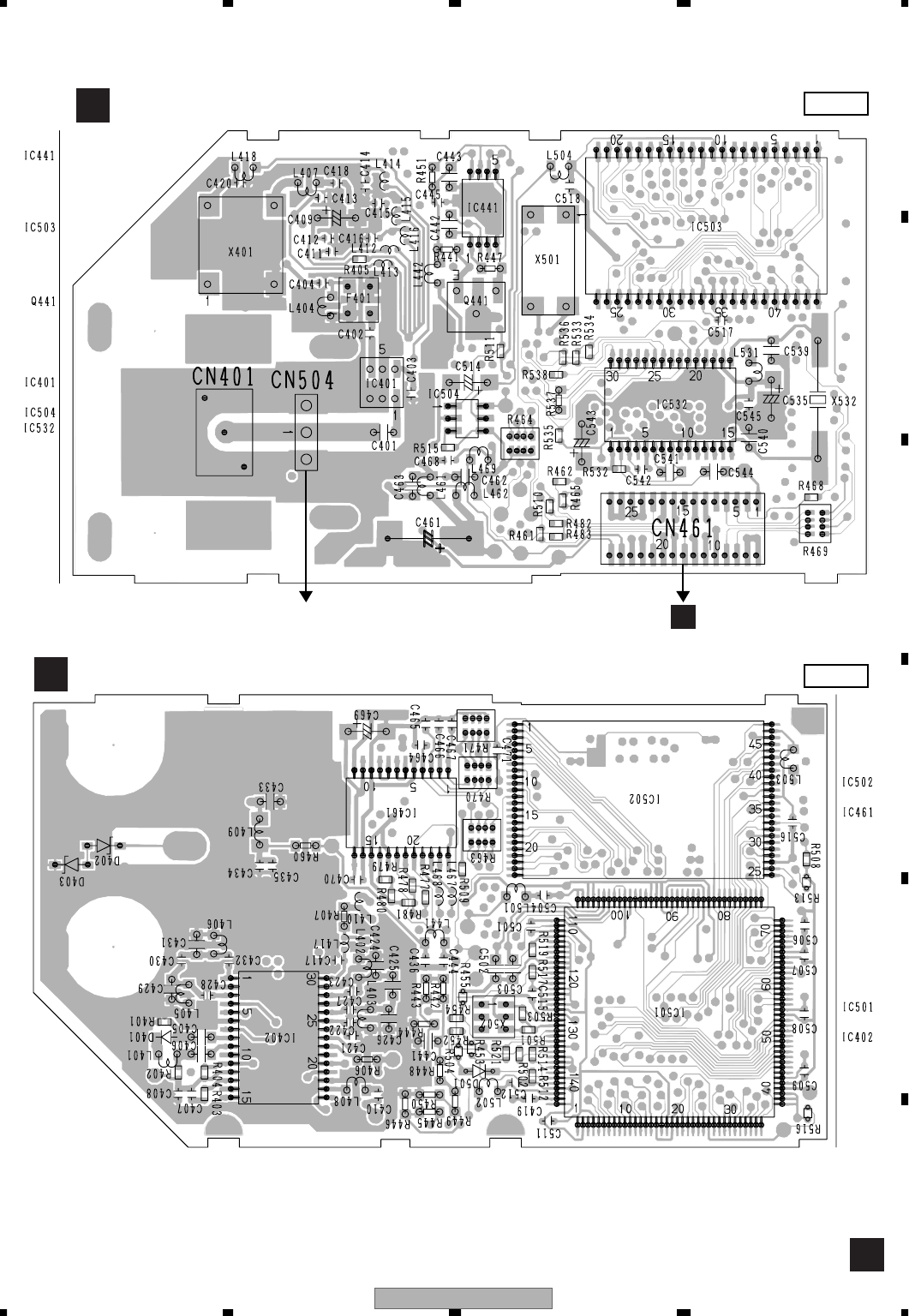
AVIC-Z1/UC 107
5678
5678
C
D
F
A
B
E
4.4 GPS UNIT
B
SIDE B
SIDE A
IC,Q
BGPS UNIT
GCN6401
GPS ANTENNA
IC,Q
BGPS UNIT
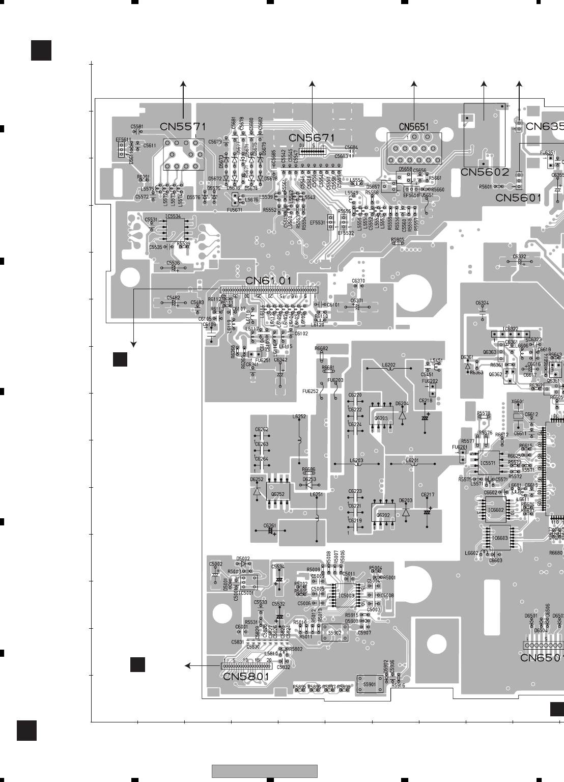
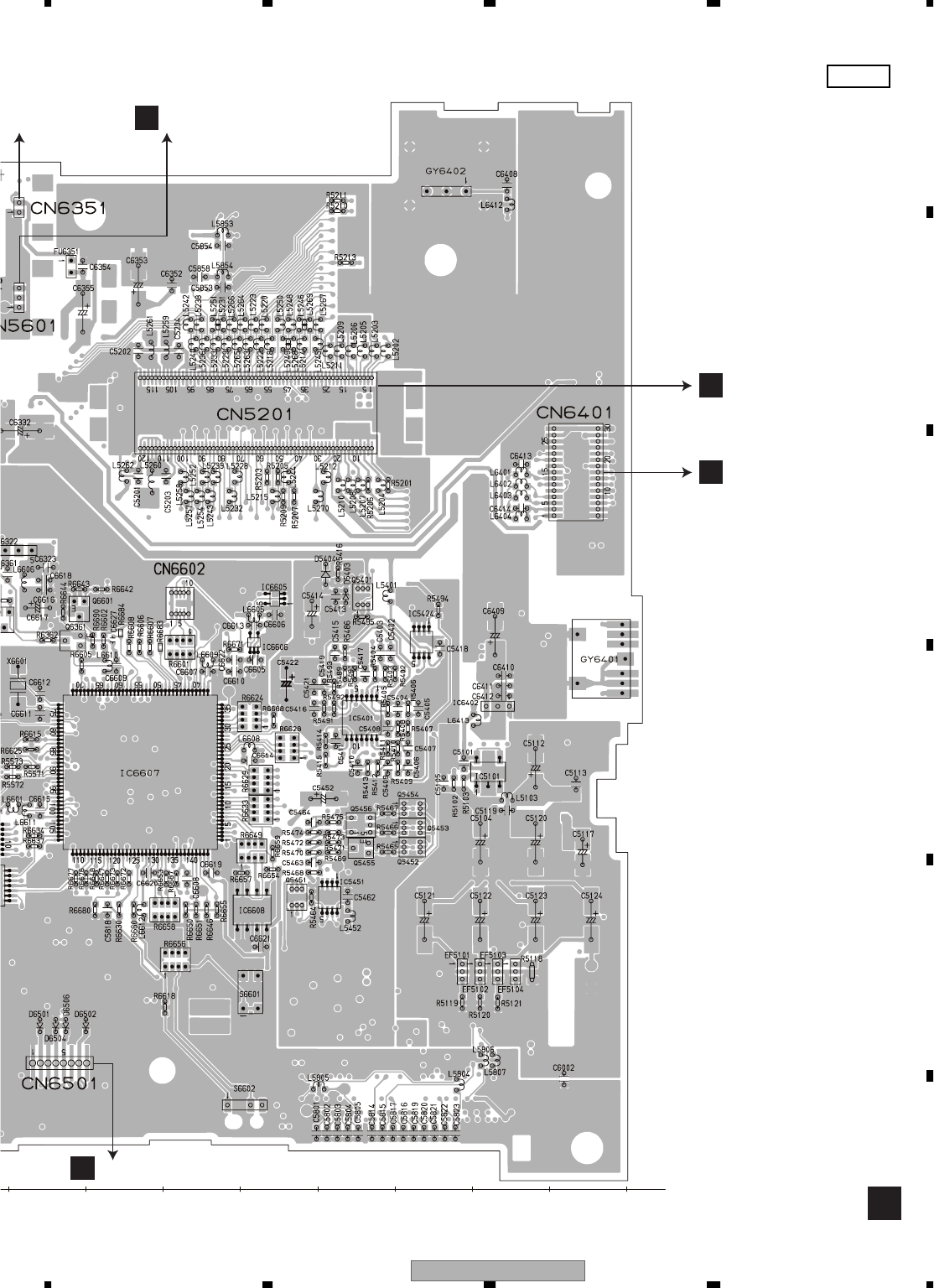
AVIC-Z1/UC 109
5678
5678
C
D
F
A
B
E
G
SIDE A
90 100 110 120 130 140 150 160 170
FU 5651 (A,72,110) Fuse 4 A CEK1260
FU 5671 (A,31,112) Fuse 1 A CEK1280
FU 6201 (A,79,57) Fuse 2 A CEK1284
FU 6202 (A,73,71) Fuse 3 A CEK1286
FU 6203 (A,52,71) Fuse 4 A CEK1260
FU 6251 (A,35,78) Fuse 2 A CEK1284
FU 6252 (A,49,71) Fuse 2.5 A CEK1258
FU 6351 (A,98,120) Fuse 1 A CEK1280
T
FAN DCN1501
ACN4804
BCN461
ICN6901
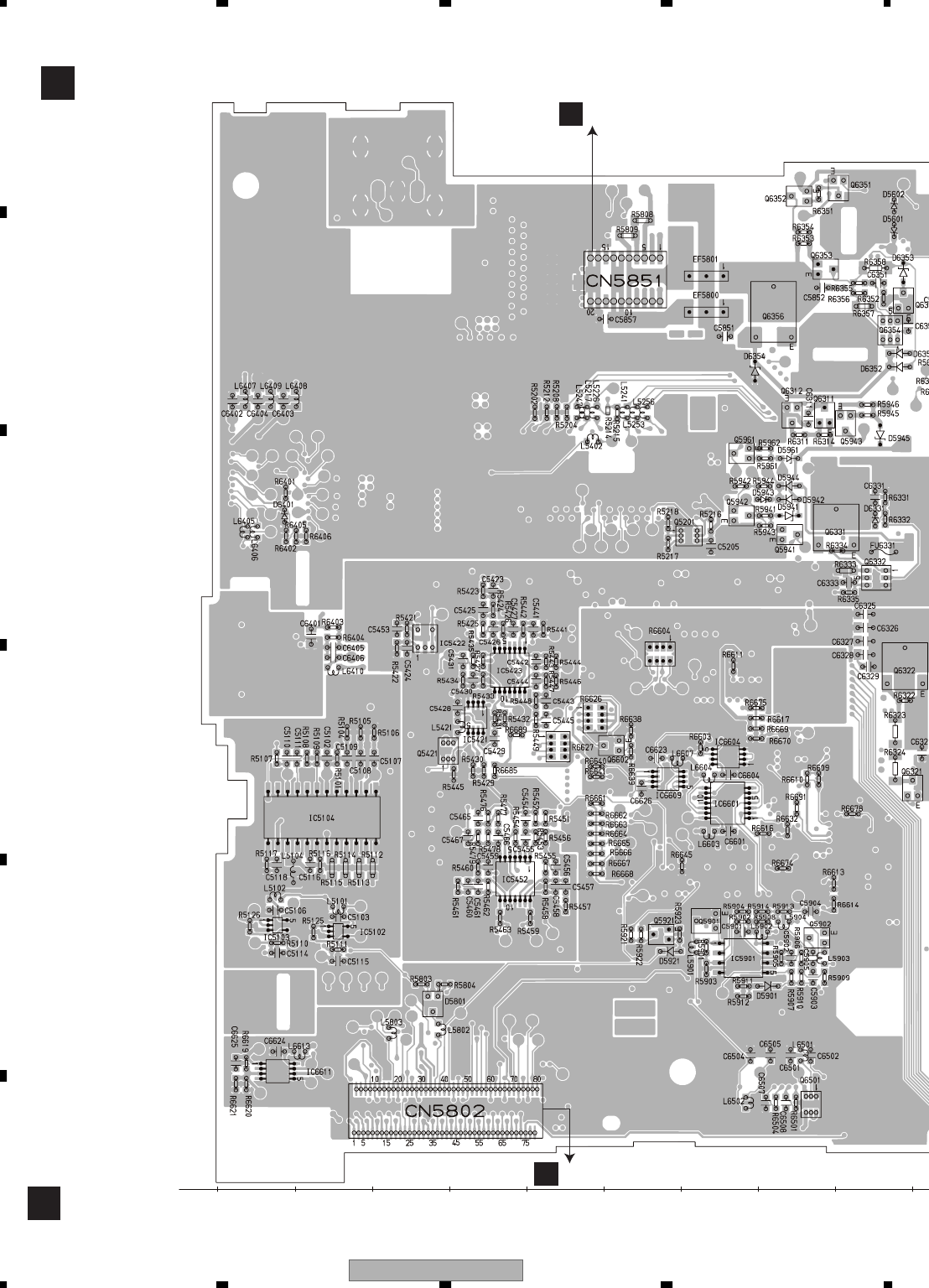
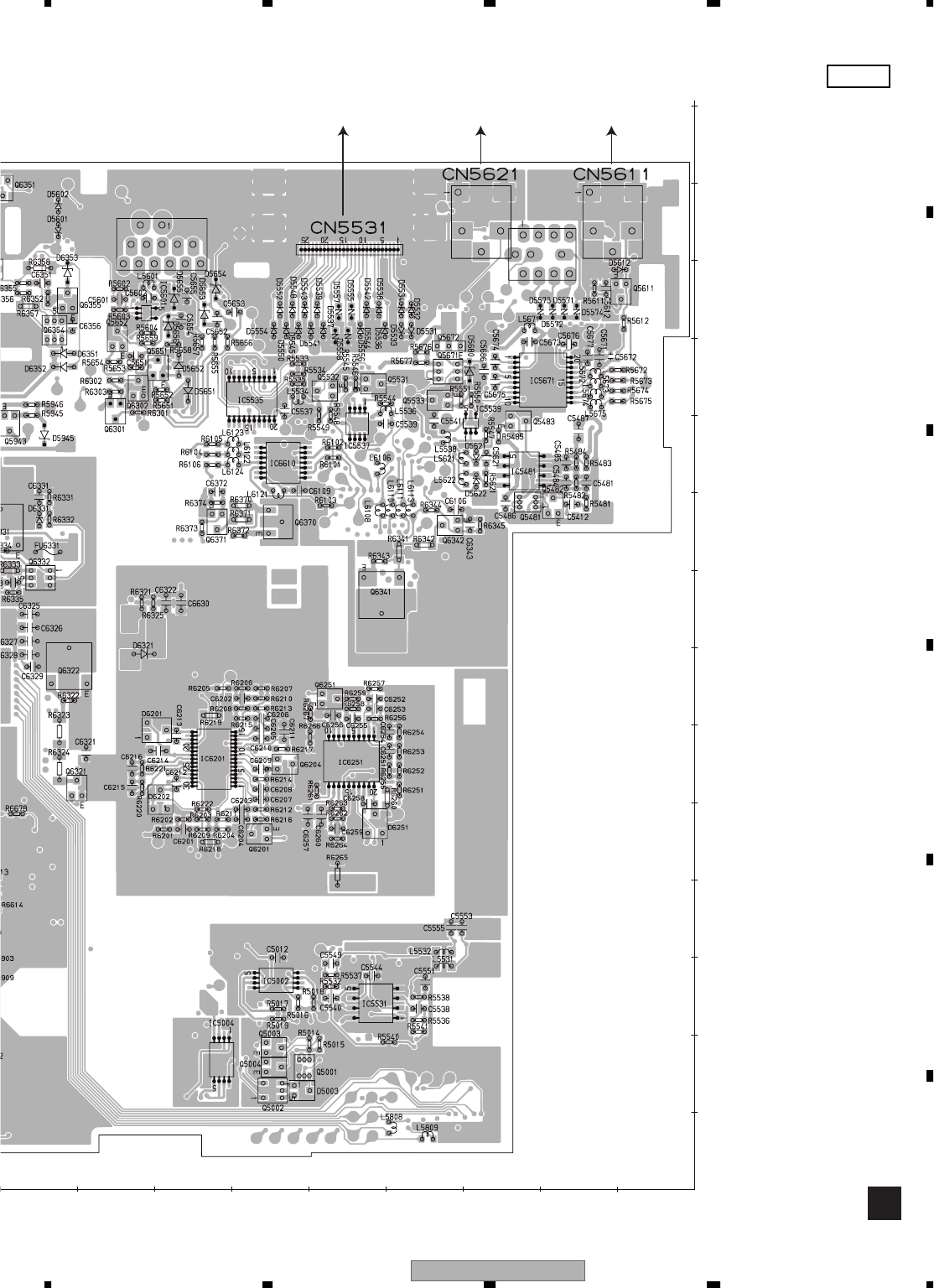
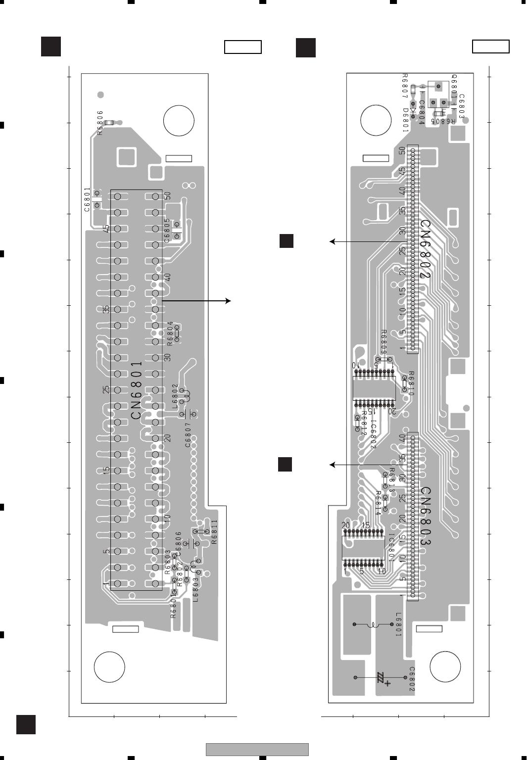
AVIC-Z1/UC
112
1234
1234
C
D
F
A
B
E
4.6 HDD RELAY PCB
H
HHDD RELAY PCB HHDD RELAY PCB
SIDE A SIDE B
10 20 30
X
140
130
120
110
100
90
80
70
60
50
40
30
20
10
0
Y
102030 X
140
130
120
110
100
90
80
70
60
50
40
30
20
10
0
Y
HDD ASSY
(SERVICE)
ACN4151
DCN1401
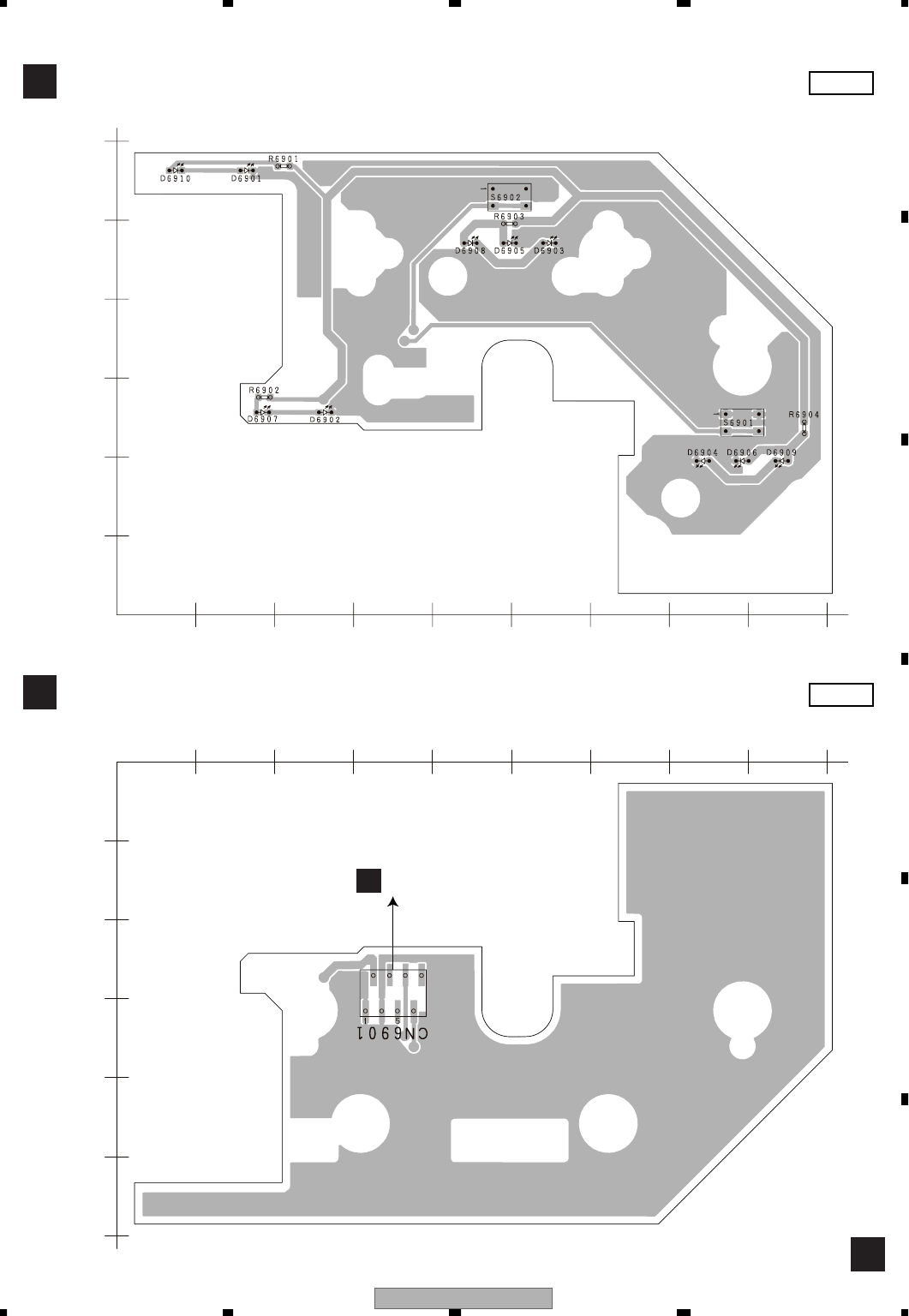
AVIC-Z1/UC 113
5678
5678
C
D
F
A
B
E
4.7 PANEL UNIT
I
IPANEL UNIT
IPANEL UNIT
SIDE A
SIDE B
10 20 30 40 50 60 70 80 900
10
20
30
40
50
60
X
Y
102030405060708090 0
10
20
30
40
50
60
X
Y
GCN6501
DISC EJECT
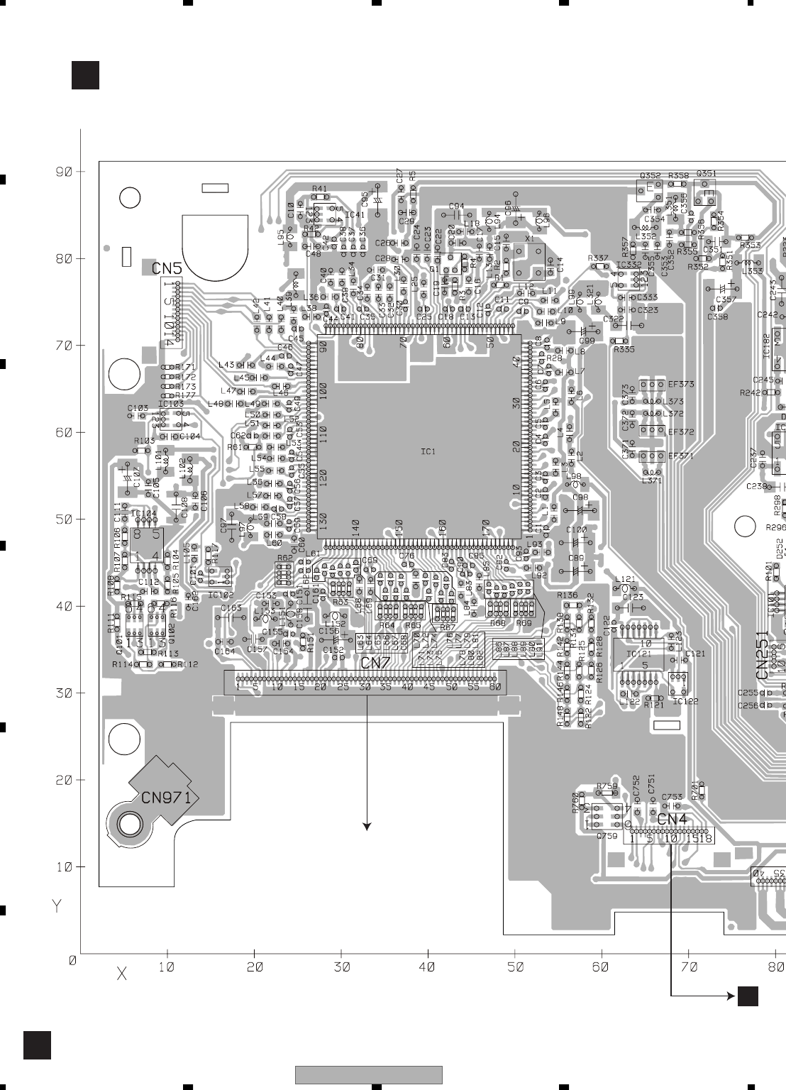
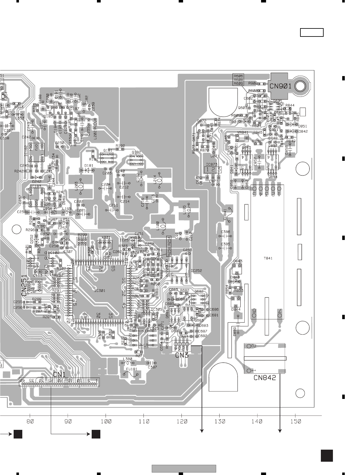
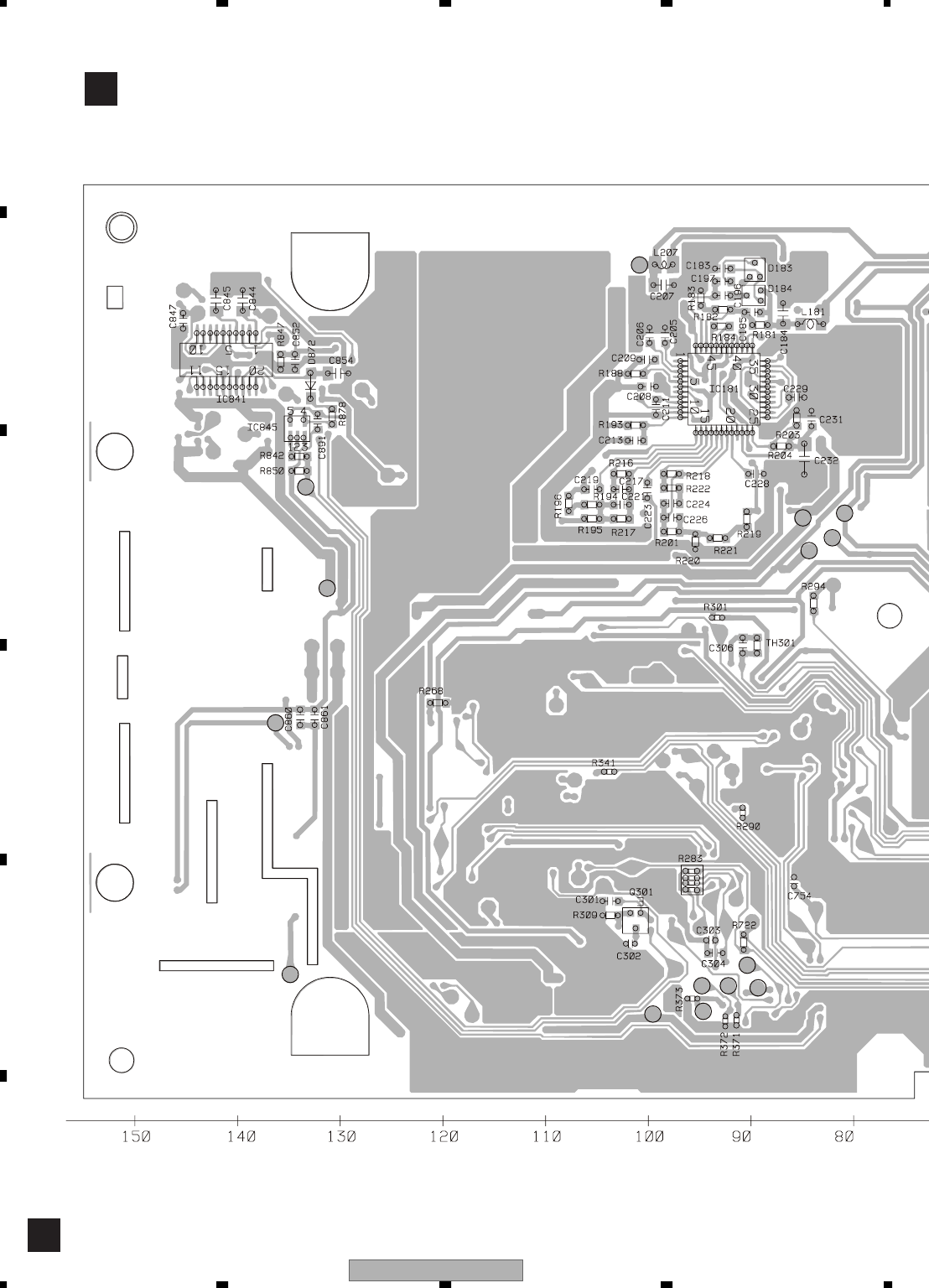
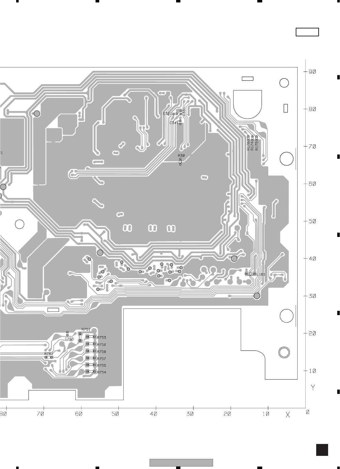
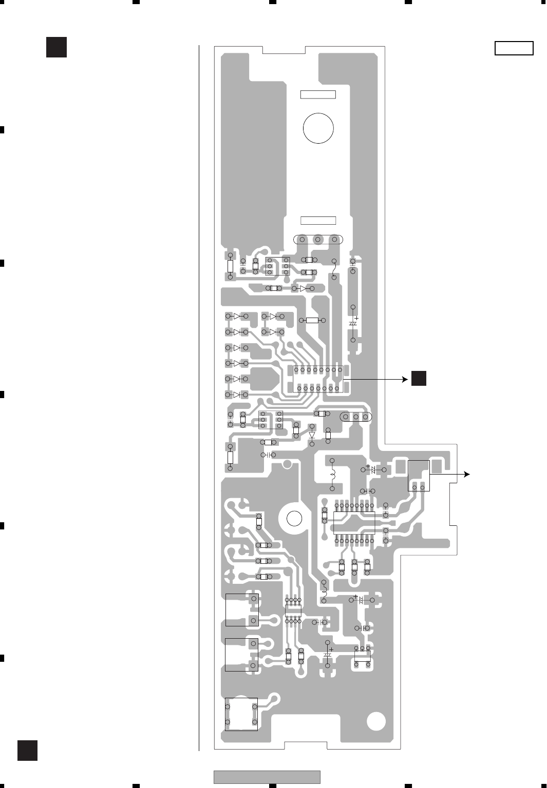
AVIC-Z1/UC
118
1234
1234
C
D
F
A
B
E
4.9 MAIN PCB UNIT
MAIN PCB UNIT
L
L
SIDE A
E
Q1
C3
C1
C4
C14
C13
C8
C9
C10
R3 R1
R4
R5
R11
R17
R16
R21
R19
R20
R14
R13
R22
R9
R8 R6
R7
R2
R18
C2
C11
C12
C7
IC3
1
4
58
1
IC2
1
916
8
L2
D10
D9
D8
D7
D4
D3
D6
D5
D1
D2
1
2
15
14
5
10
CN2
12
CN1
L1
Q4
FU1
E
Q3
S2
S1
S3
Q2
IC1
IC,Q
Q1
Q2
Q4
Q3
IC1
IC2
IC3
1
2
3
6
5
4
1
2
3
6
5
4
2
3
45
OPEN
HOME
HALF
R15
R12
C6
R10
CCN1003
M1000
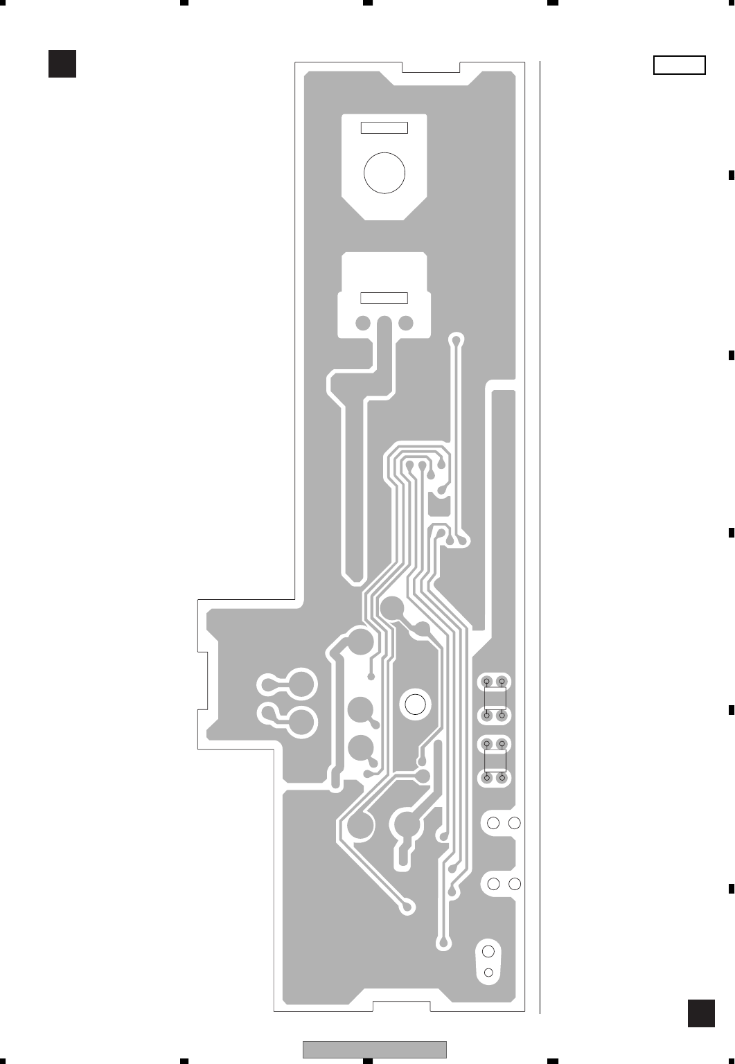
AVIC-Z1/UC 119
5678
5678
C
D
F
A
B
E
MAIN PCB UNIT
L
L
SIDE B
IC,Q
IC4
IC5
IC4
A
E
CK
IC5
A
E
CK
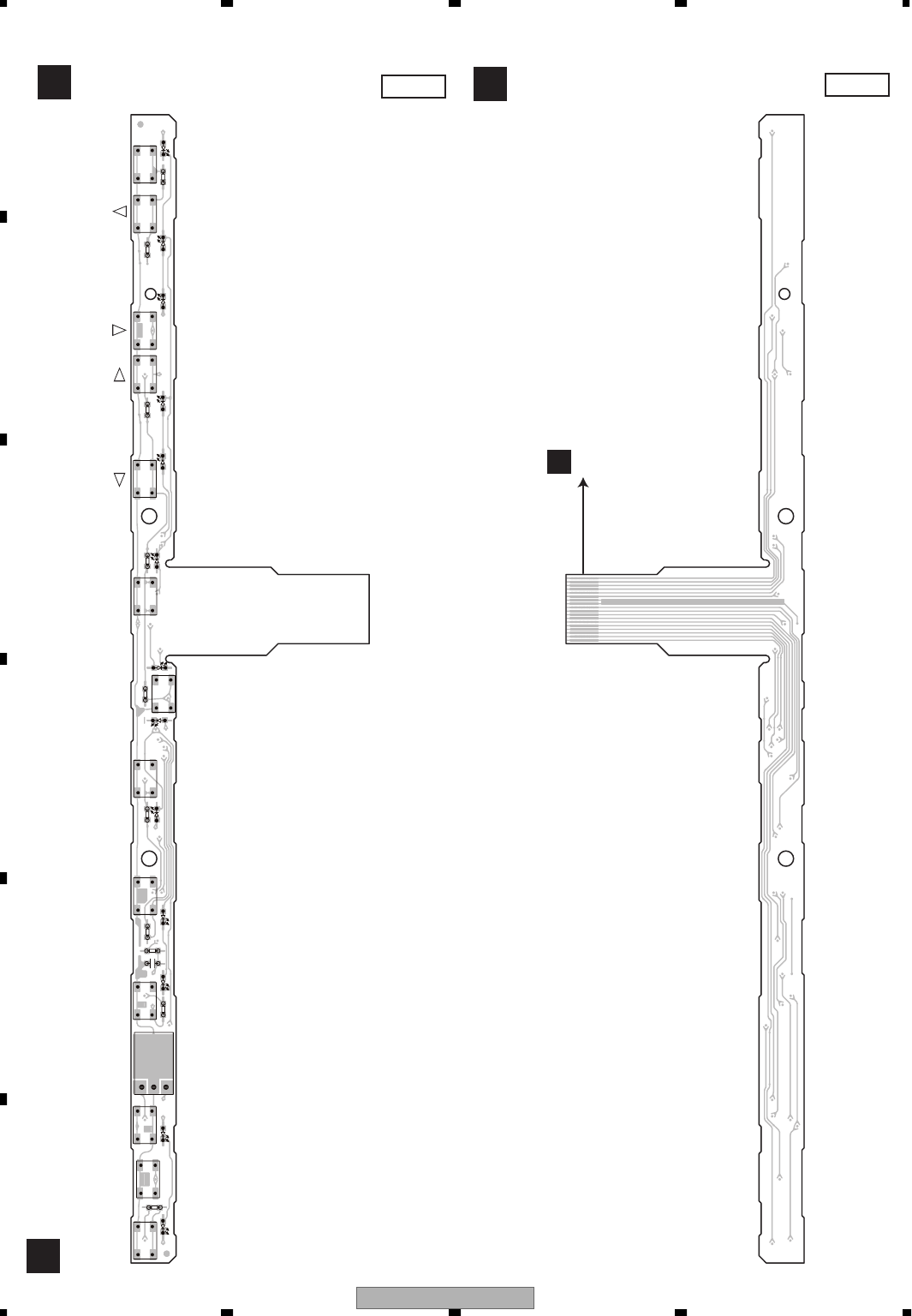
AVIC-Z1/UC
120
1234
1234
C
D
F
A
B
E
4.10 KEYBOARD UNIT
KEYBOARD UNIT
J
JKEYBOARD UNIT
J
SIDE A SIDE B
S3005 S3021 S3004 S3003 S3002 S3001
S3009
S3010 S3011 S3006 S3012 S3007 S3008
2
IC3021
1
3
R3004
R3003 R3007
R3006
R3010
R3009
R3001
R3002 R3011
R3021
C3021
D3013 D3014 D3010 D3012 D3015
D3003
R3016
D3002
D3009 D3007 D3006 D3004 D3001
KCN4
OPEN/
CLOSE RESET VOL- VOL+ AV
MENU
MAP TA/NEWS
V.ADJ

AVIC-Z1/UC 121
5678
5678
C
D
F
A
B
E
5. ELECTRICAL PARTS LIST
N
OTE:
• Parts whose parts numbers are omitted are subject to being not supplied.
• The part numbers shown below indicate chip components.
Chip Resistor
RS1/_S___J,RS1/__S___J
Chip Capacitor (except for CQS.....)
CKS....., CCS....., CSZS.....
• The > mark found on some component parts indicates the importance of the safety factor of the part.
Therefore, when replacing, be sure to use parts of identical designation.
• Meaning of the figures and others in the parentheses in the parts list.
Example) IC 301 is on the point (face A, 91 of x-axis, and 111 of y-axis) of the corresponding
PC board.
IC 301 (A, 91, 111) IC NJM2068V
Circuit Symbol and No. Part No.
Unit Number : CWX3304(UC)
Unit Number : CWX3305(EW5)
Unit Name : GPS Unit
Unit Number : CWN1583(UC)
Unit Number : CWN1633(EW5)
Unit Name : Audio Unit
Unit Number : CWX3301
Unit Name : DVD Core Unit
Unit Number : CWX3154
Unit Name : Compound Unit(A)
Unit Number : CWX3394
Unit Name : Compound Unit(B)
Unit Number : CWN1581(UC)
Unit Number : CWN1631(EW5)
Unit Name : Navi Mother Unit
Unit Number : CWN1586
Unit Name : Panel Unit
Unit Number : CWN1585(UC)
Unit Number : CWN1635(EW5)
Unit Name : Keyboard Unit
Unit Number : CWN1584(UC)
Unit Number : CWN1634(EW5)
Unit Name : Monitor Unit
Unit Number : CZW5026
Unit Name : Main PCB Unit
B
Unit Number : CWX3304(UC)
Unit Number : CWX3305(EW5)
Unit Name : GPS Unit
MISCELLANEOUS
IC 401 (A,24,15) IC UPC2749T
IC 402 (B,19,26) IC UPB1027GS
IC 441 (A,31,29) IC NJM2100V
IC 461 (B,28,9) IC ADC12H034CIMSAS1
IC 501 (B,49,24) IC PD3390A
IC 502 (B,47,8) IC(UC) PEH026A
IC 502 IC(EW5) PEH027A
IC 503 (A,48,27) IC M5M5V216ATP-70HI
IC 504 (A,30,13) IC MAX6364PUT29
IC 532 (A,46,14) IC(EW5) LC72720YVSS1
Q 441 (A,31,21) Transistor 2SB1132
D 401 (B,10,26) Diode 1SV314
D 501 (B,34,29) Diode RB751V-40
L 401 (B,10,27) Inductor CTF1549
L 402 (B,25,21) Inductor CTF1486
L 403 (B,26,25) Inductor CTF1486
L 404 (A,20,21) Inductor LCSA3N3R1608
L 405 (B,12,23) Inductor LCYB22NJ1608
L 406 (B,14,19) Inductor LCYB22NJ1608
L 407 (A,18,31) Inductor CTF1410
L 408 (B,25,30) Inductor(UC) CTF1556
L 408 Inductor(EW5) CTF1410
L 409 (B,17,10) Inductor LCYC1R0K2125
L 410 (B,25,16) Inductor CTF1547
L 412 (A,24,25) Inductor CTF1547
L 413 (A,24,24) Inductor CTF1547
L 414 (A,24,31) Inductor CTF1547
L 415 (A,25,28) Inductor CTF1547
L 416 (A,25,27) Inductor CTF1547
L 417 (B,24,19) Inductor CTF1547
L 418 (A,13,32) Inductor CTF1410
L 441 (B,31,19) Inductor CTF1410
L 442 (A,28,24) Inductor CTF1410
L 461 (A,27,7) Inductor CTF1410
L 462 (A,30,7) Inductor CTF1410
L 467 (B,32,15) Inductor CTF1547
L 468 (B,31,15) Inductor CTF1547
L 469 (A,31,9) Inductor CTF1410
L 501 (B,37,15) Inductor CTF1410
L 502 (B,35,30) Inductor CTF1410
Circuit Symbol and No. Part No.

AVIC-Z1/UC
122
1234
1234
C
D
F
A
B
E
L 503 (B,58,5) Inductor CTF1410
L 504 (A,37,32) Inductor CTF1410
L 531 (A,52,16) Inductor CTF1410
X 401 (A,13,26) TCXO 16.368 MHz CWX2381
X 501 (A,36,25) Radiator 32.768 kHz CSS1319
X 502 (B,35,25) Radiator 20.00 MHz CSS1549
X 532 (A,57,14) Radiator 4.332 MHz(EW5) CSS1550
F 401 (A,22,22) Filter CTF1548
RESISTORS
R 401 (B,10,25) RS1/16SS472J
R 402 (B,11,29) RS1/16SS472J
R 403 (B,13,30) RS1/16SS122J
R 404 (B,13,29) RS1/16SS622J
R 405 (A,22,25) RS1/16SS100J
R 406 (B,25,28) RS1/16S271J
R 407 (B,24,17) RS1/16S2R2J
R 441 (A,29,25) RN1/16SC10R0D
R 442 (B,31,22) RN1/16SE1501D
R 443 (B,30,22) RN1/16SE2402D
R 444 (B,30,25) RN1/16SE3302D
R 445 (B,30,32) RN1/16SE4702D
R 446 (B,28,31) RN1/16SE4702D
R 447 (A,32,24) RS1/16S432J
R 448 (B,31,29) RN1/16SE1002D
R 449 (B,32,31) RN1/16SE2202D
R 450 (B,30,31) RN1/16SE3302D
R 451 (A,27,31) RS1/16S103J
R 452 (B,32,26) RS1/16SS102J
R 454 (B,32,25) RS1/16SS102J
R 460 (B,21,12) RS1/16S0R0J
R 461 (A,36,4) RS1/16SS102J
R 462 (A,37,8) RS1/16SS102J
R 463 (B,34,11) RAB4CQ102J
R 464 (A,34,11) RAB4CQ333J
R 465 (A,37,6) RS1/16SS102J
R 468 (A,56,7) (EW5) RS1/16SS471J
R 469 (A,57,5) (EW5) RAB4CQ471J
R 470 (B,34,6) RAB4CQ471J
R 471 (B,34,2) RAB4CQ104J
R 477 (B,30,15) RS1/16SS222J
R 478 (B,29,15) RS1/16SS222J
R 479 (B,27,14) RS1/16SS222J
R 480 (B,27,15) RS1/16SS332J
R 481 (B,29,16) RS1/16SS332J
R 482 (A,37,5) RS1/16SS223J
R 483 (A,37,4) RS1/16SS473J
R 501 (B,38,26) RS1/16SS0R0J
R 502 (B,37,27) RS1/16SS102J
R 503 (B,37,24) RS1/16SS154J
R 508 (B,59,13) (UC) RS1/16SS103J
R 508 (EW5) RS1/16SS472J
R 509 (B,33,13) RS1/16SS473J
R 510 (A,36,6) RS1/16SS102J
R 511 (A,33,18) RS1/16SS103J
R 512 (B,38,29) RS1/16SS473J
R 513 (B,59,14) RS1/16SS103J
R 514 (B,38,27) RS1/16SS473J
R 515 (A,29,10) RS1/16SS473J
Circuit Symbol and No. Part No.
R 517 (B,38,21) RS1/16SS103J
R 519 (B,38,19) RS1/16SS473J
R 521 (B,36,27) RS1/16SS473J
R 532 (A,42,9) (EW5) RS1/16SS104J
R 533 (A,38,17) (UC) RS1/16SS103J
R 533 (EW5) RS1/16SS332J
R 534 (A,39,18) RS1/16SS103J
R 535 (A,37,11) RS1/16SS103J
R 536 (A,37,17) RS1/16SS0R0J
R 537 (A,37,14) (EW5) RS1/16S0R0J
R 538 (A,37,16) (EW5) RS1/16SS0R0J
CAPACITORS
C 401 (A,24,12) CCSRCH100D50
C 402 (A,23,19) CCSSCH101J50
C 403 (A,26,14) CKSSYB104K10
C 404 (A,19,23) CCSSCH101J50
C 405 (B,13,26) CCSRUJ220J50
C 406 (B,13,27) CCSRUJ220J50
C 407 (B,12,30) CKSSYB333K16
C 408 (B,11,30) CKSSYB182K50
C 409 (A,20,28) CSZS100M6R3
C 410 (B,26,31) CKSSYB103K16
C 411 (A,20,25) CKSSYB102K50
C 412 (A,19,26) CKSSYB102K50
C 413 (A,19,29) CKSSYB104K10
C 414 (A,22,30) CKSSYB104K10
C 415 (A,23,29) CKSSYB104K10
C 416 (A,23,26) CKSSYB104K10
C 417 (B,23,20) CKSSYB104K10
C 418 (A,20,31) CKSSYB102K50
C 419 (B,38,31) CKSSYB104K10
C 420 (A,13,31) CKSSYB104K10
C 421 (B,24,26) CKSSYB102K50
C 422 (B,24,25) CKSSYB103K16
C 423 (B,24,23) CKSSYB104K10
C 424 (B,26,21) CCSRCH102J50
C 425 (B,27,22) CCSRCH271J50
C 426 (B,27,25) CCSRCH102J50
C 427 (B,24,24) CKSSYB104K10
C 428 (B,13,23) CKSSYB103K16
C 429 (B,11,22) CCSRCH301J50
C 430 (B,11,20) CCSSCH120J50
C 431 (B,12,19) CCSRCH301J50
C 432 (B,15,20) CKSSYB103K16
C 433 (B,18,8) CCSRCH101J50
C 434 (B,17,13) CKSSYB102K50
C 435 (B,18,13) CKSSYB103K16
C 436 (B,30,20) CKSSYB104K10
C 441 (B,30,26) CKSRYB104K16
C 442 (A,29,27) CCSRCH101J50
C 443 (A,29,31) CKSRYB104K16
C 444 (B,31,20) CKSSYB103K16
C 445 (A,28,29) CKSSYB104K10
C 461 (A,27,3) 22 µF/6.3 V CCH1408
C 462 (A,30,8) CKSRYB104K16
C 463 (A,26,7) CKSRYB104K16
C 464 (B,30,4) CKSSYB103K16
C 465 (B,30,2) CKSSYB103K16
Circuit Symbol and No. Part No.

AVIC-Z1/UC 123
5678
5678
C
D
F
A
B
E
C 466 (B,31,2) CKSSYB103K16
C 467 (B,32,2) CKSSYB103K16
C 468 (A,29,9) CKSSYB104K10
C 469 (B,25,3) CSZS100M10
C 470 (B,25,14) CKSSYB104K10
C 471 (B,35,4) CCSSCH101J50
C 501 (B,38,18) CKSSYB104K10
C 502 (B,35,21) CCSRCH150J50
C 503 (B,37,21) CCSRCH150J50
C 504 (B,39,15) CKSSYB104K10
C 506 (B,59,18) CKSSYB104K10
C 507 (B,59,20) CKSSYB104K10
C 508 (B,59,24) CKSSYB104K10
C 509 (B,59,29) CKSSYB104K10
C 511 (B,39,33) CKSSYB104K10
C 512 (B,37,30) CKSSYB104K10
C 514 (A,30,15) CSZS100M6R3
C 515 (B,38,23) CKSSYB104K10
C 516 (B,58,10) CKSSYB104K10
C 517 (A,49,20) CKSSYB104K10
C 518 (A,38,30) CKSSYB104K10
C 535 (A,53,14) (EW5) CSZS100M6R3
C 539 (A,53,18) (EW5) CCSRCH100D50
C 540 (A,52,11) (EW5) CCSRCH100D50
C 541 (A,46,8) (EW5) CCSRCH561J50
C 542 (A,43,9) (EW5) CKSSYB104K10
C 543 (A,39,11) (EW5) CSZS100M6R3
C 544 (A,49,9) (EW5) CCSRCH331J50
C 545 (A,52,14) (EW5) CKSSYB104K10
C
Unit Number : CWN1583(UC)
Unit Number : CWN1633(EW5)
Unit Name : Audio Unit
MISCELLANEOUS
IC 1200 (B,104,22) IC NJM2235M
IC 1201 (B,93,22) IC NJM2246M
IC 1202 (B,116,23) IC NJM2235M
IC 1204 (B,125,103) IC TK15405BMI
IC 1270 (B,117,110) IC NJM2137V
IC 1401 (A,98,139) IC PAL007B
IC 1402 (B,104,75) IC PML009A
IC 1403 (A,172,93) IC BA00CC0WT
IC 1486 (B,76,74) IC BA3121F
IC 1501 (B,57,33) IC NJM2060V
IC 1520 (B,63,59) IC TC4052BFT
IC 1530 (B,55,59) IC NJM2125F
IC 1621 (B,104,103) IC NJM2060V
IC 1802 (B,138,114) IC TPD1018F
IC 1821 (A,142,53) IC(EW5) M5237ML
IC 1850 (B,64,93) IC M5237ML
IC 1900 (A,111,34) IC NJM2505F
IC 1901 (A,89,37) IC NJM2505F
IC 1940 (A,91,46) IC BA3121F
IC 1960 (B,58,45) IC BA3121F
IC 2501 (A,35,60) IC NJM2391DL1-33
Q 1001 (B,147,113) Transistor 2SC4116
Q 1004 (B,123,120) Transistor 2SC4081
Circuit Symbol and No. Part No.
Q 1006 (A,129,121) Transistor DTC114EU
Q 1200 (A,114,14) Transistor 2SA1385-ZS1
Q 1201 (A,123,15) Transistor DTC114EU
Q 1202 (A,73,28) Transistor 2SA1797
Q 1203 (A,85,29) Transistor DTC114EU
Q 1204 (B,69,23) Transistor 2SC4081
Q 1205 (B,76,23) Transistor 2SA1577
Q 1206 (A,126,60) Transistor 2SD1760F5
Q 1207 (A,172,82) Transistor 2SB1185
Q 1242 (B,98,27) Transistor IMD3A
Q 1350 (B,69,13) Transistor IMD3A
Q 1420 (B,106,118) Transistor FMG12
Q 1421 (B,75,106) Transistor FMG12
Q 1422 (B,75,115) Transistor FMG12
Q 1430 (B,92,123) Transistor 2SC4081
Q 1431 (B,98,123) Transistor DTC114EU
Q 1432 (B,98,118) Transistor IMD3A
Q 1470 (B,89,110) Transistor IMD3A
Q 1521 (A,66,59) Transistor DTC114EU
Q 1540 (B,71,59) Transistor FMG12
Q 1541 (B,71,53) Transistor 2SC2412K
Q 1542 (B,71,64) Transistor 2SC2412K
Q 1611 (B,100,94) Transistor DTC323TK
Q 1612 (B,108,95) Transistor DTC323TK
Q 1613 (B,98,90) Transistor IMD3A
Q 1614 (B,108,92) Transistor IMD3A
Q 1821 (A,134,50) Transistor(EW5) 2SB1184F5
Q 1822 (A,123,50) Transistor(EW5) 2SB1260
Q 1823 (A,133,40) Transistor(EW5) DTC114EU
Q 1830 (B,136,64) Transistor IMX1
Q 1840 (A,172,104) Transistor 2SB1185
Q 1841 (B,139,100) Transistor IMX1
Q 1850 (A,54,97) Transistor 2SB1185
Q 1851 (B,47,95) Transistor 2SB1260
Q 1852 (B,60,102) Transistor DTC114EU
Q 2501 (B,32,33) Transistor(EW5) DTC124EU
Q 2502 (B,27,33) Transistor(EW5) DTC124EU
Q 2503 (B,32,36) Transistor(EW5) DTC124EU
Q 2504 (B,26,37) Transistor(EW5) DTC124EU
Q 2550 (A,23,124) Transistor(EW5) 2SC3357
Q 2551 (B,20,116) Transistor(EW5) 2SC3127
Q 2800 (B,148,73) Transistor(EW5) 2SC3545
Q 2801 (B,144,58) Transistor(EW5) DTC144EK
Q 2802 (B,141,55) Transistor(EW5) DTC144EK
D 1001 (B,157,146) Diode PTZ18A
D 1004 (B,149,116) Diode UDZS5R1(B)
D 1005 (B,122,113) Diode HZU6R8(B2)
D 1006 (A,151,128) Diode PTZ27(B)
D 1007 (A,139,102) Diode KS926S2
D 1008 (B,156,123) Diode UDZS18(B)
D 1009 (B,156,127) Diode UDZS18(B)
D 1010 (B,154,123) Diode 1SS355
D 1011 (A,130,111) Diode 1SR154-400
D 1013 (A,174,136) Diode 5KP22A
D 1030 (A,53,115) Diode 1SS355
D 1031 (A,51,115) Diode 1SS355
D 1050 (B,58,138) Diode UDZS5R6(B)
D 1051 (B,55,120) Diode UDZS5R6(B)
D 1070 (B,133,130) Diode DAN202U
D 1071 (B,136,133) Diode PTZ27(B)
Circuit Symbol and No. Part No.

AVIC-Z1/UC
124
1234
1234
C
D
F
A
B
E
D 1202 (A,135,66) Diode UDZS5R6(B)
D 1203 (B,140,65) Diode HZU8R2(B1)
D 1204 (B,129,129) Diode UDZS6R8(B)
D 1205 (B,131,127) Diode UDZS6R8(B)
D 1206 (A,67,120) Diode UDZS6R8(B)
D 1207 (A,70,116) Diode UDZS6R8(B)
D 1208 (B,65,119) Diode UDZS6R8(B)
D 1209 (B,67,121) Diode UDZS6R8(B)
D 1210 (B,125,135) Diode UDZS6R8(B)
D 1211 (B,122,135) Diode UDZS6R8(B)
D 1401 (A,116,96) Diode UDZS4R7(B)
D 1405 (B,131,130) Diode
AVR-M1608C080MTAAB
D 1406 (B,131,133) Diode
AVR-M1608C080MTAAB
D 1407 (B,133,134) Diode
AVR-M1608C080MTAAB
D 1408 (B,131,135) Diode
AVR-M1608C080MTAAB
D 1410 (B,109,126) Diode 1SR154-400
D 1412 (B,139,130) Diode PTZ27(B)
D 1420 (B,102,118) Diode DAP202K
D 1430 (B,88,117) Diode MA111
D 1501 (A,74,35) Diode UDZS4R7(B)
D 1530 (B,55,64) Diode 1SS355
D 1531 (A,55,58) Diode EDZ4R3(B)
D 1540 (A,79,61) Diode DAP202U
D 1541 (A,82,62) Diode DAN202U
D 1611 (B,97,86) Diode DAN202K
D 1612 (B,107,88) Diode DAN202K
D 1803 (B,142,122) Diode PTZ27(B)
D 1804 (B,145,120) Diode 1SR154-400
D 1840 (B,146,101) Diode HZU7R5(B2)
D 1841 (B,149,95) Diode RSX201L-30
D 1905 (A,65,119) Diode UDZS6R8(B)
D 1906 (A,64,117) Diode UDZS6R8(B)
D 2501 (B,38,56) Diode 1SR154-400
D 2502 (B,38,59) Diode 1SR154-400
D 2503 (B,38,62) Diode 1SR154-400
D 2800 (B,144,47) Diode(EW5) HZU3R3(B1)
ZNR2501 (B,31,108) Surge Protector RCCA-201Q31UA-PI
L 1001 (B,159,144) Inductor CTF1410
L 1002 (B,149,123) Inductor CTF1410
L 1003 (B,153,125) Inductor CTF1410
L 1004 (A,162,119) Choke Coil 600 mH CTH1213
L 1030 (A,52,122) Inductor CTF1556
L 1050 (B,54,138) Inductor CTF1334
L 1051 (B,57,122) Inductor CTF1334
L 1070 (B,139,134) Inductor LCTC2R2K1608
L 1200 (A,103,15) Inductor CTH1256
L 1201 (B,77,18) Inductor CTF1306
L 1202 (A,69,27) Inductor CTF1410
L 1203 (A,103,39) Inductor CTF1410
L 1204 (A,98,36) Inductor CTF1410
L 1206 (A,116,39) Inductor CTF1410
L 1207 (A,123,97) Inductor LCTAW100J3225
L 1270 (B,114,106) Chip Ferrite Bead CTF1399
L 1400 (B,103,65) Inductor LCTAW2R2J2520
L 1430 (B,88,122) Inductor CTF1410
L 1486 (A,81,74) Inductor LCYC2R2K2125
L 1487 (A,81,72) Inductor LCYC2R2K2125
L 1540 (A,78,56) Inductor LCTAW101J2520
L 1830 (A,41,10) Inductor CTF1379
L 1940 (A,96,55) Inductor LCYC2R2K2125
Circuit Symbol and No. Part No.
L 1960 (B,49,51) Inductor LCYC2R2K2125
L 2501 (B,28,85) Chip Coil LCTAW4R7J2520
L 2502 (A,32,67) Inductor LCTAW2R2J3225
L 2503 (B,28,45) Inductor LCTAW2R2J2520
L 2504 (B,32,45) Chip Ferrite Bead CTF1399
L 2505 (B,28,40) Inductor LCTAW2R2J3225
L 2506 (B,43,60) Chip Coil LCTAW1R0J2520
L 2550 (A,21,133) Inductor(EW5) LCTAWR12J2520
L 2551 (A,24,130) Inductor(EW5) LCYCR10K2125
L 2552 (B,25,118) Inductor(EW5) LCYCR10K2125
L 2553 (A,23,116) Coil(EW5) CTC1143
L 2554 (B,26,104) Inductor(EW5) LCTAW101J2520
L 2555 (B,18,129) Inductor(EW5) LCTAW101J2520
L 2556 (B,23,115) Inductor(EW5) LCYCR18K2125
L 2557 (A,17,124) Coil(EW5) CTC1142
L 2558 (A,16,113) Coil(EW5) CTC1139
L 2800 (B,148,76) Inductor(EW5) LCYCR22K2125
L 2801 (B,136,50) Chip Ferrite Bead(EW5) CTF1557
L 2802 (B,148,65) Chip Coil(EW5) LCTAW1R0J2520
L 2803 (B,144,43) Inductor(EW5) LCTAW2R2J2520
L 2804 (B,146,49) Chip Coil(EW5) LCTAW1R0J2520
VR1200 (A,68,17) Semi-fixed 1 KΩ(OB) CCP1390
>FU1001 (B,134,121) Fuse 750 mA CEK1279
>FU1200 (A,175,87) Fuse 2.5 A CEK1285
>FU1201 (A,116,123) Fuse 3.15 A CEK1259
>FU1204 (A,74,126) Fuse 3.15 A CEK1259
>FU1400 (A,77,127) Fuse 3 A CEK1286
>FU1820 (A,125,45) Fuse 750 mA(EW5) CEK1279
>FU1840 (B,131,87) Fuse 2.5 A CEK1258
>FU1850 (B,47,91) Fuse 630 mA CEK1252
Y 2600 (A,153,60) Tuner Unit(EW5) CWE2023
EF1201 (A,130,135) EMI Filter CCG1067
EF1202 (A,64,124) EMI Filter CCG1067
EF1203 (A,67,124) EMI Filter CCG1067
EF1402 (A,132,135) EMI Filter CCG1067
EF1404 (A,135,135) EMI Filter CCG1067
EF1421 (A,118,128) EMI Filter CCG1067
EF1422 (A,121,128) EMI Filter CCG1067
EF1423 (A,120,135) EMI Filter CCG1067
EF1424 (A,122,135) EMI Filter CCG1067
EF1425 (A,124,135) EMI Filter CCG1067
EF1426 (A,127,135) EMI Filter CCG1067
RESISTORS
R 1001 (A,143,122) RS1/4S102J
R 1002 (B,154,145) RS1/4S103J
R 1003 (B,151,114) RS1/16S473J
R 1004 (B,151,115) RS1/16S104J
R 1008 (B,150,119) RS1/16S102J
R 1009 (B,152,119) RS1/16S472J
R 1010 (B,150,121) RS1/4S102J
R 1012 (B,121,118) RS1/16S223J
R 1013 (B,123,116) RS1/16S223J
R 1014 (B,132,118) RS1/4SA472J
R 1016 (A,130,115) RS1/16S103J
R 1017 (A,134,118) RS1/4SA472J
R 1018 (A,134,114) RS1/4SA102J
R 1030 (A,53,118) RS1/10S103J
R 1070 (B,139,135) RS1/16S153J
Circuit Symbol and No. Part No.

AVIC-Z1/UC 125
5678
5678
C
D
F
A
B
E
R 1200 (A,123,12) RS1/4SA331J
R 1201 (A,127,13) RS1/4SA331J
R 1202 (A,121,15) RS1/16S153J
R 1203 (A,81,31) RS1/4SA471J
R 1204 (A,84,33) RS1/4SA471J
R 1205 (A,81,29) RS1/16S153J
R 1206 (B,70,18) RS1/16S391J
R 1207 (B,70,20) RS1/16S0R0J
R 1208 (A,65,15) RS1/16S332J
R 1209 (B,73,20) RS1/16S362J
R 1210 (B,73,23) RS1/16S102J
R 1211 (B,102,30) RS1/16S105J
R 1212 (B,105,31) RS1/16S225J
R 1213 (B,109,22) RS1/16S225J
R 1214 (B,89,25) RS1/16S105J
R 1215 (B,93,30) RS1/16S105J
R 1216 (B,97,20) RS1/16S105J
R 1217 (B,120,23) RS1/16S105J
R 1218 (B,112,19) RS1/16S225J
R 1219 (B,114,28) RS1/16S225J
R 1222 (B,125,108) RS1/16S750J
R 1223 (B,125,101) RS1/16S104J
R 1224 (A,135,61) RS1/16S102J
R 1225 (B,134,66) RS1/16S222J
R 1226 (B,136,66) RS1/16S471J
R 1227 (B,139,62) RS1/10S271J
R 1228 (A,175,84) RS1/16S223J
R 1229 (B,134,60) RS1/16S332J
R 1231 (A,66,117) RS1/16S750J
R 1235 (A,85,18) RS1/16S153J
R 1237 (B,128,104) RS1/16S101J
R 1238 (B,104,29) RS1/16S101J
R 1239 (B,107,27) RS1/16S101J
R 1240 (B,135,15) RS1/16S0R0J
R 1241 (B,92,28) RS1/16S101J
R 1242 (B,97,23) RS1/16S104J
R 1243 (B,116,17) RS1/16S101J
R 1244 (B,114,17) RS1/16S101J
R 1245 (B,96,28) RS1/16S102J
R 1270 (B,124,129) RS1/16SS750J
R 1271 (B,127,126) RS1/16SS103J
R 1272 (B,128,126) RS1/16SS103J
R 1273 (B,119,122) RS1/16S4701D
R 1274 (B,119,120) RS1/16S4701D
R 1275 (B,113,108) RS1/16SS101J
R 1276 (B,117,119) RS1/16S4701D
R 1277 (B,115,110) RS1/16S4701D
R 1278 (B,121,107) RS1/16SS102J
R 1279 (B,114,109) RS1/16SS563J
R 1280 (B,120,108) RS1/16SS473J
R 1290 (A,45,20) RS1/16S0R0J
R 1401 (A,114,92) RS1/16S102J
R 1402 (A,166,97) RS1/4S0R0J
R 1404 (A,175,95) RN1/16SE1002D
R 1405 (A,175,98) RN1/16SE2701D
R 1406 (A,175,90) RN1/16SE2201D
R 1408 (B,93,120) RS1/16S473J
R 1425 (B,109,119) RS1/16S821J
R 1426 (B,109,116) RS1/16S821J
R 1427 (B,110,123) RS1/16S223J
Circuit Symbol and No. Part No.
R 1428 (B,111,116) RS1/16S223J
R 1429 (B,107,124) RS1/16S471J
R 1430 (B,112,116) RS1/16S471J
R 1431 (B,94,118) RS1/16S102J
R 1432 (B,90,120) RS1/16S103J
R 1433 (B,101,125) RS1/16S103J
R 1434 (B,95,127) RS1/16S103J
R 1435 (B,85,122) RS1/4SA102J
R 1436 (B,76,103) RS1/16S681J
R 1437 (B,76,109) RS1/16S681J
R 1438 (B,76,112) RS1/16S681J
R 1439 (B,76,118) RS1/16S681J
R 1440 (B,79,104) RS1/16S223J
R 1441 (B,79,107) RS1/16S223J
R 1442 (B,79,114) RS1/16S223J
R 1443 (B,79,117) RS1/16S223J
R 1444 (B,80,104) RS1/16S471J
R 1445 (B,80,107) RS1/16S471J
R 1446 (B,80,114) RS1/16S471J
R 1447 (B,80,117) RS1/16S471J
R 1448 (B,99,126) RS1/16S331J
R 1449 (B,90,118) RS1/16S391J
R 1450 (B,92,117) RS1/16S391J
R 1451 (A,101,58) RS1/16S181J
R 1452 (A,111,60) RS1/16S181J
R 1453 (A,100,58) RS1/16S223J
R 1454 (A,111,61) RS1/16S223J
R 1455 (A,99,58) RS1/16S102J
R 1456 (A,109,62) RS1/16S102J
R 1459 (A,96,122) RS1/16S101J
R 1460 (A,92,121) RS1/16S101J
R 1461 (A,90,121) RS1/16S101J
R 1462 (A,86,120) RS1/16S101J
R 1463 (A,124,131) RS1/16S103J
R 1464 (A,123,131) RS1/16S103J
R 1465 (B,94,123) RS1/16S103J
R 1466 (B,119,55) RS1/16S0R0J
R 1467 (B,119,53) RS1/16S0R0J
R 1468 (B,117,54) RS1/16S0R0J
R 1469 (B,117,52) RS1/16S0R0J
R 1470 (B,92,110) RS1/16S102J
R 1480 (B,80,78) RS1/16S220J
R 1486 (B,71,81) RS1/16S102J
R 1487 (B,72,69) RS1/16S102J
R 1488 (B,71,82) RS1/16S101J
R 1489 (B,75,68) RS1/16S101J
R 1490 (B,70,76) RS1/16S223J
R 1491 (B,71,72) RS1/16S223J
R 1501 (A,74,39) RS1/16S102J
R 1506 (B,53,30) RS1/16S103J
R 1507 (B,54,39) RS1/16S104J
R 1508 (B,53,29) RS1/16S103J
R 1510 (B,53,27) RS1/16S103J
R 1511 (B,59,37) RS1/16S0R0J
R 1512 (B,59,28) RS1/16S103J
R 1513 (A,95,62) RS1/16S0R0J
R 1514 (A,89,61) RS1/16S0R0J
R 1515 (A,39,20) RS1/16S0R0J
R 1520 (B,60,52) RS1/16S473J
R 1521 (B,60,53) RS1/16S473J
Circuit Symbol and No. Part No.

AVIC-Z1/UC
126
1234
1234
C
D
F
A
B
E
R 1530 (B,55,66) RS1/16S102J
R 1531 (B,55,56) RS1/16S104J
R 1532 (B,55,55) RS1/16S104J
R 1533 (B,55,62) RS1/16S104J
R 1534 (B,55,61) RS1/16S104J
R 1540 (B,74,55) RS1/16S303J
R 1541 (B,70,57) RS1/16S104J
R 1542 (A,74,56) RS1/16S471J
R 1543 (A,74,63) RS1/16S471J
R 1544 (A,75,53) RS1/16S821J
R 1545 (A,75,65) RS1/16S821J
R 1546 (A,75,56) RS1/16S104J
R 1547 (A,75,63) RS1/16S104J
R 1548 (B,74,63) RS1/16S303J
R 1549 (B,70,61) RS1/16S104J
R 1551 (A,43,34) RS1/16S104J
R 1552 (A,51,31) RS1/16S104J
R 1553 (A,44,36) RS1/16S681J
R 1554 (A,53,31) RS1/16S681J
R 1555 (A,52,38) RS1/16S681J
R 1556 (A,52,29) RS1/16S681J
R 1611 (B,103,89) RS1/16S102J
R 1612 (B,111,89) RS1/16S102J
R 1613 (B,102,98) RS1/16S821J
R 1614 (B,106,98) RS1/16S821J
R 1615 (B,97,98) RS1/16S104J
R 1616 (B,111,95) RS1/16S104J
R 1621 (A,100,102) RS1/16S472J
R 1622 (A,107,100) RS1/16S472J
R 1623 (B,102,99) RS1/16S562J
R 1624 (B,107,99) RS1/16S562J
R 1625 (B,99,102) RS1/16S472J
R 1626 (B,109,101) RS1/16S472J
R 1627 (B,97,103) RS1/16S472J
R 1628 (B,111,101) RS1/16S472J
R 1629 (B,99,105) RS1/16S472J
R 1630 (B,109,105) RS1/16S472J
R 1821 (A,141,49) (EW5) RS1/16S2702D
R 1822 (A,143,49) (EW5) RS1/16S4701D
R 1823 (A,127,45) (EW5) RS1/16S223J
R 1824 (A,137,54) (EW5) RS1/10S271J
R 1825 (A,127,51) (EW5) RS1/16S221J
R 1826 (A,126,43) (EW5) RS1/4SA331J
R 1827 (A,130,43) (EW5) RS1/4SA331J
R 1840 (A,172,30) (UC) RS1/16S0R0J
R 1841 (A,172,26) (EW5) RS1/16S0R0J
R 1842 (B,143,102) RS1/16S121J
R 1843 (B,143,101) RS1/16S471J
R 1844 (B,144,99) RS1/8S101J
R 1845 (B,139,103) RS1/10S680J
R 1846 (B,135,101) RS1/10S680J
R 1847 (A,175,104) RS1/16S223J
R 1848 (B,131,101) RS1/16S472J
R 1850 (B,44,97) RS1/16S153J
R 1851 (B,47,98) RS1/8S821J
R 1852 (B,47,100) RS1/8S821J
R 1853 (B,62,90) RS1/16S221J
R 1854 (B,64,90) RS1/16S821J
R 1855 (B,64,99) RS1/16S2202D
R 1856 (B,64,97) RS1/16S2201D
R 1857 (B,62,97) RS1/16S4301D
Circuit Symbol and No. Part No.
R 1900 (A,111,38) RS1/16S0R0J
R 1901 (A,86,38) RS1/16S0R0J
R 1904 (A,111,40) RS1/16S750J
R 1906 (A,53,111) RS1/16S473J
R 1908 (A,69,115) RS1/16S473J
R 1940 (A,96,51) RS1/16S220J
R 1941 (A,96,49) RS1/16S102J
R 1942 (A,96,58) RS1/16S102J
R 1943 (A,98,47) RS1/16S223J
R 1944 (A,86,51) RS1/16S223J
R 1946 (A,97,56) RS1/16S101J
R 1947 (A,98,50) RS1/16S101J
R 1948 (A,150,28) RS1/16S0R0J
R 1960 (B,65,48) RS1/16S220J
R 1961 (B,50,53) RS1/16S102J
R 1962 (B,50,48) RS1/16S102J
R 1963 (B,49,54) RS1/16S223J
R 1964 (B,51,45) RS1/16S223J
R 1966 (B,47,53) RS1/16S101J
R 1967 (B,48,48) RS1/16S101J
R 2501 (B,25,70) RS1/16S681J
R 2502 (B,25,67) RS1/16S681J
R 2503 (B,25,65) RS1/16S681J
R 2504 (B,25,63) RS1/16S681J
R 2505 (B,25,61) RS1/16S681J
R 2506 (B,30,48) RS1/16S681J
R 2508 (B,28,60) RS1/16S223J
R 2515 (B,33,38) (EW5) RS1/16S0R0J
R 2516 (B,34,42) (EW5) RS1/16S0R0J
R 2531 (A,40,44) RS1/16S0R0J
R 2532 (A,39,36) RS1/16S0R0J
R 2535 (A,43,44) RS1/16S0R0J
R 2536 (A,41,36) RS1/16S0R0J
R 2550 (A,21,135) (EW5) RS1/16S105J
R 2551 (B,25,121) (EW5) RS1/16S821J
R 2552 (B,25,120) (EW5) RS1/16S330J
R 2553 (B,22,113) (EW5) RS1/16S151J
R 2554 (B,20,114) (EW5) RS1/16S681J
R 2555 (B,17,117) (EW5) RS1/16S152J
R 2556 (B,17,118) (EW5) RS1/16S680J
R 2557 (B,15,117) (EW5) RS1/16S151J
R 2558 (B,14,113) (EW5) RS1/16S151J
R 2559 (B,22,131) (EW5) RS1/16S332J
R 2560 (B,17,121) (EW5) RS1/16S101J
R 2561 (B,12,112) (EW5) RS1/16S680J
R 2562 (B,35,86) (UC) RS1/4S0R0J
R 2563 (B,25,59) (EW5) RS1/16S681J
R 2564 (B,12,116) (EW5) RS1/8S0R0J
R 2800 (B,147,69) (EW5) RS1/16S152J
R 2801 (B,149,78) (EW5) RS1/16S151J
R 2802 (B,150,69) (EW5) RS1/16S681J
R 2806 (B,140,47) (EW5) RS1/10S391J
R 2807 (B,149,53) (EW5) RS1/16S221J
R 2808 (B,142,61) (EW5) RS1/16S473J
CAPACITORS
C 1002 (B,152,147) CKSRYB102K50
C 1003 (B,152,117) CKSRYB102K50
C 1006 (B,151,124) CKSRYB102K50
Circuit Symbol and No. Part No.

AVIC-Z1/UC 127
5678
5678
C
D
F
A
B
E
C 1011 (A,121,89) 2 200 µF/16 V CCH1659(P35)
C 1013 (A,138,89) 10 000 µF/16 V CCH1664(P30)
C 1015 (B,124,114) CKSRYB102K50
C 1017 (A,130,116) CKSQYB105K16
C 1018 (A,134,112) CKSRYB102K50
C 1019 (A,155,104) 3 300 µF/16 V CCH1018(P30)
C 1020 (B,152,144) CKSRYB392K50
C 1021 (B,152,128) CKSRYB392K50
C 1022 (B,150,144) CKSRYB392K50
C 1023 (B,150,128) CKSRYB392K50
C 1024 (B,149,144) CKSRYB392K50
C 1025 (B,148,128) CKSRYB392K50
C 1026 (B,144,144) CKSRYB392K50
C 1027 (B,146,128) CKSRYB392K50
C 1030 (A,53,120) CKSRYF103Z50
C 1050 (B,52,138) CKSRYB102K50
C 1051 (B,55,122) CKSRYB102K50
C 1071 (A,136,135) CKSRYB102K50
C 1200 (A,92,21) CEVW101M16
C 1201 (A,100,23) CEVW101M16
C 1202 (A,114,24) CKSRYB104K25
C 1203 (A,109,23) CEVW101M16
C 1204 (A,121,29) CKSRYB104K25
C 1205 (A,118,23) CEVW101M16
C 1209 (A,84,20) CKSRYB104K25
C 1210 (A,80,24) CEVW101M16
C 1211 (A,79,35) CEVWNP100M10
C 1212 (A,109,45) CEVWNP100M10
C 1213 (A,106,50) CEVWNP100M10
C 1214 (B,68,16) CKSRYB104K25
C 1215 (B,73,21) CCSRCH5R0C50
C 1216 (A,69,25) CKSRYB102K50
C 1217 (B,102,18) CCSRCH101J50
C 1218 (A,68,22) CEVW100M16
C 1219 (A,89,32) CEVWNP100M10
C 1220 (A,103,44) CEVWNP100M10
C 1221 (A,103,34) CEVW470M16
C 1222 (B,107,24) CKSRYB104K25
C 1223 (A,125,33) CEVWNP100M10
C 1225 (B,97,19) CKSRYB104K25
C 1226 (A,95,31) CEVW470M16
C 1227 (B,93,18) CKSRYB104K25
C 1230 (A,117,34) CEVW470M16
C 1231 (B,117,29) CKSRYB104K25
C 1232 (A,124,111) CEVW220M16
C 1233 (A,117,110) CEVW101M16
C 1234 (A,134,33) CEVWNP100M10
C 1235 (B,122,103) CKSRYB104K25
C 1236 (A,126,103) CEVW101M16
C 1237 (A,127,67) CEVW101M16
C 1238 (A,132,67) CKSRYB104K25
C 1239 (A,135,64) CKSRYB104K25
C 1240 (A,142,61) 100 µF/16 V CCH1565
C 1241 (A,136,61) CKSRYB105K10
C 1242 (B,134,62) CKSRYB153K25
C 1250 (A,105,62) CEVWNP100M10
C 1251 (A,80,40) CEVWNP100M10
C 1270 (B,123,127) 10 µF CCG1171
C 1271 (B,125,127) 10 µF CCG1171
C 1272 (B,127,125) CKSRYB473K50
Circuit Symbol and No. Part No.
C 1273 (B,117,118) CCSRCH5R0C50
C 1275 (B,121,109) CKSRYB105K10
C 1276 (A,119,118) CEVW100M16
C 1277 (B,118,105) CKSRYB104K16
C 1350 (B,70,17) CKSRYB104K50
C 1401 (A,130,77) CEVW220M16
C 1402 (A,116,94) CKSRYB102K50
C 1403 (A,168,94) CCSRCH102J50
C 1404 (A,162,98) CKSQYF334Z25
C 1405 (A,117,100) CEVW101M16
C 1419 (A,101,85) CKSRYB104K25
C 1420 (A,110,74) CEVW100M16
C 1421 (A,94,93) CEVW100M16
C 1423 (A,100,98) 10 µF CCG1138
C 1424 (A,105,96) 10 µF CCG1138
C 1425 (A,99,78) CEVW100M16
C 1426 (A,100,86) CKSRYB104K25
C 1427 (B,110,124) CKSRYB222K50
C 1428 (B,113,119) CKSRYB222K50
C 1429 (A,107,82) CEVW100M16
C 1430 (A,105,119) CEVW330M10
C 1431 (B,90,122) CKSRYB103K50
C 1432 (A,99,81) CKSRYB104K25
C 1433 (A,102,72) CKSRYB104K25
C 1434 (A,106,72) CKSRYB104K25
C 1435 (A,87,111) CEVW100M16
C 1436 (A,79,112) CEVW100M16
C 1437 (A,86,116) CEVW100M16
C 1438 (A,79,117) CEVW100M16
C 1439 (B,78,103) CKSRYB222K50
C 1440 (B,80,109) CKSRYB222K50
C 1441 (B,80,111) CKSRYB222K50
C 1442 (B,78,118) CKSRYB222K50
C 1443 (A,98,115) CEVW470M16
C 1451 (A,90,65) CKSQYB105K10
C 1452 (A,92,63) CKSQYB105K10
C 1453 (B,101,66) CKSQYB475K10
C 1454 (B,105,62) CKSQYB475K10
C 1457 (A,88,65) CKSQYB104K16
C 1458 (A,96,64) CKSQYB104K16
C 1459 (A,98,61) CKSQYB475K10
C 1460 (A,109,65) CKSQYB475K10
C 1461 (B,115,126) CKSRYB104K25
C 1462 (A,90,129) CKSRYB105K10
C 1463 (A,95,125) CKSQYB105K16
C 1464 (A,91,123) CKSQYB105K16
C 1465 (A,93,123) CKSQYB105K16
C 1466 (A,86,122) CKSQYB105K16
C 1467 (A,95,129) CKSRYB105K10
C 1468 (A,91,126) CKSRYB105K10
C 1469 (A,91,127) CKSRYB105K10
C 1470 (A,86,123) CKSRYB105K10
C 1471 (A,108,129) CKSQYB225K10
C 1472 (B,102,126) CKSRYB104K25
C 1473 (A,87,130) CKSRYB104K25
C 1474 (A,106,127) CKSQYB225K10
C 1475 (A,82,122) CEVW100M16
C 1476 (A,111,65) CKSQYB475K10
C 1477 (A,100,61) CKSQYB475K10
C 1478 (B,113,77) CKSQYB475K10
Circuit Symbol and No. Part No.

AVIC-Z1/UC
128
1234
1234
C
D
F
A
B
E
C 1479 (B,94,77) CKSQYB475K10
C 1480 (B,113,75) CKSQYB475K10
C 1481 (B,94,75) CKSQYB475K10
C 1482 (B,113,73) CKSQYB475K10
C 1483 (B,94,72) CKSQYB475K10
C 1484 (B,113,70) CKSQYB475K10
C 1485 (B,94,70) CKSQYB475K10
C 1486 (A,75,74) CEVW220M16
C 1487 (B,73,76) CKSRYB105K10
C 1488 (B,80,76) CKSRYB104K50
C 1489 (A,80,82) CEVW220M16
C 1490 (B,81,76) CCSRCH471J50
C 1491 (B,80,72) CCSRCH471J50
C 1492 (B,74,82) CKSRYB105K10
C 1493 (B,75,69) CKSRYB105K10
C 1494 (B,69,76) CCSRCH471J50
C 1495 (B,70,72) CCSRCH471J50
C 1501 (A,73,36) CKSRYB102K50
C 1502 (A,68,33) CEVW101M16
C 1503 (A,60,33) CEVW101M16
C 1504 (A,60,28) CKSRYB104K25
C 1506 (B,49,30) CKSRYB105K10
C 1507 (B,50,27) CKSRYB105K10
C 1508 (B,59,27) CCSRCH101J50
C 1517 (A,96,60) CKSRYB105K10
C 1520 (A,66,54) 10 µF CCG1203
C 1521 (A,66,56) 10 µF CCG1203
C 1522 (A,66,62) 10 µF CCG1203
C 1523 (A,66,63) 10 µF CCG1203
C 1525 (B,59,56) CKSRYB104K50
C 1530 (A,60,59) CEVW100M16
C 1531 (A,56,58) CKSRYB103K50
C 1540 (A,62,52) CKSQYB475K10
C 1541 (A,64,65) CKSQYB475K10
C 1542 (B,75,59) CKSRYB103K50
C 1543 (A,71,55) CEVW100M16
C 1544 (A,71,64) CEVW100M16
C 1551 (A,42,30) CEVWNP100M10
C 1552 (A,47,30) CEVWNP100M10
C 1554 (A,54,30) CKSRYB562K50
C 1555 (A,53,37) CKSRYB562K50
C 1556 (A,52,26) CKSRYB272K50
C 1557 (A,55,39) CKSRYB272K50
C 1621 (B,100,99) CKSRYB105K10
C 1622 (B,109,97) CKSRYB105K10
C 1623 (B,98,102) CCSRCH221J50
C 1624 (B,110,101) CCSRCH221J50
C 1625 (B,98,105) CCSRCH221J50
C 1626 (B,110,105) CCSRCH221J50
C 1627 (A,107,103) CKSRYB104K25
C 1628 (A,105,109) CEVW101M16
C 1809 (B,143,113) CKSRYB104K25
C 1811 (B,141,118) CKSRYB102K50
C 1812 (B,145,124) CKSRYB102K50
C 1821 (A,141,47) (EW5) CCSRCH102J50
C 1822 (A,141,50) (EW5) CCSRCH102J50
C 1823 (A,137,43) (EW5) CEVW101M16
C 1824 (A,117,52) (EW5) CEVW101M16
C 1840 (B,143,105) CKSRYB104K16
C 1841 (B,140,105) CKSRYB103K50
Circuit Symbol and No. Part No.
C 1842 (A,119,77) CEHVW471M16
C 1843 (A,141,110) CEHVW331M16
C 1850 (B,44,93) CKSRYB104K25
C 1851 (B,44,95) CKSRYB103K50
C 1852 (A,45,92) CEVW101M16
C 1853 (B,62,99) CKSRYB102K50
C 1854 (B,61,99) CKSRYB103K50
C 1855 (A,45,100) CEVW101M16
C 1900 (A,112,38) CKSQYB475K10
C 1901 (A,109,38) CKSQYB475K10
C 1903 (A,67,114) CKSQYB475K10
C 1904 (A,64,113) CKSQYB475K10
C 1905 (A,52,111) CKSRYB473K50
C 1906 (A,92,37) CKSRYB104K25
C 1910 (A,113,34) CKSRYB104K25
C 1940 (A,96,46) CKSRYB105K10
C 1941 (A,91,53) CEVW220M16
C 1942 (A,93,49) CKSRYB104K50
C 1943 (A,91,42) CKSRYB105K10
C 1944 (A,83,46) CEVW220M16
C 1945 (A,93,58) CKSRYB105K10
C 1946 (A,97,47) CCSRCH471J50
C 1947 (A,85,51) CCSRCH471J50
C 1960 (A,60,47) CEVW220M16
C 1961 (B,62,46) CKSRYB104K50
C 1962 (B,54,47) CKSRYB105K10
C 1963 (B,52,52) CKSRYB105K10
C 1964 (A,67,48) CEVW220M16
C 1965 (B,51,50) CKSRYB105K10
C 1966 (B,49,56) CCSRCH471J50
C 1967 (B,51,47) CCSRCH471J50
C 2501 (A,35,73) CKSRYB103K50
C 2502 (A,42,69) CEVW221M10
C 2503 (A,35,68) CKSRYB103K50
C 2504 (B,25,44) CKSRYB103K50
C 2506 (B,25,41) 10 µF CCG1171
C 2507 (A,33,42) CEVW470M16
C 2508 (B,30,57) CKSRYB103K50
C 2509 (A,30,52) CKSRYB103K50
C 2512 (A,35,51) CEVW470M16
C 2514 (A,51,69) CEVW221M10
C 2515 (B,34,40) (EW5) CKSRYB102K50
C 2516 (B,32,41) (EW5) CKSRYB102K50
C 2550 (A,24,133) (EW5) CCSRCH270J50
C 2551 (A,26,132) (EW5) CCSRCH220J50
C 2552 (A,26,127) (EW5) CCSRCH470J50
C 2555 (B,16,114) (EW5) CKSRYB103K50
C 2556 (B,24,111) (EW5) CCSRCH270J50
C 2557 (B,25,115) (EW5) CCSRCH150J50
C 2558 (A,21,131) (EW5) CCSRCH270J50
C 2559 (A,23,127) (EW5) CCSRCH330J50
C 2560 (B,24,129) (EW5) CKSRYB103K50
C 2561 (A,22,110) (EW5) CKSRYB103K50
C 2562 (B,17,115) (EW5) CKSRYB222K50
C 2563 (B,16,113) (EW5) CKSRYB103K50
C 2564 (B,14,119) (EW5) CKSRYB222K50
C 2565 (A,15,119) (EW5) CKSRYB222K50
C 2566 (A,14,129) (EW5) CKSRYB103K50
C 2567 (B,12,120) (EW5) CKSRYB222K50
C 2568 (B,26,112) (EW5) CCSRCH220J50
Circuit Symbol and No. Part No.

AVIC-Z1/UC 129
5678
5678
C
D
F
A
B
E
C 2800 (B,148,69) (EW5) CKSRYB222K50
C 2801 (B,148,67) (EW5) CKSRYB103K50
C 2802 (B,149,79) (EW5) CCSRCH220J50
C 2804 (A,145,35) (EW5) CEVW100M16
C 2805 (B,144,45) (EW5) CKSRYB473K50
C 2806 (B,147,45) (EW5) CKSRYB103K50
C 2807 (A,145,44) (EW5) CEVW220M16
C 2808 (B,143,51) (EW5) CKSRYB103K50
C 2809 (B,143,53) (EW5) CKSRYB221K50
C 2810 (B,145,61) (EW5) CKSRYB103K50
C 2811 (B,139,53) (EW5) CKSRYB473K50
D
Unit Number : CWX3301
Unit Name : DVD Core Unit
MISCELLANEOUS
IC 1101 (A,37,85) IC AN8703FH
IC 1201 (A,76,64) IC BA5985FM
IC 1202 (A,62,64) IC AN8471SAT1
IC 1301 (A,38,58) IC MNZS26EDCUB
IC 1401 (B,33,41) IC TC74LCX245FTS1
IC 1402 (B,28,25) IC TC7SH04FUS1
IC 1403 (B,35,19) IC TC74LCX244FTS1
IC 1405 (A,38,18) IC TC74LCX244FTS1
IC 1501 (B,87,22) IC K4S641632H-TC75
IC 1502 (A,94,45) IC TC74VCX74FT
IC 1503 (A,85,25) IC MN677531KAUB
IC 1504 (A,85,48) IC TC74VCX74FT
IC 1505 (B,95,39) IC TC7PA04FU
IC 1507 (A,60,54) IC SM8707FV
IC 1602 (B,65,34) IC NJM2100M
IC 1604 (B,58,44) IC NJM2100V
IC 1605 (B,59,29) IC PCM1742KE
IC 1701 (A,114,28) IC PE5511A
IC 1702 (A,59,38) IC M5M5V216ATP-70HI
IC 1705 (B,114,27) IC PD6527A
IC 1706 (A,127,40) IC TC7SH08FUS1
Q 1101 (B,59,108) Transistor 2SB1260
Q 1102 (B,59,102) Transistor 2SB1260
Q 1103 (A,45,108) Transistor UN2211
Q 1104 (A,48,109) Transistor 2SB709A
Q 1105 (A,51,109) Transistor 2SD601A
Q 1201 (A,30,19) Transistor DTC124EU
Q 1501 (A,87,7) Transistor 2SA1037K
D 1101 (B,55,108) Diode 1SS355
D 1102 (B,55,102) Diode 1SS355
D 1301 (A,26,43) Diode UDZS2R7(B)
D 1302 (B,32,84) Chip LED CL205IRXTU
L 1301 (A,25,38) Inductor CTF1409
L 1302 (A,24,41) Inductor CTF1394
L 1303 (B,30,72) Inductor CTF1395
L 1305 (A,23,76) Inductor CTF1409
L 1504 (A,76,48) Inductor CTF1394
L 1505 (B,80,39) Inductor CTF1409
L 1506 (A,98,44) Inductor CTF1473
L 1507 (A,89,51) Inductor CTF1473
L 1508 (B,98,39) Inductor CTF1473
L 1509 (A,82,6) Chip Ferrite Bead CTF1399
Circuit Symbol and No. Part No.
L 1510 (B,80,9) Inductor CTF1409
L 1518 (B,70,22) Inductor CTF1385
L 1520 (A,65,55) Chip Ferrite Bead CTF1399
L 1522 (B,82,36) Inductor CTF1395
L 1605 (B,58,35) Inductor CTF1379
L 1701 (A,105,15) Inductor CTF1395
L 1702 (A,68,40) Inductor CTF1409
L 1703 (B,122,39) Inductor CTF1473
L 1704 (A,129,27) Inductor CTF1473
X 1501 (A,55,54) Radiator 27 MHz CSS1609
X 1701 (A,129,31) Ceramic Resonator 4.97 MHz
CSS1575
VR1502 (A,96,7) Semi-fixed 2.2 kΩ(B) CCP1444
RESISTORS
R 1101 (B,51,106) RS1/16SS101J
R 1102 (B,52,108) RS1/16SS3R9J
R 1103 (B,51,110) RS1/16SS3R9J
R 1104 (B,52,110) RS1/16SS3R9J
R 1105 (B,53,110) RS1/16SS3R9J
R 1106 (B,51,108) RS1/16SS330J
R 1107 (B,48,102) RS1/16SS3R9J
R 1108 (B,49,103) RS1/16SS3R9J
R 1109 (B,51,103) RS1/16SS3R9J
R 1110 (B,53,104) RS1/16SS3R9J
R 1111 (A,44,111) RS1/16SS272J
R 1112 (A,46,111) RS1/16SS472J
R 1113 (A,49,111) RS1/16SS102J
R 1124 (A,29,86) RS1/16SS273J
R 1125 (A,29,85) RS1/16SS273J
R 1126 (B,35,87) RS1/16SS224J
R 1130 (A,25,84) RS1/16SS0R0J
R 1131 (A,29,84) RS1/16SS0R0J
R 1132 (A,25,82) RS1/16SS0R0J
R 1133 (A,28,83) RS1/16S2402D
R 1134 (A,28,81) RS1/16S1002D
R 1135 (A,26,81) RS1/16S2702D
R 1140 (A,46,84) RS1/16SS105J
R 1141 (A,45,86) RS1/16SS105J
R 1142 (B,41,87) RS1/16SS105J
R 1151 (A,35,94) RS1/16SS103J
R 1152 (A,34,93) RS1/16SS103J
R 1201 (A,82,54) RS1/16SS221J
R 1202 (A,81,54) RS1/16SS393J
R 1203 (A,80,54) RS1/16SS303J
R 1205 (A,77,53) RS1/16SS0R0J
R 1206 (A,77,52) RS1/16SS102J
R 1209 (A,68,71) RS1/16SS221J
R 1210 (A,69,61) RS1/16SS393J
R 1211 (A,69,60) RS1/16SS393J
R 1212 (A,69,57) RS1/16SS393J
R 1213 (A,69,56) RS1/16SS393J
R 1214 (A,71,54) RS1/16SS221J
R 1215 (A,67,57) RS1/16SS1R0J
R 1216 (A,67,58) RS1/16SS1R0J
R 1218 (A,53,69) RS1/16SS221J
R 1219 (A,52,73) RS1/16SS221J
R 1220 (A,68,70) RS1/16SS221J
R 1221 (A,30,16) RS1/16SS822J
R 1222 (A,31,16) RS1/16SS822J
Circuit Symbol and No. Part No.

AVIC-Z1/UC
130
1234
1234
C
D
F
A
B
E
R 1223 (A,32,16) RS1/16SS822J
R 1224 (A,30,14) RS1/16SS563J
R 1225 (A,31,14) RS1/16SS243J
R 1226 (A,32,14) RS1/16SS473J
R 1227 (A,29,17) RS1/16SS473J
R 1228 (A,67,56) RS1/16SS1R0J
R 1229 (A,67,55) RS1/16SS1R0J
R 1230 (A,64,59) RS1/16SS1R0J
R 1232 (A,33,16) RS1/16SS822J
R 1233 (A,33,14) RS1/16SS243J
R 1234 (B,30,81) RS1/16S391J
R 1235 (B,28,81) RS1/16S471J
R 1236 (A,65,70) RS1/16SS513J
R 1237 (A,60,59) RS1/16SS513J
R 1301 (A,26,40) RS1/16SS222J
R 1321 (B,41,62) RS1/16SS104J
R 1322 (B,41,63) RS1/16SS0R0J
R 1323 (B,41,64) RS1/16SS221J
R 1324 (B,41,65) RS1/16SS221J
R 1334 (A,48,74) RS1/16SS221J
R 1336 (B,48,74) RS1/16SS103J
R 1337 (B,47,74) RS1/16SS103J
R 1338 (B,40,67) RS1/16SS472J
R 1339 (A,38,74) RS1/16SS273J
R 1340 (B,39,67) RS1/16SS472J
R 1341 (A,37,74) RS1/16SS273J
R 1342 (B,41,67) RS1/16SS273J
R 1344 (B,38,67) RS1/16SS273J
R 1349 (A,31,73) RS1/16SS562J
R 1350 (A,31,75) RS1/16SS242J
R 1352 (A,29,75) RS1/16S2702D
R 1353 (A,23,69) RS1/16SS102J
R 1360 (A,22,63) RS1/16SS153J
R 1361 (B,30,58) RS1/16SS105J
R 1362 (B,31,54) RS1/16SS473J
R 1363 (B,35,54) RS1/16SS101J
R 1364 (B,31,53) RS1/16SS123J
R 1365 (B,35,53) RS1/16SS101J
R 1367 (B,31,52) RS1/16SS473J
R 1369 (B,31,51) RS1/16SS473J
R 1375 (B,27,46) RS1/16SS103J
R 1376 (B,30,46) RS1/16SS103J
R 1377 (B,28,46) RS1/16SS103J
R 1378 (B,29,46) RS1/16SS103J
R 1379 (B,32,46) RS1/16SS103J
R 1380 (B,36,50) RS1/16SS103J
R 1383 (B,48,49) RS1/16SS103J
R 1391 (B,51,44) RS1/16SS103J
R 1392 (B,53,44) RS1/16SS103J
R 1393 (B,50,44) RS1/16SS103J
R 1394 (B,52,44) RS1/16SS471J
R 1395 (B,30,64) RS1/16SS0R0J
R 1396 (B,30,62) RS1/16SS0R0J
R 1401 (B,47,7) RS1/16SS101J
R 1403 (B,48,12) RAB4CQ220J
R 1404 (B,46,12) RAB4CQ220J
R 1405 (B,43,12) RAB4CQ220J
R 1406 (B,41,12) RAB4CQ220J
R 1407 (B,39,13) RS1/16SS220J
R 1408 (B,39,11) RS1/16SS103J
Circuit Symbol and No. Part No.
R 1409 (B,38,11) RS1/16SS820J
R 1410 (B,38,13) RS1/16SS820J
R 1411 (B,36,13) RAB4CQ0R0J
R 1412 (B,35,12) RS1/16SS100J
R 1413 (B,34,12) RS1/16SS820J
R 1414 (B,32,13) RAB4CQ820J
R 1415 (B,26,8) RS1/16SS103J
R 1418 (B,27,27) RS1/16SS221J
R 1421 (A,33,19) RS1/16SS221J
R 1423 (A,43,16) RS1/16SS221J
R 1424 (A,43,19) RS1/16SS221J
R 1425 (A,30,43) RAB4CQ221J
R 1426 (A,30,40) RAB4CQ221J
R 1501 (A,102,25) RS1/16SS220J
R 1502 (B,97,12) RAB4CQ220J
R 1503 (A,55,50) RS1/16S101J
R 1504 (B,97,15) RAB4CQ220J
R 1505 (A,59,48) RS1/16S101J
R 1508 (B,97,17) RAB4CQ220J
R 1512 (B,97,20) RAB4CQ220J
R 1518 (B,97,22) RAB4CQ220J
R 1522 (B,97,26) RAB4CQ220J
R 1523 (B,83,35) RS1/16S0R0J
R 1527 (B,96,29) RAB4CQ220J
R 1533 (A,89,45) RS1/16SS201J
R 1534 (B,97,34) RAB4CQ220J
R 1538 (B,94,34) RAB4CQ220J
R 1539 (B,91,35) RS1/16SS221J
R 1542 (A,87,44) RS1/16SS103J
R 1543 (A,89,48) RS1/16SS680J
R 1544 (A,86,44) RS1/16SS0R0J
R 1545 (A,84,44) RS1/16SS0R0J
R 1549 (A,49,37) RS1/16SS0R0J
R 1550 (A,87,41) RS1/16SS0R0J
R 1551 (A,85,41) RS1/16SS0R0J
R 1552 (A,89,6) RS1/16SS471J
R 1553 (A,92,6) RS1/16S68R0D
R 1554 (A,90,6) RS1/16SS471J
R 1555 (A,89,8) RS1/16SS0R0J
R 1556 (A,84,6) RS1/16SS750J
R 1557 (A,83,44) RS1/16SS0R0J
R 1558 (A,82,8) RS1/16SS622J
R 1559 (A,80,42) RAB4CQ0R0J
R 1560 (A,99,8) RS1/16SS122J
R 1561 (A,99,6) RS1/16SS162J
R 1562 (A,82,44) RS1/16SS0R0J
R 1563 (A,100,5) RS1/16SS4R7J
R 1564 (A,83,42) RAB4CQ0R0J
R 1565 (B,77,14) RS1/16S101J
R 1566 (B,78,15) RS1/16S101J
R 1567 (A,77,42) RAB4CQ0R0J
R 1568 (B,71,19) RS1/16S101J
R 1569 (B,71,20) RS1/16S101J
R 1570 (B,71,17) RS1/16S101J
R 1571 (B,70,23) RS1/16S220J
R 1572 (A,75,42) RAB4CQ0R0J
R 1573 (B,74,13) RS1/16SS473J
R 1574 (A,72,42) RAB4CQ0R0J
R 1575 (B,73,31) RAB4CQ0R0J
R 1576 (B,73,34) RAB4CQ0R0J
Circuit Symbol and No. Part No.

AVIC-Z1/UC 131
5678
5678
C
D
F
A
B
E
R 1577 (B,73,36) RAB4CQ0R0J
R 1578 (B,70,24) RS1/16SS472J
R 1579 (B,72,22) RS1/16SS101J
R 1587 (B,78,16) RS1/16SS101J
R 1595 (B,90,39) RS1/16SS472J
R 1596 (B,91,39) RS1/16SS472J
R 1597 (A,62,49) RS1/16SS104J
R 1598 (A,62,58) RS1/16SS270J
R 1601 (B,70,28) RS1/16SS821J
R 1602 (B,70,31) RS1/16SS821J
R 1603 (B,55,26) RS1/16SS0R0J
R 1604 (B,58,36) RS1/16SS0R0J
R 1605 (B,63,27) RS1/16SS102J
R 1606 (B,61,41) RS1/16SS102J
R 1607 (B,63,28) RS1/16SS222J
R 1608 (B,61,40) RS1/16SS222J
R 1609 (B,64,27) RS1/16SS472J
R 1610 (B,63,41) RS1/16SS472J
R 1611 (B,64,28) RS1/16SS472J
R 1612 (B,63,40) RS1/16SS472J
R 1613 (B,66,29) RS1/16SS103J
R 1614 (B,65,40) RS1/16SS103J
R 1615 (B,66,30) RS1/16SS472J
R 1616 (B,65,39) RS1/16SS472J
R 1626 (B,53,26) RS1/16SS0R0J
R 1627 (B,52,26) RS1/16SS0R0J
R 1628 (B,51,26) RS1/16SS0R0J
R 1637 (B,107,10) RS1/16SS104J
R 1638 (B,109,10) RS1/16SS104J
R 1642 (B,118,10) RS1/16SS221J
R 1643 (B,119,10) RS1/16SS221J
R 1645 (B,114,11) RS1/16SS0R0J
R 1647 (B,120,10) RS1/16SS221J
R 1648 (B,121,11) RS1/16SS221J
R 1649 (B,114,9) RS1/16SS0R0J
R 1650 (B,113,11) RS1/16SS0R0J
R 1651 (B,111,9) RS1/16SS0R0J
R 1653 (B,50,26) RS1/16SS473J
R 1656 (B,124,12) RS1/16SS102J
R 1701 (A,110,14) RS1/16SS473J
R 1704 (A,121,14) RS1/16SS473J
R 1706 (A,125,17) RS1/16SS104J
R 1707 (A,122,14) RS1/16SS221J
R 1708 (B,121,21) RS1/16SS221J
R 1714 (A,128,24) RS1/16SS221J
R 1715 (A,129,24) RS1/16SS473J
R 1716 (B,122,26) RS1/16SS221J
R 1717 (B,121,26) RS1/16SS104J
R 1718 (B,127,26) RS1/16SS104J
R 1720 (B,125,27) RS1/16SS104J
R 1721 (B,125,28) RS1/16SS104J
R 1722 (B,121,32) RS1/16SS104J
R 1723 (B,129,27) RS1/16SS104J
R 1724 (B,128,31) RS1/16SS222J
R 1725 (A,122,42) RS1/16SS223J
R 1726 (B,54,32) RS1/16SS104J
R 1727 (B,106,33) RS1/16SS104J
R 1728 (B,107,33) RS1/16SS104J
R 1730 (B,125,33) RS1/16SS221J
R 1731 (B,121,34) RS1/16SS104J
Circuit Symbol and No. Part No.
R 1732 (B,114,39) RS1/16SS0R0J
R 1733 (A,102,43) RS1/16SS104J
R 1734 (B,122,33) RS1/16SS221J
R 1735 (B,122,36) RS1/16SS104J
R 1736 (B,125,35) RS1/16SS104J
R 1737 (A,104,40) RS1/16SS104J
R 1738 (A,104,43) RS1/16SS104J
R 1739 (A,114,40) RS1/16SS330J
R 1740 (A,122,43) RS1/16SS0R0J
R 1741 (A,117,40) RS1/16SS0R0J
R 1742 (B,107,17) RS1/16SS473J
R 1746 (A,106,43) RS1/16SS104J
R 1748 (A,116,40) RS1/16SS104J
R 1749 (A,124,42) RS1/16SS103J
R 1750 (A,124,41) RS1/16SS473J
R 1751 (A,124,40) RS1/16SS103J
R 1752 (B,121,18) RS1/16SS104J
R 1753 (A,112,40) RS1/16SS104J
R 1754 (A,112,41) RS1/16SS104J
R 1756 (A,115,40) RS1/16SS104J
R 1757 (A,115,42) RS1/16SS472J
R 1758 (A,116,42) RS1/16SS104J
R 1759 (A,117,42) RS1/16SS104J
R 1760 (A,121,44) RS1/16S1002D
R 1761 (B,122,48) RS1/16SS105J
R 1762 (A,117,14) RS1/16SS473J
R 1763 (A,106,40) RS1/16SS104J
R 1764 (A,116,14) RS1/16SS104J
R 1765 (A,120,14) RS1/16SS104J
R 1767 (B,122,32) RS1/16SS104J
R 1768 (A,124,43) RS1/16SS473J
R 1769 (A,113,14) RS1/16SS104J
R 1770 (B,121,22) RS1/16SS473J
R 1771 (B,121,23) RS1/16SS473J
R 1773 (B,124,16) RS1/16SS103J
R 1790 (A,50,40) RS1/16SS473J
R 1792 (A,50,41) RS1/16SS0R0J
R 1794 (A,121,41) RS1/16SS222J
R 1795 (A,114,14) RS1/16SS104J
R 1796 (A,124,14) RS1/16SS473J
R 1797 (A,115,14) RS1/16SS104J
R 1798 (A,124,42) RS1/16SS104J
R 1801 (A,112,44) RS1/16SS104J
R 1802 (A,125,40) RS1/16SS104J
R 1803 (A,125,39) RS1/16SS104J
R 1804 (B,127,45) RS1/16SS102J
R 1805 (B,128,42) RS1/16SS102J
CAPACITORS
C 1101 (B,37,106) CSZSC470M16
C 1102 (A,48,103) CSZSR470M6R3
C 1103 (B,53,106) CKSSYB104K10
C 1104 (B,54,108) CKSSYB103K16
C 1105 (A,44,103) CSZSR101M6R3
C 1106 (B,47,102) CKSSYB104K10
C 1107 (B,54,102) CKSSYB103K16
C 1108 (B,52,106) CKSSYB104K10
C 1109 (A,48,107) CKSRYB473K25
C 1110 (A,52,106) CKSRYB473K25
C 1111 (B,62,102) CKSSYB103K16
Circuit Symbol and No. Part No.

AVIC-Z1/UC
132
1234
1234
C
D
F
A
B
E
C 1112 (A,47,100) CKSRYB105K10
C 1113 (A,47,99) CKSRYB105K10
C 1114 (A,50,101) CKSSYB103K16
C 1121 (B,35,88) CKSSYB221K50
C 1122 (A,28,80) CKSRYB393K16
C 1124 (B,37,81) CKSSYB221K50
C 1125 (A,38,77) CKSSYB104K10
C 1126 (A,39,77) CKSSYB104K10
C 1127 (A,40,77) CKSSYB104K10
C 1128 (A,42,77) CKSRYB472K50
C 1129 (A,44,82) CKSSYB104K10
C 1132 (A,46,85) CKSRYB561K50
C 1133 (A,46,87) CKSRYB561K50
C 1134 (A,46,88) CKSRYB273K16
C 1135 (A,45,90) CKSSYB473K10
C 1136 (A,45,90) CKSSYB104K10
C 1137 (A,45,91) CKSSYB104K10
C 1138 (B,37,87) CKSSYB104K10
C 1139 (B,39,88) CKSSYB104K10
C 1201 (A,82,58) CKSSYB104K10
C 1204 (B,23,55) CEVW101M16
C 1205 (A,83,67) CKSRYB104K16
C 1206 (A,83,69) CKSRYB103K50
C 1207 (A,83,70) CKSRYB103K50
C 1208 (A,70,61) CCSSCH5R0C50
C 1209 (A,70,57) CCSSCH470J50
C 1213 (A,55,68) CKSRYB104K25
C 1214 (A,56,68) CKSRYB104K25
C 1215 (A,57,59) CKSSYB104K10
C 1216 (A,55,61) CSZSC470M16
C 1217 (A,67,59) CKSRYB104K25
C 1218 (A,67,51) CSZSC470M16
C 1221 (A,32,21) CKSRYB104K25
C 1301 (A,53,49) CKSSYB104K10
C 1302 (B,50,57) CKSSYB104K10
C 1303 (A,53,58) CKSSYB224K6R3
C 1304 (A,53,63) CKSSYB104K10
C 1305 (A,53,65) CKSSYB224K6R3
C 1306 (A,49,74) CKSSYB471K50
C 1307 (A,44,73) CKSSYB104K10
C 1308 (A,42,73) CKSRYB224K10
C 1309 (A,39,74) CKSSYB104K10
C 1310 (A,36,74) CKSSYB104K10
C 1311 (B,42,67) CKSSYB103K16
C 1312 (B,38,65) CKSSYB103K16
C 1313 (A,33,73) CKSSYB104K10
C 1314 (B,31,68) CKSRYB224K10
C 1315 (A,30,74) CKSRYB102K50
C 1316 (A,27,75) CKSRYB393K16
C 1317 (A,26,72) CKSSYB104K10
C 1318 (A,23,70) CKSSYB103K16
C 1319 (A,22,70) CKSSYB104K10
C 1320 (A,23,68) CKSSYB103K16
C 1329 (A,24,63) CKSSYB104K10
C 1330 (A,23,66) CKSRYB183K25
C 1331 (A,22,64) CCSSCH470J50
C 1332 (A,23,62) CKSRYB224K10
C 1333 (A,23,60) CKSRYB224K10
C 1334 (B,33,57) CKSRYB102K50
C 1335 (B,30,57) CKSSYB152K50
Circuit Symbol and No. Part No.
C 1336 (A,24,59) CKSSYB104K10
C 1337 (B,35,56) CKSRYB102K50
C 1338 (B,31,56) CKSRYB102K50
C 1339 (A,22,56) CKSRYB102K50
C 1340 (A,24,56) CKSSYB104K10
C 1341 (A,22,55) CCSSCH101J50
C 1342 (A,22,53) CKSRYB391K50
C 1343 (A,22,51) CKSRYB471K50
C 1344 (A,22,50) CKSRYB331K50
C 1346 (A,24,50) CKSRYB224K10
C 1347 (A,33,44) CKSSYB104K10
C 1348 (A,37,44) CKSSYB104K10
C 1349 (A,39,44) CKSSYB104K10
C 1350 (A,42,44) CKSSYB104K10
C 1351 (A,46,44) CKSSYB104K10
C 1352 (A,48,44) CKSSYB104K10
C 1401 (B,46,7) CCSSCH181J25
C 1402 (B,38,39) CKSSYB104K10
C 1403 (B,28,23) CKSSYB104K10
C 1404 (B,32,23) CKSSYB104K10
C 1406 (A,43,21) CKSSYB104K10
C 1501 (B,79,12) CKSRYB224K10
C 1502 (B,80,14) CKSRYB224K10
C 1503 (B,80,19) CKSRYB224K10
C 1504 (B,80,23) CKSRYB224K10
C 1505 (B,86,35) CKSRYB224K10
C 1507 (B,95,17) CKSRYB224K10
C 1508 (B,95,22) CKSRYB224K10
C 1510 (B,79,33) CSZSC101M10
C 1513 (B,100,13) CKSRYB224K10
C 1514 (B,101,20) CKSRYB224K10
C 1515 (B,100,15) CKSRYB224K10
C 1516 (B,100,19) CKSRYB224K10
C 1517 (B,100,21) CKSRYB224K10
C 1518 (B,100,24) CKSRYB224K10
C 1519 (B,100,27) CKSRYB224K10
C 1520 (B,100,29) CKSRYB224K10
C 1521 (B,100,32) CKSRYB224K10
C 1522 (B,100,34) CKSRYB224K10
C 1523 (B,100,37) CKSRYB224K10
C 1524 (A,98,47) CKSRYB224K10
C 1525 (A,100,10) CKSSYB104K10
C 1526 (A,100,41) CKSRYB224K10
C 1527 (A,95,41) CKSRYB224K10
C 1528 (A,93,8) CKSSYB104K10
C 1529 (A,92,41) CKSRYB224K10
C 1530 (A,86,51) CKSRYB224K10
C 1531 (B,92,35) CKSSYB471K50
C 1532 (A,92,8) CKSSYB104K10
C 1533 (A,90,41) CKSSYB104K10
C 1534 (B,97,39) CKSRYB224K10
C 1535 (B,86,37) CKSSYB104K10
C 1538 (B,84,10) CKSSYB104K10
C 1539 (B,80,10) CKSRYB105K10
C 1540 (A,100,7) CKSRYB105K10
C 1542 (B,80,37) CKSSYB104K10
C 1543 (B,84,9) CSZS4R7M16
C 1544 (A,81,8) CKSSYB104K10
C 1547 (A,77,7) CSZSR330M10
C 1548 (B,76,12) CKSSYB104K10
Circuit Symbol and No. Part No.

AVIC-Z1/UC 133
5678
5678
C
D
F
A
B
E
C 1549 (A,70,38) CKSSYB104K10
C 1550 (B,74,12) CKSSYB104K10
C 1551 (B,72,12) CKSSYB104K10
C 1552 (B,74,14) CKSSYB104K10
C 1554 (B,74,15) CKSSYB104K10
C 1555 (B,73,18) CKSSYB104K10
C 1556 (A,69,22) CKSSYB104K10
C 1557 (A,69,26) CKSSYB104K10
C 1558 (A,69,29) CKSSYB104K10
C 1559 (A,69,33) CKSSYB104K10
C 1560 (A,69,37) CKSSYB104K10
C 1562 (A,64,56) CKSSYB104K10
C 1563 (A,60,50) CKSSYB104K10
C 1564 (A,60,58) CKSSYB104K10
C 1566 (A,57,56) CCSSCH7R0D50
C 1567 (A,57,52) CCSSCH7R0D50
C 1605 (B,70,29) CKSSYB471K50
C 1606 (B,70,30) CKSSYB471K50
C 1609 (B,60,37) CKSRYB104K16
C 1610 (B,58,33) CKSRYB224K10
C 1611 (B,57,38) CSZSR100M16
C 1612 (B,70,36) CKSQYB225K10
C 1615 (B,67,27) CCSRCH471J50
C 1616 (B,66,41) CCSRCH471J50
C 1617 (B,64,29) CCSRCH471J50
C 1618 (B,63,39) CCSRCH471J50
C 1619 (B,59,41) CKSRYB104K16
C 1620 (B,59,24) CKSRYB104K16
C 1641 (B,64,25) CKSRYB104K16
C 1650 (A,104,9) CKSYB475K16
C 1651 (A,102,10) CKSYB475K16
C 1676 (B,67,24) CSZSR100M10
C 1701 (A,118,15) CKSRYB224K10
C 1702 (A,109,15) CKSRYB224K10
C 1703 (B,122,29) CKSRYB224K10
C 1706 (B,104,24) CKSRYB224K10
C 1707 (A,127,24) CKSRYB224K10
C 1708 (B,121,24) CKSSYB471K50
C 1710 (B,104,29) CKSRYB224K10
C 1711 (B,128,30) CKSSYB103K16
C 1712 (B,129,28) CKSSYB103K16
C 1713 (A,66,38) CKSRYB224K10
C 1716 (B,105,35) CKSRYB224K10
C 1717 (A,127,36) CKSSYB104K10
C 1718 (B,122,37) CKSRYB224K10
C 1719 (B,114,15) CKSSYB104K10
C 1720 (A,128,27) CKSRYB224K10
C 1721 (A,126,42) CKSSYB104K10
C 1722 (A,110,40) CKSRYB224K10
C 1723 (A,119,40) CKSRYB224K10
C 1724 (A,119,43) CKSSYB103K16
C 1727 (B,125,31) CKSSYB224K6R3
E
Unit Number : CWX3154
Unit Name : Compound Unit(A)
Q 1299 Photo-taransistor CPT231SCTD
S 1201 Spring Switch(12 cm) CSN1069
S 1202 Spring Switch(8 cm) CSN1069
Circuit Symbol and No. Part No.
S 1203 Spring Switch(DISC SENS) CSN1069
S 1204 Spring Switch(DISC SENS) CSN1070
S 1205 Spring Switch(8 cm) CSN1070
R 1298 RS1/16S0R0J
R 1299 RS1/16S0R0J
F
Unit Number : CWX3394
Unit Name : Compound Unit(B)
S 1206 Switch(CLAMP) CSN1067
Navi Mother Unit
Consists of
Navi Mother PCB
HDD Relay PCB
GH
Unit Number : CWN1581(UC)
Unit Number : CWN1631(EW5)
Unit Name : Navi Mother Unit
MISCELLANEOUS
IC 5001 (A,34,30) IC NJM2125F
IC 5002 (B,54,27) IC NJM2904V
IC 5003 (A,54,27) IC TC4052BFT
IC 5004 (B,61,17) IC NJM2904V
IC 5103 (B,162,34) IC TC7SET08FUS1
IC 5104 (B,157,48) IC BH7236AF
IC 5401 (A,136,61) IC NJM3403AV
IC 5421 (B,137,61) IC TC4W53FU
IC 5422 (B,143,71) IC NJM2125F
IC 5423 (B,132,67) IC NJM3403AV
IC 5424 (A,144,71) IC TC4W53FU
IC 5451 (A,132,38) IC TC4W53FU
IC 5452 (B,132,40) IC NJM3403AV
IC 5481 (B,22,93) IC TDA7052BT
IC 5531 (B,41,24) IC BA3121F
IC 5535 (B,57,102) IC TC74VHC541FTS1
IC 5537 (B,44,99) IC TC7W04FU
IC 5539 (B,29,99) IC TC7SET04FUS1
IC 5571 (A,85,55) IC HA12241FP
IC 5601 (B,71,114) IC TC7SET08FUS1
IC 5671 (B,20,105) IC UPD4721GSS1
IC 5901 (B,102,30) IC NJM2904M
IC 6201 (B,62,56) IC TPS5102IDBT
IC 6251 (B,45,56) IC TPS5103IDB
IC 6322 (A,90,88) IC BD3931HFP
IC 6402 (A,153,61) IC S-812C50AUA-C3E
IC 6601 (B,104,50) IC TC74VHC32FTS1
IC 6602 (A,86,45) IC TC74VHC32FTS1
IC 6603 (A,87,39) IC TC74VHCT125AFTS1
IC 6604 (B,104,56) IC TC7WH14FU
IC 6605 (A,125,76) IC TC7S04FU
IC 6606 (A,122,71) IC BD5335FVE
IC 6607 (A,107,54) IC(UC) PE5539A
Circuit Symbol and No. Part No.

AVIC-Z1/UC
134
1234
1234
C
D
F
A
B
E
IC 6607 IC(EW5) PE5540A
IC 6609 (B,112,53) IC TC7WH08FU
IC 6610 (B,53,94) IC TC74VHC125FTS1
IC 6611 (B,162,15) IC LM56BIMM
IC 6801 (B,22,7) IC TC7MZ245FK
IC 6802 (B,42,8) IC TC7MBL3244AFK
Q 5001 (B,51,16) Transistor UMD3N
Q 5002 (B,55,13) Transistor FMG12
Q 5003 (B,55,18) Transistor DTC114EU
Q 5004 (B,55,16) Transistor DTC114EU
Q 5201 (B,109,85) Transistor UMZ1N
Q 5401 (A,136,77) Transistor UMD3N
Q 5421 (B,140,57) Transistor UMD3N
Q 5451 (A,127,38) Transistor UMD3N
Q 5452 (A,142,44) Transistor UMD3N
Q 5453 (A,142,47) Transistor UMD3N
Q 5454 (A,142,49) Transistor UMD3N
Q 5455 (A,136,44) Transistor DTC323TU
Q 5456 (A,136,47) Transistor FMG12
Q 5481 (B,22,89) Transistor UMD3N
Q 5482 (B,18,89) Transistor DTC323TU
Q 5483 (B,23,100) Transistor DTC114EU
Q 5531 (B,42,104) Transistor 2SC4081
Q 5532 (B,48,103) Transistor 2SC4081
Q 5533 (B,33,102) Transistor 2SC4081
Q 5611 (B,10,116) Transistor 2SC4081
Q 5651 (B,70,106) Transistor 2SA1576
Q 5652 (B,75,110) Transistor 2SC4081
Q 5671 (B,32,106) Transistor IMD3A
Q 5672 (B,32,111) Transistor 2SD1767
Q 5901 (B,107,35) Transistor DTC114WK
Q 5902 (B,93,33) Transistor DTC114EU
Q 5921 (B,113,33) Transistor 2SA1576
Q 5941 (B,96,85) Transistor 2SC4081
Q 5942 (B,102,87) Transistor 2SC4081
Q 5961 (B,102,95) Transistor 2SC4081
Q 6201 (B,57,46) Transistor DTC114EU
Q 6202 (A,62,45) FET SP8K2
Q 6203 (A,62,65) FET SP8K2
Q 6204 (B,53,55) Transistor DTC114EU
Q 6251 (B,47,64) Transistor DTC114EU
Q 6252 (A,40,49) FET SP8K2
Q 6301 (B,75,101) Transistor 2SA1576
Q 6302 (B,72,104) Transistor DTC114EU
Q 6311 (B,92,100) Transistor 2SA1576
Q 6312 (B,96,100) Transistor DTC114EU
Q 6321 (B,80,52) Transistor 2SC4081
Q 6322 (B,81,70) Transistor 2SA1834F5
Q 6331 (B,90,88) Transistor 2SB1184F5
Q 6332 (B,85,79) Transistor IMX1
Q 6341 (B,41,75) Transistor 2SA1834F5
Q 6342 (B,32,86) Transistor 2SC4081
Q 6351 (B,90,130) Transistor DTA114EU
Q 6352 (B,95,129) Transistor DTC114EU
Q 6353 (B,91,119) Transistor 2SA1587
Q 6354 (B,83,111) Transistor IMX1
Q 6355 (B,81,115) Transistor DTC114EU
Q 6356 (B,98,115) Transistor 2SD1760F5
Q 6370 (B,54,87) Transistor 2SB1260
Q 6371 (B,62,87) Transistor 2SC4081
Circuit Symbol and No. Part No.
Q 6501 (B,93,11) Transistor UMD3N
Q 6601 (A,99,75) Transistor 2SA1576
Q 6602 (B,119,58) Transistor 2SC4081
D 5001 (A,30,29) Diode EDZ4R3(B)
D 5002 (A,33,34) Diode 1SS355
D 5003 (B,51,13) Diode DAP202U
D 5403 (A,134,77) Diode EDZ4R3(B)
D 5404 (A,131,80) Diode 1SS355
D 5531 (B,37,111) Diode EDZ6R8(B)
D 5532 (B,37,114) Diode EDZ6R8(B)
D 5533 (B,38,111) Diode EDZ6R8(B)
D 5534 (B,38,114) Diode EDZ6R8(B)
D 5536 (B,40,111) Diode EDZ6R8(B)
D 5537 (B,48,111) Diode EDZ6R8(B)
D 5538 (B,41,114) Diode EDZ6R8(B)
D 5539 (B,49,114) Diode EDZ6R8(B)
D 5541 (B,50,111) Diode EDZ6R8(B)
D 5542 (B,43,114) Diode EDZ6R8(B)
D 5543 (B,51,114) Diode EDZ6R8(B)
D 5544 (B,43,111) Diode EDZ6R8(B)
D 5545 (B,51,111) Diode EDZ6R8(B)
D 5548 (B,52,114) Diode EDZ6R8(B)
D 5550 (B,53,111) Diode EDZ6R8(B)
D 5552 (B,54,114) Diode EDZ6R8(B)
D 5554 (B,55,111) Diode EDZ6R8(B)
D 5555 (B,45,114) Diode
AVR-M1608C080MTAAB
D 5556 (B,45,111) Diode
AVR-M1608C080MTAAB
D 5557 (B,46,114) Diode
AVR-M1608C080MTAAB
D 5558 (B,47,111) Diode
AVR-M1608C080MTAAB
D 5571 (B,17,114) Diode
AVR-M1608C080MTAAB
D 5572 (B,19,114) Diode
AVR-M1608C080MTAAB
D 5573 (B,20,114) Diode
AVR-M1608C080MTAAB
D 5574 (B,15,114) Diode
AVR-M1608C080MTAAB
D 5575 (A,26,112) Diode UDZS18(B)
D 5576 (A,24,112) Diode UDZS18(B)
D 5601 (B,83,124) Diode EDZ5R6(B)
D 5602 (B,83,127) Diode EDZ5R6(B)
D 5611 (A,9,123) Diode EDZ6R8(B)
D 5612 (B,10,119) Diode EDZ6R8(B)
D 5621 (B,28,95) Diode EDZ10(B)
D 5622 (B,28,92) Diode EDZ10(B)
D 5651 (B,66,103) Diode 1SS355
D 5652 (B,67,107) Diode 1SS355
D 5653 (B,64,113) Diode HZU12(B2)
D 5654 (B,62,117) Diode HZU12(B2)
D 5655 (B,68,115) Diode HZU12(B2)
D 5656 (B,68,112) Diode HZU12(B2)
D 5657 (A,64,114) Diode UMZ6R8N
D 5658 (A,67,116) Diode UMZ6R8N
D 5671 (A,32,120) Diode UDZS6R8(B)
D 5672 (A,29,116) Diode UDZS20(B)
D 5673 (A,29,120) Diode UDZS20(B)
D 5674 (A,34,116) Diode UDZS20(B)
D 5675 (A,34,120) Diode UDZS20(B)
D 5676 (A,31,116) Diode UDZS20(B)
D 5677 (A,31,120) Diode UDZS20(B)
D 5678 (A,36,116) Diode UDZS20(B)
D 5679 (A,36,120) Diode UDZS20(B)
D 5680 (B,29,106) Diode HZU8R2(B1)
D 5801 (B,142,24) Diode DAN202U
Circuit Symbol and No. Part No.

AVIC-Z1/UC 135
5678
5678
C
D
F
A
B
E
D 5901 (B,99,26) Diode 1SS355
D 5921 (B,111,31) Diode 1SS355
D 5941 (B,96,87) Diode HZU7R5(B3)
D 5942 (B,96,89) Diode RB500V-40
D 5943 (B,99,89) Diode EDZ20(B)
D 5944 (B,96,91) Diode RB500V-40
D 5961 (B,96,95) Diode UDZS8R2(B)
D 6201 (B,70,60) Diode RB400D
D 6202 (B,69,51) Diode RB400D
D 6203 (A,67,45) Diode RB060L-40
D 6204 (A,66,65) Diode RB060L-40
D 6251 (B,42,47) Diode RB400D
D 6252 (A,35,49) Diode RB060L-40
D 6253 (A,47,51) Diode 1SR154-400
D 6331 (B,85,87) Diode EDZ7R5(B)
D 6351 (B,82,108) Diode RB500V-40
D 6352 (B,82,107) Diode RB500V-40
D 6353 (B,81,119) Diode HZU8R2(B1)
D 6354 (B,101,106) Diode HZU13(B1)
D 6401 (B,161,87) Diode EDZ5R6(B)
D 6501 (A,94,21) Diode EDZ12(B)
D 6502 (A,100,21) Diode EDZ5R6(B)
D 6504 (A,96,21) Diode EDZ5R6(B)
D 6506 (A,97,21) Diode EDZ5R6(B)
L 5102 (B,163,38) Inductor CTF1410
L 5103 (A,155,50) Inductor CTF1410
L 5104 (B,160,41) Inductor LCTAW680J3225
L 5202 (A,139,109) Inductor CTF1306
L 5203 (A,138,109) Inductor CTF1306
L 5204 (A,138,91) Inductor CTF1378
L 5205 (A,136,109) Inductor CTF1306
L 5206 (A,135,109) Inductor CTF1306
L 5207 (A,135,91) Inductor CTF1378
L 5208 (A,134,91) Inductor CTF1378
L 5209 (A,133,109) Inductor CTF1306
L 5210 (A,133,91) Inductor CTF1378
L 5211 (A,132,109) Inductor CTF1306
L 5212 (A,131,92) Inductor CTF1306
L 5214 (A,128,109) Inductor CTF1306
L 5215 (A,124,90) Inductor CTF1306
L 5217 (B,122,101) Inductor CTF1467
L 5218 (A,124,109) Inductor CTF1306
L 5220 (A,123,112) Inductor CTF1306
L 5222 (A,123,109) Inductor CTF1306
L 5223 (A,122,112) Inductor CTF1306
L 5226 (B,121,101) Inductor CTF1334
L 5228 (A,119,92) Inductor CTF1334
L 5229 (A,119,109) Inductor CTF1334
L 5231 (A,118,112) Inductor CTF1334
L 5232 (A,119,90) Inductor CTF1306
L 5233 (A,117,109) Inductor CTF1334
L 5236 (A,116,109) Inductor CTF1334
L 5238 (A,115,112) Inductor CTF1334
L 5239 (A,117,92) Inductor CTF1334
L 5240 (A,114,109) Inductor CTF1334
L 5241 (B,117,101) Inductor CTF1334
L 5242 (A,114,112) Inductor CTF1334
L 5243 (A,116,90) Inductor CTF1306
L 5244 (A,126,92) Inductor CTF1306
L 5245 (A,130,109) Inductor CTF1306
Circuit Symbol and No. Part No.
L 5246 (A,128,112) Inductor CTF1384
L 5247 (B,124,101) Inductor CTF1389
L 5248 (A,126,112) Inductor CTF1306
L 5249 (A,126,109) Inductor CTF1306
L 5250 (A,125,112) Inductor CTF1306
L 5251 (A,116,112) Inductor CTF1387
L 5252 (A,115,92) Inductor CTF1334
L 5253 (B,116,101) Inductor CTF1379
L 5254 (A,114,90) Inductor CTF1306
L 5256 (B,114,101) Inductor CTF1334
L 5257 (A,113,90) Inductor CTF1334
L 5258 (A,112,92) Inductor CTF1334
L 5259 (A,110,109) Inductor CTF1393
L 5260 (A,109,92) Inductor CTF1488
L 5261 (A,108,109) Inductor CTF1393
L 5262 (A,105,92) Inductor CTF1306
L 5263 (A,121,109) Inductor CTF1334
L 5264 (A,121,112) Inductor CTF1334
L 5265 (A,120,109) Inductor CTF1334
L 5266 (A,119,112) Inductor CTF1334
L 5267 (A,130,112) Inductor CTF1334
L 5268 (A,127,109) Inductor CTF1334
L 5269 (A,129,112) Inductor CTF1334
L 5270 (A,130,90) Inductor CTF1306
L 5401 (A,140,77) Inductor CTF1410
L 5402 (B,122,97) Inductor CTF1334
L 5421 (B,139,60) Inductor CTF1410
L 5451 (A,74,76) Inductor CTF1306
L 5452 (A,134,35) Inductor CTF1410
L 5531 (B,33,29) Inductor LCYC2R2K2125
L 5532 (B,33,31) Inductor LCYC2R2K2125
L 5534 (B,51,103) Inductor CTF1410
L 5536 (B,40,101) Inductor CTF1410
L 5538 (B,33,97) Inductor CTF1410
L 5539 (A,40,112) Inductor CTF1410
L 5540 (A,43,109) Inductor CTF1410
L 5542 (A,44,112) Inductor CTF1410
L 5543 (A,45,112) Inductor CTF1410
L 5549 (A,56,112) Inductor CTF1410
L 5550 (A,57,109) Inductor CTF1410
L 5551 (A,59,109) Inductor CTF1410
L 5552 (A,61,109) Inductor CTF1410
L 5553 (A,63,109) Inductor CTF1410
L 5554 (A,57,115) Inductor CTF1393
L 5571 (A,85,50) Inductor LCYC2R2K1608
L 5572 (A,16,114) Inductor CTF1334
L 5573 (A,18,114) Inductor CTF1334
L 5574 (A,19,114) Inductor CTF1334
L 5575 (A,15,114) Inductor CTF1334
L 5601 (B,71,117) Inductor CTF1379
L 5621 (B,30,95) Inductor CTF1558
L 5622 (B,30,92) Inductor CTF1558
L 5671 (B,22,111) Inductor CTF1410
L 5672 (B,13,105) Inductor CTF1334
L 5673 (B,13,104) Inductor CTF1334
L 5674 (B,13,103) Inductor CTF1334
L 5675 (B,13,101) Inductor CTF1334
L 5676 (A,32,112) Inductor CTF1463
L 5802 (B,142,21) Inductor CTF1334
L 5803 (B,148,20) Inductor CTF1334
Circuit Symbol and No. Part No.

AVIC-Z1/UC
136
1234
1234
C
D
F
A
B
E
L 5804 (A,148,13) Inductor CTF1334
L 5805 (A,130,13) Inductor CTF1334
L 5806 (A,151,17) Inductor CTF1306
L 5807 (A,153,17) Inductor CTF1306
L 5808 (B,40,8) Inductor CTF1306
L 5809 (B,35,7) Inductor CTF1306
L 5810 (A,41,14) Inductor CTF1306
L 5853 (A,118,124) Inductor CTF1306
L 5854 (A,118,118) Inductor CTF1306
L 5901 (B,108,31) Inductor CTF1334
L 5902 (B,100,33) Inductor CTF1334
L 5903 (B,92,30) Inductor CTF1334
L 5904 (B,97,35) Inductor CTF1334
L 6102 (A,46,88) Inductor CTF1386
L 6103 (A,44,88) Inductor CTF1306
L 6104 (A,43,88) Inductor CTF1306
L 6106 (B,41,93) Inductor CTF1380
L 6107 (A,42,88) Inductor CTF1467
L 6108 (B,41,88) Inductor CTF1334
L 6109 (A,40,88) Inductor CTF1306
L 6110 (B,39,88) Inductor CTF1306
L 6111 (B,38,88) Inductor CTF1306
L 6112 (A,39,88) Inductor CTF1306
L 6113 (B,37,88) Inductor CTF1306
L 6114 (A,38,88) Inductor CTF1306
L 6115 (A,41,82) Inductor CTF1393
L 6116 (A,39,82) Inductor CTF1393
L 6117 (A,35,82) Inductor CTF1661
L 6118 (A,35,87) Inductor CTF1488
L 6119 (A,30,85) Inductor CTF1393
L 6120 (A,49,86) Inductor CTF1393
L 6121 (B,54,91) Inductor CTF1410
L 6122 (B,60,95) Inductor CTF1386
L 6123 (B,60,97) Inductor CTF1386
L 6124 (B,60,94) Inductor CTF1386
L 6201 (A,69,55) Inductor CTH1255
L 6202 (A,64,75) Inductor CTH1257
L 6203 (A,57,55) Inductor CTH1253
L 6251 (A,48,43) Inductor CTH1255
L 6252 (A,44,60) Inductor CTH1257
L 6401 (A,156,93) Inductor(EW5) CTF1334
L 6402 (A,156,91) Inductor(EW5) CTF1334
L 6403 (A,156,90) Inductor(EW5) CTF1334
L 6404 (A,156,87) Inductor(EW5) CTF1334
L 6405 (B,166,85) Inductor CTF1334
L 6406 (B,165,85) Inductor CTF1334
L 6407 (B,167,102) Inductor CTF1394
L 6408 (B,160,102) Inductor CTF1394
L 6409 (B,163,102) Inductor CTF1394
L 6410 (B,155,68) Inductor CTF1334
L 6412 (A,155,128) Inductor CTF1334
L 6413 (A,150,61) Inductor CTF1334
L 6501 (B,95,17) Inductor CTF1379
L 6502 (B,102,11) Inductor CTF1379
L 6601 (A,91,50) Inductor CTF1410
L 6602 (A,84,36) Inductor CTF1410
L 6603 (B,106,46) Inductor CTF1410
L 6604 (B,106,54) Inductor CTF1410
L 6605 (A,122,74) Inductor CTF1410
L 6606 (A,92,79) Inductor CTF1393
Circuit Symbol and No. Part No.
L 6607 (B,111,56) Inductor CTF1410
L 6608 (A,121,57) Inductor CTF1410
L 6609 (A,116,69) Inductor CTF1410
L 6610 (A,102,68) Inductor CTF1410
L 6611 (A,93,49) Inductor CTF1410
L 6612 (A,108,36) Inductor CTF1410
L 6613 (B,159,18) Inductor CTF1410
L 6801 (B,12,8) Inductor CTH1261
L 6802 (A,41,8) Inductor CTF1410
L 6803 (A,19,6) Inductor CTF1410
X 6601 (A,91,65) Resonator 18.874 MHz CSS1622
S 5901 (A,60,8) Spring Switch(HDD SENSE) CSN1055
S 5902 (A,52,19) Spring Switch(DOOR SENSE) CSN1055
>FU5651 (A,72,110) Fuse 4 A CEK1260
>FU5671 (A,31,112) Fuse 1 A CEK1280
>FU6201 (A,79,57) Fuse 2 A CEK1284
>FU6202 (A,73,71) Fuse 3 A CEK1286
>FU6203 (A,52,71) Fuse 4 A CEK1260
>FU6251 (A,35,78) Fuse 2 A CEK1284
>FU6252 (A,49,71) Fuse 2.5 A CEK1258
>FU6331 (B,84,83) Fuse 1 A CEK1254
>FU6351 (A,98,120) Fuse 1 A CEK1280
GY6402 (A,147,131) Gyro sensor CSX1107
GY6401 (A,167,69) Gyro sensor CSX1105
EF5101 (A,149,28) EMI Filter CCG1082
EF5102 (A,151,28) EMI Filter CCG1082
EF5103 (A,153,28) EMI Filter CCG1082
EF5104 (A,156,28) EMI Filter CCG1067
EF5531 (A,51,107) EMI Filter CCG1067
EF5532 (A,54,107) EMI Filter CCG1067
EF5611 (A,6,122) EMI Filter CCG1161
EF5651 (A,68,114) EMI Filter CCG1067
EF5800 (B,107,114) EMI Filter CCG1172
EF5801 (B,107,118) EMI Filter CCG1172
RESISTORS
R 5001 (A,61,31) RS1/16S472J
R 5002 (A,45,29) RS1/16S472J
R 5003 (A,33,32) RS1/16S102J
R 5004 (A,61,32) RS1/16S473J
R 5005 (A,45,27) RS1/16S473J
R 5006 (A,53,33) RS1/16S104J
R 5007 (A,52,33) RS1/16S104J
R 5008 (A,51,33) RS1/16S104J
R 5009 (A,49,33) RS1/16S104J
R 5010 (A,45,20) RS1/16S104J
R 5011 (A,46,20) RS1/16S104J
R 5012 (A,47,20) RS1/16S104J
R 5013 (A,49,20) RS1/16S104J
R 5014 (B,50,19) RS1/16S473J
R 5015 (B,49,19) RS1/16S473J
R 5016 (B,51,24) RS1/16S0R0J
R 5017 (B,54,23) RS1/16S0R0J
R 5101 (B,155,56) RS1/16S222J
R 5102 (A,148,53) RS1/16S0R0J
R 5104 (B,153,59) RS1/16S181J
R 5105 (B,152,59) RS1/16S181J
R 5106 (B,150,59) RS1/16S181J
R 5107 (B,162,56) RS1/16S222J
Circuit Symbol and No. Part No.

AVIC-Z1/UC 137
5678
5678
C
D
F
A
B
E
R 5108 (B,159,56) RS1/16S0R0J
R 5110 (B,162,32) RS1/16S101J
R 5111 (B,155,31) RS1/16S101J
R 5112 (B,150,42) RS1/10S750J
R 5113 (B,152,42) RS1/10S750J
R 5114 (B,154,42) RS1/10S750J
R 5115 (B,155,42) RS1/10S750J
R 5118 (A,158,28) RS1/10S750J
R 5119 (A,149,24) RS1/16S750J
R 5120 (A,151,24) RS1/16S750J
R 5121 (A,153,24) RS1/16S750J
R 5125 (B,158,33) RS1/16S0R0J
R 5201 (A,139,91) RS1/16S681J
R 5202 (B,129,101) RS1/16S241J
R 5203 (A,124,92) RS1/16S431J
R 5204 (B,125,101) RS1/16S0R0J
R 5205 (A,125,92) RS1/16S0R0J
R 5206 (A,137,91) RS1/16S0R0J
R 5207 (A,127,90) RS1/16S0R0J
R 5208 (B,126,101) RS1/16S0R0J
R 5209 (A,126,90) RS1/16S0R0J
R 5210 (A,133,127) RS1/16S681J
R 5211 (A,133,128) RS1/16S681J
R 5213 (A,134,120) RS1/16S222J
R 5214 (B,120,101) RS1/16SS104J
R 5215 (B,118,101) RS1/16S103J
R 5216 (B,106,86) RS1/16S103J
R 5217 (B,112,84) RS1/16S473J
R 5218 (B,112,86) RS1/16S473J
R 5402 (A,140,67) RS1/16S104J
R 5403 (A,139,67) RS1/16S104J
R 5404 (A,138,67) RS1/16S104J
R 5405 (A,139,62) RS1/16S104J
R 5406 (A,142,62) RS1/16S102J
R 5407 (A,142,60) RS1/16S104J
R 5408 (A,140,60) RS1/16S104J
R 5409 (A,140,55) RS1/16S683J
R 5410 (A,140,57) RS1/16S473J
R 5411 (A,139,57) RS1/16S101J
R 5412 (A,138,55) RS1/16S682J
R 5413 (A,137,55) RS1/16S332J
R 5414 (A,131,58) RS1/16S682J
R 5415 (A,131,56) RS1/16S0R0J
R 5416 (A,133,80) RS1/16S102J
R 5421 (B,146,73) RS1/16S223J
R 5422 (B,147,70) RS1/16S223J
R 5423 (B,136,78) RS1/16S104J
R 5424 (B,134,75) RS1/16S104J
R 5425 (B,136,73) RS1/16S104J
R 5426 (B,133,73) RS1/16S104J
R 5427 (B,136,69) RS1/16S101J
R 5429 (B,136,54) RS1/16S104J
R 5430 (B,137,54) RS1/16S104J
R 5432 (B,133,61) RS1/16S303J
R 5433 (B,136,66) RS1/16S104J
R 5434 (B,138,66) RS1/16S101J
R 5435 (B,137,69) RS1/16S104J
R 5441 (B,128,73) RS1/16S104J
R 5442 (B,131,73) RS1/16S473J
R 5443 (B,128,68) RS1/16S393J
Circuit Symbol and No. Part No.
R 5444 (B,126,68) RS1/16S101J
R 5445 (B,140,54) RS1/16S104J
R 5446 (B,126,66) RS1/16S393J
R 5447 (B,128,66) RS1/16S683J
R 5448 (B,129,63) RS1/16S154J
R 5449 (B,129,61) RS1/16S101J
R 5451 (B,128,48) RS1/16S102J
R 5452 (B,129,48) RS1/16S102J
R 5453 (B,129,46) RS1/16S153J
R 5454 (B,132,46) RS1/16S683J
R 5455 (B,128,42) RS1/16S562J
R 5456 (B,128,46) RS1/16S0R0J
R 5457 (B,125,37) RS1/16S104J
R 5458 (B,128,39) RS1/16S564J
R 5459 (B,130,35) RS1/16S101J
R 5460 (B,136,42) RS1/16S682J
R 5461 (B,139,39) RS1/16S183J
R 5462 (B,135,39) RS1/16S683J
R 5463 (B,134,35) RS1/16S101J
R 5464 (A,129,38) RS1/16S473J
R 5465 (A,139,44) RS1/16S0R0J
R 5466 (A,139,46) RS1/16S0R0J
R 5467 (A,139,49) RS1/16S0R0J
R 5468 (A,130,41) RS1/16S473J
R 5469 (A,132,44) RS1/16S105J
R 5470 (A,130,44) RS1/16S102J
R 5471 (A,132,45) RS1/16S472J
R 5472 (A,130,45) RS1/16S152J
R 5473 (A,132,46) RS1/16S472J
R 5474 (A,130,46) RS1/16S472J
R 5475 (A,132,47) RS1/16S472J
R 5476 (B,135,48) RS1/16S333J
R 5477 (B,134,48) RS1/16S683J
R 5478 (B,135,46) RS1/16S154J
R 5479 (B,136,46) RS1/16S101J
R 5481 (B,14,89) RS1/16S821J
R 5482 (B,15,92) RS1/16S104J
R 5483 (B,14,94) RS1/16S1003D
R 5484 (B,15,94) RS1/16S1202D
R 5485 (B,26,98) RS1/16S101J
R 5486 (A,134,69) RS1/16S102J
R 5489 (A,134,67) RS1/16S104J
R 5490 (A,135,67) RS1/16S104J
R 5491 (A,131,62) RS1/16S683J
R 5492 (A,132,62) RS1/16S473J
R 5493 (A,132,65) RS1/16S101J
R 5494 (A,146,75) RS1/16S104J
R 5495 (A,136,74) RS1/16S104J
R 5531 (A,36,21) RS1/16S220J
R 5532 (B,47,26) RS1/16S102J
R 5533 (B,51,107) RS1/16S103J
R 5534 (B,51,106) RS1/16S103J
R 5535 (B,51,104) RS1/16S103J
R 5536 (B,36,22) RS1/16S102J
R 5537 (B,47,28) RS1/16S223J
R 5538 (B,36,25) RS1/16S223J
R 5539 (A,20,101) RS1/16S153J
R 5540 (B,40,19) RS1/16S101J
R 5541 (B,36,21) RS1/16S101J
R 5544 (B,40,102) RS1/16S103J
Circuit Symbol and No. Part No.

AVIC-Z1/UC
138
1234
1234
C
D
F
A
B
E
R 5545 (B,45,104) RS1/16S103J
R 5546 (B,44,104) RS1/16S223J
R 5547 (B,27,98) RS1/16S103J
R 5548 (B,47,100) RS1/16S103J
R 5549 (B,49,100) RS1/16S223J
R 5550 (B,29,102) RS1/16S103J
R 5551 (B,30,102) RS1/16S223J
R 5552 (A,40,109) RS1/16S390J
R 5553 (A,44,109) RS1/16S390J
R 5554 (A,45,109) RS1/16S390J
R 5555 (A,56,109) RS1/16S102J
R 5556 (A,65,109) RS1/16S27R0D
R 5557 (A,69,109) RS1/16S27R0D
R 5558 (A,68,109) RS1/16S153J
R 5559 (A,64,109) RS1/16S153J
R 5561 (A,41,112) RS1/16S471J
R 5568 (A,60,112) RS1/16S471J
R 5571 (A,93,55) RS1/16S472J
R 5572 (A,91,53) RS1/16S102J
R 5573 (A,91,55) RS1/16S101J
R 5575 (A,83,52) RS1/16S102J
R 5576 (A,84,60) RS1/10S101J
R 5577 (A,83,60) RS1/10S101J
R 5578 (A,84,65) RS1/10S620J
R 5601 (A,87,114) RS1/16S221J
R 5602 (B,75,117) RS1/16S621J
R 5603 (B,75,114) RS1/16S473J
R 5604 (B,71,111) RS1/16S121J
R 5612 (B,9,112) RS1/16S473J
R 5621 (B,27,92) RS1/16S101J
R 5651 (B,69,102) RS1/16S473J
R 5652 (B,69,104) RS1/16S473J
R 5653 (B,72,106) RS1/16S473J
R 5654 (B,75,107) RS1/16S473J
R 5655 (B,62,110) RS1/16S0R0J
R 5656 (B,61,110) RS1/16S0R0J
R 5657 (B,64,110) RS1/16S0R0J
R 5658 (B,68,109) RS1/16S473J
R 5659 (B,71,110) RS1/16S0R0J
R 5660 (A,71,114) RS1/16S473J
R 5661 (A,72,116) RS1/16S473J
R 5671 (A,32,116) RS1/16S681J
R 5672 (B,10,106) RS1/16S681J
R 5673 (B,10,105) RS1/16S681J
R 5674 (B,10,103) RS1/16S681J
R 5675 (B,10,102) RS1/16S681J
R 5676 (B,36,108) RS1/16S471J
R 5677 (B,36,107) RS1/16S471J
R 5802 (A,41,16) RS1/16S102J
R 5803 (B,144,27) RS1/16S0R0J
R 5804 (B,141,27) RS1/16S681J
R 5805 (A,66,102) RS1/10S0R0J
R 5808 (B,115,126) RS1/10S0R0J
R 5895 (A,45,7) (UC) RS1/16S0R0J
R 5896 (A,48,7) (EW5) RS1/16S0R0J
R 5901 (B,107,31) RS1/16S104J
R 5902 (B,102,35) RS1/16S473J
R 5903 (B,107,29) RS1/16S563J
R 5904 (B,102,36) RS1/16S513J
R 5905 (B,97,30) RS1/16S104J
Circuit Symbol and No. Part No.
R 5906 (B,95,30) RS1/16S513J
R 5907 (B,96,28) RS1/16S513J
R 5908 (B,100,35) RS1/16S102J
R 5909 (B,92,28) RS1/16S102J
R 5910 (B,95,28) RS1/16S564J
R 5911 (B,102,26) RS1/16S822J
R 5912 (B,102,25) RS1/16S202J
R 5913 (B,97,36) RS1/16S203J
R 5914 (B,100,36) RS1/16S333J
R 5915 (A,58,23) RS1/16S271J
R 5916 (A,66,9) RS1/16S271J
R 5921 (B,117,33) RS1/16S102J
R 5922 (B,115,33) RS1/16S103J
R 5923 (B,110,33) RS1/16S103J
R 5941 (B,99,87) RS1/16S473J
R 5942 (B,102,91) RS1/16S103J
R 5943 (B,99,86) RS1/16S104J
R 5944 (B,99,91) RS1/16S103J
R 5961 (B,99,95) RS1/16S473J
R 5962 (B,99,96) RS1/16S104J
R 6001 (A,11,116) RS1/16S0R0J
R 6101 (B,47,95) RS1/16S0R0J
R 6102 (B,47,96) RS1/16S0R0J
R 6103 (B,48,89) RS1/16S0R0J
R 6104 (B,63,95) RS1/16S151J
R 6105 (B,63,97) RS1/16S151J
R 6106 (B,63,94) RS1/16S151J
R 6110 (A,49,87) RS1/16S6R8J
R 6111 (A,29,89) RS1/16S0R0J
R 6113 (A,27,87) RS1/16S0R0J
R 6201 (B,69,47) RS1/16S0R0J
R 6202 (B,66,48) RS1/16S3300D
R 6203 (B,64,48) RS1/16S2701D
R 6204 (B,61,47) RS1/16S1601D
R 6205 (B,61,65) RS1/16S0R0J
R 6206 (B,59,65) RS1/16S3300D
R 6207 (B,56,65) RS1/16S3001D
R 6208 (B,59,62) RS1/16S1001D
R 6209 (B,64,47) RS1/16S101J
R 6210 (B,56,64) RS1/16S102J
R 6211 (B,61,48) RS1/16S332J
R 6212 (B,56,49) RS1/16S104J
R 6213 (B,56,62) RS1/16S152J
R 6214 (B,56,53) RS1/16S1103D
R 6215 (B,59,61) RS1/16S104J
R 6216 (B,56,48) RS1/16S8203D
R 6217 (B,54,57) RS1/16S100J
R 6218 (B,63,45) RS1/10S150J
R 6219 (B,63,61) RS1/10S150J
R 6220 (B,72,52) RS1/16S224J
R 6221 (B,72,55) RS1/16S224J
R 6222 (B,64,49) RS1/16S473J
R 6251 (B,38,52) RS1/16S0R0J
R 6252 (B,38,54) RS1/16S4700D
R 6253 (B,38,57) RS1/16S4701D
R 6254 (B,38,59) RS1/16S1002D
R 6255 (B,40,54) RS1/16S101J
R 6256 (B,42,61) RS1/16S152J
R 6257 (B,42,65) RS1/16S104J
R 6258 (B,44,62) RS1/16S1103D
Circuit Symbol and No. Part No.

AVIC-Z1/UC 139
5678
5678
C
D
F
A
B
E
R 6259 (B,44,64) RS1/16S8203D
R 6260 (B,40,51) RS1/10S100J
R 6262 (B,46,48) RS1/16S184J
R 6263 (B,46,49) RS1/16S100J
R 6264 (B,46,46) RS1/16S105J
R 6265 (B,46,41) RS1/4SA561J
R 6267 (B,50,62) RS1/16S0R0J
R 6268 (A,31,79) RS1/16S0R0J
R 6301 (B,72,101) RS1/16S222J
R 6302 (B,75,105) RS1/16S682J
R 6303 (B,75,103) RS1/16S332J
R 6311 (B,95,98) RS1/16S103J
R 6314 (B,92,98) RS1/16S103J
R 6321 (B,72,76) RS1/16S392J
R 6322 (B,81,63) RS1/16S103J
R 6323 (B,82,59) RS1/4SA470J
R 6324 (B,82,55) RS1/4SA470J
R 6325 (B,70,76) RS1/16S102J
R 6331 (B,84,90) RS1/16S121J
R 6332 (B,84,87) RS1/16S471J
R 6333 (B,89,80) RS1/10S221J
R 6334 (B,90,83) RS1/16S223J
R 6335 (B,88,77) RS1/16S562J
R 6341 (B,38,83) RS1/10S820J
R 6342 (B,35,84) RS1/10S820J
R 6343 (B,41,81) RS1/16S103J
R 6344 (B,34,88) RS1/16S103J
R 6345 (B,28,86) RS1/16S103J
R 6351 (B,92,129) RS1/16S472J
R 6352 (B,84,115) RS1/16S472J
R 6353 (B,94,123) RS1/16S103J
R 6354 (B,94,124) RS1/16S512J
R 6355 (B,87,117) RS1/16S224J
R 6356 (B,87,116) RS1/16S472J
R 6357 (B,86,114) RS1/10S221J
R 6358 (B,85,119) RS1/4SA471J
R 6370 (B,59,89) RS1/10S221J
R 6371 (B,59,87) RS1/10S221J
R 6372 (B,59,85) RS1/16S103J
R 6373 (B,64,86) RS1/16S103J
R 6374 (B,62,89) RS1/16S103J
R 6401 (B,161,90) RS1/16S104J
R 6402 (B,161,85) RS1/16S1001D
R 6403 (B,155,73) RS1/16S151J
R 6404 (B,155,72) RS1/16S104J
R 6405 (B,160,85) RS1/16S1101D
R 6406 (B,159,85) RS1/16S1001D
R 6501 (B,95,11) RS1/16S102J
R 6504 (B,98,11) RS1/16S102J
R 6602 (A,102,71) (EW5) RS1/16S223J
R 6603 (B,108,57) RS1/16S104J
R 6604 (B,113,69) RAB4C104J
R 6605 (A,99,68) RS1/16S104J
R 6606 (A,107,70) RS1/16S471J
R 6607 (A,108,70) RS1/16S471J
R 6608 (A,106,70) RS1/16S471J
R 6609 (B,92,53) RS1/16S104J
R 6610 (B,94,53) RS1/16S104J
R 6611 (B,103,68) RS1/16S104J
R 6612 (A,88,60) RS1/16S104J
Circuit Symbol and No. Part No.
R 6613 (B,90,40) RS1/16S104J
R 6614 (B,90,37) RS1/16S104J
R 6615 (A,93,58) RS1/16S302J
R 6616 (B,99,46) RS1/16S104J
R 6617 (B,100,61) RS1/16S104J
R 6619 (B,166,16) RS1/16S4702D
R 6620 (B,166,14) RS1/16S1302D
R 6624 (A,121,61) RAB4C681J
R 6626 (B,121,61) RAB4C473J
R 6627 (B,126,57) (EW5) RAB4C223J
R 6628 (A,126,57) (EW5) RAB4C681J
R 6629 (A,123,53) RAB4C471J
R 6630 (A,104,36) RS1/16S0R0J
R 6632 (B,96,47) RS1/16S104J
R 6633 (A,123,49) RAB4C681J
R 6634 (A,93,46) RS1/16S220J
R 6637 (A,93,44) RS1/16S220J
R 6638 (B,117,60) RS1/16S473J
R 6639 (B,117,57) RS1/16S473J
R 6640 (B,121,55) RS1/16S104J
R 6641 (B,121,54) RS1/16S104J
R 6642 (A,102,78) RS1/16S472J
R 6643 (A,99,78) RS1/16S472J
R 6644 (A,97,75) RS1/16S473J
R 6645 (B,110,42) RS1/16S104J
R 6646 (A,116,36) RS1/16S104J
R 6647 (A,103,40) RS1/16S220J
R 6648 (A,101,40) RS1/16S220J
R 6649 (A,122,44) RAB4C0R0J
R 6650 (A,113,36) RS1/16S104J
R 6653 (A,110,40) RS1/16S102J
R 6654 (A,124,41) RS1/16S473J
R 6655 (A,117,36) RS1/16S104J
R 6656 (A,112,30) RAB4C104J
R 6658 (A,110,36) RAB4C104J
R 6660 (A,106,36) RS1/16S104J
R 6662 (B,121,49) RS1/16S104J
R 6664 (B,121,46) RS1/16S104J
R 6666 (B,121,44) RS1/16S104J
R 6668 (B,121,41) RS1/16S104J
R 6670 (B,100,58) RS1/16S104J
R 6671 (A,119,70) RS1/16S102J
R 6672 (A,106,40) RS1/16S471J
R 6673 (A,104,40) RS1/16S471J
R 6674 (B,97,42) RS1/16S104J
R 6676 (A,100,40) RS1/16S220J
R 6677 (A,99,40) RS1/16S220J
R 6678 (B,88,49) RS1/16S104J
R 6680 (A,101,36) RS1/16S104J
R 6681 (A,51,75) RS1/10S0R0J
R 6683 (A,110,70) (EW5) RS1/16SS681J
R 6684 (A,105,72) (EW5) RS1/16SS681J
R 6685 (B,134,54) RS1/16S103J
R 6686 (A,47,53) RS1/10S0R0J
R 6687 (A,112,40) RS1/16S102J
R 6688 (A,124,61) RS1/16S102J
R 6689 (B,131,59) RS1/16S103J
R 6690 (A,101,71) RS1/16S102J
R 6691 (B,95,49) RS1/16S101J
R 6803 (A,20,9) RS1/16S0R0J
Circuit Symbol and No. Part No.

AVIC-Z1/UC
140
1234
1234
C
D
F
A
B
E
R 6804 (A,48,9) RS1/16S0R0J
R 6810 (B,42,12) RS1/16S473J
R 6812 (B,37,6) RS1/16S0R0J
R 6813 (B,30,10) RS1/16S103J
CAPACITORS
C 5001 (A,31,29) CKSRYB103K50
C 5002 (A,27,31) CEVW100M16
C 5003 (A,60,25) 10 µF CCG1203
C 5004 (A,60,29) 10 µF CCG1203
C 5005 (A,48,27) 10 µF CCG1203
C 5006 (A,48,25) 10 µF CCG1203
C 5008 (A,60,27) 10 µF CCG1203
C 5009 (A,48,30) 10 µF CCG1203
C 5011 (A,55,30) CKSRYB104K50
C 5012 (B,54,30) CKSRYB104K50
C 5101 (A,149,55) CKSRYB334K10
C 5102 (B,156,56) CCSRCH5R0C50
C 5104 (A,151,45) CEVW470M16
C 5105 (A,146,53) CKSRYB103K50
C 5106 (B,163,36) CKSRYB104K50
C 5107 (B,150,56) CKSRYB104K50
C 5108 (B,152,56) CKSRYB104K50
C 5109 (B,153,56) CKSRYB104K50
C 5110 (B,161,56) CCSRCH470J50
C 5112 (A,158,55) CEVW470M16
C 5113 (A,164,52) CKSRYB103K50
C 5116 (B,158,42) CCSRCH220J50
C 5117 (A,164,44) CEVW100M16
C 5119 (A,155,49) CKSRYB103K50
C 5120 (A,158,45) CEVW470M16
C 5121 (A,144,35) CEVW221M4
C 5122 (A,151,35) CEVW221M4
C 5123 (A,158,35) CEVW221M4
C 5124 (A,166,35) CEVW221M4
C 5201 (A,107,92) CKSRYB104K50
C 5202 (A,107,109) CKSRYB104K50
C 5203 (A,110,92) CKSRYB104K50
C 5204 (A,112,109) CKSRYB104K50
C 5205 (B,106,83) CKSRYB104K50
C 5402 (A,140,69) CKSRYB105K10
C 5403 (A,138,69) CKSRYB105K10
C 5404 (A,140,62) CCSRCH100D50
C 5405 (A,143,62) CKSRYB103K50
C 5406 (A,142,55) CKSRYB104K50
C 5407 (A,142,57) CCSRCH151J50
C 5408 (A,139,60) CCSRCH151J50
C 5409 (A,139,55) CKSRYB105K10
C 5410 (A,135,55) CKSRYB105K10
C 5411 (A,132,58) CCSRCH101J50
C 5412 (B,16,89) CKSRYB474K10
C 5413 (A,132,77) CKSRYB103K50
C 5414 (A,129,75) CEVW100M16
C 5415 (A,132,69) CKSRYB103K50
C 5416 (A,130,62) CKSRYB104K50
C 5417 (A,136,67) CCSRCH471J50
C 5418 (A,146,70) CKSRYB104K50
C 5419 (A,131,65) CCSRCH471J50
C 5421 (A,130,65) CKSRYF104Z25
Circuit Symbol and No. Part No.
C 5422 (A,126,65) CEVW220M16
C 5423 (B,134,78) CKSRYB105K10
C 5424 (B,146,70) CKSRYB105K10
C 5425 (B,136,75) CCSRCH391J50
C 5426 (B,134,73) CCSRCH102J50
C 5427 (B,132,73) CCSRCH560J50
C 5428 (B,139,62) CKSRYB104K50
C 5429 (B,134,58) CKSRYB105K10
C 5430 (B,137,66) CCSRCH470J50
C 5431 (B,138,69) CKSRYB105K10
C 5441 (B,129,73) CKSRYB104K50
C 5442 (B,129,68) CCSRCH101J50
C 5443 (B,128,63) CCSRCH471J50
C 5444 (B,129,66) CCSRCH680J50
C 5445 (B,128,61) CKSRYB105K10
C 5451 (A,72,76) CKSRYB104K50
C 5452 (A,131,51) CEVW220M6R3
C 5453 (B,147,73) CKSRYB104K50
C 5454 (B,130,48) CKSRYB473K50
C 5455 (B,130,46) CKSRYB473K50
C 5456 (B,126,42) CKSRYB104K50
C 5457 (B,125,39) CKSRYB222K50
C 5458 (B,126,39) CCSRCH391J50
C 5459 (B,135,42) CKSRYB104K50
C 5460 (B,138,39) CKSRYB682K50
C 5461 (B,136,39) CCSRCH331J50
C 5462 (A,134,38) CKSRYB104K50
C 5463 (A,130,42) CKSRYB105K10
C 5464 (A,130,47) CKSRYB474K10
C 5465 (B,136,48) CCSRCH471J50
C 5466 (B,134,46) CCSRCH680J50
C 5467 (B,138,46) CKSRYB105K10
C 5481 (B,14,92) CKSRYB332K50
C 5482 (A,18,89) CEVW101M16
C 5483 (A,23,88) CKSRYB104K50
C 5484 (B,17,92) CKSRYB105K10
C 5485 (B,17,94) CKSRYB105K10
C 5531 (A,13,106) CKSRYB103K50
C 5532 (A,40,22) CEVW220M16
C 5533 (A,36,24) CKSRYB104K50
C 5534 (A,40,30) CEVW220M16
C 5535 (A,17,101) CKSRYB103K50
C 5536 (A,18,97) CEVW101M10
C 5537 (B,53,101) CKSRYB104K50
C 5538 (B,36,24) CKSRYB105K10
C 5539 (B,40,99) CKSRYB104K50
C 5540 (B,47,25) CKSRYB105K10
C 5541 (B,34,100) CKSRYB104K50
C 5542 (A,41,118) CCSRCH121J50
C 5543 (A,41,109) CCSRCH121J50
C 5544 (B,42,28) CKSRYB105K10
C 5545 (A,42,118) CCSRCH121J50
C 5546 (A,45,118) CCSRCH121J50
C 5547 (A,44,118) CCSRCH121J50
C 5548 (A,46,118) CCSRCH121J50
C 5549 (B,47,29) CCSRCH471J50
C 5550 (A,48,118) CCSRCH121J50
C 5551 (B,35,27) CCSRCH471J50
C 5552 (A,60,109) CCSRCH121J50
C 5553 (B,30,34) CCSRCH471J50
Circuit Symbol and No. Part No.

AVIC-Z1/UC 141
5678
5678
C
D
F
A
B
E
C 5554 (A,49,118) CCSRCH121J50
C 5555 (B,32,34) CCSRCH471J50
C 5558 (A,52,118) CKSRYB104K50
C 5571 (A,85,52) CKSRYB472K50
C 5572 (A,13,112) CKSRYB104K50
C 5581 (A,10,126) CKSRYB104K50
C 5601 (B,75,115) CCSRCH150J50
C 5602 (B,71,115) CKSRYB104K50
C 5612 (B,12,117) CKSRYB103K50
C 5621 (B,27,95) CKSRYB222K50
C 5651 (B,72,108) CKSRYB103K50
C 5656 (A,70,116) CKSRYB473K50
C 5671 (B,12,108) CKSQYB475K6R3
C 5672 (B,11,108) CKSSYB103K16
C 5673 (B,22,110) CKSRYB105K10
C 5674 (B,26,107) CKSRYB105K10
C 5675 (B,26,105) CKSRYB105K10
C 5676 (B,16,110) CKSRYB105K10
C 5677 (B,14,108) CKSRYB105K10
C 5685 (A,39,118) CKSQYF104Z50
C 5686 (B,27,106) CKSRYB104K50
C 5832 (A,41,13) (EW5) CCSRCH101J50
C 5851 (B,104,111) CKSRYB104K50
C 5852 (B,92,117) CKSRYB104K50
C 5901 (B,102,33) CKSRYB104K50
C 5902 (B,96,30) CKSRYB102K50
C 5903 (B,93,28) CKSRYB104K50
C 5904 (B,93,36) CKSRYB103K50
C 5905 (B,93,30) CKSRYB823K16
C 5906 (A,64,9) CKSRYB103K50
C 5907 (A,58,20) CKSRYB103K50
C 6001 (A,32,19) CKSRYB103K50
C 6002 (A,162,14) CKSRYB103K50
C 6101 (A,49,89) 10 µF CCG1192
C 6102 (A,43,83) CKSRYF104Z25
C 6103 (A,38,83) CKSRYF104Z25
C 6104 (A,36,83) CKSRYF104Z25
C 6105 (A,27,86) CKSRYF104Z25
C 6106 (B,31,88) CKSRYF104Z25
C 6107 (A,30,87) CKSRYF104Z25
C 6108 (A,26,83) 10 µF CCG1223
C 6109 (B,51,91) CKSRYB104K50
C 6201 (B,66,47) CKSRYB682K50
C 6202 (B,59,64) CKSRYB682K50
C 6203 (B,59,49) CCSRCH101J50
C 6204 (B,59,48) CKSRYB224K16
C 6205 (B,56,60) CCSRCH221J50
C 6206 (B,56,61) CKSRYB104K50
C 6207 (B,56,51) CKSRYB223K50
C 6208 (B,56,52) 47 pF CCG1231
C 6209 (B,56,55) CKSRYB105K10
C 6210 (B,56,58) CKSRYB223K50
C 6211 (B,53,59) 4.7 µF CCG1222
C 6212 (B,67,53) CKSRYF474Z16
C 6213 (B,67,59) CKSRYF474Z16
C 6214 (B,70,57) CKSQYB475K10
C 6215 (B,73,52) CKSRYB104K50
C 6216 (B,73,55) CKSRYF104Z25
C 6217 (A,72,45) 330 µF/6.3 V CCH1366
C 6218 (A,71,65) 330 µF/6.3 V CCH1366
Circuit Symbol and No. Part No.
C 6219 (A,56,42) 10 µF CCG1223
C 6220 (A,56,68) 10 µF CCG1223
C 6221 (A,56,45) 10 µF CCG1223
C 6222 (A,56,65) 10 µF CCG1223
C 6251 (B,40,57) CKSRYB103K50
C 6252 (B,42,64) CCSRCH101J50
C 6253 (B,42,62) CKSRYB104K50
C 6254 (B,40,59) CKSRYB103K50
C 6255 (B,44,61) 47 pF CCG1231
C 6256 (B,47,61) CKSRYB105K10
C 6257 (B,50,48) CKSQYB475K10
C 6258 (B,42,50) CKSRYF474Z16
C 6259 (B,46,47) CKSRYB104K50
C 6260 (B,48,48) 4.7 µF CCG1222
C 6261 (A,38,41) 220 µF/10 V CCH1409
C 6262 (A,36,61) 10 µF CCG1223
C 6263 (A,36,58) 10 µF CCG1223
C 6264 (A,36,55) 10 µF CCG1223
C 6311 (B,94,100) CKSRYB104K50
C 6321 (B,79,57) CKSRYB104K50
C 6322 (B,69,76) 10 µF CCG1203
C 6323 (A,95,81) CKSQYB105K16
C 6324 (A,84,87) CKSYB105K25
C 6325 (B,86,75) 10 µF CCG1220
C 6329 (B,86,68) CKSRYB103K50
C 6331 (B,85,90) CKSRYB104K50
C 6332 (A,92,98) CEVW101M16
C 6333 (B,88,79) CKSRYB103K50
C 6341 (A,35,75) CKSRYB103K50
C 6342 (A,40,74) CEVW101M16
C 6343 (B,29,86) CKSRYB105K10
C 6351 (B,85,117) CKSRYB104K50
C 6352 (A,111,117) CKSRYB103K50
C 6353 (A,107,117) CEVW470M16
C 6354 (A,100,120) CKSRYB103K50
C 6355 (A,100,114) CEVW101M16
C 6356 (B,81,112) CKSRYB472K50
C 6370 (A,57,93) CKSRYB103K50
C 6371 (A,57,88) CEVW101M16
C 6372 (B,62,90) CKSRYB105K10
C 6401 (B,158,72) 10 µF CCG1203
C 6402 (B,168,102) CKSRYB102K50
C 6403 (B,162,102) CKSRYB102K50
C 6404 (B,165,102) CKSRYB102K50
C 6405 (B,155,70) CKSRYB103K50
C 6406 (B,155,69) CKSRYB105K10
C 6408 (A,155,130) CKSRYB104K50
C 6409 (A,153,72) CEVW101M16
C 6410 (A,154,66) CKSRYB104K50
C 6411 (A,154,65) CKSRYB105K10
C 6412 (A,154,64) CKSRYB105K10
C 6501 (B,96,17) CKSRYB104K50
C 6502 (B,93,17) CCSRCH101J50
C 6504 (B,101,17) CCSRCH101J50
C 6505 (B,99,17) CKSRYB103K50
C 6507 (B,99,11) CKSRYB103K50
C 6508 (B,97,11) CKSRYB103K50
C 6601 (B,104,46) CKSRYB104K50
C 6602 (A,88,49) CKSRYB104K50
C 6603 (A,86,36) CKSRYB104K50
Circuit Symbol and No. Part No.

AVIC-Z1/UC
142
1234
1234
C
D
F
A
B
E
C 6604 (B,104,54) CKSRYB104K50
C 6605 (A,122,69) CKSRYB153K50
C 6606 (A,125,74) CKSRYB104K50
C 6607 (A,116,67) CKSRYB104K50
C 6608 (A,113,40) CKSRYB104K50
C 6609 (A,104,68) CKSRYB104K50
C 6610 (A,119,67) CKSRYB105K10
C 6611 (A,94,62) CCSRCH7R0D50
C 6612 (A,94,64) CCSRCH6R0D50
C 6613 (A,122,73) CKSRYB104K50
C 6614 (A,121,55) CKSRYB104K50
C 6615 (A,94,49) CKSRYB104K50
C 6616 (A,95,78) CKSRYB104K50
C 6617 (A,94,75) CSZSR100M16
C 6618 (A,95,79) CKSRYB104K50
C 6619 (A,116,41) CKSRYB104K50
C 6620 (A,108,41) CKSRYB104K50
C 6622 (A,119,69) CKSRYB104K50
C 6623 (B,113,56) CKSRYB104K50
C 6624 (B,162,18) CKSRYB104K50
C 6625 (B,168,16) CKSRYB104K50
C 6626 (B,115,52) CCSRCH101J50
C 6801 (A,65,19) CKSRYB104K50
C 6802 (B,6,9) 330 µF/10 V CCH1623
C 6805 (A,61,9) CKSRYB104K50
C 6806 (A,22,7) CKSRYB105K10
C 6807 (A,38,8) CKSRYB105K10
I
Unit Number : CWN1586
Unit Name : Panel Unit
D 6901 LED SDDB16001A(CA)
D 6905 LED SDDB16001A(CA)
D 6910 LED SDDB16001A(CA)
S 6902 Push Switch(DISC) CSG1155
R 6901 RS1/16S241J
R 6903 RS1/16S202J
J
Unit Number : CWN1585(UC)
Unit Number : CWN1635(EW5)
Unit Name : Keyboard Unit
MISCELLANEOUS
IC 3021 IC SBX3050-01
D 3001 LED SDDB16001A(CA)
D 3002 LED SDDB16001A(CA)
D 3003 LED(UC) SDDB16001A(CA)
D 3003 LED(EW5) CL-196HR-CD(AB)
D 3004 LED SDDB16001A(CA)
D 3006 LED SDDB16001A(CA)
D 3007 LED SDDB16001A(CA)
D 3009 LED SDDB16001A(CA)
D 3010 LED SDDB16001A(CA)
D 3012 LED SDDB16001A(CA)
D 3013 LED SDDB16001A(CA)
D 3014 LED SDDB16001A(CA)
D 3015 LED SDDB16001A(CA)
Circuit Symbol and No. Part No.
S 3001 Push Switch CSG1155
S 3002 Push Switch CSG1155
S 3003 Push Switch CSG1155
S 3004 Push Switch CSG1155
S 3005 Push Switch CSG1155
S 3006 Push Switch CSG1155
S 3007 Push Switch CSG1155
S 3008 Push Switch CSG1155
S 3009 Push Switch CSG1155
S 3010 Push Switch CSG1155
S 3011 Push Switch CSG1155
S 3012 Push Switch CSG1155
S 3021 Push Switch CSG1155
RESISTORS
R 3001 RS1/16S822J
R 3002 RS1/16S302J
R 3003 RS1/16S103J
R 3004 RS1/16S303J
R 3006 RS1/16S103J
R 3007 RS1/16S303J
R 3009 RS1/16S512J
R 3010 RS1/16S103J
R 3011 RS1/16S303J
R 3016 LED(UC) SDDB16001A
R 3016 LED(EW5) CL-196HR-CD
R 3021 RS1/16S470J
CAPACITORS
C 3021 CKSRYB104K25
K
Unit Number : CWN1584(UC)
Unit Number : CWN1634(EW5)
Unit Name : Monitor Unit
MISCELLANEOUS
IC 1 (A,40,59) IC TC90A96AFG-P
IC 41 (A,29,85) IC TC7SH08FUS1
IC 101 (A,84,40) IC NJM2100V
IC 102 (A,17,43) IC TC7SET04FUS1
IC 103 (A,12,61) IC TC7S66FU
IC 104 (A,9,46) IC NJM082BV
IC 121 (A,66,34) IC TC74VHC04FTS1
IC 122 (A,70,30) IC TC7SET04FUS1
IC 181 (B,94,71) IC BD6171KV
IC 182 (A,83,69) IC S-1132B25-U5
IC 183 (A,83,57) IC S-1132B15-U5
IC 251 (A,109,45) IC S-80835CNNB-B8U
IC 252 (A,121,38) IC BR93L56FJ-W
IC 301 (A,100,32) IC PE5538A
IC 305 (A,112,25) IC TC7SH08FUS1
IC 332 (A,64,77) IC TC7SH08FUS1
IC 841 (B,142,74) IC OZ964ISN
IC 845 (B,136,67) IC TC7SH08FUS1
IC 873 (A,130,64) IC TA78L05F
Q 1 (A,44,79) Transistor 2SC4617
Circuit Symbol and No. Part No.

AVIC-Z1/UC 143
5678
5678
C
D
F
A
B
E
Q 101 (A,8,37) Transistor UMX2N
Q 102 (A,10,37) Transistor UMT2N
Q 181 (A,102,67) FET RSQ035P03
Q 182 (A,109,67) FET RSQ035P03
Q 251 (A,84,51) Transistor 2SC4617
Q 301 (B,103,19) Transistor 2SC4617
Q 351 (A,73,87) Transistor 2SC4081
Q 352 (A,67,87) Transistor 2SA1576
Q 602 (A,141,79) Transistor 2SC4617
Q 603 (A,140,81) Transistor 2SC4617
Q 605 (A,146,81) Transistor UMX2N
Q 681 (A,120,26) Transistor XN4381
Q 682 (A,126,30) Transistor XN4381
Q 683 (A,123,26) Transistor FMG12
Q 842 (A,149,79) Transistor 2SA1774
Q 843 (A,138,66) FET TS8M1
Q 844 (A,145,66) FET TS8M1
Q 871 (A,126,73) Transistor 2SC4617
Q 872 (A,127,75) Transistor 2SC4617
D 181 (A,96,64) Diode RB160M-30
D 182 (A,111,62) Diode RSX201L-30
D 183 (B,91,82) Diode RB548W
D 184 (B,91,80) Diode RB548W
D 185 (A,87,80) Diode RB548W
D 186 (A,89,80) Diode RB548W
D 187 (A,91,80) Diode RB548W
D 241 (A,89,56) Diode RB500V-40
D 242 (A,83,62) Diode RB500V-40
D 601 (A,138,77) Diode UDZS8R2(B)
D 681 (A,119,30) Diode UDZS5R6(B)
D 682 (A,119,23) Diode UDZS5R6(B)
D 683 (A,124,23) Diode 1SS355
D 840 (A,135,35) Diode HZU6R2(B3)
D 841 (A,136,64) Diode HZU6R2(B3)
D 842 (A,150,75) Diode HZU6R2(B3)
D 843 (A,136,38) Diode MA147
D 844 (A,136,29) Diode MA147
D 851 (A,150,76) Diode 1SS355
D 871 (A,130,70) Diode UDZS6R2(B)
D 872 (B,134,71) Diode RB751V-40
L 1 (A,56,50) Inductor CTF1306
L 2 (A,58,57) Inductor CTF1306
L 3 (A,56,55) Inductor CTF1306
L 4 (A,58,59) Inductor CTF1306
L 5 (A,56,62) Inductor CTF1306
L 6 (A,58,64) Inductor CTF1306
L 7 (A,57,66) Inductor CTF1306
L 8 (A,57,69) Inductor CTF1306
L 9 (A,55,72) Inductor CTF1306
L 10 (A,55,73) Inductor CTF1306
L 11 (A,55,75) Inductor CTF1306
L 12 (A,53,75) Inductor CTF1306
L 13 (A,48,80) Inductor CTF1306
L 18 (A,46,83) Inductor CTF1306
L 25 (A,41,76) Inductor CTF1306
L 30 (A,39,76) Inductor CTF1306
L 34 (A,33,76) Inductor CTF1306
L 36 (A,30,75) Inductor CTF1306
L 38 (A,28,73) Inductor CTF1306
L 39 (A,26,73) Inductor CTF1306
Circuit Symbol and No. Part No.
L 40 (A,24,72) Inductor CTF1306
L 41 (A,23,72) Inductor CTF1306
L 42 (A,22,72) Inductor CTF1306
L 43 (A,20,67) Inductor CTF1306
L 44 (A,24,67) Inductor CTF1306
L 45 (A,22,66) Inductor CTF1306
L 46 (A,24,65) Inductor CTF1306
L 47 (A,20,64) Inductor CTF1306
L 48 (A,19,63) Inductor CTF1306
L 49 (A,23,63) Inductor CTF1306
L 50 (A,23,61) Inductor CTF1306
L 51 (A,23,60) Inductor CTF1306
L 52 (A,23,59) Inductor CTF1306
L 53 (A,24,58) Inductor CTF1306
L 54 (A,24,56) Inductor CTF1306
L 55 (A,24,55) Inductor CTF1306
L 56 (A,24,54) Inductor CTF1306
L 57 (A,23,52) Inductor CTF1306
L 58 (A,22,51) Inductor CTF1306
L 59 (A,24,49) Inductor CTF1306
L 60 (A,24,48) Inductor CTF1306
L 61 (A,27,45) Ferrite Bead CTF1528
L 62 (A,27,44) Ferrite Bead CTF1528
L 63 (A,29,43) Ferrite Bead CTF1528
L 64 (A,29,44) Ferrite Bead CTF1528
L 65 (A,30,43) Ferrite Bead CTF1528
L 66 (A,31,44) Ferrite Bead CTF1528
L 67 (A,32,44) Ferrite Bead CTF1528
L 68 (A,33,42) Inductor CTF1306
L 69 (A,35,42) Inductor CTF1306
L 70 (A,36,43) Ferrite Bead CTF1528
L 71 (A,36,41) Ferrite Bead CTF1528
L 72 (A,37,43) Ferrite Bead CTF1528
L 73 (A,38,41) Ferrite Bead CTF1528
L 74 (A,38,42) Ferrite Bead CTF1528
L 75 (A,39,41) Ferrite Bead CTF1528
L 76 (A,40,42) Inductor CTF1306
L 77 (A,41,43) Ferrite Bead CTF1528
L 78 (A,41,41) Ferrite Bead CTF1528
L 79 (A,42,42) Ferrite Bead CTF1528
L 80 (A,43,41) Ferrite Bead CTF1528
L 81 (A,43,42) Ferrite Bead CTF1528
L 82 (A,44,40) Ferrite Bead CTF1528
L 83 (A,45,41) Inductor CTF1306
L 84 (A,47,39) Inductor CTF1306
L 85 (A,47,42) Inductor CTF1306
L 86 (A,48,42) Ferrite Bead CTF1528
L 87 (A,49,41) Ferrite Bead CTF1528
L 88 (A,50,41) Ferrite Bead CTF1528
L 89 (A,51,41) Ferrite Bead CTF1528
L 90 (A,52,42) Ferrite Bead CTF1528
L 91 (A,53,42) Ferrite Bead CTF1528
L 92 (A,53,44) Inductor CTF1306
L 93 (A,54,46) Inductor CTF1306
L 94 (A,48,84) Inductor CTF1635
L 95 (A,25,82) Inductor CTF1635
L 96 (A,54,84) Inductor CTF1635
L 97 (A,21,48) Inductor CTF1635
L 98 (A,58,53) Inductor CTF1635
L 99 (A,59,74) Inductor CTF1635
Circuit Symbol and No. Part No.

AVIC-Z1/UC
144
1234
1234
C
D
F
A
B
E
L 100 (A,116,49) Choke Coil 18 µH CTH1250
L 101 (A,11,56) Inductor LCKAW101J2520
L 102 (A,14,55) Inductor LCKAW101J2520
L 105 (A,14,46) Inductor CTF1306
L 121 (A,64,41) Inductor CTF1635
L 122 (A,65,29) Inductor CTF1306
L 123 (A,69,35) Inductor CTF1306
L 151 (A,26,39) Inductor DTL1096
L 152 (A,31,38) Inductor CTF1635
L 153 (A,23,38) Inductor CTF1635
L 161 (B,16,35) Inductor DTL1096
L 171 (A,26,76) Inductor LCKAW101J2520
L 181 (B,86,77) Inductor DTL1096
L 185 (A,123,54) Choke Coil 10 µH CTH1249
L 186 (A,88,65) Inductor CTF1635
L 195 (A,91,53) Inductor CTF1635
L 203 (A,95,60) Choke Coil 68 µH CTH1318
L 207 (B,100,83) Inductor CTF1635
L 214 (A,115,62) Choke Coil 18 µH CTH1250
L 251 (A,90,50) Inductor CTF1635
L 321 (A,61,75) Inductor CTF1635
L 351 (A,70,85) Chip Coil(UC) LCTAW270J2520
L 351 Chip Coil(EW5) LCTAW220J2520
L 352 (A,66,83) Chip Coil(UC) LCTAW390J2520
L 352 Chip Coil(EW5) LCTAW270J2520
L 353 (A,78,79) Inductor LCKAW101J2520
L 371 (A,67,55) Inductor CTF1630
L 372 (A,67,62) Inductor CTF1630
L 373 (A,67,63) Inductor CTF1630
L 380 (A,107,13) Inductor CTF1488
T 841 (A,144,43) Transformer CTT1119
TH301 (B,91,46) Thermistor CCX1051
X 1 (A,53,79) Crystal Resonator 42 MHz CSS1604
X 301 (A,101,45) Radiator 12.58 MHz CSS1601
VR841 (A,137,73) Semi-fixed 10 kΩ(B) CCP1423
>FU181 (A,108,10) Fuse 500 mA CEK1251
>FU841 (A,134,52) Fuse 1.25 A CEK1255
RESISTORS
R 1 (A,50,76) RS1/16S105J
R 2 (A,50,78) RS1/16S391J
R 3 (A,44,76) RS1/16S152J
R 4 (A,46,79) RS1/16S331J
R 5 (A,40,87) RS1/16S0R0J
R 41 (A,29,87) RS1/16S0R0J
R 42 (A,28,82) RS1/16S101J
R 61 (A,21,58) RS1/16S333J
R 62 (A,25,43) RAB4CQ221J
R 63 (A,31,41) RAB4CQ221J
R 64 (A,37,39) RAB4CQ221J
R 65 (A,40,39) RAB4CQ221J
R 67 (A,43,39) RAB4CQ221J
R 68 (A,49,39) RAB4CQ221J
R 69 (A,52,39) RAB4CQ221J
R 101 (A,81,43) RS1/16S101J
R 102 (A,89,40) RS1/16S101J
R 103 (A,8,57) RS1/16S472J
R 104 (A,11,45) RS1/16S223J
R 106 (A,6,47) RS1/16S3302F
R 107 (A,6,45) RS1/16S5602F
Circuit Symbol and No. Part No.
R 108 (A,6,42) RS1/16S101J
R 111 (A,6,38) RS1/16S153J
R 112 (A,11,33) RS1/16S153J
R 113 (A,9,34) RS1/16S0R0J
R 114 (A,9,33) RS1/16S0R0J
R 115 (A,8,40) RS1/16S100J
R 116 (A,11,40) RS1/16S100J
R 117 (A,16,45) RS1/16S681J
R 122 (A,59,27) RS1/16S27R0D
R 124 (A,59,29) RS1/16S10R0D
R 125 (A,59,32) RS1/16S6800D
R 126 (A,60,32) RS1/16S1000D
R 128 (A,60,35) RS1/16S82R0F
R 132 (A,60,37) RS1/16S56R0D
R 134 (A,59,37) RS1/16S47R0D
R 136 (A,58,40) RS1/16S36R0D
R 138 (A,57,37) RS1/16S33R0F
R 142 (A,57,35) RS1/16S27R0D
R 144 (A,57,32) RS1/16S1800D
R 146 (A,57,29) RS1/16S82R0F
R 148 (A,57,27) RS1/16S12R0F
R 151 (A,27,35) RS1/16S102J
R 171 (A,11,67) RS1/16SS104J
R 172 (A,11,66) RS1/16SS104J
R 173 (A,11,65) RS1/16SS104J
R 174 (B,16,72) RS1/16SS473J
R 175 (B,14,72) RS1/16SS473J
R 176 (B,17,72) RS1/16SS472J
R 177 (A,11,64) RS1/16SS473J
R 181 (B,90,77) RS1/16S3303D
R 182 (B,94,78) RS1/16S1802F
R 183 (B,96,80) RS1/16S821J
R 184 (B,94,77) RS1/16S5102D
R 185 (A,92,79) RS1/16S2202F
R 186 (A,93,77) RS1/16S1802F
R 187 (A,93,74) RS1/16S1002F
R 188 (B,103,72) RS1/16S563J
R 191 (A,98,69) RS1/16S150J
R 192 (A,105,70) RS1/16S150J
R 193 (B,103,67) RS1/16S273J
R 194 (B,107,59) RS1/16S1600D
R 195 (B,107,58) RS1/16S1001D
R 196 (B,109,60) RS1/16S2700D
R 201 (B,99,57) RS1/16S682J
R 203 (B,87,68) RS1/16S5100F
R 204 (B,88,65) RS1/16S2001F
R 216 (B,104,62) RS1/16S333J
R 217 (B,104,58) RS1/16S102J
R 218 (B,99,62) RS1/16S684J
R 219 (B,92,58) RS1/16S6801F
R 220 (B,97,56) RS1/16S1001D
R 221 (B,95,56) RS1/16S201J
R 222 (B,99,61) RS1/16S182J
R 241 (A,87,58) RS1/16S684J
R 242 (A,81,64) RS1/16S474J
R 251 (A,115,42) RS1/16S103J
R 252 (A,112,42) RS1/16SS0R0J
R 253 (A,110,40) RS1/16S473J
R 254 (A,114,40) (EW5) RS1/16S473J
R 256 (A,115,40) RS1/16S473J
Circuit Symbol and No. Part No.

AVIC-Z1/UC 145
5678
5678
C
D
F
A
B
E
R 258 (A,114,37) (UC) RS1/16S473J
R 260 (A,111,35) RS1/16S473J
R 261 (A,113,37) RS1/16S473J
R 263 (A,111,32) RS1/16S473J
R 264 (A,112,29) RAB4CQ102J
R 268 (B,122,40) RS1/16S0R0J
R 270 (A,117,40) RS1/16S473J
R 271 (A,110,16) RS1/16S102J
R 283 (B,97,23) RAB4CQ473J
R 284 (A,88,28) RS1/16S272J
R 285 (A,86,28) RS1/16S272J
R 286 (A,88,25) RS1/16S471J
R 287 (A,83,28) RS1/16S470J
R 288 (A,83,29) RS1/16S470J
R 291 (A,88,30) RAB4CQ471J
R 292 (A,88,35) RAB4CQ471J
R 294 (B,85,50) RS1/16S0R0J
R 296 (A,84,48) RS1/16S473J
R 297 (A,87,50) RS1/16S473J
R 298 (A,82,51) RS1/16S223J
R 299 (A,95,45) RAB4CQ123J
R 300 (A,98,43) RS1/16S473J
R 301 (B,95,48) RS1/16SS0R0J
R 302 (A,103,21) RS1/16S471J
R 303 (A,107,43) RS1/16S101J
R 304 (A,109,42) RS1/16SS0R0J
R 305 (A,90,45) RS1/16S153J
R 306 (A,114,26) RS1/16S473J
R 307 (A,110,25) RS1/16S103J
R 308 (A,101,21) RS1/16S104J
R 309 (B,105,19) RS1/16S103J
R 335 (A,63,70) RS1/16S0R0J
R 337 (A,61,79) RS1/16S101J
R 351 (A,75,79) RS1/16S0R0J
R 352 (A,73,79) RS1/16S104J
R 353 (A,78,82) RS1/16S153J
R 354 (A,74,84) RS1/16S104J
R 355 (A,71,81) RS1/16S681J
R 356 (A,71,82) RS1/16S471J
R 357 (A,65,80) RS1/16S272J
R 358 (A,70,88) RS1/16S391J
R 602 (A,142,85) RS1/16S621J
R 603 (A,143,79) RS1/16S103J
R 604 (A,141,77) RS1/16S104J
R 605 (A,138,79) RS1/16S473J
R 606 (A,143,84) RS1/16S621J
R 607 (A,146,78) RS1/16S821J
R 608 (A,143,82) RS1/16S101J
R 609 (A,143,81) RS1/16S101J
R 681 (A,118,20) RS1/16S104J
R 682 (A,122,32) RS1/16S104J
R 683 (A,122,21) RS1/16S102J
R 684 (A,125,27) RS1/16S102J
R 701 (A,73,18) RS1/16S103J
R 722 (B,92,17) RS1/16S470J
R 751 (B,62,18) RS1/10S152J
R 752 (B,59,17) RS1/10S751J
R 753 (B,59,19) RS1/10S751J
R 754 (B,59,9) RS1/10S751J
R 755 (B,59,11) RS1/10S751J
Circuit Symbol and No. Part No.
R 757 (B,59,13) RS1/10S152J
R 758 (B,59,15) RS1/10S152J
R 759 (A,62,18) (UC) RS1/10S751J
R 759 (EW5) RS1/10S561J
R 760 (A,59,17) RS1/16S0R0J
R 761 (B,70,13) RS1/16S822J
R 842 (B,135,64) RS1/16S103J
R 843 (A,148,77) RS1/16S183J
R 844 (A,149,81) RS1/16S473J
R 845 (A,151,79) RS1/16S472J
R 846 (A,143,74) RS1/16S513J
R 847 (B,137,73) RS1/16S105J
R 848 (A,142,71) RS1/16S563J
R 849 (A,150,73) RS1/16S103J
R 850 (B,135,63) RS1/16S105J
R 851 (A,136,68) RS1/16S103J
R 853 (A,136,33) RS1/16S561J
R 871 (A,128,73) RS1/16S103J
R 872 (A,128,70) RS1/16S104J
R 873 (A,125,70) RS1/16S473J
R 874 (A,130,77) RS1/16S105J
R 878 (B,132,68) RS1/16S153J
CAPACITORS
C 1 (A,55,48) CKSSYF104Z16
C 2 (A,55,52) CKSSYF104Z16
C 3 (A,55,54) CKSSYF104Z16
C 4 (A,55,59) CKSSYF104Z16
C 5 (A,55,60) CKSSYF104Z16
C 6 (A,55,65) CKSSYF104Z16
C 7 (A,55,67) CKSSYF104Z16
C 8 (A,55,70) CKSSYF104Z16
C 9 (A,52,73) CKSSYF104Z16
C 11 (A,50,74) CKSSYF104Z16
C 12 (A,48,74) CKSSYF104Z16
C 13 (A,46,74) CKSSYF104Z16
C 14 (A,55,79) CCSRCH9R0D50
C 15 (A,50,81) CCSRCH9R0D50
C 16 (A,46,76) CKSRYB103K50
C 17 (A,47,80) CCSRCH181J50
C 18 (A,44,74) CKSSYF104Z16
C 19 (A,43,76) CCSRCH4R0D50
C 20 (A,45,81) CKSRYF104Z16
C 22 (A,42,80) CKSRYB104K25
C 23 (A,41,80) CKSRYB104K25
C 24 (A,40,80) CKSRYB104K25
C 25 (A,41,74) CKSSYF104Z16
C 26 (A,38,81) CKSRYB104K25
C 27 (A,38,87) CKSRYB104K25
C 28 (A,38,79) CKSRYB104K25
C 30 (A,39,74) CKSSYF104Z16
C 31 (A,35,78) CKSRYB104K25
C 32 (A,37,76) CKSRYB104K25
C 33 (A,36,76) CKSRYB104K25
C 34 (A,34,76) CKSRYB104K25
C 35 (A,34,74) CKSSYF104Z16
C 36 (A,34,80) CKSSYF104Z16
C 37 (A,33,80) CKSSYF104Z16
C 38 (A,32,80) CKSSYF104Z16
Circuit Symbol and No. Part No.

AVIC-Z1/UC
146
1234
1234
C
D
F
A
B
E
C 39 (A,31,77) CKSRYB104K25
C 40 (A,30,77) CKSRYB104K25
C 41 (A,31,74) CKSSYF104Z16
C 42 (A,31,81) CKSSYF104Z16
C 44 (A,30,74) CKSSYF104Z16
C 45 (A,26,71) CKSSYF104Z16
C 46 (A,25,68) CKSSYF104Z16
C 47 (A,26,67) CKSSYF104Z16
C 48 (A,28,81) CCSRCH331J50
C 49 (A,25,62) CKSSYF104Z16
C 53 (A,25,59) CKSSYF104Z16
C 54 (A,26,57) CKSSYF104Z16
C 55 (A,26,55) CKSSYF104Z16
C 56 (A,25,53) CKSSYF104Z16
C 57 (A,25,51) CKSSYF104Z16
C 58 (A,24,51) CKSSYF104Z16
C 59 (A,25,49) CKSSYF104Z16
C 60 (A,26,47) CKSRYF105Z10
C 62 (A,21,59) CKSSYF104Z16
C 68 (A,33,44) CKSSYF104Z16
C 69 (A,35,44) CKSSYF104Z16
C 76 (A,39,44) CKSSYF104Z16
C 83 (A,44,44) CKSSYF104Z16
C 85 (A,46,44) CKSSYF104Z16
C 89 (A,58,43) CSZSR330M10
C 90 (A,46,43) CKSSYF104Z16
C 91 (A,121,47) CKSRYB104K25
C 92 (A,50,44) CKSSYF104Z16
C 93 (A,53,45) CKSSYF104Z16
C 94 (A,45,84) CKSYF105Z16
C 95 (A,36,86) CSZSR330M10
C 96 (A,51,85) CSZSR330M10
C 97 (A,19,49) CSZS100M16
C 98 (A,59,50) CSZSR220M10
C 99 (A,59,71) CSZSR220M10
C 100 (A,58,47) CSZSR330M10
C 101 (A,15,43) CKSSYF104Z16
C 102 (A,86,42) CKSSYF104Z16
C 103 (A,8,61) CKSRYB105K6R3
C 104 (A,12,59) CKSRYB104K25
C 105 (A,9,53) CKSRYB104K25
C 106 (A,15,52) CKSRYB104K25
C 107 (A,7,54) CSZSR220M16
C 108 (A,12,51) 4.7 µF CCG1111
C 111 (A,6,50) CKSRYB105K6R3
C 112 (A,9,41) CKSRYF104Z16
C 121 (A,70,33) CKSRYF104Z16
C 122 (A,63,37) CKSSYF104Z16
C 123 (A,65,39) CSZS100M16
C 151 (A,25,41) CKSSYF104Z16
C 152 (A,31,34) CKSSYF104Z16
C 153 (A,23,40) CKSRYB104K25
C 154 (A,24,35) CKSRYB104K25
C 155 (A,25,36) CKSSYF104Z16
C 156 (A,31,36) CSZSR330M10
C 157 (A,21,36) CKSQYF334Z25
C 158 (A,27,39) CSZS100M16
C 161 (A,29,41) CKSSYF104Z16
C 162 (A,14,40) CKSRYB104K25
C 163 (A,19,38) 4.7 µF CCG1111
Circuit Symbol and No. Part No.
C 164 (A,18,35) CKSRYB104K25
C 181 (A,85,76) CKSQYF105Z25
C 182 (A,96,81) CKSQYF105Z25
C 183 (B,94,82) CKSRYB104K25
C 184 (B,88,78) CKSQYF105Z25
C 188 (A,85,81) CKSQYF105Z25
C 190 (A,91,83) CKSQYF225Z16
C 191 (A,89,84) CKSQYF225Z16
C 192 (A,93,83) CKSQYF105Z25
C 193 (A,89,78) CKSRYF474Z16
C 194 (A,88,78) CKSRYF474Z16
C 195 (A,95,76) CKSYF475Z16
C 196 (B,94,80) CKSRYB472K50
C 197 (B,94,81) CKSRYB472K50
C 198 (A,86,53) CKSQYF105Z25
C 199 (A,91,78) CKSRYF474Z16
C 200 (A,87,83) CKSQYF105Z25
C 201 (A,95,53) 33 µF/10 V CCH1586
C 202 (A,95,55) CKSRYB104K25
C 203 (A,102,65) CKSRYB103K50
C 204 (A,101,59) 10 µF CCG1223
C 205 (B,100,76) CKSRYB103K50
C 206 (B,101,76) CKSRYB105K6R3
C 207 (B,100,81) CKSQYF105Z25
C 208 (B,101,71) CKSRYB102K50
C 209 (B,101,74) CKSRYB104K25
C 210 (A,123,47) CKSQYF105Z25
C 211 (B,101,69) CKSRYB105K6R3
C 212 (A,106,61) 10 µF CCG1223
C 213 (B,103,66) CKSRYB104K25
C 214 (A,106,57) 10 µF CCG1223
C 215 (A,115,57) CKSRYB104K25
C 216 (A,112,56) 68 µF/6.3 V CCH1440
C 217 (B,104,61) CCSRCH101J50
C 219 (B,107,61) CKSRYB103K50
C 221 (B,104,59) CCSRCH331J50
C 223 (B,101,61) CKSRYB393K16
C 224 (B,99,60) CKSRYB103K25
C 226 (B,99,58) CKSRYB473K25
C 228 (B,91,62) CKSRYB393K16
C 229 (B,87,70) CKSRYB393K16
C 230 (A,89,70) CKSRYB102K50
C 231 (B,85,68) CKSRYB104K25
C 232 (B,86,64) CSZS100M16
C 233 (A,92,74) CKSRYB105K6R3
C 234 (A,88,67) CKSRYB104K25
C 235 (A,97,77) CKSRYB103K50
C 236 (A,88,56) CKSRYF105Z10
C 237 (A,80,56) CKSRYB104K25
C 238 (A,82,53) CSZS100M10
C 239 (A,97,81) CKSSYF104Z16
C 240 (A,105,63) CKSRYB103K50
C 241 (A,84,64) CKSRYF105Z10
C 242 (A,83,73) CKSRYB104K25
C 243 (A,82,76) CSZS100M10
C 244 (A,86,61) CSZS100M16
C 245 (A,82,65) CKSRYB104K25
C 248 (A,86,56) CKSRYB104K25
C 251 (A,110,47) CKSSYF104Z16
C 252 (A,113,44) CKSRYB103K50
Circuit Symbol and No. Part No.

AVIC-Z1/UC 147
5678
5678
C
D
F
A
B
E
C 253 (A,123,42) CKSSYF104Z16
C 257 (A,90,47) CSZSR330M10
C 258 (A,88,45) CKSSYF104Z16
C 261 (A,102,42) CKSSYF104Z16
C 301 (B,105,21) CKSRYB105K6R3
C 302 (B,103,17) CKSSYF104Z16
C 303 (B,95,17) CKSSYF104Z16
C 304 (B,95,16) CKSRYB104K50
C 305 (A,112,23) CKSSYF104Z16
C 307 (A,90,44) CKSRYB104K25
C 322 (A,64,72) CSZS100M10
C 323 (A,64,74) CKSRYF104Z16
C 333 (A,64,75) CKSRYF104Z16
C 351 (A,75,81) 10 µF CCG1171
C 352 (A,69,82) (UC) CCSRCH680J50
C 352 (EW5) CCSRCH470J50
C 353 (A,68,80) (UC) CCSRCH101J50
C 353 (EW5) CCSRCH680J50
C 354 (A,67,85) (UC) CCSRCK2R0C50
C 354 (EW5) CCSRCH5R0C50
C 355 (A,66,80) (UC) CCSRCH680J50
C 355 (EW5) CCSRCH470J50
C 356 (A,72,84) CKSSYF104Z16
C 357 (A,75,76) CSZSR330M10
C 385 (A,133,44) 10 µF CCG1223
C 386 (A,133,47) 10 µF CCG1223
C 387 (A,113,13) CKSQYF224Z25
C 602 (A,141,83) CKSRYB104K25
C 681 (A,128,26) CKSRYB102K50
C 682 (A,125,20) CKSRYB102K50
C 683 (A,119,32) CKSRYB102K50
C 684 (A,116,20) CKSRYB102K50
C 685 (A,120,29) CKSSYF104Z16
C 686 (A,128,27) CKSRYB102K50
C 687 (A,125,22) CKSRYB102K50
C 751 (A,67,16)
AVR-M1608C080MTAAB
C 752 (A,65,16)
AVR-M1608C080MTAAB
C 753 (A,69,16)
AVR-M1608C080MTAAB
C 754 (B,87,23) CKSSYF104Z16
C 755 (B,65,19) CKSSYB102K50
C 843 (A,128,75) CKSRYB104K25
C 844 (B,141,79) CKSQYB105K10
C 845 (B,143,79) CKSQYB474K16
C 846 (A,134,72) CKSRYF105Z10
C 847 (B,147,77) CKSRYF104Z50
C 848 (A,146,74) CKSRYB562K50
C 849 (A,148,74) CKSRYB152K50
C 852 (B,136,73) CKSRYB103K50
C 853 (A,145,72) CKSRYB473K50
C 854 (B,132,72) CFHXSQ221J50
C 855 (A,135,70) CKSRYB473K50
C 856 (A,150,70) 10 µF CCG1223
C 857 (A,142,66) 10 µF CCG1223
C 858 (A,135,61) CKSQYB105K10
C 859 (A,136,24) 15 pF CCG1194
C 861 (B,134,39) CKSRYB153K50
C 862 (A,137,61) CKSQYB105K10
C 871 (A,130,60) CKSRYF104Z50
C 872 (A,126,62) CKSRYF105Z10
C 891 (B,134,68) CKSRYF104Z50
Circuit Symbol and No. Part No.
L
Unit Number : CZW5026
Unit Name : Main PCB Unit
MISCELLANEOUS
IC 1 IC BA6288FS
IC 2 IC S-812C50AMC-C3E
IC 3 IC TC7W14FU
IC 4 Photo-interrupter GP2L24B
IC 5 Photo-interrupter GP2L24B
Q 1 Transistor 2SB1185
Q 2 Transistor IMX1
D 1 Diode HZU6R2(B2)
L 2 Inductor LCTAW2R2J2520
>FU1 Fuse 2 A CEK1304
RESISTORS
R 1 RS1/16S223J
R 2 RS1/8S271J
R 3 RS1/16S332J
R 4 RS1/16S471J
R 5 RS1/16S222J
R 11 RS1/10S0R0J
R 12 RS1/16S222J
R 13 RS1/16S222J
R 14 RS1/16S821J
R 15 RS1/16S821J
R 19 RS1/16S102J
R 20 RS1/16S102J
R 21 RS1/16S102J
R 22 RS1/16S102J
CAPACITORS
C 1 CKSRYB153K50
C 2 39 µF/16 V CZC5169
C 3 CKSRYB105K10
C 7 CEVW100M16
C 8 CKSRYB104K50
C 9 CKSRYB473K50
C 10 CKSRYB473K50
C 11 CEVW100M16
C 12 CEVW100M16
C 13 CKSRYB104K50
C 14 CKSRYB104K50
Miscellaneous Parts List
Pickup Unit(Service)(DP5) CXX1945
M 1 Motor Unit(LOADING) CXC4315
M 2 Motor Unit(CARRIAGE) CXC4314
M 3 Motor(SPINDLE) CXM1308
Circuit Symbol and No. Part No.
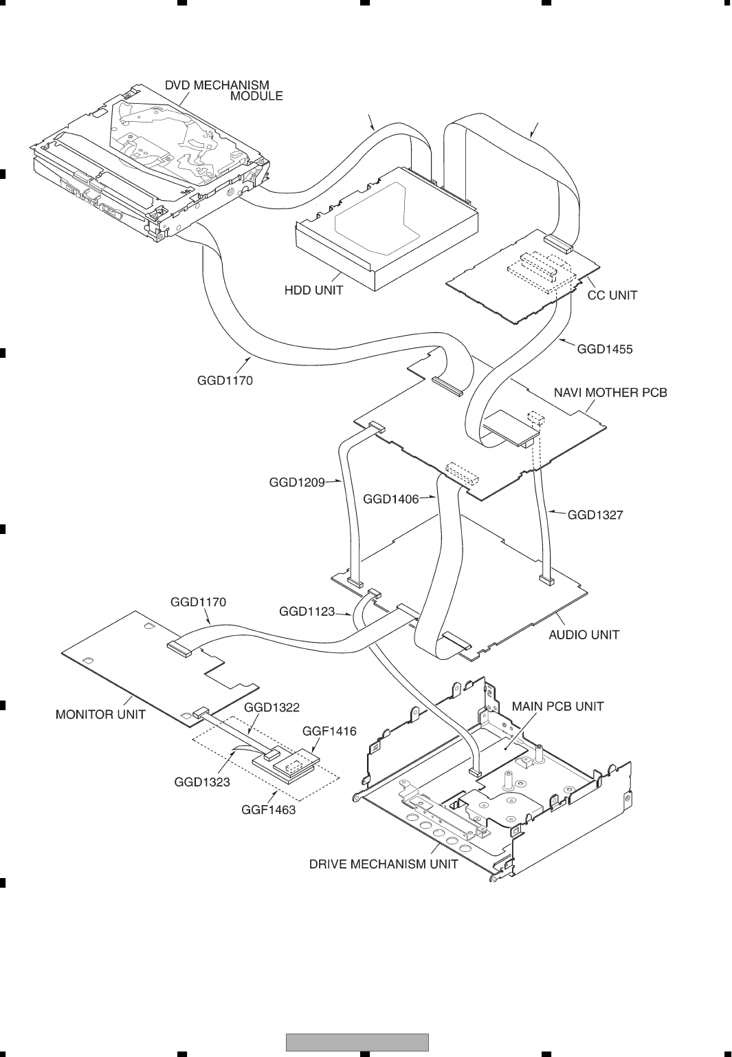
AVIC-Z1/UC
148
1234
1234
C
D
F
A
B
E
6. ADJUSTMENT
6.1 JIG CONNECTION DIAGRAM
GGD1284 CDE8077
(used in the product)
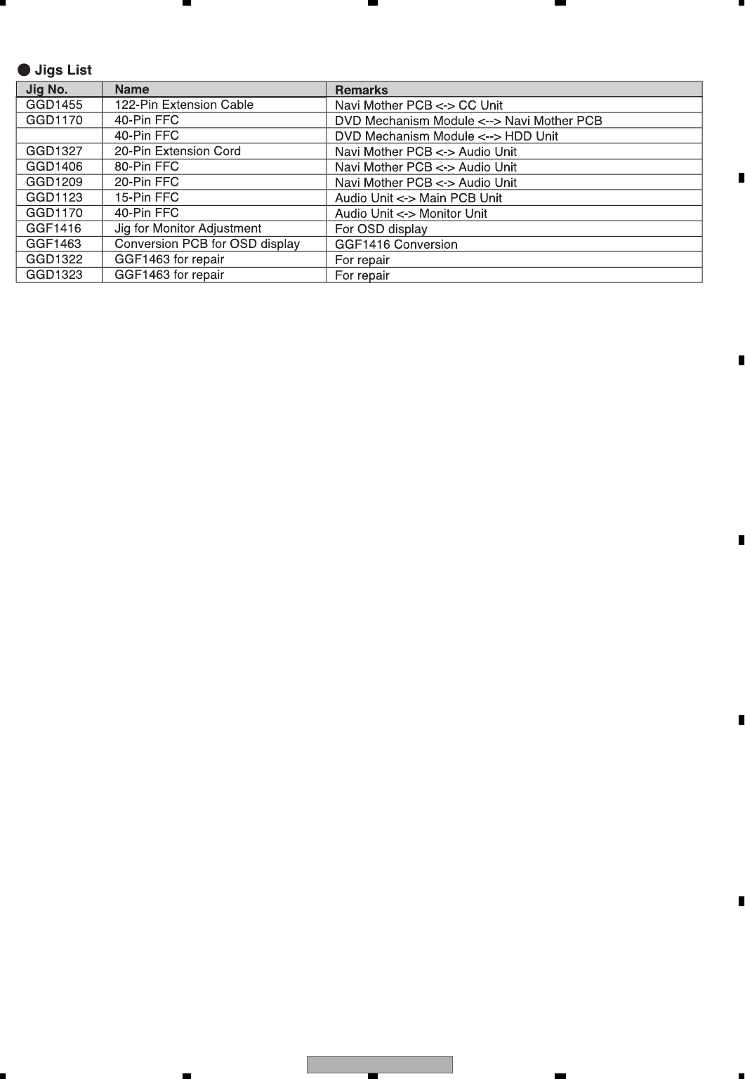
AVIC-Z1/UC 149
5678
5678
C
D
F
A
B
E
GGD1284 BBR
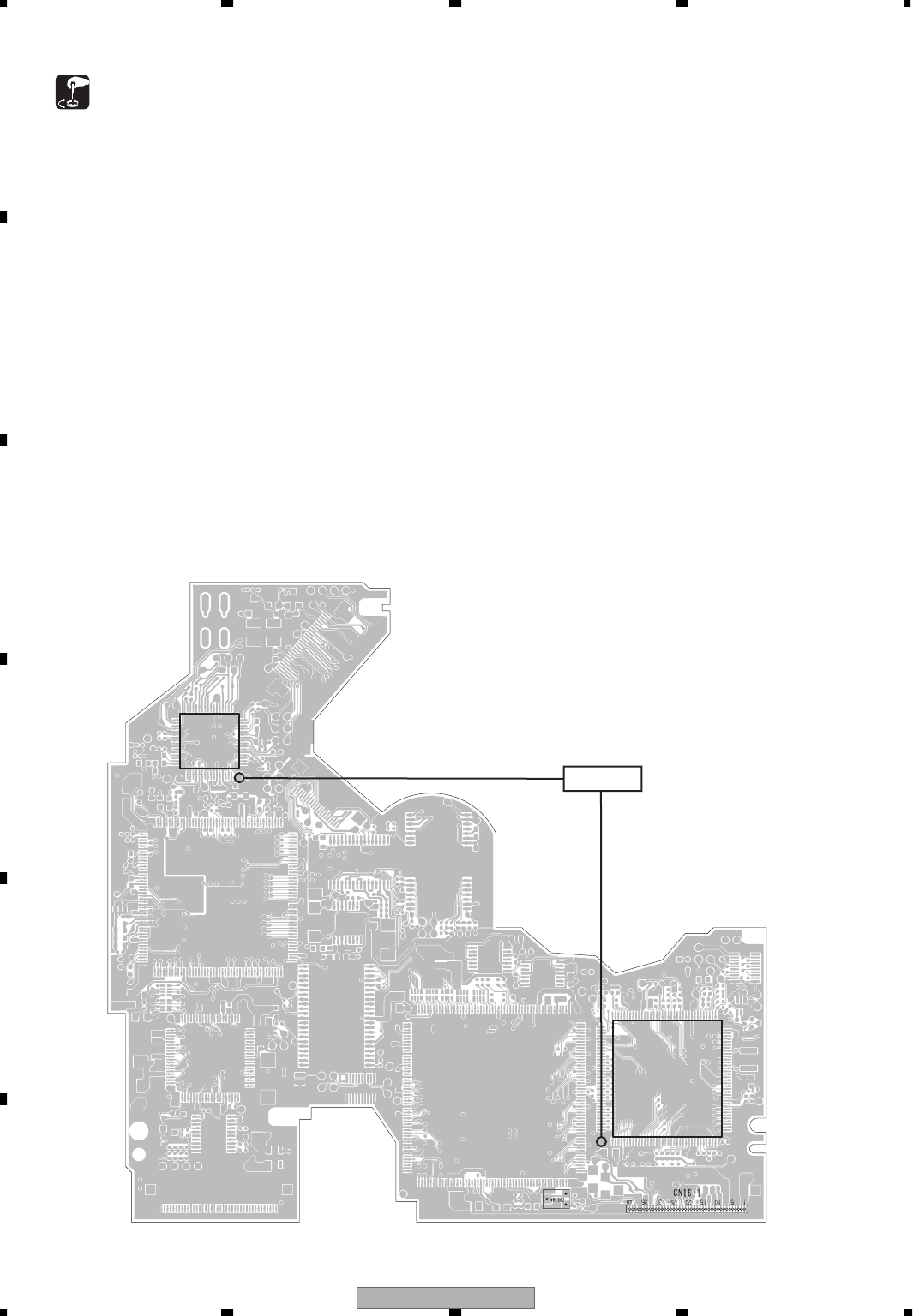
AVIC-Z1/UC
150
1234
1234
C
D
F
A
B
E
6.2 DVD ADJUSTMENT
Skew adjustment connection diagram
• DVD core unit (MS3)
-Skew adjustment
If any of the following replacements have been performed on the system, adjustments for pick up,
must be conducted:
1. Pick up unit replacement
2. Spindle motor replacement
3. Carriage chassis replacement
4. Pick up unit main shaft replacement
5. Pick up unit sub-shaft replacement
Measurement device and tools : Oscilloscope
Allen key wrench
Screw rock(GYL1001)
Disk used : GGV1018
Measurement reference : GND1
Measurement point : RFOUT
COMPO
GNDV
IC1706
IC1101
GND1
Oscilloscope
RFOUT
AVIC-Z1/UC 151
5678
5678
C
D
F
A
B
E
Apply glue
Shaft
Skew adj. screw Skew adj. screw
Prevent applied glue
from extending beyond this position.
Prevent applied glue
from extending beyond this position.
B
A
C
1
Symptoms in case of poor adjustment:
Caution: Avoid exposing your eyes to laser beams for a long time.
Preparation for adjustment: Clean both ends of the shafts.
Use brand new skew screws supplied with the service kit GXX1259.
Procedures:
1. Place the DVD mechanism module upside down.
To avoid the disc from being robbed when it is turned upside down, first put a coin of about 1.5 mm on the table,
then turn the disc upside down and set it so that the 1 in the figure comes to the point immediately above
the coin.
2. After replacing the pickup (by referring to the procedures of "Removing the Pickup."), roughly adjust the three
skew screws through visual check so that the pickup is mounted in parallel to the CRG chassis around the inner
and outer tacks.
3. Connect an oscilloscope as shown in the connecting diagram.
4. Turn on the power of the product. Load the test disc (GGV1018).
5. In the front-end test mode, set the disc type to DVD layer 1. Then, turn on the power. Move the pickup toward
the inner tracks.
6. Turn on the laser diodes.
7. With the focus servo closed, complete all automatic adjustments. Close the tracking servo, and then complete all
automatic adjustments.
8 Follow the next procedures, from 8-1 to 8-5, and adjust the (three) skew screws.
8-1 Move the pickup toward the inner track and turn the skew adjustment screw C so that the RF level of
oscilloscope becomes the maximum.
(Tangential adjustment at the inner track position: Adjust the flatness of the disc at the inner track position with
the adjustment screw C)
8-2 Move the pickup toward the outer track and turn the skew adjustment screw B so that the RF level becomes
the maximum.
(Tangential adjustment at the outer track position: Adjust the flatness of the disc at the outer track position with
the adjustment screw B)
8-3 Leave the pickup at the outer track position and turn the skew adjustment screws A and B in the same direction
alternately one quarter at a time (A•B•A•B •••) so that the RF level becomes the maximum.
(Radial adjustment at the outer track position: Keeping the flatness at the outer track position, adjust the flatness
of the whole disk with the adjustment screws A and B)
8-4 Move the pickup toward the inner track and turn the skew adjustment screw C so that the RF level becomes
the maximum.
(Tangential adjustment at the inner track position: Adjust the flatness of the disc at the inner track position with
the djustment screw C)
8-5 Repeat the steps from 8-2 to 8-4 three times, and adjust at the position where the RF level becomes the
maximum.
9. Turn off the power in the test mode. After confirming that the disc has stopped, eject the disc.
10. Adjust with a screw rock the shaft and skew adjustment screw to the same state as initial one.
Error efficiency deteriorated: 10
(Optimum value: 10
or lower)
High jitter of the RF signal RF waveform deformed
Unstable operation in tracking closing and servo control
-3 -4
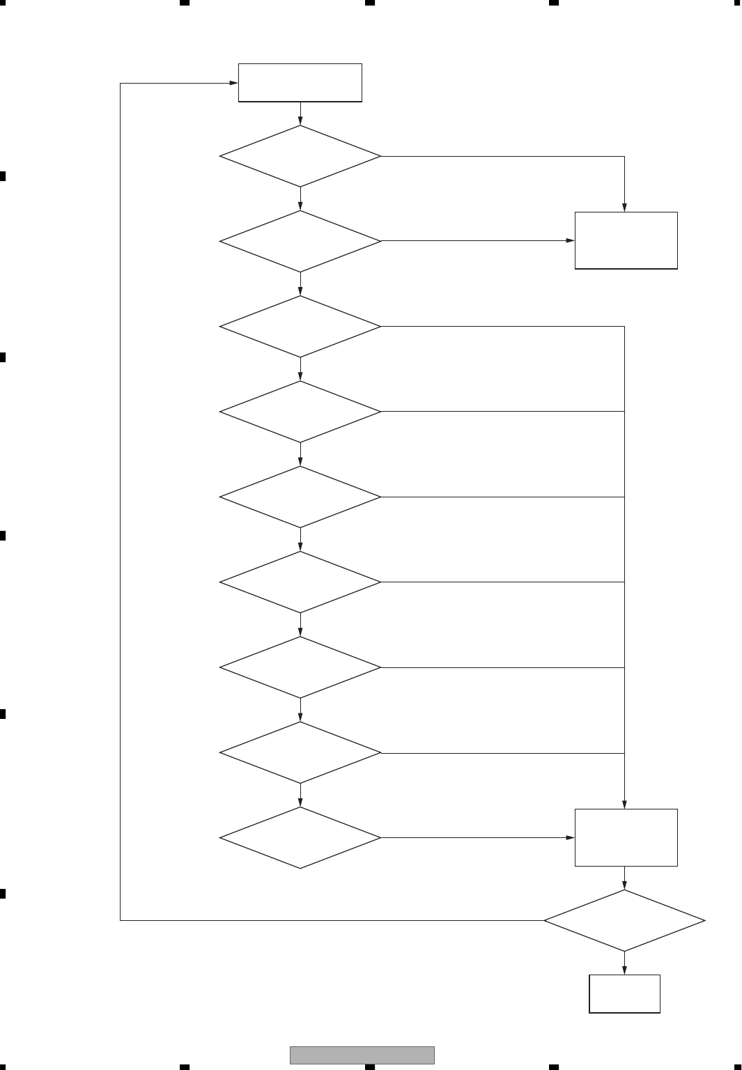
AVIC-Z1/UC
152
1234
1234
C
D
F
A
B
E
Are all
reproduced images and
sounds normal?
NO
NO
NG
NG
NG
NG
NG
Are all
clocks operating
normally?
Is
the
streaming I/F
Is the audio
circuit operating normally?
Is
the video
circuit operating
normally?
Is
SDRAM
I/F operating
normally?
All checks normal?
Start
Go to the F.E.
section check
Repair or replace
any defective unit
Check
completed
NG
NO
OK
OK
OK
OK
OK
OK
YES
YES
YES
Is the F.E. section
normal?
Are all
power supply
voltages
Is
the microprocessor
operating normally?
- Back end section check flow chart
AVIC-Z1/UC 153
5678
5678
C
D
F
A
B
E
Check 1: Are all power supply voltages normal?
Reproduce DVD-REF-A1 Title 1.
Verify the voltage of the sensing pin.
If results are not satisfactory, check to see if there are any problems with the resin flux cored solder,
parts and components.
NO. Verification location Rated value Unit
1 VD8-PGND 8±0.4 V
2 VD33-GND 3.3±0.3 V
3 SRVDD33-GND 3.3±0.3 V
4 VCC5-GND V
5 AVCC5-GND 5±0.3
5±0.25
V
6 VCC33-GND 3.3±0.15 V
7 VCC18-GND V
1.8±0.15
8 VCC25-GND V
2.5±0.2
AVIC-Z1/UC
154
1234
1234
C
D
F
A
B
E
Check 2: Are all clocks operating normally?
Reproduce DVD-REF-A1 Title 1.
Checks are to be conducted with a GND reference.
If locations listed under "verification location 2", can be verified, there will be no need to perform verifications
for the locations listed under "verification location 1."
If the result is not satisfactory, check to see if there are any problems with the resin flux cored solder,
parts and components, in the vicinity of IC1507.
Verification Verification
NO. location 1 location 2 Media Rated value1 Rated value 2 Rated value 3
(contact
measurements)
1 CLK27 IC1503 96pin ALL 2.65V~VCC33 GND~0.65V 27MHz±50ppm
2 EXTCK1 IC1503 100pin DVD 2.65V~VCC33 GND~0.65V 36.8640MHz±100ppm
3 EXTCK1 IC1503 100pin CD 2.65V~VCC33 GND~0.65V 33.8688MHz±100ppm
4 MCK16 IC1301 79pin ALL 2.33~VCC33 GND~0.99V 16.9344MHz±100ppm
5 MCK33 IC1601 3,33pin ALL 2.33~VCC33 GND~0.10V 33.8688MHz~40.0000MHz
Rated value 1 Rated value 3
Rated value 2GND
Clock rated values
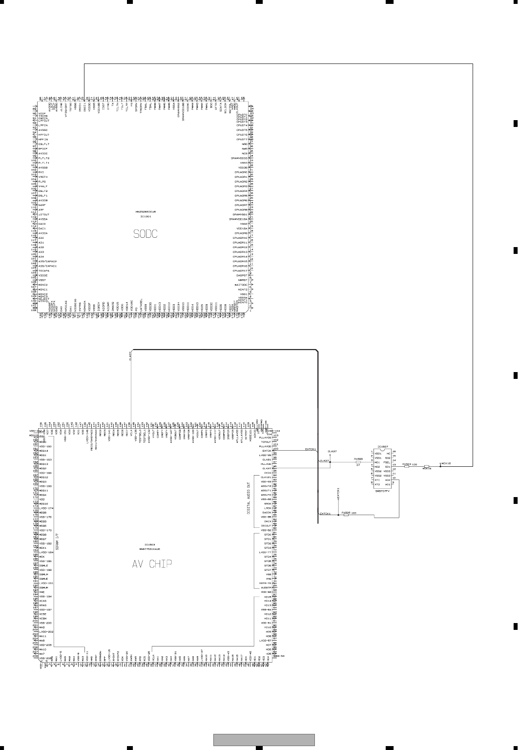
AVIC-Z1/UC 155
5678
5678
C
D
F
A
B
E
System Computer I/F
MPEG stream
Clock generator
AVIC-Z1/UC
156
1234
1234
C
D
F
A
B
E
Rated value 1
Rated value 2
GND
Check 3: Is the streaming I/F operating normally?
Reproduce DVD-REF-A1 Title 1.
Checks are to be conducted with a GND reference.
If the locations listed under "verification location 2" can be verified, then there is no need to conduct verifications
for the locations listed under "verification location 1."
If the result is not satisfactory, check to see if there are any problems with the resin flux cored solder, parts
and components, in areas where a problem occurs, for the overall sequence of“output " input"of the checked location.
Verification
NO. location 1 Verification Verification Rated Rated Reference Others
(contact location2 Media value 1 value 2 waveform
measurements)
1 STD0 IC1503 81pin DVD 2V~VCC33 GND~0.8V
Waveform
1 Line name OHDD8 at R1425
2 STD1 IC1503 80pin DVD 2V~VCC33 GND~0.8V
Waveform
1 Line name OHDD9 at R1425
3 STD2 IC1503 79pin DVD 2V~VCC33 GND~0.8V
Waveform
1 Line name OHDD10 at R1425
4 STD3 IC1503 78pin DVD 2V~VCC33 GND~0.8V
Waveform
1 Line name OHDD11 at R1425
5 STD4 IC1503 76pin DVD 2V~VCC33 GND~0.8V
Waveform
1 Line name OHDD12 at R1426
6 STD5 IC1503 75pin DVD 2V~VCC33 GND~0.8V
Waveform
1 Line name OHDD13 at R1426
7 STD6 IC1503 74pin DVD 2V~VCC33 GND~0.8V
Waveform
1 Line name OHDD14 at R1426
8 STD7 IC1503 73pin DVD 2V~VCC33 GND~0.8V
Waveform
1 Line name OHDD15 at R1426
9 STCLK IC1503 70pin DVD 2V~VCC33 GND~0.8V
Waveform
2 Line name ODA2 at IC1405
10 STVALID IC1503 69pin DVD 2V~VCC33 GND~0.8V
Waveform
2 Line name OINTRQ at IC1405
11 MASTER IC1301 176pin DVD 2V~VCC33 GND~0.8V
Waveform
2Line name STENABLE at IC1405
Streaming I/F rated value
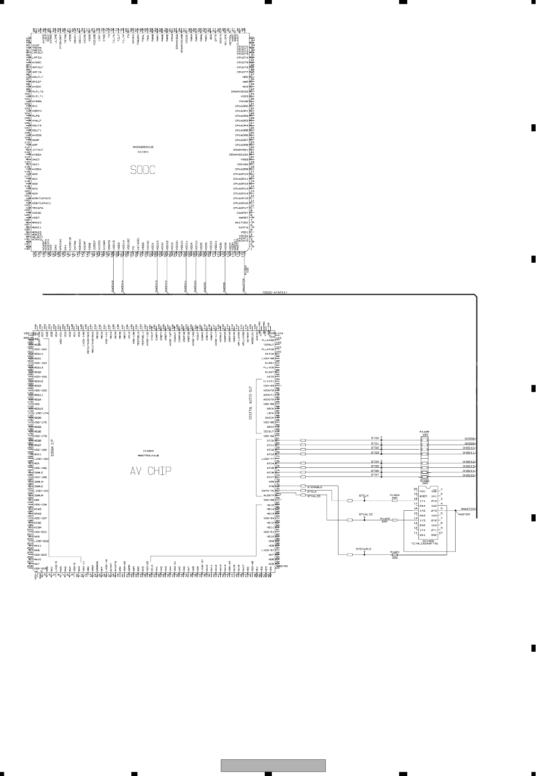
AVIC-Z1/UC 157
5678
5678
C
D
F
A
B
E
System Computer I/F
MPEG stream
MPEG stream
AVIC-Z1/UC
158
1234
1234
C
D
F
A
B
E
Check 4: Is the audio circuit operating normally?
Reproduce DVD-REF-A1 Title 2 Chapter (48V/16-bit/1 kHz/0dB). Verify the circuit described in Figure 2.
Checks are to be conducted using GNDAU1 (sensing pins) as a reference.
If the locations, listed under "verification location 2", can be verified, there is no need to conduct verifications for
the locations listed under "verification location 1."
If the result is not satisfactory, check to see if there are any problems with the resin flux cored solder, parts
and components, in the vicinity of the main components.
NO. Verification Verification Rated Rated Reference
location 1 location 2 value 1 value 2 waveform
1 AOUT0 IC1503 90pin 2.0V 0.8V Waveform 3
and over and lower
2 SRCK IC1605 1pin 2.0V 0.8V Waveform 3
and over and lower
3 LRCK IC1605 3pin 2.0V 0.8V Waveform 3
and over and lower
Rated value1
Rated value 2
GND
Three serial output rated values
Checks are conducted with the measurement circuit below.
NO. Verification Verification Rated value Reference
location 1 location 2 waveform
4 LO CN1611 36pin 1100±150mV Waveform 4
5 RO CN1611 34pin 1100±150mV Waveform 4
Analog audio outputs (LO and RO) rated values
LO and RO output measurement circuit
Rated value
22kΩ
AAGND
HOST I/F
RO
LO
These resistors are inserted.
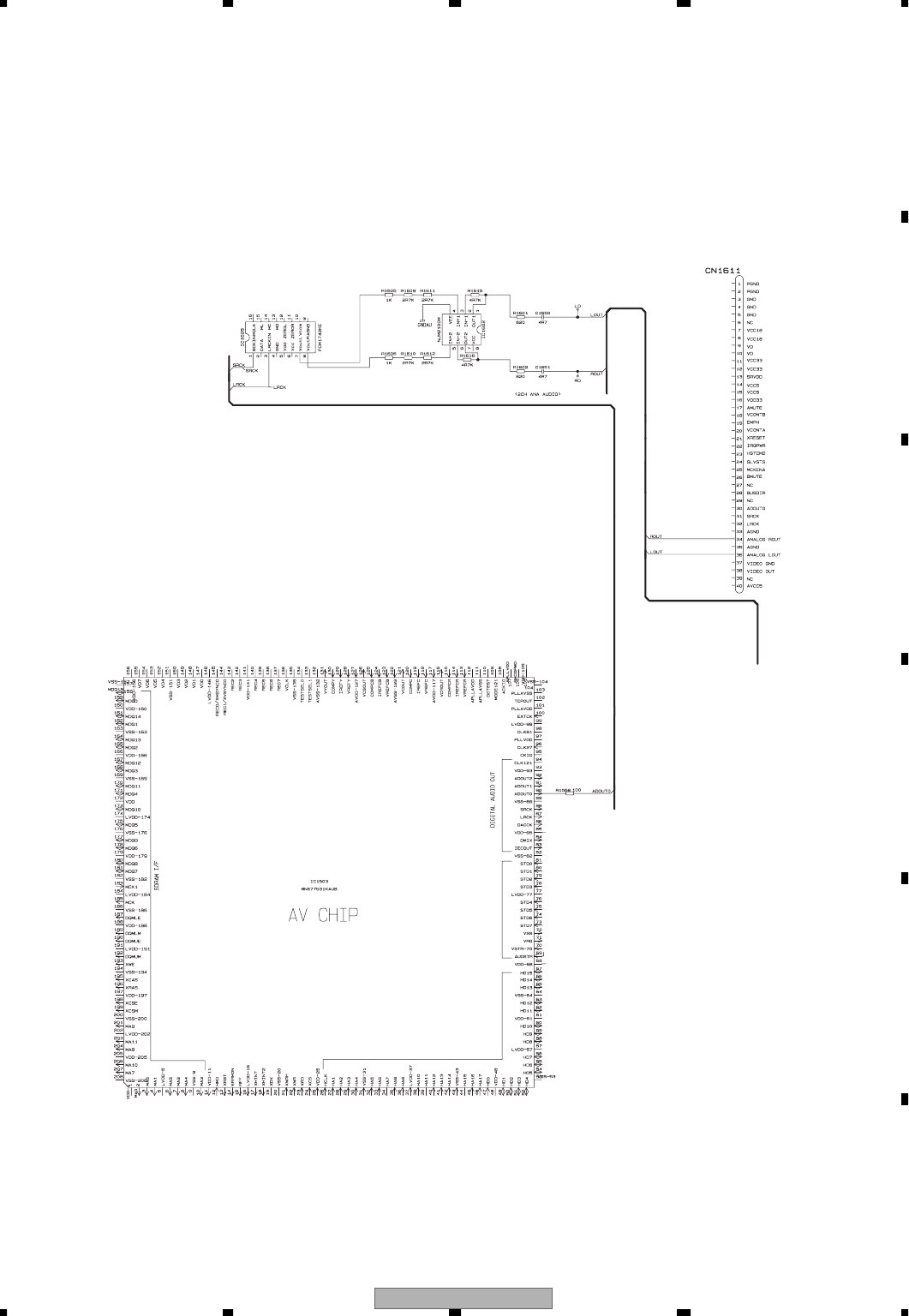
AVIC-Z1/UC 159
5678
5678
C
D
F
A
B
E
System Computer I/F
MPEG stream
AVIC-Z1/UC
160
1234
1234
C
D
F
A
B
E
Check 5: Is the video circuit operated normally?
Reproduce DVD-REF-A1 Title 2 Chapters (White 100IRE).
Monitor the output with the oscilloscope, by setting the COMPO signal to a GND reference.
Set the Trigger mode to the TV trigger, and the Trigger line to line-150.
NO. Verification location Rated value Reference
(sensing pin) waveform
1 COMPO 1.0±0.05Vpp Waveform 5
If the result is not satisfactory, check to see if there are any problems with resin flux cored solder, parts
and components, in the vicinity of line-150 (the section marked 5 in the circuit diagram) and peripheral components.
Color burst
Horizontal periodic signal
Rated
value
When the result is not satisfactory,
adjust the noise level to 1.0 + 0.05 Vpp.
PEAK
BOTTOM
Pedestal
COMPO signal
Composite signal 100% output waveform
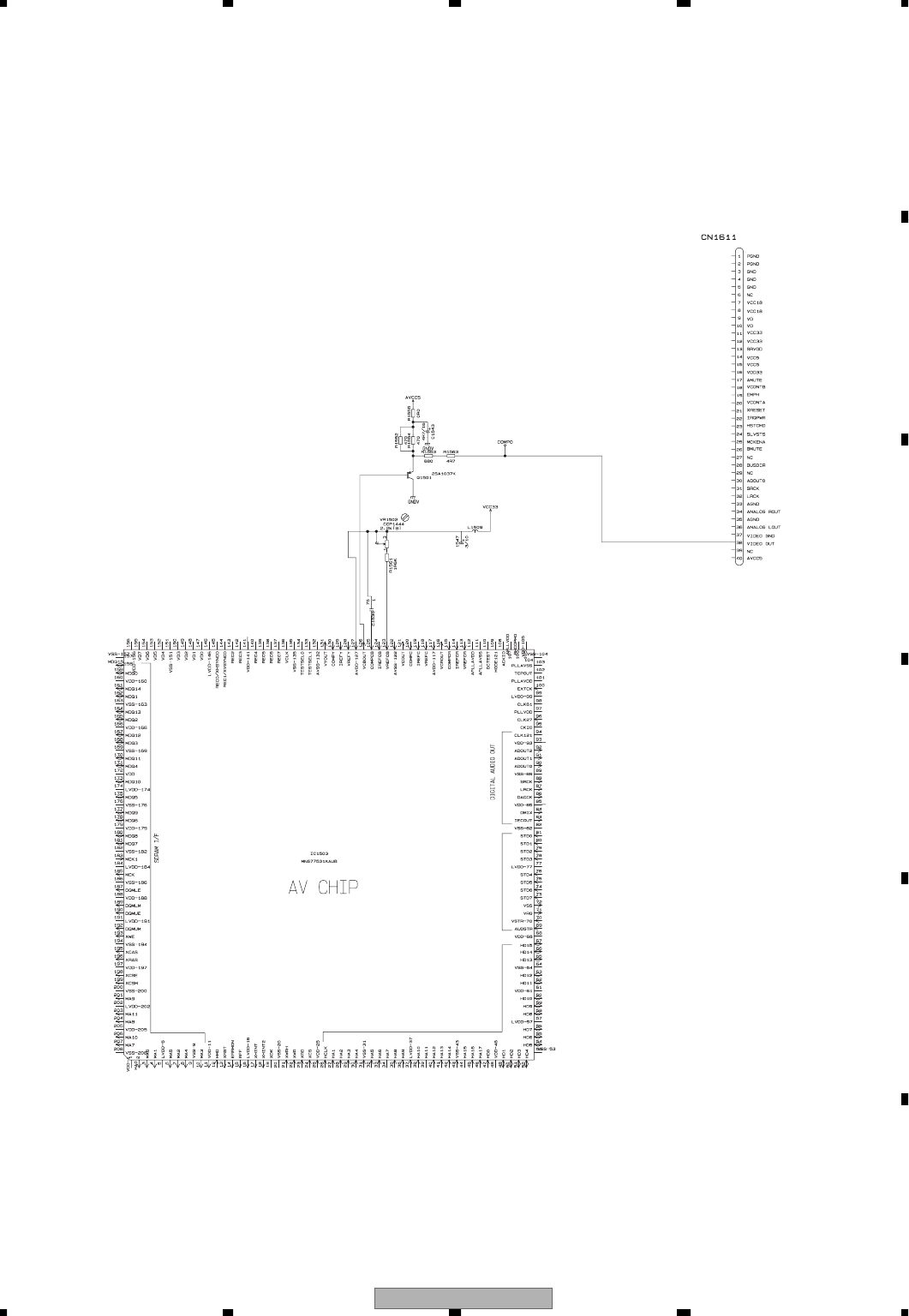
AVIC-Z1/UC 161
5678
5678
C
D
F
A
B
E
System Computer I/F
MPEG stream

AVIC-Z1/UC
162
1234
1234
C
D
F
A
B
E
Check 6: Is SDRAM I/F operating normally?
Reproduce DVD-REF-A1 Title 1.
Check the conductivity of both the "Verification location 1" and the "Verification location2."
If the result is not satisfactory, check to see if there are any problems with the resin flux cored solder, parts
and components, in areas where a problem occurs, for the overall sequence of “output " input" of the checked location.
NO. Signal name Verification location 1 Verification location 2 Rated value
1 MA0 IC1501 23pin IC1503 2pin 22Ω±5%
2 MA1 IC1501 24pin IC1503 4pin 22Ω±5%
3 MA2 IC1501 25pin IC1503 7pin 22Ω±5%
4 MA3 IC1501 26pin IC1503 10pin 22Ω±5%
5 MA4 IC1501 29pin IC1503 8pin 22Ω±5%
6 MA5 IC1501 30pin IC1503 6pin 22Ω±5%
7 MA6 IC1501 31pin IC1503 3pin 22Ω±5%
8 MA7 IC1501 32pin IC1503 207pin 22Ω±5%
9 MA8 IC1501 33pin IC1503 204pin 22Ω±5%
10 MA9 IC1501 34pin IC1503 201pin 22Ω±5%
11 MA10 IC1501 22pin IC1503 206pin 22Ω±5%
12 MA11 IC1501 20pin IC1503 203pin 22Ω±5%
13 MDQ0 IC1501 2pin IC1503 159pin 22Ω±5%
14 MDQ1 IC1501 4pin IC1503 162pin 22Ω±5%
15 MDQ2 IC1501 5pin IC1503 165pin 22Ω±5%
16 MDQ3 IC1501 7pin IC1503 168pin 22Ω±5%
17 MDQ4 IC1501 8pin IC1503 171pin 22Ω±5%
18 MDQ5 IC1501 10pin IC1503 175pin 22Ω±5%
19 MDQ6 IC1501 11pin IC1503 178pin 22Ω±5%
20 MDQ7 IC1501 13pin IC1503 181pin 22Ω±5%
21 MDQ8 IC1501 42pin IC1503 180pin 22Ω±5%
22 MDQ9 IC1501 44pin IC1503 177pin 22Ω±5%
23 MDQ10 IC1501 45pin IC1503 173pin 22Ω±5%
24 MDQ11 IC1501 47pin IC1503 170pin 22Ω±5%
25 MDQ12 IC1501 48pin IC1503 167pin 22Ω±5%
26 MDQ13 IC1501 50pin IC1503 164pin 22Ω±5%
27 MDQ14 IC1501 51pin IC1503 161pin 22Ω±5%
28 MDQ15 IC1501 53pin IC1503 158pin 22Ω±5%
29 MCK IC1501 38pin IC1503 185pin 22Ω±5%
30 XWE IC1501 16pin IC1503 193pin 22Ω±5%
31 XCAS IC1501 17pin IC1503 195pin 22Ω±5%
32 XRAS IC1501 18pin IC1503 196pin 22Ω±5%
33 XCSM IC1501 19pin IC1503 199pin 22Ω±5%
34 XCSE IC1501 35pin IC1503 198pin 22Ω±5%
35 DQMUM IC1501 39pin IC1503 192pin 22Ω±5%
36 DQMLM IC1501 15pin IC1503 189pin 22Ω±5%
37 DQMUE IC1501 21pin IC1503 190pin 22Ω±5%
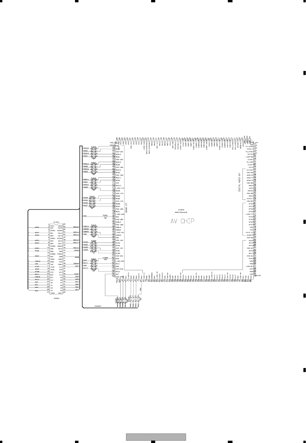
AVIC-Z1/UC 163
5678
5678
C
D
F
A
B
E
System Computer I/F
MPEG stream
K4S641632H-TC75

AVIC-Z1/UC
164
1234
1234
C
D
F
A
B
E
Check 7: Is the microprocessor operating normally?
Check the conductivity of both the "Verification location 1" and the "Verification location2."
If the result is not satisfactory, check to see if there are any problems with the resin flux cored solder, parts
and components, in areas where a problem occurs, for the overall sequence of "output – input" of the checked location.
NO. Signal name Verification Verification Verification Rated value Others
location 1 location 2 Media
1 A1 IC1701 142pin IC1503 27pin ALL 0Ω
2 A2 IC1701 141pin IC1503 28pin ALL 0Ω
3 A3 IC1701 140pin IC1503 29pin ALL 0Ω
4 A4 IC1701 139pin IC1503 30pin ALL 0Ω
5 A5 IC1701 138pin IC1503 32pin ALL 0Ω
6 A6 IC1701 137pin IC1503 33pin ALL 0Ω
7 A7 IC1701 136pin IC1503 34pin ALL 0Ω
8 A8 IC1701 133pin IC1503 35pin ALL 0Ω
9 A9 IC1701 132pin IC1503 36pin ALL 0Ω
10 A10 IC1701 131pin IC1503 38pin ALL 0Ω
11 A11 IC1701 130pin IC1503 39pin ALL 0Ω
12 A12 IC1701 129pin IC1503 40pin ALL 0Ω
13 A13 IC1701 128pin IC1503 41pin ALL 0Ω
14 A14 IC1701 127pin IC1503 42pin ALL 0Ω
15 A15 IC1701 126pin IC1503 44pin ALL 0Ω
16 A16 IC1701 123pin IC1503 45pin ALL 0Ω
17 A17 IC1701 122pin IC1503 46pin ALL 0Ω
18 D0 IC1701 17pin IC1503 47pin ALL 0Ω
19 D1 IC1701 16pin IC1503 49pin ALL 0Ω
20 D2 IC1701 15pin IC1503 50pin ALL 0Ω
21 D3 IC1701 14pin IC1503 51pin ALL 0Ω
22 D4 IC1701 13pin IC1503 52pin ALL 0Ω
23 D5 IC1701 12pin IC1503 54pin ALL 0Ω
24 D6 IC1701 11pin IC1503 55pin ALL 0Ω
25 D7 IC1701 10pin IC1503 56pin ALL 0Ω
26 D8 IC1701 7pin IC1503 58pin ALL 0Ω
27 D9
D10
D11
D12
D13
D14
D15
IC1701 6pin IC1503 59pin ALL 0Ω
28
XCSAVR
IC1701 5pin IC1503 60pin ALL 0Ω
29
XCSAVW
IC1701 4pin IC1503 62pin ALL 0Ω
30
XCSAV
IC1701 3pin IC1503 63pin ALL 0Ω
31
XAVINT2
XAVINT
IC1701 2pin IC1503 65pin ALL 0Ω
32
XRD
IC1701 1pin IC1503 66pin ALL 0Ω
33
CLKOUT
IC1701 144pin IC1503 67pin ALL 0Ω
Dividing circuitFor verification location 2,
include also IC1502 pin-3
34
HCLK
IC1701 101pin IC1706 1pin ALL 0Ω
35
XSRAMWR
IC1701 100pin IC1706 2pin ALL 0Ω
36
XHWR
IC1706 4pin IC1503 24pin ALL 0Ω
37 IC1701 42pin IC1503 17pin ALL 0Ω
38 IC1701 41pin IC1503 18pin ALL 0Ω
39 IC1701 95pin IC1503 23pin ALL 0Ω
40 IC1701 90pin IC1505 3pin ALL 33Ω
41 IC1502 5pin IC1503 26pin ALL 200Ω ± 5%
42 IC1701 105pin IC1505 1pin ALL 0Ω
43 IC1504 8pin IC1503 21pin ALL 68Ω ± 5%
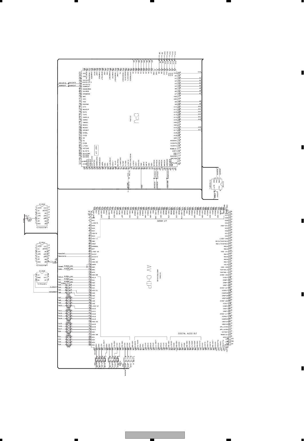
AVIC-Z1/UC 165
5678
5678
C
D
F
A
B
E
System Computer I/F
MPEG stream
PE5511A
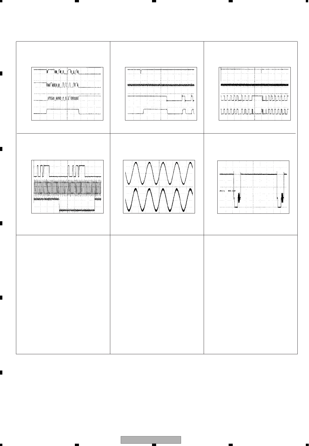
AVIC-Z1/UC
166
1234
1234
C
D
F
A
B
E
Note:1 The encircled number denote measuring pointes in the circuit diagram.
2 Reference voltage VHALF : 1.65V
!CH1: STD1
@CH2: STD4
#CH3: STD7
$CH4: STENABLE
G→
5V/div. 2µs/div.
G→
G→
G→←T
%CH1: AVRTM
^CH2: STCLK
&CH3: STVALID
$CH4: STENABLE
G→
5V/div. 2µs/div.
G→
G→
G→
←T
%CH1: AVRTM
^CH2: STCLK
&CH3: STVALID
$CH4: STENABLE
G→
5V/div. 50µs/div.
G→
G→
G→
←T
*CH1: AOUT0
(CH2: SRCKAV
)CH3: LRCKAV
G→
2V/div. 2µs/div.
G→
G→←T
¤CH1: LO
‹CH2: RO
G→
1V/div. 500µs/div.
G→
←T
›CH1: COMPO 200mV/div. 10µs/div.
[White 100% output]
G→
Wave 1 Wave 2(1) Wave 2(2)
Wave 4Wave 3 Wave 5
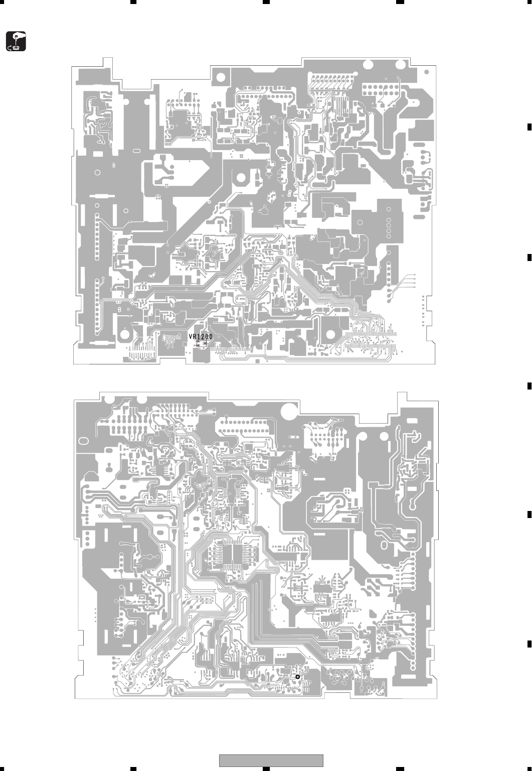
AVIC-Z1/UC 167
5678
5678
C
D
F
A
B
E
6.3 VIDEO LEVEL ADJUSTMENT
Audio Unit(SIDE A)
Audio Unit(SIDE B)
- Adjustment Point
CSYNCO
AVIC-Z1/UC
168
1234
1234
C
D
F
A
B
E
[When adjustment is improper] Video image sources will have black or white regions on the screen.(DVD,AV,TV etc.)
Order Items Modes
Audio Unit Adjustment Specification
Specification
(Other precautions)
Output signal
(test pin for measurement,
description of circuit)
Measuring
instrument
Adjustment of
video level
Measurement point : TP • CSYNCO
(Termination at
10k Ω or greater)
1.0 + 0.02
− 0.05Vp-p
1-1
1 Checking and
inspection of
video images
Video
image
Input signal
(Input test pin, specifications,
and other measurement conditions)
100% white (1Vp-p) signal should be added
to TP-DVDV and video output for the monitor
should be set to DVD.
Name of
adjustment
element
VR1200
Oscilloscope
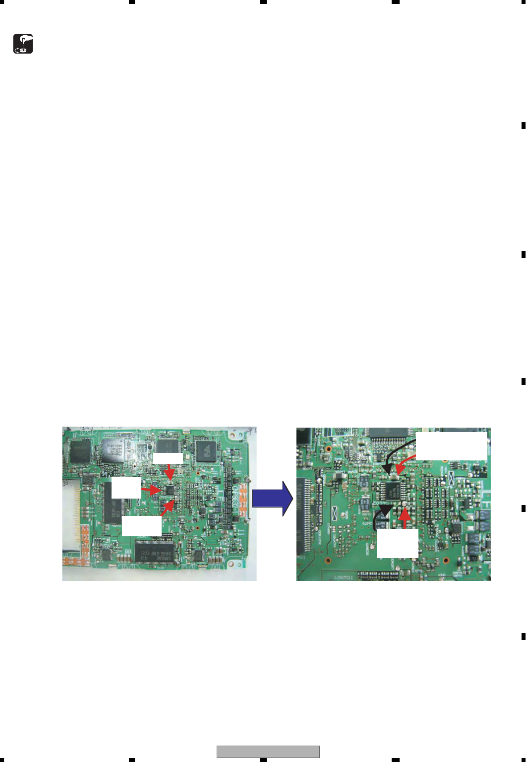
AVIC-Z1/UC 169
5678
5678
C
D
F
A
B
E
6.4 PLL ADJUSTMENT
When parts shown below are replaced, adjustment is required.
IC4001 inside the CC unit • Part replacement on PLL circuit area block on the CC unit.
Distortion of the screen
(Please refer to the pictures below.)
1 With HDD unconnected, connect the navigation unit to the product and apply power.
(The caution "HDD is unconnected." will appear in 10 seconds.)
2 Confirm that the voltage on both sides of C4024 (B side) attached to IC4002 power supply terminal
pin No.16 is within 3.3 ± 0.1V.
3 Control the potential of the sensing pin DEM (B side) at the IC4002 DEMOUT terminal (10 pin) to within
1.5 ± 0.1V while adjusting the VR4001(A side).
Be aware that extension of a CC unit, etc may cause the potential of 3.3 V to go beyond the limit.
When parts are replaced in IC4001(NAVICORE)/PLL circuit area, adjustment is required.
Other cases than that also require confirmation.
<How to adjust VR of PLL area>
[Purpose]
[The sign of insufficient adjustment]
[Method]
[Concerns]
B side of the CC unit The scale-up of B side of the CC unit
C4024
Potential of both ends
3.3V±0.1V
PLL IC
IC4002
Sensing pin
DEM
C4024
Sensing pin
DEM
1.5V±0.1V
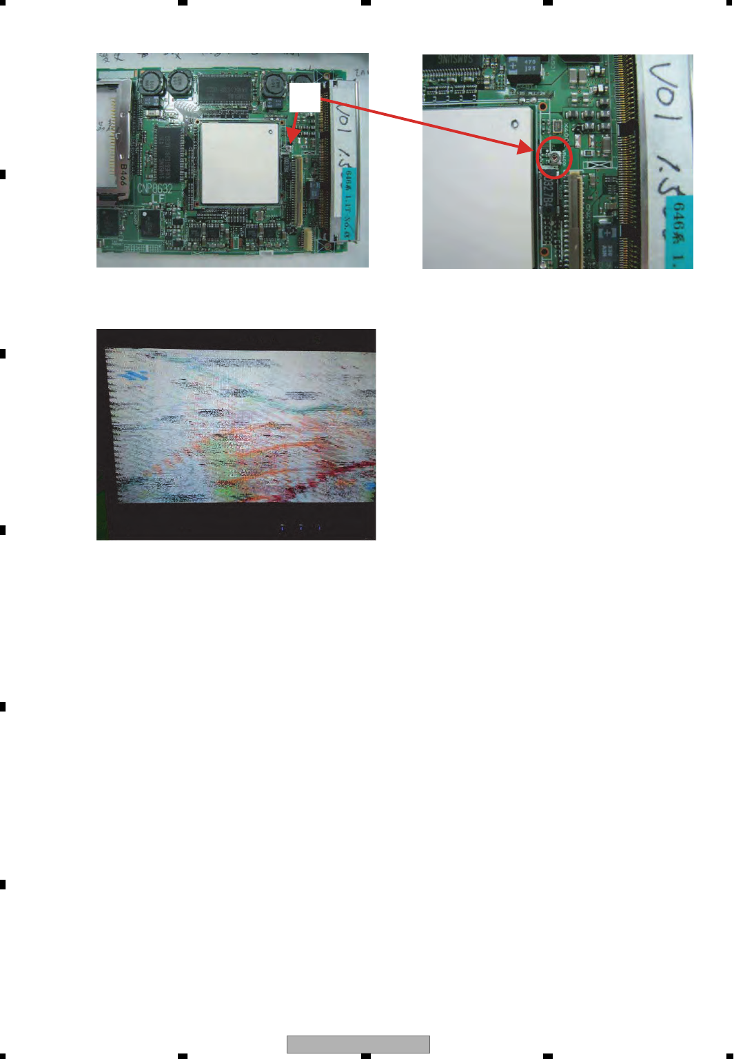
AVIC-Z1/UC
170
1234
1234
C
D
F
A
B
E
A side of the CC unit The scale-up of A side of the CC unit
[When adjustment is improper.]Distortion of the navigation screen
VR
4001
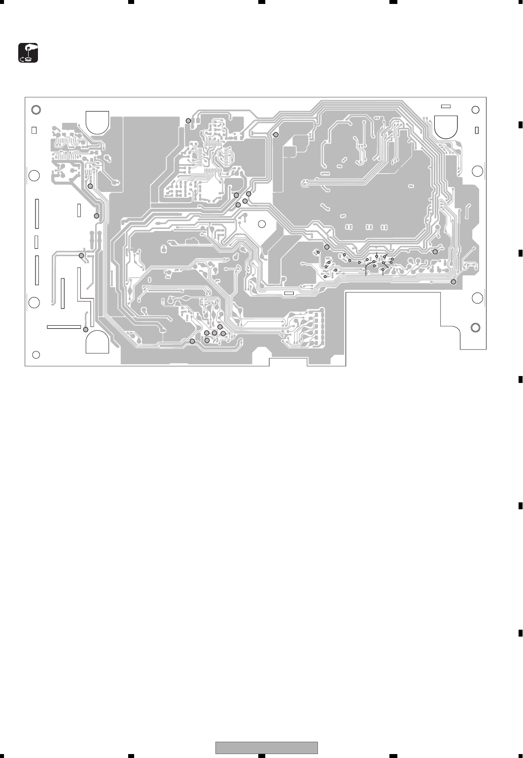
AVIC-Z1/UC 171
5678
5678
C
D
F
A
B
E
6.5 MONITOR UNIT ADJUSTMENT
Monitor Unit(SIDE B)
- Adjustment Point
V33 V25
V15
V5
V8
V14
V18
VM12
COM
V01
V03
V05 V07
V09
B02
B03 B04
B05
G02
G03
G04
G05 R02
R03
R04
R05
CSYNC
ANRYSIN
ANB
ANG
CVBS
FL1
FL2
INVPUL
VFL2

AVIC-Z1/UC
172
1234
1234
C
D
F
A
B
E
1
No. Adjustment
items
Input signal Measurement
point
Adjustment
point
Details
Confirming
3.3V power
supply voltage
Remarks
2
3
4
5
6
Confirming
2.5V power
supply voltage
Confirming
5V power
supply voltage
Confirming
8V power
supply voltage
Confirming
18.5V power
supply voltage
Confirming
−12V power
supply voltage
Ditto
Ditto
Ditto
Ditto
Ditto
14.4V for TP V14
TP V25
TP V5
TP V8
TP V18
TP VM12
TP V33 V33=3.3±0.25V
V25=2.5±0.15V
V5=4.9±0.30V
V8=8.0±0.50V
V18=18.5±0.80V
VM12=
−
12.0±0.60V
Important: Power for IC 1(TC90A96AFG-P) is off, make sure that DC voltage should not be applied to each terminal of IC.
However, IIC lines (SDA and SCL) are exceptional and 5V or less can be applied to them.
Adjustment of Monitor Unit Area
7
Nothing appears on the monitor.
Nothing appears on the monitor.
Nothing appears on the monitor.
The screen becomes brighter or darker, etc.
The color becomes lighter or horizontal
lines are seen on the monitor screen.
Nothing appears on the monitor.
Nothing appears on the screen.
Confirming
1.5V power
supply voltage
Ditto TP V15 V15=1.5±0.08V
AVIC-Z1/UC 173
5678
5678
C
D
F
A
B
E
8
No. Adjustment
items
Input signal Measurement
point
Adjustment
point
Details
Adjustment of
amplitude Vcom
amplifier output
Remarks
9
10
12
13
Confirmation of
amplitude of
gradation voltage
(V1)
Confirmation of
amplitude of
gradation voltage
(V3)
Confirmation of
amplitude of
gradation voltage
(V7)
Confirmation of
amplitude of
gradation voltage
(V9)
No definition
No definition
No definition
No definition
No definition
TP V03
TP V01
TP V07
TP V09
TP COM 4.70±0.10V
Measure at LCD panel connection
Measure at LCD panel connection
[Symptoms that occur when adjustment is improper]
• Halation on the screen.
• Irradiation on the screen
Measure at LCD panel connection
Measure at LCD panel connection
11 Confirmation of
amplitude of
gradation voltage
(V5)
No definition TP V05 Measure at LCD panel connection
Measure at LCD panel connection
EEP-ROM's
COM_AC data
4.20±0.30V
1.75±0.10V
0.35±0.10V
0.60±0.10V
3.30±0.20V
AVIC-Z1/UC
174
1234
1234
C
D
F
A
B
E
15
No. Adjustment
items
Input signal Measurement
points
Adjustment
points
Details
Confirmation of
RGB digital output
Remarks
16
18
19
Confirmation of
YS_OFFSET
Setting
Adjustment of
composite level
Video image
confirmation
Composite image
10STEP signal
input to TP CVBS.
(1.0Vpp ± 1%)
No definition
Composite image
lamp signal input
to TP CVBS
(Monochrome)
TP B02-B05
TP G02-G05
TP R02-R05
Confirm that each output is "H"
(3.3V) while image is displayed.
Set [YS DELAY] to 8 in EEPROM
adjustment mode.
Check if the gradation changes
smoothly and there is no colored
part on the whole screen.
DAC Jig output
14 Preparation for
video image
confirmation
Input white 100%
signal to TR ANR,
ANG and ANB
(0.70Vpp ± 1%)
TP CSYNC
synchronous
signal input
Register setting of
SA13h D5-0
Register setting of
SA2Fh D3-0
When OSD is displayed in EEPROM adjustment
mode, in which "L" output is mixed the area with
letters, ignore it.
[Symptoms of improper adjustment]
• Halation occurs on TV/Video screen
• TV/Video screen gets dim
Check EEPROM setting value after it is written.
15.734kHz
3.3V
Screen
This is done to check if the double window IC
digital out is not "BRIDGE" or OPEN.
SA**h in the list is a sub-address of TC90A96FG
50µS
0-3.3V logic level input
(Synchronous area 0V)
3.3V
Amplitude of 9th gradation and 0th
gradation shall be 1.77V±0.03V.
17 Confirmation of
YS operation Confirm YS operation
Signal input to
TR YSIN
0-3.3V
15.734kHz

AVIC-Z1/UC 175
5678
5678
C
D
F
A
B
E
1
No Adjustment
items
Input signal Measurement
points
Backlight basic drive
frequency adjustment
TP:14.4±0.2V for V14
TP: 14.4±0.2V for VFL
TP:GND INVPUL
TP : FL1,FL2 VR841
Remarks
Adjustment
points
Details
47.9-48.1kHz Connect 100kΩ between TP FL1 and FL2.
Monitor waveform or TPFL2 after voltage dividing.
Do not monitor TP FL1 directly.
(High pressure may cause damage to measuring equipment)
[Symptoms that occur because of improper adjustment]
• Backlight does not come on.
Noise occurs at AM certain frequency.
2Confirmation 1 of
frequency switching
Tune into AM530kHz.(UC)
Tune into AM531kHz.(EW)
TP : FL1,FL2 49.2±1.0kHz Confirm that the frequency of the waveform measured by
No.1 will be 49.2kHz.
3Confirmation 2 of
frequency switching
Tune into AM540kHz. TP : FL1,FL2 52.4±1.0kHz Confirm that the frequency of the waveform measured by
No.1 will be 52.4kHz.
Adjustment of Backlight Inverter
AVIC-Z1/UC
176
1234
1234
C
D
F
A
B
E
No. Adjustment
items
Measurement
points
Adjustment
points
Details Remarks
1
2
Aging
Flickering adjustment
Test mode calling
Leaving it in operation for over 30 minutes.
(at room temperatures)
Start the product in test mode.
→ Select "Monitor Test Mode".
→ Select "reglation mode(for service)"
3
Confirm screen display Screen
Back ground : Pattern for adjusting flicker
Text display : SERVICE MODE
COM DC * *
[FACTORY * *]
Pattern for flicker adjustment
Image with alternate black (50%) and white (50%) horizontal
scanning lines.
Values for * * vary depending on the product conditions.
4
Flicker adjustment Screen
Use the right and left buttons to change
value to the level where flicker on the
screen is minimized.
COM DC [Symptom occurring when adjustment is improper.]
• The screen flickers.
5
End
End by pressing the return button Operable using a Raku-Navi remote control unit.
Flicker Adjustment (When performing an adjustment in the product form)
Flicker adjustment (When performing on the LCD module)
No. Adjustment
item
Indication
signal
Measurement
points
Adjustment
points
Details Remarks
2
Flicker adjustment Pattern for flicker
adjustment
Adjust so that the flickering on the
screen will be minimized.
1
Aging
No definition
COM DC setting
value
(COM DC output
of the monitor
microcomputer)
Pattern for flicker adjustment
Image with alternate black (50%) and white (50%)
horizontal scanning lines.
Inverse video signal can be also entered into TP CVBS.
(However, adjustment using RGB is given higher priority.)
[Symptom occurring when adjustment is improper.]
• The screen flickers
Screen
Perform either of the two ways:
leaving it in operation status for over
30 minutes (at room temperatures) or
leaving it for over 5 minutes (50±5°C)
while no applying current.

AVIC-Z1/UC 177
5678
5678
C
D
F
A
B
E
[Operation Specification]
• For displaying OSD, install a jig (GGF1416 and GGF1463) for monitor adjustment onto Service OSD connector for CN5.
• When ACC is turned ON with [EPRTES/EPTESA] terminal in Low status, shift to [Flicker adjustment mode] will occur.
• Switch the setting modes with the [map] key.
[Flicker adjustment mode] → [Line adjustment 1 mode] → [Line adjustment 2 mode] → [Line adjustment 3 mode] →
→ [Line adjustment 4 mode] → [Line adjustment 5 mode] → [Line adjustment 6 mode] → [Line adjustment 7 mode] →
→ [Line adjustment 8 mode] → [Line adjustment 9 mode] → [Line adjustment 10 mode] → [Dimmer parameter setting
mode]
→ [Flicker adjustment mode]
• Select items to be adjusted using the [ ↓ ] [ ] keys.
• Adjust items selected using the [←] [→] keys.
It is possible to shift to the adjustment mode also while performing the monitor adjustment using a test disc.
After set values are written in EEPROM, they are read out and displayed.
Writing and reading shall be performed in 16 bit unit. Settings have different bit numbers item by item.
Values for CS (checksum) calculation have 8 Bit XOR when they are changed and writing will be done.
After this CS values are written into EEPROM, they are read out and displayed.
When the written values are different from the read-out ones, the read-out ones should be colored differently.
When the service adjustment mode is involved, this test mode does not start.
(Shift to the service adjustment mode)
● EEPROM adjustment mode
↓
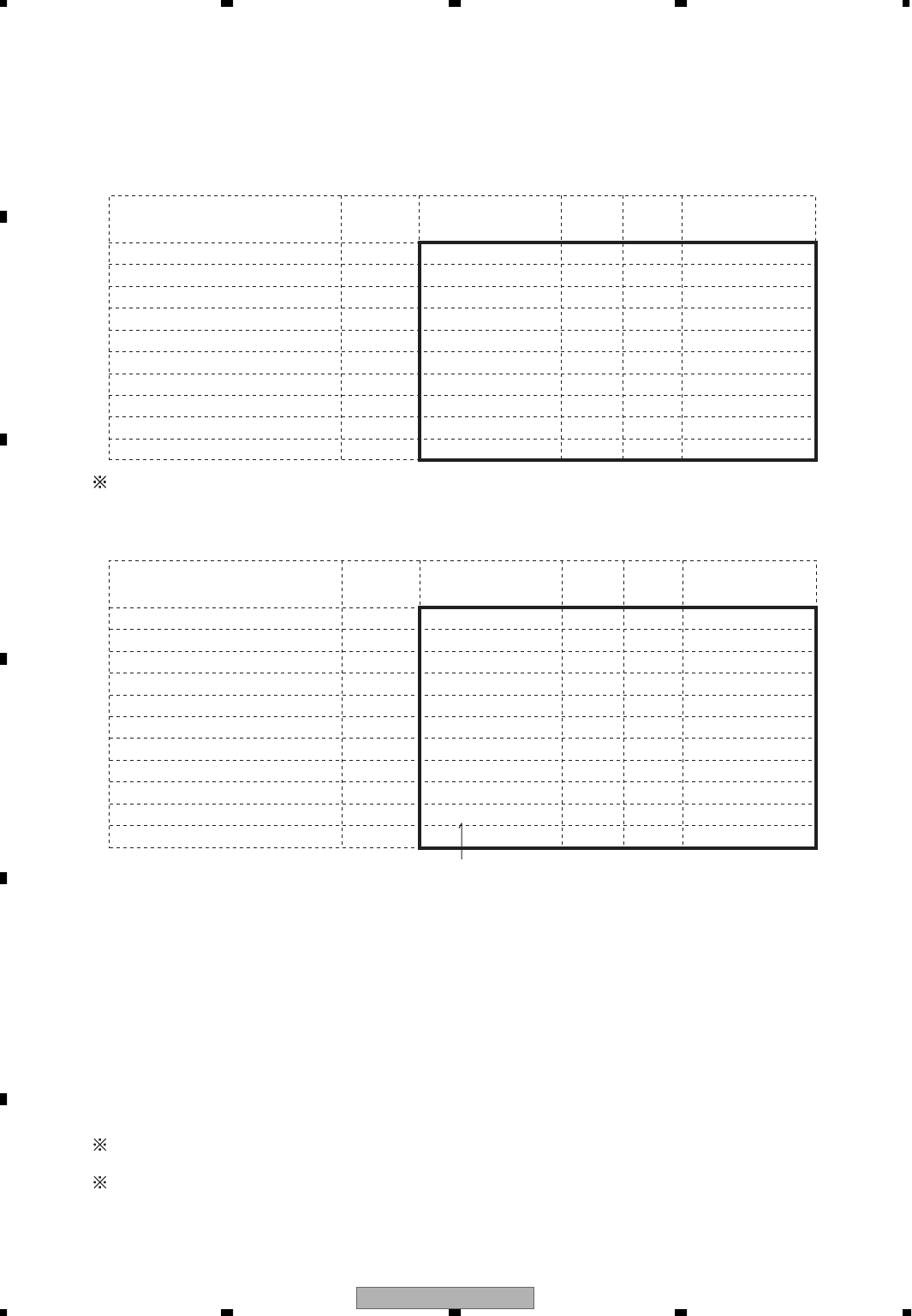
AVIC-Z1/UC
178
1234
1234
C
D
F
A
B
E
[Display specification of each mode]
Examples of actual OSD display are shown within the heavy line frame.
Numerical values in the adjusted values to be written are the segment that changes according to the adjustment for
each screen.
The adjustment details and the item display are items for design review and line adjustment.
Common inverse output center value
[0-255] COM DC 92
Settings
Adjustment
range
Adjustment
range
Item display
Adjusted value
Written value
(DEC)
Adjusted value
Written value
(DEC)
■ Flicker adjustment mode
■ Note 1: Details of [COM DC] shall be reflected on the common inverse output center reference value.
(Common inverse output center reference value is treated as an initial value to be set in the line.)
■ Line adjustment 1 mode
Bright [0-255] BRIGHT 150
RGB simultaneous contrast [0-255] CONTRAST 168
Common inverse output frequency adjusted value
[0-255] COM AMPAJ 150
R output DC offset [0-15] ROUT BIAS 8
G output DC offset [0-15] GOUT BIAS
B output DC offset [0-15] BOUT BIAS
Main Y contrast [0-63] RGB CNTRST
Sub Y Contrast [0-63] CMP CNTRST
DTR ON
Settings Item display
CS FFFF
LINE1
8
8
34
26
61
NOT
NOT
EEPROM
EEPROM
Monitor Microcomputer 5 pin [COM AC] Output voltage (V) = 4.8 (V) X [BRIGHT] Value/255
• In order to correct variation in hardware, common inverse output frequencies should be adjusted in the line.
• [COM AMPAJ] is an initial value set in the line and memorized in EEPROM bank 1.
• While the product is in normal operation, [BRIGHT] value is decided by [COM AMPAJ] and this value controls
the 5-pin [COM AC] output of the monitor microprocessor.
• In the single monitor operation test mode, the user-configurable "color density" is not reflected in "BRIGHT" value.
• When [COM AMPAJ] is adjusted, [BRIGHT] changes according to it.
([COM AMPAJ] has the same value kept in memory as [BRIGHT] value at the time of "black density" step 0.)
• When the test mode starts in the stage of the product, the user configurable "color density" will be reflected in
"BRIGHT" value.
Even if "BRIGHT" value is changed in the test mode, it will not be reflected in the user setting value.
■ Note 1: Contents of [BRIGHT] and [CONTRAST] are reference values (adjustable) for adjusting the other
items and are not memorized in EEPROM.
■ Note 2: Be aware that [R, G, BOUT BIAS] and [RGB, CMP CNTRST] have different indicated values/
EEPROM written values and double window IC (TC90A96FG-P) register setting values.
(As the double window IC register value and the screen output are not related linearly,
software is used for conversion.)
It is set as ON.
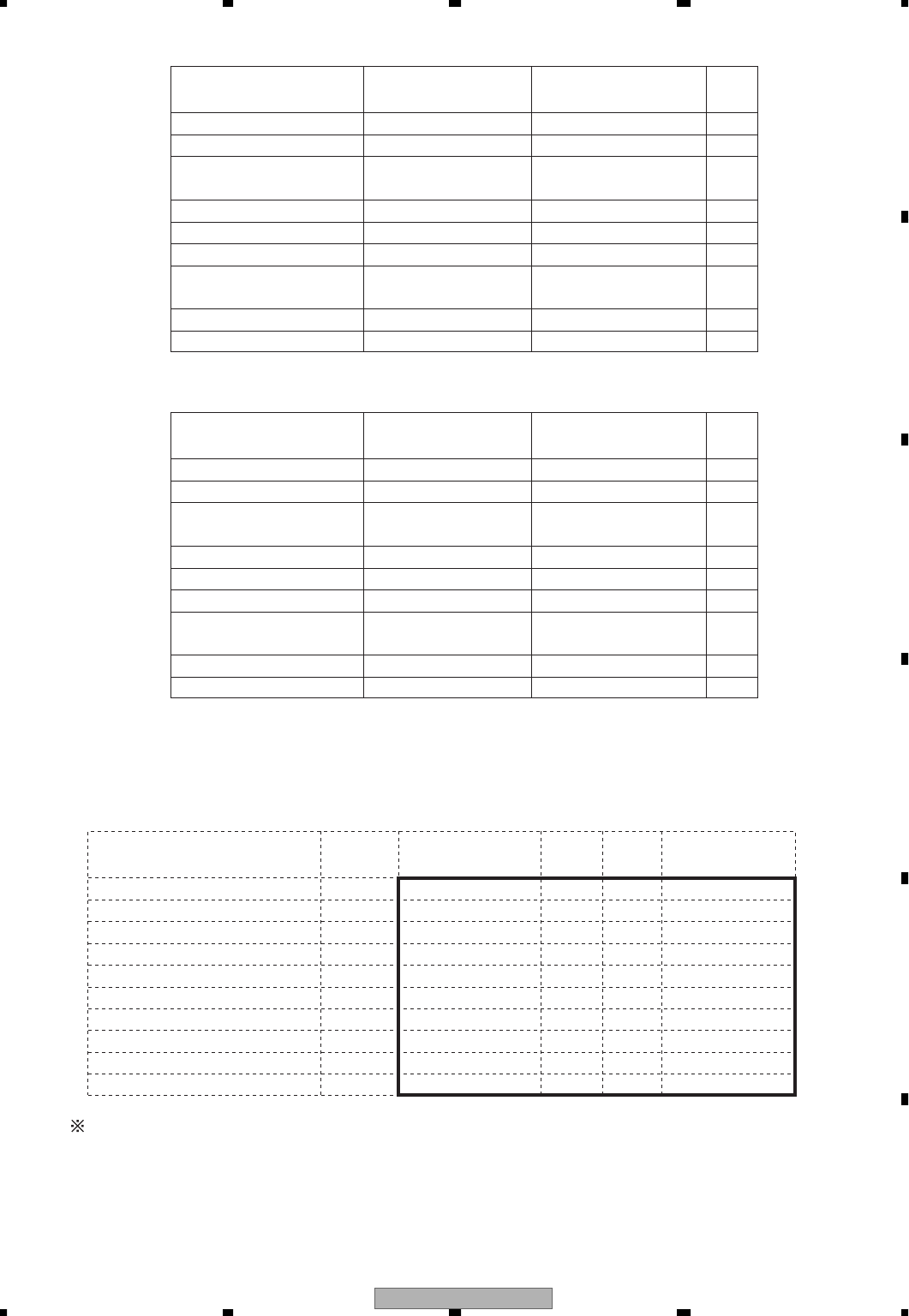
AVIC-Z1/UC 179
5678
5678
C
D
F
A
B
E
15
14
•
•
9
8
7
•
•
Indicated value (=Adjusted value)
(DEC)
1
0
15
14
•
•
9
8
7
•
•
EEPROM written value
(DEC)
1
0
0111
0110
•
•
0001
0000
1111
•
•
Double screen IC register value
(BIN)
1001
1000
(MAX)
(TYP)
(MIN)
[R,G,BOUT BIAS]
63
62
•
•
33
32
31
•
•
Indicated value (=Adjusted value)
(DEC)
1
0
63
62
•
•
33
32
31
•
•
EEPROM written value
(DEC)
1
0
011111
011110
•
•
000001
000000
111111
•
•
Double screen IC register value
(BIN)
100001
100000
(MAX)
(TYP)
(MIN)
[RGB,CMP CNTRST]
■ Line adjustment 2 mode
RGB & YS horizontal alignment [0-255] DOT H POSIT 63
YS sampling phase 1 [0-15] YS SAMPL 8
AD sampling phase B [0-15] B SAMPL 8
AD sampling phase G [0-15] G SAMPL 8
AD sampling phase R [0-15] R SAMPL
YS internal delay adjustment [0-15] YS DELAY
Settings
Adjustment
range
Item display
Adjusted value
Written value
(DEC)
CS FFFF
LINE2
8
8
■ Note 1: Be aware that [YS, R, G, B SAMPL] and [YS DELAY] have different indicated values/EEPROM written
values and double window IC(TC90A96FG-P) register set values.
(As the double window IC register values and the screen output are not related linearly,
software is used for conversion.)
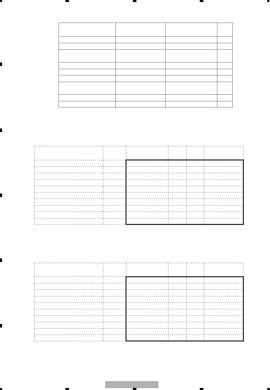
AVIC-Z1/UC
180
1234
1234
C
D
F
A
B
E
■ Line adjustment 3 mode
Dot search threshold [0-255] TH DOT 112
YS search threshold [0-4] TH YS 3
Phase search threshold [0-255] TH PHASE 112
Xdisp [0-63] X DISP 32
YSdisp [0-4] YS DISP
Settings
Adjustment
range
Item display
Adjusted value
Written value
(DEC)
CS FFFF
2
■ Line adjustment 4 mode
Main horizontal enhancer gain [0-3] M H GAIN 0
Main horizontal enhancer limiter [0-3] M H LIMIT 0
Main horizontal enhancer f0 [0-1] M H F0 0
Main vertical enhancer gain [0-3] M V GAIN 0
Main vertical enhancer loopback [0-3] M V ORI
Main vertical enhancer coring [0-3] M V CORE
Settings
Adjustment
range
Item display
Adjusted value
Written value
(DEC)
CS FFFF
LINE4
0
0
LINE3
15
14
•
•
9
8
7
•
•
Indicated value (=Adjusted value)
(DEC)
1
0
15
14
•
•
9
8
7
•
•
EEPROM written value
(DEC)
1
0
0111
0110
•
•
0001
0000
1111
•
•
Double screen IC register value
(BIN)
1001
1000
(MAX)
(TYP)
(MIN)
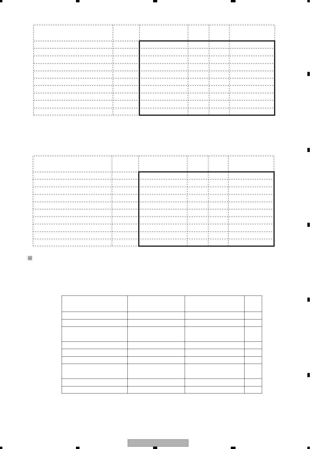
AVIC-Z1/UC 181
5678
5678
C
D
F
A
B
E
■ Line adjustment 5 mode
Sub horizontal enhancer gain [0-3] S H GAIN 1
Sub horizontal enhancer limiter [0-3] S H LIMIT 1
Sub horizontal enhancer f0 [0-1] S H F0 1
Sub vertical enhancer gain [0-3] S V GAIN 2
Sub vertical enhancer loopback [0-3] S V ORI
Sub vertical enhancer coring [0-3] S V CORE
Settings
Adjustment
range
Item display
Adjusted value
Written value
(DEC)
CS FFFF
LINE5
1
2
Brightness R [0-63] BRIGHT R 16
Brightness G [0-63] BRIGHT G 16
Brightness B [0-63] BRIGHT B 16
γ correction ON/OFF
[0-7]
GAMMA OFF
RGB simultaneous γ 1 inflection point
[0-63] GAMMA 1 0
RGB simultaneous γ 2 inflection point
[0-31] GAMMA 2 4
RGB simultaneous γ 3 inflection point
[0-31] GAMMA 3 1
RGB simultaneous γ gradient A [0-7] GAMMASLP A 4
FFFFCS
Settings
Adjustment
range
Item display
Adjusted value
Written value
(DEC)
LINE6
■ Line adjustment 6 mode
RGB simultaneous γ gradient B
RGB simultaneous γ gradient C [0-7]
GAMMASLP B 1
GAMMASLP C 1
■ Note 1: Be aware that [BRIGHT R, G, B] have different indicated values/EEPROM written values and double
window IC(TC90A96FG-P) register set values.
(As the double window IC register values and the screen output are not related linearly,
software is used for conversion.)
63
62
•
•
33
32
31
•
•
Indicated value (=Adjusted value)
(DEC)
1
0
63
62
•
•
33
32
31
•
•
EEPROM written value
(DEC)
1
0
011111
011110
•
•
000001
000000
111111
•
•
Double screen IC register value
(BIN)
100001
100000
(MAX)
(TYP)
(MIN)
[BRIGHT R,G,B]
AVIC-Z1/UC
182
1234
1234
C
D
F
A
B
E
■ Line adjustment 7 mode
Main PLL 0 [0-255] MAIN PLL 0 158
Main PLL 1 [0-255] MAIN PLL 1 13
Main PLL 2 [0-255] MAIN PLL 2 204
Main PLL 3 [0-255] MAIN PLL 3 4
Settings
Adjustment
range
Item display
Adjusted value
Written value
(DEC)
CS FFFF
LINE7
Sub PLL 0 for TV [0-255] SUB PLL 0 TV 140
Sub PLL 1 for TV [0-255] SUB PLL 1 TV 136
Sub PLL 0 for others [0-255] SUB PLL 0 140
Sub PLL 1 for others SUB PLL 1 141
Sub PLL 2 for TV [0-255] SUB PLL 2 TV 100
Sub PLL 3 for TV [0-255] SUB PLL 3 TV 68
PLL 2 for others [0-255] SUB PLL 2 152
PLL 3 for others [0-255] SUB PLL 3 135
FFFFCS
Settings
Adjustment
range
Item display
Adjusted value
Written value
(DEC)
LINE8
■ Line adjustment 8 mode
[0-255]
SA46 UPPER [0-255] SA46H UPPER 0
SA46 LOWER [0-255] SA46H LOWER 0
SA47 UPPER [0-255] SA47H UPPER 0
SA47 LOWER
[0-255]
SA47H LOWER 0
SA48 UPPER [0-255] SA48H UPPER 0
SA48 LOWER [0-255] SA48H LOWER 0
SA49 UPPER [0-255] SA49H UPPER 0
SA49 LOWER [0-255] SA49H LOWER 0
FFFFCS
Settings
Adjustment
range
Item display
Adjusted value
Written value
(DEC)
LINE9
■ Line adjustment 9 mode
SA4A UPPER
SA4A LOWER [0-255]
SA4AH UPPER 0
SA4AH LOWER 0
[0-255]
SA4B UPPER [0-255] SA4BH UPPER 0
SA4B LOWER [0-255] SA4BH LOWER 0
SA4C UPPER [0-255] SA4CH UPPER 0
SA4C LOWER
[0-255]
SA4CH LOWER 0
SA4D UPPER [0-255] SA4DH UPPER 0
SA4D LOWER [0-255] SA4DH LOWER 0
SA4E UPPER [0-255] SA4EH UPPER 0
SA4E LOWER [0-255] SA4EH LOWER 0
FFFFCS
Settings
Adjustment
range
Item display
Adjusted value
Written value
(DEC)
LINE10
■ Line adjustment 10 mode
SA4F UPPER
SA4F LOWER [0-255]
SA4FH UPPER 0
SA4FH LOWER 0
[0-255]
AVIC-Z1/UC 183
5678
5678
C
D
F
A
B
E
■ Note 1: Data on the dimmer points (coordinates) is memorized in EEPROM, however, it is not used in
CS calculation because it is user-configurable.
■ Parameter setting mode for DIMMER
Backlight output max value [0-255] BL MAX
59
Backlight output min value [0-255] BL MIN
C4
Dimmer threshold value (High) [0-255] REF H C0
Dimmer threshold value (Low) [0-255] REF L 60
Outside light point (High) [0-255] LUM H E2
Outside light point (Middle) [0-255] LUM M 87
Outside light point (Low) [0-255] LUM L 52
Backlight point (High) [0-255] BL H C4
Backlight point (Middle) [0-255] BL M C4
Backlight point (Low) [0-255] BL L 68
Settings
Adjustment
range
Item display
Adjusted value
Written value
(HEX)
FFFF
DIMMER
CS
[Operation specification]
•Turn ACC on with [SRV/SRVA] terminal Low, and [Adjustment mode for services] will start.
•In the order of ACC OFF→ON (BUP OFF→ON), cancel [Adjustment mode for services].
•Use [ ] [→] keys for adjustment.
It is possible to move to the adjustment mode from 6.6 Monitor Test Mode or 6.7 Test Disc Monitor adjustment.
Set values are read out after they are written in EEPROM and the read-out values shall be displayed.
Writing and reading shall be done in 16 bit unit.
● Adjustment mode for services
Examples of actual OSD display are shown inside the heavy line frame.
Numeric values in the common inverse output center value are changed by adjustment.
(The example inside the heavy line frame shows MAX value.)
The FACTORY numerical value is the default for using in the line for adjustment.
(Rewritable in EEPROM setting mode)
This default value is not a set value for each product, however setting to this value will work out OK in most cases.
■ Adjustment mode for services
■ Note 1: CS display is not performed
Common inverse output center value
[0-255] COM DC 92
Settings
Adjustment
range
Item display
Adjusted value
Written value
(DEC)
Common inverse output center set value
[0-255] [FACTORY 92 ]
(Factory value)
↓
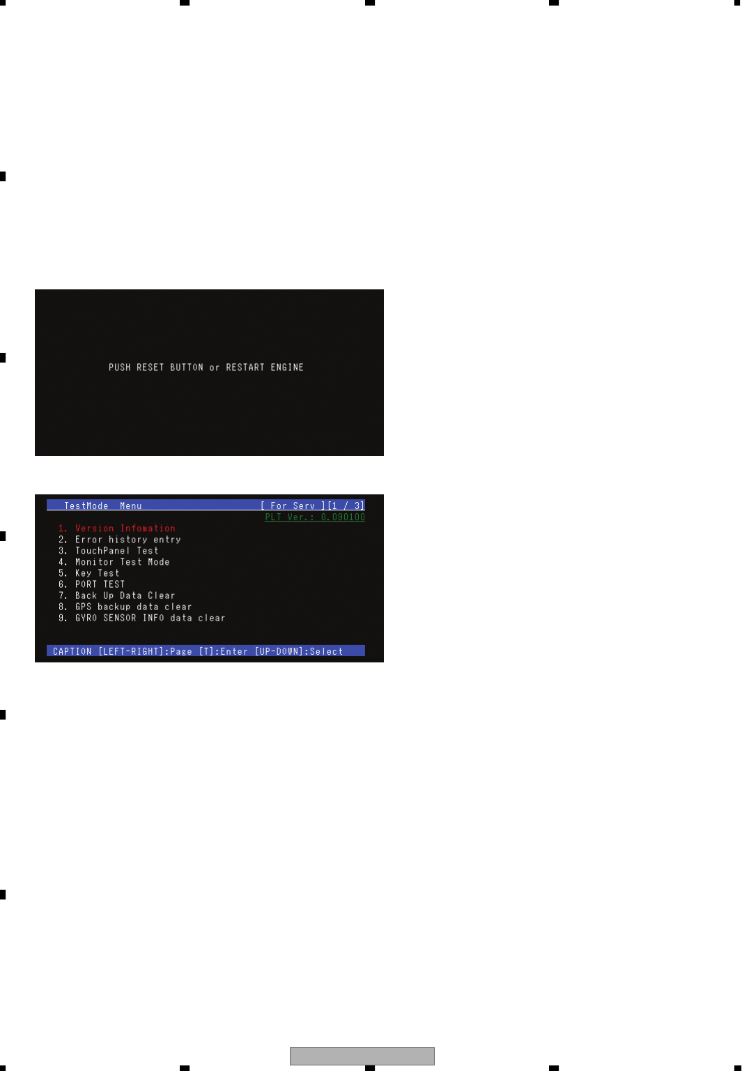
AVIC-Z1/UC
184
1234
1234
C
D
F
A
B
E
6.6 TEST MODE
06 Overseas Navigation Test Mode Ver 1.00
1. Test mode startup procedure
1. Press the RESET and EJECT buttons simultaneously while +Battery, ACC ON.
2. Release only the RESET button.
3. Release the EJECT button when the password input screen is displayed.
4. Input the password.
5. Test mode menu will be displayed when the password matches.
<<Password for Service Division>>
Input the password from the keys in the order of [P.LIST▲]→[P.LIST▲]→[P.LIST▼]→[P.LIST▼]→[TRFC(TA/NEWS)]
Password input screen
When the password is OK
When the password is NG
The password input screen remains.
2. Test mode menu selection procedure
Select an optional menu using the main unit keys [P.LIST▲] and [P.LIST▼] and execute it by the [TRFC(TA/NEWS)] key.
Move through the page using the main unit key [TRK].
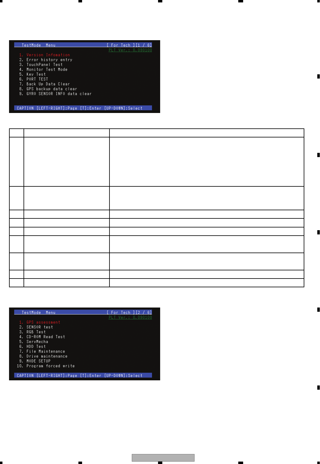
AVIC-Z1/UC 185
5678
5678
C
D
F
A
B
E
3. Test mode menu
[PAGE 1]
[PAGE 2]
No
1
9
Version Infomation
GYRO SENSOR INFO data clear
Test item
Error history entry
3 TouchPanel Test
Monitor Test Mode
Key Test
Display of various data
♦Navigation platform, navigation platform recovery image, boot loader,
CPU core, application program and GPS program versions
♦Navigation destination data, TV model information, information for GPS
destination, hard disk version data, volume data
♦Machine microcontroller (core application), monitor microcontroller (version,
ROM COLLE), system microcontroller (version, ROM COLLE) data
Deletion of learned values in gyro sensor
Description of test
Display of error history for driver and system software contained in
RAM/FLASH, display of forced reset error history, serial output switching
for copying, deleting and debugging
Test on touch panel coordinates
Adjustment of regulation and calibration
Test on main unit keys
6 PORT TEST
Back Up Data Clear
GPS backup data clear
2
4
5
7
8
Display of CF card door sensor, illumination, parking, reversing and
vehicle speed pulse conditions
Initialization of the backup variable used in device driver/class library and
system restart at completion
Initialization of backup variables used in GPS
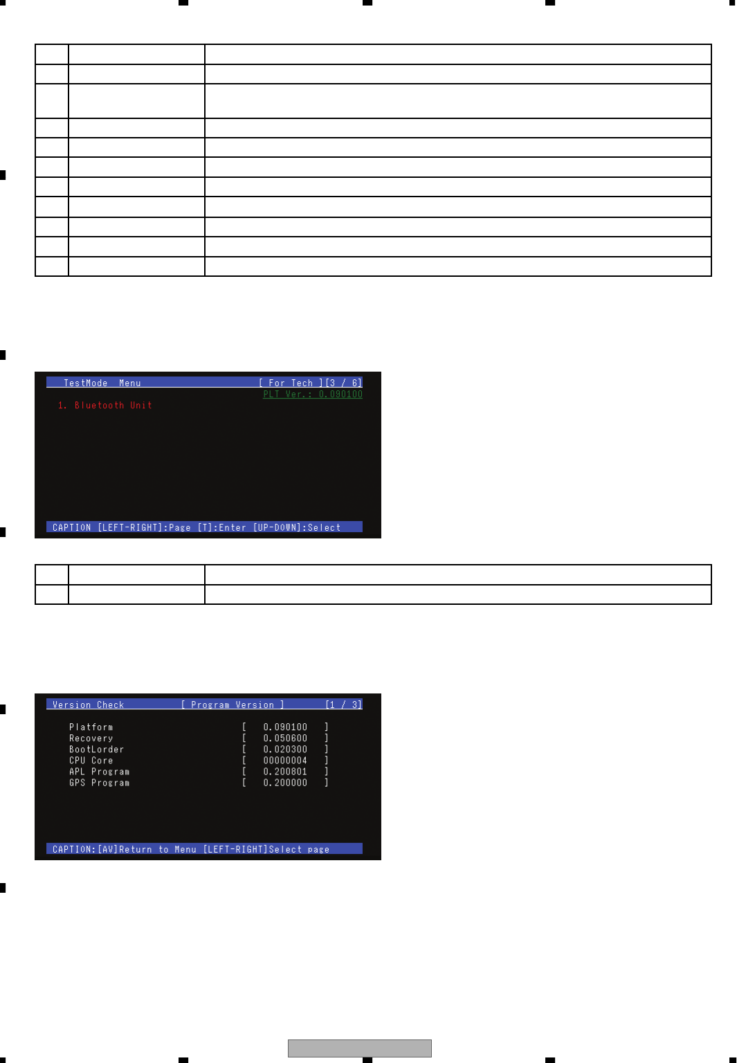
AVIC-Z1/UC
186
1234
1234
C
D
F
A
B
E
[PAGE 3]
No
1
10
GPS assessment
Profram forced write
Test item
SENSOR test
3 RGB Test
CD-ROM Read Test
ServMecha
Display of GPS conditions
Forced rewriting of PLT (platform), APL (application) software, GPS (GPS) program
Description of test
Display of G sensor, gyro value, power supply voltage value, temperature and attachment
conditions
Display in order of red (FULL)→green (FULL)→blue (FULL)→white (FULL)→color pattern
CD-ROM decoder testing
Various tests on the machine
6 HDD Test
File Maintenance File Maintenance
Drive maintenance
2
4
5
7
8
HDD data display, read and write test
Drive data display, scan disk (volume verification)
MODE SETUP9 HDD setup
No
1Bluetooth Unit
Test item
Bluetooth unit test and firmware updating are implemented.
Description of test
Specifications of 06 Overseas Navigation Test Mode Version Display
■ Version information screen [PAGE 1]
<<Key operation>>
[ TRK> ] ¥ ¥ ¥ ¥Proceeds to the next page.
[ AV ] ¥ ¥ ¥ ¥ ¥ ¥ ¥ ¥
Escapes from the version information display screen and returns to the menu screen.
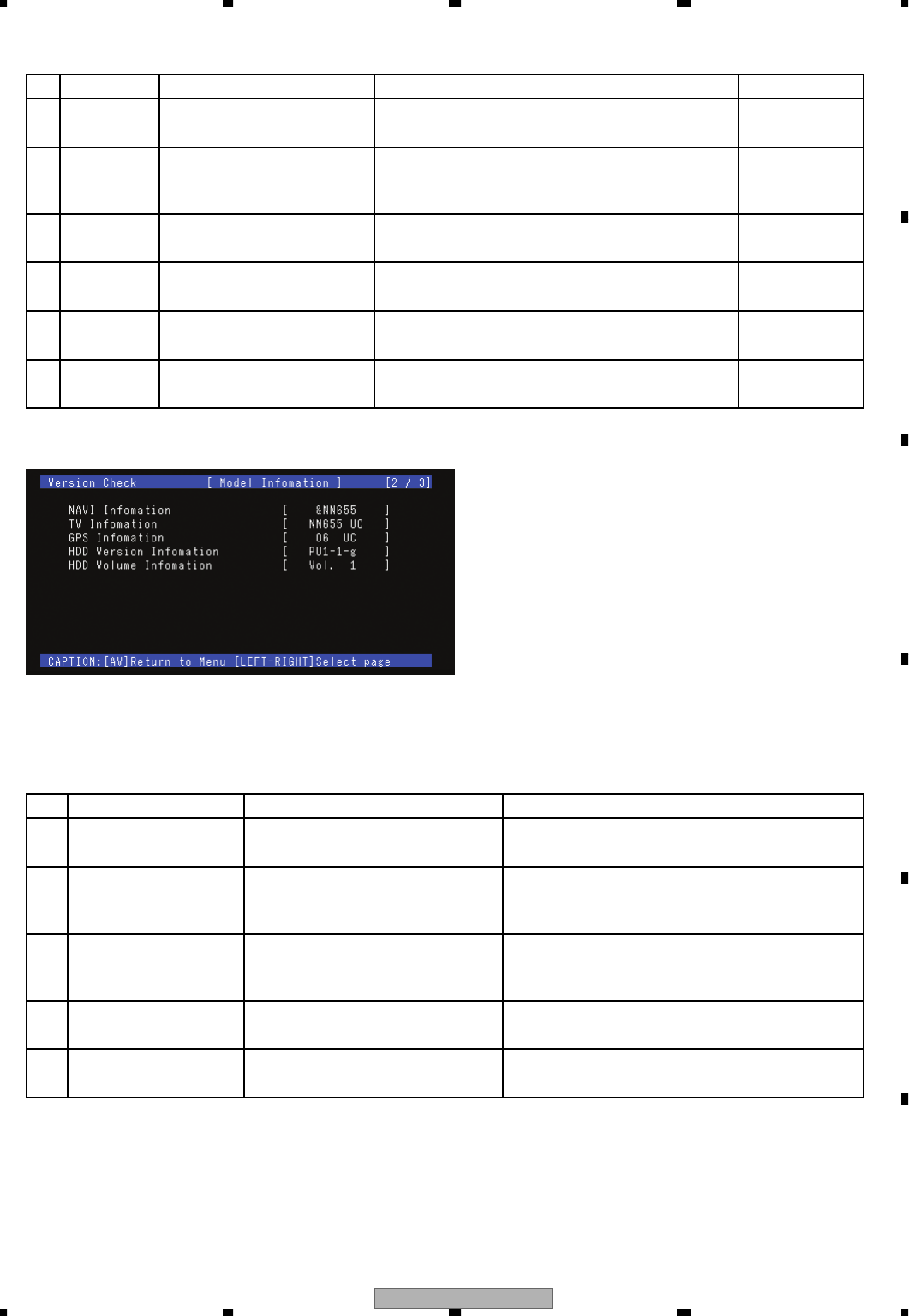
AVIC-Z1/UC 187
5678
5678
C
D
F
A
B
E
No
1
Platform
Item
Recovery
3
BootLorder
CPU Core
APL Program
[ *.****** ]→Version for system software OS block (FLASH)
[ UNKNOWN ]→Version acquisition failure or no program
Information displayed
[ *.****** ]→Version of the recovery software in
system software OS block (FLASH)
[ UNKNOWN ]→Version acquisition failure or no program
[ *.****** ]→Version of the boot loader block
[ NG ]→Version acquisition failure or no program
[ ******** ]→Version of the CPU core block
[ NG ]→Version acquisition failure
[ *.****** ]→Version of the application program
[ UNKNOWN ]→Version acquisition failure
6
GPS Program
[ *.****** ]→Version of the GPS program
[ UNKNOWN ]→Version acquisition failure
Displays the version for the system
software OS block (FLASH).
Item description
Displays the version of the
recovery software in system
software OS block (FLASH).
Displays the version of the
boot loader block (FLASH).
Displays the CPU version
Displays the version of
application program (HDD)
Displays the version of
GPS program (GIDRA).
EU060PLT.EXE
File name
EU060PLT.EXE
EU060APL.EXE
EU060GPS.EXE
2
4
5
Description of items
■ Version information screen [PAGE 2]
<<Key operation>>
[ TRK> ] • • • •Proceeds to the next page.
[ AV ] • • • • • • • •Escapes from the version information display screen and returns to the menu screen.
No
1 NAVI Information
Item
TV Information
3 GPS Information
HDD Version Information
HDD Volume Information
[ &NN*** ]→Navigation model information
[ UNKNOWN ]→Information acquisition failure
Information displayed
[ NN655 UC ]→NN655
[ NN656 EW ]→NN656
[ UNKNOWN ]→Information acquisition failure
[ 06 UC ]→NN655GPS unit is connected.
[ 06 EW ]→NN656GPS unit is connected.
[ UNKNOWN ]→Information acquisition failure
[ ***-*-* ]→Hard disk version
[ UNKNOWN ]→Information acquisition failure
[ Vol.* ]→Volume information
[ Vol.0 ]→Information acquisition failure
Displays the navigator destination
information.
Item description
Displays the TV model information.
Displays the GPS destination
information.
Displays the hard disk version
Displays the volume information.
2
4
5
Description of items
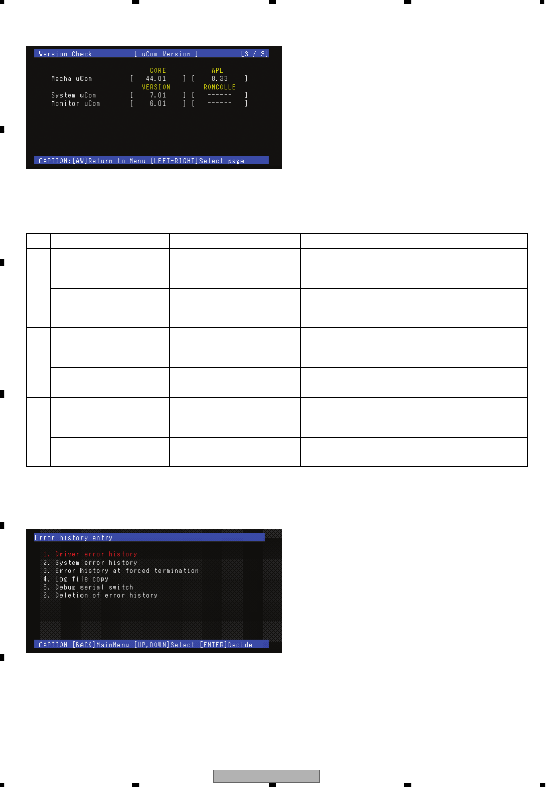
AVIC-Z1/UC
188
1234
1234
C
D
F
A
B
E
No
1 Mecha uCom Core
Item
Mecha uCom APL
2 System uCom VERSION
System uCom ROMCOLLE
Monitor uCom VERSION
[ **.** ]→Core version for machine microcontroller
[ UNKNOWN ]→Communication with machine
microcontroller is not established.
Information display
[ **.** ]→
Application version for machine microcontroller
[ UNKNOWN ]→Communication with machine
microcontroller is not established.
[ **.** ]→Version of the system microcontroller
[ UNKNOWN ]→Communication with the system
microcontroller is not established.
[ **.** ]→
ROM COLLE version for system microcontroller
[ - - - - - - ]→No ROM COLLE version
[ **.** ]→Version of the monitor microcontroller
[ UNKNOWN ]→Communication with system
microcontroller is not established.
Displays the core version for
machine microcontroller.
Description of item
Displays the application
version for machine
microcontroller.
Displays the version
for system microcontroller.
Displays the ROM COLLE version
for system microcontroller.
Displays the version of the
monitor microcontroller.
Monitor uCom ROMCOLLE [ **.** ]→
ROM COLLE version for monitor microcontroller
[ - - - - - - ]→No ROM COLLE version
Displays the ROM COLLE version
for monitor microcontroller.
3
■ Version information screen [PAGE 3]
<<Key operation>>
[ TRK> ] • • • •Proceeds to the next page
[ AV ] • • • • • • • •Escapes the version information display screen and returns to the menu screen.
Description of items
Specifications of 06 Overseas Navigation Test Mode Error History Entry Screen
● Error history menu screen
Select error history, history deletion, file copy or debug serial switch.
Select driver error/system error to move to reading drive selection screen.
Select error history at forced reset to move to forced reset error log display screen.
Select log file copy to move to media selection screen.
Select debug serial switch to move to debug serial switch screen.
Select deletion of error history to move to deletion of error history screen.
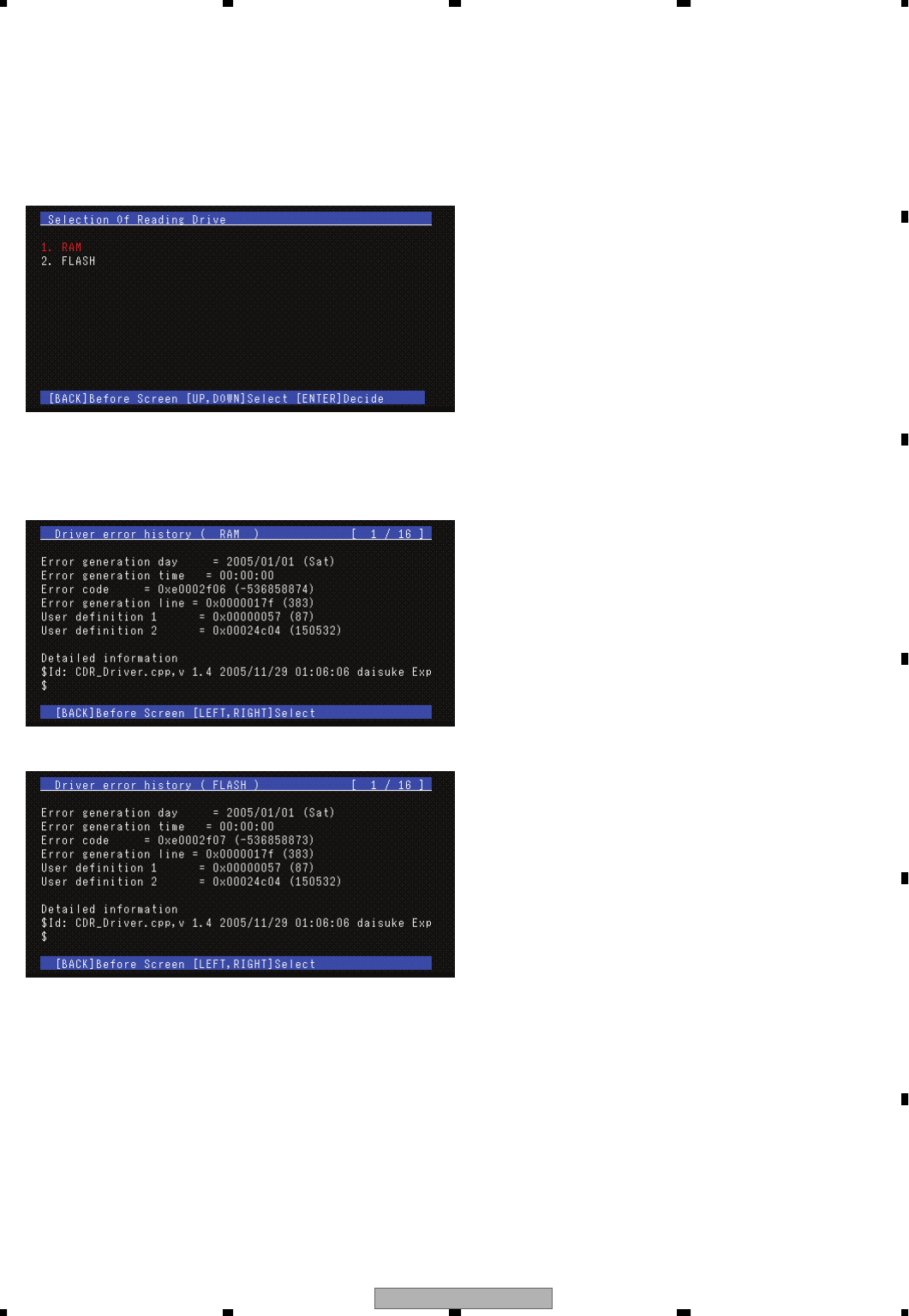
AVIC-Z1/UC 189
5678
5678
C
D
F
A
B
E
1. Reading drive selection screen (driver error, system error)
2. Forced termination error log display screen (forced termination error history)
3. Media selection screen (log file copy)
4. Debug serial switch screen (debug serial switch)
5. Deletion of error history selection screen (deletion of error history)
● Drive selection screen
1. Driver error
2. System error
● RAM drive driver error history screen
● FLASH drive driver error history screen
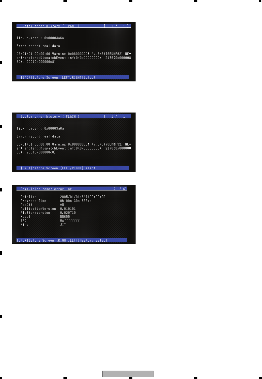
AVIC-Z1/UC
190
1234
1234
C
D
F
A
B
E
● RAM drive system error history screen
[Description]
♦Tick number : Counter value for beginning count from OS startup. 1 count is equivalent to 10msec.
● FLASH drive system error history screen
● Error history at forced reset
[Description]
♦DataTime : Date and time of forced reset
♦Progress Time : Time from forced reset to startup
♦AccOff : When there is a forced reset during AccOff process→ON Other cases→OFF
♦ApllicationVersion : Application version
♦PlatformVersion : Platform version
♦Model : Model name
♦SPC : Retreat program counter : Command address in case of exceptions (for CPU watchdog only)
♦Kind : Type of forced reset (JIT/CL/CPUWDT)
Press [Return] key to return to the menu.
[←→] to display history.
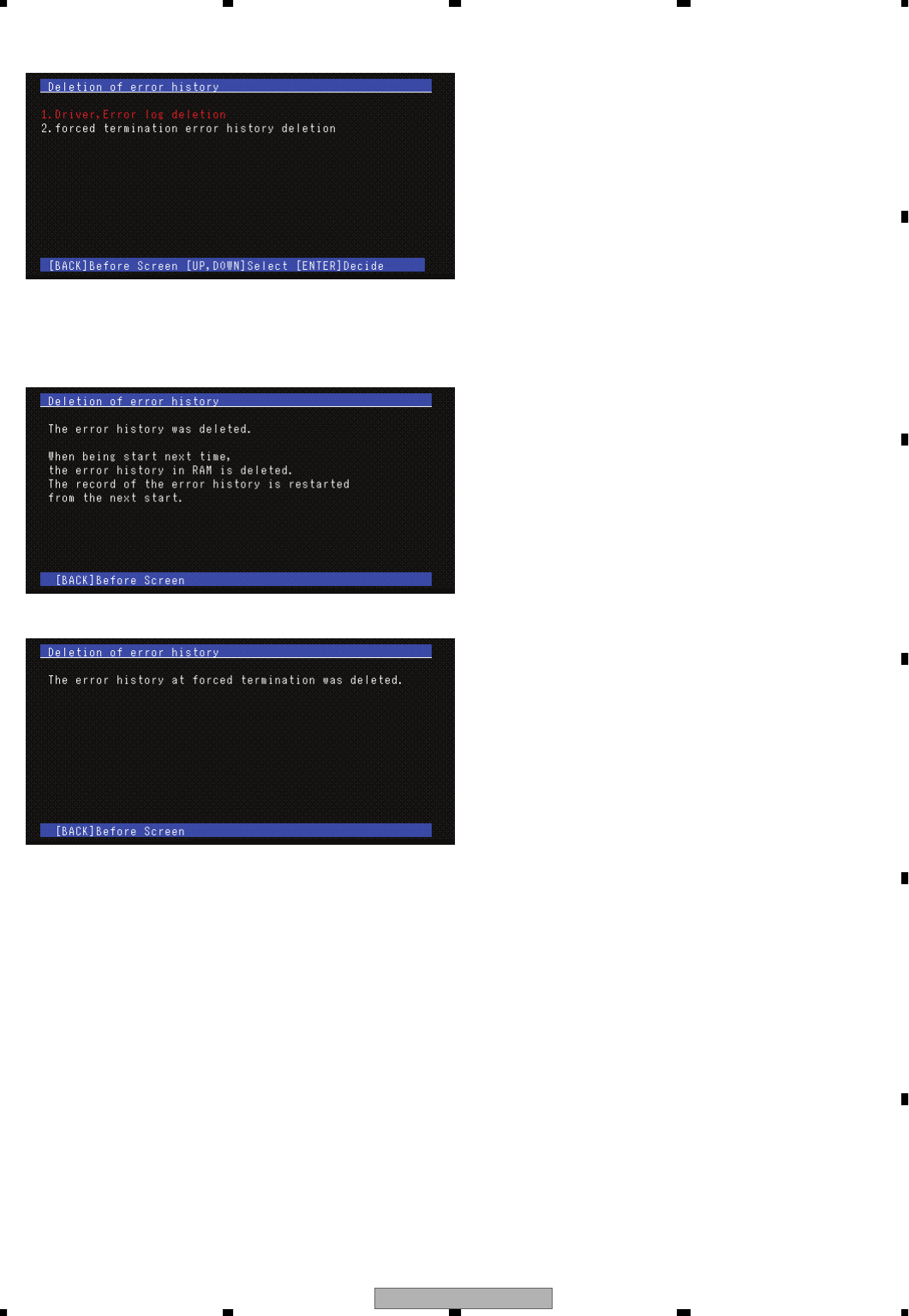
AVIC-Z1/UC 191
5678
5678
C
D
F
A
B
E
● Deletion of error history screen
1. Deletion of driver, and error log
2. Deletion of forced reset error history
● Deletion of driver/error log screen
● Deletion of error history at forced reset screen
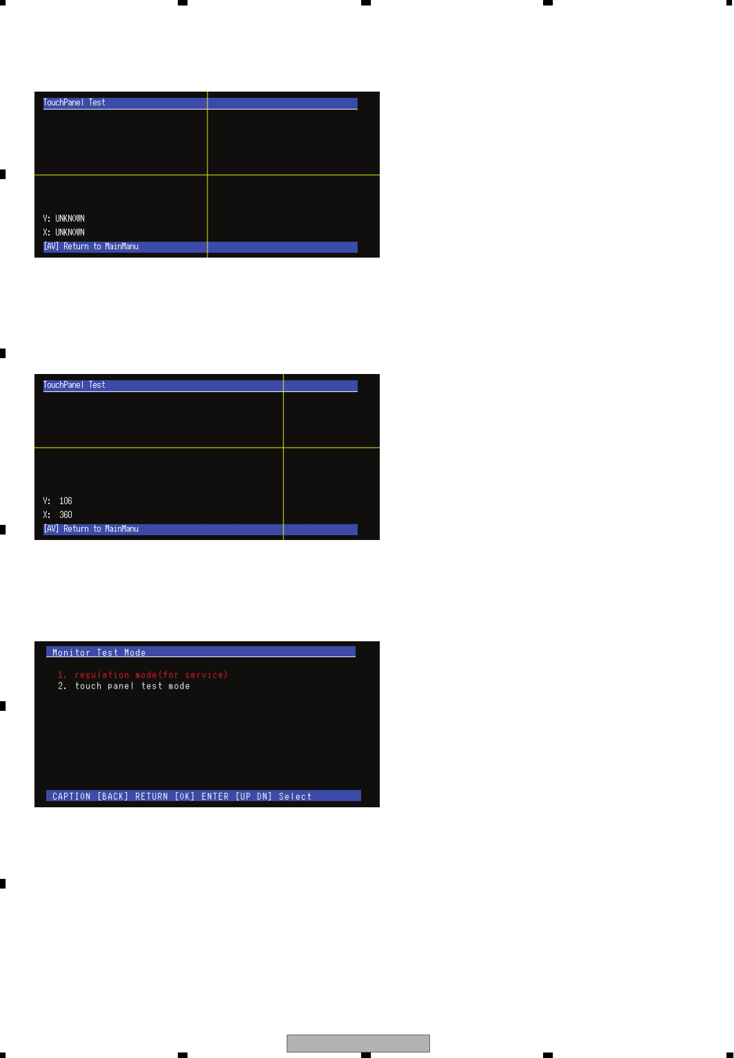
AVIC-Z1/UC
192
1234
1234
C
D
F
A
B
E
Test Mode Touch Panel Test Operation Specifications
● Touch panel test
•Description of operation
[AV] (main unit) key : Returns to the test mode main menu.
Touch panel : The coordinates of the pressed point will be displayed by 2-axis horizontal and vertical lines.
•By pressing an optional point on screen, the coordinates of the pressed point are displayed by 2-axis horizontal and
vertical lines. (In the initial condition after starting the test and before pressing the panel, the value display says
"UNKNOWN" and the lines are at the "center.")
Test Mode Monitor Test Mode Operation Specifications
● Monitor test mode menu
1.regulation mode(for service)
−Adjustment mode for service: Adjustable monitor setting value can be changed.
2.touch panel test mode
−Touch panel test mode: Settings related to touch panel such as calibration can be provided.
•Description of operation
[AV] (main unit) key : Returns to test mode main menu.
[TI] (main unit) key : Selects the item.
[P.LIST
↓ ] (main unit) key : Moves the cursor (selected line: red).
↓
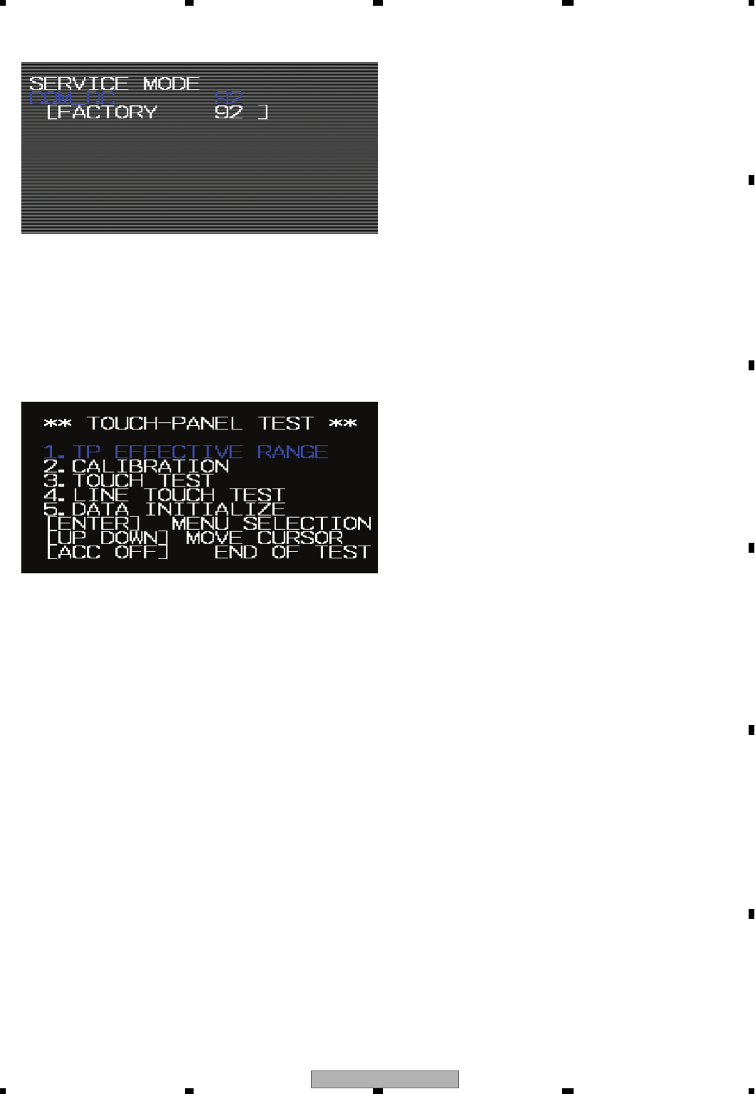
AVIC-Z1/UC 193
5678
5678
C
D
F
A
B
E
● Adjustment mode for service
COM DC
−Common inversion output center value: Line setting default value = 92
•Description of operation
[AV] (main unit) key : Returns to monitor test mode menu.
[TRK ←] (main unit) key : Moves DOWN the setting value.
[TRK →] (main unit) key : Moves UP the setting value.
● Touch panel test mode menu
1.TP EFFECTIVE RANGE
−Outermost rim test: Tests the outermost rim of the touch panel screen.
2.CALIBRATION
−Calibration: Calibration setting can be provided by pressing the cursor on screen successively.
3.TOUCH TEST
−Touch panel confirmation: Displays the status before and after pressing the touch panel.
4.LINE TOUCH TEST
−Line touch panel test: OK/NG judgment for touch panel is made by pressing the cursor on screen.
5.DATA INITIALIZE
−Data initialization: Returns the outermost rim and calibration data to the initial values.
•Description of operation
[AV] (main unit) key : Returns to monitor test mode menu.
[Navigation] (main unit) key : Selects the item.
[P.LIST
↓ ] (main unit) key : Moves the cursor (selected line: blue).
↓
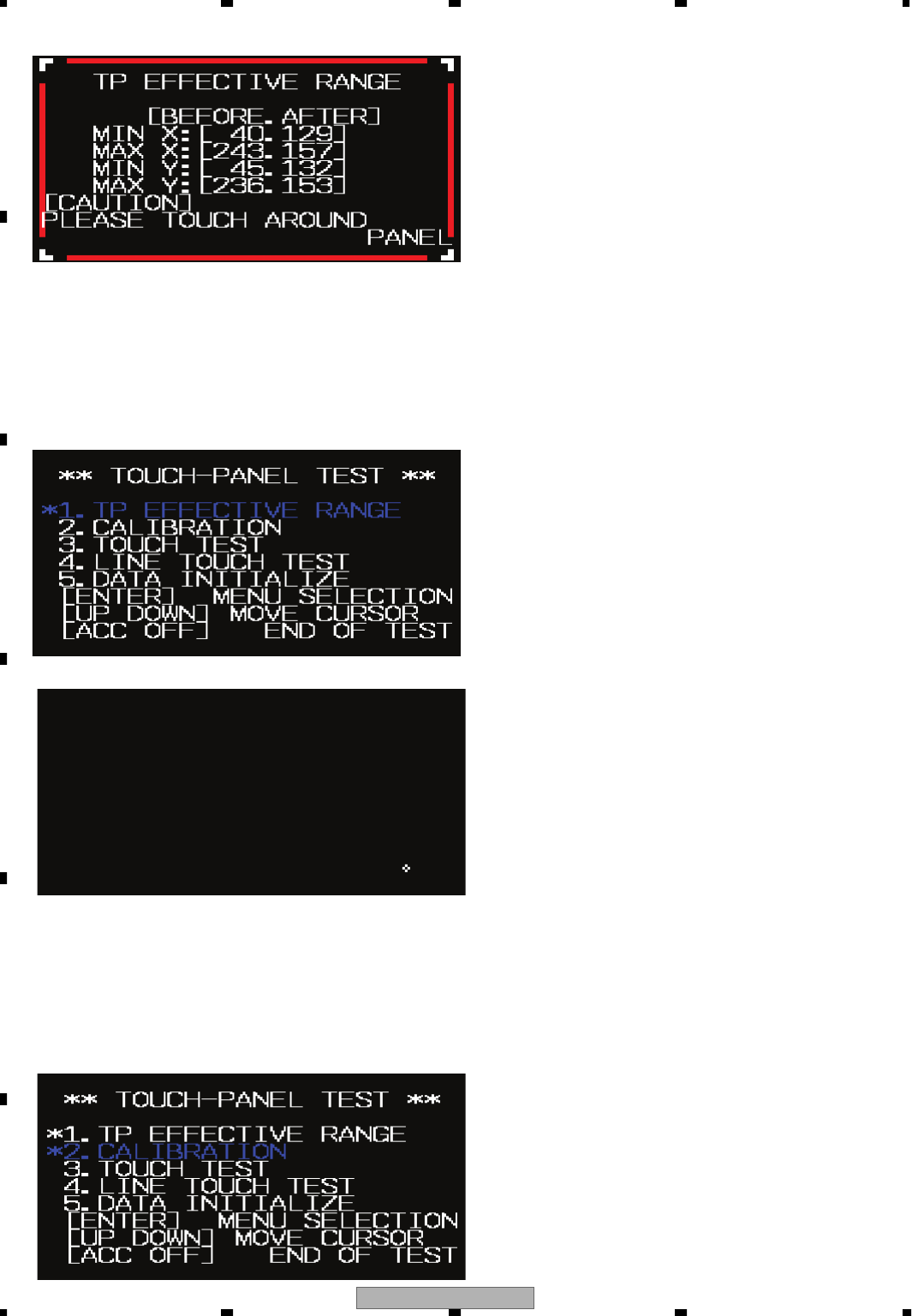
AVIC-Z1/UC
194
1234
1234
C
D
F
A
B
E
● Outermost rim test
• Description of operation
[AV] (main unit) key : Returns to monitor test mode menu.
[Navigation] (main unit) key : Terminates setting.
Touch panel : Outermost rim is set up by touching the range than can be pressed (outer rim).
• "OK" is displayed for about 2 seconds when it is successful and "NG" when it fails, and the system returns to
the touch panel test mode menu.
• When successful, "*" is displayed on the left of "1. TP EFFECTIVE RANGE" of the touch panel test mode menu.
• Description of operation
[AV] (main unit) key : Returns to monitor test mode menu.
[Navigation] (main unit) key : Escapes from setting.
Touch panel : Calibration is set up by pressing the cursor on screen successively.
• "FINISHED" is displayed for about 2 seconds when touching at 17 points has been completed and "NG" when it is closed
by pressing the [Navigation] key during calibration, and the system returns to the touch panel test mode menu.
● Calibration
• When successful, "*" is displayed on the left of "2. CALIBRATION" of the touch panel test mode menu.
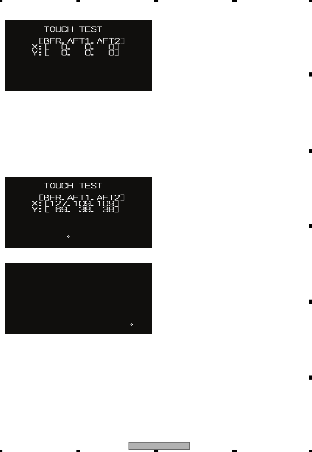
AVIC-Z1/UC 195
5678
5678
C
D
F
A
B
E
• Description of operation
[AV] (main unit) key : Returns to monitor test mode menu.
[Navigation] (main unit) key : Returns to touch panel test mode menu.
Touch panel : An optional point on screen is pressed.
• The coordinates for the pressed point are displayed as values and cursor.
[BFR] : The value of the A/D value from the touch panel.
These values are not indicated the X-Y coordinate
on the monior.
[AFT1] : After compensation by Factory setting.
[AFT2] : After compensation by User setting.
● Touch panel confirmation
• Description of operation
[AV] (main unit) key : Returns to monitor test mode menu.
[Navigation] (main unit) key : Escapes from the test.
Touch panel : Test is executed by pressing the cursor on screen successively.
● Line touch panel test
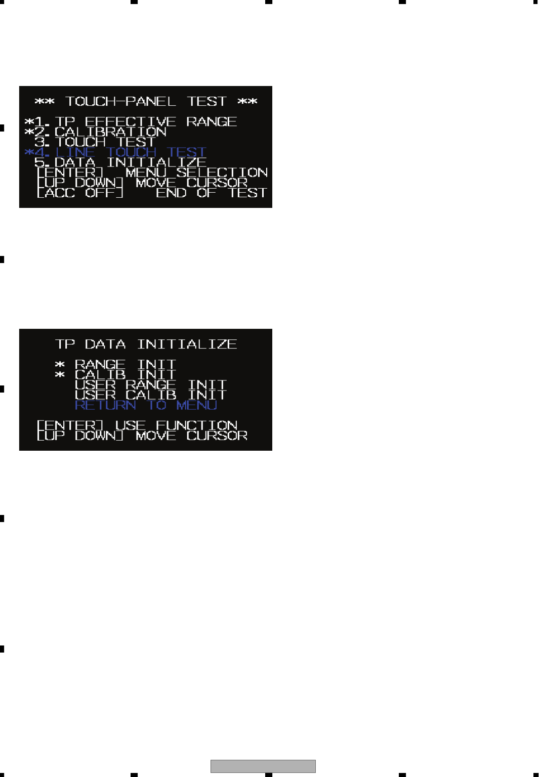
AVIC-Z1/UC
196
1234
1234
C
D
F
A
B
E
•
"Cursor turns red" if the displayed cursor position cannot be pressed, and it moves to the "next cursor" when it is pressed properly.
• When successful, "*" is displayed on the left of "4. LINE TOUCH TEST" of the touch panel test mode menu.
• "OK" is displayed for about 2 seconds when touching is completed at 17 points and "NG" when it is closed by pressing
the [Navigation] key during test, and it returns to the touch panel test mode menu.
● Data initialization
RANGE INIT
− Initialization of outermost rim setting: Initializes the outermost rim setting obtained in monitor test mode.
CALIB INIT
− Initialization of calibration correction: Initializes the calibration correction obtained in monitor test mode.
USER RANGE INIT
− Initialization of user setting outermost rim: Initializes the outermost rim set up by the user.
USER CALIB INIT
− Initialization of user calibration correction: Initializes the calibration correction set up by the user.
RETURN TO MENU
− Return to menu: The system returns to the touch panel test mode menu.
• Description of operation
[AV] (main unit) key: Returns to monitor test mode menu.
[Navigation] (main unit) key: Executes the item.
[P.LIST
↓ ] (main unit) key: Moves the cursor (selected line: blue).
↓
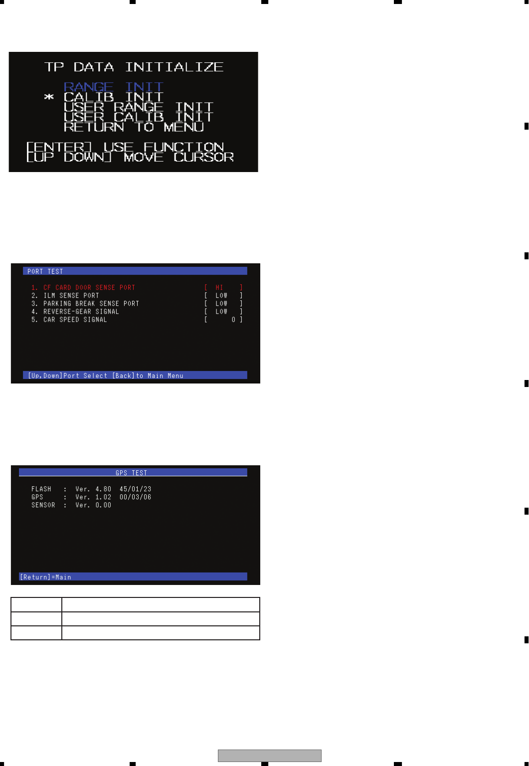
AVIC-Z1/UC 197
5678
5678
C
D
F
A
B
E
• If "*" is shown on the right of an item, the item has already been set up or corrected. Match the cursor there and
execute initialization to eliminate "*" (ex.: initialization of outermost rim).
Test mode port test specifications
● Port test screen
The status of each port is displayed as Hi / Low. The car speed pulse indicates the pulse number within the time unit.
Test Mode GPS Evaluation System Startup Screen Specifications
● Execution screen
FLASH Displays the version of DRAGON FLASH ROM.
GPS Displays the version of GPS.
Displays the version of the sensor.SENSOR
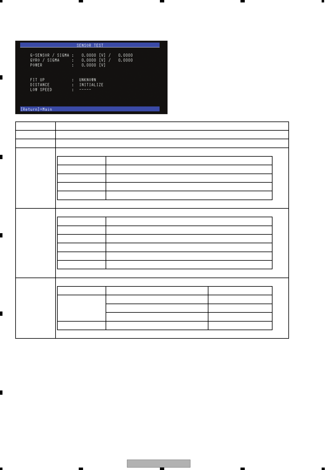
AVIC-Z1/UC
198
1234
1234
C
D
F
A
B
E
Specification of sensor test screen
● Test screen
G-SENSOR
GYRO Display of GYRO voltage value
Display of G sensor voltage value
Display of power supply voltage value
FIT UP Display of attachment status
Display of distance calculation status
Displays the minimum output speed for low-speed vehicle (depends on the DISTANCE status).
POWER
DISTANCE
LOW SPEED
Display Status
• NG Attachment position NG
Attachment position OK (third best)• OK
• OK(Better) Attachment position OK (second best)
Attachment position OK (best)• OK(Best)
Display Status
• INITIALIZE Sensor in initial learning
GPS distance (pulse unconnected with a model without G sensor)• GPS
• G-SENSOR G sensor distance (simple hybrid)
ND-PG1 distance• ND-PG1
Vehicle speed pulse distance• SPEED PULSE
DISTANCE status SPEED PULSE status
SPEED PULSE Learning low vehicle speed pulse
Low vehicle speed pulse OK
Low vehicle speed pulse NG
Display
CHECK
OK
NG xx [ km/h ]
− − − − −OTHERS
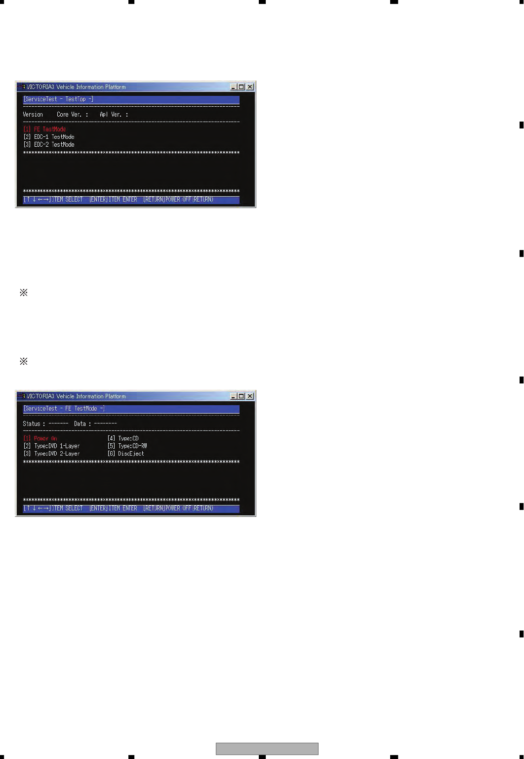
AVIC-Z1/UC 199
5678
5678
C
D
F
A
B
E
Test Mode Operation Specification Document for Mecha Service
1. About the test for Mecha service
[ Mecha ServiceTest - TestTop - ] screen
Mecha Version: Version of the macha used
[1] FE TestMode ¥ ¥ ¥ ¥ ¥ ¥ ¥ ¥
FE test mode startup
[2] EDC-1 TestMode ¥ ¥ ¥
EDC-1 mode (DVD only): EDC test is executed successively.
[3] EDC-2 TestMode ¥ ¥ ¥
EDC-2 mode (DVD only): EDC test is executed by the unit of blocks.
By pressing [Return] button on this screen, the system escapes from Mecha service test mode.
Though it may take some time in this case, do not press any key until the screen changes.
2. About FE test
If an error is displayed in Data, please turn the POWER OFF or restart the test mode.
[ Mecha ServiceTest - FE TestMode - ] screen
[1] Power On ¥ ¥ ¥ ¥ ¥ ¥ ¥ ¥ ¥ ¥ ¥ ¥ ¥
Execution of FE test (Power on after choosing inserted disc type.)
[2] Type:DVD 1-Layer ¥ ¥DVD 1-layer
[3] Type:DVD 2-Layer ¥ ¥DVD 2-layer
[4] Type:CD ¥ ¥ ¥ ¥ ¥ ¥ ¥ ¥ ¥ ¥ ¥ ¥ ¥ ¥ ¥
CD
[5] Type:CD-RW ¥ ¥ ¥ ¥ ¥ ¥ ¥ ¥ ¥
CD-RW
[6] DiscEject ¥ ¥ ¥ ¥ ¥ ¥ ¥ ¥ ¥ ¥ ¥ ¥ ¥ ¥
Disc ejection
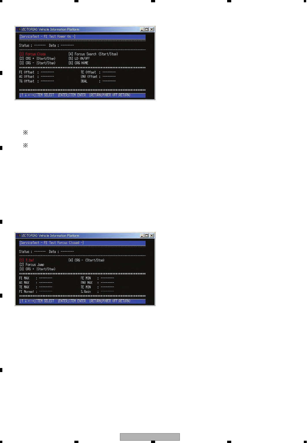
AVIC-Z1/UC
200
1234
1234
C
D
F
A
B
E
[ Mecha ServiceTest - FE Test Power On - ] screen
[1] T.Bal • • • • • • • • • • • • • • • • • • • •Adjusts the tracking balance.
[2] Forcus Jump • • • • • • • • • •Focus jump
[3] CRG + (Start/Stop) • •Moves the carriage to the rim or stops the carriage.
[4] CRG − (Start/Stop) • •Moves the carriage to the center or stops the carriage.
FE MAX : FE MAX level
AS MAX : AS MAX level
FE Normal : FE normalization coefficient
TE MAX : TE MAX level
FE MIN : FE MIN level
ENV MAX : ENV MAX level
TE MIN : TE MIN level
S.Gain : Spindle gain coefficient
[1] Forcus Close • • • • • • • • • • • • • • • • • • •Closes Focus.
[2] CRG + (Start/Stop) • • • • • • • • • • •Moves the carriage to the rim or stops the carriage.
[3] CRG − (Start/Stop) • • • • • • • • • • •Moves the carriage to the center or stops the carriage.
[4] Forcus Search(Start/Stop) • •Implements or stops focus search.
To close focus after focus search, turn the POWER OFF once and then turn the POWER ON again.
[5] LD-ON/OFF • • • • • • • • • • • • • • • • • • • •Implements LD-ON/OFF.
The system will turn LD-OFF automatically if no there is no operation for 10 seconds after LD-ON. If LD-ON is not
executed within 10 seconds even during focus search, LD-OFF will be executed in 9 seconds even if focus search
is executed after LD-ON.
[6] CRG HOME • • • • • • • • • • • • • • • • • • • •Returns the carriage to home position.
FE Offset : FE offset coefficient
AS Offset : AS offset coefficient
TG Offset : TG offset coefficient
TE Offset : TE offset coefficient
ENV Offset : ENV offset coefficient
DBAL : DBAL coefficient
[ Mecha ServiceTest - FE Test Focus Closed - ] screen
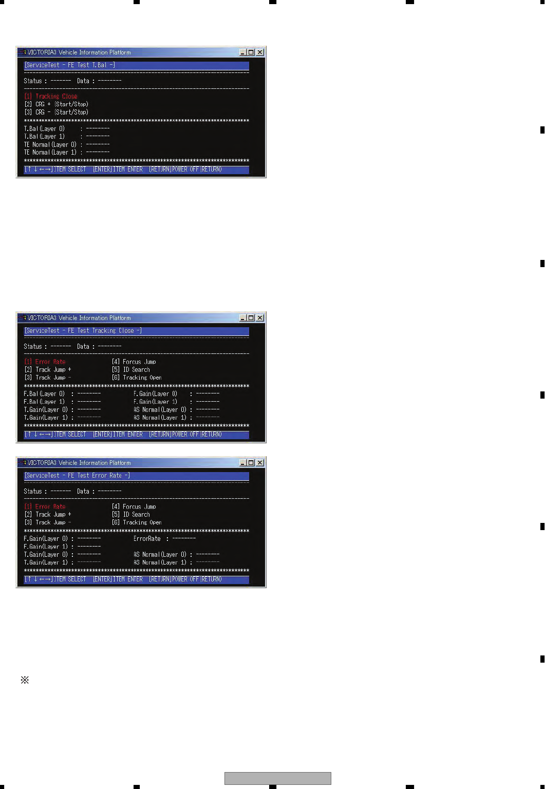
AVIC-Z1/UC 201
5678
5678
C
D
F
A
B
E
[ Mecha ServiceTest - FE Test T.Bal - ] screen
[1] Tracking Close • • • • • • • •Closes the tracking
[2] CRG + (Start/Stop) • • •Moves the carriage to the rim or stops the carriage.
[3] CRG − (Start/Stop) • • •Moves the carriage to the center or stops the carriage.
T.Bal (Layer 0) : TBAL coefficient (layer 0)
T.Bal (Layer 1) : TBAL coefficient (layer 1)
TE Normal (Layer 0) : TE normalization coefficient (layer 0)
TE Normal (Layer 1) : TE normalization coefficient (layer 1)
[ Mecha ServiceTest - FE Test Tracking Close - ] screen
[1] Error Rate • • • • • • • • •Implements measurement of error rate (no other operation is possible for approximately 10 seconds).
[2] Track Jump + • • • •Jumps by the specified number of tracks (in outer direction)
[3] Track Jump − • • • •Jumps by the specified number of tracks (in inner direction)
[4] Forcus Jump • • • • •Implements focus jump (DVD only)
[5] ID Search • • • • • • • • •Specifies ID Search (DVD only)
[6] Tracking Open • • •
Opens tracking (Focus closed status: Returns to [ Mecha ServiceTest - FE Test Focus Closed - ] screen.)
Play speed was fixed→L0 layer DVDx1.3-1.6CAV, CDx4CLV L1 layer DVDx1.3-1.6CAV
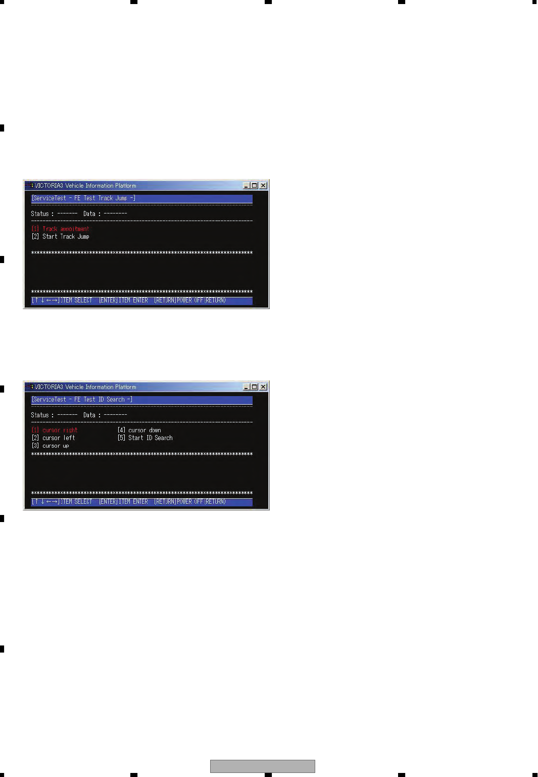
AVIC-Z1/UC
202
1234
1234
C
D
F
A
B
E
F.Bal (0) : FBAL coefficient (layer 0)
F.Bal (1) : FBAL coefficient (layer 1)
T.Gain (0) : Tracking gain coefficient (layer 0)
T.Gain (1) : Tracking gain coefficient (layer 1)
F.Gain (0) : Focus gain coefficient (layer 0)
F.Gain (1) : Focus gain coefficient (layer 1)
AS Normal (0) : AS normalization adjustment value (layer 0)
AS Normal (1) : AS normalization adjustment value (layer 1)
ErrorRate : Error rate
[ Mecha ServiceTest - FE Test Track Jump - ] screen
[1] Track appointment ¥ ¥ ¥Specification of track number (Mecha switches the 7 (DVD type), 5 (CD type) pattern cyclically.)
[2] Start Track Jump ¥ ¥ ¥Starts tracking jump (returns to [ Mecha ServiceTest - FE Test Tracking Close - ] screen).
[ Mecha ServiceTest - FE Test ID Search - ] screen
[1] cursor right ¥ ¥ ¥ ¥ ¥ ¥ ¥ ¥
Moves the cursor to the right.
[2] cursor left ¥ ¥ ¥ ¥ ¥ ¥ ¥ ¥ ¥
Moves the cursor to the left.
[3] cursor up ¥ ¥ ¥ ¥ ¥ ¥ ¥ ¥ ¥ ¥
Moves the cursor up.
[4] cursor down ¥ ¥ ¥ ¥ ¥ ¥
Moves the cursor down.
[5] Start ID search ¥ ¥ ¥Starts ID search (returns to [ Mecha ServiceTest - FE Test TrackingClose - ] screen).
3. About EDC test
EDC-1 Mode : Implements EDC test successively.
EDC-2 Mode : Implements EDC test by the unit of blocks.
Operation procedure is similar for EDC-1 and EDC-2.
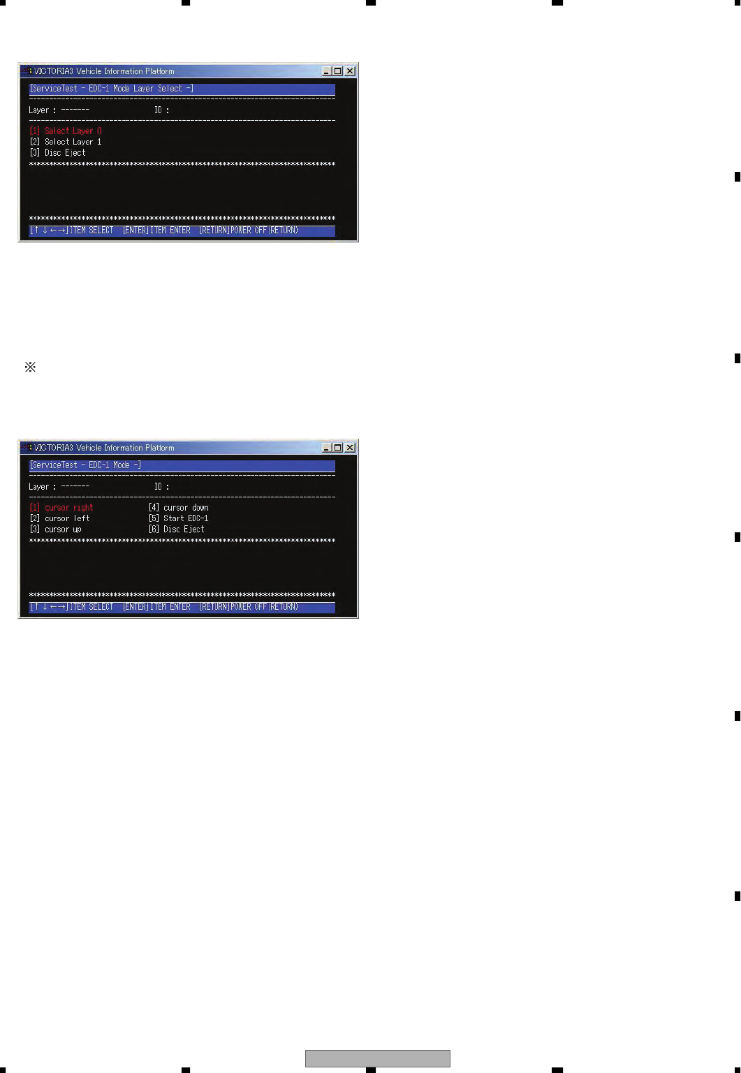
AVIC-Z1/UC 203
5678
5678
C
D
F
A
B
E
[ Mecha ServiceTest - EDC-1 mode Layer Select - ] screen
Layer : Currently tested layer
ID : Currently tested ID
[1] Select Layer 0 • • •Selects layer 0
[2] Select Layer 1 • • •Selects layer 1
[3] Disc Eject • • • • • • • •Ejects the disc.
The system escapes from the Mecha service test mode by pressing [Return] on this screen.
Though it may take some time in this case, do not press any key until the screen changes.
[ Mecha ServiceTest - EDC-1 mode - ]
Layer : Currently tested layer
ID : Currently tested ID
[1] cursor right • • • • • • • •Moves the cursor to the right.
[2] cursor left • • • • • • • • •Moves the cursor to the left.
[3] cursor up • • • • • • • • • •Moves the cursor up.
[4] cursor down • • • • • •Moves the cursor down.
[5] Start EDC-1 • • • • • •Starts EDC test.
[6] Disc Eject • • • • • • • • •Ejects the disc.
4. Flow of test mode for Mecha service
Flow of test mode for Mecha service

AVIC-Z1/UC
204
1234
1234
C
D
F
A
B
E
1) Precautions
This product uses 5V and 3.3V as standard voltages.
The electrical potential that is the reference for signals,
is not GND, but VREF (approximately 2.2V) and VHALF
(approximately 1.65V).
During product adjustments, if the reference voltage is
mistakenly taken as GND, and a grounding contact is
made, not only would it be impossible to measure the
accurate electrical potential, but also the servo motor
would malfunction, resulting in the application of a
strong impact on the pick up. The following precaution-
ary measures should be strictly adhered to, in order to
avoid such problems.
The reference voltage and GND should not be confused
when using the minus probe of a measurement device.
When an oscilloscope is being used special care should
be taken to make sure that the reference voltage is not
connected to the probe of ch1 (on the minus side),
while the probe of ch2 (on the minus side), is connected
to GND. Further, since the body frame of most mea-
surement devices have the same electrical potential as
the minus side of the probe, the body frame of the mea-
surement device should be set to floating ground.
If the reference voltage is connected to GND by mis-
take, turn the regulator OFF immediately, or turn the
power OFF.
• Remove the filters and wires used for measurements
only after the regulator has been turned OFF.
• After the power supply is turned on, regulator ON the
following adjustment and measurement are promptly
done.
• Whenever the product is in the test mode, the software
will not take any protective action. For this reason,
special care should be taken to make sure that no
mechanical or electrical shock could be applied to the
product when taking measurements in the test mode.
• Whenever the EJECT key is pressed to eject the disk,
no other keys, other than the EJECT key, should be
pressed until the disk eject action has been complet-
ed.
• Press the EJECT key only after the disk has stopped
completely.
• If the product hangs up turn the power OFF immedi-
ately.
•
Laser didoes may be damaged, if the volume switch for
the laser power adjustment of the pick up unit, is turned.
Attention)
• Test mode starting procedure
ACC ON while pressing the BAND and ESC keys together.
• Test mode stopping procedure
ACC and Backup OFF.
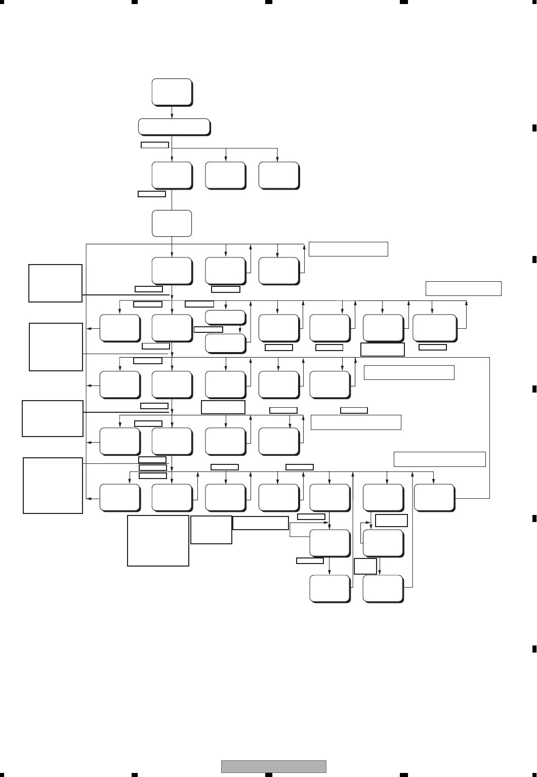
AVIC-Z1/UC 205
5678
5678
C
D
F
A
B
E
Test mode In
Set source to DVD
Start test mode
FE
test mode
Power On
Power Off CRG + CRG –LD_ON
Focus close
adjustment
Focus Search
Power Off CRG + CRG –
T.Bal and
other
adjustments
Focus Jump
Power Off
Focus Jump ID Search
Tracking
Open
T. Jump
+/–
ID
specification
Track number
specification
Error Rate
measurement
(Note 2)
Reproduction
speed switching
(Note 3)
Power Off CRG –
Tracking close
adjustment
CRG +
Disc Type
(Note 1)
Eject
EDC1
mode
EDC2
mode
8
8
8
8
Focus Search
Stop
3,4
CRG_HOME
21
1
12
2
25
5
LD_ON
5
6
6
55
34
4
4
3
3
3
2
1
1
1
3
1~4
EJECT Power off condition
Power on condition
Focus close condition 2
Focus close condition 1
Tracking close condition
ID
Search Start
Jump start
0X00 0000
0FFF 00000FFF 0000
1X00 0000
2000 0000
1FFF 0000
0000 0000
1A00 0000
1100 0000
TEST
FE offset coefficient
TE offset coefficient
AS offset coefficient
ENV offset coefficient
TG offset coefficient
DBALt coefficient
FE MAX level
FE MIN level
AS MAX level
ENV MAX level
FE normalization feature
Spindle gain coefficient
TEMAX level
TEMIN level
TBAL Coefficient(Layer 0)
TBAL Coefficient(Layer 1)
TE normalization feature
(Layer0)
TE normalization feature
(Layer1)
FBAL Coefficient(Layer0)
FBAL Coefficient(Layer1)
Focus Gain Coefficient(Layer0)
Focus Gain Coefficient(Layer1)
Tracking Gain Coefficient(Layer0)
Tracking Gain Coefficient(Layer1)
AS normalization adjustment feature
(Layer0)
AS normalization adjustment feature
(Layer1)
2FFF 0000
Layer L0:2000 0000
Layer L1:2100 0000
Layer L0:4X00 0000
Layer L1:4X00 0000
3000 0000
3FFF 0000
3B00 0000
DVD x 1CLV
DVD x 1.3CLV
CD x 2CLV
4X00 0000
3C00 0000
4A00 0000 Jump+:
4B00 0000
ID display Track
number
display
4000 0000
4X00 0000
Error Rate
Focus Gain Coefficient(Layer0)
Focus Gain Coefficient(Layer1)
Tracking Gain Coefficient(Layer0)
Tracking Gain Coefficient(Layer1)
AS normalization adjustment feature
(Layer0)
AS normalization adjustment feature
(Layer1)
Operation while key is being pushed.Operation while key is being pushed.
Operation while key is being pushed.Operation while key is being pushed.
2B00 0000 2C00 0000
Note 1: At this stage select the media type. Various settings are carried out
according to the media selection made here.
Note 2: While measurements are being taken, only the operation, for which
the measurement is being taken, is allowed.
Note 3: Reproduction (play) speed is selectable from
DVD: x 1CLV ↔ x 1.3CLV, CD x 2CLV
2: DVD, single-layer
3: DVD, dual-layer
4: CD
5: CD-RW
-Front-End test mode flow chart
1B00 0000 1C00 0000 1D00 0000
LD_ON :1100 0000
LD_OFF:1000 0000
7
2~5
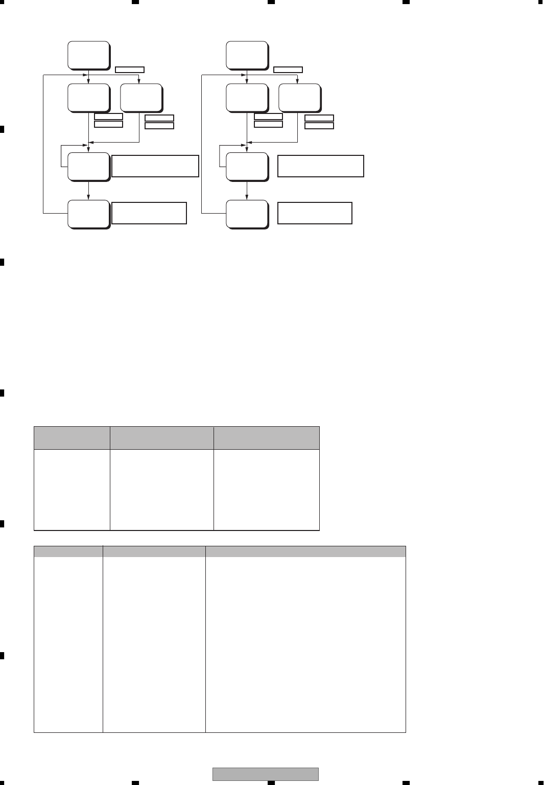
AVIC-Z1/UC
206
1234
1234
C
D
F
A
B
E
Layer 0
selected Layer 1
selected
EDC1
mode
ID
designation
EDC1 start
5
Layer 0
selected Layer 1
selected
EDC2
mode
ID
designation
EDC2 start
5
F-close and F-search cannot be executed, unless LD-ON is set.
0000 0000 0000 0000
0100 0000
1103 0000
Layer0:10** ****
Layer1:11** ****
** ****: ID specification value
Layer0:20** ****
Layer1:21** ****
** ****: Present ID value
0000 0000
1003 0000
0100 0000
1103 0000
0000 0000
1003 0000
Layer0:10** ****
Layer1:11** ****
** ****: ID specification value
Layer0:20** ****
Layer1:21** ****
** ****: Present ID value
The track number designation is selected from the track numbers already prepared for selection.
Switching to cyclic operation is made at step 3, and the decision is finalized (entered) in step 4.
For CD: Tracks 1, 4, 10, 11 and 32.
For DVD: Tracks 1, 4, 10, 11, 32, 64 and 100.
Method for designating an ID address:
•
A number of digits are determined through commands
1
and
2
. Numerical UP/DOWN operations are performed
through commands 3 and 4. The decision is finalized (entered) with command 5.
Error status from
DVD microcomputer Contents Display
0X50 Mecha. error No display
0X40 No disc No display
0X30 The temperature is abnormal Thermal Protection in Motion
0X20 Read error Error-02-XX
0XE2 Non-playable disc NON-PLAYABLE DISC
0X90
Different region disc
DIFFERENT REGION DISC
0XFF Undefined error Error-FF
Error code of read error(Part of XX)
Error Code Contents Display
0X99 Data cannot read Please confirm the disc
0X80 The address cannot be found Please confirm the disc
0X90 Focus error Please confirm the disc
0X91 Spindle lock NG DVD is stopping because mechanism detected abnormality
0X92 Carriage home NG DVD is stopping because mechanism detected abnormality
0X93 FOK error Please confirm the disc
0X94 ID/Subcode cannot be read Please confirm the disc
0X95 High spindle rotation
0X96 Row spindle rotation DVD is stopping because mechanism detected abnormality
DVD is stopping because mechanism detected abnormality
0X98 TOC cannot be found Please confirm the disc
0X9A AV chip error DVD is stopping because mechanism detected abnormality
0X9B RecaveryNG(BE)
Play state error
Disc data error
DVD is stopping because mechanism detected abnormality
Display
Error Code List
1
4
~
1
4
~
[If F-close isn't executed within 9 seconds after LD-ON, it switches to LD-OFF automatically.
And even if F-search is executed within 9 seconds after LD-ON, it also switches to LD-OFF.]
Please carry out F-close after carrying out power-off at once and carrying out power-on again,
when carrying out F-close after performing F-search.
1122
0X9C
0X9D
0X9E Serface error
(Disc distinction is improper)
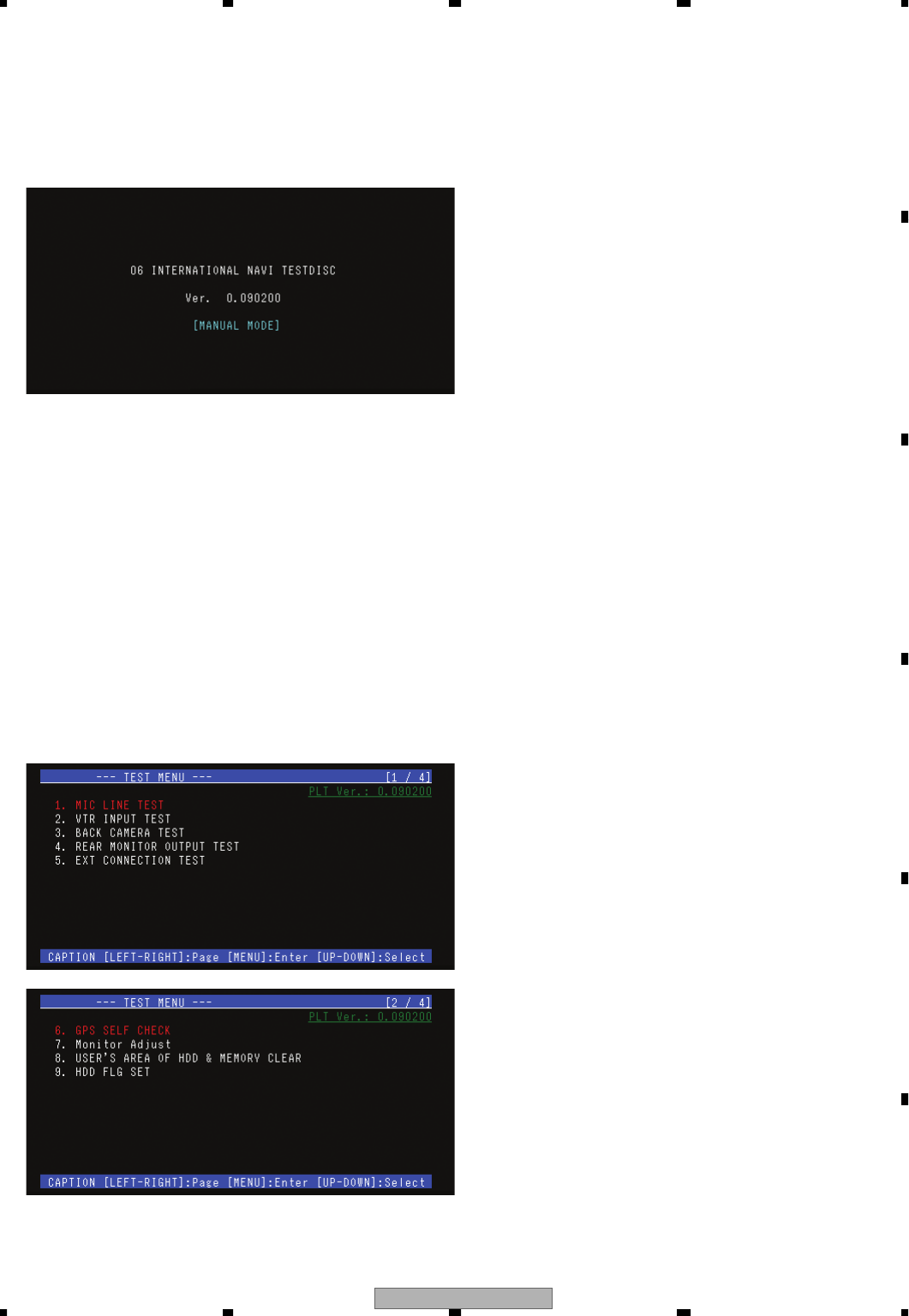
AVIC-Z1/UC 207
5678
5678
C
D
F
A
B
E
6.7 TEST DISC
1. Start/Shutdown
1-1. Start
After inserting the test disc, the title "06 INTERNATIONAL NAVI TESTDISC:GGV1194" will appear.
After the title is displayed, the main menu will be displayed.
1-2. Shutdown
No operation is required.
2. Key operation
• How to operate the MANUAL MODE [Manual Check Version] is as follows:
1. Use the remote control for operation
2. Use [←][→] keys to select the menu screen.
3. Use keys to select the test items and select [MENU] key and move to the testing screen.
4. Use [AV] key to return to the menu screen.
* Please refer to explanation on each screen for details.
3. Line test (Common testing items for service)
Menu screen
[↓]
[↓]
Test Disc (Manual Check Version) Title Screen
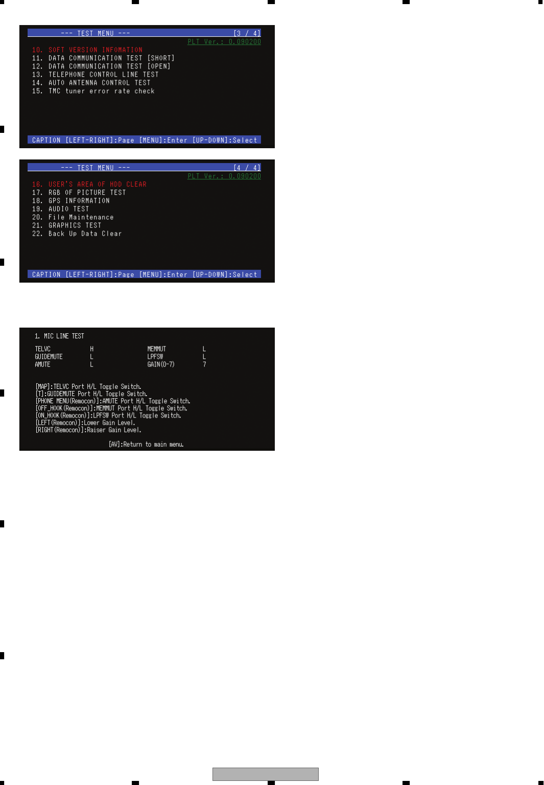
AVIC-Z1/UC
208
1234
1234
C
D
F
A
B
E
3-1(4-1). Microphone Input Line Test(not for service)
• Signals are relayed in the following order:
MICIN→ADC-L→Inside ASIC→DAC-L→Jig→ADC-R→Inside ASIC→DAC-R→SP line
Put audio signals into MICIN and test the audio output and input level.
• Using [MAP] key, conduct a toggle operation of "H"/"L" on TELVC(TEL/NOISE) terminal.
• Using [T] key, conduct a toggle operation of "H"/"L" in GUIDEMUTE(ONSEIMUTE) terminal.
• Using [PHONE MENU] key (Steering Remote Controller <CD-SR1>), perform a toggle operation of "H"/"L" in
AMUTE (GUIDEMUTE) terminal.
• Using [OFF HOOK] key (Steering Remote Controller <CD-SR1>), perform a toggle operation of "H"/"L" in
MEMMUT (MEMMUTE) terminal.
•
Using [ON HOOK] key (Steering Remote Controller <CD-SR1>), perform a toggle operation of "H"/"L" in LPFSW terminal.
• Perform Gain UP using [→] and Gain Down [←].
• After test is completed, use [AV] key to return to the main menu.

AVIC-Z1/UC 209
5678
5678
C
D
F
A
B
E
3-2(4-2). Testing of External Input
•When starting the test, set VTR 1 input ON and switch the source to VTR.
When finishing the test, set the VTR 1 input OFF and switch the source to OFF.
•During the test, input parking brake signals (GND).
•Video image of VTR1 appears on the screen.
•After the test is completed, use [AV] key to go back to the main menu.
3-3(4-3). Testing of Back Camera
•The purpose is to confirm that by inputting the reverse gear signal, camera video image become available in the
setting of monitoring images from the rear view camera.
•When starting the test, set the back camera input ON and set it OFF when it is completed.
•During the test, keep sending back-signals.
•After test is completed, use [AV] key to go back to the main menu.
3-4(4-4). Testing of Rear Monitor Output
•Confirm that a navigation video image is output on the rear monitor.
•When starting the test, set the rear monitor output ON and set the rear monitor output Off when finishing it.
•After test is completed, use [AV] key to go back to the main menu.
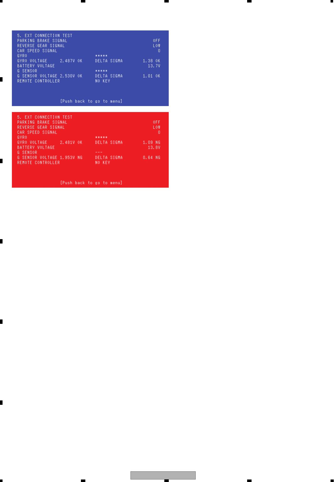
AVIC-Z1/UC
210
1234
1234
C
D
F
A
B
E
3-5(4-5). External connection test
• The status of the items shown above will be renewed every around 0.5 second.
• When the gyro is in operation, beep sound comes out while G sensor is in action.
Gyro under operating conditions : Low pitched sound (440Hz)
G sensor in action : High pitched sound (660Hz)
AVIC-Z1/UC 211
5678
5678
C
D
F
A
B
E
• OK/NG judgment conditions
◆OK/NG judgment of Gyro output values
(Determine differences between Gyro output value and Offset standard values and make OK/NG judgment.)
Offset standard value : 2.5[V]
• Within ±0.15[V] : Output voltage OK (OK display)
• Within ±0.15 - ±0.30[V] : Secular change tolerance (USABLE display)
• ±0.30[V] or greater : Output voltage NG (NG display)
◆OK/NG judgment of G sensor output values
(Determine differences between G sensor output values and Offset standard values and make OK/NG judgment.)
Offset standard value : 2.674[V]
• Within ±0.25[V] : Output voltage OK (OK display)
• Within ±0.25 - ±0.40[V] : Secular change tolerance (USABLE display)
• ±0.40[V] or greater : Output voltage NG (NG display)
◆OK/NG judgment of temperature sensor output values
(Check temperature [°C]of the temperature sensor to make OK/NG judgment)
• −40.0[°C] - 85.0[°C] :Temperature sensor OK (OK display)
• Other than above : Temperature sensor NG (NG display)
USABLE range is OK range of parts with secular change considered. (The screen displays USABLE.)
OK range is criteria to judge if they are within OK range at the time of shipping inspection.
Service division is expected to determine parts to be OK items when they are Usable.
• After the test, use [AV] key to return to the main menu.
When some errors occur to each inspection item, the following error messages are displayed.
Inspection item
<Error List>
Parking brake
Reverse
Pulse
Gyro
Gyro voltage
Back up voltage
G sensor
G sensor voltage
Temperature of
Temperature sensor
Remote control key
When no API response is returned from GPS unit, this will be displayed.
Following incidents can be causes for it.
• Timeout occurs just because something is wrong with serial interface
(poor contact), or data gets garbled and looks like another response.
• When a response different from the requested API is returned
because of malfunction of GPS unit and another request for API is
already requested, the time-out response to the first request is
determined to be incorrect one.
• Navigation system performs so slow that it cannot handle the
response within the time limit even though a response is returned
from GPS unit, or GPS unit cannot handle the same kind of situation
within the time limit. (The time limit is 1.5 sec.)
• Others
−
−
Error details
−
COMMAND ERROR
−
Displayed message
GPS UN-CONNECT When communication between the navigation system and GPS unit is not
established for some reason, this will be displayed.
This can be mainly because something is wrong with the hardware.
Something can be wrong with the navigation system itself, serial interface
(including poor serial connection), and GPS unit.
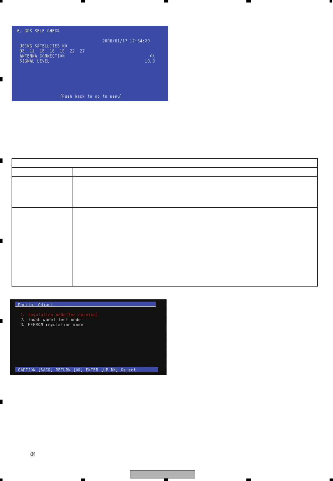
AVIC-Z1/UC
212
1234
1234
C
D
F
A
B
E
3-6(4-6). GPS reception Check
• Conditions for GPS signal reception are shown below:
• Test OK criteria:
• Antenna connection is OK.
• Data can be acquired from more than one satellite.
• Time is displayed.
• When all the conditions are satisfied, the background color turns blue.
• After inspection, use [AV] key to go back to the main menu.
<Error List>
COMMAND ERROR
INVALID DATA
Displayed messages
When no API response is returned from GPS unit, this will be displayed.
Following incidents can be causes for it.
• Timeout occurs just because something is wrong with serial interface (poor contact), or
data gets garbled and looks like another response.
• When a response different from the requested API is returned because of malfunction of
GPS unit and another request for API is already requested, the time-out response to the
first request is determined to be incorrect one.
• Navigation system performs so slow that it cannot handle the response within the time limit
even though a response is returned from GPS unit, or GPS unit cannot handle the same
kind of situation within the time limit. (The time limit is 1.5 sec.)
• Others
Error details
GPS UN-CONNECTING
When communication between the navigation system and GPS unit is not established for some
reason, this will be displayed.
This can be mainly because something is wrong with the hardware. Something can be wrong
with the navigation system itself, serial interface (including poor serial connection), and GPS unit.
3-7(4-7). Monitor adjustment
• Perform monitor adjustment as follows:
1. Adjustment mode for service : Monitor setting values are adjustable.
2. Touch panel test mode : Touch panel related settings such as calibration can be performed.
3. EEPROM adjustment mode : This mode is not used for service.
• Please refer to the description of "Monitor test mode" of Test mode for details.
3-8(4-8). Clearing of all HDD user region & Main memory
SENSOR STUDY is cleared in this inspection.
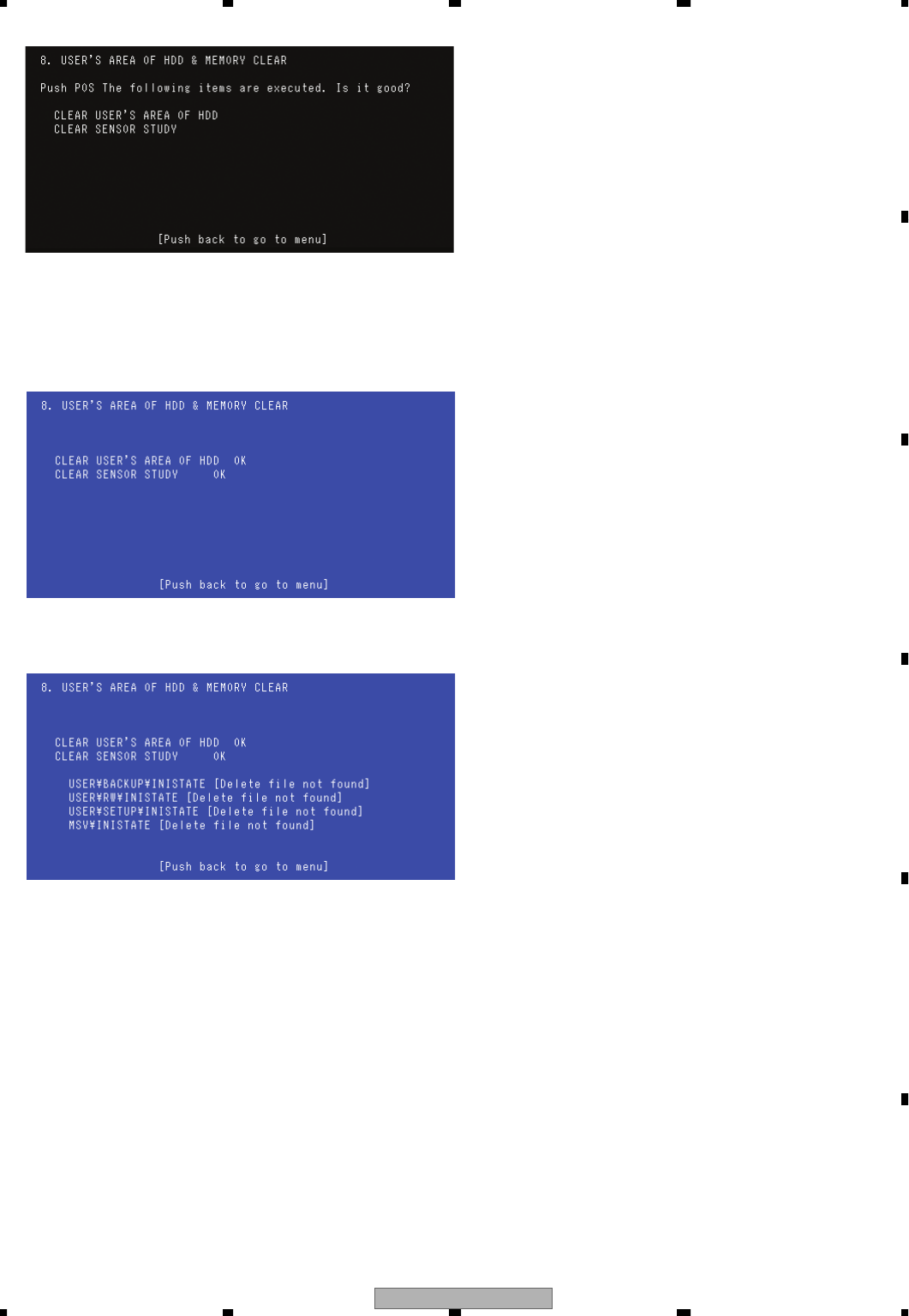
AVIC-Z1/UC 213
5678
5678
C
D
F
A
B
E
• Push down "MAP" key, clearing will start.
• Clear Sensor. (clear SENSOR STUDY data on HDD (USER \ SYSTEM \ GPS related) and SENSOR STUDY data
region of GPS unit.)
• Clear HDD user data area. (MSV, USER \ RW, USER \ RW \ HOLD, USER \ SETUP, USER \ RACKUP shall be deleted.)
• After the inspection screen is displayed, use [MAP] key to perform the process described above.
• After clearing is completed, the executing result is displayed.
• After clearing is completed, use [AV] key to go back to the main menu.
• Once HDD user area is cleared, no folders exist until the next restart and no folders to be deleted are found.
Then the results above will be displayed.
• Although there are no files to be deleted, processing is completed normally.
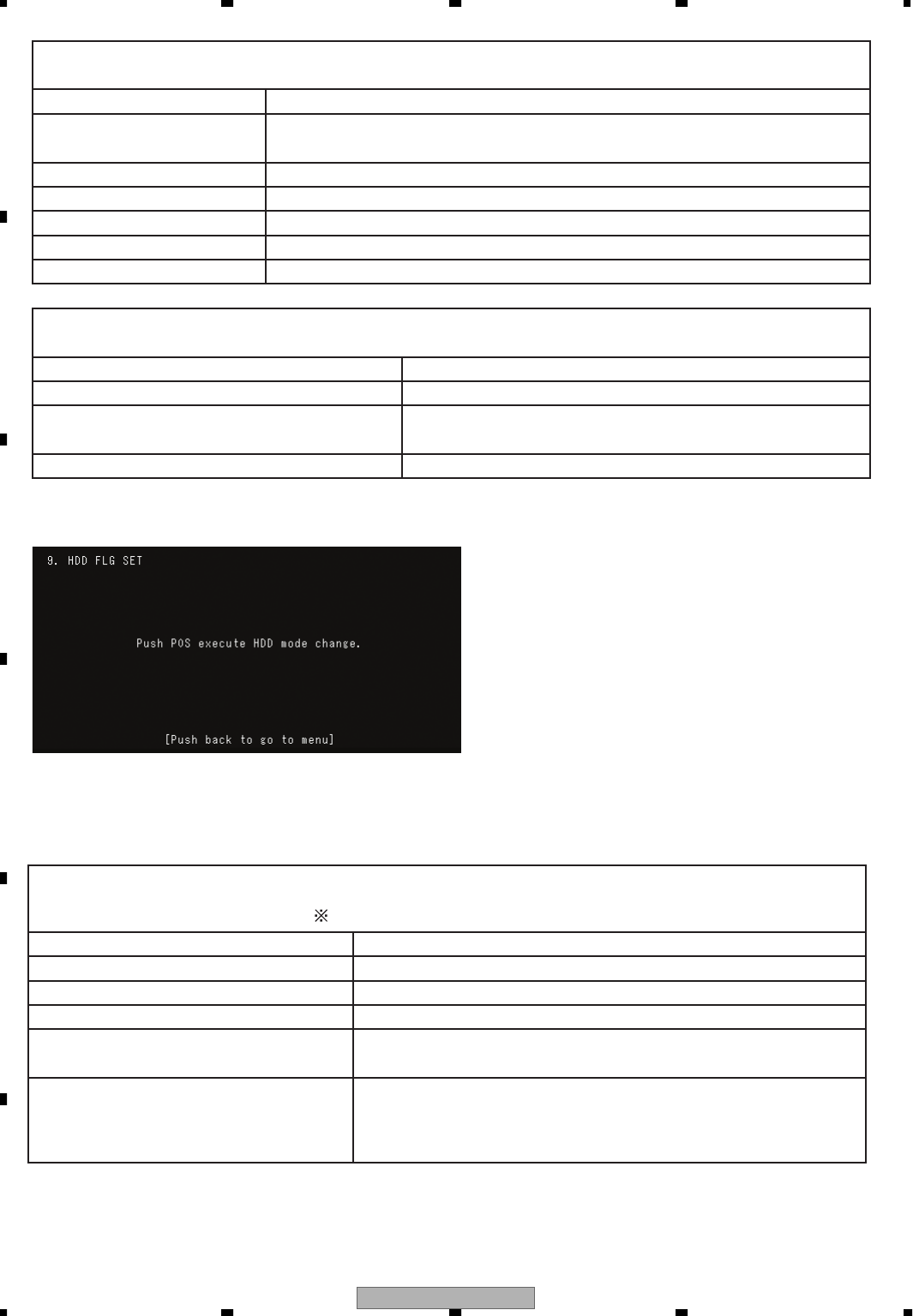
AVIC-Z1/UC
214
1234
1234
C
D
F
A
B
E
3-9(4-9). HDD shipping flag setting
• Set HDD to the shipping status. Contents of HDD will not be damaged.
• Push down "MAP" key, and HDD shipping flag setting (HDD mode change) will start.
• After setting HDD shipping flag, use [AV] key to go back to the main menu.
Displayed errors
<Clearing of HDD user area Error list>
Shown below are errors which occur when HDD user area is cleared.
Delete file not found
Atapi device error
Error
When no files or directory to be deleted are found, this will be displayed.
However, this is not an error as HDD has no files to delete.
This will be displayed in the case of errors other than those mentioned above.
Error factors
When something is wrong with the device, this will be displayed.
CRC error, UnCorrectable error When it fails in reading and writing data, this will be displayed.
It failed to find Drive. When no drive is specified or HDD driver cannot be opened, this will be displayed.
Drive format error When format command is not executed successfully, this will be displayed.
Displayed errors
<Clearing of Main Memory Error list>
Shown below are errors which occur when Main Memory (Clearing of SENSOR STUDY) is cleared.
CLEAR ONLY SENSOR STUDY OF HDD. GPS NONCONNECT.
It failed to clear SENSOR STUDY.
This is displayed when GPS is not connected (when GPS is out of order).
Error factors
This is displayed when SENSOR STUDY CLEAR COMMAND
does not work. (Both HDD and GPS cannot be cleared.)
It failed to communicate with GPS unit.
This is displayed when time-out occurs while communicating with GPS unit.
Displayed errors
<Error list>
Shown below are errors that take place at the time of HDD shipping flag NG (HDD mode change NG).
Error codes are all decimal numbers.
It failed to open HDD device.
Parameter error of HDD mode change.
This error occurs because it fails to open HDD device.
Error factors
This error occurs because the parameter is incorrect. (Error code : 87)
It was refused to request HDD mode change.
This error occurs because the parameter is incorrect. (Error code : 5)
It was timeout to request HDD mode change. This error occurs because the request take so long that timeout occurs.
(Error code : 1053)
It failed HDD mode change. [0x********] This is displayed when mode change fails to be executed.
[********] represents error codes value.
[Example]
• NG occurs because HDD is unconnected. (Error code : 55)
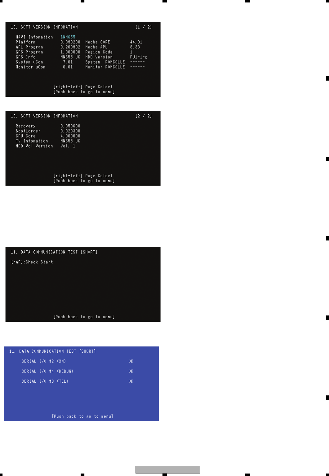
AVIC-Z1/UC 215
5678
5678
C
D
F
A
B
E
3-10(4-10). Soft Version Display
• Software version will be displayed.
• Using [←→] key, pages can be turned.
• Use [↓] key to move to the next item.
• ROM's location for each microcomputer is indicated as "------", ROM's location is not indicated.
• After the inspection is completed, use [AV] key to go back to the main menu.
3-11(4-11). Data communication test (Short)(not for service)
• Perform SIO connection short check.
• Use [MAP] key to start the test.
•
When loopback for CH2, CH4, CH8 is OK, all the test channels are supposed to be OK and the screen above will be displayed.
• After the test is completed, use [AV] key to go back to the main menu.
SERIAL I/O #2(XM) is displayed
UC model only.
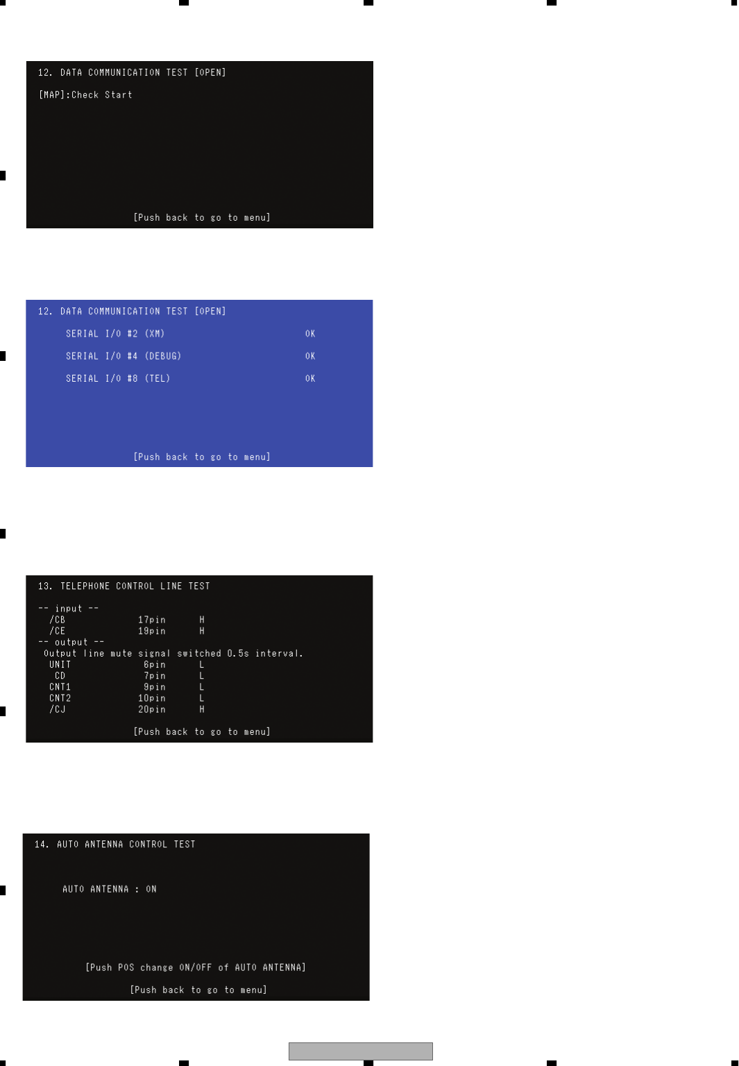
AVIC-Z1/UC
216
1234
1234
C
D
F
A
B
E
3-12(4-12). Data communication (Open check)
• Perform SIO connection open check.
• Do not connect anything to the terminal of each channel. It is OK when the terminal is open.
• Use [MAP] key to start the test.
•
When open-checking of CH2, CH4, and CH8 turned out OK, and the test channels are all OK, the screen above will be displayed.
• After the test, use [AV] key to go back to the main menu.
3-13(4-13). Telephone Control Line Test
• This is a telephone control line test. Output line signal is switched at 0.5 second interval.
• After the test is completed, use [AV] key to go back to the main menu.
SERIAL I/O #2(XM) is displayed
UC model only.
3-14(4-14). Auto Antenna Control Test

AVIC-Z1/UC 217
5678
5678
C
D
F
A
B
E
• When this test starts, NAVI link setting of AUTO ANTENNA will also function.
• Push down [MAP] key, and ON/OFF of the auto antenna can be switched.
• After the test is completed, use [AV] key to go back to the main menu.
• When getting back to the main menu, restore AM/FM link setting to Auto ANTENNA (initial setting).
3-15(4-15). TMC Tuner Error Measurement Check(EW only)
• TMC tuner error rate check is perfomed in this item.
Default frequerey is 87.5MHz.
After checking 500 block, if the error occurs less than 10%, the test results is "OK".
• Use [AV] key to go back to the main menu.
4. Testing for Services
4-16. Clearing of all HDD user region
Sensor Study will not be cleared in this test.
• Push "MAP" key, and clearing will be started.
• Clear HDD user data region. (MSV, USER \ RW, USER \ RW \ HOLD, USER \ SETUP, USER \ BACKUP will be cleared.)
• After the testing screen is displayed, use [MAP] key to carry out the steps above.
• After the execution of clearing, the screen above will be displayed.
• Use [AV] key to go back to the menu screen.
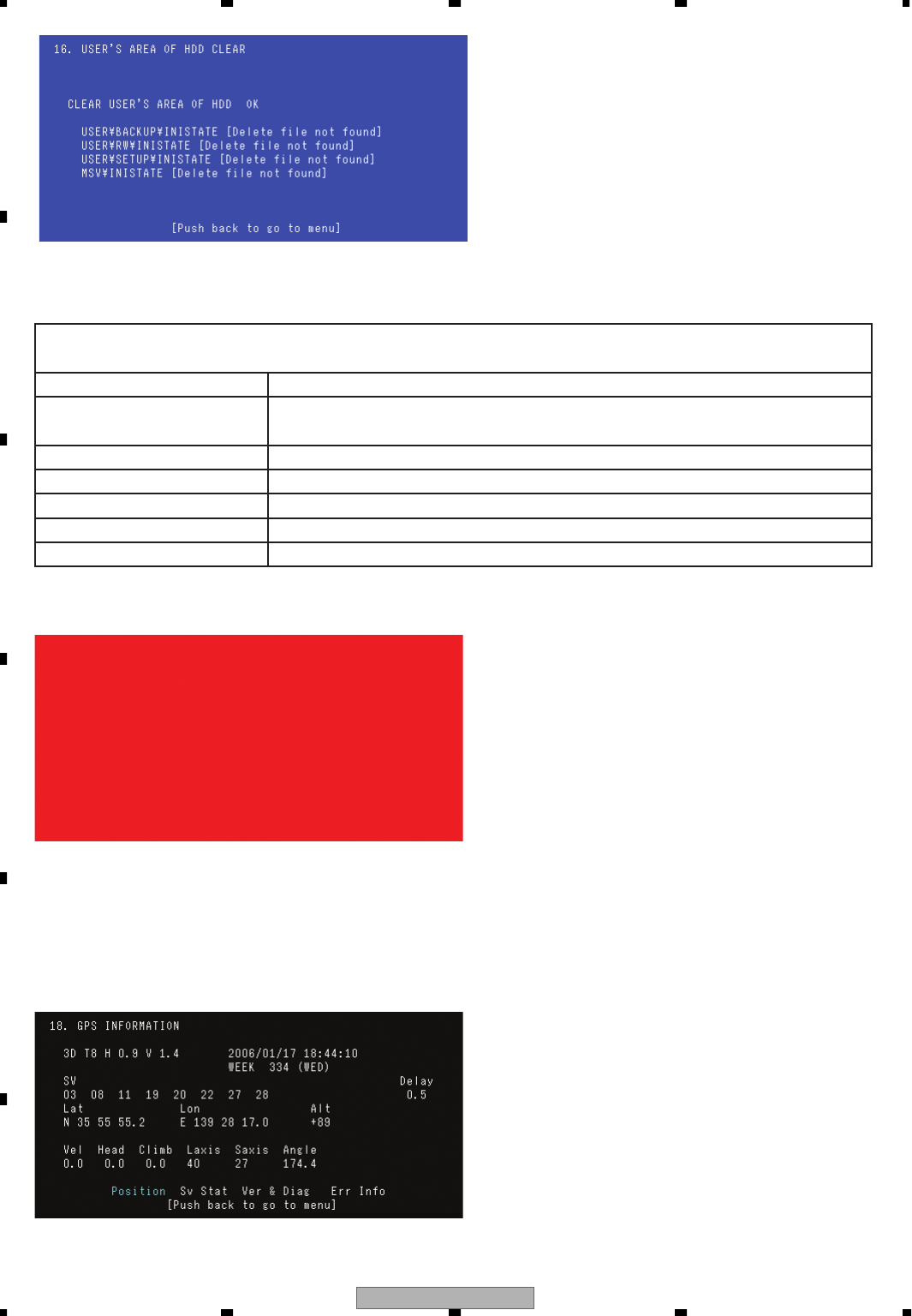
AVIC-Z1/UC
218
1234
1234
C
D
F
A
B
E
• Once HDD user area is cleared, no folders exist until the next restart and no folders to be deleted are found.
Then the results above will be displayed.
• Although there are no files to be deleted, processing is completed normally.
Displayed errors
<HDD user region clearing Error list>
Shown below are errors that occur when clearing HDD user region.
Delete file not found
Atapi device error
Error
When no files or directory to be deleted are found, this will be displayed.
However, this is not an error as HDD has no files to delete.
This will be displayed in the case of errors other than those mentioned above.
Error factors
When something is wrong with the device, this will be displayed.
CRC error, UnCorrectable error When it fails in reading and writing data, this will be displayed.
It failed to find Drive. When no drive is specified or HDD driver cannot be opened, this will be displayed.
Drive format error When format command is not executed successfully, this will be displayed.
4-17. Image RGB
• Perform a bridge test on RGB.
• Switch screens using [←] [→] keys.
• Make drawings by following the pattern of R100%→G100%→B100%→W(WHITE)100%.
• 4 windows will be displayed in total. Normally no characters are displayed.
• The rear monitor will have the same screen.
• Use [AV] key to go back to the menu screen.
4-18. GPS information
• Push [MENU] key with the cursor at "Position", "GPS information" will appear.
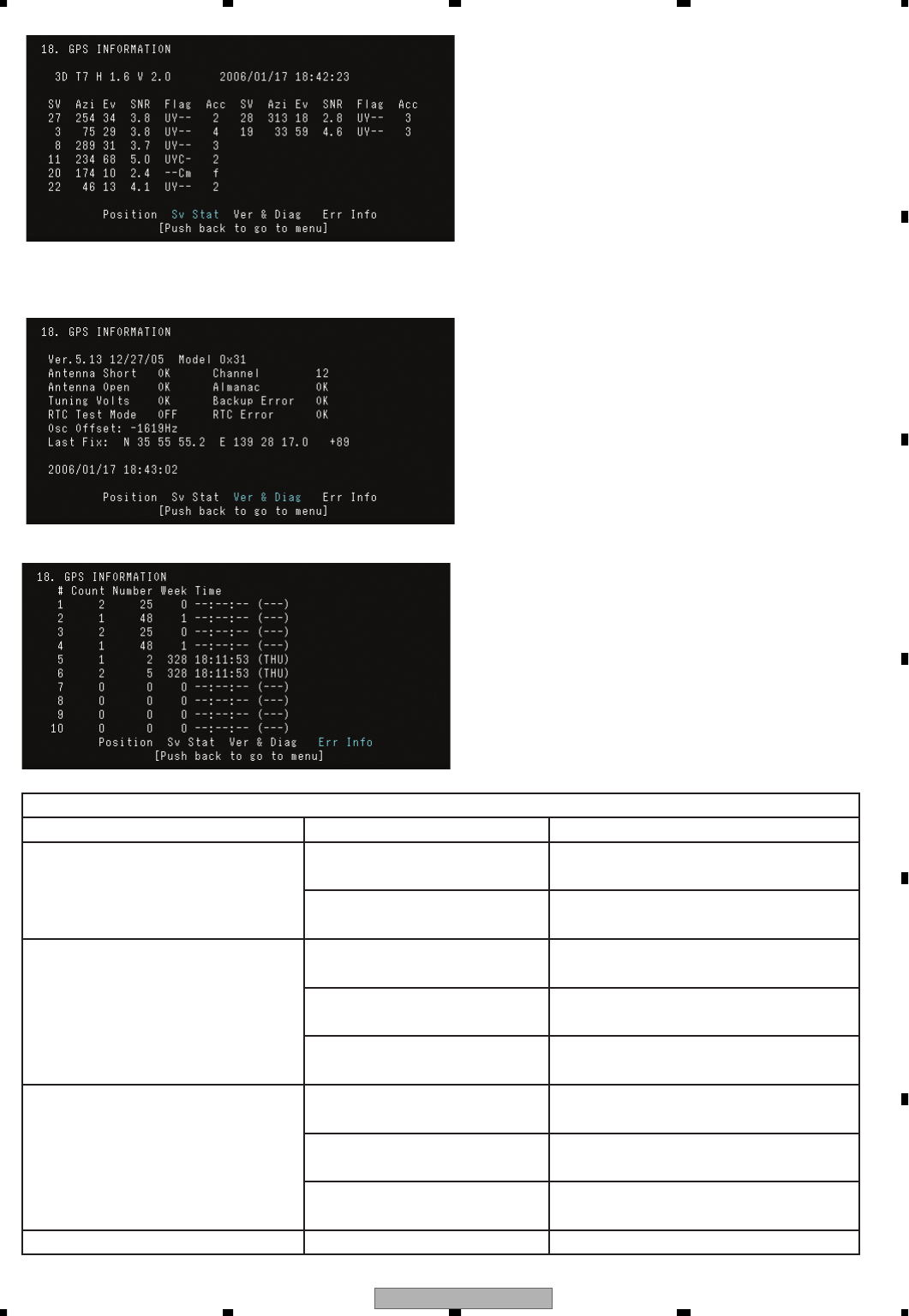
AVIC-Z1/UC 219
5678
5678
C
D
F
A
B
E
• Push [MENU] key with the cursor at "Sv Stat", "Status information" will be displayed.
• When this item is selected, this screen will be displayed by default.
• Push [MENU] key with the cursor at "Ver & Diag", "Diag information" will be displayed.
• Push [MENU] key with the cursor at "Err Info", "Error information" will be displayed.
Screen names for each error message
<Error List>
Position
Err Info
GET_POS_ERROR
GET_ERR_ERROR
Displayed messages
GET_TIME2_ERROR
Sv Stat GET_POS_ERROR
GET_TIME2_ERROR
GET_SV_STATUS2_ERROR
Data is invalid.
GPS is unconnected.
GPS is unconnected.
Error details
GPS is unconnected.
Command error
Data is invalid.
GPS is unconnected.
GPS is unconnected.
Command error
GPS is unconnected.
Command error
Ver&Diag GET_VERS_ERROR
GET_DIAG_ERROR
GET_TIME2_ERROR
GPS is unconnected.
Command error
GPS is unconnected.
Command error
GPS is unconnected.
Command error
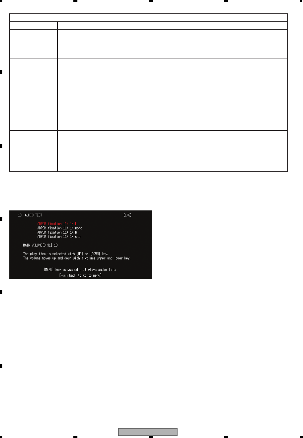
AVIC-Z1/UC
220
1234
1234
C
D
F
A
B
E
Error details
<Error details>
GPS unconnected
Command error
When communication between the navigation system and GPS unit is not established for some
reason, this will be displayed.
This can be mainly because something is wrong with the hardware. Something can be wrong with
the navigation system itself, serial interface (including poor serial connection), and GPS unit.
Error factors
When no API response is returned from GPS unit, this will be displayed.
Following incidents can be causes for it.
• Timeout occurs just because something is wrong with serial interface (poor contact), or data
gets garbled and looks like another response.
• When a response different from the requested API is returned because of malfunction of
GPS unit and another request for API is already requested, the time-out response to the first
request is determined to be incorrect one.
• Navigation system performs so slow that it cannot handle the response within the time limit
even though a response is returned from GPS unit, or GPS unit cannot handle the same kind
of situation within the time limit. (The time limit is 1.5 sec.)
• Others
Invalid error When connection to GPS unit is established, however, routine communication cannot be received
for some reason, this will be displayed.
Following incidents can be causes for it.
• After confirming the connection, GPS unit is reset before routine communication is started.
• Connection is only confirmed when serial contact is poor.
• Others
4-19. Sound Reproduction Test
Sound file selecting screen
• Sound file can be reproduced.
• Use [←] [→] key to change the volume.
• Use [MENU] key to reproduce the selected sound.
• When sound reproduction stops, use [AV] key to go back to the menu screen.

AVIC-Z1/UC 221
5678
5678
C
D
F
A
B
E
File identification
<Sound File List>
ADPCM fixation 11K 1K L
ADPCM fixation 11K 1K mono
ste 22K narration
1KHz sine-wave sampled at 11KHz is reproduced.
Sounds are output only from L side (Mobile phone side)
Narration sampled at 22KHz is reproduced. Sounds are output in stereo.
File contents
1KHz sine-wave sampled at 11KHz is reproduced. Sounds are output in mono mode.
ADPCM fixation 11K 1K R 1KHz sine-wave sampled at 11KHz is reproduced.
Sounds are output only from R side (Speaker)
ADPCM fixation 11K 1K ste 1KHz sine-wave sampled at 11KHz is reproduced. Sounds are output in stereo.
ADPCM fixation 19K 1K L 1KHz sine-wave sampled at 19KHz is reproduced.
Sounds are output only from L side (Mobile phone side)
ADPCM fixation 19K 1K mono
ADPCM fixation 19K 1K R
1KHz sine-wave sampled at 19KHz is reproduced. Sounds are output in mono.
1KHz sine-wave sampled at 19KHz is reproduced.
Sounds are output only from R side (Speaker side).
ADPCM fixation 19K 1K ste 1KHz sine-wave sampled at 19KHz is reproduced. Sounds are output in stereo.
ADPCM fixation 22K 1K L 1KHz sine-wave sampled at 22KHz is reproduced.
Sounds are output only from L side (Mobile phone).
ADPCM fixation 22K 1K mono 1KHz sine-wave sampled at 22KHz is reproduced. Sounds are output only in mono.
ADPCM fixation 22K 1K R
ADPCM fixation 22K 1K ste
1KHz sine-wave sampled at 22KHz is reproduced.
Sounds are output only from R side (Speaker side).
1KHz sine-wave sampled at 22KHz is reproduced. Sounds are output in stereo.
mono fixation 11K music A music file sampled at 11KHz is reproduced. Sounds are output in mono.
mono fixation 19K music A music file sampled at 19KHz is reproduced. Sounds are output in mono.
mono fixation 22K music A music file sampled at 22KHz is reproduced. Sounds are output in mono.
mono fixation 11K narration
mono fixation 19K narration
Narration sampled at 11KHz is reproduced. Sounds are output in mono.
Narration sampled at 19KHz is reproduced. Sounds are output in mono.
mono fixation 22K narration Narration sampled at 22KHz is reproduced. Sounds are output in mono.
ste 11K music A music file sampled at 11KHz is reproduced. Sounds are output in stereo.
ste 19K music A music file sampled at 19KHz is reproduced. Sounds are output in stereo.
ste 22K music A music file sampled at 22KHz is reproduced. Sounds are output in stereo.
ste 11K narration Narration sampled at 11KHz is reproduced. Sounds are output in stereo.
ste 19K narration Narration sampled at 19KHz is reproduced. Sounds are output in stereo.
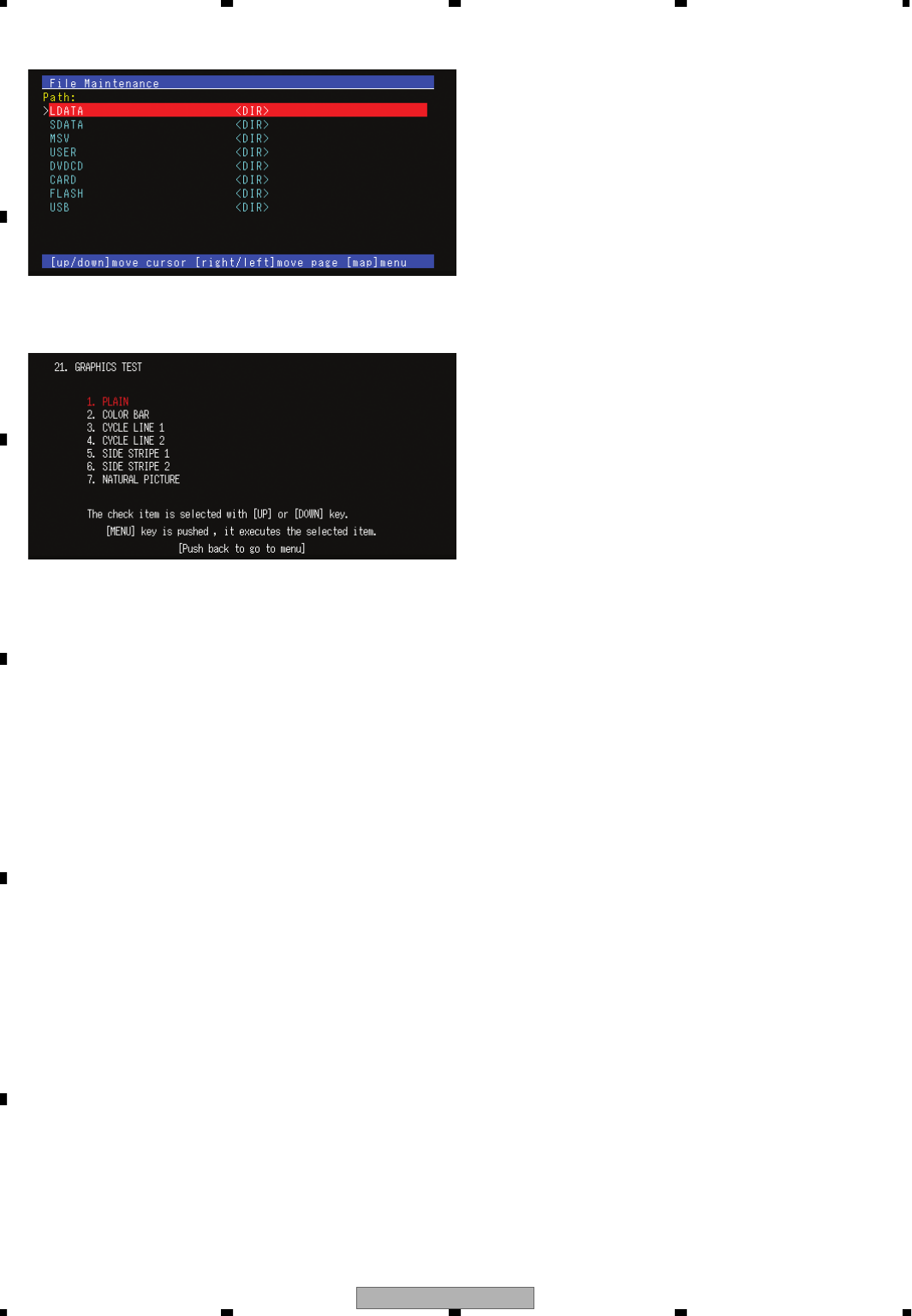
AVIC-Z1/UC
222
1234
1234
C
D
F
A
B
E
4-20. File Maintenance
4-21. Graphics Test
• Use keys to select patterns and [MENU] key to display images.
• Pattern
1. PLAIN
• • • • • • • Use [←] [→] keys to display blue, red, pink, green, light blue, yellow, white and black.
2. COLOR BAR
• • • • • • • Bars colored, white, yellow, light blue, green, pink, red, blue and black are displayed from left.
3. CYCLE LINE 1
4. CYCLE LINE 2
5. SIDE STRIPE 1
6. SIDE STRIPE 2
7. NATURAL PICTURE
• Use [AV] key to menu screen.
[↓]
[↓]

AVIC-Z1/UC 223
5678
5678
C
D
F
A
B
E
• Select "7. NATURAL PICTURE", the image above will be displayed.
4-22. Initialization of backup variables
• Initialize backup variables for system reset.
• After displaying the testing screen, use [MAP] key to execute the test.
• After initialization, restart the system.
• Use [AV] key to return to the menu screen.
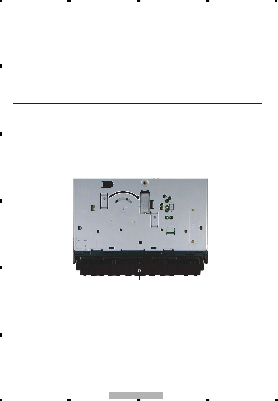
AVIC-Z1/UC
224
1234
1234
C
D
F
A
B
E
7. GENERAL INFORMATION
7.1 DIAGNOSIS
7.1.1 DISASSEMBLY
Fig.1
Cautions
- Be careful not to confuse screws.
- Before disassembling, make sure to remove the HDD Assembly exclusive for Service.
- The HDD Assembly (CXX2121 and CXX2122) exclusive for Service is a precision apparatus. So, handle it carefully
and avoid shock and static electricit
y.
-
Preparation for Removin
g
the Monitor Assy
To remove the Monitor Ass
y
block, it must alwa
y
s be moved to the OPEN position
.
1. Rotate the
g
ear usin
g
a screwdriver, etc.
(
ø
2.8 or smaller
)
from the slit on the bottom surface of the mai
n
unit (Fi
g
.1) in the direction of the arrow, and move the Monitor Assy to OPEN position
.
Note
)
Thou
g
h the
g
ear is heavy, please turn carefully not to inflict too much force. Turnin
g
with excessive force ma
y
cause dama
g
e in the rack or
g
ear in the drivin
g
section
.
Monitor Assy
How to remove the case in the monitor area.
Be sure to remove the case from downside. It cannot be removed from the upper side.
Insert the smallest flathead screw driver of the precision screw drivers into under the 4 claws.
When inserting the screw driver into the clearance between the case (sheet metal) and the grille,
put it 45 degrees diagonally under the case to prevent it from touching the grille, then they will be easily loosened.
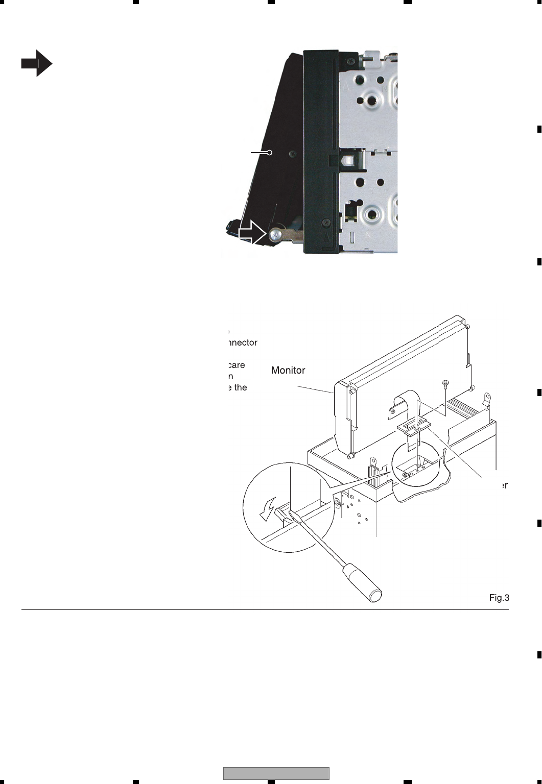
AVIC-Z1/UC 225
5678
5678
C
D
F
A
B
E
-
Removin
g
the Monitor Ass
y
3
(
2
)
Remove the screw to remove the Cover
.
Do not pull the connectin
g
flexible cable. (Fi
g
.3
)
(
3
)
Remove the flexible cable from the connector t
o
remove the Monitor Ass
y
. Push the lid of the co
n
up with the top of precision screwdriver
(
minus
),
a
n
d
th
e
n r
e
mov
e
th
e
fl
e
xi
b
l
e
cab
l
e
. T
a
k
e
m
uc
h
c
not to pull the connector forcedl
y
or break it ope
because it is easy to be dama
g
ed. And also, us
e
precision screwdriver in the same wa
y
in th
e
installation. (Fig.3)
Fi
g
.
2
1
Monitor Assy
1
Remove the two screws. (Fi
g
.2
)
C
ov
e
Ass
y
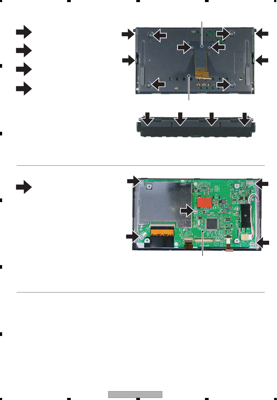
AVIC-Z1/UC
226
1234
1234
C
D
F
A
B
E
- Removing the Case Unit (Fig.4)
Fig.4
Fig.5
- Removing the Monitor Unit (Fig.5)
Caution:
When assembling the case unit, be careful not
to nip (damage) the touch-panel’s tail (left side) and FFC
with back of the case.
Guide
Case Unit
Remove the two screws and then
remove the Guide.
1
2
3
Remove the four screws.
2
Remove the five screws and then
remove the Case Unit.
3
2
2
2
3
1
3
3
1
Insert a flat screwdriver (2mm in width) selected
among precision-type screwdrivers into four
tabs shown below. When inserting the
screwdriver into the gap between the case unit
and the grill, push the screwdriver toward the
case unit approximately at 45 degree angle to
avoid it from contacting the grill. By doing so,
you can open the unit easily.
4
4444
1
1
1
1
1
Monitor Unit
1Remove the five screws.
Disconnect the connector and then remove the
Monitor Unit.
About handling of touch panel
When replacing the touch panel
(hereafter, "panel") located below the LCD panel,
pay attention to the following.
- The panel is made of glass. So, be careful not to
break or damage it.
- Do not leave your fingerprints on the panel display.
- The four sides and corners of the glass panel are sharp.
So, handle it carefully to avoid any injury
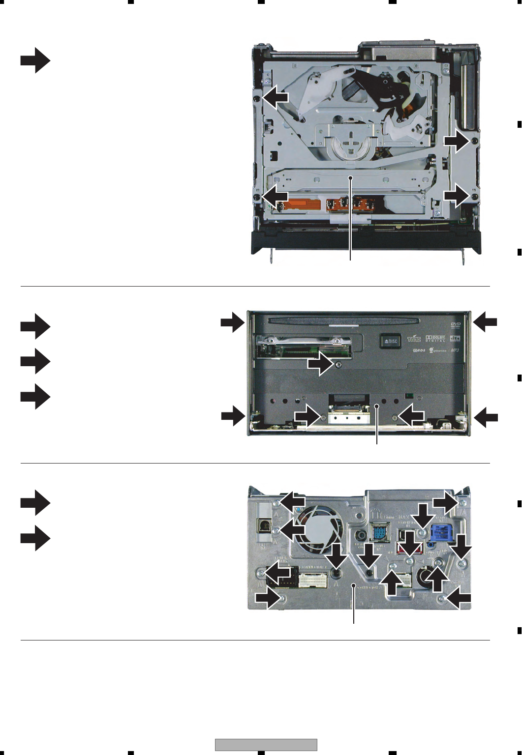
AVIC-Z1/UC 227
5678
5678
C
D
F
A
B
E
- Removing the DVD Mechanism Module (Fig.6)
Fig.6
Remove the four screws.
1
1
DVD Mechanism Module
Fig.7
2
2
Panel Unit
- Removing the Panel Unit (Fig.7)
Remove the screw.
1
1
1
1
33
33
Fig.8
Heat Sink
2
2
2
2
- Removing the Heat Sink (Fig.8)
Remove the two screws.
1
Remove the eleven screws.
2
Caution:
When assembling or disassembling the
DVD mechanism module, be sure to hold the
external side.
When lifting the DVD mechanism module,
lift it from the front side to avoid a burden on
the connected connector.
1
Remove the two screws.
2
Remove the four screws and then remove
the Panel Unit.
3
2
2
Disconnect the connector and then remove the
DVD Mechanism Module.
11
22
2
2
2
Disconnect the connector and then remove the
Heat Sink.
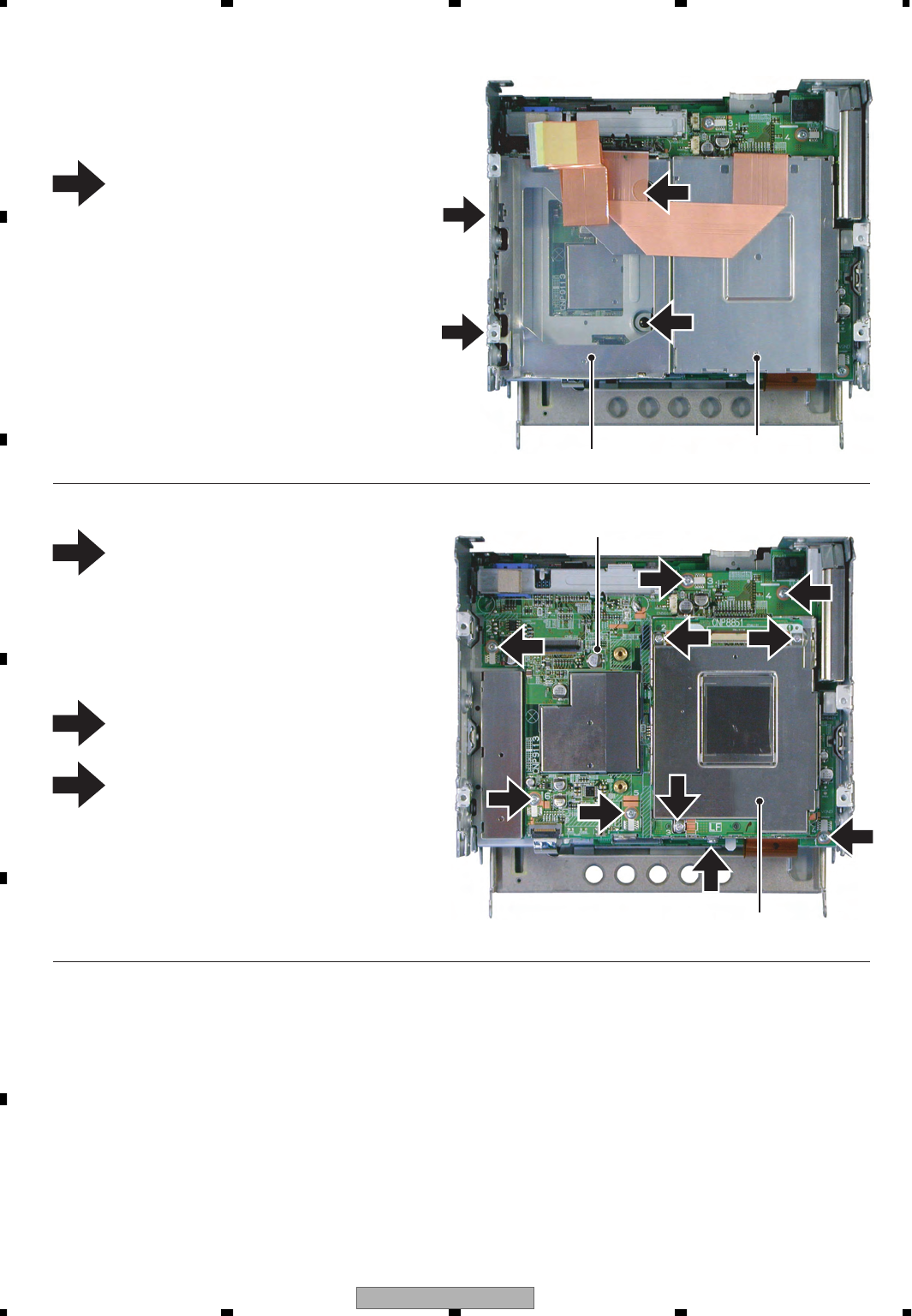
AVIC-Z1/UC
228
1234
1234
C
D
F
A
B
E
- Removing the Hard Disk Unit (Fig.9)
Fig.9
Fig.10
Shield
Remove the four screws.
1
Hard Disk Unit
- Removing the CC Unit (Fig.10)
Remove the three screws and then remove
the CC Unit.
1
Remove the screw.
2
Remove the six screws.
3
- Removing the Navi Mother PCB (Fig.10)
3
Navi Mother PCB
3
3
3
3
3
CC Unit
2
1
1
1
1
1
1
1
Disconnect the connector and then remove the
Hard Disk Unit.
Disconnect the connector and then remove the
Navi Mother PCB.
1. Insert tweezers into holes (four places) near the
circumference of shield top surface, and lift
the shield gradually with the tweezers.
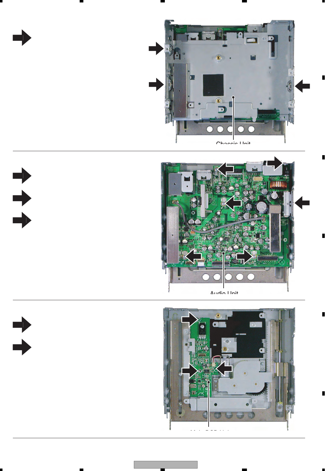
AVIC-Z1/UC 229
5678
5678
C
D
F
A
B
E
Fig.11
Chassis
Unit
-
Removin
g
the Chassis Unit (Fi
g
.11)
R
e
mov
e
th
e
thr
ee
sc
r
e
w
s
a
n
d
th
e
n r
e
mov
e
the
C
hassis
U
nit
.
1
-
Removin
g
the Audio Unit (Fi
g
.12
)
Fig.12
R
e
mov
e
th
e
sc
r
e
w
.
1
Fig.13
2
M
a
i
n
PCB
U
n
it
Audio
Unit
Strai
g
hten the tab at location indicated.
2
1
1
3
3
3
3
1
-
Removin
g
the Main PCB Unit (Fi
g
.13
)
Strai
g
hten the tabs at two locations
in
d
i
cated.
1
R
e
mov
e
th
e
sc
r
e
w
a
n
d
th
e
n r
e
mov
e
th
e
Main P
C
B
U
nit
.
2
R
e
mov
e
th
e
fo
u
r
sc
r
e
w
s
a
n
d
th
e
n r
e
mov
e
the Audio
U
nit
.
3
2
1
1
1
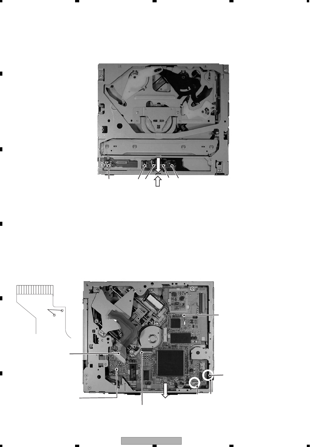
AVIC-Z1/UC
230
1234
1234
C
D
F
A
B
E
- Precautions on handling the mechanism module
1. Hold the upper and main frames.
2. Do not hold the front portion of the upper frame. It is a delicate part.
3. Do not touch the switches on the top panel.
4. Be careful not to catch the flexible cables.
Do not touch here. Do not touch here.
Do not hold this delicate portion.
- Removing the module pc board
Load motor
leads and clamp SW leads
Connector
(for 8/12 detection flexible cable)
Connector
(for pickup flexible cable)
Connector
(for CRG flexible cable)
Short here.
A
BC
Module pc board
1. Set the mechanism to the lock position (disc load standby position).
2. Place the mechanism module upside down.
3. Short the two lands on the pickup flexible cable as shown below.
4. Be sure to disconnect the pickup flexible cable and the CRG flexible cable from the connectors
to protect them from damages.
5. Remove solder from the load motor leads and clamp SW leads.
6. Loosen the two fixing screws. Lift the position A of the module pc board lightly and move it
in the direction B to remove it. Be careful not to damage the flexible cable C.
7. Disconnect the 8/12 detection flexible-cable from the connector.
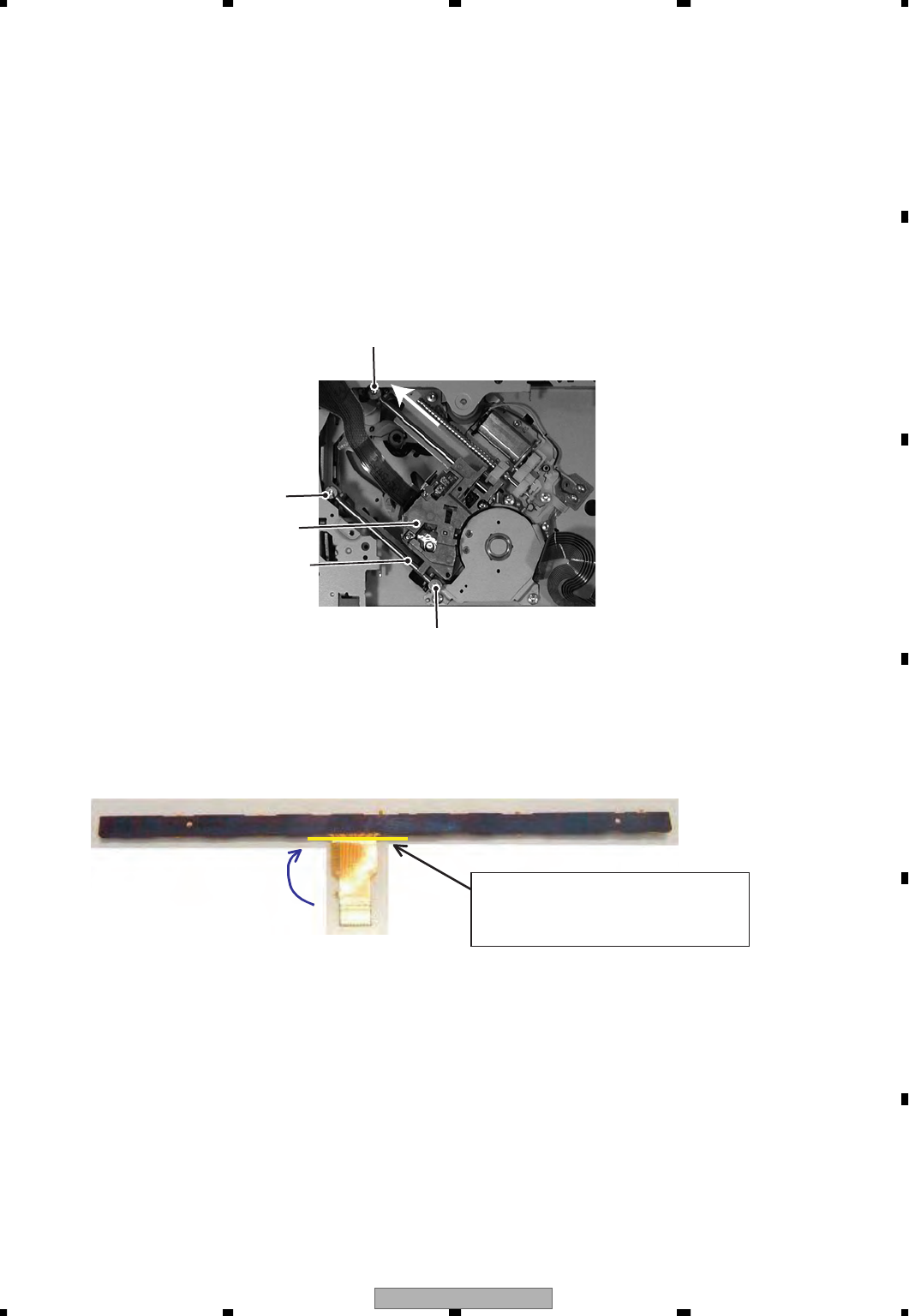
AVIC-Z1/UC 231
5678
5678
C
D
F
A
B
E
-Removing the pickup unit
1. Remove the module pc board in accordance with the procedure of "Removing the module pc board.”
2. While holding the pickup case, remove the skew screw (main).
3. Lifting the end of the pickup rack, slide the main shaft, and remove the pickup unit.
Notes:
Replacing the pickup unit requires the skew adjustment.
Remove glue from both ends of the main and sub shafts, and skew stud.
Do not reuse the old skew screw. Be sure to use a brand-new skew screw supplied with a new pickup unit.
Fix the skew screw with glue (GYL1001) after adjustment.
Sub shaft
Pickup unit
Skew screw
Skew screw (main)
Skew screw
• Howe to fold the flexible cable
The Keyboard unit of the service parts is not folded.
Please see the following picture and fold the flexible cable at 90 degrees.
<Keyboard Unit>
Please check the following item after exchange the Keyboard unit
1Lighting check of all LED device.
2Operation check of the all switches.
3Remote control receiver function check
• Fold the flexible cable at this line
• Don't fold the cable while rubbing it.
Notice of Exchange the Keyboard unit
AVIC-Z1/UC
232
1234
1234
C
D
F
A
B
E
7.1.2 PCB LOCATIONS
UNIT
COMPOUND
COMPOUND
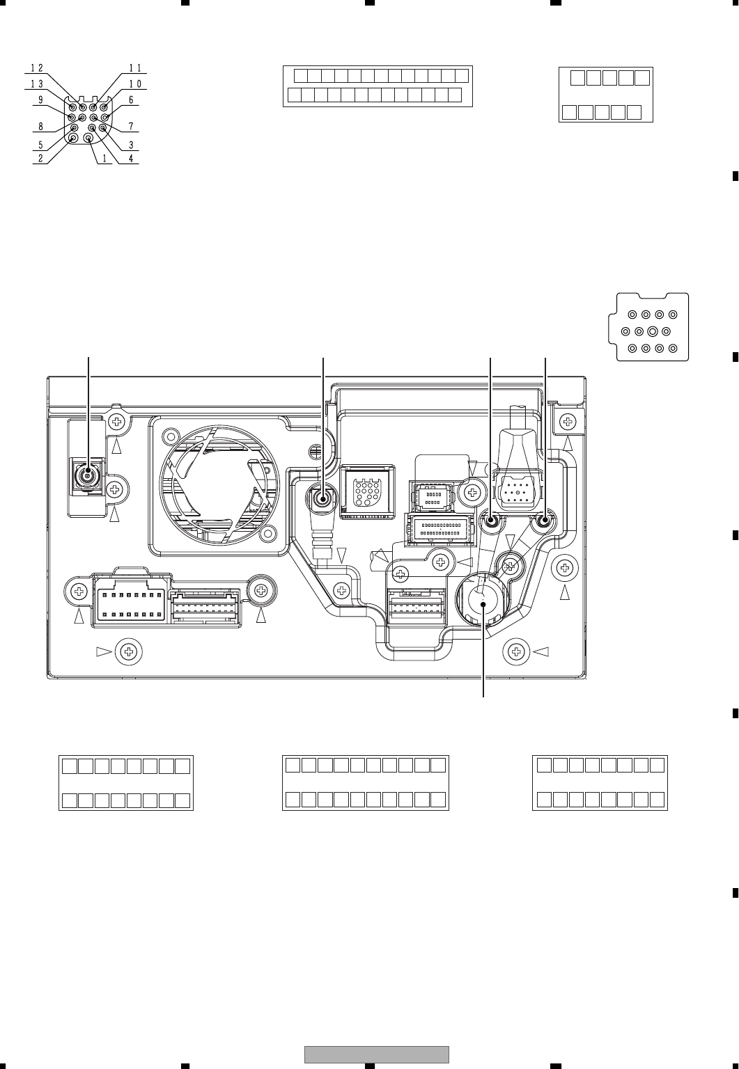
AVIC-Z1/UC 233
5678
5678
C
D
F
A
B
E
7.1.3 CONNECTOR FUNCTION DESCRIPTION
AV I/O
2 4 6 8 10 12 14 16
1 3 5 7 9 11 13 15
1 : BUP
2 : GND
3 : ILM
4 : ANT
5 : ACC
6 : SPEED
7 : REV
8 : PKB
9 : FL-
10 : RR-
11 : FL+
12 : RR+
13 : FR-
14 : RL-
15 : FR+
16 : RL+
13579111315
246810121416
1719
1820
11 : FR
12 : GNDA
13 : VIN
14 : GNDV
15 : VTR_L
16 : GNDL
17 : VTR_R
18 : GNDR
19 : BREM
20 : TELMUTE
1 : POSWL
2 : GNDA
3 : POSWR
4 : GNDA
5 : RL
6 : GNDA
7 : RR
8 : GNDA
9 : FL
10 : GNDA
13579111315
246810121416
11 : GNDA
12 : LOUT
13 : GNDV
14 : VOUT
15 : BCVGND
16 : BCV
1 :
2 : NC
3 : NC
4 : NC
5 : GND
6 : WREM AN
7 : WREM SEL
8 : GUIDEON
9 : GNDA
10 : ROUT
VEHICLE I/F
GPS ANTENNA GUIDE SP OUT
ANTENNA JACK
DIGITAL OUT MIC IN
1 : IPBUS+
2 : IPBUSG
3 : IPLG
4 : NC
5 : IPBUS-
1234
56 7
8 9 10 11
6 : IPRG
7 : IPL+
8 : ASENBO
9 : IPR+
10 : IPR-
11 : IPL-
IP-BUS IN
1 : DT2-
2 : T-A
3 : R-A
4 : PDC/CDMA/FOMA
5 : AGND
6 : UNIT
7 : CD
8 : UNB/CC
9 : CNT1
10 : CNT2
11 : AVPL
12 : GNDL
13 : AVPR
1 : VIDEO GND
2 : COMP VIDEO
3 : (REMPW)
4 : IP-SEL1
5 : IP-SEL2
6 : LED-V
7 : GND
14 : GNDR
15 : TCHC/
16 : /BA
17 : /CB
18 : /BB
19 : /CE
20 : /CJ
21 : NC
22 : SYNC CLOCK
23 :
24 :
25 :
26 : GND
BLUETOOTH
AV BUS
262422201816141210 8 6 4 2
2523211917151311 9 7 5 3 1 2 4 6 8 10
13579
1 : GTOEX
2 : EXTOG
3 : GND
4 : CTOEX
5 : EXTOC
6 : HYOKA
7 : CTOTA
8 : TATOC
9 : VTA
10 : TAGND
EXTENSION
8 : BEEP MUTE
9 : BEEP-
10 : REMOUT
11 : NEW AV SENS
12 : AV ON
13 : BEEP+
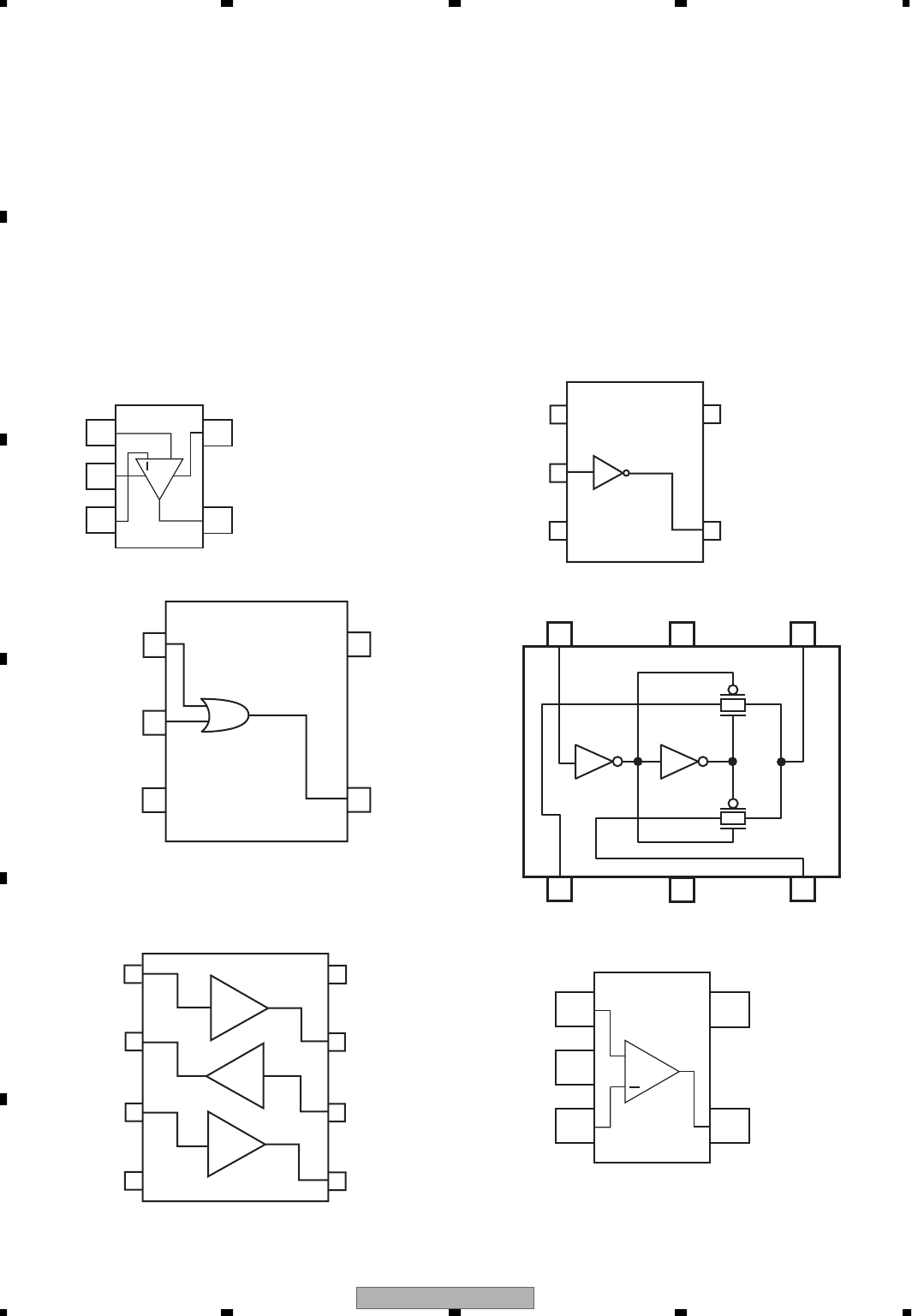
AVIC-Z1/UC
234
1234
1234
C
D
F
A
B
E
7.2 IC
1
3
2
IN+
GND
IN- OUT
V+
4
5
+
NJM2730F
NJM2730F
TC7SH04FUS1
TC7SH32FUS1
TC7PA53FU
TC7WH34FK
NJM2125F
TC74LCX244FTS1
K4S641632H-TC75
PD6527A
UPB1027GS
ADC12H034CIMSAS1
LC72720YVSS1
TK15405BMI
NJM2060V
BA00CC0WT
PAL007B
NJM2505F
BH7236AF
NJM3403AV
TPS2051AD
TC74VHC541FTS1
TC7SET04FUS1
HA12241FP
UPD4721GSS1
BD3931HFP
TC74VHC32FTS1
TC74VHCT125AFTS1
TC74VHC125FTS1
TC7WH14FU
BD5335FVE
TC74LCX245FTS1
TC7MZ245FK
LM56BIMM
TC74VHC04FTS1
S-1132B25-U5
S-1132B15-U5
TC7MBL3244AFK
BR93L56FJ-W
OZ964ISN
TC7PA53FU
123
4
5
6
CH1 GND CH0
COMMON
VCCA
1 IN B
2 IN A
3 GND 4 OUT Y
5 VCC
TC7SH32FUS1
TC7WH34FK
1A
3Y
2A
GND
VCC
1Y
3A
2Y
1
2
3
4
8
7
6
5
NJM2125F
1
3
2
+INPUT
V-
-INPUT OUTPUT
V+
4
5
+
TC7SH04FUS1
1 NC
2 IN A
3 GND
4 OUT Y
5 VCC
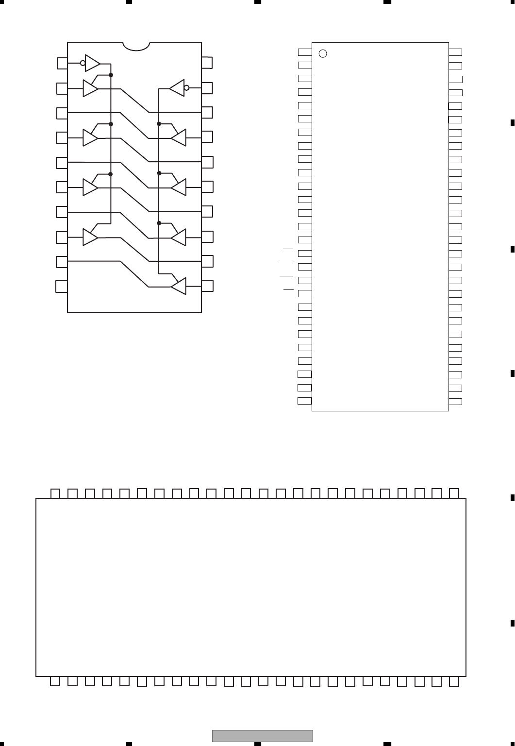
AVIC-Z1/UC 235
5678
5678
C
D
F
A
B
E
14 1Y3
13 2A2
12 1Y4
11 2A1
10 GND
9 2Y1
8 1A4
1 1oe
2 1A1
3 2Y4
4 1A2
5 2Y3
6 1A3
7 2Y2
15 2A3
16 1Y2
17 2A4
18 1Y1
19 2oe
20 VCC
2
10
11
12
13
14
15
16
17
18
19
20
21
22
39
38
37
36
35
34
33
32
31
30
29
28
27
43
42
41
40
47
46
45
44
48
A15
A14
A13
A12
A11
A10
A9
A8
A19
A20
we
reset
NC
ACC
RY/by
A18
A17
A7
A6
A5
A4
A3
A16
byte
VSS
DQ15/A-1
DQ7
DQ14
DQ6
DQ13
DQ5
DQ12
DQ4
VCC
DQ11
DQ3
DQ10
DQ2
DQ9
DQ1
DQ8
DQ0
oe
VSS
23
24
26
25
A2
A1
ce
A0
A-1
A0-A20
DQ0-D15
byte
ce
oe
RY/by
reset
ACC
VCC
VSS
we
8
9
4
5
6
7
3
1
:Data output/Address input
:Address input
:Data input output
:Mode select
:Chip enable input
:Output enable input
:Ready/Busy output
:Reset
:Acc
:Power supply
:GND
:Write enable
PD6527A
TC74LCX244FTS1 K4S641632H-TC75
DQ0 2
VDDQ 3
DQ1 4
DQ2 5
VSSQ 6
DQ3 7
DQ4 8
VDDQ 9
DQ5 10
DQ6 11
VSSQ 12
DQ7 13
VDD 14
WE
15
CAS
16
RAS
17
CS
18
BA1
19
A10
20
A0
21
A1
22
A2
23
A3
24
48
DQ14
47
VSSQ
46
DQ13
45
DQ12
44
VDDQ
43
DQ11
42
DQ10
41
VSSQ
40
DQ9
39
DQ8
38
37
VSS
36
DQM
35
CLK
34
CKE
33
NC
32
A9
31
A8
30
A7
29
A6
28
A5
54
A4
53
VSS
VDD 1
VDD
25
49
DQ15
50
VSS
26
27
52
51
DQM
BA0 A11
NC
VDDQ
A0-A11 : Address input
BA0-BA1 : Bank select address
DQ0-DQ15 : Data input/output
CLK : Clock input
CKE : Clock enable
cs : Chip select
ras : Row address strobe
cas : Column address strobe
we : Write enable
DQM : Data input/output mask
VDD : Power supply
VSS : GND
VDDQ : Data output power supply
VSSQ : Data output GND
NC : Not used
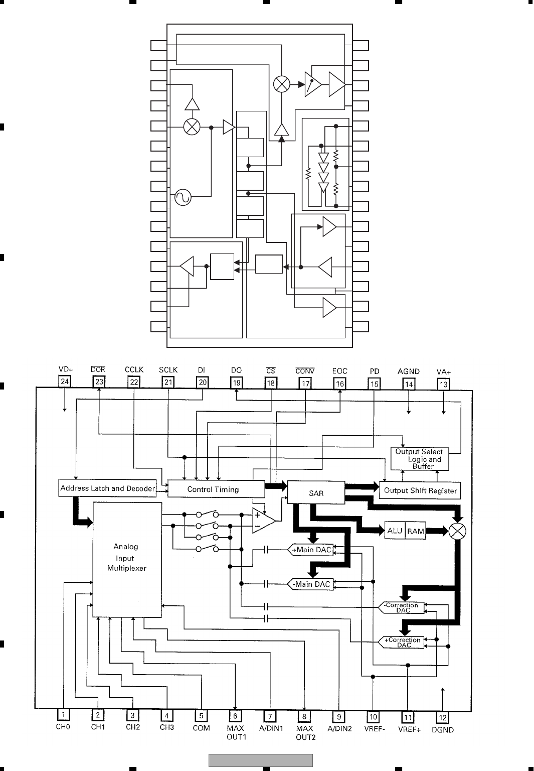
AVIC-Z1/UC
236
1234
1234
C
D
F
A
B
E
ADC12H034CIMSAS1
IF-MIXin
GND(IF-MIX)
RF-MIXout
Vcc(RF-MIX)
RF-MIXin
GND(RF-MIX)
Vcc(1stLO-OSC)
1stLO-OSC1
1stLO-OSC2
GND(1stLO-OSC)
Vcc(phase detector)
PD-Vout3
PD-Vout2
PD-Vout1
GND(phase detector)
Vcc(IF-IMX)
VGC(IF-IMX)
IF-MIXout
GND(2ndIF-AMP)
2ndIFin1
2ndIFin2
2ndIFbypass
Vcc(2ndIF-AMP)
2ndIFout
TCXOout
Vcc(reference block)
TCXOin
GND(divider block)
LOout
Vcc(divider block)
1
2
3
4
5
6
7
8
9
10
11
12
13
14
15
30
1/25
1/2
1/2
1/2
1/2
PFD
29
28
27
26
25
24
23
22
21
20
19
18
17
16
UPB1027GS
AVIC-Z1/UC 237
5678
5678
C
D
F
A
B
E
TK15405BMI
GND
Vcc
Output
Stand-by
Input
SAG
3
2
1
4
5
6
Reference &
Standby Logic Clamp
NJM2060V
6
4 5
9
1114 1213 8
10
D OUTPUT
D -INPUT
D +INPUT
V-
C +INPUT
C -INPUT
C OUTPUT
A OUTPUT
A -INPUT
A +INPUT
V+
B +INPUT
B -INPUT
B OUTPUT
27
13
Pin No. Pin Name I/O
O
l
Function and Operation
1 VREF Reference voltage output
2 MPXIN Base band (multiplexed) signal input
3 Vdda Analog system power supply (+ 5 V)
4 NC Not used
5 Vssa Analog system GND
6 FLOUT O Sub carrier output (filter output)
7 CIN l Sub carrier input (comparator input)
8 NC Not used
9 T1 l Test input (connect to GND)
10 T2 l Test input (stand-by control)
11 T3 O RDS clock output
12 NC Not used
13 T4 O RDS data output
14 T5 O Soft-decision control data output
15 XOUT O Crystal oscillator output
16 XIN l Crystal oscillator input
17 Vddd Digital system power supply (+ 5 V)
18 Vssd Digital system GND
19 NC Not used
20 T6 O Error status,regenerated carrier and error block count outputs
21 T7 O Error correction status, SK detection and error block count outputs
22 SYNC O Block synchronization detection output
23 NC Not used
24 RDS-ID O RDS detection output
25 DO O Data output
26 CL l Clock input
27 NC Not used
28 DI l Data input
29 CE l Chip enable input
30 SYR l Synchronization and RAM address reset input
- Pin Functions(LC72720YVSS1)
LC72720YVSS1
1
15
30
16
OVP TSD OCP
Vref Driver
12345
CTL VCC GND VOUT C
BA00CC0WT
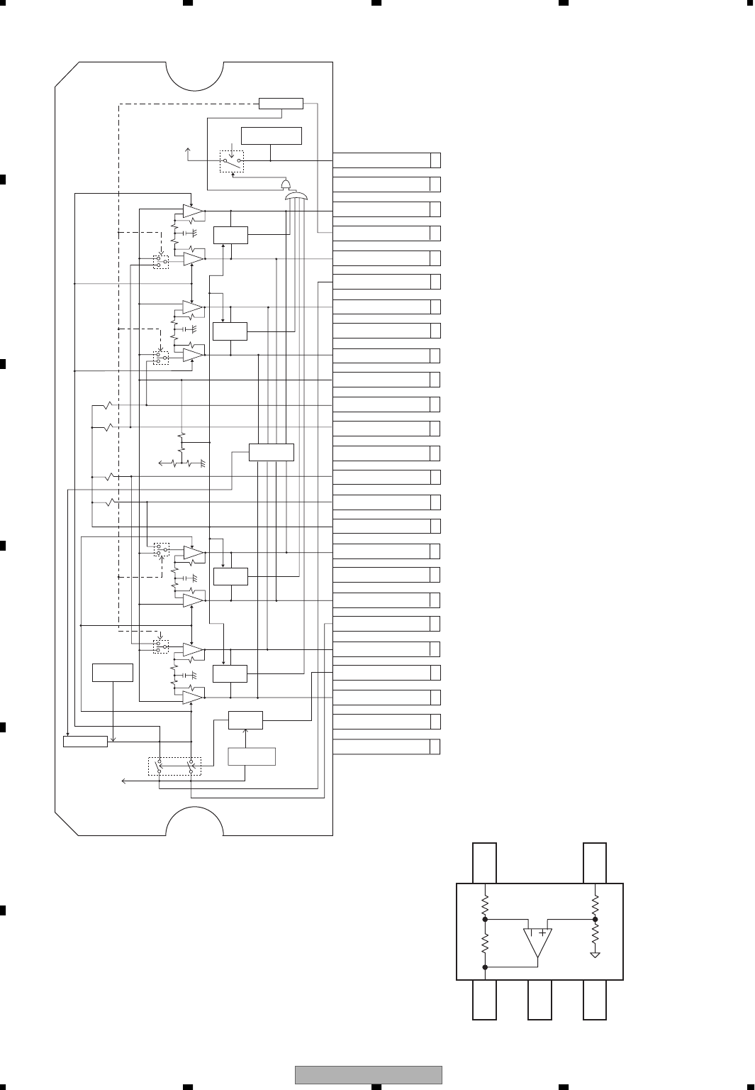
AVIC-Z1/UC
238
1234
1234
C
D
F
A
B
E
1
TAB
2
P-GND2
3
OUT2-
4
STBY
5
OUT2+
6
VCC
7
OUT1-
8
P-GND1
9
OUT1+
10
SVR
11
IN1
12
IN2
13
S-GND
14
IN4
15
IN3
16
AC-GND
17
OUT3+
18
P-GND3
19
OUT3-
20
VCC
21
OUT4+
22
MUTE
23
OUT4-
24
P-GND4
SWITCH
25
+-+
-
Offset
Detection
+-+
-
Offset
Detection
+-+
-
Offset
Detection
+-+
-
Offset
Detection
Protector;
Over current limit
sw_vcc
stby
Protector;
Short circuit
Mute circuit
amp_vcc
Stand-by
Circuit
Protector;
Over voltage
sw_vcc
Protector;
Thermal
Reference
amp_vcc
PAL007B
NJM2505F
54
123
VOUT GND V+
VGND VIN
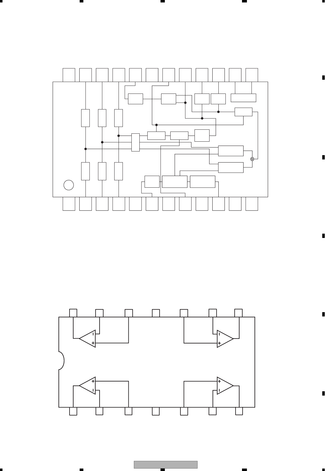
AVIC-Z1/UC 239
5678
5678
C
D
F
A
B
E
BH7236AF
GND1
R IN
NC
SCIN
NPIN
B IN
G IN
BFOUT
YCLPC
SYNC IN
NC
VCC1
12 5 967834 10 11 12
14
24 23 20 19 18 1617
21 15 13
GND2
ROUT
CVOUT
VCC2
FO
GOUT
BOUT
YTRAP
YOUT
COUT
VREF
I REF
REGULATOR
BPF
DELAY CLAMP
B-OUT
MATRIX
G-OUT
R-OUT
CLAMP
CLAMP
CLAMP
75
DRIVER
R-Y
MODULATOR
B-Y
MODULATOR
75
DRIVER
SYNC
ADD
Y/C
MIX
VIDEO
OUT
SIN
PULSE
PHASE
SHIFTER
PULSE
GEN
22
NJM3403AV
D OUTPUT
D- INPUT
D+ INPUT
V-
C+ INPUT
C- INPUT
C OUTPUT
A OUTPUT
A- INPUT
A+ INPUT
V+
B+ INPUT
B- INPUT
B OUTPUT
1
2
3
4
5
6
78
9
10
11
12
13
14
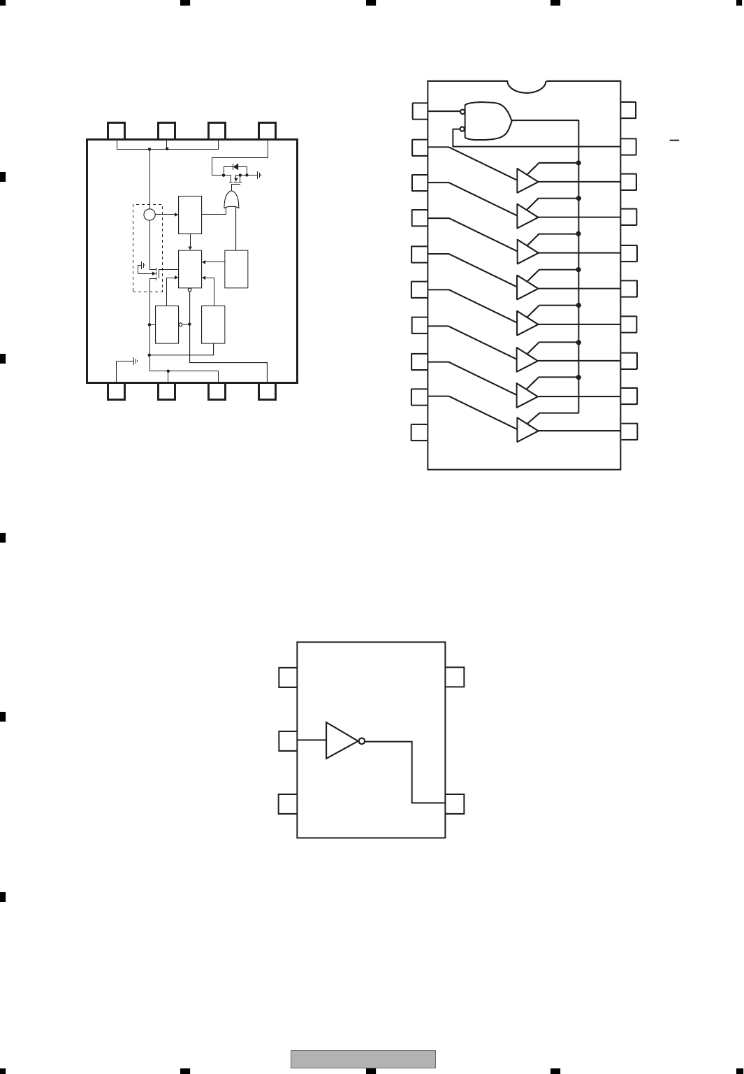
AVIC-Z1/UC
240
1234
1234
C
D
F
A
B
E
TPS2051AD
Charge
Pump
UVLO
Driver
Thermal
Sense
Current
Limit
CS
Power switch
EN
IN
IN
GND 1
2
3
4
8
7
6
5oc
OUT
OUT
OUT
TC74VHC541FTS1
14 Y5
13 Y6
12 Y7
11 Y8
10 GND
9 A8
8 A7
1 g1
2 A1
3 A2
4 A3
5 A4
6 A5
7 A6
15 Y4
16 Y3
17 Y2
18 Y1
19 G2
20 VCC
1
2
34
5
GND
IN A
NC VCC
OUT Y
TC7SET04FUS1
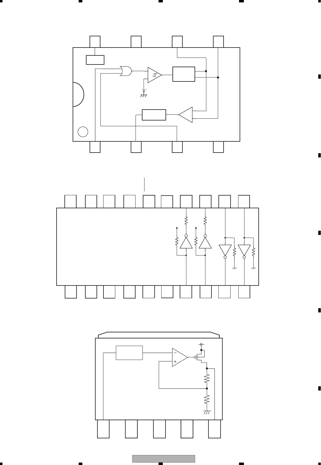
AVIC-Z1/UC 241
5678
5678
C
D
F
A
B
E
132
S1 R out S2 GND
-BUS
+BUS
VCCstb
4
5678
BIAS
DRIVER
OUTPUT
(current)
+
-
-
+
COM
RECEIVER
OUTPUT
HA12241FP
VCC
Reference
Voltage
VCC NC
12
GND NC
3
VO
54
BD3931HFP
VDD
C1+
VCC
C5+
DIN2
C5-
C4+
GND
C4-
STBY
DOUT2
VCHA
20 1819 17 14
15
16 13
1324 7
6
58
C1-
DIN1 DOUT1
VSS
ROUT2 RIN2
12 11
910
ROUT1 RIN1
UPD4721GSS1
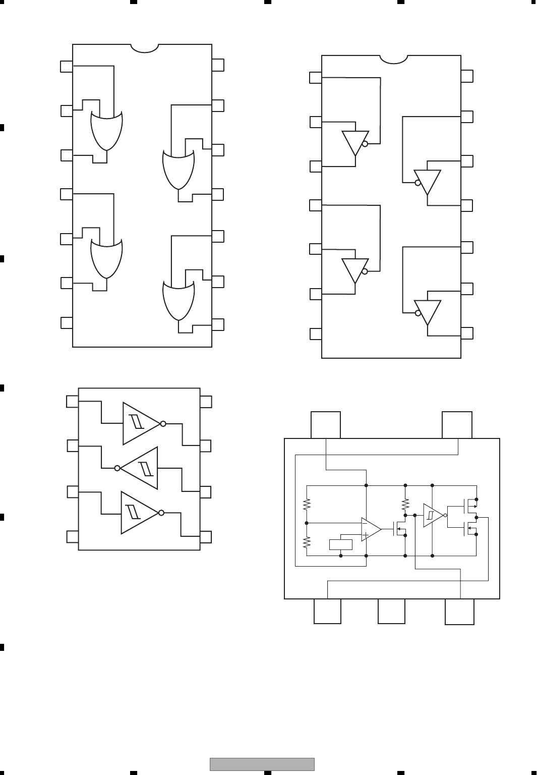
AVIC-Z1/UC
242
1234
1234
C
D
F
A
B
E
14 VCC
13 4B
12 4A
11 4Y
10 3B
9 3A
8 3Y
1 1A
2 1B
3 1Y
4 2A
5 2B
6 2Y
7 GND
14 VCC
13 4g
12 4A
11 4Y
10 3g
9 3A
8 3Y
1 1g
2 1A
3 1Y
4 2g
5 2A
6 2Y
7 GND
1A
3Y
2A
GND
VCC
1Y
3A
2Y
1
2
3
4
8
7
6
5
TC74VHCT125AFTS1
TC74VHC125FTS1
TC74VHC32FTS1
TC7WH14FU
Vref
VOUT
VDD
CT
GND
SUB
12 3
45
BD5335FVE
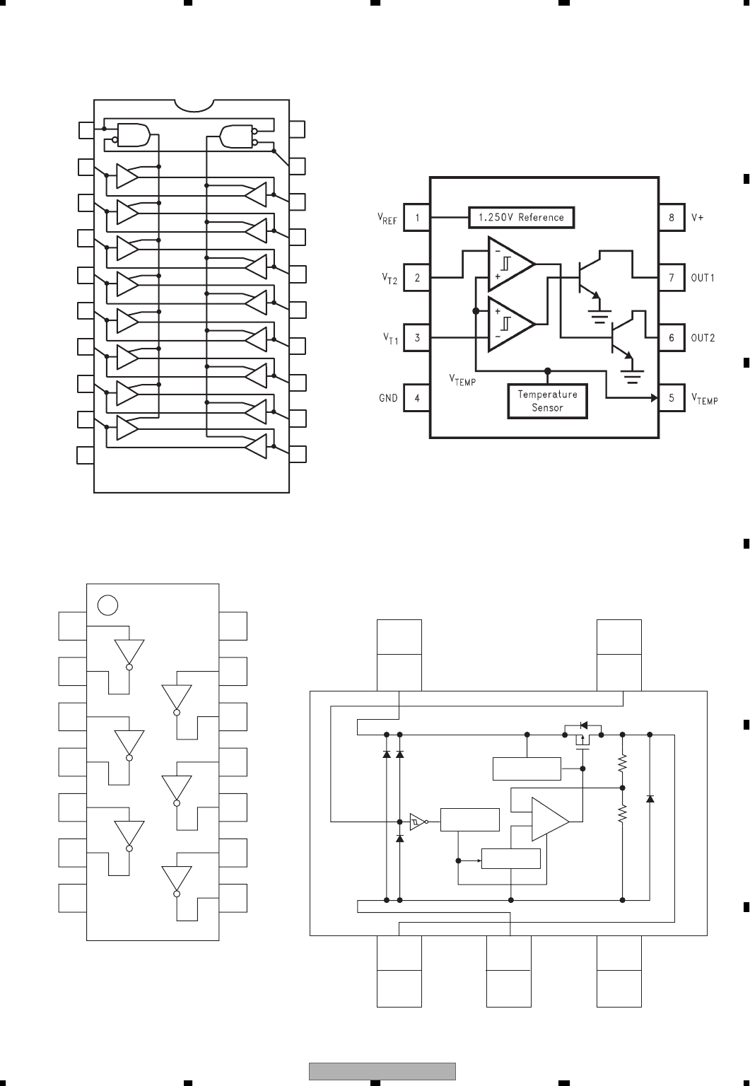
AVIC-Z1/UC 243
5678
5678
C
D
F
A
B
E
TC74LCX245FTS1
TC7MZ245FK
14 B5
13 B6
12 B7
11 B8
10 GND
9 A8
8 A7
1 DIR
2 A1
3 A2
4 A3
5 A4
6 A5
7 A6
15 B4
16 B3
17 B2
18 B1
19 oe
20 VCC
LM56BIMM
VOUT VSS NC
123
54
VIN ON/OFF
+
-
S-1132B25-U5
S-1132B15-U5
Overcurrent
Protector
ON/OFF
circuit
Reference
voltage circuit
1
5
7
6
4
3
2
1A
3A
GND
3Y
2Y
2A
1Y
VCC
5Y
4Y
4A
5A
6Y
6A
14
10
8
9
11
12
13
TC74VHC04FTS1
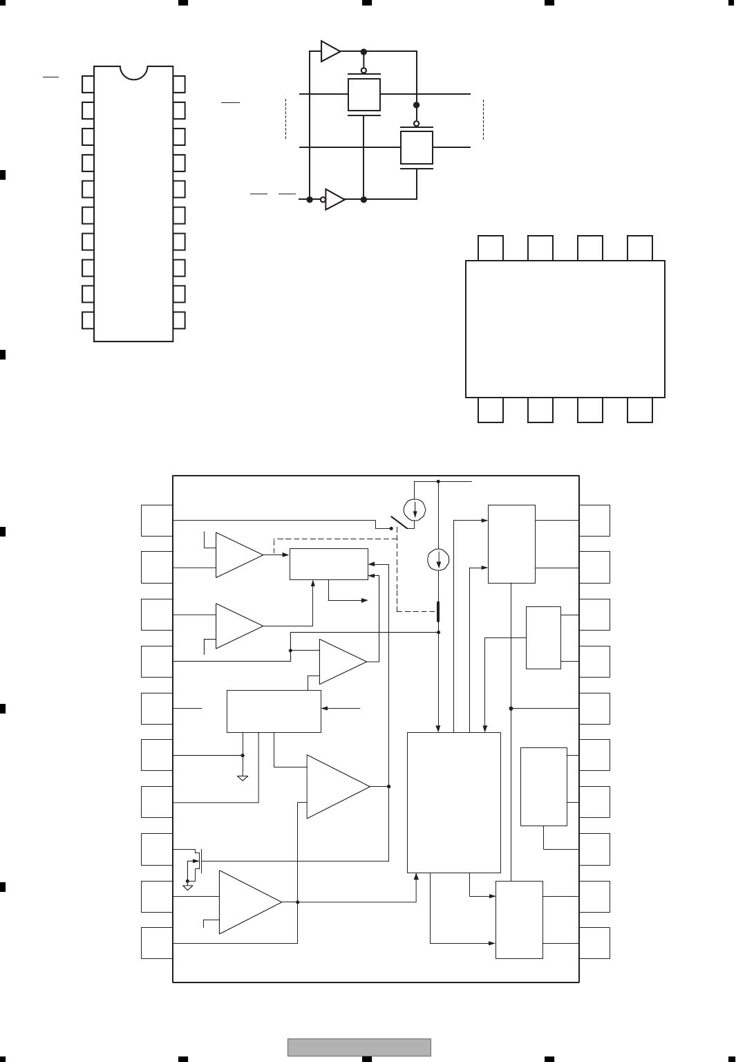
AVIC-Z1/UC
244
1234
1234
C
D
F
A
B
E
1
2
3
4
5
6
7
8
9
10
20
19
18
17
16
15
14
13
12
11
CTIMR
OVP
ENA
SST
VCCA
GNDA
REF
RT1
FB
CMP
NDR_B
PDR_A
CT
RT
PGND
LCT
DIM
LPWM
PDR_C
NDR_D
Protection
NDR_B
PDR_A
ZVS
Phase-Shift
Controller
HF
OSC
PDR_C
NDR_D
Burst-
Mode
Control
OVP
ENA
hys.
COMP
hys.
COMP
1.5 V 2 V
+
-
+
-
Reference
OPLAMP
-
+
EA
-
+
1.25V
3 V
3.35 V
sub.
POFF
POFF
I = 3 uA
I = 6 uA
Soft
Start
ACTIVE
"HIGH"
VCCA
SST2
+
-
SST/2.5
OZ964ISN
8
VCC : Power Supply
GND : Ground
CS : Chip select control input
SK : Serial data clock input
DI : Serial data input
DO : Serial data output
NC : Not used
7 6 5
1 2 3 4
BR93L56FJ-W
NC VCC CS SK
DIDOGNDNC
1A1,2A1
TC7MBL3244AFK
1A4,2A4
1OE,2OE
1B1,2B1
1B4,2B4
1OE
1A1
2B4
1A2
2B3
1A2
2B3
1A4
2B1
GND
VCC
2OE
1B1
2A4
1B2
2A3
1B3
2A2
1B4
2A1
1
2
3
4
5
6
7
8
9
10
20
19
18
17
16
15
14
13
12
11
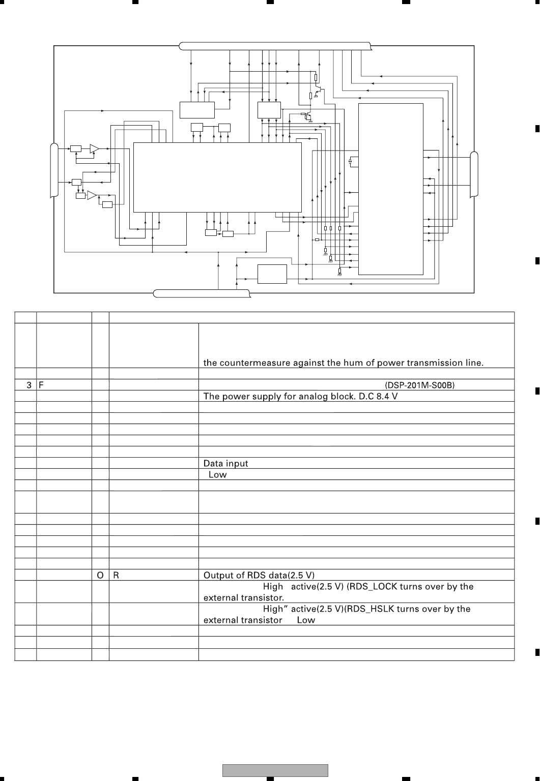
AVIC-Z1/UC 245
5678
5678
C
D
F
A
B
E
N
o.
S
y
mbo
l
I
/O
Ex
p
lai
n
1
AMANT
I
AM antenna in
p
u
t
AM antenna input hi
g
h impedance AMANT pin is connected wit
h
an all antenna b
y
wa
y
of 4.7
µ
H. (LAU t
yp
e inductor
)
A
se
ri
es
c
ir
cu
i
t
includin
g
an inductor and a resistor is connected with RF
g
round for
2
RF
G
N
D
RF
g
roun
d
g
G
r
ou
n
d
o
f
a
n
te
nn
a
b
l
ock
MANT
IF
M antenna in
p
u
t
In
p
ut of FM antenna 7
5
Ω
Sur
g
e absorbe
r
g
i
s
n
ecessar
y.
4
V
CC
p
ower su
pp
l
y
±
0
.
3
V
5S
LO
si
g
nal leve
l
g
Output of FM/AM si
g
nals leve
l
g
6
C
E
2
I
chi
p
enable-
2
Chi
p
enable for EEPROM
”
L
ow
”
act
i
v
e
7
N
C
n
o
n
co
nn
ect
i
on
N
ot
used
8
C
E
1
I
chi
p
enable-
1
Chi
p
enable for A
F
•
RF
”
Hi
gh
g
”
act
i
v
e
9C
KI
c
l
ock
C
l
ock
1
0
DI
I
data
in
11
LDET
Ol
oc
k
detector
“
”
act
iv
e
12
OSCG
N
D
osc
g
round
g
G
r
ou
n
d
o
f
osc
ill
ato
r
b
l
oc
k
1
3
ROM
_
VD
D
p
ower su
pp
l
y
Power su
pp
l
y
for EEPROM
p
in 13 is connected with a
p
ower su
pp
l
y
o
f
micro com
p
uter
.
14
D
O
O
data
out
Data out
p
u
t
1
5
D
G
N
D
di
g
ital
g
roun
d
gg
Ground of di
g
ital bloc
k
g
1
6
N
C
n
o
n
co
nn
ect
i
on
N
ot
used
17
VDD
_
3.
3
p
ower su
pp
l
y
The power supply for di
g
ital block. 3.3 V
g
±
0
.2
V
1
8
RDS
_
C
K
O
RD
S
c
l
ock
Out
p
ut of RDS clock(2.5 V
)
1
9
RDS
_D
ATA
D
S
data
2
0
RDS
_
LOC
K
O
RD
S
l
ock
Out
p
ut unit
“
”
“
L
ow
”
active
)
21
RDS
_
HS
L
KO
RDS hi
g
h spee
d
Out
p
ut unit
“
l
ock
.
“
”
active
)
22
A
U
DI
OG
N
D
audio
g
roun
d
g
G
r
ou
n
d
o
f
aud
i
o
b
l
ock
2
3
L
ch
OL
channel out
p
u
t
FM
ste
r
eo
“
L-
ch
”
si
g
nal output or AM audio outpu
t
24
R
ch
OR
channel out
p
u
t
FM
ste
r
eo
“
R-
ch
”
si
g
nal output or AM audio outpu
t
FMRF
ANT adj RF adj
FM ANT
T51 CF52
RFGND
OSCGND
DGND
AUDIOGND
NC
VCC
VDD_3.3
3.3 V 2.5 V
IC 4
3.3 V 2.5 V
←
IC 2
2.5 V
NC
CE2
ROM_VDD
SL
DI
CK
CE1
LDET
DO
RDS_CK
RDS_DATA
RDS_LOCK
RDS_HSLK
7 6 13 5 10 9 8 11 14 18 19 20 21
1
3
21
21
52
21
64
17
IC 1
3.3 V
AM ANT FMRF
ATT
LPF
OSC
IC 3 EEPROM
5.0 V
IC 5
5 V 3.3 V
←
ATT
MIXER, IF AMP DET, FM MPX,
RDS DECODER
24
23
Rch
Lch
-
FM
/
AM Tuner
U
ni
t
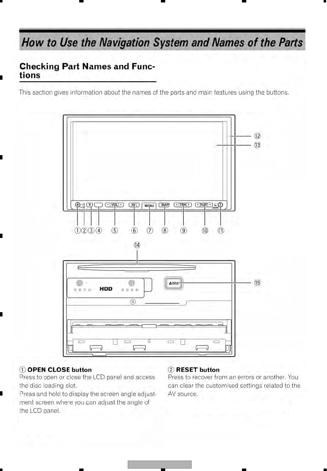
AVIC-Z1/UC
246
1234
1234
C
D
F
A
B
E
8. OPERATIONS
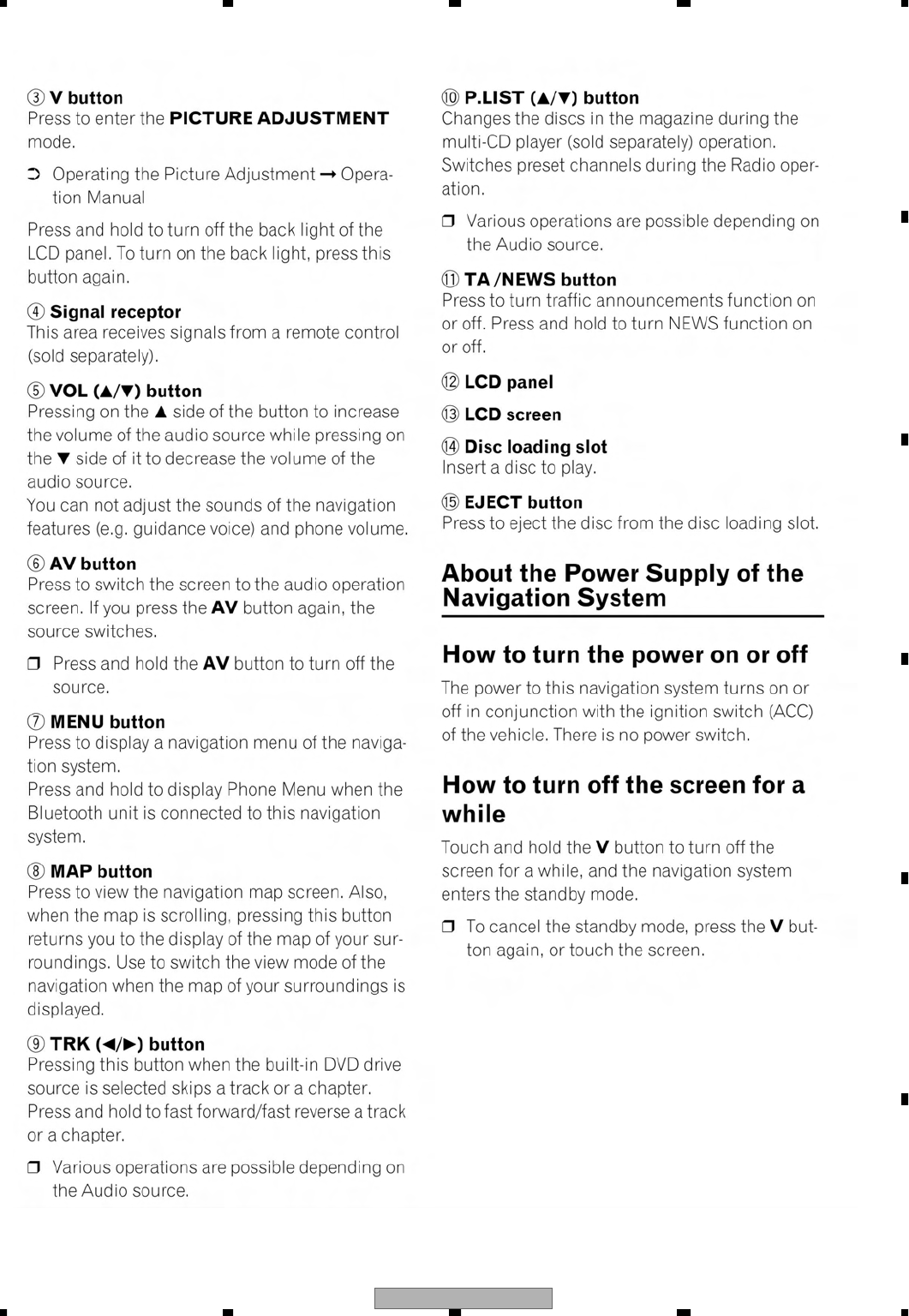
AVIC-Z1/UC 247
5678
5678
C
D
F
A
B
E
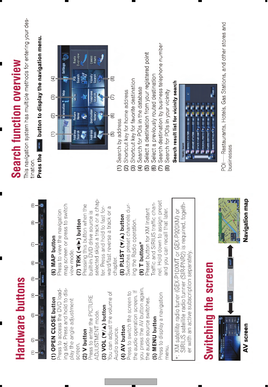
AVIC-Z1/UC
248
1234
1234
C
D
F
A
B
E
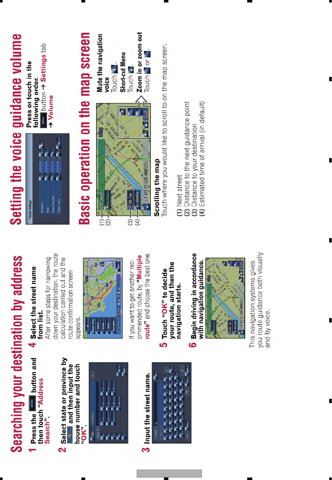
AVIC-Z1/UC 249
5678
5678
C
D
F
A
B
E
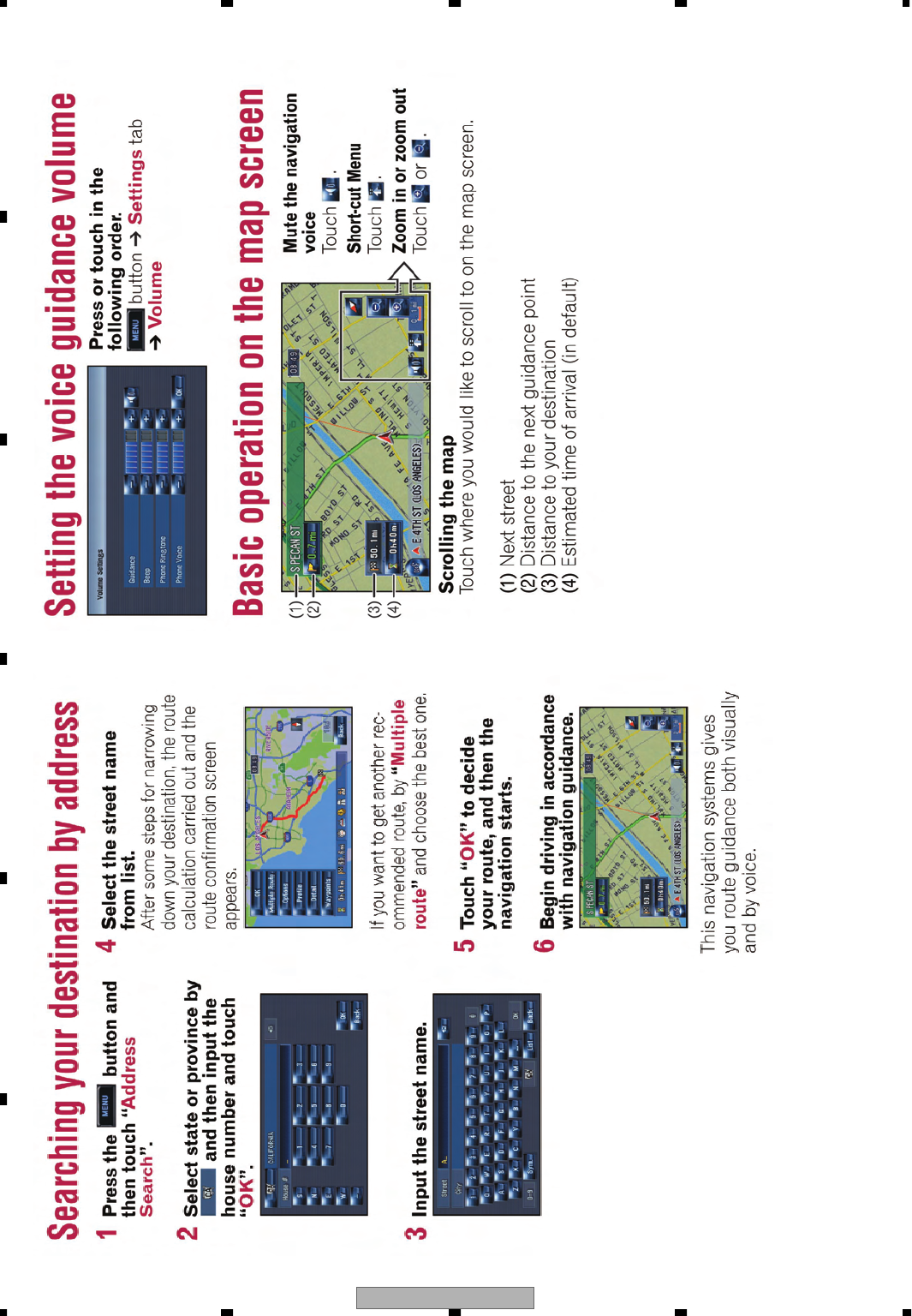
AVIC-Z1/UC
250
1234
1234
C
D
F
A
B
E
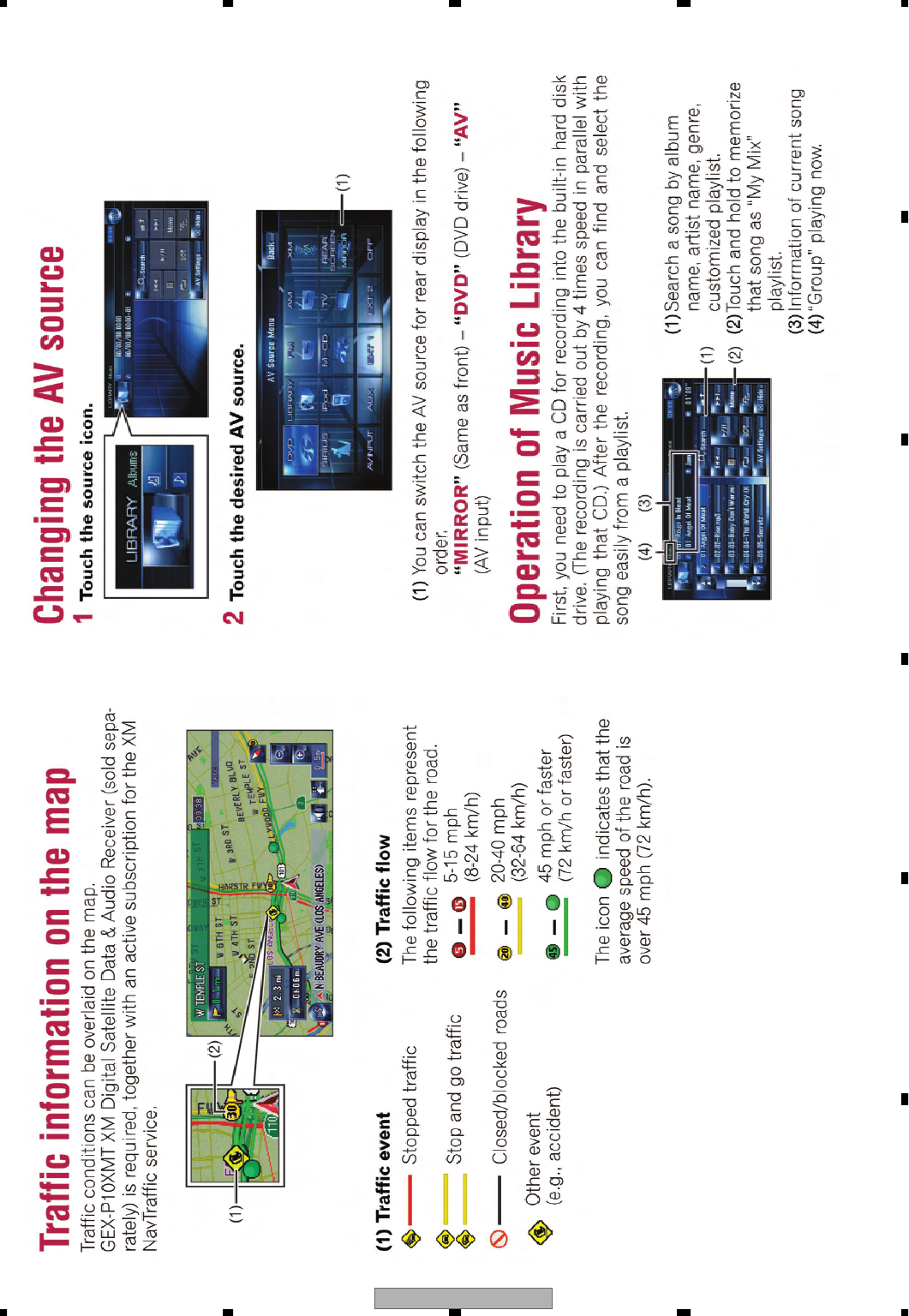
AVIC-Z1/UC 251
5678
5678
C
D
F
A
B
E
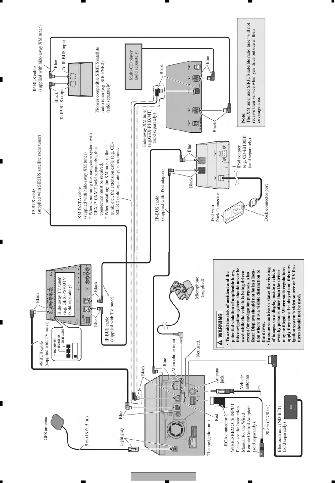
AVIC-Z1/UC
252
1234
1234
C
D
F
A
B
E

AVIC-Z1/UC 253
5678
5678
C
D
F
A
B
E
AVIC-Z1/UC
254
1234
1234
C
D
F
A
B
E
-
Ji
g
s List
Na
m
e
1
22-Pin Extension
C
able
4
0-Pin FF
C
4
0-Pin FF
C
BBR
20
-Pin Extension
C
ord
80
-Pin FF
C
2
0-Pin FF
C
1
5-Pin FF
C
40
-Pin FF
C
J
i
g
for Monitor Adjustment
C
onversion P
C
B for
OS
D display
GG
F1463 for repair
GG
F1463 for repair
Torques screwdriver
Test Disc
J
i
g
No.
GG
D1455
GG
D1170
GG
D1
284
GG
D1
3
27
GG
D14
06
GG
D1209
GG
D1123
GG
D117
0
GG
F141
6
GG
F1463
GG
D1322
GG
D1323
GG
K1
068
GG
V11
9
4
R
emar
k
s
N
avi Mother P
C
B <->
CC
U
ni
t
D
VD Mechanism Module <--> Navi Mother P
C
B
DVD
M
ec
h
an
i
sm
M
o
d
u
l
e <-->
HDD
U
n
i
t
N
avi Mother P
C
B <-> Audio Unit
N
avi Mother P
C
B <-> Audio Unit
N
avi Mother P
C
B <-> Audio
U
nit
A
udio
U
nit <-> Main P
C
B
U
ni
t
A
u
di
o
U
n
i
t <->
M
on
i
tor
U
n
it
F
or
OS
D displa
y
G
GF1416 Conversio
n
F
or repai
r
F
or repa
ir
T
8
(
For HDD
CO
VER
)
y
()
Before shipping out the product, be sure to clean the following portions by using the prescribed cleaning tools:
Portions to be cleaned Cleaning tools
DVD pickup lenses Cleaning liquid : GEM1004
Cleaning paper : GED-008
Portions to be cleaned Cleaning tools
Fans Cleaning paper : GED-008
-
G
rease List
Na
m
e
G
rease
G
rease
G
rease
G
rease
J
ig No.
G
EM1
0
4
5
G
EM1043
G
EM1024
G
EM1
050
R
emar
k
s
