TN1276 Advanced ICE40 I2C And SPI Hardened IP Usage Guide Advancedi CE40SPII2CHardened IPUsage
iCE40%20Advanced%20I2C_SPI%20Usage%20Guide
AdvancediCE40SPII2CHardenedIPUsageGuide
User Manual:
Open the PDF directly: View PDF ![]() .
.
Page Count: 42
- Advanced iCE40 I2C and SPI Hardened IP Usage Guide
- Introduction
- System Bus Interface for iCE40LM and iCE40 Ultra
- System Bus Interface for iCE40
- Hardened I2C IP Cores
- I2C Registers for iCE40LM and iCE40 Ultra
- I2C Registers for iCE40 UltraLite and iCE40 UltraPlus
- I2C_PRESCALE[9:0]
- I2C Status Register (I2CSR/I2CFIFOSR)
- I2C Transmitting Data Register (I2CTXDR/I2CTXFIFO)
- I2C Receiving Data Register (I2CRXDR/I2CRXFIFO)
- I2C General Call Data Register
- I2C Slave Address MSB Register (I2CSADDR/I2CFIFOSADDR)
- I2C Interrupt Control Register (I2CIRQEN/I2CFIFOIRQEN)
- I2C Interrupt Status Register (I2CIRQ//I2CFIFOIRQ)
- I2C Read/Write Flow Chart
- I2C Framing
- I2C Functional Waveforms
- I2C Timing Diagram
- Hardened SPI IP Core
- SPI Registers
- SPI Read/Write Flow Chart
- SPI Framing
- SPI Functional Waveforms
- SPI Timing Diagrams
- Technical Support Assistance
- Revision History
October 2015 Technical Note TN1276
www.latticesemi.com 1TN1276_1.4
© 2015 Lattice Semiconductor Corp. All Lattice trademarks, registered trademarks, patents, and disclaimers are as listed at www.latticesemi.com/legal. All other brand
or product names are trademarks or registered trademarks of their respective holders. The specifications and information herein are subject to change without notice.
Introduction
This reference guide provides guidance for the advanced usage of iCE40LM, iCE40 Ultra™, iCE40 UltraLite™ and
iCE40 UltraPlus™ I2C and SPI IP. It is used as a supplement to TN1274, iCE40 I2C and SPI Hardened IP Usage
Guide. Note that the module generator - GUI flow is the recommended flow for initializing the Hard IP blocks as in
TN1274. In this document you will find:
• System Bus Protocol
• I2C/SPI Register Mapping
• I2C/SPI Timing Diagram
• Command Sequences
• Examples
System Bus Interface for iCE40LM and iCE40 Ultra
The System Bus in the iCE40LM and iCE40 Ultra provides connectivity between FPGA user logic and the Hard-
ened IP functional blocks. The user can implement a System Bus Master interface to interact with the Hardened IP
System Bus Slave interface.
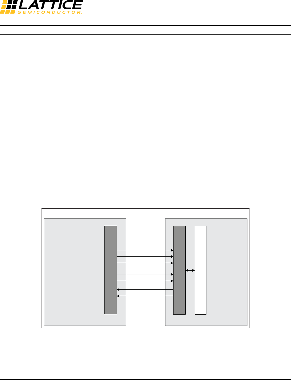
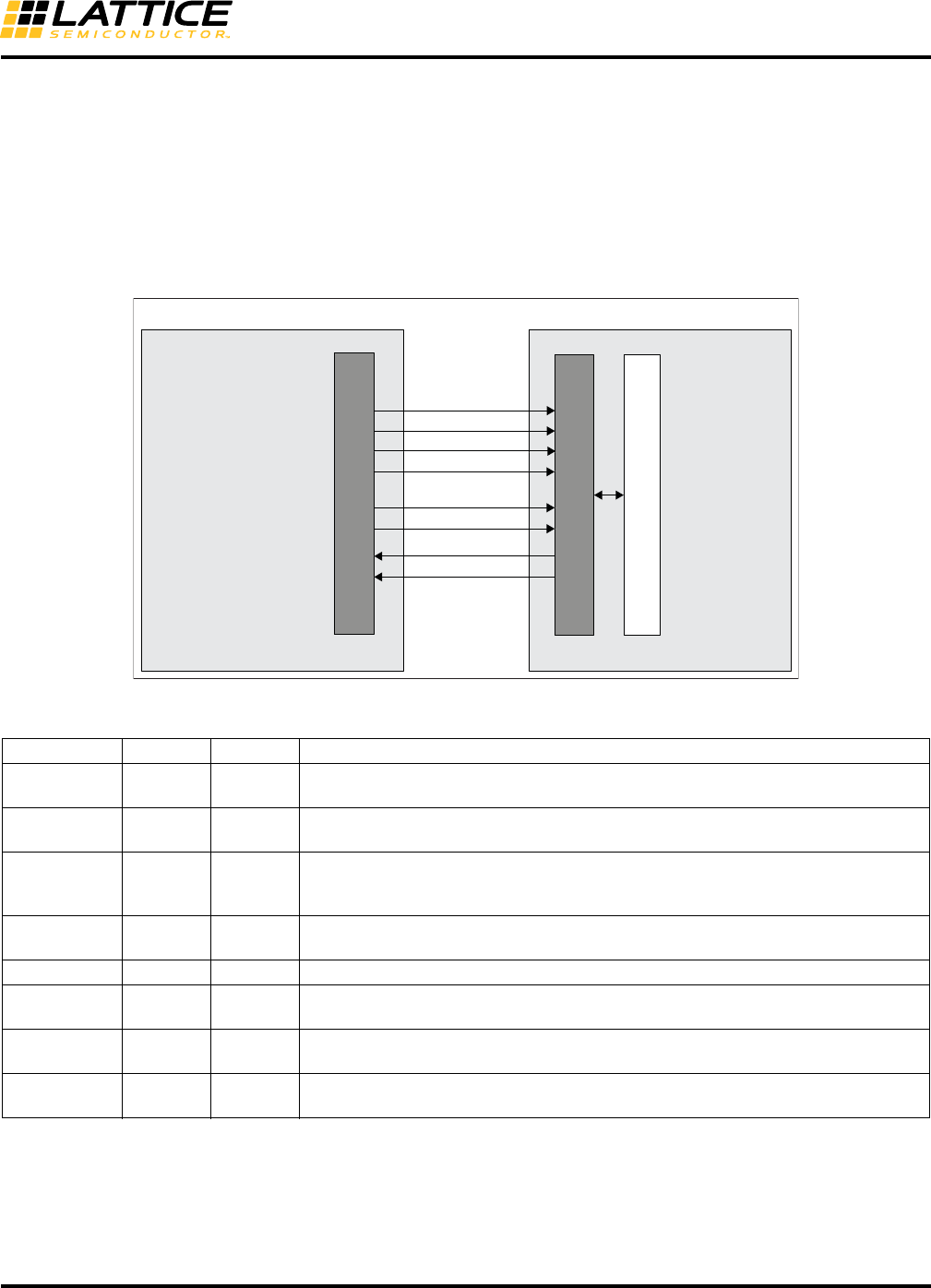
The block diagram in Figure 4 shows the supported System Bus signals between the FPGA core and the Hard-
ened IP. Table 2 provides a detailed definition of the supported signals.
Figure 1. System Bus Interface Between the FPGA Core and the IP
IP Register Map
System Bus Slave Interface
Hardened IP
SBCLKI
System Bus Master (User Logic)
SBSTBI
SBRWI
SBADRI[31:0]
SBDATI[31:0]
SBDATO[31:0]
SBACKO
iCE40LM/iCE40 Ultra
User Logic
Advanced iCE40 I2C and SPI
Hardened IP Usage Guide
Advanced iCE40 I2C and SPI
Hardened IP Usage Guide
2
Table 1. System Bus Slave Interface Signals of the Hardened IP Module
To interface with the IP, you must create a System Bus Master controller in the User Logic. In a multiple-Master
configuration, the System Bus Master outputs are multiplexed through a user-defined arbiter. If two Masters
request the bus in the same cycle, only the outputs of the arbitration winner reach the Slave interface.
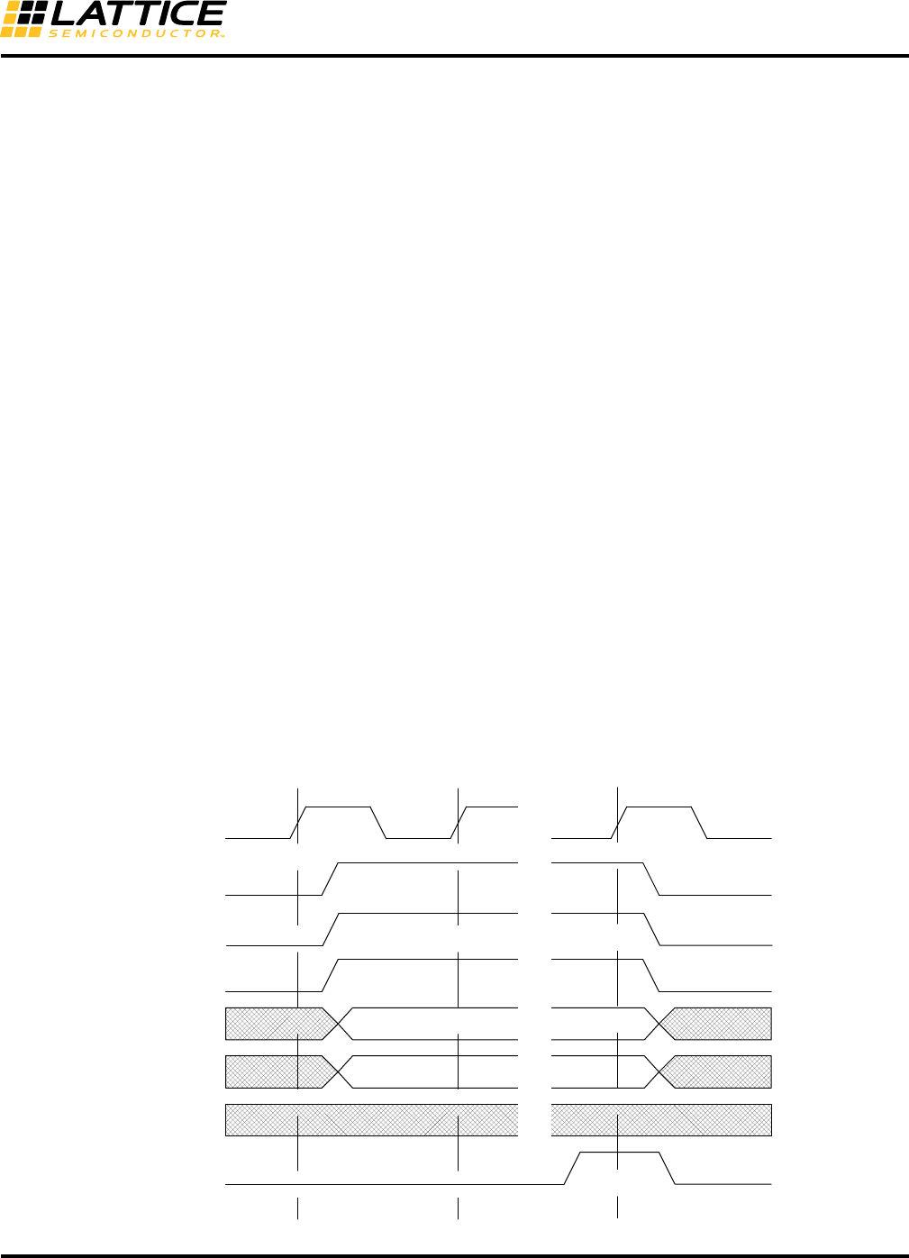
System Bus Write Cycle
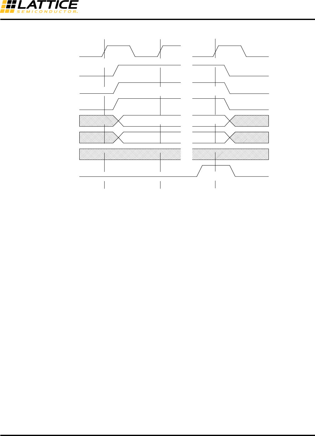
Figure 5 shows the waveform of a Write cycle from the perspective of the System Bus Slave interface. During a sin-
gle Write cycle, only one byte of data is written to the IP block from the System Bus Master. A Write operation
requires a minimum three clock cycles.
On clock Edge 0, the Master updates the address, data and asserts control signals. During this cycle:
• The Master updates the address on the SBADRI[7:0] address lines
• Updates the data that will be written to the IP block, SBDATI[7:0] data lines
• Asserts the write enable SBRWI signal, indicating a write cycle
• Asserts the SBSTBI, selecting a specific slave module
On clock Edge 1, the System Bus Slave decodes the input signals presented by the master. During this cycle:
• The Slave decodes the address presented on the SBADRI[7:0] address lines
• The Slave prepares to latch the data presented on the SBDATI[7:0] data lines
• The Master waits for an active-high level on the SBACKO line and prepares to terminate the cycle on the next
clock edge, if an active-high level is detected on the SBACKO line
• The IP may insert wait states before asserting SBACKO, thereby allowing it to throttle the cycle speed. Any num-
ber of wait states may be added
• The Slave asserts SBACKO signal
The following occurs on clock Edge 2:
• The Slave latches the data presented on the SBDATI[7:0] data lines
• The Master de-asserts the strobe signal, SBSTBI, and the write enable signal, SBRWI
• The Slave de-asserts the acknowledge signal, SBACKO, in response to the Master de-assertion of the strobe
signal
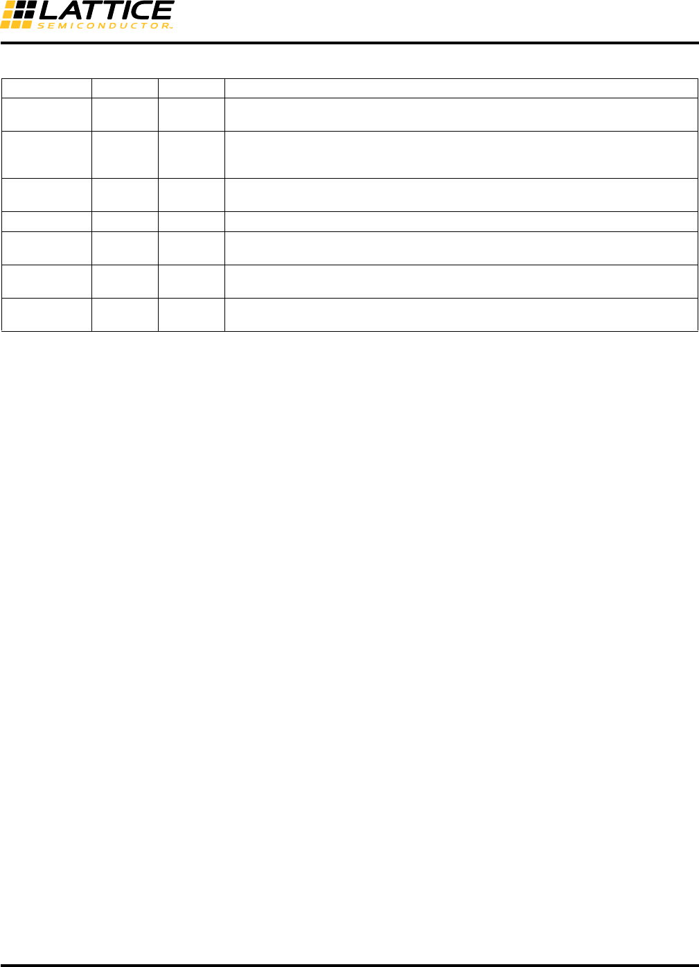
Signal Name I/O Width Description
SBCLKI Input 1 Positive edge clock used by System Bus Interface registers and hardened functions.
Supports clock speeds up to 133 MHz.
SBSTBI Input 1
Active-high strobe, input signal, indicating the System Bus slave is the target for the
current transaction on the bus. The IP asserts an acknowledgment in response to the
assertion of the strobe.
SBRWI Input 1 Level sensitive Write/Read control signal. Low indicates a Read operation, and High
indicates a Write operation.
SBADRI1Input 8 8-bit wide address used to select a specific register from the register map of the IP.
SBDATI Input 8 8-bit input data path used to write a byte of data to a specific register in the register
map of the IP.
SBDATO Output 8 8-bit output data path used to read a byte of data from a specific register in the regis-
ter map of the IP.
SBACKO Output 1 Active-high, transfer acknowledge signal asserted by the IP, indicating the requested
transfer is acknowledged.
1. SBADRI[7:4] must be set to 0001 for upper left I2C and to 0011 for upper right I2C. For values SBADRI[3:0], see Table 3.
Advanced iCE40 I2C and SPI
Hardened IP Usage Guide
3
Figure 2. System Bus Write Operation
System Bus Read Cycle
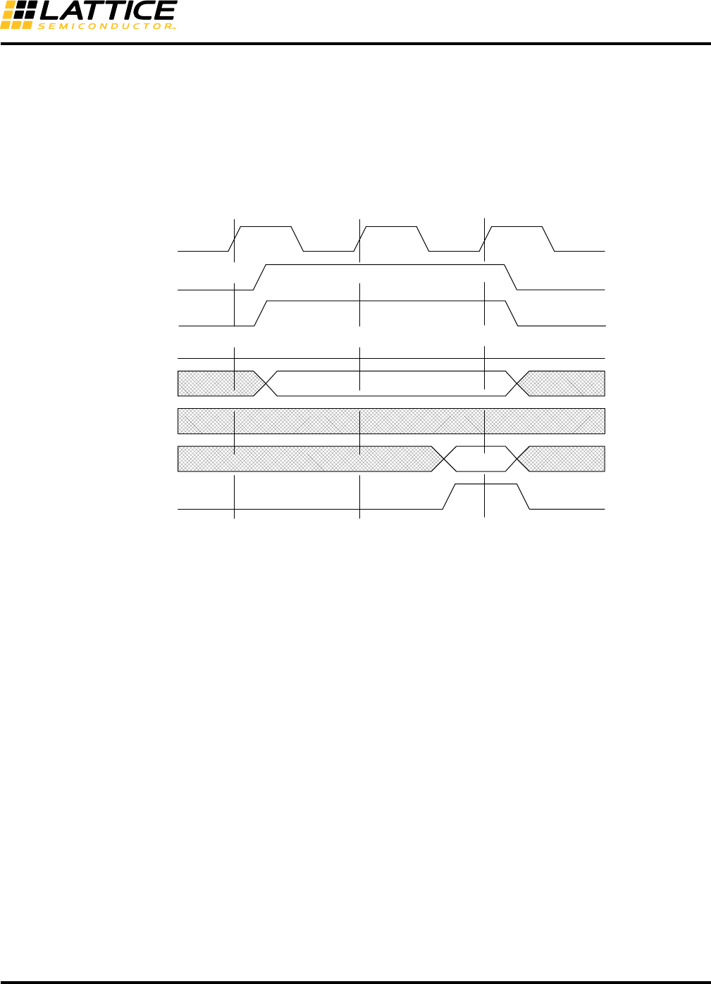
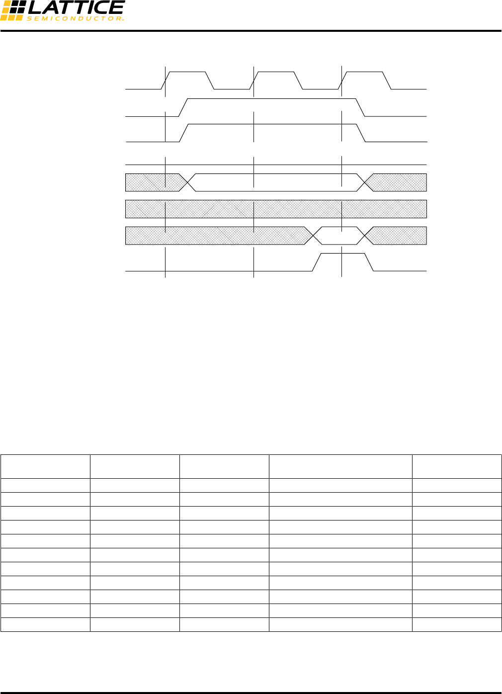
Figure 6 shows the waveform of a Read cycle from the perspective of the System Bus Slave interface. During a sin-
gle Read cycle, only one byte of data is read from the IP block by the System Bus master. A Read operation
requires a minimum three clock cycles.
On clock Edge 0, the Master updates the address, data and asserts control signals. The following occurs during
this cycle:
• The Master updates the address on the SBADRI[7:0] address lines
• De-asserts the write enable SBRWI signal, indicating a Read cycle
• Asserts the SBSTBI, selecting a specific Slave module
On clock Edge 1, the System Bus slave decodes the input signals presented by the master. The following occurs
during this cycle:
• The Slave decodes the address presented on the SBADRI[7:0] address lines
• The Master prepares to latch the data presented on SBDATO[7:0] data lines from the System Bus slave on the
following clock edge
• The Master waits for an active-high level on the SBACKO line and prepares to terminate the cycle on the next
clock edge, if an active-high level is detected on the SBACKO line
• The IP may insert wait states before asserting SBACKO, thereby allowing it to throttle the cycle speed. Any num-
ber of wait states may be added.
• The Slave presents valid data on the SBDATO[7:0] data lines
• The Slave asserts SBACKO signal in response to the strobe, SBSTBI signal
VALID ADDRESS
VALID DATA
Edge 0 Edge 1 Edge 2
SBCLKI
SBSTBI
SBRWI
SBADRI[3:0]
SBDATI[9:0]
SBDATO[9:0]
SBACKO
SBCSI
Advanced iCE40 I2C and SPI
Hardened IP Usage Guide
4
The following occurs on clock Edge 2:
• The Master latches the data presented on the SBDATO[7:0] data lines
• The Master de-asserts the strobe signal SBSTBI
• The Slave de-asserts the acknowledge signal, SBACKO, in response to the master de-assertion of the strobe
signal
Figure 3. System Bus Read Operation
VALID ADDRESS
VALID DATA
Edge 0 Edge 1 Edge 2
SBCLKI
SBSTBI
SBRWI
SBADRI[7:0]
SBDATI[7:0]
SBDATO[7:0]
SBACKO
SBCSI
Advanced iCE40 I2C and SPI
Hardened IP Usage Guide
5
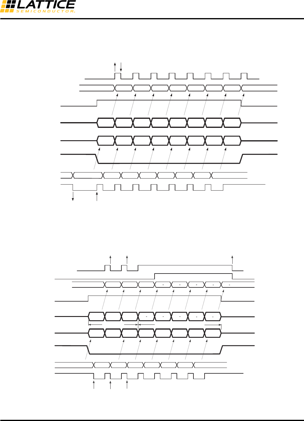
System Bus Interface for iCE40
The System Bus in the iCE40LM, iCE40 Ultra, iCE40 UltraLite and iCE40 UltraPlus provides connectivity between
FPGA user logic and the Hardened IP functional blocks. The user can implement a System Bus Master interface to
interact with the Hardened IP System Bus Slave interface.
The block diagram in Figure 4 shows the supported System Bus signals between the FPGA core and the Hard-
ened IP. Table 2 provides a detailed definition of the supported signals.
Figure 4. System Bus Interface Between the FPGA Core and the IP
Table 2. System Bus Slave Interface Signals of the Hardened IP Module
To interface with the IP, you must create a System Bus Master controller in the User Logic. In a multiple-Master
configuration, the System Bus Master outputs are multiplexed through a user-defined arbiter. If two Masters
request the bus in the same cycle, only the outputs of the arbitration winner reach the Slave interface.
Signal Name I/O Width Description
SBCSI Input 1 This chip select signal activates the IP to allow system bus to communicate with the
IP.
SBCLKI Input 1 Positive edge clock used by System Bus Interface registers and hardened functions.
Supports clock speeds up to 133 MHz.
SBSTBI Input 1
Active-high strobe, input signal, indicating the System Bus slave is the target for the
current transaction on the bus. The IP asserts an acknowledgment in response to the
assertion of the strobe.
SBRWI Input 1 Level sensitive Write/Read control signal. Low indicates a Read operation, and High
indicates a Write operation.
SBADRI Input 4 4-bit wide address used to select a specific register from the register map of the IP.
SBDATI Input 10 8-bit input data path used to write a byte of data to a specific register in the register
map of the IP. 10 bits used for FIFO mode.
SBDATO Output 10 8-bit output data path used to read a byte of data from a specific register in the regis-
ter map of the IP. 10 bits used for FIFO mode.
SBACKO Output 1 Active-high, transfer acknowledge signal asserted by the IP, indicating the requested
transfer is acknowledged.
IP Register Map
System Bus Slave Interface
Hardened IP
SBCLKI
System Bus Master (User Logic)
SBSTBI
SBRWI
SBADRI[31:0]
SBDATI[31:0]
SBDATO[31:0]
SBACKO
iCE40
User Logic
SBCSI
Advanced iCE40 I2C and SPI
Hardened IP Usage Guide
6
System Bus Write Cycle
Figure 5 shows the waveform of a Write cycle from the perspective of the System Bus Slave interface. During a sin-
gle Write cycle, only one byte of data is written to the IP block from the System Bus Master. A Write operation
requires a minimum three clock cycles.
On clock Edge 0, the Master updates the address, data and asserts control signals. During this cycle:
• The Master updates the address on the SBADRI[3:0] address lines
• Updates the data that will be written to the IP block, SBDATI[9:0] data lines
• Asserts the write enable SBRWI signal, indicating a write cycle
• Asserts the SBSTBI, selecting a specific slave module
On clock Edge 1, the System Bus Slave decodes the input signals presented by the master. During this cycle:
• The Slave decodes the address presented on the SBADRI[9:0] address lines
• The Slave prepares to latch the data presented on the SBDATI[9:0] data lines
• The Master waits for an active-high level on the SBACKO line and prepares to terminate the cycle on the next
clock edge, if an active-high level is detected on the SBACKO line
• The IP may insert wait states before asserting SBACKO, thereby allowing it to throttle the cycle speed. Any num-
ber of wait states may be added
• The Slave asserts SBACKO signal
The following occurs on clock Edge 2:
• The Slave latches the data presented on the SBDATI[9:0] data lines
• The Master de-asserts the strobe signal, SBSTBI, and the write enable signal, SBRWI
• The Slave de-asserts the acknowledge signal, SBACKO, in response to the Master de-assertion of the strobe
signal
Figure 5. System Bus Write Operation
VALID ADDRESS
VALID DATA
Edge 0 Edge 1 Edge 2
SBCLKI
SBSTBI
SBRWI
SBADRI[3:0]
SBDATI[9:0]
SBDATO[9:0]
SBACKO
SBCSI

Advanced iCE40 I2C and SPI
Hardened IP Usage Guide
7
System Bus Read Cycle
Figure 6 shows the waveform of a Read cycle from the perspective of the System Bus Slave interface. During a sin-
gle Read cycle, only one byte of data is read from the IP block by the System Bus master. A Read operation
requires a minimum three clock cycles.
On clock Edge 0, the Master updates the address, data and asserts control signals. The following occurs during
this cycle:
• The Master updates the address on the SBADRI[3:0] address lines
• De-asserts the write enable SBRWI signal, indicating a Read cycle
• Asserts the SBSTBI, selecting a specific Slave module
On clock Edge 1, the System Bus slave decodes the input signals presented by the master. The following occurs
during this cycle:
• The Slave decodes the address presented on the SBADRI[3:0] address lines
• The Master prepares to latch the data presented on SBDATO[9:0] data lines from the System Bus slave on the
following clock edge
• The Master waits for an active-high level on the SBACKO line and prepares to terminate the cycle on the next
clock edge, if an active-high level is detected on the SBACKO line
• The IP may insert wait states before asserting SBACKO, thereby allowing it to throttle the cycle speed. Any num-
ber of wait states may be added.
• The Slave presents valid data on the SBDATO[9:0] data lines
• The Slave asserts SBACKO signal in response to the strobe, SBSTBI signal
The following occurs on clock Edge 2:
• The Master latches the data presented on the SBDATO[9:0] data lines
• The Master de-asserts the strobe signal SBSTBI
• The Slave de-asserts the acknowledge signal, SBACKO, in response to the master de-assertion of the strobe
signal
Advanced iCE40 I2C and SPI
Hardened IP Usage Guide
8
Figure 6. System Bus Read Operation
Hardened I2C IP Cores
I2C is a widely used two-wire serial bus for communication between devices on the same board. Every iCE40LM,
iCE40 Ultra, iCE40 UltraLite and iCE40 UltraPlus device contains two hardened I2C IP cores. Either of the two
cores can be operated as an I2C Master or as an I2C Slave.
I2C Registers for iCE40LM and iCE40 Ultra
Both I2C cores communicate with the System Bus interface through a set of control, command, status and data
registers. Table 3 shows the register names and their functions.
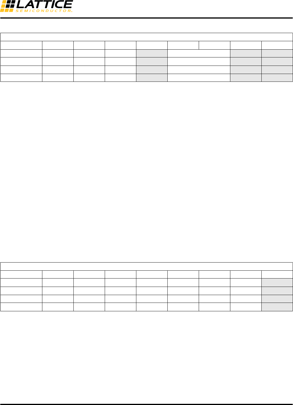
Table 3. I2C Registers Summary
I2C Register Name Simulation Model
Register Name Address[3:0] Register Function Access
I2CCR1 I2CCR1 1000 Control Read/Write
I2CCMDR I2CCMDR 1001 Command Read/Write
I2CBRLSB I2CBRLSB 1010 Clock Prescale register, LSB Read/Write
I2CBRMSB I2CBRMSB 1011 Clock Prescale register, MSB Read/Write
I2CSR I2CSR 1100 Status Read
I2CTXDR I2CTXDR 1101 Transmit Data Write
I2CRXDR I2CRXDR 1110 Receive Data Read
I2CGCDR I2CGCDR 1111 General Call Information Read
I2CSADDR I2CSADDR 0011 Slave Address MSB Read/Write
I2CIRQEN I2CINTCR 0111 Interrupt Enable Read/Write
I2CIRQ I2CINTSR 0110 Interrupt Status Read/Write1
1. I2CIRQ is Read Only. Write operation upon this register will not change the content of this register, but will clear corresponding interrupt flag
caused by the flags inside I2CIRQ.
VALID ADDRESS
VALID DATA
Edge 0 Edge 1 Edge 2
SBCLKI
SBSTBI
SBRWI
SBADRI[7:0]
SBDATI[7:0]
SBDATO[7:0]
SBACKO
SBCSI
Advanced iCE40 I2C and SPI
Hardened IP Usage Guide
9
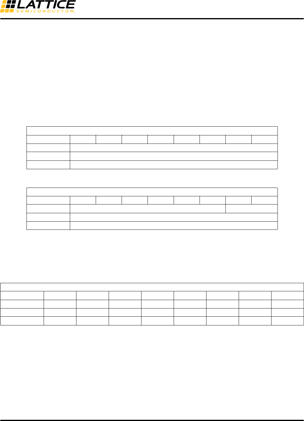
Table 4. I2C Control Register 1 (I2CCR1)1
I2CEN I2C System Enable Bit – This bit enables the I2C core functions. If I2CEN is cleared,
the 2C core is disabled and forced into idle state.
GCEN Enable bit for General Call Response – Enables the general call response in slave
mode.
0: Disable
1: Enable
The General Call address is defined as 0000000 and works with either 7-bit or 10-bit
addressing
WKUPEN Wake-up from Standby/Sleep(by Slave Address matching) Enable Bit – When this bit
is enabled the, I2C core can send a wake-up signal to wake the device up from
standby/sleep. The wake-up function is activated when the Slave Address is matched
during standby/sleep mode.
SDA_DEL_SEL[1:0] SDA Output Delay (Tdel) Selection (See Figure 14)
00: 300 ns (min) 300 ns + 2000/[wb_clk_i frequency in MHz] (max)
01: 150 ns (min) 150 ns + 2000/[wb_clk_i frequency in MHz] (max)
10: 75 ns (min) 75 ns + 2000/[wb_clk_i frequency in MHz] (max)
11: 0 ns (min) 0 ns + 2000/[wb_clk_i frequency in MHz] (max)
Table 5. I2C Command Register (I2CCMDR)
STA Generate START (or Repeated START) condition (Master operation)
STO Generate STOP condition (Master operation)
RD Indicate Read from slave (Master operation)
WR Indicate Write to slave (Master operation)
ACK Acknowledge Option – when receiving, ACK transmission selection
0: Send ACK
1: Send NACK
I2CCR1
Bit Bit7 Bit6 Bit5 Bit4 Bit3 Bit2 Bit1 Bit0
Name I2CEN GCEN WKUPEN (Reserved) SDA_DEL_SEL (Reserved) (Reserved)
Default 0 0 0 0000 0
0 to Disable YES YES YES --- -
Access R/WR/WR/W-R/W- -
1. A write to this register will cause the I2C core to reset
I2CCMDR
Bit Bit7 Bit6 Bit5 Bit4 Bit3 Bit2 Bit1 Bit0
Name STA STO RD WR ACK CKSDIS RBUFDIS (Reserved)
Default 00000000
0 to Disable YES YES YES - - No No -
Access R/WR/WR/WR/WR/WR/WR/W-
Advanced iCE40 I2C and SPI
Hardened IP Usage Guide
10
CKSDIS Clock Stretching Disable – Disables the clock stretching if desired by the user for both
master and slave mode. Then overflow error flag must be monitored.0:Send ACK
0: Enable Clock Stretching
1: Disable Clock Stretching
RBUFDIS Read Command with Buffer Disable – Read from Slave in master mode with the dou-
ble buffering disabled for easier control over single byte data communication scenario.
0: Read with buffer enabled as default
1: Read with buffer disabled
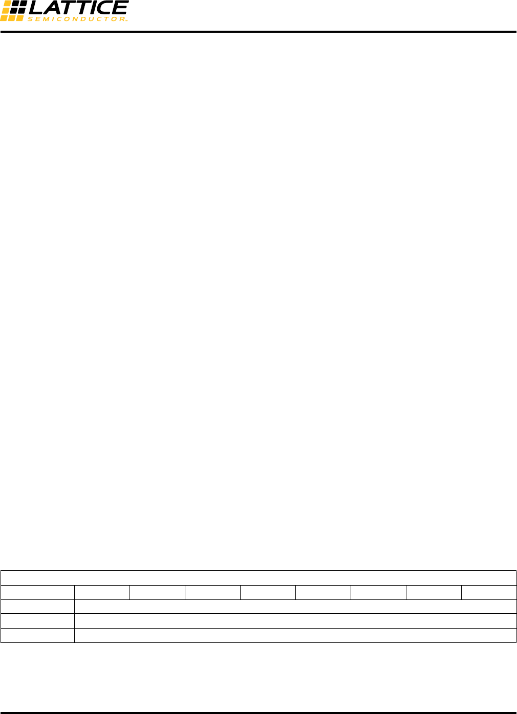
Table 6. I2C Clock Pre-scale Register (I2CBRLSB)
Table 7. I2C Clock Pre-scale Register (I2CBRMSB)
I2C_PRESCALE[9:0]
I2C Clock Pre-scale value. A write operation to I2CBRMSB[1:0] will cause an I2C core reset. The System Bus
clock frequency is divided by (I2C_PRESCALE*4) to produce the Master I2C clock frequency supported by the I2C
bus (50KHz, 100KHz, 400KHz).
Table 8. I2C Status Register (I2CSR)
TIP Transmitting In Progress - This bit indicates that current data byte is being transferred
for both master and slave mode. Note that the TIP flag will suffer half SCL cycle
latency right after the start condition because of the signal synchronization. Note also
that this bit could be high after configuration wake-up and before the first valid I2C
transfer start (when BUSY is low), and it is not indicating byte in transfer, but an invalid
indicator.
0: Byte transfer completed
1: Byte transfer in progress
I2CBRLSB
Bit Bit7 Bit6 Bit5 Bit4 Bit3 Bit2 Bit1 Bit0
Name I2C_PRESCALE
Default 00000000
Access R/W
I2CBRMSB
Bit Bit7 Bit6 Bit5 Bit4 Bit3 Bit2 Bit1 Bit0
Name - I2C_PRESCALE
Default 00000000
Access R/W
I2CSR
Bit Bit7 Bit6 Bit5 Bit4 Bit3 Bit2 Bit1 Bit0
Name TIP BUSY RARC SRWARBL TRRDY TROE HGC
Default --------
Access RRRRRRRR
Advanced iCE40 I2C and SPI
Hardened IP Usage Guide
11
BUSY Bus Busy – This bit indicates the bus is involved in transaction. This will be set at start
condition and cleared at stop. Therefore, only when this bit is high, should all other
status bits be treated as valid indicators for a valid transfer.
RARC Received Acknowledge – This flag represents acknowledge response from the
addressed slave during master write or from receiving master during master read.
0: No acknowledge received
1: Acknowledge received
SRWSlave RW
0: Master transmitting / Slave receiving
1: Master receiving / Slave transmitting
ARBL Arbitration Lost – This bit will go high if master has lost its arbitration in Master mode,
It will cause an interrupt to System Bus Host if SCI set up allowed.
0: Normal
1: Arbitration Lost
TRRDY Transmitter or Receiver Ready Bit – This flag indicate that a Transmit Register ready
to receive data or Receiver Register if ready for read depend on the mode (master or
slave) and SRW bit. It will cause an interrupt to System Bus Host if SCI set up allowed.
0: Transmitter or Receiver is not ready
1: Transmitter or Receiver is ready
TROE Transmitter/Receiver Overrun or NACK Received Bit – This flag indicate that a Trans-
mit or Receive Overrun Errors happened depend on the mode (master or slave) and
SRW bit, or a no-acknowledges response is received after transmitting a byte. If
RARC bit is high, it is a NACK bit, otherwise, it is overrun bit. It will cause an interrupt
to System Bus Host if SCI set up allowed.
0: Transmitter or Receiver Normal or Acknowledge Received for Transmitting
1: Transmitter or Receiver Overrun or No-Acknowledge Received for
Transmitting
HGC Hardware General Call Received – This flag indicate that a hardware general call is
received from the slave port. It will cause an interrupt to System Bus Host if SCI set up
allowed.
0: NO Hardware General Call Received in Slave Mode
1: Hardware General Call Received in Slave Mode
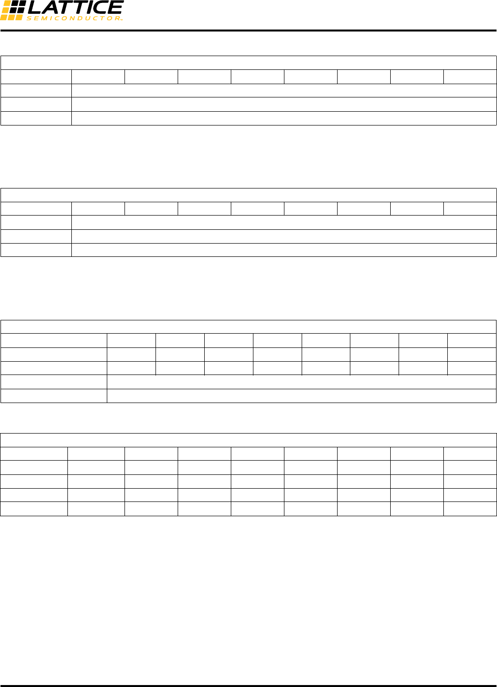
Table 9. I2C Transmitting Data Register (I2CTXDR)
I2C_ Transmit_Data[7:0] I2C Transmit Data – This register holds the byte that will be transmitted on the I2C bus
during the Write Data phase. Bit 0 is the LSB and will be transmitted last. When trans-
mitting the slave address, Bit 0 represents the Read/Write bit.
I2CTXDR
Bit Bit7 Bit6 Bit5 Bit4 Bit3 Bit2 Bit1 Bit0
Name I2C_Transmit_Data[7:0]
Default 00000000
Access W
Advanced iCE40 I2C and SPI
Hardened IP Usage Guide
12
Table 10. I2C Receiving Data Register (I2CRXDR)
I2C_ Receive _Data[7:0] I2C Receive Data – This register holds the byte captured from the I2C bus during the
Read Data phase. Bit 0 is LSB and was received last.
Table 11. I2C General Call Data Register (I2CGCDR)
I2C_ GC _Data[7:0] I2C General Call Data – This register holds the second (command) byte of the Gen-
eral Call transaction on the I2C bus.
Table 12. I2C Slave Address MSB Register (I2CSADDR)
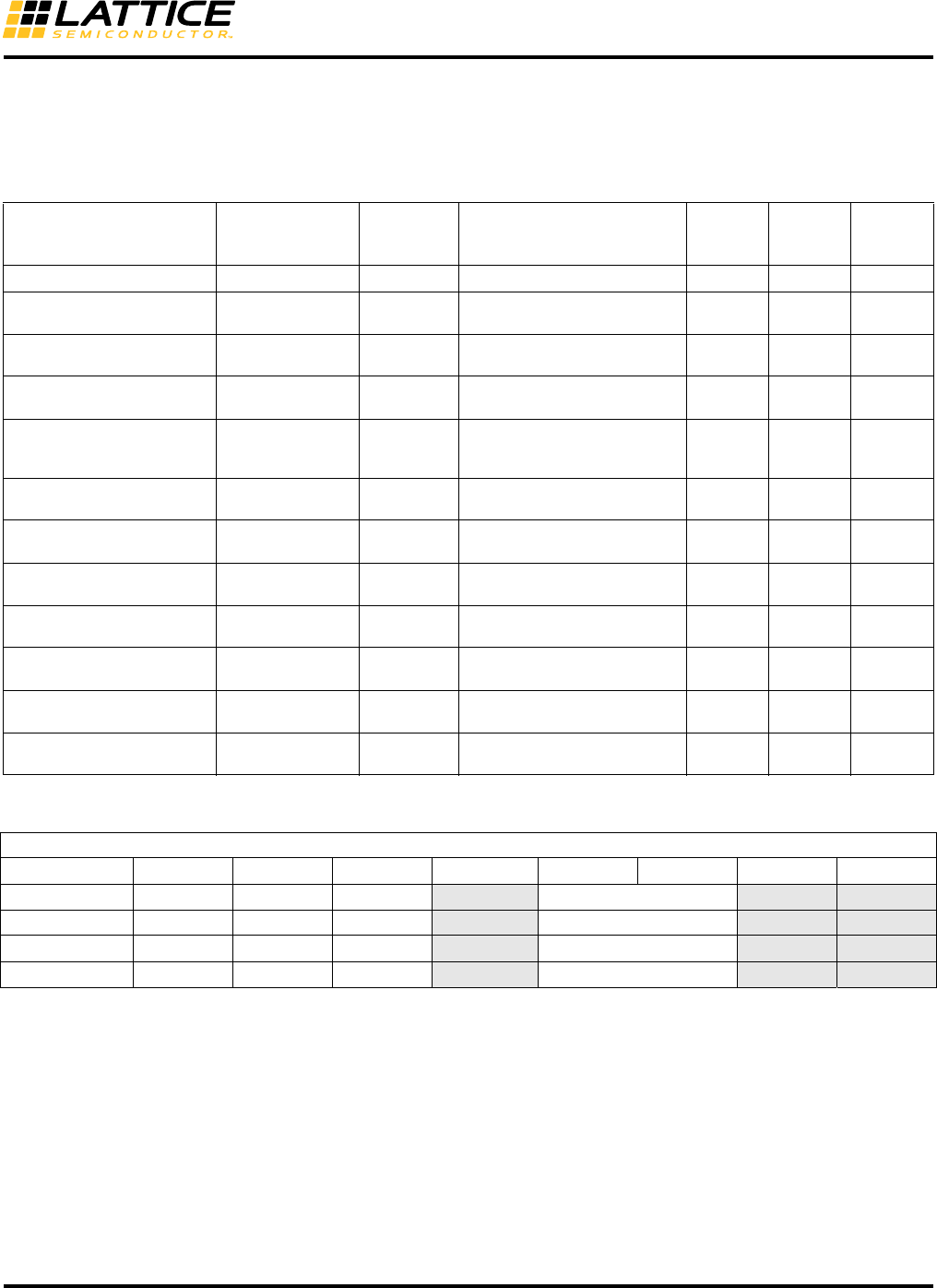
Table 13. I2C Interrupt Control Register (I2CIRQEN)
IRQINTCLREN Auto Interrupt Clear Enable – Enable the interrupt flag auto clear when the I2CIRQ
has been read.
IRQINTFRC Force Interrupt Request On – Force the Interrupt Flag set to improve testability
IRQARBLEN Interrupt Enable for Arbitration Lost
IRQTRRDYEN Interrupt Enable for Transmitter or Receiver Ready
IRQTROEEN Interrupt Enable for Transmitter/Receiver Overrun or NACK Received
IRQHGCEN Interrupt Enable for Hardware General Call Received
I2CTXDR
Bit Bit7 Bit6 Bit5 Bit4 Bit3 Bit2 Bit1 Bit0
Name I2C_Receive_Data[7:0]
Default -
Access R
I2CGCDR
Bit Bit7 Bit6 Bit5 Bit4 Bit3 Bit2 Bit1 Bit0
Name I2C_GC_Data[7:0]
Default -
Access R
I2CSADDR
Bit Bit7 Bit6 Bit5 Bit4 Bit3 Bit2 Bit1 Bit0
7 Bits Addressing - - - A6 A5 A4 A3 A2
10 Bits Addressing A9 A8 A7 A6 A5 A4 A3 A2
Default 00000000
Access R/W
I2CIRQEN
Bit Bit7 Bit6 Bit5 Bit4 Bit3 Bit2 Bit1 Bit0
Name IRQINTCLREN IRQINTFRC RSVDRSVD IRQARBLEN IRQTRRDYEN IRQTROEEN IRQHGCEN
Default 0 0 - - 0000
0 to Disable YES YES - - YES Yes YES YES
Access R/WR/W--R/WR/WR/WR/W

Advanced iCE40 I2C and SPI
Hardened IP Usage Guide
13
Table 14. I2C Interrupt Status Register (I2CIRQ)
IRQARBL Interrupt Status for Arbitration Lost.
When enabled, indicates ARBL was asserted. Write a ‘1’ to this bit to clear the inter-
rupt.
0: No interrupt
1: Arbitration Lost Interrupt
IRQTRRDY Interrupt Status for Transmitter or Receiver Ready.
When enabled, indicates TRRDY was asserted. Write a ‘1’ to this bit to clear the inter-
rupt.
0: No interrupt
1: Transmitter or Receiver Ready Interrupt
IRQTROE Interrupt Status for Transmitter/Receiver Overrun or NACK received.
When enabled, indicates TROE was asserted. Write a ‘1’ to this bit to clear the inter-
rupt.
0: No interrupt
1: Transmitter or Receiver Overrun or NACK received Interrupt
IRQHGC Interrupt Status for Hardware General Call Received.
When enabled, indicates HGC was asserted. Write a ‘1’ to this bit to clear the inter-
rupt.
0: No interrupt
1: General Call Received in slave mode Interrupt
I2CIRQ
Bit Bit7 Bit6 Bit5 Bit4 Bit3 Bit2 Bit1 Bit0
Name (Reserved) IRQARBL IRQTRRDY IRQTROE IRQHGC
Default --------
Access ----R/WR/WR/WR/W
Advanced iCE40 I2C and SPI
Hardened IP Usage Guide
14
I2C Registers for iCE40 UltraLite and iCE40 UltraPlus
Both I2C cores communicate with the System Bus interface through a set of control, command, status and data
registers. Table 15 shows the register names and their functions.
Table 15. I2C Registers Summary
Table 16. I2C Control Register 1 (I2CCR1)1
I2CEN I2C System Enable Bit – This bit enables the I2C core functions. If I2CEN is cleared,
the 2C core is disabled and forced into idle state.
GCEN Enable bit for General Call Response – Enables the general call response in slave
mode.
0: Disable
1: Enable
The General Call address is defined as 0000000 and works with either 7-bit or 10-bit
addressing
Name
Simulation
Model
Register Name
SB
Address
[3:0]
Register Function Register
Width
Support
Modes Access
I2CCR1 I2CCR1 0001 I2C Control Register 1 8 Both RW
I2CBRLSB I2CBRLSB 0010 I2C Clock Presale register,
LSB
8BothRW
I2CBRMSB I2CBRMSB 0011 I2C Clock Presale register,
MSB
8BothRW
I2CSADDR/I2CFIFOSADDR I2CSADDR 0100 I2C Slave address / FIFO
Slave Address
8/10 Both RW
I2CIRQEN/I2CFIFOIRQEN 0101 I2C Interrupt Control Register
/ FIFO interrupt Control regis-
ter
8/10 Both RW
I2CFIFOTHRESHOLD 0110 I2C FIFO Threshold Register 10 FIFO
mode
RW
I2CCMDR I2CCMDR 0111 I2C Command Register 8 Reg
mode
RW
I2CTXDR/I2CTXFIFO I2CTXDR 1000 I2C Transmitting Data Regis-
ter / FIFO
8/10 Both W
I2CRXDR/I2CRXFIFO I2CRXDR 1001 I2C Receiving Data Register /
FIFO
8/10 Both R
I2CGCDR I2CGCDR 1010 I2C General Call Information
Register
8BothR
I2CSR/I2CFIFOSR I2CSR 1011 I2C Status Register / FIFO
Status Register
8/10 Both R
I2CIRQ/I2CFIFOIRQ I2CINTCR 1100 I2C Interrupt Status Register /
FIFO Interrupt Status register
8/10 Both R
I2CCR1
Bit Bit7 Bit6 Bit5 Bit4 Bit3 Bit2 Bit1 Bit0
Name I2CEN GCEN WKUPEN FIFO_MODE SDA_DEL_SEL CLKSDIS (Reserved)
Default 0 0 0 0000 0
0 to Disable Yes Yes Yes Ye s - Ye s -
Access R/WR/WR/WR/WR/WR/W-
1. A write to this register will cause the I2C core to reset

Advanced iCE40 I2C and SPI
Hardened IP Usage Guide
15
WKUPEN Wake-up from Standby/Sleep(by Slave Address matching) Enable Bit – When this bit
is enabled the, I2C core can send a wake-up signal to wake the device up from
standby/sleep. The wake-up function is activated when the Slave Address is matched
during standby/sleep mode.
FIFO_MODE 0: Register mode (default)
1: FIFO mode
SDA_DEL_SEL[1:0] SDA Output Delay (Tdel) Selection (See Figure 14)
00: 300 ns
CKSDIS Clock Stretching Disable Option (used in FIFO mode only)
Disable the clock stretching if desired by user for both master and slave mode. Then
overflow error flag must be monitored.
0: Clock Stretching is Enabled
1: Clock Stretching is Disabled
Table 17. I2C Command Register (I2CCMDR)
STA Generate START (or Repeated START) condition (Master operation)
STO Generate STOP condition (Master operation)
RD Indicate Read from slave (Master operation)
WR Indicate Write to slave (Master operation)
ACK Acknowledge Option – when receiving, ACK transmission selection
0: Send ACK
1: Send NACK
CKSDIS Clock Stretching Disable – Disables the clock stretching if desired by the user for both
master and slave mode. Then overflow error flag must be monitored.0:Send ACK
0: Enable Clock Stretching
1: Disable Clock Stretching
RBUFDIS Read Command with Buffer Disable – Read from Slave in master mode with the dou-
ble buffering disabled for easier control over single byte data communication scenario.
0: Read with buffer enabled as default
1: Read with buffer disabled
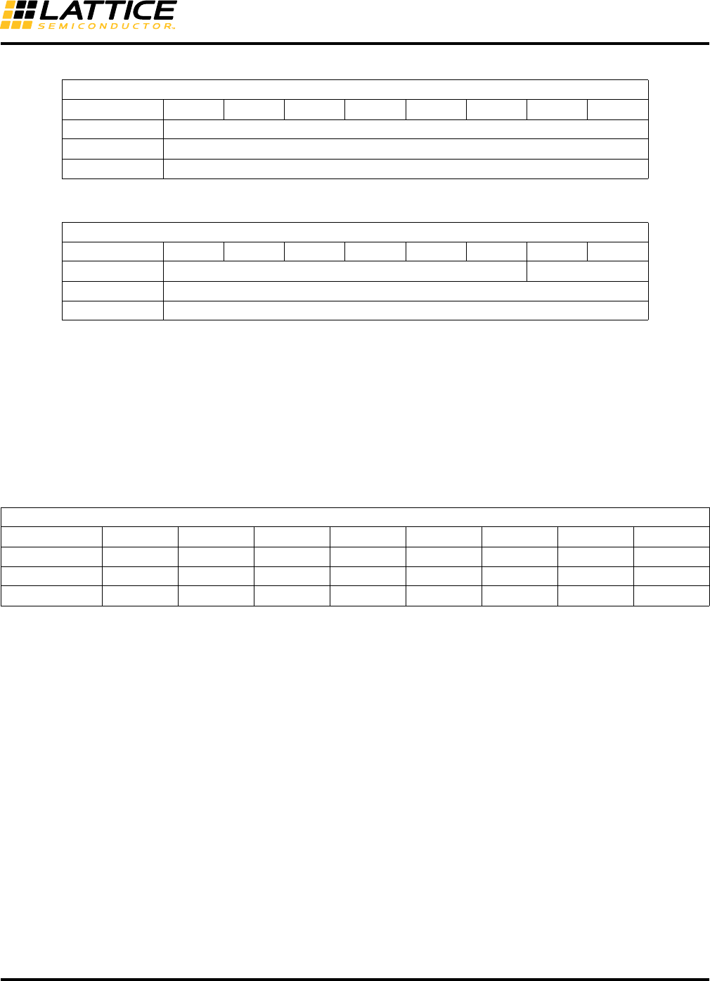
I2CCMDR
Bit Bit7 Bit6 Bit5 Bit4 Bit3 Bit2 Bit1 Bit0
Name STA STO RD WR ACK CKSDIS RBUFDIS (Reserved)
Default 00000000
0 to Disable YES YES YES - - No No -
Access R/WR/WR/WR/WR/WR/WR/W-
Advanced iCE40 I2C and SPI
Hardened IP Usage Guide
16
Table 18. I2C Clock Pre-scale Register (I2CBRLSB)
Table 19. I2C Clock Pre-scale Register (I2CBRMSB)
I2C_PRESCALE[9:0]
I2C Clock Pre-scale value. A write operation to I2CBRMSB[1:0] will cause an I2C core reset. The System Bus
clock frequency is divided by (I2C_PRESCALE*4) to produce the Master I2C clock frequency supported by the I2C
bus (50 kHz, 100 kHz, 400 kHz).
I2C Status Register (I2CSR/I2CFIFOSR)
This address is shared by both Register mode and FIFO mode. However, the definition of each status bit is different
for each mode.
Table 20. I2C Status Register (I2CSR)
TIP Transmitting In Progress - This bit indicates that current data byte is being transferred
for both master and slave mode. Note that the TIP flag will suffer half SCL cycle
latency right after the start condition because of the signal synchronization. Note also
that this bit could be high after configuration wake-up and before the first valid I2C
transfer start (when BUSY is low), and it is not indicating byte in transfer, but an invalid
indicator.
0: Byte transfer completed
1: Byte transfer in progress
BUSY Bus Busy – This bit indicates the bus is involved in transaction. This will be set at start
condition and cleared at stop. Therefore, only when this bit is high, should all other
status bits be treated as valid indicators for a valid transfer.
RARC Received Acknowledge – This flag represents acknowledge response from the
addressed slave during master write or from receiving master during master read.
0: No acknowledge received
1: Acknowledge received
SRWSlave RW
I2CBRLSB
Bit Bit7 Bit6 Bit5 Bit4 Bit3 Bit2 Bit1 Bit0
Name I2C_PRESCALE
Default 00000000
Access R/W
I2CBRMSB
Bit Bit7 Bit6 Bit5 Bit4 Bit3 Bit2 Bit1 Bit0
Name - I2C_PRESCALE
Default 00000000
Access R/W
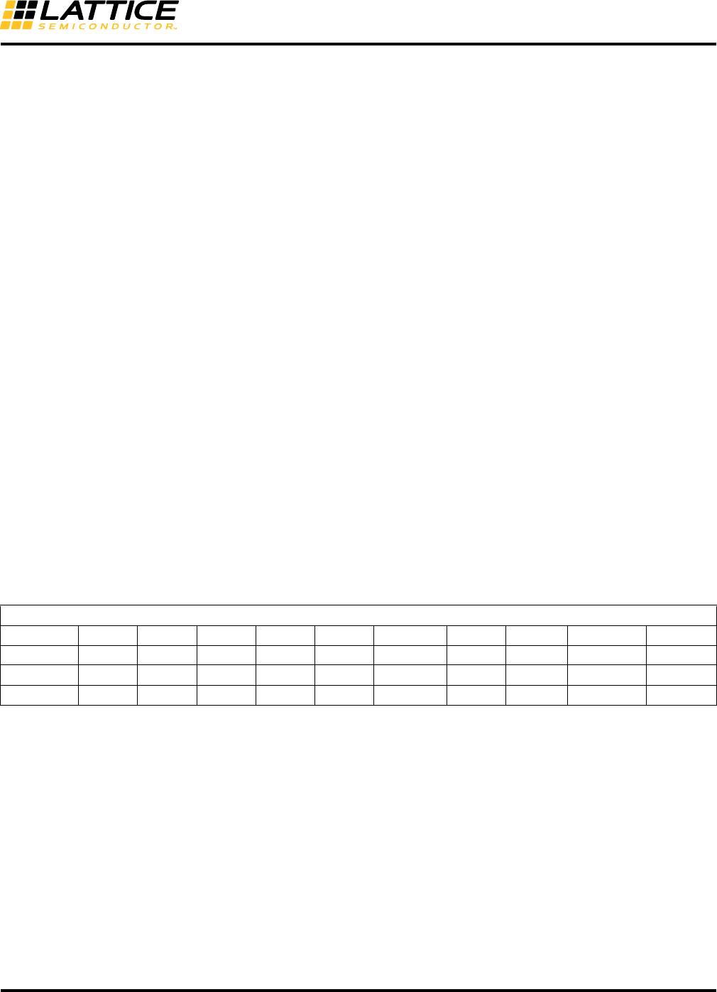
I2CSR (Register Mode)
Bit Bit7 Bit6 Bit5 Bit4 Bit3 Bit2 Bit1 Bit0
Name TIP BUSY RARC SRWARBL TRRDY TROE HGC
Default --------
Access RRRRRRRR
Advanced iCE40 I2C and SPI
Hardened IP Usage Guide
17
0: Master transmitting / Slave receiving
1: Master receiving / Slave transmitting
ARBL Arbitration Lost – This bit will go high if master has lost its arbitration in Master mode,
It will cause an interrupt to System Bus Host if SCI set up allowed.
0: Normal
1: Arbitration Lost
TRRDY Transmitter or Receiver Ready Bit – This flag indicate that a Transmit Register ready
to receive data or Receiver Register if ready for read depend on the mode (master or
slave) and SRW bit. It will cause an interrupt to System Bus Host if SCI set up allowed.
0: Transmitter or Receiver is not ready
1: Transmitter or Receiver is ready
TROE Transmitter/Receiver Overrun or NACK Received Bit – This flag indicate that a Trans-
mit or Receive Overrun Errors happened depend on the mode (master or slave) and
SRW bit, or a no-acknowledges response is received after transmitting a byte. If
RARC bit is high, it is a NACK bit, otherwise, it is overrun bit. It will cause an interrupt
to System Bus Host if SCI set up allowed.
0: Transmitter or Receiver Normal or Acknowledge Received for Transmitting
1: Transmitter or Receiver Overrun or No-Acknowledge Received for
Transmitting
HGC Hardware General Call Received – This flag indicate that a hardware general call is
received from the slave port. It will cause an interrupt to System Bus Host if SCI set up
allowed.
0: NO Hardware General Call Received in Slave Mode
1: Hardware General Call Received in Slave Mode
Table 21. I2C Status Register (I2CFIFOSR)
HGC Hardware General Call Received – This flag indicate that a hardware general call is
received from the slave port. It will cause an interrupt to System Bus Host if SCI set up
allowed.
0: NO Hardware General Call Received in Slave Mode
1: Hardware General Call Received in Slave Mode
RNACK Received NACK – This flag represents acknowledge response from the addressed
slave during master write.
0: Acknowledge received
1: No acknowledge (NACK) is received, FIFO state machine issues a
STOP and go to idle state.
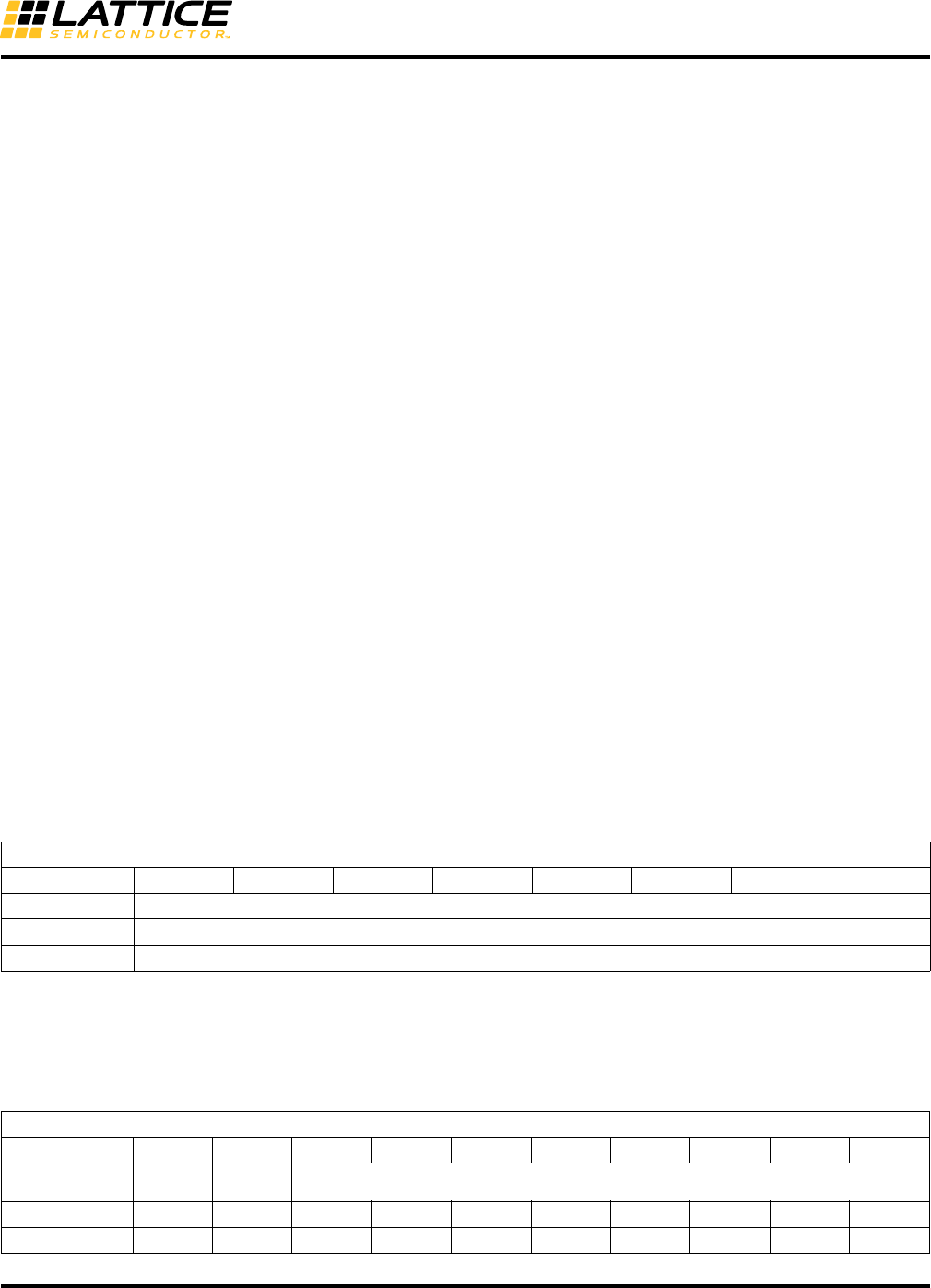
I2CFIFOSR (FIFO Mode)
Bit Bit 9 Bit 8 Bit7 Bit6 Bit5 Bit4 Bit3 Bit2 Bit1 Bit0
Name RSVDRSVDRSVD HGC RNACK MRDCMPL ARBL TXSERR TXUNDERF RXOVERF
Default ----- - -- - -
Access R R R R R R R R R R
Advanced iCE40 I2C and SPI
Hardened IP Usage Guide
18
MRDCMPL Master Read Complete – This is only valid for Master Read mode.
0: Transaction is not completed.
1: Transaction is completed. In Master read mode, it means 1) the number of
bytes read equals to the expected number, 2) Master terminates the read
earlier but there is data in the RX FIFO.
ARBL Arbitration Lost – This bit will go high if the master has lost its arbitration in Master
mode.
0: Normal
1: Arbitration Lost, FIFO state machine goes to idle state.
TXSERR TX FIFO synchronization error. This happens when there are back-to-back commands
in the FIFO.
0: No synchronization error
1: Synchronization error, the previous command is overwritten, then continues
with the next data entry in the FIFO.
TXUNDERF TX FIFO underflow – This indicates an error condition, mutually exclusive with clock
stretching function.
0: No underflow
1: FIFO underflow, data is not valid
RXOVERF RX FIFO overflow – This indicates an error condition, mutually exclusive with clock
stretching function.
0: No overflow
1: FIFO overflow, data is not valid
I2C Transmitting Data Register (I2CTXDR/I2CTXFIFO)
This address is shared by both Register mode and FIFO mode. However, the definition of each status bit is different
for each mode.
Table 22. I2C Transmitting Data Register (I2CTXDR)
I2C_ Transmit_Data[7:0] I2C Transmit Data – This register holds the byte that will be transmitted on the I2C bus
during the Write Data phase. Bit 0 is the LSB and will be transmitted last. When trans-
mitting the slave address, Bit 0 represents the Read/Write bit.
Table 23. I2C Transmitting Data Register (I2CTXFIFO)
I2CTXDR (Register Mode)
Bit Bit7 Bit6 Bit5 Bit4 Bit3 Bit2 Bit1 Bit0
Name I2C_Transmit_Data[7:0]
Default 00000000
Access W
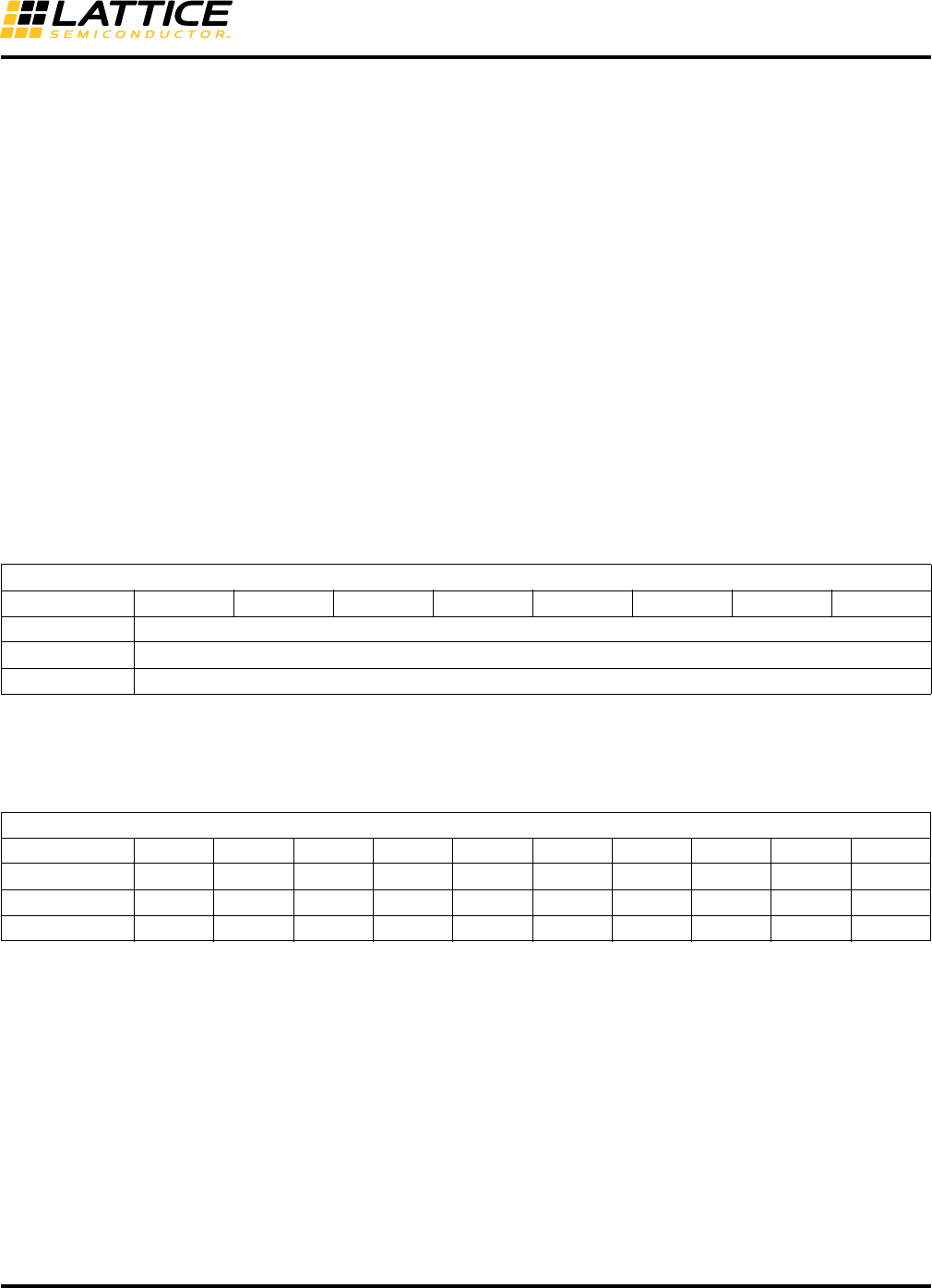
I2CTXFIFO (FIFO Mode)
Bit Bit 9 Bit 8 Bit7 Bit6 Bit5 Bit4 Bit3 Bit2 Bit1 Bit0
Name CMD RSTAEN/
LTXBYTE RXBYTE
Default 0000000000
Access WWWWWWWWWW
Advanced iCE40 I2C and SPI
Hardened IP Usage Guide
19
CMD, RSTAEN 10: Bits [4:0] of this byte is the number of bytes to be received (in Master
mode). Following data transaction should be sent using a STOP then a
START.
11: Bits [4:0] of this byte is the number of bytes to be received (in Master mode).
Following data transaction should be sent using a START/ReSTART. The 1st
data byte should always has RSTAEN bit set to 1.
CMD, LTXBYTE 00: Bits [7:0] of this byte are data bits. If this is the last data byte in the TXFIFO,
then depending on the CKSDIS bit, Master Write will either go into clock
stretching (CKSDIS=0), or TXFIFO will underflow (CKSDIS=1).
01: Bit [7:0] of this byte are data bytes. If this is the last data byte in TXFIFO, this
indicates the last byte to be transferred and a STOP will be issued. If this is
not the last byte in TXFIFO, then this bit is ignored.
RXBYTE[7:5] Not used when CMD =1; data byte when CMD =0
RXBYTE[4:0] Data byte
I2C Receiving Data Register (I2CRXDR/I2CRXFIFO)
This address is shared by both Register mode and FIFO mode. However, the definition of each status bit is different
for each mode.
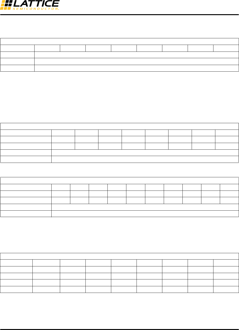
Table 24. I2C Receiving Data Register (I2CRXDR)
I2C_ Receive _Data[7:0] I2C Receive Data – This register holds the byte captured from the I2C bus during the
Read Data phase. Bit 0 is LSB and was received last.
Table 25. I2C Receiving Data Register (I2CRXFIFO)
DFIRST Last byte of data
0: Normal data
1: First byte received after a Start or a ReStart is detected
DATA Data received
I2CRXDR (Register Mode)
Bit Bit7 Bit6 Bit5 Bit4 Bit3 Bit2 Bit1 Bit0
Name I2C_Receive_Data[7:0]
Default -
Access R
I2CRXFIFO (FIFO Mode)
Bit Bit 9 Bit 8 Bit7 Bit6 Bit5 Bit4 Bit3 Bit2 Bit1 Bit0
Name RSVDDFIRST DATA
Default ----------
Access R R R R R R R R R R
Advanced iCE40 I2C and SPI
Hardened IP Usage Guide
20
I2C General Call Data Register
Table 26. I2C General Call Data Register (I2CGCDR)
I2C_ GC _Data[7:0] I2C General Call Data – This register holds the second (command) byte of the Gen-
eral Call transaction on the I2C bus.
I2C Slave Address MSB Register (I2CSADDR/I2CFIFOSADDR)
This address is shared by both Register mode and FIFO mode. However, the definition of each status bit is different
for each mode.
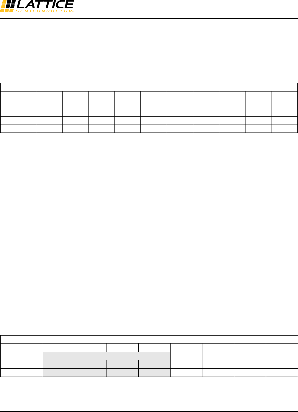
Table 27. I2C Slave Address MSB Register (I2CSADDR)
Table 28. I2C Slave Address MSB Register (I2CFIFOSADDR)
I2C Interrupt Control Register (I2CIRQEN/I2CFIFOIRQEN)
This address is shared by both Register mode and FIFO mode. However, the definition of each status bit is different
for each mode.
Table 29. I2C Interrupt Control Register (I2CIRQEN)
IRQINTCLREN Auto Interrupt Clear Enable – Enable the interrupt flag auto clear when the I2CIRQ
has been read.
IRQINTFRC Force Interrupt Request On – Force the Interrupt Flag set to improve testability
I2CGCDR
Bit Bit7 Bit6 Bit5 Bit4 Bit3 Bit2 Bit1 Bit0
Name I2C_GC_Data[7:0]
Default -
Access R
I2CSADDR (Register Mode)
Bit Bit7 Bit6 Bit5 Bit4 Bit3 Bit2 Bit1 Bit0
7 Bits Addressing - - - A6 A5 A4 A3 A2
10 Bits Addressing A9 A8 A7 A6 A5 A4 A3 A2
Default 00000000
Access R/W
I2CFIFOSADDR (FIFO mode)
Bit Bit9 Bit8 Bit7 Bit6 Bit5Bit4Bit3Bit2Bit1Bit0
7 Bits Addressing - - - A6 A5 A4 A3 A2 A1 A0
10 Bits Address A9A8A7A6A5A4A3A2A1A0
Default 000000000
Access R/W
I2CIRQEN (Register Mode)
Bit Bit7 Bit6 Bit5 Bit4 Bit3 Bit2 Bit1 Bit0
Name IRQINTCLREN IRQINTFRC RSVDRSVD IRQARBLEN IRQTRRDYEN IRQTROEEN IRQHGCEN
Default 0 0 - - 0000
0 to Disable YES YES - - YES Yes YES YES
Access R/WR/W--R/WR/WR/WR/W
Advanced iCE40 I2C and SPI
Hardened IP Usage Guide
21
IRQARBLEN Interrupt Enable for Arbitration Lost
IRQTRRDYEN Interrupt Enable for Transmitter or Receiver Ready
IRQTROEEN Interrupt Enable for Transmitter/Receiver Overrun or NACK Received
IRQHGCEN Interrupt Enable for Hardware General Call Received
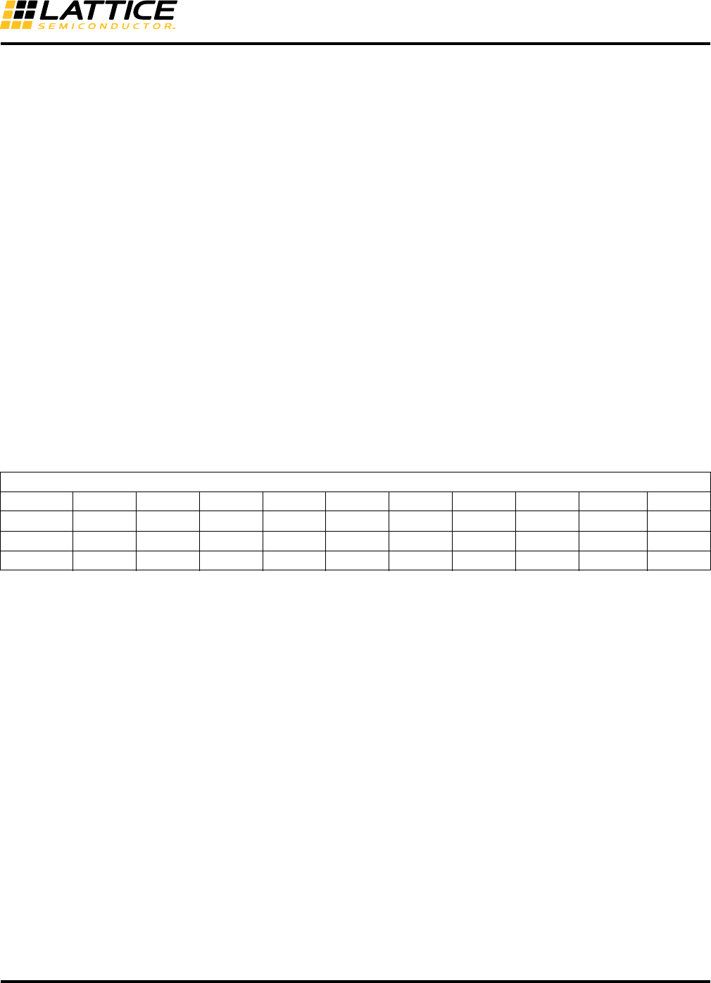
Table 30. I2C Interrupt Control Register (I2CFIFOIRQEN)
IRQCLREN Auto Interrupt Clear Enable – Enable the interrupt flag auto clear when the I2CINTSR
been read
IRQFRC Force Interrupt Request On – Force the Interrupt Flag set to improve testability
0: Normal operation
1: Force the Interrupt Request
HGCEN Force Interrupt Request On — Force the Interrupt Flag set to improve testability
0: Normal operation
1: Force the Interrupt Request
RNACKEN Receive NACK Interrupt Enable
MRDCMPLEN Master Read Complete Enable
ARBLEN Arbitration Lost Interrupt Enable — Enable arbitration Lost Interrupt
TXSERREN TX FIFO Synchronization error Interrupt Enable
TXUNDERFEN TXFIFO Underflow interrupt enable
RXOVERFEN RXFIFO overflow interrupt enable
I2C Interrupt Status Register (I2CIRQ//I2CFIFOIRQ)
This address is shared by both Register mode and FIFO mode. However, the definition of each status bit is different
for each mode.
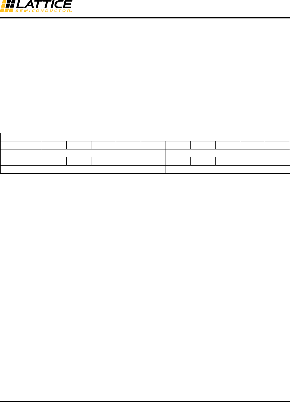
Table 31. I2C Interrupt Status Register (I2CIRQ)
I2CFIFOIRQEN (FIFO Mode)
Bit Bit 9 Bit 8 Bit7 Bit6 Bit5 Bit4 Bit3 Bit2 Bit1 Bit0
Name IRQCLREN IRQFRC RSVD HGCEN RNACKEN MRDCMPLEN ARBLEN TXSERREN TXUNDERFEN RXOVERFEN
Default 0000000000
0 to Disable YES YES YES YES YES YES YES YES YES YES
Access R/WR/WR/WR/WR/WR/WR/WR/WR/WR/W
I2CIRQ (Register Mode)
Bit Bit7 Bit6 Bit5 Bit4 Bit3 Bit2 Bit1 Bit0
Name (Reserved) IRQARBL IRQTRRDY IRQTROE IRQHGC
Default --------
Access ----R/WR/WR/WR/W
Advanced iCE40 I2C and SPI
Hardened IP Usage Guide
22
IRQARBL Interrupt Status for Arbitration Lost.
When enabled, indicates ARBL was asserted. Write a ‘1’ to this bit to clear the inter-
rupt.
0: No interrupt
1: Arbitration Lost Interrupt
IRQTRRDY Interrupt Status for Transmitter or Receiver Ready.
When enabled, indicates TRRDY was asserted. Write a ‘1’ to this bit to clear the inter-
rupt.
0: No interrupt
1: Transmitter or Receiver Ready Interrupt
IRQTROE Interrupt Status for Transmitter/Receiver Overrun or NACK received.
When enabled, indicates TROE was asserted. Write a ‘1’ to this bit to clear the inter-
rupt.
0: No interrupt
1: Transmitter or Receiver Overrun or NACK received Interrupt
IRQHGC Interrupt Status for Hardware General Call Received.
When enabled, indicates HGC was asserted. Write a ‘1’ to this bit to clear the inter-
rupt.
0: No interrupt
1: General Call Received in slave mode Interrupt
IRQHGC General Call Interrupt Request Flag. Write a "1" to this bit clear the interrupt
0: No interrupt request
1: Interrupt request pending
IRQRNACK NACK Interrupt Request Flag. Write a "1" to this bit clear the interrupt
0: No interrupt request
1: Interrupt request pending
IRQMRDCMPL Master Read Completion Interrupt Request Flag. Write a "1" to this bit clear the inter-
rupt
0: No interrupt request
1: Interrupt request pending
IRQARBL Arbitration Lost Interrupt Request Flag. Write a "1" to this bit clear the interrupt
0: No interrupt request
1: Interrupt request pending
I2CFIFOIRQ (FIFO Mode)
Bit Bit 9 Bit 8 Bit7 Bit6 Bit5 Bit4 Bit3 Bit2 Bit1 Bit0
Name RSVDRSVDRSVD IRQHGC IRQRNACK IRQMRDCMPL IRQARBL IRQTXSERR IRQTXUNDERF IRQRXOVERF
Default - - - - - - - - - -
Access R/WR/WR/WR/WR/WR/WR/WR/WR/WR/W
Advanced iCE40 I2C and SPI
Hardened IP Usage Guide
23
IRQTXSERR TXFIFO Synchronization Error Interrupt Request Flag. Write a "1" to this bit clear the
interrupt
0: No interrupt request
1: Interrupt request pending
IRQTXUNDERF TXFIFO Underflow Interrupt Request Flag. Write a "1" to this bit clear the interrupt
0: No interrupt request
1: Interrupt request pending
IRQRXOVERF RXFIFO Overflow Interrupt Request Flag. Write a "1" to this bit clear the interrupt
0: No interrupt request
1: Interrupt request pending
Table 32. I2C FIFO Threshold Register (I2CFIFOTHRESHOLD)
RXFIFO_AF_VAL 5-bit Almost Full value for the RX FIFO
TXFIFO_AE_VAL 5-bit Almost Empty value for the TX FIFO
I2CFIFOTHRESHOLD (FIFO mode)
Bit Bit 9 Bit 8 Bit7 Bit6 Bit5 Bit4 Bit3 Bit2 Bit1 Bit0
Name RXFIFO_AF_VAL TXFIFO_AE_VAL
Default - -
Access R/WR/W
Advanced iCE40 I2C and SPI
Hardened IP Usage Guide
24
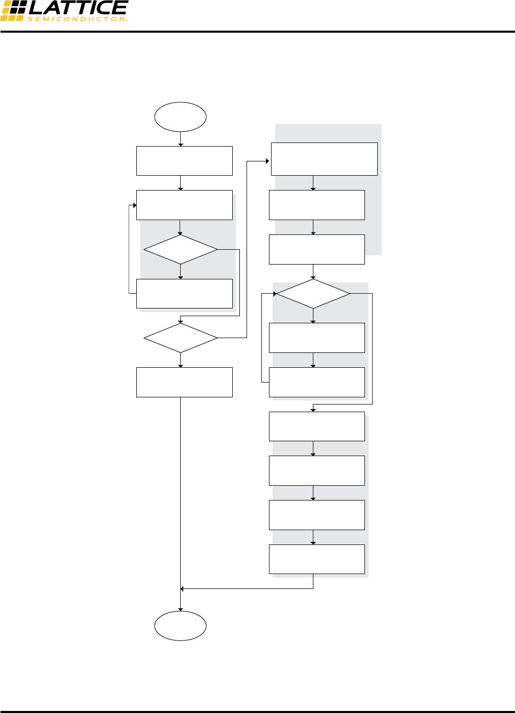
I2C Read/Write Flow Chart
Figure 7 shows a flow diagram for controlling Master I2C reads and writes initiated via the System Bus interface.
Figure 7. I2C Master Read/Write Example (via System Bus)
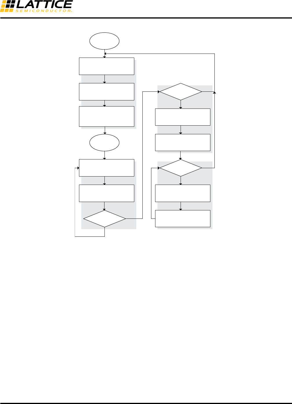
Figure 8 shows a flow diagram for reading and writing from an I2C Slave device via the System Bus interface.
Start
TXDR <= I
2
C addr + ‘W’
CMDR <= 0x94 (STA+WR)
Wait for TRRDY
TXDR <= WRITE_DATA
CMDR <=0x14 (WR)
Write more data?
Read data?
CMDR <= 0x44 (STOP)
Done
TXDR <= I
2
C addr + ‘R’
CMDR <= 0x94 (STA+WR)
Wait for SRW
CMDR <= 0x24 (RD)
Last Read?
Wait for TRRDY
READ_DATA <= RXDR
Wait *
CMDR <= 0x6C
(RD+NACK+STOP)
Wait for TRRDY
READ_DATA <= RXDR
Y
N
Y
N
*Real-Time Delay Requirement
Read only 1 byte: min < wait < max
Read last of 2+ bytes: 0 < wait < max
where:
min = 2 * (1/fSCL)
max = 7 * (1/fSCL)
Y
N
Advanced iCE40 I2C and SPI
Hardened IP Usage Guide
25
Figure 8. I2C Slave Read/Write Example (via System Bus)
Start
wait for not BUSY
CMDR <=0x04 (CKSDIS)
IRQEN <= 0x00
Read more data?
wait for SRW
Y
N
* Required only for IRQ
driven algorithms
discard <= RXDR
discard <= RXDR
IRQEN <= 0x04 (TRRDY)*
Idle
wait for TRRDY
IN_DATA <= RXDR
IRQ <= 0x04*
Write reply data?
TXDR <= OUT_DATA
wait for TRRDY
Write more data?
TXDR <= OUT_DATA
IRQ <= 0x04*
N
N
Y
Y
Advanced iCE40 I2C and SPI
Hardened IP Usage Guide
26
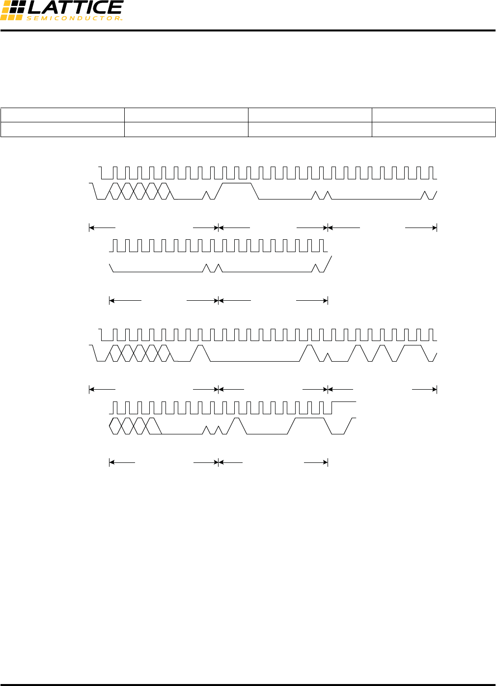
I2C Framing
Each command string sent to the I2C port must be correctly “framed” using the protocol defined for each interface.
In the case of I2C, the protocol is well known and defined by the industry as shown below.
Table 33. Command Framing Protocol, by Interface
Figure 9. I2C Read Device ID Example
Interface Pre-op (+) Command StringPost-op (-)
I2C Start (Command/Operands/Data) Stop
SCL
A6 A5 A4 A3 A2 0 W 11100000 00000000
SDA
SCL
(continued)
00000000
SDA
(continued)
00000000
0
...
...
...
...
Start By
Master
ACK By
iCE40LM
ACK By
iCE40LM
ACK By
iCE40LMHH
Frame 1 I
2
C Slave Address Byte Frame 2 CMD Byte Frame 3 Op Byte 1
Frame 4 Op Byte 2
ACK By
iCE40LM
Frame 5 Op Byte 3
ACK By
iCE40LM
A6 A5 A4 A3 A2 0 R 00000001 00101011
01000011
ID
0000
0
...
...
Restart
By Master
ACK By
iCE40LM
ACK By
Master
ACK By
Master
Frame 6 I
2
C Slave Address Byte Frame 7 Read ID Byte 1 Frame 8 Read ID Byte 2
Frame 9 Read ID Byte 3
ACK By
Master
Frame 10 Read ID Byte 4
NACK By
Master
Stop By
Master
SCL
(continued)
SDA
(continued)
SCL
(continued)
SDA
(continued)
ID ID ID
Advanced iCE40 I2C and SPI
Hardened IP Usage Guide
27
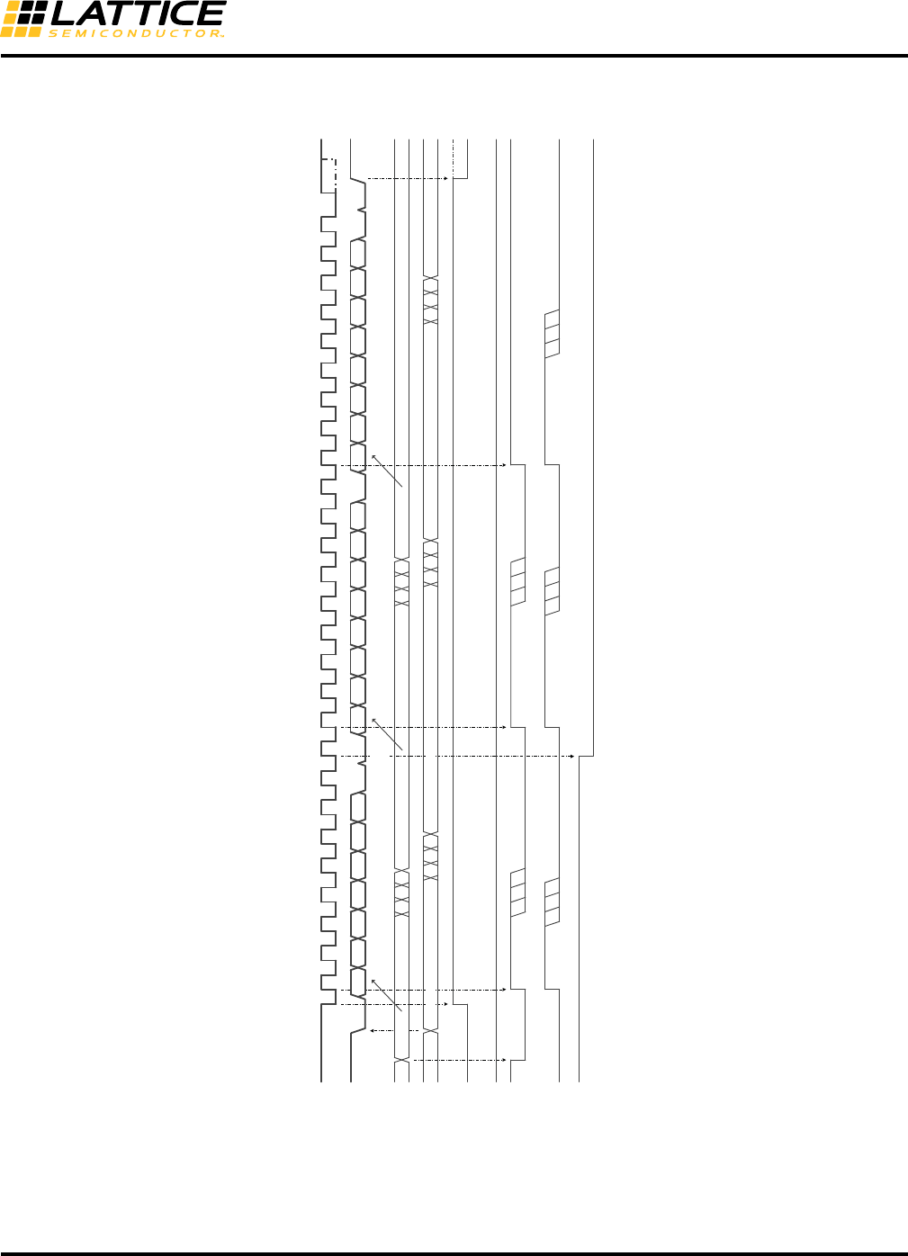
I2C Functional Waveforms
Figure 10. Master – I2C Write
AD[(6:0),W]
AD6
SCL
AD5 AD4 AD3 AD2 AD1 AD0 Write
191 91 9
SDA D7 D6 D5 D4 D3 D2 D1 D0 D7 D6 D5 D4 D3 D2 D1 D0
Master Start
Ack from
Slave
Ack from
Slave
Ack from
Slave
Master Stop
I2C_1_SR[BUSY]
I2C_1_SR[SRW]
I2C_1_SR[TRRDY]
Write IRQTRRDY
I2C_1_IRQ[IRQTRRDY]
Write IRQTRRDY
Write I2C_1_TXDR Write I2C_1_TXDR
I2C_1_SR[RARC]
Write IRQTRRDY
I2C_1_CMDR 0x14(WR) 0x14(WR)
I2C_1_TXDR D[7:0] D[7:0]
0x94(Start+WR) 0x44(STOP)
Idle

Advanced iCE40 I2C and SPI
Hardened IP Usage Guide
28
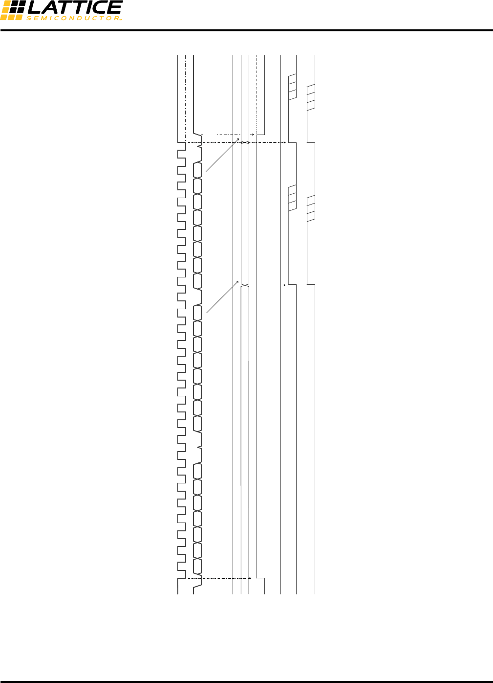
Figure 11. Master – I2C Read
AD[(6:0),W]
0x94 (START+WR)
D[7:0]
0x6C (RD+NACK+STOP)
Stop from
Master
SCL
AD6 AD5 AD4 AD3 AD2 AD1 AD0 Read
191 91 9
SDA D7 D6 D5 D4 D3 D2 D1 D0 D7 D6 D5 D4 D3 D2 D1 D0
Master Start/
Restart
Ack from
Slave
Ack from
Master
Nack from
Master
I2C_1_SR[BUSY]
I2C_1_SR[SRW]
I2C_1_SR[TRRDY]
Read I2C1_RXDR
Write IRQTRRDY
I2C_1_IRQ[IRQTRRDY]
Write IRQTRRDY
I2C_1_CMDR
I2C_1_TXDR
I2C_1_RXDR D[7:0]
0x24 (RD)
Write IRQTRRDY
Read I2C1_RXDR
Advanced iCE40 I2C and SPI
Hardened IP Usage Guide
29
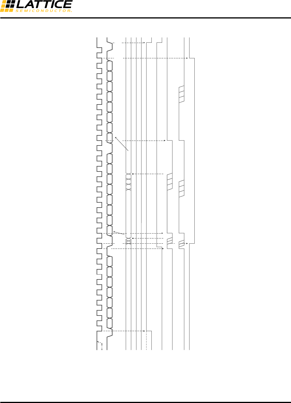
Figure 12. Slave – I2C Write
SCL
AD6 AD5 AD4 AD3 AD2 AD1 AD0 Write
191 91 9
SDA D7 D6 D5 D4 D3 D2 D1 D0 D7 D6 D5 D4 D3 D2 D1 D0
Start from
Master
Ack from
Slave
Ack from
Slave
Ack from
Slave
Stop from
Master
I2C_1_SR[BUSY]
I2C_1_SR[SRW]
I2C_1_SR[TRRDY]
Write IRQTRRDY
I2C_1_IRQ[IRQTRRDY]
Read I2C_1_RXDR
Write IRQTRRDY
I2C_1_TXDR
I2C_1_RXDR
Read I2C_1_RXDR
D[7:0] D[7:0]
Advanced iCE40 I2C and SPI
Hardened IP Usage Guide
30
Figure 13. Slave – I2C Read
SCL
AD6 AD5 AD4 AD3 AD2 AD1 AD0
191 919
SDA D7 D6 D5 D4 D3 D2 D1 D0 D7 D6 D5 D4 D3 D2 D1 D0
Start from
Master
I2C_1_SR[BUSY]
I2C_1_SR[SRW]
I2C_1_SR[TRRDY]
Write IRQTRRDY
I2C_1_IRQ[IRQTRRDY]
Write IRQTRRDY
Write I2C_1_TXDR Write I2C_1_TXDR
I2C_1_SR[RARC]
I2C_1_TXDR
I2C_1_RXDR
D[7:0] D[7:0]
Write IRQTRRDY
Read
Ack from
Slave
Ack from
Master
No Ack from
Master
Stop from
Master
Advanced iCE40 I2C and SPI
Hardened IP Usage Guide
31
I2C Timing Diagram
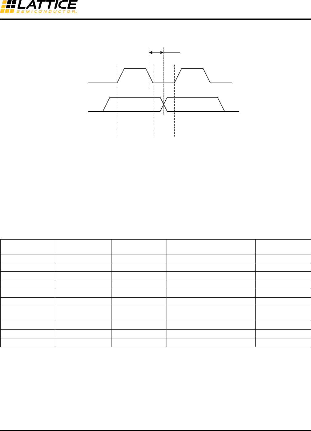
Figure 14. I2C Bit Transfer Timing
Hardened SPI IP Core
The iCE40LM and iCE40 Ultra devices contain two hard SPI IP cores that can be configured as a SPI Master or
Slave. When the SPI core is configured as a Master it is able to control other devices with Slave SPI interfaces that
are connected to the SPI bus. When the SPI core is configured as a Slave, it is able to interface to an external SPI
Master device.
The SPI core communicates with the System Bus interface through a set of control, command, status and data reg-
isters. Table 3 shows the register names and their functions.
SPI Registers
Table 34. SPI Registers Summary
SPI Register Name Simulation Model
Register Name Address[3:0] Register Function Access
SPICR0 SPICR0 1000 SPI Control Register 0 Read/Write
SPICR1 SPICR1 1001 SPI Control Register 1 Read/Write
SPICR2 SPICR2 1010 SPI Control Register 2 Read/Write
SPIBR SPIBR 1011 SPI Baud Rate Register Read/Write
SPITXDR SPITXDR 1101 SPI Transmit Data Register Read/Write
SPIRXDR SPIRXDR 1110 SPI Receive Data Register Read
SPICSR SPICSR 1111 SPI Chip Select Mask
For Master Mode
Read/Write
SPISR SPISR 1100 SPI Status Register Read
SPIIRQ SPIINTSR 0110 SPI Interrupt Status Register Read/Write1
SPIIRQEN SPIINTCR 0111 SPI Interrupt Control Register Read/Write
1. SPIIRQ is Read Only. Write operation upon this register will not change the content of this register, but will clear corresponding interrupt flag
caused by the flags inside SPIIRQ.
data line
stable;
data valid
change
of data
allowed
tSDA_DEL
SCL
SDA
Advanced iCE40 I2C and SPI
Hardened IP Usage Guide
32
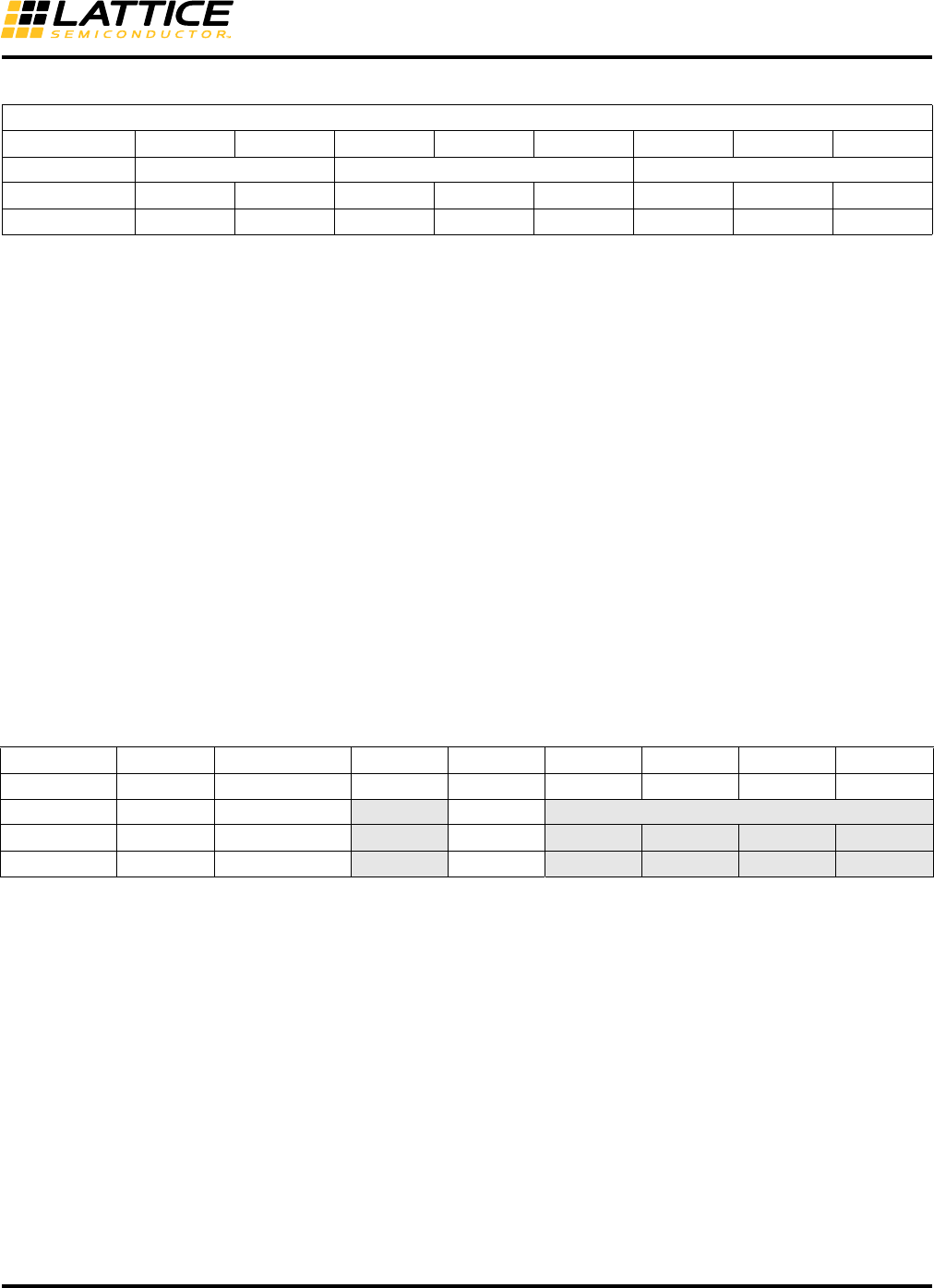
Table 35. SPI Control Register 0 (SPICR0)1
TIdle_XCNT[1:0]Idle Delay Count – Specifies the minimum interval prior to the Master Chip Select low assertion (Master Mode
only), in SCK periods.
00:½
01:1
10:1.5
11:2
TTrail_XCNT[2:0]Trail Delay Count – Specifies the minimum interval between the last edge of SCK and the high deassertion of
Master Chip Select (Master Mode only), in SCK periods.
000:½
001:1
010:1.5
…
111:4
TLead_XCNT[2:0]Lead Delay Count – Specifies the minimum interval between the Master Chip Select low assertion and the
first edge of SCK (Master Mode only), in SCK periods.
000:½
001:1
010:1.5
…
111:4
Table 36. SPI Control Register 1 (SPICR1)1
SPEThis bit enables the SPI core functions. If SPE is cleared, SPI is disabled and forced into idle state.
0:SPI disabled
1:SPI enabled, port pins are dedicated to SPI functions.
WKUPEN_USERWake-up Enable via User – Enables the SPI core to send a wake-up signal to the on-chip Power Controller to
wake the part from Standby mode when the User slave SPI chip select (spi_scsn) is driven low.
0:Wakeup disabled
1:Wakeup enabled.
WKUPEN_CFGWake-up Enable Configuration – Enables the SPI core to send a wake-up signal to the on-chip power controller
to wake the part from standby mode when the Configuration slave SPI chip select (ufm_sn) is driven low.
0:Wakeup disabled
1:Wakeup enabled.
TXEDGEData Transmitting selection bit – This bit gives user capability to select which clock edge to transmit data for fast SPI
applications. Note that this bit should not be set when CPHA or MCSH of SPICR2 is set.
SPICR0
Bit Bit7 Bit6 Bit5 Bit4 Bit3 Bit2 Bit1 Bit0
Name TIdle_XCNT[1:0] TTrail_XCNT[2:0] TLead_XCNT[2:0]
Default 00000000
Access R/WR/WR/W-R/W--
1. A write to this register will cause the SPI core to reset
SPICR1
Bit Bit7 Bit6 Bit5 Bit4 Bit3 Bit2 Bit1 Bit0
Name SPE WKUPEN_USER (Reserved) TXEDGE (Reserved)
Default 0 0 000 0 0 0
Access R/WR/W-R/W- - - -
1. A write to this register will cause the SPI core to reset

Advanced iCE40 I2C and SPI
Hardened IP Usage Guide
33
0:Transmit data on the different clock edge of data receiving (receiving on rising / transmit on falling)
1:Transmit data on the same clock edge of data receiving (receiving on rising /transmit on rising)
Table 37. SPI Control Register 2 (SPICR2) 1
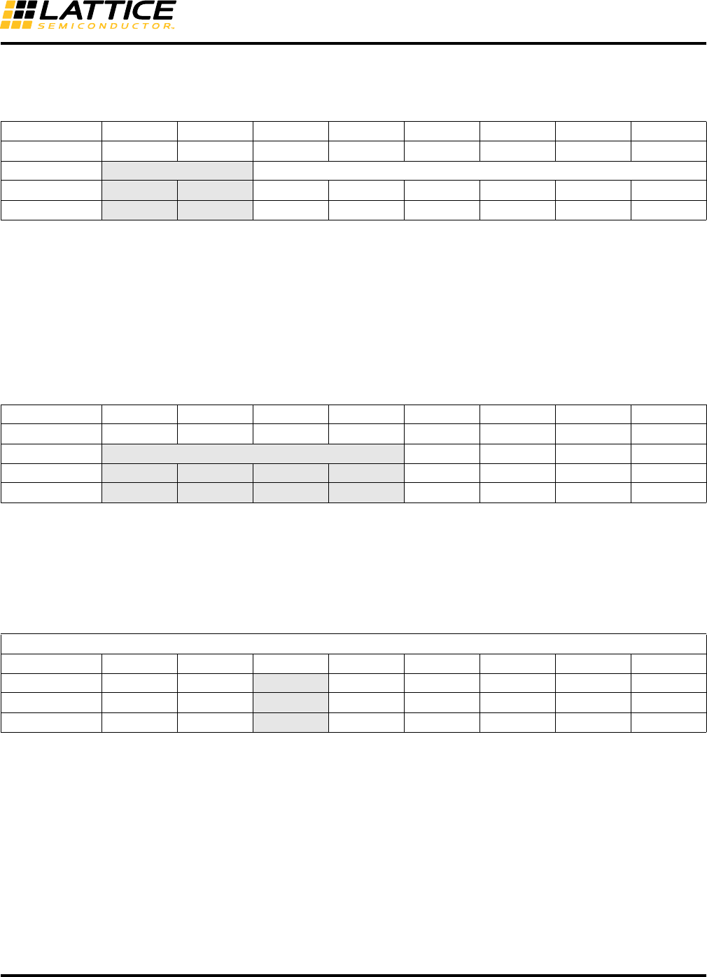
MSTRSPI Master/Slave Mode – Selects the Master/Slave operation mode of the SPI core. Changing this bit forces the SPI sys-
tem into idle state.
0:SPI is in Slave mode
1:SPI is in Master mode
MCSHSPI Master CSSPIN Hold – Holds the Master chip select active when the host is busy, to halt the data transmission with-
out de-asserting chip select.
Note: This mode must be used only when the System Bus clock has been divided by a value greater than three (3).
0:Master running as normal
1:Master holds chip select low even if there is no data to be transmitted
SDBRESlave Dummy Byte Response Enable – Enables Lattice proprietary extension to the SPI protocol. For use when the
internal support circuit (e.g. System host) cannot respond with initial data within the time required, and to make the slave read
out data predictably available at high SPI clock rates.
When enabled, dummy 0xFF bytes will be transmitted in response to a SPI slave read (while SPISR[TRDY]=1) until an initial
write to SPITXDR. Once a byte is written into SPITXDR by the System host, a single byte of 0x00 will be transmitted then fol-
lowed immediately by the data in SPITXDR. In this mode, the external SPI master should scan for the initial 0x00 byte when
reading the SPI slave to indicate the begin-ning of actual data. Refer to Figure 18
0:Normal Slave SPI operation
1:Lattice proprietary Slave Dummy Byte Response Enabled
Note: This mechanism only applies for the initial data delay period. Once the initial data is available, subsequent data must be
supplied to SPITXDR at the required SPI bus data rate.
CPOLSPI Clock Polarity – Selects an inverted or non-inverted SPI clock. To transmit data between SPI modules, the SPI mod-
ules must have identical SPICR2[CPOL] values. In master mode, a change of this bit will abort a transmission in progress and
force the SPI system into idle state. Refer to Figure 19 through Figure 21.
0:Active-high clocks selected. In idle state SCK is low.
1:Active-low clocks selected. In idle state SCK is high.
CPHASPI Clock Phase – Selects the SPI clock format. In master mode, a change of this bit will abort a transmission in progress
and force the SPI system into idle state. Refer to Refer to Figure 19 through Figure 21.
0:Data is captured on a leading (first) clock edge, and propagated on the opposite clock edge.
1:Data is captured on a trailing (second) clock edge, and propagated on the opposite clock edge*.
Note: When CPHA=1, the user must explicitly place a pull-up or pull-down on SCK pad corresponding to the value of CPOL
(e.g. when CPHA=1 and CPOL=0 place a pull-down on SCK). When CPHA=0, the pull direction may be set arbitrarily.
Slave SPI Configuration mode supports default setting only for CPOL, CPHA.
LSBFLSB-First – LSB appears first on the SPI interface. In master mode, a change of this bit will abort a transmission in prog-
ress and force the SPI system into idle state. Refer to Figure 19 through Figure 21.
Note: This bit does not affect the position of the MSB and LSB in the data register. Reads and writes of the data register always
have the MSB in bit 7.
SPICR2
Bit Bit7 Bit6 Bit5 Bit4 Bit3 Bit2 Bit1 Bit0
Name MSTR MCSH SDBRE (Reserved) CPOL CPHA LSBF
Default 0 0 0 00000
Access R/WR/WR/W--R/WR/WR/W
1. A write to this register will cause the SPI core to reset
Advanced iCE40 I2C and SPI
Hardened IP Usage Guide
34
0:Data is transferred most significant bit (MSB) first
1:Data is transferred least significant bit (LSB) first
Table 38. SPI Clock Prescale (SPIBR)
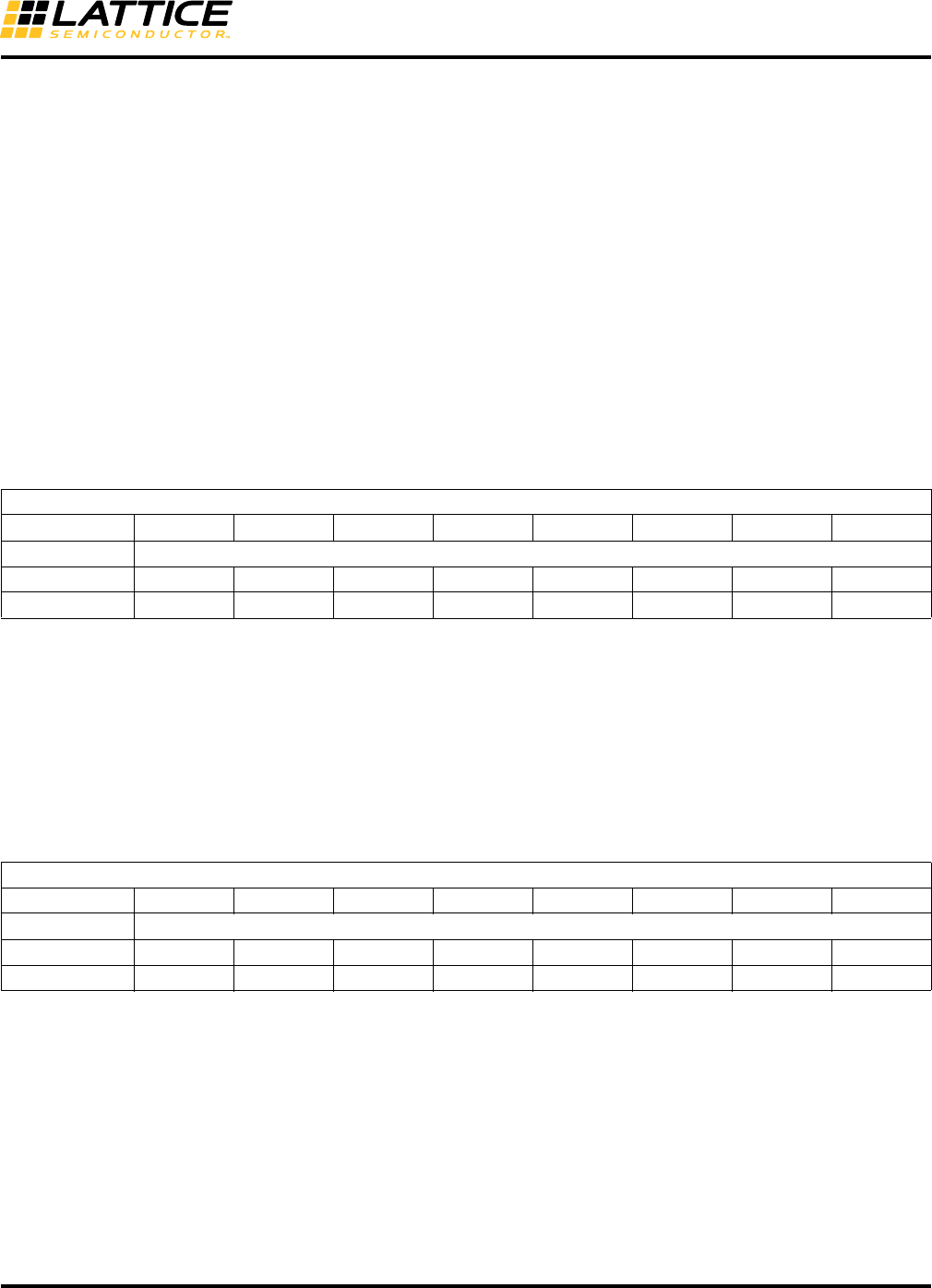
DIVIDER[5:0]SPI Clock Prescale value – The System clock frequency is divided by (DIVIDER[5:0] + 1) to produce the desired
SPI clock frequency. A write operation to this register will cause a SPI core reset. DIVIDER must be >= 1.
Note: The digital value is calculated by Module Generator when the SPI core is configured in the SPI tab of the Module Genera-
tor GUI. The calculation is based on the System Bus Clock Frequency and the SPI Frequency, both entered by the user. The
digital value of the divider is loaded in the iCE40LM and iCE40 Ultra devices using Soft IP into the SPIBR register.
Register SPIBR has Read/Write access from the System Bus interface. Designers can update the clock pre-scale register
dynamically during device operation.
Table 39. SPI Master Chip Select Register (SPICSR)
CSN_[7:0]SPI Master Chip Selects – Used in master mode for asserting a specific Master Chip Select (MCSN) line. The regis-
ter has four bits, enabling the SPI core to control up to four external SPI slave devices. Each bit represents one master chip
select line (Active-Low). Bits [3:1] may be connected to any I/O pin via the FPGA fabric. Bit 0 has a pre-assigned pin location.
The register has Read/Write access from the System Bus interface. A write operation on this register will cause the SPI core to
reset.
Table 40. SPI Status Register(SPISR)
TIPSPI Transmitting In Progress – Indicates the SPI port is actively transmitting/receiving data.
0:SPI Transmitting complete
1:SPI Transmitting in progress*
BUSYSPI Busy Flag – This bit indicate that the SPI port in the middle of data transmitting / receiving (CSN is low)
0:SPI Transmitting complete
1:SPI Transmitting in progress*
TRDYSPI Transmit Ready – Indicates the SPI transmit data register (SPITXDR) is empty. This bit is cleared by a write to
SPITXDR. This bit is capable of generating an interrupt.
0:SPITXDR is not empty
1:SPITXDR is empty
SPIBR
Bit Bit7 Bit6 Bit5 Bit4 Bit3 Bit2 Bit1 Bit0
Name (Reserved) DIVIDER[5:0]
Default 00000000
Access --R/WR/WR/WR/WR/WR/W
SPICSR
Bit Bit7 Bit6 Bit5 Bit4 Bit3 Bit2 Bit1 Bit0
Name (Reserved) CSN_3 CSN_2 CSN_1 CSN_0
Default 00000000
Access ----R/WR/WR/WR/W
SPISR
Bit Bit7 Bit6 Bit5 Bit4 Bit3 Bit2 Bit1 Bit0
Name TIP BUSY (Reserved) TRDY RRDY TOE ROE MDF
Default - - -----0
Access R R - RRRRR
Advanced iCE40 I2C and SPI
Hardened IP Usage Guide
35
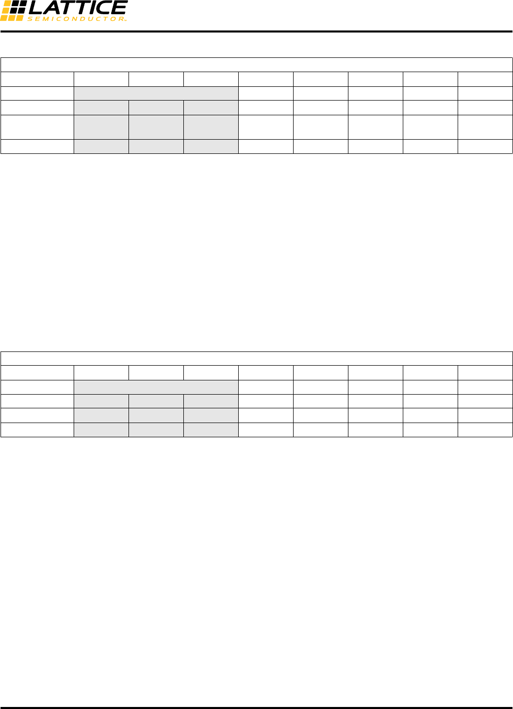
RRDYSPI Receive Ready – Indicates the receive data register (SPIRXDR) contains valid receive data. This bit is cleared by a
read access to SPIRXDR. This bit is capable of generating an interrupt.
0:SPIRXDR does not contain data
1:SPIRXDR contains valid receive data
TOEReceive Overrun Error – This bit indicates that the SPIRXDR received new data before the previous data was read. The
previous data will be lost if occurs. It will cause an interrupt to System Host if SCI set up allowed.
0:Normal
1:Transmit Overrun detected
ROEReceive Overrun Error – Indicates SPIRXDR received new data before the previous data was read. The previous data is
lost. This bit is capable of generating an interrupt.
0:Normal
1:Receiver Overrun detected
MDFMode Fault – Indicates the Slave SPI chip select (spi_scsn) was driven low while SPICR2[MSTR]=1. This bit is cleared by
any write to SPICR0, SPICR1 or SPICR2. This bit is capable of generating an interrupt.
0:Normal
1:Mode Fault detected
Table 41. SPI Transmit Data Register (SPITXDR)
SPI_Receive_Data[7:0]SPI Transmit Data – This register holds the byte that will be transmitted on the SPI bus. Bit 0 in this reg-
ister is LSB, and will be transmitted last when SPICR2[LSBF]=0 or first when SPICR2[LSBF]=1.
Note: When operating as a Slave, SPITXDR must be written when SPISR[TRDY] is '1' and at least 0.5 CCLKs before the first bit
is to appear on SO. For example, when CPOL = CPHA = TXEDGE = LSBF = 0, SPITXDR must be written prior to the CCLK ris-
ing edge used to sample the LSB (bit 0) of the previous byte. See Figure 17-25. This timing requires at least one protocol
dummy byte be included for all slave SPI read operations.
Table 42. SPI Receive Data Register (SPIRXDR)
SPI_Receive_Data[7:0]SPI Receive Data This register holds the byte captured from the SPI bus. Bit 0 in this register is LSB and
was received last when LSBF=0 or first when LSBF=1.
SPITXDR
Bit Bit7 Bit6 Bit5 Bit4 Bit3 Bit2 Bit1 Bit0
Name SPI_Transmit_Data[7:0]
Default --------
Access WWWWWWWW
SPIRXDR
Bit Bit7 Bit6 Bit5 Bit4 Bit3 Bit2 Bit1 Bit0
Name SPI_Receive_Data[7:0]
Default --------
Access RRRRRRRR
Advanced iCE40 I2C and SPI
Hardened IP Usage Guide
36
Table 43. SPI Interrupt Status Register (SPIIRQ)
IRQTRDYInterrupt Status for SPI Transmit Ready.
When enabled, indicates SPISR[TRDY] was asserted.
Write a ‘1’ to this bit to clear the interrupt.
IRQRRDYInterrupt Status for SPI Receive Ready.
When enabled, indicates SPISR[RRDY] was asserted.
Write a ‘1’ to this bit to clear the interrupt.
IRQROEInterrupt Status for Receive Overrun Error.
When enabled, indicates ROE was asserted.
Write a ‘1’ to this bit to clear the interrupt.
IRQMDFInterrupt Status for Mode Fault.
When enabled, indicates MDF was asserted.
Write a ‘1’ to this bit to clear the interrupt.
Table 44. SPI Interrupt Enable Register (SPIIRQEN)
IRQTRDYENInterrupt Enable for SPI Transmit Ready.
IRQRRDYENInterrupt Enable for SPI Receive Ready
IRQTOEEN Interrupt Enable for SPI Transmit Overrun Ready.
IRQROEEN Interrupt Enable for SPI Receive Overrun Ready.
IRQMDFEN Interrupt Enable for SPI Mode Default Ready.
SPIIRQ
Bit Bit7 Bit6 Bit5 Bit4 Bit3 Bit2 Bit1 Bit0
Name (Reserved) IRQTRDY IRQRRDY IRQTOE IRQROE IRQMDF
Default --------
0 means
No Interrupt --- YES YES YES YES YEs
Access ---R/WR/WR/WR/WR/W
SPIIRQ
Bit Bit7 Bit6 Bit5 Bit4 Bit3 Bit2 Bit1 Bit0
Name (Reserved) IRQTRDYEN IRQRRDYEN IRQTOEEN IRQROEEN IRQMDFEN
Default --------
0 means Disable --- YES YES YES YES YEs
Access ---R/WR/WR/WR/WR/W
Advanced iCE40 I2C and SPI
Hardened IP Usage Guide
37
SPI Read/Write Flow Chart
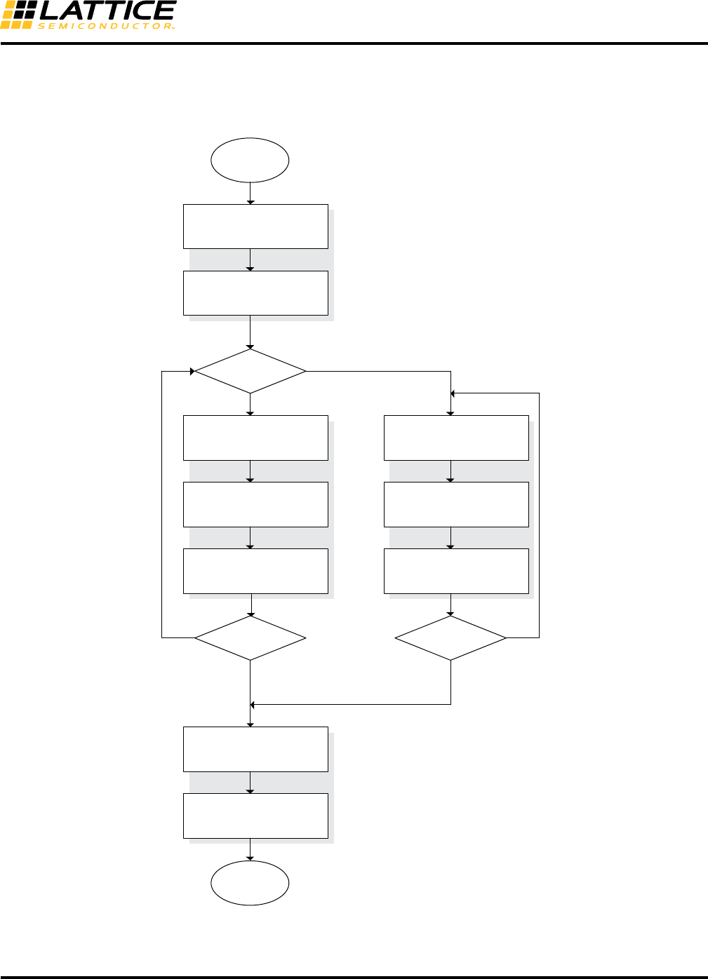
Figure 15 shows a flow diagram for controlling Master SPI reads and writes initiated via the System Bus interface.
Figure 15. SPI Master Read/Write Example (via System Bus)
Note: Assumes CR2 register, MSCH = '1'. The algorithm when MSCH = '0' is application dependent and not pro-
vided. See Figure 17 for guidance.
Start
CR2 <= 0xC0
wait for TRDY
Done?
Read data?
TXDR <= SPI Write Data TXDR <= 0x00
wait for RRDY
SPI Read Data <= RXDR
Y
N
Y
N
wait for RRDY
Discard Data <= RXDR
Last Read?
CR2 <= 0x80
Y
N
wait for not TIP
Done
Advanced iCE40 I2C and SPI
Hardened IP Usage Guide
38
SPI Framing
Each command string sent to the SPI port must be correctly ‘framed’ using the protocol defined for each interface.
In the case of SSPI the protocol is well known and defined by the industry as shown below:
Table 45. Command Framing Protocol, by Interface
Figure 16. SSPI Read Device ID Example
Interface Pre-op (+) Command StringPost-op (-)
SPI Assert CS (Command/Operands/Data) De-assert CS
111000000000000000000000
CMD Byte Op Byte 1 Op Byte 2
SCSN
SPI_SCK
MOSI
MISO
...
...
...
...
00000000
Op Byte 3 Read ID Byte 1 Read ID Byte 2
(continued)
(continued)
(continued)
(continued)
...
...
...
...
IDIDIDID000001000011
Read ID Byte 3 Read ID Byte 4
(continued)
(continued)
(continued)
(continued)
000000010010101 1
SCSN
SPI_SCK
MOSI
MISO
SCSN
SPI_SCK
MOSI
MISO
Advanced iCE40 I2C and SPI
Hardened IP Usage Guide
39
SPI Functional Waveforms
Figure 17. Fully Specified SPI Transaction (iCE40LM and iCE40 Ultra as SPI Master or Slave)
Figure 18. Minimally Specified SPI Transaction Example (iCE40LM and iCE40 Ultra as SPI Slave)
R1 from SI
to SPIRXDR
(auto)
T1 written to
SPITXDR via
WISHBONE
(user)
T1 from
SPITXDR to SO
(auto)
T1 T2 T3 T4 T5 T6 T7 T8
T1 T2 T3 T4 T5 T6 T7 T8
R1 R2 R3 R4 R5 R6 R7 R8
R1 R2 R3 R4 R5 R6 R7 R8
SPISR[RRDY]
SPIRXDR
SPISR[TIP]
MOSI
MISO
MCSN or SCSN
SPITXDR
SPISR[TRDY]
R1 read from
SPIRXDR via
WISHBONE
(user)
Addr read from
SPIRXDR via
WISHBONE
(user)
Flush SPIRXDR
via WISHBONE
(user)
Quit reading SPIRXDR (data is “don’t care”)
CMD read from
SPIRXDR via
WISHBONE
(user)
0x08addr dum
0x08addr dum
old
old dum1 dum2 D1 D2 D3 D4 D5
FF* dum2 D1 D2 D3 D4 D5
Command Reply to Command
After SPISR[TIP] detected,
write dummy to SPITXDR
(user)
After CMD/Addr decode,
write good to SPITXDR
(user)
*Note: If SPITXDR is ‘empty’ at the start of a transaction,
the second byte will be ‘FF’ (silicon limitation).
Must write dummy byte in first byte period to get
good Tx data in third period (dummy data may be
overwritten in second period if necessary).
SPISR[TRDY]
SPISR[TRDY]
SPIRXDR
SPISR[TIP]
MOSI
MISO
SCSN
SPITXDR
SPISR[TRDY]
Advanced iCE40 I2C and SPI
Hardened IP Usage Guide
40
SPI Timing Diagrams
Figure 19. SPI Control Timing (SPICR2[CPHA]=0, SPICR1[TXEDGE]=0)
Figure 20. SPI Control Timing (SPICR2[CPHA]=1, SPICR1[TXEDGE]=0)
SPI_SCK
(CPOL=0)
SPI_SCK
(CPOL=1)
MOSI
MISO
MSCN/SCSN/SN
MSB first (LSBF=0):
LSB first (LSBF=1):
MSB
LSB
bit6
bit1
bit5
bit2
bit4
bit3
bit3
bit4
bit2
bit5
bit1
bit6 MSB
LSB
tL tT tI tL
tL = TLead_XCNT
tT = TTrail_XCNT
tL = Tidle_XCNT
sample instants
*Note: iCE40LM supports only
CPHA = CPOL = LSBF = TXEDGE = 0
MSB first (LSBF=0):
LSB first (LSBF=1):
MSB
LSB
bit6
bit1
bit5
bit2
bit4
bit3
bit3
bit4
bit2
bit5
bit1
bit6 MSB
LSB
tL tT tI tL
tL = TLead_XCNT
tT = TTrail_XCNT
tL = Tidle_XCNT
sample instants
SPI_SCK
(CPOL=0)
SPI_SCK
(CPOL=1)
MOSI
MISO
MSCN or SCSN
Advanced iCE40 I2C and SPI
Hardened IP Usage Guide
41
Figure 21. SPI Control Timing (SPICR2[CPHA]=0, SPICR1[TXEDGE]=1)
MSB first (LSBF=0):
LSB first (LSBF=1):
MSB
LSB
bit6
bit1
bit5
bit2
bit4
bit3
bit3
bit4
bit2
bit5
bit1
bit6 MSB
LSB
tL tT tI tL
tL = TLead_XCNT
tT = TTrail_XCNT
tL = Tidle_XCNT
sample instants
MCSN or SCSN
SPI_SCK
(CPOL=0)
SPI_SCK
(CPOL=1)
MOSI
MISO

Advanced iCE40 I2C and SPI
Hardened IP Usage Guide
42
Technical Support Assistance
Submit a technical support case through www.latticesemi.com/techsupport.
Revision History
Date Version Change Summary
October 2015 1.4 Added support for iCE40 UltraPlus.
Updated I2C Registers for iCE40LM and iCE40 Ultra section. Revised
SDA_DEL_SEL[1:0] description.
Updated Technical Support Assistance section.
Fixed link to TN1274 on page 1.
January 2015 1.3 Added support for iCE40 UltraLite.
June 2014 1.2 Changed document title to Advanced iCE40 I2C and SPI Hardened IP
Usage Guide.
Added support for iCE40 Ultra.
November 2013 01.1 Changed the interface signal names of hardened IP module.
Updated I2C Registers Summary table.
October 2013 01.0 Initial release.