Airoha IoT SDK For RTOS Memory Layout Developer's Guide Io T Developers
User Manual:
Open the PDF directly: View PDF ![]() .
.
Page Count: 55
- 1. Overview
- 2. Memory Layout and Configuration for MT76x7
- 3. Memory Layout and Configuration for MT2523x
- 3.1. Memory layout without FOTA
- 3.2. Memory layout with FOTA of full binary update
- 3.3. Programming guide
- 3.4. Memory layout adjustment with a linker script
- 3.5. Memory layout adjustment with a scatter file
- 4. Memory Layout and Configuration for MT7682
- 4.1. Memory layout without FOTA
- 4.2. Memory layout with FOTA of full binary update
- 4.3. Programming guide
- 4.4. Memory layout adjustment with a linker script
- 4.5. Memory layout adjustment with a scatter file
- 4.6. Memory layout adjustment with an IAR configuration file
- 5. Memory Layout and Configuration for MT7686
- 5.1. Memory layout without FOTA
- 5.2. Memory layout with FOTA of full binary update
- 5.3. Programming guide
- 5.4. Memory layout adjustment with a linker script
- 5.5. Memory layout adjustment with a scatter file
- 5.6. Memory layout adjustment with an IAR configuration file
- 6. Memory Layout and Configuration for MT5932

Airoha IoT SDK for RTOS Memory Layout
Developer's Guide
Version: 4.0
Release date: 5 May 2017
© 2016 - 2017 Airoha Technology Corp.
This document contains information that is proprietary to Airoha Technology Corp. (“Airoha”) and/or its licensor(s). Airoha cannot grant you
permission for any material that is owned by third parties. You may only use or reproduce this document if you have agreed to and been
bound by the applicable license agreement with Airoha (“License Agreement”) and been granted explicit permission within the License
Agreement (“Permitted User”). If you are not a Permitted User, please cease any access or use of this document immediately. Any
unauthorized use, reproduction or disclosure of this document in whole or in part is strictly prohibited. THIS DOCUMENT IS PROVIDED ON AN
“AS-IS” BASIS ONLY. AIROHA EXPRESSLY DISCLAIMS ANY AND ALL WARRANTIES OF ANY KIND AND SHALL IN NO EVENT BE LIABLE FOR ANY
CLAIMS RELATING TO OR ARISING OUT OF THIS DOCUMENT OR ANY USE OR INABILITY TO USE THEREOF. Specifications contained herein are
subject to change without notice.
Airoha IoT SDK for RTOS Memory
Layout Developer's Guide
© 2015 - 2018 Airoha Technology Corp.
Page i of iii
This document contains information that is proprietary to Airoha Technology Corp. (“Airoha”) and/or its licensor(s).
Any unauthorized use, reproduction or disclosure of this document in whole or in part is strictly prohibited.
Document Revision History
Revision Date Description
1.0 7 March 2016 Initial release.
1.1 31 March 2016 Add MT2533x memory layout description.
2.0 30 June 2016 Add 4MB memory layout of MT76x7.
2.1 2 September 2016 MT76x7 layout adjustment
3.0 4 November 2016 Added MT2533 memory layout description.
4.0 5 May 2017 Added MT7682, MT7686, MT5932 memory layout description.

Airoha IoT SDK for RTOS Memory
Layout Developer's Guide
© 2015 - 2018 Airoha Technology Corp.
Page ii of iii
This document contains information that is proprietary to Airoha Technology Corp. (“Airoha”) and/or its licensor(s).
Any unauthorized use, reproduction or disclosure of this document in whole or in part is strictly prohibited.
Table of Contents
1. Overview ............................................................................................................................................... 1
2. Memory Layout and Configuration for MT76x7 ..................................................................................... 2
2.1. 2MB memory layout view .................................................................................................................. 2
2.2. 4MB memory layout view .................................................................................................................. 4
2.3. Programming guide ............................................................................................................................ 6
2.4. Memory layout adjustment with a linker script ................................................................................. 7
2.5. Memory layout adjustment with a scatter File .................................................................................. 8
3. Memory Layout and Configuration for MT2523x .................................................................................. 10
3.1. Memory layout without FOTA .......................................................................................................... 11
3.2. Memory layout with FOTA of full binary update .............................................................................. 13
3.3. Programming guide .......................................................................................................................... 15
3.4. Memory layout adjustment with a linker script ............................................................................... 17
3.5. Memory layout adjustment with a scatter file ................................................................................. 20
4. Memory Layout and Configuration for MT7682 .................................................................................... 22
4.1. Memory layout without FOTA .......................................................................................................... 23
4.2. Memory layout with FOTA of full binary update .............................................................................. 24
4.3. Programming guide .......................................................................................................................... 26
4.4. Memory layout adjustment with a linker script ............................................................................... 28
4.5. Memory layout adjustment with a scatter file ................................................................................. 31
4.6. Memory layout adjustment with an IAR configuration file .............................................................. 32
5. Memory Layout and Configuration for MT7686 .................................................................................... 35
5.1. Memory layout without FOTA .......................................................................................................... 36
5.2. Memory layout with FOTA of full binary update .............................................................................. 38
5.3. Programming guide .......................................................................................................................... 40
5.4. Memory layout adjustment with a linker script ............................................................................... 43
5.5. Memory layout adjustment with a scatter file ................................................................................. 46
5.6. Memory layout adjustment with an IAR configuration file .............................................................. 47
6. Memory Layout and Configuration for MT5932 .................................................................................... 49
6.1. Memory layout without External Flash ............................................................................................ 49
6.2. Memory layout with External Flash .................................................................................................. 51

Airoha IoT SDK for RTOS Memory
Layout Developer's Guide
© 2015 - 2018 Airoha Technology Corp.
Page iii of iii
This document contains information that is proprietary to Airoha Technology Corp. (“Airoha”) and/or its licensor(s).
Any unauthorized use, reproduction or disclosure of this document in whole or in part is strictly prohibited.
Lists of Tables and Figures
Table 1. Tips for changing the memory layout of MT76x7 platform ...................................................................... 7
Figure 1. The load view of the 2MB flash memory layout ...................................................................................... 3
Figure 2. The execution view of the 2MB flash memory layout ............................................................................. 4
Figure 3. The load view of the 4MB flash memory layout ...................................................................................... 5
Figure 4. The execution view of the 4MB flash memory layout ............................................................................. 6
Figure 5. MT2523x virtual memory mapping ........................................................................................................ 10
Figure 6. Load view of the MT2523D and MT2523G memory layout without FOTA ............................................ 11
Figure 7. Load view of the MT2533 memory layout without FOTA ...................................................................... 12
Figure 8. Execution view of the MT2523D, MT2523G and MT2533 memory layout without FOTA .................... 13
Figure 9. Load view of the MT2523D and MT2523G memory layout with full binary FOTA ................................ 13
Figure 10 Load view of the MT2533 memory layout with full binary FOTA ......................................................... 14
Figure 11. Execution view of the MT2523D and MT2523G memory layout with full binary FOTA ...................... 15
Figure 12. Execution view of the MT2533 memory layout with full binary FOTA ................................................ 15
Figure 13 MT7682 virtual memory mapping ........................................................................................................ 22
Figure 14 Load view of the MT7682 memory layout without FOTA ..................................................................... 23
Figure 15. Execution view of the MT7682 memory layout without FOTA ............................................................ 24
Figure 16. Load view of the MT7682 memory layout with full binary FOTA ........................................................ 25
Figure 17. Execution view of the MT7682 memory layout with full binary FOTA ................................................ 26
Figure 18. MT7686 virtual memory 1 mapping..................................................................................................... 35
Figure 19. MT7686 virtual memory 2 mapping..................................................................................................... 36
Figure 20. Load view of the MT7686 memory layout without FOTA .................................................................... 37
Figure 21. Execution view of the MT7686 memory layout without FOTA ............................................................ 38
Figure 22. Load view of the MT7686 memory layout with full binary FOTA ........................................................ 39
Figure 23. Execution view of the MT7682 memory layout with full binary FOTA ................................................ 40
Figure 24 MT5932 load view memory layout without external flash ................................................................... 50
Figure 25 MT5932 execution view memory layout without external flash .......................................................... 50

Airoha IoT SDK for RTOS Memory
Layout Developer's Guide
© 2015 - 2018 Airoha Technology Corp.
Page 1 of 51
This document contains information that is proprietary to Airoha Technology Corp. (“Airoha”) and/or its licensor(s).
Any unauthorized use, reproduction or disclosure of this document in whole or in part is strictly prohibited.
1. Overview
This document provides details on the memory layout design and configuration of Airoha IoT development
platform for RTOS. The platform includes:
• MT76x7 chipsets: MT7687F, MT7697, and MT7697D
• MT2523x chipsets: MT2523D, MT2523G, and MT2533
• MT76x2 chipsets : MT7686, MT7682, and MT5932
Each memory layout has two types of views, load view and an execution view. The design concept will be
described based on the two views:
• Load view describes a memory region and section of each image in terms of the address it is located at
before the image is processed.
• Execution view describes a memory region and section of each image in terms of the address it is located
at during the image execution.
Different toolchains have different layout configuration files. The GCC toolchain uses a linker script, the ARMCC
toolchain uses a scatter file. The memory layout configuration will be described separately for each toolchain.
Airoha IoT SDK for RTOS Memory
Layout Developer's Guide
© 2015 - 2018 Airoha Technology Corp.
Page 2 of 51
This document contains information that is proprietary to Airoha Technology Corp. (“Airoha”) and/or its licensor(s).
Any unauthorized use, reproduction or disclosure of this document in whole or in part is strictly prohibited.
2. Memory Layout and Configuration for MT76x7
The memory layout for Airoha IoT Development Platform for RTOS is based on a type of memory available on the
supported SOCs. MT76x7 is equipped with three types of memory storage: Serial Flash, SYSRAM and Tightly
Coupled Memory (TCM). This document guides you through the details of the memory layout and its use.
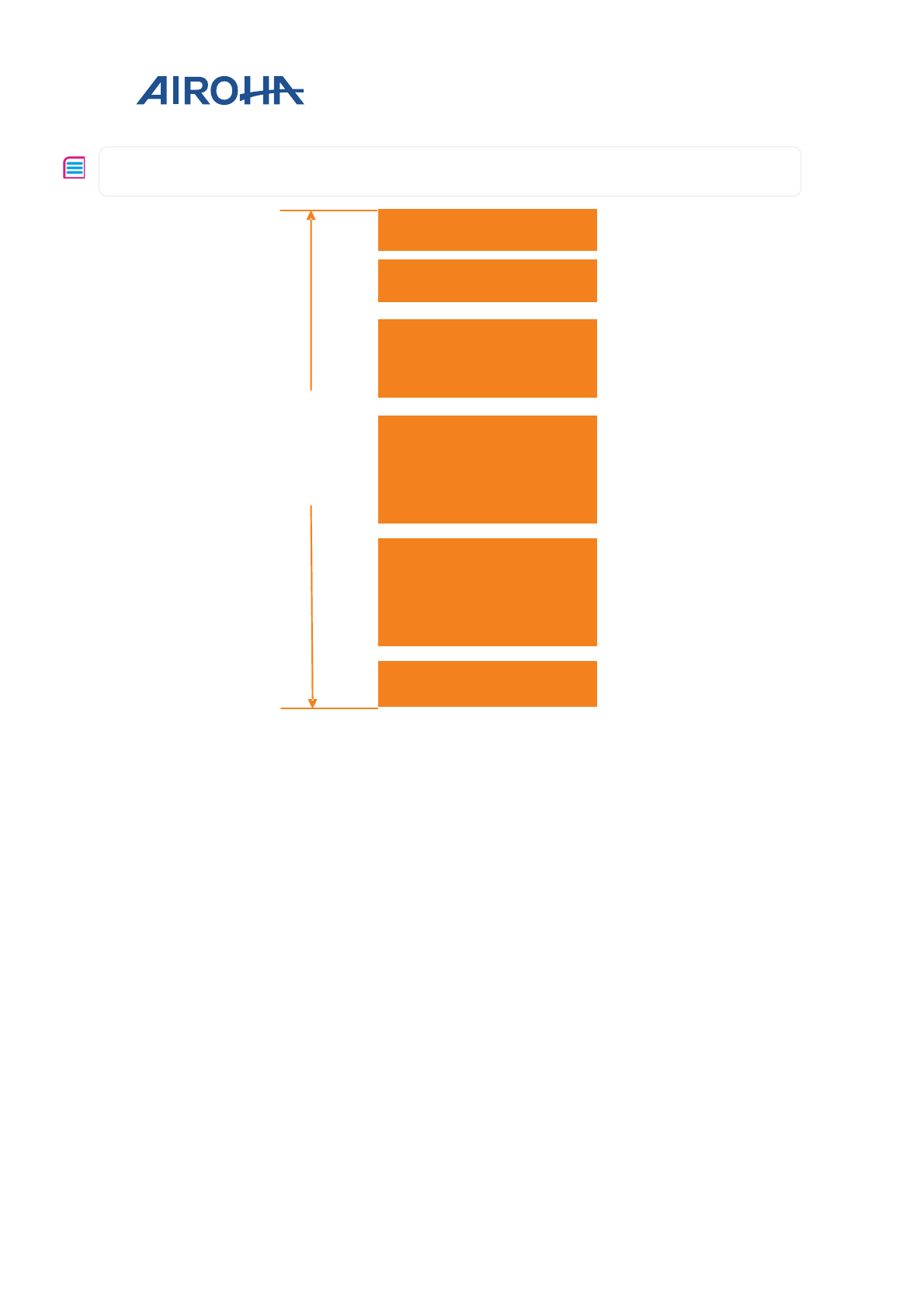
2.1. 2MB memory layout view
2.1.1. Load view
MT7687F has 2MB internal serial flash memory. The load view on the flash memory of the HDK is shown in Figure
1.
• Bootloader. The first 32kB of memory is allocated for the bootloader. The bootloader binary is located at
out/<board>/<project>/. The bootloader is not configurable.
• Non-Volatile Data Management (NVDM) buffer. There are two blocks reserved for the NVDM buffer
management. The first NVDM buffer after the Bootloader (see Figure 1) is not configurable, but the
second NVDM buffer is configurable, see section 2.4, “Memory layout adjustment with a linker script” for
more details.
• N9 RAM Code. The N9 binary is located under out/<board>/<project>/. The N9 RAM Code is not
configurable.
• ARM Cortex-M4 firmware. The application binary is located under out/<board>/<project>/. ARM
Cortex-M4 firmware is configurable see section 2.4, “Memory layout adjustment with a linker script” for
more details.
• FOTA buffer. Firmware update over the air (FOTA) buffer is reserved for FOTA memory management. The
FOTA buffer is configurable see section 2.4, “Memory layout adjustment with a linker script” for more
details.
Note: For more information about FOTA, please refer to Airoha IoT Development Platform for RTOS
Firmware Update Developer's Guide located under SDK /doc folder.

Airoha IoT SDK for RTOS Memory
Layout Developer's Guide
© 2015 - 2018 Airoha Technology Corp.
Page 3 of 51
This document contains information that is proprietary to Airoha Technology Corp. (“Airoha”) and/or its licensor(s).
Any unauthorized use, reproduction or disclosure of this document in whole or in part is strictly prohibited.
Bootloader
N9 RAM code
NVDM buffer
Reserved
ARM Cortex-M4 Firmware
-
FOTA buffer
2MB
Serial Flash
32kB
32kB
420kB
764kB
764kB
36kB
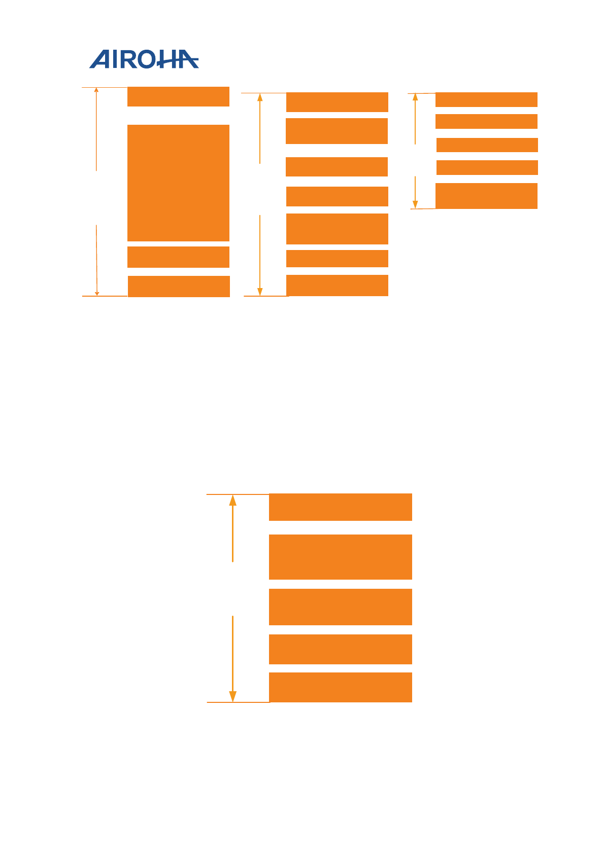
Figure 1. The load view of the 2MB flash memory layout
2.1.2. Execution view
Execution view describes where the code and data are located during the program execution. The execution view
is based on the Serial Flash, SYSRAM and TCM, as described below:
• Serial Flash. The code and read-only (RO) data are located in the flash memory during runtime.
• SYSRAM. Vector table, read-write (RW) data, zero initialized (ZI) data will be moved to SYSRAM during
runtime.
• TCM. Some special code and ZI data can be placed into the TCM during runtime, see section 2.3,
“Programming ” for more details about placing the code and the data into the TCM.
The detailed execution view of the memory layout is shown in Figure 2.

Airoha IoT SDK for RTOS Memory
Layout Developer's Guide
© 2015 - 2018 Airoha Technology Corp.
Page 4 of 51
This document contains information that is proprietary to Airoha Technology Corp. (“Airoha”) and/or its licensor(s).
Any unauthorized use, reproduction or disclosure of this document in whole or in part is strictly prohibited.
Bootloader
N9 RAM code
NVDM buffer
Reserved
ARM Cortex-M4 Firmware
FOTA buffer
2MB
Serial Flash
Vector Table
RW data
ZI data
Stack
Heap
TCM code
TCM data
256kB
SYSRAM
64kB
TCM
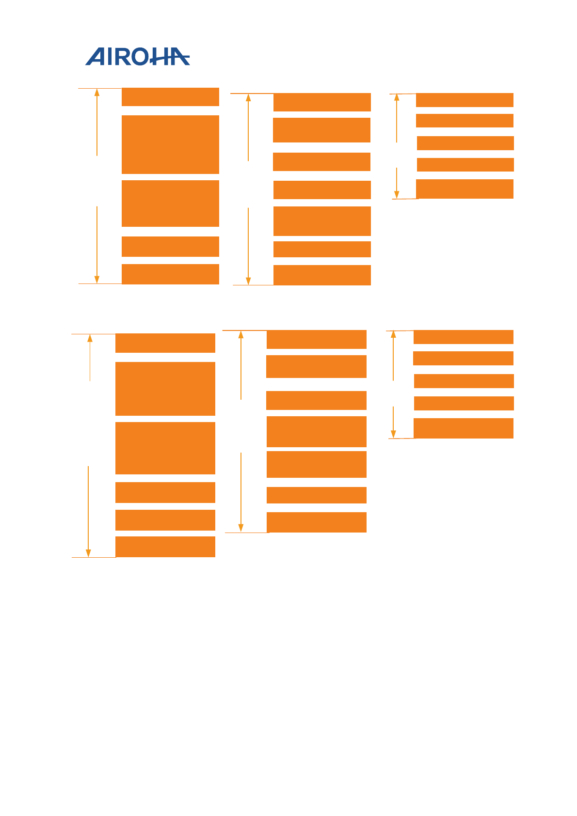
Figure 2. The execution view of the 2MB flash memory layout
The size and address of the flash layout are not configurable. A user defined memory layout could be created by
modifying or customizing the flash layout with two restrictions applied as follows:
• Load view: The bootloader must be located at the beginning of the flash.
• Execution view: Vector table must be located at the beginning of the SYSRAM.
2.2. 4MB memory layout view
MT7697 or MT7697D has a 4MB external flash. This section will introduce the memory layout based on the 4MB
flash.
2.2.1. Load view
The load view on the flash memory of the HDK is shown in Figure 3.
• Bootloader. The first 32kB of memory is allocated for the bootloader. The bootloader binary is located at
out/<board>/<project>/. The bootloader is not configurable.
• N9 RAM Code. The N9 binary is located under out/<board>/<project>/. The N9 RAM Code is not
configurable.
• ARM Cortex-M4 firmware. The application binary is located under out/<board>/<project>/. The
ARM Cortex-M4 firmware is configurable. See section 2.4, “Memory layout adjustment with a linker
script” for more details.
• FOTA buffer. Firmware update over the air (FOTA) buffer is reserved for FOTA memory management. The
FOTA buffer is configurable. See section 2.4, “Memory layout adjustment with a linker script” for more
details.
• Non-Volatile Data Management (NVDM) buffer is reserved for NVDM management. The NVDM buffer is
configurable. See section 2.4, “Memory layout adjustment with a linker script” for more details.
Airoha IoT SDK for RTOS Memory
Layout Developer's Guide
© 2015 - 2018 Airoha Technology Corp.
Page 5 of 51
This document contains information that is proprietary to Airoha Technology Corp. (“Airoha”) and/or its licensor(s).
Any unauthorized use, reproduction or disclosure of this document in whole or in part is strictly prohibited.
Note: For more information about FOTA, please refer to Airoha IoT Development Platform for RTOS Firmware
Update Developer's Guide located under SDK /doc folder.
Bootloader
N9 RAM code
NVDM buffer
Reserved
ARM Cortex-M4 Firmware
-
FOTA buffer
4MB
Serial Flash
32kB
32kB
420kB
1972kB
1546kB
64kB
Figure 3. The load view of the 4MB flash memory layout
2.2.2. Execution view
Execution view describes where the code and data are located during the program execution. The execution view
is based on the Serial Flash, SYSRAM and TCM, as described below:
• Serial Flash. The code and read-only (RO) data are located in the flash memory during runtime.
• SYSRAM. Vector table, read-write (RW) data, zero initialized (ZI) data will be moved to SYSRAM during
runtime.
• TCM. Some special code and ZI data can be placed into the TCM during runtime, see section 2.3,
“Programming guide” for more details about placing the code and the data into the TCM.
The detailed execution view of the memory layout is shown in Figure 4.

Airoha IoT SDK for RTOS Memory
Layout Developer's Guide
© 2015 - 2018 Airoha Technology Corp.
Page 6 of 51
This document contains information that is proprietary to Airoha Technology Corp. (“Airoha”) and/or its licensor(s).
Any unauthorized use, reproduction or disclosure of this document in whole or in part is strictly prohibited.
Bootloader
N9 RAM code
NVDM buffer
Reserved
ARM Cortex-M4 RTOS code, RO
data
FOTA buffer
4MB
Serial Flash
Vector Table
RW data
ZI data
Stack
Heap
TCM code
TCM ZI data
256kB
SYSRAM
64kB
TCM
Figure 4. The execution view of the 4MB flash memory layout
The size and address of the flash layout are not configurable. A user defined memory layout could be created by
modifying or customizing the flash layout with two restrictions applied as follows:
• Load view: The bootloader must be located at the beginning of the flash.
• Execution view: Vector table must be located at the beginning of the SYSRAM.
2.3. Programming guide
This programming guide is based on the memory layout described in section 2.1, “2MB memory layout view” and
section 2.2, “4MB memory layout view”. The following recommendations allow the developers to place the code
successfully to the desired memory location during runtime.
1) Place the code or the RO data to the Serial Flash at runtime.
By default, the code or the RO data is placed in the flash (XIP - Execute in Place), no need to modify.
2) Place the code or RO data to TCM at run time.
To run the code or access the data in the TCM with better performance, specify the attribute explicitly in your
code, as shown in the example below.
//code: The function func will be put into TCM by linker.
ATTR_TEXT_IN_TCM int func(int par)
{
int s;
s = par;
//....
}
//ro-data: The variable b will be put into TCM by linker.
ATTR_TEXT_IN_TCM const int b = 8;
For comparison, if the attribute is not explicitly defined, during the function call the code will be placed in the
SYSRAM instead of the TCM.
//code: The function func will NOT be put into TCM by linker. It will be
put //into FLASH.
int func(int par)

Airoha IoT SDK for RTOS Memory
Layout Developer's Guide
© 2015 - 2018 Airoha Technology Corp.
Page 7 of 51
This document contains information that is proprietary to Airoha Technology Corp. (“Airoha”) and/or its licensor(s).
Any unauthorized use, reproduction or disclosure of this document in whole or in part is strictly prohibited.
{
int s;
s = par;
//....
}
//ro-data: The variable b will NOT be placed into TCM by linker. It will
be placed //into the SYSRAM.
int b = 8;
3) Place ZI data into TCM at runtime.
The code below declares an attribute to place the ZI data into the TCM.
// zi-data: The variable b will be put into TCM by linker.
ATTR_ZIDATA_IN_TCM int b;
For comparison, if the attribute is not explicitly defined, during the function call the ZI data will be placed in the
SYSRAM instead of the TCM.
// zi-data: The variable b will NOT be put into TCM by linker. It will
be put //into SYSRAM.
int b;
2.4. Memory layout adjustment with a linker script
The memory layout can be configured with different toolchains. When the code is built based on the GCC
toolchain, the memory layout description file called a linker script is required. When the code is built based on the
ARMCC toolchain, the memory layout description file called a scatter file is used.
This section describes how to use the linker script provided by Airoha and how to configure the linker script when
building code with GCC toolchain. The scatter file will be introduced in see section 2.5.1, “Adjusting the memory
layout”.
The linker script is located under /project/<board>/apps/<project>/GCC/. Each application has its own
linker script based on the preferred memory layout.
2.4.1. Memory layout configuration
By default, there is no need to modify the linker script. To create a new memory layout, a new linker script should
be written.
The layout configuration information you can use in the modules is shown in Table 1.
Table 1. Tips for changing the memory layout of MT76x7 platform
Modules Tips
Bootloader The starting address and size of the bootloader are fixed, no need to modify.
N9 RAM The starting address and size of the N9 RAM are fixed, no need to modify.
ARM Cortex-M4 firmware The starting address of the ARM Cortex-M4 firmware is fixed, but the size is
configurable.
FOTA buffer The starting address and size of the FOTA buffer are configurable.
NVDM buffer The first NVDM buffer located after the Bootloader is not configurable, no
need to modify. The second NVDM buffer starting address and size are
configurable (see Figure 1).
Airoha IoT SDK for RTOS Memory
Layout Developer's Guide
© 2015 - 2018 Airoha Technology Corp.
Page 8 of 51
This document contains information that is proprietary to Airoha Technology Corp. (“Airoha”) and/or its licensor(s).
Any unauthorized use, reproduction or disclosure of this document in whole or in part is strictly prohibited.
2.4.2. Rules to adjust the memory layout
2.4.2.1. Adjusting the layout for ARM Cortex-M4 firmware
If the FOTA feature is not in use, you can increase the size of the ARM Cortex-M4 firmware for your application
usage. The steps to increase the size of the ARM Cortex-M4 firmware are shown below:
1) Modify the XIP_CODE length in the MT76x7_flash.ld.
MEMORY
{
...
XIP_CODE (arx) : ORIGIN = 0x10079000, LENGTH = 0x000BF000
...
}
2) Modify the macro definition CM4_CODE_LENGTH in
project\<board>\apps\<application>\inc\flash_map.h.
3) Rebuild the bootloader and the ARM Cortex-M4 firmware.
2.4.2.2. Adjusting the FOTA buffer size
The steps to adjust the FOTA buffer are shown below:
1) Modify the size of the ARM Cortex-M4 firmware, if necessary. See section 2.4.2.1, “Adjusting the layout
for ARM Cortex-M4 firmware”.
2) Modify the macro definition for FOTA buffer size FOTA_LENGTH in
project\<board>\apps\<application>\inc\flash_map.h.
Note: For more information about FOTA buffer, please refer to Airoha IoT Development Platform for RTOS Firmware
Update Developer's Guide located under the SDK /doc folder.
2.4.2.3. Adjusting the NVDM buffer size
The steps to adjust NVDM buffer size are shown below;
1) Modify size of the ARM Cortex-M4 firmware if necessary. Please see section 2.4.2.1, “Adjusting the layout
for ARM Cortex-M4 firmware”.
2) Modify FOTA buffer size if necessary. Please see section 2.4.2.2, “Adjusting the FOTA buffer size”.
3) Modify the macro definition for the NVDM buffer size NVDM_LENGTH in the
project\<board>\apps\<application>\inc\flash_map.h. This macro represents the NVDM
buffer size.
For more details, please refer to the NVDM module of HAL in the Airoha IoT Development Platform for RTOS API
reference.
2.5. Memory layout adjustment with a scatter File
The scatter file is located under /project/<board>/apps/<project>/MDK-ARM/. Each application has its
own scatter file and each scatter file can have different memory layout based on the specific application, see
section 2.4, “Memory layout adjustment with a linker script” for a difference between the linker script and the
scatter file.

Airoha IoT SDK for RTOS Memory
Layout Developer's Guide
© 2015 - 2018 Airoha Technology Corp.
Page 9 of 51
This document contains information that is proprietary to Airoha Technology Corp. (“Airoha”) and/or its licensor(s).
Any unauthorized use, reproduction or disclosure of this document in whole or in part is strictly prohibited.
2.5.1. Adjusting the memory layout
By default, there is no need to modify the scatter file. To create a new memory layout, a new scatter files should
be written. For more information about writing a scatter file, please refer to chapter 5 of the RealView®
Compilation Tools, Linker and Utilities Guide.
For more details about how to adjust the memory layout, see section 2.4.2, “Rules to adjust the memory layout”.
Airoha IoT SDK for RTOS Memory
Layout Developer's Guide
© 2015 - 2018 Airoha Technology Corp.
Page 10 of 51
This document contains information that is proprietary to Airoha Technology Corp. (“Airoha”) and/or its licensor(s).
Any unauthorized use, reproduction or disclosure of this document in whole or in part is strictly prohibited.
3. Memory Layout and Configuration for MT2523x
The MT2523x chipsets support three types of physical memory, Serial Flash, Pseudo Static Random Access Memory
(PSRAM) and Tightly Coupled Memory (TCM). The memory layouts are designed based on the three types of
memory.
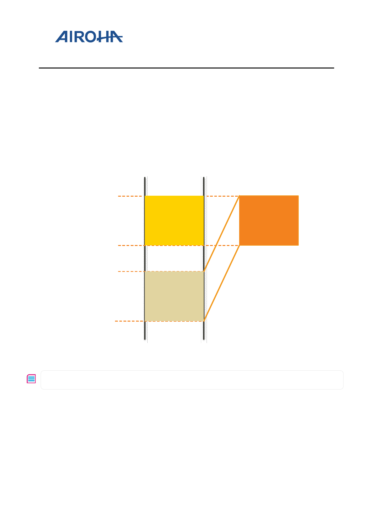
The virtual memory on the MT2523x is provided for cacheable memory and is implemented based on the memory
mapping mechanism of ARM Cortex-M4. The virtual address range from 0x10000000 to 0x14000000 is mapped
to the PSRAM address range from 0x00000000 to 0x04000000, as shown in Figure 5. The virtual memory region
(0x10000000 ~ 0x14000000) is used as cacheable memory. All read-write (RW) data is stored in this region by
default.
Physical memory
Physical memory
address range
Virtual memory
address range
Address map
0x00000000
0x10000000
Figure 5. MT2523x virtual memory mapping
Note, that the address 0x04000000 doesn’t limit the PSRAM size to 64MB. It only specifies the maximum range of
the PSRAM region supported by the LinkIt 2523 HDK.
The memory layout can be defined with the firmware update over the air (FOTA) and without FOTA. Each of the
layouts has two views described above.
This section guides you through:
• Types of the memory layout
• Programming guide
• Memory Layout Adjustment with a

Airoha IoT SDK for RTOS Memory
Layout Developer's Guide
© 2015 - 2018 Airoha Technology Corp.
Page 11 of 51
This document contains information that is proprietary to Airoha Technology Corp. (“Airoha”) and/or its licensor(s).
Any unauthorized use, reproduction or disclosure of this document in whole or in part is strictly prohibited.
o Linker Script
o Scatter File
3.1. Memory layout without FOTA
3.1.1. Load view
MT2523x has 4MB internal serial flash memory. The load view on the flash memory with disabled FOTA for
MT2523D and MT2523G is shown in Figure 6. The load view on the flash memory with disabled FOTA for MT2533
is shown in Figure 7.
• Bootloader. The bootloader binary is always located at the very beginning of the flash memory. The size of
the bootloader is not configurable and is fixed to 64kB size.
• ARM Cortex-M4 firmware. This section of the memory is reserved for the RTOS binary.
• External DSP buffer. This section is only available on MT2533 and it’s reserved for external DSP image.
External DSP is a third-party DSP which provides voice recognition and advanced noise suppression
technologies. Other third-party audio/speech handling algorithms can also be integrated in this external
DSP, if needed.
• The end of the flash is a reserved buffer for NVDM buffer and Extended Prediction Orbit (EPO) buffer. For
more information about the EPO, please refer to Airoha IoT Development Platform for RTOS GNSS
Developers Guide under SDK/doc folder. The size of the NVDM is configurable, but the size of the EPO
buffer is not configurable.
The start address and the maximum size of each binary and reserved buffer are configurable, see section 3.4,
“Memory layout adjustment with a linker script” for more details.
Bootloader
NVDM buffer
ARM Cortex-M4 Firmware
-
4MB
Serial Flash
EPO buffer
Figure 6. Load view of the MT2523D and MT2523G memory layout without FOTA

Airoha IoT SDK for RTOS Memory
Layout Developer's Guide
© 2015 - 2018 Airoha Technology Corp.
Page 12 of 51
This document contains information that is proprietary to Airoha Technology Corp. (“Airoha”) and/or its licensor(s).
Any unauthorized use, reproduction or disclosure of this document in whole or in part is strictly prohibited.
Bootloader
NVDM buffer
ARM Cortex-M4 Firmware
4MB
Serial Flash
EPO buffer
External DSP buffer
Figure 7. Load view of the MT2533 memory layout without FOTA
For more information about FOTA, refer to Airoha IoT Development Platform for RTOS Firmware Update
Developer's Guide located under SDK/doc folder.
For more information about NVDM, refer to Airoha IoT Development Platform for RTOS API reference guide.
For more information about EPO, refer to the Airoha IoT Development Platform for RTOS GNSS Developers
Guide under SDK/doc folder.
3.1.2. Execution view
Execution view describes where the code and data are located during the program runtime, as shown in Figure 8
for MT2523D, MT2523G and for MT2533. The execution view is based on the Serial Flash, PSRAM and TCM, as
described below:
• Serial Flash. The code and read-only (RO) data are located in the flash memory during runtime.
• PSRAM
o Vector table, single bank code, and some high-performance code and data are stored at the
beginning of PSRAM.
o Non-cacheable read-write (RW) data and zero-initialized (ZI) data.
o Cacheable RW data and ZI data.
• TCM. Some critical and high-performance code or data can be stored into the TCM. See section 3.3,
“Programming guide” to learn how to put code or data to the TCM.
o Code and RO data.
o RW data and ZI data.
o The system stack.
Airoha IoT SDK for RTOS Memory
Layout Developer's Guide
© 2015 - 2018 Airoha Technology Corp.
Page 13 of 51
This document contains information that is proprietary to Airoha Technology Corp. (“Airoha”) and/or its licensor(s).
Any unauthorized use, reproduction or disclosure of this document in whole or in part is strictly prohibited.
Bootloader
NVDM buffer
ARM Cortex-M4 RTOS code,
RO data
4MB
Serial Flash
Vector table
Non-Cacheable RW data
Non-Cacheable ZI data
Cacheable ZI data
Cacheable RW data
TCM code
System Stack
4MB
PSRAM
128kB
TCM
TCM RO data
TCM RW data
TCM ZI data
RAM code
RAM RO data
EPO buffer
Figure 8. Execution view of the MT2523D, MT2523G and MT2533 memory layout without FOTA
3.2. Memory layout with FOTA of full binary update
3.2.1. Load view
If FOTA is enabled, the memory flash layout’s load view is, as shown in Figure 9 for MT2523D and MT2523G, and
Figure 10 for MT2533. A FOTA buffer is added for temporary storage of the binary that will be used to update the
current ARM Cortex-M4 firmware. The start address and maximum size of each binary and the reserved space of
certain memory layouts are configurable, see section 3.4, “Memory layout adjustment with a linker script” for
more details. To enable FOTA, please refer to the Airoha IoT Development Platform for RTOS Firmware Update
Developer's Guide located under the SDK /doc folder.
Bootloader
FOTA buffer
ARM Cortex-M4 Firmware
4MB
Serial Flash
NVDM buffer
EPO buffer
Figure 9. Load view of the MT2523D and MT2523G memory layout with full binary FOTA

Airoha IoT SDK for RTOS Memory
Layout Developer's Guide
© 2015 - 2018 Airoha Technology Corp.
Page 14 of 51
This document contains information that is proprietary to Airoha Technology Corp. (“Airoha”) and/or its licensor(s).
Any unauthorized use, reproduction or disclosure of this document in whole or in part is strictly prohibited.
Bootloader
FOTA buffer
ARM Cortex-M4 Firmware
4MB
Serial Flash
NVDM buffer
EPO buffer
External DSP buffer
Figure 10 Load view of the MT2533 memory layout with full binary FOTA
3.2.2. Execution view
The execution view (see Figure 11 for MT2523D and MT2523G, and Figure 12 for MT2533) at runtime is described
below.
• Serial Flash. The code and RO data are located in the flash memory during runtime.
• PSRAM
o Vector table, single bank code, and some high-performance code and data are stored at the
beginning of the PSRAM.
o Non-cacheable RW data.
o Cacheable RW data.
• TCM. Some critical and high-performance code and data can be stored in the TCM. See section 3.3,
“Programming guide” to learn how to put code or data to the TCM.
o Code and RO data.
o RW data, ZI data.
o The system stack.
Airoha IoT SDK for RTOS Memory
Layout Developer's Guide
© 2015 - 2018 Airoha Technology Corp.
Page 15 of 51
This document contains information that is proprietary to Airoha Technology Corp. (“Airoha”) and/or its licensor(s).
Any unauthorized use, reproduction or disclosure of this document in whole or in part is strictly prohibited.
Bootloader
NVDM buffer
ARM Cortex-M4 RTOS code,
RO data
4MB
Serial Flash
Vector table
Non-Cacheable RW data
Non-Cacheable ZI data
Cacheable ZI data
Cacheable RW data
TCM code
System Stack
4MB
PSRAM
128kB
TCM
TCM RO data
TCM RW data
TCM ZI data
RAM code
RAM RO data
EPO buffer
FOTA buffer
Figure 11. Execution view of the MT2523D and MT2523G memory layout with full binary FOTA
Bootloader
FOTA buffer
ARM Cortex-M4 Firmware
4MB
Serial Flash
NVDM buffer
EPO buffer
External DSP buffer
Vector table
Non-Cacheable RW data
Non-Cacheable ZI data
Cacheable ZI data
Cacheable RW data
TCM code
System Stack
128kB
TCM
TCM RO data
TCM RW data
TCM ZI data
RAM code
RAM RO data
4MB
PSRAM
Figure 12. Execution view of the MT2533 memory layout with full binary FOTA
3.3. Programming guide
This programming guide is based on the memory layout described in see section 3.1.2, “Execution view”. The
following recommendations allow the developers to place the code successfully to the desired memory location
during runtime.
1) Place the code or RO data to the Serial Flash at runtime.
By default, the code or RO data is placed in the flash, execute in place (XIP), no need to modify.
2) Place the code or RO data to the PSRAM at runtime.
Airoha IoT SDK for RTOS Memory
Layout Developer's Guide
© 2015 - 2018 Airoha Technology Corp.
Page 16 of 51
This document contains information that is proprietary to Airoha Technology Corp. (“Airoha”) and/or its licensor(s).
Any unauthorized use, reproduction or disclosure of this document in whole or in part is strictly prohibited.
To run the code or access RO data in the PSRAM with better performance, specify the attribute explicitly in your
code, as shown in the example below.
//code
ATTR_TEXT_IN_RAM int func(int par)
{
int s;
s = par;
//....
}
//RO data
ATTR_RODATA_IN_RAM const int b = 8;
For comparison, if the attribute is not explicitly defined, during the function call the code will be placed in the
Serial Flash instead of the PSRAM.
//code
int func(int par)
{
int s;
s = par;
//....
}
//RO data
const int b = 8;
3) Place RW data or ZI data to non-cacheable memory at runtime.
To access RW data and ZI data in the non-cacheable memory with special purpose such as direct memory access
(DMA) buffer, specify the attribute explicitly in your code, as shown in the example below.
//RW data
ATTR_RWDATA_IN_NONCACHED_RAM int b = 8;
//ZI data
ATTR_ZIDATA_IN_NONCACHED_RAM int b;
For comparison, if the attribute is not explicitly defined, the data will be placed in the cacheable memory instead
of the non-cacheable memory.
//RW data
int b = 8;
//ZI data
int b;
4) Place RW data or ZI data to cacheable memory at runtime.
By default, RW data/ZI data are placed in the cacheable memory, no need to modify.
5) Place code or RO data to the TCM at runtime.
To run the code or access RO data in the TCM with better performance, specify the attribute explicitly in your
code, as shown in the example below.
//code
ATTR_TEXT_IN_TCM int func(int par)
{
int s;
s = par;
//....
}
//RO data
ATTR_RODATA_IN_TCM const int b = 8;
Airoha IoT SDK for RTOS Memory
Layout Developer's Guide
© 2015 - 2018 Airoha Technology Corp.
Page 17 of 51
This document contains information that is proprietary to Airoha Technology Corp. (“Airoha”) and/or its licensor(s).
Any unauthorized use, reproduction or disclosure of this document in whole or in part is strictly prohibited.
For comparison, if the attribute is not explicitly defined, during the function call the code will be placed in the
Serial Flash instead of the TCM.
//code
int func(int par)
{
int s;
s = par;
//....
}
//RO data
const int b = 8;
6) Put RW data/ZI data to TCM at runtime.
To access RW data and ZI data in the TCM with better performance, you should specify the attribute explicitly in
your code, as shown in the example below.
//rw-data
ATTR_RWDATA_IN_TCM int b = 8;
//zi-data
ATTR_ZIDATA_IN_TCM int b;
For comparison, if the attribute is not explicitly defined, the data will be placed in the PSRAM instead of the TCM.
//RW data
int b = 8;
//ZI data
int b;
3.4. Memory layout adjustment with a linker script
The memory layout can be configured with different toolchains. When the code is built based on the GCC
toolchain, the memory layout description file called a linker script is required. When the code is built based on
ARMCC toolchain, the memory layout description file called a scatter file is used.
This section describes how to use the linker script provided by Airoha and how to configure the linker script when
building code with the GCC toolchain. The scatter file will be introduced in see section 3.5, “Memory layout
adjustment with a scatter file”.
3.4.1. Types of linker scripts
Two kinds of linker scripts are provided:
• Template linker script – every application linker script should be based on the template linker script.
• Application linker script – every application has its particular linker script. This linker script is passed to the
linker during linking stage.
3.4.1.1. Template linker script
Template linker scripts are based on the memory layout see section 3.1 and 3.2. If the memory layout is modified,
the linker script should also be modified manually. It’s recommended to use the layout and linker scripts provided
by Airoha as a reference for your customizations.
The template linker scripts are located under /driver/CMSIS/Device/MTK/<chip>/linkerscript/GCC/
folder.
The folder includes:

Airoha IoT SDK for RTOS Memory
Layout Developer's Guide
© 2015 - 2018 Airoha Technology Corp.
Page 18 of 51
This document contains information that is proprietary to Airoha Technology Corp. (“Airoha”) and/or its licensor(s).
Any unauthorized use, reproduction or disclosure of this document in whole or in part is strictly prohibited.
• default. This folder contains a template linker script to build a project without FOTA memory layout, see
section 3.1, “Memory layout without FOTA”.
• full_bin_fota. This folder contains a template linker script to build a project with full binary FOTA
memory layout, see section 3.2, “Memory layout with FOTA of full binary update”
• ram. This folder contains a template linker script to enable RAM debugging. To place all your code into
PSRAM, use this linker script as a reference.
3.4.1.2. Application linker script
The application linker script is located under /project/<board>/apps/<project>/GCC/ folder. Each
application has its own linker script and each linker script can have a different memory layout configuration based
on the application requirements.
3.4.2. How to use the linker script
To create a new linker script file for your application:
• Clone a linker script from the template folder.
• Create a new linker script manually. The memory layout in this case should also be user-defined to match
your linker script.
3.4.2.1. Cloning the linker script
To clone a linker script from the template:
1) Specify the memory layout feature for your application development, such as without FOTA, full binary
FOTA see section 3.1 and 3.2.
2) Copy the template linker script from template folder to your application project’s folder see section 3.4.1,
“Types of linker scripts”.
3) Memory layout without FOTA.
Copy /driver/CMSIS/Device/MTK/<chip>/linkerscript/GCC/default to
/project/<board>/apps/<project>/GCC/.
4) Memory layout with FOTA full binary update.
Copy /driver/CMSIS/Device/MTK/<chip>/linkerscript/GCC/full_bin_fota to
/project/<board>/apps/<project>/GCC/.
5) Memory layout with RAM debugging.
Copy /driver/CMSIS/Device/MTK/<chip>/linkerscript/GCC/ram to
/project/<board>/apps/<project>/GCC/.
6) Modify the linker script according to the application requirements.
3.4.3. Rules to adjust the memory layout
The memory layout can be customized to fit the application requirements. However, the bootloader and EPO
buffer is not configurable. The rest of the memory layout can be adjusted as follows.
Common rules for different memory layout adjustment settings are described below.
1) The address and size must be block aligned. The default block size is 4kB and is defined in
driver/chip/<chip>/inc/flash_opt_gen.h header file.
Airoha IoT SDK for RTOS Memory
Layout Developer's Guide
© 2015 - 2018 Airoha Technology Corp.
Page 19 of 51
This document contains information that is proprietary to Airoha Technology Corp. (“Airoha”) and/or its licensor(s).
Any unauthorized use, reproduction or disclosure of this document in whole or in part is strictly prohibited.
2) To configure the size or the address, make sure there is no overlap between two adjacent memory
regions. The total size of all the regions should not exceed the physical flash size.
3.4.3.1. Adjusting the layout for ARM Cortex-M4 firmware
To adjust the memory assigned to ARM Cortex-M4 firmware:
1) Modify the ROM_RTOS length and starting address in the flash.ld linker script under the GCC folder of
the project.
MEMORY
{
...
ROM_RTOS(rx) : ORIGIN = 0x08010000, LENGTH = 3072K
...
}
2) Modify the macro definitions for RTOS_BASE and RTOS_LENGTH in
project/<board>/apps/<application>/inc/memory_map.h header file.
3) Rebuild the bootloader and the ARM Cortex-M4 firmware.
Execute the following command under the root folder of the SDK.
./build.sh project_board example_name BL
The project_board is the project folder of a specific hardware board and example_name is the name of the
example. For example, to build the hal_adc of mt2523_hdk, the command will be:
./build.sh mt2523_hdk hal_adc BL
4) Make sure the length of ROM region doesn’t exceed the flash size of the system and for MT2523 the
internal flash is 4MB.
3.4.3.2. Adjusting the memory layout with FOTA full binary update
1) Modify ARM Cortex-M4 firmware size if needed see section 3.4.3.1, “Adjusting the layout for ARM Cortex-
M4 firmware”.
2) Modify the ROM_FOTA_RESERVED length and starting address in the flash.ld linker script under the
GCC folder of a project.
MEMORY
{
...
ROM_FOTA_RESERVED(rx) : ORIGIN = 0x08200000, LENGTH = 1920K
...
}
3) Modify the macro definitions for FOTA_RESERVED_BASE and FOTA_RESERVED_LENGTH in
project/<board>/apps/<application>/inc/memory_map.h header file.
Note, refer to the SDK Firmware Upgrade Developer’s Guide located under SDK /doc folder for more details about
how to adjust the FOTA buffer.
3.4.3.3. Adjusting the NVDM buffer
To adjust the NVDM buffer layout:

Airoha IoT SDK for RTOS Memory
Layout Developer's Guide
© 2015 - 2018 Airoha Technology Corp.
Page 20 of 51
This document contains information that is proprietary to Airoha Technology Corp. (“Airoha”) and/or its licensor(s).
Any unauthorized use, reproduction or disclosure of this document in whole or in part is strictly prohibited.
1) Modify size of the ARM Cortex-M4 firmware if needed see section 3.4.3.1, “Adjusting the layout for ARM
Cortex-M4 firmware”.
2) Modify FOTA buffer size if needed see section 3.4.3.2, “Adjusting the memory layout with FOTA full binary
update”.
3) Modify the ROM_NVDM_RESERVED length and starting address in the flash.ld if no FOTA or full binary
FOTA feature is enabled
MEMORY
{
...
ROM_NVDM_RESERVED(rx) : ORIGIN = 0x083E0000, LENGTH = 64K
...
}
4) Modify the macro definitions for ROM_NVDM_BASE, ROM_NVDM_LENGTH in
project\<board>\apps\<application>\inc\memory_map.h header file.
Note, to adjust the NVDM buffer, please refer to the NVDM module of HAL in the Airoha IoT development platform
for RTOS API reference.
3.5. Memory layout adjustment with a scatter file
3.5.1. Types of scatter files
Two types of scatter files are provided:
• Template scatter file – every application scatter file should be based on the template scatter file.
• Application scatter file – every application has its particular scatter file. This scatter file will be passed to
the linker during linking stage.
3.5.1.1. Template scatter file
Template scatter files are based on the memory layout, see section 3.1 and 3.2. If you’ve changed the memory
layout, you should also modify the scatter file manually. It’s recommended to use the layout and scatter files
provided by Airoha as a reference for your customizations.
The template scatter files are located under /driver/CMSIS/Device/MTK/<chip>/linkerscript/RVCT/
folder. The folder includes:
• default. This folder contains a template scatter file to build a project without FOTA memory layout, see
section 3.1, “Memory layout without FOTA”.
• full_bin_fota. This folder contains a template scatter file to build a project with full binary FOTA
memory layout, see section 3.2, “Memory layout with FOTA of full binary update”
• ram. This folder contains a template scatter file to enable RAM debugging. To place all your code into
PSRAM, you can use this scatter file as a reference.

Airoha IoT SDK for RTOS Memory
Layout Developer's Guide
© 2015 - 2018 Airoha Technology Corp.
Page 21 of 51
This document contains information that is proprietary to Airoha Technology Corp. (“Airoha”) and/or its licensor(s).
Any unauthorized use, reproduction or disclosure of this document in whole or in part is strictly prohibited.
3.5.1.2. Application scatter file
The application scatter file is located under /project/<board>/apps/<project>/MDK-ARM/ folder. Each
application has its own scatter file and each scatter file can have a different memory layout configuration based on
the application requirements.
3.5.2. How to use the scatter file
To create a new scatter file for your application:
• Clone a scatter file from the MDK-ARM folder of the template folder.
• Create a new scatter file manually. The memory layout in this case should also be user-defined to match
your scatter file.
3.5.2.1. Cloning the scatter file
To clone a scatter file from the template:
1) Specify the memory layout feature for your application development, such as without FOTA, full binary
FOTA see section 3.1 and 3.2.
2) Copy the template scatter file from template folder to your application project’s folder see section 3.5.1,
“Types of scatter files”.
3) Memory layout without FOTA.
Copy /driver/CMSIS/Device/MTK/<chip>/linkerscript/rvct/default to
/project/<board>/apps/<project>/MDK-ARM/.
4) Memory layout with FOTA full binary update.
Copy /driver/CMSIS/Device/MTK/<chip>/linkerscript/rvct/full_bin_fota to
/project/<board>/apps/<project>/MDK-ARM/.
5) Memory layout with RAM debugging.
Copy /driver/CMSIS/Device/MTK/<chip>/linkerscript/rvct/ram to
/project/<board>/apps/<project>/MDK-ARM/.
6) Modify the scatter file according to the application requirements.
3.5.3. How to configure the scatter file
The configuration is the same; see section 3.4.3, “Rules to adjust the memory layout”.
Airoha IoT SDK for RTOS Memory
Layout Developer's Guide
© 2015 - 2018 Airoha Technology Corp.
Page 22 of 51
This document contains information that is proprietary to Airoha Technology Corp. (“Airoha”) and/or its licensor(s).
Any unauthorized use, reproduction or disclosure of this document in whole or in part is strictly prohibited.
4. Memory Layout and Configuration for MT7682
The MT7682 supports three types of physical memory, Serial Flash, System Random Access Memory (SYSRAM) and
Tightly Coupled Memory (TCM). The memory layouts are designed based on the three types of memory.
The virtual memory on the MT7682 is provided for cacheable memory and is implemented based on the memory
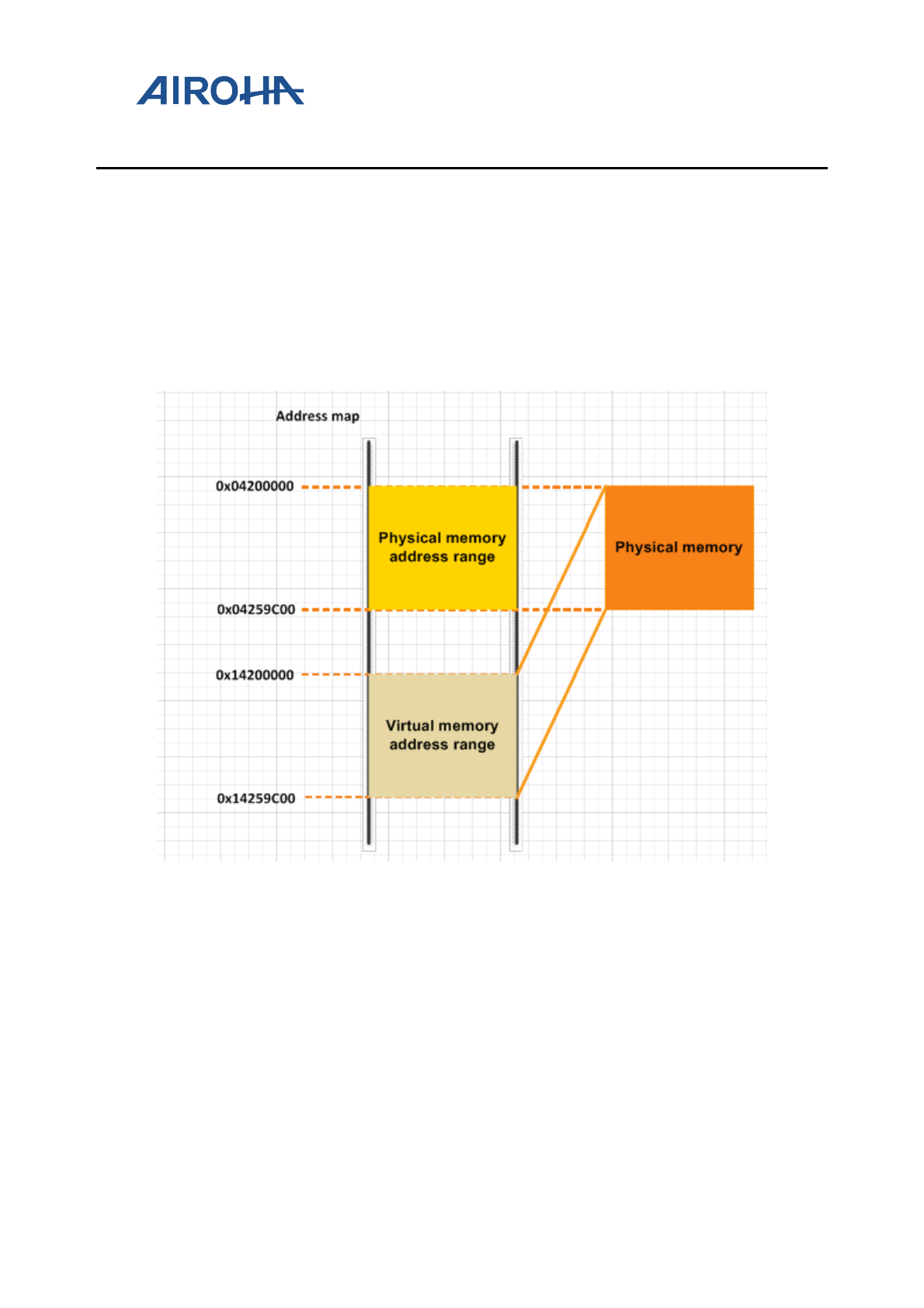
mapping mechanism of ARM Cortex-M4. The virtual address range from 0x14200000 to 0x14259C000 is mapped
to the SYSRAM address range from 0x04200000 to 0x04259C00, as shown in Figure 13. The virtual memory
region (0x14200000 ~ 0x14259C00) is used as cacheable memory. All read-write (RW) data is stored in this
region by default.
Figure 13 MT7682 virtual memory mapping
The memory layout can be defined with the firmware update over the air (FOTA) and without FOTA. Each of the
layouts has two views described above.
This section guides you through:
• Types of the memory layout
• Programming guide
• Memory Layout Adjustment with a
o Linker Script
o Scatter File
o IAR Configuration File

Airoha IoT SDK for RTOS Memory
Layout Developer's Guide
© 2015 - 2018 Airoha Technology Corp.
Page 23 of 51
This document contains information that is proprietary to Airoha Technology Corp. (“Airoha”) and/or its licensor(s).
Any unauthorized use, reproduction or disclosure of this document in whole or in part is strictly prohibited.
4.1. Memory layout without FOTA
4.1.1. Load view
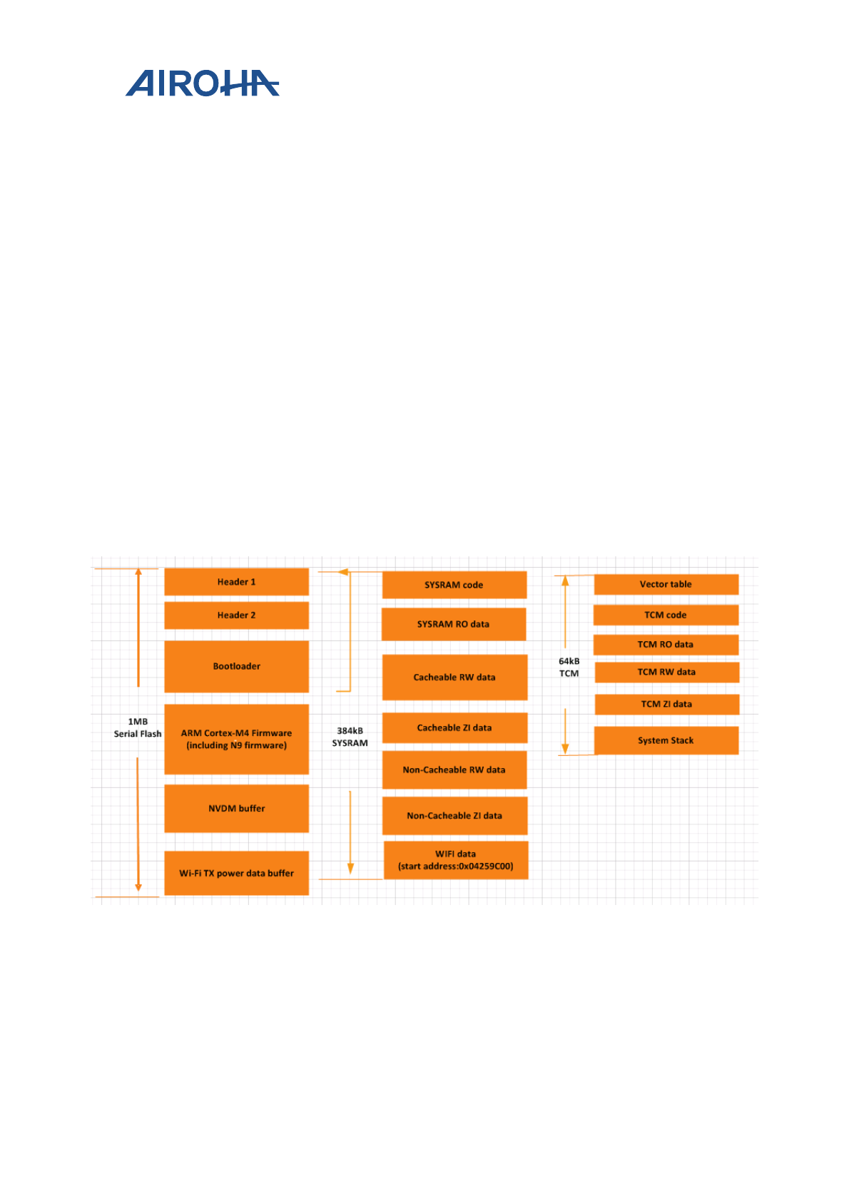
MT7682 has 1MB internal serial flash memory. The load view on the flash memory with disabled FOTA for MT7682
is shown in Figure 14.
• Header 1. Always located at the very beginning of the flash memory and is reserved for bootloader
security information. The size of the Header 1 is not configurable and is fixed to 4kB.
• Header 2. Reserved for RTOS binary security information. The size of the Header 2 is not configurable and
is fixed to 4kB.
• Bootloader. The size of the bootloader is not configurable and is fixed to 64kB.
• ARM Cortex-M4 firmware. This section of the memory is reserved for the RTOS binary and N9 firmware.
• The end of the flash is a reserved buffer for NVDM buffer and Wi-Fi transmit power data buffer. The sizes
of the NVDM and Wi-Fi transmit power data buffer are configurable.
The start address and the maximum size of each binary and reserved buffer are configurable, see section 4.4,
“Memory layout adjustment with a linker script”, for more details.
Header 1
Bootloader
Wi-Fi TX power data buffer
Header 2
ARM Cortex-M4 Firmware
(including N9 firmware)
-
NVDM buffer
1MB
Serial Flash
Figure 14 Load view of the MT7682 memory layout without FOTA
For more information about FOTA, refer to Airoha IoT Development Platform for RTOS Firmware Update
Developer's Guide located under SDK/doc folder.
For more information about NVDM, refer to Airoha IoT Development Platform for RTOS API reference guide.
Airoha IoT SDK for RTOS Memory
Layout Developer's Guide
© 2015 - 2018 Airoha Technology Corp.
Page 24 of 51
This document contains information that is proprietary to Airoha Technology Corp. (“Airoha”) and/or its licensor(s).
Any unauthorized use, reproduction or disclosure of this document in whole or in part is strictly prohibited.
4.1.2. Execution view
Execution view describes where the code and data are located at runtime, as shown in Figure 15 for MT7682. The
execution view is based on the Serial Flash, SYSRAM and TCM, as described below:
• Serial Flash. The code and read-only (RO) data are located in the flash memory during runtime.
• SYSRAM.
o SYSRAM code and RO data. The SYSRAM code and RO data are cacheable.
o Cacheable RW data and ZI data.
o Non-cacheable read-write (RW) data and zero-initialized (ZI) data.
o WIFI ROM RW/ZI data and code
• TCM. Some critical and high-performance code or data can be stored into the TCM. See section 4.3,
“Programming guide” to learn how to put code or data to the TCM.
o Vector table, single bank code, and some high-performance code and data are stored at the
beginning of TCM.
o Code and RO data.
o RW data and ZI data.
o The system stack.
Figure 15. Execution view of the MT7682 memory layout without FOTA
4.2. Memory layout with FOTA of full binary update
4.2.1. Load view
The memory flash layout’s load view with FOTA enabled is shown in Figure 16 for MT7682. A FOTA buffer is added
for temporary storage of the binary that will be used to update the current ARM Cortex-M4 firmware. The start

Airoha IoT SDK for RTOS Memory
Layout Developer's Guide
© 2015 - 2018 Airoha Technology Corp.
Page 25 of 51
This document contains information that is proprietary to Airoha Technology Corp. (“Airoha”) and/or its licensor(s).
Any unauthorized use, reproduction or disclosure of this document in whole or in part is strictly prohibited.
address and maximum size of each binary and the reserved space of certain memory layouts are configurable, see
section 4.4, “Memory layout adjustment with a linker script”, for more details. To enable FOTA, refer to the Airoha
IoT Development Platform for RTOS Firmware Update Developer's Guide located under the SDK /doc folder.
Header 1
Bootloader
Wi-Fi TX power data buffer
Header 2
ARM Cortex-M4 Firmware
(including N9 firmware)
-
NVDM buffer
1MB
Serial Flash
FOTA buffer
Figure 16. Load view of the MT7682 memory layout with full binary FOTA
4.2.2. Execution view
The execution view (see Figure 17 for MT7682) at runtime is described below.
• Serial Flash. The code and RO data are located in the flash memory during runtime.
• SYSRAM.
o SYSRAM code and RO data. The SYSRAM code and RO data is cacheable.
o Cacheable RW data and ZI data.
o Non-cacheable RW data and ZI data.
o WIFI ROM RW/ZI data and code
• TCM. Some critical and high-performance code or data can be stored into the TCM. See section 4.3,
“Programming guide” to learn how to put code or data to the TCM.
o Vector table, single bank code, and some high-performance code and data are stored at the
beginning of TCM.

Airoha IoT SDK for RTOS Memory
Layout Developer's Guide
© 2015 - 2018 Airoha Technology Corp.
Page 26 of 51
This document contains information that is proprietary to Airoha Technology Corp. (“Airoha”) and/or its licensor(s).
Any unauthorized use, reproduction or disclosure of this document in whole or in part is strictly prohibited.
o Code and RO data.
o RW data and ZI data.
o The system stack.
Figure 17. Execution view of the MT7682 memory layout with full binary FOTA
4.3. Programming guide
This programming guide is based on the memory layout described in see section 4.1.2, “Execution view”. The
following recommendations allow the developers to place the code successfully to the desired memory location
during runtime.
1) Place the code or RO data to the Serial Flash at runtime.
By default, the code or RO data is placed in the flash, execute in place (XIP), no need to modify.
2) Place the code or RO data to the SYSRAM at runtime.
To run the code or access RO data in the SYSRAM with better performance, specify the attribute explicitly in your
code, as shown in the example below.
//code
ATTR_TEXT_IN_SYSRAM int func(int par)
{
int s;
s = par;
//....
}
//RO data
ATTR_RODATA_IN_SYSRAM const int b = 8;
Airoha IoT SDK for RTOS Memory
Layout Developer's Guide
© 2015 - 2018 Airoha Technology Corp.
Page 27 of 51
This document contains information that is proprietary to Airoha Technology Corp. (“Airoha”) and/or its licensor(s).
Any unauthorized use, reproduction or disclosure of this document in whole or in part is strictly prohibited.
For comparison, if the attribute is not explicitly defined, during the function call the code will be placed in the
Serial Flash instead of the SYSRAM.
//code
int func(int par)
{
int s;
s = par;
//....
}
//RO data
const int b = 8;
3) Place RW data or ZI data to non-cacheable memory at runtime.
To access RW data and ZI data in the non-cacheable memory with special purpose such as direct memory access
(DMA) buffer, specify the attribute explicitly in your code, as shown in the example below.
//RW data
ATTR_RWDATA_IN_NONCACHED_SYSRAM int b = 8;
//ZI data
ATTR_ZIDATA_IN_NONCACHED_SYSRAM int b;
For comparison, if the attribute is not explicitly defined, the data will be placed in the cacheable memory instead
of the non-cacheable memory.
//RW data
int b = 8;
//ZI data
int b;
4) Place RW data or ZI data to cacheable memory at runtime.
By default, RW data/ZI data are placed in the cacheable memory, no need to modify.
5) Place code or RO data to the TCM at runtime.
To run the code or access RO data in the TCM with better performance, specify the attribute explicitly in your
code, as shown in the example below.
//code
ATTR_TEXT_IN_TCM int func(int par)
{
int s;
s = par;
//....
}
//RO data
ATTR_RODATA_IN_TCM const int b = 8;
For comparison, if the attribute is not explicitly defined, during the function call the code will be placed in the
Serial Flash instead of the TCM.
//code
int func(int par)
{
int s;
s = par;
Airoha IoT SDK for RTOS Memory
Layout Developer's Guide
© 2015 - 2018 Airoha Technology Corp.
Page 28 of 51
This document contains information that is proprietary to Airoha Technology Corp. (“Airoha”) and/or its licensor(s).
Any unauthorized use, reproduction or disclosure of this document in whole or in part is strictly prohibited.
//....
}
//RO data
const int b = 8;
6) Put RW data/ZI data to TCM at runtime.
To access RW data and ZI data in the TCM with better performance, you should specify the attribute explicitly in
your code, as shown in the example below.
//rw-data
ATTR_RWDATA_IN_TCM int b = 8;
//zi-data
ATTR_ZIDATA_IN_TCM int b;
For comparison, if the attribute is not explicitly defined, the data will be placed in the SYSRAM instead of the TCM.
//RW data
int b = 8;
//ZI data
int b;
4.4. Memory layout adjustment with a linker script
The memory layout can be configured with different toolchains. When the code is built based on the GCC
toolchain, the memory layout description file called a linker script is required. When the code is built based on
ARMCC toolchain, the memory layout description file called a scatter file is used. When the code is built based on
IAR toolchain, the memory layout description file called an IAR configuration file is used.
This section describes how to use the linker script provided by Airoha and how to configure the linker script when
building code with the GCC toolchain. The scatter file will be introduced in section 4.5, “Memory layout adjustment
with a scatter file”.
4.4.1. Types of linker scripts
Two types of linker scripts are provided:
• Template linker script — every application linker script should be based on the template linker script.
• Application linker script — every application has its particular linker script. This linker script is passed to
the linker during linking stage.
4.4.1.1. Template linker script
Template linker scripts are based on the memory layout. If the memory layout is modified, the linker script should
also be modified manually. It’s recommended to use the layout and linker scripts provided by Airoha as a reference
for your customizations.
The template linker scripts are located under /driver/CMSIS/Device/MTK/<chip>/linkerscript/GCC/
folder.
The folder includes:
• default. This folder contains a template linker script to build a project without FOTA memory layout, see
section 4.1, “Memory layout without FOTA”.
• full_bin_fota. This folder contains a template linker script to build a project with full binary FOTA
memory layout, see section 4.2, “Memory layout with FOTA of full binary update”

Airoha IoT SDK for RTOS Memory
Layout Developer's Guide
© 2015 - 2018 Airoha Technology Corp.
Page 29 of 51
This document contains information that is proprietary to Airoha Technology Corp. (“Airoha”) and/or its licensor(s).
Any unauthorized use, reproduction or disclosure of this document in whole or in part is strictly prohibited.
• sysram. This folder contains a template linker script to enable RAM debugging. To place all your code
into SYSRAM, use this linker script as a reference.
4.4.1.2. Application linker script
The application linker script is located under /project/<board>/apps/<project>/GCC/ folder. Each
application has its own linker script and each linker script can have a different memory layout configuration based
on the application requirements.
4.4.2. How to use the linker script
To create a new linker script file for your application:
• Clone a linker script from the template folder.
• Create a new linker script manually. The memory layout in this case should also be user-defined to match
your linker script.
4.4.2.1. Cloning the linker script
To clone a linker script from the template:
1) Specify the memory layout feature for your application development, such as without FOTA, full binary
FOTA.
2) Copy the template linker script from template folder to your application project’s folder, see section 4.4.1,
“Types of linker scripts”.
3) Memory layout without FOTA.
Copy /driver/CMSIS/Device/MTK/<chip>/linkerscript/GCC/default to
/project/<board>/apps/<project>/GCC/.
4) Memory layout with FOTA full binary update.
Copy /driver/CMSIS/Device/MTK/<chip>/linkerscript/GCC/full_bin_fota to
/project/<board>/apps/<project>/GCC/.
5) Memory layout with RAM debugging.
Copy /driver/CMSIS/Device/MTK/<chip>/linkerscript/GCC/sysram to
/project/<board>/apps/<project>/GCC/.
6) Modify the linker script according to the application requirements.
4.4.3. Rules to adjust the memory layout
The memory layout can be customized to fit the application requirements. However, the sections for header 1,
header 2 and bootloader are not configurable. The rest of the memory layout can be adjusted as follows.
Common rules for different memory layout adjustment settings are described below.
1) The address and size must be block aligned. The default block size is 4kB and is defined in
driver/chip/<chip>/inc/flash_opt_gen.h header file.
2) To configure the size or the address, make sure there is no overlap between two adjacent memory
regions. The total size of all the regions should not exceed the physical flash size.
Airoha IoT SDK for RTOS Memory
Layout Developer's Guide
© 2015 - 2018 Airoha Technology Corp.
Page 30 of 51
This document contains information that is proprietary to Airoha Technology Corp. (“Airoha”) and/or its licensor(s).
Any unauthorized use, reproduction or disclosure of this document in whole or in part is strictly prohibited.
4.4.3.1. Adjusting the layout for ARM Cortex-M4 firmware
To adjust the memory assigned to ARM Cortex-M4 firmware:
1) Modify the ROM_RTOS length and starting address in the mt7682_flash.ld linker script under the GCC
folder of the project.
MEMORY
{
...
ROM_RTOS(rx) : ORIGIN = 0x08012000, LENGTH = 884K
...
}
2) Modify the macro definitions for RTOS_BASE and RTOS_LENGTH in
project/<board>/apps/<application>/inc/memory_map.h header file.
3) Rebuild the bootloader and the ARM Cortex-M4 firmware.
Execute the following command under the root folder of the SDK.
./build.sh project_board example_name BL
The project_board is the project folder of a specific hardware board and example_name is the name of the
example. For example, to build the hal_adc of mt7682_hdk, the command is:
./build.sh mt7682_hdk hal_adc BL
4) Make sure the length of ROM region doesn’t exceed the flash size of the system and for MT7682 the
internal flash is 1MB.
4.4.3.2. Adjusting the memory layout with FOTA full binary update
1) Modify ARM Cortex-M4 firmware size, if needed see section 4.4.3.1, “Adjusting the layout for ARM
Cortex-M4 firmware”.
2) Modify the ROM_FOTA_RESERVED length and starting address in the flash.ld linker script under the
GCC folder of a project.
MEMORY
{
...
ROM_FOTA_RESERVED(rx) : ORIGIN = 0x08098000, LENGTH = 348K
...
}
3) Modify the macro definitions for FOTA_RESERVED_BASE and FOTA_RESERVED_LENGTH in
project/<board>/apps/<application>/inc/memory_map.h header file.
Note, refer to the SDK Firmware Upgrade Developer’s Guide located under SDK /doc folder for more details about
how to adjust the FOTA buffer.
4.4.3.3. Adjusting the NVDM buffer
To adjust the NVDM buffer layout:
Airoha IoT SDK for RTOS Memory
Layout Developer's Guide
© 2015 - 2018 Airoha Technology Corp.
Page 31 of 51
This document contains information that is proprietary to Airoha Technology Corp. (“Airoha”) and/or its licensor(s).
Any unauthorized use, reproduction or disclosure of this document in whole or in part is strictly prohibited.
1) Modify the size of the ARM Cortex-M4 firmware, if needed see section 4.4.3.1, “Adjusting the layout for
ARM Cortex-M4 firmware”.
2) Modify FOTA buffer size, if needed see section 4.4.3.2, “Adjusting the memory layout with FOTA full
binary update”.
3) Modify the ROM_NVDM_RESERVED length and starting address in the flash.ld if no FOTA or full binary
FOTA feature is enabled
MEMORY
{
...
ROM_NVDM_RESERVED(rx) : ORIGIN = 0x080EF000, LENGTH = 64K
...
}
4) Modify the macro definitions for ROM_NVDM_BASE, ROM_NVDM_LENGTH in
project\<board>\apps\<application>\inc\memory_map.h header file.
Note, to adjust the NVDM buffer, refer to the NVDM module of HAL in the Airoha IoT development platform for
RTOS API reference.
4.5. Memory layout adjustment with a scatter file
4.5.1. Types of scatter files
Two types of scatter files are provided:
• Template scatter file – every application scatter file should be based on the template scatter file.
• Application scatter file – every application has its particular scatter file. This scatter file will be passed to
the linker during linking stage.
4.5.1.1. Template scatter file
Template scatter files are based on the memory layout. If the memory layout is modified, the scatter file should
also be modified manually. It’s recommended to use the layout and scatter files provided by Airoha as a reference
for your customizations.
The template scatter files are located under /driver/CMSIS/Device/MTK/<chip>/linkerscript/RVCT/
folder. The folder includes:
• default. This folder contains a template scatter file to build a project without FOTA memory layout, see
section 4.1, “Memory layout without FOTA”.
• full_bin_fota. This folder contains a template scatter file to build a project with full binary FOTA
memory layout, see section 4.2, “Memory layout with FOTA of full binary update”
• sysram. This folder contains a template scatter file to enable RAM debugging. To place all your code into
SYSRAM, you can use this scatter file as a reference.

Airoha IoT SDK for RTOS Memory
Layout Developer's Guide
© 2015 - 2018 Airoha Technology Corp.
Page 32 of 51
This document contains information that is proprietary to Airoha Technology Corp. (“Airoha”) and/or its licensor(s).
Any unauthorized use, reproduction or disclosure of this document in whole or in part is strictly prohibited.
4.5.1.2. Application scatter file
The application scatter file is located under /project/<board>/apps/<project>/MDK-ARM/ folder. Each
application has its own scatter file and each scatter file can have a different memory layout configuration based on
the application requirements.
4.5.2. How to use the scatter file
To create a new scatter file for your application:
• Clone a scatter file from the MDK-ARM folder of the template folder.
• Create a new scatter file manually. The memory layout in this case should also be user-defined to match
your scatter file.
4.5.2.1. Cloning the scatter file
To clone a scatter file from the template:
1) Specify the memory layout feature for your application development, such as without FOTA, full binary
FOTA see section 4.1 and 4.2.
2) Copy the template scatter file from template folder to your application project’s folder, see section 4.5.1,
“Types of scatter files”.
3) Memory layout without FOTA.
Copy /driver/CMSIS/Device/MTK/<chip>/linkerscript/rvct/default to
/project/<board>/apps/<project>/MDK-ARM/.
4) Memory layout with FOTA full binary update.
Copy /driver/CMSIS/Device/MTK/<chip>/linkerscript/rvct/full_bin_fota to
/project/<board>/apps/<project>/MDK-ARM/.
5) Memory layout with RAM debugging.
Copy /driver/CMSIS/Device/MTK/<chip>/linkerscript/rvct/ram to
/project/<board>/apps/<project>/MDK-ARM/.
6) Modify the scatter file according to the application requirements.
4.5.3. How to configure the scatter file
The configuration is the same; see section 4.4.3, “Rules to adjust the memory layout”.
4.6. Memory layout adjustment with an IAR configuration file
4.6.1. Types of scatter files
Two types of scatter files are provided:
• Template scatter file – every application scatter file should be based on the template scatter file.
• Application scatter file – every application has its particular scatter file. This scatter file will be passed to
the linker during linking stage.

Airoha IoT SDK for RTOS Memory
Layout Developer's Guide
© 2015 - 2018 Airoha Technology Corp.
Page 33 of 51
This document contains information that is proprietary to Airoha Technology Corp. (“Airoha”) and/or its licensor(s).
Any unauthorized use, reproduction or disclosure of this document in whole or in part is strictly prohibited.
4.6.1.1. Template scatter file
Template scatter files are based on the memory layout. If the memory layout is modified, the scatter file should
also be modified manually . It’s recommended to use the layout and scatter files provided by Airoha as a reference
for your customizations.
The template scatter files are located under /driver/CMSIS/Device/MTK/<chip>/linkerscript/IAR/
folder. The folder includes:
• default. This folder contains a template scatter file to build a project without FOTA memory layout, see
section 4.1, “Memory layout without FOTA”.
• full_bin_fota. This folder contains a template scatter file to build a project with full binary FOTA
memory layout, see section 4.2, “Memory layout with FOTA of full binary update”
• sysram. This folder contains a template scatter file to enable RAM debugging. To place all your code into
SYSRAM, you can use this scatter file as a reference.
4.6.1.2. Application scatter file
The application scatter file is located under /project/<board>/apps/<project>/EWARM/ folder. Each
application has its own scatter file and each scatter file can have a different memory layout configuration based on
the application requirements.
4.6.2. How to use the scatter file
To create a new scatter file for your application:
• Clone a scatter file from the EWARM folder of the template folder.
• Create a new scatter file manually. The memory layout in this case should also be user-defined to match
your scatter file.
4.6.2.1. Cloning the scatter file
To clone a scatter file from the template:
1) Specify the memory layout feature for your application development, such as without FOTA, full binary
FOTA see section 4.1 and 4.2.
2) Copy the template scatter file from template folder to your application project’s folder, see section 4.5.1,
“Types of scatter files”.
3) Memory layout without FOTA.
Copy /driver/CMSIS/Device/MTK/<chip>/linkerscript/iar/default to
/project/<board>/apps/<project>/EWARM/.
4) Memory layout with FOTA full binary update.
Copy /driver/CMSIS/Device/MTK/<chip>/linkerscript/iar/full_bin_fota to
/project/<board>/apps/<project>/EWARM/.
5) Memory layout with RAM debugging.
Copy /driver/CMSIS/Device/MTK/<chip>/linkerscript/iar/ram to
/project/<board>/apps/<project>/EWARM/.
6) Modify the scatter file according to the application requirements.

Airoha IoT SDK for RTOS Memory
Layout Developer's Guide
© 2015 - 2018 Airoha Technology Corp.
Page 34 of 51
This document contains information that is proprietary to Airoha Technology Corp. (“Airoha”) and/or its licensor(s).
Any unauthorized use, reproduction or disclosure of this document in whole or in part is strictly prohibited.
4.6.3. How to configure the scatter file
The configuration is the same; see section 4.4.3, “Rules to adjust the memory layout”.
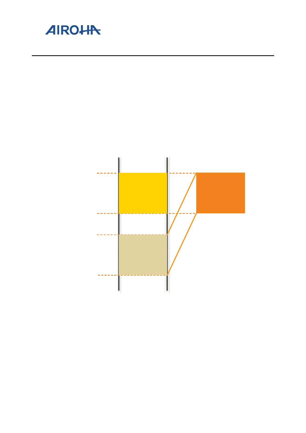
Airoha IoT SDK for RTOS Memory
Layout Developer's Guide
© 2015 - 2018 Airoha Technology Corp.
Page 35 of 51
This document contains information that is proprietary to Airoha Technology Corp. (“Airoha”) and/or its licensor(s).
Any unauthorized use, reproduction or disclosure of this document in whole or in part is strictly prohibited.
5. Memory Layout and Configuration for MT7686
MT7686 supports four types of physical memory, Serial Flash, Pseudo Static Random Access Memory (PSRAM),
System Random Access Memory (SYSRAM) and Tightly Coupled Memory (TCM). The memory layouts are designed
based on the four types of memory.
The virtual memory on the MT7686 is provided for cacheable memory and is implemented based on the memory
mapping mechanism of ARM Cortex-M4. There are two virtual address ranges, the first memory address range
from 0x100000000 to 0x14000000 is mapped to the SYSRAM address range from 0x00000000 to 0x04000000,
as shown in Figure 18. The second memory address range from 0x142000000 to 0x14259C00 is mapped to the
SYSRAM address range from 0x04200000 to 0x04259C00, as shown in Figure 19. The first virtual memory region
(0x10000000 to 0x14000000) and the second virtual memory region (0x14200000 to 0x14259C00) are used as
cacheable memory. RW data is stored in the first virtual memory region, by default.
Physical memory
1
Physical memory
address 1 range
Virtual memory
address 1 range
First address
map
0x00000000
0x10000000
0x04000000
0x14000000
Figure 18. MT7686 virtual memory 1 mapping

Airoha IoT SDK for RTOS Memory
Layout Developer's Guide
© 2015 - 2018 Airoha Technology Corp.
Page 36 of 51
This document contains information that is proprietary to Airoha Technology Corp. (“Airoha”) and/or its licensor(s).
Any unauthorized use, reproduction or disclosure of this document in whole or in part is strictly prohibited.
Figure 19. MT7686 virtual memory 2 mapping
The memory layout can be defined with FOTA and without FOTA. Each of the layouts has two views described
above.
This section guides you through:
• Types of the memory layout
• Programming guide
• Memory Layout Adjustment with a
o Linker Script
o Scatter File
o IAR Configuration File
5.1. Memory layout without FOTA
5.1.1. Load view
MT7686 has 1MB internal serial flash memory. The load view on the flash memory with disabled FOTA for MT7686
is shown in Figure 20.
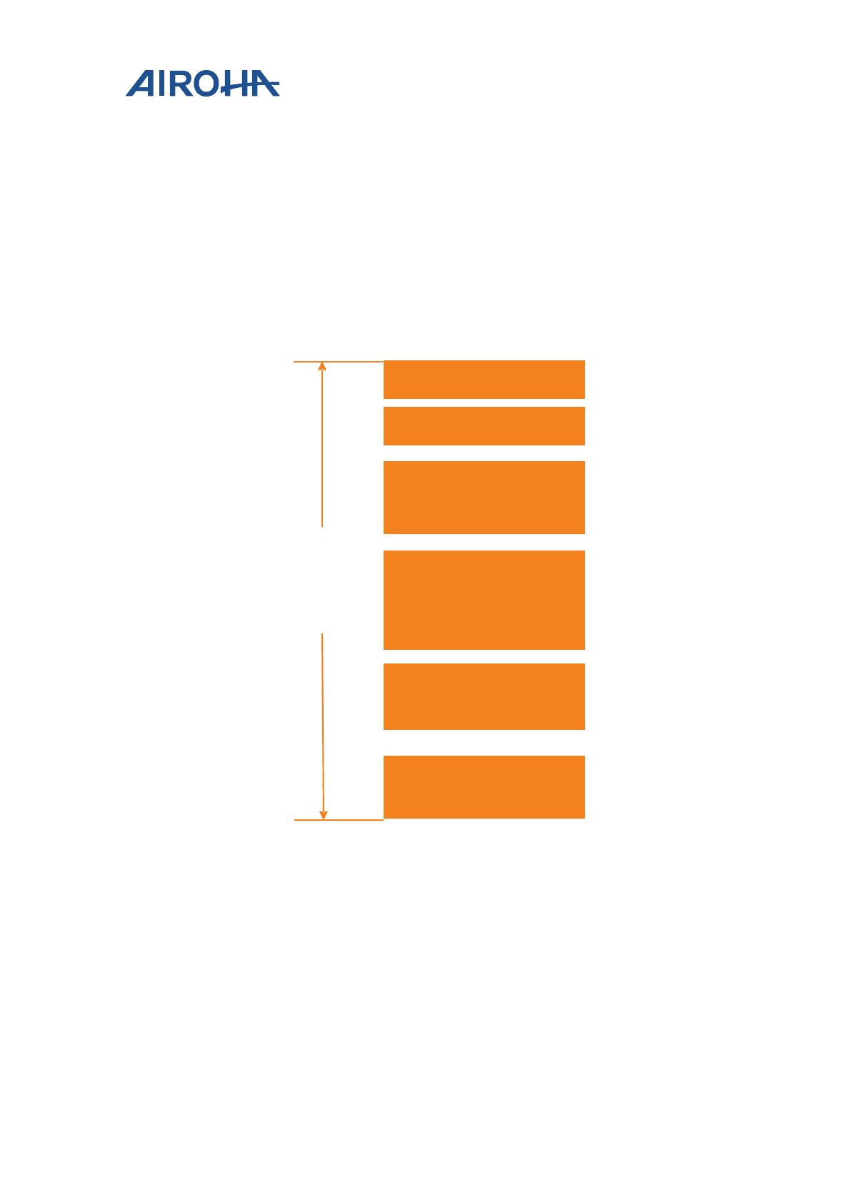
Airoha IoT SDK for RTOS Memory
Layout Developer's Guide
© 2015 - 2018 Airoha Technology Corp.
Page 37 of 51
This document contains information that is proprietary to Airoha Technology Corp. (“Airoha”) and/or its licensor(s).
Any unauthorized use, reproduction or disclosure of this document in whole or in part is strictly prohibited.
• Header 1. Always located at the very beginning of the flash memory and it’s reserved for bootloader
security information. The size of the Header 1 is not configurable and is fixed to 4kB.
• Header 2. Reserved for RTOS binary security information. The size of the Header 2 is not configurable and
is fixed to 4kB.
• Bootloader. The size of the bootloader is not configurable and is fixed to 64kB size.
• ARM Cortex-M4 firmware. This section of the memory is reserved for the RTOS binary and N9 firmware.
• The end of the flash is a reserved buffer for NVDM buffer and WIFI TX Power data buffer. The sizes of the
NVDM Wi-Fi transmit power data buffer are configurable.
The start address and the maximum size of each binary and reserved buffer are configurable, see section 5.4,
“Memory layout adjustment with a linker script”, for more details.
Header 1
Bootloader
Wi-Fi TX power data buffer
Header 2
ARM Cortex-M4 Firmware
(including N9 firmware)
-
NVDM buffer
4MB
Serial Flash
Figure 20. Load view of the MT7686 memory layout without FOTA
For more information about FOTA, refer to Airoha IoT Development Platform for RTOS Firmware Update
Developer's Guide located under SDK/doc folder.
For more information about NVDM, refer to Airoha IoT Development Platform for RTOS API reference guide.
5.1.2. Execution view
Execution view describes where the code and data are located during the program runtime, as shown in Figure 21
for MT7686. The execution view is based on the Serial Flash, PSRAM, SYSRAM and TCM, as described below:
• Serial Flash. The code and read-only (RO) data are located in the flash memory during runtime.
• PSRAM.
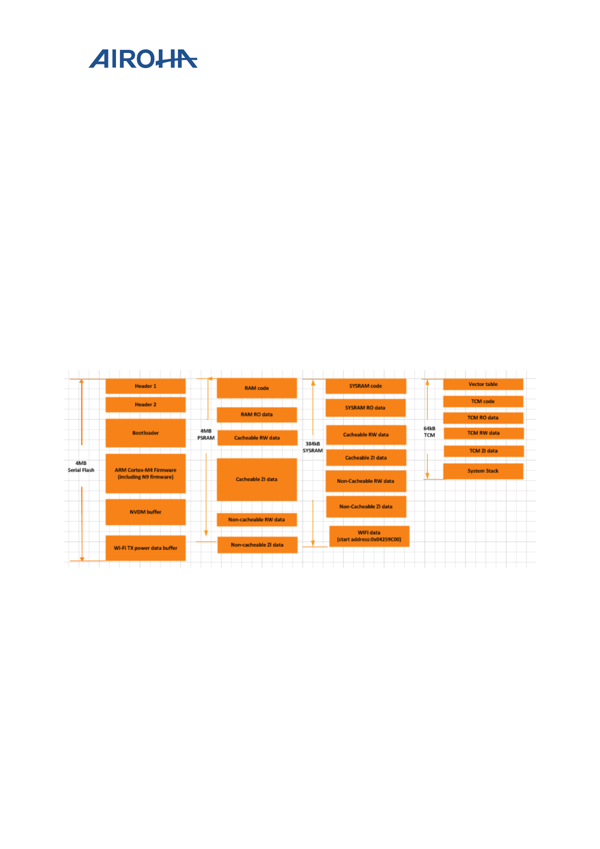
Airoha IoT SDK for RTOS Memory
Layout Developer's Guide
© 2015 - 2018 Airoha Technology Corp.
Page 38 of 51
This document contains information that is proprietary to Airoha Technology Corp. (“Airoha”) and/or its licensor(s).
Any unauthorized use, reproduction or disclosure of this document in whole or in part is strictly prohibited.
o PSRAM code and RO data. The PSRAM code and RO data is cacheable.
o Cacheable RW data and ZI data.
o Non-cacheable RW data and ZI data.
• SYSRAM.
o SYSRAM code and RO data. The SYSRAM code and RO data is cacheable.
o Cacheable RW data and ZI data.
o Non-cacheable RW data and ZI data.
o WIFI ROM RW/ZI data and code
• TCM. Some critical and high-performance code or data can be stored into the TCM. See section 5.3,
“Programming guide” to learn how to put code or data to the TCM.
o Vector table, single bank code, and some high-performance code and data are stored at the
beginning of TCM.
o Code and RO data.
o RW data and ZI data.
o The system stack.
Figure 21. Execution view of the MT7686 memory layout without FOTA
5.2. Memory layout with FOTA of full binary update
5.2.1. Load view
The memory flash layout’s load view with enabled FOTA is shown in Figure 22 for MT7686. A FOTA buffer is added
for temporary storage of the binary that will be used to update the current ARM Cortex-M4 firmware. The start
address and maximum size of each binary and the reserved space of certain memory layouts are configurable, see
section 5.4, “Memory layout adjustment with a linker script”, for more details. To enable FOTA, refer to the Airoha
IoT Development Platform for RTOS Firmware Update Developer's Guide located under the SDK /doc folder.
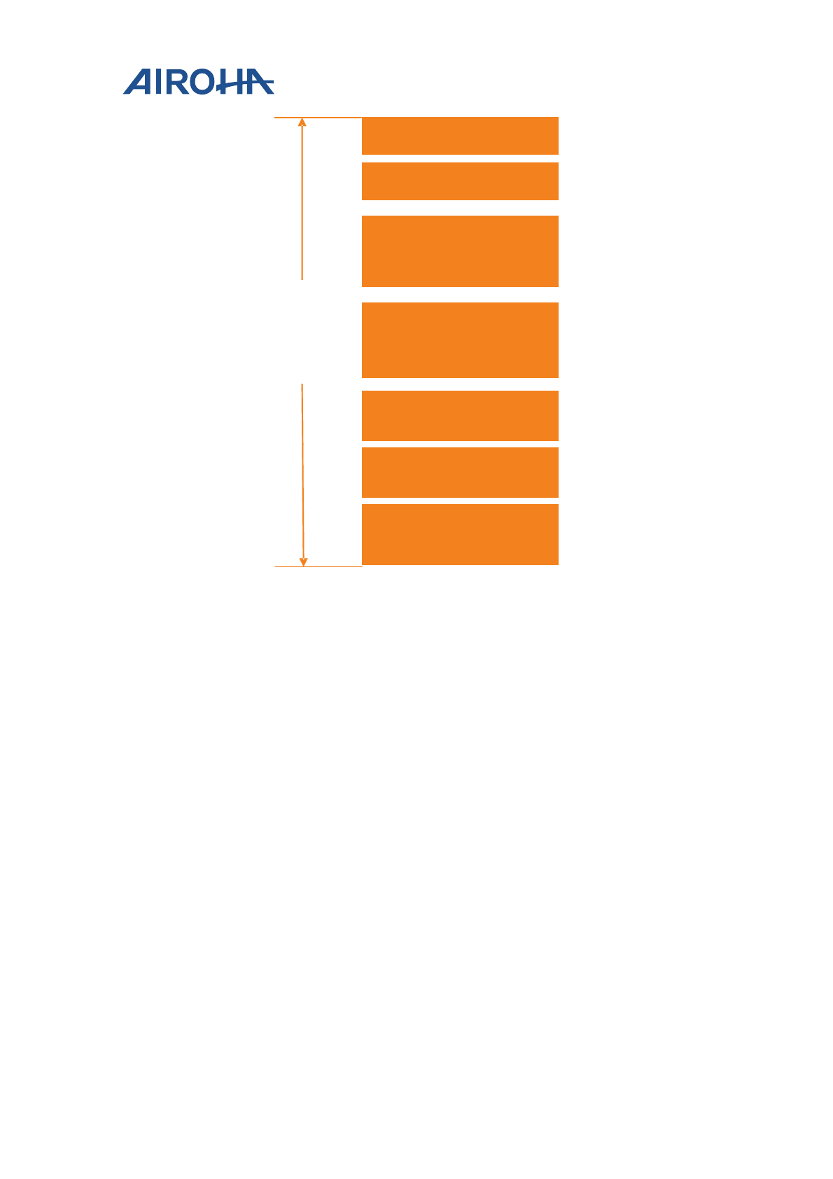
Airoha IoT SDK for RTOS Memory
Layout Developer's Guide
© 2015 - 2018 Airoha Technology Corp.
Page 39 of 51
This document contains information that is proprietary to Airoha Technology Corp. (“Airoha”) and/or its licensor(s).
Any unauthorized use, reproduction or disclosure of this document in whole or in part is strictly prohibited.
Header 1
Bootloader
Wi-Fi TX power data buffer
Header 2
ARM Cortex-M4 Firmware
(including N9 firmware)
NVDM buffer
FOTA buffer
Figure 22. Load view of the MT7686 memory layout with full binary FOTA
5.2.2. Execution view
The execution view (see Figure 23 for MT7686) at runtime is described below.
• Serial Flash. The code and read-only (RO) data are located in the flash memory during runtime.
• PSRAM.
o PSRAM code and RO data. The PSRAM code and RO data is cacheable.
o Cacheable RW data and ZI data.
o Non-cacheable RW data and ZI data.
o WIFI ROM RW/ZI data and code
• SYSRAM.
o SYSRAM code and RO data. The SYSRAM code and RO data is cacheable.
o Cacheable RW data and ZI data.
o Non-cacheable RW data and ZI data.
• TCM. Some critical and high-performance code or data can be stored into the TCM. See section 5.3,
“Programming guide” to learn how to put code or data to the TCM.
o Vector table, single bank code, and some high-performance code and data are stored at the
beginning of TCM.
o Code and RO data.
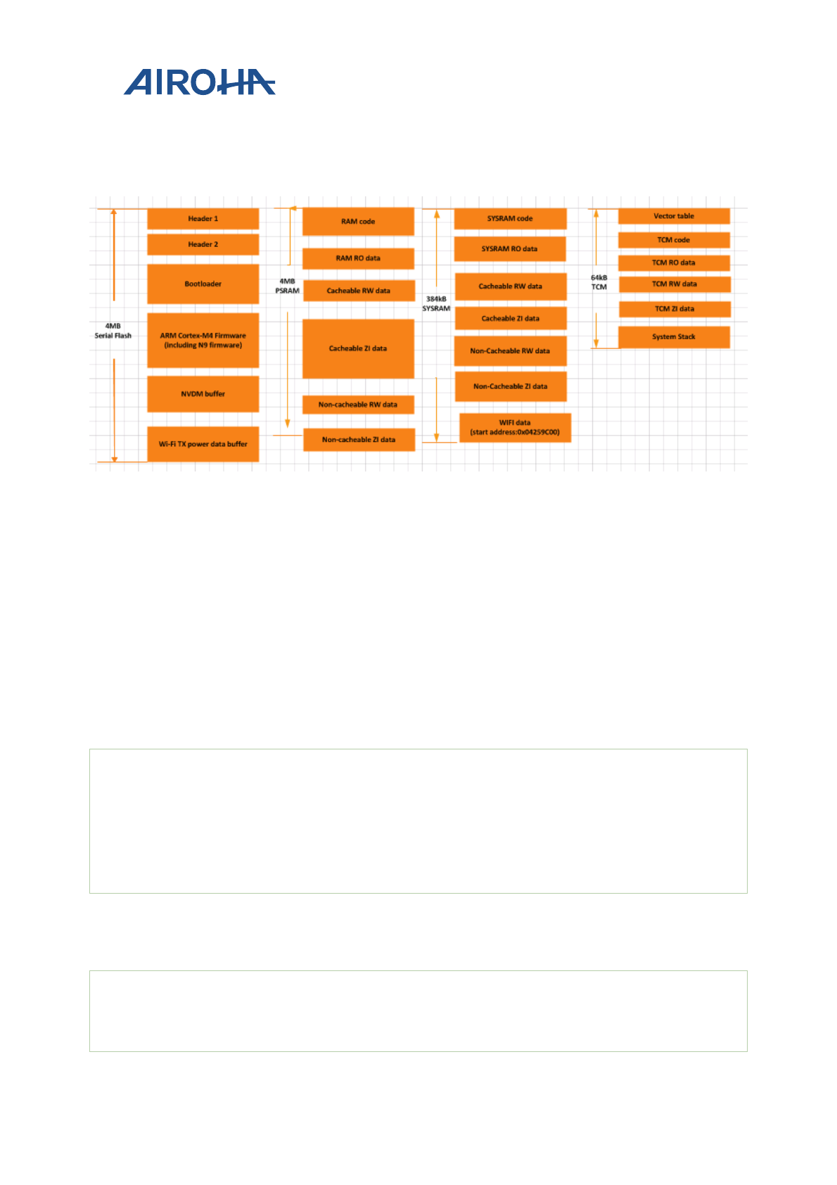
Airoha IoT SDK for RTOS Memory
Layout Developer's Guide
© 2015 - 2018 Airoha Technology Corp.
Page 40 of 51
This document contains information that is proprietary to Airoha Technology Corp. (“Airoha”) and/or its licensor(s).
Any unauthorized use, reproduction or disclosure of this document in whole or in part is strictly prohibited.
o RW data and ZI data.
o The system stack.
Figure 23. Execution view of the MT7682 memory layout with full binary FOTA
5.3. Programming guide
This programming guide is based on the memory layout described in section 5.1.2, “Execution view”. The
following recommendations allow the developers to place the code successfully to the desired memory location
during runtime.
1) Place the code or RO data to the Serial Flash at runtime.
By default, the code or RO data is placed in the flash, execute in place (XIP), no need to modify.
2) Place the code or RO data to the PSRAM at runtime.
To run the code or access RO data in the PSRAM with better performance, specify the attribute explicitly in your
code, as shown in the example below.
//code
ATTR_TEXT_IN_RAM int func(int par)
{
int s;
s = par;
//....
}
//RO data
ATTR_RODATA_IN_RAM const int b = 8;
For comparison, if the attribute is not explicitly defined, during the function call the code will be placed in the
Serial Flash instead of the PSRAM.
//code
int func(int par)
{
int s;
s = par;

Airoha IoT SDK for RTOS Memory
Layout Developer's Guide
© 2015 - 2018 Airoha Technology Corp.
Page 41 of 51
This document contains information that is proprietary to Airoha Technology Corp. (“Airoha”) and/or its licensor(s).
Any unauthorized use, reproduction or disclosure of this document in whole or in part is strictly prohibited.
//....
}
//RO data
const int b = 8;
3) Place RW data or ZI data to PSRAM non-cacheable memory at runtime.
To access RW data and ZI data in the non-cacheable memory with special purpose such as direct memory access
(DMA) buffer, specify the attribute explicitly in your code, as shown in the example below.
//RW data
ATTR_RWDATA_IN_NONCACHED_RAM int b = 8;
//ZI data
ATTR_ZIDATA_IN_NONCACHED_RAM int b;
For comparison, if the attribute is not explicitly defined, the data will be placed in the PSRAM cacheable memory
instead of the non-cacheable memory.
//RW data
int b = 8;
//ZI data
int b;
4) Place RW data or ZI data to PSRAM cacheable memory at runtime.
By default, RW data/ZI data are placed in the cacheable memory, no need to modify.
5) Place the code or RO data to the SYSRAM at runtime.
To run the code or access RO data in the SYSRAM with better performance, specify the attribute explicitly in your
code, as shown in the example below.
//code
ATTR_TEXT_IN_SYSRAM int func(int par)
{
int s;
s = par;
//....
}
//RO data
ATTR_RODATA_IN_SYSRAM const int b = 8;
For comparison, if the attribute is not explicitly defined, during the function call the code will be placed in the
Serial Flash instead of the SYSRAM.
//code
int func(int par)
{
int s;
s = par;
//....
}
//RO data
const int b = 8;
6) Place RW data or ZI data to SYSRAM cacheable memory at runtime.
To access RW data and ZI data in the SYSRAM cacheable memory, specify the attribute explicitly in your code, as
shown in the example below.

Airoha IoT SDK for RTOS Memory
Layout Developer's Guide
© 2015 - 2018 Airoha Technology Corp.
Page 42 of 51
This document contains information that is proprietary to Airoha Technology Corp. (“Airoha”) and/or its licensor(s).
Any unauthorized use, reproduction or disclosure of this document in whole or in part is strictly prohibited.
//RW data
ATTR_RWDATA_IN_CACHED_SYSRAM int b = 8;
//ZI data
ATTR_ZIDATA_IN_CACHED_SYSRAM int b;
For comparison, if the attribute is not explicitly defined, the data will be placed in the PSRAM cacheable memory
instead of the non-cacheable memory, because RW and ZI are default in PSRAM cacheable memory.
//RW data
int b = 8;
//ZI data
int b;
7) Place RW data or ZI data to SYSRAM non-cacheable memory at runtime.
To access RW data and ZI data in the non-cacheable memory with special purpose such as direct memory access
(DMA) buffer, specify the attribute explicitly in your code, as shown in the example below.
//RW data
ATTR_RWDATA_IN_NONCACHED_SYSRAM int b = 8;
//ZI data
ATTR_ZIDATA_IN_NONCACHED_SYSRAM int b;
For comparison, if the attribute is not explicitly defined, the data will be placed in the PSRAM cacheable memory
instead of the non-cacheable memory, because RW and ZI are default in PSRAM cacheable memory.
//RW data
int b = 8;
//ZI data
int b;
8) Place code or RO data to the TCM at runtime.
To run the code or access RO data in the TCM with better performance, specify the attribute explicitly in your
code, as shown in the example below.
//code
ATTR_TEXT_IN_TCM int func(int par)
{
int s;
s = par;
//....
}
//RO data
ATTR_RODATA_IN_TCM const int b = 8;
For comparison, if the attribute is not explicitly defined, during the function call the code will be placed in the
Serial Flash instead of the TCM.
//code
int func(int par)
{
int s;
s = par;
//....
}
//RO data
const int b = 8;

Airoha IoT SDK for RTOS Memory
Layout Developer's Guide
© 2015 - 2018 Airoha Technology Corp.
Page 43 of 51
This document contains information that is proprietary to Airoha Technology Corp. (“Airoha”) and/or its licensor(s).
Any unauthorized use, reproduction or disclosure of this document in whole or in part is strictly prohibited.
9) Put RW data/ZI data to TCM at runtime.
To access RW data and ZI data in the TCM with better performance, you should specify the attribute explicitly in
your code, as shown in the example below.
//rw-data
ATTR_RWDATA_IN_TCM int b = 8;
//zi-data
ATTR_ZIDATA_IN_TCM int b;
For comparison, if the attribute is not explicitly defined, the data will be placed in the PSRAM instead of the TCM.
//RW data
int b = 8;
//ZI data
int b;
5.4. Memory layout adjustment with a linker script
The memory layout can be configured with different toolchains. When the code is built based on the GCC
toolchain, the memory layout description file called a linker script is required. When the code is built based on
ARMCC toolchain, the memory layout description file called a scatter file is used.
This section describes how to use the linker script provided by Airoha and how to configure the linker script when
building code with the GCC toolchain. The scatter file is introduced in section 5.5, “Memory layout adjustment with
a scatter file”.
5.4.1. Types of linker scripts
Two types of linker scripts are provided:
• Template linker script – every application linker script should be based on the template linker script.
• Application linker script – every application has its particular linker script. This linker script is passed to the
linker during linking stage.
5.4.1.1. Template linker script
Template linker scripts are based on the memory layout see section 5.1 and 5.2. If the memory layout is modified,
the linker script should also be modified manually. It’s recommended to use the layout and linker scripts provided
by Airoha as a reference for your customizations.
The template linker scripts are located under /driver/CMSIS/Device/MTK/<chip>/linkerscript/GCC/
folder.
The folder includes:
• default. This folder contains a template linker script to build a project without FOTA memory layout, see
section 5.1, “Memory layout without FOTA”.
• full_bin_fota. This folder contains a template linker script to build a project with full binary FOTA
memory layout, see section 5.2, “Memory layout with FOTA of full binary update”
• sysram. This folder contains a template linker script to enable RAM debugging. To place all your code
into SYSRAM, use this linker script as a reference.

Airoha IoT SDK for RTOS Memory
Layout Developer's Guide
© 2015 - 2018 Airoha Technology Corp.
Page 44 of 51
This document contains information that is proprietary to Airoha Technology Corp. (“Airoha”) and/or its licensor(s).
Any unauthorized use, reproduction or disclosure of this document in whole or in part is strictly prohibited.
5.4.1.2. Application linker script
The application linker script is located under /project/<board>/apps/<project>/GCC/ folder. Each
application has its own linker script and each linker script can have a different memory layout configuration based
on the application requirements.
5.4.2. How to use the linker script
To create a new linker script file for your application:
• Clone a linker script from the template folder.
• Create a new linker script manually. The memory layout in this case should also be user-defined to match
your linker script.
5.4.2.1. Cloning the linker script
To clone a linker script from the template:
1) Specify the memory layout feature for your application development, such as without FOTA, full binary
FOTA see section 5.1 and 5.2.
2) Copy the template linker script from template folder to your application project’s folder see section 5.4.1,
“Types of linker scripts”.
3) Memory layout without FOTA.
Copy /driver/CMSIS/Device/MTK/<chip>/linkerscript/GCC/default to
/project/<board>/apps/<project>/GCC/.
4) Memory layout with FOTA full binary update.
Copy /driver/CMSIS/Device/MTK/<chip>/linkerscript/GCC/full_bin_fota to
/project/<board>/apps/<project>/GCC/.
5) Memory layout with RAM debugging.
Copy /driver/CMSIS/Device/MTK/<chip>/linkerscript/GCC/sysram to
/project/<board>/apps/<project>/GCC/.
6) Modify the linker script according to the application requirements.
5.4.3. Rules to adjust the memory layout
The memory layout can be customized to fit the application requirements. However, the sections for header 1,
header 2 and bootloader are not configurable. The rest of the memory layout can be adjusted.
Common rules for different memory layout adjustment settings are described below.
1) The address and size must be block aligned. The default block size is 4kB and is defined in
driver/chip/<chip>/inc/flash_opt_gen.h header file.
2) To configure the size or the address, make sure there is no overlap between two adjacent memory
regions. The total size of all the regions should not exceed the physical flash size.
5.4.3.1. Adjusting the layout for ARM Cortex-M4 firmware
To adjust the memory assigned to ARM Cortex-M4 firmware:
Airoha IoT SDK for RTOS Memory
Layout Developer's Guide
© 2015 - 2018 Airoha Technology Corp.
Page 45 of 51
This document contains information that is proprietary to Airoha Technology Corp. (“Airoha”) and/or its licensor(s).
Any unauthorized use, reproduction or disclosure of this document in whole or in part is strictly prohibited.
1) Modify the ROM_RTOS length and starting address in the mt7686_flash.ld linker script under the GCC
folder of the project.
MEMORY
{
...
ROM_RTOS(rx) : ORIGIN = 0x08012000, LENGTH = 2344K
...
}
2) Modify the macro definitions for RTOS_BASE and RTOS_LENGTH in
project/<board>/apps/<application>/inc/memory_map.h header file.
3) Rebuild the bootloader and the ARM Cortex-M4 firmware.
Execute the following command under the root folder of the SDK.
./build.sh project_board example_name BL
The project_board is the project folder of a specific hardware board and example_name is the name of the
example. For example, to build the hal_adc of mt7686_hdk, the command will be:
./build.sh mt7686_hdk hal_adc BL
4) Make sure the length of ROM region doesn’t exceed the flash size of the system and for MT7686 the
internal flash is 4MB.
5.4.3.2. Adjusting the memory layout with FOTA full binary update
1) Modify ARM Cortex-M4 firmware size if needed see section 5.4.3.1, “Adjusting the layout for ARM Cortex-
M4 firmware”.
2) Modify the ROM_FOTA_RESERVED length and starting address in the flash.ld linker script under the
GCC folder of a project.
MEMORY
{
...
ROM_FOTA_RESERVED(rx) : ORIGIN = 0x0825C000, LENGTH = 1612K
...
}
3) Modify the macro definitions for FOTA_RESERVED_BASE and FOTA_RESERVED_LENGTH in
project/<board>/apps/<application>/inc/memory_map.h header file.
Note, refer to the SDK Firmware Upgrade Developer’s Guide located under SDK /doc folder, for more details about
how to adjust the FOTA buffer.
5.4.3.3. Adjusting the NVDM buffer
To adjust the NVDM buffer layout:
1) Modify size of the ARM Cortex-M4 firmware if needed see section 5.4.3.1, “Adjusting the layout for ARM
Cortex-M4 firmware”.
2) Modify FOTA buffer size if needed see section 5.4.3.2, “Adjusting the memory layout with FOTA full binary
update”.
Airoha IoT SDK for RTOS Memory
Layout Developer's Guide
© 2015 - 2018 Airoha Technology Corp.
Page 46 of 51
This document contains information that is proprietary to Airoha Technology Corp. (“Airoha”) and/or its licensor(s).
Any unauthorized use, reproduction or disclosure of this document in whole or in part is strictly prohibited.
3) Modify the ROM_NVDM_RESERVED length and starting address in the flash.ld, if no FOTA or full binary
FOTA feature is enabled.
MEMORY
{
...
ROM_NVDM_RESERVED(rx) : ORIGIN = 0x080EF000, LENGTH = 64K
...
}
4) Modify the macro definitions for ROM_NVDM_BASE, ROM_NVDM_LENGTH in
project\<board>\apps\<application>\inc\memory_map.h header file.
Note, to adjust the NVDM buffer, refer to the NVDM module of HAL in the Airoha IoT development platform for
RTOS API reference.
5.5. Memory layout adjustment with a scatter file
5.5.1. Types of scatter files
Two types of scatter files are provided:
• Template scatter file – every application scatter file should be based on the template scatter file.
• Application scatter file – every application has its particular scatter file. This scatter file will be passed to
the linker during linking stage.
5.5.1.1. Template scatter file
Template scatter files are based on the memory layout. If the memory layout is modified, the scatter file should
also be modified manually. It’s recommended to use the layout and scatter files provided by Airoha as a reference
for your customizations.
The template scatter files are located under /driver/CMSIS/Device/MTK/<chip>/linkerscript/RVCT/
folder. The folder includes:
• default. This folder contains a template scatter file to build a project without FOTA memory layout, see
section 5.1, “Memory layout without FOTA”.
• full_bin_fota. This folder contains a template scatter file to build a project with full binary FOTA
memory layout, see section 5.2, “Memory layout with FOTA of full binary update”
• sysram. This folder contains a template scatter file to enable RAM debugging. To place all your code into
SYSRAM, you can use this scatter file as a reference.
5.5.1.2. Application scatter file
The application scatter file is located under /project/<board>/apps/<project>/MDK-ARM/ folder. Each
application has its own scatter file and each scatter file can have a different memory layout configuration based on
the application requirements.
5.5.2. How to use the scatter file
To create a new scatter file for your application:

Airoha IoT SDK for RTOS Memory
Layout Developer's Guide
© 2015 - 2018 Airoha Technology Corp.
Page 47 of 51
This document contains information that is proprietary to Airoha Technology Corp. (“Airoha”) and/or its licensor(s).
Any unauthorized use, reproduction or disclosure of this document in whole or in part is strictly prohibited.
• Clone a scatter file from the MDK-ARM folder of the template folder.
• Create a new scatter file manually. The memory layout in this case should also be user-defined to match
your scatter file.
5.5.2.1. Cloning the scatter file
To clone a scatter file from the template:
1) Specify the memory layout feature for your application development, such as without FOTA, full binary
FOTA see section 5.1 and 5.2.
2) Copy the template scatter file from template folder to your application project’s folder see section 5.5.1,
“Types of scatter files”.
3) Memory layout without FOTA.
Copy /driver/CMSIS/Device/MTK/<chip>/linkerscript/rvct/default to
/project/<board>/apps/<project>/MDK-ARM/.
4) Memory layout with FOTA full binary update.
Copy /driver/CMSIS/Device/MTK/<chip>/linkerscript/rvct/full_bin_fota to
/project/<board>/apps/<project>/MDK-ARM/.
5) Memory layout with RAM debugging.
Copy /driver/CMSIS/Device/MTK/<chip>/linkerscript/rvct/ram to
/project/<board>/apps/<project>/MDK-ARM/.
6) Modify the scatter file according to the application requirements.
5.5.3. How to configure the scatter file
The configuration is the same; see section 5.4.3, “Rules to adjust the memory layout”.
5.6. Memory layout adjustment with an IAR configuration file
5.6.1. Types of scatter files
Two types of scatter files are provided:
• Template scatter file – every application scatter file should be based on the template scatter file.
• Application scatter file – every application has its particular scatter file. This scatter file will be passed to
the linker during linking stage.
5.6.1.1. Template scatter file
Template scatter files are based on the memory layout, see section 5.1 and 5.2. If the memory layout is modified,
the scatter file should also be modified manually. It’s recommended to use the layout and scatter files provided by
Airoha as a reference for your customizations.
The template scatter files are located under /driver/CMSIS/Device/MTK/<chip>/linkerscript/IAR/
folder. The folder includes:
• default. This folder contains a template scatter file to build a project without FOTA memory layout, see
section 5.1, “Memory layout without FOTA”.

Airoha IoT SDK for RTOS Memory
Layout Developer's Guide
© 2015 - 2018 Airoha Technology Corp.
Page 48 of 51
This document contains information that is proprietary to Airoha Technology Corp. (“Airoha”) and/or its licensor(s).
Any unauthorized use, reproduction or disclosure of this document in whole or in part is strictly prohibited.
• full_bin_fota. This folder contains a template scatter file to build a project with full binary FOTA
memory layout, see section 5.2, “Memory layout with FOTA of full binary update”
• sysram. This folder contains a template scatter file to enable RAM debugging. To place all your code into
SYSRAM, you can use this scatter file as a reference.
5.6.1.2. Application scatter file
The application scatter file is located under /project/<board>/apps/<project>/EWARM/ folder. Each
application has its own scatter file and each scatter file can have a different memory layout configuration based on
the application requirements.
5.6.2. How to use the scatter file
To create a new scatter file for your application:
• Clone a scatter file from the EWARM folder of the template folder.
• Create a new scatter file manually. The memory layout in this case should also be user-defined to match
your scatter file.
5.6.2.1. Cloning the scatter file
To clone a scatter file from the template:
1) Specify the memory layout feature for your application development, such as without FOTA, full binary
FOTA.
2) Copy the template scatter file from template folder to your application project’s folder see section 5.5.1,
“Types of scatter files”.
3) Memory layout without FOTA.
Copy /driver/CMSIS/Device/MTK/<chip>/linkerscript/iar/default to
/project/<board>/apps/<project>/EWARM/.
4) Memory layout with FOTA full binary update.
Copy /driver/CMSIS/Device/MTK/<chip>/linkerscript/iar/full_bin_fota to
/project/<board>/apps/<project>/EWARM/.
5) Memory layout with RAM debugging.
Copy /driver/CMSIS/Device/MTK/<chip>/linkerscript/iar/ram to
/project/<board>/apps/<project>/EWARM/.
6) Modify the scatter file according to the application requirements.
5.6.3. How to configure the scatter file
The configuration is the same; see section 5.4.3, “Rules to adjust the memory layout”.

Airoha IoT SDK for RTOS Memory
Layout Developer's Guide
© 2015 - 2018 Airoha Technology Corp.
Page 49 of 51
This document contains information that is proprietary to Airoha Technology Corp. (“Airoha”) and/or its licensor(s).
Any unauthorized use, reproduction or disclosure of this document in whole or in part is strictly prohibited.
6. Memory Layout and Configuration for MT5932
The MT5932 default supports two types of physical memory, System Random Access Memory (SYSRAM) and
Tightly Coupled Memory (TCM). The memory layouts are designed based on the two types of memory. The
MT5932 has no SIP flash, so external flash may be a choice for users.
This section guides you through the types of the memory layout
6.1. Memory layout without External Flash
6.1.1. Load View
MT5932 has 384KB SYSRAM, and 96KB TCM. MT5932 without external flash does not support FOTA. The load view
for MT5932 is shown in Figure 24.
• ARM Cortex-M4 firmware code. Reserved for the RTOS code only
• Data. The RW data
• Block started by symbol (BSS). The BSS does not occupy the size of SYSRAM on load view, but the start
address of executive view is at the end of data section.
• TCM. TCM code and data.
• Boson. Wi-Fi boson data, includes boson data/code, slim codes and more.
• N9_fw. N9 firmware section to be loaded into N9.
• BootROM temporary buffer, 6KB temp buffer for SDIO Xboot.
Boson data
ARM Cortex-M4 Firmware code
TCM
Data
4MB
Serial Flash
N9 Firmware
BootROM temporary buffer
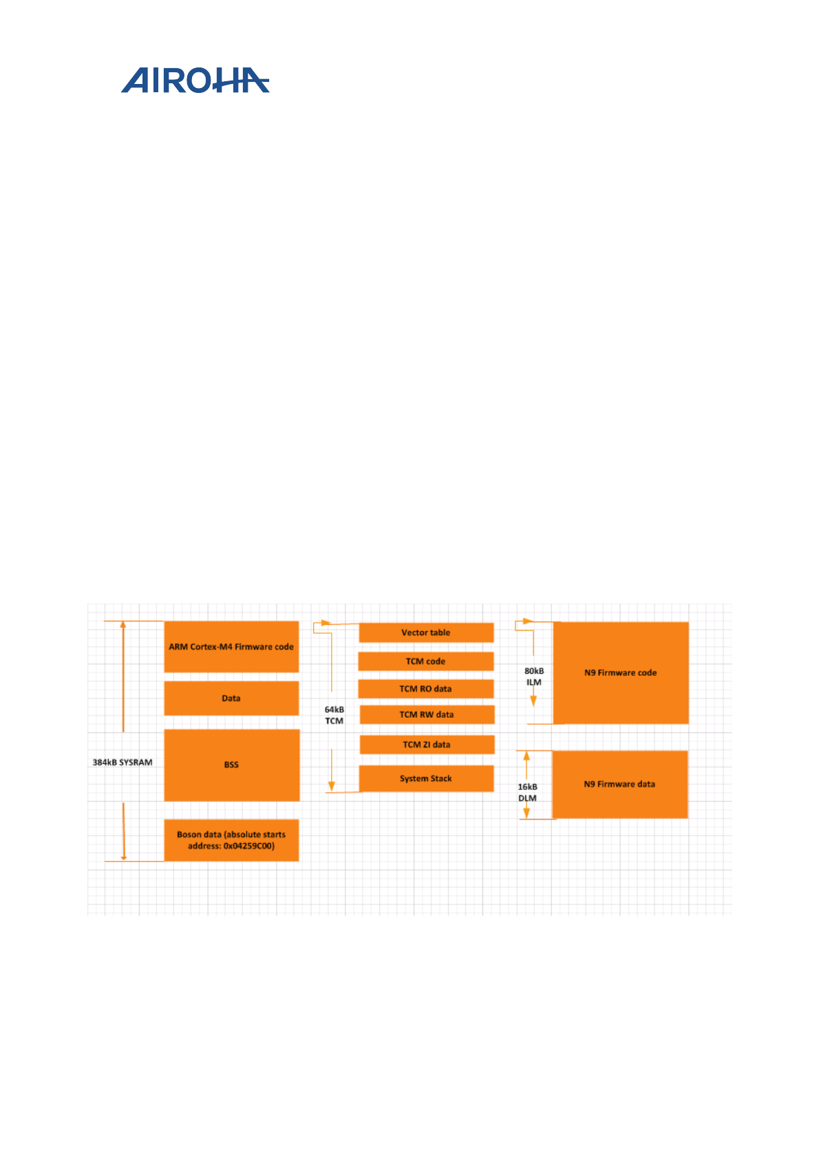
Airoha IoT SDK for RTOS Memory
Layout Developer's Guide
© 2015 - 2018 Airoha Technology Corp.
Page 50 of 51
This document contains information that is proprietary to Airoha Technology Corp. (“Airoha”) and/or its licensor(s).
Any unauthorized use, reproduction or disclosure of this document in whole or in part is strictly prohibited.
Figure 24 MT5932 load view memory layout without external flash
6.1.2. Execution view
The execution view (see Figure 25 for MT5932) at runtime is described below.
• SYSRAM.
o ARM Cortex-M4 firmware code. Reserved for the RTOS code only
o Data. The RW data
o Block started by symbol (BSS). The BSS data
o Boson data. The boson code and data for Wi-Fi.
• TCM. Some critical and high-performance code or data can be stored into the TCM. See section 5.3,
“Programming guide” to learn how to put code or data to the TCM.
o Vector table, single bank code, and some high-performance code and data are stored at the
beginning of TCM.
o Code and RO data.
o RW data and ZI data.
o The system stack.
• N9 FW. N9 firmware execution view is in the N9 core memory.
o N9 firmware code. Instruction local memory (ILM )code
o N9 firmware data. Data local memory (DLM) data
Figure 25 MT5932 execution view memory layout without external flash

Airoha IoT SDK for RTOS Memory
Layout Developer's Guide
© 2015 - 2018 Airoha Technology Corp.
Page 51 of 51
This document contains information that is proprietary to Airoha Technology Corp. (“Airoha”) and/or its licensor(s).
Any unauthorized use, reproduction or disclosure of this document in whole or in part is strictly prohibited.
6.2. Memory layout with External Flash
MT5932 with external flash is the same as MT7682. The only difference about memory layout is that the flash size
is different. Default external flash size of MT5932 is 4MB instead of 1MB compared with MT7682 see section 4,
“Memory Layout and Configuration for MT7682”.
