Microsoft Altium_Designer_Intermediate_Guide [Compatibility Mode] Altium Designer Intermediate Guide
Altium_Designer_Intermediate_Guide
Altium_Designer_Intermediate_Guide
Altium_Designer_Intermediate_Guide
User Manual:
Open the PDF directly: View PDF ![]() .
.
Page Count: 352 [warning: Documents this large are best viewed by clicking the View PDF Link!]

Altium Designer Guide
Beginning & Intermediate Version
Glenn Mercier
mercierg@unlv.nevada.edu
Research Engineer, TBE-B311
University of Las Vegas, Nevada

Part 1: Beginning Guide
This guide is a beginner’s guide to PCB
design using Altium Designer and is
geared towards the following individuals:
◦Possess ample theoretical electronics
knowledge
◦Has little or no PCB design experience
◦Has little or no Altium Designer experience

Beginning Guide
Before proceeding to the actual software
tutorial, It is important to understand
when it is absolutely necessary to use a
PCB rather than design with a
breadboard
Most students have a reluctance to
learning new software and spending
money for something they could possibly
build on a breadboard.

Breadboard vs. PCB
For many electronic designs, one has a
choice to build a circuit on either a
breadboard or on a printed circuit board.
Most students have a certain comfort
zone working with breadboards, but there
comes a time when the complexity of the
project or the physical requirements
requires electronic design through CAD
(computer aided design).

Breadboard Advantages
Very quick to prototype using standard
components
Can easily make changes to schematic or
the functional working of the circuit
Easy to connect to electronic equipment
such as function generator, oscilloscope,
power supplies, etc.

Breadboard Disadvantages
Unprofessional appearance
Difficult to troubleshoot due to human
error and poor connections
Works very poorly for high speed design
Difficult to modify complex SMD
components for prototyping
Excessive capacitance
Difficult to replicate

Printed Circuit Board Advantages
Professional appearance
Repeatable and controllable stray
inductance and capacitance
Can handle most power requirements
Can make very compact
Excellent high speed capabilities
Easy to assemble and replicate

Printed Circuit Board Disadvantages
Increased design time
Drastically increased schematic-to-finished
product timeframe
Development Cost
Difficult to modify once board is fabricated
Must learn at least a basic form of CAD software
Quality of PCB can be affected by limited
knowledge of software package
Capabilities vary greatly with different software
packages.
High end CAD software is very expensive
Required PCB Design
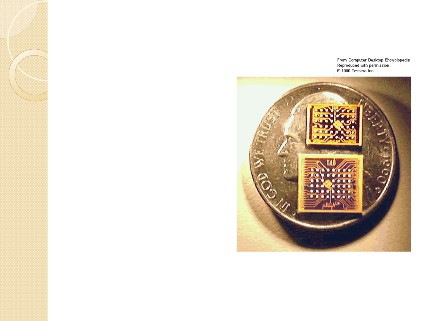
Small Packages,
such as a BGA,
MLF, QFP are
practically
impossible to
prototype on a
breadboard due
to their small
size and MUST
be designed on a
PCB.
http://content.answers.com/main/content/img/CDE/_MCROBGA.GIF

Required PCB Design
Just dealing with the sheer number of pins
on modern practical designs required a
PCB.
It is common to see single components
containing up to 1,500 pins
High speed design cannot be performed
using traditional prototyping methods

Altium Designer
This is based off the current version of Altium Designer,
6.9.0.12759
The Altium Designer Suite contains many unified features such as:
◦FPGA schematic design
◦VHDL/Verilog compilers
◦C/ASM compilers
◦Scripting
◦Simulation
◦2D Field Solver
◦Simulation Engine
◦Library Management
◦Database and advanced query language
◦CAM display management
◦Schematic Capture
◦PCB Layout
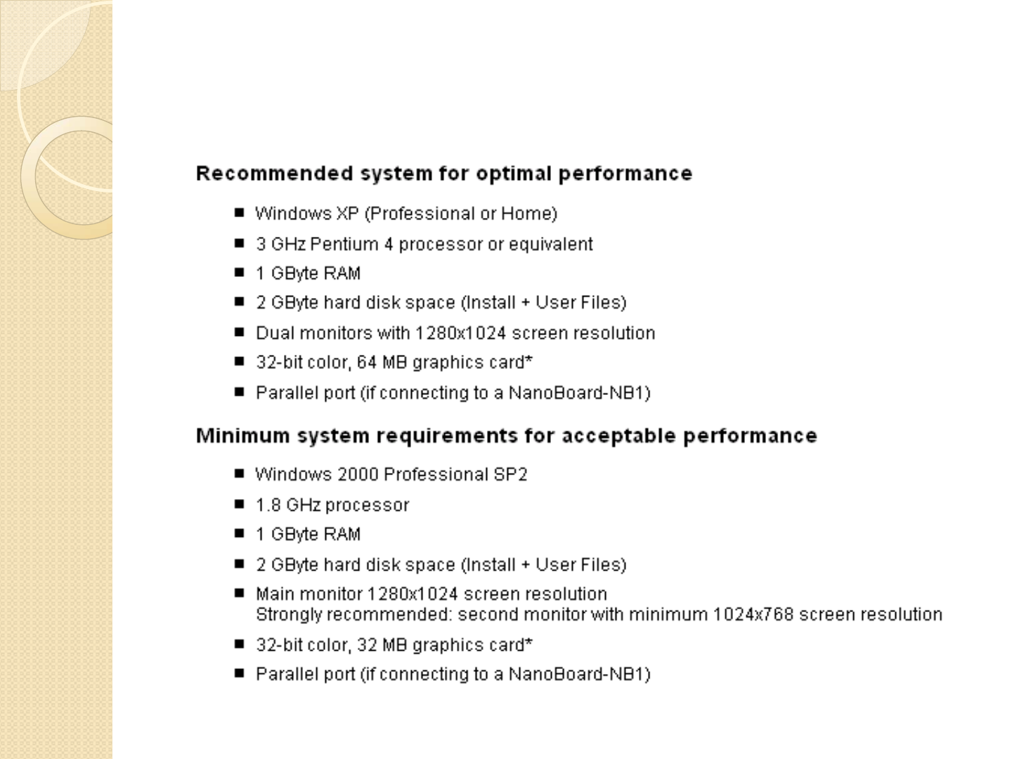
System Requirements
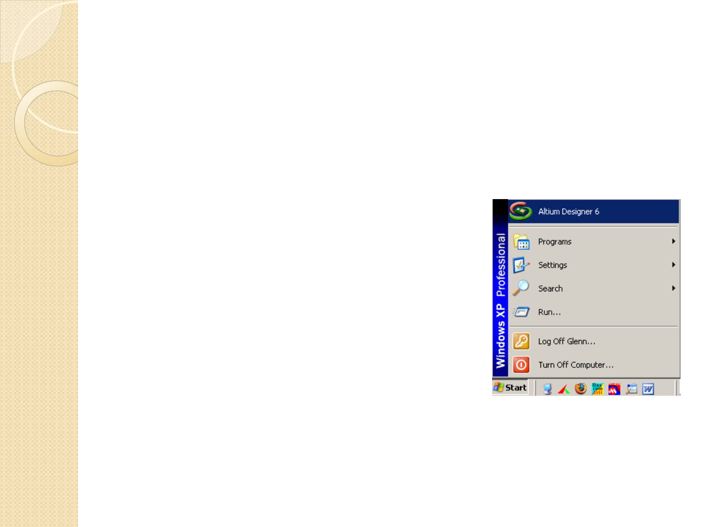
Getting Started
Start the software by
clicking
START
PROGRAMS
ALTIUM DESIGNER
Altium Designer 6
Create a start bar shortcut
if you plan on using the
software a lot. (shown on
right)

Project File
Project files are like a container for your project.
There are many different things you will need for
even a basic project, such as:
◦PCB Footprint libraries
◦Schematic libraries
◦Schematic documents
◦PCB documents
◦Scripts
◦CAM files
◦Settings
◦Generated reports
◦Generated files
◦Version Control features
◦Etc.

Creating a Project
When the
software starts,
follow the
menu sequence
in the image to
create a new
‘PCB Project’
Many people
skip this step
and just create
a schematic file.
This a huge
mistake!
Absolutely
everything in
Altium
Designer is
based on
project files
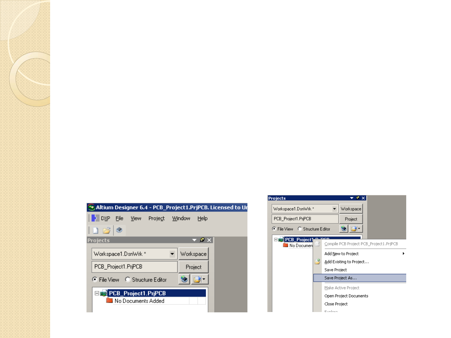
Project Name
We need to save our project and rename the project to something
more meaningful.
Right click on PCB_Project.prjPCB and save the project as
‘PROJECT- EE495’ to a new folder (preferably on a flash drive)
called ‘EE495 Project’ inside a root folder called ‘EE495 Altium’
EX: F:\EE495 Altium\EE495 Project\PROJECT-EE495.prjPCB
Inside this folder, we will place all relevant project data
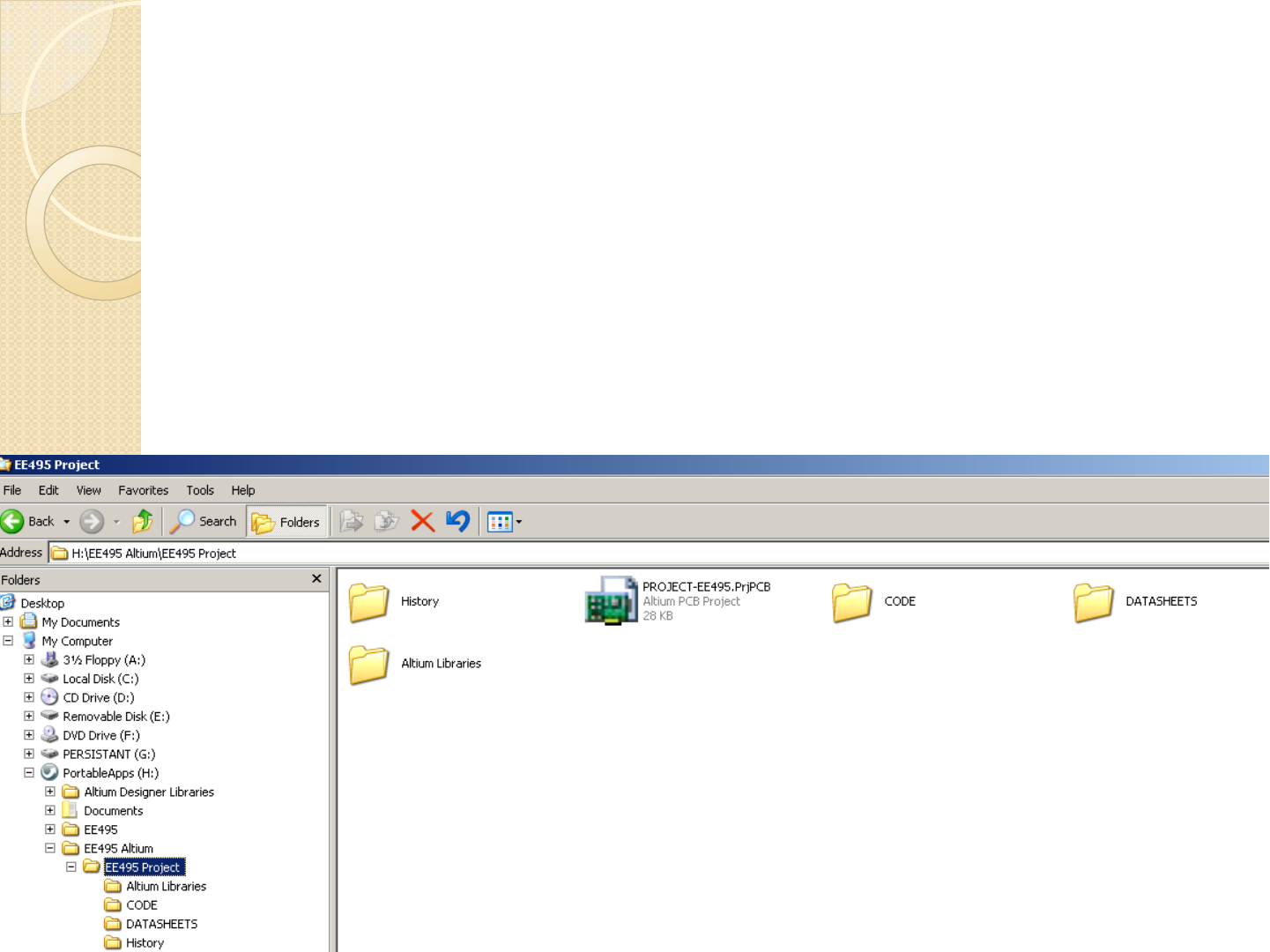
Organization
It is useful to place all project information inside this folder.
Inside this root folder, create subfolders called ‘CODE’ and
‘DATASHEETS’
Organization and centralization is also important for backing up all
your data properly, version control, and copying project data to a
CD for all finished projects (which you should do for future
reference)

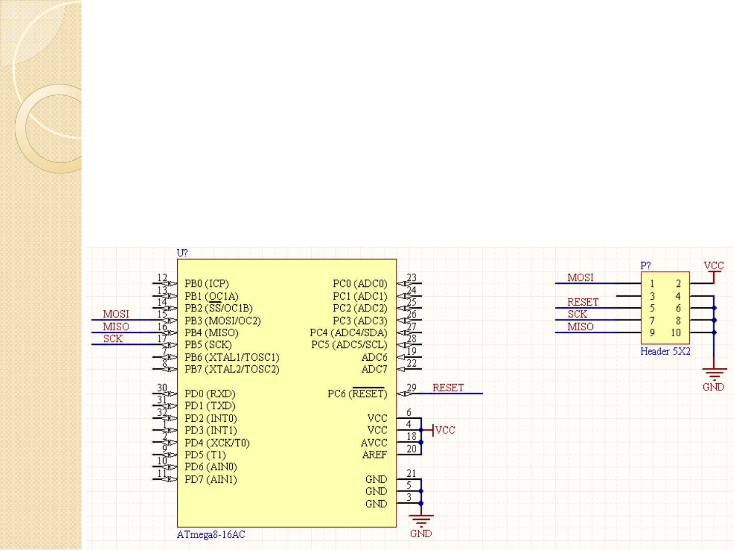
(Group) Quiz Project #1
For the first quiz project, we are going to create
a schematic that will contain:
Atmega8 - Atmel Microcontroller , 16 MHz, QFP
USB-B Connector
FT232 USB- UART interface chip , TSSOP28
2x5 Programming Input Header (0.1” Pitch)
SMD (Surface Mount Device) LEDs , 0805 Size
This project contains all the necessary parts to create a
PCB that can communicate directly with a computer
through a USB (Male B- Male A) Cable.
◦You are encouraged to actually build this PCB as an
inexpensive, functional development board.
◦This project is to be finished by next Wednesday (5/28)
with a possible in-class portion

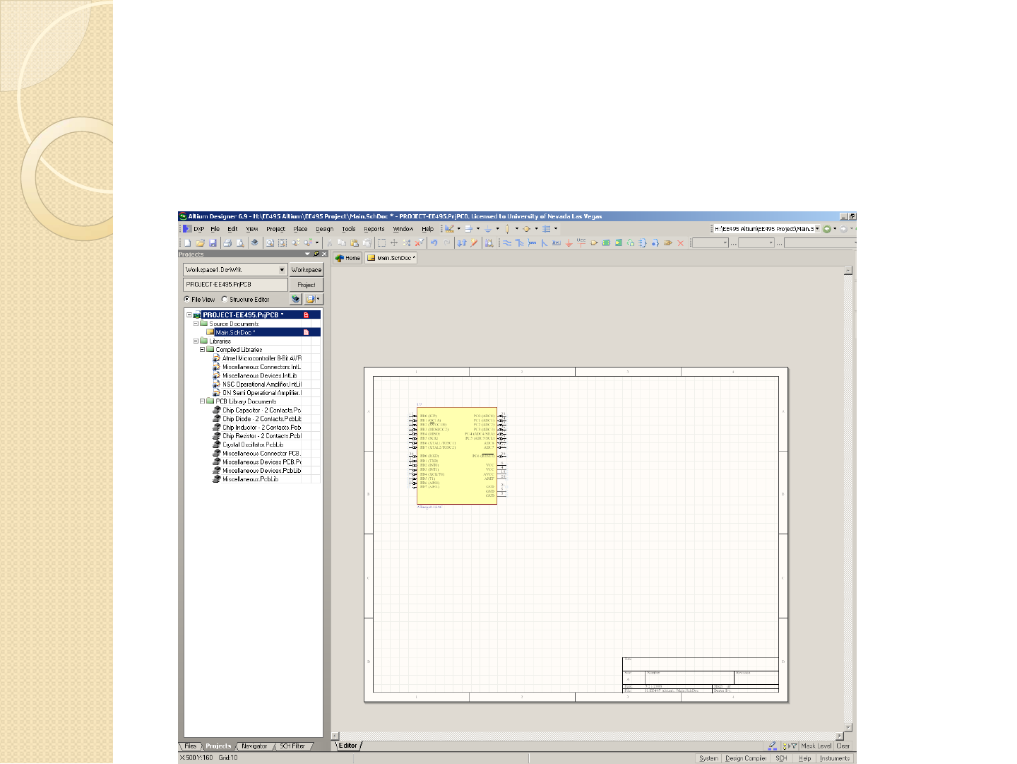
Adding a Schematic Drawing
Follow the menu sequence shown to
create a new schematic. This will
automatically be added to the project
tree we created.
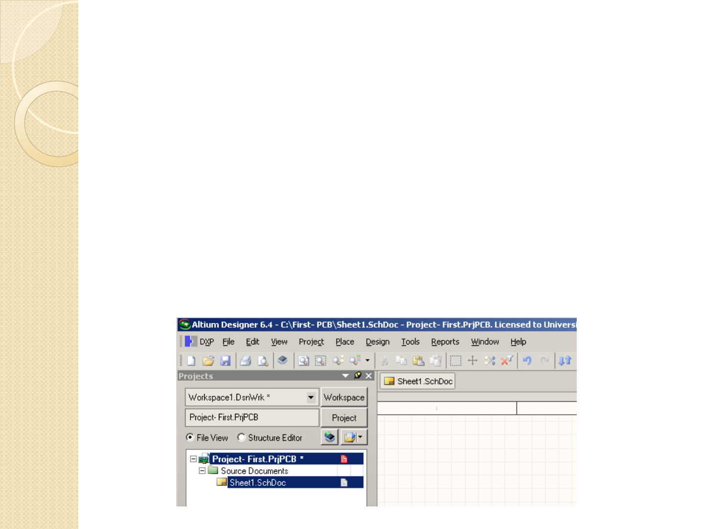
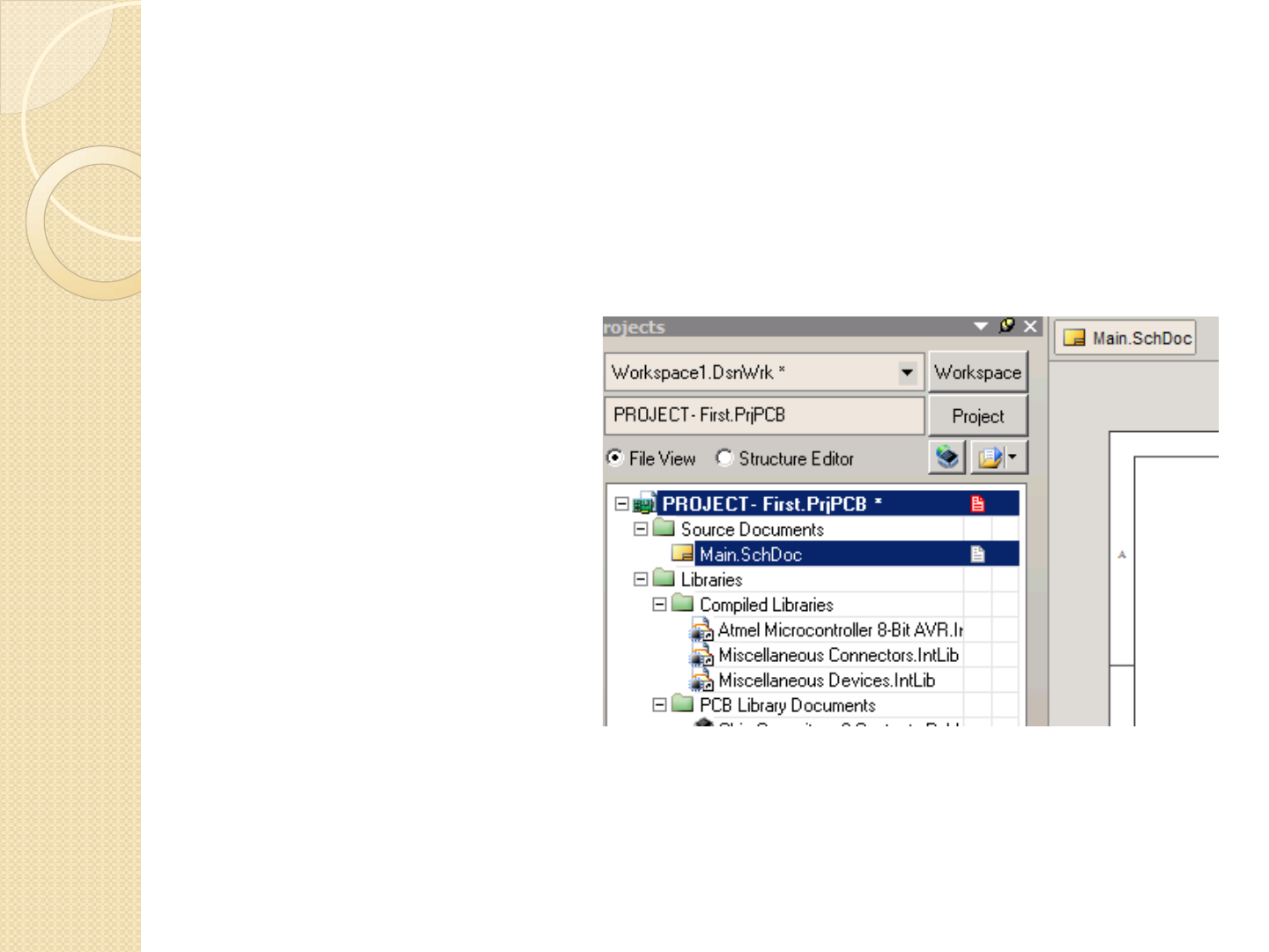
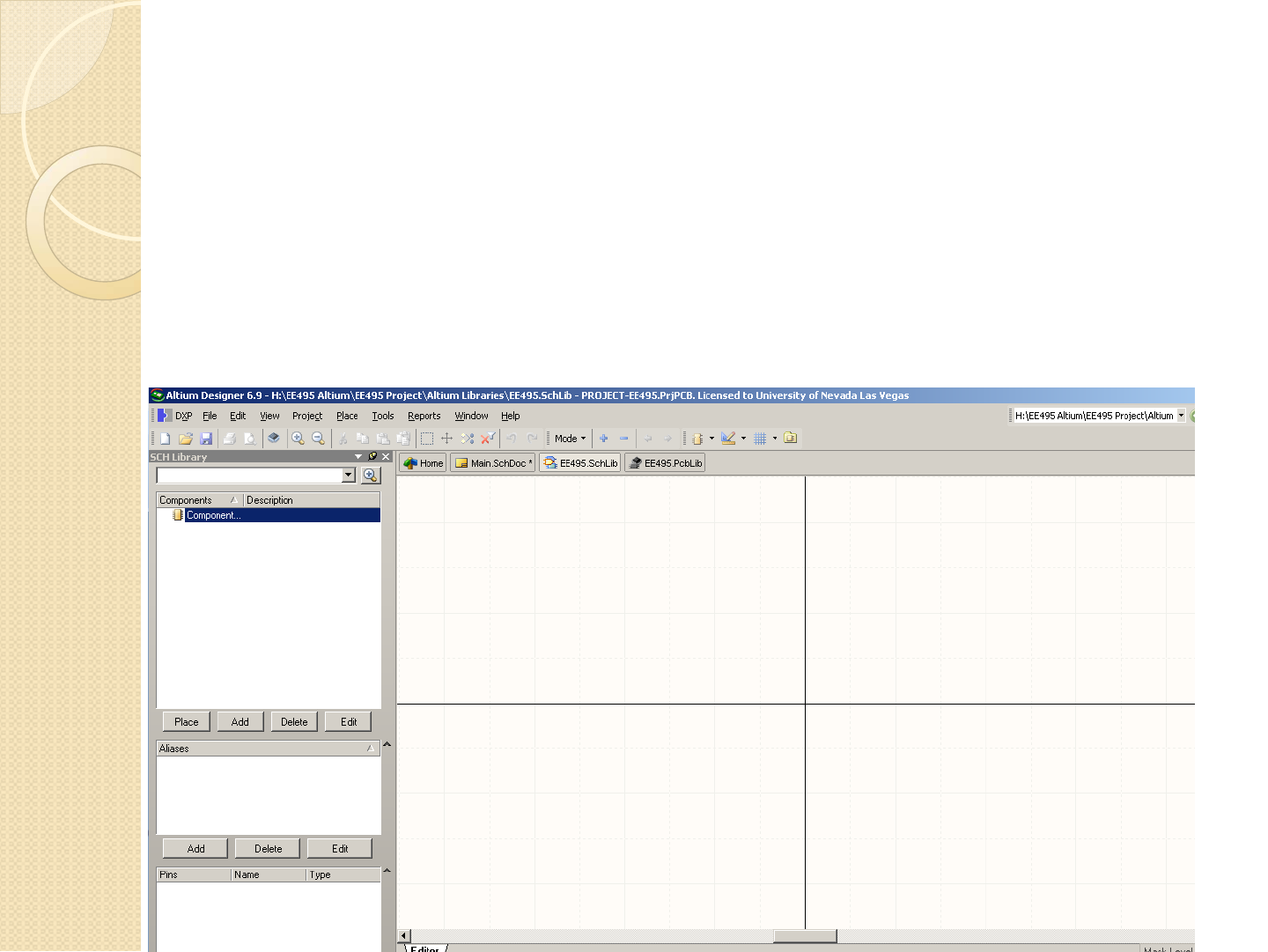
Schematic Entry
The ‘sheet1’ schematic document is now added
to the project tree as shown below.
Rename this file to something with a more
meaningful name such as ‘Main’. There are many
times when you will have multiple schematic
entries and it helps to have a descriptive name
Any open project files will appear in the menu
area above where the blank schematic page
appears.

Libraries
Similar to a real laboratory, to build a design
from a schematic you must first add real
parts to the project.
For this, we must add what are called
‘libraries’ to our project. Libraries contain
vital information about the parts we are
going to add.
Once libraries are added to the project, any
component inside that library can be freely
inserted into your design.

Types of Libraries
There are three main types of libraries for PCB
design:
◦Schematic Library- Contains schematic drawings of parts,
when we look at a schematic, we are looking at a collection
of schematic parts
◦PCB Footprint Library- This contains the physical dimensions
of a real component. This information is readily available in
datasheets.
◦Integrated Library- These are the most useful libraries
because they combine a physical part (footprint) with a
schematic drawing.

Libraries
Libraries are located in the folder:
C:\Program Files\Altium Designer 6\Library
Updated libraries are available online at
http://www.altium.com/Community/support/Libraries/Designer6libraries/
Altium has since changed some of their
library files, I have included a ZIP file on
the course website with library files we’ll
be using.
Download and unzip the file into the
‘library’ folder in your project directory

Libraries
Copy the following Libraries to a folder called ‘Libraries’ in your Custom Altium
folder:
Integrated Libraries (*.IntLib)
Atmel Microcontroller 8-bit AVR
Miscellaneous Connectors
Miscellaneous Devices
NSC Operational Amplifier
ON Semi Operational Amplifier
Schematic Libraries (*.SchLib)
<none>
Footprint Libraries (*.PcbLib)
Chip Capacitor – 2 Contacts
Chip Diode – 2 Contacts
Chip Inductor – 2 Contacts
Chip Resistor – 2 Contacts
Crystal Oscillator
Miscellaneous Connector PCB
Miscellaneous Devices PCB
Miscellaneous Devices
Miscellaneous
NOTE: When you create your own schematic and footprint libraries, you should
place them in the same library directory in your project folder
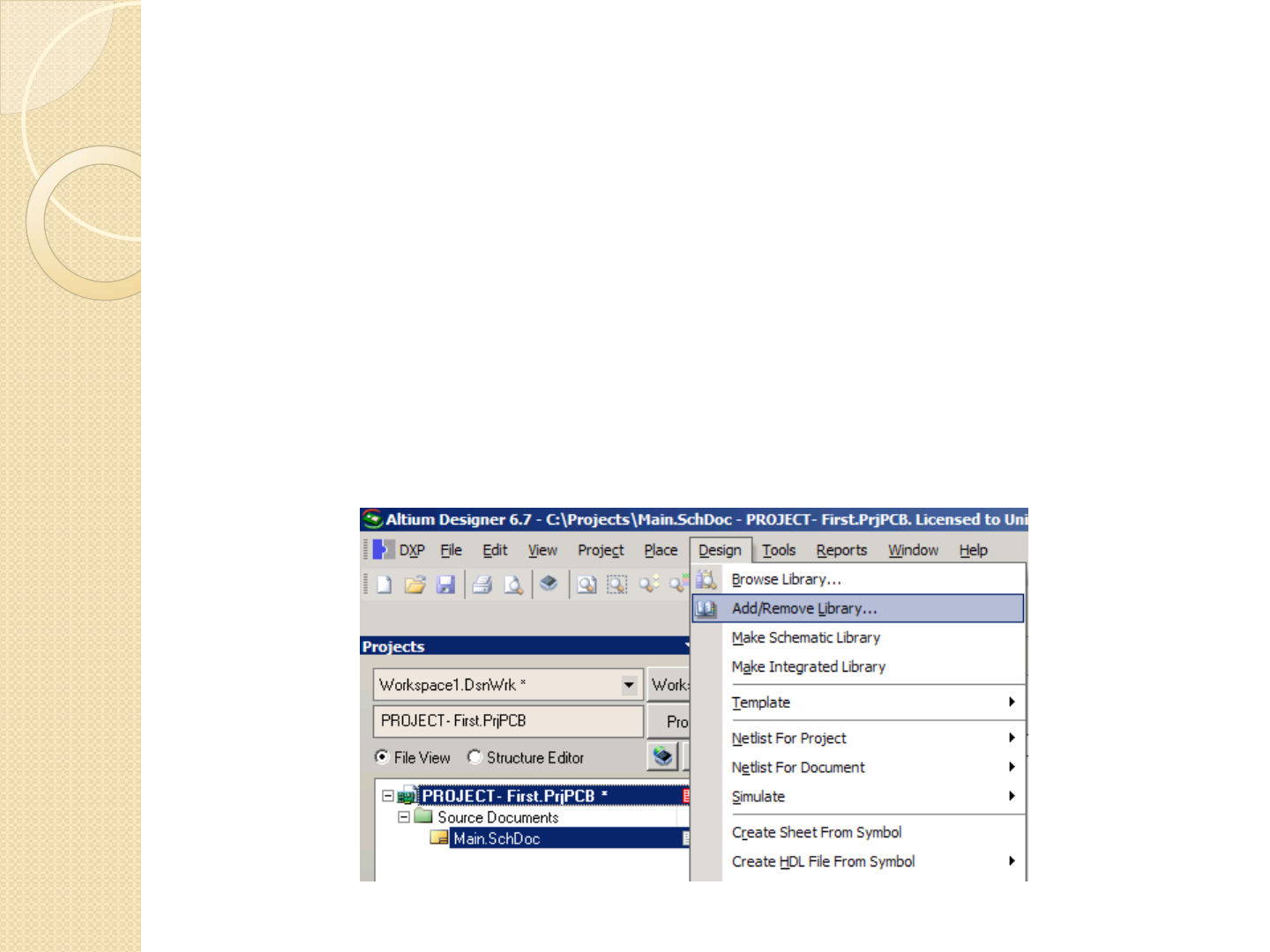
Adding Libraries To A Project
We have organized all the libraries in a
folder, now we need to add these to the
project
Follow the following prompt to add
libraries to the project
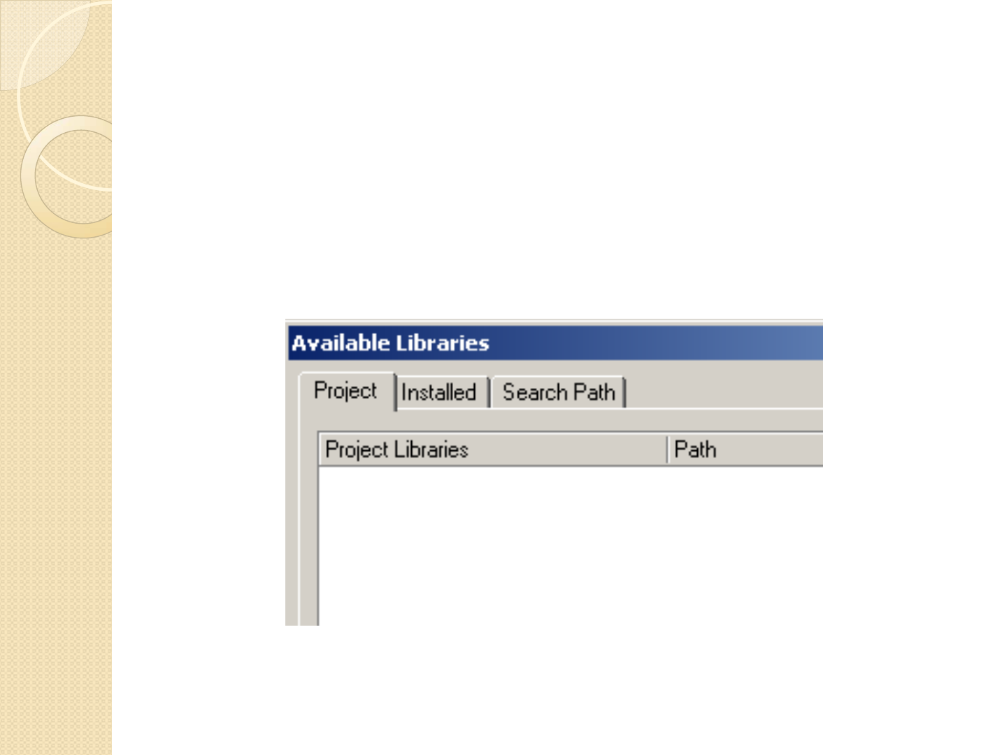
Adding Libraries
There are two methods of adding libraries
◦Project Libraries- Libraries available only for the scope of this project
◦Installed libraries – Libraries available to ALL projects by default. These do not show
up in the project tree.
The Search Path modifies the search location when searching for parts.
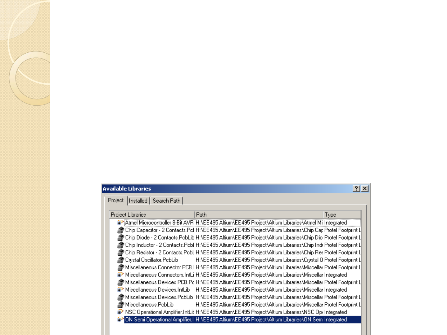
Adding Libraries
We want to make these libraries project-
specific only instead of global availability with
the ‘Installed’ tab
Make sure the ‘Project’ tab is selected, and add
all libraries from your project library folder
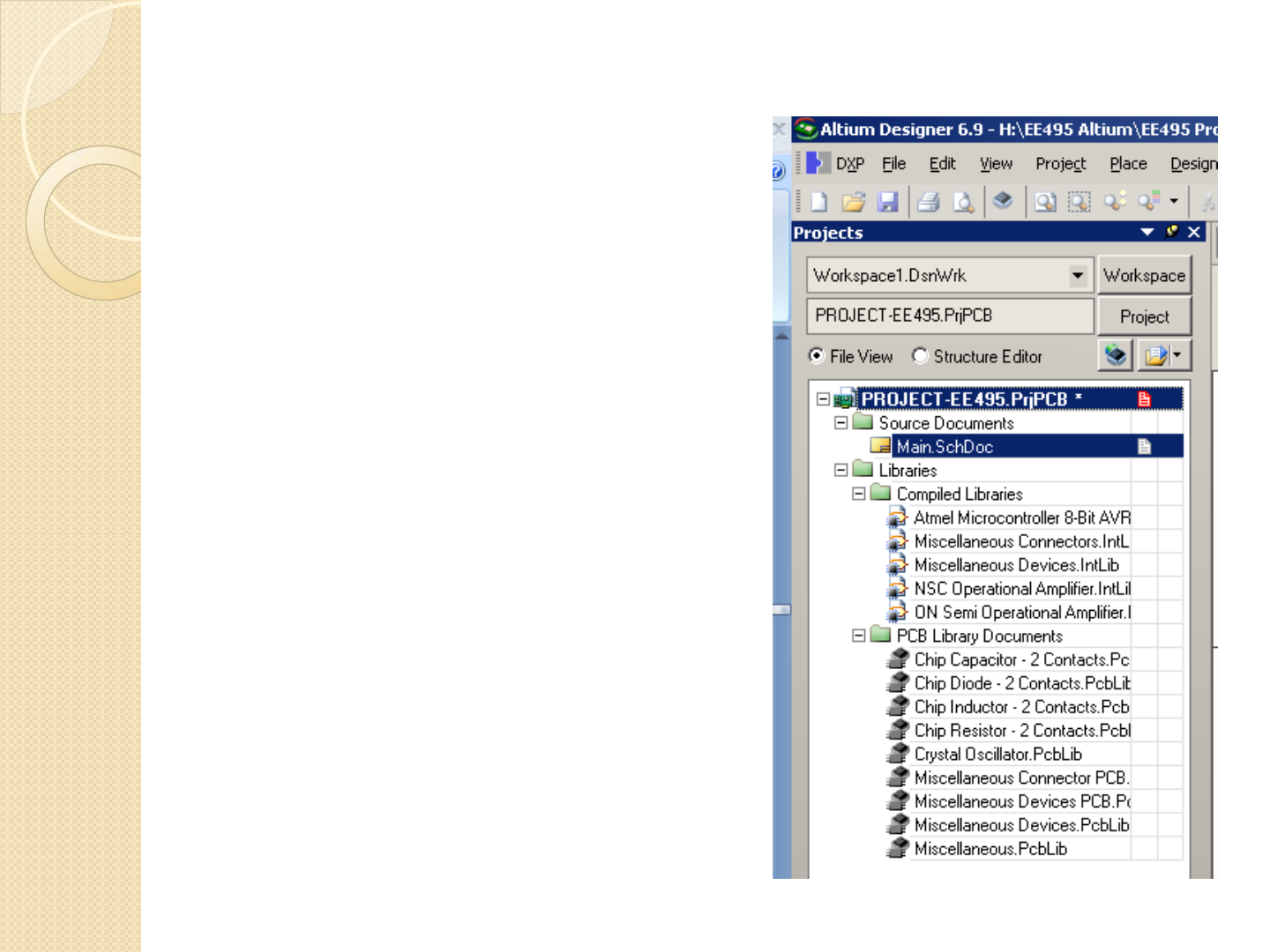
Project Hierarchy
By expanding the ‘+’
next to libraries, you
should see a list of all
the project libraries.
Make sure you have all
these libraries
installed before
continuing.
Notice how the
project tree separates
source documents and
libraries automatically
Open, Saved, Unsaved Files
Open files are indicated
with a ‘white paper’
Example: Main.SchDoc
Open modified and
unsaved files are
indicated with a ‘red
paper’
Example: The Project file
itself has been modified.
Closed files have
nothing in the column
Example: The Atmel
Microcontroller library
All open files are
accessible by clicking on
them in the project tree,
or in the top bar in a
windows- taskbar type
window
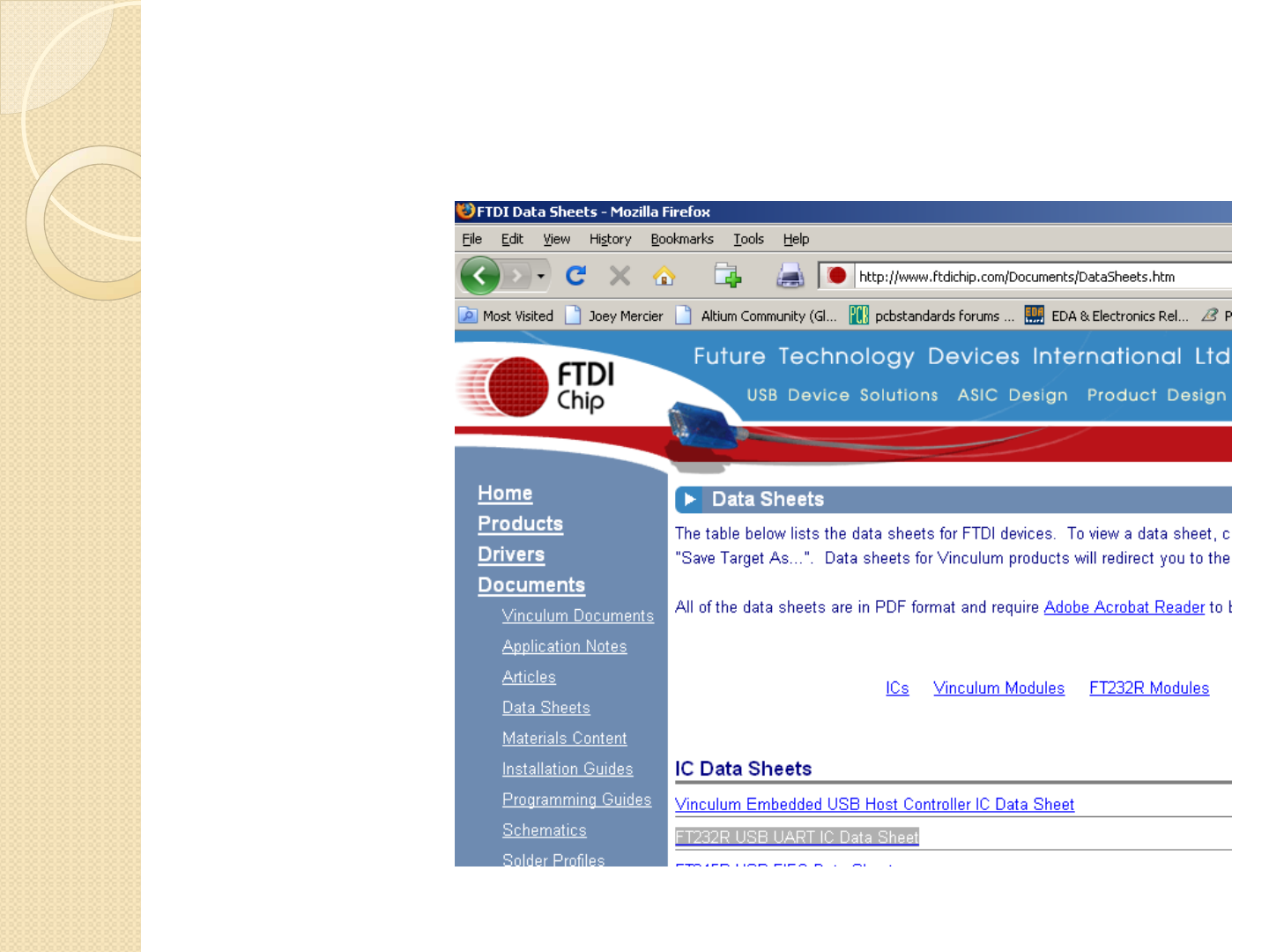
Project Documentation
We can’t create
a schematic
without knowing
more details
about the parts
we’ll be using.
Obtain the FTDI
FT232R UART
IC Datasheet
Rename the file
something less
cryptic such as
FT232 USB.pdf

Project Documentation
Specifications are often given or required for components, You should check and
double check each meets the project specifications.
Atmega8 Microcontroller, QFP Package, 16 MHz, ROHS Compliant
Mouser P/N: 556-ATMEGA8-16AU
Save as ‘Atmega8 QFP Atmel Microcontroller.pdf’
USB-B (Female/Socket) , ROHS Compliant, Right Angle Mount
Mouser P/N: 806-KUSBX-BS1N-B30
Save datasheet as ‘USB-B Connector’
SMD LEDs (0805), ROHS Compliant
Mouser P/N: 638-172BHC-AN1P23T
2x5 Box Header (Prog. Connector), Gold Plated, ROHS Compliant, Pitch=0.1”
Mouser P/N: 649-66506-066LF
Save datasheet as ‘2x5 Box Header.pdf’

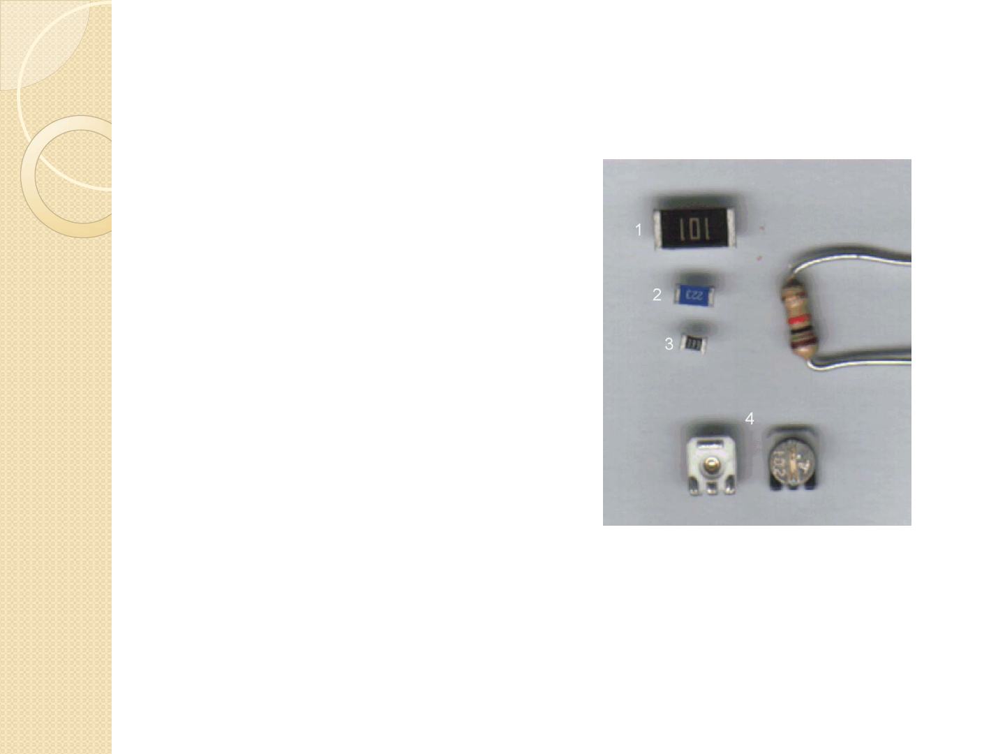
Chip Sizing Information
‘Chip’ components are devices that come in small rectangles
The 0805 specification for the LED are actually dimensions of the chip component
itself (Size Code).
Split up the numbers to 08 05, These are the dimensions in inches
The Length of the chip diode is 0.08” = 80 mils
The Width of the chip diode is 0.05” = 50 mils
Therefore, the larger the numbers, the larger the chip device:
Larger chip sizes can handle more power
Smaller chip size can handle higher frequencies (ideally)

Chip Sizing Information
1) Tantalum Capacitor (A-Case)
2) Tantalum Capacitor (D-Case)
3 & 4) Electrolytic Capacitor
5) 0805 Ceramic Capacitor
6) 1206 Ceramic Capacitor
7) 1210 Ceramic (Same length, but wider)
¼ Watt through-hole resistor
given as size reference
(Same as in our lab)
http://www.geocities.com/vk3em/smtguide/pics/caps.jpg
Chip Sizing Information
1) 1218 (1 Watt)
2) 1206 (1/4 Watt)
3) 0805 (1/8 Watt)
4) Potentiometer (Bottom & Top)
¼ Watt through-hole resistor
given as size reference
(Same as in our lab)
http://www.geocities.com/vk3em/smtguide/pics/resistor.jpg

Chip Sizing Information
1) 20 Pin DIP Package
2) SOIC20, Wide
3) SOIC8, W/Power Tab
4) SOIC8, Standard
5) SSOP20
¼ Watt through-hole resistor
given as size reference
(Same as in our lab)
http://www.geocities.com/vk3em/smtguide/pics/ic.jpg

Placing Parts
We have now added all the necessary
libraries for the project, now we need to
draw the schematic.
Follow the menu sequence below to place
a part
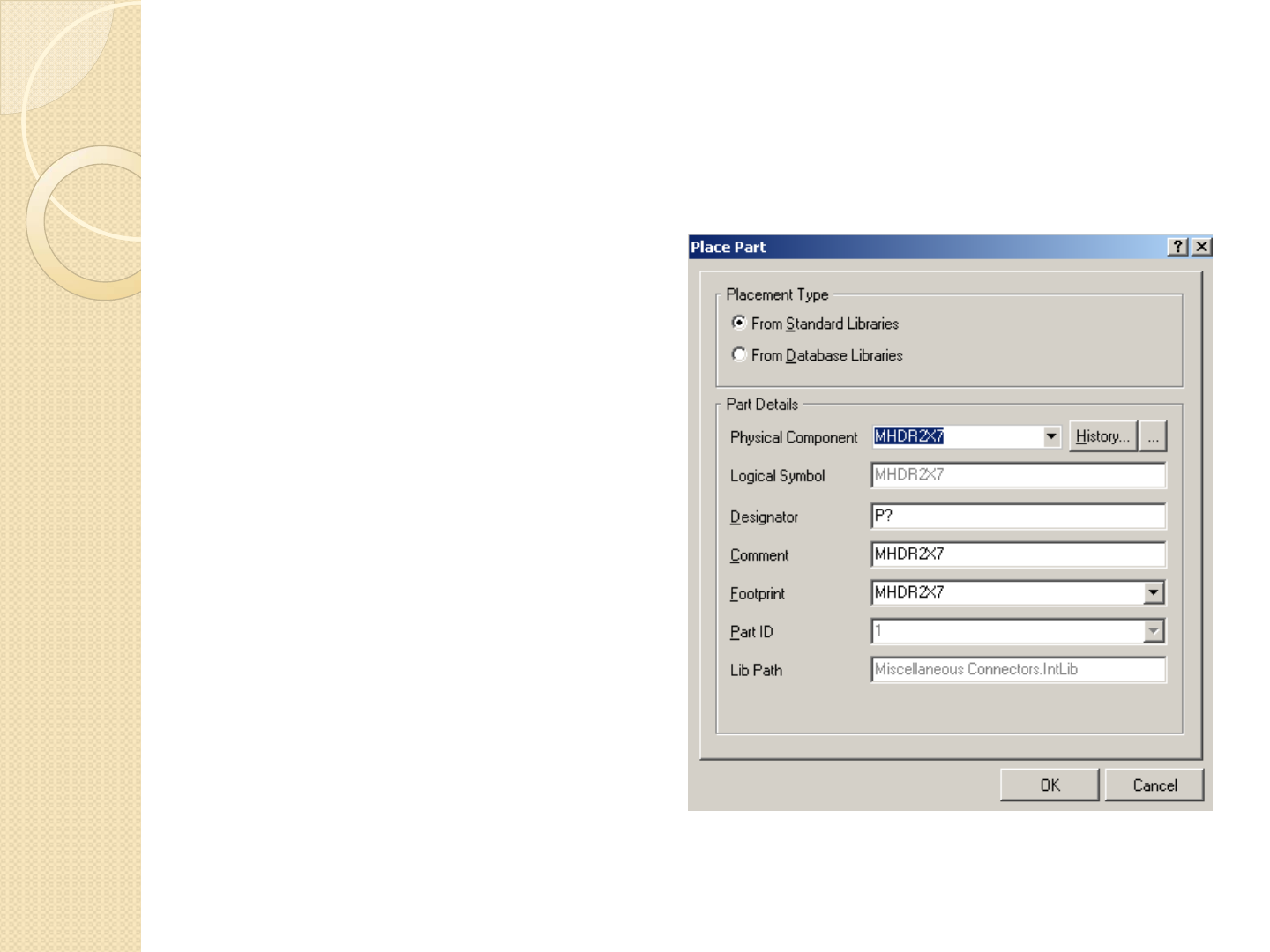
Placing Parts
After clicking ‘place
part’ from the
previous screen, you
will have an option to
place from standard
libraries or database
libraries. Keep this on
standard libraries
Click the button to
the right of the
‘History’ button to
bring up a list of
available libraries.

Creating a Schematic
At the top of the screen, there is a dropdown box which lists available schematic and integrated
libraries (but not PCB footprint libraries). For the highlighted library, in this case Miscellaneous
Devices, there will be a list of the parts inside that library in the bottom left.
Creating a Schematic
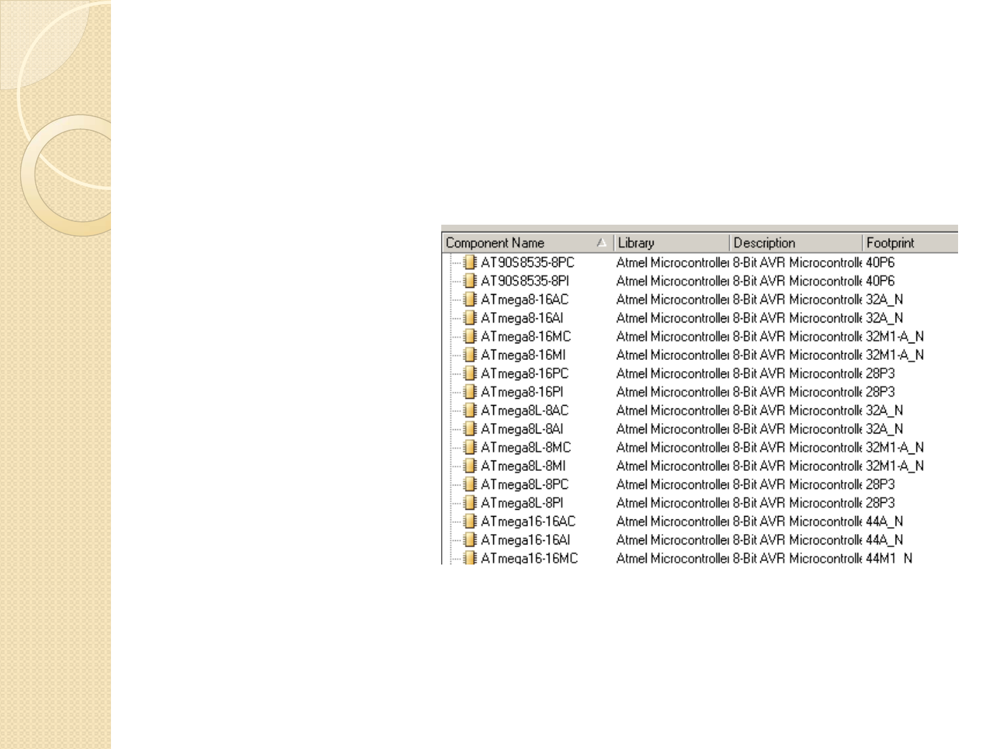
Select the Atmel
Library and navigate
down to Atmega8.
Notice there are
many options for the
same chip. This is
because although the
device is the same,
there are many
different ‘packages’
that this chip comes
in.
NOTE: The Atmega8
costs about $3.50
Creating a Schematic
Add the ATmega8-16AC
Looking at the datasheet for the ATmega8, we can see exactly what the -16AI stands for.
◦Supports up to a 16 Mhz clock
◦Commercial grade fabrication (Temperature ranges from 0C to 70C
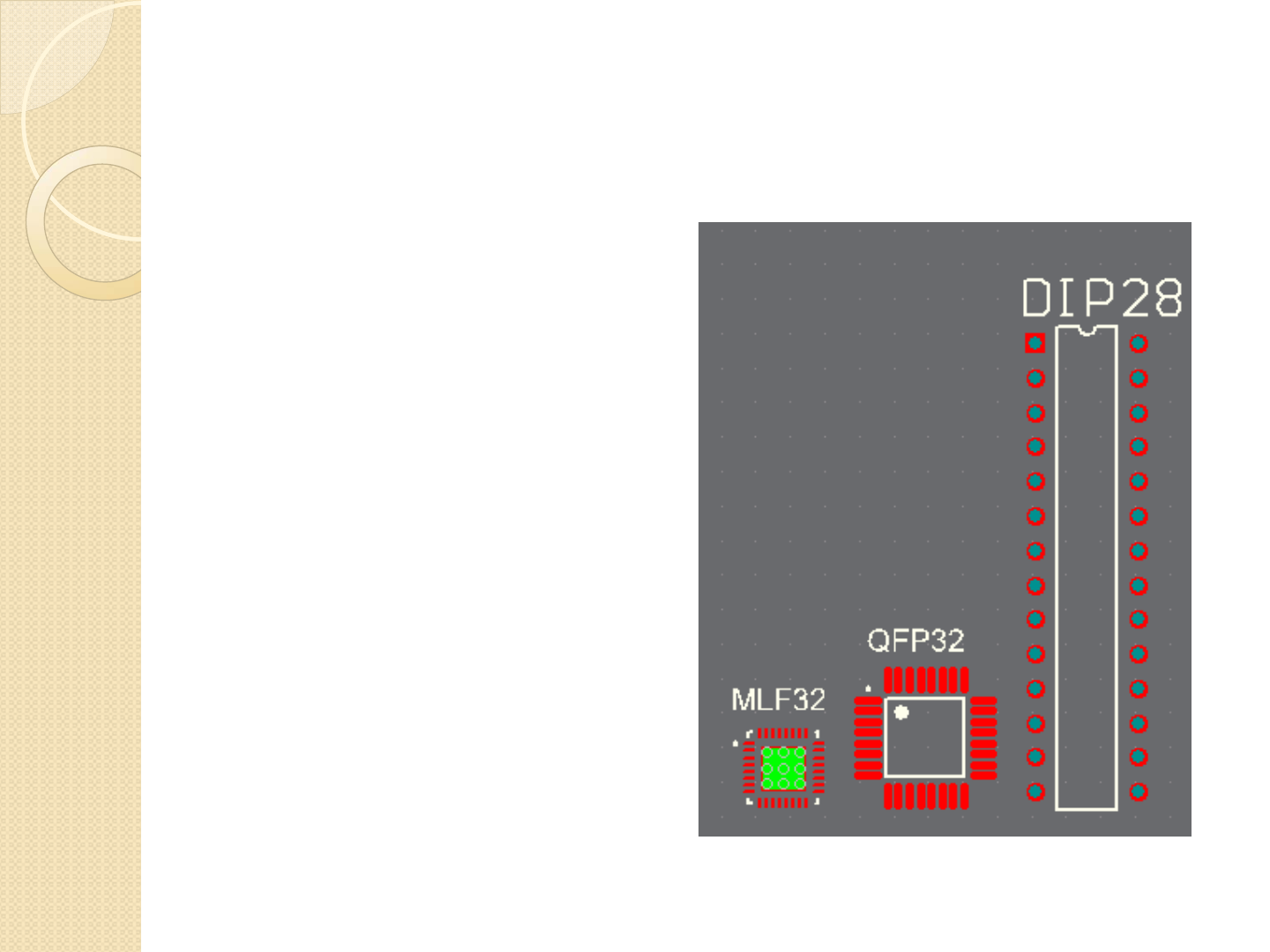
Creating a Schematic
Here are the three
common packages for
the ATmega8
microcontroller.
These are scaled relative
to each other with the
close to the same
functionality with each
package.
NOTE: Why does the
QFP package have 4
more pins than the DIP
package?

Creating a Schematic
We were given constraints with the assignment of
this project. Sometimes constraints are based on:
◦Economics, Size, Power handling, ability to assemble the part
, etc ..
For the microcontroller, we were told it must
function with a clock rate of 16 MHz, and must have
a QFP Package
It is crucial to take note of all constraints BEFORE
entering the schematic and/or pcb layout. It is a
HUGE waste of time to design around a part that
doesn’t meet the specifications.
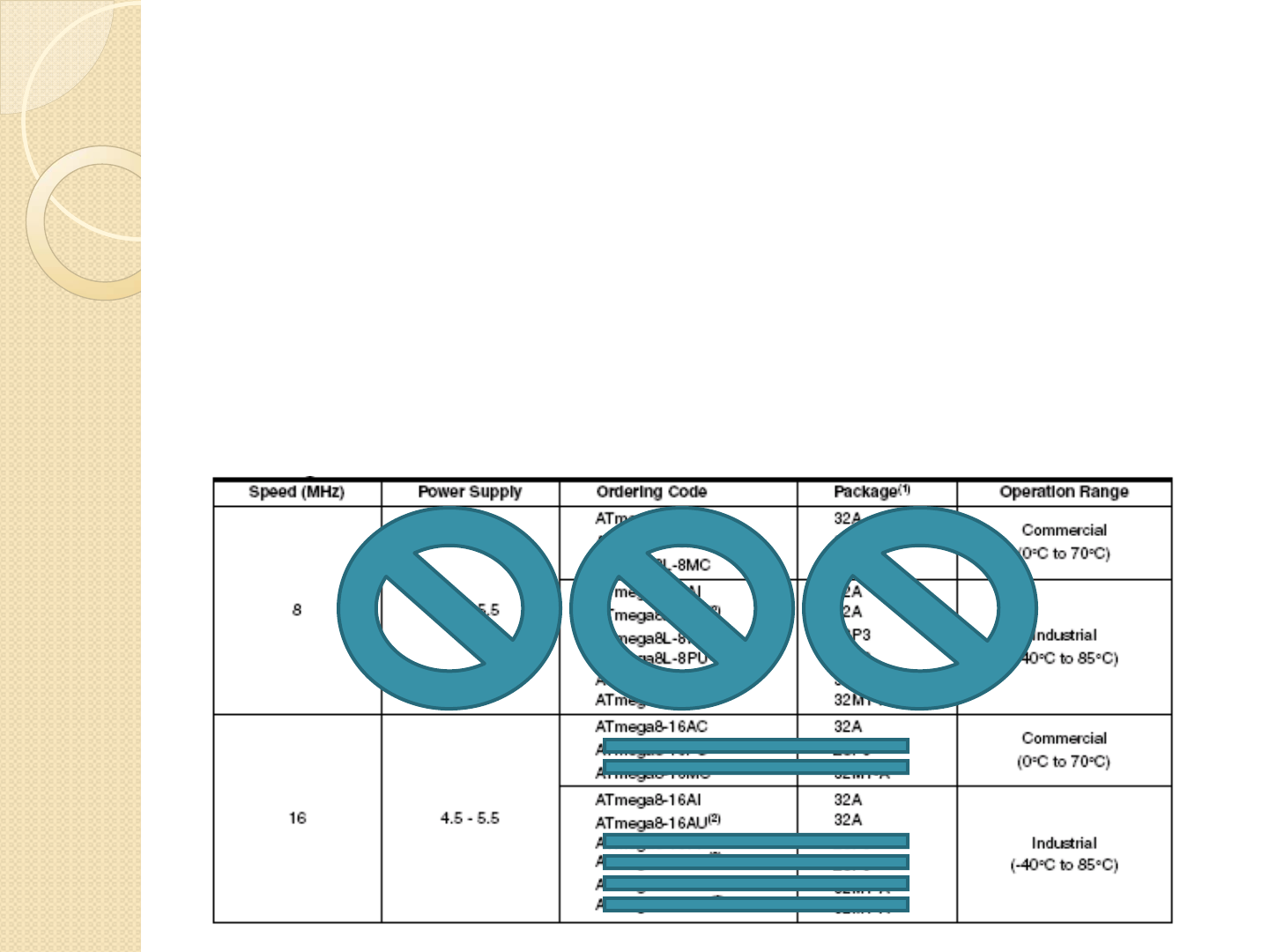
Creating a Schematic
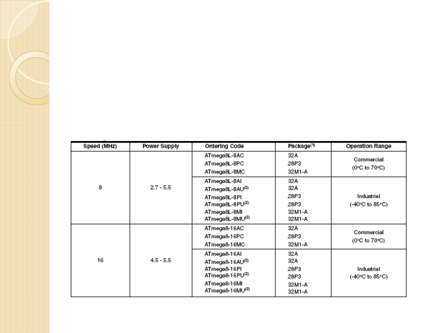
Looking again at the ordering information available in the datasheet, we know
that:
◦The Chip must be able to work with a 16 MHz clock, we can eliminate all 8MHz rated
microcontrollers
◦The DIP package is 28 pins, we can eliminate any package that has a ‘28’ in the
package information
◦The 32M1 refer to the MLF packaging, we can eliminate all those items
◦This leaves us with a decision to choose between commercial rated or industrial
rated temperature ranges, Either the ending in -16AC, -16AI, -16AU are acceptable

Creating a Schematic
Usually the industrial rated components are more costly than the commercial
rated components, so we will choose the Atmega8-16AC
QUESTION: A temperature rating doesn’t affect the footprint or simulation
of the device, is there a reason we can’t/shouldn’t just choose any of the three
possible options ???
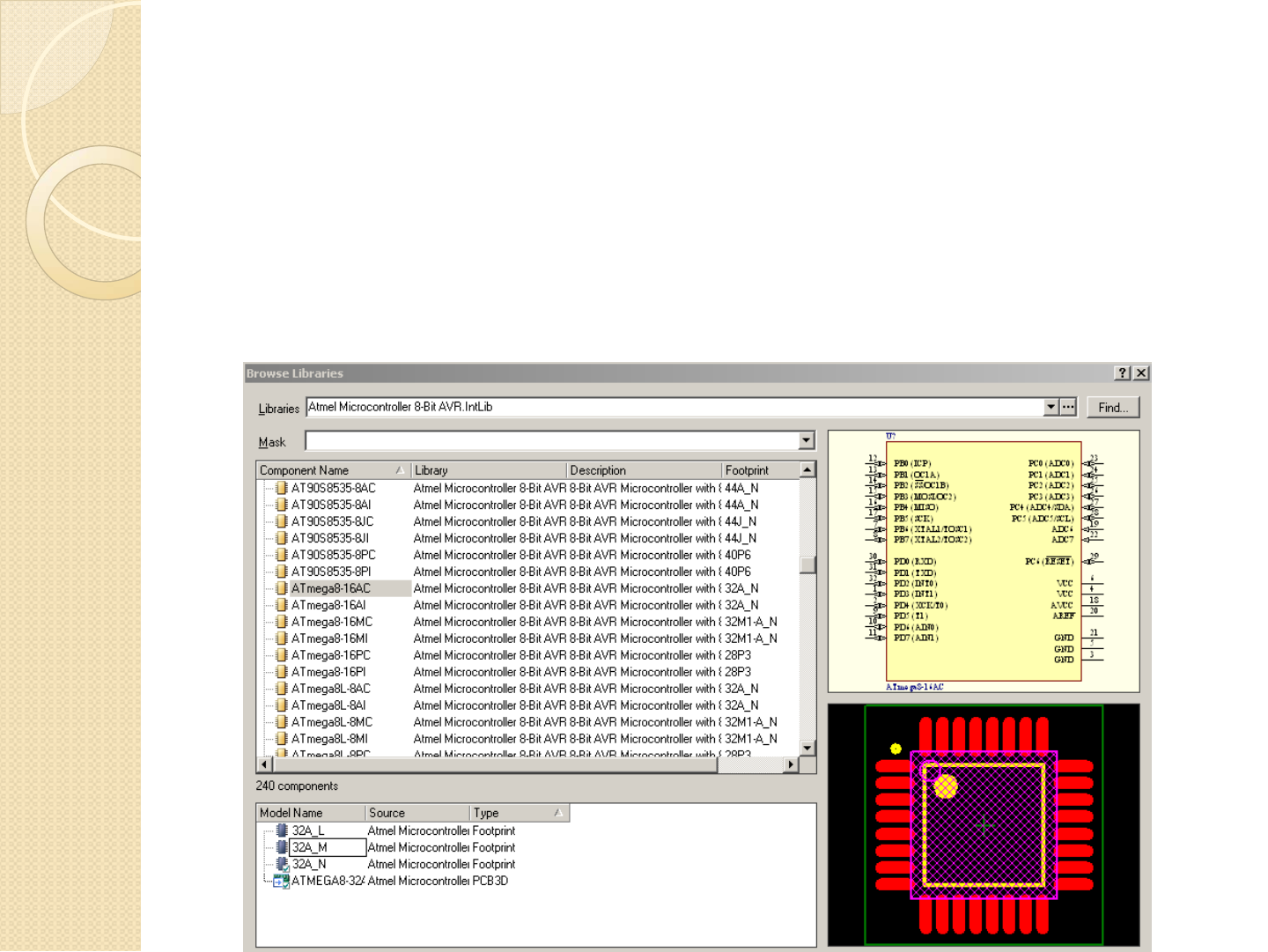
Creating a Schematic
Notice to the right, there is the schematic drawing and associated pinout
of the device, beneath that is a drawing of the PCB Footprint (this should
match what you expect from the datasheet)
The bottom shows all footprints associated with the part
◦Why do you think there are three different footprints for a QFP32 ?
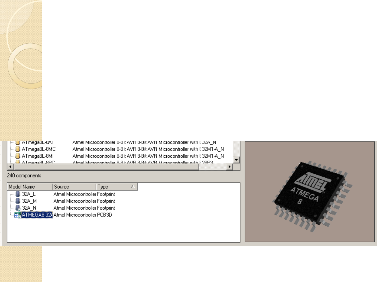
Creating a Schematic
Many vendor supplied integrated libraries contain much more than just a
schematic drawing and PCB footprint
Shown below is a rendering of a 3D Image of the chip. Altium has an option to
view the PCB in 3D, and this image will represent the Atmega8 in the 3D
rendering
Also included are SPICE files and/or IBIS files (more on this later)
Creating a Schematic
Place the Atmega8 into the schematic drawing
◦You can always move the location later
◦What function does pin 20 perform ?
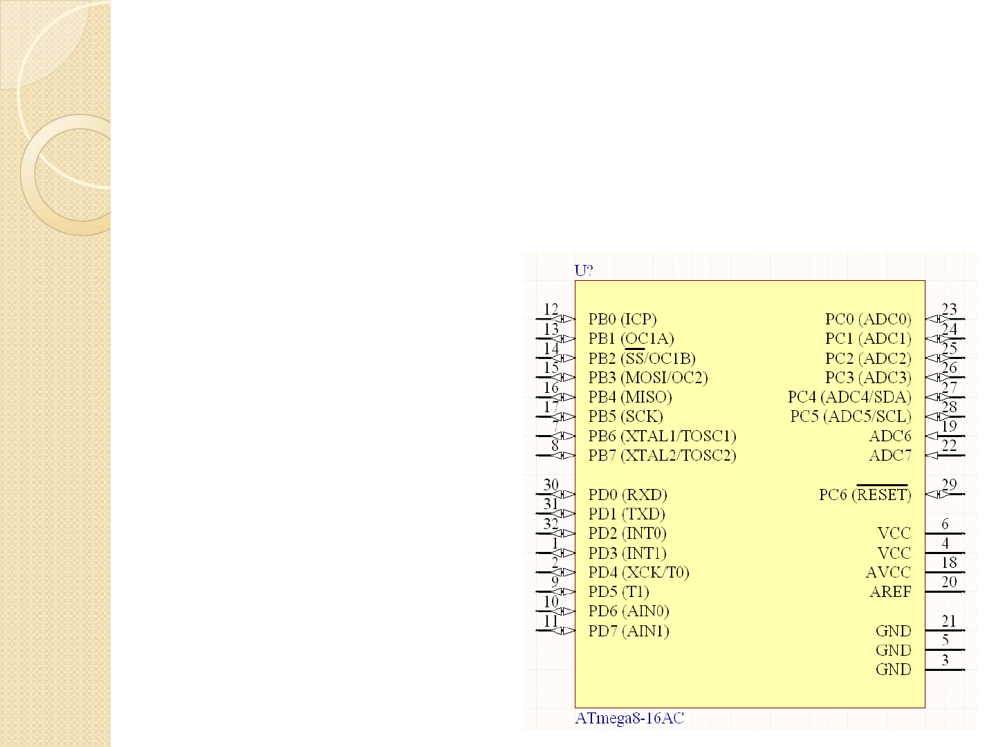
Zooming In and Out
You can’t see the function of pin 20 because the image is zoomed out.
To Zoom In/Out
◦Wheel Mouse and Control Key
◦Page Up/Page Down Key
To Pan Left/Right/Up/Down
◦Wheel Mouse and Shift Key
◦Left/Right/Up/Down Arrow (Small Pan)
◦Shift Key and Left/Right/Up/Down Arrow (Larger Pan)
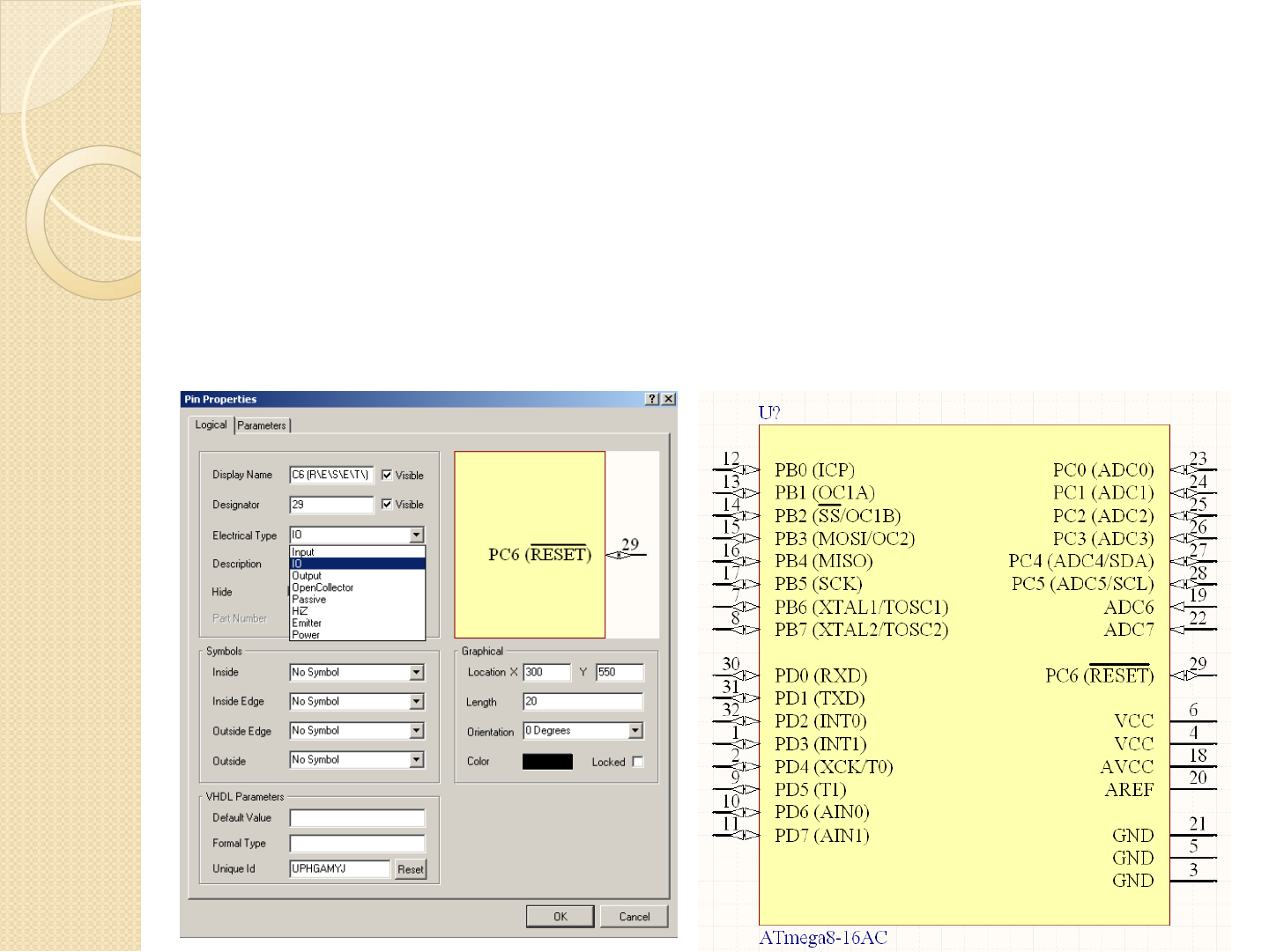
Pin Functions
Pins can be setup for the following functions:
◦Input, Output, I/O
◦Open Collector, Passive, HiZ, Emitter,
◦Power
Depending on how the pin is set, will determine how the DRC (Design Rule Check)
Interprets the Pin and what connections are allowed

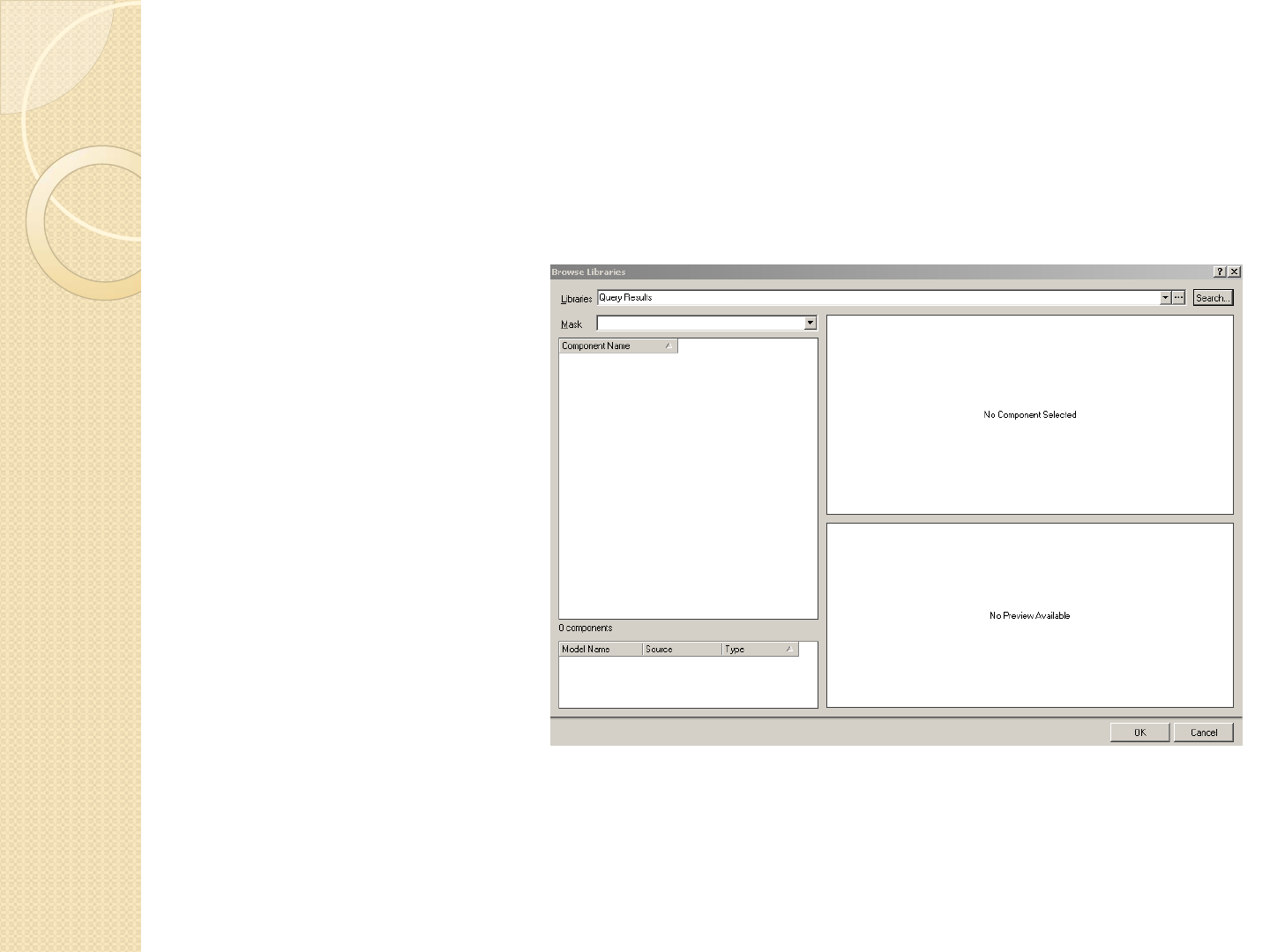
Add the USB-B Connector
It seemed obvious which library contained the Atmel Atmega8, but
now we need to add a USB-B connector.
An easier method than searching each component and each library is
to search the libraries.
Click the ‘Find’ button to the right of the library selection
(It doesn’t matter which library is selected/active)
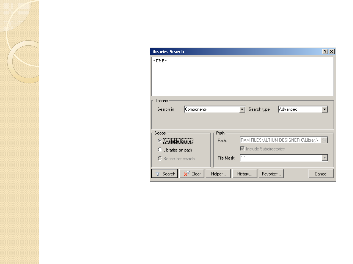
Add the USB-B Connector
Ty p e i n th e key wo rd
you are looking for
We are looking for a
USB-B connector, For
now let’s just search
for ‘USB’ and narrow
down the search after
that.
NOTE: Using
wildcards *before and
after allow for words
such as xxxUSBxxx
to be recognized.
Add the USB-B Connector
The search can take a
while depending on
how many libraries
you are searching
through.
We are searching
through only the
libraries we added to
the project, so it
should happen very
quickly.
The result of this
search came back
negative, That means
there are no USB
items in any of our
project libraries.
Click the ‘Search’ tab
in the top right corner
Add the USB-B Connector
Change the scope of
the search from
available libraries
(available to the
project) to ALL
libraries in the path.
The path will
automatically be
entered for the default
library location in
Altium
* make sure ‘include
subdirectories’ is
ticked.
Click the search
button
Add the USB-B Connector
USB is a very common term, so very quickly the list fills up
Expanding the box to read the description helps with identifying what each
part is (in case names such as ‘1-353576-1’ mean nothing to you)
We are looking for a SINGLE Through Hole, Right Angle, USB-B
Receptacle socket, which is located at the 8th row down
Add the USB-B Connector
Select the 1-1470156-1
and click OK
You will get a message
stating that the library is
not available to the
project, but Altium is
willing to install it for you,
click yes
Click ‘OK’ again to add
the part

Add the USB-B Connector
The library AMP Serial Bus is added automatically to the ‘Installed’ libraries,
NOT the project libraries
This action DOES NOT MOVE ANY LIBRARIES PHYSICAL LOCATION
For ease of future design, it is a good idea to move libraries added by this
method to your ever-growing list of libraries
You can do this by copying the AMP Serial Bus USB from the path given in
the ‘available libraries’ below
C:\Program Files\Altium Designer 6\Library\Amp
to your custom library in your flash drive
X:\EE495 Altium\EE495 Project\Altium Libraries
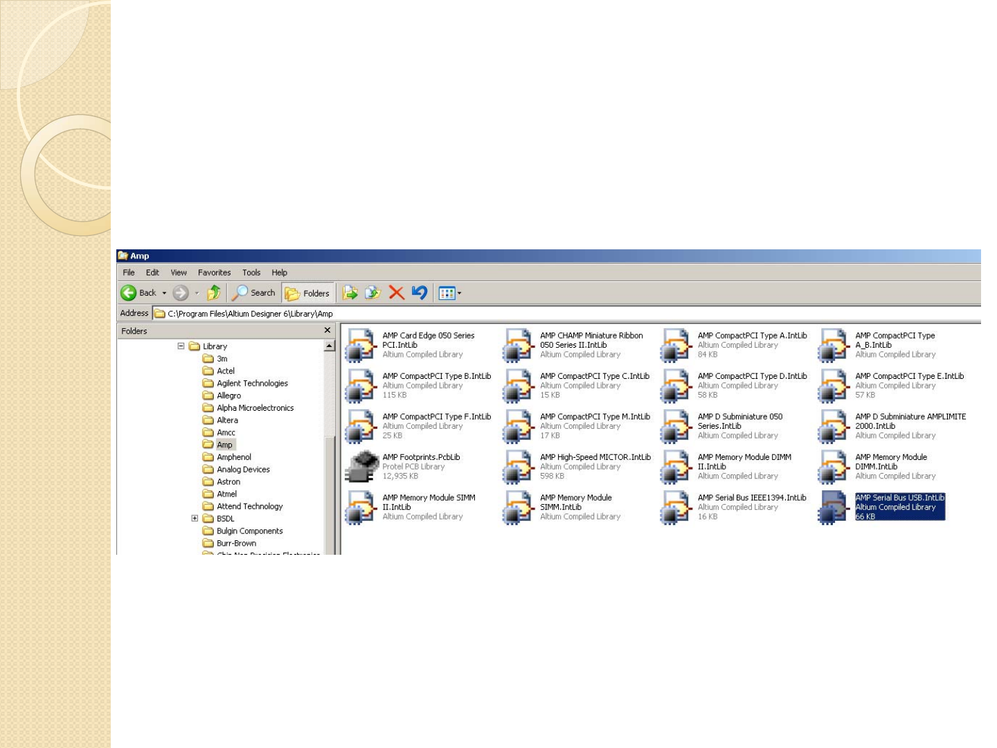
Add the USB-B Connector
AMP makes several different libraries, so be sure to copy the correct one!
Rotating Parts
The easiest way
to rotate parts is
to select the item
and hold the left
mouse button
down, and tap
the space button,
this will rotate 90
degrees each tap.
Another method
is to double click
the component
to open up the
component
properties
window, and in
the bottom left
corner you can
set the
orientation
NOTE: the
‘mirrored’ tab
will flip the
component
about its axis

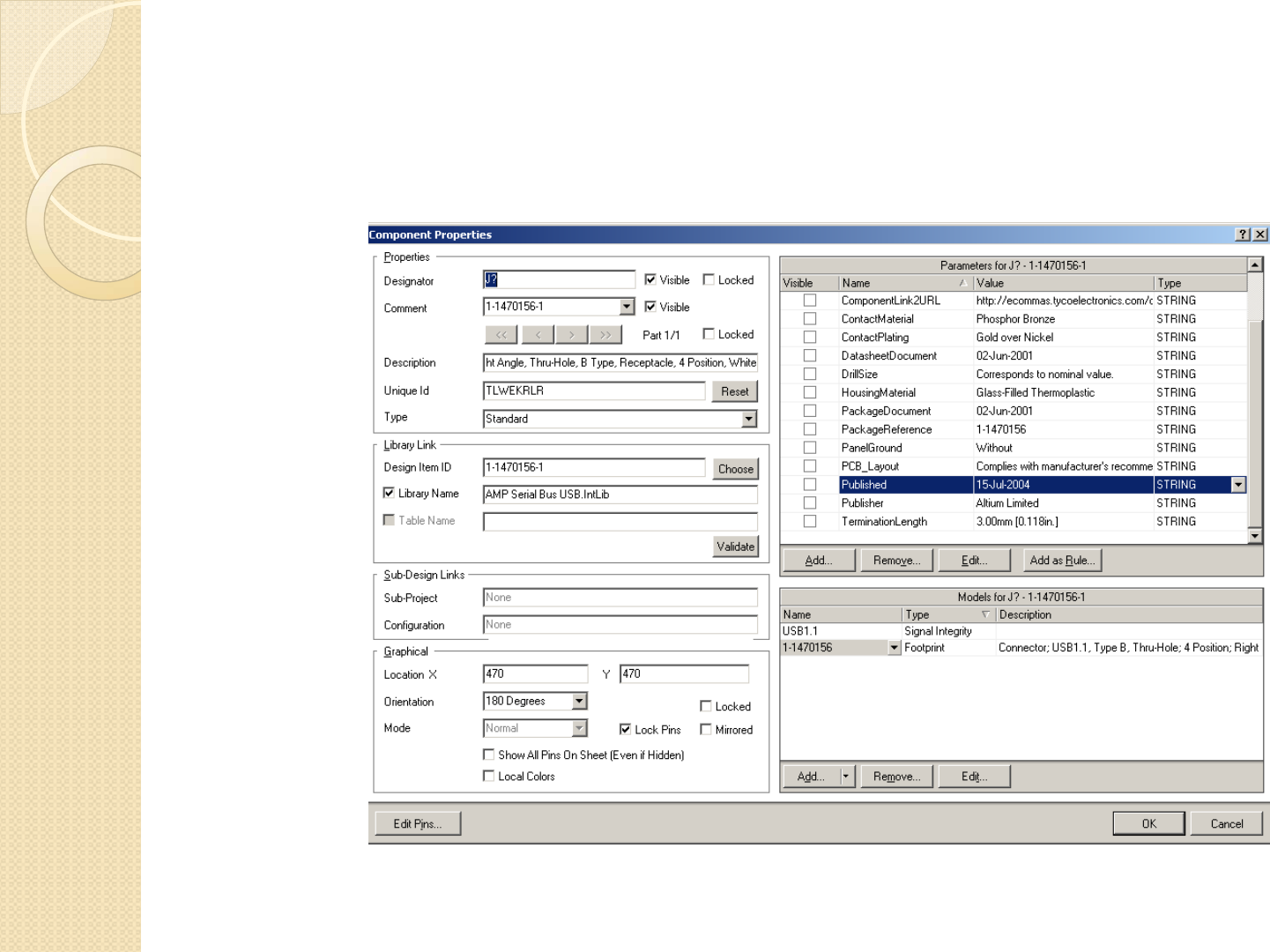
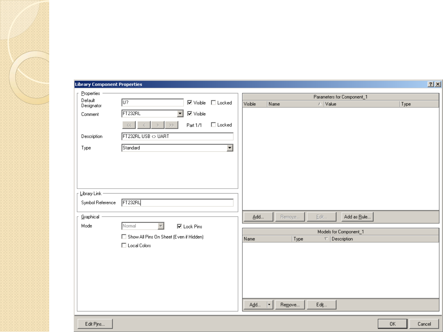
Component Properties
In the top left corner of the
component properties, you can set
comments, descriptions, designator
values and library link information
NOTE: Unique ID is a unique value
which links the schematic part with
the PCB document.
In the bottom left corner, you can set
graphical properties such as
orientation, mirrored, locked (stuck
in schematic)
The ‘Edit Pins’ button will allow you
to reassign pins, pin functions, and pin
numbers. This should only be used if
you are absolutely positive you know
what you are doing!!
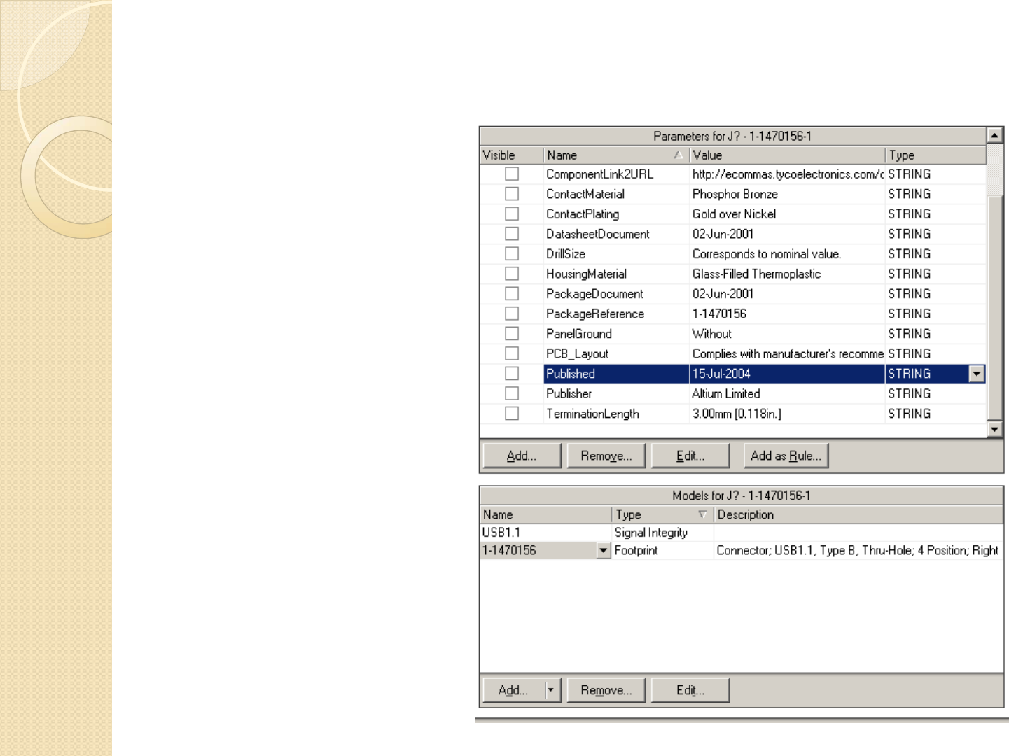
Component Properties
In the top right corner of
component properties of a
standard component will contain
information such as publishing
date, termination length, URL’s,
drill sizes, etc.
NOTE: You can add your own
custom fields (such as ordering
information, ordering part
numbers, etc.)
NOTE: You can also add a
custom PCB rule to the
component while you are still in
schematic capture mode
The bottom right corner
contains model information for
the component, such as
footprint model information and
signal integrity models.
Component Properties
Mirror the
USB-B
connector
and orient
the parts so
they match
the diagram
to the right.

Programming Header
Add a part from the Miscellaneous Connectors library called ‘Header
5x2’
Make sure to use caution when selecting parts. If you accidentally add
‘Header 5x2a’ they make look the same, but look at the numbering
system of the pins. Always make sure the numbering method is the same
as you expect it to be.
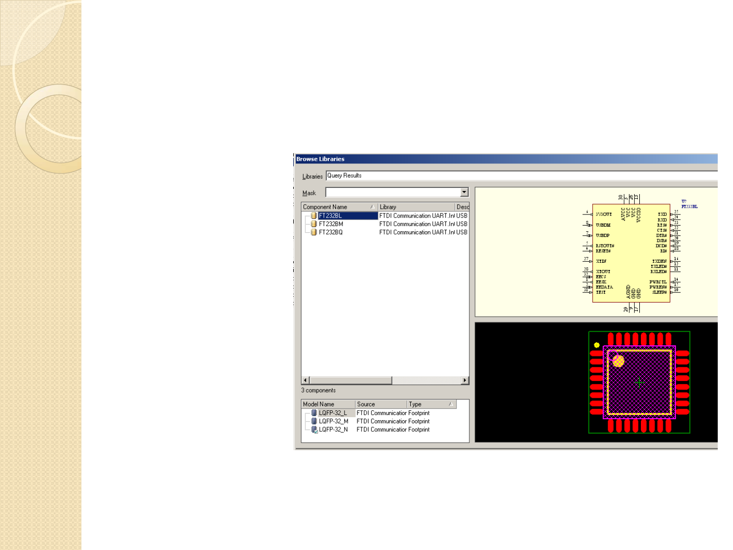
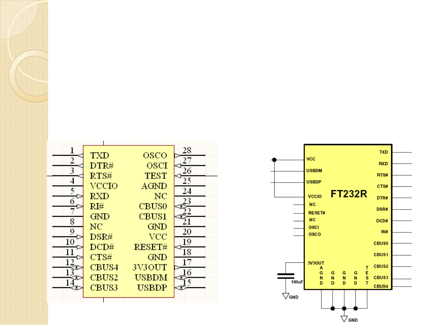
FTDI Chip- FT232 (TSSOP28)
A quick search for
the FT232 chip we
will be using gives
the following result
Although there are
three matches for
the FT232, We are
actually looking for
the FT232RL as we
will see on the next
slide

FTDI Chip- FT232 (TSSOP28)
Like all aspects of
PCB layout, you
must pay attention
to every detail on
everything.
The datasheet
states that the
FT232RL is a 28-pin
SSOP package.
Since this footprint
is not available, we
must create the
part in a custom
library
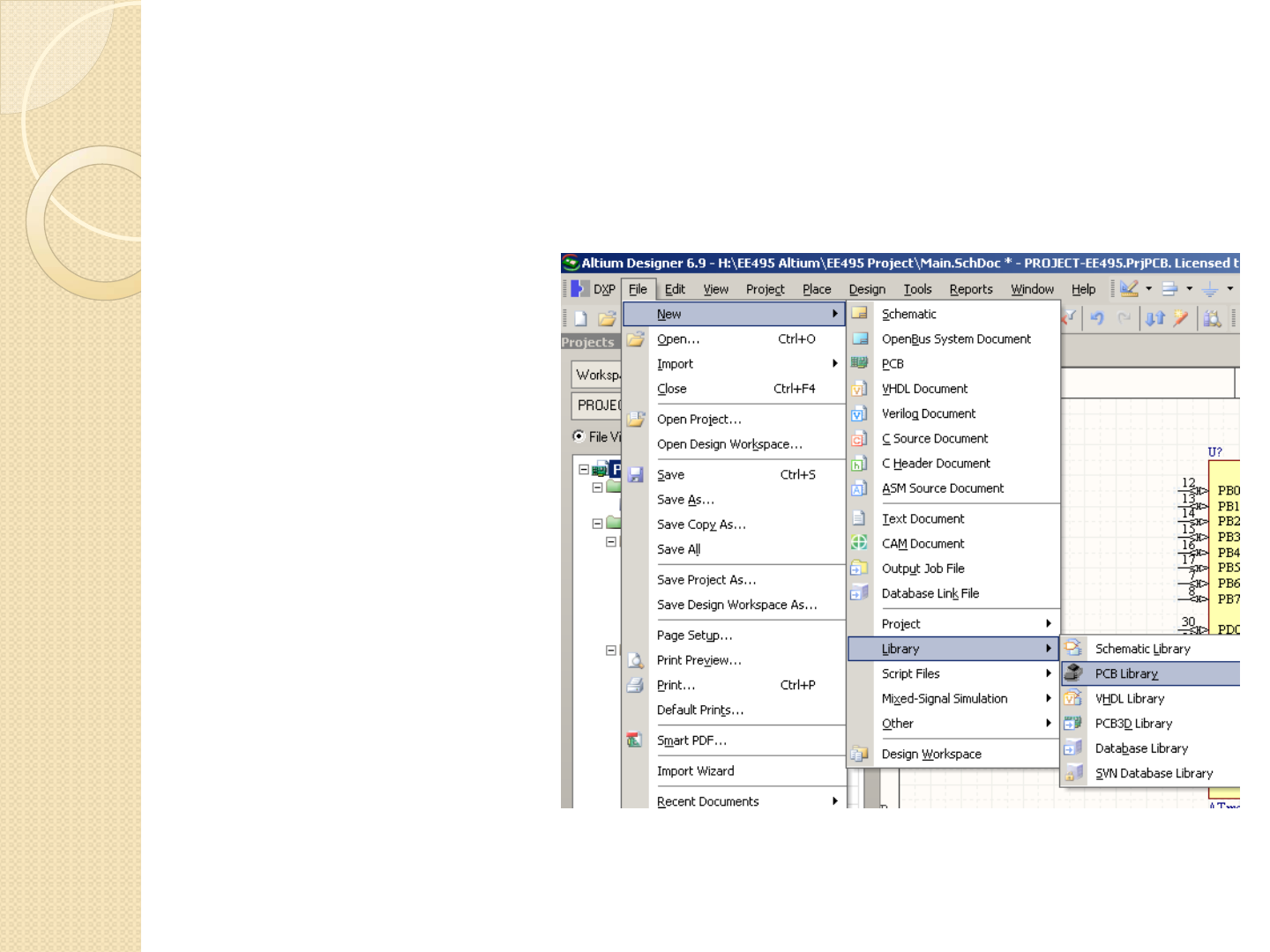
FTDI Chip- FT232 (TSSOP28)
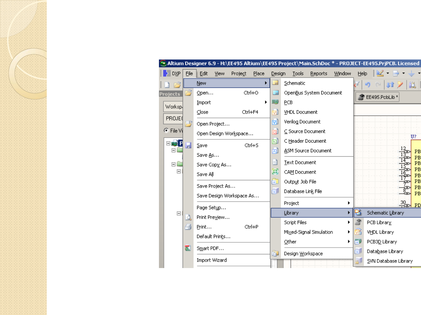
Follow the menu
sequence shown to
the right to create a
new PCB library.
This library will
house ALL of your
components
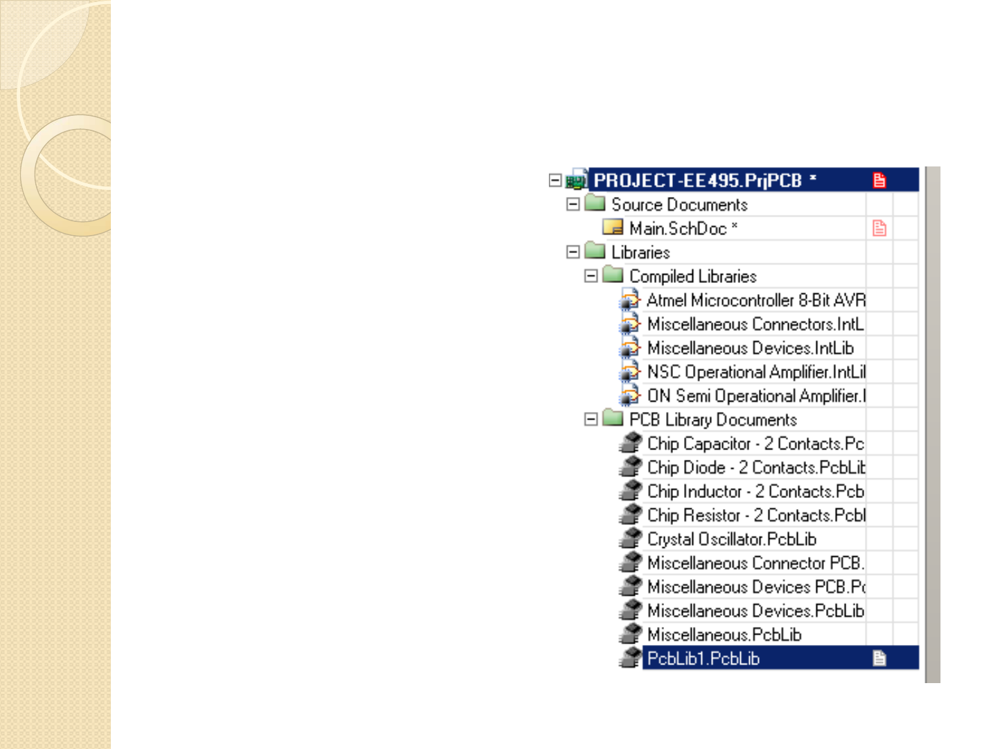
FTDI Chip- FT232 (TSSOP28)
The new library is
automatically added to
the project.
Right click and click
‘save as’ and rename
the library to a more
appropriate name:
EE495 and save it in the
directory with the rest
of your libraries

FTDI Chip- FT232 (TSSOP28)
Notice the small tabs in
the bottom left corner.
Double click the new
PCB library you
created to open it, and
click on the one titled
‘PCB Library’ to work
inside that library.

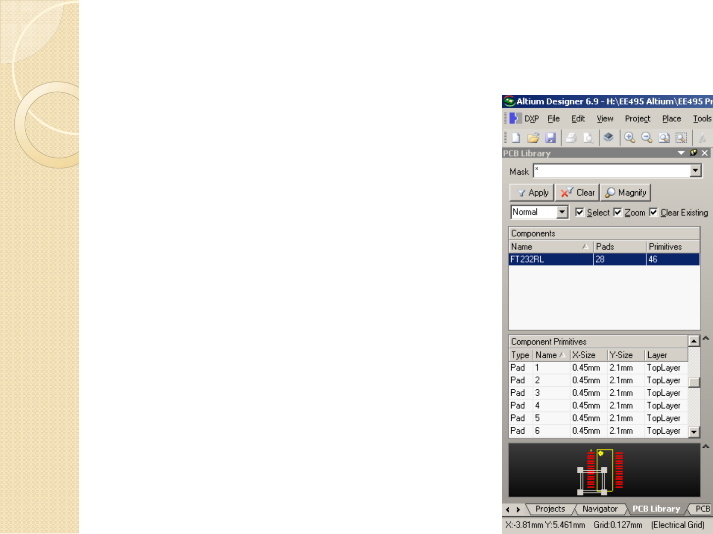
FTDI Chip- FT232 (TSSOP28)
With the PCB Library
tab selected, we can see
that there is only one
component inside our
library called
PCBCOMPONENT_1
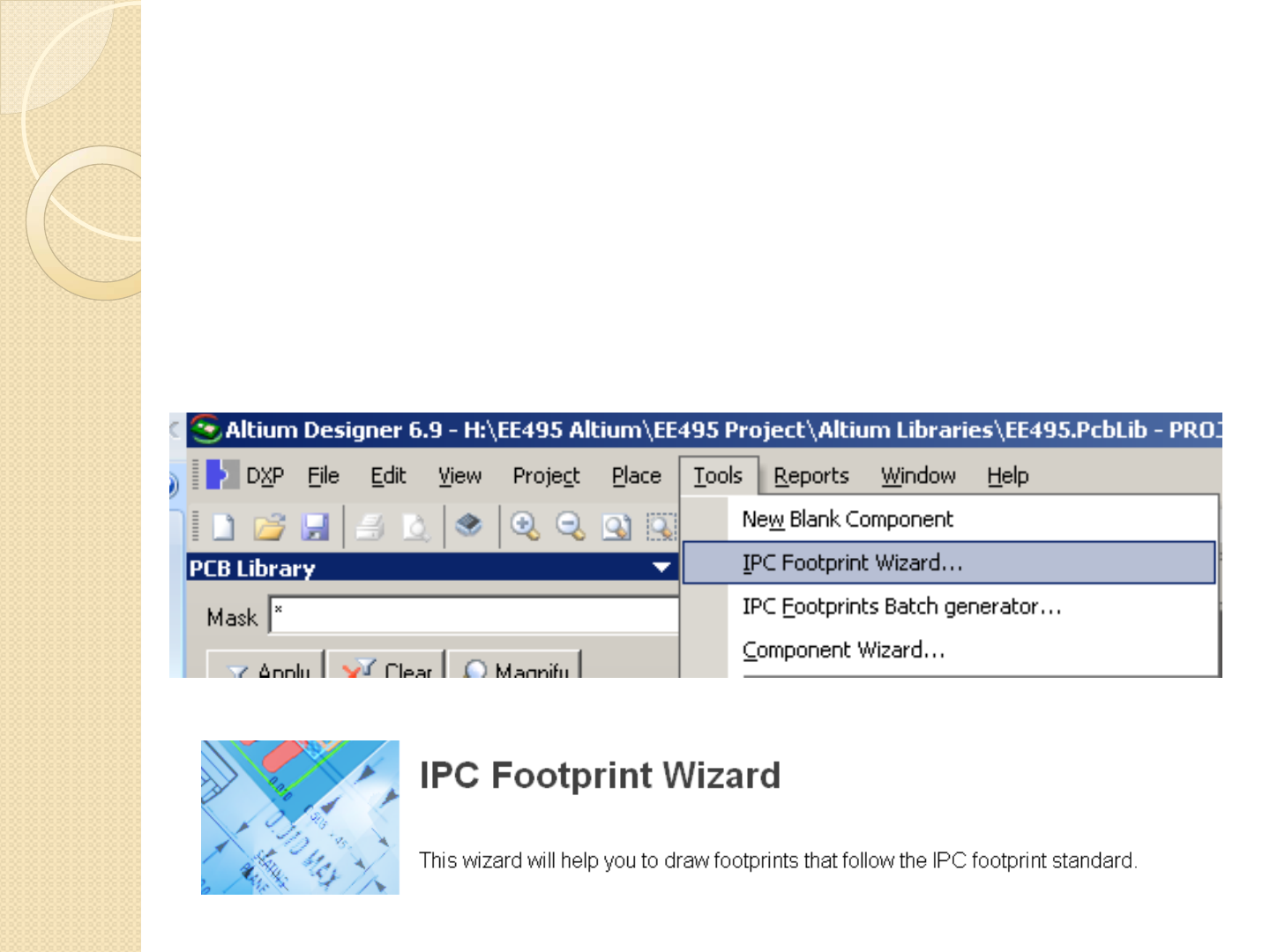
FTDI Chip- FT232 (TSSOP28)
From inside your PCB library, click TOOLS > IPC Footprint Wizard
to open the IPC Footprint Wizard.
This will help you easily create the footprint for the device
You will see why it is so important and helpful to have standards
when it comes to documentation, naming conventions, etc…
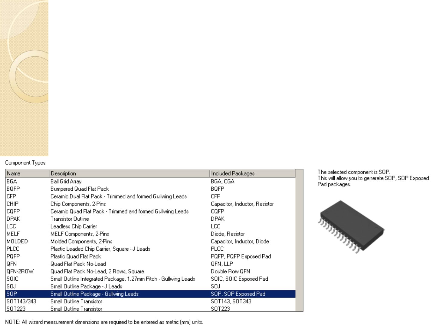
FTDI Chip- FT232 (TSSOP28)
The first step is selecting what type of part it is. They don’t
specifically have SSOP, but SSOP is just a modified version of the
SOP so select that
There is a diagram of what the chip looks like to the right
NOTE: check the note on the bottom of the wizard: All wizard
measurements must be entered as metric (mm) units
FTDI Chip- FT232 (TSSOP28)
At first this might seem a bit daunting and intimidating, but when you
pull up the datasheet to find the values, you will see that the graphics
and naming convention matches what we must entered

FTDI Chip- FT232 (TSSOP28)
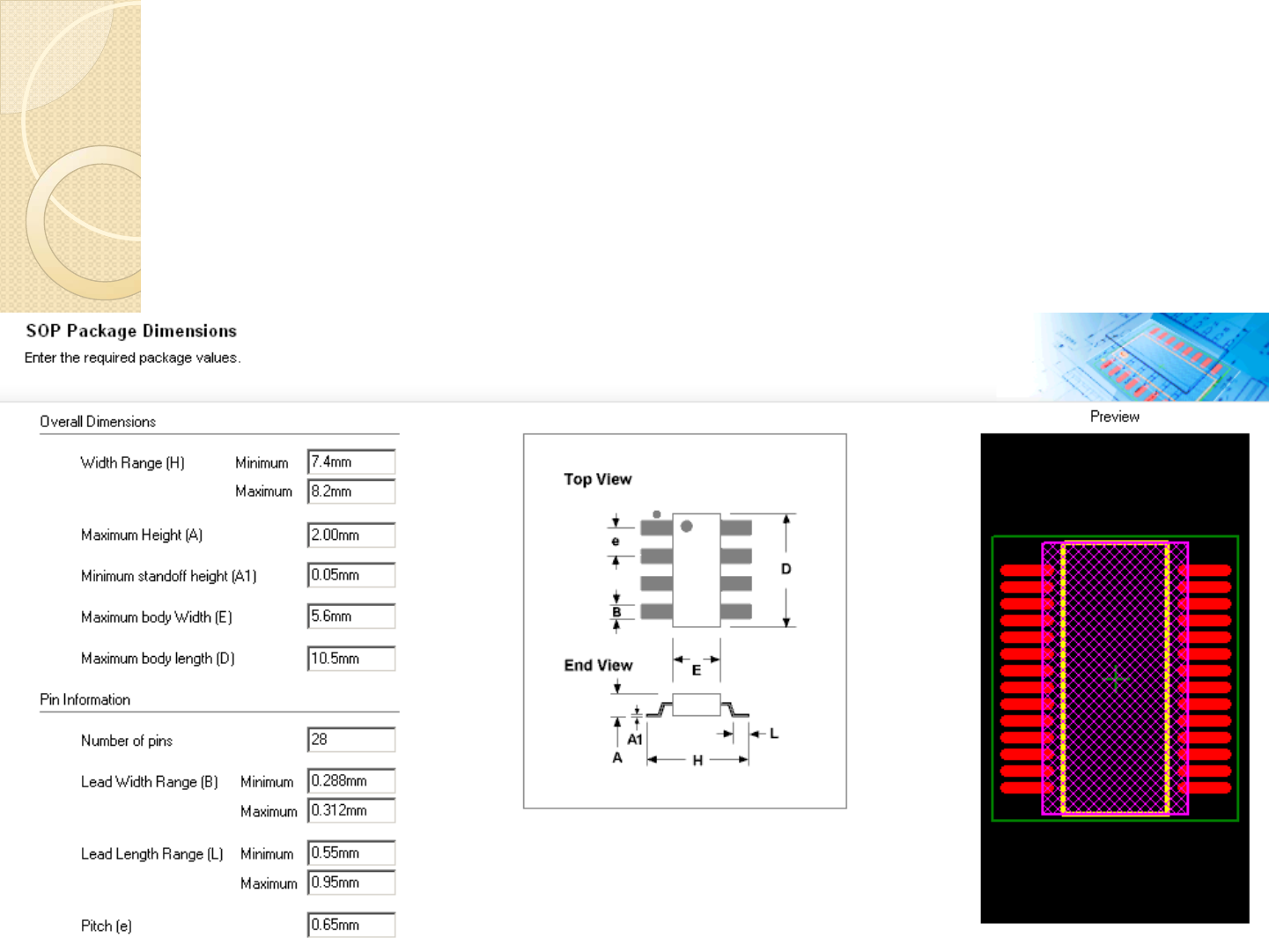
The first entry is for width range. The datasheet gives a width range
of 7.80 +/- 0.40mm (Min width = 7.4mm, Max = 8.2mm)
FTDI Chip- FT232 (TSSOP28)
The max height of the chip (A) is
2.00mm
Enter this in for maximum height
Question: Why would the height
of the chip matter ??
FTDI Chip- FT232 (TSSOP28)
Fill out the rest of the values, you should get the numbers below
NOTE: Watch as you enter values, the graphic on the right will
dynamically change
FTDI Chip- FT232 (TSSOP28)
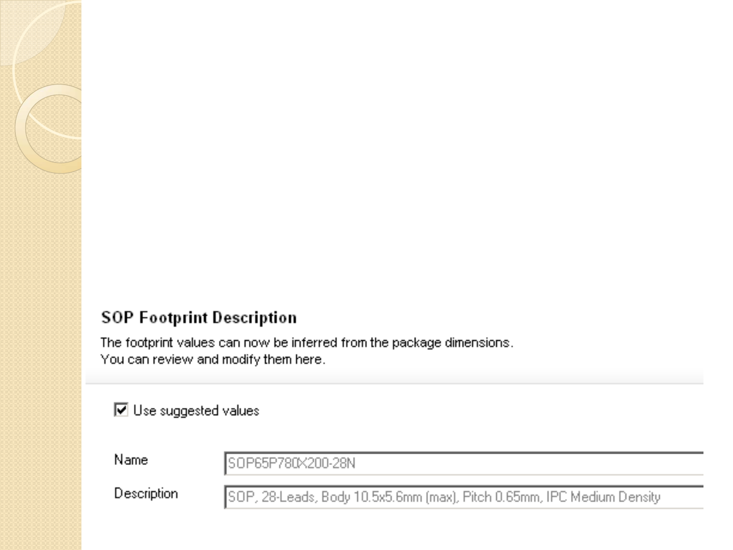
Accept the automatically entered values for the next few slides until
you get to the slide below
Uncheck the ‘use suggested values’ and change the name to FT232RL
Click ‘Finish’ and the part will be added to your library
FTDI Chip- FT232 (TSSOP28)
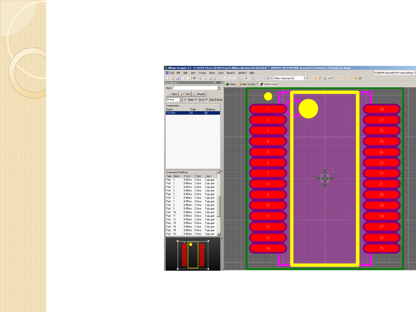
Your library will
automatically open
with your new part
included.
Notice how there
are two yellow
dots , those are ‘pin
1 indicators’ so
the board is
assembled properly
You can now be
confident that the
FT232RL chip will
fit on this footprint
FTDI Chip- FT232 (TSSOP28)
Click the ‘Projects’ tab on the
bottom left to return back to
the project file hierarchy
Since a PCB footprint is useless
as far as a schematic is
concerned, we must create a
schematic drawing and link the
drawing with the footprint we
created

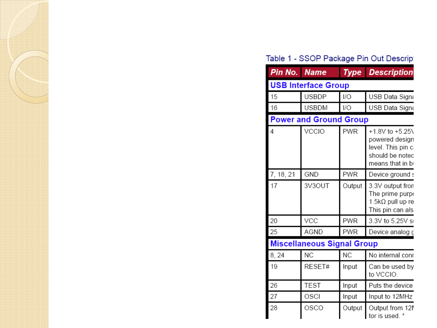
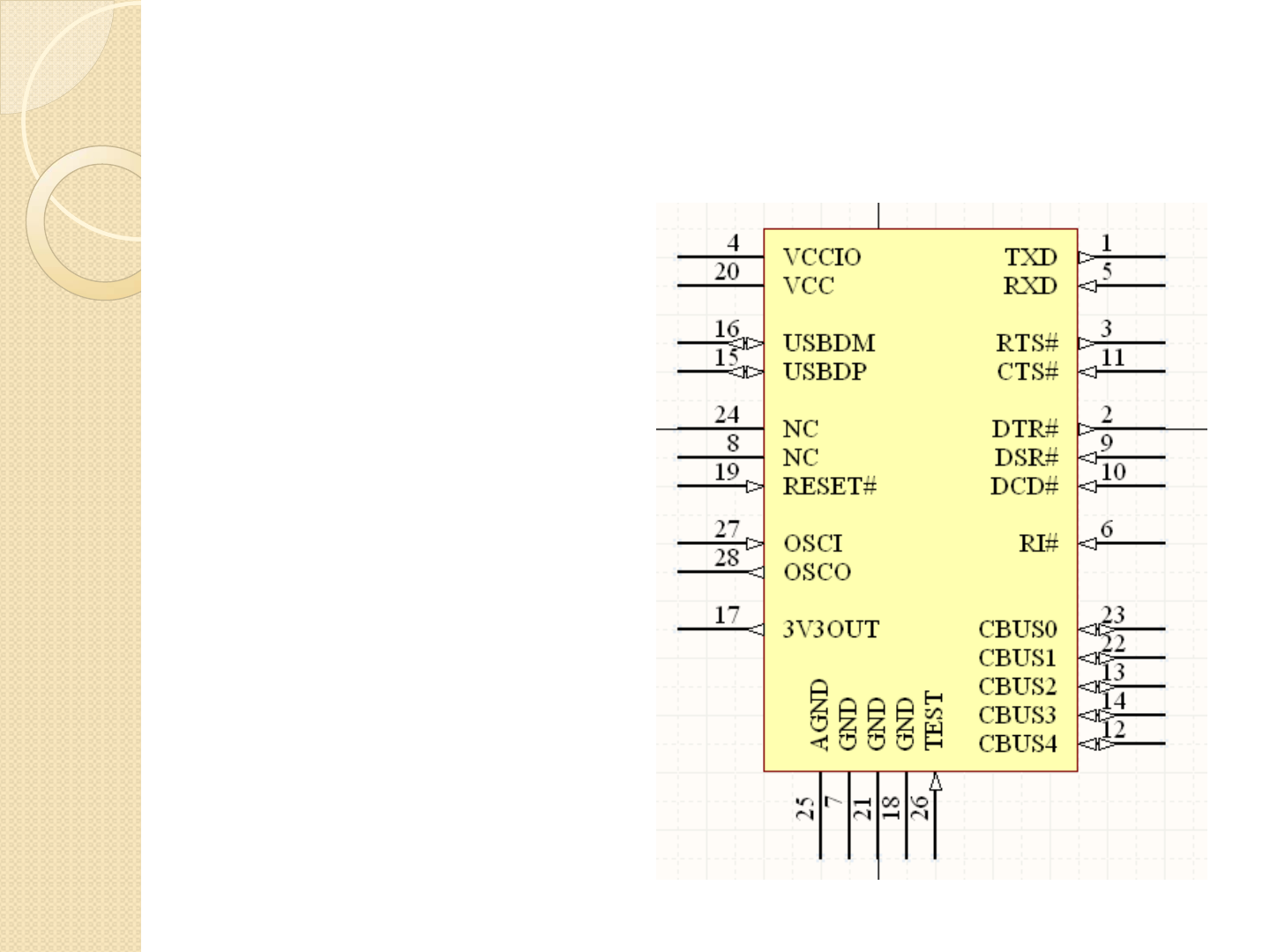
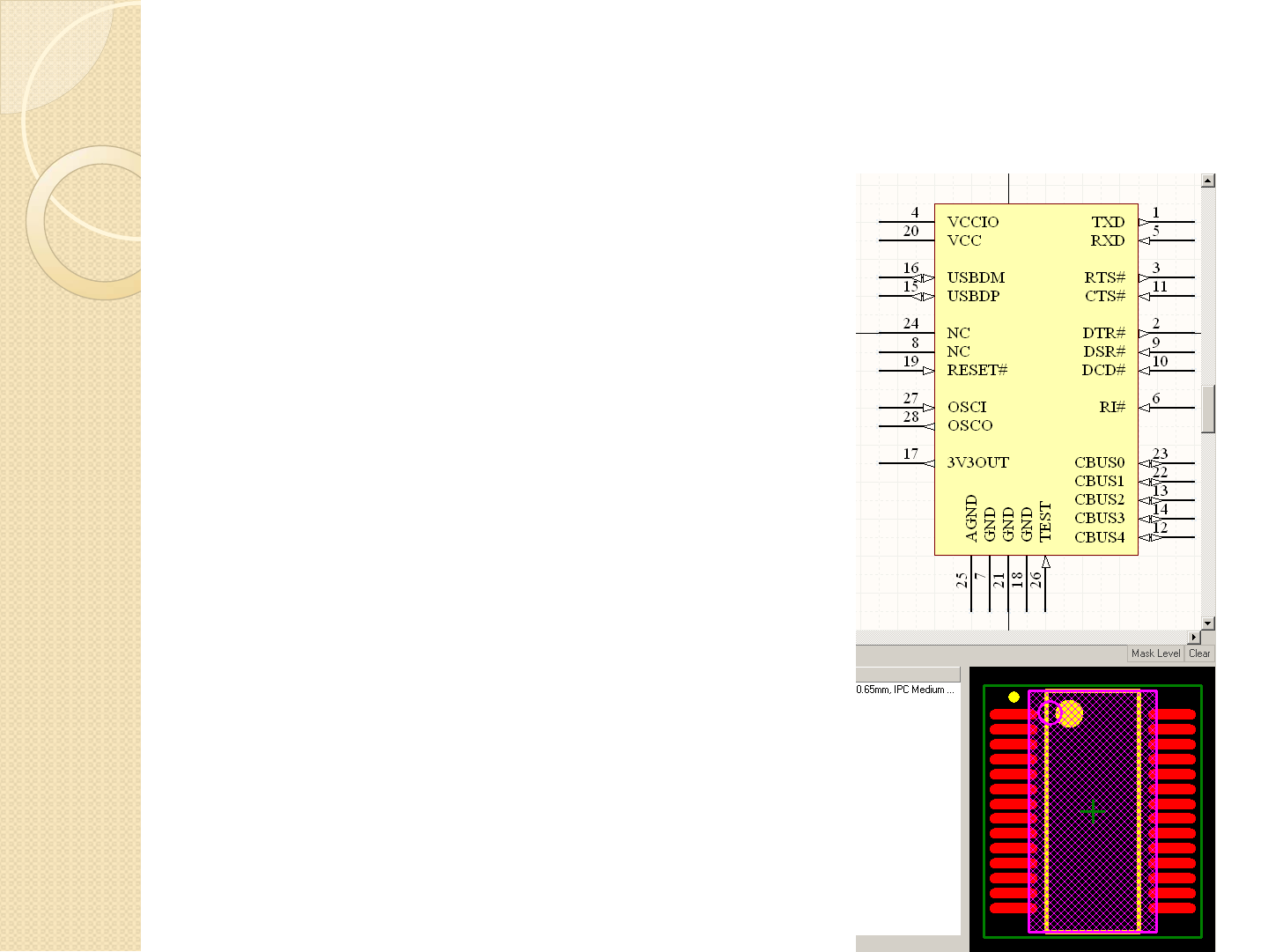
FTDI Chip- FT232 (TSSOP28)
Keep in mind that
we cannot keep the
schematic drawing
of the FT232 and
change only the
footprint because
sometimes pins are
added, removed, or
are different.
Shown to the right
is the pinout of the
device obtained
from the datasheet
Creating a Schematic Part
Create a Schematic
library like we
created a PCB
footprint library
Rename the library
to EE495, and save
in the same
directory as the
rest of your
libraries.
Double click the
schematic library to
open the library,
and then view the
library by clicking
the ‘SCH Library’
tab in the bottom
left of the screen
Creating a Schematic Part
The large portion of the screen is for creating your schematic drawing, the
top left part contains all the parts in the library, the towards the bottom left
is the pins and associated function/name
Creating a Schematic Part
Double click the component and enter the values as shown below

Creating a Schematic Part
Your component should have a descriptive component name and
description such as the one below
Click the ruler tab to see the dropdown list
as shown in the right. This is the main icon we’ll
Be using in creating the schematic drawing
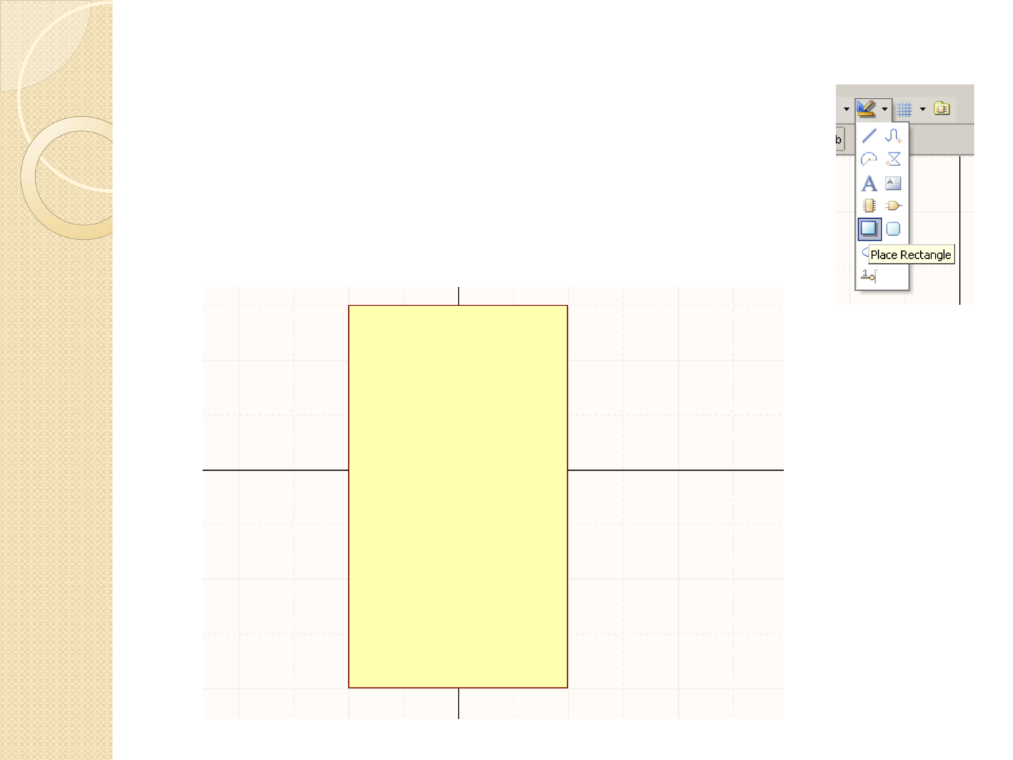
Creating a Schematic Part
Place a rectangle and draw it so it looks like below
(Size doesn’t matter)
Creating a Schematic Part
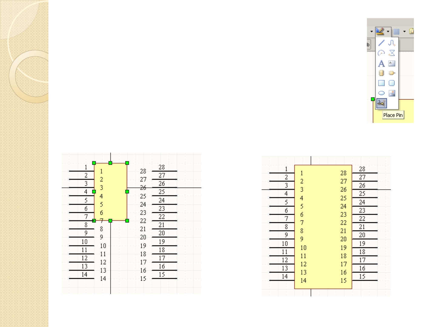
Click the ‘place pin’ and place 28 pins around the rectangle
like below
Click and drag the rectangle to the proper size
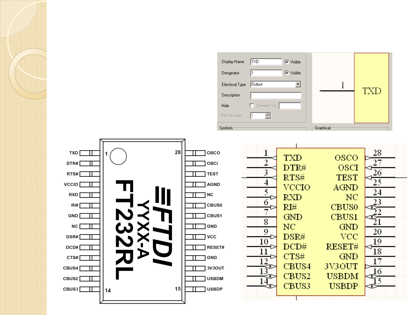
Creating a Schematic Part
Double click Pin 1 and change
display name to TXD,
Change electrical type to
OUTPUT
Creating a Schematic Part
Sometimes the datasheet
will explicitly give the
function of the pin, this is an
added bonus and not usually
given
You must usually define the
pin type from reading the
description of what the pin
does
Defining pin types is not a
necessity, and things may
work fine without defining
them properly, but you
should usually add the pin
function to allow the DRC
to catch your errors.
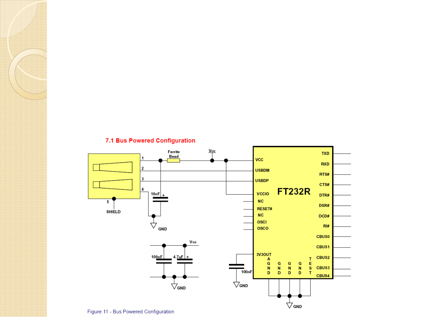
Creating a Schematic Part
There are usually typical applications schematics which will help
you properly use the device.
You should always read each and every pin description to see if
you need to add functionality, but it is always a good starting point
to use the typical application sheet
Creating a Schematic Part
Usually these typical application notes have corresponding notes
associated with it that you should consider.
The following rules for this device are a combination of rules for
the USB standard, and for the FT232
These notes should be regarded as bible, written by people who
understand and have tested their product to death.
Creating a Schematic Part
Now that we have verified that the pins all match the ones in the
datasheet (with the correct pin numbers!) we can move pins
around and make it look more like the application schematic given
This usually allows for a cleaner looking schematic drawing and
much easier to reference the datasheet.
Creating a Schematic Part
Now that we have verified
that the pins all match the
ones in the datasheet (with
the correct pin numbers!) we
can move pins around and
make it look more like the
application schematic given
This usually allows for a
cleaner looking schematic
drawing and much easier to
reference the datasheet.
NOTE: You can also hide pins
from the schematic
document. Double click on
the pin and check ‘hide’
Creating a Schematic Part
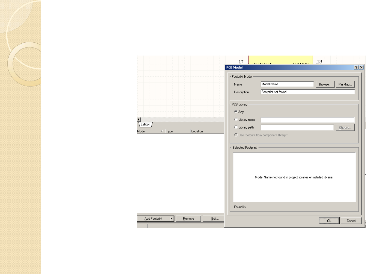
Now we need
to associate the
PCB Footprint
we created
with the
schematic
drawing
Click the ‘add
footprint at the
bottom of the
page
Click ‘browse’
in the ‘footprint
model’ section
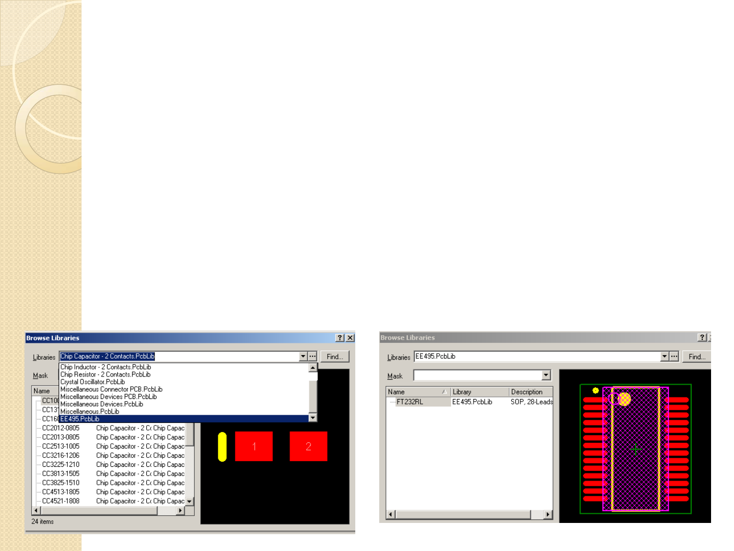
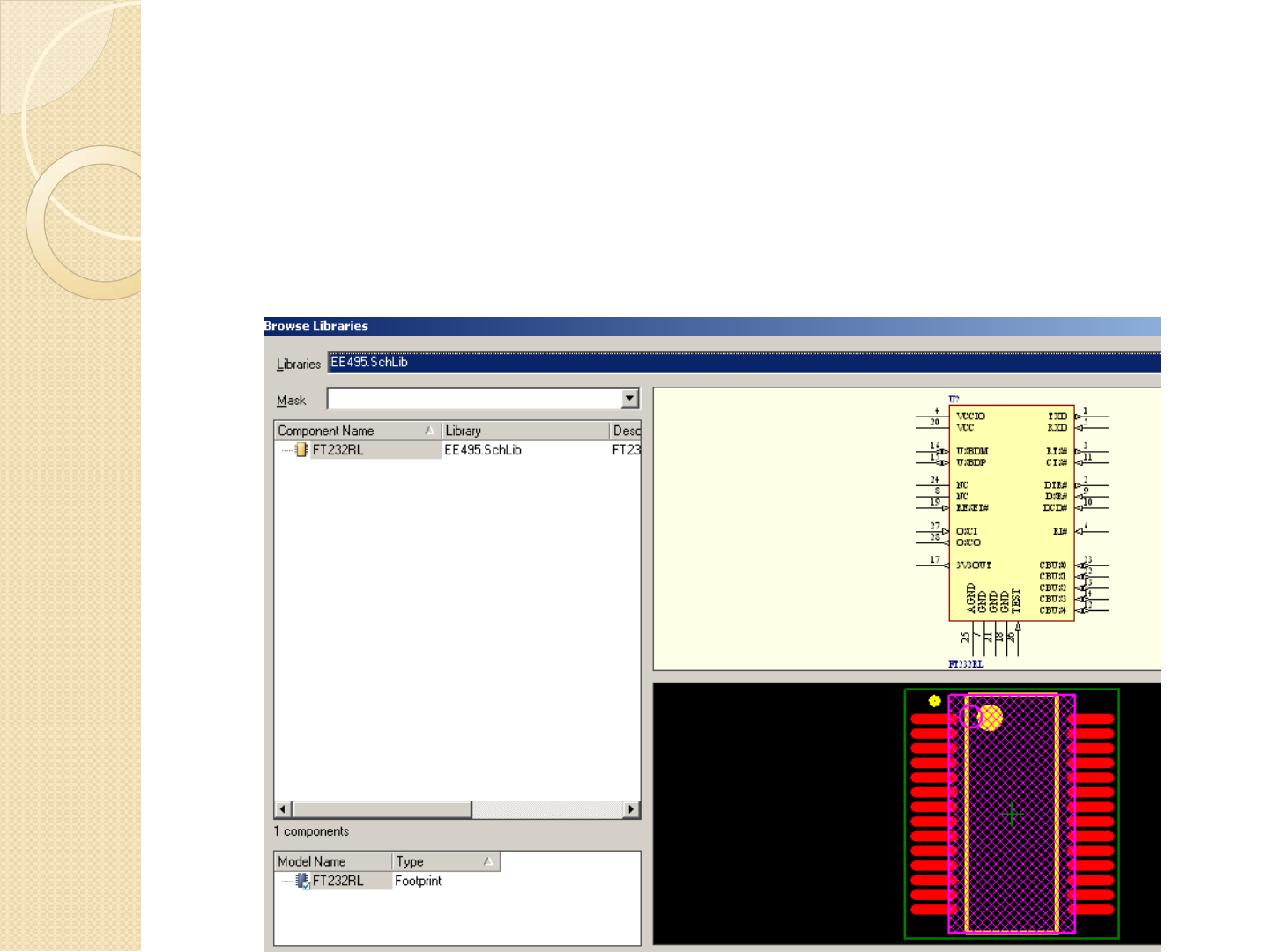
Creating a Schematic Part
Select your EE495 Library from the dropdown list
There is only one part inside your custom EE495 library, so the
choice is easy. Select your part and click ‘OK’
Creating a Schematic Part
In your schematic library, you
should now see the footprint
you created along with the
schematic drawing you made
Finally the part is complete!!
NOTE: This gets much faster
as you do it more, but you can
see the value of the large list
of integrated libraries included
with Altium
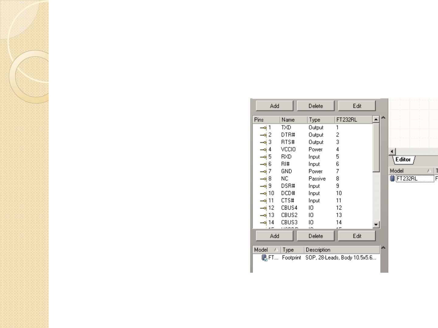
Creating a Schematic Part
One last check is to look at
the left side of the screen. The
first three columns in this case
all refer to data you entered
when creating the schematic
document
The last column (FT232RL) is
the name that you gave the
PCB Footprint
Check and compare that pin 1
on the schematic is linked to
pin 1 on the PCB footprint
Repeat for the rest. If
something doesn’t match,
something went wrong!!

Save the Project
Now is a good time to save
the project and all the
changes you made.
Follow the menu sequence
to the right to save the
project
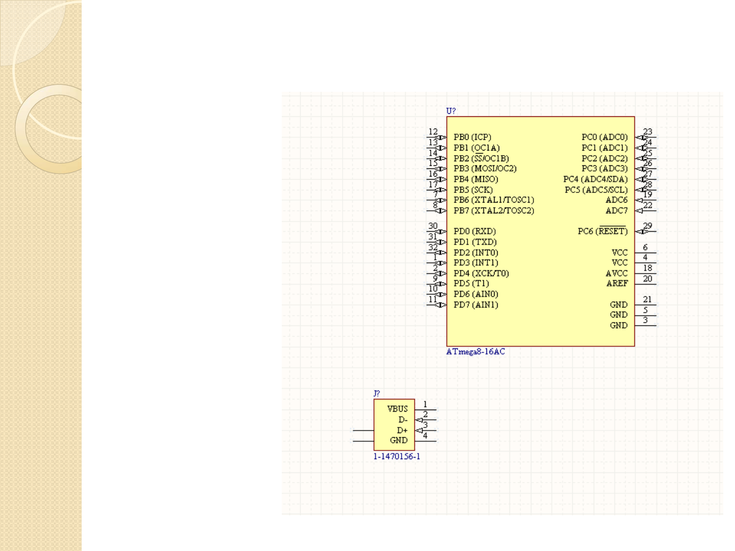
Insert The FTDI Chip
Select your EE495 library, and place the only component in your
library (so far). You should see the schematic drawing and also the
PCB footprint. If not something is wrong
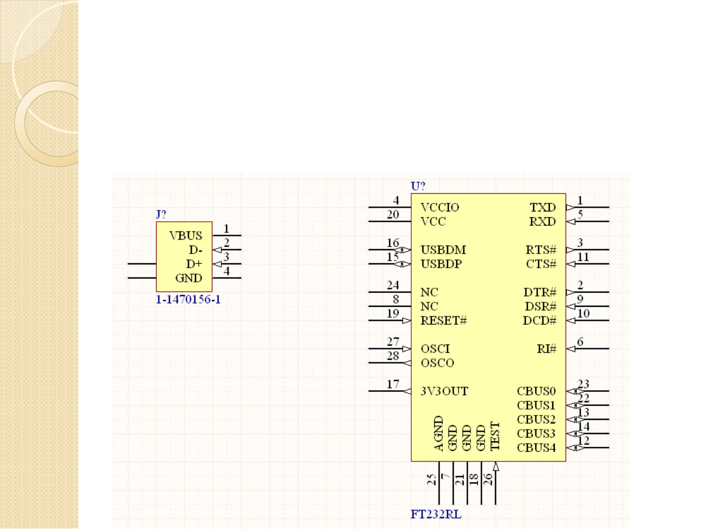
Insert The FTDI Chip
Notice how the rotated and mirrored USB-B connector matches up
perfectly with the FT232 chip. (D- goes to USBDM, D+ goes to
USBD+) This did not happen by chance
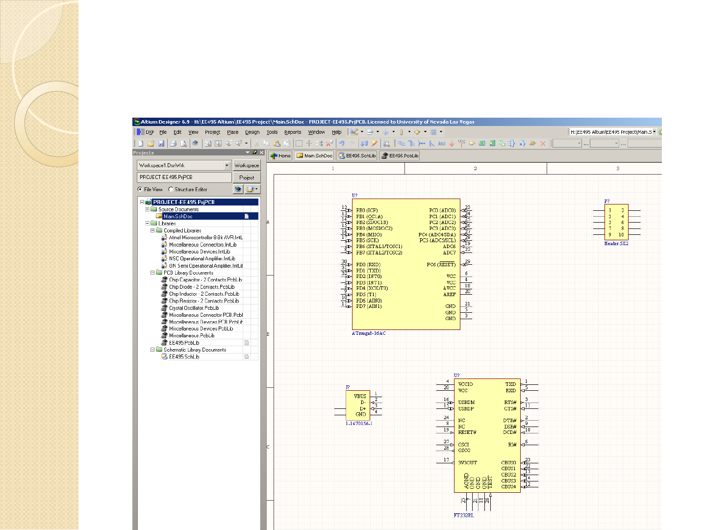
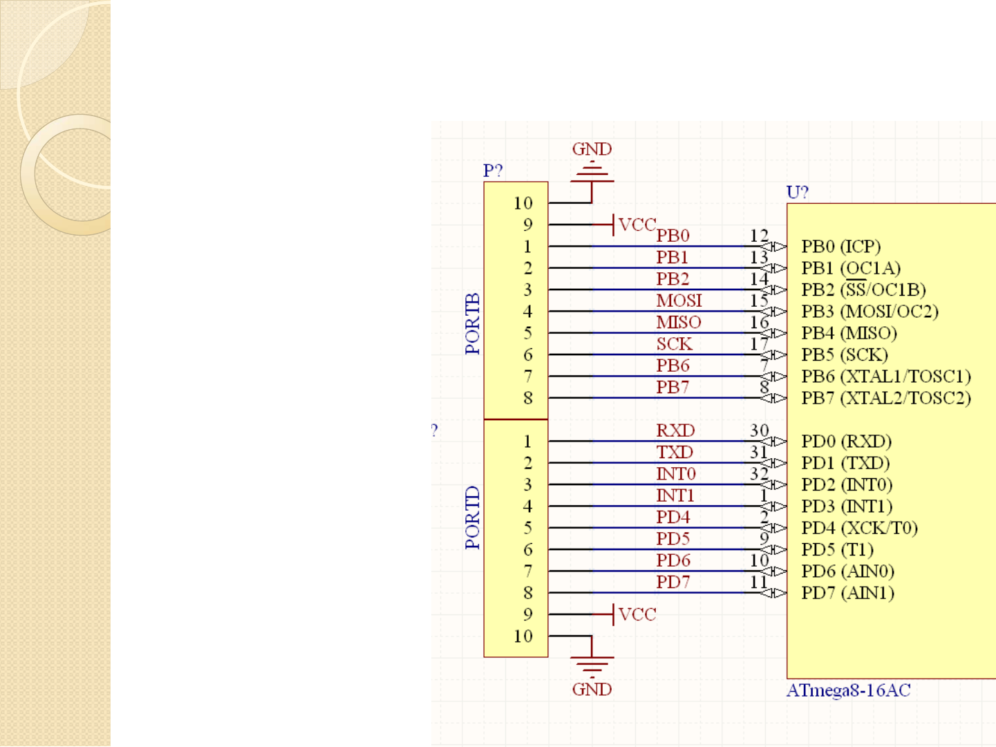
Current Schematic
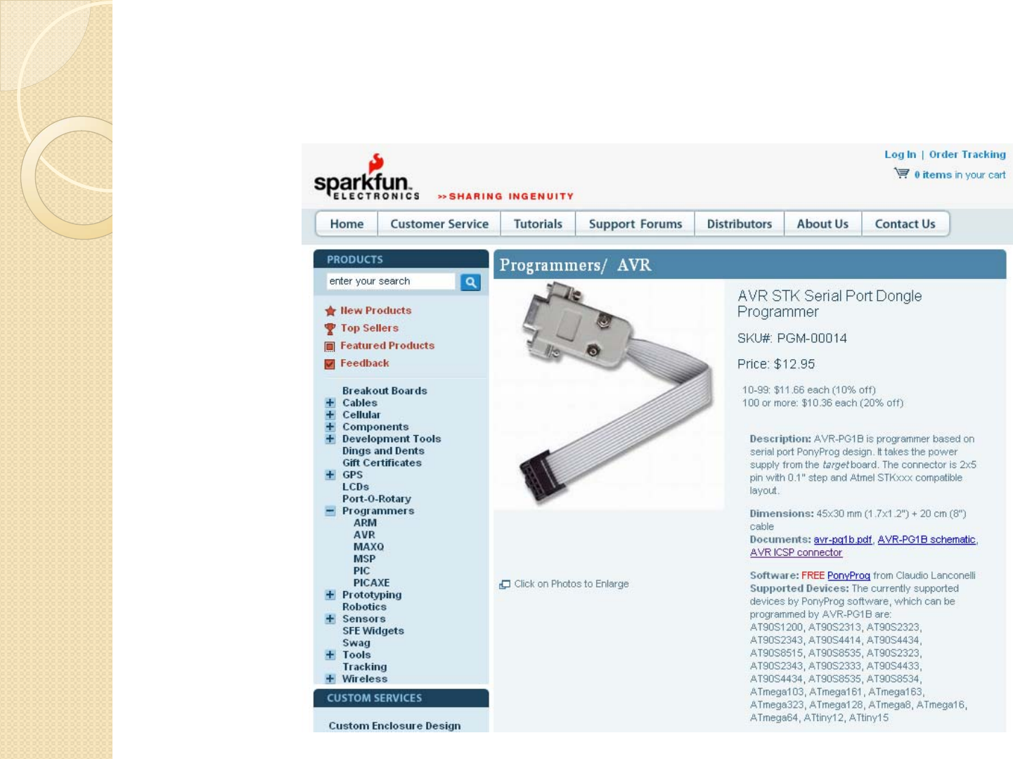
Programming Interface
We need a device
that will send our
compiled HEX
code to the
microcontroller.
This type of
device is called a
programmer
Sparkfun sells
many decent
programmers that
are cheap ($13)
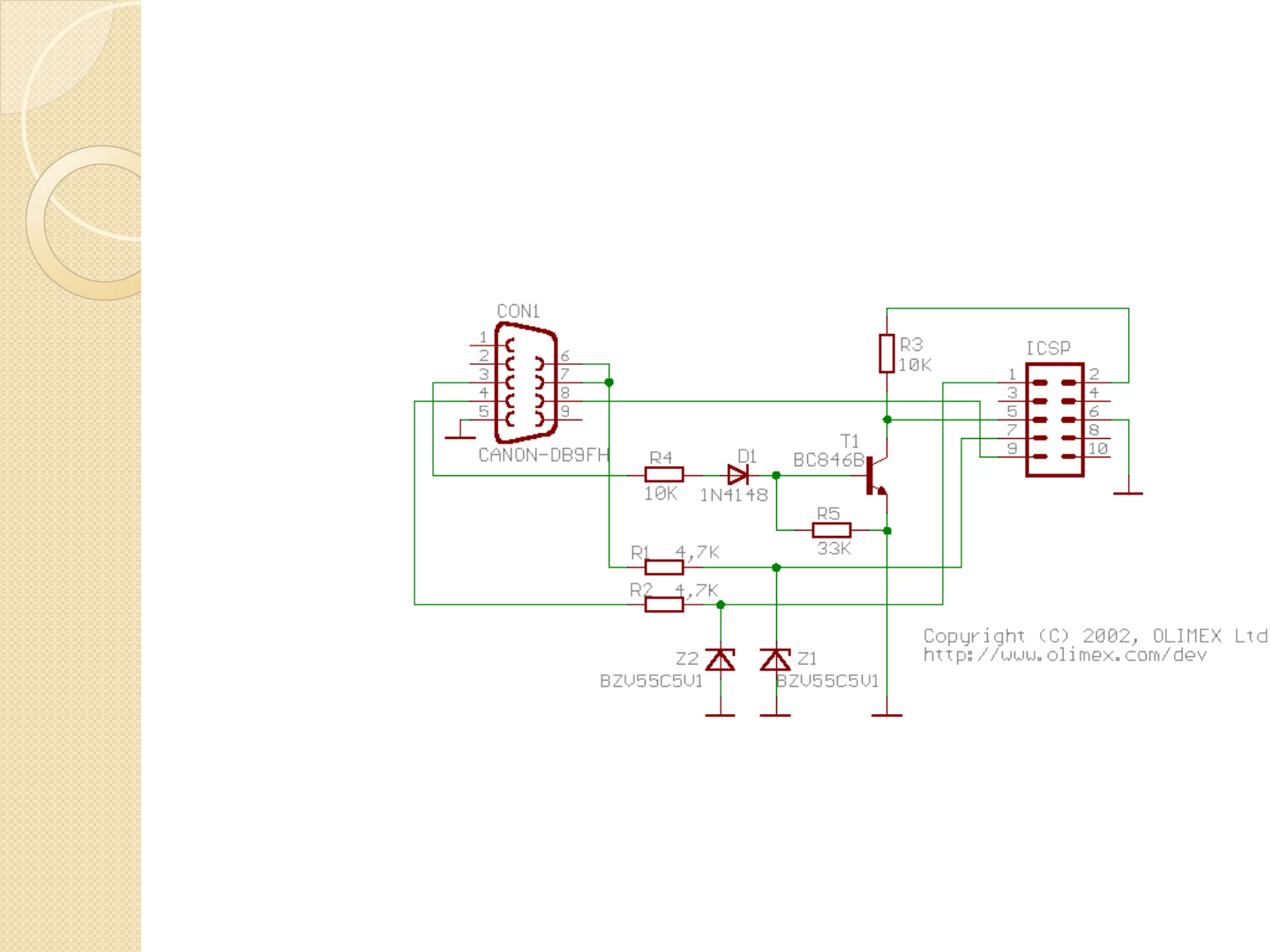
Programming Interface
If you want, you
can see the
schematic of the
programmer, and
integrate it onto
your development
board
As you can see,
this is a simple
device which
would only add a
few components
to your project
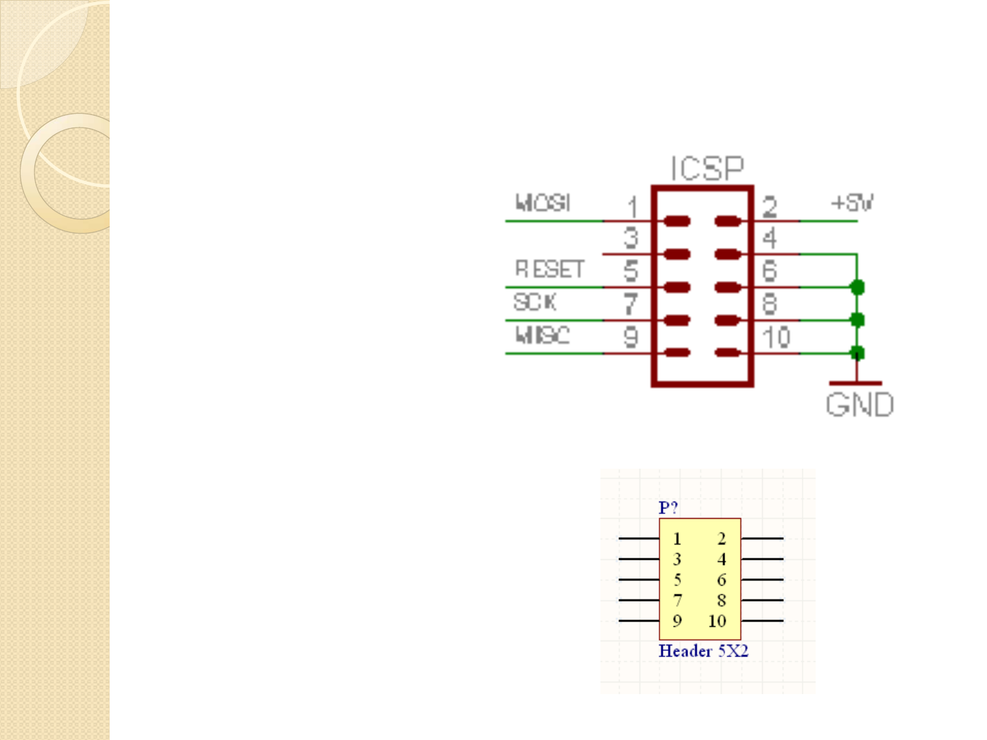
Programming Interface
The specification for the
2x5 header, spaced 0.1”
apart perfectly matches
the connection for the
programmer.
Although you may not
know what these pins
are, we will assign them
to the programmer
header
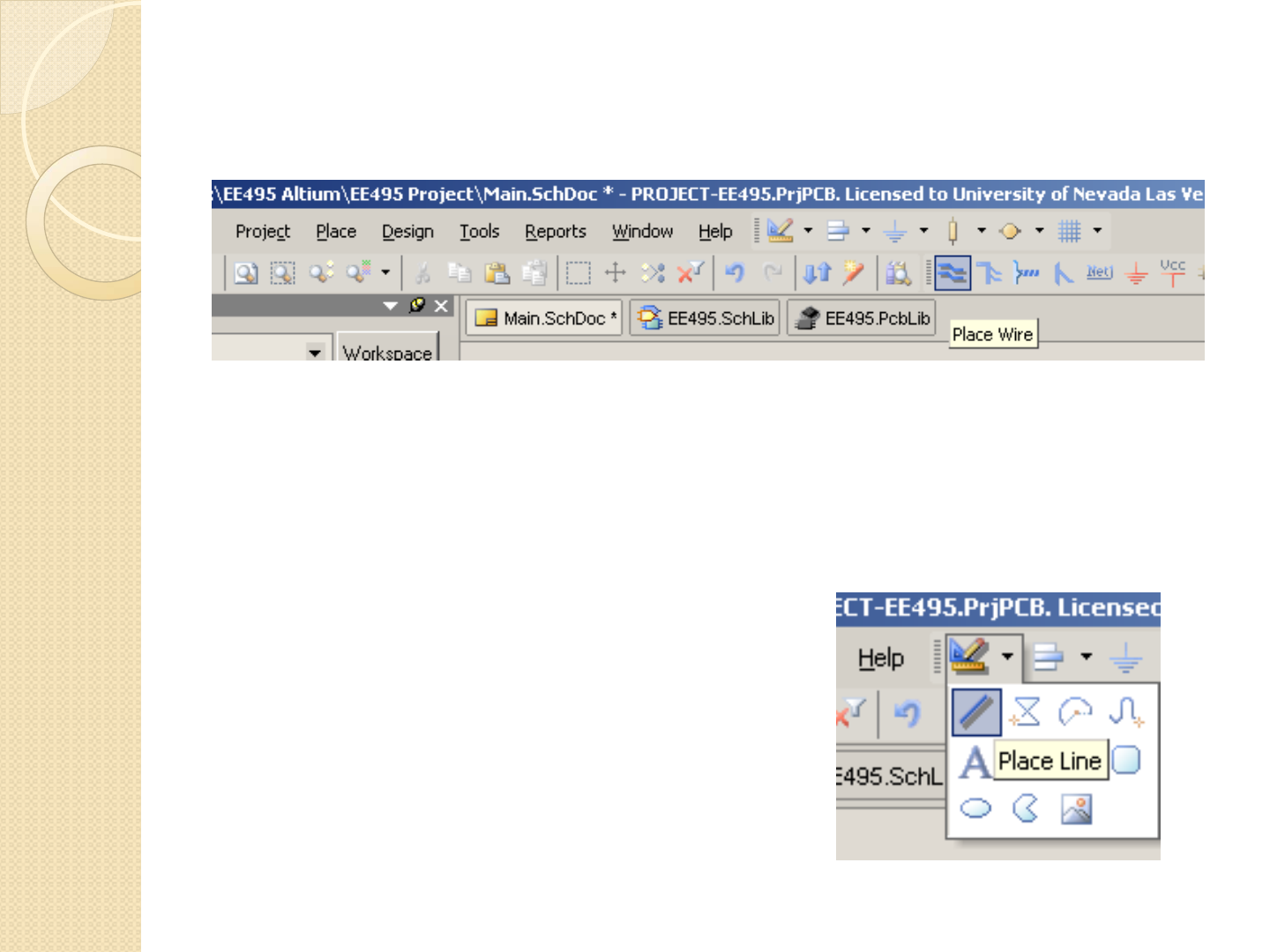
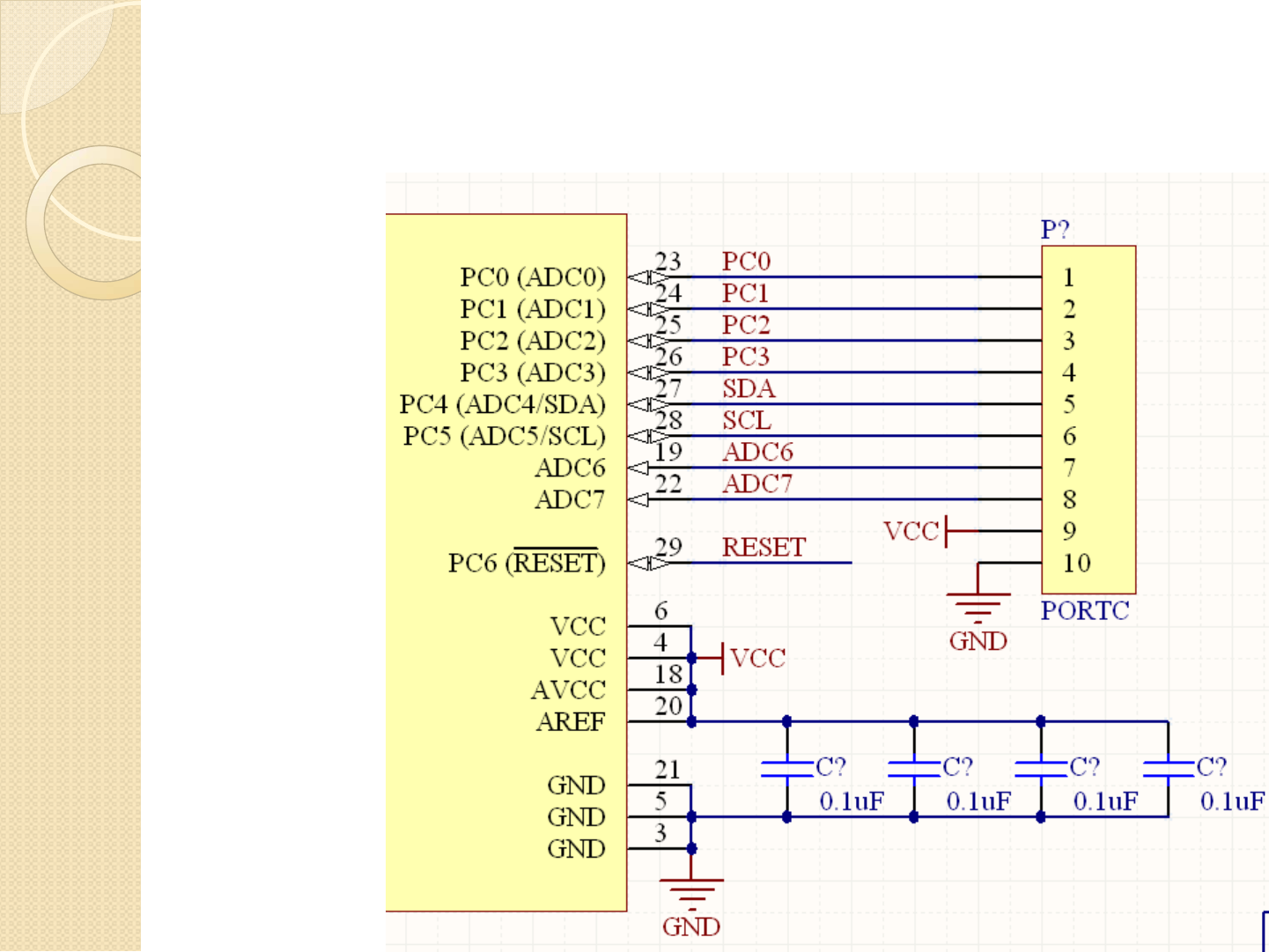
Placing a Connective Wire
Find the icon that looks like the one above, and
click it to place a wire, it will be blue in appearance
WARNING!!: Make sure not to use the
‘place line’ from the drawing box. This
will draw a line that LOOKS like a
connective wire, but a connection
won’t be made
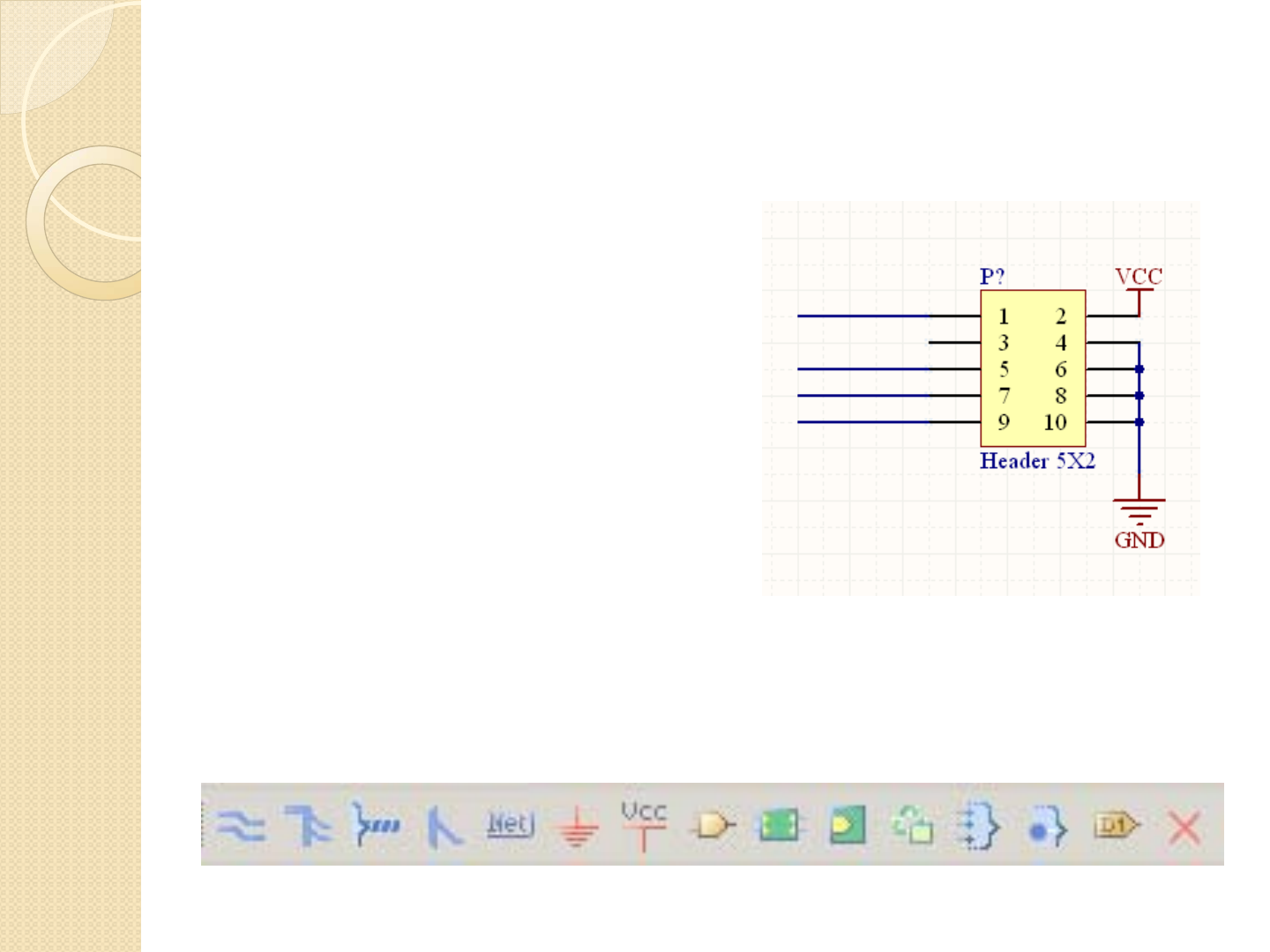
Placing a Connective Wire
Draw wires on the
2x5 header as shown
on the right
Click the GND and
VCC icons from the
wiring menu (shown
below) and make it
look like the diagram
to the right

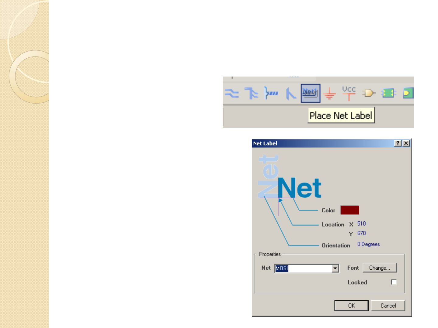
Net Labels
A net label is a method of electrically connecting nets
of the same name
This allows a method to make a connection without
requiring placing a wire
So what’s wrong with running wires ?? It is far more
difficult and more confusing to run wires, especially
when routing a large bus.
Net Labels
Here is a schematic which is very confusing and would benefit from using
net labels
Net Labels
This is a design
that uses direct
wires for short
connections, and
net labels for long
connections.
Notice how the
schematic looks
more clean and
professional.
NOTE: Even if
direct wire
connections are
used, it’s still a
good idea to give
the net a name for
PCB reasons
Net Labels
Another example
Using Net Labels
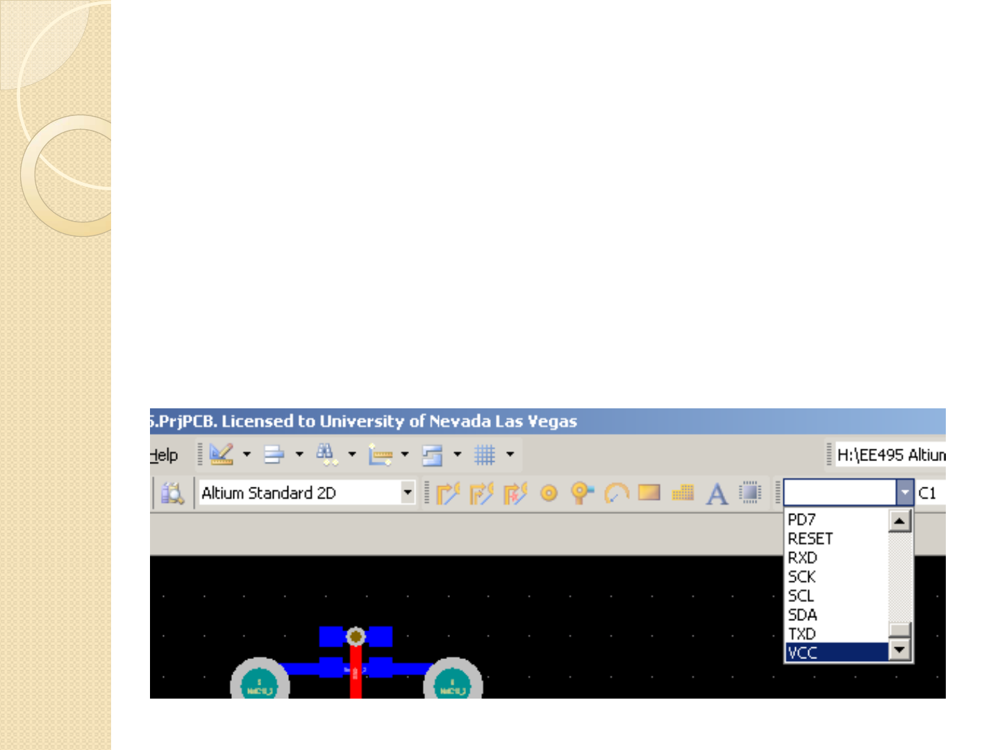
Click on the net label
icon and place the net
label on each of the
wires.
Double click the
rename the net. You
can type in a new net,
or select one from the
drop down list.
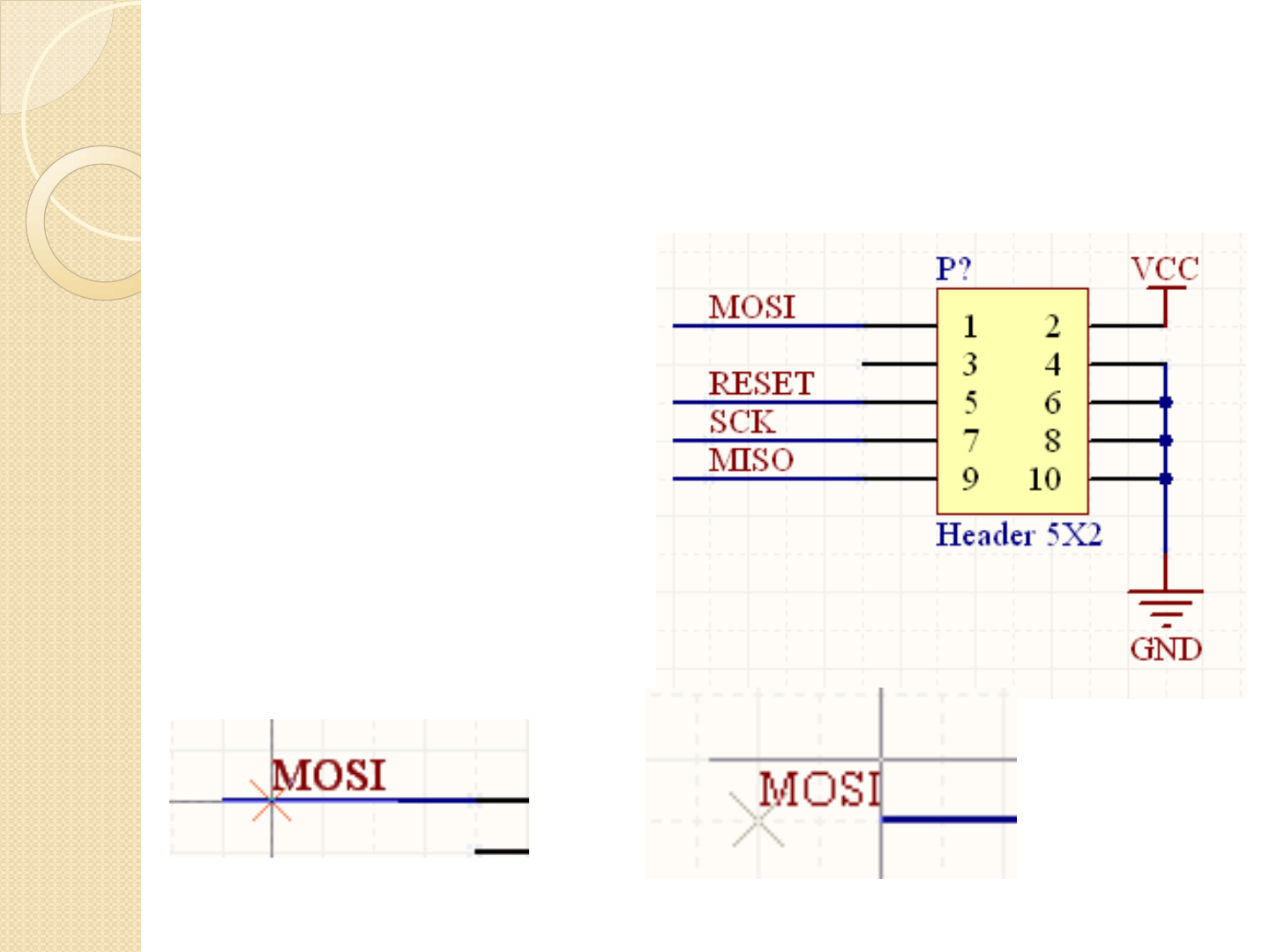
Using Net Labels
Rename the nets to
match the diagram on
the right
WARNING: When
placing netlabels, make
sure there is a red X
at the connection
point. If it is a gray X,
there is no electrical
connection
Good Bad
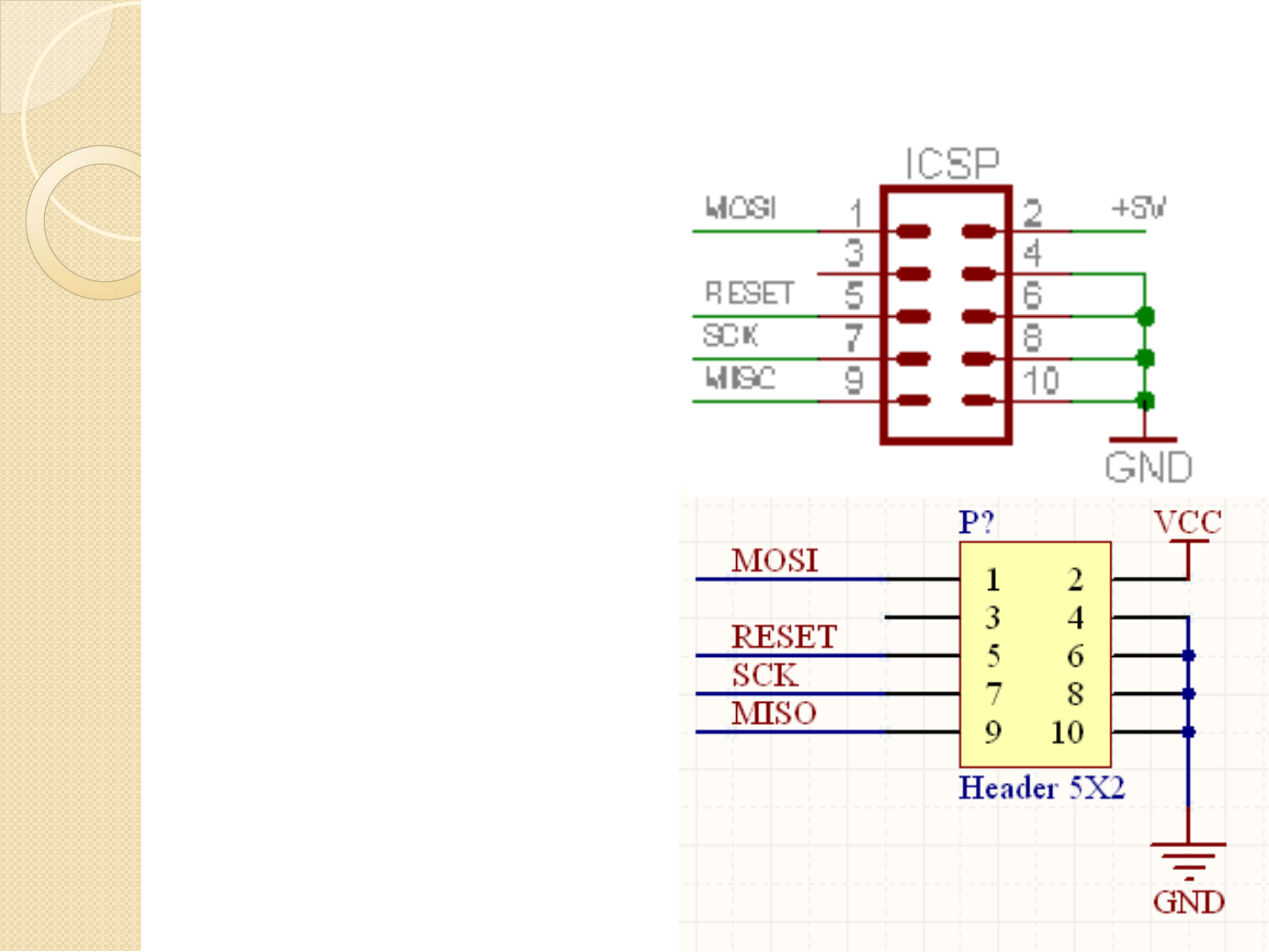
Using Net Labels
Our programming
connector now
exactly matches the
pinout of the
programmer we
selected to buy
Using Net Labels
Make the same net labels on the microcontroller as you did on
the programming connector
Connect the Power and Ground nets as shown below.
The programmer is now electrically connected to the
microcontroller

Using Net Labels
Make the same net labels on the microcontroller as you did on
the programming connector
Connect the Power and Ground nets as shown below.
The programmer is now electrically connected to the
microcontroller
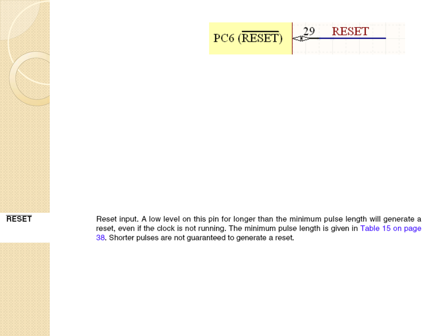
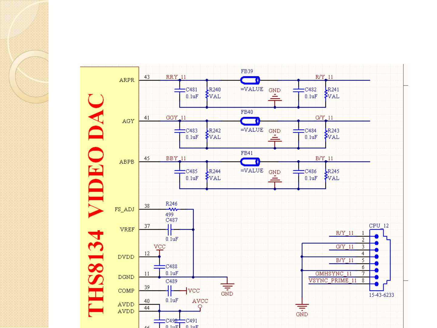
Reset Pin
The reset pin on the microcontroller is an active low
pin, indicated by the bar above the name
This means the device functions normally as long as the
reset line is held high, and will go into reset mode
when brought low (like rebooting a computer)
Looking at the datasheet, we can see characteristics on
each pin and how it works.
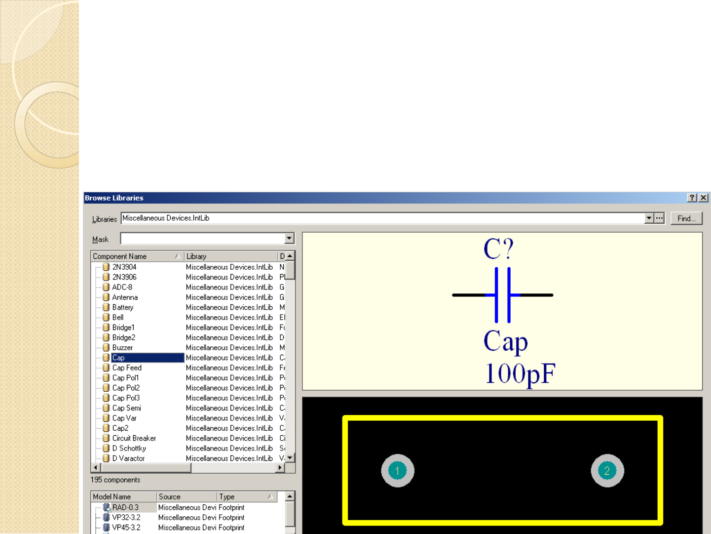
Passive Components
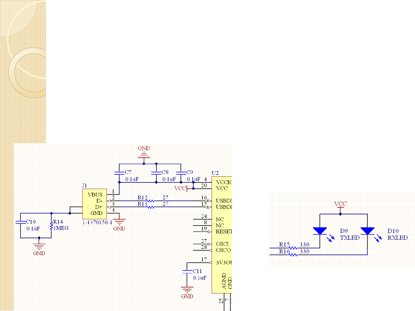
Now we need to add capacitors, resistors, and the LEDs.
Place a part, select the Miscellaneous Devices library, and scroll down to
CAP
Place this part (Don’t worry that the footprint isn’t SMD 0805)
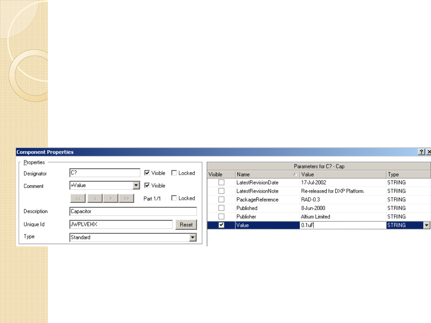
Passive Components
Change the comment to =Value, and uncheck the
visible
Change the value to 0.1uF

Passive Components
In the footprint section,
click the ‘add’ button to
add our 0805 footprint to
this capacitor
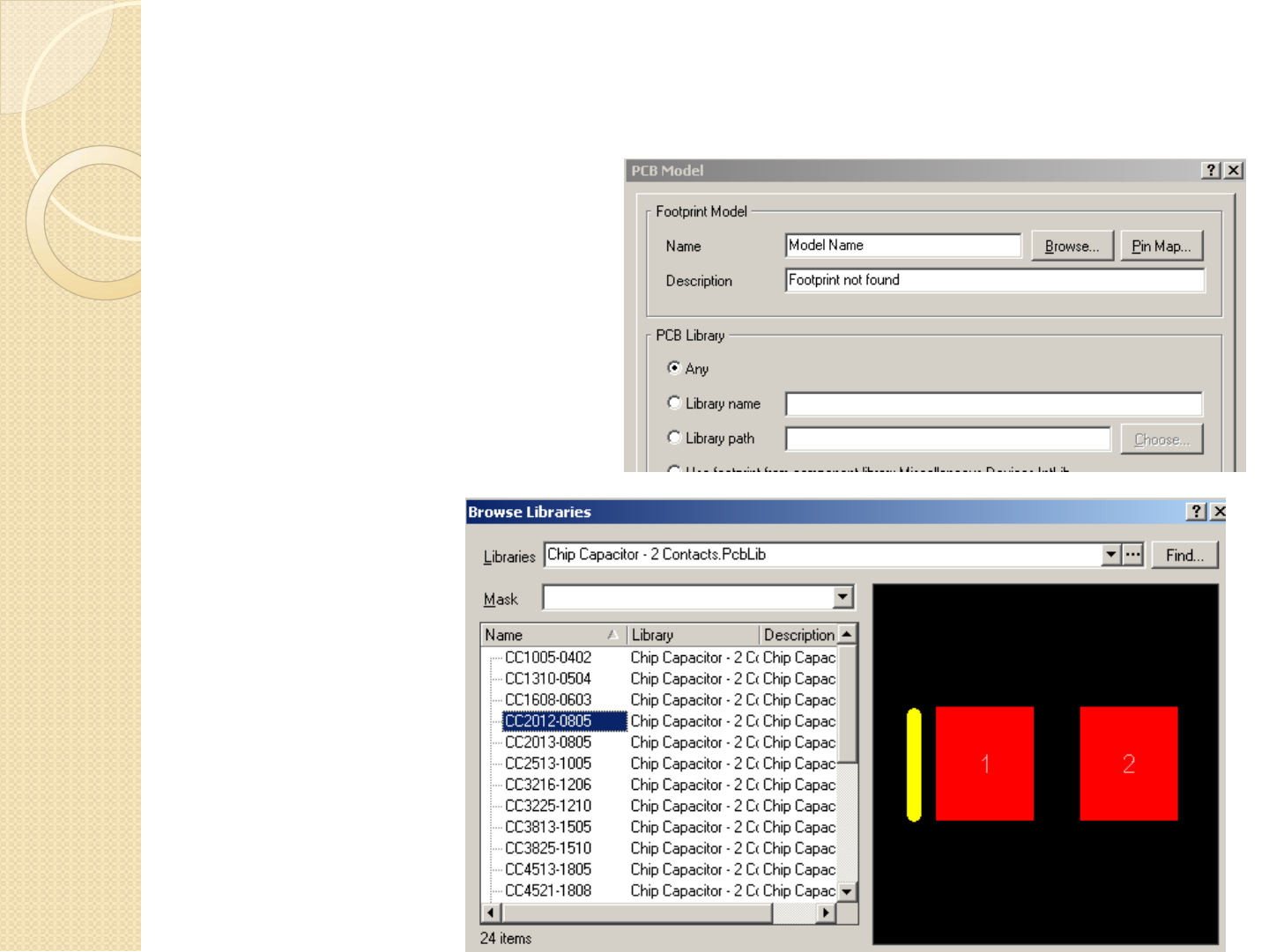
Passive Components
Click ‘browse’
and make sure
‘any’ PCB library
is selected
Select the ‘Chip
Capacitor’
library, and
choose
CC2012-0805
This is code for:
CC= Chip Cap
2012- metric
0805 - empirical
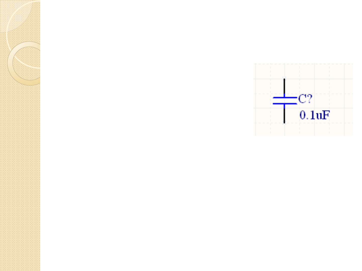
Passive Components
Place the capacitor down. It should look
something like this:
This is now our template for a capacitor,
just copy & paste whenever you need
capacitors and they will all have the same
footprint and settings we set for this
capacitor
Do not worry about the ‘C?’ , we will deal
with labeling the parts at the end. For now
it is a waste of time.
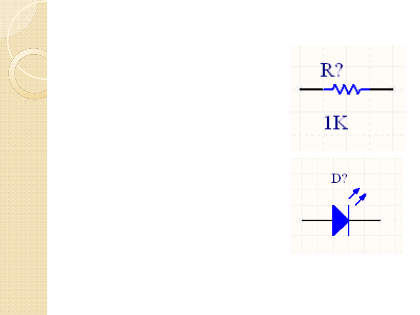
Passive Components
Repeat the same process with resistors and
LEDs (all in same miscellaneous devices
library)
Modify the settings and change the
footprints
◦Diodes are from the Chip Diode library
◦Resistors are from the Chip Resistor library
Complete the Schematic
Copy and paste the
parts as needed to
finish this schematic
◦Highlight, CTRL-C (copy),
CTRL-V (paste)
The parts to the left are
in the miscellaneous
connectors library and
are called HDR1X10
NOTE: I moved the pin
locations on the top
connector, this does not
change functionality at all,
it just allows for a
cleaner schematic. To do
this you must first unlock
the pins. Double click the
part and uncheck the
‘lock pins’ to move the
pins around
Complete the Schematic
It is common
practice to
add a 0.1uF
decoupling
capacitor to
EVERY
power pin
per IC

Complete the Schematic
The reset line must be
held high with external
circuitry.
Using a 10k pull-up
resistor we can keep
this out of reset
NOTE: Try adding a
switch from the reset
line to ground. This is a
hardware reset switch
Complete the Schematic
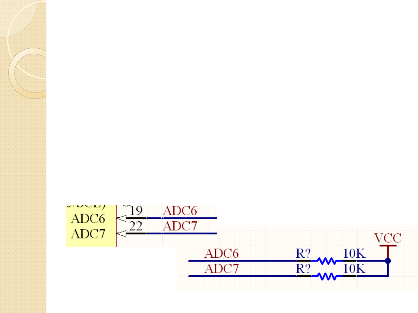
Pins 19 and 22 are INPUT pins on the
microcontroller. These pins are both 10-bit
analog to digital converters. It is necessary to pull
these pins high with pull-up resistors if they are
going to be unused (or possibly unused)
Complete the Schematic
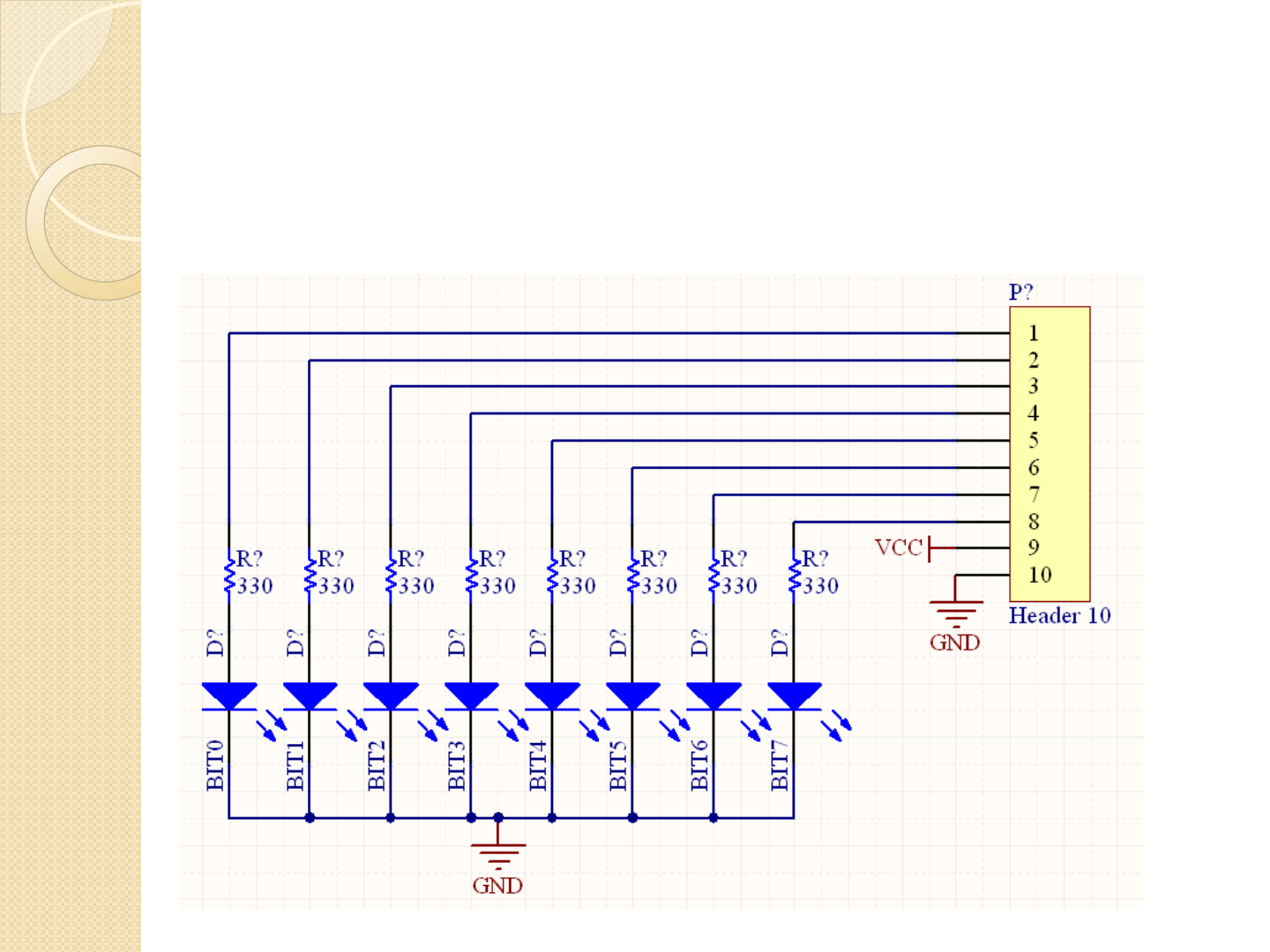
Don’t forget we cannot apply 5V across the LED’s. We must use current limiting resistors
To ensure maximum functionality of the development board, rather than hardwiring the LEDs to a
specific port, we will make it so a user can connect any of the three 8-bit ports

Complete the Schematic
Notice how RXD on the microcontroller connects to TXD on the FT232 chip, This is because two
transmitting signals cannot appear on the same line. One pin is an OUTPUT and one is an input.
Because these pins are correctly defined with both parts, The DRC would catch that if we made
the mistake of connecting TXD to TXD
The LED’s here are optional and light when data is being sent or received
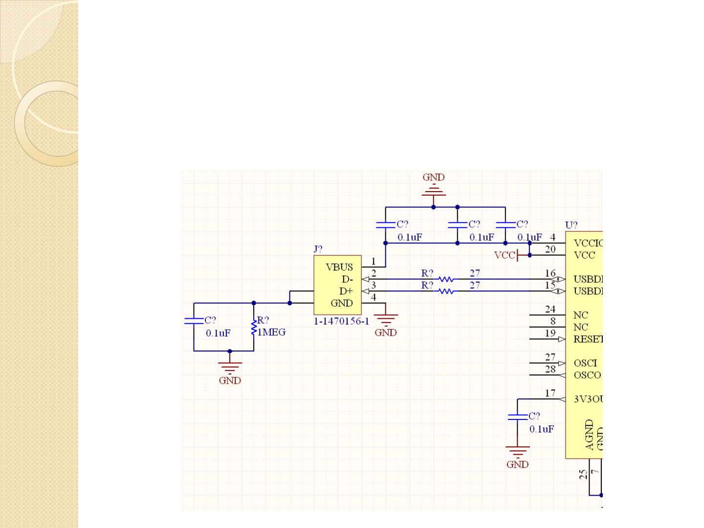
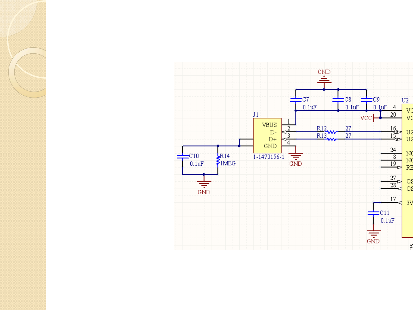
Complete the Schematic
I have altered the typical application circuit for this in two ways:
◦I have added terminating resistors on the differential pair
◦I have not included the ferrite bead , you should include this . You can include a 0805 footprint as a
placeholder for the ferrite bead which comes in a chip
Complete the Schematic
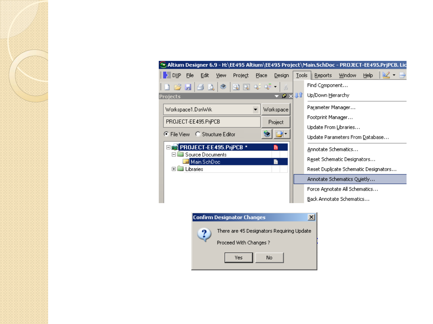
Now that all the
parts are added, we
must label all the
components
Follow the menu
sequence to the right
to label all the parts
automatically
Click ‘Yes’ when
asking to update the
changes
Complete the Schematic
All the parts are
now properly
numbered
NOTE: This step
is necessary
before working
with simulations
or PCB Layout
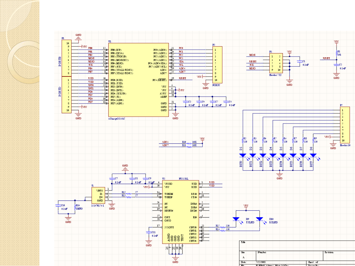
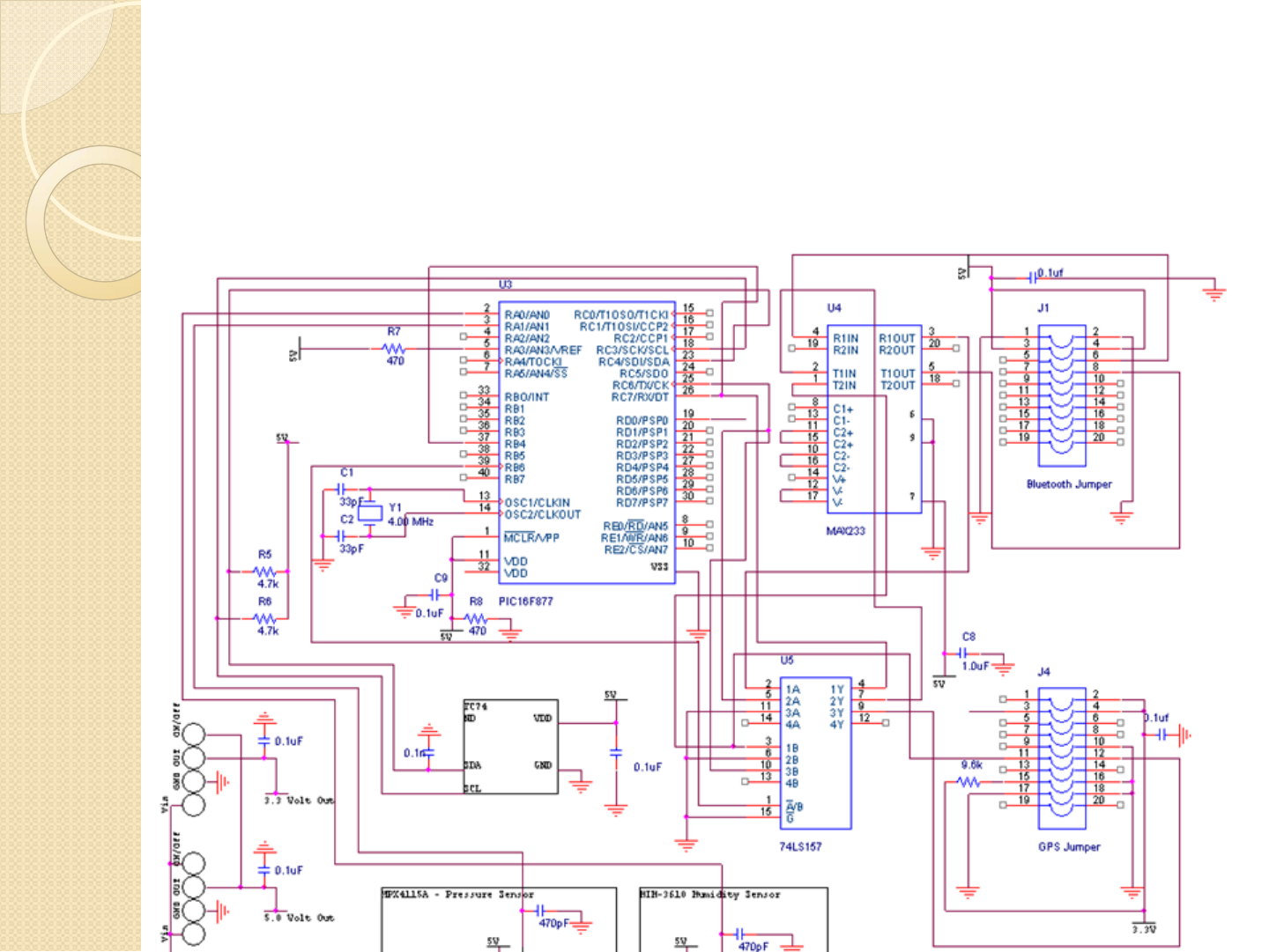
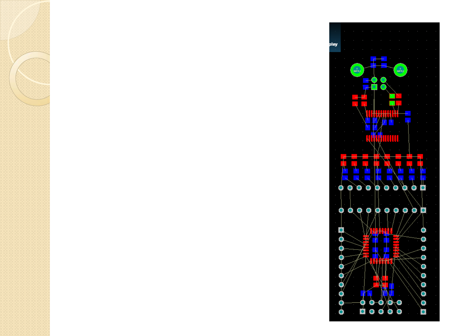
Finished Schematic
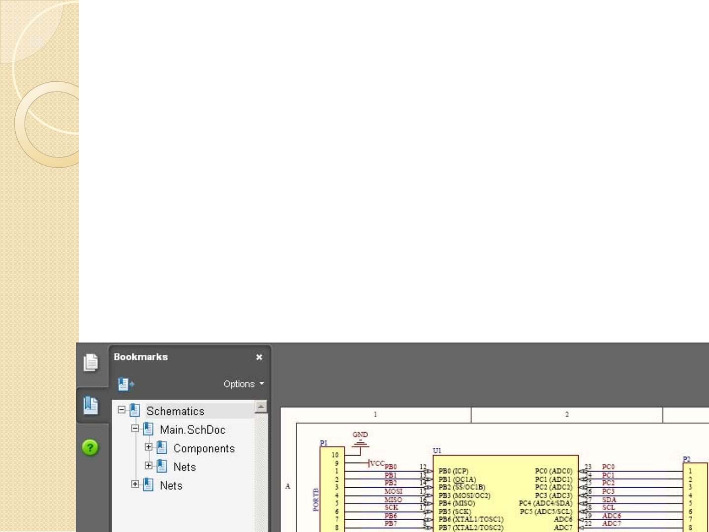
Smart PDF
I have included a Smart PDF of the
schematic for this development board in
the downloads section of the website.
In this PDF file you can select and zoom
in to see parts, nets, etc …

Compiling the Project
Compiling the project is fancy
terminology for error checking.
Error checking, although not required, is a
must before converting the schematic
drawing into a PCB document.
We can’t error check without setting up
rules, so first we must setup rules
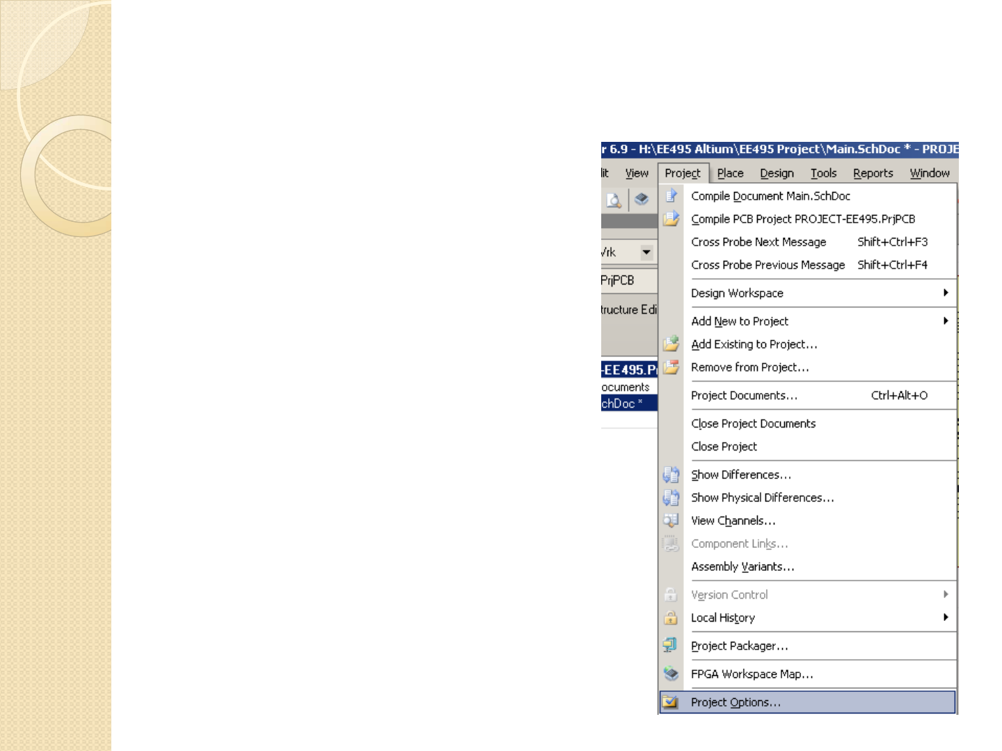
Compiling the Project
Click
◦Project > Project
Options
Compiling the Project
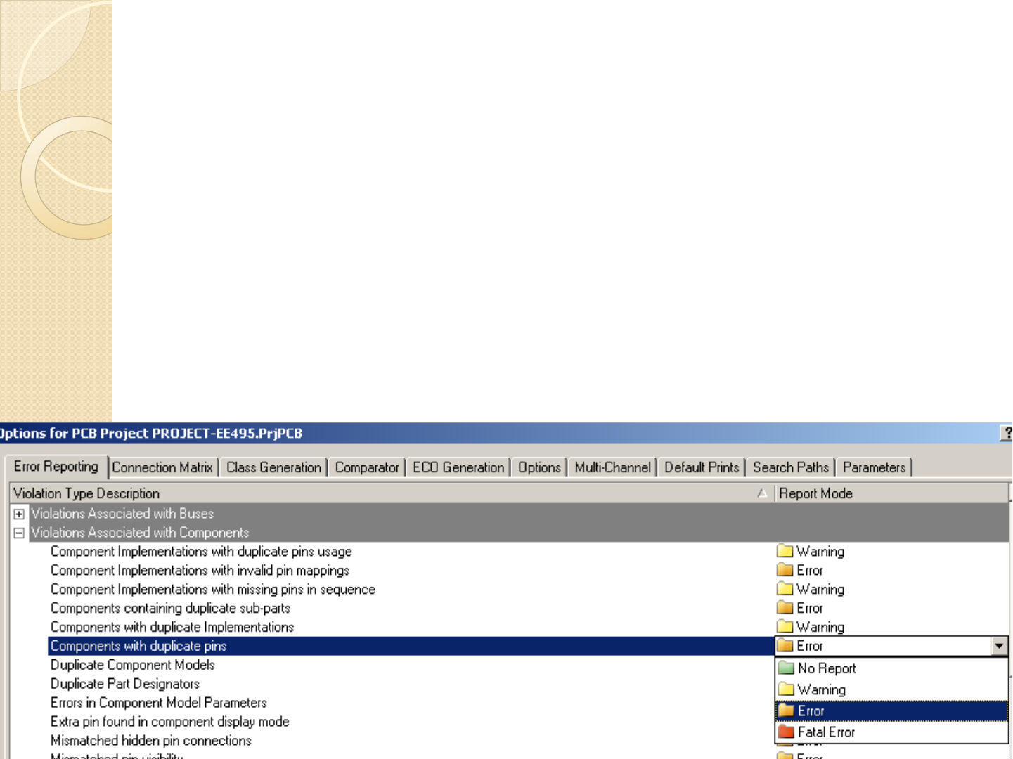
Under the Error Reporting tab, you can
set options for which level of report you
will get.
◦Some errors are serious
◦Some are not a big deal
Compiling the Project
A setting of ‘no report’ is the same as the
software ignoring it
A warning will allow an action, but won’t
be happy about it
Set the ‘Error’ level or above to see
immediate feedback
Fatal error will not allow compilation of
the project
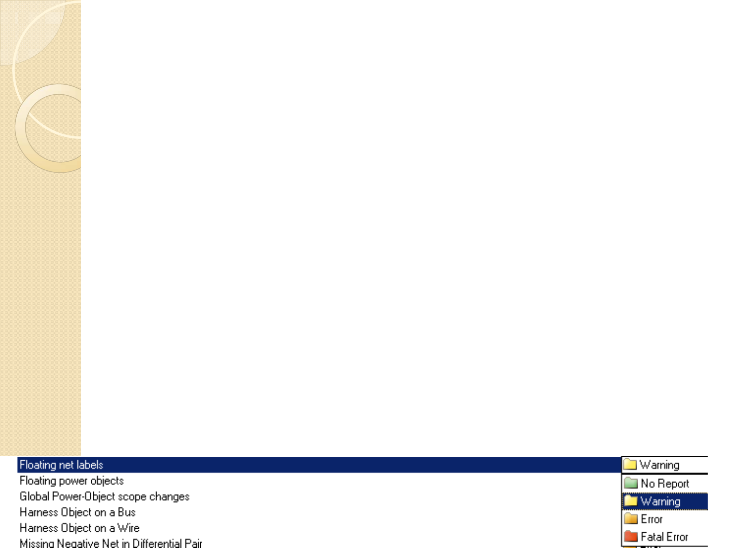
Compiling the Project
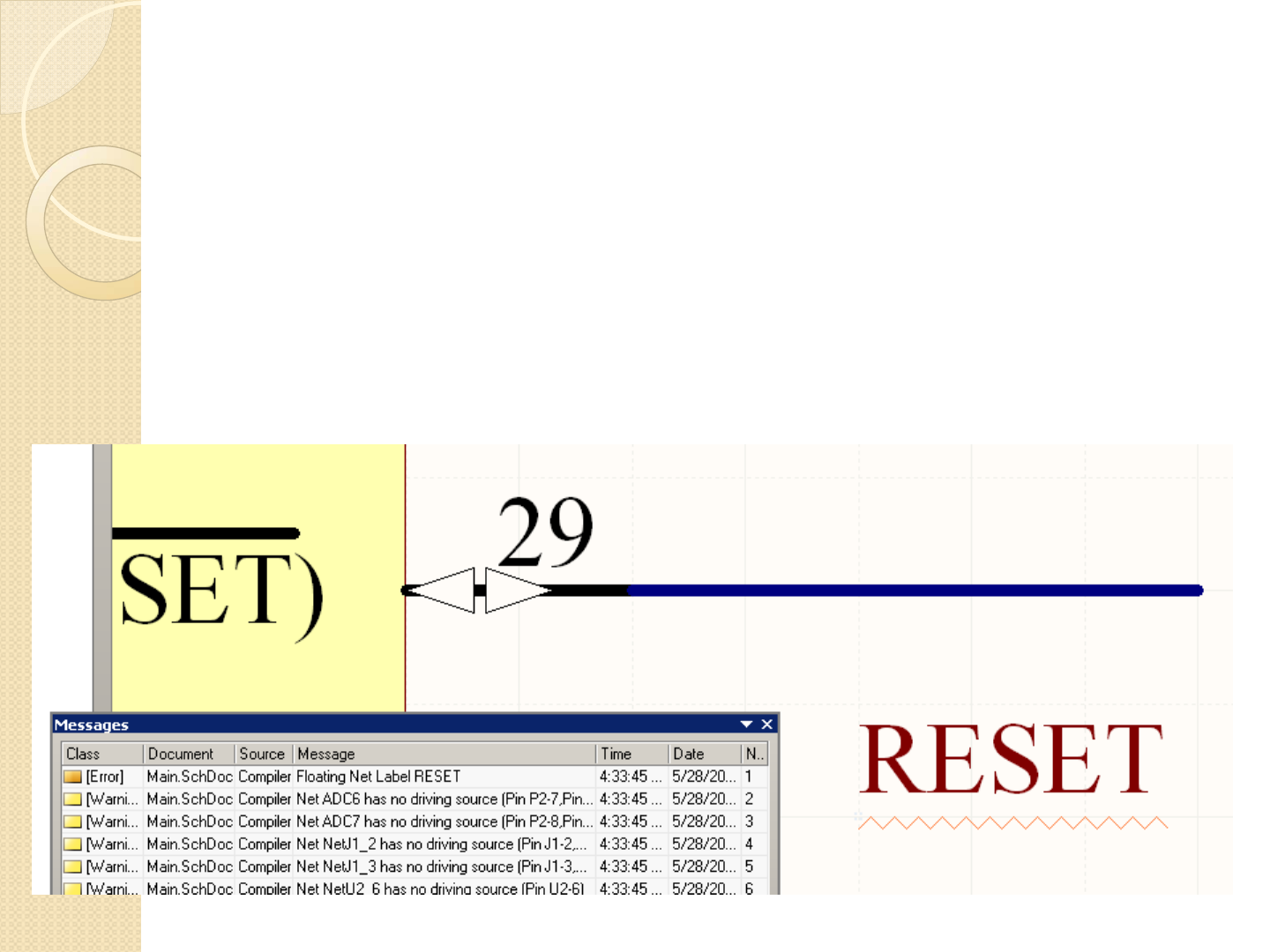
If we set ‘floating net labels’ to error, when we
compile the document, a red squiggly line will
appear beneath the floating label and it will
appear in the compilation report
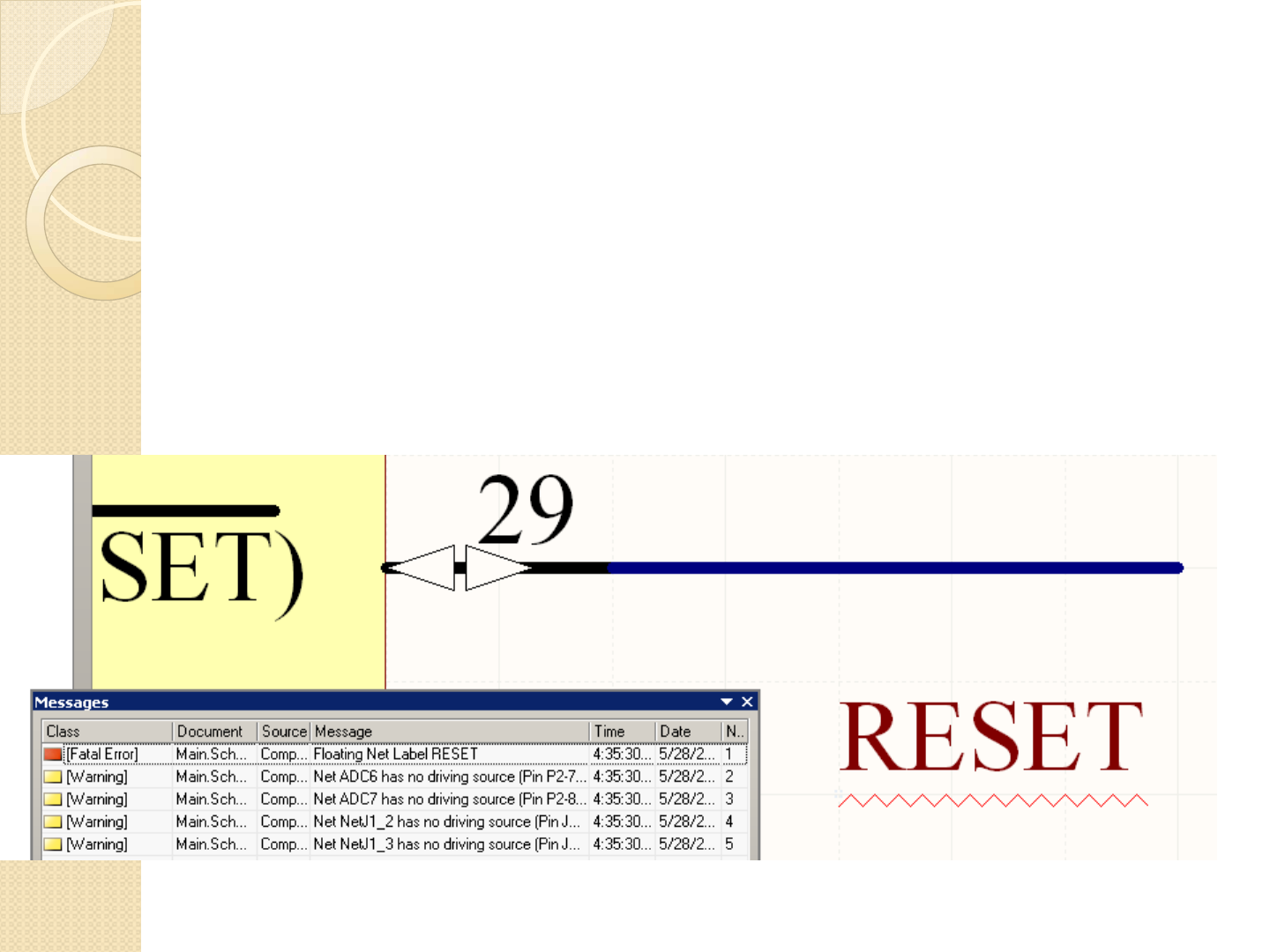
Compiling the Project
If we set ‘floating net labels’ to fatal error,
when we compile the document, a red squiggly
line will appear beneath the floating label and it
will appear in the compilation report.
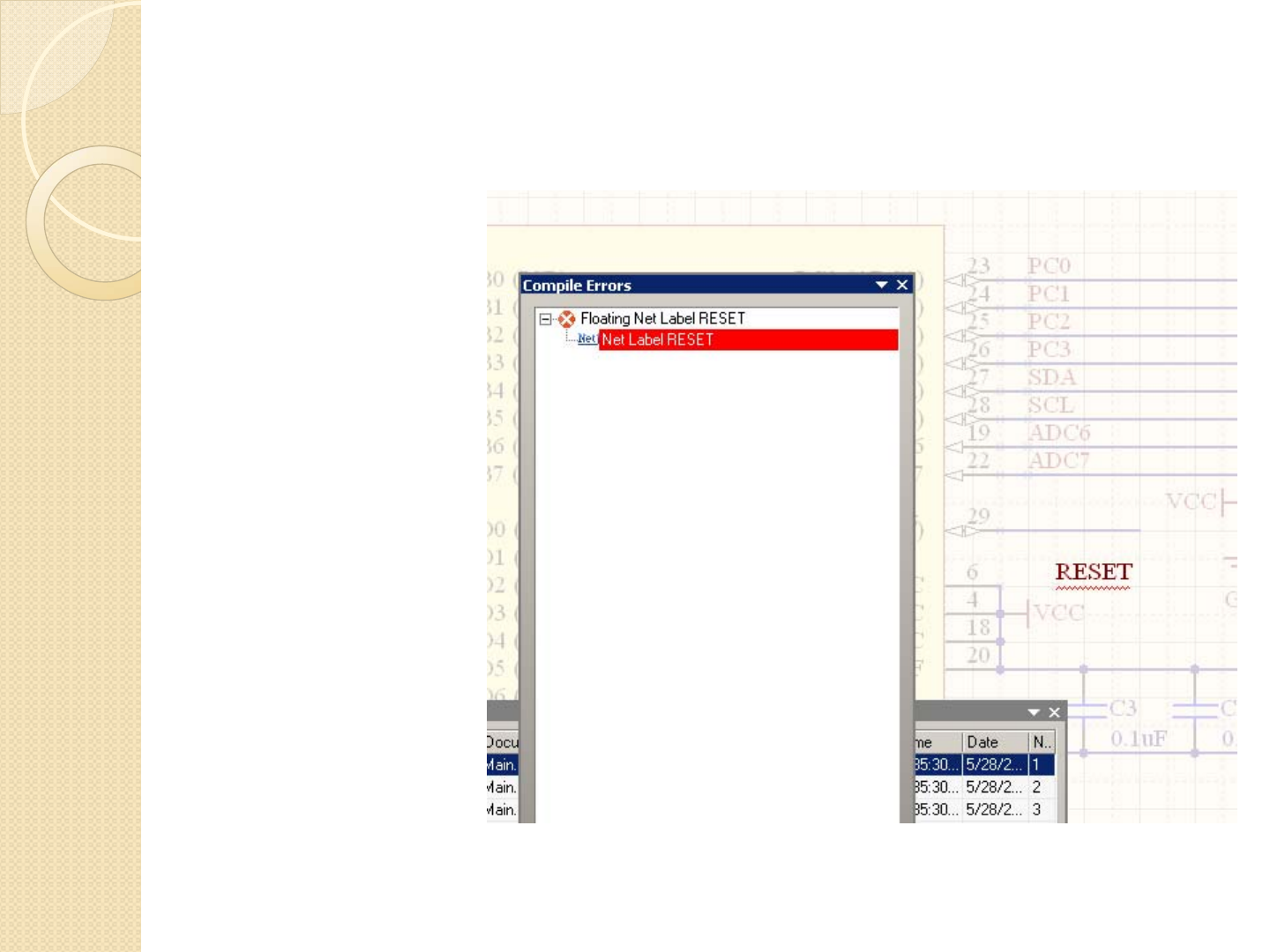
Compiling the Project
If you double-
click the error
in the messages
box, it will
show you
compile errors
From there you
can select the
offending error
and it will dim
the schematic
except for the
error

Compiling the Project
I recommend reading through and setting whatever rules
you think will be appropriate.
Keep in mind it is better to have a compilation report
with a lot of information that you don’t care about than to
have an important error slip past
If there are no errors, you will not get a popup screen
when the compilation is complete

Connection Matrix
The next
tab over is
connection
matrix. This
is a quick
way to
allow
certain
connections
to be made
or denied.
Usually this
doesn’t
need to be
changed

PROJECT UPDATE
DUE WED. 06/04/08 !!
Single page report with the following
◦What have you done for your project- (Be Specific!!) I expect
this to be mostly schematic design and research at this point
◦What do you have left to complete
◦Who is responsible for each part of the design
Schematic Entry
PCB Layout
Implementing Technology (Ex: Mike will be in charge of interfacing the transmitter with a
microcontroller)
◦Exam 1 will be based on this report.
Do not think that if you have done no work yet that you are not responsible for the project or
that your test will be easy. The more work you have done by the 9th, the easier the test should be.
Every group member is responsible if someone is trying to get out of doing work. Do not cover
for anyone else. If I find out that the work was not done by an individual, I will hold the entire
group responsible
If there is a problem with someone not working, you have until the 7th to split from the group and
work on the same project by yourself if you let me know.

Creating the PCB
One of the reasons why it is important to define the PCB footprints
while entering in the schematic is to be able to provide a good estimate
of how much board area you will need.
Generally speaking the following things make production more
expensive
◦Larger area
◦More layers
◦Smaller holes
◦Closer tolerances
◦Closer traces and spacing
◦Thinner or Thicker PCB
Our goal is to keep cost as low as possible while still being able to
transfer a schematic to a functioning PCB.
There are no special characteristics of this design that require any
exotics, and we can use a 2 layer PCB for low cost
Creating the PCB
From the project tab in the
bottom left corner, click the ‘Files’
tab and click the upward facing
arrows until you can see
NEW FROM TEMPLATE
Select PCB Board Wizard
Creating the PCB
You will get a very friendly wizard screen, click next to continue
Creating the PCB
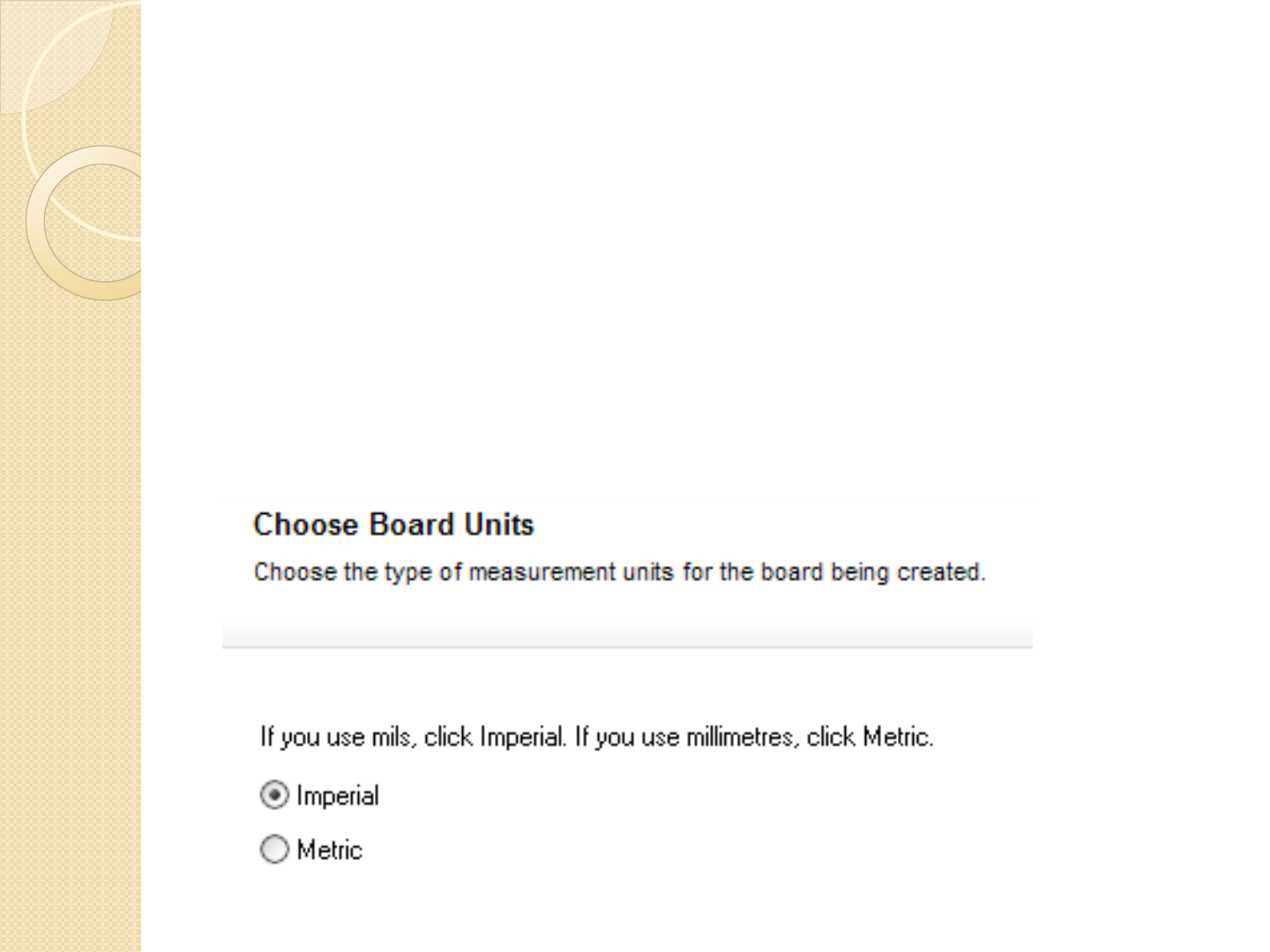
Choose the board units as Imperial for this since that is what most of us are
most familiar with
NOTE: You are not stuck with the choice of units that you choose here. The
units specified are ONLY used for the PCB wizard
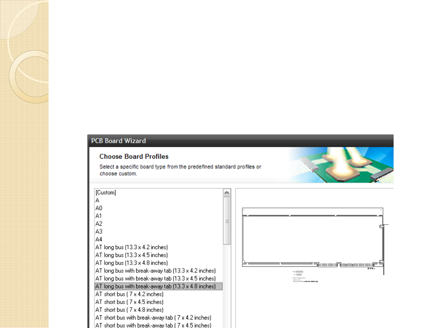
Creating the PCB
There are many predefined templates for exotic designs or standard PCB
computer interface forms, such as AT Bus, PCI bus, Eurocard, and many
others.
Choose CUSTOM (at the top)
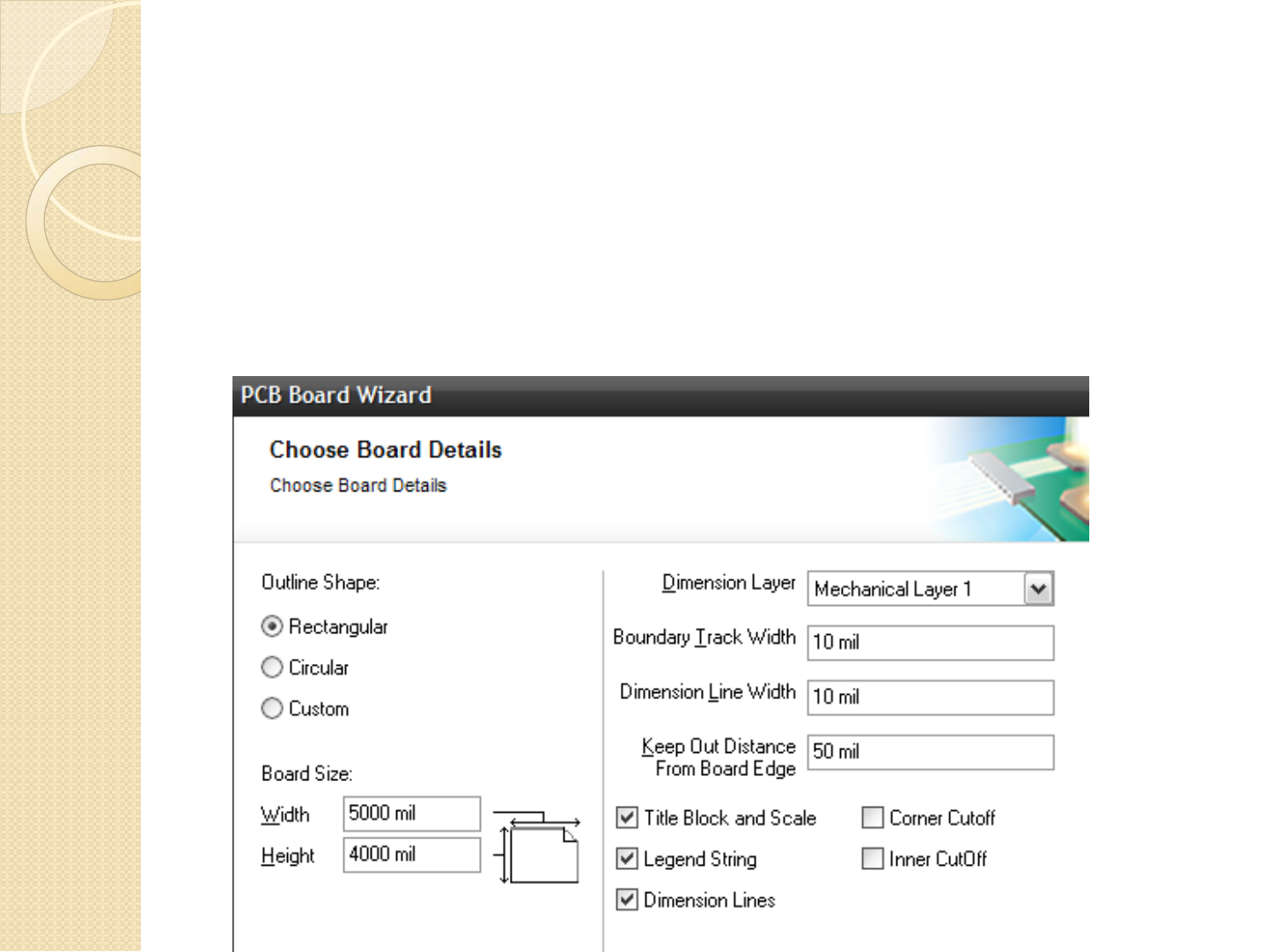
Creating the PCB
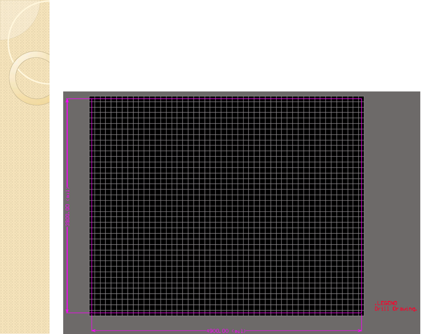
Leave the default settings (Rectangular, 5000 mils x 4000 mils )
The dimensions of the board will be on a generic, information layer
(Mechanical layer) which is used to give information to the board house.
Creating the PCB
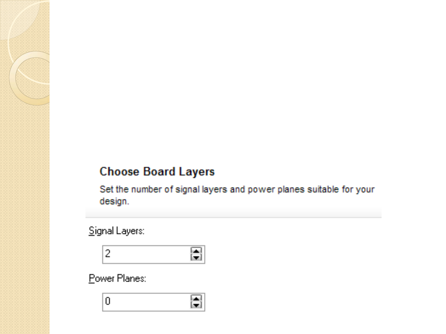
We want to have a two layer board. This is two signal layers (top of board,
bottom of board) and zero internal plane layers, make this change
Do you remember what a power plane is ? How does it differ from a signal
layer? (HINT: you can have signal layers internal or external, and you can have
power planes internal and external)
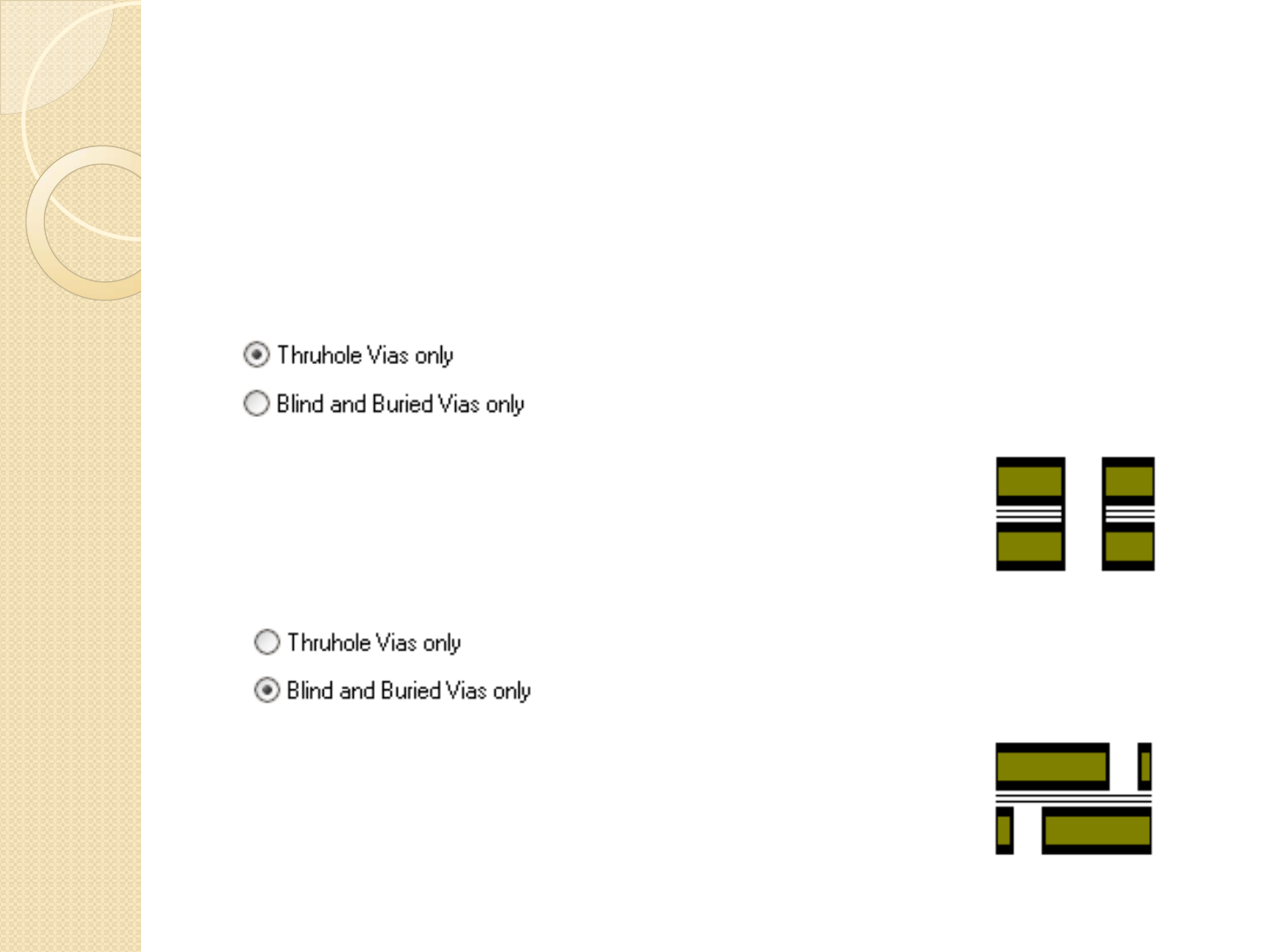
Creating the PCB
Make sure the hole type is set on thruhole vias only
Do you remember what a via is ??
Creating the PCB
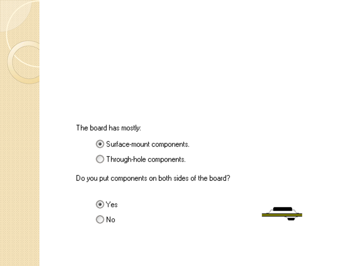
Our board contains mostly surface mount components, so check this option
Choose that both sides of the board can contain components.
NOTE: These settings really don’t matter. They exist for the autorouter which
we will not be using
Creating the PCB
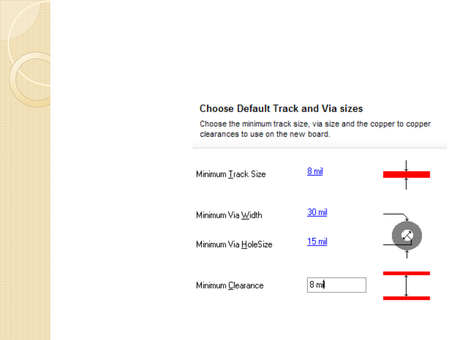
Change track size
(10mils) and trace
clearance (8 mils)
What is the metric
length of 8 mils ????
Change the minimum via
hole size to 15 mils, and
the min. via width to 30
mils
NOTE: ALWAYS be sure
your settings can be
fabricated at a
reasonable price before
setting these values
Creating the PCB
The wizard is now complete and your PCB is created based on the values you
have given.
Creating the PCB
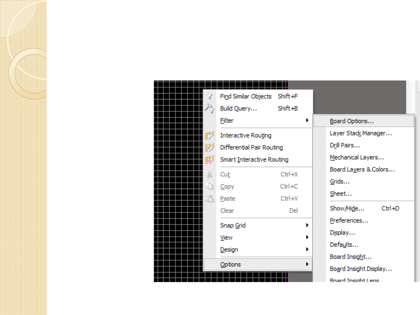
Right click on
the PCB >
Click ‘Options’
Click ‘Board
Options
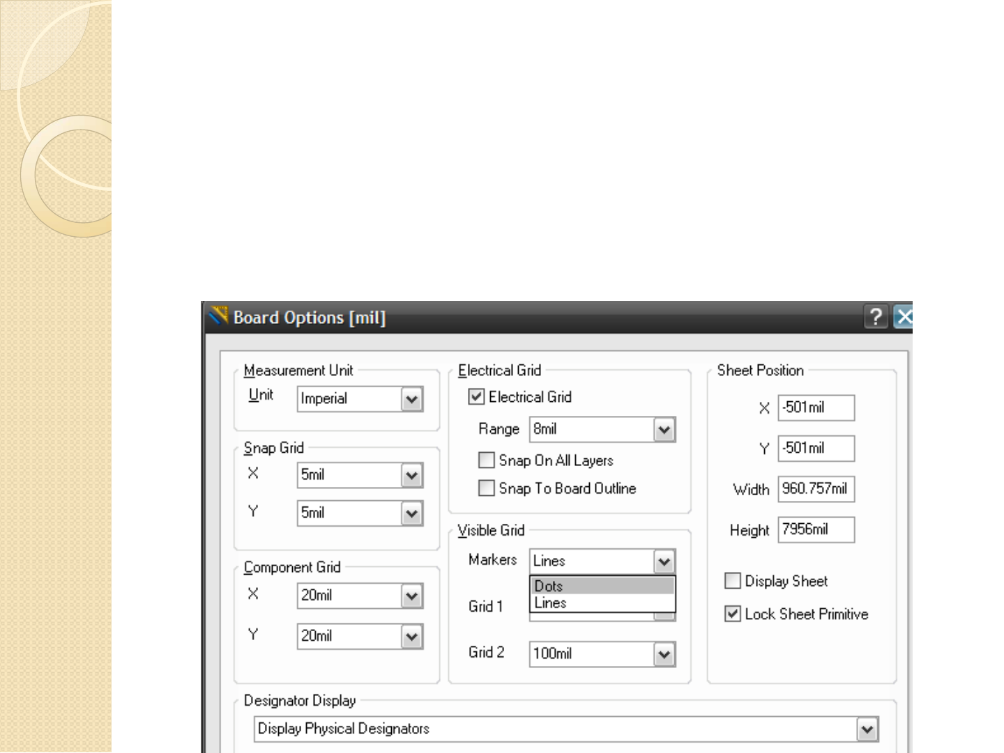
Creating the PCB
Uncheck ‘Display Sheet’ (this has a use, but for now we want to reduce
clutter)
Change the markers from lines to dots and click OK.
NOTE: The snap grid and component grid are very important, we will get
into this later though.
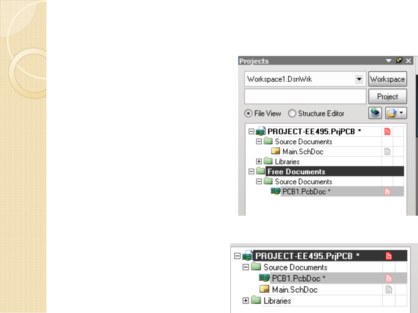
Creating the PCB
The PCB has been added to the
list of documents, but has NOT
been added to the project (Notice
it is listed as a free document)
Click and drag the PCB to your
project
Right click on the PCB1.PcbDoc
file and save the file in your project
directory.
Save the file as ‘Dev Board’
Creating the PCB
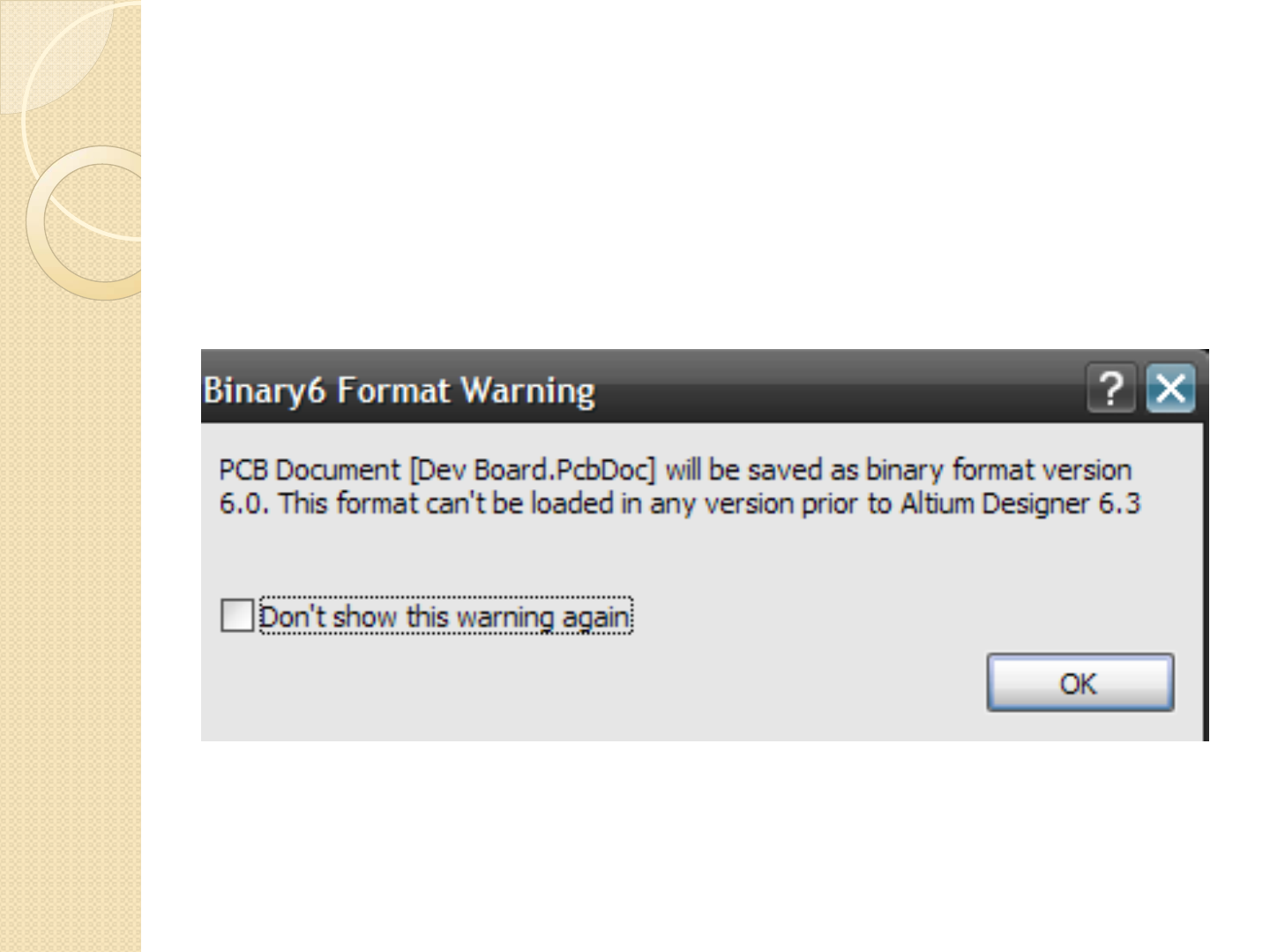
If you get the following warning, just click OK. It is telling you there may be
compatibility issues if you try to open the PCB document in an older version
of Altium.
Creating the PCB
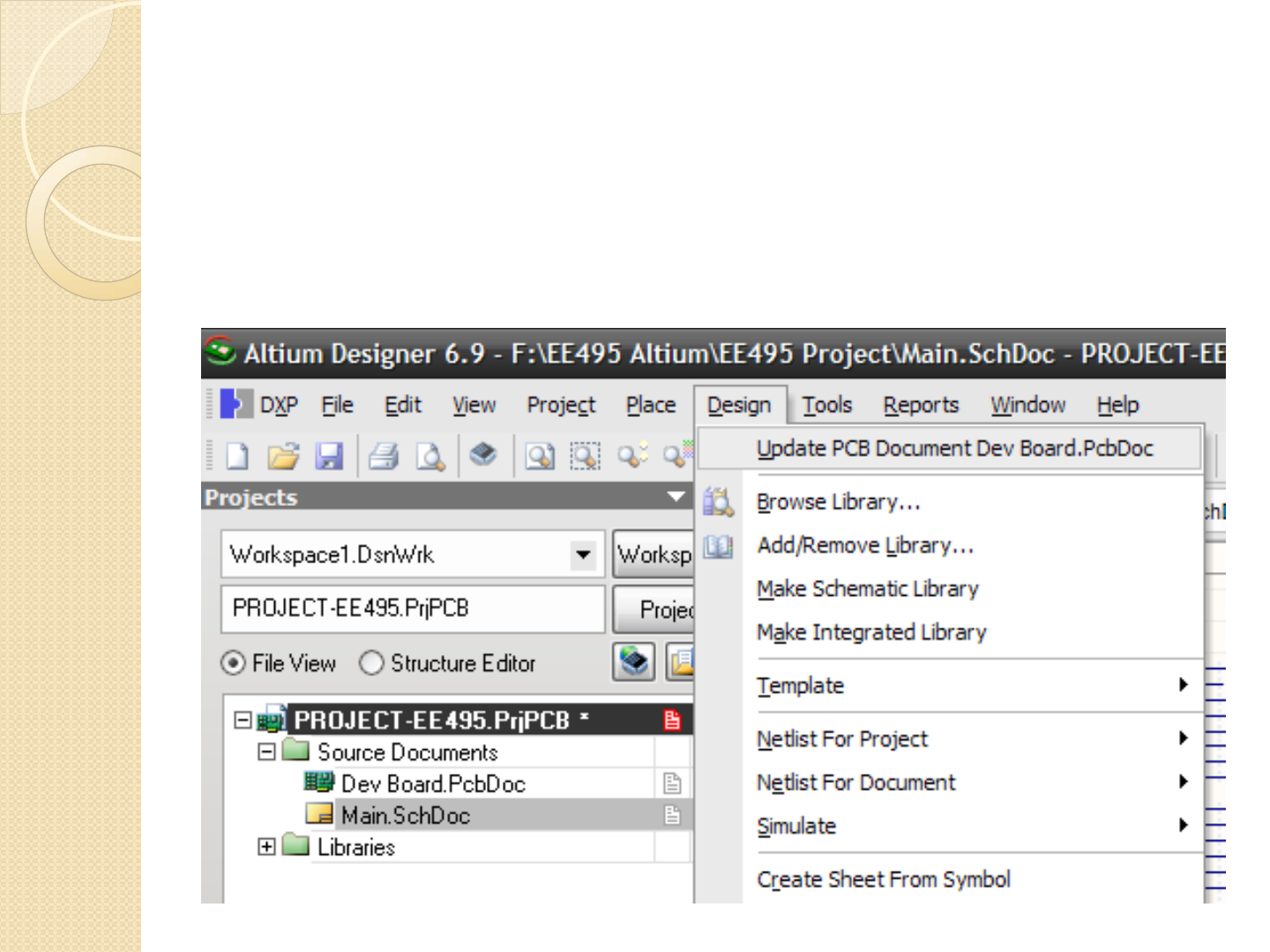
If you select your schematic again, click the Design button up top and then
click on ‘UPDATE PCB DOCUMENT DEV BOARD.PcbDoc’
This will begin the process to turn your schematic into a PCB
Creating the PCB
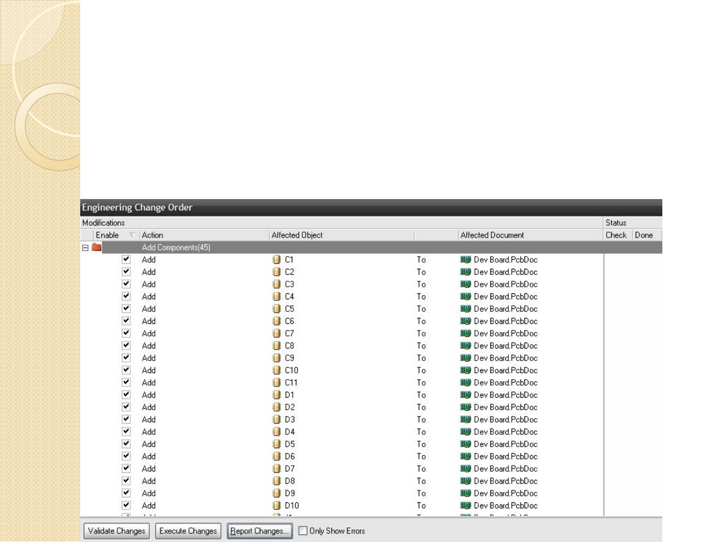
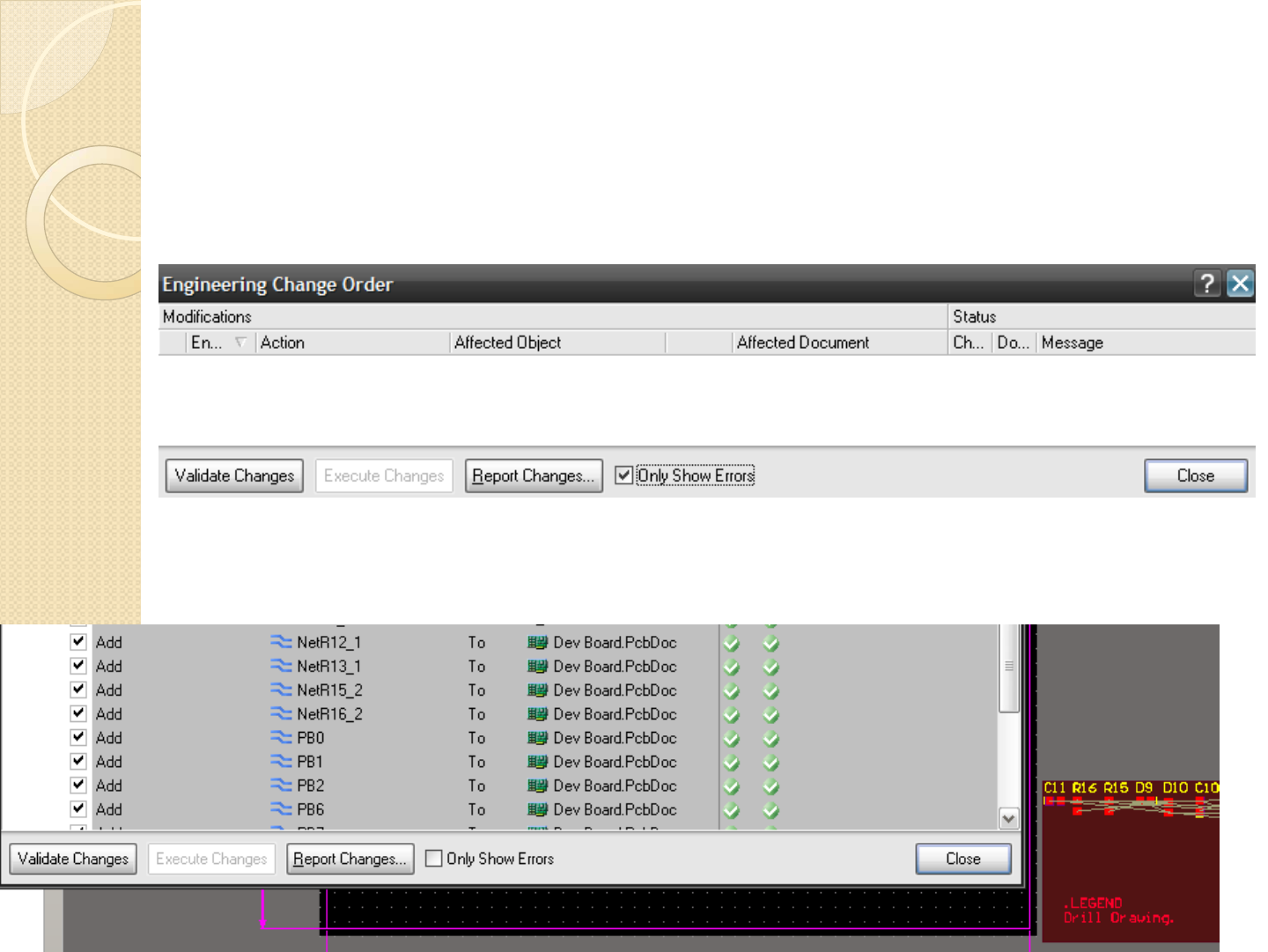
This will open the ECO (Engineering Change Order)
This is asking which changes to make.
Validate changes will check for errors in the process
Execute will actually perform the change
Creating the PCB
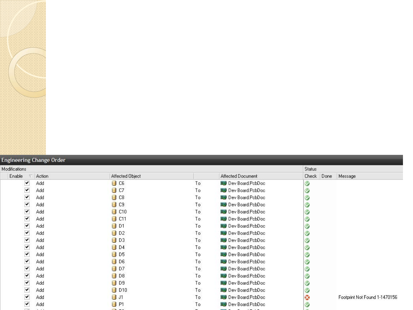
Click ‘Validate’ at the bottom. This may take a while depending on the
complexity of the project.
Notice the green check boxes to the right. This means that each step with the
green check mark can be performed sucessfully.
I have deliberately removed the library for the USB connector to show what
will happen if there is an error for a step (red x) Adding the library will fix
this error
Creating the PCB
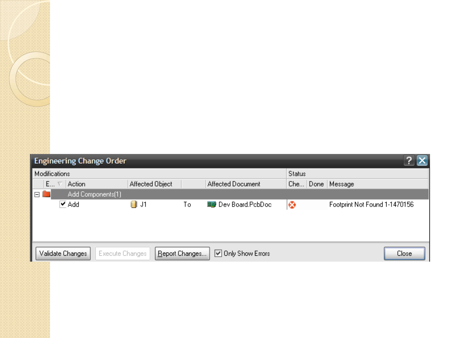
Because there are usually many different steps to creating the ECO, it is
usually helpful to check the box that says ‘Only show errors’ at the bottom.
You are in good shape when no errors occur and this list is empty
Creating the PCB
When no errors appear during the validation step, you can click the ‘execute
changes’ to actually import the schematic to the PCB
You will see a second row of green check boxes when you execute the
changes. Again, check for errors by checking the ‘Only show errors’
Creating the PCB
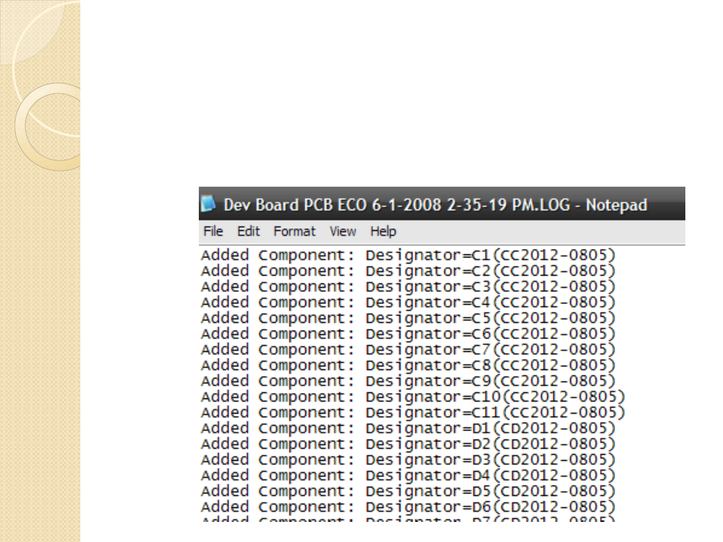
NOTE: Every time you perform an ECO, the results are saved in a text file in
your project directory
Creating the PCB
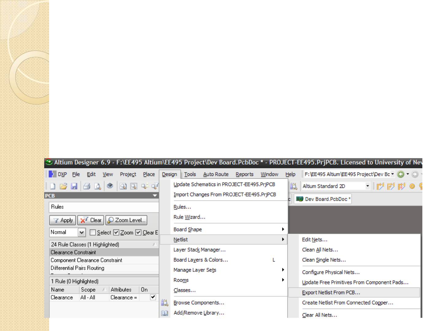
Export the NETLIST following the menu sequence below (You must be on
the PCB document, not the schematic document
This will export the Netlist to your project directory
Creating the PCB
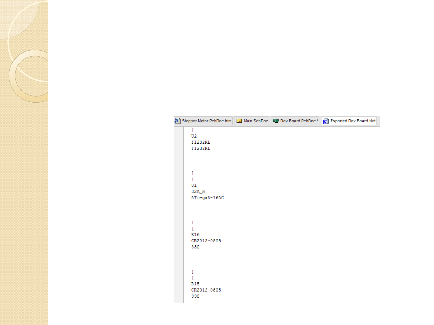
The Netlist contains information such as parts,
footprint, and value (as shown below)
Creating the PCB
It also contains connection
information as shown to the right
Each Netlabel (either assigned by
you or the software, every net
has a netlabel) shows which
component and pin number
connects to that node
Obviously a connection like GND
will have many connections, and
netlabels such as MISO might only
have a few (3 in this case)

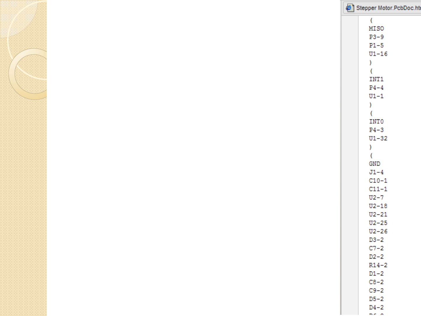
Creating the PCB
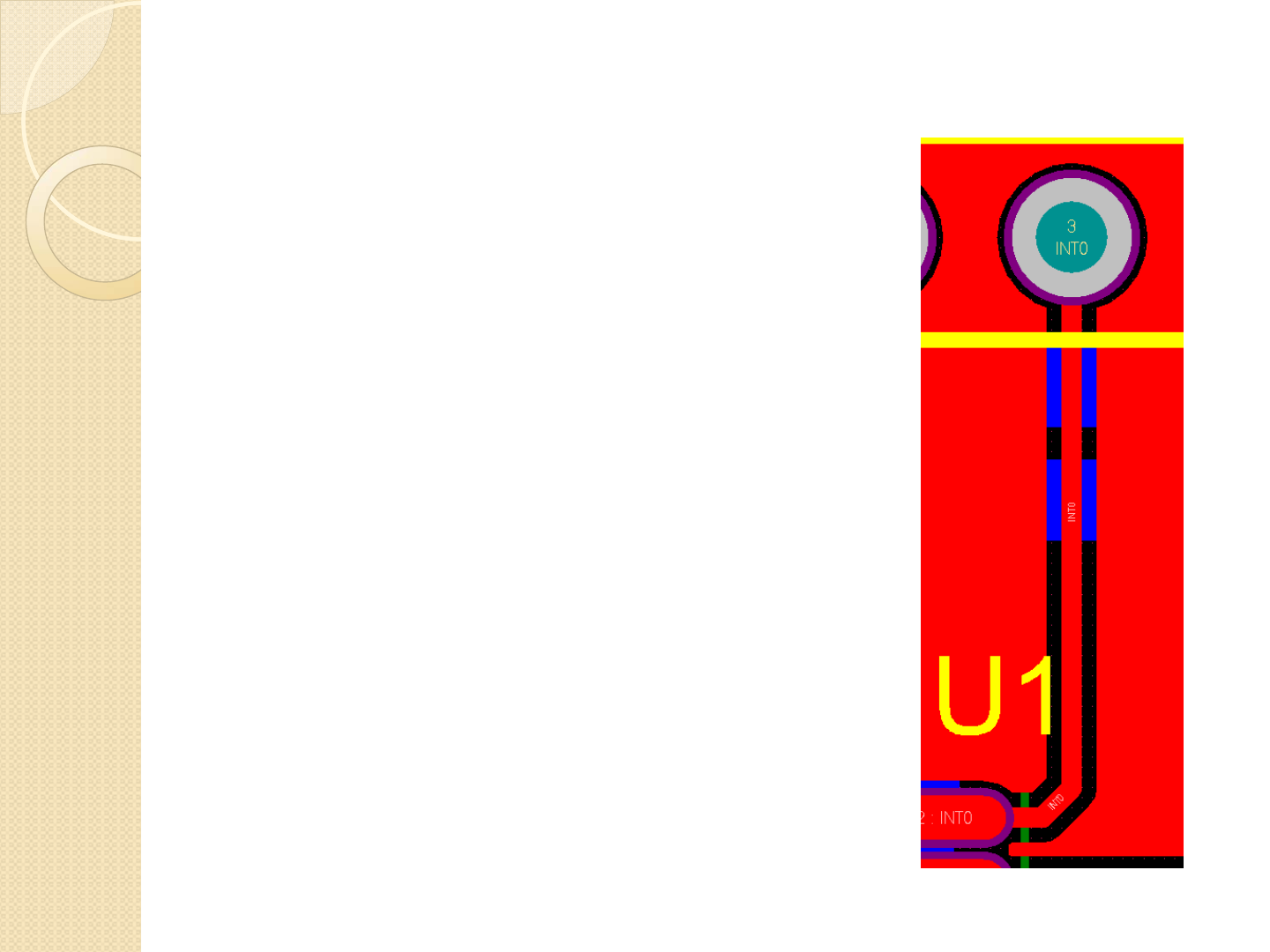
◦Netlist Connections for Net MISO:
P3 pin 9
P1 pin 5
U1 pin 16
◦A quick look at the schematic shows
that this net is properly connected

Creating the Netlist
Fortunately, Altium handles the Netlist transparently to
the end user, but it is important to at least be familiar
with the term and how the schematic is transferred to
the PCB and vice versa
Any changes that are made must be made to the Netlist.
The Netlist is the ‘link’ between the PCB and the
schematic. It is important that the schematic and PCB
agree on connections, nets, footprints, etc..
Creating the PCB
After executing changes. If there are errors or not,
whatever the software can import into the PCB it will do
so
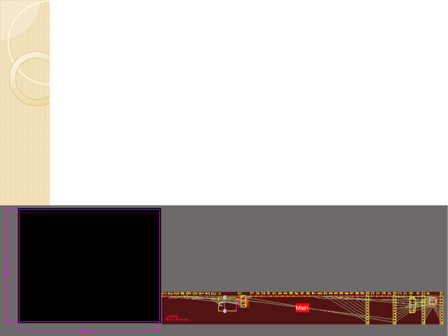
Notice how the software just sort of ‘dumps’ all your
parts (PCB Footprints) off to the side of the board.
Does anyone know why the software doesn’t place
the parts ???

Creating the PCB
You may have
noticed the words
on the right on
your design. Leave
it where it is and
don’t mess with it.
We will get to that
later what it does
This is called a
Special String
Creating the PCB
Notice how all the parts are placed inside a colored
rectangle box called ‘Main’. This is called a ROOM.
Rooms are used to group common circuit types. A room
is created for each schematic page we have
Since we only have one page, called ‘MAIN’, there is only
one room

Creating the PCB
Rooms are like borders for your parts. An item inside a
room cannot escape without an error message.
Since we only have one room, we can delete the room
without affecting our layout at all.
Click anywhere in the room and hit the DEL key
The room will disappear and the components will remain
NOTE: You can disable the use of rooms in project
options
Creating the PCB
If you hit the ‘L’ key on the PCB page, it will bring up the
following prompt.
Change the option under mechanical layers that says ‘Used
Layers Only’
Creating the PCB
Notice the different tabs at the bottom of the screen. The selected
layer will look different than the others (in this case, top layer)
Unlike a schematic, which is 2D, a PCB is a 3D entity with a whole
bunch of layers on top of each other. These layers are all combined to
form your PCB.
NOTE: These layers are all color coded!!!!

Creating the PCB
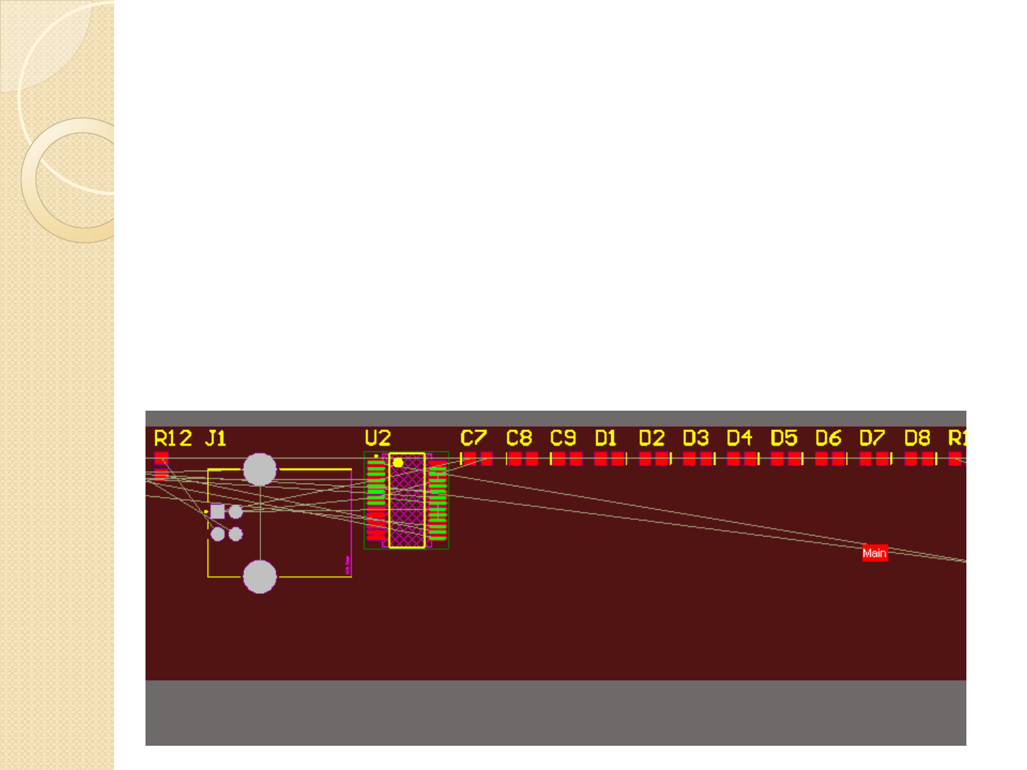
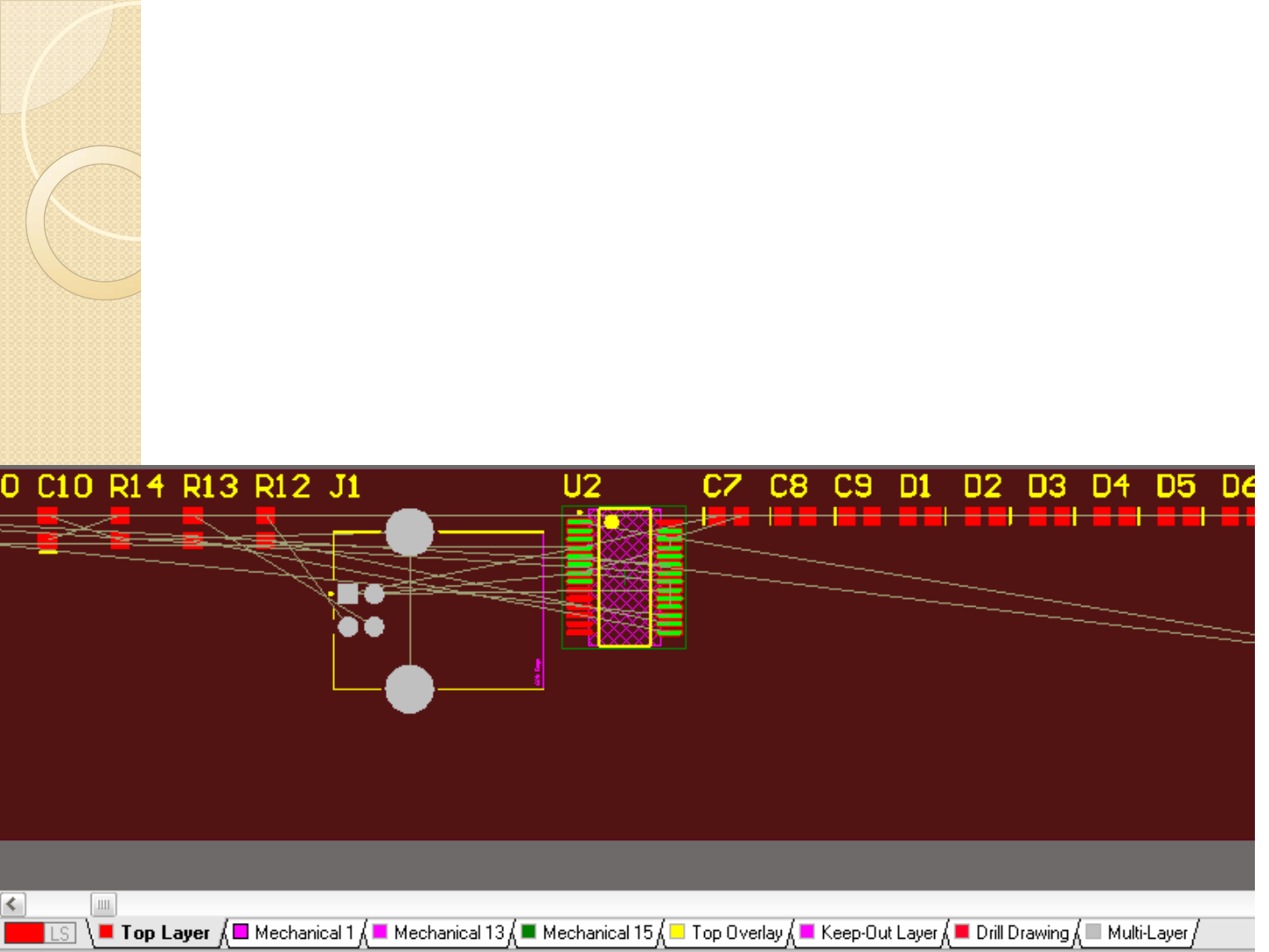
If we zoom in, notice that U2 (The FT232 chip) has
several green pads, and several red pads.
The red pads represent something on the top layer. But
why are some of the pads green ??
Creating the PCB
If we type ‘L’ again, it
will bring up the board
layer lists.
Since the layers are
color coded, we can
quickly look for the
green one and notice
that this is a DRC error
marker (Design Rule
Check)
For some reason Altium
has a problem with our
FT232 Chip
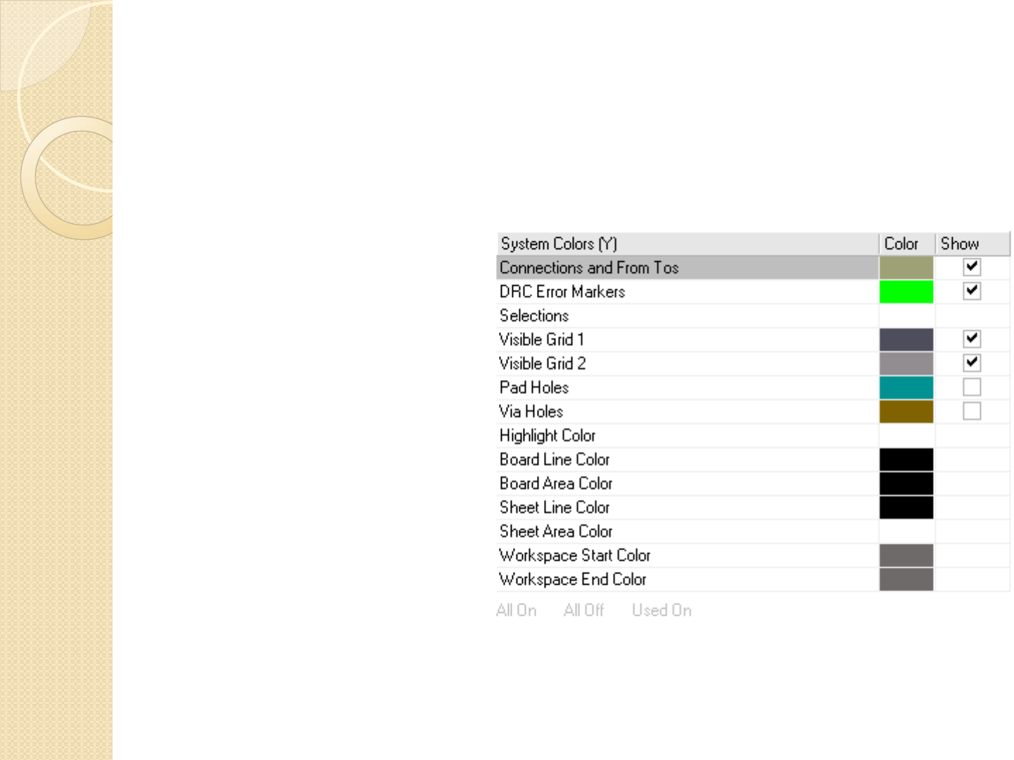
Check the boxes for
pad holes and via holes
Creating the PCB
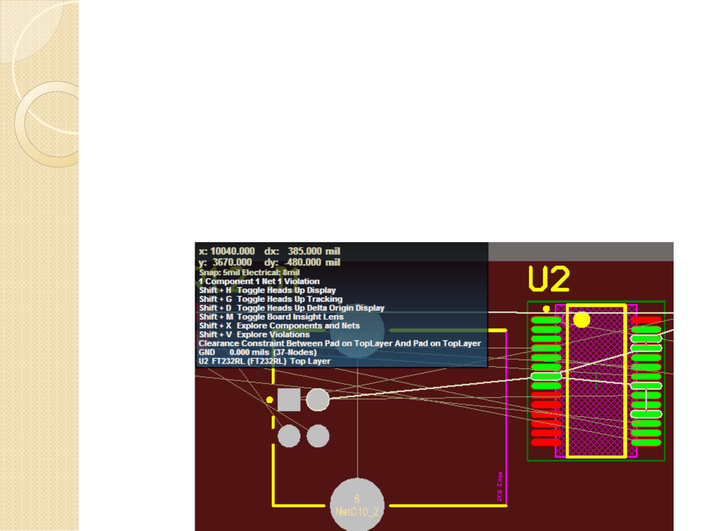
If we put the mouse over one of the green pads, it will tell us
information about the pad, most importantly it will tell us what the
error is
For these pads, there is a clearance constraint error between a pad on
the top layer, and another pad on the top layer
NOTE: It is up to you to decide is this is a real error, or an improperly
set rule
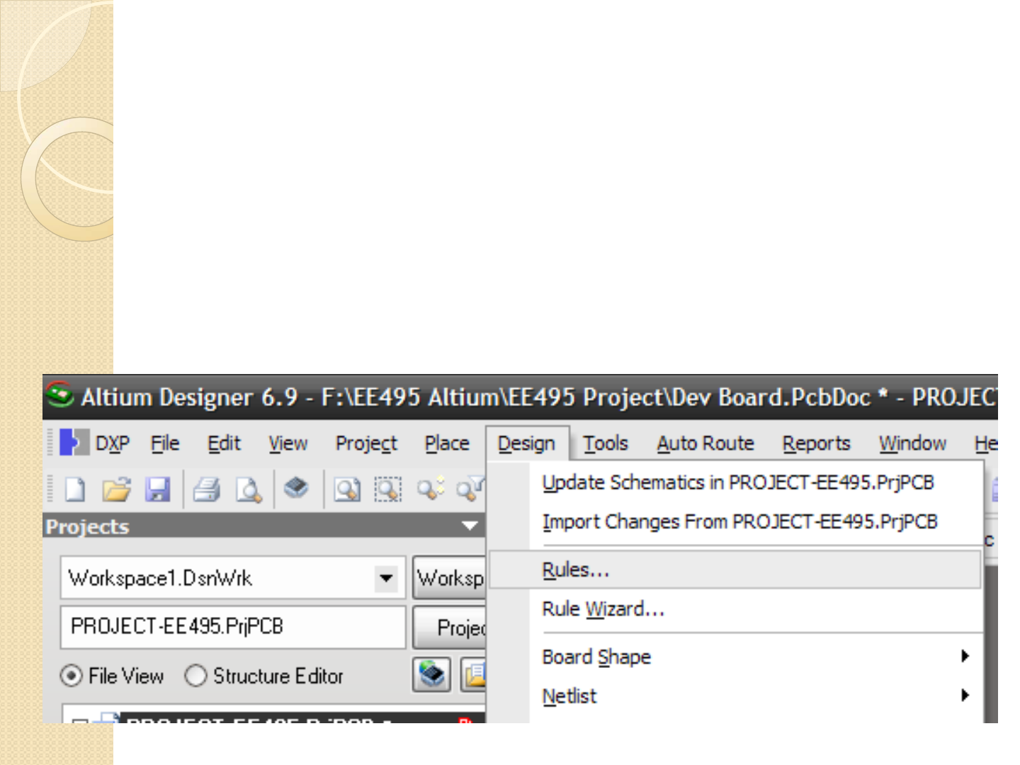
Creating the PCB
Like the schematic, there are rules we need to set.
Click Design > Rules (or) Rules wizard to create/modify rules
NOTE: The software only creates errors based on your rules. It is up
to you to know if something is OK or not. If you tell the software that
2 mil traces are OK, the software will enforce that.
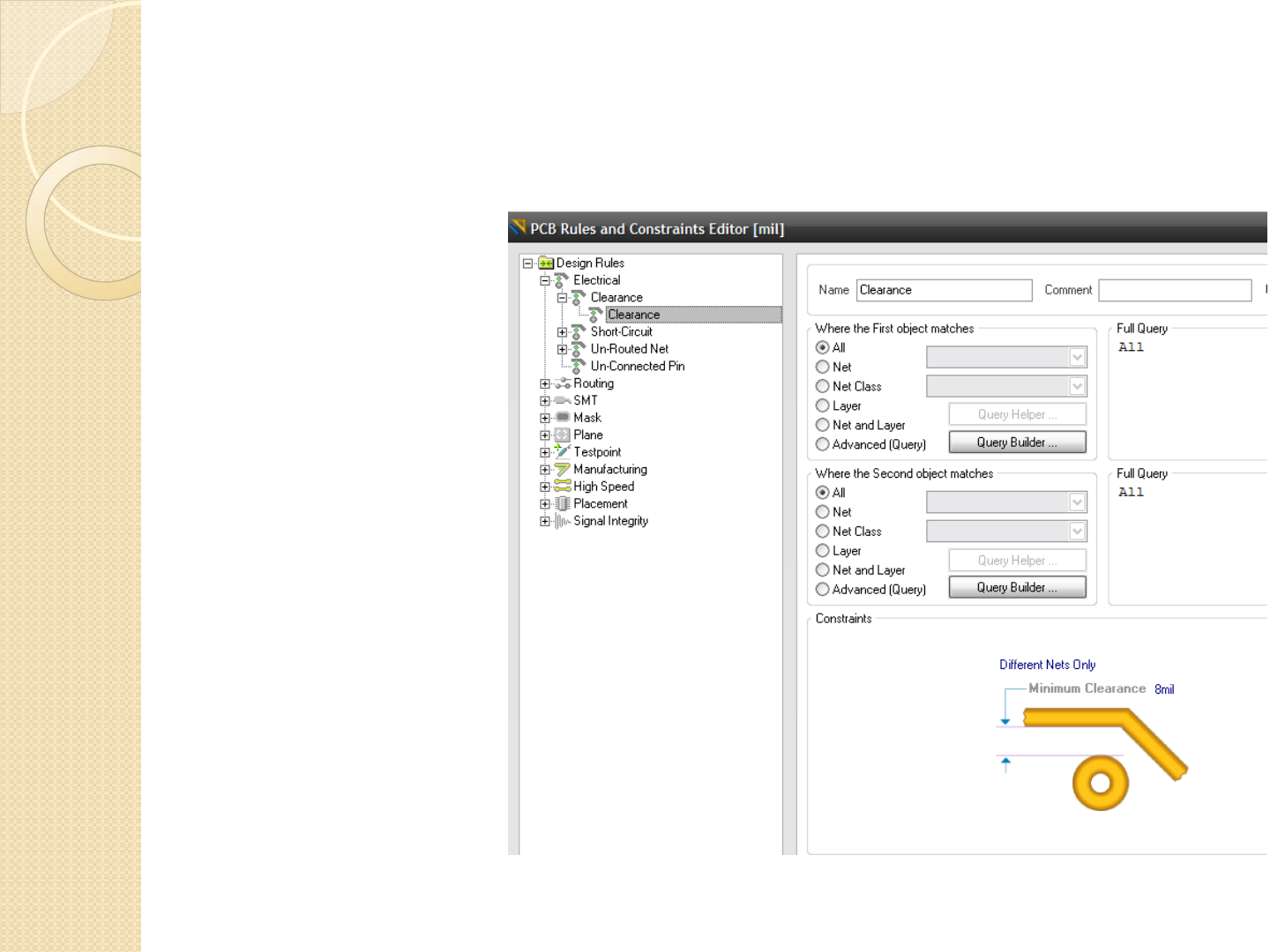
Creating the PCB
The DRC
expects a
minimum
spacing
between
different
nets of 8
mils.
Creating the PCB
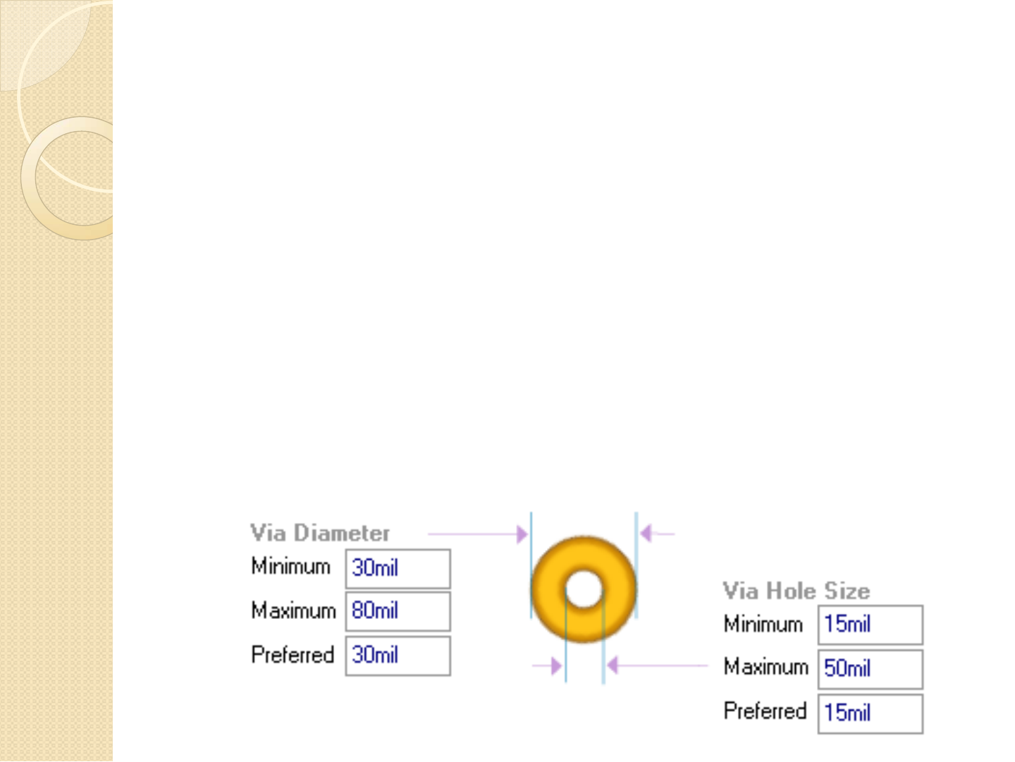
Make the following rule changes (from top of list down):
◦Max Trace Width= 200 mils
◦Minimum Via Size = 15 mils, Min Via diameter = 30 mils
◦Maximum Via size = 50 mils, Max Via diameter = 80 mils
◦Minimum hole size = 15 mils, Max hole size = 200
Creating the PCB
Try using trial and error
and change the setting to
7 mils and you’ll notice
the error markers go
away.
NOTE: There are many
better ways of
determining the actual
spacing, but we want to
keep things simple for
now

Creating the PCB
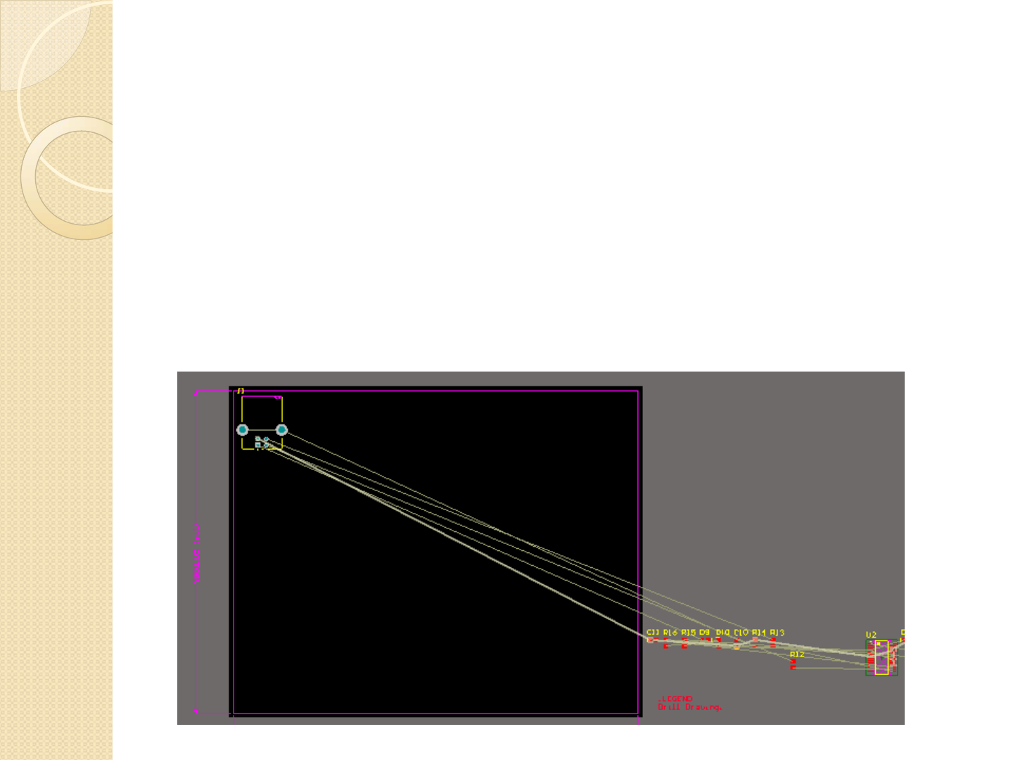
Notice the small
lines, these are
collectively referred
to as a Ratsnest.
It is a way of
telling you which
connections need
to be made still
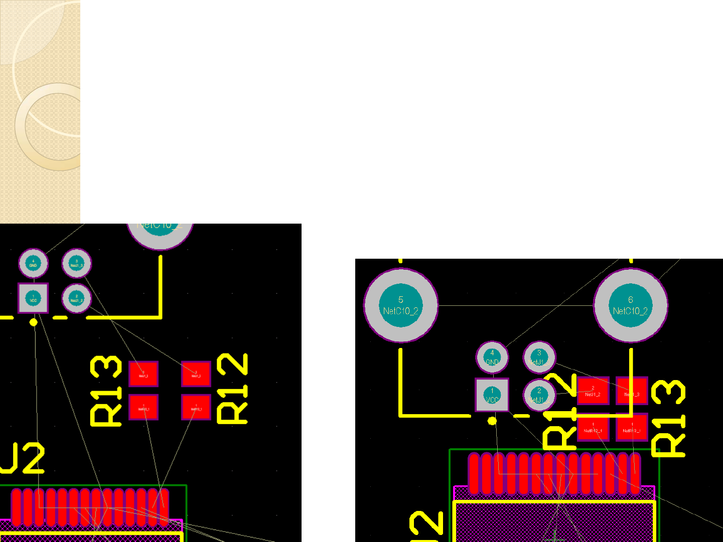
Example: You can see
pin 2 of R12 needs
to connect to Pin 2
of the USB
connector
Creating the PCB
Components are moved in the PCB the same way they
are moved in the schematic.
Notice how the Ratsnest connections remain and will
dynamically change based on how a component is
rotated.
Creating the PCB
There is usually a tradeoff when placing components.
This USB connector might be easier to route if it is in
the middle of the board, but will be difficult for a user to
use a connector in the middle of the board.
For this design, do the best you can to make it easier to
route, for your project, it should make physical sense to
an end user, even if it means harder routing

Creating the PCB
EVERYONE’S PCB WILL BE DIFFERENT!!!
Do not try to make yours exactly like mine or anyone
else’s.
This design I went out of my way to create a more
dense design for clarity and to resize the board. Feel
free to use the entire board area.
Creating the PCB
Usually, components that are close together in the
schematic are placed close together in the PCB.
NOTE: If you have two monitors, keep the schematic
open on one side, and the PCB on the other side. If you
have one monitor, just write down the components

Creating the PCB
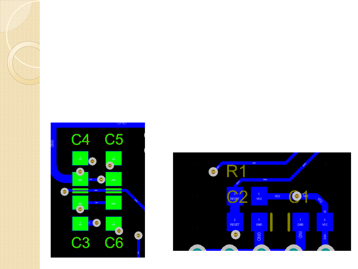
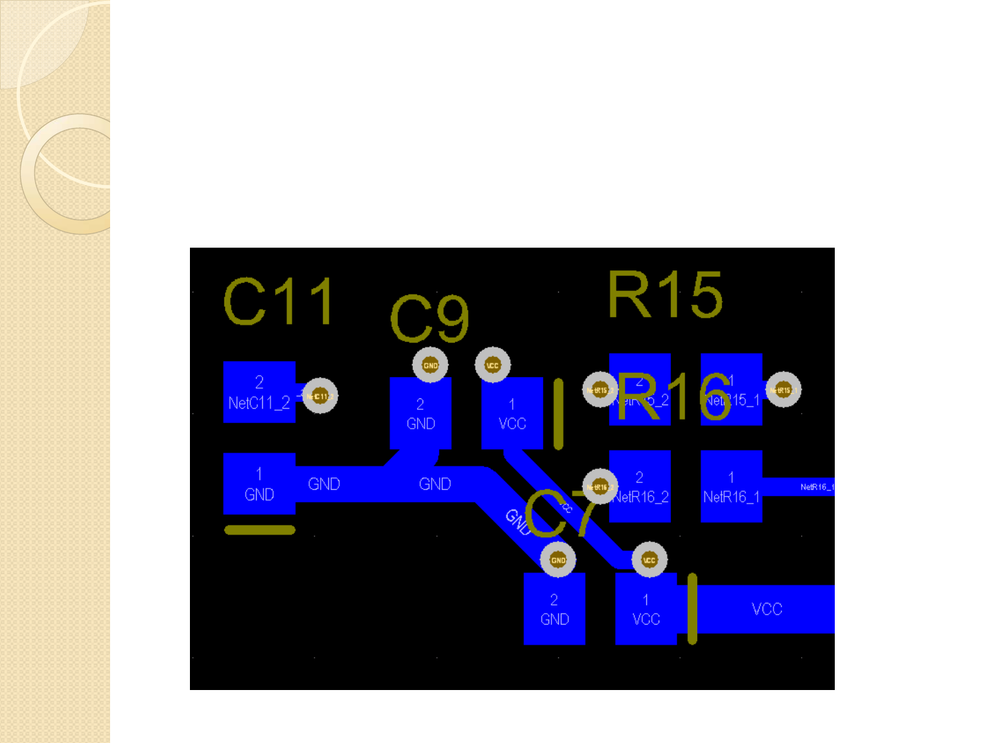
For the USB circuit,
we will group the
following components
◦C7- C11
◦R12 – R16
◦U2
◦D9, D10

Creating the PCB
Next group the
components as they
are arranged in the
schematic.
Prioritize the
placement by
organizing the high
speed or critical
components first at
closest length
Creating the PCB
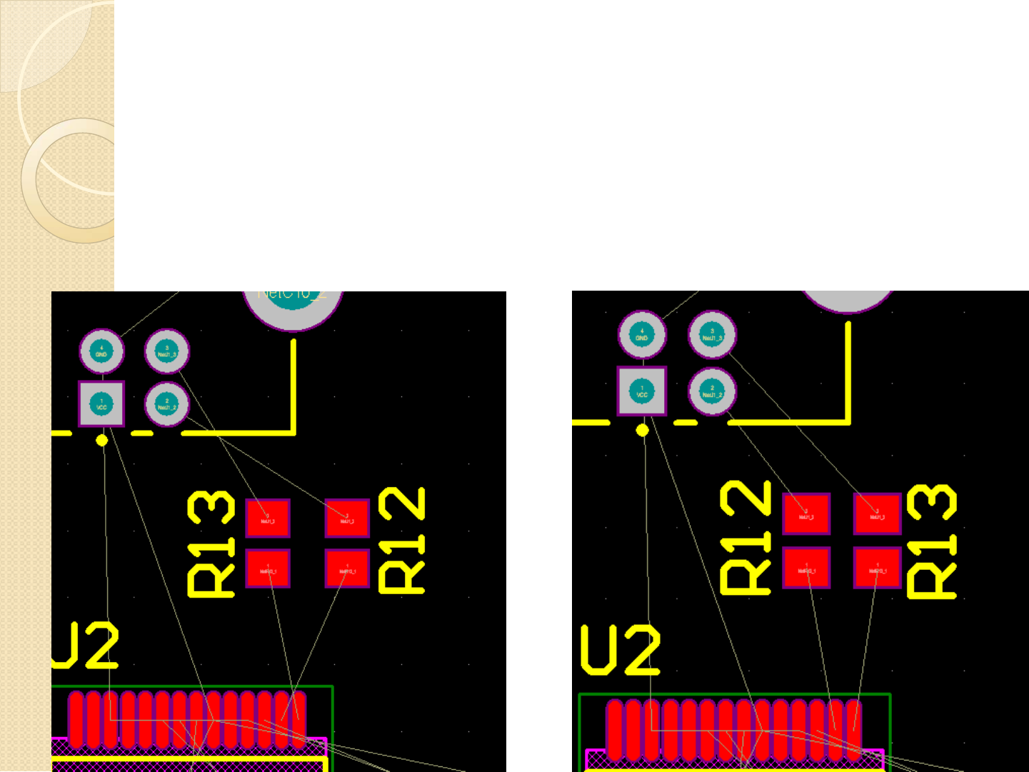
Usually the more time you take in component
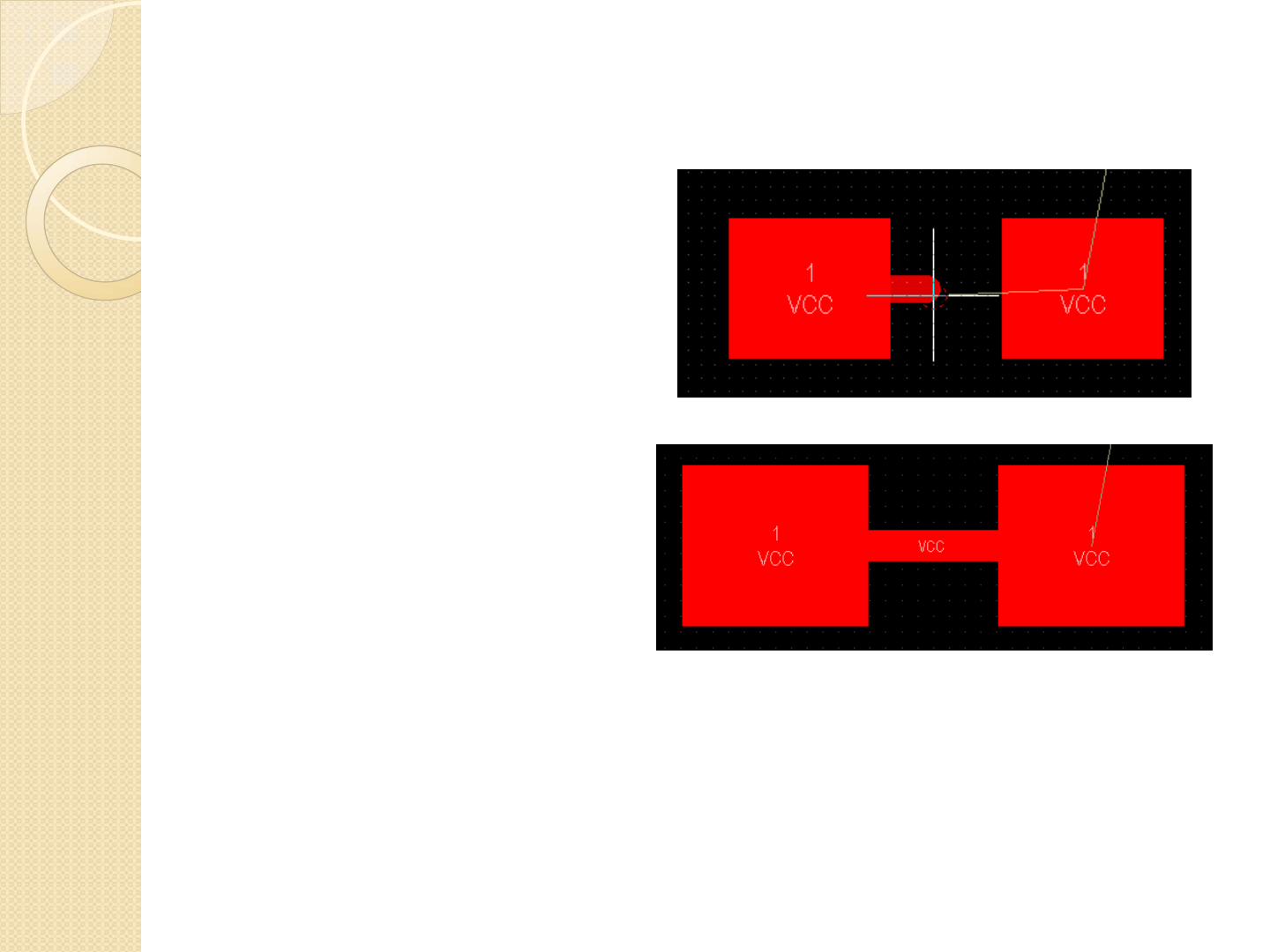
placement, the less time you will need for routing
Which placement is better and why ??? (L or R)
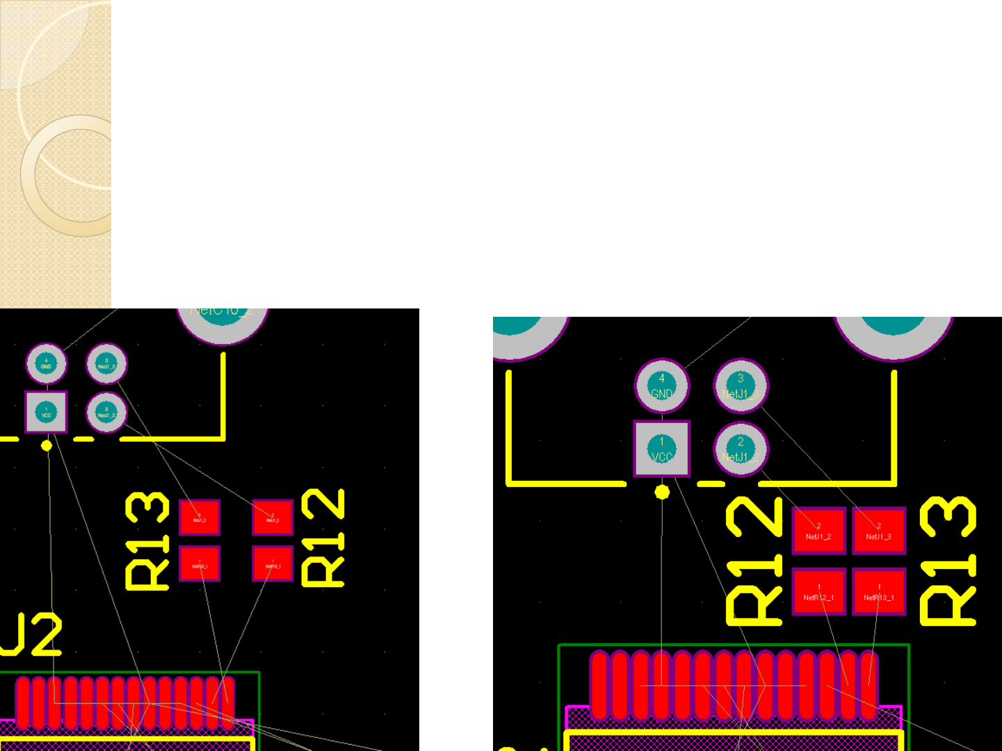
Creating the PCB
Which placement is better and why ??? (L or R)
Creating the PCB
Which placement is better and why ??? (L or R)
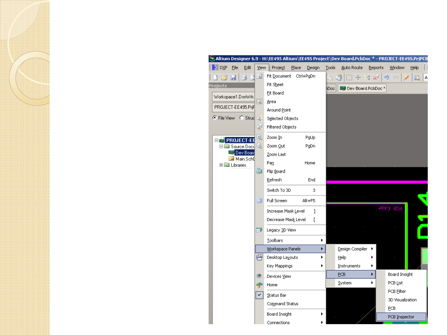
PCB Inspector
Start the PCB
Inspector.
This is one of the
most useful and
time saving
features in Altium
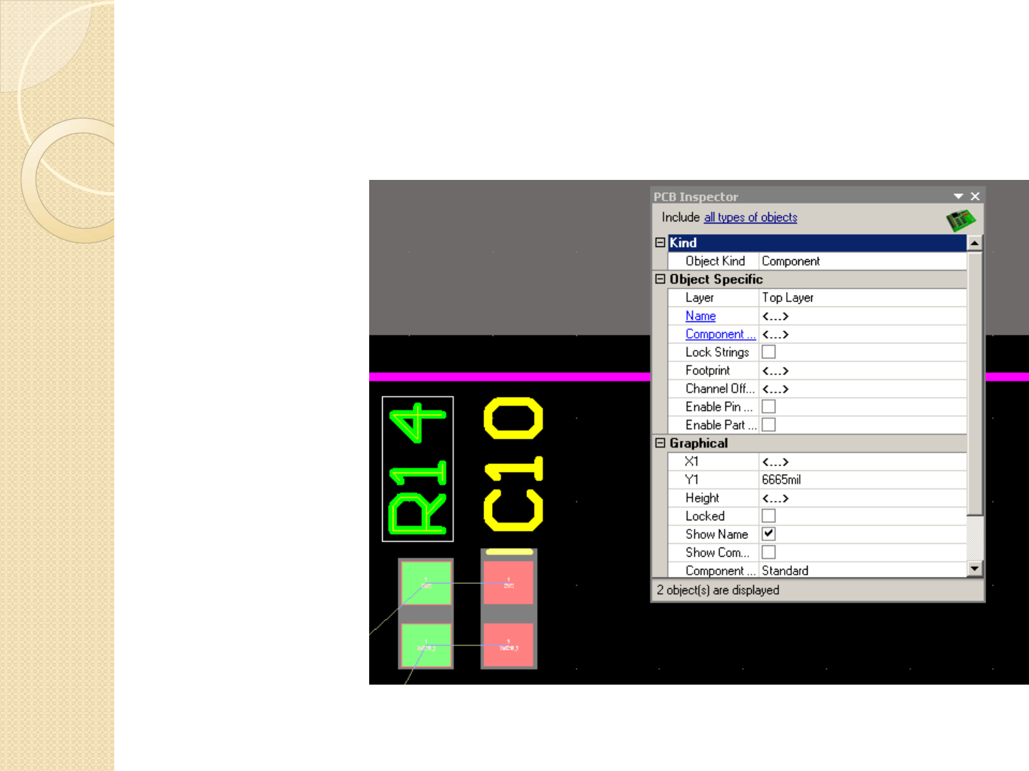
PCB Inspector
Hold down
control and
click both R14
and C10
The PCB
inspector
shows two
objects are
displayed/selec
ted.
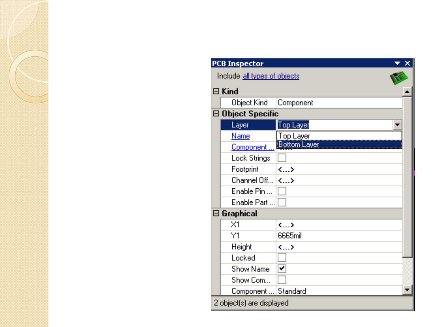
PCB Inspector
Change the layer
from TOP to
BOTTOM, and all
selected objects are
immediately changed
to the bottom layer
This change moved
the component pads
from the top of the
board to the bottom
of the board and
mirrored them
PCB Inspector
We can now place R14 and
C10 underneath the USB
connector and make the
connection from the bottom of
the board.
Notice the pads are BLUE
(color code bottom layer), This
lets you know that these
components are on the bottom
of the board
Component Placement
Place the three
decoupling
capacitors on the
bottom layer, and
position them as
close to the power
pins as possible as
shown below
Component Placement
The current limiting
resistors can be
place on the bottom
of the board (under
the FT232 chip)
The RX and TX
indicator LEDs
should be placed on
the top of the board

Component Placement
This is beginning to
look very cramped
and hard to see
things which are
overlapping.
We don’t care
where the
component labels
(top overlay) go, and
will position them
last, so they are just
getting in the way
right now
Component Placement
Click on the LS at
the left of the list of
layers. This is to
change the active
Layer Set (Visible
layers)
This will bring up a
screen like that on
the right. Change
the setting to ‘Signal
Layers’

Component Placement
This shows only
SIGNAL LAYERS or
layers that conduct
electricity and hides
the rest of the layers
that we don’t care
about at the
moment.
Most of routing is
best done with the
Signal Layers
layerset active

Component Placement
It is much easier to look
for lines that cross over
here and make changes
with component
placement.
NOTE: Be careful when
placing components in
this mode. The top
overlay (silkscreen) is
sometimes used for
component boundaries
and you might place a
component inside the
boundary of another
part
Component Placement
Place the rest of the
components however you
want to

Routing
Now we need to make electrical connections
between the components
Click the icon to interactively route connections
NOTE: Whichever layer is active, the trace will
being on that layer
Routing
Make a connection
between two
components as
shown to the right.
Notice that the wire
itself is associated
with the net VCC

Routing
By lowering the ‘Masked Objects Factor’ in
the ‘Mask Level’ in the bottom right corner,
when you click on a pad to wire, such as VCC, it
will dull out the other connections to make it
easier to see where the connections need to go
Routing
You should
adjust this so
you can easily
see the
highlighted net,
but still see the
outlines of the
other pads
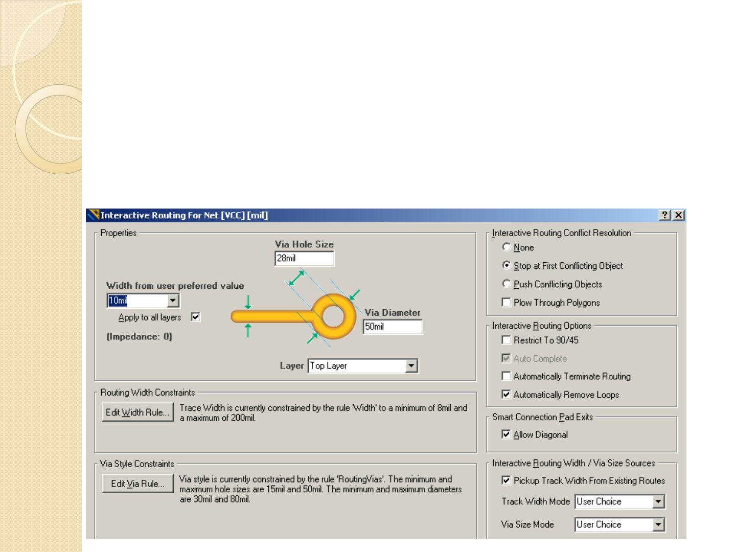
Routing
Press the TAB key while routing and you can
change the width of the trace for that particular
net, and specific hole sizes. Make VCC 15 mils
Routing
Notice the new VCC trace is 15 mils thick

Routing
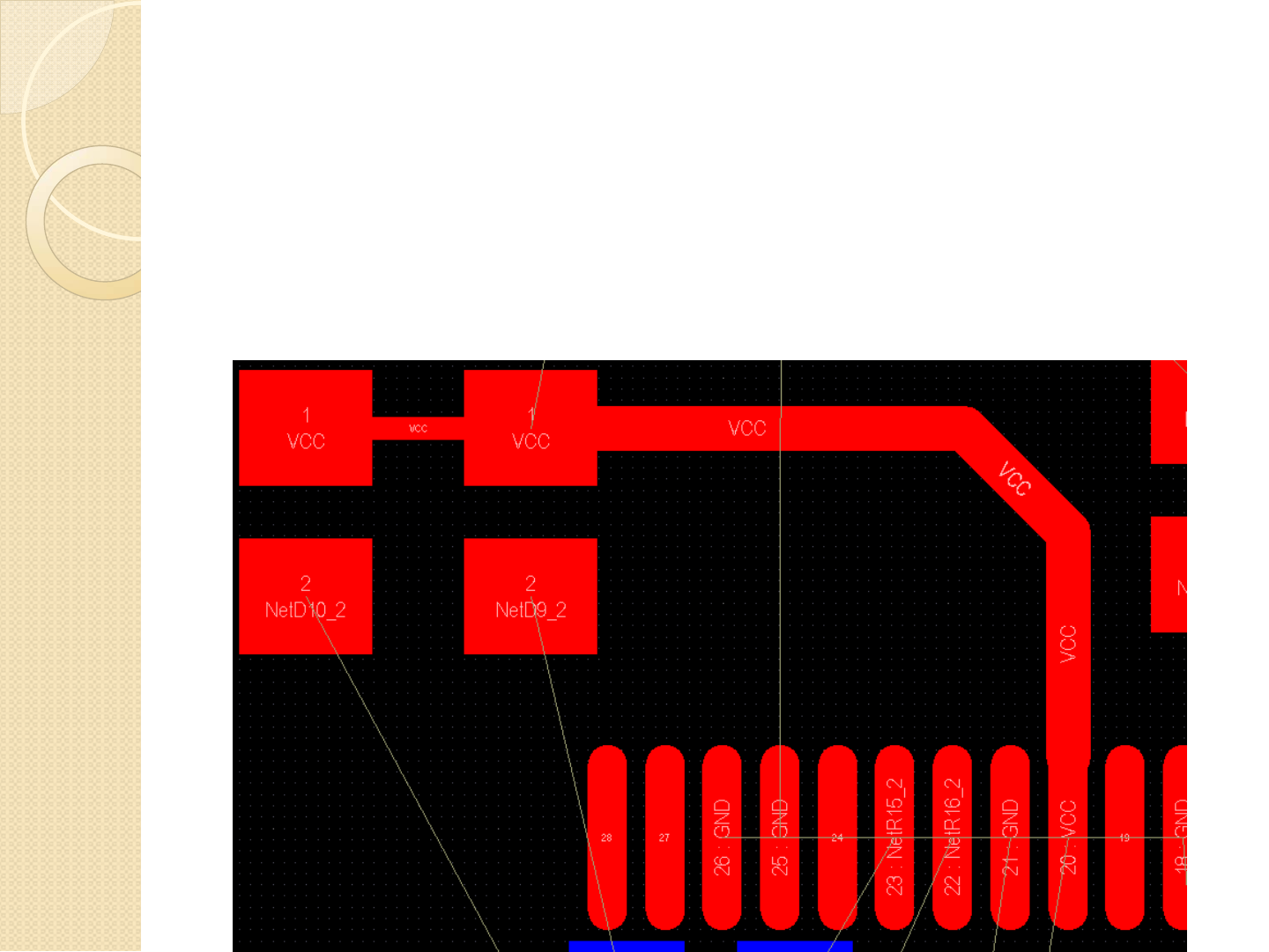
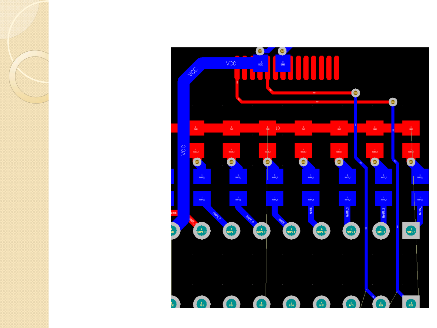
Try to route this board using mostly perpendicular traces.
For example, use the bottom layer for horizontal traces, and the top
layer for vertical traces. This will make the routing much easier (at
the expense of more holes)
Routing
The connection on the
right is a differential pair at
a high frequency.
Differential pairs should be
kept closer together
Although you are using an
orthogonal method of
laying out the board,
Critical nets do not need
to apply.
Try to keep the layer
changes and discontinuities
to a minimum for critical
lines
Routing
As a general rule for right now, you want to make the traces about as
large as you can make them.
Why ?
Routing
When the USB
connector is
complete, there
should be four
traces coming
from the USB
interface to the
rest of the circuit
◦VCC
◦GND
◦TX
◦RX
Routing
The TX and RX
traces from the
FT232 Chip to
the rest of the
chip can be
relatively high
speed (1 MB/s)
For reasons we
will go over later,
this means we
should try to
maintain the same
geometry
throughout the
trace. (Don’t vary
the width)
Routing
When the routing is complete, you should
have something that looks like the picture
to the right.
VCC and GND connections are not all
complete though.
We will work on VCC first
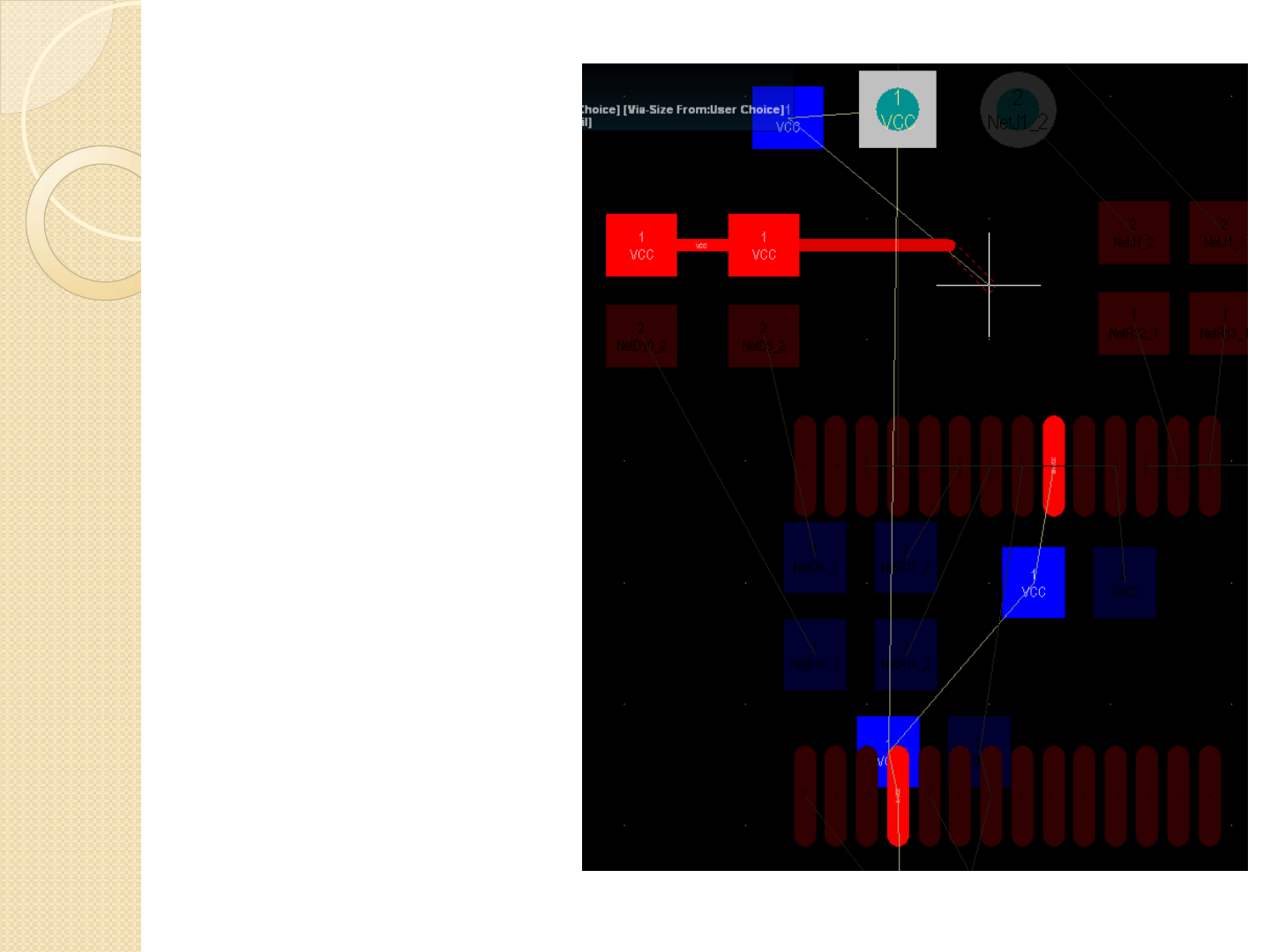
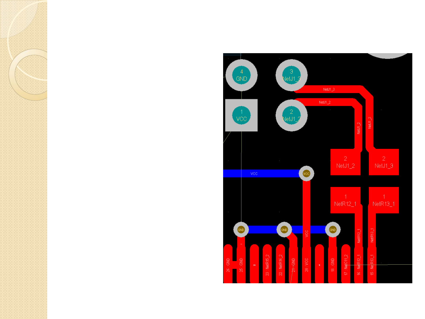
Routing
In the left-hand drop down box at the top, select VCC. This will
highlight the VCC net
NOTE: The box to the right will highlight and jump to a particular
component.

Routing
The VCC net is highlighted
and there are three ‘ratsnest’
wires that need to be
connected.
Make the connections to
connect all the VCC’s
together

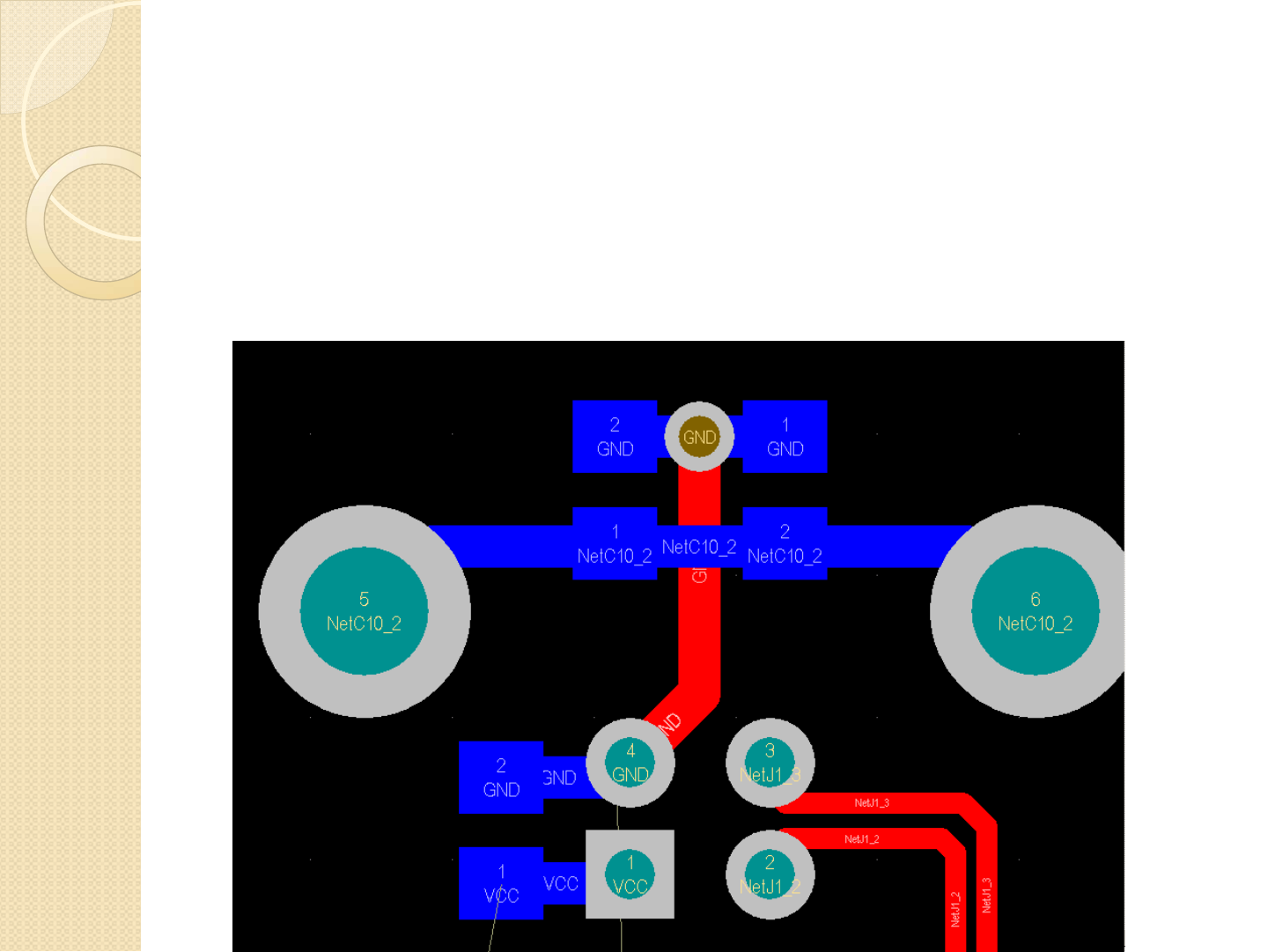
Routing
The VCC net is highlighted
and there are three ‘ratsnest’
wires that need to be
connected.
Make the connections to
connect all the VCC’s
together
Repeat the process for GND
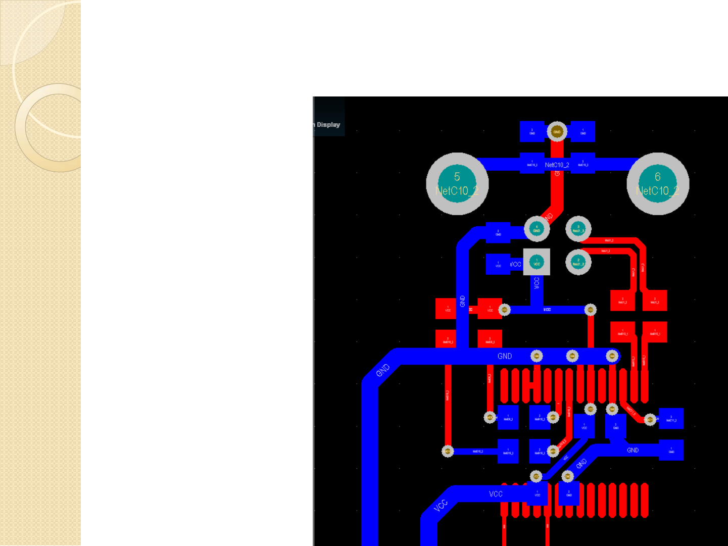
Routing
When the routing is complete, there
should be no more ‘ratsnest’ wires
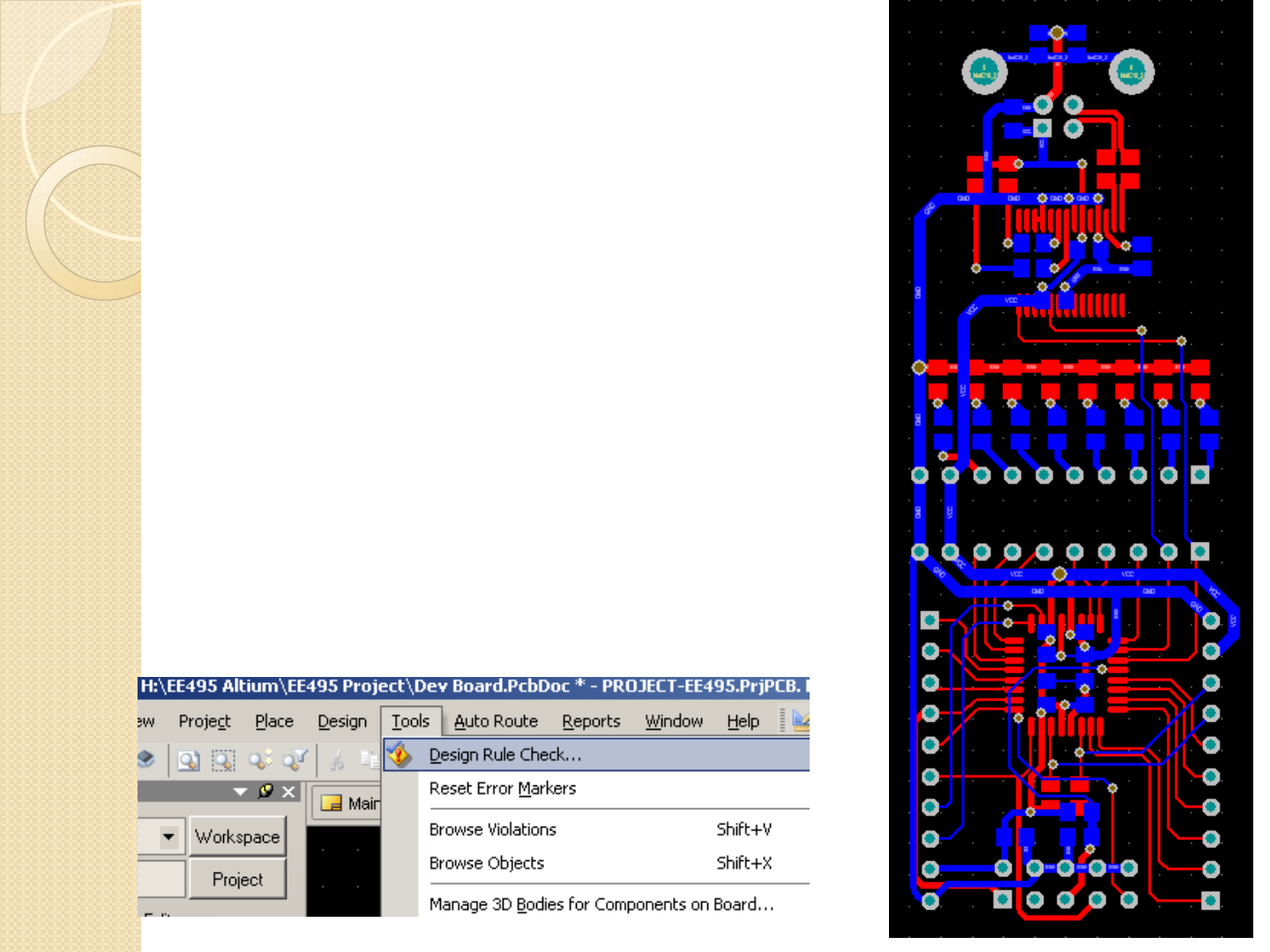
We must run a DRC (Design Rule
Check) to make sure there are no
errors.
Click TOOLS > Design rule check
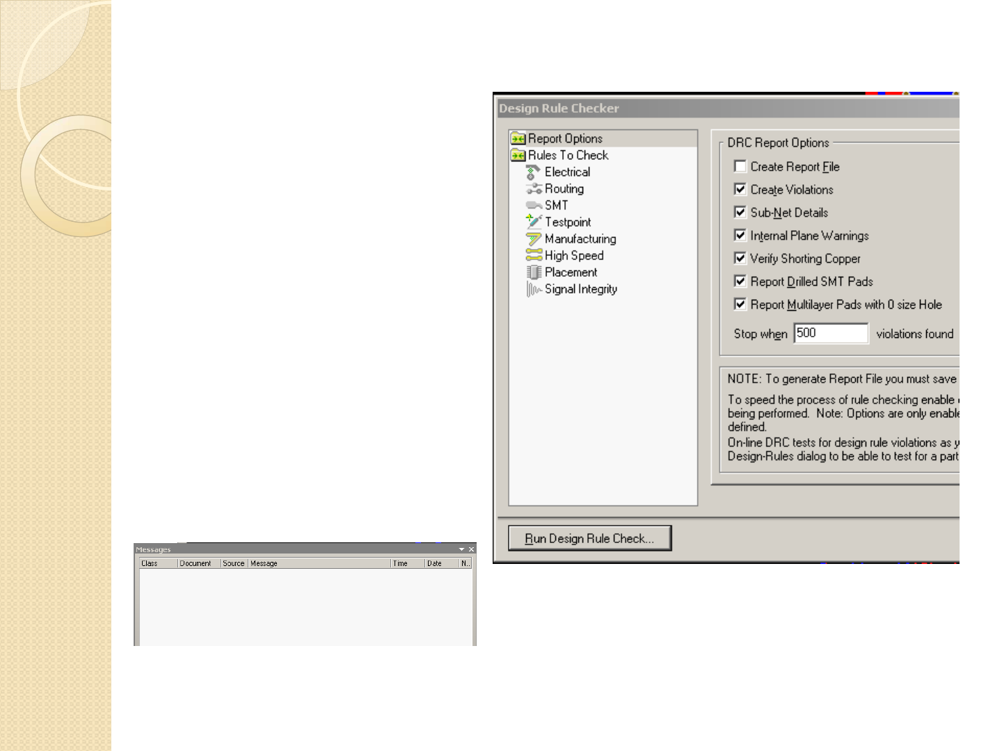
Routing
Uncheck the box to create
a report file
Click Run Design Rule
Check
If there are no errors, you
should get an empty
message box like below
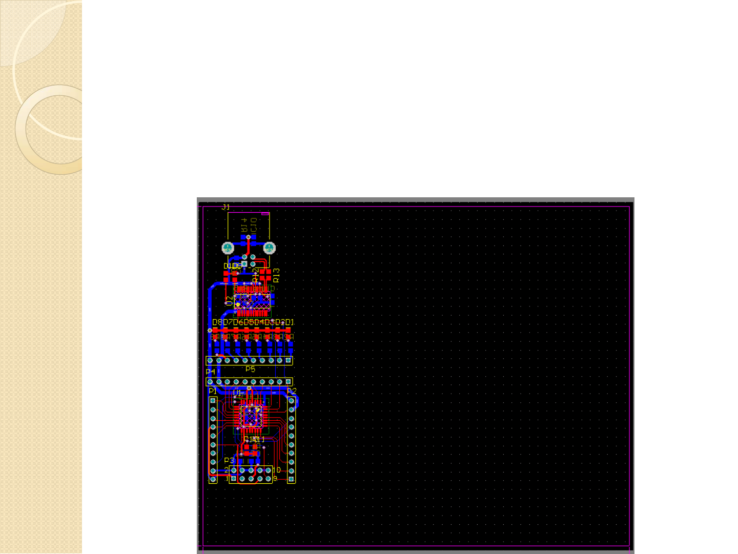
Routing
Change the Layer Set back to ALL LAYERS and view the entire board.
As you can see, we have a lot of wasted area, so this gives us a chance to
resize the board
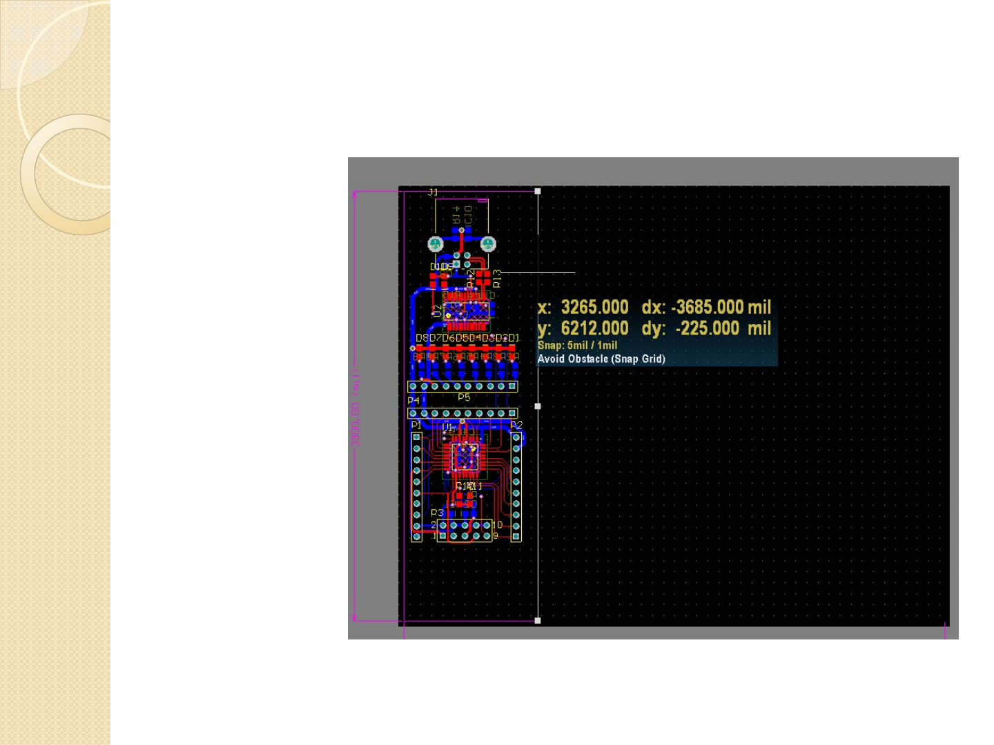
Routing
Click and drag
the pink line to
the right to the
left, leaving
about 50 mils
spacing
between the
pink line and
the
traces/compon
ents

Routing
Notice the
dimensions are
automatically
fixed to the
new distance
between the
arrows
Repeat this
process with
the bottom
pink line
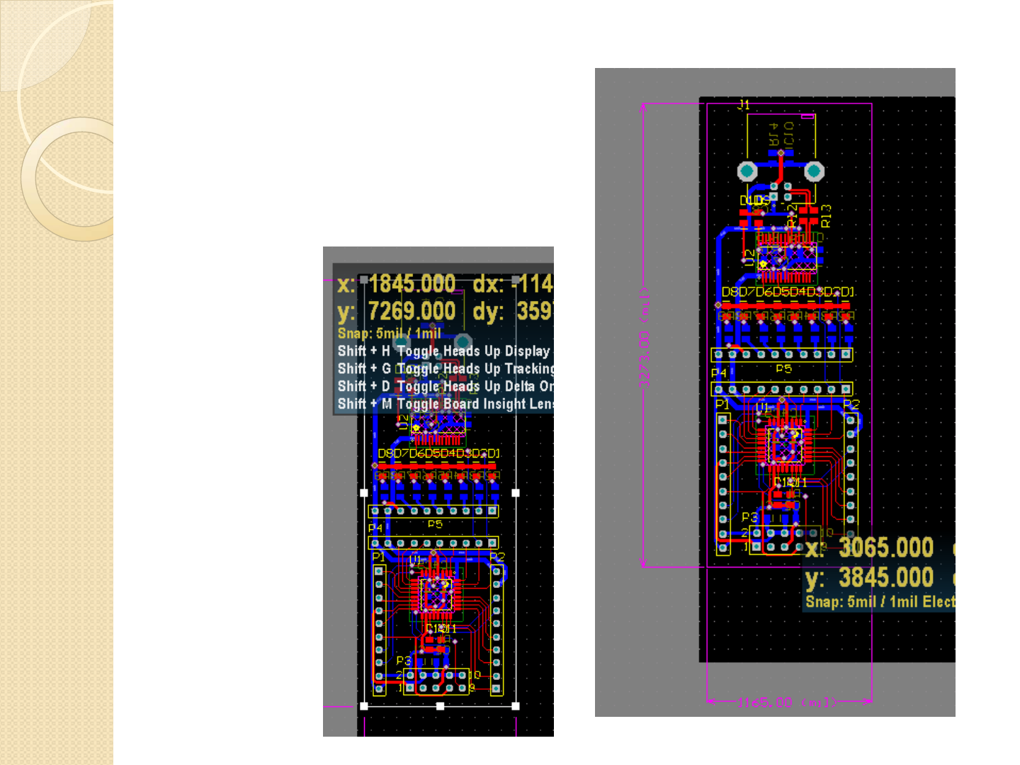
Routing
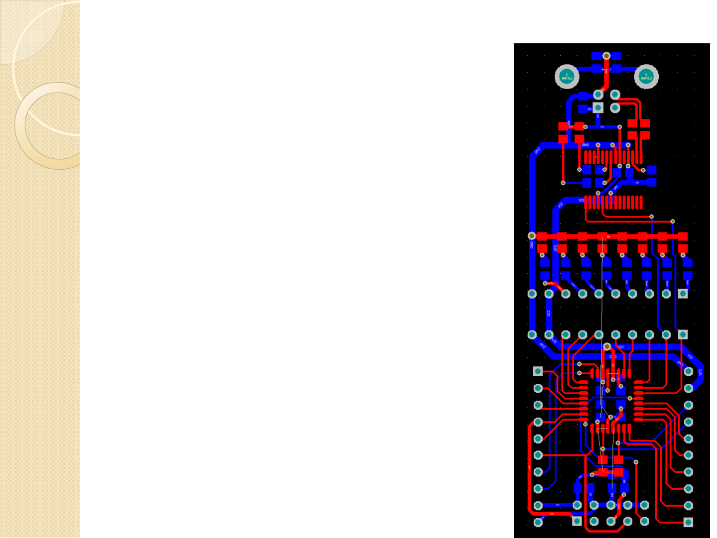
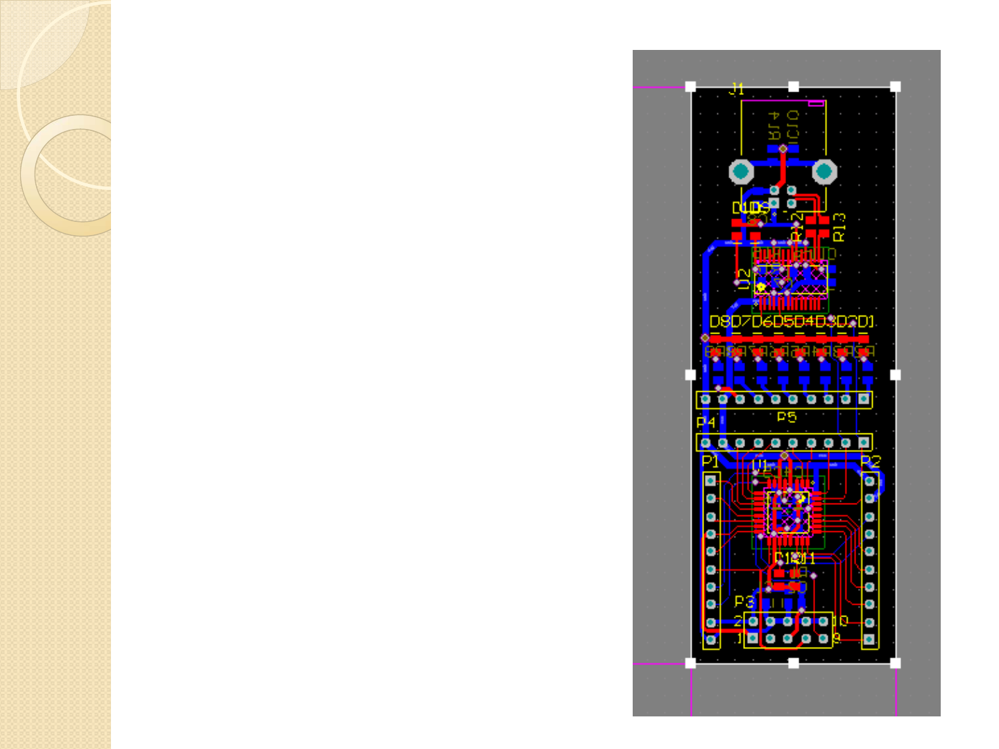
The board should look something like this.
Shift and click to select all four pink lines
Routing
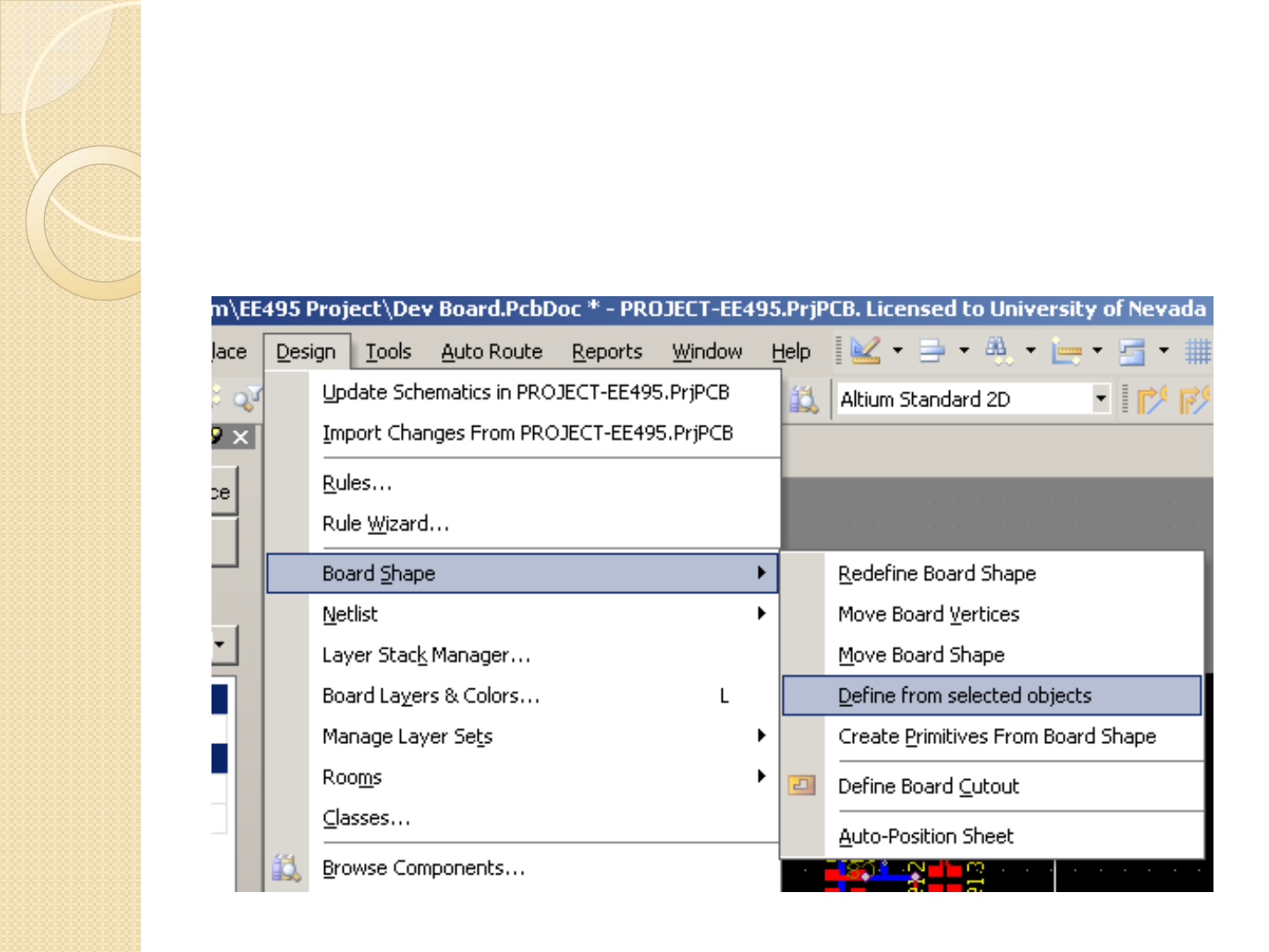
Click
◦Design > Board Shape > Define from selected objects
Routing
The board should now be resized to the
new dimensions
NOTE: The pink line is a special line called
a Keep-Out layer. This is to prevent placing
components too close to the edge of the
board
This is technically not the smartest way to
change the board size, but the simplest to
see how it works.
If you want to change the board size on a
real board please let me know and I’ll show
you better methods
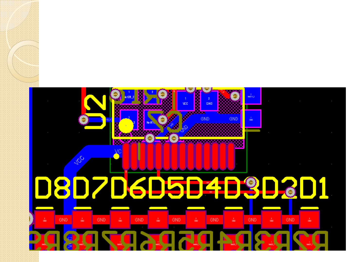
Cleaning Up The Design
Now we should clean up the design. The top overlay (silkscreen) are
overlapping VIAs so they wont show up well, the fonts are too big, and the
spacing is too close together
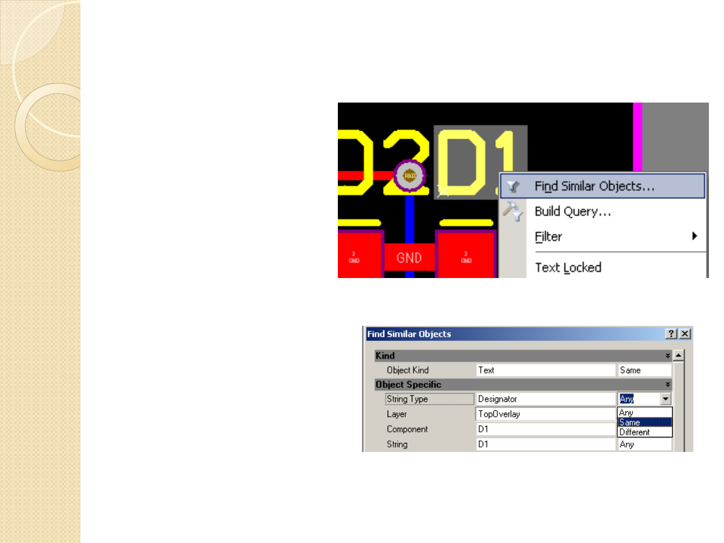
Cleaning Up The Design
Right click on any of the
top overlay (such as D1)
and click ‘Find Similar
Objects
Under String Type-
DESIGNATOR, change
from ANY to SAME. This
will select all designators
on the board
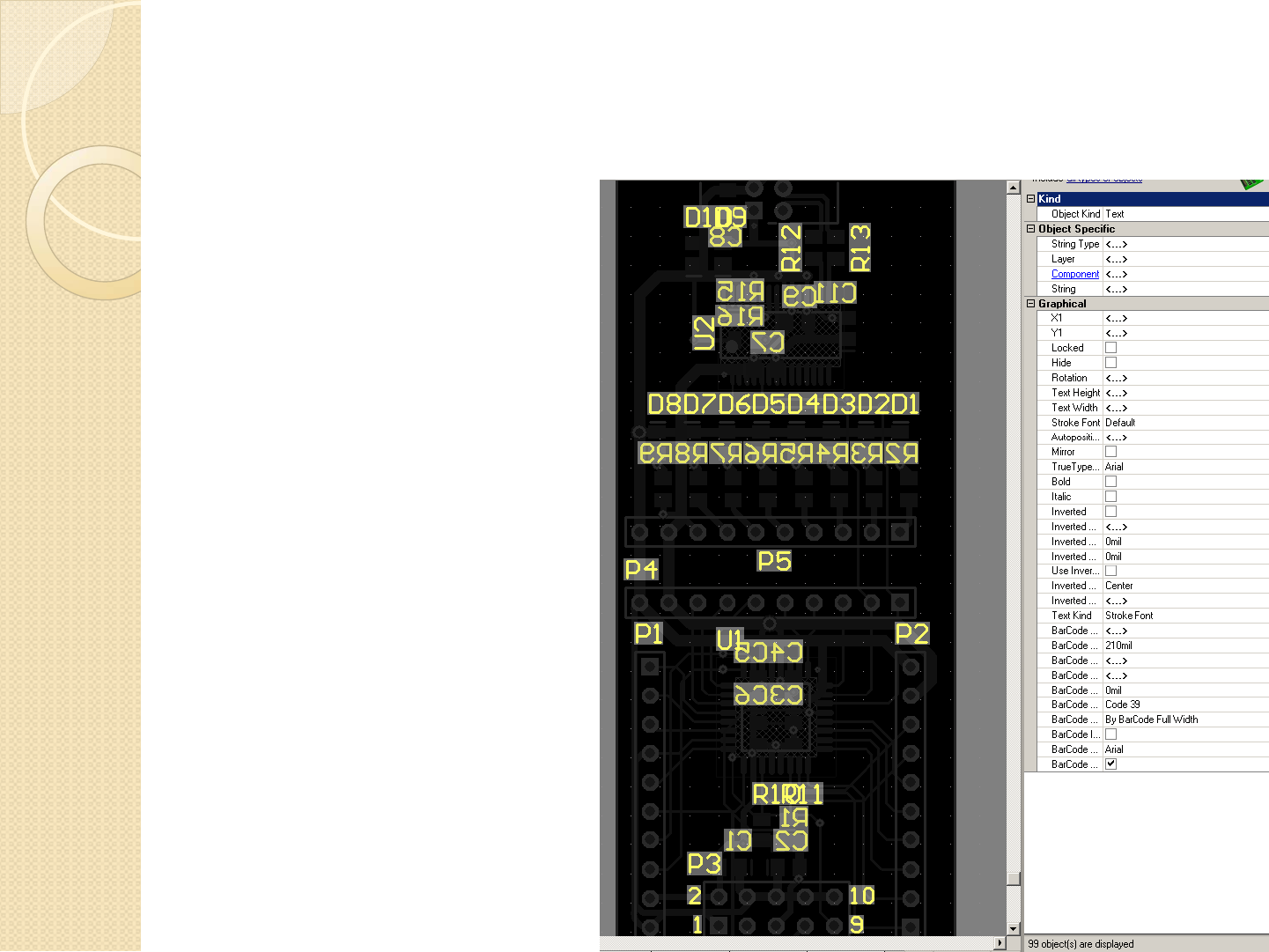
Cleaning Up The Design
You can see that all the
component designators are
selected, and nothing else
The PCB inspector shows
that 99 objects are selected
Change the ‘Text Kind’
from ‘Stroke Font’ to ‘True
Type’

Cleaning Up The Design
The changes are
immediately made and all
99 designators are changed
from stroke font to true
type font.
The reduced size and
cleaner font type already
makes the board look a lot
better
Cleaning Up The Design
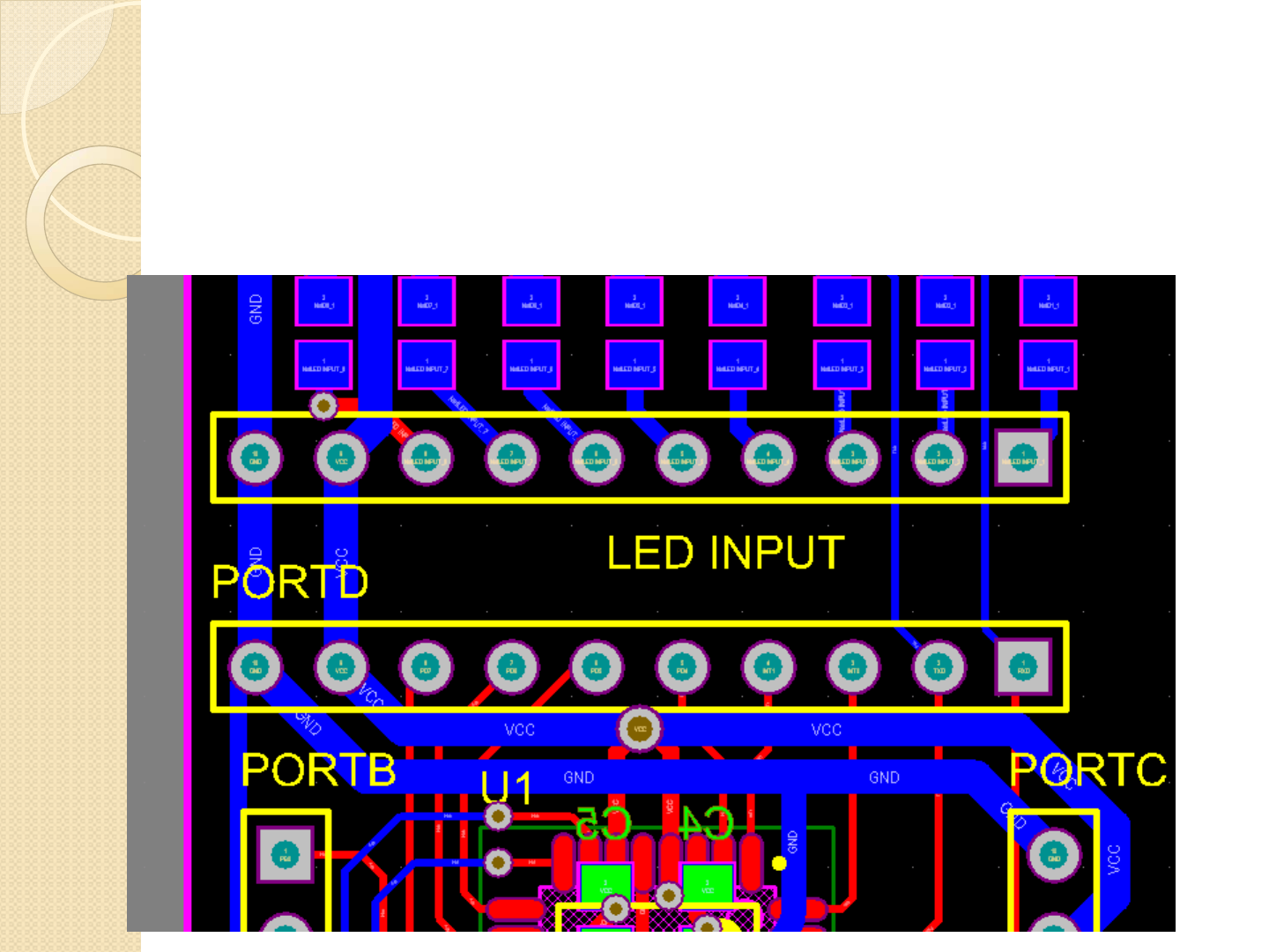
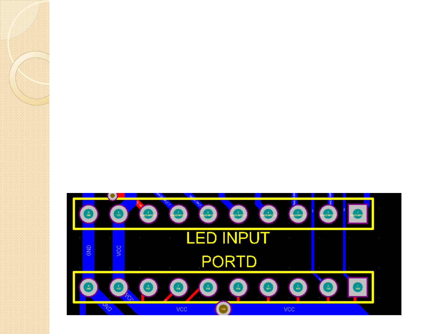
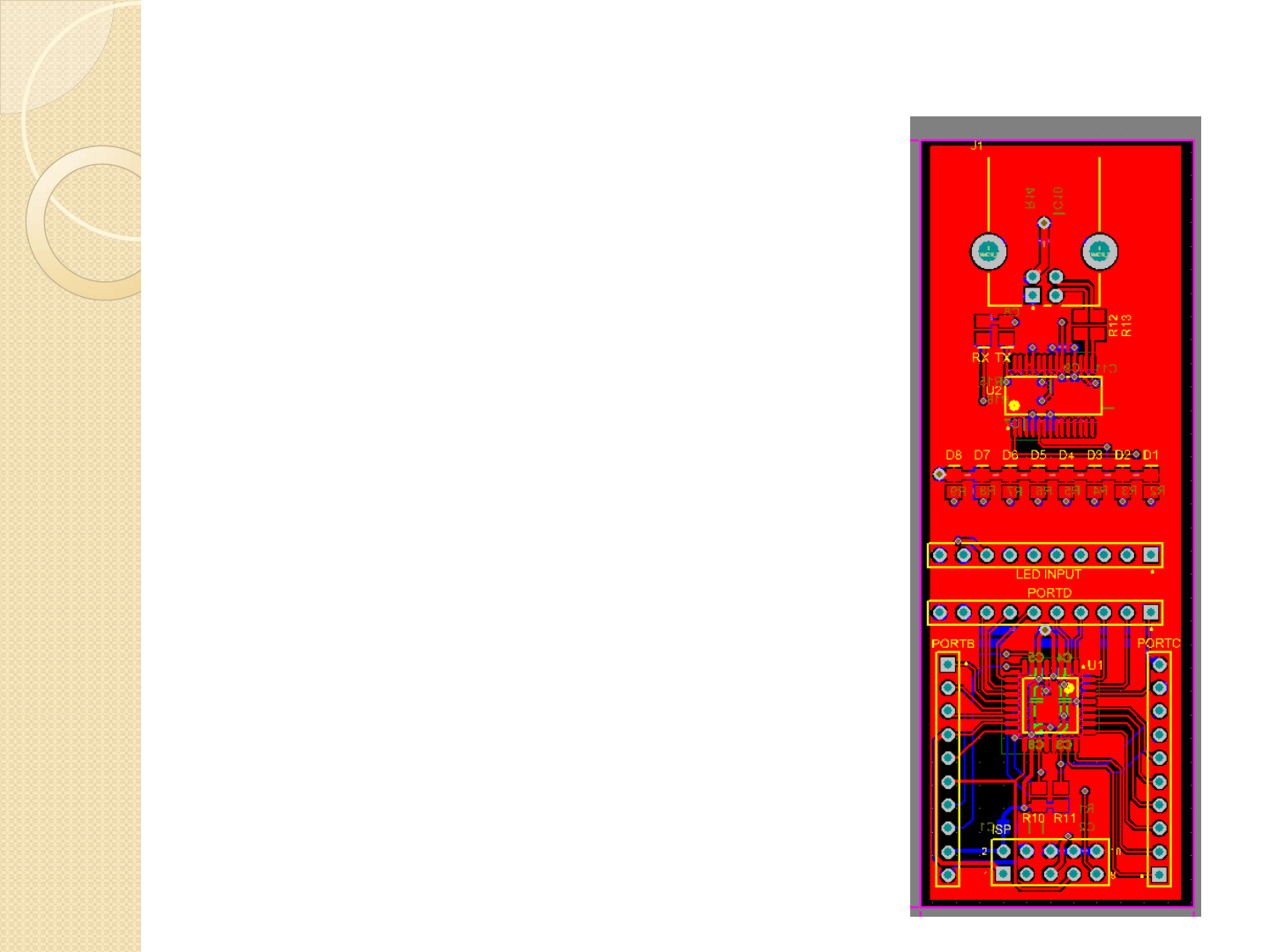
P4 and P5 are not very intuitive to the end user and should probably be
changed to something more descriptive.
Also, the 8-bit LED display can also be changed to Bit0, Bit1, etc… or
1,2,4,8,… so a user can easily add the binary numbers
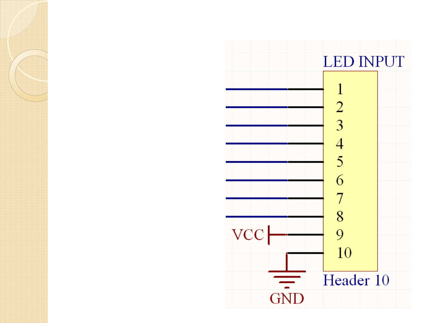
Cleaning Up The Design
Go back to the
schematic, and change P5
to ‘LED INPUT’
Change P1 to PORTB
Change P4 to PORTD
Change P2 to PORTC
Change P3 to ISP (In
circuit serial
programming)
Change D9 to TX
Change D10 to RX
We are making 7
changes to component
names here
Cleaning Up The Design
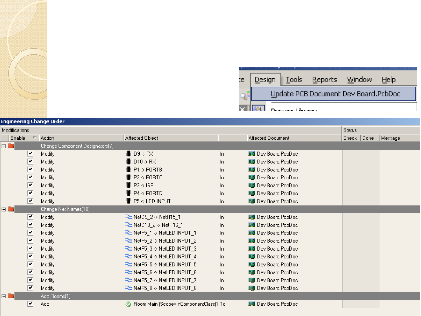
Click DESIGN > Update PCB Document
Dev Board
As a result of changing the component
names, some nets changed also. Apply all
changes except adding the room
Cleaning Up The Design
The changes have taken place and now we each connector is more descriptive
This method can also be used to change PCB footprints, etc…
Cleaning Up The Design
You can make the font larger or in bold, or change the font itself if you want to, just
double click the text to bring up the menu
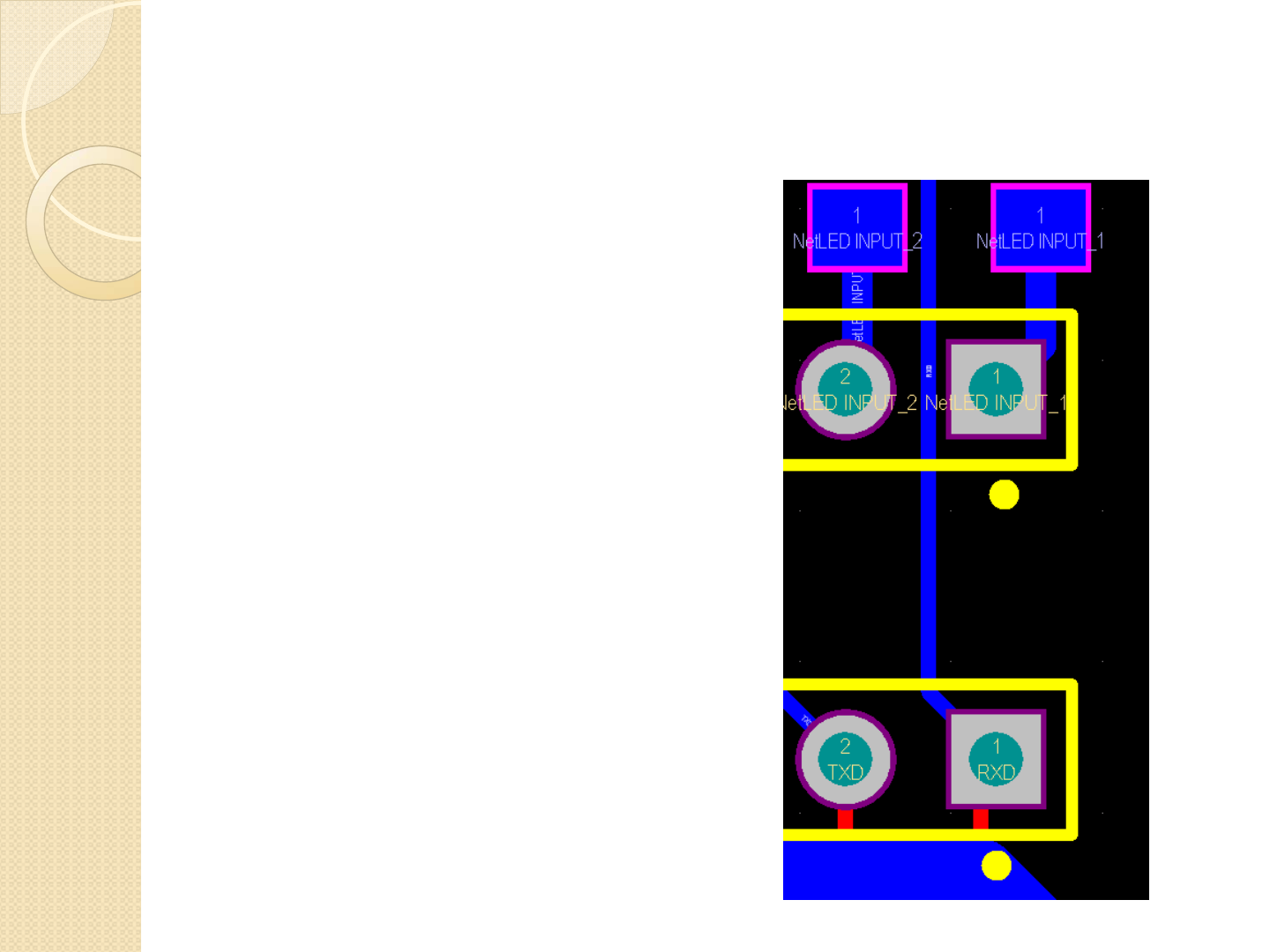
These connectors will have pin headers on them once assembled, so the Pin 1
indicator with the rectangular pad will be invisible to us. We need to add a better
Pin 1 indicator.
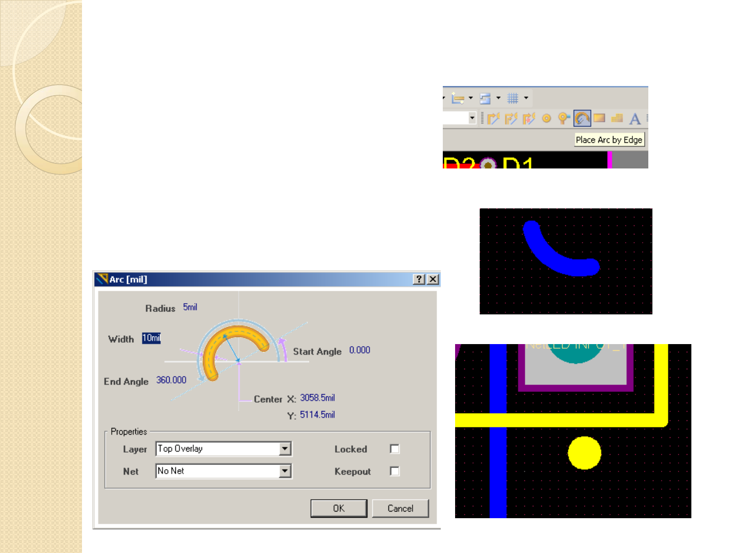
Cleaning Up The Design
Click the place arc by edge
Place an arc anywhere on the board
Double click on the arc to get the
prompt below, change:
◦Radius = 5 mil
◦Width = 10 mil
◦Start Angle = End Angle = 0
◦Layer = Top Overlay
Cleaning Up The Design
Copy & Paste the arc and place next to
the Pin 1’s for the 10 pin headers
Cleaning Up The Design
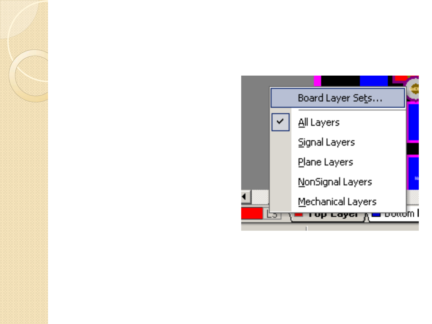
We should create two new board layer
sets.
One where only items on the TOP of
the board are visible
One where items on the BOT of the
board are visible
Click the ‘LS’ at the bottom of the
screen and click ‘Board Layer Sets’
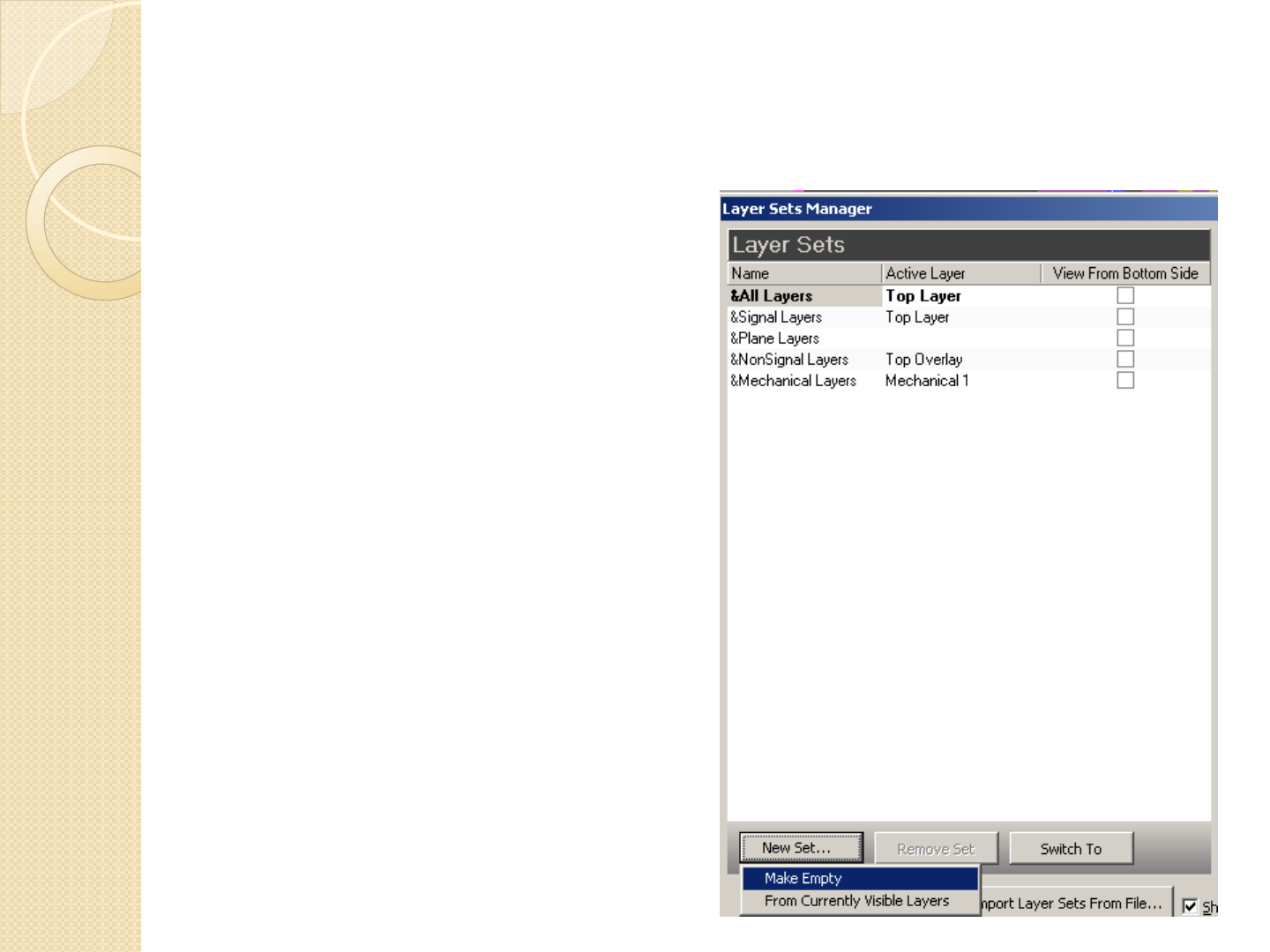
Cleaning Up The Design
Click ‘New Set’ in the bottom left
Click ‘Make Empty
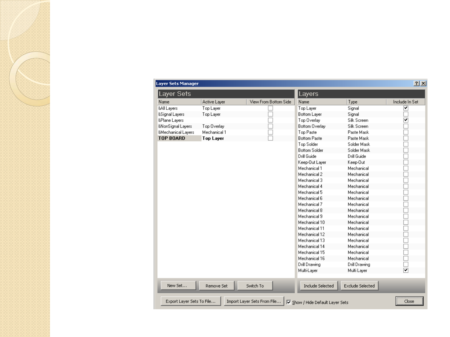
Cleaning Up The Design
Name the set
‘TOP BOARD’
Check the
following boxes:
◦To p L ay e r
◦To p O v e r l ay
◦Multi-Layer
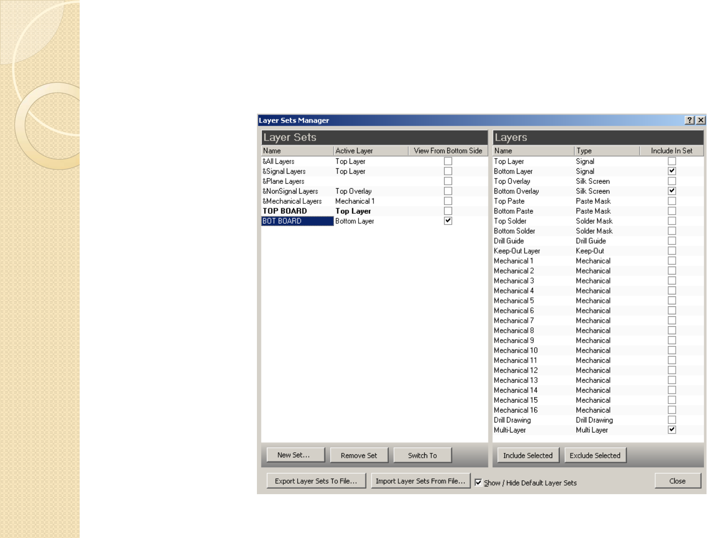
Cleaning Up The Design
Create another
new set called
‘BOT BOARD’
Check the ‘View
from bottom side’
Check the
following boxes:
◦To p L ay e r
◦To p O v e r l ay
◦Multi-Layer
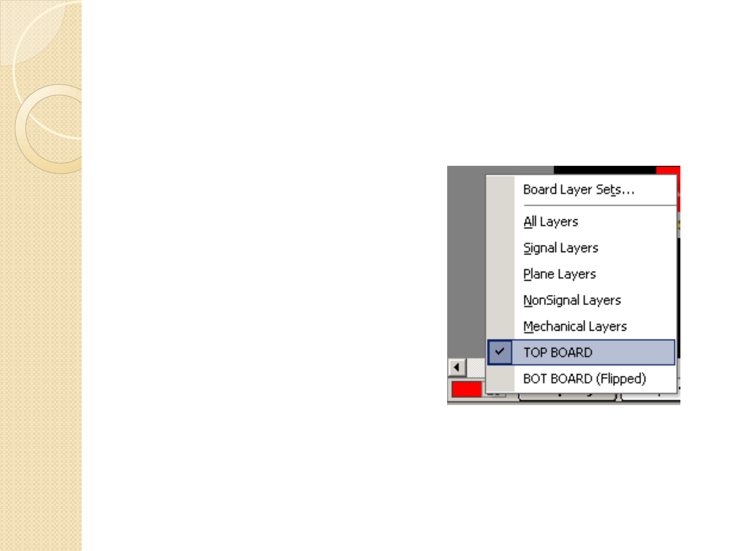
Cleaning Up The Design
Select the TOP BOARD from the layer
set.
This is what the real board will look
like from the top looking down
without the default Superman ability to
see through all the layers
Cleaning Up The Design
This is the best view to
move the top
overlay/silkscreen layers
around to make sure it will
look good when you are
done.
NOTE: You should avoid the
holes with the top overlay,
but do not worry if the top
overlay is on top of a trace

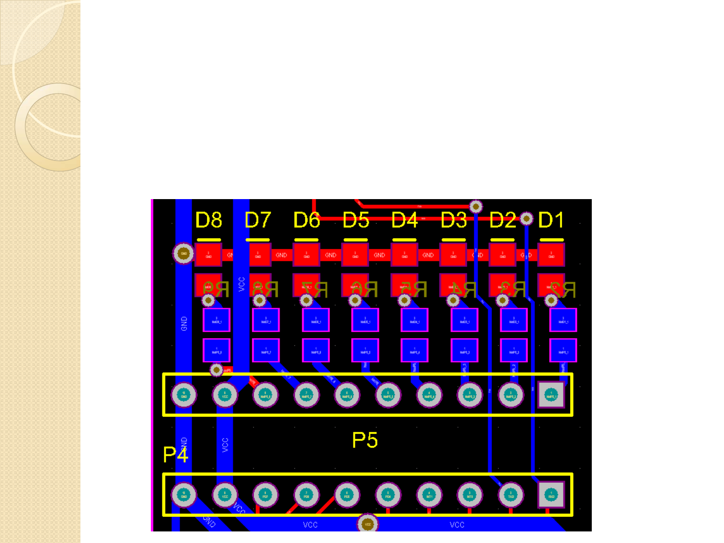
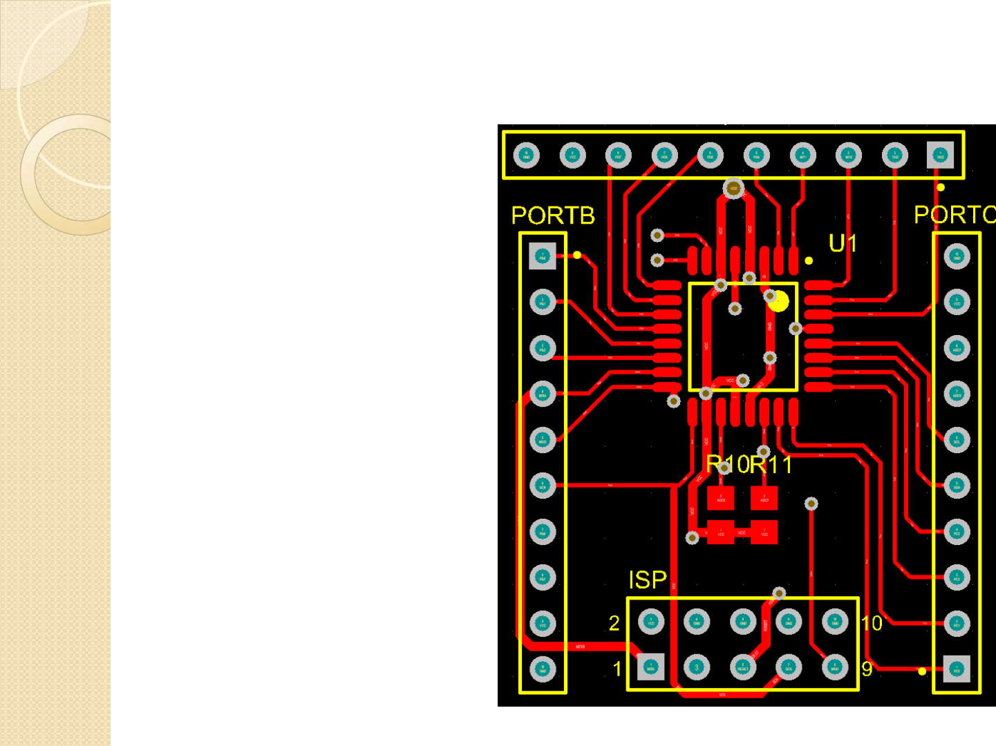
Cleaning Up The Design
I have moved R10 and
R11 indicators to a
location with less
clutter and without
being blocked by a via.

Cleaning Up The Design
I have moved R10 and
R11 indicators to a
location with less
clutter and without
being blocked by a via.
Cleaning Up The Design
This is also the time
where you should
optimize your traces.
The trace on the top
image looks silly and
was probably done
because of optical
interference with the
bottom layer
Viewing ONLY the top
layer can help spot
errors easily and make
a clean and professional
looking PCB
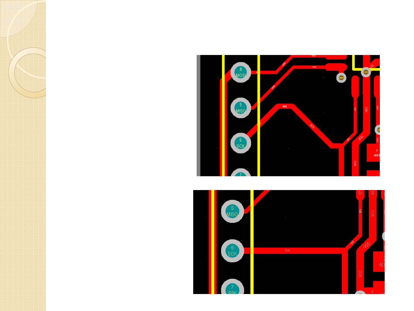
Cleaning Up The Design
Set the active layer set to the BOT LAYER you made
Perform the same optimizations as with the top layer
Cleaning Up The Design
The image to the left shows a DRC error because the polarity marking for
the capacitors are too close together. This is not a real error and we don’t
care about it
The image on the right does not flag for an error, but the bottom overlay for
C1 will not show up properly because of the location of the via.
Does anyone notice anything else wrong with the image to the right ???
Cleaning Up The Design
Is anything wrong with the bottom overlay in this picture ?

Cleaning Up The Design
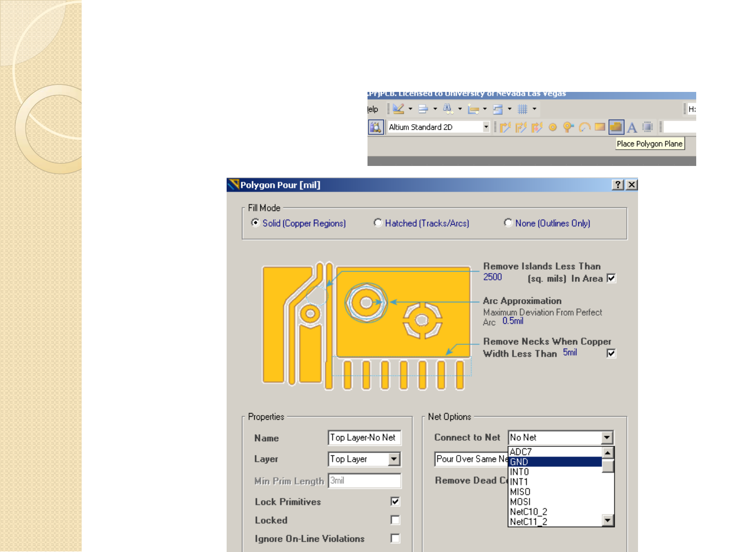
Our board looks OK, but there is a lot of
unused space
We will add what is called a ‘copper pour’ or
‘polygon pour’ to fill in the empty areas
Cleaning Up The Design
Click the polygon plane icon as
shown to the right
Change net to GND
Cleaning Up The Design
Click about 50-100 mils away from
the each corner and then right click
This will begin the polygon
calculation and placement.
NOTE: For large designs this can
take hours
Cleaning Up The Design
Notice how the polygon pour will
avoid a net that is different than
the net assigned to it.
It will put copper everywhere
possible that doesn’t create a
violation
Cleaning Up The Design
On nets that there
is a connection
(GND), you can
see it handles it
exactly the same
as any other net,
but has a few
short connectors
that connect the
pad/hole to the
pour
Cleaning Up The Design
Repeat this
process on the
bottom layer of
the board, also
connecting to
GND
PCB Complete!
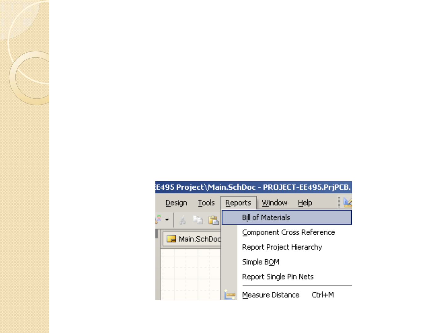
Rather than trying to manually figure out what to
order, we can extract a bill of materials from the
design
This is why it was so important to enter all the
details in correctly earlier
Click ‘Bill of Materials’ as shown below
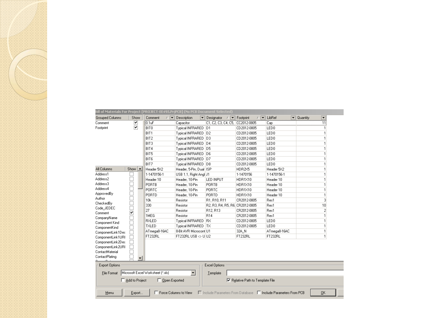
PCB Complete!
Check the box to ‘Open Exported’ and click
‘Export’

PCB Complete!
An Excel spreadsheet of the B.O.M. will open with
all the information you need to quickly order the
parts
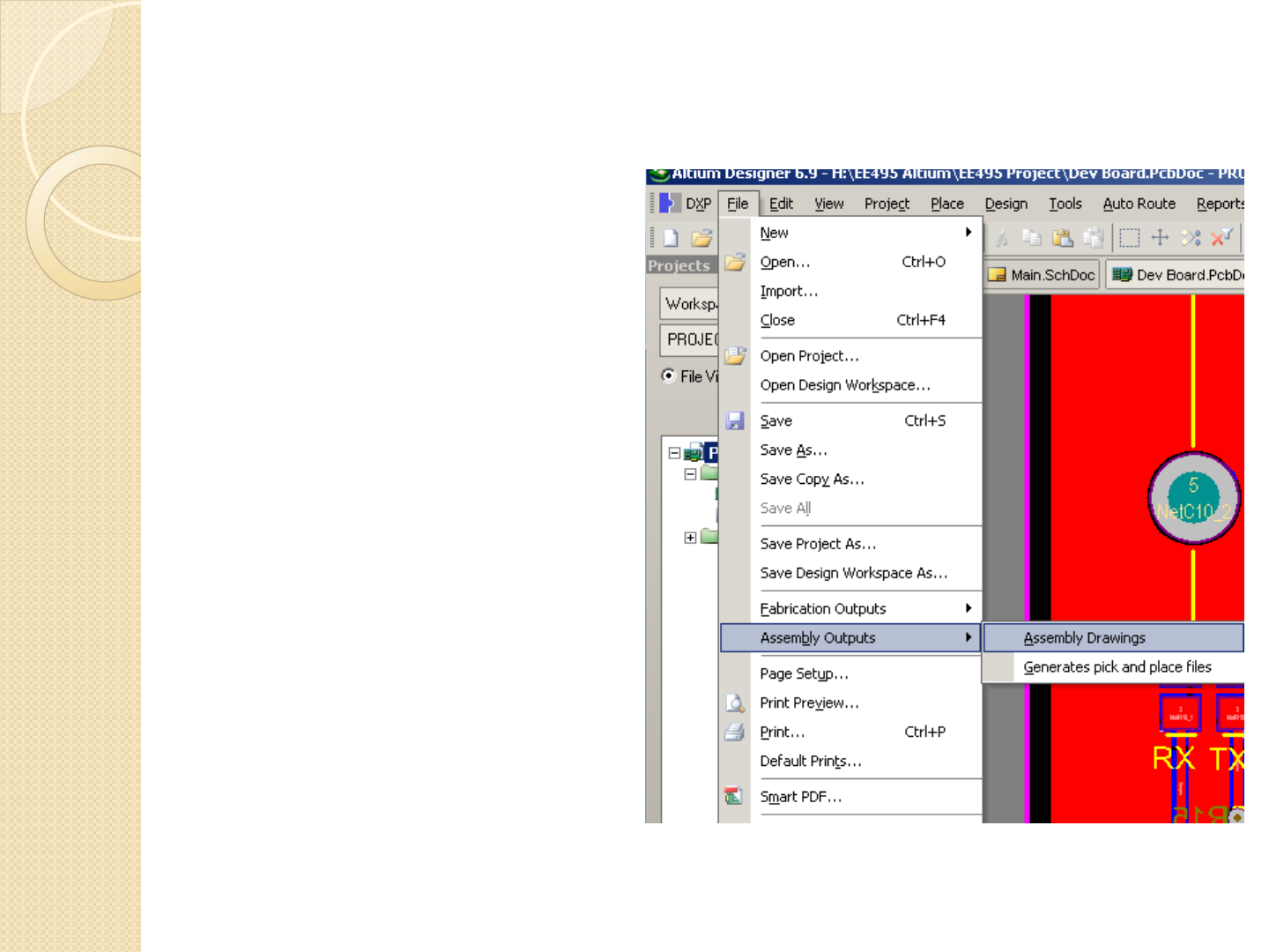
PCB Complete!
From the PCB, click
File > Assembly
Outputs > Assembly
Drawings
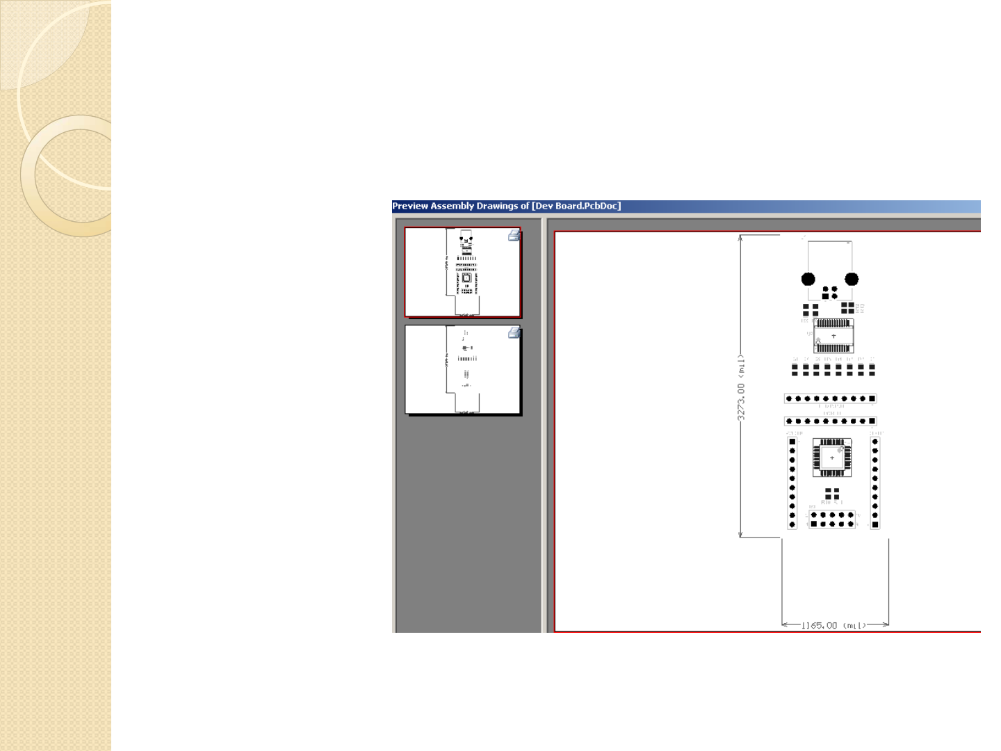
PCB Complete!
This will create
Assembly
Drawings that are
helpful when
assembling the
parts.
Usually I print
these and write
the value of each
component where
the component
goes
PCB Complete!
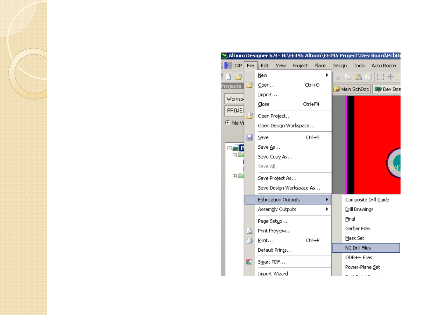
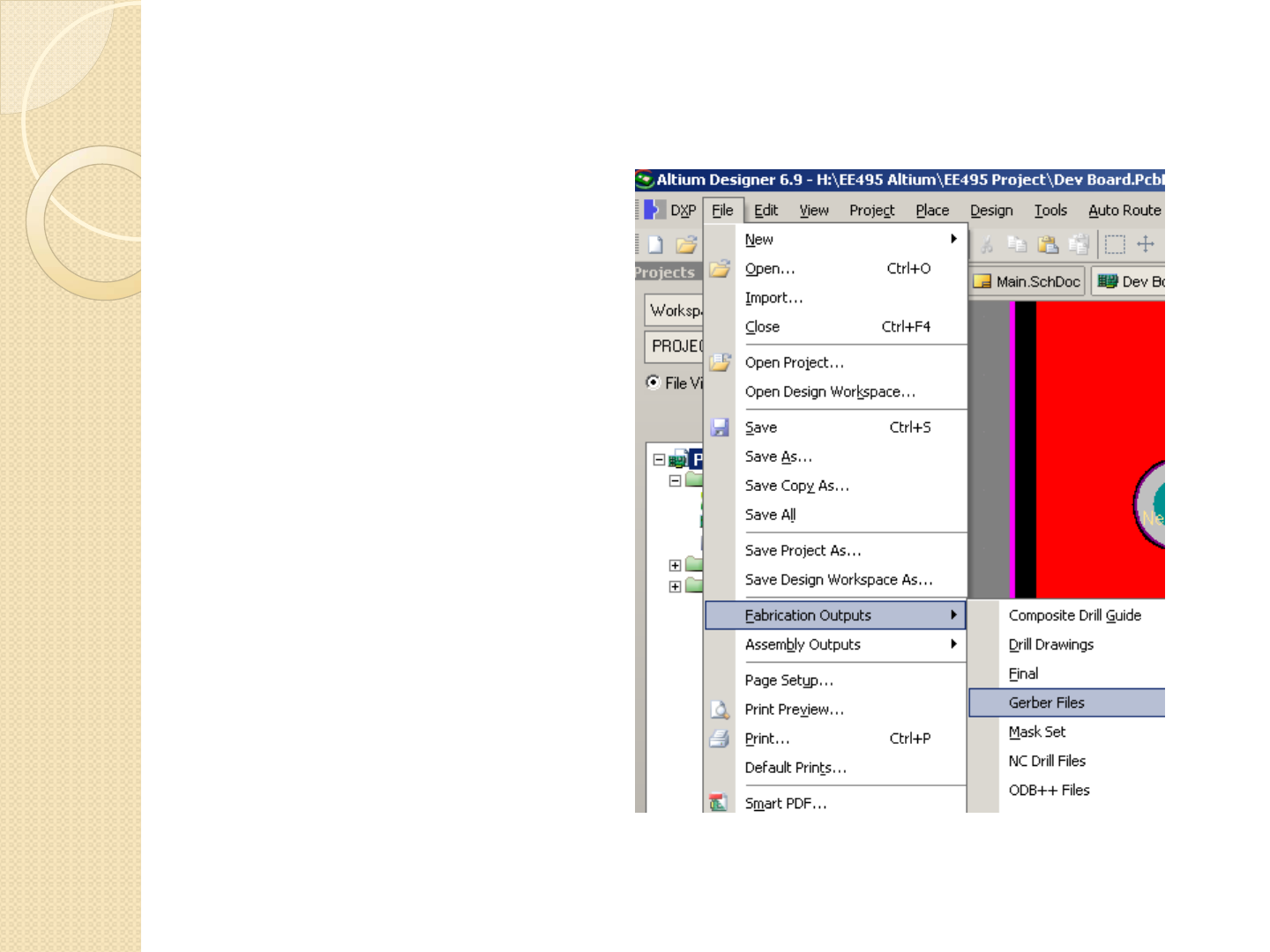
To get the PCB
fabricated the
board house needs
two things:
◦Gerber Files
◦NC Drill Files
Follow the menu
sequence to obtain
the NC Drill files
first
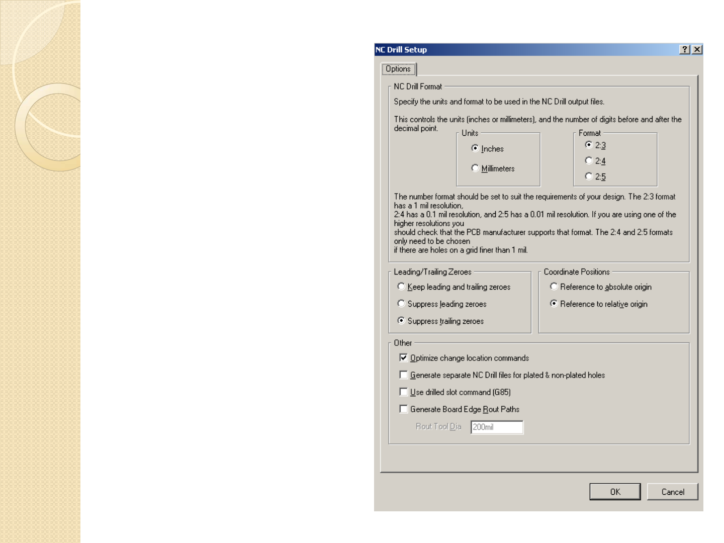
PCB Complete!
Leave these values
as default unless
you know what
you are doing
Click OK
PCB Complete!
Leave these values
as default unless
you know what
you are doing
Click OK

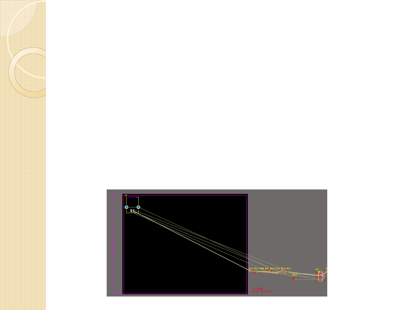
PCB Complete!
A PCB with only
holes in it should
appear.
These holes match
the holes of your
design
Go back to the
PCB
PCB Complete!
Follow the menu
sequence to create
the output Gerber
files
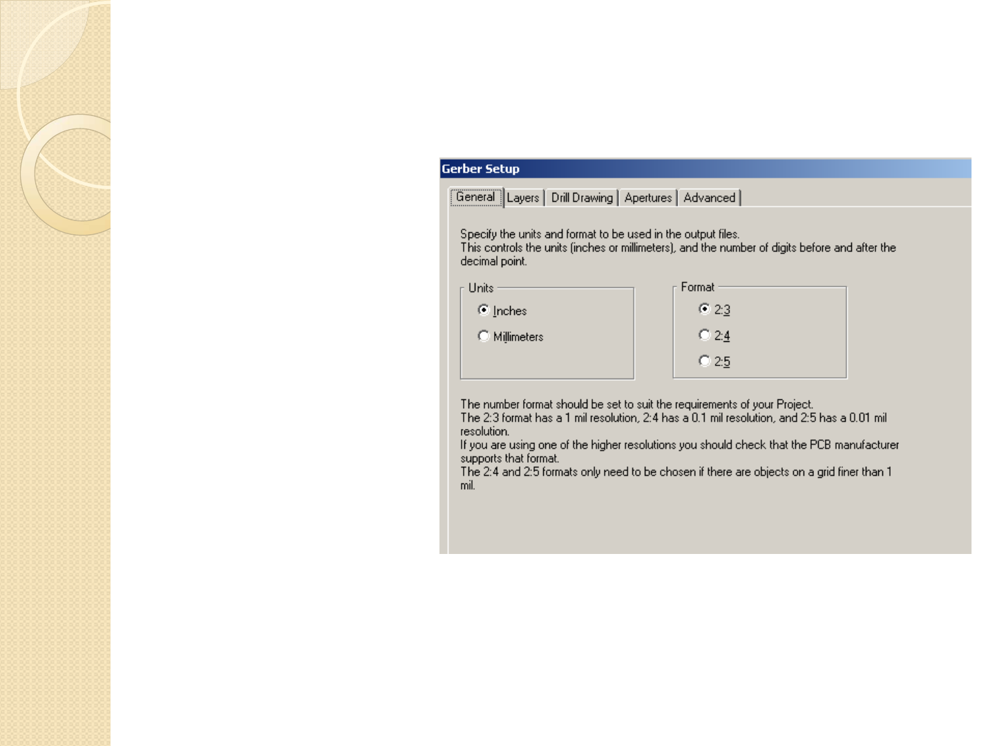
PCB Complete!
Leave the values
intact under the
‘General’ tab
PCB Complete!
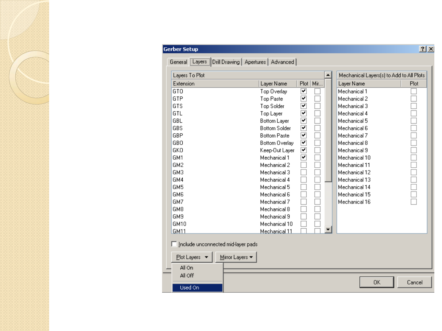
Under the Layers
tab, click ‘Plot
Layers’ and you
can either choose
ALL ON or USED
ON.
If you choose
USED ON you
should manually
check the bottom
two layers called
◦GPT – Top Pad
Master
◦GPB – Bottom Pad
Master
PCB Complete!
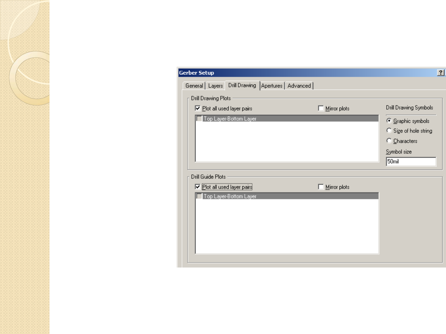
Under ‘Drill
Drawing’ (This is
different than NC
Drill files) check
the ‘plot all used
layer pairs’ in the
two locations at
the left
PCB Complete!
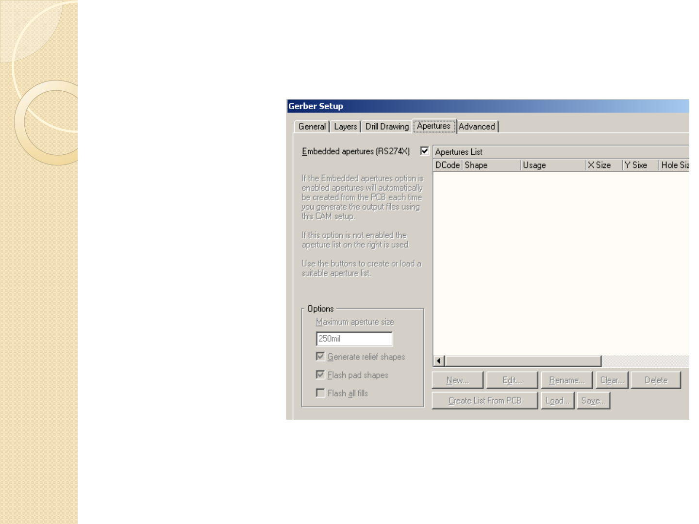
Under ‘Apertures’
make sure
Embedded Apertures
are selected
(RS274X)
NOTE: Before
RS274X, there was
RS274D, which did
not contain the
embedded
Apertures, most
everyone requires
RS274-X format
Ignore the Advanced
tab and click OK

PCB Complete!
Again, depending on
the complexity of
the design and the
capabilities of your
computer, this could
take hours.
This design should
take around 10
seconds
Notice how two
new files have been
created, These are
CAM files
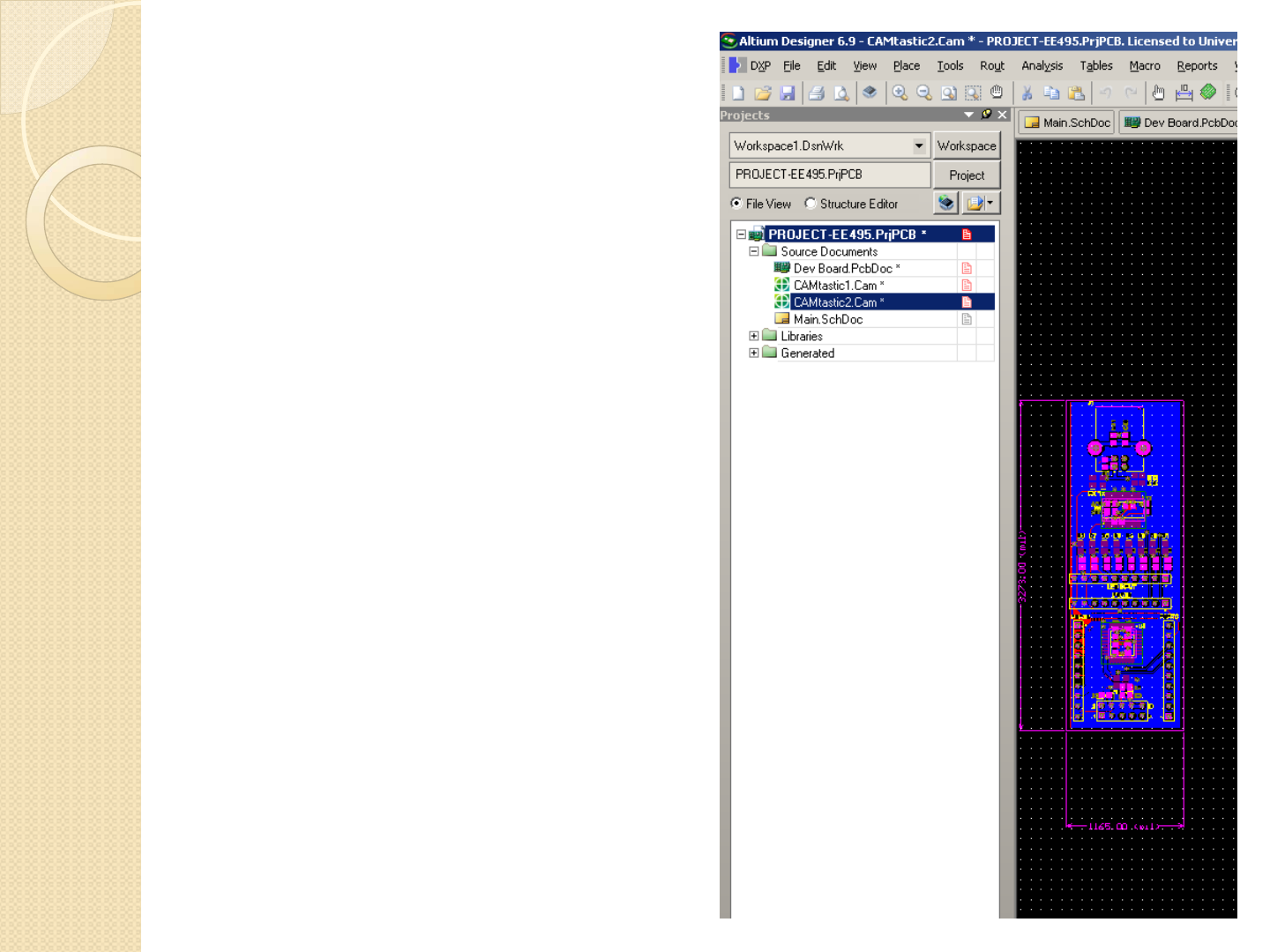
PCB Complete!
The PCB Document is a single
document
The Gerber files are a list of
around 10-40 individual files
with information on each layer
This standardized format of
Gerber files means the board
house does not need to own
every software package
imaginable
CAM Viewers are required to
open these ‘generic’ Gerber
files. CAMtastic is Altiums
included CAM viewer

PCB Complete!
Highlight the CAMtastic file
with your board layout on it
Click the CAMtastic tab

PCB Complete!
Inside the CAM viewer, you
can see a rather crappy
rendition of your board and
a bunch of color coded files.
You may also notice there
are new buttons in the menu
screen. This is so you can
modify the output files
(Gerber files) directly.
PCB Complete!
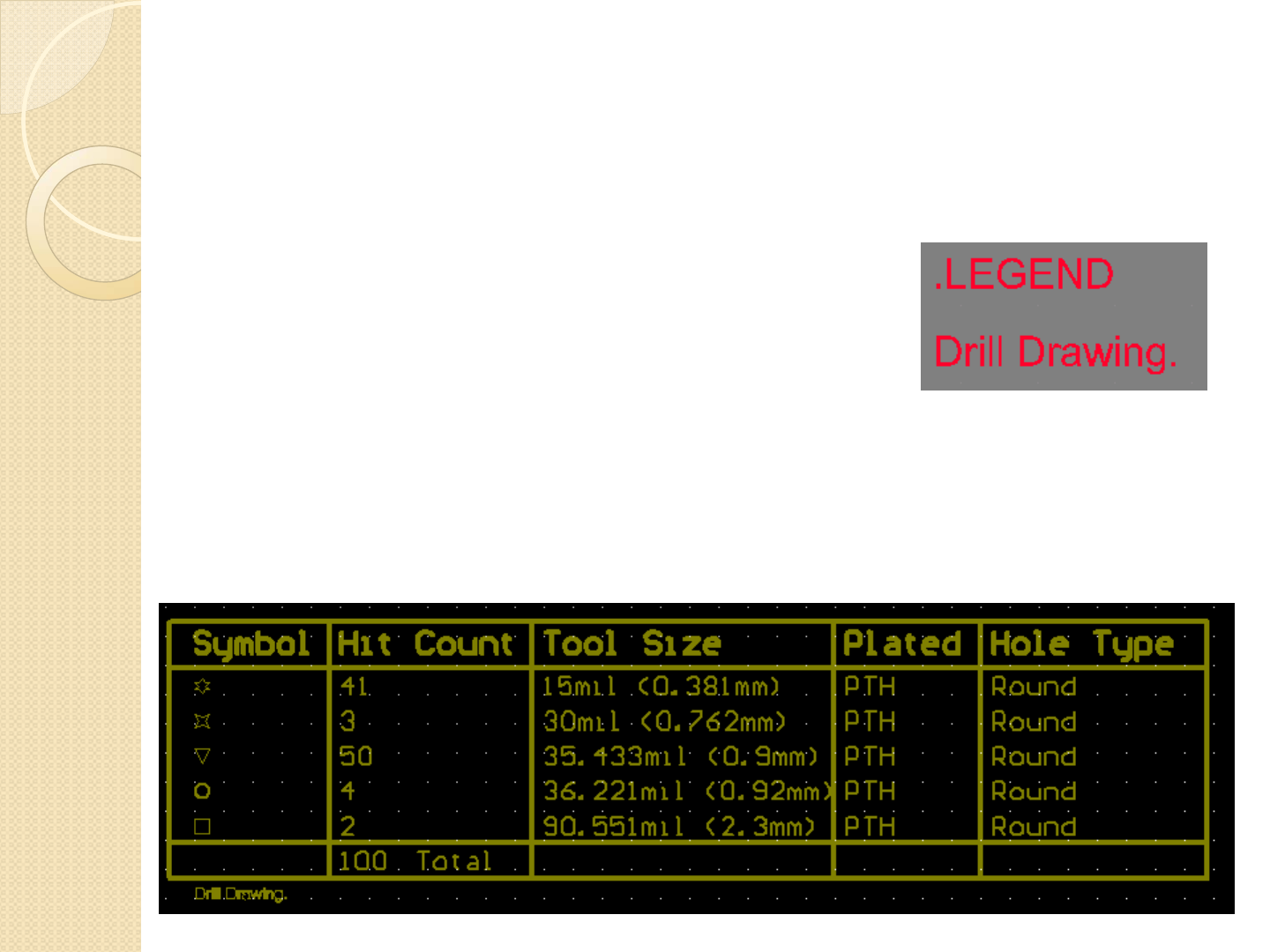
You may notice a new chart that appears
in the Gerber files.
If you remember the .LEGEND from the
PCB layout, that is known as a SPECIAL
STRING which performs a special
function.
This particular one creates information
about the holes and represents this
information with symbols

PCB Complete!
Although it looks like
someone did graffiti on your
work, these patterns
represent the type of hole it
is, and the size of the hole
The + is the center of the
hole, and the pattern reveals
drill information from the
.LEGEND special string
NOTE: There are much
better CAM viewers than
Altium’s, Some are included
in my syllabus
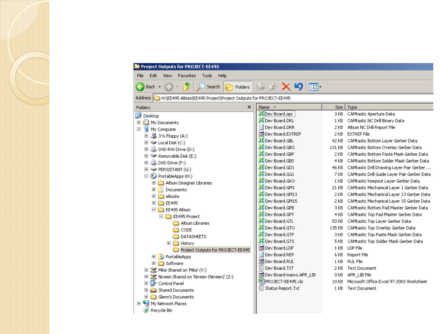
PCB Complete!
When you
created the
Gerber files
and NC Drill
files, a new
folder is
automatically
created in
your project
folder called
‘Project
Outputs’
All these files
are what you
send to get
your board
made
Altium is nice
enough to
register the
file extensions
with Windows
so you can
see which
each file is

PCB Complete!
Click Report > Board information for a quick
summary of your board
Click ‘REPORT’ and include this report file in
any project files you send me. POINTS
WILL BE TAKEN OFF IF IT IS NOT
INCLUDED
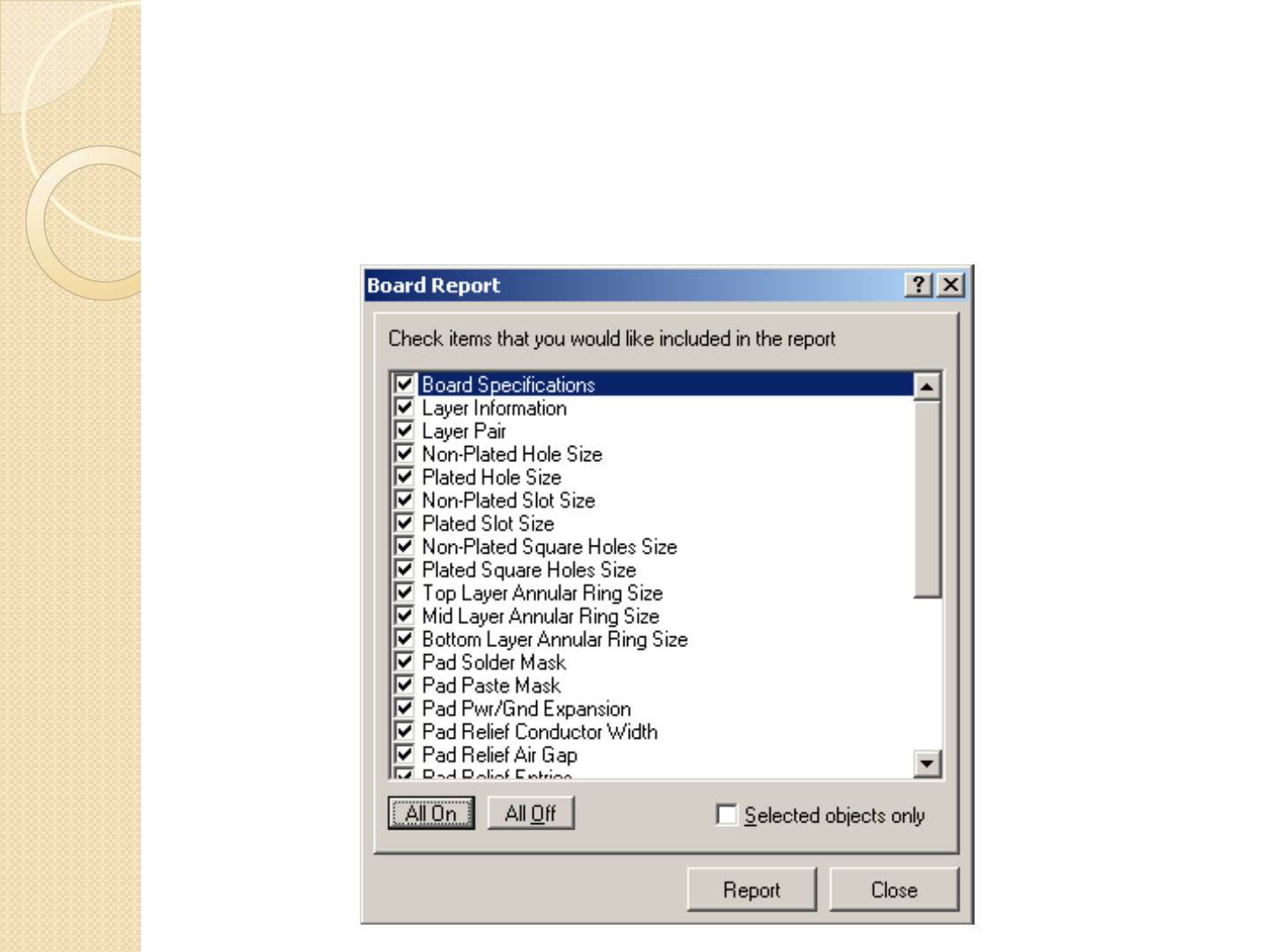
PCB Complete!
Click the ‘All On’ box and click ‘Report’
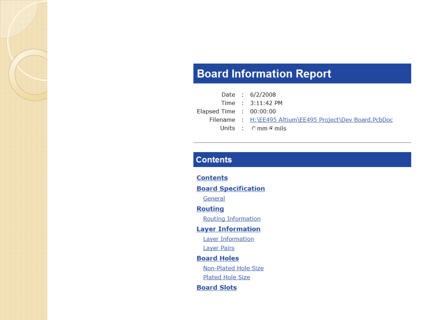
PCB Complete!
An HTML report file is created
(file path is given) and you can
select the units.
This HTML file has hyperlinks so
you can quickly view areas

PCB Complete!

PCB Complete!
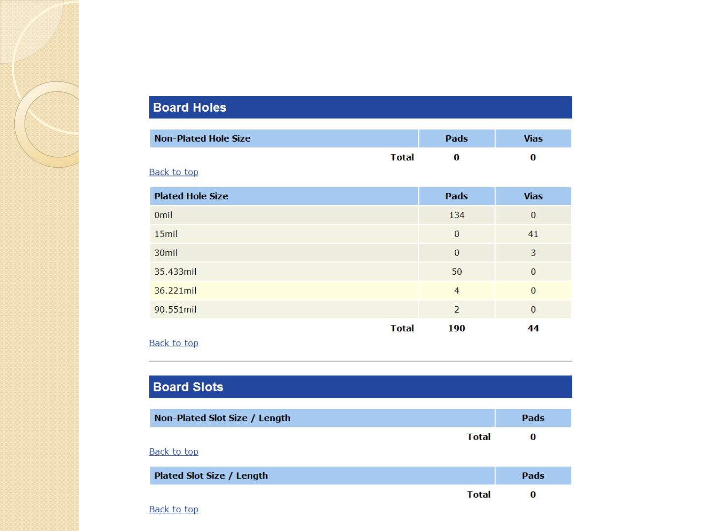
PCB Complete!
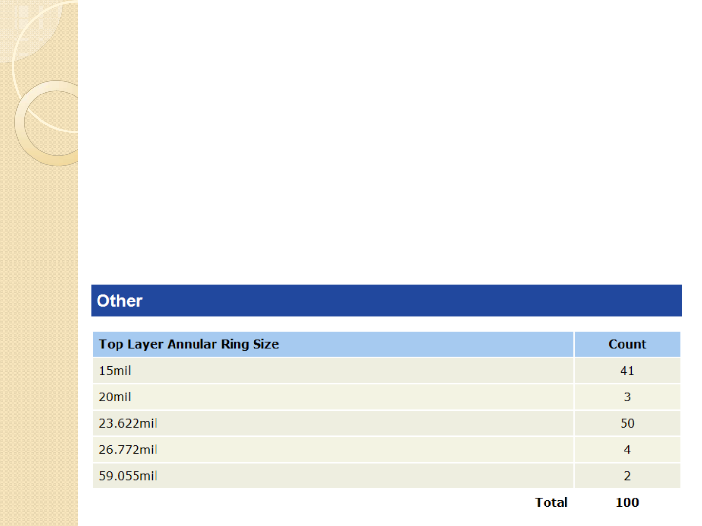
PCB Complete!
Be careful with this one, The annular ring
size from board vendors is defined
differently. The Ring size is this
number divided by 2
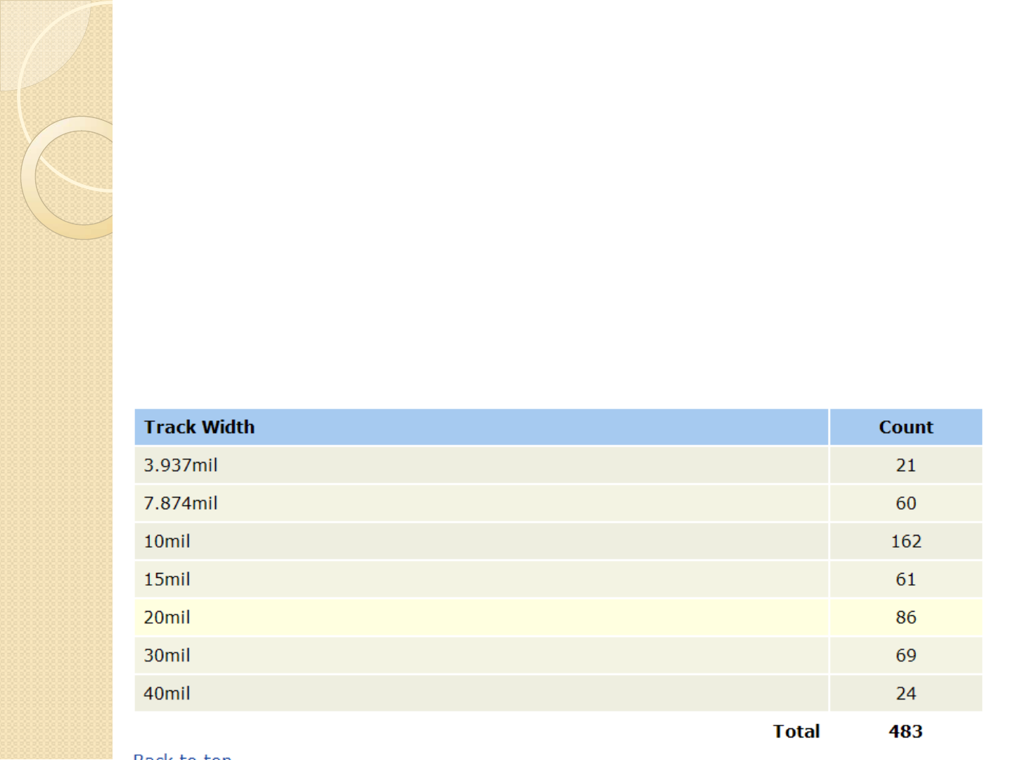
PCB Complete!
What’s wrong with this ????
We specified a minimum trace width of
10 mils, yes we have 81 tracks with a
more narrow width. Is the DRC Broken ?
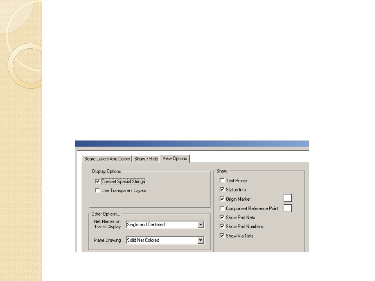
Special Strings
Type ‘L’ from the PCB screen and click the ‘View
Options’
Check the box that allows you to Convert Special
Strings
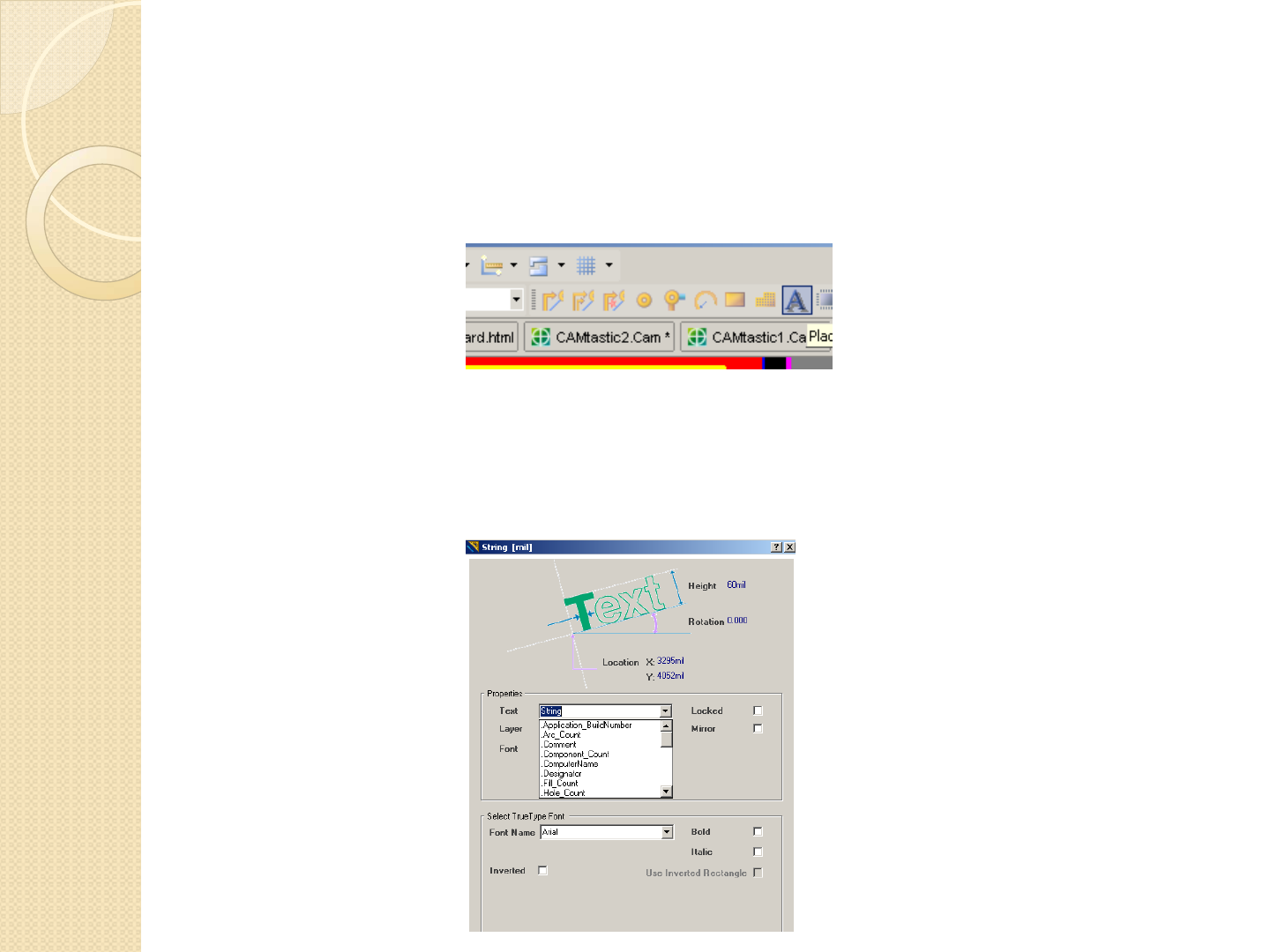
Special Strings
Click the Text Entry icon from the PCB menu
Double click on the text you placed to get the
following menu

Special Strings
Shown to the right
are all the available
Special Strings that
can be placed in
PCB Entry.
NOTE: This list
usually changes
with each revision


Part 2: Intermediate Guide
This portion of the guide contains more
advanced features as is geared towards:
◦Hardware Engineers
◦Signal Integrity Issues
◦Advanced Altium Designer features
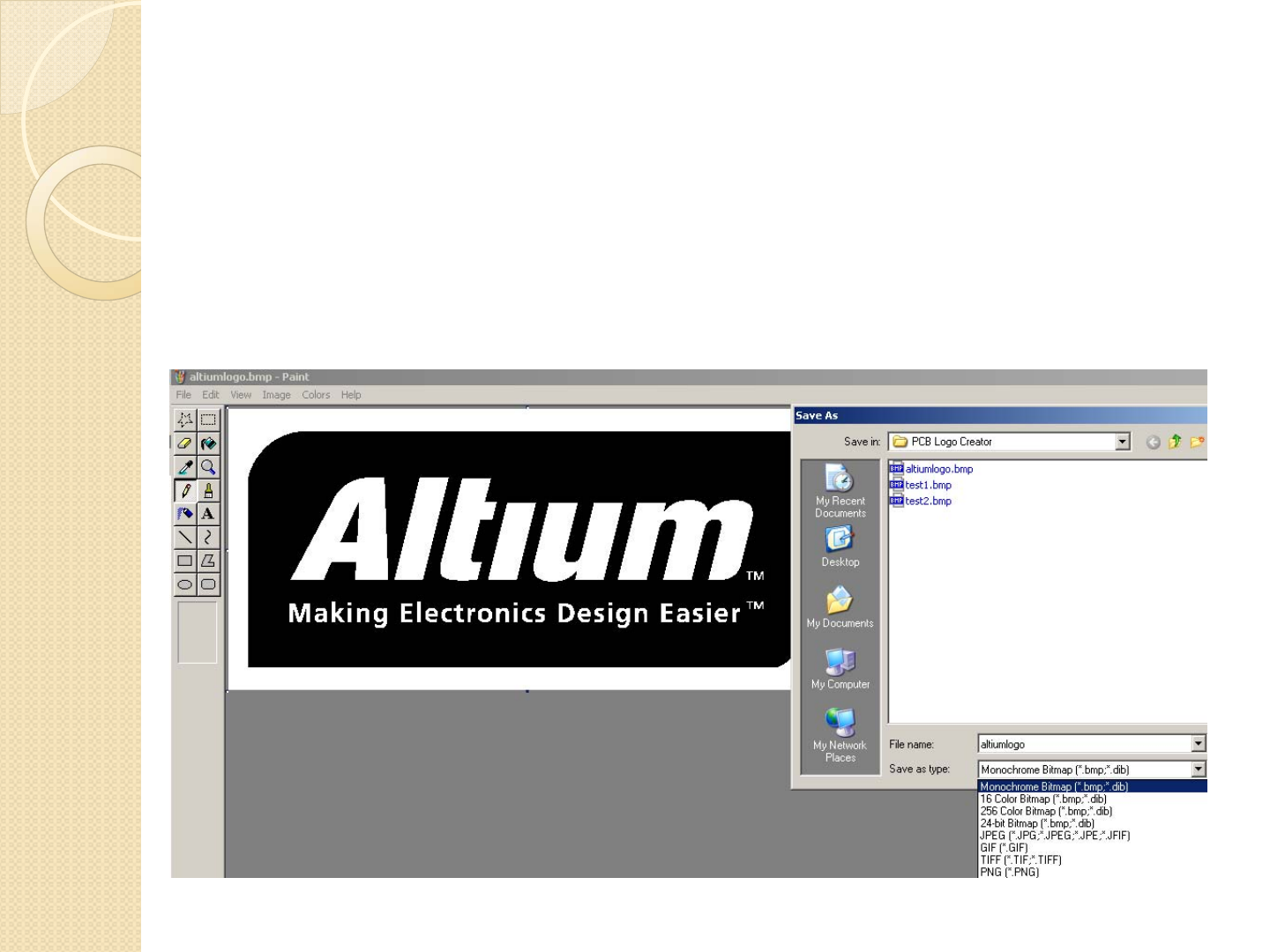
Logos
The image you want to create a logo out of MUST be saved
as a MONOCHROME BITMAP file. This can be done by
opening the file in MS Paint and saving the file as shown in
the box below

Logos
The most requested feature people want
to know is how to implement a logo in
their design. There is a script located in
this directory
C:\Program Files\Altium Designer 6\Examples\
Scripts\Delphiscript Scripts\Pcb\PCB Logo Creator
Add Converter.Pas to your project. This
script will convert any Black and white
image to a PCB footprint.
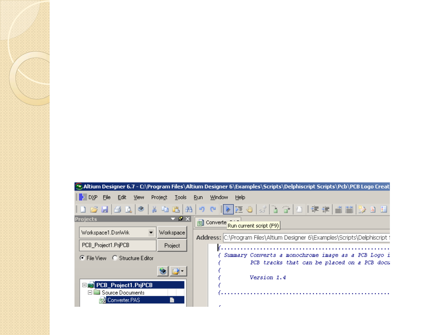
Logos
Notice the different menu icons when
you have a script selected. From here, you
can click the small triangle button to
execute the script or press F9
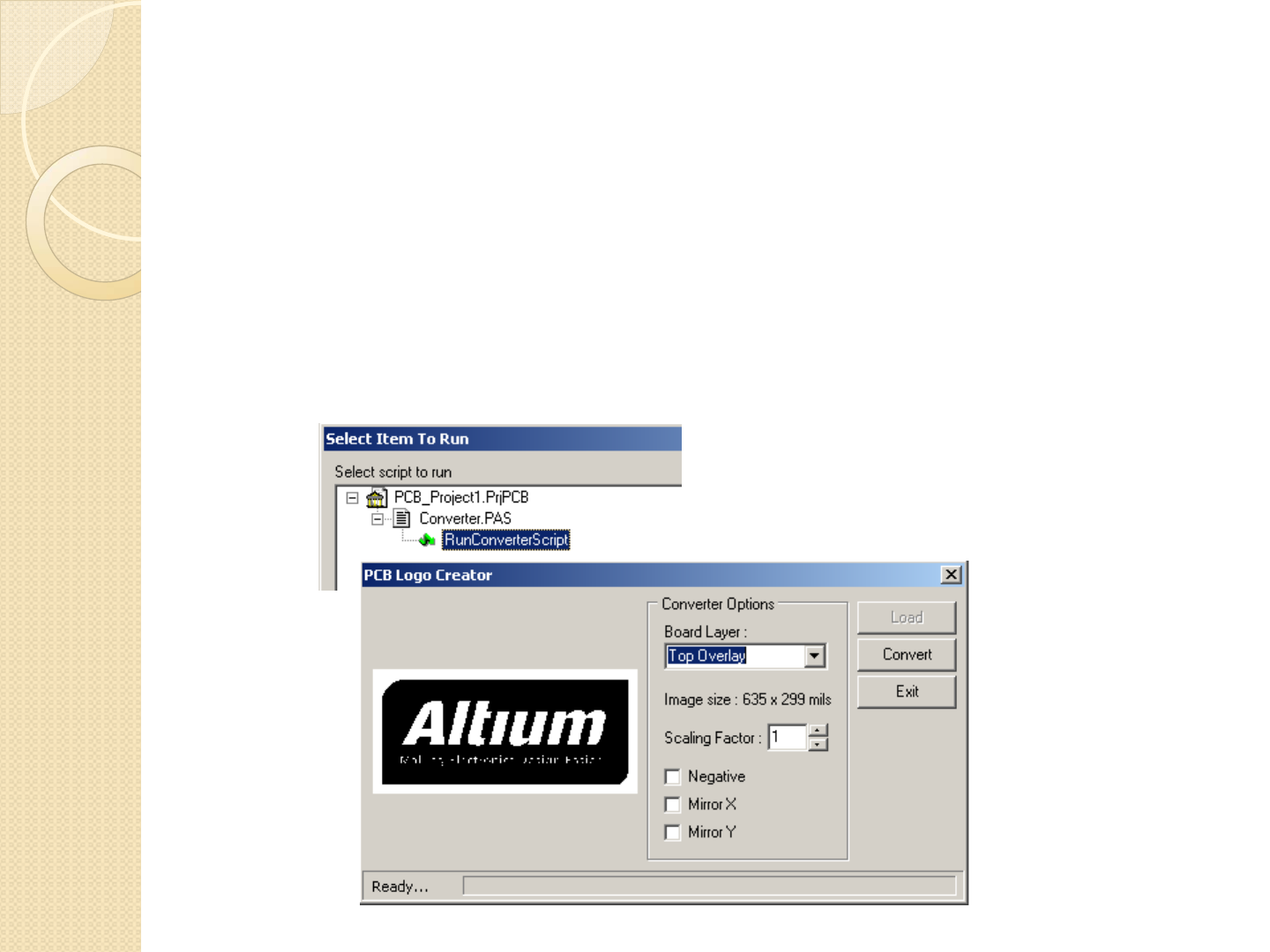
Logos
Make sure to change the layer to TOP OVERLAY
(Silkscreen) and load the .BMP image. Notice there is an
option for scaling factor, and it shows image size.
Image size will be the dimensions of the logo in mils
once the conversion is complete. Using the scaling
allows you to make the exact dimensions you want for
the image
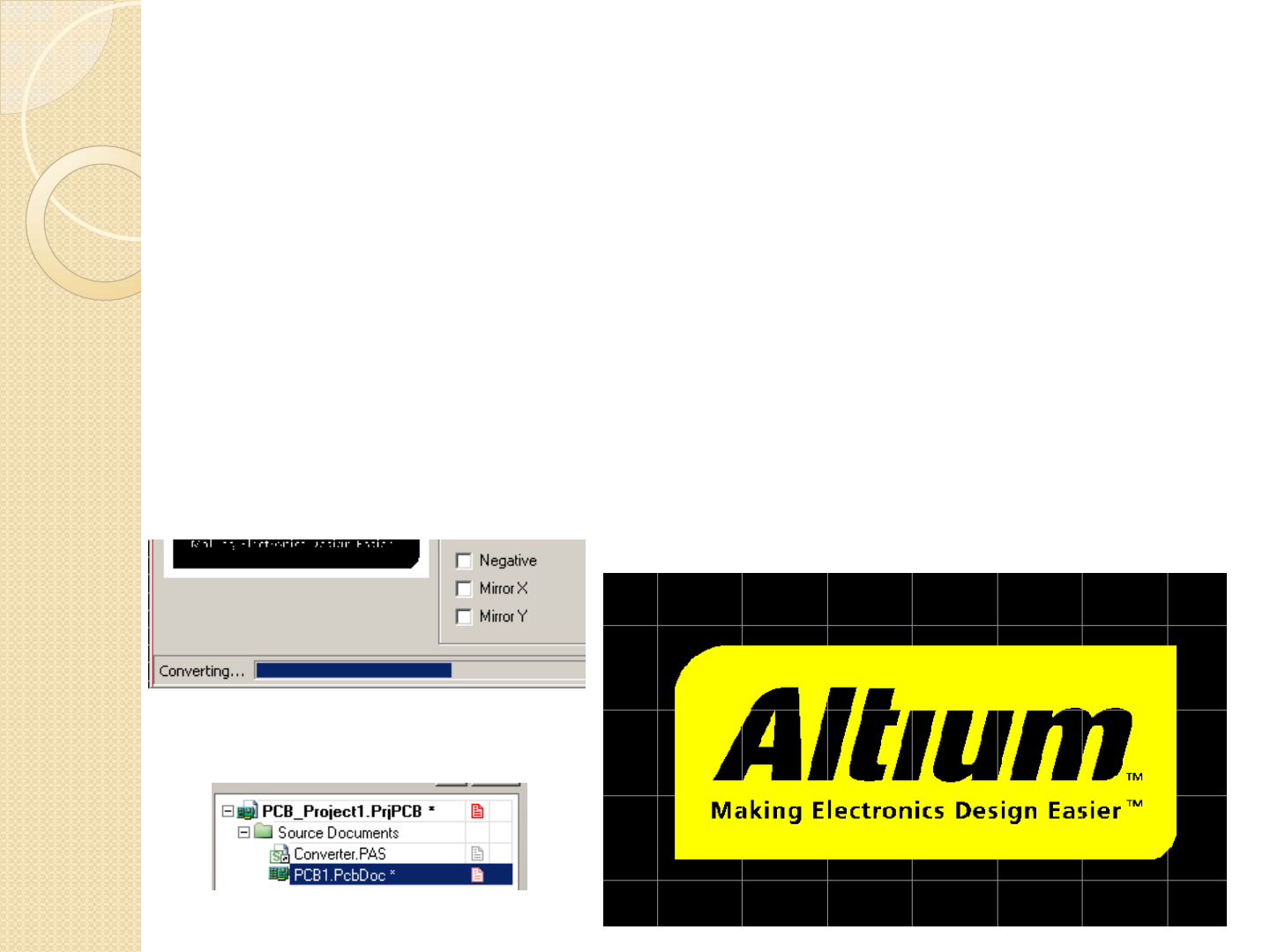
Logos
Depending on many factors, such as complexity,
and processing power, the converting time may
vary
When complete, there will be a new PCB
document added to your project containing your
logo. It is a good idea to copy & paste the logo
into your footprint library for future use
Logos
Logos can also include:
◦Compliance icons such as FCC, ROHS, CE,
etc..
◦Warnings such as ESD, High Voltage, Etc
◦Make sure you can legally use any logos you
place on your PCB

Multiple Monitor Setup

Schematic/PCB Interaction with
Multiple Monitors

Circuit Simulation

Version Control System

Snippets
Snippets allow for quick reuse of existing
designs.
Schematic, PCB, Routing can all be saved as
snippets.
Easily found by clicking the ‘System’ bar in
the bottom right corner, then enabling
‘Snippets’
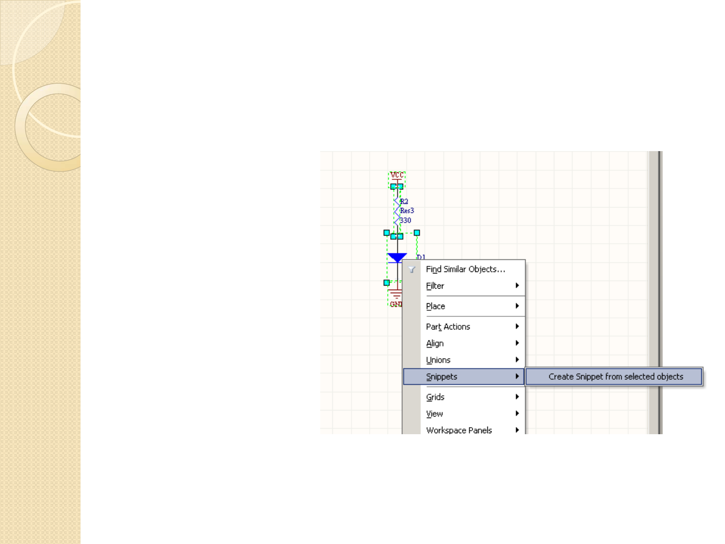
Snippets
To create a snippet,
simply highlight the
schematic/pcb
information you
would like to reuse,
right click, then
select ‘Add to
Snippet’
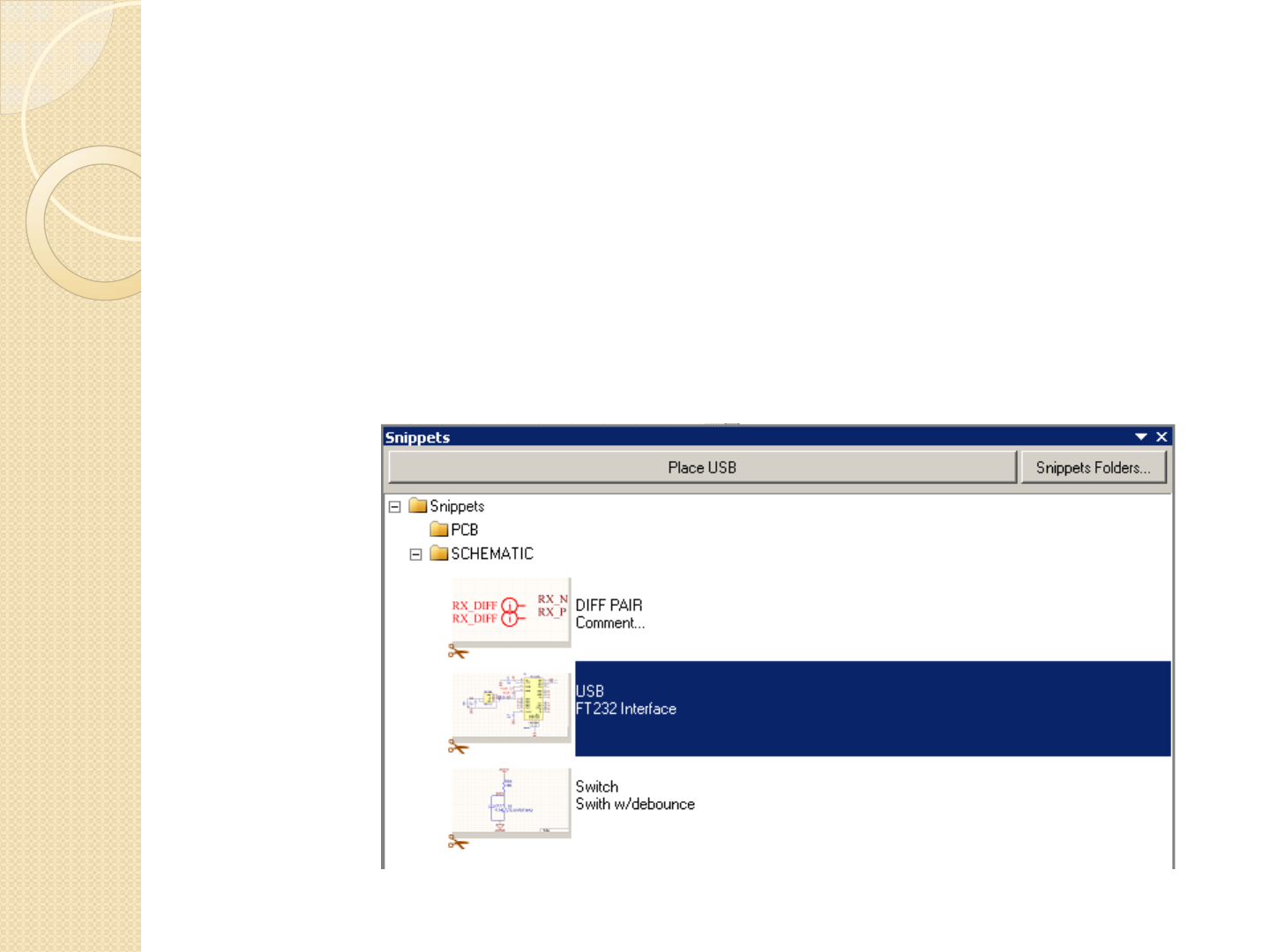
Snippets
You can create multiple subfolders to keep your snippets
organized.
To place a snippet, simply highlight the snippet of your choice,
and click the ‘PLACE’ button at the top of the snippets box.
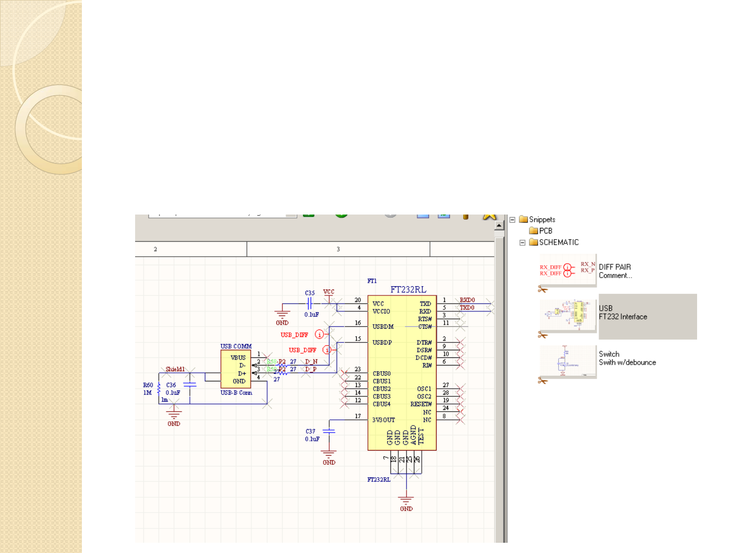
Snippets
When placing a snippet, you will see a rectangular boundary outline of the object. Once the location is
held, you will place the ENTIRE snippet as shown below.
Notice that nodes, net labels, differential pairs, and component ID’s are all pasted from the snippet.
When pasting a PCB snippet, the footprint, layer information, traces, etc.. Are all pasted from the
snippet
This powerful, simple to use feature is a great timesaving tool when creating multiple projects

Inspector Tools
The PCB and Schematic Inspector tools
for some reason are hidden a little deep
inside the software.
This feature allows you to easily and
quickly make project-wide changes to
components, nets, etc.
Serious users will be amazed at how
much time is saved by using the Inspector
tools
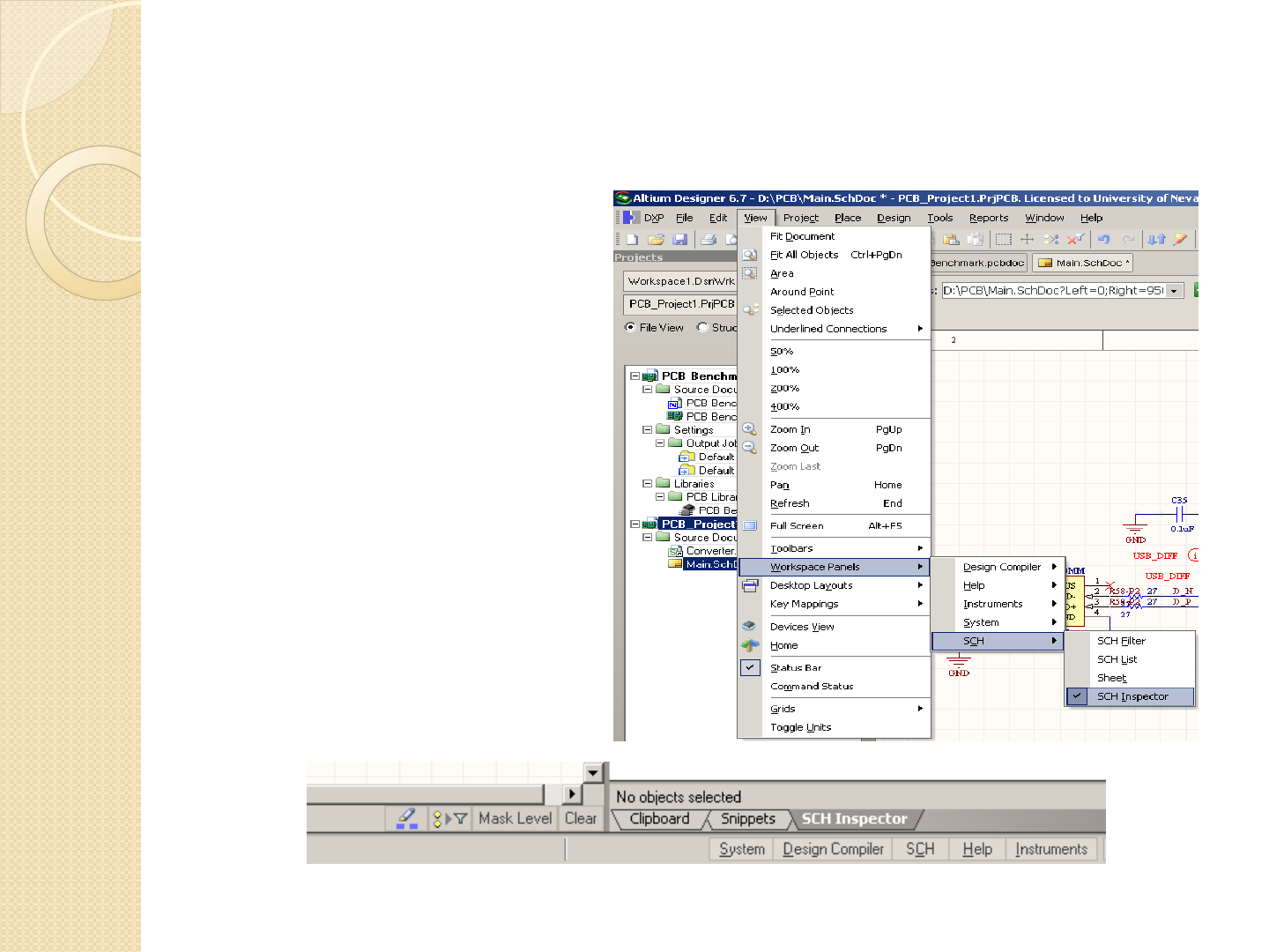
Schematic Inspector
Start out by
docking the
Schematic
Inspector. I
usually keep it
in the side
dockbar
which is
useful for a
multiple-
screen display.

Schematic Inspector
By selecting multiple objects (shift & left
click), you can see the Schematic
Inspector update the display for all
selected parts.
Items showing <…> have varying values
for more than one component (Such as
location X/Y coordinates)
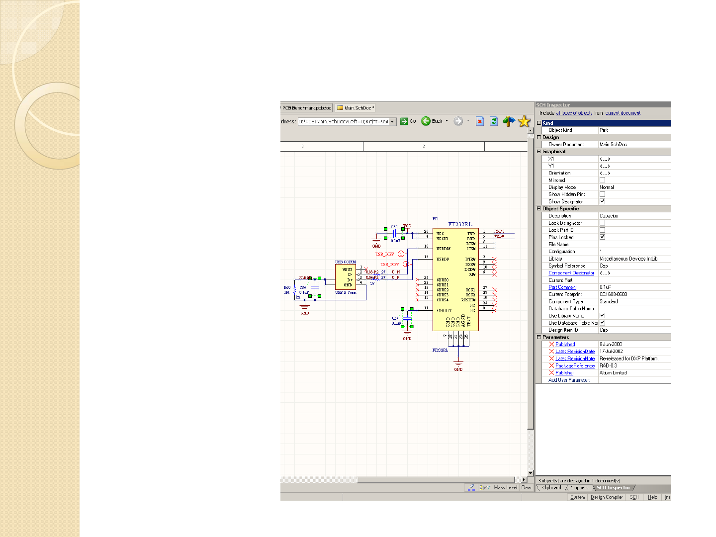
Schematic Inspector
In this example,
Three
capacitors are
selected
Schematic
Inspector
shows that 3
objects are
selected in the
bottom of it’s
taskbar.
From this stage,
any value
changed inside
the inspector
will
immediately be
changed in ALL
SELECTED
OBJECTS
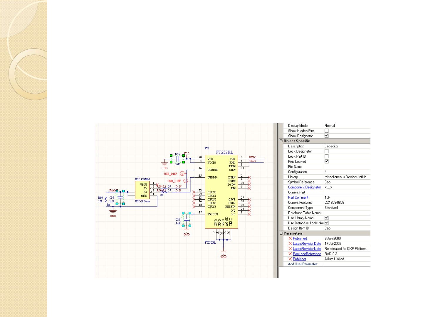
Schematic Inspector
Changes such as changing the part comment from 0.1uF
to 1uF are immediately visible in the schematic
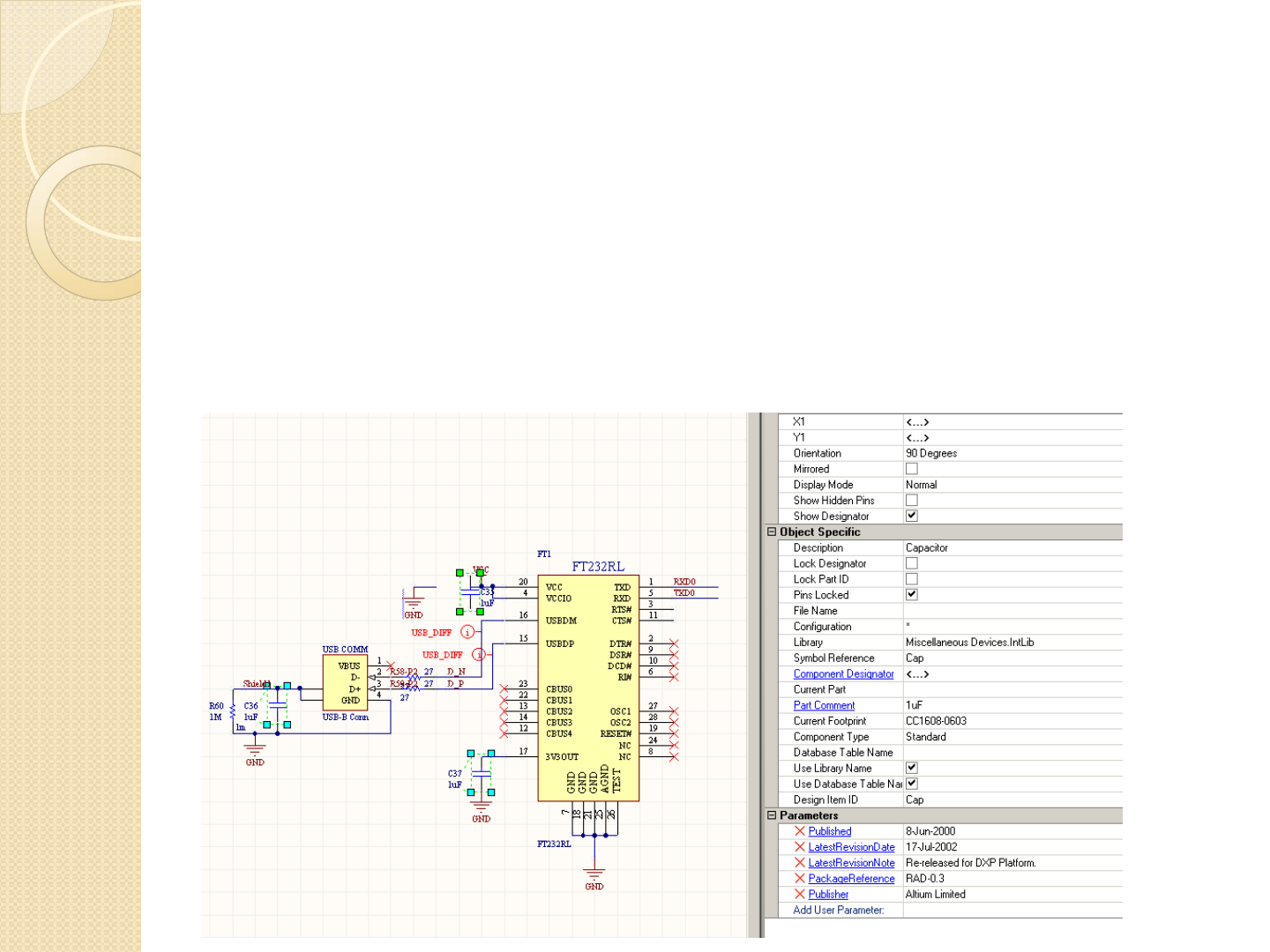
Schematic Inspector
Allows changing a field with different values (Showing <…>) to make all values uniform
In the example below, component orientation is changed from <…> to 90 Degrees.
Immediately each component is rotated to the 90 degree position.
For this example, the lower two capacitors are unchanged, as their value was already 90 degrees,
and the top capacitor is rotated from 0 degrees to 90 degrees.
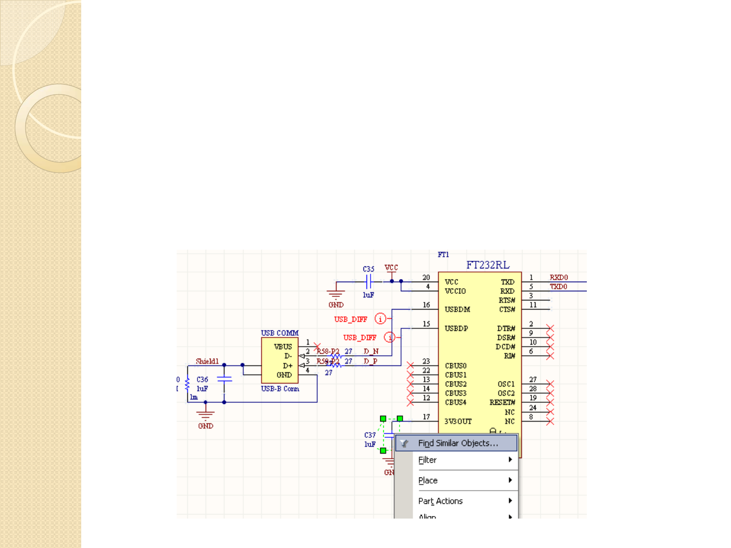
Find Similar Objects
The perfect complimentary tool used
with Inspector is the ‘Find Similar
Objects’ right click menu.
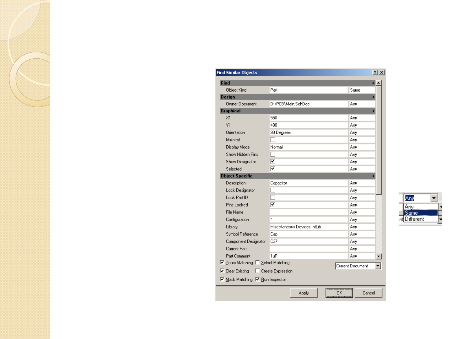
Find Similar Objects
To find ALL
capacitors with
a part comment
of 1uF we
change the
following
objects from
‘ANY’ to
‘SAME’
◦Description:
Capacitor
◦Part
Comment: 1uF
Click OK when
finished
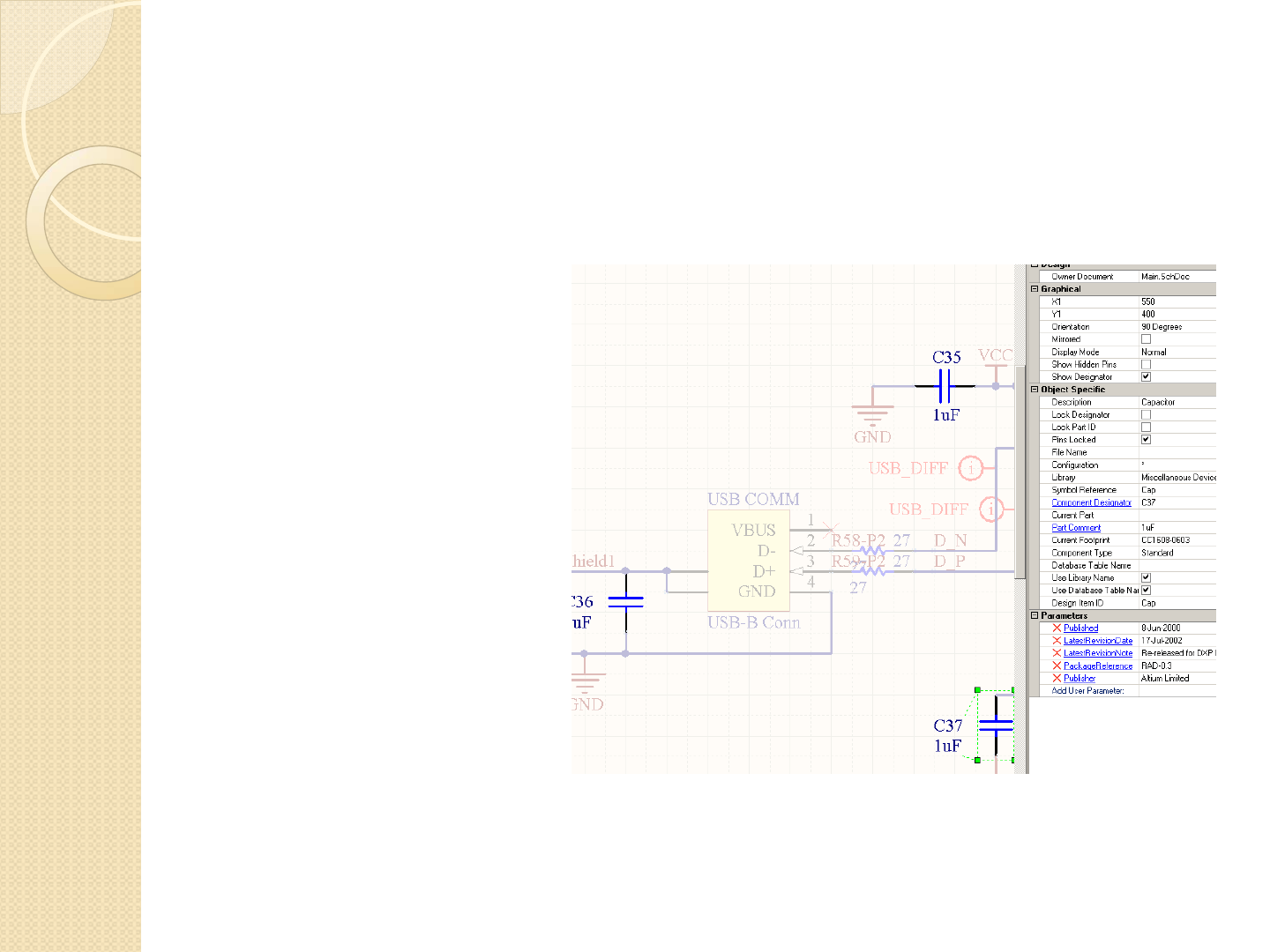
Schematic Inspector- Find Similar
Objects
After hitting
‘Apply’ or ‘OK’,
the Schematic
Inspector
immediately finds
all matching parts.
In this case the
three capacitors
we changed
earlier to 1uF are
highlighted over
the rest of the
schematic, and
selected in the
Inspector.
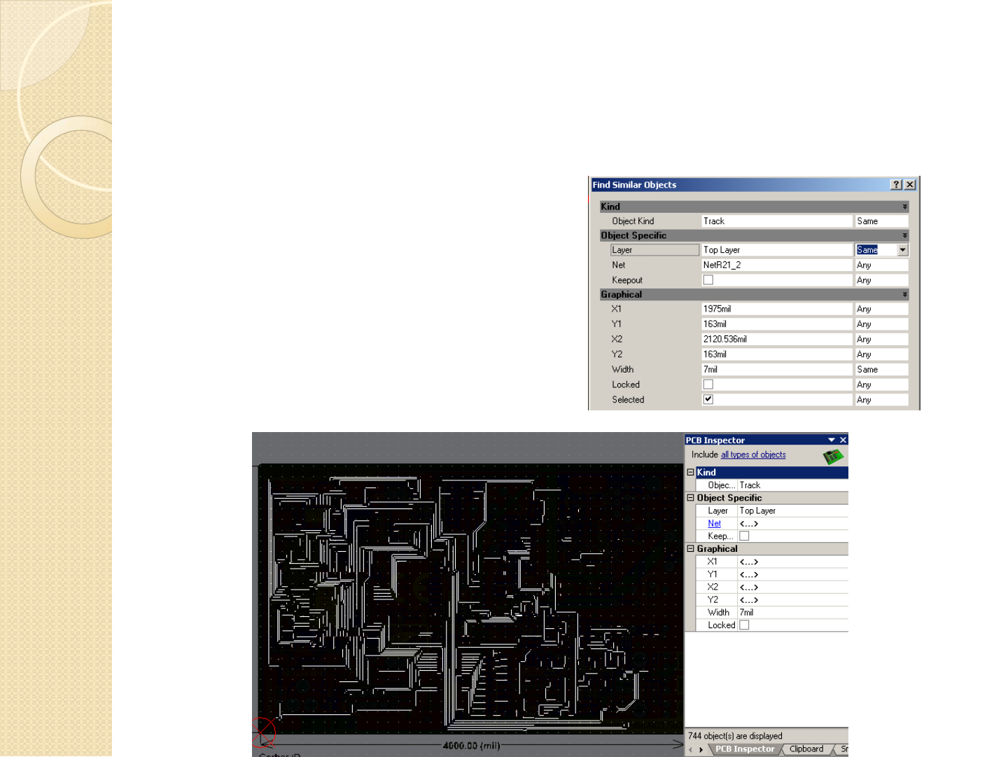
PCB Inspector
PCB Inspector works similar
to the Schematic Inspector.
Shown below is an example of
finding and selecting all traces
that are 7 mils width on the
top layer only
Notice how quickly we
selected and can modify 744
objects meeting this criteria!!

PCB Inspector
We can almost immediately find any
group of objects on the PCB and change
values.
This is an important feature because it
will allow you to quickly adhere to
changes in project requirements, such as
fabrication trace-width parameters
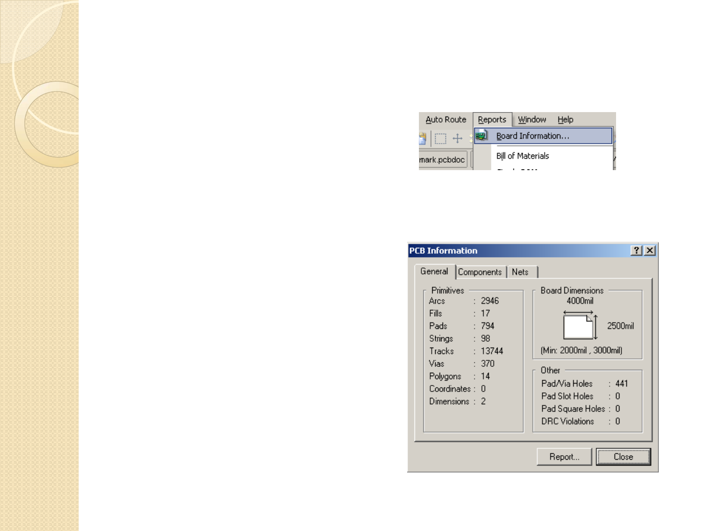
Project Report
A quick detour from
the PCB Inspector
allows us to see a
general report on the
project
From the main
toolbar, click
‘Reports’ then Board
information
You will see a general
summary as shown
to the right, click on
the ‘Report’ button
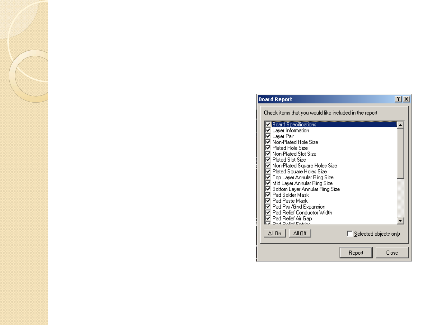
Project Report
Select the
information you
want included in the
report.
Usually it is best to
select all and then
navigate to when you
want in the report
with hyperlinks
Click ‘Report’ when
done selecting
objects

Project Report
An HTML based
report will be
generated with a
table of contents
and hyperlink
navigation available
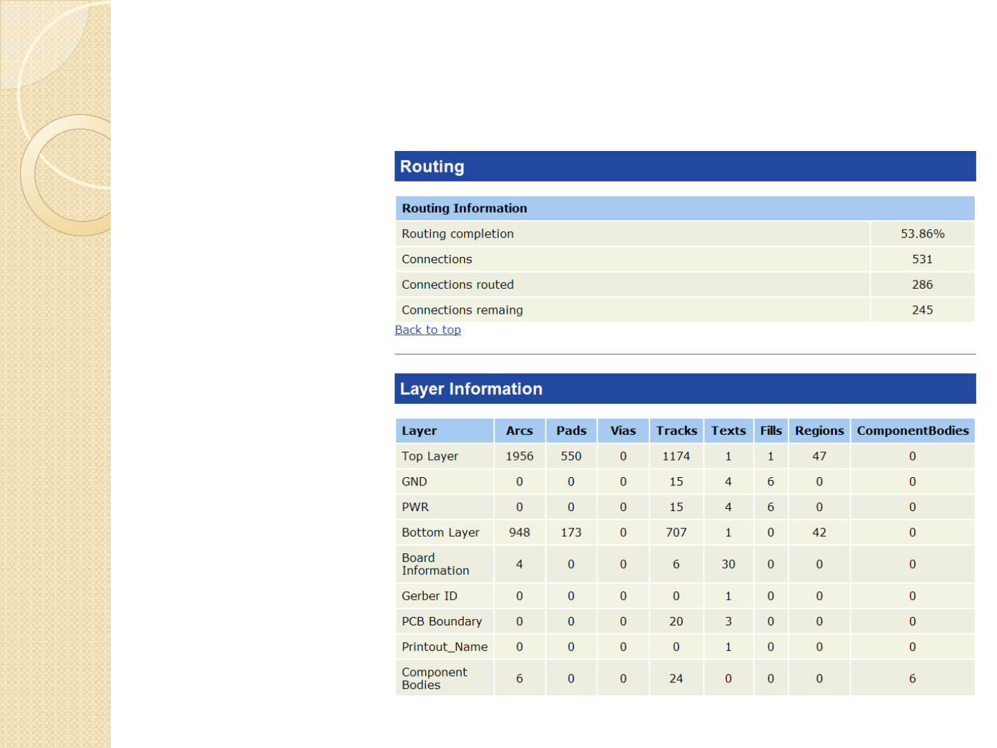
Project Report
The report
will probably
give more
information
than you will
ever want to
know, such as
a detailed
breakdown
of the
routing, layer
information,
vias, tracks,
etc..

Project Report
Shown below
is a part of the
report on
board holes.
This contains
EVERY hole
on the board,
and includes
the drill size
of the hole.

Report and PCB Inspector
Scenario: Your PCB Manufacturer tells you that your hole size must
be 20 mils in diameter, and that the holes in your submitted project
are 15 mils (As shown in the previous slide)
Go to the report to see a detailed analysis of the holes. For this
board we can see the smallest hole size we need to change is 15 to
20 mils, every other hole is larger
◦Use ‘Find similar objects’ to find pads/vias that match 15 mil hole size
◦In the PCB Inspector, we know from the report that we need to change
351 Vias, and 10 pads from 15 mils to 20 mils. We can see in the
Inspector window how many objects are selected.
◦Change the hole size from 15 to 20 mils using PCB Inspector
◦Find any clearance conflicts with the online DRC and quickly fix
◦Regenerate output files with smallest hole size = 20 mils
A process like this, to quickly find and modify 361 holes might take
just a few minutes rather than hours of finding and modifying each
pad/via manually.

Output Job File

Scale Print (1:1Footprint Verification)

PCB Tab

The Return Path

Bandwidth

Microstrips

Differential Pairs

Signal Integrity Introduction

Fourier Series and Transform

Physical Resistance

Physical Inductance

Physical Capacitance

Reflections

Multi-Layer Boards
The term ‘Multi-Layer board’ usually
refers to more than two layers.
A multi-layer board contains a lot more
information such as
◦Layer Stack

Layer Stack
A Layer Stack is a detailed report that contains information
on:
◦Physical Layers and ordering of layers
External signal layers
Internal signal layers
Internal planes
◦Copper thickness per layer (1oz = 1.4 mil, ½ oz = 0.7 mil)
◦Dielectric material and permittivity constant
◦Prepreg thickness
◦Core thickness
◦Total board thickness
This information is crucially important when implementing
transmission lines, microstrips, striplines, etc.

Internal Planes

Internal Signal Layers
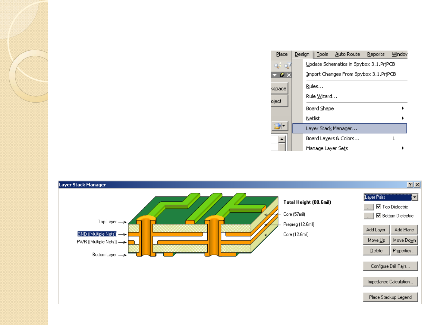
Layer Stack
Design > Layer Stack
manager will show a
3D representation of
the layer stack

Layer Stack

Impedance Controlled Routing
Transmission lines usually required if:

Microstrip

Stripline

Reflections

Cross Talk

EMI

Output Files

CAM Viewers
CAM Viewers allow the re/viewing of Gerber files.
CAMTastic: Basic, Included in Altium Designer
http://www.altium.com/files/learningguides/AR0119%20CAMtastic%20Introduction.pdf
ViewMate- Pentalogix FREE Gerber Viewer
http://www.pentalogix.com/Download/download.html
CAMMaster- Pentalogix
http://www.pentalogix.com/Products/CAMMaster/cammaster.html
CAM350- Downstream Technology
http://www.downstreamtech.com/cam350.html
GC Prevue- FREE Gerber Viewer
http://www.graphicode.com/
GerbTool- Wise Software
http://www.wssi.com/index.php?option=com_content&task=section&id=16&Itemid=1
67

IPC: Formerly known as
Institute of Interconnecting and Packaging Electronic Circuits
IPC Guides the electronic
interconnection industry through
dramatic changes. IPC brings together
designers, board manufacturers, assembly
companies, suppliers, and OEM’s.
IPC is responsibly for creating over 200
standards

IPC: Certification
IPC also has a certification program which
allows one to be certified as:
◦Certified Interconnect Designer (C.I.D.)
Proves a designer’s knowledge of how to transform
a schematic into a reliable rigid PCB design.
◦Advanced Certified Interconnect Designer
(C.I.D.+)
Recognition of a designer’s accomplishments. Exam
covers forty key objectives which go beyond the
C.I.D. certification.

IPC: C.I.D. Certification
Interested individuals who wish to be
certified should obtain the following articles:
◦IPC-2221A: Generic Standard on Printed Board
Design ($30 members/$60 nonmembers)
◦IPC-2222: Sectional Standard on Rigid Organic
Printed Boards ($20/$40)
◦IPC-D-325A: Documentation Requirements for
Printed Circuit Boards ($25/$50)
◦IPC-T-50G: Terms and Definitions for
Interconnecting and Packaging Electronic
Circuits ($40/$80)
◦PWB-CRT-SGA: PWB Designer Certification
Study Guide ($35/$70)
IPC: C.I.D. Certification
Shown to the right
are some of the
sample questions
available on the IPC
Website

IPC: For More Information
IPC Homepage
http://www.ipc.org/
Online Store – Purchase Articles
http://webvision.ipc.org/scripts/mgrqispi.dll?APPNA
ME=IPCWEB&PRGNAME=TOCFRAME&ARGUME
NTS=-N,-N,-A,-A,-N50
Certification
http://dc.ipc.org/certification.htm

Keyboard Shortcuts

References
Bogatin, Eric. Signal Integrity- Simplified. Upper
Saddle River, NJ: Prentice Hall, 2006
Schmitt, Ron. Electromagnetics Explained.
Boston, MA: Newnes, 2002
Johnson, Howard, and Graham, Martin. High
Speed Signal Propagation- Advanced Black
Magic. Upper Saddle River, NJ: Prentice Hall,
2003
Altium Designer Learning Guides
http://www.altium.com/community/support/lea
rningguides/altiumdesigner6learningguides/
