Archive_SC 499_Tape_Controller_Information_Guide Archive SC 499 Tape Controller Information Guide
Archive_SC-499_Tape_Controller_Information_Guide Archive_SC-499_Tape_Controller_Information_Guide
User Manual: Archive_SC-499_Tape_Controller_Information_Guide
Open the PDF directly: View PDF ![]() .
.
Page Count: 42
ARCHIVE
CORPORATION
SC-499
TAPE
CONTROLLER
Information
Guide
This
information
Guide
may
be
filed
in
your
IBM
PC
m~nual
binder
for
future
use.
PARAGRAPH
1 • 1
1
.2
1.3
1
.4
1.5
1
.5.
1
1.6
1
.7
1
.8
1
.8.
1
1.9
1 •
10
1 • 11
1.12
1.13
1.13.1
1.13.2
1.13.3
1.13.4
bt/t
C
~L/
,u/[{
9
tJ1'
!J1vll£
ki'~4
jV)GL
TABLE
OF
CONTENTS
INTRODUCTION
•••••••••••••
. . . . . . . . . . . . . . . . . . . . . . .
HANDLING
•••••••••••••••••
. . . . . . . . . . . . . . . . . . . . . . .
UNPACKING
AND
INSPECTION
••••••••••••••••••••••••
JUMPER-SELECTABLE
OPTIONS
•••••••••••••••••••••••
JUMPER
CONFIGURATION
••••••••••••••••••••••••••••
CONTENTION.
eo
••••••••••••••••••••••••••••••••••••
ELECTRICAL
SIGNAL
DESCRIPTION
••••
. . . . . . . . . . . . . . .
INTERFACE
CONNECTIONS
•••••••••••••••••••••••••••
INSTALLATION
••••••••••••••••••••••••••••••••••
. .
POWER-ON
CONFIDENCE
(POC) TEST. . . . . . . . . . . . . . . . . .
I/O
STRUCTURE
••••••••••••••••
. . . . . . . . . . . . . . . . . . .
INTERRUPTS
••••••••••••••
. . . . . . . . . . . . . . . . . . . . . . . .
DMA
•••••••••••••••••••••••••••••••••••••••••••••
RESETS
••••••••••••••••••••••••••••••••••••••••••
PROGRAMMING
•••••••••••••••••••••••••••••••••••••
QIC-02
COMMAND
DESCRIPTIONS
•••••••••••••••••••••
INTERFACE
TIMING
•••••••••••
. . . . . . . . . . . . . . . . . . . . .
COMMAND
FLOW
CHARTS
•••••••••••••••••••••••••••••
PC
IT/AT
TIMING
SPECIFICATION
•••••••••••••••••••
11
PAGE
1
1
3
3
4
4
6
7
9
1 1
12
12
13
13
14
14
16
23
40
FIGURE
1-1
1-2
1-3
1-4
TABLE
1-1
1-2
1-3
1-4
LIST
OF
ILLUSTRATIONS
TITLE
SC-499
Tape
Controller
PCB
Assembly
SC-499
Jumper,
Indicator,
and
Connector
Locations
PC
Cover
Removal
PC
Expansion
Slots
LIST
OF
TABLES
Jumper-Selectable
Options
Connector
J1
Pin
Assignments/
Signal
Descriptions
Connector
J2/J3
Pin
Assignments/
Signal
Descriptions
SC-499
Power
Requirements
iii
PAGE
2
5
9
10
PAGE
3
7
8
9
SC-499
TAPE
CONTROLLER
Information
Guide
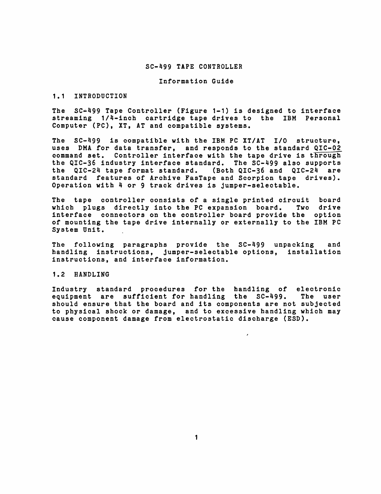
1.1
INTRODUCTION
The
SC-499
Tape
Controller
(Figure
1-1)
is
designed
to
interface
streaming
1/4-inch
cartridge
tape
drives
to
the
IBM
Personal
Computer
(PC),
XT,
AT
and
compatible
systems.
The
SC-499
is
compatible
with
the
IBM
PC
XTIAT
IIO
structure,
uses
DMA
for
data
transfer,
and
responds
to
the
standard
QIC-02
command
set.
Controller
interface
with
the
tape
drive
is
through
the
QIC-36
industry
interface
standard.
The
SC-499
also
supports
the
QIC-24
tape
format
standard.
(Both
QIC-36
and
QIC-24
are
standard
features
of
Archive
FasTape
and
Scorpion
tape
drives).
Operation
with
4
or
9
track
drives
is
jumper-selectable.
The
tape
controller
consists
of
a
single
printed
circuit
which
plugs
directly
into
the
PC
expansion
board.
Two
interface
connectors
on
the
controller
board
provide
the
of
mounting
the
tape
drive
internally
or
externally
to
the
System
Unit.
board
drive
option
IBM
PC
The
following
paragraphs
provide
the
SC-499
unpacking
and
handling
instructions,
jumper-selectable
options,
installation
instructions,
and
interface
information.
1.2
HANDLING
Industry
standard
procedures
for
the
handling
of
electronic
equipment
are
sufficient
for
handling
the
SC-499.
The
user
should
ensure
that
the
board
and
its
components
are
not
subjected
to
physical
shock
or
damage,
and
to
excessive
handling
which
may
cause
component
damage
from
electrostatic
discharge
(ESD).
1
""
..
'
....
1 2
03;;:
..
~
I ' ( F I (
()JI]!
,
'F
I
~
...
c:::::»
... c::::;)
-[-J
I ,
~
I ( I I (
en
•
...
c:::::I
eM
..E3
! i
,..
[-lO
t:jp-
leD
I (
II]
.J
: I
r-
I!!::t
' ...
c:::::I
I It a
L-
..
,C)
9 • .uec:J 0 U •
~----'
I
=rr:
.
I I ( C I (
c::::J
- - - L f
.t::J..
~
:
I
.n
......a.
0r-
,-..,
...-..,
D
...
-.,
...
--
..
r-------.. I
I
..
c:J
P
...
~
l:::I."
,.
•
!..-.!
--
....
'
,,-----'.
t I : 8
.'
~
r--l='
IDE!
:
()!
tf.: '
l:j
p....It';
......
;
......
)
c:'
:::::::)::)
J:=:'
W . :
= L l
...
c:::::»."
~5·'--1
(-0,
( '-=-::3-"'---" I :
[-~
I
il = a
A,
,".
~
e,C!J
E3::t
I::3t'
11ft'
'...
~
!'
_ ............. .
•
cr
2 = 8 !
E3
::.'
t::t
~'ia
68
c!,"
e t:J
~:,.'
............
'
10
~,
1~.
I
.....
~~
"---:.---=-----~~----------=-:------.,
.
.--.
--
-
--
-
..,
..
-
...I==I~'"
"-"'
__
3'
...
--~{
....---.-.
::.
e
.I~
__
-.
__
"'!'"'!'-~I
,
J3
11 - ,
10
• •
• -
c:."
c:::I
..
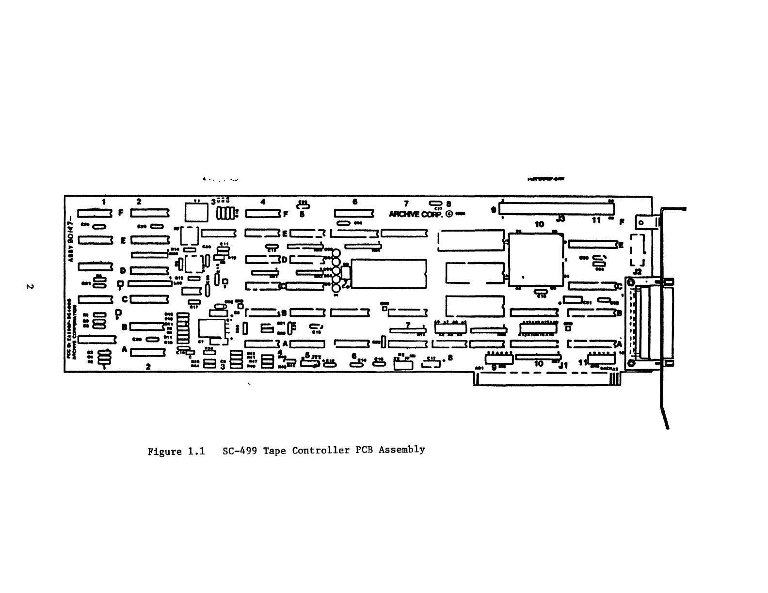
Figure
1.1
SC-499 Tape
Controller
PCB
Assembly
1.3
UNPACKING
AND
INSPECTION
The
SC-499
has
been
packaged
for
maximum
protection
from
shipping
damage.
still,
an
inspection
of
the
board
and
components
should
be
performed
upon
receipt
to
assure
that
no
damage
has
occured.
If
damage
is
detected
notify
the
manufacturer
and
the
common
carrier
immediately.
If
practical,
save
all
containers
and
packing
materials
for
reshipment
or
storage.
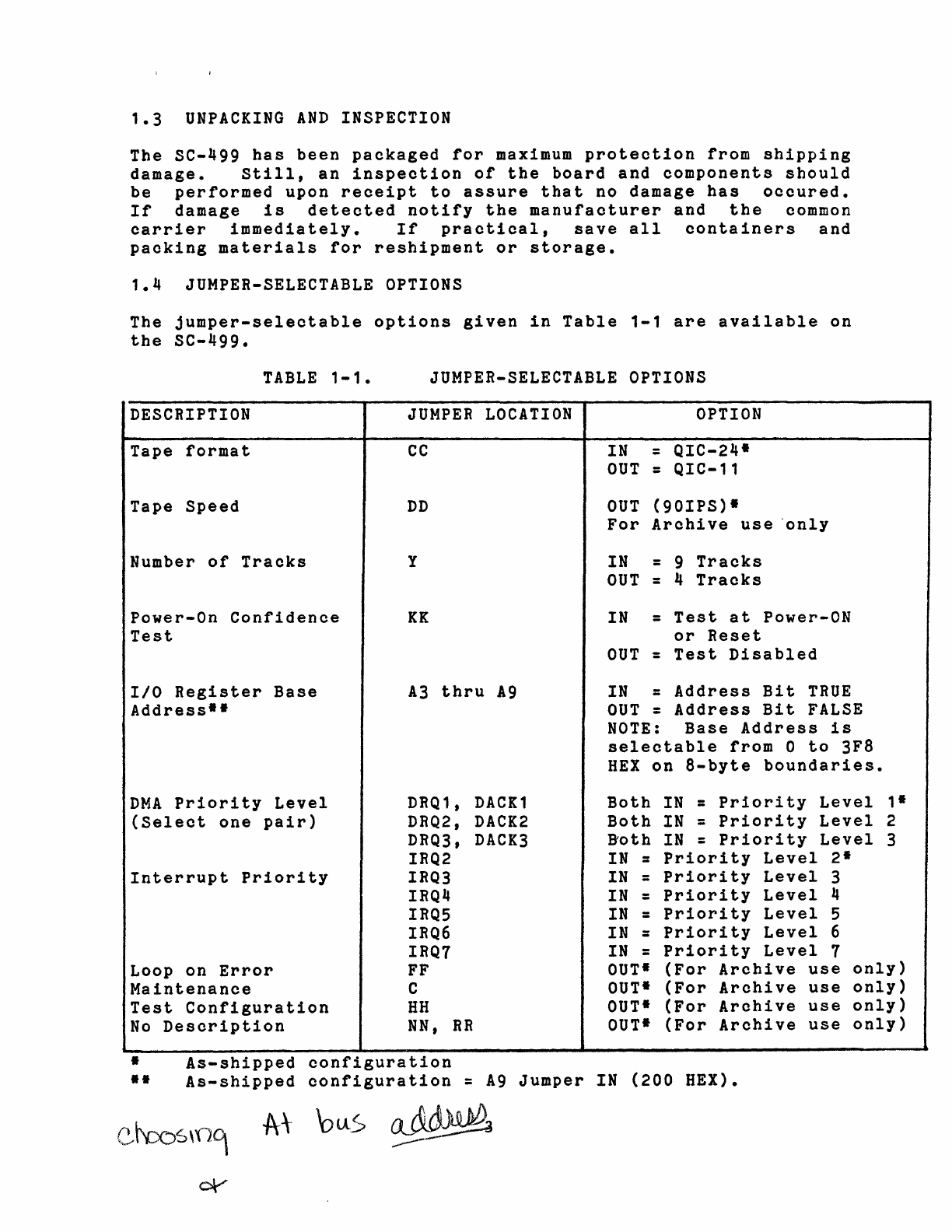
1.4
JUMPER-SELECTABLE
OPTIONS
The
jumper-selectable
options
given
in
Table
1-1
are
available
on
the
SC-499.
TABLE
1-1.
DESCRIPTION
Tape
format
Tape
Speed
Number
of
Tracks
Power-On
Confidence
Test
I/O
Register
Base
Address··
DMA
Priority
Level
(Select
one
pair)
Interrupt
Priority
JUMPER-SELECTABLE
OPTIONS
JUMPER
LOCATION
CC
DD
y
KK
A3
thru
A9
DRQ1,
DACK1
DRQ2,
DACK2
DRQ3,
DACK3
IRQ2
IRQ3
IRQ4
IRQ5
IRQ6
IRQ7
OPTION
IN =
QIC-24·
OUT
= QIC-11
OUT
(90IPS)·
For
Archive
use
'only
IN = 9
Tracks
OUT
= 4
Tracks
IN =
Test
at
Power-ON
or
Reset
OUT
=
Test
Disabled
IN
=
Address
Bit
TRUE
OUT
=
Address
Bit
FALSE
NOTE:
Base
Address
is
selectable
from
0
to
3FB
HEX
on
B-byte
boundaries.
Both
IN
=
Priority
Level
Both
IN =
Priority
Level
Doth
IN
=
Priority
Level
IN =
Priority
Level
2.
IN =
Priority
Level
3
IN =
Priority
Level
4
IN
=
Priority
Level
5
IN =
Priority
Level
6
IN
=
Priority
Level
7
1·
2
3
Loop
on
Error
Maintenance
FF
OUT·
(For
Archive
use
only)
Test
Configuration
No
Description
C
HH
NN,
•
As-shipped
configuration
OUT·
(For
Archive
OUT·
(For
Archive
RR
OUT·
(For
Archive
••
As-shipped
configuration
=
A9
Jumper
IN
(200
HEX).
use
only)
use
only)
use
only)
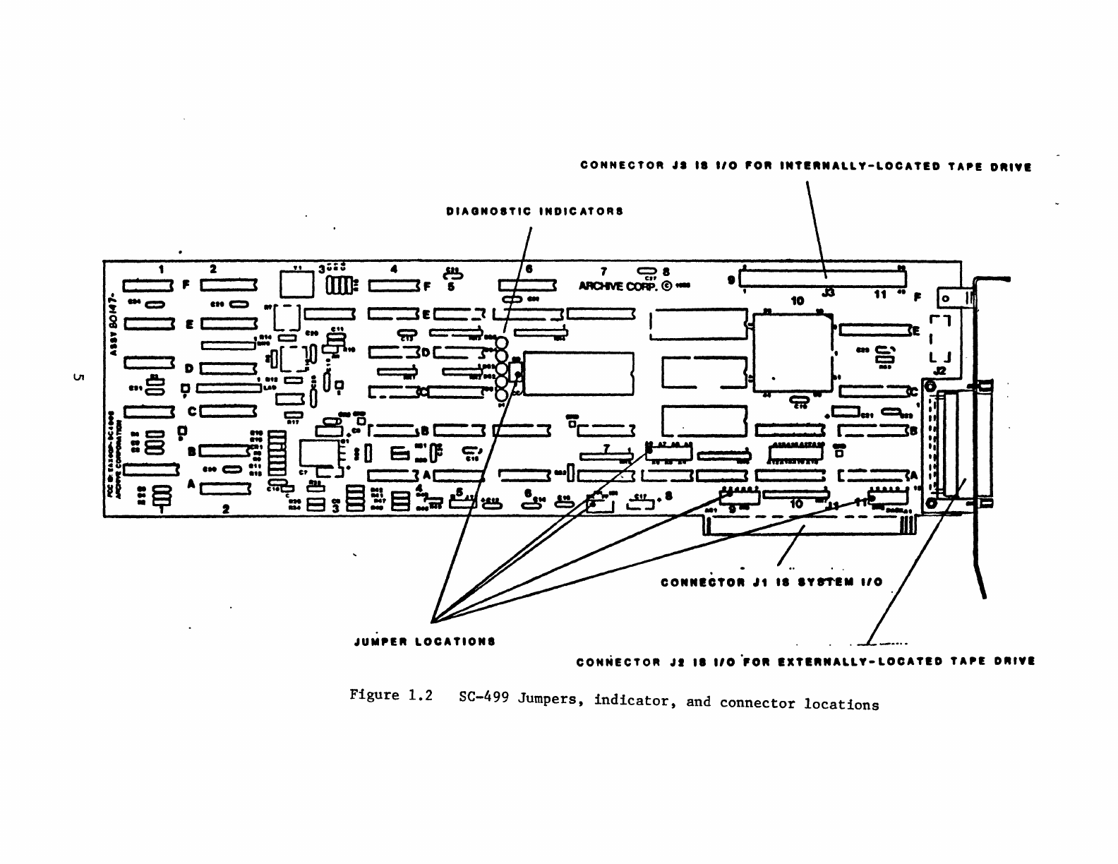
15.
JUMPER
CONFIGURATION
The
tape
oontroller
jumpers
are
installed
at
the
faotory
and
the
110
board
oonneotors
are
shown
in
Figure
1-2.
NOTE:
Jumper
location
Y
is
open
on
the
4-track
oontroller.
1.5.1
Contention
The
as-shipped
oonfiguration
(Base
Address
=
200
HEX,
DMA
Channel
=
1,
Interrupt
Priority
=
2)
of
the
SC-499
provides
contentionless
operation
for
the
majority
of
the
system
users,
though
a
oontention
problem
can
arise
between
the
tape
oontroller
and
certain
other
options
if
both
are
installed.
___________
~
NOTE:
Be
advised
that
most
IBM
PC
models
use
DMA
Channel
2 f r ?
the
floppy
disk
drive
and
DMA
Channel
3
for
the
hard
disk
drive.
However,
the
AT
does
not
use
DMA
Channel
3
for
the
hard
disk
drive.
It
is
handled
through
110.
4
e
~~~'
CONNECTOR
....
1
110
'OR
'''TI''NALLY-LOCATID
TAP.
D"'YI
DIAGNOITIC
INDIC
ATORe
1 2
OU
3~
4
~
:::=::::<
F «
lWJi
---.C,
I
;
...
«:::)
.1.
c::::)
-[-J
I (
~
I « I I «
.tt
•
••
t.
c:::J c
..
..9
!
"..
[-10
Cjf'''
I 1 D I
<a(]....:
c!:I
• ...
t::2
:
~
a
...
c:::::)
D ,
"..
0 U •
•
c::3
r.-_~(
I
c:::::=:;)
I .. , -.... c c. « r::::J
--
il
..
c::t
p
...."
a.c.Dr-,.c=='
~_.....a
tl
: 8
.'
tE
~
Q'
10
E:s
:1J5
c;;.'
:.
I (
...
-
••
, •
_'"
- -
.,.
c,
,-=1
A
I
:~
AI 2 «
~:::~!~UH3~
•
CO""ICTO"
.I,
.1
IY8'T'IM
110
..
UMP.R
LOCAT.O".
CONNICTOR
....
1
110
·'0"
IXTI"NALLY-LOCATID
TAP.
0'''.1
Figure
1.2
SC-499
Jumpers,
indicator,
and
connector
locations
1.6
ELECTRICAL SIGNAL DESCRIPTION
All
voltage
measurements
are
taken
at
the
controller
connector
(J2
or
J3)
with
terminators
installed.
Standard
TTL
levels
are
used
on
signal
lines
to
the
drive
as
follows:
FALSE -
Logic
0 (HIGH) =
2.4
to
5.25
VDC
TRUE
-
Logic
1
(LOW)
=
0.0
to
0.55
VDC
Standard
TTL
levels
are
required
on
signal
lines
to
the
controller
as
follows:
FALSE -
Logic
0 (HIGH) =
2.0
to
5.25
VDC
TRUE
-
Logic
1
(LOW)
=
0.0
to
0.80
VDC
6
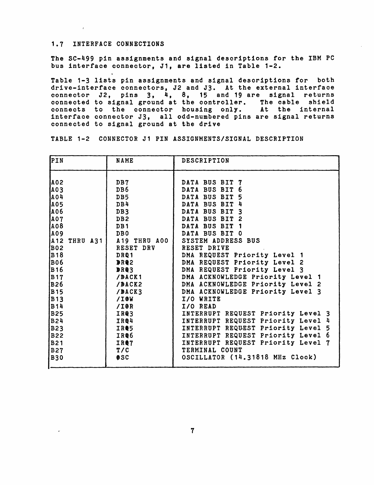
1.7
INTERFACE
CONNECTIONS
The SC-499
pin
assignments
and
signal
descriptions
for
the
IBM
PC
bus
interface
connector,
J1,
are
listed
in
Table
1-2.
Table
1-3
lists
pin
assignments
and
signal
descriptions
for
both
drive-interface
connectors,
J2
and
J3.
At
the
external
interface
connector
J2,
pins
3,
4.
8.
15
and
19
are
signal
returns
connected
to
Signal
ground
at
the
controller.
The
cable
shield
connects
to
the
connector
housing
only.
At
the
internal
interface
connector
J3,
all
odd-numbered
pins
are
signal
returns
connected
to
Signal
ground
at
the
drive
TABLE
1-2
CONNECTOR
J1 PIN
ASSIGNMENTSISIGNAL
DESCRIPTION
PIN
A02
A03
A04
A05
A06
A07
A08
A09
A12
THRU
A31
B02
B18
B06
B16
B17
B26
B15
B13
B14
B25
B24
B23
B22
B21
B27
B30
NAME
DB7
DB6
DB5
DB4
DB3
DB2
DB1
DBO
A19
THRU
AOO
RESET
DRV
DR~1
)R'2
IRI3
IIACK1
IIACK2
IJACK3
IIIW
IIIR
IRt3
IRt4
IRt5
IRt6
IRt7
TIC
eSC
DESCRIPTION
DATA
BUS
BIT 7
DATA
BUS
BIT 6
DATA
BUS
BIT 5
DATA
BUS
BIT 4
DATA
BUS
BIT 3
DATA
BUS
BIT 2
DATA
BUS
BIT 1
DATA
BUS
BIT 0
SYSTEM
ADDRESS
BUS
RESET
DRIVE
DMA
REQUEST
Priority
Level
1
DMA
REQUEST
Priority
Level
2
DMA
REQUEST
Priority
Level
3
DMA
ACKNOWLEDGE
Priority
Level
1
DMA
ACKNOWLEDGE
Priority
Level
2
DMA
ACKNOWLEDGE
Priority
Level
3
1/0
WRITE
1/0
READ
INTERRUPT
REQUEST
INTERRUPT
REQUEST
INTERRUPT
REQUEST
INTERRUPT
REQUEST
INTERRUPT
REQUEST
TERMINAL
COUNT
Priority
Priority
Priority
Priority
Priority
Level
3
Level
4
Level
5
Level
6
Level
7
OSCILLATOR
(14.31818
MHz
Clock)
7
TABLE
1-3
CONNECTOR
J2/J3
PIN ASSIGNMENTS/SIGNAL DESCRIPTIONS
PIN
J2
J3
13
02
25
04
12 06
24 08
11
10
23 12
10 14
22 22
09 24
21
26
20
28
07
30
06 34
18 36
05
38
17
40
16
42
02
46
14 48
01
50
NAME
GO-
REV-
TR3-
TR2-
TR1-
TRO-
RST-
DSO-
HC-
RDP-
UTH-
LTH-
CIN-
USF-
TCH-
WDA-
WDA+
HSD-
WEN-
EEN-
.C
=
Controller
D =
Drive
TO*
D
D
D
D
D
D
D
D
D
c
C
C
C
C
C
D
D
D
D
D
DESCRIPTION
GO.
Motion
Control
for
capstan
servo.
REVERSE.
Direction
control
for
capstan
servo.
TRACK
SELECT
Bit
3 (MSB).
TRACK
SELECT
Bit
2.
TRACK
SELECT
Bit
1.
TRACK
SELECT
Bit
0
(LSB).
RESET.
Cause
drive
to
perform
initialization
and
head
recalibration.
DRIVE
SELECT
HIGH
CURRENT.
Enables
operation
with
alternate
tape
type
(DC600A).
READ
DATA
PULSE.
Read
data
is
present
at
the
drive
interface.
UPPER
TAPE
HOLE.
LOWER
TAPE
HOLE.
CARTRIDGE
IN.
Tape
cartridge
in
place.
UNSAFE.
Safe
plug
on
cartridge
is
in
the
unsafe
position,
i.e.
writing
is
enabled.
TACHOMETER.
Capstan
tachometer
pulses.
WRITE
DATA.
Inverse
of
WRITE
DATA
signal.
HIGH
SPEED
DRIVE.
Tape
speed
= 90
ips.
WRITE
ENABLE.
ERASE
ENABLE.
8
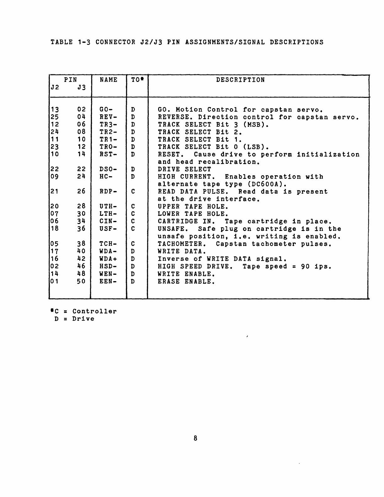
1.8
INSTALLATION
1
("-
/
The SC-499
fits
and
functions
in
at
y
expansion
slot
in
the
IBM
PC
System
Unit
except
slots
7
and
8.
Power
requirements
from
the
System
Unit
are
given
in
Table
1-4.
TABLE
1-4.
SC-499
POWER
REQUIREMENTS
~OLTAGE
CURRENT
MAXIMUM
RIPPLE
~5V+/-5'
including
1.0A
(typ)
100
mv
ripple
1.25A
(max)
~12+/-5'
including
65ma
(typ)
500
mv
to
10KHz;
~ipple
125ma (max)
200
mv
beyond
10KHz
To
install
controller:
1.
Set
all
external
power
switches
to
OFF,
and
unplug
the
external
power
cord(s)
from
their
power
source.
NOTE
Steps
2
thru
7
are
for
mounting
the
SC-499
in
a
System
Unit
expansion
slot.
2.
Disconnect
any
interface
cabling
which
may
obstruct
cover
removal.
Remove
the
System
Unit
cover
(Figure
1-3)
to
gain
access
to
the
interior
(see
Figure
1-4).
3.
Connect
the
tape
drive
interface
cable
to
controller
connector
J3
(see
Figure
1-2),
which
is
a
50-pin
(male)
header
connector.
Figure
1.3
PC
Cover Removal
9
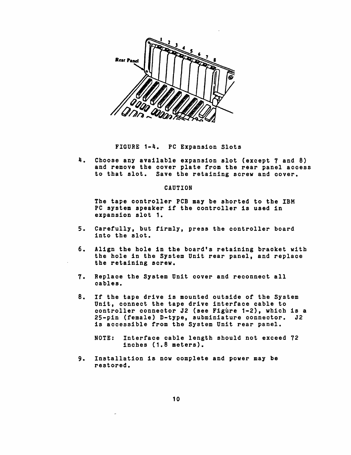
FIGURE
1-4.
PC
Expansion
Slots
4.
Choose
any
available
expansion
slot
(except
1
and
8)
and
remove
the
cover
plate
from
the
rear
panel
access
to
that
slot.
Save
the
retaining
screw
and
cover.
CAUTION
The
tape
controller
PCB
may
be
shorted
to
the
IBM
PC
system
speaker
if
the
controller
is
used
in
expansion
slot
1.
5.
Carefully,
but
firmly,
press
the
controller
board
into
the
slot.
6.
Align
the
hole
in
the
board's
retaining
bracket
with
the
hole
in
the
System
Unit
rear
panel,
and
replace
the
retaining
screw.
1.
Replace
the
System
Unit
cover
and
reconnect
all
cables.
8.
If
the
tape
drive
is
mounted
outside
of
the
System
Unit,
connect
the
tape
drive
interface
cable
to
controller
connector
J2
(see
Figure
1-2),
which
is
a
25-pin
(female)
D-type,
subminiature
connector.
J2
is
accessible
from
the
System
Unit
rear
panel.
NOTE:
Interface
cable
length
should
not
exceed
12
inches
(1.8
meters).
9.
Installation
is
now
complete
and
power
may
be
restored.
10
1.8.1
Power-On
Confidence
(POC)
Test
A
POC
test
occurs
automatically
when
power
is
applied
or
when a
reset
command
is
issued.
This
test
includes
sub-tests
of
the
following:
-Microprocessor
internal
RAM
and
basic
instructions
-LSI
controller
operation
-16K
RAM
IC
-Data
separator
logic
(discrete)
~Successful
completion
of
the
above
tests
are
reported
to
the
by
the
assertion
of
EXC-within
five
seconds.
If
EXC-
is
asserted
within
this
time
a
failure
is
indicated.
host
_._!
0'(\
\
not
hJ.
~;..
j~
• '
- \ \,,(,'\fC{
Each
logic
group
except
the
microprocessor
has
an
associated
diagnostic
indicator
as
follows:
-DS1-LS1
controller
chip
-DS2-16K
RAM
buffer
logic
-DS4,DS5 -
not
used
LED
~~
Successful
completion
of
all
tests
is
indicated
by a
single
blink
of
all
five
LED's
following
the
off
period
during
which
the
tests
are
performed.
Each
time
a
test
fails
the
associated
LED
blinks
and
the
test
is
repeated;
hence,
a
blinking
indicator
is
a
visual
indication
of
the
area
of
failure.
If
the
microprooessor
fails
the
results
are
unpredictable.
1 1
1
\
\
1.9
I/O
STRUCTIRE
The
SC-499
is
fully
oompatible
with
the
IBM
PC
I/O
structure.
The
I/O
registers
ocouPY
eight
adjaoent
locations
in
the
IBM
PC
I/O
address
map.
Only
four
of
the
address
locations
are
used
by
the
SC-499.
NOTE:
Jumper-seleotable
BASE
ADDRESS
is
factory-set
at
200
HEX.
1.
,BASE
.'DDRESS
+0
(200
HEX):
\ N
Ql<"f~\C--~W~.-
...
--_
....
_
....
-,,-.-
.~-
Data/Command
Register~
(Read
or
Write).
..,
~~
BAS,
ADDRESS
+1
(201 HEX):
Control
Register
(Write
Only).
Status
~egister
(Read
Only).
CONTROL
REGISTER
DESCRIPTION
(Wri
te)
on
~
VJf<t,
{''I
(\
0\\"'1
BIT 7
BIT 6
BIT 5
BIT 4
(BITS
0-3
Not
Used)
f"'"
Reset
controller
microprocessor~
Request
to
LSI
chip
Enables
interrupts
lEN =
0,
masks
interrupts
, /
Enables
DONE
interrupt
DNIEN
=
0,
masks
DONE
interrupt.
STATUS
REGISTER
DESCRIPTION
(Read)
-
C)\"'}~
a"
,
Interrupt
Request
Flag.
OR~ng
of
RDY
AND
EXC,
and
DONE
if
DNIEN
is
set.
Ready,
from
LSI
ohip.
-
Exception,
from
LSI
chip.
Done,
from
DMA
10giQ.
Direction,
indicates
direction
of
bus
is
from
controller
to
IBM.
PC.
3.
BASE
ADDRESS
+2
(202
HEX):
Start
DMA
(DMAGO).
Any
write
to
this
register
will
cause
DMAGO
to
be
active.
4.
BASE
ADDRESS
+3
(203
HEX):
Reset
DMA
(BSTDMA).
Any
write
to
this
register
will
cause
RSTDMA
to
be
active.
1.10
INTERRUPTS
The
SC-499
interrupt
priority
level
is
jumper-selectable
(see
Table
1-1).
Each
interrupt
source
bit,
RDY,
EXC,
and
DONE
(see
Status
Register
Description),
can
be
read
through
the
Status
Register
regardless
of
the
state
of
the
interrupt
masks:
lEN =
0,
DNIEN
=
0,
(see
Control
Register
Description).
The
IRQ
line,
is
tri-stated
when lEN
is
cleared.
This-~llows
other
IBM
PC
options
the
use
of
that
interrupt
line
when
the
tape
controller
is
not
using
it.
Therefore,
the
IBM
PC
8259
interrupt
controller
should
be
programmed
to
respond
to
the
tape
oontro11er's
IRQF
only
after
IRQ
has
been
enabled
by
setting
lEN.
12
1.11
DMA
The
tape
oontroller
uses
the
IBM
PC
8237
DMA
oontroller
transfer
data
to
and
from
the
IBM
PC
main
memory. The
ohannel
is
also
jumper-seleotable
(see
Table
1-1).
The
tape-oontroller
DMA
logic
can
be
initialized
by
writing
address
location
BASE+3
(RSTDMA).
RSTDMA
initializes
the
sequencer,
clears
all
Control
Register
bits
to
0,
and
sets
to
1
(power-on
reset
from
the
IBM
PC
performs
the
funotions).
The
following
sequence
may
be
used
to
start
transfer:
'
1 •
2.
3.
r
Issue
a
transfer
command
to
the
tape
controller.
Set
up
the
8237
DMA
controller's
register
(but
~
leave
the
mast
bit
set).
"~
Write
(any
value)
to
the
tape
oontroller
register
at
BASE
ADDRESS+2
(DMAGO).
to
DMA
to
DMA
DONE
same
DMA
\
(j.
~\
A
~4.
b\O
.'Q5V
\.V
5.
I
Clear
the
mask
bit
in
the
8237
DMA
oontroller.
11
,~~,
Repeat
above
from
step
2
for
each
subsequent
block.
ry("
l\
/'
"",;
\
r:J:7
1 • 12
RESETS
Four
reset
Signals
(two
DMA
resets,
and two
mioroprocessor/tape
drive
resets)
are
available
on
the
SC-499.
1.
DMA
Resets:
•
RSTDMA.
(RSTDMA
is
discussed
in
the
DMA
paragraph
above).
•
RESET
DRV.
This
is
the
power-on
reset
from
the
IBM
PC
power
supply,
and
performs
the
same
funotions
as
RSTDMA~
2.
Microprocessor
and
Tape
Drive
Resets:
•
Mioroprocessor
RESET.
Reset
the
controller
microprocessor
when
any
of
the
following
conditions
oocur:
a.
The
+5V
supply
drops
below
4.6v.
b.
The +12V
supply
drops
below
9V.
c.
RSTSAC
is
set.
NOTE
Mioroprocessor
RESET
will
also
cause
a
tape
drive
reset
•
•
RSTSAC.
Activated
by
writing
a 1
to
Control
Register
B~
7.
RSTSAC
must
be
set
held
for
more
25
usee
then
cleared
by
either
writing
a
to
Control
Register
Bit
7
or
by a
RSTDMA.
13
lf
l.
'/
,I.
'
I
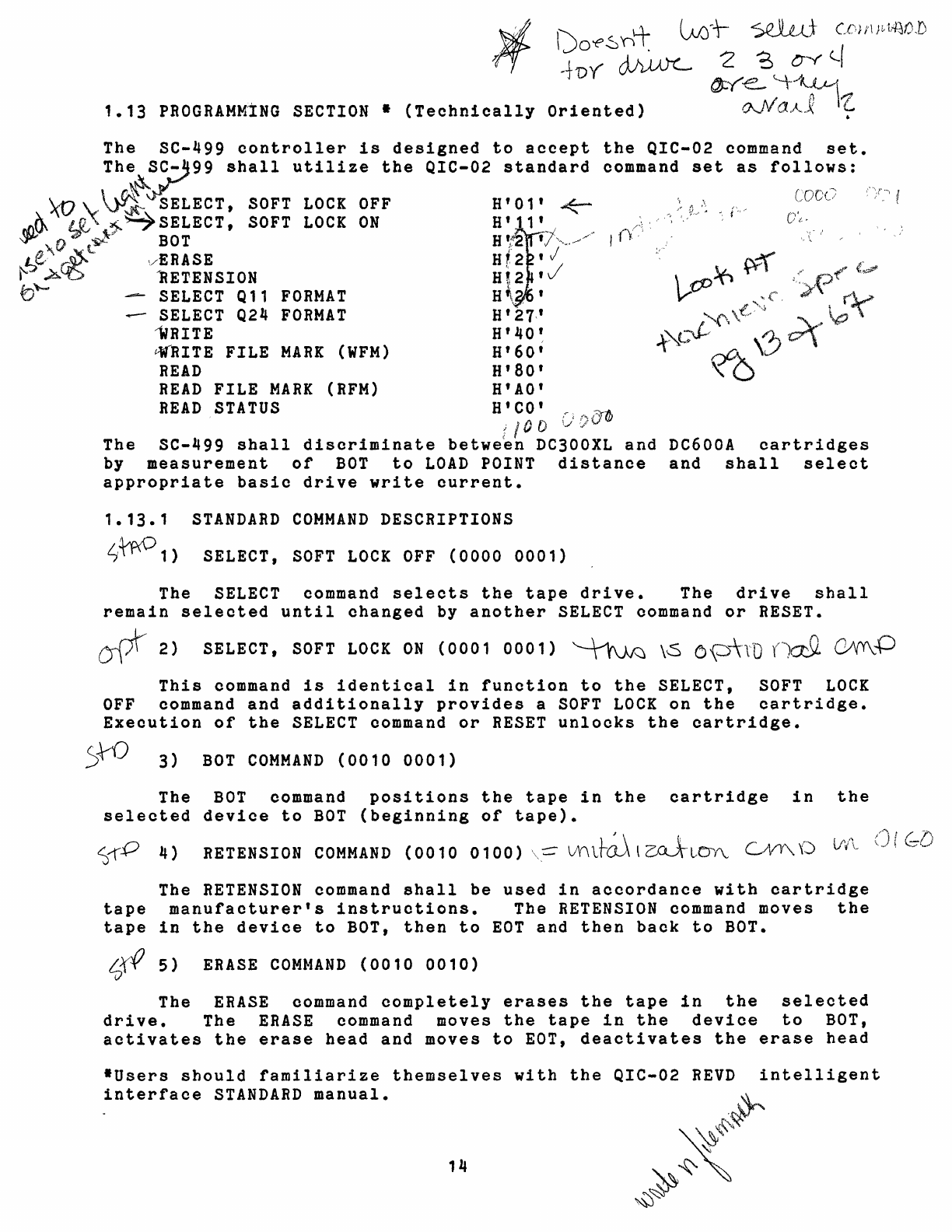
1.13
PROGRAMM'ING
SECTION
•
(Technically
The
SC-499
controller
is
designed
to
accept
The
S~-J99
shall
utilize
the
QIC-02
standard
the
QIC-02
command
set.
command
set
as
follows:
~-
'XV
\"'"
~-
SELECT,
SOFT
LOCK
OFF
r/)().
~
'\.
~
~
SELECT,
SOFT
LOCK
ON
~
,0
.t~~
BOT
~e.
'_fi}~
vERASE
~
.>,.~
/RETENSION
b'-
~
SELECT
Q11
FORMAT
--
SELECT
Q24
FORMAT
"WRITE
·WRITE
FILE
MARK
(WFM)
READ
READ
FILE
MARK
(RFM)
READ
STATUS
H'2.7"
H'40~
H'60'
H'SO'
H'AO'
H t
CO'
:r,
f'J.
,-::;r'OJ
ill)
D
v,,_V
The
SC-499
shall
discriminate
between
DC300XL
and
by
measurement
of
BOT
to
LOAD
POINT
distance
appropriate
basic
drive
write
current.
1.13.1
STANDARD
COMMAND
DESCRIPTIONS
4t'P<01)
SELECT,
SOFT
LOCK
OFF
(0000
0001)
coco
O't.·
DC600A
cartridges
and
shall
select
The
SELECT
command
selects
the
tape
drive.
The
drive
shall
remain
selected
until
changed
by
another
SELECT
command
or
RESET.
u{t
2}
SELECT,
SOFT
LOCK
ON
(0001
0001)
~
\6
o,(:::y\ro
()::t9.
(],/('r\{:)
This
command
is
identical
in
function
to
the
SELECT,
SOFT
LOCK
OFF
command
and
additionally
provides
a
SOFT
LOCK
on
the
cartridge.
Execution
of
the
SELECT
command
or
RESET
unlocks
the
cartridge.
S~
3)
BOT
COMMAND
(0010
0001)
The
BOT
command
positions
the
tape
in
the
cartridge
in
the
selected
device
to
BOT
(beginning
of
tape).
S--r.P
4)
RETENSION
COMMAND
(0010
0100)
\-==
vy\tt-~
l
ZA1'lCJY\,
GVY'\
\J
The
RETENSION
command
shall
be
used
in
accordance
with
cartridge
tape
manufacturer's
instructions.
The
RETENSION
command moves
the
tape
in
the
device
to
BOT,
then
to
EOT
and
then
back
to
BOT.
~rf
5)
ERASE
COMMAND
(0010
0010)
The
ERASE
command
completely
erases
the
tape
in
the
selected
drive.
The
ERASE
command moves
the
tape
in
the
device
to
BOT,
activates
the
erase
head
and
moves
to
EOT,
deactivates
the
erase
head
.Users
should
familiarize
themselves
with
the
QIC-02
REVD
intelligent
interface
STANDARD
manual.
14
and
moves
the
tape
back
to
BOT.
The
ERASE
command
also
fulfills
the
requirements
of
initialization.
6)
WRITE
COMMAND
(0100
0000)
When
the
WRITE
command
is
issued
the
device
requests
and
transfers
data.
The
READY
line
is
activated
when
the
device
is
ready
for
a
data
block
transfer.
When
the
READY
line
is
active,
the
host
terminates
transfer
of
write
data
by
issuing
a WRITE-FILE-MARK
command.
NOTE:
A
write
command
following
cartride
insertion
or
RESET
shall
commence
recording
at
BOT
end
of
tape,
otherwise,
recording
shall
commence
at
the
curre~t
tape
position.
NOTE:
If
the
host
starts
transfer
between
blocks
before
READY
is
asserted,
READY
may
not
be
asserted
when
the
early
warning
hole
of
the
last
traok
is
detected
by
the
devioe,
thus
the
device
ceases
to
transfer
additional
data
blocks
from
the
host.
The
device
terminates
the
WRITE
command
and
reports
END
OF
MEDIA
by
means
of
an
EXCEPTION
and.READ STATUS.
7)
READ
COMMAND
(1000
0000)
When
the
READ
command
is
issued
the
device
transfers
data.
The
READY
line
is
activated
when
the
devlce
is
ready
for
a
data
block
transfer.
The
READ
command
shall
be
terminated
by
the
device
if
a
file
mark
is
detected.
The
host
is
informed
by
means
of
an
EXCEPTION
and
a
READ
STATUS
sequence.
When
READY
is
true,
the
host
may
alternatively
terminate
the
READ
command by
issuing
a READ-FILE-MARK
command.
If
a
READ
command
is
issued,
the
command
is
accepted
and
the
drive
continues
reading.
NOTE:
A
READ
command
following
cartridge
insertion
or
RESET
shall
commence
at
BOT,
otherwise
the
read
command commences
from
the
current
tape
position.
NOTE;
If
the
host
starts
transfer
between
blocks
before
READY
is
asserted,
READY
MAY
NOT
BE
ASSERTED.
8)
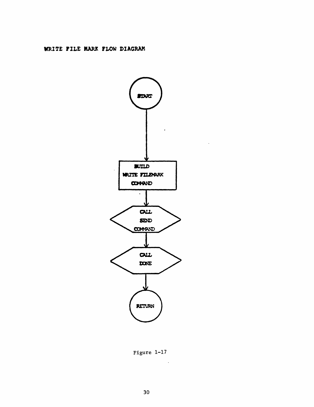
WRITE-FILE-MARK
COMMAND
(0110
0000)
The WRITE-FILE-MARK
(WFM)
command
causes
a
file
mark
to
be
written
on
the
tape
in
the
selected
drive.
NOTE:
a
WFM
command
following
cartridge
insertion
or
RESET
shall
commence
recording
at
BOT
end
of
tape,
otherwise,
recording
shall
commence
at
the
current
tape
position.
~~
9)
READ-FILE-MARK
COMMAND
(1010
0000)
The READ-FILE-MARK
(RFM)
command
causes
the
tape
in
the
selected
drive
to
be
moved
to
the
next
FILE
MARK.
NOTE:
A
RFM
command
following
cartridge
insertion
or
RESET
shall
commence
reading
at
the
BOT,
otherwise,
reading
shall
commence
at
the
current
tape
position.
~10)
READ
STATUS
COMMAND
(1100
0000)
The
READ
status
command
provides
the
host
with
information
about
the
selected
device.
The
host
issues
the
READ
STATUS
oommand. The
device
transfers
the
standard
six
bytes
to
the
host.
15
J
11)
SELECT
Q11
FORMAT
COMMAND
(0010
0110)
The
SELECT
Q11
format
command
selects
the
Q 11
format
as
the
rrent
format.
12)
SELECT Q24
FORMAT
COMMAND
(0010
0111)
The
SELECT Q24
format
command
selects
the
Q24
format
as
the
current
format.
1.13.2
INTERFACE TIMING
Timing
specif
-
defined
at
the
driven
end.
Requirements
involving
deskew
hall
be
the
responsibility
of
the
receiving
end.
Interface
s
timing
shall
be
outlined
in
the
following
diagrams.
FIGURE
DATA
TRANSFER
Write
Operation.......................................
1-5
Read
Operation........................................
1-6
COMMAND
TRANSFER
Ready
Asserted........................................
1-7
Exception
Asserted....................................
1-8
Direction
Deasserted..................................
1-9
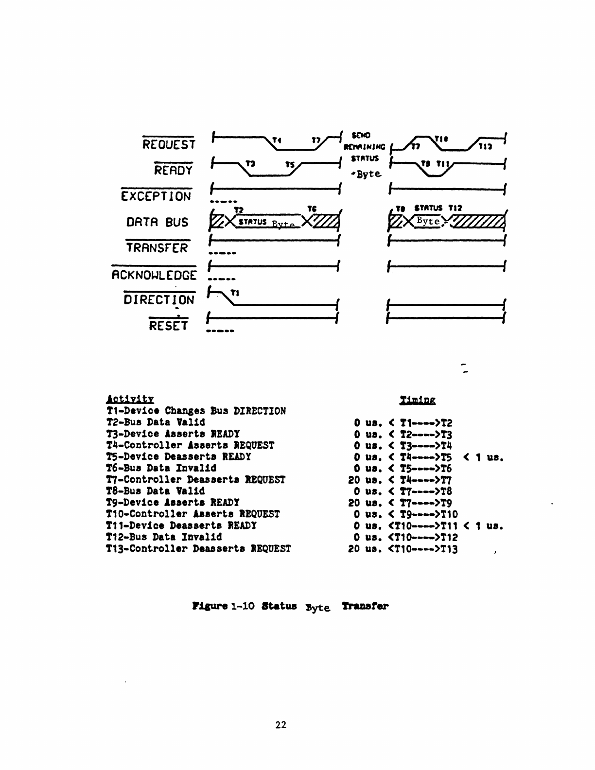
STATUS
BYTE
TRANSFER
. . . . . . . . . . . . . . . . . . . . . . . . . . . . . . . . . . . . . .
1-10
16
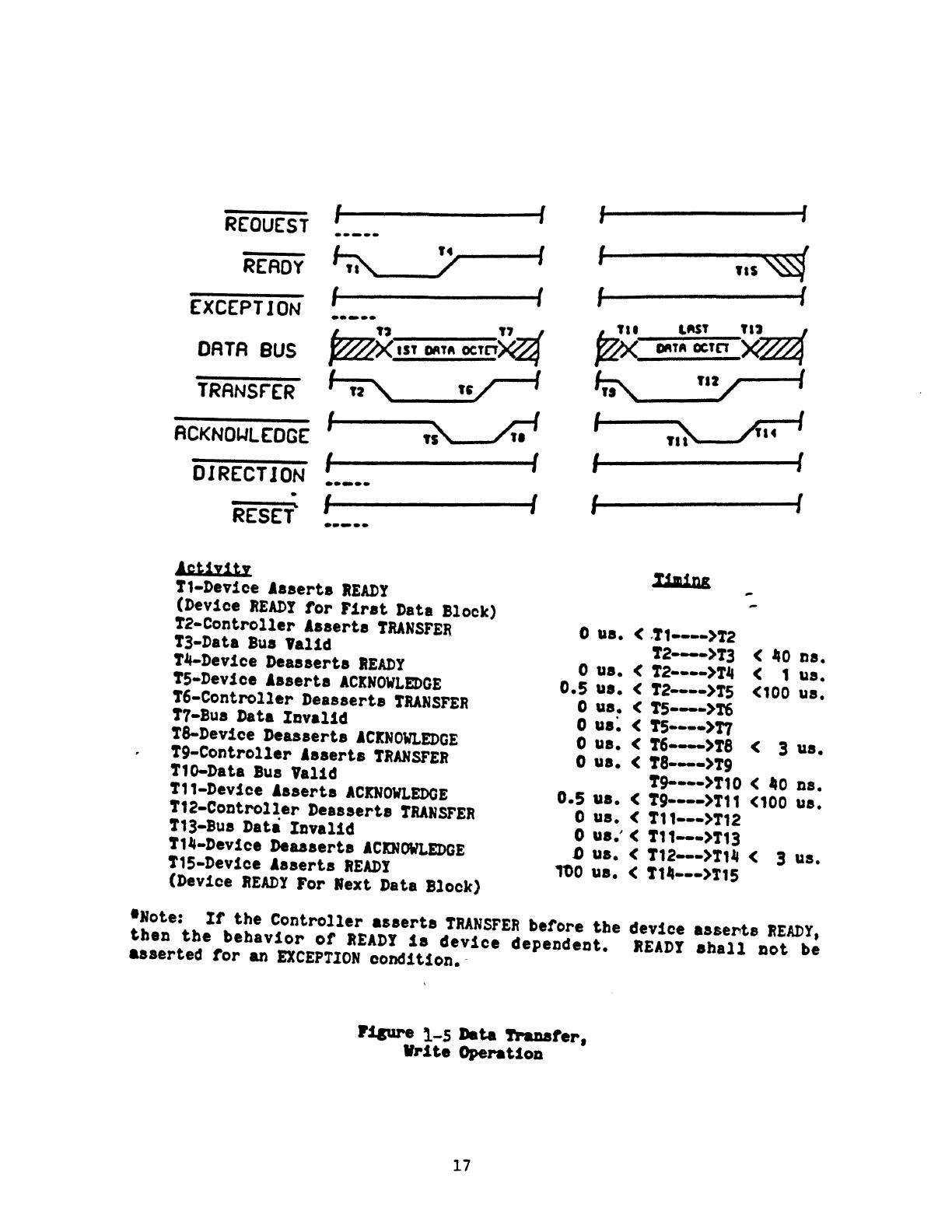
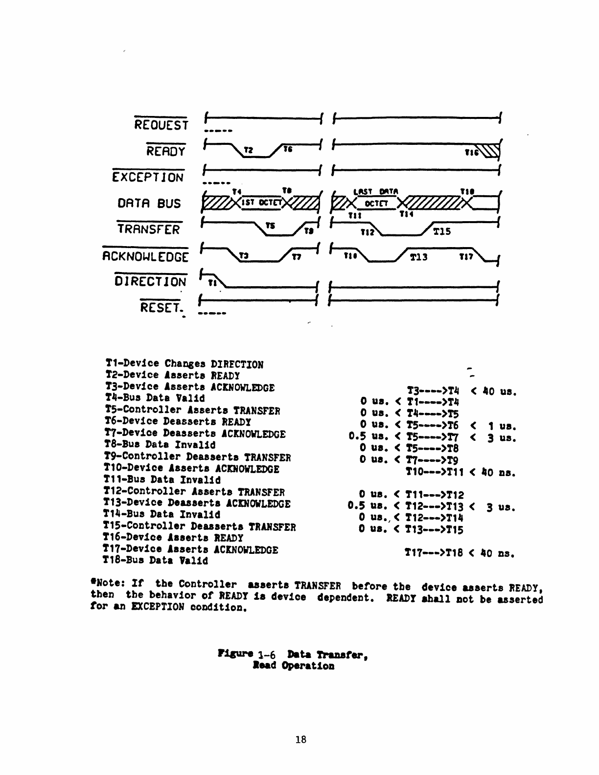
REOUEST
I I
---
..
~
,.
I
READY
/
I I
EXCEPTION
......
DATA
BUS
lTd<
~
1ST DATA
OCTO
TRANSrER
"
ACKNO£.JL(OGE
I
,~
A;-/
I
DIRECT
JON
......
I
-
RESET
......
,1ptly1ty
T1-Device Asserta
READY
(Device
READY
tor
Firat
Data Slock)
T2-Controller Asserta
TRANSFER
!3-Data Sus
'alid
T4-Device Deasserts
READY
!S-Device Asaerts
ACKNOWLEDGE
T6-Controller Deaaaerta
TRANSFER
!7-Bus Data
Iavalid
fa-Device Deaaserta
ACKNOWLEDGE
T9-Controller Aaserta
TRANSFER
TlO-Data Sus
'alid
T1'-Device Asserts
ACKNOWLEDGE
T12-Controller DeesBerta
TRANSFER
!13-Bus Data
Invalid
T1_-Device Deaaserts
ACKNOWLEDGE
T1S-Device Asserts
READI
(Device
READY
For
.ext
Data Slock)
I
I
I I
I I
'IS~
I I
/n':J
""ST
'~}77nf
¥LA.
DATA
OCTn
NLLL4
'""
'.2/
I
I I
I I
tim
ln
s
o us. < ,T1----)12
T2---->13 <
_0
as.
o
us.
(T2----)T_
< 1 us.
0.5
us.
< T2---->T5
<100
us.
o us. < 1'5--->'1'6
o us
~
< 1'5---->1'7
o us. < T6---->T8 < 3 us.
o
us.
<
T8--->19
1'9----)T10 <
_0
DS.
0.5
us.
< 1'9---->T11 (100 us.
o us. < T11---)T12
o
us:
< T11---)T13
D us. < 1'12---)T1_ < 3 us.
TOO
us. < T1---->115
'Hote:
It
the
Controller
asserts
TRANSFER
before
the
device
.Bse~t8
READY,
then
the
behavior
or
READY
is
device
dependent.
READY
ahall
Dot
be
asserted
tor
an
EXCEPTION
condition.-
P!pre
1-5
Data
Trauter,
WrIte Operat1oD
17
REOUEST
READY
I
~--------~I
I~------------~I
.-~.-
~
--
~
I-------------------~~I
.
~
,.
. 'I~
[XCEPTJON
DATA
BUS
TRANSfER
I I I I
-----
,.
Y.w4'
b7J
IIST
DII'"
~
b7n:J
IST
OCTET
JCL~,
OCTET
W'$!'%
~,
I..
114
I
I
,IS
R I
'I~
/~lS
ACKNO'-JLEOGE
OlRECTJON
~
I
RESET.
----.-
.
fl-Device Chanses
DIRECTION
f2-Device Asserta
READY
f3-Device Asserts
AC[NOWLEDGE
T~-Bus
Data Valid
fS-Controller Asserts
TRANSFER
T6-Device Deasserts
READY
fT-Device Deasserta
ACKNOWLEDGE
fS-Bus Data
Invalid
T9-Controller Deaaserta
TRANSFER
flO-Device Asserta
ACENOWLEDGE
T1'-Bus Data
Invalid
f12-Controller Asserta
TRANSFER
!13-Device Deaaaerts
AC[NOWLEDGE
T1~-Bus
Data
Invalid
!15-Controller
Deaaaerts
TRANSFER
T16-Dev1ce
Asserta
READY
T17-Device Assert a
ACKNOWLEDGE
!lS-Bua Data
'alid
I f
I f
!'13
f,7
I
I
f3---->T~
<'0
us.
o us. <
!t----)T~
o us. <
T~--->rs
o
us.
< TS----)T6 < ,
us.
0.5
us.
< TS---->!7 < 3 us.
o us. < TS----)TS
o us. < T7----)Tg
fl0---)Tl1
<
'0
DS.
o
us.
< T1,---)T12
0.5
us.
< T12---)T13 < 3
us.
o uS.,<
Tt2---)Tt'
o us. < T13---)T1S
T17---)T18 <
'0
DB.
-Note:
It
the
Controller
asserta
TRANSFER
betore
the
device
asaerts
READY,
then
the
behavior
or
READY
is
device dependent.
READY
aball
Dot
be
asserted
tor
an
EXCEPTION
conditioD.
"!pre
1-6
Data
fraut.,.,
...
d
Operat10D
18
.
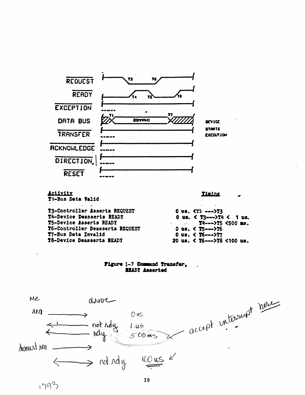
REOUEST
I
~J
'v
READY
I
4.
~
I
EXCEPTJON
.. _ ..
DRTA
BUS
f$<
~
I
TRANsr£R
..
_
..
ACKNOI.JL£DG£
I
. f .
DJRECT
JON.I
••
_
••
RESET
I
.----
Agt1y1ty
t1-Bus Data
'altd
!3-Controller
'aaerts
REQUEST
t~-Dev1ce
Deasaert.
IEADY
!5-Device
'aaerts
READY
!6-Controller
Dealsert.
REQUEST
!7-Sus
Data
Invaltd
!8-Device Deaaaerta
IEADY
I
,r
I
n I
~$~
DCVlce
I STMTS
CICCUTION
I
I
I
tWins
o
ua.
<Ti-
---)T3
o ua. <
t3-)Tj&
< , ua.
'.---)T5
<500
~.
~
us.
<
!5--)!6
o ua. <
1'6--)T7
20 ua. <
1'6-)T8
(100
us.
PJ.&ure
1-'
C: M
rrauter,
R&D!
Aaaerted
D
~~
.........
t
____
nor
hJ~
+---I\d'}
( -
~t·--.uP_
506~;"~~~
,..-,'
~
.I
~ID.\~
19
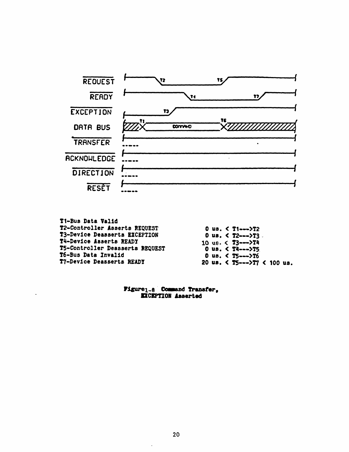
REOUEST
I
~~
READY
I
"t4
rXCEPTJON
I
"/
DATA
BUS
~X
• I
TRANSF"(R
,
ACKNOWLEDGE
.-
...
-
I
DIRECTJON
..
~-.
I
•
RESET
......
',-Bus
Data Valid
T2-Controller Asserts
REQUEST
'3-Devlce Deaaaerts
EICEPTIOH
'.-Device
Asserte
READY
'5-Controller
Deaaeerta
REQUEST
T6-Bus
Data
Invalid
'7-Devlce Deasserts
READY
~
tv
I
"/
I
I
" I
X000//7/7/ff//~
o
us.
<
"--)1'2
o
us.
< '2--->13
~
10
\'\s. <
1'3--)1"
o
us.
< 1'''---)1'5<
o
us.
< 1'5--->16
20
us.
< 1'5---)17 ( 100
us.
I
I
I
I
P1pre1-8
'C:
nd
rruate
.. ,
DClPnOI
haerted
20
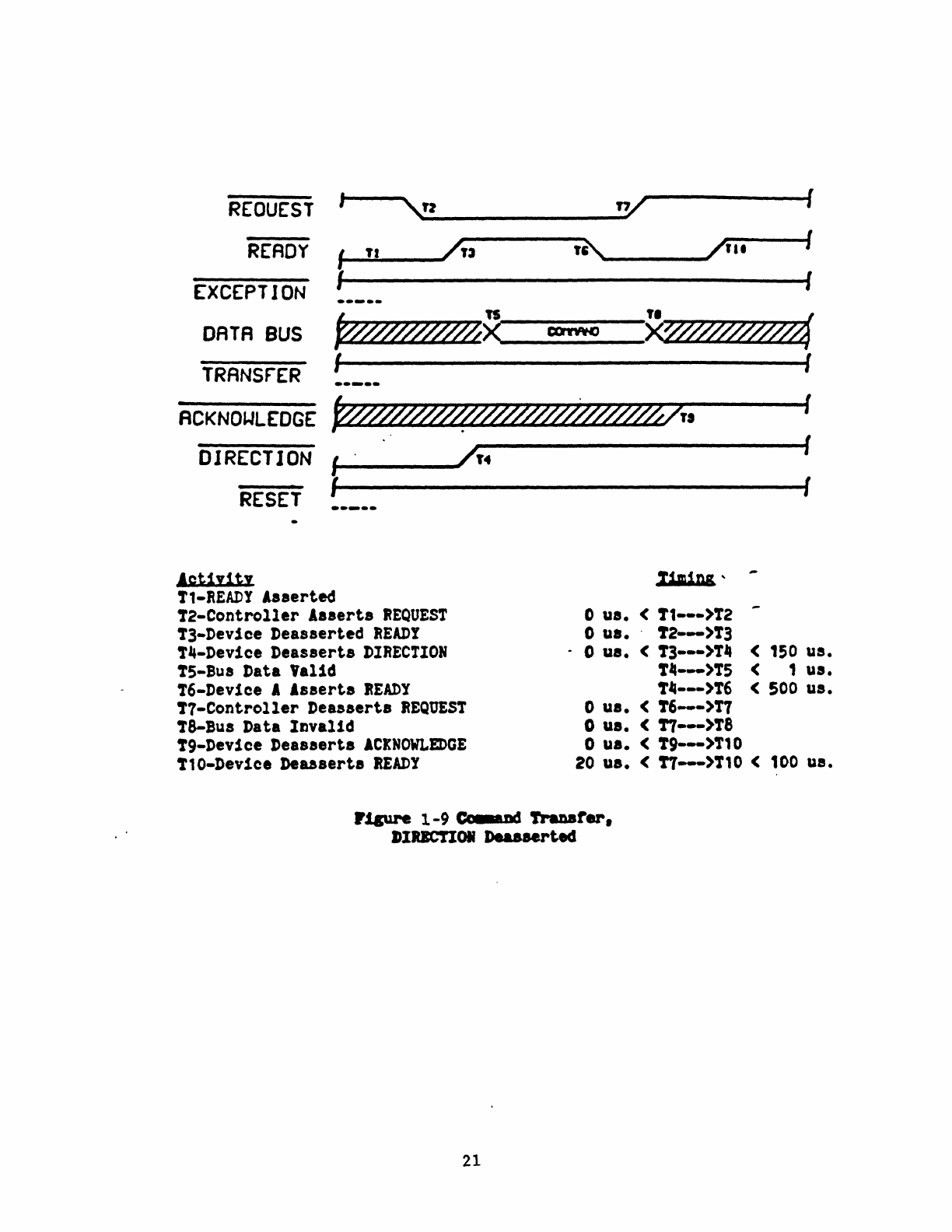
REOUEST
READY
I
".,
~
____________
-Jn~
I
EXCEPTION
DATA
BUS
TRANSrER
,
I
fl
/fJ
DIRECTION,
....
___
--'/14
i
RESET
•
___
_
Apt1y1ty
T1-READY
Asserted
T2-Controller
'sserta
REQUEST
!3-Device Deaaaerted
READY
!4-Device Deasaerta
DIRECTION
T5-Bus
Data
'alid
!6-Dev1ce , Asserts
READY
!7-Controller
Deaaserts
REQUEST
!8-Bus Data
Invalid
'9-Device Deaaserts
ACKNOWLEDGE
!10-Device Deaaaerts
READY
f"~
__
--,/'I'
I
I
I
I
I
tim
ins
' -
o
us.
< T1---)'1'2
o us
•.
T2--)'1'3
- 0 us. < T3---)'1'_ < 150 us.
'_---)T5
< 1 us.
'.---)T6
<
500
ua.
o
us.
<
'6--)'1'1
o us. <
TT--)T8
o us. < T9---)T10
20 us. <
TT--)T10
< 100 us.
PJ.sure
1-9
Cc
ncS
1'rauter,
IIIICTIOI
Deaaeerted
21
REQUEST
,
~4
,y-/ICIO
~
KN'IHJHG J 112
'T"TUS
READY
"Byte.
EXCEPTION
I I I I
~n
~
TI
I'''TUS
TI2
I
DATA
BUS
><
ST"TUS
~~t
il
~><ByteXWY~
TRANsrER
I
ACKNOl.JL(OGE
I
DIRECTION
~I
.
. I
RESET
-----
Agt1y1tx
'1'1-Device
Changes
Bus
DIRECTION
'1'2-Bus
Data Valid
T3-Dev1ce
Aaserta
READY
'1'.-Controller Aaserts
REQUEST
!S-Device Deaaserts
READY
!6-Bua Data
Invalid
!7-Controller
Deaaserta
IEQOEST
!8-Bua Data
'al1d
tg-Device Aaaerta
READY
'1'10-Controller Aaaerta
REQUEST
'1'1'-Device Deaaaerts
READY
'1'12-Bus
Data
Invalid
'1'13-Controller »eaaaerts
REQUEST
I
I
I
I
I I
I.
I
I I
I I
"imiag
o
us.
< '1'1----)T2
o ua. <
,2----)13
o ua. <
'1'3---->'1'_
o ua. <
'1'.-)T5
<,
us.
o ua. < T5----)'1'6
20
us.
<
,.----)'1"1
o ua. < !1----)T8
20
us.
(
T7---)T9
o
us.
<
'9----)T10
o ua. ('1'10----)T11 < ,
us.
o
us.
(110----)T12
20
us.
<T10----)T13
P.taure
1-10
Statu
l'yte.
tnDater
22
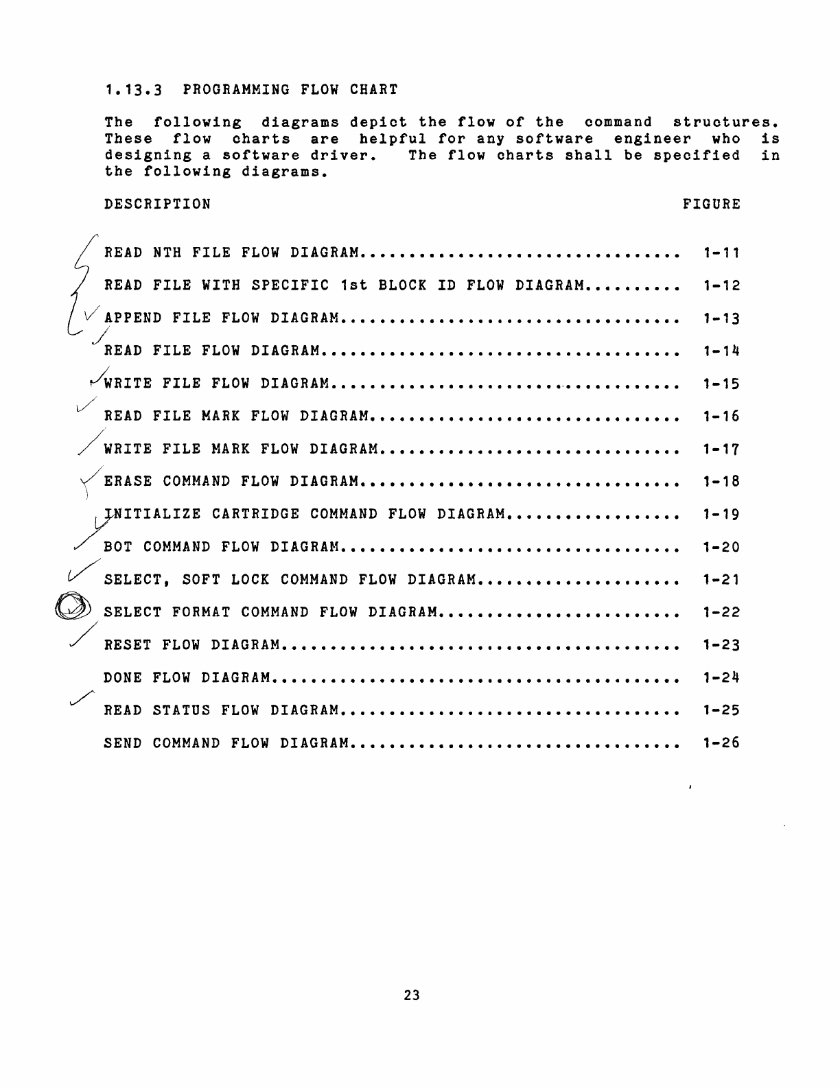
1.13.3
PROGRAMMING
FLOW
CHART
The
following
diagrams
depict
the
flow
of
the
command
structures.
These
flow
charts
are
helpful
for
any
software
engineer
who
is
designing
a
software
driver.
The
flow
charts
shall
be
specified
in
the
following
diagrams.
DESCRIPTION
FIGURE
READ
NTH
FILE
FLOW
DIAGRAM
•••••••••••••••••••••••••••••••••
1-11
READ
FILE
WITH
SPECIFIC
1st
BLOCK
ID
FLOW
DIAGRAM
••••••••••
V"
APPEND
FILE
FLOW
DIAGRAM
•••••••••••••••••••••••••••••••••••
/
READ
FILE
FLOW
DIAGRAM
•••••••••••••••••••••••••••••••••••••
/wRITE
FILE
FLOW
DIAGRAM
••••••••••••••••••••••••.••••••••••••
t/
READ
FILE
MARK
FLOW
DIAGRAM
••••••••••••••••••••••••••••••••
~WRITE
FILE
MARK
FLOW
DIAGRAM
•••••••••••••••••••••••••••••••
1-12
1-13
1-14
1-15
1-16
1-17
~ERASE
COMMAND
FLOW
DIAGRAM
•••••••••••••••••••••••••••••••••
1-18
~ITIALIZE
CARTRIDGE
COMMAND
FLOW
DIAGRAM
••••••••••••••••••
~BOT
COMMAND
FLOW
DIAGRAM
•••••••••••••••••••••••••••••••••••
~
SELECT,
SOFT
LOCK
COMMAND
FLOW
DIAGRAM
•••••••••••••••••••••
~
SELECT
FORMAT
COMMAND
FLOW
DIAGRAM
•••••••••••••••••••••••••
/
RESET
FLOW
DIAGRAM
•••••••••••••••••••••••••••••••••••••••••
DONE
/'
READ
SEND
FLOW
DIAGRAM
••••••••••••••••••••••••••••••••••••••••••
STATUS
FLOW
DIAGRAM
•••••••••••••••••••••••••••••••••••
COMMAND
FLOW
DIAGRAM
••••••••••••••••••••••••••••••••••
23
1-19
1-20
1-21
1-22
1-23
1-24
1-25
1-26
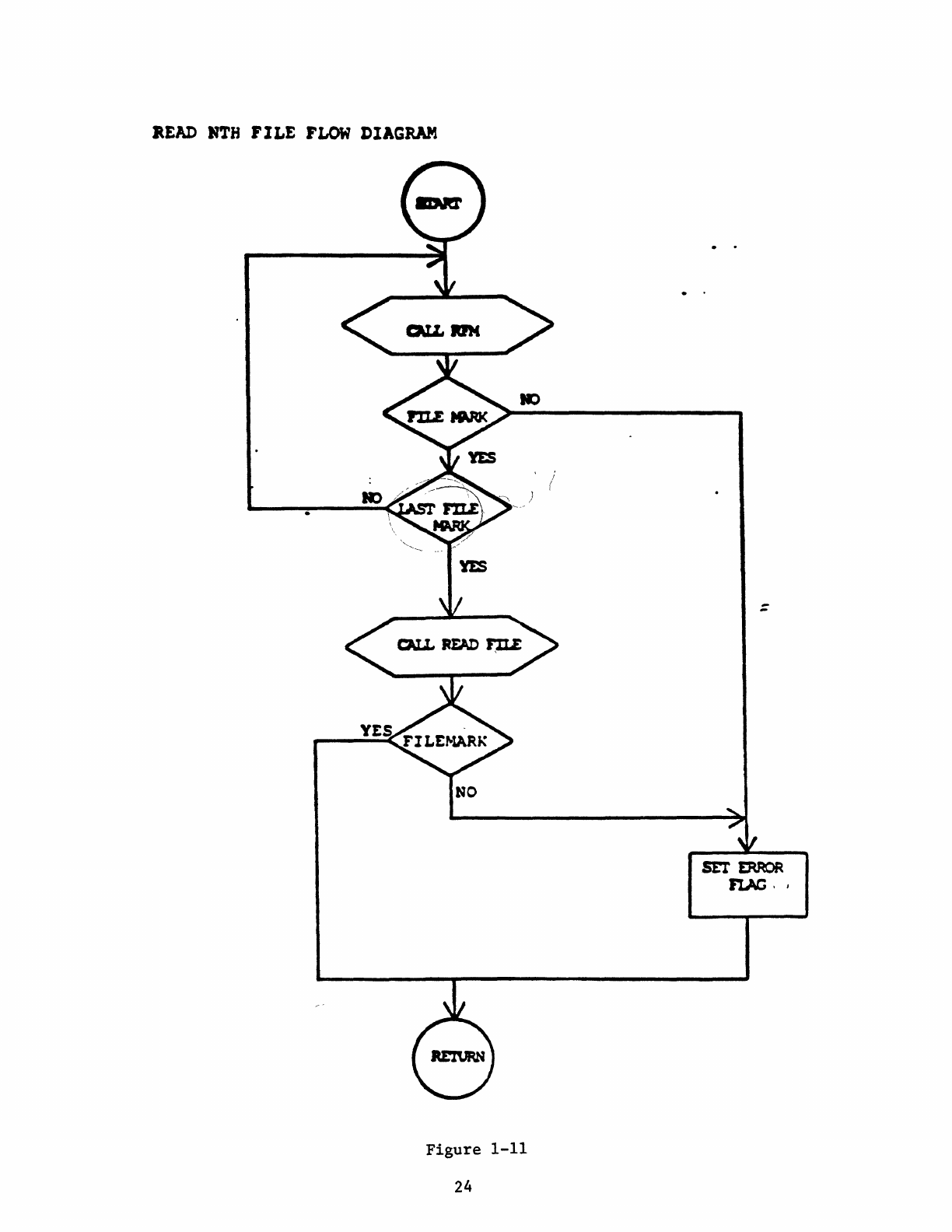
READ
NTH
FILE
FLOW
DIAGRAM
NO
Figure
1-11
24
::
SET
ERROR
1tAC·
,
READ
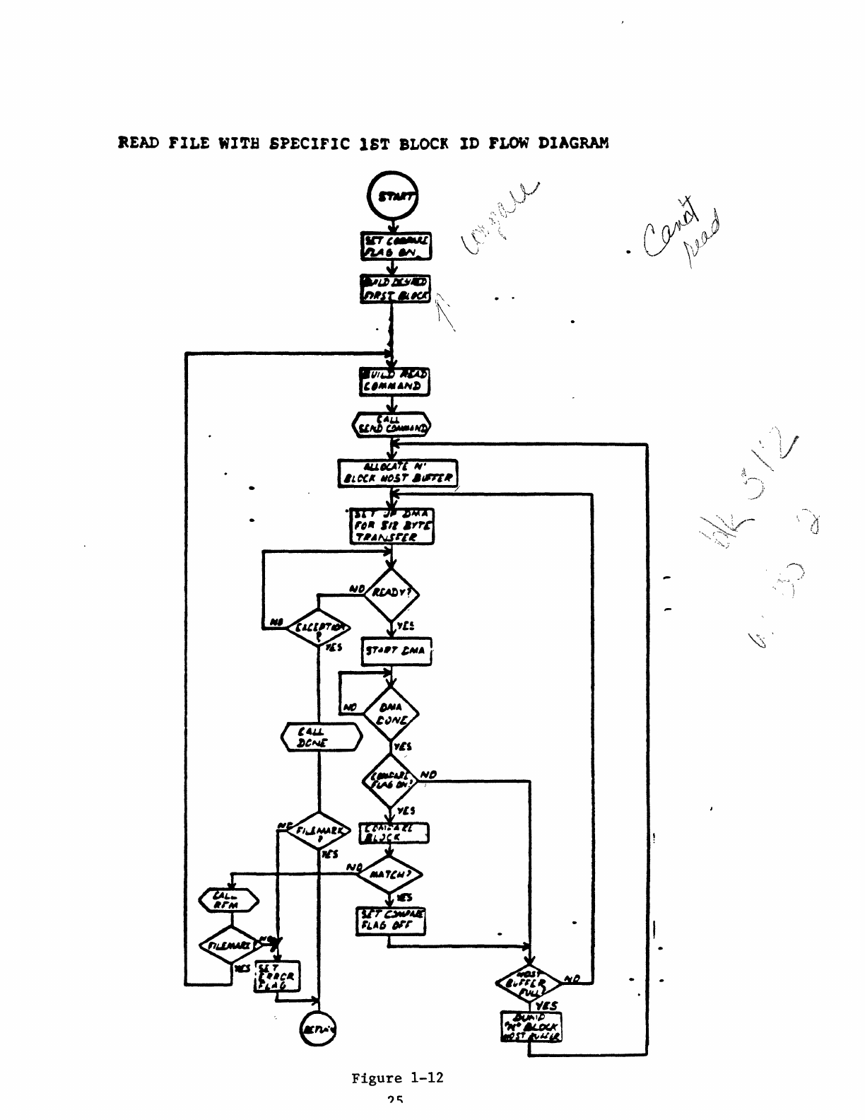
FILE
WITH
SPECIFIC
1ST
BLOCI
ID
FLOW
DIAGRAM
Figure
1-12
?J;
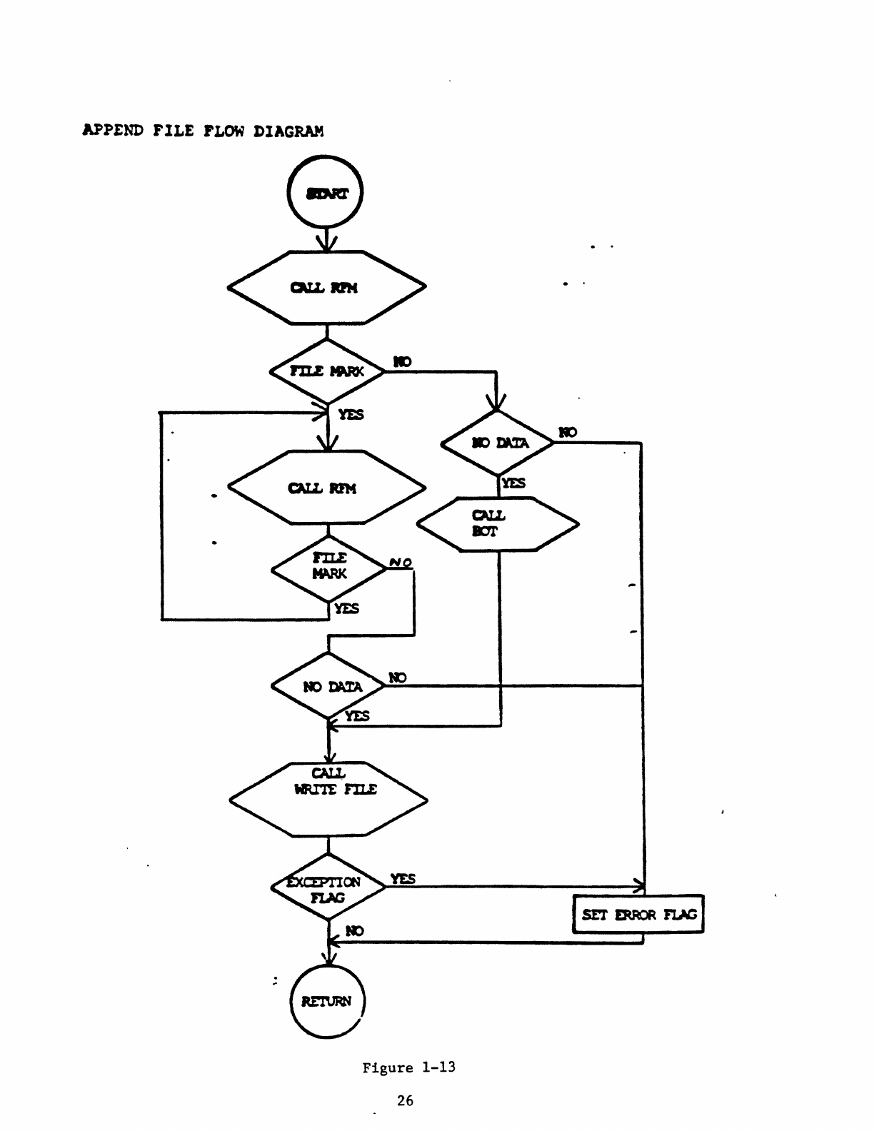
APPEND
FILE
FLOW
DIAGRAM
Figure
1-13
26
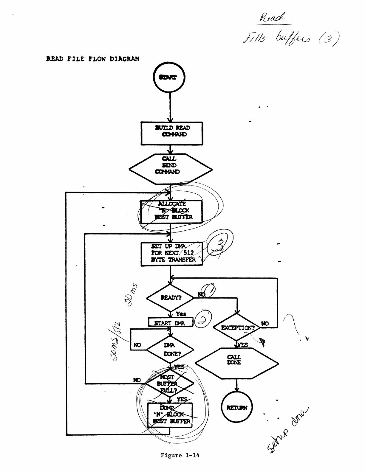
~£AD
FILE
FLOW
DIAGRAM
Figure
1-14
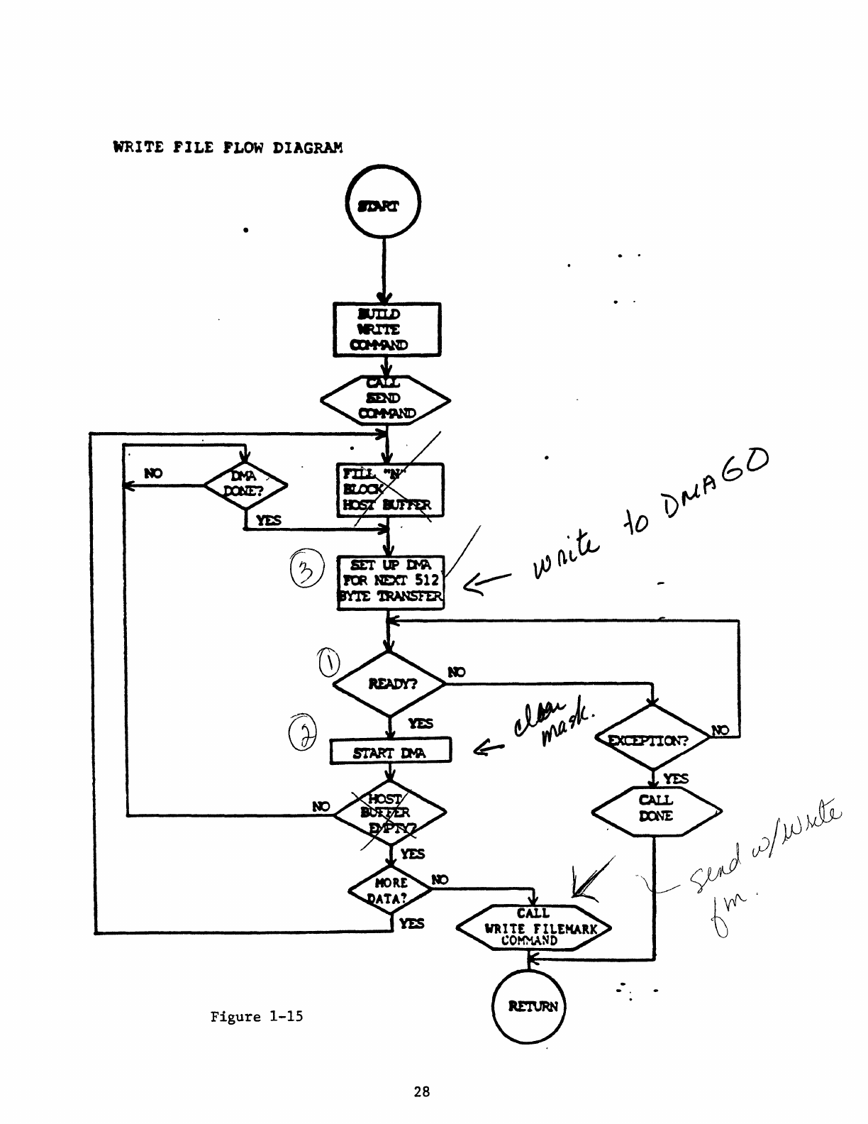
WRITE
FILE
FLOW
DIAGRAM
•
Figure
1-15
28
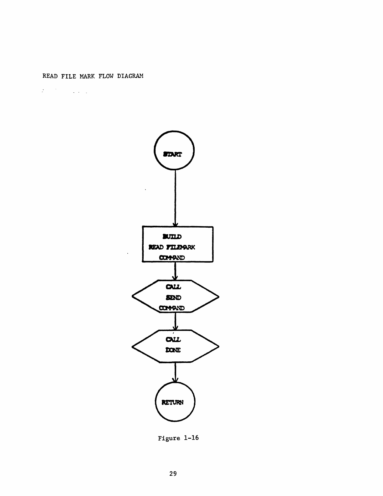
READ
FILE
MARK
FLOW
DIAGRAH
Figure
1-16
29
WRITE
rILE
MARX
FLOW
nIAGRAM
Figure
1-17
30
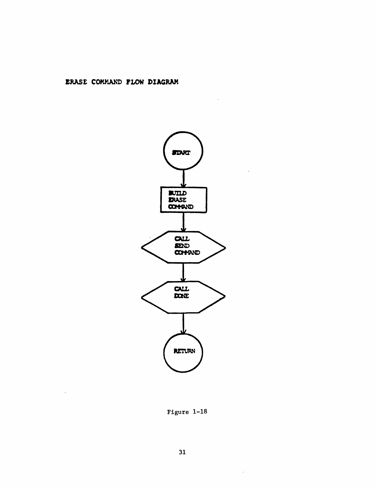
ERASE
COMMAND
FLOW
DIAGRAM
Figure
1-18
31
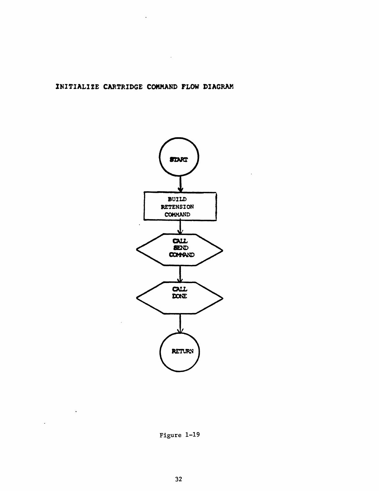
INITIALI2E
CARTRIDGE
COMMAND
FLOW
DIAGRAM
BUILD
RETENSION
COMMAND
Figure
1-19
32
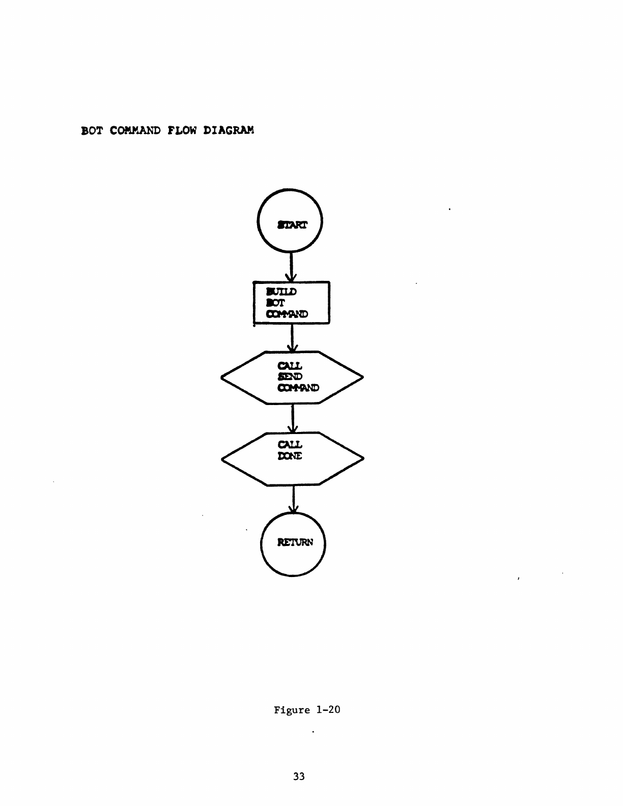
BOT
C()M)'.ANI)
FLOW
DIAGRAM
Figure
1-20
33
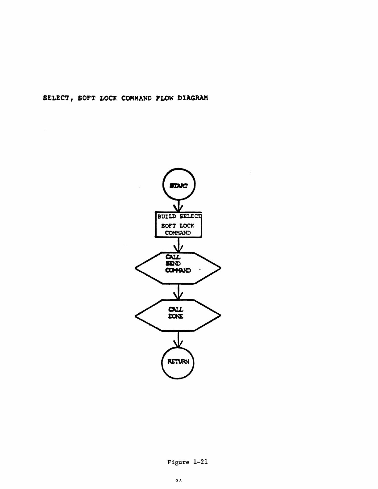
SELECT,
SOFT
LOCI
COMMAND
FLOW
DIAGRAM
BUILD
SELE
SOFT
LOCK
COMMAND
Figure
1-21
'1/.
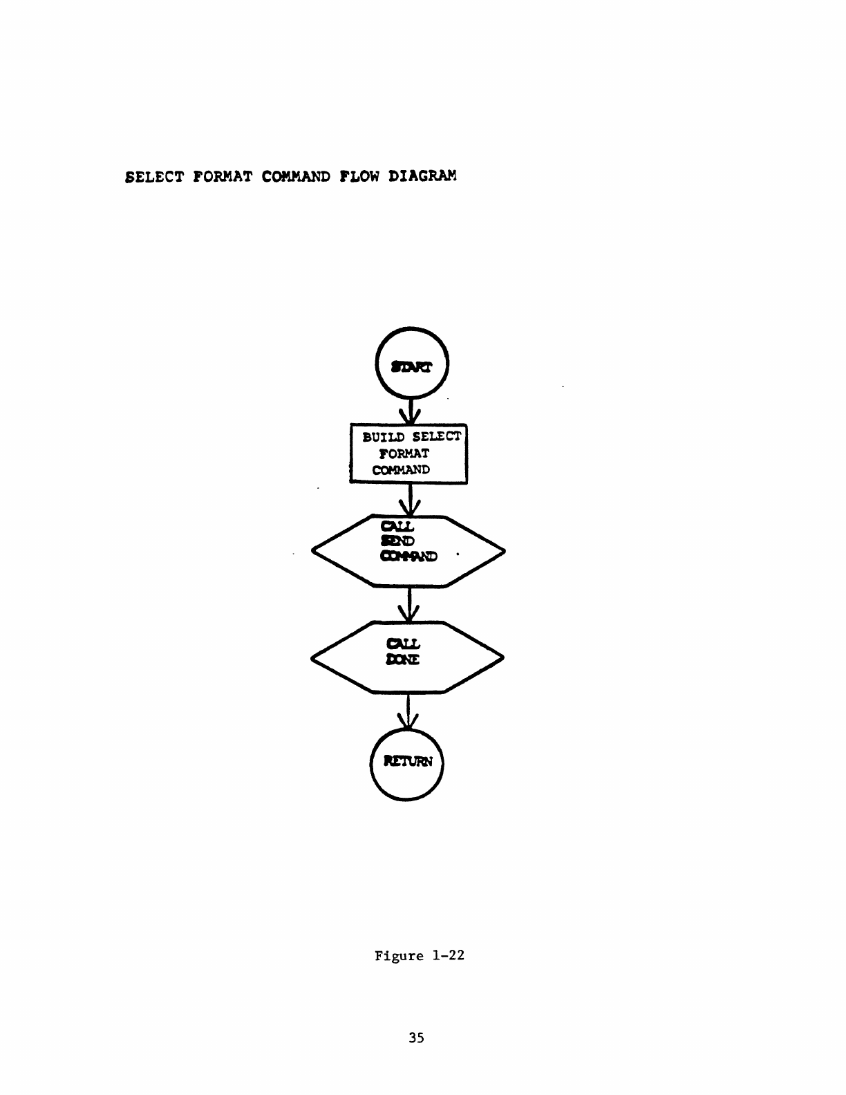
SELECT
FORMAT
COMMAND
FLOW
DIAGRAM
BUILD
SELECT
FOP.MAT
COMMAND
Figure
1-22
35

RESET
FLOW
DIAGRAM
ESE
I
Figure
1-23
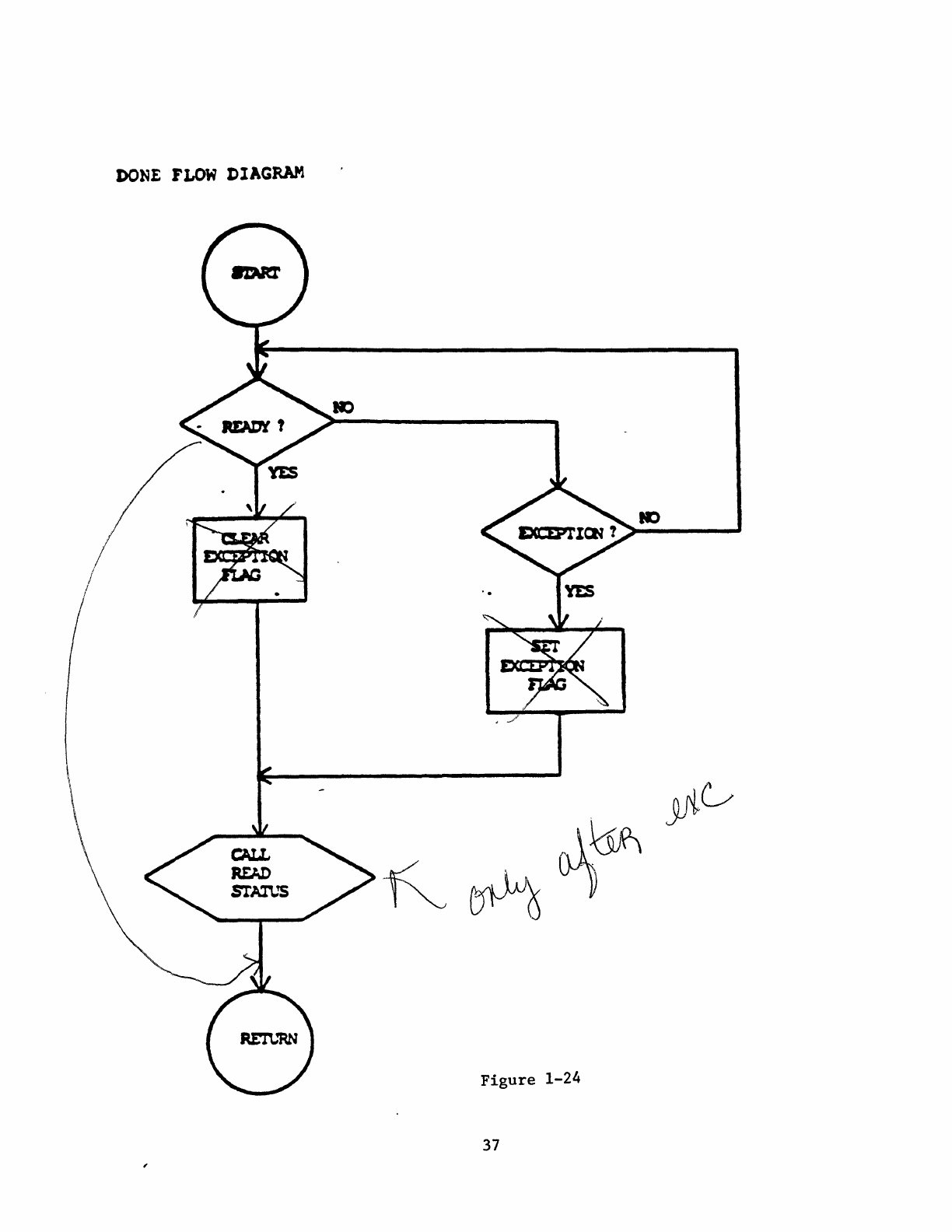
DONE
FLOW
DIAGRAM
(
Figure
1-24
37
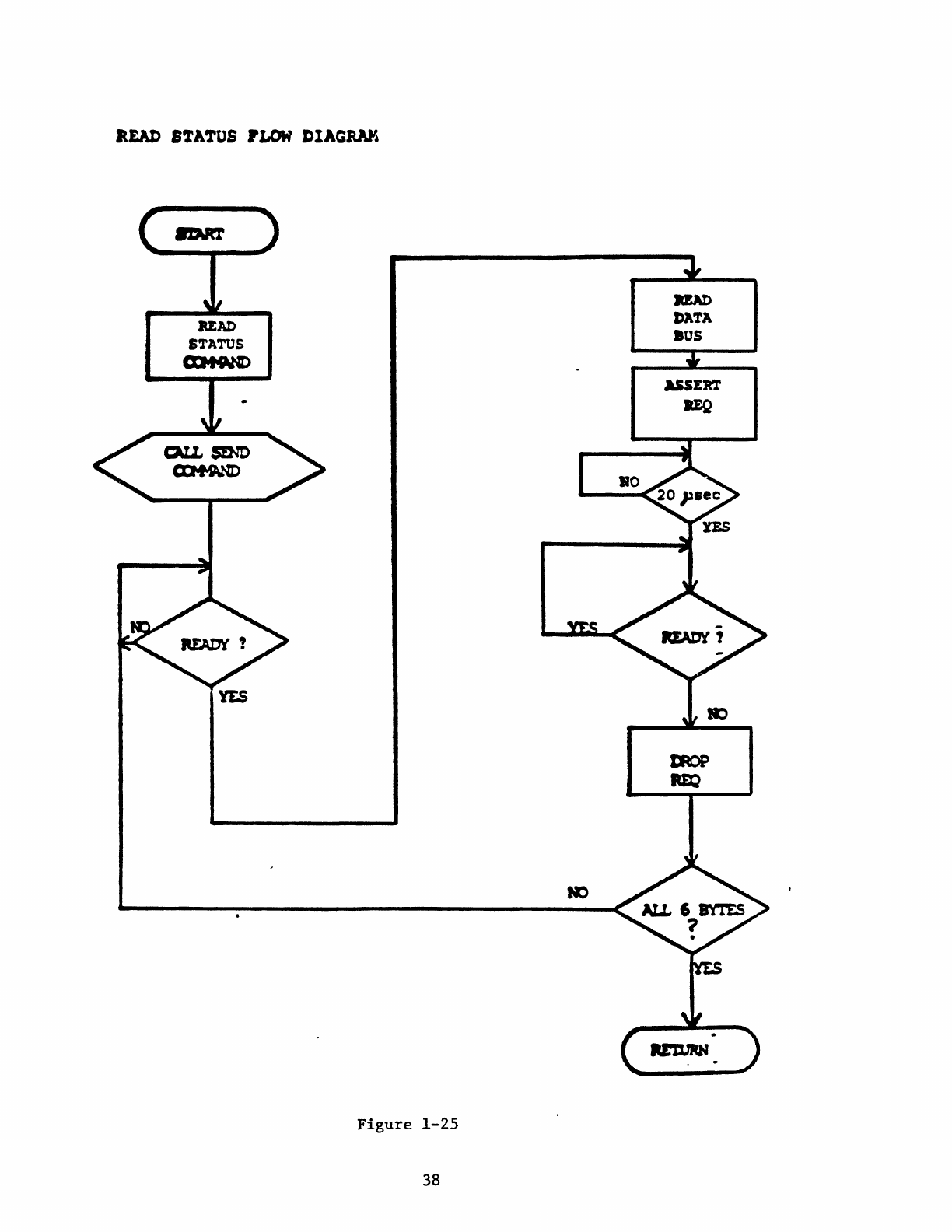
aEAD
STATOS
PLOW
»IAGRAK
BEAD
STATUS
CDt9.ND
Figure
1-25
38
MAD
I>ATA
BUS
ASSER'!'
DQ
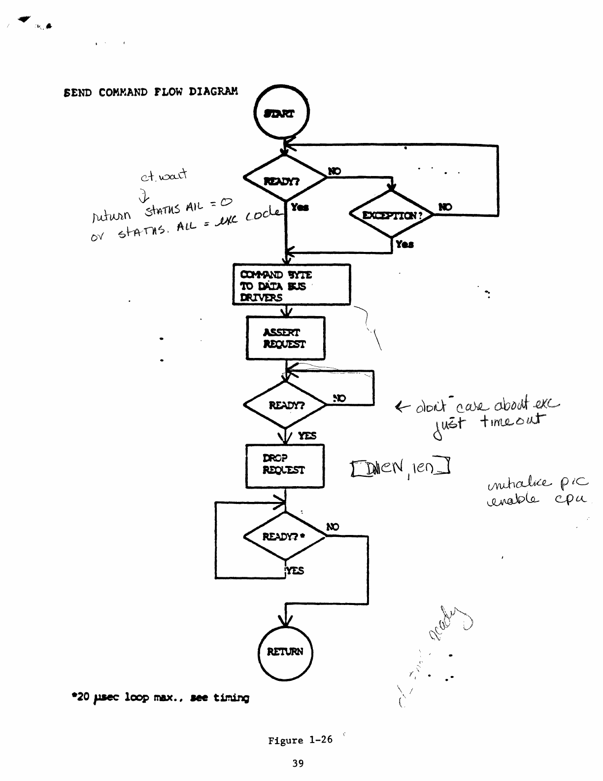
SEND
COMMAND
FLOW
DIAGRAM
Figure
1-26
39
-.
{-
0)D6
-
~a.}L
otllcNf'
.
.ex(--~
~lAbt
tl/IU-DtAT
~e\\l
J
1ef):J
f,
•
\ /
(
