ATtiny25/ATtiny45/ATtiny85, Appendix B Automotive Specification At 1.8V 1 Atmel 7669 ATtiny25 45 85 Datasheet
User Manual: AT 1
Open the PDF directly: View PDF ![]() .
.
Page Count: 8

7669E-AVR-04/14
This document contains information specific to devices operating at voltage between 1.8V
and 3.6V. Only deviations with standard operating characteristics are covered in this
appendix, all other information can be found in the complete Automotive datasheet. The
complete ATtiny25/ATtiny45/ATtiny85 automotive datasheet can be found on
http://www.atmel.com
ATtiny25/ATtiny45/ATtiny85
Appendix B - Automotive Specification at 1.8V
DATASHEET
ATtiny25/ATtiny45/ATtiny85 [DATASHEET]
7669E–AVR–04/14
2
1. Electrical Characteristics
1.1 Absolute Maximum Ratings
Stresses beyond those listed under “Absolute Maximum Ratings” may cause permanent damage to the device. This is a stress rating
only and functional operation of the device at these or any other conditions beyond those indicated in the operational sections of this
specification is not implied. Exposure to absolute maximum rating conditions for extended periods may affect device reliability.
Parameters Min. Typ. Max. Unit
Operating temperature –55 +150 °C
Storage temperature –65 +175 °C
Voltage on any pin except RESET with
respect to ground –0.5 VCC + 0.5 V
Voltage on RESET with respect to ground –0.5 +13.0 V
Maximum operating voltage 6.0 V
DC current per I/O pin 30.0 mA
DC current VCC and GND pins 200.0 mA
1.2 DC Characteristics
TA = –40°C to +85°C, VCC = 1.8V to 3.6V (unless otherwise noted)
Parameter Condition Symbol Min. Typ. Max. Unit
Input low voltage, except
XTAL1 and RESET pin VCC = 1.8V - 3.6V VIL –0.5 0.2VCC(1) V
Input high voltage, except
XTAL1 and RESET pins VCC = 1.8V - 3.6V VIH 0.7VCC(2) VCC + 0.5 V
Input low voltage,
XTAL1 pin VCC = 1.8V - 3.6V VIL1 –0.5 0.1VCC(1) V
Input high voltage,
XTAL1 pin VCC = 1.8V - 3.6V VIH1 0.9VCC(2) VCC + 0.5 V
Input low voltage,
RESET pin VCC = 1.8V - 3.6V VIL2 –0.5 0.2VCC(1) V
Input high voltage,
RESET pin VCC = 1.8V - 3.6V VIH2 0.9VCC(2) VCC + 0.5 V
Input low voltage,
RESET pin as I/O VCC = 1.8V - 3.6V VIL3 –0.5 0.3VCC(1) V
Input high voltage,
RESET pin as I/O VCC = 1.8V - 3.6V VIH3 0.6VCC(2) VCC + 0.5 V
Output low voltage(3),
I/O pin except RESET IOL = 0.5mA, VCC = 1.8V VOL 0.4 V
Notes: 1. “Max” means the highest value where the pin is guaranteed to be read as low
2. “Min” means the lowest value where the pin is guaranteed to be read as high
3. Although each I/O port can sink more than the test conditions (0.5mA at VCC = 1.8V) under steady state conditions (non-
transient), the following must be observed:
1] The sum of all IOL, for ports B0 - B5, should not exceed 50mA.
If IOL exceeds the test condition, VOL may exceed the related specification. Pins are not guaranteed to sink current
greater than the listed test condition.
4. Although each I/O port can source more than the test conditions (0.5mA at VCC = 1.8V) under steady state conditions
(non-transient), the following must be observed:
1] The sum of all IOH, for ports B0 - B5 should not exceed 50mA.
If IOH exceeds the test condition, VOH may exceed the related specification. Pins are not guaranteed to source current
greater than the listed test condition.
3
ATtiny25/ATtiny45/ATtiny85 [DATASHEET]
7669E–AVR–04/14
Output high voltage(4),
I/O pin except RESET IOH = –0.5mA, VCC = 1.8V VOH 1.2 V
Input leakage
current I/O pin VCC = 3.6V, pin low
(absolute value) IIL 1µA
Input leakage
current I/O pin VCC = 3.6V, pin high
(absolute value) IIH 1µA
Reset pull-up resistor RRST 30 60 k
I/O pin pull-up resistor RPU 20 50 k
Power supply current Active 4MHz, VCC = 1.8V ICC 0.8 1mA
Idle 4MHz, VCC = 1.8V ICC 0.2 0.3 mA
Power-down mode WDT disabled, VCC = 1.8V
WDT enabled, VCC = 1.8V ICC 0.2
410
20 µA
Analog comparator
Input offset voltage VCC = 2.7V
Vin = VCC/2 VACIO <10 40 mV
Analog comparator
input leakage current VCC = 2.7V
Vin = VCC/2 IACLK –50 50 nA
Analog comparator
propagation delay VCC = 2.7V tACPD 500 ns
1.2 DC Characteristics (Continued)
TA = –40°C to +85°C, VCC = 1.8V to 3.6V (unless otherwise noted)
Parameter Condition Symbol Min. Typ. Max. Unit
Notes: 1. “Max” means the highest value where the pin is guaranteed to be read as low
2. “Min” means the lowest value where the pin is guaranteed to be read as high
3. Although each I/O port can sink more than the test conditions (0.5mA at VCC = 1.8V) under steady state conditions (non-
transient), the following must be observed:
1] The sum of all IOL, for ports B0 - B5, should not exceed 50mA.
If IOL exceeds the test condition, VOL may exceed the related specification. Pins are not guaranteed to sink current
greater than the listed test condition.
4. Although each I/O port can source more than the test conditions (0.5mA at VCC = 1.8V) under steady state conditions
(non-transient), the following must be observed:
1] The sum of all IOH, for ports B0 - B5 should not exceed 50mA.
If IOH exceeds the test condition, VOH may exceed the related specification. Pins are not guaranteed to source current
greater than the listed test condition.
ATtiny25/ATtiny45/ATtiny85 [DATASHEET]
7669E–AVR–04/14
4
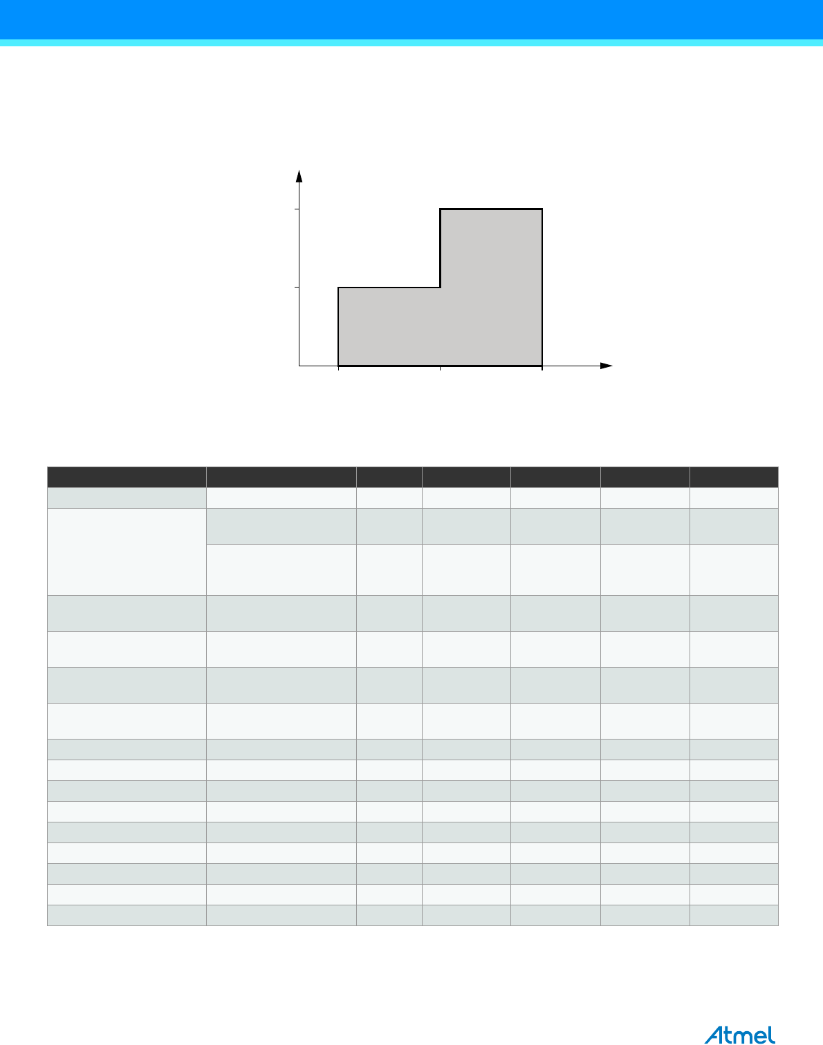
1.3 Maximum Speed vs. VCC
Maximum frequency is dependent on VCC. As shown in Figure 1-1, the maximum frequency versus VCC curve is linear
between 1.8V < VCC < 3.6V.
Figure 1-1. Maximum Frequency versus VCC
8MHz
4MHz
3.6V2.7V
1.8V
1.4 ADC Characteristics
TA = –40°C to +85°C, VCC = 1.8V to 3.6V (unless otherwise noted)
Parameter Condition Symbol Min Typ Max Unit
Resolution 8Bits
Absolute accuracy
(Including INL, DNL,
quantization error, gain and
offset error)
VREF = 2.7V, VCC = 2.7V,
ADC clock = 200kHz 23.5 LSB
VREF = 2.7V, VCC = 2.7V,
ADC clock = 200kHz
Noise reduction mode 23.5 LSB
Integral non-linearity (INL) VREF = 2.7V, VCC = 2.7V,
ADC clock = 200kHz 0.6 2.5 LSB
Differential non-linearity
(DNL) VREF = 2.7V, VCC = 2.7V,
ADC clock = 200kHz 0.30 1.0 LSB
Gain error VREF = 2.7V, VCC = 2.7V,
ADC clock = 200kHz –3.5 –1.3 +3.5 LSB
Offset error VREF = 2.7V, VCC = 2.7V,
ADC clock = 200kHz 1.8 3.5 LSB
Conversion time Free running conversion 13 cycles µs
Clock frequency 50 200 kHz
Analog supply voltage AVCC VCC – 0.3 VCC + 0.3 V
Reference voltage VREF 1.0 AVCC V
Input voltage VIN GND VREF – 50mV V
Input bandwidth 38.5 kHz
Internal voltage reference VINT 1.0 1.1 1.2 V
Reference input resistance RREF 25.6 32 38.4 k
Analog input resistance RAIN 100 M
5
ATtiny25/ATtiny45/ATtiny85 [DATASHEET]
7669E–AVR–04/14
2. Ordering Information
Power Supply Speed (MHz) ISP Flash Ordering Code Package Operation Range
1.8 - 3.6V 4-8 2KB ATtiny25V-15ST 8S2 Automotive (–40°C to +85°C)
1.8 - 3.6V 4-8 4KB ATtiny45V-15ST 8S2 Automotive (–40°C to +85°C)
1.8 - 3.6V 4-8 8KB ATtiny85V-15ST 8S2 Automotive (–40°C to +85°C)
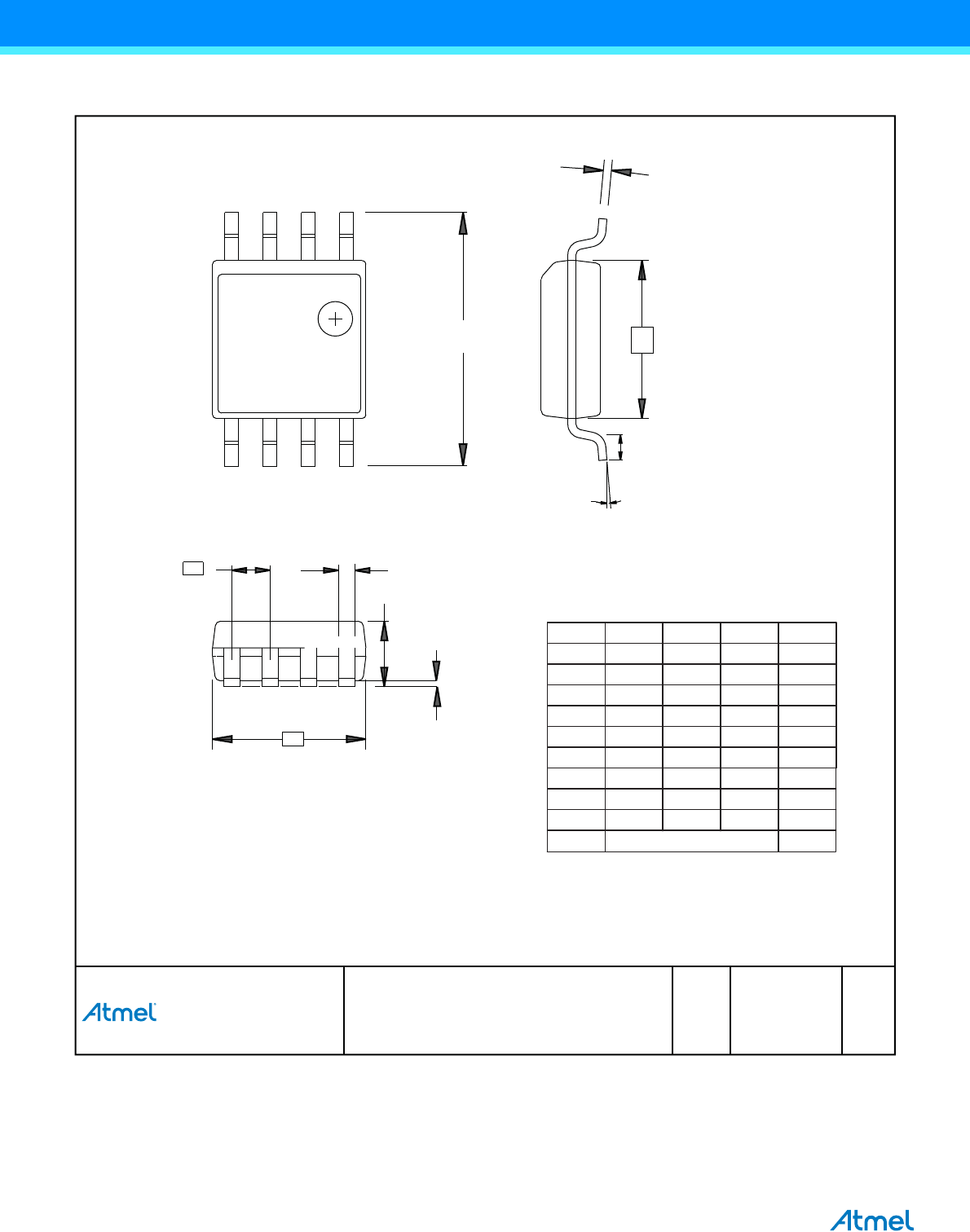
3. Package Information
Package Type Remarks
8S2 8-lead, 0.208" wide, plastic gull-wing small outline (EIAJ SOIC)
ATtiny25/ATtiny45/ATtiny85 [DATASHEET]
7669E–AVR–04/14
6
Figure 3-1. 8S2
Package Drawing Contact:
packagedrawings@atmel.com
GPC DRAWING NO.
REV. TITLE
8S2STN F
04/15/08
8S2, 8-lead, 0.208” Body, Plastic Small
Outline Package (EIAJ)
E
eb
A
D
A1
C
E1
L
COMMON DIMENSIONS
(Unit of Measure = mm)
MIN NOM NOTEMAXSymbol
0.25
1.70
0.05
0.480.35
A1
5.405.18E1
1.27 BSCe
8°0°θ
7.70 8.26E
0.51 0.85L
5.355.13D
0.350.15C
b
2
3
4
4
2.16A
Notes: 1. This drawing is for general information only; refer to EIAJ Drawing EDR-7320 for additional information.
2. Mismatch of the upper and lower dies and resin burrs aren't included.
3. Determines the true geometric position.
4. Values b,C apply to plated terminal. The standard thickness of the plating layer shall measure between 0.007 to .021 mm.
θ
θ
1
1
N
N
Top View
End View
Side View

7
ATtiny25/ATtiny45/ATtiny85 [DATASHEET]
7669E–AVR–04/14
4. Revision History
Please note that the following page numbers referred to in this section refer to the specific revision mentioned, not to this
document.
Revision No. History
7669E-AVR-04/14 Put datasheet in the latest template

X
XXX
XX
Atmel Corporation 1600 Technology Drive, San Jose, CA 95110 USA T: (+1)(408) 441.0311 F: (+1)(408) 436.4200 | www.atmel.com
© 2014 Atmel Corporation. / Rev.: 7669E–AVR–04/14
Atmel®, Atmel logo and combinations thereof, Enabling Unlimited Possibilities®, AVR®, and others are registered trademarks or trademarks of Atmel Corporation or its
subsidiaries. Other terms and product names may be trademarks of others.
DISCLAIMER: The information in this document is provided in connection with Atmel products. No license, express or implied, by estoppel or otherwise, to any intellectual property right
is granted by this document or in connection with the sale of Atmel products. EXCEPT AS SET FORTH IN THE ATMEL TERMS AND CONDITIONS OF SALES LOCATED ON THE
ATMEL WEBSITE, ATMEL ASSUMES NO LIABILITY WHATSOEVER AND DISCLAIMS ANY EXPRESS, IMPLIED OR STATUTORY WARRANTY RELATING TO ITS PRODUCTS
INCLUDING, BUT NOT LIMITED TO, THE IMPLIED WARRANTY OF MERCHANTABILITY, FITNESS FOR A PARTICULAR PURPOSE, OR NON-INFRINGEMENT. IN NO EVENT
SHALL ATMEL BE LIABLE FOR ANY DIRECT, INDIRECT, CONSEQUENTIAL, PUNITIVE, SPECIAL OR INCIDENTAL DAMAGES (INCLUDING, WITHOUT LIMITATION, DAMAGES
FOR LOSS AND PROFITS, BUSINESS INTERRUPTION, OR LOSS OF INFORMATION) ARISING OUT OF THE USE OR INABILITY TO USE THIS DOCUMENT, EVEN IF ATMEL HAS
BEEN ADVISED OF THE POSSIBILITY OF SUCH DAMAGES. Atmel makes no representations or warranties with respect to the accuracy or completeness of the contents of this
document and reserves the right to make changes to specifications and products descriptions at any time without notice. Atmel does not make any commitment to update the information
contained herein. Unless specifically provided otherwise, Atmel products are not suitable for, and shall not be used in, automotive applications. Atmel products are not intended,
authorized, or warranted for use as components in applications intended to support or sustain life.
SAFETY-CRITICAL, MILITARY, AND AUTOMOTIVE APPLICATIONS DISCLAIMER: Atmel products are not designed for and will not be used in connection with any applications where
the failure of such products would reasonably be expected to result in significant personal injury or death (“Safety-Critical Applications”) without an Atmel officer's specific written
consent. Safety-Critical Applications include, without limitation, life support devices and systems, equipment or systems for the operation of nuclear facilities and weapons systems.
Atmel products are not designed nor intended for use in military or aerospace applications or environments unless specifically designated by Atmel as military-grade. Atmel products are
not designed nor intended for use in automotive applications unless specifically designated by Atmel as automotive-grade.
