C Sony CRT Television KV 13FS110 BA6 Chassis Training Manual (CTV30)
User Manual: Sony CRT Television KV-13FS110
Open the PDF directly: View PDF ![]() .
.
Page Count: 41
Training Manual
Course: CTV-30
BA-6 Chassis
Models: KV-13FS100
KV-13FS110
KV-20FS100
KV-20FV300
KV-24FS100
KV-24FV300
Circuit Description and Troubleshooting
KV-24FV300

Table of Contents
Introduction ...........................................1
Overview................................................................. 1
CTV-30 Objectives................................................ 1
1. Features .............................................2
Overview................................................................. 2
Audio Features ...................................................... 2
Video Features ...................................................... 3
Convenience Features ......................................... 3
Feature Glossary .................................................. 3
2. Overall BA-6 Block ...........................5
Overview................................................................. 5
A Board ................................................................... 6
CV Board................................................................ 7
3. Power Supply ....................................8
Power Supply Block.............................................. 8
5V Standby Power Supply & Power-ON
Switching Circuits.................................................. 9
Main Switching Power Supply Circuit ............... 11
Static MOSFET Resistance Tests ..................... 13
4. Deflection Circuits ...........................15
Vertical Theory ..................................................... 15
Horizontal and Pincushion.................................. 16
Vertical Deflection Circuit.................................... 19
Horizontal Deflection and
Pincushion Circuits .............................................. 18
5. Protection Circuits ...........................22
Overview................................................................ 22
Protection Circuits................................................ 24
6. Video/RGB.........................................26
Overview................................................................ 26
Video/RGB ............................................................ 27
7. Audio ..................................................32
Overview................................................................ 32
Audio Circuit [KV20FV300 & KV24FV300]...... 32
Troubleshooting .................................................... 35
8. Self-Diagnostics ...............................36
Power ON.............................................................. 36
Self-Diagnostic Indication................................... 36
Failure History Display ........................................ 37

1
1. Features
Introduction
Overview
This course will cover the new BA-6 chassis. The USA model sizes for the BA-6 chassis are 13", 20" and 24".
This chassis has major circuit changes from the BA-5 chassis, the main one being the integration of Syscon, YC
Jungle and Comb Filter into one IC package (called One-Chip). Other changes are in the Power Supply (Main
and Standby) and the Audio section. The Vertical and Horizontal deflection section are similar to previous
chassis’s except for the Horizontal Output transistor, which is a new design. Although this single chip design may
seem to eliminate a large portion of circuit troubleshooting, there are still discreet circuits and external ICs that
can fail. In addition, when the unit becomes defective, a good understanding of the One-Chip IC functions will be
needed to determine if the problem is in the One-Chip IC or in external circuits.
CTV-30 Objectives
•Cover features of the BA-6 chassis.
•Define the One-Chip design.
•Provide a Theory of Operations (Waveforms and Voltages) and Troubleshooting Tips for each major
section of the BA-6 chassis.
•Discuss unit Self-Diagnostic functions and how they can assist in troubleshooting.
2
1. Features
Chapter 1 - Features
Overview
This section covers the Audio, Video, Convenience features of the BA-6 chassis models. Also included is a
Features Glossary.
BA-6 Chassis Models:
KV-13FS100 KV-13FS110
KV-20FS100 KV-20FV300
KV-24FS100 KV-24FV300
NOTE: The BA-6 chassis meets the Energy Star® guidelines for energy efficiency
Audio Features
Reference Table 1-1 for the Audio features of each model using the BA-6 chassis.
Table 1-1 – Audio Features per Model
Audio
Power Speaker
Box Head-
Phones
(wired)
Audio
Output
Var/Fix
MTS Steady
Sound Audio
Effects Auto
Mute
13FS100
3Wx2 NO YES NO YES NO NO YES
13FS110
3Wx2 NO YES NO YES NO NO YES
20FS100
5Wx2 NO YES NO YES NO NO YES
20FV300
10Wx2 YES YES YES YES YES YES YES
24FS100
7.5Wx2 NO YES NO YES NO NO YES
24FV300
10Wx2 YES YES YES YES YES YES YES
NOTE: Reference feature glossary for definition of terms.
Audio Effects includes the following:
•Simulated Stereo
•WOW
•SRS
3
1. Features
Table 1-2 – Video Features per Model
3D
Comb
filter
S-
Video
Input
Rear
Tilt
Correction
V.M Video
2
Input
Front
YUV
Input
Rear
V-
Chip XDS/CC
13FS100 YES NO YES NO YES YES YES YES
13FS110 YES NO YES NO YES YES YES YES
20FS100 YES NO YES YES YES YES YES YES
20FV300 YES YES YES YES YES YES YES YES
24FS100 YES YES YES YES YES YES YES YES
24FV300 YES YES YES YES YES YES YES YES
Video Features
Reference Table 1-2 for the Video features of each model using the BA-6 chassis.
•FD Trinitron WEGA TV (Flat CRT)
NOTE: Reference feature glossary for definition of terms
Convenience Features
All BA-6 chassis models contain the following Convenience Features:
•Auto Channel Programming
•Channel Label
•Favorite Channel
•Front Panel Controls (Including On-Screen Menu)
•Parental Control (V-Chip)
•Real Time Clock
•Trilingual Menus (English, Spanish, or French)
•Two Event Timer
•Video Label
Feature Glossary
Audio
Audio Effects – Covers three sound effect modes: Simulated Stereo, WOW and SRS.
Auto Mute – A feature designed to automatically mute the TV audio when no RF signal is received
BBE – Shifts the phase of the audio signal to improve TV sound.
MTS – Allows direct access to the Multi-Channel TV Sound: Stereo, Mono or Auto SAP (Second Audio
Program) with a touch of a button.
Simulated Stereo – Simulates stereo quality sound for mono programs.
Speaker Box – A speaker enclosure used to improve sound quality.
SRS – Produces a dynamic three-dimensional sound for stereo audio signals (surround sound virtual
speakers).

4
1. Features
Steady Sound – Stabilizes volume during sudden sound fluctuations of received audio.
WOW – Provides a dramatic presence with full, deep bass sound. When WOW is enabled, BBE is
directly activated to further enhance the audio program.
Video
3D comb Filter – Looks at the horizontal line above and below the line being processed, along with the
same three lines in the frame before and after, to optimally remove the chroma component from the Y in
a composite video signal. This reduces dot crawl and other noise to produce the best picture possible.
V-Chip – (Parental Control) Allows parental control over rated television programs.
VM – (Velocity Modulation) Sharpens the picture definition by varying the beam-scanning rate to give
every object a sharp, clean edge.
XDS/CC – Information services that some broadcasters are adding to their signals, including time, station
call letters and programming information.
YUV – (Component Video) Delivers optimum picture quality by supplying separate connections for the
luminance (Y) and color information (UV).
5
2. Overall BA-6 Block
Chapter 2 - Overall BA-6 Block
FIGURE 2-1 - BA5 - BA6 BOARD COMPARISON
A
CV
K
A
MB
C
V
3/11/022.1CTV30
BA-5 BA-6
BA-5 BA-6
Overview
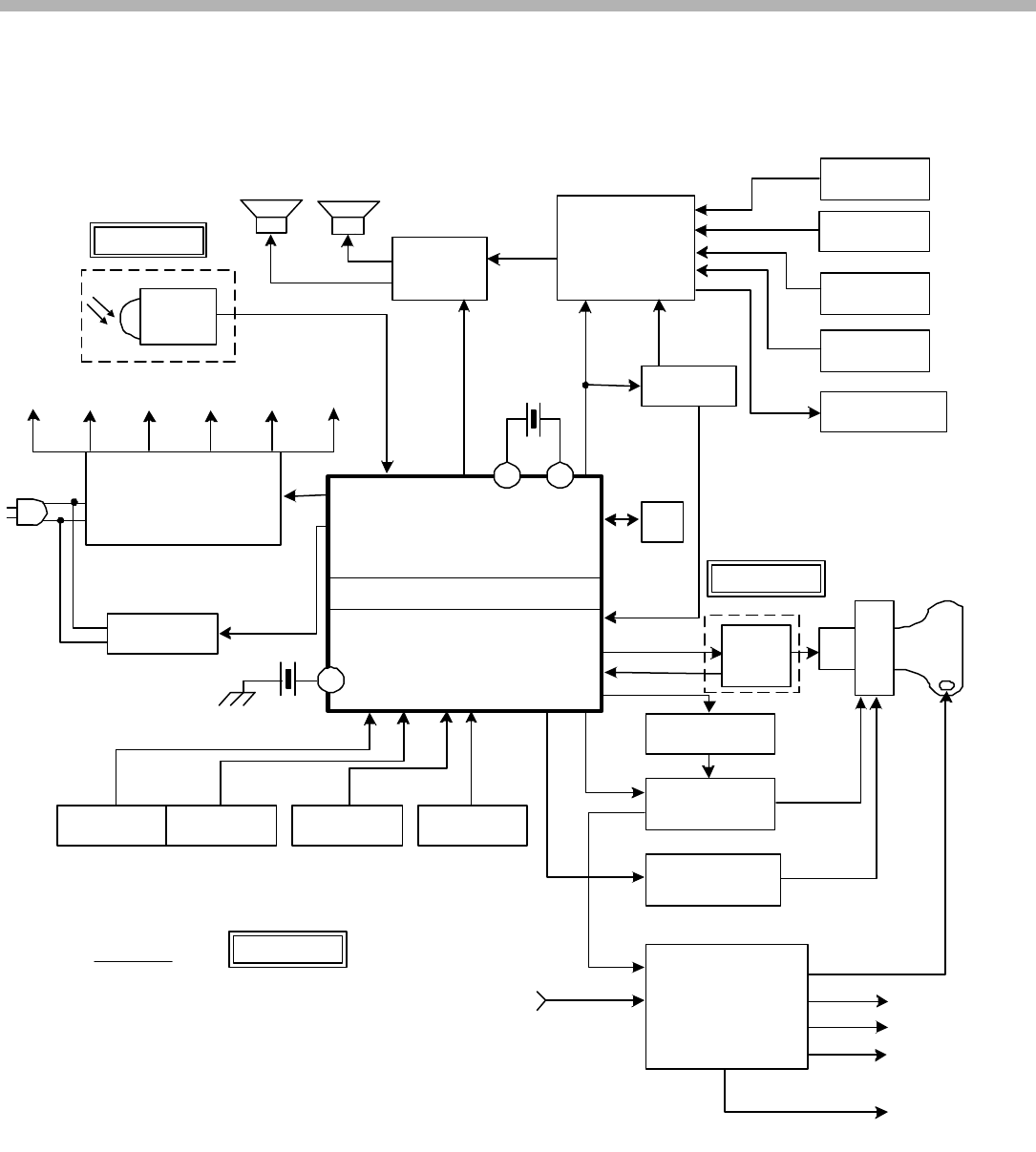
The BA-6 chassis has taken a major step towards the “TV on a Chip” concept. The One Chip (IC001) performs
all System Control and Signal Processing functions. In previous models these functions were handled by three
different ICs: System Control, YC Jungle and Comb Filter. A direct result of the higher circuit integration is the
lower PCB count. The number PCBs went from five in the BA-5 to only two in the BA-6 chassis (as illustrated in
Figure 2-1).
6
2. Overall BA-6 Block
IC001
ONE CHIP
SYSCON
3D COMB FILTER
YC JUNGLE
S-VIDEO VIDEO 1 VIDEO 2 YUV
V V V VD
DEGAUSS
POWER
SUPPLY
14V 9V B+
STBY
5V MAIN
3.3V STBY
3.3V
AUDIO
AMP
IR
LRAUDIO
PROCESSOR
& INPUT
SWITCHER
TUNER
NVM
VIDEO 1
VIDEO 2
AUDIO IN
AUDIO OUT
HEADPHONE
A
A
A
A
A
PINCUSHION
HORIZONTAL
DEFLECTION
VERTICAL
DEFLECTION
HP
E/W
HP
B+ FOCUS
G2
SECONDARY
VOLTAGES
ABL
Y
O
K
E
FLYBACK
TRANSFORMER
HV
V
A
A
A
D
C
C
RGB
A
FIGURE 2-2 - OVERALL BLOCK 3/25/022.1CTV30
A BOARD
LEGEND
A - AUDIO
C - CONTROL
D - DATA
V - VIDEO
HR BOARD
V
C
CRGB
AMPS
IK
CV BOARD
3 4
X001
8mHz
37
X301
6mHz
A Board
The A board contains all the Power Supply, System Control, Deflection, Video Processing and Audio Processing
circuits.

7
2. Overall BA-6 Block
System Control
All system control functions are performed by IC001 (OneChip). The main operating crystal is X001 (8MHz).
The following control functions are handled by IC001:
1) Remote commands (SIRSC) decoding
2) Main Converter Power Supply ON/OFF
3) Audio IC Input switching (commands ONLY)
4) Audio Muting and Volume Control
5) Video Input Switching (Performed Inside IC001)
6) Degauss ON/OFF
7) Tuner Control and Muting
Power Supply
The Standby Power Supply on the BA-6 is Energy Star® compliant. It supplies Standby 5V and Standby 3.3V to
keep various circuits on the A board active in Standby Mode. The Main Converter Power Supply supplies the rest
of the voltages (+135V, 14V, 9V, Main 3.3V) to the A board when an ON command is received..
Audio Section
The A board contains audio switching, processing (both of these functions are performed in IC400 for the
appropriate models) and amplifier circuits. The only circuit change on the A board between models is the Audio
processing IC. The KV-20FV100, and KV-24FV300 use IC400 (IC400 contains the Surround Sound processing
circuits); the KV-20FS100, KV-24FS100, and KV-13FS100/110 use IC401. All models use Audio Amplifier IC404.
Video Section
All Front/Rear Video input jacks and the Tuner are located on the A board. All video switching and processing is
performed by the ONE-Chip (IC001) on the A board. New on the BA-6 chassis is the addition of a component
(YUV) jack on the rear of the unit. Crystal X301 (6MHz) is used for NTSC signal (Composite) color signal
processing. If X301 is defective, the unit will still operate normally, except the picture will be in Black and White.
Deflection
The Horizontal, Vertical and Pincushion correction circuits are all on the A board. These circuits, along with the
Fly-back transformer, drive the CRT electron beam for picture scanning. The Horizontal output transistor is new
on the BA-6 chassis for better performance.
The Degauss circuit and relay is also on the A board.
CV Board
The CV board connects to the neck of the CRT via J1751. The circuits found on this PCB are the RGB amplifier
and buffer transistors and Output Drive IC (IC1751), N/S Amplifier and VM Drive circuit. The N/S amplifier and
coil are used to rotate the trace for good level horizontal scanning (Tilt Correction). The VM (Velocity Modulation)
circuit assists in sharpening the image when transitioning from Black to White and visa-versa.
8
3.Power Supply Block
Chapter 3 - Power Supply
LINEAR
STANDBY
POWER
SUPPLY
IC001
SYSCON
D050 D051 R099 STBY 3.3V
TO IC001 &
STANDBY
CIRCUITS
IC002
16K NVM
IC004
SIRCS
IC003
STBY 5V
RESET
T601ACIN
IC603
IC633
IC404
15V
9V
MAIN 3.3V
+135V
PH602
IC604
ERROR
AMP
B+
IC001
SYSCON
(0-RELAY)
RY600
DEGAUSS
SWITCH
Q501
IC001/PIN 60
(0-DGC)
DEGAUSS
COIL
14V
FIGURE 3-1 - POWER SUPPLY OVERALL BLOCK 3/26/023.1CTV30
RY501
5V
MAIN
SWITCHING
POWER
SUPPLY
FROM
Q604 12V
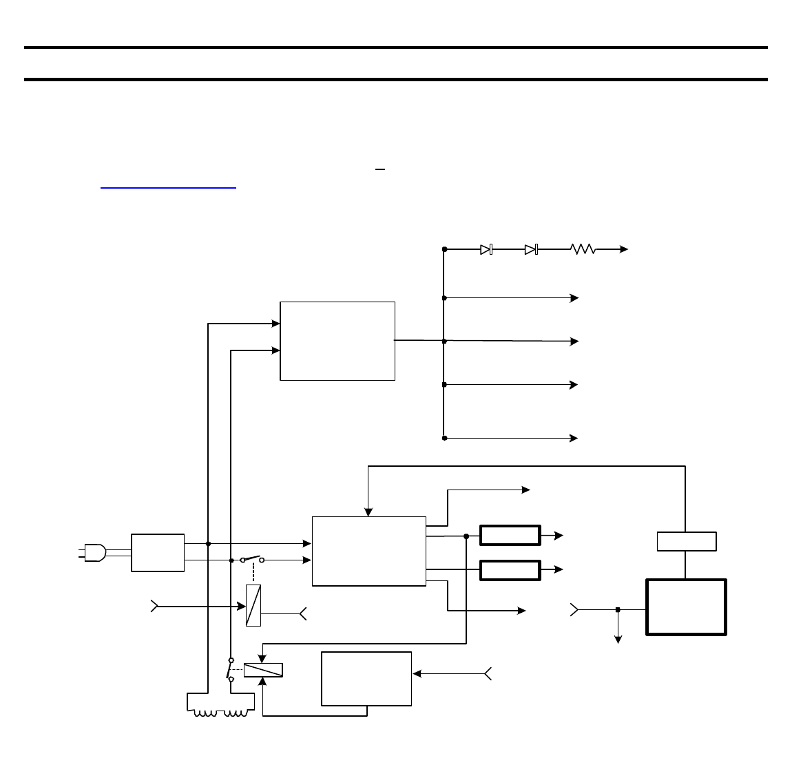
Power Supply Block
The power supply section in the BA-6 chassis is labeled Energy Star® compliant. This means that the power
supply meets or exceeds the power conservation standard set forth by the EPA and the Department of Energy.
That standard states that an analog TV should draw <1 Watt in Standby Mode. For more information on Energy
Star, go to www.energystar.gov. The power supply section consists of the 5V Standby Supply and the Main
Converter Switching Supply (ref. Figure 3-1). Also included in this diagram is the Degauss circuit.
5V Standby Power Supply
The Standby Power supply in the BA-6 chassis is a Conventional Full-wave rectifier, capacitor filtered type. This
is a departure from previous models, which use switch-mode power supplies in the standby circuit. The AC input
to the Standby supply is connected directly across the ACIN source, before the AC input relay RY600. So, the
Standby Power supply outputs the voltages listed on Figure 3-1 once AC is applied to the set.
Main Switching Power Supply
As in previous models, the Main Switching supply is a switch-mode power supply. The Main supply receives AC
input through relay RY600 after System Control receives an ON command. Once the switching oscillations
begin and feedback (through IC604) is established, the Main Power outputs the voltages listed in Figure 3-1.
9
3. Power Supply Block
T601
F601
ACIN
R605
C611
C609
Q604 D620
I
G
O
IC608
STBY 5V
IC001
SYSCON
D050 D051 R099 STBY 3.3V
IC002
16K NVM
IC004
SIRCS
IC003
STBY 5V
RESET
D628
D629
RY600
AC
TO D605
MAIN SWITCHING
POWER SUPPLY
C600
R680 R614
STBY 5V
FROM
IC001/PIN 66
SYSCON
O- RELAY
STBY 5V
R054
Q006
TO
IC001/PIN 72
SYSCON
(I - HLDWN)
FROM
PROTECTION
LATCH
Q573 & Q572
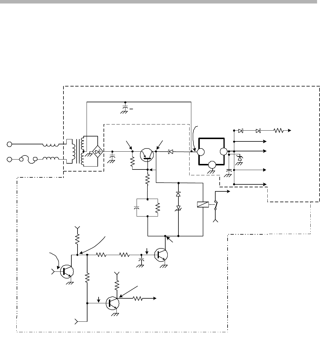
FIGURE 3-2 - 5V STANDBY POWER SUPPLY & POWER-ON SWITCHING CIRCUIT
5V STANDBY POWER SUPPLY CIRCUIT
POWER-ON SWITCHING CIRCUIT
3/27/023.2CTV30
STBY 0.65V
ON 0V
R092
STBY 0V
ON 2.6V
Q008
STBY 0V
ON 0.6V
R056
R055 STBY 5V
ON 0V
Q608
STBY 0V
ON 0.677V
C612 R607
STBY - OPEN CIRCUIT
ON - GROUND
STBY 13V
ON 9.7V
5V
5V
5V
5V
D608T602
STBY 30V
ON 23.8V
STBY 30V
ON 24.3V STBY 30V
ON 9V
+
C023
D052
5.6V
R606
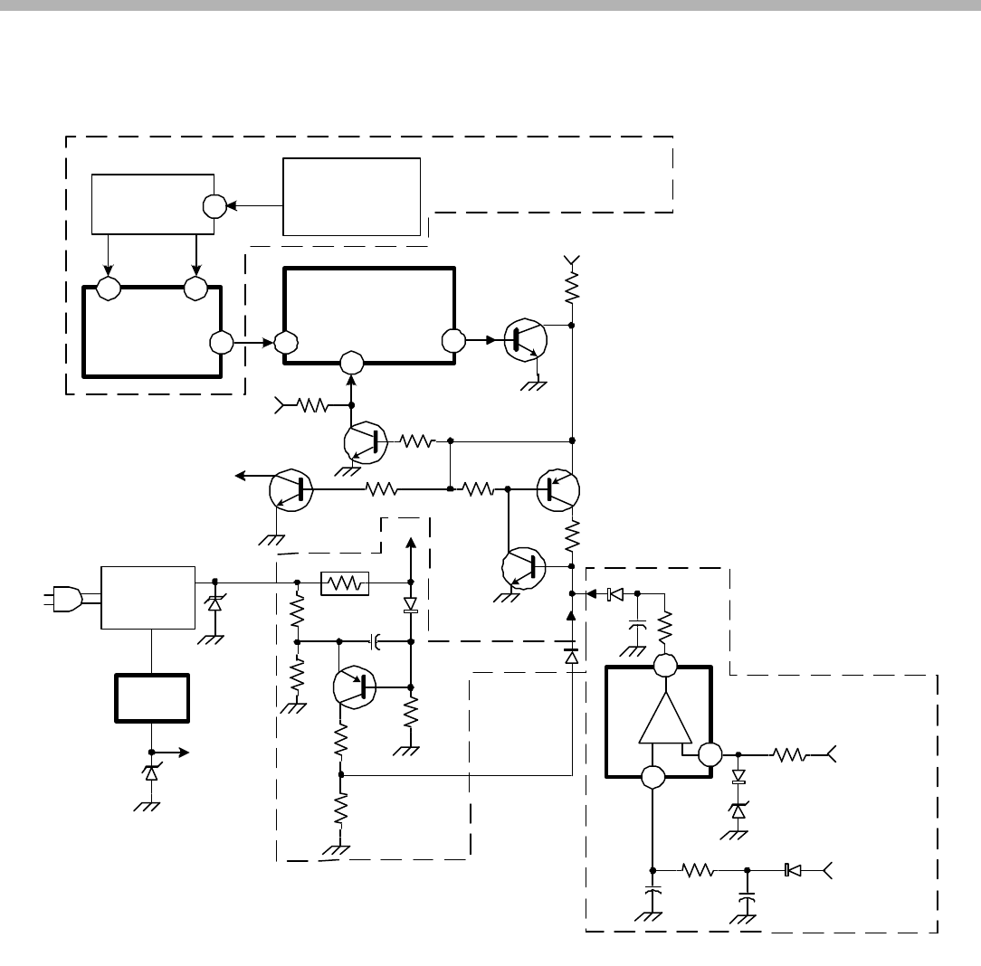
Degauss Circuit
The degauss circuit consists of the Degauss Coil, Degauss Switch circuit (Q501) and relay RY501. b The DC
power (14V) for the relay comes from the rectifier circuit (D621, C616, L607 and C632) that feeds the 9V regulator
circuit. The Degauss circuit is activated once System Control (IC001) receives a Power-ON command. IC001/
pin 60 (O-DGC) outputs a High to turn Q501 ON and ground is applied to RY501. RY501 activates briefly
(approximately one second and then shuts off) and the hum of the degauss coil can be heard. The degauss coil
eliminates any magnetic fields present in metallic parts in the picture tube, which could cause color purity problems.
5V Standby Power Supply & Power-ON Switching Circuits
5V Standby Power Supply Circuit
Reference Figure 3-2 for the following circuit description:
The Standby Power supply is operational as long as the set is plugged into an AC outlet. AC power is applied
through choke T601 and transformer T602 to the full-wave rectifier block D608. Capacitor C609 filters out the
AC component and a DC voltage of 13V is applied to IC608 (Input Pin). IC608 then outputs the Standby 5V to
activate the circuits listed on the diagram at the output of IC608. A Standby 3.3V source is produced from the
Standby 5V source using components D050, D051 and R099.
The voltages labeled “STBY” on the diagram are the voltages present at the designated points in Standby Mode.

10
3.Power Supply Block
Power-ON Switching Circuit
Reference Figure 3-2 for the following circuit description:
In the Standby Mode, the System Control (IC001) is partially ON (using the Standby 5V and Standby 3.3V), and
waiting for an “ON” command from either the Front Panel Controls or the Remote Control Input (IC004 not
shown).
Once the System Control IC001 receives an “ON” command at either IC001/pin 70 (I-SIRCS) or IC001/pin71 (I-
PWR), it outputs a LOW (0V) at IC001/pin66 (O-RELAY). IC001 is not shown on this diagram.
The LOW from IC001/pin 66 is applied to the base circuit of Q008. Q008 turns “OFF” and 2.6V appears on the
collector through pull-up resistor R092. After passing through dropping resistors, the 2.6V source supplies
approximately 0.6V to the base circuits of Q608 and Q006.
Q608 turns “ON” and supplies a ground to the AC relay RY600 and to the bottom of C612 and R607. The ground
at the bottom of C612 and R607 turns “ON” Q604, which supplies initial high current to the AC relay RY600
through its emitter/collector junction. Q604 shuts OFF once C612 is fully charged, and now RY600 receives its
ON/HOLD voltage of 9V through D620. D620 acts as a blocking diode when Q604 initially supplies current to
RY600. RY600 actuates and sends AC voltage to rectifier block D605 in the Main Switching Power Supply
(operation will be discussed next).
Q006 is turned “ON” in normal operation, supplying a LOW (0V) to System Control IC001/pin 72 (I-HLDWN).
Q006 is used to tell the System Control IC001 to activate the self-diagnostics indicator (HLDWN operation is
discussed in the Protection circuit section).
Troubleshooting Tip:
Obviously, if a failure occurs in the 5V Standby Power Supply the unit will not even attempt to turn ON. If this
condition occurs, check the following components:
1) F601
2) 13V at IC608 Input Pin (I). If missing, suspect T602, D608, and/or C609
3) 5V at IC608 Output Pin (O). If missing, suspect a defective IC608.
4) NOTE: Q604 is used as a current source for the AC relay (RY600). If Q604 the collector/emitter junction
becomes an Open circuit, the set will still turn ON (using voltage through D620) and function properly with
sufficient AC power input. If the AC power input is weak (Low Voltage ~90VAC, the unit will have difficulty
turning ON without Q604 functioning properly.
11
3. Power Supply Block
FILTER
CIRCUIT
3
4
2
1
1
16
15
12
18
6
8
4
2
14
10
9
7
6
16
17
10
12
11
15
13
14
V
SENSE
VG
(H)
IC633
IC603
2
IC604
ERROR
AMP.
1
4
AC FROM
T601
FROM
RY600
VD
VS
VG
(L)
VB
VC2
TIMER
OCP
VC1
F/B
IC600
R615
3.3V
9V
TO
DEGAUSS
RY501
TO PH602
PIN1
5
12V FROM
9V SUPPLY
TO T602 STANDBY POWER
SUPPLY
D605
R601
R630
R629
R627
R626
D618
C634
R671 C672
R647
R632
D631
R619
C642 R668
T603
D621
D615
Q600
Q601
R640
+135V
15V
PH602
D611
D624
FIGURE 3-3 - MAIN SWITCHING POWER SUPPLY 3.3CTV30a 1443 3/26/02
2.7V
10.2V
10.6V
0V
1.9V 24V
0V
4.5V
140V
145V
291V
14V
14V
- All voltages are present under
normal operating conditions and
all referenced to HOT GRND.
Except for IC600/pin 14 which
is referenced to IC600/pin 15
(VS).
D614
275Vpp
85KHz
R625
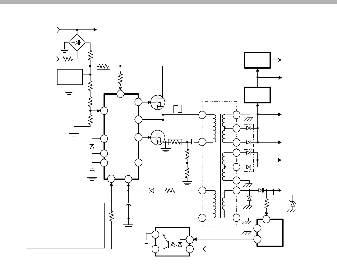
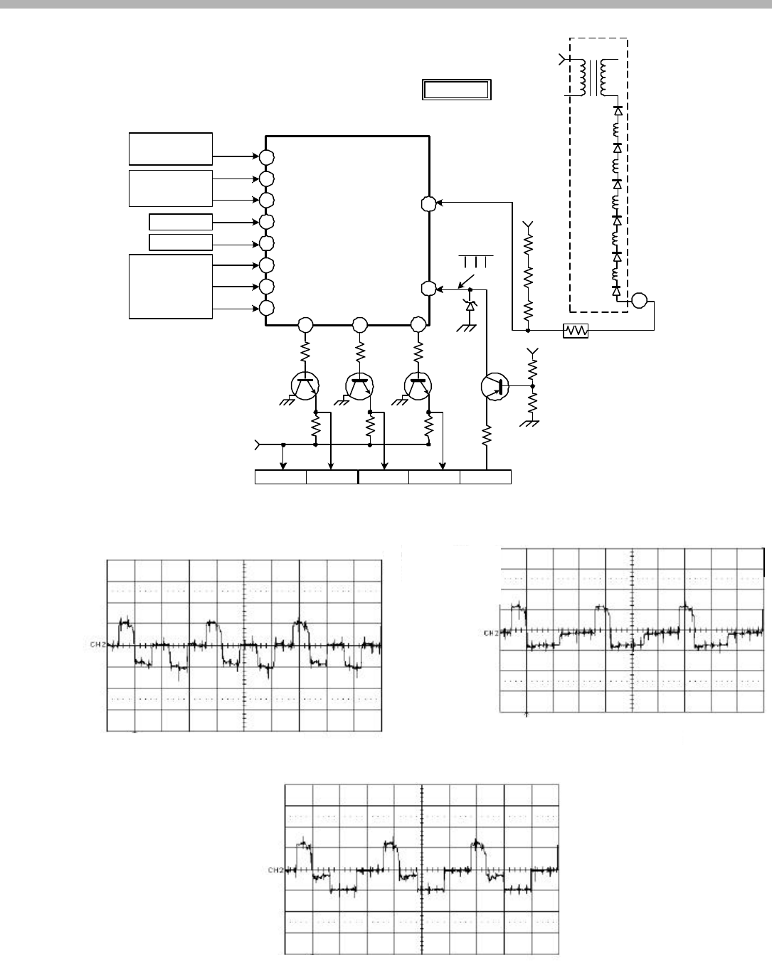
Main Switching Power Supply Circuit
The Main Switching Power supply is basically IC600 (Switch Regulator Controller). IC600 contains all the needed
circuitry necessary to function as a switching power supply, except for the Power Switching MOSFETS (Q600
and Q601).
IC600 contents:
•Control circuit
•Oscillator/Oscillator control
•Output Driver transistors
•10V regulator
•Shut-Off Timer
•Over Current Protection
Main Switching Power Supply Operation
Reference Figure 3-3 for the following circuit description:
AC signal is applied to the rectifier block D605. The AC component is filtered-out by the filter circuit (C629 and
C621 shown in block form). A DC voltage of 293V is produced at this time.

12
3.Power Supply Block
IC600 Startup Sequence
1) Turn ON voltage: The 293Vdc from the filter circuit is voltage divided by R630, R629, R627 and R626
down to 2.7Vdc. This voltage is applied to IC600/pin 1 (Vsense) and IC600 turns ON. IC600/pin 1
(Vsense) is also used for OVP protection (IC001/pin 1 > 8 volts will trigger OVP).
2) Internal circuit Start Voltage: The 293Vdc also passes through voltage dropping resistors R615 and
R640, and 291Vdc is applied to IC600/pin 18. This voltage is used to initially power the internal circuits
and begin oscillations. Note that the 293Vdc from R615 is connected directly to the Drain of Q600 and
serves as the High-side FET power source.
Internal circuits initially power by IC600/pin 18
•Internal drive transistors for High-side output FET Q600.
•Oscillator
•Control circuit
•10V regulator (IC600/pin 10)
Note: The 10V output at IC600/pin 10 passes through D618 and supplies power to the internal
driver transistor for the Low-side output FET Q601
3) Output Oscillations: At this point, initial square-wave oscillations of approximately 125KHz are output at
IC600/ pins 16 and 12. Normal operation frequency is approximately 85KHz.
4) Regulator Feedback: The feedback line is connected to the +135V secondary output. Once IC600 is
turned ON and oscillations begin, the secondary winding at T603/pin 17 and associated circuitry produces
+135. The +135V is applied to Error Amp. IC604/pin 1.
IC604 outputs an error voltage, which controls the current output of the optic-coupler PH602. The amount
of current supplied to IC600/pin 2 depends on how hard PH602 is turned ON. In normal operation, a
voltage of 1.9Vdc (which is proportional to the amount of current) is present at IC600/pin 2. The feedback
loop is now complete.
5) IC600 normal operating power supply (VC1): Produced simultaneously with the oscillator feedback is
the operating power source VC1.
IC600/pin 8 (VC1) is produced using a primary winding on T603/pin 6. The AC is rectified, filtered and a
DC voltage of 24V is applied to IC600/pin 8. Once the 24V is stable, IC600’s internal control circuit
disconnects (internally) the power source at IC600/pin 18. All IC600 internal circuits are now powered
from IC600/pin 8.
Over Current Protection (OCP): ref. Figure 3-3
The current flowing through the switching FETS (Q600 & Q601) also passes through R671. The voltage
drop across R671 is directly proportional to the current through the switching FETS. The voltage across
R671 is voltage divided by R647 and R632, and applied to IC600/pin 9. The OCP is activated when the
voltage at IC600/pin 9 exceeds 0.2V. The self-diagnostic indicator will flash four times, pause and then
repeat.
Over Voltage Protection (OVP) and Under Voltage Protection (UVP): The voltage at IC600/pin 8 (VC1) is
monitored by circuitry inside IC600 for Under-voltage and Over-voltage conditions. The two conditions are as
follows:
OVP – greater then 33V
UVP – less then 8V
If either of these two conditions occur at IC600/pin 8, the unit will go into protection mode. The self-diagnostic
indicator will flash four time times, pause and then repeat.
Troubleshooting Tips (ref. Figure 3-3)
NOTE: Follow previously discussed “IC600 Startup Sequence”. The five steps are in order of occurrence.

13
3. Power Supply Block
NOTE: Use HOT GRND when making measurements on primary side of T603. This includes all measurements
on IC600.
Symptom: Unit goes into protection mode LED flashes four times.
Check: This indicates either a Vertical deflection or Power Supply problem.
1) Check power supply secondary outputs.
•If voltages are present and at the proper level, then the problem is in the Vertical deflection drive
circuit.
•If the secondary voltages are low or missing, then the problem is in the power supply.
2) The power supply can be safely tested by unloading the +135v line. Unsolder R591. This will unload the
+135V line of the power supply, but still send needed feedback to IC600 for proper power supply operation.
3) If the power supply outputs proper secondary voltages after unsoldering R591, suspect a shorted +135V
line. Check the Horizontal Output transistor (Q505 or 506) for shorted conditions.
4) If the unit still goes into protection mode after unsoldering R591, check the following items:
•D614 for shorted condition.
•IC600/pin 15 (this is midpoint for output MOSFETS Q600 and Q601). A 275Vpp, 85KHz square-
wave should be present. If the waveform pulses four times and stops, check the next Item.
•IC600 Feedback circuit. The amount of current feedback can be determined by monitoring the
voltage drop across R625. The minimum current feedback is 80uA, which is a minimum voltage
drop of 37.6mV. In normal operation, this voltage drop is approximately 223mV. If the voltage
drop is below 37.6mV, suspect components in the feedback path e.g. PH602 and IC604. Reference
Figure 3-3 for proper voltages at these components.
•If no waveform is present when unit is turned ON, then check IC600/pins 1 and 18 for proper
voltages (reference “IC600 Startup Sequence” above).
If these voltages check OK, check IC600/pin 8 for proper voltage of 24V. This is the voltage used
to power IC600 after initial startup.
If 24V is present at IC600/pin8, check IC600/pin 10 for 10.2V. This voltage is developed using the
24Vs and a voltage regulator circuit inside IC600. If 10.2V is missing, suspect a defective IC600.
Also check voltage at IC600/pin 14 (Use battery powered VM for this measurement, and use
IC600/pin 15 (VS) as ground ref.). The voltage at IC600/pin 14 should be 10V. If the voltage
measured at IC600/pin 14 is incorrect, check D618.
•If all the above measurements check OK, suspect a defective IC600.
5) Defective Output MOSFET transistors: The output MOSFETS will cause a “no output square-wave”
condition. To properly test MOSFETS, reference the following test procedure:
14
3.Power Supply Block
Operational Test
To prove the device is functional:
1. Connect the negative lead of the ohmmeter to the SOURCE lead.
2. Touch the ohmmeter positive lead to the gate, to pre-charge it.
3. Connect the ohmmeter positive lead to the DRAIN.
If the device is good you will get a resistance reading of about 400-1k ohms.
Table 3-1 - Static MOSFET Resistance Tests
+ / - - / +
Gate – Source Infinity Infinity
Gate - Drain Infinity Infinity
Drain - Source There is a zener diode connected internally
across these terminals
oD
GDS
Power MOSFET
TO 220 case
P or N channel
Static MOSFET Resistance Tests – Table 3-1
15
4. Deflection Circuits
Chapter 4 - Deflection Circuits
BUFFER
IC565
& AMP 1
47
COMPARATOR
IC561
2Q521
Q522
E/W OUT
Q50250
H-OUT
T505
D505
D506
Q505
OR
Q506
DEFLECTION
YOKE
FLYBACK
TRANSFORMER
T510
T511 SW515
D514, D515
BUFFER
IC565
10
12
8
14
45
44
DRIVER
IC545
7
1
5
78
DEFLECTION
YOKE
5
VD+
V RAMP
VD-
V RAMP
PROTECT
HORIZONTAL
DEFLECTION
PINCUSHION
VERTICAL
DEFLECTION
IC001(ONE CHIP)
3
FIGURE 4-1 - DEFLECTION AND PINCUSHION OVERALL BLOCK
4.1CTV30a 1435 3/27/02
HV G2 HEATER +200V
3
HP
FOCUS
ABL
+/-13V
1
Waveform 4-2
Waveform 4-1
Waveform 4-4
Waveform 4-5
The One Chip IC001 contains the YC Jungle. Vertical Drive, Horizontal Drive and Pincushion Correction circuits
are all located on the A-board in the BA-6 chassis. In the BA-5, these circuits are divided up between two boards:
the A-board and MB board. Aside from the higher circuit integration, the circuit operations remain unchanged
from previous models. So, a brief circuit theory of operation will first be discussed. The next two sections and
diagrams following that will concentrate on deflection troubleshooting tips.
Vertical Theory
Note: Reference Figure 4-1 during circuit description.
The VD+ and VD- Vramp signals are generated by the YC Jungle circuitry internal to IC001 (OneChip). The 180
degrees out-of-phase ramp waveforms are output from IC001/pin 45 (VD+) and IC001/pin 44 (VD-). The ramp
waveforms first pass through buffer IC565 (Input pins 10 and 12; Output pins 8 and 14), and are then applied to
the Vertical Drive IC545.
The Vertical Drive IC receives the ramp waveforms on IC545/pins 7 and 1, and outputs the final drive signal on
IC545/pin 5. This final signal drives the deflection yoke for vertical scan on the picture tube.
If the vertical deflection circuit is defective, IC545/pin 3 outputs a protect signal to IC001/pin 78. This function will
be discussed in the upcoming Protection circuit section.

16
4. Deflection Circuits
IC565
ONE-CHIP
IC001
I-PROT
45
44
10
12
9
13
-
+
-
+14
8
78
IC545
7 5 4 3 2 16
6
5
R532
R539
R540
+13V
-13V +13V
R543
VDY
CN515
6
CN585 VD+
TO CV
BOARD
DR +
BOOST
OUT
VCC-
REF
VCC+
DR -
FIGURE 4-2 - VERTICAL DEFLECTION CIRCUIT 3/27/024.2CTV30
R548
3 4
8mHz
X001
R541
R545
R542
Horizontal and Pincushion
Note: Reference Figure 4-1 during circuit descriptions.
Horizontal Theory
The Horizontal Drive pulse (HD) is developed inside IC001 (OneChip) and output on IC001/pin 50. The HD is
first amplified by drive transistor Q502 and then applied to T505. T505 couples the signal to the Horizontal
output transistor Q505 or Q506 depending on model; Q506 is used in 20"; Q505 is used in 24". At this point, the
Horizontal output signal goes off in two directions. The signal is applied to the Fly-Back Transformer (FBT) and
is used to develop HV, G2, Heater, +200, Focus, ABL and +/- 13 voltages. It is also applied to the Horizontal
deflection yoke for horizontal scanning on the picture tube.
Pincushion Theory
Also shown on this diagram is the Pincushion correction circuit. The purpose of this circuit is to compensate for
the non-linear scanning characteristics of the horizontal deflection circuit. The distortion caused by this non-
linearity is the sides of the picture are bowed inward. The pincushion signal is used to incrementally increase the
drive current to the horizontal deflection yoke as the beam is scanned down the picture tube. The drive current
increases as the beam passes through the middle edge section of the tube.
Vertical Deflection Circuit
Note: Reference Figure 4-2 during troubleshooting descriptions.
Overview
Troubleshooting of the vertical deflection circuit will be the subject of this section. When the vertical section is
operating correctly, pulses are output from IC545/pin 3 and applied to System control section of IC001/pin78.
This signal tells System Control that the vertical drive IC545 is working properly. If the vertical section becomes
defective, the pulse from IC545/pin 3 will stop and obviously so will the pulses at IC001/pin 78. System Control
will now turn Off the AC Relay (RY600), and the Standby/Timer LED will flash four times, pause and repeat until
the defect is fixed.
17
4. Deflection Circuits
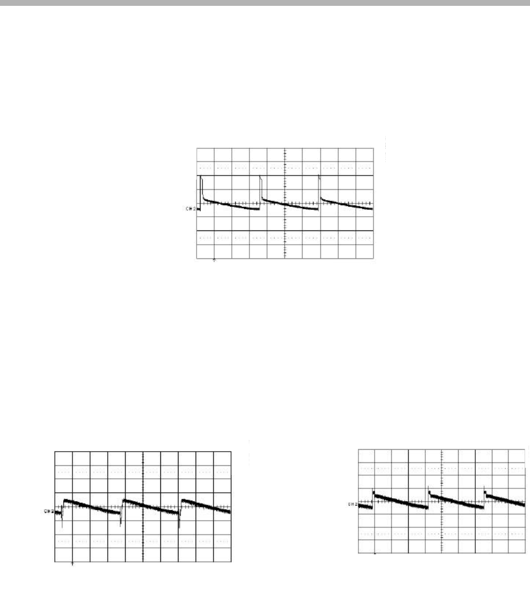
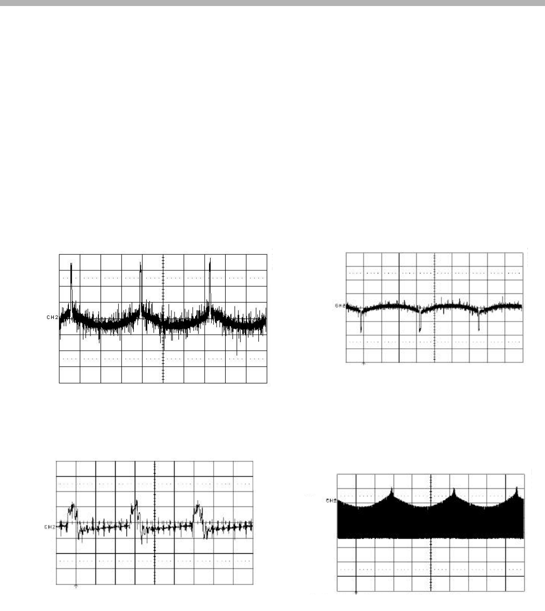
IC545/Pin 5 (Vertical Deflection Coil Drive Signal
Waveform 4-5
Oscilloscope
Settings:
20V
5ms
Troubleshooting
There are three defects can cause the Standby/Timer LED to flash in groups of four:
1) +13V and/or –13V from FBT/pins 9 and 7 respectively are missing on Vertical Drive IC545.
2) Vertical Drive IC545 is defective (no reference pulses output on IC545/pin 3 to IC001/pin 78).
3) No Horizontal Drive pulse to FBT. NOTE: Not a short circuit on the horizontal output, this would cause a
B+ OCP condition (two-time flash).
The following troubleshooting tips are assuming a “No Output Signal” condition exists on IC545/pin 5. The
output signal on IC545/pin 5 should appear as shown in Waveform 4-5.
First, confirm that the +/- 13V supplies to IC545/pins 2 and 4 are coming from the FBT. If the voltages seem
low, unsolder IC545/pins 2 and 4 and check the supplies again for proper level. If there is a problem with the +/
-13V supplies, check the Horizontal Drive pulse to the FBT (which will be discussed in the next section), FBT and
the Half-wave rectifier circuit for each supply line.
Next, check the drive signals (DR+ and DR-) to IC545/pins 1 and 7. Waveforms 4-6 and 4-7 illustrate how the
signals should appear at IC545/pins 1 and 7 (confirm amplitude and frequency). If these signals are missing,
check the output pins on IC001/pins 44 and 45. These signals should look the same as Waveforms 4-6 and 4-
7 with an amplitude difference. If the drive signals are not present at IC001/pins 44 and 45, check the power
sources (5V and 3.3V) and crystal X001 (8MHz) on OneChip IC001.
IC545/Pin 1(Vertical& Ramp Drive Signal
from IC001)
Waveform 4-6
Oscilloscope
Settings:
0.5V
5ms
IC545/Pin 7 (Vertical & Ramp Drive Signal
from IC001)
Waveform 4-7
Oscilloscope
Settings:
0.5V
5ms
18
4. Deflection Circuits
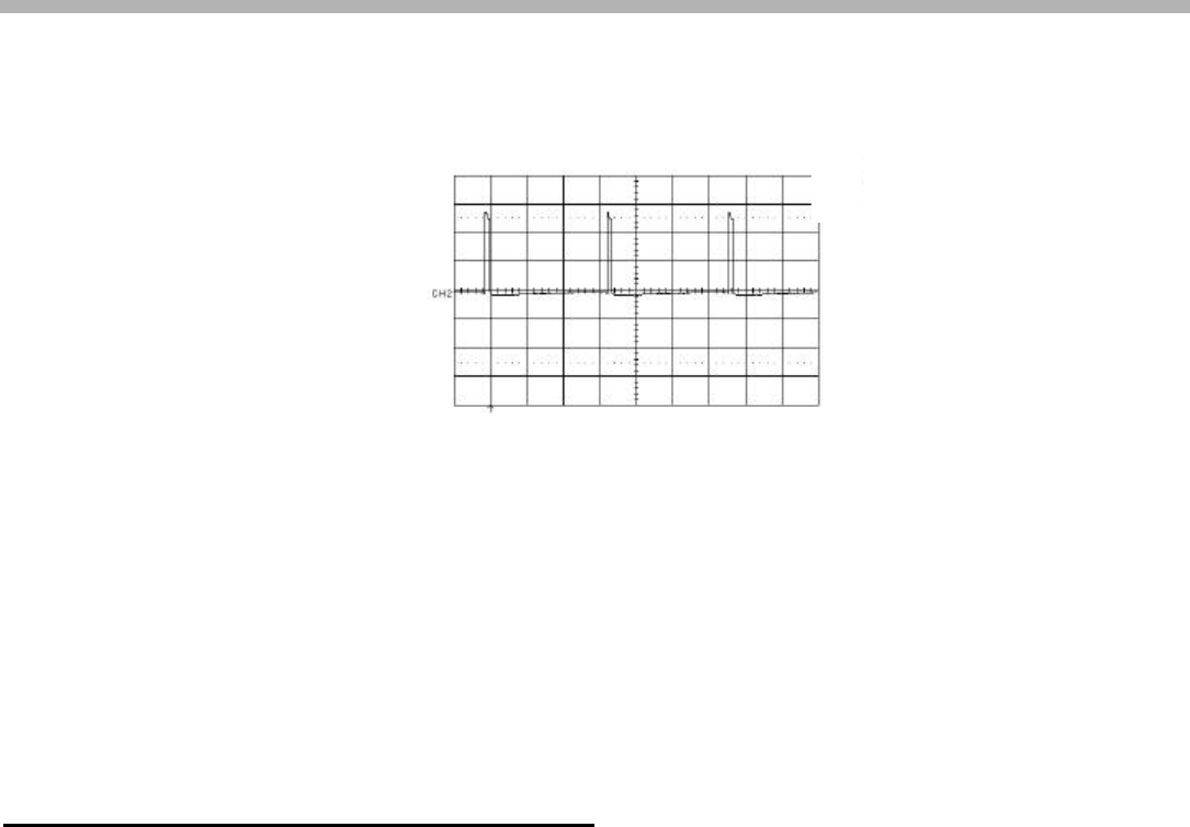
IC545/Pin 3 (Vertical Reference Signal)
Waveform 4-8
Oscilloscope
Settings:
10V
5ms
If the drive signals check OK, check the signal output on IC545/pin 3 (Ref. Signal). This signal should appear
as shown in Waveform 4-8. This pulse is used to tell the system control in IC001/pin 78 that the vertical drive is
working properly. Also, confirm that this signal is reaching IC001/pin 78. If this signal is missing or distorted at
IC545/pin 3, then replace IC545.
Horizontal Deflection and Pincushion Circuits
Note: Reference Figure 4-3 during troubleshooting descriptions.
Overview
The subject of this section will be horizontal circuit troubleshooting tips. The Standby/Timer LED may flash in
groups of two or four depending on the type of failure in the horizontal circuit.
Horizontal Deflection Circuit
Horizontal Failure conditions: (reference Figure4-3)
1) Shorted Output transistors (Q505 or Q506): Standby/Timer LED will flash in groups of two. Shorted
Output transistors will cause a shorted B+ line. System Control detects a B+ Over Current condition.
2) Open Output transistors (Q505 or Q506): Standby/Timer LED will flash in groups of four. The Open
Output transistors cause no HD to the FBT; which causes no +/- 13V supply output. In turn, this causes
no vertical drive (IC545) output. System control detects a “No Vertical drive” condition.
3) Excessive Horizontal Output Drive (OVP HV): Standby/Timer LED will flash in groups of four. Because
of the excessive HD, the FBT will be over-driven causing excessive secondary voltages. This includes
High Voltage (HV) and the +/- 13V outputs. FBT/pin 7 is monitored by IC561 for excessive voltage (this
will be discussed in Protection Circuit section). This voltage is proportional to the HV. So, System Control
detects an excessive HV condition.
19
4. Deflection Circuits
47
5 6
7
1
23
50
3
2 1
HORIZ.
LINEARITY
CIRCUIT
D515
2
1
4
HV
FOCUS
G2
+13V
+135V R503
H-
OUT C501
Q502
IC001
R511
T585 FLYBACK
HDY
9V
Q505 OR
Q506
R505
R506
IC565
CN515
C511
L525
+135V
C526 D526
C525
R525
Q522
Q521
+13V
R533
R535
D569
5.1V
D514
R514
R512
R513
+135V
D528
R528
D525
HP
9V
R574
IC561
200V
+135V
EW-
OUT
+-
-
+
T505
-
+
FIGURE 4-3 - HORIZONTAL DEFLECTION CIRCUIT 4.3CTV30 1436 3/26/02
63
1
4
2
ABL
-13V
D505
D506
A BOARD
7
11
3
9
M-Board
The M-board varies the H-pulse (ref. waveform 4-9) width from IC001/pin 50 depending on the level of the ABL
voltage feedback from the FBT/pin 11 to the M-board (CN302/pin 2). This will adjust the H-drive to the FBT to
supply more current during sudden bright scenes. When a sudden bright scene occurs, there is an increase in
current draw through the FBT; the ABL voltage will increase in direct proportion to the increase in current draw.
The M-board senses the ABL voltage (ABL-IN) increase and increases the H-pulse width (CN302/pin 4; H-OUT)
to drive the FBT harder and more current is supplied to the picture tube.
M-Board Test:
Place oscilloscope probe on CN302/pin 4 (H-OUT) and switch the video input between Color Bars and Cross
Hatch displays; a small change in H-pulse width can be observed.

20
4. Deflection Circuits
IC001/Pin 50 (HD Pulse)
Waveform 4-9
Oscilloscope
Settings:
2V
5ms
Troubleshooting
NOTE: The presence of HV for even a short time is an indication that the horizontal circuit is functioning properly
and the problem is in the vertical deflection circuit.
Q502 Collector and T501/Pin 6
(R505 Unsoldered)
Waveform 4-10
Oscilloscope
Settings:
2V
5ms
As long as there is power to the One Chip IC001, the Horizontal Drive pulse (HD) should be output on IC001/
pin 50. This waveform is illustrated in Waveform 4-9. The HD is then applied to the base of Q502. If HD is
present at the base of Q502 but not at the collector, then unsolder R505 located in the base circuit of Q505/
506.Recheck waveform at the collector of Q502 (reference Waveform 4-10). This will unload the collector Q502
safely and enable Q502 to function properly if there is a defective horizontal output circuit. This also checks
T501’s ability to couple the signal to Q505/506 (check for Waveform 4-10 at T501/pin 6). Note that if HD is
present at the output of T501 (unloaded condition), then B+ must also be OK because it is the collector voltage
for Q502.
IC001
M BOARD
1 6 3 2
4
50
52
Q502
T505
Q505
OR Q506
FBT
11
1
3.3V 9V
CN302
FIGURE 4-4 - M BOARD CONNECTIONS 4/2/024.4CTV30
H-OUT
ABL
ABL
9V
3.3V
H-IN
1.89V
H-OUT
21
4. Deflection Circuits
If all the above tests are passed then either the Horizontal Output transistor or the FBT is defective. The
Horizontal Output transistor can be checked using an Ohmmeter. The Base-Emitter junction should check the
same as a normal BJT. When checking the Collector-Emitter junction, note that a diode is connected in parallel
(the C-E junction will test the same as the B-E junction).
If Q505 or 506 checks OK then replace the FBT.
NOTE: The amplitude of the HD at the collector of Q505 or Q506 is approximately 1000V. If attempting to make
a measurement at this point, use a X10 probe and make sure the oscilloscope can handle the power at its input.
Pincushion Circuit (reference Figure 4-3)
An inverted parabola waveform is used to control the amount of drive current supplied to the FBT to compensate
for the pincushion distortion. The E/W signal (inverted parabola) is output on IC001/pin 47 (ref. Waveform 4-1)
and passes through Buffer/Amp IC565/pin 5 to IC565/pin 1 (ref. Waveform 4-2). The signal is then applied to
gating circuit IC561/pin2 and the HD pulse on IC561/pin 3 (ref. Waveform 4-3) is used to gate the parabola
waveform through at the horizontal rate. The resultant signal is output on IC561/pin 1 is amplified by Q521 and
Q522. The output signal of Q522 is applied to the anode of D505 (ref. Waveform 4-4) and controls the conduction
of D505. Depending on the level of conduction of D505, the current supplied to the FBT will increase or decrease.
IC565/Pin 1 (Parabola)
Waveform 4-2
Oscilloscope
Settings:
0.5V
5ms
IC001/Pin 47 (Inverted Parabola)
Waveform 4-1
Oscilloscope
Settings:
0.2V
5ms
IC561/Pin 3 (HD Pulses)
Waveform 4-3
Oscilloscope
Settings:
0.1V
20ms
D505 Anode (Inverted Parabola)
Waveform 4-4
Oscilloscope
Settings:
50V
5ms

22
4. Deflection Circuits
Troubleshooting
1) Symptom: Picture is compressed horizontally with Pincushion distortion
Check: a) Missing HP on IC561/pin 3
b) Missing complete pincushion waveform at anode D505 (Trace from IC561/pin 1 to D505
anode)
c) D505 or D506 open circuit
2) Symptom: Picture expanded horizontally with Pincushion distortion.
Check: Missing Parabola waveform (Trace signal from IC001/pin 47 through IC565/pin 5 to 7, and
then to IC561/pin 2)
3) Symptom: Picture slightly compressed with No Pincushion distortion
Check: C525 and R525
23
5. Protection Circuits
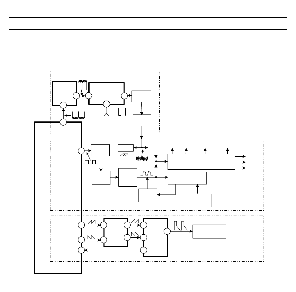
Chapter 5 - Protection Circuits
IC545
VERTICAL
DRIVE
IC001
ONE
CHIP HV PROTECT
IC561
OVP FLYBACK
LATCH
Q573
Q572
Q590
OCP
IC608
STBY 5V
D614
OVP
D052
OVP
+135V (B+)
STBY 5V
A/C POWER
SUPPLY
FIGURE 5-1 - PROTECTION BLOCK
3/27/025.1CTV30
78
72
3
7 5
HORIZONTAL
OUTPUT
Q505 OR Q506
AC RELAY
RY600
+/- 13V
72
STBY
5V
D001 O-LED
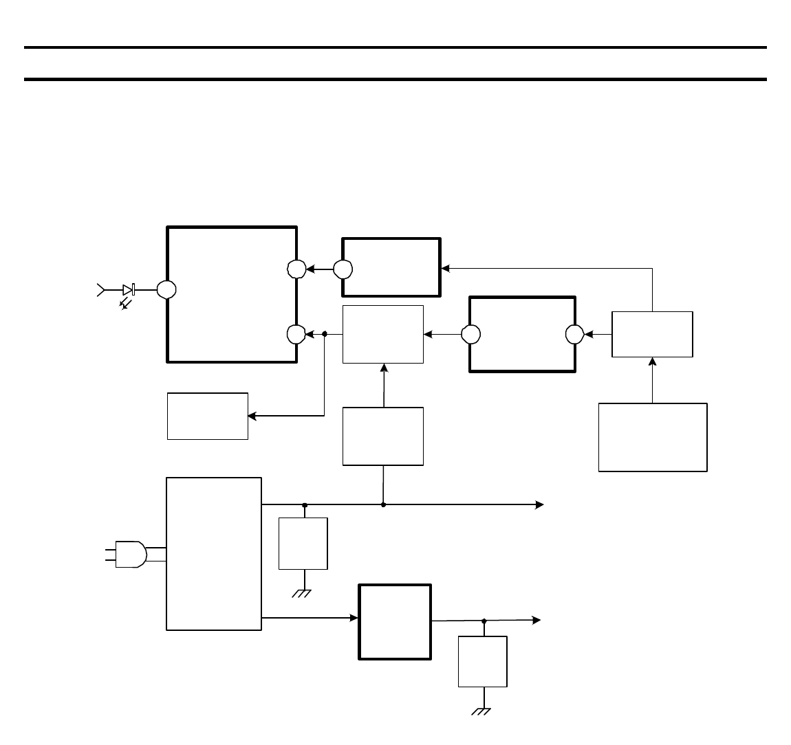
Overview
Note: Reference figure 5-1 during the following overview discussion:
24
5. Protection Circuits
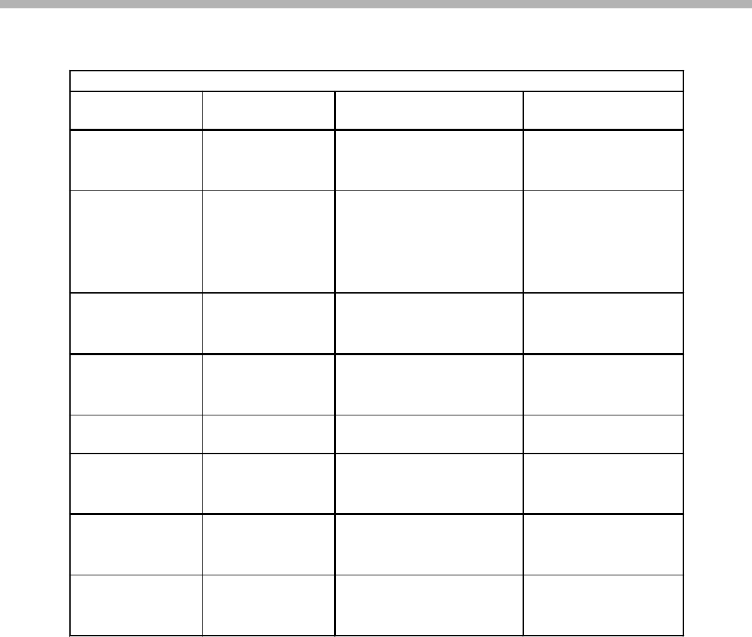
In this section, the protection circuits contained on the BA-6 chassis will be discussed. Table 5-1 below is a quick
reference that shows how each protection circuit affects the BA-6 chassis when activated.
Table 5-1 – Protection Circuits at a Glance
Monitored
Circuit Monitored
Parameter Affected Circuit Circuit Used to
Shut-Off AC relay
+135V Line OCP • -AC Relay (OFF)
• -I-HLDWN
(IC001/pin 72)
Latch Q572 and
Q573
+135 Line OVP • AC Relay
(OFF)
• D614
• I-PROT
(IC001/pin 78)
IC001/pin 66
Vertical
Deflection No output signal
(IC545/pins 1 &
7)
• AC Relay (OFF)
• I-PROT
(IC001/pin 78)
IC001/pin 66
Horizontal
Deflection No output signal
(Q505/506)
• AC Relay (OFF)
• I-PROT
(IC001/pin 78)
IC001/pin 66
5V Standby
voltage OVP D052 (Shorted) No Power ON
function
HV Excessive
Voltage • -AC Relay (OFF)
• I-HLDWN
(IC001/pin 72)
Latch Q572 and
Q573
IC600/pin 8 OVP, OCP, UVP • AC Relay (OFF)
• I-PROT
(IC001/pin 78)
IC001/pin 66
Q600/Q601 OCP • AC Relay (OFF)
• I-PROT
(IC001/pin 78)
IC001/pin 66
The protection circuits for IC600 (Power Supply Switching IC), and Q600 and Q601 (Power Supply Switching
FETS) have already been covered in Chapter 3 (Power Supply Circuits). Reference this chapter for the theory of
operation for these protection circuits. They will not be discussed in this section.
The Vertical and Horizontal protection circuits were briefly mentioned in Chapter 4 (Deflection Circuits) in
their respective troubleshooting sections. The circuit theory of their operation will be discussed in this section.
Reference Chapter 4 for troubleshooting tips concerning these circuits.
The Standby 5V supply is protected for over-voltage using zener diode D052. If the voltage increases above
5.6V, D052 will break down and regulate at 5.6V.
NOTE: There are many zener diodes (OVP) connected to various inputs on the One Chip IC001. Not all of these
OVP zener diodes will be discussed. Just be aware that they are present in the circuit. So, when a voltage or
signal is found to be low or missing, you should check to see if an OVP zener diode is connected to that input.
NOTE:
•If the protection mode is activated from the Latch Circuit, then the unit must be unplugged from the AC
Outlet and reconnected to RESET.
•If the protection mode is activated from IC001/pin 66, the unit only needs to be turned OFF and then
ON from the remote or front panel to RESET
25
5. Protection Circuits
A/C
3
I-PROT.
I-HLDWN
O--
RELAY
IC001 ONE CHIP
REF.
POWER
SUPPLY
IC608
R575
D614
(150V)
TO
RY600
(AC RELAY) B+
R594
C590
Q590
D052
(5.6V)
STBY
5V
D562
R595
R592
R593
C562 R562
Q572
R572
Q573
Q006
Q608
R589
D587
R092
STBY 5V
R591
Q008
R566C564 C566
D566 FROM
PIN 7
T585
FLYBACK
+135V (B+)
R567
D567
D568(8.2V)
FIGURE 5-2 - PROTECTION CIRCUIT 5.2CTV30 1437 4/2/02
IC545
VERTICAL
DRIVE 72
66
78
+
-
IC561
7
6
5
R055
9V
R614
R056
2 4
FBT
HORIZONTAL
OUTPUT
Q505/506
1
+13V -13V
D563
VERTICAL & HORIZONTAL
PROTECT
+135V
OCP
HV OVP
Protection Circuits
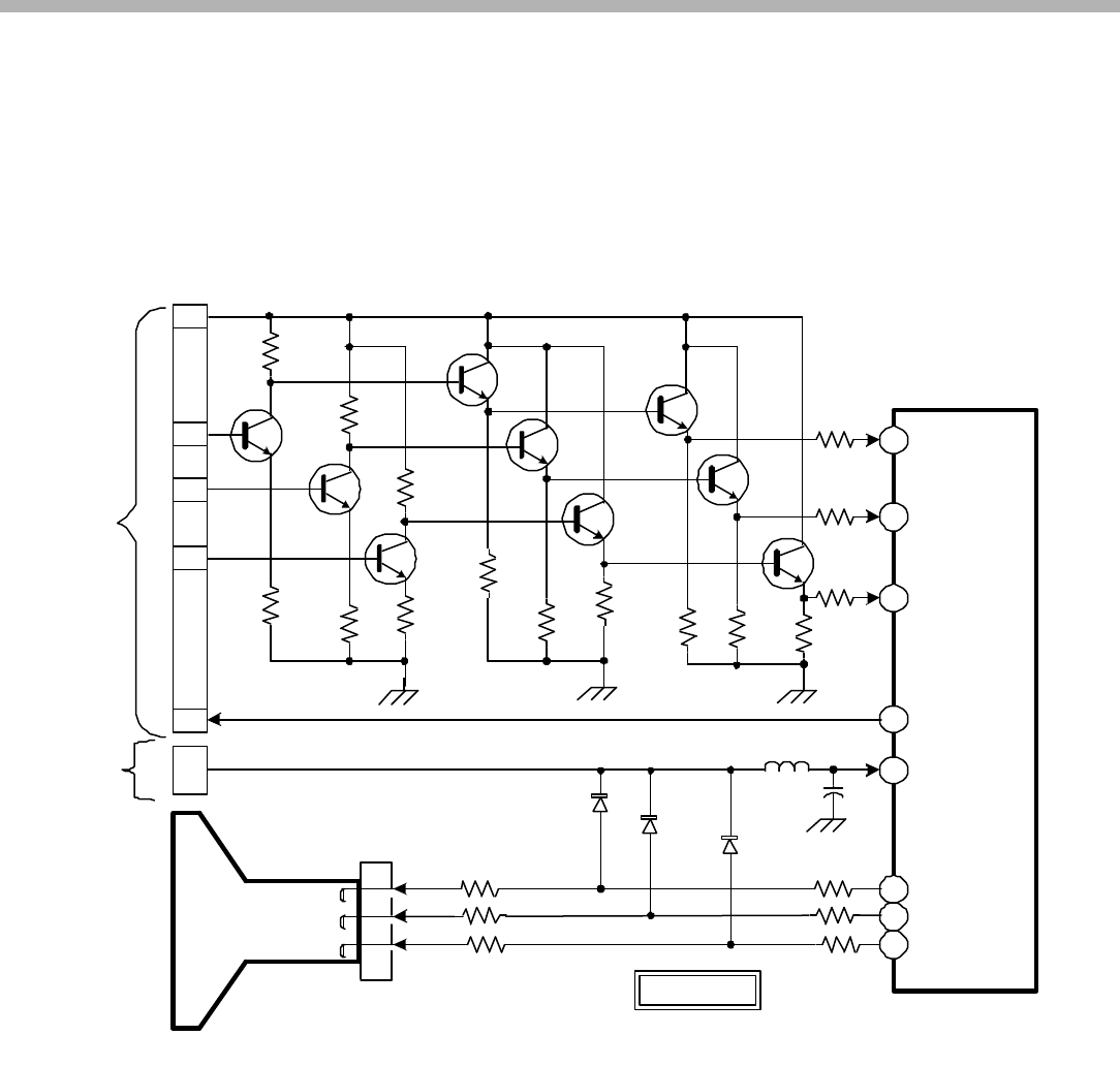
The four main functions monitored by the protection circuits are the Vertical deflection, Horizontal deflection,
High Voltage (HV) and +135V supply (Ref. Figure 5-1 for block diagram and Figure 5-2 for circuit detail).
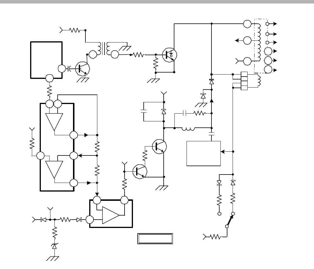
Vertical and Horizontal Deflection
Note: Reference Figure 5-2 during the following discussion:
The Vertical and Horizontal deflection circuit outputs are both monitored by the same circuit. If the vertical
deflection circuit fails, IC545/pin 3 will stop outputting pulses to IC001/78. IC001 will detect an absence of input
pulses and place the unit into protection mode by outputting a HIGH at IC001/pin 66 and turning ON Q008. Q008
then applies a ground to the base of Q608, causing Q608 to turn OFF and remove the ground from AC Relay
(RY600). RY600 turns OFF and the unit goes into Standby Mode. This same circuit indirectly monitors a failure
in the horizontal output circuit. The main thing to notice here is that the Vertical drive IC545 gets its supply
voltages from the FBT (+/- 13V). The FBT is driven by the HD pulse from output transistor package Q505/506.
If there is no horizontal output, then there will be no drive signal to the FB and no +/- 13V developed on the

26
5. Protection Circuits
secondary of the FBT. With the +/- 13V missing, IC545 will not function and IC001 will detect a vertical failure
and place the unit into protection mode.
+135 Supply (OVP and OCP)
Note: Reference Figure 5-2 during the following discussion:
The +135V supply OVP is simply zener diode D614. If +135V line rises above 150V, D614 will break down and
regulate the voltage at 150V. Most likely D614 will be destroyed (shorted circuit) and short the +135V to ground.
Note: D614 is physically connected prior to the OCP circuit (Q590). So, when D614 shorts, all current is sent
through D614. The OCP is not triggered. System Control in IC001 detects a vertical circuit failure due to the
following sequence of events:
Follow the order of events as shown below:
1) +135V is missing
2) +135V is supply voltage to FBT and Horizontal Output transistor
3) No drive to FBT
4) No +/- 13V developed on FBT secondary
5) +/- 13V is supply to IC545 (Vertical drive IC)
6) No Vertical drive output
7) IC001 detects vertical failure
The +135V supply OCP is monitored using Q590, R591 and associated circuitry. The current draw on the
+135V line flows through voltage divider R594 and R595 series resistor R591. If the current rises on the +135V
line, so will the voltage drop across R591. When the current is great enough to cause the voltage drop across
R591 to be approximately 1.2V, Q590 will turn ON. Current will now flow through voltage divider R592 and R593.
Once the voltage drop across R592 reaches 1.2V, D562 and 0.6V will be applied to latching transistor Q572.
The Latch circuit (Q572 and Q573) operates in the following manner: Q572 is forward biased by applying 0.6V
to its base circuit. Q572 then saturates and passes ground to the base circuit of Q573. Q573 turns ON (once the
Latch is activated, it will remain in this state until the unit is unplugged from AC power and reconnected). The
voltage at the base circuits of Q006 and Q608 is reduced below turn-on (0.6V). Q006 shuts off and a High is
applied through R055 to IC001/pin 72 (I-HLDWN). Q608 is simultaneously shut off, which removes the ground
return to the AC relay (RY600). AC power to the Main Switching Power Supply is disconnected and the unit is
placed into Standby Mode. The High at IC001/pin 72 (I-HLDWN) activates the self-diagnostics and the Standby/
Timer LED flashes in groups of TWO.
High Voltage (OVP)
Note: Reference Figure 5-2 during the following discussion:
The HV (OVP) monitoring circuit will also trigger the Latch circuit (Q572 and Q573). The condition of the High
Voltage (HV) is continuously checked by monitoring FBT/pin 7 secondary AC voltage (not shown). This Ac
voltage is fed to a half-wave rectifier circuit D566 and C566. The resulting DC voltage is then applied to IC561/
pin 5. This voltage is proportional the HV and will follow if HV increases. The voltage at IC561/pin 5 is compared
to the reference voltage (10.3Vdc) on IC561/pin 6. The reference voltage 10.3V is developed from +135V using
regulator circuit consisting of D568, D567 and R567. A High will be output on IC561/pin 7 when the voltage on
IC561/pin 5 rises above the reference voltage on IC561/pin 6. This high will activate the Latch circuit as described
in the previous paragraph. Once again, the unit is placed in Standby Mode and the Standby LED Flashes in
groups of TWO.
27
6. Video/RGB
Chapter 6 - Video/RGB
Overview
IC001
ONE
CHIP
TUNER
S-VIDEO
VIDEO 1
VIDEO 2
VIDEO 3
ABL
FROM PIN 11
T585
FLYBACK
CN301
IK RGB
IC1751
RGB
IK
A BOARD
R
G
BCRT
FIGURE 6-1 - VIDEO / RGB BLOCK
CV BOARD
2/27/026.1CTV30
J1751
Note: Reference Figure 6-1 during the following discussion:
All video source inputs (Tuner, S-Video and Video 1, 2, 3) are connected directly to the “OneChip” IC001. IC001
performs all video input switching and processing internally. The Comb Filter processing (Y/C separation) for
composite video inputs (Tuner, Video 1, 2, 3) to create RGB is performed inside IC001.
Further RGB processing is performed on the CV board and then applied to the CRT through J1751 for display.
IK pulses are sent back from the CV board to IC001 on the A board for each color cathode current check.
28
6. Video/RGB
Video/RGB
16
18
19
21
23
25
26
27
MAIN-TV-IN
Y-IN
C-IN
VIDEO 1-IN
VIDEO 2-IN
Y-IN
U-IN
V-IN
52
51
ABL-ACL-IN
IK-AKB-IN
TUNER
DET-OUT
VIDEO 1
VIDEO 2
VIDEO 3
S-VIDEO Y
C
Y
U
V
IC001
ONE CHIP
RGB
R322 R318 R316
Q303 Q304 Q305
18542
CN301
TO CV BOARD (CN1751)
11
R585
R584
R580
+13.5V
R583
RGBIK
FLYBACK
T585
HP
FIGURE 6-2 - VIDEO CIRCUIT 3/27/026.2CTV30
31 33 35
9V
D351
3.3V
R313
Q301 R312
R314
9V
R319 R317 R315
123
1.89V
A BOARD
IC001/Pin 31 -Red Component Signal
Waveform 6-1
Oscilloscope
Settings:
0.5V
20 s
µ
IC001/Pin 33 - Green Component Signal
Waveform 6-2
Oscilloscope
Settings:
0.5V
20 s
µ
IC001/Pin 35 - Blue Component Signal
Waveform 6-3
Oscilloscope
Settings:
0.5V
20 s
µ
29
6. Video/RGB
FROM
A-BOARD
CN301
FROM
A-BOARD
CN585
1
2
3
5
6
7
8
9
4
5
8
2
1
5
R1764 R1757
R1756
R1758
R1763
R1765
BUFFERS
Q763
Q773
Q783
BUFFERS
Q762
Q772
Q782
AMPLIFIERS
Q761
Q771
Q781
CN1752 9V
L1751
C1751
D1756
D1755
D1754
CRT
CN1751
200V
J1751
R
G
B
B IN
G IN
R IN
R OUT
G OUT
B OUT
IK
VDD
IC1751
FIGURE 6-3 - RGB DRIVE 6.3CTV30 1440 3/28/02
CV BOARD
B
G
R
Note: Reference Figures 6-2 and 6-3 during the following discussion:
A more detailed diagram of the Video and RGB path is shown in Figure 6-2. The video source is input directly to
IC001 on the designated input port. IC001 performs all video processing internally and outputs RGB on IC001/
pins 31, 33 and 35 respectively (ref. Waveforms 6-1, 6-2, and 6-3). The RGB is buffered by Q303, Q304 and
Q305 before being sent to the CV board through CN301.
The RGB signals are first amplified by transistors Q761, Q771 and Q781 (ref. Figure 6-3); then pass through two
transistor buffer banks (Q762; Q772; Q782 and Q763; Q773; Q783) on the CV board (ref. Figure 6-3). The
amplified and buffered RGB signal is then applied to the RGB Driver IC1751/pins 1, 2 and 3. The CRT receives
RGB final drive signals from outputs at IC1751/pins 7, 8 and 9.
The two input signals (ref. Figure 6-2) IC001/pin 52 (ABL) and IC001/pin 51 (IK-AKB) are used to adjust the
levels at the RGB outputs (IC001/pins 31, 33 and 35), depending on certain picture tube conditions.
The Automatic Brightness Limiting (ABL) input monitors the current drawn by the picture tube’s High Voltage.
If the picture gets suddenly bright, the ABL voltage input to IC001/pin 52 causes a reduction in the R, G and B
output levels.
30
6. Video/RGB
Horizontal Field & Vertical Blanking (IC001/Pins 31, 33 & 35)
Waveform 6-4
Location of IK pulses just before active video on each field
Oscilloscope
Settings:
0.2V
5 s
µ
Location of IK Pulses just before active video.
One Horizontal Field and Vertical Blanking
(IC001/Pins 31, 33 & 35)
Waveform 6-5
Oscilloscope
Settings:
0.2V
5 s
µ
IK Pulse Waveform Diagrams
NOTE: Waveforms 6-4, 6-5, 6-6, 6-7, and 6-8 are a sequence of pictures illustrating where the IK are found, and
how they appear on an oscilloscope display. Reference these Waveforms during the following IK_AKB circuit
description. Note: Use IC545/pin 3 to trigger oscilloscope and lock signal on the display. All oscilloscope settings
are where taken using a X10 probe
The Waveform sequence description is as follows:
1) Waveform 6-4 shows the oscilloscope time-base starting point at the field rate. The IK pulse and IK
Feedback pulses occur during the vertical blanking areas. These areas are shown as gaps between each
field.
2) Waveform 6-5 is an expanded view of Waveform 6-4 showing one field and one vertical blanking area.
3) Waveform 6-6 is an expanded view of Waveform 6-4 showing the IK pulses to the CRT’s from IC001/pins
31, 33, and 35. These pulses are located in the vertical blanking area just before active video. Two
consecutive pulses at a flat video level (or brightness level) can be seen.
4) Waveform 6-7 is a further expansion of Waveform 6-4, showing the IK Feedback pulses (IC1751/pin 5) in
the vertical blanking area just before active video (one field). Three small consecutive IK feedback pulses
can be seen.
5) Waveform 6-8 is a close-up shot of the IK feedback pulses.
Also shown in Figures 6-2 and 6-3 is the IK_AKB signal path. The purpose of the IK signal and AKB circuit is to
monitor and adjust the cathode bias on CRT’s (Red, Green and Blue) for optimal white balance. The IK pulses
are output from IC001/pins 31, 33 and 35 (RGB Drive signals) initially when the unit is turned ON, and then
repeated for each field thereafter (reference Waveform 6-6). The pulses are output during the over-scan (or
vertical blanking) portion of the picture, so they are not visible on the picture tube. The IK pulses are shown in
Waveform 6-6 as two flat video levels just before active video. These pulses are sent to their respective color
cathode in a staggered order with red first, then green and blue to drive the tube at a flat raster level. They follow
the same path as the RGB signal described in the previous paragraph.
Once the IK cathode drive pulses are applied to each color cathode in sequence (red-green-blue), IC1751/pin 5
outputs a corresponding IK Feedback pulse proportional to the current draw of each cathode (feedback pulses
shown in Waveform 6-7). The IK feedback pulses are sent through CN1752/pin 2 and applied to buffer transistor
Q301. After buffer Q301, the IK feedback pulses are input to IC001/pin 51 and evaluated by the internal AKB
circuit. The AKB circuit determines if the drive to the cathodes needs to be adjusted for optimal white balance, or
if one of the CRT’s is defective (No feedback pulse). The IK-AKB input IC001/pin 51 is also level protected using
D351 (3.3V).
31
6. Video/RGB
IK Pulses to CRTs (IC001/Pins 31, 33 & 35)
Waveform 6-6
CRT Drive
Pulse
Oscilloscope
Settings:
0.2V
2 s
µ
IK Feedback Pulses in Vertical Blanking (CN301/Pin 2)
Waveform 6-7
IK Feedback
Pulses
Oscilloscope
Settings:
0.5V
0.2 s
µ
Closeup of IK Feedback Pulses
Waveform 6-8
Troubleshooting
NOTE: Presently the IK-AKB circuit Video Blanking and Standby/Timer LED 5 flash sequence indication functions
have been bypassed in this first version of the One Chip (IC001). Instead, the video is passed to the CRT so
that any problem in the IK-AKB circuit can be viewed. The problems described below can be quickly diagnosed
by observing the condition of the video present on the CRT and the voltages as described can be used to confirm
a defect.
The IK-AKB circuit indication function as described in the service manual will be implemented in the second
version of IC001.
The following three possible IK-AKB circuit failures and the circuit operation descriptions during these failures
are for the present first version IK-AKB circuit. These descriptions will apply to the second version of IC001
except for: 1) the Video will be Blanked; and 2) the Standby/Timer LED will flash in groups of five in the
second version IC001.
Failures and Circuit/Unit Operation During Failure:
1) Failure: The picture tube is old (one or more cathodes are weak) and the amplitude of the IK feedback pulses
is too low to perform automatic cathode adjustment (Replace Picture Tube).
Circuit Operation: If the IK-AKB circuit cannot compensate for the weakened state of the cathode, video can
still be viewed on the CRT with the defective cathode color missing. To confirm that the tube is defective,
check the voltages on the individual cathodes.
In normal operation with video (color bars) applied, the voltages at the cathodes should be as follows:
KR = 150V
KG = 150V
KB = 150V

32
6. Video/RGB
If there is a defective cathode, the voltage at that cathode will be less then 130V. For the extreme case of an
open cathode, the voltage will be 116V. The other good cathode voltages will be normal at 150V. What’s
happening is the IK-AKB circuit is trying to compensate for the defective cathode by driving it harder (116V) then
the other cathodes (150V). If this voltage variation appears on one or more cathodes, suspect a defective
cathode, and thus a defective tube.
Also, check the IK Feedback pulse at IC545/pin 5 (ref. Waveform 6-7) one pulse will be completely missing.
Failure: One or more of the IK Drive pulses is not output from IC001/pins 31, 33 and 35 to the CRT.
Circuit Operation: The video (color bars) will appear on the picture tube with one or more colors missing.
Check for the Video and IK Drive Pulses at IC001/pins 31, 33, 35 Video and pulses should appear as shown in
Waveform 6-6. Most likely, the output will be completely missing Video and IK Drive Pulses. A defective IC001
or Open in path from IC001 to IC1751 to the CRT can be confirmed by checking the voltages on each cathode
(CV board). The voltages on the good cathodes with drive will be normal at 150V; the cathode with no drive pulse
will be ~175V.
Failure: The IK Feedback pulses are not returned to IC001/pin 51 from IC1751/pin 5 (open return path or
defective IC1751).
Circuit Operation: The video (color bars) will appear washed-out on the picture tube (bright white halo throughout
picture). If IC001/pin 51 does not receive the IK Feedback pulses from IC1751/pin 5, then IC001 will detect three
defective cathodes. The voltage measured at each cathode will be 120V. IC001/pins 31, 33 and 35 will output
maximum signal level in an attempt to compensate (ref. Waveform 6-6). Check IC1751/pin 5 for IK Feedback
Pulses (ref. Waveform 6-7). If these pulses are missing, suspect defective IC1751. If the pulses are present,
trace pulses to IC001/pin 51 to find open circuit.
33
7. Audio
Chapter 7 - Audio
AUDIO OUT
J205
12
10
1
40
8
6
14
27
18
19
R
L
2
39
R
L
3
38
R
L
4
37
R
L
13
28
R
L4
2
1
21
SPKR R+
SPKR R-
SPKR L-
SPKR L+
TUNER
OUT A IN R
OUT B IN L
C457
C458
IN 1A
IN1B
1
2
3
4
VA STBY
IC404
VIDEO 1
J200 IN 2A
IN 2B
IN 3A
IN 3B
IN 4A
IN 4B
LINE A
LINE B
VIDEO 2
J201
AUDIO IN
J202
SDA
SCL
IC400 CN401
R+
R-
L+
L-
14V FROM
POWER
SUPPLY
PS401
9V FROM POWER
SUPPLY
FROM IC001PIN 54
(IO-SDAT)
FROM IC001
PIN 56 (0-SCLK)
SPEAKERS
C450
FROM IC001
PIN 66 (O-RELAY)
FIGURE 7-1 - AUDIO CIRCUIT (KV-20FV300 & KV-24FV300)
5
7.1CTV30 1441 3/28/02
Q435 12V
D435
R437
R435
R463
R464
9V
Q411 R436
3.6V (ON)
0.25V (STBY)
Overview
There are two different audio circuits depending on the model. Table 7-1 indicates which audio IC is used in each
model. Table 7-1
Model Audio Circuit IC’s Features
KV13FS100 IC401 & IC404 Input Switching Only
KV13FS110 IC401& IC404 Input Switching Only
KV20FS100 IC401 & IC404 Input Switching Only
KV20FV300 IC400 & IC404 SRS, WOW, Simulated Stereo
and Input Switching
KV24FS100 IC401 & IC404 Input Switching Only
KV24FV300 IC400 & IC404 SRS,WOW, Simulated Stereo and
Input Switching
All models use the same power amplifier IC404. The audio processor (IC400, IC401 or IC402) used in the
various models depends on the features available; IC400 is installed in Surround Sound models; IC401 is installed
in Stereo models. There is a thrid audio IC shown on the schematic; IC402 is installed in Mono models, which are
not sold in the US. The following sections will discuss and illustrate each US model audio circuit configuration.
Audio Circuit [KV20FV300 & KV24FV300]
34
7. Audio
IC404
12
10
14
2
R+
R-
L-
L+
8IN-R
IN-L
C457
R459
R484
C459
6
R487
Q405
AUDIO-R
FROM AUDIO
PROCESSOR
AUDIO-L
FROM AUDIO
PROCESSOR R460
R485
C460
FROM IC001
PIN 80
(0-MEGABASS)
FIGURE 7-2 - AUDIO, "WOW" CIRCUIT 3/6/027.2CTV30
Q404
C458
Figure 7-1 illustrates the audio circuit configuration for models KV-20FV300 and KV-24FV300.
Because these two models have the feature of WOW, SRS and Simulated Stereo, IC400 is installed. The Right
and Left inputs from each audio jack and Tuner are connected to IC400 as illustrated in Figure 7-1. All audio
functions are performed inside IC400. The following IC400 internal functions are controlled by IC001/pin 54 (IO-
DAT); via serial data input IC400/pin 18 (SDA):
•Volume
•Mute
•Input Switching
•Audio Effect modes (WOW, SRS)
Note: There is no volume control on IC404 when IC400 is installed. IC404/pin 9 is used as a redundant muting
function only in this configuration.
The selected audio is output at IC400/pins 14 and 27. All “FV” models have an audio output jack on the rear of
the set. This audio output is at IC400/pins 13 and 28.
The audio outputs of IC400 are applied to Audio Amplifier IC404/pins 6 and 8. The audio signal is amplified and
output on IC404/pins 2, 4, 10 and 12 to the speakers.
IC404/pin 1 receives its power from the 14V supply line and is protected using PS401.
Figure 7-2 shows the WOW circuit consisting of Q405, R484, C459 (Left channel); Q404, R485 and C460 (Right
channel). This audio sound effect is found in the “FV” models. When activated through the menu, a full, deep
bass sound is produced. Along with the WOW effect, BBE is directly activated to further enhance the sound.
In normal operation, IC001/pin 80 (O-MEGABASS) sends a high to the base circuits of Q404 and Q405. The
base circuits are tied together so they are both turned ON. With Q405 turned ON, the high pass filter circuit R484
and C459 is bypassed; with Q404 turned ON, the high pass filter circuit R485 and C460 is bypassed. When the
WOW effect is turned ON through the menu, IC001/pin 80 sends a Low to turn OFF Q404 and Q405. With Q404
and Q405 turned OFF, the High Pass filters are placed in the circuit and a portion of the high frequency band will
sent to ground, thus enhancing the low frequency content of the input audio.
35
7. Audio
FIGURE 7-3 - AUDIO CIRCUIT [KV-20FS100, KV-24FS100 & KV-13FS100/110]
7.3CTV30 1445 3/8/02
1
6
2 4 14
11
L
R
3
7
L
R
5
8
L
R
9
13
L
R
12
10
8
9
1
15 6
IN -R
IN -L
TV-L
TV-R
V1-L
V1-R
YUV-L
YUV-R
V2-R
V2-L
C457
C458
R-OUT
L-OUT
+
-
2
4
+
-
S2 S1 V+
VA
IC401
IC404
PS401
14V
R498
C499
STBY 5V
R036
D410
9V
VC
FROM IC001
PIN 68
(0-SEL 1 )
FROM IC001
PIN 68 (0-SEL 0 )
TUNER
J200
J202
J201
FROM IC001
PIN 62
(0-VOL )
VIDEO 1
AUDIO IN
VIDEO 2
The next diagram (Figure 7-3) shows the audio circuit configuration for the models KV-20FS100, KV-24FS100
and KV-13FS100/110 where IC400 audio processor is not installed. These models use IC401 for stereo audio
input switching and IC404 for volume control and audio amplification. IC401/pins 2 and 4 (switching inputs) are
controlled using a simple two binary signal from IC001/pins 67 and 68. Table 7-2 shows the state IC401/pins 2
and 4 depending on the input selected.
Table 7-2 - IC401(IC402)/pins 2 and 4 Input Select States
Input IC401/pin 2 (S2) IC401/pin 4 (S1)
Tuner (TV) Low Low
Video 1 High Low
Video 2 Low High
Video 3 (YUV)
(IC401 Only)
High High
DC voltage using D410, C499 and R498. The level of this DC voltage depends on the pulse duration of the PWM
signal, which is modified by IC001, and ultimately the user volume setting. The DC is applied to IC404/pin 9 and
is finally used to set the audio level output on IC404/pins 2, 4, 10 and 12.

36
7. Audio
Troubleshooting
No Audio from IC404 (inputs OK): check the following:
• PS401 for open condition
• Voltage at IC404/pin 5 (~3V). If voltage is low or missing check, Q411 and Q435 for shorted condition.
•
Voltage at IC404/pin 9. If this voltage goes below 0.5V, the unit will mute. This is true even when
IC400 audio processor is installed.
• If all voltages and inputs check OK, replace IC404
No audio output from IC400:
• Check audio input from audio jacks
• Check power supply IC400/pin 21 (9V)
• Check IC400/pin 18 (Data) and IC400/pin 19 (Clock)
Check for presence of digital signal
No audio output from IC401 (IC402):
• Check audio input from audio jacks
• Check power supply IC401/pin 14 (9V)
• Check power supply IC402/pin 6 (9V)
• Check two bit binary switch pattern IC401 (IC402)/pins 2 and 4. (Ref. Table 7-1)
37
8. Self-Diagnostics
Chapter 8 - Self-Diagnostics
Power ON
When the unit is plugged into an AC outlet, power is supplied to the Standby Power Supply and the unit is in
Standby Mode. The Standby Power Supply powers-up the System Control, EEPROM, IR Remote sensor and
Reset circuits (reference Power Supply section for details). If a Power-ON command is received after reset is
completed, the System Control outputs command to power-up the rest of the unit. When operating correctly, the
following sequence of events should occur:
•The AC power relay clicks.
•One second later the degauss relay clicks and the hum of the DGC can be heard for about two seconds.
•The degauss relay will then click again (turning OFF).
•Picture is displayed.
This entire sequence occurs in the first five to ten seconds the unit is powered ON. During this time, the Standby/
Timer LED will be flashing once per second.
Self-Diagnostic Indication
In the Power Supply, Deflection and Protection sections of this book, a number of failure detection circuits
(protection) were discussed. Here is a summary of those circuits:
•IC600/pin9 OCP
•IC600/pin8 OCP, OVP, and UVP
•IC001/pin 72 (+135 OCP, HV OVP)
•IC001/pin 78 (No Vertical deflection, No horizontal Output)
Any one of these defects will activate the self-diagnostics programmed in the unit and depending on the type of
failure, the Standby/Timer LED will flash in a designated sequence. Use the Table 8-1 for a quick reference in
understanding self-diagnostic indications.
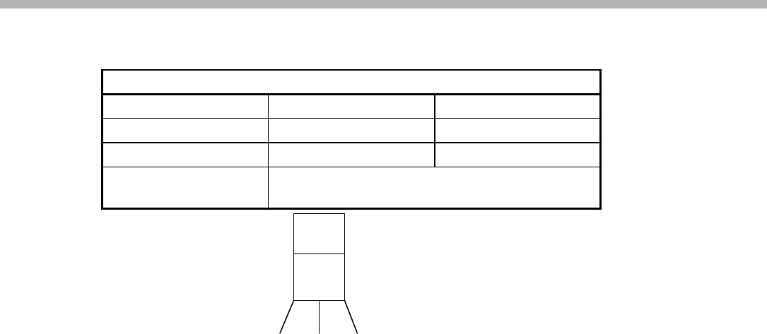
Table 8-1 – Self-Diagnostics
Diagnostic
Description Standby/Timer
LED Flash
Sequence
Failure History
Display Probable Cause
Power does not
turn on Does not light N/A - AC power disconnected
- Fuse F601 open
HV OVP
(AC relay OFF)
2 times N/A - HD output over-driving FBT
- FBT defective
+135V (B+) OCP
(AC relay OFF)
2 times 2:0 or 2:1 - H-out (Q505 or Q506)
shorted
- IC1751 is shorted (CV brd)
I-PROT
(AC relay OFF)
4 times 4:0 or 4:1 - +13V missing on IC545
- IC545 defective
- No HD to FBT (open circuit)
IK (AKB)
N/A in IC001,
version 1.
5 times 5:0 or 5:1 - IC545 defective
- IC001 defective
- G2 is improperly adjusted

38
8. Self-Diagnostics
NOTE: if a B+ over current condition is detected, the vertical deflection output stops simultaneously. The symptom
that is diagnosed first by System Control is displayed on the history screen.
The unit must be disconnected from AC power to stop Standby/Timer LED flashing and reset unit.
Failure History Display
Reading Results
The History display can be accessed by quickly pressing the following buttons on the remote control sequentially
while the unit is in the Standby Mode:
[Display]———>channel [5]———>sound volume [-]———>[Power ON]
Display will look like the following:
Self-Diagnostic
2: 000
3: N/A
4: 000
5: 001
101: N/A
The number on the left of the display (e.g. 2:) indicates the Standby/Timer LED flash sequence.
The number on the right of the display (e.g. 000) indicates the number of times the failure occurred.
The display can register up 99 failures.
All failure information is stored in EEPROM IC002 on the A board.
Clearing Display
The failure display should be reset after repair. If the display is not reset, subsequent failure will not be registered.
To clear the results display to zero, press the following buttons on the remote control sequentially when the
diagnostic screen is displayed:
Channel [8]———>[ENTER]
Quitting the Self-Diagnostic Screen
To quit the entire self-diagnostic screen, turn off the power switch either on the remote control or on the
main unit.

Sony Electronics Inc.
EMCS - A Service Company
1 Sony Drive
Park Ridge, New Jersey 07656
All Rights Reserved ©2002
CTV300402 04/04/02
is a trademark of Sony Electronics
