BBC Microcomputer Advanced User Guide
User Manual:
Open the PDF directly: View PDF ![]() .
.
Page Count: 510 [warning: Documents this large are best viewed by clicking the View PDF Link!]

The
Advanced
User
Guide
for the BBC Microcomputer
Andrew C. Bray,
St. Catherines College,
Dept. of Computer Science,
Cambridge University
Adrian C. Dickens,
Churchill College,
Dept. of Engineering,
Cambridge University
Mark A. Holmes BA,
Fitzwilliam College,
Dept. of Clinical Veterinary Medicine,
Cambridge University

2

3
Contents
Introduction 5
1 Introduction for those new to machine code 7
Operating System Commands
2 Operating System commands 11
Assembly Language Programming
3 The BASIC assembler 21
4 Machine code arithmetic 31
5 Addressing modes 35
6 The assembler mnemonics 41
Operating System interfaces
7 Operating system calls 101
8 *FX/OSBYTE calls 109
9 OSWORD calls 247
10 Vectors 253
11 Memory usage 267
12 Events 287
13 Interrupts 295
14 RS432 309
15 Paged ROMs 317
16 Filing systems 333

4
Hardware
17 An introduction to the hardware 353
18 The video circuit (6845) 359
19 The video ULA 377
20 The serial interface 385
21 The paged ROM select register 395
22 Programming the 6522 VIA 397
23 The system 6522, including sound and speech 417
24 The user 6522 425
25 Disc and Econet interfaces 427
26 The analogue-to-digital converter 429
27 The Tube 433
28 The 1 MHz bus 437
Appendices
A *FX/OSBYTE call index 449
B Operating System calls summary 455
C Table of key numbers 456
D VDU codes 459
E PLOT number summary 460
F Screen mode layouts 462
G US MOS differences 478
H Disc upgrade 480
I Circuit board links 482
J Keyboard circuit diagram 489
K Main circuit diagram Inside Back Cover
Bibliography 491
Glossary 493
Index 499

5
Introduction
The ‘Advanced User Guide for the BBC Microcomputer’ has
been designed to be an invaluable supplement to the User
Guide. Information already contained in the User Guide is only
repeated in this book in sections which contain much new
information and where omitting the duplicated details would
have left the section incomplete. Some parts of the User Guide
are factually inaccurate or incomplete and where details in this
book are at variance with corresponding information in the
User Guide the reader will find that a more accurate description
is usually found in these pages.
This reference manual contains a considerable amount of
information about 6502 assembly language programming, the
operating system and the BBC Microcomputer hardware. The
intention has not been to provide the inexperienced user with a
tutorial to guide him or her through the complexities of these
advanced concepts. However, it is hoped that the information
has been presented in a way that enables users new to assembly
language programming and unfamiliar with hardware topics to
develop their understanding of the machine and to expand the
scope of their programming. Contained within this book is an
extensive description of the software environment and the
hardware facilities available to the assembly language
programmer. The authors have presumed that the readers of
this Advanced Guide are reasonably familiar with the basic use
of the BBC Microcomputer. While every attempt has been made
not to bury the facts under a mountain of computer jargon the
use of technical terms is an inevitable consequence of
attempting to condense a large number of facts into an easily
accessible form.
All the information about the operating system is exclusively
based on OS 1.20. The hardware information has been verified
with an issue 4 circuit board but where possible differences on
earlier issue boards have been noted.
While this book gives the programmer full access to all the BBC
microcomputer’s extensive software and hardware facilities
using techniques which the designers of the machine

6
intended programmers to use, it also opens the door to a
multitude of ‘illegal’ programming techniques. For the
enthusiast, direct access to operating system variables or chip
registers may enable him to perform the bizarre or even the
merely curious. For the serious programmer, on the other hand,
attention to compatibility and machine standards will enable
him to write software which will run on BBC Microcomputers
of all configurations. The responsibility rests with YOU, the
user. The value of your machine depends on continued
software support of the highest quality; unlike many machines
the BBC microcomputer has been designed to be used in a
variety of different configurations and the operating system
software provides extensive information about the current
hardware and software status. The operating system makes
most of the allowances required for the different configurations
automatically, but only when the legal techniques are adhered
to, so please use them.
The final paragraph in this introduction must be a word of
apology to those programmers engaged in the task of software
protection. Many of the details contained in this book will give
those intent on pirating software inspiration to circumvent their
protection techniques. On the other hand these same details
may also give the software protectors inspiration. In the end no
software protection is complete. Any protection technique relies
on the fact that the person trying to break the protection has a
threshold at which he decides that the effort and resources
required are greater than the reward. For some this threshold is
higher than others but for these people the reward is often the
victory in the intellectual battle with the programmer of the
protection method. For those intent on denying the software
producer his income, one hopes that this threshold is somewhat
lower.

7
1 Introduction for those
new to machine code
There comes a time in every programmer’s life (well, most
programmers’, anyway) when the constraints of a high level
language (e.g. BASIC) prevents him from implementing a
particular program idea or from utilising some machine facility.
At this stage the programmer must often seek recourse to the
microprocessor’s native language, its machine code.
At the heart of any microcomputer is the microprocessor. This
microprocessor is the brain of the computer and provides the
computer with all its computing power. The BBC
Microcomputer uses a 6502 microprocessor and the brief
description of machine code given here applies specifically to
the 6502. The microprocessor performs instructions which are
contained in memory. Each instruction which the
microprocessor understands can be contained within a single
byte of memory. Depending on the nature of this instruction the
microprocessor may fetch a number of bytes of data from the
memory locations following the instruction byte. Having
executed this instruction the microprocessor moves on to the
byte after the last data byte to get its next instruction. In this
way the microprocessor works its way sequentially through a
program. These single byte instructions are called operation
codes (or just opcodes) although they are frequently referred to
as machine instructions (or just instructions). The data used by
the instructions are called the operands. A program using the
native machine instructions is called a machine code program.
An assembler is a software package (a language or a program)
which enables a programmer to create a machine code program.
Machine code is substantially different from a higher level
language such as BASIC. The machine code programmer is
limited to three registers for temporary storage of data while in
BASIC he has unlimited use of variables. For more permanent
storage in machine code programs, the register values can be
copied to bytes of memory. Only very limited

8
arithmetic is available; there are no multiply or divide
instructions. There are no automatic loop structures such as
FOR... NEXT or REPEAT... UNTIL and any loops must be
explicitly set up by the programmer using conditional branches
(these approximate to IF .. THEN GOTO .. in BASIC). The range
of instructions available are sufficient to enable extremely
complex programs to be written but a lot more effort is required
to implement the program. One of the most grave
disadvantages of machine code is that very little error checking
is made available to the programmer. A well designed
assembler will help the programmer, but once the machine code
program is running the only error checking is that which is
provided within the program itself.
At first glance it may appear that there is little to be gained
from writing a machine code program. The principal advantage
is that of speed. While assigning a value to a variable in BASIC
will take about 1 millisecond, in machine code assigning a
similar value will only take 10 microseconds. This is why fast
moving arcade games have to be written in machine code. Some
of the facilities available on the BBC Microcomputer can only be
used when programming in machine code. For example, a user
printer driver can only be implemented in machine code.
Of no less importance than the design of the hardware or the
choice of microprocessor in the machine is the operating
system. This is a large, and highly complex machine code
program which governs the machine. The operating system
consists of a large number of routines which perform operations
such as scanning the keyboard, updating the screen, performing
analogue-to-digital conversions (for the joysticks) and
controlling the sound generator. All these functions are
performed by the operating system and are made available to
other machine code programs. A machine code program with
which all users will be familiar is BASIC. This program which
provides the user with an easier way of using the
microprocessor s computing power constantly uses the
operating system routines to get input from the keyboard and
to reflect that input on the screen. BASIC recognises words of
text and when it wants to use a hardware facility it calls a
machine code routine within the operating system.

9
The great advantage of this independence of the language
program from the direct use of hardware is that the same
facilities can be offered to different languages.
Writing a machine code program requires the programmer to
place the appropriate values into successive memory locations
corresponding to the opcodes and operands. This would be a
very tedious business if it had to be done by looking up the
opcode values in tables and poking in the values by hand. It is
much faster, easier and more efficient to get the computer to do
most of the work. A program which analyses text input
representing opcode symbols, converts these to opcode values
and inserts these values into memory is called an assembler.
The text input consists of opcode mnemonics (three-letter
words which specify the opcode type) followed by numbers,
variable names or expressions which give the values of the
operand to be used by the opcode. Like BASIC the assembler
requires the program to be written in a defined way according
to a syntax. The language that an assembler understands is
called assembler or assembly language. In the BBC
Microcomputer an assembler is available as part of the BASIC
language and a description of how this assembler can be used is
contained in the chapter on the BASIC assembler.
Many of the following sections include descriptions of the
various operating system routines and facilities which are
available to the machine code programmer.

10

1
1
2 Operating System
commands
The command-line interpreter resident within the operating
system will recognise a number of commands and act upon
receiving them. These commands are most appropriately often
used from the keyboard or in BASIC programs using the ‘*’
prefix. Commands may also be passed to the command-line
interpreter using the OSCLI call (&FFF7) from machine code
(see section 7.12 for details of OSCLI).
Any command offered to the command-line interpreter but not
recognised as a command resident in the command table is
offered to paged ROMs for possible action. If it is not claimed
by a paged service ROM it is presented to the currently selected
filing system ROM. The filing system may recognise the
command as one of its internal file commands or attempt to
load and execute a file specified by the may command name
(the cassette and ROM filing systems excepted), i.e. it is
equivalent to ‘*RUN <command name>’.
Each command name may be abbreviated by using enough
letters to identify the command terminated by a full stop. The
minimum abbreviations for each command are noted below
with the description of each command.
The command-line interpreter does not distinguish between
upper and lower case characters in the command name (‘*cat’
has the same effect as ‘*CAT’).
Where a string or filename is specified as a parameter the text
need not be enclosed within paired quotation marks but must
be separated from the command name by at least one space.
Several of the operating system commands invoke OSBYTE
calls and so their action mimics these calls. Where there is an
equivalent OSBYTE call this has been indicated.

12
A number of commands are filing system dependent. Any
command which creates or uses files is described for the ROM
and cassette filing systems only.
2.1 *|
An operating system command-line with a ‘|’, string escape
character, as its first non-blank character will be ignored by the
operating system. This could be used to put comment lines into
a series of operating system commands placed in an EXEC file
for example.
2.2 *.
This command is directly equivalent to the *CAT command.
2.3 */<file name>
This command is treated exactly the same as typing *RUN <file
name> or *<file name>. The file name is offered directly to the
filing system and will not be interpreted as a command.
2.4 *BASIC (*B.)
While the operating system is independent of any particular
language and only serves to provide an interface between
languages or utility software and the machine hardware, BASIC
has been accorded special status. The *BASIC command is
resident in the operating system command table and it enables
the operating system to select a language in paged ROM not
possessing a service entry point (for further details about paged
ROMs see chapter 15). The operating system scans the paged
ROMs and keeps a record of which paged ROM contains BASIC
(see OSBYTE &BB/187). If a BASIC ROM is not present this
command is offered to other paged ROMs.

1
3
2.5 *CAT (*.)
This command displays a catalogue of files from the selected
filing system. When the cassette or ROM filing systems are
selected the name of each file encountered is printed on the
screen along with the block number of the last block read.
When the last block is reached further information is printed
out. If the default messages are selected then the length of the
file will be added to the block number.
FILENAME 09 0904
If extended messages have been selected then the catalogue
printout after the final block has been reached will look like
this:-
FILENAME 09 0904 FFFF0E00
FFFF801F
This file is a BASIC (level 1) program SAVEed from BASIC with
PAGE=&E00 and the program is &904 bytes long. The fourth
field in the catalogue printout is the start address of the file and
the file will *LOAD to this address by default. The fifth field is
the execution address. When using level 2 BASIC the execution
address will be &8023. When an attempt is made to *RUN a file
the processor jumps (using JSR) to this address. The two most-
significant bytes of the four-byte fourth and fifth fields are set
to the machine high order address (see OSBYTE &82/130).
For details about selecting extended messages see *OPT.
2.6 *CODE x,y (*CO.) OSBYTE with A=&88 (136)
This command enables the user to incorporate his own
command into the operating system command table. *CODE
executes machine code indirected through the user vector
(USERV) at locations &200,&201 (low-byte, high-byte). The
default contents of the user vector produce the ‘Bad Command’
message. The machine code at USERV is entered with A=0, X=x
and Y=y.

14
For example:
10 DIM MC% 100
20 OSASCI=&FFE3
30 USERV=&200
40 FOR opt%=0 TO 3 STEP3
50 P%=MC%
60 [
70 OPT opt%
80 .write
90 CMP #0 \
is this *CODE ?
100 BEQ code \
if *CODE call act upon it
110 BRK \
anything else, print error message
120 ]
130 ?P%=255 : P%=P%+l REM error number
140 $P%="*CODE only please"
150 P%=P%+LEN$P%
160 [
170 OPT opt% \
reset OPT
180 BRK \
op code value=0
190 .code TXA \ transfer contents of X req. to Acc.
200 JSR OSASCI \ print ASCII character
210 RTS \
return to BASIC
220 ]
230 NEXT
240 ?USERV=write MOD 256
250 ?(USERV+1)=write DIV 256
This example prints out the ASCII character corresponding to
the value of the first parameter given to the *CODE command.
After this program has been run typing in ‘*CODE 65’ or ‘*FX
136,65’ will cause a letter ‘A’ to be printed. The second
parameter (stored in Y) if included, is ignored.
See also *LINE
2.7 *EXEC<filename> (*E.)
Text files from the currently selected filing system can be used
as if they were keyboard input using this command. A typical
application might involve the setting up of a user’s favourite
soft key definitions which are *EXECed in at the beginning of a
programming session.
See also *SPOOL and OSBYTE &C6/198.

1
5
2.8 *FXa,x,y (*F.)
OSBYTE calls may be performed directly from the keyboard
using this command. A, X and Y are loaded by the operating
system from the command-line parameters. Any OSBYTE call
may be made using the *FX command but it is not always
appropriate to make an OSBYTE call using this direct method
e.g. OSBYTE calls that return values in any of the registers. The
*FX command is a useful way of making those OSBYTE calls
which have a direct effect from a BASIC program or from the
command-line interpreter. For further information on specific
*FX/OSBYTE calls refer to chapter 8.
2.9 *HELP (*H.)
Typed in on a machine containing only the operating system
and BASIC ROMs this command causes the version number of
the operating system to be printed out i.e.
OS 1.20
Each *HELP call is offered to any paged ROMs that are resident
and these may be able to respond to further command-line
parameters. e.g.
*HELP VIEW
*HELP UTILS
For more information about *HELP handling in paged ROMs
see section 15.1.1 (service call 9).
2.10 *KEYn<string> (*K.)
The ten red-topped function keys, the BREAK key, the COPY
key and the four cursor control keys may be set up using this
command. Using *KEYn with n in the range 0 to 9 sets up the
function keys. *KEY10 can be used to program the BREAK key.
Before the remaining programmable keys can be used a *FX4,2
must be performed. This disables cursor editing and enables the
following soft keys:-

16
*KEY 11 COPY
*KEY 12 left cursor
*KEY 13 right cursor
*KEY 14 down cursor
*KEY 15 up cursor
Each time a soft key is pressed a soft key character is inserted
into the keyboard buffer. The soft key characters may be
calculated by adding the soft key number to &80 (128). (A soft
break actually places a character of value &CA in the input
buffer but this behaves identically to character &8A.)
See OSBYTEs &DD/221 to &E4/228 for more information
about the function keys.
Control codes may be introduced into the string by using an
‘escape’ character, ‘|’. This acts in a similar way to the CTRL
key and so ‘G’ gives a bell sound as the CTRL and G keys
would if pressed simultaneously; ‘|G’ actually places a
character of value 7 into the soft key buffer. The ‘|’ character
may be inserted using the sequence ‘||’ and a quotation mark
(“) may be represented by preceding the quotation mark with
the ‘escape’ character (‘|’). The delete character (ASCII &7F/
127) may be introduced using the ‘escape’ character followed by
a question mark. Characters of value greater than 127 may be
inserted by using the escape sequence ‘|!’; this sequence will
add 128 to the value of the next character in the string.
e.g. ‘|!A’ 128+65=193
‘|!|A’128+1=129
This method of including non-printable characters into a string
may be used in any string which is processed using the
operating system routines GSINIT and GSREAD (see section
7.9) and is not restricted to use of the *KEY command.
2.11 *LINE<text> (*LI.)
This command executes machine code at the location pointed to
by the contents of the user vector (USERV) at locations
&200,&201 (low-byte, high-byte). The command enters this
code with the A=1, X=least significant byte of string address
and Y=most significant byte of string address. *LINE provides

1
7
an easy method of incorporating a user function into the
operating system command table.
10 DIM MC% 100
20 OSASCI=&FFE3
30 USERV=&200
40 FOR opt%=0 TO 3 STEP3
50 P%=MC%
60 [
70 OPT opt%
80 .write
90 CMP #1
\
is this *LINE?
100 BEQ code
\
execute machine code if *LINE
110 BRK
\
otherwise print Out error message
120 ]
130 ?P%=255 : P%=P%+1 : REM error number
140 $P%="*LINE only please"
150 P%=P%+LEN$p%
160 [
170 OPT opt%
\
reset OPT
180 BRK
\
op code value 0
190 .code STX &70
\
*LINE code entry point and store
200 STY &71
\
string address; low-byte,high-byte
210 LDY #0
\
set up Y register for indexing
220 .loop LDA(&70),Y
\
Post-Indexed Indirect addressing
230 JSR OSASCI
\
print Out character
240 INY
\
increment index
250 CMP #&0D
\
test for end of string
260 BNE loop
\
if not last character go round again
270 RTS
\
finished
280 ]
290 NEXT
300 ?USERV=write MOD 256
310 ?(USERV+l)=write DIV 256
This example program sets up the user vector to point to some
machine code which prints out the string pointed to by X and Y.
After this program has been run typing in
‘*LINE THIS IS SOME TEXT’
results in ‘THIS IS SOME TEXT’ being printed out.
See also *CODE

18
2.12 *LOAD<filename><address> (*L.)
A file may be loaded into memory from the selected filing
system using the *LOAD command. If the load address is not
specified in the command line then the file will load at its start
address (this is usually the address from which it was saved).
2.13 *MOTORn (*M.) OSBYTE with A=&89 (137)
This command executed with n=0 opens the cassette relay (i.e.
switches the motor off) and with n=1 closes the cassette relay
(i.e. motor on).
2.14 *OPTx,y (*O.) OSBYTE with A=&8B (139)
This command is highly filing-system specific and although the
general protocol of the cassette filing system is usually adhered
to, other filing systems may interpret this command differently
and expand upon it.
For the cassette and ROM filing systems:-
*OPT 0,0 restore *OPT default values
*OPT 1,0 turn off filing system messages
*OPT 1,1 turn on filing system messages (non-extended)
*OPT 1,2 turn on extended messages
*OPT 2,0 errors ignored though messages may be given
*OPT 2,1 on error, prompt for re-try
*OPT 2,2 on error, abort
*OPT 3,n set interblock gaps to n/10 seconds (only relevant to
cassette SAVE operations)
When extended messages have been selected the following
information is printed on the screen on completion of the filing
system operation:
file name - block no. - file length - start adr. - execution adr.
All numeric values are printed in hexadecimal.
See also *CAT

1
9
2.15 *ROM (RO.) OSBYTE with A=&8D (141)
The *ROM filing system is initialised using this command. The
*ROM filing system is able to use paged ROMs or serially
accessed ROMs associated with the speech processor. These
ROMs must contain data in a block format similar to that used
in the cassette filing system. With the ROM filing system
initialised all other filing systems are disabled.
For further details see section 16.11 in the filing systems
chapter.
2.16 *RUN<file name> (*R.)
This command causes a file to be loaded into memory at its
start address and then the microprocessor jumps (using JSR) to
the execution address. This is a method of loading and running
machine code programs. Any text following the file name is
available to pass parameters to the program. Parameter passing
is not implemented for the cassette or ROM filing systems (see
filing systems chapter 16).
2.17 *SAVE <file name> <start addr> <end addr> <exec.addr>
<reload addr> (*S.)
The contents of memory may be saved to a file on the currently
selected filing system using *SAVE. Only the start address and
the end address are mandatory. If omitted the execution
address will default to the start address. The reload address
allows the start address stored with the file to be different to the
actual start address used when saving. The end address may be
in the form
+ length
where the second field is preceded by a '+' and the size of
memory to be saved is specified in hexadecimal.

20
2.18 *SPOOL <filename> (*SP.)
The *SPOOL command causes all screen output to be repeated
into a file. The file is opened by *SPOOL <file name> and closed
by repeating this command or by typing *SPOOL alone.
See OSBYTEs &03 and &C7/199 for more information.
2.19 *TAPEn (*T.) OSBYTE with A=&8C (140)
*TAPE without any number selects cassette filing system and
sets the default baud rate (1200). *TAPE3 selects tape with 300
baud and *TAPE12 selects 1200 baud.
2.20 *TVx,y (no abbreviation) OSBYTE with A=&90 (144)
The *TV command allows the vertical position of the screen to
be altered and interlace to be switched on or off. The first
parameter causes the vertical position to be altered; a value of 0
causes no change, a value of 1 would cause the screen to be
moved up one line and a value of 255 would cause the screen to
be moved down one line. The second parameter should be 0 or
1, a value of 0 causes interlace to be enabled and a value of 1
causes interlace to be switched off. Any change of interlace or
screen position will only come into effect at the next mode
change and will remain until a further *TV command or a hard
reset. Interlace cannot be turned off in mode 7.
(It is possible to switch off interlace in mode 7 but the character
set stored in the SAA 5050 is designed to be used with interlace
on. Type in VDU23,0,8,&90;0;0;0,23,0,9,&09;0;0;0 and you will
see why the operating system disallows this. See chapter 18 for
more information about programming the 6845 video controller
chip.)

2
1
3 The BASIC Assembler
One of the many attractive features of BBC BASIC is the
incorporation of a mnemonic assembler within the language
itself. This provides a powerful environment for the assembler
and allows machine code to be easily incorporated within
BASIC programs. Hybrid BASIC/machine code programs may
often lead to the use of the best features of each language, the
speed of machine code when it is required, coupled with the
increased power of BASIC when speed is not of paramount
importance.
The assembler facilities available to users are dependent on the
version of BASIC that is resident in the machine. To ascertain
which version of BASIC is present type 'REPORT' following a
BREAK. If the copyright message is dated 1981 then this is 'old
BASIC' which will henceforth be referred to as Level 1 BASIC,
and if the message is dated 1982 then this is 'new BASIC' which
will be referred to as Level 2 BASIC.
Below is an example of a simple machine code program written
using the BASIC assembler.
10 OSWRCH=&FFE3
20 DIM MC% 100
25 DIM data &20
30 FOR opt%=0 TO 3 STEP 3
40 P%=MC%
50 [
60 OPT opt%
70 .entry LDX #0 \ set index count (in X reg.) to 0
75 LDA data \ load first item in accumulator
80 .loop JSR OSWRCH \ perform VDU command
90 INX \ increment index count
100 LDA data,X \ load next VDU parameter
110 CPX #&20 \ has count reached 32 (&20) ?
120 BNE loop \ if not then go round again
130 RTS \ hack to BASIC
140 ]
150 NEXT opt%
160 !data=&04190516
170 data!4=&00C800C8
180 data!8=&00000119
190 data!&C=&01190064
200 data!&10=&000000C8
210 data!&14=&00000119
220 data!&18=&0119FF9C
230 data!&1C=&0000FF38
240 CALL entry

22
This program performs some simple graphics using the BASIC
VDU method to select the screen MODE and perform
PLOTting. All the VDU codes are contained within the block of
memory labelled ‘data’. Using the operator does not make it
immediately obvious what is going on. Four bytes are inserted
into memory with each operator. The least significant byte
being inserted at the address specified. Each subsequent byte is
inserted into the next byte of memory.
i.e.
!data=&04190416
data!4=&00C800C8
will result in an equivalent to, VDU &16, &04, &19, &04, &C8,
&00, &C8, &00 or, to separate it into its two components,
VDU &16,&04
VDU &19,&04,&00C8;&00C8;
or
VDU 22,4 select MODE 4
VDU 25,4,200;200; PLOT 4,200,200 - move absolute X,Y
Any program which can be written in BASIC may also be
implemented in machine code although it is not always sensible
to do so.
There now follows a detailed description of using the BASIC
mnemonic assembler.
3.1 The assembler delimiters '[' and ']'.
All the assembler statements should be enclosed within a pair
of square brackets. When the BASIC program is RUN, the
assembler statements contained between the square brackets
are assembled into machine code. This code is inserted directly
into memory at the address specified by P% and P% is
incremented by the number of bytes in each instruction or
directive.

2
3
Within the assembler delimiters the text of the assembly
language program may be written. The assembly language
program will consist of a number of assembler statements
separated by new lines or colons (as in BASIC).
Each assembler statement should consist of an optional label
followed by an instruction (this will be a three letter assembler
mnemonic or an assembler directive) and an operand (or
address). If a label is included it should be separated from the
instruction by at least one space. The operand need not be
separated from the instruction. Any character following the
operand and separated by at least one space from it will be
totally ignored by the assembler which will move onto the next
colon or line for the next statement. A comment may be placed
after the operand field and should be preceded by an backslash
(\). Any text following an backslash in an assembly statement
will be ignored by the assembler up to the next colon or end-of-
line.
N.B. In level 1 BASIC colons cannot be included in expressions.
Missing out a colon in a multi-statement line will result in the
statement after the intended colon being ignored by the
assembler. This error is often difficult to spot in a program
which assembles without error but then fails to function as the
programmer had anticipated.
During assembly of the example program above the following
printout is produced (with PAGE=&1900):
>RUN
1BEA OPT opt%
1BEA A2 00 .entry LDX #0 \set index count (in X reg.)
to 0
1BEC 00 5A 1C .loop LDA data,X \ load next VDU parameter
1BEF 20 E3 FF JSR OSASCI \ perform VDU command
1BF2 E8 INX \ increment index count
1BF3 EQ 20 CPX #&20 \ has count reached 32 (&20)
?
1BF5 00 F5 BNE loop \ if not then go round again
1BP7 60 RTS \ back to BASIC
location label/mnemonic/address
op.code/data \ comment

24
3.2 OPT, assembler option selection
OPT is an assembler directive or non-assembling statement
which can be included within an assembly program to select a
number of different assembler options.
The OPT command should be followed by a number to make
the option selection. The assembler options are selected on the
state of the least significant 2 or 3 bits of the OPT parameter.
bit 0 if set, assembly listing enabled.
bit 1 if set, assembler errors enabled.
bit 2 if set, assembled code placed in memory at O%
(Implemented in Level 2 BASIC only)
In the example program above OPT is set up using the FOR..
NEXT loop variable, opt%. On the first pass of the assembler
OPT 0 is used, listing is suppressed and assembler errors are
not enabled. For the second pass an OPT 3 is used which
switches on assembly listing and enables assembler errors.
BASIC errors will be flagged as normal. The assembler errors
which are suppressed are the ‘Branch out of range’ error and
the ‘No such variable’ error. These will normally be generated
during the first pass when the assembler is resolving forward
passes (see section 3.5).
Bit 2 allows a program to be assembled into one region of
memory while being set up to run at a different address. P%,
the program counter (see below) should be set up as usual to
provide the source of label values. If bit 2 is set then O% should
be set up at the same time as P% to point to the start of memory
into which the machine code is to be assembled. This facility is
useful for assembling machine code where it is impossible to
use the memory in which the program is eventually going to
reside (e.g. Assembling programs which are going to be blown
into EPROM for paged ROMs). This option is only available in
Level 2 BASIC.
Each time the assembler is entered the OPT value is initialised
to 3. This means that a second chunk of assembler in the same
BASIC program must perform its own OPT selection.

2
5
3.3 The Location Counter P%
When the assembler is creating the machine code program the
code produced is placed in memory starting from the address in
P% (one of the resident integer variables) unless remote
assembly has been selected using OPT (see section 3.2).
The programmer must set P% to a meaningful value before the
assembly begins. The usual method for short programs is to
DIMension a block of memory and to set P% to this value at the
beginning of each pass of the assembler (as in the example
above). A classic problem is sometimes encountered when a
programmer adds more code to a short program which has
been allocated space by this method. If the code created
overflows the space DIMensioned for it and is over-written by
BASIC, it will fail to operate as expected when tested;
alternatively the code may over-write the BASIC dynamic
storage and a ‘No such variable’ error will be flagged during
the second pass of the assembler.
The assembler updates P% as it is assembling and when it
reaches the end of a pass the value of P% represents the address
of the first 'free' byte of memory after the machine code
program.
3.4 Labels
Any BASIC numerically assignable item may be used as a label
with the assembler (such as a variable or an array element). A
label is defined by preceding the variable name with a full stop.
The full stop prefix causes the assembler to set up a BASIC
variable containing the current value of P%. Once set up this
variable is available for use by any other part of the assembler
or BASIC program.
3.5 Forward Referencing and Two Pass Assembly
In the construction of a machine code program using the BASIC
assembler a large number of labels may be generated. It is often
the case that one part of the program needs to jump forward
over another part of the program. Labels provide a convenient
way of marking that point in the program to

26
which the processor is to jump. When assembling the machine
code, the assembler works sequentially through the program
and in the case of a forward reference the assembler will
encounter the reference before the label. In the normal course of
events an error will be flagged (No such variable). In order to
resolve forward references, two passes of the assembler are
required. The first pass should be performed with error
trapping switched off and during this pass all the labels will be
initialised. A second pass will provide all the correct values
required for forward referencing. During this second pass error
trapping should be enabled to pick up any genuine
programming mistakes.
The most convenient way of performing the two passes is to use
a FOR... NEXT loop. The programmer should make sure that
P% is reinitialised at the beginning of the second pass. It is often
convenient to set up the pseudo-operation OPT using the FOR
loop variable (errors and listing disabled for the first pass,
errors enabled and listing as required for the second).
3.6 The EQUate Facility in Level 2 BASIC
One of the improvements made to Level 2 BASIC was the
incorporation of some EQU pseudo-operation commands.
These allow the incorporation of data by reserving memory
within the body of the assembly language program.
The EQUate operations available are:-
EQUB equate byte reserves 1 byte of memory
EQUW equate word reserves 2 bytes of memory
EQUD equate double word reserves 4 bytes of memory
EQUS equate string reserves memory as
required
These operations initialise the reserved memory to the values
specified by the address field. The address field may contain a
string, in double quotes, or string variable for the EQUS
operation or a number or numeric variable for the other EQU
operations. The assembler will use the least significant part of
the value if too large a value is specified.

2
7
The example program, written in Level 2 BASIC, could have
been written with lines 30 and 170 to 240 replaced with:-
141.data EQUD &04190516
142 EQUD &00C800C8
143 EQUD &00000119
144 EQUD &01190064
145 EQUD &000000C8
146 EQUD &00000119
147 EQUD &Ol19FF9C
148 EQUD &0000FF38
In Level 1 BASIC one way to reserve space for data within the
body of a machine code program is to leave the assembler using
a right-hand square bracket and insert the data using the
address contained in P%. P% should then be incremented by
the appropriate amount before entering the assembler.
e.g. to incorporate a string into a machine code program.
10 DIM MC% 100
20 OSRDCH=&FFE0
30 OSASCI=&FFE3
40 FOR opt%=0 TO 3 STEP3
50 P%=MC%
60 [
70 OPT opt%
80 .entry LDY #0 \ zero loop index
90 .loop LDA string,Y \ load accumulator with Y?string
100 JSR OSASCI \ write the character
110 INY \ increment loop index
120 CMP #&0D \ is the current character a CR
130 BNE loop \ if not get the next character
140 JSR OSRDCH \ get character from keyboard
150 CMP #9 \ is it the TAB key
160 BNE error \ if not flag an error
170 RTS \ return to BASIC
180 .string
190 ]
200 $P%="Please press the TAB key'
210 P%=P%+LEN($P%)+1
220 [
230 OPT opt%
240 .error BRK \ cause an error
250 ]
260 NEXT opt%
270 ?P%=&FF
280 P%=P%+1
290 $P%="Wrong key pressed"
300 ?(P%+LEN($P%))=0
310 CALL entry
This program prompts the user to press the TAB key by
printing out a message. If the wrong key is pressed an error is
flagged.

28
3.7 Handling errors with BRK
In the example program above the BRK instruction is used to
generate an error. The BRK instruction forces an interrupt
which is interpreted by the operating system as an error. As
part of the error handling in BASIC the programmer can
incorporate an error number and an error message into his code
to identify the error. The byte in memory following the BRK
instruction should contain the error number. The error message
string should follow the error number and must be terminated
by a zero byte.
The following lines set this up:-
240 .error BRK \cause an error
270 ?P%=&FF Error number 255
280 P%=P%+l
290 $P%=”Wrong key pressed” Error message
300 ?(P%+LEN($P%))=0 Terminating byte
When a BRK is encountered in a machine code program called
from BASIC the error message is printed out together with the
line number from which the machine code was called. Typing
‘REPORT’ or printing ERR will reproduce the message and
error number as with any BASIC error.
The user can provide his own BRK handling routine which may
be useful when using machine code away from the BASIC
environment (see section 10.2 for more information about the
BRK vector).
3.8 Entering machine code from BASIC - CALL and USR
Machine code routines can be entered from a BASIC program
using either the CALL statement or the USR function. On entry
to the machine code program using these instructions, the
accumulator, the X register, the Y register and the carry flag are
set to the least significant bytes (or bit) of the resident integer
variables A%, X%, Y% and C%. A number of parameters may
be passed to the machine code routine if the

2
9
CALL statement is used, the addresses and data types of these
parameters being available to the machine code in a parameter
block at location &600. The USR function allows the machine
code routine to return a value to the BASIC program made up
from the register contents. For more details of CALL and USR
refer to the ‘USER GUIDE’.
3.9 Conditional Assembly and Macros
Working within the BASIC environment it is possible to use
BASIC functions to implement these higher level assembly
language structures.
Conditional assembly is a method of varying the code
assembled according to a test. All the facilities of BASIC are
available for setting up the test criteria. Typical applications for
conditional assembly include the conditional incorporation of
debugging routines and selecting different hardware specific
sub-routines from a number of alternatives.
A macro is a group of assembler statements which may be
inserted into the assembler program when called. A macro may
be thought of as being a type of sub-routine which is used to
include a portion of assembler used more than once within a
program. A number of statements which are likely to be used
more than once can be enclosed within assembler delimiters
and placed within either a sub-routine (called using GOSUB
and terminated by RETURN), or a function definition or a
procedure definition. Using a procedure or a function is the best
way to implement macros because the programmer is then able
to pass parameters to the macro and the procedure/function
name serves to identify the macro.
e.g. 10 DIM MC% 100
20 FOR opt%=0 TO 3 STEP 3
30 P%=MC%
40 [
50 OPT opt%
60 .add CLC \ clear carry
70 LDA &80 \ A=?&80
80 ADC &81 \ AA+?&81+carry
90 STA &81 \ ?&81=A
100 OPT FNdebug(TRUE)
110 ]
120 NEXT
130 ?&80=l

30
140 ?&81=2
150 CALL add
160 PRINT'"Result of addition : ";?&81
170 PRINT'"A=&";~?&70,"X&" ~?&71,"Y&";~?&72
180 END
190 DEF FNdebug(switch)
200 IF switch [OPT opt%:STA &70:STX &71:STY &72 \ save
registers:]
210 [OPT opt%:RTS:]
220 =opt%
This highly contrived program adds two bytes together. It uses
a macro within which conditional assembly occurs. Hanging a
function on the end of an OPT command enables the
programmer to call the macro in a tidy manner. If FNdebug is
called with the value TRUE then some code which saves the
registers in zero page is inserted into the program otherwise an
RTS instruction is inserted. The function returns with the value
to which OPT was set in the first place. This example indicates
how the close inter-relation of the mnemonic assembler with
BASIC results in a very powerful assembler. The programmer
should always remember that BASIC is always available as an
aid when using the BASIC assembler.
3.10 User Zero Page
32 bytes of zero page locations are reserved by BASIC for the
users machine code programs. These locations are from &70 to
&8F (inclusive). These are the only zero page locations that a
user program (resident in RAM) should use if the program is to
be made commercially available or run on a variety of other
BBC Microcomputers.
The locations from &0 to &6F which are part of BASIC’s zero
page workspace are available to the machine code program if
BASIC is not required while the code is running.
Depending on the nature of the machine code program other
zero page locations may be available. See chapter 11, memory
usage, for more details.

3
1
4 Machine Code
Arithmetic
4.1 2’s Complement
The 6502 microprocessor normally performs all arithmetic using
the 2’s complement method of representing numbers. In 2’s
complement representation the most significant bit of the value
is a sign bit. If the most significant bit is clear then the number
is positive. The remaining bits represent the binary value of the
positive number. Negative values are represented by the
complement of the positive value plus 1. The complement of
any binary value is made by ‘flipping’ each bit (i.e. changing
each 1 to a 0 and each 0 to a 1). When negative values are
represented by the complement of the positive value this is
called l’s complement. The disadvantage with l’s complement is
that there are two ways of representing 0, a positive 0 (all bits
clear) and a negative 0 (all bits set). By adding one to the
complemented value (2’s complement) there is only one way of
representing 0 (all bits clear).
e.g. Using 8 bits to store a value
5= 00000101, -5 = 11111010 = 111111011
and -5 + 5=
11111011 -5
00000101 +5
00000000 =0 (ignore the carry from the last bit)
Numbers in the range -128 (10000000) to +127 (01111111) can be
represented using 8 bit 2’s complement values.
Using 2’s complement arithmetic the same addition and
subtraction operations work identically on negative and
positive numbers. Negative numbers can be always be
recognised by the state of the most significant bit; this is always
set for negative numbers.

32
The 6502 microprocessor can only perform its arithmetic
operations using 8 bit values. This limitation can lead to errors
when a carry is generated on the most significant bit so that the
result cannot be stored in 8 bits. The sign bit may also be
wrongly changed when a carry occurs into it. Two flags in the
status register are set when certain conditions occur. These flags
are the carry flag and the overflow flag.
The carry flag is set when a carry is generated during an
addition operation if a carry is generated from bit 7 (i.e. the
carry flag is a ninth bit of the result). The carry flag is cleared if
a borrow occurred into bit 7 during a subtraction. The addition
and subtraction instructions on the 6502 include the carry bit in
the operation. Using the carry bit makes it possible to perform
multi-byte arithmetic. The examples for ADC and SBC in the
mnemonics section illustrate how the carry flag may be used.
The overflow flag is set when the sign of the result is incorrect
following an arithmetic operation. During additions overflow
will occur in two situations
(a) When a carry occurs from bit 6 into bit 7 without the
generation of an external carry.
(b) When an external carry is generated without a carry
occurring from bit 6 into bit 7.
During subtractions the carry flag is used as a borrow source.
The overflow flag will be set in the analogous situations where
borrows occur rather than carries. When the overflow flag is set
it indicates that the 2’s complement 8 bit result of an arithmetic
operation is incorrect.
It is often more convenient to think of bytes as always
containing positive values. The eight bits of the byte can
represent a maximum binary value of 255 (&FF). This is no
problem because the microprocessor performs exactly the same
arithmetic operations regardless of the sign of the values
involved. When the result of any arithmetic operation has bit 7
set then a negative flag is set in the status register. The
programmer can test this flag if the program must react to
negative values. The overflow and carry flags will also be set as
described above.

3
3
4.2 Binary Coded Decimal
A binary coded decimal arithmetic mode may be selected by
setting the decimal flag in the status register. The binary coded
decimal form of representing numbers uses each byte to store a
two digit decimal value. Each digit is stored as a binary value in
4 bits (1 nibble). Normally 4 bits can be used to represent
numbers in the range 0 to 15. In BCD arithmetic 6 of the values
that could be represented in 4 bits are not used. Adding 1 to 9 in
BCD will cause the low-nibble to be set to 0 and the high nibble
to be set to 1. The carry flag is used to store the carry from the
high-nibble.
This is an example of a program which uses BCD arithmetic.
10 DIM MC% 100
20 OSWRCH=&FFEE
30 OSRDCH=&FFE0
40 OSNEWL=&FFE7
50 FORopt%=0 TO 3 STEP3
60 P%=MC%
70 [
80 OPT opt%
90 .start SED \set flag for BCD arithmetic
100 CLC \clear carry flag
110 LDA &80 \A=?&80
120 ADC #1 \A=A+l+C
130 STA &80 \replace value
140 LDA &81 \A=?&81
150 ADC #0 \A=A+0+C
160 STA &81 \replace value
170 CLD \clear flag, no more BCD
180 CLC \clear carry flag
190 LDX #2 \set loop index
200 .loop DEX \decrement index
210 LDA #&F0 \mask for high-nibble
220 AND &80,X \A=A AND X?&80
230 LSR A:LSR A:LSR A:LSR A
240 \move high-nibble to low nibble
250 ADC #&30 \add value to ASCO"
260 JSR OSWRCH \print value
270 LDA #&F \mask for low-nibble
280 AND &80,X \A=A AND X?&80
290 ADC #&30 \add value to ASC"0"
300 JSR OSWRCH \print number
310 CPX #0 \has index reached 0
320 BNE loop \if not, go round again
330 LDA #&D \A=carriage return value
340 JSR OSWRCH \perform carriage return (no LF)
350 JSR OSRDCH \A=GET
360 CMP #&0D \was it RETURN
370 BNE start \if not, back to the start
380 JSR OSNEWL \carriage return and line feed
390 RTS \back to BASIC

34
400 ]
410 NEXT
420 !&80=0
430 PRINT''"Binary Coded Decimal"''
440 PRINT"press key to add 1"
450 PRINT"press RETURN to exit"''
460 CALL start
This program could be altered to subtract 1 each time a key is
pressed by changing line 100 to SEC and changing the ADC
instructions in lines 120 and 150 to SBC instructions.
The decimal flag must always be cleared before using operating
system routines.
There is no standard representation of negative numbers using
BCD. In order to implement more complex arithmetic including
floating point applications the programmer must define his
own conventions and number formats.

3
5
5 Addressing Modes
When an assembly language instruction needs some data or an
address to work on this must be provided in the operand field
of the assembler statement. Although there are a limited
number of different machine code instructions which can be
used with the 6502, the power of the instruction set is enhanced
by a number of different addressing modes by which the data
or addresses used by each instruction may be provided. The
addressing mode used by the assembler depends on the syntax
of the assembly language statement. The following text
describes how the different addressing modes work and the
assembler syntax which is necessary.
N.B. Not all addressing modes are available for all instructions.
Details of which addressing modes can be used with which
instructions are contained in the Assembler Mnemonics section
6.2.
5.1 Implicit addressing
Many instructions do not require any addressing mode to be
specified in the operand field. In such cases the addressing is
implicit in the instruction itself. For example an RTS instruction
will always cause the processor to jump to the location
addressed by the top two bytes of the stack.
5.2 Accumulator addressing
Some instructions may operate on either a memory location or
the accumulator. The accumulator is specified by putting a
capital A in the operand field.
e.g.
ASL A \ shift accumulator contents one bit left
ROR A \ rotate accumulator contents one bit right
(Note that the variable A cannot therefore be used as an
operand.)

36
5.3 Immediate addressing - using a data constant
If, at the time of programming, the data required for a machine
code instruction is known then immediate addressing may be
used. Immediate addressing is indicated to the assembler by
preceding the operand with a ‘#’ character. The assembler uses
the least significant byte of the value given to define the
operand. The machine code instruction actually uses the byte of
memory immediately following the instruction in program
memory.
e.g.
LDA #&FF \ load the accumulator with value &FF
LDX #count \ load X with value of the constant 'count'
5.4 Absolute addressing - using a fixed address
When the address required for an instruction is known at the
time of assembly then absolute addressing may be used.
Absolute addressing is the default addressing mode used by the
assembler. If a number or variable is placed in the operand field
of the assembler it will be treated as a 16 bit effective address.
e.g.
CMP &1900 \ compare A with contents of location &1900
JMP label \ goto address specified by 'label'
5.5 Zero page addressing - using a fixed zero page address
This mode is the same as absolute addressing except that an 8
bit address is specified. This 8 bit addressing limits use to the
first &100 bytes of memory (zero page). The assembler will
automatically select zero page addressing when the operand
value is less than 256 (&100).
e.g.
CPY &80 \ compare y with contents of location &80
ASL &81 \ shift left contents of location &81 one bit

3
7
5.6 Indirect addressing - using an address stored in memory
Using this addressing mode an instruction can use an address
which is actually computed when the program runs. The JMP
instruction may use this addressing mode. The address used for
the jump is taken from the two bytes in memory starting at the
address specified in the operand field (low byte first, high byte
second). Indirect addressing is indicated to the assembler by
enclosing the address within brackets.
e.g. LDA #&40 \ load accumulator with &40
STA &1900 \ store low byte of indirection
LDA #&28 \ load accumulator with &28
STA &1901 \ store high byte of indirection
JMP (&1900) \ goto address in &1900 and &1901
N.B. A JMP &2840 instruction would have been more sensible
in this case.
There is a bug in the 6502. When the indirect address crosses a
page boundary the 6502 does not add the carry to calculate the
address of the high byte.
i.e. JMP (&19FF) will use the contents of &19FF and &1900 for
the JMP address.
Indexed Addressing
The following 5 addressing modes use the X or Y registers as an
offset which is used to modify another address specified in the
operand field. These addressing modes give the program access
to a table of memory locations specified in terms of a base
address to which is added the 8 bit offset value.
5.7 Absolute,X or Y addressing - using an absolute address+X
These are the simplest indexed addressing modes. An absolute 16
bit address is specified in the operand field. This should be followed
by a comma and either X or Y. The address used by the instruction
will be the 16 bit address + the contents of the register specified.

38
The X and Y register contents are always taken as positive
values in the range 0 to 255 and so only forward offsets are
available (c.f. Relative addressing, below).
e.g.
LDA &2800,X \ load accumulator from &2800+X
ADC table,Y \ A=A+?(table+Y)
5.8 Zero page,X addressing - using zero page address+X
This mode is the same as the absolute X addressing mode
except that an 8 bit base address is used. The assembler
automatically uses this mode, where available, if a zero page
address is specified in the operand field.
If a variable is used to describe the address of the zero page
location it should be set up before the first pass of the
assembler. This is because the assembler will assume 16 bit
addressing on the first pass if the variable is unrecognised and
allocate two bytes for the address. On the second pass, the zero-
page opcode and one byte of address will be assembled,
causing all further label values to be wrong.
N.B. For the LDX instruction a zero page,Y addressing mode is
provided.
e.g.
LDX &72,Y \ load X with contents of (&72+Y)
LSR &80,X \ one bit right shift contents of (&80+X)
5.9 Pre-indexed indirect addressing - using a table of indirect
addresses in zero page
This addressing mode is designed for use with a table of
addresses in zero page locations. The operation is performed on
a memory location, the address of which is contained within the
zero page locations specified by an 8 bit base address plus the
contents of the X register.

3
9
N.B. The Y register cannot be used for this addressing mode.
?&80=&00
?&8l=&40
?&82=&00
?&83=&41
LDX #0 \ set X to 0
LDA (&80,X) \ A=?&4000, address in (&80+X),(&81+X)
INX \ X=X+l, i.e. 1
INX \ X=X+l
LDA (&80,X) \ A=?&4100, address in (&82),(&83)
5.10 Post-indexed indirect addressing - using an indirect
address in zero page plus offset in Y
This indexed indirect addressing mode uses a single address
held in zero page. The contents of the Y register are then added
to that address held in zero page to give the effective address
used.
N.B. The X register cannot be used for this addressing mode.
e.g.
Set 256 bytes of memory to 0 starting at the address contained
in locations &80 (low byte) and &81 (high byte).
?&80=&40
?&81=&72
LDY #0 \ set loop index to 0
TYA \ A=0
.loop STA (&80),Y \ ?(&7240+Y)=0, base addr. in &80 and &81
INY \ Y=Y+l
CPY #0 \ Y-0 comparison [not needed after INY)
BNE loop \ if Y<>0 goto loop

40
5.11 Relative addressing
The 6502 instruction set contains 8 branch instructions which
cause a jump if a certain condition is met. In the example above
a BNE instruction is used to cause the loop to be executed again
if the loop index (Y register) does not equal 0. These branch
instructions can only be used with relative addressing. If the
condition of the branch is satisfied the byte following the
branch instruction is added to the program counter as an 8 bit
two's complement number. This method of relative addressing
allows a branch forward 127 bytes or back 128 bytes from the
program counter value after the branch instruction has been
executed. The calculation of the relative branch value is
normally quite transparent to the programmer using the BASIC
assembler. When writing in assembly language the
programmer follows the branch instruction with a label or
absolute address and the assembler performs the necessary
calculations. The use of relative addressing will only become
apparent when a label or absolute address is specified outside
the relative addressing range. When this occurs the assembler
will flag an ‘Out of range’ error to the user. OPT 0 is used to
suppress this error from forward references on the first
assembler pass.

4
1
6 The 6502 Instruction Set
6.1 The 6502 registers and abbreviations
Accumulator - A
An 8 bit general purpose register used for all the arithmetic and
logical operations.
X Index Register - X
An 8 bit register used as the offset in indexed and pre-indexed
indirect addressing modes, or as a counter.
Y Index Register - Y
An 8 bit register used as the offset in indexed and post-indexed
indirect addressing modes, or as a counter.
Status Register
An 8 bit register containing various status flags and an interrupt
mask. These are:-
Carry flag - C
Bit 0, Set if a carry occurs during an add operation and cleared
if a borrow occurs during subtraction. Used as a 9th bit in rotate
and shift operations.
Zero flag - Z
Bit 1, Set if the result of an operation is zero, otherwise cleared.
Interrupt disable - I
Bit 2, When set, IRQ interrupts are disabled. Set by the
processor during interrupts.

42
Decimal mode flag - D
Bit 3, When set the add and subtract instructions work in binary
coded decimal arithmetic. When clear these operations are
performed using binary arithmetic.
Break flag - B
Bit 4, This flag is set by the processor during a BRK interrupt.
Otherwise this flag is clear.
Unused flag
Bit 5, Unused by the processor.
Overflow flag - V
Bit 6, If, during an operation, there is a carry from bit 6 to bit 7
and no external carry then the overflow flag is set. This flag is
also set if there is no carry from bit 6 to bit 7 but there is an
external carry.
Negative flag - N
Bit 7, Set if bit 7 of a result is set, otherwise cleared.
Stack Pointer - SP
An 8 bit register which forms the low order byte of the address
of the next free stack location (the high order byte of this
address is always &1).
Program Counter - PC (PCL, PCH low-byte, high-byte)
A 16 bit register which always contains the address of the next
instruction to be executed.

4
3
6.2 The Assembler Mnemonics
The following section contains a detailed description of each of
the operation codes (or instructions) in the 6502 instruction set.
The assembler recognises three letter mnemonics which it
translates into the 8 bit values which the microprocessor
actually takes as its instructions.
Each assembler mnemonic is described on a new page. At the
head of the page is the three letter mnemonic which the
assembler recognises.
Beneath the heading there is a short phrase indicating the
function of the instruction and the derivation of the mnemonic.
A short hand ‘BASIC like’ description of the operation is given
on the top right of the page. The registers and flags are denoted
by the abbreviations given on the previous two pages. The
initial ‘M’ represents the data byte obtained using the selected
addressing mode.
A brief description of the instruction and its operation is given
beneath the headings.
Any changes to the status register are noted in a list of the
status register flags.
All the available addressing modes are listed together with the
number of bytes of memory which the instruction and its data
will occupy when this mode is used. The number of instruction
cycles taken for the execution of the instruction in each
addressing mode is also given (1 instruction cycle=0.5
microseconds).
A short example of the use of the instruction within an
assembly language routine is given at the bottom of each page.

44
ADC
Add with Carry A,C=A+M+C
This instruction adds the contents of a memory location to the
accumulator together with the carry bit. If overflow occurs the
carry bit is set, this enables multiple byte addition to be
performed.
Processor Status after use
C (carry flag): set if overflow in bit 7
Z (zero flag): set if A=0
I (interrupt disable): not affected
D (decimal mode flag): not affected
B (break command): not affected
V(overflow flag): set if sign bit is incorrect
N (negative flag): set if bit 7 set
Addressing mode bytes used cycles
immediate 2 2
zero page 2 3
zero page, X 2 4
absolute 3 4
absolute, X 3 4 (+1 if page crossed)
absolute, Y 3 4 (+1 if page crossed)
(indirect,X) 2 6
(indirect),Y 2 5 (+1 if page crossed)
Example: Add 1 to a 2 byte value in locations &80 and &81
CLC \ clear carry flag
LDA #1 \ load accumulator with 1
ADC &80 \ A=A+?&80, carry set if overflow occurs
STA &81 \ place result of addition in &80
LDA #0 \ set accumulator to 0 (carry unchanged)
ADC &81 \ A=A+?&81+C, add 1 if carry set
STA &81 \ store result back in &81

4
5
AND
Logical AND A=A AND M
A logical AND is performed, bit by bit, on the accumulator
contents using the contents of a byte of memory. The truth table
for the logical AND is:-
Acc. Mem. Result
bit bit bit
000
010
100
111
Processor Status after use
C (carry flag): not affected
Z(zero flag): set if A=0
I (interrupt disable): not affected
D (decimal mode flag): not affected
B (break command): not affected
V(overflow flag): not affected
N (negative flag): set if bit 7 set
Addressing mode bytes used cycles
immediate 2 2
zero page 2 3
zero page,X 2 4
absolute 3 4
absolute,X 3 4 (+1 if page crossed)
absolute,Y 3 4 (+1 if page crossed)
(indirect,X) 2 6
(indirect),Y 2 5 (+1 if page crossed)
Example: Clear the top 4 bits of location &80
LDA &80 \ load value to be ANDed into A
AND #&F0 \ perform AND, (mask=llll0000)
STA &80 \ load memory with the modified value

46
ASL
Arithmetic Shift Left M=M*2, C=M7 (or accumulator)
This operation shifts all the bits of the accumulator or memory
contents one bit left. Bit 0 is set to 0 and bit 7 is placed in the
carry flag. The effect of this operation is to multiply the memory
contents by 2 (ignoring 2's complement considerations), setting
the carry if the result will not fit in 8 bits.
C< 7654321< 0
Processor Status after use
C (carry flag): set to old contents of bit 7
Z (zero flag): set if result=0
I (interrupt disable): not affected
D (decimal mode flag): not affected
B (break command): not affected
V(overflow flag): not affected
N (negative flag): set if bit 7 of the result is set
Addressing mode bytes used cycles
accumulator 1 2
zero page 2 5
zero page,X 2 6
absolute 3 6
absolute,X 3 7
Example: Rapid multiplication of memory contents by 4
ASL data \ ?data=?data*2
ASL data \ ?data=?data*2, gross effect *4.

4
7
BCC
Branch on Carry Clear Branch if C=0
This instruction causes a relative jump if the carry flag is clear.
The address to which the branch is directed must be within
relative addressing range otherwise the assembler will throw
up an 'Out of range' message.
Used after a CMP instruction this branch occurs when
A<DATA.
Processor Status after use
C (carry flag): not affected
Z (zero flag): not affected
I (interrupt disable): not affected
D (decimal mode flag): not affected
B (break command): not affected
V (overflow flag): not affected
N (negative flag): not affected
Addressing mode bytes used cycles
relative 2 2 (+1 if branch
succeeds +2 if to new
page)
Example: Branch if contents of &80 < 100
LDA #100 \ load accumulator with data
CMP &80 \ A-data (comparison)
BCC finish \ goto finish if ?&80<100

48
BCS
Branch on Carry Set Branch if C=1
A relative branch will occur if the carry flag is set. The branch
address given to the assembler must be within relative
addressing range.
Used after a CMP instruction this branch occurs when A>=data.
Processor Status after use
C (carry flag): not affected
Z (zero flag): not affected
I (interrupt disable): not affected
D (decimal mode flag): not affected
B (break command): not affected
V(overflow flag): not affected
N (negative flag): not affected
Addressing mode bytes used cycles
relative 2 2 (+1 if branch
succeeds +2 if to new
page)
Example: Branch if contents of X register are greater than or
equal to 5
CPX #5 \ X-5, compare
BCS label \ branch to label if X>=5

4
9
BEQ
Branch on result zero Branch if Z = 1
This instruction causes a relative branch if the zero flag is set
when the instruction is executed. The assembler automatically
calculates the relative address from the address given and will
cause an error if the address is out of range.
Used after a CMP instruction this branch occurs if A=data.
Used after an LDA instruction this branch occurs if A=0.
Processor Status after use
C (carry flag): not affected
Z (zero flag): not affected
I (interrupt disable): not affected
D (decimal mode flag): not affected
B (break command): not affected
V (overflow flag): not affected
N (negative flag): not affected
Addressing mode bytes used cycles
relative 2 2 (+1 if branch
succeeds +2 if to new
page)
Example: Subroutine not used when A=3
CMP #3 \ A-3, comparison
BEQ over \ if A=3 goto over
JSN anything \ subroutine to be missed if A=0
.over .....

50
BIT
Test memory bits with accumulator A AND M, N=M7, V=M6
This instruction can be used to test whether one or more
specified bits are set. The zero flag is set if the result is 0
otherwise the zero flag is cleared. Bits 7 and 6 of the memory
location are transferred to the status register. The BIT
instruction performs an AND operation without storing the
result but setting the status flags.
Processor Status after use
C (carry flag): not affected
Z (zero flag): set if the result=0
I (interrupt disable): not affected
D (decimal mode flag): not affected
B (break command): not affected
V(overflow flag): set to bit 6 of memory
N (negative flag): set to bit 7 of memory
Addressing mode bytes used cycles
zero page 2 3
absolute 3 4
Example: Test bit 7 of location &8F
LDA #&02 \ load mask into accumulator (000000l0)
BIT flags \ A AND flags, if bit 1=1 then Z=0
BNE flagset \ action to be performed if bit 1 set

5
1
BMI
Branch if negative flag set Branch if N=1
This relative branch is performed if the result of a previous
operation was negative. Relative branch calculations are made
by the assembler which will flag an error if an address is given
outside the relative addressing range.
Branch occurs after a result which sets bit 7 of the accumulator.
(All 8 bit 2’s complement negative numbers have this bit set.)
Processor Status after use
C (carry flag): not affected
Z (zero flag): not affected
I (interrupt disable): not affected
D (decimal mode flag): not affected
B (break command): not affected
V(overflow flag): not affected
N (negative flag): not affected
Addressing mode bytes used cycles
relative 2 2 (+1 if branch
succeeds +2 if to new
page)
Example: Branching if a byte of memory contains a negative
number
LDA &3010 \ load accumulator from memory, N set if -Ve
BMI negative \ branch if ?&3010 is negative

52
BNE
Branch on result not zero Branch if Z=0
This instruction causes a relative branch if the zero flag is clear
when the instruction is executed. The assembler automatically
calculates the relative address from the address given and will
cause an error if the address is out of range.
Used after a CMP instruction this branch occurs if A<>data.
Used after an LDA instruction this branch occurs if A<>0.
Processor Status after use
C (carry flag): not affected
Z (zero flag): not affected
I (interrupt disable): not affected
D (decimal mode flag): not affected
B (break command): not affected
V(overflow flag): not affected
N (negative flag): not affected
Addressing mode bytes used cycles
relative 2 2 (+1 if branch
succeeds +2 if to new
page)
Example: Memory location to be written to if it contains zero
(i.e. IF ?&84=0 then ?&84=&7F)
LDA &84 \ load memory into A to set flags
BNE round \ if not zero skip the next bit
LDA #&7F \ lead A with value to he written
STA &84 \ write to location &84
.round .... \ rest of program

5
3
BPL
Branch on positive result Branch if N=0
Depending on the state of the negative flag a relative branch
will be made. The relative address is calculated by the
assembler from an address provided by the programmer. This
address must be within the relative addressing range.
Branch occurs after a result which sets accumulator bit 7 to 0.
Processor Status after use
C (carry flag): not affected
Z (zero flag): not affected
I (interrupt disable): not affected
D (decimal mode flag): not affected
B (break command): not affected
V(overflow flag): not affected
N (negative flag): not affected
Addressing mode bytes used cycles
relative 2 2 (+1 if branch
succeeds +2 if to new
page)
Example: A loop which shifts A left until bit 7 is set
.loop ASL A \ shift accumulator 1 hit left
BPL loop \ if bit 7 not set then go round again
N.B. This will be an endless loop if A=0 on entry.

54
BRK
Forced Interrupt PC and P pushed on stack
PCL = ?&FFFE, PCH = ?&FFFF
This instruction forces an interrupt to occur. The processor
jumps to the location stored at &FFFE. The program counter is
pushed onto the stack followed by the status register. A BRK
instruction usually represents an error condition and the BRK
handling code is usually an error handling routine. Using
machine code in a BASIC environment it is possible to use
BASIC's error handling facilities, see section 3.7. A user BRK
handling routine may be implemented, see Vectors section,
section 10.2.
Processor Status after use
C (carry flag): not affected
Z (zero flag): not affected
I (interrupt disable): not affected
D (decimal mode flag): not affected
B (break command): set
V(overflow flag): not affected
N (negative flag): not affected
Addressing mode bytes used cycles
implied 1 7
N.B. A BRK instruction cannot be disabled by setting the
interrupt disable flag.
Example: Cause an error if A is greater than 4
CMP #5 \ A-5. comparison
BCC noerr \ if A<5 then branch round error
BRK \ cause error
.noerr .... \ rest of program (or error message)

5
5
BVC
Branch if overflow clear Branch if V=0
A relative branch is made if the overflow flag is clear. The
relative address calculation is performed by the assembler
which will flag an error if given an address out of relative
addressing range.
Processor Status after use
C (carry flag): not affected
Z (zero flag): not affected
I (interrupt disable): not affected
D (decimal mode flag): not affected
B (break command): not affected
V(overflow flag): not affected
N (negative flag): not affected
Addressing mode bytes used cycles
relative 2 2 (+1 if branch
succeeds +2 if to new
page)
Example: Branching on overflow when carry is deliberately set
ADC &80 \ A=A+?&80-4-C
SEC \ set carry flag
BVC somewhere \ goto somewhere if no overflow

56
BVS
Branch if overflow set Branch if V= 1
Branch to a relative address if the overflow flag is set. Overflow
is generally set when the carry flag is set except when a
subtraction is performed. In this case overflow is set when the
carry flag is cleared. The address specified in the operand field
of the assembler statement must be within the relative
addressing range otherwise an assembly error will be flagged.
Processor Status after use
C (carry flag): not affected
Z (zero flag): not affected
I (interrupt disable): not affected
D (decimal mode flag): not affected
B (break command): not affected
V(overflow flag): not affected
N (negative flag): not affected
Addressing mode bytes used cycles
relative 2 2 (+1 if branch
succeeds +2 if to new
page)
Example: Branching if overflow occurs during subtraction
SEC \ set the carry flag
LDA #8 \ load A with the value 8
SBC &86 \ A=A-M (-carry if required)
BVS help \ if overflow has occurred goto help
STA &86 \ otherwise put new value in &86
N.B. A BCC instruction would have performed the same
purpose in this instance.

5
7
CLC
Clear carry flag C=0
This instruction clears the carry flag. This is often a sensible
operation to perform before using an ADC instruction if there is
any doubt as to the status of the carry flag.
Processor Status after use
C (carry flag): cleared
Z (zero flag): not affected
I (interrupt disable): not affected
D (decimal mode flag): not affected
B (break command): not affected
V(overflow flag): not affected
N (negative flag): not affected
Addressing mode bytes used cycles
implied 1 2
Example: Clearing the carry flag before an 8 bit addition
CLC \ clear carry flag
LDA counter \ load first low order byte
ADC increment \ add second low order to it
STA counter \ place new value in counter

58
CLD
Clear decimal flag D=0
This flag is used to place the 6502 into decimal mode. This
instruction returns the processor into non-decimal mode. See
machine code arithmetic, chapter 4.
Processor Status after use
C (carry flag): not affected
Z (zero flag): not affected
I (interrupt disable): not affected
D (decimal mode flag): cleared
B (break command): not affected
V(overflow flag): not affected
N (negative flag): not affected
Addressing mode bytes used cycles
implied 1 2
Example: Turn decimal mode off
CLD \ No more BCD arithmetic

5
9
CLI
Clear interrupt disable flag I=0
This instruction is used to re-enable interrupts after they have
been disabled by setting the interrupt flag. In a machine where
the operating system relies heavily on interrupts it is unwise to
play around with the interrupt flag without good reason. For
information about interrupts see chapter 13.
Processor Status after use
C (carry flag): not affected
Z (zero flag): not affected
I (interrupt disable): cleared
D (decimal mode flag): not affected
B (break command): not affected
V(overflow flag): not affected
N (negative flag): not affected
Addressing mode bytes used cycles
implied 1 2
Example: Re-enabled interrupts
CLI \ interrupts responded to now

60
CLV
Clear the overflow flag V=0
This instruction forces the overflow flag to be cleared.
Processor Status after use
C (carry flag): not affected
Z (zero flag): not affected
I (interrupt disable): not affected
D (decimal mode flag): not affected
B (break command): not affected
V(overflow flag): cleared
N (negative flag): not affected
Addressing mode bytes used cycles
implied 1 2
Example: Explicitly clear the overflow flag
CLV \ overflow now clear

6
1
CMP
Compare memory and accumulator A-M
This is a very useful instruction for comparing the accumulator
contents to the contents of a memory location. The status
register flags are set according to the result of a subtraction of
the memory contents from the accumulator. The accumulator
contents are preserved but the status register flags may be used
to cause branches depending on the values which were
compared.
Processor Status after use
C (carry flag): set if A greater than or equal to M
Z (zero flag): set if A=M
I (interrupt disable): not affected
D (decimal mode flag): not affected
B (break command): not affected
V (overflow flag): not affected
N (negative flag): set if bit 7 of the result is set
Addressing mode bytes used cycles
immediate 2 2
zero page 2 3
zero page,X 2 4
absolute 3 4
absolute,X 3 4 (+1 if page crossed)
absolute,Y 3 4 (+1 if page crossed)
(indirect),X 2 6
(indirect,Y) 2 5 (+1 if page crossed)
Examples: Branching on the result of a comparison
The test which if true
is to cause the branch. Code.
A>M or M<A BEQ over (or BEQ P%+4, no label)
BCS somewhere

62
A>=M or M< =A BCS somewhere
A=M or M=A BEQ somewhere
A<=M or N> =A BCC somehwere
BEQ somewhere
A<M or M>A BCC somewhere

6
3
CPX
Compare memory with X register X-M
This instruction performs a subtraction of the contents of the
memory location from the contents of the X register, the
memory location and the register remain intact but the status
register flags are set on the result.
Processor Status after use
C (carry flag): set if X greater than or equal to M
Z (zero flag): set if X=M
I (interrupt disable): not affected
D (decimal mode flag): not affected
B (break command): not affected
V(overflow flag): not affected
N (negative flag): set if bit 7 of the result is set
Addressing mode bytes used cycles
immediate 2 2
zero page 2 3
absolute 3 4
Example: Clearing an area of memory (max &100 bytes). The
number of bytes to be cleared is stored in ‘count’.
LDA #0 \ set accumulator to 0
TAX \ set loop index to 0
.loop STA page,X \ write 0 to byte page+X
INX \ increment loop index
CPX count \ X-?count, comparison
BNE loop \ if not equal go round again

64
CPY
Compare memory with Y register Y-M
This instruction performs a subtraction from the Y register of
the specified memory location contents. The memory location
and the register remain intact but the status register flags are set
on the result.
Processor Status after use
C (carry flag): set if Y greater than or equal to M
Z (zero flag): set if Y=M
I (interrupt disable): not affected
D (decimal mode flag): not affected
B (break command): not affected
V(overflow flag): not affected
N (negative flag): set if bit 7 of the result is set
Addressing mode bytes used cycles
immediate 2 2
zero page 2 3
absolute 3 4
Example: Branch if Y=&0D
CPY #&OD \ compare Y with &0D/13
BEQ cr \ if Y=13 goto cr

6
5
DEC
Decrement memory by one M=M-1
This instruction decrements the value contained in the specified
memory location.
Processor Status after use
C (carry flag): not affected
Z (zero flag): set if memory contents become 0
I (interrupt disable): not affected
D (decimal mode flag): not affected
B (break command): not affected
V(overflow flag): not affected
N (negative flag): set if bit 7 of the result is set
Addressing mode bytes used cycles
zero page 2 5
zero page,X 2 6
absolute 3 6
absolute,X 3 7
Example: Decrement location &2900
DEC &2900 \ ?&2900=?&2900-l

66
DEX
Decrement X register by one M=M-1
This instruction decrements the contents of the X register by
one.
Processor Status after use
C (carry flag): not affected
Z (zero flag): set if X becomes 0
I (interrupt disable): not affected
D (decimal mode flag): not affected
B (break command): not affected
V(overflow flag): not affected
N (negative flag): set if bit 7 of X becomes set
Addressing mode bytes used cycles
implied 1 2
Example: Decrement X register
DEX \ X=X-l

6
7
DEY
Decrement the Y register by one Y=Y-1
This instruction decrements the contents of the Y register by
one.
Processor Status after use
C (carry flag): not affected
Z (zero flag): set if Y becomes 0
I (interrupt disable): not affected
D (decimal mode flag): not affected
B (break command): not affected
V(overflow flag): not affected
N (negative flag): set if bit 7 of Y becomes set
Addressing mode bytes used cycles
implied 1 2
Example: Decrement Y register
DEY \ Y=Y-1

68
EOR
Exclusive OR memory with accumulator A=A EOR M
This instruction performs a bit by bit Exclusive OR of the
specified memory location contents with the contents of the
accumulator leaving the result in the accumulator. The truth
table for the logical EOR operation is:-
Acc. Mem. Result
bit bit bit
000
011
101
110
Processor Status after use
C (carry flag): not affected
Z (zero flag): set if A becomes 0
I (interrupt disable): not affected
D (decimal mode flag): not affected
B (break command): not affected
V(overflow flag): not affected
N (negative flag): set if bit 7 of A becomes set
Addressing mode bytes used cycles
immediate 2 2
zero page 2 3
zero page,X 2 4
absolute 3 4
absolute,X 3 4 (+1 if page crossed)
absolute,Y 3 4 (+1 if page crossed)
(indirect, X) 2 6
(indirect), Y 2 5 (+1 if page crossed)
Example: EOR contents of memory with &FF
LDA #&FF \ load accumulator with &FF
EOR temp \ A=A EON (?temp)
STA temp \ reload memory

6
9
INC
Increment memory by one M=M+1
This instruction increments the value contained in the specified
memory location.
Processor Status after use
C (carry flag): not affected
Z (zero flag): set if memory contents become 0
I (interrupt disable): not affected
D (decimal mode flag): not affected
B (break command): not affected
V(overflow flag): not affected
N (negative flag): set if bit 7 of memory becomes set
Addressing mode bytes used cycles
zero page 2 5
zero page,X 2 6
absolute 3 6
absolute,X 3 7
Example: Increment location &80
INC &80 \ ?&80=?&80+l

70
INX
Increment X register by one X = X + 1
This instruction increments the contents of the X register by
one.
Processor Status after use
C (carry flag): not affected
Z (zero flag): set if X becomes 0
I (interrupt disable): not affected
D (decimal mode flag): not affected
B (break command): not affected
V(overflow flag): not affected
N (negative flag): set if bit 7 of X becomes set
Addressing mode bytes used cycles
implied 1 2
Example: Increment X register
INX \ X=X+1

7
1
INY
Increment the Y register by one Y=Y+1
This instruction increments the contents of the Y register by
one.
Processor Status after use
C (carry flag): not affected
Z (zero flag): set if Y becomes 0
I (interrupt disable): not affected
D (decimal mode flag): not affected
B (break command): not affected
V(overflow flag): not affected
N (negative flag): set if bit 7 of Y becomes set
Addressing mode bytes used cycles
implied 1 2
Example: Increment Y register
INY \ Y=Y+1

72
JMP
Jump to new location PC - new address
This instruction is the machine code equivalent of a GOTO
statement in BASIC. An indirect addressing mode is available
where the address for the JMP is contained in memory specified
by the address in the operand field (see examples below).
Processor Status after use
C (carry flag): not affected
Z (zero flag): not affected
I (interrupt disable): not affected
D (decimal mode flag): not affected
B (break command): not affected
V(overflow flag): not affected
N (negative flag): not affected
Addressing mode bytes used cycles
absolute 3 3
indirect 3 5
Examples: A direct jump
JMP entry \ goto entry
An indirect jump (a contrived example)
LDA #&00 \ A=0
STA &2800 \ ?&2800=A (address low byte)
LDA #&40 \ A=&40
STA &2801 \ ?&2801=A (address high byte)
JMP (&2800) \ jump to &4000

7
3
JSR
Jump Subroutine Push current PC onto stack; PC=new
address
This instruction causes a jump but also saves the current
program counter on the stack. The subroutine which is called
returns to the part of the program that called it by pulling the
saved address and jumping back to it. A subroutine must
always be terminated by an RTS instruction which performs the
return to the location from which the subroutine was called.
Processor Status after use:
C (carry flag): not affected
Z (zero flag): not affected
I (interrupt disable): not affected
D (decimal mode flag): not affected
B (break command): not affected
V (overflow flag): not affected
N (negative flag): not affected
Addressing Mode bytes used cycles
absolute 3 6
Examples: Using an OS call
LDA #ASC"X"
JSR OSWRCH \ print 'X' on screen

74
LDA
Load accumulator from memory A=M
This instruction is used to set the contents of the accumulator to
that contained in a specified byte of memory.
Processor Status after use
C (carry flag): not affected
Z (zero flag): set if A=0
I (interrupt disable): not affected
D (decimal mode flag): not affected
B (break command): not affected
V(overflow flag): not affected
N (negative flag): set if bit 7 of A set
Addressing mode bytes used cycles
immediate 2 2
zero page 2 3
zero page,X 2 4
absolute 3 4
absolute,X 3 4 (+1 if page crossed)
absolute,Y 3 4 (+1 if page crossed)
(indirect, X) 2 6
(indirect),Y 2 5 (+1 if page crossed)
Example: Load accumulator with ASCII value for ‘A’
LDA #ASC'A' \ A=65

7
5
LDX
Load X register from memory X=M
This instruction is used to set the contents of the X register to
that contained in a specified byte of memory.
Processor Status after use
C (carry flag): not affected
Z (zero flag): set if X=0
I (interrupt disable): not affected
D (decimal mode flag): not affected
B (break command): not affected
V (overflow flag): not affected
N (negative flag): set if bit 7 of X set
Addressing mode bytes used cycles
immediate 2 2
zero page 2 3
zero page,Y 2 4
absolute 3 4
absolute,Y 3 4 (+1 if page crossed)
Example: Load X register with contents of location &80
LDX &80 \ X=?&80

76
LDY
Load Y register from memory Y=M
This instruction is used to set the contents of the Y register to
that contained in a specified byte of memory. Processor Status
after use
C (carry flag): not affected
Z (zero flag): set if Y=0
I (interrupt disable): not affected
D (decimal mode flag): not affected
B (break command): not affected
V(overflow flag): not affected
N (negative flag): set if bit 7 of Y set
Addressing mode bytes used cycles
immediate 2 2
zero page 2 3
zero page,X 2 4
absolute 3 4
absolute,X 3 4 (+1 if page crossed)
Example: Load Y register with contents of location labelled
'data' with an offset in X
LDY data,X \ Y=?(data+X)

7
7
LSR
Logical Shift Right by one bit M=M/2 (or A)
This instruction causes each bit in the memory location or
accumulator to shift one bit left. Bit 7 is set to 0 and the carry
flag will be set to the old contents of bit 0. The arithmetic effect
of this is to divide the value by 2.
0 > 76543210 > C
Processor Status after use
C (carry flag):set to bit of operand
Z (zero flag): set if result=0
I (interrupt disable): not affected
D (decimal mode flag):not affected
B (break command): not affected
V(overflow flag): not affected
N (negative flag): cleared
Addressing mode bytes used cycles
accumulator 1 2
zero page 2 5
zero page,X 2 6
absolute 3 6
absolute,X 3 7 (+1 if page crossed)
Example: Shift accumulator contents right one bit
LSR A \ C=bit 0, A=A/2

78
NOP
No operation
This is a dummy instruction which has no effect on any
memory or register contents except to increment the program
counter by one.
Processor Status after use
C (carry flag): not affected
Z (zero flag): not affected
I (interrupt disable): not affected
D (decimal mode flag): not affected
B (break command): not affected
V(overflow flag): not affected
N (negative flag): not affected
Addressing Mode bytes used cycles
implied 1 2
Example: A NOP instruction
NOP \ this instruction does nothing

7
9
ORA
OR memory with accumulator A=A OR M
This instruction performs a bit by bit logical OR operation
between the contents of the accumulator and the contents of the
specified memory and places the result in the accumulator. The
truth table for logical OR is:-
Acc. Mem. Result
bit bit bit
000
011
101
111
Processor Status after use
C (carry flag): not affected
Z (zero flag): set if A=0
I (interrupt disable): not affected
D(decimal mode flag): not affected
B (break command): not affected
V (overflow flag): not affected
N (negative flag): set if bit 7 of A set
Addressing mode bytes used cycles
immediate 2 2
zero page 2 3
absolute 2 4
absolute,X 3 4 (+1 if page crossed)
absolute, Y 3 4 (+1 if page crossed)
(indirect,X) 2 6
(indirect), Y 2 5 (+1 if page crossed)
Example: Set the top 4 bits of the accumulator
ORA #&F0 \ mask is 1111000, 1 OR anything=1

80
PHA
Push accumulator onto stack Push A
This instruction places the value held in the accumulator onto
the stack. This value is accessible using the instruction PLA
(pull A from stack).
Processor Status after use
C (carry flag): not affected
Z (zero flag): not affected
I (interrupt disable): not affected
D (decimal mode flag): not affected
B (break command): not affected
V (overflow flag): not affected
N (negative flag): not affected
Addressing Mode bytes used cycles
implied 1 3
Example: Save registers at the beginning of a routine
.entry PHP \ save status register (see below)
PHA \ save accumulator contents
TXA \ A=X
PHA \ save X register contents
TYA \ A=Y
PHA \ save Y register contents
.... \ rest of program

8
1
PHP
Push Status register onto stack Push P
This instruction places the value held in the status register onto
the stack. This value is accessible using the instruction PLP (pull
P from stack).
Processor Status after use
C (carry flag):not affected
Z (zero flag): not affected
J (interrupt disable): not affected
D (decimal mode flag):not affected
B (break command): not affected
V (overflow flag): not affected
N (negative flag): not affected
Addressing Mode bytes used cycles
implied 1 3
Example: See the example given for PHA above.

82
PLA
Pull accumulator off stack Pull A
This instruction loads the accumulator with a value which is
pulled from the stack. This is usually a previous accumulator
value which has been saved on the stack using a PHA
instruction.
Processor Status after use
C (carry flag): not affected
Z (zero flag): set if A=0
I (interrupt disable): not affected
D (decimal mode flag): not affected
B (break command): not affected
V (overflow flag): not affected
N (negative flag): set if bit 7 of A set
Addressing Mode bytes used cycles
implied 1 4
Example: Restore registers at the end of a routine
PLA \ pull Y value from stack
TAY \ put it back in Y
PLA \ pull X value from stack
TAX \ put it back in X
PLA \ pull A value from stack
PLP \ restore status register
RTS \ back to calling routine

8
3
PLP
Pull status register off stack Pull P
This instruction loads the status register with a value which is
pulled from the stack. This is usually a previous status register
value which has been saved on the stack using a PHP
instruction.
Processor Status after use
C (carry flag): bit 0 from stack
Z (zero flag): bit 1 from stack
I (interrupt disable): bit 2 from stack
D(decimal mode flag): bit 3 from stack
B (break command): bit 4 from stack
V (overflow flag): bit6from stack
N (negative flag): bit 7 from stack
Addressing Mode bytes used cycles
implied 1 4
Example: See the example for PLA above.

84
ROL
Rotate one bit left M=M*2, M0=C, C=M7 (A or M)
This instruction causes a shift left one bit. The bit shifted out of
the byte, bit 7, is placed in the carry flag. The contents of the
carry flag are placed in bit 0.
<76543210 < C <
|_____________|
Processor Status after use
C (carry flag): set to old value of bit 7
Z (zero flag): set if result=0
I (interrupt disable): not affected
D (decimal mode flag): not affected
B (break command): not affected
V (overflow flag): not affected
N (negative flag): set if bit 7 of the result is set
Addressing Mode bytes used cycles
accumulator 1 2
zero page 2 5
zero page,X 2 6
absolute 3 6
absolute,X 3 7
Example: Rotate accumulator contents one bit left
ROL A \ A=A rotated left
N.B. The carry flag state should be known before this operation
is performed.

8
5
ROR
Rotate one bit right M=M/2, M7=C, C=M0 (A or M)
This instruction causes a shift right one bit. The bit shifted out
of the location, bit 0 is placed in the carry flag. The contents of
the carry flag are placed in bit 7.
>76543210>C
|___________|
Processor Status after use
C (carry flag): set to old value of bit 0
Z (zero flag): set if result=0
I (interrupt disable): not affected
D (decimal mode flag): not affected
B (break command): not affected
V (overflow flag): not affected
N (negative flag): set if bit 7 of the result is set
Addressing Mode bytes used cycles
accumulator 1 2
zero page 2 5
zero page,X 2 6
absolute 3 6
absolute,X 3 7
Example: Reverse the order of bits in a byte
.start STA &80 \ store byte in &80
LDX #8 \ set loop count to 8
.loop ROL &80 \ bit 7 of &80 to carry
ROR A \ carry to bit 8 of A
DEX \ decrement loop count
BNE loop \ if not 0 goto loop
RTS \ exit with A reversed

86
RTI
Return from Interrupt Status register and PC pulled
from stack
This instruction is used to return from an interrupt handling
routine. When an interrupt occurs the current program counter
and status register are pushed onto the stack. These are restored
by the RTI instruction.
Processor Status after use
C (carry flag): bit 0 from stack
Z (zero Hag): bit 1 from stack
I (interrupt disable): bit 2 from stack
D (decimal mode flag): bit 3 from stack
B (break command): bit 4 from stack
V (overflow flag): bit 6 from stack
N (negative flag): bit 7 from stack
Addressing Mode Bytes used cycles
implied 1 6
Example: Instruction at the end of an interrupt handling routine
.... \ code dealing with the interrupt
RTI \ back to what we were doing before ...

8
7
RTS
Return from subroutine Pull PC from stack
The RTS instruction is used to terminate the execution of a
subroutine. Any routine terminated in this way should be
called using a JSR instruction which places a return address on
the stack. The top two stack values are placed in the program
counter and execution is resumed at the point in the program
after the JSR instruction. During a subroutine the same number
of items pushed on the stack must be removed before the RTS
instruction is reached if the subroutine is to return to the correct
address.
Processor Status after use
C (carry flag): not affected
Z (zero flag): not affected
I (interrupt disable): not affected
D (decimal mode flag): not affected
B (break command): not affected
V (overflow flag): not affected
N (negative flag):not affected
Addressing Mode Bytes used Cycles
implied 1 6
Example: Last instruction in a subroutine
.... \ body of subroutine
RTS \ return to calling routine

88
SBC
Subtract memory from accumulator with carry A,C=A-M-(1-C)
This instruction subtracts the contents of the specified memory
from the accumulator contents leaving the result in the
accumulator. If the carry flag is used as a 'borrow' source and if
clear then an extra unit is subtracted from the accumulator. This
enables the 'borrow' to be carried over in multi-byte
subtractions (see example below).
Processor Status after use
C (carry flag): cleared if a borrow occurs
Z (zero flag): set if result=0
I (interrupt disable): not affected
D (decimal mode flag): not affected
B (break command): not affected
V (overflow flag): set if the sign of the result is wrong
N (negative flag): set if bit 7 of the result is set
Addressing mode bytes used cycles
immediate 2 2
zero page 2 3
zero page,X 2 4
absolute 3 4
absolute, X 3 4 (+1 if page crossed)
absolute,Y 3 4 (+1 if page crossed)
(indirect, X) 2 6
(indirect), Y 2 5 (+1 if page crossed)
Example: 16 bit value at locations &80 and &81 subtracted from
16 bit value at locations &82 and &83, result at locations &82
and &83.
SEC \ ready for any borrow
LDA &80 \ low order byte of first value
SBC &82 \ A=A-?&82 (borrow may occur)
STA &82 \ place result in &82
LDA &81 \ high order byte of first value
SBC &83 \ A=A-&83(l-C)
STA &83 \ place result in &83

8
9
SEC
Set carry flag C=1
This instruction is used to set the carry flag. This instruction
should be used to set the carry flag prior to a subtraction unless
the carry flag has been deliberately left as a 'borrow' from a
previous subtraction.
Processor Status after use
C (carry flag): set
Z (zero flag): not affected
I (interrupt disable): not affected
D (decimal mode flag): not affected
B (break command): not affected
V (overflow flag): not affected
N (negative flag): not affected
Addressing mode Bytes used Cycles
implied 1 2
Example: Explicit setting of the carry flag
SEC \ C=l

90
SED
Set decimal mode D=1
This instruction is used to place the 6502 in decimal mode. This
causes arithmetic operations to be performed in BCD mode
See machine code arithmetic, chapter 4.
Processor Status after use:
C (carry flag): not affected
Z (zero flag): not affected
I (interrupt disable): not affected
D (decimal mode flag): set
B (break command): not affected
V (overflow flag): not affected
N (negative flag): not affected
Addressing mode Bytes used Cycles
implied 1 2
Example: Set decimal mode for arithmetic
SED \ BCD from now on

9
1
SEI
Set interrupt disable flag I=1
This instruction is used to set the interrupt disable flag. When
this flag is set maskable interrupts cannot occur. See interrupts
chapter 13.
Processor Status after use
C (carry flag): not affected
Z (zero flag): not affected
I (interrupt disable): set
D (decimal mode flag):not affected
B (break command): not affected
V (overflow flag): not affected
N (negative flag): not affected
Addressing mode Bytes used Cycles
implied 1 2
Example: Disable interrupts
SEI \ No maskable interrupts

92
STA
Store accumulator contents in memory M=A
This instruction is used to copy the contents of the accumulator
into a memory location specified in the operand field.
Processor Status after use
C (carry flag): not affected
Z (zero flag): not affected
I (interrupt disable): not affected
D (decimal mode flag): not affected
B (break command): not affected
V (overflow flag): not affected
N (negative flag): not affected
Addressing mode bytes used cycles
zero page 2 3
zero page,X 2 4
absolute 3 4
absolute,X 3 5
absolute,Y 3 5
(indirect,X) 2 6
(indirect),Y 2 6
Example: Store accumulator in location 'save' + Y offset
STA save,y \ ?(save+Y)=A

9
3
STX
Store X contents in memory M=X
This instruction is used to copy the contents of the X register
into a memory location.
Processor Status after use
C (carry flag): not affected
Z (zero flag): not affected
I (interrupt disable): not affected
D (decimal mode flag): not affected
B (break command): not affected
V (overflow flag): not affected
N (negative flag): not affected
Addressing mode bytes used cycles
zero page 2 3
zero page,Y 2 4
absolute 3 4
Example: Store X in location &80
STX &80 \ ?&80=X

94
STY
Store Y contents in memory M=Y
This instruction is used to copy the contents of the Y register
into a memory location.
Processor Status after use
C (carry flag): not affected
Z (zero flag): not affected
I (interrupt disable): not affected
D (decimal mode flag): not affected
B (break command): not affected
V (overflow flag): not affected
N (negative flag): not affected
Addressing mode bytes used cycles
zero page 2 3
zero page,X 2 4
absolute 3 4
Example: Store Y in location &5FF0
STY &5FF0 \ ?&5FF0=Y

9
5
TAX
Transfer A to X X=A
This instruction is used to copy the contents of the accumulator
to the X register.
Processor Status after use
C (carry flag): not affected
Z (zero flag): set if X becomes 0
I (interrupt disable): not affected
D (decimal mode flag): not affected
B (break command): not affected
V (overflow flag): not affected
N (negative flag): set if bit 7 of X is set
Addressing mode Bytes used Cycles
implied 1 2
Example: Transfer contents of A to X
TAX \ X=A

96
TAY
Transfer A to Y Y=A
This instruction is used to copy the contents of the accumulator
to the Y register.
Processor Status after use
C (carry flag): not affected
Z (zero flag): set if Y becomes 0
I (interrupt disable): not affected
D (decimal mode flag): not affected
B (break command): not affected
V (overflow flag): not affected
N (negative flag): set if bit 7 of Y is set
Addressing mode Bytes used Cycles
implied 1 2
Example: Transfer contents of A to Y
TAY \ Y=A

9
7
TSX
Transfer S to X X = S
This instruction is used to copy the contents of the stack pointer
to the X register.
Processor Status after use
C (carry flag): not affected
Z (zero flag): set if X becomes 0
I (interrupt disable): not affected
D (decimal mode flag): not affected
B (break command): not affected
V (overflow flag): not affected
N (negative flag): set if bit 7 of X is set
Addressing mode Bytes used Cycles
implied 1 2
Example: Transfer contents of S to X
TSX \ X=S

98
TXA
Transfer X to A A=X
This instruction is used to copy the contents of the X register to
the accumulator.
Processor Status after use
C (carry flag): not affected
Z (zero flag): set if A becomes 0
I (interrupt disable): not affected
D (decimal mode flag): not affected
B (break command): not affected
V (overflow flag): not affected
N (negative flag): set if bit 7 of A is set
Addressing mode Bytes used Cycles
implied 1 2
example: Transfer contents of X to A
TXA \ A=X

9
9
TXS
Transfer X to S S = X
This instruction is used to copy the contents of the X register to
the stack pointer.
Processor Status after use
C (carry flag): not affected
Z (zero flag): not affected
I (interrupt disable): not affected
D (decimal mode flag): not affected
B (break command): not affected
V (overflow flag): not affected
N (negative flag): not affected
Addressing mode Bytes used Cycles
implied 1 2
Example: Transfer contents of X to S
TXS \ S=X

100
TYA
Transfer Y to A A = Y
This instruction is used to copy the contents of the Y register to
the accumulator.
Processor Status after use
C (carry flag): not affected
Z (zero flag): set if A becomes 0
I (interrupt disable): not affected
D (decimal mode flag): not affected
B (break command): not affected
V (overflow flag): not affected
N (negative flag): set if bit 7 of A is set
Addressing mode Bytes used Cycles
implied 1 2
Example: Transfer contents of Y to A
TYA \ A=Y

1
01
7 Operating System calls
Input/Output
The input device from which characters may be fetched can be
selected using the OSBYTE call with A=2 (*FX 2). Input may be
selected from the keyboard and/or RS423.
Output may be channelled to any combination of the following
destinations: Screen, Printer, RS423 or Spooled file. Selection of
destination is achieved using OSBYTE call with A=3 (*FX 3)
See the OSBYTE call section (chapter 8) for a full description of
these OSBYTE calls.
7.1OSWRCH Write character to currently
selected O/P stream.
Call address &FFEE
Indirected through &20E
This routine writes the character given in the accumulator to the
currently selected output stream or streams.
NB. Unrecognised VDU commands are passed to a vector at
location &226. See Vectors section, 10.8.
After an OSWRCH call,
A, X and Y are preserved.
C, N, V and Z are undefined.
The interrupt status is preserved (though it may be
enabled during a call).

102
7.2 Non-Vectored OSWRCH
Call address &FFCB
This routine is normally used by OSWRCH and the call address
is contained in the OSWRCH vector on reset. The non-vectored
OSWRCH routine is believed to be used by the Tube system.
This routine has not been documented by Acorn and should be
used with caution.
7.3 OSRDCH Read character from currently
selected I/P stream.
Call address &FFE0
Indirected through &210
This routine reads a character from the currently selected input
stream and returns the character read in the accumulator.
After an OSRDCH call,
C=0 indicates that a valid character has been read.
C=1 flags an error condition, A contains an error number.
If an escape condition occurs then A=&1B (27) and C=1,
if detected an escape condition must be acknowledged
using an OSBYTE call with A=&7E (126).
X and Y are preserved.
N, V and Z are undefined.
The interrupt status is preserved (though interrupts may
be enabled during a call).

1
03
7.4 Non vectored OSRDCH
Call address &FFC8
This routine is normally used by OSRDCH and the call address
is placed in the OSRDCH vector on reset. The non-vectored
OSRDCH is believed to be used by the Tube system. This call
has not been documented by Acorn and should be used with
caution.
7.5 OSNEWL Write a newline to selected output
stream.
Call address &FFE7
Not indirected
This routine uses OSWRCH to write a linefeed (ASCII &0A/ 10)
followed by a carriage-return (ASCII &0D/13) to the currently
selected output stream(s).
After an OSNEWL call,
A=&0D (13)
X and Y are preserved.
C, N, V and Z are undefined.
Interrupt status is preserved (though it may be enabled
during a call).

104
7.6 OSASCI Write character routine where OSNEWL is called
when A=&0D (13).
Call address &FFE3
Not indirected
This routine performs an OSWRCH call with the accumulator
contents unless called with accumulator contents of &0D (13)
when an OSNEWL call is performed.
After an OSASCI call,
A, X and Y are preserved.
C, N, V and Z are undefined.
Interrupt status is preserved (though interrupts may be
enabled during a call).
7.7 Main VDU character output entry point
Call address &FFBC
This is the entry point for raw VDU character processing. On
entry the accumulator contains the character to be written to the
VDU drivers. Any settings of OSBYTE &3/*FX 3 are totally
ignored and no output will go to any other destination (except
characters preceded by VDU 1 which will be sent to the printer
if the printer has previously been enabled with a VDU2). This
call has not been documented by Acorn. There will normally be
no need to use this routine as OSWRCH with the appropriate
*FX3 call can be used to the same effect.

1
05
7.8 GSINIT General string input initialise
routine.
Call address &FFC2
The GSINIT and GSREAD routines are used by the operating
system to process strings used for commands such as *KEY and
*LOAD. The advantage of using this system for reading strings
is that an escape sequence can be used to introduce control
characters which would otherwise be difficult to type in directly
from the keyboard (the escape character is see section 2.10 for
details of its use.).
This routine should be used to initialise a string which is to be
used for input using the GSREAD routine (see below). The
routine requires locations &F2 and &F3 plus a Y register offset
to specify the string address. The string need not be enclosed by
quotation marks. GSINIT must be used not only to strip off
leading spaces but also to set up an information byte in zero
page which indicates the termination character and if the string
is surrounded by quotation marks.
If the carry flag is clear on entry then the first space or carriage
return or second quotation mark will be considered as the
terminating character for the string.
If the carry flag is set then only a carriage return or a second
quotation mark will be considered as the terminal character.
On exit,
Y contains the offset of the first non-blank character from
the address contained in &F2 and &F3.
A contains the first non-blank character (as returned by the
first call of GSINIT.
Z flag is set if the string is a null string (e.g. a BEQ
instruction will cause a branch).
This routine has not been documented by Acorn but has been
used in applications software.

106
7.9 GSREAD Read character from string input.
Call address &FFC5
This routine should only be used following a GSINIT call.
GSREAD should be entered with Y set to either the Y value
following a GSINIT call or following a previous GSREAD call.
Locations &F2 and &F3 should contain the address of the start
of the string (i.e. should not have been altered since the last
GSINIT call).
On exit,
A contains the character read from the string.
Y contains the index for the next character to be read.
Carry flag is set if the end of string is reached.
Xis preserved.
This routine has not been documented by Acorn but has been
used in applications software.
7.10 OSRDRM Read byte in paged ROM.
Call address &FFB9
On entry,
Y=ROM number.
Locations &F6 and &F7 should contain the address of the
byte to be read.
On exit,
A contains the value of the byte read.
This routine has not been documented by Acorn but has been
used in applications software.

1
07
7.11 OSEVEN Generate an event.
Call address &FFBF
This call generates or causes an event. The event number should
be placed in the Y register when this routine is called. The
accumulator contents are transferred to the Y register and the
event number is placed in the accumulator when the event
handling routine is entered. See Events, chapter 12,for more
information about events.
This routine has not been documented by Acorn and should be
used with caution.
The Command Line Interpreter
For details of which commands are recognised by the command
line interpreter see chapter 2 (Operating System Commands).
7.12 OSCLI Passes line of text to the CLI.
Call address &FFF7
Indirected through &208
This routine passes a line of text to the command line
interpreter which decodes and executes any command
recognised.
On entry,
Xand Y should point to a line of text
(X= low-byte, Y= high-byte).
The line of text should be terminated by a carriage return
character (ASCII &0D/13)
After an OSCLI call,
A, X, Y, C, N, V and Z are undefined. Interrupt status is
preserved but interrupts may be enabled during a call.

108

1
09
8 *FX and OSBYTE calls
The OSBYTE call to the operating system is a powerful and
flexible way of invoking many of the available operating system
facilities. The *FX command can be used to make OSBYTE calls
from BASIC programs or directly from the keyboard (see
section 2.8).
OSBYTE - OS call specified by the contents of A
taking parameters in X and Y
Call address &FFF4
Indirected through &20A
One entry,
A selects an OSBYTE routine
X contains an OSBYTE parameter
Y contains an OSBYTE parameter
Any OSBYTE calls which are not recognised by the operating
system will be offered to paged ROMs (see section 15.1.1,
service call 4). If the unrecognised OSBYTE is not claimed by a
paged ROM then a ‘Bad command’ error will be issued (error
number 254).
All the OSBYTE calls recognised by the operating system are
described in detail in the following pages. Each OSBYTE call or
group of related OSBYTE calls is assigned a separate page. The
description for each call includes details of the entry parameters
required and the state of the registers on exit. All OSBYTE calls
may be made using the *FX command, but it is not always
appropriate to do so (i.e. those calls returning values in the X
and Y registers). Where it is appropriate to use a *FX command
this has been indicated. Preceding the full OS BYTE
descriptions is a complete summary of the OSBYTE calls in a
list.

110
OSBYTE calls &A6/166 to &FF/255 can be used to read or write
operating system status flags or variables. In OS 1.20 these
memory locations extend from &236 to &28F. The action of
these calls is to replace the contents of the specified location
with
‘(<old value> AND Y) EOR X’.
To read a location set X=0, Y=&FF.
To write a location set X=value, Y=0.
On exit,
X=old value, Y=value of next location
Many of these calls repeat the function of lower value OSBYTEs
(N.B. These equivalent calls are not guaranteed to have an
identical effect when used to set flags or OS variables, and other
calls are of no practical use, these are included for
completeness).

1
11
OSBYTE/*FX Call Summary
dec. hex. function
0 0 Print operating system version
1 1 User OSBYTE call, read/write location &281
2 2 Select input stream
3 3 Select output stream
4 4 Enable/disable cursor editing
5 5 Select printer destination
6 6 Set character ignored by printer
7 7 Set RS423 baud rate for receiving data
8 8 Set RS423 baud rate for data transmission
9 9 Set flashing colour mark state duration
10 A Set flashing colour space state duration
11 B Set keyboard auto-repeat delay interval
12 C Set keyboard auto-repeat rate
13 D Disable events
14 E Enable events
15 F Flush selected buffer class
16 10 Select ADC channels to be sampled
17 11 Force an ADC conversion
18 12 Reset soft keys
19 13 Wait for vertical sync
20 14 Explode soft character RAM allocation
21 15 Flush specific buffer
OSBYTE/*FX calls 22 (&15) to 116 (&74) are not used by OS1.20
117 75 Read VDU status
118 76 Reflect keyboard status in LEDs
119 77 Close any SPOOL or EXEC files
120 78 Write current keys pressed information
121 79 Perform keyboard scan
122 7A Perform keyboard scan from 16 (&10)
123 7B Inform OS, printer driver going dormant
124 7C Clear ESCAPE condition
125 7D Set ESCAPE condition
126 7E Acknowledge detection of ESCAPE condition
127 7F Check for EOF on an open file

112
128 80 Read ADC channel or get buffer status
129 81 Read key with time limit
130 82 Read machine high order address
131 83 Read top of OS RAM address (OSHWM)
132 84 Read bottom of display RAM address (HIMEM)
133 85 Read bottom of display address for a given MODE
134 86 Read text cursor position (POS and VPOS)
135 87 Read character at cursor position
136 88 Perform *CODE
137 89 Perform *MOTOR
138 8A Insert value into buffer
139 8B Perform *OPT
140 8C Perform *TAPE
141 8D Perform *ROM
142 8E Enter language ROM
143 8F Issue paged ROM service request
144 90 Perform *TV
145 91 Get character from buffer
146 92 Read from FRED, 1 MHz bus
147 93 Write to FRED, 1 MHz bus
148 94 Read from JIM, 1 MHz bus
149 95 Write to JIM, 1 MHz bus
150 96 Read from SHEILA, mapped I/O
151 97 Write to SHEILA, mapped I/O
152 98 Examine buffer status
153 99 Insert character into input buffer
154 9A Write to video ULA control register and copy
155 9B Write to video ULA palette register and copy
156 9C Read/write 6850 control register and copy
157 9D Fast Tube BPUT
158 9E Read from speech processor
159 9F Write to speech processor
160 A0 Read VDU variable value
OSBYTE/*FX calls 161(&A1) to 165(&A5) are not used by OS1.20
166 A6 Read start address of OS variables (low byte)
167 A7 Read start address of OS variables (high byte)
168 A8 Read address of ROM pointer table (low byte)
169 A9 Read address of ROM pointer table (high byte)

1
13
170 AA Read address of ROM information table (low byte)
171 AB Read address of ROM information table (high byte)
172 AC Read address of key translation table (low byte)
173 AD Read address of key translation table (high byte)
174 AE Read start address of OS VDU variables (low byte)
175 AF Read start address of OS VDU variables (high byte)
176 B0 Read/write CFS timeout counter
177 B1 Read/write input source
178 B2 Read/write keyboard semaphore
179 B3 Read/write primary OSHWM
180 B4 Read/write current OSHWM
181 B5 Read/write RS423 mode
182 B6 Read character definition explosion state
183 B7 Read/write cassette/ROM filing system switch
184 B8 Read RAM copy of video ULA control register
185 B9 Read RAM copy of video ULA palette register
186 BA Read/write ROM number active at last BRK (error)
187 BB Read/write number of ROM socket containing BASIC
188 BC Read current ADC channel
189 BD Read/write maximum ADC channel number
190 BE Read ADC conversion type
191 BF Read/write RS423 use flag
192 C0 Read RS423 control flag
193 C1 Read/write flash counter
194 C2 Read/write mark period count
195 C3 Read/write space period count
196 C4 Read/write keyboard auto-repeat delay
197 C5 Read/write keyboard auto-repeat period
198 C6 Read/write *EXEC file handle
199 C7 Read/write *SPOOL file handle
200 C8 Read/write ESCAPE, BREAK effect
201 C9 Read/write Econet keyboard disable
202 CA Read/write keyboard status byte
203 CB Read/write RS423 handshake extent
204 CC Read/write RS423 input suppression flag

114
205 CD Read/write cassette/RS423 selection flag
206 CE Read/write Econet OS call interception status
207 CF Read/write Econet OSRDCH interception status
208 D0 Read/write Econet OSWRCH interception status
209 Dl Read/write speech suppression status
210 D2 Read/write sound suppression status
211 D3 Read/write BELL channel
212 D4 Read/write BELL envelope number/amplitude
213 D5 Read/write BELL frequency
214 D6 Read/write BELL duration
215 D7 Read/write startup message and !BOOT options
216 D8 Read/write length of soft key string
217 D9 Read/write number of lines printed since last page
218 DA Read/write number of items in VDU queue
219 DB Read/write TAB character value
220 DC Read/write ESCAPE character value
221 DD Read/write character &CO to &CF status
222 DE Read/write character &DO to &DF status
223 DF Read/write character &EO to &EF status
224 E0 Read/write character &FO to &FF status
225 El Read/write function key status
226 E2 Read/write SHIFT+ function key status
227 E3 Read/write CTRL+function key status
228 E4 Read/write CTRL+SHIFT+function key status
229 E5 Read/write ESCAPE key status
230 E6 Read/write flags determining ESCAPE effects
231 E7 Read/write JRQ bit mask for user 6522
232 E8 Read/write IRQ bit mask for 6850
233 E9 Read/write IRQ bit mask for system 6S22
234 EA Read flag indicating Tube presence
235 EB Read flag indicating speech processor presence
236 EC Read/write write character destination status
237 ED Read/write cursor editing status
238 FE Read/write location &27E, not used by 05 1.20
239 EF Read/write location &27F, not used by 05 1.20
240 F0 Read/write location &280, not used by 05 1.20
241 F1 Read/write location &281, used by *FX 1
242 F2 Read RAM copy of serial processor ULA
243 F3 Read/write timer switch state
244 F4 Read/write soft key consistency flag
245 F5 Read/write printer destination flag

1
15
246 F6 Read/write character ignored by printer
247 F7 Read/write first byte of BREAK intercept code
248 F8 Read/write second byte of BREAK intercept code
249 F9 Read/write third byte of BREAK intercept code
250 FA Read/write location &28A, not used by OS1.20
251 FB Read/write location &28B, not used by OS1.20
252 FC Read/write current language ROM number
253 FD Read/write last BREAK type
254 FE Read/write available RAM
255 FF Read/write start up options

116
OSBYTE &00 (0) *FX 0
Identify Operating System version
Entry parameters:
X=0 Execute BRK with a message giving the O.S. type
X<>0 RTS with O.S. type returned in X
On exit,
X=0, OS 1.00
X=1, OS 1.20
A and Y are preserved
C is undefined

1
17
OSBYTE &01 (1) *FX 1
Read/write the user flag
Entry parameters: The user flag is replaced by
(<old value> AND Y) EOR X
i.e. Y=0 for write, Y=&FF for read
On exit,
X=old value
This call uses OSBYTE call with A=&F1 (241). This OSBYTE call
is left free for user applications and is not used by the operating
system. The user flag is stored in location &281 and its default
value is 0.

118
OSBYTE &02 (2) *FX 2
Select input stream
Entry parameters: X determines input device(s)
*FX 2,0 X=0 keyboard selected, RS423 disabled
*FX 2,1 X=1 RS423 selected and enabled
*FX 2,2 X=2 keyboard selected, RS423 enabled
Default: *FX 2,0
On exit,
X=0 if previous input was from the keyboard X=1 if
previous input was from RS423
After call,
A is preserved
Y and C are undefined

1
19
OSBYTE&03 (3) *FX3
Select output stream
Entry parameters: X determines output device(s), Y=0
BIT 0 - Enables RS423 driver
BIT 1 - Disables VDU driver
BIT 2 - Disables printer driver
BIT 3 - Enables printer, independent of CTRL B or C
BIT 4 - Disables spooled output
BIT 5 - Not used
BIT 6 -Disables printer driver unless the character is
preceded by a VDU 1 (or equivalent)
BIT 7- Not used
*FX 3,0 selects the default output options which are:
RS423 disabled
VDU enabled
Printer enabled (if selected by VDU 2)
Spooled output enabled (if selected by *SPOOL)
This OSBYTE call uses OSBYTE call with A=&EC (236). It is
thus possible to set Y as a bit mask and only change those bits
which are required.
After call,
A is preserved
X contains the old *FX 3 status
Y and C are undefined

120
OSBYTE &04 (4) *FX 4
Enable/disable cursor editing
Entry parameters: X determines editing keys' status, Y=0
*FX 4,0 X=0 Enable cursor editing (default
setting)
*FX 4,1 X=1 Disable cursor editing
The cursor control keys will
return the following codes:
COPY &87 (135)
LEFT &88 (136)
RIGHT &89 (137)
DOWN &8A (138)
UP &8B (139)
*FX 4,2 X=2 Disable cursor editing and make
the keys act as soft keys with the
following soft key association
numbers:
COPY 11
LEFT 12
RIGHT 13
DOWN 14
UP 15
after call,
A is preserved
X contains the previous *FX 4 setting
Y and C are undefined

1
21
OSBYTE &05 (5) *FX 5
Select printer destination
Entry parameters: X determines print destination
*FX 5,0 X=0 Printer sink (printer output ignored)
*FX 5,1 X=1 Parallel output (default setting)
*FX 5,2 X=2 RS423 output (will act as sink if RS423 is
enabled using OSBYTE with A=3)
*FX 5,3 X=3 User printer routine (see Vectors, 10.6)
*FX 5,4 X=4 Net printer (see Vectors, 10.7)
*FX 5,5-255 X=5-255 User printer routine (see Vectors, 10.6)
After call,
A is preserved
X contains the previous *FX 5 setting
Y and C are undefined
Interrupts are enabled by this call
This call is not reset to default by a soft break

122
OSBYTE &06 (6) *FX 6
Set character ignored by printer
Entry parameters: X contains the character value to be ignored
*FX 6,10 X=10 This prevents LINE FEED
characters being sent to the
printer, unless preceded by VDU
1 (this is the default setting)
after call,
A is preserved
X contains the previous *FX 6 setting
Y and C are undefined

1
23
OSBYTE &07 (7) *FX 7
Set RS423 baud rate for receiving data
Entry parameters: X determines transmission rate
*FX 7,1 X=1 75 baud transmit
*FX 7,2 X=2 150 baud transmit
*FX 7,3 X=3 300 baud transmit
*FX 7,4 X=4 1200 baud transmit
*FX 7,5 X=5 2400 baud transmit
*FX 7,6 X=6 4800 baud transmit
*FX 7,7 X=7 9600 baud transmit
*FX 7,8 X=8 19200 baud transmit
After call,
A is preserved
X and Y contain the old
C is undefined

124
OSBYTE &08 (8) *FX 8
Set RS423 baud rate for data transmission
Entry parameters: X determines transmission rate
*FX 8,1 X=1 75 baud transmit
*FX 8,2 X=2 150 baud transmit
*FX 8,3 X=3 300 baud transmit
*FX 8,4 X=4 1200 baud transmit
*FX 8,5 X=5 2400 baud transmit
*FX 8,6 X=6 4800 baud transmit
*FX 8,7 X=7 9600 baud transmit
*FX 8,8 X=8 19200 baud transmit
After call,
A is preserved
X and Y contain the old serial ULA register contents
C is undefined

1
25
OSBYTE &09 (9) *FX 9
Set duration of the mark state of flashing colours (Duration of
first named colour)
Entry parameters: X determines length of duration, Y=0
*FX 9,0 X=0 Sets mark duration to infinity.
Forces mark state if space is set to
0
*FX 9,n X=n Sets mark duration to n
centiseconds
(n=25 is the default setting)
After call,
A and X are preserved
Y contains the old mark duration
C is undefined

126
OSBYTE &0A (10) *FX 10
Set duration of the space state of flashing colours (Duration of
second named colour)
Entry parameters: X determines length of duration, Y=0
*FX 10,0 X=0 Sets space duration to infinity
Forces space state if mark is set to
0
*FX 10,n X=n Sets space duration to n
centiseconds
(n=25 is the default setting)
After call,
A and X are preserved
Y contains the old space duration
C is undefined

1
27
OSBYTE &0B (11) *FX 11
Set keyboard auto-repeat delay
Entry parameters: X determines delay before repeating starts,
Y=0
*FX 11,0 X=0 Disables auto—repeat facility
*FX 11,n X=n Sets delay to n centiseconds
(n=32 is the default setting)
After call,
A is preserved
X contains the old setting
Y and C are undefined

128
OSBYTE &0C (12) *FX 12
Set keyboard auto-repeat rate
Entry parameters: X determines auto—repeat periodic interval,
Y= 0
*FX 12,0 X=0 Resets delay and repeat to
default values
*FX 12,n X=n Sets repeat interval to n
centiseconds
(n=8 is the default value)
After call
A is preserved
X contains the old *FX 12 setting
Y and C are undefined

1
29
OSBYTE &0D (13) *FX 13
Disable events
Entry parameters: X contains the event code, Y=0
*FX 13,0 X=0 Disable output buffer empty event
*FX 13,1 X=1 Disable input buffer full event
*FX 13,2 X=2 Disable character entering buffer event
*FX 13,3 X=3 Disable ADC conversion complete event
*FX 13,4 X=4 Disable start of vertical sync event
*FX 13,5 X=5 Disable interval timer crossing 0 event
*FX 13,6 X=6 Disable ESCAPE pressed event
*FX 13,7 X=7 Disable RS423 error event
*FX 13,8 X=8 Disable network error event
*FX 13,9 X=9 Disable user event
For more information about events see chapter 12
After call,
A is preserved
X and Y contain the old enable state (0= disabled)
C is undefined

130
OSBYTE &0E (14) *FX 14
Enable events
Entry parameters: X contains the event code, Y not important
*FX 14,0 X=0 Enable output buffer empty event
*FX 14,1 X=1 Enable input buffer full event
*FX 14,2 X=2 Enable character entering buffer event
*FX 14,3 X=3 Enable ADC conversion complete event
*FX 14,4 X=4 Enable start of vertical sync event
*FX 14,5 X=5 Enable interval timer crossing 0 event
*FX 14,6 X=6 Enable ESCAPE pressed event
*FX 14,7 X=7 Enable RS423 error event
*FX 14,8 X=8 Enable network error event
*FX 14,9 X=9 Enable user event
For more information about events see chapter 12
After call,
A is preserved
X and Y contain the old enable state (>0=enabled)
C is undefined

1
31
OSBYTE &0F (15) *FX 15
Flush selected buffer class
Entry parameters: X value selects class of buffer
X=0 All buffers flushed
X<>0 Input buffer flushed only
See OSBYTE call &16/*FX 21
After call,
Buffer contents are discarded
A is preserved
X, Y and C are undefined

132
OSBYTE &1C (16) *FX 16
Select ADC channels which are to be sampled
Entry parameters: X value selects number of channels sampled
*FX 16,0 X=0 Sampling disabled
*FX 16,n X=n Number of channels to be sampled (n
must be in the range 0 to 4, if greater then set to 4)
After call,
A is preserved
X contains the old *FX 16 value

1
33
OSBYTE &11 (17) *FX 17
Force an ADC conversion
Entry parameters: X value specifies ADC channel
*FX 17,n X=n Force ADC conversion on
channel n
(if n>4 then n=4)
See OSBYTE with A=&80 (128) also
After call,
A is preserved
X is preserved if it is in the range 0 to 4 otherwise it is
returned containing the value 4
Y and C are undefined

134
OSBYTE &12 (18) *FX 18
Reset soft keys
No parameters
This call clears the soft key buffer so the character strings are no
longer available
After call,
A and Y are preserved
X and C are undefined

1
35
OSBYTE &13 (19) *FX 19
Wait for vertical sync
No parameters
This call forces the machine to wait until the start of the next
frame of the display. This occurs 50 times per second on the UK
BBC Microcomputer and can be used for timing or animation.
N.B. User trapping of IRQ1 may stop this call from working.
After call,
A is preserved
X, Y and C are undefined

136
OSBYTE &14 (20) *FX 20
Explode soft character RAM allocation
Entry parameters: X value explodes/implodes memory
allocation
In the default state 32 characters may be user defined using the
VDU 23 statement from BASIC (or the OSWRCH call in
machine code). These characters use memory from &C00 to
&CFF. Printing ASCII codes in the range 128 (&80) to 159 (&9F)
will cause these user defined characters to be printed up (these
characters will also be printed out for characters in the range
&A0-&BF, &C0-&DF, &E0-&FF). In this state the character
definitions are said to be IMPLODED.
If the character definitions are EXPLODED then ASCII
characters 128 (&80) to 159 (&9F) can be defined as before using
VDU 23 and memory at &C00. Exploding the character set
definitions enables the user to uniquely define characters 32
(&20) to 255 (&FF) in steps of 32 extra characters at a time. The
operating system must allocate memory for this which it does
using memory starting at the ‘operating system high-water
mark’ (OSHWM). This is the value to which the BASIC variable
PAGE is usually set and so if a totally exploded character set is
to be used in BASIC then PAGE must be reset to
OSHWM+&600 (i.e. PAGE=PAGE+&600).
ASCII characters 32 (&20) to 128 (&7F) are defined by memory
within the operating system ROM when the character
definitions are imploded.
See OSBYTE &83 (131) for details about reading OSHWM from
machine code.
The memory allocation for ASCII codes in the expanded state is
as follows:-
ASCII code Memory allocation
*FX 20,0 X=0 &80-&8F &C00-&CFF (imploded)

1
37
*FX 20,1 X=1 &A0-&BF OSHWM-OSHWM+&FF
(A-above)
*FX 20,2 X=2 &C0-&DF OSHWM+&100-
OSHWM+&1FF (A-above)
*FX 20,3 X=3 &E0-&FF OSHWM+&200-
OSHWM+&2FF (A-above)
*FX 20,4 X=4 &20-&3F OSHWM+&300-
OSHWM+&3FF (A- above)
*FX 20,5 X=5 &40-&5F OSHWM+&400-
OSHWM+&4FF (A-above)
*FX 20,6 X=6 &60-&7F OSHWM+&500-
OSHWM+&5FF (A-above)
See also OSBYTE call with A=&B6 (182).
after call,
A is preserved
X contains the new OSHWM (high byte)
Y and C are undefined

138
OSBYTE &15 (21) *FX 21
Flush specific buffer
Entry parameters: X determines the buffer to be cleared
*FX 21,0 X=0 Keyboard buffer emptied
*FX 21,1 X=1 RS423 input buffer emptied
*FX 21,2 X=2 RS423 output buffer emptied
*FX 21,3 X=3 Printer buffer emptied
*FX 21,4 X=4 Sound channel 0 buffer emptied
*FX 21,5 X=5 Sound channel 1 buffer emptied
*FX 21,6 X=6 Sound channel 2 buffer emptied
*FX 21,7 X=7 Sound channel 3 buffer emptied
*FX 21,8 X=8 Speech buffer emptied
See also OSBYTE calls with A=&0F (*FX15) and A=&80 (128)
After call,
A and X are preserved
Y and C are undefined

1
39
OSBYTE &75 (117)
Read VDU status
No entry parameters
On exit the X register contains the VDU status. Information is
conveyed in the following bits:
Bit 0 Printer output enabled by a VDU 2
Bit 1 Scrolling disabled
Bit 2 Paged scrolling selected
Bit 3 Software scrolling selected i.e. text window
Bit 4 not used
Bit 5 Printing at the graphics cursor enabled by VDU 5
Bit 6 Set when input and output cursors are separated
(i.e. cursor editing mode).
Bit 7 Set if VDU is disabled by a VDU 21
After call,
A and Y are preserved
C is undefined

140
OSBYTE &76 (118)
Reflect keyboard status in keyboard LEDs
This call reflects the keyboard status in the state of the keyboard
LEDs, and is normally used after the status has been changed
by OSBYTE &CA/202.
On exit,
A is preserved
X has bit 7 is set if CTRL is pressed
Y is undefined

1
41
OSBYTE &77 (119) *FX 119
Close any SPOOL or EXEC files
This call closes any open files being used as *SPOOLed output
or *EXEC d input to be closed. This call also performs a paged
ROM call with A=&10 (16). See paged ROM section, 15.1.1.
On exit,
A is preserved
X, Y and C are undefined

142
OSBYTE &78 (120) *FX 120
Write current keys pressed information
The operating system operates a two key roll-over for keyboard
input (recognising a second key press even when the first key is
still pressed). There are two zero page locations which contain
the values of the two key-presses which may be recognised at
any one time. If no keys are pressed, location &EC contains 0
and location &ED contains 0. If one key is pressed, location
&EC contains the internal key number + 128 (see table below
for internal key numbers) and location &ED contains 0. If a
second key is pressed while the original key held down,
location &EC contains the internal key number + 128 of the
most recent key pressed and location &ED contains the internal
key number + 128 of the first key pressed.
Internal Key Numbers
hex. dec. key hex. dec.key
&00 0 SHIFT &40 64 CAPS LOCK
&01 1 CTRL &41 65 A
&02 2 bit7 &42 66 X
&03 3 bit6 &43 67 F
&04 4 bit5 &44 68 Y
&05 5 bit4 &45 69 J
&06 6 bit3 &46 70 K
&07 7 bit2 &47 71 @
&08 8 bit1 &48 72 :
&09 9 bit 0 &49 73 RETURN
&10 16 Q &50 80 SHIFT LOCK
&11 17 3 &51 81 S
&12 18 4 &52 82 C
&13 19 5 &53 83 G
&14 20 f4 &54 84 H
&15 21 8 &55 85 N
&16 22 f7 &56 86 L
&17 23 - &57 87 ;
&18 24 A &58 88 ]
&19 25 LEFT CURSOR &59 89 DELETE

1
43
&20 32 f0 &60 96 TAB
&21 33 W &61 97 Z
&22 34 E &62 98 SPACE
&23 35 I &63 99 V
&24 36 7 &64 100 B
&25 37 9 &65 101 M
&26 38 1 &66 102 ,
&27 39 0 &67 103 .
&28 40 _ &68 104 /
&29 41 DOWN CURSOR &69 105 COPY
&30 48 1 &70 112 ESCAPE
&31 49 2 &71 113 f1
&32 50 D &72 114 f2
&33 51 R &73 115 f3
&34 52 6 &74 116 f5
&35 53 U &75 117 f6
&36 54 0 &76 118 f8
&37 55 P &77 119 f9
&38 56 [ &78 120 \
&39 57 UP CURSOR &79 121 RIGHT CURSOR
Bits 0 to 7 refer to the links at the front of the keyboard circuit
board on the right-hand side. See OSBYTE &FE for further
information about these links.
To convert these internal key numbers to the INKEY numbers
they should be EOR (Exclusive ORed) with &FF (255).
Entry parameters: X and Y contain values to be written. Value
in X is stored in &ED (old key). Value in Y is stored in &EC
(new key).
See also OSBYTE calls with A=&AC and A=&AD.
After call,
A, X and Y are preserved
C is undefined

144
OSBYTE &79 (121)
Keyboard scan
Entry parameters: X determines the key to be detected and also
determines the range of keys to be scanned.
Key numbers refer to internal key numbers in the table above.
To scan a particular key:
X=key number EOR &80 on exit X<0 if the key is pressed
To scan the matrix starting from a particular key number:
X=key number on exit X=key number of any key pressed or
&FF if no key pressed
During the keyboard scan the key whose value is stored in
location &EE is ignored. The contents of this location are set to 0
by the operating system on reset.
After call,
A is preserved
Y and C are undefined

1
45
OSBYTE &7A (122)
Keyboard scan from 16 decimal
No entry parameters
Internal key number (see table above) of the key pressed is
returned in X.
This call is directly equivalent to an OSBYTE call with A=&79
and X=16.
After call,
A is preserved
Y and C are undefined

146
OSBYTE &7B (123)
Inform operating system of printer driver going dormant
Entry parameters: X should contain the value 3 (print buffer
i.d.)
This OSBYTE call should be used by user printer drivers when
they go dormant. The operating system will need to wake up
the printer driver if more characters are placed in the printer
buffer.
See Vectors Section (user printer drivers), 10.6.
After call,
A, X and Y are preserved
C is undefined

1
47
OSBYTE &7C (124) *FX 124
Clear ESCAPE condition
No entry parameters
This call clears any ESCAPE condition without any further
action. The Tube is informed if active.
The ESCAPE flag is stored as the top bit of location &FF and
should never be interfered with directly.
After call,
A, X and Y are preserved
C is undefined

148
OSBYTE &7D (125) *FX 125
Set Escape condition
No entry parameters
This call partially simulates the ESCAPE key being pressed. The
Tube is informed (if active). An ESCAPE event is not generated.
After call,
A, X and Y are preserved
C is undefined

1
49
OSBYTE &7E (126) *FX 126
Acknowledge detection of an ESCAPE condition
No entry parameters
This call attempts to clear the ESCAPE condition. All active
buffers will be flushed and any open EXEC files closed. On exit,
X=&FF if the ESCAPE condition cleared
X=0 if the ESCAPE condition not cleared
After call,
A is preserved
Y and C are undefined

150
OSBYTE &7F (127)
Check for end-of-file on an opened file
Entry parameters: X contains file handle
On exit,
X<>0 If end-of-file has been reached
X=0 If end-of-file has not been reached
See filing system section 16.8.
After call,
A and Y are preserved
C is undefined

1
51
OSBYTE &80 (128)
Read ADC channel (ADVAL) or get buffer status
Entry parameters: X determines action and buffer or channel
On entry On exit
X=0 Y contains channel number (range 1 to 4) showing
which channel was last used for ADC conversion.
Note that OSBYTE calls with A=&10 (16) and
A=&11 (17) set this value to 0. A value of 0 indicates
that no conversion has been completed. Bits 0 and 1
of X indicate the status of the two 'fire buttons'.
X=1 to 4 X and Y contain the 16 bit value (X—low, Y—high)
read from channel specified by X.
X<0 If X contains a negative value (in 2's complement
=&FF notation) then this call will return information
about various buffers.
X=255 keyboard buffer
(&FF)
X=254 RS423 input buffer
(&FE)
X=253 RS423 output buffer
(&FD)
X=252 printer buffer
(&FC)
X=251 sound channel 0
(&FB)
X=250 sound channel 1
(&FA)
X=249 sound channel 2
(&F9)
X=248 sound channel 3
(&F8)
X=249 speech buffer
(&F7)

152
For input buffers X contains the number of
characters in the buffer and for output buffers the
number of spaces remaining.
After call,
A is preserved
C is undefined

1
53
OSBYTE &81 (129)
Read key with time limit (INKEY)
Entry parameters: X and Y specify time limit in centiseconds
If a time limit of n centiseconds is required,
X=n AND &FF (LSB)
Y=n DIV &100 (MSB)
Maximum time limit is &7FFF centiseconds (5.5 minutes
approx.)
On exit,
If a character is detected, X=ASCII value of key pressed,
Y=0 and C=0.
If a character is not detected within timeout then Y=&FF
and C=1 If Escape is pressed then Y=&1B (27) and C=1.
If called with Y=&FF and a negative INKEY value in X (see
appendix C) this call performs a keyboard scan.
On exit, X and Y contain &FF if the key being scanned is
pressed.

154
OSBYTE &82 (130)
Read machine high order address
No entry parameters
This call provides a 16 bit high order address for filing system
addresses which require 32 bits. As the BBC microcomputer
uses 16 bit addresses internally a padding value must be
provided which associates a given address to that machine.
On exit, X and Y contain the padding address (X-high, Y-low)
(This address is &FFFF for the BBC microcomputer I/O
processor)
After call,
A is preserved
C is undefined

1
55
OSBYTE &83 (131)
Read top of operating system RAM address (OSHWM)
No entry parameters
On exit, X and Y contain the OSHWM address (X=low-byte, Y=
high-byte)
This call is used by BASIC to initialise the value of PAGE.
After call,
A is preserved
C is undefined

156
OSBYTE &84 (132)
Read bottom of display RAM address (HIMEM)
No entry parameters
On exit, X and Y contain the HIMEM address (X-low,Y-high)
A is preserved
C is undefined

1
57
OSBYTE &85 (133)
Read bottom of display RAM address for a specified mode
Entry parameters: X determines mode number
On exit, X and Y contain the address (X—low byte, Y—high
byte)
This call may be used to investigate the consequences of a
particular mode's selection.
After call,
A is preserved
C is undefined

158
OSBYTE &86 (134)
Read text cursor position (POS and VPOS)
No entry parameters
On exit,
X contains horizontal position of the cursor (POS)
Y contains vertical position of the cursor (VPOS)
After call,
A is preserved
C is undefined

1
59
OSBYTE &87 (135)
Read character at text cursor position
No entry parameters
On exit,
X contains character value (0 if char. not recognised)
Y contains graphics MODE number
After call,
A is preserved
C is undefined

160
OSBYTE &88 (136) *FX 136
Execute code indirected via USERV (*CODE equivalent)
This call JSRs to the address contained in the user vector
(USERV &200). The X and Y registers are passed on to the user
routine.
See *CODE section 2.6.

1
61
OSBYTE &89 (137)*FX 137
Switch cassette relay (*MOTOR equivalent)
Entry parameters:
x=0 relay off
X=1 relay on
The cassette motor LED will reflect the relay state.
The cassette filing system calls this routine with Y=0 for write
operations and Y=1 for read operations.
After call,
A is preserved
X, Y and C are undefined

162
OSBYTE &8A (138) *FX 138
Insert value into buffer
Entry parameters:
X identifies the buffer (See OSBYTE call with A=&15/*FX21
for buffer numbers)
Y contains the to be value inserted into buffer
After call,
A is preserved
C is undefined

1
63
OSBYTE &8B (139) *FX 139
Select file options (*OPT equivalent)
Entry parameters:
X contains file option number and Y the option value
required
See *OPT section 2.14.
After call,
A is preserved
C is undefined

164
OSBYTE &8C (140) *FX 140
Select tape filing system (*TAPE equivalent)
Entry parameters: X selects baud rate
See *TAPE section 2.19.
After call,
A is preserved
C is undefined

1
65
OSBYTE &8D (141) *FX 141
Select ROM filing system (*ROM equivalent)
No entry parameters
See *ROM section 2.15.
After call,
A is preserved
X, Y and C are undefined

166
OSBYTE &8E (142) *FX 142
Enter language ROM
Entry parameters: X determines which language ROM is
entered
The selected language will be re-entered after a soft BREAK.
The action of this call is to printout the language name and
enter the selected language ROM at &8000 with A=1. Locations
&FD and &FE in zero page point to the copyright message in
the ROM. When a Tube is present this call will copy the
language across to the second processor.

1
67
OSBYTE &8F (143) *FX 143
Issue paged ROM service request
Entry parameters: X=service type, Y=argument for service
On exit, Y may contain return argument (if appropriate)
See Paged ROM section 15.1.1.
After call,
A is preserved
C is undefined

168
OSBYTE &90 (144) *FX 144
Alter display parameters (*TV equivalent)
Entry parameters:
X=vertical screen shift in lines
Y=0 interlace on
Y=1 interlace off
On exit, X and Y contain the previous settings of the respective
parameters
After call,
A and C are preserved

1
69
OSBYTE &91 (145)
Get character from buffer
Entry parameters:
X contains buffer number (see OSBYTE with A=&15/*FX
21 for buffer numbers)
On exit,
Y contains the extracted character.
If the buffer was empty then C=1 otherwise C=0.
After call,
A is preserved

170
OSBYTEs &92 to &97 (146 to 151) *FX 146 to 151
Read or Write to mapped I/O
Entry parameters: X contains offset within page
Y contains byte to be written (if write)
OSBYTE call Memory addressed Name
read write
&92 (146)&93 (147) &FC00 to &FCFF FRED
&94 (148)&95 (148) &FD00 to &FDFF JIM
&96 (150)&97 (151) &FE00 to &FEFF SHEILA
Refer to the hardware section for details about these 1 MHz
buses.
On exit,
Read operations return with the value read in the Y
register
After call,
A is preserved
C is undefined

1
71
OSBYTE &98 (152)
Examine Buffer status
Entry parameters: X contains buffer number
For buffer numbers see OSBYTE call with A=&15/*FX 21.
On exit,
If the buffer is not empty
Y= pointer to next character to be read from the buffer
indexed from zero page locations &FA and &FB.
C=0
If the buffer is empty
Y is preserved
C=1
After using this call to examine the next character to be read
from a non-empty buffer the instructions LDA (&FA),Y will be
required. Interrupts should be disabled while the OSBYTE call
is made and the buffer examined to prevent any interrupt
changing the buffer.
After call,
A and X are preserved
(This appears to be at variance with an ACORN press release
which said that Y was returned containing the value of the
character itself.)

172
OSBYTE &99 (153) *FX 153
Insert character into input buffer, checking for ESCAPE
Entry parameters:
X contains buffer number (0 or 1) and Y contains the
character value
X=0 keyboard buffer
X=1 RS423 input
If RS423 input is enabled and X=1 then RS423 ESCAPEs are
suppressed (this is the default state plus OSBYTE call with
A=&B5 and X=l/*FX181,1), this is identical to OSBYTE call with
A=&8A (*FX 138).
Otherwise if the character to be inserted is not the ESCAPE
character (set by OSBYTE &DC/*FX 220) or if ESCAPE
characters are to be treated as normal characters (following
OSBYTE with A=&E5/*FX 229), then an input event (even if
input is from RS423) is caused and the character is inserted into
the buffer.
If the character is an ESCAPE character and ESCAPEs are not
protected (using OSBYTE &C8/*FX 200) then an ESCAPE event
is generated instead of the keyboard event.
after call,
A is preserved
X, Y and C are undefined

1
73
OSBYTE &9A (154) *FX 154
Write to video ULA control register and OS copy
Entry parameters: X contains value to be written
This call writes to register 0 of the video ULA and also writes
the value in location &248 of the operating system's workspace.
For details of the effects of writing to this register see Video
Hardware chapter 19.
This call also sets the flash counter (stored in location &251) to
the mark value (stored in &252).
After call,
A, X, Y and C are preserved

174
OSBYTE &9B (155) *FX 155
Write to video ULA palette register and OS copy
Entry parameters: X contains value to be written
This call writes to register 1 of the video ULA and also stores a
copy of this value at location &249. The actual value written to
the register and the internal copy is X EOR 7. See chapter 19,
The Video ULA, for further details.
After call,
A, X, Y and C are preserved

1
75
OSBYTE &9C (156) *FX 156
Read/update 6850 ACIA control register and OS copy
Entry parameters: X and Y determine action
(<register contents> AND Y) EOR X are written to the register
i.e. if Y=&FF and X=0 then no change is made
N.B. Using this call has no effect on the cassette interface
operation and so this is the best way of implementing non-
standard RS423 formats.
See serial interface hardware chapter 20. On exit, X=old register
contents
After call,
A and Y are preserved
C is undefined

176
OSBYTE &9D (157) *FX 157
Fast Tube BPUT
entry parameters: X=byte to be output, Y=file handle
In OS 1.2 this is channelled through the standard BPUT routine.
A fast BPUT routine may be implemented in other software.
After call,
A is preserved
X, Y and C are undefined

1
77
OSBYTE &9E (158)
Read from speech processor
No entry parameters
This call may be used to read data from the serial speech ROM
or to read the status register of the speech processor. In order to
read from the speech ROM a read byte command must have
previously been sent to the speech processor using OSBYTE call
with A=&9F/*FX 159. If the speech processor has not been
primed in this way then a copy of the speech processor s status
register is returned in the Y register.
After call,
A is preserved
X and C are undefined

178
OSBYTE &9F (159) *FX 159
Write to speech processor
Entry parameters: Data/command in Y
This call enables the user to pass opcodes (commands) or bytes
of data to the speech processor.
After call,
A is preserved
X, Y and C are undefined

1
79
OSBYTE &A0 (160)
Read VDU variable value
Entry parameters: X contains the number of the number to be
read
On exit, X contains low byte of number and Y contains the high
byte
This call reads locations &300,X and &301,X. See memory usage
section 11.4.
After call,
A is preserved
X, Y and C are undefined

180
OSBYTEs &A6 (166) and &A7 (167)
Read start address of OS variables
<NEW VALUE>=(<OLD VALUE> AND Y) EOR X
The old value is returned in X. The contents of the next location
are returned in Y.
This call returns the start address of the memory used by the
operating system to store its internal variables.
These values are never written by the operating system except
at BREAK and are not read by it either.
After call,
A is preserved
X=&90 and Y=&01
C is undefined

1
81
OSBYTEs &A8 (168) and &A9 (169)
Read address of ROM pointer table
<NEW VALUE>=(<OLD VALUE> AND Y) EOR X
The old value is returned in X. The contents of the next location
are returned in Y.
This table of extended vectors consists of 3 byte vectors in the
form Location (2 bytes), ROM no. (1 byte). See Paged ROM
section 15.1.3 for a complete description of extended vectors.
On exit,
X=&9F (low byte)
Y=&0D (high byte)
i.e. address returned is &0D9F for OS 1.2
After call,
A is preserved
C is undefined

182
OSBYTEs &AA (170) and &AB (171)
Read address of ROM information table
<NEW VALUE>=(<OLD VALUE> AND Y) EOR X
The old value is returned in X. the contents of the next location
are returned in Y.
This call returns the origin of a 16 byte table, containing one
byte per paged ROM. This byte contains the ROM type byte
contained in location &8006 of the ROM or contains 0 if a valid
ROM is not present. See Paged ROMs chapter 15.
On exit,
X=&A1
Y=&02
i.e. origin address, &02A1 for OS 1.20
After call,
A is preserved
C is undefined

1
83
OSBYTEs &AC (172) and &AD (173)
Read address of keyboard translation table
<NEW VALUE>=(<OLD VALUE> AND Y) EOR X
The old value is returned in X. The contents of the next location
are returned in Y.
This call returns the address of a table which contains the
ASCII values of each key where the offset into the table is the
internal key number (see OSBYTE with A=&78/*FX 120).
Values returned for non-ASCII keys are:-
f0 128 (&80) COPY 139 (&8B)
f1 129 (&81) LEFT CURSOR 140 (&8C)
f2 130 (&82) RIGHT CURSOR 141 (&8D)
f3 131 (&83) DOWN CURSOR 142 (&8E)
f4 132 (&84) UP CURSOR 143 (&8F)
f5 133 (&85)
f6 134 (&86) TAB 0
f7 135 (&87) CAPS LOCK 1
f8 136 (&88) SHIFT LOCK 2
f9 137 (&89) ESCAPE 27 (&1B)
Non-valid key numbers and SHIFT or CTRL return values with
no significance.
On exit,
X=&2B
Y=&F0
i.e. address is &F02B for OS 1.20

184
OSBYTEs &AE (174) and &AF (175)
Read VDU variables origin
NEW VALUE>=(<OLD VALUE> AND Y) EOR X
The old value is returned in X. The contents of the next location
are returned in Y.
This call returns with the address of the table of internal VDU
variables. See memory section, 11.4, for list of these.
On exit,
x=&00
Y=&03
i.e. address is &300 for OS 1.20

1
85
OSBYTE &B0 (176)
Read/write CFS timeout counter
<NEW VALUE>=(<OLD VALUE> AND Y) EOR X
The old value is returned in X. The contents of the next location
are returned in Y.
This counter is decremented once every vertical sync pulse (50
times per second) which is also used for OSBYTE &13/*FX 19.
The timeout counter is used to time interblock gaps and leader
tones.

186
OSBYTE &B1 (177) *FX 177
Read/write input source (equivalent to OSBYTE with A2)
<NEW VALUE>=(<OLD VALUE> AND Y) EOR X
The old value is returned in X. The contents of the next location
are returned in Y.
This location should contain 0 for keyboard input and 1 for
RS423 input (i.e. contains buffer no.)

1
87
OSBYTE &B2 (178) *FX 178
Read/write keyboard semaphore
<NEW VALUE> (<OLD VALUE> AND Y) EOR X
The old value is returned in X. The contents of the next location
are returned in Y.
If this location contains 0 then keyboard interrupts are ignored.
Keyboard interrupts are enabled if it contains &FF.

188
OSBYTE &B3 (179) *FX 179
Read/write primary OSHWM (for imploded font)
<NEW VALUE>=(<OLD VALUE> AND Y) EOR X
The old value is returned in X. The contents of the next location
are returned in Y.
This location contains the OSHWM page value for an imploded
font (even when character definition RAM explosion has been
selected). See OSBYTE &B4/180 and OSBYTE &14/20.

1
89
OSBYTE &B4 (180) *FX 180
Read/write OSHWM (equivalent to OSBYTE &83 (131) on
read)
<NEW VALUE>=(<OLD VALUE> AND Y) EOR X
The old value is returned in X. The contents of the next location
are returned in Y.
This location is updated by any character definition RAM
explosion which may have been selected and returns with the
high byte of the OSHWM address (the low byte always being
0). See OSBYTE &14/20.

190
OSBYTE &B5 (181) *FX 181
Read/write RS423 mode
<NEW VALUE> =(<OLD VALUE> AND Y) EOR X
The old value is returned in X. The contents of the next location
are returned in Y.
If this location contains 0 then RS423 input is treated exactly the
same as keyboard input i.e. ESCAPEs are recognised, soft keys
are expanded and each character entering the input buffer
causes a keyboard event.
If this location contains 1 (the usual situation) then ESCAPEs
are ignored, soft keys are not expanded and no events are
caused.

1
91
OSBYTE &B6 (182)
Read character definition explosion state
<NEW VALUE>=(<OLD VALUE> AND Y) EOR X
The old value is returned in X. The contents of the next location
are returned in Y.
This location contains the state of font explosion as set by
OSBYTE call with A=&14/*FX 20.

192
OSBYTE &B7 (183) *FX 183
Read/write cassette/ROM filing system switch
<NEW VALUE>=(<OLD VALUE> AND Y) EOR X
The old value is returned in X. The contents of the next location
are returned in Y.
This location contains 0 for *TAPE selection and 2 for *ROM
selection. Other values are meaningless.

1
93
OSBYTEs &B8 (184) and &B9 (185)
Read video processor ULA registers (OS copies only)
<NEW VALUE>=(<OLD VALUE> AND Y) EOR X
The old value is returned in X. The contents of the next location
are returned in Y.
See OSBYTE calls with A=&9A and A=&9B and the Video
Hardware chapter 19.
The last value written to the ULA registers can be read using
this method.
These calls should not be used to write to these locations
because to do so would make the internal operating system
copy of the registers inconsistent with the actual register
contents.

194
OSBYTE &BA (186)
Read ROM number active at last BRK (error)
<NEW VALUE>=(<OLD VALUE> AND Y) EOR X
The old value is returned in X. The contents of the next location
are returned in Y.
This location contains the ROM number of the paged ROM that
was in use at the last BRK.

1
95
OSBYTE &BB (187)
Read number of ROM socket containing BASIC
<NEW VALUE>=(<OLD VALUE> AND Y) EOR X
The old value is returned in X. The contents of the next location
are returned in Y.
Basic is recognised by the fact that it is a language ROM which
does not possess a service entry. This ROM is then selected by
the *BASIC command (see section 2.4). If no BASIC ROM is
present then this location contains &FF. See Paged ROMs
chapter 15.

196
OSBYTE &BC (188)
Read current ADC channel
<NEW VALUE>=(<OLD VALUE> AND Y) EOR X
The old value is returned in X. The contents of the next location
are returned in Y.
This location contains the number of the ADC channel currently
being converted. This call should not be used to force ADC
conversions, use OSBYTE &11/*FX 17.

1
97
OSBYTF &BD (189)
Read maximum ADC channel number.
<NEW VALUE>=(<OLD VALUE> AND Y) EOR X
The old value is returned in X. The contents of the next location
are returned in Y.
The maximum channel number to be used for ADC conversions
in the range 0 to 4. Set by OSBYTE &16/*FX 10.

198
OSBYTE &BE (190)
Read ADC conversion type, 12 or 8 bits.
<NEW VALUE>=(<OLD VALUE> AND Y) EOR X
The old value is returned in X. The contents of the next location
are returned in Y.
Set to &00, default (12 bit)
Set to &08, 8 bit conversion
Set to &0C, 12 bit conversion
Other values have undefined effects. 8 bit conversion creates
values in the same range (0 to &FFFF) but with less precision
and two to three times as fast.

1
99
OSBYTE &BF (191) *FX 191
Read/write RS423 use flag.
<NEW VALUE>=(<OLD VALUE> AND Y) EOR X
The old value is returned in X. The contents of the next location
are returned in Y.
bit 7 set — RS423 free. bit 7 clear — RS423 busy. bits 0 to 6 —
undefined.

200
OSBYTE &C0 (192)
Read RS423 control flag.
<NEW VALUE>=(<OLD VALUE> AND Y) EOR X
The old value is returned in X. The contents of the next location
are returned in Y.
This call is equivalent to OSBYTE &9C/*FX 156 except that it
does not update the 6850 chip. This call should not be used to
write the control flag as it would cause the operating system
RAM copy to become inconsistent with the 6850 register
contents.

2
01
OSBYTE &C1 (193) *FX 193
Read/write flash counter.
<NEW VALUE>=(<OLD VALUE> AND Y) EOR X
The old value is returned in X. The contents of the next location
are returned in Y.
This location contains the number of 1/50th sec. units until the
next change of colour for flashing colours.
OSBYTE &C2 (194) *FX 194
Read/write mark period count.
<NEW VALUE>=(<OLD VALUE> AND Y) EOR X
The old value is returned in X. The contents of the next location
are returned in Y.
Equivalent to OSBYTE &09/*FX 9.
OSBYTE &C3 (195) *FX 195
Read/write space period count.
<NEW VALUE>=(<old VALUE> AND Y) EOR X
The old value is returned in X. The contents of the next location
are returned in Y.
Equivalent to OSBYTE &0A/*FX 10.

202
OSBYTE &C4 (196) *FX 196
Read/write keyboard auto-repeat delay.
<NEW VALUE>=(<OLD VALUE> AND Y) EOR X
The old value is returned in X. The contents of the next location
are returned in Y.
This call is used by OSBYTE &0B/*FX 11.
OSBYTE &C5 (197) *FX 197
Read/write keyboard auto-repeat period (rate).
<NEW VALUE>=(<OLD VALUE> AND Y) EOR X
The old value is returned in X. The contents of the next location
are returned in Y.
This call is used by OSBYTE &0C/*FX 12.

2
03
OSBYTE &C6 (198) *FX 198
Read/write *EXEC file handle.
<NEW VALUE>=(<OLD VALUE> AND Y) EOR X
The old value is returned in X. The contents of the next location
are returned in Y.
This location contains zero if no file handle has been allocated
by the operating system.

204
OSBYTE &C7 (199) *FX 199
Read/write *SPOOL file handle.
<NEW VALUE>=(<OLD VALUE> AND Y) EOR X
The old value is returned in X. The contents of the next location
are returned in Y.
This location contains the file handle of the current SPOOL file
or zero if not currently spooling.

2
05
OSBYTE &C8 (200) *FX 200
Read/write ESCAPE, BREAK effect
<NEW VALUE>=(<OLD VALUE> AND Y) EOR X
The old value is returned in X. The contents of the next location
are returned in Y.
bit 0=0 Normal ESCAPE action
bit 0=1 ESCAPE disabled unless caused by OSBYTE &7D/125
bit 1=0 Normal BREAK action
bit 1=1 Memory cleared on BREAK
e.g. A value 0000001x (binary) will cause memory to be cleared
on BREAK.
Note: memory location used is: &258

206
OSBYTE &C9 (201) *FX 201
Read/write keyboard disable.
<NEW VALUE>=(<OLD VALUE> AND Y) EOR X
The old value is returned in X. The contents of the next location
are returned in Y.
If this location contains 0 then the keyboard is scanned
normally otherwise lock keyboard (all keys ignored except
BREAK).
This call is used by the *REMOTE Econet facility.

2
07
OSBYTE &CA (202) *FX 202
Read/write keyboard status byte.
<NEW VALUE>=(<OLD VALUE> AND Y) EOR X
The old value is returned in X. The contents of the next location
are returned in Y.
bit 3-1 if SHIFT is pressed.
bit 4-0 if CAPS LOCK is engaged.
bit 5-0 if SHIFT LOCK is engaged.
bit 6-1 if CTRL is pressed.
bit 7-1 SHIFT enabled, if a LOCK key is engaged then SHIFT
reverses the LOCK.
SHIFT enable (bit 7) may be set by holding SHIFT down as the
CAPS LOCK key is engaged which enables lower-case letters to
be typed when capitals are selected by pressing the required
key plus SHIFT. The only way to set SHIFT enable for the
SHIFT LOCK key is to use *FX202,144 (or OSBYTE &CA).
See also OSBYTE with A=&76 (118).

208
OSBYTE &CB (203) *FX 203
Read/write RS423 handshake extent
<NEW VALUE>=(<OLD VALUE> AND Y) EOR X
The old value is returned in X. The contents of the next location
are returned in Y.
This location determines the space remaining in the RS423 input
buffer when RS423 input is halted by the operating system
entering a buffer full state (which sets the RTS line high). The
default value is 9. The free space remaining in the buffer allows
some manipulation of the buffer contents to be carried out
before being passed on. The value selected should reflect the
response time at the transmission end and the time taken for the
operating system to act upon the buffer full situation.

2
09
OSBYTE &CC (204) *FX 204
Read/write RS423 input suppression flag.
<NEW VALUE>=(<OLD VALUE> AND Y) EOR X
The old value is returned in X. The contents of the next location
are returned in Y.
If this location contains 0 then RS423 input is accepted
otherwise RS423 input is ignored (RS423 receive errors will still
cause an event).

210
OSBYTE &CD (205) *FX 205
Read/write cassette/RS423 selection flag.
<NEW VALUE>=(<OLD VALUE> AND Y) EOR X
The old value is returned in X. The contents of the next location
are returned in Y.
If this location contains 0 then RS423 data is channelled to the
RS423 hardware.
If this location contains &40 then RS423 data is channelled to
the cassette hardware.
This location is only checked, and so any change will only come
into effect, when a baud rate selection is made using *FX 7 or 8.

2
11
OSBYTE &CE (206) *FX 206
Read/write Econet OS call interception status.
<NEW VALUE>=(<OLD VALUE> AND Y) EOR X
The old value is returned in X. The contents of the next location
are returned in Y.
If bit 7 of this location is set then all OSBYTE and OSWORD
calls (except those sent to paged ROMs) are indirected through
the Econet vector (&224) to the Econet. Bits 0 to 6 are ignored.
OSBYTE &CF (207) *FX 207
Read/write Econet read character interception status.
<NEW VALUE>=(<OLD VALUE> AND Y) EOR X
The old value is returned in X. The contents of the next location
are returned in Y.
If bit 7 of this location is set then input is pulled from the Econet
vector.
OSBYTE &D0 (208) *FX 208
Read/write Econet write character interception status.
<NEW VALUE>=(<OLD VALUE> AND Y) EOR X
The old value is returned in X. The contents of the next location
are returned in Y.
If bit 7 of this location is set then output is directed to the
Econet. Output may go through the normal write character on
return from the Econet code.
See expansion vectors section 10.7

212
OSBYTE &D1 (209) *FX 209
Read/write speech suppression status.
<NEW VALUE>=(<OLD VALUE> AND Y) EOR X
The old value is returned in X. The contents of the next location
are returned in Y.
This location contains the value sent to the speech processor
when speech is output. A value of &50 represents the SPEAK
op. code and is the default value (speech enabled). Writing &20
(NOP) to this location will disable speech.

2
13
OSBYTE &D2 (210) *FX 210
Read/write sound suppression status.
<NEW VALUE>=(<OLD VALUE> AND Y) EOR X
The old value is returned in X. The contents of the next location
are returned in Y.
If this location contains any value other than 0 then sound
output is disabled.

214
OSBYTE &D3 (211) *FX 211
Read/write BELL (CTRL G) channel.
<NEW VALUE>=(<OLD VALUE> AND Y) EOR X
The old value is returned in X. The contents of the next location
are returned in Y.
This location contains the channel number to be used for the
BELL sound. Default value is 3.

2
15
OSBYTE &D4 (212) *FX 212
Read/write BELL (CTRL G) SOUND information.
<NEW VALUE>=(<OLD VALUE> AND Y) EOR X
The old value is returned in X. The contents of the next location
are returned in Y.
This location contains a byte which determines either the
amplitude or the ENVELOPE number to be used by the BELL
sound. If an ENVELOPE is specified then the value should be
set to (ENVELOPE no.-1)*8. Similarly an amplitude in the range
-15 to 0 must be translated by subtracting 1 and multiplying by
8.
The least significant three bits of this location contain the H and
S parameters of the SOUND command (see User Guide).
e.g. Try *FX 212,216 for a softer BELL sound (amplitude -4).
Default value 144 (&90).

216
OSBYTE &D5 (213) *FX 213
Read/write bell (CTRL G) frequency.
<NEW VALUE>=(<OLD VALUE> AND Y) EOR X
The old value is returned in X. The contents of the next location
are returned in Y.
This value contains the pitch parameter (as used by SOUND
command third parameter) used for the BELL sound.
Default value 101 (&65).

2
17
OSBYTE &D6 (214) *FX 214
Read/write bell (CTRL G) duration.
<NEW VALUE>=(<OLD VALUE> AND Y) EOR X
The old value is returned in X. The contents of the next location
are returned in Y.
This value contains the duration parameter (as for SOUND
command) used for the BELL sound.
Default value 7.

218
OSBYTE &D7 (215) *FX 215
Read/write start up message suppression and !BOOT option
status.
<NEW VALUE>=(<OLD VALUE> AND Y) EOR X
The old value is returned in X. The contents of the next location
are returned in Y.
bit 7 If clear then ignore OS startup message. If set then print
up OS startup message as normal.
bit 0 If set then if an error occurs in a !BOOT file in *ROM
carry on but if an error is encountered from a disc
!BOOT file because no language has been initialised the
machine locks up.
If clear then the opposite will occur, i.e. locks up if there
is an error in *ROM
This can only be over-ridden by a paged ROM on initialisation
or by intercepting BREAK, see OSBYTE calls &F7 to &F9.

2
19
OSBYTE &D8 (216) *FX 216
Read/write length of soft key string.
<NEW VALUE>=(<OLD VALUE> AND Y) EOR X
The old value is returned in X. The contents of the next location
are returned in Y.
This location contains the number of characters yet to be read
from the soft key buffer of the current soft key. It may be useful
to set this value to 0 to cancel a soft key expansion without
clearing the input buffer. To clear input buffer use *FX
15/OSBYTE &0F.

220
OSBYTE &D9 (217) *FX 217
Read/write number of lines since last halt in page mode.
<NEW VALUE>=(<OLD VALUE> AND Y) EOR X
The old value is returned in X. The contents of the next location
are returned in Y.
This location contains the number of lines printed since the last
page halt.

2
21
OSBYTE &DA (218) *FX 218
Read/write number of items in the VDU queue.
<NEW VALUE>=(<OLD VALUE> AND Y) EOR X
The old value is returned in X. The contents of the next location
are returned in Y.
This contains the 2's complement negative number of bytes still
required for the execution of a VDU command.
Writing 0 to this location can be a useful way of abandoning a
VDU queue otherwise writing to this location is not
recommended.

222
OSBYTE &DB (219) *FX 219
Read/write character value returned by pressing TAB key.
<NEW VALUE>=(<OLD VALUE> AND Y) EOR X
The old value is returned in X. The contents of the next location
are returned in Y.
This location contains the value to be returned by the TAB key.
It is possible to use the TAB key as a soft key by setting this
location to &80+n where n is the soft key number.
Default value is 9 (forward cursor 1 char.).

2
23
OSBYTE &DC (220) *FX 220
Read/write Escape character.
<NEW VALUE>=(<OLD VALUE> AND Y) EOR X
The old value is returned in X. The contents of the next location
are returned in Y.
This location contains the ASCII character (and key) which will
generate an ESCAPE.
e.g. *FX 220,32 will make the SPACE bar the ESCAPE key.
Default value &1B (27).

224
OSBYTEs &DD (221) to &EO (224) *FX 221 to 224
Read/write I/P buffer code interpretation status.
<NEW VALUE>=(<OLD VALUE> AND Y) EOR X
The old value is returned in X. The contents of the next location
are returned in Y.
These locations determine the effect of the character values &C0
(192) to &FF (255) when placed in the input buffer. See
OSBYTEs &E1 (225) to &E4 (228) for details about the different
effects which may be selected. Note that these values cannot be
inserted into the input buffer from the keyboard. RS423 input or
a user keyboard handling routine may place these values into
the input buffer.
OSBYTE &DD affects interpretation of values &C0 to &BF
OSBYTE &DE affects interpretation of values &D0 to &CF
OSBYTE &DF affects interpretation of values &E0 to &EF
OSBYTE &EO affects interpretation of values &F0 to &FF
Default values &01,&D0,&E0 and &F0 (respectively)

2
25
OSBYTE &E1 (225) *FX 225
Read/write function key status (soft keys or codes).
Input buffer characters &80 to &8F.
OSBYTE &E2 (226) *FX 226
Read/write SHIFT+function key status (soft key or code).
Input buffer characters &90 to &9F.
OSBYTE &E3 (227) *FX 227
Read/write CTRL+ function key status (soft key or code).
Input buffer characters &A0 to &AF.
OSBYTE &E4 (228) *FX 228
Read/write CTRL+SHIFT+function key Status (soft key or
code).
Input buffer characters &B0 to &BF.
<NEW VALUE>=(<OLD VALUE> AND Y) EOR X
The old value is returned in X. The contents of the next location
are returned in Y.
These locations determine the action taken by the operating
system when a function key is pressed.
value 0 totally ignore key.
value 1 expand as normal soft key.
value 2 to &FF add n (base) to soft key number to provide
‘ASCII’ code.

226
The default settings are:-
fn keys alone &01 expand using soft key
strings
fn keys+SHIFT &80 code &80-soft key
number
fn keys+CTRL &90 code &90-soft key
number
fn keys+SHIFT+CTRL &A0 code &A0-soft key
number
When the BREAK key is pressed a character of value &CA is
entered into the input buffer. The effect of this character may be
set independently of the other soft keys using OSBYTE &DD
(221). One of the other effects of pressing the BREAK key is to
reset this OSBYTE call and so the usefulness of this facility is
limited.

2
27
OSBYTE &E5 (229) *FX 229
Read/write status of ESCAPE key (escape action or ASCII
code).
<NEW VALUE>=(<OLD VALUE> AND Y) EOR X
The old value is returned in X. The contents of the next location
are returned in Y.
If this location contains 0 then the ESCAPE key has its normal
action. Otherwise treat currently selected ESCAPE key as an
ASCII code.

228
OSBYTE &F6 (230) *FX 230
Read/write flags determining ESCAPE effects.
<NEW VALUE>=(<OLD VALUE> AND Y) EOR X
The old value is returned in X. The contents of the next location
are returned in Y.
If this location contains 0 then when an ESCAPE is
acknowledged (using OSBYTE &7E/*FX 126) then:-
ESCAPE is cleared
EXEC file is closed (if open)
Purge all buffers (including input buffer)
Reset VDU paging counter.
If this location contains any value other than 0 then ESCAPE
causes none of these.

2
29
OSBYTE &E7 (231) *FX 231
Read/write IRQ bit mask for the user 6522.
<NEW VALUE>=(<OLD VALUE> AND Y) EOR N
The old value is returned in X. The contents of the next location
are returned in Y.
See User VIA chapter 24.
Default value &FF.
OSBYTE &E8 (232) *FX 232
Read/write IRQ bit mask for 6850 (RS423).
<NEW VALUE>=(<OLD VALUE> AND Y) EOR N
The old value is returned in X. The contents of the next location
are returned in Y.
See serial interface, chapter 20.
Default value &FF.
OSBYTE &E9 (233) *FX 233
Read/write interrupt bit mask for the system 6522.
<NEW VALUE>=(<OLD VALUE> AND Y) EOR N
The old value is returned in X. The contents of the next location
are returned in Y.
See system 6522 chapter 23.
Default value &FF.
For more information about interrupts see chapter 13.

230
OSBYTE &EA (234)
Read flag indicating Tube presence.
<NEW VALUE>=(<OLD VALUE> AND Y) EOR X
The old value is returned in X. The contents of the next location
are returned in Y.
This location contains 0 if a Tube system is not present and &FF
if Tube chips and software are installed. No other values are
meaningful or valid.

2
31
OSBYTE &EB (235)
Read flag indicating speech processor presence.
<NEW VALUE>=(<OLD VALUE> AND Y) EOR X
The old value is returned in X. The contents of the next location
are returned in Y.
This location contains 0 if the speech processor is not present
and &FF if it is.

232
OSBYTE &EC (236) *FX 236
Read/write write character destination status.
<NEW VALUE>=(<OLD VALUE> AND Y EOR X
The old value is returned in X. The contents of the next location
are returned in Y.
This call is used by OSBYTE &3/*FX 3.

2
33
OSBYTE &ED (237) *FX 237
Read/write cursor editing status.
<NEW VALUE>=(<OLD VALUE> AND Y) EOR X
The old value is returned in X. The contents of the next location
are returned in Y.
This call is used by OSBYTE &4/*FX 4.

234
OSBYTEs A=&EE (238), &FF (239) and &F0 (240)
Read/write location &27E, &27F and &280.
<NEW VALUE>=(<OLD VALUE> AND Y) EOR X
The old value is returned in X. The contents of the next location
are returned in Y.
These locations are not used by the operating system. Default
values 0.

2
35
OSBYTE &F1 (241) *FX 241
Read/write location &281.
<NEW VALUE>=(<OLD VALUE> AND Y) EOR X
The old value is returned in X. The contents of the next location
are returned in Y.
This call is not used by the operating system and is unlikely to
be used by later issues either. This location is reserved as a user
flag for use with *FX 1.
Default value 0.

236
OSBYTE &F2 (242)
Read copy of the serial processor ULA register.
<NEW VALUE>=(<OLD VALUE> AND Y) EOR X
The old value is returned in X. The contents of the next location
are returned in Y.
See serial interface chapter 20, for the significance of this
register. This call should not be used for writing as it would
place this copy of the register contents out of sync with the
register contents themselves.
All the serial ULA functions can be controlled with:—
OSBYTE with A=&89/*FX 137 motor control
OSBYTE with A=&CD/*FX 205 cassette/RS423 select
OSBYTE with A=&7,&8/*FX 7,8 RS423 baud rate control

2
37
OSBYTE &F3 (243)
Read timer switch state.
<NEW VALUE>=(<OLD VALUE> AND Y) EOR X
The old value is returned in X. The contents of the next location
are returned in Y.
The operating system maintains two internal clocks which are
updated alternately. As the operating system alternates
between the two clocks it toggles this location between values
of 5 and 10. These values represent offsets from &28D where
the clock values are stored.

238
OSBYTE &F4 (244) *FX 244
Read/write soft key consistency flag.
<NEW VALUE>=(<OLD VALUE> AND Y) EOR X
The old value is returned in X. The contents of the next location
are returned in Y.
If this location contains 0 then the soft key buffer is in a
consistent state. A value other than 0 indicates that the soft key
buffer is in an inconsistent state (the operating system does this
during soft key string entries and deletions). If the soft keys are
in an inconsistent state during a soft break then the soft key
buffer is cleared (otherwise it is preserved).

2
39
OSBYTE &F5 (245) *FX 245
Read/write printer destination flag.
<NEW VALUE>=(<OLD VALUE> AND Y) EOR X
The old value is returned in X. The contents of the next location
are returned in Y.
This call is used by OSBYTE &5/*FX 5. Using this call does not
check for the printer previously selected being inactive or
inform the user printer routine. See Expansion vectors, section
10.6.

240
OSBYTE &F6 (246) *FX 246
Read/write character ignored by printer.
<NEW VALUE>=(<OLD VALUE> AND Y) EOR X
The old value is returned in X. The contents of the next location
are returned in Y.
This call is used by OSBYTE &6/*FX 6.

2
41
OSBYTEs &F7 (247), &F8 (248) and &F9 (249)
Read/write BREAK intercept code.
<NEW VALUE>=(<OLD VALUE> AND Y) EOR X
The old value is returned in X. The contents of the next location
are returned in Y.
The contents of these locations must be JMP instruction for
BREAKs to be intercepted (the operating system identifies the
presence of an intercept by testing location &287 contents equal
to &4C -JMP). This code is entered twice during each break. On
the first occasion C=0 and is performed before the reset
message is printed or the Tube initialised. The second call is
made with C=1 after the reset message has been printed and the
Tube initialised.
Note: memory locations used in OS1.02
Jmp lobyte hibyte
&287 &288 &289

242
OSBYTEs &FA (250) and &FB (251) *FX 250 to
251
Read/write locations &28A and &28B.
<NEW VALUE>=(<OLD VALUE> AND Y) EOR X
The old value is returned in X. The contents of the next location
are returned in Y.
Not used by the operating system.
Default values 0.

2
43
OSBYTE &FC (252) *FX 252
Read/write current language ROM number.
<NEW VALUE>=(<OLD VALUE> AND Y) EOR X
The old value is returned in X. The contents of the next location
are returned in Y.
This location is set after use of OSBYTE &8E/*FX 126. This
ROM is entered following a soft BREAK or a BRK (error).

244
OSBYTE &FD (253)
Read hard/soft BREAK.
<NEW VALUE>=(<OLD VALUE> AND Y) EOR X
The old value is returned in X. The contents of the next location
are returned in Y.
This location contains a value indicating the type of the last
BREAK performed.
value 0- soft BREAK
value 1 - power up reset
value 2- hard BREAK

2
45
OSBYTE &FE (254) *FX 254
Read/write available RAM.
<NEW VALUE>=(<OLD VALUE> AND Y) EOR X
The old value is returned in X. The contents of the next location
are returned in Y.
This location contains a value indicating the available RAM.
value &40 — 16 K (usually model A)
value &80 — 32 K (usually model B)

246
OSBYTE &FF (255) *FX 255
Read/write start up options.
<NEW VALUE>=(<OLD VALUE> AND Y) EOR X
The old value is returned in X. The contents of the next location
are returned in Y.
This location is determined by the 8 links on the right hand
front corner of the keyboard pcb following a hard BREAK.
bits 0 to 2 screen MODE selected following reset.
(MODE number = 3 bit value)
bit 3 if clear reverse action of SHLFT+BREAK.
bits 4 and 5 used to set disc drive timings (see below).
bits 6 and 7 not used by operating system.
(reserved for future applications)
Disc drive timing links:—
link link step settle head
3 4 time time load
114160
106160
0165032
0 0 24 20 64

2
47
9 OSWORD CALLS
The OSWORD routines are a similar concept to the OSBYTE
routines except that instead of the parameters being passed in
the X and Y registers parameters are placed in a parameter
block, the address of which is sent to the OSWORD routine in
the X (low byte) and Y (high byte) registers.
9.1 OSWORD OS call specified by contents of A taking
parameters in a parameter block.
Call address &FFF1
Indirected through &20C
On entry,
A selects an OSWORD routine.
X contains low byte of the parameter block address.
Y contains high byte of the parameter block address.
OSWORD calls which are called with accumulator values in the
range &E0 (224) to &FF (255) are passed to the USERV (&200).
The routine indirected through the USERV is entered with the
register contents unchanged from the original OSWORD call.
(See Vectors, section 10.1 and Operating system commands,
sections 2.6 and 2.11 for more information about the user
vector.)
Other unrecognised OSWORD calls are offered to the paged
ROMs (see Paged ROM section, section 15.1.1, reason code 8).
OSWORD summary
A=0 Read line from currently selected input into memory.
A=1 Read system clock.
A=2 Write system clock.
A=3 Read interval timer.
A=4 Write interval timer.
A=5 Read byte of I/O processor memory.
A=6 Write byte of I/O processor memory.
A=7 Perform a SOUND command.
A=8 Define an ENVELOPE.

248
A=9 Read pixel value.
A=&A Read character definition.
A=&B Read palette value for a given logical colour.
A=&C Write palette value for a given logical colour.
A=&D Read previous and current graphics cursor positions.
9.2 OSWORD call with A=&0 Read line from input
This routine takes a specified number of characters from the
currently selected input stream. Input is terminated following a
RETURN or an ESCAPE. DELETE (&7F/127) deletes the
previous character and CTRL U (&15/21) deletes the entire line.
If characters are presented after the maximum line length has
been reached the characters are ignored and a BEL (ASCII 7)
character is output.
The parameter block:—
XY+ 0 Buffer address for input LSB
1MSB
2 Maximum line length
3 Minimum acceptable ASCII value
4 Maximum acceptable ASCII value
Only characters greater or equal to XY+3 and lesser or equal to
XY+4 will be accepted.
On exit,
C=0 if a carriage return terminated input.
C=1 if an ESCAPE condition terminated input.
Y contains line length, including carriage return if used.
9.3 OSWORD call with A=&1 Read system clock
This routine may be used to read the system clock (used for the
TIME function in BASIC). The five byte clock value is written to
the address contained in the X and Y registers. This clock is
incremented every hundredth of a second and is set to 0 by a
hard BREAK.

2
49
9.4 OSWORD call with A=&2 Write system clock
This routine may be used to set the system clock to a five byte
value contained in memory at the address contained in the X
and Y registers.
9.5 OSWORD call with A=&3 Read interval timer
This routine may be used to read the interval timer (Used for
events, see chapter 12). The five byte clock value is written to
the address contained in the X and Y registers.
9.6 OSWORD call with A=&4 Write interval timer
This routine may be used to set the interval timer to a five byte
value contained in memory at the address in the X and Y
registers.
9.7 OSWORD call with A=&5 Read I/O processor memory
A byte of I/O processor memory may be read across the Tube
using this call. A 32 bit address should be contained in memory
at the address contained in the X and Y registers.
XY+ 0 LSB of address to be read
1
2
3 MSB of address to be read
If the I/O processor uses 16 bit memory addressing only least
significant two bytes need to be specified.
On exit,
The byte read will be contained in location XY+4.
9.8 OSWORD call with A=&6 Write I/O processor memory
This call permits I/O processor memory to be written across the
Tube. A 32 bit address is contained in the parameter block
addressed by the X and Y registers and the byte to be written
should be placed in XY+4.

250
9.9 OSWORD call with A=&7 SOUND command
This routine takes an 8 byte parameter block addressed by the X
and Y registers. The 8 bytes of the parameter block may be
considered as the four parameters used for the SOUND
command in BASIC.
e.g. To perform a 'SOUND 1,-15,200,20
XY+ 0 Channel LSB 1 &01
1MSB&00
2 Amplitude LSB -15 &F1
3MSB&FF
4 Pitch LSB 200 &C8
5MSB&00
6 Duration LSB 20 &14
7MSB&00
This call has exactly the same effect as the SOUND command.
9.10 OSWORD call with A=&8 Define an ENVELOPE
The ENVELOPE parameter block should contain 14 bytes of
data which correspond to the 14 parameters described in the
ENVELOPE command. This call should be entered with the
parameter block address contained in the X and Y registers.
9.11 OSWORD call with A=&9 Read pixel value
This routine returns the status of a screen pixel at a given pair
of X and Y co-ordinates. A four byte parameter block is
required and result is contained in a fifth byte.
XY+ 0 LSB of the X co-ordinate
1 MSB of the X co-ordinate
2 LSB of the Y co-ordinate
3 MSB of the Y co-ordinate

2
51
On exit,
XY+4 contains the logical colour at the point or &FF if the
point specified was off screen.
9.12 OSWORD call with A=&A Read character definition
The 8 bytes which define the 8 by 8 matrix of each character
which can be displayed on the screen may be read using this
call. The ASCII value of the character definition to be read
should be placed in memory at the address stored in the X and
Y registers. After the call the 8 byte definition is contained in the
following 8 bytes.
XY+ 0 Character required
1 Top row of character definition
2 Second row of character definition
…
8 Bottom row of character definition
9.13 OSWORD call with A=&B Read palette
The physical colour associated with each logical colour may be
read using this routine. On entry the logical colour is placed in
the location at XY and the call returns with 4 bytes stored in the
following four locations corresponding to a VDU 19 statement.
e.g. Assuming that a VDU 19,1,3,0,0,0 had previously been
issued then OSWORD &B with 1 at XY would yield:—
XY+ 0 1 logical colour
1 3 physical colour
2 0 padding for future expansion
30
40

252
9.14 OSWORD call with A=&C Write palette
This call performs the same task as a VDU 19 command (which
can be used from machine code using OSWRCH). The
advantage of using this OSWORD call rather than the
conventional VDU route is that there is a significant saving in
time. Another advantage is that OSWORD calls can be used in
interrupt routines while VDU routines cannot. This call works
in the same way as OSWORD &B (see above); a parameter
block should be set up with the logical colour being defined at
XY, the physical colour being assigned to it in XY+1 and XY+2
to XY+4 containing padding 0s.
9.15 OSWORD call with A=&D Read last two graphics cursor
positions
The operating system keeps a record of the last two graphics
cursor positions in order to perform triangle filling if requested.
These cursor positions may be read using this call. X and Y
should provide the address of 8 bytes of memory into which the
data may be written.
XY+ 0 previous X co-ordinate, low byte
1 previous X co-ordinate, high byte
2 previous Y co-ordinate, low byte
3 previous Y co-ordinate, high byte
4 current X co-ordinate, low byte
5 current X co-ordinate, high byte
6 current Y co-ordinate, low byte
7 current Y co-ordinate, high byte

2
53
10 Vectors
One of the features of the BBC microcomputer that greatly
enhances its power is the extensive use of VECTORS. A vector
is a word in memory containing the address of a service
routine. Many of the more important operating system routines
are indirected through vectors. The write character routine,
OSWRCH, uses a vector called WRCHV. Each time OSWRCH is
called it jumps to the routine whose address is contained in
WRCHV. All of the vectors used for operating system routines
are initialised on reset by the operating system. Normally each
vector contains the address of the relevant routine in the
operating system.
The advantage of using vectors is that standard operating
system routines can be intercepted by changing the address
contained in the vector. The user can replace the address in the
vector with the address of his own routine. This routine may
totally replace the operating system routine or it may perform
some function and then pass control to the routine whose
address was previously contained in the vector (when changing
the operating system vector the user would have to save the old
contents of the vector and store them in a vector of his own in
his routine).
Some of the internal operating system routines are also
indirected through vectors. This enables the user to alter the
function of the operating system in certain areas. For example,
the buffer management routines can be modified by
intercepting INSV and REMV which indirect the buffer
insertion and removal routines.
Vectors also provide a way of allowing the user to enter
routines for which there is no direct entry point such as the
Filing System Control vector.
When providing new routines for vectors, the programmer
should note that there are two basic strategies for returning
from vectored code, these are:

254
a) The routine provided completely replaces the standard
code. In this case, the routine should exit with an RTS
instruction (or an RTI if it is one of the interrupt or break
vectors).
b) The routine provided does not completely replace the
standard code. This is the more usual case, and routines
of this sort should exit with a JMP (oldvec), where
oldvec is the old vector contents. Routines passing
control on to further code should exit with the registers
preserved from the entry to the routine.
c) A combination of the above. This can occur with vectors
that provide more than one function (this is most of
them), and some of the functions are to be completely
replaced, and others passed on to the standard routine.
In this case, both of the above exit strategies should be
adopted.
The use of strategy (b) allows a whole series of routines to be
daisy chained together on one vector, each taking over one or
two functions of that vector. Wherever possible, this strategy
should be used, as it maximises the possible flexibility of the
system.
The main operating system vectors reside in page two of
memory. There is also an extended vector space in page &D for
use by paged ROMs (see the section on vector entry to paged
ROMs number 15.1.3 for details of the use of extended vectors).
The operating system vectors are:—
&200,1 USERV. The user vector. This is used to take out
certain unrecognised operating system calls,
including instructions *CODE and *LINE.
&202,3 BRKV. The break vector. This is used to trap errors
within the system. This vector is normally set by
the current language.

2
55
&204,5 IRQ1V. The primary interrupt vector. All interrupts are
directed through this vector.
&206,7 IRQ2V. The secondary interrupt vector. All interrupts
unrecognised by the standard interrupt processing
routine, or which have been masked out are passed
through this vector.
&208,9 CLIV. The command line interpreter vector. All
operating system commands (*commands) are passed
through this vector.
&20A,B BYTEV. The OSBYTE indirection vector. All OSBYTE
calls are passed through this vector.
&20C,D WORDV. The OSWORD indirection vector. All
OSWORD calls are passed through this vector.
&20E,F WRCHV. Write character vector. All writes to the
screen and printer etc. are passed through this vector.
&210,1 RDCHV. Read character vector. All reads from the
currently selected input stream are passed through this
vector.
&212,3 FILEV. Read/write a whole file. All file loads and saves
are passed through this vector.
&214,5 ARGSV. Read/write file arguments. All calls of
OSARGS pass through this vector.
&216,7 BGETV. Read one byte from a file. Used for BASIC
BGET and *EXEC commands.
&218,9 BPUTV. Put one byte to a file. Used for BASIC BPUT
and *SPOOL commands.
&21A,B GBPBV. Get/put a block of bytes from/to a file.
&21C,D FINDV. Open/close a file for
BPUT,BGET,GBPB,ARGS calls.

256
&21E,F FSCV. Various filing system control functions.
&220,1 EVENTV. Pointer to the event handling routine.
&222,3 UPTV. Pointer to user print routine.
&224,5 NETV. Used by Econet to take control of the
computer.
&226,7 VDUV. Used by the VDU driver to direct
unrecognised VDU 23 and PLOT commands.
&228,9 KEYV. Used by the operating system for all
keyboard access. Enables the use of external
keyboards.
&22A,B INSV. Insert into buffer vector.
&22C,D REMV. Remove from buffer vector.
&22E,F CNPV. Count / purge buffer vector. &230,1 IND1V.
Spare vector.
&232,3 IND2V. Spare vector.
&234,5 IND3V. Spare vector.
These vectors are now described in more detail:
10.1 The user vector, USERV &200,1
The user vector exists to allow the user some expansion
facilities without needing to take full control of one of the main
vectors. Two operating system commands, *CODE and *LINE
are passed through the user vector, as are 32 OSWORD calls.
When a routine which is pointed to by the user vector is
entered, the contents of the accumulator describe the type of
entry required:

2
57
A=0 *CODE has been executed (or OSBYTE &88), X
and Y contain the two parameters. See OS
commands, section 2.6.
A=1 *LINE has been executed. X and Y point to the
rest of the command line. See OS commands,
section 2.11.
A=&E0…&FF OSWORD has been entered with the
accumulator in the range &EO…&FF. Registers
as on entry to OSWORD.
10.2 The break vector, BRKV &202,3
The break vector is primarily used to trap errors. On entry to
the break vector the following conditions prevail:
a) The registers A, X and Y are unchanged from when the
BRK instruction was executed.
b) The stack is prepared ready for an RTI instruction to
return to the instruction following the BRK instruction.
For this purpose, the BRK instruction is taken as a two
byte instruction, ie. the instruction pointed to is two
bytes after the BRK instruction. This is because many of
the 6502 instructions that might be replaced by a BRK
instruction are two bytes long.
c) Locations &ED and &FE contain the address of the byte
after the BRK instruction, which normally contains the
error number. See below.
Note that although a fully prepared exit from a BRK instruction
is possible, neither the operating system or BASIC expect a
return from this vector. Possibly fatal results may occur if such
a return is made as paged ROM software typically stores the
BRK, error number and message in page one below the stack,
returning there is very hazardous. The exception to this is when
using the BRK instruction as a breakpoint in user supplied
machine code, and is not used as a standard error generating
mechanism.

258
Note also that the break vector only refers to the BRK assembler
instruction, it should not be confused with the 'BREAK' key on
the keyboard, which causes a hardware reset. This vector is
changed to its default state during the course of processing such
a reset.
The BBC microcomputer adopts a standard pattern of bytes
following a BRK instruction, this is:
A single byte error number
An error message
A zero byte to terminate the message
10.3 The interrupt vectors, IRQ1V and IRQ2V &204-6
For the entry conditions to these vectors, refer to the interrupts
chapter, number 13.
10.4 Main vector zone, vectors from &208-21F
Entry conditions for these vectors are covered in the following
sections:
‘OSBYTE calls’ (chapter 8) for BYTEV,
‘OSWORD calls’ (chapter 9) for WORDV,
‘Operating System calls’ (chapter 7) for WRCHV and RDCHV,
and ‘Filing systems’ (chapter 16) for FILEV to FSCV.
10.5 The event vector, EVNTV &220,1
For entry conditions to the event vector refer to the chapter on
events, number 12.
10.6 The user print vector, UPTV &222,3
This vector contains the address of the user provided printer
driver. The facility for providing a user print driver is
important, since not all printers have Centronics parallel, or
standard serial interfaces. Using this vector allows specialised
code for driving the hardware on a particular printer to be
inserted.

2
59
The user printer driver acts as an interface between the printer
buffer in memory and the printer hardware. The driver is
responsible for removing the characters from the printer buffer
when the printer is ready to accept them, and passing them on
to the printer hardware. The printer driver is regularly entered,
allowing it to poll its hardware and the printer buffer, and
informing it of relevant changes in printer conditions.
The user printer driver should preserve all registers. On entry,
the X register contains the buffer number that should be
'tapped' to claim bytes for output. The Y register contains the
printer type selected by *FX 5. The driver should recognise calls
to itself by checking the Y register against the printer type it
recognises. The normal number to recognise is 3, but it is
possible to design a printer driver that will run two types of
printer. The driver can also use any number from 5 to 255, 4
being reserved for the networked printer. If the user printer
driver recognises a call to itself, it should respond to the
following codes in the accumulator:
A=0 The operating system enters the user print routine on
interrupt once every 10 milliseconds, if it is not
dormant. The user print routine can poll the printer in
response to this call. This should eliminate the need for
the user printer hardware to generate interrupts.
A=1 The printer is to be activated because at least one
character is in the print buffer. This entry is only made if
the driver had previously marked itself as dormant with
OSBYTE &7F. The driver should take one character from
the designated buffer and send it to the printer. It
should exit with the carry flag clear if the printer is
going active. When the printer is active it is no longer
warned of characters entering the buffer, but is expected
to use the 10ms (A=0) entry to continually poll the
printer hardware and the designated buffer until the last
character in the buffer has been printed.
A=2 Warning that a VDU 2 has been received. Note that
characters can be printed without a VDU 2 occurring if
some options of *FX 3 are used.

260
A=3 Warning that a VDU 3 has been received.
A=5 Printer type change. The X register contains the new
printer type being selected. This call is made every time
an OSBYTE 5 is made, irrespective of the currently
selected printer type, or that being selected.
Printer drivers should declare themselves inactive (with
OSBYTE &7B) after they have finished printing the last
character in the buffer. This has the following effects:
a) The user is allowed to select a new printer type with
OSBYTE 5.
b) The operating system no longer offers interrupts to the
user print driver.
c) The printer driver will be warned with an entry code 1
when a new character is printed.
10.7 The Econet vector, NETV &224,5
The net vector is used for various network effects. In non
networked machines, this vector can be used for a variety of
purposes. The user can be entirely disconnected from the
operating system with this call, or have all his actions vetted.
This vector has rather more program protection applications
than main line uses. Usually other vectors which allow more
specific control of functions would be used.
The effects are specified by the value in the accumulator. The
net routine should preserve registers. The net effect codes are:
0,1,2,3,5 These codes are used to control the networked
printer. The printer is in every respect the same as a
user printer, see the previous section on the user
print driver. Printer type number 4 is nominally
allocated to the networked printer.

2
61
4 Write character attempted. This call to the net
vector is only made when enabled by OSBYTE
&D0. On entry Y is the character to be output. On
exit, if the carry flag is set the output of the
character is not passed on to the operating system.
6 Read character attempted. This call to the net
vector is only made when enabled by OSBYTE
&CF. The net system must provide a character for
processing on exit in the accumulator.
7 OSBYTE attempted. This call to the net vector is
only made if enabled with OSBYTE &CE. The entry
parameters of the OSBYTE call are held in &EF,
&F0, and &F1 for A,X and Y registers respectively.
If on exit the overflow flag is set, the user is
prevented from making the call.
8 OSWORD attempted. Exactly as call 7 (OSBYTE),
only an OSWORD call was attempted.
&0D A line has been entered with OSWORD 1, and is
now complete. This is a warning to the net system
that it can now take over the read character input
without too much mess.
10.8 The VDU extension vector, VDUV &226,7
This vector is used whenever an unrecognised VDU command
occurs. This happens in three situations:
(1) VDU 23,n has been issued with n in the range 2. .31. The
vector is entered with the carry flag set. The accumulator
contains 'n'. Locations &31C. .&323 contain the eight parameters
always sent with the VDU 23 command.
(2) A plot command has been issued in a non-graphics mode.
(3) An unrecognised PLOT number has been used.

262
In cases (2) and (3), the vector is entered with the carry flag
clear. The accumulator contains the PLOT number. Locations
&320 to &323 contain the X and Y co-ordinates sent via the
PLOT command. If the command was issued within a graphics
mode, the co-ordinates are converted to internal co-ordinates,
with relative plots and the graphics origin taken into account.
See the memory usage section number 11.4 for more
information on internal co-ordinates and VDU variables space
layout.
10.9 The keyboard control vector, KEYV &228,9
This vector is used whenever the keyboard is accessed. It has
the following entry conditions:
C=0,V=0: Test the SHIFT and CTRL keys, exit with the
N (minus) flag set if the CTRL key is pressed, and the V
flag (overflow) is set if the SHIFT key is pressed.
C=1,V=0: Scan the keyboard. Exactly as OSBYTE call
&79. On exit, the accumulator is equal to the X register on
exit.
C=0,V=1: Key pressed interrupt entry. Each time a key
is pressed the system VIA generates an interrupt. The
operating system uses this interrupt to provide the 'type
ahead' facility.
C=1,V=1: Timer interrupt entry. This entry is used for
most of the keyboard processing. Keyboard auto repeat
timing is performed during this call, as is the two key
rollover processing.
This vector can usefully be used as an entry point into the
operating system, as well as replacing the normal routine
provided. This entry can be used, for example, to test the
control and shift keys.

2
63
10.10 The buffer insert vector, INSV &22A,B
The routine indirected through this vector is used by the
operating system to enter a character into a buffer.
On entry,
A= character to be inserted.
X= buffer number. No range checking is done on this
number.
On exit,
A,X preserved.
Y is undefined.
C is set if the insertion failed due to the buffer being full. It
is the responsibility of the calling routine to attempt
retries, or abandon the insertion, if the insertion failed.
10.11The buffer remove vector, REMV &22C,D
The routine indirected through this vector is used by the
operating system to remove a character from a buffer, or to
examine the buffer only.
On entry,
X= buffer number. No range checking is done on this
number.
The overflow flag is set if only an examination is needed.
If the buffer is only examined, the next character to be
withdrawn from the buffer is returned, but not removed, hence
no buffer empty event can be caused.
If the last character is removed, a buffer empty event will be
caused.
On exit,
A is the next character to be removed, for the examine
option, undefined otherwise.
X is preserved.
Y is the character removed for the remove option.
C is set if the buffer was empty on entry.

264
10.12The buffer count/purge vector, CNPV &22E,F
The routine indirected through this vector is used by the
operating system to count the entries in a buffer or to purge the
contents of a buffer.
On entry,
X= buffer number. No range checking is done on this
number.
The overflow flag is set if the buffer is to be purged.
The overflow flag is clear if the buffer is to be counted.
For a count operation, if the carry flag is set, the amount of
space left in the buffer is returned, otherwise the number
of entries in the buffer is returned.
On exit,
For purge: X and Y are preserved.
For count: X=low byte of result Y=high byte of result
A is undefined.
V,C are preserved.
10.13The spare vectors, IND1V…IND3V &230. .235
These vectors are not used by OS 1.20. Future versions of the
operating system may use these vectors or Acorn may allocate
them for use by application software.

2
65
10.14 The default vector table
There exists within the operating system (OS 1.2 onwards), a
lookup table of the default vector contents. This table is useful
for restoring the vectors after changing them, or for software
protection (some people use events to get past software
protection). The information on the table is given thus:
Location:
&FFB6 length of lookup table in bytes.
&FFB7 low byte of the address of the table.
&FFB8 high byte of the address of the table.

266

2
67
11 Memory usage
This chapter describes how the memory in the BBC
microcomputer is allocated between the different contenders.
The area allocated to the operating system is described in some
detail, but that used by the language and user programs is only
outlined, as it varies from language to language.
Some of the information in this section is also to be found
elsewhere (see chapters on filing systems and paged ROMs
numbers 15 and 16). The majority of this information is specific
to OS 1.2, although most of it is correct on other series 1
operating systems, and the general overview is true for
operating system 0.1.
It should be noted that all locations described here are highly
‘unofficial’ and are not documented by Acorn. For compatibility
with future operating systems, users should not use any of
these locations directly unless it is totally unavoidable. Access
to these locations via OSBYTE calls should remain fairly
operating system independent. Acorn have not documented
OSBYTE &A0, so the VDU variable locations should therefore
not be relied upon to remain constant. The locations listed here
should prove of great use to those disassembling the operating
system ROM.
11.1 Zero page
The zero page on the 6502 is very valuable, as many
instructions and addressing modes need to work through page
zero. For this reason, areas of zero page are allocated to each of
the main memory contenders.
Zero page is allocated thus:
&00-&8F are allocated to the current language. BASIC' reserves
locations &70-&8F for the user.
&90-&9F are allocated to the Econet system.

268
&A0-&A7 are allocated to the current NMI owner (see section
in paged ROMs number 15.3.2). This area is not used on basic
cassette machines. It is used extensively by the disc and
network filing systems.
&A8-&AF are allocated for use by operating system commands
during execution.
&B0-&BF are allocated as filing system scratch space. but are
not exclusively used by the currently active filing system.
&C0-&CF are allocated to the currently active filing system.
This area is nominally private, and will not be altered unless the
filing system is changed, or the absolute workspace is claimed
(see paged ROMs chapter 15).
&D0-&E1 are allocated to the VDU driver.
&D0 is the VDU status as returned by OSBYTE &75.
&D1 contains a byte mask for the current graphics point. This
byte indicates which bits in the screen memory byte correspond
to the point. For example, for the rightmost pixel in a two
colour mode, this byte would contain &01, and for a sixteen
colour mode, &55.
&D2 and &D3 are the text colour bytes to be ORed and EORed
into memory, respectively. When writing text to the screen in
modes 0 to 6, the pattern byte to be written to the screen is first
ORed with the contents of &D2, and then EORed with the
contents of &D3. The pattern byte contains a bit set where the
pixel is to be the foreground colour, and a bit clear where the
pixel is to be the background colour. In four and sixteen colour
modes, the pattern byte is expanded before using these
locations to take account of the extra bits per pixel.
&D4 and &D5 are similar in function to locations &D2 and
&D3, only they are the graphics colour bytes. By performing an
OR operation, and then an FOR operation, all the GCOL
plotting operations can be taken into account by changing the
data in these two bytes. The graphics mask at location &D1 is
used to mask out the bits in these bytes when they are used.

2
69
&D6 and &D7 contain the address of the top line of the current
graphics character cell (eight bytes long). (See location &31A)
&D8 and &D9 contain the address of the top scan line of the
current text character.
&DA-F are used as temporary workspace.
&E0 and &E1 are used as a pointer to the row multiplication
table, high bytes first. This table is used to calculate the offsets
of a character row within memory, thus as an eighty column
row takes 80*8=640 bytes, for eighty column modes this points
to a *640 table. This table is also used for the *320 operation
needed by the 40 column modes, the results being divided by
two. A *40 table is pointed to when in teletext mode. The tables
consist of 32 or 24 sequential entries for the
*640 and *40 tables respectively. Each entry consists of two
bytes of the multiplied figure, the high byte being stored first.
&E2 is the cassette filing system status byte:
bit 0 Set if the input file is open. bit 1 Set if the output
file is open. bit 2 Not used.
bit 3 Set if currently CATaloguing. bit 4 Not used.
bit 5 Not used.
bit 6 Set if at end of file.
bit 7 Set if end of file warning given.
&E3 is the cassette filing system options byte, as set by the
*OPT command. The byte is organised as two nibbles, the top
four bits are used for load and save operations, and the bottom
four bits are used for sequential access. The format of each
nibble is:
Bits 0 and 1, the least significant bits of the nibble are used to
control what happens after a tape error. When accessing the

270
EXEC file the 'retry' and 'ignore error' options are ignored, so
the EXEC is always aborted. These bits have the following
meanings (note the higher bit is mentioned first:
00 Ignore errors
10 Retry after an error
01 Abort after an error
Bits 2 and 3, the most significant bits of the nibble are used to
control the printing of messages during access. These bits have
the following meanings (note the format given is high bit, low
bit): 00 No messages
10 Short messages
11 Long messages
&E4-&E6 are used as general operating system workspace.
&E7 is the auto repeat countdown timer. This is decremented at
100Hz to zero, at which point the key is re-entered into the
buffer.
&E8 and &E9 are a pointer to the input buffer into which data
is entered by OSWORD &01.
&EA is the RS423 timeout counter, which can take the following
values:=1 The cassette filing system is using 6850 =0 The
RS423 system holds 6850, but has timed out.
<0 The RS423 system holds 6850, but has not yet
timed out.
&EB is the 'cassette critical' flag. Bit 7 is set if the cassette filing
system is called whilst doing a BGET for EXEC or a BPUT for
SPOOL. It is used to ensure that no messages are printed during
the access.
&EC contains the internal key number of the most recently
pressed key, or zero if none is currently pressed. See the table of
internal key numbers in Appendix D.

2
71
&ED contains the internal key number of the first key pressed
of those still pressed, or zero if one or no keys are pressed. This
is used to implement two key rollover.
&EE contains the internal key number of the character to be
ignored when scanning the keyboard with OSBYTE &79. Note
that Acorn have allocated this location for a RAM copy of the
1MHz bus paging register (see section 28.2). When using the
1MHz memory, OSBYTE calls &79 and &7A should not be
used, as unpredictable results can occur.
&EF contains the accumulator value for the most recent
OSBYTE/OSWORD.
&F0 contains the X register value for the most recent
OSBYTE/OSWORD, or the stack pointer value at the last BRK
instruction.
&F1 contains the Y register value for the most recent
OSBYTE/OSWORD.
&F2 and &F3 are used as a text pointer for processing operating
system commands and filenames.
&F4 contains a RAM copy of the number of the currently
selected paged ROM. This location should always reflect the
contents of the paged ROM selection latch at location &FE30.
&F5 contains the current logical speech PHROM or ROM filing
system ROM number. For the ROM filing system, if it is
negative, it refers to a PHrase ROM, and if positive to a paged
ROM.
&F6 and &F7 are used as an address pointer into a paged ROM
or a speech PHrase ROM. These locations must be used by any
paged ROM service processors for service types &0D and &0E.
(see paged ROM section 15.1.1 and 15.4).
&F8 and &F9 are not used by OS 1.2.
&FA and &FB are used as general operating system workspace.

272
&FC is used as an interrupt accumulator save register. This
location is only used temporarily at the very beginning of an
interrupt routine while it is setting up the stack.
&FD and &FE point to the byte after the last BRK instruction,
or to the language version string after a language has been
selected. See the section on the BRK vector, section 10.2 for
details of the standard layout of post-BRK data. See the paged
ROMs chapter 15 for details of language ROM version strings.
&FF is the escape flag. Bit 7 is set if an unserviced escape is
pending. Programs that could hang up, or take a very long
time, should poll this bit, and exit if it is set. The tidiest way to
perform such an exit is to execute a BRK with error number
&11, and the message ‘Escape’.
11.2 Page one, &100-&1FF
Page one is used by the 6502 stack. Locations &100 upwards are
also used by some service paged ROMs to save error messages
in.
11.3 Page two, &200-&2FF
Page two is the main work zone of the operating system. It
contains all of the main vectors and user accessible operating
system variables. Page two is laid out thus:
&200-&235 are the vectors. See the vectors chapter 10.
&236-&28F are the main system variables, accessed by OSBYTE
calls &A6 through &FF.
&290 is the VDU vertical adjust, as set by *TV (OSBYTE &90).
&291 is the interlace toggle flag, as set by *TV (OSBYTE &90).
&292-&296 and &297-&27B are the two stored values of the
system clock, as read by ‘TIME’. Two values are kept, so one
can be read while the other is being updated by the interrupt
routines.

2
73
&29C-&2A0 are the countdown interval timer value. This is
used to cause an event after a certain time has elapsed. See the
chapters on events, number 12, and on OSWORD, number 9, for
more details of using the countdown timer.
&2A1-&2B0 form the paged ROM type table, as pointed to by
value read by OSBYTEs &AA and &AB. Each byte contains the
ROM type of the corresponding ROM, or zero if there is no
ROM in that socket. For details of ROM types, see the Paged
ROMs chapter number 15.
&2B1 and &2B2 are the INKEY countdown timer. This is used
to time out an INKEY call.
&2C5-&2C7 are used as work locations by OSWORD 1.
&2B6-&2B9 are the low bytes of the most recent analogue
converter values. These are in the order channel 1.2.3 and 4.
&2BA-&2BD are the high bytes of the most recent analogue
converter values.
&2BE is the analogue system flag. This contains the number of
the last channel to finish conversion, or zero if no channels have
finished since this value was last read. This byte is read by
OSBYTE &80.
&2BF-&2C8 are the event enable flags. If zero, the event is
disabled, otherwise enabled. See the chapter on events, number
12.
&2C9 is the soft key expansion pointer. The next byte to be
expanded in a soft key is to be found at &B01+'&'C9
&2CA is the first auto repeat count. This is the next value to go
into the auto repeat counter at &E7. This location can be
considered a one byte queue for the counter.
&2CB-&2CD are used as workspace for two key rollover
processing.

274
&2CE is the sound semaphore. If it is zero it means that an
envelope interrupt is being processed, so another must be
ignored. If it is &FF it means that the envelope software is free.
&2CF-&2D7 are buffer busy flags. Bit 7 of these bytes is set if
the matching buffer is empty. For a list of buffer numbers see
OSBYTE &15 (21).
&2D8-&2E0 are the buffer start indices. They contain the offset
of the next byte to be removed from each buffer. The offsets are
adjusted so that the highest location in the buffer has the offset
&FF for all buffers irrespective of size.
&2E1-&2E9 are the buffer end indices. They contain the offset
of the last byte to be entered into each buffer. If this value is the
same as the start offset, the buffer is empty. If this value is less
than the start offset, it means the buffer has wrapped around to
the start.
&2EA and &2EB contain the block size of currently resident
block of the open cassette input file.
&2EC contains the block flag of the currently resident block of
the open cassette input file. (see section 16.10 for the cassette
format and details of the flag byte).
&2ED contains the last character in currently resident block of
the open cassette input file.
&2EE-&2FF are used as an area to build OSFILE control blocks
for *LOAD and *SAVE
11.4 Page three, &300-&3FF
Page three is used for the VDU workspace, the cassette system
workspace and the keyboard buffer.
Locations &300-&37F provide the VDU workspace. In
examining these locations, it should be noted that there are two
forms of graphic co-ordinate, internal and external. The external
graphics co-ordinate is exactly that used by the PLOT

2
75
command in BASIC. The internal graphics co-ordinate is
derived from the external by taking into account the graphics
origin and scaling so that it is measured in pixels horizontally
and vertically. Graphics co-ordinates are stored in four bytes,
with the low byte of the X co-ordinate first.
VDU workspace is laid out thus:
&300-&307 contain the current graphics window in internal co-
ordinates.
&300,1 Left hand column in pixels.
&302,3 Bottom row in pixels.
&304,5 Right hand column in pixels.
&306,7 Top row in pixels.
&308-&30B contain the current text window in absolute
characters offset from the top left of the screen.
&308 Left hand column.
&309 Bottom row.
&30A Right hand column.
&30B Top row.
&30C-&30F contain the current graphics origin in external co-
ordinates.
&310-&313 contain the current graphics cursor in external co-
ordinates. This is used for calculating relative PLOTs.
&314-&317 contain the old graphics cursor in internal co-
ordinates. This is used for the generation of triangles.
&318 contains the current text cursor X co-ordinate.
&319 contains the current text cursor Y co-ordinate.

276
&3lA contains the line within current graphics character of the
current graphics point. Because the BBC microcomputer has a
non linear address space for the graphics screen, it is simpler to
calculate the address of the byte at the top of the character cell
that contains a point, and then calculate the row within the
character. Thus the location of the byte containing the current
graphics point is ?&D6 + 256*?&D7 + &31A.
&31B-&31E is used either as graphics workspace or as the first
part of the VDU queue.
&31F-&323 is the VDU queue. The queue is organised so that
whatever the number of characters queued, the last byte
queued is always at &323.
&324-&327 contain the current graphics cursor in internal co-
ordinates.
&328-&349 is used as general graphics co-ordinate workspace.
&34A and &34B contain the text cursor position as an address
as sent to 6845.
&34C and &34D contain the text window width in bytes, ie. the
number of characters wide*the number of horizontal bytes per
character*8 for graphics modes or 1 for teletext. This is used to
control the number of bytes which are soft scrolled for each line
of scrolling.
&34E contains the high byte of the address of the bottom of
screen memory.
&34F contains the number of bytes of memory taken up by a
single character. This is 8 for 2 colour modes, 16 for 4 colour
modes, 32 for 16 colour modes, and 1 for teletext mode.
&350 and &351 contain the address of the top left hand corner
of the displayed screen, as is sent to the 6845.

2
77
&352 and &353 contain the number of bytes taken per character
row of the screen. This is 40 for teletext mode, 320 for 8K and
10K modes and 640 for 16K and 20K modes.
&354 contains the high byte of the size of the screen memory in
bytes.
&355 contains the current screen mode.
&356 contains the memory map type. The contents indicate the
size of the screen memory. It has the value 0 for 20K modes, 1
for the 16K mode, 2 for 10K modes, 3 for the 8K mode, and 4 for
teletext. The bottom two bits of the number in this location are
sent to the addressable latch on the system VIA to control the
hardware wrap around on the display.
&357-&35A contain the current colours. These are stored as the
value that would be stored in a byte in screen memory to
completely colour that byte to the colour required. The locations
are: &357 Foreground text colour.
&358 Background text colour.
&359 Foreground graphics colour.
&35A Background graphics colour.
&35B and &35C contain the graphics plot mode for the
foreground and background plotting respectively. These are set
by the GCOL first parameter.
&35D and &35E are used as a general jump vector. The vector
is used for decoding VDU control codes and PLOT numbers.
&35F contains a record of the last setting of the 6845 cursor start
register (even if changed through VDU 23,0) so that the cursor
can be turned off and back on tidily using VDU 23,1.
&360 contains the number of logical colours in the current
mode minus one.
&361 contains the number of pixels per byte minus one for the
current mode, or zero if text only mode.

278
&362 and &363 contain the left and right colour masks,
respectively. These bytes contain a bit set in each bit position
corresponding to the leftmost or rightmost pixel. For example in
a two colour mode, these bytes would contain &80 and &01,
and in a sixteen colour mode &AA and &55.
&364 and &365 contain the X and Y co-ordinates of the text
input cursor. The input cursor is the position from which
characters are COPYed.
&366 contains the character to be used as the output cursor in
teletext mode (this is normally the block character &FF).
&367 contains the font flag. This byte marks whether or not a
particular font zone is being taken from ROM or RAM. If a bit is
set it indicates that that zone is in RAM. See OSBYTE &14 (20)
for more information on fonts.
bit 7 characters 32-63 (&20-&3F)
bit 6 characters 64-95 (&40-&5F)
bit 5 characters 96-127 (&60-&7F)
bit 4 characters 128-159 (&80-&9F)
bit 3 characters 160-191 (&A0-&BF)
bit 2 characters 192-223 (&C0-&DF)
bit 1 characters 224-255 (&E0-&FF)
&368-&36E are the font location bytes. These contain the upper
bytes of the addresses of the fonts for each of the 7 zones
mentioned above.
&36F-&37E form the colour palette. One byte is used for each
logical colour. That byte contains the physical colour
corresponding to the logical colour. The bytes are stored in
numerical order of logical colour.
The area of page three from &380 to &3DF is used by the
cassette filing system as working storage.
&380-&39C is used to store the header block for the BPUT file.
See the section on the cassette filing system, number 16.10 for
details of header block layout.

2
79
&39D contains the offset of the next byte to be output into the
BPUT buffer.
&39E contains the offset of the next byte to be read from the
BGET buffer.
&39F-&3A6 are not used in OS 1.2.
&3A7-&3B1 contain the filename of the file being BGETed.
&3B2-&3D0 contains the block header of the most recent block
read: &3B2-&3BD Filename terminated by zero.
&3BE-&3C1 Load address of the file.
&3C2-&3C5 Execution address of the file.
&3C6-&3C7 Block number of the block.
&3C8-&3C9 Length of the block.
&3CA Block flag byte.
&3CB-&3CE Four spare bytes.
&3CF-&3D0 Checksum bytes.
&3D1 contains the sequential block gap as set by *OPT 3.
&3D2-&3DC contain the filename of the file being searched for.
Terminated by zero.
&3DD-&3DE contain the number of the next block expected for
BGET.
&3DF contains a copy of the block flags of the last block read.
This is used to control newlines whilst printing file information
during file searches.
&3E0-&3FF are used as the keyboard input buffer.
It should be noted that although OSBYTE &A0 is officially for
reading VDU variables, it may be used to read any of the values
in page three.
11.5 Pages four through seven, &400-&7FF
This memory is the main workspace for the currently active
language such as BASIC, FORTH, BCPL or VIEW.

280
11.6 Page eight, &800—&8FF
This page is primarily buffers, but does also contain the sound
processing workspace. This page is laid out thus:
&800—&83F Sound workspace.
&840—&84F Sound channel 0 buffer.
&850—&85F Sound channel 1 buffer.
&860—&86F Sound channel 2 buffer.
&870—&87F Sound channel 3 buffer.
&880—&8BF Printer buffer.
&8C0—&8FF Envelope storage area, envelopes 1-4.
11.7 Page nine, &900—&9FF
This page can be used in one of three basic ways:
a) As an extended envelope storage area:
&900—&9BF Envelope storage area, envelopes 5-16.
&9C0—&9FF Speech buffer.
b) As an RS423 output buffer:
&900-&9BF RS423 output buffer.
&9C0-&9FF Speech buffer.
c) As a cassette output buffer:
&900—&9FF Cassette output buffer.
Uses (b) and (c) are largely compatible apart from speech, as the
6850 can only be used by either the cassette or the RS423 system
at any one time, and the cassette system waits until the RS423
output has timed out before taking control of the 6850. At time
out, the RS423 output buffer is usually clear.
11.8 Page ten, &A00—&AFF
This page is used for either the cassette input buffer, or for the
RS423 input buffer.

2
81
11.9 Page eleven, &B00—&BFF
This page is the soft key buffer. The first seventeen bytes define
the start and end locations of the sixteen soft keys. The rest of
the page is allocated to the keys themselves. The start offset of
soft key string n is held at location &B00+n. The address of the
first character of the string is &B0l+?(&B00+n). The address of
the last character of the string is &B00+?(&B01+n).
11.10Page twelve, &C00—&CFF
This page contains the font for characters 224—255. Each
character requires eight sequential bytes. The first byte
corresponds to the top line of the character, the second for the
line below, etc.
11.11Page thirteen, &D00—&DFF
This page is used for three functions, it contains the NMI
processing routine, the expanded vector set, and the paged
ROM private workspace table.
&D00—&D9E NMI routine.
&D9F—&DEF Expanded vector set. See vectored entry
to paged ROMs, section 15.1.3 for
details.
&DF0—&DFF Paged ROM workspace storage
locations. There is one byte per ROM,
containing the upper byte of the address
of the first location of its private
workspace. See paged ROMs chapter,
section 15.1.1 for more details on private
workspace.
11.12The remainder of RAM, &E00—&7FFF
Location &E00 is nominally the start of user workspace
(OSHWM), but OSHWM may be raised by font explosion, or by
paged ROMs taking workspace.
HIMEM is the location of the start of the screen memory, it has
the value &3000 for modes 0,1, and 2; &4000 for mode 3; &5800
for modes 4 and 5; &6000 for mode 6; and &7C00 for mode 7
(teletext).

282
Memory is thus allocated:
OSHWM—HIMEM User programs.
HIMEM—&7FFF Screen memory.
11.13The ROMs
The upper 32K of address space is allocated to the various
ROMs on the BBC microcomputer.
&8000—&BFFF is allocated to the paged ROMs, including the
BASIC and Disc Filing System ROMs.
&C000—&FFFF is allocated to the operating system ROM.
Locations &FC00—&FEFF are taken out to provide space for the
memory mapped peripherals.
There exist near the start of the operating system ROM some
tables which are used by the operating system to assist in high
resolution graphics processing. The user may be interested in
the existence of these tables when disassembling the operating
system. While it is possible to use these tables to speed up
graphics routines, it should be noted that these tables are not
Acorn supported, so a copy of the tables should be taken, rather
than use them directly. These tables have not moved between
operating systems 1.00 and 1.20, but there is no guarantee that
these locations will not move in a future operating system
version.
&C31F—&C32E is a lookup table of byte masks for four colour
modes. The table is normally used for writing characters to the
screen. The table is used thus:
Prepare a four bit binary number, with a bit set for each pixel in
a display byte to be changed. The leftmost pixel is the highest
bit. Index this table with the number generated to find the
mask. If this mask were stored directly in screen memory, all
the ‘changed’ pixels will be in colour 3, and all the 'unchanged'
pixels in colour 0. By simple masking operations with the AND,
ORA, and EOR instructions the mask can be used to only
change those bits required, or to set a screen byte to an
appropriate mix of chosen foreground and background colours.

2
83
&C32F—&C332 is a similar lookup table to that at &C31F—
&C32E, but is used for sixteen colour modes. The table is only
four entries long as only two pixels can be fitted into a byte. The
mask byte given in the table contains colour 15 for set bits in the
index, and colour 0 for cleared bits.
&C333—&C374 contains an address table for decoding VDU
codes 0 through 31. This should not be used by the user as it is
even more prone to changes than the other tables.
&C375—&C3B4 this contains 32 entries of a *640 multiplication
table. The high byte of each entry is held first. This table can be
used to find the address of the first byte of the first character on
each screen row in the 20K and 16K modes, and by dividing by
2, for 10K and 8K modes.
&C3B5—&C3E6 this contains 25 entries of a *40 multiplication
table. The high byte of each entry is held first. This table can be
used to find the address of the first character on each screen
row in the teletext mode.
&C3E7—&C3EE contain one byte per display mode, giving the
number of character rows displayed minus one.
&C3EF—&C3F6 contain one byte per display mode, giving the
number of character columns displayed minus one.
&C3F7—&C3FE contain one byte per display mode, giving the
value stored in the video ULA control register for that mode.
&C3FF—&C406 contain one byte per display mode, giving the
number of bytes storage taken per character. This is 1 for
teletext, 8 for two colour modes, 16 for 4 colour modes, and 32
for 16 colour modes.
&C407—&C408 contain the mask table for sixteen colour
modes. There are two entries, one per pixel in the byte. Each
mask contains the value that would be stored in screen memory
if the appropriate pixel were set to colour 15, and the other to
zero. The left pixel is stored in the first byte of the table, and the
right in the second.

284
&C409—&C40C contain the mask table for four colour modes.
There are four entries, one per pixel in the byte. Each mask
contains the value that would be stored in screen memory if the
appropriate pixel were set to colour 3, and all the others to zero.
The leftmost pixel is stored first byte in the table, and the
rightmost in the last.
&C40D—&C414 contain the mask table for two colour modes.
There are eight entries, one per pixel in the byte. Each mask
contains the value that would be stored in screen memory if the
appropriate pixel were set to colour 1, and all the others to zero.
The leftmost pixel is stored first byte in the table, and the
rightmost in the last.
&C414—&C41B Note that this table overlaps the last. This table
contains one byte per mode containing the number of colours
available minus one.
&C41B—&C425 Note that this table overlaps the last. This table
contains four five byte tables used to process the five GCOL
plotting options. These tables are highly overlapped.
&C424—&C439 are the colour tables. There is a colour table for
each of: 2 colours, 4 colours and 16 colours. Each table contains
one byte per colour, in ascending order of colour number. The
byte contains the value that would be stored in screen memory
to give a fully coloured byte of that colour. These colour bytes
are used in conjunction with the various masks mentioned
above.
&C424—&C425 The two colour table. &C426—&C429 The four
colour table. &C42A—&C439 The sixteen colour table.
&C43A—&C441 contain one byte per display mode, giving the
number of pixels per byte on the screen minus one. The value
stored is zero for non graphics modes.
&C440—&C447 contain one byte per display mode, giving the
memory map type for the mode. This is zero for 20K modes, 1
for the 16K mode, 2 for 10K modes, 3 for the 8K mode, and 4 for
teletext. Note that this table overlaps the last.

2
85
&C447—&C458 contain various VDU section control numbers,
of no direct relation to any screen parameters. Note that this
zone overlaps the previous table.
&C459—&C45D contain one byte per memory map type (see
above) giving the most significant byte of the number of bytes
taken up by the screen. The least significant byte is always zero.
&C45E—&C462 contain one byte per memory map type (see
above) giving the most significant byte of the address of the
first location used by the screen. The least significant byte is
always zero.
&C463—&C46D contain tables used by the VDU section to
index into the other tables.
&C46E—&C4A9 contain tables of values to be sent to the
various 6845 registers. There is one block of 12 bytes for each of
the five memory map types (see above).
&C46E—&C479 6845 registers 0-11 for memory map type 0
(modes 0-2).
&C47A—&C485 6845 registers 0-11 for memory map type 1
(mode 3).
&C486—&C491 6845 registers 0-11 for memory map type 2
(modes 4-5).
&C492—&C49D 6845 registers 0-11 for memory map type 3
(mode 6).
&C49E—&C4A9 6845 registers 0-11 for memory map type 4
(mode 7).
&C4AA—&C4B5 are used by the VDU driver as Jump table
addresses into its internal plotting routines. They should not be
used by the user at all.

286
&C4B6—&C4B9 are a teletext conversion table. The teletext
character generator uses slightly different character codes to the
rest of the BBC microcomputer. This table contains four bytes,
an ASCII value followed by the byte to be stored in screen
memory, for three characters.
&23 (#) is translated to &5F
&5F (_) is translated to &60
&60 (£) is translated to &23

2
87
12 Events and Event
Handling
The concept of events and event handling provides the user
with an easy to use, pre-packaged interrupt. A routine may be
written to perform a second function while another program is
running. Because the microprocessor can only do one thing at a
time the second function will be executed by interrupting the
first program and then returning control to allow it to continue
from where it was interrupted.
The interrupt facility is provided by the designers of the
microprocessor and is a fairly primitive level of control. The
operating system uses interrupts extensively and also provides
the user with the ability to trap interrupts (see Interrupts,
chapter 13).
The operating system interrupts whatever is going on in the
foreground (e.g. the user program) every 10 milliseconds and
performs any tasks which are required. This background work
includes controlling the sound chip, storing key strokes in the
input buffer and keeping up with ADC conversions. In the
process of performing the background processing, the
operating system may generate a number of events which hand
the processor over to an event handling routine provided by the
user. Thus the user is able to append some code of his own to
the operating system’s interrupt handling routine.
The events available are:
event number cause of event
0 Output buffer becomes empty
1 Input buffer becomes full
2 Character entering input buffer
3 ADC conversion complete
4 Start of vertical sync
5 Interval timer crossing zero
6 ESCAPE condition detected
7 RS423 error detected.
8 Econet generated event.
9User event.

288
12.1 OSBYTE calls &D/*FX 13 and &E/*FX 14
Disable/enable event
These calls are used to switch particular events on and off. On
entry both these calls require the event to be specified by its
event number in X. OSBYTE &D/*FX 13 can be used to disable
a particular event and OSBYTE &E/*FX 14 can be used to
enable each event. Even though events continue to be generated
when disabled they will not be passed on to the event handling
routine.
12.2 The Event Vector (EVNTV)
Address &220
When any event is enabled the operating system jumps (using
JSR) to the address contained in EVNTV. To interface the user's
event handling routine the entry address of the routine must be
placed in the EVNTV.
12.3 Event handling routines
The user’s event handling routine is entered with the
accumulator containing the event number. Other information
may also be passed to the event handling routine in X or Y; this
is specific for each event (see below).
The event handling routine should preserve all registers.
The event handling routine is entered with interrupts disabled
and should not enable interrupts. Because interrupts are
disabled, an overly long routine will have dire consequences
and the routine should be terminated after no more than about
2 milliseconds.

2
89
Great care must be taken when using operating system calls
from within an event handling routine. Many operating system
calls may enable interrupts during execution (see chapter 7). If
an interrupt occurs while the user's event handling routine is
being executed the interrupt may cause the user's routine to be
re-entered before it has finished processing the previous event.
It may be possible to write the event handling routine in such a
way that this will not have any ill effects. A routine which may
be re-entered in this way is described as re-entrant or re-
enterable. While the event facility has been designed to enable
users easy access to a form of interrupt handling this aspect of
their use may complicate the issue. For more information see
interrupts, chapter 13.
The event handling routine should never be exited using an RTI
instruction. Using the old contents of the event vector is a good
way of leaving the routine. Making a copy of the vector
contents before changing this vector allows the user routine to
JMP indirect when the new routine has finished. Using this
method allows more than one event handling routine to be used
at one time. An RTS instruction may be used to exit the routine
if no other event handling is to be allowed.
Event Descriptions
12.5 Output buffer empty 0
This event enters the event handling routine with the buffer
number (see OSBYTE &15/*FX21) in X. It is generated when a
buffer becomes empty (i.e. just after the last character is
removed).
12.6 Input buffer full 1
This event enters the event handling routine with the buffer
number (see OSBYTE &15/*FX 21) in X. It is generated when
the operating system fails to enter a character into a buffer
because it is full. Y contains the character value which could not
be inserted.

290
12.7 Character entering input buffer 2
This event is normally generated by a key press and the ASCII
value of the key is placed in Y. It is generated independently of
the input stream selected.
For example:
10 OSWORD=&FFF1
20 EVNTV=&220
30 DIM MC% 100
40 DIM sound_pars 8
50 FOR I=0 TO 3 STEP3
60 P%=MC%
70 [
80 OPT I
90 POP
100 PHA
110 TXA
120 PHA
130 TYA
140 PHA \save registers
150 STY sound_pars+4 \ SOUND pitch=key ASCII value
160 LDX #sound_pars AND 255
170 LDY #sound_pars DIV 256
180 LDA #7
190 JSR OSWORD \ perform SOUND command
200 PLA
210 TAY
220 PLA
230 TAX
240 PLA
250 PLP \ restore registers
260 RTS \ return from event handler
270 ]
280 NEXT I
290 ?EVNTV=MC% AND &FF
300 EVNTV?1=MC% DIV &100
310 !sound_pars=&FFF5000l
320 sound_pars!4=&000l0000 :REM set up SOUND l,-11,x,l
330 *FX 14,2
340 :REM enable keyboard event
This example program illustrates how the keyboard event can
be used. When this program has been run, each key press
causes a sound to be made. The pitch of this sound is
dependent on the key pressed. This event handling routine does
not check the identity of the event calling it and so enabling
events other than the keyboard event will have curious
consequences.
12.8 ADC conversion complete 3
When an ADC conversion is completed on a channel this event
is generated. The event handling routine is entered with the
channel number on which the conversion was made in Y.

2
91
12.9 Start of vertical sync 4
This event is generated 50 times per second coincident with
vertical sync. One use of this event is to time the change to a
6845 or video ULA register so that the change to the screen
occurs during fly back and not while the screen is being
refreshed. This avoids flickering on the screen.
12.10Interval timer crossing zero 5
This event uses the interval timer (see OSWORD calls &3 and
&4, sections 9.5 and 9.6). This timer is a 5 byte value
incremented 100 times per second. The event is generated when
the timer reaches zero.
For example:
10 MODE7
20 OSWORD=&FFFl
30 OSBYTE=&FFF4
40 OSWRCH=&FFEE
50 EVNTV=&220
60 DIM MC% 100
70 DIM clock_parc 5
80 DIM count 1
90 FOR I=0 TO 2 STEP 2
100 P%=MC%
110 [
120 .entry OPT I
130 PHP
140 PHA
150 TXA
160 PHA
130 TYA
180 PHA \ save registers
190 LDX #clock_pars AND 255
200 LDY #clock_pars DIV 256
210 LDA #4
220 JSR OSWORD \ write to interval timer
230 LDA #&86
240 JSR OSBYTE \ read current text cursor position
250 TYA \ and save it on the stack
260 PHA
270 TXA
280 PHA
290 LDA 831 \ reposition text cursor
300 JSR OSWRCH \ with VDU 31,38,1
310 LDA #38
320 JSR OSWRCH
330 LDA #1
340 JSR OSWRCH
350 LDA count \ put count in A
360 JSR OSWRCH \ write it not
370 CMP #ASC”9”\ has count reached 9
380 BNE over \ jump next bit if it hasn't
390 LDA #ASC"/"
400 STA count \ put ‘-1’ in count
410 .over INC count \ count=count+l
420 LDA #31 \ restore old cursor position
430 JSR OSWRCH \ using VDU 31

292
440 PLA
450 JSR OSWRCN
460 PLA
470 JSR OSWRCH
480 PLA
490 TAY
500 PLA
510 TAX
520 PLA
530 PLP \ restore registers
540 RTS \ return from event handler
550 ]
560 NEXT I
570 ?EVNTV=MC% AND &FF
580 EVNTV?1=MC% DIV &l00
590 !clockpars=&FFFFEF9C
600 clock_pars?4=&FF :REM clock value -100 centiseconds
610 *FX 14,5
620 :REM interval timer event
630 ?count=ASC"0" :REM initialise count
640 CALL entry :REM initialise clock
This demonstration program uses the interval timer event to
call the event handling routine at one second intervals. The 5
byte clock value is incremented every centisecond and so the
first task the routine must perform is to write a new value (-100)
to the timer to prepare for the next call. Each time the routine is
entered a count is incremented and the ASCII character printed
up on the top right corner of the screen. In this simple example
repeating a count from &30 to &39 (ASCII ‘0’ to ‘9’) makes the
programming easy. It does not require a lot of imagination to
see how this concept could be expanded to provide a constant
digital time read out.
12.11ESCAPE condition detected 6
When the ESCAPE key is pressed or an ESCAPE is received
from the RS423 (when RS423 ESCAPEs are enabled) this event
is generated. When this event is enabled, the ESCAPE state
(indicated by the flag at &FF) is not set when an ESCAPE
condition occurs. Therefore after a *FX136 the ESCAPE key has
no effect in BASIC.
12.12RS423 error 7
This event is generated when an RS423 error is detected (see
RS423 chapter 14). This event is entered with the 6850 status
byte shifted right by one bit in the X register and the character
received in Y.

2
93
12.13Network error 8
This event is generated when a network event is detected. If the
net expansion is not present then this could be used for user
events.
12.14User event 9
This event number has been set aside for the user event. This is
most usefully generated from a user interrupt handling routine
to enable other user software to trap an interrupt easily (e.g. an
event generated from an interrupt driven utility in paged
ROM). An event may be generated using OSEVEN, see section
7.11.

294

2
95
13 Interrupts
13.1 A brief introduction to interrupts
An interrupt is a hardware signal to the microprocessor. It
informs the 6502 that a hardware device, somewhere in the
system, requires immediate attention. When the microprocessor
receives an interrupt, it suspends whatever it was doing, and
executes an interrupt servicing routine. Upon completion of the
servicing routine, the 6502 returns to whatever it was doing
before the interrupt occurred.
A simple analogy of an interrupt is a man working hard at his
desk writing a letter (a foreground task). Suddenly the
telephone rings (an interruption). The man has to stop writing
and answer the telephone (the interrupt service routine). After
completion of the call, he has to put the telephone down, and
pick up his writing exactly where he left off (return from
interrupt).
In a computer system, the main objective is to perform
foreground tasks such as running BASIC programs. This is
equivalent to writing the letter in the above example. The
computer may however be concerned with performing lots of
other functions in the background (equivalent to the man
answering the telephone). A computer which is running the
house heating system for example would not wish to keep on
checking that the temperature in every room is correct — it
would take up too much of its processing time. However, if the
temperature gets too high or too low in any of the rooms it must
do something about it very quickly. This is where interrupts
come in. The thermostat could generate an interrupt. The
computer quickly jumps to the interrupt service routine,
switches a heater on or off, and returns to the main program.
There are two basic types of interrupts available on the 6502.
These are maskable interrupts (IRQs) and non maskable
interrupts (NMIs). To distinguish between the two types, there
are two separate pins on a 6502. One of these is used to generate
IRQs (maskable) and the other is used to generate NMIs (non
maskable).

296
13.1.1 Non Maskable Interrupts
When a non maskable interrupt is asserted by a hardware
device connected to the NMI input on the 6502, a call is
immediately made to the NMI service routine at &0D00 on the
BBC microcomputer. Nothing in software can prevent this from
happening. So that the 6502 is only interrupted in very urgent
situations, only very high priority devices such as the Floppy
Disc Controller chip or Econet chip are allowed to generate
NMIs. They are then guaranteed to get immediate attention
from the 6502. To return to the main program from an NMI, an
RTI instruction is executed. It is always necessary to ensure that
all of the 6502 registers are restored to their original state before
returning to the main program. If they are modified, the main
program will suddenly find garbage in its registers in the
middle of some important processing. It is probable that a total
system ‘crash’ would result from this.
13.1.2 Maskable Interrupts
Maskable interrupts are very similar to non-maskable interrupts
in most respects. A hardware device can generate a maskable
interrupt to which the 6502 must normally respond. The
difference comes from the fact that the 6502 can choose to
ignore all maskable interrupts under software control if it so
desires. To disable interrupts (only the maskable ones though),
an SEI (set interrupt disable flag) instruction is executed.
Interrupts can be re-enabled at a later time using the CLI (clear
interrupt disable flag) instruction.
When an interrupt is generated, the processor knows that an
interrupt has occured somewhere in the system. Initially, it
doesn't know where the interrupt has come from. If there were
only one device that could have caused the interrupt, then there
would be no problem. However, since there is more than one
device causing interrupts in the BBC microcomputer, each
device must be interrogated. That is, that each device is asked
whether it caused the interrupt.
When the interrupt processing routine has discovered the
source of a maskable interrupt, it must decide what type of
action is required. This usually involves transferring some

2
97
data to or from the interrupting unit, and clearing the interrupt
condition. The interrupt condition must be cleared because
most devices that use interrupts continue to signal an interrupt
until they have been serviced. The completion of servicing often
has to be signalled by the processor writing to a special register
in the device.
Interrupts must not have any effect on the interrupted program.
The interrupted program will expect the processor registers and
flags to be exactly the same after return from an interrupt
routine as they were before the interrupt occurred. Thus an
interrupt routine must either not alter any registers (which is
difficult) or restore all register contents to their original values
before returning.
Interrupt routines are entered with interrupts disabled, so a
second interrupt cannot occur whilst an interrupt routine is still
processing, unless interrupts are deliberately enabled because
the interrupt servicing is likely to take an appreciable time.
When this is done, the interrupt routine must be written with
care because the interrupt service routine can then itself be
interrupted. For this reason it is usual to save register contents
onto the processor stack, rather than to fixed memory locations
which may get overwritten in a subsequent incarnation of the
interrupt routine.
13.2 Interrupts on the BBC microcomputer
Interrupts are required on the BBC microcomputer to process
all of the ‘background’ operating system tasks. These tasks
include incrementing the clock, processing envelopes or
transferring keys pressed to the input buffer. All of these tasks
must continue whilst the user is typing in, or running his
program. The use of interrupts can give the impression that
there is more than one processor, one for the user, one updating
the clock, one processing envelopes, etc.
As was mentioned in the introduction, normal (maskable)
interrupts may be disabled. Care should be taken to ensure that
interrupts are not disabled for a long time. If they are then the
operating system will cease to function properly. Interrupts
should only be disabled for such critical things as

298
changing the two bytes of a vector, writing to the system VIA
(see the system VIA chapter 23) or handling an interrupt or
event. Interrupts should not be disabled for long, because
whilst interrupts are disabled, the clock stops, and all other
interrupt activity ceases. Interrupts are disabled by the SEI
assembler instruction, and re-enabled with CLI. Most devices
that generate interrupts will continue to signal an interrupt
until it is serviced, and so will wait through the period of
interrupts being disabled. For this reason most short periods of
interrupts disabled are safe, it is only if a second interrupt
occurs from a device before the first is serviced that problems
can occur.
13.3 Using Non—Maskable Interrupts
Generally, NMIs are reserved for specialised pieces of hardware
which require very fast response from the 6502. NMIs are not
used on a standard system. They are used in disc and Econet
systems. An NMI causes a jump to location &0D00 to be made.
13.4 Using Maskable Interrupts
Most of the interrupts on the BBC microcomputer are maskable.
This means that a machine-code program can choose to ignore
interrupts if it wishes, by disabling them. Since all of the
operating system features such as scanning the keyboard,
updating the clock and running the serial system are run on an
interrupt basis, it is unwise to disable interrupts for more than
about 2ms.
There are two levels of priority for maskable interrupts, defined
by two indirection vectors in page &02. The priority of an
interrupt indicates its relative importance with respect to other
interrupts. If two devices signal an interrupt simultaneously,
the higher priority interrupt is serviced first.
13.5 Interrupt Request Vector 1 (IRQ1V)
This is the highest priority vector through which all maskable
interrupts are indirected. This is nominally reserved for the
system interrupt processing routine. This operating system

2
99
routine handles all anticipated internal IRQs. Anticipated IRQs
include interrupts from the keyboard, system VIA, serial system
and the analogue to digital converter. Any interrupt which
cannot be dealt with by the operating system routine (such as
an interrupt from the user VIA or a piece of specialised
hardware) is passed on through the second interrupt vector.
Within this interrupt routine the devices are serviced in the
following order of priority (see the hardware section chapters
17 et seq.), highest first:
The 6850 serial chip
The system 6522 VIA
The user 6522 VIA
13.6 Interrupt Request Vector 2 (IRQ2V)
Any interrupts which cannot be dealt with by the operating
system are passed on through this lower priority vector. This
vector is reserved for user supplied interrupt routines. The user
should intercept the interrupts at this point, rather than at
IRQ1V whenever possible. It should only be necessary to
intercept IRQ1V when a very high priority is required by the
user routine.
Note that the user supplied routine must return control to the
operating system routine to ensure clean handling of interrupts.
It is therefore advisable to store the original contents of the
indirection vector in memory somewhere. This will enable the
user routine to jump to the correct operating system routine.
Also, by using this method of jumping to the old contents of the
vector, several user routines can all intercept it correctly.
13.7 Operating system interrupt processing
The following sections describe how the operating system deals
with interrupts indirected via IRQ1V. In very specialised
circumstances, the programmer may wish to process these
interrupts himself in some special way.

300
13.8 Serial interrupt processing
The 6850 asynchronous communications interface adapter (see
serial system chapter 20) will produce three types of interrupt:
1. Receiver interrupt - a character has been received.
2. Transmitter interrupt - a character has been transmitted.
3. Data Carrier Detect (DCD) interrupt - a 2400Hz tone has
been discontinued - at the end of a cassette block.
The 6850 contains a status byte that enables the 6502 to locate
the cause of the interrupt. This byte is organised as:
bit 0 This bit is set on a receiver interrupt. Bits four
five and six are valid after this interrupt.
bit 1 This bit is set on a transmit interrupt.
bit 2 This bit is set on a DCD (data carrier detect)
interrupt.
bit 3 This bit is set if the 6850 is not CLEAR TO SEND.
bit 4 Framing error. Receive error.
bit 5 Receiver overrun. Receive error.
bit 6 Parity error. Receive error.
bit 7 Set if the 6850 was the source of the current
interrupt. This bit is the first to be checked by the
operating system interrupt handling routine. If it
isn’t set, the routine moves on to checking the
system VIA to see if it generated the interrupt.
Serial processing can be split into two parts, that done for the
cassette filing system, and that done for the RS423 system.

3
01
13.8.1 The cassette serial system
The cassette system uses the interrupts in the following ways:
A transmitter interrupt causes the next byte of output data
to be sent to the 6850.
A receiver interrupt causes a byte to be taken from the
6850 and stored in memory.
A Data Carrier Detect interrupt is used to mark the end of
a data block when skipping to find files or during a
cataloging process.
13.8.2 The RS423 serial system
The RS423 system uses the interrupts in the following ways:
A transmitter interrupt causes a character to be sent to the
6850 from the RS423 transmit buffer, or the printer buffer if
the RS423 printer is selected. If both buffers are empty, the
RS423 system is flagged as available (see OSBYTE &BF) and
transmitter interrupts are disabled.
A receiver interrupt is used to cause a character to be read from
the 6850 and inserted into the RS423 receive buffer (if enabled
by use of OSBYTE &9C). If there is a receive error, (which can
be ignored by use of OSBYTE &E8) event number 7 is
generated, and the character is ignored. The character is also
ignored if OSBYTE &CC has been made non-zero. The RTS line
is pulled high if the receive buffer is getting full. The number of
characters which need to be in the buffer to cause RTS to go
high is set by OSBYTE &CB.
A DCD interrupt cannot occur unless the RS423 has been
switched to the cassette connector by use of OSBYTE &CD.
The DCD interrupt is normally cleared by reading from the
6850 receive register. An event number 7 (RS423 receive error
event) is then generated.

302
The RS423 system can be made to ignore any of the above
interrupts by use of OSBYTE &E8. The 6850 status register is
ANDed with the OSBYTE value. Any bit cleared by this is
ignored, and passed over to the user interrupt vector. The user
is then responsible for clearing the interrupt condition. This is
done by either reading the receive data register or writing to the
transmit data register of the 6850 (see serial hardware chapter
20).
13.9 System VIA interrupt processing
The system VIA controls and monitors many of the BBC
microcomputer's internal hardware devices. An interrupt
generated by the system VIA may have many different
interpretations. The reader is referred to the VIAs in general
chapter 22 and the system VIA in particular, chapter 23 sections
in the hardware section.
When it generates an interrupt the system VIA's status byte
indicates the type of interrupt:
bit 0 Set if a key has been pressed.
bit 1 Set if vertical synchronisation has occurred on
the video system (a 50Hz time signal).
bit 2 Set if the system VIA shift register times out.
This should not normally occur since the shift
register is not used on the system VIA.
bit 3 Set if a lightpen strobe off the screen has
occurred.
bit 4 Set if the analogue converter has finished a
conversion.
bit 5 Set if timer 2 has timed out. Used for the speech
system.
bit 6 Set if timer 1 has timed out. This timer provides
the 100Hz signal for running the internal
clocks.
bit 7 Set if the system VIA was the source of the
interrupt.

3
03
The standard interrupt routine can be made to ignore any of the
above interrupts by use of OSBYTE &E9. The status register is
ANDed with this OSBYTE value. Any bit masked by this is
ignored, and passed over to the user interrupt vector. The user
is then responsible for clearing the interrupt condition. This is
done by writing a byte to location &FE4D with the bit
corresponding to the interrupt to be cancelled set.
The standard interrupt routine uses the interrupts in the
following ways:
A key pressed interrupt causes the operating system to mark
the key pressed as the current key. It will be processed on a
subsequent timer interrupt.
A vertical sync interrupt is used to time the colour flashing and
change the colours when required. Modifying colours in this
way ensures that the colours do not change halfway through
displaying the screen. It is also used to ‘time out’ the cassette
and RS423 systems (when one of these has timed out after half a
second of inactivity, the 6850 can be claimed for use by the
cassette or RS423 systems). This interrupt also causes a frame
sync event (number 4).
The shift register of the system VIA is not used, and its
interrupt is passed over to the user.
The analogue conversion completion interrupt is used to cause
a the newly converted value to be read, and stored in RAM. The
next channel to be converted is then initialised. This interrupt
also causes event number 3.
The light pen interrupt is not used by the operating system, as it
has no software to support the light pen. This interrupt is
always passed over to the user. An example lightpen interrupt
processing routine concludes this chapter.

304
Timer 2 is used by the operating system to count transitions of
the speech ‘ready’ output. When an interrupt occurs, there is an
attempt to speak another word.
Timer 1 is used to provide regular 100Hz interrupts. On receipt
of this interrupt, the following happens:
a) The interrupt is cleared.
b) The ‘TIME’ clock is swapped with its alternate and
incremented. There are two 5 byte clocks provided by
the operating system. They are updated alternately. This
ensures that any program which is in the middle of
reading the clock when an interrupt occurs can still read
a valid value.
c) The interval timer is incremented, and if zero an event is
caused (number 5). See section 12.9.
d) The INKEY timer is decremented.
e) One element of sound processing is performed.
f) If a new key has been pressed, its code is entered into
the buffer, and auto repeat processing is begun.
g) Then three emergency back-door operations are
performed:
1) The speech chip is checked, in case a speech
interrupt has been missed.
2) The 6850 is checked, because the transmitter
interrupts must be disabled to set the RTS line
high.
3) The analogue converter is checked, to ensure
that an interrupt is not missed.
If system VIA interrupts are disabled, sound, speech, the clock,
the countdown timer, INKEY, the keyboard, colour flash, and
analogue converters will all cease to work. It is therefore
inadvisable to disable interrupts for more than about 2ms at
any time.
13.10User VIA interrupt processing
Port B of the user VIA is reserved for user applications, and
port A is used as a parallel printer interface (refer to chapter 22
on VIAs in general and chapter 24 on the user VIA).

3
05
The standard interrupt routine only uses the CA1 interrupt; all
others are passed over to the user. The CA1 interrupt is used to
signify that the parallel printer is ready to accept a new
character. A new character is sent to the printer if the printer
output buffer is not empty. OSBYTE call &E7 can be used to
mask out the CA1 interrupt and cause it to be passed on to the
user in the same way as interrupts are masked out of the system
VIA.
13.11Intercepting interrupts
If the user intercepts either IRQ1V or IRQ2V by changing the
vector value at &204,5 or &206,7, the following conditions apply
on entry to the user’s interrupt routine:
The original processor status byte and return address are
already stacked ready for an RTI instruction.
The original X and Y states are still in their registers. The
original A register contents are in location &FC.
Note that the interrupt routine should not call any operating
system routines if at all possible. This is because it is possible
that the foreground process was using the desired routine at the
time of the interrupt. If the routine to be called is not re-entrant,
the foreground process will be disturbed, and may crash.
The user’s interrupt routine should be ‘re-entrant’. This means
that if any routines called by the interrupt routine re-enable
interrupts, and a second interrupt occurs before the first is
finished, the interrupt routine should be able to handle it. This
is achieved by:
Pushing the original X, and Y registers onto the stack.
Pushing the contents of &FC onto the stack.
Not using any absolute temporary storage locations.
Note that enabling interrupts during a user interrupt routine is
unofficial, in that Acorn state that it should not be done, but
with care it is safe to do so.

306
If a non-re-entrant zone is entered (such as an operating system
routine, or an area that needs temporary storage), keep a
semaphore for that zone. If another interrupt then occurs, that
area of code must not be used again until it has finished.
There now follows an example of a routine using interrupts
which will stop all keyboard input entering the buffer until
break is pressed.
10 DIM M% 100
20 FOR opt%=0 TO 3 STEP 3
30 P%=M%
40 [
50 OPT opt%
60 .init SEI \ Disable interrupts
70 LDA &206 \ Save old vector
80 STA oldv
90 LDA &207
100 STA oldv+l
110 LDA #int MOD 256 \ Low byte of address
120 STA &206 \ IRQ2V low
130 LDA #int DIV 256 \ High byte of address
140 STA &207 \ IRQ2V high
150 CLI
160 RTS \ Exit
170 .int LDA &FC \ Do save
180 PHA
190 TXA
200 PHA
210 TYA
220 PHA
230 LDA &FE4D \ Get system VIA interrupt status
240 AND #&81 \ Mask Out bits out interested in
250 CMP #&81 \ Is it a keyboard interrupt?
260 BNE exit \ No - exit
270 STA &FE4D \ Clear interrupt
280 LDA #7 \ BELL character
290 JSR &FFEE \ Make a tone
300 .exit PLA \ Restore registers..
310 TAY
320 PLA
330 TAX
340 PLA
350 STA &FC \ Just in case its changed
360 JMP (oldv) \ Continue interrupt chain
370 .oldv EQUB 0 \ BASIC II reserve space
380 ]
390 NEXT opt%
400 REM grab the vector
410 CALL init
420 REM grab keyboard interrupts
430 REN Using mask 11111110=254
440 *FX 233,254
450 REM Demonstrate machine not crashed by;
460 X%=0
470 REPEAT
480 PRINI X%;
490 VDU 13
500 X%=X%+l
510 UNTIL FALSE

3
07
This example introduces some interesting points:
When a key is held down for some time, the machine seizes up
until the key is released. This is because keyboard interrupts
occur continuously so that the operating system has no time for
anything other than interrupt processing. The operating system,
on receiving an keyboard interrupt, immediately disables it and
polls the keyboard. The keyboard interrupts are only re-enabled
when all keys are released.
Note the clearing of the interrupt. If this was not done, the
keyboard interrupt would last for ever. It is the responsibility of
the interrupt routine to clear an interrupt, whether it is the
operating system interrupt routine, or a user provided one.
Note the direct poking of the I/O devices. This is necessary in
interrupt routines, which must operate fast and with a
minimum of calls to external routines. There is no need to
worry about Tube compatibility, since interrupt routines must
always run on the I/O processor.
An interesting example of a lightpen handler follows. It detects
invalid light pen strobe pulses, such as might be generated
when a lightpen is directed away from the screen. It allows for a
small amount of fluctuation in the output from the light pen
such as could be generated by other light sources in the room.
Note that to keep the example as short as possible, the code
below assumes that there are no other claimers of IRQ2V. The
previous example should be consulted for the correct code to
account for the other users of the vector.
10 DIM M% 150
20 olp=&70:lpen=&74
30 FOR opt%=0 TO 3 STEP 3
40 P%=M%
50 [
60 OPT opt%
70 .init SEI \ Disable interrupts
80 LDA #int MOD 256 \ Low byte of address
90 STA &206 \ IRQ2V low
100 LDA #int DIV 256 \ High byte of address
110 STA &207 \ IRQ2V high
120 LDA #&88 \ Interrupt change mask
130 STA &FE4E \ Enable lightpen interrupt
140 CLI
150 RTS \ Exit
160 .int LDA &FC \ Do save

308
170 PHA
180 TXA
190 PHA
200 TYA
210 PHA
220 LDA &FE4D \ Get system VIA interrupt status
230 AND #&88 \ Mask out bits not interested in
240 CMP #&88 \ is it a lightpen interrupt?
250 BNE exit \ No - exit
260 LDA &FE40 \ Clear interrupt
270 LDX &16 \ Lightpen register
280 STE &FE00 \ 6845 address
290 INX \ Ready for next read
300 LDA &FE01 \ 6845 data
310 CMP olp+l \ =o1d value?
320 STA olp+l \ Update with new value
330 BNE diff1
340 STE &FE00 \ Next register
350 LDA &FE0l \ Get low address
360 TAY \ Temporary store
370 SBC olp \ Is it nearly eq.
380 CLC
390 ADC #1 \ Nearly eq if 0,1,2
400 BMI diff2
410 CMP #3 \ Compare with 2-4
420 BCS diff2 \ >=3 so not nearly eq..
430 \ Have two values same so update lpen
440 STY lpen
450 LDA olp+l
460 STA lpen+l
470 JMP exit \ And depart
480 .diff1 STX &FE00 \ Next register

3
09
14 The RS423 serial system
This chapter describes how the RS423 serial interface system
can be used. The flexibility provided by the BBC
microcomputer hardware and software enables the serial
system to be reconfigured in a variety of ways. Details on using
the RS423 system to run the cassette port are also included in
this chapter.
The BBC microcomputer is equipped with a fairly sophisticated
serial system which can be used for a variety of purposes. These
include controlling external serial printers, other devices with
an RS423 (or RS232) interface, and running the BBC
microcomputer from or as a serial terminal.
The serial interface has two channels, one for output and one
for input. Using OSBYTE calls 2 and 3, the input channel can be
used to replace the keyboard input, and the output channel can
be connected to the computer’s output stream. The RS423
system can also be used to control the cassette port.
14.1 OSBYTE calls relating to the serial system
The following OSBYTE calls all relate to the serial system:
&02 2 Select input channel. Keyboard/RS423.
&03 3 Select output channels, including RS423.
&05 5 Select printer type.
&07 7 Select receive baud rate.
&08 8 Select transmit baud rate.
&9C 156 Direct 6850 control.
&B5 181 RS423 mode.
&BF 191 RS423 use flag.
&C0 192 RS423 control (do not use).
&CB 203 RS423 handshake control.
&CC 204 RS423 input ignore.
&CD 205 RS423/cassette select.
&E8 232 6850 interrupt mask.
The buffer management OSBYTEs and event control OSBYTEs
(13 and 14) are also relevant, because an event is generated if an
RS423 error occurs (number 7).

310
14.2 Uses of the RS423 system
14.2.1 RS423 printers
RS423 printers can easily be interfaced to the BBC
microcomputer using the RS423 system. Simply select the RS423
printer with OSBYTE call 5, and set the transmit baud rate with
OSBYTE call 8. Note that R5232 printers are normally
compatible with the RS423 interface.
14.2.2 RS423 terminals
It is possible to connect remote terminals to the BBC
microcomputer. By selecting RS423 input with OSBYTE 2, all
input from the terminal will be treated by the operating system
as if it had come from the integral keyboard. Selecting RS423
output using OSBYTE 3, will ensure that all output is echoed
back to the remote terminal.
Note that normally characters received from the RS423 input
channel are not treated exactly as those received from the
keyboard. The differences are that neither softkey expansions,
nor the escape character are processed. To enable this
processing, a OSBYTE &B5 must be performed.
14.2.3 Using the BBC computer as an intelligent terminal
Using the BBC microcomputer as an intelligent terminal to
another computer is not trivial. This is because this application
requires the RS423 channels to be connected in the opposite
way to that normally assumed. That is: the RS423 input has to
be directed to the VDU output stream, and the keyboard input
has to be directed to the RS423 output channel.
A simple example of use of the BBC microcomputer as a
terminal to a remote computer is given here. This program is
extremely ‘dumb’, and merely transfers input characters to the
VDU output stream.

3
11
10 REM Enable RS423 input
20 *FX 2,2
30 REM Set baud rates to 4800
40 *FX 7,6
50 *FX 8,6
60 REM Disable escape
70 *FX 229,1
80 REM This to be an 80 column VDU
90 MODE 3
100 OSBYTE=&FFF4
110 REM Main loop
120 REPEAT
130 REM Set next OSBYTE to insert in buffer.
140 A%=138:X%=2
150 REM If character in input buffer..
160 IF ADVAL(-1)>0 AND ADVAL(-3)>0 THEN Y%=GET:CALL OSBYTE
170 REM Set next input to read RS423
180 *FX 2,1
190 REM Check RS423 buffer
200 IF ADVAL(-2)>0 THEN VDU GET
210 REM Restore old state
220 *FX 2,2
230 REM Forever so..
240 UNTIL FALSE
This program continually scans the RS423 input and keyboard
input buffers. Whenever the keyboard input buffer is not
empty, and the RS423 buffer not full, the character is transferred
to the RS423 output buffer. Whenever the RS423 input buffer is
not empty, that character is transferred to the VDU. Note that
for a real application this program would usually be translated
into machine code.
14.2.4 Writing to the cassette port
The user may wish to have direct control over the cassette port,
for doing such things as reading tapes from other computers, or
writing protected tapes for the BBC.
When writing to the cassette port using the RS423 system, it is
not as simple as merely directing the RS423 to transfer to the
cassette port, as the cassette port is controlled differently to the
RS423 port. The main difference applies to the RTS line (see the
serial chapter 20).
In the RS423 system this line is used to inform the remote
device that the computer’s RS423 input buffer is getting full,
and that transmission should cease until the buffer has been
emptied somewhat.

312
The cassette uses the RTS line to control the ‘carrier’. Data on
the cassette system is frequency modulated, one tone is used to
represent a ‘1’ state, and another is used for ‘0’. A third state is
also required - silence, this is used to indicate the gap between
blocks. When transmitting silence the carrier is said to be
absent. When the RTS line is at logical zero, the 2400Hz carrier
tone is enabled.
The RTS line cannot be controlled directly within the RS423
system. Control has to be achieved by rendering the RS423
input buffer non-empty, and enabling receiver interrupts. This
has the effect of allowing the RS423 system to make changes to
the RTS line. The state of the RTS line depends on the fullness of
the RS423 input buffer. Program control of the RTS line can thus
be achieved by changing the tolerance of the buffer to being full
when one byte is present, from being full when 247 characters
are present in the buffer (the default state). When the buffer still
has space in it, the RTS line is low, and the 2400Hz tone is
enabled.
There follows an example program to output to the cassette
port via the RS423 system.
Note the use of ADVAL to sense the buffer going empty. This is
needed because if the tone were turned off immediately after
sending the last character, it is possible that the last few
characters remain in the buffer and be corrupted when sent to
the tape.
10 REM Fudge factor: put 2 dummy bytes in RS423 input buffer
20 REM to allow control of RTS flag by use of buffer
30 REM tolerance (OSBYTE &CB, 203)
40 *FX 138,1,1
50 *FX 138,1,1
60 REM Enable receive interrupts to allow control of RTS
70 *FX 2,2
80 REM Indicate that RS423 is cassette
90 *FX 205,64
100 REM Select baud rates
110 *FX 7,4
120 *FX 8,4
130 REM Reset 6850
140 *FX 156,3,252
150 *FX 156,2,252
160 REM Turn tone on
170 *FX 203,9
180 REM Turn motor on
190 *MOTOR 1
200 REM Inform user
210 PRINT "Press record and return"
220 DUMMY=GET

3
13
230 REM Select output route
240 *FX 3,1
250 REM Send ULA synchronisation
260 VDU &AA
270 REM Wait (header tone)
280 TIME=0
290 REPEAT UNTIL TIME=500
300 REM Send data with a '*' tape synchronisation
310 PRINT "HELLO THERE"
320 REM Wait until buffer empty
330 REPEAT UNTIL ADVAL(-3)>&BE
340 REM Pause for a short period of tone
350 TIME=0
360 REPEAT UNTIL TIME=50
370 REM Disconnect RS423 output
380 *FX 3,0
390 REM Turn off tone
401 *FX 203,255
410 REM Wait (for an interblock gap of silence)
420 TIME=0
431 REPEAT UNTIL TIME=150
440 REM Turn motor off
450 *MOTOR 0
460 REM Restore RS423
470 *FX 205,0
480 REM Tidy up serial input
490 *FX 2,0
500 *FX 21,1
14.2.5 Reading from the cassette port
Reading from the cassette port also cannot be achieved directly
by reading from the RS423 system. This is because the RS423
system does not use the DCD line in the same way as the
cassette system.
The RS423 system does not expect a DCD condition to occur, as
the carrier is assumed always to exist, and no pin connection is
made for it. The RS423 system thus considers a DCD interrupt
as an error condition, an causes an RS423 receive error event.
The cassette system, however, uses a carrier detection circuit in
the ULA to detect the gaps between blocks on the cassette. A
block start will only be recognised as the first thing after the
detection of a carrier. Note that after receiving an invalid block
start, the motor is blipped. This has the effect of breaking the
carrier, so a new carrier detect interrupt will be caused as soon
as a 2400Hz tone is detected.

314
Thus a simple event must be set up that detects a DCD
interrupt. In the example program it only marks the condition
in a byte in the base page.
Another problem that occurs when reading from tape, is that
the data separator on the ULA chip needs the baud rate to be
set to 300 baud for it to work. Thus to read at 1200 baud, the
6850 must convert the 300 baud clock into a 1200 baud clock.
This is achieved at line 420 by changing the clock divide bits in
the 6850 control register to divide by 16 instead of 64.
10 REM Insert assembler code to handle RS423 event
20 DIM M% 40
30 FOR PASS%=0 TO 2 STEP 2
40 P%=M%
50 [OPT PASS%
60 .event CMP #7 \ Check for RS423 event
70 BEQ rsev \ If it is, then branch
80 RTS \ Otherwise exit.
90 .rsev PHA \ Save the accumulator
100 TXA \ And test the status byte
110 AND #2 \ ... for the DCD bit
120 BEQ ntdcd \ Branch if not a DCD error
130 SEA &70 \ If DCD, mark it in &70
140 .ntdcd PLA \ Restore accumulator
130 RTS \ And exit.
560 ]
170 NEXT PASS%
180 REM Set event vector
190 ?&220=event MOD 256
200 ?&22l=event DIV 256
210 REM Enable the RS423 event
220 *FX 14,7
230 REM indicate that the RS423 system is connected to cassette
240 *FX 205,64
250 REM Select band rates (note they are 300 baud)
260 *FX 7,3
270 *FX 8,3
280 REM reset 6850
290 *FX 156,3,252
300 *FX 156,2,252
310 REM Turn motor off then on to cause a break in the data
320 REM carrier signal.
330 *MOTOR 0
340 *MOTOR 1
350 REM Ensure that the computer is left tidy if user escapes
360 ON ERROR GOTO 560
370 REM Wait for DCD interrupt
380 ?&70=0
390 REPEAT UNTIL ?&70<>0
400 REM Set for RS423 input, and do a bit adjust for 1200 band
410 *FX 2,1
420 *FX 156,1,252
430 REM Search for synch character ‘*’ (see previous example)
440 ?&70=0
450 REPEAT X%=INKEY(0)
460 UNTIL X%<>—1 OR ?&70<>0
470 REM if something else found, such as a DCD, or another
480 REM character, then await another DCD interrupt.

3
15
490 IF X%<>ASC"*" OR ?&70<>0 THEN 320
500 REM Sync found and carrier present, so can now input...
510 REPEAT
520 X%=GET
530 VDUX%
540 UNTIL X%=13
550 REM All done so.. reset input route
560 *FX 2,0
570 REM Turn motor off
580 *MOTOR 0
590 REM Disable event
600 *FX 13,7
610 REM Restore 6850
620 *FX 156,2,252
630 REM Restore RS423
640 *FX 205,0

316

3
17
15 Paged ROMs
Paged ROMs are ROMs that fit in the four rightmost ROM
sockets on the BBC microcomputer circuit board. They all have
the following features in common:
They exist in the address space &8000 to &BFFF; thus only one
can be active at a time, the rest being ‘paged’ out.
They are scanned by the operating system under certain
circumstances, usually associated with an occurrence which is
not understood by the operating system, eg. inexplicable
interrupts, unrecognised operating system commands.
The operating system has the software to handle up to 16 paged
ROMs, although the hardware can only handle four.
A paged ROM is used in the following applications:
Filing systems, such as disc operating systems, or the Econet
system.
Languages, such as BASIC, FORTH, BCPL, etc.
Utilities, such as wordprocessors, debugging aids, file utilities
etc.
Hardware drivers, for personalised hardware on the 1MHz bus,
or the lightpen.
A paged ROM must be recognised by the operating system. To
be recognised the first few bytes must conform to:
00-02 JMP language entry
03-05 JMP service entry
06 ROM type
07 Copyright offset pointer (=nn)
08 Binary version number
09.. Title string, printed on selection as a
language.
vv.. Optional version string, preceded by &00.
nn-nn+3 &00, &28 ‘(‘, &43 ‘C’, &29 ‘)’

318
nn+4.. Copyright message
xx Copyright message terminator (&00)
xx+1-xx+5 If applicable, second processor relocation
address.
a) The language entry is called upon initialising the ROM as a
language, and after copying over to the second processor, if
applicable.
b) The service entry is called regularly, whenever a service is
needed by the MOS.
c) The ROM type is a flag byte informing the MOS as to what
the ROM is expected to do.
bit 7 If set, this indicates that the ROM has a service entry.
Note that a ROM with no service entry is assumed to be
the BASIC ROM. ALL user ROMs should have a service
entry.
bit 6 If set, this indicates that the ROM has a language entry,
and wishes to be considered for selection on a hard
reset. If not set, the ROM may still have a language
entry, but it must be started up by an operating system
command; such a language, if selected, will still be
selected after a soft reset.
bit 5 If set, this indicates that a second processor relocation
address is provided, and that the code in this ROM,
excepting that for the service entry, has been assembled
from that address. This is only relevant if there is a
language resident in the ROM; service routines are
never copied across the Tube.
bit 4 This bit controls the Electron soft key expansions, and is
not relevant on the BBC microcomputer.
bit 1 Must be set.
d)The copyright offset pointer is the offset from the beginning
of the ROM to the zero byte preceding the copyright message.

3
19
e) The binary version number is ignored by the operating
system. It should be used to indicate the version number to
anyone examining the ROM.
f) The title string is printed out on selection of the ROM as a
language ROM. Apart from this, its only use is to identify the
ROM to those examining the ROM.
g) The version string is optional, and if it exists, it must be
preceded by a zero byte. It is only really of relevance to
languages, because on entry to a language the error pointer
(&FD and &FE) will point to this, or if not present, the
copyright message. ‘REPORT’ in BASIC demonstrates that
BASIC has no version string.
h) The copyright string is essential. This is because the ROM is
recognised by this string, and if it does not exist, the ROM will
be ignored. The format must always be a zero byte followed by
‘(C)’.
i) The tube relocation address, if present, indicates to the tube
system that the language part of the contents of this ROM have
been assembled to an address other than &8000. The address
given is the address to which the program must be copied in the
second processor. The service call code should still be
assembled into the &8000 space, because, for service entries, the
ROM is executed within the I/O processor.
15.1 Entering Paged ROMs
Paged ROMs are entered via one of three methods: by a service
call, via an extended vector, or through the language entry
point. Generally, a ROM should never be executed at all until it
has responded to at least one service call; the exception to this is
BASIC which has no service entry point. Always when within a
paged ROM, location &F4 contains the ROM number of the
ROM being executed.

320
15.1.1 Service Call entries
When the paged ROMs are asked to provide a service, the
highest priority ROMs (the ones in the sockets to the right of the
board) are offered the chance first. They are entered at the
service entry point with the registers set up thus:
A Service type requested
X ROM number of the current ROM
Y Any parameter required for the service
If a ROM wishes to issue further service calls to other ROMs, for
example to claim memory, it should issue such calls using
OSBYTE call &8F, with the service type in the X register and the
parameter in the Y register.
If a ROM does not wish to provide the service, it should exit
with all the registers preserved. If, however, the ROM performs
the requested service, and wishes to prevent other ROMs also
performing the service, the accumulator should be zero on exit.
The service types are:
00 No operation. All ROMs are to ignore this service
request: a higher priority ROM has already provided it.
01 Absolute workspace claim. On break, each ROM is
asked to stake a claim for absolute workspace. Absolute
workspace is a single block of memory which is only
allocated to one ROM at any one time. Being absolute,
this memory runs from &E00 to the highest address
asked for by any of the ROMs. On entry, the Y register
contains the current upper limit of the absolute
workspace. This starts off as &0E (the upper byte of the
first address of absolute workspace). Each ROM should
compare the value in the Y register with the upper limit
of absolute memory required by the ROM, and if
necessary replace it by the level required by the ROM.
This memory is shared between all the ROMs, and
should be claimed with service call &0A before use. The
accumulator should be preserved during this call.

3
21
02 Private workspace claim. On break, after absolute
workspace allocation, each ROM is offered the chance to
take some private workspace. This memory is exclusive
to the ROM claiming it. The ROM is entered with the
first page number of the workspace available to it in the
Y register. It should save this value in the ROM
workspace table at &DF0 to &DFF (for ROMs 0 to &F
respectively), and add to the Y register the length in 256
byte pages of the private workspace required. Because
the absolute workspace is shared between all the paged
ROMs, each ROM that uses it should keep a flag within
its private workspace which indicates whether or not it
currently has control of the absolute workspace. This
enables the ROM to claim the workspace when it needs
it, and to respond to such a claim from other ROMs.
03 Auto-boot. Each service ROM is given the opportunity
to initialise itself on break. This is primarily used for
filing systems to set up their vectors on break rather
than having to be reselected every time with an
operating system command. To allow lower priority
ROMs a look in, each ROM should examine the
keyboard before initialisation, and initialise only if no
key is pressed, or a key exclusive to that ROM is pressed
(eg. the discs are selected by ‘D-break’). If the ROM
initialises, it should look for, and RUN, EXEC or LOAD,
a boot file (typically called '!BOOT') if on entry the Y
register is zero.
04 Unrecognised command. When the user issues an OS
command that is not recognised by the central operating
system, the command is first offered to the paged
ROMs, and then to the currently active filing system.
ROMs containing general utilities should use this call to
activate them. Filing system and language ROMs should
trap this to catch their selection command. Note that
most filing system commands should be intercepted via
the filing system control entry (see filing systems section
16.8). On entry, the command to be interpreted is in the
form of an ASCII string terminated by &0D and pointed
to by the contents of &F2 and &F3 plus the Y register.

322
05 Unrecognised interrupt. When an interrupt occurs that is
either not recognised by the operating system, or has been
software masked out, the interrupt is first offered to the
paged ROMs, and then to the user via the ‘IRQ2’ vector. A
paged ROM accepting interrupts should interrogate the
device(s) that it will respond to, to see if any of them are
responsible for the interrupt, and if so process it. If the
interrupt is processed by a ROM, it should set the
accumulator to zero to prevent it being offered elsewhere.
Always return with an RTS instruction, not RTI.
06 Break. The user has executed a BRK instruction, usually
flagging an error. Paged ROMs are informed before handing
over the error to the current language via the break vector.
The Y register should be preserved during this call, but only if
the service routine intends to return and allow control to pass
back to the current language. On entry location &F0 contains
the value of the stack pointer after the BRK instruction was
executed. Locations &FD and &FE point to the error number
in memory. Note that the error may have occurred in another
ROM, whose contents are not directly accessible by the
service routine. OSBYTE &BA will give the ROM number of
the ROM which was active when the BRK occurred.
07 Unrecognised OSBYTE call. The user has issued an OSBYTE
call not known to the operating system. The A, X and Y
registers on entry to the OSBYTE are stored at &EF, &F0 and
&F1 respectively. The OSBYTE call should be recognised on
the contents of &EF.
08 Unrecognised OSWORD call. The user has issued an
OSWORD call not known to the operating system. The A, X
and Y registers on entry to OSWORD are stored at &EF, &F0
and &F1 respectively. The OSWORD call should be
recognised on the contents of &EF. Note that it is not worth
trapping OSWORD calls with numbers greater than &E0, as
these are all sent to the user vector at &200. Note also that
OSWORD number 7 (make a sound) will cause this service
call if an unrecognised channel number is used (in the range
&2000 to &FFFF), allowing for future sound channel
expansion over the 1MHz bus.

3
23
09 *HELP instruction expansion. This service call is made
whenever the user issues a *HELP command. ROMs
should allow all resident ROMs to respond to it at once,
so that the user can find out about all the resident ROMs
at once. On entry, the rest of the command after the
*HELP is pointed to by the contents of locations &F2
and &F3 plus the Y register. ROMs should recognise
keywords on that line to provide information on a
particular area. If the rest of the line is blank, the ROM
should type its name, and a list of keywords to which it
will respond.
0A Claim static workspace. When a paged ROM requires
use of the absolute workspace starting at location &E00,
it should ask the current owner to relinquish it by
issuing this call. On receiving this call, a ROM should
copy its valuable information to its private area, and
update its flag in its private area to indicate that it no
longer owns the workspace. When it again needs the
absolute workspace, it should itself issue this call to get
it back.
0B NMI release. This call, when issued, means that the
current user of the NMI space no longer requires it, and
it may be claimed. The Y register on entry should
contain the ROM number of the previous owner
(usually the net system), and each ROM should compare
it with their own ROM number (in the X register and
&F4), before reasserting control over the NMI space.
0C NMI claim. This call should be made with Y=&FF, and if
a ROM is currently the owner of the NMI space, it
should return in the Y register its ROM number, and
clear from the NMI space any important data. Y should
not be altered if the NMI space was not previously in
use. The claimer of NMI should store the returned ROM
number for use when releasing the NMI claim.

324
0D ROM filing system initialise. This call is issued when the
ROM filing system is active, and the paged ROMs are
being scanned for a particular file. On entry, the Y
register contains 15 minus the ROM number of the next
ROM to be scanned. If that adjusted ROM number is
less than the number of the ROM receiving the call, the
call should be ignored. Otherwise, the number should
be replaced by the ROM number of the active ROM and
stored at &F5 after adjusting it. The current ROM
should mark itself as active by returning with the
accumulator zero, and store in locations &F6 and &F7 a
pointer to the data within the ROM. The alteration of
location &F5 is necessary because the ROM filing system
will abort a search if it gets no response from any of the
ROMs for any particular ROM number. Altering &F5
causes non-existent ROMs to be skipped over. See the
example on ROM filing system use in section 15.4.
0E ROM filing system byte get. This call is issued after
initialising the ROM with service type to retrieve one
byte from the ROM. A ROM should only respond to this
if the ROM number in &F5 is 15-(ROM’s physical
number in &F4). The fetched byte should be returned in
the Y register. See the example on ROM filing system
use in section 15.4.
0F Vectors claimed. When a new filing system is initialised,
it should, after writing its new vectors, issue this service
call. This is to inform all the paged ROMs that there is a
filing system change imminent.
10 SPOOL/EXEC file closure warning. This call is issued
prior to closing the SPOOL and EXEC files when
changing filing systems. This call is made primarily to
allow any users of these files to tidy them up prior to
their closure with the disappearance of the filing system.
If a ROM responds to this call and returns with the
accumulator zero, the SPOOL and EXEC files will not be
closed. Care is necessary to prevent accidental access to
files belonging to another (inactive) filing system.

3
25
11 Font implosion/explosion warning. Each time the fonts
are exploded or imploded the high water mark will
change. This call exists to inform languages that the high
water mark has changed, and that the Y register
contains the new value. This call should be used to get
your precious data out of the way before being
destroyed by the character set. BASIC, it should be
noted, ignores this warning, as it has no service entry.
12 Initialise filing system. If a program is transferring files
from one filing system to another, it may need to have
files open in more than one filing system. To do this,
filing systems need to be re-activated before an access
(all filing systems allow files to be open whilst inactive).
This call exists to initialise a filing system without the
fuss of issuing operating system commands. A filing
system should respond to this call if the value in the Y
register is its identification number (for filing system
numbers see OSARGS, section 16.3). The filing system
should initialise and restore all files still open when the
filing system shut down.
FE Tube system post initialisation. This call is always
issued after OSHWM has been set up. It is intended to
allow the Tube system to explode the character set, or
make other use of the main memory. On systems
without the Tube, this call can be used for nefarious
break trapping.
FF Tube system main initialisation. This call is issued only
if the Tube hardware has been detected, and is called
prior to message generation and filing system
initialisation.
15.1.2 The language entry point
The language entry point is used to start up a language, and
should only be entered with &01 in the accumulator on the BBC
microcomputer. No return is expected from a language. The
language entry point is always entered with a JMP instruction.
The stack state on entry is undefined, and the stack pointer
should be reinitialised.

326
The actual entry codes in the accumulator are:
0 No language present on break. No language ROM is
entered this way, but the Tube language entry point
might be.
1 Normal language start up.
2 Electron only. Request next byte of soft key expansion.
Key number set by call with A=3. Byte out in Y.
3 Electron only. Request length of soft key expansion. Key
number in Y. Length out in Y.
15.1.3 Vectored entry into paged ROMs
As many filing systems are paged ROM resident, a mechanism
has been provided for changing vectors to point into paged
ROMs.
Each vector has a number, n, such that the vector normally
exists at location &0200+2*n. Any vector can be made to point
into a sideways ROM by:
a) Making the main vector at location &0200+2*n point to
&FF00+3*n. This is the operating system's entry point for
processing extended vectors.
b) Ascertaining the extended vector space by issuing OSBYTE
with A=&A8, X=&00, Y=&FF; this returns in X and Y the
address of the extended vector space. Call this address V. (In
OS1.20 V=&0D9F)
c) Setting the extended vector at location V+3*n to:
address in ROM low byte address in ROM high byte ROM
number (held in &F4)

3
27
15.2 Languages
A language on the BBC microcomputer is not necessarily a
language at all, but could be any self contained machine code
program that is independent of language. Examples are:
Text editors and word processors
Terminal emulators
Teletext systems
Languages can only be started up by issuing an OSBYTE call
with A=&8E, X=ROM number (excepting BASIC which is a
special case). This is normally inconvenient and dependant on
ROM position. A service entry should therefore be provided
which uses the unrecognised command entry (service type 4) to
recognise the language name as a command. Upon recognising
the language name, the ROM should issue the OSBYTE call to
properly start up the language.
When starting up a language the operating system does the
following:
a) Records the ROM number to reselect the language on
errors and soft breaks
b) Displays the ROM name
c) Leaves the error message pointer pointing to the
copyright message or the version string if present
d) If a second processor is active, copies the language
across the Tube to the second processor and executes it
there. If there is a relocation address it is taken account
of during the transfer
e) Enters the language at its language entry point
When entered at the language entry point, a language should
always set up the BRK vector to its error handler. Even the
simplest language requires error handling, since just writing a
character to the screen can cause an error when output is
spooled. The error handler should output the error message,
and continue execution within the language ROM at a suitable
well defined point (such as the keyboard input prompt).

328
The BRK vector does not need to be an extended vector, as the
operating system automatically switches to the current
language ROM on a BRK. When a BRK occurs, the currently
active paged ROM number is recorded, and can be read with
OSBYTE &BA. Service paged ROMs normally copy their error
messages into RAM, so that the language does not have to read
the error message from another ROM.
Languages must also enable interrupts, otherwise the operating
system will fail to work.
Languages have the following workspace available:
&0000 - &008F Page zero
&0400 - &07FF Main language workspace
OSHWM - screen bottom Program space
15.3 Filing systems
Filing systems are discussed fully in the Filing Systems chapter
(number 16). This section covers filing systems and their
relations with paged ROMs.
15.3.1 Initialising a filing system
Filing systems that are ROM resident can be initialised in three
ways, all of which should be catered for in a filing system ROM:
An operating system command is issued naming the filing
system. The filing system should watch for its selection
command coming through a service call.
A service call &12 is issued with Y equal to the filing system
number.
Auto-booting on system reset. If a filing system receives a
service call &03, it should initialise if appropriate (see service
call &03 details). Note that at this stage the language has not
been initialised, so errors will be treated oddly. If Y=0 at this
point, a boot file should be searched for if appropriate.

3
29
On initialisation a filing system should do the following:
a) Call OSFSC with A=6 (see filing systems section) to
warn the old vector owner that the vectors are about to
be redefined.
b) Set up the extended vectors, as previously specified.
c) Issue service call &0F, to warn all other paged ROMs of
the vector change.
d) Restore all open files from the last activation of the filing
system. Filing systems should be able to keep files open
on ‘hold’ whilst inactive.
15.3.2 Other considerations for filing systems
If a filing system wishes to issue an error, it cannot do it in the
normal way of executing a BRK instruction, because when the
language comes to process the message, the message will be
unavailable in another ROM. The usual way of issuing errors is
to copy to location &0100 (the far end of the stack) a BRK
instruction, the error number and error message, and then jump
to location &0100.
The following workspace is reserved for filing systems:
Base page:
&A0-&A7 NMI workspace. Can only be used
whilst NMI claimed.
&A8-&AF Utilities area. Can only be used within
an operating system command (can be
a filing system command).
&B0-&BF Filing system scratch space. Contents
are not guaranteed to remain present
from one call to another. Do not use
for interrupt routines.
&C0-&CF Filing system dedicated workspace.
This is guaranteed to remain intact as
long as the filing system is active, and
as long as the absolute workspace is
not claimed.

330
Main memory:
&0D00 - &0D5F NMI code area. Filing systems using
NMI code should copy the code to this
space after claiming this space with
service call &0C. If the NMI code must
access the ROM, it should save the old
ROM number to restore at the end of
NMI service.
&0E00 - &ssss Absolute workspace. The address ssss
is set at reset by service call &01. Must
be claimed before use by service call
&0A.
15.4 ROM filing system software
ROM filing system (RFS) software that is resident in paged
ROMs should contain header code to provide data which has
been requested by service calls &0D and &0E. Each paged ROM
should contain an end-of-ROM code (&2B ‘+’) after the last
block. Data should be formatted as specified in the ROM Filing
System section number 16.11. A simple ROM filing system
service code block could be:
.serve CMP #&00 \ Is it a ROM initialising call?
BNE ninit \ No - branch
PHA \ Save the service call type
TYA \ Get logical ROM number
EOR #&0F \ Adjust it (do 15-x)
CMP &F4 \ Compare with this ROM’s number
BCC notus \ Number lose, this ROM already been done
LDA #data MOD 256 \ Low byte of data address
STA &F6 \ Location &F6 and &F7 reserved for this
LDA #data DIV 256 \ High byte of data address
STA &F7 \ Save high byte
LDA &F4 \ This ROM's number
EOR #&0F \ Adjust it back (15-x)
STA &F5 \ Pass over any higher non-filing system
\ ROMs
PLA \ Discard service type
LDA #0 \ Set service type to no-operation
RTS \ Exit
.notus PLA \ Restore service type
.exit RTS \ Exit
.ninit CMP #&0E \ Is it a byte requests call?
BNE exit \ No - exit
PHA \ Save service type
LDA &F5 \ Find the current ROM number
EOR #&0F \ Adjust it
CMP &F4 \ Compare it with this ROM
BNE notus \ Not the same, must be for another ROM
LDY #0 \ Prepare to get the data

3
31
LDA (&F6),Y \ Get the data
TAY \ In the Y register ready for exit
INC &F6 \ Increment the address for next time
BNE ninc7 \ No need to increment &F?
INC &57
.ninc7 PLA \ Discard service type
LDA #0 \ Set service type to no-operation
RTS \ Exit
.data \ Data onward from here

332

3
33
16 Filing systems
16.1 Filing systems in general
16.1.1 Files
A file, to the BBC microcomputer, is a sequence of bytes. A file
has a number of attributes: a load address, an execution
address, a length, and, if ‘open’, a sequential pointer.
Every file is given a name when it is created. When a file is used
it is identified by this file name.
When a file is opened for single byte access the filing system
allocates the file a ‘channel’. The channel can be considered to
be a window into a file. A ‘handle’ is assigned to each channel
to identify it internally. A file may be opened more than once
for input, and so more than one channel can be associated with
one file at any one time. When the file is closed and no further
access is required then the channel is released and is no longer
valid. The channel that was in use is now available to be
assigned to another file if required. Any filing system can only
have a limited number of open channels at one time and so
there are only a limited number of handles available. A
sequential pointer is maintained for each open file. The
sequential pointer always points to the next byte to be read or
written. In the disc filing system it is possible to change the
value of this pointer to give random access within a file. Only
serial access is available with the tape filing system.
16.1.2 Directories
On the disc and network filing systems, each file is resident in a
directory. A file is identified by its directory followed by its
name. Directories are separated from filenames by a full stop.
For example, in ‘A.NAME’, ‘A’ is the directory name, and
‘NAME’ is the file name.
For convenience, the user may specify a ‘current’ directory,
which is assumed if the directory name is omitted from the file
identification.

334
The user may also specify a ‘library’ directory, which is similar
to a ‘current’ directory. The library directory is searched for
unrecognised commands unless a different directory is
included in the command name.
16.1.3 Cycle numbers
The network and disc filing systems also use a ‘cycle number’
associated with the disc. The cycle number represents the
number of times that a particular disc catalogue has been
written to. It is of use in helping to identify a disc with greater
reliability.
16.1.4 Filing systems
A filing system is a program that manages files on a particular
storage medium. Filing systems are entered through vectors
held in page 2 of memory.
Filing systems, upon selection, must provide a series of seven
vectors, from location &212 to &21F. These point to the relevant
routines within the filing system.
The filing system vectors are:-
&212 FILEV Operations on whole files.
&214 ARGSV Adjust file arguments.
&216 BGETV Get one byte from an open file.
&218 BPUTV Put one byte to an open file.
&21A GBPBV Get/put a block of bytes to/from an open file.
&21C FINDV Open/close a file for byte access.
&21E FSCV Filing system control - various actions.
Filing systems are selected either during a reset, or by means of
an operating system command; thus filing systems must also
trap the command line interpreter (see section 7.12) to catch
their selection command. Filing systems resident in paged
ROMs are automatically informed by the operating system of
any unrecognised command attempted.

3
35
16.2 OSFILE Read or write a whole file or its attributes
Call address &FFCE Indirected through &212
Note: the correct address seems to be &FFDD
This routine is concerned with actions on whole files. Actions
performed by this routine are loading a file into memory,
saving a file from memory and writing file attributes.
On entry,
X and Y points to a parameter block in memory (X= low
byte, Y=high byte).
The accumulator contains a number indicating the action
to be performed.
The format of the parameter block is:
00 Address of filename, terminated by RETURN &0D.
01
02 Load address of the file.
03 Low byte first.
04
05
06 Execution address of the file.
07 Low byte first.
08
09
0A Start address of data for save,
0B length of file otherwise.
0C Low byte first.
0D
0E End address of data for save,
0F file attributes otherwise.
10 Low byte first.
11

336
The value in the accumulator has the following interpretations:
A=0 Save a block of memory as a file using the
information provided in the parameter block.
A=1 Write the information in the parameter block to the
catalogue entry for an existing file (i.e. file name
and addresses).
A=2 Write the load address (only) for an existing file.
A=3 Write the execution address (only) for an existing
file.
A=4 Write the attributes (only) for an existing file.
A=5 Read a file’s catalogue information, with the file
type returned in the accumulator. The information
is written to the parameter block.
A=6 Delete the named file.
A=&FF Load the named file, the address to which the file is
loaded being determined by the lowest byte of the
execution address in the control block (XY+6). If
this byte is zero, the address given in the control
block is used, otherwise the file's own load address
is used.
File attributes are stored in four bytes, the most significant three
bytes are filing system specific. The least significant byte is
defined as:-
Bit=1 Means: By
0 Not Readable You
1 Not Writable You
2 Not Executable You
3 Not Deletable You
4 Not Readable Others
5 Not Writable Others

3
37
6 Not Executable Others
7 Not Deletable Others
In this instance, ‘you’ means the user reading the attributes, and
‘others’ means other users of, say, the Econet filing system.
File types returned in the accumulator are:
0 Nothing found
1 File found
2Directory found
On exit,
X and Y are preserved.
The accumulator contains the file type.
C, N, V and Z are undefined.
Interrupt status is preserved, but may be enabled during
a call.
16.3 OSARGS Read or write an open file's arguments
Call address &FFDA Indirected through &214
This routine reads or writes an open file's attributes.
On entry,
X points to a four byte zero page control block.
Y contains the file handle as provided by OSFIND, or
zero.
The accumulator contains a number specifying the action
required.
If Y is zero:
A=0 Returns the current filing system in A:
0 No filing system currently selected.
1 1200 baud cassette
2 300 baud cassette
3 ROM filing system

338
4 Disc filing system
5 Econet filing system
6 Telesoftware system
A=1 Returns the address of the rest of the command line
in the base page control block. This gives access to
the parameters passed with *RUN or *command.
A=&FF Update all files onto the media, ie ensure that the
latest copy of the memory buffer is saved.
If Y is not zero:
A=0 Read sequential pointer of file (BASIC PTR#)
A=1 Write sequential pointer of file
A=2 Read length of file (BASIC EXT#)
A=&FF Update this file to media
Note: the control block always resides in the I/O processor's
memory, regardless of the existence of a Tube processor. After
an OSARGS call,
X and Y are preserved.
A is preserved, except when entered with Y=0, A=0.
C, N, V and Z undefined, D=0.
Interrupt state is preserved, but may be enabled during
the call.
16.4 OSBGET Get one byte from an open file
Call address &FFD7 Indirected through &216
This routine reads a single byte from a file.
On entry,
Y contains the file handle, as provided by OSFIND.
The byte is obtained from the point in the file designated by the
sequential pointer.

3
39
On exit,
X and Y are preserved.
A contains the byte read.
C is set if the end of the file has been reached, and
indicates that the byte obtained is invalid.
N, V, and Z are undefined.
Interrupt state is preserved, but may be enabled during
the call.
16.5 OSBPUT Write a single byte to an open file
Call address &FFD4 Indirected through &218
OSBPUT writes a single byte to a file.
On entry,
Y contains the file handle, as provided by OSFIND. A
contains the byte to be written.
The byte is placed at the point in the file designated by the
sequential pointer.
On exit,
X, Y and A are preserved.
C, N, V, and Z are undefined.
Interrupt state is preserved, but may be enabled during
the call.
16.6 OSGBPB Read or write a group of bytes.
Call address &FFD1 Indirected through &21A
This routine transfers a number of bytes to or from an open file.
It can also be used to transfer filing system information.
On entry,
X and Y point to a control block in memory. A defines the
information to be transferred.

340
The control block format is:
00 File handle
01 Pointer to data in either I/O processor or Tube
02 processor.
03 Low byte first.
04
05 Number of bytes to transfer
06 Low byte first.
07
08
09 Sequential pointer value to be used for transfer
0A Low byte first.
0B
0C
The sequential pointer value given replaces the old value of the
sequential pointer.
The real utility of the OSGBPB call comes in the Econet system,
where there is a considerable time overhead for the transfer of
each piece of data. If single bytes are transferred using OSBPUT
and OSBGET, the overhead incurred for each transfer has a
marked effect on performance times. The greater the number of
bytes that can be read or written the more efficient that transfer
is; a single OSGBPB call can replace an OSARGS call, and a
large number of OSBGET or OSBPUT calls.
The accumulator value before the OSGBPB call has the
following effects:-
A=1 Put bytes to media, using the new sequential
pointer
A=2 Put bytes to media, ignoring the new sequential
pointer

3
41
A=3 Get bytes from media, using the new sequential
pointer
A=4 Get bytes from media, ignoring the new sequential
pointer
A=5 Get media title, and boot up option. The data
returned is:
Single byte giving the length of the title. The title in
ASCII character values. Single byte start option.
The start option meaning is filing system
dependant.
A=6 Read the currently selected directory, and device.
Single byte giving the length of device identity.
Device identity in ASCII characters. Single byte
giving the length of directory name. Directory
name in ASCII characters. The device identity is the
name of the device containing the directory. On the
disc filing system, it is the drive number, but is not
applicable on the network filing system, so its
length is zero.
A=7 Read the currently selected library, and device. The
data format is the same as that used for A=6.
A=8 Read file names from the current directory. The
control block is modified, so that the file handle
byte contains the ‘cycle number’ (see section above,
16.1.3), and the sequential pointer is adjusted to
ensure that the next call with A=8 gets the next file
name. On entry, the number of bytes to transfer is
interpreted as the number of file names to transfer;
for the first call, the sequential pointer should be
zero. The data returned is:
Length of filename 1. Filename 1. Length of
filename 2. Filename 2 ...

342
The requested transfer cannot be completed if the end of the file
has been reached, or there are no more file names to be
transferred. In this case, the C flag is set on exit. If a transfer has
not been completed the number of bytes or names which have
not been transferred are written to the parameter block in the
‘number of bytes to transfer’ field. The address field is always
adjusted to point to the next byte to be transferred, and the
sequential pointer always points to the next entry in the file to
be transferred.
On exit,
X,Y and the accumulator are preserved.
N, V and Z are undefined.
C is set if the transfer could not be completed.
Interrupt state is preserved, but may be enabled during
operation.
16.7 OSFIND Open or close a file for byte access
Call address &FFCE
Indirected through &21C
OSFIND is used to open and close files. ‘Opening’ a file declares
a file requiring byte access to the filing system. ‘Closing’ a file
declares that byte access is complete. To use OSARGS, OSBGET,
OSBPUT, or OSGBPB with a file, it must first be opened.
On entry,
The accumulator specifies the operation to be performed:
If A is zero, a file is to be closed:
Y contains the handle for the file to be closed. If Y=0, all
open files are to be closed.
If A is non zero, a file is to be opened:
X and Y point to the file name.
(X = low-byte, Y = high-byte)
The file name is terminated by carriage return (&0D).

3
43
The accumulator can take the following values:
&40, a file is to be opened for input only. &80, a file is to be
opened for output only. &C0, a file is to be opened for
update (random access).
When opening a file for output only, an attempt is made to
delete the file before opening.
On exit,
Xand Y are preserved.
A is preserved on closing, and on opening contains the file
handle assigned to the file. If A=0 on exit, the file could not
be opened.
C, N, V and Z are undefined.
Interrupt state is preserved, but may be enabled during the
call.
16.8 OSFSC Various filing system control functions. This has
no direct call address. Indirected through &21E
This entry point is used for miscellaneous filing system control
actions.
The accumulator on entry contains a code defining the action to
be performed.
A=0 A *OPT command has been used, X and Y are the
two parameters. See operating system commands,
section 2.14 for details of how *OPT is interpreted
for the cassette and ROM filing systems. Other
filing systems should follow the same pattern as
nearly as is appropriate.
A=1 EOF is being checked. On entry X is the file handle
of the file being checked. On exit, X=&FF if an end
of file condition exists, X=0 otherwise.
A=2 A */ command has been used. The ‘/’character is
not part of the command name. The filing system
should attempt to *RUN the file whose name
follows the ‘/’ character. This gives the user an

344
abbreviated way of *RUNning a file when
specifying a directory in the file name. e.g.
*/L.FORM80 (*L.FORM80 would load the program
FORM80 from the current directory).
A=3 An unrecognised operating system command has
been used, the current filing system is offered the
command last, after all the paged ROMs (this may
include the filing system itself which will be
offered the command initially as a filing system
command via the service entry point. See paged
ROMs, section 15.1.1) The filing system should
normally attempt to *RUN unrecognised
commands. If the currently selected filing system is
unable to *RUN a file quickly (i.e. within a few
seconds) it should not attempt to *RUN the file but
issue a ‘Bad Command’ message instead. The
cassette filing system is unable to execute a tape file
quickly and so does not try to *RUN unrecognised
operating system commands. On entry X and Y
point to the command name.
A=4 A *RUN command has been used. Load and
execute the file whose name is pointed to by X and
Y.
A=5 A *CAT command has been used. Produce a
catalogue. X and Y point to the rest of the
command line for any parameters required.
A=6 A new filing system is about to take over, so shut
down gracefully, close the *SPOOL and *EXEC files
(using OSBYTE &77), and do anything else
considered necessary.
A=7 A request has been issued for the range of file
handles usable by the filing system. Return in X the
lowest handle issued, and in Y the highest handle
possible. Most filing system handles do not
overlap.

3
45
A=8 This call is issued by the operating system each
time it is about to process an operating system
command. It is used by the disc system to
implement a protection mechanism on dangerous
commands, by insisting that the previous operating
system command was *ENABLE.
On exit,
All registers are undefined, where not defined as described
above.
Interrupt state is preserved, but may be enabled during
operation.
16.9 Filing systems and the Tube
Filing systems are required to communicate with the Tube
system, and inform it of the following transactions:
Write to second processor memory
Read from second processor memory
Start execution in the second processor from a given
address
A filing system should only enter communication with the Tube
system when the Tube is present (checked with OSBYTE &EA),
and when the address required is not in the I/O processor. The
BBC microcomputer system uses a 32 bit addressing system,
and the I/O processor's memory is normally selected when the
top 16 bits are &FFFF, other addresses being second processor
memory.
When the Tube is present some machine code instructions will
be present at location &406. If file addresses require data to be
transferred over the Tube a call should be made to &406 with
the following parameters:-
X,Y point to a control block in memory, X low byte, Y
high byte. The control block contains a four byte
address.

346
A operation parameter, this can take the following
values:
A=0 Initialise read of second processor memory
A=1 Initialise writing of second processor memory
A=4 Start execution in the second processor
Data is transferred to and from second processor memory over
the Tube via a Tube register at location &FEE5. Thus to read
second processor memory, a memory read is initialised with
A=0, then successive reads are performed of location &FEE5.
16.10 The Cassette filing system
This filing system is provided as standard on all BBC
microcomputers. It is very basic, and many entry points are not
implemented, or are only partially implemented. The calls
implemented are:
OSFILE Partly implemented: entry with A=0 is save, all
other entries are considered to be ‘load file’
(A=&FF).
OSARGS Hardly implemented: only filing system
identification performed (A=0, Y=0).
OSBGET Fully implemented.
OSBPUT Fully implemented.
OSGBPB Not implemented at all.
OSFIND Implemented, allowing one file to be open for
input, and one for output. If an attempt is made to
open a file for update, it is opened for input.
OSFSC Calls 0 through 6 are implemented, though no
extra commands exist (ie. code 3 just gives ‘Bad
command’).

3
47
The file handles given are constant: 1 is the input file; 2 is the
output file.
The cassette tape format is:
5 seconds of 2400Hz tone to synchronise the ACIA (see also bug
fix in the hardware section in section 20.10).
A header block, which is:
1 byte synchronisation. (&2A ‘*’)
Filename (1 to 10 characters)
Filename terminator (&00)
Load address of file, four bytes, low byte first.
Execution address of file, four bytes, low byte first.
Block number, two bytes, low byte first.
Block length, two bytes, low byte first.
Block flag, one byte:
Bit 0 Protection bit. The file can only be *RUN if this bit is
set
Bit 6 Empty block bit. This block contains no data if this
bit is set. An empty block is created when a file is opened
for output and immediately closed again without
BPUTting anything
Bit 7 Last block bit. This block is the last block of a file if
this bit is set
Four spare bytes (&00)
Header Cyclic Redundancy Check (CRC), two bytes, high
byte first.
A data block, which is:
Data, 0 to 65535 bytes (the usual maximum is 256), as
specified in the header.
Data CRC, two bytes, high byte first.
The header CRC excludes the synchronisation byte.
A cyclic redundancy check value (CRC) is a number which can
be calculated from a block of data. If the data is changed and
another CRC performed the CRC value will probably be

348
different. When the cassette filing system saves data onto tape it
calculates the CRC for each block of data and includes it in the
cassette format. When data is reloaded from cassette a CRC is
calculated and compared with the CRC value stored with the
data. If the two CRC values are not the same then the data has
been corrupted.
Cyclic redundancy checking is sensitive enough to detect single
bit errors, but robust enough so that multibit errors are unlikely
to cancel out. Parity checking is used in some data transfer
situations where the consistency of the data is being checked.
Parity checking involves adding a bit to each byte of output.
This bit is calculated so that the total number of set bits,
including the parity bit, is consistently either odd or even.
Whether odd or even is not important, as long as it is consistent.
CRCs are usually used rather than byte-by-byte parity checking
because if two bits are in error in a single byte, parity may not
pick it up, though a CRC will.
CRCs may be calculated by using the following code, which
calculates the CRC for a block of bytes of length ‘lblk’ and
starting at ‘data’.
On exit, H contains the CRC high byte and L contains the CRC
low byte.
LDA #0
STA H \ Initialise the CRC to zero
STA L
TAY \ Initialise the data pointer
.nbyt LDA H \ Work data into CRC
EOR data,Y
STA H
LDX #8 \ Perform polynomial recycling
.loop LDA H \ Loop is performed 8 times, once for bit
ROL A Test if a bit is being cycled out
BCC b7z
LDA H \ Yes, add it back in *~8~5
EOR #8
STA H
LDA L
EOR #&l0
STA L
.b7z ROL L \ Always, rotate whole CRC left one bit
ROL H
DEX
BNE loop \Do once for each bit
INY \Point to next data byte
CPY #lblk \All done yet?
BNE nbyt
RTS \All done- H=CRC Hi, L=CRC Lo

3
49
16.11 ROM filing system
The ROM filing system is standard on all BBC microcomputers
with 1.0 operating system, or later. The ROM filing system uses
data stored in paged ROM or in serially accessed ROMs
associated with the speech processor. The socket on the left
hand side of the keyboard is designed to accommodate ROM
packs containing speech ROM devices; these require the
presence of a speech system upgrade.
This filing system is the same as the cassette filing system in
every way, except:
OSFILE Save is meaningless.
OSBPUT Writing to ROM is not sensible.
OSFIND Opening for output is not possible. The handle
given for input is 3.
The internal format for ROMs is the same as the tape format,
with the following exceptions:
&2B (‘+’) is used as an end-of-ROM marker. Files can span over
an end of a ROM marker, but care should be taken to ensure
that the right ROM is read at the right time (i.e. the next
sequential block in the file must be in the next ROM to be read).
In the ROM filing system, the whole header may be replaced by
a single character (&43 ‘#’) for all bar the first and last blocks.
If the header is abbreviated in this way, it is assumed to mean
that the header is unchanged from the last block, except for the
block number.
In the ROM filing system, the ‘four spare bytes’ in the cassette
header block are used to contain the address of the byte after
the end of the file, enabling file searches to be a lot faster. Fast
searching is used by the ROM filing system by default. Full
CRC checking of each block during a *CAT can be enabled by
issuing a *OPT 1,2 command.

350
ROM software may be resident in standard paged ROMs, or, if
the speech chips are fitted, in a PHROM (PHrase Read Only
Memory). Storing data in paged ROMs will be covered in the
section on paged ROMs. Data stored in PHROMs, is recognised
as data, as opposed to speech, by an identification sequence.
This has the following format:
00 ignored
01 &00
02 &28 ‘(‘
03 &43 ‘C’
04 &29 ‘)’
05
…ignored
3D address of data in internal format for the speech chip
3E indirection command.
16.12Disc filing system
The disc filing system is not provided as standard with the BBC
microcomputer. Extra hardware and software are required to
operate disc drives. The disc filing system is complete except in
some small areas. It differs from the standard filing system
protocol in the following ways:-
A restricted form of file attributes is used: the four bytes
are compressed into one bit. This bit is referred to as the
‘lock’ bit. A file is locked if either of the ‘you cannot write’
or ‘you cannot delete’ bits is set. If either of these
attributes is set (see OSFILE, section 16.2) then both
attributes are set.
File types 0 or 2 are never returned, instead a ‘File not
found’ error is issued.
The device identity is the drive number and is one
character long.
Directory names are one ASCII character.

3
51
File names are up to 7 ASCII characters long. The media
title is the disc title, and is up to twelve characters long.
16.13Econet filing system
The net filing system is not provided as standard with the BBC
microcomputer. Extra hardware and software are required. The
networked filing system has the following characteristics:
File attributes are complete. The second and third bytes of
the attribute block are used to store the date when the file
was created.
The device identity is not applicable, and its length is zero.
Directory names are one to ten ASCII characters long. File
names are one to ten ASCII characters long.
The media title is the disc title, and is up to sixteen
characters long.

352

3
53
17An Introduction to
Hardware
Most users of the BBC microcomputer will be familiar with
BASIC programs, but from BASIC the hardware is virtually
invisible. Commands are provided to deal with output to the
screen, input from the keyboard and analogue to digital
converter, plus all of the other hardware. The same applies to
machine code to a large extent through the use of OSBYTES,
OSWORDS and other operating system commands. However, a
much more detailed understanding of the hardware and how it
can be controlled from machine code programs is very useful
and allows certain features to be implemented which would
have been impossible in BASIC.
The hardware section of this book satisfies the requirements of
two types of people; those who wish to use the hardware
features already present on the computer, and those who wish
to add their own hardware to the computer. All of the standard
hardware features available on the BBC microcomputer are
therefore outlined in detail from a programmer's point of view.
Wherever possible, it is better to use operating system routes
for controlling the hardware. These are very powerful and will
be referred to whenever relevant. In certain specialised cases, it
is necessary to directly access hardware, but even in such cases,
OSBYTES &92-&97 should be used. This will ensure that the
software will still operate on machines fitted with a Tube
processor. For those who wish to add their own hardware, full
details on using the USER port and 1MHz BUS are supplied.
The hardware on the BBC microcomputer consists of a large
quantity of integrated circuits, resistors, capacitors, transistors
and various other electronic components. All of these are
shown on the full circuit diagram inside the back cover of this
book. In order to help those who are not familiar with the
general layout of a computer circuit and the devices attached to
it, the rest of this introduction is devoted to analysing the
hardware as a series of discrete blocks interconnected by a
series of system buses.
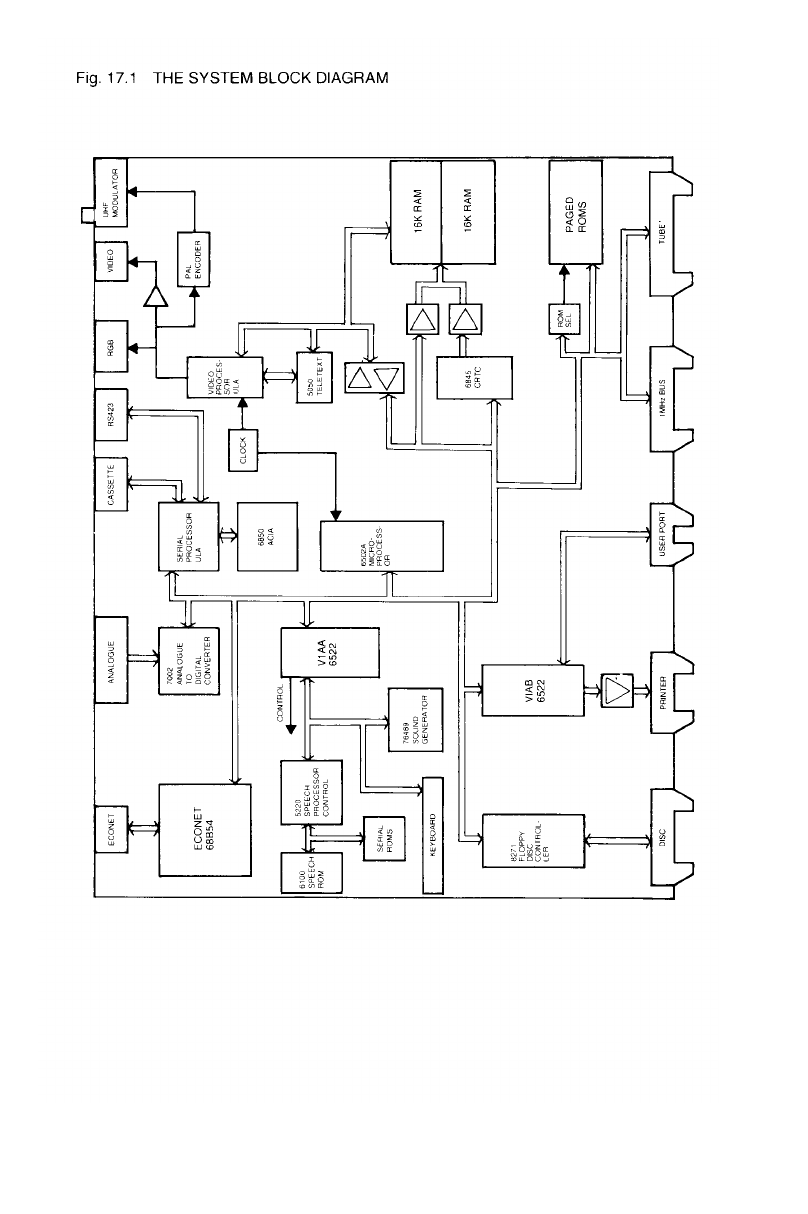
354

3
55
Refer to figure 17.1 whilst reading the following outline of the
hardware. At the centre of the system is the 6502A central
processing unit (CPU). This is the chip which executes all of the
programs including BASIC. It is connected to the rest of the
system via three buses. These are the data bus, the address bus
and the control bus. For clarity on the diagram, these buses are
all compressed into one which is represented by the double
lines terminated with arrows at each major block.
A bus is simply a number of electrical links connected in parallel
to several devices. Normally one of these devices is talking to
another device on the bus. The communication protocols which
enable this transfer of data to take place are set up by the
control, address and data buses. In the case of the address bus,
there are 16 separate lines which allow 65536 different
combinations of l’s and 0’s. The maximum amount of directly
addressable memory on a 6502 is therefore 65536 bytes. The
data bus consists of 8 lines, one for each bit of a byte. Any
number between 0 and &FF (255) can be transferred across the
data bus. Communication between the peripherals, memory
and the CPU occurs over the data bus. The CPU can either send
out a byte or receive a byte. The data bus is therefore called a
bidirectional bus because data flows in any one of two directions.
The address bus is unidirectional since the 6502 provides, but
cannot receive addresses. Note that some address buffers are
included in the video circuit to allow either the 6845, 5050 or
6502 to provide addresses for system random access memory
(RAM).
In order to control the direction of data flow on the data bus, a
read or write signal is provided by the control bus. Hardware
connected to the system can thereby determine whether it is
being sent data or is meant to send data back to the CPU. The
other major control bus functions are those of providing a clock,
interrupts and resets. The clock signal keeps all of the chips
running together at the same rate. The RESET line allows all
hardware to be initialised to some predefined state after a reset.
An interrupt is a signal sent from a peripheral to the 6502
requesting the 6502 to look at that peripheral. Two forms of
interrupt are provided. One of these is the interrupt

356
request (IRQ) which the 6502 can ignore under software control.
The other in the non-maskable interrupt (NMI) which can never
be ignored. Refer to chapter 13 on interrupts for more
information.
When power is first applied to the system, a reset is generated
to ensure that all devices start up in their reset states. The 6502
then starts to get instructions from the MOS ROM. These
instructions tell the 6502 what it should do next. A variety of
different instructions exist on the 6502. The basic functions
available are reading or writing data to memory or an input!
output device and performing arithmetic and logical operations
on the data. Once the MOS (machine operating system)
program is entered, this piece of software gains full control of
the system.
SHEILA and the system hardware
All of the main blocks connected to the 6502 in the block
diagram, figure 17.1, together form the system hardware. In
6502 systems, the hardware is memory mapped which means that
any hardware device registers appear in the main memory
address space. Page &FE (the 256 bytes of memory starting at
&FE00) is reserved especially for the system hardware in the
BBC microcomputer. The special name of ‘SHEILA’ has been
assigned to this page of memory. Two other special pages are
&FC (called ‘FRED’) and &FD (called ‘JIM’). FRED and JIM are
concerned with external user hardware attached to the one
megahertz bus. They are dealt with in chapter 28 on the one
megahertz bus.
In the following chapters, all of the devices attached to Sheila
are described in detail. The table below shows the memory map
of Sheila, the function of the devices attached to it, and the
sections in which they are described.

3
57
SHEILA Integrated Description Section
address circuit number
(offset from&FE00)
&00-&07 6845 CRTC Video controller 18
&08-&0F 6850 ACIA Serial controller 20.3
&10-&1F Serial ULA Serial system chip 20.9
&20-&2F Video ULA Video system chip 19
&30-&3F 74LS161 Paged ROM selector 21
&40-&5F 6522 VIA SYSTEM VIA 23
&60-&7F 6522 VIA USER VIA 24
&80-&9F 8271 FDC Floppy disc controller 25.1
&A0-&BF 68B54 ADLC ECONET controller 25.2
&C0-&DF uPD7002 Analogue to digital converter 26
&E0-&FF Tube ULA Tube system interface 27
Note: Some Sheila addresses are not normally used. This is
because the same devices appear at several different Sheila
addresses. For example, the paged ROM select register is
normally addressed at location &30, but it could equally well be
addressed at any one of the fifteen other locations
&31-&3F.

358

3
59
18 THE 6845 CRTC
Sheila address &00-&07
18.1 General introduction to the 6845
The 6845 cathode ray tube controller chip (CRTC) forms the
heart of the BBC Micro’s video display circuitry. Its major
function is that of displaying the video data in memory on a
raster scan display device (a television or monitor). As an extra
bonus, the 6845 also refreshes all of the random access memory
so that the data stored there is not lost. This refreshing process
is inherent in the sequential nature of accessing memory for the
video display. The 6845 does not interfere with processor access
to the memory since the processor and 6845 operate on alternate
phases of the system clock. The 6845 is responsible for
producing the correct format on the display device, positioning
the cursor, performing interlace if it is required and monitoring
the light pen input. Other video processing functions involving
colour and teletext are dealt with in conjunction with other
sections in Sheila.
Inside, the 6845 is a very powerful and complex VLSI chip.
From a user’s point of view it is useful to know how to define a
specialised screen layout, and how the screen layouts (modes)
have been defined by Acorn. A generalised overview of the
6845 is therefore given first, followed by the values in each of
the registers in the various modes. This chapter ends with a
general summary table which describes the functions of the
various registers. Appendix F contains diagrams illustrating all
of the screen modes in a very concise and easily referred to
format.
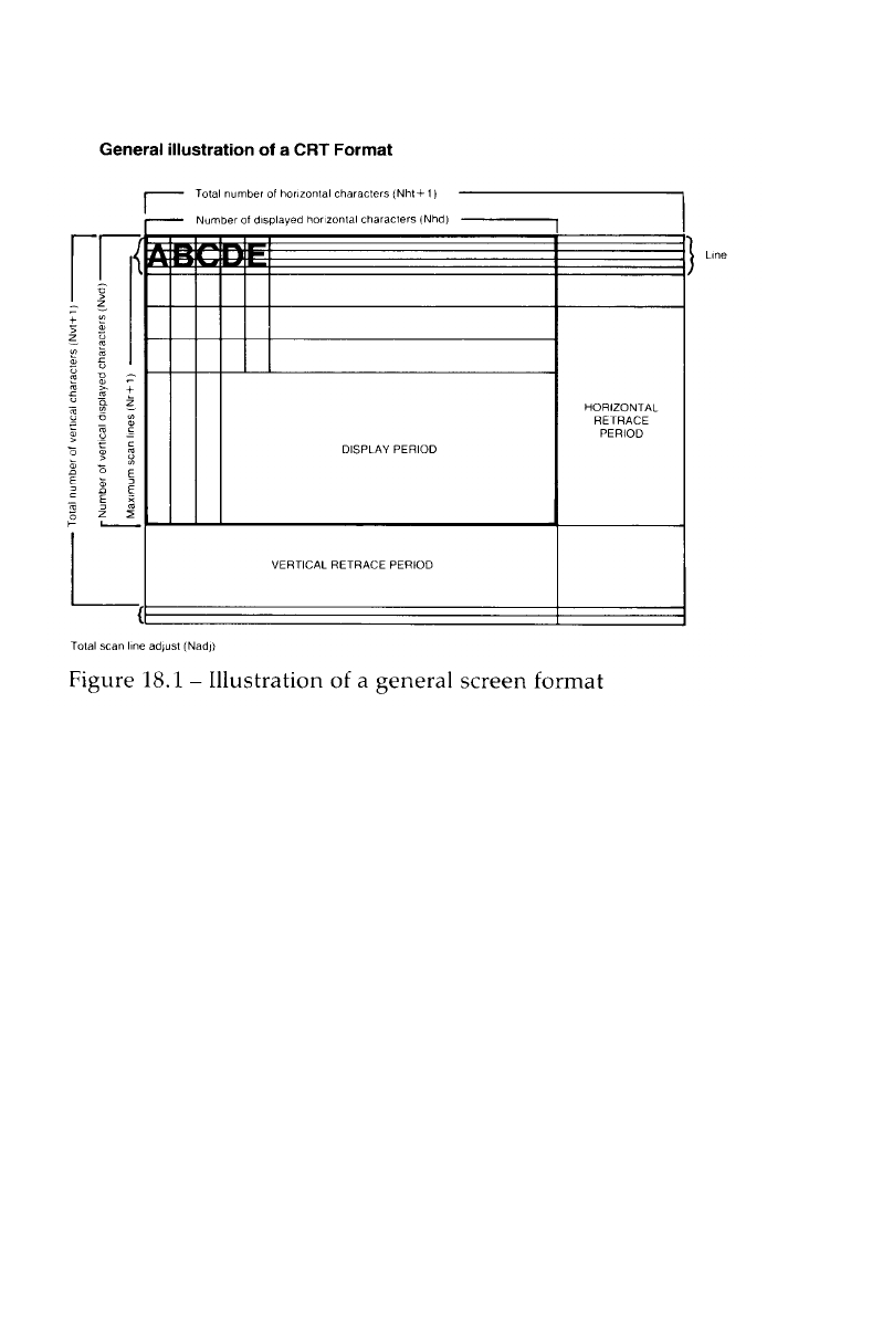
360
18.2 Programming the 6845
The 6845 possesses 18 internal registers, 14 of which are write
only (R0-R13), 2 of which are read and write (R14-R15) and 2 of
which are read only (R16-R17). In order to gain access to any of
these registers, the register address must be written into the
6845 address register. This is situated at Sheila address &00.
Having written a 5 bit number into the address register, the
selected internal register may be written to or read from at
Sheila address &01.
The best way of programming the 6845 is by using the VDU23
command. For example VDU23,0,R,V,0,0,0,0,0,0 will put the
value V into register R. In BASIC programs it can be shortened
by using semicolons instead of commas. A semicolon causes a 2
byte word to be included in the VDU command. For example
VDU23;R,V;0;0;0 has the same effect as the first example.

3
61
18.3 THE HORIZONTAL TIMING REGISTERS
The horizontal timing registers define all of the horizontal
timing for the screen layout. The point of reference for these
registers is the left most displayed character position. The
registers are programmed in ‘character time units’ relative to
the reference point.
18.3.1 Horizontal total register (R0)
This 8 bit write only register determines the horizontal sync.
frequency. It should be programmed with the total number of
displayed plus non-displayed character time units across the
screen minus one (Nht on figure 18.1).
Note that the number of displayed characters is not necessarily
the same as the number of characters per line. This is because of
the variable number of bits attributed to each pixel, depending
upon the number of colours available. The table for R1 contents
illustrates this.
Mode 0 1 2 3 4 5 6 7
R0 127 127 127 127 63 63 63 63
18.3.2 Horizontal displayed register (R1)
This 8 bit write only register determines the number of
displayed characters per horizontal line (Nhd on figure 18.1).
Mode 01 2345 67
No. of CHRS as 80 80 80 80 40 40 40 40
seen by 6845
(Nhd)
No. of CHRS as 80 40 20 80 40 20 40 40
seen on the
screen
No.of bits used12 4112 11
to store colour
information

362
18.3.2 Horizontal sync position register (R2)
This 8 bit write only register determines the horizontal sync.
pulse position on the horizontal line. The specification is in
terms of character widths from the left hand side of the screen.
Mode 01 2345 67
R2 98 98 98 98 49 49 49 51
Increasing the value of this register pushes the entire screen left
whilst decrementing it pushes the whole screen right.
18.4 The sync width register (R3)
This 8 bit write only register defines both the horizontal and the
vertical sync. pulse times.
18.4.1 Horizontal sync pulse width
The lower 4 bits contain the horizontal sync. pulse width in
number of characters. Any number between 1 and 15 can be
programmed, but 0 is not valid. It is however not advisable to
change this register since most monitors and televisions require
the standard sync. width to operate properly.
Mode 01234567
Lower 4 bits of88884444
R3
18.4.2 Vertical sync pulse width
The upper 4 bits contain the number of scan line times for the
vertical sync. pulse. This is set to 2 in all modes.
18.5 THE VERTICAL TIMING REGISTERS
The point of reference for vertical registers is the top displayed
character position. Vertical registers are programmed in
character row times or scan line times.

3
63
18.5.1 Vertical total register (R4)
The vertical sync. frequency is determined by both R4 and R5.
In order to obtain an exact 50Hz or 60Hz vertical refresh rate,
the required number of character line times is usually an integer
plus a fraction. The integer number of character lines minus one
(Nvt on figure 18.1) is programmed into this 7 bit write only
register.
Mode 01 2345 67
R4 38 38 38 30 38 38 30 30
18.5.2 Vertical total adjust register (R5)
This 5 bit write only register is programmed with the fraction
for use in conjunction with register R4. It is programmed with a
number of scan lines (Nadj on figure 18.1). It can be varied
slightly in conjunction with R4 to move the whole display area
up or down a little on the screen. It is usually set to 0 except
when using modes 3,6 and 7 in which it is set to 2. *TV
(OSBYTE &90) controls the vertical positioning of a display on
the screen. Refer to the OSBYTE section for more details.
18.5.3 Vertical displayed register (R6)
This 7 bit write only register determines the number of
displayed Character rows (Nvd on figure 18.1) on the CRT
screen and is programmed in character row times.
Mode 01 23 4567
character lines 32 32 32 25 32 32 25 25
18.5.4 Vertical sync position (R7)
This 7 bit write only register determines the vertical sync
position with respect to the reference. It is programmed in
character row times.
Mode 01234567
Sync position 34 34 34 27 34 34 27 27

364
18.6 Interlace and delay register (R8)
This 6 bit write only register controls the raster scan mode and
cursor/display delay. The interlace options are:
18.6.1 Interlace modes (bits 0,1)
Interlace mode Description
register
Bit 1 Bit 0
0 0 Normal (non-interlaced) sync mode (figure 18.2a)
1 0 Normal (non-interlaced) sync mode (figure 18.2a)
0 1 Interlace sync mode (figure 18.2b)
1 1 Interlace sync and video (figure 18.2c)
All BBC microcomputer screen modes are interlaced sync only
except for mode 7 which is interlaced sync and video. The
default values can easily be changed using *TV (*FX 144)
followed by a 0 to turn interlacing on or a 1 to turn interlacing
off.
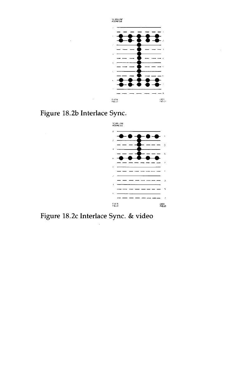
3
65
18.6.2 Display blanking delay (bits 4,5)
Bits 4 and 5 control the display blanking signal. This signal
must be enabled for all of the character output period and is
used to take account of the time to transfer data from memory
to the video output circuitry. No delay is required in modes 0-6,
but a one character delay is required in mode 7 because the
SAA5050 character generator is used.
Display blanking delay
Bit5 Bit4 Description
00No delay
0 1 One character delay
1 0 Two character delay
11Disable video output

366
18.6.3 Cursor blanking delay (bits 6,7)
Bits 6 and 7 control the cursor blanking signal. This signal must
be enabled at the exact time when a cursor should appear on
the screen. No delay is required in modes 0-6, but a two
character delay is required in mode 7.
Cursor enable signal
Bit 7 Bit 6 Description
00No delay
0 1 One character delay
1 0 Two character delay
1 1 Disable cursor output
18.7 Scan lines per character (R9)
This 5 bit write only register determines the number of scan
lines per character row including spacing. The programmed
value is one less than the total number of output scan lines.
Mode 0123456 7
Scans per 7779779 18
character
18.8 THE CURSOR
It is possible to program a cursor to appear at any character
position (defined by R14 and R15). Its blink rate can be set to 16
or 32 times the field period of 20 ins. Optional non-blink and
non-display (i.e no cursor on the screen) modes can also be
selected. Its height in number of lines and its vertical position in
a character slot can be defined as well.
18.8.1 The cursor start register (R10)
This 7 bit write only register controls the cursor format (see
figure 18.3).Bit 7 is not used. Bit 6 enables or disables the blink
feature. Bit 5 is the blink timing control bit. When bit 5=0, blink
frequency = 1/16th of field rate. When bit 5=1, blink frequency =
1/32nd of the field rate. The cursor start line is set by the lower
five bits.
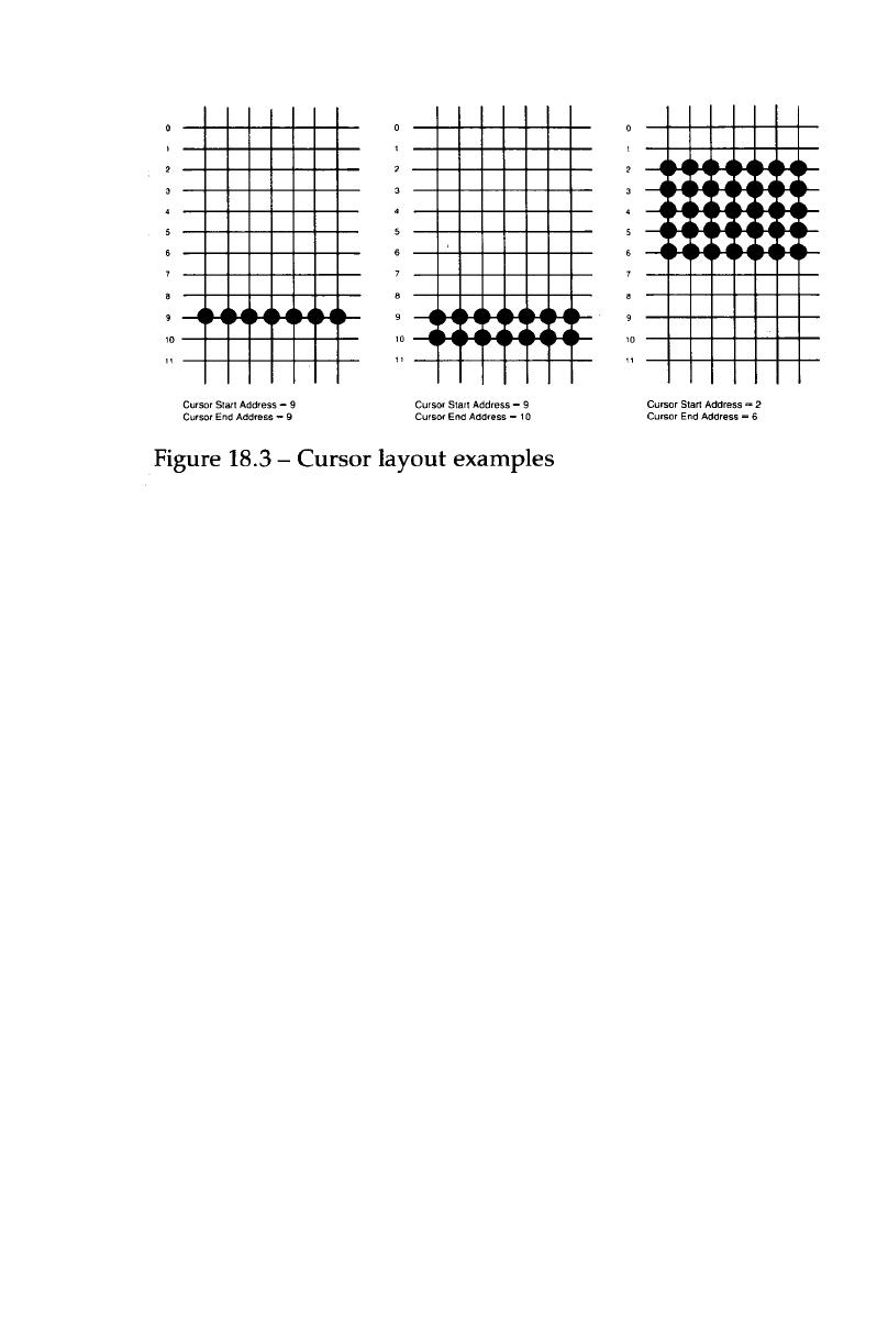
3
67
18.8.2 The cursor end register (R11)
This 5 bit write only register sets the cursor end scan line (see
diagram).
Mode 0123456 7
Cursor end 8889889 19
18.8.3 Cursor position register (R14 and R15)
This 14 bit read/write register stores the current cursor location.
It consists of 8 low order (R15) and six high order (R14) bits.
18.9 LIGHT PENS
18.9.1 Light pens in general
A typical light pen consists of a small light sensitive device
fixed to the end of a pen shaped holder. The sensor picks up the
light given out from the monitor screen and sends an electronic
signal into the micro. This LPSTB (light pen strobe) signal can
be decoded (because the screen is scanned on a raster basis) and
the position of the pen head determined

368
Light pens can be used for a multitude of tasks such as
drawing, ‘painting’, designing layouts, playing games etc., but
their use in many applications is limited by the resolution. The
reason for this is that a fairly large area of screen (ie. perhaps
.5cm x .5cm) is usually required to provide sufficient light to
operate the pen. The maximum resolution for defining the
position of the light pen is therefore a patch on the screen of this
size, so accurate line drawings are impossible. The position of
the light pen is stored to the nearest character position, so this
limits the resolution to a character cell.
18.9.2 Light pen position register (R16 and R17)
This 14 bit read only register is used to store the location of a
light pen sensor placed in front of the screen. The register is
modified whenever the LPSTB signal is pulsed high.
18.9.3 Constructing a light pen
The light pen hardware must produce a positive going TTL
pulse whenever the display scan position is under the sensor.
The light pen position will then be stored in the light pen
register R16,R17. Note that slow light pen response will require
a delay factor to be subtracted from R16,R17 to produce the
correct light pen position.
Luckily, there are small light sensitive devices available which
provide a direct TTL logic level output. If one of these is fixed to
the end of an empty pen and connected to the light pen input
on the rear of the BBC microcomputer, an operational light pen
can be constructed. The connections for such a pen are
illustrated in figure 18.4. A special photosensor called a ‘Sweet
spot’ is available from RS Components or most of their
distributors, and is supplied as part number RS 303-292.
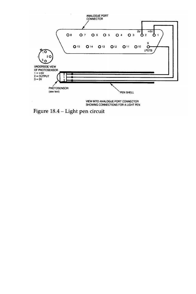
3
69
18.9.4 Light pen software
In order to take account of the different screen start addresses
for the various modes, a further correction factor must be
subtracted from the contents of the light pen register. These
correction factors are:
Mode Correction factor
0 &0606 (1542)
1 &0606 (1542)
2 &0606 (1542)
3 &0806 (2054)
4 &0B04 (2820)
5 &0B04 (2820)
6 &0C04 (3076)
7 &2808 (10248)
The light pen position in terms of x,y co-ordinates is given by:
y = (L.p register-correction) DIV number of characters per
line
x= (L.p register-correction) MOD number of characters per
line

370
This x value will be in terms of 6845 characters and will have to
be modified by multiplying by
Number of characters per line on screen
Number of characters as seen by 6845
e.g. for mode 2 = 20/80 = 1/4 The resolutions are therefore:
Modes single displayed character
0,3,4,6,7
Modes 1,5 half of a displayed character
Mode 2 quarter of a displayed character
Note that the screen should be cleared before using a light pen
and not scrolled whilst the pen is in use. If it is scrolled, the
position of the start of the screen will have to be taken into
account as well.
18.10 Displayed screen start address register (R12,R13)
This 14 bit write only register determines the location in
memory which corresponds to the upper left hand character
displayed on the screen. R13 (8 bits) is the low order address
and R12 (6 bits) is the high order address. It can often be useful
to know what the current contents of this register are.
Unfortunately, being a write only register it is not possible to
read the value directly. However, OSBYTE &A0 can be used to
get these parameters from the operating system workspace in
page &03. The start of screen address is stored in locations &350
and &351. Call OSBYTE &A0 with X=&30. The contents of &350
will be returned in the X register and the contents of &351 will
be returned in the Y register.
Note that the actual screen start address must be divided by 8
before being sent to R12,R13 because there are 8 lines per
character (modes 0-6). In mode 7 a rather more complex
correction has to be applied. See section 18.11.3 on mode 7
scrolling at the end of this chapter.
The ability to define the start of the screen to be anywhere in
memory is very useful because it allows fast scrolling of the

3
71
screen up, down, left and right. Provided that the start address
is inside the screen memory of the mode being used, a
hardware wrap around feature will also operate. Characters
which would have scrolled off the top of the screen will
therefore reappear at the bottom. The wrap around circuit
simply detects whenever the 6845 tries to get video data from a
ROM (an address above &7FFF), and adds an offset to that
address. This has the effect of bringing the address back inside
the video RAM. Since the screen sizes are different in the
various modes, 2 bits on the SYSTEM VIA are used to define the
length of the hardware scrolled screen, see section 23.2.
18.11 HARDWARE SCROLLING
Scrolling the screen fast in any direction can be of immense use
in a large number of applications. Text can be scrolled in word
processing applications, landscapes can be made to rush by in a
horizontal direction (see games such as Acornsoft Planetoid). If
it were not for the hardware scroll feature, it would be
necessary to move every byte on the screen to perform a scroll.
This is very time consuming for 20000 bytes and therefore slow.
In order to make effective use of the hardware scrolling
facilities available, it is necessary to understand both the
advantages and the limitations which are imposed.
Modes 0-6 will now be analysed in detail followed by mode 7
which is slightly different.
18.11.1 Modes 0-6 vertical scrolling
In order to move the screen position upwards by one character
line, it is necessary to increment the current start address
register (R12,R13) by the number of characters per line.
Remember that these are characters as produced by the 6845
and not as seen on the screen. There are 80 6845 characters per
line in modes 0-3 and 40 characters per line in modes 4,5 and 6.
The screen can be scrolled downwards by decrementing the
screen start address register by the number of characters per
line. Note that you should not normally allow the screen start
address register to contain a value less

372
than the official screen start address or greater than the official
screen end address in the mode being used. If this occurs then
areas of the main system memory will be displayed directly on
the screen. This produces some interesting results, especially if
zero page is displayed! Remember that the value put into
R12,R13 is the actual memory address DIV 8. See the example
program in section 18.14.
18.11.2 Sideways scrolling
The whole screen can be made to move left by one character (as
seen by 6845) by incrementing the screen start register. It will
move one character to the right by decrementing this register.
Note that each character which moves off the left of the screen
will appear on the next line up at the right of the screen. It is
therefore necessary to move each of these characters down a
line in software to maintain a true sideways scroll.
This scrolling technique is good for text, but may produce
jumpy movements in graphics due to the limited resolution in
the screen position. On a mode 0 screen, each sideways scroll
moves the screen by 8 pixels. On a mode 2 screen, each 6845
character only represents 2 graphics pixels so a fairly effective
hardware scroll can be used.
18.11.3 Mode 7 scrolling
Hardware scrolling in mode 7 is slightly more complex than in
modes 0-6. To calculate the value to put into registers 12 and 13,
first of all calculate the required start address in RAM (e.g
&7C28). Take the high byte and subtract &74, then EOR the
result with &20. This new value should be put into R12. R13
contains the low order address byte. A similar correction factor
should be applied when working out the cursor register
contents.

3
73
18.12 FAST ANIMATION
18.12.1 Fast animation using mode 2
Mode 2 has several advantages over all of the other modes for
fast animation. It is for this reason, plus the fact that all 16
colours are available that this mode is used in most fast
graphics games. Provided that the programmer is prepared to
put up with a 2 pixel at a time movement instead of a 1 pixel at
a time movement, moving objects simplifies to moving
complete bytes in memory. Consider for a moment the layout of
each byte on a mode 2 screen.
P2d P1d P2c Plc P2b P1b P2a P1a
BIT 7 6 5 4 3 2 1 0
P1a-P1d are 4 bits defining the colour of pixel 1
P2a-P2d are 4 bits defining the colour of pixel 2
To move graphics sideways by one pixel involves extracting
Pla-Pid from P2a-P2d. These removed bits must then be
reinserted into the adjacent byte. This process is tricky and
consumes a lot of processing time leading to very slow
movement in all but the simplest of cases. It will be appreciated
how much faster it is to simply move a byte (2 pixels) at a time
from one memory location to another, which can be done very
fast indeed.
18.12.2 Fast animation using mode 0
Unlike mode 2, moving a byte at a time in mode (1 moves 8
pixels. Animation moving 8 pixels at a time will generally
produce very uneven motion. However, since the packing of
pixels in mode 0 assigns one bit per pixel, animation can be
implemented by shifting all of the bits in a byte left or right by
one position. This uses a 6502 'ROR' or 'ROL' instruction. The
bit which moves off the edge of one byte must be put into the
adjacent byte.
18.13 Wrap around
To ensure that the hardware wrap around feature operates
correctly, the start of screen address must be kept within the
screen boundaries. If it goes below the start of screen address
then add the length of the screen to it. If it goes above the top of
screen address then subtract the length of screen from it.

374
eg. in mode 0, the calculated start of screen address may be
&8050. Since this is outside of the screen, it should be changed
to &3050 by subtracting &5000, the screen size. The amount of
memory which is wrapped around is controlled by the system
VIA as described in section 23.2.
18.14Hardware scroll example
The program listed below uses the hardware scroll facilities in
mode 0. A line of text can be moved around the screen using the
cursor keys. Note that as text moves off one side of the screen
(sideways scroll), it reappears on the other side either one line
up or one line down from its original position. If a true
sideways scroll is required, it is necessary to move all of the
bytes on the relevant side of the screen up or down one
character position. During motion of the line of text in a vertical
direction, there will be brief flashes of another line on the
screen. This is partially due to the delay in BASIC between
setting register 12 and register 13 on the 6845, and also because
the change occurs in the middle of a screen display. The
flashing will be reduced in machine code programs which wait
until the frame sync period before changing any of the 6845
registers.
10REM HARDWARE SCROLL EXAMPLE IN MODE 0
20 MODE0
30START=&3000
40PRINT”THIS TEXT CAN BE SCROLLED IN ANY DIRECTION USING THE
CURSOR KEYS”
50REM SET KEYS REPEAT RATE AND CURSOR KEYS TO GIVE 136 ETC.
60*FX4,1
70*FX12,3
80REPEAT
90 A=INKEY(0)
100 IF A=136 THEN PROCMOVE(8)
110 IF A=137 THEN PROCMOVE (-8)
120 IF A=138 THEN PROCMOVE(-640)
130 IF A=139 THEN PROCMOVE(640)
140 UNTIL FALSE
150DEF PROCMOVE(offset)
160START=START+offset
170REM IF ABOVE OFFICIAL START THEN SUBTRACT SCREEN LENGTH
181IF START>=&8000 THEN START=STARI-&5000
190REM IF BELOW OFFICIAL START ADDRESS, ADD SCREEN LENGTH
200IF START<&3000 THEN START=START+&5000
190REM MODIFY 6845 MEMORY START ADDRESS REGISTER
220VDU23;12,START DIV 2048;0;0;0
231VDU23;13,START MOD 2048 DIV 8;0;0;0
240ENDPROC

3
75
18.15 6845 REGISTER SUMMARY TABLE
Register Register Program Data bit
number name unit 7 6 5 4 3 2 1 0
AR Address register —xxxA4A3A2A1A0
R0 Horizontal total Character D7 D6 D5 D4 D3 D2 D1 D0
R1 Horizontal Character D7D6D5D4D3D2D1D0
displayed
R2 Horizontal sync Character D7D6D5D4D3D2D1D0
position
R3 Horizontal sync Character h3 h2 h1 h0
width
Vertical sync Scan line v3 v2 v1 v0
width
R4 Vertical total Char, row x D6 D5 D4 D3 D2 D1 D0
R5 Vertical total Scan line x x x D4 D3 D2 D1 D0
adjust
R6 Vertical displayed Char. row x D6 D5 D4 D3 D2 D1 D0
R7 Vert. sync. Char, row x D6 D5 D4 D3 D2 D1 D0
position
R8 Interlace mode V S
Display enable Character d1 d0
delay
Cursor enable Character c1 c0
delay
R9 Scan lines/ Scan line x x x D4 D3 D2 D1 D0
character
R10 Cursor start Scan line x s4 s3 s2 s1 s0
Cursor blink rate - r
Cursor blink - b
ON OFF
R11 Cursor end Scan line xxxD4D3D2D1D0
R12 Screen start —x x h5 h4 h3 h2 h1 h0
address H
R13 Screen start 1716151413121110
address L
R14 Cursor address H x x h5h4h3h2h1h0
R15 Cursor address L 17161514131211l0
R16 Light pen H x x h5h4h3h2h1h0
R17 Light pen L 1716151413121110
x = not used

376
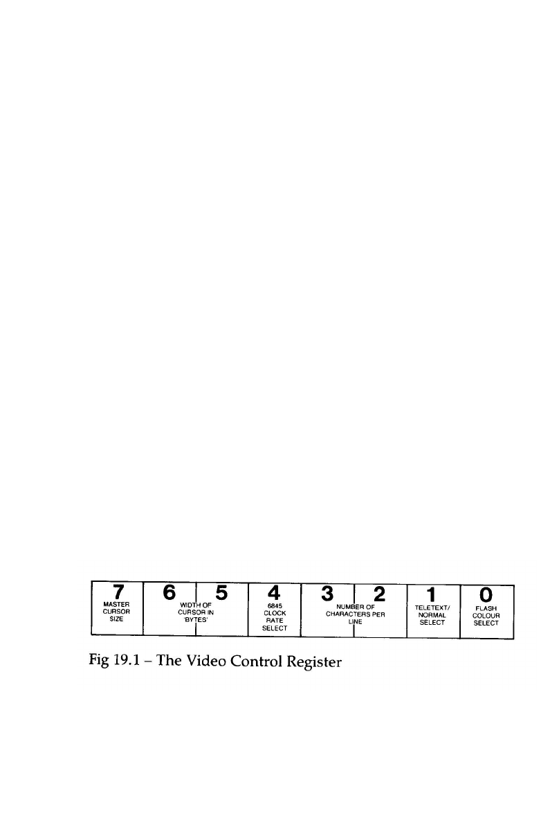
3
77
19 The video ULA
Sheila address &20-&21
The Video ULA is a special chip, designed by Acorn especially
for use in the BBC microcomputer. It provides all of the video
timing for the rest of the system (including the 6845),
determines the relationship between logical and physical
colours, controls the cursor width and provides Red, Green and
Blue (R G B) video outputs. This section explains how the ULA
is programmed for the various modes 0 - 7 and then gives an
example of creating a totally new mode with 16 colours but
only 10 characters across the screen. This only uses 10K of
memory and therefore allows a 16 colour mode on model A
micros, or large games programs on a model B which require
lots of memory and full 16 colour graphics.
19.1 THE VIDEO CONTROL REGISTER - SHEILA &20
WRITE ONLY
This 8 bit register controls which flashing colour is present at
any one time, whether teletext is selected, the number of
characters per line, the clock rate sent to the 6845, the width in
bytes of each character and the master cursor size. *FX154
should be used to write data into this register.

378
19.1.1 Selected flash colour (bit 0)
This bit selects which colour of the two flashing colours is
actually displayed at any particular time. It is continually
changed by the operating system to generate the flashing
colours. *FX9 and *FX10 control how long each colour is on the
screen and can be defined down to one fiftieth of a second. By
varying the flash rates of the colours it is possible to generate
‘new’ colours. This is because a flash rate of one fiftieth of a
second is fast enough to fool the eye into seeing a single colour
rather than two rapidly flashing colours.
0 = first colour selected
1 = second colour selected
19.1.2 Teletext output select (bit 1)
This bit selects whether RGB input comes from the video
serialiser in the ULA or from the teletext chip.
0 = on chip serialiser used
1 = teletext input selected
19.1.3 Number of characters per line (bits 2,3)
These two bits determine the actual number of displayed
characters per line. It is by varying this number that the new 10
character per line mode can be generated.
Bit 3 Bit 2 Number of characters per line
1180
1040
0120
0010
19.1.4 6845 Video Controller Chip Clock Rate Select (Bit 4)
The clock frequency sent to the 6845 can be varied using this bit.
0 = low frequency clock (modes 4-7)
1 = high frequency clock (modes 0-3)

3
79
19.1.5 Width of cursor in bytes (bits 5,6)
These two bits determine the number of bytes of memory
required to generate a cursor width.
Bit 6 Bit 5 Number of bytes per cursor
0 0 1 (modes 0,3,4,6)
0 1 not defined
1 0 2 (modes 1,5,7)
1 1 4 (mode 2)
19.1.6 Master cursor width (bit 7)
If set, this bit will cause a large cursor to be generated. If reset it
will cause a small cursor to be generated.
NOTE — setting bits 5,6 and 7 to 0 will cause the cursor to vanish
from the screen under ALL conditions.
19.1.7 General summary of the video control register
Cursor Bytes per Clock Number of chrs Flash
size cursor speed per line select
Mode Bit7 Bit6 Bit5 Bit4 Bit3 Bit2 Bit1 Bit0 Hex
0 1001110x&9C
1 1101100x&D8
2 1111010x&F4
3 1001110x&9C
4 1000100x&88
5 1100010x&C4
6 1000100x&88
7 01001011&4B
x signifies that the flash bit is changed regularly
19.2 THE PALETTE - SHEILA &21 WRITE ONLY
The ‘Palette’ is a 64 bit RAM in the video ULA which defines
the relationship between the logical and actual colours displayed
on the screen. If you don’t understand the difference between
logical and actual colours yet, then refer to the COLOUR section
in the User Guide. *FX155 can be used to write colour data into
the Palette. It will automatically EOR the physical colour with 7
(see later). Usually, it is better to use VDU19 or OSWORD &0C to
program logical and actual colours.

380
The palette register consists of two 4 bit fields. Bits 0 - 3 are the
actual colour field. Bits 4 - 7 are the logical colour field, as
illustrated in figure 19.2.
19.2.1 Logical colour field
The following description of programming the palette only
applies to direct programming using *FX155. If OSWORD &0C
or VDU19 are used, none of the problems which are about to be
outlined will be relevant.
Programming the logical colour directly is easy in mode 2. The
logical colour number then occupies the entire 4 bit field. In two
colour modes 0,3,4 and 6, programming the logical colour directly
is more complex. Bit 7 defines the logical colour, but bits 4,5 and
6 must be programmed to all their possible values. In other
words, in order to set logical colour 1 to actual colour 5, it is
necessary to program logical colours 9, 10, 11, 12, 13, 14 and 15
to 5. If this is not done, some parts of characters will be in one
colour and other parts will be in a different colour.
Programming the logical colours in a four colour mode is
slightly more complex. Bits 7 and 5 together contain the logical
colour number. All other possible combinations of bits 6 and 4
must also be programmed. The following table shows how to
program logical colours 0-3. For example, to program logical
colour 0, it is necessary to program four separate locations in
the palette.

3
81
Logical colour bit 7bit 6 bit 5 bit 4
000
00
0001
0100
0101
10010
0011
0110
0111
21000
1001
1100
1101
31010
1011
1110
11I1
19.2.2 General Summary for logical colour programming
Mode Bit7 Bit6 Bit5 Bit4
2 colour Logical colour x x x
Bit 0
4 colour Logical colour x Logical colour x
Bit1 Bit0
16 colour Logical colour Logical colour Logical colour Logical colour
Bit3 Bit 2 Bit 1 Bit 0

382
19.2.3 Physical colour field
The physical colours are:
&00(0) black
&01(1) red
&02(2) green
&03(3) yellow (green—red)
&04(4) blue
&05(5) magenta (red—blue)
&06(6) cyan (green—blue)
&07(7) white
&08(8) flashing black—white
&09(9) flashing red—cyan
&0A(10) flashing green—magenta
&0B(11) flashing yellow—blue
&0C(12) flashing blue—yellow
&0D(13) flashing magenta—green
&0E(14) flashing cyan—red
&0F(15) flashing white—black
It is these colour numbers which should be used with *FX155.
Note however that the actual number sent to the Palette is the
above number EOR &07, ie with the three colour bits inverted
and the flash bit as above.
19.2.4 Some interesting effects using the palette
Because of the necessity to program 4 different palette locations
for each colour in a four colour mode, some ‘nasty’ effects can
be produced on the screen if all four locations are not
programmed with the same colour. To illustrate this point, try
displaying four colours on the screen at once, then run this line
of BASIC:
A%=155: REPEAT: X%=RND(255): CALL &FFF4: UNTIL0

3
83
19.3 'MODE 8' Implementation example
This example program will set up a brand new mode which has
been nominated as ‘MODE 8’. This is a full 16 colour mode and
can be implemented on a Model A as well as a Model B since
only 10K of RAM is used. There will only be 10 characters
across the screen, but printing and plotting will operate
properly. One word of warning however. Do not try to redefine
the text window when this mode is in use because it will not
work! All error checking on window bounds will be ineffective
in this mode since the operating system does not expect mode 8
to exist.
10 REM CREATE ‘MODE 8’
20 REM NOTE: NO WINDOWING ALLOWED
30 REM
40 REM NOTE: POKING VDU VARIABLES
50 REM IS GENERALLY ILL ADVISED.
60 MODE 5:REM BASIC MODE
70 REM CONFIGURE VIDEO ULA FOR 10 COLUMN, 16 CHARACTER
80 *FX 154,224
90 ?&360=&F:REM COLOUR MASK
l00 ?&361=1:REM PIXELS PER BYTE—1
110 ?&34F=&20:REM BYTES PER CHARACTER (4 wide x 8 high)
120 ?&363=&55:REM GRAPHICS RIGHT MASK
130 ?&362=&AA:REM GRAPHICS LEFT MASK
140 ?&30A=9:REM NO. OF CHARS PER LINE
150 VDU 20
160 REM DEMO
170 MOVE 0,0:DRAW 640,512:DRAW 1279,0
180 PRINT TAB(1,2);
190 A$=”***HelloThere***”
200 COLOUR 129
210 FOR A%=1 TO 16
220 IF A%=9 THEN PRINT TAB(l,8);
230 COLOUR A%-1
240 PRINT MID$(A$,A%,l);
250 NEXT A%
260 PRINT

384

3
85
20 The serial system
Sheila address &08-&1F
The serial system on the BBC microcomputer deals with the
transmission and reception of asynchronous serial data. Serial
data is used in conjunction with the cassette and RS423
interfaces where it is impractical to use the 8 databus lines. The
heart of the system is the 6850 Asynchronous Communications
Interface Adapter (ACIA). This chip interfaces serial data to the
8 bit parallel processor bus. The input and output devices (ie
cassette or RS423) and baud rates are all defined by the serial
ULA. As with all the other hardware interfaces in this guide,
the official operating system commands should be used to
communicate with the chip registers. This will allow programs
written in this way to operate over the Tube.
20.1 General description of a serial interface
This general description aims to introduce the terms which are
used throughout the rest of this chapter. It is most relevant to
the RS423 interface. A serial interface will usually consist of a
data IN line, data OUT line and a ground connection. This is the
barest minimum for a bi-directional serial link. Handshaking
lines are often supplied as well. The RTS (Request to send) goes
low when the BBC micro is ready to accept data on the RS423 (it
acts as a data carrier enable for the cassette). The other device
can control when data is sent to it via the CTS (Clear to send)
line. The device pulls this low to indicate that it can receive data
and pulls it high to indicate that it is unable to receive data (eg
because its input buffer is full). Data should therefore only be
sent out from the BBC microcomputer if the CTS input is low.
OSBYTE &CB controls the serial handshaking and OSBYTE
&CC suppresses all RS423 input.
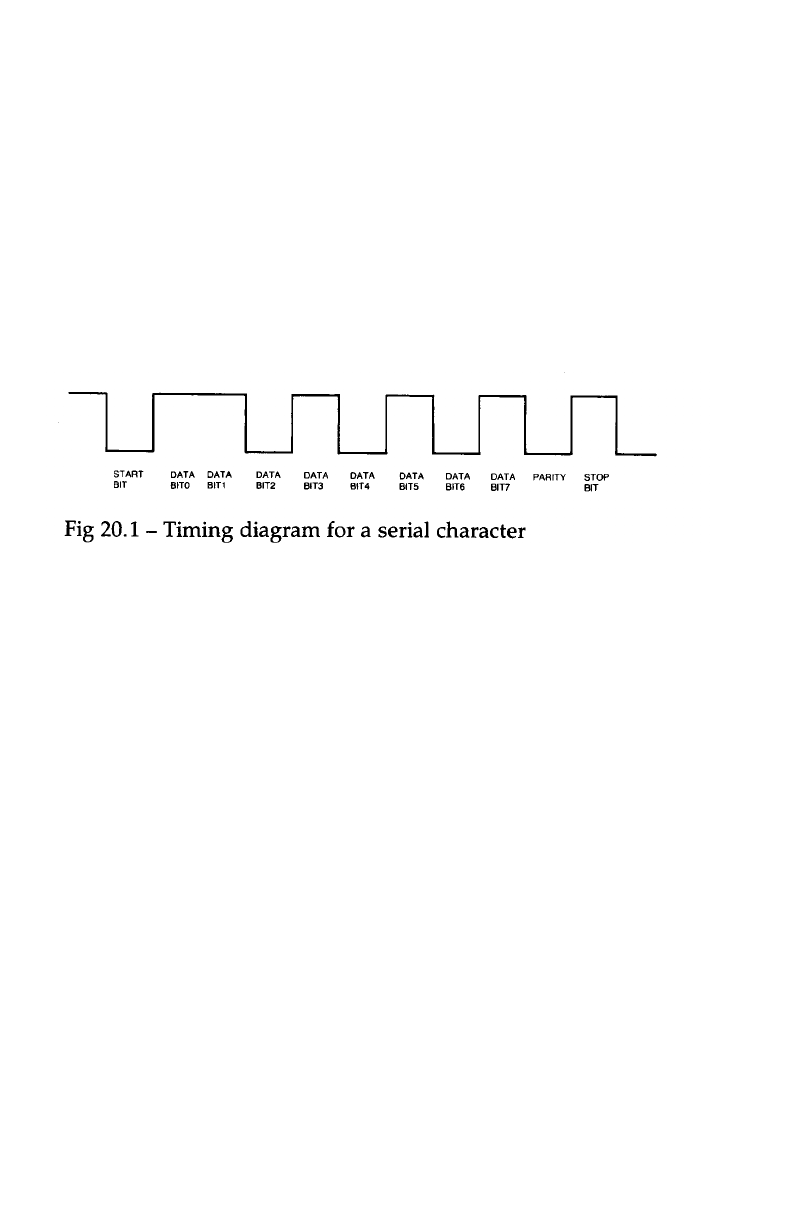
386
Each character is transmitted serially according to a predefined
format. A start bit indicates that a character will follow. 7 or 8
bits of character are then sent followed by a parity bit, if parity
is selected. This parity bit may be set to either 1 or 0 to indicate
whether the number of high bits in the character were odd or
even. The parity bit (if selected) is then followed by one or two
stop bits. The idea behind using a parity bit is that the receiving
device can check that parity is correct. If it is incorrect then an
error has occurred between the transmitter and receiver. The
following diagram illustrates the format of an 8 bit word with
odd parity and 1 stop bit selected.
20.2 Line termination
If very long lines are used to connect devices over an RS423
link, then it may be necessary to terminate the line. This will
only be necessary in exceptional circumstances where both high
baud rates and long line lengths are in use. Refer to Appendix I
which describes the necessary links, for more information.
20.3 The 6850 ACIA (Asynchronous Communications
Interface Adapter)
This chip performs two basic functions. It converts 8 bit parallel
data to serial data, which it then transmits. It also converts a
serial input stream into parallel data for the system bus,
automatically providing the formatting and error checking.

3
87
20.4 Transmit data register (TDR) Sheila &09 write only
A character may be written into the Transmit Data Register
(TDR) if a status read operation has indicated that the TDR is
empty. OSBYTE &97 (151) should be used to perform the write.
This character is transferred to a serial shift register where it is
transmitted, preceded by a start bit and followed by one or two
stop bits. Internal parity (odd or even) can optionally be added
to the character and will appear after the last data bit and before
the first stop bit. After the first character has been written to the
TDR, the Status register can be checked for a Transmit Data
Register Empty condition. If the register is empty, another
character can be loaded for transmission even though the first
character is in the process of being transmitted. The second
character will automatically be transferred into the Shift
Register when the first character transmission is complete.
20.5 Receive data register (RDR) Sheila &09 read only
Data is received from a peripheral via the cassette or RS423
serial interfaces. A divide by 64 clock ratio is provided to select
the baud rate from the serial ULA, and divide by 16 or 1 ratios
are provided as well. The 6850 waits until a full half of the start
bit has been received before it synchronises its clock to the bit
time. As a character is being received, parity (odd or even) will
be checked and any errors will be available in the Status
register. When parity has been selected for an S bit word (7 bits
plus parity), the 6850 sets bit 8 to 0 so that only the 7 bit data is
transferred to the 6502. To read from the RDR, OSBYTE &96
(150) should be used.
20.6 THE CONTROL REGISTER — Sheila &08 write only
The 8 bit 6850 control register determines the function of the
transmitter, receiver, interrupts and the RS423 Request to send
(RTS). Since this is a write only register, it is not possible to read
its current contents directly. There is a way of determining its
current contents via the operating system. OSBYTE &9C (156) is
a powerful command to do this. The X and Y registers must be
set, the old contents of the control register are then AND Y EOR
X. Y therefore masks bits and X

388
toggles bits. Setting Y=&FF and X=0 will generate no change at
all. The routine returns with the old value of the control register
in the X register. This register is normally set to &56 when using
a cassette based system which isn’t in the process of
transmitting or receiving anything.
20.6.1 Counter Divide Select Bits (CR0 and CR1)
These bits determine the divide ratios used in both the
transmitter and receiver sections of the ACIA. Additionally,
these bits provide a master reset which initialises the
transmitter, receiver and status register. The clock division rate
is normally set to 64 whilst the RS423 system is in operation.
The cassette system selects between 300 and 1200 baud using
this division ratio. The serial ULA is always set to 300 baud for
cassette, so division by 64 actually generates 300 baud. Division
by 16 makes it 4 times faster so 1200 baud is generated. Division
by 1 would make it a further 16 times faster, ie 19200 baud but
the cassette will not operate at this speed.
CR1 CR0 Function
0 0 divide by 1
0 1 divide by 16
1 0 divide by 64
1 1 Master reset
20.6.2 Word Select Bits (CR2, CR3 and CR4)
Select bits are used to select word length, parity and the number
of stop bits. Any changes become effective immediately.
CR4 CR3 CR2 Function
0 0 0 7 bits + even parity + 2 stop bits
0 0 1 7 bits + odd parity + 2 stop bits
0 1 0 7 bits + even parity + 1 stop bit
0 1 1 7 bits + odd parity + I stop bit
1 0 0 8 bits + 2 stop bits
1018 bits + l stop bit
1 1 0 8 bits + even parity + 1 stop bit
1 1 1 8 bits + odd parity + 1 stop bit

3
89
20.6.3 Transmitter Control Bits (CR5 and CR6)
Two transmitter control bits provide control of the interrupt
from the Transmit Data Register Empty condition, the RTS
output, and the transmission of a break level (space).
CR6 CR5 Function
00RTS
= low, transmitting interrupt disabled
01RTS
= low, transmitting interrupt enabled
10RTS
= high, transmitting interrupt disabled
1 1 RTS =low, transmits a break level on the transmit data output.
Transmitting interrupt is disabled.
20.6.4 Receive Interrupt Enable Bit (CR7)
The conditions of receive data register full, overrun, or a low to
high transition on the Data Carrier Detect (DCD) signal line are
enabled by a high level bit in this position.
20.7 THE STATUS REGISTER — Sheila &08 read only
Information on the status of the 6850 is available from this
register.
20.7.1 Receive Data Register Full (RDRF) Bit 0
The RDRF register indicates that received data has been
transferred to the Receive Data Register. RDRF is cleared after
the processor has read from the Receive Data Register or by a
master reset. DCD being high also causes RDRF to indicate
empty.
20.7.2 Transmit Data Register Empty (TDRE) Bit 1
This bit goes high to indicate that the Transmit Data Register
contents have been transferred and that new data may now be
entered. The low state indicates that the TDR is full.
20.7.3 Data Carrier Detect (DCD) Bit 2
When DCD goes high it indicates that the carrier is not present
from the cassette input. It will always be low when the RS423
interface is selected.

390
20.7.4 Clear To Send (CTS) Bit 3
This is always low when using the cassette. On the RS423 this
bit indicates that the RS423 is Clear To Send data out while this
bit is low. Master reset doesn’t affect the CTS bit since it is an
external input.
20.7.5 Framing Error (FE) Bit 4
The Framing Error indicates that the received character was
incorrectly framed by a start and stop bit. The error persists
throughout the time that the associated character is available in
the RDR.
20.7.6 Receiver Overrun (OVRN) Bit 5
This indicates that a character, or number of characters were
received but not read from the receive data register. Character
synchronisation is maintained during overrun. The overrun
indication is reset after the reading of data from the Receive
Data Register or after a Master reset.
20.7.7 Parity Error (PE) Bit 6
This bit indicates that the number of ones in the character
doesn’t agree with the preselected odd or even parity. The
parity error is present whilst the character is in the RDR. If no
parity is selected then both transmitter parity output generation
and receiver parity input checks are inhibited.
20.7.8 Interrupt Request (IRQ) Bit 7
This indicates the state of the IRQ output. Whenever the IRQ
output is low the IRQ bit is high. IRQ is cleared by a read
operation to the Receive Data Register or a write operation the
Transmit Data Register.
Note that OSBYTE &E8 is used to mask the 6850 ACIA LRQ.
See chapter 13 on interrupts for further details about using
interrupts.

3
91
20.8 6850 ACIA Summary table
Bit Control Register Status Register
WRITE ONLY READ ONLY
0 Counter Divide select 1 (CR0) Receive Data Register Full
(RDRF)
1 Counter Divide select 2 (CR1) Transmit Data Register Empty
(TDRE)
2 Word select I (CR2) Data Carrier Detect
3 Word select 2 (CR3) Clear To Send
4 Word select 3 (CR4) Framing Error (FE)
5 Transmit control 1 (CR5) Receiver overrun
6 Transmit control 2 (CR6) Parity error (PE)
7 Receiver interrupt enable (CR7) Interrupt request (IRQ)

392
20.9 THE SERIAL ULA - SHEILA &10
The serial ULA performs several functions related to the
cassette and RS423 interfaces. It allows the input to the 6850 to
be switched between cassette and RS423. It produces the
transmit and receive data clocks for the 6850, thereby defining
the baud rate. This ULA synthesises the data carrier signal for
the cassette recording and has a data separator and run in
detector when playing back cassette tapes. It produces the data
carrier present signal from the cassette whenever a pre-
recorded program is played back.
The Serial ULA is operated from a single 8 bit control register.
The various bits operate as follows:
20.9.1 Serial ULA bits 0-2
These define the transmit baud rate so that 000 generates 19200
baud and 111 generates 75 baud. Note that this relies upon the
6850 control register being set to divide the incoming clock
signal by 64. *FX8 is used to select the transmit baud rate on an
RS423 input.
20.9.2 Serial ULA bits 3-5
These operate in a similar way to bits 0-2 except that they define
the receiver baud rate. *FX7 is used to select the receiving baud
rate for the RS423 interface.
Bit 5 Bit 4 Bit 3 Bit 2 Bit 1 Bit 0 Baud
rate
0 00 000 19200
1 00 100 9600
0 10 010 4800
1 10 110 2400
0 01 001 1200
1 01 101 300
0 11 011 150
1 11 111 75

3
93
20.9.3 Serial ULA bit 6
This selects between the cassette or RS423 system. If it is set to 0
then the cassette system is selected. If it is set to 1 the RS423 is
selected. Normally, the cassette will only be selected when
input from or output to cassette is in progress under the
cassette filing system. OSBYTE &CD is provided to select
between the RS423 and cassette serial systems.
20.9.4 Serial ULA bit 7
The cassette motor relay and LED can be turned on by setting
this bit to 1, or off by setting it to 0. Note that the command
*MOTOR (*FX137 or OSBYTE &89) is available to do this.
20.10 The ‘BUG’ fix required when using the cassette system
On early versions of the operating system, there was a bug
which led to erroneous recording of programs on cassettes. This
has been corrected on later versions of the operating system (1.0
onwards) but it is necessary to know how to fix the bug if the
cassette hardware is being used directly from a user program.
The problem occurred because it was possible for the serial
ULA to get out of sync for a few bits when the 6850 divide bits
were changed. This tended to corrupt the first character of the
first block in a SAVE, or the first character of any block during
sequential access (since the 6850 is reset for each block during
putbytes). The cure is to write a dummy byte to tape at the start
of a SAVE and the start of every block during putbytes. If the
leader of a prerecorded program is played back. a run in tone
followed by a blip (the dummy byte) followed by more run in
tone will be heard. It is necessary to have a run in period of high
tone after the dummy byte. Preferably this should be done by
polling the 6850 to check if the TDR is empty, since it is difficult
to accomplish if the 6850 is continually interrupting. The 6850
can then be turned on to interrupt just before starting the block
write operation.

394

3
95
21 Paged ROM select
register
Sheila address &30
This 4 bit write only register determines which paged ROM is
switched into the memory map (eg BASIC, FORTH or LISP
etc.). Up to 16 paged ROMS are therefore catered for, 4 of which
are on the main circuit board. The operating system keeps track
of which paged ROM is being used at any one time, so it will
change the value in this register quite often. It is not advisable
to POKE directly to this register, especially from BASIC since it
is likely to crash the machine.
The ROM sockets on the main BBC microcomputer circuit
board hold paged ROM numbers 12, 13, 14 and 15. These
correspond to IC52, IC88, IC100 and IC101 respectively. ROM
number 15 is the highest priority ROM.
There is an official way to read a byte from any paged ROM.
This is by CALLing the routine OSRDRM at &FFB9 with the
relevant paged ROM number in the Y register and the address
in the paged ROM in locations &00F6 and &00F7. The value in
the byte at this location will be returned in the A register. For
more details about paged ROMs, refer to the paged ROM
chapter 15.

396

3
97
22 The 6522 Versatile
Interface Adapters
Sheila addresses &40-&7F
There are two 6522 VIAs (Versatile Interface Adapters) inside
the BBC Micro. One of these is dedicated to the MOS and
controls the keyboard, sound, speech, joystick fire buttons etc.
The other drives the parallel printer port and the user port. The
devices connected to each VIA are therefore completely
different. The 6522 by itself will be considered first of all, since
it applies to both units. Separate sections on the MOS VIA and
the printer/user VIA then follow on.
22.1 6522 Versatile interface adapters in general
Each VIA chip is housed inside a large 40 pin package. It
contains two fully programmable bi-directional 8 bit I/O ports.
These are designated port A and port B, each one of which has
its own ‘handshaking’ capability. There are two 16 bit
programmable timer/counters, a serial/parallel or
parallel/serial shift register and latched input/output registers.
22.1.1 PIN DESCRIPTIONS
PA0-PA7 (peripheral port A)
These 8 lines can be individually programmed as inputs or
outputs under control of a Data Direction Register. The logic
level on the output pins is controlled by an output register and
input data can be latched into an internal register under control
of the CA1 line. These various modes of operation are all
controlled via internal control registers which are programmed
by the 6502.

398
CA1, CA2 (port A control lines)
These two lines can act either as interrupt inputs or as
handshake outputs. Each line controls an internal interrupt flag
with a corresponding interrupt enable bit. In addition, CA1
controls the latching of data on port A input lines.
PB0-PB7 (peripheral port B)
The 8 bi-directional port B lines are controlled by an output
register and a data direction register in a similar way to port A.
The logic level of the PB7 output signal can also be controlled
by one of the interval timers. The second timer can be
programmed to count pulses on the PB6 input. These outputs
are capable of sourcing up to 1 mA at 1.5 volts in the output
mode. This allows direct drive of Darlington transistor circuits.
Note that only the port B lines can provide 1mA, the port A
lines cannot.
CB1, CB2 (port B control lines)
The port B control lines act as interrupt inputs or as handshake
outputs just like port A. They can also be programmed to act as
a serial port under the control of the shift register. These lines
cannot source 1mA either.
22.1.2 ELECTRICAL SPECIFICATION
Inputs
Input voltage for logic 1 = 2.4 VDC minimum
Input voltage for logic 0 = 0.4 VDC maximum
Maximum required input = 1.8 mA
current
Outputs
Output logic 1 voltage = 2.4 VDC minimum at a load
of 100 uA maximum (except
PB0-PB7)
Output logic 0 voltage = 0.4 VDC maximum when
sinking 1.6 mA
Current sinking capability = 1.6 mA minimum
3
99
22.2 FUNCTIONAL DESCRIPTION
Register RS Coding Register Description
Number RS3 RS2 RS1 RS0 Desig. Write Read
0 0 0 0 0 ORB/IRB Output Register “B”Input Register “B”
1 0 0 0 1 ORA/IRA Output Register “A”Input Register “A”
2 0 0 1 0 DDRB Data Direction Register “B”
3 0 0 1 1 DDRA Data Direction Register “A”
4 0 1 0 0 T1C-L T1 Low-Order Latches T1 Low-Order
Counter
5 0 1 0 1 T1C-H T1High-Order Counter
6 0 1 1 0 T1L-L T1 Low-Order Latches
7 0111T1L-H T1 High-Order Latches
8 1 0 0 0 T2C-L T2 Low-Order Latches T2 Low-Order
Counter
9 1 0 0 1 T2C-H T2 High-Order Counter
10 1010SR Shift Register
11 1 0 1 1 ACR Auxiliary Control Register
12 1100PCR Peripheral Control Register
13 1101IFR Interrupt Flag Register
14 1110IER Interrupt Enable Register
15 1 1 1 1 ORA/IRA Same as Reg 1 Except No Handshake
Figure 22.1 — 6522 Internal Register Summary

400
22.2.1 Operation of port A and port B
There are two data direction registers DDRA and DDRB which
specify whether the peripheral pins are to operate as inputs or
outputs. Placing a ‘0’ in a bit of a DDR will cause the
corresponding bit of that port to be defined as an input. A ‘1’
will cause it to be defined as an output.
Each of the port’s I/O pins is controlled by a bit in an output
register (ORA or ORB) and an input register (IRA or IRB).
When programmed as an output, a port line will be controlled
by the corresponding bit in the output register. If the line is
defined as an input then writing data into its output register
will have no effect. Reading from a peripheral port will read the
value of the input register (IRA or IRB). With input latching
disabled IRA will contain the value present at PA0-PA7 when
the read is performed. If input latching is enabled then IRA will
contain the value present at PA0-PA7 when the latching
occurred (via CA1).
The IRB register is similar to the IRA register, but there is a
difference for pins programmed as outputs. When reading IRA,
it is the voltage level on PA0-PA7 which determines the level
read back. When reading IRB, it is always the bit in the output
register which is read back. This means that with loads which
pull an output ‘1’ low or an output ‘0’ high. reading IRA may
indicate a different logic level to that written to the output.
Reading IRB will however always read back the value
programmed no matter what loading is applied to the pin.
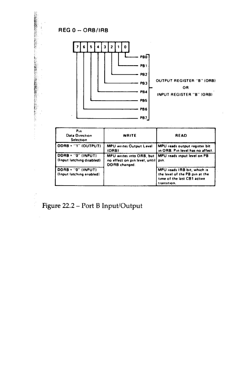
4
01
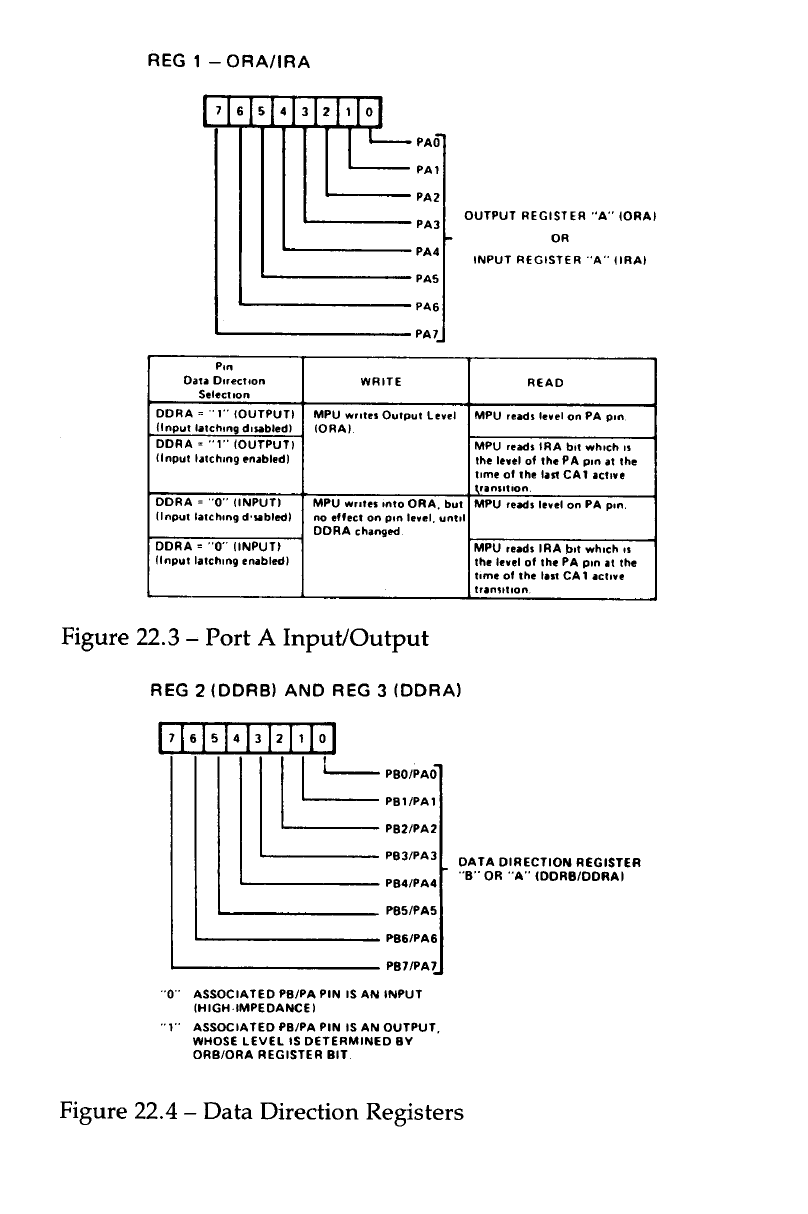
402
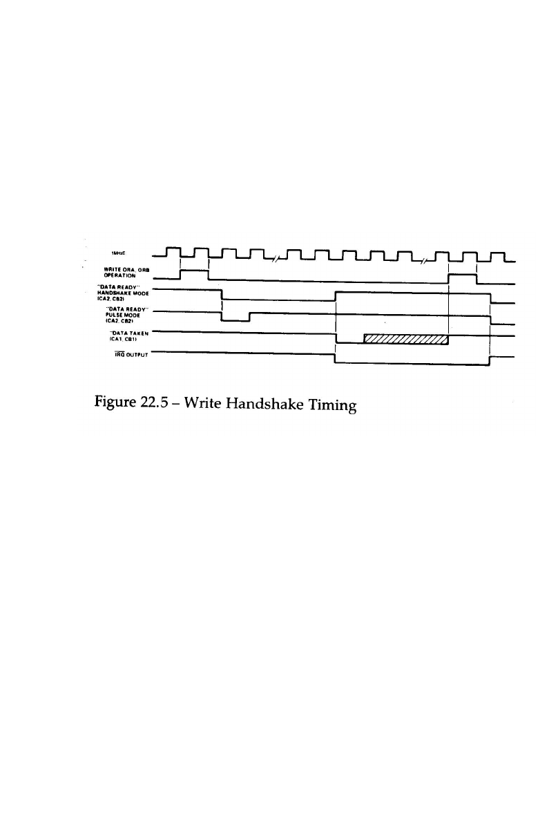
4
03
22.2.2 Write handshaking data transfer
Handshaking allows data transfers between two asynchronous
devices. Write handshaking operates with ‘data ready’ and
‘data taken’ signals. The 6522 provides the ‘data ready’ (CA2 or
CB2) signal and accepts the ‘data taken’ (CA1 or CB1) signal
from the peripheral device. This ‘data taken’ signal sets the
interrupt flag and clears the ‘data ready’ output. See the timing
diagram figure 22.5.
Selection of operating modes for CA1, CA2, CB1 and CB2 is
controlled by the Peripheral Control Register, see figure 22.6.
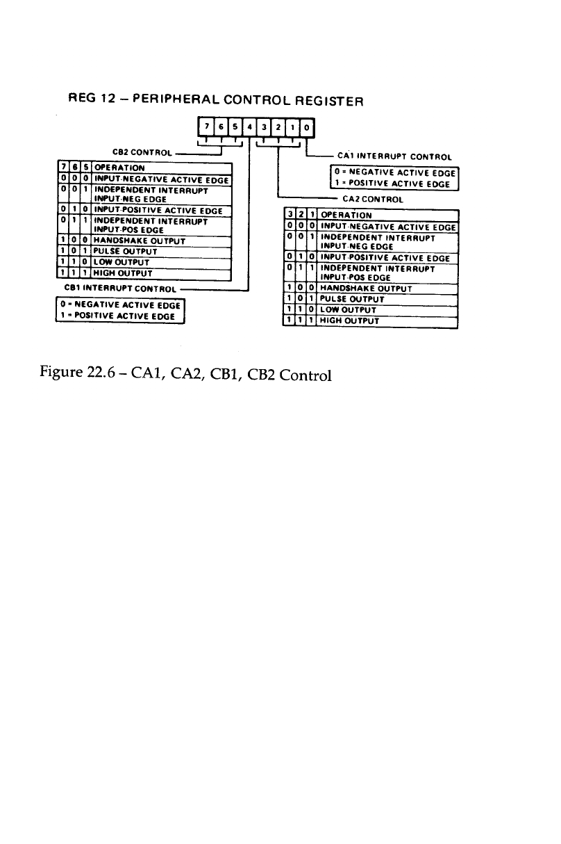
404
22.2.3 Timer operation
The interval timer, referred to from now on as ‘T1’, consists of
two 8 bit latches and a 16 bit counter. After it has been loaded,
the counter decrements at the system clock rate (1 MHz) until it
reaches zero. When it reaches zero, an interrupt flag will be set
and an interrupt will be requested of the 6502, if enabled. The
timer then disables any further interrupts, or automatically
transfers the contents of the latches into the counter and
continues to decrement. The timer may also be programmed to
invert the output level on an output line every time its count
reaches zero. Figure 22.7 and figure 22.8 illustrate the T1
counter and latches.

4
05
22.2.4 Timer 1 one-shot mode
This mode allows a single interrupt to be generated for each
timer load operation. The delay between writing T1C-H and
generation of the interrupt to the 6502 is a direct function of the
data loaded into the counter. T1 can be programmed to produce
a single negative pulse on the PB7 peripheral pin as well as
generating a single interrupt. With output enabled (ACR=1),
writing T1C-H will cause PB7 to go low. PB7 will go high again
when T1 ‘times out’. The overall result of this is a
programmable width pulse on PB7.

406
Writing into the high order latch has no effect on the operation of T1 in
the one-shot mode. It is however necessary to ensure that the low order
latch contains the correct data before initiating the countdown by
writing T1C-H. When the 6502 writes into the high order counter, the
T1 interrupt flag is cleared, the contents of the low order latch are
transferred into the low order counter, and the timer begins to
decrement at 1MHz. If PB7 output is enabled then it will go low after
the write operation. Upon reaching zero, the T1 interrupt flag is set, an
interrupt is generated (if enabled) and PB7 goes high. The counter
continues to decrement at the system clock rate. The 6502 is then able to
read the contents of the counter to determine the time since the
interrupt occurred. The T1 interrupt must be cleared before it can be set
again.
22.2.5 Timer 1 free-run mode
The advantage of having latches which remember the initial value put
into the counter is that the initial value can be restored after the counter
has decremented to zero. If this is done automatically then the timer
enters a free-running mode. In the free-running mode, PB7 is inverted
and the interrupt flag is set each time the counter has decremented to
zero. The contents of the 16 bit latch are then transferred to the counter,
which decrements to zero again and so on. This produces a true square
wave of variable frequency on the PB7 output. The interrupt flag can be
cleared by writing T1C-H. by reading T1C-L, or by writing directly into
the flag as will be described.
All of the timers in the 6522 can be retriggered. This means that
rewriting the value in the counter will always re-initialise the time-out
period. Time-out will therefore be completely inhibited if the processor
continues to rewrite the timer before it reaches zero. T1 operates in this
way if the 6502 writes into the high order counter (T1C-H). If the 6502
only loads the latches, this will not affect the counter until the next time
zero is reached. The timer can be read without affecting its value. This
can be very useful because the new timer time doesn’t come into effect
until zero is reached. If the 6502 responds to each interrupt by
programming a new value into the latches, the period of the next half
cycle on the PB7 output will be determined. Waveforms with complex
mark—space ratios can be generated in this way.
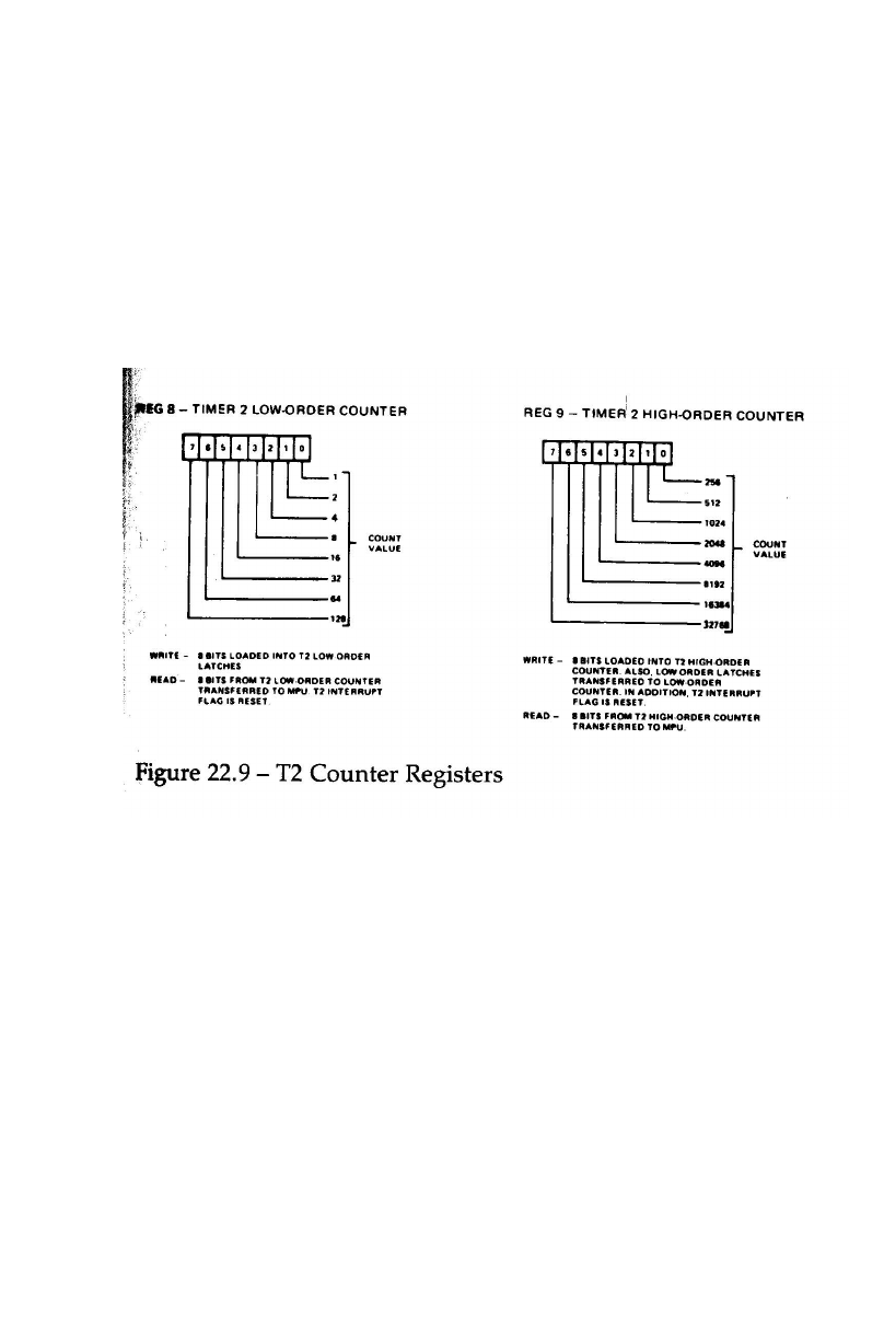
4
07
22.2.6 Timer 2 operation
Timer 2 operates either as an interval timer (in the one-shot
mode only) or as a counter for counting negative pulses on the
PB6 pin. A single control bit in the Auxiliary Control Register
selects between these two modes. Timer 2 comprises a ‘write
only’ low order latch (T2L-L), a ‘read only’ low order counter
and a read/write high order counter. The counter register
contents are decremented at 1 MHz. Figure 22.9 illustrates the
timer 2 counter registers.
22.2.7 Timer 2 one-shot mode
In the one-shot mode, the operation of timer 2 is similar to that
of timer 1. T2 provides a single interrupt for each time out after
T2C-H had been set. The counter continues to decrement after
time-out, but the interrupt is disabled after the initial time-out
so that it will not be set again each time that the timer
decrements through zero. T2C-H must be rewritten to re-enable
the interrupt flag. The interrupt flag is cleared by reading T2C-L
or by writing T2C-H.
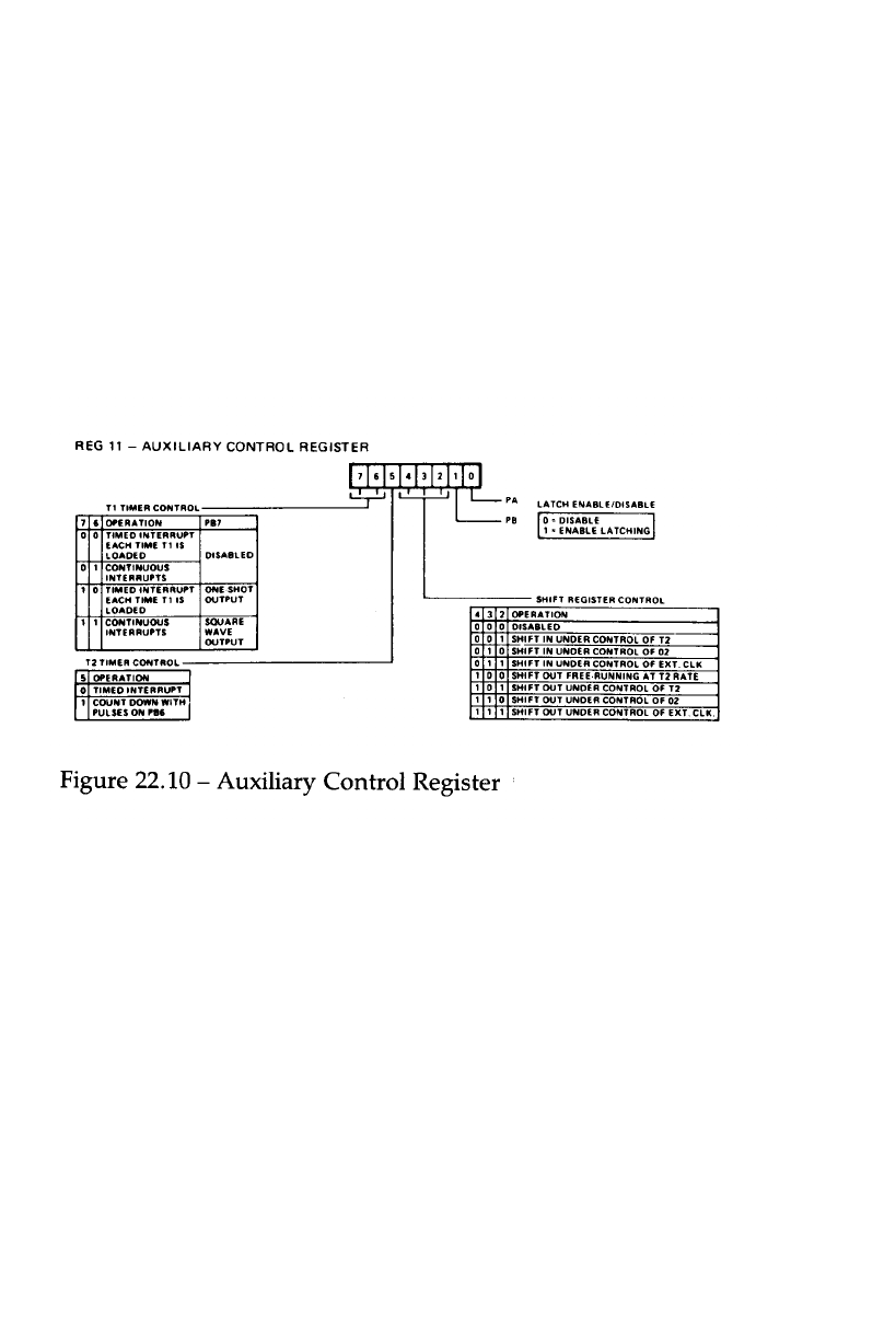
408
22.2.8 Timer 2 pulse counting mode
In this mode, T2 counts a predetermined number of negative
going pulses applied to PB6. This can be accomplished by first
of all loading a number into T2. Writing into T2C-H will clear
the interrupt flag and allow the counter to decrement every
time that a pulse is applied to PB6. The interrupt flag is set
when T2 counts down past zero. The timer continues to
decrement with each pulse applied to PB6. T2C-H must be
rewritten to allow the interrupt flag to set on subsequent down
counts.
22.2.9 Shift register operation
The shift register (SR) enables serial data to be transferred into
and out of the CB2 pin under the control of an internal modulo-
8 counter. Pulses from an external source can be applied to CB1
to shift a bit into or out of CB2. Alternatively, with proper mode
selection, shift pulses generated internally will appear on the
CB1 pin for controlling external devices.
The control bits which select the various shift register operating
modes are located in the Auxiliary Control Register. The
configuration of the SR data bits and the SR control bits of the
ACR are illustrated in figure 22.10 and figure 22.11.
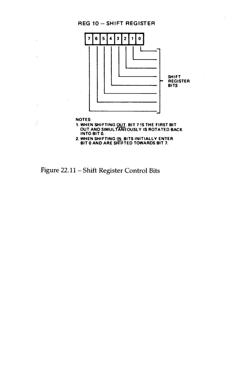
4
09
22.2.10 Shift register modes of operation
Shift Register Disabled (SRMODE 0)
In this mode the SR is disabled. The 6502 can however write or
read the SR and the SR will shift one bit left on each CB1
positive edge. The logic level present on CB2 is shifted into bit
0. The SR interrupt flag is always disabled in this mode.
Shift in under control of T2 (SRMODE 1)
In mode 1 the shifting rate is controlled by the 8 low order bits
of T2. Shift pulses are generated on the CB1 pin to control
shifting in external devices. The time between transitions of this
output clock is controlled by the low order T2 latch.
Reading from or writing to the SR will trigger a shifting
operation if the SR flag in the IFR is set. If it isn’t set then the
first shift will occur when T2 next times out after a read or

410
write SR. Data is shifted first into the low order bit of the SR.
then into the next higher order bit and so on the negative edge
of each shift clock pulse. The input data should then change
before the next positive going edge of CB1. Data is shifted into
the shift register on the positive going edge of the CB1 pulse.
After 8 CB1 clock pulses, the shift register interrupt flag will be
set and an interrupt will be requested of the 6502.
Shift in under control of system clock (SRMODE 2)
In mode 2 the shift rate is a direct function of the 1MHz system
clock. Pulses for controlling external devices are generated on
the CB1 output. Timer 2 has no effect on the SR and acts as an
independent interval timer. The shifting operation is triggered
by reading or writing the SR. Data is first shifted into bit 0 and
then into successively higher order bits on the trailing edges of
system clock pulses. After 8 clock pulses, the shift register
interrupt flag will be set and output clock pulses from CB1 will
cease.

4
11
Shift in under control of external CB1 clock (SRMODE 3)
CB1 is a clock input in mode 3 so that external devices can load
the shift register at their own pace. The shift register counter
will generate an interrupt each time that 8 bits have been
shifted in. The SR counter does NOT stop the shifting operation,
it simply operates as a pulse counter. Reading from or writing
to the shift register resets the interrupt flag and initialises the SR
counter to count another 8 pulses. Note that data is shifted in on
the first system clock cycle following the positive going edge of
the CB1 shift pulse. Data must therefore be held stable during
the first full system clock cycle after CB1 has gone high.
Shift out free running at T2 clock rate (SRMODE 4)
In this mode the shift rate is controlled by timer 2 (T2). Unlike
mode 5, the SR counter will not stop the shifting operation. Shift
register bit 7 is recirculated back into bit 0, so the 8 bits loaded
into the shift register will be clocked onto CB2 repetitively. The
shift register counter is disabled in this mode.

412
Shift out under control of T2 (SRMODE 5)
The shift rate is controlled by T2 as in mode 4. if the SR flag in
the IFR is set, then the shifting operation is triggered by the
read or write of the SR. Alternatively the first shift will occur at
the next timeout of T2 after a read or write of the SR. With each
write or read of the SR. the SR counter is reset and 8 bits are
shifted onto CB2. Eight shift pulses appear on the CB1 output to
facilitate the control of shifting into external devices. When the
8 shift pulses have occurred, shifting is disabled, the SR
interrupt flag is set and CB2 remains fixed at the last data bit
level.
Shift out under control of the system clock (SRMODE 6)
In this mode, the shift rate is controlled directly by the 1MHz
system clock.
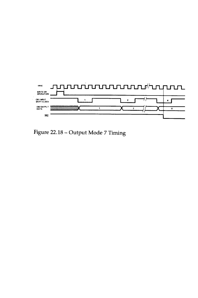
4
13
Shift out under control of external CB1 clock (SRMODE 7)
Shifting is controlled by pulses applied to the CB1 pin by an
external device in this mode. The SR interrupt flag is set each
time that the SR counter counts 8 pulses, but the shifting
function is not disabled. The SR interrupt flag is reset and the
SR counter is initialised to begin counting the next 8 shift pulses
on CB1, each time that the 6502 writes or reads the shift register.
The interrupt flag is set after 8 shift pulses. The 6502 can then
load the next byte of data into the shift register.
22.2.11Interrupt operation
Interrupt flags are set either by an interrupt condition in the
chip (eg. from a counter), or an interrupt condition on an input
to the chip. Interrupt flags normally remain in the set condition
until the interrupt has been serviced. The source of an interrupt
can be determined by reading these interrupt flags in order
from highest priority to lowest priority. This is best performed
by reading the flag register into the processor accumulator,
shifting either right or left and using conditional branch
instructions to detect an active interrupt.
There is an interrupt enable bit associated with each interrupt
flag. If this enable bit is set to a logic 1 and the associated
interrupt occurs, then the 6502 will be interrupted. If the enable
bit is set to 0 then the 6502 will not be interrupted.
All interrupt flags are contained in the interrupt flag register
(IFR — see figure 22.19). To enable the 6502 to check the 6522
without checking each bit in the IFR, bit 7 will be set to a logic
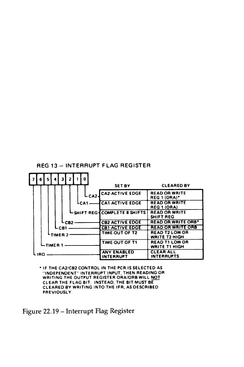
414
1 if the 6522 has generated the interrupt. In addition to reading
the IFR, individual bits may be cleared by writing a 1 into the
appropriate bit of the IFR. Note however that IFR bit 7 is not a
flag as such and will not be cleared by writing a 1 into it. It can
only be cleared by clearing all the flags in the register or by
disabling ALL of the active interrupts.
The 6502 can set or clear selected bits in the interrupt enable
register without affecting the other bits. This is accomplished by
writing to the IER. If bit 7 of the byte written is a 0 then each 1
in bits 0—6 will clear the corresponding bit in the IER. For each
zero in bits 0-6, the corresponding bit will not be affected.
Selected bits can be SET in a similar manner. In this case, bit 7 of
the written byte should be set to 1. Each 1 in bits 0—6 will then
SET the selected bit. A zero will cause the corresponding bit to
remain unaffected. The contents of the IER can be read by the
6502. Bit 7 is then always read as a logic 1.
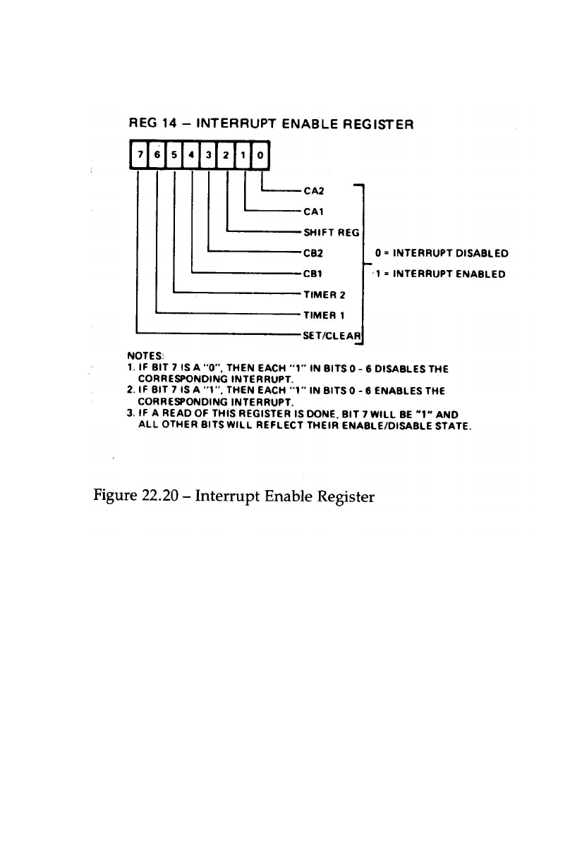
4
15

416

4
17
23 The System VIA
Sheila addresses &40-&4F
The System VIA is responsible for a large amount of control
within the BBC Micro itself. It controls the speech system,
sound system and keyboard. Also, several other sections can be
partially controlled from this VIA. These are the hardware
scrolling, vertical sync pulse interrupt, joysticks input, end of
conversion input from the ADC and a light pen strobe input.
23.1 System VIA line allocation PA0-PA7
The 6502 CPU does not talk to the speech system, sound
generator or keyboard directly over its data bus. Instead, it
writes to and reads from the 8 bit port A I/O lines. This forms a
‘slow’ databus over which the CPU can communicate. To write
to this databus, the data direction register A at Sheila &43
should set all lines as outputs. The 6502 can then write directly
into output register A at Sheila &41. To read from the slow data
bus, DDRA must set all lines as inputs by writing &00 to Sheila
address &43. A direct read from input register A at Sheila &41
can then be made. NOTE that any reading or writing over this
slow databus will have to be done from machine code with ALL
6502 interrupts disabled. This is because the interrupt routines
themselves will make extensive use of the system VIA and keep
changing the register values.
CA1 input
This is the vertical sync input from the 6845. CA1 is set up to
interrupt the 6502 every 20 ms (50 Hz) as a vertical sync from
the video circuitry is detected. The operating system changes
the flash colours on the display in this interrupt time so that
they maintain synchronisation with the rest of the picture.

418
CA2 input
This input comes from the keyboard circuit, and is used to
generate an interrupt whenever a key is pressed. See the
keyboard circuit diagram in Appendix J for more details.
PB0-PB2 outputs
These 3 outputs form the address to an 8 bit addressable latch,
IC32 on the main circuit diagram. See the following
‘Addressable Latch’ section.
PB3 output
This output holds the data to be written to the selected
addressable latch bit.
PB4 and PB5 inputs
These are the inputs from the joystick FIRE buttons. They are
normally at logic 1 with no button pressed and change to 0
when a button is pressed. OSBYTE &80 can be used to read the
status of the joystick fire buttons.
PB6 and PB7 inputs from the speech processor
PB6 is the speech processor ‘ready’ output and PB7 is from the
speech processor ‘interrupt’ output.
CB1 input
The CB1 input is the end of conversion (EOC) signal from the
7002 analogue to digital converter. It can be used to interrupt
the 6502 whenever a conversion is complete. See chapter 26 on
the Analogue to Digital Converter.
CB2 input
This is the light pen strobe signal (LPSTB) from the light pen. It
also connects to the 6845 video processor, see section 18.9. CB2
can be programmed to interrupt the processor whenever a light
pen strobe occurs. See the light pen example in the interrupts
chapter 13.

4
19
23.2 The addressable latch
This 8 bit addressable latch is operated from port B lines 0-3
inclusive. PB0-PB2 are set to the required address of the output
bit to be set. PB3 is set to the value which should be
programmed at that bit. An example illustrating how to use this
latch from BASIC is described in conjunction with the sound
generator, see section 23.5. The functions of the 8 output bits
from this latch are:-
B0 —Write Enable to the sound generator IC
B1 —READ select on the speech processor
B2 —WRITE select on the speech processor
B3 —Keyboard write enable (see Appendix J)
B4,B5 —these two outputs define the number to be
added to the start of screen address in hardware to
control hardware scrolling:-
Mode Size Start of screen Number to B5 B4
add
0,1,2 20K &3000 12K 1 1
3 16K &4000 16K 0 0
4,5 10K &5800 (or &1800) 22K 1 0
6 8K &6000 (or &2000) 24K 0 1
B6 —Operates the CAPS lock LED
B7 —Operates the SHIFT lock LED
23.3 The 76489 sound chip
The sound chip on the BBC microcomputer is in itself a very
simple chip. There are three channels for which the frequency
and volume of output can be defined. There is also a fourth
white noise generator. The output from all of these channels is
automatically mixed on chip. The complex sound commands
available from BASIC are very powerful but require a large
amount of time to process, especially if complex envelopes are
defined. In fast machine code programs it may sometimes be
advantageous to write directly to the sound chip. The example
program shows how this can

420
be done. The data to be written into the sound chip is first of all
put onto the slow databus. Note that interrupts are disabled
before this is started. The sound generator write enable line is
then pulled low for at least 8 µS then pulled high again.
23.3.1 Tone generators
There are 3 tone generators. The frequency of each channel is
determined by 10 bits of data. F9 is the most significant bit. The
frequency of each channel can be calculated as:- frequency =
4000000/32 x 10 bit binary number
The volume level for each channel is variable to 16 different
levels these are:
Bit A3 Bit A2 Bit A1 Bit A0 VOLUME
000015 (MAX)
000114
001013
001112
010011
010110
01109
01118
10007
10016
10105
10114
11003
11012
11101
11110 (OFF)

4
21
23.3.2 Noise generator
The noise generator comprises a noise source and volume
control. The noise generator parameters are defined by three
bits.
FB — this bit when set to ‘0’ causes PERIODIC NOISE to be
generated. When set to ‘1’ it causes WHITE NOISE to be
generated.
Noise frequency control — the noise base frequency can be
defined in 4 possible states by bits NF1 and NF0.
NF1 NF0 FREQUENCY
00low
01medium
10high
1 1 tone generator 1 frequency
23.3.3 Sound chip register address field
R2 R1 R0 Description
0 0 0 Tone 3 frequency
001Tone 3 volume
0 1 0 Tone 2 frequency
011Tone 2 volume
1 0 0 Tone 1 frequency
101Tone 1 volume
110Noise control
111Noise volume

422
23.4 PROGRAMMING BYTE FORMATS
The sound generator is programmed by sending it bytes in the
following format:-
23.4.1 Frequency (First byte)
Register Address Data
Bit 7 6 5 4 3 2 1 0
1R2 R1R0 F3F2F1F0
23.4.2 Frequency (Second byte)
Data
Bit 76543210
0 X F9 F8 F7 F6 F5 F4
Note that the second low order frequency byte may be
continually updated without rewriting the first byte.
23.4.3 Noise source byte
Register Address
Bit 76 5 4 32 1 0
1R2R1R0 XFBNF1NF0
23.4.4 Update volume level
Register Address Data
Bit 76 54 3 2 1 0
1R2R1R0A3A2A1A0

4
23
23.5 Example program for direct control of the sound
generator
10 REM Demonstration of direct poke to Sound chip
20 PROCINIT
30 REPEAT
40 INPUT”Byte to send to sound chip”;A$
50 A% = EVAL(A$)
60 CALL DIRECT
70 UNTIL FALSE
80 DEF PROCINIT
90 DIM Q% 40
100 OSBYTE = &FFF4
110 FOR C=0 TO 3 STEP 3
120 P% = Q%
130 [OPT C
140 .DIRECT SEI \Disable interrupts
150 PHA
160 LDA #&97
170 LDX #&43 \Data direction register A
380 LDY #&FF \Set all B bits as output
190 .JSR OSBYTE \Write to SHEILA OSBYTE CALL
200 LDX #&41 \Output register A
210 PLA
220 TAY \Y holds byte to sound chip
230 LDA #&97 \Write to SHETLA OSBYTE CALL
240 JSR OSBYTE \Output to slow data bus
250 LDX #&40 \Output register B
260 LDY #&00 \Set sound chip write pin low
270 JSR OSBYTE
280 LDY #&08 \Set sound chip write pin high
290 JSR OSBYTE
300 CLI \Enable interrupts
310 RTS: ]
320 NEXT
330 ENDPROC
Run the example program and enter &80, &20 and &90 to
generate a frequency at maximum volume on channel 3.
23.6 The speech chip
The Speech processor can be added as an optional upgrade. It
can be programmed through OSBYTE CALLS &9E, &9F and
SOUND &FFxx. The speech data is held in a special serial
speech ROM. The standard one provided with the Acorn
speech upgrade kit has a selection of words spoken by the
newsreader Kenneth Kendall. It is also possible to purchase
serial ROMs for the speech system which contain games. These
plug into the slot on the left hand side of the keyboard. Again,
system software is available to read data from these ROMs
using OSBYTE calls &9E, &9F and *ROM For more information
about the speech system, refer to the Speech System User
Guide.

424

4
25
24 The User/Printer VIA
Sheila addresses &60-&6F
Full programming details for the 6522 VIA are contained in
chapter 22. This brief section is designed to help anyone who
specifically wishes to use the USER VIA.
24.1 PORT A — The printer port
All of the port A lines PA0-PA7 are buffered before being
connected to the printer connector. This means that they can
only be operated as output lines, but they do have a much
larger drive capacity than do unbuffered lines. CA1 can be used
directly as described in the general section on 6522s, but note
that it is connected to ±5 volts via a 4K7 resistor. CA1 normally
acts as an ‘acknowledge’ line when a printer is used. CA2 is
buffered so that it has become an open collector output only. It
usually acts as the printer STROBE line. Note that CA2 can be
connected directly to the edge connector using link option 1, see
Appendix I.
24.2 PORT B — The user port
All of port B lines, ie PB0-PB7 and CB1, CB2 are available
directly on the user port connector. Chapter 22 explains how
port B can be programmed. The diagram below (figure 24.1)
illustrates the connector. The view is shown looking into the
board mounted connector from outside. Note that wires 1 and
20 are the two outermost wires on the ribbon cable. The ‘female’
part to the connector is a standard 20 way IDC connector. IDC
means ‘insulation displacement connector’. The plug is
normally connected to users’ circuits via a length of special 20
way ribbon cable which is available from most good computing
shops. This cable can be connected to a circuit directly by
soldering the wires to the circuit board, or indirectly by another
IDC plug and header or a DIL header. A DIL header will plug
into any ordinary integrated circuit socket.
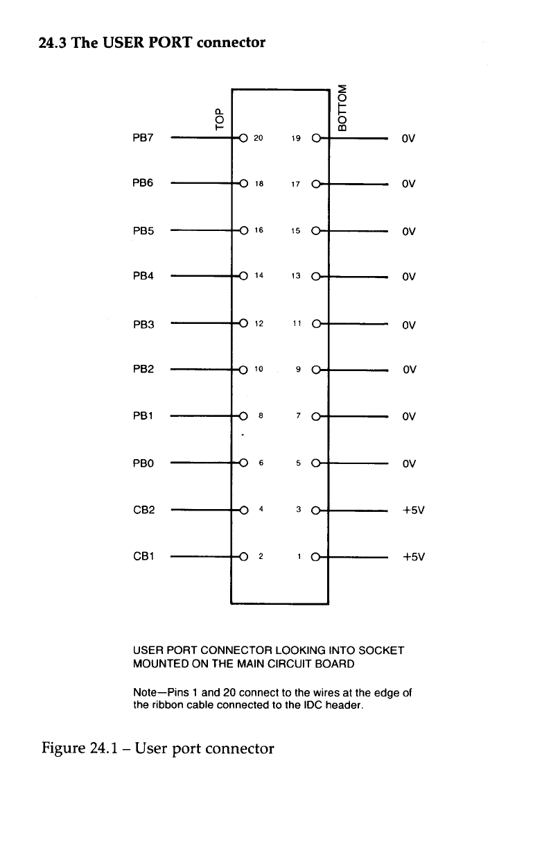
426

4
27
25 Floppy Disc and Econet
Sheila addresses &80-&BF
25.1 The 8271 floppy disc controller — Sheila &80-&9F
The 8271 floppy disc controller chip and its associated
hardware must be fitted to the standard model B before discs
can be used. The upgrade information is in Appendix H. The
function of this chip is to extract data from a disc or to write
data to a disc. Many other tasks have to be performed to ensure
that this one basic task is carried out properly. For example, the
8271 will detect read errors, refuse to write to a ‘protected’ disc,
automatically position the read/write head on the disc drive
plus much more. It is an exceptionally complex chip, but luckily
there are several very powerful filing system and OSBYTE
options available to communicate with the 8271 at a higher level
than sending bits to control registers and examining results bit
by bit. Refer to the Disc System User Guide and chapter 16 on
filing systems for more information about using discs.
This list of 8271 register addresses is included for reference:
Sheila
address Read function Write function
&80 Status register Command register
&81 Result register Parameter register
&82 Reset register
&83 Not used Not used
&84 Read data Write data
(DMA Ack. set) (DMA Ack. set)

428
25.2 The 68B54 Advanced Data Link Controller - Sheila &A0-
&BF
The 68B54 ADLC is the central component in the Econet
Interface circuit. In an Econet system up to 255 BBC
microcomputers can be connected together. The advantage of
doing this is that they may all share expensive peripheral
devices such as discs and printers. This is of immense use in an
educational environment where a large number of users can
have access to expensive peripherals without purchasing them
for each user. Refer to the Econet Manual and OSBYTES &C9,
&CE, &CF, &D0 for more information.
The addresses of registers within the 68B54 are given here for
reference:
Sheila
address Write function Read function
&A0 Control Register 1 Status Register 1
&A1 Control Registers 2,3 Status Register 2
&A2 Transmit FIFO Receive FIFO
(Frame Continue)
&A3 Transmit FIFO Receive FIFO
(Frame Terminate)
25.3 The Econet station ID register — Sheila &20 Read only
This will only be valid for users on an Econet system. Reading
from this register will return the station ID number. This is set
via links S11 to any number between 0 and 255. The Econet data
link controller circuit produces NMIs to the CPU. These
interrupts are automatically enabled by the hardware every
time when the station ID is read.

4
29
26 The Analogue to
Digital converter
Sheila addresses &C0-&C2
The analogue to digital converter (ADC) chip provided in the
BBC microcomputer is a 10 bit integrating converter. It has four
input channels which can be selected under software control.
By applying a voltage of between 0 volts and Vref to the
channel inputs, a 10 bit binary number will be generated which
is directly proportional to the applied voltage. For example
applying a voltage Vref/2 would produce a 10 bit value of
approximately 511. Vref itself corresponds to about
1023.
26.1 Programming the Analogue to Digital converter
The analogue to digital conversion is initiated by writing to the
Data Latch/AD start register at Sheila &CO. Bits Dl and DO
together define which one of the four input channels is selected.
Bit D3 defines whether an 8 bit resolution or a 10 bit resolution
conversion should occur. If set to 0, an 8 bit conversion occurs,
if set to 1 a 10 bit conversion occurs. 8 bit conversions typically
take 4 ms to complete whereas 10 bit conversions typically take
10 ms to complete. Unless high resolution is required, it is often
better to use the fast 8 bit conversion. If enabled, an interrupt
will be generated when the conversion is complete. This
indicates that valid data can be read from the ADC.

430
26.1.1 Channel Summary:-
Bit 1 Bit 0 Channel Designation
control control number in
MOS and
BASIC Master Joystick
0 0 1 Left/Right (low =right)
0 1 2 Up/Down (low =down)
Secondary Joystick
0 3 Left/Right (low =right)
1 4 Up/Down (low =down)
Relevant OSBYTES which write to the ADC are &10, &11 and
&BD.
WRITING TO THE ADC
There is one register in the analogue to digital converter which
can be written to.
26.1.2 Data latch and conversion start — Sheila &C0 Write
only
Writing to this register will select the current input channel and
select an 8 or 10 bit conversion. The operation of writing to this
register automatically initiates a conversion.
Bit 0 and Define the input channel as shown in
Bit 1 section 26.1.1
Bit 2 Flag input, normally set to 0
Bit 3 8 bit mode = 0
10 bit mode = 1
Bits 4-7 not used

4
31
READING FROM THE ADC
There are three registers in the ADC which can be read directly,
the status register and two data registers.
26.1.3 Status Register — Sheila &C0 Read only
Bit 0 and These define the currently selected input channel
Bit 1 as in the AD start register.
Bit 2 not used
Bit 3 8 bit mode = 0 10 bit mode = 1
Bit 4 2nd most significant bit (MSB) of conversion.
Bit 5 MSB of conversion.
Bit6 0 = busy, 1 = not busy
Bit 7 0 = conversion completed
1 = conversion not completed
26.1.4 High data byte — Sheila &C1 Read only
This byte contains the 8 most significant bits of the analogue to
digital conversion.
26.1.5 Low data byte — Sheila &C2 Read only
Bits 7 to bit 4 define the four low order bits of a 12 bit
conversion. In 8 bit only mode, all four bits are inaccurate. In 10
bit mode, bits 7 and 6 are accurate. Bits 5 and 4 are likely to be
inaccurate but this will depend upon the particular qualities of
individual 7002 chips. Bits 3—0 are always set to low.
OSBYTES &80, &BC, &BD and &BE are relevant when reading
from the ADC.
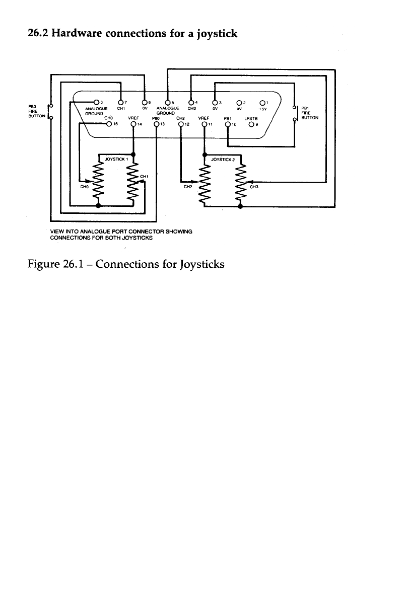
432
A 15 way ‘D’ type connector is provided on the rear of all
model Bs. This is the analogue port connector. The pin
designations and layout are illustrated in figure 26.1.
Connections required for the various joysticks are also
illustrated. Note the two ‘fire’ buttons are there as well. Their
states can be determined using OSBYTE &80.
Apart from giving the information needed to construct
joysticks, this diagram should be helpful to anyone wishing to
be a bit more adventurous with their hardware. One use for the
full 10 bits available would be communication with a graphics
tablet. By using high-quality variable resistors and a series of
pulleys or lever arms, the position of a pointer can be
determined. This would allow high resolution graphic drawing
to be entered into the BBC microcomputer for display on the
high resolution screen. Some other possibilities include
measuring temperature, light level, pH (hydrogen ion
concentration), current, voltage, resistance or pressure.

4
33
27 The Tube
Sheila addresses &E0-&FF
27.1 General introduction to the Tube
The BBC microcomputer is provided with three basic methods
of expansion. The user port and the one megahertz bus are
covered in other chapters. This chapter covers the third
expansion route - the Tube. The Tube itself is just a fast parallel
communication link between two computers. First of all, the
basic fundamentals required of any Tube system are explained
followed by some specific examples of its use with different
processors.
The Tube connector on the BBC microcomputer simply consists
of the system data bus, the lower half of the system address bus
and some miscellaneous control lines. These connect via a
ribbon cable to a second processor card. The second processor is
connected to the Tube interface by a Tube ULA (uncommitted
logic array) chip which has been designed specifically for this
application by Acorn.
The Tube ULA provides a completely asynchronous parallel
interface between the two processor systems. The original BBC
microcomputer is the ‘HOST’ system and the new second
processor forms the heart of the ‘PARASITE’ system. To each
system, the Tube resembles a conventional peripheral device
which occupies 8 bytes of memory or I/O space. Four byte-
wide read only and four byte-wide write only latches are
provided within this address space, together with their
associated control registers.
The byte-wide communication paths fall into two distinct
categories. The first set are simply latches, so data written in on
one side is read out directly on the other side. The second set
are FIFO (first in first out) buffers which store two or more
bytes at a time. These bytes can then be read out on the other
side of the Tube in the same order that they were entered into
the buffer.

434
Data and messages are passed back and forth through the
various registers according to carefully designed software
protocols. Proper allocation of the registers to specific tasks
allows both systems to operate at maximum efficiency. For
example, complex VDU plot and colour fill commands can be
sent via the largest FIFO from the parasite to the host processor.
The parasite processor will not then have to wait for the host to
finish processing the laborious VDU commands before
continuing with its language processing.
27.2 Some second processors and their uses
Currently, three second processors can be used on the Tube.
These are a 6502, Z80 and 16032.
27.2.1 The 6502 Second processor
The 6502B on the Tube is a faster 3MHz version of the 2Mhz
6502A used in the main BBC microcomputer. It is provided
with a full 64K of RAM. When the machine is powered up, the
default language is copied across from the main BBC to the
Tube processor. From then on the main BBC microcomputer
6502A is turned into a servant. Its purpose is that of handling
all input from the RS423, keyboard, joysticks etc. and output to
the screen, sound generator etc. It sends its input across the
Tube to the fast 6502B and executes laborious tasks which the
fast 6502B sends back. All of the processing for languages or
applications packages are performed by the Tube processor.
The advantage is that the work load is shared out. Because the
fast 6502B doesn’t have to worry about interrupts from any of
the devices connected to a BBC microcomputer, it can process at
a very fast speed. The old 6502A does all output like plotting
graphics on the screen, but it doesn’t ever need to do any
language processing. Programs will generally run at almost
twice their original speed.
If the above process sounds rather complex, then don’t worry.
BBC BASIC will appear to operate almost exactly as normal
over the Tube. The major difference will be the extra memory
available. Since all of the screen memory resides in the host
processor, the parasite has all of its memory available for

4
35
program and data storage. Naturally, 16K of the parasite’s RAM
will be required for BASIC, but most of the remaining 48K is
available to the programmer (compared with a maximum of
27K on an ordinary BBC microcomputer). The 16K operating
system ROM stays in the host processor’s memory map and is
not transferred across the Tube.
27.2.2 The Z80 Second processor
Like the 6502, the Z80 is a microprocessor, but with a different
instruction set. It can also operate over the Tube. The set up is
still very similar to that for a 6502 since the Z80 does all
language processing and the BBC microcomputer 6502 does all
of the I/O processing. Machine code programs written to run
on the BBC micro will not operate with a Z80 Tube. However,
the vast amount of Z80 software which is available will operate
on a Z80 Tube machine. The operating system called CP/M is
supplied as standard with all Z80 second processors. There is a
large quantity of CP/M software (business packages, most
languages, games + almost everything else) available on other
CPM machines. Some of this software will operate on the BBC
microcomputer with a Z80 second processor, provided that the
disc format is correct.
27.2.3 The 16032 Second processor
As with the 6502 and Z80 Tubes, the old BBC micro 6502 still
does all input/output and the 16032 runs languages. Unlike the
6502 and Z80 which are both relatively old 8 bit processors, the
16032 is one of a new generation of 16 bit processors. Its internal
structure operates on 32 bits, and it has a very nicely organised
instruction set which is very powerful. With one of these sitting
on the end of the Tube, and a Hard Disc Drive connected to the
host processor, the computing power available will be equal that
available on many mainframe computers. One standard
operating system provided on 16032 Tube machines will be
UNIX.

436

4
37
28 The One Megahertz
bus
28.1 Introduction to the 1MHz bus
There are basically two routes which a user can take towards
adding his own hardware. One of these is the 6522 USER port.
The problem with the USER port is that there are only 8 I/O
lines and a couple of control lines. For more complex
peripherals, direct access to the 6502 address and data buses are
required. This interface is provided by the one megahertz bus.
Physically, the one megahertz bus interface is a 34 pin
connector mounted at the front edge of the main BBC
microcomputer circuit board. It is accessed from underneath the
keyboard. A buffered databus and the lower 8 bits of the
address bus are connected to this socket together with a series
of useful control signals. Whilst the designer could use the one
megahertz bus in innumerable different configurations, Acorn
has defined how the bus should be used to maintain
compatibility with other devices.
The standard uses of the one megahertz bus allow up to 64K
bytes of paged memory to be used as well as 255 direct memory
mapped devices (plus the paging register). ‘FRED’ is normally
assigned as the memory mapped I/O page and ‘JIM’ is
normally assigned as the 64K memory expansion page.
Communication between FRED, JIM and programs should be
implemented using OSBYTEs &92, &93, &94 and &95.
28.2 ‘FRED’ and Memory Mapped Hardware
Page &FC in the BBC microcomputer is reserved for peripherals
with small memory requirements. The initial allocations of
space in FRED are:- &FC00 - &FC0F Test Hardware
&FC10 - &FC13 Teletext
&FC14 - &FC1F Prestel
&FC20 - &FC27 IEEE 488 Interface
&FC28 - &FC2F Acorn Expansion, currently unused

438
&FC30 - &FC3F Cambridge Ring Interface
&FC40 - &FC47 Winchester Disc Interface
&FC48 - &FC7F Acorn Expansion, currently unused
&FC80 - &FC8F Test Hardware
&FC90 - &FCBF Acorn Expansion, currently unused
&FCC0 - &FCFE User Applications
&FCFF Paging Register for JIM
When designing circuits to add on to the one megahertz bus,
the ‘Not page &FC’ (NPGFC) signal together with the lower 8
address lines should be decoded to select the add-on circuit.
Note that a ‘clean up’ circuit will be required on the NPGFC
signal in most applications. This is described in section 28.5. For
very keen constructors who require more than the 63 page &FC
locations reserved for User Applications, either page &FD can
be used for memory mapped peripherals or other FRED
locations can be used. Using reserved FRED locations in this
way will mean that the hardware add-ons specified for those
locations cannot be added in future if user hardware is already
using the slot.
28.3 ‘JIM’ and 64K Paged Memory
28.3.1 General description of JIM
Page &FD in the BBC microcomputer address space is used in
conjunction with the paging register in FRED to provide an
extra 64K of memory. This memory is accessed one page at a
time. The particular page being accessed is selected by the value
in FRED’s paging register, and is referred to as the ‘Extended
page number’. Note that a ‘Not page &FD’ (NPGFD) signal is
available on the one megahertz bus connector. Accessing
memory through the 1MHz bus will generally be about twenty
times slower than accessing memory directly.
28.3.2 Extended page allocation
‘Extended pages’ &00 - &7F in JIM are reserved for use by
Acorn. The other pages &80 - &FF are reserved for user
applications.
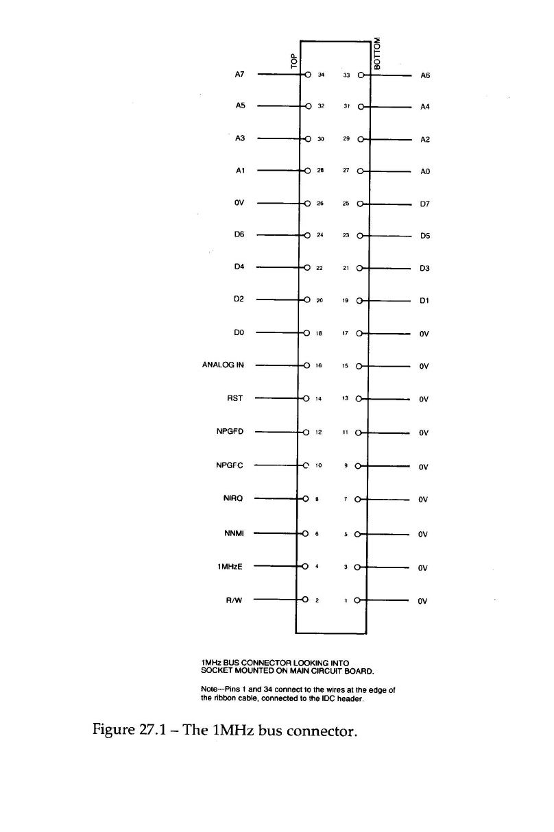
4
39

440
8.4 Bus signal definitions
The one megahertz bus connector is illustrated in figure 28.1.
The specification for the signals on the one megahertz bus are:-
0 volts This is connected to the main system 0
volts line. The reason for putting 0V lines
between the active signal lines is to
reduce the interference between different
signals.
R/W (pin 2) This is the read-not-write signal from the
6502 CPU, buffered by two 74LS04
inverters.
1MHzE (pin 4) This is the 1MHz system timing clock. It
is a 50% duty-cycle square wave. The
6502 CPU is operating at 2MHz, so the
main processor clock is stretched
whenever 1MHz bus peripherals are
being accessed. The trailing edges of the
1MHzE and 2MHz processor clock are
then coincidental. The processor clock is
only ever truly 2MHz when accessing
main memory.
NNMI (pin 6) Not Non-Maskable Interrupt. This is
connected directly to the 6502 NMI input.
It is pulled up to +5 volts with a 3K3
resistor. Use of Non-Maskable Interrupts
on the BBC microcomputer is only
advisable after the chapter on interrupts
has been read and thoroughly
understood. Both Disc and Econet
systems rely heavily upon NMIs for their
operation so take care. Note that NMIs
are triggered on negative going edges of
NMI signals.

4
41
NIRQ (pin 8) Not Interrupt Request. This is connected
directly to the 6502 IRQ input. Any
devices connected to this input should
have open collector outputs. The line is
pulled up to +5 volts with a 3K3 resistor.
Interrupts from the 1MHz bus must not
occur until the software on the main
system is able to cope with them. All
interrupts must therefore be disabled
after a reset. Note that the main system
software may operate very slowly if
considerable use is made of interrupts.
Certain functions such as the real time
clock which is incremented every 10 mS
will be affected if interrupts are masked
for more than this period. Refer to the
chapter on interrupts, section 13.1 for
more information.
NPGFC (pin 10) Not page &FC. This signal is derived
from the 6502 address bus. It goes low
whenever page &FC is written to or read
from. FRED is the name given to this
page in memory and it is described in
more detail in section 28.2.
NPGFD (pin 12) Not page &FD. This signal is derived
from the 6502 address bus. It goes low
whenever page &FD is accessed. JIM is
the name given to this page in memory
and it is in section 28.3.
NRST (pin 14) Not RESET. This is an active low output
from the system reset line. It may be used
to initialise peripherals whenever a
power up or a BREAK causes a reset.

442
Analogue Input This is an input to the audio amplifier on
(pin 16) the main computer. The
amplified signal is produced over the
speaker on the keyboard. Its input
impedance is 9K Ohms and a 3 volt RMS
signal will produce maximum volume on
the speaker. Note however that signals as
large as this will cause distortion if the
sound or speech is used at the same time.
D0 - D7 (pins 18 24) This is a bi-directional 8 bit data bus
which is connected via a 74LS245 buffer
(IC72) to the CPU. The direction of data
transfer is determined by the R/W line
signal. The buffer is enabled whenever
FRED or JIM are accessed.
A0-A7 (pins 27 –34) These connected directly to the lower 8
CPU address lines via a 74LS244 buffer
(1C71) which is always enabled.
28.5 ‘Cleaning up’ FRED and JIM’s page selects
All 1MHz peripherals are clocked by a 1MHz 50% duty cycle
square wave, designated as 1MHzE in figure 28.2. This clock
rate was chosen to allow chips such as 6522 VIAs to use their
internal timing elements correctly. The system 6502 CPU is
normally clocked at twice the speed of the peripherals and so it
operates at 2MHz. However, if the CPU wishes to access any
device on the 1MHz bus, the processor has to be slowed down.
The effect of this slow down circuit is illustrated in figure 28.2.
After generating a valid 1MHz address, the slow down circuit
stretches the clock high period (from ‘T’ to ‘U’). Unfortunately,
two major problems arise from this mode of operation:
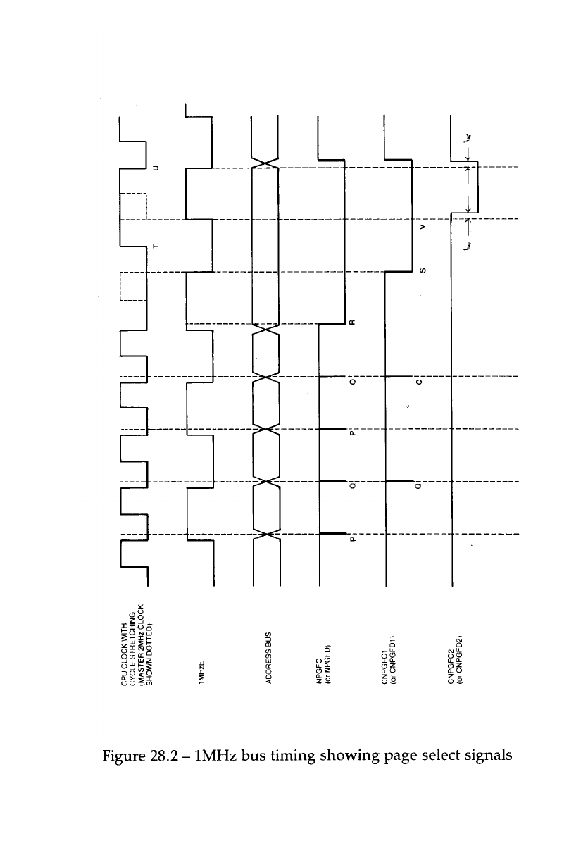
4
43

444
28.5.1 Spurious address decoding ‘glitches’ - PROBLEM 1
Addresses on the system address bus will only usually change
when the 2MHz processor clock is low. However, the 1MHz
clock is alternately low, then high when the CPU addresses
change. This gives rise to the address decoding glitches labelled
‘P’ and ‘Q’ in figure 28.2. The ‘Q’ glitches are not normally
important because the 1MHzE clock is then low. The ‘P’ glitches
can cause problems because the 1MHzE signal is then high.
Spurious pulses may therefore occur on the various chip select
pins, leading to possible malfunction of some devices.
28.5.2 Double accessing of 1MHz bus devices - PROBLEM 2
If a 1MHz bus device is accessed during a period when the
1MHzE clock is high (point ‘R’ in figure 28.2), that device will
be accessed immediately. The device will then be accessed
again when 1MHzE is next high (point ‘V’ in figure 28.2). This is
because the CPU clock is held high until the next coincident
falling edge of the 2MHz and 1MHz clocks (point ‘U’). Double
accessing a peripheral does not normally present a problem.
However, if reading from or writing to a device has some other
function, such as clearing an interrupt flag, a problem may
occur.
28.5.3 ‘Clean up’ circuit 1
This standard ‘clean up’ circuit for the page select signals is
shown in figure 28.3. Three NOR gates are used to create a
standard R-S flip-flop with a gated input. The ‘clean page select’
output (CNPGFC1) can only be set low if 1MHzE is low. The
net effect of the circuit is illustrated in figure 28.2. Both of the
problems outlined above are overcome, since the ‘P’ glitches are
removed and the page select only goes low at ‘5’, after the
1MHzE clock has gone low. The ‘Q’ glitches due to spurious
addresses whilst 1MHzE is low are still there. In most
applications, this will not affect circuit operation, but
occasionally a totally glitch free page select will be required.
Circuit 2 will provide this type of page select.

4
45
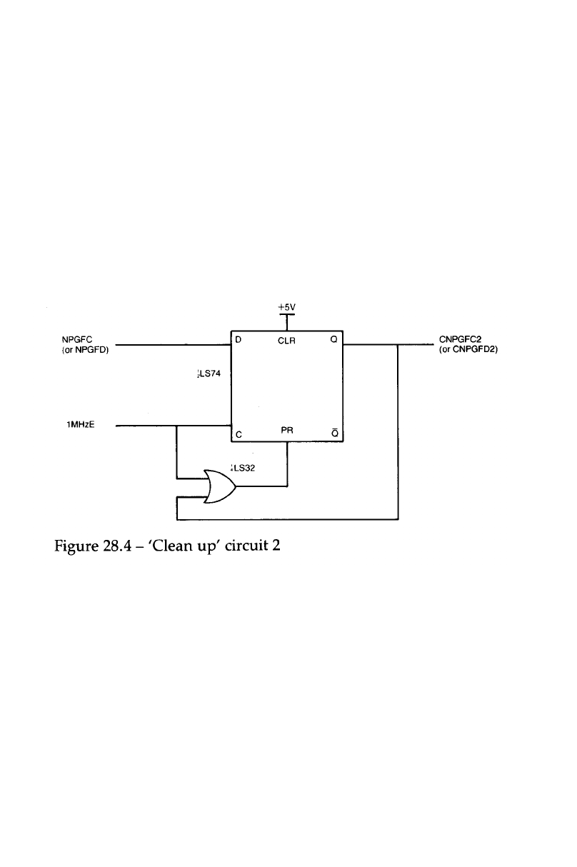
446
28.5.4 ‘Clean up’ circuit 2
In situations in which a 100% ‘clean’ page select signal is
required, circuit 2 which is illustrated in figure 28.4 should be
used. Before CNPGFC can go low, a valid page address with
1MHzE low must occur. The page low is then latched into a D-
type flip-flop on the rising edge of the 1MHzE clock. As shown
in figure 28.2, CNPGFC2 will go low a time lag (40nS) after
1MHzE goes high and it will remain valid until 40nS after
1MHzE has gone low again. Take care if any of the lines on the
1MHz bus are buffered, because delays introduced by buffers
could make data invalid when it is latched. Refer to the precise
timing information in section 28.6.5 for more details.

4
47
28.6 Hardware requirements for 1MHz bus peripherals
All additional hardware designed to operate from the 1MHz
bus must conform to the following standards:
28.6.1 Power supply
No power should be drawn from the BBC microcomputer. All
peripherals should have their own integral power supply, or
use a separate power supply unit.
28.6.2 Logic line loading
No more than one low power Schottky TTL load should be
presented to any of the logic lines by a peripheral. In most
instances, this means that all logic lines will have to be buffered
for each peripheral.
28.6.3 Connection to the BBC microcomputer
Connection to the BBC microcomputer should be via a b00mm
length of 34-way ribbon cable terminated with a 34-way IDC
socket. The 1MHz bus connections should ‘feed through’ the
unit, ie. a 34-way output header plug connector should be
provided so that more devices can be connected as required.
28.6.4 Bus termination
All bus lines except NRST, NNMI and NIRQ should be
provided with the facility for adding optional termination. The
recommended way of terminating lines is to connect each one
to +5V with a 2K2 resistor and to 0V with a 2K2 resistor
28.6.5 Timing requirements
The 1MHz bus timing requirements are illustrated in the timing
diagram, figure 28.5. It should be noted that these timings are
based on the assumption of only one peripheral being attached
to the bus. Heavier loading may extend the rise and fall times of
1MHzE with possible adverse effects on timings.
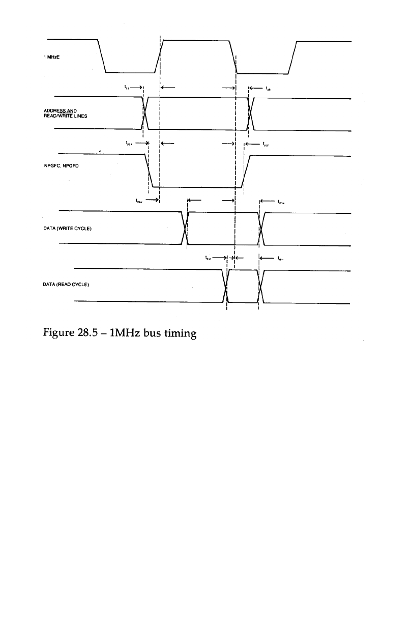
448
The timing requirements are:
Description Symbol Min. Max.
Address (and Read/Write) t as 300nS l000nS
Set-up time
Address (and Read/Write) t ah 30nS -
Hold time
NPGFC & NPGFD Set-up time t pgs 250nS l000nS
NPGFC & NPGFD Hold time t pgh 30nS -
Write data set-up time t dsw —150nS
Write data hold time t dhw 50nS -
Read data set-up time t dsr 200nS -
Read data hold time t dhr 30nS -

4
49
Appendix A - *FX/OSBYTE call index
brief description dec.hex.
*CODE perform *CODE 136 88
*MOTOR perform *MOTOR 137 89
*OPT perform *OPT 139 8B
*ROM perform *ROM 141 8D
*TAPE perform *TAPE 140 8C
*TV perform *TV 144 90
ADC select channels sampled 16 10
force ADC conversion 17 11
read ADC channel 128 80
read current ADC channel 188 BC
read/write max channel number 189 BD
read ADC conversion type 190 BE
BELL/ctrl G read/write BELL channel number 211 D3
read/write BELL envelope number 212 D4
read/write BELL frequency 213 D5
read/write BELL duration 214 D6
BREAK/reset read/write critical region 200 C8
read/write message + !BOOT opts 215 D7
read/write BREAK intercept code 247 F7
+248 F8
+249 F9
read/write last BREAK type 253 FD
read/write start up options 255 FF

450
brief description dec.hex.
buffer flush selected class 15 F
flush particular buffer 21 15
get buffer status 128 80
insert value into buffer 138 8A
get character from buffer 145 91
examine buffer status 152 98
insert char. into I/P buffer 153 99
bus read from FRED 146 92
write to FRED 147 93
read from JIM 148 94
write to JIM 149 95
read from SHEILA 150 96
write to SHEILA 151 97
cursor enable cursor editing 4 4
read text cursor position 134 86
read character at cursor 135 87
read/write cursor editing state 237 ED
Econet read/write net keyboard disable 201 C9
read/write OS call intercept 206 CE
read/write OSRDCH intercept 207 CF
read/write OSWRCH intercept 208 D0
ESCAPE clear ESCAPE condition 124 7C
set ESCAPE condition 123 7D
acknowledge ESCAPE 126 7E
read/write BREAK, ESCAPE effects 200 C8
read/write ESCAPE key value 220 DC
read/write ESCAPE key status 229 ES
read/write ESCAPE effects flag 230 E4
events disable event 13 D
enable event 14 E
explode character definition RAM 20 14
read/write explosion state 182 B6

4
51
brief description dec.hex.
files close EXEC or SPOOL files 119 77
check for EOF of open file 127 7F
fast Tube BPUT 157 9D
read/write CFS timeout counter 176 B0
*TAPE/*ROM switch 183 B7
read/write EXEC file handle 198 C6
read/write SPOOL file handle 199 C7
flashing flashing col. mark duration 9 9
flashing col. space duration 10 A
read/write flash counter 193 C1
read/write mark period count 194 C2
read/write space period count 195 C3
input select I/P stream 2 2
read/write input source 177 B1
keyboard auto—repeat delay 11 B
auto—repeat rate 12 C
reflect keyboard status in LEDs 118 76
write current keys pressed 120 78
perform keyboard scan 121 79
perform keyboard scan from 16 122 7A
read key with time limit 129 81
read key translate address 172 AC
+173 AD
read/write keyboard semaphore 178 B2
read/write auto—repeat delay 196 C4
read/write auto-repeat period 197 C5
read/write net keyboard disable 201 C9
read/write keyboard status 202 CA
read/write TAB key value 219 DB
read/write ESCAPE key value 220 DC

452
brief description dec.hex.
memory character definition RAM 20 14
read high order address 130 82
read top of OS RAM (OSHWM) 131 83
read bottom of display (HIMEM) 132 84
read hypothetical HIMEM 133 85
read/write primary OSHWM 179 B3
read/write current OSHWM 180 B4
read/write ch. explosion state 182 B6
read/write ESCAPE, BREAK effects 200 C5
read/write location &280 240 F0
read/write user OSBYTE location 241 Fl
read/write location &28A 250 FA
read/write location &28B 251 FB
read/write available RAM 254 FE
O.S. version number 0 0
read address of OS variables 166 A6
+167 A7
output select O/P stream 3 3
read/write O/P status 236 EC
paged ROM enter language ROM 142 8E
issue ROM service request 143 8F
read address of ROM pointers 168 A8
+169 A9
read address of ROM information 170 AA
+171 AB
read ROM active at last BRK 186 BA
BASIC ROM number 187 BB
read/write current language no. 252 FC
printer printer destination 55
set printer char. ignored 6 6
printer driver going dormant 123 7B
read/write printer destination 245 F5
read/write character ignored 246 F6

4
53
brief description dec.hex.
RS423 RX baud rate 7 7
TX baud rate 8 8
read/write RS423 mode 181 B5
read /write RS423 use flag 191 BF
read RS423 control flag 192 C0
read/write RS423 handshake 203 CB
read/write I/P suppression flag 204 CC
read/write RS423/cassette select
serial read/write 6850 control reg. 156 9C
read/write IRQ mask, 6850 232 E5
read RAM copy of serial ULA reg 242 F2
soft keys disable cursor editing 4 4
reset soft keys 18 12
read/write key string length 216 D8
read/write &C0 to &CF status 221 DD
read/write &D0 to &DF status 222 DE
read/write &E0 to &EF status 223 DF
read/write &F0 to &FF status 224 E0
read/write function key status 225 E1
read/write SHIFT fn key status 226 E2
read/write CTRL fn key status 227 E3
read/write CTRL+SHIFT fn status 228 E4
read/write consistency flag 244 F4
sound read/write sound suppression 210 D2
speech read from speech processor 158 9E
write to speech processor 159 9F
read/write speech suppression 209 Dl
read speech presence 235 EB
timer read/write timer switch state 243 F3
Tube fast Tube BPUT 157 B9
read Tube presence 234 EA

454
brief description dec.hex.
user user OSBYTE call 1 1
read/write user OSBYTE location 241 F1
vertical sync wait for vertical sync 19 13
VDU read VDU status 117 75
read VDU variable value 160 A0
read address of VDU variables 174 AE
+ 175 AF
read/write VDU queue length 218 D8
VIA/6522 read/write IRQ mask, user VIA 231 E7
read/write IRQ mask, system VIA 233 E9
video flashing col. mark duration 9 9
flashing col. space duration 10 A
wait for vertical sync 19 13
write to ULA palette register 154 9A
write to ULA control register 155 9B
read RAM copy of ULA ctrl reg. 184 B8
read RAM copy of ULA pal. reg. 185 B9
read/write flash counter 193 C1
read/write mark period count 194 C2
read/write space period count 195 C3
read/write lines from page halt 217 D9

4
55
Appendix B — Operating System calls summary
Routine Vector Summary of function
Name Address Name Address
USERV 200 The user vector
BRKV 202 The BRK vector
IRQ1V 204 Primary interrupt vector
IRQ2V 206 Unrecognised IRQ vector
OSCLI FFF7 CLIV 208 Command line interpreter
OSBYTE FFF4 BYTEV 20A *FX/OSBYTE call
OSWORD FFF1 WORDV 20C OSWORD call
OSWRCH FFEE WRCHV 20E Write character
OSNEWL FFE7 ——Write LF,CR to screen
OSASCI FFE3 ——Write character &0D=LF
OSRDCH FFE0 RDCHV 210 Read character
OSFILE FFDD FILEV 212 Load/save file
OSARGS FFDA ARGSV 214 Load/save file data
OSBGET FFD7 BGETV 216 Get byte from file
OSBPUT FFD4 BPUTV 218 Put byte in file
OSGBPB FFD1 GBPBV 21A Multiple BPUT BGET
OSFIND FFCE FINDV 21C Open or close file
FSCV 21E File system control entry
EVNTV 220 Event vector
UPTV 222 User print routine
NETV 224 Econet vector
VDUV 226 Unrecognised VDU commands
KEYV 228 Keyboard vector
INSV 22A Insert into buffer vector
REMV 22C Remove from buffer vector
CNPV 22E Count/purge buffer vector
IND1V 230 Spare vector
IND2V 232 Spare vector
IND3V 234 Spare vector
NVRDCH FFCB ——Non—vectored read char.
NVWRCH FFC8 ——Non—vectored write char.
GSREAD FFC5 ——Read char. from string
GSINIT FFC2 ——String input initialise
OSEVEN FFBF ——Generate an event
OSRDRM FFB9 ——Read byte in paged ROM

456
Appendix C - Key Values Summary
Key/ ASCII INKEY Internal Key No.
character dec. hex. dec. hex. dec. hex.
SPACE 32 20 - 99 9D 98 62
!3321
“34 22
#3523
$3624
%3725
&3826
‘39 27
(4028
)4129
*422A
+432B
, 44 2C -103 99 102 66
- 45 2D -24 E8 23 17
. 46 2E -104 98 103 67
/ 47 2E -121 87 104 68
0 48 30 -40 D8 39 27
1 49 31 -49 CF 48 30
2 50 32 -50 CE 49 31
3 51 33 -18 EE 17 11
4 52 34 -19 ED 18 12
5 53 35 -20 EC 19 13
6 54 36 -53 CB 52 34
7 55 37 -37 DB 36 24
8 56 38 -22 EA 21 15
9 57 39 -39 D9 37 25
: 58 3A -73 B7 72 48
; 59 3B -88 A8 87 57
<603C
=613D
>623E
?633F
@ 64 40 -72 B8 71 47
A 65 41 -66 BE 65 41
B 6642-1019B 10064
C 67 43 -83 AD 82 52
D 68 44 -51 CD 50 32
E 69 45 -35 DD 34 22
F 70 46 -68 BC 67 43
G 71 47 - 84 AC 83 53
H 72 48 -85 AB 84 54
I 73 49 -38 DA 38 26
J 74 4A -70 BA 69 45
K 75 4B -71 B9 70 46
L 76 4C -87 A9 86 56
M 77 4D -102 9A 101 65
N 78 4E -86 AA 85 55
O 79 4E -55 C9 54 36
P 80 50 - 56 C8 55 37
Q 81 51 -17 FE 16 10

4
57
Key/ ASCII INKEY Internal key No.
character dec. hex. dec. hex. dec. hex.
R 82 52 - 52 CC 51 33
S 83 53 -82 AF 81 51
T 84 54 -36 DC 35 23
U 85 55 - 54 CA 53 35
V8656-1009C9963
W 87 57 - 34 DE 33 21
X 88 58 -67 BD 66 42
Y 89 59 -69 BB 68 44
Z 90 5A -98 9E 97 61
[ 91 5B -57 C7 56 38
\ 92 5C -121 87 120 78
] 93 5D -89 A7 88 58
^ 94 5E -25 E7 24 18
_ 95 5F -41 D7 40 28
£9660
a9761
b9862
c9963
d10064
e1016S
f10266
g10367
h10468
i10569
j1066A
k1076B
l1086C
m1096D
n1106E
o1116F
p11270
q11371
r11472
s11573
t11674
u11775
v11876
w11977
x12078
y12179
z122 7A
{1237B
|1247C
}1257D
~1267E

458
Key/ ASCII INKEY Internal Key No.
character dec. hex. dec. hex. dec. hex.
ESCAPE 27 1B -113 8F 112 70
TAB 9 9 -97 9F 86 60
CAPSLOCK - 65 BF 64 40
CTRL -2 FE 1 1
SHIFT LOCK - 81 AF 80 50
SHIFT - 1 FF 0 0
DELETE 127 7F - 90 A6 89 59
COPY -106 96 105 69
RETURN 13 D - 74 B6 73 49
UP CURSOR -58 C6 57 39
DOWN CURSOR - 42 D6 41 29
LEFT CURSOR - 26 E6 25 19
RIGHT CURSOR -122 86 121 79
f0 -33 DF 32 20
f1 -114 8E 113 71
f2 -115 8D 114 72
f3 -116 8F 115 73
f4 -21 EB 20 14
f5 -117 8B 116 74
f6 -118 8C 117 75
f7 -23 E9 22 16
f8 -19 8D 118 76
f9 -120 8E 119 77
Start up option switch (on front of keyboard)
bit 0 9 9
bit 1 8 8
bit 2 7 7
bit 3 6 6
bit 4 5 5
bit 5 4 4
bit 6 3 3
bit 7 2 2

4
59
Appendix D - VDU Code Summary
dec hex CTRL +bytes function
00—0Does nothing
1 1 A 1 Send next character to printer only
2 2 B 0 Enable printer
33C0 Disable printer
4 4 D 0 Write text at text cursor
5 5 E 0 Write text at graphics cursor
6 6 F 0 Enable VDU drivers
7 7 C 0 Make a short bleep (BEL)
8 8 H 0 Move cursor back one character
9 9 I 0 Move cursor forward one character
10 A J 0 Move cursor down one line
11 B K 0 Move cursor up one line
12 C L 0 Clear text area
13 D M 0 Carriage return
14 E N 0 Paged mode on
15 F O 0 Paged mode off
16 10 P 0 Clear graphics area
17 11 Q 1 Define text colour
18 12 R 2 Define graphics colour
19 13 S 5 Define logical colour
20 14 T 0 Restore default logical colours
21 15 U 0 Disable VDU drivers or delete current line
22 16 V 1 Select screen MODE
23 17 W 9 Re-program display character
24 18 X 8 Define graphics window
25 19 Y 5 PLOT K,X,Y
26 1A Z 0 Restore default windows
27 1B [ 0 ESCAPE value
28 1C \ 4 Define text window
29 1D ] 4 Define graphics origin
30 1E * 0 Home text cursor to top left of window
31 1F _ 2 Move text cursor to X,Y
127 7F DEL 0 Backspace and delete

460
Appendix E - Plot Number Summary
0 Move relative to last point
1 Draw relative to last point in current foreground colour
2 Draw relative to last point in logical inverse colour
3 Draw relative to last point in current background colour
4 Move absolute
5 Draw absolute in current foreground colour
6 Draw absolute in logical inverse colour
7 Draw absolute in current background colour
Higher PLOT numbers have other effects which are related to
the effects given by the values above.
8—15 Last point in line omitted when ‘inverted’ plotting used
16—23 Using a dotted line
24—31 Dotted line, omitting last point
32—63 Reserved for Graphics Extension ROM
64—71 Single point plotting
72—79 Horizontal line filling
80—87 Plot and fill triangle
88—95 Horizontal line blanking (right only)
96—255 Reserved for future expansions
Horizontal line filling
These PLOT numbers start from the specified X,Y co-ordinates.
The graphics cursor is then moved left until the first non-
background pixel is encountered. The graphics cursor is then
moved right until the first non-background coloured pixel is
encountered on the right hand side. If the PLOT number is 73 or
77 then a line will be drawn between these two points in the
current foreground colour. If the PLOT number is 72 or 76 then
no line is drawn but the cursor movements are made (these
may be read using OSWORD call with A=&D/13, see chapter
9).

4
61
Horizontal line blanking right
These PLOT numbers can be used to ‘undraw’ an object on the
screen. They have an the opposite effect to those of the
horizontal line filling functions except that the graphics cursor
is moved right only. PLOT numbers 91 and 95 will cause a line
to be drawn from the specified co-ordinates to the nearest
background coloured pixel to the right in the background
colour. PLOT numbers 89 and 93 move the graphics cursor but
do not cause the line to be blanked.

462
Appendix F — Screen mode layouts
MODE 0 Screen layout
Graphics 640 x 256
Colours 2
Text 80 x 32
Registers
R0 Horizontal total &7F (127)
R1 Characters per line &50 (80)
R2 Horizontal sync position &62 (98)
R3 Horizontal sync width &08 (8)
Vertical sync time &02 (2)
R4 Vertical total &26 (38)
R5 Vertical total adjust &00 (0)
R6 Vertical displayed characters &20 (32)
R7 Vertical sync position &22 (34)
R8 Interlace mode bits 0,1 &01 (1)
Display delay bits 4,5 &00 (0)
Cursor delay bits 6,7 &00 (0)
R9 Scan lines per character &07 (7)
R10 Cursor start, blink, type &67 (103)
Cursor start (bits 0-4) &07 (7)
Cursor blink (bit 6) &01 (1)
Cursor type (bit 5) &01 (1)
R11 Cursor end &08 (8)
R12,R13 Screen start address Variable
R14,R15 Cursor position Variable
R16,R17 Light pen position Variable
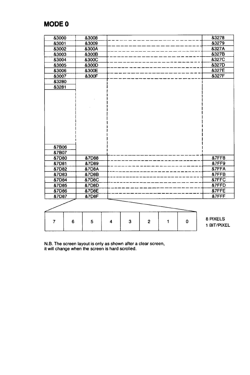
4
63

464
MODE 1 Screen layout
Graphics 320 x 256
Colours 4
Text 40 x 32
Registers
R0 Horizontal total &7F (127)
R1 Characters per line &50 (80)
R2 Horizontal sync position &62 (98)
R3 Horizontal sync width &08 (8)
Vertical sync time &02 (2)
R4 Vertical total &26 (38)
R5 Vertical total adjust &00 (0)
R6 Vertical displayed characters &20 (32)
R7 Vertical sync position &22 (34)
R8 Interlace mode bits 0,1 &01 (1)
Display delay bits 4,5 &00 (0)
Cursor delay bits 6,7 &00 (0)
R9 Scan lines per character &07 (7)
R10 Cursor start, blink, type &67 (103)
Cursor start (bits 0—4) &07 (7)
Cursor blink (bit 6) &01 (1)
Cursor type (bit 5) &01 (1)
R11 Cursor end &08 (8)
R12,R13 Screen start address Variable
R14,R15 Cursor position Variable
R16,R17 Light pen position Variable
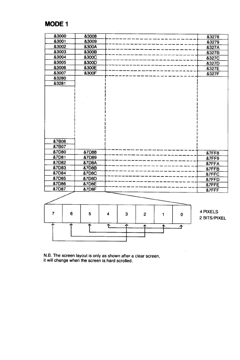
4
65

466
MODE 2 Screen layout
Graphics 160 x 256
Colours 16
Text 20 x 32
Registers
R0 Horizontal total &7F (127)
R1 Characters per line &50 (80)
R2 Horizontal sync position &62 (98)
R3 Horizontal sync width &08 (8)
Vertical sync time &02 (2)
R4 Vertical total &26 (38)
R5 Vertical total adjust &00 (0)
R6 Vertical displayed characters &20 (32)
R7 Vertical sync position &22 (34)
R8 Interlace mode bits 0,1 &01 (1)
Display delay bits 4,5 &00 (0)
Cursor delay bits 6,7 &00 (0)
R9 Scan lines per character &07 (7)
R10 Cursor start, blink, type &67 (103)
Cursor start (bits 0-4) &07 (7)
Cursor blink (bit 6) &01 (1)
Cursor type (bit 5) &01 (1)
R11 Cursor end &08 (8)
R12,R13 Screen start address Variable
R14,R15 Cursor position Variable
R16,R17 Light pen position Variable
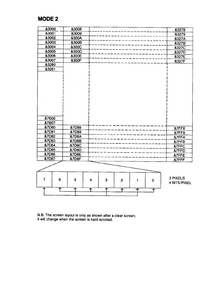
4
67

468
MODE 3 Screen layout
Graphics Not available
Colours 2
Text 80 x 25
Registers
R0 Horizontal total &7F (127)
R1 Characters per line &50 (80)
R2 Horizontal sync position &62 (98)
R3 Horizontal sync width &08 (8)
Vertical sync time &02 (2)
R4 Vertical total &1E (30)
R5 Vertical total adjust &02 (2)
R6 Vertical displayed characters &19 (25)
R7 Vertical sync position &1B (27)
R8 Interlace mode bits 0,1 &01 (1)
Display delay bits 4,5 &00 (0)
Cursor delay bits 6,7 &00 (0)
R9 Scan lines per character &09 (9)
R10 Cursor start, blink, type &67 (103)
Cursor start (bits 0-4) &07 (7)
Cursor blink (bit 6) &01 (1)
Cursor type (bit 5) &01 (1)
R11 Cursor end &09 (9)
R12,R13 Screen start address Variable
R14,R15 Cursor position Variable
R16,R17 Light pen position Variable
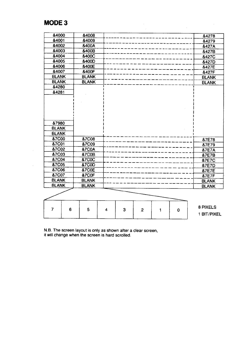
4
69

470
MODE 4 Screen layout
Graphics 320 x 256
Colours 2
Text 40 x 32
Registers
R0 Horizontal total &3F (63)
R1 Characters per line &28 (40)
R2 Horizontal sync position &31 (49)
R3 Horizontal sync width &04 (4)
Vertical sync time &02 (2)
R4 Vertical total &26 (38)
R5 Vertical total adjust &00 (0)
R6 Vertical displayed characters &20 (32)
R7 Vertical sync position &22 (34)
R8 Interlace mode bits 0,1 &01 (1)
Display delay bits 4,5 &00 (0)
Cursor delay bits 6,7 &00 (0)
R9 Scan lines per character &07 (7)
R10 Cursor start, blink, type &67 (103)
Cursor start (bits 0-4) &07 (7)
Cursor blink (bit 6) &01 (1)
Cursor type (bit 5) &01 (1)
R11 Cursor end &08 (8)
R12,R13 Screen start address Variable
R14,R15 Cursor position Variable
R16,R17 Light pen position Variable
4
71

472
MODE 5 Screen layout
Graphics 160 x 256
Colours 4
Text 20 x 32
Registers
R0 Horizontal total &3F (63)
R1 Characters per line &28 (40)
R2 Horizontal sync position &31 (49)
R3 Horizontal sync width &04 (4)
Vertical sync time &02 (2)
R4 Vertical total &26 (38)
R5 Vertical total adjust &00 (0)
R6 Vertical displayed characters &20 (32)
R7 Vertical sync position &22 (34)
R8 Interlace mode bits 0,1 &01 (1)
Display delay bits 4,5 &00 (0)
Cursor delay bits 6,7 &00 (0)
R9 Scan lines per character &07 (7)
R10 Cursor start, blink, type &67 (103)
Cursor start (bits 0-4) &07 (7)
Cursor blink (bit 6) &01 (1)
Cursor type (bit 5) &01 (1)
R11 Cursor end &08 (8)
R12,R13 Screen start address Variable
R14,R15 Cursor position Variable
R16,R17 Light pen position Variable
4
73

474
MODE 6 Screen layout
Graphics Not available
Colours 2
Text 40 x 25
Registers
R0 Horizontal total &3F (63)
R1 Characters per line &28 (40)
R2 Horizontal sync position &31 (49)
R3 Horizontal sync width &04 (4)
Vertical sync time &02 (2)
R4 Vertical total &1E (30)
R5 Vertical total adjust &02 (2)
R6 Vertical displayed characters &19 (25)
R7 Vertical sync position &1B (27)
R8 Interlace mode bits 0,1 &01 (1)
Display delay bits 4,5 &00 (0)
Cursor delay bits 6,7 &00 (0)
R9 Scan lines per character &09 (9)
R10 Cursor start, blink, type &67 (103)
Cursor start (bits 0-4) &07 (7)
Cursor blink (bit 6) &01 (1)
Cursor type (bit 5) &01 (1)
R11 Cursor end &09 (9)
R12,R13 Screen start address Variable
R14,R15 Cursor position Variable
R16,R17 Light pen position Variable
4
75

476
MODE 7 Screen layout
Graphics TELETEXT graphics only
Colours TELETEXT
Text 40 x 25
Registers
R0 Horizontal total &3F (63)
R1 Characters per line &28 (40)
R2 Horizontal sync position &33 (51)
R3 Horizontal sync width &04 (4)
Vertical sync time &02 (2)
R4 Vertical total &1E (30)
R5 Vertical total adjust &02 (2)
R6 Vertical displayed characters &19 (25)
R7 Vertical sync position &1B (27)
R8 Interlace mode bits 0,1 &01 (1)
Display delay bits 4,5 &01 (1)
Cursor delay bits 6,7 &02 (2)
R9 Scan lines per character &12 (18)
R10 Cursor start, blink, type &72 (114)
Cursor start (bits 0-4) &12 (18)
Cursor blink (bit 6) &01 (1)
Cursor type (bit 5) &01 (1)
R11 Cursor end &13 (19)
R12,R13 Screen start address Variable
R14,R15 Cursor position Variable
R16,R17 Light pen position Variable
4
77

478
Appendix G - The American MOS differences
This Appendix outlines the fundamental differences between
the English and American BBC Microcomputers. The hardware
is basically the same in both machines, except for minor
changes in the video circuitry. The software in the MOS is
however somewhat different to cope with the difference in
television display frequency.
G.1 Text display
Both versions of the machine have eight screen modes. The text
resolution in each mode is:
Mode United States Britain
columns x rows columns x rows
0 80x25 80x32
1 40x25 40x32
2 20x25 20x32
3 80x22 80x25
4 40x25 40x32
5 20x25 20x32
6 40x22 40x25
7 40x20 40x25
G.2 Graphics modes
In the U.K version, the MOS regards the screen as 1280 points
horizontally and 1024 points vertically in all modes.
In the U.S version, the MOS regards the screen as 1280 points
horizontally (the same as in the U.K) and 800 points vertically
(compared with 1024 in the U.K).

4
79
G.3 Actual graphics resolution
The graphics resolutions available on the screen in the various
modes are:
Mode United States Britain
Horiz. x Vert. Horiz. x Vert.
0 640 x 200 640 x 256
1 320 x 200 320 x 256
2 160 x 200 160 x 256
3 text only text only
4 320 x 200 320 x 256
5 160 x 200 160 x 256
6 text only text only
7 Teletext Teletext
G.4 Video frame period
In the U.K. the frame sync occurs at 50Hz. In the U.S, the frame
video frame sync occurs at 60Hz.
G.5 Memory usage
The amount of memory used by the screen memory is different
between U.K and U.S machines in some modes. The value of
HIMEM (the top of user memory) is:
Mode United States Britain
0 &4000 &3000
1 &4000 &3000
2 &4000 &3000
3 &4000 &4000
4 &6000 &5800
5 &6000 &5800
6 &6000 &6000
7 &7C00 &7C00

480
Appendix H - Disc Upgrade
Ensure that the following ICs are present:-
IC 78 8271
ICs 79,80 7438
IC 82 74LS10
ICs 81,86 74LS393
ICs 83,84 CD4013B
IC 85 CD4020B
IC 87 74LS123
Disc Filing System in paged ROM socket
OS 1.00 or greater (IC 51)
On issue 1 or 2 circuit boards it will be necessary to connect the
two pads of link S8 with a wire link.
A switch-mode power supply must be present (i.e. not a linear
supply in a black case).
On issue 1, 2 or 3 issue boards, carefully cut the leg of IC 27, pin
9 (do not totally remove the leg). Cut the track connected to this
pin on the component side of the board between IC 27 and IC
89. Reconnect the cut IC leg to the east pad of link S9 with a
short length of insulated wire.
Ensure that the following link selections have been made:-
S18 - NORTH
S19 - EAST
S20 - NORTH
S21 - 2 x EAST/WEST
S22 - NORTH
S32 - WEST
S33 - WEST
On issue 4 boards onwards, remove the connector from S9.
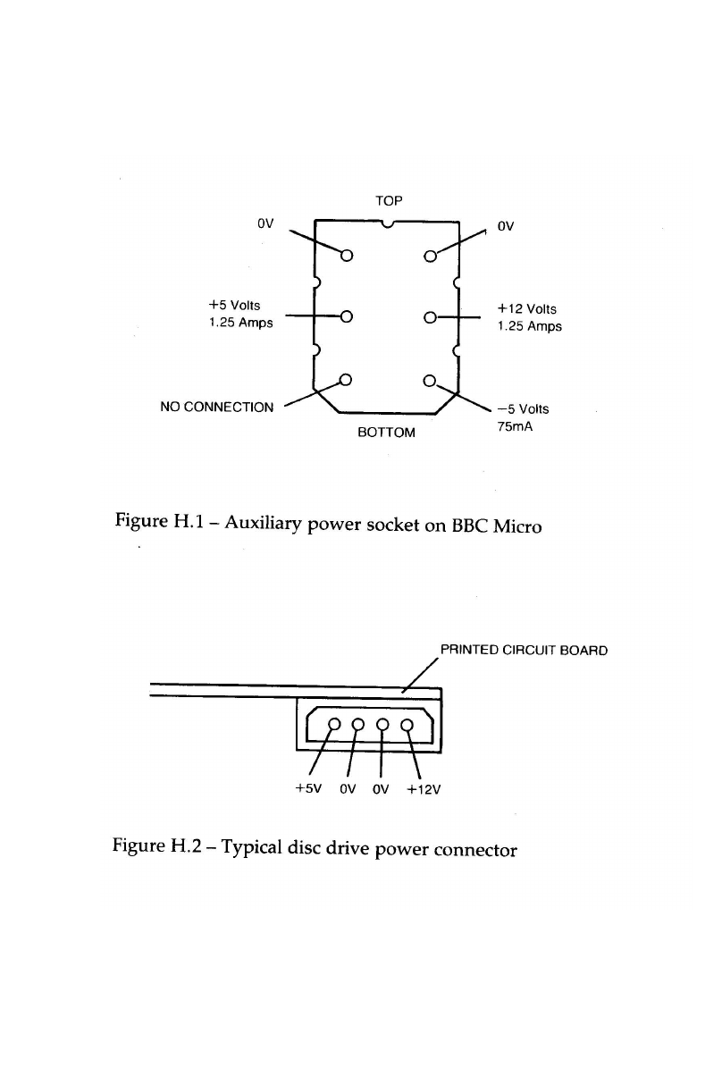
4
81
For details of the power connections see the diagrams below.
Figure H. 1 shows the power supply connector on the BBC
microcomputer. Figure H.2 shows a standard disc drive
connector.
482
Appendix I — Link options

4
83
There are several options which can be selected using the links
on the main circuit board. These generally take one of three
forms, a printed circuit track, a soldered wire link or a plug-in
jumper. In the list which follows, the link positions are
described in points of the compass. On this basis NORTH is the
direction looking from the keyboard towards the back of the
BBC microcomputer. All of the link positions are illustrated in
figure 1.
1. NORTH selects printer strobe on printer
connector.
SOUTH selects 6522 CA2 connected to printer
strobe
TYPE circuit board track
Note not fitted to issues 1—3
2. OPEN enables Econet NMI
CLOSED disables Econet NMI
TYPE wire link
Note NEVER fit this link with 1C91 fitted
3. Selects the clock base frequency for
Econet. This bank of 9 links is only
fitted on issues 1—3
4. EAST 5.25inch DISC select
WEST 8 inch DISC select
TYPE circuit board track
5. NORTH enable Econet clock
SOUTH disable Econet clock
Note only fitted to issues 1—3
6. NORTH divide Econet clock by 2
SOUTH divide Econet clock by 4
Note only fitted to issues 1—3
7. WEST connects pin 30 of 8271 FDC chip to
+5 volts.
EAST connects pin 30 of 8271 FDC chip to 0
volts.

484
8. OPEN disconnects disc head load signal from
PL8
CLOSED connects disc head load signal to PL8
9. OPEN enables disc NMI
CLOSED disables Disc NMI
Note this link must be OPEN when IC78 is
fitted.
10. WEST select 5.25inch disc
EAST select 8inch disc
11 This block of 8 links selects the Econet
ID. The NORTH connection is the least
significant bit. A different Econet ID
will be assigned to each station on an
Econet system. Refer to the Econet
manual for more details.
12. CLOSED connects ROM select line A to 0v
(model A)
OPEN ROM select line is driven by IC76
(model B)
Note do NOT make this link with IC76
fitted
13. CLOSED connects ROM select line B to 0v
(model A)
OPEN ROM select line is driven by IC76
(model B)
Note do NOT make this link with IC76
fitted
14. OPEN enables JIM, disables ROM output
from page &FD
CLOSED disables JIM, enables ROM output
from page &FD
Note link 16 must be CLOSED if link 14 is
OPEN

4
85
15. OPEN enables fast access to page &FD
CLOSED disables fast access to page &FD via
IC23
Note link 15 must be CLOSED when link 17
is OPEN.
16. OPEN enable fast access to page &FC via
IC23
CLOSED disable fast access to page &FC
Note link 16 must be CLOSED if link 14 is
OPEN
17. OPEN disable FRED, enable ROM output
from page &FC
CLOSED enable FRED, disable ROM output
from page &FC
Note link 15 must be CLOSED if link 17 is
OPEN
18. NORTH fast access to IC100 memory chip
SOUTH slow access to IC100 memory chip
19. WEST slow access to memory chips IC52,
IC88 and IC101
EAST fast access to memory chips IC52,
IC88 and IC101
Note diodes D10, D11 and D12 can be
removed to speed up ROMs IC101,
IC88 and IC52 respectively when link
19 is in the WEST position.
20. NORTH ROMSEL provides HIGH ROM select
bit to IC20
SOUTH A13 provides HIGH ROM select bit to
IC20
21. NORTH/SOUTH 1C51 = blocks &08—&0B
x2 IC52, IC88, IC100 & IC101 = blocks
&0C-&0F
EAST/WEST x2 IC5I = blocks &0C—&0F
IC52, IC88, IC100 & IC101 = blocks
&08-&0B

486
22. NORTH ROMSEL provides the LOW ROM
select bit to IC20
SOUTH A12 provides the LOW ROM select bit
to IC20
23. OPEN RS423 DATA line not terminated
CLOSED RS423 DATA line is terminated
Note see Note for link 24
24. OPEN RS423 CTS line not terminated
CLOSED RS423 CTS line is terminated
Note It is not normally necessary to
terminate the RS423 lines unless high
baud rates or long interconnecting
wires are being used.
25. NORTH 32K RAM select (model B)
SOUTH 16K RAM select (model A)
26. WEST NORMAL video output
EAST INVERTED video output
27. WEST 5.25inch disc 8MHz clock select
EAST 8inch disc 16MHz clock select
28. WEST base baud rate select
EAST 1200 baud rate select
Note RS423 rate is affected with link 28 set
EAST
29. WEST 1200 baud rate select
EAST base baud rate select
Note RS423 rate is affected with link 29 set
WEST
30a used to ‘WIRE-OR’ two or more ROM
& select signals
30b Note see links 34—38 and the circuit
diagram.

4
87
31. WEST positive CSYNC to RGB video output
EAST negative CSYNC to RGB video output
32. WEST connects A13 to A13 pin of IC52 and
IC88
EAST connects +5 volts to A13 pin of IC52
and IC88
33. WEST connects A13 to A13 pin of IC100 and
IC101
EAST connects +5 volts to A13 pin of IC100
and IC101
34. OPEN allows the OS ROM to be
‘WIRE-OR’ed
CLOSED use ordinary OS ROM select from
IC20
Note see full circuit diagram for more
details
35. OPEN allows IC52 ROM to be ‘WIRE-OR’ed
CLOSED use ordinary IC52 ROM select from
IC20
Note Link only available on issue 4.
Replaced by R125 in issues 1-3.
36. OPEN allows IC88 ROM to be ‘WIRE-OR’ed
CLOSED use ordinary IC88 ROM select from
IC20
Note Link only available on issue 4.
Replaced by R142 in issues 1-3.
37. OPEN allows IC100 ROM to be
‘WIRE-OR’ed
CLOSED uses IC100 ROM select from IC20
Note Link only available on issue 4.
Replaced by R149 in issues 1-3.

488
38. OPEN allows IC101 ROM to be
‘WIRE-OR’ed
CLOSED uses IC101 ROM select from IC20
Note Link only available on issue 4.
Replaced by R153 in issues 1-3.
39. OPEN standard monochrome monitor
output on BNC socket
CLOSED colour output on BNC video socket
4
89
Appendix J — The keyboard circuit
The keyboard circuit is connected to the main printed circuit
board by two ribbon cables. The larger of these is fitted to all
BBC microcomputers and carries all key pressed and start-up
option data. The smaller one is connected directly to the speech
processor. With the speech system installed, this extra
connector allows serial ROMs to be plugged in to the hole on
the left hand side of the keyboard.
In the lower right hand corner of the keyboard printed circuit
board, there are two rows of eight holes. These are the keyboard
link options. The operation of these links is defined by a made
or unmade connection. The function of each link bit is described
under OSBYTE &FF. The diagram below illustrates the layout
of the links. If a user wishes to vary the settings fairly often, it is
a good idea to buy a standard 8 way SPST switch in a 16 pin
DIL package, and solder it onto the keyboard.
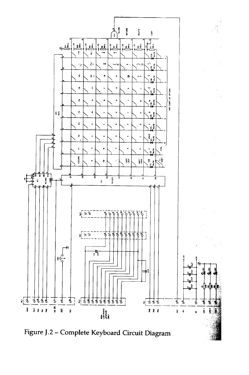
490

4
91
Bibliography
Acorn User Magazine, published monthly, Addison Wesley
6502 Assembly Language Programming, L.A.Leventhal,
OSBORNE/Mc Graw Hill, Berkeley, California
BBC Microcomputer Application Note No.1 - 1MHz Bus, Kim
Spence—Jones, Acorn Computers Ltd., 1982
The BBC Microcomputer User Guide, John Coil, British
Broadcasting Microcomputer, London, 1982
Beebug Magazine, published every five weeks, BEEBUG, P0 Box
109, High Wycombe, Bucks.
HD6845 Cathode Ray Tube Controller Data Sheet, Hitachi
Disc System User Guide, Brian Ward, British Broadcasting
Corporation, London, 1982
Econet System User Guide, British Broadcasting Corporation,
London, 1982
8271 Floppy Disc Controller Data Sheet, Intel Microprocessor &
Memory Data Book, Thomson—EFCIS, 1981
NEC 1982 Catalogue (uPD7002), NEC Electronics (Europe)
GmbH, 1982
Programming the 6502, Rodnay Zaks, Sybex, 1980
Service Manual for the BBC Microcomputer, Acorn Computers
Ltd., Cambridge, 1982
SN76489N Sound Generator Data Sheet, Texas Instruments Inc.,
1978
Speech System User Guide, Acorn Computers Ltd., Cambridge,
1983

492
R6522 Versatile Interface Adapter Data Sheet, Rockwell
International, 1981
TTL Data Book, Texas Instruments Inc., 1980
TMS 6100 Voice Synthesis Memory Data Manual, Texas
Instruments Inc., 1980
TMS 5220 Voice Synthesis Processor Data Manual, Texas
Instruments Inc., 1981

4
93
Glossary
Address Bus — a set of 16 connections, each one of which can be
set to logic 0 or logic 1. This allows the CPU to address &FFFF
(65536) different memory locations.
Active low — signals which are ‘active low’ are said to be valid
when they are at logic level 0.
Analogue to digital converter (ADC) — this is a chip which can
accept an analogue voltage at one of its inputs and provide a
digital output of that voltage. The ADC in the BBC
microcomputer is a 7002.
Asynchronous — two devices which are operating
independently of one another are said to be operating
asynchronously.
Baud Rate — used to define the speed at which a serial data link
transfers data. One baud is equal to I bit of data transferred per
second. The standard cassette baud rate of 1200 baud is
therefore equal to 1200 bits per second.
Bidirectional — a communication line is bidirectional if data can
be sent and received over it. The data bus lines are bidirectional.
Bit of memory — this is the fundamental unit of a computer’s
memory. It may only be in one of two possible states, usually
represented by a 0 or 1.
Buffer — there are two types of buffer in the BBC
microcomputer. A software buffer is an area of memory set
aside for data in the process of being transferred from one
device or piece of software to another. A hardware buffer is put
into a signal line to increase the line’s drive capability. For
example, the printer port has buffered outputs which are
capable of supplying several milliamperes. The inputs to the
buffer could only supply microamperes.

494
Byte of memory — 8 bits of memory. Data is normally
transferred between devices one byte at a time over the data
bus.
Chip — derived from the small piece of silicon wafer or chip
which has all of the computer logic circuits etched into it. A
chip is normally packaged in a black plastic case with small
metal leads to connect it to the outside world.
Clock — since there are so many devices in the BBC
microcomputer, it is necessary to provide some master timing
reference to which all data transfers are tied. The clock provides
this synchronisation. A 2MHz clock is applied to the CPU, but
this can be stretched into a 1MHz clock when slow peripherals
such as the 6522s are being accessed. See chapter 28 on the
1MHz bus for more details about cycle stretching.
CPU (Central processing unit) — the 6502A in the BBC
microcomputer. It is this chip which does all of the computing
work associated with running programs.
Cycle — this is usually applied to the system clock. A complete
clock cycle is the period between a clock going high, low, then
high again. See ‘clock’.
Data bus — a set of eight connections over which all data
transactions between devices in the BBC microcomputer take
place.
Field — a space allocated for some data in a register, or in a
program listing. For example, in an Assembly language
program, the first few spaces are allocated to the line number
field, the next few spaces are allocated to the label field, and so
on.
Handshaking — this type of communications protocol is used
when data is being transferred between two asynchronous
devices. Two handshaking lines are normally required. One of
these is a ‘data ready’ signal from the originating device to the
receiving device. When the receiving device has accepted the
data, it sends a ‘data taken’ signal back to the originating
device, which then knows that it can send the second lot of data
and so on.

4
95
High — sometimes used to designate logic ‘1’
Interrupt — this signal is produced by peripheral devices and is
always directed to the 6502A CPU. Upon receiving an interrupt,
the 6502 will normally run a special interrupt routine program
before continuing with the task in hand before it was
interrupted.
Latch — a latch is used to retain information applied to it after
the data has been removed. It is rather like a memory location
except that the outputs from the bits within the latch are
connected to some hardware.
LED (Light emitting diode) — acts like a diode by only allowing
current to pass in one direction. Light is emitted whilst current
is passed.
Low — sometimes used to designate logic ‘0’.
Machine code — the programs produced by the 6502 BASIC
Assembler are machine code. A machine code program consists
of a series of bytes in memory which the 6502 can execute
directly.
Mnemonic — the name given to the text string which defines a
particular 6502 operation in the BASIC assembler. LDA is a
mnemonic which means ‘load accumulator’.
Opcode — the name given to the binary code of a 6502
instruction. For example, &AD is the opcode which means ‘load
accumulator’.
Open Collector — this is a characteristic of a transistor output
line. It simply means that the collector pin of the transistor is
not driving a resistor load, ie it is ‘open’.
Operand — a piece of data on which some operation is
performed. Usually the operand will be a byte in the
accumulator of the 6502, or a byte in some memory location.

496
Page — a page of memory in the 6502 memory map is &100 (256)
bytes long. There are therefore 256 pages in the entire address
space. 256 pages of 256 bytes each account for the 65536 bytes of
addressable memory.
Parallel — parallel data transfers occur when data is sent along
two or more lines at once. The system data bus for example has
eight lines operating in parallel.
Peripheral — any device connected to the 6502 central processor
unit, such as the analogue port, printer port, econet interface
disc interface etc., but not including the memory.
Poll — most of the hardware devices on the BBC microcomputer
generate interrupts to the 6502 CPU. If interrupts have been
enabled, the CPU has to find out which device generated the
interrupt. It does this by successively reading status bytes from
each of the hardware devices which could have caused an
interrupt. This successive reading of devices is called ‘polling’.
RAM (Random access memory) — the main memory in the BBC
microcomputer is RAM because it can be both written to and
read from.
Refresh — all of the memories in the BBC microcomputer are
dynamic memories. This means that they have to be refreshed
every few milliseconds so that their data is not lost. The
refreshing function is performed by the 6845 as it accesses
memory regularly for video output.
Register — the 6502 and many of the peripheral devices in the
BBC microcomputer contain registers. These are effectively one
byte memory locations which do not necessarily reside in the
main memory map. All software on the 6502 makes extensive
use of the internal registers for programming. The bits in most
peripheral registers define the operation of a particular piece of
hardware, or tell the processor something about that
peripheral’s state.

4
97
Rollover — this is a function provided on the keyboard to cope with
fast typists. Two keys can be pressed at once. The previous key with a
finger being removed, and the next key with the finger hitting the key.
The software in the operating system ensures that rollover normally
operates correctly. It doesn’t operate at all when the shift key is held
down.
ROM (Read only memory) — as the name implies, ROM can only be
read from and cannot be modified by being written to. The MOS and
BASIC plus any resident software in the BBC microcomputer are held
in ROMs.
Serial — data transmitted along only one line is transmitted serially.
Serial data transmission is normally slower than parallel data
transmission, because only one bit instead of several bits are
transferred at a time.
Stack — a page of memory in the 6502 used for temporary storage of
data. Data is pushed onto a stack in sequence, then removed by
pulling the data off the stack. The last byte to be pushed is the first
byte to be pulled off again. The stack is used to store return addresses
from subroutines. Page &01 is used for the stack in the BBC
microcomputer.
Transducer — a device which converts some analogue quantity such
as temperature, humidity or gas concentration into another quantity,
usually voltage or current, which can be measured by a computer.
Tristate — in the BBC microcomputer, it is often necessary to connect
the outputs of several chips together. At any one time only one of the
chips should have priority. If the other chips were allowed to be in the
opposite logic state, the power supplies would effectively be shorted
through the chips. A special tristate level is therefore provided on
some chips in which the output doesn’t care if it is high or low.
ULA (Uncommitted logic array) — these are special chips which
contain a large number of logic gates. The connection between the
gates is defined when the chip is manufactured. Acorn have produced
two special ULAs, on containing most of the serial circuitry, the other
containing some of the video circuitry.

498

4
99
Index *SPOOL 20
file closing 141
file handle 204
!BOOT 218 OSFSC 344
*. 12 paged ROM service call 324
*/ 12 *T. 20
OSFSC 343 *TAPE 20,164,192
*B. 12 *TAPE12 20
*BASIC 12 *TAPE3 20
*CAT 12 *TV 20,168
OSFSC 344 OS variable locations 272
ROM filing system 349 *| 12
*CO. 13 16032 second processor 435
*CODE 13 1MHz bus see One megahertz bus
user vector 256 6502
*E. 14 break flag 42
*ENABLE 14 bug 37
OSFSC 345 carry flag 41
*EXEC 14 decimal mode flag 42
file closing 141 instruction 43
file handle 203 instruction set 41
files closed at ESCAPE 149 interrupt disable 41
OSFSC 344 mnemonics 43
paged ROM service call 324 negative flag 42
*F. 15 overflow flag 42
*FX 15 program counter 42
summary table 111 second processor 434
*FX calls 109 stack pointer 42
*H. 15 status register 41
*HELP 15 unused flag 42
paged ROM service call 323 zero flag 41
*KEY 15 6522
*L. 18 versatile interface adapter 395
*LI. 16 6845
*LINE 16 address register 360
user vector 256 characters per line 361
*LOAD 18 cursor blanking 366
*M. 18 cursor positions 367
*MOTOR 18,161,393 cursor shape 366
*O. 18 display blanking 365
*OPT 18,163 fast animation 373
OSFSC 343 horizontal sync 362
ROM filing system 349 horizontal timing 361
*R. 19 interlace control 364
*REMOTE 206 introduction 359
*RO. 19 lightpen software 369
*ROM 165,192 lightpens 367
filing system 19 number of character rows 363
paged ROM service calls 324 programming 360
paged ROM software 330 register summary 375
ROM filing system 349 scan lines per character 366
*RUN 19 screen display start address 370
address 13 scrolling 371
OSFSC 344 scrolling example 374
*S. 19 vertical sync 362,363
*SAVE 19 vertical timing 362
*SP. 20 wrap around 373

500
6850 EQUB,EQUW,EQUD,EQUS 26
IRQ bit mask 229 errors 24
6850 ACIA forward referencing 25
read/modify control register 175 from BASIC 21
76489 label 23,25
sound chip 419 listing 24
location counter 25
A macros 29
Absolute addressing 36 mnemonics 43
Absolute, X or Y addressing 37 operand 23
Accumulator 41 OPT (options) 24
Accumulator addressing 35 syntax 23
Active low 493 two pass 25
Actual colours 382 Asynchronous 493
ADC 493 Auto-repeat
conversion complete event 290 countdown timer in zero page 270
page two locations 273 countdown timer queue 273
ADC (Add with Carry) 44 Auto-repeat delay
ADC channel keyboard 127
read current channel 196 Auto-repeat rate 128
read maximum channel number 197 Available RAM 245
ADC channel read 151
ADC conversion forcing 133 B
ADC conversion type 198 Backslash
ADC end of conversion 418 in assembler programs 23
ADC number of channel select 132 BASIC
Address bus 493 level 1 21
Addressable latch 419 level 2 21,26
Addressing new 21
absolute 36 ROM socket with BASIC 195
absolute, X or Y 37 Baud rate 493
accumulator 35 Baud rate selection for RS423 123,124
immediate 36 BCC (Branch on Carry Clear) 47
implicit 35 BCD 33
indexed 37 BCS (Branch on Carry Set) 48
indirect 37 BELL
modes 35 channel 214
post-indexed indirect 39 duration 217
pre-indexed indirect 38 frequency 216
relative 40 sound 215
zero page 36 BEQ (Branch on result zero) 49
zero page, X or Y 38 BGETV
ADVAL 151 OSBGET 338
American MOS Bibliography 491
differences from UK 478 Bidirectional 493
Analogue to digital converter 429,493 Binary 31
joystick connection 432 Binary Coded Decimal 33
AND (Logical AND) 45 Bit 493
Animation BIT (Test memory hits) 50
fast hardware 373 BMI (Branch if negative) 51
ARGSV BNE (Branch if not zero) 52
OSARGS 337 BPL (Branch on positive result) 53
ASL (Arithmetic Shift Left) 46 BPUT
Assemb1er fast for Tube 176
addressing modes 35 BPUTV
conditional assembly 29 OSBPUT 339
delimiters 22
EQU 26

5
01
BREAK 166 Cassette critical flag
effect control 205 zero page location 270
intercept code 241 Cassette filing system see CFS
status of last BREAK 244 Cassette LED 393
Break flag 42 Cassette motor
Break vector 257 control of 161
BRK Cassette Port
handling errors 28 example input program 314
paged ROM service call 322 example output program 312
pointer in zero page 272 reading form user software 313
BRK (errors) software control 311
reading active ROM after 194 Cassette relay 18,393
BRK (Forced interrupt) 54 Cassette tape format 347
BRK vector 257 Cassette RS423 selection flag 210,393
BRKV 257 Catalogue
Buffer 493 *CAT 13
count/purge vector 264 CFS 346
examine status 171 page three work space 278
flush class of buffer 131 page two work space 274
flush specific buffer 138 software select switch 192
input code interpretation 224 tape format 347
insert character 172 timeout counter 185
insert vector 263 CFS options byte
insertion into 162 zero page location 269
read status 151 CFS status byte 269
remove vector 263 Character definition OSWORD 251
removing characters from 169 Chip 494
RS423 buffer limit 208 CLC (Clear carry flag) 57
Buffer CLD (Clear decimal flag) 58
page eight addresses 280 CLI (Clear interrupt disable flag) 59
Buffer busy flags Clock see system clock
page two locations 274 Clock (electronic) 494
Buffer indices 274 Clocks in software 237
Buffers Closing files
events 289 OSFIND 342
flushing at ESCAPE 149 CLV (Clear the overflow flag) 60
Bug CMP (Compare memory with A) 61
in the 6502 37 CNPV 264
in the cassette system 393 Colour code
Bus 355 selection in ULA 378
1MHz 437 Colour palette
Bus signals read OSWORD 251
clock 355 selection in ULA 379
interrupt 355 write OSWORD 252
read/write 355 Colours
reset 355 actual 382
BVC (Branch if overflow clear) 55 flashing 125,126
BVS (Branch if overflow set) 56 logical 380
Byte 494 Command-line interpreter (CLI) 107
Command-line interpreter 11
CControl codes
CALL insertion into text 16
from BASIC 28 Countdown timer see interval timer
Carry flag 32,41,89 CPU (Central processing unit) 494
Cassette CPX (Compare memory with X) 63
buffer storage 280 CPY (Compare memory with Y) 64
bug 393 CRC 348
interblock gaps 18 CRTC video controller see 6845

502
CTRL G Error handling
channel 214 after a BRK 28
duration 217 BRK vectoring 257
frequency 216 using BRK 54
sound 215 ESCAPE
Cursor effect control 205
editing status 233 event 172
position 367 Escape 292
position of text cursor 158 flag 147
positions storage in page 3 275 ESCAPE
reading graphics cursors 252 providing escape action 227
shape 366 read/write flags 228
Cursor control returning an ASCII value 227
in video ULA 379 Escape character
Cursor editing 120 insertion into text 16
Cursor keys ESCAPE character read/write 223
defining as soft keys 120 ESCAPE condition acknowledge 149
Cycle (Clock) 494 ESCAPE condition clear 147
Cycle numbers 334 ESCAPE condition set 148
Cyclic redundancy checking 348 ESCAPE flag
zero page location 272
DEvent
Data bus 494 ESCAPE 172
Data carrier detect 313 keyboard 172
DCD see data carrier detect Event disable
DEC (Decrement memory by one) 65 ADC conversion complete 129
Decimal flag 33, 90 character entering buffer 129
Decimal mode flag 42 ESCAPE pressed 129
Default input buffer full 129
messages 13 interval counter crossing 0 129
Default vector table 265 network error 129
DEX (Decrement X by one) 66 output buffer empty 129
DEY (Decrement Y by one) 67 RS423 error 129
Directories 333 start of vertical sync 129
Disc drive timings 246 user 129
Disc filing system 350 Event enable
Disc upgrades 480 ADC conversion complete 130
character entering buffer 130
ESCAPE pressed 130
E input buffer full 130
Econet interval counter crossing 0 130
event 293 network error 130
hardware 427 output buffer empty 130
OS call interception status 211 RS423 error 130
read character status 211 start of vertical sync 130
write character status 211 user 130
zero page work space 267 Event vector 258,288
Econet filing system 351 Events 287
Econet vector 260 ADC conversion complete 290
Editing status of cursor 233 character entering input buffer 290
Editing using the cursor 120 disabling 129
Electrical specification for 6522 398 Econet error 293
End-of-conversion for ADC 418 enabling 130
End-of-file check 150 ESCAPE condition detected 292
Envelope command OSWORD 250 generator of using OSEVEN 107
EOR (exclusive OR memory with A)68 handling routines 288
EQU input buffer full 289
in assembler programs 26 interval timer crossing zero 291

5
03
output buffer empty 289 RS423 input suppression 209
page two flags 273 RS423 use 199
RS423 error 292 RS423/cassette selection 210
user 293 soft key consistency 238
vertical sync 291 user 117, 235
EVNTV 258, 288 Flags
Example determining ESCAPE effects 228
hardware scrolling 374 Flashing
MODE 8 implementation 383 control in ULA 378
Exploring soft character RAM 136 Flashing colours 173
Extended duration of 1st colour 125
messages 13, 18 duration of 2nd colour 126
Extended vector space 281 read/write flash counter 201
Extended vectors 326 read/write mark period 201
read/write space period 201
FFloppy disc
Field 494 hardware 427
File attributes upgrade 480
OSFILE 336 Flushing buffers 131
File handle for *EXEC file 203 Font
File handle for * SPOOL file 204 reading character definitions 251
File options 163 storage 281
Files 333 Font
Files opening/closing flags on page 2 278
OSFIND 342 Font explosion
FILEV pages ROM service call 325
OSFILE 335 read definition state 191
Filing system FRED
messages 18 expansion bus 437
Filing systems 333 reading and writing 170
control vector 343 Function keys
cycle numbers 334 plus CTRL 225
directories 333 plus SHIFT 225
files 333 plus SHIFT+CTRL 225
initialise paged ROM call 325 soft key status 225
paged ROM implementation 328
Tube 345 G
zero page work space 268 Get Byte
FINDV OSBGET 338
OSFIND 342 Graphics
Fire buttons on joysticks 418 OS ROM table 282
Flag Graphics byte mask
6502 break 42 zero page location 268
6502 carry 41 Graphics colour bytes
6502 interrupt disable 41. zero page locations 268
6502 negative 42 Graphic colour cell 269
6502 overflow 42 Graphics cursor OSWORD 252
6502 unused 42 Graphic origin
6502 zero 41 storage in page 3 275
carry 32, 89 GSINIT 105
decimal 33,90 GSREAD 106
escape 147
indicating speech present 231 H
indicating Tube presence 230 Handshaking 494
interrupt disable 59, 91 Hard BRK 244
overflow 32, 60 Hardware
printer destination 239 introduction 353
read RS423 control flag 200 screen wrap around 419

504
High order address 154 J
HIMEM 156 JIM
Host processor 433 expansion bus 438
reading and writing 170
IJMP (Jump to new location) 72
I/O processor memory Joysticks
read OSWORD 249 connections 432
write OSWORD 249 fire buttons 418
Immediate addressing 36 JSR (Jump subroutine) 73
Implicit addressing 35
INC (Increment memory by one) 69 K
Index registers 41 Key
indexed addressing 37 read with time limit 153
Indirect addressing 37 Key number table 142
INKEY 153 Key numbers
INKEY countdown timer summary 456
page two location 273 Keyboard
Input buffer (OSWORD 1) auto-repeat delay 127
zero page location 270 auto-repeat rate 128
Input line OSWORD 248 buffer status 151
input stream selection 118 control vector 262
Instruction disable 206
6502 43 empty keyboard buffer 138
cycle 43 event 172
Instruction set for the 6502 41 function keys f0-f9 225
INSV 263 input buffer storage 279
Interlace 168,20 input select 186
Internal key numbers table 142 insert character in buffer 172
Interrupt 495 interrupts 187
bit masks 229 LEDs 139
disable flag 41, 59, 91 links 246
forced 54 locking 206
return from 86 read status 207
unrecognised (paged ROM) 322 scan from 16 145
Interrupt vectors 258 scanning 144
Interrupts 297 selection for input 18
example program 306, 307 semaphore 187
interception 305 translation table 183
keyboard 187 write status 207
rnaskable 296 Keyboard auto repeat count
non-maskable 296 page two location 273
OS processing 299 Keyboard auto repeat timer
serial processing 300 zero page location 270
system VIA 302 Keyboard auto-repeat delay
user VIA 304 read/write 202
vectors 298 Keyboard auto-repeat rate 202
VIAs 413 Keyboard scan ignore character
zero page accumulator storage 272 zero page location
Interval timer 271 Keys
crossing zero event 291 function keys f0-f9 225
page two address 272 Keys pressed information 142
read OSWORD 249 KEYV 262
write OSWORD 249
INX (Increment X by one) 70
INY (Increment Y by one) 71
IRQ1V 258, 298
IRQ2V 258, 299

5
05
LN
Label Negative flag 42
in assembler programs 25 Negative numbers
Language in machine code 31
zero page work space 267 Net
Language ROM printer 121, 260
entering 166 station identity register 428
Language ROM number 243 NETV 260
Language workspace 279 NMI 296
Languages handling routine address 281
in paged ROMs 327 paged ROM service calls 323
paged ROM entry point 325 zero page work space 267
workspace available 328 Noise generator 421
Latch 495 Non maskable interrupts 296
LDA (Load A from memory) 74 NOP (No operation) 78
LDX (Load X from memory) 75
LDY (load Y from memory) 76
LED 495 O
cassette motor 161 On error
LEDs abort 18
on the keyboard 140 prompt for re-entry 18
Lightpens One megahertz bus
construction 368 cleaning up 444
software 369 FRED—for peripherals 437
strobe unit 418 hardware requirements 447
Line input OSWORD 248 introduction 437
Link options 482 JIM—memory expansion 438
Load file signal definitions 440
OSFILE 335 timing 447
Location counter Opcode 495
in assembler programs 25 Open collector 495
Logical colours 380 Open files
LPSTB signal 418 OSBGET 338
LSR (Logical Shift Right) 77 OSBPUT 339
OSFILE 337
M OSGBPB 339
Machine code 495 Opening files
Arithmetic 31 OSFIND 342
Macros Operand 495
in assembler programs 29 Operating system
Maskable interrupts 296 OSBYTES 109
Masks for interrupts 229 version number 116
Memory mapped for I/O Operating system 101
reading and writing from 170 GSINIT 105
Memory refresh 359 OSREAD 106
Memory usage 267 input 101
Messages non-vectored OSRDCH 103
default 13 non-vectored OSWRCH 102
extended 13,18 OSASCI 104
filing system 18 OSCLI 107
Mnemonic 495 OSEVEN 107
Mnemonics 43 OSNEWL 103
MODE 8 OSRDCH 102
implementation 383 OSRDRM 106
OSWRCH 101
output 101
VDU character output 104

506
Operating system high-water mark 136,155 read line 248
OPT 24 read palette 251
Options read pixel value 250
on files 163 read system clock 248
Options at start up 246 sound command 250
ORA (OR A with memory) 79 summary 247
OS command unrecognised 256
paged ROM activation 321 user 256
unrecognised command 321 write I/O processor memory 249
OS command, unrecognised write interval timer 249
OSFSC 344 write palette 252
OS commands write system clock 249
paged ROMs 11 zero page register storage 271
zero page text pointer 271 OSWRCH 101, 104
zero page work space 268 Output stream selection 119
OS ROM tables 282 Output stream status 232
OS variables Overflow flag 32,42,60,232
read start address of 180
OS version number 15 P
OSARGS 337 Page 496
CFS 346 Page mode 220
OSASCI 104 Paged ROM select register
OSBGET 338 zero page RAM copy 271
CFS 346 Paged ROMs
OSBPUT 339 *HELP service call 323
CFS 346 *ROM software 330
ROM filing system 349 absolute workspace claim 320
OSBYTE address pointer 271
paged ROM service call 322 auto boot 321
summary table 111 BRK service call 322
zero page register storage 271 claim static work space 323
OSBYTES 109 copyright string 319
OSCLI 107 EXEC/SPOOL closure warning 324
OSEVEN 107 expanded vectors location 281
OSFILE 335 filing systems 328
CFS 346 font explosion warning 325
filing system 349 information table 273
OSFIND initialise Filing system 325
CFS 346 language entry point 325
ROM filing system 349 language ROMs 327
OSFSC 343 NMI service calls 323
CFS 346 OS command 321
OSGBPB 339 OS commands 11
CFS 346 private work space addresses 281
OSHWM 136,154,188 private work space claim 321
read 189 read byte 106
write 189 read ROM info table address 182
OSNEWL 103 read ROM pointer table address 181
OSRDCH 102 recognition bytes 317
OSRDRM 106 ROM filing system 324
OSWORD 247 ROM type byte 317
envelope command 250 select register 393
paged ROM service call 322 service call entry 320
parameter block 247 service call types 320
read character definition 251 service request 167
read graphics cursor positions 252 sockets 395
read I/O processor memory 249 title string 319
read interval timer 249 Tube service calls 325

5
07
unrecognised interrupt 322 R
unrecognised OSBYTE 322 RAM 496
unrecognised OSWORD 322 RAM available 245
vectored entry 326 Raster scan display 359
vectors claimed service call 324 Read byte from an open file
version number 319 OSBGET 338
version string 319 OSGBPB 339
Palette Read byte in paged ROM 106
read OSWORD 251 Read character (OSRDCH) 102
write OSWORD 252 Read character from string 106
Palette selection Read file attributes
in video ULA 379 OSAGS 337
Parallel 496 OSFILE 335
Parallel printer 121 Read I/O processor memory 249
Parameter block 28 Read line OSWORD 248
Parasite processor 434 Read user flag 117
Pass Refresh 496
in assembling programs 25 Register 496
Peripheral 496 Relative addressing 40
PHA (Push A onto stack) 80 Relay for cassette motor 393
PHP (Push status onto stack) 81 REMV 263
Phrase ROM REPORT 21,28
logical number storage 271 Reset
Physical colours 382 soft keys 134
Pixel value OSWORD 250 ROL (Rotate Left) 84
PLA (Pull A from stack) 82 Rollover 497
PLOT numbers Rollover on keyboard input 142
expansions 261 ROM 497
summary 460 current language ROM number 243
PLP (Pull Status from stack) 83 number containing BASIC 195
POINT ROM active at last BRK 194
read pixel value 250 ROM filing system 165, 349
Poll 496 address pointer 271
POS 158 data format 349
Post-indexed indirect addressing 39 logical ROM number storage 271
Power up 356 paged ROM service calls 324
Pre-indexed indirect addressing 38 software select switch 192
Printer ROM information table 182
buffer status 151 ROM pointer table 181
destination flag 239 ROR (Rotate Right) 85
empty printer buffer 138 Row multiplication table
ignore character 122 zero page locations 269
ignored character 240 RS423
networked 260 buffer storage 280
output enabled by VDU 2 139 controlling the cassette Port 311
port 425 DCD 313
select output destination 121 empty input buffer 138
sections for output 119 empty output buffer 138
used defined 258 error detected event 292
Printer driver example program 311
going dormant warning 146 handshaking extent 208
Printers input buffer status 151
RS423 309 input select 186
Program counter 42 input suppression flag 209
Put Byte insert character in buffer 172
OSBPUT 339 interrupt processing 301
output buffer status 151
printer output 121

508
printers 309 SHEILA
read control flag 200 address &20 428
read/write mode 190 address &30 395
read/write use flag 199 addresses &00-&07 356
receive baud rate 123 addresses &08-&1F 385
RTS 312 addresses &20-&21 377
selection for input 118 addresses &40-&7F 397
selection for output 119 addresses &80-&BF 427
terminals 310 addresses &C0-&C2 429
transmit baud rate 124 addresses &E0-&FF 433
RS423 timeout counter introduction 356
zero page location 270 reading and writing 170
RS423/cassette selection flag 210, 393 SHIFT+BREAK action 246
RTI (Return from interrupt) 86 Slow data bus 417
RTS 312 Sockets for paged ROMs 395
RTS (Return from subroutine) 87 Soft BREAK 166, 244
Soft character
S RAM allocation 136
Save file Soft character explosion state 191
OSFILE 335 Soft character RAM explosion 188
SBC (Subtract memory from A) 88 Soft key
Screen *KEY 15
selection for output 119 buffer storage 281
vertical position 20 string length 219
wrap around 373 Soft keys
Screen display see 6845 and video ULA 11-15 120
Screen format 360 consistency flag 238
Screen mode function key status 225
storage in page 3 276 page two expansion pointer 273
Screen mode at power up 246 plus CTRL 225
Screen modes 359 plus SHIFT 225
layouts 462 plus SHIFT+CTRL 225
Screen positioning 168 resetting 134
Scrolling using TAB key 222
disabling 139 Sound
example 374 buffer storage 280
hardware 371 channel status 151
paged scroll selected 139 chip 419
soft scrolling selected 139 empty a sound channel buffer 138
SEC (Set Carry flag) 89 input on 1MHz bus 442
Second processor suppression status 213
16032 435 Sound command OSWORD 250
6502 434 Sound semaphore
Z80 435 page two location 274
SED (Set Decimal mode) 90 Spare vectors 264
SEI (Set interrupt disable flag) 91 Speech
Select input stream 118 buffer status 151
Select output stream 119 buffer storage 280
Serial 497 empty speech buffer 138
Serial ROM presence flag 231
reading of 177 processor 418, 423
Serial ULA read from speech processor 177
read register 236 suppression status 212
Service call entry write to speech processor 178
paged ROMs 320 Spooling
Service call types 320 selection of 119

5
09
STA (Store A in memory) 92 Two key roll-over
Stack 497 zero page locations 270
position in memory 272 Two's complement 31
Stack pointer 4 TXA (Transfer X to A) 98
Start up message 218 TXS (Transfer X to S) 99
Start up options 246 TYA (Transfer Y to A) 100
String processing 105
STX (Store X in memory) 93 U
STY (Store Y in memory) 94 ULA 497
Subroutine video 377
jump to 73 Uncommitted logic array 497
return from 87 Upgrading to discs 480
Syntax UPTV 258
in assembler programs 35 US MOS
System 6522 see system VIA difference from UK 478
System clock User
page two address 272 vector 13, 16
read OSWORD 248 zero page 30
write OSWORD 249 User 6522
System VIA IRQ bit mask 229
hardware 417 User defined characters 136
interrupt processing 302 User defined keys
IRQ bit mask 229 *KEY 15
User event 293
User flag 117, 235
TUser port 425
TAB key definition 222 User print routine 121
Tape filing system User print routines 258
selection of 164 User print vector 258
Tape format User vector 256
CFS 347 indirect via USERV 160
TAX (Transfer A to X) 95 User VIA
TAY (Transfer A to Y) 96 interrupt processing 304
Terminals USERV 160,256
RS423 310 *CODE 13
Text colour bytes *LINE 16
zero page locations 268 use through OSWORDS 247, 256
Text cursor USR
read character from 159 from BASIC 28
Text cursor position 158
Timer see interval timer V
Timer switch 237 VDU
Tone generators 420 page three work space 274
Transducer 497 read VDU variable value 179
Tri state 497 unrecognised codes 261
TSX (Transfer S to X) 97 VDU character output
Tube entry point 104
16032 second processor 435 VDU codes
6502 second processor 434 summary 459
fast BPUT 176 VDU driver
filing systems 345 zero page work space 268
introduction 433 VDU extension vector 261
paged ROM service calls 325 VDU queue 221
presence flag 230 storage in page 3 276
Read I/O processor memory 249 VDU status 139
ULA 433 zero page location 268
Write I/O processor memory 249 VDU variables
Z80 second processor 435 read origin of table 184

510
VDUV 261 W
Vector 253 Wait until vertical sync 135
break (BRK) 257 Windows
buffer count/purge 264 storage in page 3 275
buffer insert 263 Wrap around for screen 419
buffer remove 263 Write a new line (OSNEWL) 103
default table 265 Write byte to an open file
extended 326 OSBPUT 339
extended vector storage 281 OSGBPB 339
keyboard control 262 Write character (OS WRCH) 101
network 260 Write file attributes
spare 264 OSARGS 337
user 13,16, 254 OSFILE 335
user printer 258 Write I/O processor memory 249
user supplied routines 254 Write user flag 117
VDU extension 261
Vectors Z
filing system control 343 Z80 second processor 435
OSFSC 343 Zero flag 41
paged ROM service call 324 Zero flag
Versatile interface adapter see VIA OS usage 267
Version user 30
operating system 15 Zero page addressing 36
Version number 116 Zero page X or Y addressing 38
Vertical sync
event 291
wait 135
VIA
counter 404
data direction registers 400
handshaking 403
interrupts 408
printer 425
pulse counting 408
register summary 399
shift register 408
system 417
user 425
Video RAM start address
for any screen mode 157
for currently selected mode 156
Video subsystem see 6845 and Video ULA
Video ULA 377
characters per line control 378
colour mode selection 378
cursor control 379
flash control 378
palette register 379
read registers 193
teletext selection 378
write control register 173
write palette register 174
Volume control 420
VPOS 158
