KV XF29M80 Service Manual Trinitron BG3S 3
User Manual: Trinitron KV-XF29M80
Open the PDF directly: View PDF ![]() .
.
Page Count: 69
MODEL COMMANDER DEST. CHASSIS NO.
KV-XF29M80 RM-954 VIETNAM SCC-U28C-A
MODEL COMMANDER DEST. CHASSIS NO.
CHASSIS
TRINITRON
®
COLOR TV
SERVICE MANUAL BG-3S
Self Diagnosis
Supported model

– 2 –
KV-XF29M80
RM-954
SPECIFICATIONS
Note
Power requirements 110-240 V AC, 50/60 Hz
Power consumption (W) Indicated on the rear of the TV
Television system B/G, I, D/K, M
Color system PAL, PAL 60, SECAM, NTSC4.43, NTSC3.58
Channel coverage
B/G VHF: E2 to E12 / UHF: E21 to E69 / CATV: S01 to S03, S1 to S41
IUHF: B21 to B68 / CATV: S01 to S03, S1 to S41
D/K VHF: C1 to C12, R1 to R12 / UHF: C13 to C57, R21 to R60
CATV: S01 to S03, S1 to S41, Z1 to Z39
MVHF: A2 to A13 / UHF: A14 to A79 /
CATV: A-8 to A-2, A to W+4, W+6 to W+84
(Antenna) 75-ohm external terminal
Audio output 8W + 8W
Number of terminal
D (Video) Input: 3 Output: 1 Phono jacks; 1 VP-P, 75 ohms
≥ (Audio) Input: 3 Output: 1 Phono jacks; 500 mVrms
(S Video) Input: 2 Y : 1 Vp-p, 75 ohms,
unbalanced, sync
negative
C : 0.286 Vp-p, 75 ohms
2 (Headphone) Output: 1 Minijack
Picture tube 29 inch
Tube size (cm) 72 Measured diagonally
Screen size (cm) 68 Measured diagonally
Dimension (w/h/d, mm) 794 × 573 × 517
Mass (kg) 50
Design and specifications are subject to change without notice.
SAFETY-RELA TED COMPONENT WARNING!!
COMPONENTS IDENTIFIED BY SHADING AND MARK ! ON
THE SCHEMA TIC DIA GRAMS, EXPLODED VIEWS AND IN THE
PAR TS LIST ARE CRITICAL TO SAFE OPERA TION. REPLA CE
THESE COMPONENTS WITH SONY P AR TS WHOSE P ART
NUMBERS APPEAR AS SHO WN IN THIS MANU AL OR IN
SUPPLEMENTS PUBLISHED BY SONY .
CAUTION
SHOR T CIRCUIT THE ANODE OF THE PICTURE TUBE AND
THE ANODE CAP TO THE MET AL CHASSIS, CR T SHIELD , OR
CARBON P AINTED ON THE CR T, AFTER REMO VING THE
ANODE.

– 3 –
KV-XF29M80
RM-954
TABLE OF CONTENTS
Section Title Page
SELF DIAGNOSIS FUNCTION................................ 4
1. GENERAL ........................................................................ 8
2. DISASSEMBLY
2-1. Rear Cover Removal................................................ 22
2-2. Speaker Removal ..................................................... 22
2-3. Chassis Assy Removal ............................................. 22
2-4. F Bracket Removal .................................................. 22
2-5. Service Position ....................................................... 23
2-6. Replacement of Parts ............................................... 23
2-6-1. Replacement of Control Button ..................................... 23
2-6-2. Replacement of Light Guide .......................................... 23
2-7. D1 Board Removal .................................................. 23
2-8. Terminal Bracket Removal ...................................... 24
2-9. H3 Board Removal .................................................. 24
2-10. A and B3 Boards Removal ...................................... 24
2-11. Picture Tube Removal .............................................. 25
3. SET-UP ADJUSTMENTS
3-1. Beam Landing .......................................................... 26
3-2. Convergence............................................................. 27
3-3. Focus Adjustment .................................................... 29
3-4. G2 (Screen) and White Balance Adjustments ......... 30
4. CIRCUIT ADJUSTMENT
4-1. Adjustments with Commander ................................ 31
4-2. Adjustment Method ................................................. 32
4-3. Picture Quality Adjustments.................................... 37
4-4. A Board Adjustment After IC003 (Memory)
Replacement............................................................. 37
4-5. Picture Distortion Adjustment ................................. 38
Section Title Page
5. DIAGRAMS
5-1. Block Diagram ......................................................... 41
5-2. Frame Schematic Diagram ...................................... 44
5-3 Circuit Boards Location .......................................... 47
5-4. Schematic Diagrams and Printed Wiring Boards ... 48
(1) Schematic Diagram of A (1/2) Board...................... 51
(2) Schematic Diagrams of A (2/2) and J2 Boards ....... 55
(3) Schematic Diagrams of F, B2 and VM1 Boards ........ 59
(4) Schematic Diagram of B3 Board ............................ 61
(5) Schematic Diagrams of C Board ............................. 66
(6) Schematic Diagrams of H3 and D1 Boards ............ 72
5-5. Semiconductors ........................................................ 76
6. EXPLODED VIEWS
6-1. Speaker Bracket ....................................................... 79
6-2. Chassis ..................................................................... 80
6-3. Picture Tube ............................................................. 81
7. ELECTRICAL PARTS LIST....................................... 83

– 4 –
KV-XF29M80
RM-954
The units in this manual contain a self-diagnostic function. If an error occurs, the STANDBY/TIMER lamp will automatically
begin to flash.
The number of times the lamp flashes translates to a probable source of the problem. A definition of the STANDBY/TIMER
lamp flash indicators is listed in the instruction manual for the user’s knowledge and reference. If an error symptom cannot
be reproduced, the remote commander can be used to review the failure occurrence data stored in memory to reveal past
problems and how often these problems occur.
1. DIAGNOSTIC TEST INDICATORS
When an errors occurs, the STANDBY/TIMER lamp will flash a set number of times to indicate the possible cause of the
problem. If there is more than one error, the lamp will identify the first of the problem areas.
Result for all of the following diagnostic items are displayed on screen. No error has occured if the screen displays a “0”.
Diagnostic
Item
Description
• Power does not
turn on
• +B overcurrent
(OCP) or
overvoltage
(OVP)
• Vertical deflection
stopped
• Horizontal
deflection
overdrive
• White balance
failure (no
PICTURE)
• Micro reset
Detected
Symptoms
• Power does not come on.
• No power is supplied to the
TV.
• AC power supply is faulty.
• Power does not come on.
• Load on power line is
shorted.
• Has entered standby state
after horizontal raster.
• Vertical deflection pulse is
stopped.
• Power line is shorted or
power supply is stopped.
• No raster is generated.
• CRT cathode current
detection reference pulse
output is small.
• Power is shut down shortly,
after this return back to
normal.
• Detect Micro latch up.
Note 1: If a + B overcurrent is detected, stoppage of the vertical deflection is detected simultaneously.
The symptom that is diagnosed first by the microcontroller is displayed on the screen.
Note 2: Refer to screen (G2) Adjustment in section 3-4 of this manual.
SELF DIAGNOSTIC FUNCTION
No. of times
STANDBY/TIMER
lamp flashes
Does not light
2 times
5 times
—
Self-diagnostic
display/Diagnostic
result
—
002:000 or
002:001~255
003:001~255
004:001~255
at the same time
005:000 or
005:001~225
101:00 or
101:001~225
Probable
Cause
Location
• Power cord is not plugged
in.
• Fuse is burned out F4601
(F)
• H.OUT Q511 is shorted. (A
board)
• IC701 is shorted. (C board)
• -13V is not supplied. (A
board)
• IC 503 faulty (A board)
• G2 is improperly adjusted.
(Note 2)
• CRT problem.
• Video OUT IC701 is faulty.
(C board)
• IC301 is faulty. (A board)
• No connection A board to C
board.
• Discharge CRT (C Board)
• Static discharge
• External noise
– 5 –
KV-XF29M80
RM-954
2. DISPLAY OF STANDBY/TIMER LIGHT FLASH COUNT
Diagnostic Item Flash Count*
+B overcurrent/overvoltage 2 times
Vertical deflection stopped
White balance failure 5 times
* One flash count is not used for self-diagnostic.
3. STOPPING THE STANDBY/TIMER FLASH
Turn off the power switch on the TV main unit or unplug the power cord from the outlet to stop the STANDBY/TIMER lamp
from flashing.
Lamp ON 0.3 sec. Lamp OFF 3 sec.
Lamp OFF 0.3 sec.
2 times
5 times
STANDBY/SLEEP lamp
– 6 –
KV-XF29M80
RM-954
4. SELF-DIAGNOSTIC SCREEN DISPLAY
For errors with symptoms such as “power sometimes shuts off” or “screen sometimes goes out” that cannot be confirmed, it
is possible to bring up past occurances of failure for confirmation on the screen:
[To Bring Up Screen Test]
In standby mode, press buttons on the remote commander sequentially in rapid succession as shown below:
[Screendisplay] /channel [5] /Sound volume [-] /Power ON
˘
Note that this differs from entering the service mode (mode volume [+]).
Self-Diagnosis screen display
002 : 000
003 : 000
004 : 000
005 : 001
Numeral "0" means that no fault has been detected.
Numeral "1" means a fault has been detected.
101 : 000
SELF DIAGNOSTIC
5. HANDLING OF SELF-DIAGNOSTIC SCREEN DISPLAY
Since the diagnostic results displayed on the screen are not automatically cleared, always check the self-diagnostic screen
during repairs. When you have completed the repairs, clear the result display to “0”.
Unless the result display is cleared to “0”, the self-diagnostic function will not be able to detect subsequent faults after
completion of the repairs.
[Clearing the result display]
To clear the result display to “0”, press buttons on the remote commander sequentially as shown below when the diagnostic
screen is being displayed.
Channel [8] /0
[Quitting Self-diagnostic screen]
To quit the entire self-diagnostic screen, turn off the power switch on the remote commander or the main unit.
– 7 –
KV-XF29M80
RM-954
6. SELF-DIAGNOSTIC CIRCUIT
[+BovercurrentªOCPº] Occurs when an overcurrent on the +B(135) line is detected by Q604. If Q604 go to ON
and the voltage to pin 18 of IC301 should go down when V.SYNC is more than seven
verticals in a period, the unit will automatically turn off.
[Verticaldeflectionstopped] Occurs when an absence of the vertical deflection pulse is detected by Q509 and IC001
shut down the power supply.
[Verticaldeflectionovercurrent] Occurs when an overcurrent on V drive line is detected by Q507. Power supply will be
shut down when detect this by IC001.
[Whitebalancefailure] If the RGB levels* do not balance or become low level within 5 seconds, this error will be
detected by IC301. TV will stay on, but there will be no picture.
* (Refers to the RGB levels of the AKB detection Ref pulse that detects IK.)
IC301
Y/CHROMA JUNGLE
FROM
CRT
FROM
[+B] Q604 C
[V] Q509/507
IC001
SYSTEM IC003
MEMORY
B-DAT
IO-SDAT
IK-IN
MP/
PROTECT
IO-8DAT
O-LED
SDA
54521
18 51
4635
– 8 –
KV-XF29M80
RM-954
SECTION 1
GENERAL
The operating instructions mentioned here are partial abstracts
from the Operating Instruction Manual. The page numbers of
the Operating Instruction Manual remain as in the manual.
2
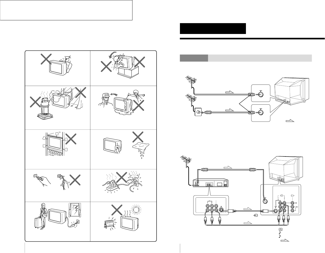
WARNING
• Dangerously high voltages are present inside the TV.
• Operate the TV only between 110 – 240 V AC.
To prevent fire or shock hazard, do not expose
the TV to rain or moisture.
Do not operate the TV if any liquid or solid object
falls into it. Have it checked immediately by
qualified personnel only.
Do not open the cabinet and the rear cover of the
TV. Refer servicing to qualified personnel.
Do not install the TV in hot, humid or excessively
dusty places.
Do not install the TV in a confined space, such
as a bookcase or built-in cabinet.
Do not block the ventilation openings of the TV.
Do not pull the power cord to disconnect the TV.
Pull it out by the plug.
Disconnect the power cord during lightning
storms or if you are not going to use the TV for
several days.
Install the TV in a stable position. Do not allow
children to climb onto it.
Do not plug in too many appliances to the same
power socket. Do not damage the power cord.
Clean the TV with a dry and soft cloth.
Do not use benzine, thinner, or any other chemicals
to clean the TV. Do not scratch the picture tube.
4
Using Your New TV
Getting Started
Step 1
Connect the antenna
If you wish to connect a VCR, see the “Connecting a VCR” diagram below.
CAUTION
Do not connect the power cord until you have completed making all other
connections; otherwise a minimum leakage current might flow through the antenna
and other terminals to ground.
Connecting a VCR
To watch the video, see page 9.
Using Your New TV
IEC connector
(not supplied)
To video and
audio outputs
VCR
(yellow)
-L (MONO) (white)
-R (red)
To S video
output
Antenna cable (not supplied)
To … 1 or 2
(video input)
Audio/Video cable
(not supplied)
S video cable
(not supplied)
: Signal flow
To
(S video input)
To antenna
output
To ˘
(antenna)
or
: Signal flow
Antenna cable (not supplied)
Antenna cable (not supplied)
Rear of TV
Rear of TV
VIDEO
VIDEO IN
VIDEO OUT
AUDIO
WOOFER
(8Ω)
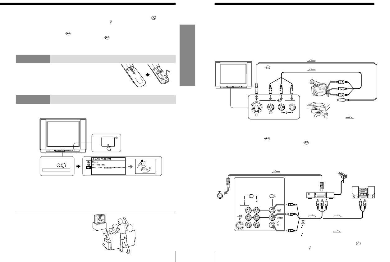
– 9 –
KV-XF29M80
RM-954
5
Using Your New TV
Using Your New TV
Front of TV
Notes
•If you connect a monaural VCR, connect the yellow plug to (the
yellow jack) and the black plug to -L (MONO) (the white jack).
•If you connect a VCR to the ˘ (antenna) terminal, preset the signal
output from the VCR to the program number 0 on the TV.
•If both (S video input) and … 1 (video input) at the rear of your TV
are input at the same time, the (S video input) is automatically
selected. To view … 1 (video input), disconnect the S video cable.
•When no signal is input to the connected video equipment, the TV screen
becomes blue.
Step 2
Insert the batteries
into the remote
Note
•Do not use old batteries nor use different types of batteries together.
Step 3
Preset the channels automatically
Tips
•If you want to stop the automatic channel presetting, press MENU twice.
•If your TV has preset an unwanted channel or cannot preset a particular
channel, then preset your TV manually (see page 21 and 22).
Note
•During automatic channel presetting, your TV screen will indicate “B/G”,
“I”, “D/K” or “M” for the TV system (TV SYS).
Now You Are Ready. . .
To watch your TV, see page 8.
1
2
AUTO
PROGR
1
ONE-PUSH AUTOMATIC PROGRAMMING
ONE-PUSH AUTOMATIC PROGRAMMING
PROGR
6
Using Your New TV
Connecting optional components
You can connect optional audio/video components, such as a VCR, multi disc player,
camcorder, video game or stereo system.
To watch the picture of the connected equipment, see page 9.
Connecting a camcorder/video game equipment
using the … (video input) jacks
Notes
•You can also connect video equipment to the … 1 or 2 (video input) jacks
at the rear of your TV.
•If both (S video input) and … 3 (video input) at the front of your TV
are input at the same time, the (S video input) is automatically
selected. To view … 3 (video input), disconnect the S video cable.
Connecting audio/video equipment using the Ú
(monitor output) jacks
Note
•When connecting a monaural VCR, connect the yellow plug to (the
yellow jack) and the black plug to -L (MONO) (the white jack).
To S video output
Front of TV
Camcorder
Video game
equipment
To video and
audio outputs
: Signal flow
To
(S video
input) To… 3
(video input)
or
Audio/Video cable (not supplied)
S video cable (not supplied)
(yellow)
-L (MONO)
(white)
-R (red)
Rear of TV
To
antenna
output
To video and
audio inputs
or
Audio system
To
audio
inputs
VCR
: Signal flow
To Ú
(monitor
output)
Antenna cable (not supplied)
Audio/Video cable
(not supplied)
or
WOOFER
(8Ω)
3
(MONO)
– 10 –
KV-XF29M80
RM-954
8
Using Your New TV
Watching the TV
This section explains functions used
while watching TV. Most operations can
be done using the remote.
1Press U to turn on the TV.
When the TV is in the
standby mode (the u
indicator on the TV is lit
red), press u on the remote
or PROGR +/– on the TV.
2Press PROGR +/– or
number buttons to select
the TV program.
For double digit numbers,
press ÷, then the number
(e.g., for 25, press ÷, then
2 and 5).
3Press
. +/– to adjust the
volume.
¤
u
…
;
Number buttons
JUMP
. +/–
PROGR +/–
MENU
+/–/ENTER
or
u indicator
1
4
7
-/--
2
5
8
0
3
6
9
FAVORITE
SOUND
MODE
PIC MODE
ENTER
MENU
A/B
SURROUND
123
456
78
0
-/--
9
7
Using Your New TV
Using Your New TV
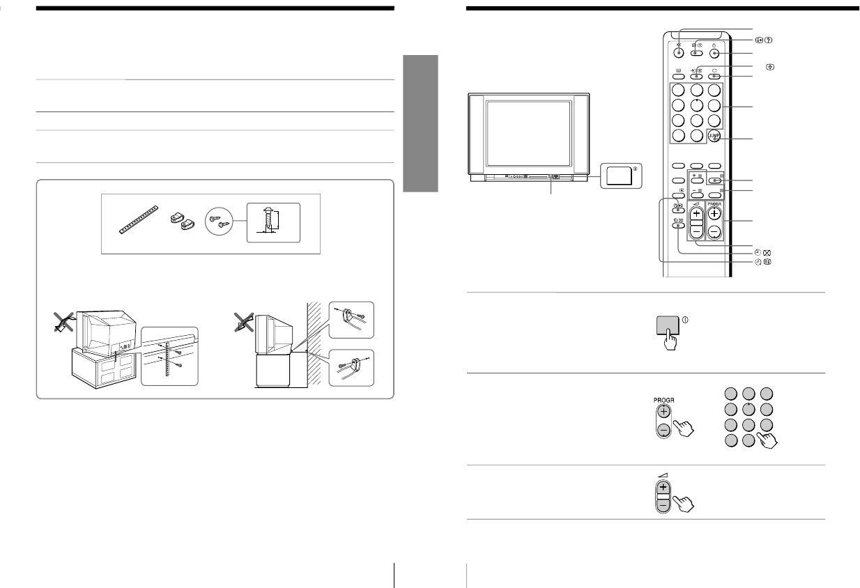
Securing the TV
To prevent the TV from falling, secure the TV using one of the following methods:
AWith the supplied screws, attach the band to the TV stand and to the rear of
the TV using the provided hole. or
BPut the cord or chain through the clamps to secure the TV against a wall or
pillar.
Note
•Use only the supplied screws. Use of other screws may damage the TV.
20
mm
AB
3.8mm
or
– 11 –
KV-XF29M80
RM-954
9
Using Your New TV
Using Your New TV
To
Turn off temporarily
Turn off completely
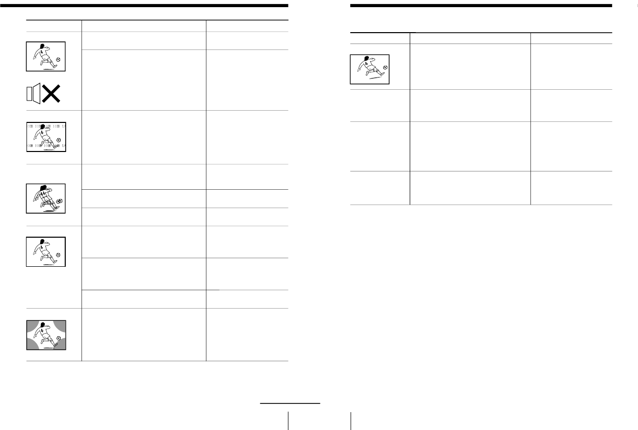
Mute the sound
Watch the video input
(VCR, camcorder, etc.)
Jump back to the previous channel
Display the on-screen information*
* The picture, sound, and either the program number or video mode are
displayed. The on-screen display for the picture and sound information
disappears after about 3 seconds.
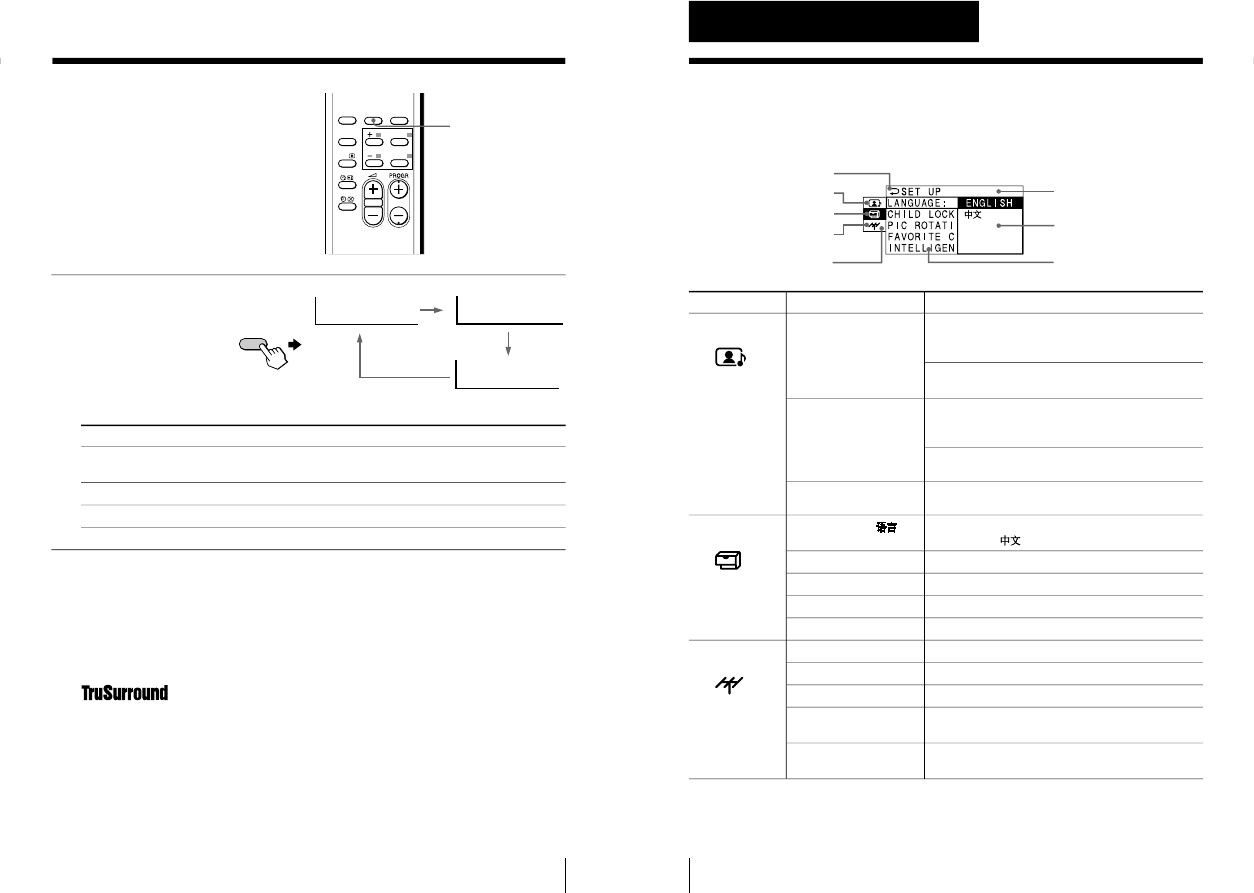
Changing the menu language
You can change the menu language as well as the on-screen language.
For details on how to use the menu, see “How to use the menu” on page 15.
Do this
Press u. The
u
indicator on the TV lights up red.
Press U on the TV.
Press ¤.
Press … to select “VIDEO 1”, “VIDEO 2” and
“VIDEO 3”.
To return to the TV program, press ;.
Press JUMP.
Press .
Additional tasks
1
Press MENU.
2
Press + or – to select the
SET UP icon ( ), then
press ENTER.
3
Make sure LANGUAGE/
is selected, then press
ENTER.
4
Press + or – to select ,
then press ENTER.
The menu language
changes to Chinese.
To return to the normal screen
Press MENU.
MENU
ENTER
ENTER
ENTER
+
continued
10
Using Your New TV
Setting the Wake Up timer
1
Press until the
desired period of time
appears.
2
Select the TV program or video mode you want to display when you wake
up.
3
Press u or set the Sleep timer if you want the TV to turn off automatically.
The indicator on the TV lights up orange.
To cancel the Wake Up timer
Press until “WAKE UP TIMER: OFF” appears or turn off the
TV’s main power.
Notes
•The Wake Up timer starts immediately after the on-screen display
disappears.
•If no buttons or controls are pressed for more than two hours after the TV
is turned on using the Wake Up timer, the TV automatically goes into the
standby mode. To continue watching the TV, press any button or control
on the TV or the remote.
Setting the Sleep timer
Press until the
desired period of time
appears.
To cancel the Sleep timer
Press until “SLEEP TIMER: OFF” appears or turn the TV off.
WAKE UP TIMER:10M
WAKE UP TIMER:OFF WAKE UP TIMER:12H00M
After 10 minutes
No Wake Up Timer After 12 hours
SLEEP TIMER:30M SLEEP TIMER:60M
SLEEP TIMER:OFF SLEEP TIMER:90M
After 30 minutes
No Sleep Timer
After 60 minutes
After 90 minutes
Watching the TV (continued)
– 12 –
KV-XF29M80
RM-954
12
Advanced Operations
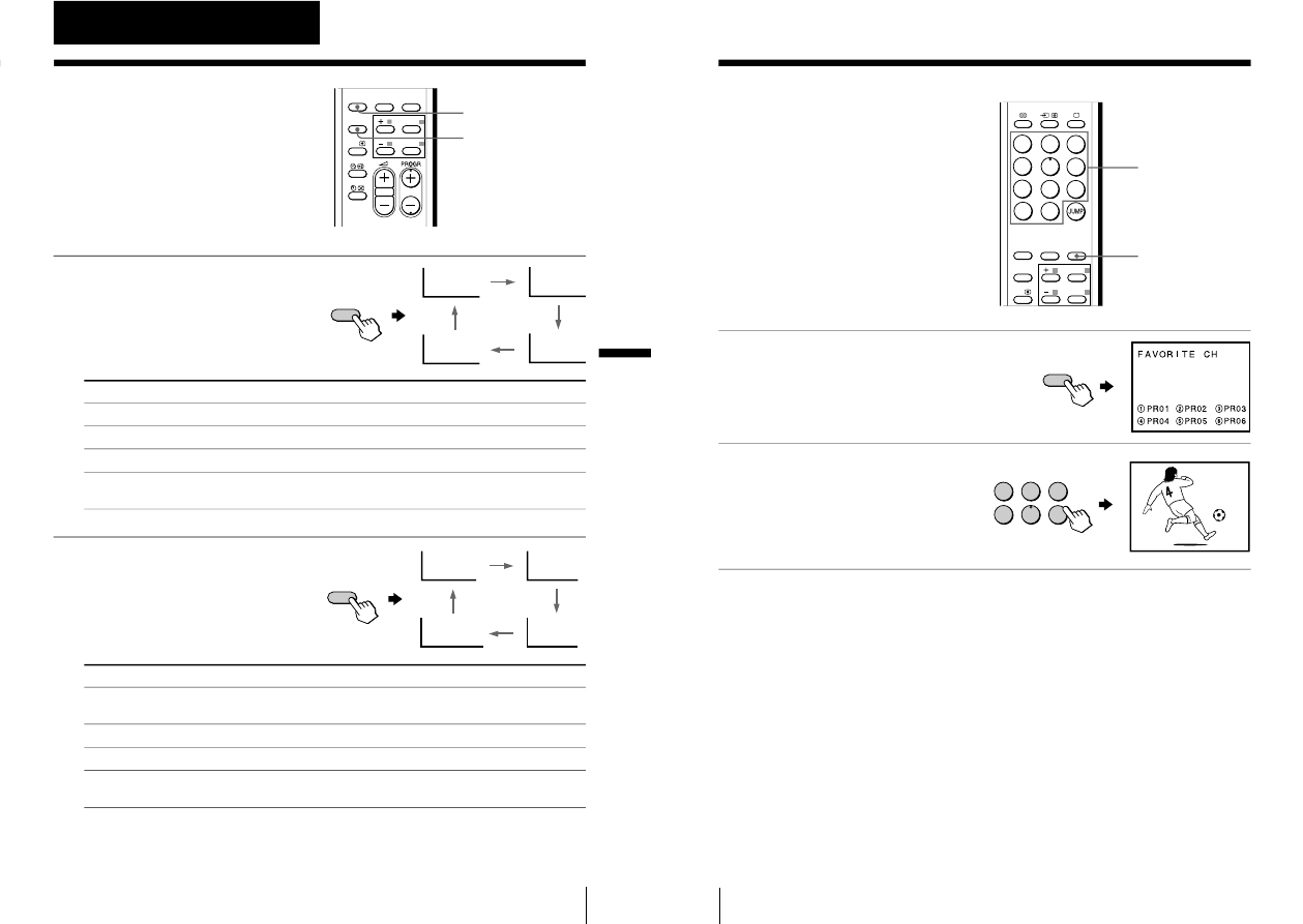
1Press FAVORITE.
2Press the number button
from 1 to 6 to select the
desired channel.
Tip
•To program your favorite channels, see “Programming your favorite
channels” on page 18.
Viewing your
favorite channels
You can display and select six of your
favorite channels directly from your TV
screen.
Number buttons
FAVORITE
1
4
7
-/--
2
5
8
0
3
6
9
FAVORITE
SOUND
MODE
PIC MODE
ENTER
MENU
A/B
SURROUND
FAVORITE
123
456
1
11
Advanced Operations
Advanced Operations
Selecting the
picture and sound
modes
You can select picture and sound modes
and adjust the setting to your preference
in PERSONAL option.
Selecting the picture mode
Press PIC MODE
repeatedly until you get
the desired picture mode.
Select To
DYNAMIC receive high contrast pictures.
STANDARD receive normal contrast pictures.
SOFT receive mild pictures.
PERSONAL receive the last adjusted picture setting from the ADJUST
option in the A/V CONTROL menu (see page 17).
Selecting the sound mode
Press SOUND MODE
repeatedly until you get
the desired sound mode.
Select To
DYNAMIC listen to dynamic and clear sound that emphasizes the low and
high tones.
DRAMA listen to sound that emphasizes voice and high tones.
SOFT receive soft sound.
PERSONAL receive the last adjusted sound setting from the ADJUST option
in the A/V CONTROL menu (see page 17).
Tip
•You can also set the picture and sound modes using the menu (see
“Changing the A/V CONTROL setting” on page 16).
FAVORITE
SOUND
MODE
PIC MODE
ENTER
MENU
A/B
SURROUND
PERSONAL
STANDARD
SOFT
DYNAMIC
PIC MODE
≥
DYNAMIC
≥
DRAMA
≥
SOFT
≥
PERSONAL
SOUND
MODE
SOUND MODE
PIC MODE
Advanced Operations
– 13 –
KV-XF29M80
RM-954
13
Advanced Operations
Select To
HIGH listen to sound that spreads out over a large area, giving the feeling
of being at a concert hall.
LOW listen to the sound that gives the feeling of being at a live concert.
OFF turn off the surround sound.
The surround of your TV is categorized as TruSurround.
TM
is a trademark of SRS Labs, Inc. SRS and the SRS symbol are
registered trademarks of SRS Labs, Inc. in the United States and selected foreign
countries. SRS and TruSurround are incorporated under license from SRS Labs,
Inc. and are protected under United States Patent Nos. 4,748,669 and 4,841,572
with numerous additional issued and pending foreign patents.
Press SURROUND
repeatedly until you
receive the desired
surround sound.
Listening with
surround sound
The surround feature enables you to
enjoy the sound effects of a concert hall
or movie theater.
SURROUND
FAVORITE
SOUND
MODE
PIC MODE
ENTER
MENU
A/B
SURROUND
SURROUND: LOW
SURROUND: HIGH
SURROUND: OFF
SURROUND
14
Adjusting Your Setup (MENU)
Introducing the menu system
The MENU button lets you open a menu and change the settings of your TV. Here’s
an overview of the menu system.
Return icon
A/V CONTROL icon
SET UP icon
CH PRESET icon
Name of the current
menu
Menu level 3
Menu level 2
Adjusting Your Setup (MENU)
Menu level 1
Level 1 Level 2 Level 3/Function
A/V CONTROL PICTURE MODE Select the picture mode.
DYNAMIC n STANDARD n SOFT n
PERSONAL n ADJUST
ADJUST Adjust the PERSONAL option.
PICTUREnCOLORnBRIGHTnHUEnSHARP
SOUND MODE Select the sound mode.
DYNAMIC n DRAMA n SOFT n
PERSONAL n ADJUST
ADJUST Adjust the PERSONAL option.
BASSnTREBLEnBALANCEnBBE *
SURROUND Select the surround mode.
HIGHn LOWnOFF
SET UP LANGUAGE/ Change the menu language.
ENGLISH - (Chinese)
CHILD LOCK Lock the channel independently.
PIC ROTATION Adjust the picture position.
FAVORITE CH
Program favorite channels.
INTELLIGENT VOL Adjust volume automatically.
CH PRESET AUTO PROGRAM Preset channels automatically.
MANUAL PROGRAM Preset channels manually.
SKIP Skip unwanted or unused program positions.
TV SYS Select the TV system.
B/Gn In D/Kn M
COL SYS Select the color system.
AUTOnPALnSECAMnNTSC3.58nNTSC4.43
* The BBE is manufactured by Sony Corporation under license from BBE
Sound, Inc. It is covered by U.S. Patent No. 4,638,258 and No. 4,482,866.
The word “BBE” and the BBE symbol are the trademarks of BBE Sound, Inc.
– 14 –
KV-XF29M80
RM-954
15
Adjusting Your Setup (MENU)
How to use the
menu
You can use the buttons on the remote
and on the TV as well to display the
menu and adjust the settings.
1Press MENU to display the
menu.
2Press + or – to select the
desired item.
3Press ENTER to confirm
your option and go to the
next menu level.
Other menu operations
To Press
Adjust the setting value +/–
Return to the previous menu level* ENTER
Cancel the menu MENU
* To return from Menu Level 2 to Level 1, press + or – to select the return
icon ( ), then press ENTER.
Tips
•If more than 60 seconds elapse between entries, the menu screen
disappears.
•You can also use the buttons on the TV for menu operations. ¸ +/– work
as + /– on the remote and … works as ENTER on the remote.
+/–/ENTER
MENU
Front of TV
FAVORITE
SOUND
MODE
PIC MODE
ENTER
MENU
A/B
SURROUND
MENU
ENTER
+
+
PROGR
ONE-PUSH AUTOMATIC PROGRAMMING
Adjusting Your Setup (MENU)
16
Adjusting Your Setup (MENU)
Changing the A/V
CONTROL setting
The A/V CONTROL menu allows you
to change the picture and sound
settings.
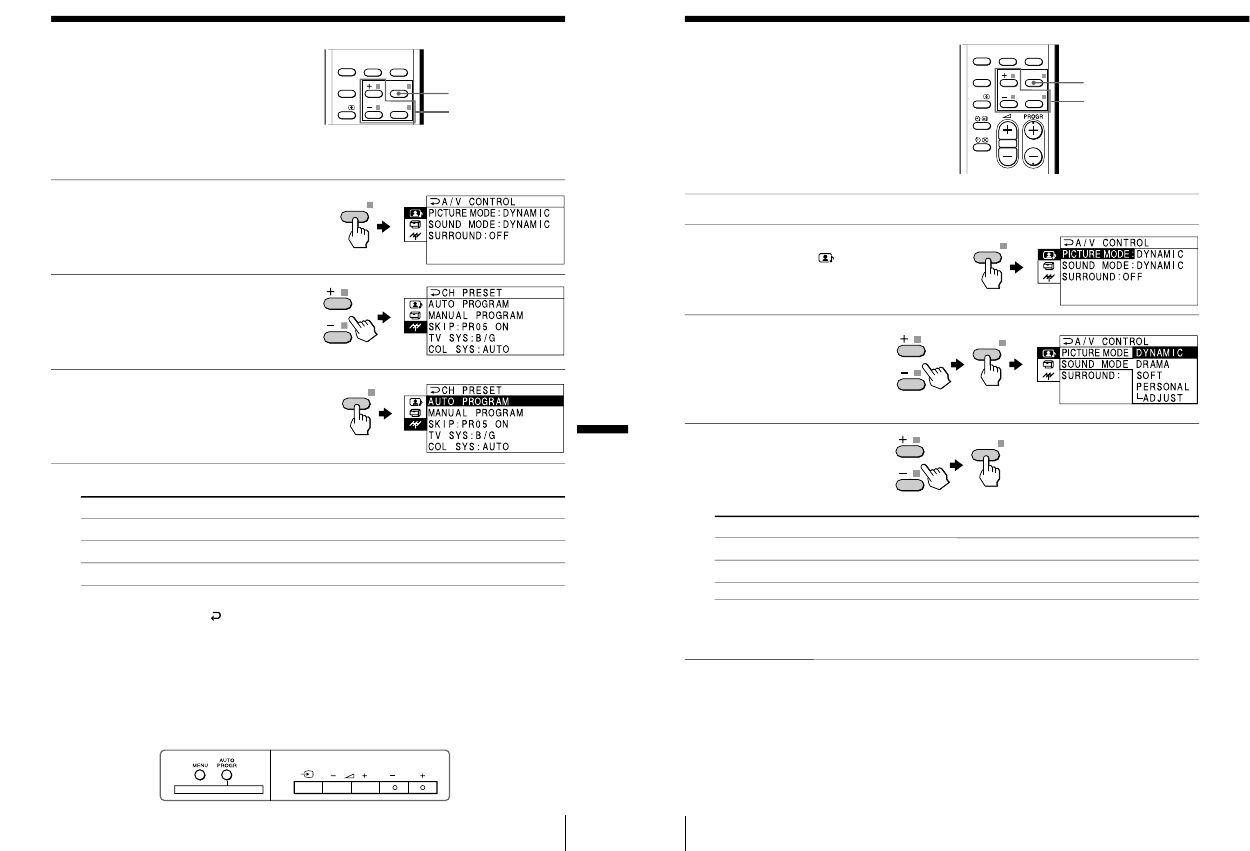
1Press MENU.
2Make sure the A/V
CONTROL icon ( ) is
selected, then press
ENTER.
3Press + or – to select
either PICTURE MODE,
SOUND MODE or
SURROUND, then press
ENTER.
4Press + or – to select the
desired option, then press
ENTER.
For Select
PICTURE MODE either DYNAMIC, STANDARD, SOFT, PERSONAL*, or ADJUST.
SOUND MODE either DYNAMIC, DRAMA, SOFT, PERSONAL*, or ADJUST.
SURROUND either HIGH, LOW, or OFF.
* When the PERSONAL mode is selected, the last adjusted picture
and sound settings from the ADJUST option are received (see
next page).
Tip
•For details on the options under “PICTURE MODE”, “SOUND MODE”
and “SURROUND”, see page 11 and 13 respectively.
To return to the normal screen
Press MENU.
+/–/ENTER
MENU
FAVORITE
SOUND
MODE
PIC MODE
ENTER
MENU
A/B
SURROUND
ENTER
ENTER
ENTER
– 15 –
KV-XF29M80
RM-954
17
Adjusting Your Setup (MENU)
Adjusting the ADJUST options under PICTURE MODE
1
Press + or – to select the
desired item (e.g.,
COLOR), then press
ENTER.
2
Adjust the value according to the following table, then press ENTER.
For Press – to Press + to
PICTURE decrease picture contrast increase picture contrast
COLOR decrease color intensity increase color intensity
BRIGHT darken the picture brighten the picture
HUE* increase red picture tones increase green picture tones
SHARP soften the picture sharpen the picture
* You can adjust HUE for the NTSC color system only.
3
Repeat the above steps to adjust other items.
The adjusted settings will be received when you select PERSONAL.
Adjusting the ADJUST options under SOUND MODE
1
Press + or – to select the
desired item (e.g., BALANCE),
then press ENTER.
2
Adjust the value according to the following table, then press ENTER.
For Press – to Press + to
BASS decrease the bass increase the bass
TREBLE decrease the treble increase the treble
BALANCE increase the left speaker’s volume
increase the right speaker’s volume
BBE select “HIGH” for higher enhancement of sound clarity;
select “LOW” for lower enhancement of sound clarity;
select “OFF” to turn off the BBE sound
3Repeat the above steps to adjust other items.
The adjusted settings will be received when you select PERSONAL.
Tip
•For details on the menu system and how to use the menu, refer to
“Introducing the menu system” on page 14 and “How to use the menu”
on page 15.
ENTER
COLOR 80
BALANCE 00
ENTER
18
Adjusting Your Setup (MENU)
Changing the SET
UP setting
The SET UP menu allows you to change
the menu language, lock channels,
adjust the picture position, program
your favorite channels and adjust
volume automatically.
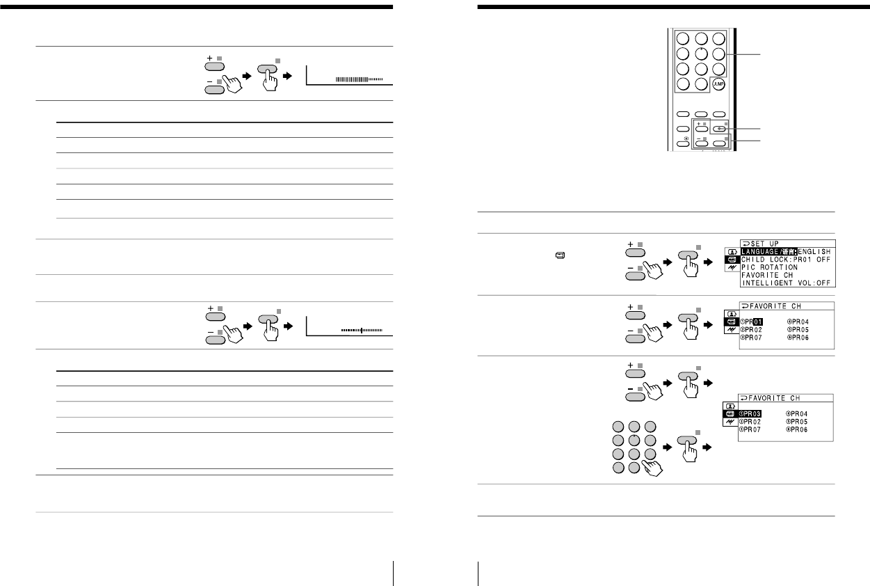
Programming your favorite channels
The FAVORITE CH feature enables you to program up to six
channels for direct selection.
1
Press MENU.
2
Press + or – to select the
SET UP icon ( ), then
press ENTER.
3
Press + or – to select
FAVORITE CH, then press
ENTER twice.
4
Press + or –, or number
buttons to program the
desired channel (e.g.,
PR03), then press ENTER.
5
To continue programming other favorite channels, press + or – and then
press ENTER. After that, repeat step 4.
To return to the normal screen
Press MENU.
MENU
Number buttons
+/–/ENTER
or
1
4
7
-/--
2
5
8
0
3
6
9
FAVORITE
SOUND
MODE
PIC MODE
ENTER
MENU
A/B
SURROUND
ENTER
ENTER
ENTER
+
++
+++++++
PRO
R02
:B/G
COL SYS :AUTO
AUTO PROGRAM
M
S
T
ENTER
123
456
78
0
-/--
9
+
++
+++++++
PRO
R02
:B/G
COL SYS :AUTO
AUTO PROGRAM
S
T
+
– 16 –
KV-XF29M80
RM-954
19
Adjusting Your Setup (MENU)
1Press MENU.
2Press + or – to select the
SET UP icon ( ), then
press ENTER.
3
Press + or – to select CHILD
LOCK, then press ENTER.
4
Press + or –, or number
buttons to select the
desired channel, then
press ENTER.
5
Press + or – to select ON, then
press ENTER.
The lock symbol ( )
appears on the screen.
To unlock the channel,
select OFF.
6
To continue locking other channels, press ENTER and then repeat step 4 to 5.
To return to the normal screen
Press MENU.
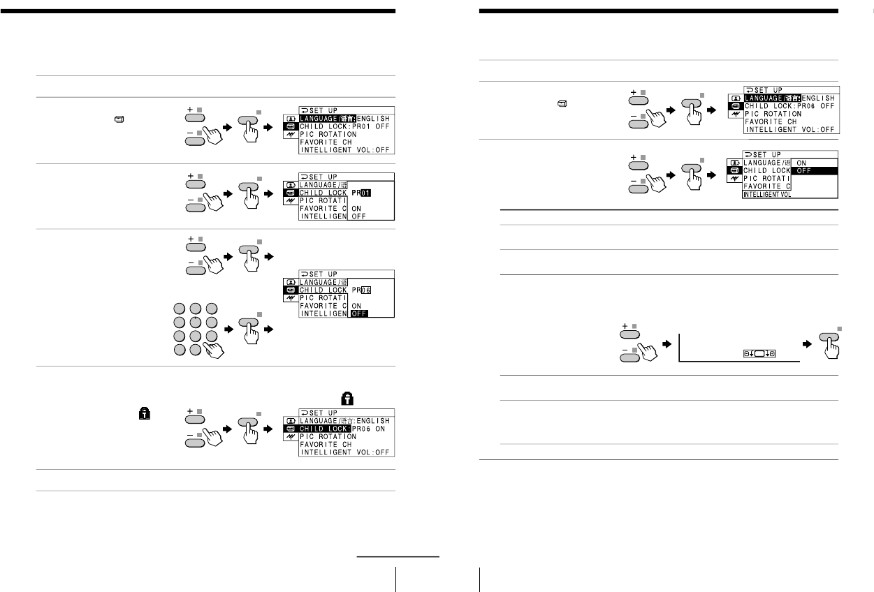
Using the CHILD LOCK feature
You can prevent your children from watching certain programs by
using the CHILD LOCK feature.
or
ENTER
ENTER
ENTER
ENTER
123
456
78
0
-/--
9
ENTER
+
+
+
+
continued
20
Adjusting Your Setup (MENU)
Changing other SET UP menu options
1
Press MENU.
2
Press + or – to select the
SET UP icon ( ), then
press ENTER.
3
Press + or – to select the
desired option (e.g.,
INTELLIGENT VOL), then
press ENTER.
Select To
LANGUAGE Change the menu language (see “Changing the menu
language” on page 9).
CHILD LOCK Prevent children from watching certain programs (see
“Using the CHILD LOCK feature” on page 19).
PIC ROTATION Adjust the picture position when it is not aligned to the
TV screen.
Press + or – to adjust the picture position, then press
ENTER.
FAVORITE CH Program channels for direct selection (see “Programming
your favorite channels” on page 18).
INTELLIGENT VOL Adjust the volume of each TV program automatically.
Press + or – to select “ON”, then press ENTER.
To turn off the Intelligent Volume function, select “OFF”,
then press ENTER.
To return to the normal screen
Press MENU.
Tip
•For details on the menu system and how to use the menu, refer to
“Introducing the menu system” on page 14 and “How to use the menu”
on page 15.
ENTER
ENTER
+
+
ENTER
PIC ROTATION
Changing the SET UP setting (continued)
– 17 –
KV-XF29M80
RM-954
21
Adjusting Your Setup (MENU)
Changing the
Channel Preset
(CH PRESET)
setting
The CH PRESET menu allows you to
adjust the setup of your TV. For
example, you can receive a channel with
a weak signal that fails to be tuned in by
automatic presetting.
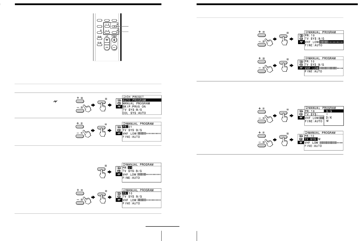
Presetting channels manually
1
Press MENU.
2
Press + or – to select the
CH PRESET icon ( ), then
press ENTER.
3
Press + or – to select
MANUAL PROGRAM, then
press ENTER.
4
Select the program
number to which you
want to preset a channel.
(1) Make sure “PR” is
selected , then press
ENTER.
(2) Press + or – until the
program number you
want to preset (e.g.,
program number 10)
appears on the menu,
then press ENTER.
+/–/ENTER
MENU
FAVORITE
SOUND
MODE
PIC MODE
ENTER
MENU
A/B
SURROUND
ENTER
ENTER
+
+
+ +
ENTER
+
+ +
ENTER
+
+ +
continued
22
Adjusting Your Setup (MENU)
Changing the Channel Preset (CH PRESET) setting (continued)
5
Select the desired
channel.
(1) Press + or – to select
either VHF LOW, VHF
HIGH or UHF, then
press ENTER.
(2) Press + or – until the
desired channel
picture appears on
the TV screen, then
press ENTER.
6
If the sound of the
desired channel is
abnormal, select the
appropriate TV system.
(1) Press + or – to select
TV SYS, then press
ENTER.
(2) Press + or –until the
sound becomes
normal (e.g., M), then
press ENTER.
ENTER
ENTER
+
+
+ +
ENTER
ENTER
+
++
+
+ +
– 18 –
KV-XF29M80
RM-954
23
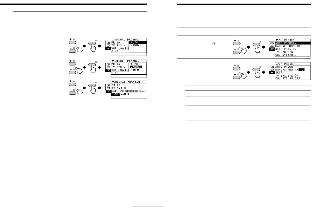
Adjusting Your Setup (MENU)
7If you are not satisfied
with the picture and
sound quality, you may
improve them by using
fine tuning.
(1) Press + or – to select
FINE, then press
ENTER.
(2) Press + or – to select
MANUAL, then press
ENTER.
(3) Press + or – until the
picture and sound
quality are optimal,
then press ENTER.
The + or – icon on the
menu flashes while
tuning.
To return to the normal screen
Press MENU.
Note
•The TV system (TV SYS) and the fine tuning (FINE) settings are
memorized for each program number.
ENTER
ENTER
ENTER
+
+ +
+
+ +
+
continued
24
Adjusting Your Setup (MENU)
Changing other CH PRESET menu options
1
Press MENU.
2
Press + or – to select the
CH PRESET icon ( ), then
press ENTER.
3
Press + or – to select the
desired option (e.g., SKIP),
then press ENTER.
Select
AUTO PROGRAM
MANUAL PROGRAM
TV SYS
COL SYS
SKIP
Tip
•For details on the menu system and how to use the menu, refer to
“Introducing the menu system” on page 14 and “How to use the menu”
on page 15.
Note
•If you preset a locked channel, that particular channel will be unlocked
automatically.
To
preset channels automatically.
preset channels manually. See “Presetting channels
manually” on page 21 and 22.
select the TV system. See “Presetting channels manually”
on page 21 and 22.
select the color system. Normally, set this to “AUTO”.
skip unwanted or unused program numbers.
1 Press + or – until the unused or unwanted program
number appears, then press ENTER.
2 Press + or – to select “ON”, then press ENTER.
To put the skipped program number back on, select
“OFF”, then press ENTER.
ENTER
ENTER
+
+
Changing the Channel Preset (CH PRESET) setting (continued)
– 19 –
KV-XF29M80
RM-954
25
Additional Information
Additional Information
Self-diagnosis function
Your TV is equipped with a self-diagnosis function. If there is a
problem with your TV, the
u
indicator flashes red. The number of
times the
u
indicator flashes indicates the possible causes.
1
Check that the
u
indicator flashes red a number of times between 3-second
intervals.
2
Count the number of times the
u
indicator flashes.
3
Press U (main power) to turn off your TV.
4
Inform your nearest Sony service center about the number of times the
u
indicator flashes.
Be sure to note the model name and serial number located on the rear of
your TV.
Front of TV
u indicator
Additional Information
26
Additional Information
Troubleshooting
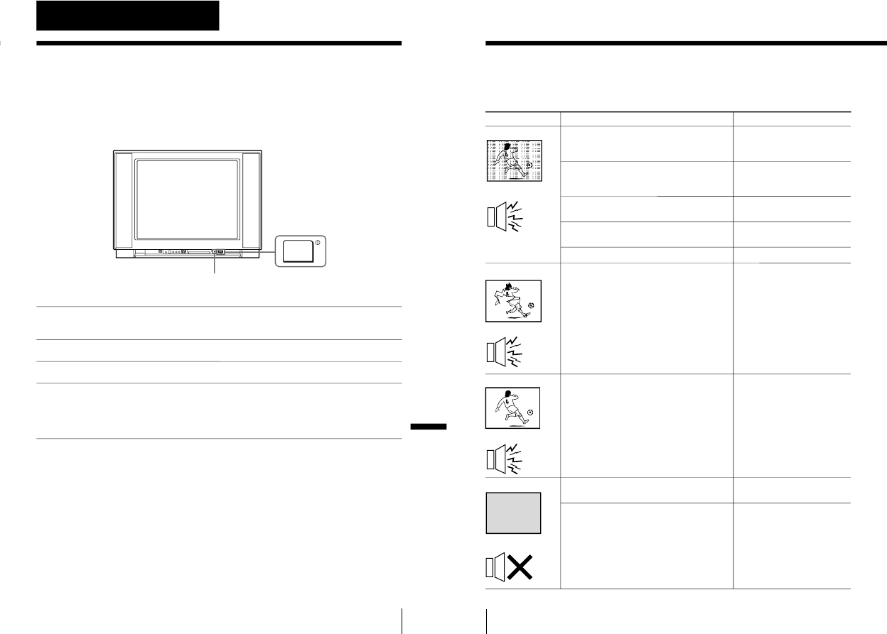
If you find any problem while viewing your TV, please check the following guide. If
any problem persists, contact your Sony dealer .
Possible causeSymptom Solutions
•Check the antenna cable and connection
on the TV, VCR and on the wall.
(page 4)
•Display the CH PRESET menu and
select “MANUAL PROGRAM” to preset
the channel again. (page 21)
•Check the antenna type (VHF/UHF).
Contact a Sony dealer for advice.
•Adjust the antenna direction. Contact a
Sony dealer for advice.
•Try using a booster.
•Turn off or disconnect the booster if it is
in use.
•If the sound of all the channels are noisy,
display the CH PRESET menu and
check the TV system (TV SYS) setting
(page 22), then select “AUTO
PROGRAM” to preset the channels
again (page 24).
•If the sound of some channels are noisy,
select the channel, then display the CH
PRESET menu and select the appropriate
TV system (TV SYS). (page 22)
•Check the power cord, antenna and the
VCR connections.
•Press u (power).
•Press U (main power) on the TV to turn
off the TV about five seconds, then turn
it on again.
•Connection is loose or the
cable is damaged.
•Channel presetting is
inappropriate or
incomplete.
•The antenna type is
inappropriate.
•The antenna direction is
inappropriate.
•Signal transmission is low.
•Broadcast signals are too
strong.
•The TV system (TV SYS)
setting or channel
presetting is inapproriate
or incomplete.
•The power cord, antenna
or VCR is not connected.
•The TV is not turned on.
Snowy picture
Noisy sound
Distorted picture
Noisy sound
Good picture
Noisy sound
No picture
No sound
– 20 –
KV-XF29M80
RM-954
27
Additional Information
•Press ¸ + to increase the volume level.
•Press ¤ to cancel the muting.
•Do not use a hair dryer or other
equipment near the TV.
•Adjust the antenna direction for
minimum interference. Contact a Sony
dealer for advice.
•Use a highly directional antenna.
•Adjust the antenna direction. Contact a
Sony dealer for advice.
•Turn off or disconnect the booster if it is
in use.
•Display the A/V CONTROL menu and
select “ADJUST” of PICTURE MODE,
then adjust the COLOR level. (pages 16
and 17)
•Display the CH PRESET menu and
check the color system (COL SYS)
setting (usually set this to AUTO).
(page 24)
•Adjust the antenna direction. Contact a
Sony dealer for advice.
•Keep external speakers or other
electrical equipment away from the TV.
Do not move the TV while the TV is
turned on. Press U (main power) on the
TV to turn off the TV for about five
minutes, then turn it on again.
Good picture
No sound
Dotted lines or stripes
Double images or
“ghosts”
No color
Abnormal color patches
•The volume level is too
low.
•The sound is muted.
•There is local interference
from cars, neon signs, hair
dryers, power generators,
etc.
•Broadcast signals are
reflected by nearby
mountains or buildings.
•The antenna direction is
inappropriate.
•Use of a booster is
inappropriate.
•The color level setting is
too low.
•The color system setting is
inappropriate.
•The antenna direction is
inapproriate.
•The magnetic disturbance
from external speakers or
other equipment, or the
direction of the earth’s
magnetic field may affect
the TV.
Possible causeSymptom Solutions
continued
28
Additional Information
•Display the SET UP menu and adjust
“PIC ROTATION” so that the picture is
aligned to the TV screen. (page 20)
•Contact your nearest Sony service
center. (page 25)
—
—
Picture slant
The
u
indicator on your
TV flashes red a number of
times between 3-second
intervals.
TV cabinet creaks.
A “boom” sound is heard
when the TV is turned on.
Possible causeSymptom Solutions
•The terrestrial magnetism
affects your TV set.
•Your TV may need service.
•Changes in room
temperature sometimes
make the TV cabinet
expand or contract,
making a noise. This does
not indicate a malfunction.
•The TV’s demagnetizing
function is working. This
does not indicate a
malfunction.
Troubleshooting (continued)
– 21 –
KV-XF29M80
RM-954
29
Additional Information
Identifying parts and controls
Refer to the pages indicated in parentheses ( ) for details.
Front panel
1
U
(main power) button (8)
2PROGR +/– (program) buttons (8)
3
¸
+/– (volume) buttons (8)
4
…
(TV/video) button (9)
5AUTO PROGR (program) button (5)
6MENU button (15)
7
2
(headphone) jack
ONE-PUSH AUTOMATIC PROGRAMMING
PROGR
continued
30
Additional Information
Button function
For general TV operations
For Teletext operations
Remote Control
Names/symbols of buttons on the
remote are indicated in different
colors to represent the available
functions.
Label color
White
Green
!£ SOUND MODE button (11)
!¢ SURROUND button (13)
!∞ FAVORITE button (12)
!§ PIC MODE button (11)
!¶ Teletext operation buttons
(not used for KV-XF29M80)
(text) (enlarge)
(reveal) (hold)
(index) (text clear)
p
(FASTEXT: red, green, yellow, blue)
1¤ (muting) button (9)
2(display) button (9)
3u (power) button (8)
4… (video) button (9)
5; (TV) button (9)
6Number buttons (8)
7JUMP button (9)
8
Menu operation buttons (15)
MENU button
+ or – buttons
ENTER button
9PROGR +/– button (8)
!º A/B button
(not used for KV-XF29M80)
!¡ Timer setting buttons (10)
(wake up timer)
(sleep timer)
!™ . (volume) +/– buttons (8)
1
4
7
-/--
2
5
8
0
3
6
9
FAVORITE
SOUND
MODE
PIC MODE
ENTER
MENU
A/B
SURROUND
5
4
3
6
7
8
9
!¡
!º
!™
1
4
7
-/--
2
5
8
0
3
6
9
FAVORITE
SOUND
MODE
PIC MODE
ENTER
MENU
A/B
SURROUND
!¶
!∞
!§
!£
!¢
Identifying parts and controls (continued)
– 22 –
KV-XF29M80
RM-954
KV-XF29M80
RM-954
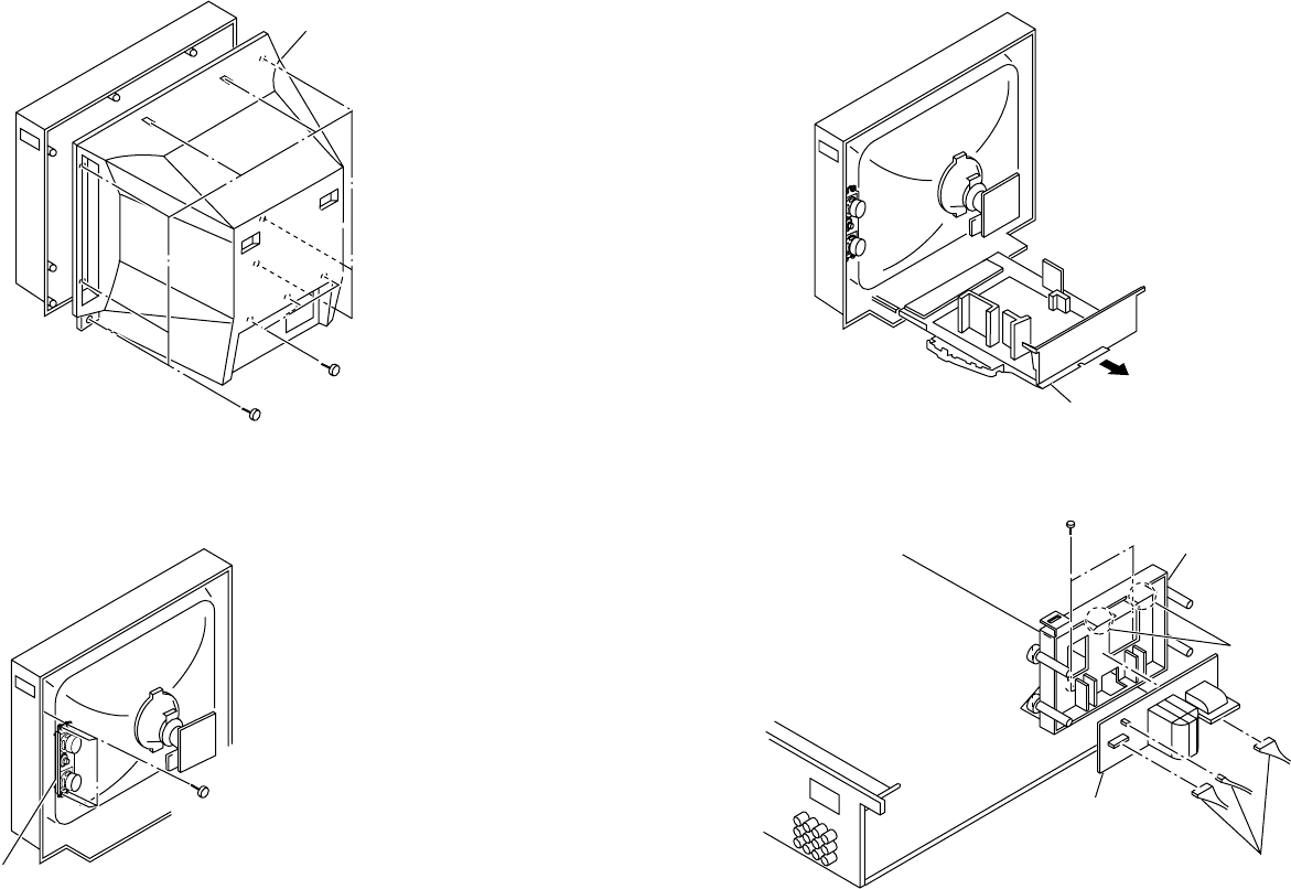
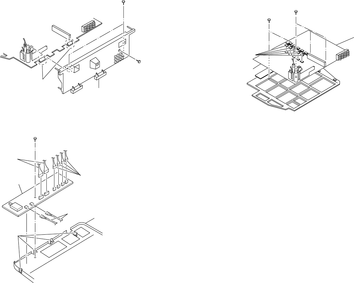
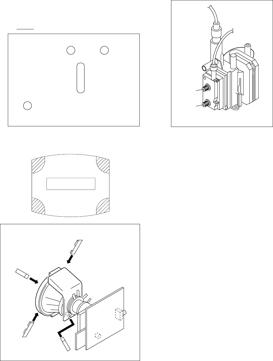
2-4. F BRACKET REMOVAL
4 Two screws
(+BVTP 3 × 12)
5 F bracket
2 Two claws
1 Three connectors
3 F board
SECTION 2
DISASSEMBLY
2-3. CHASSIS ASSY REMOVAL
2-2. SPEAKER REMOVAL
1 Four screws (Washer head)
(+P 4 × 16)
2 Bracket, speaker
1 Chassis assy
2-1. REAR COVER REMOVAL
1 Eight screws
(+BVTP 4 × 16)
1 Three screws
(+BVTP 4 × 16)
2 Rear cover
– 23 –
KV-XF29M80
RM-954
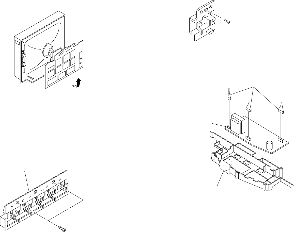
2-6-2. REPLACEMENT OF LIGHT GUIDE
2-5. SERVICE POSITION
(Note: Remove F Bracket first.)
2-6. REPLACEMENT OF PARTS
For replacement of the Control Button and Light Guide, unscrew them, exchange
with the new parts, and fix them with screws (+BVTP) respectively.
2-6-1. REPLACEMENT OF CONTROL BUTTON
Control button
Two screws
(+BVTP 3 × 12)
One screw
(+BVTP 3 × 12)
2-7. D1 BOARD REMOVAL
1 Three connectors
2One claw
3 D1 board
– 24 –
KV-XF29M80
RM-954
KV-XF29M80
RM-954
4 B3 Board
5 A Board
3 Five connectors
1 Two screws
(+BVTAP 3 × 12)
2 Three screws
(+BVTAP 3 × 12)
2-10. A AND B3 BOARDS REMOVAL
2-9. H3 BOARD REMOVAL
3 Two connectors
6 One screw (+BVTP 3 × 12 with washer)
1 Two connectors
4 Four claws
5 H3 Board 2 Four connectors
2-8. TERMINAL BRACKET REMOVAL
1 Two screws
(+BVTP 3 × 12)
4 One screw
(+BVTP 4 × 16)
2 Two claws
3 Terminal bracket
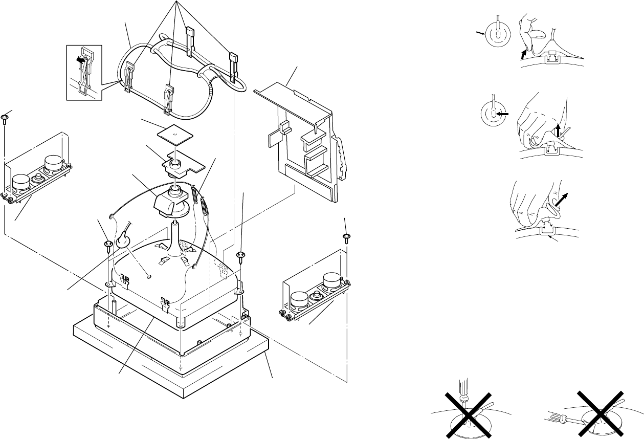
– 25 –
KV-XF29M80
RM-954
2-11. PICTURE TUBE REMOVAL
!¡ Four DGC clip
!™ Demagnetic coil
0Four claws
1Four screws
(washer head)
(+P 4 × 16)
3Four screws
(washer head)
(+P 4 × 16)
2Speaker Bracket
assy (L)
4Speaker Bracket
assy (R)
!¢ Two screws
(Tapping)
6Chassis assy
9Deflection
yoke
8Neck assy
7C board
5Anode cap
!∞ Picture tube Cushion
!¢ Two screws
(Tapping)
!£ Tension
spring
•REMOVAL OF ANODE-CAP
NOTE : After removing the anode, short circuit the anode of the picture tube and
the anode cap to the metal chassis, CRT shield or carbon paint on the
CRT.
•REMOVING PROCEDURES
1Do not damage the surface of anode-caps with sharp shaped objects.
2Do not press the rubber too hard so as not to damage the inside of anode-cap.
A metal fitting called the shatter-hook terminal is built into the rubber.
3Do not turn the foot of rubber over too hard.
The shatter-hook terminal will stick out or damage the rubber.
•HOW TO HANDLE AN ANODE-CAP
3When one side of the rubber cap is separated from the anode button, the anode-cap
can be removed by turning up the rubber cap and pulling it up in the direction of the
arrow c.
2Using a thumb pull up the rubber cap firmly in the direction indicated by the arrow b.
1Turn up one side of the rubber cap in the direction indicated by the arrow a.
a
a
b
b
c
Anode button
– 26 –
KV-XF29M80
RM-954
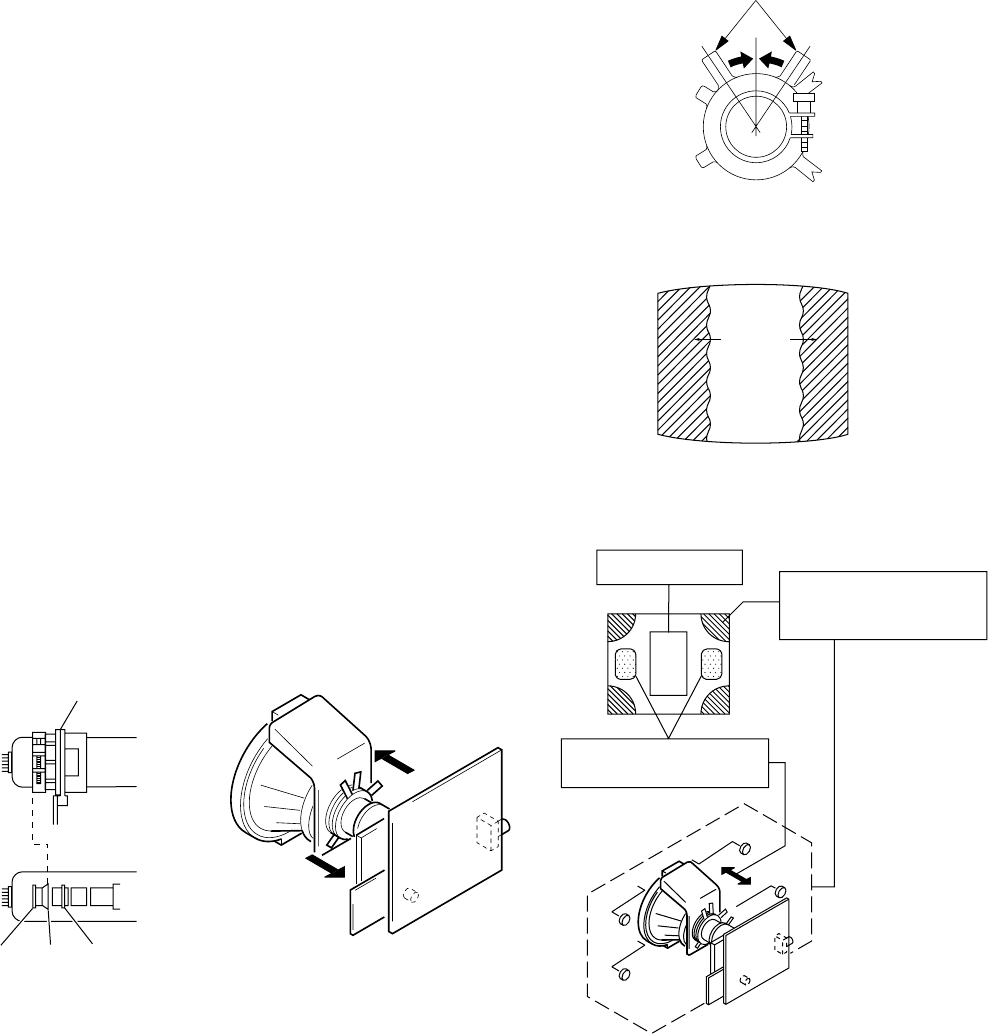
•The following adjustments should be made when a complete
realignment is required or a new picture tube is installed.
•These adjustments should be performed with rated power
supply voltage unless otherwise noted.
Controls and switches should be set as follows unless otherwise noted:
PICTURE control........................................................... normal
BRIGHTNESS control................................................... normal
Perform the adjustments in the following order :
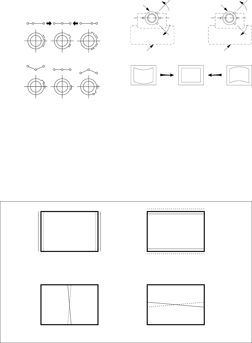
1. Beam Landing
2. Convergence
3. Focus
4. White Balance
Note : Test Equipment Required.
1. Color-bar/Pattern Generator
2. Degausser
3. Oscilloscope
SECTION 3
SET-UP ADJUSTMENTS
................................................................................................................................................................................................................................
Fig. 3-2
Neck assy
G2G1 G3
Behind the G2 edge
Fig. 3-1
Fig. 3-5
Purity control
corrects this area. Disk magnets or rotatable
disk magnets correct these
areas (a-d).
Deflection yoke positioning
corrects these areas.
a
b
b
c
c
d
d
a
Fig. 3-4
Red
Blue
Green
}normal
Preparation :
•In order to reduce the influence of geomagnetism on the set's
picture tube, face it east or west.
•Switch on the set's power and degauss with the degausser.
3-1. BEAM LANDING
1. Input a white signal with the pattern generator.
Contrast
Brightness
2. Position neck assy as shown in Fig3-2.
3. Set the pattern generator raster signal to a green raster.
4. Move the deflection yoke to the rear and adjust with the purity
control so that the green is at the center and the blue and the red
take up equally sized areas on each side.
(See Figures 3-1 through 3-4.)
5. Move the deflection yoke forward and adjust so that the entire
screen is green. (See Figure 3-2.)
6. Switch the raster signal to blue, then to red and verify the
condition.
7. When the position of the deflection yoke has been decided,
fasten the deflection yoke with the screws and DY spacers.
8. If the beam does not land correctly in all the corners, use a
magnet to adjust it.
(See Figure 3-5.)
Purity control
Fig. 3-3
– 27 –
KV-XF29M80
RM-954
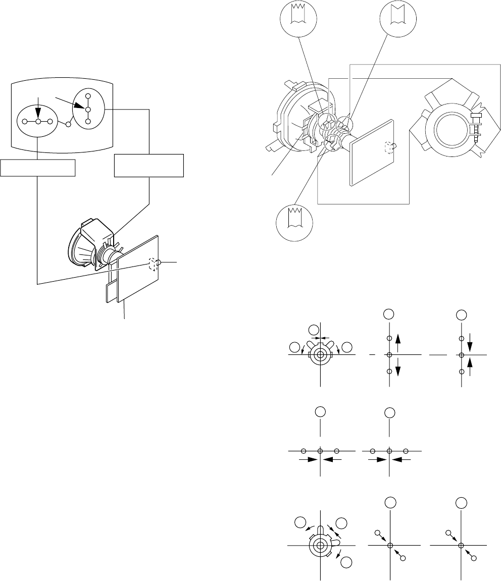
3-2. CONVERGENCE
Preparation :
•Before starting this adjustment, adjust the focus, horizontal size
and vertical size.
•Minimize the brightness setting.
•Provide dot pattern.
(1) Horizontal and Vertical Static Convergence
1. (Moving horizontally), adjust the H.STAT control so that the
red, green and blue dots are on top of each other at the center of
the screen.
2. (Moving vertically), adjust the V.STAT magnet so that the red,
green and blue dots are on top of each other at the center of the
screen.
3. If the H.STAT variable resistor cannot bring the red, green and
blue dots together at the center of the screen, adjust the
horizontal convergence with the H.STAT variable resistor and
the V.STAT magnet in the manner given below.
(In this case, the H.STAT variable resistor and the V.STAT
magnet influence each other, so be sure to perform adjustments
while tracking.)
Center dot
R G B
R
G
B
H. STAT VR V. STAT
Magnet
RV702
H. STAT
C Board
1V. STAT
2H. STAT VR
BMC (Hexapole)
V.STAT
DY pocket
Purity
V.STAT
BMCPurity
3
R
R
R
R
G
G
G
G
B
B
B
B
a
a
a
b
b
b b
R
R
G
G
B
B
a
a
b
b
b
– 28 –
KV-XF29M80
RM-954
5Y separation axis correction magnet adjustment.
1. Receive the cross-hatch signal and adjust [PICTURE] to [MIN]
and [BRIGHTNESS] to [STANDARD] .
2. Adjust the Y separation axis correction magnet on the neck
assembly so that the horizontal lines at the top and bottom of
the screen are straight.
Blue
Red
VM1 board
Blue
Red
VM1 board
Neck assy Neck assy
Note
1. The Red and Blue magnets should be equally far from the
horizontal center line.
2. Do not separate the Red and Blue magnets too far. (Less than
8 mm)
(2) Dynamic Convergence Adjustment
Preparation:
•Before starting this adjustment, adjust the horizontal static
convergence and the vertical static convergence
RB
RB
TLH TLV
YCH XCV
B
R
R
B
4BMC (Hexapole) Magnet.
If the red, green and blue dots are not balanced or aligned, then
use the BMC magnet to adjust in the manner described below.
RG B R G B R GB
RB
RG
GGB RB
– 29 –
KV-XF29M80
RM-954
(3) Screen-corner Convergence
ba
cd
a-d : screen-corner
misconvergence
Fix a Permalloy assy corresponding to the misconverged
areas.
a
b
c
d
Permalloy assembly
3-3. FOCUS ADJUSTMENT
Adjust FOCUS control on the flyback transformer for the best
focus.
FLYB ACK TRANSFORMER (T503)
Screen
Focus
TLV Rotate TLV-2 VOL (29”, 34”) on DY
Rotate TLV VOL (25”) on DY
XCV Rotate XCV Adj core on DY
YCH Rotate YCH VOL on DY
TLH Insert TLH Correction Plate to DY Pocket (Left or
Right)
ON DY:
YCH
XCV
TLV1
TLV2
– 30 –
KV-XF29M80
RM-954
2. WHITE BALANCE ADJUSTMENT
1) Set to Service Mode (Refer Section 4-1: ADJUSTMENTS
WITH COMMANDER).
2) Input white raster signal.
3) Set the PICTURE to minimum.
4) Select GCT (WHB 4) and BCT (WHB 5) with [1] and [4], and
adjust the level with [3] and [6] for the best white balance.
5) Set the PICTURE to maximum.
6) Select GDR (WHB 1) and BDR (WHB 2) with [1] and [4], and
adjust the level with [3] and [6] for the best white balance.
7) Write into the memory by pressing [MUTING] then [0].
3. SUB BRIGHT ADJUSTMENT
1) Set to service mode.
2) Input a staircase signal of black to white from the pattern
generator.
3) BRIGHTNESS ....50%.
PICTURE ............MINIMUM
4) Select SBR (WHB7) with [1] and [4], and adjust SBR (WHB7)
level with [3] and [6] so that the second stripe from the right is
dimly lit.
White
second from the right
Black
3-4. G2 (SCREEN) AND WHITE BALANCE
ADJUSTMENTS
1. G2 (SCREEN) ADJUSTMENT
1) Set the PICTURE to normal.
2) Put to VIDEO input mode without signals.
3) Connect R, G and B of the C board cathode to the oscilloscope.
4) Adjust BRIGHTNESS to obtain the cathode voltage to the value
below.
5) Adjust G2 (screen) on the FBT until picture shows the point
before cut off.
0 V
Cathode setting voltage:
175 V ±2(VDC)...34",25",21"
180V ±2(VDC)...29"
– 31 –
KV-XF29M80
RM-954
SECTION 4
CIRCUIT ADJUSTMENTS
With the unit on standby
↓
[DISPLAY]
↓
5
↓
VOL (+)
↓
[POWER]
This operation sequence puts the unit into service mode.
4-1. ADJUSTMENTS WITH COMMANDER
Service adjustments are made with the RM-954 that comes with
this unit.
a. ENTERING SERVICE MODE
1, 4Select the adjustment item.
↓
3, 6Raise/lower the data value.
↓
[MUTING] Writes.
↓
-Executes the writing.
7, -All the data becomes the values in memory.
8, -All user control goes to the standard state.
5, -Service data initialization (Be sure not to use
usually.)
2, -Write 50Hz adjustment data to 60Hz, or vice
versa.
PAL, SECAM : 50
NTSC : 60
00
HPS 1C SERVICE
Data
Mode
Item Name
Item No
Software version
Suffix No
(OEM Code)
Total Power-On time (hours)
p
Marking of virgin NVM
GEO
1.0C
59 7F 000A0620S
Device Name
50
1
4
7
-/--
2
5
8
0
3
6
9
FAVORITE
SOUND
MODE
PIC MODE
ENTER
MENU
A/B
SURROUND
RM-954
b. METHOD OF CANCELLATION FROM SERVICE
MODE
Set the standby condition (Press [POWER] button on the commander),
then press [POWER] button again, hereupon it becomes TV mode.
c. METHOD OF WRITE INTO MEMORY
1) Set to Service Mode.
2) Press [1] (UP) and [4] (DOWN), select an item of adjustment.
3) Press [MUTING] button and it will indicate WRITE on the screen.
4) Press [0] button to write into memory.
d. MEMORY WRITE CONFIRMATION METHOD
1) After adjustment, pull out the plug from AC outlet, and then
plug into AC outlet again.
2) Turn the power switch ON and set to Service Mode.
3) Call the adjusted items again to confirm adjustments were made.
The screen display is :
– 32 –
KV-XF29M80
RM-954
4-2. ADJUSTMENT METHOD
Item Number 00 of device GEO
This explanation uses H-Position as an example.
1. Select “GEO 00 HPS” with the 1 and 4 buttons.
2. Raise/lower the data with the 3 and 6 buttons.
3. Select the optimum state. (The standard is 1F for PAL reception.)
4. Write with the [MUTING] button. (The display changes to
WRITE.)
5. Execute the writing with the - button. (The WRITE
display will be changed to red color while excuting, and back
to SERVICE.)
Use the same method for all Items. Use 1 and 4 to select the
adjustment item, use 3 and 6 to adjust, write with [MUTING],
then execute the write with -.
Note : 1. In [WRITE], the data for all items are written into memory
together.
2. For adjustment items that have different standard data
between 50Hz or 60Hz, be sure to use the respective
input signal after adjustment.
1F SERVICE 50HPS
Adjusted with [3]
and [6] buttons.
GREEN
Written with [MUTING]
Write executed with [0]
GEO 00
7F 0 000A59
620S 1.0C
1F SERVICE 50HPS RED
The WRITE display
then the display
returns to a green
SERVICE.
GEO 00
7F 0 000A59
620S 1.0C
1F WRITE 50HPS GREEN
GEO 00
7F 0 000A59
620S 1.0C
– 33 –
KV-XF29M80
RM-954
Adjustment Item Table
Device Functionality Note Data Range Function Note for Register Slava RAM Address
Name No Name Different Data No. (bit) Address (bit)
GEO 0 HPS 7 3F H Position 50/60HZ 12 (7-2) CXA2130S(88H) 96 (7-2)
1 HSZ 1F 3F H Size 50/60HZ 11 (7-2) 95 (7-2)
2 PAP 1F 3F Pin Amp 50/60HZ 13 (7-2) 97 (7-2)
3 TLT 7 0F Trapezium 50/60HZ 15 (7-4) 99 (7-4)
4 VPS 1F 3F V Position 50/60HZ 0F (7-2) 93 (7-2)
5 VSZ 1F 3F V Size 50/60HZ 0E (7-2) 92 (7-2)
6 SCO 7 0F S Correction 50/60HZ 10 (7-4) 94 (7-4)
7 VLN 7 0F V Linearity 50/60HZ 10 (3-0) 94 (3-0)
8 BOW 7 0F AFC Bow 50/60HZ 16 (7-4) 9A (7-4)
9 AGL 7 0F AFC-Angle 50/60HZ 16 (3-0) 9A (3-0)
0A UPN 1F 3F Upper Pin 50/60HZ 14 (7-2) 98 (7-2)
0B LPN 2F 3F Lower Pin 50/60HZ 18 (7-2) 9C (7-2)
0C HBL 1 1 H Blanking on/off 18 (1) 6C (1)
0D LBL 0F 0F Left H Blanking 50/60HZ 17 (7-4) 9B (7-4)
0E RBL 02 0F Right H Blanking 50/60HZ 17 (3-0) 9B (3-0)
WHB 0 RDR 25 3F R Drive DYNAMIC/other 09 (7-2) CXA2130S(88H) A3 (7-2)
1 GDR 1F 3F G Drive DYNAMIC/other 0A (7-2) A4 (7-2)
2 BDR 1F 3F B Drive DYNAMIC/other 0B (7-2) A5 (7-2)
3 RCT 7 0F R Cutoff SECAM/other 07 (3-0) A7 (3-0)
4 GCT 7 0F G Cutoff SECAM/other 08 (7-4) A8 (3-0)
5 BCT 7 0F B Cutoff SECAM/other 08 (3-0) A8 (3-0)
6 BMN 15 1F Brightness Minimum Data 06 (7-2) 106
7 SBR 1F 3F Sub Brightness Control 06 (7-2) 107
SAJ 0 PMX 33 3F Picture Maximum Data 03 (7-2) CXA2130S(88H) 105
1 SHU 8 0F Sub Hue Control TV/Video 05 (7-2) 108
2 SSH 03 0F Sub Sharpness Control TV/Video 07 (7-4) 109
3 SCL 1F 3F Sub Color Control NTSC/others 04 (7-2) 10A
VP 0 EHT 5 0F EHT Comp 50/60HZ 15 (3-0) CXA2130S(88H) 99 (3-0)
1 GMA 2 03 Gamma Correction NTSC/others 0B (1-0) 25B (1-0)
2 YDL 6 0F Y Delay PAL/SECAM/NTSC 0C (3-0) A0 (3-0)
3 SST 1 03 SECAM ID Start Position 1B (1-0) 6F (1-0)
4 SSP 1 03 SECAM ID Stop Position 1B (3-2) 6F (3-2)
5 SLV 2 03 SECAM ID Level 1C (1-0) 70 (1-0)
6 SBF 22 3F SECAM BELL fO 1C (7-2) 70 (7-2)
7 DYC 1 1 Dynamic Color on/off 0A (1) 5E (1)
8 ABL 1 1 ABL Mode Switching (except STANDARD mode) 09 (1) 5D (1)
9 VTH 1 1 ABL Detection Vth Switching 09 (0) 5D (0)
0A SFO 1 1 FO Switching for Sharpness NTSC/others 05 (1) 24A (1)
0B DCX 1 1 DC Trans. Ratio Switching 06 (1) 5A (1)
0C SHT 1 1 Pre-/Overshoot ratio Switch NTSC/others 06 (0) 24A (0)
– 34 –
KV-XF29M80
RM-954
Adjustment Item Table
Device Functionality Note Data Range Function Note for Register Slava RAM Address
Name No Name Different Data No. (bit) Address (bit)
VP 0D HDW 0 1 H Drive Pulse Width Switch 00 (6) 54 (6)
0E AFC 1 03 AFC Gain Control TV/Video 0F (1-0) A1 (1-0)
0F HOS 7 0F H Oscillation 0C (7-4) 60 (7-4)
10 HSS 0 1 Slice Level of H Sync Sep. 0D (1) 61 (1)
11 VSS 0 1 Slice Level of V Sync Sep. 0D (0) 61 (0)
12 HMS 1 1 Macro Vision C/m off/on 50/60Hz 0E (0) 92 (0)
13 YUV 0 1 YUV Switch Control 01 (0) 55 (0)
14 CDV 1 3 CD mode for Video Video only 0D (5-4) 259 (5-4)
15 RON 1 1 R ON not memorized 01 (3) 55 (3)
16 GON 1 1 G ON not memorized 01 (2) 55 (2)
17 BON 1 1 B ON not memorized 01 (1) 55 (1)
18 PON 1 1 P ON not memorized 00 (7) 54 (7)
19 BLK 0 1 BLK Off 12 (0) 66 (0)
1A VMC 0 1 VM Off 13 (0) 67 (0)
AP 0 BCS 1 3 Bass Center Shift #4 (3-0) TDA7315(80H) 24C (1-0)
1 TCS 0 3 Treble Center Shift #5 (3-0) 24D (1-0)
2 TRF 2 3 RF Treble Offset #5 (3-0) 24E (1-0)
MSP 0 WST 15 FF W/G Stereo Threshold MSP3415D(84H) 165
1 WBT EC FF W/G Bilingual Threshold 166
2 WLL 5 FF W/G Monaural Threshold 167
3 WAC 1 0F W/G Agreement Count 168
4 WDL 30 FF W/G Search Delay 169
5 NDL 20 FF NICAM Search Delay 16A
6 SDL 10 FF Stereo status Read Delay 16B
7 AGC 1 1 AGC Switch Auto/Constant 00BB (7) 116 (7)
8 REL 28 3F AGC Gain at Constant Mode 00BB (6-1) 116 (6-1)
9 CRM 0 1 Carrier muting on/off 00BB (9) 115 (9)
0A ACO 1 1 Audio Clock out on/off 0083 (5) 11A (5)
0B FP 1B 7F FM Prescale for non-M system 000E (14-8) 221
0C FPM 32 7F FM Prescale for M system 000E (14-8) 222
0D FH 36 7F FM Prescale for HDEV 000E (14-8) 223
0E FHM 65 7F FM Prescale for HDEV and M 000E (14-8) 224
0F WGP 2A 7F W/G Prescale 000E (14-8) 225
10 NIP 6D 7F NICAM Prescale 0010 (14-8) 14F
11 ERR 50 FF Auto FM switch Threshold 0021 (10-3) 174
12 VOL 6D FF Loud Speaker gain 07xx0 TEMPORARY 0000 (11-4) 254
– 35 –
KV-XF29M80
RM-954
Adjustment Item Table
Device Functionality Note Data Range Function Note for Register Slava RAM Address
Name No Name Different Data No. (bit) Address (bit)
SVP 0 SBF 22 3F SECAM BELL f0 1C (7-2) CXA2060AS(8AH) 85 (7-2)
1 HOS 7 0F H Oscillation 0C (7-4) 80 (7-4)
2 SHU 8 0F Sub Hue Control 05 (7-2) 210
3 SCL 1F 3F Sub Color Control 04 (7-2) 211
PIP 0 SDL 02 0F Delay of output SELECT 01 (6-3) SDA9288X(D6H) 1A0 (6-3)
1 PPH 15 FF H Position of TOP-LEFT Pin P 01/02 1AF
2 PPV 2E FF V Position of TOP-LEFT Pin P 03 (7-0) 1B0
3 YDL 0 07 Delay of Luminance Input 04 (2-0) 1A3 (2-0)
4 HDI 00 0F H Sync Delay for Inset 06 (3-0) 1A5 (3-0)
5 ISC 01 1 Inset Clock Selection 06 (4) 1A5 (4)
6 CLP 1 1 Clamp Pulse Selection 06 (5) 1A5 (5)
7 CLC 0 1 Clamp Cycle Selection 06 (6) 1A5 (6)
8 CON 00 0F Contrast Adjustment for inset 09 (7-4) 1A8 (7-4)
9 PLL 2 03 H Position For A-ch 0D (6-5) 1AC (6-5)
0A PDV 0 0F PIP V Pedestal Level 0E (7-4) 1AD (7-4)
0B PDU 0 0F PIP U Pedestal Level 0E (3-0) 1AD (3-0)
TXT 0 TXH 1 3 Teletext Horizontal Position 10 (1-0) SAA5261(58H) 248 (1-0)
1 TXV 0 3 Teletext Vertical Position 10 (6-4) 248 (5-4)
OPM 0 OSH 0A 3F OSD H Position Option-Misc 1F1 CXP86461(60H) 18D (7-2)
1 COM 1 03 Comb Selection 23F (7-6)
2 APC 1 1 APC Switch 23E (5)
3 TSY 0 03 TV Sys at Auto TV Sys 23E (4-3)
4 MUT 0 1 No Signal Mute 23E (0)
5 AFM 1 1 Auto FM switch 23E (1)
6 RFB 0 3 C-BPF Control 23F (5-4)
7 TVO 0 7 Tilt to V-Angle offset 23F (2-0)
OPB 0 OP1 FF FF Optional Bits 1 (see below) Option-Bits CXP86461(60H) 48
1 OP2 03 FF Optional Bits 2 (see below) 49
2 OP3 20 FF Optional Bits 3 (see below) 4A
NOTE
• shaded items are fixed data.
•Standard data listed on the Adjustment Item Table are reference values, therefore it may be different for each model and for each mode.
•Note for Different Data Those are the standard data values written on the microprocessor. Therefore, the data values of the modes and stored respectively in the
memory.
In case of a device replacement, adjustment by rewriting the data value is necessary for some items.
– 36 –
KV-XF29M80
RM-954
Item
KV-XF29M80
M
1
D/K
1
I
1
B/G
1
2nd. Lang
1
SECAM
1
XTAL 3.58
1
XTAL 4.43
1
ITEM INFORMATION.
No. OPB0 OP1
No. OPB1 OP2
No. OPB2 OP3
Item
KV-XF29M80 11
DVD Input
0
–
0
Thai Bil
0
HDEV
0
NICAM
0
TOP
0
Item
KV-XF29M80
Color SW
0
11 KEY
0
A/V Mono
0
US ST
0
Auto TV sys
0
Auto PIC
1
–
0
–
0
AV Input
– 37 –
KV-XF29M80
RM-954
SUB HUE ADJUSTMENT
1. Select Video 1.
2. Input a NTSC color-bar, video into Video 1.
3. Set the following condition:
PICTURE 100%, BRIGHTNESS 50%, COLOR 50%
4. Connect an oscilloscope to pin 1 (B OUT) of CN305, A board.
5. Select SAJ 1 ‘SHU’ with 1 and 4 of the commander by set-
ting to Service Mode and adjust to VB1=VB2=VB3=VB4 with
3 and 6.
4-3. PICTURE QUALITY ADJUSTMENTS
SUB COLOR ADJUSTMENT
1. Input a PAL color-bar.
2. Set to the following condition:
PICTURE 100%, BRIGHTNESS 50%, COLOR 50%
3. Connect an oscilloscope to pin 1 (B OUT) of CN305, A board.
4. Set to Service Mode and select SAJ 3 ‘SCL’ with 1 and 4 of
the commander then adjust to VB2=VB3=VB4 with 3 and
6.
5. Press [MUTING] → - of the commander to write the data.
6. Adjust SAJ 3 ‘SCL’ as step 2 to 5 when receiving NTSC color-
bar.
VB1 VB2 VB3 VB4
VB2 = VB3 = VB4
6. Press [MUTING] → - of the commander to write the data.
VB1 VB2 VB3 VB4
VB1 = VB2 = VB3 = VB4
BELL FILTER ADJUSTMENT
1. Input SECAM color-bar signal.
2. Connect the dual-trace oscilloscope to CN303 pin 9
(not mounted).
3. Adjust SERVICE MODE, ITEMS ‘SBF’ as shown below.
4-4. A BOARD ADJUSTMENT AFTER IC003
(MEMORY) REPLACEMENT
When replacing IC003 (MEMORY), be sure to change IC001 (µ-
COM) to the following new IC at the same time.
IC001(µ-CON):
CXP86461-620S
1. Enter to Service Mode.
2. Press commander buttons 5 and - (Data Initialize), and 2
and - (Data Copy) to initialize the data.
3. Call each item number and check if the respective screen shows
the normal picture.
In cases where items are not well adjusted, rectify the items
with fine adjustment.
Write the data per each item number ([MUTING] +-).
4. Select item numbers “OPB0” (OP1), “OPB1” (OP2) and
“OPB2” (OP3) and respectively set the bit per model with
command buttons 3 and 6.
5. Press commander buttons 8 and - (Test Normal) to return
to the data that was set on the shipment from the factory.
(This will also cancel Service Mode.)
– 38 –
KV-XF29M80
RM-954
4-5. PICTURE DISTORTION ADJUSTMENT (1)
Item Number 00 – 0B
GEO 0 HPS (H POSITION)
GEO 1 HSZ (H SIZE)
GEO 2 PAP (PIN AMP)
GEO 5 VSZ (V SIZE)
GEO 7 VLN (V LINEARITY)
GEO 4 VPS (V POSITION)
GEO 6 SCO (VERTICAL S-Correction)
GEO 8 BOW (AFC.BOW)
GEO 9 AGL (AFC.ANGLE)
GEO 3 TLT (TRAPEZIUM)
GEO 0A UCP (UPPER CORNER PIN)
GEO 0B LCP (LOWER CORNER PIN)
PICTURE DISTORTION ADJUSTMENT (2)
H-TRAPEZOID (Rotate RV1801)
– 42 –
– 41 – – 43 –
KV-XF29M80
RM-954 KV-XF29M80
RM-954
KV-XF29M80
RM-954
SECTION 5
DIAGRAM
5-1. BLOCK DIAGRAM
MAIN. TUVIF
TU101
BTF-LG433
<slave:C0H>
COMB FILTER
(Glass Combs)
YC JUNGLE
IC301
CXA2130S
<slave:88H>
MONITOR
OUT
TV V in 47
TV L in 48
TV R in
L1 out
CV/Y in
C in
CV/Y out
43
45
4
6
97
2
C1 out
CN1405
CN2302
CN304
COMB Y in COMB C in
R1 out
46
39
38
V1 V in 1
V1 L in 2
V1 R in 4
V1 Y in 3
V1 C in 5
V1 S1 in 6
V2 V in 7
V2 L in 8
V2 R in 10
V out 2 29
L out 2 28
R out 2 26
JACK BLOCK
J1402
PIN 9P
VIDEO IN 1
VIDEO IN 2
B3
TRU Surround
IC3201
NJM2187L
AV SW
IC1401
CXA1855S
<slave: 90H>
BBE
IC3206
NJM2150D
DAC IC3205
CXA1315P
<slave:48H>
AUDIO PROCESSOR
IC3207 TDA7315D
<slave:80H>
DBFB IC3202
Q3204/3201
DBFB (3D)
*No use for this model
Q6202/Q6206/6207
AUDIO OUT
IC6201 *No use for this model
TA74811
AUDIO OUT
IC6200
TA8200AH
RED OUT
GREEN OUT
BLUE OUT
STV5112
IC701
N/S DRIVE
IC1800
H3
CVM1
D1
F
3D SP BOX ASSY
*No use for this model
SP ASSY
R out
CRT SOCKET
G out CRT
M68LNH010X
NECK ASSY
DY
Y29RSA-M2
B out
R out
V out
U out
Y out
V in
U in
Y in
VM out
G out
B out
22
23
24
21
19
18
11
13
14
IK in
H. DRIVE
H. PULSE
E/W
VD+
VD-
VM DRIVE
Q5902/5906
H-OUT
Q511
2SC4927
V-OUT
IC503
TDA8172
HDT
T501
H-DRIVE
Q506
2SC2688
PIN-CONT
IC502
NJM2903M
PIN-OUT
Q505
IRF614
PMT
T505 HLT
T504
FBT
T503
NX-4009
V. PARA
IC2805 DQP V. DRIVE
Q2822/2823 DQP H. DRIVE
Q2811 DF TRANS
T2801
H TIMING SHAPE
Q2821/IC2801 DF DRIVE
Q2805/2806/2807
+B
Audio Front Vcc
+9V 11V
7V
+5V
5V REG & RESET
IC002 MM1319AF
9V REC IC603
5V REC IC604
STB TRANS
T604 STB SW TR
Q605
2SK2845
SRT
T603 POWER
IC601
STR-F6656 LINE FILTER
T601
LINE
FILTER
T4601
T4602
THP
THP600
AC CORD
DGC
Additional
Color Matrix
SYSTEM
Ucom
IC001
CXP86461
RECEIVER
SBX1981-11
IC3901
H3
B2
SIRCS
HALF
R G B BLK
I2L MEMORY
IC003
ST24C08FB6
32 31 30 37 39 40 15 28 29 30 31
CN101
Mon out
V1 out
A
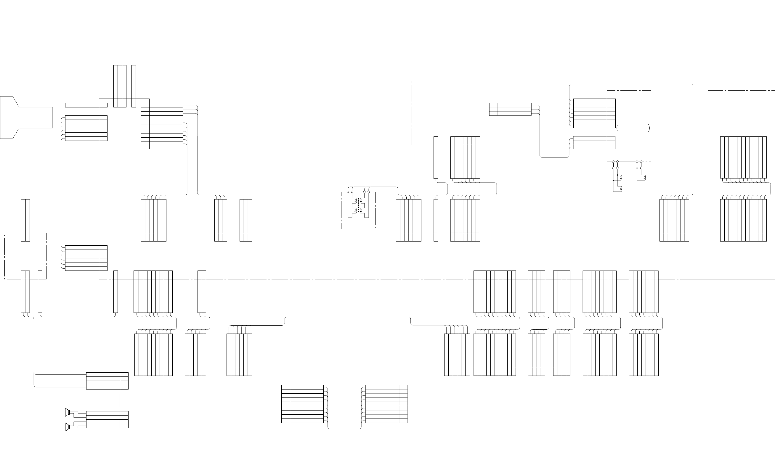
– 45 –– 44 – – 46 –
KV-XF29M80
RM-954 KV-XF29M80
RM-954
KV-XF29M80
RM-954
5-2. FRAME DIAGRAM
CN1405
CN6205
CN604
CN306
CN304
CN703
DY1
DGC
B
9V
IK
1
5
6
(RGB OUT)
1
2
3
4
5
6
1
VD+ OUT
VD- OUT
15V
N/S ROT
N/S MUTE
GND
E
CN1801
CN704
PICTURE
TUBE
1
2
3
4
5
6
H+
H+
H-
H-
V-
V+
1
2
3
4
5
6
7
VM
GND
9V
VM MUTE
GND
NC
+B
CN5901
1
2
3
4
5
6
7
8
9
10
11
C OUT
NC
NC
Y OUT
NC
NC
VIDEO IN
VCC
GND
NC
NC
CN2302
1
2
3
4
5
6
7
8
9
10
11
1
2
3
7
VM
C OUT
APCN
FSC
GND
9V
+B
Y OUT
5V
GND
GND
VIDEO
9V
GND
NT/PAL
(POWER SUPPLY, HV, MICON, Y/C JUNGLE)
1
2
3
4
5
6
7
8
9
10
1
2
3
4
CN605
CN101
L OUT
GND
CV/Y OUT
C OUT
NC
GND
SCL
SDA
11V
3D GND
3D +VCC
R OUT
3D -VCC
3D GND
1
2
3
4
5
6
7
8
9
10
1
2
3
4
1
2
3
DGC
NC
DGC
1
2
3
4
5
6
7
8
9
2
1
GND
LED 1
KEY 2
SIRCS
STBY +5V
7V
LED 2
GND
KEY 1
AC IN
AC IN
KEY 2
LED 1
GND
7V
KEY 1
SIRCS
GND
LED 2
STBY +5V
NC
NC
NC
AC OUT
AC OUT
1
2
3
4
5
6
7
8
9
1
2
3
4
5
1
2
3
4
5
6
VD+
GND
VD-
15V
NS ROT
NS MUTE
CN507
CN3901
1
2
3
4
SP OUT
SP GND
SP GND
SPR OUT
SP L
SP R
(AUDIO PROCESSOR)
VELOCITY
VM1
B2
(COMB FILTER)
A
H3
(FUNCTION KEY)
B3
C
R IN
11V
SDA
SCL
GND
S IN
C IN
CV/Y IN
GND
L IN
GND
3D -VCC
3D +VCC
GND
PROUT
MUTE
9V
3
2
1
CN6206
AV SWITCH
NECK ASSY
DY ASSY
N/S COIL +
N/S COIL -
3
1
NS COIL
CN1802
2NC
CN702
1 G2 FBT
4
3
GND
R
H13
2
1
E
200V
CN701
2G
9V
IK
GND
GND
R
B
6
5
4
3
2
1
CN305
1
2
3H1
GND
200V
CN505
CN904CN3905
CN3602
CN601
SP GND
SP GND
SP L IN
PH L IN
4
3
2
1
CN3902
4
5
7
GND
NC
NC
GND6
CN201
R OUT
GND
L OUT
GND
PROUT
MUTE
9V
7
6
5
4
3
2
1
1
2
3
4
5
6
7
GND
TV OUT
GND
TV R OUT
GND
TV L OUT
GND
CN102
6 TV L IN
GND
GND
TV R IN
7
5
4
CN1407
1
2
3
GND
TV IN
GND
STBY-MUTE8 STBY-MUTE 8
AUD GND
AUD +VCC
AUD GND
AUD +VCC
4
3
2
1
AUDI +VCC
AUDI GND
AUDI +VCC
AUDI GND
CN608
4
3
2
1
CN6200
CN6204
GND2
L IN
GND
3
4
9
5
1
Y IN
C IN
R IN
CN3904
7
6GND
CV IN
S IN8
CN1400
GND
C IN
Y IN
GND
L IN
R IN
9
5
4
3
2
1
6
7
8
GND
CV IN
S IN
MODULATION
NC
GND
6
5
MUTE4
CRT
CN4602
AC OUT
AC OUT
2
1
AC IN
AC IN
2
1
CN4601
AC IN
AC IN
4
1
CN3601
2
3NC
NC
(CISPR)
F
1GND
CN4603
CN104
GND 1
PH R IN
SP R IN5
6
6
5 R SP
R PH
1
2
3
4
L PH
L SP
AUDIO GND
AUDIO GND
CN504
CN503
1
2
3
4
5
6
7
1DF
FBP
135V
NC
GND
GND
15V
VD+
CN2822
CN2823
1
2
3
4
5
6
7
1DF
FBP
135V
NC
GND
GND
15V
VD+
D1
(DF, DQP DRIVE)
CN2801
QP+
NC
QP-
3
2
1
1
2
3
QP+
NC
QP-
CN2821
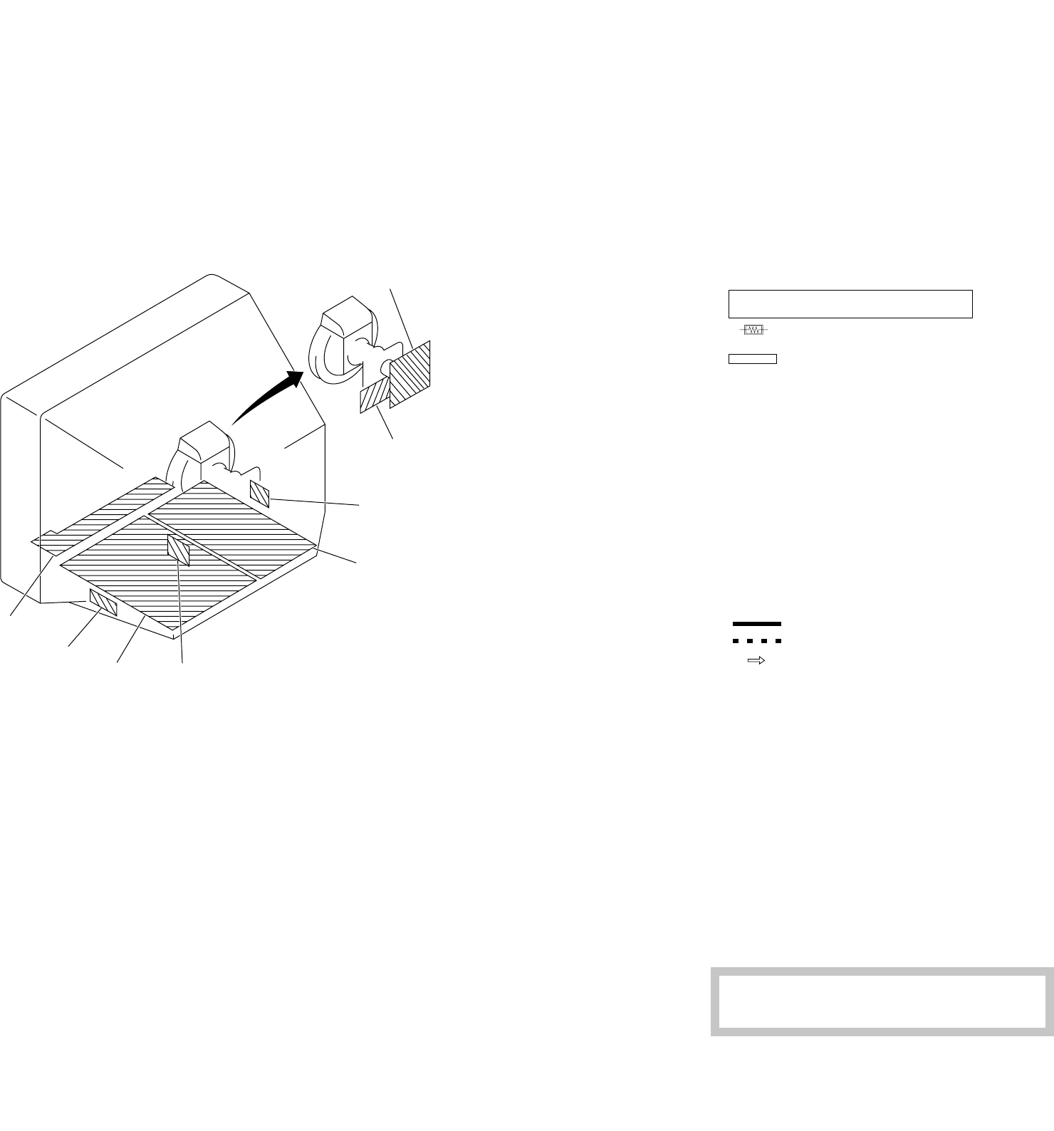
KV-XF29M80
RM-954
KV-XF29M80
RM-954
– 47 – – 48 –
5-3. CIRCUIT BOARDS LOCATION
VM1
AB2
B3
F
D1
H3
C
5-4. SCHEMATIC DIAGRAMS AND PRINTED WIRING BOARDS
Note:
•All capacitors are in µF unless otherwise noted.
•All electrolytic capacitors are rated at 50V unless otherwise noted.
•All resistors are in ohms.
k = 1000 , M = 1000k
•Indication of resistance which does not have rating electrical power is as
follows.
Pitch: 5 mm
Rating electrical power 1/4W (CHIP: 1/10W)
•: nonflammable resistor.
•¢: internal component.
•: panel designation or adjustment for repair.
•All variable and adjustable resistors have characteristic curve B unless
otherwise noted.
•Readings are taken with a color-bar signal input.
no mark : PAL
( ) : SECAM
[ ] : NTSC 3.58
« » : NTSC 4.43
•Readings are taken with a 10 M digital m ultimeter.
•Voltage are dc with respect to ground unless
otherwise noted.
•Voltage variations may be noted due to normal
production tolerances.
•All voltages are in V.
•:Cannot be measured.
•Circled numbers are waveform references.
•:B + bus.
•:B – bus.
•:signal path.
Ref erence inf ormation
RESISTOR : RN METAL FILM
: RC SOLID
: FPRD NONFLAMMABLE CARBON
: FUSE NONFLAMMABLE FUSIBLE
: RS NONFLAMMABLE METAL OXIDE
: RB NONFLAMMABLE CEMENT
: RW NONFLAMMABLE WIREWOUND
: *ADJUSTMENT RESISTOR
COIL : LF-8L MICRO INDUCTOR
CAPACITOR : TA TANTALUM
: PS STYROL
: PP POLYPROPYLENE
: PT MYLAR
: MPS METALIZED POLYESTER
: MPP METALIZED POLYPROPYLENE
: ALB BIPOLAR
: ALT HIGH TEMPERATURE
: ALR HIGH RIPPLE
*
Note: The component identified by shading and
mark ! are critical for safety. Replace only with
part number specified.
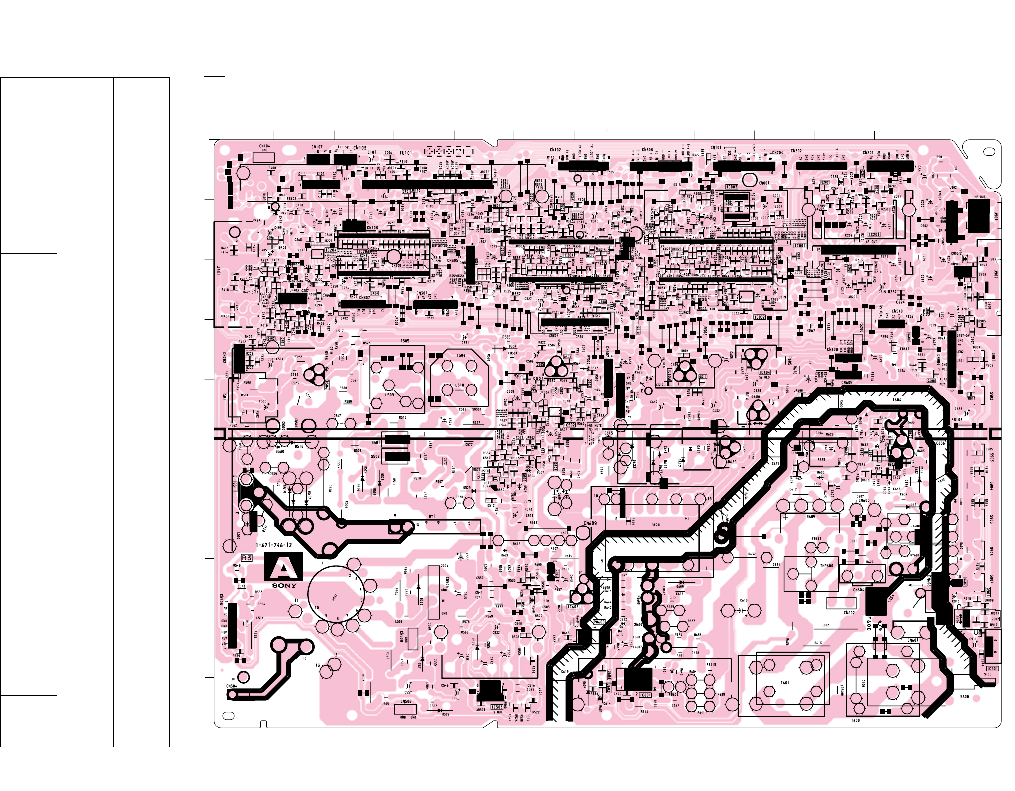
KV-XF29M80
RM-954
KV-XF29M80
RM-954
– 49 – – 50 –
A BOARD
IC
IC001 B-10
IC002 C-9
IC003 A-9
IC100 B-5
IC201 B-11
IC203 C-3
IC204 B-2
IC301 B-6
IC502 E-6
IC503 J-5
IC601 I-8
IC602 H-6
IC603 D-8
IC604 D-10
IC901 I-13
PH600 H-7
Q001 B-8
Q002 B-8
Q003 C-9
Q004 C-9
Q101 A-4
Q201 A-11
Q202 A-11
Q203 C-11
Q204 C-11
Q205 A-12
Q206 A-11
Q207 A-11
Q301 B-8
Q302 A-6
Q303 A-6
Q304 B-6
Q305 B-5
Q306 B-5
Q307 C-7
Q308 C-7
Q309 C-7
Q310 D-7
Q311 D-9
Q312 B-7
Q313 B-8
Q315 B-5
Q401 D-2
Q402 D-1
Q403 D-2
Q404 C-3
Q501 D-6
Q502 E-7
Q503 F-6
Q505 D-6
Q506 D-2
Q507 H-6
Q509 F-6
Q511 F-1
Q600 C-12
Q601 F-11
Q602 J-7
Q603 I-7
Q604 H-6
Q605 E-12
Q606 F-11
Q607 H-13
Q901 H-13
Q902 H-13
DIODE
D001 B-8
D002 C-8
D003 C-9
TRANSISTOR
D004 D-8
D005 B-8
D006 A-3
D203 C-11
D300 A-9
D301 B-9
D302 B-6
D303 B-5
D304 B-5
D305 B-5
D306 C-5
D307 C-5
D308 B-5
D309 B-6
D310 A-6
D311 C-6
D312 C-6
D313 A-8
D315 B-7
D316 C-7
D317 B-9
D314 A-9
D319 C-6
D320 C-6
D321 B-6
D401 D-2
D402 C-3
D403 B-1
D404 C-2
D405 C-1
D406 B-1
D407 C-2
D408 C-1
D409 A-1
D504 D-5
D505 H-6
D506 F-6
D507 F-6
D508 I-5
D509 E-6
D510 F-5
D511 F-5
D512 G-5
D513 I-5
D517 F-2
D518 F-2
D519 F-2
D520 E-5
D521 I-4
D522 J-4
D525 F-5
D526 F-6
D527 F-3
D528 F-3
D529 F-5
D530 F-2
D531 E-6
D532 E-6
D533 D-2
D534 E-6
D600 G-13
D601 I-8
D602 G-13
D603 F-11
D604 J-7
D605 G-10
D606 E-11
D607 F-10
D608 E-11
D609 H-8
D610 J-8
D611 I-7
D612 F-8
D613 I-7
D614 H-7
D615 E-7
D616 E-9
D617 F-8
D618 F-9
D620 D-8
D621 F-8
D622 F-7
D623 F-12
D624 F-12
D625 D-12
D627 F-8
D628 G-5
D629 F-9
D630 E-9
D631 G-12
D632 F-12
D633 E-12
D634 F-11
D635 F-12
D636 D-12
D637 F-11
D638 E-11
D901 C-13
D902 D-13
D903 C-13
D904 D-13
D905 F-13
D906 I-13
PRINTED WIRING BOARDS
– A Board –
A
123456789101112
13
B
C
D
E
F
G
H
I
J
[POWER SUPPLY, HV, MICON, Y/C JUNGLE]
A
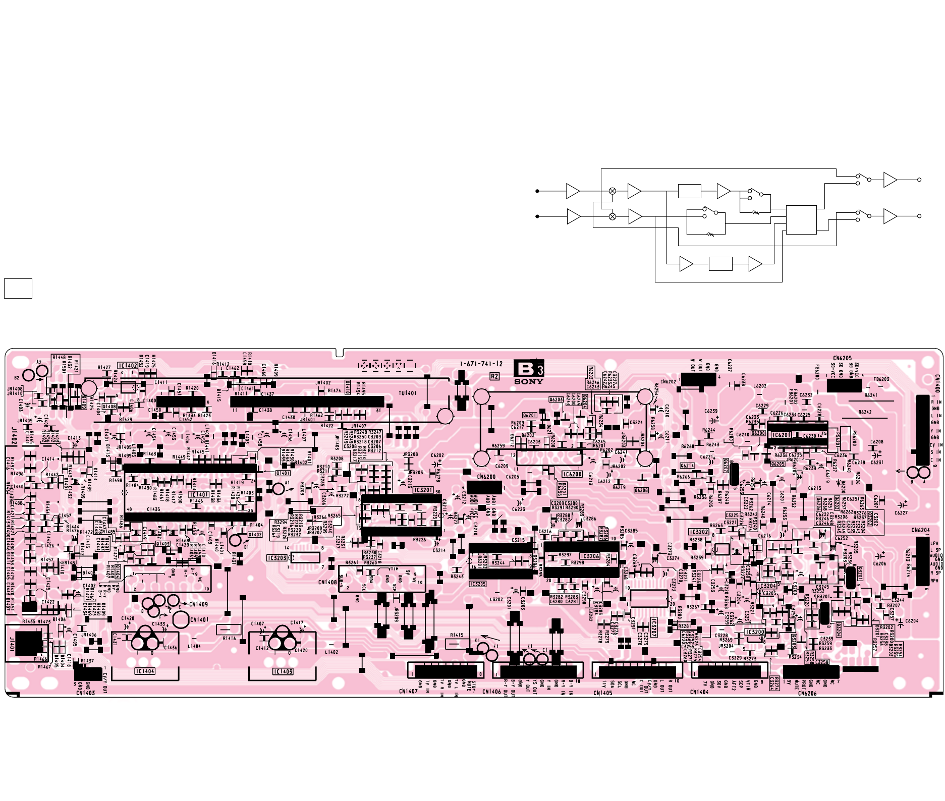
KV-XF29M80
RM-954
KV-XF29M80
RM-954
B3 BOARD IC3201 NJM2187L
– B3 Board –
PRINTED WIRING BOARDS
3D–STEREO
BYPASS
TRU
Rch out
Lch out
Rch in
Lch in TRU
3D–STEREO
TRU
SPACE VR
CENTER VR
MIX
EXT
FIL 2
EXT
FIL 1
R
R
BYPASS
TRU
B3[COMB FILTER]
– 66 –– 65 –
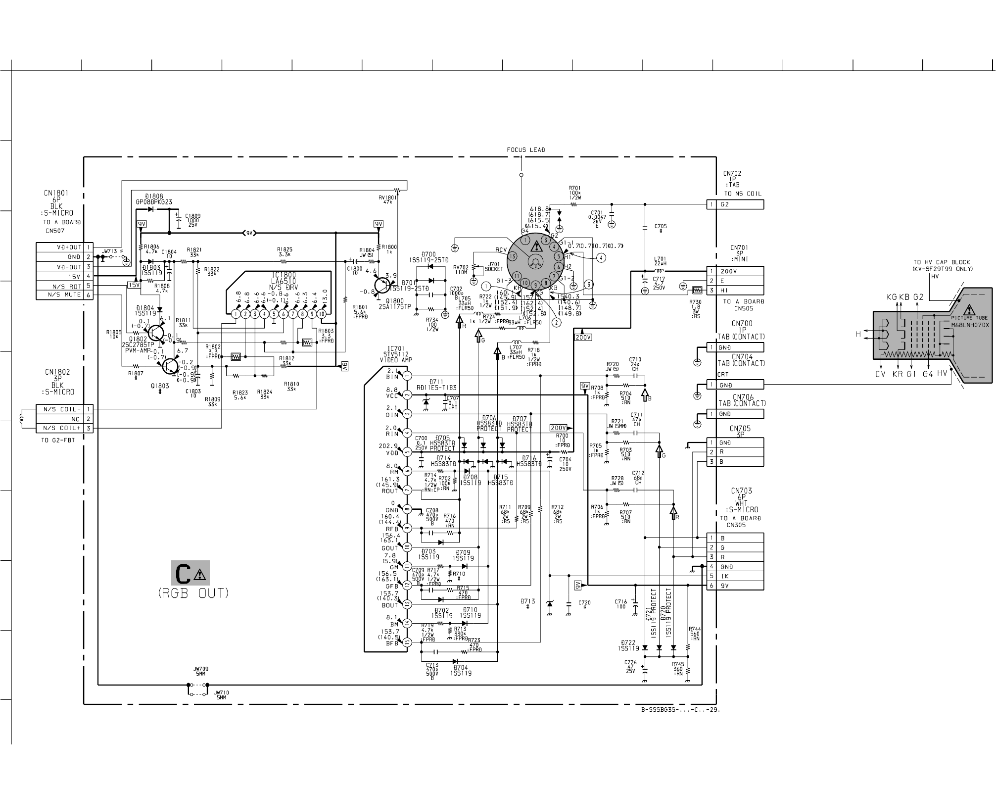
KV-XF29M80
RM-954
KV-XF29M80
RM-954
A
123456789101112
13 14
B
C
D
D
E
F
G
H
I
(5) Schematic Diagram of C Board
– 67 – – 68 –
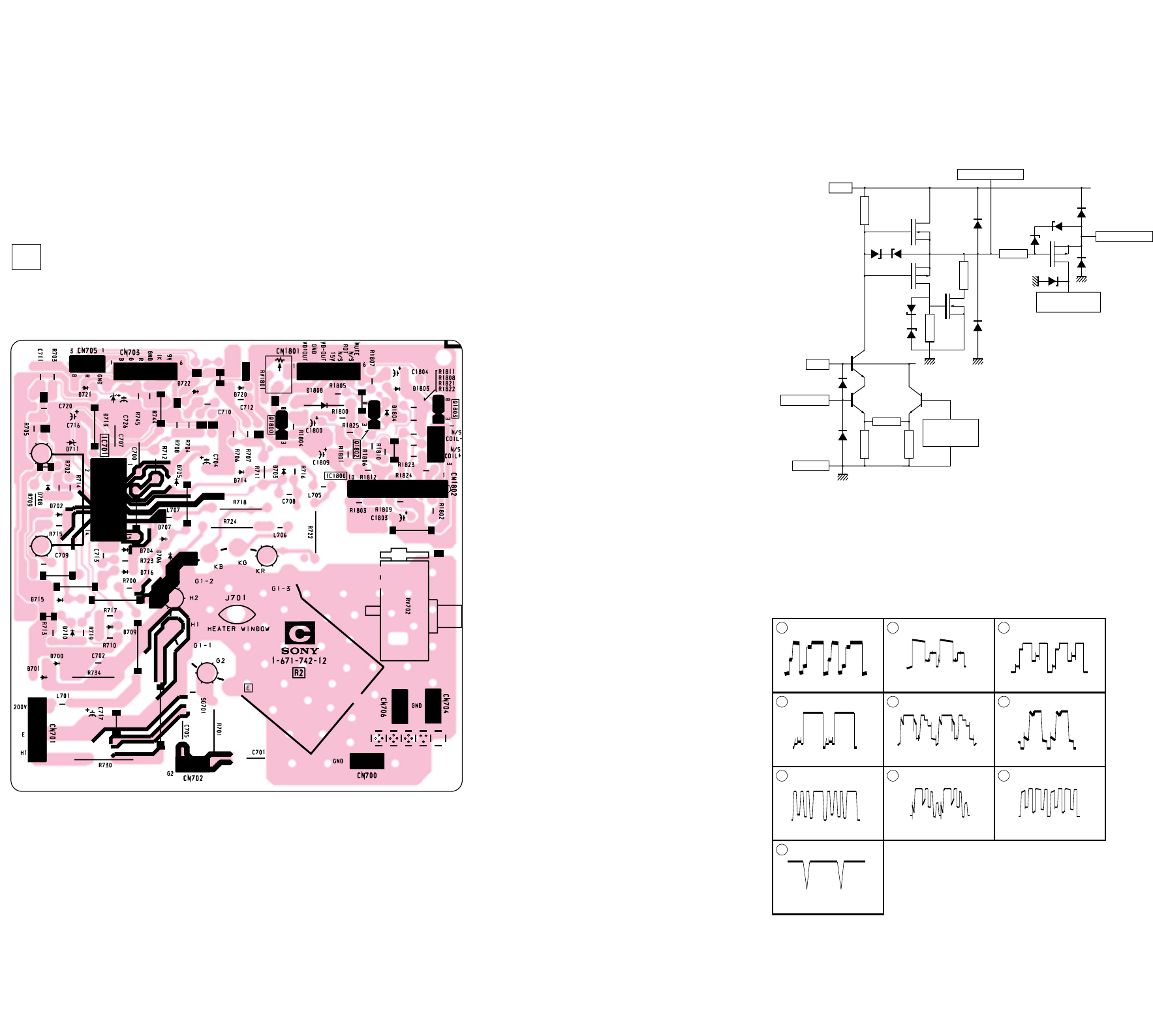
KV-XF29M80
RM-954
KV-XF29M80
RM-954
SECAMPAL
132Vp-p (H) 158Vp-p (H)
PAL SECAM
144Vp-p (H)
SECAMPAL
146Vp-p (H) 160Vp-p (H)
NTSC :
4
33
22
111
2
3
140Vp-p (H)
NTSC
NTSC
142Vp-p (H)
NTSC
118Vp-p (H) 126Vp-p (H)
25.2Vp-p (H)
PAL/SECAM : 24.8Vp-p (H)
C BOARD WAVEFORMS
– C Board –
BLUE CATHODE
CURRENT
(RED CATHODE CURRENT,
GREEN CATHODE CURRENT)
VDD
VDD
BLUE INPUT
(GREEN INPUT,
RED INPUT)
(RED FEEDBACK,
GREEN FEEDBACK)
BLUE FEEDBACK
(RED OUTPUT,
GREEN OUTPUT)
BLUE OUTPUT
GROUNDGND
REFERENCE
VOLTAGE
C BOARD IC701 STV5112
PRINTED WIRING BOARDS
[RGB OUT]
C
– 70 –– 69 –
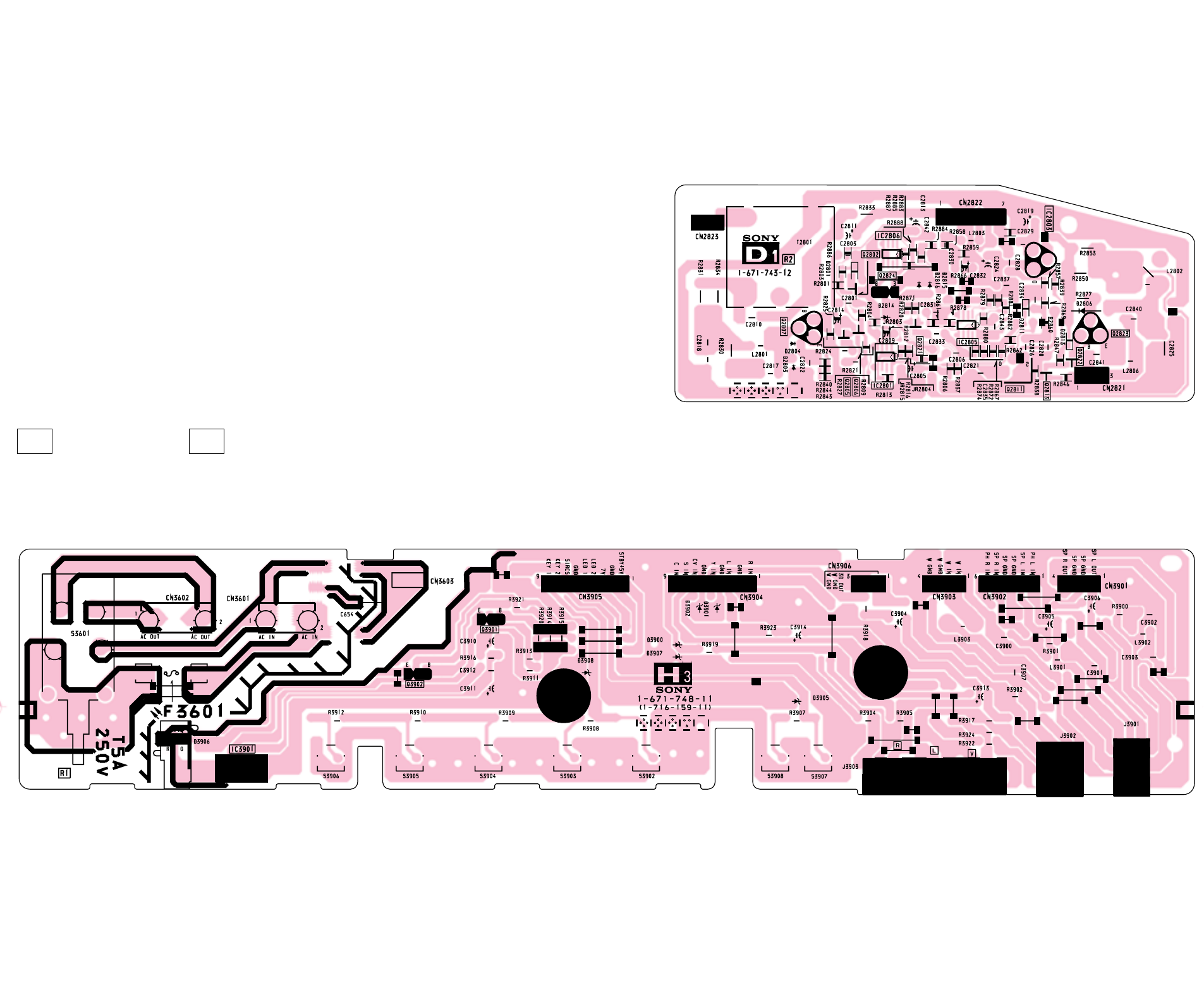
KV-XF29M80
RM-954
KV-XF29M80
RM-954
PRINTED WIRING BOARDS
– D1 Board –
[FUNCTION KEY]
H3[DF, DQP DRIVE]
D1
– 71 – – 72 –
– H3 Board –
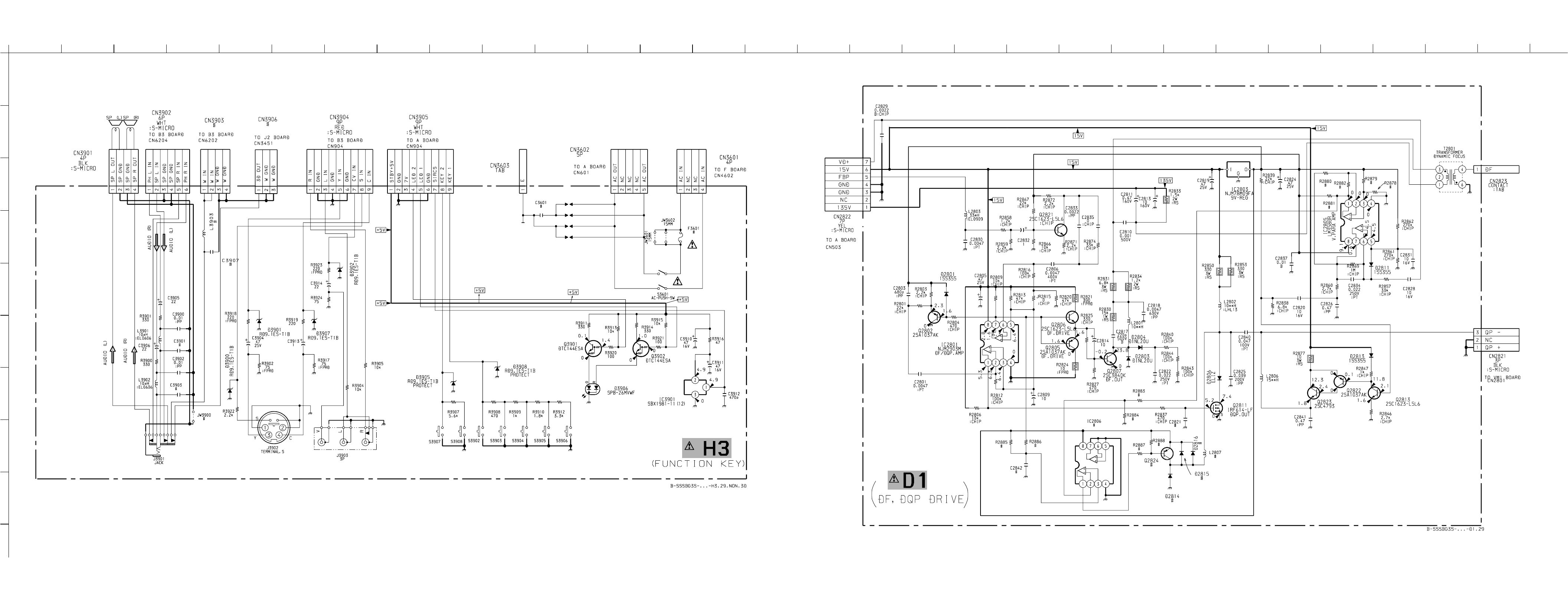
– 73– – 74 – – 75 – – 76 –
KV-XF29M80
RM-954
KV-XF29M80
RM-954 KV-XF29M80
RM-954
KV-XF29M80
RM-954
A
123456789101112
13 14 15 16 17 18 19 20 21 22 23 24 25 26 27 28 29 30
B
C
D
E
F
G
H
I
J
(6) Schematic Diagrams of H3 and D1 boards
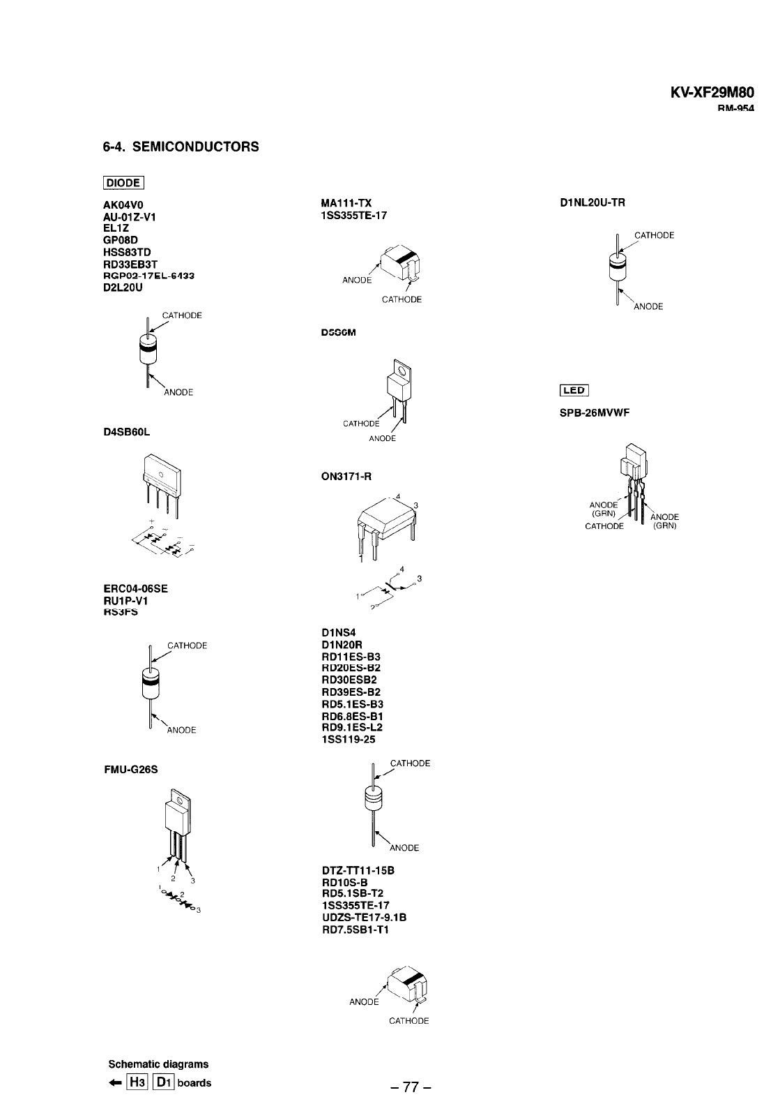
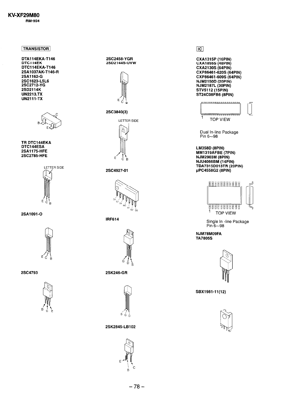
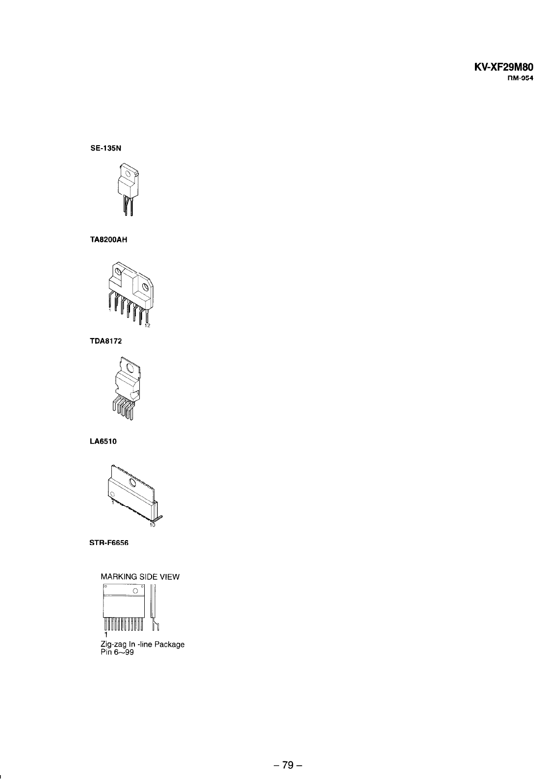
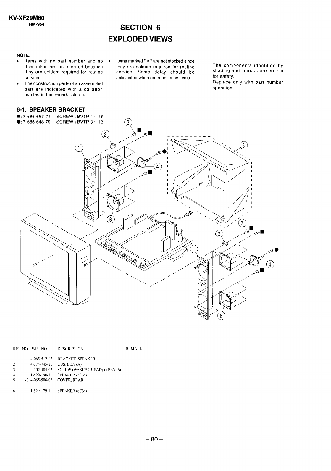
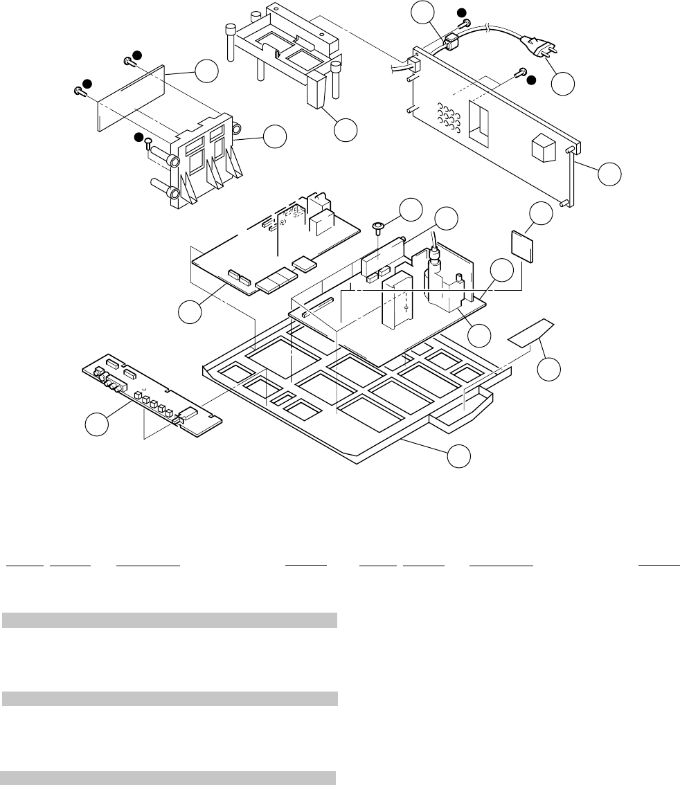
– 81 –
KV-XF29M80
RM-954
6-2. CHASSIS
r: 7-685-648-71 SCREW BVTP 3 × 12
REF. NO. PART NO. DESCRIPTION REMARK
51 * A-1372-699-A H3 BOARD MOUNTED
52 * A-1136-036-A B3 BOARD COMPLETE
53 4-022-115-00 HOLDER, AC CORD
54 !1-574-062-61 CORD, POWER (WITH CONNECTOR) 2.5A/250V
55 4-066-684-21 BRACKET, TERMINAL
56 4-046-797-01 SCREW (3X12), (+)BVTAP
57 * A-1131-478-A B2 BOARD MOUNTED
58 * A-1299-014-A A BOARD COMPLETE
59 !1-453-284-11 TRANSFORMER ASSY, FLYBACK (NX-4009//M3I4)
60 * 4-066-681-04 BRACKET, MAIN
61 * A-1343-719-A D1 BOARD MOUNTED
62 * A-1241-392-A F BOARD MOUNTED
63 * 4-066-682-01 BRACKET, F PWB
64 !8-598-449-01 TUNER,FSS BTF-LG433
REF. NO. PART NO. DESCRIPTION REMARK
57
67
62
64
63
55
53
58
59
60
61
51
52
56
54
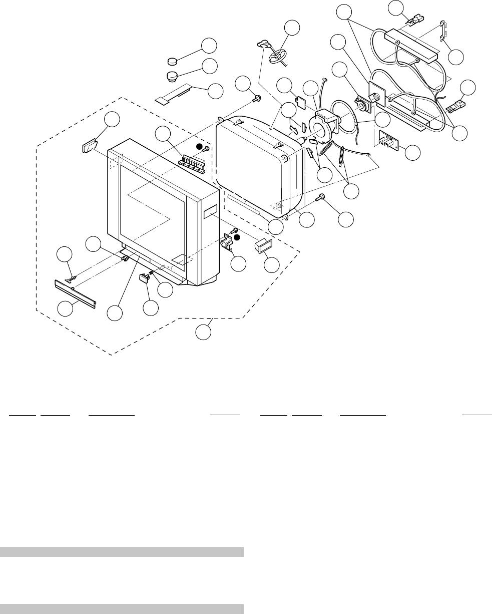
– 82 –
KV-XF29M80
RM-954
6-3. PICTURE TUBE
r: 7-685-648-79 SCREW BVTP 3 × 12
REF. NO. PART NO. DESCRIPTION REMARK
101 X-4036-454-4 BEZNET ASSY 102-110,129
102 4-036-405-11 SPRING, COMPRESSION
103 4-065-508-01 BUTTON, POWER
104 4-047-464-01 CATCHER, PUSH
105 4-045-250-21 DAMPER
106 4-065-507-22 DOOR, CONTROL
107 X-4035-861-4 HANDLE ASSY (L)
108 X-4035-862-4 HANDLE ASSY (R)
109 4-065-509-01 BUTTON, CONTROL
110 * 4-065-510-01 GUIDE, LIGHT
111 4-072-569-11 SHEET, BLOTTING
112 !8-735-056-05 PICTURE TUBE (M68LNH070X)
113 4-046-765-12 SCREW, TAPPING 7+CROWN WASHER
114 * 3-704-372-11 HOLDER, HV CABLE
115 4-046-600-11 SPACER, DY
116 2-163-920-01 PLATE, TLH CORRECTION
117 !8-451-494-31 DEFLECTION YOKE (Y29RSA-S)
118 8-453-011-11 NA299-M
119 * A-1331-987-A C BOARD MOUNTED
120 1-416-495-11 COIL, DEMAGNETIC
REF. NO. PART NO. DESCRIPTION REMARK
121 * 4-062-970-11 CLIP (29RSN), DGC
122 4-061-369-01 HOLDER, DEGAUSE COIL
123 1-452-896-11 COIL, NA ROTATION (RT200)
124 * A-1342-501-A VM1 BOARD MOUNTED
125 4-369-318-61 SPRING, TENSION
126 1-452-032-00 MAGNET,DISC
127 1-452-094-00 CIRCULAR DISC MAGNET B
128 X-4387-214-3 PERMALOY ASSY, CORRECTION
129 4-032-761-01 SHAFT (S), DOOR
130 4-068-028-01 BAND, DGC
126
127
128
108 109
104
102
103
129
101
106
105 110 107
112
111 113
115
117
116
114
115
113 118
119
124
123
121
120
122
121
130
125

– 83 –
REF. NO. PART NO. DESCRIPTION REMARK
The components identified by shading
and mark ! are critical for safety.
Replace only with part number specified.
REF. NO. PART NO. DESCRIPTION REMARK
KV-XF29M80
RM-954
* A-1299-014-A A BOARD COMPLETE
********************
4-382-854-11 SCREW (M3X10), P, SW (+)
4-382-854-21 SCREW (M3X14), P, SW (+)
<CAPACITOR>
C004 1-163-001-11 CERAMIC CHIP 220PF 10% 50V
C005 1-163-001-11 CERAMIC CHIP 220PF 10% 50V
C006 1-164-004-11 CERAMIC CHIP 0.1MF 10% 25V
C007 1-104-664-11 ELECT 47MF 20% 16V
C013 1-163-021-91 CERAMIC CHIP 0.01MF 10% 50V
C014 1-104-664-11 ELECT 47MF 20% 25V
C015 1-163-009-11 CERAMIC CHIP 0.001MF 10% 50V
C016 1-163-243-11 CERAMIC CHIP 47PF 5% 50V
C017 1-163-113-00 CERAMIC CHIP 68PF 5% 50V
C019 1-104-664-11 ELECT 47MF 20% 25V
C022 1-163-227-11 CERAMIC CHIP 10PF 0.5PF 50V
C023 1-163-227-11 CERAMIC CHIP 10PF 0.5PF 50V
C024 1-163-227-11 CERAMIC CHIP 10PF 0.5PF 50V
C026 1-164-004-11 CERAMIC CHIP 0.1MF 10% 25V
C027 1-164-004-11 CERAMIC CHIP 0.1MF 10% 25V
C028 1-163-037-11 CERAMIC CHIP 0.022MF 10% 50V
C030 1-126-965-11 ELECT 22MF 20% 50V
C031 1-164-004-11 CERAMIC CHIP 0.1MF 10% 25V
C032 1-107-823-11 CERAMIC CHIP 0.47MF 10% 16V
C034 1-163-031-11 CERAMIC CHIP 0.01MF 50V
C041 1-163-251-11 CERAMIC CHIP 100PF 5% 50V
C042 1-163-251-11 CERAMIC CHIP 100PF 5% 50V
C044 1-163-251-11 CERAMIC CHIP 100PF 5% 50V
C047 1-163-251-11 CERAMIC CHIP 100PF 5% 50V
C103 1-164-004-11 CERAMIC CHIP 0.1MF 10% 25V
C104 1-104-665-11 ELECT 100MF 20% 10V
C107 1-163-005-11 CERAMIC CHIP 470PF 10% 50V
C108 1-104-664-11 ELECT 47MF 20% 16V
C109 1-163-005-11 CERAMIC CHIP 470PF 10% 50V
C110 1-163-005-11 CERAMIC CHIP 470PF 10% 50V
C111 1-163-005-11 CERAMIC CHIP 470PF 10% 50V
C112 1-104-664-11 ELECT 47MF 20% 16V
C113 1-104-664-11 ELECT 47MF 20% 25V
C114 1-126-967-11 ELECT 47MF 20% 50V
C300 1-164-505-11 CERAMIC CHIP 2.2MF 16V
C301 1-126-935-11 ELECT 470MF 20% 16V
C302 1-163-005-11 CERAMIC CHIP 470PF 10% 50V
C303 1-126-959-11 ELECT 0.47MF 20% 50V
C304 1-126-967-11 ELECT 47MF 20% 50V
C305 1-164-004-11 CERAMIC CHIP 0.1MF 10% 25V
REF.NO. PART NO. DESCRIPTION REMARKREF.NO. PART NO. DESCRIPTION REMARK
C306 1-163-233-11 CERAMIC CHIP 18PF 5% 50V
C307 1-163-233-11 CERAMIC CHIP 18PF 5% 50V
C308 1-163-259-91 CERAMIC CHIP 220PF 5% 50V
C309 1-126-957-11 ELECT 0.22MF 20% 50V
C311 1-126-964-11 ELECT 10MF 20% 50V
C312 1-164-346-11 CERAMIC CHIP 1MF 16V
C313 1-164-346-11 CERAMIC CHIP 1MF 16V
C315 1-164-004-11 CERAMIC CHIP 0.1MF 10% 25V
C316 1-104-664-11 ELECT 47MF 20% 25V
C317 1-164-004-11 CERAMIC CHIP 0.1MF 10% 25V
C318 1-163-031-11 CERAMIC CHIP 0.01MF 50V
C319 1-163-031-11 CERAMIC CHIP 0.01MF 50V
C320 1-163-031-11 CERAMIC CHIP 0.01MF 50V
C322 1-163-005-11 CERAMIC CHIP 470PF 10% 50V
C323 1-126-965-11 ELECT 22MF 20% 50V
C324 1-163-017-00 CERAMIC CHIP 0.0047MF 10% 50V
C325 1-126-960-11 ELECT 1MF 20% 50V
C327 1-126-965-11 ELECT 22MF 20% 50V
C328 1-164-004-11 CERAMIC CHIP 0.1MF 10% 25V
C329 1-126-965-11 ELECT 22MF 20% 50V
C330 1-164-004-11 CERAMIC CHIP 0.1MF 10% 25V
C331 1-126-963-11 ELECT 4.7MF 20% 50V
C332 1-126-963-11 ELECT 4.7MF 20% 50V
C335 1-164-004-11 CERAMIC CHIP 0.1MF 10% 25V
C336 1-164-004-11 CERAMIC CHIP 0.1MF 10% 25V
C337 1-126-961-11 ELECT 2.2MF 20% 50V
C338 1-163-017-00 CERAMIC CHIP 0.0047MF 10% 50V
C341 1-115-340-11 CERAMIC CHIP 0.22MF 10% 25V
C342 1-163-259-91 CERAMIC CHIP 220PF 5% 50V
C502 1-163-145-00 CERAMIC CHIP 0.0015MF 5% 50V
C503 1-126-964-11 ELECT 10MF 20% 50V
C506 1-107-638-11 ELECT 33MF 20% 160V
C507 1-161-830-00 CERAMIC 0.0047MF 500V
C510 1-102-112-00 CERAMIC 330PF 10% 50V
C513 1-163-263-11 CERAMIC CHIP 330PF 5% 50V
C514 1-106-383-00 MYLAR 0.047MF 10% 200V
C517 1-164-182-11 CERAMIC CHIP 0.0033MF 10% 50V
C518 1-104-665-11 ELECT 100MF 20% 10V
C519 1-102-212-00 CERAMIC 820PF 10% 500V
C521 1-126-934-11 ELECT 220MF 20% 16V
C522 1-126-933-11 ELECT 100MF 20% 16V
C523 1-102-002-00 CERAMIC 680PF 10% 500V
C524 1-126-967-11 ELECT 47MF 20% 50V
C526 1-130-495-00 MYLAR 0.1MF 5% 50V
C527 1-102-820-00 CERAMIC 330PF 5% 50V
C528 1-162-116-00 CERAMIC 680PF 10% 2KV
C530 1-137-372-11 FILM 0.022MF 5% 50V
SECTION 7
ELECTRICAL PARTS LIST
NOTE:
The components identified by shading
and mark ! are critical for safety.
Replace only with part number specified.
When indicating parts by reference
number, please include the board name.
•All resistors are in ohms
•F : nonflammable
CAPACITORS
•MF : µF, PF : µµF
COILS
• MMH : mH, UH : µH
•Items marked " ∗ " are not stocked since they
are seldom required for routine service.
Some delay should be anticipated when or-
dering these items.
•All variable and adjustable resistors have
characteristic curve B, unless otherwise
noted.
A

– 84 –
REF. NO. PART NO. DESCRIPTION REMARK REF. NO. PART NO. DESCRIPTION REMARK
The components identified by shading
and mark ! are critical for safety.
Replace only with part number specified.
KV-XF29M80
RM-954
C531 1-107-903-11 ELECT 2.2MF 20% 50V
C532 1-126-941-11 ELECT 470MF 20% 25V
C533 1-126-941-11 ELECT 470MF 20% 25V
C536 1-136-165-00 FILM 0.1MF 5% 50V
C537 1-126-969-11 ELECT 220MF 20% 50V
C538 1-136-617-11 FILM 0.019MF 3% 2KV
C539 1-129-723-00 FILM 0.056MF 5% 630V
C540 1-136-171-00 FILM 0.33MF 5% 50V
C546 1-165-319-11 CERAMIC CHIP 0.1MF 50V
C549 1-163-017-00 CERAMIC CHIP 0.0047MF 10% 50V
C550 1-106-220-00 MYLAR 0.1MF 10% 100V
C551 1-126-960-11 ELECT 1MF 20% 50V
C552 1-162-116-00 CERAMIC 680PF 10% 2KV
C553 1-162-116-00 CERAMIC 680PF 10% 2KV
C554 1-137-417-11 MYLAR 0.0047MF 10% 200V
C556 1-126-941-11 ELECT 470MF 20% 25V
C557 1-126-941-11 ELECT 470MF 20% 25V
C558 1-123-024-21 ELECT 33MF 160V
C560 1-102-228-00 CERAMIC 470PF 10% 500V
C561 1-129-898-00 FILM 0.0022MF 5% 630V
C562 1-102-228-00 CERAMIC 470PF 10% 500V
C564 1-163-038-91 CERAMIC CHIP 0.1MF 25V
C565 1-107-655-11 ELECT 47MF 20% 250V
C566 1-102-244-00 CERAMIC 220PF 10% 500V
C567 1-115-520-11 FILM 0.68MF 5% 250V
C568 1-102-228-00 CERAMIC 470PF 10% 500V
C570 1-115-522-11 FILM 1MF 5% 250V
C572 1-117-661-71 FILM 0.15MF 5% 250V
C573 1-106-387-00 MYLAR 0.068MF 10% 200V
C574 1-107-652-11 ELECT 10MF 20% 250V
C576 1-130-495-00 MYLAR 0.1MF 5% 50V
C577 1-106-395-00 MYLAR 0.15MF 10% 200V
C582 1-164-004-11 CERAMIC CHIP 0.1MF 10% 25V
C584 1-163-251-11 CERAMIC CHIP 100PF 5% 50V
C586 1-163-251-11 CERAMIC CHIP 100PF 5% 50V
C600 !1-104-705-11 FILM 0.1MF 20% 250V
C601 1-136-601-11 FILM 0.01MF 5% 630V
C603 1-104-664-11 ELECT 47MF 20% 25V
C604 1-163-009-11 CERAMIC CHIP 0.001MF 10% 50V
C605 !1-119-886-51 CERAMIC 470PF 10% 250V
C606 !1-119-886-51 CERAMIC 470PF 10% 250V
C607 1-161-830-00 CERAMIC 0.0047MF 99% 500V
C608 1-161-830-00 CERAMIC 0.0047MF 99% 500V
C609 1-126-968-11 ELECT 100MF 20% 50V
C610 1-126-964-11 ELECT 10MF 20% 50V
C611 1-161-830-00 CERAMIC 0.0047MF 99% 500V
C612 1-161-830-00 CERAMIC 0.0047MF 99% 500V
C613 1-125-906-11 ELECT 560MF 20% 450V
C614 1-126-964-11 ELECT 10MF 20% 50V
C615 !1-119-886-51 CERAMIC 470PF 10% 250V
C616 1-130-202-00 FILM 0.022MF 5% 400V
C617 1-107-792-11 CERAMIC 100PF 5% 1KV
C618 1-125-893-11 FILM 680PF 3% 1.5KV
C619 !1-119-886-51 CERAMIC 470PF 10% 250V
C620 1-163-133-00 CERAMIC CHIP 470PF 5% 50V
C621 1-102-114-00 CERAMIC 470PF 10% 50V
C622 1-102-119-00 CERAMIC 0.0015MF 10% 50V
C623 1-104-665-11 ELECT 100MF 20% 25V
C624 1-125-772-91 CERAMIC 1500PF 10% 2KV
C625 1-102-002-00 CERAMIC 680PF 10% 500V
C626 1-102-002-00 CERAMIC 680PF 10% 500V
C629 1-126-964-11 ELECT 10MF 20% 50V
C630 1-125-494-11 ELECT(BLOCK) 560MF 20% 160V
C631 1-128-550-11 ELECT 2200MF 20% 50V
C632 1-128-339-11 ELECT 2200MF 20% 16V
C633 1-104-999-11 MYLAR 0.1MF 10% 200V
C634 1-126-933-11 ELECT 100MF 20% 16V
C635 1-104-665-11 ELECT 100MF 20% 10V
C636 1-104-760-11 CERAMIC CHIP 0.047MF 10% 50V
C638 1-161-830-00 CERAMIC 0.0047MF 500V
C641 1-102-002-00 CERAMIC 680PF 10% 500V
C642 1-126-943-11 ELECT 2200MF 20% 25V
C643 1-104-665-11 ELECT 100MF 20% 10V
C644 1-104-331-11 CERAMIC 0.0022MF 10% 1KV
C645 1-137-605-11 FILM 0.01MF 10% 250V
C646 1-107-679-91 ELECT 10MF 20% 450V
C647 1-163-275-11 CERAMIC CHIP 0.001MF 5% 50V
C649 1-126-940-11 ELECT 330MF 20% 25V
C650 1-163-275-11 CERAMIC CHIP 0.001MF 5% 50V
C651 1-163-133-00 CERAMIC CHIP 470PF 5% 50V
C652 1-126-965-11 ELECT 22MF 20% 50V
C653 1-104-664-11 ELECT 47MF 20% 25V
C655 !1-119-886-51 CERAMIC 470PF 10% 250V
C657 1-101-821-00 CERAMIC 0.0022MF 500V
C912 1-164-004-11 CERAMIC CHIP 0.1MF 10% 25V
C913 1-104-665-11 ELECT 100MF 20% 10V
<CONNECTOR>
CN101 * 1-779-890-11 CONNECTOR, BOARD TO BOARD 10P
CN102 * 1-779-889-11 CONNECTOR, BOARD TO BOARD 8P
CN104 1-695-915-11 TAB (CONTACT)
CN105 * 1-508-784-21 PIN, CONNECTOR (5MM PITCH) 1P
CN106 * 1-564-506-11 PLUG, CONNECTOR 3P
CN201 * 1-564-508-11 PLUG, CONNECTOR 5P
CN202 * 1-508-847-00 PIN, CONNECTOR 4P
CN304 * 1-766-955-11 CONNECTOR, BOARD TO BOARD 11P
CN305 * 1-564-509-11 PLUG, CONNECTOR 6P
CN501 * 1-508-784-21 PIN, CONNECTOR (5MM PITCH) 1P
CN502 * 1-508-784-21 PIN, CONNECTOR (5MM PITCH) 1P
CN503 * 1-564-510-11 PLUG, CONNECTOR 7P
CN504 1-695-915-11 TAB (CONTACT)
CN505 1-508-766-00 PIN, CONNECTOR (5MM PITCH) 4P
CN507 * 1-564-509-11 PLUG, CONNECTOR 6P
CN508 1-695-915-11 TAB (CONTACT)
CN509 1-695-915-11 TAB (CONTACT)
CN601 * 1-580-843-11 PIN, CONNECTOR (POWER)
CN602 * 1-508-786-00 PIN, CONNECTOR (5MM PITCH) 2P
CN603 * 1-508-784-21 PIN, CONNECTOR (5MM PITCH) 1P
CN604 * 1-573-963-11 PIN, CONNECTOR (PC BOARD) 3P
CN608 * 1-564-507-11 PLUG, CONNECTOR 4P
CN904 * 1-564-512-11 PLUG, CONNECTOR 9P
A

– 85 –
REF. NO. PART NO. DESCRIPTION REMARK
The components identified by shading
and mark ! are critical for safety.
Replace only with part number specified.
REF. NO. PART NO. DESCRIPTION REMARK
KV-XF29M80
RM-954
<DIODE>
D001 8-719-988-61 DIODE 1SS355TE-17
D002 8-719-988-61 DIODE 1SS355TE-17
D005 8-719-988-61 DIODE 1SS355TE-17
D006 1-216-295-91 SHORT 0
D300 1-216-295-91 SHORT 0
D301 8-719-988-61 DIODE 1SS355TE-17
D303 8-719-988-61 DIODE 1SS355TE-17
D304 8-719-988-61 DIODE 1SS355TE-17
D305 8-719-988-61 DIODE 1SS355TE-17
D306 8-719-988-61 DIODE 1SS355TE-17
D307 8-719-988-61 DIODE 1SS355TE-17
D308 8-719-988-61 DIODE 1SS355TE-17
D309 8-719-069-54 DIODE UDZS-TE17-5.1B
D311 8-719-988-61 DIODE 1SS355TE-17
D312 8-719-988-61 DIODE 1SS355TE-17
D313 8-719-988-61 DIODE 1SS355TE-17
D315 8-719-988-61 DIODE 1SS355TE-17
D316 8-719-037-06 DIODE RD7.5SB1-T1
D320 8-719-069-60 DIODE UDZS-TE17-9.1B
D321 8-719-069-60 DIODE UDZS-TE17-9.1B
D504 8-719-302-43 DIODE EL1Z
D505 8-719-988-61 DIODE 1SS355TE-17
D506 8-719-911-19 DIODE 1SS119-25
D507 8-719-988-61 DIODE 1SS355TE-17
D508 8-719-988-61 DIODE 1SS355TE-17
D509 1-216-073-00 RES,CHIP 10K 5% 1/10W
D510 8-719-988-61 DIODE 1SS355TE-17
D511 8-719-988-61 DIODE 1SS355TE-17
D512 8-719-988-61 DIODE 1SS355TE-17
D513 8-719-908-03 DIODE GP08D
D517 8-719-312-71 DIODE RS3FS
D518 8-719-074-35 DIODE RU4AM-T4
D519 8-719-312-71 DIODE RS3FS
D521 8-719-302-43 DIODE EL1Z
D522 8-719-028-45 DIODE D2L20U
D523 8-719-302-43 DIODE EL1Z
D527 8-719-908-03 DIODE GP08D
D528 8-719-908-03 DIODE GP08D
D531 8-719-988-61 DIODE 1SS355TE-17
D532 8-719-988-61 DIODE 1SS355TE-17
D534 8-719-988-61 DIODE 1SS355TE-17
D600 8-719-911-19 DIODE 1SS119-25
D602 8-719-911-19 DIODE 1SS119-25
D603 8-719-150-92 DIODE RD33EB3T
D604 8-719-028-72 DIODE RGP02-17EL-6433
D605 8-719-510-53 DIODE D4SB60L
D606 8-719-108-18 THYRISTOR 5P6M
D607 8-719-073-01 DIODE MA111-(K8).S0
D608 8-719-110-53 DIODE RD20ESB2
D609 8-719-311-31 DIODE RU-1P
D610 8-719-043-76 DIODE AK04V0
D611 8-719-046-74 DIODE AU-01Z-V1
D612 8-719-071-38 DIODE D5S6M
D613 8-719-046-74 DIODE AU-01Z-V1
D614 8-719-046-74 DIODE AU-01Z-V1
D620 8-719-110-72 DIODE RD30ESB2
D621 8-719-071-38 DIODE D5S6M
D622 8-719-071-39 DIODE FMU-G26S
D623 8-719-978-65 DIODE DTZ-TT11-15B
D624 8-719-073-01 DIODE MA111-(K8).S0
D625 8-719-977-28 DIODE DTZ10B
D628 8-719-911-19 DIODE 1SS119-25
D630 8-719-052-74 DIODE FMX-12S
D631 8-719-068-00 DIODE ERC04-06SE
D632 8-719-068-00 DIODE ERC04-06SE
D633 8-719-030-25 DIODE EG01CV0
D634 8-719-073-01 DIODE MA111-(K8).S0
D635 8-719-073-01 DIODE MA111-(K8).S0
D636 8-719-510-02 DIODE D1NS4
D637 8-719-109-96 DIODE RD6.8ESB1
D638 8-719-510-48 DIODE D1N20R
<CONNECTOR>
DY1 *1-580-798-11 CONNECTOR PIN (DY) 6P
<FERRITE BEAD>
FB501 1-410-397-21 FERRITE 1.1UH
FB502 1-410-397-21 FERRITE 1.1UH
FB600 1-410-397-21 FERRITE 1.1UH
FB601 1-410-397-21 FERRITE 1.1UH
FB602 1-410-397-21 FERRITE 1.1UH
FB603 1-410-397-21 FERRITE 1.1UH
FB604 1-410-397-21 FERRITE 1.1UH
FB605 1-412-911-31 FERRITE 0UH
FB606 1-412-911-31 FERRITE 0UH
FB608 1-412-911-31 FERRITE 0UH
FB611 1-410-397-21 FERRITE 1.1UH
FB612 1-410-397-21 FERRITE 1.1UH
FB613 1-412-911-11 FERRITE 0UH
FB615 1-410-397-21 FERRITE 1.1UH
<IC>
IC001 8-752-905-63 IC CXP86461-620S
IC002 8-759-371-21 IC MM1319AFBE
IC003 8-759-370-34 IC ST24C08FB6
IC003 8-759-527-71 IC M24C08-BN6
IC301 8-752-088-39 IC CXA2130S
IC502 8-759-700-07 IC NJM2903M
IC503 8-759-980-58 IC TDA8172
IC601 8-749-014-48 IC STR-F6656
IC602 8-749-920-61 IC SE-135N
IC603 8-759-701-59 IC NJM78M09FA
IC604 8-759-231-53 IC TA7805S
A

– 86 –
REF. NO. PART NO. DESCRIPTION REMARK REF. NO. PART NO. DESCRIPTION REMARK
The components identified by shading
and mark ! are critical for safety.
Replace only with part number specified.
KV-XF29M80
RM-954
<CHIP CONDUCTOR>
JR001 1-216-295-91 SHORT 0
JR002 1-216-295-91 SHORT 0
JR004 1-216-295-91 SHORT 0
JR005 1-216-295-91 SHORT 0
JR006 1-216-295-91 SHORT 0
JR007 1-216-295-91 SHORT 0
JR008 1-216-295-91 SHORT 0
JR010 1-216-295-91 SHORT 0
JR012 1-216-295-91 SHORT 0
JR014 1-216-295-91 SHORT 0
JR015 1-216-295-91 SHORT 0
JR016 1-216-295-91 SHORT 0
JR102 1-216-295-91 SHORT 0
JR109 1-216-295-91 SHORT 0
JR301 1-216-295-91 SHORT 0
JR303 1-216-295-91 SHORT 0
JR500 1-216-295-91 SHORT 0
JR501 1-216-295-91 SHORT 0
JR502 1-216-295-91 SHORT 0
JR503 1-216-295-91 SHORT 0
JR600 1-216-295-91 SHORT 0
<COIL>
L002 1-414-856-11 INDUCTOR 10UH
L003 1-414-180-11 INDUCTOR 3.3UH
L005 1-414-233-22 INDUCTOR CHIP 0UH
L101 1-414-856-11 INDUCTOR 10UH
L102 1-414-856-11 INDUCTOR 10UH
L103 1-414-856-11 INDUCTOR 10UH
L104 1-414-856-11 INDUCTOR 10UH
L105 1-414-856-11 INDUCTOR 10UH
L301 1-414-189-31 INDUCTOR 100UH
L302 1-414-185-41 INDUCTOR 22UH
L501 1-412-525-31 INDUCTOR 10UH
L502 1-422-613-11 COIL, AIR CORE
L503 1-412-525-31 INDUCTOR 10UH
L504 1-412-525-31 INDUCTOR 10UH
L505 1-412-525-31 INDUCTOR 10UH
L506 1-412-525-31 INDUCTOR 10UH
L507 1-416-931-11 INDUCTOR 0UH
L508 1-412-525-31 INDUCTOR 10UH
L511 1-406-977-21 INDUCTOR 100UH
L512 1-412-549-31 INDUCTOR 1MMH
L513 1-412-549-31 INDUCTOR 1MMH
L515 1-459-104-00 COIL, WITH CORE
L518 1-414-187-11 INDUCTOR 47UH
L601 1-412-527-11 INDUCTOR 15UH
L905 1-414-856-11 INDUCTOR 10UH
<PHOTO COUPLER>
PH600 !8-749-924-35 PHOTO COUPLER ON3171-R
<TRANSISTOR>
Q001 8-729-216-22 TRANSISTOR 2SA1162-G
Q002 8-729-230-49 TRANSISTOR 2SC2712-YG
Q003 8-729-424-08 TRANSISTOR UN2111
Q004 8-729-421-22 TRANSISTOR UN2211
Q101 8-729-230-49 TRANSISTOR 2SC2712-YG
Q301 8-729-216-22 TRANSISTOR 2SA1162-G
Q302 8-729-230-49 TRANSISTOR 2SC2712-YG
Q303 8-729-216-22 TRANSISTOR 2SA1162-G
Q305 8-729-216-22 TRANSISTOR 2SA1162-G
Q306 8-729-216-22 TRANSISTOR 2SA1162-G
Q307 8-729-230-49 TRANSISTOR 2SC2712-YG
Q308 8-729-216-22 TRANSISTOR 2SA1162-G
Q312 8-729-216-22 TRANSISTOR 2SA1162-G
Q313 8-729-230-49 TRANSISTOR 2SC2712-YG
Q315 8-729-421-19 TRANSISTOR UN2213
Q501 8-729-216-22 TRANSISTOR 2SA1162-G
Q502 8-729-216-22 TRANSISTOR 2SA1162-G
Q503 8-729-230-49 TRANSISTOR 2SC2712-YG
Q505 8-729-931-45 TRANSISTOR IRF614
Q506 8-729-140-96 TRANSISTOR 2SD774-34
Q507 8-729-216-22 TRANSISTOR 2SA1162-G
Q509 8-729-230-49 TRANSISTOR 2SC2712-YG
Q511 8-729-016-32 TRANSISTOR 2SC4927-01
Q600 8-729-119-78 TRANSISTOR 2SC2785-HFE
Q601 8-729-023-22 TRANSISTOR 2SD2114K
Q602 8-729-230-49 TRANSISTOR 2SC2712-YG
Q603 8-729-424-08 TRANSISTOR UN2111
Q604 8-729-200-17 TRANSISTOR 2SA1091-O
Q605 8-729-044-30 TRANSISTOR 2SK2845-LB102
Q606 8-729-230-49 TRANSISTOR 2SC2712-YG
Q607 8-729-922-37 TRANSISTOR 2SD2144S-UVW
Q608 8-729-230-49 TRANSISTOR 2SC2712-YG
<RESISTOR>
R001 1-414-233-22 INDUCTOR CHIP 0UH
R002 1-216-025-91 RES,CHIP 100 5% 1/10W
R003 1-216-073-00 RES,CHIP 10K 5% 1/10W
R004 1-216-025-91 RES,CHIP 100 5% 1/10W
R005 1-216-025-91 RES,CHIP 100 5% 1/10W
R008 1-216-065-91 RES,CHIP 4.7K 5% 1/10W
R010 1-216-065-91 RES,CHIP 4.7K 5% 1/10W
R011 1-216-065-91 RES,CHIP 4.7K 5% 1/10W
R012 1-216-065-91 RES,CHIP 4.7K 5% 1/10W
R013 1-216-065-91 RES,CHIP 4.7K 5% 1/10W
R014 1-216-025-91 RES,CHIP 100 5% 1/10W
R015 1-216-025-91 RES,CHIP 100 5% 1/10W
R018 1-216-033-00 RES,CHIP 220 5% 1/10W
R019 1-216-073-00 RES,CHIP 10K 5% 1/10W
R021 1-216-073-00 RES,CHIP 10K 5% 1/10W
R022 1-216-025-91 RES,CHIP 100 5% 1/10W
R023 1-216-049-91 RES,CHIP 1K 5% 1/10W
R024 1-216-063-91 RES,CHIP 3.9K 5% 1/10W
R025 1-216-063-91 RES,CHIP 3.9K 5% 1/10W
R026 1-216-063-91 RES,CHIP 3.9K 5% 1/10W
A

– 87 –
REF. NO. PART NO. DESCRIPTION REMARK
The components identified by shading
and mark ! are critical for safety.
Replace only with part number specified.
REF. NO. PART NO. DESCRIPTION REMARK
KV-XF29M80
RM-954
R027 1-216-049-91 RES,CHIP 1K 5% 1/10W
R029 1-216-049-91 RES,CHIP 1K 5% 1/10W
R031 1-216-049-91 RES,CHIP 1K 5% 1/10W
R032 1-216-025-91 RES,CHIP 100 5% 1/10W
R034 1-216-049-91 RES,CHIP 1K 5% 1/10W
R035 1-216-025-91 RES,CHIP 100 5% 1/10W
R036 1-216-025-91 RES,CHIP 100 5% 1/10W
R037 1-216-025-91 RES,CHIP 100 5% 1/10W
R038 1-216-049-91 RES,CHIP 1K 5% 1/10W
R040 1-216-025-91 RES,CHIP 100 5% 1/10W
R041 1-216-025-91 RES,CHIP 100 5% 1/10W
R042 1-216-295-91 SHORT 0
R043 1-216-049-91 RES,CHIP 1K 5% 1/10W
R044 1-216-025-91 RES,CHIP 100 5% 1/10W
R045 1-414-233-22 INDUCTOR CHIP 0UH
R046 1-216-049-91 RES,CHIP 1K 5% 1/10W
R047 1-414-233-22 INDUCTOR CHIP 0UH
R048 1-216-073-00 RES,CHIP 10K 5% 1/10W
R049 1-216-073-00 RES,CHIP 10K 5% 1/10W
R050 1-216-073-00 RES,CHIP 10K 5% 1/10W
R052 1-216-053-00 RES,CHIP 1.5K 5% 1/10W
R053 1-216-049-91 RES,CHIP 1K 5% 1/10W
R054 1-216-049-91 RES,CHIP 1K 5% 1/10W
R055 1-216-073-00 RES,CHIP 10K 5% 1/10W
R056 1-216-073-00 RES,CHIP 10K 5% 1/10W
R061 1-216-295-91 SHORT 0
R062 1-216-041-00 RES,CHIP 470 5% 1/10W
R063 1-216-041-00 RES,CHIP 470 5% 1/10W
R064 1-216-041-00 RES,CHIP 470 5% 1/10W
R065 1-216-041-00 RES,CHIP 470 5% 1/10W
R066 1-216-049-91 RES,CHIP 1K 5% 1/10W
R105 1-216-295-91 SHORT 0
R109 1-216-041-00 RES,CHIP 470 5% 1/10W
R111 1-216-025-91 RES,CHIP 100 5% 1/10W
R112 1-216-025-91 RES,CHIP 100 5% 1/10W
R113 1-216-025-91 RES,CHIP 100 5% 1/10W
R225 1-216-033-00 RES,CHIP 220 5% 1/10W
R226 1-216-033-00 RES,CHIP 220 5% 1/10W
R227 1-216-033-00 RES,CHIP 220 5% 1/10W
R237 1-216-295-91 SHORT 0
R301 1-216-113-00 RES,CHIP 470K 5% 1/10W
R302 1-216-295-91 SHORT 0
R303 1-216-049-91 RES,CHIP 1K 5% 1/10W
R304 1-216-073-00 RES,CHIP 10K 5% 1/10W
R306 1-216-085-00 RES,CHIP 33K 5% 1/10W
R308 1-216-025-91 RES,CHIP 100 5% 1/10W
R309 1-216-025-91 RES,CHIP 100 5% 1/10W
R310 1-216-025-91 RES,CHIP 100 5% 1/10W
R311 1-216-017-91 RES,CHIP 47 5% 1/10W
R312 1-216-041-00 RES,CHIP 470 5% 1/10W
R313 1-216-053-00 RES,CHIP 1.5K 5% 1/10W
R314 1-216-043-91 RES,CHIP 560 5% 1/10W
R316 1-216-053-00 RES,CHIP 1.5K 5% 1/10W
R317 1-216-077-91 RES,CHIP 15K 5% 1/10W
R318 1-216-051-00 RES,CHIP 1.2K 5% 1/10W
R319 1-216-025-91 RES,CHIP 100 5% 1/10W
R320 1-216-065-91 RES,CHIP 4.7K 5% 1/10W
R321 1-216-073-00 RES,CHIP 10K 5% 1/10W
R322 1-216-033-00 RES,CHIP 220 5% 1/10W
R326 1-216-029-00 RES,CHIP 150 5% 1/10W
R327 1-216-033-00 RES,CHIP 220 5% 1/10W
R331 1-216-295-91 SHORT 0
R332 1-216-033-00 RES,CHIP 220 5% 1/10W
R333 1-216-083-00 RES,CHIP 27K 5% 1/10W
R334 1-216-129-00 RES,CHIP 2.2M 5% 1/10W
R335 1-216-045-00 RES,CHIP 680 5% 1/10W
R338 1-216-037-00 RES,CHIP 330 5% 1/10W
R339 1-216-033-00 RES,CHIP 220 5% 1/10W
R340 1-216-025-91 RES,CHIP 100 5% 1/10W
R345 1-216-081-00 RES,CHIP 22K 5% 1/10W
R346 1-216-051-00 RES,CHIP 1.2K 5% 1/10W
R347 1-216-051-00 RES,CHIP 1.2K 5% 1/10W
R348 1-216-675-91 METAL CHIP 10K 0.50% 1/10W
R349 1-216-073-00 RES,CHIP 10K 5% 1/10W
R350 1-216-061-00 RES,CHIP 3.3K 5% 1/10W
R351 1-216-053-00 RES,CHIP 1.5K 5% 1/10W
R354 1-216-057-00 RES,CHIP 2.2K 5% 1/10W
R355 1-216-057-00 RES,CHIP 2.2K 5% 1/10W
R356 1-216-057-00 RES,CHIP 2.2K 5% 1/10W
R357 1-216-079-00 RES,CHIP 18K 5% 1/10W
R358 1-216-049-91 RES,CHIP 1K 5% 1/10W
R359 1-216-033-00 RES,CHIP 220 5% 1/10W
R360 1-216-033-00 RES,CHIP 220 5% 1/10W
R361 1-216-073-00 RES,CHIP 10K 5% 1/10W
R362 1-216-075-00 RES,CHIP 12K 5% 1/10W
R363 1-216-079-00 RES,CHIP 18K 5% 1/10W
R364 1-216-295-91 SHORT 0
R365 1-216-033-00 RES,CHIP 220 5% 1/10W
R366 1-216-073-00 RES,CHIP 10K 5% 1/10W
R367 1-216-073-00 RES,CHIP 10K 5% 1/10W
R368 1-216-073-00 RES,CHIP 10K 5% 1/10W
R370 1-216-033-00 RES,CHIP 220 5% 1/10W
R373 1-216-025-91 RES,CHIP 100 5% 1/10W
R376 1-216-081-00 RES,CHIP 22K 5% 1/10W
R377 1-216-121-91 RES,CHIP 1M 5% 1/10W
R378 1-216-031-00 RES,CHIP 180 5% 1/10W
R500 1-249-417-11 CARBON 1K 5% 1/4W
R501 1-216-049-91 RES,CHIP 1K 5% 1/10W
R505 1-216-699-91 METAL CHIP 100K 0.50% 1/10W
R506 1-216-081-00 RES,CHIP 22K 5% 1/10W
R507 1-249-389-11 CARBON 4.7 5% 1/4W F
R508 1-216-471-11 METAL OXIDE 27 5% 3W F
R509 1-216-473-11 METAL OXIDE 56 5% 3W F
R510 1-216-449-11 METAL OXIDE 56 5% 2W F
R511 1-215-908-00 METAL OXIDE 33 5% 3W F
R515 1-215-911-11 METAL OXIDE 100 5% 3W F
R517 1-208-798-11 RES,CHIP 4.7K 0.50% 1/10W
R518 1-247-807-31 CARBON 100 5% 1/4W
R519 1-215-913-11 METAL OXIDE 220 5% 3W F
R520 1-215-445-00 METAL 10K 1% 1/4W
R522 1-216-675-91 METAL CHIP 10K 0.50% 1/10W
R523 1-249-411-11 CARBON 330 5% 1/4W
R525 1-208-846-11 RES,CHIP 470K 0.50% 1/10W
R526 1-216-673-11 METAL CHIP 8.2K 0.50% 1/10W
A

– 88 –
REF. NO. PART NO. DESCRIPTION REMARK REF. NO. PART NO. DESCRIPTION REMARK
The components identified by shading
and mark ! are critical for safety.
Replace only with part number specified.
KV-XF29M80
RM-954
R597 1-247-750-11 CARBON 680 5% 1/2W F
R598 1-249-438-11 CARBON 56K 5% 1/4W
R599 1-249-389-11 CARBON 4.7 5% 1/4W
R600 1-249-438-11 CARBON 56K 5% 1/4W
R601 1-249-420-11 CARBON 1.8K 5% 1/4W F
R602 1-249-389-11 CARBON 4.7 5% 1/4W F
R603 1-215-485-00 METAL 470K 1% 1/4W
R604 1-216-097-91 RES,CHIP 100K 5% 1/10W
R607 1-249-425-11 CARBON 4.7K 5% 1/4W
R608 1-240-205-91 CARBON 22M 5% 1/2W
R609 1-216-057-00 RES,CHIP 2.2K 5% 1/10W
R610 1-216-073-00 RES,CHIP 10K 5% 1/10W
R611 1-216-089-91 RES,CHIP 47K 5% 1/10W
R612 1-216-045-00 RES,CHIP 680 5% 1/10W
R614 1-216-041-00 RES,CHIP 470 5% 1/10W
R615 1-216-369-00 METAL OXIDE 1 5% 2W F
R616 1-260-302-51 CARBON 6.8 5% 1/2W F
R617 1-247-791-91 CARBON 22 5% 1/4W
R619 1-260-128-11 CARBON 270K 5% 1/2W
R621 1-215-859-00 METAL OXIDE 22 5% 1W F
R623 1-216-095-00 RES,CHIP 82K 5% 1/10W
R624 1-216-089-91 RES,CHIP 47K 5% 1/10W
R626 1-216-049-91 RES,CHIP 1K 5% 1/10W
R627 1-240-251-11 CMT,MELF 6.8 5% 10W
R629 1-247-747-11 CARBON 470 5% 1/2W F
R630 1-249-429-11 CARBON 10K 5% 1/4W F
R631 1-216-089-91 RES,CHIP 47K 5% 1/10W
R632 1-220-886-11 FUSIBLE 0.1 10% 1W F
R634 !1-218-265-11 METAL 8.2M 5% 1W
R635 1-216-492-11 METAL OXIDE 82K 5% 3W F
R636 1-215-924-00 METAL OXIDE 15K 5% 3W F
R637 1-216-492-11 METAL OXIDE 82K 5% 3W F
R639 1-216-361-21 METAL OXIDE 0.22 5% 2W F
R640 1-249-415-11 CARBON 680 5% 1/4W
R641 1-216-361-21 METAL OXIDE 0.22 5% 2W F
R642 1-249-419-11 CARBON 1.5K 5% 1/4W
R643 1-247-843-11 CARBON 3.3K 5% 1/4W
R644 1-249-419-11 CARBON 1.5K 5% 1/4W
R646 1-215-924-00 METAL OXIDE 15K 5% 3W F
R647 1-249-387-11 CARBON 3.3 5% 1/4W
R648 1-216-057-00 RES,CHIP 2.2K 5% 1/10W
R649 1-249-417-11 CARBON 1K 5% 1/4W
R650 1-215-882-00 METAL OXIDE 22 5% 2W F
R652 1-215-900-11 METAL OXIDE 22K 5% 2W F
R653 1-215-873-00 METAL OXIDE 4.7K 5% 1W F
R656 1-249-417-11 CARBON 1K 5% 1/4W
R657 1-260-127-11 CARBON 220K 5% 1/2W
R659 1-216-049-91 RES,CHIP 1K 5% 1/10W
R660 1-216-073-00 RES,CHIP 10K 5% 1/10W
R661 1-215-873-00 METAL OXIDE 4.7K 5% 1W F
R909 1-216-065-91 RES,CHIP 4.7K 5% 1/10W
R910 1-216-065-91 RES,CHIP 4.7K 5% 1/10W
<RELAY>
RY600 !1-755-040-11 RELAY
RY601 !1-755-266-11 RELAY, AC POWER
R527 1-216-001-00 RES,CHIP 10 5% 1/10W
R528 1-216-683-11 METAL CHIP 22K 0.50% 1/10W
R529 1-216-635-11 METAL CHIP 220 0.50% 1/10W
R531 1-247-843-11 CARBON 3.3K 5% 1/4W
R533 1-249-417-11 CARBON 1K 5% 1/4W
R534 1-216-364-11 METAL OXIDE 0.39 5% 2W F
R535 1-216-067-00 RES,CHIP 5.6K 5% 1/10W
R536 1-216-067-00 RES,CHIP 5.6K 5% 1/10W
R537 1-216-673-11 METAL CHIP 8.2K 0.50% 1/10W
R539 1-216-049-91 RES,CHIP 1K 5% 1/10W
R540 1-216-065-91 RES,CHIP 4.7K 5% 1/10W
R541 1-216-065-91 RES,CHIP 4.7K 5% 1/10W
R542 1-216-073-00 RES,CHIP 10K 5% 1/10W
R543 1-216-437-00 METAL OXIDE 5.6K 5% 1W F
R544 1-215-918-00 METAL OXIDE 1.5K 5% 3W F
R545 1-216-077-91 RES,CHIP 15K 5% 1/10W
R546 1-216-077-91 RES,CHIP 15K 5% 1/10W
R547 1-216-085-00 RES,CHIP 33K 5% 1/10W
R548 1-216-665-11 METAL CHIP 3.9K 0.50% 1/10W
R549 1-215-452-00 METAL 20K 1% 1/4W
R550 1-216-097-91 RES,CHIP 100K 5% 1/10W
R551 1-249-441-11 CARBON 100K 5% 1/4W
R552 1-216-057-00 RES,CHIP 2.2K 5% 1/10W
R553 1-215-453-00 METAL 22K 1% 1/4W
R554 1-215-453-00 METAL 22K 1% 1/4W
R556 1-215-437-00 METAL 4.7K 1% 1/4W
R557 1-216-363-00 METAL OXIDE 0.33 5% 2W F
R558 1-247-843-11 CARBON 3.3K 5% 1/4W
R559 1-249-429-11 CARBON 10K 5% 1/4W
R560 1-216-073-00 RES,CHIP 10K 5% 1/10W
R561 1-216-049-91 RES,CHIP 1K 5% 1/10W
R562 1-249-401-11 CARBON 47 5% 1/4W
R564 1-216-689-11 METAL CHIP 39K 0.50% 1/10W
R565 1-216-073-00 RES,CHIP 10K 5% 1/10W
R567 1-216-105-91 RES,CHIP 220K 5% 1/10W
R568 1-249-383-11 CARBON 1.5 5% 1/4W F
R570 1-216-069-00 RES,CHIP 6.8K 5% 1/10W
R571 1-215-443-00 METAL 8.2K 1% 1/4W
R573 1-216-083-00 RES,CHIP 27K 5% 1/10W
R575 1-216-665-11 METAL CHIP 3.9K 0.50% 1/10W
R577 1-215-913-11 METAL OXIDE 220 5% 3W F
R578 1-216-369-00 METAL OXIDE 1 5% 2W F
R579 1-216-295-91 SHORT 0
R580 1-216-699-91 METAL CHIP 100K 0.50% 1/10W
R581 1-216-659-11 METAL CHIP 2.2K 0.50% 1/10W
R582 1-208-846-11 RES,CHIP 470K 0.50% 1/10W
R584 1-216-667-11 METAL CHIP 4.7K 0.50% 1/10W
R587 1-216-295-91 SHORT 0
R588 1-215-888-00 METAL OXIDE 220 5% 2W F
R589 1-215-888-00 METAL OXIDE 220 5% 2W F
R590 1-215-465-00 METAL 68K 1% 1/4W
R591 1-260-288-11 CARBON 0.47 5% 1/2W F
R592 1-216-689-11 METAL CHIP 39K 0.50% 1/10W
R593 1-260-288-11 CARBON 0.47 5% 1/2W F
R594 1-260-288-11 CARBON 0.47 5% 1/2W F
R595 1-216-073-00 RES,CHIP 10K 5% 1/10W
R596 1-215-918-00 METAL OXIDE 1.5K 5% 3W F
A

– 89 –
REF. NO. PART NO. DESCRIPTION REMARK
The components identified by shading
and mark ! are critical for safety.
Replace only with part number specified.
REF. NO. PART NO. DESCRIPTION REMARK
KV-XF29M80
RM-954
<SWITCH>
S501 1-572-707-11 SWITCH, LEVER
S502 1-572-707-11 SWITCH, LEVER
<TRANSFORMER>
T501 1-437-195-11 TRANSFORMER, HORIZONTAL DRIVE
T503 !8-598-831-00 FBT ASSY, NX-4009
T504 1-431-693-11 TRANSFORMER, HORIZONTAL LINEAR
T505 1-426-981-11 TRANSFORMER, FERRITE (PMT)
T601 1-431-536-11 TRANSFORMER, LINE FILTER
T603 !1-431-976-11 TRANSFORMER, CONVERTER (SRT)
T604 !1-431-852-11 TRANSFORMER, CONVERTER (SRT)
<THERMISTOR>
THP600 1-809-827-11 THERMISTOR, POSITIVE
<TUNER>
TU101 8-598-449-10 TUNER, FSS BTF-LG433
<CRYSTAL>
X001 1-781-174-21 VIBRATOR, CERAMIC
X301 1-781-134-21 VIBRATOR, CRYSTAL
X302 1-781-132-21 VIBRATOR, CRYSTAL
*****************************************************************
* A-1131-478-A B2 BOARD MOUNTED
*********************
<CONNECTOR>
CN2302* 1-766-952-11 CONNECTOR, BOARD TO BOARD 11P
<MODULE>
YCM230 1-466-162-42 BLOCK, COM FILTER (CFB-4)
*****************************************************************
* A-1136-036-A B3 BOARD COMPLETE
*********************
4-382-854-11 SCREW (M3X10), P, SW (+)
<CAPACITOR>
C1402 1-104-664-11 ELECT 47MF 20% 25V
C1404 1-216-295-91 SHORT 0
C1405 1-104-664-11 ELECT 47MF 20% 25V
C1410 1-104-664-11 ELECT 47MF 20% 25V
C1411 1-216-295-91 SHORT 0
C1413 1-126-935-11 ELECT 470MF 20% 16V
C1414 1-164-346-11 CERAMIC CHIP 1MF 16V
C1415 1-104-664-11 ELECT 47MF 20% 25V
C1416 1-164-346-11 CERAMIC CHIP 1MF 16V
C1418 1-163-031-11 CERAMIC CHIP 0.01MF 50V
C1422 1-164-346-11 CERAMIC CHIP 1MF 16V
C1423 1-164-346-11 CERAMIC CHIP 1MF 16V
C1425 1-164-346-11 CERAMIC CHIP 1MF 16V
C1426 1-164-346-11 CERAMIC CHIP 1MF 16V
C1428 1-104-665-11 ELECT 100MF 20% 25V
C1429 1-104-663-11 ELECT 33MF 20% 25V
C1431 1-163-038-91 CERAMIC CHIP 0.1MF 25V
C1433 1-104-664-11 ELECT 47MF 20% 16V
C1434 1-163-133-00 CERAMIC CHIP 470PF 5% 50V
C1435 1-163-038-91 CERAMIC CHIP 0.1MF 25V
C1436 1-163-038-91 CERAMIC CHIP 0.1MF 25V
C1440 1-163-133-00 CERAMIC CHIP 470PF 5% 50V
C1441 1-163-133-00 CERAMIC CHIP 470PF 5% 50V
C1443 1-163-133-00 CERAMIC CHIP 470PF 5% 50V
C1444 1-164-005-11 CERAMIC CHIP 0.47MF 25V
C1445 1-163-133-00 CERAMIC CHIP 470PF 5% 50V
C1446 1-163-133-00 CERAMIC CHIP 470PF 5% 50V
C1447 1-126-964-11 ELECT 10MF 20% 50V
C1448 1-164-005-11 CERAMIC CHIP 0.47MF 25V
C1449 1-104-664-11 ELECT 47MF 20% 16V
C1459 1-163-133-00 CERAMIC CHIP 470PF 5% 50V
C1460 1-163-133-00 CERAMIC CHIP 470PF 5% 50V
C1461 1-164-346-11 CERAMIC CHIP 1MF 16V
C1462 1-164-346-11 CERAMIC CHIP 1MF 16V
C3201 1-126-964-11 ELECT 10MF 20% 50V
C3202 1-136-169-00 FILM 0.22MF 5% 50V
C3203 1-115-339-11 CERAMIC CHIP 0.1MF 10% 50V
C3206 1-163-021-91 CERAMIC CHIP 0.01MF 10% 50V
C3207 1-164-489-11 CERAMIC CHIP 0.22MF 10% 16V
C3208 1-164-489-11 CERAMIC CHIP 0.22MF 10% 16V
C3209 1-163-017-00 CERAMIC CHIP 0.0047MF 10% 50V
C3210 1-126-964-11 ELECT 10MF 20% 50V
C3211 1-126-964-11 ELECT 10MF 20% 50V
C3212 1-126-964-11 ELECT 10MF 20% 50V
C3213 1-104-664-11 ELECT 47MF 20% 25V
C3214 1-104-664-11 ELECT 47MF 20% 25V
C3215 1-117-720-11 CERAMIC CHIP 4.7MF 10V
C3216 1-117-720-11 CERAMIC CHIP 4.7MF 10V
C3217 1-163-021-91 CERAMIC CHIP 0.01MF 10% 50V
C3218 1-163-017-00 CERAMIC CHIP 0.0047MF 10% 50V
C3219 1-163-017-00 CERAMIC CHIP 0.0047MF 10% 50V
C3220 1-163-037-11 CERAMIC CHIP 0.022MF 10% 50V
C3221 1-163-037-11 CERAMIC CHIP 0.022MF 10% 50V
C3222 1-163-037-11 CERAMIC CHIP 0.022MF 10% 50V
C3223 1-163-037-11 CERAMIC CHIP 0.022MF 10% 50V
C3224 1-164-505-11 CERAMIC CHIP 2.2MF 16V
C3225 1-163-038-91 CERAMIC CHIP 0.1MF 25V
C3226 1-126-964-11 ELECT 10MF 20% 50V
C3227 1-164-505-11 CERAMIC CHIP 2.2MF 16V
C3228 1-107-698-11 ELECT 10MF 20% 25V
B2A B3

– 90 –
REF. NO. PART NO. DESCRIPTION REMARK REF. NO. PART NO. DESCRIPTION REMARK
The components identified by shading
and mark ! are critical for safety.
Replace only with part number specified.
KV-XF29M80
RM-954
C3229 1-107-698-11 ELECT 10MF 20% 25V
C3238 1-164-005-11 CERAMIC CHIP 0.47MF 25V
C3239 1-136-169-00 FILM 0.22MF 5% 50V
C3240 1-115-339-11 CERAMIC CHIP 0.1MF 10% 50V
C3243 1-163-989-11 CERAMIC CHIP 0.033MF 10% 25V
C3244 1-164-346-11 CERAMIC CHIP 1MF 16V
C3245 1-164-005-11 CERAMIC CHIP 0.47MF 25V
C3246 1-163-243-11 CERAMIC CHIP 47PF 5% 50V
C3247 1-126-963-11 ELECT 4.7MF 20% 50V
C3248 1-163-251-11 CERAMIC CHIP 100PF 5% 50V
C3249 1-164-505-11 CERAMIC CHIP 2.2MF 16V
C3250 1-164-346-11 CERAMIC CHIP 1MF 16V
C3251 1-126-964-11 ELECT 10MF 20% 50V
C3252 1-163-251-11 CERAMIC CHIP 100PF 5% 50V
C3253 1-126-933-11 ELECT 100MF 20% 16V
C3254 1-164-505-11 CERAMIC CHIP 2.2MF 16V
C3255 1-163-243-11 CERAMIC CHIP 47PF 5% 50V
C3256 1-126-963-11 ELECT 4.7MF 20% 50V
C3257 1-164-346-11 CERAMIC CHIP 1MF 16V
C3258 1-163-989-11 CERAMIC CHIP 0.033MF 10% 25V
C3259 1-126-963-11 ELECT 4.7MF 20% 50V
C3260 1-163-251-11 CERAMIC CHIP 100PF 5% 50V
C3262 1-104-664-11 ELECT 47MF 20% 16V
C3264 1-163-251-11 CERAMIC CHIP 100PF 5% 50V
C3265 1-126-964-11 ELECT 10MF 20% 50V
C3266 1-126-964-11 ELECT 10MF 20% 50V
C3268 1-164-004-11 CERAMIC CHIP 0.1MF 10% 25V
C3269 1-164-004-11 CERAMIC CHIP 0.1MF 10% 25V
C3270 1-164-690-91 CERAMIC CHIP 0.0022MF 5% 50V
C3271 1-164-690-91 CERAMIC CHIP 0.0022MF 5% 50V
C3272 1-126-965-11 ELECT 22MF 20% 50V
C3273 1-115-339-11 CERAMIC CHIP 0.1MF 10% 50V
C3274 1-126-964-11 ELECT 10MF 20% 50V
C3276 1-164-344-11 CERAMIC CHIP 0.068MF 10% 25V
C3277 1-164-344-11 CERAMIC CHIP 0.068MF 10% 25V
C3278 1-164-344-11 CERAMIC CHIP 0.068MF 10% 25V
C3279 1-164-344-11 CERAMIC CHIP 0.068MF 10% 25V
C3280 1-115-419-11 CERAMIC CHIP 3300PF 5% 25V
C3281 1-163-037-11 CERAMIC CHIP 0.022MF 10% 50V
C3282 1-126-964-11 ELECT 10MF 20% 50V
C3283 1-126-964-11 ELECT 10MF 20% 50V
C3284 1-115-339-11 CERAMIC CHIP 0.1MF 10% 50V
C3285 1-126-964-11 ELECT 10MF 20% 50V
C3286 1-126-964-11 ELECT 10MF 20% 50V
C3287 1-126-964-11 ELECT 10MF 20% 50V
C3288 1-163-037-11 CERAMIC CHIP 0.022MF 10% 50V
C3289 1-115-419-11 CERAMIC CHIP 3300PF 5% 25V
C3290 1-164-505-11 CERAMIC CHIP 2.2MF 16V
C3291 1-164-505-11 CERAMIC CHIP 2.2MF 16V
C6200 1-216-295-91 SHORT 0
C6202 1-128-550-11 ELECT 2200MF 20% 50V
C6203 1-163-021-91 CERAMIC CHIP 0.01MF 10% 50V
C6204 1-128-550-11 ELECT 2200MF 20% 50V
C6205 1-130-495-00 MYLAR 0.1MF 5% 50V
C6206 1-128-550-11 ELECT 2200MF 20% 50V
C6209 1-130-495-00 MYLAR 0.1MF 5% 50V
C6210 1-126-924-11 ELECT 330MF 20% 10V
C6211 1-126-924-11 ELECT 330MF 20% 10V
C6212 1-104-664-11 ELECT 47MF 20% 25V
C6213 1-136-169-00 FILM 0.22MF 5% 50V
C6217 1-164-004-11 CERAMIC CHIP 0.1MF 10% 25V
C6220 1-164-505-11 CERAMIC CHIP 2.2MF 16V
C6222 1-164-505-11 CERAMIC CHIP 2.2MF 16V
C6223 1-126-960-11 ELECT 1MF 20% 50V
C6241 1-136-169-00 FILM 0.22MF 5% 50V
C6249 1-216-295-91 SHORT 0
<CONNECTOR>
CN1400* 1-564-512-11 PLUG, CONNECTOR 9P
CN1401* 1-508-784-21 PIN, CONNECTOR (5MM PITCH) 1P
CN1403* 1-564-506-11 PLUG, CONNECTOR 3P
CN1405* 1-779-892-11 CONNECTOR, BOARD TO BOARD 10P
CN1407* 1-779-891-11 CONNECTOR, BOARD TO BOARD 8P
CN6200* 1-564-507-11 PLUG, CONNECTOR 4P
CN6204* 1-564-509-11 PLUG, CONNECTOR 6P
CN6206* 1-564-508-11 PLUG, CONNECTOR 5P
<DIODE>
D1401 8-719-069-60 DIODE UDZS-TE17-9.1B
D1402 8-719-069-60 DIODE UDZS-TE17-9.1B
D1403 8-719-069-60 DIODE UDZS-TE17-9.1B
D1404 8-719-069-60 DIODE UDZS-TE17-9.1B
D1405 8-719-069-60 DIODE UDZS-TE17-9.1B
D1406 8-719-069-60 DIODE UDZS-TE17-9.1B
D1407 8-719-069-60 DIODE UDZS-TE17-9.1B
D1408 8-719-069-60 DIODE UDZS-TE17-9.1B
D1409 8-719-069-60 DIODE UDZS-TE17-9.1B
D1410 8-719-069-60 DIODE UDZS-TE17-9.1B
D1411 8-719-069-60 DIODE UDZS-TE17-9.1B
D1412 8-719-069-60 DIODE UDZS-TE17-9.1B
D1415 8-719-069-60 DIODE UDZS-TE17-9.1B
D1416 8-719-069-60 DIODE UDZS-TE17-9.1B
D3201 8-719-988-61 DIODE 1SS355TE-17
D3203 8-719-988-61 DIODE 1SS355TE-17
D6211 8-719-073-01 DIODE MA111-(K8).S0
D6212 8-719-073-01 DIODE MA111-(K8).S0
<IC>
IC1401 8-752-068-46 IC CXA1855S
IC1404 8-759-701-59 IC NJM78M09FA
IC3200 8-759-100-96 IC UPC4558G2
IC3201 8-759-553-44 IC NJM2187L
IC3202 8-759-100-96 IC UPC4558G2
IC3203 8-759-711-10 IC NJU4066BM
IC3204 8-759-100-96 IC UPC4558G2
IC3205 8-752-057-18 IC CXA1315P
IC3206 8-759-496-02 IC NJM2150D
IC3207 8-759-273-12 IC TDA7315D013TR
IC6200 8-759-168-24 IC TA8200AH
B3

– 91 –
REF. NO. PART NO. DESCRIPTION REMARK
The components identified by shading
and mark ! are critical for safety.
Replace only with part number specified.
REF. NO. PART NO. DESCRIPTION REMARK
KV-XF29M80
RM-954
<JACK>
J1401 1-784-646-11 TERMINAL, S
J1402 1-778-388-11 JACK BLOCK, PIN 9P
<CHIP CONDUCTOR>
JR1405 1-216-295-91 SHORT 0
JR1406 1-216-295-91 SHORT 0
JR1407 1-216-295-91 SHORT 0
JR1408 1-216-295-91 SHORT 0
JR3200 1-216-295-91 SHORT 0
JR3201 1-216-295-91 SHORT 0
JR3202 1-216-295-91 SHORT 0
JR3203 1-216-295-91 SHORT 0
JR3204 1-216-295-91 SHORT 0
JR3207 1-216-295-91 SHORT 0
JR3208 1-216-295-91 SHORT 0
JR3209 1-216-295-91 SHORT 0
JR6200 1-216-295-91 SHORT 0
JR6202 1-216-295-91 SHORT 0
JR6203 1-216-295-91 SHORT 0
JR6204 1-216-295-91 SHORT 0
<COIL>
L1404 1-412-537-31 INDUCTOR 100UH
L3202 1-414-856-11 INDUCTOR 10UH
<TRANSISTOR>
Q1402 8-729-216-22 TRANSISTOR 2SA1162-G
Q1403 8-729-230-49 TRANSISTOR 2SC2712-YG
Q1404 8-729-230-49 TRANSISTOR 2SC2712-YG
Q3201 8-729-224-62 TRANSISTOR 2SK246-GR
Q3202 8-729-230-49 TRANSISTOR 2SC2712-YG
Q3203 8-729-230-49 TRANSISTOR 2SC2712-YG
Q3204 8-729-224-62 TRANSISTOR 2SK246-GR
Q6201 8-729-421-19 TRANSISTOR UN2213
Q6203 8-729-421-19 TRANSISTOR UN2213
Q6204 8-729-421-19 TRANSISTOR UN2213
Q6208 8-729-421-19 TRANSISTOR UN2213
<RESISTOR>
R1403 1-216-033-00 RES,CHIP 220 5% 1/10W
R1404 1-216-295-91 SHORT 0
R1406 1-216-017-91 RES,CHIP 47 5% 1/10W
R1407 1-216-033-00 RES,CHIP 220 5% 1/10W
R1408 1-216-031-00 RES,CHIP 180 5% 1/10W
R1409 1-216-105-91 RES,CHIP 220K 5% 1/10W
R1410 1-216-105-91 RES,CHIP 220K 5% 1/10W
R1411 1-216-295-91 SHORT 0
R1412 1-216-295-91 SHORT 0
R1414 1-216-025-91 RES,CHIP 100 5% 1/10W
R1417 1-216-025-91 RES,CHIP 100 5% 1/10W
R1418 1-216-025-91 RES,CHIP 100 5% 1/10W
R1426 1-216-025-91 RES,CHIP 100 5% 1/10W
R1428 1-216-025-91 RES,CHIP 100 5% 1/10W
R1429 1-216-295-91 SHORT 0
R1430 1-216-025-91 RES,CHIP 100 5% 1/10W
R1431 1-216-025-91 RES,CHIP 100 5% 1/10W
R1433 1-216-025-91 RES,CHIP 100 5% 1/10W
R1435 1-216-022-00 RES,CHIP 75 5% 1/10W
R1436 1-216-025-91 RES,CHIP 100 5% 1/10W
R1437 1-216-022-00 RES,CHIP 75 5% 1/10W
R1438 1-216-025-91 RES,CHIP 100 5% 1/10W
R1441 1-216-025-91 RES,CHIP 100 5% 1/10W
R1442 1-216-049-91 RES,CHIP 1K 5% 1/10W
R1443 1-216-049-91 RES,CHIP 1K 5% 1/10W
R1445 1-216-025-91 RES,CHIP 100 5% 1/10W
R1446 1-216-105-91 RES,CHIP 220K 5% 1/10W
R1447 1-216-025-91 RES,CHIP 100 5% 1/10W
R1449 1-216-073-00 RES,CHIP 10K 5% 1/10W
R1450 1-216-073-00 RES,CHIP 10K 5% 1/10W
R1451 1-216-073-00 RES,CHIP 10K 5% 1/10W
R1452 1-216-295-91 SHORT 0
R1453 1-216-025-91 RES,CHIP 100 5% 1/10W
R1455 1-216-073-00 RES,CHIP 10K 5% 1/10W
R1456 1-216-113-00 RES,CHIP 470K 5% 1/10W
R1457 1-216-073-00 RES,CHIP 10K 5% 1/10W
R1458 1-216-073-00 RES,CHIP 10K 5% 1/10W
R1459 1-216-025-91 RES,CHIP 100 5% 1/10W
R1460 1-216-033-00 RES,CHIP 220 5% 1/10W
R1461 1-216-025-91 RES,CHIP 100 5% 1/10W
R1463 1-216-073-00 RES,CHIP 10K 5% 1/10W
R1464 1-216-113-00 RES,CHIP 470K 5% 1/10W
R1465 1-216-113-00 RES,CHIP 470K 5% 1/10W
R1466 1-216-033-00 RES,CHIP 220 5% 1/10W
R1467 1-216-057-00 RES,CHIP 2.2K 5% 1/10W
R1468 1-216-093-91 RES,CHIP 68K 5% 1/10W
R1469 1-216-105-91 RES,CHIP 220K 5% 1/10W
R1470 1-216-105-91 RES,CHIP 220K 5% 1/10W
R1471 1-216-022-00 RES,CHIP 75 5% 1/10W
R1472 1-216-033-00 RES,CHIP 220 5% 1/10W
R1473 1-216-033-00 RES,CHIP 220 5% 1/10W
R1477 1-216-047-91 RES,CHIP 820 5% 1/10W
R1478 1-216-051-00 RES,CHIP 1.2K 5% 1/10W
R1479 1-216-105-91 RES,CHIP 220K 5% 1/10W
R1480 1-216-105-91 RES,CHIP 220K 5% 1/10W
R1481 1-216-022-00 RES,CHIP 75 5% 1/10W
R1482 1-216-025-91 RES,CHIP 100 5% 1/10W
R1483 1-216-025-91 RES,CHIP 100 5% 1/10W
R1484 1-216-025-91 RES,CHIP 100 5% 1/10W
R1485 1-216-025-91 RES,CHIP 100 5% 1/10W
R1486 1-216-067-00 RES,CHIP 5.6K 5% 1/10W
R1490 1-216-025-91 RES,CHIP 100 5% 1/10W
R1491 1-216-025-91 RES,CHIP 100 5% 1/10W
R1492 1-216-021-00 RES,CHIP 68 5% 1/10W
R1493 1-216-067-00 RES,CHIP 5.6K 5% 1/10W
R1496 1-216-041-00 RES,CHIP 470 5% 1/10W
R1497 1-216-041-00 RES,CHIP 470 5% 1/10W
R1498 1-216-025-91 RES,CHIP 100 5% 1/10W
B3

– 92 –
REF. NO. PART NO. DESCRIPTION REMARK REF. NO. PART NO. DESCRIPTION REMARK
The components identified by shading
and mark ! are critical for safety.
Replace only with part number specified.
KV-XF29M80
RM-954
R1499 1-2116-025-91 RES,CHIP 100 5% 1/10W
R1500 1-216-025-91 RES,CHIP 100 5% 1/10W
R3200 1-216-121-91 RES,CHIP 1M 5% 1/10W
R3201 1-216-121-91 RES,CHIP 1M 5% 1/10W
R3202 1-216-097-91 RES,CHIP 100K 5% 1/10W
R3203 1-216-121-91 RES,CHIP 1M 5% 1/10W
R3204 1-216-061-00 RES,CHIP 3.3K 5% 1/10W
R3205 1-216-069-00 RES,CHIP 6.8K 5% 1/10W
R3206 1-216-039-00 RES,CHIP 390 5% 1/10W
R3207 1-216-073-00 RES,CHIP 10K 5% 1/10W
R3208 1-216-053-00 RES,CHIP 1.5K 5% 1/10W
R3209 1-216-069-00 RES,CHIP 6.8K 5% 1/10W
R3210 1-216-053-00 RES,CHIP 1.5K 5% 1/10W
R3211 1-216-069-00 RES,CHIP 6.8K 5% 1/10W
R3212 1-216-049-91 RES,CHIP 1K 5% 1/10W
R3213 1-216-091-00 RES,CHIP 56K 5% 1/10W
R3214 1-216-295-91 SHORT 0
R3215 1-216-295-91 SHORT 0
R3216 1-216-073-00 RES,CHIP 10K 5% 1/10W
R3217 1-216-073-00 RES,CHIP 10K 5% 1/10W
R3218 1-216-065-91 RES,CHIP 4.7K 5% 1/10W
R3219 1-216-077-91 RES,CHIP 15K 5% 1/10W
R3220 1-216-097-91 RES,CHIP 100K 5% 1/10W
R3221 1-216-073-00 RES,CHIP 10K 5% 1/10W
R3222 1-216-073-00 RES,CHIP 10K 5% 1/10W
R3223 1-216-061-00 RES,CHIP 3.3K 5% 1/10W
R3224 1-216-115-00 RES,CHIP 560K 5% 1/10W
R3225 1-216-073-00 RES,CHIP 10K 5% 1/10W
R3226 1-216-073-00 RES,CHIP 10K 5% 1/10W
R3227 1-216-129-00 RES,CHIP 2.2M 5% 1/10W
R3228 1-216-085-00 RES,CHIP 33K 5% 1/10W
R3229 1-216-095-00 RES,CHIP 82K 5% 1/10W
R3230 1-216-055-00 RES,CHIP 1.8K 5% 1/10W
R3231 1-216-091-00 RES,CHIP 56K 5% 1/10W
R3232 1-216-089-91 RES,CHIP 47K 5% 1/10W
R3233 1-216-069-00 RES,CHIP 6.8K 5% 1/10W
R3234 1-216-039-00 RES,CHIP 390 5% 1/10W
R3235 1-216-101-00 RES,CHIP 150K 5% 1/10W
R3236 1-216-113-00 RES,CHIP 470K 5% 1/10W
R3237 1-216-061-00 RES,CHIP 3.3K 5% 1/10W
R3238 1-216-073-00 RES,CHIP 10K 5% 1/10W
R3239 1-216-073-00 RES,CHIP 10K 5% 1/10W
R3240 1-216-081-00 RES,CHIP 22K 5% 1/10W
R3241 1-216-093-91 RES,CHIP 68K 5% 1/10W
R3242 1-216-081-00 RES,CHIP 22K 5% 1/10W
R3243 1-216-073-00 RES,CHIP 10K 5% 1/10W
R3244 1-216-073-00 RES,CHIP 10K 5% 1/10W
R3245 1-216-097-91 RES,CHIP 100K 5% 1/10W
R3246 1-216-061-00 RES,CHIP 3.3K 5% 1/10W
R3247 1-216-101-00 RES,CHIP 150K 5% 1/10W
R3248 1-216-081-00 RES,CHIP 22K 5% 1/10W
R3249 1-216-073-00 RES,CHIP 10K 5% 1/10W
R3250 1-216-049-91 RES,CHIP 1K 5% 1/10W
R3251 1-216-101-00 RES,CHIP 150K 5% 1/10W
R3252 1-216-113-00 RES,CHIP 470K 5% 1/10W
R3253 1-216-061-00 RES,CHIP 3.3K 5% 1/10W
R3254 1-216-073-00 RES,CHIP 10K 5% 1/10W
R3255 1-216-121-91 RES,CHIP 1M 5% 1/10W
R3256 1-216-121-91 RES,CHIP 1M 5% 1/10W
R3257 1-216-097-91 RES,CHIP 100K 5% 1/10W
R3258 1-216-121-91 RES,CHIP 1M 5% 1/10W
R3259 1-216-061-00 RES,CHIP 3.3K 5% 1/10W
R3260 1-216-025-91 RES,CHIP 100 5% 1/10W
R3261 1-216-025-91 RES,CHIP 100 5% 1/10W
R3262 1-216-115-00 RES,CHIP 560K 5% 1/10W
R3263 1-216-093-91 RES,CHIP 68K 5% 1/10W
R3264 1-216-053-00 RES,CHIP 1.5K 5% 1/10W
R3266 1-216-295-91 SHORT 0
R3267 1-216-049-91 RES,CHIP 1K 5% 1/10W
R3268 1-216-049-91 RES,CHIP 1K 5% 1/10W
R3269 1-216-057-00 RES,CHIP 2.2K 5% 1/10W
R3270 1-216-295-91 SHORT 0
R3271 1-216-069-00 RES,CHIP 6.8K 5% 1/10W
R3272 1-216-069-00 RES,CHIP 6.8K 5% 1/10W
R3273 1-216-057-00 RES,CHIP 2.2K 5% 1/10W
R3274 1-216-069-00 RES,CHIP 6.8K 5% 1/10W
R3277 1-216-073-00 RES,CHIP 10K 5% 1/10W
R3278 1-216-067-00 RES,CHIP 5.6K 5% 1/10W
R3279 1-216-067-00 RES,CHIP 5.6K 5% 1/10W
R3280 1-216-033-00 RES,CHIP 220 5% 1/10W
R3281 1-216-033-00 RES,CHIP 220 5% 1/10W
R3282 1-216-079-00 RES,CHIP 18K 5% 1/10W
R3283 1-216-081-00 RES,CHIP 22K 5% 1/10W
R3284 1-216-073-00 RES,CHIP 10K 5% 1/10W
R3285 1-216-073-00 RES,CHIP 10K 5% 1/10W
R3286 1-216-073-00 RES,CHIP 10K 5% 1/10W
R3287 1-216-073-00 RES,CHIP 10K 5% 1/10W
R3288 1-216-073-00 RES,CHIP 10K 5% 1/10W
R3289 1-216-073-00 RES,CHIP 10K 5% 1/10W
R3290 1-216-081-00 RES,CHIP 22K 5% 1/10W
R3291 1-216-079-00 RES,CHIP 18K 5% 1/10W
R3294 1-216-073-00 RES,CHIP 10K 5% 1/10W
R3295 1-216-065-91 RES,CHIP 4.7K 5% 1/10W
R3296 1-216-065-91 RES,CHIP 4.7K 5% 1/10W
R3297 1-216-069-00 RES,CHIP 6.8K 5% 1/10W
R3298 1-216-069-00 RES,CHIP 6.8K 5% 1/10W
R3299 1-216-069-00 RES,CHIP 6.8K 5% 1/10W
R6201 1-216-065-91 RES,CHIP 4.7K 5% 1/10W
R6202 1-216-065-91 RES,CHIP 4.7K 5% 1/10W
R6203 1-216-295-91 SHORT 0
R6209 1-216-049-91 RES,CHIP 1K 5% 1/10W
R6213 1-216-073-00 RES,CHIP 10K 5% 1/10W
R6214 1-216-073-00 RES,CHIP 10K 5% 1/10W
R6219 1-216-089-91 RES,CHIP 47K 5% 1/10W
R6245 1-216-053-00 RES,CHIP 1.5K 5% 1/10W
R6246 1-216-053-00 RES,CHIP 1.5K 5% 1/10W
R6254 1-216-017-91 RES,CHIP 47 5% 1/10W
R6255 1-216-308-00 RES,CHIP 4.7 5% 1/10W
R6258 1-216-017-91 RES,CHIP 47 5% 1/10W
R6259 1-216-308-00 RES,CHIP 4.7 5% 1/10W
R6278 1-216-295-91 SHORT 0
*****************************************************************
B3

– 93 –
REF. NO. PART NO. DESCRIPTION REMARK
The components identified by shading
and mark ! are critical for safety.
Replace only with part number specified.
REF. NO. PART NO. DESCRIPTION REMARK
KV-XF29M80
RM-954
* A-1331-987-A C BOARD MOUNTED
********************
4-382-854-11 SCREW (M3X10), P, SW (+)
<CAPACITOR>
C700 1-110-389-11 FILM MELF 0.1MF 5% 250V
C701 1-162-114-00 CERAMIC 0.0047MF 2KV
C702 1-102-074-00 CERAMIC 0.001MF 10% 50V
C704 1-107-652-11 ELECT 10MF 20% 250V
C707 1-137-399-11 MYLAR 0.1MF 5% 50V
C708 1-102-228-00 CERAMIC 470PF 10% 500V
C709 1-102-228-00 CERAMIC 470PF 10% 500V
C710 1-102-960-00 CERAMIC 24PF 5% 50V
C711 1-102-852-91 CERAMIC 47PF 5% 50V
C712 1-102-525-11 CERAMIC 68PF 5% 50V
C713 1-102-228-00 CERAMIC 470PF 10% 500V
C716 1-104-665-11 ELECT 100MF 20% 25V
C717 1-107-651-11 ELECT 4.7MF 20% 250V
C726 1-104-664-11 ELECT 47MF 20% 25V
C1800 1-126-964-11 ELECT 10MF 20% 50V
C1803 1-126-964-11 ELECT 10MF 20% 50V
C1804 1-126-964-11 ELECT 10MF 20% 50V
C1809 1-126-942-61 ELECT 1000MF 20% 25V
<CONNECTOR>
CN700 1-695-915-11 TAB (CONTACT)
CN701 1-508-765-00 PIN, CONNECTOR (5MM PITCH) 3P
CN702 1-695-915-11 TAB (CONTACT)
CN703 * 1-564-509-11 PLUG, CONNECTOR 6P
CN704 1-695-915-11 TAB (CONTACT)
CN706 1-695-915-11 TAB (CONTACT)
CN1801* 1-564-509-11 PLUG, CONNECTOR 6P
CN1802* 1-564-506-11 PLUG, CONNECTOR 3P
<DIODE>
D700 8-719-911-19 DIODE 1SS119-25
D701 8-719-911-19 DIODE 1SS119-25
D702 8-719-911-19 DIODE 1SS119-25
D703 8-719-911-19 DIODE 1SS119-25
D704 8-719-911-19 DIODE 1SS119-25
D705 8-719-051-85 DIODE HSS83TD
D706 8-719-051-85 DIODE HSS83TD
D707 8-719-051-85 DIODE HSS83TD
D708 8-719-911-19 DIODE 1SS119-25
D709 8-719-911-19 DIODE 1SS119-25
D710 8-719-911-19 DIODE 1SS119-25
D711 8-719-110-23 DIODE RD11ESB3
D714 8-719-051-85 DIODE HSS83TD
D715 8-719-051-85 DIODE HSS83TD
D716 8-719-051-85 DIODE HSS83TD
D720 8-719-911-19 DIODE 1SS119-25
D721 8-719-911-19 DIODE 1SS119-25
D722 8-719-911-19 DIODE 1SS119-25
D1803 8-719-911-19 DIODE 1SS119-25
D1804 8-719-911-19 DIODE 1SS119-25
D1808 8-719-908-03 DIODE GP08D
<IC>
IC701 8-759-561-28 IC STV5112
IC1800 8-759-822-38 IC LA6510
<JACK>
J701 !1-540-071-22 SOCKET, CRT
<COIL>
L701 1-410-667-31 INDUCTOR 22UH
L705 1-414-186-31 INDUCTOR 33UH
L706 1-414-186-31 INDUCTOR 33UH
L707 1-414-186-31 INDUCTOR 33UH
<TRANSISTOR>
Q1800 8-729-119-76 TRANSISTOR 2SA1175-HFE
Q1802 8-729-119-78 TRANSISTOR 2SC2785-HFE
Q1802 8-729-230-45 TRANSISTOR 2SC2458-YGR
<RESISTOR>
R700 1-249-393-11 CARBON 10 5% 1/4W F
R701 1-249-496-11 CARBON 100K 5% 1/2W
R702 1-215-469-00 METAL 100K 1% 1/4W
R703 1-215-414-00 METAL 510 1% 1/4W
R704 1-215-414-00 METAL 510 1% 1/4W
R705 1-249-417-11 CARBON 1K 5% 1/4W
R706 1-249-417-11 CARBON 1K 5% 1/4W
R707 1-215-414-00 METAL 510 1% 1/4W
R708 1-249-417-11 CARBON 1K 5% 1/4W
R709 1-215-903-11 METAL OXIDE 68K 5% 2W F
R711 1-215-903-11 METAL OXIDE 68K 5% 2W F
R712 1-215-903-11 METAL OXIDE 68K 5% 2W F
R713 1-215-481-00 METAL 330K 1% 1/4W
R714 1-249-425-11 CARBON 4.7K 5% 1/4W
R715 1-249-413-11 CARBON 470 5% 1/4W
R716 1-249-413-11 CARBON 470 5% 1/4W
R717 1-249-425-11 CARBON 4.7K 5% 1/4W
R718 1-247-752-11 CARBON 1K 5% 1/2W
R719 1-249-425-11 CARBON 4.7K 5% 1/4W
R722 1-247-752-11 CARBON 1K 5% 1/2W
R723 1-249-413-11 CARBON 470 5% 1/4W
R724 1-247-752-11 CARBON 1K 5% 1/2W
R730 1-216-392-11 METAL OXIDE 1.8 5% 3W F
R734 1-247-739-11 CARBON 100 5% 1/2W
R744 1-215-415-00 METAL 560 1% 1/4W
R745 1-215-410-00 METAL 360 1% 1/4W
R1800 1-249-417-11 CARBON 1K 5% 1/4W
R1801 1-249-426-11 CARBON 5.6K 5% 1/4W
C

– 94 –
REF. NO. PART NO. DESCRIPTION REMARK REF. NO. PART NO. DESCRIPTION REMARK
The components identified by shading
and mark ! are critical for safety.
Replace only with part number specified.
KV-XF29M80
RM-954
R1802 1-249-387-11 CARBON 3.3 5% 1/4W F
R1803 1-249-387-11 CARBON 3.3 5% 1/4W F
R1805 1-249-429-11 CARBON 10K 5% 1/4W
R1806 1-249-425-11 CARBON 4.7K 5% 1/4W
R1808 1-249-425-11 CARBON 4.7K 5% 1/4W
R1809 1-249-435-11 CARBON 33K 5% 1/4W
R1810 1-249-435-11 CARBON 33K 5% 1/4W
R1811 1-249-435-11 CARBON 33K 5% 1/4W
R1812 1-249-435-11 CARBON 33K 5% 1/4W
R1821 1-249-435-11 CARBON 33K 5% 1/4W
R1822 1-249-435-11 CARBON 33K 5% 1/4W
R1823 1-249-426-11 CARBON 5.6K 5% 1/4W
R1824 1-249-435-11 CARBON 33K 5% 1/4W
R1825 1-247-843-11 CARBON 3.3K 5% 1/4W
<VARIABLE RESISTOR>
RV702 1-241-656-21 RES, ADJ, METAL FILM 110M
RV1801 1-223-241-11 RES, ADJ, CARBON 47K
****************************************************************
* A-1343-719-A D1 BOARD MOUNTED
*********************
<CAPACITOR>
C2801 1-130-479-00 MYLAR 0.0047MF 5% 50V
C2803 1-136-357-11 FILM 680PF 5% 50V
C2805 1-104-664-11 ELECT 47MF 20% 25V
C2806 1-136-559-11 MYLAR 0.0047MF 10% 400V
C2809 1-126-964-11 ELECT 10MF 20% 50V
C2810 1-162-318-11 CERAMIC 0.001MF 10% 500V
C2811 1-107-938-11 ELECT 0.47MF 20% 160V
C2813 1-107-636-11 ELECT 10MF 20% 160V
C2814 1-126-964-11 ELECT 10MF 20% 50V
C2817 1-102-244-00 CERAMIC 220PF 10% 500V
C2818 1-136-347-11 FILM 0.0047MF 5% 630V
C2819 1-104-664-11 ELECT 47MF 20% 25V
C2820 1-107-714-11 ELECT 10MF 20% 16V
C2822 1-106-375-12 MYLAR 0.022MF 10% 250V
C2824 1-104-664-11 ELECT 47MF 20% 25V
C2825 1-136-759-11 FILM 0.039MF 5% 200V
C2826 1-137-194-81 FILM 0.47MF 5% 50V
C2828 1-107-714-11 ELECT 10MF 20% 16V
C2829 1-164-161-11 CERAMIC CHIP 0.0022MF 10% 50V
C2830 1-130-479-00 MYLAR 0.0047MF 5% 50V
C2831 1-107-714-11 ELECT 10MF 20% 16V
C2832 1-126-960-11 ELECT 1MF 20% 50V
C2833 1-137-366-11 FILM 0.0022MF 5% 50V
C2834 1-106-375-12 MYLAR 0.022MF 10% 250V
C2835 1-216-295-91 SHORT 0
C2837 1-102-129-00 CERAMIC 0.01MF 10% 50V
C2840 1-106-383-00 MYLAR 0.047MF 5% 100V
C2841 1-137-194-81 FILM 0.47MF 5% 50V
<CONNECTOR>
CN2821* 1-564-506-11 PLUG, CONNECTOR 3P
CN2822* 1-564-510-11 PLUG, CONNECTOR 7P
CN2823 1-695-915-11 TAB (CONTACT)
<DIODE>
D2801 8-719-988-61 DIODE 1SS355TE-17
D2803 8-719-063-73 DIODE D1NL20U-TR
D2804 8-719-063-73 DIODE D1NL20U-TR
D2806 8-719-302-43 DIODE EL1Z
D2811 8-719-988-61 DIODE 1SS355TE-17
D2813 8-719-988-61 DIODE 1SS355TE-17
<IC>
IC2801 8-759-700-07 IC NJM2903M
IC2803 8-759-701-59 IC NJM78M09FA
IC2805 8-759-998-98 IC LM358D
<CHIP CONDUCTOR>
JR2803 1-216-295-91 SHORT 0
JR2804 1-216-295-91 SHORT 0
JR2815 1-216-295-91 SHORT 0
<COIL>
L2801 1-406-677-11 INDUCTOR 10MMH
L2802 1-406-989-21 INDUCTOR 10MMH
L2803 1-414-502-41 INDUCTOR 33MMH
L2806 1-406-678-11 INDUCTOR 15MMH
<TRANSISTOR>
Q2802 8-729-026-49 TRANSISTOR 2SA1037AK-T146-R
Q2805 8-729-026-49 TRANSISTOR 2SA1037AK-T146-R
Q2806 8-729-120-28 TRANSISTOR 2SC1623-L5L6
Q2807 8-729-043-95 TRANSISTOR 2SC3840(3)
Q2811 8-729-931-45 TRANSISTOR IRF614
Q2813 8-729-120-28 TRANSISTOR 2SC1623-L5L6
Q2821 8-729-120-28 TRANSISTOR 2SC1623-L5L6
Q2822 8-729-026-49 TRANSISTOR 2SA1037AK-T146-R
Q2823 8-729-017-06 TRANSISTOR 2SC4793
<RESISTOR>
R2801 1-216-081-00 RES,CHIP 22K 5% 1/10W
R2803 1-216-057-00 RES,CHIP 2.2K 5% 1/10W
R2804 1-216-041-00 RES,CHIP 470 5% 1/10W
R2806 1-216-073-00 RES,CHIP 10K 5% 1/10W
R2809 1-216-073-00 RES,CHIP 10K 5% 1/10W
R2812 1-216-097-91 RES,CHIP 100K 5% 1/10W
R2813 1-216-089-91 RES,CHIP 47K 5% 1/10W
R2816 1-216-097-91 RES,CHIP 100K 5% 1/10W
R2820 1-216-089-91 RES,CHIP 47K 5% 1/10W
R2821 1-249-412-11 CARBON 390 5% 1/4W F
C D1
– 95 –
REF. NO. PART NO. DESCRIPTION REMARK
The components identified by shading
and mark ! are critical for safety.
Replace only with part number specified.
REF. NO. PART NO. DESCRIPTION REMARK
KV-XF29M80
RM-954
R2824 1-249-393-11 CARBON 10 5% 1/4W F
R2825 1-216-037-00 RES,CHIP 330 5% 1/10W
R2827 1-216-041-00 RES,CHIP 470 5% 1/10W
R2830 1-215-876-00 METAL OXIDE 15K 5% 1W F
R2831 1-215-922-11 METAL OXIDE 6.8K 5% 3W F
R2833 1-215-893-11 METAL OXIDE 1.5K 5% 2W F
R2834 1-216-463-00 METAL OXIDE 12K 5% 2W F
R2837 1-216-041-00 RES,CHIP 470 5% 1/10W
R2838 1-216-069-00 RES,CHIP 6.8K 5% 1/10W
R2839 1-216-081-00 RES,CHIP 22K 5% 1/10W
R2840 1-216-097-91 RES,CHIP 100K 5% 1/10W
R2843 1-216-097-91 RES,CHIP 100K 5% 1/10W
R2844 1-216-097-91 RES,CHIP 100K 5% 1/10W
R2846 1-216-059-00 RES,CHIP 2.7K 5% 1/10W
R2847 1-216-049-91 RES,CHIP 1K 5% 1/10W
R2850 1-215-914-11 METAL OXIDE 330 5% 3W F
R2853 1-215-914-11 METAL OXIDE 330 5% 3W F
R2857 1-216-085-00 RES,CHIP 33K 5% 1/10W
R2858 1-216-051-00 RES,CHIP 1.2K 5% 1/10W
R2859 1-216-057-00 RES,CHIP 2.2K 5% 1/10W
R2860 1-216-059-00 RES,CHIP 2.7K 5% 1/10W
R2861 1-216-107-00 RES,CHIP 270K 5% 1/10W
R2862 1-216-107-00 RES,CHIP 270K 5% 1/10W
R2866 1-216-073-00 RES,CHIP 10K 5% 1/10W
R2867 1-216-081-00 RES,CHIP 22K 5% 1/10W
R2869 1-216-121-91 RES,CHIP 1M 5% 1/10W
R2871 1-216-057-00 RES,CHIP 2.2K 5% 1/10W
R2872 1-216-057-00 RES,CHIP 2.2K 5% 1/10W
R2874 1-216-085-00 RES,CHIP 33K 5% 1/10W
R2877 1-215-905-11 METAL OXIDE 10 5% 3W F
<TRANSFORMER>
T2801 1-424-584-11 TRANSFORMER, DYNAMIC FOCUS
****************************************************************
* A-1241-392-A F BOARD MOUNTED
********************
1-533-223-11 CLIP, FUSE
<CAPACITOR>
C654 !1-117-703-11 CERAMIC 0.0047MF 99% 250V
C4601 !1-104-708-11 FILM 0.47MF 20% 250V
C4602 !1-109-835-11 FILM 0.68MF 20% 250V
<CONNECTOR>
CN4601* 1-580-843-11 PIN, CONNECTOR (POWER)
CN4602* 1-580-843-11 PIN, CONNECTOR (POWER)
CN4603 1-695-915-11 TAB (CONTACT)
<FUSE>
F4601 !1-532-299-00 FUSE, TIME-LAG 5A/250V
<RESISTOR>
R4601 1-202-719-00 SOLID 1M 10% 1/2W
<TRANSFORMER>
T4601 1-431-536-11 TRANSFORMER, LINE FILTER
T4602 1-431-182-11 TRANSFORMER, LINE FILTER
<VARISTOR>
VDR461 1-801-073-31 VARISTOR TNR14V471K660
****************************************************************
* A-1372-699-A H3 BOARD MOUNTED
*********************
* 4-055-304-01 HOLDER, LED
<CAPACITOR>
C3900 1-136-153-00 FILM 0.01MF 5% 50V
C3902 1-136-153-00 FILM 0.01MF 5% 50V
C3904 1-104-664-11 ELECT 47MF 20% 25V
C3905 1-126-965-11 ELECT 22MF 20% 50V
C3906 1-126-965-11 ELECT 22MF 20% 50V
C3910 1-104-664-11 ELECT 47MF 20% 16V
C3911 1-104-664-11 ELECT 47MF 20% 16V
C3912 1-102-114-00 CERAMIC 470PF 10% 50V
C3913 1-126-960-11 ELECT 1MF 20% 50V
C3914 1-126-965-11 ELECT 22MF 20% 50V
<CONNECTOR>
CN3601* 1-580-844-11 PIN, CONNECTOR (POWER)
CN3602* 1-695-292-11 PIN, CONNECTOR (POWER)
CN3603 1-695-915-11 TAB (CONTACT)
CN3901* 1-564-507-11 PLUG, CONNECTOR 4P
CN3902* 1-564-509-11 PLUG, CONNECTOR 6P
CN3904* 1-564-512-11 PLUG, CONNECTOR 9P
CN3905* 1-564-512-11 PLUG, CONNECTOR 9P
<DIODE>
D3900 8-719-070-16 DIODE NNCD9.1A-T1
D3901 8-719-070-16 DIODE NNCD9.1A-T1
D3902 8-719-070-16 DIODE NNCD9.1A-T1
D3905 8-719-070-16 DIODE NNCD9.1A-T1
D3906 8-719-045-19 DIODE SPB-26MVWF
D3907 8-719-070-16 DIODE NNCD9.1A-T1
D3908 8-719-070-16 DIODE NNCD9.1A-T1
FD1H3
– 96 –
REF. NO. PART NO. DESCRIPTION REMARK REF. NO. PART NO. DESCRIPTION REMARK
The components identified by shading
and mark ! are critical for safety.
Replace only with part number specified.
KV-XF29M80
RM-954
****************************************************************
* A-1342-501-A VM1 BOARD MOUNTED
**********************
4-382-854-11 SCREW (M3X10), P, SW (+)
<CAPACITOR>
C5902 1-104-661-91 ELECT 330MF 20% 16V
C5903 1-161-830-00 CERAMIC 0.0047MF 500V
C5905 1-126-925-11 ELECT 470MF 20% 10V
C5906 1-130-491-00 MYLAR 0.047MF 5% 50V
C5907 1-107-638-11 ELECT 33MF 20% 160V
C5908 1-106-383-00 MYLAR 0.047MF 10% 200V
C5909 1-126-933-11 ELECT 100MF 20% 16V
C5910 1-130-471-00 MYLAR 0.001MF 5% 50V
C5911 1-107-949-11 ELECT 2.2MF 20% 160V
C5912 1-104-999-11 MYLAR 0.1MF 10% 200V
C5913 1-130-471-00 MYLAR 0.001MF 5% 50V
C5914 1-126-933-11 ELECT 100MF 20% 16V
C5916 1-130-491-00 MYLAR 0.047MF 5% 50V
C5917 1-126-925-11 ELECT 470MF 20% 10V
C5918 1-115-341-51 CERAMIC 120PF 10% 500V
C5920 1-126-964-11 ELECT 10MF 20% 50V
C5921 1-102-852-91 CERAMIC 47PF 5% 50V
<CONNECTOR>
CN2801* 1-564-506-11 PLUG, CONNECTOR 3P
CN5901* 1-564-510-11 PLUG, CONNECTOR 7P
CN5904* 1-770-723-11 CONNECTOR, BOARD TO BOARD 8P
<DIODE>
D5901 8-719-911-19 DIODE 1SS119-25
D5902 8-719-110-88 DIODE RD39ESB2
D5903 8-719-911-19 DIODE 1SS119-25
D5904 8-719-110-88 DIODE RD39ESB2
D5905 8-719-911-19 DIODE 1SS119-25
D5906 1-249-406-11 CARBON 120 5% 1/4W
D5907 1-249-406-11 CARBON 120 5% 1/4W
<COIL>
L5901 1-414-187-11 INDUCTOR 47UH
L5902 1-414-856-11 INDUCTOR 10UH
<TRANSISTOR>
Q5901 8-729-230-45 TRANSISTOR 2SC2458-YGR
Q5902 8-729-809-26 TRANSISTOR 2SA1606-E
Q5903 8-729-230-45 TRANSISTOR 2SC2458-YGR
Q5904 8-729-119-76 TRANSISTOR 2SA1175-HFE
Q5905 8-729-230-45 TRANSISTOR 2SC2458-YGR
Q5906 8-729-809-29 TRANSISTOR 2SC4159-E
Q5908 8-729-119-78 TRANSISTOR 2SC2785-HFE
Q5909 8-729-119-78 TRANSISTOR 2SC2785-HFE
<IC>
IC3901 8-742-014-11 HYB IC SBX1981-51
<JACK>
J3901 1-750-264-11 JACK
J3902 1-784-646-11 TERMINAL, S
J3903 1-770-329-11 JACK, PIN 3P
<COIL>
L3901 1-414-183-41 INDUCTOR 10UH
L3902 1-414-183-41 INDUCTOR 10UH
<TRANSISTOR>
Q3901 8-729-030-02 TRANSISTOR DTC144ESA
Q3902 8-729-030-02 TRANSISTOR DTC144ESA
<RESISTOR>
R3900 1-249-411-11 CARBON 330 5% 1/4W
R3901 1-249-411-11 CARBON 330 5% 1/4W
R3902 1-247-804-11 CARBON 75 5% 1/4W
R3904 1-249-429-11 CARBON 10K 5% 1/4W
R3905 1-249-429-11 CARBON 10K 5% 1/4W
R3907 1-249-426-11 CARBON 5.6K 5% 1/4W
R3908 1-249-413-11 CARBON 470 5% 1/4W
R3909 1-249-417-11 CARBON 1K 5% 1/4W
R3910 1-249-420-11 CARBON 1.8K 5% 1/4W
R3911 1-249-411-11 CARBON 330 5% 1/4W
R3912 1-247-843-11 CARBON 3.3K 5% 1/4W
R3913 1-249-429-11 CARBON 10K 5% 1/4W
R3914 1-249-411-11 CARBON 330 5% 1/4W
R3915 1-249-429-11 CARBON 10K 5% 1/4W
R3916 1-249-401-11 CARBON 47 5% 1/4W
R3917 1-247-804-11 CARBON 75 5% 1/4W
R3918 1-247-815-91 CARBON 220 5% 1/4W
R3919 1-247-815-91 CARBON 220 5% 1/4W
R3920 1-247-807-31 CARBON 100 5% 1/4W
R3921 1-247-807-31 CARBON 100 5% 1/4W
R3922 1-249-421-11 CARBON 2.2K 5% 1/4W
R3923 1-247-815-91 CARBON 220 5% 1/4W
R3924 1-247-804-11 CARBON 75 5% 1/4W
<SWITCH>
S3601 !1-571-433-21 SWITCH, PUSH (AC POWER)
S3902 1-692-431-21 SWITCH, TACTILE
S3903 1-692-431-21 SWITCH, TACTILE
S3904 1-692-431-21 SWITCH, TACTILE
S3905 1-692-431-21 SWITCH, TACTILE
S3906 1-692-431-21 SWITCH, TACTILE
S3907 1-692-431-21 SWITCH, TACTILE
S3908 1-692-431-21 SWITCH, TACTILE
VM1H3

– 97 –
REF. NO. PART NO. DESCRIPTION REMARK
The components identified by shading
and mark ! are critical for safety.
Replace only with part number specified.
REF. NO. PART NO. DESCRIPTION REMARK
KV-XF29M80
RM-954
<RESISTOR>
R5901 1-247-815-91 CARBON 220 5% 1/4W
R5902 1-249-414-11 CARBON 560 5% 1/4W F
R5903 1-247-734-11 CARBON 39 5% 1/2W F
R5904 1-249-411-11 CARBON 330 5% 1/4W
R5905 1-249-417-11 CARBON 1K 5% 1/4W
R5906 1-249-417-11 CARBON 1K 5% 1/4W
R5907 1-249-417-11 CARBON 1K 5% 1/4W
R5908 1-249-383-11 CARBON 1.5 5% 1/4W F
R5909 1-247-815-91 CARBON 220 5% 1/4W
R5910 1-249-403-11 CARBON 68 5% 1/4W
R5911 1-249-439-11 CARBON 68K 5% 1/4W
R5912 1-249-437-11 CARBON 47K 5% 1/4W
R5914 1-249-403-11 CARBON 68 5% 1/4W
R5915 1-249-429-11 CARBON 10K 5% 1/4W
R5916 1-249-419-11 CARBON 1.5K 5% 1/4W
R5917 1-249-416-11 CARBON 820 5% 1/4W
R5918 1-249-429-11 CARBON 10K 5% 1/4W
R5919 1-249-417-11 CARBON 1K 5% 1/4W F
R5920 1-249-439-11 CARBON 68K 5% 1/4W
R5921 1-216-476-11 METAL OXIDE 180 5% 3W F
R5922 1-249-414-11 CARBON 560 5% 1/4W
R5923 1-249-383-11 CARBON 1.5 5% 1/4W F
R5925 1-249-400-11 CARBON 39 5% 1/4W F
R5929 1-215-880-00 METAL OXIDE 10 5% 2W F
R5930 1-249-413-11 CARBON 470 5% 1/4W
R5931 1-249-413-11 CARBON 470 5% 1/4W
R5932 1-249-413-11 CARBON 470 5% 1/4W
R5933 1-249-413-11 CARBON 470 5% 1/4W
R5934 1-249-430-11 CARBON 12K 5% 1/4W
R5935 1-249-429-11 CARBON 10K 5% 1/4W
****************************************************************
MISCELLANEOUS
*************
1-416-495-11 COIL, DEMAGNETIC
1-452-032-00 MAGNET,DISC
1-452-094-00 CIRCULAR DISC MAGNET B
1-452-896-11 COIL, NA ROTATION (RT200)
1-529-179-11 SPEAKER (8CM)
1-529-190-11 SPEAKER (5CM)
!1-574-062-11 CORD, POWER (WITH CONNECTOR) 2.5A/250V
8-451-494-31 DEFLECTION YOKE (Y29RSA-S)
!8-735-056-05 PICTURE TUBE (M68LNH070X)
8-453-011-11 NA299-M
****************************************************************
ACCESORIES AND PACKING MATERIALS
**************************************
3-701-910-00 SCREW, SPECIAL (DIA. 3.8X20)
3-867-626-11 MANUAL, INSTRUCTION
* 4-062-970-11 CLIP (29RSN), DGC
4-065-210-01 JOINT
4-065-506-01 COVER, REAR
* 4-066-926-02 CUSHION (UPPER) (ASSY)
* 4-066-927-02 CUSHION (LOWER) (ASSY)
4-068-028-01 BAND, DGC
* 4-071-725-01 BAG, PROTECTION
* 4-071-787-01 INDIVIDUAL CARTON
* 4-071-788-01 TRAY
4-369-318-61 SPRING, TENSION
4-372-556-11 SHEET, BLOTTING
4-392-004-11 CLIP
4-392-003-11 BAND, HOLD
****************************************************************
REMOTE COMMANDER
**********************
1-418-038-11 REMOTE COMMANDER (RM-954)
9-933-895-01 BATTERY COVER, REMOTE COMMANDER
VM1

– 98 –
REF. NO. PART NO. DESCRIPTION REMARK REF. NO. PART NO. DESCRIPTION REMARK
The components identified by shading
and mark ! are critical for safety.
Replace only with part number specified.
KV-XF29M80
RM-954
Sony Corporation
SONY TV Industries (M) Sdn. Bhd.
TV Business of General Area
English
99GM70024-1
Printed in Malaysia
1999. 79-965-753-01
