Discovery Kit For IoT Node, Multi Channel Communication With STM32L4 B L475E IOT01A User Manual
User Manual:
Open the PDF directly: View PDF ![]() .
.
Page Count: 57
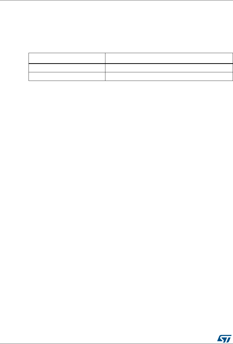
- Figure 1. B-L475E-IOT01A Discovery kit
- 1 Features
- 2 Product marking
- 3 System requirements
- 4 Development toolchains
- 5 Demonstration software
- 6 Ordering information
- 7 Hardware layout and configuration
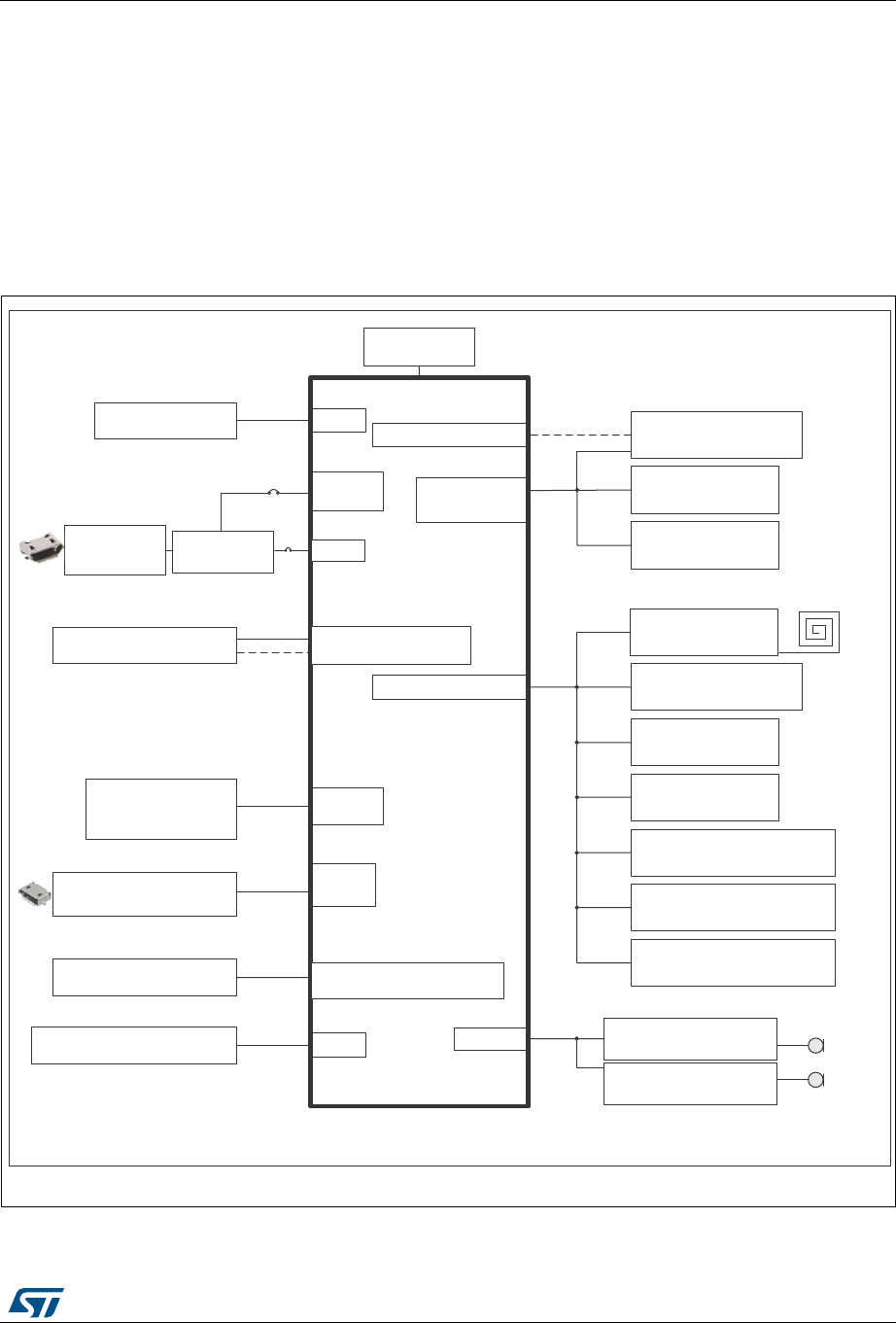
- Figure 2. Hardware block diagram
- 7.1 STM32L4 Discovery kit for IoT node layout
- 7.2 STM32L4 Discovery kit for IoT node mechanical drawing
- 7.3 Embedded ST-LINK/V2-1
- 7.4 Power supply
- 7.5 Programming/debugging when the power supply is not from ST-LINK (5V_ST_LINK)
- 7.6 Clock sources
- 7.7 Reset sources
- 7.8 USB OTG FS
- 7.9 Quad-SPI NOR Flash memory
- 7.10 Virtual COM port
- 7.11 RF modules
- 7.12 STMicroelectronics sensors
- 7.12.1 Two on-board ST-MEMS microphones (MP34DT01)
- 7.12.2 Capacitive digital sensor for relative humidity and temperature (HTS221)
- 7.12.3 High-performance 3-axis magnetometer (LIS3MDL)
- 7.12.4 3D accelerometer and 3D gyroscope (LSM6DSL)
- 7.12.5 260-1260 hPa absolute digital output barometer (LPS22HB)
- 7.12.6 Time-of-Flight and gesture detection sensor (VL53L0X)
- 7.13 STSAFE-A 100
- 7.14 Buttons and LEDs
- 7.15 I2C addresses of modules used on MB1297
- 8 Connectors
- Appendix A STM32L4 Discovery kit for IoT node I/O assignment
- Appendix B Schematics
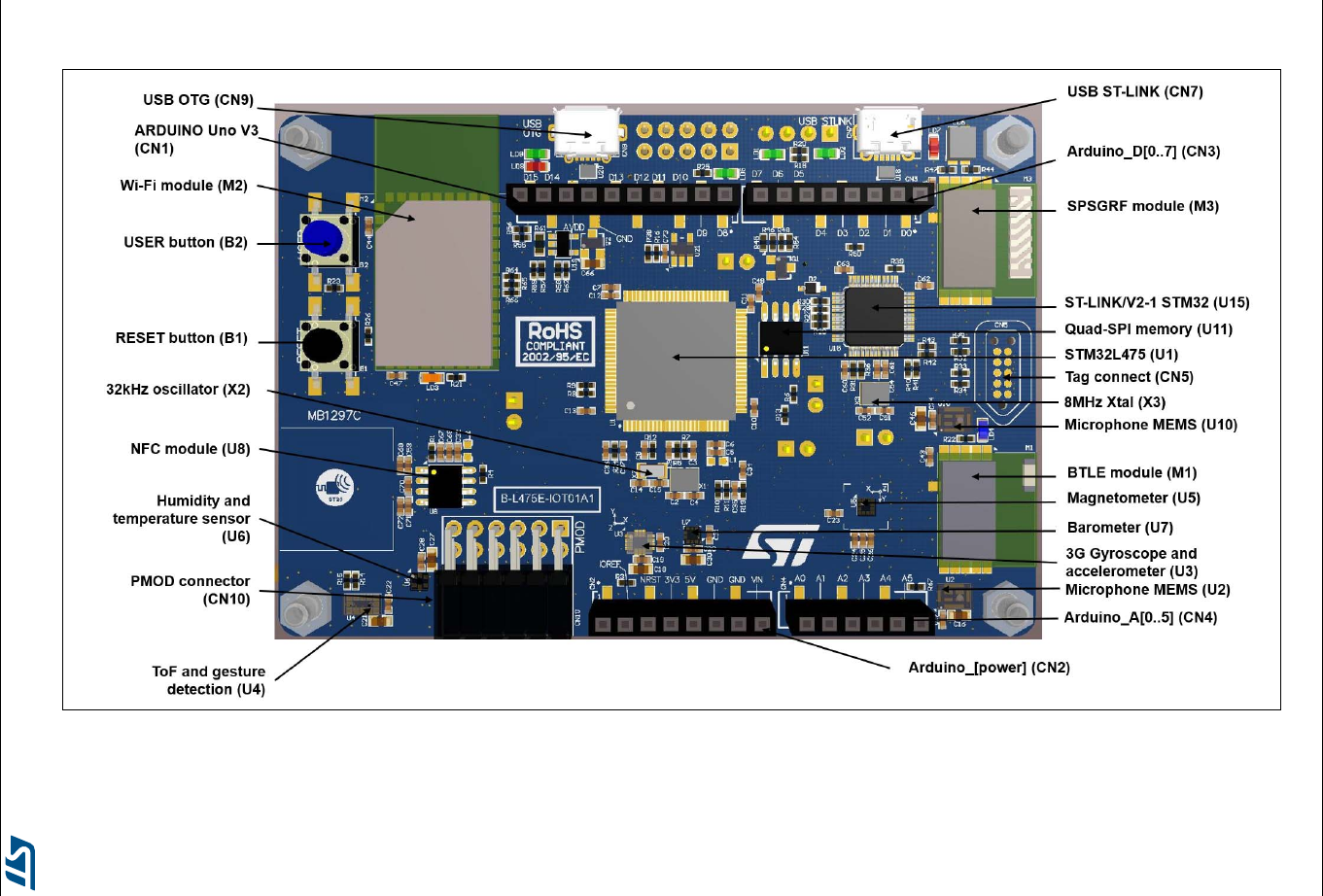
- Figure 22. STM32L4 Discovery kit for IoT node (top)
- Figure 23. STM32L475VG microcontroller
- Figure 24. STM32L475VG microcontroller
- Figure 25. USB OTG FS
- Figure 26. RF module
- Figure 27. ST-MEMS sensors
- Figure 28. NFC and STSAFE part
- Figure 29. Power supply
- Figure 30. Arduino Uno V3 connector
- Figure 31. Peripherals
- Figure 32. ST-LINK/V2-1 with support of SWD only
- Appendix C Board revision history and limitations
- Appendix D Federal Communications Commission (FCC) and Industry Canada (IC) Compliance
- Revision history
June 2017 DocID030118 Rev 3 1/57
1
UM2153
User manual
Discovery kit for IoT node, multi-channel communication
with STM32L4
Introduction
The STM32L4 Discovery kit for the IoT node (B-L475E-IOT01A) allows users to develop
applications with direct connection to cloud servers.
The STM32L4 Discovery kit enables a wide diversity of applications by exploiting low-power
multilink communication (BLE, Sub-GHz), multiway sensing (detection, environmental
awareness) and ARM® Cortex®-M4 core-based STM32L4 Series features.
Arduino™ Uno V3 and PMOD connectivity provide unlimited expansion capabilities with a
large choice of specialized add-on boards.
The STM32L4 Discovery kit includes an ST-LINK debugger/programmer and comes with
the comprehensive STM32Cube software libraries together with packaged software
examples to seamlessly connect to cloud servers. In addition a direct access to the ARM®
mbed Enabled™ on-line resources at http://mbed.org is available.
Figure 1. B-L475E-IOT01A Discovery kit
1. Picture is not contractual.
www.st.com

Contents UM2153
2/57 DocID030118 Rev 3
Contents
1 Features . . . . . . . . . . . . . . . . . . . . . . . . . . . . . . . . . . . . . . . . . . . . . . . . . . . 6
2 Product marking . . . . . . . . . . . . . . . . . . . . . . . . . . . . . . . . . . . . . . . . . . . . 7
3 System requirements . . . . . . . . . . . . . . . . . . . . . . . . . . . . . . . . . . . . . . . . 7
4 Development toolchains . . . . . . . . . . . . . . . . . . . . . . . . . . . . . . . . . . . . . . 7
5 Demonstration software . . . . . . . . . . . . . . . . . . . . . . . . . . . . . . . . . . . . . . 7
6 Ordering information . . . . . . . . . . . . . . . . . . . . . . . . . . . . . . . . . . . . . . . . 8
7 Hardware layout and configuration . . . . . . . . . . . . . . . . . . . . . . . . . . . . . 9
7.1 STM32L4 Discovery kit for IoT node layout . . . . . . . . . . . . . . . . . . . . . . . 10
7.2 STM32L4 Discovery kit for IoT node mechanical drawing . . . . . . . . . . . . 12
7.3 Embedded ST-LINK/V2-1 . . . . . . . . . . . . . . . . . . . . . . . . . . . . . . . . . . . . . 13
7.3.1 Drivers . . . . . . . . . . . . . . . . . . . . . . . . . . . . . . . . . . . . . . . . . . . . . . . . . . 13
7.3.2 ST-LINK/V2-1 firmware upgrade . . . . . . . . . . . . . . . . . . . . . . . . . . . . . . 14
7.4 Power supply . . . . . . . . . . . . . . . . . . . . . . . . . . . . . . . . . . . . . . . . . . . . . . 14
7.5 Programming/debugging when the power supply is not from
ST-LINK (5V_ST_LINK) . . . . . . . . . . . . . . . . . . . . . . . . . . . . . . . . . . . . . . 19
7.6 Clock sources . . . . . . . . . . . . . . . . . . . . . . . . . . . . . . . . . . . . . . . . . . . . . . 19
7.7 Reset sources . . . . . . . . . . . . . . . . . . . . . . . . . . . . . . . . . . . . . . . . . . . . . 19
7.8 USB OTG FS . . . . . . . . . . . . . . . . . . . . . . . . . . . . . . . . . . . . . . . . . . . . . . 19
7.9 Quad-SPI NOR Flash memory . . . . . . . . . . . . . . . . . . . . . . . . . . . . . . . . . 20
7.10 Virtual COM port . . . . . . . . . . . . . . . . . . . . . . . . . . . . . . . . . . . . . . . . . . . . 20
7.11 RF modules . . . . . . . . . . . . . . . . . . . . . . . . . . . . . . . . . . . . . . . . . . . . . . . 20
7.11.1 Bluetooth (V4.1 compliant) SPBTLE-RF module . . . . . . . . . . . . . . . . . . 20
7.11.2 Sub-GHz low-power-programmable RF module
(SPSGRF-868 or SPSGRF-915) . . . . . . . . . . . . . . . . . . . . . . . . . . . . . . 21
7.11.3 Wi-Fi module Inventek ISM43362-M3G-L44 (802.11 b/g/n) . . . . . . . . . 22
7.11.4 Dynamic NFC Tag based on M24SR with its printed NFC antenna . . . . 23
7.12 STMicroelectronics sensors . . . . . . . . . . . . . . . . . . . . . . . . . . . . . . . . . . . 24
7.12.1 Two on-board ST-MEMS microphones (MP34DT01) . . . . . . . . . . . . . . 24

DocID030118 Rev 3 3/57
UM2153 Contents
3
7.12.2 Capacitive digital sensor for relative humidity and
temperature (HTS221) . . . . . . . . . . . . . . . . . . . . . . . . . . . . . . . . . . . . . . 25
7.12.3 High-performance 3-axis magnetometer (LIS3MDL) . . . . . . . . . . . . . . . 25
7.12.4 3D accelerometer and 3D gyroscope (LSM6DSL) . . . . . . . . . . . . . . . . 26
7.12.5 260-1260 hPa absolute digital output barometer (LPS22HB) . . . . . . . . 26
7.12.6 Time-of-Flight and gesture detection sensor (VL53L0X) . . . . . . . . . . . . 27
7.13 STSAFE-A 100 . . . . . . . . . . . . . . . . . . . . . . . . . . . . . . . . . . . . . . . . . . . . . 28
7.14 Buttons and LEDs . . . . . . . . . . . . . . . . . . . . . . . . . . . . . . . . . . . . . . . . . . 28
7.15 I2C addresses of modules used on MB1297 . . . . . . . . . . . . . . . . . . . . . . 29
8 Connectors . . . . . . . . . . . . . . . . . . . . . . . . . . . . . . . . . . . . . . . . . . . . . . . 30
8.1 Arduino Uno V3 connectors . . . . . . . . . . . . . . . . . . . . . . . . . . . . . . . . . . . 30
8.2 TAG connector CN5 . . . . . . . . . . . . . . . . . . . . . . . . . . . . . . . . . . . . . . . . . 32
8.3 ST-LINK/V2-1 USB Micro-B . . . . . . . . . . . . . . . . . . . . . . . . . . . . . . . . . . . 33
8.4 ST-LINK debug connector CN8 . . . . . . . . . . . . . . . . . . . . . . . . . . . . . . . . 33
8.5 USB OTG FS micro-AB . . . . . . . . . . . . . . . . . . . . . . . . . . . . . . . . . . . . . . 34
8.6 PMOD connector CN10 . . . . . . . . . . . . . . . . . . . . . . . . . . . . . . . . . . . . . . 34
8.7 Jumper JP5 for IDD measurements . . . . . . . . . . . . . . . . . . . . . . . . . . . . . 36
Appendix A STM32L4 Discovery kit for IoT node I/O assignment . . . . . . . . . . . 37
Appendix B Schematics. . . . . . . . . . . . . . . . . . . . . . . . . . . . . . . . . . . . . . . . . . . . . 41
Appendix C Board revision history and limitations . . . . . . . . . . . . . . . . . . . . . . 53
Appendix D Federal Communications Commission (FCC)
and Industry Canada (IC) Compliance . . . . . . . . . . . . . . . . . . . . . . . 54
D.1 FCC Compliance Statement . . . . . . . . . . . . . . . . . . . . . . . . . . . . . . . . . . . 54
D.1.1 Part 15.19 . . . . . . . . . . . . . . . . . . . . . . . . . . . . . . . . . . . . . . . . . . . . . . . . 54
D.1.2 Part 15.105 . . . . . . . . . . . . . . . . . . . . . . . . . . . . . . . . . . . . . . . . . . . . . . . 54
8.7.1 Part 15.21 . . . . . . . . . . . . . . . . . . . . . . . . . . . . . . . . . . . . . . . . . . . . . . . 54
8.8 IC Compliance Statement . . . . . . . . . . . . . . . . . . . . . . . . . . . . . . . . . . . . . 54
8.8.1 Compliance Statement . . . . . . . . . . . . . . . . . . . . . . . . . . . . . . . . . . . . . . 55
8.8.2 Déclaration de conformité . . . . . . . . . . . . . . . . . . . . . . . . . . . . . . . . . . . 55
8.8.3 RF exposure statement . . . . . . . . . . . . . . . . . . . . . . . . . . . . . . . . . . . . . 55
Revision history . . . . . . . . . . . . . . . . . . . . . . . . . . . . . . . . . . . . . . . . . . . . . . . . . . . . 56

List of tables UM2153
4/57 DocID030118 Rev 3
List of tables
Table 1. Ordering information . . . . . . . . . . . . . . . . . . . . . . . . . . . . . . . . . . . . . . . . . . . . . . . . . . . . . . . 8
Table 2. Button and LED control port . . . . . . . . . . . . . . . . . . . . . . . . . . . . . . . . . . . . . . . . . . . . . . . . 29
Table 3. I2C addresses for each module . . . . . . . . . . . . . . . . . . . . . . . . . . . . . . . . . . . . . . . . . . . . . 29
Table 4. Arduino connector pinout . . . . . . . . . . . . . . . . . . . . . . . . . . . . . . . . . . . . . . . . . . . . . . . . . . 31
Table 5. TAG connector pinout. . . . . . . . . . . . . . . . . . . . . . . . . . . . . . . . . . . . . . . . . . . . . . . . . . . . . 32
Table 6. USB Micro-B connector . . . . . . . . . . . . . . . . . . . . . . . . . . . . . . . . . . . . . . . . . . . . . . . . . . . 33
Table 7. ST-LINK debug connector . . . . . . . . . . . . . . . . . . . . . . . . . . . . . . . . . . . . . . . . . . . . . . . . . 33
Table 8. USB OTG FS Micro-AB pinout . . . . . . . . . . . . . . . . . . . . . . . . . . . . . . . . . . . . . . . . . . . . . . 34
Table 9. USB OTG FS power management . . . . . . . . . . . . . . . . . . . . . . . . . . . . . . . . . . . . . . . . . . . 34
Table 10. PMOD solder bridge configuration . . . . . . . . . . . . . . . . . . . . . . . . . . . . . . . . . . . . . . . . . . . 35
Table 11. STM32L4 Discovery kit for IoT node I/O assignment . . . . . . . . . . . . . . . . . . . . . . . . . . . . . 37
Table 12. Board revision history and limitations . . . . . . . . . . . . . . . . . . . . . . . . . . . . . . . . . . . . . . . . . 53
Table 13. Document revision history . . . . . . . . . . . . . . . . . . . . . . . . . . . . . . . . . . . . . . . . . . . . . . . . . 56

DocID030118 Rev 3 5/57
UM2153 List of figures
5
List of figures
Figure 1. B-L475E-IOT01A Discovery kit. . . . . . . . . . . . . . . . . . . . . . . . . . . . . . . . . . . . . . . . . . . . . . . 1
Figure 2. Hardware block diagram. . . . . . . . . . . . . . . . . . . . . . . . . . . . . . . . . . . . . . . . . . . . . . . . . . . . 9
Figure 3. STM32L4 Discovery kit for IoT node (top view) . . . . . . . . . . . . . . . . . . . . . . . . . . . . . . . . . 10
Figure 4. STM32L4 Discovery kit for IoT node (bottom view) . . . . . . . . . . . . . . . . . . . . . . . . . . . . . . 11
Figure 5. STM32L4 Discovery kit for IoT node mechanical drawing . . . . . . . . . . . . . . . . . . . . . . . . . 12
Figure 6. USB composite device . . . . . . . . . . . . . . . . . . . . . . . . . . . . . . . . . . . . . . . . . . . . . . . . . . . . 13
Figure 7. JP4: 5V_ST_LINK selection . . . . . . . . . . . . . . . . . . . . . . . . . . . . . . . . . . . . . . . . . . . . . . . . 15
Figure 8. JP4: 5V_ARD selection from CN6 (VIN). . . . . . . . . . . . . . . . . . . . . . . . . . . . . . . . . . . . . . . 15
Figure 9. JP4: 5V_USB_FS . . . . . . . . . . . . . . . . . . . . . . . . . . . . . . . . . . . . . . . . . . . . . . . . . . . . . . . . 16
Figure 10. JP4: 5V_VBAT . . . . . . . . . . . . . . . . . . . . . . . . . . . . . . . . . . . . . . . . . . . . . . . . . . . . . . . . . . 16
Figure 11. JP4: 5V_USB_CHARGER selection. . . . . . . . . . . . . . . . . . . . . . . . . . . . . . . . . . . . . . . . . . 17
Figure 12. Power tree . . . . . . . . . . . . . . . . . . . . . . . . . . . . . . . . . . . . . . . . . . . . . . . . . . . . . . . . . . . . . 18
Figure 13. SPBTLE-RF module . . . . . . . . . . . . . . . . . . . . . . . . . . . . . . . . . . . . . . . . . . . . . . . . . . . . . . 21
Figure 14. SPSGRF module . . . . . . . . . . . . . . . . . . . . . . . . . . . . . . . . . . . . . . . . . . . . . . . . . . . . . . . . 22
Figure 15. ISM43362-M3G-L44 module . . . . . . . . . . . . . . . . . . . . . . . . . . . . . . . . . . . . . . . . . . . . . . . 23
Figure 16. Label for Class 1 laser products . . . . . . . . . . . . . . . . . . . . . . . . . . . . . . . . . . . . . . . . . . . . . 28
Figure 17. Arduino connector (front view) . . . . . . . . . . . . . . . . . . . . . . . . . . . . . . . . . . . . . . . . . . . . . . 30
Figure 18. TAG connector . . . . . . . . . . . . . . . . . . . . . . . . . . . . . . . . . . . . . . . . . . . . . . . . . . . . . . . . . . 32
Figure 19. TC2050-IDC-NL cable . . . . . . . . . . . . . . . . . . . . . . . . . . . . . . . . . . . . . . . . . . . . . . . . . . . . 32
Figure 20. USB Micro-B connector CN7 (front view) . . . . . . . . . . . . . . . . . . . . . . . . . . . . . . . . . . . . . . 33
Figure 21. USB OTG FS Micro-AB connector CN9 (front view). . . . . . . . . . . . . . . . . . . . . . . . . . . . . . 34
Figure 22. STM32L4 Discovery kit for IoT node (top) . . . . . . . . . . . . . . . . . . . . . . . . . . . . . . . . . . . . . 42
Figure 23. STM32L475VG microcontroller . . . . . . . . . . . . . . . . . . . . . . . . . . . . . . . . . . . . . . . . . . . . . 43
Figure 24. STM32L475VG microcontroller . . . . . . . . . . . . . . . . . . . . . . . . . . . . . . . . . . . . . . . . . . . . . 44
Figure 25. USB OTG FS . . . . . . . . . . . . . . . . . . . . . . . . . . . . . . . . . . . . . . . . . . . . . . . . . . . . . . . . . . . 45
Figure 26. RF module . . . . . . . . . . . . . . . . . . . . . . . . . . . . . . . . . . . . . . . . . . . . . . . . . . . . . . . . . . . . . 46
Figure 27. ST-MEMS sensors . . . . . . . . . . . . . . . . . . . . . . . . . . . . . . . . . . . . . . . . . . . . . . . . . . . . . . . 47
Figure 28. NFC and STSAFE part . . . . . . . . . . . . . . . . . . . . . . . . . . . . . . . . . . . . . . . . . . . . . . . . . . . . 48
Figure 29. Power supply . . . . . . . . . . . . . . . . . . . . . . . . . . . . . . . . . . . . . . . . . . . . . . . . . . . . . . . . . . . 49
Figure 30. Arduino Uno V3 connector . . . . . . . . . . . . . . . . . . . . . . . . . . . . . . . . . . . . . . . . . . . . . . . . . 50
Figure 31. Peripherals . . . . . . . . . . . . . . . . . . . . . . . . . . . . . . . . . . . . . . . . . . . . . . . . . . . . . . . . . . . . . 51
Figure 32. ST-LINK/V2-1 with support of SWD only . . . . . . . . . . . . . . . . . . . . . . . . . . . . . . . . . . . . . . 52

Features UM2153
6/57 DocID030118 Rev 3
1 Features
•Ultra-low-power STM32L4 Series MCUs based on ARM® Cortex®-M4 core with 1 Mbyte
of Flash memory and 128 Kbytes of SRAM, in LQFP100 package
•64-Mbit Quad-SPI (Macronix) Flash memory
•Bluetooth® V4.1 module (SPBTLE-RF)
•Sub-GHz (868 or 915 MHz) low-power-programmable RF module
(SPSGRF-868 or SPSGRF-915)
•Wi-Fi® module Inventek ISM43362-M3G-L44 (802.11 b/g/n compliant)
•Dynamic NFC tag based on M24SR with its printed NFC antenna
•2 digital omnidirectional microphones (MP34DT01)
•Capacitive digital sensor for relative humidity and temperature (HTS221)
•High-performance 3-axis magnetometer (LIS3MDL)
•3D accelerometer and 3D gyroscope (LSM6DSL)
•260-1260 hPa absolute digital output barometer (LPS22HB)
•Time-of-Flight and gesture-detection sensor (VL53L0X)
•2 push-buttons (user and reset)
•USB OTG FS with Micro-AB connector
•Board expansion connectors:
– Arduino™ Uno V3
–PMOD
•Flexible power-supply options: ST-LINK USB VBUS or external sources
•On-board ST-LINK/V2-1 debugger/programmer with USB
re-enumeration capability: mass storage, virtual COM port and debug port
•Comprehensive free software including a
variety of examples, as part of the STM32Cube
package, as well as a cloud connector software expansion, enabling direct access to cloud
servers
•Support of wide choice of Integrated Development Environments (IDEs) including IAR™,
Keil®, GCC-based IDEs, ARM® mbed Enabled™
•ARM® mbed Enabled™ (see http://mbed.org)

DocID030118 Rev 3 7/57
UM2153 Product marking
56
2 Product marking
Evaluation tools marked as "ES" or "E" are not yet qualified and therefore they are not ready
to be used as reference design or in production. Any consequences deriving from such
usage will not be at ST charge. In no event, ST will be liable for any customer usage of
these
engineering sample tools as reference design or in production.
"E" or "ES" marking examples of location:
•On the targeted STM32 that is soldered on the board (for illustration of STM32 marking,
refer to the section “Package characteristics” of the STM32 datasheet at www.st.com).
•Next to the evaluation tool ordering part number, that is stuck or silk-screen printed on
the board.
3 System requirements
•Windows® OS (XP, 7, 8 and 10), Linux® or MacOS™
•USB Type-A to Micro-B cable
4 Development toolchains
•Keil® MDK-ARM(a)
•IAR™ EWARM(a)
•GCC-based IDEs including free SW4STM32 from AC6
•ARM® mbed Enabled™ online
5 Demonstration software
The demonstration software, included in the STM32Cube package, is preloaded in the
STM32 Flash memory for easy demonstration of the device peripherals in standalone mode.
The latest versions of the demonstration source code and associated documentation can be
downloaded from the www.st.com/stm32app-discovery webpage.
a. On Windows® only.
Ordering information UM2153
8/57 DocID030118 Rev 3
6 Ordering information
To order the B-L475E-IOT01A Discovery kit for IoT node, depending on the frequency of the
Sub-GHz module, refer to Table 1.
Table 1. Ordering information
Order code Sub-GHz operating frequency
B-L475E-IOT01A1 915 MHz
B-L475E-IOT01A2 868 MHz
DocID030118 Rev 3 9/57
UM2153 Hardware layout and configuration
56
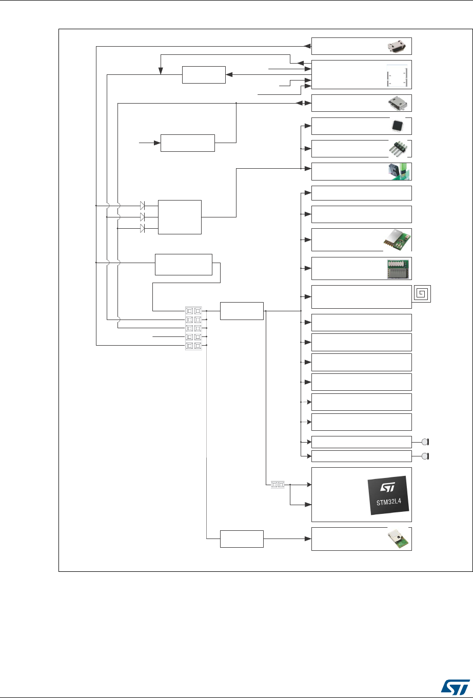
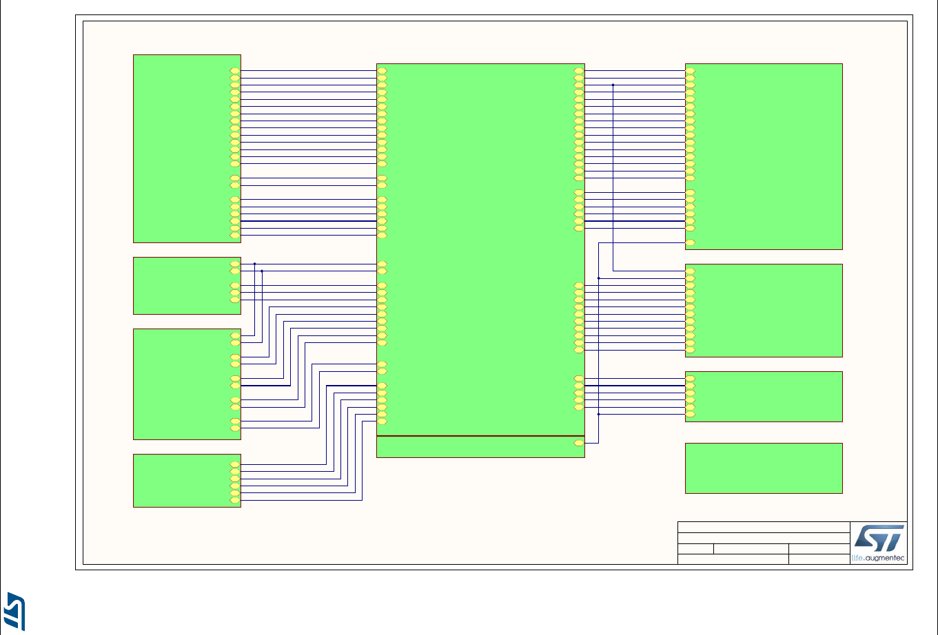
7 Hardware layout and configuration
The STM32L4 Discovery kit for IoT node is designed around the STM32L475VGT6 (100-
pin, LQFP package). The hardware block diagram (see Figure 2) illustrates the connection
between the STM32 and peripherals (embedded ST-LINK, Arduino Uno V3 shields, PMOD
connector, Quad-SPI Flash memory, USB OTG connectors, digital microphones, various
ST-MEMS sensors and the four RF modules (Wi-Fi, Bluetooth, Sub-GHz and NFC)).
Figure 4 and Figure 5 help users to locate these features on the STM32L4 Discovery kit.
Figure 2. Hardware block diagram
06Y9
670/9*7
03'7GLJLWDO
PLFURSKRQH
57&
6:'
93RZHU
6XSSO\
.+]&U\VWDO
67/,1.
9
*3,2VDQG8$57
')6'0
,600*/
:L)LPRGXOH
302'$FRQQHFWRU
302'$FRQQHFWRU
/('V
UHVHWDQGZDNHXS
EXWWRQV
*3,2V
*3,2VDQG63,
*3,2VDQG8$57
+63+<DQG
0LFUR$%86%FRQQHFWRU
27*
)6
463,
0ELW463,)ODVK
0;5)
9&3
8$57
$UGXLQR8QR6KLHOG
FRQQHFWRUV
*3,2VDQG
8$57DQG63,
0LFUR%86%
FRQQHFWRU
*3,2VDQG
63,
63%7/(5)
%OXHWRRWKPRGXOH
636*5)6XE*+]
6SLULWPRGXOH
0651)&
PRGXOH
*3,2VDQG,& /,60'/
D[LVPDJQHWRPHWHU
/60'6/
'J\URVFRSH
/36+%
GLJLWDOEDURPHWHU
+76
KXPLGLW\DQGWHPSHUDWXUH
9//;
7R)DQGJHVWXUHGHWHFWLRQ
676$)($
DXWKHQWLFDWLRQDQGVHFXULW\
03'7GLJLWDO
PLFURSKRQH
DocID030118 Rev 3 13/57
UM2153 Hardware layout and configuration
56
7.3 Embedded ST-LINK/V2-1
The ST-LINK/V2-1 programming and debugging tool is integrated on the STM32L4 Discovery
kit for IoT node. Compared to the ST-LINK/V2 the changes are listed below.
The new features supported on the ST-LINK/V2-1 are:
•USB software re-enumeration
•Virtual COM port interface on USB
•Mass storage interface on USB
•USB power management request for more than 100 mA power on USB
The following features are no more supported on the ST-LINK/V2-1:
•SWIM interface
•Application voltage lower than 3 V
For all general information concerning debugging and programming features common
between V2 and V2-1 versions, refer to ST-LINK/V2 in-circuit debugger/programmer for
STM8 and STM32 User manual (UM1075) at the www.st.com website.
7.3.1 Drivers
Before connecting STM32L475VG to a Windows® PC (XP, 7, 8 or 10) via USB, a driver for
the ST-LINK/V2-1 must be installed. It is available at the www.st.com website.
In case the STM32L4 Discovery kit for IoT node is connected to the PC before the driver is
installed, some STM32L4 Discovery kit interfaces may be declared as “unknown” in the PC
device manager. In this case the user must install the driver files, and update the driver of
the connected device from the device manager (see Figure 6).
Note: Prefer using the “USB Composite Device” handle for a full recovery.
Figure 6. USB composite device

Hardware layout and configuration UM2153
14/57 DocID030118 Rev 3
7.3.2 ST-LINK/V2-1 firmware upgrade
The ST-LINK/V2-1 embeds a firmware upgrade mechanism for in-situ upgrade through the
USB port. As the firmware may evolve during the lifetime of the ST-LINK/V2-1 product (for
example new functionalities, bug fixes, support for new microcontroller families), it is
recommended to visit the www.st.com website, before starting to use the STM32L4
Discovery kit for IoT node and periodically, to stay up-to-date with the latest firmware
version.
7.4 Power supply
The STM32L4 Discovery kit for IoT node is designed to be powered by 5 V DC power
supply. It is possible to configure the STM32L4 Discovery kit to use any of the following five
sources for the power supply: 5V_ST_LINK, 5V_ARD, 5V_USB_FS, 5V_VBAT and
5V_USB_CHARGER.
In case of external 5 V DC power adapter, the STM32L4 Discovery kit must be powered by
a power supply unit or by an auxiliary equipment complying with the standard EN-60950-1:
2006+A11/2009, and must be Safety Extra Low Voltage (SELV) with limited power
capability.
•5V_ST_LINK (See Figure 7) is a 5V DC power with limitation from CN7 (the USB type
Micro-B connector of ST-LINK/V2-1). In this case, jumper of JP4 should be on pins 1
and 2 to select the 5V_ST_LINK power source on silkscreen of JP4. This is the default
setting. If the USB enumeration succeeds, the 5V_ST_LINK power is enabled, by
asserting the PWR_ENn signal (from STM32F103CBT6). This pin is connected to a
power switch ST890, which powers the board. This power switch features also a
current limitation to protect the PC in case of a short-circuit on board (more than
750 mA). STM32L4 Discovery kit for IoT node can be powered from the ST-LINK USB
connector CN7, but only ST-LINK circuit has the power before USB enumeration,
because the host PC only provides 100 mA to the board at that time. During the USB
enumeration, STM32L4 Discovery kit for IoT node asks for the 500 mA power to the
host PC. If the host is able to provide the required power, the enumeration finishes by a
“SetConfiguration” command and then, the power transistor ST890 is switched ON, the
red LED LD7 is turned ON, thus the STM32L4 Discovery kit for IoT node consumes up
to 500 mA current, but no more. If the host is not able to provide the requested current,
the enumeration fails. Therefore the ST890 remains OFF and the MCU part including
the extension board is not powered. As a consequence the red LED LD7 remains
turned OFF. In this case it is mandatory to use an external power supply.
DocID030118 Rev 3 15/57
UM2153 Hardware layout and configuration
56
Figure 7. JP4: 5V_ST_LINK selection
•5V_ARD (see Figure 8) is the 7 to 12 V DC power from Arduino CN2 pin 8 (named VIN
on Arduino connector silkscreen). In this case, jumper of JP4 should be on pins 3 and 4
to select the 5V_ARD power source on silkscreen of JP4. In that case, the DC power
comes from the power supply through the Arduino Uno V3 battery shield (compatible
with Adafruit PowerBoost 500 Shield).
Figure 8. JP4: 5V_ARD selection from CN6 (VIN)
•5V_USB_FS (see Figure 9) is the DC power with 500 mA limitation from CN9, the USB
OTG FS micro-AB connector. In this case, jumper of JP4 should be on pins 5 and 6 to
select the 5V_USB_FS power source on silkscreen of JP4.
06Y9
9B67B/,1.
9B$5'
9B86%B)6
9B9%$7
9B86%B&+$5*(5
-3
06Y9
9B67B/,1.
9B$5'
9B86%B)6
9B9%$7
9B86%B&+$5*(5
-3
Hardware layout and configuration UM2153
16/57 DocID030118 Rev 3
Figure 9. JP4: 5V_USB_FS
•5V_VBAT (see Figure 10) is the DC power coming from external. In this case, jumper of
JP4 should be on pins 7 and 8 to select the 5V_VBAT power source on silkscreen of
JP4.
Figure 10. JP4: 5V_VBAT
•5V_USB_CHARGER (see Figure 11) is the DC power charger connected to the USB
ST-LINK (CN7). To select the 5V_USB_CHARGER power source on silkscreen of JP4,
the jumper of JP4 should be on pins 9 and 10. In this case, if the STM32L4 Discovery kit
for IoT node is powered by an external USB charger then the debug is not available. If
the PC is connected instead of the charger, the limitation is no longer effective and the
PC could be damaged.
06Y9
9B67B/,1.
9B$5'
9B86%B)6
9B9%$7
9B86%B&+$5*(5
-3
06Y9
9B67B/,1.
9B$5'
9B86%B)6
9B9%$7
9B86%B&+$5*(5
-3
DocID030118 Rev 3 17/57
UM2153 Hardware layout and configuration
56
Figure 11. JP4: 5V_USB_CHARGER selection
Note: If the board is powered by a USB charger, there is no USB enumeration, so the led LD7
remains OFF permanently and the board is not powered. In this specific case only, the
resistor R30 needs to be soldered, to allow the board to be powered anyway.
Caution: Do not connect the PC to the ST-LINK (CN7) when R30 is soldered. The PC may be damaged
or the board may not be powered correctly.
The green LED LD5 is lit when the STM32L4 Discovery kit for IoT node is powered by the 5 V
correctly.
The power tree is showed in the Figure 12.
06Y9
9B67B/,1.
9B$5'
9B86%B)6
9B9%$7
9B86%B&+$5*(5
-3
Hardware layout and configuration UM2153
18/57 DocID030118 Rev 3
Figure 12. Power tree
06Y9
86%B67B/,1.
86%B27*B)6
$UGXLQR
670)67B/,1.
%LFRORU/('
67/,1.GHEXJ
7$*
0&8670/9*7
0ELW463,)ODVK
0;5)
03'7GLJLWDOPLFURSKRQH
,600*/
:L)LPRGXOH
63%7/(5)
%OXHWRRWKPRGXOH
636*5)6XE*+]
6SLULWPRGXOH
0651)&PRGXOH
/,60'/
D[LVPDJQHWRPHWHU
/60'6/
'J\URVFRSH
/36+%
GLJLWDOEDURPHWHU
+76
KXPLGLW\DQGWHPSHUDWXUH
9//;
7R)DQGJHVWXUHGHWHFWLRQ
676$)($
DXWKHQWLFDWLRQDQGVHFXULW\
03'7GLJLWDOPLFURSKRQH
/'2
/'675
9
9
9
''B0&8
-3
,&
-3
9B:LIL
/'2
/7(67
9
,&
302'
,&
/'2
/'05
,&
9B67B/LQN
9B$5'
9B86%B)6
9B9%$7
9B86%BFKDUJHU
/'2
/'675
8
9,1 9
9
''$
9B$5'
9
9B$5'
9B86%B67B/LQN
9B67B/LQN
6ZLWFK9$
67&'5
,&
9
9B86%B)6
9
''$
3RZHUVZLWFK9$
67&'5

DocID030118 Rev 3 19/57
UM2153 Hardware layout and configuration
56
7.5 Programming/debugging when the power supply is not from
ST-LINK (5V_ST_LINK)
It is mandatory to power the board first using CN2 (VIN) or CN9 (USB_FS_OTG), then
connecting the USB cable to the PC. Proceeding this way ensures that the enumeration
succeeds thanks to the external power source.
The following power sequence procedure must be respected:
•Connect the jumper JP4 on (5V_ARD) or (5V_USB_FS)
•Connect the external power source to CN2 in case of an Arduino shield or to CN9 in
case of USB FS host interface
•Check that the red LED LD5 is turned ON
•Connect the PC to USB connector CN7
If this sequence is not respected, the board may be powered by VBUS first from ST-LINK, and
the following risks may be encountered:
•If more than 500 mA current is needed by the board, the PC may be damaged or
current can be limited by PC. As a consequence the board is not powered correctly.
•500 mA is requested at the enumeration, so there is a risk that the request is
rejected
and enumeration does not succeed if the PC cannot provide such current.
7.6 Clock sources
Three clock sources are described below:
•X1 which is the 8 MHz oscillator for STM32L475VG microcontroller. This clock is not
implemented in a basis configuration.
•X2 which is the 32.768 KHz crystal for the STM32L475VG embedded RTC
•X3 which is the 8 MHz clock from ST-LINK MCU for the STM32L475VG microcontroller.
7.7 Reset sources
The reset signal of the STM32L4 Discovery kit is active low and the reset sources includes:
•A reset button B1
•An Arduino Uno V3 shield board from CN2
•An embedded ST-LINK/V2-1
7.8 USB OTG FS
The STM32L4 Discovery kit supports USB OTG FS communication via a USB Micro-AB
connector (CN9).
To do this the following components must be added by the users:
•8 MHz crystal (at X1 position); ref: NX3225GD-8.00M
•8.2 pF capacitor (0402 size) at C2 position
•8.2 pF capacitor (0402 size) at C4 position

Hardware layout and configuration UM2153
20/57 DocID030118 Rev 3
•0 ohm resistor (0402 size) at R5 position
•0 ohm resistor (0402 size) at R7 position
The STM32L4 Discovery kit can be powered by the USB connectors at 5 V DC with 500 mA
current limitation.
A USB power switch (IC19) is also connected on VBUS and provides power to CN9. The
green LED LD9 is lit when either:
•Power switch is ON and STM32L4 Discovery kit works as an USB host
•VBUS is powered by another USB host when STM32L4 Discovery kit works as a USB
device.
The red LED LD8 is lit when an over-current occurs.
7.9 Quad-SPI NOR Flash memory
64-Mbit Quad-SPI NOR Flash memory (N25Q128A13EF840F from MICRON) is connected
to the Quad-SPI interface of the STM32L475VGT6.
7.10 Virtual COM port
The serial interface USART6 is directly available as a virtual COM port of the PC connected
to the ST-LINK/V2-1 USB connector CN7. The virtual COM port settings are configured as:
115200 b/s, 8 bits data, no parity, 1 stop bit, no flow control.
7.11 RF modules
Four RF interfaces are available on the STM32L4 Discovery kit for IoT node board:
•Bluetooth (V4.1 compliant) SPBTLE-RF module
•Sub-GHz (868 or 915 MHz) low-power-programmable RF module (SPSGRF-868 or
SPSGRF-915),
•Wi-Fi module Inventek ISM43362-M3G-L44 (802.11 b/g/n compliant)
•Dynamic NFC tag based on M24SR with its printed NFC antenna (double layer
inductive antenna etched on the PCB).
7.11.1 Bluetooth (V4.1 compliant) SPBTLE-RF module
The ST SPBTLE-RF module (M1) is implemented on top side of the STM32L4 Discovery kit
for IoT node board.
The SPBTLE-RF is an easy to use Bluetooth smart master/slave network processor module,
compliant with Bluetooth V4.1. The SPBTLE-RF B-Smart module supports multiple roles
simultaneously, and it can act at the same time as Bluetooth Smart sensor and hub device.
The entire Bluetooth Smart stack and protocol are embedded into the SPBTLE-RF B-Smart
module. The external host application processor, where the application resides, is
connected to the SPBTLE-RF B-Smart module through a standard SPI interface (SPI3 of
STM32L475VGT6).
The SPBTLE-RF B-Smart module provides a complete RF platform in a tiny form factor (foot
print of this module is 13.5 mm x 11.5 mm). Radio, antenna, high frequency and LPO
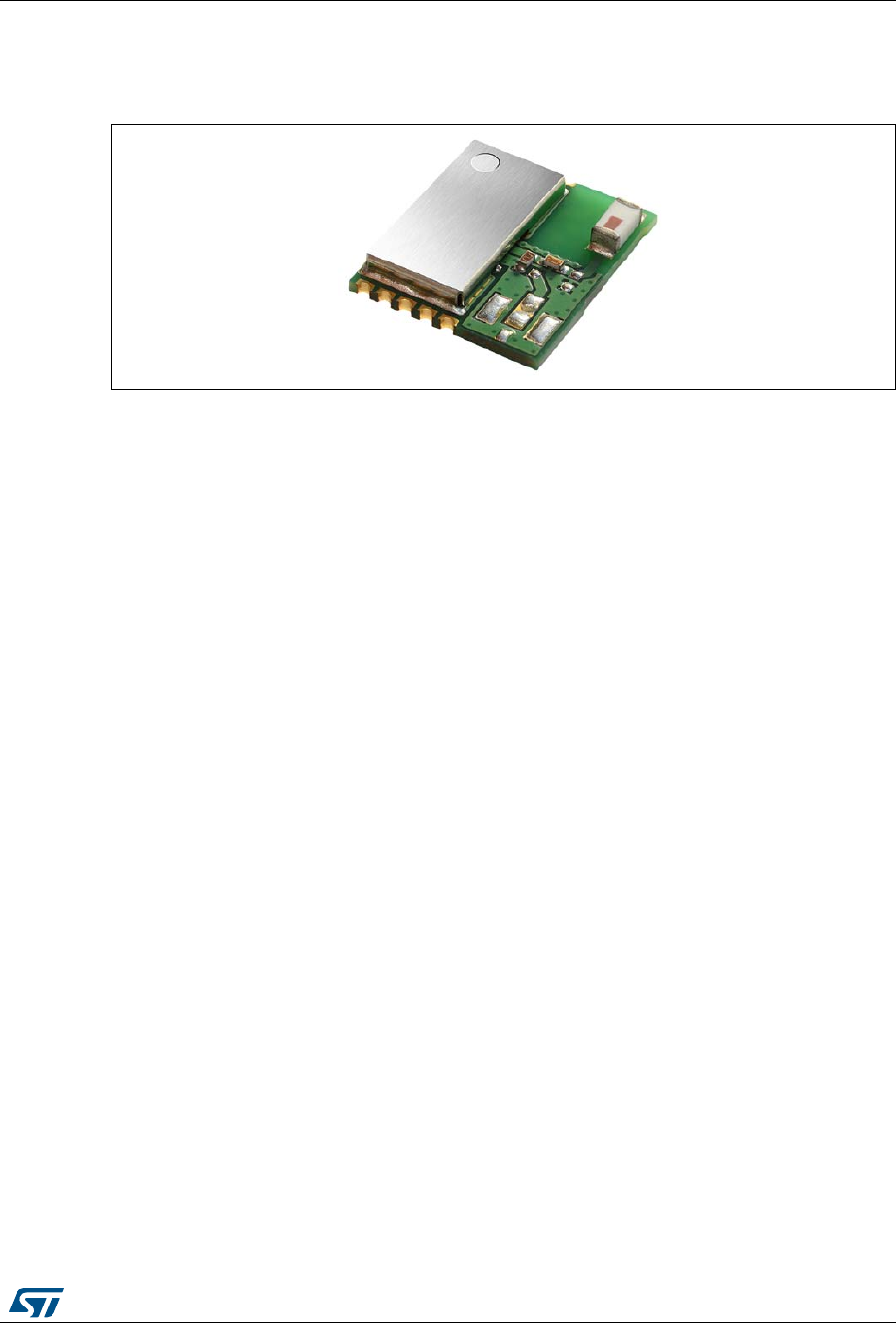
DocID030118 Rev 3 21/57
UM2153 Hardware layout and configuration
56
oscillators are integrated to offer a certified solution to optimize the time to market of the
final applications.
Figure 13. SPBTLE-RF module
The main features of the ST SPBTLE-RF module are listed below.
•Bluetooth V4.1 compliant (supports master and slave modes, multiple roles supported
simultaneously
•Embedded Bluetooth low-energy protocol stack (GAP, GATT, SM, L2CAP, LL, RFPHY)
•Bluetooth low-energy profiles provided separately
•Bluetooth radio performance:
•Embedded ST BlueNRG-MS
•Tx power: + 4 dBm
•Host interface: SPI, IRQ, and RESET. On-field stack upgrading available via SPI.
•Certification: CE qualified, FCC, IC modular approval certified, BQE qualified
•On-board chip antenna
7.11.2 Sub-GHz low-power-programmable RF module
(SPSGRF-868 or SPSGRF-915)
Two modules are available depending on the frequency of the Sub-GHz module (M3). The
SPSGRF-868 and SPSGRF-195 are easy-to-use, low-power Sub-GHz modules based on
the SPIRIT1 RF transceiver, operating respectively in the 868 MHz SRD and 915 MHz ISM
bands.
The modules provide a complete RF platform in a tiny form factor (foot print of this module is
13.5 mm x 11.5 mm). The SPSGRF-915 is an FCC certified module (FCC ID: S9NSPSGRF)
and IC certified (IC 8976CSPSGRF), while the SPSGRF-868 is certified CE0051.
The modules include four programmable I/O pins and an SPI serial interface (SPI3 of
STM32L475VG).
Hardware layout and configuration UM2153
22/57 DocID030118 Rev 3
Figure 14. SPSGRF module
The main features of the ST SPSGRF module are listed below.
•Programmable radio features:
– Based on Sub-1GHz SPIRIT1 transceiver and integrated Balun (BALF-SPI-01D3)
– Modulation schemes: 2-FSK, GFSK, MSK, GMSK, OOk and ASK
– Air data rate from 1 to 500 kbps
– On-board antenna
•Programmable RF output power up to +11.6 dBm
•Host interface: SPI
•General I/O (up to 32 programmable I/O functions on 4 GPIO programmable module
pins
•Two typical carrier frequency versions:
– SPSGRF-868 with 868 MHz tuned antenna
– SPSGRF-195 with 915 MHz tuned antenna
7.11.3 Wi-Fi module Inventek ISM43362-M3G-L44 (802.11 b/g/n)
The Inventek ISM43362-M3G-L44 module (M2) is implemented on top side of the STM32L4
Discovery kit for IoT node board. This module is an embedded (eS-WiFi) wireless Internet
Connectivity device. The Wi-Fi module hardware consists of an ARM® Cortex® -M3 STM32
host processor, an integrated antenna (or optional external antenna) and a Broadcom Wi-Fi
device. The module uses either a UART (UART3 of STM32L475VG) or an SPI (SPI3 of
STM32L475VG) interface. As default, an SPI interface is used, as the corresponding
firmware (for SPI capability) is downloaded on the Wi-Fi ISM43362-M3G-L44 module. The
Wi-Fi module requires no operating system and has a completely integrated TCP/IP stack
that only requires AT commands to establish connectivity for wireless product. The foot print
of this module is 14.5 mm x 30 mm.
DocID030118 Rev 3 23/57
UM2153 Hardware layout and configuration
56
Figure 15. ISM43362-M3G-L44 module
The main features of the Inventek ISM43362-M3G-L44 module are:
•Based on the Broadcom BCM43362 MAC/Baseband/Radio device
•Supports Broadcom WICED SDK
•CPU ARM® Cortex®-M3 32-bit RISC core from ST Microelectronics
•IEEE 802.11n D7.0 -OFDM-72.2 Mbps -single stream w/20 MHz, Short GI
•IEEE 802.11g (OFDM 54 Mbps)
•IEEE 802.11b (DSSS 11 Mbps)
•IEEE 802.11i (Security)
– WPA (Wi-Fi Protected Access) –PSK/TKIP
– WPA2 (Wi-Fi Protected Access 2)- AES/CCMP/802.1x Authentication
•GPIO, 5 ADC (SPI interface utilizes ADC pins)
•Power-saving mode allows the design of low-power applications
•Lead Free Design which is compliant with ROHS requirements
•EMI/EMC Metal Shield for best RF performance in noisy environments and to
accommodate for lower RF emissions/signature for easier FCC compliance.
•FCC/CE compliance certification
On both MB1297 rev C and MB1297 rev D, the firmware revision inside the Wi-Fi module
must be: C3.5.2.3.BETA9. The Wi-Fi module maximum output power is limited to 9 dBm to
fulfill FCC/IC/CE requirements. A Wi-Fi output power higher than 9 dBm at the Wi-Fi
antenna is not allowed.
Note: Since Wi-Fi and BLE modules are using the same frequency ISM band (2.4 to 2.485 GHz),
the simultaneous activity of both modules may affect the RF performances of Wi-Fi and/or
BLE (in term of range or throughput).
7.11.4 Dynamic NFC Tag based on M24SR with its printed NFC antenna
M24SR64-Y belongs to the ST25 family which includes all STMicroelectronics NFC/RFID
Tag and reader products. The M24SR64-Y device is a dynamic NFC/RFID Tag IC with a
dual interface. It embeds an EEPROM memory. It can be operated from an I2C interface or
by a 13.56 MHz RFID reader or by an NFC phone. The I2C interface uses a two-wire serial
interface, consisting of a bidirectional data line and a clock line. It behaves as a slave in the
I2C protocol.
The RF protocol is compatible with ISO/IEC 14443 Type A and NFC Forum Type 4 Tag.

Hardware layout and configuration UM2153
24/57 DocID030118 Rev 3
The main features of the M24SR64-Y are:
•I2C interface (I2C2 of STM32L475VGT6). The two-wire I2C serial interface supports
1 MHz protocol.
•Contactless interface:
– NFC Forum Type 4 Tag
– ISO/IEC 14443 Type A
– 106 Kbps data rate
– Internal tuning capacitance: 25 pF
•Memory:
– 8-Kbyte (64-kbit) EEPROM
– Support of NDEF data structure
– Data retention: 200 years
– Write cycle endurance:
1 million Write cycles at 25 °C
600 K Write cycles at 85 °C
500 K Write cycles at 105 °C
•Read up to 246 Bytes in a single command
•Write up to 246 Bytes in a single command
•7-Byte unique identifier (UID)
•128-bit password protection
7.12 STMicroelectronics sensors
Several STMicroelectronics sensors are available on the STM32L4 Discovery kit for IoT
node board, they are listed below:
•2 on-board ST-MEMS audio sensor omnidirectional digital microphones (MP34DT01)
•Capacitive digital sensor for relative humidity and temperature (HTS221)
•High-performance 3-axis magnetometer (LIS3MDL)
•3D accelerometer and 3D gyroscope (LSM6DSL)
•260-1260 hPa absolute digital output barometer (LPS22HB)
•Time-of-Flight and gesture detection sensor (VL53L0X)
7.12.1 Two on-board ST-MEMS microphones (MP34DT01)
The MP34DT01 is an ultra-compact, low-power, omnidirectional, digital ST-MEMS
microphone built with a capacitive sensing element and an IC interface.
The sensing element, capable of detecting acoustic waves, is manufactured using a
specialized silicon micromachining process dedicated to produce audio sensors.
The IC interface is manufactured using a CMOS process that allows designing a dedicated
circuit able to provide a digital signal externally in PDM format.
The MP34DT01 has an acoustic overload point of 120 dBSPL with a 63 dB signal-to-noise
ratio and –26 dBFS sensitivity.

DocID030118 Rev 3 25/57
UM2153 Hardware layout and configuration
56
On the STM32L4 Discovery kit for IoT node, there are two MP34DT01 microphones: one
with LR pulled to VDD and the second with LR pulled low. DFSDM1_CKOUT and
DFSDM1_DATIN2 are connected for both. In addition, both microphones are spaced at
21 mm apart for the beamforming algorithm to work. Indeed, several algorithm
configurations are available for the user to find the best trade off between audio output
quality and resource consumption. For more details refer to STEVAL-IHM038V1: 3-phase
BLDC/PMSM motor drive up to 50 W, suitable for fan controllers User manual (UM1697) on
the www.st.com website.
The MP34DT01 is available in a package HCLGA (3x4 x1 mm) 4LD, in a top-port design,
SMD-compliant, EMI-shielded package and it is guaranteed to operate over an extended
temperature range from -40°C to +85°C.
7.12.2 Capacitive digital sensor for relative humidity and
temperature (HTS221)
The HTS221 is an ultra-compact sensor for relative humidity and temperature. It includes a
sensing element and a mixed signal ASIC to provide the measurement information through
digital serial interfaces.
The sensing element consists of a polymer dielectric planar capacitor structure capable of
detecting relative humidity variations and it is manufactured using a dedicated ST process.
The HTS221 is available in a small top-holed cap land grid array (HLGA-6L (2 x 2 x 0.9
mm)) package guaranteed to operate over a temperature range from -40 °C to +120 °C.
The main features of the HTS221 are:
•0 to 100% relative humidity range,
•Low-power consumption: 2 μA @ 1 Hz ODR
•Selectable ODR from 1 Hz to 12.5 Hz
•High rH sensitivity: 0.004% rH/LSB
•Humidity accuracy: ± 3.5% rH, 20 to +80% rH
•Temperature accuracy: ± 0.5 °C,15 to +40 °C
•Embedded 16-bit ADC
•16-bit humidity and temperature output data
•SPI and I2C interfaces. On the STM32L4 Discovery kit for IoT node, the I2C2 bus from
STM32L475VG is used.
•Factory calibrated
•Tiny 2 x 2 x 0.9 mm package
•ECOPACK® compliant
7.12.3 High-performance 3-axis magnetometer (LIS3MDL)
The LIS3MDL is an ultra-low-power high-performance three-axis magnetic sensor.
The LIS3MDL has user-selectable full scales of ±4/ ±8/ ±12/±16 gauss.
The self-test capability allows the user to check the functionality of the sensor in the final
application.
The device may be configured to generate interrupt signals for magnetic field detection.

Hardware layout and configuration UM2153
26/57 DocID030118 Rev 3
The LIS3MDL includes an I2C serial bus interface, that supports standard and fast mode
(100 kHz and 400 kHz), and an SPI serial standard interface. On the STM32L4 Discovery
kit IoT node, the I2C2 bus from STM32L475VG is used.
The LIS3MDL is available in a small thin plastic land grid array package (LGA-12
(2.0x2.0x1.0 mm)) and is guaranteed to operate over an extended temperature range of -40
°C to +85 °C.
LIS3MDL is also ECOPACK®, RoHS and “Green” compliant.
7.12.4 3D accelerometer and 3D gyroscope (LSM6DSL)
The LSM6DSL is a system-in-package featuring a 3D digital accelerometer and a 3D digital
gyroscope performing at 0.65 mA in high-performance mode and enabling always-on
low-power features for an optimal motion experience for the consumer.
The event-detection interrupts enable efficient and reliable motion tracking and contextual
awareness, implementing hardware recognition of free-fall events, 6D orientation, click and
double-click sensing, activity or inactivity, and wake-up events.
The LSM6DSL supports main OS requirements, offering real, virtual and batch sensors with
4 Kbytes for dynamic data batching.
The LSM6DSL has been designed to implement features such as significant motion, tilt,
pedometer functions, step detector and step counter, time stamping and to support the data
acquisition of an external magnetometer with ironing correction (hard, soft).
The LSM6DSL has a full-scale acceleration range of ±2/±4/±8/±16 g and an angular rate
range of ±125/±245/±500/±1000/±2000 dps.
The registers embedded inside the LSM6DSL may be accessed through both the I2C and
SPI serial interfaces. On the STM32L4 Discovery kit for IoT node, the I2C2 bus from
STM32L475VGT6 is used.
The LSM6DSL is available in a plastic land grid array (LGA-14L (2.5x3x0.83mm)) package,
ECOPACK®, RoHS and “Green” compliant.
7.12.5 260-1260 hPa absolute digital output barometer (LPS22HB)
The absolute pressure-sensing device LPS22HB is an ultra-compact piezoresistive sensor
which functions as a digital output barometer.
The device comprises a sensing element and an IC interface which communicates from the
sensing element to the application through I2C or SPI. On the STM32L4 Discovery kit for
IoT node the I2C2 bus from the STM32L475VG is used.
The sensing element, which detects absolute pressure, consists of a suspended membrane
manufactured using a dedicated process developed by ST.
The LPS22HB is available in a full-mold, holed LGA package (HLGA). It is guaranteed to
operate over a temperature range extending from -40 °C to +85 °C. The package is holed to
allow external pressure to reach the sensing element.

DocID030118 Rev 3 27/57
UM2153 Hardware layout and configuration
56
The main features of the LPS22HB are:
•260 to 1260 hPa absolute pressure range
•Current consumption down to 3 μA
•High overpressure capability: 20x full-scale
•Embedded temperature compensation
•24-bit pressure data output
•16-bit temperature data output
•ODR from 1 Hz to 75 Hz
•SPI and I²C interfaces
•Embedded FIFO
•Interrupt functions: Data Ready, FIFO flags, pressure thresholds
•Supply voltage: 1.7 to 3.6 V
•High shock survivability: 22,000 g
•Small and thin package
•ECOPACK® lead-free compliant
7.12.6 Time-of-Flight and gesture detection sensor (VL53L0X)
The VL53L0X is a new generation Time-of-Flight (ToF) laser-ranging module housed in a
small package, providing accurate distance measurement whatever the target reflectance
unlike conventional technologies. It can measure absolute distances up to 2 m, setting a
new benchmark in ranging performance levels, opening the door to various new
applications.
The VL53L0X integrates a leading-edge SPAD array (Single Photon Avalanche Diodes) and
embeds an ST second generation FlightSense™ patented technology.
The VL53L0X 940 nm VCSEL emitter (Vertical Cavity Surface-Emitting Laser), is totally
invisible to the human eye, coupled with internal physical infrared filters, it enables longer
ranging distance, higher immunity to ambient light and better robustness to cover-glass
optical cross-talk.
The main features of the VL53L0X are listed below.
•Fully integrated miniature module:
– 940 nm Laser VCSEL
– VCSEL driver
– Ranging sensor with advanced embedded micro controller
– 4.4 x 2.4 x 1.0 mm size
•Fast, accurate distance ranging:
– Measures absolute range up to 2 m
– Reported range is independent of the target reflectance
– Operates in high infrared ambient light levels
– Advanced embedded optical cross-talk compensation to simplify cover glass
selection
•Eye safe:
– Class 1 laser device compliant with the latest standard IEC 60825-1:2014 - 3rd
edition. The laser output will remain within Class 1 limits as long as the

Hardware layout and configuration UM2153
28/57 DocID030118 Rev 3
STMicroelectronics recommended device settings are used and the operating
conditions, specified in the STM32L4 datasheets, are respected. The laser output
power must not be increased by any means and no optics should be used with the
intention of focusing the laser beam. Figure 16 shows the warning label for
Class 1 laser products.
•Easy integration:
– No additional optics
– Single power supply
–I
2C interface for device control and data transfer: I2C2 from STM32L475VGT6 is
used
– Xshutdown (Reset) and interrupt GPIO
– Programmable I2C address
Figure 16. Label for Class 1 laser products
7.13 STSAFE-A 100
The STSAFE-A100 is a highly secure solution that acts as a secure element, providing
authentication and data management services to a local or remote host. It consists of a full
turnkey solution with a secure operating system running on the latest generation of secure
microcontrollers. The STSAFE-A100 can be integrated in IoT (Internet of things) devices,
smart-home, smart-city and industrial applications, consumer electronics devices,
consumables and accessories. The STSAFE-A100 can be mounted on:
•A device that authenticates to a remote host (IoT device case), the local host being
used as a pass-through to the remote server.
•A peripheral that authenticates to a local host, for example games, mobile accessories
or consumables.
The STSAFE-A100 is not implemented on the MB1297 Rev C board.
7.14 Buttons and LEDs
The black button B1 located on top side is the reset of the microcontroller
STM32L475VGT6. Refer to the Figure 3: STM32L4 Discovery kit for IoT node (top view).
The blue button B1 located top side is available to be used as a digital input or as alternate
wake-up function.
When the button is depressed the logic state is “0”, otherwise the logic state is “1”.
Two green LEDs (LD1 and LD2), located on the top side are available for the user. To light a
LED a high logic state “1” should be written in the corresponding GPIO.
Table 2 gives the assignment of the control ports to the LED indicators.
DocID030118 Rev 3 29/57
UM2153 Hardware layout and configuration
56
7.15 I2C addresses of modules used on MB1297
The Table 3 displays the I2C addresses (read and write) for the modules that are connected
to the I2C2 bus.
Table 2. Button and LED control port
Reference Color Name Comment
B1 black Reset -
B2 blue Wake-up Alternate function Wake-up
LD1 green LED1 PA5 (alternate with ARD.D13)
LD2 green LED2 PB14
LD3 yellow LED3 (Wi-Fi) PC9, Wi-Fi activity
LD4 blue LED4 (BLE) PC9, Bluetooth activity
LD5 green 5V Power 5 V available
LD6 Bicolor (red and green) ST-LINK COM green when communication
LD7 red Fault Power Current upper than 750 mA
LD8 red VBUS OCRCR PE3
LD9 green VBUSOK 5 V USB available
Table 3. I2C addresses for each module
Modules Description SAD[6:0] + R/W I2C write
address
I2C read
address
HTS221 Capacitive digital sensor for
relative humidity and temperature 1011111x 0xBE 0xBF
LIS3MDL 3-axis magnetometer 0011110x 0x3C 0x3D
LPS22HB MEMS nano pressure sensor 1011101x 0xBA 0xBB
LSM6DSL 3D accelerometer and 3D
gyroscope 1101010x 0xD4 0xD5
VL53L0X Time-of-Flight ranging and gesture
detection sensor 0101001x 0x52 0x53
M24SR64-Y Dynamic NFC/RFID tag IC 1010110x 0xAC 0xAD
STSAFE-A100 - 0100000x 0x40 0x41
Connectors UM2153
30/57 DocID030118 Rev 3
8 Connectors
Nine connectors are implemented on the STM32L4 Discovery kit for IoT node:
•CN1, CN2, CN3 and CN4 for Arduino Uno V3 connector
•CN5: Tag connector
•CN7: ST-LINK USB connector,
•CN8: ST-LINK debug connector,
•CN9: USB_OTG_FS connector,
•CN10: PMOD connector.
In addition, one jumper JP5 is used for IDD measurements.
8.1 Arduino Uno V3 connectors
CN1, CN2, CN3 and CN4 are female connectors (SMD component devices) compatible with
Arduino Uno V3. Most shields designed for Arduino can fit to the STM32L4 Discovery kit for
IoT node.
Example connector references (see Figure 17):
•CN4: Header 6X1_Female_SMD
•CN3: Header 8X1_Female_SMD
•CN2: Header 8X1_Female_SMD
•CN1: Header 10X1_Female_SMD
Figure 17. Arduino connector (front view)
06Y9
&1
&1
&1
&1
DocID030118 Rev 3 31/57
UM2153 Connectors
56
Table 4. Arduino connector pinout
Connector Pin
number Pin name Signal name STM32
pin Function
CN2
1NC - - -
2 IOREF - - 3.3 V reference
3 NRST STM_NRST NRST Reset
4 3.3 V - - 3.3 V input/output
55V - - 5V
6GND - - GND
7GND - - GND
8 VIN - - Power input
CN4
1 A0 ARD.A0-ADC PC5 ADC
2 A1 ARD.A1-ADC PC4 ADC
3 A2 ARD.A2-ADC PC3 ADC
4 A3 ARD.A3-ADC PC2 ADC
5 A4 ARD.A4-ADC PC1 ADC / I2C3_SDA
6 A5 ARD.A5-ADC PC0 ADC / I2C3_SCL
CN1
10 SCL/D15 ARD.D15-I2C1_SCL PB8 I2C1_SCL
9 SDA/D14 ARD.D14-I2C1_SDA PB9 I2C1_SDA
8 AVDD VDDA - VDDA
7 GND GND - Ground
6SCK/D13 ARD.D13-
SPI1_SCK/LED1 PA5 SPI1_SCK / LED1
5 MISO/D12 ARD.D12-SPI1_MISO PA6 SPI1_MISO
4PWM/MOSI/
D11
ARD.D11-
SPI1_MISO/PWM PA7 SPI1_MOSI /
TIMxx
3PWM/CS/D1
0
ARD.D10-
SPI_SSN/PWM PA2 SPI1_NSS /
TIM2_CH3
2 PWM/D9 ARD.D9-PWM PA15 TIM2_CH1
1 D8 ARD.D8 PB2 GPIO
CN3
8 D7 ARD.D7 PA4 GPIO
7 PWM/D6 ARD.D6-PWM PB1 TIM3_CH4
6 PWM/D5 ARD.D5-PWM PB4 TIM3_CH1
5D4 ARD.D4 PA3TIMxx
4PWM/D3 ARD.D3-
PWM/INT1_EXTI0 PB0 TIM3_CH3 / EXTI0
3 D2 ARD.D2-INT0_EXTI14 PD14 EXTI14
2 TX/D1 ARD.D1-UART4_TX PA0 UART4_TX
1 RX/D0 ARD.D0-UART4_RX PA1 UART4_RX
Connectors UM2153
32/57 DocID030118 Rev 3
8.2 TAG connector CN5
The TAG connector is implemented on the STM32L4 Discovery kit for IoT node. The TAG
connector is a 10-pin footprint supporting SWD mode, which is shared with the same signals
as for the ST-LINK.
The TC2050-IDC-NL cable is used to link ST-LINK and TAG connector on the STM32L4
Discovery kit for IoT node, so that the STM32L4 can be easily programmed and debugged
without any extra accessory.
Figure 18. TAG connector Figure 19. TC2050-IDC-NL cable
Table 5. TAG connector pinout
Connector Pin
number Pin name Signal name STM32L4
pin Function
CN5
1 3.3 V 3V3_ST_LINK - Power
2 SWD SYS_JTMS-SWDIO PA13 Serial Wire Data
Input/Output
3 GND - - Ground
4 SWCLK SYS_JTCK-SWCLK PA14 Serial Wire Clock
5 GND - - Ground
6 SWO STLINK_JTDO_SWO PB3 Serial Wire Output
7NC - --
8NC - --
9NC - --
10 NRST STM_NRST NRST RESET
DocID030118 Rev 3 33/57
UM2153 Connectors
56
8.3 ST-LINK/V2-1 USB Micro-B
The USB connector is used to connect the embedded ST-LINK/V2-1 to the PC to program
and debug the STM32L475VGT6 microcontroller.
Figure 20. USB Micro-B connector CN7 (front view)
8.4 ST-LINK debug connector CN8
The ST-LINK debug connector is a 1x4-pin, 2.54-mm pitch male connector. It provides
access to the embedded SWJ-DP interface of the STM32F103CBT6 MCU. This SWJ-DP
interface is a combined JTAG and serial wire debug port that enables either a serial wire
debug or a JTAG probe, to be connected to the target.
Table 6. USB Micro-B connector
Connector Pin
number Pin name Signal name STM32L4
pin Function
CN7
1V
BUS 5V_USB_ST_LINK - 5 V power and
detection
2 DM USB_STLK_N PA11 USB diff pair M
3 DP USB_STLK_P PA12 USB diff pair P
4 ID USB_STLK_ID - USB Identification
5GND - -GND
Table 7. ST-LINK debug connector
Connector Pin number Signal name STM32F103CBT6 Function
CN8
1 3V3_ST_LINK VBAT, VDDA, VDD_1,
VDD_2, VDD_3 3.3 V voltage supply
2 STM_JTCK PA14 TCK/SWCLK
3 GND All GND pins GND
4 STM_JTMS PA13 JTMS/SWDIO
Connectors UM2153
34/57 DocID030118 Rev 3
8.5 USB OTG FS micro-AB
Figure 21. USB OTG FS Micro-AB connector CN9 (front view)
8.6 PMOD connector CN10
On STM32L4 Discovery kit for IoT node, the PMOD connector provides flexibility in small
form factor application. Based on PMOD Digilent standard popular in connectivity, the
PMOD connector is implemented in type 2A and 4A.
The related STM32L475VG I/Os for PMOD function are listed in Table 10. The PMOD
connector is 2x6 pins with 2.54 mm pitch and right angle female connector.
Table 8. USB OTG FS Micro-AB pinout
Connector Pin
number Pin names Signal name STM32L4
pin Function
CN9
1V
BUS USB_OTG_5V_VBUS PA9 5 V power and
detection
2 DM USB_OTG_FS_DM PA11 USB diff pair M
3 DP USB_OTG_FS_DP PA12 USB diff pair P
4 ID USB_OTG_FS_ID PA10 USB identification
5GND - -GND
Table 9. USB OTG FS power management
Pin number Pin names Signal names STM32L4 pin Function
IC19-3 FAULTn USB_OTG_FS_OVRCR_EXTI3 PE3 Over Current IT
IC19-4 ENn USB_OTG_FS_PWR_EN PD12 USB Power enable
UM2153 Connectors
DocID030118 Rev 3 35/57
Table 10. PMOD solder bridge configuration
Alternate configuration (UART) Standard configuration (SPI)
STM32L4
pin
Solder bridge
configuration Pin name STM32L4
pin
Solder bridge
configuration Pin name PMOD pin
number
Pin
name STM32L4 pin
-- --- ---- -
-- --- ---- -
-- --- ---- -
PD3 SB14 open;
SB19 close
PMOD-UART2_
CTS/SPI2_MISO PD5 SB14 close;
SB19 open
PMOD-UART2_
Tx/SPI2_CSN 1 7 PMOD-IRQ_EXTI2 PD2
PD5 SB15 open;
SB12 close
PMOD-UART2_
Tx/SPI2_CSN PD4 SB15 close;
SB12 open
PMOD-UART2_
RTS/SPI2_MOSI 2 8 PMOD-RESET PD0
PD6 SB18 open;
SB20 close
PMOD-
UART2_RX PD3 SB18 close;
SB20 open
PMOD-UART2_
CTS/SPI2_MISO 39 NC NC
PD4 SB21 open;
SB16 close
PMOD-UART2_
RTS/SPI2_MOSI PD1 SB21 close;
SB16 open
PMOD-
SPI2_SCK 410 NC NC
- - - - - GND 5 11 GND -
- - - - - 3.3 V 6 12 3.3 V -


DocID030118 Rev 3 37/57
UM2153 STM32L4 Discovery kit for IoT node I/O assignment
56
Appendix A STM32L4 Discovery kit for IoT node I/O
assignment
Table 11. STM32L4 Discovery kit for IoT node I/O assignment
Pin
No. Pin Name Feature / Comment Signal or Label
1 PE2 GPIO_Output M24SR64-Y-RF_DISABLE
2 PE3 GPIO_EXTI3 USB_OTG_OVRCR_EXTI3
3 PE4 GPIO_EXTI4 M24SR64-Y-GPO
4 PE5 GPIO_EXTI5 SPSGRF-915-GPIO3_EXTI5
5 PE6 GPIO_EXTI6 SPBTLE-RF-IRQ_EXTI6
6V
BAT Voltage supply VBAT
7 PC13 GPIO_EXTI13 BUTTON_EXTI13
8 PC14/OSC32_IN RTC CLK RCC_OSC32_IN
9 PC15/OSC32_OUT RTC CLK RCC_OSC32_OUT
10 VSS GND GND
11 VDD 3.3 V VDD_MCU
12 PH0/OSC_IN 8MHz CLK RCC_OSC_IN
13 PH1/OSC_OUT 8MHz CLK RCC_OSC_OUT
14 NRST reset STM_NRST
15 PC0 ADC1_IN1 ARD.A5-ADC
16 PC1 ADC1_IN2 ARD.A4-ADC
17 PC2 ADC1_IN3 ARD.A3-ADC
18 PC3 ADC1_IN4 ARD.A2-ADC
19 VSSA GND GND
20 VREF- GND GND
21 VREF+ 3.3 V VDDA
22 VDDA 3.3 V VDDA
23 PA0 UART4_TX ARD.D1-UART4_TX
24 PA1 UART4_RX ARD.D0-UART4_RX
25 PA2 TIM2_CH3 ARD.D10-SPI_SSN/PWM
26 PA3 GPIO_Output ARD.D4
27 VSS GND VSS
28 VDD 3.3 V VDD_MCU
29 PA4 GPIO_Output ARD.D7
30 PA5 SPI1_SCK ARD.D13-SPI1_SCK/LED1
31 PA6 SPI1_MISO ARD.D12-SPI1_MISO

STM32L4 Discovery kit for IoT node I/O assignment UM2153
38/57 DocID030118 Rev 3
32 PA7 SPI1_MOSI ARD.D11-SPI1_MOSI/PWM
33 PC4 ADC1_IN13 ARD.A1-ADC
34 PC5 ADC1_IN14 ARD.A0-ADC
35 PB0 TIM3_CH3 ARD.D3-PWM/INT1_EXTI0
36 PB1 TIM3_CH4 ARD.D6-PWM
37 PB2 GPIO_Output ARD.D8
38 PE7 MEMS microphone DFSDM1_DATIN2
39 PE8 GPIO_Output ISM43362-RST
40 PE9 MEMS microphone DFSDM1_CKOUT
41 PE10 QSPI NOR Flash memory QUADSPI_CLK
42 PE11 QSPI NOR Flash memory QUADSPI_NCS
43 PE12 QSPI NOR Flash memory QUADSPI_BK1_IO0
44 PE13 QSPI NOR Flash memory QUADSPI_BK1_IO1
45 PE14 QSPI NOR Flash memory QUADSPI_BK1_IO2
46 PE15 QSPI NOR Flash memory QUADSPI_BK1_IO3
47 PB10 I2C2_SCL INTERNAL-I2C2_SCL
48 PB11 I2C2_SDA INTERNAL-I2C2_SDA
49 VSS GND VSS
50 VDD 3.3 V VDD_MCU
51 PB12 GPIO_Output ISM43362-BOOT0
52 PB13 GPIO_Output ISM43362-WAKEUP
53 PB14 GPIO_Output LED2
54 PB15 GPIO_Output SPSGRF-915-SDN
55 PD8 USART3_TX INTERNAL-UART3_TX
56 PD9 USART3_RX INTERNAL-UART3_RX
57 PD10 GPIO_EXTI10 LPS22HB_INT_DRDY_EXTI10
58 PD11 GPIO_EXTI11 LSM6DSL_INT1_EXTI11
59 PD12 GPIO_EXTI12 USB_OTG_FS_PWR_EN
60 PD13 GPIO_Output SPBTLE-RF-SPI3_CSN
61 PD14 GPIO_EXTI14 ARD.D2-INT0_EXTI14
62 PD15 GPIO_EXTI15 HTS221_DRDY_EXTI15
63 PC6 GPIO_Output VL53L0X_XSHUT
64 PC7 GPIO_EXTI7 VL53L0X_GPIO1_EXTI7
65 PC8 GPIO_EXTI8 LIS3MDL_DRDY_EXTI8
Table 11. STM32L4 Discovery kit for IoT node I/O assignment (continued)
Pin
No. Pin Name Feature / Comment Signal or Label

DocID030118 Rev 3 39/57
UM2153 STM32L4 Discovery kit for IoT node I/O assignment
56
66 PC9 GPIO_EXTI9 LED3 (WIFI) & LED4 (BLE)
67 PA8 GPIO_Output SPBTLE-RF-RST
68 PA9 USB_OTG USB_OTG_FS_VBUS
69 PA10 USB_OTG USB_OTG_FS_ID
70 PA11 USB_OTG USB_OTG_FS_DM
71 PA12 USB_OTG USB_OTG_FS_DP
72 PA13 ST-LINK SYS_JTMS-SWDIO
73 VDDUSB 3.3 V VDD_MCU
74 VSS GND GND
75 VDD 3.3 V VDD_MCU
76 PA14 ST-LINK SYS_JTCK-SWCLK
77 PA15 TIM2_CH1 ARD.D9-PWM
78 PC10 SPI3_SCK INTERNAL-SPI3_SCK
79 PC11 SPI3_MISO INTERNAL-SPI3_MISO
80 PC12 SPI3_MOSI INTERNAL-SPI3_MOSI
81 PD0 GPIO_Output PMOD-RESET
82 PD1 GPIO_Output PMOD-SPI2_SCK
83 PD2 GPIO_EXTI2 PMOD-IRQ_EXTI2
84 PD3 USART2_CTS PMOD-UART2_CTS/SPI2_MISO
85 PD4 USART2_RTS PMOD-UART2_RTS/SPI2_MOSI
86 PD5 USART2_TX PMOD-UART2_TX/SPI2_CSN
87 PD6 USART2_RX PMOD-UART2_RX
88 PD7 GPIO_Output STSAFE-A100-RESET
89 PB3 ST-LINK SYS_JTDO-SWO
90 PB4 TIM3_CH1 ARD.D5-PWM
91 PB5 GPIO_Output SPSGRF-915-SPI3_CSN
92 PB6 USART1_TX ST-LINK-UART1_TX
93 PB7 USART1_RX ST-LINK-UART1_RX
94 BOOT0 Boot BOOT0
95 PB8 I2C1_SCL ARD.D15-I2C1_SCL
96 PB9 I2C1_SDA ARD.D14-I2C1_SDA
97 PE0 GPIO_Output ISM43362-SPI3_CSN
98 PE1 GPIO_EXTI1 ISM43362-DRDY_EXTI1
Table 11. STM32L4 Discovery kit for IoT node I/O assignment (continued)
Pin
No. Pin Name Feature / Comment Signal or Label

DocID030118 Rev 3 41/57
UM2153 Schematics
56
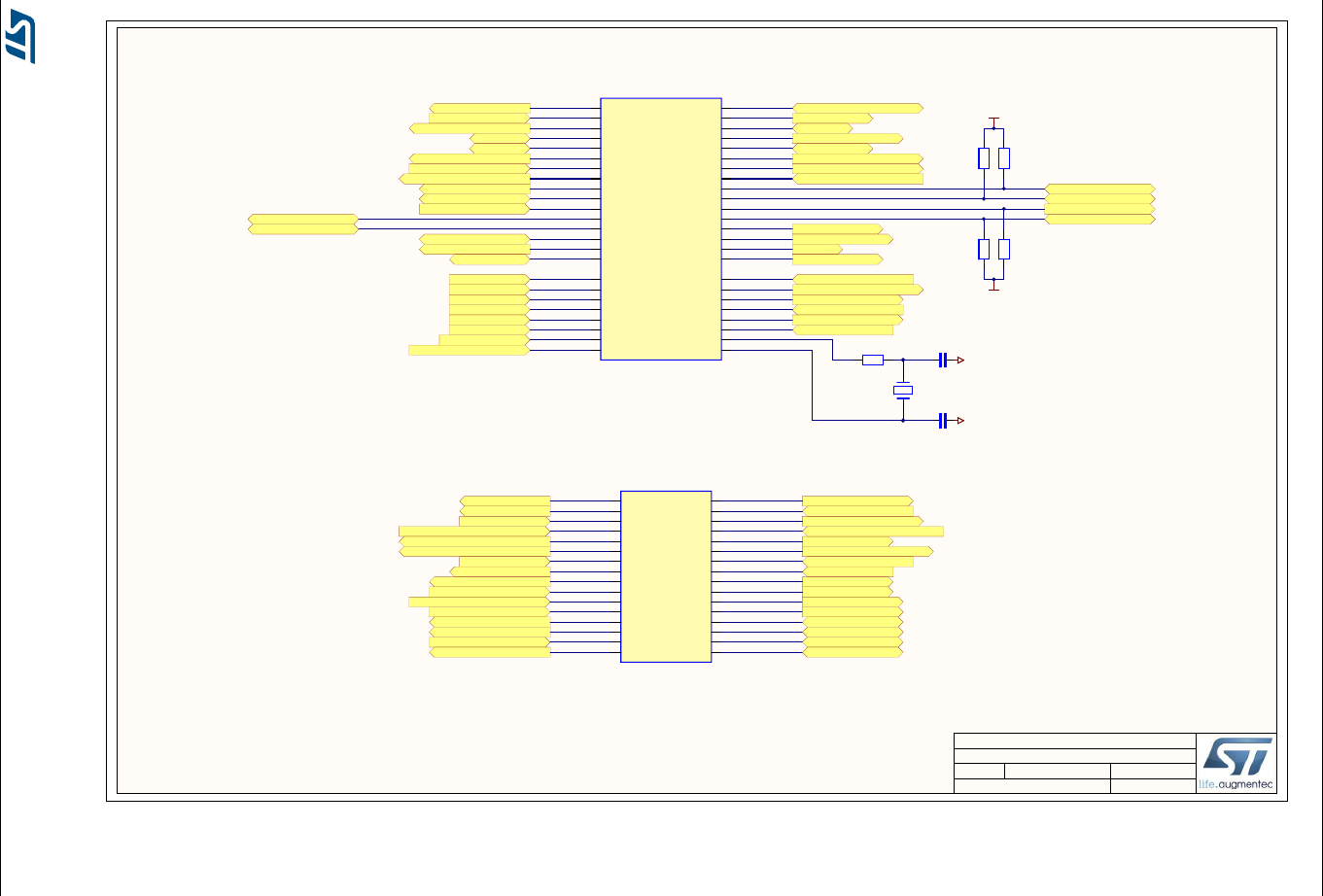
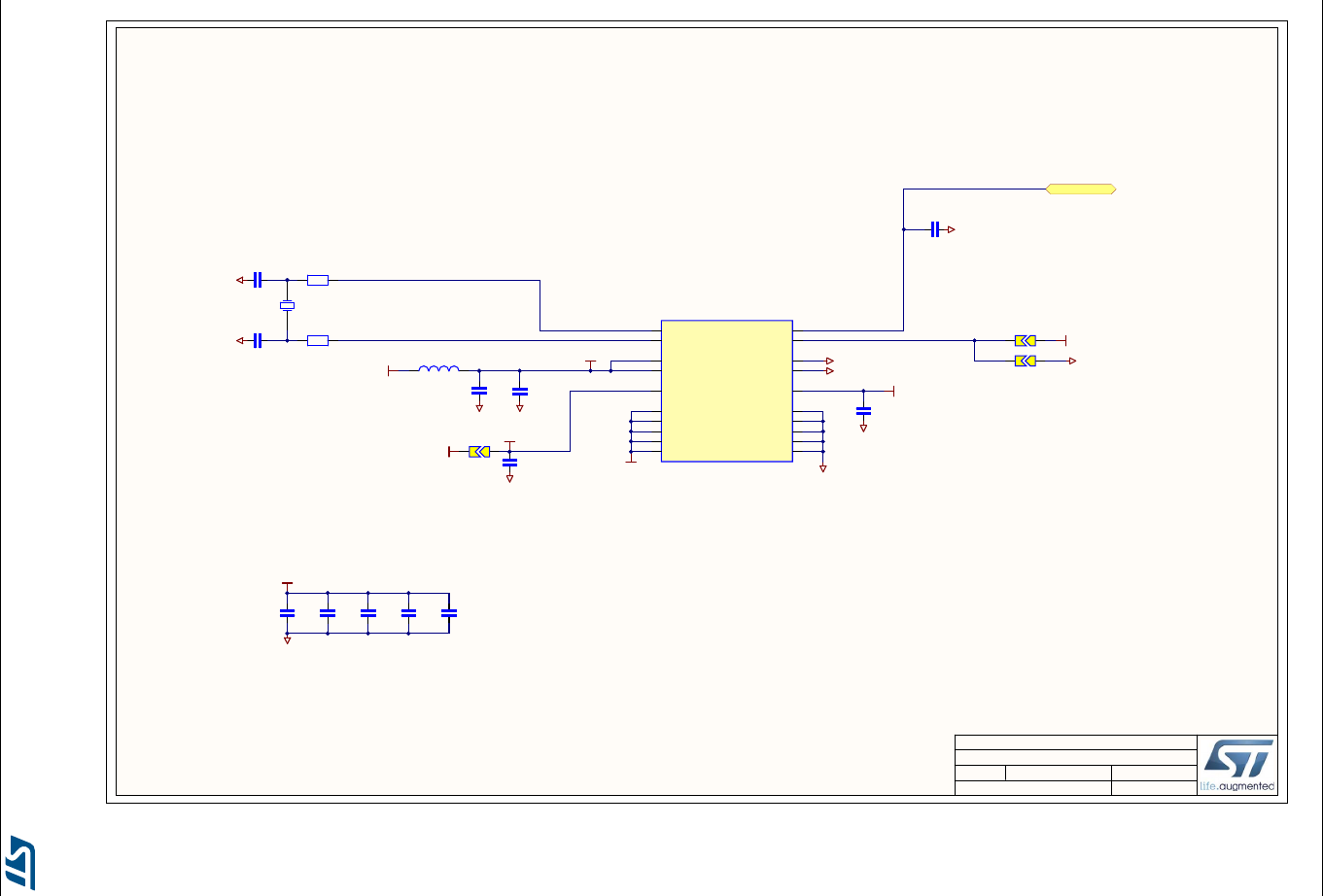
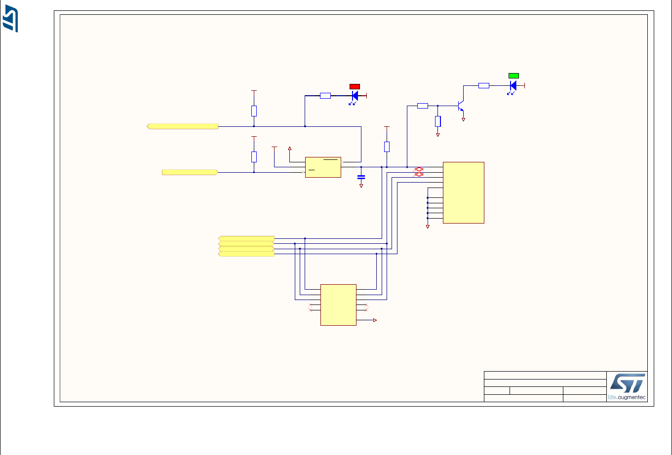
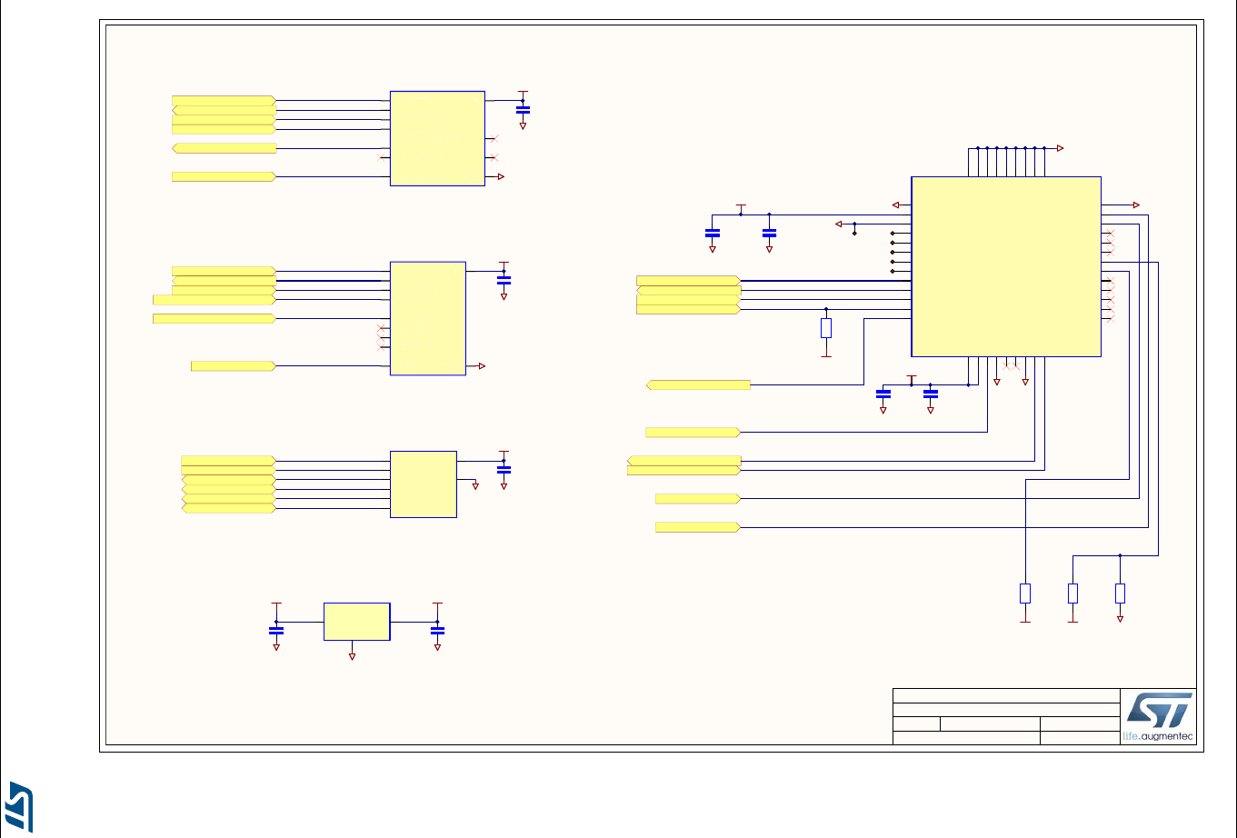
Appendix B Schematics
This section provides the design schematics for the STM32L4 Discovery kit for IoT node:
•Overall schematics for the B-L475E-IOT01A, see Figure 22
•STM32L475VG MCU, see Figure 23 and Figure 24
•USB OTG FS, see Figure 25
•RF Module, see Figure 26
•ST-MEMS sensors, see Figure 27
•NFC and STSAFE Part, see Figure 28
•Power supply, see Figure 29
•Arduino Uno V3 connector, see Figure 30
•Peripherals, see Figure 31
•ST-LINK with support of SWD only, see Figure 32
Schematics UM2153
42/57 DocID030118 Rev 3
Figure 22. STM32L4 Discovery kit for IoT node (top)
111
IOT Node Discovery Kit
MB1297 D
29/01/2017
Title:
Size: Reference:
Date: Sheet: of
A4 Revision:
ProjectProject:
Designed by DiZiC
MB1297
INTERNAL-SPI3_SCK
INTERNAL-SPI3_MOSI
INTERNAL-SPI3_MISO
ISM43362-SPI3_CSN
SPSGRF-915-SDN
SPSGRF-915-SPI3_CSN
SPBTLE-RF-SPI3_CSN
SYS_JTCK-SWCLK
SYS_JTMS-SWDIO
ARD.D3-PWM/INT1_EXTI0
ARD.D2-INT0_EXTI14
ARD.D1-UART4_TX
ARD.D0-UART4_RX
ARD.D4
ARD.D5-PWM
ARD.D6-PWM
ARD.D7
ARD.D8
ARD.D9-PWM
ARD.D10-SPI_SSN/PWM
ARD.D11-SPI1_MOSI/PWM
ARD.D12-SPI1_MISO
ARD.D13-SPI1_SCK/LED1
ARD.D14-I2C1_SDA
ARD.D15-I2C1_SCL
ARD.A5-ADC
ARD.A4-ADC
ARD.A3-ADC
ARD.A2-ADC
ARD.A1-ADC
ARD.A0-ADC
USB_OTG_FS_OVRCR_EXTI3
USB_OTG_FS_PWR_EN
USB_OTG_FS_VBUS
USB_OTG_FS_DM
USB_OTG_FS_DP
USB_OTG_FS_ID
INTERNAL-I2C2_SCL
INTERNAL-I2C2_SDA
M24SR64-Y-GPO
M24SR64-Y-RF_DISABLE
STSAFE-A100-RESET
LED2
LED3(WIFI) & LED4(BLE)
BUTTON_EXTI13
PMOD-UART2_RTS/SPI2_MOSI
PMOD-UART2_CTS/SPI2_MISO
PMOD-SPI2_SCK
PMOD-IRQ_EXTI2
PMOD-RESET
PMOD-UART2_RX
PMOD-UART2_TX/SPI2_CSN
LSM6DSL_INT1_EXTI11
LSM3MDL_DRDY_EXTI8
LPS22HB_INT_DRDY_EXTI10
HTS221_DRDY_EXTI15
VL53L0X_GPIO1_EXTI7
VL53L0X_XSHUT
DFSDM1_CKOUT
DFSDM1_DATIN2
SPBTLE-RF-RST
SYS_JTDO-SWO
QUADSPI_NCS
QUADSPI_CLK
QUADSPI_BK1_IO0
QUADSPI_BK1_IO1
QUADSPI_BK1_IO2
QUADSPI_BK1_IO3
SPSGRF-915-GPIO3_EXTI5
SPBTLE-RF-IRQ_EXTI6
ISM43362-DRDY_EXTI1
ISM43362-RST
ISM43362-WAKEUP
ISM43362-BOOT0
INTERNAL-UART3_RX
INTERNAL-UART3_TX
ST-LINK-UART1_RX
ST-LINK-UART1_TX
MCU1 Page 2/11
MB1297_MCU1.SchDoc
STM_NRST
MCU2 Page 3/11
MB1297_MCU2.SchDoc
INTERNAL-SPI3_SCK
INTERNAL-SPI3_MOSI
INTERNAL-SPI3_MISO
SPSGRF-915-SPI3_CSN
SPSGRF-915-GPIO3_EXTI5
SPSGRF-915-SDN
SPBTLE-RF-SPI3_CSN
SPBTLE-RF-RST
SPBTLE-RF-IRQ_EXTI6
QUADSPI_NCS
QUADSPI_CLK
QUADSPI_BK1_IO0
QUADSPI_BK1_IO1
QUADSPI_BK1_IO2
QUADSPI_BK1_IO3
INTERNAL-UART3_RX
INTERNAL-UART3_TX
ISM43362-SPI3_CSN
ISM43362-RST
ISM43362-WAKEUP
ISM43362-BOOT0
ISM43362-DRDY_EXTI1
RF Modules Page 5/11
MB1297_RF_Module.SchDoc
STM_NRST
ARD.D13-SPI1_SCK/LED1
LED2
LED3(WIFI) & LED4(BLE)
BUTTON_EXTI13
PMOD-UART2_RTS/SPI2_MOSI
PMOD-UART2_CTS/SPI2_MISO
PMOD-SPI2_SCK
PMOD-IRQ_EXTI2
PMOD-RESET
PMOD-UART2_RX
PMOD-UART2_TX/SPI2_CSN
Peripherals Page 10/11
MB1297_Peripherals.SchDoc
INTERNAL-I2C2_SCL
INTERNAL-I2C2_SDA
M24SR64-Y-GPO
M24SR64-Y-RF_DISABLE
STSAFE-A100-RESET
NFC & ST-SAFE Page 7/11
MB1297_NFC_SAFE.SchDoc
SYS_JTCK-SWCLK
SYS_JTMS-SWDIO
SYS_JTDO-SWO
ST-LINK-UART1_RX
ST-LINK-UART1_TX
STM_NRST
STLink V2.1 Page 11/11
MB1297_STLINK_V2-1.SCHDOC
ARD.D3-PWM/INT1_EXTI0
ARD.D2-INT0_EXTI14
ARD.D1-UART4_TX
ARD.D0-UART4_RX
ARD.A5-ADC
ARD.A4-ADC
ARD.A3-ADC
ARD.A2-ADC
ARD.A1-ADC
ARD.A0-ADC
ARD.D4
ARD.D5-PWM
ARD.D6-PWM
ARD.D7
ARD.D8
ARD.D9-PWM
ARD.D10-SPI_SSN/PWM
ARD.D11-SPI1_MOSI/PWM
ARD.D12-SPI1_MISO
ARD.D13-SPI1_SCK/LED1
ARD.D14-I2C1_SDA
ARD.D15-I2C1_SCL
STM_NRST
Arduino Connectors Page 9/11
MB1297_Arduino.SchDoc
INTERNAL-I2C2_SCL
INTERNAL-I2C2_SDA
LSM6DSL_INT1_EXTI11
LSM3MDL_DRDY_EXTI8
LPS22HB_INT_DRDY_EXTI10
HTS221_DRDY_EXTI15
VL53L0X_GPIO1_EXTI7
VL53L0X_XSHUT
DFSDM1_CKOUT
DFSDM1_DATIN2
MEMS Part Page 6/11
MB1297_MEMS.SchDoc
USB_OTG_FS_OVRCR_EXTI3
USB_OTG_FS_PWR_EN
USB_OTG_FS_VBUS
USB_OTG_FS_DM
USB_OTG_FS_DP
USB_OTG_FS_ID
USB_OTG_FS Page 4/11
MB1297_USB_OTG_FS.SchDoc
Power part Page 8/11
MB1297_POWER.SchDoc
UM2153 Schematics
DocID030118 Rev 3 43/57
Figure 23. STM32L475VG microcontroller
211
STM32L475 - 1/2
MB1297 D
29/01/2017
Title:
Size: Reference:
Date: Sheet: of
A4 Revision:
Project:
Designed by DiZiC
PE2 1
PE3 2
PE4 3
PE5 4
PE6 5
PE7 38
PE8 39
PE9 40
PE10 41
PE11 42
PE12 43
PE13 44
PE14 45
PE15 46
PD8
55
PD9
56
PD10
57
PD11
58
PD12
59
PD13
60
PD14
61
PD15
62
PD0
81
PD1
82
PD2
83
PD3
84
PD4
85
PD5
86
PD6
87
PD7
88
PE0 97
PE1 98
U1B
STM32L475VGTx
PA0/WKUP1
23
PA1
24
PA2
25
PA3
26
PA4
29
PA5
30
PA6
31
PA7
32
PB0 35
PB1 36
PB2 37
PB10 47
PB12 51
PB13 52
PB14 53
PB15 54
PA8
67
PA9
68
PA1 0
69
PA11
70
PA1 2
71
PA13/SWDIO
72
PA14/SWCLK
76
PA1 5
77
PB3/SWO 89
PB4 90
PB5 91
PB6 92
PB7 93
PB8 95
PB9 96
PC13/WKUP2 7
PC14-OSC32_IN 8
PC15-OSC32_OUT 9
PC0
15
PC1
16
PC2
17
PC3
18
PC4
33
PC5
34
PC6
63
PC7
64
PC8 65
PC9 66
PC10 78
PC11 79
PC12 80
PB11 48
U1A
STM32L475VGTx
M24SR64-Y-RF_DISABLE
M24SR64-Y-GPO
SPSGRF-915-GPIO3_EXTI5
SPBTLE-RF-IRQ_EXTI6
BUTTON_EXTI13
X2
NX3215SA-32.768K
ARD.A5-ADC
ARD.A4-ADC
ARD.A3-ADC
ARD.A2-ADC
ARD.D1-UART4_TX
ARD.D0-UART4_RX
ARD.D10-SPI_SSN/PWM
ARD.D4
ARD.D7
ARD.D13-SPI1_SCK/LED1
ARD.D12-SPI1_MISO
ARD.D11-SPI1_MOSI/PWM
ARD.A1-ADC
ARD.A0-ADC
ARD.D3-PWM/INT1_EXTI0
ARD.D6-PWM
ARD.D8
ISM43362-RST
INTERNAL-I2C2_SCL
INTERNAL-I2C2_SDA
ISM43362-BOOT0
ISM43362-WAKEUP
LED2
SPSGRF-915-SDN
INTERNAL-UART3_TX
INTERNAL-UART3_RX
LPS22HB_INT_DRDY_EXTI10
LSM6DSL_INT1_EXTI11
USB_OTG_FS_PWR_EN
SPBTLE-RF-SPI3_CSN
ARD.D2-INT0_EXTI14
HTS221_DRDY_EXTI15
VL53L0X_XSHUT
VL53L0X_GPIO1_EXTI7
LSM3MDL_DRDY_EXTI8
LED3(WIFI) & LED4(BLE)
SPBTLE-RF-RST
DFSDM1_DATIN2
DFSDM1_CKOUT
SYS_JTMS-SWDIO
SYS_JTCK-SWCLK
ARD.D9-PWM
USB_OTG_FS_VBUS
USB_OTG_FS_ID
USB_OTG_FS_DM
USB_OTG_FS_DP
QUADSPI_CLK
QUADSPI_NCS
QUADSPI_BK1_IO0
QUADSPI_BK1_IO1
QUADSPI_BK1_IO2
QUADSPI_BK1_IO3
SYS_JTDO-SWO
INTERNAL-SPI3_SCK
INTERNAL-SPI3_MISO
INTERNAL-SPI3_MOSI
PMOD-RESET
PMOD-SPI2_SCK
PMOD-IRQ_EXTI2
PMOD-UART2_CTS/SPI2_MISO
PMOD-UART2_RTS/SPI2_MOSI
PMOD-UART2_TX/SPI2_CSN
PMOD-UART2_RX
STSAFE-A100-RESET
ARD.D5-PWM
SPSGRF-915-SPI3_CSN
ST-LINK-UART1_TX
ST-LINK-UART1_RX
ARD.D14-I2C1_SDA
ARD.D15-I2C1_SCL
ISM43362-SPI3_CSN
ISM43362-DRDY_EXTI1
3V3
R8
2K2
R9
2K2
3V3
R10
2K2
R11
2K2
R12
0R
C14
5.1pF
GND
C15
5.1pF
GND
USB_OTG_FS_OVRCR_EXTI3
USB_N
USB_P
Schematics UM2153
44/57 DocID030118 Rev 3
Figure 24. STM32L475VG microcontroller
311
STM32L475 - 2/2
MB1297 D
29/01/2017
Title:
Size: Reference:
Date: Sheet: of
A4 Revision:
ProjectProject:
Designed by DiZiC
STM_NRST
L1
FCM1608KF-601T03
VDDA
VDD_MCU
VBAT
VDD_MCU
VDD_MCU
C3
100nF
GND
GND
GND
GND
SB17
Close
C8
1uF
GND
VDD_MCU
SB13
Close
SB9
Open
C5
100nF
GND
VDD_MCU
GND
1 2
X1
Not Fitted (NX3225GD-8.00M)
VSS 10
VDD
11
VSSA 19
VREF+
21
VDDUSB 73
PH0/PF0-OSC_IN
12
PH1/PF1-OSC_OUT
13 NRST 14
BOOT0 94
VDDA
22
VDD
28
VDD
50
VDD
75
VDD
100
VBAT
6
VREF- 20
VSS 74
VSS 27
VSS 49
VSS 99
U1C
STM32L475VGTx
GND
C6
1uF
GND
VDD_MCU
C7
100nF
GND
C2
Not Fitted (8.2pF)
GND
C4
Not Fitted (8.2pF)
GND
R5
Not Fitted (0R)
R7
Not Fitted (0R)
C9
100nF
C10
100nF
C11
100nF
C12
100nF
C13
100nF
UM2153 Schematics
DocID030118 Rev 3 45/57
Figure 25. USB OTG FS
411
USB_OTG_FS
MB1297 D
29/01/2017
Title:
Size: Reference:
Date: Sheet: of
A4 Revision:
Project:
5V
3V3
USB_OTG_FS_VBUS
5V_USB_FS
USB_OTG_FS_DM
USB_OTG_FS_DP
USB_OTG_FS_ID
USB_OTG_FS_PWR_EN
GND
2
IN
5
EN
4OUT 1
FAU LT 3
U19
STMPS2141STR
Dz
A2
ID A3
Pd1 B1
Pup
B2
Vbus
B3
D+in C1
Pd2 C2
D+out
C3
D-in D1
GND D2
D-out
D3
U20
EMIF02-USB03F2
VBUS
1
DM
2
DP
3
ID
4
GND
5
Shield
6
USB_Micro-AB receptacle
Shield
7
Shield
8
Shield
9
EXP
10
CN9
475900001
VBUS OK LED
3V3
USB_OTG_FS_OVRCR_EXTI3
3V3
VBUS OVRCR LED
ESD PROTECTION SHOULD BE CLOSE TO THE CONNECTOR
GND
GND
GND
GND
GND
GND
Designed by DiZiC
R62
47K
R58
47K
RED
LD8
LED
R56
1K
R61
0R
R57
47K
0603
R59
100K
3V3
GREEN
LD9
LED
R55
330R
3
1
2
Q2
BSR14
C66
4.7uF
0603
USB_N
USB_P
Schematics UM2153
46/57 DocID030118 Rev 3
Figure 26. RF module
511
RF Modules
MB1297 D
29/01/2017
Title:
Size: Reference:
Date: Sheet: of
A4 Revision:
Project:
Designed by DiZiC
GND
1
VDD
2
GND
3
TMS
4
TCK
5
TDI
6
TDO
7
TRSTN
8
ADC4/MOSI
9
ADC3/MISO
10
ADC2/SCK
11
ADC1/SSN
12
ADC0/DATARDY
13
VDD
14
VBAT
15
WKUP
16
GND
17
DP
18
DM
19
GND
20
RX
21
TX
22
GPIO0 23
GPIO1 24
GPIO2 25
GPIO3 26
GPIO4 27
CFG0 28
CFG1 29
RES 30
RES 31
RES 32
BOOT0 33
RSTN 34
GND 35
GND 36
GND 37
GND 38
GND 39
GND 40
GND 41
GND 42
GND 43
GND 44
M2
ISM43362-M3G-L44
GPIO (3)
1
GPIO (2)
2
GPIO (1)
3
GPIO (0)
4
Vin 5
GND 6
SPI_CLK
7
SPI_MISO
8
SPI_MOSI
9
SPI_CS
10
SDN
11
G
PI
O
(3
)
G
PI
O
(2
)
G
PI
O
(1
)
G
PI
O
(0
)
V
i
VV
n
G
N
D
S
PI_
CL
K
S
PI_MI
SO
S
PI_M
O
S
I
S
PI_
CS
SD
N
M3
SPSGRF
EXT_LPCLK 1
GPIO2
2
ANA_TEST 0 3
SPI_IRQ
4
Vin 5
GND 6
SPI_SCLK
7
SPI_MISO
8
SPI_MOSI
9
SPI_CS
10
BT_RESET
11
E
X
T
_
L
P
CL
K
G
PI
O
2
A
N
A
_
T
E
ST
0
S
PI
_
IR
Q
V
i
V
V
n
G
N
D
S
PI
_
SCL
K
S
PI_MI
SO
S
PI
_
M
O
S
I
S
PI
_
CS
BT
_
RE
S
E
T
M1
BT Module
3V3_WIFI
GND
C47
100nF
GND
GND
GND
C44
100nF
GND
GND
GND GND
3V3
GND
C43
100nF
3V3
GND
C45
100nF
GND
GND
SPBTLE-RF-RST
SPBTLE-RF-SPI3_CSN
SPBTLE-RF-IRQ_EXTI6
ISM43362-RST
ISM43362-SPI3_CSN
ISM43362-DRDY_EXTI1
INTERNAL-SPI3_SCK
INTERNAL-SPI3_MISO
INTERNAL-SPI3_MOSI
INTERNAL-SPI3_SCK
INTERNAL-SPI3_MISO
INTERNAL-SPI3_MOSI
ISM43362-BOOT0
ISM43362-WAKEUP
SPSGRF-915-SDN
INTERNAL-UART3_TX
INTERNAL-UART3_RX
SO/SIO1
2
WP#/SIO2
3
RESET#/SOI3
7
GND 4
SCLK
6CS#
1
SI/SIO0
5
VCC 8
U11
MX25R6435F
IN
1OUT 3
GND
2
U12
LT1963EST-3.3
3V3_WIFI
3V3_WIFI
GND
GND
C50
10uF
GND
C49
10uF
5V
3V3
GND
C48
100nF
GND
QUADSPI_CLK
QUADSPI_NCS
QUADSPI_BK1_IO0
QUADSPI_BK1_IO1
QUADSPI_BK1_IO2
QUADSPI_BK1_IO3
SPSGRF-915-SPI3_CSN
SPSGRF-915-GPIO3_EXTI5
3V3
INTERNAL-SPI3_SCK
INTERNAL-SPI3_MISO
INTERNAL-SPI3_MOSI
GND3V3_WIFI3V3_WIFI
R66
Not Fitted (10K)
R65
Not Fitted (10K)
R64
Not Fitted (10K)
R26
47K
0603
0603
TP1
TP2
TP3
TP4
TP5
TP6
GND
C75
2.2uF
GND
C76
2.2uF
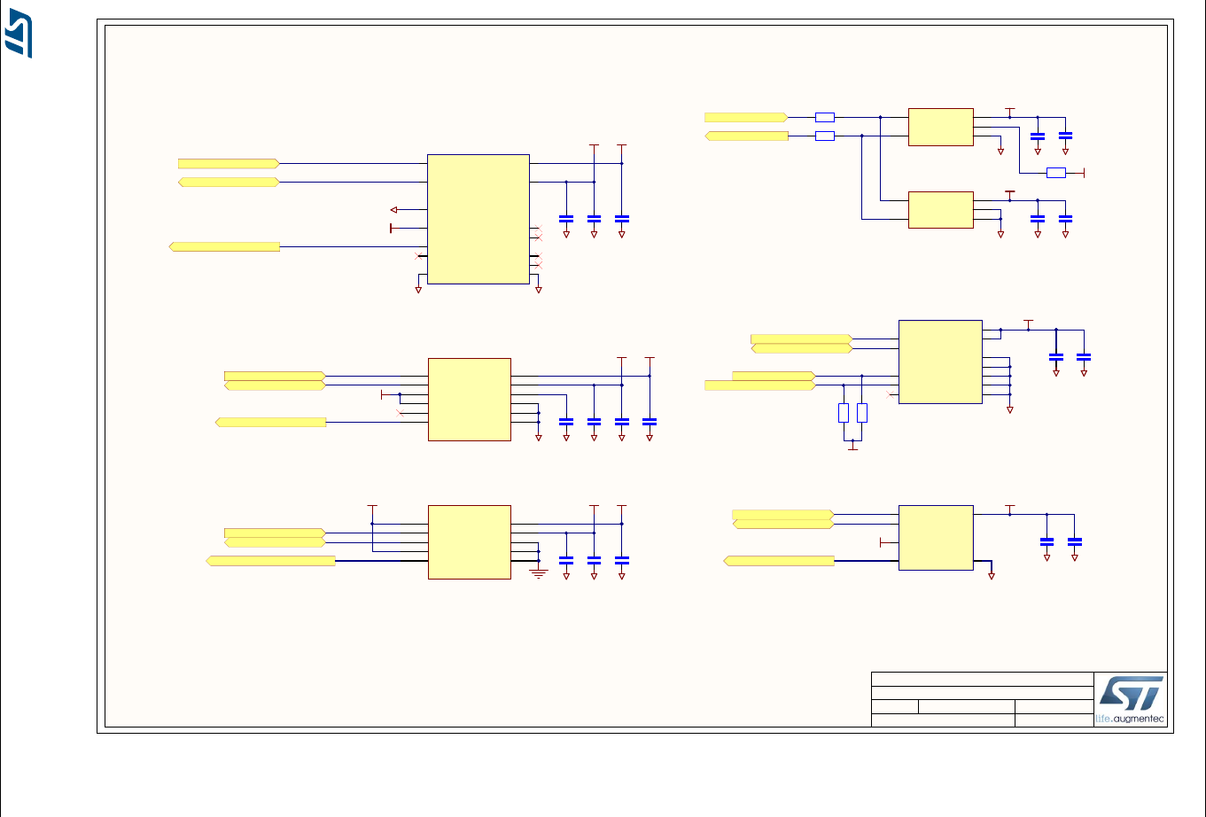
UM2153 Schematics
DocID030118 Rev 3 47/57
Figure 27. ST-MEMS sensors
611
MEMS Sensors
MB1297 D
29/01/2017
Title:
Size: Reference:
Date: Sheet: of
A4 Revision:
Project:
VDD_IO 6
C1 4
SCL/SPC
1
GND 3
SDA/SDI/SDO
11
SDO/SA1
9
CS
10
DRDY
8Res 2
INT
7
Res 12
VDD 5
U5
LIS3MDL
3V3
GND
Microphone MEMS
GND GND
Designed by DiZiC
C19
100nF
GND
C18
4.7uF
GND
C20
100nF
GND
GND
C25
100nF
GND
C24
1uF
GND
C26
100nF
GNDGND
C23
100nF
GND
C31
100nF
GND
C30
4.7uF
GND
C29
100nF
GND
VDD_IO 1
SCL/SPC
2
GND 8
SDA/SDI/SDO
4
SDO/SA0
5
CS
6
RES 3
INT_DRDY
7GND 9
VDD 10
U7
LPS22HB
VDD 1
SCL/SPC
2
DRDY
3
SDA/SDI/SDO
4
GND 5
CS
6
U6
HTS221
3V3
GND
GND GND
C28
100nF
C27
2.2uF
GPIO1
7
DNC
8
GND 3
XSHUT
5
SCL
10
SDA
9
GND2 4
AVDD_VCSEL 1
AVSS_VCSEL 2
AV D D 11
GND3 6
GND4 12
U4
VL53L0X
3V3
GND GND
C22
100nF
C21
4.7uF
GND
3V3
R15
10K
R14
10K
INTERNAL-I2C2_SCL
INTERNAL-I2C2_SDA
INTERNAL-I2C2_SCL
INTERNAL-I2C2_SDA
VL53L0X_XSHUT
VL53L0X_GPIO1_EXTI7
INTERNAL-I2C2_SCL
INTERNAL-I2C2_SDA
INTERNAL-I2C2_SCL
INTERNAL-I2C2_SDA
LSM3MDL_DRDY_EXTI8
LPS22HB_INT_DRDY_EXTI10
LSM6DSL_INT1_EXTI11
INTERNAL-I2C2_SCL
INTERNAL-I2C2_SDA
3V3 3V3
3V3 3V3
3V3
3V3 3V33V3
3V3
VDDIO 5
SCL
13
SDA
14
SDO/SA0
1
CS
12
SDx 2
INT1
4
SCx 3
nc 11
nc 10
GND
6GND 7
VDD 8
INT2
9
U3
LSM6DSL
GND
GND
3V3
HTS221_DRDY_EXTI15
Read=10111011 (BBh)
Write=10111010 (BAh)
Read=00111101 (3Dh)
Write=00111100 (3Ch)
Read=11010101 (D5h)
Write=11010100 (D4h)
Read=01010011(53h)
Write=01010010(52h)
Read=10111111 (BFh)
Write=10111110 (BEh)
0603
0603
0603
0603 0603
CLK
3VDD 1
LR 2
DOUT
4GND 5
U2
MP34DT01-M
GND
Microphone MEMS
C17
100nF
GND
C16
10uF
GND
DFSDM1_DATIN2
DFSDM1_CKOUT
3V3
0603
3V3
R67 10K
CLK
3VDD 1
LR 2
DOUT
4GND 5
U10
MP34DT01-M
C74
100nF
C46
10uF
R6 0R
R13 0R
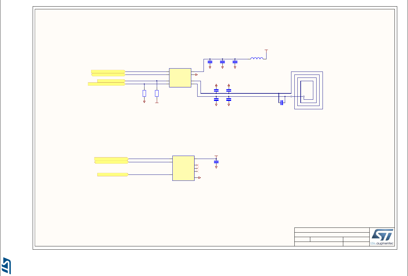
Schematics UM2153
48/57 DocID030118 Rev 3
Figure 28. NFC and STSAFE part
711
NFC & ST-SAFE Part
MB1297 D
12/03/2017
Title:
Size: Reference:
Date: Sheet: of
A4 Revision:
Project:
Designed by DiZiC
PCB Antenna 15x15mm
GND
GND
/RESET
1
VCC 2
NC 3
GND 4
SDA
5
NC 6
SCL
7
NC 8
U9
STSAFE-A100 (Not Fitted)
3V3
GND
C32
100nF
3V3
GND
C33
100nF
STSAFE-A100-RESET
INTERNAL-I2C2_SCL
INTERNAL-I2C2_SDA
INTERNAL-I2C2_SCL
INTERNAL-I2C2_SDA
M24SR64-Y-GPO
M24SR64-Y-RF_DISABLE RFDIS
1AC0 2
AC1 3
VSS 4
SDA
5SCL
6
GPO
7
VCC 8
U8
M24SR64-Y
See ANT7-T-M24SR-MB1255
GND
C67
100pF
GND
C68
1uF
GND
C71
10pF
GND
C53
10pF
GND
C72
Not Fitted
GND
C69
Not Fitted
C70
Not Fitted
R1
30K
GND
L2
742792042
R4
20K
3V3
Read=01000001(41h)
Write=01000000(40h)
Read=10101101(ADh)
Write=10101100(ACh)
ANT
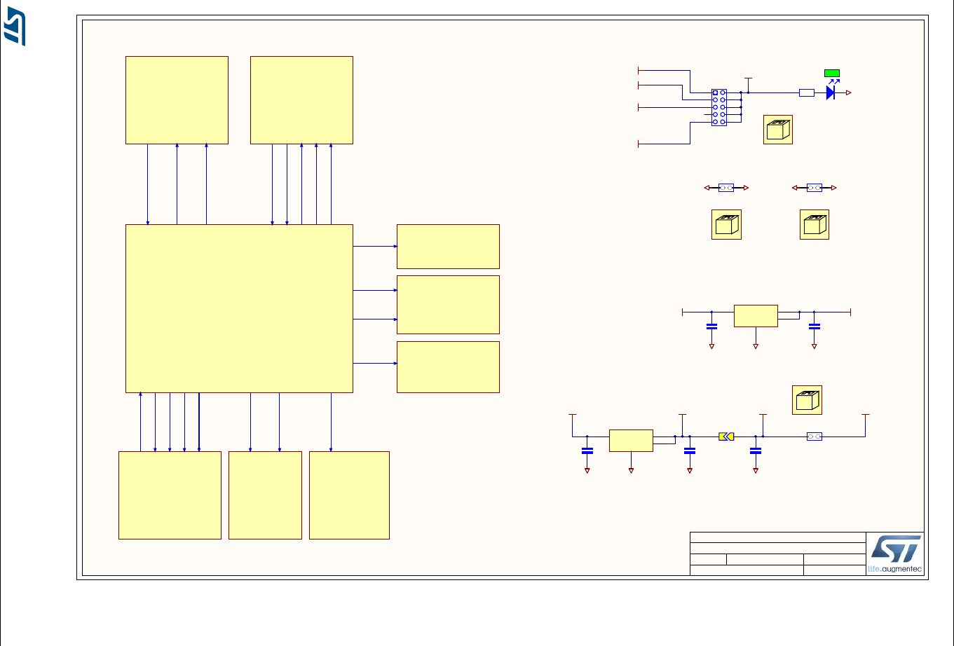
UM2153 Schematics
DocID030118 Rev 3 49/57
Figure 29. Power supply
811
POWER SUPPLY
MB1297 D
29/01/2017
Title:
Size: Reference:
Date: Sheet: of
A4 Revision:
Project:
Designed by DiZiC
5V_ARD
5V
5V 3V3
5V_ARD
5V_ST_LINK
VDD_MCU
VIN
From Arduino power pin
5V_USB_FS
Open solder bridge if Discovery is supplied
from +3V3 of extension connector
Jumper to measure IDD of the MCU
IDD
5V / 800mA
3V3 / 800mA
5V PWR SELECTION FROM EXTERNAL SOURCES
GND PROBE
5V INPUT PWR FROM ARDUINO
3V3 PWR
Vin
3Vo u t 2
Gnd
1
Tab 4
U13 LD1117S50TR
Vin
3Vo u t 2
Gnd
1
Tab 4
U14
LD1117S33TR
5V_USB_CHARGER
JP6
JP5
Cannot
open
file
C:\Data
HW1
SHUNT_BK
Cannot
open
file
C:\Data
HW2
SHUNT_BK
LDO_3V3
GND
GNDGNDGND
GND GND GND GND
GNDGND
JP7
GNDGND
2
4
6
8
10
1
3
5
7
9
JP4
HEADER_2X5
5V_VBAT
Cannot
open
file
C:\Data
HW3
SHUNT_BK
Cannot
open
file
C:\Data
HW4
SHUNT_BK
0603
0603
0603
0603
GREEN
LD5
LED
R25
330R
C38
10uF
C39
10uF
C41
10uF
C40
10uF
C42
100nF
SB4
Close
+5V
STLINK_V2-1 Page11/11USB_OTG_FS Page4/11
POWER SUPPLY Page8/11
MEMS Page6/11
RF_Module Page5/11
NFC_SAFE Page7/11
ARDUINO Page9/11 Peripherals Page10/11
3V3
3V3
5V
3V3
5V_ARD
3V3
5V
VDDA
3V3
VIN
MCU1&2 Page2&3/11
5V_USB_FS
5V
3V3
5V_USB_ST_LINK
5V_USB_CHARGER
5V_ARD
5V
5V_USB_FS
3V3
VDD_MCU
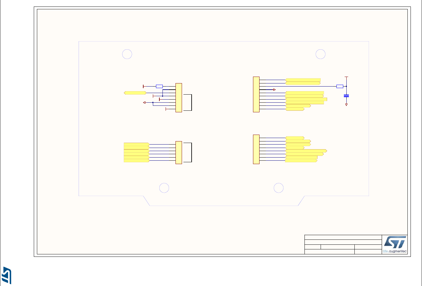
Schematics UM2153
50/57 DocID030118 Rev 3
Figure 30. Arduino Uno V3 connector
911
Arduino Uno connector
MB1297 D
29/01/2017
Title:
Size: Reference:
Date: Sheet: of
A4 Revision:
Project:
ARDUINO UNO connector
A0
A1
A2
A3
A4
A5 RX/D0
TX/D1
D2
D4
PWM/D3
PWM/D5
PWM/D6
D7
D8
PWM/D9
PWM/CS/D10
SDA/D14
SCL/D15
VIN
SCK/D13
MISO/D12
PWM/MOSI/D11
AVDD
GNDIOREF
NRST
3V3
5V
GND
GND
VIN
POWERAIN
3V3
5V
WARNING voltage applied to VIN <11.5V
5V_ARD
GND
GND
ARD.D1-UART4_TX
ARD.D0-UART4_RX
ARD.D10-SPI_SSN/PWM
ARD.D4
ARD.D7
ARD.D13-SPI1_SCK/LED1
ARD.D12-SPI1_MISO
ARD.D11-SPI1_MOSI/PWM
ARD.A5-ADC
ARD.A4-ADC
ARD.A3-ADC
ARD.A2-ADC
ARD.A1-ADC
ARD.A0-ADC
ARD.D3-PWM/INT1_EXTI0
ARD.D6-PWM
ARD.D8
ARD.D5-PWM
ARD.D14-I2C1_SDA
ARD.D15-I2C1_SCL
ARD.D2-INT0_EXTI14
STM_NRST
ARD.D9-PWM
VDDA
Designed by DiZiC
R3 1k R2
0R
GND
C1
100nF
1
2
3
4
5
6
CN4
Header 6X1_Female_SMD
1
2
3
4
5
6
7
8
CN2
Header 8X1_Female_SMD
1
2
3
4
5
6
7
8
CN3
Header 8X1_Female_SMD
1
2
3
4
5
6
7
8
9
10
CN1
Header 10X1_Female_SMD
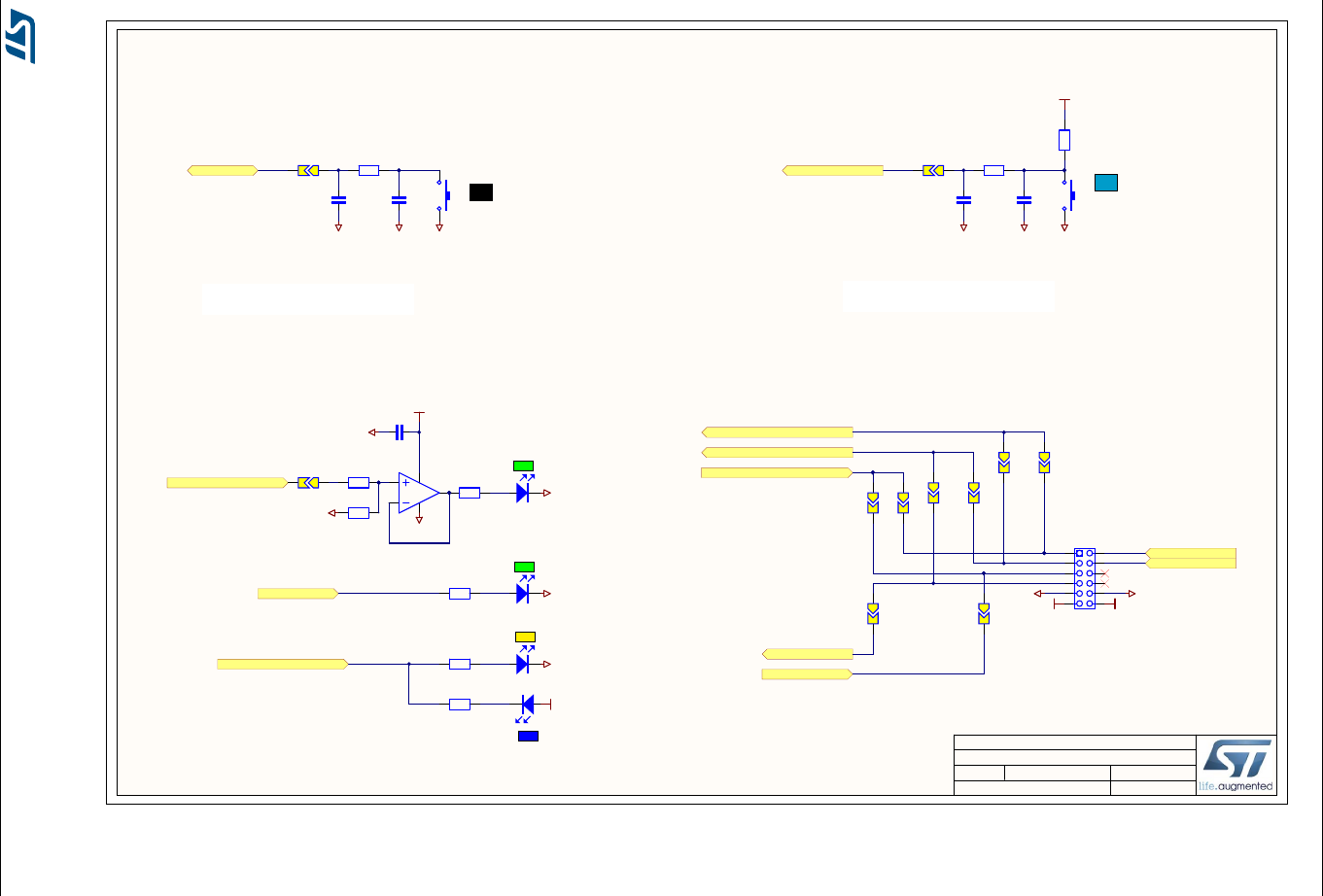
UM2153 Schematics
DocID030118 Rev 3 51/57
Figure 31. Peripherals
10 11
Peripherals
MB1297 D
29/01/2017
Title:
Size: Reference:
Date: Sheet: of
A4 Revision:
Project:
LED2
The 2 LEDs are top side
USER LED
RESET BUTTON USER & WAKE-UP Button
3V3
100nF should be place close to the MCU
10pF and 1K should be place close to the button
100nF should be place close to the MCU
10pF and 1K should be place close to the button
GND GND
GND
STM_NRST BUTTON_EXTI13
PMOD-RESET
PMOD-SPI2_SCK
PMOD-IRQ_EXTI2
PMOD-UART2_CTS/SPI2_MISO
PMOD-UART2_RTS/SPI2_MOSI
PMOD-UART2_TX/SPI2_CSN
PMOD-UART2_RX
LED3(WIFI) & LED4(BLE) GND
3V3
WIFI
BLE
GND
3V3
Designed by DiZiC
ARD.D13-SPI1_SCK/LED1
2
4
6
8
10
12
1
3
5
7
9
11
CN10
HEADER_2X6_PMOD
3V3
GND GND
PMOD
4
5
1
32VCC-
VCC+
U21
TSV631AILT
GND
GND
3V3
GND
C34
100nF
GND
C35
10pF
GND
C73
100nF
R19
1K
R16
10K
R38
200K
R18
1K GREEN
LD1 LED
GREEN
LD2 LED
YELLOW
LD3 LED
BLUE
LD4 LED
GND
C36
100nF
GND
C37
10pF
R24
1K
R23
100K
R20
330R
R21
1K
R22
680R
SB2
Close
SB1
Close
SB3
Close
SB14
Close
SB12
Open
SB15
Close
SB16
Open
SB19
Open
SB18
Close
SB21
Close
SB20
Open
B1
SW-PUSH-CMS_BLACK
B2
SW-PUSH-CMS_BLUE
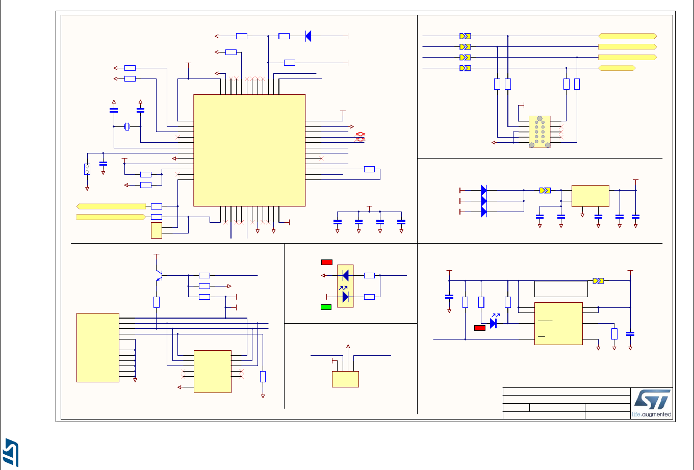
Schematics UM2153
52/57 DocID030118 Rev 3
Figure 32. ST-LINK/V2-1 with support of SWD only
11 11
ST-LINK/V2-1 with support of SWD only
MB1297 D
12/03/2017
Title:
Size: Reference:
Date: Sheet: of
A4 Revision:
Project:
STM_RST
T_JTCK
T_JTCK
T_JTMS
STM_JTMS
STM_JTCK
OSC_IN
OSC_OUT
T_NRST
AIN_1
3V3_ST_LINK
3V3_ST_LINK
USB_STLK_N
USB_STLK_P
ST-LINK USB CONNECTOR STLINK_LED
ST-LINK POWER 3V3 / 150mA
3V3_ST_LINK
Board Ident: PC13=0
T_JTCK
T_JTMS
SWD INTERFACE
3V3_ST_LINK
Fitted: NO
1
2
3
4
CN8 Header 4 pins
STM_JTMSSTM_JTCK
SWCLK SWDIO
T_SWDIO_IN
T_SWO
LED_STLINK
LED_STLINK
3V3_ST_LINK
Red
_Green
21
34
LD6
LD_BICOLOR_CMS
T_NRST
51
2
GND
3
4
BYPASS
INH
Vin Vout
U16 LD3985M33R
3V3_ST_LINK
USB_RENUMn
PWR_EXT
PWR_ENn
3V3_ST_LINK
USB_RENUMn
PWR_ENn
3V3_ST_LINK
3V3_ST_LINK
3V3_ST_LINK
VBAT
1
PA7
17
PC13
2
PA1 2 33
PC14
3
PB0
18
PC15
4JTMS/SWDIO 34
OSCIN
5
PB1
19
OSCOUT
6
VSS_2 35
NRST
7
PB2/BOOT1
20
VSSA
8
VDD_2 36
VDDA
9
PB10
21
PA0
10
JTCK/SWCLK 37
PA1
11
PB11
22
PA2
12
PA 1 5 /J T D I 38
PA3
13
VSS_1
23
PA4
14
PB3/JTDO 39
PA5
15
VDD_1
24
PA6
16
PB4/JNTRST 40
PB12 25
PB5 41
PB13 26
PB6 42
PB14 27
PB7 43
PB15 28
BOOT0 44
PA8 29
PB8 45
PA9 30
PB9 46
PA1 0 31
VSS_3 47
PA11 32
VDD_3 48
U15
STM32F103CBT6
5V_USB_ST_LINK
D2
BAT60JFILM
IN
1
IN
2
ON
3GND 4
SET 5
OUT 6
OUT 7
FAU LT
8
U17
ST890CDR
T_SWO
Ilim = 625mA
1.2Ilim = 750mA < Isc
1.5Ilim = 938mA > Isc
Must be on a border or the PCB.
5V_ST_LINK
D3 BAT60JFILM
D4 BAT60JFILM
5V_USB_ST_LINK
5V
VBUS 1
DM 2
DP 3
ID 4
GND 5
Shield 6
USB_Micro-B receptacle
Shield 7
Shield 8
Shield 9
EXP 10
EXP 11
CN7
1050170001
USB_STLK_N
USB_STLK_P
5V_USB_ST_LINK
5V_ARD
ST-LINK MCU
ST LINK USB Power switch 5V / 1.2A
ST-LINK DEBUG
5V_USB_FS D5 BAT60JFILM
1 2
X3
NX3225GD-8.00M
Dz A2
ID
A3
Pd1
B1
Pup B2
Vbus B3
D+in
C1
Pd2
C2
D+out C3
D-in
D1
GND
D2
D-out D3
U18
EMIF02-USB03F2
USB_STLK_ID
ESD PROTECTION SHOULD BE CLOSE TO THE CONNECTOR
3V3_ST_LINK
Only footprint with Cable: TC2050-IDC-NL
TAG_NRST
TAG _SW O
TAG _SW CLK
TAG _SW DIO
Fitted: NO
110
2 9
3 8
4 7
5 6
CN5
TC2050-IDC-NL
Fitted: NO
1
2
CN6
5V_USB_CHARGER
GND
GND
GND
GND
GND
GND GND
GND
GND
GND
GND
GND GND
GND
GND GND GND GND
GND
GND
GND
GND
GND
GND
GND GND GND
GND
GND GND
GND
GND GND GND
GND
ST-LINK-UART1_TX
ST-LINK-UART1_RX
SYS_JTMS-SWDIO
SYS_JTCK-SWCLK
SYS_JTDO-SWO
STM_NRST
Designed by DiZiC
JP8
3
1
2
Q1
BSR14
SB5 Close
SB6 Close
SB7 Close
SB8 Close
R33
22R
R32
22R
R34
22R
R35
22R
SB10
Close
C56
1uF
C57
100nF
C58
10nF
C59
1uF
C55
100nF
SB11
Open
C65
100nF
C64
1uF
R51
10K
R52
1K
R49
100K
R53
2K2
RED
LD7
LED
R44
330R
R47
330R
R45 100R
R46 36K
R48 10K
R50
1K5
R54
100K
C60
100nF
C61
100nF
C62
100nF
C63
100nF
R39
100R
R27
4K7
R28
2K7
R29
100K R30 Not Fitted (0R)
R31
10K
R36
Not Fitted (10K)
C51
10pF
C52
10pF
C54
100nF
R42 0R
R43 0R
R41 4K7
R40 4K7

DocID030118 Rev 3 53/57
UM2153 Board revision history and limitations
56
Appendix C Board revision history and limitations
Table 12. Board revision history and limitations
Board Version Revision details Known limitations
MB1297 A Not available; engineering samples
only -
MB1297 B Not available; engineering samples
only -
MB1297 C-01
First official IoT Discovery kit
version with following changes
compared to MB1297C
schematics:
– Capacitor value for NFC
matching changed (C53 = 10 pF
instead of 47 pF and C71 =
10 pF instead of 47 pF)
– STSAFE-A100 (U9 component)
not fitted on MB1297C
– Firmware revision inside the
Wi-Fi module must be:
C3.5.2.3.BETA9. The Wi-Fi
module maximum output power
is limited to 9 dBm to fulfill
FCC/IC/CE requirements.
– A limitation is present on the
MB1297C-01 board. The reset
connexion between STM32L4
and the ST-LINK MCU
(STM32F103) is not present
even if schematics are correct.
The software reset is available
so that the hardware missing
reset may not be necessary. If
the hardware reset is needed, a
simple workaround is available
by soldering an external wire
between the SB2 and SB8.
– Firmware revision inside the
Wi-Fi module must be:
C3.5.2.3.BETA9. The Wi-Fi
module maximum output power
is limited to 9 dBm to fulfill
FCC/IC/CE requirements.
MB1297 D-01
Second official IoT Discovery kit.
No BOM changes compared to the
MB1297 C-01 BOM, that is C53 =
10pF, C71 = 10pF and STSAFE-
A100 (U9 component) not fitted.
Two pcb changes compared to the
MB1297 C-01 pcb:
– The reset connexion between
STM32L4 and the ST-LINK MCU
(STM32F103) is implemented of
the MB1297 rev D
– The pcb below the Wi-Fi antenna
has been removed to have more
Wi-Fi radiated output power
Firmware revision inside the Wi-Fi
module must be: C3.5.2.3.BETA9.
The Wi-Fi module maximum
output power is then limited to 9
dBm to fulfill FCC/IC/CE
requirements.

Federal Communications Commission (FCC) and Industry Canada (IC) Compliance UM2153
54/57 DocID030118 Rev 3
Appendix D Federal Communications Commission (FCC)
and Industry Canada (IC) Compliance
Applicable for IoT node Discovery kit products with order code B-L475E-IOT01A1
(containing SPSGRF-915 module).
D.1 FCC Compliance Statement
Contains FCC ID: O7P-362
Contains FCC ID: S9NSPBTLERF
Contains FCC ID: S9NSPSGRF
D.1.1 Part 15.19
This device complies with Part 15 of the FCC Rules. Operation is subject to the following
two
conditions: (1) this device may not cause harmful interference, and (2) this device must
accept any interference received, including interference that may cause undesired
operation.
D.1.2 Part 15.105
This equipment has been tested and found to comply with the limits for a Class B digital
device, pursuant to part 15 of the FCC Rules. These limits are designed to provide
reasonable protection against harmful interference in a residential installation. This
equipment generates uses and can radiate radio frequency energy and, if not installed and
used in accordance with the instructions, may cause harmful interference to radio
communications. However, there is no guarantee that interference will not occur in a
particular installation. If this equipment does cause harmful interference to radio or
television
reception, which can be determined by turning the equipment off and on, the user is
encouraged to try to correct the interference by one or more of the following measures:
•Reorient or relocate the receiving antenna.
•Increase the separation between the equipment and the receiver.
•Connect the equipment into an outlet on a circuit different from that to which the
receiver
is connected.
•Consult the dealer or an experienced radio/TV technician for help.
8.7.1 Part 15.21
Any changes or modifications to this equipment not expressly approved by
STMicroelectronics may cause harmful interference and void the user’s authority to operate
this equipment.
8.8 IC Compliance Statement
Contains/Contient IC: 10147A-362
Contains/Contient IC: 8976C-SPBTLERF

DocID030118 Rev 3 55/57
UM2153 Federal Communications Commission (FCC) and Industry Canada (IC) Compliance
56
Contains/Contient IC: 8976C-SPSGRF
8.8.1 Compliance Statement
Industry Canada ICES-003 Compliance Label: CAN ICES-3 (B)/NMB-3(B)
This device complies with Industry Canada’s licence-exempt RSSs. Operation is subject to
the following two conditions:
1. This device may not cause interference; and
2. This device must accept any interference, including interference that may cause
undesired operation of the device.
8.8.2 Déclaration de conformité
Étiquette de conformité à la NMB-003 d’Industrie Canada: CAN ICES-3 (B)/NMB-3(B)
Le présent appareil est conforme aux CNR d’Industrie Canada applicables aux appareils
radio exempts de licence. L’exploitation est autorisée aux deux conditions suivantes:
1. L’appareil ne doit pas produire de brouillage;
2. L’appareil doit accepter tout brouillage radioélectrique subi, même si le brouillage est
susceptible d’en compromettre le fonctionnement.
8.8.3 RF exposure statement
To satisfy FCC and IC RF Exposure requirements for mobile devices, a separation distance
of 20 cm or more should be maintained between the antenna of this device and persons
during operation. To ensure compliance, operation at closer than this distance is not
recommended. This transmitter must not be co-located or operating in conjunction with any
other antenna or transmitter.
Pour satisfaire aux exigences FCC et IC concernant l'exposition aux champs RF pour les
appareils mobiles, une distance de séparation de 20 cm ou plus doit être maintenu entre
l'antenne de ce dispositif et les personnes pendant le fonctionnement. Pour assurer la
conformité, il est déconseillé d'utiliser cet équipement à une distance inférieure. Cet
émetteur ne doit pas être co-situé ou fonctionner conjointement avec une autre antenne ou
un autre émetteur.

Revision history UM2153
56/57 DocID030118 Rev 3
Revision history
Table 13. Document revision history
Date Revision Changes
31-Mar-2017 1 Initial version.
14-Apr-2017 2 Updated Section 7.12.6: Time-of-Flight and gesture detection
sensor (VL53L0X) to add Class 1 laser information.
28-Jun-2017 3
Updated: Section 7.11.3: Wi-Fi module Inventek ISM43362-M3G-
L44 (802.11 b/g/n) and Section Appendix B: Schematics to reflect
MB1297 rev D updates.

DocID030118 Rev 3 57/57
UM2153
57
IMPORTANT NOTICE – PLEASE READ CAREFULLY
STMicroelectronics NV and its subsidiaries (“ST”) reserve the right to make changes, corrections, enhancements, modifications, and
improvements to ST products and/or to this document at any time without notice. Purchasers should obtain the latest relevant information on
ST products before placing orders. ST products are sold pursuant to ST’s terms and conditions of sale in place at the time of order
acknowledgement.
Purchasers are solely responsible for the choice, selection, and use of ST products and ST assumes no liability for application assistance or
the design of Purchasers’ products.
No license, express or implied, to any intellectual property right is granted by ST herein.
Resale of ST products with provisions different from the information set forth herein shall void any warranty granted by ST for such product.
ST and the ST logo are trademarks of ST. All other product or service names are the property of their respective owners.
Information in this document supersedes and replaces information previously supplied in any prior versions of this document.
© 2017 STMicroelectronics – All rights reserved
