EWF 14450 Booklet
User Manual: EWF 14450
Open the PDF directly: View PDF ![]() .
.
Page Count: 15
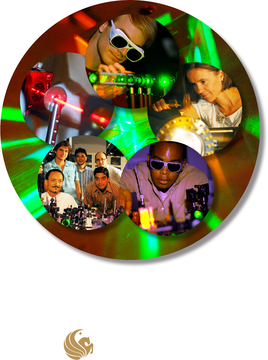
CREOL
The College of Optics & Photonics
2009
Industrial Aliates Day
“High Power Optical Sources
for the 21st Century”
JACQUEPHOTO.COM

CREOL, The College of Optics & Photonics
presents
“High Power Light Sources for the 21st Century”
Industrial Aliates Day
April 17, 2009
Program Schedule...................................................................................... 2
Exhibits......................................................................................................... 3
Invited Presentations................................................................................. 4
• The Art of Innovation: Laser Technology for New Markets
• HEL Joint Technology Oce (JTO): Research & Programs
• DPAL: A Hybrid Diode/Gas Laser Approach to High Power & Brightness
• High Power Fiber Lasers and Their Applications
• Townes Laser Institute: Update on progress to date
• High Power Beam Combining
Student of the Year Presentation............................................................ 10
Poster Presentation Abstracts................................................................. 11
Lab Tours...................................................................................................... 18
CREOL Lab Directory.................................................................................. 19
CREOL, The College of Optics & Photonics Contact Information..... 22
Industrial Aliate Program Members................................................... 23
Event Sponsors........................................................................................... 24
CREOL, The College of Optics and Photonics
Industrial Affiliates Day – April 17, 2009
Theme - “High Power Optical Sources for the 21st Century”
Morning Session –UCF Student Union
Time
Topic
Speaker
Affiliation
8:30
Continental Breakfast and Walk-in Registrations
9:00
Welcoming Remarks
Dr. MJ Soileau
Dr. Bahaa Saleh
UCF Vice-President for Research
Dean & Director, CREOL, The
College of Optics and Photonics
9:20
The Art of Innovation – Laser
Technology for new Markets
Prof. Dr. Reinhart Poprawe,
M.A.
Fraunhofer-Institute for Laser
Technology and Chair for Laser
Technology RWTH-Aachen
University
10:00
HEL Joint Technology Office
(JTO) Research & Programs
Mr. Albert Ogloza
HEL/JTO – Albuquerque, NM
10:40
BREAK
11:00
DPAL: a hybrid diode/gas laser
approach to high power and
brightness
Dr. Bill Krupke
WFK Lasers – Pleasanton, CA
11:40
High power fibers lasers and their
applications
Dr. Peter Moulton
Q-Peak – Bedford, MA
12:10
LUNCH Served
Student Center
Afternoon Session – CREOL Building
Time
Topic
Speaker
Affiliation
1:00
Walk to CREOL Bldg. Exhibits
Open
1:15
Townes Laser Institute – Update
on progress to date
Dr. Martin Richardson
CREOL, The College of Optics
and Photonics
1:30
High Power Beam Combining
Dr. Leonid Glebov
CREOL, The College of Optics
and Photonics
2:10
CREOL, The College of Optics and
Photonics – Research Overview
Dr. Bahaa Saleh
Dean, CREOL, The College of
Optics and Photonics
2:50
Student of the Year – Research
Presentation
Oleksandr Savchyn
CREOL, The College of Optics
and Photonics
3:20
Poster Sessions ; Lab Tours
(contiguous)
CREOL Graduate Students
CREOL Balcony; Tours start from
Lobby
5:00 -
6:15
Reception & Award presentations
Dr. Bahaa Saleh
CREOL, The College of Optics
and Photonics
Tabletop Exhibits – CREOL Lobby
Program Guide Exhibitors
Agilent Technologies
3501 Stevens Creek Blvd.
Santa Clara, CA 95051
408-345-8886
www.us@agilent.com
ER Precision Optical
505 W. Robinson St.
Orlando, FL 32801
407-292-5395
www.eroptics.com
Horiba Jobin Yvon
3880 Park Ave.
Edison, NJ 08820
732 -473-0560
www.jobinyvon.com
Laser Institute of America
13501 Ingenuity Drive, Suite 128
Orlando, FL 32826
407-380-1553
www.LaserInstitute.com
LIMO
Bookenburgweg 4-8
44319 Dortmund, Germany
49-231-22241–0
sales@limo.de
New Focus
2584 Junction Avenue
San Jose, CA 95134
408-919-1500
www.newfocus.com
Newport & Spectra Physics
1791 Deere Ave.
Irvine, CA 92714
949-253-1461
www.newport.com
Olympus Industrial America
One Corporate Drive
Orangeburg, NY 10962
866-642-4725
olympusmicroimaging.com
Ophir-Spiricon
60 West 1000 North
Logan, UT 84321
435-753-3729
www.ophir-spiricon.com
Optronic Laboratories
4632 36th St.
Orlando, FL 32811
407-422-3171
www.olinet.com
Optical Society of America
2010 Massachusetts Ave, NW
Washington, DC 20036
202-223-8130
www.osa.org
Photonics Online
VertMarkets, Inc
5 Walnut Grove Ste 320
Horsham, PA 19044
215-675-1800
www.vertmarkets.com
Qioptiq Linos, Inc.
78 Schuyler Baldwin Drive
Fairport, NY 14450
585-223-2370
www.qiopticlinos.com
Tektronix
14200 SW Karl Braun Drive
Beaverton, OR 97077
800-835-9433
www.tek.com
TeraComm, LLC
1016 SE Fleming Way
Stuart, FL 34997
321-431-1503
www.teracomm.com
Vytran
1400 Campus Drive West
Morganville, NJ 07751
732-972-2880
www.vytran.com
CREOL, The College of Optics and Photonics
Industrial Aliates Day — April 17, 2009
“High Power Optical Sources for the 21st Century”
CREOL, The College of Optics and Photonics
Industrial Affiliates Day – April 17, 2009
Theme - “High Power Optical Sources for the 21st Century”
Morning Session –UCF Student Union
Time
Topic
Speaker
Affiliation
8:30
Continental Breakfast and Walk-in Registrations
9:00
Welcoming Remarks
Dr. MJ Soileau
Dr. Bahaa Saleh
UCF Vice-President for Research
Dean & Director, CREOL, The
College of Optics and Photonics
9:20
The Art of Innovation – Laser
Technology for new Markets
Prof. Dr. Reinhart Poprawe,
M.A.
Fraunhofer-Institute for Laser
Technology and Chair for Laser
Technology RWTH-Aachen
University
10:00
HEL Joint Technology Office
(JTO) Research & Programs
Mr. Albert Ogloza
HEL/JTO – Albuquerque, NM
10:40
BREAK
11:00
DPAL: a hybrid diode/gas laser
approach to high power and
brightness
Dr. Bill Krupke
WFK Lasers – Pleasanton, CA
11:40
High power fibers lasers and their
applications
Dr. Peter Moulton
Q-Peak – Bedford, MA
12:10
LUNCH Served
Student Center
Afternoon Session – CREOL Building
Time
Topic
Speaker
Affiliation
1:00
Walk to CREOL Bldg. Exhibits
Open
1:15
Townes Laser Institute – Update
on progress to date
Dr. Martin Richardson
CREOL, The College of Optics
and Photonics
1:30
High Power Beam Combining
Dr. Leonid Glebov
CREOL, The College of Optics
and Photonics
2:10
CREOL, The College of Optics and
Photonics – Research Overview
Dr. Bahaa Saleh
Dean, CREOL, The College of
Optics and Photonics
2:50
Student of the Year – Research
Presentation
Oleksandr Savchyn
CREOL, The College of Optics
and Photonics
3:20
Poster Sessions ; Lab Tours
(contiguous)
CREOL Graduate Students
CREOL Balcony; Tours start from
Lobby
5:00 -
6:15
Reception & Award presentations
Dr. Bahaa Saleh
CREOL, The College of Optics
and Photonics
Tabletop Exhibits – CREOL Lobby
Morning Session - UCF Student Union
Afternoon Session - CREOL Building
Tabletop Exhibits - CREOL Lobby
Exhibitor tables will either be in the atrium of the Student Union (am) or the CREOL Lobby (pm).
2 Industrial Affiliates Day 2009 Industrial Affiliates Day 2009 3

Invited Presentations Invited Presentations
Dr. Leonid Glebov
CREOL, The College of Optics and Photonics
University of Central Florida
lbglebov@mail.ucf.edu
Abstract
This presentation is a survey of recent achievements in lasers with resonators which include volume
Bragg gratings – volume Bragg lasers. The technology of diffractive optical elements (volume
Bragg gratings, VBGs) recorded in a photo-thermo-refractive (PTR) glass was developed at CREOL/
The College of Optics and Photonics, University of Central Florida and licensed to OptiGrate
Corporation. These elements enable dramatic improvement of parameters of different types of lasers
demonstrated by a number of different research groups.
The use of reecting Bragg gratings as output couplers in external resonators for semiconductor
diodes, bars and stacks provided efcient spectral locking with efciency which usually exceeds
95%. Bragg mirrors enable spectral narrowing of solid state lasers down to couple picometers.
Experiments with wide stripe semiconductor lasers have shown that the use of VBGs with angular
selectivity comparable with diffraction limited divergence of emitter provides amplication for a
single mode only. Effective transverse mode selection in solid state lasers is also demonstrated.
Coherent radiation from two and three laser diodes placed at separated stages was observed by phase
locking with narrow-band VBG. Chirped Bragg gratings stretch and compress short laser pulses. It
was shown that stretching and compression could be performed with efciency of about 95% for
pulse widths down to 200 fs and average power exceeding 100 W. VBGs were used for spectral
combining of beams of Yb-doped ber lasers. Efciency of ve-channel combining of 93% with
divergence close to diffraction limit and total power of 750 W were demonstrated.
Biographical Note
Leon Glebov got his Ph.D. in Physics (major in Optics) and Doctor of Sciences from State Optical
Institute, Leningrad, Russia (1976 and 1987), where he hold a number of research and administrative
positions. His main directions of his research at that institute were color center generation, laser
induced breakdown, planar waveguides and photosensitive glasses for amplitude and phase recording.
He is a Research Professor at CREOL/The College of Optics and Photonics, University of Central
Florida since 1995. He has published a book and more than 280 papers in scientic journals and
holds a number of patents. He is a member of Organizing and Program Committees for a number of
International Conferences. He is Fellow of Optical Society of America and American Ceramic Society,
and a recipient of Denis Gabor award for contribution in holography. The main directions of his
research are optical properties of glasses including nonlinear phenomena, photosensitive glasses for
hologram recording, holographic optical elements, and lasers with volume Bragg external resonators.
Dr. Glebov is a Founder of OptiGrate Corporation, Orlando, FL, where he holds a position of CTO.
Prof. Dr. Reinhart Poprawe
Fraunhofer-Institute for Laser Technology and
Chair for Laser Technology RWTH-Aachen University
Reinhart.Poprawe@ilt.Fraunhofer.de
Abstract
Innovation did happen, if measurable benets – usually in the form of nancial surplus – can be
documented. This strict denition implies that scientic or technical demonstrations are necessary,
however too often too soon published, claimed and most importantly seen as success. The true
innovation needs partners not only with market know how, but with market presence, i.e. industry.
Therefore it is vital to create innovation in networks covering necessary scientic depth for sustainable
innovations and – more important – early stage involvement and commitment of market relevant partners.
The Fraunhofer Model is designed to meet the demands of this challenging process. The presentation
will focus on the systematics of that model, however in parallel always display actual real world
applications and cases, e.g. high quality Diode Lasers, 400W-average power fs-lasers, ablation
technology by ps-lasers, EUV-Sources for NG-Lithography, Individual Production by Laser SLM,
Metal Deposition for jet engine repair, Laser Polishing, Laser Sorting of scrap metals or material
analysis by LIBS. In all cases the entanglement of Fraunhofer-ILT with its partners can be identied
as necessary and sufcient condition for success.
Biographical Note
Professor Poprawe holds a M. A. in Physics degree from the California State University in Fresno
which he received in 1977. After completion of his diploma and PhD in physics (Darmstadt 1984) he
joined the Fraunhofer Institute for Laser Technology in Aachen where he began working as head of the
department “Laser oriented process development” in 1985. From 1989 to 1/1996 he has been managing
director of Thyssen Laser Technik GmbH in Aachen. Since February 1996 he is managing director of
the Fraunhofer Institute for Laser Technology and holds the University Chair for Laser Technology
at the RWTH Aachen. He is vice president the AKL Arbeitskreis Lasertechnik e. V. Aachen. Prof.
Poprawe has been elected to the grade of Fellow in the Society of Manufacturing Engineers in
USA (SME) since 1998 and a Fellow of the Laser Institute of America. Since 2008 he is a member
of the board of the Laser Institute of America (LIA) and serves in many national and international
boards as advisor, referee or consultant. Relevant R&D-expertise: Diode pumped solid state lasers,
diode lasers, pump modules and amplier modules for multisectorial applications, ps-, fs-lasers,
beam forming in space and time, short pulse laser, production process for diode lasers, EUV- and
x-ray lasers, drilling, cutting, joining (welding, soldering), surface processing, laser polishing, laser
generating, selective laser melting, laser metal deposition, micro technology, nano photonics, system
technology, process control, photonics in Life Science.
The Art of Innovation — Laser Technology for New Markets High Power Lasers Based on Volume Bragg Gratings
Creating the Future of Optics and Photonics
4 Industrial Affiliates Day 2009 Industrial Affiliates Day 2009 5

Invited Presentations Invited Presentations
Dr. Peter F. Moulton
Q-Peak, Inc.
135 South Road, Bedford, MA 01730
moulton@qpeak.com
Abstract
The power scaling of ber lasers to the multi-kW level is one of the more notable advances in laser
technology in the past 5 years. Nearly all of the scaling work has been concentrated on Yb-doped
silica bers, operating in the wavelength range around 1070 nm. The severe retinal hazard from lasers
in this region has motivated the search for power-scalable ber lasers at “eyesafer” wavelengths
beyond 1400 nm. Tm-doped silica ber lasers, providing output around 2050 nm, are one of the
more promising technologies. The energy-level properties of the Tm:silica material allow efcient
laser operation with pumping by conventional, 795-nm, high-power diode lasers. In this talk, we
described efforts at Q-Peak to better characterize the Tm:silica ber laser and scale power output to
the kW level and beyond. Our work to date includes basic spectroscopy, laboratory demonstrations
of efcient lasers at powers nearing 1 kW and technology development of “all-glass” systems. We
will discuss these results along with our latest advances.
Biographical Note
Peter Moulton received an A.B. in Physics from Harvard College in 1968 and M.S. and Ph.D.
degrees in Electrical Engineering from M.I.T. in 1972 and 1975 respectively. After nishing graduate
school he was employed in the Quantum Electronics Group at M.I.T. Lincoln Laboratory, Lexington,
Massachusetts. In 1985 he joined a start-up company, Schwartz Electro-Optics, as Vice-President
and managed the founding of the company’s Research Division in Concord, Massachusetts. He
became Senior Vice-President of SEO in 1997 and was involved in spinning out the Research Division
as a separate company, Q-Peak, in 1998, and in the sale of Q-Peak to its current parent company,
Physical Sciences Inc. in 2001. At present he is the Vice-President and Chief Technology Ofcer of
Q-Peak. Moulton’s technical work began in the eld of bulk solid state lasers, and in recent years
has extended to include nonlinear optics and ber lasers. Some of his work has been motivated
by defense applications, including infrared countermeasures, detection of chemical and biological
weapons, advanced ladar and targeting systems, laser communications and directed-energy systems.
He has also been involved in scientic applications, including global monitoring of atmospheric water
vapor, ozone aerosols and wind, in commercial applications in the semiconductor industry, in laser
systems for medical treatment and diagnostics, and in the development of lasers for large-screen
color displays. Dr. Moulton is a Fellow of the Optical Society of America (OSA.) He was awarded the
R.W. Wood Prize from the OSA and the William Streifer Scientic Achievement Award from IEEE/
LEOS, both in 1997, and in 2000 he was elected to the National Academy of Engineering.
Power Scaling of Tm: ber Lasers to the kW Level
Dr. William F. Krupke
WFK Lasers, LLC
Pleasanton, CA 94588
bkrupke@comcast.net
Abstract
The development of high power semiconductor laser diode pump sources during the past decade
enabled a great increase in the efciency, power, and compactness of solid state lasers (DPSSLs).
DPSSL output powers have now been scaled well into the multi-kW regime with excellent beam
quality. However, in these lasers waste heat in the static solid state gain must be removed by thermal
conduction, resulting in thermo-optical distortions that limit the high brightness power scaling these
lasers in a single (spatially) coherent aperture. To overcome this limitation, several years ago the
concept of the hybrid diode-pumped-alkali-laser (DPAL) was proposed to retain the attractive efciency
and power scaling properties of high power pump semiconductor laser diodes, while replacing the
static solid state gain medium with a gaseous (vapor) gain medium, recovering the feature of con-
vective transport of waste heat out of the laser resonator. In this talk the basic quasi-two level DPAL
laser scheme and its physical characteristics will be reviewed, the present state of DPAL R&D will
be summarized, and architectures for power scaling will be described.
Biographical Note
Bill received the PhD degree in Physics from the University of California at Los Angeles in 1966.
After graduation Bill held technical and management positions at the Hughes Aircraft Company
(1958-1961; 1961-1972), Minneapolis Honeywell Company (1962-1963), and the Aerospace
Corporation (1963-1966), where he performed research on various gas, chemical, and solid state
lasers. In 1972 Bill co-founded the Laser Directorate at the Lawrence Livermore National Laboratory
(LLNL), responsible for the development and execution of the Laboratory’s Inertial Connement
Fusion (ICF) and Atomic Vapor Laser Isotope Separation (AVLIS) national R&D programs. During
his 27 years there, Bill variously served as Program Leader, Chief Scientist, and nally Deputy
Associate Director for 20 years. At LLNL, he participated in the design, development, and construction
of evermore powerful Nd:glass lasers for fusion research, and the development of lasers for use in
an industrial scale, economic uranium enrichment process. Since 1985, he actively engaged in the
development of diode-pumped high-average-power solid state lasers, and their use in military, industrial,
and commercial applications. In 1999, Bill left LLNL and formed WFK Lasers, LLC to devote full
time to develop laser intellectual property and to consult for photonics technology companies. Bill is
a Fellow of the Optical Society of America, and has served as an elected member of the OSA Board
of Directors. He is also a member the IEEE Laser and Electro-optics Society (LEOS).
A Hybrid Diode-gas Laser Approach to High Power & Brightness
6 Industrial Affiliates Day 2009 Industrial Affiliates Day 2009 7
Creating the Future of Optics and Photonics

Martin Richardson
CREOL, The College of Optics and Photonics
University of Central Florida
UCF Trustee Chair: Northrup Grumman Professor of X-ray Photonics
and Director Townes Laser Institute Laser Plasma Laboratory
mrichard@creol.ucf.edu
Abstract
"The Townes Laser Institute was dedicated May 4, 2007 as a State center of excellence in advanced
lasers and laser technologies and recognizing Dr Charles Hard Townes, 1964 Nobel Laureate for
Physics, whose ideas lead to the invention of the laser . The primary goal of this institute is to make
UCF the premier institution in advanced laser technology in the United States, focusing on applica-
tions in medicine, advanced manufacturing tools, and defense. We will provide a brief summary of
its mission and progress, with a vision of its future impact on the College, UCF, and academic laser
research in the nation."
Biographical Note
Martin Richardson graduated from Imperial College, London, in Physics and gained his Ph.D from
London University. He is now a Professor of Optics in the School of Optics at the University of
Central Florida, and also holds similar positions in the departments of Physics and Electrical &
Computer Engineering. He directs a research program on the development of new high power lasers,
and their applications to dense laser plasma studies and x-ray generation in the Laser Plasma Labo-
ratory at the Center for Research & Education in Optics & Lasers (CREOL). Since coming to North
America in 1967, his career has been in the development of high power lasers and their application
to laser plasma studies.
For 12 years he held positions at the NRC laboratories in Ottawa, Canada, making contributions to
high power, ultrashort laser pulsed plasmas and the development of CO2 lasers and their use in laser
fusion studies. In 1980 he joined the University of Rochester where he worked for nine years as
group leader for experiments for the then new 24-beam OMEGA system at the Laboratory for Laser
Energetics.
Dr Richardson has held visiting scientic positions at the Institute for Laser Engineering (ILE)
Osaka University, the Max Planck Institute for Quantum Optics in Germany, and other institutions
in Australia, Canada, France and the former Soviet Union. He has published over 300 scientic
articles in professional scientic journals, most on them on high power lasers and x-rays and their
applications. He holds ve patents, with several pending. He has chaired many international confer-
ences including IQEC, ICHSP, and several SPIE meetings. He is a former Associate Editor of JQE, a
recipient of the Schardin Medal, and a Fellow of OSA.
Invited Presentations Invited Presentations
Townes Laser Institute Update
Mr. Albert A. Ogloza
Navy Representative to the
Joint Technology Ofce for High Energy Lasers
albert.ogloza@jto.hpc.mil
Abstract
The Joint Technology Ofce for High Energy Lasers (JTO-HEL) supports the development of laser
technology across a broad spectrum research elds and institutions. The research areas include Solid
State Lasers, Gas Lasers, Free Electron Laser, Beam Control Systems, Modeling and Simulation,
and Laser Effects. This talk will discuss each of these research areas in detail and some of the
research institutions performing the work. The main purpose of this talk is to acquaint the audience
with the Joint Technology Ofce and the research that we support.
Biographical Note
Mr. Ogloza received a Masters degree in Physics from Southern Illinois University at Carbondale
in 1987. As part of an IMMRRI fellowship his dissertation was on irreversible phase transitions in
Solid State materials.
Mr. Ogloza has been a research physicist the Naval Weapons Center at China Lake (NWC) for over
20 years. There he conducted research in High Energy Lasers, including Imaging spectral sensor
development, optical metrology, optical fabrication, and optical thin lm growth. In 1991 Mr.
Ogloza received a NWC Graduate fellowship to attend the University of Arizona at the Optical
Sciences Center where he completed his PhD coarse work and conducted research into optical thin
lm coating development.
In 2002 Mr. Ogloza started working with the Joint Technology Ofce for High Energy Lasers on the
development of Optical Thin Film Coatings and advanced thin lm metrology systems. In 2005 Mr.
Ogloza received the Michelson Award for scientic achievement, for the development of advanced
sensor systems and his work with High Energy Lasers. In 2007 Mr. Ogloza received the position as
Navy Representative to the Joint Technology Ofce for High Energy Lasers. There his duties are to
represent the Navy interest in the development of Laser Technology and High Energy Laser Systems.
The JTO-HEL coordinates the development of the HEL technology base throughout industry,
Government agencies and academia. His primary responsibilities are to represent the Navy interests
at the JTO and to select and monitor programs funded by the JTO-HEL.
HEL Joint Technology Oce (JTO): Research & Programs
Creating the Future of Optics and Photonics
8 Industrial Affiliates Day 2009 Industrial Affiliates Day 2009 9

CREOL Student of the Year Poster Presentation Abstracts
CREOL Building 2nd Floor — 3:20 - 5pm
Abstracts are numbered in the order Posters are displayed: Student Presenter
is listed rst and underlined. Faculty Supervisor is underlined. All listed
contributors are aliated with The College of Optics & Photonics, unless
otherwise noted.
Oleksandr Savchyn
osavchyn@creol.ucf.edu
407-823-6950
Abstract
The implementation of silicon photonics requires the development of a compact silicon-compatible
light source. One of the possible routes for its realization is to use the emission from optical centers
incorporated into silicon-based matrices and sensitized with dopants. It has long been thought that
silicon nanocrystals can be used as efcient and dominant sensitizers of erbium in silicon-doped
SiO2. In the current presentation it will be shown that the indirect excitation of erbium in this material
does not require the presence of silicon nanocrystals. This conclusion claries a number of previously
unexplained results and opens new opportunities in the eld of silicon photonics.
Biographical Note
Oleksandr Savchyn received his M.S. in Optics from CREOL in 2007 and his Specialist degree
(B.S. & M.S.) in Physics from the Lviv ‘Ivan Franko’ National University (Lviv, Ukraine) in 2002.
During 2002-2004 he worked as a research assistant at the Department of Physics of Lviv ‘Ivan
Franko’ National University. In 2004 he joined the Nanophotonics and Near-eld Optics group at
CREOL led by Dr. Peter Kik where he currently pursues his Ph.D. studies. His scientic interests
include semiconductor photonics, indirect excitation of erbium in glass matrices, optical properties
of silicon nanocrystals. He is a student member of OSA, SPIE, IEEE/LEOS, MRS.
Sensitizers of Erbium in Silicon-rich SiO2: Nanochrystals
or Luminescence Centers?
Gero Nootz,1,2 Lazaro A. Padilha,1 Scott Webster1, David J. Hagan,1,2 Eric W. Van Stryland,1,2 and
Edward H. Sargent3
1CREOL: The College of Optics and Photonics, Univ. of Central Florida, 4000 Central Florida
Blvd, Orlando, FL, 32826
2Physics Department, Univ. of Central Florida, 4000 Central Florida Blvd, Orlando, FL, 32826
3The Edward S Rogers Sr. Department of Electrical and Computer Engineering, Univ. of Toronto,
Toronto, ON, Canada, M5S3G4
gnootz@creol.ucf.edu
Abstract
Semiconductor quantum dots (QDs), semiconductor particles with sizes small enough for effects due
to quantum connement of the electronic wave functions to be observed, have been investigated for
several decades, but only recently have high-quality lead-salt QDs with narrow size distribution
successfully been synthesized. Understanding the electronic structure and carrier dynamics is of
fundamental importance for future applications of these mane made and highly customizable materials.
In this work we investigate the carrier dynamics in PbS and PbSe QD’s, measured by femtosecond
white-light-continuum transient-absorption, and two-photon absorption (2PA) spectra, measured by
two-photon uorescence and Z-scan. We identify different relaxation processes and measure their
time constants. The buildup time of the 1S state population when electrons are excited to the 1P level
in PbS QDs is measured and found to increase with increasing QD size. For the interband transition
from the 1S level into the ground state Auger recombination is determined to be the dominant relax-
ation process in QDs when more than one exciton is generated.
We show that symmetry breaking in QDs relaxes the selection rules for one and two-photon transi-
tions. This is evident from linear absorption measurement where features in the one photon spectra
appear where theoretical calculations predict two-photon allowed transitions. Similarly, features in
the 2PA spectra are seen where one-photon transitions are measured and predicted.
POSTER I
Symmetry Breaking and Carrier Dynamics
in Lead Salt Quantum Dots
Creating the Future of Optics and Photonics
10 Industrial Affiliates Day 2009 Industrial Affiliates Day 2009 11
Poster Presentation Abstracts Poster Presentation Abstracts
Ciceron O. Yanez,† Carolina D. Andrade,† Sheng Yao,† Gheorge Luchita,† Kevin D. Beleld*†‡
† Department of Chemistry University of Central Florida, Orlando, FL 32816 and
‡CREOL, The College of Optics and Photonics, University of Central Florida, Orlando, FL 32816
*Kevin D. Beleld, Beleld@mail.ucf.edu, 407-823-1028
Abstract
A uorescence readout, WORM optical data storage system has been previously reported by this group
where protonation of a 2PA uorene dyes in solution with 2PA photoacid generator (PAGs) were performed
by both one and two-photon excitation of photosensitive polymer lms. Commercially available photoacid
generators (PAGs) were used in this work. We evaluate the versatility of this data storage system by
modifying all of its three components. PAG photoacid efciency, uorescent dye versatility and polymer
substrates were the elements that were modied. One of the 2PA WORM ODS systems proved to be
resilient to overexposure. Furthermore, the inherent nonlinearity of 2PA components enabled a crosstalk
free system in which the 3D character of the ODS was demonstrated. The advantages of two-photon writing
and readout were clearly evidenced, affording a substantial storage density capacity (up to ca. 1011
bytes/cm3).
Yan Li and Thomas X. Wu, Shin-Tson Wu
*For information, contact: yanli@creol.ucf.edu, 407-823-6800; swu@creol.ucf.edu, 407-823-4763
Abstract
We propose a broadband wide-incident-angle reective polarization converter for light recycling inside a
liquid crystal display (LCD) panel. The polarization converter consists of a twisted nematic (TN) liquid
crystal lm, a uniaxial A-lm and a reector. The device conguration is optimized using genetic algo-
rithm. As a result, our design can convert light from TM to TE polarization (or TE to TM) at a maximum
99.7%, minimum 91.3%, and average 96.7% conversion efciency for the whole visible spectrum and
incident angle from 0 to 60 degrees. Such a broadband reective polarization converter is particularly
useful in enhancing the light efciency of LCD and reducing power consumption.
POSTER II
Photosensitive Polymeric Materials for Two-Photon
3D WORM Optical Data Storage Systems
POSTER III
Broadband Wide-angle Reective Polarization
Converter Using Liquid Crystal Films
J. W. Cleary*,1 R. E. Peale,1 W. Buchwald,2 and R. Soref2
1University of Central Florida, 4000 Central Florida Blvd, Orlando, FL 32816
2Air Force Research Labs / RYHC, 80 Scott Dr, Hanscom AFB, MA 01731
Point of contact: Justin Cleary, jcleary@physics.ucf.edu, 407-823-3076
Abstract
Experimental investigation of the coupling of free space radiation to surface plasmons by silver or
Pd2Si gratings was performed for different grating proles at CO2 laser wavelengths. Comparison
of the results with the theory of Hessel and Oliner 1965 and of Wheeler, Arakawa, and Ritchie 1976
suggests that the former gives the more accurate description in the long-wave IR. For that theory, the
comparison gives an empirical non-linear relation between the physical depth of the grating grooves
and the surface-impedance modulation amplitude. The Hessel-Oliner theory predicts stronger photon-
plasmon coupling for the higher impedance silicide, suggesting that these conductors may be preferable
for silicon-based IR plasmonic devices. Shifts and broadening of the surface Plasmon resonances
with increasing grating height are also reported and found to be weaker than similar effects observed
previously at visible wavelengths.
POSTER IV
Optimization of Long-wave IR Surface Plasmon Grating Couplers
POSTER V
Cubic Oxide Alloys for Deep-UV Applications
J. W. Mares*, R. C. Boutwell, A. Schuerer, M. Falanga, and W. V. Schoenfeld
*For information, contact: Jmares@creol.ucf.edu, 407-257-2123
Abstract
In this work, the epitaxial growth and characterization of lattice-matched NinMg1-nO thin lms on
MgO bulk crystal is presented. Radio frequency oxygen plasma assisted molecular beam epitaxy
was exploited to produce lms of varying nickel concentrations as measured by Rutherford Back-
scattering. Optical characterization was carried out using standard transmission spectrophotometry
and indicates well behaved shifts in lm bandgaps over the range Eg = 3.45eV to 4.75eV with
decreasing Nickel. Atomic force microscopy revealed good surface morphological quality with
root-mean square roughness ranging from 0.7 Å to approximately 25 Å. These results will be used
in device development for deep-UV applications.
Creating the Future of Optics and Photonics
12 Industrial Affiliates Day 2009 Industrial Affiliates Day 2009 13
Poster Presentation Abstracts Poster Presentation Abstracts
Jiyeon Choi, Mark Ramme, Troy Anderson and Martin Richardson
Laser processing technology group, Laser plasma laboratory, Townes Laser Institute
jichoi@creol.ucf.edu, 407-823-6895
Abstract
Femtosecond laser direct writing has become a powerful tool to create 3D volumetric structures in transparent
materials. It relies on the nonlinear absorption process that occurs when a laser beam is tightly focused into the
material and the intensity of the focused beam exeeds the threshold intensity of photo-structural modication. This
method has been widely employed to various areas of photonic device fabrication such as active and passive wave-
guides, couplers, gratings, and diffractive optical elements (DOEs). DOEs are very attractive elements to replace
bulky refractive optics to reduce device size for compactness. However, conventional fabrication methods such as
lithography and holography cannot produce volumetric 3D structures because most glasses and polymers are opaque
to the VUV illumination light source. Fabrication of volumetric 3D diffractive optical elements using femtosecond
laser direct writing is attractive not only to enable 3D processes but also to bring many more advantages such as
its simple production scheme, ease of changing patterns, clean production process etc. LPL has been heavily working on
the fabrication of volumetric DOEs via femtosecond laser direct writing. We present DOE fabrication technique using
laser direct writing as well as the characterization of laser-written DOEs by various techniques such as refractive
index change measurement and diffraction efciency measurement. We also propose new integration schemes of
DOEs with other photonic devices that would impact on the fabrication of integrated photonic devices.
POSTER VI
Femtosecond Laser Direct Written Volumetric
Diractive Optical Elements and Their Applications
POSTER VII
E-beam Assisted Fabrication of an Aluminium
Sub-wavelength Mesh for High Eciency UV Photodetectors
Clarisse Mazuir* and Winston V. Schoenfeld
For information contact: e-mail: cmazuir@creol.ucf.edu
Abstract
Using e-beam lithography on a single layer of polymethylmethacrylate (PMMA) we designed a relatively thick
subwavelength aluminum mesh on top of sapphire. The 100 nm thick mesh consisted of two perpendicularly
oriented sets of 100 nm wide parallel metal lines with a center to center distance as low as 260 nm. This metallic
structures were predicted to enhance transmission of light into UV sensitive GaN based photodetectors for both
transverse electric (TE) and transverse magnetic (TM) polarizations. Due to the large proximity effect during
e-beam exposure and the small spacing between metallic lines the use of an adhesion promoting layer appeared
necessary to avoid premature peeling of the photoresist. Using a monoatomic layer of hexamethyldisilazane
(HMDS) as an adhesion promoter between the sapphire and the PMMA, a 500 nm thick photoresist layer could
be exposed and developed with excellent control over the features sizes. Line spacing distances from 500 nm
down to 160 nm were achieved. An oxide plasma etch was found to be necessary for a better metal lines adhesion
during the lift-off process. Thermal evaporation of aluminum was performed and compared with e-beam evaporation.
An additional ultrasonic bath in the resist stripper was found necessary to ease the lift-off process.
POSTER VIII
Principal Component Analysis (PCA) of Femtosecond and
Nanosecond Laser Induced Breakdown Spectroscopy (LIBS) for
Organic Thin Film Discrimination
Christopher G. Brown1, Candice Bridge1, Matthew Fisher1, Matthieu Baudelet1, Michael Sigman2,
Martin C. Richardson1, Paul Dagdigian3
1Townes Laser Institute, College of Optics and Photonics, UCF, Orlando, FL, USA
2National Center for Forensic Science, UCF, Orlando, FL, USA
3Chemistry Department, Johns Hopkins University, Baltimore, MD, USA
For information contact: cgbrown@creol.ucf.edu
Abstract
While not specically suited for molecular spectroscopy, Laser Induced Breakdown Spectroscopy (LIBS) can utilize
molecular emission along with the atomic emission in order to enhance discrimination. Previous studies have shown that
atmosphere can be ionized along with plasma constituents resulting in a skewed interpretation of the data. This study
makes a comparison of single shot LIBS emission of the molecular species from plasmas produced from organic thin lm
residues on a silicon substrate. It is important to understand the inuence of the surrounding atmosphere on the spectrum
of material that is largely comprised of carbon, nitrogen, and oxygen, and identify how the entrainment with air skews the
results of the discrimination. The spectra were produced by either a 5 ns duration, 1064 nm/ 266 nm Nd:YAG laser, or a 40
fs, 800 nm Ti:Sapphire laser in both air and aragon atmospheres. Principle component analysis (PCA), considered to be an
exploratory technique, was used in order to gain a better understanding of the selected variables. The variables of interest
were based on the atomic carbon and oxygen peaks as well as the diatomic species CN violet bands and the
C2 Swan bands PCA was used to identify similarities between the organic analytes via the emission spectra,
and Receiver Operating Characteristics (ROC) curves were then generated to measure the performance of the analysis and
the inuence of the atmosphere on the spectral signatures for the different laser regimes.
POSTER IX
Preparation of Functional Three-Dimensional Nanophotonic
Materials and Devices by Multi-Photon Direct-Laser Writing
in SU-8 on Silicon
Henry E. Williams2 Marco A. Melino2, Touc G. Jabbour2, and Stephen M. Kuebler1,2,*
1Department of Chemistry, 2CREOL, The College of Optics and Photonics
For information contact: kuebler@mail.ucf.edu, 407-823-3720
Abstract
Multi-photon direct laser writing (DLW) is a powerful and versatile method for creating truly three-dimensional micro
and nano-scale structures and devices. SU-8 is a negative tone photoresist designed for patterning at 365 nm, but exhibits
sufcient multi-photon absorption at 800 nm which can be used for DLW. Being able to fabricate photonic structures
into materials such as silicon is of particular interest for future applications in integrated photonics and optoelectronics,
but complicates the DLW process further because the material is opaque near 800 nm. Here we demonstrate how DLW
can be used to prepare photonic structures directly onto silicon substrates, and how sample preparation and exposure
conditions, such as resin bake time and focus depth, affects feature size and structure delity.
(B2Σ – X2Σ)
(d3Πg – a3Πu).
(B2Σ – X2Σ)
(d3Πg – a3Πu).
Creating the Future of Optics and Photonics
14 Industrial Affiliates Day 2009 Industrial Affiliates Day 2009 15

Poster Presentation Abstracts Poster Presentation Abstracts
Jiyeon Choi, Mark Ramme, Troy Anderson and Martin Richardson
Laser processing technology group, Laser plasma laboratory, Townes Laser Institute
jichoi@creol.ucf.edu, Phone: 407-823-6895
Abstract
Femtosecond laser direct writing has become a powerful tool to create 3D volumetric structures in transparent
materials. It relies on the nonlinear absorption process that occurs when a laser beam is tightly focused into the material
and the intensity of the focused beam exeeds the threshold intensity of photo-structural modication. This method
has been widely employed to various areas of photonic device fabrication such as active and passive waveguides,
couplers, gratings, and diffractive optical elements (DOEs). DOEs are very attractive elements to replace bulky
refractive optics to reduce device size for compactness. However, conventional fabrication methods such as lithog-
raphy and holography cannot produce volumetric 3D structures because most glasses and polymers are opaque to
the VUV illumination light source. Fabrication of volumetric 3D diffractive optical elements using femtosecond
laser direct writing is attractive not only to enable 3D processes but also to bring many more advantages such
as its simple production scheme, ease of changing patterns, clean production process etc. LPL has been heavily
working on the fabrication of volumetric DOEs via femtosecond laser direct writing. We present DOE fabrication
technique using laser direct writing as well as the characterization of laser-written DOEs by various techniques such
as refractive index change measurement and diffraction efciency measurement. We also propose new integration
schemes of DOEs with other photonic devices that would impact on the fabrication of integrated photonic devices.
POSTER X
Femtosecond Laser Direct Written Volumetric
Diractive Optical Elements and Their Applications
POSTER XI
Gate Voltage Tunable Plasmon Resonances in Two Dimensional
Electron Gas in InGaAs/InP HEMT
Himanshu Saxena*,1 R. E. Peale,1 and W. R. Buchwald2
1Department of Physics, University of Central Florida, Orlando FL 32816
2Air Force Research Lab, Sensors Directorate, Hanscom AFB MA 01731
Contact: hsaxena.ucf@gmail.com, 407-823-3076
Abstract
We report voltage-tunable plasmon resonances in the two dimensional electron gas (2-deg) of a high electron
mobility transistor (HEMT) fabricated from the InGaAs/InP materials system. The device was fabricated from a
commercial HEMT wafer by depositing source and drain contacts using standard photolithography process and
a semi-transparent gate contact that consisted of a 0.5 µm period transmission grating formed by electron-beam
lithography. Narrow-band resonant absorption of THz radiation was observed in transmission in the frequency
range 10 – 50 cm-1. The resonance frequency depends on the gate voltage-tuned sheet-charge density of the 2deg.
The observed separation of resonance fundamental from its harmonics and their shift with gate bias follows theory,
although the absolute frequencies are lower by about a factor of 2-3.
Authors: Amitabh Ghoshal*, Pieter G. Kik
* aghoshal@creol.ucf.edu, Phone: 407-823-6899
Abstract
Surface plasmon excitation using a periodic array of metal nanoparticles near a metal lm is studied via full-eld
simulations and experiments. Illumination of a nanoparticle array induces resonant electron oscillations in the nanoparticles.
The resulting local electromagnetic eld oscillations excite propagating surface plasmons in the nearby metal lm.
Simulations (using Finite Integration Technique) of an innite array show the separate contributions of the particle
resonances and the grating resonances towards excitation of surface plasmons. Tuning of the two resonances to match
reveals strong inter-coupling and resulting anticrossing of the two resonances, and a reduced surface plasmon excitation
strength at the predicted crossing of resonances.Electron-beam lithography was used to fabricate nite metal nanoparticle
arrays above a metal lm. Geometry dependent reection measurements reveal the existence of several optical resonances.
Strong coupling of the in-plane nanoparticle plasmon resonance and propagating plasmons is evident from clear anticrossing
behavior. Reection measurements at high numerical aperture demonstrate the excitation of surface plasmons via out-of
plane particle polarization. The thus excited plasmons do not exhibit anticrossing in the considered frequency range. The
results are explained in terms of the known surface plasmon dispersion relation and the anisotropic frequency dependent
nanoparticle polarizability. These ndings are important for applications utilizing surface-coupled nanoparticle
plasmon resonances.
POSTER XII
Surface Plasmon Excitation Using Compact
Nanoparticle Enhanced Grating Couplers
POSTER XIII
Guided Mode Resonance Filters as Stable Line-narrowing
Feedback Elements for Thulium Fiber Lasers
Robert A. Sims1*, Zachary Roth2, Timothy McComb1, Lawrence Shah1, Christina Willis1, Pankaj Kadwani1,
Vikas Sudesh1, Poutous Menelaos2, Eric Johnson2, Martin C. Richardson1
1.Townes Laser Institute, CREOL, The College of Optics and Photonics, University of Central Florida,
4000 Central Florida Boulevard, Orlando, Florida 32816, USA
2.The Center for Optoelectronics and Optical Communications, University of North Carolina at Charlotte,
9201 University City Boulevard, Charlotte, NC 28223, USA
Corresponding Author: rasims@creol.ucf.edu
Abstract
Guided Mode Resonance Filters (GMRF) were used as external feedback elements for thulium ber lasers in order to
spectrally narrow and stabilize their output. GMRFs were fabricated with a diffractive array of holes etched into a top layer
of Plasma Enhanced Chemical Deposition (PECVD) grown SiO2 on top of a PECVD grown waveguide layer of SixNy.
Using this grating waveguide structure, externally propagating waves are coupled into the waveguide by phase matching
diffracted orders with allowable modes of the waveguide. Due to index modulation on the surface of the waveguide,
guided modes become leaky and recombine with the incident wave creating a resonance. Spectral reectivity was char-
acterized by placing GMRFs in the beam path of an amplied spontaneous emission source showing 0.4-1.0 nm FWHM
with 30-50% reectivity depending on properties of individual lters. Laser spectral output was stabilized at ~1985 nm
with ~30 pm linewidths at ~20 W pump powers. Slope efciency of a GMRF stabilized laser was 44% with a maximum
of 5.8 W CW output.
Creating the Future of Optics and Photonics
16 Industrial Affiliates Day 2009 Industrial Affiliates Day 2009 17
Industrial Affiliates Day 2009
Laboratory Tour Schedule
There will be guided group tours through several CREOL laboratories today.
Each guided tour will cover four labs, and will last approximately 60 minutes.
All tours start at 3:20pm in the CREOL lobby after the Student of the Year presentation.
Successive tours groups will be assembled starting with group A according to the schedule below.
Note: There is a live video view of our 3,000 sq ft class 1000 / class 100 cleanroom, just off one side of
the Lobby, near the front windows, including views of the Leica 5000+ e-beam writer.
In addition, presentations of work in the group of Dr. Richardson are shown on monitors near several
laboratories, including [1] the Northrop Grumman EUV Laboratory, [2] the Laser Development
Laboratory, [3] the Laser Spectroscopy Laboratory, [4] the Laser Plasma Laboratory, and [5] the Laser
Processing Technology Laboratory. Please look for the signs directing you to these displays.
Laboratory Tour Schedule
There will be guided group tours through several CREOL laboratories today.
Each guided tour will cover four labs, and will last approximately 60 minutes.
All tours start at 3:20pm in the CREOL lobby after the “Student of the Year” presentation.
Successive tour groups will be assembled starting with Group A (see schedule below).
Industrial Affiliates Day 2009
Laboratory Tour Schedule
There will be guided group tours through several CREOL laboratories today.
Each guided tour will cover four labs, and will last approximately 60 minutes.
All tours start at 3:20pm in the CREOL lobby after the Student of the Year presentation.
Successive tours groups will be assembled starting with group A according to the schedule below.
Note: There is a live video view of our 3,000 sq ft class 1000 / class 100 cleanroom, just off one side of
the Lobby, near the front windows, including views of the Leica 5000+ e-beam writer.
In addition, presentations of work in the group of Dr. Richardson are shown on monitors near several
laboratories, including [1] the Northrop Grumman EUV Laboratory, [2] the Laser Development
Laboratory, [3] the Laser Spectroscopy Laboratory, [4] the Laser Plasma Laboratory, and [5] the Laser
Processing Technology Laboratory. Please look for the signs directing you to these displays.
CREOL Laboratory Directory
Dr. Ayman Abouraddy
• Optical Fiber Characterization and Mid-infrared Nonlinear Fiber Optics – Rm. A114
• Optical Fiber Draw Tower – Rm. A105
• Thin-lm Thermal Evaporation – Rm. 216
• Multi-material Fiber Preform Fabrication – Rm. A302
Dr. Michael Bass
Solid State Lasers
• Laser Spectroscopy and Optically Written Displays – Rm. 157
• Thermal Management of Diode and Solid State Lasers – Rm. 158
• Microscopy, Electronics, Wave Propagation Studies – Rm. 175
Dr. Glenn Boreman
• Infrared Systems – Measurements & Characterization – Rm. 130
• Infrared Systems – E-Beam Lithography – Rm. 130A
• THz Laser Facility – Rm. 125
Dr. Demetri Christodoulides
• Soliton Theory – Rm. 210
• Nonlinear Guided Wave Lab – Rm. 203
Dr. Peter Delfyett
• Femtosecond Semiconductor Lasers & Dynamics – Rm. 252
• Modelocked Erbium Fiber & Glass Waveguide Laboratory – Rm. 254
• Femtosecond Optical Frequency Comb Lab – Rm. 255
• Optical Clocks for Photonic Sampling and Waveform Synthesis – Rm. 256
• High Power Ultrafast Semiconductor Laser Laboratory – Rm. 245A
• OCDMA & Chip Scale WDM Technologies – Rm. 244A
• Quantum Dot Semiconductor Laser Laboratory – Rm. 243A
Dr. Dennis Deppe
• MBE Lab – Rm. 180C
• PL Lab – Rm. 177
• Nanophotonics Fabrication Facility – Rm. 180
Dr. Aristide Dogariu
• Photonic Diagnostics in Random Media – Rms. 142, 144
Dr. Sasan Fathpour
• Integrated Semiconductor Photonic Device Characterization Laboratory Rm. – A212
Dr. Leon Glebov
• Volume Holographic Elements: recording – Rm. 153
• Photo-Thermo-Refractive Glass: metrology, photoinduced processing – Rm. 151
• Photo-Thermo-Refractive Glass: Melting – Rm. 152
• Volume Bragg semiconductor lasers, spectral beam combining – Rm. 154
• Volume holographic elements: high power applications (with Boris Zeldovich) – Rm. 249
• Photo-Thermo-Refractive Glass: Grinding, polishing – Rm. 150
Creating the Future of Optics and Photonics
18 Industrial Affiliates Day 2009 Industrial Affiliates Day 2009 19

CREOL Laboratory Directory
Drs. David Hagan and Eric Van Stryland
• Femtosecond Lasers – Rm. 22
• Nanosecond Tunable OPO (400-1,500 nm) – Rm. 236
• Picosecond tunable OPA lab (400nm–16microns) – Rm. 230
• Single Mode Nanosecond CO2 – Rm. 233
• Two-Photon Confocal Microscope with Femtosecond OPO – Rm. 246
• Near-infrared picoseconds laser lab – Rm. 242
Dr. James Harvey
• X-Ray Telescopes – Rm. A113
• Optical Surface Scattering – Rm. 155
• Generalized Scalar Diffraction Theory – Rm. A113
• Launch Vehicle Imaging Telescopes – Rm. A113
• Interferometry (with Jannick Rolland) – Rm. 146
Dr. Aravinda Kar
Laser Advanced Materials Processing (LAMP)
• Laser Advanced Manufacturing – Rms. 263, 264
• Laser Synthesis of Materials – Rms. 263, 264
• Laser Processing of Wide Bandgap semiconductors – Rms. 263, 264
• Modeling and Simulation for materials processing and materials synthesis – Rms. 263, 264
Dr. Pieter Kik
Nanophotonics and Near-eld Optics
• Nanophotonics Characterization Lab – Rm. 247
• Near-infrared picoseconds laser lab – Rm. 242
Dr. Stephen M. Kuebler
3D Micro- and Nano-fabrication
• Fabrication of 3D micro- and nano-scale structures – CHM Rm. 324
Dr. Guifang Li
• Optical Fiber Communications – Rms. 246A, 248, 278(ofce)
Dr. Patrick LiKamWa
• Quantum Well Optoelectronics – Rms. 220, 223
Dr. Jim Moharam
• Diffractive Optics – Rm. 258
Dr. Martin Richardson
Laser Plasma Laboratory
• Northrop Grumman Extreme Ultraviolet Photonics Laboratory (Rm. 143)
• Multi-TW Femtosecond Laser Interaction Facility (Rm. 140)
• High Intensity femtosecond laser interactions (Rms. 140, 112-117)
• Laser Development Laboratory (Rm. 141)
• X-ray microscopy Rm. 140
• Femtosecond THz Laboratory Rm. 140
• Femtosecond Laser Waveguide Writing & Micromachining Lab Rm. 141
• Laser Development Lab: New Solid State Laser Development Rm. 141B
• Laser induced breakdown spectroscopy (LIBS) laboratory Rms. 140, 123 & 123A, 112-117
• Zygo New View 6300 Interferometer – 2nd Floor Cleanroom Rm. 211
(continued)
Dr. Nabeel Riza
• Photonic Information Processing Systems – Rms. 250, 251, 253
Dr. Jannick Rolland
ODALab – Optical Diagnostics and Applications Laboratory
• 3D Visualization (Augmented Reality, Vision, 3D Lungs Alive) – Rm. 147
• 3D Optical Imaging (Optical Coherence Imaging, Curvature Sensing) – Rm. 146
• Optical System Design (Head Mounted Displays, Biophotonics) – Rms. 146-147
Dr. Winston Schoenfeld
Nano-Photonics Device Group (NPDG)
• Nanophotonics Devices Lab – Rm. 156
• Nanophotonics Fabrication Facility – Rm. 180
• Wide Band Gap Characterization Lab – Rm. 156A
• Oxide MBE Lab – Rm. 180C
Dr. William Silfvast
• Short Wave Length Source Lab – Rm. 123 (123A)
Dr. George Stegeman
Nonlinear Guided Wave Optics
• Ti:sapphire Laser – Solitons in Semiconductor Optical Ampliers – Rm. 243
Dr. Eric Van Stryland (See Drs. Hagan and Van Stryland)
Dr. Shin-Tson Wu
Photonics and Displays
• Liquid Crystal Displays – Rm. 245
• Liquid Crystal Materials Processing – Rm. 257
• Tunable Photonics Devices – Rm. 259
• Adaptive Lens – Rm. 260
Dr. Boris Zeldovich
• Optical Beam Combining Quantum Optics – Rm. 249
Other CREOL User Facilities
• Varian Cary 500 Scan UV-Vis-NIR Spectrophotometer – Rm. 159
• Olympus Nomarski Interference Microscope – Rm. 159
• Clean room – Rm. 211
• Class 1000/ Class 100 Clean Room – Rm. 180 (Nano-Fabrication Facility)
• Fiber Tower – Rm. A105
• Machine Shop – Rm. A106
CREOL Laboratory Directory
(continued)
Creating the Future of Optics and Photonics
20 Industrial Affiliates Day 2009 Industrial Affiliates Day 2009 21
CREOL Contact Information
Name Location Phone E-Mail
Ayman Abouraddy CREOL A116 407-823-6809 raddy@creol.ucf.edu
Dr. Michael Bass CREOL 161 407-823-6977 bass@creol.ucf.edu
Dr. Glenn D. Boreman CREOL A110 407-823-6815 boreman@creol.ucf.edu
Dr. Demetrios Christodoulides CREOL 210 407-882-0074 demetri@creol.ucf.edu
Dr. Peter J. Delfyett CREOL 272 407-823-6812 delfyett@creol.ucf.edu
Dr. Aristide Dogariu CREOL 164 407-823-6839 adogariu@creol.ucf.edu
Dr. Dennis Deppe CREOL 172 407-823-6870 ddeppe@creol.ucf.edu
Sasan Fathpour CREOL A212 407-823-6961 fathpour@creol.ucf.edu
Dr. Leonid B. Glebov CREOL 285 407-823-6983 lbglebov@creol.ucf.edu
Dr. David J. Hagan CREOL 208 407-823-6817 hagan@creol.ucf.edu
Dr. James E. Harvey CREOL A113 407-823-6818 harvey@creol.ucf.edu
Dr. Aravinda Kar CREOL 284 407-823-6921 akar@creol.ucf.edu
Dr. Pieter Kik CREOL 270 407-823-4622 kik@creol.ucf.edu
Dr. Stephen Kuebler Chem 221 407-823-3720 kuebler@creol.ucf.edu
Dr. Guifang Li CREOL 278 407-823-6811 li@creol.ucf.edu
Dr. Patrick L. LiKamWa CREOL A211 407-823-6816 patrick@creol.ucf.edu
Dr. M. G. "Jim" Moharam CREOL 274 407-823-6833 moharam@creol.ucf.edu
Dr. Martin C. Richardson CREOL 126 407-823-6819 mcr@creol.ucf.edu
Dr. Nabeel A. Riza CREOL 290 407-823-6829 riza@creol.ucf.edu
Dr. Bahaa Saleh CREOL 206 407-882-3326 basaleh@creol.ucf.edu
Dr. Winston Schoenfeld CREOL A215 407-823-6898 winston@creol.ucf.edu
Dr. M.J. Soileau Millican 243 407-823-3558 mj@creol.ucf.edu
Dr. George I. Stegeman CREOL 215 407-823-6915 george@creol.ucf.edu
Dr. Eric W. Van Stryland CREOL 271 407-823-6835 ewvs@creol.ucf.edu
Dr. Shin-Tson Wu CREOL 280 407-823-4763 swu@creol.ucf.edu
Dr. Boris Y. Zeldovich CREOL A222 407-823-6831 boris@creol.ucf.edu
Dr. Larry C. Andrews 125 Math & Physics 407-823-2418 landrews@mail.ucf.edu
Dr. Kevin D. Beleld 222 Chemistry Bldg 407-823-1028 kbelel@mail.ucf.edu
Dr. Kurt Busch Karlsruhe University 49-721-608-6054 kurt@tfp.uni-karlsruhe.de
Dr. Bruce Chai Crystal Photonics 407-328-9111 Chai@crystalphotonics.com
Dr. Louis Chow 219 Engineering Bldg 407-823-3666 lchow@mail.ucf.edu
Dr. Alfred Ducharme 118 Engineering Bldg 407-823-0070 ducharme@mail.ucf.edu
Dr. Florencio Eloy Hernandez 224 Chemistry Bldg 407-823-0843 orenzi@mail.ucf.edu
Dr. Hans Jenssen AC Materials 727-937-4135 h.jenssen@ac-materials.com
Dr. David Kaup 202C Math & Physics 407-823-2795 kaup@ucf.edu
Dr. Michael Leuenberg 12424 Research Pkwy 407-882-2846 mleuenbe@mail.ucf.edu
Dr. Jannick Rolland University of Rochester 585-273-4040 rolland@optics.rochester.edu
Dr. Robert E. Peale 404 Math & Physics 407-823-5208 rep@physics.ucf.edu
Dr. Alfons Schulte 427 Math & Physics 407-823-5196 afs@physics.ucf.edu
Dr. Mubarak A. Shah 238 Computer Science 407-823-5077 shah@cs.ucf.edu
Dr. Arthur Weeks 453 Engineering 407-275-3220 weeks@mail.ucf.edu
Dr. Emil Wolf CREOL 101 585-275-4397 ewlupus@pas.rochester.edu
Dr. Cynthia Young Math & Physics 231G 407-823-598 cyyoung@mail.ucf.edu
Dr. James Pearson CREOL 213 407-823-6858 jpearson@creol.ucf.edu
Mr. Mark Wagenhauser CREOL 109 407-823-6878 markw@creol.ucf.edu
Ms. Denise Whiteside CREOL 205 407-823-6834 dwhitesi@creol.ucf.edu
Ms. Jenna Reiser Marketing 407-408-4071 jreiser@creol.ucf.edu
CREOL Faculty Contacts
CREOL Faculty - Joint and Courtesy Appointments
Additional Contacts
Industrial Affiliates Program
Life Members
Cobb Family Foundation
Northrop Grumman Corporation
Nufern
Memoriam Members: Dr. Arthur H. Guenther and Dr. William C. Schwartz
Medallion Members
Agilent Technologies
Breault Research Organization
CST of America
Northrop Grumman Laser
Powerlase Limited
Paul G. Suchoski, Jr
Tektronix
Zemax Development Corp.
Senior Members
Newport Corporation
Coherent, Inc.
Crystal Photonics
Edmund Optics
ER Precision Optical
Essilor of America
Goodrich Corp.-Sensors Unlimited
Lambda Research Corporation
Lee Laser
Lockheed Martin
Ocean Optics
Opt-E
Optical Research Associates
Optimax Systems
TRUMPF, Inc.
Zygo Corporation
Affiliate Members
Aerotech, Inc.
Analog Modules
Applicote Associates, LLC
The Boeing Company
Coastal Optical Systems
DataRay, Inc.
DRS Optronics
Gentec Electro-Optics, Inc.
Harris Corporation
HORIBA Jobin Yvon
L-3 Comminications
Laser Institute of America
LaserPath Technologies
LIMOS
Lockheed Martin Coherent Technologies
Luna Innovations, Inc.
MZA Associates Corporation
New Focus
OKO Technologies
Olympus Industrial
Ophir-Spiricon
Optical Society of America
Optigrate Corp.
Opto-Sigma
Optronic Laboratories, Inc
Photonics Spectra
Photonics Online
Quioptic Linos
R-Soft Design Group
Ray Williamson Consulting
Raydiance, Inc.
Rini Technologies
Sciperio, Inc.
SPIE- The Int’l Society for Optics & Photonics
Tower Optical Corporation
TwinStar Optics, Coatings & Crystals
Vytran LLC
Yokogawa Corporation of America
Creating the Future of Optics and Photonics
22 Industrial Affiliates Day 2009 Industrial Affiliates Day 2009 23

Industrial Aliates Day
Event Sponsors
Agilent Technologies
5301 Stevens Creek Blvd.
Santa Clara, CA 95051
877-424-4536
www.agilent.com
Laser Institute of America
13501 Ingenuity Drive, Suite 128
Orlando, FL 32826
407-380-1553
www.LaserInstitute.com
Metro Orlando Economic
Development Commission
301 East Pine St., Suite 900
Orlando, FL 32801
407-422-7159
www.orlandoedc.com
Olympus
One Corporate Drive
Orangeburg, NY 10962
866-642-4725
www.olympusimaging.com
OptoSigma Corporation
2001 Deere Ave.
Santa Ana, CA 92705
949-851-5881
www.optosigma.com
Optronic Laboratories
4632 36th St.
Orlando, FL 32811
407-422-3171
www.olinet.com
Tektronix
14200 SW Karl Braun Drive
Beaverton, OR 97077
800-835-9433
www.tek.com
Varian Vacuum Technologies, Inc.
2435 Aloma Ave.
PMB 301
Oviedo, FL 32765
407-366-8602
www.varianinc.com
Vector Engineering
32111 Dewberry Lane
Sorrento, FL 32776
352-383-5319
vectoreng@aol.com
A Special Thank You to:
Gary and Connie Washam
Creating the Future of Optics and Photonics
All high-tech companies benet from
Florida’s business environment that
emphasizes innovation, collaboration,
and talent formation for today’s global
markets. From start-ups focused on
turning the latest academic research
into commercially viable products and
technologies, to established industry
giants, Florida has what high-tech
companies need.
Florida Photonics Industry Cluster
Florida’s photonics cluster is the 4th largest in the US, with
some 270 companies employing over 5,700 professionals
focused on the design, development, manufacturing, testing,
and integration of photonics and related systems. The photonics
& optics cluster in Florida spans a very broad range of industry
sectors, including lasers, ber optics, optical and laser materials,
thin lm coatings, optical components, optoelectronic fabrication
and packaging, and optical systems integrators, addressing
almost all applications from energy to medicine to defense.
The state’s colleges and universities have established interdis-
ciplinary programs and centers focusing on photonics/optics,
which graduate about ~100 photonics specialists each year.
Innovation Economy
Florida companies attracted more than $608 million in venture
capital in 2007 – nearly double the 2006 total.
Business Friendly Climate
Florida’s low taxes and smart growth policies have placed
it among the top 5 “Best States for Starting a Business,”
according to Fortune Small Business. Florida continues to
rank among the top states for best tax climates for business,
with no state income tax, low corporate taxes, a low unem-
ployment insurance tax rate, and sales tax exemptions for
certain business transactions.
Excellent Quality of Life
Florida continues its reign as one of the most desirable places
to live in the US, second only to California in 2007 in a Harris
Poll. Source: eorida.com, Enterprise Florida, Inc., 2008
It’s no surprise why Florida has become a top
destination for high-tech industry and in partic-
ular for the photonics industry. In 1971, thanks
to what Walt Disney termed “Imagineering,”
Central Florida took its place on the high-tech
map. Since then, with the growth of the high-
tech industry throughout the state, spawned by
space programs at Cape Canaveral and
establishment in 1987 of CREOL, the Center
for Research and Education in Optics and Lasers
at the University of Central Florida, “the mouse”
has taken on a whole new meaning. Inspired by
Disney’s initial vision, the imagination and genius
of the world’s leading research scientists and
engineers have made Florida the hub for a
wide range of industrial companies and venture
capitalists from around the world and in nearly
all application areas from energy to medicine
to aerospace.
On the Earth’s grid, Florida is a 3-D landmark
for the photonics industry. CREOL, The College
of Optics and Photonics, the Florida Photonics
Cluster, several vigorous university incubators
and regional economic development organiza-
tions, and a dynamic grouping of cutting-edge
companies form a photonics hub focused on
advancing Florida’s photonics industry.
Why Florida?
Florida is a High-tech Leader
For more information on “Why Florida” to grow your business, visit Enterprise Florida
at www.eorida.com and the Florida High Tech Corridor at www.oridahightech.com.
24 Industrial Affiliates Day 2009
To learn more about CREOL research collaborations, go to
www.optics.ucf.edu/Partnerships/Collaboration.aspx
PARTNER WITH CREOL
A research collaboration with CREOL helps advance
both your company’s business and the science
and technology of the optics and photonics field.
Industrial Affiliates Day 2009
