Flash Programmable System Devices With 8032 MCU USB And Logic UPSD3212CV CD00003200 81420
User Manual: UPSD3212CV
Open the PDF directly: View PDF ![]() .
.
Page Count: 182 [warning: Documents this large are best viewed by clicking the View PDF Link!]
- Table 1. Device summary
- 1 UPSD321xx description
- 2 Architecture overview
- 2.1 Memory organization
- 2.2 Registers
- 2.3 Program memory
- 2.4 Data memory
- 2.5 RAM
- 2.6 XRAM-PSD
- 2.7 SFR
- 2.8 Addressing modes
- 2.9 Arithmetic instructions
- 2.10 Logical instructions
- 2.11 Data transfers
- 2.12 Boolean instructions
- 2.13 Relative offset
- 2.14 Jump instructions
- 2.15 Machine cycles
- 3 UPSD321xx hardware description
- 4 MCU module description
- 5 Interrupt system
- 6 Power-saving mode
- 7 I/O ports (MCU module)
- 8 Oscillator
- 9 Supervisory
- 10 Watchdog timer
- 11 Timer/counters (Timer 0, Timer 1 and Timer 2)
- 12 Standard serial interface (UART)
- 12.1 Multiprocessor communications
- 12.2 Serial port control register
- Table 43. Serial port control register (SCON)
- Table 44. Description of the SCON bits
- 12.2.1 Baud rates
- 12.2.2 Using Timer 1 to generate baud rates
- 12.2.3 Using Timer/counter 2 to generate baud rates
- 12.2.4 More about Mode 0
- 12.2.5 More about Mode 1
- 12.2.6 More about Modes 2 and 3
- Figure 26. Serial port Mode 0 block diagram
- Figure 27. Serial port Mode 0 waveforms
- Figure 28. Serial port Mode 1 block diagram
- Figure 29. Serial port Mode 1 waveforms
- Figure 30. Serial port Mode 2 block diagram
- Figure 31. Serial port Mode 2 waveforms
- Figure 32. Serial port Mode 3 block diagram
- Figure 33. Serial port Mode 3 waveforms
- 13 Analog-to-digital convertor (ADC)
- 14 Pulse width modulation (PWM)
- 15 I2C interface
- Figure 38. Block diagram of the I2C bus serial I/O
- Table 50. Serial control register (SxCON: S1CON, S2CON)
- Table 51. Description of the SxCON bits
- Table 52. Selection of the serial clock frequency SCL in Master mode
- 15.1 Serial status register (SxSTA: S1STA, S2STA)
- 15.2 Data shift register (SxDAT: S1DAT, S2DAT)
- 15.3 Address register (SxADR: S1ADR, S2ADR)
- 16 USB hardware
- 16.1 USB related registers
- Table 60. USB address register (UADR: 0EEh)
- Table 61. Description of the UADR Bits
- Table 62. USB interrupt enable register (UIEN: 0E9h)
- Table 63. Description of the UIEN bits
- Table 64. USB interrupt status register (UISTA: 0E8h)
- Table 65. Description of the UISTA bits
- Table 66. USB Endpoint0 transmit control register (UCON0: 0EAh)
- Table 67. Description of the UCON0 bits
- Table 68. USB Endpoint1 (and 2) transmit control register (UCON1: 0EBh)
- Table 69. Description of the UCON1 bits
- Table 70. USB control register (UCON2: 0ECh)
- Table 71. Description of the UCON2 bits
- Table 72. USB Endpoint0 status register (USTA: 0EDh)
- Table 73. Description of the USTA bits
- Table 74. USB Endpoint0 data receive register (UDR0: 0EFh)
- Table 75. USB Endpoint0 data transmit register (UDT0: 0E7h)
- Table 76. USB Endpoint1 data transmit register (UDT1: 0E6h)
- Table 77. USB SFR memory map
- 16.2 Transceiver
- 16.3 Receiver characteristics
- 16.4 External USB pull-up resistor
- 16.1 USB related registers
- 17 PSD module
- 18 Development system
- 19 PSD module register description and address offset
- 20 PSD module detailed operation
- 21 Memory blocks
- 21.1 Primary Flash memory and secondary Flash memory description
- 21.2 Memory block select signals
- 21.3 Instructions
- 21.4 Power-down instruction and Power-up mode
- 21.5 Read
- 21.6 Programming Flash memory
- 21.7 Erasing Flash memory
- 21.8 Specific features
- 21.9 SRAM
- 21.10 Sector Select and SRAM Select
- 21.11 Page register
- 22 PLDs
- 23 I/O ports (PSD module)
- 23.1 General port architecture
- 23.2 Port operating modes
- 23.3 MCU I/O mode
- 23.4 PLD I/O mode
- 23.5 Address Out mode
- 23.6 Peripheral I/O mode
- 23.7 JTAG in-system programming (ISP)
- 23.8 Port configuration registers (PCR)
- 23.9 Port data registers
- 23.10 Ports A and B – functionality and structure
- 23.11 Port C – functionality and structure
- 23.12 Port D – functionality and structure
- 23.13 External chip select
- 24 Power management
- 25 RESET timing and device status at reset
- 26 Programming in-circuit using the JTAG serial interface
- 27 Initial delivery state
- 28 AC/DC parameters
- 29 Maximum ratings
- 30 EMC characteristics
- 31 DC and AC parameters
- Table 110. Operating conditions (5 V devices)
- Table 111. Operating conditions (3 V devices)
- Table 112. AC signal letters for timing
- Table 113. AC signal behavior symbols for timing
- Figure 68. Switching waveforms – key
- Table 114. Major parameters
- Table 115. DC characteristics (5 V devices)
- Table 116. DC characteristics (3 V devices)
- Figure 69. External program memory Read cycle
- Table 117. External program memory AC characteristics (with the 5 V MCU module)
- Table 118. External program memory AC characteristics (with the 3 V MCU module)
- Table 119. External clock drive (with the 5 V MCU module)
- Table 120. External clock drive (with the 3 V MCU module)
- Figure 70. External data memory Read cycle
- Figure 71. External data memory Write cycle
- Table 121. External data memory AC characteristics (with the 5 V MCU module)
- Table 122. External data memory AC characteristics (with the 3 V MCU module)
- Table 123. A/D analog specification
- Figure 72. Input to output disable / enable
- Table 124. CPLD combinatorial timing (5 V devices)
- Table 125. CPLD combinatorial timing (3 V devices)
- Figure 73. Synchronous clock mode timing – PLD
- Table 126. CPLD macrocell synchronous clock mode timing (5 V devices)
- Table 127. CPLD macrocell synchronous clock mode timing (3 V devices)
- Figure 74. Asynchronous Reset / Preset
- Figure 75. Asynchronous clock mode timing (product term clock)
- Table 128. CPLD macrocell asynchronous clock mode timing (5 V devices)
- Table 129. CPLD macrocell asynchronous clock mode timing (3 V devices)
- Figure 76. Input macrocell timing (product term clock)
- Table 130. Input macrocell timing (5 V devices)
- Table 131. Input macrocell timing (3 V devices)
- Table 132. Program, Write and Erase times (5 V devices)
- Table 133. Program, Write and Erase times (3 V devices)
- Figure 77. Peripheral I/O Read timing
- Table 134. Port A peripheral data mode Read timing (5 V devices)
- Table 135. Port A peripheral data mode Read timing (3 V devices)
- Figure 78. Peripheral I/O Write timing
- Table 136. Port A peripheral data mode Write timing (5 V devices)
- Table 137. Port A peripheral data mode Write timing (3 V devices)
- Figure 79. Reset (RESET) timing
- Table 138. Reset (RESET) timing (5 V devices)
- Table 139. Reset (RESET) timing (3 V devices)
- Figure 80. ISC timing
- Table 140. ISC timing (5 V devices)
- Table 141. ISC timing (3 V devices)
- Figure 81. MCU module AC measurement I/O waveform
- Figure 82. PSD module AC float I/O waveform
- Figure 83. External clock cycle
- Figure 84. Recommended oscillator circuits
- Figure 85. PSD module AC measurement I/O waveform
- Figure 86. PSD module AC measurement load circuit
- Table 142. Capacitance
- 32 Package mechanical information
- 33 Part numbering
- 34 Revision history
January 2009 Rev 6 1/181
1
UPSD3212A
UPSD3212C, UPSD3212CV
Flash programmable system devices
with 8032 MCU and USB and programmable logic
Features
■Fast 8-bit 8032 MCU
– 40 MHz at 5.0 V, 24 MHz at 3.3 V
– Core, 12-clocks per instruction
■Dual Flash memories with memory
management
– Place either memory into 8032 program
address space or data address space
– Read-while-write operation for in-
application programming and EEPROM
emulation
– Single voltage program and erase
– 100 K minimum erase cycles, 15-year
retention
■Clock, reset, and supply management
– Normal, idle, and power down modes
– Power-on and low voltage reset supervisor
– Programmable watchdog timer
■Programmable logic, general-purpose
– 16 macrocells
– Implements state machines, glue-logic, etc.
■Timers and interrupts
– Three 8032 standard 16-bit timers
– 10 Interrupt sources with two external
interrupt pins
■A/D converter
– Four channels, 8-bit resolution, 10 µs
■Communication interfaces
– USB v1.1, low-speed 1.5 Mbps,
3 endpoints
–I
2C master/slave bus controller
– Two UARTs with independent baud rate
– Six I/O ports with up to 46 I/O pins
– 8032 address/data bus available on
TQFP80 package
– 5 PWM outputs, 8-bit resolution
■JTAG in-system programming
– Program the entire device in as little as
10 seconds
■Single supply voltage
– 4.5 to 5.5 V
– 3.0 to 3.6 V
■ECOPACK® packages
LQFP52 (T)
52-lead, thin,
quad flat package
LQFP80 (U)
80-lead, thin, quad
flat package
Table 1. Device summary
Order code Max. clock
(MHz)
1st
Flash
2nd
Flash SRAM GPIO USB 8032
bus VCC (V) Pkg. Temp.
UPSD3212C-40T6 40 64 KB 16 KB 2 KB 37 No No 4.5-5.5 TQFP52 –40°C to 85°C
UPSD3212CV-24T6 24 64 KB 16 KB 2 KB 37 No No 3.0-3.6 TQFP52 –40°C to 85°C
UPSD3212C-40U6 40 64 KB 16 KB 2 KB 46 No Yes 4.5-5.5 TQFP80 –40°C to 85°C
UPSD3212CV-24U6 24 64 KB 16 KB 2 KB 46 No Yes 3.0-3.6 TQFP80 –40°C to 85°C
UPSD3212A-40T6 40 64 KB 16 KB 2 KB 37 Yes No 4.5-5.5 TQFP52 –40°C to 85°C
UPSD3212A-40U6 40 64 KB 16 KB 2 KB 46 Yes Yes 4.5-5.5 TQFP80 –40°C to 85°C
www.st.com
Obsolete Product(s) - Obsolete Product(s)

Contents UPSD3212A, UPSD3212C, UPSD3212CV
2/181
Contents
1 UPSD321xx description . . . . . . . . . . . . . . . . . . . . . . . . . . . . . . . . . . . . . . 9
1.1 52-pin package I/O port . . . . . . . . . . . . . . . . . . . . . . . . . . . . . . . . . . . . . . 15
2 Architecture overview . . . . . . . . . . . . . . . . . . . . . . . . . . . . . . . . . . . . . . . 16
2.1 Memory organization . . . . . . . . . . . . . . . . . . . . . . . . . . . . . . . . . . . . . . . . 16
2.2 Registers . . . . . . . . . . . . . . . . . . . . . . . . . . . . . . . . . . . . . . . . . . . . . . . . . 16
2.2.1 Accumulator . . . . . . . . . . . . . . . . . . . . . . . . . . . . . . . . . . . . . . . . . . . . . . 17
2.2.2 B register . . . . . . . . . . . . . . . . . . . . . . . . . . . . . . . . . . . . . . . . . . . . . . . . 17
2.2.3 Stack pointer . . . . . . . . . . . . . . . . . . . . . . . . . . . . . . . . . . . . . . . . . . . . . 17
2.2.4 Program counter . . . . . . . . . . . . . . . . . . . . . . . . . . . . . . . . . . . . . . . . . . 18
2.2.5 Program status word . . . . . . . . . . . . . . . . . . . . . . . . . . . . . . . . . . . . . . . 18
2.2.6 Registers R0~R7 . . . . . . . . . . . . . . . . . . . . . . . . . . . . . . . . . . . . . . . . . . 18
2.2.7 Data pointer register . . . . . . . . . . . . . . . . . . . . . . . . . . . . . . . . . . . . . . . 18
2.3 Program memory . . . . . . . . . . . . . . . . . . . . . . . . . . . . . . . . . . . . . . . . . . . 19
2.4 Data memory . . . . . . . . . . . . . . . . . . . . . . . . . . . . . . . . . . . . . . . . . . . . . . 19
2.5 RAM . . . . . . . . . . . . . . . . . . . . . . . . . . . . . . . . . . . . . . . . . . . . . . . . . . . . . 19
2.6 XRAM-PSD . . . . . . . . . . . . . . . . . . . . . . . . . . . . . . . . . . . . . . . . . . . . . . . 20
2.7 SFR . . . . . . . . . . . . . . . . . . . . . . . . . . . . . . . . . . . . . . . . . . . . . . . . . . . . . 20
2.8 Addressing modes . . . . . . . . . . . . . . . . . . . . . . . . . . . . . . . . . . . . . . . . . . 21
2.8.1 Direct addressing . . . . . . . . . . . . . . . . . . . . . . . . . . . . . . . . . . . . . . . . . . 21
2.8.2 Indirect addressing . . . . . . . . . . . . . . . . . . . . . . . . . . . . . . . . . . . . . . . . 21
2.8.3 Register addressing . . . . . . . . . . . . . . . . . . . . . . . . . . . . . . . . . . . . . . . . 22
2.8.4 Register-specific addressing . . . . . . . . . . . . . . . . . . . . . . . . . . . . . . . . . 22
2.8.5 Immediate constants addressing . . . . . . . . . . . . . . . . . . . . . . . . . . . . . . 22
2.8.6 Indexed addressing . . . . . . . . . . . . . . . . . . . . . . . . . . . . . . . . . . . . . . . . 22
2.9 Arithmetic instructions . . . . . . . . . . . . . . . . . . . . . . . . . . . . . . . . . . . . . . . 23
2.10 Logical instructions . . . . . . . . . . . . . . . . . . . . . . . . . . . . . . . . . . . . . . . . . . 24
2.11 Data transfers . . . . . . . . . . . . . . . . . . . . . . . . . . . . . . . . . . . . . . . . . . . . . . 25
2.11.1 Internal RAM . . . . . . . . . . . . . . . . . . . . . . . . . . . . . . . . . . . . . . . . . . . . . 25
2.11.2 External RAM . . . . . . . . . . . . . . . . . . . . . . . . . . . . . . . . . . . . . . . . . . . . . 27
2.11.3 Lookup tables . . . . . . . . . . . . . . . . . . . . . . . . . . . . . . . . . . . . . . . . . . . . 28
2.12 Boolean instructions . . . . . . . . . . . . . . . . . . . . . . . . . . . . . . . . . . . . . . . . . 29
2.13 Relative offset . . . . . . . . . . . . . . . . . . . . . . . . . . . . . . . . . . . . . . . . . . . . . . 30
Obsolete Product(s) - Obsolete Product(s)

UPSD3212A, UPSD3212C, UPSD3212CV Contents
3/181
2.14 Jump instructions . . . . . . . . . . . . . . . . . . . . . . . . . . . . . . . . . . . . . . . . . . . 30
2.15 Machine cycles . . . . . . . . . . . . . . . . . . . . . . . . . . . . . . . . . . . . . . . . . . . . . 33
3 UPSD321xx hardware description . . . . . . . . . . . . . . . . . . . . . . . . . . . . . 35
4 MCU module description . . . . . . . . . . . . . . . . . . . . . . . . . . . . . . . . . . . . 36
4.1 Special function registers . . . . . . . . . . . . . . . . . . . . . . . . . . . . . . . . . . . . . 36
5 Interrupt system . . . . . . . . . . . . . . . . . . . . . . . . . . . . . . . . . . . . . . . . . . . 42
5.1 External Int0 interrupt . . . . . . . . . . . . . . . . . . . . . . . . . . . . . . . . . . . . . . . . 42
5.2 Timer 0 and 1 interrupts . . . . . . . . . . . . . . . . . . . . . . . . . . . . . . . . . . . . . . 42
5.3 Timer 2 interrupt . . . . . . . . . . . . . . . . . . . . . . . . . . . . . . . . . . . . . . . . . . . . 42
5.4 I2C interrupt . . . . . . . . . . . . . . . . . . . . . . . . . . . . . . . . . . . . . . . . . . . . . . . 42
5.5 External Int1 interrupt . . . . . . . . . . . . . . . . . . . . . . . . . . . . . . . . . . . . . . . . 43
5.6 USB interrupt . . . . . . . . . . . . . . . . . . . . . . . . . . . . . . . . . . . . . . . . . . . . . . 43
5.7 USART interrupt . . . . . . . . . . . . . . . . . . . . . . . . . . . . . . . . . . . . . . . . . . . . 43
5.8 Interrupt priority structure . . . . . . . . . . . . . . . . . . . . . . . . . . . . . . . . . . . . . 44
5.9 Interrupt enable structure . . . . . . . . . . . . . . . . . . . . . . . . . . . . . . . . . . . . . 45
5.10 How interrupts are handled . . . . . . . . . . . . . . . . . . . . . . . . . . . . . . . . . . . 47
6 Power-saving mode . . . . . . . . . . . . . . . . . . . . . . . . . . . . . . . . . . . . . . . . . 48
6.1 Idle mode . . . . . . . . . . . . . . . . . . . . . . . . . . . . . . . . . . . . . . . . . . . . . . . . . 48
6.2 Power-down mode . . . . . . . . . . . . . . . . . . . . . . . . . . . . . . . . . . . . . . . . . . 48
6.3 Power control register . . . . . . . . . . . . . . . . . . . . . . . . . . . . . . . . . . . . . . . . 48
6.4 Idle mode . . . . . . . . . . . . . . . . . . . . . . . . . . . . . . . . . . . . . . . . . . . . . . . . . 49
6.5 Power-down mode . . . . . . . . . . . . . . . . . . . . . . . . . . . . . . . . . . . . . . . . . . 49
7 I/O ports (MCU module) . . . . . . . . . . . . . . . . . . . . . . . . . . . . . . . . . . . . . 50
7.1 Port type and description . . . . . . . . . . . . . . . . . . . . . . . . . . . . . . . . . . . . . 51
8 Oscillator . . . . . . . . . . . . . . . . . . . . . . . . . . . . . . . . . . . . . . . . . . . . . . . . . 53
9 Supervisory . . . . . . . . . . . . . . . . . . . . . . . . . . . . . . . . . . . . . . . . . . . . . . . 54
9.1 External reset . . . . . . . . . . . . . . . . . . . . . . . . . . . . . . . . . . . . . . . . . . . . . . 54
9.2 Low VDD voltage reset . . . . . . . . . . . . . . . . . . . . . . . . . . . . . . . . . . . . . . . 54
Obsolete Product(s) - Obsolete Product(s)

Contents UPSD3212A, UPSD3212C, UPSD3212CV
4/181
9.3 Watchdog timer overflow . . . . . . . . . . . . . . . . . . . . . . . . . . . . . . . . . . . . . 55
9.4 USB reset . . . . . . . . . . . . . . . . . . . . . . . . . . . . . . . . . . . . . . . . . . . . . . . . . 55
10 Watchdog timer . . . . . . . . . . . . . . . . . . . . . . . . . . . . . . . . . . . . . . . . . . . . 56
11 Timer/counters (Timer 0, Timer 1 and Timer 2) . . . . . . . . . . . . . . . . . . 58
11.1 Timer 0 and Timer 1 . . . . . . . . . . . . . . . . . . . . . . . . . . . . . . . . . . . . . . . . . 58
11.1.1 Mode 0 . . . . . . . . . . . . . . . . . . . . . . . . . . . . . . . . . . . . . . . . . . . . . . . . . . 59
11.1.2 Mode 1 . . . . . . . . . . . . . . . . . . . . . . . . . . . . . . . . . . . . . . . . . . . . . . . . . . 59
11.1.3 Mode 2 . . . . . . . . . . . . . . . . . . . . . . . . . . . . . . . . . . . . . . . . . . . . . . . . . . 60
11.1.4 Mode 3 . . . . . . . . . . . . . . . . . . . . . . . . . . . . . . . . . . . . . . . . . . . . . . . . . . 61
11.2 Timer 2 . . . . . . . . . . . . . . . . . . . . . . . . . . . . . . . . . . . . . . . . . . . . . . . . . . . 61
12 Standard serial interface (UART) . . . . . . . . . . . . . . . . . . . . . . . . . . . . . . 65
12.1 Multiprocessor communications . . . . . . . . . . . . . . . . . . . . . . . . . . . . . . . . 65
12.2 Serial port control register . . . . . . . . . . . . . . . . . . . . . . . . . . . . . . . . . . . . 66
12.2.1 Baud rates . . . . . . . . . . . . . . . . . . . . . . . . . . . . . . . . . . . . . . . . . . . . . . . 67
12.2.2 Using Timer 1 to generate baud rates . . . . . . . . . . . . . . . . . . . . . . . . . . 67
12.2.3 Using Timer/counter 2 to generate baud rates . . . . . . . . . . . . . . . . . . . 67
12.2.4 More about Mode 0 . . . . . . . . . . . . . . . . . . . . . . . . . . . . . . . . . . . . . . . . 68
12.2.5 More about Mode 1 . . . . . . . . . . . . . . . . . . . . . . . . . . . . . . . . . . . . . . . . 69
12.2.6 More about Modes 2 and 3 . . . . . . . . . . . . . . . . . . . . . . . . . . . . . . . . . . 70
13 Analog-to-digital convertor (ADC) . . . . . . . . . . . . . . . . . . . . . . . . . . . . . 76
13.1 ADC interrupt . . . . . . . . . . . . . . . . . . . . . . . . . . . . . . . . . . . . . . . . . . . . . . 76
14 Pulse width modulation (PWM) . . . . . . . . . . . . . . . . . . . . . . . . . . . . . . . 79
14.1 4-channel PWM unit (PWM 0-3) . . . . . . . . . . . . . . . . . . . . . . . . . . . . . . . . 79
14.2 Programmable period 8-bit PWM . . . . . . . . . . . . . . . . . . . . . . . . . . . . . . . 81
14.3 PWM 4-channel operation . . . . . . . . . . . . . . . . . . . . . . . . . . . . . . . . . . . . 82
15 I2C interface . . . . . . . . . . . . . . . . . . . . . . . . . . . . . . . . . . . . . . . . . . . . . . . 83
15.1 Serial status register (SxSTA: S1STA, S2STA) . . . . . . . . . . . . . . . . . . . . 85
15.2 Data shift register (SxDAT: S1DAT, S2DAT) . . . . . . . . . . . . . . . . . . . . . . . 85
15.3 Address register (SxADR: S1ADR, S2ADR) . . . . . . . . . . . . . . . . . . . . . . 86
Obsolete Product(s) - Obsolete Product(s)

UPSD3212A, UPSD3212C, UPSD3212CV Contents
5/181
16 USB hardware . . . . . . . . . . . . . . . . . . . . . . . . . . . . . . . . . . . . . . . . . . . . . 88
16.1 USB related registers . . . . . . . . . . . . . . . . . . . . . . . . . . . . . . . . . . . . . . . . 88
16.2 Transceiver . . . . . . . . . . . . . . . . . . . . . . . . . . . . . . . . . . . . . . . . . . . . . . . . 94
16.2.1 USB physical layer characteristics . . . . . . . . . . . . . . . . . . . . . . . . . . . . . 94
16.2.2 Low speed driver characteristics . . . . . . . . . . . . . . . . . . . . . . . . . . . . . . 95
16.3 Receiver characteristics . . . . . . . . . . . . . . . . . . . . . . . . . . . . . . . . . . . . . . 95
16.4 External USB pull-up resistor . . . . . . . . . . . . . . . . . . . . . . . . . . . . . . . . . . 96
17 PSD module . . . . . . . . . . . . . . . . . . . . . . . . . . . . . . . . . . . . . . . . . . . . . . . 99
17.1 Functional overview . . . . . . . . . . . . . . . . . . . . . . . . . . . . . . . . . . . . . . . . . 99
17.2 In-system programming (ISP) . . . . . . . . . . . . . . . . . . . . . . . . . . . . . . . . 100
18 Development system . . . . . . . . . . . . . . . . . . . . . . . . . . . . . . . . . . . . . . 102
19 PSD module register description and address offset . . . . . . . . . . . . 103
20 PSD module detailed operation . . . . . . . . . . . . . . . . . . . . . . . . . . . . . . 104
21 Memory blocks . . . . . . . . . . . . . . . . . . . . . . . . . . . . . . . . . . . . . . . . . . . 105
21.1 Primary Flash memory and secondary Flash memory description . . . . 105
21.2 Memory block select signals . . . . . . . . . . . . . . . . . . . . . . . . . . . . . . . . . 105
21.2.1 Ready/Busy (PC3) . . . . . . . . . . . . . . . . . . . . . . . . . . . . . . . . . . . . . . . . 105
21.2.2 Memory operation . . . . . . . . . . . . . . . . . . . . . . . . . . . . . . . . . . . . . . . . 105
21.3 Instructions . . . . . . . . . . . . . . . . . . . . . . . . . . . . . . . . . . . . . . . . . . . . . . . 106
21.4 Power-down instruction and Power-up mode . . . . . . . . . . . . . . . . . . . . . 107
21.4.1 Power-up mode . . . . . . . . . . . . . . . . . . . . . . . . . . . . . . . . . . . . . . . . . . 107
21.5 Read . . . . . . . . . . . . . . . . . . . . . . . . . . . . . . . . . . . . . . . . . . . . . . . . . . . . 108
21.5.1 Read memory contents . . . . . . . . . . . . . . . . . . . . . . . . . . . . . . . . . . . . 108
21.5.2 Read memory sector protection status . . . . . . . . . . . . . . . . . . . . . . . . 108
21.5.3 Reading the Erase/Program status bits . . . . . . . . . . . . . . . . . . . . . . . . 108
21.5.4 Data polling flag (DQ7) . . . . . . . . . . . . . . . . . . . . . . . . . . . . . . . . . . . . 108
21.5.5 Toggle flag (DQ6) . . . . . . . . . . . . . . . . . . . . . . . . . . . . . . . . . . . . . . . . . 109
21.5.6 Error flag (DQ5) . . . . . . . . . . . . . . . . . . . . . . . . . . . . . . . . . . . . . . . . . . 109
21.5.7 Erase time-out flag (DQ3) . . . . . . . . . . . . . . . . . . . . . . . . . . . . . . . . . . 109
21.6 Programming Flash memory . . . . . . . . . . . . . . . . . . . . . . . . . . . . . . . . . 110
21.6.1 Data Polling . . . . . . . . . . . . . . . . . . . . . . . . . . . . . . . . . . . . . . . . . . . . . 110
Obsolete Product(s) - Obsolete Product(s)

Contents UPSD3212A, UPSD3212C, UPSD3212CV
6/181
21.6.2 Data toggle . . . . . . . . . . . . . . . . . . . . . . . . . . . . . . . . . . . . . . . . . . . . . 111
21.7 Erasing Flash memory . . . . . . . . . . . . . . . . . . . . . . . . . . . . . . . . . . . . . . 112
21.7.1 Flash Bulk Erase . . . . . . . . . . . . . . . . . . . . . . . . . . . . . . . . . . . . . . . . . 112
21.7.2 Flash Sector Erase . . . . . . . . . . . . . . . . . . . . . . . . . . . . . . . . . . . . . . . 113
21.7.3 Suspend Sector Erase . . . . . . . . . . . . . . . . . . . . . . . . . . . . . . . . . . . . . 113
21.7.4 Resume Sector Erase . . . . . . . . . . . . . . . . . . . . . . . . . . . . . . . . . . . . . 113
21.8 Specific features . . . . . . . . . . . . . . . . . . . . . . . . . . . . . . . . . . . . . . . . . . . 114
21.8.1 Flash memory sector protect . . . . . . . . . . . . . . . . . . . . . . . . . . . . . . . . 114
21.8.2 Reset Flash . . . . . . . . . . . . . . . . . . . . . . . . . . . . . . . . . . . . . . . . . . . . . 114
21.9 SRAM . . . . . . . . . . . . . . . . . . . . . . . . . . . . . . . . . . . . . . . . . . . . . . . . . . . 115
21.10 Sector Select and SRAM Select . . . . . . . . . . . . . . . . . . . . . . . . . . . . . . . 115
21.10.1 Example . . . . . . . . . . . . . . . . . . . . . . . . . . . . . . . . . . . . . . . . . . . . . . . . 115
21.10.2 Memory Select configuration in Program and Data spaces . . . . . . . . . 116
21.10.3 Separate Space mode . . . . . . . . . . . . . . . . . . . . . . . . . . . . . . . . . . . . . 116
21.10.4 Combined Space modes . . . . . . . . . . . . . . . . . . . . . . . . . . . . . . . . . . . 117
21.11 Page register . . . . . . . . . . . . . . . . . . . . . . . . . . . . . . . . . . . . . . . . . . . . . 117
22 PLDs . . . . . . . . . . . . . . . . . . . . . . . . . . . . . . . . . . . . . . . . . . . . . . . . . . . . 119
22.1 Turbo bit in PSD module . . . . . . . . . . . . . . . . . . . . . . . . . . . . . . . . . . . . . 119
22.2 Decode PLD (DPLD) . . . . . . . . . . . . . . . . . . . . . . . . . . . . . . . . . . . . . . . 120
22.3 Complex PLD (CPLD) . . . . . . . . . . . . . . . . . . . . . . . . . . . . . . . . . . . . . . 121
22.4 Output macrocell (OMC) . . . . . . . . . . . . . . . . . . . . . . . . . . . . . . . . . . . . 122
22.5 Product term allocator . . . . . . . . . . . . . . . . . . . . . . . . . . . . . . . . . . . . . . 123
22.5.1 Loading and Reading the Output Macrocells (OMC) . . . . . . . . . . . . . . 124
22.5.2 OMC mask register . . . . . . . . . . . . . . . . . . . . . . . . . . . . . . . . . . . . . . . 124
22.5.3 Output enable of the OMC . . . . . . . . . . . . . . . . . . . . . . . . . . . . . . . . . . 124
22.6 Input macrocells (IMC) . . . . . . . . . . . . . . . . . . . . . . . . . . . . . . . . . . . . . . 125
23 I/O ports (PSD module) . . . . . . . . . . . . . . . . . . . . . . . . . . . . . . . . . . . . . 126
23.1 General port architecture . . . . . . . . . . . . . . . . . . . . . . . . . . . . . . . . . . . . 126
23.2 Port operating modes . . . . . . . . . . . . . . . . . . . . . . . . . . . . . . . . . . . . . . . 127
23.3 MCU I/O mode . . . . . . . . . . . . . . . . . . . . . . . . . . . . . . . . . . . . . . . . . . . . 128
23.4 PLD I/O mode . . . . . . . . . . . . . . . . . . . . . . . . . . . . . . . . . . . . . . . . . . . . . 128
23.5 Address Out mode . . . . . . . . . . . . . . . . . . . . . . . . . . . . . . . . . . . . . . . . . 128
23.6 Peripheral I/O mode . . . . . . . . . . . . . . . . . . . . . . . . . . . . . . . . . . . . . . . . 128
Obsolete Product(s) - Obsolete Product(s)

UPSD3212A, UPSD3212C, UPSD3212CV Contents
7/181
23.7 JTAG in-system programming (ISP) . . . . . . . . . . . . . . . . . . . . . . . . . . . . 128
23.8 Port configuration registers (PCR) . . . . . . . . . . . . . . . . . . . . . . . . . . . . . 130
23.8.1 Control register . . . . . . . . . . . . . . . . . . . . . . . . . . . . . . . . . . . . . . . . . . 130
23.8.2 Direction register . . . . . . . . . . . . . . . . . . . . . . . . . . . . . . . . . . . . . . . . . 130
23.8.3 Drive Select register . . . . . . . . . . . . . . . . . . . . . . . . . . . . . . . . . . . . . . 130
23.9 Port data registers . . . . . . . . . . . . . . . . . . . . . . . . . . . . . . . . . . . . . . . . . 131
23.9.1 Data In . . . . . . . . . . . . . . . . . . . . . . . . . . . . . . . . . . . . . . . . . . . . . . . . . 131
23.9.2 Data Out register . . . . . . . . . . . . . . . . . . . . . . . . . . . . . . . . . . . . . . . . . 131
23.9.3 Output macrocells (OMC) . . . . . . . . . . . . . . . . . . . . . . . . . . . . . . . . . . 131
23.9.4 OMC mask register . . . . . . . . . . . . . . . . . . . . . . . . . . . . . . . . . . . . . . . 132
23.9.5 Input macrocells (IMC) . . . . . . . . . . . . . . . . . . . . . . . . . . . . . . . . . . . . . 132
23.9.6 Enable out . . . . . . . . . . . . . . . . . . . . . . . . . . . . . . . . . . . . . . . . . . . . . . 132
23.10 Ports A and B – functionality and structure . . . . . . . . . . . . . . . . . . . . . . 133
23.11 Port C – functionality and structure . . . . . . . . . . . . . . . . . . . . . . . . . . . . 133
23.12 Port D – functionality and structure . . . . . . . . . . . . . . . . . . . . . . . . . . . . 134
23.13 External chip select . . . . . . . . . . . . . . . . . . . . . . . . . . . . . . . . . . . . . . . . 135
24 Power management . . . . . . . . . . . . . . . . . . . . . . . . . . . . . . . . . . . . . . . . 137
24.1 PLD power management . . . . . . . . . . . . . . . . . . . . . . . . . . . . . . . . . . . . 139
24.2 PSD chip select input (CSI, PD2) . . . . . . . . . . . . . . . . . . . . . . . . . . . . . . 140
24.3 Input clock . . . . . . . . . . . . . . . . . . . . . . . . . . . . . . . . . . . . . . . . . . . . . . . 140
24.4 Input control signals . . . . . . . . . . . . . . . . . . . . . . . . . . . . . . . . . . . . . . . . 140
25 RESET timing and device status at reset . . . . . . . . . . . . . . . . . . . . . . 142
25.1 Warm RESET . . . . . . . . . . . . . . . . . . . . . . . . . . . . . . . . . . . . . . . . . . . . . 142
25.2 I/O pin, register and PLD status at RESET . . . . . . . . . . . . . . . . . . . . . . 142
26 Programming in-circuit using the JTAG serial interface . . . . . . . . . . 144
26.1 Standard JTAG Signals . . . . . . . . . . . . . . . . . . . . . . . . . . . . . . . . . . . . . 144
26.2 JTAG extensions . . . . . . . . . . . . . . . . . . . . . . . . . . . . . . . . . . . . . . . . . . . 144
26.3 Security and Flash memory protection . . . . . . . . . . . . . . . . . . . . . . . . . . 145
27 Initial delivery state . . . . . . . . . . . . . . . . . . . . . . . . . . . . . . . . . . . . . . . . 146
28 AC/DC parameters . . . . . . . . . . . . . . . . . . . . . . . . . . . . . . . . . . . . . . . . . 147
Obsolete Product(s) - Obsolete Product(s)

Contents UPSD3212A, UPSD3212C, UPSD3212CV
8/181
29 Maximum ratings . . . . . . . . . . . . . . . . . . . . . . . . . . . . . . . . . . . . . . . . . . 150
30 EMC characteristics . . . . . . . . . . . . . . . . . . . . . . . . . . . . . . . . . . . . . . . 151
30.1 Functional EMS (electromagnetic susceptibility) . . . . . . . . . . . . . . . . . . 151
30.1.1 ESD . . . . . . . . . . . . . . . . . . . . . . . . . . . . . . . . . . . . . . . . . . . . . . . . . . . 151
30.1.2 FTB . . . . . . . . . . . . . . . . . . . . . . . . . . . . . . . . . . . . . . . . . . . . . . . . . . . 151
30.2 Designing hardened software to avoid noise problems . . . . . . . . . . . . . 151
30.2.1 Software recommendations . . . . . . . . . . . . . . . . . . . . . . . . . . . . . . . . . 151
30.2.2 Prequalification trials . . . . . . . . . . . . . . . . . . . . . . . . . . . . . . . . . . . . . . 151
30.3 Absolute maximum ratings (electrical sensitivity) . . . . . . . . . . . . . . . . . . 152
30.3.1 Electro-static discharge (ESD) . . . . . . . . . . . . . . . . . . . . . . . . . . . . . . . 152
30.3.2 Latch-up . . . . . . . . . . . . . . . . . . . . . . . . . . . . . . . . . . . . . . . . . . . . . . . . 152
30.3.3 Dynamic latch-up . . . . . . . . . . . . . . . . . . . . . . . . . . . . . . . . . . . . . . . . . 152
31 DC and AC parameters . . . . . . . . . . . . . . . . . . . . . . . . . . . . . . . . . . . . . 153
32 Package mechanical information . . . . . . . . . . . . . . . . . . . . . . . . . . . . . 177
33 Part numbering . . . . . . . . . . . . . . . . . . . . . . . . . . . . . . . . . . . . . . . . . . . 179
34 Revision history . . . . . . . . . . . . . . . . . . . . . . . . . . . . . . . . . . . . . . . . . . 180
Obsolete Product(s) - Obsolete Product(s)

UPSD3212A, UPSD3212C, UPSD3212CV UPSD321xx description
9/181
1 UPSD321xx description
The UPSD321xx Series combines a fast 8051-based microcontroller with a flexible memory
structure, programmable logic, and a rich peripheral mix including USB, to form an ideal
embedded controller. At its core is an industry-standard 8032 MCU operating up to 40MHz.
A JTAG serial interface is used for In-System Programming (ISP) in as little as 10 seconds,
perfect for manufacturing and lab development.
The USB 1.1 low-speed interface has one Control endpoint and two Interrupt endpoints
suitable for HID class drivers.
The 8032 core is coupled to Programmable System Device (PSD) architecture to optimize
the 8032 memory structure, offering two independent banks of Flash memory that can be
placed at virtually any address within 8032 program or data address space, and easily
paged beyond 64 Kbytes using on-chip programmable decode logic.
Dual Flash memory banks provide a robust solution for remote product updates in the field
through In-Application Programming (IAP). Dual Flash banks also support EEPROM
emulation, eliminating the need for external EEPROM chips.
General purpose programmable logic (PLD) is included to build an endless variety of glue-
logic, saving external logic devices. The PLD is configured using the software development
tool, PSDsoft Express, available from the web at www.st.com/psm, at no charge.
The UPSD321xx also includes supervisor functions such as a programmable watchdog
timer and low-voltage reset.
In order to meet environmental requirements, ST offers these devices in different grades of
ECOPACK® packages, depending on their level of environmental compliance. ECOPACK®
specifications, grade definitions and product status are available at: www.st.com.
ECOPACK® is an ST trademark.
Obsolete Product(s) - Obsolete Product(s)
UPSD321xx description UPSD3212A, UPSD3212C, UPSD3212CV
10/181
Figure 1. UPSD321xx block diagram
PA0:7
PB0:7
PD1:2
PC0:7
MCU
Bus
P4.0:7
P1.0:7
P3.0:7
uPSD321x
SYSTEM BUS
Dedicated
Pins
Supervisor:
Watchdog and Low-Voltage Reset
1st Flash Memory:
64K Bytes
2nd Flash Memory:
16K Bytes
SRAM:
2K Bytes
Programmable
Decode and
Page Logic
General
Purpose
Programmable
Logic,
16 Macrocells
(8) GPIO, Port A
(80-pin only)
(8) GPIO, Port B
(4) GPIO, Port C
(2) GPIO, Port D
JTAG ISP
8032 Address/Data/Control Bus
(80-pin device only)
VCC, VDD, GND, Reset, Crystal In
8032
MCU
Core
(3) 16-bit
Timer/
Counters
(2)
External
Interrupts
I2C
(4) 8-bit ADC
UART0
(8) GPIO, Port 1
(8) GPIO, Port 3
(8) GPIO, Port 4
UART1
(5) 8-bit PWM
AI10428b
USB+,
USB– USB v1.1
Obsolete Product(s) - Obsolete Product(s)
UPSD3212A, UPSD3212C, UPSD3212CV UPSD321xx description
11/181
1. Pull-up resistor required on pin 5 (2 kΩ for 3 V devices, 7.5 kΩ for 5 V devices) for all 52-pin devices, with
or without USB function.
Figure 2. TQFP52 connections
39 P1.5/ADC1
38 P1.4/ADC0
37 P1.3/TXD1
36 P1.2/RXD1
35 P1.1/T2X
34 P1.0/T2
33 VCC
32 XTAL2
31 XTAL1
30 P3.7/SCL1
29 P3.6/SDA1
28 P3.5/T1
27 P3.4/T0
PD1/CLKIN
PC7
JTAG TDO
JTAG TDI
USB–(1)
PC4/TERR_
USB+
VCC
GND
PC3/TSTAT
PC2/VSTBY
JTAG TCK
JTAG TMS
1
2
3
4
5
6
7
8
9
10
11
12
13
52
51
50
49
48
47
46
45
44
43
42
41
40
PB0
PB1
PB2
PB3
PB4
PB5
VREF
GND
RESET_
PB6
PB7
P1.7/ADC3
P1.6/ADC2
14
15
16
17
18
19
20
21
22
23
24
25
26
P4.7/PWM4
P4.6/PWM3
P4.5/PWM2
P4.4/PWM1
P4.3/PWM0
GND
P4.2
P4.1
P4.0
P3.0/RXD
P3.1/TXD
P3.2/EXINT0
P3.3/EXINT1
AI07423c
Obsolete Product(s) - Obsolete Product(s)
UPSD321xx description UPSD3212A, UPSD3212C, UPSD3212CV
12/181
1. Pull-up resistor required on pin 8 (2 kΩ for 3 V devices, 7.5 kΩ for 5 V devices) for all 82-pin devices, with
or without USB function.
2. NC = Not Connected
Figure 3. TQFP80 connections
Table 2. 80-pin package pin description
Port
pin
Signal
name
Pin
no.
In/
out
Function
Basic Alternate
AD0 36 I/O External Bus: Multiplexed
Address/Data bus A1/D1
AD1 37 I/O Multiplexed Address/Data bus A0/D0
AD2 38 I/O Multiplexed Address/Data bus A2/D2
AD3 39 I/O Multiplexed Address/Data bus A3/D3
AD4 41 I/O Multiplexed Address/Data bus A4/D4
AD5 43 I/O Multiplexed Address/Data bus A5/D5
AD6 45 I/O Multiplexed Address/Data bus A6/D6
60 P1.5/ADC1
59 P1.4/ADC0
58 P1.3/TXD1
57 A11
56 P1.2/RXD1
55 A10
54 P1.1/TX2
53 A9
52 P1.0/T2
51 A8
50 VCC
49 XTAL2
48 XTAL1
47 AD7
46 P3.7/SCL1
45 AD6
44 P3.6/SDA1
43 AD5
42 P3.5/T1
41 AD4
PD2
P3.3 /EXINT1
PD1/CLKIN
ALE
PC7
JTAG/TDO
JTAG/TDI
USB–(1)
PC4/TERR_
USB+
NC(2)
VCC
GND
PC3/TSTAT
PC2/VSTBY
JTAG TCK
NC(2)
P4.7/PWM4
P4.6/PWM3
JTAG TMS
1
2
3
4
5
6
7
8
9
10
11
12
13
14
15
16
17
18
19
20
80
79
78
77
76
75
74
73
72
71
70
69
68
67
66
65
64
63
62
61
PB0
P3.2/EXINT0
PB1
P3.1/TXD0
PB2
P3.0/RXD0
PB3
PB4
PB5
NC(2)
VREF
GND
RESET_
PB6
PB7
RD_
P1.7/ADC3
PSEN_
WR_
P1.6/ADC2
21
22
23
24
25
26
27
28
29
30
31
32
33
34
35
36
37
38
39
40
PA7
PA6
P4.5/PWM2
PA5
P4.4/PWM1
PA4
P4.3/PWM0
PA3
GND
P4.2
P4.1
PA2
P4.0
PA1
PA0
AD0
AD1
AD2
AD3
P3.4/T0
AI07424c
Obsolete Product(s) - Obsolete Product(s)

UPSD3212A, UPSD3212C, UPSD3212CV UPSD321xx description
13/181
AD7 47 I/O Multiplexed Address/Data bus A7/D7
P1.0 T2 52 I/O General I/O port pin Timer 2 Count input
P1.1 TX2 54 I/O General I/O port pin Timer 2 Trigger input
P1.2 RxD1 56 I/O General I/O port pin 2nd UART Receive
P1.3 TxD1 58 I/O General I/O port pin 2nd UART Transmit
P1.4 ADC0 59 I/O General I/O port pin ADC Channel 0 input
P1.5 ADC1 60 I/O General I/O port pin ADC Channel 1 input
P1.6 ADC2 61 I/O General I/O port pin ADC Channel 2 input
P1.7 ADC3 64 I/O General I/O port pin ADC Channel 3 input
A8 51 O External Bus, Address A8
A9 53 O External Bus, Address A9
A10 55 O External Bus, Address A10
A11 57 O External Bus, Address A11
P3.0 RxD0 75 I/O General I/O port pin UART Receive
P3.1 TxD0 77 I/O General I/O port pin UART Transmit
P3.2 EXINT0 79 I/O General I/O port pin Interrupt 0 input / Timer 0
gate control
P3.3 EXINT1 2 I/O General I/O port pin Interrupt 1 input / Timer 1
gate control
P3.4 T0 40 I/O General I/O port pin Counter 0 input
P3.5 T1 42 I/O General I/O port pin Counter 1 input
P3.6 SDA1 44 I/O General I/O port pin I2C Bus serial data I/O
P3.7 SCL1 46 I/O General I/O port pin I2C Bus clock I/O
P4.0 DDC
SDA 33 I/O General I/O port pin
P4.1 DDC
SCL 31 I/O General I/O port pin
P4.2 DDC
VSYNC
30 I/O General I/O port pin
P4.3 PWM0 27 I/O General I/O port pin 8-bit Pulse Width
Modulation output 0
P4.4 PWM1 25 I/O General I/O port pin 8-bit Pulse Width
Modulation output 1
P4.5 PWM2 23 I/O General I/O port pin 8-bit Pulse Width
Modulation output 2
P4.6 PWM3 19 I/O General I/O port pin 8-bit Pulse Width
Modulation output 3
Table 2. 80-pin package pin description (continued)
Port
pin
Signal
name
Pin
no.
In/
out
Function
Basic Alternate
Obsolete Product(s) - Obsolete Product(s)
UPSD321xx description UPSD3212A, UPSD3212C, UPSD3212CV
14/181
P4.7 PWM4 18 I/O General I/O port pin Programmable 8-bit Pulse
Width modulation output 4
USB– 8 I/O Pull-up resistor required (2 kΩ for
3V devices, 7.5kΩ for 5 V devices)
VREF 70 O Reference Voltage input for ADC
RD_ 65 O READ signal, external bus
WR_ 62 O WRITE signal, external bus
PSEN_ 63 O PSEN signal, external bus
ALE 4 O Address Latch signal, external bus
RESET_ 68 I Active low RESET input
XTAL1 48 I Oscillator input pin for system clock
XTAL2 49 O Oscillator output pin for system clock
PA0 35 I/O General I/O port pin
PLD macrocell outputs
PLD inputs
Latched address out (A0-
A7)
Peripheral I/O mode
PA1 34 I/O General I/O port pin
PA2 32 I/O General I/O port pin
PA3 28 I/O General I/O port pin
PA4 26 I/O General I/O port pin
PA5 24 I/O General I/O port pin
PA6 22 I/O General I/O port pin
PA7 21 I/O General I/O port pin
PB0 80 I/O General I/O port pin
PLD macrocell outputs
PLD inputs
Latched address out (A0-
A7)
PB1 78 I/O General I/O port pin
PB2 76 I/O General I/O port pin
PB3 74 I/O General I/O port pin
PB4 73 I/O General I/O port pin
PB5 72 I/O General I/O port pin
PB6 67 I/O General I/O port pin
PB7 66 I/O General I/O port pin
Table 2. 80-pin package pin description (continued)
Port
pin
Signal
name
Pin
no.
In/
out
Function
Basic Alternate
Obsolete Product(s) - Obsolete Product(s)
UPSD3212A, UPSD3212C, UPSD3212CV UPSD321xx description
15/181
1.1 52-pin package I/O port
The 52-pin package members of the UPSD321xx devices have the same port pins as those
of the 80-pin package except:
●Port 0 (P0.0-P0.7, external address/data bus AD0-AD7)
●Port 2 (P2.0-P2.3, external address bus A8-A11)
●Port A (PA0-PA7)
●Port D (PD2)
●Bus control signal (RD,WR,PSEN,ALE)
●Pin 5 requires a pull-up resistor (2 kΩ for 3 V devices, 7.5 kΩ for 5 V devices) for all
devices, with or without USB function.
JTAG
TMS 20 I JTAG pin
PLD macrocell outputs
PLD inputs
JTAG pins are dedicated
pins
JTAG
TCK 16 I JTAG pin
PC3 TSTAT 14 I/O General I/O port pin
PC4 TERR_ 9 I/O General I/O port pin
JTAG
TDI 7 I JTAG pin
JTAG
TDO 6 O JTAG pin
PC7 5 I/O General I/O port pin
PD1 CLKIN 3 I/O General I/O port pin
PLD I/O
Clock input to PLD and
APD
PD2 1 I/O General I/O port pin PLD I/O
Chip select to PSD module
Vcc 12
Vcc 50
GND 13
GND 29
GND 69
USB+ 10
NC 11
NC 17
NC 71
Table 2. 80-pin package pin description (continued)
Port
pin
Signal
name
Pin
no.
In/
out
Function
Basic Alternate
Obsolete Product(s) - Obsolete Product(s)
Architecture overview UPSD3212A, UPSD3212C, UPSD3212CV
16/181
2 Architecture overview
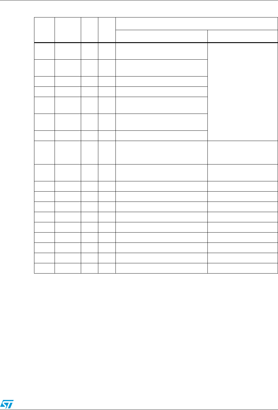
2.1 Memory organization
The UPSD321xx devices’ standard 8032 Core has separate 64-Kbyte address spaces for
Program memory and Data Memory. Program memory is where the 8032 executes
instructions from. Data memory is used to hold data variables. Flash memory can be
mapped in either program or data space. The Flash memory consists of two Flash memory
blocks: the main Flash memory (512 Kbit) and the Secondary Flash memory (128 Kbit).
Except during flash memory programming or update, Flash memory can only be read, not
written to. A Page Register is used to access memory beyond the 64-Kbyte address space.
Refer to the PSD module for details on mapping of the Flash memory.
The 8032 core has two types of data memory (internal and external) that can be read and
written. The internal SRAM consists of 256 bytes, and includes the stack area.
The SFR (Special Function Registers) occupies the upper 128 bytes of the internal SRAM,
the registers can be accessed by Direct addressing only. Another 2 Kbytes resides in the
PSD module that can be mapped to any address space defined by the user.
2.2 Registers
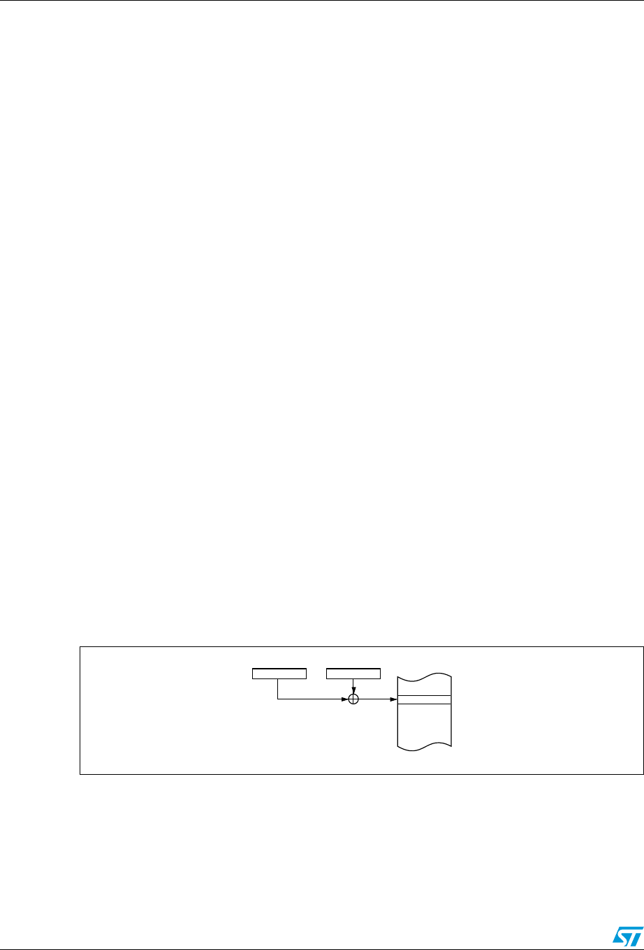
The 8032 has several registers; these are the Program Counter (PC), Accumulator (A), B
Register (B), the Stack Pointer (SP), the Program Status Word (PSW), General purpose
registers (R0 to R7), and DPTR (Data Pointer register).
Figure 4. Memory map and address space
AI07425
SECONDARY
FLASH
FLASH
MAIN
16KB
64KB
FF
7F
0
2KB
INT. RAM
EXT. RAM
Addressing
Indirect
Indirect
Direct
or
Addressing
Addressing
Direct
SFR
Internal RAM Space
(256 Bytes) External RAM Space
(MOVX)
Flash Memory Space
Obsolete Product(s) - Obsolete Product(s)
UPSD3212A, UPSD3212C, UPSD3212CV Architecture overview
17/181
Figure 5. 8032 MCU registers
2.2.1 Accumulator
The Accumulator is the 8-bit general purpose register, used for data operation such as
transfer, temporary saving, and conditional tests. The Accumulator can be used as a 16-bit
register with B Register as shown below.
Figure 6. Configuration of BA 16-bit registers
2.2.2 B register
The B Register is the 8-bit general purpose register, used for an arithmetic operation such
as multiply, division with Accumulator.
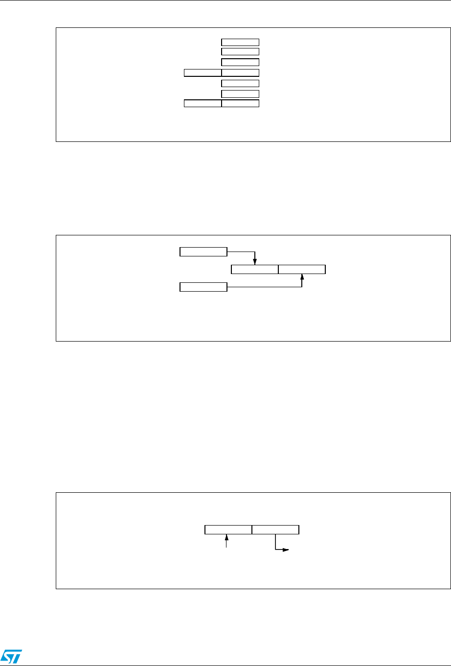
2.2.3 Stack pointer
The Stack Pointer Register is 8 bits wide. It is incremented before data is stored during
PUSH and CALL executions. While the stack may reside anywhere in on-chip RAM, the
Stack Pointer is initialized to 07h after reset. This causes the stack to begin at location 08h.
Figure 7. Stack pointer
AI06636
Accumulator
B Register
Stack Pointer
Program Counter
Program Status Word
General Purpose
Register (Bank0-3)
Data Pointer Register
PCH
DPTR(DPH)
A
B
SP
PCL
PSW
R0-R7
DPTR(DPL)
AI06637
Two 8-bit Registers can be used as a "BA" 16-bit Registers
A
B
AB
AI06638
SP (Stack Pointer) could be in 00h-FFh
SP00h
Stack Area (30h-FFh)
00h-FFh
Hardware Fixed
Bit 15 Bit 0Bit 8 Bit 7
Obsolete Product(s) - Obsolete Product(s)
Architecture overview UPSD3212A, UPSD3212C, UPSD3212CV
18/181
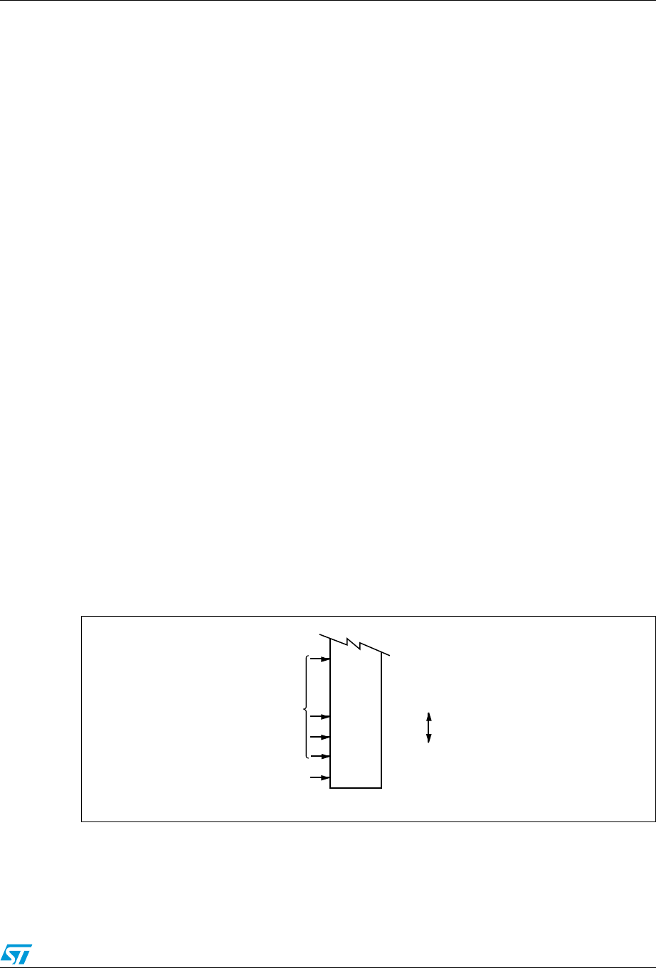
2.2.4 Program counter
The Program Counter is a 16-bit wide which consists of two 8-bit registers, PCH and PCL.
This counter indicates the address of the next instruction to be executed. In RESET state,
the program counter has reset routine address (PCH:00h, PCL:00h).
2.2.5 Program status word
The Program Status Word (PSW) contains several bits that reflect the current state of the
CPU and select Internal RAM (00h to 1Fh: Bank0 to Bank3). The PSW is described in
Figure 8. It contains the Carry flag, the Auxiliary Carry flag, the Half Carry (for BCD
operation), the General Purpose flag, the Register Bank Select flags, the Overflow flag, and
Parity flag.
[Carry flag, CY]. This flag stores any carry or not borrow from the ALU of CPU after an
arithmetic operation and is also changed by the Shift Instruction or Rotate Instruction.
[Auxiliary Carry flag, AC]. After operation, this flag is set when there is a carry from Bit 3 of
ALU or there is no borrow from Bit 4 of ALU.
[Register Bank Select flags, RS0, RS1]. These flags select one of four banks
(00~07H:bank0, 08~0Fh:bank1, 10~17h:bank2, 17~1Fh:bank3) in Internal RAM.
[Overflow flag, OV]. This flag is set to '1' when an overflow occurs as the result of an
arithmetic operation involving signs. An overflow occurs when the result of an addition or
subtraction exceeds +127 (7Fh) or -128 (80h). The CLRV instruction clears the overflow
flag. There is no set instruction. When the BIT instruction is executed, Bit 6 of memory is
copied to this flag.
[Parity flag, P]. This flag reflects the number of Accumulator’s 1. If the number of
Accumulator’s 1 is odd, P=0; otherwise, P=1. The sum when adding Accumulator’s 1 to P is
always even.
2.2.6 Registers R0~R7
General purpose 8-bit registers that are locked in the lower portion of internal data area.
2.2.7 Data pointer register
Data Pointer Register is 16-bit wide which consists of two-8bit registers, DPH and DPL. This
register is used as a data pointer for the data transmission with external data memory in the
PSD module.
Figure 8. PSW (Program Status Word) register
AI06639
CY Reset Value 00h
Parity Flag
Bit not assigned
Overflow Flag
Register Bank Select Flags
(to select Bank0-3)
Carry Flag
Auxillary Carry Flag
General Purpose Flag
AC FO RS1 RS0 OV P
MSB LSB
PSW
Obsolete Product(s) - Obsolete Product(s)
UPSD3212A, UPSD3212C, UPSD3212CV Architecture overview
19/181
2.3 Program memory
The program memory consists of two Flash memories: the main Flash memory (64 Kbit)
and the Secondary Flash memory (16 Kbit). The Flash memory can be mapped to any
address space as defined by the user in the PSDsoft Tool. It can also be mapped to Data
memory space during Flash memory update or programming.
After reset, the CPU begins execution from location 0000h. As shown in Figure 9, each
interrupt is assigned a fixed location in Program Memory. The interrupt causes the CPU to
jump to that location, where it commences execution of the service routine. External
Interrupt 0, for example, is assigned to location 0003h. If External Interrupt 0 is going to be
used, its service routine must begin at location 0003h. If the interrupt is not going to be
used, its service location is available as general purpose Program Memory.
The interrupt service locations are spaced at 8-byte intervals: 0003h for External Interrupt 0,
000Bh for Timer 0, 0013h for External Interrupt 1, 001Bh for Timer 1 and so forth. If an
interrupt service routine is short enough (as is often the case in control applications), it can
reside entirely within that 8-byte interval. Longer service routines can use a jump instruction
to skip over subsequent interrupt locations, if other interrupts are in use.
2.4 Data memory
The internal data memory is divided into four physically separated blocks: 256 bytes of
internal RAM, 128 bytes of Special Function Registers (SFRs) areas and 2 Kbytes (XRAM-
PSD) in the PSD module.
2.5 RAM
Four register banks, each 8 registers wide, occupy locations 0 through 31 in the lower RAM
area. Only one of these banks may be enabled at a time. The next 16 bytes, locations 32
through 47, contain 128 directly addressable bit locations. The stack depth is only limited by
the available internal RAM space of 256 bytes.
Figure 9. Interrupt location of program memory
AI06640
0000hReset
8 Bytes
•
•
•
•
•
Interrupt
Location
0003h
000Bh
0013h
008Bh
•
•
•
•
Obsolete Product(s) - Obsolete Product(s)
Architecture overview UPSD3212A, UPSD3212C, UPSD3212CV
20/181
2.6 XRAM-PSD
The 2 Kbytes of XRAM-PSD resides in the PSD module and can be mapped to any address
space through the DPLD (Decoding PLD) as defined by the user in PSDsoft Development
tool.
2.7 SFR
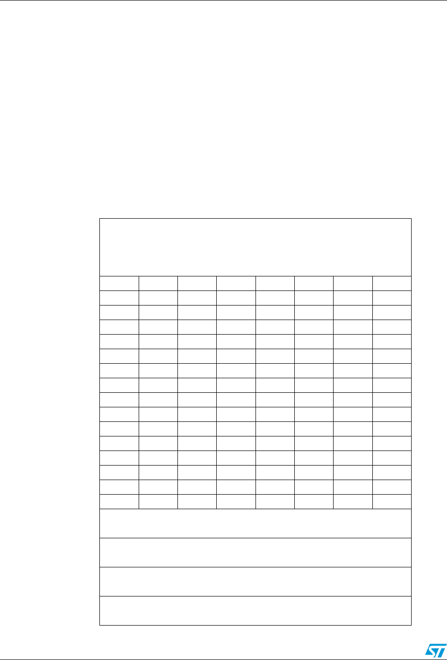
The SFRs can only be addressed directly in the address range from 80h to FFh. Ta bl e 1 5
gives an overview of the Special Function Registers. Sixteen address in the SFRs space are
both-byte and bit-addressable. The bit-addressable SFRs are those whose address ends in
0h and 8h. The bit addresses in this area are 80h to FFh.
Table 3. RAM address
Byte address
(in hexadecimal)
Byte address
(in decimal)
¯ ¯
FFh 255
30h 48
MSB Bit address (hex) LSB
2Fh 7F 7E 7D 7C 7B 7A 79 78 47
2Eh777675747372717046
2Dh 6F 6E 6D 6C 6B 6A 69 68 45
2Ch676665646362616044
2Bh 5F 5E 5D 5C 5B 5A 59 58 43
2Ah575655545352515042
29h 4F 4E 4D 4C 4B 4A 49 48 41
28h474645444342414040
27h 3F 3E 3D 3C 3B 3A 39 38 39
26h373635343332313038
25h 2F 2E 2D 2C 2B 2A 29 28 37
24h272625242322212036
23h 1F 1E 1D 1C 1B 1A 19 18 35
22h171615141312111034
21h 0F 0E 0D 0C 0B 0A 09 08 33
20h070605040302010032
1Fh Register bank 3 31
18h 24
17h Register bank 2 23
10h 16
0Fh Register bank 1 15
08h 8
07h Register bank 0 7
00h 0
Obsolete Product(s) - Obsolete Product(s)
UPSD3212A, UPSD3212C, UPSD3212CV Architecture overview
21/181
2.8 Addressing modes
The addressing modes in UPSD321xx devices instruction set are as follows
1. Direct addressing
2. Indirect addressing
3. Register addressing
4. Register-specific addressing
5. Immediate constants addressing
6. Indexed addressing
2.8.1 Direct addressing
In a direct addressing the operand is specified by an 8-bit address field in the instruction.
Only internal Data RAM and SFRs (80~FFH RAM) can be directly addressed.
Example:
mov A, 3EH ; A <----- RAM[3E]
Figure 10. Direct addressing
2.8.2 Indirect addressing
In indirect addressing the instruction specifies a register which contains the address of the
operand. Both internal and external RAM can be indirectly addressed. The address register
for 8-bit addresses can be R0 or R1 of the selected register bank, or the Stack Pointer. The
address register for 16-bit addresses can only be the 16-bit “data pointer” register, DPTR.
Example:
mov @R1, #40 H ;[R1] <-----40H
Figure 11. Indirect addressing
AI06641
3Eh
Program Memory
04 A
AI06642
R1
55h
Program Memory
55
40h
Obsolete Product(s) - Obsolete Product(s)
Architecture overview UPSD3212A, UPSD3212C, UPSD3212CV
22/181
2.8.3 Register addressing
The register banks, containing registers R0 through R7, can be accessed by certain
instructions which carry a 3-bit register specification within the opcode of the instruction.
Instructions that access the registers this way are code efficient, since this mode eliminates
an address byte. When the instruction is executed, one of four banks is selected at
execution time by the two bank select bits in the PSW.
Example:
mov PSW, #0001000B ; select Bank0
mov A, #30H
mov R1, A
2.8.4 Register-specific addressing
Some instructions are specific to a certain register. For example, some instructions always
operate on the Accumulator, or Data Pointer, etc., so no address byte is needed to point it.
The opcode itself does that.
2.8.5 Immediate constants addressing
The value of a constant can follow the opcode in Program memory.
Example:
mov A, #10H.
2.8.6 Indexed addressing
Only Program memory can be accessed with indexed addressing, and it can only be read.
This addressing mode is intended for reading look-up tables in Program memory. A 16-bit
base register (either DPTR or PC) points to the base of the table, and the Accumulator is set
up with the table entry number. The address of the table entry in Program memory is formed
by adding the Accumulator data to the base pointer.
Example:
movc A, @A+DPTR
Figure 12. Indexed addressing
AI06643
3Eh
Program Memory
ACC DPTR
3Ah 1E73h
Obsolete Product(s) - Obsolete Product(s)
UPSD3212A, UPSD3212C, UPSD3212CV Architecture overview
23/181
2.9 Arithmetic instructions
The arithmetic instructions is listed in Ta b l e 4 . The table indicates the addressing modes
that can be used with each instruction to access the <byte> operand. For example, the ADD
A, <byte> instruction can be written as:
ADD a, 7FH (direct addressing)
ADD A, @R0 (indirect addressing)
ADD a, R7 (register addressing)
ADD A, #127 (immediate constant)
Note: Any byte in the internal Data Memory space can be incremented without going through the
Accumulator.
One of the INC instructions operates on the 16-bit Data Pointer. The Data Pointer is used to
generate 16-bit addresses for external memory, so being able to increment it in one 16-bit
operation is a useful feature.
The MUL AB instruction multiplies the Accumulator by the data in the B register and puts the
16-bit product into the concatenated B and Accumulator registers.
The DIV AB instruction divides the Accumulator by the data in the B register and leaves the
8-bit quotient in the Accumulator, and the 8-bit remainder in the B register.
In shift operations, dividing a number by 2n shifts its “n” bits to the right. Using DIV AB to
perform the division completes the shift in 4?s and leaves the B register holding the bits that
were shifted out. The DAA instruction is for BCD arithmetic operations. In BCD arithmetic,
ADD and ADDC instructions should always be followed by a DAA operation, to ensure that
the result is also in BCD.
Note: DAA will not convert a binary number to BCD. The DAA operation produces a meaningful
result only as the second step in the addition of two BCD bytes.
Table 4. Arithmetic instructions
Mnemonic Operation
Addressing modes
Dir. Ind. Reg. Imm.
ADD A,<byte> A = A + <byte> XXXX
ADDC A,<byte>A = A + <byte> + C XXXX
SUBB A,<byte> A = A – <byte> – C XXXX
INC A = A + 1 Accumulator only
INC <byte> <byte> = <byte> + 1 X X X
INC DPTR DPTR = DPTR + 1 Data Pointer only
DEC A = A – 1 Accumulator only
DEC <byte> <byte> = <byte> – 1 X X X
MUL AB B:A = B x A Accumulator and B only
DIV AB A = Int[ A / B ]
B = Mod[ A / B ] Accumulator and B only
DA A Decimal Adjust Accumulator only
Obsolete Product(s) - Obsolete Product(s)

Architecture overview UPSD3212A, UPSD3212C, UPSD3212CV
24/181
2.10 Logical instructions
Ta bl e 5 lists logical instructions for UPSD321xx devices. The instructions that perform
Boolean operations (AND, OR, Exclusive OR, NOT) on bytes perform the operation on a bit-
by-bit basis. That is, if the Accumulator contains 00110101B and byte contains 01010011B,
then:
ANL A, <byte>
will leave the Accumulator holding 00010001B.
The addressing modes that can be used to access the <byte> operand are listed in Ta bl e 5 .
The ANL A, <byte> instruction may take any of the forms:
ANL A,7FH(direct addressing)
ANL A, @R1 (indirect addressing)
ANL A,R6 (register addressing)
ANL A,#53H (immediate constant)
Note: Boolean operations can be performed on any byte in the internal Data Memory space
without going through the Accumulator. The XRL <byte>, #data instruction, for example,
offers a quick and easy way to invert port bits, as in:
XRL P1, #0FFH.
If the operation is in response to an interrupt, not using the Accumulator saves the time and
effort to push it onto the stack in the service routine.
The Rotate instructions (RL A, RLC A, etc.) shift the Accumulator 1 bit to the left or right. For
a left rotation, the MSB rolls into the LSB position. For a right rotation, the LSB rolls into the
MSB position.
The SWAP A instruction interchanges the high and low nibbles within the Accumulator. This
is a useful operation in BCD manipulations. For example, if the Accumulator contains a
binary number which is known to be less than 100, it can be quickly converted to BCD by
the following code:
MOVE B,#10
DIV AB
SWAP A
ADD A,B
Dividing the number by 10 leaves the tens digit in the low nibble of the Accumulator, and the
ones digit in the B register. The SWAP and ADD instructions move the tens digit to the high
nibble of the Accumulator, and the ones digit to the low nibble.
Table 5. Logical instructions
Mnemonic Operation
Addressing modes
Dir. Ind. Reg. Imm.
ANL A,<byte> A = A .AND. <byte> XXXX
ANL <byte>,A A = <byte> .AND. A X
ANL <byte>,#data A = <byte> .AND. #data X
ORL A,<byte> A = A .OR. <byte> XXXX
Obsolete Product(s) - Obsolete Product(s)
UPSD3212A, UPSD3212C, UPSD3212CV Architecture overview
25/181
2.11 Data transfers
2.11.1 Internal RAM
Ta bl e 6 shows the menu of instructions that are available for moving data around within the
internal memory spaces, and the addressing modes that can be used with each one. The
MOV <dest>, <src> instruction allows data to be transferred between any two internal RAM
or SFR locations without going through the Accumulator. Remember, the Upper 128 bytes of
data RAM can be accessed only by indirect addressing, and SFR space only by direct
addressing.
Note: In UPSD321xx devices, the stack resides in on-chip RAM, and grows upwards. The PUSH
instruction first increments the Stack Pointer (SP), then copies the byte into the stack. PUSH
and POP use only direct addressing to identify the byte being saved or restored, but the
stack itself is accessed by indirect addressing using the SP register. This means the stack
can go into the Upper 128 bytes of RAM, if they are implemented, but not into SFR space.
The Data Transfer instructions include a 16-bit MOV that can be used to initialize the Data
Pointer (DPTR) for look-up tables in Program Memory.
The XCH A, <byte> instruction causes the Accumulator and ad-dressed byte to exchange
data. The XCHD A, @Ri instruction is similar, but only the low nibbles are involved in the
exchange. To see how XCH and XCHD can be used to facilitate data manipulations,
consider first the problem of shifting and 8-digit BCD number two digits to the right. Ta b l e 8
shows how this can be done using XCH instructions. To aid in understanding how the code
works, the contents of the registers that are holding the BCD number and the content of the
Accumulator are shown alongside each instruction to indicate their status after the
instruction has been executed.
ORL <byte>,A A = <byte> .OR. A X
ORL <byte>,#data A = <byte> .OR. #data X
XRL A,<byte> A = A .XOR. <byte> XXXX
XRL <byte>,A A = <byte> .XOR. A X
XRL <byte>,#data A = <byte> .XOR. #data X
CRL A A = 00h Accumulator only
CPL A A = .NOT. A Accumulator only
RL A Rotate A Left 1 bit Accumulator only
RLC A Rotate A Left through Carry Accumulator only
RR A Rotate A Right 1 bit Accumulator only
RRC A Rotate A Right through Carry Accumulator only
SWAP A Swap Nibbles in A Accumulator only
Table 5. Logical instructions
Mnemonic Operation
Addressing modes
Dir. Ind. Reg. Imm.
Obsolete Product(s) - Obsolete Product(s)
Architecture overview UPSD3212A, UPSD3212C, UPSD3212CV
26/181
After the routine has been executed, the Accumulator contains the two digits that were
shifted out on the right. Doing the routine with direct MOVs uses 14 code bytes. The same
operation with XCHs uses only 9 bytes and executes almost twice as fast. To right-shift by
an odd number of digits, a one-digit must be executed. Ta bl e 9 shows a sample of code that
will right-shift a BCD number one digit, using the XCHD instruction. Again, the contents of
the registers holding the number and of the accumulator are shown alongside each
instruction.
First, pointers R1 and R0 are set up to point to the two bytes containing the last four BCD
digits. Then a loop is executed which leaves the last byte, location 2EH, holding the last two
digits of the shifted number. The pointers are decremented, and the loop is repeated for
location 2DH. The CJNE instruction (Compare and Jump if Not equal) is a loop control that
will be described later. The loop executed from LOOP to CJNE for R1 = 2EH, 2DH, 2CH,
and 2BH. At that point the digit that was originally shifted out on the right has propagated to
location 2AH. Since that location should be left with 0s, the lost digit is moved to the
Accumulator.
Table 7. Shifting a BCD number 2 digits to the right (using direct MOVs: 14 bytes)
Table 6. Data transfer instructions that access internal data memory space
Mnemonic Operation
Addressing modes
Dir. Ind. Reg. Imm.
MOV A,<src> A = <src> XXXX
MOV <dest>,A <dest> = A X X X
MOV <dest>,<src> <dest> = <src> XXXX
MOV DPTR,#data16 DPTR = 16-bit immediate
constant X
PUSH <src> INC SP; MOV “@SP”,<src> X
POP <dest> MOV <dest>,”@SP”; DEC SP X
XCH A,<byte> Exchange contents of A and
<byte> XXX
XCHD A,@Ri Exchange low nibbles of A and
@Ri X
2A 2B 2C 2D 2E ACC
MOV A,2Eh 00 12 34 56 78 78
MOV 2Eh,2Dh 00 12 34 56 56 78
MOV 2Dh,2Ch 00 12 34 34 56 78
MOV 2Ch,2Bh 00 12 12 34 56 78
MOV2Bh,#0 0000123456 78
Obsolete Product(s) - Obsolete Product(s)

UPSD3212A, UPSD3212C, UPSD3212CV Architecture overview
27/181
Table 8. Shifting a BCD number 2 digits to the right (using direct XCHs: 9 bytes)
Table 9. Shifting a BCD number one digit to the right
2.11.2 External RAM
Ta bl e 1 0 shows a list of the Data Transfer instructions that access external Data Memory.
Only indirect addressing can be used. The choice is whether to use a one-byte address,
@Ri, where Ri can be either R0 or R1 of the selected register bank, or a two-byte
address, @DTPR.
Note: In all external Data RAM accesses, the Accumulator is always either the destination or
source of the data.
2A 2B 2C 2D 2E ACC
CLR A 00 12 34 56 78 00
XCH A,2Bh 00 00 34 56 78 12
XCH A,2Ch 00 00 12 56 78 34
XCH A,2Dh 00 00 12 34 78 56
XCH A,2Eh 00 00 12 34 56 78
2A 2B 2C 2D 2E ACC
MOV R1,#2Eh 00 12 34 56 78 xx
MOV R0,#2Dh 00 12 34 56 78 xx
; loop for R1 = 2Eh
LOOP:MOV A,@R1 0012345678 78
XCHDA,@R0 0012345878 76
SWAP A 00 12 34 58 78 67
MOV @R1,A 00 12 34 58 67 67
DEC R1 0012345867 67
DEC R0 0012345867 67
CNJE R1,#2Ah,LOOP 00 12 34 58 67 67
; loop for R1 = 2Dh 0012384567 45
; loop for R1 = 2Ch 0018234567 23
; loop for R1 = 2Bh 0801234567 01
CLR A 08 01 23 45 67 00
XCH A,2Ah 00 01 23 45 67 08
Obsolete Product(s) - Obsolete Product(s)
Architecture overview UPSD3212A, UPSD3212C, UPSD3212CV
28/181
2.11.3 Lookup tables
Ta bl e 1 1 shows the two instructions that are available for reading lookup tables in Program
Memory. Since these instructions access only Program Memory, the lookup tables can only
be read, not updated.
The mnemonic is MOVC for “move constant.” The first MOVC instruction in Ta b l e 1 1 can
accommodate a table of up to 256 entries numbered 0 through 255. The number of the
desired entry is loaded into the Accumulator, and the Data Pointer is set up to point to the
beginning of the table. Then:
MOVC A, @A+DPTR
copies the desired table entry into the Accumulator.
The other MOVC instruction works the same way, except the Program Counter (PC) is used
as the table base, and the table is accessed through a subroutine. First the number of the
desired en-try is loaded into the Accumulator, and the subroutine is called:
MOV A , ENTRY NUMBER
CALL TABLE
The subroutine “TABLE” would look like this:
TABLE: MOVC A , @A+PC
RET
The table itself immediately follows the RET (return) instruction is Program Memory. This
type of table can have up to 255 entries, numbered 1 through 255. Number 0 cannot be
used, because at the time the MOVC instruction is executed, the PC contains the address of
the RET instruction. An entry numbered 0 would be the RET opcode itself.
Table 10. Data transfer instruction that access external data memory space
Table 11. Lookup table READ instruction
Address Width Mnemonic Operation
8 bits MOVX A,@Ri READ external RAM @Ri
8 bits MOVX @Ri,A WRITE external RAM @Ri
16 bits MOVX A,@DPTR READ external RAM @DPTR
16 bits MOVX @DPTR,a WRITE external RAM @DPTR
Mnemonic Operation
MOVC A,@A+DPTR READ program memory at (A+DPTR)
MOVC A,@A+PC READ program memory at (A+PC)
Obsolete Product(s) - Obsolete Product(s)

UPSD3212A, UPSD3212C, UPSD3212CV Architecture overview
29/181
2.12 Boolean instructions
The UPSD321xx devices contain a complete Boolean (single-bit) processor. One page of
the internal RAM contains 128 address-able bits, and the SFR space can support up to 128
addressable bits as well. All of the port lines are bit-addressable, and each one can be
treated as a separate single-bit port. The instructions that access these bits are not just
conditional branches, but a complete menu of move, set, clear, complement, OR and AND
instructions. These kinds of bit operations are not easily obtained in other architectures with
any amount of byte-oriented software.
The instruction set for the Boolean processor is shown in Tabl e 1 2 . All bits accesses are by
direct addressing.
Bit addresses 00h through 7Fh are in the Lower 128, and bit addresses 80h through FFh
are in SFR space.
Note how easily an internal flag can be moved to a port pin:
MOV C,FLAG
MOV P1.0,C
In this example, FLAG is the name of any addressable bit in the Lower 128 or SFR space.
An I/O line (the LSB of Port 1, in this case) is set or cleared depending on whether the Flag
bit is '1' or '0.'
The Carry Bit in the PSW is used as the single-bit Accumulator of the Boolean processor. Bit
instructions that refer to the Carry Bit as C assemble as Carry-specific instructions (CLR C,
etc.). The Carry Bit also has a direct address, since it resides in the PSW register, which is
bit-addressable.
Note: The Boolean instruction set includes ANL and ORL operations, but not the XRL (Exclusive
OR) operation. An XRL operation is simple to implement in software. Suppose, for example,
it is required to form the Exclusive OR of two bits:
C = bit 1 .XRL. bit2
The software to do that could be as follows:
MOV C , bit1
JNB bit2, OVER
CPL C
OVER: (continue)
First, Bit 1 is moved to the Carry. If bit2 = 0, then C now contains the correct result. That is,
Bit 1 .XRL. bit2 = bit1 if bit2 = 0. On the other hand, if bit2 = 1, C now contains the
complement of the correct result. It need only be inverted (CPL C) to complete the
operation.
This code uses the JNB instruction, one of a series of bit-test instructions which execute a
jump if the addressed bit is set (JC, JB, JBC) or if the addressed bit is not set (JNC, JNB). In
the above case, Bit 2 is being tested, and if bit2 = 0, the CPL C instruction is jumped over.
JBC executes the jump if the addressed bit is set, and also clears the bit. Thus a flag can be
tested and cleared in one operation. All the PSW bits are directly addressable, so the Parity
Bit, or the general-purpose flags, for example, are also available to the bit-test instructions.
Obsolete Product(s) - Obsolete Product(s)
Architecture overview UPSD3212A, UPSD3212C, UPSD3212CV
30/181
2.13 Relative offset
The destination address for these jumps is specified to the assembler by a label or by an
actual address in Program memory. However, the destination address assembles to a
relative offset byte. This is a signed (two’s complement) offset byte which is added to the PC
in two’s complement arithmetic if the jump is executed.
The range of the jump is therefore -128 to +127 Program Memory bytes relative to the first
byte following the instruction.
2.14 Jump instructions
Ta bl e 1 3 shows the list of unconditional jump instructions. The table lists a single “JMP add”
instruction, but in fact there are three SJMP, LJMP, and AJMP, which differ in the format of
the destination address. JMP is a generic mnemonic which can be used if the programmer
does not care which way the jump is en-coded.
The SJMP instruction encodes the destination address as a relative offset, as described
above. The instruction is 2 bytes long, consisting of the opcode and the relative offset byte.
The jump distance is limited to a range of -128 to +127 bytes relative to the instruction
following the SJMP.
Table 12. Boolean instructions
Mnemonic Operation
ANL C,bit C = A .AND. bit
ANL C,/bit C = C .AND. .NOT. bit
ORL C,bit C = A .OR. bit
ORL C,/bit C = C .OR. .NOT. bit
MOV C,bit C = bit
MOV bit,C bit = C
CLR C C = 0
CLR bit bit = 0
SETB C C = 1
SETB bit bit = 1
CPL C C = .NOT. C
CPL bit bit = .NOT. bit
JC rel Jump if C =1
JNC rel Jump if C = 0
JB bit,rel Jump if bit =1
JNB bit,rel Jump if bit = 0
JBC bit,rel Jump if bit = 1; CLR bit
Obsolete Product(s) - Obsolete Product(s)

UPSD3212A, UPSD3212C, UPSD3212CV Architecture overview
31/181
The LJMP instruction encodes the destination address as a 16-bit constant. The instruction
is 3 bytes long, consisting of the opcode and two address bytes. The destination address
can be anywhere in the 64K Program Memory space.
The AJMP instruction encodes the destination address as an 11-bit constant. The
instruction is 2 bytes long, consisting of the opcode, which itself contains 3 of the 11 address
bits, followed by another byte containing the low 8 bits of the destination address. When the
instruction is executed, these 11 bits are simply substituted for the low 11 bits in the PC. The
high 5 bits stay the same. Hence the destination has to be within the same 2K block as the
instruction following the AJMP.
In all cases the programmer specifies the destination address to the assembler in the same
way: as a label or as a 16-bit constant. The assembler will put the destination address into
the correct format for the given instruction. If the format required by the instruction will not
support the distance to the specified destination address, a “Destination out of range”
message is written into the List file.
The JMP @A+DPTR instruction supports case jumps. The destination address is computed
at execution time as the sum of the 16-bit DPTR register and the Accumulator. Typically.
DPTR is set up with the address of a jump table. In a 5-way branch, for ex-ample, an integer
0 through 4 is loaded into the Accumulator. The code to be executed might be as follows:
MOV DPTR,#JUMP TABLE
MOV A,INDEX_NUMBER
RL A
JMP @A+DPTR
The RL A instruction converts the index number (0 through 4) to an even number on the
range 0 through 8, because each entry in the jump table is 2 bytes long:
JUMP TABLE:
AJMP CASE 0
AJMP CASE 1
AJMP CASE 2
AJMP CASE 3
AJMP CASE 4
Ta bl e 1 3 shows a single “CALL addr” instruction, but there are two of them, LCALL and
ACALL, which differ in the format in which the subroutine address is given to the CPU. CALL
is a generic mnemonic which can be used if the programmer does not care which way the
address is encoded.
The LCALL instruction uses the 16-bit address format, and the subroutine can be anywhere
in the 64K Program Memory space. The ACALL instruction uses the 11-bit format, and the
subroutine must be in the same 2K block as the instruction following the ACALL.
In any case, the programmer specifies the subroutine address to the assembler in the same
way: as a label or as a 16-bit constant. The assembler will put the address into the correct
format for the given instructions.
Subroutines should end with a RET instruction, which returns execution to the instruction
following the CALL.
RETI is used to return from an interrupt service routine. The only difference between RET
and RETI is that RETI tells the interrupt control system that the interrupt in progress is done.
Obsolete Product(s) - Obsolete Product(s)

Architecture overview UPSD3212A, UPSD3212C, UPSD3212CV
32/181
If there is no interrupt in progress at the time RETI is executed, then the RETI is functionally
identical to RET.
Ta bl e 1 4 shows the list of conditional jumps available to the UPSD321xx device user. All of
these jumps specify the destination address by the relative offset method, and so are limited
to a jump distance of -128 to +127 bytes from the instruction following the conditional jump
instruction. Important to note, however, the user specifies to the assembler the actual
destination address the same way as the other jumps: as a label or a 16-bit constant.
There is no Zero Bit in the PSW. The JZ and JNZ instructions test the Accumulator data for
that condition.
The DJNZ instruction (Decrement and Jump if Not Zero) is for loop control. To execute a
loop N times, load a counter byte with N and terminate the loop with a DJNZ to the
beginning of the loop, as shown below for N = 10:
MOV COUNTER,#10
LOOP: (begin loop)
•
•
•
(end loop)
DJNZ COUNTER, LOOP
(continue)
The CJNE instruction (Compare and Jump if Not Equal) can also be used for loop control as
in Ta b l e 9 . Two bytes are specified in the operand field of the instruction. The jump is
executed only if the two bytes are not equal. In the example of Ta bl e 9 Shifting a BCD
Number One Digits to the Right, the two bytes were data in R1 and the constant 2Ah. The
initial data in R1 was 2Eh.
Every time the loop was executed, R1 was decremented, and the looping was to continue
until the R1 data reached 2Ah.
Another application of this instruction is in “greater than, less than” comparisons. The two
bytes in the operand field are taken as unsigned integers. If the first is less than the second,
then the Carry Bit is set (1). If the first is greater than or equal to the second, then the Carry
Bit is cleared.
Table 13. Unconditional Jump instructions
Mnemonic Operation
JMP addr Jump to addr
JMP @A+DPTR Jump to A+DPTR
CALL addr Call Subroutine at addr
RET Return from subroutine
RETI Return from interrupt
NOP No operation
Obsolete Product(s) - Obsolete Product(s)
UPSD3212A, UPSD3212C, UPSD3212CV Architecture overview
33/181
2.15 Machine cycles
A machine cycle consists of a sequence of six states, numbered S1 through S6. Each state
time lasts for two oscillator periods. Thus, a machine cycle takes 12 oscillator periods or 1µs
if the oscillator frequency is 12MHz. Refer to Table 13: State sequence in UPSD321xx
devices.
Each state is divided into a Phase 1 half and a Phase 2 half. State Sequence in UPSD321xx
devices shows that retrieve/execute sequences in states and phases for various kinds of
instructions.
Normally two program retrievals are generated during each machine cycle, even if the
instruction being executed does not require it. If the instruction being executed does not
need more code bytes, the CPU simply ignores the extra retrieval, and the Program Counter
is not incremented.
Execution of a one-cycle instruction (Figure 13: State sequence in UPSD321xx devices)
begins during State 1 of the machine cycle, when the opcode is latched into the Instruction
Register. A second retrieve occurs during S4 of the same machine cycle. Execution is
complete at the end of State 6 of this machine cycle.
The MOVX instructions take two machine cycles to execute. No program retrieval is
generated during the second cycle of a MOVX instruction. This is the only time program
retrievals are skipped. The retrieve/execute sequence for MOVX instruction is shown in
Figure 13 (d).
Table 14. Conditional jump instructions
Mnemonic Operation
Addressing modes
Dir. Ind. Reg. Imm.
JZ rel Jump if A = 0 Accumulator only
JNZ rel Jump if A ≠ 0 Accumulator only
DJNZ <byte>,rel Decrement and jump if not zero X X
CJNE A,<byte>,rel Jump if A ≠ <byte> X X
CJNE <byte>,#data,rel Jump if <byte> ≠ #data X X
Obsolete Product(s) - Obsolete Product(s)
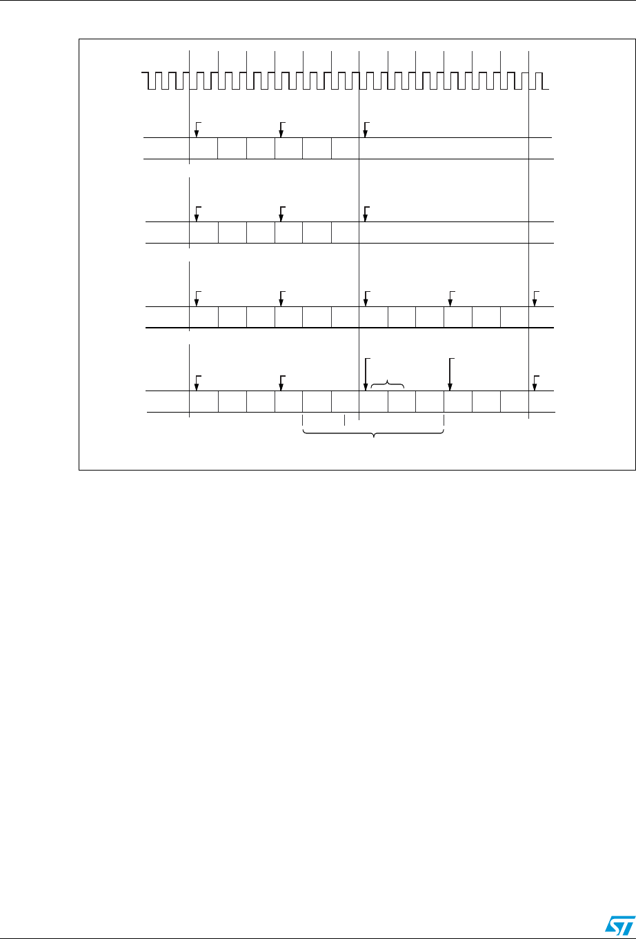
Architecture overview UPSD3212A, UPSD3212C, UPSD3212CV
34/181
Figure 13. State sequence in UPSD321xx devices
Osc.
(XTAL2)
Read opcode
Read next
opcode
Read next
opcode and
discard
Read next
opcode and
discard
Read 2nd
Byte
No Fetch No Fetch
No ALE
S1 S2 S3 S4 S5 S6 S1 S2 S3 S4 S5 S6
S1 S2 S3 S4 S5 S6
Read opcode
Read next
opcode
S1 S2 S3 S4 S5 S6
Read opcode
Read next
opcode
S1 S2 S3 S4 S5 S6
Read next
opcode and
discard
S1 S2 S3 S4 S5 S6
Read next
opcode and
discard
Read next
opcode and
discard
Read opcode
(MOVX)
Read next
opcode
S1 S2 S3 S4 S5 S6 S1 S2 S3 S4 S5 S6
Addr Data
Access External Memory
AI06822
p1 p1 p1 p1 p1 p1 p1 p1 p1 p1 p1 p1p2 p2 p2 p2 p2 p2 p2 p2 p2 p2 p2 p2
a. 1-Byte, 1-Cycle Instruction, e.g. INC A
b. 2-Byte, 1-Cycle Instruction, e.g. ADD A, adrs
c. 1-Byte, 2-Cycle Instruction, e.g. INC DPTR
d. 1-Byte, 2-Cycle MOVX Instruction
Obsolete Product(s) - Obsolete Product(s)
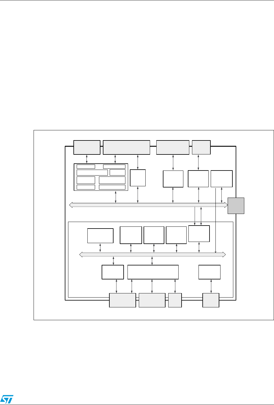
UPSD3212A, UPSD3212C, UPSD3212CV UPSD321xx hardware description
35/181
3 UPSD321xx hardware description
The UPSD321xx devices have a modular architecture with two main functional modules: the
MCU module and the PSD module. The MCU module consists of a standard 8032 core,
peripherals and other system supporting functions. The PSD module provides configurable
Program and Data memories to the 8032 CPU core. In addition, it has its own set of I/O
ports and a PLD with 16 macrocells for general logic implementation. Ports A,B,C, and D
are general purpose programmable I/O ports that have a port architecture which is different
from Ports 0-4 in the MCU module.
The PSD module communicates with the CPU Core through the internal address, data bus
(A0-A15, D0-D7) and control signals (RD_, WR_, PSEN_ , ALE, RESET_). The user
defines the Decoding PLD in the PSDsoft Development Tool and can map the resources in
the PSD module to any program or data address space.
Figure 14. UPSD321xx functional modules
AI07426b
4
Channel
ADC
512Kb
Main Flash
Decode PLD
16Kb
SRAM
CPLD - 16 MACROCELLSJTAG ISP
Port 1Port 3
2 UARTs
Interrupt
3 Timer /
Counters
256 Byte SRAM
8032 Core
Port 3, UART,
Intr, Timers,I2C
PSD Internal Bus
8032 Internal Bus
Port 1, Timers and
2nd UART and ADC
PWM
5
Channels
Port 4 PWM
Port A & B, PLD
I/O and GPIO Port D
GPIO
Port C,
JTAG, PLD I/O
and GPIO
VCC, GND,
XTAL
128Kb
Secondary
Flash
Dedicated
Pins
I2C
Port 0, 2
Ext. Bus
Reset Logic
LVD & WDT
Bus
Interface
Reset
D0-D7
A0-A15
RD,PSEN
WR,ALE
Page Register
PSD MODULE
MCU MODULE
USB
&
Transceiver
Dedicated
USB Pins
Obsolete Product(s) - Obsolete Product(s)
MCU module description UPSD3212A, UPSD3212C, UPSD3212CV
36/181
4 MCU module description
This section provides a detail description of the MCU module system functions and
Peripherals, including:
●Special function registers
●Timers/counter
●Interrupts
●PWM
●Supervisory function (LVD and Watchdog)
●USART
●Power-saving modes
●I2C Bus
●On-chip oscillator
●ADC
●I/O Ports
4.1 Special function registers
A map of the on-chip memory area called the Special Function Register (SFR) space is
shown in Tabl e 1 5 .
Note: In the SFRs not all of the addresses are occupied. Unoccupied addresses are not
implemented on the chip. READ accesses to these addresses will in general return random
data, and WRITE accesses will have no effect. User software should write '0s' to these
unimplemented locations.
Table 15. SFR memory map
F8 FF
F0 B(1) F7
E8 UISTA(1) UIEN UCON0 UCON1 UCON2 USTA UADR UDR0 EF
E0 ACC(1) USCL UDT1 UDT0 E7
D8 S2CON S2STA S2DAT S2ADR DF
D0 PSW(1) D7
C8 T2CON(1) T2MOD RCAP2L RCAP2H TL2 TH2 CF
C0 P4(1) C7
B8 IP(1) BF
B0 P3(1) PSCL0L PSCL0H PSCL1L PSCL1H IPA B7
A8 IE(1) PWM4P PWM4W WDKEY AF
A0 P2(1) PWMCON PWM0 PWM1 PWM2 PWM3 WDRST IEA A7
98 SCON SBUF SCON2 SBUF2 9F
90 P1(1) P1SFS P3SFS P4SFS ASCL ADAT ACON 97
Obsolete Product(s) - Obsolete Product(s)

UPSD3212A, UPSD3212C, UPSD3212CV MCU module description
37/181
1. Register can be bit addressing
88 TCON(1) TMOD TL0 TL1 TH0 TH1 8F
80 P0(1) SP DPL DPH PCON 87
Table 15. SFR memory map (continued)
Table 16. List of all SFRs
SFR
Addr
Reg Name
Bit Register Name
Reset
Value
Comments
76543210
80 P0 FF Port 0
81 SP 07 Stack Ptr
82 DPL 00 Data Ptr Low
83 DPH 00 Data Ptr High
87 PCON SMOD SMOD1 LVREN ADSFINT RCLK1 TCLK1 PD IDLE 00 Power Ctrl
88 TCON TF1 TR1 TF0 TR0 IE1 IT1 IE0 IT0 00 Timer / Cntr
Control
89 TMOD Gate C/T M1 M0 Gate C/T M1 M0 00 Timer / Cntr
mode Control
8A TL0 00 Timer 0 Low
8B TL1 00 Timer 1 Low
8C TH0 00 Timer 0 High
8D TH1 00 Timer 1 High
90 P1 FF Port 1
91 P1SFS P1S7 P1S6 P1S5 P1S4 00 Port 1 Select
Register
93 P3SFS P3S7 P3S6 00 Port 3 Select
Register
94 P4SFS P4S7 P4S6 P4S5 P4S4 P4S3 P4S2 P4S1 P4S0 00 Por t 4 Select
Register
95 ASCL 00
8-bit
Prescaler for
ADC clock
9 6 A DAT A D AT 7 A DAT 6 A DAT 5 A DAT 4 A D AT 3 A DAT 2 A DAT 1 A D AT 0 0 0 ADC Data
Register
97 ACON ADEN ADS1 ADS0 ADST ADSF 00 ADC Control
Register
98 SCON SM0 SM1 SM2 REN TB8 RB8 TI RI 00 Serial Control
Register
99 SBUF 00 Serial Buffer
9A SCON2 SM0 SM1 SM2 REN TB8 RB8 TI RI 00 2nd UART
Ctrl Register
9B SBUF2 00 2nd UART
Serial Buffer
A0 P2 FF Port 2
Obsolete Product(s) - Obsolete Product(s)

MCU module description UPSD3212A, UPSD3212C, UPSD3212CV
38/181
A1 PWMCON PWML PWMP PWME CFG4 CFG3 CFG2 CFG1 CFG0 00 PWM Control
Polarity
A2 PWM0 00
PWM0
Output Duty
Cycle
A3 PWM1 00
PWM1
Output Duty
Cycle
A4 PWM2 00
PWM2
Output Duty
Cycle
A5 PWM3 00
PWM3
Output Duty
Cycle
A6 WDRST 00 Watch Dog
Reset
A7 IEA ES2 EI2C00
Interrupt
Enable (2nd)
A8 IE EA - ET2 ES ET1 EX1 ET0 EX0 00 Interrupt
Enable
A9
AA PWM4P 00 PWM 4
Period
AB PWM4W 00 PWM 4 Pulse
Width
AE WDKEY 00 Watch Dog
Key Register
B0 P3 FF Port 3
B1 PSCL0L 00 Prescaler 0
Low (8-bit)
B2 PSCL0H 00 Prescaler 0
High (8-bit)
B3 PSCL1L 00 Prescaler 1
Low (8-bit)
B4 PSCL1H 00 Prescaler 1
High (8-bit)
B7 IPA PS2 PI2C 00 Interrupt
Priority (2nd)
B8 IP PT2 PS PT1 PX1 PT0 PX0 00 Interrupt
Priority
C0 P4 FF New Port 4
C8 T2CON TF2 EXF2 RCLK TCLK EXEN2 TR2 C/T2 CP/RL2 00 Timer 2
Control
Table 16. List of all SFRs (continued)
SFR
Addr
Reg Name
Bit Register Name
Reset
Value
Comments
76543210
Obsolete Product(s) - Obsolete Product(s)

UPSD3212A, UPSD3212C, UPSD3212CV MCU module description
39/181
C9 T2MOD DCEN 00 Timer 2
mode
CA RCAP2L 00 Timer 2
Reload low
CB RCAP2H 00 Timer 2
Reload High
CC TL2 00 Timer 2 Low
byte
CD TH2 00 Timer 2 High
byte
D0 PSW CY AC FO RS1 RS0 OV P 00 Program
Status Word
D2 S2SETUP 00 I2C (S2)
Setup
DC S2CON CR2 EN1 STA STO ADDR AA CR1 CR0 00 I2C Bus
Control Reg
DD S2STA GC Stop Intr TX-Md Bbusy Blost ACK_R SLV 00 I2C Bus
Status
DE S2DAT 00 Data Hold
Register
DF S2ADR 00 I2C address
E0 ACC 00 Accumulator
E1 USCL 00
8-bit
Prescaler for
USB logic
E6 UDT1 UDT1.7 UDT1.6 UDT1.5 UDT1.4 UDT1.3 UDT1.2 UDT1.1 UDT1.0 00 USB Endpt1
Data Xmit
E7 UDT0 UDT0.7 UDT0.6 UDT0.5 UDT0.4 UDT0.3 UDT0.2 UDT0.1 UDT0.0 00 USB Endpt0
Data Xmit
E8 UISTA SUSPND — RSTF TXD0F RXD0F RXD1F EOPF RESUMF 00 USB Interrupt
Status
E9 UIEN 00 USB Interrupt
Enable
EA UCON0 TSEQ0 STALL0 TX0E RX0E TP0SIZ3 TP0SiZ2 TP0SIZ1 TP0SIZ0 00 USB Endpt0
Xmit Control
EB UCON1 TSEQ1 EP12SEL — FRESUM TP1SIZ3 TP1SiZ2 TP1SIZ1 TP1SIZ0 00 USB Endpt1
Xmit Control
EC UCON2 — — — SOUT EP2E EP1E STALL2 STALL1 00 USB Control
Register
ED USTA RSEQ SETUP IN OUT RP0SIZ3 RP0SIZ2 RP0SIZ1 RP0SIZ0 00 USB Endpt0
Status
EE UADR USBEN UADD6 UADD5 UADD4 UADD3 UADD2 UADD1 UADD0 00 USB Address
Register
Table 16. List of all SFRs (continued)
SFR
Addr
Reg Name
Bit Register Name
Reset
Value
Comments
76543210
Obsolete Product(s) - Obsolete Product(s)
MCU module description UPSD3212A, UPSD3212C, UPSD3212CV
40/181
EF UDR0 UDR0.7 UDR0.6 UDR0.5 UDR0.4 UDR0.3 UDR0.2 UDR0.1 UDR0.0 00 USB Endpt0
Data Recv
F0 B 00 B Register
Table 16. List of all SFRs (continued)
SFR
Addr
Reg Name
Bit Register Name
Reset
Value
Comments
76543210
Table 17. PSD module register address offset
CSIOP
addr
offset
Register name
Bit register name Reset
value Comments
76543210
00 Data In (Port A) Reads Port pins as input
02 Control (Port A) Configure pin between I/O or Address Out mode. Bit = 0 selects
I/O 00
04 Data Out (Port
A) Latched data for output to Port pins, I/O Output mode 00
06 Direction (Port
A) Configures Port pin as input or output. Bit = 0 selects input 00
08 Drive (Port A) Configures Port pin between CMOS, Open Drain or Slew rate. Bit
= 0 selects CMOS 00
0A Input Macrocell
(Port A) Reads latched value on Input Macrocells
0C Enable Out
(Port A)
Reads the status of the output enable control to the Port pin
driver. Bit = 0 indicates pin is in input mode.
01 Data In (Port B)
03 Control (Port B) 00
05 Data Out (Port
B) 00
07 Direction (Port
B) 00
09 Drive (Port B) 00
0B Input Macrocell
(Port B)
0D Enable Out
(Port B)
10 Data In (Port C)
12 Data Out (Port
C) 00
14 Direction (Port
C) 00
16 Drive (Port C) 00
18 Input Macrocell
(Port C)
Obsolete Product(s) - Obsolete Product(s)

UPSD3212A, UPSD3212C, UPSD3212CV MCU module description
41/181
1. (Register address = CSIOP address + address offset; where CSIOP address is defined by user in PSDsoft)
* indicates bit is not used and must be set to ‘0’.
1A Enable Out
(Port C)
11 Data In (Port D) * * * * * * Only Bit 1 and
2 are used
13 Data Out (Port
D) ***** * 00
Only Bit 1 and
2 are used
15 Direction (Port
D) ***** * 00
Only Bit 1 and
2 are used
17 Drive (Port D) * * * * * * 00 Only Bit 1 and
2 are used
1B Enable Out
(Port D) ***** * Only Bit 1 and
2 are used
20 Output
Macrocells AB
21 Output
Macrocells BC
22 Mask Macrocells
AB
23 Mask Macrocells
BC
C0 Primary Flash
Protection
Sec3_
Prot
Sec2_
Prot
Sec1_
Prot
Sec0_
Prot
Bit = 1 sector
is protected
C2 Secondary Flash
Protection
Security
_Bit *****
Sec1_
Prot
Sec0_
Prot
Security Bit =
1 device is
secured
B0 PMMR0 * *
PLD
Mcells
clk
PLD
array-
clk
PLD
Turb o *APD
enable *00
Control PLD
power
consumption
B4 PMMR2 *
PLD
array
Ale
PLD
array
Cntl2
PLD
array
Cntl1
PLD
array
Cntl0
**00
Blocking
inputs to PLD
array
E0 Page 00 Page Register
E2 VM Periph-
mode **
FL_
data
Boot_
data
FL_
code
Boot_
code
SR_
code
Configure
8032 Program
and Data
Space
Table 17. PSD module register address offset (continued)
CSIOP
addr
offset
Register name
Bit register name Reset
value Comments
76543210
Obsolete Product(s) - Obsolete Product(s)

Interrupt system UPSD3212A, UPSD3212C, UPSD3212CV
42/181
5 Interrupt system
There are interrupt requests from 10 sources as follows.
●INT0 external interrupt
●2nd USART interrupt
●Timer 0 interrupt
●I2C interrupt
●INT1 external interrupt (or ADC interrupt)
●Timer 1 interrupt
●USB interrupt
●USART interrupt
●Timer 2 interrupt
5.1 External Int0 interrupt
●The INT0 can be either level-active or transition-active depending on Bit IT0 in register
TCON. The flag that actually generates this interrupt is Bit IE0 in TCON.
●When an external interrupt is generated, the corresponding request flag is cleared by
the hardware when the service routine is vectored to only if the interrupt was transition
activated.
●If the interrupt was level activated then the interrupt request flag remains set until the
requested interrupt is actually generated. Then it has to deactivate the request before
the interrupt service routine is completed, or else another interrupt will be generated.
5.2 Timer 0 and 1 interrupts
●Timer 0 and Timer 1 Interrupts are generated by TF0 and TF1 which are set by an
overflow of their respective Timer/Counter registers (except for Timer 0 in Mode 3).
●These flags are cleared by the internal hardware when the interrupt is serviced.
5.3 Timer 2 interrupt
●Timer 2 Interrupt is generated by TF2 which is set by an overflow of Timer 2. This flag
has to be cleared by the software - not by hardware.
●It is also generated by the T2EX signal (Timer 2 External Interrupt P1.1) which is
controlled by EXEN2 and EXF2 Bits in the T2CON register.
5.4 I2C interrupt
●The interrupt of the I2C is generated by Bit INTR in the register S2STA.
●This flag is cleared by hardware.
Obsolete Product(s) - Obsolete Product(s)

UPSD3212A, UPSD3212C, UPSD3212CV Interrupt system
43/181
5.5 External Int1 interrupt
●The INT1 can be either level active or transition active depending on Bit IT1 in register
TCON. The flag that actually generates this interrupt is Bit IE1 in TCON.
●When an external interrupt is generated, the corresponding request flag is cleared by
the hardware when the service routine is vectored to only if the interrupt was transition
activated.
●If the interrupt was level activated then the interrupt request flag remains set until the
requested interrupt is actually generated. Then it has to deactivate the request before
the interrupt service routine is completed, or else another interrupt will be generated.
●The ADC can take over the External INT1 to generate an interrupt on conversion being
completed
5.6 USB interrupt
●The USB interrupt is generated when endpoint0 has transmitted a packet or received a
packet, when Endpoint1 or Endpoint2 has transmitted a packet, when the suspend or
resume state is detected and every EOP received.
●When the USB interrupt is generated, the corresponding request flag must be cleared
by software. The interrupt service routine will have to check the various USB registers
to determine the source and clear the corresponding flag.
●Please see the dedicated interrupt control registers for the USB peripheral for more
information.
5.7 USART interrupt
●The USART Interrupt is generated by RI (receive interrupt) OR TI (transmit interrupt).
●When the USART Interrupt is generated, the corresponding request flag must be
cleared by software. The interrupt service routine will have to check the various USART
registers to determine the source and clear the corresponding flag.
●Both USART’s are identical, except for the additional interrupt controls in the Bit 4 of the
additional interrupt control registers (A7h, B7h)
Obsolete Product(s) - Obsolete Product(s)
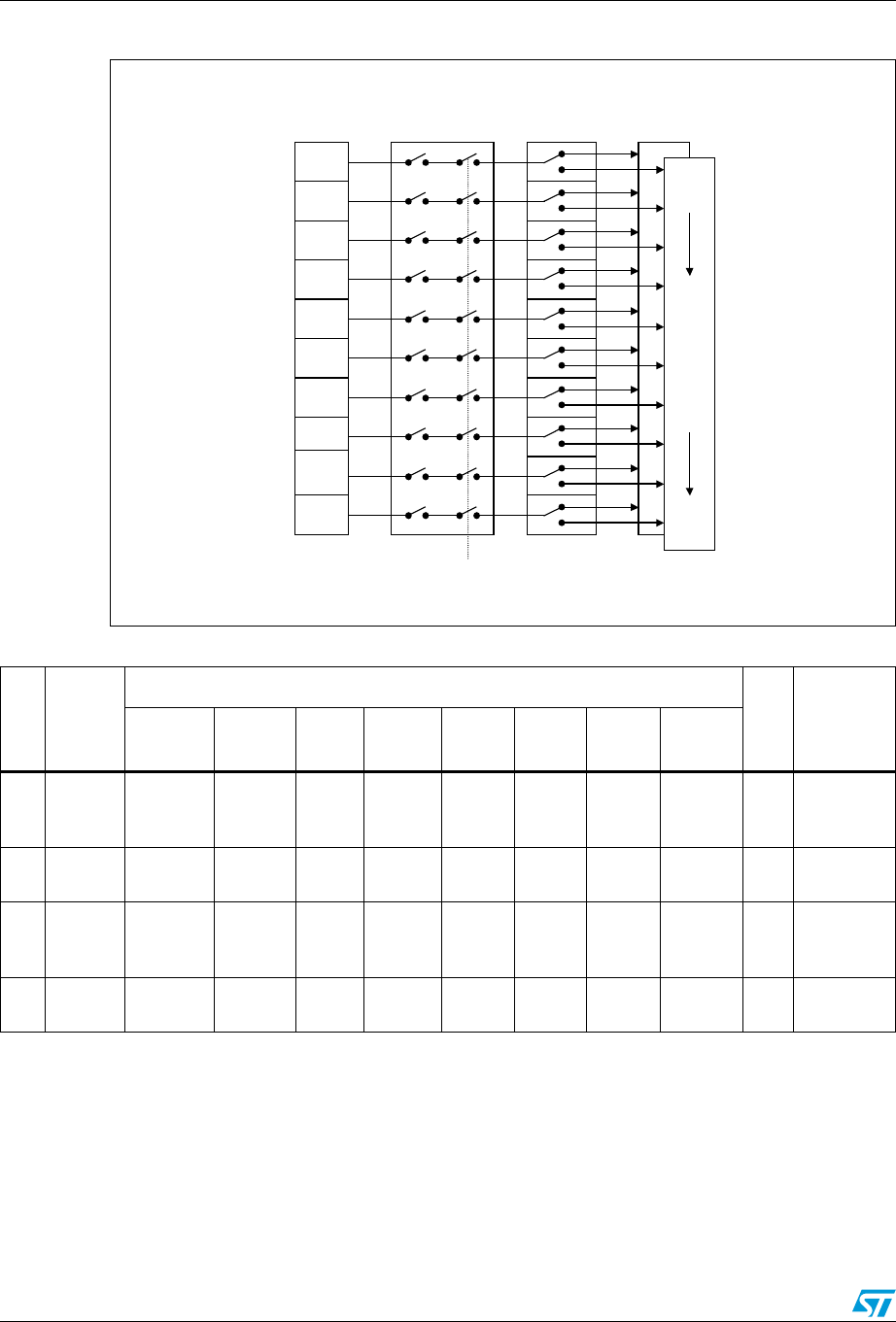
Interrupt system UPSD3212A, UPSD3212C, UPSD3212CV
44/181
5.8 Interrupt priority structure
Each interrupt source can be assigned one of two priority levels. Interrupt priority levels are
defined by the interrupt priority special function register IP and IPA.
0 = low priority
1 = high priority
Figure 15. Interrupt system
AI07427b
INT0
USART
Timer
0
I2C
INT1
Timer
1
2nd
USART
Timer
2
High
Low
Interrupt Polling
Interrupt
Sources
IE / IP / IPA Priority
Global
Enable
USB
Table 18. SFR register description
SFR
Add
r
Reg
Name
Bit Register Name Rese
t
Valu
e
Comments
76543210
A7 IEA — — — ES2 — — EI2CEUSB00
Interrupt
Enable
(2nd)
A8 IE EA — ET2 ES ET1 EX1 ET0 EX0 00 Interrupt
Enable
B7 IPA — — — PS2 — — PI2CPUSB00
Interrupt
Priority
(2nd)
B8 IP — — PT2 PS PT1 PX1 PT0 PX0 00 Interrupt
Priority
Obsolete Product(s) - Obsolete Product(s)
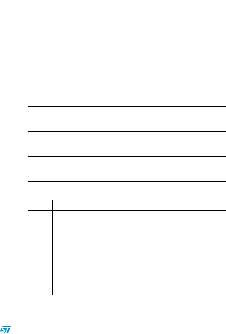
UPSD3212A, UPSD3212C, UPSD3212CV Interrupt system
45/181
A low priority interrupt may be interrupted by a high priority interrupt level interrupt. A high
priority interrupt routine cannot be interrupted by any other interrupt source. If two interrupts
of different priority occur simultaneously, the high priority level request is serviced. If
requests of the same priority are received simultaneously, an internal polling sequence
determines which request is serviced. Thus, within each priority level, there is a second
priority structure determined by the polling sequence.
5.9 Interrupt enable structure
Each interrupt source can be individually enabled or disabled by setting or clearing a bit in
the interrupt enable special function registers IE and IEA. All interrupt sources can also be
globally disabled by clearing Bit EA in register IE.
Table 19. Priority levels
Source Priority with Level
Int0 0 (highest)
2nd USART 1
Timer 0 2
I²C 3
Int1 4
Reserved 5
Timer 1 6
USB 7
1st USART 8
Timer 2+EXF2 9 (lowest)
Table 20. Description of the IE bits
Bit Symbol Function
7EA
Disable all interrupts:
0: no interrupt with be acknowledged
1: each interrupt source is individually enabled or disabled by setting or
clearing its enable bit
6—Reserved
5 ET2 Enable Timer 2 Interrupt
4 ES Enable USART Interrupt
3 ET1 Enable Timer 1 Interrupt
2 EX1 Enable External Interrupt (Int1)
1 ET0 Enable Timer 0 Interrupt
0 EX0 Enable External Interrupt (Int0)
Obsolete Product(s) - Obsolete Product(s)
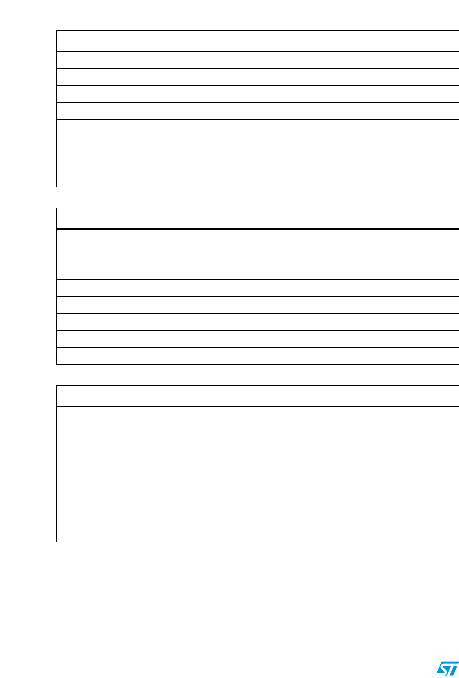
Interrupt system UPSD3212A, UPSD3212C, UPSD3212CV
46/181
Table 21. Description of the IEA bits
Bit Symbol Function
7 — Not used
6 — Not used
5 — Not used
4 ES2 Enable 2nd USART Interrupt
3 — Not used
2 — Not used
1 EI2C Enable I²C Interrupt
0 EUSB Enable USB Interrupt
Table 22. Description of the IP bits
Bit Symbol Function
7—Reserved
6—Reserved
5 PT2 Timer 2 Interrupt priority level
4 PS USART Interrupt priority level
3 PT1 Timer 1 Interrupt priority level
2 PX1 External Interrupt (Int1) priority level
1 PT0 Timer 0 Interrupt priority level
0 PX0 External Interrupt (Int0) priority level
Table 23. Description of the IPA bits
Bit Symbol Function
7 — Not used
6 — Not used
5 — Not used
4 PS2 2nd USART Interrupt priority level
3 — Not used
2 — Not used
1 PI2C I²C Interrupt priority level
0 PUSB USB Interrupt priority level
Obsolete Product(s) - Obsolete Product(s)

UPSD3212A, UPSD3212C, UPSD3212CV Interrupt system
47/181
5.10 How interrupts are handled
The interrupt flags are sampled at S5P2 of every machine cycle. The samples are polled
during following machine cycle. If one of the flags was in a set condition at S5P2 of the
preceding cycle, the polling cycle will find it and the interrupt system will generate an LCALL
to the appropriate service routine, provided this H/W generated LCALL is not blocked by any
of the following conditions:
●An interrupt of equal priority or higher priority level is already in progress.
●The current machine cycle is not the final cycle in the execution of the instruction in
progress.
●The instruction in progress is RETI or any access to the interrupt priority or interrupt
enable registers.
The polling cycle is repeated with each machine cycle, and the values polled are the values
that were present at S5P2 of the previous machine cycle.
Note: If an interrupt flag is active but being responded to for one of the above mentioned
conditions, if the flag is still inactive when the blocking condition is removed, the denied
interrupt will not be serviced. In other words, the fact that the interrupt flag was once active
but not serviced is not remembered. Every polling cycle is new.
The processor acknowledges an interrupt request by executing a hardware generated
LCALL to the appropriate service routine. The hardware generated LCALL pushes the
contents of the Program Counter on to the stack (but it does not save the PSW) and reloads
the PC with an address that depends on the source of the interrupt being vectored to as
shown in Tabl e 2 4 .
Execution proceeds from that location until the RETI instruction is encountered. The RETI
instruction informs the processor that the interrupt routine is no longer in progress, then
pops the top two bytes from the stack and reloads the Program Counter. Execution of the
interrupted program continues from where it left off.
Note: A simple RET instruction would also return execution to the interrupted program, but it would
have left the interrupt control system thinking an interrupt was still in progress, making future
interrupts impossible.
Table 24. Vector addresses
Source Vector address
Int0 0003h
2nd USART 004Bh
Timer 0 000Bh
I²C 0043h
Int1 0013h
Timer 1 001Bh
USB 0033h
1st USART 0023h
Timer 2+EXF2 002Bh
Obsolete Product(s) - Obsolete Product(s)
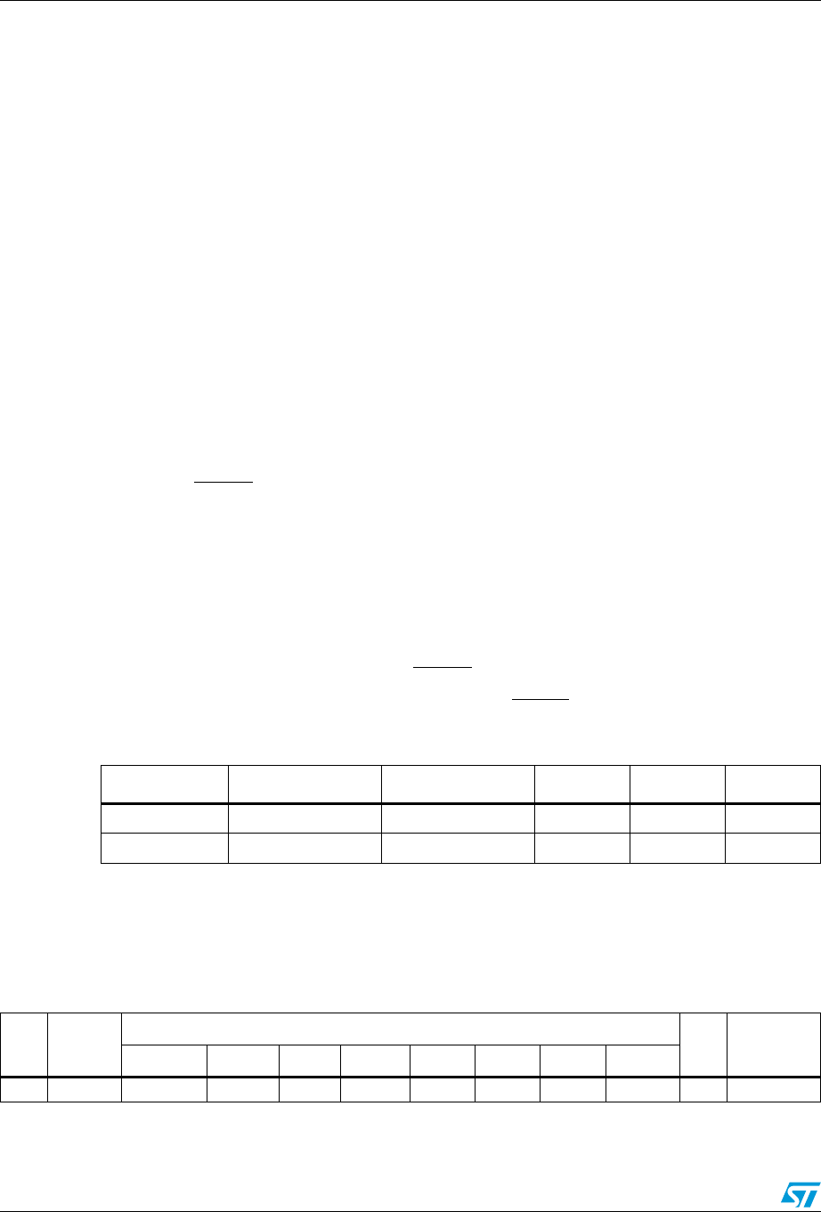
Power-saving mode UPSD3212A, UPSD3212C, UPSD3212CV
48/181
6 Power-saving mode
Two software selectable modes of reduced power consumption are implemented.
6.1 Idle mode
In Idle mode, the following functions are switched Off.
●CPU (Halted)
The following functions remain Active during Idle mode:
●External Interrupts
●Timer 0, Timer 1, Timer 2
●PWM Units
●USB Interface
●USART
●8-bit ADC
●I2C Interface
Note: Interrupt or RESET terminates the Idle mode.
6.2 Power-down mode
●System Clock Halted
●LVD Logic Remains Active
●SRAM content remains unchanged
●The SFRs retain their value until a RESET is asserted
Note: The only way to exit Power-down mode is through a RESET
.
6.3 Power control register
The Idle and Power-down modes are activated by software via the PCON register.
Table 25. Power-saving mode power consumption
Mode Addr/data Ports 1,3,4 PWM I2CUSB
Idle Maintain Data Maintain Data Active Active Active
Power-down Maintain Data Maintain Data Disable Disable Disable
Table 26. Pin status during Idle and Power-down mode
SFR
Addr
Reg
Name
Bit Register Name Reset
Value Comments
76543210
87 PCON SMOD SMOD1 LVREN ADSFINT RCLK1 TCLK1 PD IDLE 00 Power Ctrl
Obsolete Product(s) - Obsolete Product(s)

UPSD3212A, UPSD3212C, UPSD3212CV Power-saving mode
49/181
1. See the T2CON register for details of the flag description
6.4 Idle mode
The instruction that sets PCON.0 is the last instruction executed in the normal operating
mode before Idle mode is activated. Once in the Idle mode, the CPU status is preserved in
its entirety: Stack pointer, Program counter, Program status word, Accumulator, RAM and All
other registers maintain their data during Idle mode.
There are three ways to terminate the Idle mode.
1. Activation of any enabled interrupt will cause PCON.0 to be cleared by hardware
terminating Idle mode. The interrupt is serviced, and following return from interrupt
instruction RETI, the next instruction to be executed will be the one which follows the
instruction that wrote a logic '1' to PCON.0.
2. External hardware reset: the hardware reset is required to be active for two machine
cycle to complete the RESET operation.
3. Internal reset: the microcontroller restarts after 3 machine cycles in all cases.
6.5 Power-down mode
The instruction that sets PCON.1 is the last executed prior to going into the Power-down
mode. Once in Power-down mode, the oscillator is stopped. The contents of the on-chip
RAM and the Special Function Register are preserved.
The Power-down mode can be terminated by an external RESET.
Table 27. Description of the PCON bits
Bit Symbol Function
7 SMOD Double baud data rate bit UART
6 SMOD1 Double baud data rate bit 2nd UART
5 LVREN LVR disable bit (active High)
4 ADSFINT Enable ADC Interrupt
3 RCLK1(1) Received clock flag (UART 2)
2TCLK1
(1) Transmit clock flag (UART 2)
1 PD Activate Power-down mode (High enable)
0 IDL Activate Idle mode (High enable)
Obsolete Product(s) - Obsolete Product(s)

I/O ports (MCU module) UPSD3212A, UPSD3212C, UPSD3212CV
50/181
7 I/O ports (MCU module)
The MCU module has five ports: Port 0, Port 1, Port 2, Port 3, and Port 4. (Refer to the PSD
module section on I/O ports A,B,C and D). Ports P0 and P2 are dedicated for the external
address and data bus and is not available in the 52-pin package devices.
Port 1- Port 3 are the same as in the standard 8032 microcontrollers, with the exception of
the additional special peripheral functions. All ports are bi-directional. Pins of which the
alternative function is not used may be used as normal bi-directional I/O.
The use of Port 1-Port 4 pins as alternative functions are carried out automatically by the
UPSD321xx devices provided the associated SFR Bit is set HIGH.
The following SFR registers (Ta bl e 2 9 , Ta b l e 3 0 , and Ta bl e 3 1 ) are used to control the
mapping of alternate functions onto the I/O port bits. Port 1 alternate functions are
controlled using the P1SFS register, except for Timer 2 and the 2nd UART which are
enabled by their configuration registers. P1.0 to P1.3 are default to GPIO after reset.
Port 3 pins 6 and 7 have been modified from the standard 8032. These pins that were used
for READ and WRITE control signals are now GPIO or I2C bus pins. The READ and WRITE
pins are assigned to dedicated pins.
Port 3 (I2C) and Port 4 alternate functions are controlled using the P3SFS and P4SFS
Special Function Selection registers. After a reset, the I/O pins default to GPIO. The
alternate function is enabled if the corresponding bit in the PXSFS register is set to '1.' Other
Port 3 alternative functions (UART, Interrupt, and Timer/Counter) are enabled by their
configuration register and do not require setting of the bits in P3SFS.
Table 28. I/O port functions
Port name Main function Alternate
Port 1 GPIO
Timer 2 - Bits 0,1
2nd UART - Bits 2,3
ADC - Bits 4..7
Port 3 GPIO
UART - Bits 0,1
Interrupt - Bits 2,3
Timers - Bits 4,5
I2C - Bits 6,7
Port 4 GPIO PWM - Bits 3..7
USB +/- USB +/- Only
Table 29. P1SFS (91h)
76543210
0=Port 1.7
1=ACH3
0=Port 1.6
1=ACH2
0=Port 1.5
1=ACH1
0=Port 1.4
1=ACH0 Bits are reserved Bits are reserved
Obsolete Product(s) - Obsolete Product(s)
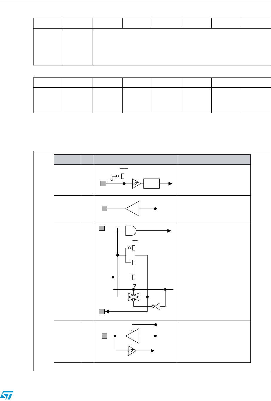
UPSD3212A, UPSD3212C, UPSD3212CV I/O ports (MCU module)
51/181
7.1 Port type and description
Figure 16. Port type and description (Part 1)
Table 30. P3SFS (93h)
76543210
0 = Port
3.7
1 = SCL
from I2C
unit
0 = Port
3.6
1 = SDA
from I2C
unit
Bits are reserved
Table 31. P4SFS (94h)
76543210
0=Port 4.7
1=PWM 4
0=Port 4.6
1=PWM 3
0=Port 4.5
1=PWM 2
0=Port 4.4
1=PWM 1
0=Port 4.3
1=PWM 0
0=Port 4.2
1=VSYNC
0=Port 4.1
1=DDC -
SCL
0=Port 4.0
1=DDC -
SDA
AI06653
Symbol Circuit Description
In /
Out
RESET I • Schmitt input with internal pull-up
CMOS compatible interface
NFC : 400ns
WR, RD,ALE,
PSEN
O Output only
XTAL1,
XTAL2
I
O
On-chip oscillator
On-chip feedback resistor
Stop in the power down mode
External clock input available
CMOS compatible interface
PORT0 I/O Bidirectional I/O port
Schmitt input
Address Output ( Push-Pull )
CMOS compatible interface
NFC
xon
Obsolete Product(s) - Obsolete Product(s)
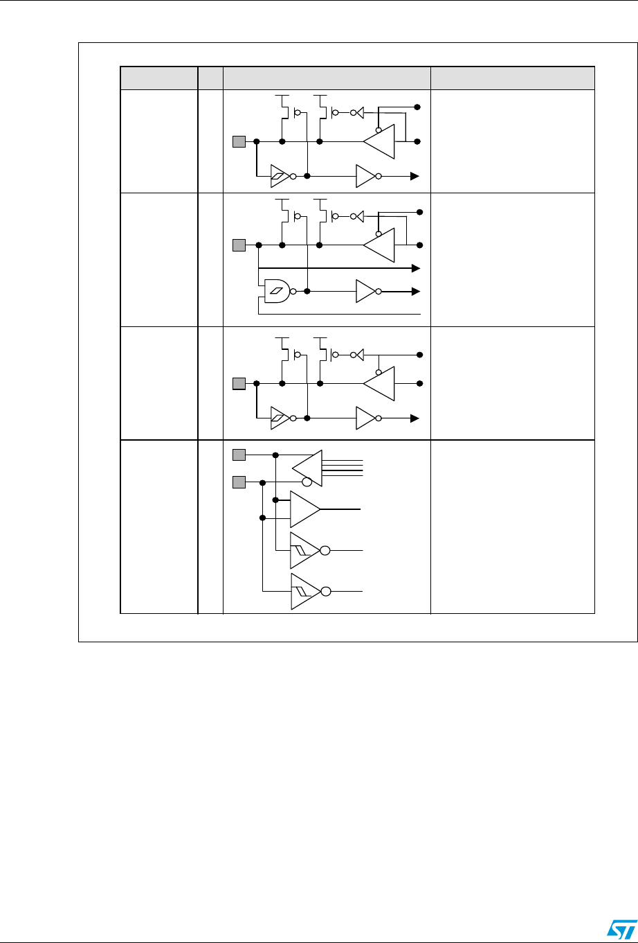
I/O ports (MCU module) UPSD3212A, UPSD3212C, UPSD3212CV
52/181
Figure 17. Port type and description (Part 2)
AI07428b
Symbol Circuit Function
In/
Out
PORT1 <3:0>,
PORT3,
PORT4<7:3,1:0>
PORT2
I/O
PORT4.2
Bidirectional I/O port with
internal pull-ups
Schmitt input
CMOS compatible interface
Bidirectional I/O port with internal
pull-ups
Schmitt input.
TTL compatible interface
PORT1 < 7:4 > I/O Bidirectional I/O port with
internal pull-ups
Schmitt input
CMOS compatible interface
Analog input option
I/O
an_enb
USB–, USB+ Bidirectional I/O port
Schmitt input
TTL compatible interface
I/O
+
–
Obsolete Product(s) - Obsolete Product(s)
UPSD3212A, UPSD3212C, UPSD3212CV Oscillator
53/181
8 Oscillator
The oscillator circuit of the UPSD321xx devices is a single stage inverting amplifier in a
Pierce oscillator configuration. The circuitry between XTAL1 and XTAL2 is basically an
inverter biased to the transfer point. Either a crystal or ceramic resonator can be used as the
feedback element to complete the oscillator circuit. Both are operated in parallel resonance.
XTAL1 is the high gain amplifier input, and XTAL2 is the output. To drive the UPSD321xx
devices externally, XTAL1 is driven from an external source and XTAL2 left open-circuit.
Figure 18. Oscillator
AI06620
XTAL1 XTAL2
8 to 40 MHz
XTAL1 XTAL2
External Clock
Obsolete Product(s) - Obsolete Product(s)
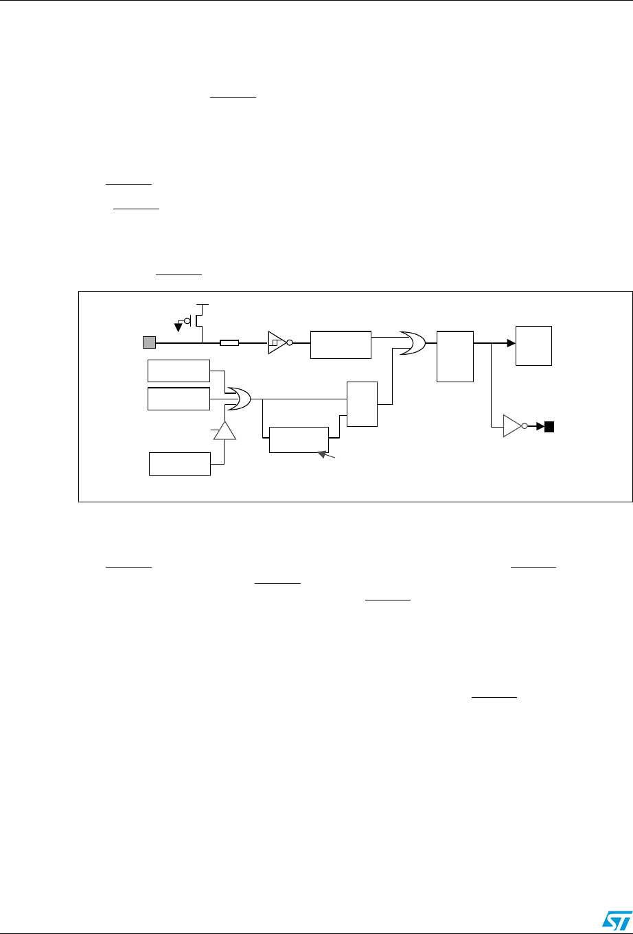
Supervisory UPSD3212A, UPSD3212C, UPSD3212CV
54/181
9 Supervisory
There are four ways to invoke a reset and initialize the UPSD321xx devices.
1. Via the external RESET pin
2. Via the internal LVR block
3. Via USB bus reset signaling
4. Via Watchdog Timer (WDT)
The RESET mechanism is illustrated in Figure 19.
Each RESET source will cause an internal reset signal active. The CPU responds by
executing an internal reset and puts the internal registers in a defined state. This internal
reset is also routed as an active low reset input to the PSD module.
Figure 19. RESET configuration
9.1 External reset
The RESET pin is connected to a Schmitt trigger for noise reduction. A RESET is
accomplished by holding the RESET pin LOW for at least 1ms at power up while the
oscillator is running. Refer to AC spec on other RESET timing requirements.
9.2 Low VDD voltage reset
An internal reset is generated by the LVR circuit when the VDD drops below the reset
threshold. After VDD reaching back up to the reset threshold, the RESET signal will remain
asserted for 10ms before it is released. On initial power-up the LVR is enabled (default).
After power-up the LVR can be disabled via the LVREN Bit in the PCON Register.
Note: The LVR logic is still functional in both the Idle and Power-down modes.
The reset threshold:
●5 V operation: 4 V ± 0.25 V
●3.3 V operation: 2.5 V ± 0.2 V
This logic supports approximately 0.1 V of hysteresis and 1 µs noise-cancelling delay.
AI06621
Reset CPU
&
PERI.
Noise
Cancel
LVR S
Q
R
CPU
Clock
Sync
10ms
Timer
USB Reset
RSTE
WDT
PSD_RST
“
Active Low
10ms at 40Mhz
50ms at 8Mhz
Obsolete Product(s) - Obsolete Product(s)

UPSD3212A, UPSD3212C, UPSD3212CV Supervisory
55/181
9.3 Watchdog timer overflow
The Watchdog timer generates an internal reset when its 22-bit counter overflows. See
Watchdog Timer section for details.
9.4 USB reset
The USB reset is generated by a detection on the USB bus RESET signal. A single-end
zero on its upstream port for 4 to 8 times will set RSTF Bit in UISTA register. If Bit 6 (RSTE)
of the UIEN Register is set, the detection will also generate the RESET signal to reset the
CPU and other peripherals in the MCU.
Obsolete Product(s) - Obsolete Product(s)

Watchdog timer UPSD3212A, UPSD3212C, UPSD3212CV
56/181
10 Watchdog timer
The hardware watchdog timer (WDT) resets the UPSD321xx devices when it overflows. The
WDT is intended as a recovery method in situations where the CPU may be subjected to a
software upset. To prevent a system reset the timer must be reloaded in time by the
application software. If the processor suffers a hardware/software malfunction, the software
will fail to reload the timer. This failure will result in a reset upon overflow thus preventing the
processor running out of control.
In the Idle mode the watchdog timer and reset circuitry remain active. The WDT consists of
a 22-bit counter, the Watchdog Timer RESET (WDRST) SFR and Watchdog Key Register
(WDKEY).
Since the WDT is automatically enabled while the processor is running. the user only needs
to be concerned with servicing it.
The 22-bit counter overflows when it reaches 4194304 (3FFFFFH). The WDT increments
once every machine cycle.
This means the user must reset the WDT at least every 4194304 machine cycles (1.258
seconds at 40MHz). To reset the WDT the user must write a value between 00-7EH to the
WDRST register. The value that is written to the WDRST is loaded to the 7MSB of the 22-bit
counter. This allows the user to pre-loaded the counter to an initial value to generate a
flexible Watchdog time out period. Writing a “00” to WDRST clears the counter.
The watchdog timer is controlled by the watchdog key register, WDKEY. Only pattern
01010101 (=55H), disables the watchdog timer. The rest of pattern combinations will keep
the watchdog timer enabled. This security key will prevent the watchdog timer from being
terminated abnormally when the function of the watchdog timer is needed.
In Idle mode, the oscillator continues to run. To prevent the WDT from resetting the
processor while in Idle, the user should always set up a timer that will periodically exit Idle,
service the WDT, and re-enter Idle mode.
Watchdog reset pulse width depends on the clock frequency. The reset period is tfOSC x 12
x 222.
The RESET pulse width is tfOSC x 12 x 215.
Table 32. Watchdog timer key register (WDKEY: 0AEh)
76543210
WDKEY7 WDKEY6 WDKEY5 WDKEY4 WDKEY3 WDKEY2 WDKEY1 WDKEY0
Table 33. Description of the WDKEY Bits
Bit Symbol Function
7 to 0
WDKEY7
to
WDKEY0
Enable or disable watchdog timer.
01010101 (=55h): disable watchdog timer. Others: enable watchdog timer
Obsolete Product(s) - Obsolete Product(s)
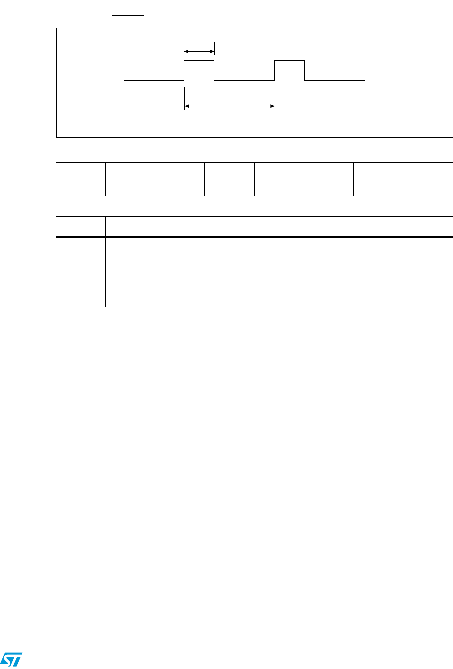
UPSD3212A, UPSD3212C, UPSD3212CV Watchdog timer
57/181
Figure 20. RESET pulse width
1. The Watchdog Timer (WDT) is enabled at power-up or reset and must be served or disabled.
Table 34. Watchdog timer clear register (WDRST: 0A6h)
76543210
Reserved WDRST6 WDRST5 WDRST4 WDRST3 WDRST2 WDRST1 WDRST0
Table 35. Description of the WDRST Bits
Bit Symbol Function
7—Reserved
6 to 0
WDRST6
to
WDRST0
To reset watchdog timer, write any value beteen 00h and 7Eh to this
register.
This value is loaded to the 7 most significant bits of the 22-bit counter.
For example: MOV WDRST,#1EH
Reset period
(1.258 second at 40Mhz)
(about 6.291 seconds at 8Mhz)
Reset pulse width (about 10ms at 40Mhz, about 50ms at 8Mhz)
AI06823
Obsolete Product(s) - Obsolete Product(s)
Timer/counters (Timer 0, Timer 1 and Timer 2) UPSD3212A, UPSD3212C, UPSD3212CV
58/181
11 Timer/counters (Timer 0, Timer 1 and Timer 2)
The UPSD321xx devices has three 16-bit Timer/Counter registers: Timer 0, Timer 1 and
Timer 2. All of them can be configured to operate either as timers or event counters and are
compatible with standard 8032 architecture.
In the “Timer” function, the register is incremented every machine cycle. Thus, one can think
of it as counting machine cycles. Since a machine cycle consists of 6 CPU clock periods,
the count rate is 1/6 of the CPU clock frequency or 1/12 of the oscillator frequency (fOSC).
In the “Counter” function, the register is incremented in response to a 1-to-0 transition at its
corresponding external input pin, T0 or T1. In this function, the external input is sampled
during S5P2 of every machine cycle. When the samples show a high in one cycle and a low
in the next cycle, the count is incremented. The new count value appears in the register
during S3P1 of the cycle following the one in which the transition was detected. Since it
takes 2 machine cycles (24 fOSC clock periods) to recognize a 1-to-0 transition, the
maximum count rate is 1/24 of the fOSC. There are no restrictions on the duty cycle of the
external input signal, but to ensure that a given level is sampled at least once before it
changes, it should be held for at least one full cycle. In addition to the “Timer” or “Counter”
selection, Timer 0 and Timer 1 have four operating modes from which to select.
11.1 Timer 0 and Timer 1
The “Timer” or “Counter” function is selected by control bits C/ T in the Special Function
Register TMOD. These Timer/Counters have four operating modes, which are selected by
bit-pairs (M1, M0) in TMOD. Modes 0, 1, and 2 are the same for Timers/ Counters. Mode 3
is different. The four operating modes are de-scribed in the following text.
Table 36. Control register (TCON)
76543210
TF1 TR1 TF0 TR0 IE1 IT1 IE0 IT0
Table 37. Description of the TCON bits
Bit Symbol Function
7TF1
Timer 1 overflow flag. Set by hardware on Timer/Counter overflow. Cleared
by hardware when processor vectors to interrupt routine
6TR1
Timer 1 run control bit. Set/cleared by software to turn Timer/Counter on or
off
5TF0
Timer 0 overflow flag. Set by hardier on Timer/Counter overflow. Cleared by
hardware when processor vectors to interrupt routine
4TR0
Timer 0 run control bit. Set/cleared by software to turn Timer/Counter on or
off
3IE1
Interrupt 1 Edge Flag. Set by hardware when external interrupt edge
detected. Cleared when interrupt processed
2IT1
Interrupt 1 Type Control Bit. Set/cleared by software to specify falling-
edge/low-level triggered external interrupt
Obsolete Product(s) - Obsolete Product(s)
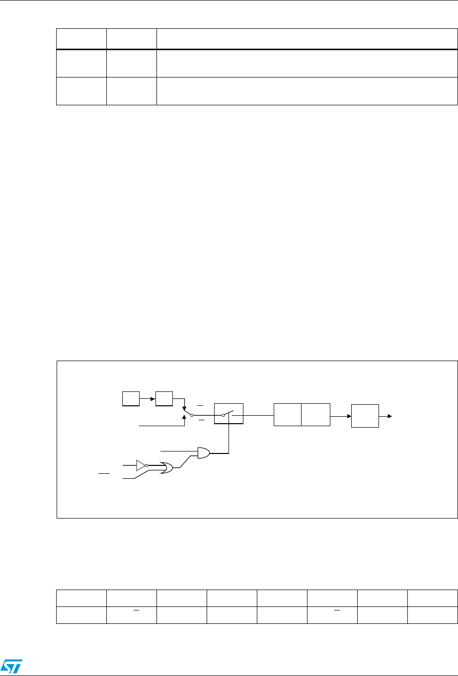
UPSD3212A, UPSD3212C, UPSD3212CV Timer/counters (Timer 0, Timer 1 and Timer 2)
59/181
11.1.1 Mode 0
Putting either Timer into Mode 0 makes it look like an 8048 Timer, which is an 8-bit Counter
with a divide-by-32 prescaler. Figure 21 shows the Mode 0 operation as it applies to Timer
1.
In this mode, the Timer register is configured as a 13-bit register. As the count rolls over
from all '1s' to all '0s,' it sets the Timer Interrupt Flag TF1. The counted input is enabled to
the Timer when TR1 = 1 and either GATE = 0 or /INT1 = 1. (Setting GATE = 1 allows the
Timer to be controlled by external input /INT1, to facilitate pulse width measurements). TR1
is a control bit in the Special Function Register TCON (TCON Control Register). GATE is in
TMOD.
The 13-bit register consists of all 8 bits of TH1 and the lower 5 bits of TL1. The upper 3 bits
of TL1 are indeterminate and should be ignored. Setting the run flag does not clear the
registers.
Mode 0 operation is the same for the Timer 0 as for Timer 1. Substitute TR0, TF0, and /INT0
for the corresponding Timer 1 signals in Figure 21 There are two different GATE Bits, one for
Timer 1 and one for Timer0.
Figure 21. Timer/counter mode 0: 13-bit counter
11.1.2 Mode 1
Mode 1 is the same as Mode 0, except that the Timer register is being run with all 16 bits.
1IE0
Interrupt 0 Edge Flag. Set by hardware when external interrupt edge
detected. Cleared when interrupt processed
0IT0
Interrupt 0 Type Control Bit. Set/cleared by software to specify falling-
edge/low-level triggered external interrupt
Table 37. Description of the TCON bits
Bit Symbol Function
AI06622
fOSC
TF1 Interrupt
Gate
TR1
INT1 pin
T1 pin Control
TL1
(5 bits)
TH1
(8 bits)
C/T = 0
C/T = 1
÷ 12
Table 38. TMOD register (TMOD)
76543210
Gate C/T M1 M0 Gate C/T M1 M0
Obsolete Product(s) - Obsolete Product(s)
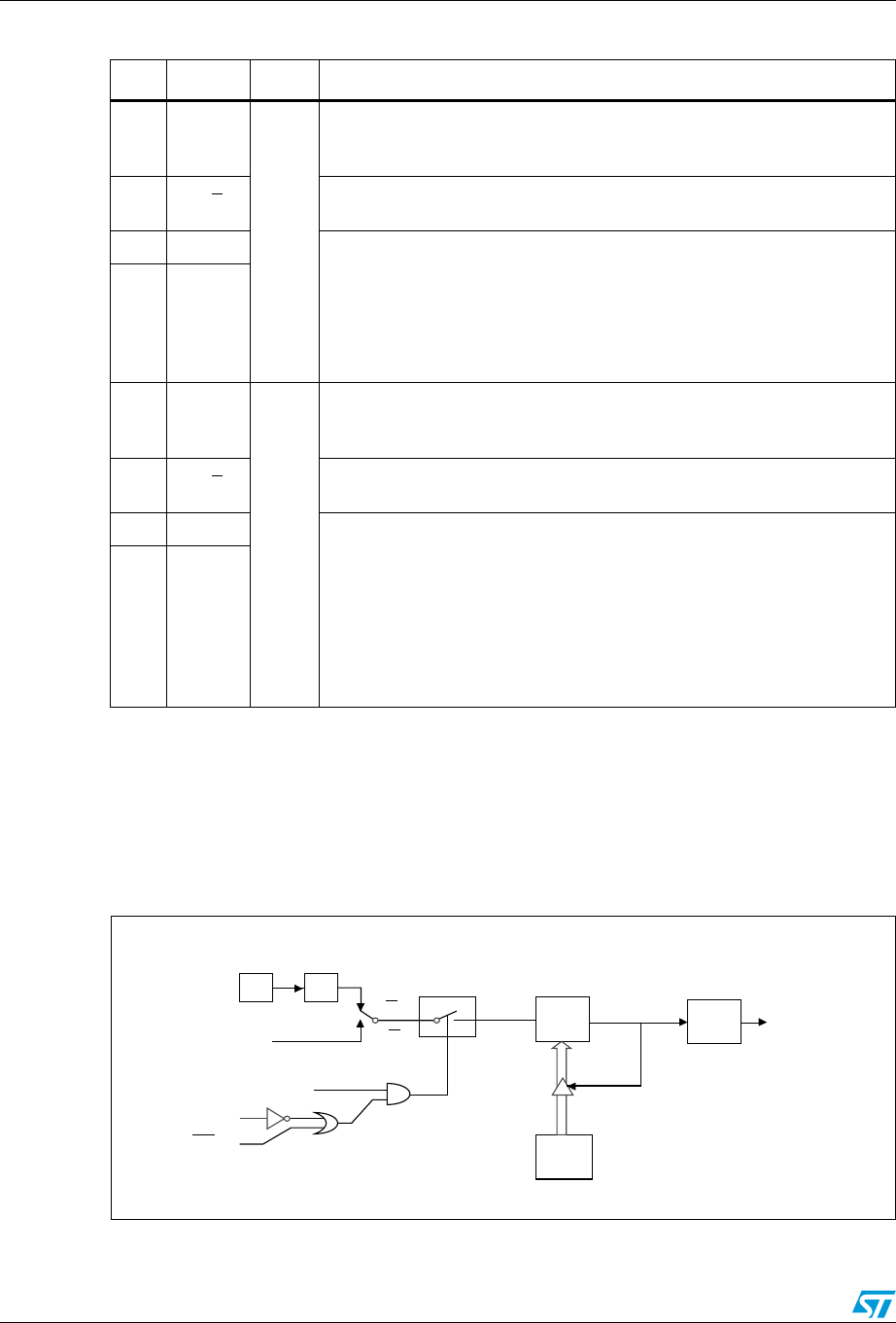
Timer/counters (Timer 0, Timer 1 and Timer 2) UPSD3212A, UPSD3212C, UPSD3212CV
60/181
11.1.3 Mode 2
Mode 2 configures the Timer register as an 8-bit Counter (TL1) with automatic reload, as
shown in Figure 22. Overflow from TL1 not only sets TF1, but also reloads TL1 with the
contents of TH1, which is preset by software. The reload leaves TH1 unchanged. Mode 2
operation is the same for Timer/Counter 0.
Figure 22. Timer/counter mode 2: 8-bit Auto-reload
Table 39. Description of the TMOD bits
Bit Symbol Timer Function
7Gate
Timer1
Gating control when set. Timer/Counter 1 is enabled only while INT1 pin
is High and TR1 control pin is set. When cleared, Timer 1 is enabled
whenever TR1 control bit is set
6C/T Timer or Counter selector, cleared for timer operation (input from internal
system clock); set for counter operation (input from T1 input pin)
5 M1 (M1,M0)=(0,0): 13-bit Timer/Counter, TH1, with TL1 as 5-bit prescaler
(M1,M0)=(0,1): 16-bit Timer/Counter. TH1 and TL1 are cascaded. There
is no prescaler.
(M1,M0)=(1,0): 8-bit auto-reload Timer/Counter. TH1 holds a value which
is to be reloaded into TL1 each time it overflows
(M1,M0)=(1,1): Timer/Counter 1 stopped
4M0
3Gate
Timer0
Gating control when set. Timer/Counter 0 is enabled only while INT0 pin
is High and TR0 control pin is set. When cleared, Timer 0 is enabled
whenever TR0 control bit is set
2C/T Timer or Counter selector, cleared for timer operation (input from internal
system clock); set for counter operation (input from T0 input pin)
1 M1 (M1,M0)=(0,0): 13-bit Timer/Counter, TH0, with TL0 as 5-bit prescaler
(M1,M0)=(0,1): 16-bit Timer/Counter. TH0 and TL0 are cascaded. There
is no prescaler.
(M1,M0)=(1,0): 8-bit auto-reload Timer/Counter. TH0 holds a value which
is to be reloaded into TL0 each time it overflows
(M1,M0)=(1,1): TL0 is an 8-bit Timer/Counter controlled by the standard
TImer 0 control bits. TH0 is an 8-bit timer only controlled by Timer 1
control bits
0M0
AI06623
fOSC
TF1 Interrupt
Gate
TR1
INT1 pin
T1 pin Control
TL1
(8 bits)
TH1
(8 bits)
C/T = 0
C/T = 1
÷ 12
Obsolete Product(s) - Obsolete Product(s)
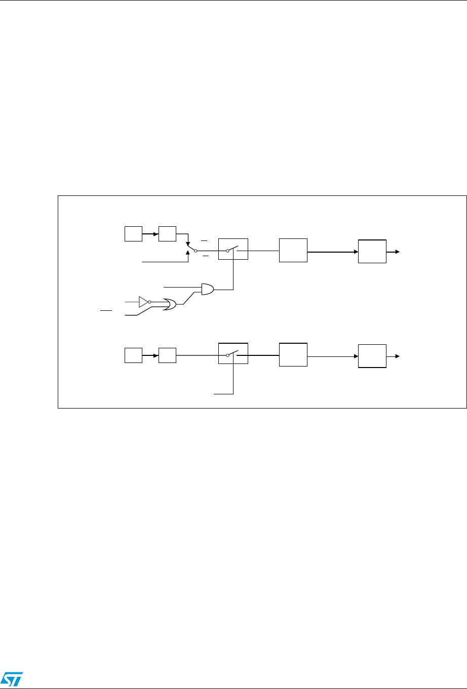
UPSD3212A, UPSD3212C, UPSD3212CV Timer/counters (Timer 0, Timer 1 and Timer 2)
61/181
11.1.4 Mode 3
Timer 1 in Mode 3 simply holds its count. The effect is the same as setting TR1 = 0.
Timer 0 in Mode 3 establishes TL0 and TH0 as two separate counters. The logic for Mode 3
on Timer 0 is shown in Figure 23. TL0 uses the Timer 0 control Bits: C/T, GATE, TR0, INT0,
and TF0. TH0 is locked into a timer function (counting machine cycles) and takes over the
use of TR1 and TF1 from Timer 1. Thus, TH0 now controls the “Timer 1“ Interrupt.
Mode 3 is provided for applications requiring an extra 8-bit timer on the counter. With Timer
0 in Mode 3, an UPSD321xx devices can look like it has three Timer/Counters. When Timer
0 is in Mode 3, Timer 1 can be turned on and off by switching it out of and into its own Mode
3, or can still be used by the serial port as a baud rate generator, or in fact, in any application
not requiring an interrupt.
Figure 23. Timer/counter mode 3: two 8-bit counters
11.2 Timer 2
Like Timers 0 and 1, Timer 2 can operate as either an event timer or as an event counter.
This is selected by Bit C/T2 in the special function register T2CON. It has three operating
modes: Capture, Auto-reload, and Baud Rate Generator, which are selected by bits in the
T2CON as shown in Ta b le 4 1 . In the Capture mode there are two options which are selected
by Bit EXEN2 in T2CON. if EXEN2 = 0, then Timer 2 is a 16-bit timer or counter which upon
overflowing sets Bit TF2, the Timer 2 Overflow bit, which can be used to generate an
interrupt. If EXEN2 = 1, then Timer 2 still does the above, but with the added feature that a
1-to-0 transition at external input T2EX causes the current value in the Timer 2 registers,
TL2 and TH2, to be captured into registers RCAP2L and RCAP2H, respectively. In addition,
the transition at T2EX causes Bit EXF2 in T2CON to be set, and EXF2 like TF2 can
generate an interrupt. The Capture mode is illustrated in Figure 24.
In the Auto-reload mode, there are again two options, which are selected by bit EXEN2 in
T2CON. If EXEN2 = 0, then when Timer 2 rolls over it not only sets TF2 but also causes the
Timer 2 registers to be reloaded with the 16-bit value in registers RCAP2L and RCAP2H,
which are preset by software. If EXEN2 = 1, then Timer 2 still does the above, but with the
added feature that a 1-to-0 transition at external input T2EX will also trigger the 16-bit reload
AI06624
f
OSC
TF0 Interrupt
Gate
TR0
INT0 pin
T0 pin Control
TL0
(8 bits)
C/T = 0
C/T = 1
÷ 12
f
OSC
TF1 Interrupt
Control
TH1
(8 bits)
÷ 12
TR1
Obsolete Product(s) - Obsolete Product(s)
Timer/counters (Timer 0, Timer 1 and Timer 2) UPSD3212A, UPSD3212C, UPSD3212CV
62/181
and set EXF2. Auto-reload mode is illustrated in the Standard Serial Interface (UART)
Figure 25. The Baud Rate Generation mode is selected by (RCLK, RCLK1)=1 and/or
(TCLK, TCLK1)=1. It is described in conjunction with the serial port.
1. The RCLK1 and TCLK1 Bits in the PCON Register control UART 2, and have the same function as RCLK
and TCLK.
Table 40. Timer/counter 2 control register (T2CON)
76543210
TF2 EXF2 RCLK TCLK EXEN2 TR2 C/T2CP/RL2
Table 41. Description of the T2CON bits
Bit Symbol Function
7TF2
Timer 2 overflow flag. Set by a Timer 2 overflow, and must be cleared by
software. TF2 will not be set when either (RCLK, RCLK1)=1 or (TCLK,
TCLK)=1
6 EXF2
Timer 2 external flag set when either a capture or reload is caused by a
negative transition on T2EX and EXEN2=1. When Timer 2 Interrupt is
enabled, EXF2=1 will cause the CPU to vector to the Timer 2 Interrupt
routine. EXF2 must be cleared by software
5 RCLK(1)
Receive clock flag (UART 1). When set, causes the serial port to use Timer
2 overflow pulses for its receive clock in Modes 1 and 3. TCLK=0 causes
Timer 1 overflow to be used for the receive clock
4TCLK
(1)
Transmit clock flag (UART 1). When set, causes the serial port to use Timer
2 overflow pulses for its transmit clock in Modes 1 and 3. TCLK=0 causes
Timer 1 overflow to be used for the transmit clock
3 EXEN2
Timer 2 external enable flag. When set, allows a capture or reload to occur
as a result of a negative transition on T2EX if Timer 2 is not being used to
clock the serial port. EXEN2=0 causes Time 2 to ignore events at T2EX
2 TR2 Start/stop control for Timer 2. A logic 1 starts the timer
1C/T
2
Timer or Counter select for Timer 2. Cleared for timer operation (input from
internal system clock, tCPU); set for external event counter operation
(negative edge triggered)
0CP/RL
2
Capture/reload flag. When set, capture will occur on negative transition of
T2EX if EXEN2=1. When cleared, auto-reload will occur either with TImer 2
overflows, or negative transitions of T2EX when EXEN2=1. When either
(RCLK, RCLK1)=1 or (TCLK, TCLK)=1, this bit is ignored, and timer is
forced to auto-reload on Timer 2 overflow
Obsolete Product(s) - Obsolete Product(s)
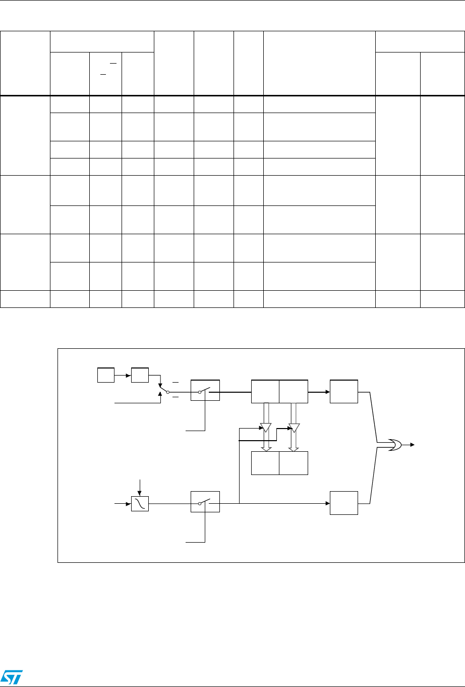
UPSD3212A, UPSD3212C, UPSD3212CV Timer/counters (Timer 0, Timer 1 and Timer 2)
63/181
1. ↓ = falling edge
Figure 24. Timer 2 in Capture mode
Table 42. Timer/counter2 operating modes
Mode
T2CON
T2MOD
DECN
T2CON
EXEN
P1.1
T2EX Remarks
Input clock
RxCLK
or
TxCLK
CP/R
L2 TR2 Internal External
(P1.0/T2)
16-bit
Auto-
reload
0 0 1 0 0 x Reload upon overflow
fOSC/12 MAX
fOSC/24
0010 1¯
Reload trigger (falling
edge)
0 0 1 1 x 0 Down counting
0 0 1 1 x 1 Up counting
16-bit
Capture
011x 0x
16-bit Timer/Counter
(only up counting) fOSC/12 MAX
fOSC/24
011x 1¯
Capture (TH1,TL2) →
(RCAP2H,RCAP2L)
Baud Rate
Generator
1x1x 0x
No overflow interrupt
request (TF2) fOSC/12 MAX
fOSC/24
1x1x 1¯
Extra External Interrupt
(Timer 2)
Off x x 0 x x x Timer 2 stops — —
AI06625
fOSC
TF2
Capture
TR2
T2 pin Control
TL2
(8 bits)
TH2
(8 bits)
C/T2 = 0
C/T2 = 1
÷ 12
EXP2
Control
EXEN2
RCAP2L RCAP2H
T2EX pin
Timer 2
Interrupt
Transition
Detector
Obsolete Product(s) - Obsolete Product(s)
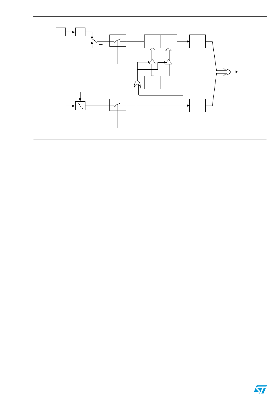
Timer/counters (Timer 0, Timer 1 and Timer 2) UPSD3212A, UPSD3212C, UPSD3212CV
64/181
Figure 25. Timer 2 in Auto-Reload mode
AI06626
fOSC
TF2
Reload
TR2
T2 pin Control
TL2
(8 bits)
TH2
(8 bits)
C/T2 = 0
C/T2 = 1
÷ 12
EXP2
Control
EXEN2
RCAP2L RCAP2H
T2EX pin
Timer 2
Interrupt
Transition
Detector
Obsolete Product(s) - Obsolete Product(s)

UPSD3212A, UPSD3212C, UPSD3212CV Standard serial interface (UART)
65/181
12 Standard serial interface (UART)
The UPSD321xx devices provides two standard 8032 UART serial ports. The first port is
connected to pin P3.0 (RX) and P3.1 (TX). The second port is connected to pin P1.2 (RX)
and P1.3(TX). The operation of the two serial ports are the same and are controlled by the
SCON and SCON2 registers.
The serial port is full duplex, meaning it can transmit and receive simultaneously. It is also
receive-buffered, meaning it can commence reception of a second byte before a previously
received byte has been read from the register. (However, if the first byte still has not been
read by the time reception of the second byte is complete, one of the bytes will be lost.) The
serial port receive and transmit registers are both accessed at Special Function Register
SBUF (or SBUF2 for the second serial port). Writing to SBUF loads the transmit register,
and reading SBUF accesses a physically separate receive register.
The serial port can operate in 4 modes: Mode 0, 1, 2 or 3.
Mode 0
Serial data enters and exits through RxD. TxD outputs the shift clock. 8 bits are
transmitted/received (LSB first). The baud rate is fixed at 1/12 the fOSC.
Mode 1
10 bits are transmitted (through TxD) or received (through RxD): a Start bit (0), 8 data bits
(LSB first), and a Stop bit (1). On receive, the Stop bit goes into RB8 in Special Function
Register SCON. The baud rate is variable.
Mode 2
11 bits are transmitted (through TxD) or received (through RxD): Start bit (0), 8 data bits
(LSB first), a programmable 9th data bit, and a Stop bit (1). On Transmit, the 9th data bit
(TB8 in SCON) can be assigned the value of ‘0’ or ‘1’. Or, for example, the Parity bit (P, in the
PSW) could be moved into TB8. On receive, the 9th data bit goes into RB8 in Special
Function Register SCON, while the Stop bit is ignored. The baud rate is programmable to
either 1/32 or 1/64 the oscillator frequency.
Mode 3
11 bits are transmitted (through TxD) or received (through RxD): a Start bit (0), 8 data bits
(LSB first), a programmable 9th data bit, and a Stop bit (1). In fact, Mode 3 is the same as
Mode 2 in all respects except baud rate. The baud rate in Mode 3 is variable.
In all four modes, transmission is initiated by any instruction that uses SBUF as a destination
register. Reception is initiated in Mode 0 by the condition RI = 0 and REN = 1. Reception is
initiated in the other modes by the incoming start bit if REN = 1.
12.1 Multiprocessor communications
Modes 2 and 3 have a special provision for multiprocessor communications. In these
modes, 9 data bits are received. The 9th one goes into RB8. Then comes a Stop bit. The
port can be programmed such that when the Stop bit is received, the serial port interrupt will
Obsolete Product(s) - Obsolete Product(s)

Standard serial interface (UART) UPSD3212A, UPSD3212C, UPSD3212CV
66/181
be activated only if RB8 = 1. This feature is enabled by setting Bit SM2 in SCON. A way to
use this feature in multi-processor systems is as follows:
When the master processor wants to transmit a block of data to one of several slaves, it first
sends out an address byte which identifies the target slave. An address byte differs from a
data byte in that the 9th bit is '1' in an address byte and 0 in a data byte. With SM2 = 1, no
slave will be interrupted by a data byte. An ad-dress byte, however, will interrupt all slaves,
so that each slave can examine the received byte and see if it is being addressed. The
addressed slave will clear its SM2 bit and prepare to receive the data bytes that will be
coming. The slaves that weren’t being addressed leave their SM2s set and go on about their
business, ignoring the coming data bytes.
SM2 has no effect in Mode 0, and in Mode 1 can be used to check the validity of the Stop
bit. In a Mode 1 reception, if SM2 = 1, the receive interrupt will not be activated unless a
valid Stop bit is received.
12.2 Serial port control register
The serial port control and status register is the Special Function Register SCON (SCON2
for the second port), shown in Figure 26. This register contains not only the mode selection
bits, but also the 9th data bit for transmit and receive (TB8 and RB8), and the Serial Port
Interrupt bits (TI and RI).
Table 43. Serial port control register (SCON)
76543210
SM0 SM1 SM2 REN TB8 RB8 TI RI
Table 44. Description of the SCON bits
Bit Symbol Function
7 SM0 (SM1,SM0)=(0,0): Shift Register. Baud rate = fOSC/12
(SM1,SM0)=(1,0): 8-bit UART. Baud rate = variable
(SM1,SM0)=(0,1): 8-bit UART. Baud rate = fOSC/64 or fOSC/32
(SM1,SM0)=(1,1): 8-bit UART. Baud rate = variable
6SM1
5SM2
Enables the multiprocessor communication features in Mode 2 and 3. In
Mode 2 or 3, if SM2 is set to '1,' RI will not be activated if its received 8th
data bit (RB8) is '0.' In Mode 1, if SM2=1, RI will not be activated if a valid
Stop bit was not received. In Mode 0, SM2 should be '0'
4REN
Enables serial reception. Set by software to enable reception. Clear by
software to disable reception
3TB8
The 8th data bit that will be transmitted in Modes 2 and 3. Set or clear by
software as desired
2RB8
In Modes 2 and 3, this bit contains the 8th data bit that was received. In
Mode 1, if SM2=0, RB8 is the Snap Bit that was received. In Mode 0, RB8
is not used
Obsolete Product(s) - Obsolete Product(s)

UPSD3212A, UPSD3212C, UPSD3212CV Standard serial interface (UART)
67/181
12.2.1 Baud rates
The baud rate in Mode 0 is fixed:
Mode 0 Baud Rate = fOSC / 12
The baud rate in Mode 2 depends on the value of Bit SMOD = 0 (which is the value on
reset), the baud rate is 1/64 the oscillator frequency. If SMOD = 1, the baud rate is 1/32 the
oscillator frequency.
Mode 2 Baud Rate = (2SMOD / 64) x fOSC
In the UPSD321xx devices, the baud rates in Modes 1 and 3 are determined by the Timer 1
overflow rate.
12.2.2 Using Timer 1 to generate baud rates
When Timer 1 is used as the baud rate generator, the baud rates in Modes 1 and 3 are
determined by the Timer 1 overflow rate and the value of SMOD as follows:
Modes 1 and 3 Baud Rate = (2SMOD / 32) x (Timer 1 overflow rate)
The Timer 1 Interrupt should be disabled in this application. The Timer itself can be
configured for either “timer” or “counter” operation, and in any of its 3 running modes. In the
most typical applications, it is configured for “timer” operation, in the Auto-reload mode (high
nibble of TMOD = 0010B). In that case the baud rate is given by the formula:
Modes 1 and 3 Baud Rate = (2SMOD / 32) x (fOSC / (12 x [256 – (TH1)]))
One can achieve very low baud rates with Timer 1 by leaving the Timer 1 Interrupt enabled,
and configuring the Timer to run as a 16-bit timer (high nibble of TMOD = 0001B), and using
the Timer 1 Interrupt to do a 16-bit software reload. Figure 21 lists various commonly used
baud rates and how they can be obtained from Timer 1.
12.2.3 Using Timer/counter 2 to generate baud rates
In the UPSD321xx devices, Timer 2 selected as the baud rate generator by setting TCLK
and/or RCLK (see Figure 21 Timer/ Counter 2 Control Register (T2CON)).
Note: The baud rate for transmit and receive can be simultaneously different. Setting RCLK and/or
TCLK puts Timer into its Baud Rate Generator mode.
The RCLK and TCLK Bits in the T2CON register configure UART 1. The RCLK1 and TCLK1
Bits in the PCON register configure UART 2.
The Baud Rate Generator mode is similar to the Auto-reload Mmode, in that a roll over in
TH2 causes the Timer 2 registers to be reloaded with the 16-bit value in registers RCAP2H
and RCAP2L, which are preset by software.
1TI
Transmit Interrupt Flag. Set by hardware at the end of the 8th bit time in
Mode 0, or at the beginning of the Stop bit in the other modes, in any serial
transmission. Must be cleared by software
0RI
Receive Interrupt Flag. Set by hardware at the end of the 8th bit time in
Mode 0, or halfway through the Stop bit in the other modes, in any serial
reception (except for SM2). Must be cleared by software
Table 44. Description of the SCON bits (continued)
Bit Symbol Function
Obsolete Product(s) - Obsolete Product(s)
Standard serial interface (UART) UPSD3212A, UPSD3212C, UPSD3212CV
68/181
Now, the baud rates in Modes 1 and 3 are determined at Timer 2’s overflow rate as follows:
Modes 1 and 3 Baud Rate = Timer 2 Overflow Rate / 16
The timer can be configured for either “timer” or “counter” operation. In the most typical
applications, it is configured for “timer” operation (C/T2 = 0). “Timer” operation is a little
different for Timer 2 when it’s being used as a baud rate generator. Normally, as a timer it
would increment every machine cycle (thus at the 1/6 the CPU clock frequency). In the
case, the baud rate is given by the formula:
Modes 1 and 3 Baud Baud Rate = fOSC / (32 x [65536 – (RCAP2H, RCAP2L)]
where (RCAP2H, RCAP2L) is the content of RC2H and RC2L taken as a 16-bit unsigned
integer.
Timer 2 also be used as the Baud Rate Generating mode. This mode is valid only if RCLK +
TCLK = 1 in T2CON or in PCON.
Note: A roll-over in TH2 does not set TF2, and will not generate an interrupt. Therefore, the Timer
Interrupt does not have to be disabled when Timer 2 is in the Baud Rate Generator mode.
Note: If EXEN2 is set, a 1-to-0 transition in T2EX will set EXF2 but will not cause a reload from
(RCAP2H, RCAP2L) to (TH2, TL2). Thus when Timer 2 is in use as a baud rate generator,
T2EX can be used as an extra external interrupt, if desired.
It should be noted that when Timer 2 is running (TR2 = 1) in “timer” function in the Baud
Rate Generator mode, one should not try to READ or WRITE TH2 or TL2. Under these
conditions the timer is being incremented every state time, and the results of a READ or
WRITE may not be accurate. The RC registers may be read, but should not be written to,
because a WRITE might overlap a reload and cause WRITE and/or reload errors. Turn the
timer off (clear TR2) before accessing the Timer 2 or RC registers, in this case.
12.2.4 More about Mode 0
Serial data enters and exits through RxD. TxD outputs the shift clock. 8 bits are
transmitted/received: 8 data bits (LSB first). The baud rate is fixed at 1/12 the fOSC.
Table 45. Timer 1-generated commonly used baud rates
Baud Rate fOSC SMOD
Timer 1
C/T Mode Reload Value
Mode 0 Max: 1MHz 12MHz X X X X
Mode 2 Max: 375K 12MHz 1 X X X
Modes 1, 3: 62.5K 12MHz 1 0 2 FFh
19.2K 11.059MHz 1 0 2 FDh
9.6K 11.059MHz 0 0 2 FDh
4.8K 11.059MHz 0 0 2 FAh
2.4K 11.059MHz 0 0 2 F4h
1.2K 11.059MHz 0 0 2 E8h
137.5 11.059MHz 0 0 2 1Dh
110 6MHz 0 0 2 72h
110 12MHz 0 0 1 FEEBh
Obsolete Product(s) - Obsolete Product(s)

UPSD3212A, UPSD3212C, UPSD3212CV Standard serial interface (UART)
69/181
Figure 26 shows a simplified functional diagram of the serial port in Mode 0, and associated
timing.
Transmission is initiated by any instruction that uses SBUF as a destination register. The
“WRITE to SBUF” signal at S6P2 also loads a '1' into the 9th position of the transmit shift
register and tells the TX Control block to commence a transmission. The internal timing is
such that one full machine cycle will elapse between “WRITE to SBUF” and activation of
SEND.
SEND enables the output of the shift register to the alternate out-put function line of RxD
and also enable SHIFT CLOCK to the alternate output function line of TxD. SHIFT CLOCK
is low during S3, S4, and S5 of every machine cycle, and high during S6, S1, and S2. At
S6P2 of every machine cycle in which SEND is active, the contents of the transmit shift are
shifted to the right one position.
As data bits shift out to the right, zeros come in from the left. When the MSB of the data byte
is at the output position of the shift register, then the '1' that was initially loaded into the 9th
position, is just to the left of the MSB, and all positions to the left of that contain zeros. This
condition flags the TX Control block to do one last shift and then deactivate SEND and set
T1. Both of these actions occur at S1P1. Both of these actions occur at S1P1 of the 10th
machine cycle after “WRITE to SBUF.”
Reception is initiated by the condition REN = 1 and R1 = 0. At S6P2 of the next machine
cycle, the RX Control unit writes the bits 11111110 to the receive shift register, and in the
next clock phase activates RECEIVE.
RECEIVE enables SHIFT CLOCK to the alternate output function line of TxD. SHIFT
CLOCK makes transitions at S3P1 and S6P1 of every machine cycle in which RECEIVE is
active, the contents of the receive shift register are shifted to the left one position. The value
that comes in from the right is the value that was sampled at the RxD pin at S5P2 of the
same machine cycle.
As data bits come in from the right, '1s' shift out to the left. When the '0' that was initially
loaded into the right-most position arrives at the left-most position in the shift register, it flags
the RX Control block to do one last shift and load SBUF. At S1P1 of the 10th machine cycle
after the WRITE to SCON that cleared RI, RECEIVE is cleared as RI is set.
12.2.5 More about Mode 1
Ten bits are transmitted (through TxD), or received (through RxD): a start Bit (0), 8 data bits
(LSB first). and a Stop bit (1). On receive, the Stop bit goes into RB8 in SCON. In the
UPSD321xx devices the baud rate is determined by the Timer 1 or Timer 2 overflow rate.
Figure 28 shows a simplified functional diagram of the serial port in Mode 1, and associated
timings for transmit receive.
Transmission is initiated by any instruction that uses SBUF as a destination register. The
“WRITE to SBUF” signal also loads a '1' into the 9th bit position of the transmit shift register
and flags the TX Control unit that a transmission is requested. Transmission actually
commences at S1P1 of the machine cycle following the next rollover in the divide-by-16
counter. (Thus, the bit times are synchronized to the divide-by-16 counter, not to the
“WRITE to SBUF” signal.)
The transmission begins with activation of SEND which puts the start bit at TxD. One bit
time later, DATA is activated, which enables the output bit of the transmit shift register to
TxD. The first shift pulse occurs one bit time after that.
Obsolete Product(s) - Obsolete Product(s)

Standard serial interface (UART) UPSD3212A, UPSD3212C, UPSD3212CV
70/181
As data bits shift out to the right, zeros are clocked in from the left. When the MSB of the
data byte is at the output position of the shift register, then the '1' that was initially loaded
into the 9th position is just to the left of the MSB, and all positions to the left of that contain
zeros. This condition flags the TX Control unit to do one last shift and then deactivate SEND
and set TI. This occurs at the 10th divide-by-16 rollover after “WRITE to SBUF.”
Reception is initiated by a detected 1-to-0 transition at RxD. For this purpose RxD is
sampled at a rate of 16 times whatever baud rate has been established. When a transition is
detected, the divide-by-16 counter is immediately reset, and 1FFH is written into the input
shift register. Resetting the divide-by-16 counter aligns its roll-overs with the boundaries of
the incoming bit times.
The 16 states of the counter divide each bit time into 16ths. At the 7th, 8th, and 9th counter
states of each bit time, the bit detector samples the value of RxD. The value accepted is the
value that was seen in at least 2 of the 3 samples. This is done for noise rejection. If the
value accepted during the first bit time is not '0,' the receive circuits are reset and the unit
goes back to looking for an-other 1-to-0 transition. This is to provide rejection of false start
bits. If the start bit proves valid, it is shifted into the input shift register, and reception of the
reset of the rest of the frame will proceed.
As data bits come in from the right, '1s' shift out to the left. When the start bit arrives at the
left-most position in the shift register (which in Mode 1 is a 9-bit register), it flags the RX
Control block to do one last shift, load SBUF and RB8, and set RI. The signal to load SBUF
and RB8, and to set RI, will be generated if, and only if, the following conditions are met at
the time the final shift pulse is generated:
1. R1 = 0, and
2. Either SM2 = 0, or the received Stop bit = 1.
If either of these two conditions is not met, the received frame is irretrievably lost. If both
conditions are met, the Stop bit goes into RB8, the 8 data bits go into SBUF, and RI is
activated. At this time, whether the above conditions are met or not, the unit goes back to
looking for a 1-to-0 transition in RxD.
12.2.6 More about Modes 2 and 3
Eleven bits are transmitted (through TxD), or received (through RxD): a Start bit (0), 8 data
bits (LSB first), a programmable 9th data bit, and a Stop bit (1). On transmit, the 9th data bit
(TB8) can be assigned the value of '0' or '1.' On receive, the data bit goes into RB8 in
SCON. The baud rate is programmable to either 1/16 or 1/32 the CPU clock frequency in
Mode 2. Mode 3 may have a variable baud rate generated from Timer 1.
Figure 30 and Figure 32 show a functional diagram of the serial port in Modes 2 and 3. The
receive portion is exactly the same as in Mode 1. The transmit portion differs from Mode 1
only in the 9th bit of the transmit shift register.
Transmission is initiated by any instruction that uses SBUF as a destination register. The
“WRITE to SBUF” signal also loads TB8 into the 9th bit position of the transmit shift register
and flags the TX Control unit that a transmission is requested. Transmission commences at
S1P1 of the machine cycle following the next roll-over in the divide-by-16 counter. (Thus, the
bit times are synchronized to the divide-by-16 counter, not to the “WRITE to SBUF” signal.)
The transmission begins with activation of SEND, which puts the start bit at TxD. One bit
time later, DATA is activated, which enables the output bit of the transmit shift register to
TxD. The first shift pulse occurs one bit time after that. The first shift clocks a '1' (the Stop
bit) into the 9th bit position of the shift register. There-after, only zeros are clocked in. Thus,
Obsolete Product(s) - Obsolete Product(s)

UPSD3212A, UPSD3212C, UPSD3212CV Standard serial interface (UART)
71/181
as data bits shift out to the right, zeros are clocked in from the left. When TB8 is at the out-
put position of the shift register, then the Stop bit is just to the left of TB8, and all positions to
the left of that contain zeros. This condition flags the TX Control unit to do one last shift and
then deactivate SEND and set TI. This occurs at the 11th divide-by 16 rollover after “WRITE
to SUBF.”
Reception is initiated by a detected 1-to-0 transition at RxD. For this purpose RxD is
sampled at a rate of 16 times whatever baud rate has been established. When a transition is
detected, the divide-by-16 counter is immediately reset, and 1FFH is written to the input shift
register.
At the 7th, 8th, and 9th counter states of each bit time, the bit detector samples the value of
R-D. The value accepted is the value that was seen in at least 2 of the 3 samples. If the
value accepted during the first bit time is not '0,' the receive circuits are reset and the unit
goes back to looking for another 1-to-0 transition. If the Start bit proves valid, it is shifted into
the input shift register, and reception of the rest of the frame will proceed.
As data bits come in from the right, '1s' shift out to the left. When the Start bit arrives at the
left-most position in the shift register (which in Modes 2 and 3 is a 9-bit register), it flags the
RX Control block to do one last shift, load SBUF and RB8, and set RI.
The signal to load SBUF and RB8, and to set RI, will be generated if, and only if, the
following conditions are met at the time the final shift pulse is generated:
1. RI = 0, and
2. Either SM2 = 0, or the received 9th data bit = 1
If either of these conditions is not met, the received frame is irretrievably lost, and RI is not
set. If both conditions are met, the received 9th data bit goes into RB8, and the first 8 data
bits go into SBUF. One bit time later, whether the above conditions were met or not, the unit
goes back to looking for a 1-to-0 transition at the RxD input.
Obsolete Product(s) - Obsolete Product(s)
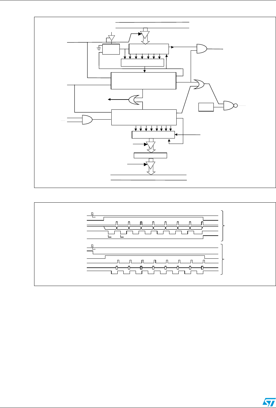
Standard serial interface (UART) UPSD3212A, UPSD3212C, UPSD3212CV
72/181
Figure 26. Serial port Mode 0 block diagram
Figure 27. Serial port Mode 0 waveforms
AI06824
Zero Detector
Internal Bus
Tx Control
Rx Control
Internal Bus
SBUF
Write
to
SBUF
Read
SBUF
Load
SBUF
SBUF
Input Shift Register
Shift
Shift
Clock
Serial
Port
Interrupt
S6
REN
R1
Rx Clock
Start
Tx Clock
Start Shift
Shift
Send
Receive
T
R
CL
DS
Q
7 6 5 4 3 2 1 0
RxD
P3.0 Alt
Input
Function
RxD
P3.0 Alt
Output
Function
TxD
P3.1 Alt
Output
Function
AI06825
Write to SBUF
Send
Shift
RxD (Data Out)
TxD (Shift Clock)
T
Write to SCON
RI
Receive
Shift
RxD (Data In)
TxD (Shift Clock)
S6P2
S3P1 S6P1
Clear RI
Receive
Transmit
D0 D1 D2 D3 D4 D5 D6 D7
D0 D1 D2 D3 D4 D5 D6 D7
Obsolete Product(s) - Obsolete Product(s)
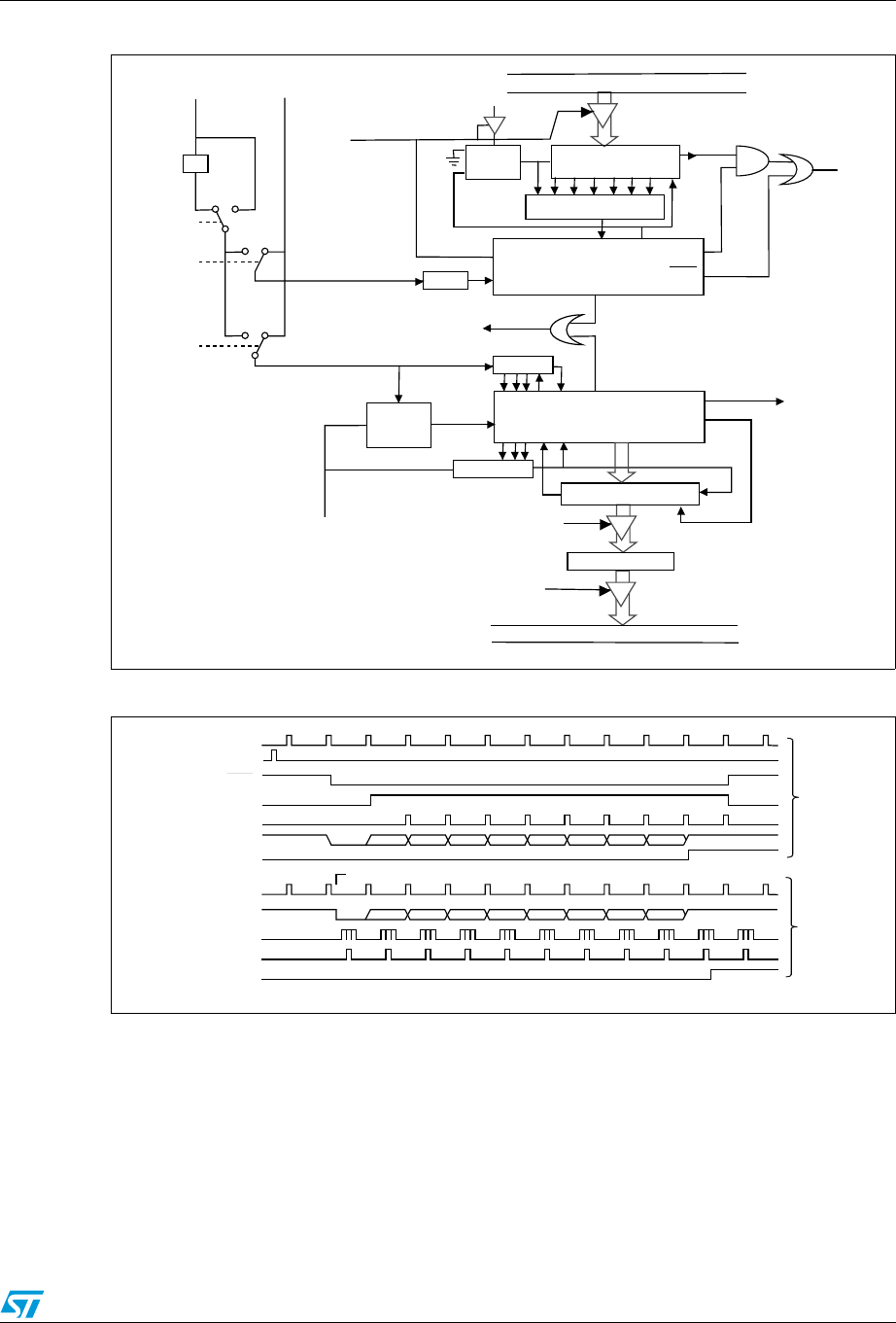
UPSD3212A, UPSD3212C, UPSD3212CV Standard serial interface (UART)
73/181
Figure 28. Serial port Mode 1 block diagram
Figure 29. Serial port Mode 1 waveforms
AI06826
Zero Detector
Internal Bus
Tx Control
Rx Control
Internal Bus
SBUF
Write
to
SBUF
Read
SBUF
Load
SBUF
SBUF
Input Shift Register
Shift
Serial
Port
Interrupt
Rx Clock
Start
Tx Clock
Start Shift
Shift
Send
Load SBUF
TI
RI
CL
DS
Q
1FFh
TxD
Data
Rx Detector
RxD
1-to-0
Transition
Detector
÷16
Sample
÷16
÷2
TB8
Timer1
Overflow
Timer2
Overflow
0
01
1
01
TCLK
RCLK
SMOD
AI06843
Write to SBUF
Data
Shift
TxD
T1
Rx Clock
RxD
Bit Detector
Sample Times
Shift
RI
S1P1
÷16 Reset
Receive
Transmit
D0 D1 D2 D3 D4 D5 D6 D7
Send
Tx Clock
Start Bit
Stop Bit
D0 D1 D2 D3 D4 D5 D6 D7
Start Bit
Stop Bit
Obsolete Product(s) - Obsolete Product(s)
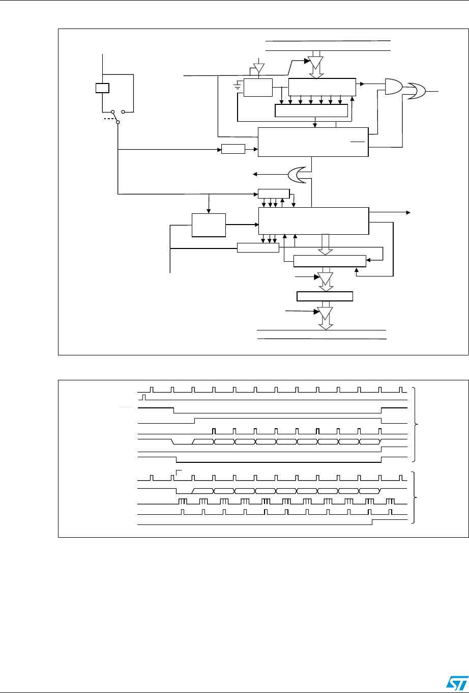
Standard serial interface (UART) UPSD3212A, UPSD3212C, UPSD3212CV
74/181
Figure 30. Serial port Mode 2 block diagram
Figure 31. Serial port Mode 2 waveforms
AI06844
Zero Detector
Internal Bus
Tx Control
Rx Control
Internal Bus
SBUF
Write
to
SBUF
Read
SBUF
Load
SBUF
SBUF
Input Shift Register
Shift
Serial
Port
Interrupt
Rx Clock
Start
Tx Clock
Start Shift
Shift
Send
Load SBUF
TI
RI
CL
DS
Q
1FFh
TxD
Data
Rx Detector
RxD
1-to-0
Transition
Detector
÷16
Sample
÷16
÷2
TB8
Phase2 Clock
1/2*fOSC
01
SMOD
AI06845
Write to SBUF
Data
Shift
TxD
TI
Rx Clock
RxD
Bit Detector
Sample Times
Shift
RI
S1P1
÷16 Reset
Receive
Transmit
D0 D1 D2 D3 D4 D5 D6 D7
Send
Tx Clock
Start Bit
Stop Bit
TB8
D0 D1 D2 D3 D4 D5 D6 D7
Start Bit
Stop Bit
RB8
Stop Bit
Generator
Obsolete Product(s) - Obsolete Product(s)
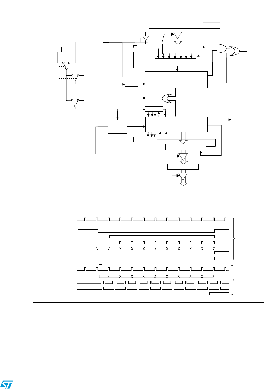
UPSD3212A, UPSD3212C, UPSD3212CV Standard serial interface (UART)
75/181
Figure 32. Serial port Mode 3 block diagram
Figure 33. Serial port Mode 3 waveforms
AI06846
Zero Detector
Internal Bus
Tx Control
Rx Control
Internal Bus
SBUF
Write
to
SBUF
Read
SBUF
Load
SBUF
SBUF
Input Shift Register
Shift
Serial
Port
Interrupt
Rx Clock
Start
Tx Clock
Start Shift
Shift
Send
Load SBUF
TI
RI
CL
DS
Q
1FFh
TxD
Data
Rx Detector
RxD
1-to-0
Transition
Detector
÷16
Sample
÷16
÷2
TB8
Timer1
Overflow
Timer2
Overflow
0
01
1
01
TCLK
RCLK
SMOD
AI06847
Write to SBUF
Data
Shift
TxD
TI
Rx Clock
RxD
Bit Detector
Sample Times
Shift
RI
S1P1
÷16 Reset
Receive
Transmit
D0 D1 D2 D3 D4 D5 D6 D7
Send
Tx Clock
Start Bit
Stop Bit
TB8
D0 D1 D2 D3 D4 D5 D6 D7
Start Bit
Stop Bit
RB8
Stop Bit
Generator
Obsolete Product(s) - Obsolete Product(s)

Analog-to-digital convertor (ADC) UPSD3212A, UPSD3212C, UPSD3212CV
76/181
13 Analog-to-digital convertor (ADC)
The analog to digital (A/D) converter allows conversion of an analog input to a
corresponding 8-bit digital value. The A/D module has four analog inputs, which are
multiplexed into one sample and hold. The output of the sample and hold is the input into the
converter, which generates the result via successive approximation. The analog supply
voltage is connected to AVREF of ladder resistance of A/D module.
The A/D module has two registers which are the control register ACON and A/D result
register ADAT. The register ACON, shown in Ta bl e 4 7 , controls the operation of the A/D
converter module. To use analog inputs, I/O is selected by P1SFS register. Also an 8-bit
prescaler ASCL divides the main system clock input down to approximately 6MHz clock that
is required for the ADC logic. Appropriate values need to be loaded into the prescaler based
upon the main MCU clock frequency prior to use.
The processing of conversion starts when the Start bit ADST is set to '1.' After one cycle, it
is cleared by hardware. The register ADAT contains the results of the A/D conversion. When
conversion is completed, the result is loaded into the ADAT the A/D Conversion Status bit
ADSF is set to '1.'
The block diagram of the A/D module is shown in Figure Figure 34. The A/D Status bit
ADSF is set automatically when A/D conversion is completed, cleared when A/D conversion
is in process.
The ASCL should be loaded with a value that results in a clock rate of approximately 6MHz
for the ADC using the following formula:
ADC clock input = (fOSC / 2) / (Prescaler register value +1)
Where fOSC is the MCU clock input frequency.
The conversion time for the ADC can be calculated as follows:
ADC Conversion Time = 8 clock * 8bits * (ADC Clock) ~= 10.67usec (at 6MHz)
13.1 ADC interrupt
The ADSF Bit in the ACON register is set to '1' when the A/D conversion is complete. The
status bit can be driven by the MCU, or it can be configured to generate a falling edge
interrupt when the conversion is complete.
The ADSF Interrupt is enabled by setting the ADSFINT Bit in the PCON register. Once the
bit is set, the external INT1 Interrupt is disabled and the ADSF Interrupt takes over as INT1.
INT1 must be configured as if it is an edge interrupt input. The INP1 pin (p3.3) is available
for general I/O functions, or Timer1 gate control.
Obsolete Product(s) - Obsolete Product(s)
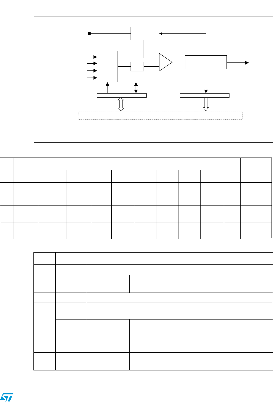
UPSD3212A, UPSD3212C, UPSD3212CV Analog-to-digital convertor (ADC)
77/181
Figure 34. ADC block diagram
AI06627
Input
MUX
ACH0
ACH1
ACH2
ACH3
ACON
INTERNAL BUS
ADAT
AVREF
Ladder
Resistor
D
ecode
S/H
Successive
Approximation
Circuit
Conversion
Complete
Interrupt
Table 46. ADC SFR memory map
SFR
addr
Reg
name
Bit register name Reset
value Comments
76543210
95 ASCL 00
8-bit
Prescaler for
ADC clock
96 ADAT ADAT7 ADAT6 ADAT5 ADAT4 ADAT3 ADAT2 ADAT1 ADAT0 00 ADC Data
Register
97 ACON ADEN ADS1 ADS0 ADST ADSF 00 ADC Control
Register
Table 47. Description of the ACON bits
Bit Symbol Function
7 to 6 — Reserved
5 ADEN ADC Enable Bit: 0 : ADC shut off and consumes no operating current
1 : enable ADC
4—Reserved
3 to 2
ADS1,
ADS0 Analog channel select
0, 0
0, 1
1, 0
1, 1
Channel0 (ACH0)
Channel1 (ACH1)
Channel2 (ACH2)
Channel3 (ACH3)
1 ADST ADC Start bit: 0 : force to zero
1 : start an ADC; after one cycle, bit is cleared to '0'
Obsolete Product(s) - Obsolete Product(s)

Analog-to-digital convertor (ADC) UPSD3212A, UPSD3212C, UPSD3212CV
78/181
0 ADSF ADC Status bit: 0 : A/D conversion is in process
1 : A/D conversion is completed, not in process
Table 48. ADC clock input
MCU clock frequency Prescaler register value ADC clock
40MHz 2 6.7MHz
36MHz 2 6MHz
24MHz 1 6MHz
12MHz 0 6MHz
Table 47. Description of the ACON bits (continued)
Bit Symbol Function
Obsolete Product(s) - Obsolete Product(s)

UPSD3212A, UPSD3212C, UPSD3212CV Pulse width modulation (PWM)
79/181
14 Pulse width modulation (PWM)
The PWM block has the following features:
●Four-channel, 8-bit PWM unit with 16-bit prescaler
●One-channel, 8-bit unit with programmable frequency and pulse width
●PWM Output with programmable polarity
14.1 4-channel PWM unit (PWM 0-3)
The 8-bit counter of a PWM counts module 256 (i.e., from 0 to 255, inclusive). The value
held in the 8-bit counter is compared to the contents of the Special Function Register (PWM
0-3) of the corresponding PWM. The polarity of the PWM outputs is programmable and
selected by the PWML Bit in PWMCON register. Provided the contents of a PWM 0-3
register is greater than the counter value, the corresponding PWM output is set HIGH (with
PWML = 0). When the contents of this register is less than or equal to the counter value, the
corresponding PWM output is set LOW (with PWML = 0). The pulse-width-ratio is therefore
defined by the contents of the corresponding Special Function Register (PWM 0-3) of a
PWM. By loading the corresponding Special Function Register (PWM 0-3) with either 00H
or FFH, the PWM output can be retained at a constant HIGH or LOW level respectively (with
PWML = 0).
For each PWM unit, there is a 16-bit Prescaler that are used to divide the main system clock
to form the input clock for the corresponding PWM unit. This prescaler is used to define the
desired repetition rate for the PWM unit. SFR registers B1h - B2h are used to hold the 16-bit
divisor values.
The repetition frequency of the PWM output is given by:
fPWM8 = (fOSC / prescaler0) / (2 x 256)
And the input clock frequency to the PWM counters is = fOSC / 2 / (prescaler data value + 1)
See Section 7: I/O ports (MCU module) for more information on how to configure the Port 4
pin as PWM output.
Obsolete Product(s) - Obsolete Product(s)
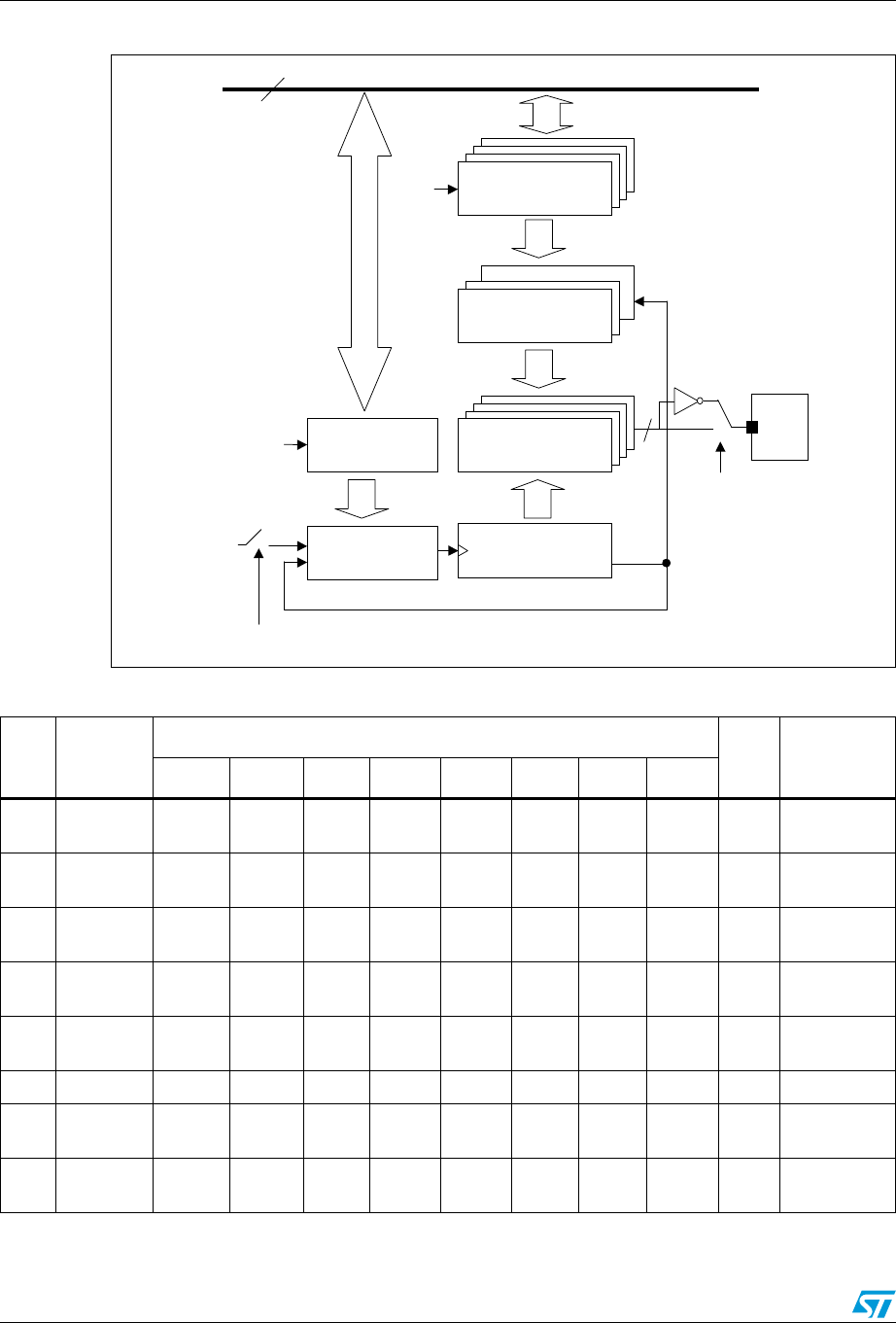
Pulse width modulation (PWM) UPSD3212A, UPSD3212C, UPSD3212CV
80/181
Figure 35. Four-channel 8-bit PWM block diagram
AI06647
8-bit PWM0-PWM3
Comparators Registers
8-bit PWM0-PWM3
Comparators
8 8
8-bit Counter
x 4
8-bit PWM0-PWM3
Data Registers
8
x 4
Port4.3
Port4.4
Port4.5
Port4.6
Overflow
clock
load
16-bit Prescaler
Register
(B2h,B1h)
16
16-bit Prescaler
Counter
fOSC/2
CPU rd/wr
CPU rd/wr
load
PWMCON bit5 (PWME)
PWMCON bit7 (PWML)
4
8
DATA BUS
x 4
8
8
Table 49. PWM SFR memory map
SFR
addr Reg name
Bit register name Reset
value Comments
76543210
A1 PWMCON PWML PWMP PWME CFG4 CFG3 CFG2 CFG1 CFG0 00 PWM Control
Polarity
A2 PWM0 00 PWM0 Output
Duty Cycle
A3 PWM1 00 PWM1 Output
Duty Cycle
A4 PWM2 00 PWM2 Output
Duty Cycle
A5 PWM3 00 PWM3 Output
Duty Cycle
AA PWM4P 00 PWM 4 Period
AB PWM4W 00 PWM 4 Pulse
Width
B1 PSCL0L 00 Prescaler 0
Low (8-bit)
Obsolete Product(s) - Obsolete Product(s)
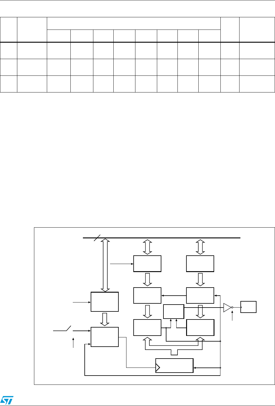
UPSD3212A, UPSD3212C, UPSD3212CV Pulse width modulation (PWM)
81/181
PWMCON register bit definition:
●PWML = PWM 0-3 polarity control
●PWMP = PWM 4 polarity control
●PWME = PWM enable (0 = disabled, 1= enabled)
●CFG3..CFG0 = PWM 0-3 Output (0 = Open Drain; 1 = Push-Pull)
●CFG4 = PWM 4 Output (0 = Open Drain; 1 = Push-Pull)
14.2 Programmable period 8-bit PWM
The PWM 4 channel can be programmed to provide a PWM output with variable pulse width
and period. The PWM 4 has a 16-bit Prescaler, an 8-bit Counter, a Pulse Width Register,
and a Period Register. The Pulse Width Register defines the PWM pulse width time, while
the Period Register defines the period of the PWM. The input clock to the Prescaler is
fOSC/2. The PWM 4 channel is assigned to Port 4.7.
Figure 36. Programmable 4-channel PWM block diagram
B2 PSCL0H 00 Prescaler 0
High (8-bit)
B3 PSCL1L 00 Prescaler 1
Low (8-bit)
B4 PSCL1H 00 Prescaler 1
High (8-bit)
Table 49. PWM SFR memory map (continued)
SFR
addr Reg name
Bit register name Reset
value Comments
76543210
AI07091
Port 4.7
16-bit Prescaler
Register
(B4h, B3h)
16-bit Prescaler
Counter
8-bit Counter
8-bit PWM4P
Register
(Period)
8-bit PWM4
Comparator
Register
8-bit PWM4
Comparator
PWM4
Control
Match
CPU RD/WR
Load
Load
Clock Reset
PWMCON
Bit 6 (PWMP)
DATA BUS
CPU RD/WR
fOSC / 2
PWMCON
Bit 5 (PWME)
8
16
8
8
8
8
8-bit PWM4W
Register
(Width)
8-bit PWM4
Comparator
Register
8-bit PWM4
Comparator
8
88
8
8
Obsolete Product(s) - Obsolete Product(s)
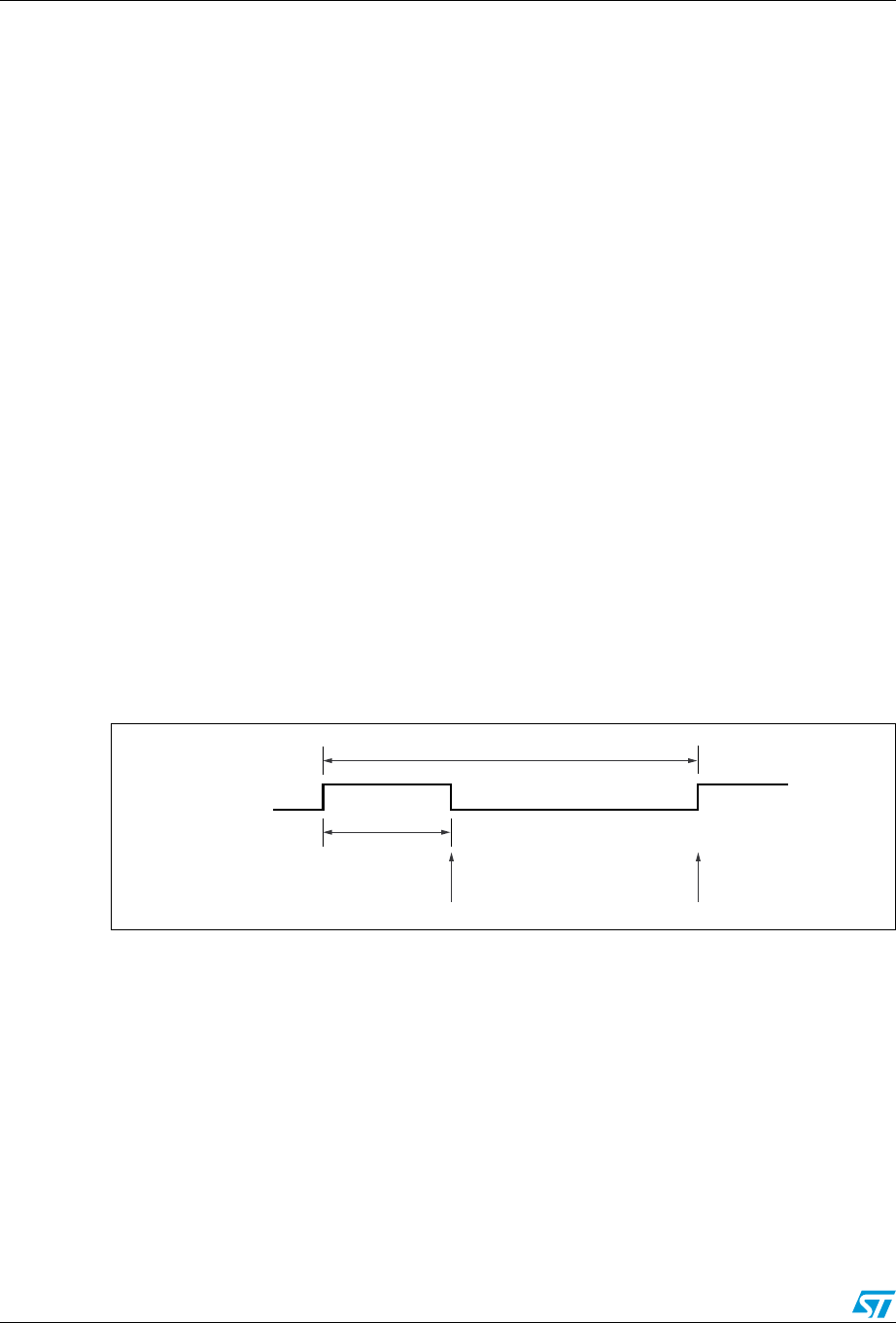
Pulse width modulation (PWM) UPSD3212A, UPSD3212C, UPSD3212CV
82/181
14.3 PWM 4-channel operation
The 16-bit Prescaler1 divides the input clock (fOSC/2) to the desired frequency, the resulting
clock runs the 8-bit Counter of the PWM 4 channel. The input clock frequency to the PWM 4
Counter is:
f PWM4 = (fOSC/2)/(Prescaler1 data value +1)
When the Prescaler1 Register (B4h, B3h) is set to data value '0,' the maximum input clock
frequency to the PWM 4 Counter is fOSC/2 and can be as high as 20MHz.
The PWM 4 Counter is a free-running, 8-bit counter. The output of the counter is compared
to the Compare Registers, which are loaded with data from the Pulse Width Register
(PWM4W, ABh) and the Period Register (PWM4P, AAh). The Pulse Width Register defines
the pulse duration or the Pulse Width, while the Period Register defines the period of the
PWM. When the PWM 4 channel is enabled, the register values are loaded into the
Comparator Registers and are compared to the Counter output. When the content of the
counter is equal to or greater than the value in the Pulse Width Register, it sets the PWM 4
output to low (with PWMP Bit = 0). When the Period Register equals to the PWM4 Counter,
the Counter is cleared, and the PWM 4 channel output is set to logic 'high' level (beginning
of the next PWM pulse).
The Period Register cannot have a value of “00” and its content should always be greater
than the Pulse Width Register.
The Prescaler1 Register, Pulse Width Register, and Period Register can be modified while
the PWM 4 channel is active. The values of these registers are automatically loaded into the
Prescaler Counter and Comparator Registers when the current PWM 4 period ends.
The PWMCON Register (Bits 5 and 6) controls the enable/disable and polarity of the PWM 4
channel.
Figure 37. PWM 4 with programmable pulse width and frequency
AI07090
PWM4
Defined by Pulse
Width Register Switch Level RESET
Counter
Defined by Period Register
Obsolete Product(s) - Obsolete Product(s)
UPSD3212A, UPSD3212C, UPSD3212CV I2C interface
83/181
15 I2C interface
There are two serial I2C ports implemented in the UPSD321xx devices.
The serial port supports the twin line I2C-bus, consists of a data line (SDAx) and a clock line
(SCLx). Depending on the configuration, the SDA and SCL lines may require pull-up
resistors.
●SDA1, SCL1: the serial port line for DDC Protocol
●SDA2, SCL2: the serial port line for general I2C bus connection
In both I2C interfaces, these lines also function as I/O port lines as follows.
●SDA1 / P4.0, SCL1 / P4.1, SDA2 / P3.6, SCL2 / P3.7
The system is unique because data transport, clock generation, address recognition and
bus control arbitration are all controlled by hardware.
The I2C serial I/O has complete autonomy in byte handling and operates in 4 modes.
●Master transmitter
●Master receiver
●Slave transmitter
●Slave receiver
These functions are controlled by the SFRs.
●SxCON: the control of byte handling and the operation of 4 mode.
●SxSTA: the contents of its register may also be used as a vector to various service
routines.
●SxDAT: data shift register.
●SxADR: slave address register. Slave address recognition is performed by On-Chip
H/W.
Figure 38. Block diagram of the I2C bus serial I/O
AI06649
SCLx
SDAx
Bus Clock Generator
Arbitration and Sync. Logic
Shift Register
Status Register
70
Slave Address
70
Control Register
70
70
Internal Bus
Table 50. Serial control register (SxCON: S1CON, S2CON)
76543210
CR2 ENII STA STO ADDR AA CR1 CR0
Obsolete Product(s) - Obsolete Product(s)
I2C interface UPSD3212A, UPSD3212C, UPSD3212CV
84/181
Table 51. Description of the SxCON bits
Bit Symbol Function
7CR2
This bit along with Bits CR1and CR0 determines the serial clock frequency
when SIO is in the Master mode.
6ENII
Enable IIC. When ENI1 = 0, the IIC is disabled. SDA and SCL outputs are
in the high impedance state.
5STA
START flag. When this bit is set, the SIO H/W checks the status of the I2C-
bus and generates a START condition if the bus free. If the bus is busy, the
SIO will generate a repeated START condition when this bit is set.
4STO
STOP flag. With this bit set while in Master mode a STOP condition is
generated.
When a STOP condition is detected on the I2C-bus, the I2C hardware
clears the STO flag.
Note: This bit have to be set before 1 cycle interrupt period of STOP. That
is, if this bit is set, STOP condition in Master mode is generated after 1
cycle interrupt period.
3 ADDR This bit is set when address byte was received. Must be cleared by
software.
2AA
Acknowledge enable signal. If this bit is set, an acknowledge (low level to
SDA) is returned during the acknowledge clock pulse on the SCL line
when:
• Own slave address is received
• A data byte is received while the device is programmed to be a Master
Receiver
• A data byte is received while the device is a selected Slave Receiver.
When this bit is reset, no acknowledge is returned.
SIO release SDA line as high during the acknowledge clock pulse.
1CR1
These two bits along with the CR2 Bit determine the serial clock frequency
when SIO is in the Master mode.
0CR0
Table 52. Selection of the serial clock frequency SCL in Master mode
CR2 CR1 CR0 fOSC
divisor
Bit rate (kHz) at fOSC
12 MHz 24 MHz 36 MHz 40 MHz
0 0 0 16 375 750 X X
0 0 1 24 250 500 750 833
0 1 0 30 200 400 600 666
0 1 1 60 100 200 300 333
1 0 0 120 50 100 150 166
1 0 1 240 25 50 75 83
1 1 0 480 12.5 25 37.5 41
1 1 1 960 6.25 12.5 18.75 20
Obsolete Product(s) - Obsolete Product(s)
UPSD3212A, UPSD3212C, UPSD3212CV I2C interface
85/181
15.1 Serial status register (SxSTA: S1STA, S2STA)
SxSTA is a “Read-only” register. The contents of this register may be used as a vector to a
service routine. This optimized the response time of the software and consequently that of
the I2C-bus. The status codes for all possible modes of the I2C-bus interface are given Table
Ta bl e 5 4 .
This flag is set, and an interrupt is generated, after any of the following events occur.
1. Own slave address has been received during AA = 1: ack_int
2. The general call address has been received while GC(SxADR.0) = 1 and AA = 1:
3. A data byte has been received or transmitted in Master mode (even if arbitration is lost):
ack_int
4. A data byte has been received or transmitted as selected slave: ack_int
5. A stop condition is received as selected slave receiver or transmitter: stop_int
15.2 Data shift register (SxDAT: S1DAT, S2DAT)
SxDAT contains the serial data to be transmitted or data which has just been received. The
MSB (Bit 7) is transmitted or received first; that is, data shifted from right to left.
1. Interrupt Flag bit (INTR, SxSTA Bit 5) is cleared by Hardware as reading SxSTA register.
2. I2C interrupt flag (INTR) can occur in below case. (except DDC2B mode at SWENB=0)
Table 53. Serial status register (SxSTA)
76543210
GC STOP INTR TX_MODE BBUSY BLOST /ACK_REP SLV
Table 54. Description of the SxSTA bits
Bit Symbol Function
7 GC General Call Flag
6 STOP Stop Flag. This bit is set when a STOP condition is received
5INTR
(1,2) Interrupt Flag. This bit is set when an I²C Interrupt condition is requested
4TX_MODE
Transmission mode Flag.
This bit is set when the I²C is a transmitter; otherwise this bit is reset
3BBUSY
Bus Busy Flag.
This bit is set when the bus is being used by another master; otherwise,
this bit is reset
2BLOST
Bus Lost Flag.
This bit is set when the master loses the bus contention; otherwise this bit
is reset
1/ACK_REP
Acknowledge Response Flag.
This bit is set when the receiver transmits the not acknowledge signal
This bit is reset when the receiver transmits the acknowledge signal
0SLV
Slave mode Flag.
This bit is set when the I²C plays role in the Slave mode; otherwise this bit
is reset
Obsolete Product(s) - Obsolete Product(s)
I2C interface UPSD3212A, UPSD3212C, UPSD3212CV
86/181
15.3 Address register (SxADR: S1ADR, S2ADR)
This 8-bit register may be loaded with the 7-bit slave address to which the controller will
respond when programmed as a slave receive/transmitter.
The Start/Stop Hold Time Detection and System Clock registers (Ta bl e 5 7 and Ta bl e 5 8 ) are
included in the I2C unit to specify the start/stop detection time to work with the large range of
MCU frequency values supported. For example, with a system clock of 40MHz.
1. SLA6 to SLA0: Own slave address.
Table 55. Data shift register (SxDAT: S1DAT, S2DAT)
76543210
SxDAT7 SxDAT6 SxDAT5 SxDAT4 SxDAT3 SxDAT2 SxDAT1 SxDAT0
Table 56. Address register (SxADR)
76543210
SLA6 SLA5 SLA4 SLA3 SLA2 SLA1 SLA0 —
Table 57. Start /Stop Hold Time Detection Register (S1SETUP, S2SETUP)
Address Register
Name
Reset
Value Note
SFR
D1h S1SETUP 00h To control the start/stop hold time detection for the
DDC module in Slave mode
D2h S2SETUP 00h To control the start/stop hold time detection for the
multi-master I²C module in Slave mode
Table 58. System clock of 40MHz
S1SETUP,
S2SETUP
Register Value
Number of
Sample Clock
(fOSC/2 -> 50ns)
Required
Start/Stop Hold
Time
Note
00h 1EA 50ns When Bit 7 (enable bit) = 0, the number of
sample clock is 1EA (ignore Bit 6 to Bit 0)
80h 1EA 50ns
81h 2EA 100ns
82h 3EA 150ns
... ... ...
8Bh 12EA 600ns Fast mode I²C Start/Stop hold time
specification
... ... ...
FFh 128EA 6000ns
Obsolete Product(s) - Obsolete Product(s)

UPSD3212A, UPSD3212C, UPSD3212CV I2C interface
87/181
Table 59. System clock setup examples
System Clock
S1SETUP,
S2SETUP
Register Value
Number of
Sample Clock
Required Start/Stop Hold
Time
40MHz (fOSC/2 -> 50ns) 8Bh 12 EA 600ns
30MHz (fOSC/2 -> 66.6ns) 89h 9 EA 600ns
20MHz (fOSC/2 -> 100ns) 86h 6 EA 600ns
8MHz (fOSC/2 -> 250ns) 83h 3 EA 750ns
Obsolete Product(s) - Obsolete Product(s)

USB hardware UPSD3212A, UPSD3212C, UPSD3212CV
88/181
16 USB hardware
The characteristics of USB hardware are as follows:
●Complies with the Universal Serial Bus specification Rev. 1.1
●Integrated SIE (Serial Interface Engine), FIFO memory and transceiver
●Low speed (1.5Mbit/s) device capability
●Supports control endpoint0 and interrupt endpoint1 and 2
●USB clock input must be 6MHz (requires MCU clock frequency to be 12, 24, or
36MHz).
The analog front-end is an on-chip generic USB transceiver. It is designed to allow voltage
levels equal to VDD from the standard logic to interface with the physical layer of the
Universal Serial Bus. It is capable of receiving and transmitting serial data at low speed
(1.5Mb/s).
The SIE is the digital-front-end of the USB block. This module recovers the 1.5MHz clock,
detects the USB sync word and handles all low-level USB protocols and error checking. The
bit-clock recovery circuit recovers the clock from the incoming USB data stream and is able
to track jitter and frequency drift according to the USB specification. The SIE also translates
the electrical USB signals into bytes or signals. Depending upon the device USB address
and the USB endpoint.
Address, the USB data is directed to the correct endpoint on SIE interface. The data transfer
of this H/W could be of type control or interrupt.
The device’s USB address and the enabling of the endpoints are programmable in the SIE
configuration header.
16.1 USB related registers
The USB block is controlled via seven registers in the memory: (UADR, UCON0, UCON1,
UCON2, UISTA, UIEN, and USTA).
Three memory locations on chip which communicate the USB block are:
●USB endpoint0 data transmit register (UDT0)
●USB endpoint0 data receive register (UDR0)
●USB endpoint1 data transmit register (UDT1)
Table 60. USB address register (UADR: 0EEh)
76543210
USBEN UADD6 UADD5 UADD4 UADD3 UADD2 UADD1 UADD0
Obsolete Product(s) - Obsolete Product(s)
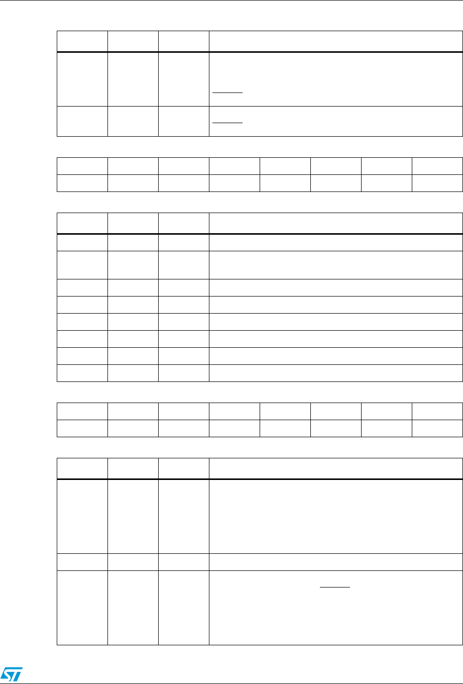
UPSD3212A, UPSD3212C, UPSD3212CV USB hardware
89/181
Table 61. Description of the UADR Bits
Bit Symbol R/W Function
7 USBEN R/W
USB Function Enable Bit.
When USBEN is clear, the USB module will not respond to
any tokens from host.
RESET clears this bit.
6 to 0 UADD6 to
UADD0 R/W Specify the USB address of the device.
RESET clears these bits.
Table 62. USB interrupt enable register (UIEN: 0E9h)
76543210
SUSPNDI RSTE RSTFIE TXD0IE RXD0IE TXD1IE EOPIE RESUMI
Table 63. Description of the UIEN bits
Bit Symbol R/W Function
7 SUSPNDI R/W Enable SUSPND Interrupt
6RSTER/W
Enable USB Reset; also resets the CPU and PSD modules
when bit is set to '1.'
5 RSTFIE R/W Enable RSTF (USB Bus Reset Flag) Interrupt
4 TXD0IE R/W Enable TXD0 Interrupt
3 RXD0IE R/W Enable RXD0 Interrupt
2 TXD1IE R/W Enable TXD1 Interrupt
1 EOPIE R/W Enable EOP Interrupt
0 RESUMI R/W Enable USB Resume Interrupt when it is the Suspend mode
Table 64. USB interrupt status register (UISTA: 0E8h)
76543210
SUSPND — RSTF TXD0F RXD0F TXD1F EOPF RESUMF
Table 65. Description of the UISTA bits
Bit Symbol R/W Function
7 SUSPND R/W
USB Suspend Mode Flag.
To save power, this bit should be set if a 3ms constant idle
state is detected on USB bus. Setting this bit stops the clock to
the USB and causes the USB module to enter Suspend mode.
Software must clear this bit after the Resume flag (RESUMF)
is set while this Resume Interrupt Flag is serviced
6 — — Reserved
5RSTFR
USB Reset Flag.
This bit is set when a valid RESET signal state is detected on
the D+ and D- lines. When the RSTE bit in the UIEN Register
is set, this reset detection will also generate an internal reset
signal to reset the CPU and other peripherals including the
USB module.
Obsolete Product(s) - Obsolete Product(s)
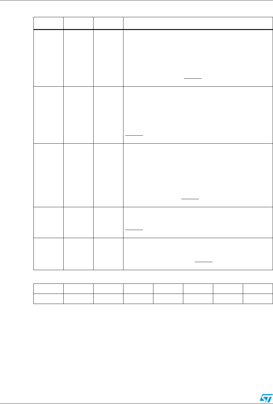
USB hardware UPSD3212A, UPSD3212C, UPSD3212CV
90/181
4TXD0FR/W
Endpoint0 Data Transmit Flag.
This bit is set after the data stored in Endpoint 0 transmit
buffers has been sent and an ACK handshake packet from the
host is received. Once the next set of data is ready in the
transmit buffers, software must clear this flag. To enable the
next data packet transmission, TX0E must also be set. If
TXD0F Bit is not cleared, a NAK handshake will be returned in
the next IN transactions. RESET clears this bit.
3RXD0FR/W
Endpoint0 Data Receive Flag.
This bit is set after the USB module has received a data
packet and responded with ACK handshake packet. Software
must clear this flag after all of the received data has been
read. Software must also set RX0E Bit to one to enable the
next data packet reception. If RXD0F Bit is not cleared, a NAK
handshake will be returned in the next OUT transaction.
RESET clears this bit.
2TXD1FR/W
Endpoint1 / Endpoint2 Data Transmit Flag.
This bit is shared by Endpoints 1 and Endpoints 2. It is set
after the data stored in the shared Endpoint 1/ Endpoint 2
transmit buffer has been sent and an ACK handshake packet
from the host is received. Once the next set of data is ready in
the transmit buffers, software must clear this flag. To enable
the next data packet transmission, TX1E must also be set. If
TXD1F Bit is not cleared, a NAK handshake will be returned in
the next IN transaction. RESET clears this bit.
1 EOPF R/W
End of Packet Flag.
This bit is set when a valid End of Packet sequence is
detected on the D+ and D-line. Software must clear this flag.
RESET clears this bit.
0 RESUMF R/W
Resume Flag.
This bit is set when USB bus activity is detected while the
SUSPND Bit is set.
Software must clear this flag. RESET clears this bit.
Table 66. USB Endpoint0 transmit control register (UCON0: 0EAh)
76543210
TSEQ0 STALL0 TX0E RX0E TP0SIZ3 TP0SIZ2 TP0SIZ1 TP0SIZ0
Table 65. Description of the UISTA bits (continued)
Bit Symbol R/W Function
Obsolete Product(s) - Obsolete Product(s)
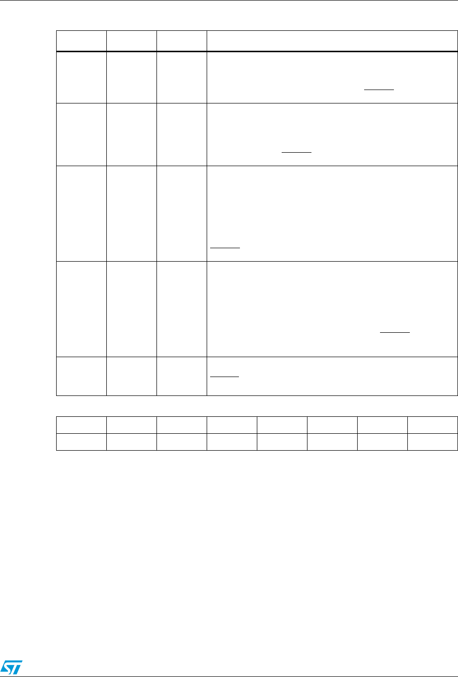
UPSD3212A, UPSD3212C, UPSD3212CV USB hardware
91/181
Table 67. Description of the UCON0 bits
Bit Symbol R/W Function
7 TSEQ0 R/W
Endpoint0 Data Sequence Bit. (0=DATA0, 1=DATA1)
This bit determines which type of data packet (DATA0 or
DATA1) will be sent during the next IN transaction. Toggling of
this bit must be controlled by software. RESET clears this bit
6 STALL0 R/W
Endpoint0 Force Stall Bit.
This bit causes Endpoint 0 to return a STALL handshake when
polled by either an IN or OUT token by the USB Host
Controller. The USB hardware clears this bit when a SETUP
token is received. RESET clears this bit.
5TX0ER/W
Endpoint0 Transmit Enable.
This bit enables a transmit to occur when the USB Host
Controller sends an IN token to Endpoint 0. Software should
set this bit when data is ready to be transmitted. It must be
cleared by software when no more Endpoint 0 data needs to
be transmitted. If this bit is '0' or the TXD0F is set, the USB will
respond with a NAK handshake to any Endpoint 0 IN tokens.
RESET clears this bit.
4RX0ER/W
Endpoint0 receive enable.
This bit enables a receive to occur when the USB Host
Controller sends an OUT token to Endpoint 0. Software should
set this bit when data is ready to be received. It must be
cleared by software when data cannot be received. If this bit is
'0' or the RXD0F is set, the USB will respond with a NAK
handshake to any Endpoint 0 OUT tokens. RESET clears this
bit.
3 to 0
TP0SIZ3
to
TP0SIZ0
R/W The number of transmit data bytes. These bits are cleared by
RESET
.
Table 68. USB Endpoint1 (and 2) transmit control register (UCON1: 0EBh)
76543210
TSEQ1 EP12SEL TX1E FRESUM TP1SIZ3 TP1SIZ2 TP1SIZ1 TP1SIZ0
Obsolete Product(s) - Obsolete Product(s)
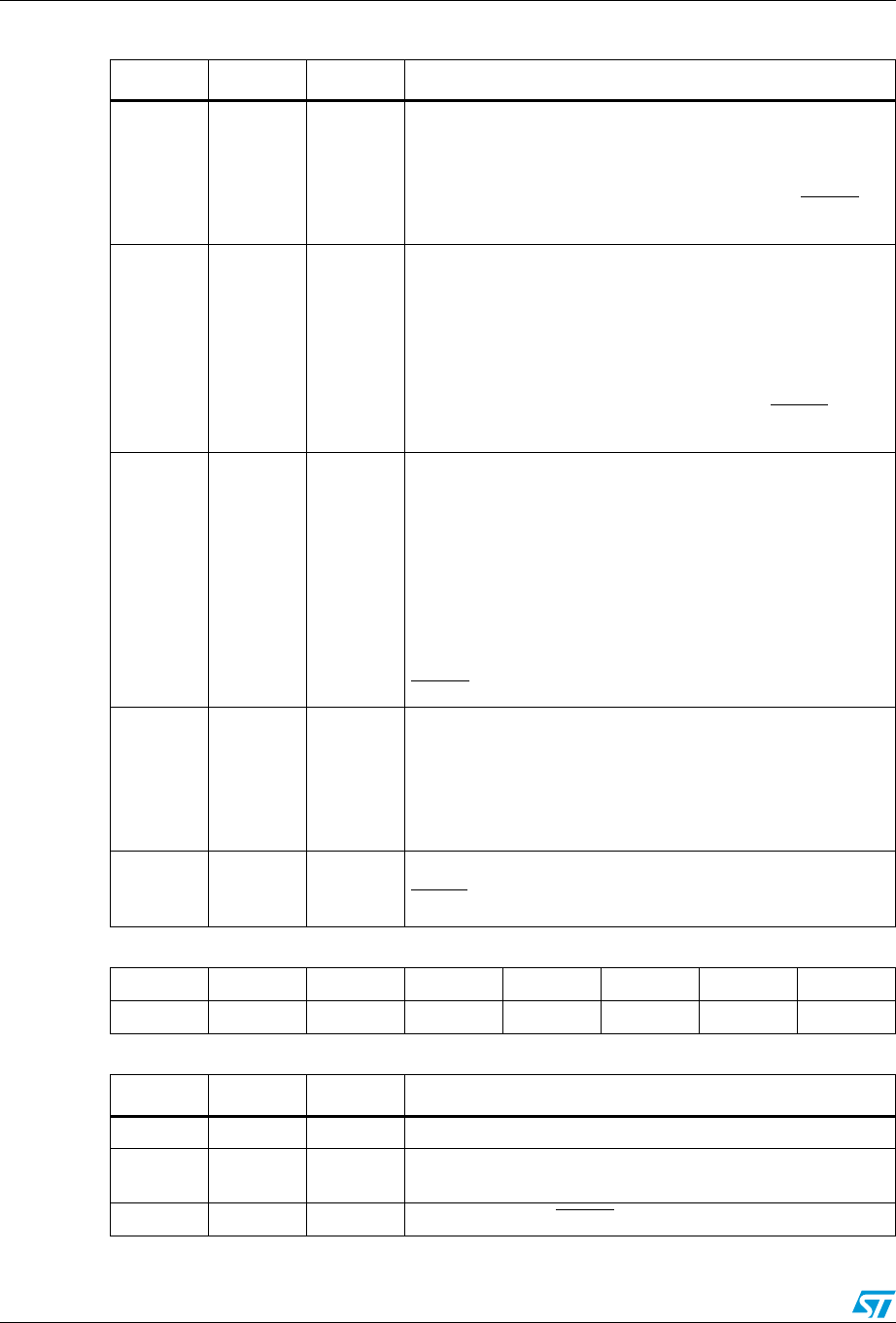
USB hardware UPSD3212A, UPSD3212C, UPSD3212CV
92/181
Table 69. Description of the UCON1 bits
Bit Symbol R/W Function
7 TSEQ1 R/W
Endpoint 1/ Endpoint 2 Transmit Data Packet PID. (0=DATA0,
1=DATA1) This bit determines which type of data packet
(DATA0 or DATA1) will be sent during the next IN transaction
directed to Endpoint 1 or Endpoint 2.
Toggling of this bit must be controlled by software. RESET
clears this bit.
6 EP12SEL R/W
Endpoint 1/ Endpoint 2 Transmit Selection. (0=Endpoint 1,
1=Endpoint 2)
This bit specifies whether the data inside the registers UDT1
are used for Endpoint 1 or Endpoint 2. If all the conditions for a
successful Endpoint 2 USB response to a hosts IN token are
satisfied (TXD1F=0, TX1E=1, STALL2=0, and EP2E=1)
except that the EP12SEL Bit is configured for Endpoint 1, the
USB responds with a NAK handshake packet. RESET clears
this bit.
5TX1ER/W
Endpoint1 / Endpoint2 Transmit Enable.
This bit enables a transmit to occur when the USB Host
Controller send an IN token to Endpoint 1 or Endpoint 2. The
appropriate endpoint enable bit, EP1E or EP2E Bit in the
UCON2 register, should also be set. Software should set the
TX1E Bit when data is ready to be transmitted. It must be
cleared by software when no more data needs to be
transmitted. If this bit is '0' or TXD1F is set, the USB will
respond with a NAK handshake to any Endpoint 1 or Endpoint
2 directed IN token.
RESET clears this bit.
4FRESUMR/W
Force Resume.
This bit forces a resume state (“K” on non-idle state) on the
USB data lines to initiate a remote wake-up. Software should
control the timing of the forced resume to be between 10ms
and 15ms. Setting this bit will not cause the RESUMF Bit to
set.
3 to 0
TP1SIZ3
to
TP1SIZ0
R/W The number of transmit data bytes. These bits are cleared by
RESET.
Table 70. USB control register (UCON2: 0ECh)
76543210
— — — SOUT EP2E EP1E STALL2 STALL1
Table 71. Description of the UCON2 bits
Bit Symbol R/W Function
7 to 5 — — Reserved
4 SOUT R/W Status out is used to automatically respond to the OUT of a
control READ transfer
3 EP2E R/W Endpoint2 enable. RESET clears this bit
Obsolete Product(s) - Obsolete Product(s)
UPSD3212A, UPSD3212C, UPSD3212CV USB hardware
93/181
The USCL 8-bit prescaler register for USB is at E1h. The USCL should be loaded with a
value that results in a clock rate of 6 MHz for the USB using the following formula:
USB clock input = (fOSC / 2) / (Prescaler register value +1)
Where fOSC is the MCU clock input frequency.
Note: USB works ONLY with the MCU Clock frequencies of 12, 24, or 36 MHz. The Prescaler
values for these frequencies are 0, 1, and 2.
2 EP1E R/W Endpoint1 enable. RESET clears this bit
1 STALL2 R/W Endpoint2 Force Stall Bit. RESET clears this bit
0 STALL1 R/W Endpoint1 Force Stall Bit. RESET clears this bit
Table 72. USB Endpoint0 status register (USTA: 0EDh)
76543210
RSEQ SETUP IN OUT RP0SIZ3 RP0SIZ2 RP0SIZ1 RP0SIZ0
Table 73. Description of the USTA bits
Bit Symbol R/W Function
7 RSEQ R/W
Endpoint0 receive data packet PID. (0=DATA0, 1=DATA1)
This bit will be compared with the type of data packet last
received for Endpoint0
6 SETUP R SETUP Token Detect Bit. This bit is set when the received
token packet is a SEPUP token, PID = b1101.
5INR
IN Token Detect Bit.
This bit is set when the received token packet is an IN token.
4OUTR
OUT Token Detect Bit.
This bit is set when the received token packet is an OUT
token.
3 to 0
RP0SIZ3
to
RP0SIZ0
R The number of data bytes received in a DATA packet
Table 74. USB Endpoint0 data receive register (UDR0: 0EFh)
76543210
UDR0.7 UDR0.6 UDR0.5 UDR0.4 UDR0.3 UDR0.2 UDR0.1 UDR0.0
Table 75. USB Endpoint0 data transmit register (UDT0: 0E7h)
76543210
UDT0.7 UDT0.6 UDT0.5 UDT0.4 UDT0.3 UDT0.2 UDT0.1 UDT0.0
Table 76. USB Endpoint1 data transmit register (UDT1: 0E6h)
76543210
UDT1.7 UDT1.6 UDT1.5 UDT1.4 UDT1.3 UDT1.2 UDT1.1 UDT1.0
Table 71. Description of the UCON2 bits (continued)
Bit Symbol R/W Function
Obsolete Product(s) - Obsolete Product(s)

USB hardware UPSD3212A, UPSD3212C, UPSD3212CV
94/181
16.2 Transceiver
16.2.1 USB physical layer characteristics
The following section describes the UPSD321xx devices compliance to the Chapter 7
Electrical section of the USB Specification, Revision 1.1. The section contains all signaling,
and physical layer specifications necessary to describe a low speed USB function.
Table 77. USB SFR memory map
SFR
Add
r
Reg
Name
Bit Register Name Reset
value Comments
7 6543210
E1 USCL 00
8-bit
Prescaler
for USB
logic
E6 UDT1 UDT1.7 UDT1.6 UDT1.5 UDT1.4 UDT1.3 UDT1.2 UDT1.1 UDT1.0 00
USB
Endpt1
Data Xmit
E7 UDT0 UDT0.7 UDT0.6 UDT0.5 UDT0.4 UDT0.3 UDT0.2 UDT0.1 UDT0.0 00
USB
Endpt0
Data Xmit
E8 UISTA SUSPND — RSTF TXD0F RXD0F RXD1F EOPF RESUMF 00
USB
Interrupt
Status
E9 UIEN SUSPNDI
ERSTE RSTFIE TXD0IE RXD0IE TXD1IE EOPIE RESUMI
E00
USB
Interrupt
Enable
EA UCON0 TSEQ0 STALL0 TX0E RX0E TP0SIZ3 TP0SIZ2 TP0SIZ1 TP0SIZ0 00
USB
Endpt0
Xmit
Control
EB UCON1 TSEQ1 EP12SE
L—FRESU
MTP1SIZ3 TP1SIZ2 TP1SIZ1 TP1SIZ0 00
USB
Endpt1
Xmit
Control
EC UCON2 — — — SOUT EP2E EP1E STALL2 STALL1 00
USB
Control
Register
ED USTA RSEQ SETUP IN OUT RP0SIZ3 RP0SIZ2 RP0SIZ1 RP0SIZ0 00
USB
Endpt0
Status
EE UADR USBEN UADD6 UADD5 UADD4 UADD3 UADD2 UADD1 UADD0 00
USB
Address
Register
EF UDR0 UDR0.7 UDR0.6 UDR0.5 UDR0.4 UDR0.3 UDR0.2 UDR0.1 UDR0.0 00
USB
Endpt0
Data Recv
Obsolete Product(s) - Obsolete Product(s)
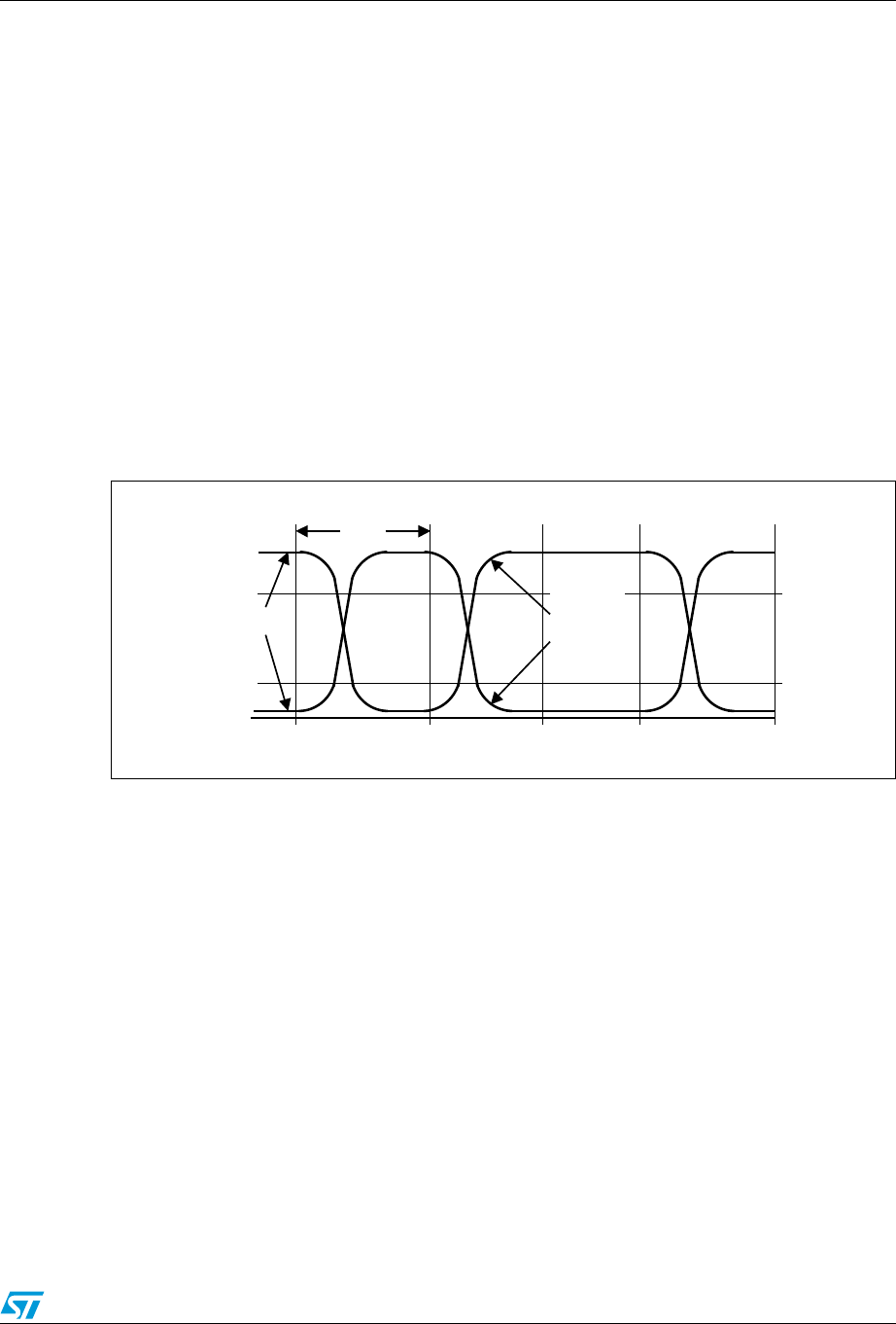
UPSD3212A, UPSD3212C, UPSD3212CV USB hardware
95/181
16.2.2 Low speed driver characteristics
The UPSD321xx devices use a differential output driver to drive the Low Speed USB data
signal onto the USB cable. The output swings between the differential high and low state are
well balanced to minimize signal skew. The slew rate control on the driver minimizes the
radiated noise and cross talk on the USB cable. The driver’s outputs support three-state
operation to achieve bi-directional half duplex operation. The UPSD321xx devices driver
tolerates a voltage on the signal pins of -0.5 V to 3.6 V with respect to local ground
reference without damage. The driver tolerates this voltage for 10.0µs while the driver is
active and driving, and tolerates this condition indefinitely when the driver is in its high
impedance state.
A low speed USB connection is made through an unshielded, untwisted wire cable a
maximum of 3 meters in length. The rise and fall time of the signals on this cable are well
controlled to reduce RFI emissions while limiting delays, signaling skews and distortions.
The UPSD321xx devices driver reaches the specified static signal levels with smooth rise
and fall times, resulting in segments between low speed devices and the ports to which they
are connected.
Figure 39. Low speed driver signal waveforms
16.3 Receiver characteristics
UPSD321xx devices have a differential input receiver which is able to accept the USB data
signal. The receiver features an input sensitivity of at least 200 mV when both differential
data inputs are in the range of at least 0.8 V to 2.5 V with respect to its local ground
reference. This is the common mode range, as shown in Figure 40. The receiver tolerates
static input voltages between -0.5 V to 3.8 V with respect to its local ground reference
without damage. In addition to the differential receiver, there is a single-ended receiver for
each of the two data lines. The single-ended receivers have a switching threshold between
0.8 V and 2.0 V (TTL inputs).
AI06629
Signal pins
pass output
spec levels
with minimal
reflections and
ringing
One Bit
Time
1.5 Mb/s
VSS
Driver
Signal Pins
VSE(min)
VSE(max)
Obsolete Product(s) - Obsolete Product(s)
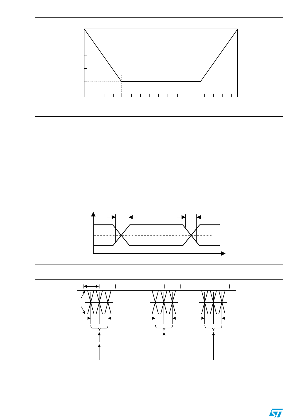
USB hardware UPSD3212A, UPSD3212C, UPSD3212CV
96/181
Figure 40. Differential input sensitivity over entire common mode range
16.4 External USB pull-up resistor
The USB system specifies a pull-up resistor on the D- pin for low-speed peripherals. The
USB Spec 1.1 describes a 1.5 kΩ pull-up resistor to a 3.3 V supply. An approved alternative
method is a 7.5 kΩ pull-up to the USB VCC supply. This alternative is defined for low-speed
devices with an integrated cable. The chip is specified for the 7.5 kΩ pull-up. This eliminates
the need for an external 3.3 V regulator, or for a pin dedicated to providing a 3.3 V output
from the chip.
Figure 41. USB data signal timing and voltage levels
Figure 42. Receiver jitter tolerance
AI06630
0.0
0.0
0.2
0.4
0.6
1.0
0.8
0.2 0.4 0.6 0.8 1.0 1.2 1.4 1.6 1.8 2.0 2.2 2.4 2.6 2.8 3.0 3.2
Common Mode Input Voltage (volts)
Minimum Differential Sensitivity (volts)
AI06631
VCR
D-
D+
tRtF
10%
90% 90%
10%
VOH
VOL
AI06632
T
JR
T
JR1
T
JR2
Consecutive
Transitions
N*T
PERIOD
+T
JR1
T
PERIOD
Paired
Transitions
N*T
PERIOD
+T
JR2
Differential
Data Lines
Obsolete Product(s) - Obsolete Product(s)
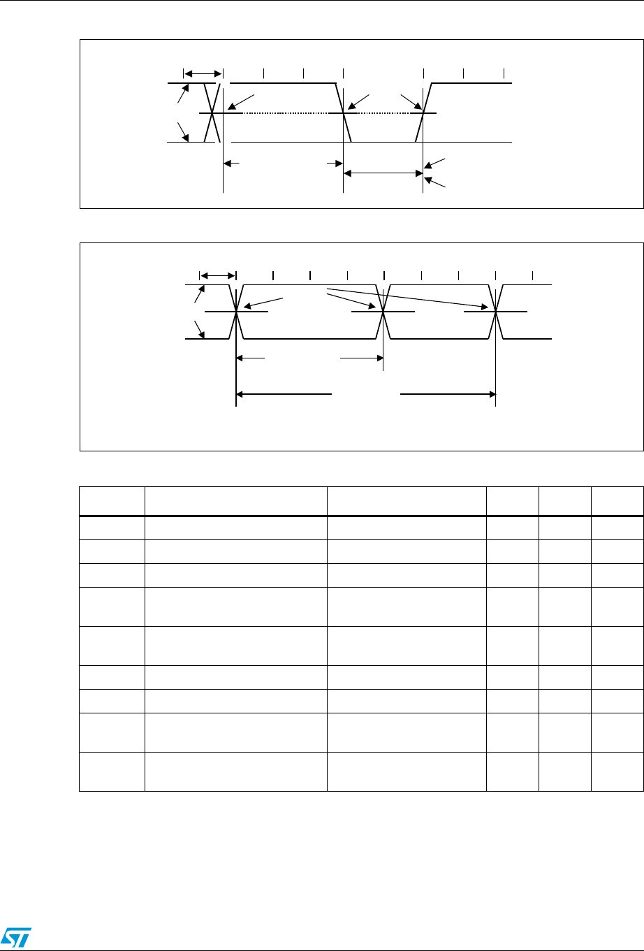
UPSD3212A, UPSD3212C, UPSD3212CV USB hardware
97/181
Figure 43. Differential to EOP transition skew and EOP width
Figure 44. Differential data jitter
1. VCC = 5 V ± 10%; VSS = 0 V; TA = 0 to 70°C.
2. Level guaranteed for range of VCC = 4.5 V to 5.5 V.
3. With RPU, external idle resistor, 7.5 κ±2%, D- to VCC.
Table 78. Transceiver DC characteristics
Symb Parameter Test Conditions(1) Min Max Unit
VOH Static Output High 15 kΩ ± 5% to GND(2,3) 2.8 3.6 V
VOL Static Output Low Notes 2, 3 — 0.3 V
VDI Differential Input Sensitivity |(D+) - (D-)|, Figure 42 0.2 — V
VCM
Differential Input Common
mode Figure 42 0.8 2.5 V
VSE
Single Ended Receiver
Threshold —0.82.0V
CIN Transceiver Capacitance — — 20 pF
IIO Data Line (D+, D-) Leakage 0 < (D+,D-) < 3.3 –10 10 µA
RPU
External Bus Pull-up
Resistance, D- 7.5 kΩ ± 2% to VCC 7.35 7.65 kΩ
RPD
External Bus Pull-down
Resistance 15 kΩ ± 5% 14.25 15.75 kΩ
Receiver EOP Width
T
EOPR1
, T
EOPR2
Differential
Data Lines
Source EOP Width: T
EOPT
Crossover
Point
Crossover
Point Extended
Diff. Data to
SE0 Skew
N*T
PERIOD
+T
DEOP
T
PERIOD
AI06634
Consecutive
Transitions
N*T
PERIOD
+T
xJR1
T
PERIOD
Crossover
Points
Paired
Transitions
N*T
PERIOD
+T
xJR2
Differential
Data Lines
Obsolete Product(s) - Obsolete Product(s)
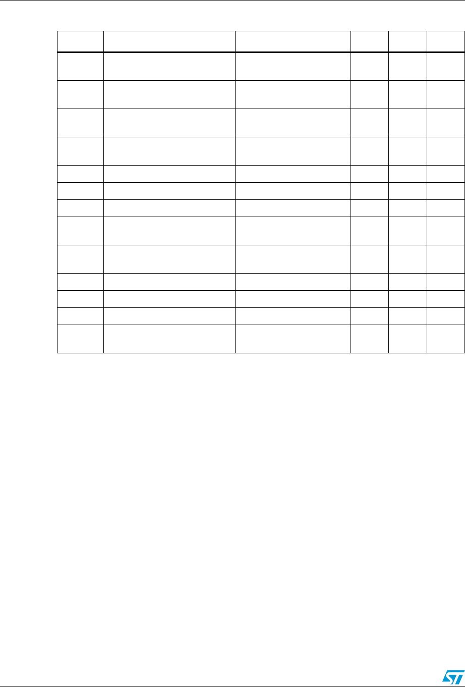
USB hardware UPSD3212A, UPSD3212C, UPSD3212CV
98/181
1. VCC = 5 V ± 10%; VSS = 0 V; TA = 0 to 70°C.
2. Level guaranteed for range of VCC = 4.5 V to 5.5 V.
3. With RPU, external idle resistor, 7.5κ±2%, D- to VCC.
4. CL of 50 pF (75 ns) to 350 pF (300 ns).
5. Measured at crossover point of differential data signals.
6. USB specification indicates 330 ns.
Table 79. Transceiver AC characteristics
Symb Parameter Test Conditions(1) Min Max Unit
tDRATE Low Speed Data Rate Ave. bit rate (1.5Mb/s ±
1.5%) 1.4775 1.5225 Mbit/s
tDJR1 Receiver Data Jitter Tolerance To next transition,
Figure 42(5) –75 75 ns
tDJR2 Differential Input Sensitivity For paired transition,
Figure 42(5) –45 45 ns
tDEOP Differential to EOP Transition
Skew Figure 43(5) –40 100 ns
tEOPR1 EOP Width at Receiver Rejects as EOP(5,6) 165 — ns
tEOPR2 EOP Width at Receiver Accepts as EOP(5) 675 — ns
tEOPT Source EOP Width — –1.25 1.50 µs
tUDJ1 Differential Driver Jitter To next transition,
Figure 44 –95 95 ns
tUDJ2 Differential Driver Jitter To paired transition,
Figure 44 –150 150 ns
tR USB Data Transition Rise Time Notes 2, 3, 4 75 300 ns
tF USB Data Transition Fall Time Notes 2, 3, 4 75 300 ns
tRFM Rise/Fall Time Matching tR / tF80 120 %
VCRS
Output Signal Crossover
Voltage —1.32.0V
Obsolete Product(s) - Obsolete Product(s)

UPSD3212A, UPSD3212C, UPSD3212CV PSD module
99/181
17 PSD module
The PSD module provides configurable Program and Data memories to the 8032 CPU core
(MCU). In addition, it has its own set of I/O ports and a PLD with 16 macrocells for general
logic implementation.
Ports A,B,C, and D are general purpose programmable I/O ports that have a port
architecture which is different from the I/O ports in the MCU module.
The PSD module communicates with the MCU module through the internal address, data
bus (A0-A15, D0-D7) and control signals (RD, WR, PSEN, ALE, RESET). The user defines
the Decoding PLD in the PSDsoft Development Tool and can map the resources in the PSD
module to any program or data address space. Figure 45 shows the functional blocks in the
PSD module.
17.1 Functional overview
●512 Kbit Flash memory. This is the main Flash memory. It is divided into four equal-
sized blocks (16 Kbytes each) that can be accessed with user-specified addresses.
●Secondary 128 Kbit Flash boot memory. It is divided into two equal-sized blocks (8
Kbytes each) thatat can be accessed with user-specified addresses. This secondary
memory brings the ability to execute code and update the main Flash concurrently.
●16 Kbit SRAM.
●CPLD with 16 Output Micro Cells (OMCs} and up to 20 Input Micro Cells (IMCs). The
CPLD may be used to efficiently implement a variety of logic functions for internal and
external control. Examples include state machines, loadable shift registers, and
loadable counters.
●Decode PLD (DPLD) that decodes address for selection of memory blocks in the PSD
module.
●Configurable I/O ports (Port A,B,C and D) that can be used for the following functions:
– MCU I/Os
– PLD I/Os
– Latched MCU address output
– Special function I/Os
– I/O ports may be configured as open-drain outputs
●Built-in JTAG compliant serial port allows full-chip In-System Programmability (ISP).
With it, you can program a blank device or reprogram a device in the factory or the field.
●Internal page register that can be used to expand the 8032 MCU module address
space by a factor of 256.
●Internal programmable Power Management Unit (PMU) that supports a low-power
mode called Power-down mode. The PMU can automatically detect a lack of the 8032
CPU core activity and put the PSD module into Power-down mode.
●Erase/WRITE cycles:
Flash memory - 100,000 minimum
PLD - 1,000 minimum
Data Retention: 15 year minimum (for Main Flash memory, Boot, PLD and
Configuration bits)
Obsolete Product(s) - Obsolete Product(s)
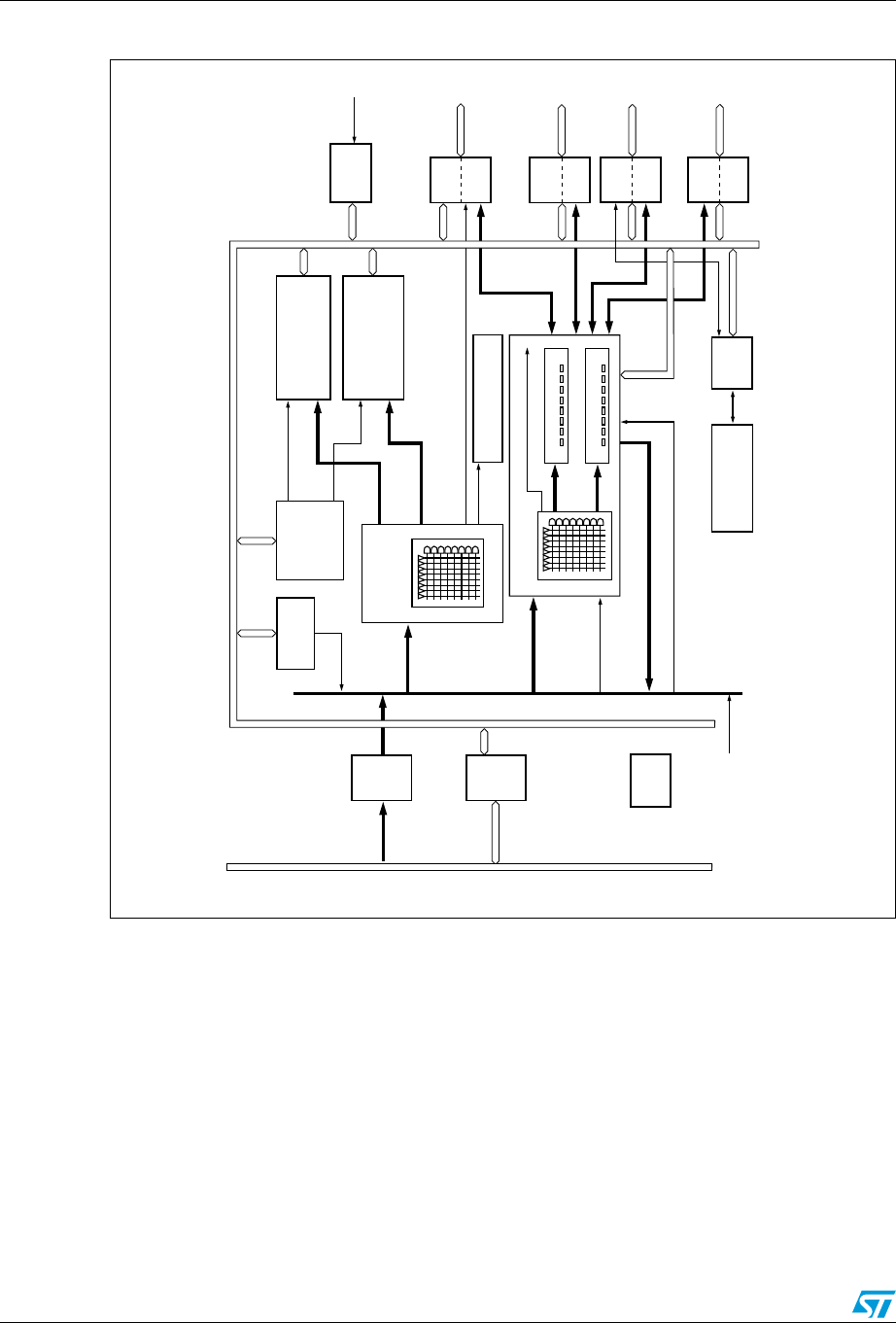
PSD module UPSD3212A, UPSD3212C, UPSD3212CV
100/181
17.2 In-system programming (ISP)
Using the JTAG signals on Port C, the entire PSD module device can be programmed or
erased without the use of the MCU. The primary Flash memory can also be programmed in-
system by the MCU executing the programming algorithms out of the secondary memory, or
SRAM. The secondary memory can be programmed the same way by executing out of the
primary Flash memory. The PLD or other PSD module configuration blocks can be
programmed through the JTAG port or a device programmer. Table Ta b l e 8 0 indicates which
programming methods can program different functional blocks of the PSD module.
Figure 45. UPSD321xx PSD module block diagram
BUS
Interface
WR_, RD_,
PSEN_, ALE,
RESET_,
A0-A15
D0 – D7
CLKIN
(PD1)
CLKIN
CLKIN
PLD
INPUT
BUS
PROG.
PORT
PORT
A
PROG.
PORT
PORT
B
POWER
MANGMT
UNIT
512KBIT PRIMARY
FLASH MEMORY
8 SECTORS
VSTDBY
PA0 – PA7
PB0 – PB7
PROG.
PORT
PORT
C
PROG.
PORT
PORT
D
PC0 – PC7
PD1 – PD2
ADDRESS/DATA/CONTROL BUS
PORT A ,B & C
2 EXT CS TO PORT D
20 INPUT MACROCELLS
PORT A ,B & C
73
73
128KBIT SECONDARY
NON-VOLATILE MEMORY
(BOOT OR DATA)
2 SECTORS
RUNTIME CONTROL
AND I/O REGISTERS
PERIP I/O MODE SELECTS
MACROCELL FEEDBACK OR PORT INPUT
CSIOP
FLASH ISP CPLD
(CPLD) 16 OUTPUT MACROCELLS
FLASH DECODE
PLD (DPLD)
PLD, CONFIGURATION
& FLASH MEMORY
LOADER
JTAG
SERIAL
CHANNEL
(PC2)
PAGE
REGISTER EMBEDDED
ALGORITHM
SECTOR
SELECTS
SECTOR
SELECTS
GLOBAL
CONFIG. &
SECURITY
AI07431
8
BUS
Interface
8032 Bus
Obsolete Product(s) - Obsolete Product(s)

UPSD3212A, UPSD3212C, UPSD3212CV PSD module
101/181
Table 80. Methods of programming different functional blocks of the PSD module
Functional Block JTAG programming Device programmer IAP
Primary Flash memory Yes Yes Yes
Secondary Flash memory Yes Yes Yes
PLD array (DPLD and CPLD) Yes Yes No
PSD module configuration Yes Yes No
Obsolete Product(s) - Obsolete Product(s)
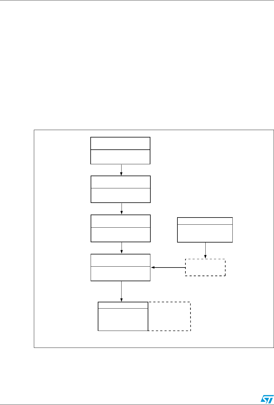
Development system UPSD3212A, UPSD3212C, UPSD3212CV
102/181
18 Development system
UPSD321xx devices are supported by PSDsoft, a Windows-based software development
tool (Windows-95, Windows-98, Windows-NT). A PSD module design is quickly and easily
produced in a point and click environment. The designer does not need to enter Hardware
Description Language (HDL) equations, unless desired, to define PSD module pin functions
and memory map information. The general design flow is shown in Figure 46. PSDsoft is
available from our web site (the address is given on the back page of this data sheet) or
other distribution channels.
PSDsoft directly supports a low cost device programmer from ST: FlashLINK (JTAG). The
programmer may be purchased through your local distributor/representative. UPSD321xx
devices are also supported by third party device programmers. See our web site for the
current list.
Figure 46. PSDsoft express development tool
Merge MCU Firmware with
PSD Module Configuration
PSD Programmer
*.OBJ FILE
FlashLINK (JTAG)
A composite object file is created
containing MCU firmware and
PSD configuration
C Code Generation
GENERATE C CODE
SPECIFIC TO PSD
FUNCTIONS
USER'S CHOICE OF
8032
COMPILER/LINKER
*.OBJ FILE
AVAILABLE
FOR 3rd PARTY
PROGRAMMERS
MCU FIRMWARE
HEX OR S-RECORD
FORMAT
AI05798
Define General Purpose
Logic in CPLD
Point and click definition of combin-
atorial and registered logic in CPLD.
Access HDL is available if needed
Define µPSD Pin and
Node Functions
Point and click definition of
PSD pin functions, internal nodes,
and MCU system memory map
Choose µPSD
Obsolete Product(s) - Obsolete Product(s)

UPSD3212A, UPSD3212C, UPSD3212CV PSD module register description and address offset
103/181
19 PSD module register description and address offset
Ta bl e 8 1 shows the offset addresses to the PSD module registers relative to the CSIOP
base address. The CSIOP space is the 256 bytes of address that is allocated by the user to
the internal PSD module registers. Ta b le 8 1 provides brief descriptions of the registers in
CSIOP space. The following section gives a more detailed description.
1. Other registers that are not part of the I/O ports.
Table 81. Register address offset
Register Name Port A Port B Port C Port D Other(1) Description
Data In 00 01 10 11 Reads Port pin as input, MCU I/O Input
mode
Control 02 03 Selects mode between MCU I/O or
Address Out
Data Out 04 05 12 13 Stores data for output to Port pins,
MCU I/O Output mode
Direction 06 07 14 15 Configures Port pin as input or output
Drive Select 08 09 16 17
Configures Port pins as either CMOS
or Open Drain on some pins, while
selecting high slew rate on other pins.
Input Macrocell 0A 0B 18 Reads Input Macrocells
Enable Out 0C 0D 1A 1B Reads the status of the output enable
to the I/O Port driver
Output Macrocells
AB 20 20 READ – reads output of macrocells AB
WRITE – loads macrocell flip-flops
Output Macrocells
BC 21 21 READ – reads output of macrocells BC
WRITE – loads macrocell flip-flops
Mask Macrocells
AB 22 22 Blocks writing to the Output Macrocells
AB
Mask Macrocells
BC 23 23 Blocks writing to the Output Macrocells
BC
Primary Flash
Protection C0 Read-only – Primary Flash Sector
Protection
Secondary Flash
memory
Protection
C2
Read-only – PSD module Security and
Secondary Flash memory Sector
Protection
PMMR0 B0 Power Management Register 0
PMMR2 B4 Power Management Register 2
Page E0 Page Register
VM E2
Places PSD module memory areas in
Program and/or Data space on an
individual basis.
Obsolete Product(s) - Obsolete Product(s)

PSD module detailed operation UPSD3212A, UPSD3212C, UPSD3212CV
104/181
20 PSD module detailed operation
As shown in Figure 14, the PSD module consists of five major types of functional blocks:
●Memory blocks
●PLD blocks
●I/O Ports
●Power Management Unit (PMU)
●JTAG Interface
The functions of each block are described in the following sections. Many of the blocks
perform multiple functions, and are user configurable.
Obsolete Product(s) - Obsolete Product(s)

UPSD3212A, UPSD3212C, UPSD3212CV Memory blocks
105/181
21 Memory blocks
The PSD module has the following memory blocks:
●Primary Flash memory
●Secondary Flash memory
●SRAM
The Memory Select signals for these blocks originate from the Decode PLD (DPLD) and are
user-defined in PSDsoft Express.
21.1 Primary Flash memory and secondary Flash memory
description
The primary Flash memory is divided evenly into four equal sectors. The secondary Flash
memory is divided into two equal sectors. Each sector of either memory block can be
separately protected from Program and Erase cycles.
Flash memory may be erased on a sector-by-sector basis. Flash sector erasure may be
suspended while data is read from other sectors of the block and then resumed after
reading.
During a Program or Erase cycle in Flash memory, the status can be output on Ready/Busy
(PC3). This pin is set up using PSDsoft Express Configuration.
21.2 Memory block select signals
The DPLD generates the Select signals for all the internal memory blocks (see Section 22:
PLDs). Each of the four sectors of the primary Flash memory has a Select signal (FS0-FS3)
which can contain up to three product terms. Each of the two sectors of the secondary Flash
memory has a Select signal (CSBOOT0-CSBOOT1) which can contain up to three product
terms. Having three product terms for each Select signal allows a given sector to be
mapped in Program or Data space.
21.2.1 Ready/Busy (PC3)
This signal can be used to output the Ready/Busy status of the Flash memory. The output
on Ready/Busy (PC3) is a '0' (Busy) when Flash memory is being written to, or when Flash
memory is being erased. The output is a '1' (Ready) when no WRITE or Erase cycle is in
progress.
21.2.2 Memory operation
The primary Flash memory and secondary Flash memory are addressed through the MCU
Bus. The MCU can access these memories in one of two ways:
●The MCU can execute a typical bus WRITE or READ operation.
●The MCU can execute a specific Flash memory instruction that consists of several
WRITE and READ operations. This involves writing specific data patterns to special
addresses within the Flash memory to invoke an embedded algorithm. These
instructions are summarized in Ta bl e 8 2 .
Obsolete Product(s) - Obsolete Product(s)

Memory blocks UPSD3212A, UPSD3212C, UPSD3212CV
106/181
Typically, the MCU can read Flash memory using READ operations, just as it would read a
ROM device. However, Flash memory can only be altered using specific Erase and Program
instructions. For example, the MCU cannot write a single byte directly to Flash memory as it
would write a byte to RAM. To program a byte into Flash memory, the MCU must execute a
Program instruction, then test the status of the Program cycle. This status test is achieved
by a READ operation or polling Ready/Busy (PC3).
21.3 Instructions
An instruction consists of a sequence of specific operations. Each received byte is
sequentially decoded by the PSD module and not executed as a standard WRITE operation.
The instruction is executed when the correct number of bytes are properly received and the
time between two consecutive bytes is shorter than the time-out period. Some instructions
are structured to include READ operations after the initial WRITE operations.
The instruction must be followed exactly. Any invalid combination of instruction bytes or
time-out between two consecutive bytes while addressing Flash memory resets the device
logic into READ mode (Flash memory is read like a ROM device).
The Flash memory supports the instructions summarized in Ta bl e 8 2 :
●Erase memory by chip or sector
●Suspend or resume sector erase
●Program a Byte
●RESET to READ mode
●Read Sector Protection Status
These instructions are detailed in Ta bl e 8 2 . For efficient decoding of the instructions, the first
two bytes of an instruction are the coded cycles and are followed by an instruction byte or
confirmation byte. The coded cycles consist of writing the data AAh to address X555h
during the first cycle and data 55h to address XAAAh during the second cycle. Address
signals A15-A12 are Don’t Care during the instruction WRITE cycles. However, the
appropriate Sector Select (FS0-FS3 or CSBOOT0-CSBOOT1) must be selected.
The primary and secondary Flash memories have the same instruction set (except for Read
Primary Flash Identifier). The Sector Select signals determine which Flash memory is to
receive and execute the instruction. The primary Flash memory is selected if any one of
Sector Select (FS0-FS3) is High, and the secondary Flash memory is selected if any one of
Sector Select (CSBOOT0-CSBOOT1) is High.
Table 82. Instructions
Instruction
FS0-FS3 or
CSBOOT0-
CSBOOT1
Cycle 1 Cycle 2 Cycle 3 Cycle 4 Cycle 5 Cycle 6 Cycle 7
READ(5) 1“Read”
RD @ RA
READ Sector
Protection(6,8,13) 1AAh@
X555h
55h@
XAAAh
90h@
X555h
Read
status @
XX02h
Program a Flash
Byte(13) 1AAh@
X555h
55h@
XAAAh
A0h@
X555h PD@ PA
Obsolete Product(s) - Obsolete Product(s)

UPSD3212A, UPSD3212C, UPSD3212CV Memory blocks
107/181
1. All bus cycles are WRITE bus cycles, except the ones with the “Read” label
2. All values are in hexadecimal.
3. X = Don’t care. Addresses of the form XXXXh, in this table, must be even addresses
4. RA = Address of the memory location to be read
5. RD = Data READ from location RA during the READ cycle
6. PA = Address of the memory location to be programmed. Addresses are latched on the falling edge of
WRITE Strobe (WR, CNTL0).
7. PA is an even address for PSD in Word Programming mode.
8. PD = Data word to be programmed at location PA. Data is latched on the rising edge of WRITE Strobe
(WR, CNTL0)
9. SA = Address of the sector to be erased or verified. The Sector Select (FS0-FS3 or CSBOOT0-CSBOOT1)
of the sector to be erased, or verified, must be Active (High).
10. Sector Select (FS0-FS3 or CSBOOT0-CSBOOT1) signals are active High, and are defined in PSDsoft
Express.
11. Only address Bits A11-A0 are used in instruction decoding.
12. No Unlock or instruction cycles are required when the device is in the READ mode
13. The RESET instruction is required to return to the READ mode after reading the Sector Protection Status,
or if the Error flag bit (DQ5) goes High.
14. Additional sectors to be erased must be written at the end of the Sector Erase instruction within 80µs.
15. The data is 00h for an unprotected sector, and 01h for a protected sector. In the fourth cycle, the Sector
Select is active, and (A1,A0)=(1,0)
16. The system may perform READ and Program cycles in non-erasing sectors, read the Flash ID or read the
Sector Protection Status when in the Suspend Sector Erase mode. The Suspend Sector Erase instruction
is valid only during a Sector Erase cycle.
17. The Resume Sector Erase instruction is valid only during the Suspend Sector Erase mode.
18. The MCU cannot invoke these instructions while executing code from the same Flash memory as that for
which the instruction is intended. The MCU must retrieve, for example, the code from the secondary Flash
memory when reading the Sector Protection Status of the primary Flash memory.
21.4 Power-down instruction and Power-up mode
21.4.1 Power-up mode
The PSD module internal logic is reset upon Power-up to the READ mode. Sector Select
(FS0-FS3 and CSBOOT0-CSBOOT1) must be held Low, and WRITE Strobe (WR, CNTL0)
High, during Power-up for maximum security of the data contents and to remove the
Flash Sector
Erase(7,13) 1AAh@
X555h
55h@
XAAAh
80h@
X555h
AAh@
X555h
55h@
XAAAh 30h@ SA 30h7@
next SA
Flash Bulk
Erase(13) 1AAh@
X555h
55h@
XAAAh
80h@
X555h
AAh@
X555h
55h@
XAAAh
10h@
X555h
Suspend Sector
Erase(11) 1B0h@
XXXXh
Resume Sector
Erase(12) 130h@
XXXXh
RESET(6) 1F0h@
XXXXh
Table 82. Instructions (continued)
Instruction
FS0-FS3 or
CSBOOT0-
CSBOOT1
Cycle 1 Cycle 2 Cycle 3 Cycle 4 Cycle 5 Cycle 6 Cycle 7
Obsolete Product(s) - Obsolete Product(s)

Memory blocks UPSD3212A, UPSD3212C, UPSD3212CV
108/181
possibility of a byte being written on the first edge of WRITE Strobe (WR, CNTL0). Any
WRITE cycle initiation is locked when VCC is below VLKO.
21.5 Read
Under typical conditions, the MCU may read the primary Flash memory or the secondary
Flash memory using READ operations just as it would a ROM or RAM device. Alternately,
the MCU may use READ operations to obtain status information about a Program or Erase
cycle that is currently in progress. Lastly, the MCU may use instructions to read special data
from these memory blocks. The following sections describe these READ functions.
21.5.1 Read memory contents
Primary Flash memory and secondary Flash memory are placed in the READ mode after
Power-up, chip reset, or a Reset Flash instruction (see Ta b l e 8 2 ). The MCU can read the
memory contents of the primary Flash memory or the secondary Flash memory by using
READ operations any time the READ operation is not part of an instruction.
21.5.2 Read memory sector protection status
The primary Flash memory Sector Protection Status is read with an instruction composed of
4 operations: 3 specific WRITE operations and a READ operation (see Tabl e 8 2 ). During the
READ operation, address Bits A6, A1, and A0 must be '0,' '1,' and '0,' respectively, while
Sector Select (FS0-FS3 or CSBOOT0-CSBOOT1) designates the Flash memory sector
whose protection has to be verified. The READ operation produces 01h if the Flash memory
sector is protected, or 00h if the sector is not protected.
The sector protection status for all NVM blocks (primary Flash memory or secondary Flash
memory) can also be read by the MCU accessing the Flash Protection registers in PSD I/O
space. See Section 21.8.1: Flash memory sector protect for register definitions.
21.5.3 Reading the Erase/Program status bits
The Flash memory provides several status bits to be used by the MCU to confirm the
completion of an Erase or Program cycle of Flash memory. These status bits minimize the
time that the MCU spends performing these tasks and are defined in Ta bl e 8 3 . The status
bits can be read as many times as needed.
For Flash memory, the MCU can perform a READ operation to obtain these status bits while
an Erase or Program instruction is being executed by the embedded algorithm. See
Section 21.6: Programming Flash memory, for details.
21.5.4 Data polling flag (DQ7)
When erasing or programming in Flash memory, the Data Polling flag bit (DQ7) outputs the
complement of the bit being entered for programming/writing on the DQ7 Bit. Once the
Obsolete Product(s) - Obsolete Product(s)

UPSD3212A, UPSD3212C, UPSD3212CV Memory blocks
109/181
Program instruction or the WRITE operation is completed, the true logic value is read on the
Data Polling flag bit (DQ7) (in a READ operation).
●Data Polling is effective after the fourth WRITE pulse (for a Program instruction) or after
the sixth WRITE pulse (for an Erase instruction). It must be performed at the address
being programmed or at an address within the Flash memory sector being erased.
●During an Erase cycle, the Data Polling flag bit (DQ7) outputs a '0.' After completion of
the cycle, the Data Polling flag bit (DQ7) outputs the last bit programmed (it is a '1' after
erasing).
●If the byte to be programmed is in a protected Flash memory sector, the instruction is
ignored.
●If all the Flash memory sectors to be erased are protected, the Data Polling flag bit
(DQ7) is reset to '0' for about 100µs, and then returns to the previous addressed byte.
No erasure is performed.
21.5.5 Toggle flag (DQ6)
The Flash memory offers another way for determining when the Program cycle is
completed. During the internal WRITE operation and when either the FS0-FS3 or
CSBOOT0-CSBOOT1 is true, the Toggle flag bit (DQ6) toggles from '0' to '1' and '1' to '0' on
subsequent attempts to read any byte of the memory.
When the internal cycle is complete, the toggling stops and the data READ on the Data Bus
D0-D7 is the addressed memory byte. The device is now accessible for a new READ or
WRITE operation. The cycle is finished when two successive Reads yield the same output
data.
●The Toggle flag bit (DQ6) is effective after the fourth WRITE pulse (for a Program
instruction) or after the sixth WRITE pulse (for an Erase instruction).
●If the byte to be programmed belongs to a protected Flash memory sector, the
instruction is ignored.
●If all the Flash memory sectors selected for erasure are protected, the Toggle flag bit
(DQ6) toggles to '0' for about 100µs and then returns to the previous addressed byte.
21.5.6 Error flag (DQ5)
During a normal Program or Erase cycle, the Error flag bit (DQ5) is to '0.' This bit is set to '1'
when there is a failure during Flash memory Byte Program, Sector Erase, or Bulk Erase
cycle.
In the case of Flash memory programming, the Error flag bit (DQ5) indicates the attempt to
program a Flash memory bit from the programmed state, '0', to the erased state, '1,' which is
not valid. The Error flag bit (DQ5) may also indicate a Time-out condition while attempting to
program a byte.
In case of an error in a Flash memory Sector Erase or Byte Program cycle, the Flash
memory sector in which the error occurred or to which the programmed byte belongs must
no longer be used. Other Flash memory sectors may still be used. The Error Flag bit (DQ5)
is reset after a Reset Flash instruction.
21.5.7 Erase time-out flag (DQ3)
The Erase Time-out Flag bit (DQ3) reflects the time-out period allowed between two
consecutive Sector Erase instructions. The Erase Time-out Flag bit (DQ3) is reset to '0' after
Obsolete Product(s) - Obsolete Product(s)

Memory blocks UPSD3212A, UPSD3212C, UPSD3212CV
110/181
a Sector Erase cycle for a time period of 100µs + 20% unless an additional Sector Erase
instruction is decoded. After this time period, or when the additional Sector Erase instruction
is decoded, the Erase Time-out Flag bit (DQ3) is set to ‘1’.
1. X = Not guaranteed value, can be read either '1' or '0.'
2. DQ7-DQ0 represent the Data Bus bits, D7-D0.
3. FS0-FS3 and CSBOOT0-CSBOOT1 are active High.
21.6 Programming Flash memory
Flash memory must be erased prior to being programmed. A byte of Flash memory is
erased to all '1's (FFh), and is programmed by setting selected bits to '0'. The MCU may
erase Flash memory all at once or by-sector, but not byte-by-byte. However, the MCU may
program Flash memory byte-by-byte.
The primary and secondary Flash memories require the MCU to send an instruction to
program a byte or to erase sectors (see Ta b l e 8 2 ).
Once the MCU issues a Flash memory Program or Erase instruction, it must check for the
status bits for completion. The embedded algorithms that are invoked support several
means to provide status to the MCU. Status may be checked using any of three methods:
Data Polling, Data Toggle, or Ready/Busy (PC3).
21.6.1 Data Polling
Polling on the Data Polling Flag bit (DQ7) is a method of checking whether a Program or
Erase cycle is in progress or has completed. Figure 47 shows the Data Polling algorithm.
When the MCU issues a Program instruction, the embedded algorithm begins. The MCU
then reads the location of the byte to be programmed in Flash memory to check status. The
Data Polling Flag bit (DQ7) of this location becomes the complement of b7 of the original
data byte to be programmed. The MCU continues to poll this location, comparing the Data
Polling Flag bit (DQ7) and monitoring the Error Flag bit (DQ5). When the Data Polling Flag
bit (DQ7) matches b7 of the original data, and the Error Flag bit (DQ5) remains '0,' the
embedded algorithm is complete. If the Error Flag bit (DQ5) is '1,' the MCU should test the
Data Polling Flag bit (DQ7) again since the Data Polling Flag bit (DQ7) may have changed
simultaneously with the Error Flag bit (DQ5) (see Figure 47).
The Error Flag bit (DQ5) is set if either an internal time-out occurred while the embedded
algorithm attempted to program the byte or if the MCU attempted to program a '1' to a bit
that was not erased (not erased is logic '0').
It is suggested (as with all Flash memories) to read the location again after the embedded
programming algorithm has completed, to compare the byte that was written to the Flash
memory with the byte that was intended to be written.
Table 83. Status bit
Functional Block
FS0-FS3/
CSBOOT0-
CSBOOT1
DQ7 DQ6 DQ5 DQ4 DQ3 DQ2 DQ1 DQ0
Flash Memory VIH
Data
Polling
To g gle
Flag
Error
Flag XErase
Time-out XXX
Obsolete Product(s) - Obsolete Product(s)
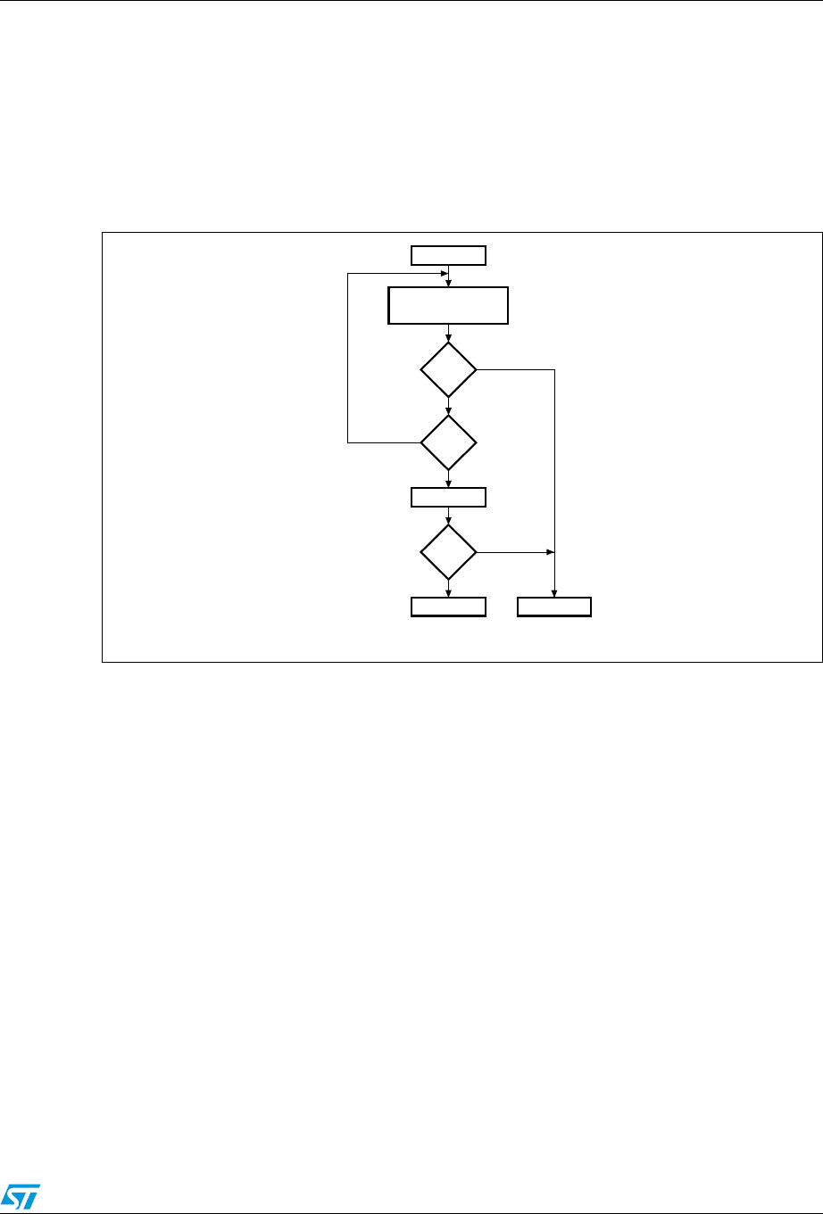
UPSD3212A, UPSD3212C, UPSD3212CV Memory blocks
111/181
When using the Data Polling method during an Erase cycle, Figure 47 still applies. However,
the Data Polling Flag bit (DQ7) is '0' until the Erase cycle is complete. A '1' on the Error Flag
bit (DQ5) indicates a time-out condition on the Erase cycle; a '0' indicates no error. The
MCU can read any location within the sector being erased to get the Data Polling Flag bit
(DQ7) and the Error Flag bit (DQ5).
PSDsoft Express generates ANSI C code functions which implement these Data Polling
algorithms.
Figure 47. Data polling flowchart
21.6.2 Data toggle
Checking the Toggle Flag bit (DQ6) is a method of determining whether a Program or Erase
cycle is in progress or has completed. Figure 48 shows the Data Toggle algorithm.
When the MCU issues a Program instruction, the embedded algorithm begins. The MCU
then reads the location of the byte to be programmed in Flash memory to check status. The
Toggle Flag bit (DQ6) of this location toggles each time the MCU reads this location until the
embedded algorithm is complete. The MCU continues to read this location, checking the
Toggle Flag bit (DQ6) and monitoring the Error Flag bit (DQ5). When the Toggle Flag bit
(DQ6) stops toggling (two consecutive reads yield the same value), and the Error Flag bit
(DQ5) remains '0,' the embedded algorithm is complete. If the Error Flag bit (DQ5) is '1,' the
MCU should test the Toggle Flag bit (DQ6) again, since the Toggle Flag bit (DQ6) may have
changed simultaneously with the Error Flag bit (DQ5) (see Figure 48).
The Error Flag bit (DQ5) is set if either an internal time-out occurred while the embedded
algorithm attempted to program the byte, or if the MCU attempted to program a '1' to a bit
that was not erased (not erased is logic '0').
It is suggested (as with all Flash memories) to read the location again after the embedded
programming algorithm has completed, to compare the byte that was written to Flash
memory with the byte that was intended to be written.
READ DQ5 & DQ7
at VALID ADDRESS
START
READ DQ7
FAIL PASS
AI01369B
DQ7
=
DATA
YES
NO
YES
NO
DQ5
= 1
DQ7
=
DATA
YES
NO
Obsolete Product(s) - Obsolete Product(s)
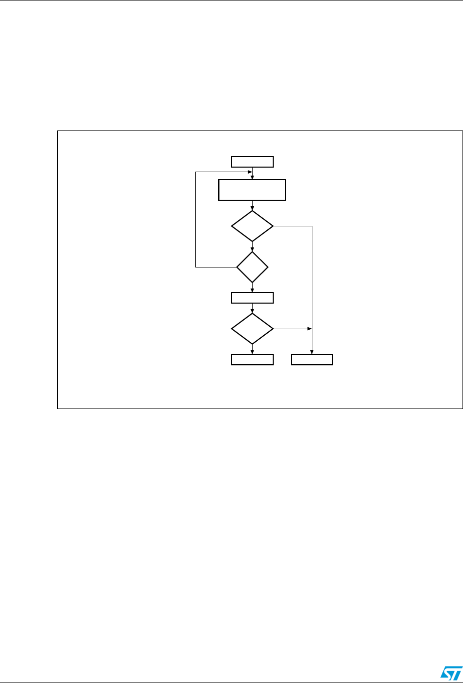
Memory blocks UPSD3212A, UPSD3212C, UPSD3212CV
112/181
When using the Data Toggle method after an Erase cycle, Figure 48 still applies. the Toggle
Flag bit (DQ6) toggles until the Erase cycle is complete. A 1 on the Error Flag bit (DQ5)
indicates a time-out condition on the Erase cycle; a '0' indicates no error. The MCU can read
any location within the sector being erased to get the Toggle Flag bit (DQ6) and the Error
Flag bit (DQ5).
PSDsoft Express generates ANSI C code functions which implement these Data Toggling
algorithms.
Figure 48. Data toggle flowchart
21.7 Erasing Flash memory
21.7.1 Flash Bulk Erase
The Flash Bulk Erase instruction uses six WRITE operations followed by a READ operation
of the status register, as described in Ta b l e 8 2 . If any byte of the Bulk Erase instruction is
wrong, the Bulk Erase instruction aborts and the device is reset to the READ Flash memory
status.
During a Bulk Erase, the memory status may be checked by reading the Error Flag bit
(DQ5), the Toggle Flag bit (DQ6), and the Data Polling Flag bit (DQ7), as detailed in
Section 21.6: Programming Flash memory. The Error Flag bit (DQ5) returns a '1' if there has
been an Erase Failure (maximum number of Erase cycles have been executed).
It is not necessary to program the memory with 00h because the PSD module automatically
does this before erasing to 0FFh.
During execution of the Bulk Erase instruction, the Flash memory does not accept any
instructions.
READ
DQ5 & DQ6
START
READ DQ6
FAIL PASS
AI01370B
DQ6
=
TOGGLE
NO
NO
YES
YES
DQ5
= 1
NO
YES
DQ6
=
TOGGLE
Obsolete Product(s) - Obsolete Product(s)

UPSD3212A, UPSD3212C, UPSD3212CV Memory blocks
113/181
21.7.2 Flash Sector Erase
The Sector Erase instruction uses six WRITE operations, as described in Ta b l e 8 2 .
Additional Flash Sector Erase codes and Flash memory sector addresses can be written
subsequently to erase other Flash memory sectors in parallel, without further coded cycles,
if the additional bytes are transmitted in a shorter time than the time-out period of about
100µs. The input of a new Sector Erase code restarts the time-out period.
The status of the internal timer can be monitored through the level of the Erase Time-out
Flag bit (DQ3). If the Erase Time-out Flag bit (DQ3) is '0,' the Sector Erase instruction has
been received and the time-out period is counting. If the Erase Time-out Flag bit (DQ3) is '1,'
the time-out period has expired and the embedded algorithm is busy erasing the Flash
memory sector(s). Before and during Erase time-out, any instruction other than Suspend
Sector Erase and Resume Sector Erase instructions abort the cycle that is currently in
progress, and reset the device to READ mode.
During a Sector Erase, the memory status may be checked by reading the Error Flag bit
(DQ5), the Toggle Flag bit (DQ6), and the Data Polling Flag bit (DQ7), as detailed in
Section 21.6: Programming Flash memory.
During execution of the Erase cycle, the Flash memory accepts only RESET and Suspend
Sector Erase instructions. Erasure of one Flash memory sector may be suspended, in order
to read data from another Flash memory sector, and then resumed.
21.7.3 Suspend Sector Erase
When a Sector Erase cycle is in progress, the Suspend Sector Erase instruction can be
used to suspend the cycle by writing 0B0h to any address when an appropriate Sector
Select (FS0-FS3 or CSBOOT0-CSBOOT1) is High. (See Ta b l e 8 2 ). This allows reading of
data from another Flash memory sector after the Erase cycle has been suspended.
Suspend Sector Erase is accepted only during an Erase cycle and defaults to READ mode.
A Suspend Sector Erase instruction executed during an Erase time-out period, in addition to
suspending the Erase cycle, terminates the time out period.
The Toggle Flag bit (DQ6) stops toggling when the internal logic is suspended. The status of
this bit must be monitored at an address within the Flash memory sector being erased. The
Toggle Flag bit (DQ6) stops toggling between 0.1µs and 15µs after the Suspend Sector
Erase instruction has been executed. The Flash memory is then automatically set to READ
mode.
If an Suspend Sector Erase instruction was executed, the following rules apply:
●Attempting to read from a Flash memory sector that was being erased outputs invalid
data.
●Reading from a Flash sector that was not being erased is valid.
●The Flash memory cannot be programmed, and only responds to Resume Sector
Erase and Reset Flash instructions (READ is an operation and is allowed).
●If a Reset Flash instruction is received, data in the Flash memory sector that was being
erased is invalid.
21.7.4 Resume Sector Erase
If a Suspend Sector Erase instruction was previously executed, the erase cycle may be
resumed with this instruction. The Resume Sector Erase instruction consists of writing 030h
Obsolete Product(s) - Obsolete Product(s)

Memory blocks UPSD3212A, UPSD3212C, UPSD3212CV
114/181
to any address while an appropriate Sector Select (FS0-FS3 or CSBOOT0-CSBOOT1) is
High. (See Ta b le 8 2 .)
21.8 Specific features
21.8.1 Flash memory sector protect
Each primary and secondary Flash memory sector can be separately protected against
Program and Erase cycles. Sector Protection provides additional data security because it
disables all Program or Erase cycles. This mode can be activated through the JTAG Port or
a Device Programmer.
Sector protection can be selected for each sector using the PSDsoft Express Configuration
program. This automatically protects selected sectors when the device is programmed
through the JTAG Port or a Device Programmer. Flash memory sectors can be unprotected
to allow updating of their contents using the JTAG Port or a Device Programmer. The MCU
can read (but cannot change) the sector protection bits.
Any attempt to program or erase a protected Flash memory sector is ignored by the device.
The Verify operation results in a READ of the protected data. This allows a guarantee of the
retention of the Protection status.
The sector protection status can be read by the MCU through the Flash memory protection
registers (in the CSIOP block). See Ta b l e 8 4 and Ta b le 8 5 .
1. Bit Definitions:
Sec<i>_Prot 1 = Primary Flash memory or secondary Flash memory Sector <i> is write-protected.
Sec<i>_Prot 0 = Primary Flash memory or secondary Flash memory Sector <i> is not write-protected.
1. Bit Definitions:
Sec<i>_Prot 1 = Secondary Flash memory Sector <i> is write-protected.
Sec<i>_Prot 0 = Secondary Flash memory Sector <i> is not write-protected.
Security_Bit 0 = Security Bit in device has not been set; 1 = Security Bit in device has been set.
21.8.2 Reset Flash
The Reset Flash instruction consists of one WRITE cycle (see Ta bl e 8 2 ). It can also be
optionally preceded by the standard two WRITE decoding cycles (writing AAh to 555h and
55h to AAAh). It must be executed after:
●Reading the Flash Protection Status or Flash ID
●An Error condition has occurred (and the device has set the Error Flag bit (DQ5) to '1'
during a Flash memory Program or Erase cycle.
Table 84. Sector protection/security bit definition – Flash protection register
Bit 7 Bit 6 Bit 5 Bit 4 Bit 3 Bit 2 Bit 1 Bit 0
Not used Not used Not used Not used Sec3_Prot Sec2_Prot Sec1_Prot Sec0_Prot
Table 85. Sector protection/security bit definition – secondary Flash protection
register
Bit 7 Bit 6 Bit 5 Bit 4 Bit 3 Bit 2 Bit 1 Bit 0
Security_B
it Not used Not used Not used Not used Not used Sec1_Prot Sec0_Prot
Obsolete Product(s) - Obsolete Product(s)

UPSD3212A, UPSD3212C, UPSD3212CV Memory blocks
115/181
The Reset Flash instruction puts the Flash memory back into normal READ mode. If an
Error condition has occurred (and the device has set the Error Flag bit (DQ5) to '1' the Flash
memory is put back into normal READ mode within a few milliseconds of the Reset Flash
instruction having been issued. The Reset Flash instruction is ignored when it is issued
during a Program or Bulk Erase cycle of the Flash memory. The Reset Flash instruction
aborts any on-going Sector Erase cycle, and returns the Flash memory to the normal READ
mode within a few milliseconds.
21.9 SRAM
The SRAM is enabled when SRAM Select (RS0) from the DPLD is High. SRAM Select
(RS0) can contain up to two product terms, allowing flexible memory mapping.
21.10 Sector Select and SRAM Select
Sector Select (FS0-FS3, CSBOOT0-CSBOOT1) and SRAM Select (RS0) are all outputs of
the DPLD. They are setup by writing equations for them in PSDsoft Express. The following
rules apply to the equations for these signals:
1. Primary Flash memory and secondary Flash memory Sector Select signals must not
be larger than the physical sector size.
2. Any primary Flash memory sector must not be mapped in the same memory space as
another Flash memory sector.
3. A secondary Flash memory sector must not be mapped in the same memory space as
another secondary Flash memory sector.
4. SRAM, I/O, and Peripheral I/O spaces must not overlap.
5. A secondary Flash memory sector may overlap a primary Flash memory sector. In
case of overlap, priority is given to the secondary Flash memory sector.
6. SRAM, I/O, and Peripheral I/O spaces may overlap any other memory sector. Priority is
given to the SRAM, I/O, or Peripheral I/O.
21.10.1 Example
FS0 is valid when the address is in the range of 8000h to BFFFh, CSBOOT0 is valid from
8000h to 9FFFh, and RS0 is valid from 8000h to 87FFh. Any address in the range of RS0
always accesses the SRAM. Any address in the range of CSBOOT0 greater than 87FFh
(and less than 9FFFh) automatically addresses secondary Flash memory segment 0. Any
address greater than 9FFFh accesses the primary Flash memory segment 0. You can see
that half of the primary Flash memory segment 0 and one-fourth of secondary Flash
memory segment 0 cannot be accessed in this example.
Note: An equation that defined FS1 to anywhere in the range of 8000h to BFFFh would not be
valid.
Figure 49 shows the priority levels for all memory components. Any component on a higher
level can overlap and has priority over any component on a lower level. Components on the
same level must not overlap. Level one has the highest priority and level 3 has the lowest.
Obsolete Product(s) - Obsolete Product(s)
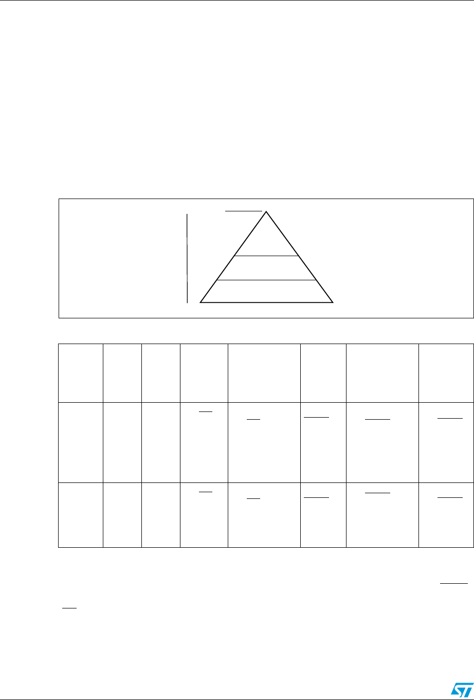
Memory blocks UPSD3212A, UPSD3212C, UPSD3212CV
116/181
21.10.2 Memory Select configuration in Program and Data spaces
The MCU Core has separate address spaces for Program memory and Data memory. Any
of the memories within the PSD module can reside in either space or both spaces. This is
controlled through manipulation of the VM Register that resides in the CSIOP space.
The VM Register is set using PSDsoft Express to have an initial value. It can subsequently
be changed by the MCU so that memory mapping can be changed on-the-fly.
For example, you may wish to have SRAM and primary Flash memory in the Data space at
Boot-up, and secondary Flash memory in the Program space at Boot-up, and later swap the
primary and secondary Flash memories. This is easily done with the VM Register by using
PSDsoft Express Configuration to configure it for Boot-up and having the MCU change it
when desired. Ta b l e 8 6 describes the VM Register.
Figure 49. Priority level of memory and I/O components in the PSD module
21.10.3 Separate Space mode
Program space is separated from Data space. For example, Program Select Enable (PSEN)
is used to access the program code from the primary Flash memory, while READ Strobe
(RD) is used to access data from the secondary Flash memory, SRAM and I/O Port blocks.
This configuration requires the VM Register to be set to 0Ch (see Figure 50).
Table 86. VM register
Bit 7
PIO_EN Bit 6 Bit 5
Bit 4
Primary
FL_Data
Bit 3
Secondary
Data
Bit 2
Primary
FL_Cod
e
Bit 1
Secondary
Code
Bit 0
SRAM_Co
de
0 =
disable
PIO
mode
not
used
not
used
0 = RD
can’t
access
Flash
memory
0 = RD can’t
access
Secondary
Flash memory
0 =
PSEN
can’t
access
Flash
memory
0 = PSEN can’t
access
Secondary
Flash memory
0 = PSEN
can’t
access
SRAM
1=
enable
PIO
mode
not
used
not
used
1 = RD
access
Flash
memory
1 = RD access
Secondary
Flash memory
1 =
PSEN
access
Flash
memory
1 = PSEN
access
Secondary
Flash memory
1 = PSEN
access
SRAM
Level 1
SRAM, I/O, or
Peripheral I/O
Level 2
Secondary
Non-Volatile Memory
Highest Priority
Lowest Priority
Level 3
Primary Flash Memory
AI02867D
Obsolete Product(s) - Obsolete Product(s)
UPSD3212A, UPSD3212C, UPSD3212CV Memory blocks
117/181
21.10.4 Combined Space modes
The Program and Data spaces are combined into one memory space that allows the
primary Flash memory, secondary Flash memory, and SRAM to be accessed by either
Program Select Enable (PSEN) or READ Strobe (RD). For example, to configure the
primary Flash memory in Combined space, Bits b2 and b4 of the VM Register are set to '1'
(see Figure 51).
21.11 Page register
The 8-bit Page Register increases the addressing capability of the MCU Core by a factor of
up to 256. The contents of the register can also be read by the MCU. The outputs of the
Page Register (PGR0-PGR7) are inputs to the DPLD decoder and can be included in the
Sector Select (FS0-FS7, CSBOOT0-CSBOOT3), and SRAM Select (RS0) equations.
If memory paging is not needed, or if not all 8 page register bits are needed for memory
paging, then these bits may be used in the CPLD for general logic.
Figure 50. Separate Space mode
Figure 51. Combined Space mode
Primary
Flash
Memory
DPLD Secondary
Flash
Memory
SRAM
RS0
CSBOOT0-1
FS0-FS3 CS CSCS
OE OE
RD
PSEN
OE
AI07433
Primary
Flash
Memory
DPLD Secondary
Flash
Memory
SRAM
RS0
CSBOOT0-1
FS0-FS3
RD
CS CSCS
RD
OE OE
VM REG BIT 2
PSEN
VM REG BIT 0
VM REG BIT 1
VM REG BIT 3
VM REG BIT 4
OE
AI07434
Obsolete Product(s) - Obsolete Product(s)
Memory blocks UPSD3212A, UPSD3212C, UPSD3212CV
118/181
Figure 52 shows the Page Register. The eight flip-flops in the register are connected to the
internal data bus D0-D7. The MCU can write to or read from the Page Register. The Page
Register can be accessed at address location CSIOP + E0h.
Figure 52. Page register
RESET
D0-D7
R/W
D0 Q0
Q1
Q2
Q3
Q4
Q5
Q6
Q7
D1
D2
D3
D4
D5
D6
D7
PAGE
REGISTER
PGR0
PGR1
PGR2
PGR3 DPLD
AND
CPLD
INTERNAL PSD MODULE
SELECTS
AND LOGIC
PLD
PGR4
PGR5
PGR6
PGR7
AI05799
Obsolete Product(s) - Obsolete Product(s)
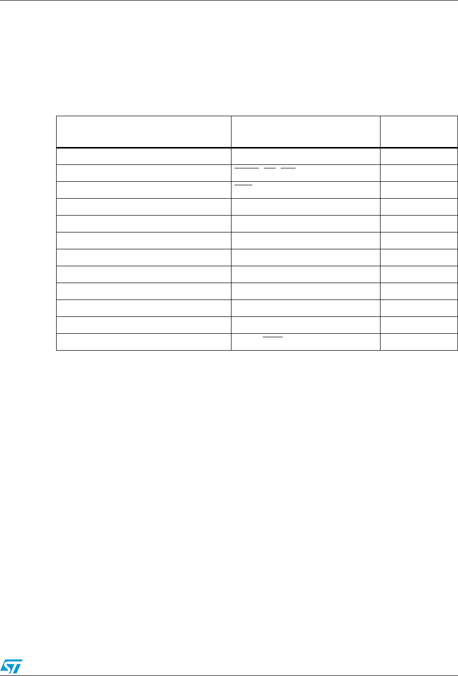
UPSD3212A, UPSD3212C, UPSD3212CV PLDs
119/181
22 PLDs
PLDs bring programmable logic functionality to the UPSD. After specifying the logic for the
PLDs using PSDsoft Express, the logic is programmed into the device and available upon
Power-up.
Note: 1. These inputs are not available in the 52-pin package.
The PSD module contains two PLDs: the Decode PLD (DPLD), and the Complex PLD
(CPLD). The PLDs are briefly discussed in the next few paragraphs, and in more detail in
Section 22.2: Decode PLD (DPLD), and Section 22.3: Complex PLD (CPLD). Figure 53
shows the configuration of the PLDs.
The DPLD performs address decoding for Select signals for PSD module components, such
as memory, registers, and I/O ports.
The CPLD can be used for logic functions, such as loadable counters and shift registers,
state machines, and encoding and decoding logic. These logic functions can be constructed
using the Output Macrocells (OMC), Input Macrocells (IMC), and the AND Array. The CPLD
can also be used to generate External Chip Select (ECS1-ECS2) signals.
The AND Array is used to form product terms. These product terms are specified using
PSDsoft. The PLD input signals consist of internal MCU signals and external inputs from the
I/O ports. The input signals are shown in Ta bl e 8 7 .
22.1 Turbo bit in PSD module
The PLDs can minimize power consumption by switching off when inputs remain unchanged
for an extended time of about 70ns. Resetting the Turbo bit to '0' (Bit 3 of PMMR0)
automatically places the PLDs into standby if no inputs are changing. Turning the Turbo
mode off increases propagation delays while reducing power consumption.
Table 87. DPLD and CPLD Inputs
Input Source Input Name Number of
Signals
MCU Address Bus A15-A0 16
MCU Control Signals PSEN, RD, WR, ALE 4
RESET RST 1
Power-down PDN 1
Port A Input Macrocells(1) PA7- PA 0 8
Port B Input Macrocells PB7-PB0 8
Port C Input Macrocells PC2-4, PC7 4
Port D Inputs PD2-PD1 2
Page Register PGR7-PGR0 8
Macrocell AB Feedback MCELLAB.FB7-FB0 8
Macrocell BC Feedback MCELLBC.FB7-FB0 8
Flash memory Program Status bit Ready/Busy 1
Obsolete Product(s) - Obsolete Product(s)
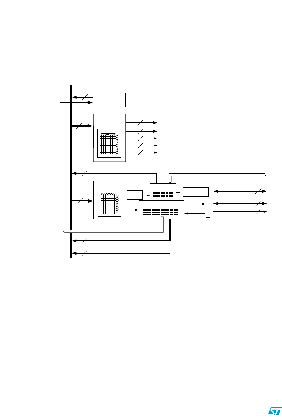
PLDs UPSD3212A, UPSD3212C, UPSD3212CV
120/181
See Section 24: Power management for details on how to set the Turbo Bit.
Additionally, five bits are available in PMMR2 to block MCU control signals from entering the
PLDs. This reduces power consumption and can be used only when these MCU control
signals are not used in PLD logic equations.
Each of the two PLDs has unique characteristics suited for its applications. They are
described in the following sections.
Figure 53. PLD diagram
1. Port A is not available in the 52-pin package
22.2 Decode PLD (DPLD)
The DPLD, shown in Figure 88, is used for decoding the address for PSD module and
external components. The DPLD can be used to generate the following decode signals:
●4 Sector Select (FS0-FS3) signals for the primary Flash memory (three product terms
each)
●2 Sector Select (CSBOOT0-CSBOOT1) signals for the secondary Flash memory (three
product terms each)
●1 internal SRAM Select (RS0) signal (two product terms)
●1 internal CSIOP Select signal (selects the PSD module registers)
●2 internal Peripheral Select signals (Peripheral I/O mode).
PLD INPUT BUS
8
INPUT MACROCELL & INPUT PORTS
DIRECT MACROCELL INPUT TO MCU DATA BUS
CSIOP SELECT
SRAM SELECT
SECONDARY NON-VOLATILE MEMORY SELECTS
DECODE PLD
PAGE
REGISTER
PERIPHERAL SELECTS
CPLD
PT
ALLOC.
MACROCELL
ALLOC.
MCELLAB
MCELLBC
DIRECT MACROCELL ACCESS FROM MCU DATA BUS
20 INPUT MACROCELL
(PORT A,B,C)
16 OUTPUT
MACROCELL
I/O PORTS
PRIMARY FLASH MEMORY SELECTS
2PORT D INPUTS
TO PORT A OR B1
TO PORT B OR C
DATA
BUS
8
8
8
4
1
1
2
EXTERNAL CHIP SELECTS
TO PORT D
2
16
20
OUTPUT MACROCELL FEEDBACK
AI06600
73
73
Obsolete Product(s) - Obsolete Product(s)
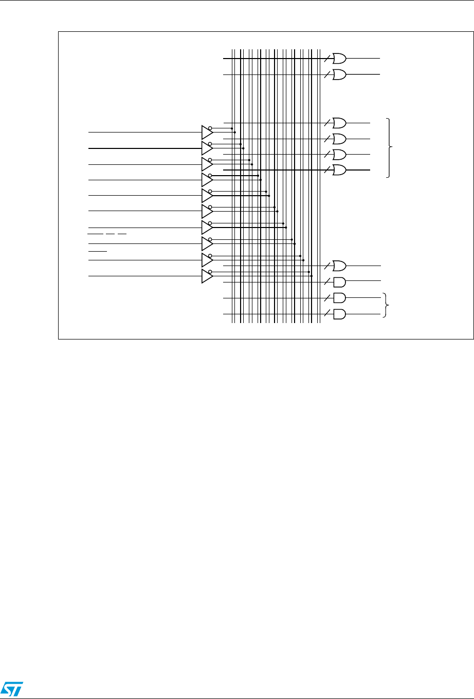
UPSD3212A, UPSD3212C, UPSD3212CV PLDs
121/181
1. Port A inputs are not available in the 52-pin package
2. Inputs from the MCU module
22.3 Complex PLD (CPLD)
The CPLD can be used to implement system logic functions, such as loadable counters and
shift registers, system mailboxes, handshaking protocols, state machines, and random logic.
The CPLD can also be used to generate External Chip Select (ECS1-ECS2), routed to Port
D.
Although External Chip Select (ECS1-ECS2) can be produced by any Output Macrocell
(OMC), these External Chip Select (ECS1-ECS2) on Port D do not consume any Output
Macrocells (OMC).
As shown in Figure 54, the CPLD has the following blocks:
●20 Input Macrocells (IMC)
●16 Output Macrocells (OMC)
●Macrocell Allocator
●Product Term Allocator
●AND Array capable of generating up to 137 product terms
●Four I/O Ports.
Each of the blocks are described in the sections that follow.
Table 88. DPLD logic array
(INPUTS)
(20)
(8)
(16)
(1)
PDN (APD OUTPUT)
I /O PORTS (PORT A,B,C)1
(8)
PGR0 -PGR7
(8)
MCELLAB.FB [7:0] (FEEDBACKS)
MCELLBC.FB [7:0] (FEEDBACKS)
A[15:0]2
(2)
(4)
PD[2:1]
PSEN, RD, WR, ALE2
(1)
(1)
RESET
2
RD_BSY
RS0
CSIOP
PSEL0
PSEL1
4 PRIMARY FLASH
MEMORY SECTOR
SELECTS
SRAM SELECT
I/O DECODER
SELECT
PERIPHERAL I/O
MODE SELECT
CSBOOT 0
CSBOOT 1
FS0
3
3
3
3
3
3
2
AI07436
FS1
FS2
FS3
1
1
1
Obsolete Product(s) - Obsolete Product(s)
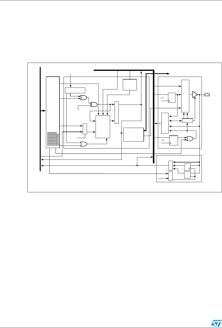
PLDs UPSD3212A, UPSD3212C, UPSD3212CV
122/181
The Input Macrocells (IMC) and Output Macrocells (OMC) are connected to the PSD
module internal data bus and can be directly accessed by the MCU. This enables the MCU
software to load data into the Output Macrocells (OMC) or read data from both the Input and
Output Macrocells (IMC and OMC).
This feature allows efficient implementation of system logic and eliminates the need to
connect the data bus to the AND Array as required in most standard PLD macrocell
architectures.
Figure 54. Macrocell and I/O ports
22.4 Output macrocell (OMC)
Eight of the Output Macrocells (OMC) are connected to Ports A and B pins and are named
as McellAB0-McellAB7. The other eight macrocells are connected to Ports B and C pins and
are named as McellBC0-McellBC7. If an McellAB output is not assigned to a specific pin in
PSDsoft, the Macrocell Allocator block assigns it to either Port A or B. The same is true for a
McellBC output on Port B or C. Ta b l e 8 9 shows the macrocells and port assignment.
The Output Macrocell (OMC) architecture is shown in Figure 55. As shown in the figure,
there are native product terms available from the AND Array, and borrowed product terms
available (if unused) from other Output Macrocells (OMC). The polarity of the product term
is controlled by the XOR gate. The Output Macrocell (OMC) can implement either sequential
logic, using the flip-flop element, or combinatorial logic. The multiplexer selects between the
sequential or combinatorial logic outputs. The multiplexer output can drive a port pin and
has a feedback path to the AND Array inputs.
The flip-flop in the Output Macrocell (OMC) block can be configured as a D, T, JK, or SR
type in PSDsoft. The flip-flop’s clock, preset, and clear inputs may be driven from a product
term of the AND Array. Alternatively, CLKIN (PD1) can be used for the clock input to the flip-
I/O PORTS
CPLD MACROCELLS
INPUT MACROCELLS
LATCHED
ADDRESS OUT
MUX
MUX
MUX
MUX MUX
D
D
Q
Q
Q
G
D
QD
WR
WR
PDR
DATA
PRODUCT TERM
ALLOCATOR
DIR
REG.
SELECT
INPUT
PRODUCT TERMS
FROM OTHER
MACROCELLS
POLARITY
SELECT
UP TO 10
PRODUCT TERMS
CLOCK
SELECT
PR DI LD
D/T
CK
CL
Q
D/T/JK FF
SELECT
PT CLEAR
PT
CLOCK
GLOBAL
CLOCK
PT OUTPUT ENABLE (OE)
MACROCELL FEEDBACK
I/O PORT INPUT
ALE
PT INPUT LATCH GATE/CLOCK
MCU LOAD
PT PRESET
MCU DATA IN
COMB.
/REG
SELECT MACROCELL
TO
I/O PORT
ALLOC.
CPLD
OUTPUT
TO OTHER I/O PORTS
PLD INPUT BUSPLD INPUT BUS
MCU ADDRESS / DATA BUS
MACROCELL
OUT TO
MCU
DATA
LOAD
CONTROL
AND ARRAY
CPLD OUTPUT
I/O PIN
AI06602
Obsolete Product(s) - Obsolete Product(s)

UPSD3212A, UPSD3212C, UPSD3212CV PLDs
123/181
flop. The flip-flop is clocked on the rising edge of CLKIN (PD1). The preset and clear are
active High inputs. Each clear input can use up to two product terms.
1. McellAB0-McellAB7 can only be assigned to Port B in the 52-pin package
2. Port PC0, PC1, PC5, and PC6 are assigned to JTAG pins and are not available as Macrocell outputs.
22.5 Product term allocator
The CPLD has a Product Term Allocator. PSDsoft uses the Product Term Allocator to
borrow and place product terms from one macrocell to another. The following list
summarizes how product terms are allocated:
●McellAB0-McellAB7 all have three native product terms and may borrow up to six more
●McellBC0-McellBC3 all have four native product terms and may borrow up to five more
●McellBC4-McellBC7 all have four native product terms and may borrow up to six more.
Each macrocell may only borrow product terms from certain other macrocells. Product
terms already in use by one macrocell are not available for another macrocell.
If an equation requires more product terms than are available to it, then “external” product
terms are required, which consume other Output Macrocells (OMC). If external product
terms are used, extra delay is added for the equation that required the extra product terms.
This is called product term expansion. PSDsoft Express performs this expansion as needed.
Table 89. Output macrocell port and data bit assignments
Output
Macrocell
Port
Assignment
(1,2)
Native Product
Terms
Max. Borrowed
Product Terms
Data Bit for
Loading or Reading
McellAB0 Port A0, B0 3 6 D0
McellAB1 Port A1, B1 3 6 D1
McellAB2 Port A2, B2 3 6 D2
McellAB3 Port A3, B3 3 6 D3
McellAB4 Port A4, B4 3 6 D4
McellAB5 Port A5, B5 3 6 D5
McellAB6 Port A6, B6 3 6 D6
McellAB7 Port A7, B7 3 6 D7
McellBC0 Port B0 4 5 D0
McellBC1 Port B1 4 5 D1
McellBC2 Port B2, C2 4 5 D2
McellBC3 Port B3, C3 4 5 D3
McellBC4 Port B4, C4 4 6 D4
McellBC5 Port B5 4 6 D5
McellBC6 Port B6 4 6 D6
McellBC7 Port B7, C7 4 6 D7
Obsolete Product(s) - Obsolete Product(s)
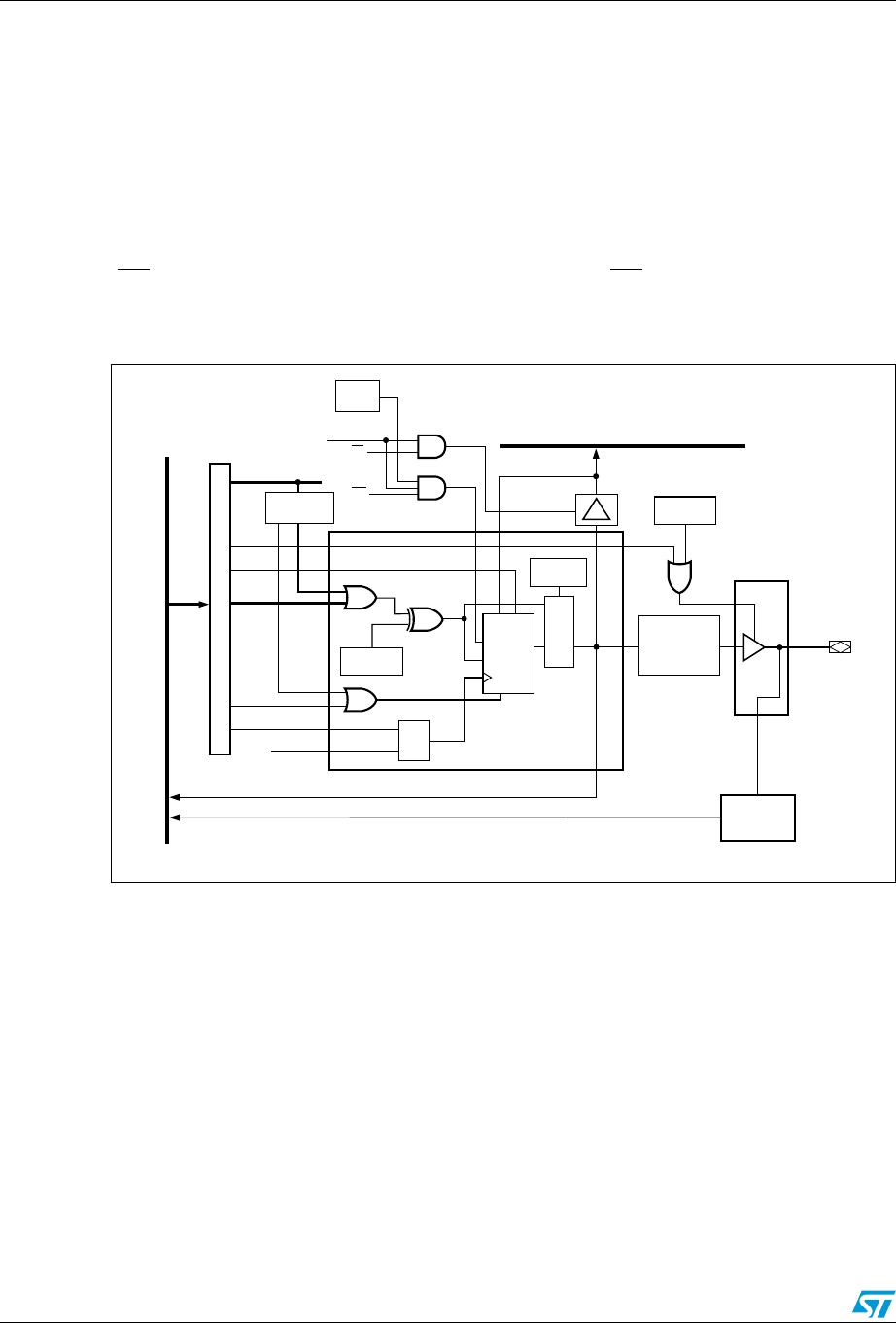
PLDs UPSD3212A, UPSD3212C, UPSD3212CV
124/181
22.5.1 Loading and Reading the Output Macrocells (OMC)
The Output Macrocells (OMC) block occupies a memory location in the MCU address
space, as defined by the CSIOP block (see Section 23: I/O ports (PSD module)). The flip-
flops in each of the 16 Output Macrocells (OMC) can be loaded from the data bus by a
MCU. Loading the Output Macrocells (OMC) with data from the MCU takes priority over
internal functions. As such, the preset, clear, and clock inputs to the flip-flop can be
overridden by the MCU. The ability to load the flip-flops and read them back is useful in such
applications as loadable counters and shift registers, mailboxes, and handshaking protocols.
Data can be loaded to the Output Macrocells (OMC) on the trailing edge of WRITE Strobe
(WR, edge loading) or during the time that WRITE Strobe (WR) is active (level loading). The
method of loading is specified in PSDsoft Express Configuration.
Figure 55. CPLD output macrocell
22.5.2 OMC mask register
There is one Mask Register for each of the two groups of eight Output Macrocells (OMC).
The Mask Registers can be used to block the loading of data to individual Output Macrocells
(OMC). The default value for the Mask Registers is 00h, which allows loading of the Output
Macrocells (OMC). When a given bit in a Mask Register is set to a '1,' the MCU is blocked
from writing to the associated Output Macrocells (OMC). For example, suppose McellAB0-
McellAB3 are being used for a state machine. You would not want a MCU write to McellAB
to overwrite the state machine registers. Therefore, you would want to load the Mask
Register for McellAB (Mask Macrocell AB) with the value 0Fh.
22.5.3 Output enable of the OMC
The Output Macrocells (OMC) block can be connected to an I/O port pin as a PLD output.
The output enable of each port pin driver is controlled by a single product term from the
PT
ALLOCATOR
MASK
REG.
PT CLK
PT
PT
PT
CLKIN
FEEDBACK (.FB)
PORT INPUT
AND ARRAY
PLD INPUT BUS
MUX
MUX
POLARITY
SELECT
LD
IN
CLR
Q
PRDIN
COMB/REG
SELECT
PORT
DRIVER
INPUT
MACROCELL
I/O PIN
MACROCELL
ALLOCATOR
MCU DATA BUS D[7:0]
DIRECTION
REGISTER
CLEAR (.RE)
PROGRAMMABLE
FF (D /T/JK /SR)
WR
ENABLE (.OE)
PRESET(.PR)
RD
MACROCELL CS
AI06617
Obsolete Product(s) - Obsolete Product(s)
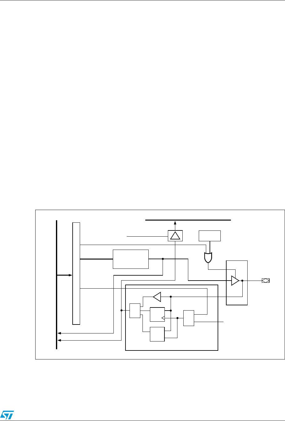
UPSD3212A, UPSD3212C, UPSD3212CV PLDs
125/181
AND Array, ORed with the Direction Register output. The pin is enabled upon Power-up if no
output enable equation is defined and if the pin is declared as a PLD output in PSDsoft
Express.
If the Output Macrocell (OMC) output is declared as an internal node and not as a port pin
output in the PSDabel file, the port pin can be used for other I/O functions. The internal node
feedback can be routed as an input to the AND Array.
22.6 Input macrocells (IMC)
The CPLD has 20 Input Macrocells (IMC), one for each pin on Ports A and B, and 4 on Port
C. The architecture of the Input Macrocells (IMC) is shown in Figure 56. The Input
Macrocells (IMC) are individually configurable, and can be used as a latch, register, or to
pass incoming Port signals prior to driving them onto the PLD input bus. The outputs of the
Input Macrocells (IMC) can be read by the MCU through the internal data bus.
The enable for the latch and clock for the register are driven by a multiplexer whose inputs
are a product term from the CPLD AND Array or the MCU Address Strobe (ALE). Each
product term output is used to latch or clock four Input Macrocells (IMC). Port inputs 3-0 can
be controlled by one product term and 7-4 by another.
Configurations for the Input Macrocells (IMC) are specified by equations written in PSDsoft
(see Application Note AN1171). Outputs of the Input Macrocells (IMC) can be read by the
MCU via the IMC buffer.
See Section 23: I/O ports (PSD module).
Figure 56. Input macrocell
OUTPUT
MACROCELLS BC
AND
MACROCELL AB
PT
PT
FEEDBACK
AND ARRAY
PLD INPUT BUS
PORT
DRIVER
I/O PIN
MCU DATA BUS D[7:0]
DIRECTION
REGISTER
MUX
MUX
ALE
PT
Q
Q
D
D
G
LATCH INPUT MACROCELL
ENABLE (.OE)
D FF
INPUT MACROCELL _ RD
AI06603
Obsolete Product(s) - Obsolete Product(s)

I/O ports (PSD module) UPSD3212A, UPSD3212C, UPSD3212CV
126/181
23 I/O ports (PSD module)
There are four programmable I/O ports: Ports A, B, C, and D in the PSD module. Each of the
ports is eight bits except Port D, which is 3 bits. Each port pin is individually user
configurable, thus allowing multiple functions per port. The ports are configured using
PSDsoft Express Configuration or by the MCU writing to on-chip registers in the CSIOP
space. Port A is not available in the 52-pin package.
The topics discussed in this section are:
●General Port architecture
●Port operating modes
●Port Configuration Registers (PCR)
●Port Data Registers
●Individual Port functionality.
23.1 General port architecture
The general architecture of the I/O Port block is shown in Figure 57. Individual Port
architectures are shown in Figure 59 to Figure 62. In general, once the purpose for a port
pin has been defined, that pin is no longer available for other purposes. Exceptions are
noted.
As shown in Figure 57, the ports contain an output multiplexer whose select signals are
driven by the configuration bits in the Control Registers (Ports A and B only) and PSDsoft
Express Configuration. Inputs to the multiplexer include the following:
●Output data from the Data Out register
●Latched address outputs
●CPLD macrocell output
●External Chip Select (ECS1-ECS2) from the CPLD.
The Port Data Buffer (PDB) is a tri-state buffer that allows only one source at a time to be
read. The Port Data Buffer (PDB) is connected to the Internal Data Bus for feedback and
can be read by the MCU. The Data Out and macrocell outputs, Direction and Control
Registers, and port pin input are all connected to the Port Data Buffer (PDB).
Obsolete Product(s) - Obsolete Product(s)
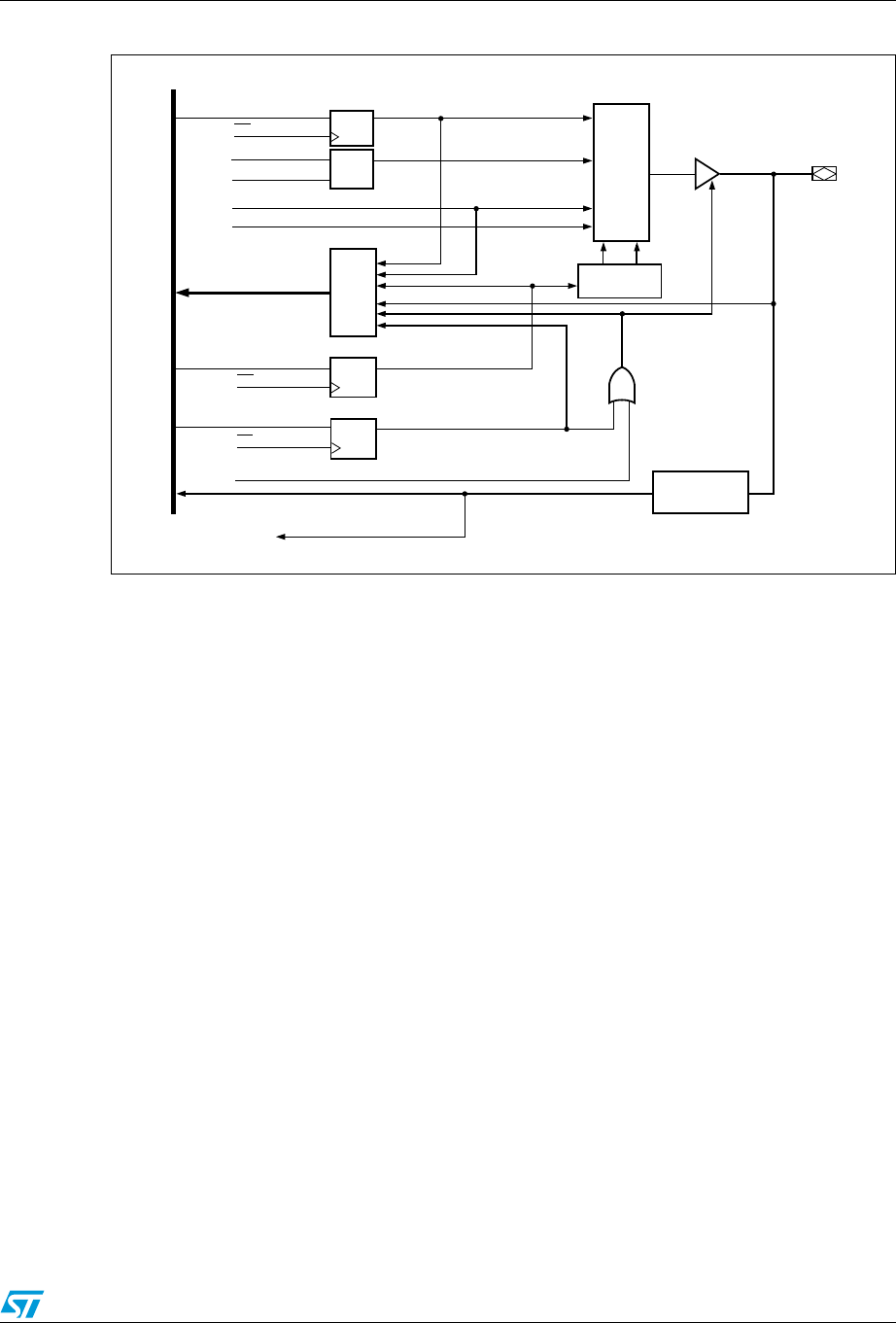
UPSD3212A, UPSD3212C, UPSD3212CV I/O ports (PSD module)
127/181
Figure 57. General I/O port architecture
The Port pin’s tri-state output driver enable is controlled by a two input OR gate whose
inputs come from the CPLD AND Array enable product term and the Direction Register. If
the enable product term of any of the Array outputs are not defined and that port pin is not
defined as a CPLD output in the PSDsoft, then the Direction Register has sole control of the
buffer that drives the port pin.
The contents of these registers can be altered by the MCU. The Port Data Buffer (PDB)
feedback path allows the MCU to check the contents of the registers.
Ports A, B, and C have embedded Input Macrocells (IMC). The Input Macrocells (IMC) can
be configured as latches, registers, or direct inputs to the PLDs. The latches and registers
are clocked by Address Strobe (ALE) or a product term from the PLD AND Array. The
outputs from the Input Macrocells (IMC) drive the PLD input bus and can be read by the
MCU. See Figure 56.
23.2 Port operating modes
The I/O Ports have several modes of operation. Some modes can be defined using PSDsoft,
some by the MCU writing to the Control Registers in CSIOP space, and some by both. The
modes that can only be defined using PSDsoft must be programmed into the device and
cannot be changed unless the device is reprogrammed. The modes that can be changed by
the MCU can be done so dynamically at run-time. The PLD I/O, Data Port, Address Input,
and Peripheral I/O modes are the only modes that must be defined before programming the
device. All other modes can be changed by the MCU at run-time. See Application Note
AN1171 for more detail.
Ta bl e 9 0 summarizes which modes are available on each port. Ta b l e 9 3 shows how and
where the different modes are configured. Each of the port operating modes are described
in the following sections.
MCU DATA BUS
DATA OUT
REG.
DQ
D
G
Q
DQ
DQ
WR
WR
WR
ADDRESS
MACROCELL OUTPUTS
ENABLE PRODUCT TERM (.OE)
EXT CS
ALE
READ MUX
P
D
B
CPLD-INPUT
CONTROL REG.
DIR REG.
INPUT
MACROCELL
ENABLE OUT
DATA IN
OUTPUT
SELECT
OUTPUT
MUX
PORT PIN
DATA OUT
ADDRESS
AI06604
Obsolete Product(s) - Obsolete Product(s)

I/O ports (PSD module) UPSD3212A, UPSD3212C, UPSD3212CV
128/181
23.3 MCU I/O mode
In the MCU I/O mode, the MCU uses the I/O Ports block to expand its own I/O ports. By
setting up the CSIOP space, the ports on the PSD module are mapped into the MCU
address space. The addresses of the ports are listed in Ta b l e 8 1 .
A port pin can be put into MCU I/O mode by writing a '0' to the corresponding bit in the
Control Register. The MCU I/O direction may be changed by writing to the corresponding bit
in the Direction Register, or by the output enable product term. See Section 23.6: Peripheral
I/O mode. When the pin is configured as an output, the content of the Data Out Register
drives the pin. When configured as an input, the MCU can read the port input through the
Data In buffer. See Figure 57.
Ports C and D do not have Control Registers, and are in MCU I/O mode by default. They can
be used for PLD I/O if equations are written for them in PSDabel.
23.4 PLD I/O mode
The PLD I/O mode uses a port as an input to the CPLD’s Input Macrocells (IMC), and/or as
an output from the CPLD’s Output Macrocells (OMC). The output can be tri-stated with a
control signal. This output enable control signal can be defined by a product term from the
PLD, or by resetting the corresponding bit in the Direction Register to '0.' The corresponding
bit in the Direction Register must not be set to '1' if the pin is defined for a PLD input signal in
PSDsoft. The PLD I/O mode is specified in PSDsoft by declaring the port pins, and then
writing an equation assigning the PLD I/O to a port.
23.5 Address Out mode
Address Out mode can be used to drive latched MCU addresses on to the port pins. These
port pins can, in turn, drive external devices. Either the output enable or the corresponding
bits of both the Direction Register and Control Register must be set to a '1' for pins to use
Address Out mode. This must be done by the MCU at run-time. See Ta b le 9 2 for the
address output pin assignments on Ports A and B for various MCUs.
23.6 Peripheral I/O mode
Peripheral I/O mode can be used to interface with external peripherals. In this mode, all of
Port A serves as a tri-state, bi-directional data buffer for the MCU. Peripheral I/O mode is
enabled by setting Bit 7 of the VM Register to a '1.' Figure 58 shows how Port A acts as a bi-
directional buffer for the MCU data bus if Peripheral I/O mode is enabled. An equation for
PSEL0 and/or PSEL1 must be written in PSDsoft. The buffer is tri-stated when PSEL0 or
PSEL1 is low (not active). The PSEN signal should be “ANDed” in the PSEL equations to
disable the buffer when PSEL resides in the data space.
23.7 JTAG in-system programming (ISP)
Port C is JTAG compliant, and can be used for In-System Programming (ISP). For more
information on the JTAG Port, see Section 26: Programming in-circuit using the JTAG serial
interface.
Obsolete Product(s) - Obsolete Product(s)
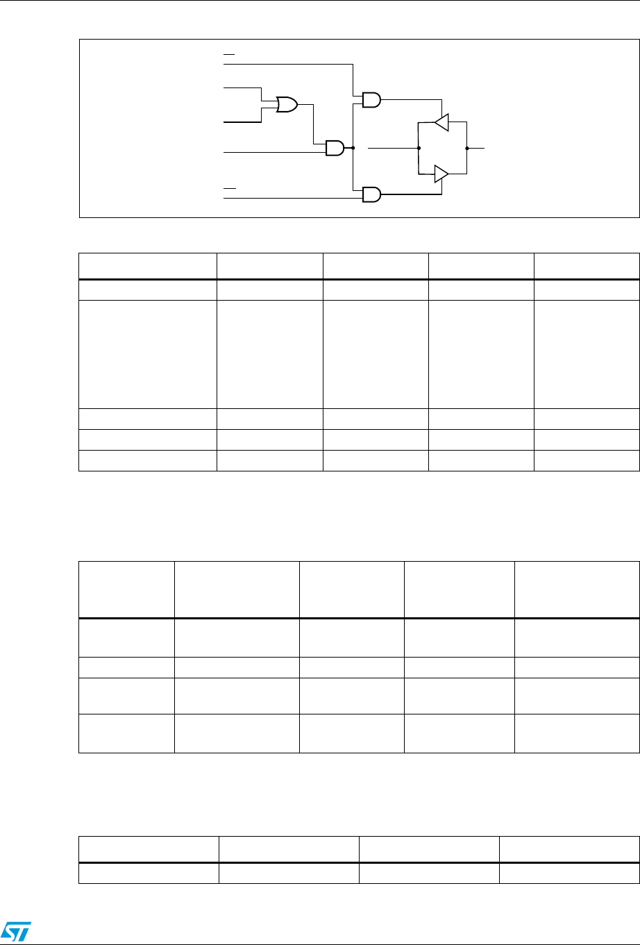
UPSD3212A, UPSD3212C, UPSD3212CV I/O ports (PSD module)
129/181
Figure 58. Peripheral I/O mode
1. Port A is not available in the 52-pin package.
2. On pins PC2, PC3, PC4, and PC7 only.
3. JTAG pins (TMS, TCK, TDI, TDO) are dedicated pins.
1. N/A = Not Applicable
2. The direction of the Port A,B,C, and D pins are controlled by the Direction Register ORed with the
individual output enable product term (.oe) from the CPLD AND Array.
Table 90. Port operating modes
Port mode Port A(1) Port B Port C Port D
M C U I / O Ye s Ye s Ye s Ye s
PLD I/O
McellAB Outputs
McellBC Outputs
Additional Ext. CS
Outputs
PLD Inputs
Ye s
No
No
Ye s
Ye s
Ye s
No
Ye s
No
Ye s (2)
No
Ye s
No
No
Ye s
Ye s
Address Out Yes (A7 – 0) Yes (A7 – 0) No No
Peripheral I/O Yes No No No
JTAG ISP No No Yes(3) No
Table 91. Port operating mode settings
Mode Defined in PSDsoft
Control
Register
Setting(1)
Direction
Register
Setting(1)
VM Register
Setting(1)
MCU I/O Declare pins only 0 1 = output,
0 = input (Note 2) N/A
PLD I/O Logic equations N/A (Note 2) N/A
Address Out
(Port A,B) Declare pins only 1 1 (Note 2) N/A
Peripheral I/O
(Port A)
Logic equations
(PSEL0 & 1) N/A N/A PIO Bit = 1
Table 92. I/O port latched address output assignments
Port A (PA3-PA0) Port A (PA7-PA4) Port B (PB3-PB0) Port B (PB7-PB4)
Address a3-a0 Address a7-a4 Address a3-a0 Address a7-a4
RD
PSEL0
PSEL1
PSEL
VM REGISTER BIT 7
WR
PA0-PA7
D0-D7
DATA BUS
AI02886
Obsolete Product(s) - Obsolete Product(s)

I/O ports (PSD module) UPSD3212A, UPSD3212C, UPSD3212CV
130/181
23.8 Port configuration registers (PCR)
Each Port has a set of Port Configuration Registers (PCR) used for configuration. The
contents of the registers can be accessed by the MCU through normal READ/WRITE bus
cycles at the addresses given in Ta b l e 8 1 . The addresses in Ta b l e 8 1 are the offsets in
hexadecimal from the base of the CSIOP register.
The pins of a port are individually configurable and each bit in the register controls its
respective pin. For example, Bit 0 in a register refers to Bit 0 of its port. The three Port
Configuration Registers (PCR), shown in Ta b le 9 3 , are used for setting the Port
configurations. The default Power-up state for each register in Ta b le 9 3 is 00h.
23.8.1 Control register
Any bit reset to '0' in the Control Register sets the corresponding port pin to MCU I/O mode,
and a '1' sets it to Address Out mode. The default mode is MCU I/O. Only Ports A and B
have an associated Control Register.
23.8.2 Direction register
The Direction Register, in conjunction with the output enable (except for Port D), controls the
direction of data flow in the I/O Ports. Any bit set to '1' in the Direction Register causes the
corresponding pin to be an output, and any bit set to '0' causes it to be an input. The default
mode for all port pins is input.
Figure 59 and Figure 60 show the Port Architecture diagrams for Ports A/B and C,
respectively. The direction of data flow for Ports A, B, and C are controlled not only by the
direction register, but also by the output enable product term from the PLD AND Array. If the
output enable product term is not active, the Direction Register has sole control of a given
pin’s direction.
An example of a configuration for a Port with the three least significant bits set to output and
the remainder set to input is shown in Ta b le 9 6 . Since Port D only contains two pins (shown
in Figure 62), the Direction Register for Port D has only two bits active.
23.8.3 Drive Select register
The Drive Select Register configures the pin driver as Open Drain or CMOS for some port
pins, and controls the slew rate for the other port pins. An external pull-up resistor should be
used for pins configured as Open Drain.
A pin can be configured as Open Drain if its corresponding bit in the Drive Select Register is
set to a '1.' The default pin drive is CMOS.
Note: The slew rate is a measurement of the rise and fall times of an output. A higher slew rate
means a faster output response and may create more electrical noise. A pin operates in a
high slew rate when the corresponding bit in the Drive Register is set to '1.' The default rate
is slow slew.
Ta bl e 9 7 shows the Drive Register for Ports A, B, C, and D. It summarizes which pins can be
configured as Open Drain outputs and which pins the slew rate can be set for.
Obsolete Product(s) - Obsolete Product(s)
UPSD3212A, UPSD3212C, UPSD3212CV I/O ports (PSD module)
131/181
Note: 1. See Table 97 for Drive Register Bit definition.
23.9 Port data registers
The Port Data Registers, shown in Ta b l e 9 8 , are used by the MCU to write data to or read
data from the ports. Ta b l e 9 8 shows the register name, the ports having each register type,
and MCU access for each register type. The registers are described below.
23.9.1 Data In
Port pins are connected directly to the Data In buffer. In MCU I/O Input mode, the pin input is
read through the Data In buffer.
23.9.2 Data Out register
Stores output data written by the MCU in the MCU I/O Output mode. The contents of the
Register are driven out to the pins if the Direction Register or the output enable product term
is set to '1.' The contents of the register can also be read back by the MCU.
23.9.3 Output macrocells (OMC)
The CPLD Output Macrocells (OMC) occupy a location in the MCU’s address space. The
MCU can read the output of the Output Macrocells (OMC). If the OMC Mask Register Bits
Table 93. Port configuration registers (PCR)
Register Name Port MCU Access
Control A,B WRITE/READ
Direction A,B,C,D WRITE/READ
Drive Select(1) A,B,C,D WRITE/READ
Table 94. Port pin direction control, output enable P.T. not defined
Direction Register Bit Port Pin mode
0 Input
1 Output
Table 95. Port pin direction control, output enable P.T. defined
Direction Register Bit Output Enable P.T. Port Pin mode
0 0 Input
0 1 Output
1 0 Output
1 1 Output
Table 96. Port direction assignment example
Bit 7 Bit 6 Bit 5 Bit 4 Bit 3 Bit 2 Bit 1 Bit 0
0 0 0 0 0 1 1 1
Obsolete Product(s) - Obsolete Product(s)

I/O ports (PSD module) UPSD3212A, UPSD3212C, UPSD3212CV
132/181
are not set, writing to the macrocell loads data to the macrocell flip-flops. See Section 22:
PLDs.
23.9.4 OMC mask register
Each OMC Mask Register Bit corresponds to an Output Macrocell (OMC) flip-flop. When the
OMC Mask Register Bit is set to a '1,' loading data into the Output Macrocell (OMC) flip-flop
is blocked. The default value is '0' or unblocked.
23.9.5 Input macrocells (IMC)
The Input Macrocells (IMC) can be used to latch or store external inputs. The outputs of the
Input Macrocells (IMC) are routed to the PLD input bus, and can be read by the MCU. See
Section 22: PLDs.
23.9.6 Enable out
The Enable Out register can be read by the MCU. It contains the output enable values for a
given port. A '1' indicates the driver is in output mode. A '0' indicates the driver is in tri-state
and the pin is in input mode.
1. NA = Not Applicable.
Table 97. Drive register pin assignment
Drive
Register Bit 7Bit 6Bit 5Bit 4Bit 3Bit 2Bit 1Bit 0
Port A Open
Drain
Open
Drain
Open
Drain
Open
Drain
Slew
Rate
Slew
Rate
Slew
Rate
Slew
Rate
Port B Open
Drain
Open
Drain
Open
Drain
Open
Drain
Slew
Rate
Slew
Rate
Slew
Rate
Slew
Rate
Port C Open
Drain NA(1) NA(1) Open
Drain
Open
Drain
Open
Drain NA(1) NA(1)
Port D NA(1) NA(1) NA(1) NA(1) NA(1) Slew
Rate
Slew
Rate NA(1)
Table 98. Port data registers
Register Name Port MCU Access
Data In A,B,C,D READ – input on pin
Data Out A,B,C,D WRITE/READ
Output Macrocell A,B,C READ – outputs of macrocells
WRITE – loading macrocells flip-flop
Mask Macrocell A,B,C WRITE/READ – prevents loading into a given
macrocell
Input Macrocell A,B,C READ – outputs of the Input Macrocells
Enable Out A,B,C READ – the output enable control of the port driver
Obsolete Product(s) - Obsolete Product(s)
UPSD3212A, UPSD3212C, UPSD3212CV I/O ports (PSD module)
133/181
23.10 Ports A and B – functionality and structure
Ports A and B have similar functionality and structure, as shown in Figure 59. The two ports
can be configured to perform one or more of the following functions:
●MCU I/O mode
●CPLD Output – Macrocells McellAB7-McellAB0 can be connected to Port A or Port B.
McellBC7-McellBC0 can be connected to Port B or Port C.
●CPLD Input – Via the Input Macrocells (IMC).
●Latched Address output – Provide latched address output as per Ta bl e 9 2 .
●Open Drain/Slew Rate – pins PA3-PA0 and PB3-PB0 can be configured to fast slew
rate, pins PA7-PA4 and PB7-PB4 can be configured to Open Drain mode.
●Peripheral mode – Port A only (80-pin package)
Figure 59. Port A and Port B structure
23.11 Port C – functionality and structure
Port C can be configured to perform one or more of the following functions (see Figure 60):
●MCU I/O mode
●CPLD Output – McellBC7-McellBC0 outputs can be connected to Port B or Port C.
●CPLD Input – via the Input Macrocells (IMC)
●In-System Programming (ISP) – JTAG pins (TMS, TCK, TDI, TDO) are dedicated pins
for device programming. (See Section 26: Programming in-circuit using the JTAG serial
interface, for more information on JTAG programming.)
●Open Drain – Port C pins can be configured in Open Drain mode
Port C does not support Address Out mode, and therefore no Control Register is required.
MCU DATA BUS
DATA OUT
REG.
DQ
D
G
Q
DQ
DQ
WR
WR
WR
ADDRESS
MACROCELL OUTPUTS
ENABLE PRODUCT TERM (.OE)
ALE
READ MUX
P
D
B
CPLD- INPUT
CONTROL REG.
DIR REG.
INPUT
MACROCELL
ENABLE OUT
DATA IN
OUTPUT
SELECT
OUTPUT
MUX
PORT
A OR B PIN
DATA OUT
ADDRESS
A[7:0]
AI06605
Obsolete Product(s) - Obsolete Product(s)
I/O ports (PSD module) UPSD3212A, UPSD3212C, UPSD3212CV
134/181
Figure 60. Port C structure
Note: 1. ISP
23.12 Port D – functionality and structure
Port D has two I/O pins (only one pin, PD1, in the 52-pin package). See Figure 61 and
Figure 62. This port does not support Address Out mode, and therefore no Control Register
is required. Of the eight bits in the Port D registers, only Bits 2 and 1 are used to configure
pins PD2 and PD1.
Port D can be configured to perform one or more of the following functions:
●MCU I/O mode
●CPLD Output – External Chip Select (ECS1-ECS2)
●CPLD Input – direct input to the CPLD, no Input Macrocells (IMC)
●Slew rate – pins can be set up for fast slew rate
Port D pins can be configured in PSDsoft Express as input pins for other dedicated
functions:
●CLKIN (PD1) as input to the macrocells flip-flops and APD counter
●PSD Chip Select Input (CSI, PD2). Driving this signal High disables the Flash memory,
SRAM and CSIOP.
MCU DATA BUS
DATA OUT
REG.
DQ
DQ
WR
WR
MCELLBC[7:0]
ENABLE PRODUCT TERM (.OE)
READ MUX
P
D
B
CPLD- INPUT
DIR REG.
INPUT
MACROCELL
ENABLE OUT
SPECIAL FUNCTION1
SPECIAL FUNCTION1
CONFIGURATION
BIT
DATA IN
OUTPUT
SELECT
OUTPUT
MUX
PORT C PIN
DATA OUT
AI06618
Obsolete Product(s) - Obsolete Product(s)
UPSD3212A, UPSD3212C, UPSD3212CV I/O ports (PSD module)
135/181
Figure 61. Port D structure
23.13 External chip select
The CPLD also provides two External Chip Select (ECS1-ECS2) outputs on Port D pins that
can be used to select external devices. Each External Chip Select (ECS1-ECS2) consists of
one product term that can be configured active High or Low. The output enable of the pin is
controlled by either the output enable product term or the Direction register. (See Figure 62.)
MCU DATA BUS
DATA OUT
REG.
DQ
DQ
WR
WR
ECS[2:1]
READ MUX
P
D
B
CPLD-INPUT
DIR REG.
DATA IN
ENABLE PRODUCT
TERM (.OE)
OUTPUT
SELECT
OUTPUT
MUX
PORT D PIN
DATA OUT
AI06606
Obsolete Product(s) - Obsolete Product(s)
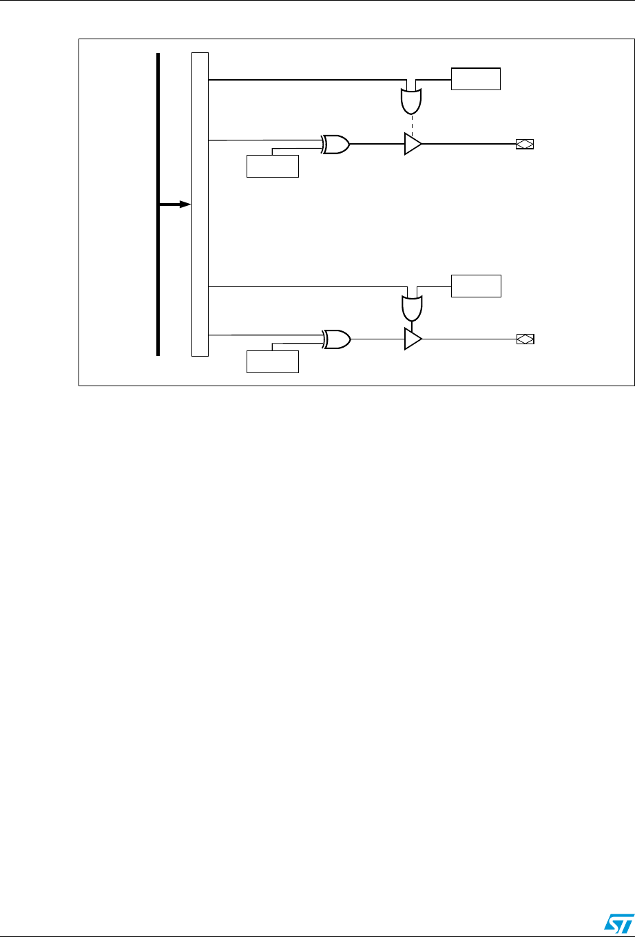
I/O ports (PSD module) UPSD3212A, UPSD3212C, UPSD3212CV
136/181
Figure 62. Port D external chip select signals
PLD INPUT BUS
POLARITY
BIT
PD2 PIN
PT2 ECS2
DIRECTION
REGISTER
ENABLE (.OE)
POLARITY
BIT
PD1 PIN
PT1 ECS1
ENABLE (.OE) DIRECTION
REGISTER
CPLD AND ARRAY
AI06607
Obsolete Product(s) - Obsolete Product(s)

UPSD3212A, UPSD3212C, UPSD3212CV Power management
137/181
24 Power management
All PSD modules offer configurable power saving options. These options may be used
individually or in combinations, as follows:
●The primary and secondary Flash memory, and SRAM blocks are built with power
management technology. In addition to using special silicon design methodology,
power management technology puts the memories into Standby mode when
address/data inputs are not changing (zero DC current). As soon as a transition occurs
on an input, the affected memory “wakes up,” changes and latches its outputs, then
goes back to standby. The designer does not have to do anything special to achieve
Memory Standby mode when no inputs are changing—it happens automatically.
●The PLD sections can also achieve Standby mode when its inputs are not changing, as
described in the sections on the Power Management mode Registers (PMMR).
●As with the Power Management mode, the Automatic Power Down (APD) block allows
the PSD module to reduce to Standby current automatically. The APD Unit can also
block MCU address/data signals from reaching the memories and PLDs.
●Built in logic monitors the Address Strobe of the MCU for activity. If there is no activity
for a certain time period (MCU is asleep), the APD Unit initiates Power-down mode (if
enabled). Once in Power-down mode, all address/data signals are blocked from
reaching memory and PLDs, and the memories are deselected internally. This allows
the memory and PLDs to remain in Standby mode even if the address/data signals are
changing state externally (noise, other devices on the MCU bus, etc.). Keep in mind
that any unblocked PLD input signals that are changing states keeps the PLD out of
Standby mode, but not the memories.
●PSD Chip Select Input (CSI, PD2) can be used to disable the internal memories,
placing them in Standby mode even if inputs are changing. This feature does not block
any internal signals or disable the PLDs. This is a good alternative to using the APD
Unit. There is a slight penalty in memory access time when PSD Chip Select Input
(CSI, PD2) makes its initial transition from deselected to selected.
●The PMMRs can be written by the MCU at run-time to manage power. The PSD
module supports “blocking bits” in these registers that are set to block designated
signals from reaching both PLDs. Current consumption of the PLDs is directly related
to the composite frequency of the changes on their inputs (see Figure Figure 66 and
Figure 67). Significant power savings can be achieved by blocking signals that are not
used in DPLD or CPLD logic equations.
Obsolete Product(s) - Obsolete Product(s)
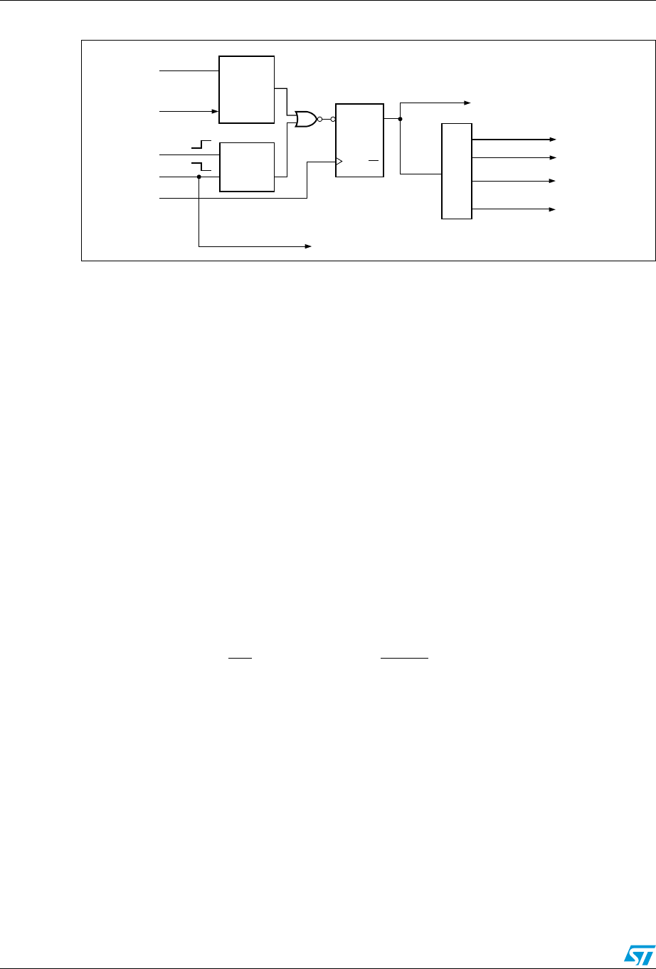
Power management UPSD3212A, UPSD3212C, UPSD3212CV
138/181
Figure 63. APD unit
The PSD module has a Turbo Bit in PMMR0. This bit can be set to turn the Turbo mode off
(the default is with Turbo mode turned on). While Turbo mode is off, the PLDs can achieve
standby current when no PLD inputs are changing (zero DC current). Even when inputs do
change, significant power can be saved at lower frequencies (AC current), compared to
when Turbo mode is on. When the Turbo mode is on, there is a significant DC current
component and the AC component is higher.
Automatic Power-down (APD) Unit and Power-down mode
The APD Unit, shown in Figure 63, puts the PSD module into Power-down mode by
monitoring the activity of Address Strobe (ALE). If the APD Unit is enabled, as soon as
activity on Address Strobe (ALE) stops, a four-bit counter starts counting. If Address Strobe
(ALE/AS, PD0) remains inactive for fifteen clock periods of CLKIN (PD1), Power-down
(PDN) goes High, and the PSD module enters Power-down mode, as discussed next.
Power-down mode
By default, if you enable the APD Unit, Power-down mode is automatically enabled. The
device enters Power-down mode if Address Strobe (ALE) remains inactive for fifteen periods
of CLKIN (PD1).
The following should be kept in mind when the PSD module is in Power-down mode:
●If Address Strobe (ALE) starts pulsing again, the PSD module returns to normal
Operating mode. The PSD module also returns to normal Operating mode if either PSD
Chip Select Input (CSI, PD2) is Low or the RESET input is High.
●The MCU address/data bus is blocked from all memory and PLDs.
●Various signals can be blocked (prior to Power-down mode) from entering the PLDs by
setting the appropriate bits in the PMMR registers. The blocked signals include MCU
control signals and the common CLKIN (PD1).
Note: Blocking CLKIN (PD1) from the PLDs does not block CLKIN (PD1) from the APD Unit.
●All memories enter Standby mode and are drawing standby current. However, the PLD
and I/O ports blocks do not go into Standby mode because you don’t want to have to
wait for the logic and I/O to “wake-up” before their outputs can change. See Ta bl e 9 9 for
Power-down mode effects on PSD module ports.
●Typical standby current is of the order of microamperes. These standby current values
assume that there are no transitions on any PLD input.
APD EN
PMMR0 BIT 1=1
ALE
RESET
CSI
CLKIN
TRANSITION
DETECTION
EDGE
DETECT
APD
COUNTER
POWER DOWN
(PDN)
DISABLE BUS
INTERFACE
CSIOP SELECT
FLASH SELECT
SRAM SELECT
PD
CLR
PD
DISABLE
FLASH/SRAM
PLD
SELECT
AI06608
Obsolete Product(s) - Obsolete Product(s)
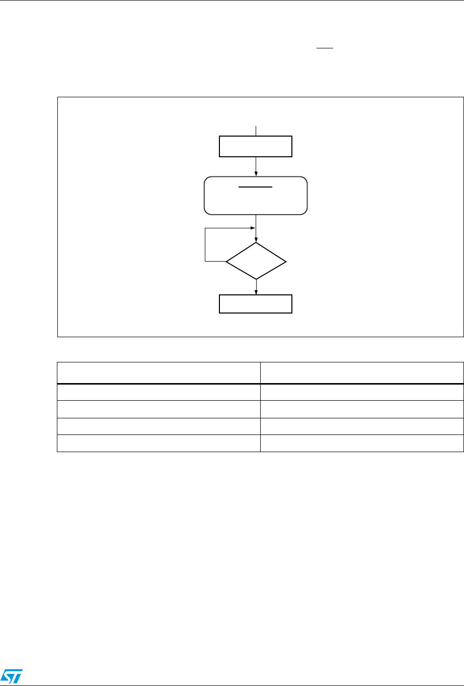
UPSD3212A, UPSD3212C, UPSD3212CV Power management
139/181
Other power-saving options
The PSD module offers other reduced power saving options that are independent of the
Power-down mode. Except for the PSD Chip Select Input (CSI, PD2) features, they are
enabled by setting bits in PMMR0 and PMMR2.
Figure 64. Enable Power-down flowchart
24.1 PLD power management
The power and speed of the PLDs are controlled by the Turbo Bit (Bit 3) in PMMR0. By
setting the bit to '1,' the Turbo mode is off and the PLDs consume the specified Standby
current when the inputs are not switching for an extended time of 70 ns. The propagation
delay time is increased by 10 ns (for a 5 V device) after the Turbo Bit is set to '1' (turned off)
when the inputs change at a composite frequency of less than 15MHz. When the Turbo Bit
is reset to '0' (turned on), the PLDs run at full power and speed. The Turbo Bit affects the
PLD’s DC power, AC power, and propagation delay. When the Turbo mode is off, the
UPSD321xx devices’ input clock frequency is reduced by 5 MHz from the maximum rated
clock frequency.
Blocking MCU control signals with the bits of PMMR2 can further reduce PLD AC power
consumption.
Table 99. Power-down mode’s effect on ports
Port Function Pin Level
MCU I/O No Change
PLD Out No Change
Address Out Undefined
Peripheral I/O Tri-State
Enable APD
Set PMMR0 Bit 1 = 1
PSD Module in Power
Down Mode
ALE idle
for 15 CLKIN
clocks?
RESET
Yes
No
OPTIONAL
Disable desired inputs to PLD
by setting PMMR0 bits 4 and 5
and PMMR2 bits 2 through 6.
AI06609
Obsolete Product(s) - Obsolete Product(s)
Power management UPSD3212A, UPSD3212C, UPSD3212CV
140/181
24.2 PSD chip select input (CSI, PD2)
PD2 of Port D can be configured in PSDsoft Express as PSD Chip Select Input (CSI). When
Low, the signal selects and enables the PSD module Flash memory, SRAM, and I/O blocks
for READ or WRITE operations. A High on PSD Chip Select Input (CSI, PD2) disables the
Flash memory, and SRAM, and reduces power consumption. However, the PLD and I/O
signals remain operational when PSD Chip Select Input (CSI, PD2) is High.
24.3 Input clock
CLKIN (PD1) can be turned off, to the PLD to save AC power consumption. CLKIN (PD1) is
an input to the PLD AND Array and the Output Macrocells (OMC).
During Power-down mode, or, if CLKIN (PD1) is not being used as part of the PLD logic
equation, the clock should be disabled to save AC power. CLKIN (PD1) is disconnected from
the PLD AND Array or the Macrocells block by setting Bits 4 or 5 to a '1' in PMMR0.
24.4 Input control signals
The PSD module provides the option to turn off the MCU signals (WR, RD, PSEN, and
Address Strobe (ALE)) to the PLD to save AC power consumption. These control signals
are inputs to the PLD AND Array. During Power-down mode, or, if any of them are not being
used as part of the PLD logic equation, these control signals should be disabled to save AC
power. They are disconnected from the PLD AND Array by setting Bits 2, 3, 4, 5, and 6 to a
'1' in PMMR2.
Table 100. Power management mode registers (PMMR0)
Bit 0 X 0 Not used, and should be set to zero.
Bit 1 APD Enable 0 = off Automatic Power-down (APD) is disabled.
1 = on Automatic Power-down (APD) is enabled.
Bit 2 X 0 Not used, and should be set to zero.
Bit 3 PLD Turbo
0 = on PLD Turbo mode is on
1 = off
PLD Turbo mode is off, saving power.
UPSD321xx devices operate at 5MHz below the maximum rated
clock frequency
Bit 4 PLD Array
clk
0 = on CLKIN (PD1) input to the PLD AND Array is connected. Every
change of CLKIN (PD1) Powers-up the PLD when Turbo Bit is '0.'
1 = off CLKIN (PD1) input to PLD AND Array is disconnected, saving
power.
Bit 5 PLD MCell
clk
0 = on CLKIN (PD1) input to the PLD macrocells is connected.
1 = off CLKIN (PD1) input to PLD macrocells is disconnected, saving
power.
Bit 6 X 0 Not used, and should be set to zero.
Bit 7 X 0 Not used, and should be set to zero.
Obsolete Product(s) - Obsolete Product(s)
UPSD3212A, UPSD3212C, UPSD3212CV Power management
141/181
1. The bits of this register are cleared to zero following Power-up. Subsequent RESET pulses do not clear the
registers.
Table 101. Power management mode registers (PMMR2)
Bit 0 X 0 Not used, and should be set to zero.
Bit 1 X 0 Not used, and should be set to zero.
Bit 2 PLD Array
WR
0 = on WR input to the PLD AND Array is connected.
1 = off WR input to PLD AND Array is disconnected, saving power.
Bit 3 PLD Array
RD
0 = on RD input to the PLD AND Array is connected.
1 = off RD input to PLD AND Array is disconnected, saving power.
Bit 4 PLD Array
PSEN
0 = on PSEN input to the PLD AND Array is connected.
1 = off PSEN input to PLD AND Array is disconnected, saving power.
Bit 5 PLD Array
ALE
0 = on ALE input to the PLD AND Array is connected.
1 = off ALE input to PLD AND Array is disconnected, saving power.
Bit 6 X 0 Not used, and should be set to zero.
Bit 7 X 0 Not used, and should be set to zero.
Table 102. APD counter operatio
APD Enable Bit ALE Level APD Counter
0 X Not Counting
1 Pulsing Not Counting
1 0 or 1 Counting (Generates PDN after 15
Clocks)
Obsolete Product(s) - Obsolete Product(s)
RESET timing and device status at reset UPSD3212A, UPSD3212C, UPSD3212CV
142/181
25 RESET timing and device status at reset
Upon Power-up, the PSD module requires a Reset (RESET) pulse of duration tNLNH-PO after
VCC is steady. During this period, the device loads internal configurations, clears some of
the registers and sets the Flash memory into operating mode. After the rising edge of Reset
(RESET), the PSD module remains in the Reset mode for an additional period, tOPR, before
the first memory access is allowed.
The Flash memory is reset to the READ mode upon Power-up. Sector Select (FS0-FS3 and
CSBOOT0-CSBOOT1) must all be Low, WRITE Strobe (WR, CNTL0) High, during Power-
on RESET for maximum security of the data contents and to remove the possibility of a byte
being written on the first edge of WRITE Strobe (WR). Any Flash memory WRITE cycle
initiation is prevented automatically when VCC is below VLKO.
25.1 Warm RESET
Once the device is up and running, the PSD module can be reset with a pulse of a much
shorter duration, tNLNH. The same tOPR period is needed before the device is operational
after a Warm RESET
. Figure 65 shows the timing of the Power-up and Warm RESET.
25.2 I/O pin, register and PLD status at RESET
Table 103 shows the I/O pin, register and PLD status during Power-on RESET, Warm
RESET, and Power-down mode. PLD outputs are always valid during Warm RESET, and
they are valid in Power-on RESET once the internal Configuration bits are loaded. This
loading is completed typically long before the VCC ramps up to operating level. Once the
PLD is active, the state of the outputs are determined by the PLD equations.
Figure 65. Reset (RESET) timing
tNLNH-PO tOPR
AI02866b
RESET
tNLNH
tNLNH-A tOPR
V
CC
V
CC
(min)
Power-On Reset Warm Reset
Obsolete Product(s) - Obsolete Product(s)
UPSD3212A, UPSD3212C, UPSD3212CV RESET timing and device status at reset
143/181
1. The SR_cod and Periphmode Bits in the VM Register are always cleared to '0' on Power-on RESET or
Warm RESET.
Table 103. Status during Power-on RESET, Warm RESET and Power-down mode
Port Configuration Power-On RESET Warm RESET Power-down mode
MCU I/O Input mode Input mode Unchanged
PLD Output
Valid after internal PSD
configuration bits are
loaded
Valid
Depends on inputs to
PLD (addresses are
blocked in PD mode)
Address Out Tri-stated Tri-stated Not defined
Peripheral I/O Tri-stated Tri-stated Tri-stated
Register Power-On RESET Warm RESET Power-down mode
PMMR0 and PMMR2 Cleared to '0' Unchanged Unchanged
Macrocells flip-flop
status
Cleared to '0' by
internal Power-on
RESET
Depends on .re and .pr
equations
Depends on .re and .pr
equations
VM Register(1)
Initialized, based on the
selection in PSDsoft
Configuration menu
Initialized, based on the
selection in PSDsoft
Configuration menu
Unchanged
All other registers Cleared to '0' Cleared to '0' Unchanged
Obsolete Product(s) - Obsolete Product(s)
Programming in-circuit using the JTAG serial interface UPSD3212A, UPSD3212C, UPSD3212CV
144/181
26 Programming in-circuit using the JTAG serial
interface
The JTAG Serial Interface pins (TMS, TCK, TDI, and TDO) are dedicated pins on Port C
(see Table 104). All memory blocks (primary and secondary Flash memory), PLD logic, and
PSD module Configuration Register Bits may be programmed through the JTAG Serial
Interface block. A blank device can be mounted on a printed circuit board and programmed
using JTAG.
The standard JTAG signals (IEEE 1149.1) are TMS, TCK, TDI, and TDO. Two additional
signals, TSTAT and TERR, are optional JTAG extensions used to speed up Program and
Erase cycles.
By default, on a blank device (as shipped from the factory or after erasure), four pins on Port
C are the basic JTAG signals TMS, TCK, TDI, and TDO.
26.1 Standard JTAG Signals
At power-up, the standard JTAG pins are inputs, waiting for a JTAG serial command from an
external JTAG controller device (such as FlashLINK or Automated Test Equipment). When
the enabling command is received, TDO becomes an output and the JTAG channel is fully
functional. The same command that enables the JTAG channel may optionally enable the
two additional JTAG signals, TSTAT and TERR.
The RESET input to the uPS3200 should be active during JTAG programming. The active
RESET puts the MCU module into RESET mode while the PSD module is being
programmed. See Application Note AN1153 for more details on JTAG In-System
Programming (ISP).
UPSD321xx devices support JTAG In-System-Configuration (ISC) commands, but not
Boundary Scan. The PSDsoft Express software tool and FlashLINK JTAG programming
cable implement the JTAG In-System-Configuration (ISC) commands.
26.2 JTAG extensions
TSTAT and TERR are two JTAG extension signals enabled by an “ISC_ENABLE” command
received over the four standard JTAG signals (TMS, TCK, TDI, and TDO). They are used to
speed Program and Erase cycles by indicating status on uPDS signals instead of having to
Table 104. JTAG port signals
Port C Pin JTAG Signals Description
PC0 TMS Mode Select
PC1 TCK Clock
PC3 TSTAT Status (optional)
PC4 TERR Error Flag (optional)
PC5 TDI Serial Data In
PC6 TDO Serial Data Out
Obsolete Product(s) - Obsolete Product(s)

UPSD3212A, UPSD3212C, UPSD3212CV Programming in-circuit using the JTAG serial interface
145/181
scan the status out serially using the standard JTAG channel. See Application Note
AN1153.
TERR indicates if an error has occurred when erasing a sector or programming a byte in
Flash memory. This signal goes Low (active) when an Error condition occurs, and stays Low
until an “ISC_CLEAR” command is executed or a chip Reset (RESET) pulse is received
after an “ISC_DISABLE” command.
TSTAT behaves the same as Ready/Busy described in Section 21.2.1: Ready/Busy (PC3).
TSTAT is High when the PSD module device is in READ mode (primary and secondary
Flash memory contents can be read). TSTAT is Low when Flash memory Program or Erase
cycles are in progress, and also when data is being written to the secondary Flash memory.
TSTAT and TERR can be configured as open-drain type signals during an “ISC_ENABLE”
command.
26.3 Security and Flash memory protection
When the Security Bit is set, the device cannot be read on a Device Programmer or through
the JTAG Port. When using the JTAG Port, only a Full Chip Erase command is allowed.
All other Program, Erase and Verify commands are blocked. Full Chip Erase returns the part
to a non-secured blank state. The Security Bit can be set in PSDsoft Express Configuration.
All primary and secondary Flash memory sectors can individually be sector protected
against erasures. The sector protect bits can be set in PSDsoft Express Configuration.
Obsolete Product(s) - Obsolete Product(s)

Initial delivery state UPSD3212A, UPSD3212C, UPSD3212CV
146/181
27 Initial delivery state
When delivered from ST, the UPSD321xx devices have all bits in the memory and PLDs set
to '1.' The code, configuration, and PLD logic are loaded using the programming procedure.
Information for programming the device is available directly from ST. Please contact your
local sales representative.
Obsolete Product(s) - Obsolete Product(s)
UPSD3212A, UPSD3212C, UPSD3212CV AC/DC parameters
147/181
28 AC/DC parameters
These tables describe the AD and DC parameters of the UPSD321xx devices:
●DC Electrical Specification
●AC Timing Specification
●PLD Timing
– Combinatorial Timing
– Synchronous Clock mode
– Asynchronous Clock mode
– Input Macrocell Timing
●MCU module Timing
– READ Timing
– WRITE Timing
– Power-down and RESET Timing
The following are issues concerning the parameters presented:
●In the DC specification the supply current is given for different modes of operation.
●The AC power component gives the PLD, Flash memory, and SRAM mA/MHz
specification. Figure 66 and Figure 67 show the PLD mA/MHz as a function of the
number of Product Terms (PT) used.
●In the PLD timing parameters, add the required delay when Turbo Bit is '0.'
Figure 66. PLD ICC/frequency consumption (5 V range)
0
10
20
30
40
60
70
80
90
100
110
V
CC
= 5V
50
010155 20 25
HIGHEST COMPOSITE FREQUENCY AT PLD INPUTS (MHz)
I
CC
– (mA)
TURBO ON (100%)
TURBO ON (25%)
TURBO OFF
TURBO OFF
PT 100%
PT 25%
AI02894
Obsolete Product(s) - Obsolete Product(s)
AC/DC parameters UPSD3212A, UPSD3212C, UPSD3212CV
148/181
Figure 67. PLD ICC/frequency consumption (3 V range)
Table 105. PSD module example, typ. power calculation at VCC = 5.0 V (Turbo mode
off)
Conditions
MCU clock frequency = 12 MHz
Highest Composite PLD input frequency
(Freq PLD) = 8 MHz
MCU ALE frequency (Freq ALE) = 2 MHz
% Flash memory access = 80%
% SRAM access = 15%
% I/O access = 5% (no additional power above base)
Operational modes
% Normal = 40%
% Power-down mode = 60%
Number of product terms used
(from fitter report) = 45 PT
% of total product terms = 45/182 = 24.7%
Turbo mode = Off
0
10
20
30
40
50
60
V
CC
= 3V
010155 20 25
I
CC
– (mA)
TURBO ON (100%)
TURBO ON (25%)
TURBO OFF
TURBO OFF
HIGHEST COMPOSITE FREQUENCY AT PLD INPUTS (MHz)
PT 100%
PT 25%
AI03100
Obsolete Product(s) - Obsolete Product(s)
UPSD3212A, UPSD3212C, UPSD3212CV AC/DC parameters
149/181
Calculation (using typical values)
ICC total
= ICC(MCUactive) x %MCUactive + ICC(PSDactive) x %PSDactive + IPD(pwrdown) x
%pwrdown
ICC(MCUactive) = 20mA
IPD(pwrdown) = 250µA
ICC(PSDactive) = ICC(ac) + ICC(dc)
= %flash x 2.5mA/MHz x Freq ALE
+ %SRAM x 1.5mA/MHz x Freq
ALE
+ % PLD x (from graph using
Freq PLD)
= 0.8 x 2.5mA/MHz x 2MHz + 0.15 x
1.5mA/MHz x 2MHz + 24mA
= (4 + 0.45 + 24) mA
= 28.45mA
ICC total = 20mA x 40% + 28.45mA x 40% + 250µA x 60%
= 8mA + 11.38mA + 150µA
= 19.53mA
This is the operating power with no Flash memory Erase or Program cycles in progress. Calculation
is based on all I/O pins being disconnected and IOUT = 0mA.
Table 105. PSD module example, typ. power calculation at VCC = 5.0 V (Turbo mode
off) (continued)
Conditions
Obsolete Product(s) - Obsolete Product(s)
Maximum ratings UPSD3212A, UPSD3212C, UPSD3212CV
150/181
29 Maximum ratings
Stressing the device above the rating listed in the Absolute Maximum Ratings” table may
cause permanent damage to the device. These are stress ratings only and operation of the
device at these or any other conditions above those indicated in the Operating sections of
this specification is not implied. Exposure to Absolute Maximum Rating conditions for
extended periods may affect device reliability. Refer also to the STMicroelectronics SURE
Program and other relevant quality documents.
1. IPC/JEDEC J-STD-020A
2. JEDEC Std JESD22-A114A (C1=100pF, R1=1500 Ω, R2=500 Ω)
Table 106. Absolute maximum ratings
Symbol Parameter Min. Max. Unit
TSTG Storage Temperature –65 125 °C
TLEAD Lead Temperature during Soldering (20 seconds max.)(1) 235 °C
VIO Input and Output Voltage (Q = VOH or Hi-Z) –0.5 6.5 V
VCC Supply Voltage –0.5 6.5 V
VPP Device Programmer Supply Voltage –0.5 14.0 V
VESD Electrostatic Discharge Voltage (Human Body Model) 2–2000 2000 V
Obsolete Product(s) - Obsolete Product(s)

UPSD3212A, UPSD3212C, UPSD3212CV EMC characteristics
151/181
30 EMC characteristics
Susceptibility test are performed on a sample basis during product characterization.
30.1 Functional EMS (electromagnetic susceptibility)
Based on a simple running application on the product (toggling 2 LEDs through I/O ports),
the product is stressed by two electromagnetic events until a failure occurs (indicated by the
LEDs).
30.1.1 ESD
Electro-Static Discharge (positive and negative) is applied on all pins of the device until a
functional disturbance occurs. This test conforms with the IEC 1000-4-2 Standard.
30.1.2 FTB
A burst of Fast Transient voltage (positive and negative) is applied to VDD and VSS through a
100pF capacitor, until a functional disturbance occurs. This test conforms with the IEC
1000-4-2 Standard.
A device reset allows normal operations to be resumed. The test results are given in
Table 107, based on the EMS levels and classes defined in Application Note AN1709.
30.2 Designing hardened software to avoid noise problems
EMC characterization and optimization are performed at component level with a typical
application environment and simplified MCU software. It should be noted that good EMC
performance is highly dependent on the user application and the software in particular.
Therefore, it is recommended that the user applies EMC software optimization and
prequalification tests in relation with the EMC level requested for the user’s application.
30.2.1 Software recommendations
The software flowchart must include the management of ‘runaway’ conditions, such as:
●Corrupted program counter
●Unexpected reset
●Critical data corruption (e.g., control registers)
30.2.2 Prequalification trials
Most of the common failures (unexpected reset and program counter corruption) can be
reproduced by manually forcing a low state on the RESET pin or the oscillator pins for 1
second.
To complete these trials, ESD stress can be applied directly on the device over the range of
specification values. When unexpected behavior is detected, the software can be hardened
to prevent unrecoverable errors occurring (see Application Note AN1015).
Obsolete Product(s) - Obsolete Product(s)
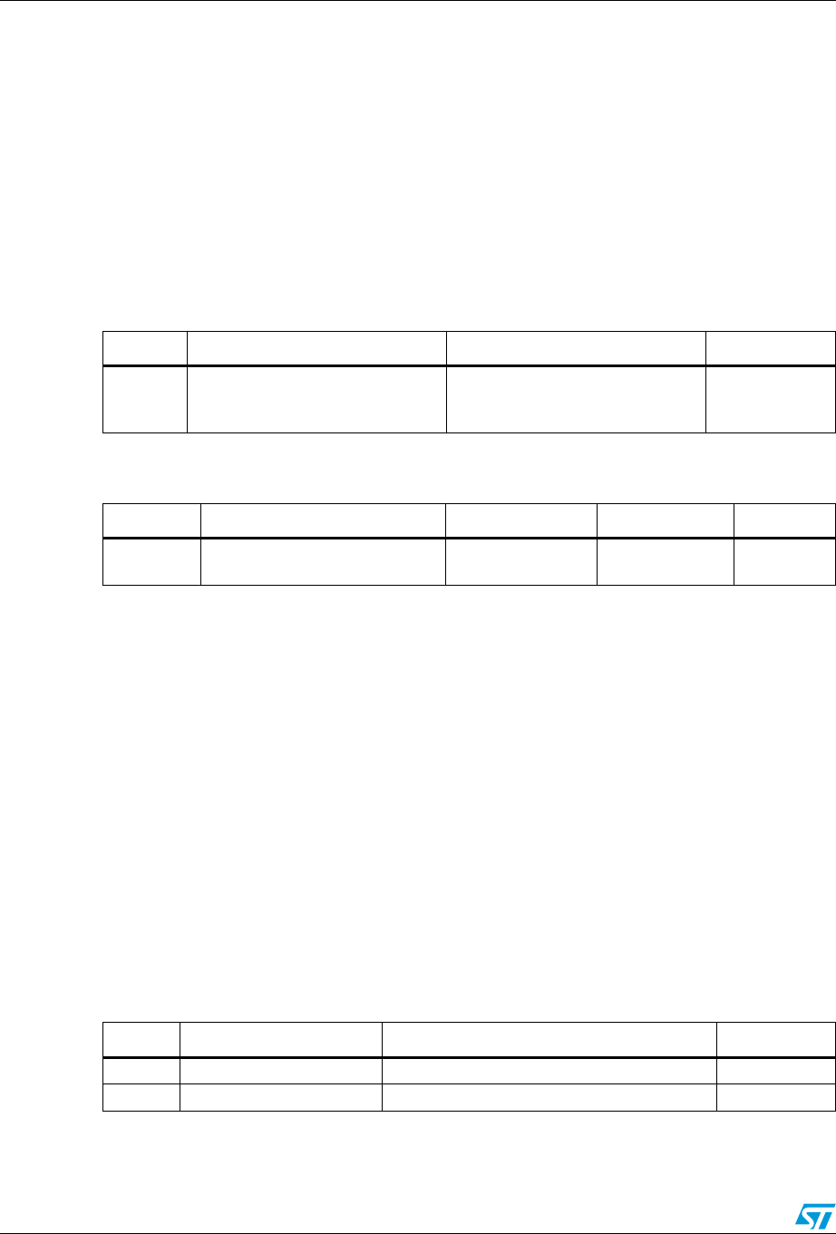
EMC characteristics UPSD3212A, UPSD3212C, UPSD3212CV
152/181
30.3 Absolute maximum ratings (electrical sensitivity)
Based on three different tests (ESD, LU, and DLU) and using specific measurement
methods, the product is stressed in order to determine its performance in terms of electrical
sensitivity. For more details, refer to the Application Note AN1181.
30.3.1 Electro-static discharge (ESD)
Electro-Static discharges (a positive then a negative pulse separated by 1 second) are
applied to the pins of each sample according to each pin combination. The sample size
depends on the number of supply pins in the device (3 parts*(n+1) supply pin). The Human
Body Model is simulated (Ta bl e 1 0 8 ). This test complies with the JESD22-A114A Standard.
1. Data based on characterization results, not tested in production.
1. Data based on characterization results, not tested in production
30.3.2 Latch-up
3 complementary static tests are required on 10 parts to assess the latch-up performance. A
supply overvoltage (applied to each power supply pin) and a current injection (applied to
each input, output, and configurable I/O pin) are performed on each sample. This test
conforms to the EIA/JESD 78 IC Latch-up Standard (see Ta b le 1 0 9 ). For more details, refer
to the Application Note, AN1181.
30.3.3 Dynamic latch-up
Electro-static discharges (one positive then one negative test) are applied to each pin of 3
samples when the micro is running to assess the latch-up performance in dynamic mode.
Power supplies are set to the typical values, the oscillator is connected as near as possible
to the pins of the micro, and the component is put in reset mode. This test conforms to the
IEC 1000-4-2 and SAEJ1752/3 Standards (see Ta b le 1 0 9 ). For more details, refer to the
Application Note, AN1181.
1. Class description: A Class is an STMicroelectronics internal specification. All of its limits are higher than the
JEDEC specifications. This means when a device belongs to “Class A,” it exceeds the JEDEC standard.
“Class B” strictly covers all of the JEDEC criteria (International standards).
Table 107. EMS test results
Symbol Parameter Conditions Level/Class (1)
VFESD
Voltage limits to be applied on any
I/O pin to induce a functional
disturbance
VDD = 4V; TA = 25°C; fOSC =
40MHz; WDT off complies with
IEC 1000-4-2
3C
Table 108. ESD absolute maximum ratings
Symbol Parameter Conditions Max. Value(1) Unit
VESD(HBM)
Electro-static discharge voltage
(Human Body Model) TA = 25°C 2000 V
Table 109. Latch-up and dynamic latch-up electrical sensitivities
Symbol Parameter Conditions Level/class (1)
LU Static latch-up class TA = 25°C A
DLU Dynamic latch-up class VDD = 5 V; TA = 25°C; fOSC = 40 MHz A
Obsolete Product(s) - Obsolete Product(s)
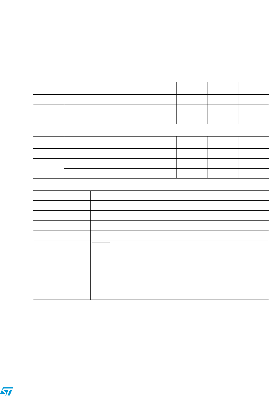
UPSD3212A, UPSD3212C, UPSD3212CV DC and AC parameters
153/181
31 DC and AC parameters
This section summarizes the operating and measurement conditions, and the DC and AC
characteristics of the device. The parameters in the DC and AC Characteristic tables that
follow are derived from tests performed under the Measurement Conditions summarized in
the relevant tables. Designers should check that the operating conditions in their circuit
match the measurement conditions when relying on the quoted parameters.
1. Example: tAVLX = Time from Address Valid to ALE Invalid.
Table 110. Operating conditions (5 V devices)
Symbol Parameter Min. Max. Unit
VCC Supply voltage 4.5 5.5 V
TA
Ambient operating temperature (industrial) –40 85 °C
Ambient operating temperature (commercial) 0 70 °C
Table 111. Operating conditions (3 V devices)
Symbol Parameter Min. Max. Unit
VCC Supply voltage 3.0 3.6 V
TA
Ambient operating temperature (industrial) –40 85 °C
Ambient operating temperature (commercial) 0 70 °C
Table 112. AC signal letters for timing
AAddress
C Clock
D Input Data
I Instruction
LALE
N RESET Input or Output
P PSEN signal
Q Output Data
R RD signal
W WR signal
M Output Macrocell
Obsolete Product(s) - Obsolete Product(s)
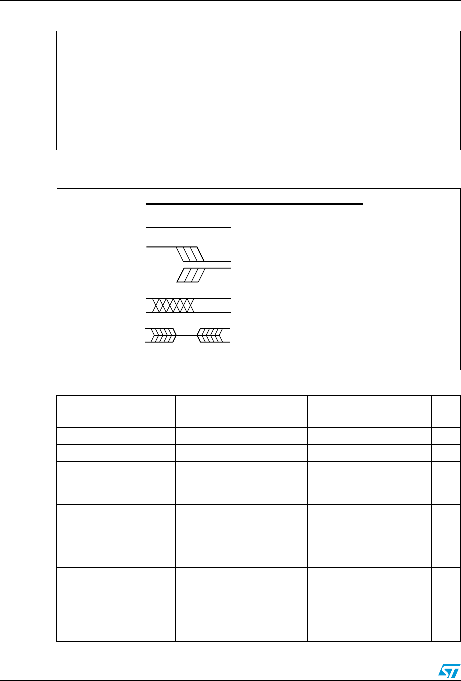
DC and AC parameters UPSD3212A, UPSD3212C, UPSD3212CV
154/181
1. Example: tAVLX = Time from Address Valid to ALE Invalid.
Figure 68. Switching waveforms – key
Table 113. AC signal behavior symbols for timing
tTime
L Logic Level Low or ALE
H Logic Level High
V Valid
X No Longer a Valid Logic Level
Z Float
PW Pulse Width
Table 114. Major parameters
Parameters/conditions/
comments
5 V test
conditions 5.0 V value 3.3 V test
conditions
3.3 V
value Unit
Operating voltage – 4.5 to 5.5 – 3.0 to 3.6 V
Operating temperature – –40 to 85 – –40 to 85 °C
MCU frequency
12 MHz (min) for USB;
8 MHz (min) for I2C
–1 Min, 40
Max –1 Min, 24
Max MHz
Active current, typical
(25°C operation; 80% Flash
and 15% SRAM accesses,
45 PLD product terms used;
PLD Turbo mode Off)
24 MHz MCU
clock, 12 MHz
PLD input
frequency, 4 MHz
ALE
72
12 MHz MCU
clock, 6 MHz
PLD input
frequency,
2MHz ALE
21 mA
Idle current, typical
(CPU halted but some
peripherals active; 25°C
operation; 45 PLD product
terms used; PLD Turbo
mode Off)
24 MHz MCU
clock, 12 MHz
PLD input
frequency
25
12 MHz MCU
clock, 1 MHz
PLD input
frequency
7mA
WAVEFORMS INPUTS OUTPUTS
STEADY INPUT
MAY CHANGE FROM
HI TO LO
MAY CHANGE FROM
LO TO HI
DON'T CARE
OUTPUTS ONLY
STEADY OUTPUT
WILL BE CHANGING
FROM HI TO LO
WILL BE CHANGING
LO TO HI
CHANGING, STATE
UNKNOWN
CENTER LINE IS
TRI-STATE
AI03102
Obsolete Product(s) - Obsolete Product(s)

UPSD3212A, UPSD3212C, UPSD3212CV DC and AC parameters
155/181
Standby current, typical
(Power-down mode,
requires reset to exit mode;
without Low-Voltage Detect
(LVD) Supervisor)
180 µA with LVD 110 100 µA with LVD 60 µA
I/O sink/source current
Ports A, B, C, and D
VOL = 0.25 V
(max);
VOH = 3.9 V (min)
IOL = 8
(max);
IOH = –2
(min)
VOL = 0.15 V
(max);
VOH = 2.6 V (min)
IOL = 4
(max);
IOH = –1
(min)
mA
PLD macrocells (For
registered or combinatorial
logic)
–16–16–
PLD inputs (Inputs from
pins, macrocell feedback, or
MCU addresses)
–69–69–
PLD outputs (Output to pins
or internal feedback) –16–16–
PLD propagation delay,
typical (PLD input to output,
Turbo mode)
– 15 – 22 ns
Table 114. Major parameters (continued)
Parameters/conditions/
comments
5 V test
conditions 5.0 V value 3.3 V test
conditions
3.3 V
value Unit
Obsolete Product(s) - Obsolete Product(s)
DC and AC parameters UPSD3212A, UPSD3212C, UPSD3212CV
156/181
Table 115. DC characteristics (5 V devices)
Symbol Parameter
Test conditions (in
addition to those in
Table 110)
Min. Typ. Max. Unit
VIH
Input high voltage (Ports 1,
2, 3, 4[Bits 7,6,5,4,3,1,0],
XTAL1, RESET)
4.5 V < VCC < 5.5 V 0.7 VCC
VCC +
0.5 V
VIH1
Input high voltage (Ports A,
B, C, D, 4[Bit 2], USB+,
USB–)
4.5 V < VCC < 5.5 V 2.0 VCC +
0.5 V
VIL
Input low voltage (Ports 1,
2, 3, 4[Bits 7,6,5,4,3,1,0],
XTAL1, RESET)
4.5 V < VCC < 5.5 V VSS–0.5 0.3 VC
C
V
VIL1
Input low voltage
(Ports A, B, C, D, 4[Bit 2]) 4.5 V < VCC < 5.5 V –0.5 0.8 V
Input low voltage
(USB+, USB–) 4.5 V < VCC < 5.5 V VSS–0.5 0.8 V
VOL
Output low voltage
(Ports A,B,C,D)
IOL = 20 µA
VCC = 4.5 V 0.01 0.1 V
IOL = 8 mA
VCC = 4.5 V 0.25 0.45 V
VOL1
Output low voltage
(Ports 1,2,3,4, WR, RD)IOL = 1.6 mA 0.45 V
VOL2
Output low voltage
(Port 0, ALE, PSEN) IOL = 3.2 mA 0.45 V
VOH
Output high voltage
(Ports A,B,C,D)
IOH = –20 µA
VCC = 4.5 V 4.4 4.49 V
IOH = –2 mA
VCC = 4.5 V 2.4 3.9 V
VOH2
Output high voltage (Port 0
in ext. Bus mode, ALE,
PSEN)
IOH = –800 µA 2.4 V
IOH = –80 µA 4.05 V
VLVR Low Voltage RESET 0.1 V hysteresis 3.75 4.0 4.25 V
VOP
XTAL open bias voltage
(XTAL1, XTAL2) IOL = 3.2 mA 2.0 3.0 V
VLKO
VCC(min) for Flash Erase
and Program 2.5 4.2 V
IIL
Logic '0' input current
(Ports 1,2,3,4)
VIN = 0.45 V
(0 V for Port 4[pin 2]) –10 –50 µA
ITL
Logic 1-to-0 transition
current (Ports 1,2,3,4)
VIN = 3.5 V
(2.5 V for Port 4[pin 2]) –65 –650 µA
IRST
Reset pin pull-up current
(RESET)VIN = VSS –10 –55 µA
Obsolete Product(s) - Obsolete Product(s)
UPSD3212A, UPSD3212C, UPSD3212CV DC and AC parameters
157/181
1. IPD (Power-down mode) is measured with:
XTAL1=VSS; XTAL2=not connected; RESET=VCC; Port 0 =VCC; all other pins are disconnected. PLD not
in Turbo mode.
2. ICC_CPU (active mode) is measured with:
XTAL1 driven with tCLCH, tCHCL = 5 ns, VIL = VSS+0.5 V, VIH = Vcc – 0.5 V, XTAL2 = not connected;
RESET=VSS; Port 0=VCC; all other pins are disconnected. ICC would be slightly higher if a crystal oscillator
is used (approximately 1mA).
3. ICC_CPU (Idle mode) is measured with:
XTAL1 driven with tCLCH, tCHCL = 5 ns, VIL = VSS+0.5 V, VIH = VCC– 0.5 V, XTAL2 = not connected;
Port 0 = VCC;
4. RESET=VCC; all other pins are disconnected.
5. PLD is in non-Turbo mode and none of the inputs are switching.
6. See Figure 66 for the PLD current calculation.
7. I/O current = 0 mA, all I/O pins are disconnected.
IFR
XTAL feedback resistor
current (XTAL1)
XTAL1 = VCC
XTAL2 = VSS
–20 –50 µA
ILI Input leakage current VSS < VIN < VCC –1 1 µA
ILO Output leakage current 0.45 < VOUT < VCC –10 10 µA
IPD(1) Power-down mode
VCC = 5.5 V
LVD logic disabled 250 µA
LVD logic enabled 380 µA
ICC_CPU
(2,3,6)
Active (12 MHz) VCC = 5 V 20 30 mA
Idle (12 MHz) 8 10 mA
Active (24 MHz) VCC = 5 V 30 38 mA
Idle (24 MHz) 15 20 mA
Active (40 MHz) VCC = 5 V 40 62 mA
Idle (40 MHz) 20 30 mA
ICC_PSD
(DC)(6)
Operating
supply current
PLD Only
PLD_TURBO = Off,
f = 0 MHz(4) 0 µA/PT(5)
PLD_TURBO = On,
f = 0 MHz 400 700 µA/PT
Flash
memory
During Flash memory
WRITE/Erase Only 15 30 mA
Read-only, f = 0 MHz 0 0 mA
SRAM f = 0 MHz 0 0 mA
ICC_PSD
(AC)(6)
PLD AC Base Note 5
Flash memory AC adder 2.5 3.5 mA/MHz
SRAM AC adder 1.5 3.0 mA/MHz
Table 115. DC characteristics (5 V devices) (continued)
Symbol Parameter
Test conditions (in
addition to those in
Table 110)
Min. Typ. Max. Unit
Obsolete Product(s) - Obsolete Product(s)
DC and AC parameters UPSD3212A, UPSD3212C, UPSD3212CV
158/181
Table 116. DC characteristics (3 V devices)
Symbol Parameter
Test conditions (in
addition to those in
Table 111)
Min. Typ. Max. Unit
VIH
Input high voltage (Ports 1,
2, 3, 4[Bits 7,6,5,4,3,1,0], A,
B, C, D, XTAL1, RESET)
3.0 V < VCC < 3.6 V 0.7VCC
VCC +
0.5 V
VIH1
Input high voltage (Port
4[Bit 2]) 3.0 V < VCC < 3.6 V 2.0 VCC +
0.5 V
VIL
Input high voltage (Ports 1,
2, 3, 4[Bits 7,6,5,4,3,1,0],
XTAL1, RESET)
3.0 V < VCC < 3.6 V VSS–0.5 0.3
VCC
V
VIL1
Input low voltage
(Ports A, B, C, D) 3.0 V < VCC < 3.6 V –0.5 0.8 V
Input low voltage
(Port 4[Bit 2]) 3.0 V < VCC < 3.6 V VSS–0.5 0.8 V
VOL
Output low voltage
(Ports A,B,C,D)
IOL = 20 µA
VCC = 3.0 V 0.01 0.1 V
IOL = 4 mA
VCC = 3.0 V 0.15 0.45 V
VOL1
Output low voltage
(Ports 1,2,3,4, WR, RD)
IOL = 1.6 mA 0.45 V
IOL = 100 µA 0.3 V
VOL2
Output low voltage
(Port 0, ALE, PSEN)
IOL = 3.2 mA 0.45 V
IOL = 200 µA 0.3 V
VOH
Output high voltage
(Ports A,B,C,D)
IOH = –20 µA
VCC = 3.0 V 2.9 2.99 V
IOH = –1 mA
VCC = 3.0 V 2.4 2.6 V
VOH2
Output high voltage (Port 0
in ext. Bus mode, ALE,
PSEN)
IOH = –800 µA 2.0 V
IOH = –80 µA 2.7 V
VLVR Low voltage reset 0.1 V hysteresis 2.3 2.5 2.7 V
VOP
XTAL open bias voltage
(XTAL1, XTAL2) IOL = 3.2 mA 1.0 2.0 V
VLKO
VCC(min) for Flash Erase
and Program 1.5 2.2 V
IIL
Logic '0' input current
(Ports 1,2,3,4)
VIN = 0.45 V
(0 V for Port 4[pin 2]) –1 –50 µA
ITL
Logic 1-to-0 transition
current (Ports 1,2,3,4)
VIN = 3.5 V
(2.5 V for Port 4[pin 2]) –25 –250 µA
IRST
Reset pin pull-up current
(RESET)VIN = VSS –10 –55 µA
IFR
XTAL feedback resistor
current (XTAL1)
XTAL1 = VCC
XTAL2 = VSS
–20 –50 µA
ILI Input leakage current VSS < VIN < VCC –1 1 µA
ILO Output leakage current 0.45 < VOUT < VCC –10 10 µA
Obsolete Product(s) - Obsolete Product(s)
UPSD3212A, UPSD3212C, UPSD3212CV DC and AC parameters
159/181
1. IPD (Power-down mode) is measured with:
XTAL1=VSS; XTAL2=not connected; RESET=VCC; Port 0 =VCC; all other pins are disconnected. PLD not
in Turbo mode.
2. ICC_CPU (active mode) is measured with:
XTAL1 driven with tCLCH, tCHCL = 5 ns, VIL = VSS+0.5 V, VIH = Vcc – 0.5 V, XTAL2 = not connected;
RESET=VSS; Port 0=VCC; all other pins are disconnected. ICC would be slightly higher if a crystal oscillator
is used (approximately 1 mA).
3. ICC_CPU (Idle mode) is measured with:
XTAL1 driven with tCLCH, tCHCL = 5 ns, VIL = VSS+0.5 V, VIH = VCC– 0.5 V, XTAL2 = not connected;
Port 0 = VCC;
4. RESET = VCC; all other pins are disconnected.
5. PLD is in non-Turbo mode and none of the inputs are switching.
6. See Figure 66 for the PLD current calculation.
7. I/O current = 0 mA, all I/O pins are disconnected.
IPD(1) Power-down mode
VCC = 3.6 V
LVD logic disabled 110 µA
LVD logic enabled 180 µA
ICC_CPU
(2,3,6)
Active (12 MHz) VCC = 3.6 V 810 mA
Idle (12 MHz) 4 5 mA
Active (24 MHz) VCC = 3.6 V 15 20 mA
Idle (24 MHz) 8 10 mA
ICC_PSD
(DC)(6)
Operating
supply current
PLD Only
PLD_TURBO = Off,
f = 0 MHz(4) 0 µA/PT (5)
PLD_TURBO = On,
f = 0 MHz 200 400 µA/PT
Flash
memory
During Flash memory
WRITE/Erase Only 10 25 mA
Read-only, f = 0 MHz 0 0 mA
SRAM f = 0 MHz 0 0 mA
ICC_PSD
(AC)(6)
PLD AC base Note 5
Flash memory AC adder 1.5 2.0 mA/MHz
SRAM AC adder 0.8 1.5 mA/MHz
Table 116. DC characteristics (3 V devices) (continued)
Symbol Parameter
Test conditions (in
addition to those in
Table 111)
Min. Typ. Max. Unit
Obsolete Product(s) - Obsolete Product(s)
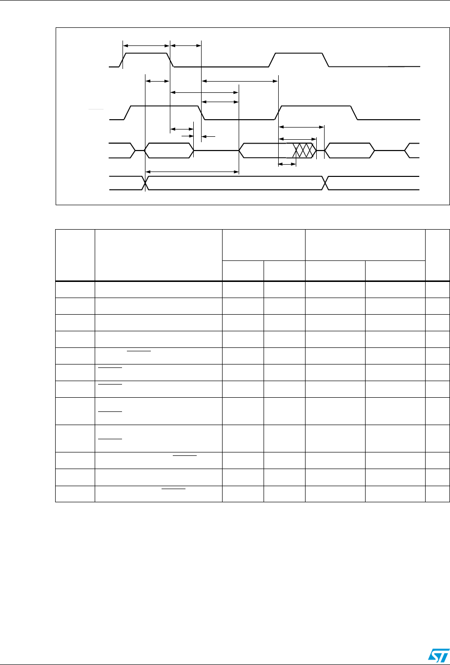
DC and AC parameters UPSD3212A, UPSD3212C, UPSD3212CV
160/181
Figure 69. External program memory Read cycle
1. Conditions (in addition to those in Table 110, VCC = 4.5 to 5.5 V): VSS = 0 V; CL for Port 0, ALE and PSEN
output is 100 pF; CL for other outputs is 80 pF
2. Interfacing the UPSD321xx devices to devices with float times up to 20 ns is permissible. This limited bus
contention does not cause any damage to Port 0 drivers.
Table 117. External program memory AC characteristics (with the 5 V MCU module)
Symbol Parameter(1) 40 MHz oscillator Variable oscillator
1/tCLCL = 24 to 40 MHz Unit
Min. Max. Min. Max.
tLHLL ALE pulse width 35 2 tCLCL – 15 ns
tAVLL Address set-up to ALE 10 tCLCL – 15 ns
tLLAX Address hold after ALE 10 tCLCL – 15 ns
tLLIV ALE Low to valid instruction in 55 4 tCLCL – 45 ns
tLLPL ALE to PSEN 10 tCLCL – 15 ns
tPLPH PSEN pulse width 60 3 tCLCL – 15 ns
tPLIV PSEN to valid instruction in 30 3 tCLCL – 45 ns
tPXIX
Input instruction hold after
PSEN 00 ns
tPXIZ(2) Input instruction float after
PSEN 15 tCLCL – 10 ns
tPXAV(2) Address valid after PSEN 20 tCLCL – 5 ns
tAVIV Address to valid instruction in 70 5 tCLCL – 55 ns
tAZPL Address float to PSEN –5 –5 ns
tAVLL tPLPH
tPXIZ
tAVIV
PSEN
PORT 2
PORT 0
AI06848
tLHLL
ALE
tLLPL
A0-A7
tLLAX
tAZPL
tLLIV
tPLIV
A0-A7
tPXAV
tPXIX
A8-A11
INSTR
IN
A8-A11
Obsolete Product(s) - Obsolete Product(s)
UPSD3212A, UPSD3212C, UPSD3212CV DC and AC parameters
161/181
1. Conditions (in addition to those in Table 111, VCC = 3.0 to 3.6 V): VSS = 0 V; CL for Port 0, ALE and PSEN
output is 100 pF, for 5 V devices, and 50 pF for 3 V devices; CL for other outputs is 80 pF, for 5 V devices,
and 50 pF for 3 V devices)
2. Interfacing the UPSD321xx devices to devices with float times up to 35 ns is permissible. This limited bus
contention does not cause any damage to Port 0 drivers.
1. Conditions (in addition to those in Table 110, VCC = 4.5 to 5.5 V): VSS = 0 V; CL for Port 0, ALE and PSEN
output is 100 pF; CL for other outputs is 80 pF
Table 118. External program memory AC characteristics (with the 3 V MCU module)
Symbol Parameter(1)
24 MHz
oscillator
Variable oscillator
1/tCLCL = 8 to 24 MHz Unit
Min. Max. Min. Max.
tLHLL ALE pulse width 43 2 tCLCL – 40 ns
tAVLL Address set-up to ALE 17 tCLCL – 25 ns
tLLAX Address hold after ALE 17 tCLCL – 25 ns
tLLIV ALE Low to valid instruction in 80 4 tCLCL – 87 ns
tLLPL ALE to PSEN 22 tCLCL – 20 ns
tPLPH PSEN pulse width 95 3 tCLCL – 30 ns
tPLIV PSEN to valid instruction in 60 3 tCLCL – 65 ns
tPXIX
Input instruction hold after
PSEN 00 ns
tPXIZ(2) Input instruction float after
PSEN 32 tCLCL – 10 ns
tPXAV(2) Address valid after PSEN 37 tCLCL – 5 ns
tAVIV Address to valid instruction in 148 5 tCLCL – 60 ns
tAZPL Address float to PSEN –10 –10 ns
Table 119. External clock drive (with the 5 V MCU module)
Symbol Parameter(1) 40 MHz oscillator Variable oscillator
1/tCLCL = 24 to 40 MHz Unit
Min. Max. Min. Max.
tRLRH Oscillator period 25 41.7 ns
tWLWH High time 10 tCLCL –
tCLCX
ns
tLLAX2 Low time 10 tCLCL –
tCLCX
ns
tRHDX Rise time 10 ns
tRHDX Fall time 10 ns
Obsolete Product(s) - Obsolete Product(s)
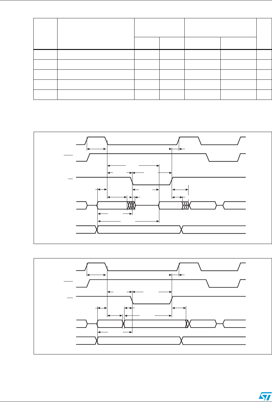
DC and AC parameters UPSD3212A, UPSD3212C, UPSD3212CV
162/181
1. Conditions (in addition to those in Table 111, VCC = 3.0 to 3.6 V): VSS = 0 V; CL for Port 0, ALE and PSEN
output is 100 pF, for 5 V devices, and 50 pF for 3 V devices; CL for other outputs is 80 pF, for 5 V devices,
and 50 pF for 3 V devices)
Figure 70. External data memory Read cycle
Figure 71. External data memory Write cycle
Table 120. External clock drive (with the 3 V MCU module)
Symbol Parameter(1) 24 MHz oscillator Variable oscillator 1/tCLCL
= 8 to 24 MHz Unit
Min. Max. Min. Max.
tRLRH Oscillator period 41.7 125 ns
tWLWH High time 12 tCLCL – tCLCX ns
tLLAX2 Low time 12 tCLCL – tCLCX ns
tRHDX Rise time 12 ns
tRHDX Fall time 12 ns
PORT 2
PORT 0
ALE
RD
PSEN
P2.0 to P2.3 or A8-A11 from DPH A8-A11 from PCH
tAVDV
tRLDV
tLLWL tRLRH
tAVLL
tLLDV
tLHLL
tRLAZ
DATA IN A0-A7 from PCL INSTR IN
A0-A7 from
RI or DPL
tLLAX2
tAVWL
tRHDZ
tWHLH
AI07088
tRHDX
PORT 2
PORT 0
ALE
WR
PSEN
P2.0 to P2.3 or A8-A11 from DPH A8-A11 from PCH
tQVWX
tLLWL tWLWH
tAVLL
tLHLL
tQVWH
DATA OUT A0-A7 from PCL INSTR IN
A0-A7 from
RI or DPL
tLLAX
tAVWL
tWHQX
tWHLH
AI07089
Obsolete Product(s) - Obsolete Product(s)
UPSD3212A, UPSD3212C, UPSD3212CV DC and AC parameters
163/181
1. Conditions (in addition to those in Table 110, VCC = 4.5 to 5.5 V): VSS = 0 V; CL for Port 0, ALE and PSEN
output is 100 pF; CL for other outputs is 80 pF
Table 121. External data memory AC characteristics (with the 5 V MCU module)
Symbol Parameter(1) 40 MHz oscillator Variable oscillator
1/tCLCL = 24 to 40 MHz Unit
Min. Max. Min. Max.
tRLRH RD pulse width 120 6 tCLCL – 30 ns
tWLWH WR pulse width 120 6 tCLCL – 30 ns
tLLAX2 Address hold after ALE 10 tCLCL – 15 ns
tRHDX RD to valid data in 75 5 tCLCL – 50 ns
tRHDX Data hold after RD 00 ns
tRHDZ Data float after RD 38 2 tCLCL – 12 ns
tLLDV ALE to valid data in 150 8 tCLCL – 50 ns
tAVDV Address to valid data in 150 9 tCLCL – 75 ns
tLLWL ALE to WR or RD 60 90 3 tCLCL – 15 tCLCL + 15 ns
tAVWL Address valid to WR or RD 70 4 tCLCL – 30 ns
tWHLH WR or RD High to ALE High 10 40 tCLCL – 15 tCLCL + 15 ns
tQVWX Data valid to WR transition 5 tCLCL – 20 ns
tQVWH Data set-up before WR 125 7 tCLCL – 50 ns
tWHQX Data hold after WR 5t
CLCL – 20 ns
tRLAZ Address float after RD 00ns
Obsolete Product(s) - Obsolete Product(s)
DC and AC parameters UPSD3212A, UPSD3212C, UPSD3212CV
164/181
1. Conditions (in addition to those in Table 111, VCC = 3.0 to 3.6 V): VSS = 0 V; CL for Port 0, ALE and PSEN
output is 100 pF, for 5 V devices, and 50 pF for 3 V devices; CL for other outputs is 80 pF, for 5 V devices,
and 50 pF for 3 V devices)
Table 122. External data memory AC characteristics (with the 3 V MCU module)
Symbol Parameter(1) 24 MHz oscillator Variable oscillator
1/tCLCL = 8 to 24 MHz Unit
Min. Max. Min. Max.
tRLRH RD pulse width 180 6 tCLCL – 70 ns
tWLWH WR pulse width 180 6 tCLCL – 70 ns
tLLAX2 Address hold after ALE 56 2 tCLCL – 27 ns
tRHDX RD to valid data in 118 5 tCLCL – 90 ns
tRHDX Data hold after RD 00 ns
tRHDZ Data float after RD 63 2 tCLCL – 20 ns
tLLDV ALE to valid data in 200 8 tCLCL – 133 ns
tAVDV Address to valid data in 220 9 tCLCL – 155 ns
tLLWL ALE to WR or RD 75 175 3 tCLCL – 50 tCLCL + 50 ns
tAVWL Address valid to WR or RD 67 4 tCLCL – 97 ns
tWHLH WR or RD High to ALE High 17 67 tCLCL – 25 tCLCL + 25 ns
tQVWX Data valid to WR transition 5 tCLCL – 37 ns
tQVWH Data set-up before WR 170 7 tCLCL – 122 ns
tWHQX Data hold after WR 15 tCLCL – 27 ns
tRLAZ Address float after RD 00ns
Table 123. A/D analog specification
Symbol Parameter Test
condition Min. Typ. Max. Unit
AVREF
Analog power supply input
voltage range VSS VCC V
VAN Analog input voltage range VSS – 0.3 AVREF + 0.3 V
IAVDD
Current following between VCC
and VSS
200 µA
CAIN Overall accuracy ±2 l.s.b.
NNLE Non-linearity error ±2 l.s.b.
NDNLE Differential non-linearity error ±2 l.s.b.
NZOE Zero-offset error ±2 l.s.b.
NFSE Full scale error ±2 l.s.b.
NGE Gain error ±2 l.s.b.
tCONV Conversion time at 8 MHz
clock 20 µs
Obsolete Product(s) - Obsolete Product(s)
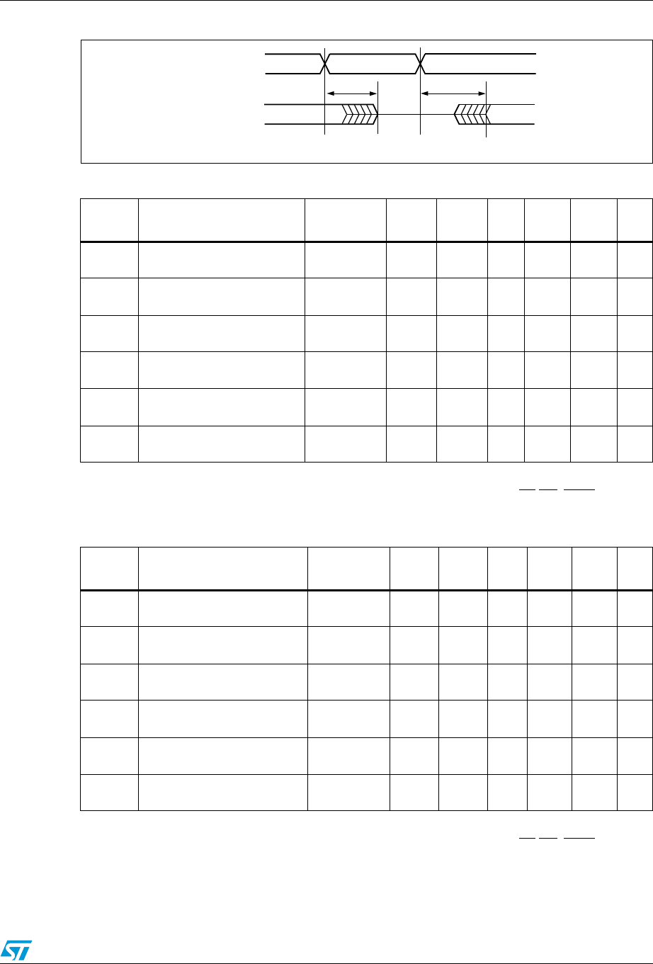
UPSD3212A, UPSD3212C, UPSD3212CV DC and AC parameters
165/181
Figure 72. Input to output disable / enable
1. Fast Slew Rate output available on PA3-PA0, PB3-PB0, and PD2-PD1. Decrement times by given amount
2. tPD for MCU address and control signals refers to delay from pins on Port 0, Port 2, RD WR, PSEN and
ALE to CPLD combinatorial output (80-pin package only)
1. Fast Slew Rate output available on PA3-PA0, PB3-PB0, and PD2-PD1. Decrement times by given amount
2. tPD for MCU address and control signals refers to delay from pins on Port 0, Port 2, RD WR, PSEN and
ALE to CPLD combinatorial output (80-pin package only)
Table 124. CPLD combinatorial timing (5 V devices)
Symbol Parameter Conditions Min. Max. PT
aloc
Turbo
off
Slew
rate(1) Unit
tPD(2) CPLD input pin/feedback to
CPLD combinatorial output 20 + 2 + 10 – 2 ns
tEA
CPLD input to CPLD output
enable 21 + 10 – 2 ns
tER
CPLD input to CPLD output
disable 21 + 10 – 2 ns
tARP
CPLD register clear or
preset delay 21 + 10 – 2 ns
tARPW
CPLD register clear or
preset pulse width 10 + 10 ns
tARD CPLD array delay Any
macrocell 11 + 2 ns
Table 125. CPLD combinatorial timing (3 V devices)
Symbol Parameter Conditions Min. Max. PT
aloc
Turbo
off
Slew
rate(1) Unit
tPD(2) CPLD input pin/feedback to
CPLD combinatorial output 40 + 4 + 20 – 6 ns
tEA
CPLD input to CPLD output
enable 43 + 20 – 6 ns
tER
CPLD input to CPLD output
disable 43 + 20 – 6 ns
tARP
CPLD register clear or
preset delay 40 + 20 – 6 ns
tARPW
CPLD register clear or
preset pulse width 25 + 20 ns
tARD CPLD array delay Any
macrocell 25 + 4 ns
tER tEA
INPUT
INPUT TO
OUTPUT
ENABLE/DISABLE
AI02863
Obsolete Product(s) - Obsolete Product(s)
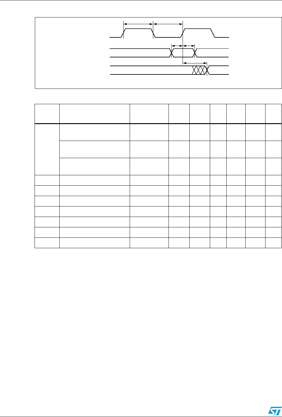
DC and AC parameters UPSD3212A, UPSD3212C, UPSD3212CV
166/181
Figure 73. Synchronous clock mode timing – PLD
1. Fast Slew Rate output available on PA3-PA0, PB3-PB0, and PD2-PD1. Decrement times by given amount.
2. CLKIN (PD1) tCLCL = tCH + tCL.
Table 126. CPLD macrocell synchronous clock mode timing (5 V devices)
Symbol Parameter Conditions Min. Max. PT
Aloc
Turbo
Off
Slew
rate(1) Unit
fMAX
Maximum frequency
external feedback 1/(tS+tCO)40.0 MHz
Maximum frequency
internal feedback (fCNT)1/(tS+tCO–10) 66.6 MHz
Maximum frequency
pipelined data 1/(tCH+tCL)83.3 MHz
tSInput setup time 12 + 2 + 10 ns
tHInput hold time 0 ns
tCH Clock high time Clock input 6 ns
tCL Clock low time Clock input 6 ns
tCO Clock to output delay Clock input 13 – 2 ns
tARD CPLD array delay Any macrocell 11 + 2 ns
tMIN Minimum clock period (2) tCH+tCL 12 ns
tCH tCL
tCO
tH
tS
CLKIN
INPUT
REGISTERED
OUTPUT
AI02860
Obsolete Product(s) - Obsolete Product(s)
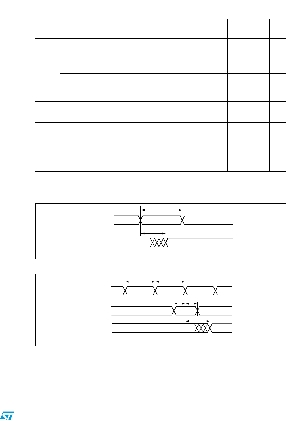
UPSD3212A, UPSD3212C, UPSD3212CV DC and AC parameters
167/181
1. Fast Slew Rate output available on PA3-PA0, PB3-PB0, and PD2-PD1. Decrement times by given amount.
2. CLKIN (PD1) tCLCL = tCH + tCL.
Figure 74. Asynchronous Reset / Preset
Figure 75. Asynchronous clock mode timing (product term clock)
Table 127. CPLD macrocell synchronous clock mode timing (3 V devices)
Symbol Parameter Conditions Min. Max. PT
aloc
Turbo
off
Slew
rate (1) Unit
fMAX
Maximum frequency
external feedback 1/(tS+tCO)22.2 MHz
Maximum frequency
internal feedback (fCNT)1/(tS+tCO–10) 28.5 MHz
Maximum frequency
pipelined data 1/(tCH+tCL)40.0 MHz
tSInput setup time 20 + 4 + 20 ns
tHInput hold time 0 ns
tCH Clock high time Clock input 15 ns
tCL Clock low time Clock input 10 ns
tCO Clock to output delay Clock input 25 – 6 ns
tARD CPLD array delay Any
macrocell 25 + 4 ns
tMIN Minimum clock period (2) tCH+tCL 25 ns
tARP
REGISTER
OUTPUT
tARPW
RESET/PRESET
INPUT
AI02864
tCHA tCLA
tCOA
tHAtSA
CLOCK
INPUT
REGISTERED
OUTPUT
AI02859
Obsolete Product(s) - Obsolete Product(s)
DC and AC parameters UPSD3212A, UPSD3212C, UPSD3212CV
168/181
Table 128. CPLD macrocell asynchronous clock mode timing (5 V devices)
Symbol Parameter Conditions Min Max PT
aloc
Turbo
off
Slew
rate Unit
fMAXA
Maximum frequency
external feedback 1/(tSA+tCOA)38.4 MHz
Maximum frequency
internal feedback (fCNTA)
1/(tSA+tCOA–
10) 62.5 MHz
Maximum frequency
pipelined data 1/(tCHA+tCLA)71.4 MHz
tSA Input setup time 7 + 2 + 10 ns
tHA Input hold time 8 ns
tCHA Clock input high time 9 + 10 ns
tCLA Clock input low time 9 + 10 ns
tCOA Clock to output delay 21 + 10 – 2 ns
tARDA CPLD array delay Any macrocell 11 + 2 ns
tMINA Minimum clock period 1/fCNTA 16 ns
Table 129. CPLD macrocell asynchronous clock mode timing (3 V devices)
Symbol Parameter Conditions Min. Max. PT
aloc
Turbo
off
Slew
rate Unit
fMAXA
Maximum frequency
external feedback 1/(tSA+tCOA)21.7 MHz
Maximum frequency
internal feedback
(fCNTA)
1/(tSA+tCOA–
10) 27.8 MHz
Maximum frequency
pipelined data 1/(tCHA+tCLA)33.3 MHz
tSA Input setup time 10 + 4 + 20 ns
tHA Input hold time 12 ns
tCHA Clock input high time 17 + 20 ns
tCLA Clock input low time 13 + 20 ns
tCOA Clock to output delay 36 + 20 – 6 ns
tARD CPLD array delay Any macrocell 25 + 4 ns
tMINA Minimum clock period 1/fCNTA 36 ns
Obsolete Product(s) - Obsolete Product(s)
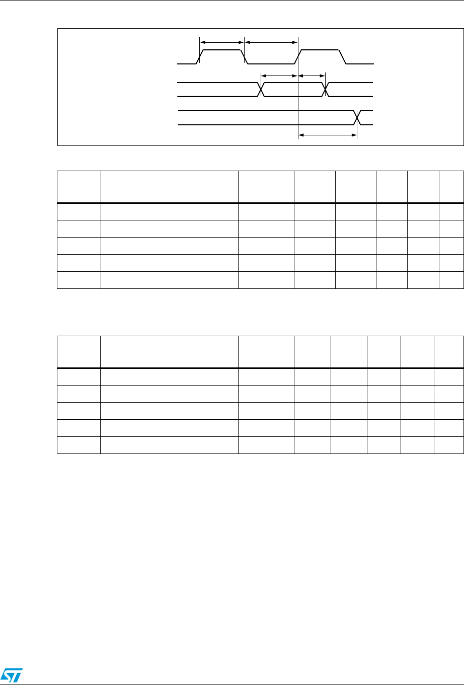
UPSD3212A, UPSD3212C, UPSD3212CV DC and AC parameters
169/181
Figure 76. Input macrocell timing (product term clock)
1. Inputs from Port A, B, and C relative to register/ latch clock from the PLD. ALE/AS latch timings refer to
tAVLX and tLXAX.
1. Inputs from Port A, B, and C relative to register/latch clock from the PLD. ALE latch timings refer to tAVLX
and tLXAX.
Table 130. Input macrocell timing (5 V devices)
Symbol Parameter Conditions Min. Max. PT
aloc
Turbo
Off Unit
tIS Input setup time (Note 1) 0 ns
tIH Input hold time (Note 1) 15 + 10 ns
tINH NIB input high time (Note 1) 9 ns
tINL NIB input low time (Note 1) 9 ns
tINO NIB input to combinatorial delay (Note 1) 34 + 2 + 10 ns
Table 131. Input macrocell timing (3 V devices)
Symbol Parameter Conditions Min. Max. PT
aloc
Turbo
Off Unit
tIS Input setup time (Note 1) 0 ns
tIH Input hold time (Note 1) 25 + 20 ns
tINH NIB input high time (Note 1) 12 ns
tINL NIB input low time (Note 1) 12 ns
tINO NIB input to combinatorial delay (Note 1) 46 + 4 + 20 ns
tINH tINL
tINO
tIH
tIS
PT CLOCK
INPUT
OUTPUT
AI03101
Obsolete Product(s) - Obsolete Product(s)
DC and AC parameters UPSD3212A, UPSD3212C, UPSD3212CV
170/181
1. Programmed to all zero before erase.
2. The polling status, DQ7, is valid tQ7VQV time units before the data byte, DQ0-DQ7, is valid for reading.
1. Programmed to all zero before erase.
2. The polling status, DQ7, is valid tQ7VQV time units before the data byte, DQ0-DQ7, is valid for reading.
Table 132. Program, Write and Erase times (5 V devices)
Symbol Parameter Min. Typ. Max. Unit
Flash Program 8.5 s
Flash Bulk Erase(1) (pre-programmed) 3 30 s
Flash Bulk Erase (not pre-programmed) 5 s
tWHQV3 Sector Erase (pre-programmed) 1 30 s
tWHQV2 Sector Erase (not pre-programmed) 2.2 s
tWHQV1 Byte Program 14 150 µs
Program / Erase Cycles (per Sector) 100,000 cycles
tWHWLO Sector Erase Time-Out 100 µs
tQ7VQV
DQ7 Valid to Output (DQ7-DQ0) Valid (Data
Polling)(2) 30 ns
Table 133. Program, Write and Erase times (3 V devices)
Symbol Parameter Min. Typ. Max. Unit
Flash Program 8.5 s
Flash Bulk Erase(1) (pre-programmed) 3 30 s
Flash Bulk Erase (not pre-programmed) 5 s
tWHQV3 Sector Erase (pre-programmed) 1 30 s
tWHQV2 Sector Erase (not pre-programmed) 2.2 s
tWHQV1 Byte Program 14 150 µs
Program / Erase Cycles (per Sector) 100,000 cycles
tWHWLO Sector Erase Time-Out 100 µs
tQ7VQV
DQ7 Valid to Output (DQ7-DQ0) Valid (Data
Polling)(2) 30 ns
Obsolete Product(s) - Obsolete Product(s)
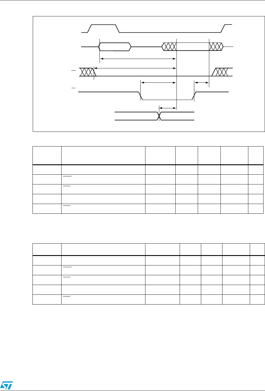
UPSD3212A, UPSD3212C, UPSD3212CV DC and AC parameters
171/181
Figure 77. Peripheral I/O Read timing
1. Any input used to select Port A Data Peripheral mode.
2. Data is already stable on Port A.
1. Any input used to select Port A Data Peripheral mode.
2. Data is already stable on Port A.
Table 134. Port A peripheral data mode Read timing (5 V devices)
Symbol Parameter Condition
sMin. Max. Turbo off Unit
tAVQV–PA Address valid to data valid (Note 1) 37 + 10 ns
tSLQV–PA CSI valid to data valid 27 + 10 ns
tRLQV–PA RD to data valid (Note 2) 32 ns
tDVQV–PA Data in to data out valid 22 ns
tRHQZ–PA RD to data high-Z 23 ns
Table 135. Port A peripheral data mode Read timing (3 V devices)
Symbol Parameter Conditions Min. Max. Turbo off Unit
tAVQV–PA Address valid to data valid (Note 1) 50 + 20 ns
tSLQV–PA CSI valid to data valid 37 + 20 ns
tRLQV–PA RD to data valid (Note 2) 45 ns
tDVQV–PA Data in to data out valid 38 ns
tRHQZ–PA RD to data high-Z 36 ns
tRLQV (PA)
tDVQV (PA)
tRHQZ (PA)
tSLQV (PA)
tAVQV (PA)
ADDRESS DATA VALID
ALE
A/ D BUS
RD
DATA ON PORT A
CSI
AI06610
Obsolete Product(s) - Obsolete Product(s)
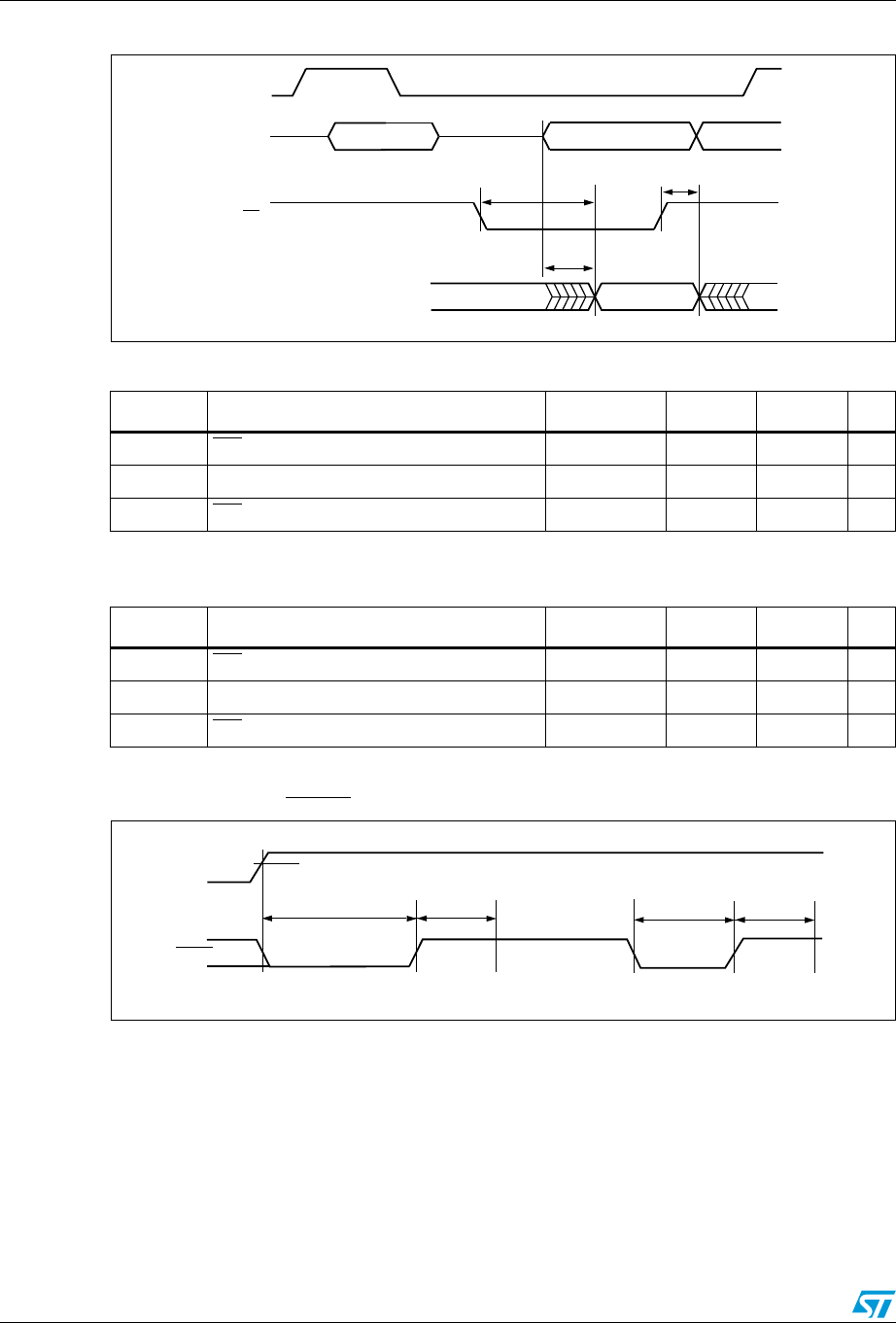
DC and AC parameters UPSD3212A, UPSD3212C, UPSD3212CV
172/181
Figure 78. Peripheral I/O Write timing
1. Data stable on Port 0 pins to data on Port A.
1. Data stable on Port 0 pins to data on Port A.
Figure 79. Reset (RESET) timing
Table 136. Port A peripheral data mode Write timing (5 V devices)
Symbol Parameter Conditions Min. Max. Unit
tWLQV–PA WR to Data Propagation Delay 25 ns
tDVQV–PA Data to Port A Data Propagation Delay (Note 1) 22 ns
tWHQZ–PA WR Invalid to Port A Tri-state 20 ns
Table 137. Port A peripheral data mode Write timing (3 V devices)
Symbol Parameter Conditions Min. Max. Unit
tWLQV–PA WR to data propagation delay 42 ns
tDVQV–PA Data to Port A data propagation delay (Note 1) 38 ns
tWHQZ–PA WR invalid to Port A tri-state 33 ns
tDVQV (PA)
tWLQV (PA) tWHQZ (PA)
ADDRESS DATA OUT
A/ D BUS
WR
PORT A
DATA OUT
ALE
AI06611
tNLNH-PO tOPR
AI02866b
RESET
tNLNH
tNLNH-A tOPR
V
CC
V
CC
(min)
Power-On Reset Warm Reset
Obsolete Product(s) - Obsolete Product(s)
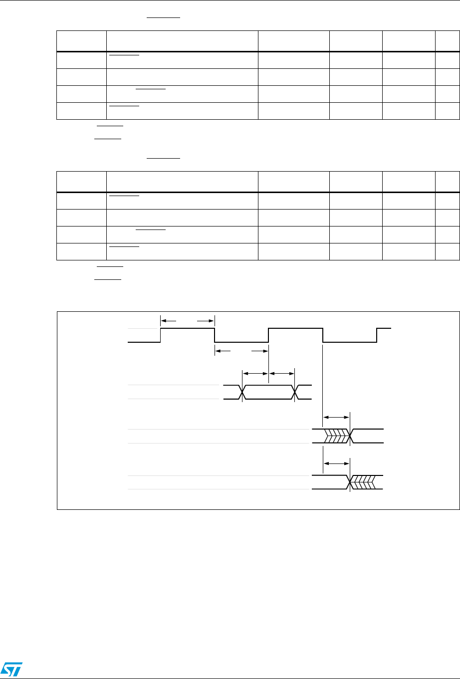
UPSD3212A, UPSD3212C, UPSD3212CV DC and AC parameters
173/181
1. Reset (RESET) does not reset Flash memory Program or Erase cycles.
2. Warm RESET aborts Flash memory Program or Erase cycles, and puts the device in READ mode.
1. Reset (RESET) does not reset Flash memory Program or Erase cycles.
2. Warm RESET aborts Flash memory Program or Erase cycles, and puts the device in READ mode.
Figure 80. ISC timing
Table 138. Reset (RESET) timing (5 V devices)
Symbol Parameter Conditions Min. Max. Unit
tNLNH RESET active low time(1) 150 ns
tNLNH–PO Power-on reset active low time 1 ms
tNLNH–A Warm RESET (2) 25 μs
tOPR RESET high to operational device 120 ns
Table 139. Reset (RESET) timing (3 V devices)
Symbol Parameter Conditions Min. Max. Unit
tNLNH RESET active low time(1) 300 ns
tNLNH–PO Power-on reset active low time 1 ms
tNLNH–A Warm RESET (2) 25 μs
tOPR RESET high to operational device 300 ns
ISCCH
TCK
TDI/TMS
ISC OUTPUTS/TDO
ISC OUTPUTS/TDO
t
ISCCL
t
ISCPH
t
ISCPSU
t
ISCPVZ
t
ISCPZV
t
ISCPCO
t
AI02865
Obsolete Product(s) - Obsolete Product(s)
DC and AC parameters UPSD3212A, UPSD3212C, UPSD3212CV
174/181
1. For non-PLD Programming, Erase or in ISC By-pass mode.
2. For Program or Erase PLD only.
1. For non-PLD Programming, Erase or in ISC By-pass mode.
2. For Program or Erase PLD only.
Figure 81. MCU module AC measurement I/O waveform
1. AC inputs during testing are driven at VCC–0.5 V for a logic '1,' and 0.45 V for a logic '0.'
2. Timing measurements are made at VIH(min) for a logic '1,' and VIL(max) for a logic '0'.
Table 140. ISC timing (5 V devices)
Symbol Parameter Conditions Min. Max. Unit
tISCCF Clock (TCK, PC1) frequency (except for PLD) (Note 1) 20 MHz
tISCCH Clock (TCK, PC1) high time (except for PLD) (Note 1) 23 ns
tISCCL Clock (TCK, PC1) low time (except for PLD) (Note 1) 23 ns
tISCCFP Clock (TCK, PC1) frequency (PLD only) (Note 2) 2 MHz
tISCCHP Clock (TCK, PC1) high time (PLD only) (Note 2) 240 ns
tISCCLP Clock (TCK, PC1) low time (PLD only) (Note 2) 240 ns
tISCPSU ISC port set-up time 7 ns
tISCPH ISC port hold-up time 5 ns
tISCPCO ISC port clock to output 21 ns
tISCPZV ISC port high-impedance to valid output 21 ns
tISCPVZ ISC port valid output to high-impedance 21 ns
Table 141. ISC timing (3 V devices)
Symbol Parameter Conditions Min. Max. Unit
tISCCF Clock (TCK, PC1) frequency (except for PLD) (Note 1) 12 MHz
tISCCH Clock (TCK, PC1) high time (except for PLD) (Note 1) 40 ns
tISCCL Clock (TCK, PC1) low time (except for PLD) (Note 1) 40 ns
tISCCFP Clock (TCK, PC1) frequency (PLD only) (Note 2) 2 MHz
tISCCHP Clock (TCK, PC1) high time (PLD only) (Note 2) 240 ns
tISCCLP Clock (TCK, PC1) low time (PLD only) (Note 2) 240 ns
tISCPSU ISC port set-up time 12 ns
tISCPH ISC port hold-up time 5 ns
tISCPCO ISC port clock to output 30 ns
tISCPZV ISC port high-impedance to valid output 30 ns
tISCPVZ ISC port valid output to high-impedance 30 ns
AI06650
VCC – 0.5V
0.45V
Test Points
0.2 VCC – 0.1V
0.2 VCC + 0.9V
Obsolete Product(s) - Obsolete Product(s)
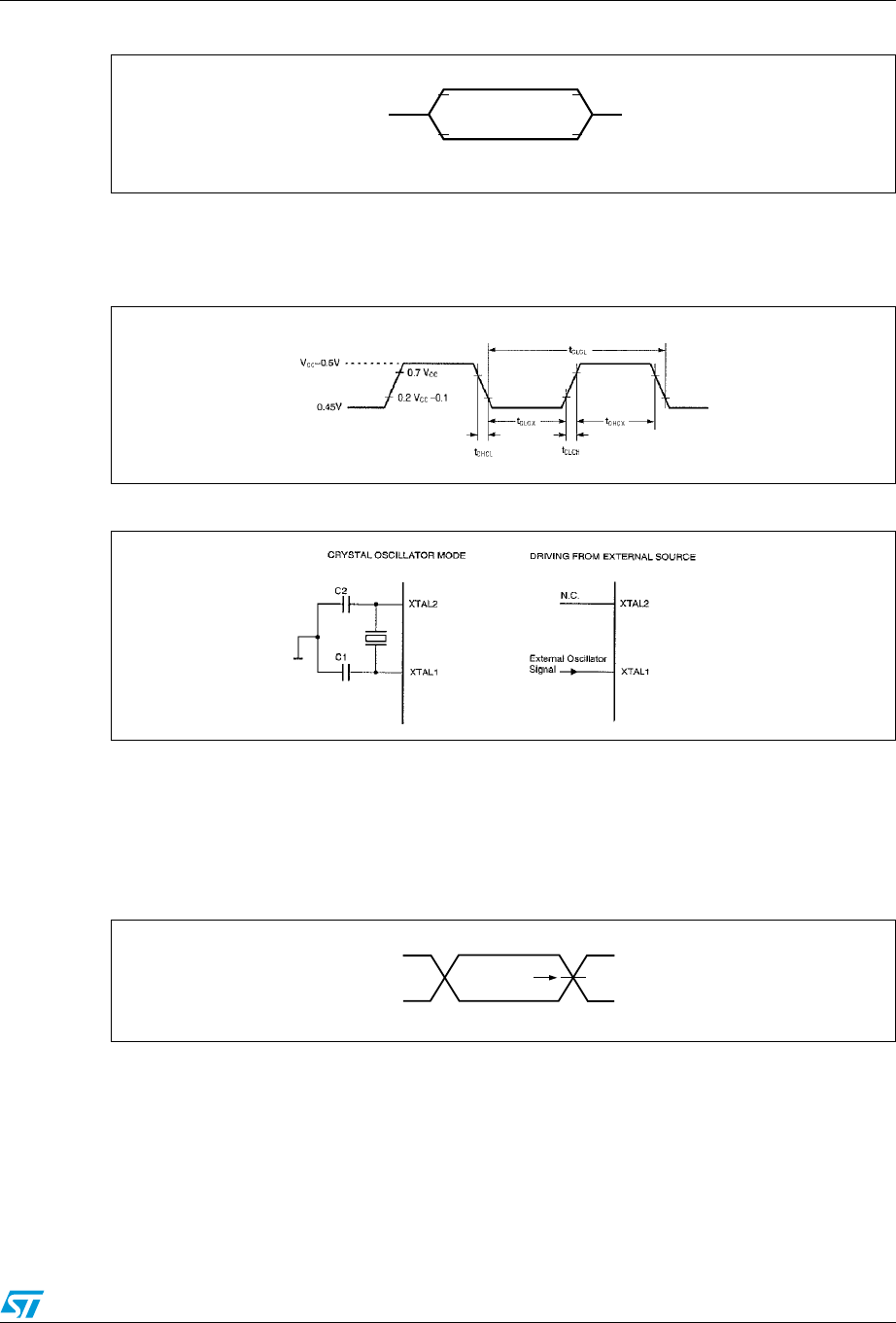
UPSD3212A, UPSD3212C, UPSD3212CV DC and AC parameters
175/181
Figure 82. PSD module AC float I/O waveform
1. For timing purposes, a Port pin is considered to be no longer floating when a 100mV change from load
voltage occurs, and begins to float when a 100mV change from the loaded VOH or VOL level occurs
2. IOL and IOH ≥ 20mA
Figure 83. External clock cycle
Figure 84. Recommended oscillator circuits
1. C1, C2 = 30 pF ± 10 pF for crystals
2. For ceramic resonators, contact resonator manufacturer
3. Oscillation circuit is designed to be used either with a ceramic resonator or crystal oscillator. Since each
crystal and ceramic resonator
4. have their own characteristics, the user should consult the crystal manufacturer for appropriate values of
external components.
Figure 85. PSD module AC measurement I/O waveform
AI06651
Test Reference Points
VOL + 0.1V
VOH – 0.1V
VLOAD – 0.1V
VLOAD + 0.1V
0.2 VCC – 0.1V
3.0V
0V
Test Point 1.5V
AI03103b
Obsolete Product(s) - Obsolete Product(s)
DC and AC parameters UPSD3212A, UPSD3212C, UPSD3212CV
176/181
Figure 86. PSD module AC measurement load circuit
1. Sampled only, not 100% tested.
2. Typical values are for TA = 25°C and nominal supply voltages.
Table 142. Capacitance
Symbol Parameter Test conditions (1) Typ.(2) Max. Unit
CIN Input capacitance (for input pins) VIN = 0 V 4 6 pF
COUT
Output capacitance (for
input/output pins) VOUT = 0 V 8 12 pF
Device
Under Test
2.01 V
195 Ω
CL = 30 pF
(Including Scope and
Jig Capacitance)
AI03104b
Obsolete Product(s) - Obsolete Product(s)
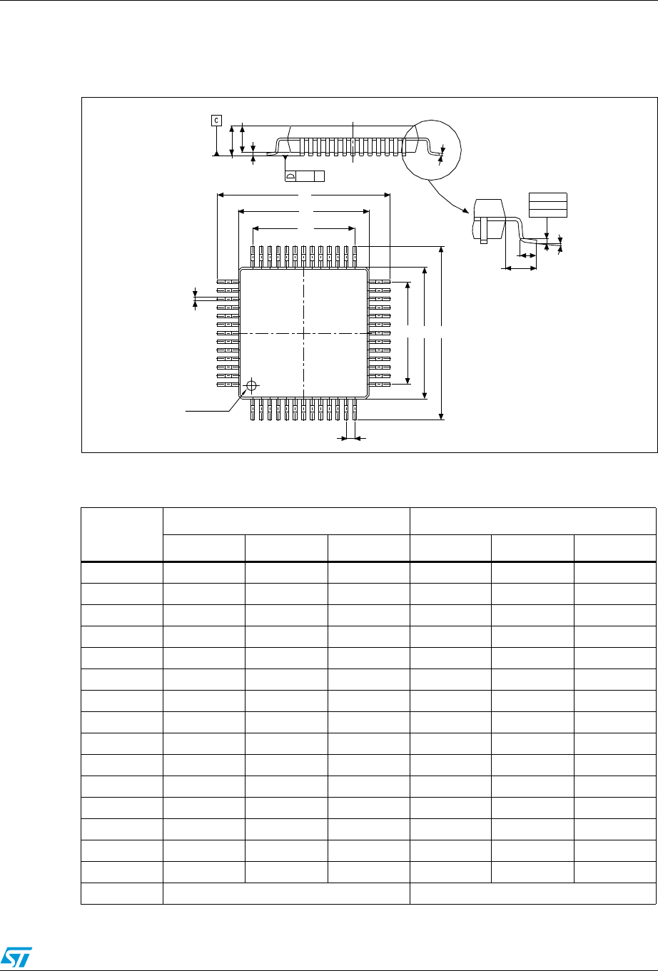
UPSD3212A, UPSD3212C, UPSD3212CV Package mechanical information
177/181
32 Package mechanical information
Figure 87. LQFP52 – 52-lead plastic thin, quad, flat package outline
1. Drawing is not to scale.
Table 143. LQFP52 – 52-lead plastic thin, quad, flat package mechanical data
Symbol
millimeters inches(1)
1. Values in inches are converted from mm and rounded to 4 decimal digits.
Typ Min Max Typ Min Max
A 1.60 0.063
A1 0.05 0.15 0.002 0.0059
A2 1.35 1.45 0.0531 0.0571
b 0.22 0.38 0.0087 0.015
C 0.09 0.2 0.0035 0.0079
D 12 0.4724
D1 10 0.3937
D2 7.8 0.3071
E 12 0.4724
E1 10 0.3937
E2 7.8 0.3071
e 0.65 0.0256
L 0.45 0.75 0.0177 0.0295
L1 1 0.0394
k 0°7° 0°7°
ddd 0.100 0.0039
Seating plane
A
A2
A1
D
D1
D2
E2 E1 E
39 27
26
40
52
113
14
Pin 1 identification
e
b
L1
Lk
0.25 mm
.010 inch
Gage plane
c
ddd C
DC_ME
Obsolete Product(s) - Obsolete Product(s)
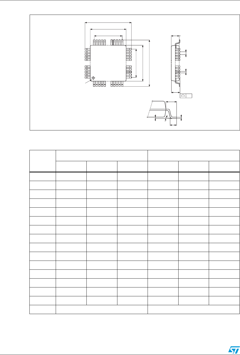
Package mechanical information UPSD3212A, UPSD3212C, UPSD3212CV
178/181
Figure 88. LQFP80 – 80-lead plastic thin, quad, flat package outline
1. Drawing is not to scale.
Table 144. LQFP80 – 80-lead plastic thin, quad, flat package mechanical data
Symbol
millimeters inches(1)
1. Values in inches are converted from mm and rounded to 4 decimal digits.
Typ Min Max Typ Min Max
A 1.600 0.0630
A1 0.050 0.150 0.0020 0.0059
A2 1.400 1.350 1.450 0.0551 0.0531 0.0571
b 0.220 0.170 0.270 0.0087 0.0067 0.0106
C 0.090 0.200 0.0035 0.0079
D 14.000 0.5512
D1 12.000 0.4724
D3 9.500 0.3740
E 14.000 0.5512
E1 12.000 0.4724
E3 9.500 0.3740
e 0.500 0.0197
L 0.600 0.450 0.750 0.0236 0.0177 0.0295
L1 1.000 0.0394
k 0° 7° 0° 7°
ccc 0.080 0.0031
9X_ME
E1
ccc
b
e
A2
A
LA1 k
D1
D
E
c
D3
E3
L1
120
21
40
41
60
61
80
Pin 1
identification
Obsolete Product(s) - Obsolete Product(s)

UPSD3212A, UPSD3212C, UPSD3212CV Part numbering
179/181
33 Part numbering
Table 145. Ordering information scheme
For other options, or for more information on any aspect of this device, please contact the ST Sales
Office nearest you.
Example: UPSD 3 2 1 4 B V – 24 U 6 T
Device type
UPSD = Microcontroller PSD
Family
3 = 8032 core
PLD size
2 = 16 Macrocells
SRAM Size
1 = 2 Kbytes
Main Flash memory size
2 = 64 Kbytes
3 = 128 Kbytes
4 = 256 Kbytes
IP mix
A = USB, I2C, PWM, DDC, ADC, (2) UARTs,
Supervisor (Reset Out, Reset In, LVD, WD)
B = I2C, PWM, DDC, ADC, (2) UARTs
Supervisor (Reset Out, Reset In, LVD, WD)
Operating voltage
blank = VCC = 4.5 to 5.5 V
V = VCC = 3.0 to 3.6 V
Speed
–24 = 24 MHz
–40 = 40 MHz
Package
T = 52-pin LQFP
U = 80-pin LQFP
Temperature range
1 = 0 to 70°C
6 = –40 to 85°C
Shipping options
F = ECOPACK® Package, Tape & Reel Packing
Obsolete Product(s) - Obsolete Product(s)

Revision history UPSD3212A, UPSD3212C, UPSD3212CV
180/181
34 Revision history
Table 146. Document revision history
Date Revision Changes
18-Dec-2002 1.0 First Issue
04-Mar-03 1.1
Updates: port information (Table 30); interface information (Figure 30,
Table 44); remove programming guide; PSD module information
(Table 82); PLD information (Figure 55); electrical characteristics
(Table 114, 115, 131, 132)
02-Sep-03 1.2 Update references for Product Catalog
03-Feb-04 2.0 Reformatted; correct package dimensions (Table 145)
02-July-04 3.0 Reformatted; add EMC characteristics information (Table 106, 107,
108)
04-Nov-04 4.0 Updates per requested data brief changes (Figure 3, 4; Table 1, 2,
113)
03-Dec-04 5.0
Add USB feature to document (Figure 2, 3, 4, 15, 16, 18, 20, 40, 41,
42, 43, 44, 45; Table 1, 2, 15, 16, 18, 19, 21, 23, 24, 25, 60, 61, 62,
63, 64, 65, 66, 67, 68, 69, 70, 71, 72, 73, 74, 75, 76, 77, 78, 79, 146)
21-Jan-2009 6.0
Removed battery backup feature and related SRAM Standby mode
information. Added Ecopack information and updated Section 32:
Package mechanical information on page 177.
Obsolete Product(s) - Obsolete Product(s)

UPSD3212A, UPSD3212C, UPSD3212CV
181/181
Please Read Carefully:
Information in this document is provided solely in connection with ST products. STMicroelectronics NV and its subsidiaries (“ST”) reserve the
right to make changes, corrections, modifications or improvements, to this document, and the products and services described herein at any
time, without notice.
All ST products are sold pursuant to ST’s terms and conditions of sale.
Purchasers are solely responsible for the choice, selection and use of the ST products and services described herein, and ST assumes no
liability whatsoever relating to the choice, selection or use of the ST products and services described herein.
No license, express or implied, by estoppel or otherwise, to any intellectual property rights is granted under this document. If any part of this
document refers to any third party products or services it shall not be deemed a license grant by ST for the use of such third party products
or services, or any intellectual property contained therein or considered as a warranty covering the use in any manner whatsoever of such
third party products or services or any intellectual property contained therein.
UNLESS OTHERWISE SET FORTH IN ST’S TERMS AND CONDITIONS OF SALE ST DISCLAIMS ANY EXPRESS OR IMPLIED
WARRANTY WITH RESPECT TO THE USE AND/OR SALE OF ST PRODUCTS INCLUDING WITHOUT LIMITATION IMPLIED
WARRANTIES OF MERCHANTABILITY, FITNESS FOR A PARTICULAR PURPOSE (AND THEIR EQUIVALENTS UNDER THE LAWS
OF ANY JURISDICTION), OR INFRINGEMENT OF ANY PATENT, COPYRIGHT OR OTHER INTELLECTUAL PROPERTY RIGHT.
UNLESS EXPRESSLY APPROVED IN WRITING BY AN AUTHORIZED ST REPRESENTATIVE, ST PRODUCTS ARE NOT
RECOMMENDED, AUTHORIZED OR WARRANTED FOR USE IN MILITARY, AIR CRAFT, SPACE, LIFE SAVING, OR LIFE SUSTAINING
APPLICATIONS, NOR IN PRODUCTS OR SYSTEMS WHERE FAILURE OR MALFUNCTION MAY RESULT IN PERSONAL INJURY,
DEATH, OR SEVERE PROPERTY OR ENVIRONMENTAL DAMAGE. ST PRODUCTS WHICH ARE NOT SPECIFIED AS "AUTOMOTIVE
GRADE" MAY ONLY BE USED IN AUTOMOTIVE APPLICATIONS AT USER’S OWN RISK.
Resale of ST products with provisions different from the statements and/or technical features set forth in this document shall immediately void
any warranty granted by ST for the ST product or service described herein and shall not create or extend in any manner whatsoever, any
liability of ST.
ST and the ST logo are trademarks or registered trademarks of ST in various countries.
Information in this document supersedes and replaces all information previously supplied.
The ST logo is a registered trademark of STMicroelectronics. All other names are the property of their respective owners.
© 2009 STMicroelectronics - All rights reserved
STMicroelectronics group of companies
Australia - Belgium - Brazil - Canada - China - Czech Republic - Finland - France - Germany - Hong Kong - India - Israel - Italy - Japan -
Malaysia - Malta - Morocco - Singapore - Spain - Sweden - Switzerland - United Kingdom - United States of America
www.st.com
Obsolete Product(s) - Obsolete Product(s)

