STM32 ST LINK Utility Software Description REV7 CD00262073
User Manual: REV7
Open the PDF directly: View PDF ![]() .
.
Page Count: 54
- 1 Getting started
- 2 STM32 ST-LINK utility user interface
- 3 STM32 ST-LINK utility features
- 4 STM32 ST-LINK utility command line interface (CLI)
- 5 STM32 ST-LINK utility external loader developing
- 6 Revision history

July 2017 DocID16987 Rev 23 1/54
UM0892
User manual
STM32 ST-LINK utility software description
Introduction
The STM32 ST-LINK utility software facilitates fast in-system programming of the STM32
microcontroller families in development environments via the ST-LINK and ST-LINK/V2
tools.
This user manual describes the software functions of the STM32 ST-LINK utility. When
working with the STM32 ST-LINK utility, it is recommended to download the ST-LINK in-
circuit debugger/programmer for STM8 and STM32 microcontrollers User manual
(UM0627) or the ST-LINK/V2 in-circuit debugger/programmer for STM8 and STM32 User
manual (UM1075), which provides more information about the ST-LINK tools.
Note: The part number of the STM32 ST-LINK utility software is STSW-LINK004.
www.st.com

Contents UM0892
2/54 DocID16987 Rev 23
Contents
1 Getting started . . . . . . . . . . . . . . . . . . . . . . . . . . . . . . . . . . . . . . . . . . . . . . 6
1.1 System requirements . . . . . . . . . . . . . . . . . . . . . . . . . . . . . . . . . . . . . . . . . 6
1.2 Hardware requirements . . . . . . . . . . . . . . . . . . . . . . . . . . . . . . . . . . . . . . . 6
1.3 Installing the STM32 ST-LINK utility . . . . . . . . . . . . . . . . . . . . . . . . . . . . . . 6
1.4 Uninstalling the STM32 ST-LINK utility . . . . . . . . . . . . . . . . . . . . . . . . . . . 7
2 STM32 ST-LINK utility user interface . . . . . . . . . . . . . . . . . . . . . . . . . . . . 8
2.1 Main window . . . . . . . . . . . . . . . . . . . . . . . . . . . . . . . . . . . . . . . . . . . . . . . . 8
2.2 Menu bar . . . . . . . . . . . . . . . . . . . . . . . . . . . . . . . . . . . . . . . . . . . . . . . . . . 9
2.2.1 File menu . . . . . . . . . . . . . . . . . . . . . . . . . . . . . . . . . . . . . . . . . . . . . . . . . 9
2.2.2 Edit menu . . . . . . . . . . . . . . . . . . . . . . . . . . . . . . . . . . . . . . . . . . . . . . . . 10
2.2.3 View menu . . . . . . . . . . . . . . . . . . . . . . . . . . . . . . . . . . . . . . . . . . . . . . . 10
2.2.4 Target menu . . . . . . . . . . . . . . . . . . . . . . . . . . . . . . . . . . . . . . . . . . . . . . 11
2.2.5 ST-LINK menu . . . . . . . . . . . . . . . . . . . . . . . . . . . . . . . . . . . . . . . . . . . . 13
2.2.6 External Loader menu . . . . . . . . . . . . . . . . . . . . . . . . . . . . . . . . . . . . . . 13
2.2.7 Help menu . . . . . . . . . . . . . . . . . . . . . . . . . . . . . . . . . . . . . . . . . . . . . . . 16
3 STM32 ST-LINK utility features . . . . . . . . . . . . . . . . . . . . . . . . . . . . . . . 17
3.1 Device information . . . . . . . . . . . . . . . . . . . . . . . . . . . . . . . . . . . . . . . . . . 17
3.2 Settings . . . . . . . . . . . . . . . . . . . . . . . . . . . . . . . . . . . . . . . . . . . . . . . . . . 18
3.3 Memory display and modification . . . . . . . . . . . . . . . . . . . . . . . . . . . . . . . 19
3.4 Flash memory erase . . . . . . . . . . . . . . . . . . . . . . . . . . . . . . . . . . . . . . . . . 21
3.5 Device programming . . . . . . . . . . . . . . . . . . . . . . . . . . . . . . . . . . . . . . . . 21
3.6 Option bytes configuration . . . . . . . . . . . . . . . . . . . . . . . . . . . . . . . . . . . . 24
3.7 MCU core functions . . . . . . . . . . . . . . . . . . . . . . . . . . . . . . . . . . . . . . . . . 29
3.8 Automatic mode functions . . . . . . . . . . . . . . . . . . . . . . . . . . . . . . . . . . . . 30
3.9 Developing customized loaders for external memory . . . . . . . . . . . . . . . 31
3.9.1 Loader_Src.c file . . . . . . . . . . . . . . . . . . . . . . . . . . . . . . . . . . . . . . . . . . 31
3.9.2 Dev_Inf.c file . . . . . . . . . . . . . . . . . . . . . . . . . . . . . . . . . . . . . . . . . . . . . 32
3.10 Printf via SWO viewer . . . . . . . . . . . . . . . . . . . . . . . . . . . . . . . . . . . . . . . 34
4 STM32 ST-LINK utility command line interface (CLI) . . . . . . . . . . . . . . 35
4.1 Command line usage . . . . . . . . . . . . . . . . . . . . . . . . . . . . . . . . . . . . . . . . 35

DocID16987 Rev 23 3/54
UM0892 Contents
3
4.1.1 Connection and memory manipulation commands . . . . . . . . . . . . . . . . 35
4.1.2 Core commands . . . . . . . . . . . . . . . . . . . . . . . . . . . . . . . . . . . . . . . . . . 37
4.1.3 Flash commands . . . . . . . . . . . . . . . . . . . . . . . . . . . . . . . . . . . . . . . . . . 38
4.1.4 Miscellaneous commands . . . . . . . . . . . . . . . . . . . . . . . . . . . . . . . . . . . 39
4.1.5 Option bytes commands . . . . . . . . . . . . . . . . . . . . . . . . . . . . . . . . . . . . 40
4.1.6 External memory command25 . . . . . . . . . . . . . . . . . . . . . . . . . . . . . . . . 46
4.1.7 ST-LINK_CLI return codes . . . . . . . . . . . . . . . . . . . . . . . . . . . . . . . . . . . 47
5 STM32 ST-LINK utility external loader developing . . . . . . . . . . . . . . . . 48
5.1 Loader_Src.c file . . . . . . . . . . . . . . . . . . . . . . . . . . . . . . . . . . . . . . . . . . . 48
5.2 Dev_Inf.c file . . . . . . . . . . . . . . . . . . . . . . . . . . . . . . . . . . . . . . . . . . . . . . . 49
6 Revision history . . . . . . . . . . . . . . . . . . . . . . . . . . . . . . . . . . . . . . . . . . . 50

List of tables UM0892
4/54 DocID16987 Rev 23
List of tables
Table 1. nBoot1 configuration for STM32F04x . . . . . . . . . . . . . . . . . . . . . . . . . . . . . . . . . . . . . . . . . 44
Table 2. nBoot1 configuration for STM32F0 and STM32F3 . . . . . . . . . . . . . . . . . . . . . . . . . . . . . . . 44
Table 3. ST-LINK_CLI return codes . . . . . . . . . . . . . . . . . . . . . . . . . . . . . . . . . . . . . . . . . . . . . . . . . 47
Table 4. Document revision history . . . . . . . . . . . . . . . . . . . . . . . . . . . . . . . . . . . . . . . . . . . . . . . . . 50

DocID16987 Rev 23 5/54
UM0892 List of figures
5
List of figures
Figure 1. STM32 ST-LINK utility user interface main window . . . . . . . . . . . . . . . . . . . . . . . . . . . . . . . 8
Figure 2. Menu bar. . . . . . . . . . . . . . . . . . . . . . . . . . . . . . . . . . . . . . . . . . . . . . . . . . . . . . . . . . . . . . . . 9
Figure 3. File menu . . . . . . . . . . . . . . . . . . . . . . . . . . . . . . . . . . . . . . . . . . . . . . . . . . . . . . . . . . . . . . . 9
Figure 4. Edit menu . . . . . . . . . . . . . . . . . . . . . . . . . . . . . . . . . . . . . . . . . . . . . . . . . . . . . . . . . . . . . . 10
Figure 5. View menu . . . . . . . . . . . . . . . . . . . . . . . . . . . . . . . . . . . . . . . . . . . . . . . . . . . . . . . . . . . . . 10
Figure 6. Target menu . . . . . . . . . . . . . . . . . . . . . . . . . . . . . . . . . . . . . . . . . . . . . . . . . . . . . . . . . . . 11
Figure 7. ST-LINK menu . . . . . . . . . . . . . . . . . . . . . . . . . . . . . . . . . . . . . . . . . . . . . . . . . . . . . . . . . . 13
Figure 8. External Loader menu . . . . . . . . . . . . . . . . . . . . . . . . . . . . . . . . . . . . . . . . . . . . . . . . . . . . 13
Figure 9. External Loader window . . . . . . . . . . . . . . . . . . . . . . . . . . . . . . . . . . . . . . . . . . . . . . . . . . . 14
Figure 10. External Loader submenus. . . . . . . . . . . . . . . . . . . . . . . . . . . . . . . . . . . . . . . . . . . . . . . . . 14
Figure 11. External memory grid . . . . . . . . . . . . . . . . . . . . . . . . . . . . . . . . . . . . . . . . . . . . . . . . . . . . . 15
Figure 12. Help menu . . . . . . . . . . . . . . . . . . . . . . . . . . . . . . . . . . . . . . . . . . . . . . . . . . . . . . . . . . . . . 16
Figure 13. Device information zone in the main user interface . . . . . . . . . . . . . . . . . . . . . . . . . . . . . . 17
Figure 14. Settings dialog box . . . . . . . . . . . . . . . . . . . . . . . . . . . . . . . . . . . . . . . . . . . . . . . . . . . . . . . 18
Figure 15. STM32 ST-LINK utility user interface . . . . . . . . . . . . . . . . . . . . . . . . . . . . . . . . . . . . . . . . . 20
Figure 16. Flash memory mapping dialog box . . . . . . . . . . . . . . . . . . . . . . . . . . . . . . . . . . . . . . . . . . . 21
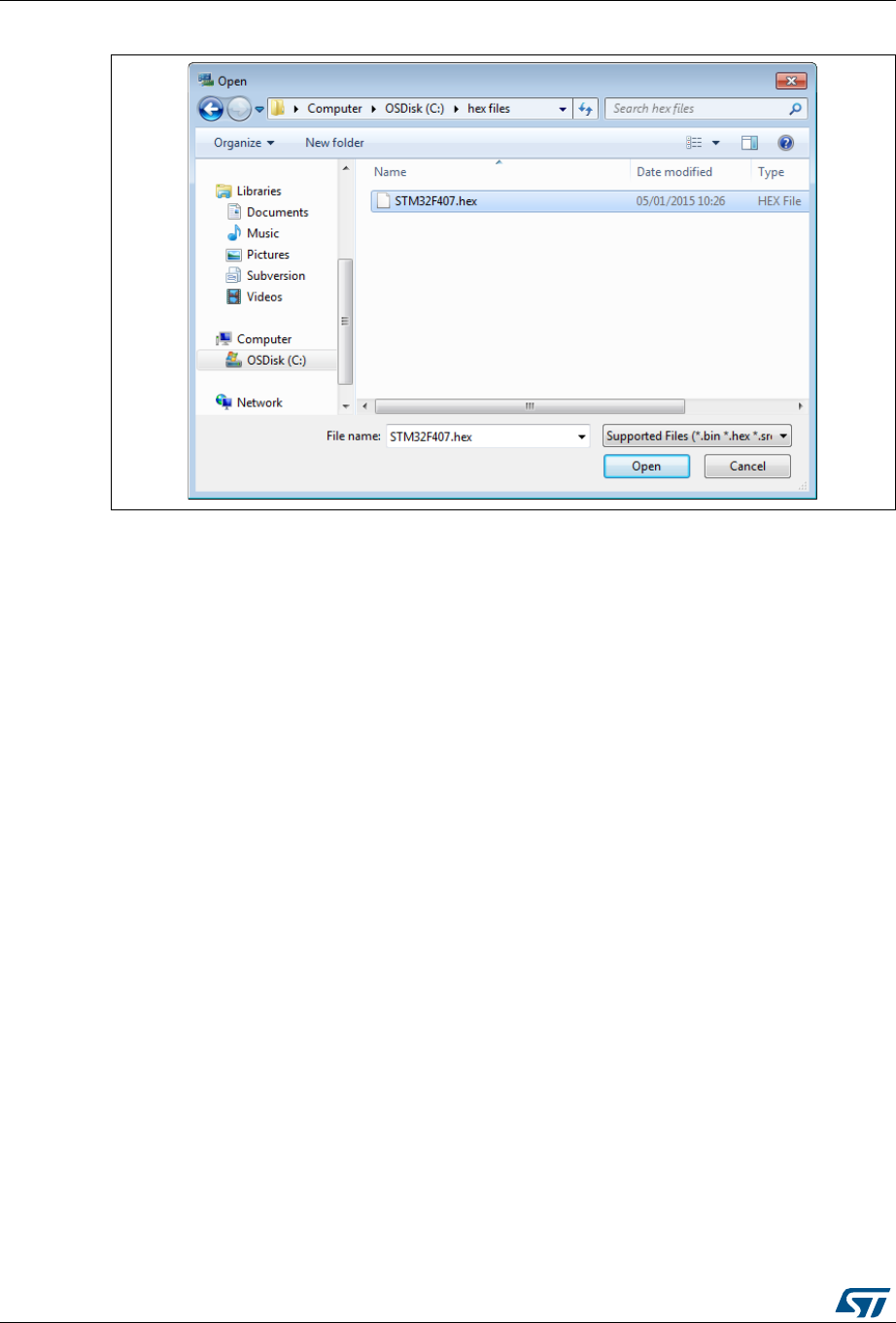
Figure 17. Open file dialog box . . . . . . . . . . . . . . . . . . . . . . . . . . . . . . . . . . . . . . . . . . . . . . . . . . . . . . 22
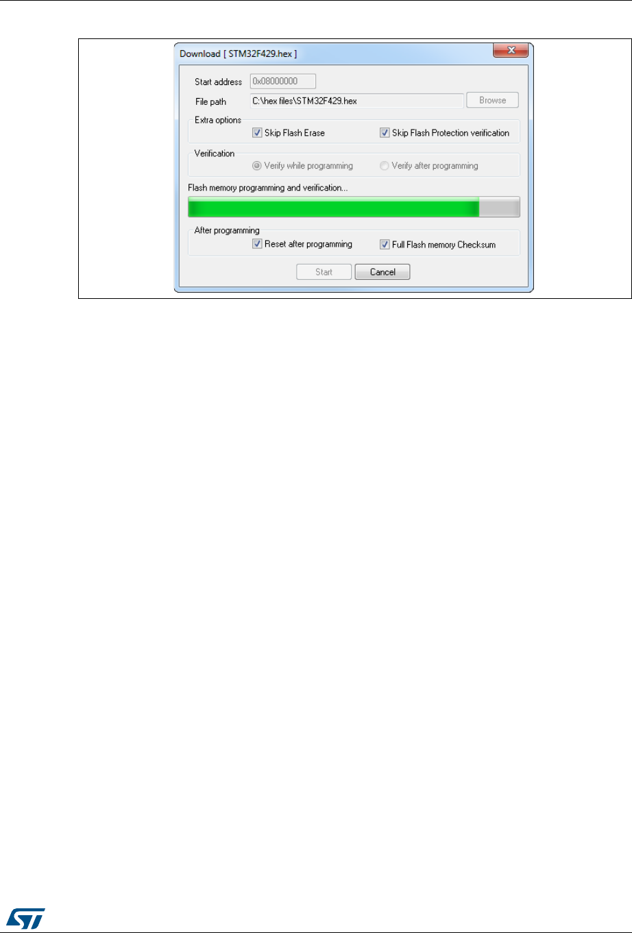
Figure 18. Device programming dialog box (programming). . . . . . . . . . . . . . . . . . . . . . . . . . . . . . . . . 23
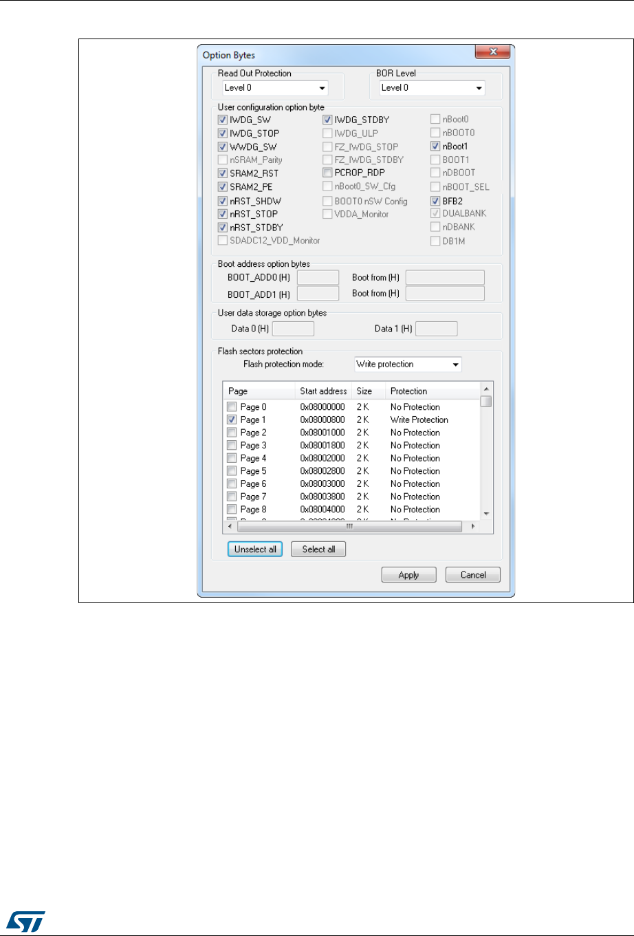
Figure 19. Option bytes dialog box . . . . . . . . . . . . . . . . . . . . . . . . . . . . . . . . . . . . . . . . . . . . . . . . . . . 27
Figure 20. Read/write protection mode . . . . . . . . . . . . . . . . . . . . . . . . . . . . . . . . . . . . . . . . . . . . . . . . 28
Figure 21. MCU Core panel dialog box . . . . . . . . . . . . . . . . . . . . . . . . . . . . . . . . . . . . . . . . . . . . . . . . 29
Figure 22. Automatic mode . . . . . . . . . . . . . . . . . . . . . . . . . . . . . . . . . . . . . . . . . . . . . . . . . . . . . . . . . 30
Figure 23. Serial wire viewer window (SWV) . . . . . . . . . . . . . . . . . . . . . . . . . . . . . . . . . . . . . . . . . . . . 34

Getting started UM0892
6/54 DocID16987 Rev 23
1 Getting started
This section describes the requirements and the procedures to install the STM32 ST-LINK
utility software.
1.1 System requirements
The STM32 ST-LINK utility PC configuration requires as a minimum:
•PC with USB port and Intel® Pentium® processor running a 32-bit version of one of the
following Microsoft® operating systems:
– Windows® XP
– Windows® 7
– Windows® 10
•256 Mbytes of RAM
•30 Mbytes of hard disk space available
1.2 Hardware requirements
The STM32 ST-LINK utility is designed to work with:
•STM32F0, STM32F1, STM32F2, STM32F3, STM32F4, STM32L4, STM32L1,
STM32L0 and STM32W Series
•ST-LINK or ST-LINK/V2 or ST-LINK/V2-ISOL in-circuit debugger/programmer probe
Note: In this document, ST-LINK/V2 refers to ST-LINK/V2 and ST-LINK/V2-ISOL, which are
functionally equivalent.
1.3 Installing the STM32 ST-LINK utility
Follow these steps and the on-screen instructions to install the STM32 ST-LINK utility:
1. Download the compressed STM32 ST-LINK utility software from the ST website.
2. Extract the contents of the .zip file into a temporary directory.
3. Double-click the extracted executable, setup.exe, to initiate the installation, and follow
the on-screen prompts to install the STM32 ST-LINK utility in the development
environment. The documentation for the utility is located in the subdirectory \Docs
where the STM32 ST-LINK utility is installed.
Note: If an earlier version of STM32 ST-LINK utility software is already installed, follow the
uninstalling instructions described in Section 1.4, before installing the new version.

DocID16987 Rev 23 7/54
UM0892 Getting started
53
1.4 Uninstalling the STM32 ST-LINK utility
Follow these steps to uninstall the STM32 ST-LINK utility:
1. Select Start | Settings | Control Panel.
2. Double-click on Add or Remove Programs.
3. Select STM32 ST-LINK utility.
4. Click on the Remove button.
STM32 ST-LINK utility user interface UM0892
8/54 DocID16987 Rev 23
2 STM32 ST-LINK utility user interface
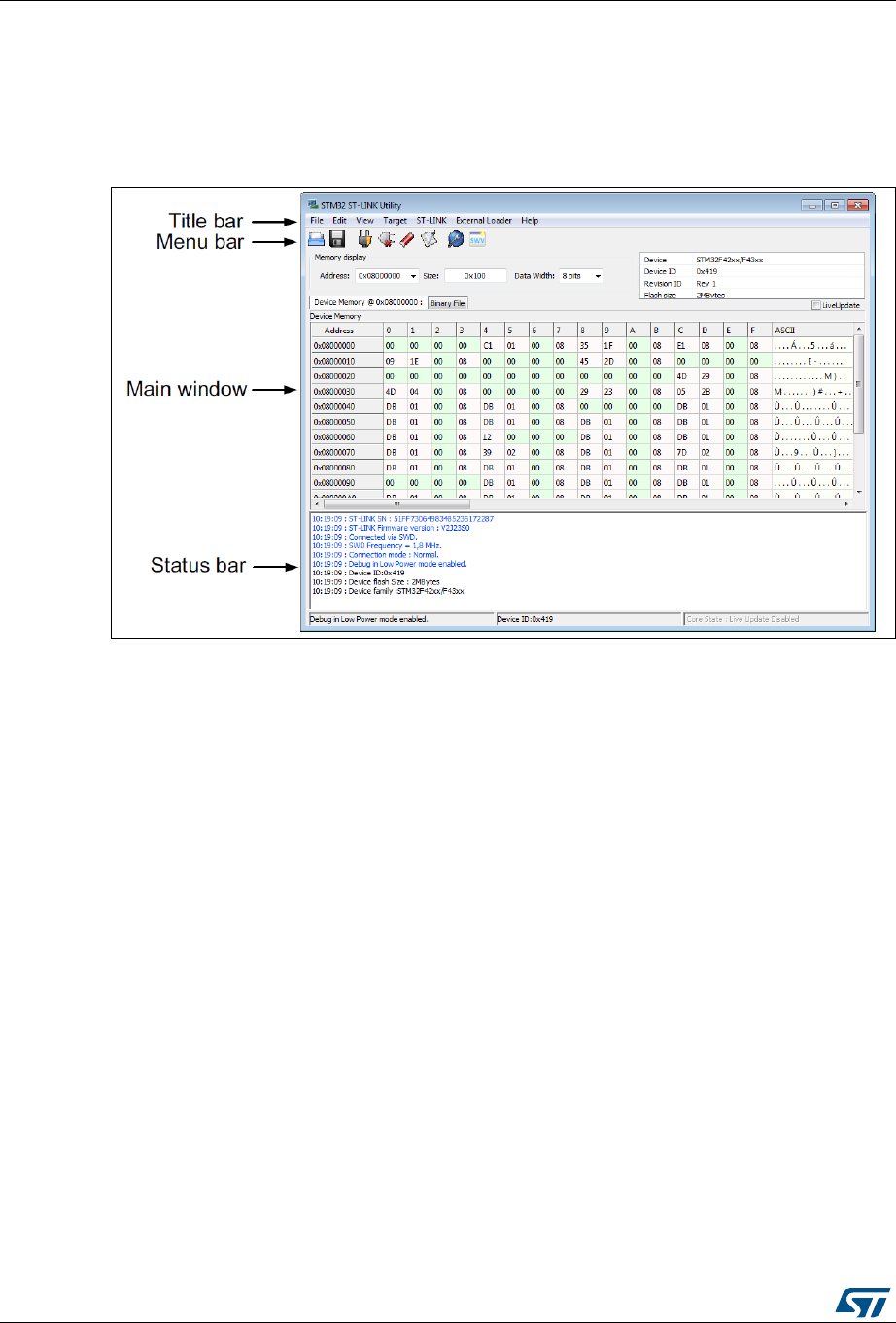
2.1 Main window
Figure 1. STM32 ST-LINK utility user interface main window
The main window is composed of three zones and three bars, as illustrated in Figure 1:
•Memory display zone
•Device information zone
•Memory content zone
–LiveUpdate checkbox to update memory data in real time
(This feature is described in more detail in Section 3.3)
•Title bar: name of the current menu
•Menu bar: Use the menu bar to access the following STM32 ST-LINK utility functions:
–File menu
–Edit menu
–View menu
–Target menu
–Help menu
These menus are described in more detail in Section 2.2.
•Status window: The status bar displays:
– Connection status and debug interface
–Device ID
– Core State (active only when LiveUpdate feature is active and memory grid is
selected)
The STM32 ST-LINK utility user interface also provides additional forms and descriptive
pop-up error messages.
DocID16987 Rev 23 9/54
UM0892 STM32 ST-LINK utility user interface
53
2.2 Menu bar
The Menu bar (Figure 2) allows users to explore the STM32 ST-LINK utility software
features.
Figure 2. Menu bar
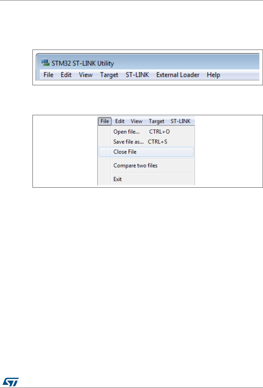
2.2.1 File menu
Figure 3. File menu
Open file... Opens a binary, Intel Hex or Motorola S-record.
Save file as… Saves the content of the memory panel into a binary, Intel Hex or Motorola S-
record.
Close File Closes the loaded file.
Compare two files
Compares two binary, hex, or srec files. The difference is colored in red in the file
panel. If a file contains a section with an address range that is unavailable in the
other file, this section is colored in violet.
Exit Closes the STM32 ST-LINK utility program.
STM32 ST-LINK utility user interface UM0892
10/54 DocID16987 Rev 23
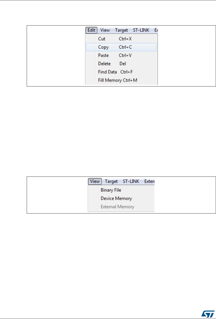
2.2.2 Edit menu
Figure 4. Edit menu
2.2.3 View menu
Figure 5. View menu
Cut Cuts the selected cells on file or memory grid.
Copy Copies selected cells on file or memory grid.
Paste Pastes the copied cells in the selected position in file or memory grid.
Delete Deletes the selected cells on file or memory grid.
Find Data Finds data in binary or Hex format in file or memory grid.
Fill Memory Fills file or memory grid with the chosen data starting from the chosen address.
Binary file Displays the content of the loaded binary file.
Device memory Displays the content of the device memory.
External memory Displays the content of the external memory.
DocID16987 Rev 23 11/54
UM0892 STM32 ST-LINK utility user interface
53
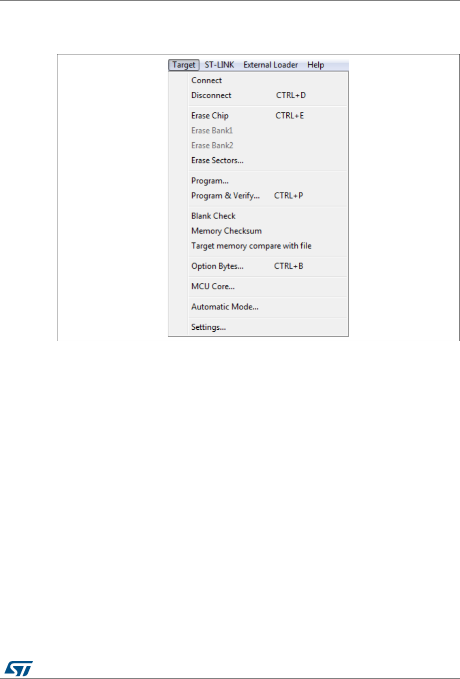
2.2.4 Target menu
Figure 6. Target menu
Connect Connects to the target device and displays the Device Type, Device ID and
Flash memory size in the device information zone.
Disconnect Disconnects from the target device.
Erase Chip Performs a Flash memory mass erase and then displays the Flash memory
content in the memory panel.
Erase Bank1 Erases bank 1 of the Flash memory. This menu is enabled only when
connected to an XL-density device.
Erase Bank2 Erases bank 2 of the Flash memory. This menu is enabled only when
connected to an XL-density device.
Erase Sectors… Selects sector(s) to erase using the erase sectors dialog window (see
Section 3.4: Flash memory erase for more details).
Program…
Loads a binary, Intel Hex or Motorola S-record file into the device memory
(Flash or RAM). To do this, select a binary, Intel Hex or Motorola S-record file,
enter the start address (where to put the file in the device) in the program
dialog window and then click on program button (see Section 3.5: Device
programming).
Program & Verify… Loads a binary, Intel Hex or Motorola S-record file into the device memory
(Flash or RAM) then performs a verification of the programmed data.
Blank Check Verifies that the STM32 Flash memory is blank. If the Flash memory is not
blank, the first address with data is highlighted in a prompt message.

STM32 ST-LINK utility user interface UM0892
12/54 DocID16987 Rev 23
Note: The “connect under reset” option is available only with ST-LINK/V2 and in SWD mode.
For JTAG mode, “connect under reset” is available since ST-LINK/V2 firmware
version V2J15Sx.
The RESET pin of the JTAG connector (pin 15) should be connected to the device reset pin.
The “HotPlug” option is available in SWD mode.
The low-power mode is disabled when the user disconnects from the target.
For JTAG mode, “HotPlug” has been available since ST-LINK firmware version V2J15Sx.
Memory checksum
Calculates the checksum value of a specified memory zone defined by the
address and the size fields in the Memory display section of the main window.
The checksum is calculated based on an arithmetic sum algorithm, byte per
byte. The result is truncated to 32-bit word.
The checksum value is displayed in the log window.
Compare device
memory with file
Compares the MCU device memory content with a binary, hex, or srec file. The
difference is colored in red in the file panel.
Option bytes… Opens the option bytes dialog window (See Section 3.6: Option bytes
configuration for more details).
MCU Core… Opens the MCU Core dialog window (See Section 3.7: MCU core functions for
more details).
Automatic Mode... Opens the Automatic mode dialog window (See Section 3.8: Automatic mode
functions for more details).
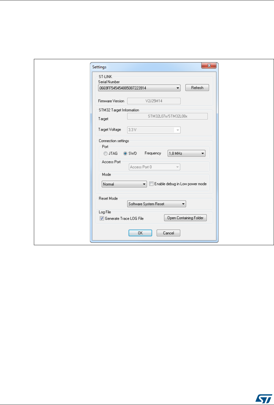
Settings...
The Settings dialog box allows to select one ST-LINK probes and defines its
connection settings.
The ST-LINK probes a list which contains the serial numbers of all probes
connected to the computer.
If some ST-LINK probes are plugged or unplugged while Settings dialog box is
displayed, the "Refresh" button allows the update of the ST-LINK probes list.
When the user selects one probe, the firmware version and the connected
target (depending on the connection settings) are displayed. After that, user
can choose the debug interface (JTAG or SWD) and select the Access Port (in
case the device contains multiple Access Ports) to which user wants to
connect.
Also the reset type can be selected:
* The “connect under reset” option allows to connect to the target before
executing any instruction. This is useful in many cases like when the target
contains a code that disables the JTAG/SWD pins.
*The “HotPlug” option allows to connect to the target without halt or reset. This
is useful to update RAM addresses or IP registers while application is running.
When connecting to the target via an ST-LINK/V2, the “Supply voltage” combo
box displays the target voltage.
When connecting to an STM32F2 or STM32F4 device using an ST-LINK, the
“Supply voltage” combo allows to select the supply voltage of the target to be
able to correctly program the Flash memory.
The "Enable debug in low-power mode" option allows to connect to a device in
low-power mode.
If any connection settings changes, the dialog tries to identify the target with
the new connection settings.
DocID16987 Rev 23 13/54
UM0892 STM32 ST-LINK utility user interface
53
The ST-LINK firmware version to be used in case of multi probes selection, should be:
•
V1J13S0 or greater for ST-LINK.
•
V2J21S4 or greater for ST-LINK/V2.
•
V2J21M5 or greater for ST-LINK/V2-1.
When an ST-LINK/V2 or ST-LINK/V2-1 probe is used with another application, the serial
number is not displayed and the probe cannot be used in the current instance of ST-LINK
utility.
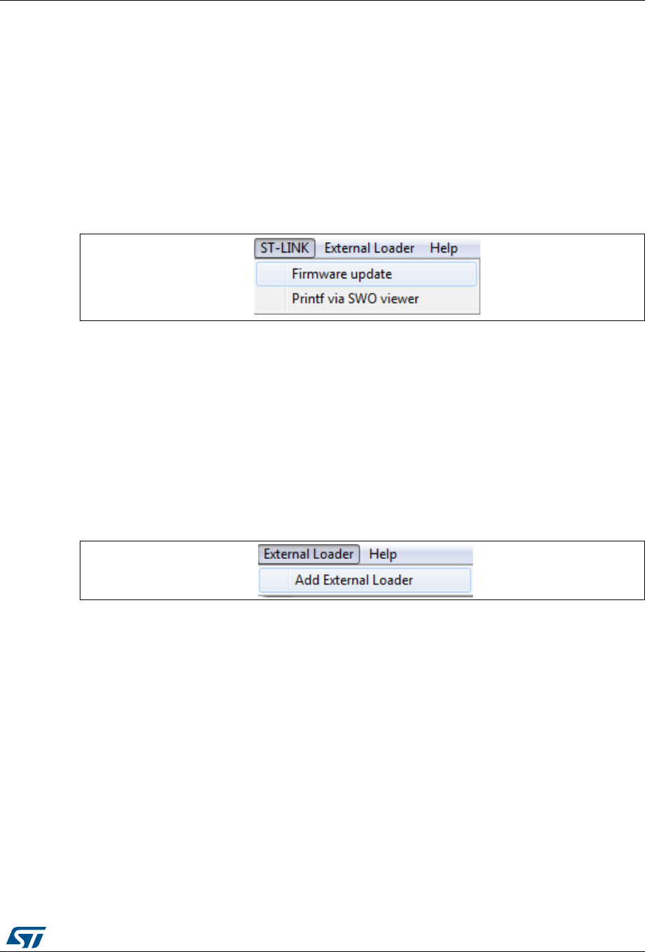
2.2.5 ST-LINK menu
Figure 7. ST-LINK menu
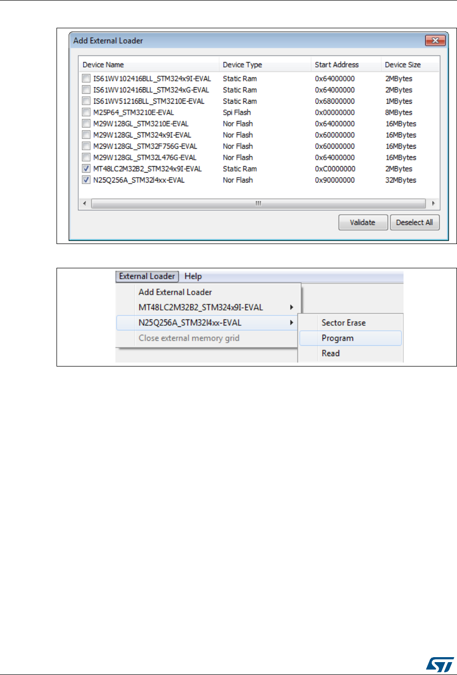
2.2.6 External Loader menu
Figure 8. External Loader menu
The STM32 ST-LINK utility includes the Add External Loader submenu which allows to
select the external loaders to be used by the ST-LINK utility to read, program, or erase
external memories.
The external loaders must be added in the ExternalLoader directory located under the ST-
LINK utility directory (see Section 3.9: Developing customized loaders for external memory
for more details on how to create a custom loader).
When the external loaders have been selected in the External Loader dialog box (see
Figure 9), new submenus are displayed, one per each external loader selected.
They offer all the functions (Program, Sector Erase...) available in the corresponding
external loader (see Figure 10).
Firmware update
Displays the version of ST-LINK and ST-LINK/V2 firmware
and updates it to the last version:
ST-LINK: V1J13S0
ST-LINK/V2: V2J21S4
ST-Link/V2-1: V2J21M5
Printf via SWO viewer Displays printf data sent from target via SWO (see
Section 3.10: Printf via SWO viewer for more details).
STM32 ST-LINK utility user interface UM0892
14/54 DocID16987 Rev 23
Figure 9. External Loader window
Figure 10. External Loader submenus
DocID16987 Rev 23 15/54
UM0892 STM32 ST-LINK utility user interface
53
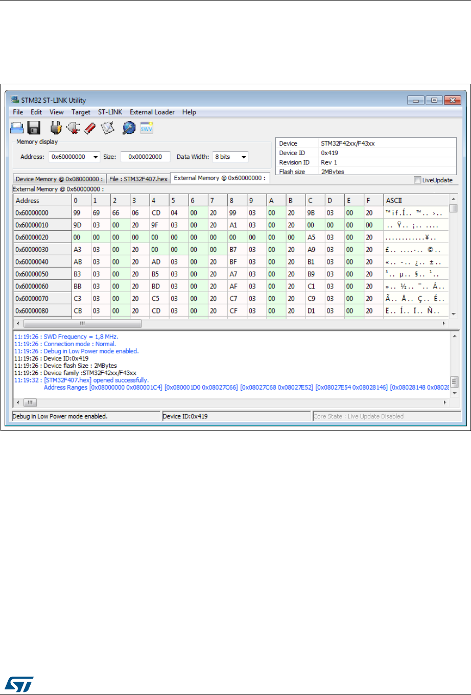
The contents of the external memory is displayed in the external memory grid (Figure 11).
Selecting the Close external memory grid submenu, shuts down the external memory
grid window.
Figure 11. External memory grid
Note: Only 10 external loaders can be selected at the same time.
The external memories connected to the STM32 via FSMC can be accessed automatically
through the Device Memory Grid, if the corresponding external loader has already been
added by using the Add External Loader submenu.
STM32 ST-LINK utility user interface UM0892
16/54 DocID16987 Rev 23
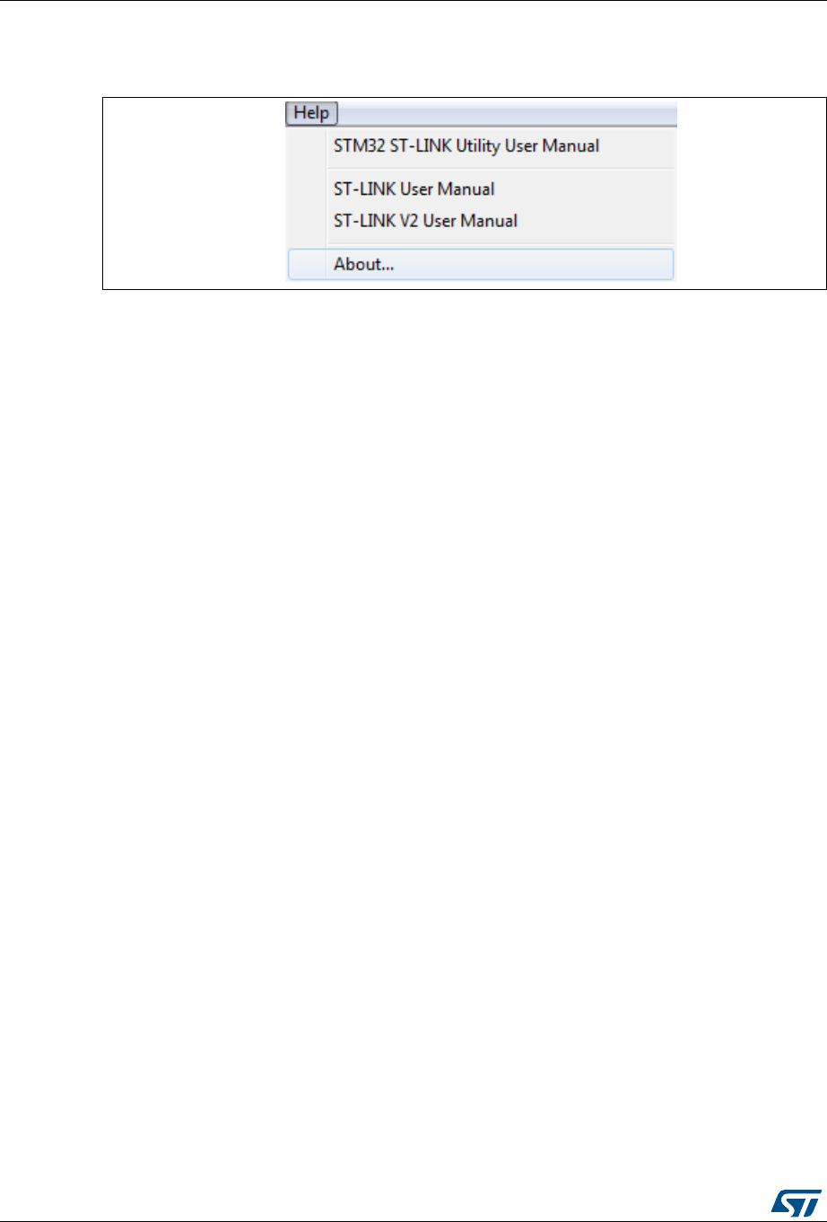
2.2.7 Help menu
Figure 12. Help menu
STM32 ST-LINK utility User Manual Opens the STM32 ST-LINK utility User Manual.
ST-LINK User Manual Opens the ST-LINK User Manual.
ST-LINK/V2 User Manual Opens the ST-LINK/V2 User Manual.
About... Displays STM32 ST-LINK utility software version and
copyright information.
DocID16987 Rev 23 17/54
UM0892 STM32 ST-LINK utility features
53
3 STM32 ST-LINK utility features
This section provides a detailed description of how to use STM32 ST-LINK utility features:
•Device information
•Settings
•Memory display and modification
•Flash memory erase
•Device programming
•Option bytes configuration
•MCU core functions
•Automatic mode functions
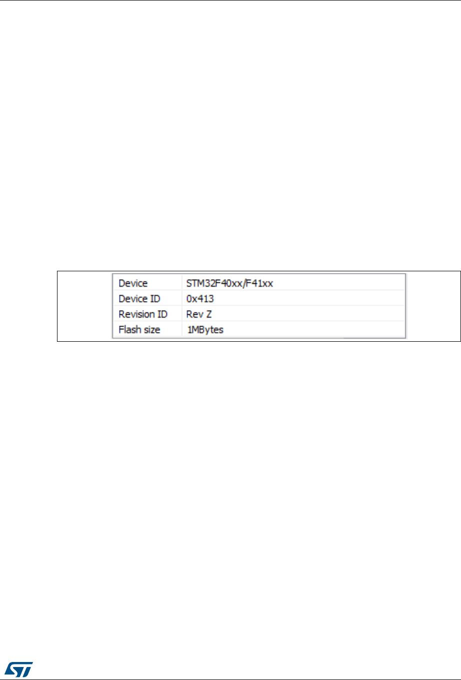
3.1 Device information
The Device information zone displays information, as shown in Figure 13.
Figure 13. Device information zone in the main user interface
Device:
Family of the connected STM32 device. Each device type includes many
devices with different characteristics such as the Flash memory size, the RAM
size and peripherals.
Device ID: MCU device ID code located in the external PPB memory map.
Revision ID: The revision ID of the connected MCU device.
Flash size: Size of the on-chip Flash memory.
STM32 ST-LINK utility features UM0892
18/54 DocID16987 Rev 23
3.2 Settings
The Settings panel dialog box, shown in Figure 14, displays useful information on the
connected ST-LINK probes and STM32 target, and allows to configure the connection
settings.
Figure 14. Settings dialog box
The user can choose one of the connected ST-LINK probes to use, based on its serial
number or on the connected target, which is displayed in the STM32 target information
section.
When using ST-LINK/V2 or ST-LINK/V2-ISOL, the target voltage is measured and displayed
in the STM32 target information section.

DocID16987 Rev 23 19/54
UM0892 STM32 ST-LINK utility features
53
Available connection settings:
•Port: JTAG or SWD
•Access Port (if device contains multiple Access Ports)
•Frequency
•Mode:
– Normal
With “Normal” connection mode, the target is rest then halted. The type of reset is
selected using the “reset Mode” option
– Connect Under Reset
The “Connect Under Reset” option allows to connect to the target using a reset
vector catch before executing any instruction. This is useful in many cases like
when the target contains a code that disables the JTAG/SWD pins.
–Hot Plug
The “Hot Plug” option allows to connect to the target without halt or reset. This is
useful to update the RAM addresses or the IP registers while the application is
running.
•Enable/Disable debug in low-power mode
•Enable/Disable Trace LOG file generation
Available reset modes:
•software system reset
•hardware reset
•core reset
Note: When the “connect under reset” mode is selected, the hardware reset mode is automatically
selected. When programming the option bytes, a reset is issued at the end of the operation.
This reset is handled separately and is not affected by this option.
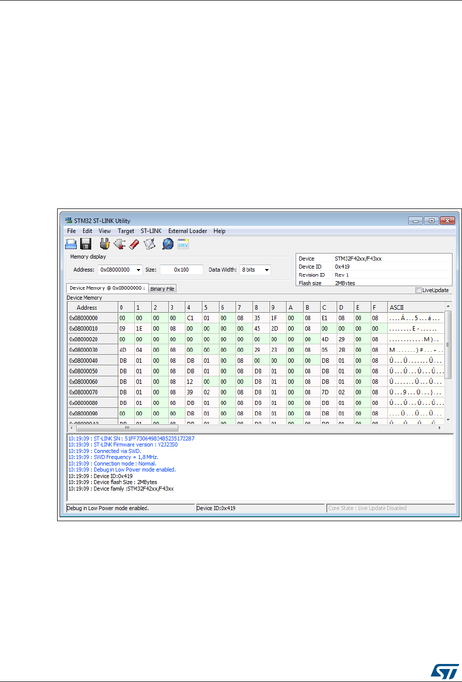
3.3 Memory display and modification
In addition to the Device information zone, the main window contains two other zones:
•Memory display
•Memory data
Memory display: This zone contains three edit boxes:
Address: Memory start address from which the user wants to read.
Size: Amount of data to read.
Data width: Width of the displayed data (8-bit, 16-bit or 32-bit).
STM32 ST-LINK utility features UM0892
20/54 DocID16987 Rev 23
Memory data: This zone displays the data read from a file or the memory content of a
connected device. The user can modify the content of the file before downloading.
•To use this zone to display the content of a binary, Intel Hex or Motorola S-record file,
go to File | Open file...
•To use this zone to read and display memory content of a connected device, enter the
memory start Address, data Size and the Data Width in the Memory display zone and
then press Enter.
•After reading data, the user also can modify each value merely by double-clicking on
the concerned cell as illustrated by Figure 15. The user also can save the device
memory content into a binary, Intel Hex or Motorola S-record file using the menu File |
Save file as...
•When LiveUpdate feature is used the device memory grid is updated in real time and
the data that have been modified are colored in red.
Figure 15. STM32 ST-LINK utility user interface
Note: When the memory data zone displays device memory contents, any modification is
automatically applied to the chip. The user can modify the user Flash memory, RAM
memory and peripherals registers.
For the STM32F2 and STM32F4 devices, the OTP area can be modified directly from the
memory data zone.
DocID16987 Rev 23 21/54
UM0892 STM32 ST-LINK utility features
53
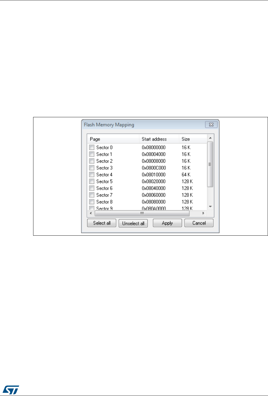
3.4 Flash memory erase
There are two types of Flash memory erase:
•Flash mass erase: Erase all the memory Flash memory sectors of the connected
device. This is done by clicking on the menu Target | Erase Chip.
•Flash sector erase: Erase the selected sector(s) of the Flash memory. To select
sector(s), go to Target | Erase Sectors... the Flash Memory Mapping dialog box is
displayed, where the user can select the sector(s) to erase, as shown in Figure 16.
–Select all button selects all the Flash memory pages.
–Deselect all button deselects all selected page.
–Cancel button discards the erase operation even if some pages are selected.
–Apply button erases all the selected pages.
Figure 16. Flash memory mapping dialog box
Note: To erase the Flash data memory sector of the ultra-low-power STM32L1 devices, select the
data memory box at the end of the list and click Apply.
3.5 Device programming
The STM32 ST-LINK utility can download binary, Hex, or srec files into Flash or RAM. To do
this, follow these steps:
1. Click on Target | Program... (or Target | Program & Verify... if the user wants to verify
the written data) to open the Open file dialog box, as shown in Figure 17. If a binary file
is already opened, go to step 3.
DocID16987 Rev 23 23/54
UM0892 STM32 ST-LINK utility features
53
Figure 18. Device programming dialog box (programming)
4. Select Skip Flash erase option to skip Flash erase operation in case the device is
already erased
5. Select Skip Flash Protection verification to skip Flash memory protection verification in
case the devise is not protected.
6. Choose a verification method by selecting one of the two radio buttons:
a) Verify while programming: fast on-chip verification method which compares the
program buffer content (portion of file) with the Flash memory content.
b) Verify after programming: slow but reliable verification method which reads all the
programmed memory zone after the program operation ends and compares it with
the file content.
7. At last, click on the Start button to start programming:
a) If the Reset after programming box is checked, an MCU reset is issued.
b) If the Full Flash memory Checksum box is checked, the checksum of the full
Flash memory is calculated after programming operation, and displayed in the log
window.
8. Choose a verification method by selecting one of the two radio buttons:
a) Verify while programming: fast on-chip verification method which compares the
program buffer content (portion of file) with the Flash memory content.
b) Verify after programming: slow but reliable verification method which reads all the
programmed memory zone after the program operation ends and compares it with
the file content.
9. At last, click on the Start button to start programming:
a) If Target | Program & Verify... is selected in the first step, a check is done during
the programming operation.
b) If the Reset after programming box is checked, an MCU reset is issued.
Note:1 The STM32F2 and STM32F4 Series supports different programming modes depending on
the MCU supply voltage. When using ST-LINK, the MCU supply voltage should be specified

STM32 ST-LINK utility features UM0892
24/54 DocID16987 Rev 23
in the Target | Settings Menu to be able to program the device with the correct mode.
When using ST-LINK/V2, the supply voltage is detected automatically.
If the device is read-protected, the protection is disabled. If some Flash memory pages are
write-protected, the protection is disabled during programming and then recovered.
Note:2 The user can program Hex/Srec files that contains multiple segments for different target
memory locations (Internal Flash memory, external Flash memory, Option bytes...).
When programming the Read Out Protection to level 2 (debug and boot in SRAM/system
Memory features are DISABLED), a message box is displayed for confirmation to avoid
protecting the chip by accident.
Note:3 The extra options are dedicated for programming operation on unprotected and erased
devices.
3.6 Option bytes configuration
The STM32 ST-LINK utility can configure all the option bytes via the Option bytes dialog
box (shown in Figure 19), which is accessed by Target | Option bytes....
The Option bytes dialog box contains the following sections:
•Read Out protection
Modifies the read protection state of the Flash memory.
For STM32F0, STM32F2, STM32F3, STM32F4, STM32L4 and STM32L1 devices,
read protection levels are available:
– Level 0: no read protection
– Level 1: memory read protection enabled
– Level 2: memory read protection enabled and all debug features disabled.
For the other devices, the read protection can only be enabled or disabled.
•BOR Level
Brownout reset level. This list contains the supply level threshold that
activates/releases the brownout reset. This option is only available on STM32L1,
STM32L4, STM32F2, STM32F4, and STM32F7 devices.
For STM32L4 devices, 5 programmable VBOR thresholds can be selected:
– BOR LEVEL 0: Reset level threshold is around 1.7 V
– BOR LEVEL 1: Reset level threshold is around 2.0 V
– BOR LEVEL 2: Reset level threshold is around 2.2 V
– BOR LEVEL 3: Reset level threshold is around 2.5 V
– BOR LEVEL 4: Reset level threshold is around 2.8 V
For ultra-low-power devices, 5 programmable VBOR thresholds can be selected:
– BOR LEVEL 1: Reset threshold level for 1.69 to 1.8 V voltage range
– BOR LEVEL 2: Reset threshold level for 1.94 to 2.1 V voltage range
– BOR LEVEL 3: Reset threshold level for 2.3 to 2.49 V voltage range
– BOR LEVEL 4: Reset threshold level for 2.54 to 2.74 V voltage range
– BOR LEVEL 5: Reset threshold level for 2.77 to 3.0 V voltage range
For STM32F2 and STM32F4 devices, 4 programmable VBOR thresholds can be
selected:

DocID16987 Rev 23 25/54
UM0892 STM32 ST-LINK utility features
53
– BOR LEVEL 3: Supply voltage ranges from 2.70 to 3.60 V
– BOR LEVEL 2: Supply voltage ranges from 2.40 to 2.70 V
– BOR LEVEL 1: Supply voltage ranges from 2.10 to 2.40 V
– BOR off: Supply voltage ranges from 1.62 to 2.10 V
•User Configuration option bytes
– WDG_SW: If checked, the watchdog is enabled by software. Otherwise, it is
automatically enabled at power-on.
– IWDG_STOP: If not checked, the independent watchdog counter is frozen in
STOP mode. If checked, this counter is active in STOP mode.
– IWDG_STBY: If not checked, the independent watchdog counter is frozen in
Standby mode. If checked this counter is active in Standby mode.
– WWDG_SW: If checked, the window watchdog is enabled by hard option bit.
–SRAM2_RST
(a): This bit allows the user to enable the SRAM2 erase on system
reset. If checked SRAM2 is not erased when a system reset occurs. If not
checked, SRAM2 is erased when system reset occurs.
–SRAM_PE
(a): This bit allows the user to enable the SRAM2 hardware parity
check. If checked, SRAM2 parity check is disabled.
– DUALBANK(b): If checked, 512/256K Dual Bank Flash with contiguous addresses.
–DB1M
(c): Dual Bank on 1-Mbyte Flash.
– PCROP_RDP(a): If checked, PCROP area is erased when the RDP level is
decreased from Level 1 to Level 0 (full mass erase).
–nRST_SHDW
(a): If checked, no reset is generated. If not checked, reset is
generated when entering the Shutdown mode.
– nRST_STOP: If not checked, a reset is generated when entering Standby mode
(1.8 V domain powered-off). If checked, no reset is generated when entering
Standby mode.
– nRST_STDBY: If not checked, reset is generated when entering Stop mode (all
clocks are stopped). If checked, no reset is generated when entering Stop mode.
– nBFB2: If not checked, and if the boot pins are set to make the device boot from
the user Flash at startup, the device boots from Flash memory bank 2; otherwise,
it boots from Flash memory bank 1. This option is enabled only when connected to
a device containing two Flash banks.
–nBoot1
(d): Together with the BOOT0 pin, selects the Boot mode:
- nBoot1 checked/unchecked and BOOT0 = 0 => Boot from Main Flash memory;
- nBoot1 checked and BOOT0 = 1 => Boot from System memory;
- nBoot1 unchecked and BOOT0 = 1 => Boot from Embedded SRAM.
– VDDA_Monitor(d): Selects the analog monitoring on VDDA Power source:
If checked, VDDA power supply supervisor is enabled; otherwise, it is disabled.
– nSRAM_Parity(d): This bit allows the user to enable the SRAM hardware parity
a. Only available on STM32L4 devices.
b. Only available on STM32L4 devices supporting Dual Bank mode.
c. Only available on STM32F42x/STM32F43x 1-Mbyte devices.
d. Only available on STM32F0 and STM32F3 devices.

STM32 ST-LINK utility features UM0892
26/54 DocID16987 Rev 23
check.
If checked, SRAM parity check is disabled; otherwise it is enabled.
– SDADC12_VDD_Monitor(a):
If checked, SDADC12_VDD power supply supervisor is enabled; otherwise it is
disabled.
– nBoot0_SW_Cfg(b): This bit allows the user to completely disable BOOT0
hardware pin and use User Option bit 11 (nBoot0).
If checked, the BOOT0 pin is bonded to GPIO pin (PB8 on LQFP32 and smaller
packages, PF11 for QFN32 and bigger packages).
•Boot address option bytes:
for devices supporting BOOT_ADDx, it allows the boot from base address defined by
option bytes BOOT_ADDx.
BOOT_ADDx[15:0] corresponds to address [29:11].
For devices supporting both BOOT_ADD0 and BOOT_ADD1, it depends upon BOOT0
pin:
– If BOOT0 = 0 boot from base address defined by option bytes BOOT_ADD0.
– If BOOT0 = 1 boot from base address defined by option bytes BOOT_ADD1.
The user can enter either the address of the boot, or the BOOT_ADDx option bytes
values.
•User data storage option bytes: contains two bytes for user storage. These two
option bytes are not available in the STM32F0, STM32F2, STM32F3, STM32F4 and
STM32L1 devices.
•Flash Sectors Protection: depending on the connected device, Flash sectors are
grouped by a defined number of pages. The user can modify the write protection of
each Flash sector here.
•For devices supporting PCRop feature, it is possible to enable/disable the Read
protection of each sector. The “Flash protection mode” allows to choose between read
or write protection.
a. Only available on STM32F37x devices.
b. Only available on STM32F04x devices.
DocID16987 Rev 23 27/54
UM0892 STM32 ST-LINK utility features
53
Figure 19. Option bytes dialog box
STM32 ST-LINK utility features UM0892
28/54 DocID16987 Rev 23
For STM32L4 devices, the PCROP zone is defined by two addresses as showed in
Figure 20:
Figure 20. Read/write protection mode
•Read/Write protection bank A: if checked, PCROPA_STRT, PCROPA_END, Start
address (H) and End address (H) fields are editable so the user can enter, either the
PCROP STRT/END field or the start/end address.
•Protect entire Bank A: if checked, all the bank A is pcrop protected.
•PCROPA_strt: The PCROP start field for the protected zone in bank A.
•Start Address: The start address defined by the PCROPA_strt field.
•PCROPA_end: The PCROP end field for the protected zone in bank A.
•End Address: The end address defined by the PCROPA_end field.
•Read/Write Protection bank B: if checked, PCROPB_STRT, PCROPB_END, Start
address (H) and End address (H) fields are editable so the user can enter, either the
PCROP STRT/END field or the start/end address.
DocID16987 Rev 23 29/54
UM0892 STM32 ST-LINK utility features
53
•Protect entire bank B: if checked, all the bank B is pcrop protected.
•PCROPB_strt: The PCROP start field for the protected zone in bank B.
•Start Address: The start address defined by the PCROPB_strt field.
•PCROPB_end: The PCROP end field for the protected zone in bank B.
•End Address: The end address defined by the PCROPB_end field.
For more details, refer to the option bytes section in the Flash programming manual and
reference manual available from the www.st.com website.
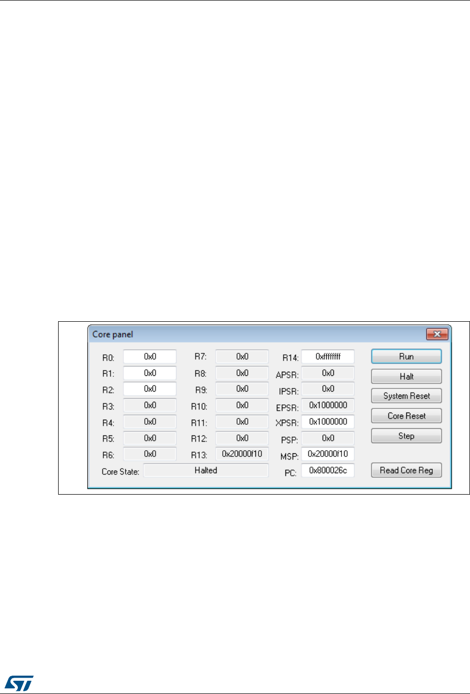
3.7 MCU core functions
The Core panel dialog box shown in Figure 21, displays the ARM® Cortex® -M3 core
register values. It also allows to carry out the following actions on the MCU, using the
buttons on the right:
•Run: Run the core.
•Halt: Halt the core.
•System Reset: Send a system reset request.
•Core Reset: Reset the core.
•Step: Execute only one step core instruction.
•Read Core Reg: Update the core registers values.
Figure 21. MCU Core panel dialog box
Note: The PC and MSP registers can be modified from this panel.
STM32 ST-LINK utility features UM0892
30/54 DocID16987 Rev 23
3.8 Automatic mode functions
The Automatic mode dialog box shown in Figure 22 allows programing and configuring
STM32 devices in loop. It allows to carry out the following actions on the STM32 devices:
•Full chip erase
•Flash programming
•Verify:
– Verify while programming
– Verify after programming
•Option bytes configuration
•Run application
Clicking on the Start button executes the selected actions on the connected STM32 device
and waits to repeat the same actions, after disconnecting the current device and connecting
the new device.
Figure 22. Automatic mode
Note: If the user deselects Flash programming action while the STM32 Flash memory is readout
protected, it is automatically unprotected.
If the user deselects Flash programming action while some or all STM32 Flash memory are
write-protected, they are automatically unprotected and restored after programming
operation.
The connection to the device should be established to be able to select the option bytes
configuration using the configure button.
The connected devices should be derivatives of the same STM32 family and must all be
connected in the same mode (JTAG or SWD).
The automatic mode cannot be used if more than one ST-LINK probe is connected to the
computer. A dialog is displayed to prevent the user and ask him to keep only one ST-LINK
probe connected to continue using this mode.
Before starting the automatic mode and if the option byte configuration is checked, the

DocID16987 Rev 23 31/54
UM0892 STM32 ST-LINK utility features
53
configuration of the option bytes using the "Configure..." button is mandatory.
When the option bytes is configured for the first time for a specific device ID, the initial
values are loaded from the connected device.
If the connected device has a different device ID from the device connected while
configuring option bytes, the option bytes have to be reconfigured using the "Configure..."
button before starting the automatic mode.
3.9 Developing customized loaders for external memory
Using the examples available under the ExternalLoader directory, users can develop their
custom loaders for a given external memory .
These examples are available for three toolchains, i.e. MDK-ARM™, EWARM and
TrueSTUDIO®. The development of the custom loaders can be performed using one of the
three toolchains keeping the same compiler/linker configurations, as in the examples.
To create a new external memory loader, follow the steps below:
1. Update the device information in StorageInfo structure in the Dev_Inf.c file with the
correct information concerning the external memory.
2. Rewrite the corresponding functions code in the Loader_Src.c file.
3. Change the output file name.
Note: Some functions are mandatory and cannot be omitted (see functions description in the
Loader_Src.c file).
Linker or scatter files should not be modified.
After building the external loader project, an ELF file is generated. The extension of the ELF
file depends on the used toolchain (.axf for Keil, .out for EWARM and .elf for TrueSTUDIO or
any gcc based toolchain).
The extension of the ELF file must be changed to ‘.stldr’ and the file must be copied under
/ExternalLoader directory.
3.9.1 Loader_Src.c file
Developing an external loader for a memory, based on a specific IP requires the following
functions:
•An Init function
The Init function defines the used GPIO pins which are connecting the external
memory to the device, and initializes the clock of the used IPs.
Returns 1 if success, and 0 in failure.
int Init (void)
•A Write function
The Write function programs a buffer defined by an address in the RAM range.
Returns 1 if success, and 0 if failure.
int Write (uint32_t Address, uint32_t Size, uint8_t* buffer)
•A SectorErase function
The SectorErase function erases the memory specified sectors.
Returns 1 if success, and 0 if failure.
Note: This function is not used in case of an SRAM memory

STM32 ST-LINK utility features UM0892
32/54 DocID16987 Rev 23
int SectorErase (uint32_t StartAddress, uint32_t EndAddress)
Where “StartAddress” = the address of the first sector to be erased and
“EndAddress” = the address of the end sector to be erased
It is imperative to define in an external loader the functions mentioned above. They are used
by the tool to erase and program the external memory.
For instance, if the user clicks on the program button from the external loader menu, the tool
performs the following actions:
•Automatically calls the Init function to initialize the interface (QSPI, FMC …) and the
Flash memory
•Calls SectorErase() to erase the needed Flash sectors
•Calls the Write() function to program the memory
Additionally to those functions, we can define also the functions below:
•A read function
The Read function is used to read a specific range of memory, and returns the reading
in a buffer in the RAM.
Returns 1 if success, and 0 if failure.
int Read (uint32_t Address, uint32_t Size, uint16_t* buffer)
Where “Address” = start address of read operation, “Size” = size of the read operation and
“buffer” = is the pointer to data read
Note: For QSPI/OSPI (Quad-SPI/ Octo-SPI) memories, the memory mapped mode can be
defined in the Init function; in that case the Read function is useless.
•A Verify function
The Verify function is called when selecting the “verify while programming” mode. This
function checks if the programmed memory corresponds to the buffer defined in the
RAM. It returns an uint64 defined as follow:
checksum<<32 + AddressFirstError
where “AddressFirstError” is the address of the first mismatch, and “checksum” is the
checksum value of the programmed buffer
uint64_t Verify (uint32_t FlashAddr, uint32_t RAMBufferAddr, uint32_t
Size)
•A MassErase function
The MassErase function erases the full memory.
Returns 1 if success, and 0 if failure.
int MassErase (void)
•A Checksum function
All the described functions return 1 in case of a successful operation and 0 in case of a fail.
3.9.2 Dev_Inf.c file
The StorageInfo structer is defined in this file. An example of the type of information that this
structer defines is presented below:
#if defined (__ICCARM__)
__root struct StorageInfo const StorageInfo = {
#else

DocID16987 Rev 23 33/54
UM0892 STM32 ST-LINK utility features
53
struct StorageInfo const StorageInfo = {
#endif
"External_Loader_Name", // Device Name + version number
MCU_FLASH, // Device Type
0x08000000, // Device Start Address
0x00100000, // Device Size in Bytes (1MBytes/8Mbits)
0x00004000, // Programming Page Size 16KBytes
0xFF, // Initial Content of Erased Memory
// Specify Size and Address of Sectors (view example below)
0x00000004, 0x00004000, // Sector Num : 4 ,Sector Size: 16KBytes
0x00000001, 0x00010000, // Sector Num : 1 ,Sector Size: 64KBytes
0x00000007, 0x00020000, // Sector Num : 7 ,Sector Size: 128KBytes
0x00000000, 0x00000000,
};
STM32 ST-LINK utility features UM0892
34/54 DocID16987 Rev 23
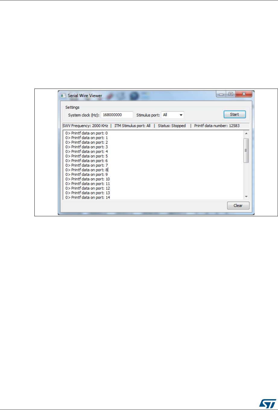
3.10 Printf via SWO viewer
The Printf via SWO Viewer displays the printf data sent from the target through SWO. It
allows to display some useful information on the running firmware.
Before starting receiving SWO data, the user has to specify the exact target system clock
frequency to allow the tool to correctly configure the ST-LINK, and the target for the correct
SWO frequency. The Stimulus port combo box allows the user to choose either a given ITM
Stimulus port (from port 0 to 31) or to receive data simultaneously from all ITM Stimulus
ports.
Figure 23. Serial wire viewer window (SWV)
The SWV information bar displays useful information on the current SWV transfer such as
the SWO frequency (deduced from the system clock frequency), and the received
(expressed in bytes).
Note: Some SWV bytes could be lost during transfer due to ST-LINK hardware buffer size
limitation.

DocID16987 Rev 23 35/54
UM0892 STM32 ST-LINK utility command line interface (CLI)
53
4 STM32 ST-LINK utility command line interface (CLI)
4.1 Command line usage
The following sections describe how to use the STM32 ST-LINK utility from the command
line.
The ST-LINK utility command line interface is located at the following address:
[Install_Directory]\STM32 ST-LINK utility\ST-LINK utility\ST-LINK_CLI.exe
4.1.1 Connection and memory manipulation commands
Description: Selects JTAG or SWD communication protocol. By default, JTAG protocol is
used.
Syntax: -c [ID=<id>/SN=<sn>] [JTAG/SWD] [FREQ=<frequency>] [UR/HOTPLUG] [LPM]
[ID=<id>]: ID of ST-LINK[0..9] to be used when multiple probes are connected to the host
[SN=<sn>]: Serial Number of the chosen ST-LINK probe.
[UR]: Connect to the target under reset.
[HOTPLUG]: Connect to the target without halt or reset.
[FREQ=<frequency>] : Frequency in KHz for JTAG or SWD protocol (the frequency value is
raised to correspond to the allowed frequency values)
SWD frequency values:
4000KHz,1800KHz, 900KHz, 480KHz, 240KHz,125KHz,100KHz, 50KHz, 25KHz,15KHz,
5KHz.The default frequency value for SWD protocol is 4000KHz.
JTAG frequency values:
9000KHz, 4500KHz, 2250KHz,1125KHz, 562KHz, 281KHz,140KHz.
The default frequency value for JTAG protocol is 9000KHz.
[LPM]: Activate debug in low-power mode
Example1: -c ID=1 SWD UR LPM JTAG freq=1000
Example2: -c SN=55FF6C064882485358622187 SWD UR LPM
Note: [SWCLK=<f>] and [JTAG=<f>] options are obsolete. Use the [FREQ=<frequency>] option
instead.
[SWCLK=<f>] : frequency [0..10] of SWD protocol
0 = 4.0 MHz (Default value when not specified)
1 = 005 KHz
2 = 015 KHz
3 = 025 KHz
4 = 050 KHz
5 = 100 KHz
6 = 125 KHz
7 = 240 KHz
8 = 480 KHz

STM32 ST-LINK utility command line interface (CLI) UM0892
36/54 DocID16987 Rev 23
9 = 0.9 MHz
10 = 1.8 MHz
[JTAGCLK=<f>]: frequency [0..6] of JTAG protocol
0 = 9.0 MHz (Default value when not specified)
1 = 140 KHz
2 = 281 KHz
3 = 562 KHz
4 = 1125 KHz
5 = 2250 KHz
6 = 4500 KHz
[JTAG=<f>] is supported with V2J24xx or greater ST-LINK/V2 firmware version.
Note: When [ID=<id>] and [SN=<sn>] are not specified, the first ST-LINK with ID=0 is selected.
Selection of ST-LINK by ID or SN should be used with:
•
V1J13S0 or greater ST-LINK firmware version
•
V2J21S4 or greater ST-LINK/V2 firmware version
•
V2J21M5 or greater ST-LINK/V2-1 firmware version
[UR] available only with ST-LINK/V2 and in SWD mode.
[LPM] mode is disabled, when the user disconnects from the target.
For JTAG mode, “connect under reset” has been available since ST-LINK firmware version
V2J15Sx.
The RESET pin of the JTAG connector (pin 15) should be connected to the device reset pin.
[HOTPLUG] available in SWD mode.
For JTAG mode, HotPlug Connect has been available since ST-LINK firmware version
V2J15Sx.
-List
Description: Lists the corresponding firmware version and the unique Serial Number (SN)
of every ST-LINK probe connected to the computer.
Note: To have a correct SN, the ST-LINK firmware version should be:
•
V1J13S0 or greater for ST-LINK.
•
V2J21S4 or greater for ST-LINK/V2.
•
V2J21M5 or greater for ST-LINK/V2-1.
When an ST-LINK/v2 or ST-LINK/V2-1 probe is used with another application, the serial
number is not displayed and the probe cannot be used in the current instance of the ST-
LINK utility.
-r8
Description: Reads <NumBytes> memory.
Syntax: -r8 <Address> <NumBytes>
Example: -r8 0x20000000 0x100

DocID16987 Rev 23 37/54
UM0892 STM32 ST-LINK utility command line interface (CLI)
53
-w8
Description: Writes 8-bit data to the specified memory address.
Syntax: -w8 <Address> <data>
Example: -w8 0x20000000 0xAA
Note: -w8 supports writing to Flash memory, OTP, SRAM and R/W registers.
-w32
Description: Writes 32-bit data to the specified memory address.
Syntax: -w32 <Address> <data>
Example: -w32 0x08000000 0xAABBCCDD
Note: -w32 supports writing to Flash memory, OTP, SRAM and R/W registers.
4.1.2 Core commands
-Rst
Description: Resets the system.
Syntax: -Rst
-HardRst
Description: Hardware reset.
Syntax: -HardRst
Note: -HardRst command is available only with ST-LINK/V2. The RESET pin of the JTAG
connector (pin 15) should be connected to the device reset pin.
-Run
Description: Sets the program counter and stack pointer as defined at user application and
performs a run operation.
Syntax:-Run [<Address>]
Example: -run 0x08003000
–Halt
Description: Halts the core.
Syntax: -Halt

STM32 ST-LINK utility command line interface (CLI) UM0892
38/54 DocID16987 Rev 23
–Step
Description: Executes Step core instruction.
Syntax:-Step
–SetBP
Description: Sets the software or hardware breakpoint at a specific address. If an
address is not specified, 0x08000000 is used.
Syntax: -SetBP [<Address>]
Example: -SetBP 0x08003000
–ClrBP
Description: Clears all hardware breakpoints, if any.
Syntax: -ClrBP
–CoreReg
Description: Reads the Core registers.
Syntax: -CoreReg
–SCore
Description: Detects the Core status.
Syntax: -SCore
4.1.3 Flash commands
-ME
Description: Executes a Full chip erase operation.
Syntax: -ME
-SE
Description: Erases Flash sector(s).
Syntax: -SE <Start_Sector> [<End_Sector>]
Example: -SE 0 => Erase sector 0
-SE 2 12 => Erase sectors from 2 to 12
*For STM32L Series, the following cmd erases data eeprom:
-SE ed1 => Erases data eeprom at 0x08080000

DocID16987 Rev 23 39/54
UM0892 STM32 ST-LINK utility command line interface (CLI)
53
-SE ed2 => Erases data eeprom at 0x08081800
-P
Description: Loads binary, Intel Hex or Motorola S-record file into device memory without
verification. For hex and srec format, the address is relevant.
Syntax: -P <File_Path> [<Address>]
Examples: -P C:\file.srec
-P C:\file.bin 0x08002000
-P C:\file.hex
Note: Depending on the STM32 supply voltage, STM32F2 and STM32F4 Series support different
programming modes . When using ST-LINK/V2, the supply voltage is detected
automatically. Therefore, the correct programming mode is selected. When using ST-LINK,
the 32-bit programming mode is selected by default.
If the device is read-protected, the protection is disabled. If some Flash memory pages are
write-protected, the protection is disabled during programming and then recovered.
-V
Description: Verifies that the programming operation was performed successfully.
Syntax: -V [while_programming/after_programming]
Example: -P *C:\file.srec* -V "after_programming"
Note: If no argument is provided the while_programming verification method is performed.
4.1.4 Miscellaneous commands
-CmpFile
Description: Compares a binary, Intel Hex or Motorola S-record file with device memory
and displays the address of the first different value.
Syntax: -CmpFile <File_Path> [<Address>]
Example1: -CmpFile "c:\\application.bin" 0x08000000
Example2: -CmpFile "c:\\application.hex
The user can also compare the file content with an external memory. The path of the
external memory loader should be specified by the -EL cmd.
Example1: -CmpFile "c:\application.bin" 0x64000000 -EL "c:\Custom-
Flash-Loader.stldr"
-Cksum
Description: Calculates the Checksum value of a given file or a specified memory zone.
The algorithm used is the simple arithmetic sum algorithm, byte per byte. The result is
truncated to 32-bit word.
Syntax: -Cksum <File_Path>

STM32 ST-LINK utility command line interface (CLI) UM0892
40/54 DocID16987 Rev 23
-Cksum <Address> <Size>
Example1: -Cksum "C:\File.hex"
Example2: -Cksum 0x08000000 0x200
Example3: -Cksum 0x90000000 0x200 -EL "C:\Custom_Flash_Loader.stldr"
-Dump
Description: Reads target memory and save it in a file
Syntax: -Dump<Address> <Memory_Size> <File_Path>
-Log
Description: Enables Trace LOG file generation.
The log file is generated under %userprofile%\STMicroelectronics\ST-LINK utility.
-NoPrompt
Description: Disables user confirmation prompts (For example, to program RDP Level 2
within a file).
-Q
Description: Enables quiet mode. No progress bar displayed.
-TVolt
Description: Displays target voltage.
4.1.5 Option bytes commands
-rOB
Description: Displays all option bytes.
Syntax: -rOB
-OB
Description: Configures the option bytes. This command:
•sets the Read Protection Level to Level 0 (no protection)
•sets the IWDG_SW option to ‘1’ (watchdog enabled by software)
•sets the nRST_STOP option to ‘0’ (reset generated when entering Standby mode)
•sets the Data0 option byte
•sets the Data1 option byte
Syntax: -OB [RDP=<Level>][BOR_LEV=<Level>][IWDG_SW=<Value>]

DocID16987 Rev 23 41/54
UM0892 STM32 ST-LINK utility command line interface (CLI)
53
[nRST_STOP=<Value>][nRST_STDBY=<Value>][nBFB2=<Value>]
[nBoot1=<Value>][nSRAM_Parity=<Value>][Data0=<Value>]
[SPRMOD=<Value>][Data1=<Value>][WRP=<Value>][WRP2=<Value>]
[WRP3=<Value>][WRP4=<Value>]
[BOOT_ADD0=<Value>]
[BOOT_ADD1=<Value>]
Example:–OB RDP=0 IWDG_SW=1 nRST_STOP=0 Data0=0xAA Data1=0xBC
Option byte command parameter descriptions
RDP=<Level>:
RDP=<Level> sets the Flash memory read protection level.
The <Level> could be one of the following levels:
0: Protection disabled
1: Protection enabled
2: Protection enabled (debug and boot in SRAM features are DISABLED)
Note: Level 2 is available on STM32F0, STM32F2, STM32F3, STM32F4 and STM32L1 Series
only.
BOR_LEV=<Level>:
BOR_LEV sets the Brownout Reset threshold level.
For STM32L4 Series:
0: Reset level threshold is around 1.7 V
1: Reset level threshold is around 2.0 V
2: Reset level threshold is around 2.2 V
3: Reset level threshold is around 2.5 V
4: Reset level threshold is around 2.8 V
For STM32L1 Series:
0: BOR OFF, 1.45 to 1.55 V voltage range
1: 1.69 to 1.8 V voltage range
2: 1.94 to 2.1 V voltage range
3: 2.3 to 2.49 V voltage range
4: 2.54 to 2.74 V voltage range
5: 2.77 to 3.0 V voltage range
For STM32F2 and STM32F4 Series:
0: BOR OFF, 1.8 to 2.10 V voltage range
1: 2.10 to 2.40 V voltage range
2: 2.40 to 2.70 V voltage range
3: 2.70 to 3.60 V voltage range

STM32 ST-LINK utility command line interface (CLI) UM0892
42/54 DocID16987 Rev 23
IWDG_SW=<Value>:
The <Value> should be 0 or 1:
0: Hardware-independent watchdog
1: Software-independent watchdog
nRST_STOP=<Value>:
The <Value> should be 0 or 1:
0: Reset generated when CPU enters the Stop mode
1: No reset generated.
nRST_STDBY=<Value>:
The <Value> should be 0 or 1:
0: Reset generated when CPU enters the Standby mode
1: No reset generated.
PCROP_RDP=<Value>:
The <Value> should be 0 or 1:
0: PCROP area is not erased when the RDP level is decreased from Level 1 to
Level 0.
1: PCROP area is erased when the RDP level is decreased from Level 1 to Level
0 (full mass erase).
PCROPA_STRT=<Value>:
Sets the PCROP start zone for bank A
Refer to the reference manual of the corresponding device <Value>
PCROPA_END
Sets the PCROP end zone for bank A
Refer to the reference manual of the corresponding device <Value>
PCROPB_STRT
Sets the PCROP start zone for bank B
Refer to the reference manual of the corresponding device <Value>
PCROPB_END
Sets the PCROP end zone for bank B
Refer to the reference manual of the corresponding device <Value>
VDDA=<Value>:
The <Value> should be 0 or 1:
0: VDDA power supply supervisor disabled
1: VDDA power supply supervisor enabled

DocID16987 Rev 23 43/54
UM0892 STM32 ST-LINK utility command line interface (CLI)
53
DUALBANK=<Value>:
The <Value> should be 0 or 1:
0: Single bank Flash.
1: Dual bank Flash.
BFB2=<Value>:
Dual-bank boot
The <Value> should be 0 or 1:
0: Dual-bank boot disable.
1: Dual-bank boot enable.
SRAM2_RST=<Value>:
SRAM2 Erase when system reset
The <Value> should be 0 or 1:
0: SRAM2 erased when a system reset occurs.
1: SRAM2 is not erased when a system reset occurs.
SRAM2_PE=<Value>:
SRAM2 parity check enable
The <Value> should be 0 or 1:
0: SRAM2 parity check enable.
1: SRAM2 parity check disable.
nBFB2=<Value>:
The <Value> should be 0 or 1:
0: Boot from Flash bank 2 when boot pins are set in boot from user Flash position
(default)
1: Boot from Flash bank 1 when boot pins are set in boot from user Flash position
(default).
Note: nBFB2 is available only on devices containing two Flash banks.
nBoot0_SW_Cfg=<Value>:
Only for STM32F04x
The <Value> should be 0 or 1:
0: It allows the user to disable BOOT0 hardware pin completely and use User
Option bit 11 (nBoot0).
1: The BOOT0 pin is bonded to GPIO pin (PB8 on LQFP32 and smaller packages,
PF11 for QFN32 and bigger packages).
nBoot0=<Value>:
Only for STM32F04x and only when nBoot0_SW_Cfg is set.
The <Value> should be 0 or 1:
Select the Boot mode together with nBoot1 (SeeTable 1 below).
STM32 ST-LINK utility command line interface (CLI) UM0892
44/54 DocID16987 Rev 23
nBoot1=<Value>:
Only for STM32F0 and STM32F3 Series
The <Value> should be 0 or 1:
nSRAM_Parity=<Value>:
This bit allows the user to enable the SRAM hardware parity check.
The <Value> should be 0 or 1.
Note: nSRAM_Parity is available only on STM32F0 and STM32F3 Series.
SDADC12_VDD=<Value>:
It selects the analog monitoring (comparison with Bgap 1.2V voltage) on SDADC12_VDD
Power source.
The <Value> should be 0 or 1.
Note: SDADC12_VDD is available only on STM32F37x devices.
Data0=<Value>:
Data0 sets the Data0 option byte.
The <Value> should be in [0..0xFF].
Note: Not available on STM32F0, STM32F2, STM32F3, STM32F4 and STM32L1 devices.
Table 1. nBoot1 configuration for STM32F04x
nBoot1 nBoot0 BOOT0 pin nBoot0_SW_Cfg Flash empty Boot mode
X X 0 1 no Main Flash memory
X X 0 1 yes System memory
0 X 1 1 X Embedded SRAM
1 X 1 1 X System memory
X 1 X 0 X Main Flash memory
0 0 X 0 X Embedded SRAM
1 0 X 0 X System memory
Table 2. nBoot1 configuration for STM32F0 and STM32F3
nBoot1 BOOT0 Boot mode
X 0 Main Flash memory
0 1 Embedded SRAM
1 1 System memory

DocID16987 Rev 23 45/54
UM0892 STM32 ST-LINK utility command line interface (CLI)
53
Data1=<Value>:
Data1 sets the Data1 option byte.
The <Value> should be in [0..0xFF].
Note: Not available on STM32F0, STM32F2, STM32F3, STM32F4 and STM32L1 Series.
SPRMOD =<Value>:
Selection of Protection Mode of WPRi bits:
The <Value> should be 0 or 1.
0: WPRi bits used for Write Protection on sector i (Default).
1: WPRi bits used for PCRoP Protection (read protection) on sector i (Sector).
Note: Available only on devices supporting PCRop feature.
WPRMOD =<Value>:
Selection of Protection Mode of WPRi bits:
The <Value> should be 0 or 1.
0: WPRi bits used for Write Protection on sector i (Default).
1: WPRi bits used for PCRoP Protection (read protection) on sector i (Sector).
Note: Available only on STM32L0 devices supporting PCRop feature.
WRP=<Value>:
WRP enables/disables the write protection of the MCU Flash sectors.
Depending on the connected device, each bit enables/disables the write protection of one
sector or more.
For STM32L1 devices, WRP[i] = 0: Flash sector(s) is protected.
For other devices, WRP[i] = 1: Flash sector(s) is protected.
This command is sufficient to enable/disable all Flash sector protection, except for
STM32L1 medium density plus and high density where WRP2, WRP3 and WRP4
commands can be mandatory.
For STM32F4 Series, each bit of WRP enables/disables the write protection of one sector.
The <Value> should be in [0..0xFFFFFFFF]
Note: For devices supporting PCRop feature, WRP controls the read protection of the MCU Flash
sectors when SPRMOD = 1.
WRP2=<Value>:
WRP2 is available only for STM32L1 medium density plus, high density and high density
plus devices to enable/disable the protection of Flash sectors from page 512 to 1023.
The <Value> should be in [0..0xFFFFFFFF].

STM32 ST-LINK utility command line interface (CLI) UM0892
46/54 DocID16987 Rev 23
Note: For devices supporting PCRop feature, WRP controls the read protection of the MCU Flash
sectors when SPRMOD = 1.
WRP3=<Value>:
WRP3 is available only for STM32L1 high density and high density plus devices to
enable/disable the protection of Flash sectors from page 1024 to 1535.
The <Value> should be in [0..0xFFFFFFFF]
WRP4=<Value>:
WRP4 is available only on STM32L1 high density plus devices to enable/disable the
protection of Flash sectors from sector 1536 to sector 2047.
The <Value> should be in [0..0xFFFFFFFF]
BOOT_ADD0=<Value>:
Boot Address enable when BOOT0 = 0.
The <Value> should be in [0..0xFFFF].
BOOT_ADD0[15:0] corresponds to address [29:14]
BOOT_ADD1=<Value>:
Boot Address enable when BOOT0 = 1.
The <Value> should be in [0..0xFFFF].
BOOT_ADD1[15:0] correspond to address [29:14]
DB1M =<Value>:
Dual-Bank on 1-Mbyte Flash memory:
The <Value> should be 0 or 1.
Note:1 Available on STM32F42x/STM32F43x 1-Mbyte devices supporting dual bank swap.
Note:2 All parameters listed above should be in hexadecimal format.
For more details, refer to the Option bytes section in the Flash programming manual
corresponding to the device available at the www.st.com website.
4.1.6 External memory command25
-EL
Description: Selects a custom Flash memory loader for external memory operations.
Syntax: -EL [<loader_File_Path>]
Example: -P c:\\application.hex -EL c:\\Custom-Flash-Loader.stldr
DocID16987 Rev 23 47/54
UM0892 STM32 ST-LINK utility command line interface (CLI)
53
4.1.7 ST-LINK_CLI return codes
In case of error, while executing ST-LINK_CLI commands, the return code (Errorlevel) is
greater than 0.
The following Table 3 summarizes the ST-LINK_CLI return codes:
Table 3. ST-LINK_CLI return codes
Return code Command Error
1 All Command arguments error.
2 All Connection problem.
3 All Command not available for the connected target.
4 -w8, -w32 Error occurred while writing data to the specified memory address.
5 -r8, r32 Cannot read memory from the specified memory address.
6 -rst, -HardRst Cannot reset MCU.
7 -Run Failed to run application.
8 -halt Failed to halt the core.
9 -STEP Failed to perform a single instruction step.
10 -SetBP Failed to set/clear a breakpoint.
11 -ME, -SE Unable to erase one or more Flash sectors.
12 -P, -V Flash programming/verification error.
13 -OB Option bytes programming error.
14 -w8, w32, -r32, -
P, -V, -ME, -SE Memory loader fails (internal Flash or external memory)

STM32 ST-LINK utility external loader developing UM0892
48/54 DocID16987 Rev 23
5 STM32 ST-LINK utility external loader developing
In an external loader project, there are two basic files: Loader_Src.c and Dev_Inf.c
5.1 Loader_Src.c file
Developing an external loader for a memory, based on a specific IP requires the functions
described below. Note that it is imperative to define these functions in an external loader.
•An Init function
The Init function, defines the GPIO used to connect to the external memory, initialize
the clock of the IP used, and it defines also the used GPIOs
int Init (void)
•A Write function
It programs a buffer defined with an address in the RAM range.
int Write (uint32_t Address, uint32_t Size, uint8_t* buffer)
•A SectorErase function (In case of Flash memory)
It erases the memory sectors defined by an start address and an end address.
Note: This function is not used in case of an SRAM memory.
int SectorErase (uint32_t StartAddress, uint32_t EndAddress)
Where “StartAddress” = address of the first sector to be erased and
“EndAddress” = address of the end sector to be erased
There are other additional functions that can be defined:
•A read function
It is s used to read a specific range of memory and returns the reading in a buffer in the
RAM
int Read (uint32_t Address, uint32_t Size, uint16_t* buffer)
Where “Address” = start address of the read operation, “Size” = size of read operation and
“buffer” = pointer to data read
Note: For QSPI/OSPI (Quad-SPI/ Octo-SPI) memories, the memory mapped mode can be
defined in the Init function, in which case the Read function is useless.
•A Verify function
This function is called when selecting the “verify while programming” mode. This
function checks if the programmed memory corresponds to the buffer defined in the
RAM. It returns an uint64 defined as follow:
checksum<<32 + AddressFirstError
Where “AddressFirstError” is the address of the first mismatch, and “Checksum” is the
Checksum value of the programmed buffer.
uint64_t Verify (uint32_t FlashAddr, uint32_t RAMBufferAddr, uint32_t Size)
•A MassErase function
It erases the full memory

DocID16987 Rev 23 49/54
UM0892 STM32 ST-LINK utility external loader developing
53
int MassErase (void)
•A Checksum function
The Checksum function calculates the programmed memory checksum. The algorithm
used is the simple arithmetic sum algorithm, byte per byte. The result is truncated to
32-bit word. This calculated value, with the opened file in ST-LINK Utility checksum
value, are a faster way to verify the program operation.
Returns 1 if success, and 0 if failure.
5.2 Dev_Inf.c file
The StorageInfo structer is defined in this file. An example of the type of information that this
structer defines is presented below:
#if defined (__ICCARM__)
__root struct StorageInfo const StorageInfo = {
#else
struct StorageInfo const StorageInfo = {
#endif
"External_Loader_Name", // Device Name + version number
MCU_FLASH, // Device Type
0x08000000, // Device Start Address
0x00100000, // Device Size in Bytes (1MBytes/8Mbits)
0x00004000, // Programming Page Size 16KBytes
0xFF, // Initial Content of Erased Memory
// Specify Size and Address of Sectors (view example below)
0x00000004, 0x00004000, // Sector Num : 4 ,Sector Size: 16KBytes
0x00000001, 0x00010000, // Sector Num : 1 ,Sector Size: 64KBytes
0x00000007, 0x00020000, // Sector Num : 7 ,Sector Size: 128KBytes
0x00000000, 0x00000000,

Revision history UM0892
50/54 DocID16987 Rev 23
6 Revision history
Table 4. Document revision history
Date Revision Changes
22-Jan-2010 1 Initial release.
12-Feb-2010 2 Changed figures 1, 2, 3, 4, 5, 6 and 7. Added SWD support.
20-May-2010 3 Added support of XL-density devices in Section 2.2.4 and Section 3.6.
27-Aug-2010 4 Added support of STM32L1.
03-Feb-2011 5
Hex, srec format support.
Command Line Interface support.
Changed name and all figures.
Added Section 3.8: Automatic mode functions
01-Aug-2011 6
Added ST-LINK/V2 support in Section 1.2: Hardware requirements
and support of different programming modes for STM32
Series in Section 3.5: Device programming and Section 4.1.3: Flash
commands.
Added MCU revision ID Display in Section 3.1: Device information.
18-Oct-2011 7
Added support of STM32W and STM32F4 throughout the document.
Added support of “Connect under reset” option in Section 2.2.4: Target
menu.
Replaced Figure 21: MCU Core panel dialog box.
Updated Flash with modifications in Section 3.3: Memory display and
modification via GUI commands and in Section 4.1.1: Connection and
memory manipulation commands via CLI commands.
Added -HardRst command in CLI mode in Section 4.1.2: Core
commands.
Added WRP2 and WRP3 for STM32L1 high density devices in Option
byte command parameter descriptions.
11-May-2012 8
Added support of STM32F0.
Added Table 1: Applicable tools.
Replaced Figure 1, Figure 15, Figure 18, Figure 19 and Figure 22.
Added note for JTAG mode in Section 2.2.4: Target menu.
Added nBoot1, VDDA, and nSRAM_Parity commands in Option byte
command parameter descriptions.
Updated “connect under reset” option in Section 2.2.4: Target menu.
Updated -c command and added -Q command in Section 4.1.1:
Connection and memory manipulation commands.
Added Section 4.1.7: ST-LINK_CLI return codes.

DocID16987 Rev 23 51/54
UM0892 Revision history
53
05-Oct-2012 9
Added support of STM32F050, STM32F3, STM32L medium density
plus.
Added “Compare two files” in Section 2.2.1: File menu and replaced
Figure 3.
Replaced Figure 6.
Added “Reset after programming option” in Section 3.5: Device
programming and replaced Figure 17 to Figure 13.
Added “SPRMOD” command in Section 4.1.5: Option bytes
commands.
Updated Flash sector protection in Section 3.6: Option bytes
configuration and replaced Figure 19.
In Section 3.7: MCU core functions, replaced Figure 21.
Updated “WRPx” commands in section Section 4.1.5: Option bytes
commands.
Fixed typos.
11-Jan-2013 10
Updated Section 1.1: System requirements
Updated Section 2.1: Main window including Figure 1: STM32 ST-
LINK utility user interface main window (LiveUpdate checkbox and
Edit menu)
Updated Figure 3
Added Section 2.2.2: Edit menu, including Figure 4: Edit menu
Updated Figure 5
Updated Section 2.2.4: Target menu including Figure 6
Updated Section 2.2.5: ST-LINK menu including Figure 7
Updated Figure 12
Updated Section 3.3: Memory display and modification inlcuding
Figure 15
Updated Section 4.1: Command line usage (HotPlug)
Added “[SPRMOD=<Value>]” in the syntax of “-OB” command, see
Section 4.1.5
Replaces all occurrences of “BFB2” by “nBFB2”
30-Apr-2013 11
Updated Figure 1: STM32 ST-LINK utility user interface main window,
Figure 3: File menu.
Added external memory in Section 2.2.3: View menu.
Added printf data in Section 2.2.5: ST-LINK menu.
Added Section 2.2.6: External Loader menu.
Updated Figure 12: Help menu , Figure 15: STM32 ST-LINK utility
user interface, Figure 17: Open file dialog box, Figure 19: Option
bytes dialog box, Figure 21: MCU Core panel dialog box, and
Figure 22: Automatic mode.
Added Section 3.9: Developing customized loaders for external
memory and Section 3.10: Printf via SWO viewer.
Added -CmpFile in Section 4.1.3: Flash commands.
Added Section 4.1.6: External memory command25.
Updated disclaimer on last page.
Table 4. Document revision history (continued)
Date Revision Changes

Revision history UM0892
52/54 DocID16987 Rev 23
10-Jul-2013 12
Updated Section 2.2.4: Target menu, “Settings” description.
Deleted “Applicable tools” table and updated part number in cover
page.
04-Nov-2013 13
Updated Figure 9: External Loader window, Figure 18: Device
programming dialog box (programming) and Figure 22: Automatic
mode.
Updated bullet (4) and added bullet (5) to Section 3.5: Device
programming., and updated bullet (3) in Section 3.8: Automatic mode
functions.
Updated the following commands: -V, WRP=<Value>:,
WRP2=<Value>:and WRP3=<Value>:, and added WRP4=<Value>:.
16-Dec-2013 14 Updated Section 1.3: Installing the STM32 ST-LINK utility description.
13-Feb-2014 15
Updated Chapter 4.1.5: Option bytes commands: Syntax OB, added
nSRAM_Parity=<Value>:, nBoot0_SW_Cfg=<Value>:, updated
nBoot1=<Value>: updated WRP=<Value>:, added WRP4=<Value>:
16-May-2014 16
Added support for ST32L0 Series.
Updated Section 2.2.4: Target menu, Section 3.8: Automatic mode
functions, Section 4.1.1: Connection and memory manipulation
commands and Section 2.2.5: ST-LINK menu.
13-Oct-2014 17
Updated User Configuration option bytes and added Boot address
option bytes: in Section 3.6: Option bytes configuration.
Updated Section 4.1.5: Option bytes commands.
Updated Figure 19: Option bytes dialog box.
11-Feb-2015 18
Added Section 3.2: Settings and Section 4.1.4: Miscellaneous
commands.
Updated Section 2.2: Menu bar, Section 3.5: Device programming,
Section 4.1.1: Connection and memory manipulation commands and
Section 4.1.3: Flash commands.
Updated figures 1, 3, 4, 5, 6, 7, 8, 9, 10, 11, 12, 13, 15, 16, 17, 18, 21
and 22.
Added Figure 2: Menu bar and Figure 14: Settings dialog box.
23-Jul-2015 19
Updated Section 1.2: Hardware requirements.
Updated Section 3.6: Option bytes configuration:
- Read out protection and BOR level sub paragraphs.
- Updated Figure 19: Option bytes dialog box.
- Added Figure 20: Read/write protection mode
- Added paragraph for STM32L4 devices.
Updated Section 3.8: Automatic mode functions completing the note
below Figure 21: MCU Core panel dialog box.
Updated Section 4.1.5: Option bytes commands for STM32L4 Series.
10-Nov-2015 20 Updated Section 2.2.4: Target menu, Section 3.2:
Settings,Section 4.1.4: Miscellaneous commands.
Table 4. Document revision history (continued)
Date Revision Changes

DocID16987 Rev 23 53/54
UM0892 Revision history
53
12-Apr-2016 21
Updated: Section 2.2.4: Target menu, Section 3.2: Settings,
Section 3.5: Device programming, Figure 14: Settings dialog box,
Figure 18: Device programming dialog box (programming), Figure 20:
Read/write protection mode, Section 4.1.1: Connection and memory
manipulation commands.
09-Aug-2016 22 Updated Section 1.1: System requirements and Section 4.1.2: Core
commands.
13-Jul-2017 23
Updated
– Memory checksum on Section 2.2.4: Target menu
–Section 3.2: Settings
–Section 3.5: Device programming
–Section 3.9: Developing customized loaders for external memory
–Section 3.9.1: Loader_Src.c file
–Section 3.9.2: Dev_Inf.c file
–Section : -Cksum on page 39
–Table 3: ST-LINK_CLI return codes
Added Section 5: STM32 ST-LINK utility external loader developing
Table 4. Document revision history (continued)
Date Revision Changes

UM0892
54/54 DocID16987 Rev 23
IMPORTANT NOTICE – PLEASE READ CAREFULLY
STMicroelectronics NV and its subsidiaries (“ST”) reserve the right to make changes, corrections, enhancements, modifications, and
improvements to ST products and/or to this document at any time without notice. Purchasers should obtain the latest relevant information on
ST products before placing orders. ST products are sold pursuant to ST’s terms and conditions of sale in place at the time of order
acknowledgement.
Purchasers are solely responsible for the choice, selection, and use of ST products and ST assumes no liability for application assistance or
the design of Purchasers’ products.
No license, express or implied, to any intellectual property right is granted by ST herein.
Resale of ST products with provisions different from the information set forth herein shall void any warranty granted by ST for such product.
ST and the ST logo are trademarks of ST. All other product or service names are the property of their respective owners.
Information in this document supersedes and replaces information previously supplied in any prior versions of this document.
© 2017 STMicroelectronics – All rights reserved
