CDC5H
User Manual: CDC5H
Open the PDF directly: View PDF ![]() .
.
Page Count: 84
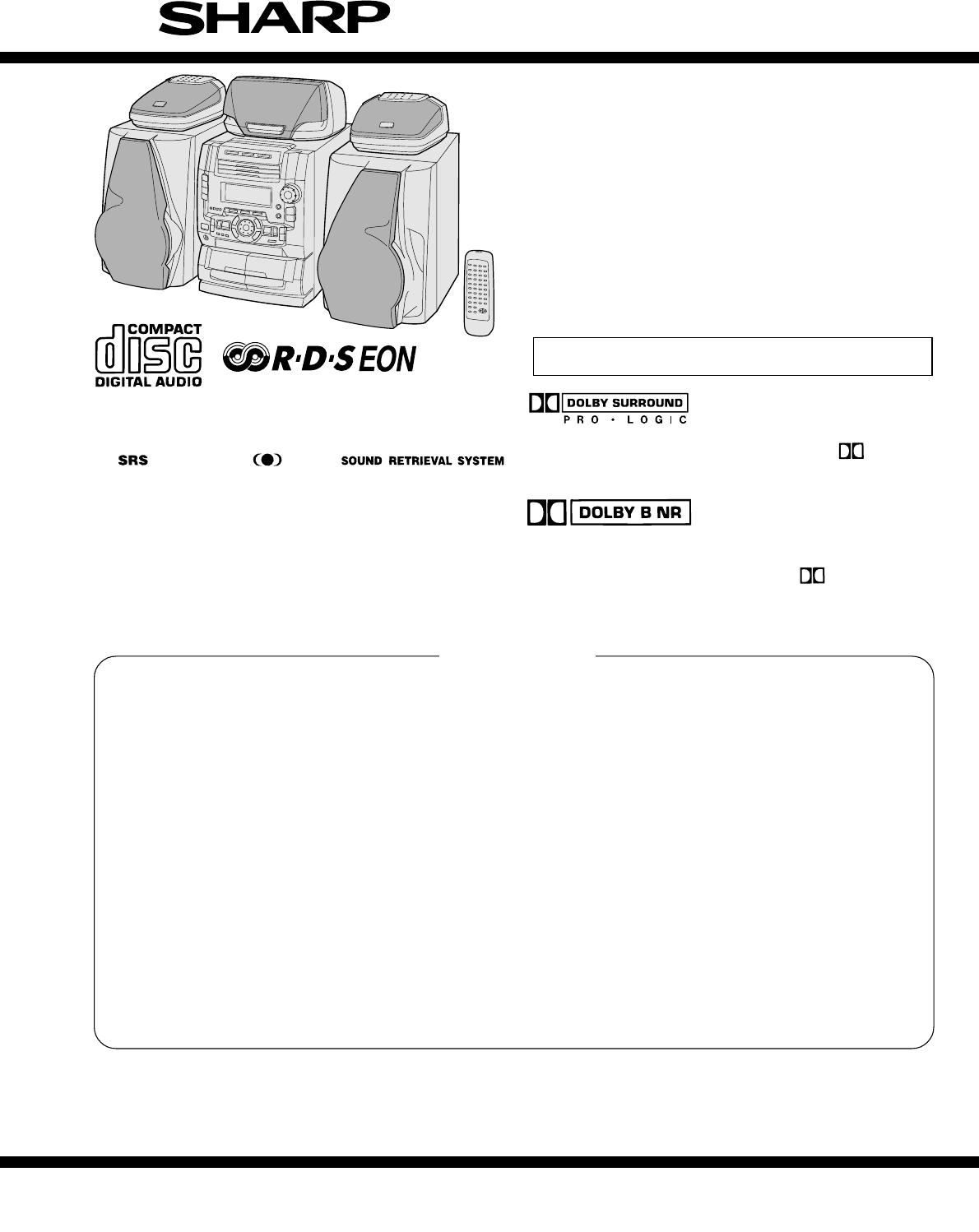
CD-C5H,CP-C5H
– 1 –
Page
SAFETY PRECAUTION FOR SERVICE MANUAL ................................................................................................................ 2
SPECIFICATIONS ................................................................................................................................................................. 3
NAMES OF PARTS ............................................................................................................................................................... 4
OPERATION MANUAL .......................................................................................................................................................... 7
DISASSEMBLY ...................................................................................................................................................................... 8
REMOVING AND REINSTALLING THE MAIN PARTS ....................................................................................................... 11
ADJUSTMENT ..................................................................................................................................................................... 12
TEST MODE ......................................................................................................................................................................... 14
RDS....................................................................................................................................................................................... 16
NOTES ON SCHEMATIC DIAGRAM .................................................................................................................................. 20
BLOCK DIAGRAM ............................................................................................................................................................... 21
SCHEMATIC DIAGRAM/WIRING SIDE OF P.W.BOARD ................................................................................................... 24
TYPES OF TRANSISTOR AND LED.................................................................................................................................... 46
WAVEFORMS OF CD CIRCUIT .......................................................................................................................................... 50
TROUBLE SHOOTING ........................................................................................................................................................ 51
FUNCTION TABLE OF IC.................................................................................................................................................... 54
FL SEGMENT ...................................................................................................................................................................... 66
PARTS GUIDE/EXPLODED VIEW
CONTENTS
CD-C5H
CP-C5H
SERVICE MANUAL
SHARP CORPORATION
No. S4827CDC5H///
• In the interests of user-safety the set should be restored to its original
condition and only parts identical to those specified should be used.
This document has been published to be used
for after sales service only.
The contents are subject to change without notice.
Center Speaker (GBOXS0008AWM2) and Surround Speaker
(GBOXS0009AWM2), Constitute CP-C5H.
●SRS technology Licensed from SRS Labs. SRS technol-
ogy holds the following patents: U.S. Patent No.
4,748,669 and U.S. Patent No. 4,841,572.
●SRS, the SRS Logo (●) and the Sound Retrieval System
are registered trademarks of SRS Labs, Inc. in the United
States.
●QSOUND and the QLogo are registered trademarks of
QSound Labs, Inc.
●QSound is protected under US Patent Nos. 5,105,462
and 5,208,860 and foreign counterparts.
Manufactured under license from Dolby Laboratories Licens-
ing Corporation. DOLBY, the double-D symbol and "PRO
LOGIC" are trademarks of Dolby Laboratories Licensing Cor-
poration.
●Dolby noise reduction manufactured under license from
Dolby Laboratories Licensing Corporation.
●"DOLBY" and the double-D symbol are trademarks
of Dolby Laboratories Licensing Corporation.
CD-C5H and CP-C5H constitute CD-C5H.
CD-C5H,CP-C5H
– 2 –
SAFETY PRECAUTION FOR SERVICE MANUAL
WARNINGS
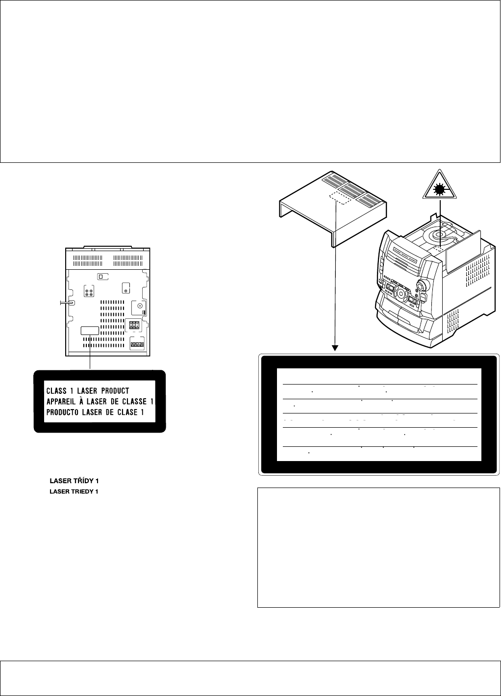
THE AEL (ACCESSIBLE EMISSION LEVEL) OF THE LASER POWER OUTPUT IS LESS THAN CLASS 1 BUT THE LASER
COMPONENT IS CAPABLE OF EMITTING RADIATION EXCEEDING THE LIMIT FOR CLASS 1. THEREFORE IT IS
IMPORTANT THAT THE FOLLOWING PRECAUTIONS ARE OBSERVED DURING SERVICING TO PROTECT YOUR EYES
AGAINST EXPOSURE TO THE LASER BEAM.
1-WHEN THE CABINET IS REMOVED, THE POWER IS TURNED ON WITDOUT A COMPACT DISC IN POSITION AND THE
PICK-UP IS ON THE OUTER EDGE THE LASER WILL LIGHT FOR SEVERAL SECONDS TO DETECT A DISC. DO NOT
LOOK INTO THE PICK-UP LENS.
2-THE LASER POWER OUTPUT OF THE PICK-UP UNIT AND REPLACEMENT SERVICE PARTS ARE ALL FACTORY
PRE-SET BEFORE SHIPMENT.
DO NOT ATTEMPT TO RE-ADJUST THE LASER PICK-UP UNIT DURING REPLACEMENT OR SERVICING.
3-UNDER NO CIRCUMSTANCES STARE INTO THE PICK-UP LENS AT ANY TIME.
4-CAUTION-USE OF CONTROLS OR ADJUSTMENTS, OR PERFORMANCE OF PROCEDURES OTHER THAN THOSE
SPECIFIED HEREIN MAY RESULT IN HAZARDOUS RADIATION EXPOSURE.
VARO ! Avattaessa ja suojalukitus ohitettaessa olet alttiina näkymättömälle lasersäteilylle. Älä katso säteeseen.
VARNING! Osynlig laserstralning när denna del är öppnad och spärren är urkopplad. Betrakta ej strälen.
●CAUTION
Use of controls or adjustments or performance of
procedures other than those specified herein may
result in hazardous radiation exposure.
As the laser beam used in this compact disc player
is harmful to the eyes, do not attempt to disassemble
the cabinet. Refer servicing to qualified personnel
only.
LASER KLASSE 1
LUOKAN 1 LASERLAITE
KLASS 1 LASERAPPARAT
Laser Diode Properties
Material: GaAIAs
Wavelength: 780 nm
Emission Duration: continuous
Laser Output: max. 0.6 mW
CAUTION-INVISIBLE LASER RADIATION WHEN OPEN. DO NOT STARE INTO
BEAM OR VIEW DIRECTLY WITH OPTICAL INSTRUMENTS.
VARNING-OSYNLIG LASERSTRALNING NAR DENNA DEL AR OPPNAD. STIRRA
EJ IN I STRALEN OCH BETRAKTA EJ STRALEN MED OPTISKA INSTRUMENT.
ADVERSEL-USYNLIG LASERSTRALING VED ABNING. SE IKKE IND I
STRALEN-HELLER IKKE MED OPTISKE INSTRUMENTER.
VARO! AVATTAESSA OLET ALTTIINA NAKYMATON LASERSATEILYLLE.
ALA TUIJOTA SATEESEEN ALAKA KATSO SITA OPTISEN LAITTEEN LAPI.
VARNING-OSYNLIG LASERSTRALNING NAR DENNA DEL AR OPPNAD.
STIRRA EJ IN I STRALEN OCH BETRAKTA EJ STRALEN GENOM OPTISKT
INSTRUMENT.
ADVERSEL-USYNLIG LASERSTRALING NAR DEKSEL APNES. STIRR IKKE
INN I STRALEN ELLER SE DIREKTE MED OPTISKE INSTRUMENTER.
VAROITUS! LAITTEEN KÄYTTÄMINEN MUULLA KUIN
TÄSSÄ
KÄYTTÖOHJEESSA MAINITULLA TAVALLA SAATTAA
ALTISTAA KÄYTTÄJÄN TURVALLISUUSLUOKAN 1
YLITTÄVÄLLE NÄKYMÄTTÖMÄLLE LASERSÄTEILYLLE.
VARNING - OM APPARATEN ANVÄNDS PÅ ANNAT SÄTT
ÄN I DENNA BRUKSANVISNING SPECIFICERAS. KAN
ANVÄNDAREN UTSÄTTAS FÖR OSYNLIG
LASERSTRÅLNING, SOM ÖVERSKRIDER GRÄNSEN FÖR
LASERKLASS 1.

CD-C5H,CP-C5H
– 3 –
SPECIFICATIONS
CD-C5H
CP-C5H
GBOXS0008AWM2
GBOXS0009AWM2
● General
Power source: AC 230 V, 50 Hz
Power
consumption: 205 W
Dimensions: Width; 270 mm (10-5/8")
Height; 356 mm (14-3/16")
Depth; 355 mm (14")
Weight: 11.0 kg (24.3 lbs.)
● Amplifier section
Output power: PMPO; 640 W (total)
(Front)
MPO; 320 W (160 W + 160
W) (DIN 45 324)
RMS; 200 W (100 W + 100
W) (DIN 45 324)
(Centre)
MPO; 100 W (DIN 45 324)
RMS; 50 W (DIN 45 324)
(Surround)
MPO; 100 W (50 W + 50
W) (DIN 45 324)
RMS; 50 W (25 W + 25 W)
(DIN 45 324)
Input terminals: Video/Auxiliary (audio signal)
× 2; 500 mV/47 kohms
Output terminals: Front speakers; 6 ohms
Centre speaker; 6 ohms
Surround speakers; 12 ohms
Headphones; 16-50 ohms
(recommended; 32 ohms)
CD digital output (optical)
Pre-output for sub woofer;
1.2 V/47 kohms
● Compact disc player section
Type: 3-disc multi-play compact
disc player
Signal readout: Non-contact, 3-beam semi-
conductor laser pickup
Rotational speed: 200 - 500 rpm CLV, Approx.
Error correction: CIRC (Cross Interleave
Reed-Solomon Code)
Quantization: 16-bit linear
Filter: 8-times oversampling digital
filter
D/A converter: 1-bit D/A converter
Frequency
response: 20 - 20,000 Hz
Dynamic range: 90 dB (1 kHz)
Wow and flutter: Unmeasurable
(less than 0.001% W. peak)
● Tuner section
Frequency range: FM; 87.5 - 108 MHz
MW; 522 - 1,620 kHz
LW; 153 - 281 kHz
● Cassette deck section
Type: Compact cassette tape
Frequency response: 50 - 14,000 Hz (Normal tape)
50 - 15,000 Hz (CrO
2
tape)
Motor: DC motor with electronic governor × 1
Signal/noise ratio: 55 dB (TAPE 1, playback, Dolby NR
off)
50 dB (TAPE 2, recording/playback,
Dolby NR off)
Dolby NR effect; 10 dB
(at over 5 kHz)
Bias and erasure
system: AC
Tape speed: 4.76 cm/sec. (1-7/8 ips.)
Wow and flutter: 0.2 % (DIN 45 511, playback)
Heads: TAPE-1: Playback × 1
TAPE-2: Record/playback × 1
Erase × 1
● Front speaker section
Type: 3-way type [16 cm (6-1/2") woofer,
5 cm (2") tweeter and super tweeter]
Rated input power: 100 W
Maximum input power: 200 W
Impedance: 6 ohms
Dimensions: Width; 240 mm (9-1/2")
Height; 350 mm (13-13/16")
Depth; 349.5 mm (13-13/16")
Weight: 5.7 kg (12.6 lbs.)/each
● Centre speaker section
Type: 2-way [12 cm (4-3/4") woofer and
5 cm (2") tweeter]
Maximum input power: 100 W
Impedance: 6 ohms
Dimensions: Width; 270 mm (10-5/8")
Height; 142 mm (5-5/8")
Depth; 220 mm (8-11/16")
Weight: 1.8 kg (4.0 lbs.)
● Surround speaker section
Type: 10 cm (4") full-range speaker
Maximum input power: 50 W
Impedance: 12 ohms
Dimensions: Width; 200 mm (7-7/8")
Height; 114 mm (4-1/2")
Depth; 240 mm (6-15/16")
Weight: 1.1 kg (2.5 lbs.)/each
CD-C5H,CP-C5H
– 4 –
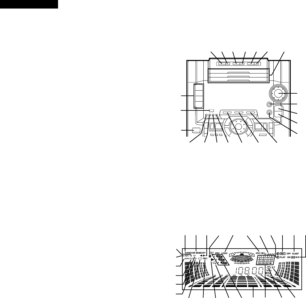
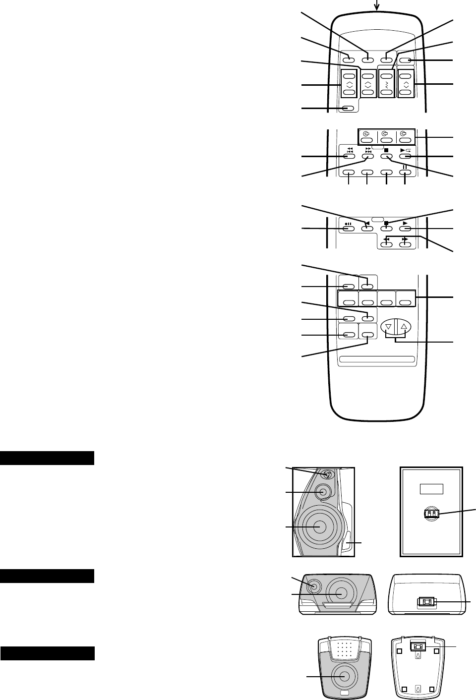
NAMES OF PARTS
CD-C5H
■ Front panel
11.
Disc 1 Select/Direct Play Button
12.
Disc 1 Open/Close Button
13.
Disc 2 Select/Direct Play Button
14.
Disc 2 Open/Close Button
15.
Disc 3 Select/Direct Play Button
16.
Disc 3 Open/Close Button
17.
Disc Trays
18.
Function Selector Buttons
19.
Remote Control Sensor
10.
On/Stand-by Button
11.
Programme Type/Traffic Information Search Button
12.
EON Button
13.
ASPM Button
14.
Display Mode Selector Button
15.
Dolby Pro Logic Button
16.
Virtual Surround Button
17.
QSOUND Button
18.
Volume Control
19.
Extra Bass Button
20.
3D Surround Mode Button
21.
3D Surround Pass Button
22.
Equalizer Selector/Demo Mode Button
23.
(CD) Random Play Indicator
24.
(CD/TUNER) Memory Indicator
25.
(TAPE 2) Direction Indicators
26.
(CD) Pause Indicator
27.
Dolby Pro Logic Indicator
28.
SRS Indicator
29.
Extra Bass Indicator
30.
Timer Play Indicator
31.
Timer Record Indicator
32.
Sleep Indicator
33.
(TAPE) Dolby NR Indicator
34.
Traffic Announcement Indicator
35.
RDS Indicator
36.
EON Indicator
37.
Programme Type Indicator
38.
Traffic Programme Indicator
39.
Traffic Information Indicator
40.
(TAPE) Reverse Mode Indicator
41.
(TAPE) Record Indicator
42.
(CD) Play Indicator
43.
(CD) Repeat Indicator
44.
(CD) Disc Number Indicators
45.
Spectrum Analyzer/Volume Level Indicator
46.
(CD) Music Schedule Indicators
47.
FM Stereo Indicator
48.
FM Stereo Mode Indicator
12
3456 7
8
9
10
18
19
20
21
22
11 12 13 14 15 16 17
23242526 28 29 30 313233
34
35
36
37
39 41 43
40
38
44
42 4546 47 48
27
CD-C5H,CP-C5H
– 5 –
11.
(CD) Clear Button
12.
Memory/Set Button
13.
(TAPE) Reverse Mode Button
14.
(TAPE) Reverse Play Button
15.
(TUNER) Tuning Down Button
3
(CD) Track Down/Review Button
3
(TAPE) Fast Wind Button
16.
Jog Dial
17.
(TUNER) Tuning Up Button
3
(CD) Track Up/Cue Button
3
(TAPE) Fast Wind Button
18.
(CD) Play/Repeat Button
3
(TAPE) Forward Play Button
19.
(TAPE) Record Pause Button
10.
(TAPE) Editing Speed Selector Buttons
11.
Headphone Socket
12.
Clock Button
13.
Timer Button
14.
Sleep Button
15.
(CD) Pause Button
16.
(CD/TAPE) Stop Button
17.
(TAPE) Dolby NR Button
18.
Beat Cancel Button
19.
(TAPE 1) Cassette Compartment
20.
(TAPE 2) Cassette Compartment
■ Rear panel
11.
Video/Auxiliary (Audio Signal) Input Sockets
12.
CD Digital Output Socket
13.
Super Woofer Output Socket
14.
AC Power Lead
15.
FM 75 Ohms Aerial Socket
16.
MW/LW Loop Aerial Input Socket
17.
Centre Speaker Terminals
18.
Surround Speaker Terminals
19.
Front Speaker Terminals
12 910
678
345
11 12 13 14 15 16 17
20
19
18
6
7
8
9
123
45
CD-C5H,CP-C5H
– 6 –
CP-C5H
GBOXS0008AWM2
GBOXS0009AWM2
■ Remote control
11.
Remote Control Transmitter LED
12.
Virtual Surround Button
13.
Dolby Pro Logic Button
14.
Surround Level Buttons
15.
Centre Level Buttons
16.
Test Tone Button
17.
QSOUND Button
18.
Balance Control Buttons
● Tuner control section
19.
Programme Type/Traffic Information Search
Button
10.
Preset Up/Down Buttons
● CD control section
11.
Track Down/Review Button
12.
Track Up/Cue Button
13.
CD Select/Direct Play Buttons
14.
Play/Repeat Button
15.
Stop Button
16.
Memory Button
17.
Clear Button
18.
Random Button
19.
Pause Button
● Tape control section
20.
Reverse Play Button
21.
Record Pause Button
22.
Stop Button
23.
Forward Play Button
24.
Fast Wind Buttons
● Common section
25.
Extra Bass Button
26.
Equalizer Mode Button
27.
3D Surround Mode Button
28.
3D Surround Pass Button
29.
On/Stand-by Button
30.
Dimmer Button
31.
Function Selector Buttons
32.
Volume Up/Down Buttons
1
2
3
4
5
6
7
8
9
11
12
13
14
15
16 171819
20
21 22
23
24
25
26
27
28
29
30
31
32
10
■ Speaker section
(Front speaker)
11. Super Tweeter
12. Tweeter
13. Woofer
14. Bass Reflex Duct
15. Speaker Terminals
(Centre speaker)
16. Tweeter
17. Woofer
18. Speaker Terminals
(Surround speaker)
19. Full-Range Speaker
10. Speaker Terminals
1
2
34
5
6
78
9
10
CD-C5H,CP-C5H
– 7 –
OPERATION MANUAL
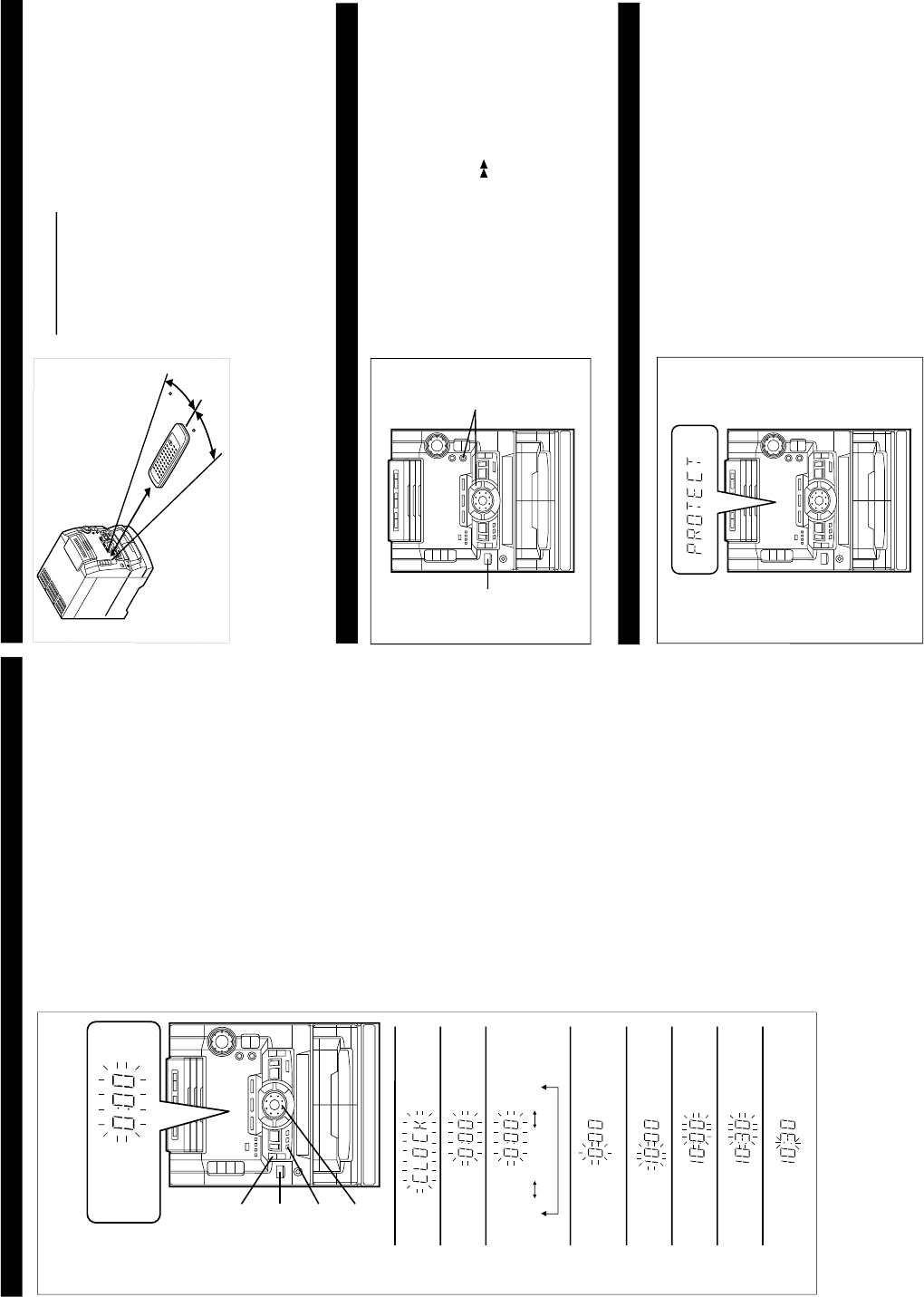
SETTING THE CLOCK
1
Press the ON/STAND-BY button to enter the stand-by mode.
2
Press the CLOCK button.
3
Within 5 seconds, press the MEMORY/SET button.
4
Turn the jog dial to select the time display mode.
"0:00" → The 24-hour display will appear.
(0:00 - 23:59)
"AM 12:00" → The 12-hour display will appear.
(AM or PM 12:00 - 11:59)
"AM 0:00" → The 12-hour display will appear.
(AM or PM 0:00 - 11:59)
●Note that this can only be set when the unit is first installed
or it has been reset.
5
Press the MEMORY/SET button.
6
Adjust the hour by turning the jog dial.
●Turn the dial one click to advance the time by 1 hour.
Keep turning the dial to advance continuously.
●When the 12-hour display is selected, "AM" will change auto-
matically to "PM".
7
Press the MEMORY/SET button.
8
Adjust the minutes by turning the jog dial.
●Turn the dial one click to advance the time by 1 minute.
Keep turning the dial to advance continuously.
●The hour setting will not advance even if minutes advance
from "59" to "00".
9
Press the MEMORY/SET button.
●The clock starts operating from "0" seconds. (Seconds are
not displayed.)
Note:
●In the event of a power failure or when the AC power lead
is disconnected, the clock display will go out.
When the AC power supply is restored, the clock display will
flash on and off to indicate the time when the power failure
occurred or when the AC power lead was disconnected.
If this happens, follow the procedure below to change the clock
time.
To change the clock time:
When the unit is in the stand-by mode:
① Press the MEMORY/SET button.
② Perform steps 6 - 9 above.
When the unit is on:
① Press the CLOCK button.
② Within 5 seconds, press the MEMORY/SET button.
③ Perform steps 6 - 9 above.
To see the time display:
Press the CLOCK button.
●The time display will appear for about 5 seconds.
To change the time display mode:
① Perform steps 1 - 2 in the section "RESETTING THE MICRO-
COMPUTER", on page 36 of Operation Manual.
② Perform steps 1 - 9 above.
In this example, the clock is set for the 24-hour
(0:00) system.
MEMORY/
SET
ON/STAND-
BY
CLOCK
0:00 AM 12:000:00 AM
3
4
5
6
7
8
9
2
Jog dial
PREPARATION FOR USE
■Remote control
Notes concerning use:
●Replace the batteries if control distance decreases or oper-
ation becomes erratic.
●Periodically clean the transmitter LED on the remote control
and the sensor on the main unit with a soft cloth.
●Exposing the sensor on the main unit to strong light may in-
terfere with operation. Change the lighting or the direction of
the unit.
●Keep the remote control away from moisture, excessive heat,
shock, and vibrations.
15
15
0.2 m - 6 m
(8" - 20')
RESETTING THE MICROCOMPUTER
Reset the microcomputer under the following conditions:
●To erase all of the stored memory contents (clock and timer
settings, and tuner and CD presets).
●If the display is not correct.
●If the operation is not correct.
1
Press the ON/STAND-BY button to enter the stand-by mode.
2
Press and hold down the button, the EQ/DEMO button
and the ON/STAND-BY button all at the same time. Hold them
for at least 1 second.
Caution:
●The operation explained above will erase all data stored in
memory including clock and timer settings, and tuner and CD
presets.
1,2 2
WHEN "PROTECT" APPEARS
"PROTECT" will appear in the display if the unit overheats.
If there is a problem in the speaker circuit, the unit will be switched
to the stand-by mode automatically.
In this case, take the following corrective actions.
1
Unplug the AC power plug from the AC socket.
2
Make sure that the unit vent is not blocked.
3
Make sure that the speaker wires have been correctly con-
nected to the speaker terminals.
4
After checking items 2 and 3 above, wait for 2 or 3 hours
before trying to use the unit.
5
Reconnect the AC power lead.
Note:
●If "PROTECT" appears again during use, please unplug the
AC power plug, and contact the SHARP authorised service
centre.
CD-C5H,CP-C5H
– 8 –
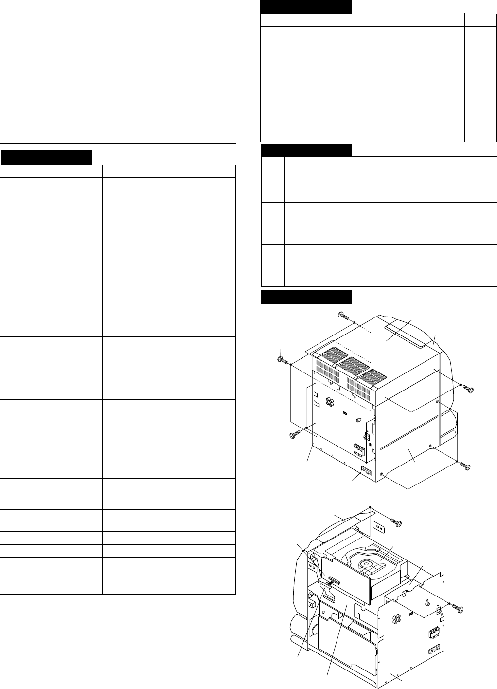
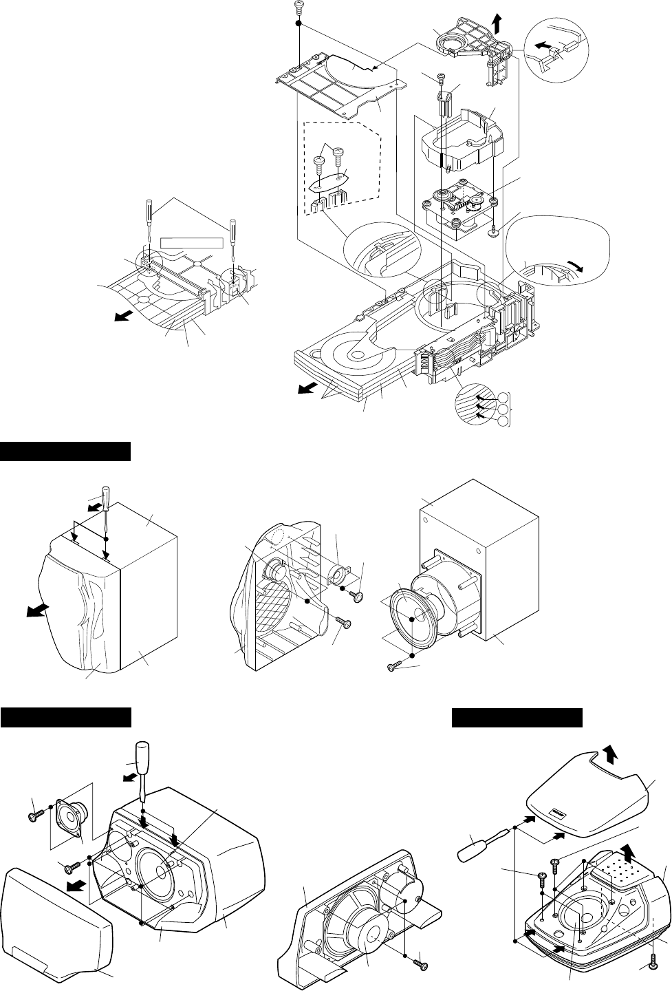
Caution on Disassembly
Follow the below-mentioned notes when disassembling
the unit and reassembling it, to keep it safe and ensure
excellent performance:
1. Take cassette tape and compact disc out of the unit.
2. Be sure to remove the power supply plug from the wall
outlet before starting to disassemble the unit.
3. Take off nylon bands or wire holders where they need be
removed when disassembling the unit. After servicing
the unit, be sure to rearrange the leads where they were
before disassembling.
4. Take suff cient care on static electricity of integrated
circuits and other circuits when servicing.
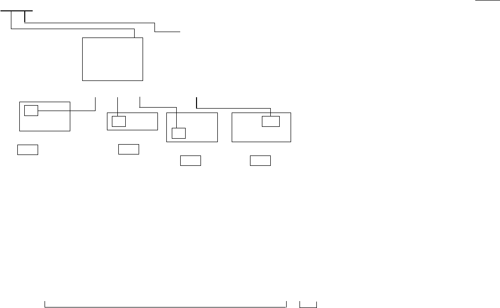
DISASSEMBLY
Figure 8-2
Figure 8-1
CD-C5H CP-C5H
CD-C5H
1 Top Cabinet 1. Screw ................. (A1) x4 8-1
2 Side Panel 1. Screw ................. (B1) x6 8-1
(Left/Right) 2. Screw ................ (B2) x4
3
CD Changer Block
1. Flat Cable ........... (C1) x1 8-2
2. Screw ................. (C2) x2
3. Screw ................. (C3) x2
4 Pro Logic PWB 1. Screw ................. (D1) x2 9-1
5 Tuner PWB 1. Screw ................. (E1) x9 9-1
2. Screw ................. (E2) x1
3. Screw ................. (E3) x4
6 Main PWB 1. Socket ................ (F1) x3 9-1
2. Flat Cable ........... (F2) x2
3. Flat Wire ............. (F3) x2
4. Screw ................. (F4) x2
5. Screw ................. (F5) x2
7 Front Panel 1. Flat Wire .............(G1) x2 9-1
2. Screw .................(G2) x1
3. Screw .................(G3) x2
8 Display PWB 1. Knob ................... (H1) x2 9-2
2. Nut ..................... (H2) x1
3. Screw .............. (H3) x12
9 CD Switch PWB 1. Screw ................. (J1) x3 9-2
10
Headphones PWB
1. Screw ................ (K1) x1 9-2
11 Tape Mechanism 1. Open the cassette holder 9-2
2. Screw ................. (L1) x6
12 Amp. PWB 1. Socket ............... (M1) x1 9-3
2. Screw ................ (M2) x2
3. Screw ................ (M3) x2
13 Power Amp. PWB 1. Socket ................ (N1) x1 9-4
2. Screw ................. (N2) x4
3. Screw ................. (N3) x2
14 Power Supply PWB 1. Screw ................ (P1) x1 9-4
2. Screw ................ (P2) x4
15 CD Digital PWB 1. Screw ................ (Q1) x1 9-5
16 CD Changer Holder 1. Screw ................. (R1) x3 9-5
17 CD Servo PWB 1. Socket ................ (S1) x6 9-6
(Note) 2. Screw ................. (S2) x3
18 Tray Switch PWB 1. Screw ................ (T1) x1 9-6
REMOVAL PROCEDURESTEP FIGURE STEP REMOVAL PROCEDURE FIGURE
1 Front Speaker 1. Screw ................... (A1) x2 10-2
2. Screw ................... (A2) x2 10-3
3. Screw ................... (A3) x4
2 Center Speaker 1. Net ....................... (B1) x1 10-4
2. Screw ................... (B2) x2
3. Screw ................... (B3) x6
4. Screw ................... (B4) x3 10-5
3 Surround Speaker 1. Net ....................... (C1) x1 10-6
2. Screw ................... (C2) x4
3. Screw ................... (C3) x2
4. Screw ................... (C4) x2
Note : After removing the connector for the optical pickup
fromthe connector wrap the conductive aluminium foil
around the front end of connector so as to protect the
optical pickup from electrostatic damage.
CD-C5H
19 CD Mechanism 1. Screw .................... (U1) x2 10-1
2. Top Bord ............... (U2) x1
3. Disc Holder ........... (U3) x1
4. Disc Tray............... (U4) x3
5. Screw .................... (U5) x1
6. Mechanism Holder ...........
Guide .................... (U6) x1
7. Screw .................... (U7) x2
8. Mechanism Holder ...........
Bracket.................. (U8) x1
9. Screw .................... (U9) x4
10.
Mechanism Holder
(U10) x1
REMOVAL PROCEDURESTEP FIGURE
(A1)x2
Ø3x12mm Top Cabinet
Front Panel
(B1)x3
Ø3x12mm
(B2)x4
Ø3x10mm
Rear Panel
(A1)x2
Ø3x12mm
(B1)x3
Ø3x12mm
Side Panel
(Left)
Side Panel
(Right)
(C3)x2
Ø3x12mm
(C2)x2
Ø3x10mm
Rear Panel
CD Changer Block
CD Changer
Holder
Front Panel
CD Servo
PWB
(C1)x1
Main PWB
CD-C5H,CP-C5H
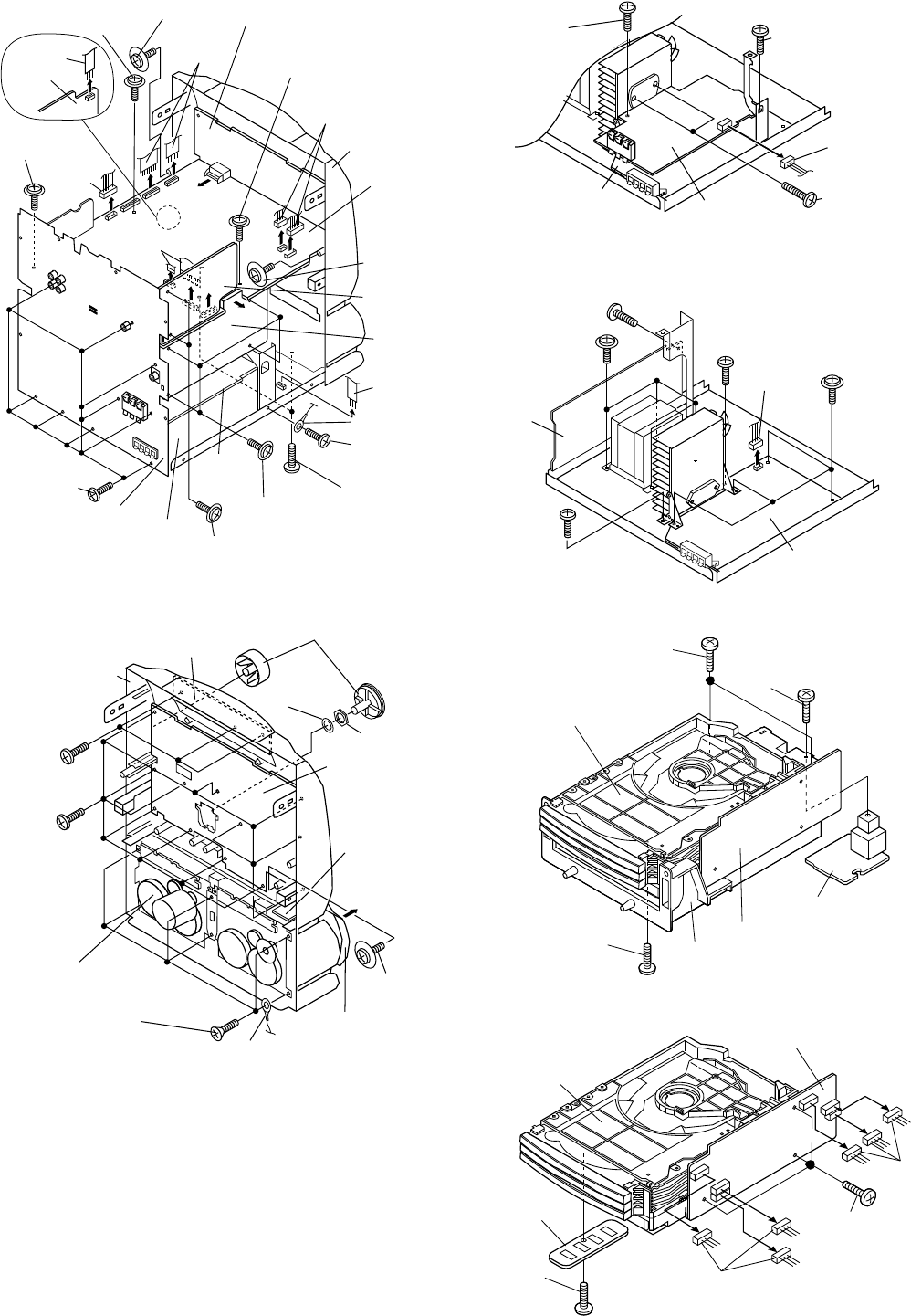
– 9 –
Figure 9-3
Figure 9-4
Figure 9-2
Figure 9-5
Figure 9-1
Figure 9-6
(E2)x1
Ø3x10mm
(F4)x1
Ø3x10mm (F5)x1
Ø3x8mm
(F1)x1
(F2)x2
(F4)x1
Ø3x10mm
(F3)x2
(F1)x2
Display PWB
Main PWB
Front Panel
Pull
Power
PWB
(G1)x1
(E1)x9
Ø3x10mm
Power Amp. PWB
(E3)x4
Ø3x10mm
(D1)x2
Ø3x10mm
Amp.
PWB
(G2)x1
Ø3x6mm
(F5)x1
Ø3x8mm
Tuner
PWB
(G1)x1
Lug Wire
(G3)x2
Ø3x10mm
Rear Panel
Pro Logic
PWB
(J1)x3
Ø3x10mm
(H3)x12
Ø3x10mm
(L1)x6
Ø3x10mm Lug Wire
(K1)x1
Ø3x8mm
Open
Headphones
PWB
Display
PWB
(H1)x2
(H2)x1
Washer
Tape Mechanism
Cassette
Holder (Left/Right)
Front Panel
CD Switch PWB
(M3)x1
Ø3x10mm
(M2)x2
Ø3x14mm
Power AMP.
PWB Amp. PWB
(M1)x1
(M3)x1
Ø3x10mm
(N3)x1
Ø3x6mm
(P1)x1
Ø3x10mm
(P2)x4
Ø4x8mm
(N2)x4
Ø3x10mm
Power AMP.
PWB
(N3)x1
Ø3x6mm
Power
Supply
PWB
(N1)x1
CD Changer Block
(R1)x2
ø3x10mm (Q1)x1
ø3x12mm
CD Servo PWB
CD Digital PWB
CD Changer Holder
(R1)x1
ø3x10mm
CD Changer
Block
CD Servo PWB
(T1)x1
ø2x7mm
(S2)x3
ø3 x10mm
(S1)x3
(S1)x3
Tray
Switch
PWB
CD-C5H,CP-C5H
– 10 –
Figure 10-1
Figure 10-2
Figure 10-4
CP-C5H
Front Panel
Speaker
Box
Bottom
Side
Driver
(A1)x2
ø3x10mm
(A2)x2
ø4x10mm (A3)x4
ø4x16mm
Front
Panel
Speaker
Box
Super
Tweeter
Tweeter
Woofer
Top Side
Figure 10-3
Figure 10-6
Figure 10-5
(Front Speaker)
(Center Speaker) (Surround Speaker)
GBOXS0008AWM2 GBOXS0009AWM2
Driver
(B2)x2
ø4x20mm
(B1)x1
(B3)x6
ø4x20mm
Front Cabinet
Rear
Cabinet
Woofer
Teeter
(B4)x3
ø4x20mm
Front Cabinet
Woofer
(C1)X1
Driver (C2)x4
ø4x16mm
Top Cabinet
Bottom
Cabinet
(C4)x2
ø4x16mm
Full-range
(C3)x2
ø3x12mm
Push the pawl of disc tray
with a proper screwdriver.
Back surface
Pawl
Disc Tray 1
Disc Tray 2
Disc Tray 3
Pawl
(After drawing out the disc trays 1, 2, and 3, turn
over the mechanism unit, push two pawls, and
remove successively the three disc trays from the
mechanism unit, starting with the disc tray 3.
Thereby the CD mechanism shown in the right
figure can be removed.)
(U1) x2
ø2 x7mm
(U5) x1
ø2.6 x12mm
(U9) x4
ø2.6 x10mm
(U3) x1
(U2) x1
(U6) x1
(U10) x1
Disc Tray 2
Disc Tray 3
Spring
(U4) x3
1
2
3
Normal state
Press in turns the arrow
parts, starting with the
uppermost one, to
withdraw the disc trays
Pawl
Push
.
CD
Mechanism
Disc Tray 1
Turn clockwise the
main cam to raise the
CD mechanism up to
the uppermost position.
(U7) x2
ø2 x6mm
(U8) x1
CD-C5H,CP-C5H
– 11 –
Figure 11-1
Figure 11-2
CD MECHANISM SECTION
For the procedure to remove the CD mechanism from the
main unit, refer to Disassembling Procedure, Steps 1~9, and
15~19. (page 8).
How to Remove the optical pickup
(See Fig. 11-1.)
1. Remove the screws (A1)x 2 pcs., to remove shaft (A2)x 1
pc.
2. Remove stop washer (A3)x 1 pc., to remove gear (A4)x 1 pc.
3. Remove the optical pickup.
Note:
After disconnecting the optical pickup connector wrap the
front end of connector in conductive aluminum foil so as to
prevent damage to the optical pickup by static electricity.
How to Remove the tray motor/main cam motor
(See Fig. 11-2.)
1. Remove the CD changer section by the method described
in page 8, and disassemble as shown in the figure.
2. Remove the belts (B1)x 2 pcs., from the motor side.
3. Remove the screws (B2)x 4 pcs.
4. Remove the tray motor and main cam motor.
How to remove the CD disc
(When CD exists in the tray)
(See Fig. 11-4.)
1. Remove the Top cabinet.
2. Disassemble as shown in the figure so that the CD disc of
CD changer can be taken out.
3. Remove the CD disc from the tray as shown in the figure.
How to remove the CD disc
(When CD is in playback state)
(See Fig. 11-3.)
1. Remove the Top cabinet .
2. Disassemble as shown in the figure so that the CD disc of
CD changer becomes visible.
3. Remove the CD disc as shown in the figure.
Figure 11-3
Figure 11-4
(A1) x2
ø2.6 x5mm
CD
Mechanism
Stop Washer
(A3) x1
Gear
(A4) x1
Shaft
(A2) x1
Pickup
Tray Motor
Main Cam
Motor
Belt
(B1) x1 Belt
(B1) x1
(B2) x2
ø2.6 x4mm
(B2) x2
ø2.6 x4mm
REMOVING AND REINSTALLING THE MAIN PARTS
(When CD is in playback state.)
CD Disc
Disc Holder
Turn the main cam clockwise,
and raise the CD mechanism
and disc holder up to
uppermost position.
CD Changer
Block
Press in turns the arrow
parts, starting with the
uppermost one, to
withdraw the disc trays
CD Disc
Disc Holder
CD Mechanism
(When CD exists in the tray)
Disc Tray 1
Disc Tray 2
Disc Tray 3
Turn the main cam clockwise,
and raise the CD mechanism
and disc holder up to
uppermost position.
CD Changer
Block
1
2
3
CD-C5H,CP-C5H
– 12 –
Figure 12-2 ADJUSTMENT POINTS
Play: TW-2412 Tape 1: Over 80 g
Tape 2: Over 80 g
Torque Meter Specified Value
• Torque Check
Play: TW-2111 30 to 60 g. cm 30 to 60 g.cm
Fast forward: TW-2231 60 to 120 g.cm 60 to 120 g.cm
Rewind: TW-2231 60 to 120 g.cm 60 to 120 g.cm
Torque Meter Specified Value
Tape 1 Tape 2
MECHANISM SECTION
• Driving Force Check
• Bias Frequency
Instrument
Connection
— 98 ± 10 kHz CNP102 1
ADJUSTMENT
Adjusting Point Specified Value
• Tape Speed
Normal MTT-111 VRM01 3,000 ±Speaker
speed 30 Hz terminal
Specified
Value
Adjusting
Point Instrument
Connection
Test Tape
Position of each switch or control
Volume MAX
3D Surround Mode Button PASS
Pre-programmed Equalizer FLAT
Extra Bass OFF
Function TAPE
Dolby NR switch OFF
X-Bass OFF
TAPE SECTION
• Bias Current
Instrument
Connection
L: VR101
Normal: 38 ± 10 mV
L: TP490 4
R: VR102 CrO2: 55 ± 15 mV R: TP490 2
Adjusting Point Specified Value
• Tape 1 Playback Amplifier Sensitivity
Adjusting
Point Instrument
Connection
L: VRD01 L: TP451 3
R: VRD02 R: TP451 1
Test Tape Specified Value
MTT-150 Normal: 300 mV
• Tape 2 Playback Amplifier Sensitivity
Adjusting
Point Instrument
Connection
L: VRD03 L: TP451 3
R: VRD04 R: TP451 1
Test Tape Specified Value
MTT-150 Normal: 300 mV
• Record/Playback Sensitivity
Adjusting
Point Instrument
Connection
Record level
control
L: VR151
R: VR152
Test Tape Specified Value
UR-127
215 mV Input: VIDEO
Output:
L: TP451 3
R: TP451 1
215 mV
UNIT
GND
TP490 2 PIN OR 4 PIN
RECORD
MODE ELECTRONIC
VOLTMETER
TP490 3 PIN
Figure 12-1 BIAS CURRENT
VR102
VR101
VR152 VRD02VRD04
VR151
VRM01
VRD03
VRD01
TP490
1234
TP451
123
R-CH BIAS
CURRENT
R-CH REC/
PLAY SENS.
L-CH REC/
PLAY SENS.
TAPE1 PLAY
R-CH SENS.
TAPE2 PLAY
R-CH SENS.
TAPE2 PLAY
L-CH SENS.
TAPE1 PLAY
L-CH SENS.
L-CH BIAS
CURRENT
WTM1 WTM2
TAPE SPEED
CFW2 CNP851
MAIN PWB
CNP102
1234567
CNP101
321
CD-C5H,CP-C5H
– 13 –
Figure 13 ADJUSTMENT POINTS
fL: Low-range frequency
fH: High-renge frequency
• AM IF/RF
Signal generator: 400 Hz, 30%, AM modulated
IF 450 kHz 1,620 kHz T351 *1
MW Band — 522 kHz (fL): T306 *2
Coverage 1.1 ± 0.1 V
MW 990 kHz 990 kHz (fL): T302 *1
Tracking
LW Band — 153 kHz (fL): T305 *2
Coverage 1.5 ± 0.1 V
LW 225 kHz 225 kHz (fL): T301 *1
Tracking
Test Stage Frequency Frequency
Display Setting/
Adjusting
Parts
Instrument
Connection
• FM
Notes:
1: Description of the "FM IF Adjustment" is not carried on this
Manual. It is because the IF coil in the FM front end section
has been best adjusted in the factory so that its further
adjustment is not needed at the field. When replacing the
FM front end assembly, no adjustment is needed either.
2: The parts in the FM front end section are prepared in a
complete unit, so you can't obtain each part individually
Adjusting
Parts Instrument
Connection
Frequency
Display
Frequency
• FM Mute Level
Signal generator: 1 kHz, 40 kHz dev., FM modulated
98.00 MHz 98.00 MHz VR351* Input: Antenna
(25 dBµV) Output: Speaker
Terminal
TUNER SECTION
*1. Input: Antenna, Output: TP302
*2. Input: Antenna, Output: TP301
TP302
TP301
R336
R357
T351 VR351
T306
T305 T302 T301
AM IF
IC303
FE301
FM MUTE
LEVEL
MW BAND
COVERAGE
LW BAND
COVERAGE
MW
TRACKING LW
TRACKING
CNP303
TUNER PWB
SO301
FM ANTENNA
TERMINAL
CNP301
MW/LW
LOOP ANTENNA
TERMINAL
CD-C5H,CP-C5H
– 14 –
Figure 14-2
Figure 14-3
Since this CD system incorporates the following automatic adjustment function, when the pickup is replaced, it is not necessary
to readjust it.
Since this CD unit does not need adjustment, the combination of PWB and laser pickup unit is not restricted.
• Automatic adjustment item
1. Focus offset (Fig. 14-2)
2. Tracking offset (Fig. 14-3)
3. E/F balance (tracking error balance) (Fig. 14-4)
4. RF level AGC function (HF level: constant)
5. RF level automatic follow-up of the tracking gain
This automatic adjustment is performed each time a disc is changed.
Therefore, each disc is played back using the optimal settings.
CD SECTION
TEST MODE
• Setting the test mode
Any one of test mode can be set by pressing several keys as follows.
Hold down the EQ and CD buttons, and press the POWER switch. TEST: CD operation test
<PLAY> key input
• TEST mode
Function — CD test mode
Setting of TEST mode
Indication of CD TEST mode (Fig. 14-1)
OPEN/CLOSE operation is manual operation.
The pickup can be moved by using the ( ) or ( ) key.
When the track-
ing servo is acti-
vated, playback
will begin at the
current position.
Press the
STOP button. The pickup
willreturn to
the STOP
position.
<MEMORY>
key input When the track-
ing servo is acti-
vated, playback
will begin at the
current position.
<STOP>
key input The pickup nor-
mally returns to
the STOP posi-
tion.
<MEMORY>
key input
IL is not performed.
Press <STOP> key. Stop
TOC. IL is performed, and the ordinary PLAY is performed.
If the following key is pressed during PLAY, it is possible
to specify directly any Track No.
<Disc Number 1> key: Track 4
<Disc Number 2> key: Track 9
<Disc Number 3> key: Track 15
Note:
Only in STOP state it is possible to slide the pickup with the
() or ( ) key.
VOL. --- Last memory
BAL. --- CENTER
R.GEQ. --- FLAT
X-BAS --- OFF
Canceling method - POWER OFF
Figure 14-1
G9 G9
G9
G6
G6
G8
G8
G5
G5
G4
G4
G10
G3
G10
G3
G2
G2
G1
G1~G8
G7
G7
S40
S39
S38
S30
S33
S35
S37
S36
S34
S31
S29 S27 S25 S23
S32
S24 S26 S28
S22
S41
S10
S1
S2
S7 S6 S5 S4 S3
S9 S8
S16S15
S14
S13 S12
S17
S19
S21 S20
S18
2
0.1s
0.50 V
IC1 16 FD
FOCUS
OFF-SET
ADJUST
TRACKING
OFF-SET
ADJUST
0.1s
0.50 V
IC1 7 TE
1
2
1
10ms
0.50 V
IC1 16 FD
10ms
0.50 V
IC1 7 TE
Enlarged
View
TRACKING
OFF-SET
ADJUST
2
1
TO
TE
200 ms
1V/diV
IC 1 15
200 ms
1V/diV
IC 1 7
TRACKING/
ERROR
BARANCE
ADJUST
Figure 14-4
CD-C5H,CP-C5H
– 15 –
EXPLANATION OF AUTOMATIC SOUND VALUE CORRECTION CONTROL
1. Outline
The recent trend is toward rise of CD record level in the world, for example rock, dancing music, etc. In case of continuous high
level playback G-EQ (graphic equalizer) and VOL (Volume) are controlled (lowered) automatically after a lapse of specific time
(10 minutes) so as to get the easy-to-listen sound level.
2. Explanation of operation
The CD playback operation is explained below.
X : Threshold value of control circuit operation
A : Hight energy (hatched area) exceeding X is detecated, and the control mode is set.
B : After a lapse of 10 minutes the control is started.
Data is fetched every 4
seconds to control. Initial frequency
characteristics.
Hand L frequency char-
acteristics are lowered. VOL (Volume) is lowered.
At first, the H and L frequency characteristics are lowered as shown above so thet the distortion
and disturbance are reduced. However, if hight energy exceeding X is detected, VOL is lowered
to get sound easy to listen.
Stable control
Continued control
The output data is fetched every 4 seconds to control. When quiet music is played back, the
control is performed so as to restore the initial frequency characteristics and initial VOL values.
Control mode cancel conditions When output exceeding X is not given
continuously for 10 minutes.
When quiet music is played back.
When VOL is lowered.
When the power is turned off or on.
B ~ C :
C ~ D :
A
X
B C D
0w
10 minutes
Distortion clip point
SP output
level
CD-C5H,CP-C5H
– 16 –
RDS
8 character can display E1 table of EBU.
Lights up when RDS with EON station is received.
Lights up when RDS station is received.
Lights up when TA station is received.
Lights up when TP station is received.
Lights up when stand-by mode and blinks during staying other network station.
DISPLAY
G9 G9 G6
G8
G5 G4G10
G3
G2 G7
DISPLAY
MODE
RDS (Radio Data System) OPERATION
■
Receiving FM Stations with RDS (Radio Data System)
RDS is a broadcasting service which a growing number of FM stations are now providing. It allows these FM stations to
send additional signals along with their regular programme signals. For example, the stations send their station names, and
information about what type of programme they broadcast, such as sports or music, etc.
When tuned to an FM station which provide the RDS service, the RDS will appear, the station frequency (and then the
station name if sent) is displayed.
The TP (Traffic Programme) will appear on the display when the received broadcast carries traffic announcements, and the
TA (Traffic Announcement) will appear whilst a traffic announcement is being received.
EON will appear whilst the EON (Enhanced Other Networks information) data is being broadcast.
Note:
When the TP and TA appear at the same time, an announcement is being made.
When only the TA appears, an announcement is not being made.
■
Information Provided by RDS
With the CD-C5H, you can display two types of RDS service. To
show them in the display, press the DISPLAY MODE button.
Each time you press the DISPLAY MODE button, the display will
change to show the following information.
PS (Programme Service): Station names commonly
known will be displayed. "NO
PS" appears if no signal is
being sent.
PTY (Programme Type): Programme type will be dis-
played.
"NO PTY" appears if no signal
is being sent.
Station Frequency: Station frequencies.
Descriptions of the PTY (Programme Type) codes, TP (Traffic Programme) and TA (Traffic Announcement)
With the CD-C5H, you can search for and receive the following PTY, TP and TA signals.
NEWS: News
AFFAIRS: Topical programme expanding on the
current news or affairs
INFO: Programmes on medical service,
weather forecast, etc.
SPORT: Sports events
EDUCATE: Educational programmes
DRAMA: Radio plays
CULTURE: Programmes on national or regional cul-
ture.
SCIENCE: Programmes on national sciences and
technology
VARIED: Other programmes like comedies or
ceremonies
POP M: Pop music
ROCK M: Rock music
M.O.R. M: Middle-of-the-road music (usually called
"easy listening")
LIGHT M: Light music
CLASSICS: Classics
OTHER M: Other music
ALARM: Emergency broadcasts
NONE: No programme type (receive only)
TP: Broadcasts which carry traffic an-
nouncements
TA: Traffic announcements are being broad-
cast at present.
Note:
●When the unit is in the EON stand-by mode and a pro-
gramme is selected, the unit will display "TI" instead of
"TA".
CD-C5H,CP-C5H
– 17 –
No
ASPM, summary operation
Hold down the ASPM button for 3 more second.
“ASPM” blinks in the display.
Preset CH memory full over? No operate. After displayed “END”. Return to
previous station.
SD (TUNE) DET out OK?
If count 1st OK?
If count 2nd OK?
RDS signal or not? PI—identify
Comparing PI cord same or not?
between current receiving PI and
before PI which is already memorized
by ASPM on this time.
Comparing freg. same or not?
between current receiving frequency
and (already) previously memorized
frequency.
Memorized to the lowest
vacant preset channel.
Preset CH memory become full over?
Begin to ASPM SCAN from the next
CH-SPAN again.
Repeat and continue with same format
ASPM operation untill 108 MHz.
After reached 108 MHz, displayed the
TTL quantity of memorized stations.
And return to the previous receiving
freq. automatically.
Displayed the TTL quantity of memo-
rized stations by ASPM operation on
this time. And return to the previous
receiving freq. automatically.
Yes
No
Yes
Yes
Yes
Yes
No
No
No
No
No No Effect
Pass
No effect
Pass
No effect
Pass
No effect
Pass
No effect
Yes
No
Yes
Compare the field strength of current
receiving signal. Is receiving signal
stronger than signal which has same PI
cord and is already memorized to
preset memory ahead of this receiving
time?
Yes No effect
No No effect
Comparing freg. same or not?
Between current receiving frequency
and (already) previously memorized
frequency.
Yes Memorized to the lowest
vacant preset channel.
Yes No effect
Begin to scan start 87.50 → 108.00 MHz
CD-C5H,CP-C5H
– 18 –
4. No adjust type (None adjusting circuit.)
5. Added EON button.
6. Need to change RDS logo due to add EON feature.
7. Added EON—TI, EON—PTY function.
3. Summary of CD-C5H RDS—EON operation
EON—PTY: Select and set the desired “PTY” → stand-by → switch to ON(other network) Station at the start of desired
PTY automatically → stay and listen to PTY of ON station → switch back to TN(This net) station automatically
at the end of PTY(ON) i.e. after changing to another PTY(except AFFAIRS) or cancelling to receive PTY of
ON station midway.
EON—TI: Select and set the “TI” → stand-by → switch to ON station at the start of traffic announcement automati
cally → stay and listen to TA of ON station → switch back to TN station autmatically at the end of TA(ON).
ie after TA(ON) is over or cancelled to receive TA of ON station midway.
When switching TN → ON station.
In case of exist 2 more stations having the desired(specified) “PTY” or “TI”, the receiver will select and switch toON station
comparing field strength at the same time. But when the frequency of ON station exists in the preset-memory, then reciver
switches straight to that ON station(CH), without comparing field strength so can make a quick switching from TN—ON sta
tion. Preset memory takes priority of switching TN—ON station.
therefore ASPM is usefull not only for PTY search but also for rapid EON switching. Anyway CD-C5H EON is basically stand-
by and receiving method, along with the Guidelines for EON implementation.
• ASPM SCAN: 87.50MHz → 108.00 MHz.
• Only RDS signal is memorized by ASPM because RDS signal has PI code and is suitable and convenient for ASPM operation.
ASPM
Comparing field strength, only one strongest RDS station is memorized of all stations (repeater relay stations) that have same
PI code.
Same PI code — freq: different
(AF’S)
PS: same
PTY: same
Each PI has AF’S list by individually.
Exa: P1 has f1, f2, f3 (same PTY).
P2 has f4, f5 (same PTY).
[For example] Pickup and memorized to preset CH.
f 1
f 2 f 3
P 1 (PI cord)
PS 1 (Station Name)
f 5 f 4
P 2
PS 2
f 6
f 7 f 8
P 3
PS 3
f 9 f 10
f 11 f 12 f13
P 4
PS 4
Select signals (f1, f5, f7, f10) are memorized in the preset memory by ASPM.
• If tentative - ASPM operation is repeated intententionally, never memorized (over write) at the same frequecy.
1st time ASPM → strongest stations of each pi are memorized.
ASPM is not only very usefull for PTY search, but also EON operation.
2nd time ASPM → 2nd strong stations of each pi are memorized and so on.
PTY search function is equal to FM band search function as a result.
1. Introduction of RDS for CD-C5H
CD-C5H RDS function is equal to adding EON feature to the current CD-C75H RDS.
EON feature is EON—PTY and EON—TI.
Although PTY and TI indicators are separated, PTY contains TI in the PTY items (software) like current PTY search items.
NEWS, AFFAIRS, INFO, ALARM, TI (TTL 17 kinds)
EON—PTY EON—TI
Can select and stand-by Can select and stand-by
EON—PTY and EON—TI are basically stand-by → receive the desired program of ON station.
2.The difference point from current CD-C75H RDS. (CD-C75H — CD-C5H)
1. PTY item: added TA.TTL 18 kind.
2. Each “TP”, “TA” ind. light up or go out individually.
“TA” ind. doesn’t light up on current model, CD-C75H due to none EON—TI.
3. Added 3 indicators(in FL) due to adding EON feature.
EON: Lights up only during receiving EON data (14A).
TI: During EON-TI stand-by → Light up
During receiving ON station. → blink.
PTY: During EON-PTY stanb-by → Light up
During receiving ON station. → blink.
---
---
↑↑

CD-C5H,CP-C5H
– 19 –
EON summary notice for reference
1. EON-TI/PTY EON stand-by can be set, only when EON ind. lights up.
While EON ind. goes out (NO EON STATION), EON stand-by can't be set.
If the EON button is pressed, then “NO EON” is indication the display.
2. EON-TI/PTY Even if switch back ON→TN station continue to keep EON stand-by.
3. EON-TI Don’t switch TN→ON during TN broadcast TA. (same item)
4. EON-TI/PTY
EON can be cancelled during receiving ON station by pressing EON button if necessary and
switch back ON
→
TN.
5. EON-TI/PTY EON stand-by is perfectly cancelled (cleared) by pressing EON button 2 times during stand-by or
powerOFF or Tun Up/ Down or change band or recall pre-set CH.
6. EON-TI/PTY After setting EON stand-by, stand-by items can be confirmed by pressing EON button one time.
7. EON-TI/PTY EON button function: •EON setting
•Confirm stand-by items
•Cancel (ON→TN)
•EON clear cancel (2 times)
8. EON-TI/PTY After setting EON-TI and EON-PTY stand-by, if when EON data is not transmitted, EON ind goes out
and EON stand-by is automatically cancelled display “NO EON”.
9. EON-TI EON-TI stand-by can't be set. When TP=0,TA=0(TN) even if EON ind. lights up and the EON button is
pressed then “NO TI” is indication the display.
10. EON-PTY Don’t switch TN→ON during TN broadcast same specified PTY. (same item of PTY)
11. EON-TI/PTY Switch TN→ON→ TN station one cycle.
Never switch TN→ON1→ON2→Other net to other net station.
12. EON-TI/PTY After switch TN→ON station. When ON station is NO RDS, NO signal, TA=OFF or different PTY items.
The receiver switch back ON→TN displaying “NO READY”.
13. During receive ON station. when ON station become to be NO RDS, NO signal, TA=ON to OFF or
different PTY item, The receiver switch back ON→TN.
14. EON-TI/PTY Switch TN→ON in case of 2 more stations exist, comparing field strength and switch to the strongest
station, if these signals are same strength, switch to the first previous station.
If same frequency as AF'Sexists in the preset memory, then switch TN→ON (preset memory station)
straight.
In case of exist 2 more preset memories of AF’S,then switch to the preset CH which taken in EON DATA
first, also in this case no concern to field strength.
15. Even if switch TN→ON preset memory straight, that ON station is very weak signal, then search another
AF'S (ON) station comparing field strength and switch to the strongest station as a result. Of all atations
of AF'S are very weak or no good condition, then, switch back ON→TN automatically display "NO
READY".
16. EON-TI/PTY No linkage volume, power ON/OFF, and switch function.
Traffic Programme code
(TP) Traffic Announcement code
(TA) Applications
OFF OFF This programme does not carry traffic announcements nor does
it refer, via EON, to a programme that does.
OFF ON This programmecarries EON information about another
programme which gives traffic information.
ON OFF This programme carries traffic announcements but none are
being broadcast at present and may also carry EON information
about other traffic announcements.
ON ON A traffic announcement is being broadcast on this programme at
present.
CD-C5H,CP-C5H
– 20 –
NOTES ON SCHEMATIC DIAGRAM
• Resistor:
To differentiate the units of resistors, such symbol as K and
M are used: the symbol K means 1000 ohm and the symbol
M means 1000 kohm and the resistor without any symbol is
ohm-type resistor. Besides, the one with “Fusible” is a fuse
type.
• Capacitor:
To indicate the unit of capacitor, a symbol P is used: this
symbol P means micro-micro-farad and the unit of the
capacitor without such a symbol is microfarad. As to electro-
lytic capacitor, the expression “capacitance/withstand volt-
age” is used.
(CH), (TH), (RH), (UJ): Temperature compensation
(ML): Mylar type
(P.P.): Polypropylene type
• Schematic diagram and Wiring Side of P.W.Board for this
model are subject to change for improvement without prior
notice.
• The indicated voltage in each section is the one measured by
Digital Multimeter between such a section and the chassis
with no signal given.
1. In the tuner section,
( ) indicates AM
< > indicates FM stereo
2. In the main section, a tape is being played back.
3. In the deck section, a tape is being played back.
( ) indicates the record state.
4. In the power section, a tape is being played back.
5. In the CD section, the CD is stopped.
• Parts marked with “ ” ( ) are important for
maintaining the safety of the set. Be sure to replace these
parts with specified ones for maintaining the safety and
performance of the set.
SW701 VOLUME UP/DOWN OFF
SW702 JOG DIAL OFF
SW702A PICKUP IN OFF
SW703 X-BASS OFF
SW704 EQUALIZER/DEMO OFF
SW705 SRS MODE OFF
SW706 SRS PASS OFF
SW707 FF OFF
SW708 STOP OFF
SW709 EDIT NORMAL OFF
SW710 EDIT HIGH OFF
SW711 RECORD/PAUSE OFF
SW712 FORWARD PLAY OFF
SW713 DOLBY-NR OFF
SW714 Q-SOUND OFF
SW715 VIRTUAL OFF
SW716 DOLBY-PRO LOGIC OFF
SW717 REWIND OFF
SW718 CD PAUSE OFF
SW719 REVERSE PLAY OFF
SW720 REVERSE MODE OFF
SW721 CLOCK OFF
SW722 TIMER OFF
SW723 SLEEP OFF
SW724 VIDEO/AUX OFF
SW725 TAPE 1/2 OFF
SW726 TUNER (BAND) OFF
SW727 CD OFF
SW728 RDS PROGRAMME TYPE/ OFF
TRAFFIC INFORMATION SEARCH
SW729 RDS EON OFF
SW730 RDS DISPLAY OFF
SW731 RDS ASPM OFF
SW732 CLEAR OFF
SW733 MEMORY/SET OFF
SW734 ON/STAND-BY OFF
SW739 DISC 3 OPEN/CLOSE OFF
SW740 DISC 3 OFF
SW741 DISC 2 OPEN/CLOSE OFF
SW742 DISC 2 OFF
SW743 DISC 1 OPEN/CLOSE OFF
SW744 DISC 1 OFF
SWB101,102
CAM1, 2 OFF
SWB103,104
CAM3, 4 OFF
SWB105 CD EJECT OFF
SWB106 CD TRAY CLOSE OFF
SWB107 CD IN OFF
SWB108 CD SET OFF
SWE1 TAPE 1 PLAY OFF
SWE2 TAPE 1 CrO2OFF
SWE4 TAPE 2 PLAY OFF
SWE5 TAPE 2 CrO2OFF
SWE7 TAPE 2 SIDE A FP OFF
SWE8 TAPE 2 SIDE B FP OFF
POSITIONREF. NO DESCRIPTIONREF. NO DESCRIPTION POSITION
CD-C5H,CP-C5H
– 21 –
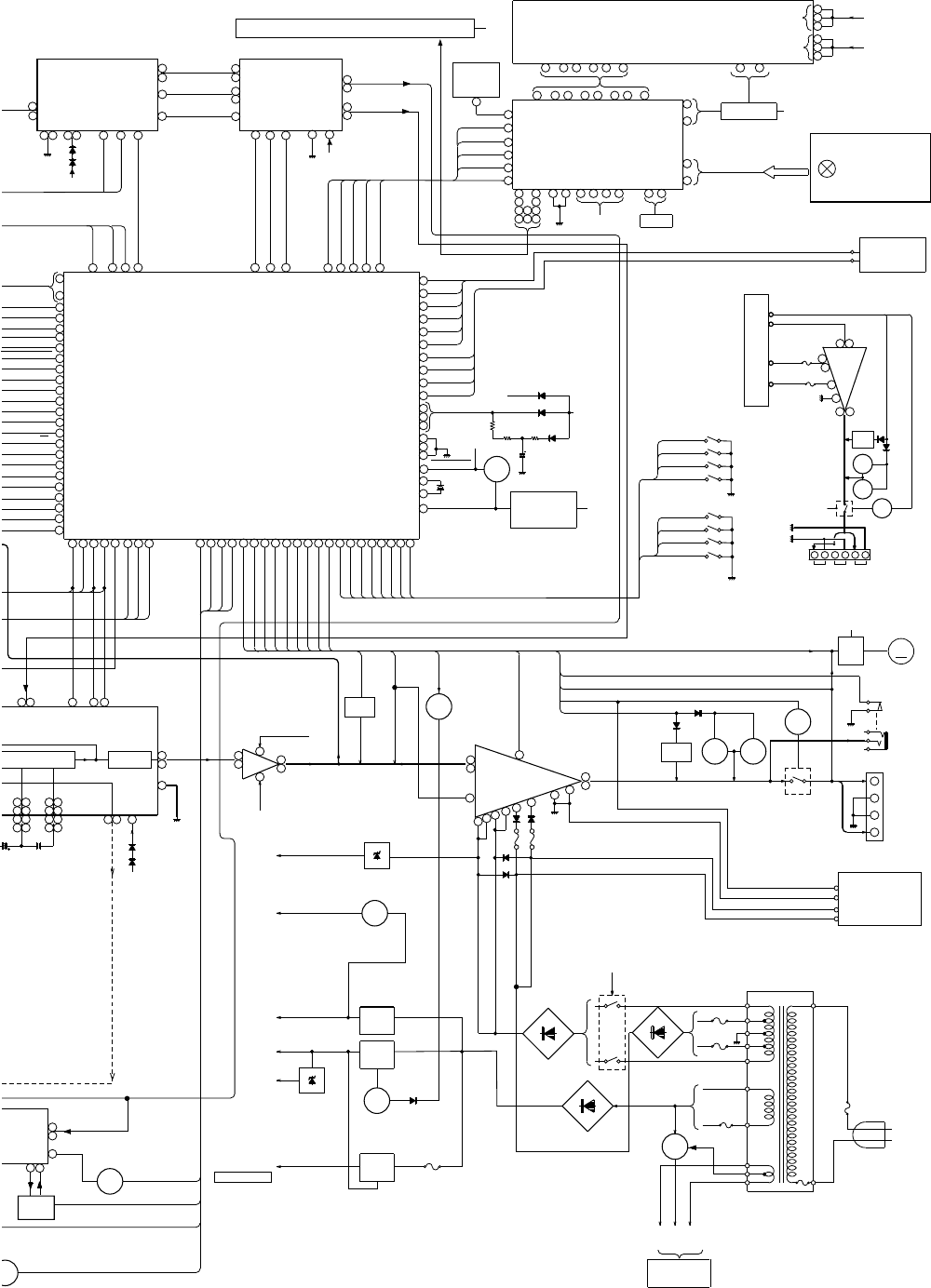
Figure 21 BLOCK DIAGRAM (1/3)
1
2
3
4
1
9
8
6
7
20 17
12
13
242530
31
22
32
34
3536
10
11
27 262829
PU-IN SW
XL1
16.934MHz
XIN
LD0
FIN2
JP–
CV+
SLC
SLI
FIN1
E
F
TO
FD
SPO
SP
SLD
SL–
SL+
DRF
CL
DAT
CE
VCC1
VCC2
6
+5V
+B4
+B4
SW702A
PICKUP IN
M
M
M702
SLED
MOTOR
OPTICAL PICKUP UNIT
9
IC2
LC78622K
SERVO SIGNAL
CONTROL
+B1
IC3
M56748FP
FOCUS/
TRACKING/
SPIN/
SLIDE DRIVER
IC1
LA9241M
SERVO AMP.
6
2
1
95
2
1
3
RES. CQCK. COIN
SQOUT. RWC. WRQ
~
~
~
CL, DAT, SELIAL CONTROL/CE
SL+. SL–. DRF
7
3
+5V
62
64
56
45
31
36
23
43
37
3839 28 25
24
2726
40
60
58
53
101220
324043
44
53
52
51
54
31
30
29
23
27
16
15
41
44
Q1
+5V
Q52
+7.3V (B2)
VOLTAGE
REGURATOR
SWITCHING
DRIVER
VOLTAGE
REGULATOR
IC82
TA7291S
TRAY MOTOR
DRIVER
XOUT
EFMO
EFMIN
CLV+
JP–
RCHO
RVSS
LVSS
LCHO
VVDD
VDD
LVDD
RVDD
XVDD
DOUT
CONT3
CONT1
CONT2
CONT4
CONT5
TO MAIN SECTION
6
2
8
1
95
IC81
TA7291S
MAIN CAM MOTOR
DRIVER
7
3
CAM SWITCH
M
M
MOB1
MAIN CAM
MOTOR
SWB101
SWB102
SWB103
SWB104
SWB105
SWB106
SWB107
SWB108
TRAY SWITCH
MOB2
TRAY
MOTOR
OPTICAL
PICKUP
IC1
IC2
50
CLK
41
RFSM
SP+
SP-
SL-
SL+
FO+
FO-
TR-
TR+
FOCUS COIL
TRACKING COIL
M701
SPINDLE
MOTOR
LASER
DRIVER
5
14
3
4
1
2
3
4
1
2
Q51
Q52
IC95
CD DIGITAL
OUTPUT
+7.3V
(B2)
CD-C5H,CP-C5H
– 22 –
Figure 22 BLOCK DIAGRAM (2/3)
D O
N
AMP
VT
T301 LW ANTENNA
T302 MW ANTENNA
L341
BALUN
FE301
FM FRONT END
OSC
FM
AM OSC
AM RF
AM LOOP ANTENNA
SO301
ANTENNA
TERMINAL
4
3
72
1
2
6
8
5
1
CNP301
75ohm CF302CF301
FM IF
AMP
Q301
FM IF
FM IF
VSSD
VDDD
XIN
XOUT
VSSA
VDDA
MPX
IN
DO
CL
DI
CE
XT21
4.332MHz
ICT21
LC72720
RDS MICROCOMPUTER
4
3
2
23 22 21 20 15 14 13
12
T305
T306
TUNER
MUTE
BEAT CUT
43
7
171213
21
20 1011161522
1
321 4
17 19 20
985
16
15141210 111321222324
76
18
3
51
7
4
8
45
46
3414 301820 28
2127226448
58
54
59
53
57
55
13
12
6
5
1
11
32 9
10
1
2
25
10
11
76
8
4
2
6
8
1
7
2
4
8
76
5
2
7
10
12
13
16
14
11
15
8
9
1
3
6
11
12
3
19
5
8
4
18
17
14
6
5
8
7
17
610
12
13
14
16
23
24
8
18
7
20
21
4
9
6
4
3
2
1
5
6
5
C
E
SURROUND
IN
SPE
OUT
SURROUND
OUT
CENTER
OUT
SIDE
CHAIN
SW
BIAS
BUF
DO
CE
CL
DI
MUTING
VOLTAGE
REGURATER
+B7
RL
MPX
VCO
CUT
Q353
Q354
IF IN
IF OUT
FM MONO/ST MONO/ST
VR351
FM MUTE LEVEL
AM OSC
REGOUT
FM IF IN
X352
4.5MHz
OSC
STEREO
+B7
AM IN
FM IN
FMOSC
T351
AM IF
L
R
R
L
R
L
PB-
REC-
TA-B
I
L354
MPX
PHASE
IN
X351
456KHz
FM IF
CF351
VCC
+B7
GND ICS03
NJM4565M
PRO LOGIC AMP.
+B7
Q463
Q451
IC452
BU4066BC
SRS MODE
SELECTOR
Q4
6
Q4
6
Q467
Q461
Q152
ICD03
BA3311L
REC./P.B.
EQUALIZER
AMP.
Q113
Q114
Q139
Q140
Q142
Q143
Q144
Q141
Q119
SWITCHING HI SPEED
Q126
Q125
REC
SWITCHING
SWITCHING
BAIS Q126 BAIS
BIAS OSC.
Q124
Q128
L104
BEAT CANSEL
Q131
Q132
HEAD
ERASE
MPX.FILTER
PB MUTING
IC101 AN7345K
PLAYBACK&RECORD
PLAYBACK AMP.
QM20
QM22
SWE4
TAPE2 PLAY
Q101
Q102
QM21 Q501
Q502
MM1
TAPE MOTOR
Q360
IC303 LA1832
FM IF DET./FM MPX./AM IF
Q361
L251
L252
SPE IN
IC502(1/2)
+B8
B.P.F
IC502/IC503/IC504
NJM4558MF
OPE AMP.
+B8 –B6
BIAS
AJDUST
VR101
VR102
HI SPEED
SOL1/2
SOLENOID
SWE1
TAPE1 PLAY
SWE7/SWE8
TAPE2 SIDE A FP/
SIDE B FP
SWE5
TAPE2 CrO
2
SWE2
TAPE1 CrO
2
MOTOR
DRIVER
QM02
QM01 QM08
QM03
QM04
T2 PLAY
T1 PLAY
PHM1/PHM2
DRIVER
TAPE MOTOR
HI SPEED
PB-EQ
HI SPEED & NOR
HI SPEED &
CrO
2
SWITCHING
T1/T2 RUN PLS
T2 CrO
2
T2 CrO
2
T2 CrO
2
FULL PROOF
T1/T2 SOLENOID
+B6
+B6
T1 CrO
2
DRIVER
M
T1/T2 VR151
VR152
REC-SENS
ADJUST
Q127
MUTING
T1/T2
PLAY-BACK
ADJUST
VRD03
VRD04
VRD01
VRD02
CD MUTE
QD09
QD10
QD07
QD08
QD06
QD01
QD02
DOLBY
ON/OFF
ICD01
HA12134AF
DOLBY NR
DOLBY
REC/PLAY
SWITCHING
QD03
MUTING
Q121
Q122
Q147
Q148
Q153
Q154
R
L
R
L
R
L
R
L
R
L
R
L
R
L
R
L
L
L
L
R
R
R
IC451
SRS5250AS1
SRS
REC M
U
T1
/
T2 B
T2
C
T2 R
T2 PLAY/ST
T2 A
T2 SOLEN
O
HIGH SP
E
T1 PLAY/ST
T1 R
T1
C
T1 SOLEN
O
TAPE MOT
O
OUT
AM RF IN
AFC
IN
SPE
1
TUNE
R
+B7
+B7
FM +B
FM
FROM CD UNIT
T1/T2
NOR/
HIGH
REC
P.B.
T1/T2 H/N
P.B
+B7
REF
L NF
REC
R
L
R NF
R REC
L REC
POP REDUCE
R
L
R NF
R(T2)
L(T2)
R(T1)
L(T1)
L NF
TAPE 1
TAPE 2
Q111
Q107
Q108
Q110
Q109
Q103 Q105
Q104 Q106
REC/PBREC
P.B
AC BIAS
P.B
RECORD/PLAYBACK
HEAD
L-CH
R-CH
PLAYBACK HEAD
L-CH
R-CH
TUNER
TAPE
CD
LR
IC501 LC753
9
AUDIO PROCE
S
IN Vref RVrefLVref
GRAPHIC EQU
A
IC302 LC72131
PLL CONTROLLER
+5V
IN
OUT
SM
SD
VIDEO/AUX1
INPUT VIDEO/AUX2
INPUT
R-CH
L-CH R-CH
L-CH
+B7
+B7
VREF
DET
VCC
GND
VCC
GND
ALC
OUT IN
NF
ICT02
NJM4558MF
LINE AMP.
+B7
–B6
HI SPEED
JT03
PRE OUT
JT01
SUPER WOOFER
ININ
L
OUT
R
L
R
L
R
QT05 S.W MUTE
SURROUND
CENTER
MUTE
OUT
IN
R
L
+B7
–B6
R
L
3
7
4
15
8
ICP02
NJM4565M
LINE AMP.
QP07
QP08
TO
CENTER/REAR
AMP UNIT
AUX2
AUX1
R
L
R
L
51
61
52
60
LR LR
2
5
8
1
4
7
11
46
43
40
37
10
45
42
39
36
TA
BEAT
C
DOLBY REC/
P
PB MUTI
SWITCHING
TAPE MOTOR DOLBY
REC
MUTE
SWITCHING
SWITCHING
SWITCHING
SWITCHING
SWITCHING
SWITCHING
SWITCHING
SWITCHING
VOLTAGE
REGULATOR SWITCHING
SWI
T
QT21
LOW PASS
FILTER
Q371
CD-C5H,CP-C5H
– 23 –
Figure 23 BLOCK DIAGRAM (3/3)
~
AC
AR
SPREAD
ICS02
QS7777PF
Q-SOUND
DECORDER
ICS01
LV1035M
DOLBY PRO LOGIC
DECORDER
DATA
CLK
ENABLE
OUT
R
L
SURR
CEN
QP03
QP04
S-MUTE
VOL SW
H/P SW
POSISTOR
SP DET
83 24 26 36
3
POSISTOR
13
F901
T4A L 250V
F902
T4A L 250V
GND
PROT
RELAY
+VL
-VL CENTER/REAR
AMP UNIT
–
SURROUND
R-CH
SURROUND
L-CH
CENTER
+B6
–VL
FH02
T4A L 250V
FH01
T4A L 250V
SOH01
SPEAKER
TERMINAL
RLH01
RELAY
QH99
QH98
QH97
QH03
QH04
CENTER
OUT
SURROUND
OUT
S-IN C-IN
ICH01
STK40705
POWER AMP.
RELAY
PROT
+VL
+
TO MAIN UNIT
–
+
–
+
12
3
6
7
15
10
14
DS RES
10
D ON/OF
64
63
62
16
6
1
5847462322
6
30
39
13
28
28
8473715250474532
27907246188915
10
2
87
85
94
88
1
91
100
99
8
9
9
679
91
5
3
4
11
94
93
92
14
13
18
56
90
15
57
89
12
16
17
27
9596979899
100
12
5479752855596362618768
46
47
43
49
48
32
30
34
35
31
38
42
41
40
33
39
37
23
19
58 70 25 67
3733 42 818 38 36 11 10 631
19
45
46
20
16
18
22
23
24
41
40
44
45
42
66 65 64
4
7
1
8
2
18
22
16 17
12
14
15
7
1
3
5
31
252324
17
26
566349
3018
24
25
28
27
26
4
8
98
97
96
95
12
29
3
2
1
CENTER
IN
R
ROUND
IN
REAR MUTE
CENT MUTE
S.W MUTE
C2B-CL
C2B-DI
C2B-DO
72 71 69 78 77 76
RELAY
H/P SW
PROT
PB-EQ
REC-EQ
VOLTAGE
REGULATOR
VOLTAGE
REGULATOR
TA-BIAS
M901
LED707~LED713
LED721~LED724
SW701~SW716
SW717~SW731
SW732~SW734
SW739~SW744
+B6
LED701~LED706
LED714~LED720 LED725,LED726
F1
F2
RX701
REMOTE
CONTROL
SENSOR
~
~
~
~
DATA1
RESET
+B2
Q702~Q711
JOG DIAL
SW702
CAM_SW1
CAM_SW2
TRY_SW1
CAM_SW4
CAM_SW3
TRY_SW2
TRY_SW3
TRY_SW4
DATA1
+B4 (+4V BACK UP)
RESET IN
RESET
Q201
+B4
SP RELAY
FUN
PROT
S-MUTE
POWER
F820
T500mA L 250V
SO901
SPEAKER
TERMINALS
F855
T2.5A L 250V
AC POWER
SUPPLY CORD
AC 230V 50HZ
TO DISPLAY
UNIT
VOLTAGE
REGULATOR
D852~D854 Q851
F853
T2A L 250V
F858
T5A L 250V
D850
F857
T5A L 250V
T851
D851
+B1
RL851
RELAY
+B7
VP VF2
(AC)
VF1
(AC)
T.F
POWER
TRANSFORMER
+4.6V
ICP01
NJM4565M
LOW BOOST AMP.
SRS PASS
Q
463
Q465
Q466
Q464
+B8
VOLTAGE
REGULATOR
SRS A/SRS B
SRS IN H
PASS/SRS STEREO/SRS MONO
SRS PASS/3D
L
R
1
0
AS1
S
REC MUTE
T1/T2
T2 B FP
T2 CrO
T2 RUN
T
2 PLAY/STOP
T2 A FP
T
2 SOLENOID
HIGH SPEED
T
1 PLAY/STOP
T1 RUN
T1 CrO
T
1 SOLENOID
T
APE MOTOR
CD MUTE
CE
CL
DI
CCB-CE
SRS IN H
SRS PASS
SRS B
SRS A
COM1
ENABLE
QS_SPREAD
QS_CLK
QS_DATA
~
SPE1~5
+B6
Q824
Q827
TO CD UNIT
Q820
Q821
Q826
Q822
Q823
Q825
+7.3V(CD)
+B9
VOLTAGE
REGULATOR
–B6 –15V
+B7
+B6
+B2 UN-SWITCHED
+12V(MOTOR)
+12V(ANALOG)
VOLTAGE
REGULATOR
SWITCHING
VOLTAGE
REGULATOR
IC201
IX0210AW
SYSTEM MICROCOMPUTER
TUNER MUTE
TUNER SD
SCK
STB
TO CD UNIT
SQ OUT
COIN
WRQ
RES
CQCK
RWC
MEMORY
BACK UP
+4.6V
UNSWITCH
+B2
VSS
VDD
+B3
CD SL+
CD-SL–
CD-PUIN
CD-DRF
OSC
X201
4.19MHz
+B3
P.FAIL DET
SYSTEM STOP Q202
Q203
ZD201
Q828
POWER
POWER ON/STB
SWITCHING
OUT
IN
L
R
L
RL
R
IC901
STK41710
POWER AMP.
–B6
+B7
R-IN
L-IN
VH+
VL+
VL-
VH-
R-OUT
L-OUT
–B1
STB
SCK1
COM1
FAN
MOTOR
Q994
Q995
FUN
RL901
RELAY
Q999
Q998Q997
Q903
Q904
M
R-CH
GND
GND
L-CH
+
–
–
+
J901
HEADPHONES
FL 701
FL DISPLAY
IC701
IX0209AW
FL DRIVER &
CONTROLLER
~~~
~~
~
~
KEY INVDD
+B2
+B7
+B7 VSS
KEY MATRIX
VF2 (AC)
VF1 (AC)
LR
OUT
OUT
LC75396N
R
OCESSOR
Vss
VDD
VOLUME
P
HIC EQUALIZER
+B7
CAM SW1 SWB101
SWB102
SWB103
SWB104
SWB105
SWB106
SWB107
SWB108
CAM SW4
CAM SW3
CAM SW2
TRY SW1
TRY SW4
TRY SW3
TRY SW2
IN
IN IN
IN
R
OUT
L
L
O
UT
R
L
R
SURR OUT
CENTER
OUT
LR LR
3
6
9
2
5
8
12
47
44
41
38
11
46
43
40
37
12
TA R/P
BEAT CUT
44
45
D
OLBY REC/PLAY
PB MUTING
51
52
53
N
G
SWITCHING
SWITCHING
SWITCHING
FAN MOTOR
CONTROL
RELAY DRIVER
PROTECTION
PROTECTION
CD-C5H,CP-C5H
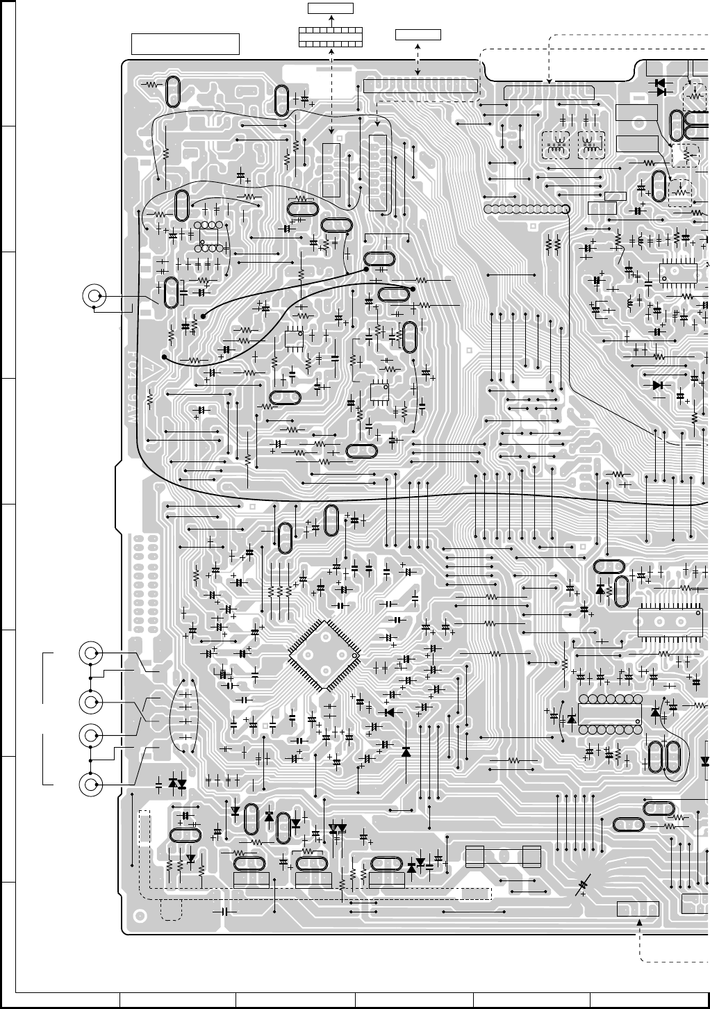
– 24 –
A
B
C
D
E
F
G
H
123456
Figure 24 WIRING OF P.W.BOARD (1/9)
RP22
R514
R512
R513
RT28
RP19
RP07
CP12
CP29
RP39
RP29
CP30
R516
RP37
RP01
RP05
RP20
RT26
CP33
RP31
RT27
CP34
CP16
RP12
CP15 RP11
CP11
RP02
RP06
RP23
R502
R835
R825
C826
R501
RT05
RT02
RT01
RT06 CT01
CT03
RT07
RT03
RT04
CT02
RT08
CT04
R506
C512
R504
C578
R505
C511
R503
C823
CT36
CT34
RT33
CT35
CT26
RT34
RT35
CT33
RT32
RT37
RT30
RT29
CT23
RT10
C522
C521
CT32
CP36
CP18
CP17
C549
C554
C551
C581
C550
C543
C552
C582
C541
C556
C553
C542
CP02
CP19
CP13
CP31
CP27
QP01
CP09
CP07
CT28
QP07
CT19
QT03
QP08
QP04
CP32
CT27
QT05
QP03
CP10
QP02
CP08 CP14
QP05
CP25
CP20
CP01
CT20
QT06
QT04
CT21
C528
C533
C531
Q828
C822
C833
Q826
Q825
C827
C555
C539
C526
C557
C558
C502
C505
C503
C501
C824
C527
C525
C523
C529
C530
C532
C524
C540
C534
C516
C518
C536
C510
C546
C508
C504 C506
C507
C545
C535
C509
C517
C579
C515
CT05
Q821
C825
Q823
C821
Q827
F820
T500mA L 250V
CT31
QT01
CT24 QT02
RT39
RT40
RP34
RP44
RP43
C831
RP32
D829
R515
R509
R511
R510
CT25
RT38
RP17
RP18
RP36
R948
RP25
R947
CP35
RP26
RT31
R821
R941
RP15
RP16
ZD820
RP14
RP33
RP30
RT36
RP13
R942
RP09 RP10
RP38
RP08
RP35
RP27
D828
R823
D827
R834
R829
ZD821
R828
R827
C820
R518
R517
R521
R522
D501
R824
D502
DT02
DT01
D826
R826
R822
ZD822
D823
R820
RT25
RT41
RT09
Q820
Q822
Q824
CFW853A CFW852
ICP01
ICP02
IC501
CNP501
ICT02
RD29
RD01
CD07
CD03
RD03
CD05
CD04
RD04
RD30
C251
C252
RD28
RD32
RD34
CD44
CD08
RD35
RD12
RD08
RD06
CD20
CD09
LD01
CD21
CD51
CD01
QD07
VRD01
C181
VRD04
CD42
CD10
QD
0
VRD03
QD06
CD40
CD38
CD45
LD02
CD11
CD02
CD14
CD18 CD12
RD21
CD06
RD15
R592
R591
RD75
RD37
RD7
1
RD27
DD02
D102
D101
R
RD02
RD09
321
TP451
FW201
L252
L251
CNP202
ICD01
C486
R462
C488
R456
R455
R459
R461
R491
R471
R469
RD22
R481
R472
R468
R490
R492
R480
C461
R488
R487
R483
C482
C471
C487
C485
Q451
Q452
C484 C483
C481
Q467
Q502
Q501
C454
C453 C472
Q458
C547
C548
R460
ZD452
ZD451
R467
R477
D403
R470
R596
R595
R210
R465
R482
D205
IC452
CNP851
IC451
C830
B
C
E
E
C
B
E
C
B
B C E
B C E
B C E
E C B
E
C
B
E C B
E C B
3
2
1
1
2
3
3
2
1
3
2
1
B C E
B C E
B C E
B C E
E C B
B C E
B C E
1
2
3
3 2 1
3 2
1
1
2
3
1 2 3
S
G
D
1
2
3
3
2
1
123
4
14
58
1
4
58
3
2
1
1
2
34
5
678
12
34
56
78
9
12
34
56
78
9
10
11 12
13 14
123456789
10 11 12 13 14 15 10
123456789
11 12
E C B
E C B
2
3
24
25
26
27
1
2
34
5
6
7
8910 11 12 13 14
1
5
10
15
16
17
20
25
30
32
33 35
40
45
48 49
50
55
60 64
1
12
18
9
16
1
5
10
14
20
15
25
28
TAPE1 PLAY
L-CH SENS,
TAPE2 PLAY
R-CH SENS, TAP
E
R-C
H
TAPE2 PLAY
L-CH SENS,
CNSP01
CNW853B P46 4-E
TO PRO LOGIC PWB
19
19
TO AMP. PWB
P48 10-A
L-CH
R-CH
L-CH
R-CH
JT01
VIDEO/AUX
INPUT
VIDEO/
AUX2
VIDEO/
AUX1
SUPER
WOOFER
JT03
PRE OUT
FW853A
MAIN PWB-B
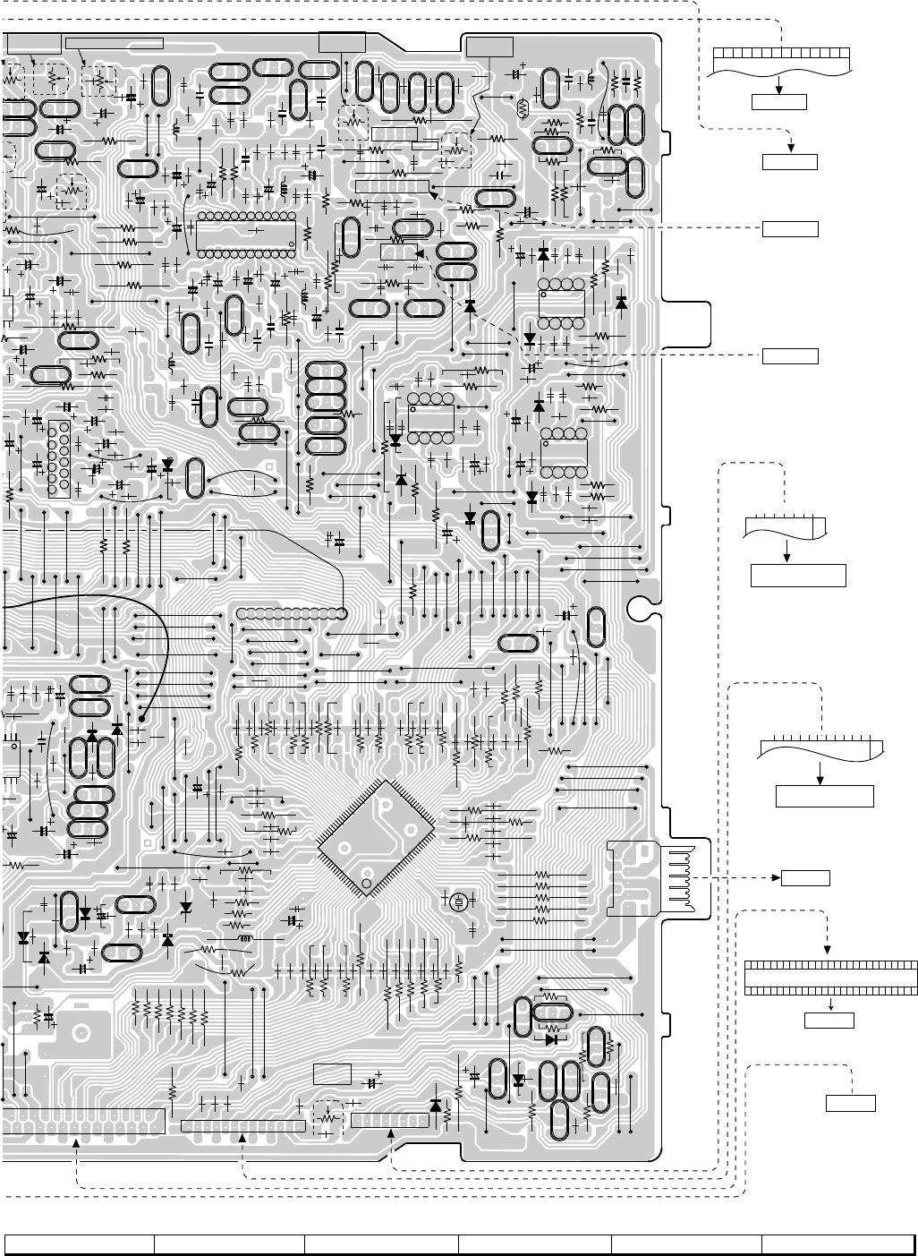
CD-C5H,CP-C5H
– 25 –
Figure 25 WIRING OF P.W.BOARD (2/9)
78 9 10 11 12
C178
R196
R180
RD78
C176
R169
R561
R571
R134
R154
R190
R128
R198
R156
R149
RD77
RD36
RD41
C177
R197
R127
R195
C175
R179
R191
CD19
R173
R174
R106
C161
R167
R168
RD70
C561
R121
R155
C131
RD39
R157
R150
R152
C140 R192
R132
R126
R124
C147
C114
C112
R130
C132
C120
R122
R107
C105
RD35
RD11
RD10
C101
C102
R557
R560
C562
C575
C560
C577
R555
C576
R570
R576
R581
R562
R563
C564
R564
C563
R566
R579
R577
C572
C571
R572
C569
R573
R574
C570 C566
R569
C565
R164
R165
R110
R108
C103
C104
R172
R123
R131 C139
C113
R145 R129
C111
C119
C127
R105
R113
C107
R139
C108
R140
R104
R103
RD23
RD26
RD24
CD34
RD25
CD33
RD31
RD33
CD43
RD08
RD06
RD07
RD05
R554
VR101
Q156
C184
C148
Q141
Q146
Q147
Q149 Q144
Q143
Q142
CD46 C117
C115
C559
C574
C567
C573
C568
Q110
Q111
Q102 Q101
C167
C121
C125
C128
Q107
Q108
C180
Q148
Q154
C124
C118
Q140
C168
Q150
L102 Q122
CD16
C182
C145
Q119
C179
QD03 Q153
L103
C123
Q139
Q113
0
1
VR151
C181
RD04
VRD02
Q131
Q132
CD42
C150
C162
RP101
C152
Q128
C151
L104
CD31
CD32
QD09
VRD03
QD10
CD15
CD45
CD17
Q121 C142
CD52
VR152
QD08
Q114
QD02
QD01
Q105
Q103
Q104
Q106
CD39
CD37
CD41
CD02
Q124
Q127
Q125
C134
C146
C126
C116
C122
C133
C141
C109
Q109
VR102
CD35
CD36
CD13
D104 D103
RD38
RD73
D554
RD76
RD69
R119
R583
R553
R582
ZD550
R558
R565
R559
R556
D552
R567
R568
D556
R580
D553
R578
D555
R575
D557
R148
R114
R101
R125
L105
R102
R120
R115
R117
R118
R109
RD16
R185
R141
R112
RD72
DD01
R153
R137
R135
RD37
R171
R170
R161
R160
R166
RD71
R133
R158
RD44
RD14
R186
R162
R163
R138
R136
L106
R111
R189
RD43
RD13
RD42
RD02
1
1
IC503
IC502
IC504
CNP101
CNP102
1
IC101
ICD03
R475
R229
RM01
RM25
R204
R257
R258
R498 RA73
RA75
R240
R206
R205 RA80
RA79
RA78
R831
RM03
RM09
R473
R474
RM02
R493
R231
R235
C202
R239
R234
R232
R233
RA82
RA83
R218
R217
RA66
RA68
RA69
RA71
RA72
RA63
RA62
RA59
RA55
RA53
RA52
RA49
RA48
RA45
RA44
RA42
RA41
RA39
RA38
RA35
RA34
RA29
RA28
RA27
RA26
RA25
RA24
RA91
C256
RA92
C206 C205
RA93
RA94
R256
RA97
RA98
RA02
RA04
RA03
RA11
RA05
RA13
RA12
RA17
R466 R479
R484
R480
C461
R488
R483
R236 C204
R237
R230
R216
R215
R222
R209
Q126
Q206
C257
Q463
C832
CM02
Q465
VRM01
Q459
Q460
Q466
Q464
Q461
C456
CM01
QM08
QM04
QM03
QM21
QM01
Q202
C203
C207
C454
C458
C457
C460
Q201
C201 Q203
QM20
QM02
QM22
C183
R220
R219
R221
R467
DM03
D402
RA87 RA88
R224
R225
R226
R227
R228
R223
R201
D401
RA76
ZD201
R207
RA77
DM02
RM10
RM12
RM04
RM11
R211
D203
L201
RA81
R208
R202
6
9
5
R210
RA08
RA09
RA07
RA06
R214
RA36
RA33
R238
RA40
RA37
RA64
RA65
RA67
RA70
RA14
RA61
RA58
RA54
RA51
RA47
RA46
RA43
RA32
RA31
RA30
RA95
RA10
RA96
RA01
RA99
4
65
D205
D204
D202
RA19
RM06
RM05
RM24
RA23
RA22
RA21
RA20
DM01
RM23
CNP201
X201
CFW2
WTM2
IC201
WTM1
23
23
4
56
71
2
3
4
3 2 1
3 2 1
3 2 1
B C E
E C B
E C B
1 2 3
E
C
B
3 2 1
3 2 1
1 2 3 1 2 3
1
2
3
B
C
E
B
C
E
B
C
E
B
C
E
E
C
B
B
C
E
B
C
E
B C E
E C B 1
2
3
E C B
E C B
1 2 3
1 2 3
1 2 3 1 2 3
E
C
B
3 2 1
3 2 1
3 2 1
3 2 1
3 2 1
3 2 1
1 2 3
1
2
3
1
2
3
1
2
3
1
2
3
1
2
3
1
2
3
3
2
1
3
2
1
3
2
1
3
2
1
B
C
E
E
C
B
B C E
1 2 3
1 2 3
1 2 3
1 2 3
E C B
S
G
D
S
G
D
1
2
3
4
5
6
789
10
11
12
1314 15 16 1718 19 20 2122 24
23
1
2
3
4
567
8
123
4
5
6
7
8
9
1011
12
13
1
2
3
E C B
E C B
1
2
3
4
5
6
7
8
9
10
11
12
13
14
15
16
17
18
19
20
21
22
23
24
25
26
27
D
G
S
12
34
56
78
910
1234
5
67
8
1234
5
6
7
8
1234
567
8
1
12
1
5
10
15
20
25 30
31
35
40
45
50
51
55
65
60
70
75
80
81 85
95
90
100
8
9
1
5
28
3 2 1
FW201
C106
2
4
6
8
10
12
1
3
5
7
9
11
TAPE1 PLAY
R-CH SENS, R-CH REC/PLAYSENS,
TP490
L-CH BIAS
CURRENT L-CH BIAS
CURRENT
CNS701
TO DISPLAY PWB
CNP303
TO TUNER PWB
CFW903
TO POWER AMP. PWB
CNS102B
FROM TAPE 2 HEAD PWB
CNS101B
FROM TAPE 1 HEAD PWB
CNS851
FROM POWER
SUPPLY PWB
P43 12-B
CFW1
FW1
TO CD SERVO PWB
P37 11-H
27 1
27 1
TO TAPE2 MECHANISM
PWB-H
TO TAPE1
MECHANISM PWB-G
1
13
1
8
114
FWM1
FWM2
P36 1-F
P33 9-F
P33 9-D
P33 12-E
P33 12-H
P33 11-A
FW903
P42 6-B
TAPE
SPEED
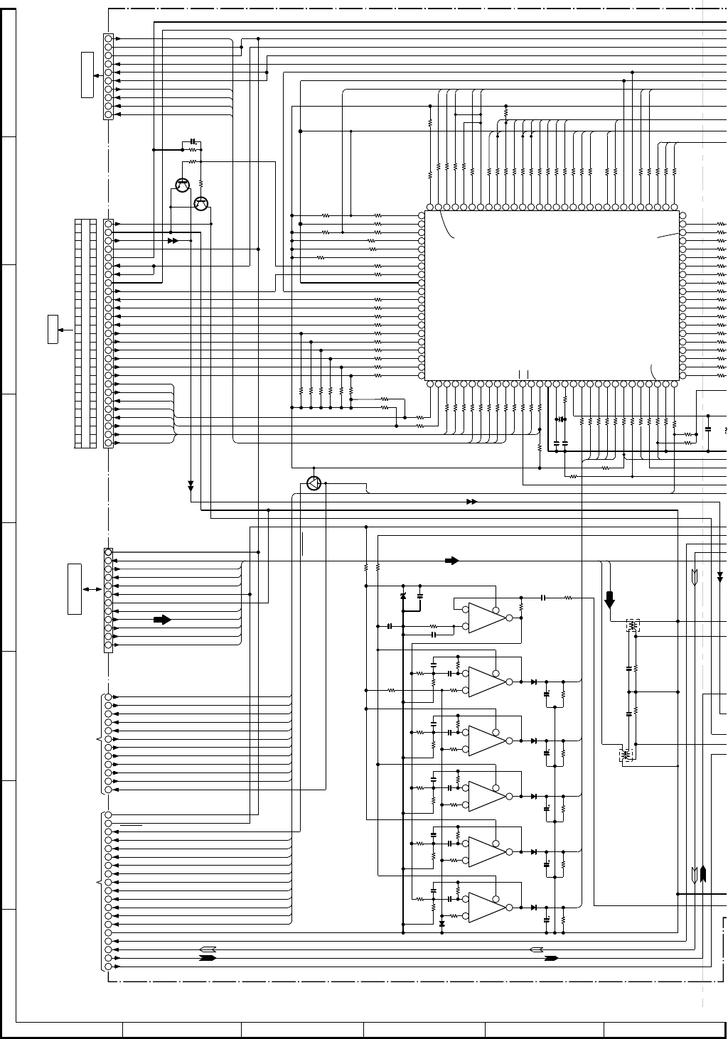
CD-C5H,CP-C5H
– 26 –
Figure 26 SCHEMATIC DIAGRAM (1/17)
NOTES ON SCHEMATIC DIAGRAM can be found on page 20.
A
B
C
D
E
F
G
H
123456
IC502
(1/2)
R555
270K
CNP202
CFW2
CNP201
FW1
R206 10K
R240 10K
R210
47K
C207
22/25
R596
2.2K
RA76 1K
RA77 1K
RA80 1K
RA78 1K
Q502
2SC3199 GR
C256
0.022
R238
100K
R216
10K
RA30
1K
R208 10K
R207 10K
Q206
KRA107 M
R592
2.7K
C251
0.0033
R591
2.7K
C252
0.0033
R211
10K
R595
2.2K
Q501
2SC3199 GR
C206
15P (CH)
C205
15P (CH)
X201
4.19MHz
RA26 1K
0.022
C576
ZD550
MTZJ5.6A
R583
220
R582
330
RA19 1K
RA17
820
RA20 1K
RA21 1K
RA22 1K
RA23 1K
RA24 10K
RA25 1K
RA27 1K
RA28 1K
C560
0.022 R553
15K
R558
100K
C575
0.022
R554
470K
RA29
47K
IC201
IX0210AW
SYSTEM MICROCOMPUTER
10K
R204
1K
RA79
R205
10K
RA55 1K
R209 10K
R223 10K
R224 10K
R225 10K
R226 10K
R227 10K
R228 10K
RA58 100
RA59 1K
R256 1K
RA99 1K
RA98 1K
RA97 1K
RA96 1K
RA95 1K
RA94 1K
RA93 1K
RA92 1K
RA91 1K
RA88 1K
RA87 1K
RA83 1K
RA82 1K
RA81
1K
RA02
1K
RA01
1K
RA06 1K
RA07 1K
RA08 1K
RA14 1K
RA13 1K
RA12 1K
RA11 1K
RA10 1K
RA09 1K
RA05 1K
RA04 1K
RA03 1K
R202 10K
R201 10K
RA51 1K
RA52 1K
RA53 1K
RA54 1K
RA61 1K
RA62 1K
RA63 1K
RA64 1K
RA65 1K
RA67 1K
RA68 1K
RA69 1K
RA70 1K
RA71 1K
RA72 1K
RA73 22K
RA75 1K
RA66 1K
D557
1SS133
C577
0.022
C562
0.0068
C561
0.0068
R557
470K R561
100K
R556
56K
R560
2.2M
R559
2.2M
D552
1SS133
C559
2.2/50
R563
22K
C563
0.0082
R566
100K
R562
18K
R565
220K
C564
0.0082
R564
680K
IC503
(2/2)
D553
1SS133
C567
2.2/50
R568
68K
C565
0.0027
R571
100K
R567
12K
R570
220K
C566
0.0027
R569
390K
D554
1SS133
C568
2.2/50
R574
39K
C569
680P
R576
100K
R573
12K
R575
220K
C570
680P
R572
470K
D555
1SS133
C573
2.2/50
R579
33K
C571
270P
R581
100K
R578
10K
R580
220K
C572
270P
R577
390K
D556
1SS133
C574
2.2/50
NJM4558D
OPE AMP.
31
30
29
28
27
25
26
24
23
22
21
20
19
18
17
16
15
14
13
12
11
10
9
8
7
6
5
4
3
2
1
11
12
10
9
8
7
6
5
4
3
2
1
27
26
25
24
23
22
21
20
19
18
17
16
15
14
13
12
11
10
9
8
7
6
5
4
3
1
2
10
9
8
7
6
5
4
3
2
1
R257
10K
R258
10K
5
6
7
1
4
3
2
+
–63Hz
SPE-5
8250Hz
SPE-4
+
–
5
6
7
3
2
1
IC504
(2/2)
4
–
+
1KHz
SPE-3
8
IC504
(1/2)
+
–4KHz
SPE-2
3
2
1
16KHz
SPE-1
4
+
–
5
68
7
+
–
PRE R-CH
PRE L-CH
REC R-CH
REC L-CH
GND(A)
HIGH_SP
PRE R-CH
PRE L-CH
REC R-CH
REC L-CH
TA_REC EQ
PB_MUTE
HIGH_SP
REC_MUT
BEAT_CUT
TA_BIAS
TA_R/P
DUBB_MOD
D-PB/REC
D-ON/OFF
TA_PB-EQ
TA_T1/T2
GND(A)
T2_B-FP
MOTOR
T1_SOL
T2_SOL
T1_RUN
T2_RUN
T1_PLAY
T2_PLAY
T2_A-FP
T1_CROM
T2_CROM
TUN MUTE
+7.3V(CD)
+7.3V(CD)
PCCC
GND(4A)
CQCK
COIN
SQ_OUT
TRY_SW4
TRY_SW3
WRQ
DRF
PU-LN
TRY_SW2
TRY_SW1
CAM_SW4
CAM_SW3
CAM_SW2
CAM_SW1
RWC
SL+
SL–
RES
GND(CD2)
GND(D)
PCCL
RWC
SL+
SL–
RES
AUT_SCAN
VOL SW
MOTOR
SP DET
POSISTOR
PROTECT
TUN_SM
SP_16K
SP_4K
SP_1K
T1_CROM
T2_A-FP
T1_RUN
BEAT_CUT
TA_BIAS
T2_B-FP
T2_CROM
T2_RUN
T2_PLAY
T2_SOL
T1_SOL
T1_PLAY
HIGH_SP
TA_R/P
TA_PB-EQ
SRS_A/NA
DOL_A/NA
DRF
CD_MUTE
CQCK
SQ_OUT
COIN
TRY_SW2
TRY_SW1
CAM_SW1
CAM_SW2
CAM_SW3
CAM_SW4
SP_63Hz
SP_250Hz
SYS_STOP
PIUN
WRQ
DS_RES
STB
SCK
DAT
COM
TRY_SW4
TRY_SW3
RES
VSS
CF1
CF2
VDD
VDD
VSS
P31
P30
P03
PB0
PA7
PB1
PB2
PB3
PB4
PB5
PB6
PB7
PC0
GND(µ-CON
+4.6V(µ-CO
N
H/P SW
TUN_ST
REC-EQ
REC_MUT
TA_T1/T2
MIC_DET
PC6
PC7
PD0
PD1
FUN_MOTO
D-ON/OFF
D-PB/REC
PB_MUT
SP_RELAY
VSS
VDD
PD2
PD3
PD4
PD5
PD6
PD7
PE0
PE1
PE2
PE3
PE4
PE5
PE6
PE7
PF0
PF1
PF2
PF3
PF4
PF5
PF6
PF7
CENT_MUT
REAR_MUT
LINE_MUT
SYS_MUT
QS_CL
QS_DA
9K/10K
C2B_DO
VOICE-CAN
TUN_MUT
SRS_INH
SRS_B
SRS_A
SRS_3D
SRS_PASS
QS_STRB
PL_ENA
C2B_CE
C2B_CL
TUN_SD
C2B_DI
SWFE_MUT
POWER
PC1
PC4
PC3
PC5
PC2
PL4
PL5
PL6
+4.6V(D)
+12V(M)
+7.3V(CD)
GND(D)
GND(CD1)
GND(CD2)
MPX.FILTER
L252
MPX.FILTER
L251
T
+12V(A)
GND(A)
SD
SM
CL
CE
DI
DO
R-CH
L-CH
GND(D)
+4.6V(D)
GND(D)
GND(D)
+12V(M)
RESET
STB1
+12V(M)
COM1
SCK1
DATA1
GND(A)
–15V
+12V(A)
HIGH SP
HIGH SP
IC502
(2/2)
IC503
(1/2)
31
32
33
34
35
36
37
38
39
40
41
42
43
44
45
46
47
48
49
50
515253545556575859606162636465666768697071727374757677787980
9
8
7
6
5
4
3
2
1
18
17
16
15
14
13
12
11
10 27
26
25 30
29
28
24
23
22
21
20
19
99
98
97
96
95
94
93
92
91
90
89
88
87
86
85
84
83
82
81
+12V(A)
GND(D)
INT0
SI1
INT3
INT2
INT1
AN7
AN6
AN5
AN4
AN3
AN2
AN1
AN0
Si0
SO0
SCK1
SO1
SCKØ
P33
P32
VDD3
VSS3
P04
P02
P01
P00
P35
P34
P05
P06
P16
P17
P07
RES
P75
P74
VSS1
CF1
CF2
VDD1
PA0
PA1
PA2
PA3
PA4
PA5
PA6
PL3
PL2
VDD2
VSS2
PL1
PL0
CNS701
CFW1
TO CD SERVO PWB
P39 7-H
TO DISPLAY PWB
P40 1-C
CNP303
TO TUNER PWB
P35 9-H
P31 12-B
TO TAPE MECHANISM
SECTION
P29 12-D
TO DECK SECTION
GND(Au)
CD R-CH
CD L-CH
100
–B
+B
+B
+B
–B
–B
+B
–B
+B
+B
–B
+
B
3
2
1+B
+B
+B
+B
+B
4.0V
4.0V
4.0V
4.0V
4.0V
3.7V
3.7V
0V
0V
4.0V
0V
4.0V
0V
4.0V
0V
0V
4.0V
0V
0V
0V
0V
3.6V
3.8V
0V
4.0V
0V
3.8V
3.8V
0V
3.8V 3.8V
0V
4.0V
0V
0V
0.3V
4.0V
4.0V
0V
0V
0V
0V
4.0V
4.0V
4.0V
4.0V
4.0V
0V
4.0V
4.0V
4.0V
0V
0V
0V
0V
0V
0V
0V
0V
4.0V
2.0V
1.7V
0.4V
0V
4.0V
0V
4.0V
2.0V
3.8V
0V
0V
4.0V
0V
4.0V
4.0V
4.0V
0V 3.8V
0V
0V
0.7V
0V
0V
0V
0V
0.7V
0V
0V
4.0V
4.0V
0V
3.8V
0V
0V
4.0V
4.0V
0V
0V
0V
0V
0V
0V
0V
0V
4.0V
4.0V 0.3V
0V
0V
0.5V
5.5V
0.4V
0.5V
0.5V
0.5V
0.5V
-11.6V
0.4V
0.4V
5.5V
0.5V
0.5V -11.6V
0.4V
0.5V
0.5V
0.5V
-11.6V
0.4V
0V
5.5V
0V
+B
+B
+B
+B
+B
+B
+B
+B
+B
+B
+B
CD MUTE
11
27
27
NJM4558D
OPE AMP.
NJM4558D
OPE AMP.
NJM4558D
OPE AMP.
NJM4558D
OPE AMP.
NJM4558D
OPE AMP.
+B
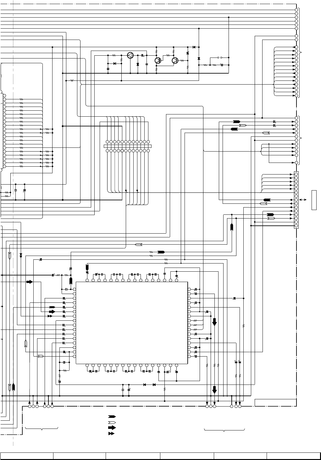
CD-C5H,CP-C5H
– 27 –
Figure 27 SCHEMATIC DIAGRAM (2/17)
78 9 10 11 12
1
2
3
4
5
6
7
8
9
C548 4.7/50
C547 4.7/50
FW201
R512
560K
C257
47/25
C256
0.022
R216
10K
RA30
1K
R516
1K
R515
1K
R517 1K
C558
2.2/50
C557
2.2/50
R518 1K
R521 1K
R522 1K
L201
2.2µH
C578
0.022
R504
15K
C512
100P
C511
100P
C581
10/50
C582
10/50
R501
560K
R513
1K
R514
1K
C579
100/16
D502
1SS133 D501
1SS133
R503
15K
R502
560K
R233
10K
D203
1SS133
R235
1K
R239
82
C201
470/10
R229
150
R230
150
R234
10K
Q202
KTC3199 GR
C202
0.01
C203
3.3/50
D204
1SS133
D202
1SS133
R231
1K
ZD201
MTZJ3.3A
R232
100
Q203
KTC3199 GR
Q201
KRC102 M
R236
3.3K
R237
1K
D205
1SS133
C204
0.01
R215
10K
R222
10K
R221
10K
R220
47K
R219
10K
R218
47K
R217
10K
RA45 1K
RA31 1K
RA32 1K
RA33 1K
RA34 1K
RA35 1K
RA36 1K
RA49 1K
RA48 1K
RA47 1K
RA46 1K
RA44 1K
RA43 4.7K
RA42 1K
RA41 1K
RA40 1K
RA39 1K
RA38 1K
RA37 1K
7881 82 83 79 80 67 68 69 70 71
72
66
65
64
63
62
61
60
59
58
57
56
55
54
53
52
51
50
49
48
47
46
42
43
44
45
41
39
38
37
36
35
34
33
32
C522
0.18 C521
0.18
C550
1/50
R258
10K
C553
1/50
C554
1/50
C510
10/50
C546
1/50
C545
1/50
C539
10/50
R505
1.8K
C509
10/50
C540
10/50
C543
47/16
C551
10/50
C549
1/50
C542
10/50
C552
10/50
R506
1.8K
C556
47/16
C555
47/16
C533
0.0047 (ML)
C541
10/50
C534
0.0047 (ML)
R511 1K
R510 1K
R509 1K
C507 2.2/50
C535 2.2/50
C536 2.2/50
C508 2.2/50
C506 2.2/50
C504 2.2/50
C502 2.2/50
C505 2.2/50
C503 2.2/50
C501 2.2/50
C526
0.22/50
C516
0.47/50
C532
0.0022
(ML)
C530
0.015
(ML)
C525
0.22/50
C515
0.47/50
C528
0.027
(ML)
C524
0.15
(ML)
C518
0.18
(ML)
LC75396N
IC501
10
11
12
13
14
15
VOL SW
MOTOR
T1_CROM
T2_A-FP
T1_RUN
BEAT_CUT
TA_BIAS
T2
_
BFP
T2_CROM
T2_RUN
T2_PLAY
T2_SOL
T1_SOL
T1_PLAY
HIGH_SP
TA_R/P
TA_PB-EQ
B
0
A
7
B
1
B
2
B
3
B
4
B
5
B
6
B
7
C
0
GND(D)
QS_DA
QS_CL
QS_STRB
PL_ENA
C2B_CL
C2B_DI
C2B_CE
C2B_DO
TUN_MUT
TUN_SD
TUN_SM
RESET
POINT
PROTECT
+4.6V(D)
LINE-MUTE
CENT_MUTE
REAR-MUTE
SWF-MUTE
VOL SW
SP DET
POSISTOR
S-MUTE
FUN CONT
SP PROT
SP RELAY
POWER
H/P SW
–15V
+12V(A)
+12V(M)
+7.3V(CD)
GND(D)
CD GND(D1)
CD GND(D2)
+4.6V(D)
+12V(M)
GND(D)
+7.3V(CD)
CD GND(D1)
CD GND(D2)
+4.6V
GND(µ-CON)
+4.6V(µ-CON)
REC-EQ
REC_MUT
TA_T1/T2
O/O
C
1
C
4
C
3
C
5
C
2
PASS
CNP501
SRS PASS
–15V
SRS INH
QS_DATA
QS_CLK
QS_SPREAD
C2B_CL
C2B_DO(µCON Side D0)
PL_ENA
L-CH OUT
R-CH OUT
C-OUT
S-OUT
L-CH IN
R-CH IN
+12V(A)
GND(AU)
SRS B
SRS A
OUT(R)
OUT(L)
IN(L)
IN(R)
+12V(A)
GND(A)
TO AMP SECTION
P30 3-H
VIDEO1 INVIDEO2 IN
R-CH OUT
L-CH OUT
TO POWER SECTION
P30 5-H
VOLUME
OUT
L-CH OUT
R-CH OUT
17
18
19
+4V
GND(A)
C-CH OUT
S-CH OUT
–15V
+12V(A)
48 47 46 45 44 43 42 41 40 39 38 37 36 35 34 33
16
15
14
1312
11
10
98
7
6
5
4321
64
63
62
61
60
59
58
57
56
55
54
53
52
51
50
49
20
21
22
23
24
25
26
27
28
29
30
31
32
GND(A)
GND(A)
R-CH OUT
L-CH OUT
GND(A)
31
32
33
34
35
36
37
38
39
40
41
42
43
44
45
46
47
48
49
50
5
1
3
0
A
0
A
1
A
2
A
3
A
4
A
5
A
6
TO SRS SECTION
P32 4-H
TO PRO LOGIC PWB
CNPS01
P47 2-H
TO POWER SECTION
P31 8-H
(5.0V) LFCOM
(5.0V) LFOUT
(5.0V) LRIN
(5.0V) LRCOM
(5.0V) LROUT
(5.0V) LVref
(0V) VSS
(0V) CE
(0V) DI
(4.0V) CL
(0V)Vref
(5.0V) RVref
(5.0V) RROUT
(5.0V) RRCOM
RRIN
(5.0V)
RFOUT
(5.0V)
LFIN
(5.0V)
(5.0V) LTOUT
(4.9V) LF4C3
(4.8V) LF5
(5.0V) LF4C2
(4.8V) LF4C1
(4.9V) LF3C3
(5.0V) LF3C2
(4.8V) LF3C1
(4.9V) LF2C3
(5.0V) LF2C2
(5.0V) LF2C1
(4.9V) LF1C3
(5.0V) LF1C2
(4.8V) LF1C1
(5.0V) LTIN
RSERO
(5.0V)
RTIN
(5.0V)
RINVIN1 (5.0V)
R5 (5.0V)
R4 (5.0V)
R3 (5.0V)
R2 (5.0V)
R1 (5.0V)
VDD (10.1V)
L1 (5.0V)
L2 (5.0V)
L3 (5.0V)
L4 (5.0V)
L5 (5.0V)
LSELO
(5.0V)
LINVIN1
(5.0V)
RFCOM (5.0V)
RFIN (5.0V)
RTOUT (5.0V)
RF5 (4.8V)
RF4C2 (5.0V)
RF4C3 (4.9V)
RF4C1 (4.8V)
RF3C3 (4.9V)
RF3C2 (5.0V)
RF3C1 (4.8V)
RF2C3 (4.9V)
RF2C2 (5.0V)
RF2C1 (5.0V)
RF1C3 (4.9V)
RF1C2(5.0V)
RF1C1 (4.8V)
MAIN PWB-B(1/4)
3
2
+B
AUDIO PROCESSOR
+B
+B
–B
+B
+B
–B
+B
+B
+B
+B
+B
–B
+B
–B
+B
12 1
12 1
+B
P.FAIL DET
1
+B
RESET
+B
+B
+B
+B
0V
4.0V
4.0V
0V
0V
0V 0V 0.4V
4.0V
0V
4.0V
0V
4.0V
3.8V
C523
0.15
(ML)
C517
0.18
(ML)
C527
0.027
(ML)
C529
0.015
(ML)
C531
0.0022
(ML)
PLAYBACK SIGNAL
RECORD SIGNAL
FM SIGNAL
CD SIGNAL
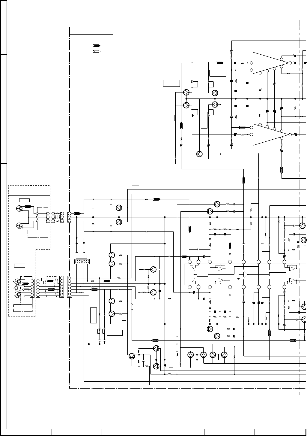
CD-C5H,CP-C5H
– 28 –
A
B
C
D
E
F
G
H
123456
Figure 28 SCHEMATIC DIAGRAM (3/17)
NOTES ON SCHEMATIC DIAGRAM can be found on page 20.
C128
3.3/50
C127
0.022
R138
6.8K R137
6.8K
C126
0.01
R130
6.8K
C122
1/50
C112
330P
C111
330P
C113
330P
12 3 4 5 6 7 8
1718192021222324
C121
1/50
C125
0.01
R129
6.8K
R109
10K
Q107
KTC3199 GR
C108
560P C107
560P
R112
15K
R111
15K
R105
3.3K
Q105
2SC1845 F
R103
2.2K
Q103
2SC1845 F
CNS102B
CNS102A
CNP102
CNS101A
CNS101B
CNP101
R193
1K
C169
0.0056
RD77
4.7K
C148
100/16
Q141
KRC104 M
RD70
10K Q142
KRC104 M
RD73
4.7K
Q143
KRC104 M
Q144
KRC104 M
C1
0.0
0
Q147
KRC107 M
Q1
5
KR
C179
0.0082
R196
1K
C180
0.0082
L102
6.8mH
C176
0.0056
C178
0.0068
Q
K
R
1
Q148
KRC1
R195
1K
L103
6.8mH R197
100
R191
1.5K
C177
0.0068
C115
47/25
C117
0.033 C119
560P
R121
100K
R125
5.6K
R123
3.9K
R131
220K
R119
56
C116
47/25
RD09
22K
CD11
1/50
CD06
330P
CD05
330P
LD02
6.8mH
L105
2.2µH
L106
2.2µH
CD08
330P
CD07
330P
LD01
6.8mH
RD78
4.7K
CD09
1/50 CD15
10/16
CD16
10/16
R140
100
R139
100
R141
1.0
C131
270P
R135
3.3K
C133
10/16
C175
0.0056
R192
1.5K
R198
100
R136
3.3K C132
270P
RD69
10K
R114
10K
Q111
KRC104 M
Q110
KRC104 M
R115
10K
R113
10K
R108
100K
R107
100K
R110
10K
Q108
KTC3199 GR
R118
1K C114
330P
C120
560P
C118
0.033
(Ra)
R122
100K R124
3.9K
R126
5.6K
R120
56
R132
220K
D101
1SS133
C168
0.01
C124
0.012
C109
0.022
Q109
KTA1266 GR
C101
270P
R102
1K
C104
270P Q102
KRC104 M
C102
270P
D102
1SS133
R101
1K
C103
270P
Q101
KRC104 M
RD75
47K
Q139
KRC104 M C167
0.01
R179
3.9K
C123
0.012
R127
5.6K
Q113
KRC104 M
CD21
47/25
RD04
1K
CD10
1/50
VRD01
22K(B)
CD52
1/50
RD72
6.8K
22K(B)
VRD02
QD07
KRC107 M
CD51
1/50
RD71
6.8K
QD06
KRC104 M
CD14
10/16 RD12
47K
RD13
10K
RD03
1K
RD14
10K
CD13
0.22/50
RD11
10K
CD17
10/16
RD01
1K
CD01
1/50
R134
68K
QD10
KRC107 M
QD09
KRC107 M
VRD04
22K(B)
VRD03
22K(B)
CD02
1/50 RD02
1K
ICD01 (1/2)
HA12134AF
DOLBY NR
RD10
10K
CD04
470P
CD03
470P CD12
0.22/50
CD18
10/16
R133
22K
RD16
1K
Q140
KRC104 M R180
3.9K
R128
5.6K
Q114
KRC104 M
C134
10/16
R104
2.2K
Q104
2SC1845 F
R106
3.3K
Q106
2SC1845 F
VR102
22K(B)
C106
330P
R190
10
VR101
22K(B)
C105
330P
R189
10
R117
1K
6
5
4
3
2
1
6
5
4
3
2
1
1
77
66
55
44
33
22
1
4321
1
11
333
22 2 2
13
QD08
KRC107 M
SWITCHING
SWITCHING
SWITCHING
SWITCHING
SWITCHING
REC
REC
REC
REC OUT
SPEED LO:L/HI:H
PB OUT
REC IN
TAPE PB:H/REC:L
+12V(A)
BIAS
GND(D)
NOR:H/CRO:L
SPEED LO:H/HI:L
Hi SPEED & NOR
Hi SPEED & CRO
HIGH=CRO
HI.SP
0V
0V
0
V
0.6V
0V
0.8V
0V
4.1V0.5V
0V0V
0V
0V
0
V
4
0
V
0V
0V
0V
0.6V
6.0V1.3V
0V
0V
0V 0V 0V
0V
0V
0V
4.0V
0V
0V
4.0V
0V
0V
0V
4.0V
0V
0V
0V
0V
3.8V
0V
0V
0.7V
0V
0V
0.7V
0V 0V
0V
0V
0V
0V
0V
4.0V0V
0V
0V
0V 0V
0V
0V
0V
0V
0V
0V
0V
0V 0V
0V
0V
0V
5.0V
5.0V
4.8V 0V 1.3V 0.2V
4.9V
5.0V
3.1V
3.1V
0V
0V
0V
0V
0V
5.0V
5.0V
0.9V 10.0V
1.3V 0.2V
4.9V
5.0V
3.1V
4.0V
0.7V
0V 0V
0.7V
0V
0V
8.7V
8.0V
8.7V
3.8V
0V
0V
4.1V
0.5V
0V
T1/T2
56K
+
56K
+
–
–
+
+
–
–112K
112K
HIGH=T1
TAPE MECHANISM
ASSEMBLY
TAPE2 HEAD
PWB
TAPE1 HEAD
PWB
ERASE
HEAD
R-CH L-CH
RECORD/
PLAYBACK HEAD
PLAYBACK
HEAD
R-CH L-CH
TAPE2
TAPE1
3
21
3
2
1
+B
+B
3
2
1
3
21
+B 3 2
1
32
1
+B
32
1
32
1
3
2
13
2
13
2
13
2
1
+B
+B
7
8
1
3
2
5
13
10
9
11
16
14
15
12
4
6
R148
220
ICD01(2/2)
MAIN PWB-B(2/4)
2
1
2
1
21
2
3
2
1
+B
3
21
3
21
3
21
+B
32
1
32
1
PLAYBACK SIGNAL
RECORD SIGNAL
TP490
L-CH BIAS
CURRENT
R-CH BIAS
CURRENT
TAPE2 PLAY
L-CH SENS.
TAPE2 PLAY
R-CH SENS.
TAPE1 PLAY
R-CH SENS.
TAPE1 PLAY
L-CH SENS.
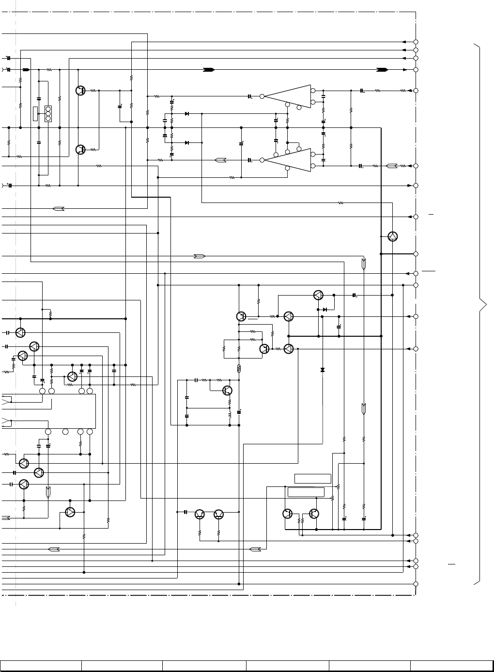
CD-C5H,CP-C5H
– 29 –
Figure 29 SCHEMATIC DIAGRAM (4/17)
78 9 10 11 12
9
10 11 12
13141516
R193
1K
C169
0.0056
RD77
4.7K
R154
10K R153
10K
R155
15K
R173
22K
C181
0.1/50
VR152
47K(B)
R156
15K
R174
22K
C182
0.1/50
RP101
POSISTOR
2.2
RD76
10K
R176
4.7K R171
3.3K
R169
10K
Q146
KRC104 M
Q131
KTC3199 GR Q132
KTC3199 GR
R158
220
R162
100K
R163
100K
R185 33
Q125
KTA1271 Y
R165
4.7K
Q127
KRC104 M
R164
4.7K
SWITCHING
Q124
KTA1271 Y
C162
0.047
(ML) R166
22K R167
47K
R168
4.7
BIAS OSC.
Q128
2SC2236 Y
C152
220/10
L104
330µH
R161
150
R160
150
R186
33
C141
47/25
R150
10K
R149
10K
R145
10K
C139
0.0033
Q149
KRC107 M
Q147
KRC107 M
Q153
KRC107 M
179
0082
C147
0.022
C140
0.0033
C142
47/25
R196
1K
C180
0.0082
C176
0.0056
C161
560P
78
068
Q154
KRC107 M
R152
10K
Q148
KRC107 M
Q150
KRC107 M
Q119
KRC104 M
1K
RD78
4.7K
CD15
10/16
R157
4.7K
C145
22/25 C146
220/10
C175
0.0056
R172
1K
VR151
47K(B)
Q122
KTC3199 GR
Q121
KTC3199 GR
CD46
10/50
RD39
100K
RD38
3.3K
RD06
10K
10K
RD05
RD08
2.2K
RD07
2.2K
QD02
2SC2878 A
P.B MUTING
QD01
2SC2878 A
RD42
4.7K
RD41
4.7K
RD37
270
CD45
47/25
CD32
2.2/50
CD31
2.2/50
RD24
2.2K
RD23
2.2K
RD44
220K
RD43
220K
RD15
270
CD34
150P
RD26
470
CD36
100/10
CD33
150P
CD35
100/10
RD25
470
CD42
22/25
RD28
68K
DD01
1SS133
DD02
1SS133
RD32
8.2K CD40
0.1/50
RD31
8.2K
CD39
0.1/50
RD29
1.2K
RD36
100
RD34
4.7K
RD33
4.7K
RD27
68K
CD43
0.01
CD44
0.01
RD30
1.2K
CD38
10/16
RD35
1M
CD41
22/25
CD37
10/16
CD20
150P
RD12
47K
RD13
10K
RD22
68K
RD21
68K
RD14
10K
RD11
10K
CD17
10/16
0
CD19
150P
CD18
10/16
3
1
2
13
21
25
18
17
19
20
14
15
26
27
31
29
28
30
23
24
16
SWITCHING
SWITCHING
C183
10/16
BEAT CUT
TA_PB-EQ H:NORM L:CrO
2
T2 CRO
BIAS
HI:H
EC:L
HI:L
TA_PB/REC H:PB L:REC
REC MUTE
GND(D)
D-PB/REC
D-ON/OFF
PB_MUTE H:ON L:OFF
NC
0V
0.6V
0V
0V
0V
10.7V
5.0V
10.8V 0V
0V
0V
3.2V
0V
0V
0V
0V
4.2V
0V
0V
8.0V
4.7V
0.8V
4.3V
0V
0V
0V
0V
0V
0V
4.0V
0V
3.2V
0V
4.2V
0V
0V
0V
0V
3.2V
0V
0V
0V
4.2V
0V
0V
4.0V
4.0V
9V
4.9V
0V
0V
0V
0.7V
0V
0V
0.7V
0V
0V
0V
0V
11.6V
11.7V
11.6V
0V
0V
0V
3.0V
0.6V
0V
5.0V
DOLBY ON/OFF
DOLBY PLAY/REC
PB.MUTE
T1/T2 H:T1 L:T2
56K
+
56K
+
–
–
GND
ALC
ALC
RIPPLE VCC
+12V(A)
PRE R-CH
REC R-CH
REC L-CH
PRE L-CH
8
4
7
9
11
6
10
12
23
5
1
1
6
C150
0.0082
(P.P)
TA_REC EQ H:CrO
2
L:NORM
T2 CrO
2
C151
0.039
(ML)
TA_BIAS H:ON L:OFF
GND(A)
HIGH_SP H:LOW L:HIGH
NOR/CRO
CRO(LO&HI)
NOR(HI)
NOR&CRO(LO)
ICD03 (1/2)
BA3311L
TO MAIN SECTION P26 1-G
ICD03 (2/2)
MUTING
+B
+B
32
1
3
2
1
3
2
1
3
21
+B
IC101
AN7345K
PLAYBACK&RECORD
/PLAYBACK AMP.
AN7345K
3
21
3
21
32
1
3
21
+B
SWITCHING
+B
+B
+B
3
2
1
SWITCHING
Q126
KRC104 M
32
1
+B
3
2
1
SWITCHING
QD03
KRC107 M
ICD03
BA3311L
REC./P.B.EQUALIZER AMP.
+B
+B
+B
0V
0V
0.7V
0V
0V
TP451
L-CH
GND
R-CH
R-CH REC/PLAY
SENS.
L-CH REC/PLAY
SENS.
0.7V
3
21C184
4.7/50
D104
1SS133
D103
1SS133
Q156
KRC107 M
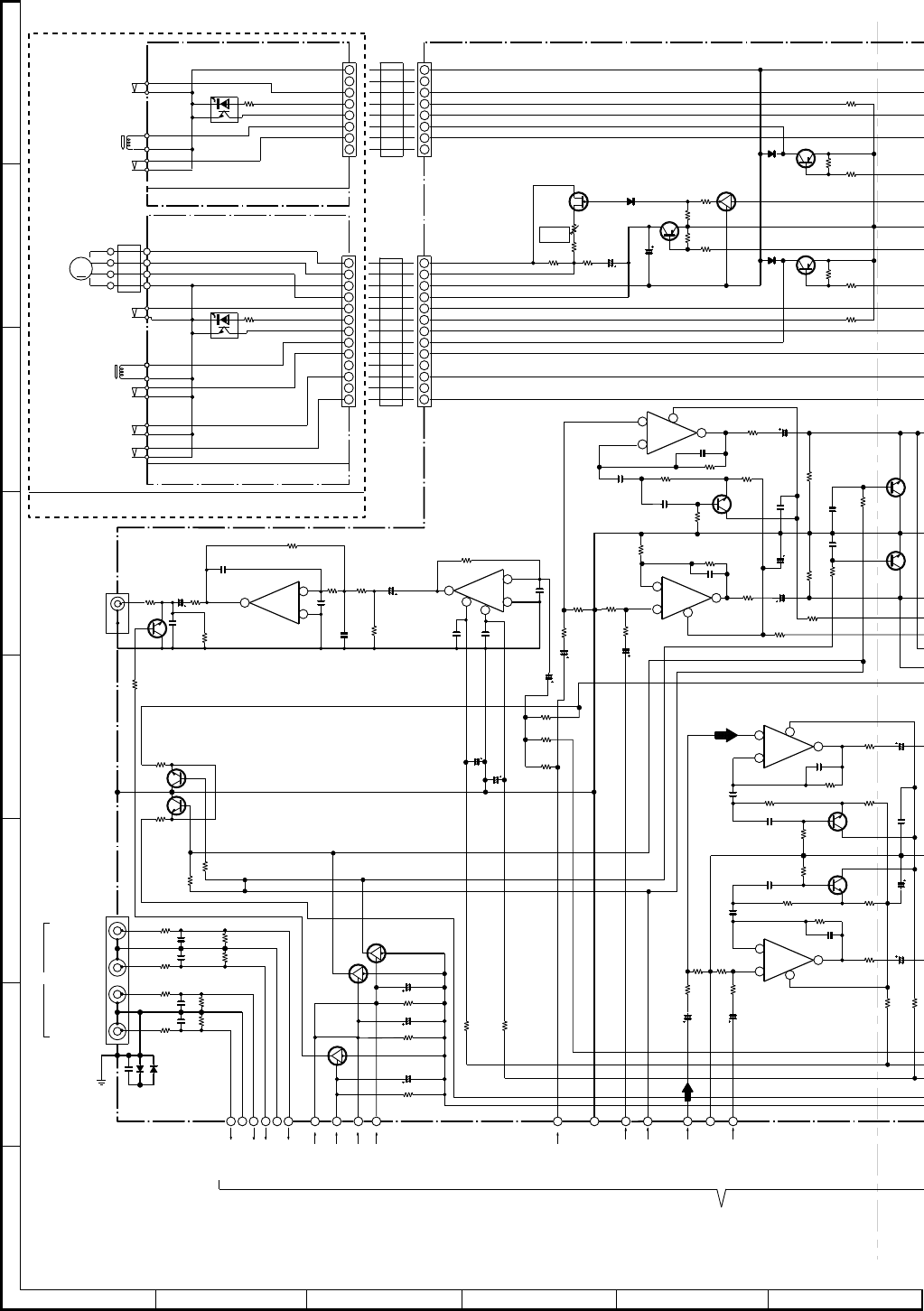
CD-C5H,CP-C5H
– 30 –
A
B
C
D
E
F
G
H
123456
Figure 30 SCHEMATIC DIAGRAM (5/17)
NOTES ON SCHEMATIC DIAGRAM can be found on page 20.
8
7
6
5
4
3
2
1
8
7
6
5
4
3
2
1
13
12
11
10
7
8
9
6
5
4
3
2
1
13
12
11
10
7
8
9
6
5
4
3
2
1
CP31
4.7/50
CP29
100P
RP29
1K
ICP02
(1/2)
6
5
7
8
–
+
ICP02
NJM4565M
LINE AMP.
WTM2 WTM1
DM03
1SS133
VRM01
47K(B)
RM02
22K
RM25
1K CM02
33/16
CM01
47/25
QM02
KTA1273 Y
MOTOR DRIVER
RM04
100K
RM05
10K
RM06
2.2K
RM03
47K
RM01
33K
RM12
2.2K
RM10
10K
DM02
1SS133
DRIVER
QM04
KTA1271 Y
RM11
2.2K
RM09
10K
DM01
1SS133
470
FWM2
FWM1
RM23
820
RM24
820
RT41 220
RT25 220
QT03
KRA107 M
RP06
2.2K
CP02
2.2/50
CP01
2.2/50
R942
1K
R941
1K
RP01
100K RP02
100K
RT09
2.2K
QT02
KTC3199 GR
QT01
KTC3199 GR
RT10
2.2K
CT05
0.022
DT02
1SS133
DT01
1SS133
QT04
KRA107 M
QT06
KRA107 M
CT19 4.7/50
CT20 4.7/50
CT21 4.7/50
RT27 47K
RT28 47K
RT26 47K
10.3V
0V
0V
0V
-11.5V
0V
0V
10.3V
0V
0V
0V
10.3V
0V
0V
QP08
KTC3199 GR
QP05
KTC3199 GR
QP07
KTC3199 GR
CT28
10/50
CT32
47/25
CT31
100/16
CP19
2.2/50
CP32
4.7/50
CP36
47/25
CP35
0.022
CP34
0.001
CP33
0.001
CP20
2.2/50
CT27
10/50
CT25
0.0056
CT35
47P
CT34
0.022
CT33
0.022
RT31
4.7K
RT38
47K
RT35
100K RP17
1K RP18
1K
RP34
5.6K
RP33
5.6K
RP32
47K
RP35
220
RP31
47K
RP22
56K
RP39
68K
RP19
100K RP20
100K
RP36 220
RP25 12K
RP26
12K
RP23
2.2K
RP30
1K
RP27
10K
RT36
47K
RT37
470K
RT34
47K
RT33
47K
RT30
100
RP44
5.6K
RP43
5.6K
RT32
1.8K
RT29
220K
CT26
0.0056
CT23
0.0022
CT24
10/50
RT39
47K
RT40
47K
ICT02
(1/2)
ICT02
(1/2)
CP18
47/25
RT08
2.2K
RT07
2.2K
RT04
2.2K
RT03
2.2K
CT04
390P
CT03
390P
CT02
390P
CT01
390P
RT06
27K
RT05
27K
RT01
27K
RT02
27K
RP15
CP13
4.7/50
CP14
4.7/50
RP16
220
RP37
68K
CP11
0.001
CP30
100P
CP27
0.33
CP25
0.12
RP07
1K
RP05
2.2K RP09
10K
QP01
KTC3199 GR
R947
12K
ICP01
(1/2)
ICP02
(2/2)
68K
RP38
CP12
0.001
RP08
1K
RP10
10K
R948
12K
QP02
KTC3199
GR
67686970 627271
42 45 43 44787980 818283
0.7V
0V
0V
0V
0V
0V
0V
0V
0V
0V
0V
0V
0V
0V
0V
-11.5V 10.3V
0.7V
3.0V
3.0V
3V
3V
3V
3V
0V
0.7V
SURROUND
SURROUND
MUTE
0V
0V
0V
10.3V
0V
0V 0V
-11.5V
470
CrO2
+SOL
NC
–COM
SENSOR OUT
+5V SENSOR
PLAY SW
MOTOR SPEED A
MOTOR SPEED B
NC
R_REC
F_REC
CrO2
+SOL
SENSOR OUT
+5V SENSOR
PLAY SW
–COM
+MTR
SENSOR OUT
+5V SENSOR
PLAY SW
CrO2
+SOL
NC
–COM
NC
R_REC
F_REC
CrO2
+SOL
SENSOR OUT
+5V SENSOR
PLAY SW
–COM
+MTR
MOTOR SPEED A
MOTOR SPEED B
VIDEO/AUX1
INPUT
TO MAIN SECTION
P27 12-B,8-H,11-H
JT03
SUPER
WOOFER
R-CH
L-CH
VIDEO/AUX2
INPUT
R-CH
L-CH
R-CH
L-CH
L-CH IN
R-CH IN
GND(A)
R-CH
L-CH
VIDEO-1
GND(A)
CP08
0.12
CP07
0.12
CP36
47P
CP10
0.33
1SRI
1SRI
SRS PASS
CP17
0.047(ML)
3
2
1
6
5
7
8
4
LINE
MUTE
S.W.
MUTE
REAR
MUTE
CENTER
MUTE
ICP01
(2/2)
GND(A)
R-CH
L-CH
VIDEO-1
GND(A)
CP09
0.33
–
+
3
2
4
1
–
+
+
–
A
B
M+
–
TAPE1 MECHANISM PWB-G
PHM1
SOL1
SOLENOID
TAPE1
CrO2
SWE2
TAPE1
PLAY
SWE1
1
6
5
7
48
–
+
3
2
1
–
+
ICT02
NJM4558MF
LINE AMP.
3
2
132
1
32
1+B
+B
–B
ICP01
NJM4565M
LOW BOOST AMP.
–B
–B
+B
–B
+B
+B
+B
DRIVER
QM03
KTA1271 Y
+B
12.2V
0.4V
0V
12.0V
0V
12.2V
10.6V
11.4V
0V
10.5V 12.2V
12.2V
12.2V0.4V
12.2V
SWITCHING
QM08
KRC104 M
D
S
G
TAPE
SPEED
DRIVER
QM01
2SK246 GR
+B
+B
TAPE MECHANISM ASSEMBLY
TAPE2 MECHANISM PWB-H
PHM2
TAPE2
SIDE B FP
SWE8
TAPE2
SIDE A FP
SWE7
TAPE2
CrO2
SWE5
SOL2
SOLENOID
TAPE2
PLAY
SWE4
TAPE
MOTOR
MM1
3
21
GND(A)
JT01
C-CH
IN S-CH
IN
QT05
2SC2878 A
S.W MUTE
C-CH
S-CH
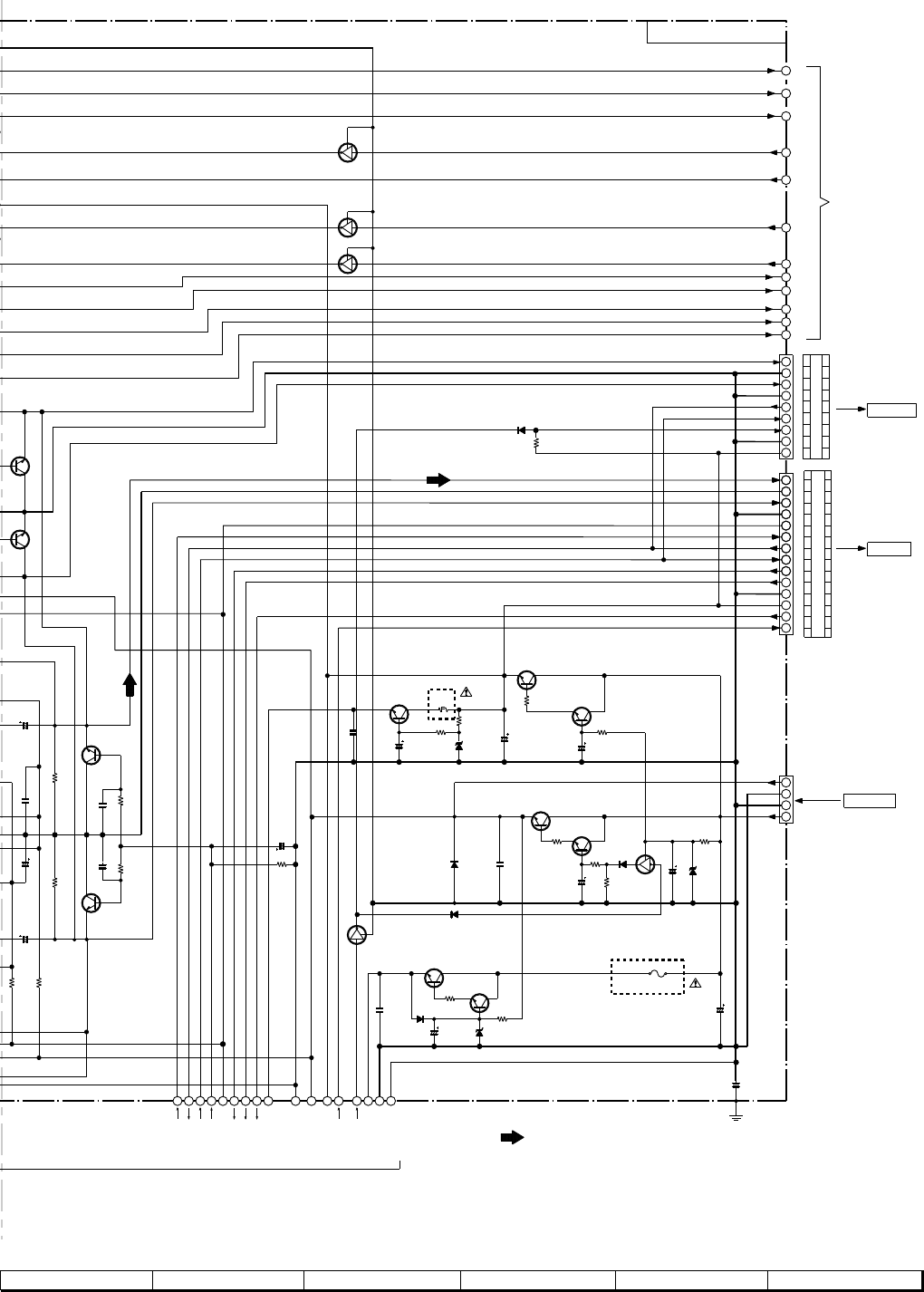
CD-C5H,CP-C5H
– 31 –
Figure 31 SCHEMATIC DIAGRAM (6/17)
78 9 10 11 12
9
8
7
6
5
4
3
2
1
GND
R-CH
L-CH
POSISTOR
RELAY
PROT
FUN CONT
–15V
GND(A)
9
8
7
6
5
4
3
2
1
GND
S-CH
C-CH
+12V(M)
GND(M)
STANDBY
RELAY
PROT
GND(A)
QM22
KRC104 M
QM21
KRC104 M
QM20
KRC104 M
4
CNP851
CFW852
C820
0.022
CP15
0.001
CP16
0.001
QP04
2SC2878 A
0V
0V
0V
0.7V
0V
0.7V
QP03
2SC2878 A
P
08
T
C3199 GR
9
9 GR
RP14
5.6K RP13
5.6K
Q828
KRC107 M
R831
22K
C832
22/25
C826
0.022
ZD821
MTZJ5.6A
R829
1.5K
R827
22
C827
47/25
Q825
2SD468 C
R828
100
R
P33
.
6K
CP18
47/25
D829
1SS133
R835
33K
R825
1K
Q826
KRA107 M
ZD820
MTZJ13B
D827
1SS133
D823
1SS133
RP12
47K RP11
47K
RP15
220
CP13
4.7/50
CP14
4.7/50
RP16
220
0
7
R
P09
1
0K
G
R
0
8
1
0
K
99
ZD822
MTZJ8.2C
C822
47/25 C833
47/25 R834
1K
Q827
KTC3199 GR
Q824
2SD2012
R826
560
C825
220/25
1SS133
D826
R822
560
C821
47/25
C823
0.022
Q822
2SD2012
C824
47/25
Q823
KTC3199 GR
C830
4700/25
F820
T500mA L 250V
Q820
2SD2012
R820
47
Q821
KTC3199 GR
C831
0.022
12
5
3
9
1
8
7
6
3233354753363834374041483946525450
4
3
2
1
14
13
12
11
10
9
8
7
6
5
4
3
2
1
11
2
10
4
SURROUND
MUTE
O
UND
D828
1SS133
+SOL
+MTR
+12V(M)
HIGH_SP
+SOL
CrO
2
SENSOR OUT
CrO
2
SENSOR OUT
GND(M)
PLAY SW
R_REC
C–CH
GND(A)
S–CH
F_REC
PLAY SW
+4.6V(D)
R-CH
L-CH
VOL SW
SP DET
+12V(M)
GND(M)
H/P SW
FW903 1
1
14
11
99
14
CD GND(D)
GND(M)
+12V(A)
SP DET
POSISTOR
H/P SW
RELAY
FUN CONT
PROT
–15V
VOL SW
POWER
POSISTOR
SP DET
–15V
GND(D)
+12V(A)
+12V(M)
RELAY
PROT
S-MUTE
H/P SW
FUN CONT
GND(D)
+4.6V(D)
S-MUTE
+12V(M)
+12V(A)
+7.3V(CD)
+7.3V(CD)
CD GND(D1)
GND(A)
CP17
0.047(ML)
R824
47
CD GND(D2)
GND
R823
47
R821
1K
T2_B-FP
T2_A-FP
T2_CROM
H:CrO
2
L:NORM
T2_RUN
T2_PLAY
T2_SOL
T1_SOL
T1_CROM
H:CrO
2
L:NOR
T1_RUN
T1_PLAY
TO MAIN SECTION
P26 1-F
–B –B
+B
+B
+B
19.3V
12.8V
4.7V
5.3V
10.5V 12.8V 19.3V
13.4V
11.6V 19.3V
12.3V 12.3V 19.3V
13.4V
13.5V
0.6V
12.8V
0V
0V
3.6V
7.1V 17.8V
7.8V 7.8V 17.8V
8.3V
12.1V
VOLTAGE REGULATOR
CFW903
TO POWER
AMP.PWB
P44 2-E
FROM POWER
SUPPLY PWB
P44 4-G
CFW853B
TO AMP PWB
P49 6-H
HIGH_SP
H:HIGHT
L:NOR
MOTOR
H:ON L:OFF
–B
+B
1
3
2
SWITCHING VOLTAGE
REGULATOR +B
CNS851
+B
3
21
SWITCHING
VOLTAGE REGULATOR
+B
VOLTAGE REGULATOR
STANDBY
MAIN PWB-B(3/4)
32
1
32
1
32
12.2V
12.2V
0V
0V
0V
0.3V
12.0V
0V
0V
1
+B
+B
+B
–B
+B
FM SIGNAL
FW853A
CFW853A
SWITCHING
SWITCHING
SWITCHING
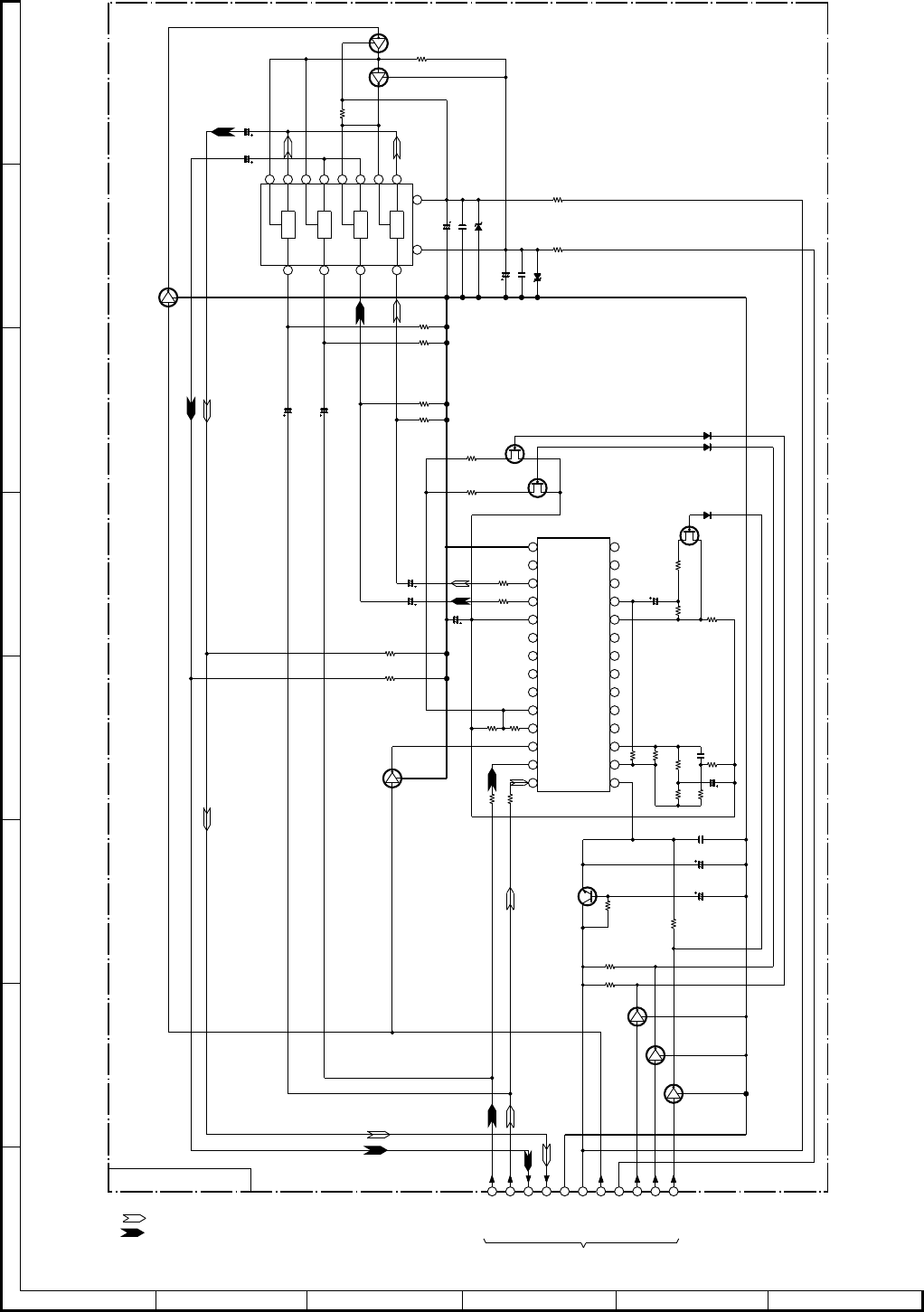
CD-C5H,CP-C5H
– 32 –
A
B
C
D
E
F
G
H
123456
Figure 32 SCHEMATIC DIAGRAM (7/17)
NOTES ON SCHEMATIC DIAGRAM can be found on page 20.
R466
1K
D401
1SS133
D402
1SS133
D403
1SS133
R493
1K
R498
4.7K
Q465
2SK246 GR
Q466
2SK246 GR
R491
1.5K
Q467
2SK246 GR
R492
4.7K
R488
4.7K
R465
1K
R468
1K
R469
1K
R487
100K
R490
4.7K
R484
1.5K
R480
47K
R479
22K
R481
3.9K
R483
100K
R482
33K
C461
0.0047
C454
2.2/50
C472
0.33/50
C460
0.47/50
IC451
SRS5250AS1
R475
2.2K
C458
0.047 (ML)
C457
100/16
C456
100/16
Q461
KTC3203 Y
Q460
KRC107 M
Q458
KRC107 M
R461
100K
C483
2.2/50
C484
2.2/50
R462
100K
Q451
KRA107 M
Q452
KRC107 M
ZD451
MTZJ8.2C
C486
0.022
C485
47/25
R455
100K
R459
100K
R460
100K
R456
100K
C482
2.2/50 C481
2.2/50
R467
680
R477
680
C488
0.022
C487
47/25 ZD452
MTZJ8.2C
Q463
KRC107 M
R470
10K
R474
10K
R473
10K
Q464
KRC107 M
C453
2.2/50
C471
100/16
R471
100K
R472
100K
56 57 58 59 60 61 62 55 63 64 65
17
6
28
27
26
25
24
23
22
21
20
19
18
16
15
13
11
14
12
10
9
8
7
5
4
3
2
1
5369
12 10 13
48
11
7
14
2
1
0V
0V
0V
0V
2.6V
0V
0V
0V
0V
0V
0V
-8.3V
0V
0V
1.6V
0V
1.6V 0V
0V
-8.3V
-8.3V
-8.3V
0V
0V
0V
0V
0V
2.6V
11.7V
11.7V
11.7V
0V
0V
0V
0V
0V
11.0V
0V
11.0V
11.6V
5.5V
5.5V
0V
5.5V
5.5V
5.5V
5.5V
5.5V
5.5V
11.0V
5.5V
5.5V
5.5V
5.5V
5.5V
5.5V
0V
5.5V
5.5V
5.5V
-8.3V
SWITCHING
SWITCHING
SWITCHING
SWITCHING
SWITCHING
SWITCHING
VOLTAGE
REGULATOR
Q459
KRC107 M
CR2
CR3
CR4
S_OUT
S_IN
C6
C5
C4
C3
C2
PN_IN
PN_OUT
L_IN
MODE
C_OUT
C_IN
CL4
VCC
C1
R_IN
CL3
CL2
CL1
Vref
L_OUT
R_OUT
CR1
GND
S
D
G
S
D
G
S
D
G
–15V
IN(L)
IN(R)
OUT(L)
OUT(R)
SRS INH
SRS B
SRS A
SRS PASS
+12V(A)
GND(A)
3
2
1
1
3
21
–B
+B
3
2
1
1
3
2
–B
+B
3
2
1
3
2
1
IC452
BU4066BC
SRS MODE
SELECTOR
TO MAIN SECTION
P27 12-C
MAIN PWB-B(4/4)
RECORD SIGNAL
PLAYBACK SIGNAL
+B
–B –B
+B
3
2
SRS
+B
+B
+B
+B
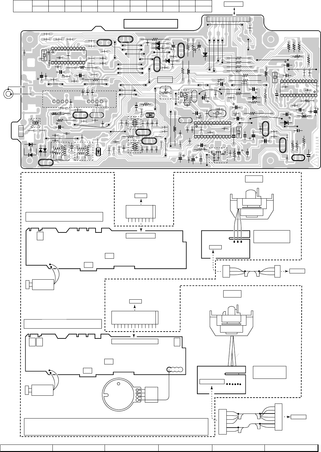
CD-C5H,CP-C5H
– 33 –
Figure 33 WIRING OF P.W.BOARD (3/9)
78 9 10 11 12
TUNER PWB-D
13 12345678
12345678
9101112
14
TAPE1 MECHANISM PWB-G
SOLENOID
SOL 2
13
FWM2
FROM MAIN PWB
P25 12-F
WTM2
FWM1
1
81
FROM MAIN PWB
P25 12-D
WTM1
TAPE MECHANISM ASSEMBLY
TAPE2 MECHANISM PWB-H
TAPE MOTOR
MM1
(300-3)
B
TAPE 2
RECORD/PLAYBACK/ERASE HEAD(300-1)
GY
GY WH
CNS102B
CNS102A
CNS101B
CNS101A
BK
PK
BL
BK
WH
YL
1
2
3
4
321
1
2
3
1
2
3
PK
BK
WH
PK
BK
WH
RD
BK
WH
5
6
7
6
5
4
3
2
1
654321
CNP102
TO MAIN PWB
P25 11-B
FLEXIBLE PWB
CNP101
TO MAIN PWB
P25 12-C
TAPE2
HEAD PWB
TAPE1
HEAD PWB
TAPE 1
PLAYBACK HEAD(300-2)
WH
BK
PK
BL
WH
YL
SOLENOID
SOL 1
SWE2
SWE8
SWE5
SWE7
A
SWE1
SWE4
PHM1
PHM2
BR
COLOR
TABLE
RD(R) OR YL GR BL VL GY WH(W) BK PK
BROWN RED ORANGE YELLOW GREEN BLUE VIOLET GRAY WHITE BLACK PINK
P25 12-B
Q371
Q362
C382
R374
C394
1
2
CF351
R370
RT30A
RT28A
CT29 CT22
RT35A
RT36A
RT37A
RT29A
RT26A
CT27A
CT28A
R367
C356
C355
XT21LT22
C370
R354
C375
RT49
RT48
RT51
RT52
RT53
RT54
C342
C354
C395
R385
R387
R384
CF352
T351
VR351
R395
L352
ZD351
C396
R392
R391
C391
Q361
ZD352
R383
Q360
D351
D352
R382
C384
C345
R345
R301
R336
C385
C386
R376
R360
R397
L351
C393
C397
C380
C392
IC302
C301
R380
R379
R381
C381
C387 R378
15
10 11
1215
20
22
R371
R372
R373
CNP301
C321
R349
L342
L341
C338
C323
C347
R369
C346
C322
C339 C333
D304
D303
D302
D301
T301
C331
C330
R331
CF301
R347 R348
R344
C328
C341
T302
VD301-1
R335
L353
T306
R334
R319
C332
C329
R337
R324
VD301-2
R323
C334
C335
C336
C337
T305
C324
C325
C327
C326
R333
R332
C373
C398
R355
R352
C352
CF302
R351
C361 C350
C344
C343
R358
C362
C363
C362
C364
C367
R350
C365
R356
L354
R359
C353
C399
C351
1510 12
1315
20
24
R353 C358
C357
R357 C369
ZDT21
CT25A
1234567
8
9
101112
151413 181716 212019 242322
C368
C374 C371
R361
Q353
R393
R368
D353
R377
CT26A
CT43
CT21A CT23A
CT24A
LT21
RT21
C302
CT36A
RT32A
RT34A
RT33A
Q354
C372
R362
R365
E
C
B
E
C
B
R366
CT37
ICT21
CNP303
1 234567 89
10 11 12
Q302
Q301
FE301
Q304
Q303
IC303
X351
R346
1 2 3
B C E
E C B 3 2 1
E C B
E C B
1
2
3
1
2
3
E
C
B
B C E
3 2 1
C366
75ohm
SO301
ANTENNA
TERMINAL
MW/LW
2345 178 6
FM MUTE
LEVEL
X352
B C E
QT21
TO MAIN PWB
CNP202
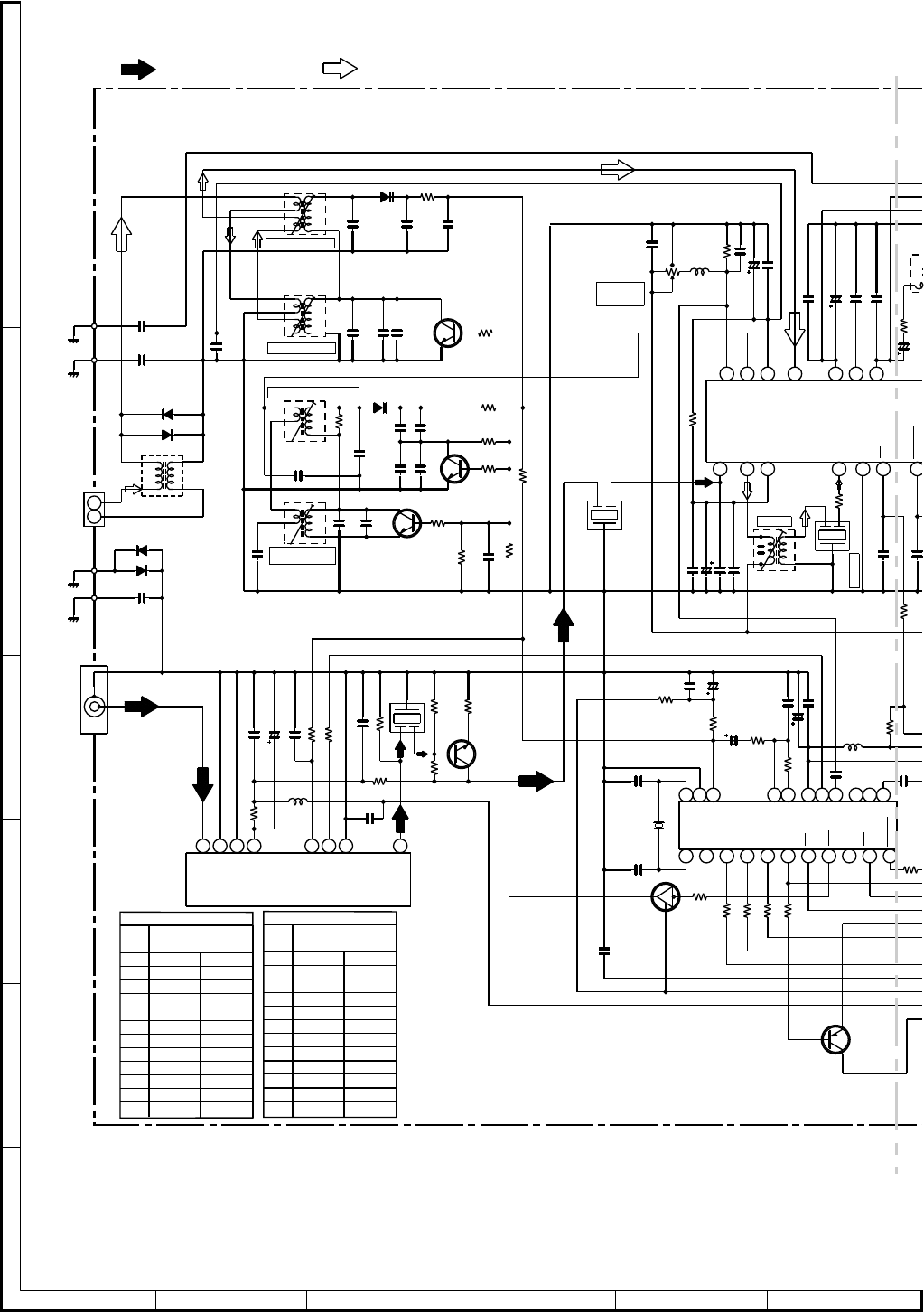
CD-C5H,CP-C5H
– 34 –
A
B
C
D
E
F
G
H
123456
Figure 34 SCHEMATIC DIAGRAM (8/17)
NOTES ON SCHEMATIC DIAGRAM can be found on page 20.
CNP301
MW/LW
R352
1K
L
F
C386
330P
C382
15P(CH)
C381
12P(CH)
X352
4.5MHz
C385
0.01
R377
47K
L351
100µH
C365 0.022
C364 10/16
VR351
10K(B)
R358
8.2K
C342
0.022
C351 0.022
C350 0.022
C352 10/16
L
F
M
FM
M
R351 5.6K
R372 1K
R374 1K
R371 1K
C354 0.022
CF351
C353
0.022
C363 0.022
C361 0.022
C366 0.001
D304
1SS133
C301
0.001
D303
1SS133
L341
BALUN
C344 33P
C362
3.3/50
C343
33P
Q362
KRA107 M
C393
1/50
R380
1.5K
R381
10K
R382
150
C394
47/16
SO301
ANTENNA
TERMINAL
C387
0.022
C392
0.001
R3
9
1
K
L353
1mH
C397
0.022
R346
330 R347
6.8K
C341
0.022
R348
680
C345 0.022
FE301
FM FRONTEND
R349
33
FM IF
CF301
C346 0.022
Q301
2SC380 O
FM IF AMP
C347 0.022
R345 4.7K
R344 470
C328
0.022
R335
100K
C325
220P
R334
5.6K
C334
18P(UJ)
R336
4.7K
R337
470
R324
100K
LW
OSCILLATION
T305
C324
27P(UJ)
R333
5.6K
MW OSCILLATION
T306
C336
470P
C335
18P(CH)
VD301-2
KV1236Z23F
R323
68K
Q303
KTC3199 GR
C327
680P
C326
18P(CH)
Q304
KTC3199 GR
C384
0.001
FM IF
CF302
LW ANTENNA
T301
C322
6.8P(CH)
C323
0.022
R331
5.6K
C330
10P(UJ)
MW ANTENNA
T302
C332
0.022
R319
100K
C331
0.047
VD301-1
KV1236Z23F
Q302
KTC3199 GR
D302
1SS133
D301
1SS133
AM IF
CF352
AM IF
T351
C337
0.022
R373 1K
C339
22P(CH)
IC302
LC72131
C338
0.001
R301 330
C329
33P
C302
0.001
C3
6
1/
5
R3
5
2.
7
R332
100K
R397
1K
C333
22P(CH)
L342
2.2
mm
H
R369
82
C321 100/16
Q371
KTA1266 GR
R37
6
1K
123 4
5
67
18
1920
21
22
23
24
123456789
10 11
1213
14
15
16
17
18
19
20
21
22
1234
5
6
7
8
1
2
L
R379
2.2K
C380
10/16
IC302
LC72131
PLL CONTROLLER
0V
0V
0V
(0.7V)
0V
0V 0V
(0.7V)
0V
0V
0V(0.7V)
0V
0V
0.8V
(9.2V)
(0V)
0V
(11.3V)
11.2V
(1.1V)
11.3V
4.8V
4.1V
0V
SWITCHING
S
ANT
GND
GND
GND
VT
VCC
IF OUT
F OUT
IF IN
X OUT
X IN
CE
DI
CL
DO
AM IN
FM IN
VDD
PD
AIN
AOUT
VSS
FM
MW
MO
/ST
ST IND
FM
NC
NC
NC
NC
FM IF IN
AM MIX OUT
AM OSC OUT
FM AFC
AM OSC IN
AM RF IN
AM LOW CUT
VSM
FM/AM OUT
STEREO
SD
GND
AM IF IN
REG
3
2
1
FM MUTE
LEVEL
3
2
1
3
2
1
+B
+B
+B
3
2
1
MW+B
MW/LW SIGNALFM SIGNAL
4.8V
3.6V
0.5V
0.3V
4.8V
4V
2.4V
0V
0V
0V
11.2V 0V
0V
9
8
7
6
5
4
3
2
1
11
10
PIN
NO. VOLTAGE
IC302
FM(ST) AM
11V
0V
2.4V
0V
2.1V
0.9V
4.8V
2.4V
0V
0.5V
0V
0V
0.9V
0.6V
2.4V
20
19
18
17
16
15
14
13
12
22
21
PIN
NO. VOLTAGE
IC302
FM(ST) AM
0.9V
FM(ST): OTHER
AM: ( )
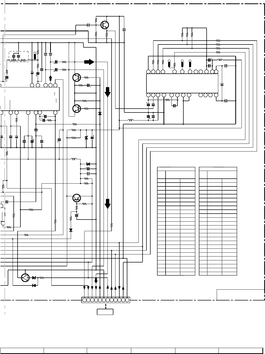
CD-C5H,CP-C5H
– 35 –
Figure 35 SCHEMATIC DIAGRAM (9/17)
78 9 10 11 12
5V(0V)
1.8(0V)
2.5V
(0V)
RT21
100K
RT54 1K
CNP303
LOW PASS
FILTER
C386
330P
47K
R366
10K
R368
33K
R365
10K
C375
3.3/50
R367
1K
Q353
KTC3199 GR
QT21
KTC3199 GR
Q354
KTC3199 GR
TUNER MUTE
X351
456kHz
R357 470K
R356
1K
C368
1/50
R353
270
IC303
LA1832
FM IF DET/
FM MPX./AM IF
L352
100µH
CT23A
10/16
ICT21
LC72720
RDS MICROCOMPUTER
C355
22P
C370
1/50
RT49
390
RT48
390
ZDT21
MTZJ4.3B
CT43
10/16
C357
2.2/50
R355
3.3K
C358
1/50
R354
4.7K
C356
0.001
C354 0.022
CF351
FM IF
0.022
C398
100/10
C399
0.022
RT32A
10K
RT33A
56K
CT37
0.022
RT34A
56K
C369 27P
C373
0.027
C374
0.027
R362
470
C372
1/50
R361
470
C371
1/50
D353
1SS133
R395
47K
R359
1.8K
R360
4.7K
ZD351
MTZJ4.7B
C396
100/10
C395
0.022
C391
47/16
R385
5.6K
Q360
KTA1266 GR
R384
5.6K
R383
5.6K
R392
390
R391 390
R393
1K
CT24A
0.022
CT25A
560P
XT21
4.332MHz
CT26A
22P
CT29
0.022
CT28A
47/10 LT22 2.2µH
1KRT28A
1KRT29A
1KRT30A
LT21
2.2µHCT21A
47/10
CT22
0.022
CT36A
0.022
R387
22K
Q361
KRC107 M
ZD352
MTZJ3.9B
D352
1SS133
D351
1SS133
RT26A
1K
CT27A
22P
C367
1/50
R350
2.7K
RT37A
220K
RT36A
220K
RT35A
220K
R370
1K
R378
82K
R376
1K
RT51 1K
RT52 1K
RT53 1K
123 4 56789
10 11 12
13
14
1516
17
18
19
20
21
22
23
24
1234
5
6
7
89
10
11
12
678910 11 12
13
14
15
16
17
8
11
1
2
L354
0V
0V
3.5V
(0V) (2.9V)
0V
0V 0.7V
(0V)
0V
0V 0.7V
(0V)
10.7V
(0V)
10.5V
(11.4V)
11.3V
FM/AM
SWITCHING
VOLTAGE
REGULATOR
TP
IF
IN
/ST
ST IND
FM/AM
OUT
MPX VCO
MPX IN
R-CH OUT
L-CH OUT
PHASE
(FM/AM)
PHASE
IF OUT
VCC
FM DET
STEREO
SD
MO/ST
VREF
FLOUT
VSSA
MPXIN
CIN
T1
T2
T3
T5
XOUT
VSSD
T7
SYNC
SYR
RDS-ID
DO
DI
CL
CE
VDDD
XIN
VDDA
T4
T6NC
NC
+B
+B
TUN MUTE
L-CH
R-CH
3
2
1
+B +B
+B
+B
+B
+B
+B
+B
MUTING
A GND
A+12V
SM
SD
DI
CE
TP
TPTP
DO
CLK
D GND
(CH)
(CH)
P26 1-E
CNP202
TO MAIN PWB
TUNER PWB-D
0.8V
0V
4.7V
2.6V
2.6V
0.8V
2.3V
2.1V
1.2V
3.5V
3.5V
3.5V
4.7V
4.8V
4.4V
0V
2.1V
4.7V
2.1V
2.1V
2.6V
3.64V
1.3V
2.0V
1.8V
3.2V
3.2V
0V
1.7V
1.1V
2.1V
9
8
7
6
5
4
3
2
1
24
23
22
21
20
19
18
17
16
15
14
13
12
11
10
PIN
NO. VOLTAGE
IC303
2.1V
2.1V
FM(ST) AM
0V
0V
0V
0V
0V
4V
0V
0V
0V
5V
2.6V
0V
0V
0V
0V
2.5V
2.5V
2.5V
2.5V
5V
0V
0V
2.4V
0V
0V
0V
0V
0V
0V
0V
0V
0V
0V
0V
0V
0V
0V
0V
9
8
7
6
5
4
3
2
1
24
23
22
21
20
19
18
17
16
15
14
13
12
11
10
PIN
NO. VOLTAGE
ICT21
0.3V
0.7V
0V
4.1V
4V
0V
0V
FM(ST) AM
0.3V
0V
0V
+B
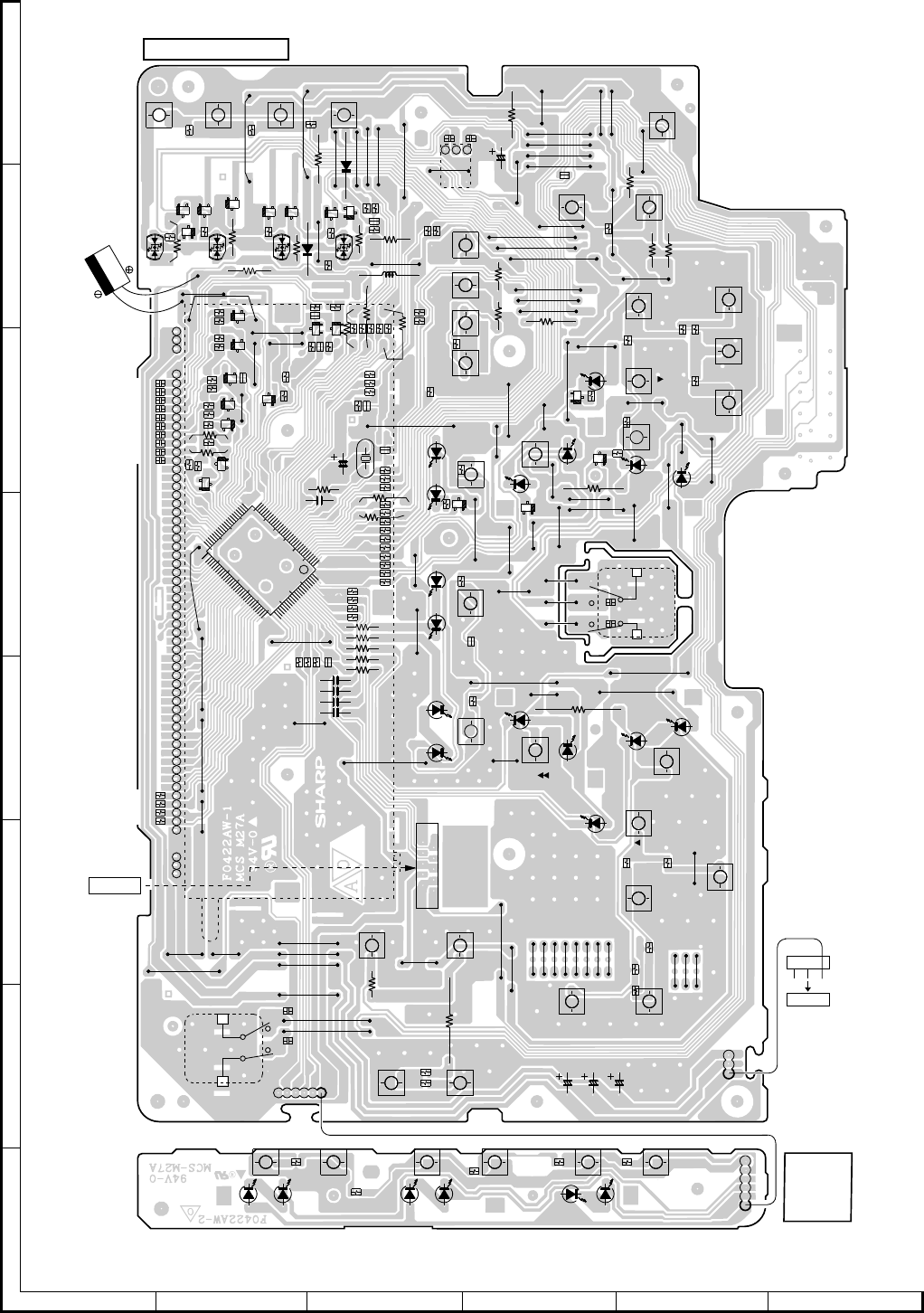
CD-C5H,CP-C5H
– 36 –
Figure 36 WIRING OF P.W.BOARD (4/9)
A
B
C
D
E
F
G
H
123456
SW702
JOG DIAL
3
3
1
1
6
7
8
9
64
59
58
57
56
55
54
53
52
51
50
49
48
47
46
45
44
43
42
41
40
39
38
37
36
35
34
33
32
31
30
29
28
27
26
25
24
23
22
21
20
19
18
17
16
15
14
13
12
11
10
2
2
RX701
REMOTE
CONTROL
SENSOR
31
1
100
5
10
15
20
25
30
35
50
51 55
60
65
70
75
8085
9095
40
45
61
97531
246
8
10
DISPLAY PWB-A1
FW853
WT853
TO POWER
SUPPLY PWB
6
1
CD
SWITCH
PWB-A2
P43 12-A
R786
R745
R741
LED714
SW718
SW715
VIRTUAL
SW714
Q-SOUND
LED720LED719
LED715
LED712LED713
R777
R776
R740
LED711
LED710
R785
Q715
R789
DOLBY
PRO LOGIC
R725
RY57
R742
SW716
R769
R767
R766
R765
RY56
R754
Q722
C709
C707
C708
R732R733
RY22
RY20
RY04
RY29
RY12
RY33
RY10
RY32
RY08
RY06
R768
R797
R755R756
R795
R792
R749
R799
R798
R751
Q718 Q719 Q720
Q721
Q723
Q717
R790
Q716
Q714
Q713
R720
R721
R722
R723
R730
R759
RY03
R757
Q712
R788
R746
R747
R748
R752
R753
R736
R735
R734
R728
C705
C706
R729
R772
R771
R770
R778
R779
R780
R781
R782
R783
R711
R710
R709
R712
R714
R715
R717 R719
RY14
RY34
RY16
RY35
RY38
Q711
RY37
Q710
RY36
RY18
Q709
Q708
Q707
Q706
Q705
Q704
R707
Q703
Q702
R784
R706
R724
RY41
RY40
R703
R702
R701
SW723
SW721
CLOCK
SW722
SLEEP
TIMER
SW713
C710
C711
LED708
LED707
LED701
LED702
LED703
LED705
C728
C729
C730
C702
X701
LED717
LED716
LED718
SW719
LED725
SW708
STOP
SW718
CD PAUSE
SW733
MEMORY/SET SW732
CLEAR
SW734
ON/
STAND-BY
SW725 SW724
LED724
LED726
LED709
SW707
F F
SW717
REWIND
SW720
REVERSE
PLAY
REVERSE
MODE
SW728
PROGRAMME TYPE/
TRAFFIC INFORMATION
SEARCH
SW731
SW730
APSM
DISPLAY
SW729
EON
SW726
LED706 LED704
SW739
DISC 3
OPEN/CLOSE
DISC 2
OPEN/CLOSE
DISC 1
OPEN/CLOSE
SW740
DISC3
SW741
SW742
DISC2
SW743
SW744
DISC1
SW703
SW704
X-BASS
EQUALIZER/
DEMO
SW727 TAPE 1/2 VIDEO/AUX
TUNER
(BAND)
CD
LED723
LED722
LED721
SW705
SW706
SRS PASS
SRS MODE
SW709 SW710
EDIT
NORMAL EDIT HIGH
SW711
SW712
DOOLBY- NR
RECORD/
PAUSE
FOWARD
PLAY
R796
D702
RY43
R44
RY42
L701
C701
R708
R737
R750
R793
R794 D701
R791
R760
R744
RY31
R731
R743
R758
R700
R716
R727
R726
C718
C717
C716
C715
R773
R774
R775
R713
R718
RY30
CNS701
FW701
FW701
SW701
VOLUME UP/DOWN
FL701
IC701
C741
C740
C739
C738
C737
C736
C735
C734
C733
C732
RY24
RY09
RY07
RY05
FROM MAIN PWB
CNP201
1
1
3
3
P25 12-F
C782
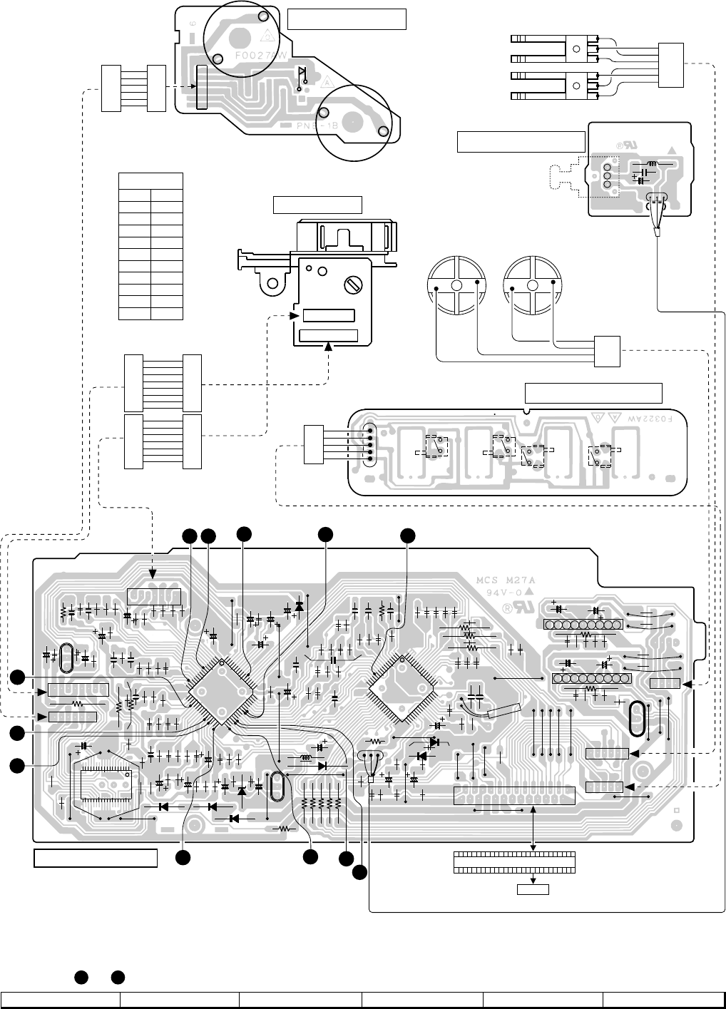
CD-C5H,CP-C5H
– 37 –
Figure 37 WIRING OF P.W.BOARD (5/9)
78 9 10 11 12
The numbers 1 to 12 are waveform numbers shown in page 50.
YL
OR
RD
BR
BIM1
TRAY MOTORMAIN CAM MOTOR
MOB2MOB1
1
4
3
2
CD MOTOR PWB-E
CD DIGITAL PWB-C4
BIM2
SWB107
SWB106
SWB108
CD SET
CD TRAY
CLOSE SWB105
5
1
CD IN
CD EJECT
TRAY SWITCH PWB-F
7654321
78 654321
PICK UP UNIT
SWB101 CAM1
SWB102 CAM2
SWB103
BIM3
CAM3
SWB104 CAM4
1
2
3
4
5
6
BR
RD
OR
YL
GY
BL
CD SERVO PWB-C3
+
-
+
-
M702
SW702A
SPINDLE MOTOR
SLED MOTOR
PICKUP IN
M701
CNP3A
1
2
3
4
5
6
1
2
3
4
5
6
1
2
3
4
5
6
BL
GY
WH
GY
WH
GY
5
4
3
2
1
YL
OR
RD
BR
BL
1
2
3
4
5
6
7
8
1
2
3
4
5
6
7
8
BK
GY
WH
GY
WH
GY
WH
GY
1
2
3
4
5
6
7
1
2
3
4
5
6
7
RD
GY
WH
GY
WH
GY
WH
CNS1B CNS1A
CNS2B CNS2A
C41
C42
XL1
1234
CNP11
IC81
IC82
C95
C96
L95
1
2
3
BI4B
IC95
13
BK
RD
WH
BK
WH
RD
13
C44
C49
C45
C27
R41
R47
R61
R62
R57
C48
C47
C46
C37
R60
C38
R55
R66
R64
R36
R46
R1
C2
R12 R9
R8
R10
C54
R31
R71
R72
R56
C23
R40
C24
R22
R24
R23
R18
R17
R73
C74
R34
R48
C73
R74
R2
R5
R4
R3
R7
R6
R33
R32
R30
R35
C16
R28
R29
C17
C21
R25
C14 R16
R14
R13
R52
R53
R44
R50
C83
C53
C56
R39
R42
R38
R43
C25
R45
C32
R27
R21
C13
R26
C10
R15
R80
R81
R82
C80
R85
R87
R86
C85
5V
48
32
64
33
17
16 1
164
48
49
32
33
17
16
Q51
C55
C6
C5
C9
C8
C11
C12
C28
C22
C26
C40
C39
Q52
C51
C52
C36
Q1
C3
C35
C7
C4
C31
C1
C71
C43
C19
C20
C72
C29
C33
C30
C34
C18
C81 C82
C87
C86
R58
R59
R63
C57
R37
ZD61
R19
R11
R89
R88
R20
R51
R49
R90
R91
R92
L61 D82
D51
D4
D3D2
D81
D1
R83
R84
IC3
IC2
IC1
123456
1
1
1
2
3
4
579
11 13 15 17 19 21 23 25 27
27
27
68
10 12 14 16 18 20 22 24 26
CFW1
CNP12
CNP13
CNP2
CNP3
CNP1
IC82
IC81
15
20
25
3035
40
45
50
55
60
5
10 15
20
25
3530
40
45
50
55
60
5
10
123456789
123456789
1
5
10
15
18
1920 25 30 35
36
1
1
2
2
3
3
4
4
5
5
6
67
123
45
67
8
E
C
B
E
C
B
23
4
5
1
7
8 9
6
11
10
12
3
2
1
12345
FW1
CFW2
TO MAIN PWB
P25 12-G
CNS3B CNS3A
CNS2
BR
COLOR TABLE
RD(R)
OR
YL
GR
BL
VL
GY
WH(W)
BK
PK
BROWN
RED
ORANGE
YELLOW
GREEN
BLUE
VIOLET
GRAY
WHITE
BLACK
PINK
IC95
CD DIGITAL
OUTPUT
R54
BI4A
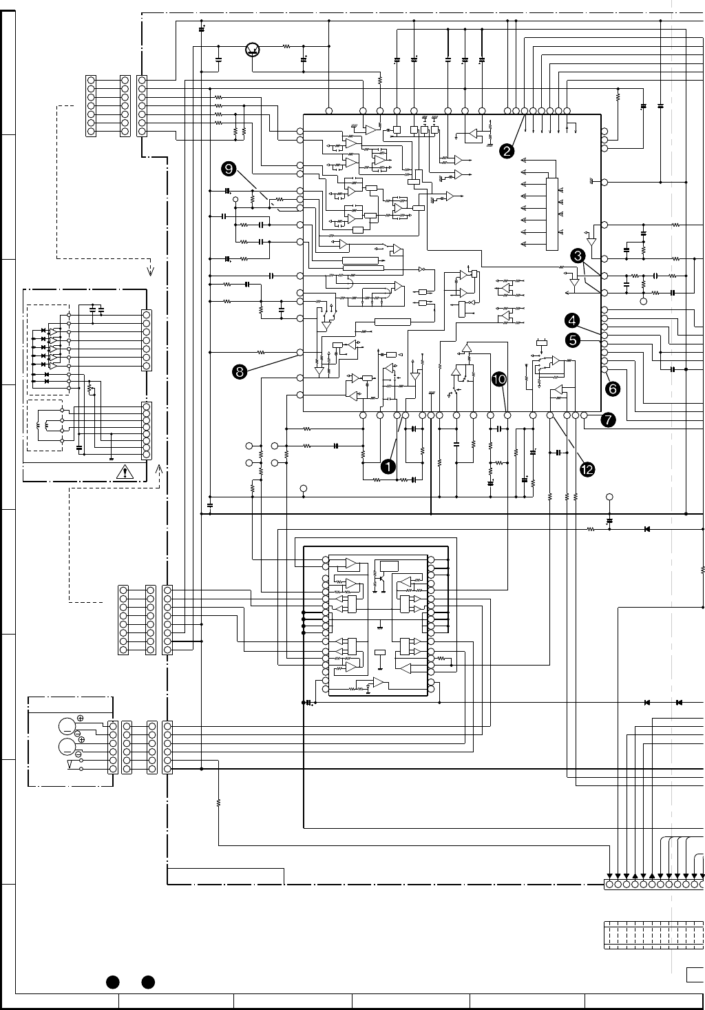
CD-C5H,CP-C5H
– 38 –
The numbers 1 to 12 are waveform numbers shown in page 50.
Figure 38 SCHEMATIC DIAGRAM (10/17)
NOTES ON SCHEMATIC DIAGRAM can be found on page 20.
A
B
C
D
E
F
G
H
123456
R20
1K
R22
22K
R21
22K
R19
1K
R24
47K
R23
10K
R25
1.5K C14
0.01
C13
330P C17
0.001
C9
0.047
C6
0.033
C5
0.033
R14
27K
R13
1K
R11
6.8K
R10
2.2K
R9
100K
R15
12K
C54
0.001
IC1
LA9241M
SERVO AMP.
Q1
KTA1266 GR
C2
0.01
CNP3
CNP2
C7
0.1/50 R12
100
R38
470 C23
0.0027
C25
27P R39
1K
R47
100K
C34
0.33/50
C33
0.47/50
C32
0.01
C31
220/6.3
C30
0.1/50
D1
1SS133
C21
0.0033
R36
220K
R35
220K
R34
22K R33
1.2K
R32
10K
C20
47/10
R29
56K
R30
6.8K
R31
1.2K
C18
0.47/50
R28
10K
C16
0.0047
R27
39K
R26
82K
R18
15K
R17
33K
C12
0.1
C11
0.1
R16
3.3K
C10
180P
C8
0.068
C36
100/10
R48
10K
FOCUS/TRACKING/
SPIN/SLIDE DRIVER
R37
82K
C35
1/50
R49
1K
R1
10
C3
1/50
C1
47/10
R6
82K
R7
82K
R2 68K
R3 82K
R4
82K
68K
R5
CNP1
R45
4.7K C28
0.1
C29
4.7/25
R8
15K
C4
0.1/50
C19
1/50
R41
47K
C24
2.2P R43
56K
R40
5.6K
R42
47K
R44
33K
C27
0.001
C26
0.033
M
M
6
5
4
3
2
6
5
4
3
2
6
5
4
3
2
6
5
4
3
2
11 1 1
888
777
666
555
444
333
222
111
7
6
5
4
3
2
1
8
7
6
5
4
3
2
1
66
77
55
44
33
22
111
5
3
2
6
7
4
D3
1N4004S
D2
1N4004S 1
N
C22
220P
R46
560
FSS
TBC
FSC
GEN
GEN
GEN
REF
CV-
JP–
JP+
CV+
JP
+
+
+
+
+
+
+
+
+
+
+
+
+
–
–
–
–
–
–
–
–
–
–
–
––
–
–
–
–
–
–
–
–
–
–
–
–
–
–
–
–
+
+
+
+
+
+
+
+
+
–
+
+
+
+
REF
REF
SLOF
SLOF
LATCH
P-ON RES
DAT
CLK
FEBAL
SHOCK;WCOMP
HIST.COMP
BAL
WCOMP
JP
REF
FOF
REF
REF
REF
REF
SPOF
REF
SLOF
OR
REF
RF
REF
REF
REF
FE1
VCR
HFL
DEF
REF
+
+
+
REF
+
CE
CL
SLOF
FSTA
TOSTA
FOSTA
8/12CM
LASER
2FREQ
RF
REF
REF
REF
REF
TO
REF
REF
REF
REF VCR
VCR
VCR
TGL1
THDL GL
THD
VCC
DRF
S.Q.R
PSTR
REF
TO
VCC1
SPI
JP
SPG
SP–
SPO
FD
FA–
FA
SP
THLD
TD–
TD
TO
TA
TH
TE
TE–
TB
F
E
FIN1
FIN2
LDS
LDO
BHI
PHI
LF2
SLI
VR
REFI
VCC2
DRF
CE
DAT
CL
CLK
DEF
DGND
SLC
RFS–
RFSM
CV+
CV–
SLOF
HFL
TES
TOFF
TGL
JP+
FE–
FE
FD–
AGND
SLEO
SLD
SL–
SL+
JP–
FSC
NC
VCC
CH1
CH2
CH4
CH3
TSD
–
+
–
+
–
+
–
+–
+
–
+
STAND
BY
IC3
M56748FP
46
47
48
49505152535455565758596061626364
45
VREF
8
9
7
6
10
11
12
13
4
3
2
1
5
SP+
SP–
SL+
SL–
TESI
SCI
HF
TE
1.5V 4.0V
3.4V
TRY_SW4
TRY_SW3
TRY_SW2
TRY_SW1
CAM_SW4
CAM SW3
COIN
PU-IN
DRF
WRQ
CQCK
SQ_OUT
2.0V
2.0V
PU-IN
0V
18 17 1
6
27 26 25 24 23 22 21 20 19
36
35
34
33
32
31
30
29
28
27
26
25
24
23
22
21
20
19
18
17
16
15
14
13
12
11
10
9
8
7
6
5
4
3
2
1
3.4V
GND
4.0V
2.0V
2.0V
2.0V
2.0V
2.0V
2.0V
2.0V
2.0V
2.0V
2.0V
2.0V
2.0V
2.0V
2.0V
2.0V
2.0V
2.0V
2.0V
2.0V
2.0V
2.0V
2.0V
2.0V
2.0V
0V
2.0V
2.0V
2.0V
2.0V
2.0V
0V
0V
4.0V
4.0V
0V
0V
4.0V
0V
0V
1.3V
2.0V
2.0V
2.0V
0V
2.0V
4.0V
4.0V
2.0V
1.9V
0.7V
1.8V
3.9V
3.9V
0V
0V
2.0V
0.7V
0V
14
16
15
44
43
42
41
40
39
38
37
36
35
34
33
32313029282726252423222120191817
+B+B
CD SERVO PWB-C3
1
1
CF
CNS3A
CNP3A
CD MOTOR PWB-E
M701
SPINDLE
MOTOR
M702
SLED
MOTOR
SW702A
PICKUP IN
CNS3B
CNS1A CNS1B
PICKUP UNIT
+
LASER DRIVER
+B
CNS2B
CNS2A
PD
GND
LD
VR
FO–
TR+
TR–
FO+
TR+
FO+
FO–
TR–
K
E
B
A
F
C
LD
MON
C
F
A
B
E
K
ACTUATOR
LD
VR
PD
GND
F+
F–
T+
T–
1
2.0V 0V
0V
V
2.0V
2.1V
2.1V
2.1V
0V
0V
0V
0V
2.1V
2.0V
2.0V
5.0V
0.7V
2.0V
2.0V
2.0V
2.0V
2.0V
2.1V
2.1V
0V
0V
0V
0V
2.1V
2.1V
2.0V
2.0V
0V
5.0V
0V
2.1V
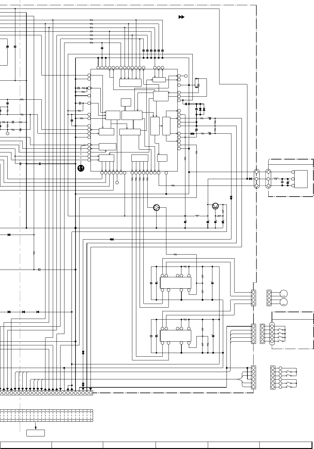
CD-C5H,CP-C5H
– 39 –
Figure 39 SCHEMATIC DIAGRAM (11/17)
78 9 10 11 12
L95
2.2µH
CD DIGITAL PWB-C4
IC95
GP1F38T
1
2
3
1
2
3
1
2
3
CD DIGITAL
OUTPUT
BI4A
BI4B
C55
3.3/16
(OS)
C51
100/10
C71
3.3/16
(OS)
C95
100/10
R71
2.7K
2.7K
R72
C72
3.3/16 (OS)
R38
470 C23
0.0027
C25
27P R39
1K
C53
0.022
C83
0.001
C56
0.022
R52
27K
L61
0.82µH
D81
1SS133
D51
1SS133
D82
1SS133
R73
680
R74
680
C43
100/10
R92 1K
R91 1K
R90 1K
R89 1K
R88 1K
C38
0.01
IC2
LC78622K
R53
1.2K
C40
0.047
C39
0.047 R50
680
C37
0.022
R47
100K
D1
1SS133
0
R60 1K
C28
0.1
C29
4.7/25
R41
47K
R43
56K
R40
5.6K
R42
47K
R44
33K
1
C26
0.033
6
5
4
3
2
6
5
4
3
2
1
5
4
3
2
1
4
3
2
11
1
6
5
4
3
2
1
4
3
2
5
4
3
2
1
5
4
3
2
1
C87
47/25 C82
47/25
R86
8.2K
R80
3.9K
C81
47/25
R83
1
R82
1M
R81
2.7K
C86
47/25
R84
1
R85
2.7K
CNP13
CNP12
CNP11
C96
0.022
C41
12P(CH)
C42
150P(CH)
XL1
16.934MHz
C57
0.001
D3
1N4004S
D2
1N4004S D4
1N4004S
R55
150
R54
330
R56
1K
Q52
KTC3203 Y
VOLTAGE
REGULATOR
R66
330
R64
22
ZD61
MTZJ4.7B
C52
100/10
R87
3.3K
C85
0.022 C80
0.022
Q51
KRC107 M
SWITCHING
DRIVER
C49 100P
C48 100P
C47 100P
C46 100P
C45 100P
C44 100P
R51 3.3M
C22
220P
R57 1K
R58 1K
R59 1K
R63 1K
R62 1K
R61 1K
DIGITAL
OUT
EXTERNAL
OUTPUT
SERVO
COMMAND
CLV
DIGITAL SERVO
TEST2
EFMIN
EFMO SLICE LEVEL
CONTROL
VCO CLOCK
OSC CONTROL
ERROR CORRECT
FLAG CONTROL
SYNC-DETECT
EFM DEMODULATE
4FS
DIGITAL
FILTER
1BIT
DAC
X-TAL
GENERATOR
SUB-CODE
µ-COM
INTERFACE
DEFI
XVDD
XIN
XOUT
XVSS
EFLG
SBSY
TA1
TEST1
PCCL
LVSS
TEST3
PDO
VSS
4M
16M
TST11
DOUT
C2F
EMPH
FSEQ
PCK
FSX
/RES
/CQCK
COIN
SQOUT
RWC
WRQ
SBCK
SFSY
PW
MUTEL
LVDD
RVDD
MUTER
RCHO
RVSS
LCHO
CONT5
CONT4
CONT1
CONT3
CONT2
FR
JP–
JP+
TGL
TOFF
CLV–
CLV+
V/P
HFL
TES
VDD
VVDD
ISET
VVSS
TEST4
TEST5
/CS
2K x8BIT
RAM
HF
GND(CD1)
GND(D)
TRY_SW4
TRY_SW3
TRY_SW2
TRY_SW1
CAM_SW4
CAM_SW3
CAM_SW2
CAM_SW1
COIN
WRQ
CQCK
SQ_OUT
RWC
SL+
SL–
RES
PCCL
+7.3V(CD)
GND(CD2)
+7.3V(CD)
987654321
18 17 16 15 14 13 12 11 1025 24 23 22 21 20 19
43
46
45
44
47
48
49505152535455565758596061626364
2.0V
0V
0V
1.8V
2
1
0V
38
11
10
13
12
16
15
14
9
8
7
6
5
4
3
37
36
35
33
32313029282726252423222120191817
34
39
41
40
42
0V
0V
2.0V
4.0V
0V
0V
4.0V
0V
2.2V
0V
4.0V
0V
0V
0V
0V
0V
0V
0V
4.0V
2.2V
0V
4.0V 7.2V
4.7V
0V
0V
7.2V
0V
4.0V
3.9V
1.7V
0V
0V
1.7V
3.9V
4.0V
4.0V
1.8V
1.8V
0V
0V
1.8V
2.0V
0V
0V
2.0V
0V
0V
0V
3.9V
3.9V
4.0V
0V
2.2V
1.8V
0V
0V
0V
4.0V
0V
0V
0V
0V
0V
4.0V
CD L-CH
GND(Au)
CD R-CH
CD SIGNAL
BIM3
+B
+B
8591
37 46 2
+B
+B
IC82
TA7291S
TRAY
MOTOR DRIVER
IC81
TA7291S
MAINCAM
MOTOR DRIVER
+B
+B
+B
3.1V
3.1V
0V
7.2V
7.2V
0V
0V
0V
7.2V
3.1V
3.1V
0V
7.2V
7.2V
0V
0V
0V
3.3V
27
27
TO MAIN PWB
P26 1-C
CFW2
FW1
CFW1
MOB2
TRAY MOTOR
CNS2
BIM1
MOB1
MAIN CAM MOTOR
3-TRAY MOTOR
CAM SWITCH
SWB104
CAM4
SWB103
CAM3
SWB102
CAM2
SWB101
CAM1
SWB108 CD SET
SWB107 CD IN
SWB106 CD TRAY
CLOSE
SWB105 CD EJECT
BIM2
TRAY SWITCH PWB-F
+B
+B
32
1+B
+B
+B
+B
+B +B
IC2
SERVO/SIGNAL
CONTROL
+B
+B
GND(D)
GND(D)
CAM SW4
CAM SW3
CAM SW2
CAM SW1
TRAY SW4
TRAY SW3
TRAY SW2
TRAY SW1
GND(D)
+
+
–
–
M
M
8591
37 46 2
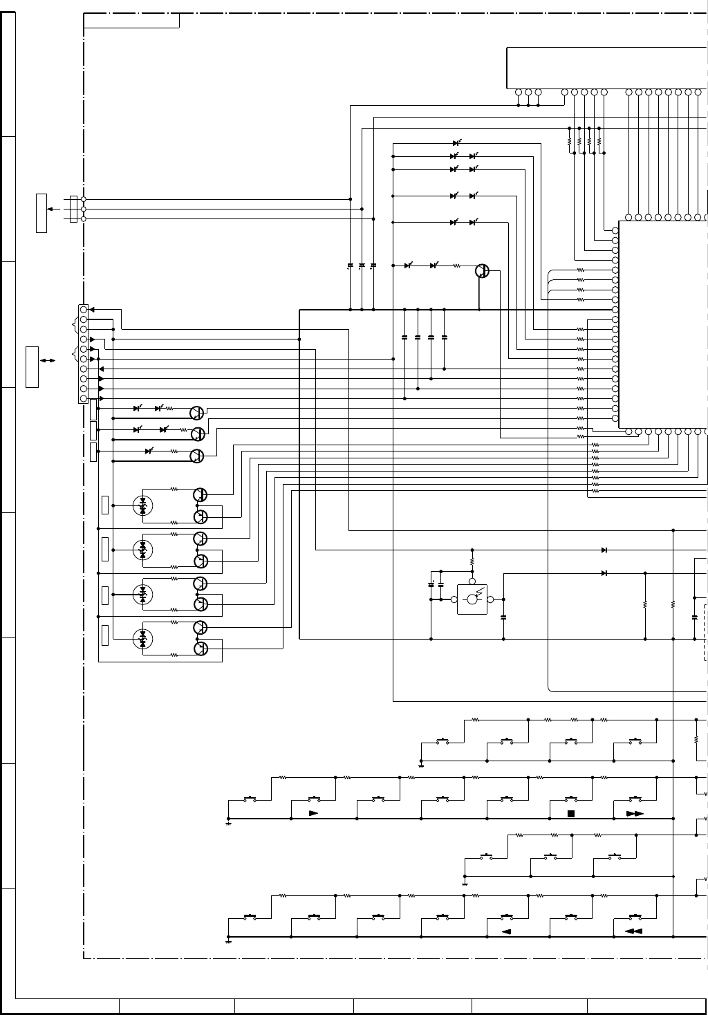
CD-C5H,CP-C5H
– 40 –
Figure 40 SCHEMATIC DIAGRAM (12/17)
A
B
C
D
E
F
G
H
123456
NOTES ON SCHEMATIC DIAGRAM can be found on page 20.
3.7V
0V
0.7V
SW707
SW704 SW703
C705
0.001
RY24 100K
RY09 100K
RY07 100K
RY05 100K
R
7
8.
2
RY44 10K
RY43 10K
RY42 10K
RY41 10K
RY40 10K
R703 10K
R702 10K
R701 10K
RY56
100K
D702
1SS133
C718
150P
C717
150P
C716
150P
C715
150P
LED707
333GTH4
LED709
333GTH4
LED708
333GTH2
LED726
333GTH4
LED710
333YTH2 LED711
333YTH2
LED712
333YTH2 LED713
333YTH2
LED720
333YTH2 LED719
333YTH2
LED725
333GTH2
LED718
333GTH4
LED716
333GTH4
LED717
333GTH4
LED714
333GTH2
LED715
333GTH2
R797
1K
Q723
KTA1504 Y
LED724
SPR325MV
R796
1K Q722
KTA1504 Y
R795
1K
Q721
KTA1504 Y
LED723
SPR325MV
R794
1K Q720
KTA1504 Y
R793
1K
Q719
KTA1504 Y
LED722
SPR325MV
R792
1K Q718
KTA1504 Y
R791
1K
Q717
KTA1504 Y
LED721
SPR325MV R790 1K
Q716
KTA1504 Y
R788 1K
Q714
KTC3875 GR
R787 680
R786
680
Q713 KTC3875 GR
Q712 KTC3875 GR
C709
150P
RX701
REMOTE CONTROL
SENSOR
C711
0.022
C710
220/6.3
R700
39
RY03
100K
R720
D701
1N4004S
R727
1.2K
R728
1.8K
R729
2.2K
R749
5.6K R748
3.9K R747
2.2K
R746
1.8K
R745
1.2K R744
1K
R736
5.6K R735
3.9K R734
2.2K R733
1.8K R732
1.2K R731
1K
R726
1K
R774 680
R775 680
R776 680
R777 680
R773 1K
R772 820
R771 820
R770 820
R789
680
R784 1K
R785 1K
R783 1K
R782 1K
R781 1K
R780 1K
R779 1K
R778 1K
SW706 SW705
SW714
R740
2.2K
R741
1.8K
R742
2.2K
SW716 SW715
C728
1/50
C729
1/50
C730
1/50
R
7
8.
2
R730
8.2K
R737
8.2K
SW723 SW722 SW721 SW720 SW719 SW718 SW717
SW713 SW712 SW711 SW710 SW709 SW708
10
9
8
7
6
5
4
3
2
1
31
2
Q715
KTC3875 GR
1
F1
11.4V
0.5V
11.5V
11.5V
0.5V
0.5V
11.4V
0.4V
0.7V
0.7V
2.0V
3.8V
0V
0V
0.6V
0.6V
0.6V
0.6V
0V
4.0V
-32.5V
-36.5V
-36.6V
-32.5V
0.5V
0.5V
0.5V
0.5V
0V
SCK1
SO0
SI0
SCK0
SO1
P16
SI1
P36
P35
P34
P33
P32
P31
P30
P17
CD ON
TUNER
PAUSEREWREV
CD
S47
S43
S44
S45
S46
PG0
PG1
PG2
PG3
P00
P01
P02
P03
VSS2
VDD2
P04
P05
P06
P07
VDD4
S40
S41
S42
4.0V
-32.5V
-32.5V
-32.6V
-32.4V
-32.5V
-36.6V
-36.6V
-36.6V
EDIT NORMAL
FL D
R
STB
SCK1
COM1
DATA1
RESET
–38(VP)
VF1
VF2
TUNER OFF
TUNER ON
TAPE OFF
TAPE ON
CD ON
CD OFF
FF
Q-SOUND
VIRTUAL
PRO LOGIC
STOP
F-PLAY
VIDEO OFF
VIDEO ON
TAPE OFF
TAPE ON
TUNER ON
TUNER OFF
CD OFF
TAPEVIDEO
D
64 63 62 59 58 57 56 55 54 53 52 51 50 49 48 47
REW
REV
GND(D)
+12V(M)
+4.6V(D)
REV
REW
PAUSE
STROBE
S30
S31
S37
S36
S35
S34
S33
S32
S41
S40
S38
S39
F1
S41
S40
S39
S38
VDD
S37
S36
S35
S34
S33
S32
S31
S30
F1
K
E
K
E
100
K
E
KE
REVERSE MODE CD PAUSE
RECORD/PAUSE EDIT HIGH
F-PLAY
FF
STOP
DISC3
DISC2
DISC1
SCK1
COM1
DATA1
VDD
VSS
99
98
97
96
95
94
93
92
91
90
89
88
87
86
85
84
83
82
81
80 79 78 77 76 75 74 73 7
2
9
8765432
CNP201
P26 1-A
+B
+B
+B
+B
+B
+B
+B
DISPLAY PWB-A1
1
+B
EQUALIZER/DEMO
+B
0.7V
3.7V 0.7V
0.2V
10.6V
0V
0V
0V
0V
0V
11.6V
12.1V
12.1V
12.1V
12.1V
12.1V
12.1V
12.1V
12.1V
12.1V
12.1V
12.1V
12.1V
11.3V
11.3V
11.3V
11.3V
11.6V
11.6V
0V
3.9V
4.6V
11.6V
0V
0V
3.7V
CNS701
WT853
TO POWER
SUPPLY PWB
33
1
FW853
P44 5-G
TO MAIN PWB
DOLBY-NR FORWARD PLAY STOP FF
X-BASS
SRS MODE
SRS PASS
Q-SOUND
VIRTUAL
DOLBY PRO LOGIC
SLEEP TIMER CLOCK REVERSE PLAY REWIND
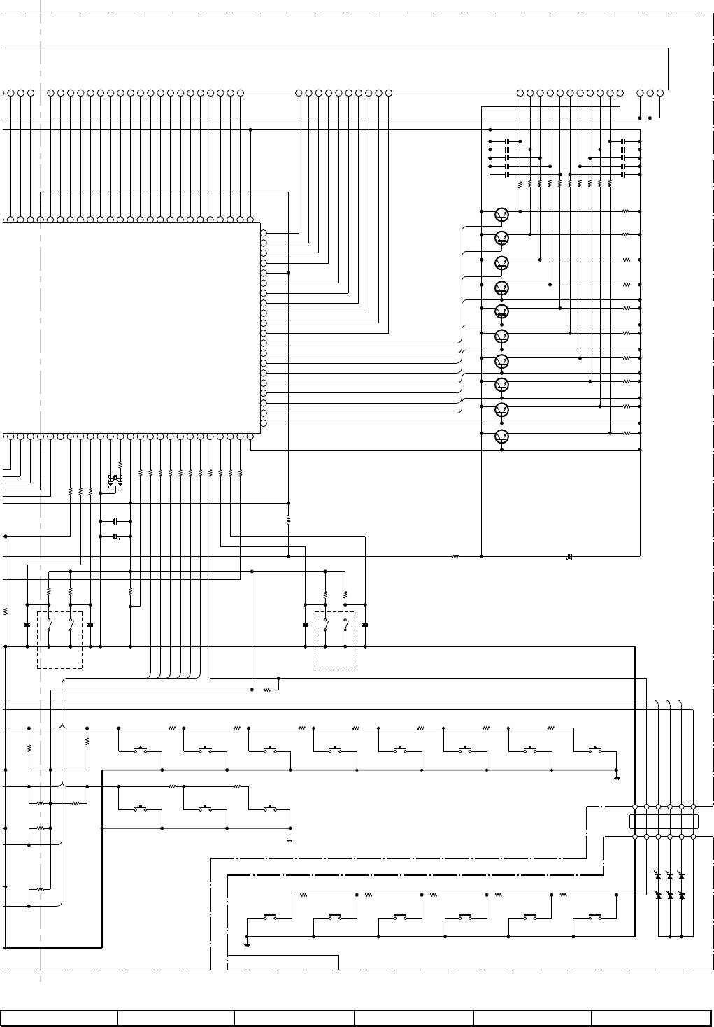
CD-C5H,CP-C5H
– 41 –
Figure 41 SCHEMATIC DIAGRAM (13/17)
78 9 10 11 12
SW702
JOG DIAL
C708
0.001
C707
0.001
LED703
333GTH4
LED705
333GTH4
LED706
333GTH4
LED704
333GTH4
LED702
333GTH4
SW744 SW743 SW742 SW741 SW740 SW739
C705
0.001
SW701
VOLUME
UP/DOWN
C706
0.001
L701
2.2µH
X701
R725
8.2K
R758
8.2K
R750
8.2K
RY30 33
RY31 33
RY32 33
RY33 33
RY34 33
RY35 33
RY36 33
RY37 33
RY38 33
RY29 33
C736 220P
C735 220P
C734 220P
C733 220P
C732 220P
C737 220P
C738 220P
C739 220P
C740 220P
C741 220P
RY20 100K
RY18 100K
RY16 100K
RY14 100K
RY12 100K
RY10 100K
RY08 100K
RY04 100K
RY06 100K
Q710
KTC3875 GR
Q709
KTC3875 GR
Q708
KTC3875 GR
Q707
KTC3875 GR
Q706
KTC3875 GR
Q705
KTC3875 GR
Q704
KTC3875 GR
Q703
KTC3875 GR
Q702
KTC3875 GR
RY22 100K
RY57 39
Q711
KTC3875 GR
R798
8.2K
R719 1K
3
K
R721
10K
R720
10K
R799
8.2K
R723
10K
R722
10K
FL701
FL DISPLAY
R724 1K
R760
1.2K
R759
1K
R753
1.8K
R752
1.2K
R751
1K
R769
3.9K R768
2.2K R767
1.8K R766
1.2K R765
1K
R706 1K
R707
1K
R708
820
R709 1K
R717 1K
R711 1K
R712 1K
R718 1K
R716 1K
R715 1K
R713 1K
R714 1K
R710 1K
LED701
333GTH4
C701
0.022
C702
100/10
C782
47/50
R743
8.2K
R730
8.2K
R737
8.2K
SW734
SW733SW732
SW727
R754 2.2K
SW728
R755 3.9K
SW729
R756 5.6K
SW730
R757 12K
SW731
SW726
SW725SW724
4.19MHz
S1
S6
S5
S4
S2
S3
S0
3.4V
4.0V
4.0V
4.0V
4.0V
4.0V
4.0V
4.0V
4.0V
4.0V
4.0V
4.0V
1.9V
1.7V
0V
3.9V
3.9V
3.9V
0.4V
0.5V
11.4V
0.5V
11.5V
11.5V
0.5V
INT3
INT2
INT1
AN7
AN6
AN5
AN4
AN3
AN2
AN1
AN0
VDD1
CF2
CF1
VSS1
P75
P74
/RES
INT0
P37
P36
P35
P34
P33
S26
S27
S28
S29
S30
S31
S32
S33
S34
S35
S36
S37
S38
S39
VDD4
S40
S41
S42
S25
S24
S23
S22
S21
S20
-36.9V
-27.4V
-36.4V
0V
-28.2V
-28.2V
-28.4V
-12.2V
-16.0V
-32.1V
-32.1V
-36.4V
-36.4V
-32.2V
-36.6V
-36.6V
-36.6V
-36.6V
-32.5V
-32.5V
-32.5V
4.0V
-32.5V
-32.5V
-32.6V
VP
VDD3
S7
S8
S9
S10
S11
S12
S13
S14
S15
S16
S17
S18
S19
6G
7G
IC701
IX0209AW
FL DRIVER & CONTROLLER
10G
1G
2.9V
2.9V
2.9V
2.9V
2.9V
2.9V
2.9V
2.9V
2.9V
2.9V
-33.1V
-19.8V
-19.8V
28.1V
-36.4V
4.0V
-36.4V
-36.4V
-16.0V
-24.0V
-36.4V
-1.5V
-33.1V
-33.1V
-33.1V
-33.1V
-33.1V
-33.1V
-33.1V
-33.1V
-33.1V
-33.1V
-33.1V
-33.1V
-33.1V
-33.1V
-33.1V
-33.1V
-33.1V
-33.1V
-33.1V
-33.1V
-33.1V
-33.1V
-33.1V
-33.1V
-33.1V
-33.1V
-33.1V
-33.1V
-33.1V
2G
3G
4G
5G
8G
9G
F
TUNER ON
TAPE OFF
TAPE ON
VIDEO ON
VIDEO OFF
DISC3
DISC1
DISC3
DISC1
H
0494847 46 45 44 43 42 41 40 39 38 37 36 35 34 33 32 31 30 29 28 27 26 25 24 23 22 21 20 19 18 17
9876
13 12 11 1016 15 14
321
S0
S0
10G
9G
3G
4G
5G
6G
7G
8G
2G
1G
10G
9G
3G
4G
5G
6G
7G
8G
2G
1G
S5
S4
S3
S2
S1
S9
S8
S7
S6
S23
S29
S28
S27
S26
S25
S24
S22
S21
S20
S19
S18
S17
S16
S15
S14
S13
S12
S11
S10
S30
S31
S33
S32
VDD
S23
S32
S31
S30
S29
S28
S27
S26
S25
S24
S22
S21
S20
S19
S18
S17
S16
S15
S14
S13
S12
S11
S10
S9
S8
S7
S6
S5
S4
S3
S2
S1
RESET
+12V
KEY7
KEY4
KEY3
VOL JOG UP
DISC 1
OPEN/CLOSE DISC 2
OPEN/CLOSE DISC 3
OPEN/CLOSE
KEY7
KEY6
KEY5KEY2
KEY1
KEY7
KEY6
KEY5
KEY3
KEY2
KEY1
KEY0
GND
DISC2
DISC2 F2
F2
F2
KEY4
VOL JOG DOWN
XCIN
XCOUT
–29(VP)
VDD
JOG UP
JOG DOWN
VSS
VDD
REMOCON
675747372717069686766656463626160595857565554535251
50
49
48
47
46
45
44
43
42
41
40
39
38
37
36
35
34
33
32
31
302928272625242322
2120191816 17151413121110
98765
CD SWITCH PWB-A2
+B
+B
+B
FW701
61
61
ON/
STAND-BY
+B
+B +B
+B
+B
+B
+B
+B
VIDEO/AUX TAPE 1/2 TUNER
(BAND) CD RDS RDS
EON RDS
DISPLAY RDS
ASPM
MEMORY/SET
CLEAR
DISC 1 DISC 2 DISC 3
PROGRAMME TYPE/
TRAFFIC INFORMATION
SEARCH
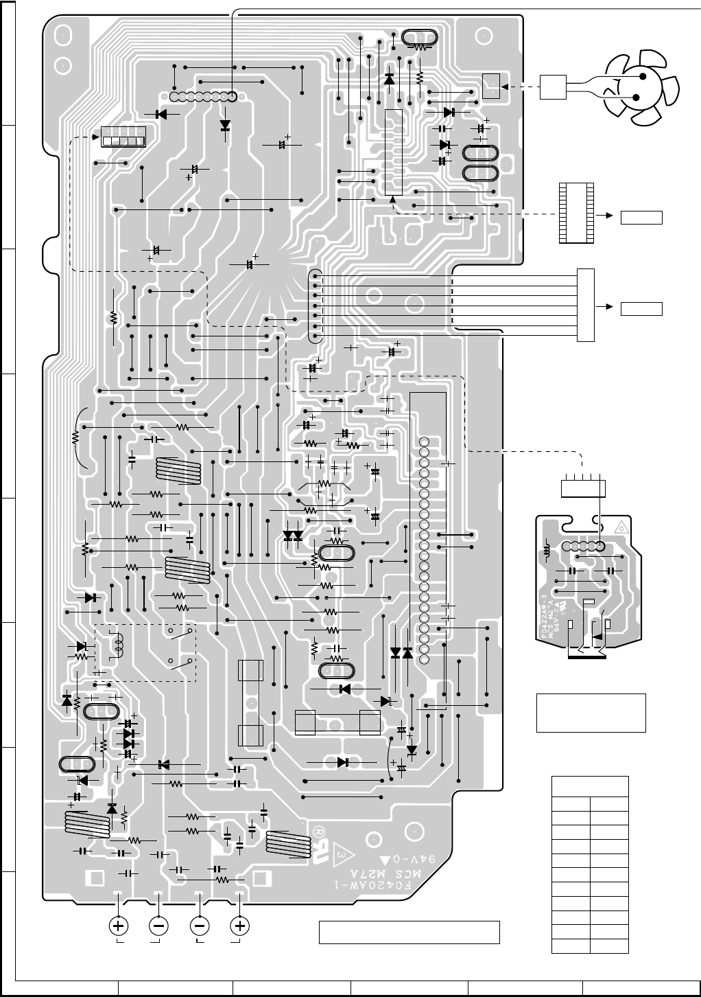
CD-C5H,CP-C5H
– 42 –
A
B
C
D
E
F
G
H
123456
Figure 42 WIRING OF P.W.BOARD (6/9)
2
1
1
3
5
7
9
11
13
2
4
6
8
10
12
14
2
1
E C B
E C B
E C B
E C B
E C B
B C E
B C E
2
3
4
5
1
7
8
9
6
12
13
14
15
11
17
18
19
10
16
22
21
20
1
14
1
14
FW903
L-CH R-CH
SO901
FRONT SPEAKER TERMINALS
C938 C937
L903
FW901
1
5
J901
HEADPHONES
HEADPHONE
PWB-A3
POWER AMP. PWB-C1
BR
COLOR TABLE
RD(R)
OR
YL
GR
BL
VL
GY
WH(W)
BK
PK
BROWN
RED
ORANGE
YELLOW
GREEN
BLUE
VIOLET
GRAY
WHITE
BLACK
PINK
T4A L 250V
F901
T4A L 250V
F902
7
6
5
4
3
2
1
GY
WH
GY
WH
GY
WH
RD
CNS905
BI9057
1
R907
R908
C914
R912
R911
C913
R909
R910
C912
C911
R973
R998
R977
R995 R974
R988
R987
R979
Q998
C984
C983
Q995
Q994 C988
C907
C908
Q904
C917
Q903
C918
C929 C931
C933
C998 C934C999
C925
C927
C928
C930
C932
C926
Q999
C989
C990 C997
Q997
C970
C923 C921
C924
C922
C936
C935
R975
D993
ZD904
D995
R976
D997
D996
R940
D901
D902
R919
R939
ZD999
D907
D908
R997
R996
D998
ZD901
R991
D999
R928
R927
R925
R931
R999
R930
R932
R929
R926
R990
R992
R989
R994
ZD903
R920
R978
ZD998
R913
R914
CNP901 CNS901
C994
C991
R923
R924
R921
R922
CFW903
WT902
C986
FW904
8
C995
IC901
C985
C996
R985
RL901
R933
R934
L902
L901
L911
L912
D905
D906
D910
D909
C992
1
5
4
3
WH
RD
CFW852
TO MAIN PWB
M901
FAN MOTOR
2
1
P25 12-A
CNP905
TO AMP PWB
P48 7-C
51
R972
R993
D912
R915
R971
D911
R916
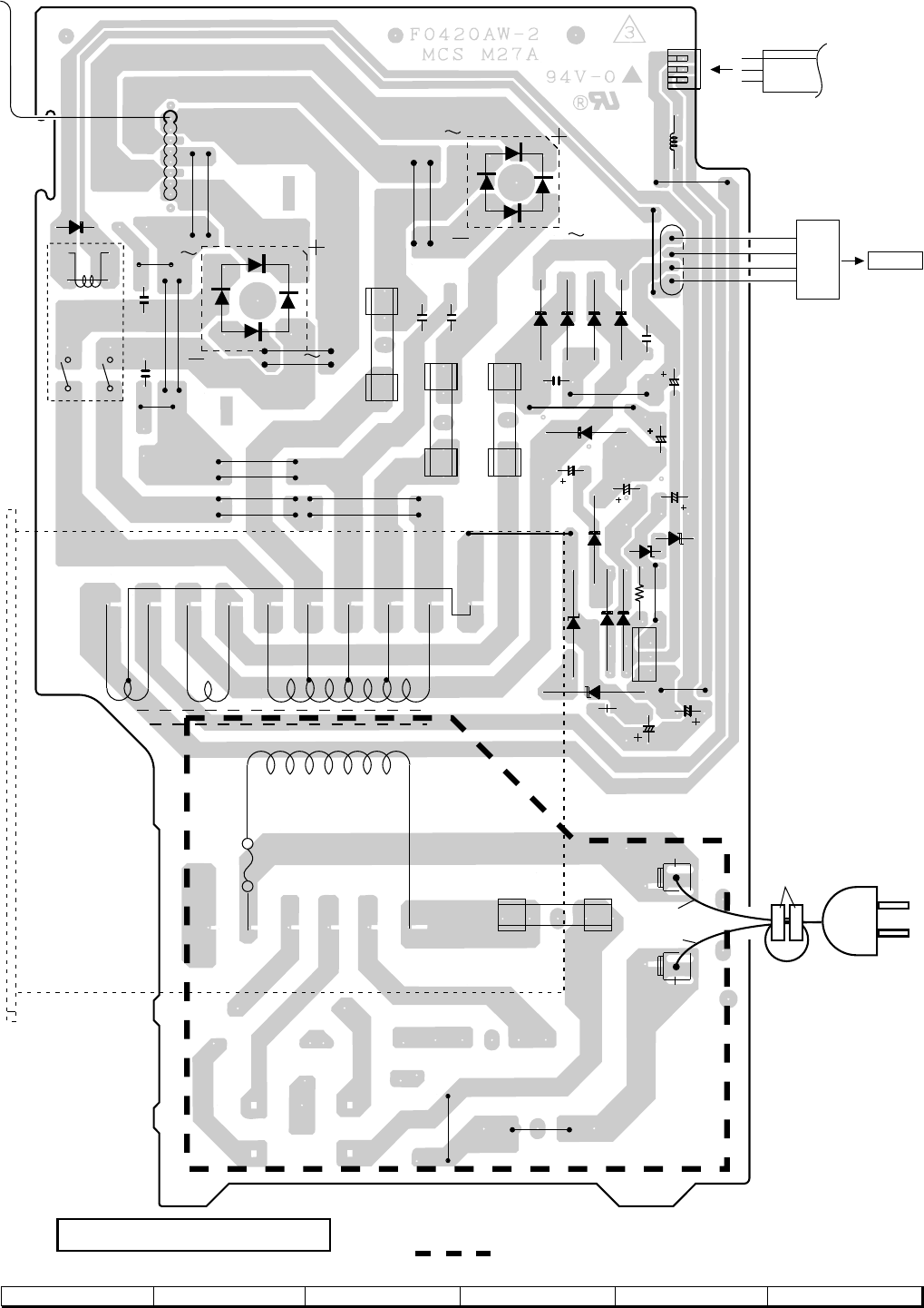
CD-C5H,CP-C5H
– 43 –
Figure 43 WIRING OF P.W.BOARD (7/9)
78 9 10 11 12
POWER SUPPLY PWB-C2
B
C
E
T.F
T851 POWER TRANSFORMER
CNS851
1
2
3
4
RD
WH
GY
WH CNP851
TO MAIN PWB
(267)
(267)
P25 12-H
C856
C853
D858
C858
C859
C860
C861
RL851
When Serving, pay attension as the area enclosed by this line
( ) is directry connected with AC main voltage.
R851
T2A L 250V
BROWN
BLUE
F855
T2.5A L 250V
T5A L 250V
T5A L 250V
F858
F857
F853
C857
C855
C851 C852
C868
C867
C854
D859
L851
D870
D853
D854
D852
D855
ZD854
D861
D860
R857
ZD851
ZD853
ZD852
WT853
BI851
FW904
Q851
D851
D850
8
1
AC POWER SUPPLY CORD
(253)
AC230V 50Hz
1
2
3
1
4
1
3
FW853 FROM
DISPLAY
PWB
P36 6-G
CORE
(268)
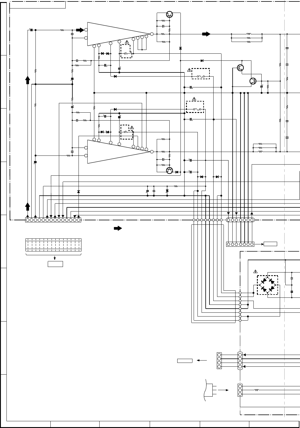
CD-C5H,CP-C5H
– 44 –
A
B
C
D
E
F
G
H
123456
Figure 44 SCHEMATIC DIAGRAM (14/17)
NOTES ON SCHEMATIC DIAGRAM can be found on page 20.
F901
T4A L 250V
F902
T4A L 250V
-B
GND1
+B
GND2
GND (SP C-CH)
GND (SP S-CH)
SPLEVEL
CNP905
TO AMP. PWB
P49 6-D
BI905
CNS905
R908
56K
C908
2.2/50
CFW903
WT853
CNS851 BI851
ZD903
MTZJ8.2C
ZD904
MTZJ8.2C
R923
0.22(2W)
L851
100µH (DH)
D993
1SS133
R927
4.7 (1/2
W
C921
0.1 (ML)
R928
4.7 (1/2
W
C922
0.1 (ML)
R910
1K
R979
33K
R994
100
R993
100
(1/2W)
C917
0.022
(ML)
C918
0.022
(ML)
D907
1N4004S
C85
2
0.22
C851
0.22
(
D851
BR102J02
D908
1N4004S
D906
1N5402M
D905
1N5402M
C984
47/50
C983
47/50
R987
3.3K
R988
3.3K
C992
47/100
C991
47/100
C986
4700/50
C985
4700/50
C995
3300/63
C996
3300/63
R985 560(2W)
Q997
KTC3199 GR
Q998
KTC3199 GR
Q903
KTC3200 GR
Q904
KTC3200 GR
R907
56K
R990
10 (1/2W)
R992
10 (1/2W)
R991
10 (1/2W)
R989
R924
0.22(2W)
R922
0.22(2W)
R921
0.22(2W)
R940
4.7K
R939
4.7K
R925
56K
R916
1K
R915
1K
R913
330
R912
56K
R911
56K
D909
1SS133
D910
1SS133
C923
0.1 (ML)
C924
0.1 (ML)
C914
33P
C913
33P
C912
47P
C911
47P
ZD901
MTZJ13B
C989
220/25
R909
1K
C990
0.022
L902
0.29µH
L901
0.29µH
C997
47/50
R998
56K
R926
56K
D902
1SS133
R920
4.7K
C936
47/50
R914
330
C935
47/50
D998
1SS133
D901
1SS133
R919
4.7K
IC901 (1/2)
STK41710
POWER AMP.
98765
14 13 12 11 10
4321
4
4
3
33
2
22
1
11
21
20
16
13 12 15
22
3
9
25
67
4
8
1
19
17
10 11 14
18
C907
2.2/50
PROTECTION
PROTECTION
PROTECTION
PROTECTION
–VH
+VH
+VL
–VL
(1/2W)
Fusible
Fusible
RELAY
VF2
–VP
VF1
FUN CONT
POSISTOR
L-CH
R-CH
VOL SW
SP DET
+12V(M)
H/P SW
GND(M)
PROT
RELAY
–15V
GND
GND(A)
+B
GND
GND
IC901 (2/2)
STK41710
POWER AMP.
+B
–B
+B
+B
+B
–B
–B
+B
8
123 4567
123 4567
1
POWER SUPPLY PWB-
C
POWER AMP. PWB-C1
FM SIGNAL
CFW852
P31 12-D
TO MAIN PWB
FW903
14
14
1
1
FROM
DISPLAY PWB
P40 1-B
CNP851
P31 12-F
TO MAIN PWB
+B
FW904
8
1
–B
–B
+B
+B
+B
+–
–B
10 (1/2W)
–B
0V
0V
0V
0V
0V
0V
0V
0V
0V
0V
0V
0V
0V
3.8V
3.8V
3.8V
0V
0V 24.4V
33.5V 42.8V
44V
–32.4V
–32.4V
–32.4V
0V
0V
-44V
-42.8V
-33.5V
-24.4V
-41.5V
3.8V
–B
FW853
0.15V
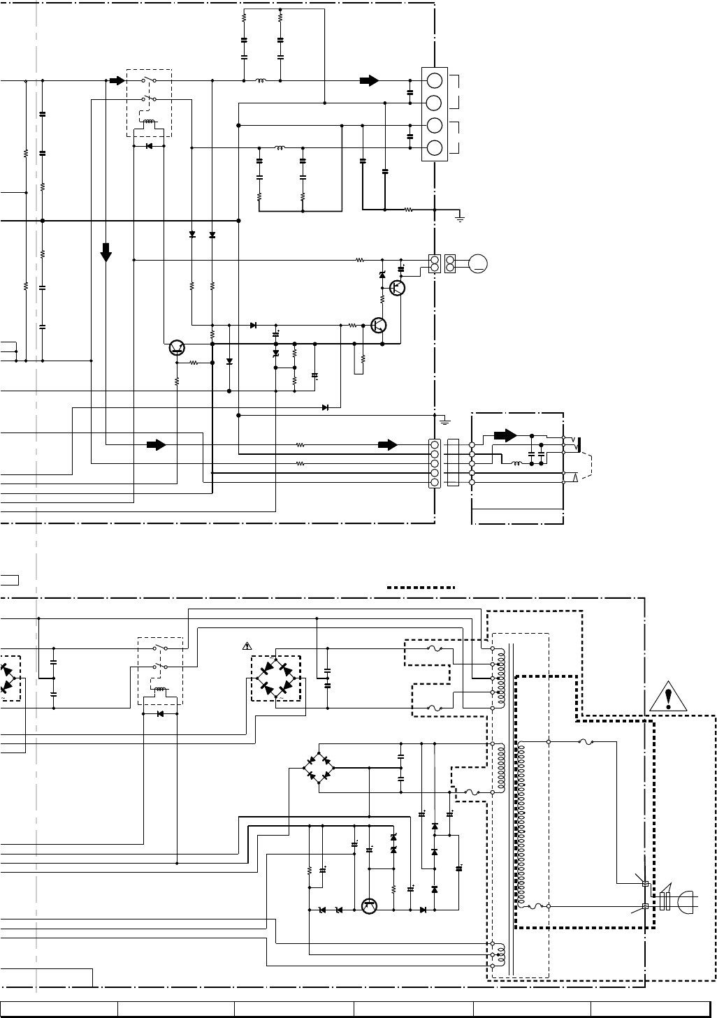
CD-C5H,CP-C5H
– 45 –
Figure 45 SCHEMATIC DIAGRAM (15/17)
78 9 10 11 12
NP905
MP. PWB
9 6-D
L903
2.2 µH(XH)
C938
100P
C937
100P
WT902
CNS901
M901
FAN MOTOR
CNP901
(DH)
C994
100/50
D995
1SS133
ZD854
MTZJ4.7B
R927
4.7 (1/2W) R930
3.9 (1/2W) R932
5.6 (1/2W)
C921
0.1 (ML)
C926
0.022
C927
0.022
C925
0.022
C928
0.022
C930
0.022 C998
0.001 C999
0.001
C934
0.001
C933
0.001
C932
0.022
R928
4.7 (1/2W)
C922
0.1 (ML)
C852
0.22 (ML)
C851
0.22 (ML)
02
D870
1SS133
RL851
RELAY
F857
T5A L 250V
F858
T5A L 250V
C867
C868
D850
S4VB20
Q851
2SB1375
220/63
C861
ZD853
MTZJ8.2C
F855
T2.5A L 250V
C859
220/63
D852
D854
D855
D853
D859
1N4004S
C858
220/50
D858
1N4004S
C860
220/50
R857
2.2K
D860
1N4004S
C857
100/35
D861
1N4004S
ZD852
MTZJ4.7B
F853
T2A L 250V
C854
0.047
(ML)
C853
0.047
(ML)
C855
47/50
C856
47/50
ZD851
MTZJ30C
R934
390
R933
390
ZD998
MTZJ5.1B
R978
100K
R977
10K
C988
10/50
D997
1SS133
D996
1SS133
0/2W)
R976
47
R999
10
R925
56K
Q999
KTC3199 GR
C923
0.1 (ML)
C924
0.1 (ML)
C970
47/25
L911
0.29µH
L912
0.29µH
R974
4.7K
R995
18K
R971
22K
R929
3.9(1/2W)
C931
0.022
C929
0.022
R931
5.6 (1/2W)
R998
56K
R926
56K
R973
12K
R972
22K
R996
47K
R997
3.3K
D999
1SS133
D912
1SS133 D911
1SS133
RL901
RELAY
SO901
SPEAKER
TERMINALS
Q994
KTA1270 Y
ZD999
MTZJ5.6B
R975
3.9K
5
4
3
2
1
2
1
M
2
1
N
FAN MOTOR
CONTROL
RELAY
DRIVER
When Servicing, pay attension as the area enclosed by this line
( ) is directry connected with AC main voltage.
Q995
KTC3199 GR
R851
12K
D852–D855
RL204F
–38V
0.22 (ML)
0.22 (ML)
SP DET
6 OHMS
+
+
–
–
HP-R CH
HP-L CH
H/P SW
H/P SW
GND(A)
R-CH
L-CH
T851
POWER TRNSFORMER
AC POWER
SUPPLY CORD
(253)
AC 230V
50Hz
+B
+B
VOLTAGE REGULATOR
T.F (267)
(267)
HEADPHONE PWB-A3
UPPLY PWB-C2
+––
–B
+B
FW901
5
1
J901
HEADPHONES
+B
+B
8.8V 9.3V
0V
8.8V
0V
0V
0V
12.1V
0V
+B
–B
-39.8V
-37.0V
-37.6V
–B
5
1
CORE(268)
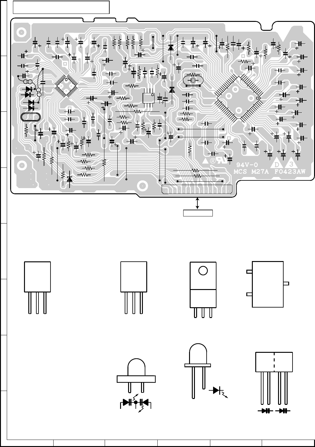
CD-C5H,CP-C5H
– 46 –
A
B
C
D
E
F
G
H
123456
Figure 46 WIRING OF P.W.BOARD (8/9)
Figure 46 TYPES OF TRANSISTOR AND LED
FRONT VIEW
2SD2012
2SK246 GR
KTA1504 Y
KTC3875 GR
2SB1375
KV1236Z23F
SPR325MV
333GTH2
333GTH4
333YTH2
(3)(2)(1)
(D)(G)(S)
B C E
VIEW
FRONT
TOP
VIEW
E C B
VIEW
FRONT
2SC1845 F
2SC2236 Y
2SC2878 A
2SC380 O
2SD468 C
KTA1266 GR
KTA1270 Y
KTA1271 Y
KTA1273 Y
KTC3199 GR
KTC3200 GR
KTC3203 Y
KRA107 M
KRC102 M
KRC104 M
KRC107 M
VIEW
FRONT
E C B
(S)(G)(D)
(1)(2)(3)
1
3
2
VIEW
FRONT
20 24
13 15
40 37
45
48
35 36
30
25
10
12
5
1
CS91
CS92
CS73
CS82
CS80
CS81
CS86
CS03
CS05
CS68
CS67
CS66
CS62
CS65
CS64
CS58
CS57
CS59
QS01
321
CS21
CS09
CS93
CS25
CS75
CS74
CS85
CS71
CS70
CS07
CS76
CS52
1
5
10
15
1617
20
25
30
32
33 35
40
45
48 49
50
55
64
CS46
CS34
CS32
CS35
CS02
CS08
CS10
CS33 CS36
CS88
CS89
CS90
CS01
CS06
CS11
CS04
CS24
CS41
CS42
CS40
CS43
CS44
CS39
CS37
CS38
CS12
CS79
CS77
CS28
CS27
CS26
CS30
CS31
CS29
CS23
CS53
CS69
CS72
CS60
CS63
CS84
CS56
CS55
XLS01
CS19
CS18
CS20
CS22
CS16
CS15
CS14
CS49
CS17
CS47
CS45
CS48
CS50
CS51
CS83
CS78
RS18
RS17
RS19
RS16
RS15
CS87
CS94
RS40
RS39
RS05
RS25
DS03
DS04
RS37
DS01
DS02
RS07
RS01
14
58
RS03
RS36
RS22
DS06
RS23
RS21
RS35
RS34
ZDS01
RS09
RS08
RS04
RS02
RS06
CS13
RS10
DS05
RS20
RS12
RS27
RS30
RS29
RS31
RS32
RS24
RS28
RS26
11 12 13 14 1510
RS14
RS11
CNPS01 123456789
ICS02
ICS03
ICS01
PRO LOGIC PWB-K
CNP501
TO MAIN PWB
P24 4-A
RS41
RS42
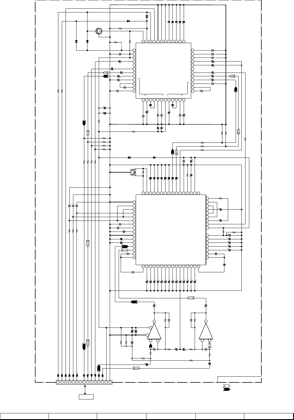
CD-C5H,CP-C5H
– 47 –
Figure 47 SCHEMATIC DIAGRAM (16/17)
78 9 10 11 12
NOTES ON SCHEMATIC DIAGRAM can be found on page 20.
+B
+B
+B
PRO LOGIC PWB-K
CNP501
P27 12-D
TO MAIN PWB
RECORD SIGNAL
PLAYBACK SIGNAL
4.8V
4.8V
4.8V
4.8V
4.8V
4.8V
4.8V
4.8V
4.8V
4.8V
4.8V
4.8V
4.8V
4.8V
4.8V
4.8V
4.8V
9.6V
4.8V
4.8V
4.8V
4.8V
4.8V
4.8V
4.8V
4.8V
4.8V
4.8V
4.8V
5.3V
5.3V
3.4V
4.8V
4.8V
4.8V
4.8V
4.8V
4.8V
4.8V
2.3V
2.5V
5V
5V
5V
5V
5V
5V
5V
5V
5V
5V
5V
5V
5V
5V
5V
5V
9.7V
5V
5V
5V
5V
5V
5V
5V
0V
5V
5V
0V
3.9V
0V
3.9V
3.9V
0V
0V
5V
5V
5V
5V
5.7V
5V
5.7V
5V
5V
5V
5V
5V
5V
5.7V
5V
5.7V
5V
5V
5V
5V
5V
5V
0V
0.7V
1.9V
9.7V
5V
4.8V
ICS02
QS7777PF
Q-SOUND
DECORDER
ICS03
NJM4565M
PRO LOGIC AMP.
ICS03
(1/2)
10/50CS18
10/50CS19
RS40
3.6K
2.2/50
CS81
RS39
3.3K
220/16CS20
RS11
18K
CS21
10/50
CS22
220/16
2.2/50
CS80
2.2/50
CS82
CS94
0.022
RS37
10K
RS41
330K
RS42
330K
0.022
(ML)
CS93
RS27
100K
RS26 100K
RS24
100K
RS25 100K
CS86
47/25
ZDS01
MTZJ5.1B
RS28
330
1KRS29
1KRS30
1KRS31
1KRS32
CS87
0.022
0.082
(ML)
CS85
0.012
(ML)
CS84
0.001
(ML)
CS83
CS75
0.022
(ML)
0.0047
(ML)
CS72
CS71
0.022
(ML)
0.047
CS33
0.022 (ML)
CS34
CS15
0.1
0.082
(ML)
CS28
0.0033
(ML)
CS29
0.082
(ML)
CS30
CS74
0.022
(ML)
CS67
0.022
(ML)
CS66
0.022 (ML)
0.022 (ML)CS57
0.0027 (ML)CS59
CS77
0.022
(ML)
CS03
47P CS04
47P
CS08
47P
CS07
47P
680P
CS32
CS13
0.022
CS91
3.3/16
39K
RS12
RS19
2.7K
RS18
2.7K
RS09
10K
RS10
10K
+B +B
+B
RS04
220K
1KRS23
1KRS22
1KRS21
1KRS15
2.7KRS16
2.7KRS17
RS20
1K
RS08
4.7K
RS06
15K
RS05
15K
RS03
220K RS02
1K
RS01
1K
RS07
4.7K
1KRS35
1KRS34
RS14
1M
ICS01
LV1035M
DOLBY PRO
LOGIC DECORDER
0.47/50
CS65
2.2/50
CS64
2.2/50
CS63
CS62
2.2/50
CS60
2.2/50
DS03
1SS133
2.2/50
CS79
2.2/50
CS78
CS76
0.47/50
CS73
0.47/50
CS69
0.47/50
CS92
47/25
RS36
220
DS06
1N4004S
0.47/50
CS35
47/16
CS36
0.47/50
CS52
4.7/50
CS51
0.47/50
CS50
4.7/50
CS49
0.15/50
CS48
3.3/50
CS47
0.15/50
CS46
0.15/50
CS45
3.3/50
CS44
0.15/50
CS43
4.7/50
CS42
0.47/50
CS41
4.7/50
CS40
0.47/50
CS39
2.2/50CS23
10/50CS24
10/50CS25
0.33/50CS26
0.47/50CS27
220/16CS31
100P
CS88
100P
CS89
100P
CS90
QS01
KRC107 M
DS01
1SS133 DS02
1SS133
DS04
1SS133
0.22/50CS58
10/50CS55
10/50CS56
CS37
0.1
CS38
0.1
CS10
10/50
CS09
10/50
CS06
47/25
CS05
47/25
CS02
2.2/50
CS01
2.2/50
CS11
47/25
CS12
47/25
CNPS01
XLS01
8MHz
DS05
1N4004S
CS53
220/16
10/50CS16
10/50CS17
+B
+B
+B
+B
1
23
3.3V
0V
0V
0V
3V
3.3V
0V
0V
0V
0V
11V
5.5V
5.5V
5.5V
0V
5.4V 5.4V
5.5V
QS_SPREAD
ICS03
(2/21)
7
5
6
2
3
4
8
1
R-CH
L-CH
+
–
–
+
+12V(A)
PL_ENA
C2B_DO
C2B_CL
QS_CLK
QS_DATA
R-CH IN
GND(AU)
L-CH IN
S OUT
C OUT
R-CH OUT
L-CH OUT
CS70
0.022
(ML)
CS68
0.0047
(ML)
VREFOUT
MSC6
1
1
2
2
3
3
4
4
112
2
3
3
4
4
VCC
MO
GND
PSAVE
MUTE
SPREAD
55
QXDC
QXAC
AR
AC
MSC1
MSC2
MSC3
VREFIN
QXCCQXBC
FLOUT
FROUT
COUT
RLOUT
RROUT
VDD
P/S
BYP
MSC5
MSC4
RRIN
RLIN
SUBIN
CIN
FRIN
FLIN
LT-IN
RT-IN
L-BPF1
L-BPF2
L-IN
AC-GND
L-OUT
R-OUT
S-OUT
C-OUT
VCC
S-IN
R-IN
CS14
0.1
GND
DC-OUT
C-MODE
NS-BPF1
NS-BPF2
OSC
CLK
DATA
ENABLE
DATA
CLK
VSS
DELAY-OUT
VREF
L-DC-OUT
R-DC-OUT
C-DC-OUT
S-DC-OUT
R-BPF1
DC-OUT
VDD
A/D
NS
D/A
OSC
OSC
DC-OUT
L-OUT
R-OUT
S-OUT
GND
IREF
DET
VCC
R-BPF3
DCOUT1
L-R-RECT
DCOUT2
L+R-RECT
VCS-TH
VCS-1
VCS-2
VLR-2
VLR-1
VLR-TH
L-RECT
DCOUT4
R-RECT
DCOUT3
L-BPF3
R-BPF2
16
15
14
13
11
12
10
9
8
25 33 34 35 36
32
31
30
29
28
27
26
24
23
22
21
20
19
18
17
16
15
14
13
9
10
11
12
87654321
48
47
46
45
44
43
42
41
40
39
38
37
32 31 30 29 28 27 26 25 24 23 22 21 20 19 18 17
49 50 51 52 53 54 55 56 57 58 59 60 61 62 63 64
7
6
5
4
3
2
1
33
34
35
36
37
38
39
40
41
42
43
44
45
46
47
48
7
6
5
4
1
11
10
9
3
2
15
14
13
12
8
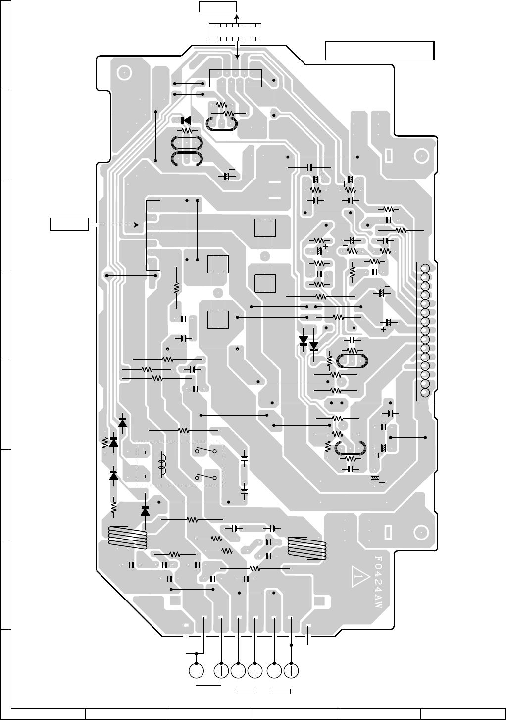
CD-C5H,CP-C5H
– 48 –
A
B
C
D
E
F
G
H
123456
Figure 48 WIRING OF P.W.BOARD (9/9)
CH87
CH88
CH97
QH97
QH98
CH18
CH17
CH19
CH20
CH30
QH99
CH25
CH27
CH26
CH32
CH28
CH31
CH29 CH99
CH33
QH03
QH04
CH90
CH36
CH14
CH09 CH10
CH08
CH07
CH12
CH35 CH11
CH13
CH89
CH98 CH34
CH23
CH22
CH24
CH21
CH37
DH98
RH98
RH85
RH27
RH31
RH30
RH28
DH96
RH96
RH97
RH29
RH72
DH95
RH71
RH73
DH97
DH99
RH32
RH99
RH39 RH19
RH40
RH20
DH01
DH02
RH84
RH83
RH12
RH16
RH14
RH07 RH08
RH10
RH15
RH13
RH09
RH11
RH26
RH25
RLH01
CFW853B
LH01
RH23
RH21
RH22
RH24
LH02
ICH01
15
10
11
12
13
14
5
1
2
3
4
6
7
8
9
CNP905
CFW853A
1
19
9
R-CH
R-CH
L-CH L-CH
CENTER
SPEAKER SURROUND SPEAKER
SOH01
CENTER/SURROUND
SPEAKER TERMINALS
1
2
3
4
5
6
7
TO MAIN PWB
P24 3-A
FW853A
CNS905
FROM POWER
AMP. PWB
P42 6-C
AMP. PWB-L
B C E
B C E
B C E
E C B
B C E
123456789
FH02
T4A L 250V
FH01
T4A L 250V
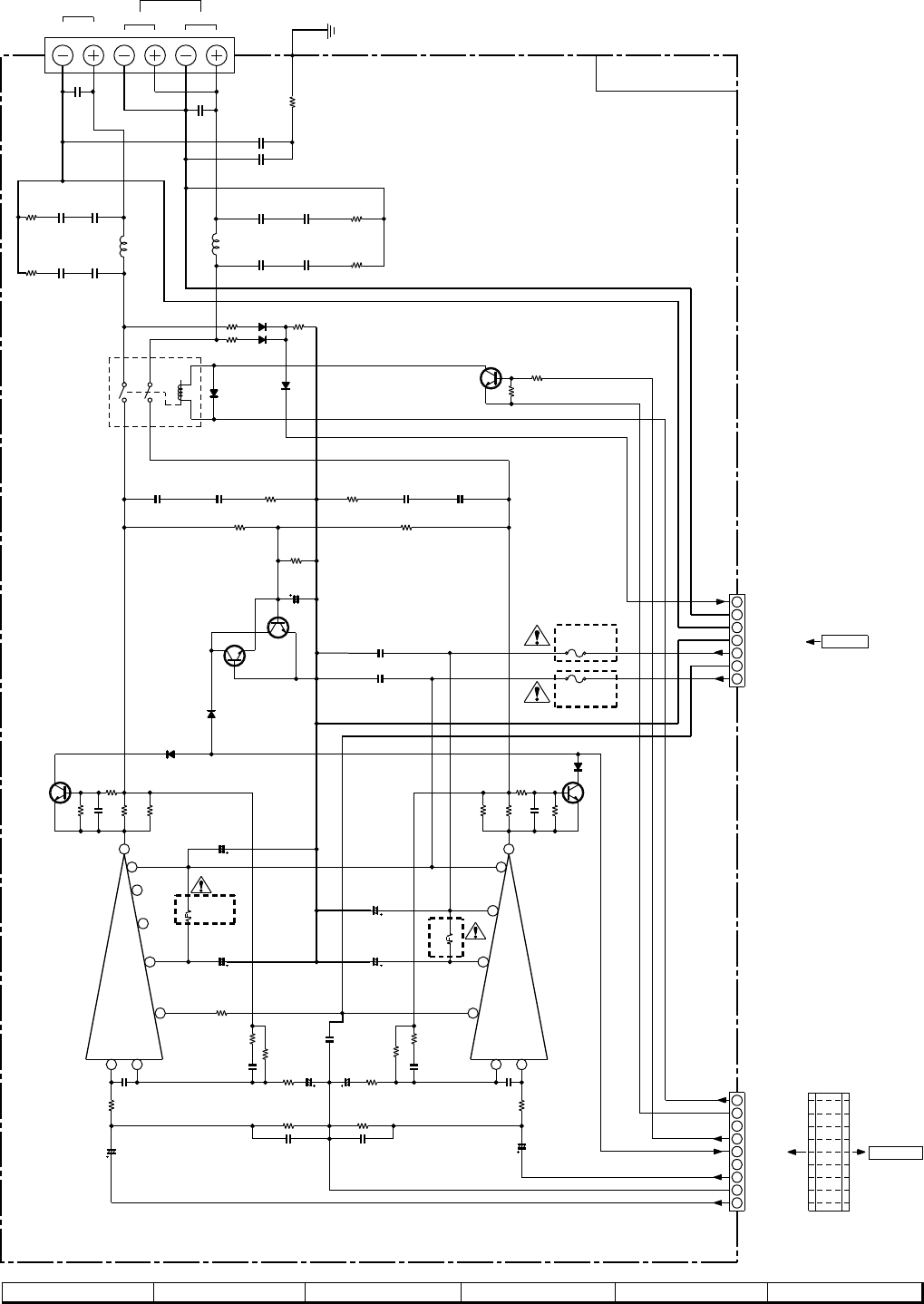
CD-C5H,CP-C5H
– 49 –
78 9 10 11 12
Figure 49 SCHEMATIC DIAGRAM (17/17)
NOTES ON SCHEMATIC DIAGRAM can be found on page 20.
RH99
10
CH34
0.001
CH99
0.001
CH32
0.022
CH33
0.001
CH98
0.001
CH30
0.022
CH19
0.022
CH20
0.022
RH32
5.6
RH31
5.6
RH29
3.9
CH28
0.022 CH26
0.022 RH30
3.9
LH02
0.29µH
LH01
0.29µH
CH29
0.022
CH25
0.022
CH31
0.022
CH27
0.022
+B–B
CENTER
SPEAKER
SURROUND SPEAKER
6 OHMS R-CHL-CH12 OHMS
NC
NC
C-CH
S-CH
1
99
1
+B
NC
NC
GND(A)
GND
PROT
RELAY
STAND-BY
GND(M)
+12V(M)
+B
Fusible
ICH01
STK40705
POWER AMP.
–B
–B -B
+B
–B
GND1
+B
GND2
GND(SP C-CH)
GND(SP S-CH)
SP LEVEL
+B
AMP.PWB-L
FROM
POWER AMP.
PWB
TO MAIN PWB
CFW853A
P31 12-C
CNS905
P44 5-E
ICH01
(2/2)
CH07
2.2/50
SOH01
CENTER
/SURROUND SPEAKER
TERMINALS
FW853A
CFW853B
CNP905
RH28
4.7
CH24
0.1
(ML)
CH22
0.1
(ML)
RH27
4.7
CH23
0.1
(ML)
CH21
0.1
(ML)
RH11
56K
RH15
1K
CH36
47/50 RH14
330
RH12
56K
RH16
1K
RH25
56K RH26
56K
RH98
56K
CH97
47/50
QH98
KTC3199 GR
QH97
KTC3199 GR
DH98
1SS133
FH01
T4A L 250V
FH02
T4A L 250V
RH13
330 CH35
47/50
CH37
0.001
RH07
56K
CH09
470P
RH08
56K
CH10
470P
RH09
1K
RH84
100
Fusible
100/50
CH89
47/50
CH87
RH83
100
CH90
100/50
RH85
22K
CH88
47/50
RH40
1K
RH39
1K
RH22
0.2 (1W)
RH24
0.2
(1W)
RH23
0.2 (1W)
RH21
0.2 (1W)
CH18
0.022
CH17
0.022
RH19
10K
QH03
KTC3199 GR
RH20
10K
QH04
KTC3199 GR
DH02
1SS133
DH01
1SS133
ICH01
(1/2)
RH10
1K
DH95
1SS133
DH96
1SS133
RH72
22K
RH71
22K
DH97
1SS133
DH99
1SS133
RLH01
RELAY
QH99
KTC3199GR
RH96
47K
RH97
3.3K
RH73
3.9K
CH14
15P
CH13
15P
CH12
47P
CH11
47P
CH08
2.2/50
9
8
7
6
5
4
3
2
1
1
7
9
3
8
5
4
2
6
1
2
3
4
5
6
7
0V
0.14V 0.8V
3.9V
0V
0V
0V
0V
3.9V
0V
0V 3.9V
3.9V
0V
0V
0V
-34V
-33V
12
11
10
32V
0V
0V
0V
-34V
34V
33V
0V
15
0V 0V
13 14
ICH01
STK40705
POWER AMP.
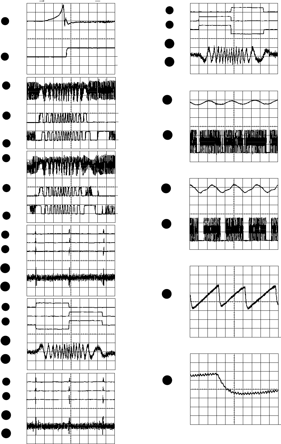
CD-C5H,CP-C5H
– 50 –
WAVEFORMS OF CD CIRCUIT
50ms
10.0 V
JP+
CUE
50ms
10.0 V
JP-
50ms
0.50 V
JP
50ms
1.00 V
TE
6
7
8
9
0.5ms
10.0 V
JP+
0.5ms
10.0 V
JP-
0.5ms
0.50 V
JP
0.5ms
1.00 V
TE
6
7
8
9
REVIEW
50ms
10.0 V
JP+
50ms
10.0 V
JP-
50ms
0.50 V
JP
50ms
1.00 V
TE
6
7
8
9
0.5ms
10.0 V
JP+
0.5ms
10.0 V
JP-
0.5ms
0.50 V
JP
0.5ms
1.00 V
TE
6
7
8
9
3
5ms
0.50 V
1
5ms
5.0 V
STOP PLAY FOCUS SERCH
2
1
FE
DRF
PLAY
20ms
1.00 V
SPO
NORMAL DISC
TN0=01
20ms
2.00 V
CLV+
10
11
PLAY
TCD-712 (140mm)
TN0=01
50ms
1.00 V
SPO
50ms
2.00 V
CLV+
10
11
PLAY
TCD-712
5ms
100mV
SLD
1
12
0.5ms
100mV
SLD
1
12
0.5ms
1.00 V
0.5ms
5.0 V
HFL
0.5ms
5.0 V
TES
1
2
3
CUE
3
4
5
HF
0.5ms
1.00 V
1
2
3
0.5ms
5.0 V
HFL
0.5ms
5.0 V
TES
REVIEW
3
4
5
HF
CD-C5H,CP-C5H
– 51 –
TROUBLESHOOTING
When the CD does not function
When the CD section does not operate When the objective lens of the optical pickup is dirty,this section may not operate.Clean
the objective lens,and check the playback operation.When this section does not operate even after the above step is taken,check
the following items.
Remove the cabinet and follow the troubleshooting instructions.
"Track skipping and/or no TOC(Table Of Contents) may be caused by build up of dust other foreign matter on the laser pickup lens.
Before attempting any adjustment make certain that the lens is clean. If not, clean it as mentioned below."
Turn the power off.
Gently clean the lens with a lens cleaning tissue and a small amount of isopropyl alcohol.
Do not touch the lens with the bare hand.
• The CD tray fails to operate.
Check the changer mechanism cam switch (SWB101 to
SWB104) and tray switch (SWB105 to SWB108).
Yes
Yes
Check the connection between IC201 and SW.
No
Check whether output of pins 3 and 7 of main cam motor
driver IC81 is normal.
Check the connection from IC2 to IC81.
No
Yes
Check whether the output of pins 3 and 7 of tray motor
driver IC82 is normal.
Yes
Check the motors MOB1 and MOB2.
No Check the connection from IC2 to IC82.
Check whether state changes to Low when
IC201 pin 95 cam SW1
pin 96 cam SW2
pin 97 cam SW3
pin 98 cam SW4
is on.
Check whether state changes to Low when
IC201 pin 33 tray SWA
pin 100 tray SWB
pin 1 tray SWC
pin 2 tray SWB
is on.
• The CD function will not work.
Yes
Yes
Check the waveform of SCK, SO (DATA) and SI (COMM).
Check the waveform of IC2 pin 54 (SQOUT), pin 55 (COIN),
and pin 56 (CQCK).
Check the CD, DSP, power supply, and 16.93 MHz clock
and reset terminal IC2 pin 57.
Yes
Yes
If the items mentioned above are OK, check the main
microcomputer IC201.
Check that the pickup is in the PICKUP IN switch position
of SW702A.
The CD operating keys don't work
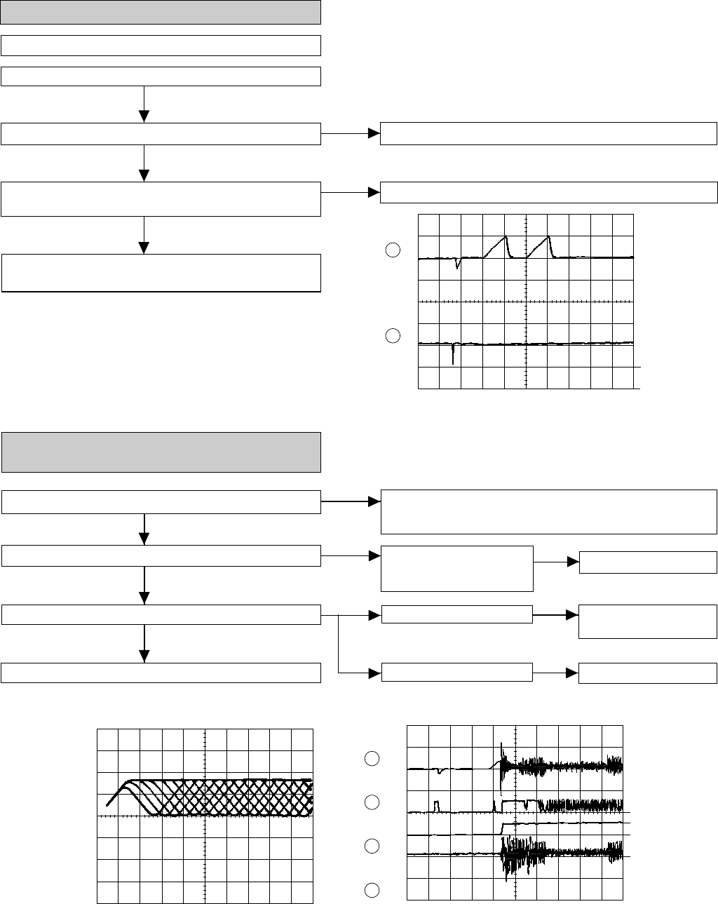
CD-C5H,CP-C5H
– 52 –
• Playback can only be performed when disc is
loaded.
Is HF waveform normal (see the Figure 52-2, Figure52-3.)?
Check the tracking system.
Is the Focus servo active? (Can you hear it working?) Check the laser diode driver.
Check the area around IC1 pin 16 to pin 21 (focus servo
circuit).
No
Yes
Yes
Yes
Does the DRF signal of IC1 pin 54 change from "L" to "H"? No Yes Check the spindle system.
If the disc is not turning,
the DRF should not
change to "H".
No Yes Check the periphery of
IC1 pin 41 and pin 42.
Level is abnormal
Yes Check the spindle system.Waveform is unstable.
Figure 52-2 Figure 52-3
• The CD operation keys work.
Check the FOCUS-HF system.
Playback can be performed without a disc.
Does the pickup move up and down two twice?
Yes
No Focus search OK
Check 4 MHz of IC1 pin 50 (CLK) line and the microcomputer
data of pin 51 (CL), pin 52 (DAT) and pin 53 (CE).
Yes
Does the output waveform of IC1 pin 16 (FD) match that
shown in Figure 52-1?
Yes
No Check the area around IC3 to CNP2.
HF
1.0V/DIV
0.5µsec/DIV(DC)
(When playing
back the disc)
0.5s
0.50 V
IC1 16 FD
2
1
0.5s
0.50 V
IC1 7 TE
Focus search is
performed two
times when play
operation is done
without disc.
3
2
1
4
0.5s
1.00 V
IC1 16 FD
0.5s
10.0 V
IC2 12 CLV+
0.5s
10.0 V
IC1 54 DRF
0.5s
2.00 V
IC1 7 TE
Waveform in case of
normal play-back
Figure 52-1
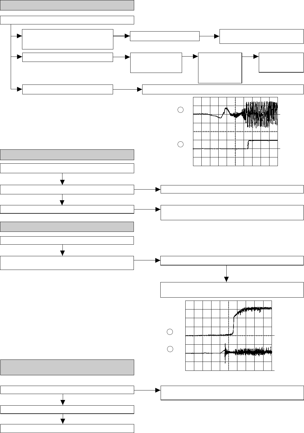
CD-C5H,CP-C5H
– 53 –
• Although HF waveform is normal and time
indication is normal, no sound is not output.
Check the IC2 pin 48 (EFLG).
Check the IC2 pin 37 and pin 40.
Check IC501 and POWER AMP. IC901.
Yes
Yes No Usually, the number of pulses of flawless disc is 100 pulses/sec
or less.
• Check the tracking system.
Data cannot be read.
Check the waveform of IC1 pin 7 (TE).
The waveform shown in Figure 53-1
appears, and no disc state appears
soon. Yes
Check the periphery of IC1 pin 8 to
pin 15, and IC3 to CNP2.
Tracking servo is inoperative.
Check the VCO-PLL system.
Yes
Yes
Playback is possible in TEST mode. Yes
Normal jump is
impeded, and the
program top
cannot be
reached.
Playback is impossible
although initialization
is possible.
Yes Yes Check the
periphery of IC1
pin 14.
Figure 53-1
3
4
5ms
1.00 V
IC1 7 TE
5 ms
5.0 V
IC1 54 DRF
• Check the spindle system
Yes
Yes
Play operation is performed without disc.
The turntable rotates a little.
The turntable fails to rotate or rotates at high speed.
The spindle driver is normal.
No
• Checking the VCO-PLL system.
Play operation is performed when disc exists.
Yes
Although the HF waveform is normal, TOC data cannot be
read. No
Check the periphery of IC1 pin 23 to pin 27, pin 39, pin 40, IC2
pin 12, pin 13, from IC3 to CNP3.
No
Check the PDO waveform of IC2 pin 3. (Figure 53-2)
Check the IC1 pin 43, pin 44, IC2 pin 3, pin 5, pin 7, pin 10, and
pin 11.
Abnormal
Figure 53-2
2
3
0.5s
1.00 V
IC2 3 PDO
0.5s
1.00 V
IC1 16 FD
As VCO freque-
ncy is locked at
4.32 MHz, voltage
of PDO rises and
stabili-zes.
Stop --> Play

CD-C5H,CP-C5H
– 54 –
IC1 VHiLA9241M/-1:Servo Amp., (LA9241M) (1/2)
1 FIN2 Connection pin for photodiode of pickup.
RF signal is generated through addition with FIN pin, and FE signal is generated through subtraction.
2 FIN1 Connection pin for photodiode of pickup.
3 E Connection pin for photodiode of pickup. TE signal is generated through subtraction with F pin.
4 F Connection pin for photodiode of pickup.
5 TB Pin for input of DC component of TE signal.
6 TE- Pin to connect gain setting resistor of TE signal to TE signal.
7 TE TE signal output pin.
8 TESI TES (Track error sense) comparator input pin. TE signal is band-passed and input.
9 SCI Input pin for shock detection.
10 TH Pin to set time constant of tracking gain.
11* TA TA amplifier output pin.
12 TD- Pin to compose tracking phase compensation constant between TD and VR pins.
13 TD Pin to set tracking phase compensation.
14 JP Pin to set amplitude of tracking jump signal (kick pulse).
15 TO Tracking control signal output pin.
16 FD Focusing control signal output pin.
17 FD- Pin to compose focusing phase compensation constant between FD and FA pins.
18 FA Pin to compose focusing phase compensation constant between FD-/FA-pins.
19 FA- Pin to compose focusing phase compensation constant between FA and FE pins.
20 FE Output pin of FE signal.
21 FE- Pin to connect gain setting resistor of FE signal across TE pin.
22 AGND GND for analog signal.
23 SP Single end output for CV+ and CV- pin input.
24 SPI Spindle amplifier input.
25 SPG Pin to connect gain setting resistor in the 12cm mode of spindle.
26 SP- Pin to connect spindle phase compensation constant together with SPD pin.
27 SPO Spindle control signal output pin.
28 SLEO Pin to connect thread phase compensation constant.
29 SLD Thread control signal output pin.
30 SL- Input pin of thread feed signal from micro computer.
31 SL+ Input pin of thread feed signal from micro computer.
32 JP- Input pin of tracking jump signal from DSP.
33 JP+ Input pin of tracking jump signal from DSP.
34 TGL Input pin of tracking gain control signal from DSP. TGL = Gain low at "H"
35 TOFF Input pin of tracking off control signal from DSP. TOFF = Off at "H"
36 TES Output pin of TES signal to DSP.
37 HFL (HIGH FREQUENCY LEVEL) is used to judge whether main beam is positioned on the bit or on the mirror.
38 SLOF Thread servo off control input pin.
39 CV- Pin to input CLV error signal from DSP.
40 CV+ Pin to input CLV error signal from DSP.
41 RFSM RF output pin.
42 RFS- Pin to set gain of RF and set 3T compensation constant together with RFSM pin.
43 SLC (SLICE LEVEL CONTROL) is the output pin to control of the level of the data slice with RF waveform DSP.
44 SLI Input pin to control the level of data slice with DSP.
45 DGND GND pin in the digital system.
46 FSC Output pin for focus search smoothening capacitor.
47 TBC (Tracking Balance Control) Pin to set EF balance variable range.
48* NC No connect.
49 DEF Defect detection output pin of disk.
50 CLK Reference clock input pin. 4.23MHz of DSP is input.
Pin No. Port Name Function
In this unit, the terminal with asterisk mark (*) is (open) terminal which is not connected to the outside.
FUNCTION TABLE OF IC
CD-C5H,CP-C5H
– 55 –
IC1 VHiLA9241M/-1:Servo Amp., (LA9241M) (2/2)
Pin No. Port Name Function
51 CL Micro computer command clock input pin.
52 DAT Micro computer command data input pin.
53 CE Micro computer command chip enable input pin.
54 DRF (DETECT RF) RF level detection output.
55 FSS (Focus Serch Select) Pin to switch focus search mode. (± search/+ search for reference voltage)
56 VCC2 VCC pin for servo system and digital system.
57 REFI Pin to connect pass control for reference voltage.
58 VR Reference voltage output pin.
59 LF2 Pin to set defect detection time constant of disk.
60 PHI Pin to connect capacitor for peak hold of RF signal.
61 BHI Pin to connect capacitor for bottom hold of RF signal.
62 LDD APC circuit output pin.
63 LDS APC circuit output pin.
64 VCC1 RF system VCC pin.
Figure 55 BLOCK DIAGRAM OF IC
IC1 VHiLA9241M/-1:Servo Amp., (LA9241M)
1
FIN2
FIN1
E
F
TB
TE-
TE
TESI
SCI
TH
TA
TD-
TD
JP
TO
FD
FD- FA FE
JP+
TGL
TOFF
TES
HFL
SLOF
CV-
CV+
RFSM
RFS-
SLC
SLI
DGND
FSC
TBC
NC
DEFCLK
CL
DAT
CE
DRF
FSS
VCC2
REFI
VRLF2
PHI
BHI
LDDLDS
SLC
RF AMP
TE
F.SERVO & F.LOGIC SPINDLE SERVO SLED SERVO
VCC1
2
3
4
6
7
5
8
9
10
11
12
13
14
15
16
17 18 19 20 21 23
22 25 26 27 28 29 30 31 32
33
34
35
36
37
38
39
40
41
42
43
44
46
47
48
49
50
51
52
53
54
55
5657
58
59
61 60
62
63
64
45
24
APC RF DET
REF
VCA
VCA INTER FACE
BAL µ-COM
I/V
T.SERVO & T.LOGIC
JP-
SL+
SL-SLDSLEO
SPO
SP-SPGSPISP
AGND
FE-FA-

CD-C5H,CP-C5H
– 56 –
1 DEFI Input Input terminal of defect detection signal (DEF). (Connected to OV when not used.)
2 TA1 Input For PLL Input terminal for test. Pull-down resistor is integrated. Surely connected to 0V.
3 PDO Output Output terminal of phase comparison for external VCO control.
4 VVSS — Ground terminal for integrated VCO. Surely connected to 0V.
5 ISET Input Resistance connection terminal for current adjustment of PDO output.
6 VVDD — Power terminal for integrated VCO.
7 FR Input VCO frequency range adjustment.
8 VSS — Ground terminal of digital system. Surely connected to 0V.
9 EFMO Output For slice level control EFM signal output terminal.
10 EFMIN Input EFM signal input terminal.
11 TEST2 Input Input terminal for test. Pull-down resistor is integrated. Surely connected to 0V.
12 CLV+ Outout Output for disk motor control. 3 values can be output with the commands.
13 CLV- Output Output for disk motor control. 3 values can be output with the commands.
14 V/P Output Monitor output terminal for automatic switch of rough servo/phase control.
"H" for rough servo, and "L" for phase servo.
15 HFL Intput Input terminal of track detection signal. Schmit input.
16 TES Input Input terminal of tracking error signal. Schmit input.
17 TOFF Output Tracking OFF output terminal.
18 TGL Output Output terminal for switch of tracking gain "L" increases the gain.
19 JP+ Output Output for track jump control. 3 values can be output with the commands.
20 JP- Output Output for track jump control. 3 values can be output with the commands.
21* PCK Output Clock monitor terminal for EFM data replay. 4,3218MHz as the phase clock.
22* FSEQ Output Output terminal synchronous signal detection. "H" is output when synchronous signal detected
by EFM signal matches synchronous signal internally generated.
23 VDD — Power terminal of digital system.
24 CONT1 Output OPEN direction
25 CONT2 Output CLOSE direction
26 CONT3 Output Cam motor forward rotation
27 CONT4 Output Cam motor reverse rotation
28 CONT5 Output Cam motor speed selection High speed "L" Low speed "H"
29* EMPH Output Difference monitor terminal At "H", deemphasis disk is being replayed.
30* C2F Output C2 flag output terminal.
31 DOUT Output Output terminal of digital OUTPUT. (EIAJ format)
32* TEST3 Input Input terminal for test. Pull-down resistor is integrated. Surely connected to 0V.
33 TEST4 Input Input terminal for test. Pull-down resistor is integrated. Surely connected to 0V.
34 PCCL — CD general-use port control signal.
35* MUTEL Output L channel 1 bit DAC Mute output terminal for L channel.
36 LVDD — Power terminal for L channel.
37 LCHO Output L channel output terminal.
38 LVSS — Ground terminal for L channel Surely connected to 0V.
39 RVSS — R channel 1 bit DAC Ground terminal for R channel Surely connected to 0V.
40 RCHO Output R channel output terminal.
41 RVDD — Power terminal for R channel.
42* MUTER Output Mute output terminal for R channel.
43 XVDD — Power terminal for quartz oscillation.
44 XOUT Output Ground terminal of 16.9344 MHz quartz oscillator.
45 XIN Input Ground terminal of 16.9344 MHz quartz oscillator.
46 XVSS — Ground terminal for quartz oscillation. Surely connected to 0V.
47* SBSY Output Output terminal of synchronous signal of subcode block.
48* EFLG Output Correction monitor terminal of C1, C2, single and double.
Pin No. FunctionTerminal Name Input/Output
In this unit, the terminal with asterisk mark (*) is (open) terminal which is not connected to the outside.
IC2 VHiLC78622K-1: Servo/Signal Control (LC78622K) (1/2)
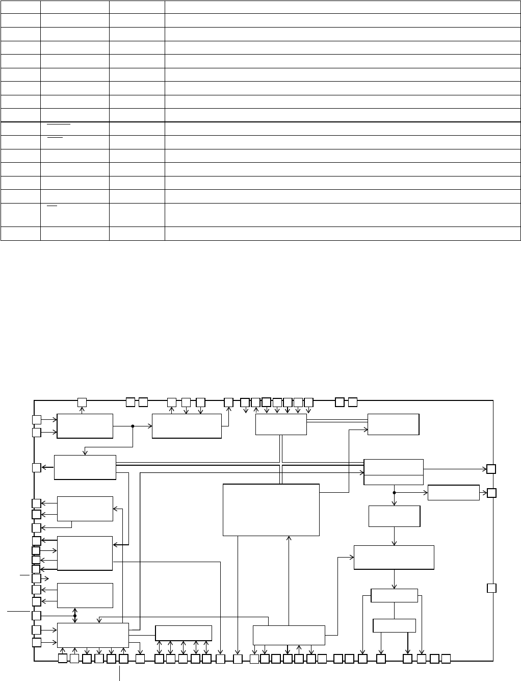
CD-C5H,CP-C5H
– 57 –
FunctionTerminal Name Input/Output
49* PW Output Output terminal of subcodes P, A, R, S, T, U and W.
50* SFSY Output Output terminal of synchronous signal of subcode frame. It drops when subcode stands by.
51 SBCK Input Clock input terminal to read subcode. Schmit input (Connected to 0V when not used.)
52* FSX Output Output terminal of synchronous signal of 7.35kHz divided from quartz oscillation.
53 WRQ Output Output terminal to stand by output of subcode Q.
54 RWC Input Input terminal of read/write. Schmit input.
55 SQOUT Output Output terminal of subcode Q.
56 COIN Input Command input terminal from microcomputer.
57 CQCK Input Clock input terminal to fetch command input, or pick up subcode from SQOUT. Schmit input
58 RES Input Reset input terminal of LC78622. When turning on power, set it at "L".
59* TST11 Output Output terminal for test. Used in the open state ("L" output as ordinary).
60* 16M Output Output terminal of 16.9344Hz.
61 4M Output Output terminal of 4.2336MHz.
62 TEST5 Input Input terminal for test Pull-down resistor is integrated. Surely connected to 0V.
63 CS Input Chip selection input terminal. Pull-down resistor is integrated.
Connected to 0when not controlled.
64 TEST1 Input Input terminal for test Pull-down resistor is integrated. Surely connected to 0V.
Pin No.
Note: The same potential must be supplied to the power terminals (VDD, VVDD, LVDD, RVDD, XVDD).
In this unit, the terminal with asterisk mark (*) is (open) terminal which is not connected to the outside.
Figure 57 BLOCK DIAGRAM OF IC
IC2 VHiLC78622K-1: Servo/Signal Control (LC78622K) (2/2)
IC2 VHiLC78622K-1: Servo/Signal Control (LC78622K)
DEFI
EFMIN
FSEQ
V/P
PW
SBCK
SBSY
SFSY
CS
WRQ
SQOUT
COIN
RWC
CQCK
HFL
TES
TOFF
JP-
JP+
RES
TGL
CONT1
CONT2
CONT3
CONT4
CONT5
EMPH
EFLG
16M
4M
XVss
FSX
XIN
XOUT
XV
DD
RVss
RV
DD
MUTER
RCHO
LCHO
MUTEL
LVss
LV
DD
PCCL
DOUT
C2F
EFMO
VV
DD
VVss
PDO
I SET
FR
PCK
TA1
TST11
TEST1
TEST2
TEST3
TEST4
TEST5
V
DD
Vss
CLV+
CLV-
Slice level
control VCO colck oscillation
clock control
2K X8bit
RAM
RAM address
generator
Interpolation mute
Bilingual
Digital OUT
Digital
attenuator
X4 oversampling
digital filter
1bitDAC
L.P.F
XTAL system timing
generator
General-use port
Servo commander
µ COM
Interface
Subcode division
QCRC
CLV
Digital servo
Sync detection
EFM demodulation
Flag processing of C1/C2
error detection and correction
1
10
22
12
13
14
49
51
47
50
63
53
55
57
56
54
15 16 17 20 19 58 18 24 25 26 27 28 29 48 60 61 46 52 45 44 43 39 41 42 40 37 35 38 36
34
31
30
8
23
6233
32
11
64
59221
75
34
96

CD-C5H,CP-C5H
– 58 –
1 P06 TRY_SW3 Input CD Chenger mechanism tray position detection switch
2 P07 TRY_SW4 Input CD Chenger mechanism tray position detection switch
3 SO0 COIN Output CD command
4 SI0 SQ_OUT Input CD Q code data
5 SCK0 CQCK Output CD seria clock
6 SO1 COM Output DISP microcomputer control line
7 SI1 DAT Input DISP microcomputer control line
8 SCK1 SCK Output DISP microcomputer control line
9 P16 STB Output DISP microcomputer control line
10 P17 DISP_RES Output DISP microcomputer control line
11 INT0 WRQ Input CD WRQ input
12 RES RES Input Reset input
13 P74 DRF Input CD DRF input
14 P75 PU-IN SW Input CD PU-IN switch input
15 VSS1 VSS — Ground terminal
16 CF1 CF1 Input Main clock 4.194304 MHz
17 CF2 CF2 Input Main clock 4.194304 MHz
18 VDD1 VDD — Positive power supply
19 AN0 SP_63 Hz Input Input for spectrum analyzer 63 Hz
20 AN1 SP_250 Hz Input Input for spectrum analyzer 250 Hz
21 AN2 SP_1 kHz Input Input for spectrum analyzer 1 kHz
22 AN3 SP_4 kHz Input Input for spectrum analyzer 4 kHz
23 AN4 SP_16 KHZ Input Input for spectrum analyzer 16 KHz
24 AN5 POSISTOR Input Input for temperature detection
25 AN6 TUNER_SM Input For tuner input detection
26 AN7 SP_DET Input For speaker output detection
27 INT1 SYS_STOP Input Power failure detection input –> HOLD mode
28 INT2 SP PROTECT Input Speaker ovecurrent detection input –> PROTECT mode
29 INT3 INT3 Input For outside break-in terminal
30 PA0 T2_B-FP SW Input Tape B-FP switch
31 PA1 T2_A-FP SW Input Tape A-FP switch
32 PA2 T2_CROM SW Input Tape T2 CrO2 switch
33 PA3 T1_CROM SW Input Tape T1 CrO2 switch
34 PA4 T2_RUN Input Tape T2 RUN pulse
35 PA5 T2_PLAY SW Inputt Tape T2 PLAY switch
36 PA6 VOL SW Output Voltage selection hold
37 PA7 MOTOR Output Tape motor output
38 PB0 T2_SOL Output For tape T2 solenoid drive
39 PB1 T1_SOL Output For tape T1 solenoid drive
40 PB2 T1_RUN Input Tape T1 RUN pulse
41 PB3 T1_PLAY SW Input Tape T1 PLAY switch
42 PB4 HI_SPEED Output Tape HIGH SPEED state "L" –> "H"
43 PB5 TA_BIAS Output Tape REC BIAS OSC
44 PB6 BEET_CANCEL Output Tape BIAS frequency selection; Usually "L"
45 PB7 TA_R/P Output Tepe PB/REC signal selection
46 PC0 TA_PB-EQ Output Tape playback side tape Equalizer selection NOR/CrO2
47 PC1 REC-EQ Output Tape record Amp Equalizer selection signal NOR/CrO2
48 PC2 REC_MUT Output Tape record muting output
49 PC3 TA_T1/T2 Output Tape T1 = "H" T2 = "L"
50 PC4 — Output Not used
51 PC5 DOLBY-ON/OFF Output DOLBY mode control ON : H OFF : L
52 PC6 DOLBY-PB/REC Output DOLBY playback/record selection output RECORD : H PLAYBACK : L
IC201 RH-iX0210AWZZ: System Microcomputer (IX0210AW)(1/2)
Port Name Terminal NamePin No. Input/Output Function

CD-C5H,CP-C5H
– 59 –
53 PC7 PB_MUT Output Tape playback muting output
54 PD0 SP_RELAY Outout For speaker relay drive
55 PD1 FUN_MOTOR Output For fan motor drive
56 VDD2 VDD — Positive power supply
57 VSS2 VSS — Ground terminal
58 PD2 TUNER_MUT Output Tuner muting output
59 PD3 SRS_PASS Output SRS control output PASS : H Otheres : L
60 PD4 SRS_3D/MONO Output SRS control output MONO : H Otheres : L
61 PD5 SRS_A Output SRS control output SRS 1, 4, 5 : H Otheres : L
62 PD6 SRS_B Output SRS control output SRS 2, 3, 5 : H Otheres : L
63 PD7 SRS_INH Output SRS control output SRS 3, 4, 5 : H Otheres : L
64 PE0 Q_A Output Q-SOUND control PASS mode : H Otheres : L
65 PE1 Q_B Output Q-SOUND control Q-Sound PASS mode : H Otheres : L
66 PE2 SPRED Output Q-SOUND control ENHANCDE mode : H Otheres : L
67 PE3 PL_ENA Output DOLBY PROLOGIC LV1035M control
68 PE4 C2B_CE Output Tuner/preamplifier C2B serial control input/output control output
69 PE5 C2B_CL Output Tuner/preamplifier C2B serial control clock output
70 PE6 TUN_SD Input Tuner signal detection input signal found : L
71 PE7 C2B_DI Input Tuner /preamplifier C2B serial control data input
72 PF0 C2B_DO Output Tuner /preamplifier C2B serial control data output
73 PF1 VOICE-CANCEL Output Karaoke function. "H": ON
74 PF2 LINE_MUT Output LINE out MUT signal
75 PF3 SYS_MUT Output Front Amp MUT signal
76 PF4 REAR_MUT Output Rear Amp MUT signal
77 PF5 CENTER_MUT Output Center Amp MUT signal
78 PF6 SWFE_MUT Output Super woofer Amp MUT signal
79 PF7 POWER Output Set power control, ON "H", "OFF"L"
80 PL6 9K/10K Input Span selection 9K "H" 10K "L"
81 PL5 MIC_DET Input MIC existence/nonexistence detection. Existence "L", Nonexistenece "H"
82 PL4 TUN_ST Input Ground connection by resistor
83 PL0 H/P SW Input H. P existence/nonexistence detection
84 PL1 AUT_SCAN Input Tuner AUT SCAN function provided/not provided
85 PL2 SRS_A/NA Input SURROUND SRS/Q-SOUND selection
86 PL3 DOL_A/NA Input Dolby Pro function provided/not provided
87 P30 CD_MUTE Output CD output MUT signal
88 P31 PCCL Output CD general-use port control signal
89 VSS3 VSS — Ground terminal
90 VDD3 VDD — Positivo power supply
91 P32 RES Output CD DSP RES signal
92 P33 SL- Output CD Sled motor -signal
93 P34 SL+ Output CD Sled motor +signal
94 P35 RWC Output CD RWC
95 P00 CAM_SW1 Input CD Changer mechanism cam detection switch
96 P01 CAM_SW2 Input CD Changer mechanism cam detection switch
97 P02 CAM_SW3 Input CD Changer mechanism cam detection switch
98 P03 CAM_SW4 Input CD Changer mechanism cam detection switch
99 P04 TRY_SW1 Input CD Chenger mechanism tray position detection switch
100 P05 TRY_SW2 Input CD Chenger mechanism tray position detection switch
Port Name Terminal Name
Pin No. Input/Output
IC201 RH-iX0210AWZZ: System Microcomputer (IX0210AW) (2/2)
Function

CD-C5H,CP-C5H
– 60 –
IC501 VHiLC75396N-1: Audio Processor (LC75396N)
1-3 RF1C1-RF1C3 Terminal to connect capacitor of filter configuration for equalizer F1 band
Connect the capacitor between LF1C1(RF1C1) and LF1C2(RF1C2) between LF1C2 (RF1C2) and LF1C3(RF1C3).
4-6 RF2C1-RF2C3 Terminal to connect capacitor of filter configuration for equalizer F2 band
Connect the capacitor between LF2C1(RF2C1) and LF2C2(RF2C2) between LF2C2 (RF2C2) and LF2C3(RF2C3).
7-9 RF3C1-RF3C3 Terminal to connect capacitor of filter configuration for equalizer F3 band
Connect the capacitor between LF3C1(RF3C1) and LF3C2(RF3C2) between LF3C2 (RF3C2) and LF3C3(RF3C3).
10-12 RF4C1-RF4C3 Terminal to connect capacitor of filter configuration for equalizer F4 band
Connect the capacitor between LF4C1(RF4C1) and LF4C2(RF4C2) between LF4C2 (RF4C2) and LF4C3(RF4C3).
13 RF5 Terminal to connect capacitor of filter configuration for equalizer F5 band
Terminal to connect the externally provided capacitor
14 RTOUT Equalizer output terminal
15 RFIN Input terminal of R-ch front side 4dB step control
16 RFCOM Common terminal of R-ch front side 1dB step control
17 RFOUT Output terminal of R-ch front side control
18 RRIN Input terminal of R-ch rear side 4dB step control
19 RRCOM Common terminal of R-ch rear side 1dB step control
20 RROUT Output terminal of R-ch rear side control
21 RVREF Internal analog ground terminal
22 VREF Connect the capacitor of about several 10 uF between Vref and AVSS (VSS) so as to prevent power supply
ripple in the VDD/2 voltage generating section.
23 CL Terminal to input serial data and clock for control
24 DI Terminal to input serial data and clock for control
25 CE Chip enable terminal. Data is written in the internal latch with a timing of changing H to L, and the specific
analog switch is actuated. Data transfer is enabled on the H level.
26 VSS GND
27 LVREF Internal analog ground terminal
28 LROUT Output terminal of L-ch rear side control
29 LRCOM Common terminal of L-ch rear side 1dB step control
30 LRIN Input terminal of L-ch rear side 4dB step control
31 LFOUT Output terminal of L-ch front side control
32 LFCOM Common terminal of L-ch front side 1dB step control
33 LFIN Input terminal of L-ch front side 4dB step control
34 LTOUT Equalizer output terminal
35 LF5 Terminal to connect capacitor of filter configuration for equalizer F5 band
Terminal to connect the externally provided capacitor
36-38 LF4C3-LF4C1 Terminal to connect capacitor of filter configuration for equalizer F4 band
Connect the capacitor between LF4C1(RF4C1) and LF4C2(RF4C2) between LF4C2 (RF4C2) and LF4C3(RF4C3).
39-41 LF3C3-LF3C1 Terminal to connect capacitor of filter configuration for equalizer F3 band
Connect the capacitor between LF3C1(RF3C1) and LF3C2(RF3C2) between LF3C2 (RF3C2) and LF3C3(RF3C3).
42-44 LF2C3-LF2C1 Terminal to connect capacitor of filter configuration for equalizer F2 band
Connect the capacitor between LF2C1(RF2C1) and LF2C2(RF2C2) between LF2C2 (RF2C2) and LF2C3(RF2C3).
45-47 LF1C3-LF1C1 Terminal to connect capacitor of filter configuration for equalizer F1 band
Connect the capacitor between LF1C1(RF1C1) and LF1C2(RF1C2) between LF1C2 (RF1C2) and LF1C3(RF1C3).
48 LTIN Equalizer input terminal
49 LSELO Input selector output terminal
50 LINVIN1 Operational amplifier reverse input terminal for input gain setting
51-55 L5-L1 Input signal terminal
56 VDD Power terminal
57-61 R1-R5 Input signal terminal
62 RINVIN1 Operational amplifier reverse input terminal for input gain setting
63 RSERO Input selector output terminal
64 RTIN Equalizer input terminal
Pin No. FunctionTerminal Name

CD-C5H,CP-C5H
– 61 –
1 P16/BUZZ DIP_STB Input Serial strobe input for system microcomputer
2 P17/PWM0 NC Output NC
3 P30 LED17 Output LED output H Lights : R-PLAY
4 P31 LED18 Output LED output H Lights : PAUSE
5 P32 LED19 Output LED output H Lights : DISC1
6 P33 LED20 Output LED output H Lights : DISC2
7 P34 LED21 Output LED output H Lights : DISC3
8 P35 LED22 Output LED output H Lights : # (SHARP)
9 P36 LED23 Output LED output H Lights : NATURAL
10 P37 LED24 Output LED output H Lights : b (FLAT)
11 P70/INT0 FL_SET Input FL initial setting input
12 RES DIP_RES Input Reset input
13 XT1/P74 VOL_UP Input Volume jog input UP
14 XT2/P75 VOL_DOW Input Volume jog input DOWN
15 Vss1 Vss — GND
16 CF1 CF_IN Input Main clock ceramic 4.19 MHz
17 CF2 CF_OUT Output Main clock ceramic 4.19 MHz
18 Vdd1 Vdd — Normal power supply
19 P80/AN0 DEST Input Initial setting input
20 P81/AN1 AU_SET Input Audio operation setting input
21 P82/AN2 KEY1 Input Button input 0 to 9
22 P83/AN3 KEY2 Input Button input 10 to 18
23 P84/AN4 KEY3 Input Button input 19 to 27
24 P85/AN5 KEY4 Input Button input 28 to 36
25 P86/AN6 KEY5 Input Button input 37 to 45
26 P87/AN7 KEY6 Input Button input 46 to 54
27 P71/INT1 MAL_UP Input Multi button jog input UP
28 P72/INT2/T0IN MAL_DOW Input Multi button jog input DOWN
29 P73/INT3/T0IN REM_IN Input Remote controller input
30 S0/T0 G15 Output Display tube grid drive
31 S1/T1 G14 Output Display tube grid drive
32 S2/T2 G13 Output Display tube grid drive
33 S3/T3 G12 Output Display tube grid drive
34 S4/T4 G12 Output Display tube grid drive
35 S5/T5 G11 Output Display tube grid drive
36 S6/T6 G10 Output Display tube grid drive
37 S7/T7 G9 Output Display tube grid drive
38 S8/T8 G8 Output Display tube grid drive
39 S9/T9 G7 Output Display tube grid drive
40 S10/T10 G6 Output Display tube grid drive
41 S11/T11 G5 Output Display tube grid drive
42 S12/T12 G4 Output Display tube grid drive
43 S13/T13 G3 Output Display tube grid drive
44 S14/T14 G2 Output Display tube grid drive
45 S15/T15 G1 Output Display tube grid drive
46 Vdd3 Vdd-F — Normal power supply for display tube drive
47 S16/PC0 S27 Output Display tube segment drive
48 S17/PC1 S26 Output Display tube segment drive
49 S18/PC2 S25 Outout Display tube segment drive
50 S19/PC3 S24 Output Display tube segment drive
51 VP VP — Negative power supply -30 V for display tube drive
IC701 RH-iX0209AWZZ: FL Driver & Controller (IX0209AW) (1/2)
Port Name Terminal Name
Pin No. Input/Output Function
CD-C5H,CP-C5H
– 62 –
52 S20/PC4 S23 Output Display tube segment drive
53 S21/PC5 S22 Output Display tube segment drive
54 S22/PC6 S21 Output Display tube segment drive
55 S23/PC7 S20 Output Display tube segment drive
56 S24/PD0 S19 Output Display tube segment drive
57 S25/PD1 S18 Output Display tube segment drive
58 S26/PD2 S17 Output Display tube segment drive
59 S27/PD3 S16 Output Display tube segment drive
60 S28/PD4 S15 Output Display tube segment drive
61 S29/PD5 S14 Output Display tube segment drive
62 S30/PD6 S13 Output Display tube segment drive
63 S31/PD7 S12 Output Display tube segment drive
64 S32/PE0 S11 Output Display tube segment drive
65 S33/PE1 S10 Output Display tube segment drive
66 S34/PE2 S9 Output Display tube segment drive
67 S35/PE3 S8 Output Display tube segment drive
68 S36/PE4 S7 Output Display tube segment drive
69 S37/PE5 S6 Output Display tube segment drive
70 S38/PE6 S5 Output Display tube segment drive
71 S39/PE7 S4 Output Display tube segment drive
72 Vdd4 Vdd-F — Normal proper supply for display tube drive
73 S40/PF0 S3 Output Display tube segment drive
74 S41/PF1 S2 Output Display tube segment drive
75 S42/PF2 S1 Output Display tube segment drive
76 S43/PF3 — Output NC
77 S44/PF4 LED1 Output LED output H Lights : Not defined
78 S45/PF5 LED2 Output LED output H Lights : Not defined
79 S46/PF6 LED3 Output LED output H Lights : F-PLAY
80 S47/PF7 LED4 Output LED output H Lights : STOP
81 S48/PG0 LED5 Output LED output H Lights : FF
82 S49/PG1 LED6 Output LED output H Lights : REW
83 S50/PG2 LED7 Output LED output H Lights : SRS-G
84 S51/PG3 LED8 Output LED output H Lights : SRS-R
85 P00 LED9 Output LED output H Lights : VIRTUAL-G
86 P01 LED10 Output LED output H Lights : VIRTUAL-R
87 P02 LED11 Output LED output H Lights : PHANTOM-G
88 P03 LED12 Output LED output H Lights : PHANTOM-R
89 Vss2 Vss — GND
90 Vdd2 Vdd — Normal power supply
91 P04 LED13 Output LED output H Lights : NORMAL-G
92 P05 LED14 Output LED output H Lights : NORMAL-R
93 P06 LED15 Output LED output H Lights : STEREO-G
94 P07 LED16 Output LED output H Lights : STEREO-R
95 P10/S00 DIP_KET Output Serial data output for system microcomputer
96 P11/S10/SB0 DIP_DAT Input Serial data input for system microcomputer
97 P12/SKC0 DIP_SCK Input Serial clock input for system microcomputer
98 P13/S01 NC Output NC
99 P14/S11/SB1 NC Output NC
100 P15/CK1 NC Outout NC
IC701 RH-iX0209AWZZ: FL Driver & Controller (IX0209AW) (2/2)
Port Name Terminal Name
Pin No. Input/Output Function

CD-C5H,CP-C5H
– 63 –
ICS02 VHiQS7777PF-1: Q-SOUND Decorder (QS7777PF)
1 VREFOUT Output Buffered reference voltage output (Vcc/2)
2 VREFIN Input Reference voltage input (Biased to Vcc/2 internally)
3 MSC3 Input Capacitor
4 MSC2 Input Capacitor
5 MSC1 Input Capacitor
6 GND — Ground
7 (Parallel) PSAVE Input Power save control (H: power save on, L: power save off)
7 (Serial) STRB Input Serial data strobe (Not applicable to I2C of QS7777CF)
8 (Parallel) MUTE Input Output mute control (H: mute on, L: mute off)
8 (Serial) SCL Input Serial data shift clock
9 (Parallel) SPREAD Input Enhancement control (H: spread maximum, L: spread minimum)
9 (Serial) SDA Input/Outout Serial data input. ACK data output for I2C (QS7777CF)
10 (Parallel) AC Input Center speaker control (H: actual center, L: virtual center)
11 (Parallel) AR Input Rear speaker control (H: actual rear, L: virtual rear)
12 (Parallel) MO Input Monaural to virtual stereo control (H: on, L: off)
13 (Parallel) BYP Input Bypass control (H: Bypass On, L: Q Surround process On)
14 P/S Input Interface mode control (H: parallel I/O, L: serial I/O)
15 VDD — Digital power supply
16 RROUT Output Rear right speaker signal out
17* RLOUT Output Rear left speaker signal out
18 COUT Output Center speaker signal out
19 FROUT Output Front right speaker out
20 FLOUT Output Front left speaker out
21 QXAC1 Input Capacitor
22 QXAC2 Input Capacitor
23 QXAC3 Input Capacitor
24 QXAC4 Input Capacitor
25 QXAC5 Input Capacitor
26 QXBC1 Input Capacitor
27 QXBC2 Input Capacitor
28 QXBC3 Input Capacitor
29 QXBC4 Input Capacitor
30 QXBC5 Input Capacitor
31 VCC — Analog power supply
32 QXCC1 Input Capacitor
33 QXCC2 Input Capacitor
34 QXCC3 Input Capacitor
35 QXCC4 Input Capacitor
36 QXDC1 Input Capacitor
37 QXDC2 Input Capacitor
38 QXDC3 Input Capacitor
39 QXDC4 Input Capacitor
40 FLIN Input Front left signal input
41 FRIN Input Front right signal input
42 CIN Input Center signal input
43* SUBIN Input Sub Woofer signal input
44 RLIN Input Rear left signal input
45 RRIN Input Rear right signal input
46 MSC4 Input Capacitor
47 MSC5 Input Capacitor
48 MSC6 Input Capacitor
Pin No. FunctionTerminal Name Input/Output
In this unit, the terminal with asterisk mark (*) is (open) terminal which is not connected to the outside.
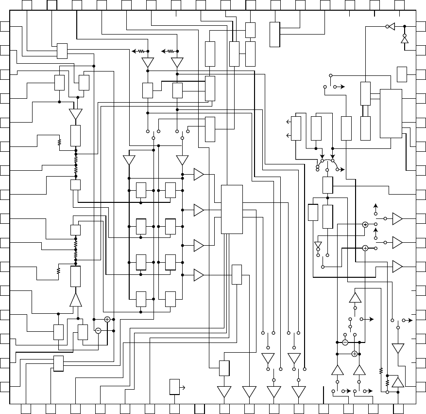
CD-C5H,CP-C5H
– 64 –
ICS01 VHiLV1035M/-1:Dolby Pro Logic Decorder (LV1035M)
Figure 64 BLOCK DIAGRAM OF IC
123456789
10 11 12
LR
S
RL
LRSC
S
L
R
S
13 14 15 16
48
L-BPF2
L-BPF1
RT-IN
LT-IN
DC-OUT
C-MODE
GND
NS-BPF1
NS-BPF2
OSC
CLK
DATA
ENABLE
DATA
CLK
VSS
R-BPF2
R-BPF1
BPF RECT
RECT
S-DC-OUT
C-DC-OUT
R-DC-OUT
L-DC-OUT
VREF
VREF
CIRIM
SW6 A
B
B
A
A
B
A
B
A
B
SW5
SW7
B
20kΩ
20kΩ
A
SW7 B
B
B
B
A
B
A
S
C
D
A
A
A
B
A
B
SW7
SW7 SW4
SW2
SW2
A
B
AB
A
B
SW7
SW7
23PIN
15PIN
SW7
SW7
SW7
SW4
SW3
13P IN
VCC
C-OUT
S-OUT
R-OUT
L-OUT
AC-GND
L-IN
R-IN
S-IN
OSC
OSC
VDD
A/D
NS
D/A
DC-OUT
DC-OUT
L-OUT
R-OUT
S-OUT
GND
IREF
DET
VCC
DELAY-
OUT
L-BPF3
DCOUT3
R-RECT
DCOUT4
L-RECT
VLR-TH
VLR-1
VLR-2
VCS-2
VCS-1
VCS-TH
L+R-RECT
DCOUT2
L-R-RECT
DCOUT1
R-BPF3
47 46 45 44 43 42 41 40 39 38 37 36 35 34 33
17
32
31
30
29
28
27
26
25
24
23
22
21
20
19
18
64
49
50
51
52
53
54
55
56
57
58
59
60
61
62
63
BPF
RECT
RECT
LR
LOGDIFFLOGDIFFVCS
OSC
VDD
DC-OUT
VOLMUTE
STRIM
B-NR
ADM
C-MODE
S-MODE
VCA
VCA
VCA
VCA
VCA
VCA
VCA
VCA
VOL
DEV
BFL-CONT
NOISE-FIL
DATA-DEC
ADM-CONT
S-RAM
IN-FILTER
OUT-FILTER
NOISE-GEN
CH-CONT
VOL
LR
LR
PG
PG
S
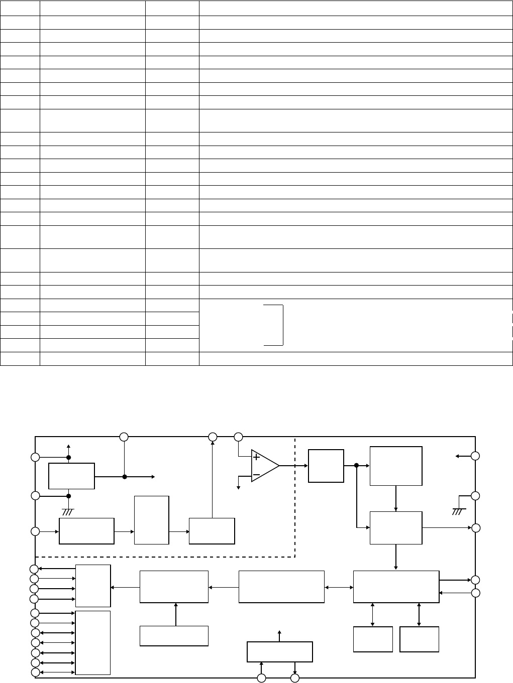
CD-C5H,CP-C5H
– 65 –
1 VREF Output Reference voltage output (Vdda/2)
2 MPXIN Input Base band (multiplex) signal input
3 VDDA — Analog system power supply (+5V)
4 VSSA — Analog system ground
5 FLOUT Output Sub-carrier input (comparator input)
6 CIN Input Sub-carrier output (filter output)
7 T1 Input Test input (to be always connected to ground)
8 T2 Input Test input (standby control)
0: Normal operation/1: Standby state (crystal oscillation stop)
9* T3 (RDCL) Input/Output Test I/O (RDS clock output)
10* T4 (RDDA) Input/Output Test I/O (RDS data output)
11 * T5 (RSFT) Input/Output Test I/O (Soft judgment control data output)
12 XOUT Output Crystal oscillation output
13 XIN Input Crystal oscillation input (external reference signal input)
14 VDDD — Digital system power supply
15 VSSD — Digital system ground
16* T6 (ERROR/57K/BE1) Input/Output Test I/O (Error existence/nonexistence output/playback carrier output/error block
number output)
17* T7 (CORREC/ARI-ID/BE0 Input/Output Test I/O (Error existence/nonexistence output/SK detection output/error block
number output)
18* SYNC Input/Output Block sync detection output
19* RDS-ID Output RDS detection output
20 DO Output Data output
21 CL Input Clock input Serial data interface (CCB)
22 DI Input Data input
23 CE Input Chip enable
24 SYR Input Sync and RAM address reset (positive logic)
ICT21 VHiLC72720/-1: RDS Microcomputer (LC72720)
Terminal NamePin No. Input/Output Function
Figure 65 BLOCK DIAGRAM OF IC
In this unit, the terminal with asterisk mark (*) is (open) terminal which is not connected to the outside.
ICT21 VHiLC72720/-1: RDS Microcomputer (LC72720)
VDDA
VREF
VREF
FLOUT CIN
VSSA
VDDD
VSSD
RDS-ID
SYNC
SYR
XOUTXIN
DO
CL
DI
CE
T1
T2
REFERENCE
VOLTAGE
57kHz
BPF
(SCF)
ANTIALIASING
FILTER
CCB
TEST
SMOOTHING
FILTER
RAM
(24 BLOCK DATA) ERROR CORRECTION
(SOFT DECISION)
PLL
(57kHz)
CLOCK
RECOVERY
(1187.5Hz)
DATA
DECODER
SYNC
DETECT-1
OSC/DIVIDER
MEMORY CONTROL
CLK(4.332MHz)
SYNC
DETECT-2
SYNC/EC CONTROLLER
156
3
4
2
20
21
22
23
7
8
13 12
24
18
19
15
14
MPXIN
9
10
11
17
T3
T4
T5
T7
16
T6
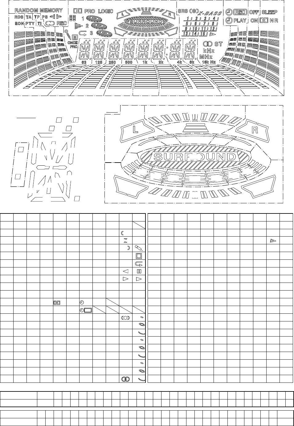
CD-C5H,CP-C5H
– 66 –
G9 G9
G9
G6
G6
G8
G8
G5
G5
G4
G4
G10
G3
G10
G3
G2
G2
G1
G1~G8
G7
G7
S40
S39
S38
S30
S33
S35
S37
S36
S34
S31
S29 S27 S25 S23
S32
S24 S26 S28
S22
S41
S10
S1
S2
S7 S6 S5 S4 S3
S9 S8
S16S15
S14
S13 S12
S17
S19
S21 S20
S18
S0
S1
S2
S3
S4
S5
S6
S7
S8
S9
S10
S11
S12
S13
S14
S15
S16
S17
S18
S19
S20
G1
S0
S1
S2
S3
S4
S5
S6
S7
S8
S9
EON
RDS
S12
S13
S14
S15
S16
S17
S18
S19
S20
G2
S0
S1
S2
S3
S4
S5
S6
S7
S8
S9
PTY
TA
S12
S13
S14
S15
S16
S17
S18
S19
S20
G3
S0
S1
S2
S3
S4
S5
S6
S7
S8
S9
TI
TP
S12
S13
S14
S15
S16
S17
S18
S19
S20
G4
S0
S1
S2
S3
S4
S5
S6
S7
S8
S9
NR
SLEEP
S12
S13
S14
S15
S16
S17
S18
S19
S20
G5
S0
S1
S2
S3
S4
S5
S6
S7
S8
S9
ON
OFF
S12
S13
S14
S15
S16
S17
S18
S19
S20
G6
S0
S1
S2
S3
S4
S5
S6
S7
S8
S9
PLAY
S12
S13
S14
S15
S16
S17
S18
S19
S20
G7
S0
S1
S2
S3
S4
S5
S6
S7
S8
S9
S10
S12
S13
S14
S15
S16
S17
S18
S19
S20
G8
S0
S1
S2
S3
S4
S5
S6
S7
S8
S9
S12
S13
S14
S15
S16
S17
S18
S19
S20
G9
S0
REC
PS
MEMORY
RANDOM
SRS
X-BASS
1
2
3
4
MHz
kHz
G10
PBC
ONCE
1
2
3
(1)
(1)
(1)
(2)
(2)
(2)
(3)
(3)
(3)
S21
S22
S23
S24
S25
S26
S27
S28
S29
S30
S31
S32
S33
S34
S35
S36
S37
S38
S39
S40
S41
G1
S21
S22
S23
S24
S25
S26
S27
S28
S29
S30
S31
S32
S33
S34
S35
S36
S37
S38
S39
S40
S41
G2
S21
S22
S23
S24
S25
S26
S27
S28
S29
S30
S31
S32
S33
S34
S35
S36
S37
S38
S39
S40
S41
G3
S21
S22
S23
S24
S25
S26
S27
S28
S29
S30
S31
S32
S33
S34
S35
S36
S37
S38
S39
S40
S41
G4
S21
S22
S23
S24
S25
S26
S27
S28
S29
S30
S31
S32
S33
S34
S35
S36
S37
S38
S39
S40
S41
G5
S21
S22
S23
S24
S25
S26
S27
S28
S29
S30
S31
S32
S33
S34
S35
S36
S37
S38
S39
S40
S41
G6
S21
S22
S23
S24
S25
S26
S27
S28
S29
S30
S31
S32
S33
S34
S35
S36
S37
S38
S39
S40
S41
G7
S21
S22
S23
S24
S25
S26
S27
S28
S29
S30
S31
S32
S33
S34
S35
S36
S37
S38
S39
S40
S41
G8
S21
S22
S23
S24
S25
S26
S27
S28
S29
S30
S31
S32
S33
S34
S35
S36
S37
S38
S39
S40
S41
G9
ST
5
15
14
13
12
11
10
9
8
7
6
S34
S35
S36
S37
S38
S39
S40
S41
G10
S21
S22
S23
S24
S25
S26
S27
S28
S29
S30
S31
S32
S33
S34
S35
S36
S37
S38
S39
S40
S41
REC
R
PIN ASSIGNMENT
Pin No.
Assignment
Pin No.
Assignment
4 5 6 7 8 9 101112 13141516 1718
NPNL H
G10
G9 G8G7G6G5 G4G3G2G1
S0S1
3334 353637 38394041 42434445 4647
S16S17 S18S19S20 S21S22S23S24 S25S26S27S28 S29S30
4849 505152 53545556 57585960 61
S31S32 S33S34S35 S36S37S38S39 S40S41
D NLNP
1920 212223 24252627 28293031 32
S2S3S4S5S6S7S8S9
S10 S11S12S13S14 S15
1~3
F1
62~64
F2
FL701 VVKCK1627M/-1
Figure 66 FL SEGMENT

CD-C5H,CP-C5H
– 67 –
PARTS GUIDE
NOTE:
Parts marked with “ ” are important for maintaining the safety of the set.
Be sure to replace parts with specified ones for maintaining the safety and performance of the set.
“HOW TO ORDER REPLACEMENT PARTS”
To have your order filled promptly and correctly, please furnish the
following information.
1. MODEL NUMBER 2. REF. No.
3. PART NO. 4. DESCRIPTION
MARK: SPARE PARTS-DELIVERY SECTION
Explanation of capacitors/resistors parts codes
For U.S.A. only
Contact your nearest SHARP Parts Distributor to order.
For location of SHARP Parts Distributor,
Please call Toll-Free;
1-800-BE-SHARP
Capacitors
VCC ....................... Ceramic type
VCK........................ Ceramic type
VCT ........................ Semiconductor type
VC • • MF ............... Cylindrical type (without lead wire)
VC • • MN............... Cylindrical type (without lead wire)
VC • • TV................ Square type (without lead wire)
VC • • TQ ............... Square type (without lead wire)
VC • • CY ............... Square type (without lead wire)
VC • • CZ ............... Square type (without lead wire)
VC • • • • • • • • • J .. The 13th character represents capacity difference.
("J" ±5%, "K" ±10%, "M" ±20%, "N" ±30%,
"C" ±0.25 pF, "D" ±0.5 pF, "Z" +80-20%.)
If there are no indications for the electrolytic capacitors, error is ±20%.
Resistors
VRD ....................... Carbon-film type
VRS........................ Carbon-film type
VRN ....................... Metal-film type
VR • • MF ............... Cylindrical type (without lead wire)
VR • • MN............... Cylindrical type (without lead wire)
VR • • TV................ Square type (without lead wire)
VR • • TQ ............... Square type (without lead wire)
VR • • CY ............... Square type (without lead wire)
VR • • CZ ............... Square type (without lead wire)
VR • • • • • • • • • J .. The 13th character represents error.
("J" ±5%, "F" ±1%, "D" ±0.5%.)
If there are no indications for other parts, the resistors are ±5%
carbon-film type.
MODEL CD-C5H
CP-C5H
Center Speaker (GBOXS0008AWM2) and Surround Speaker
(GBOXS0009AWM2), Constitute CP-C5H.

PRICE
RANK
DESCRIPTIONNO. PART CODE NO. PARTS CODE
PRICE
RANK
DESCRIPTION
CD-C5H,CP-C5H
– 1 –
INTEGRATED CIRCUITS
IC1 VHILA9241M/-1 J AS Servo Amp.,LA9241M
IC2 VHILC78622K-1 J AY Servo/Signal Control,LC78622K
IC3 VHIM56748FP-1 J AR Focus/Tracking/Spin/Slide
Driver,M56748FP
IC81 VHITA7291S/-1 J AH Main Cam Motor Driver,
TA7291S
IC82 VHITA7291S/-1 J AH Tray Motor Driver, TA7291S
IC101 VHIAN7345K/-1 J AM Playback and Record/ Playback
Amp.,AN7345K
IC201 RH-IX0210AWZZ J AZ System Microcomputer,
IX0210AW
IC302 VHILC72131/-1 J AP PLL Controller,LC72131
IC303 VHILA1832//-1 J AR FM IF Det./FM Mpx./ AM IF,
LA1832
IC451 VHISRS5250AS1 J AZ SRS,SRS5250AS1
IC452 VHIBU4066BC-1 J AG SRS Mode Selector,BU4066BC
IC501 VHILC75396N-1 J AX Audio Processor,LC75396N
IC502~504 VHINJM4558D-1 J AH Ope Amp.,NJM4558D
IC701 RH-IX0209AWZZ J BA FL Driver & Controller,IX0209AW
IC901 VHISTK41710-1 J BK Power Amp.,STK41710
ICD01 VHIHA12134AF1 J AK Dolby NR,HA12134AF
ICD03 VHIBA3311L/-1 J AK REC./P.B.Equalizer Amp.,
BA3311L
ICH01 VHISTK40705-1 J BA Power Amp.,STK40705
ICP01 VHINJM4565M-1 J AC Low Boost Amp.,NJM4565M
ICP02 VHINJM4565M-1 J AC Line Amp.,NJM4565M
ICS01 VHILV1035M/-1 J BC Dolby Pro Logic Decorder,
LV1035M
ICS02 VHIQS7777PF-1 J BC Q-Sound Decorder,QS7777PF
ICS03 VHINJM4565M-1 J AC Pro Logic Amp.,NJM4565M
ICT02 VHINJM4558MF- J AE Line Amp.,NJM4558MF
ICT21 VHILC72720/-1 J AW RDS Microcomputer,LC72720
TRANSISTORS
Q1 VSKTA1266GR-1 J AB Silicon,PNP,KTA1266 GR
Q51 VSKRC107M//-1 J AC Digital,NPN,KRC107 M
Q52 VSKTC3203Y/-1 J AC Silicon,NPN,KTC3203 Y
Q101,102 VSKRC104M//-1 J AC Digital,NPN,KRC104 M
Q103~106 VS2SC1845F/-1 J AC Silicon,NPN,2SC1845F
Q107,108 VSKTC3199GR-1 J AB Silicon,NPN,KTC3199 GR
Q109 VSKTA1266GR-1 J AB Silicon,PNP,KTA1266 GR
Q110,111 VSKRC104M//-1 J AC Digital,NPN,KRC104 M
Q113,114 VSKRC104M//-1 J AC Digital,NPN,KRC104 M
Q119 VSKRC104M//-1 J AC Digital,NPN,KRC104 M
Q121,122 VSKTC3199GR-1 J AB Silicon,NPN,KTC3199 GR
Q124,125 VSKTA1271Y/-1 J AC Silicon,PNP,KTA1271 Y
Q126,127 VSKRC104M//-1 J AC Digital,NPN,KRC104 M
Q128 VS2SC2236-Y-1 J AB Silicon,NPN,2SC2236 Y
Q131,132 VSKTC3199GR-1 J AB Silicon,NPN,KTC3199 GR
Q139~144 VSKRC104M//-1 J AC Digital,NPN,KRC104 M
Q146 VSKRC104M//-1 J AC Digital,NPN,KRC104 M
Q147~150 VSKRC107M//-1 J AC Digital,NPN,KRC107 M
Q153,154 VSKRC107M//-1 J AC Digital,NPN,KRC107 M
Q156 VSKRC107M//-1 J AC Digital,NPN,KRC107 M
Q201 VSKRC102M//-1 J AC Digital,NPN,KRC102 M
Q202,203 VSKTC3199GR-1 J AB Silicon,NPN,KTC3199 GR
Q206 VSKRA107M//-1 J AE Digital,PNP,KRA107 M
Q301 VS2SC380-O/-1 J AC Silicon,NPN,2SC380 O
Q302~304 VSKTC3199GR-1 J AB Silicon,NPN,KTC3199 GR
Q353,354 VSKTC3199GR-1 J AB Silicon,NPN,KTC3199 GR
Q360 VSKTA1266GR-1 J AB Silicon,PNP,KTA1266 GR
Q361 VSKRC107M//-1 J AC Digital,NPN,KRC107 M
Q362 VSKRA107M//-1 J AE Digital,PNP,KRA107 M
Q371 VSKTA1266GR-1 J AB Silicon,PNP,KTA1266 GR
Q451 VSKRA107M//-1 J AE Digital,PNP,KRA107 M
Q452 VSKRC107M//-1 J AC Digital,NPN,KRC107 M
Q458~460 VSKRC107M//-1 J AC Digital,NPN,KRC107 M
Q461 VSKTC3203Y/-1 J AC Silicon,NPN,KTC3203 Y
Q463,464 VSKRC107M//-1 J AC Digital,NPN,KRC107 M
Q465~467 VS2SK246GR/-1 J AB FET,2SK246 GR
Q501,502 VSKTC3199GR-1 J AB Silicon,NPN,KTC3199 GR
Q702~715 VSKTC3875GR-1 J AB Silicon,NPN,KTC3875 GR
Q716~723 VSKTA1504Y/-1 J AB Silicon,PNP,KTA1504 Y
Q820 VS2SD2012//-1 J AD Silicon,NPN,2SD2012
Q821 VSKTC3199GR-1 J AB Silicon,NPN,KTC3199 GR
Q822 VS2SD2012//-1 J AD Silicon,NPN,2SD2012
Q823 VSKTC3199GR-1 J AB Silicon,NPN,KTC3199 GR
Q824 VS2SD2012//-1 J AD Silicon,NPN,2SD2012
Q825 VS2SD468-C/-1 J AD Silicon,NPN,2SD468 C
Q826 VSKRA107M//-1 J AE Digital,PNP,KRA107 M
Q827 VSKTC3199GR-1 J AB Silicon,NPN,KTC3199 GR
Q828 VSKRC107M//-1 J AC Digital,NPN,KRC107 M
Q851 VS2SB1375//-1 J AF Silicon,PNP,2SB1375
Q903,904 VSKTC3200GR-1 J AC Silicon,NPN,KTC3200 GR
Q994 VSKTA1270Y/-1 J AD Silicon,PNP,KTA1270 Y
Q995 VSKTC3199GR-1 J AB Silicon,NPN,KTC3199 GR
Q997~999 VSKTC3199GR-1 J AB Silicon,NPN,KTC3199 GR
QD01,02 VS2SC2878A/-1 J AE Silicon,NPN,2SC2878 A
QD03 VSKRC107M//-1 J AC Digital,NPN,KRC107 M
QD06 VSKRC104M//-1 J AC Digital,NPN,KRC104 M
QD07~10 VSKRC107M//-1 J AC Digital,NPN,KRC107 M
QH03,04 VSKTC3199GR-1 J AB Silicon,NPN,KTC3199 GR
QH97~99 VSKTC3199GR-1 J AB Silicon,NPN,KTC3199 GR
QM01 VS2SK246GR/-1 J AB FET,2SK246 GR
QM02 VSKTA1273Y/-1 J AE Silicon,PNP,KTA1273 Y
QM03,04 VSKTA1271Y/-1 J AC Silicon,PNP,KTA1271 Y
QM08 VSKRC104M//-1 J AC Digital,NPN,KRC104 M
QM20~22 VSKRC104M//-1 J AC Digital,NPN,KRC104 M
QP01,02 VSKTC3199GR-1 J AB Silicon,NPN,KTC3199 GR
QP03,04 VS2SC2878A/-1 J AE Silicon,NPN,2SC2878 A
QP05 VSKTC3199GR-1 J AB Silicon,NPN,KTC3199 GR
QP07,08 VSKTC3199GR-1 J AB Silicon,NPN,KTC3199 GR
QS01 VSKRC107M//-1 J AC Digital,NPN,KRC107 M
QT01,02 VSKTC3199GR-1 J AB Silicon,NPN,KTC3199 GR
QT03,04 VSKRA107M//-1 J AE Digital,PNP,KRA107 M
QT05 VS2SC2878A/-1 J AE Silicon,NPN,2SC2878 A
QT06 VSKRA107M//-1 J AE Digital,PNP,KRA107 M
QT21 VSKTC3199GR-1 J AB Silicon,NPN,KTC3199 GR
DIODES
D1 VHD1SS133//-1 J AA Silicon,1SS133
D2~4 VHD1N4004S/-1 J AB Silicon,1N4004S
D51 VHD1SS133//-1 J AA Silicon,1SS133
D81,82 VHD1SS133//-1 J AA Silicon,1SS133
D101~104 VHD1SS133//-1 J AA Silicon,1SS133
D202~205 VHD1SS133//-1 J AA Silicon,1SS133
D301~304 VHD1SS133//-1 J AA Silicon,1SS133
D310 VHD1SS133//-1 J AA Silicon,1SS133
D351~353 VHD1SS133//-1 J AA Silicon,1SS133
D401~403 VHD1SS133//-1 J AA Silicon,1SS133
D501,502 VHD1SS133//-1 J AA Silicon,1SS133
D552~557 VHD1SS133//-1 J AA Silicon,1SS133
D701 VHD1N4004S/-1 J AB Silicon,1N4004S
D702 VHD1SS133//-1 J AA Silicon,1SS133
D823 VHD1SS133//-1 J AA Silicon,1SS133
D826~829 VHD1SS133//-1 J AA Silicon,1SS133
!D850 VHDS4VB20//-1 J AG Rectifier,S4VB20
!D851 VHDBR102J02-1 J AM Silicon,BR102J02
D852~855 VHDRL204F//-1 J AC Silicon,RL204F
D858~861 VHD1N4004S/-1 J AB Silicon,1N4004S
D870 VHD1SS133//-1 J AA Silicon,1SS133
D901,902 VHD1SS133//-1 J AA Silicon,1SS133
D905,906 VHD1N5402M/-1 J AE Silicon,1N5402M
D907,908 VHD1N4004S/-1 J AB Silicon,1N4004S
D909~912 VHD1SS133//-1 J AA Silicon,1SS133
D993 VHD1SS133//-1 J AA Silicon,1SS133
D995~999 VHD1SS133//-1 J AA Silicon,1SS133
DD01,02 VHD1SS133//-1 J AA Silicon,1SS133
DH01,02 VHD1SS133//-1 J AA Silicon,1SS133
DH95~99 VHD1SS133//-1 J AA Silicon,1SS133
DM01~03 VHD1SS133//-1 J AA Silicon,1SS133
DS01~04 VHD1SS133//-1 J AA Silicon,1SS133
DS05,06 VHD1N4004S/-1 J AB Silicon,1N4004S
DT01,02 VHD1SS133//-1 J AA Silicon,1SS133
LED701~707 VHP333GTH4/-1 J AC LED,Green,333GTH4
LED708 VHP333GTH2/-1 J AD LED,Green,333GTH2
LED709 VHP333GTH4/-1 J AC LED,Green,333GTH4
LED710~713 VHP333YTH2/-1 J AD LED,Orange,333YTH2
LED714,715 VHP333GTH2/-1 J AD LED,Green,333GTH2
LED716~718 VHP333GTH4/-1 J AC LED,Green,333GTH4
LED719,720 VHP333YTH2/-1 J AD LED,Orange,333YTH2
LED721~724 VHPSPR325MV-1 J AF LED,Red,SPR325MV
LED725 VHP333GTH2/-1 J AD LED,Green,333GTH2
LED726 VHP333GTH4/-1 J AC LED,Green,333GTH4
VD301 VHCKV1236Z23F J AS Variable Capacitance,
KV1236Z23F
ZD61 VHEMTZJ4R7B-1 J AB Zener,4.7V,MTZJ4.7B
CD-C5H

NO.
PRICE
RANK
DESCRIPTIONPARTS CODE
NO. PART CODE
PRICE
RANK
DESCRIPTION
CD-C5H,CP-C5H
ZD201 VHEMTZJ3R3A-1 J AB Zener,3.3V,MTZJ3.3A
ZD351 VHEMTZJ4R7B-1 J AB Zener,4.7V,MTZJ4.7B
ZD352 VHEMTZJ3R9B-1 J AC Zener,3.9V,MTZJ3.9B
ZD451,452 VHEMTZJ8R2C-1 J AB Zener,8.2V,MTZJ8.2C
ZD550 VHEMTZJ5R6A-1 J AC Zener,5.6V,MTZJ5.6A
ZD820 VHEMTZJ130B-1 J AC Zener,13V,MTZJ13B
ZD821 VHEMTZJ5R6A-1 J AC Zener,5.6V,MTZJ5.6A
ZD822 VHEMTZJ8R2C-1 J AB Zener,8.2V,MTZJ8.2C
ZD851 VHEMTZJ300C-1 J AC Zener,30V,MTZJ30C
ZD852 VHEMTZJ4R7B-1 J AB Zener,4.7V,MTZJ4.7B
ZD853 VHEMTZJ8R2C-1 J AB Zener,8.2V,MTZJ8.2C
ZD854 VHEMTZJ4R7B-1 J AB Zener,4.7V,MTZJ4.7B
ZD901 VHEMTZJ130B-1 J AC Zener,13V,MTZJ13B
ZD903,904 VHEMTZJ8R2C-1 J AB Zener,8.2V,MTZJ8.2C
ZD998 VHEMTZJ5R1B-1 J AC Zener,5.1V,MTZJ5.1B
ZD999 VHEMTZJ5R6B-1 J AD Zener,5.6V,MTZJ5.6B
ZDS01 VHEMTZJ5R1B-1 J AC Zener,5.1V,MTZJ5.1B
ZDT21 VHEMTZJ4R3B-1 J AC Zener,4.3V,MTZJ4.3B
FILTERS
CF301 RFILF0072AFZZ J AG FM IF
CF302 RFILF0072AFZZ J AG FM IF
CF351 RFILF0003AWZZ J AK FM IF
CF352 RFILA0009AWZZ J AE AM IF
TRANSFORMERS
T301 RCILA1074AFZZ J AD LW Antenna
T302 RCILA1064AFZZ J AD MW Antenna
T305 RCILB1073AFZZ J AC LW Oscillation
T306 RCILB1074AFZZ J AC MW Oscillation
T351 RCILI0011AWZZ J AD AM IF
!T851 RTRNP0190AWZZ J BR Power
COILS
L61 VP-XHR82K0000 J AC 0.82 µH
L95 VP-XH2R2K0000 J AB 2.2 µH,Choke
L102,103 RCILC0094AFZZ J AD 6.8 mH
L104 VP-MK331K0000 J AB 330 µH,Choke
L105,106 VP-XH2R2K0000 J AB 2.2 µH,Choke
L201 VP-DH2R2M0000 J AB 2.2 µH,Choke
L251,252 RCILL0105AFZZ J AE MPX. Filter
L341 RBLN-0001AWZZ J AD Balun
L342 VP-DH2R2K0000 J AB 2.2 mmH,Peaking
L351,352 VP-DH101K0000 J AB 100 µH,Choke
L353 VP-DH102K0000 J AB 1 mH,Choke
L354 RFILL0001AWZZ J AE Low Pass Filter
L701 VP-CH2R2M0000 J AB 2.2 µH
L851 VP-DH101K0000 J AB 100 µH,Choke
L901,902 RCILZ0137AFZZ J AA 0.29 µH
L903 VP-XH2R2K0000 J AB 2.2 µH,Choke
L911,912 RCILZ0137AFZZ J AA 0.29 µH
LD01,02 RCILC0094AFZZ J AD 6.8 mH
LH01,02 RCILZ0137AFZZ J AA 0.29 µH
LT21,22 VP-XH2R2K0000 J AB 2.2 µH,Choke
VARIABLE RESISTORS
VR101 RVR-M0028AWZZ J AC 22 kohms (B),Semi-VR
[L-CH Bias Current]
VR102 RVR-M0028AWZZ J AC 22 kohms (B),Semi-VR
[R-CH Bias Current]
VR151 RVR-M0030AWZZ J AC 47 kohms (B),Semi-VR
[L-CH Rec/Play Sens.]
VR152 RVR-M0030AWZZ J AC 47 kohms (B),Semi-VR
[R-CH Rec/Play Sens.]
VR351 RVR-M0026AFZZ J AC 10 kohm (B),Semi-VR
[FM Mute Level]
VRD01 RVR-M0028AWZZ J AC 22 kohms (B),Semi-VR
[Tape 1 Play L-CH Sens.]
VRD02 RVR-M0028AWZZ J AC 22 kohms (B),Semi-VR
[Tape 1 Play R-CH Sens.]
VRD03 RVR-M0028AWZZ J AC 22 kohms (B),Semi-VR
[Tape 2 Play L-CH Sens.]
VRD04 RVR-M0028AWZZ J AC 22 kohms (B),Semi-VR
[Tape 2 Play R-CH Sens.]
VRM01 RVR-M0030AWZZ J AC 47 kohms (B),Semi-VR
[Tape Speed]
VIBRATORS
X201 RCRSP0003AWZZ J AH Crystal,4.19MHz
X351 92LCRSTL1425A J AF Crystal,456 kHz
X352 RCRSP0002AWZZ J AH Crystal,4.5 MHz
X701 RCRM-0031AWZZ J AE Ceramic,4.19 MHz
XL1 RCRSP0005AWZZ J AF Crystal,16.934 MHz
XLS01 RCRM-0173AFZZ J AE Ceramic,8 MHz
XT21 RCRSB0030AWZZ J AH Crystal,4.332 MHz
CAPACITORS
C1 VCEAZA1AW476M J 47 µF,10V,Electrolytic
C2 VCTYMN1CY103N J AA 0.01 µF,16V
C3 VCEAZA1HW105M J AB 1 µF,50V,Electrolytic
C4 VCEAZA1HW104M J AB 0.1 µF,50V,Electrolytic
C5,6 VCTYPA1CX333K J AA 0.033 µF,16V
C7 VCEAZA1HW104M J AB 0.1 µF,50V,Electrolytic
C8 VCTYPA1CX683K J AA 0.068 µF,16V
C9 VCTYPA1CX473K J AA 0.047 µF,16V
C10 VCKYMN1HB181K J AA 180 pF,50V
C11,12 VCTYPA1CX104K J AB 0.1 µF,16V
C13 VCKYMN1HB331K J AA 330 pF,50V
C14 VCTYMN1CY103K J AA 0.01 µF,16V
C16 VCTYMN1CX472K J AA 0.0047 µF,16V
C17 VCKYMN1HB102K J AA 0.001 µF,50V
C18 VCEAZA1HW474M J AB 0.47 µF,50V,Electrolytic
C19 VCEAZA1HW105M J AB 1 µF,50V,Electrolytic
C20 VCEAZA1AW476M J 47 µF,10V,Electrolytic
C21 VCTYMN1CX332K J AA 0.0033 µF,16V
C22 VCCSPA1HL221J J AA 220 pF,50V
C23 VCTYMN1CX272K J AA 0.0027 µF,16V
C24 VCCSMN1HL2R2C J AB 2.2 pF,50V
C25 VCCSMN1HL270J J AA 27 pF,50V
C26 VCTYPA1CX333K J AA 0.033 µF,16V
C27 VCKYMN1HB102K J AA 0.001 µF,50V
C28 VCTYPA1CX104K J AB 0.1 µF,16V
C29 VCEAZA1EW475M J AC 4.7 µF,25V,Electrolytic
C30 VCEAZA1HW104M J AB 0.1 µF,50V,Electrolytic
C31 VCEAZA0JW227M J AC 220 µF,6.3V,Electrolytic
C32 VCTYMN1CY103N J AA 0.01 µF,16V
C33 VCEAZA1HW474M J AB 0.47 µF,50V,Electrolytic
C34 VCEAZA1HW334M J AB 0.33 µF,50V,Electrolytic
C35 VCEAZA1HW105M J AB 1 µF,50V,Electrolytic
C36 VCEAZA1AW107M J AB 100 µF,10V,Electrolytic
C37 VCTYMN1EF223Z J AA 0.022 µF,25V
C38 VCTYMN1CY103N J AA 0.01 µF,16V
C39,40 VCTYPA1CX473K J AA 0.047 µF,16V
C41 VCCCBT1HH120J J AA 12 pF (CH),50V
C42 VCCCBT1HH150J J AA 15 pF (CH),50V
C43 VCEAZA1AW107M J AB 100 µF,10V,Electrolytic
C44~49 VCKYMN1HB101K J AA 100 pF,50V
C51,52 VCEAZA1AW107M J AB 100 µF,10V,Electrolytic
C53 VCTYMN1EF223Z J AA 0.022 µF,25V
C54 VCKYMN1HB102K J AA 0.001 µF,50V
C55 RC-EZ0004AWZZ J AD 3.3 µF,16V,Electrolytic
C56 VCTYMN1EF223Z J AA 0.022 µF,25V
C57 VCKYBT1HB102K J AA 0.001 µF,50V
C71,72 RC-EZ0004AWZZ J AD 3.3 µF,16V,Electrolytic
C80 VCTYMN1EF223Z J AA 0.022 µF,25V
C81,82 VCEAZA1EW476M J AB 47 µF,25V,Electrolytic
C83 VCKYMN1HB102K J AA 0.001 µF,50V
C85 VCTYMN1EF223Z J AA 0.022 µF,25V
C86,87 VCEAZA1EW476M J AB 47 µF,25V,Electrolytic
C95 VCEAZA1AW107M J AB 100 µF,10V,Electrolytic
C96 VCTYBT1EF223Z J AA 0.022 µF,25V
C101~104 VCKYMN1HB271K J AA 270 pF,50V
C105,106 VCKYMN1HB331K J AA 330 pF,50V
C107,108 VCKYMN1HB561K J AA 560 pF,50V
C109 VCKYPA1HF223Z J AB 0.022 µF,50V
C111~114 VCKYMN1HB331K J AA 330 pF,50V
C115,116 VCEAZA1EW476M J AB 47 µF,25V,Electrolytic
C117,118 VCTYPA1CX333K J AA 0.033 µF,16V
C119,120 VCKYMN1HB561K J AA 560 pF,50V
C121,122 VCEAZA1HW105M J AB 1 µF,50V,Electrolytic
C123,124 VCTYPA1CX123K J AA 0.012 µF,16V
C125,126 VCTYPA1CX103K J AA 0.01 µF,16V
C127 VCTYMN1EF223Z J AA 0.022 µF,25V
C128 VCEAZA1HW335M J AB 3.3 µF,50V,Electrolytic
C131,132 VCKYMN1HB271K J AA 270 pF,50V
C133,134 VCEAZA1CW106M J AC 10 µF,16V,Electrolytic
C139,140 VCTYMN1CX332K J AA 0.0033 µF,16V
– 2 –

PRICE
RANK
DESCRIPTIONNO. PART CODE NO. PARTS CODE
PRICE
RANK
DESCRIPTION
CD-C5H,CP-C5H
C141,142 VCEAZA1EW476M J AB 47 µF,25V,Electrolytic
C145 VCEAZA1EW226M J AB 22 µF,25V,Electrolytic
C146 VCEAZA1AW227M J AC 220 µF,10V,Electrolytic
C147 VCTYMN1EF223Z J AA 0.022 µF,25V
C148 VCEAZA1CW107M J AC 100 µF,16V,Electrolytic
C150 VCQPKA2AA822J J AA 0.0082 µF,100V,Polypropylene
C151 VCQYKA1HM393J J AB 0.039 µF,50V,Mylar
C152 VCEAZA1AW227M J AC 220 µF,10V,Electrolytic
C161 VCKYMN1HB561K J AA 560 pF,50V
C162 VCQYKA1HM473J J AB 0.047 µF,50V,Mylar
C167,168 VCTYPA1CX103K J AA 0.01 µF,16V
C175,176 VCTYMN1CX562K J AA 0.0056 µF,16V
C177,178 VCTYMN1CX682K J AA 0.0068 µF,16V
C179,180 VCTYPA1EX822K J AA 0.0082 µF,25V
C181,182 VCEAZA1HW104M J AB 0.1 µF,50V,Electrolytic
C183 VCEAZA1CW106M J AC 10 µF,16V,Electrolytic
C184 VCEAZA1HW475M J AB 4.7 µF,50V,Electrolytic
C201 VCEAZA1AW477M J AC 470 µF,10V,Electrolytic
C202 VCTYMN1CY103N J AA 0.01 µF,16V
C203 VCEAZA1HW335M J AB 3.3 µF,50V,Electrolytic
C204 VCTYMN1CY103N J AA 0.01 µF,16V
C205,206 VCCCMN1HH150J J AA 15 pF (CH),50V
C207 VCEAZA1EW226M J AB 22 µF,25V,Electrolytic
C251,252 VCTYMN1CX332K J AA 0.0033 µF,16V
C256 VCTYMN1EF223Z J AA 0.022 µF,25V
C257 VCEAZA1EW476M J AB 47 µF,25V,Electrolytic
C301 VCKYMN1HB102K J AA 0.001 µF,50V
C302 VCKYBT1HB102K J AA 0.001 µF,50V
C321 VCEAZA1CW107M J AC 100 µF,16V,Electrolytic
C322 VCCCMN1HH6R8D J AA 6.8 pF (CH),50V
C323 VCTYMN1EF223Z J AA 0.022 µF,25V
C323 VCTYMN1EF223Z J AA 0.022 µF,25V
C324 VCCUMN1HJ270J J AA 27 pF (UJ),50V
C325 VCKYMN1HB221K J AA 220 pF,50V
C326 VCCCMN1HH180J J AA 18 pF (CH),50V
C327 VCKYMN1HB681K J AA 680 pF,50V
C328 VCTYMN1EF223Z J AA 0.022 µF,25V
C329 VCCSPA1HL330J J AA 33 pF,50V
C330 VCCUMN1HJ100J J AA 10 pF (UJ),50V
C331 VCKYPA1HF473Z J AB 0.047 µF,50V
C332 VCTYMN1EF223Z J AA 0.022 µF,25V
C333 VCCCMN1HH220J J AA 22 pF (CH),50V
C334 VCCUMN1HJ180J J AA 18 pF (UJ),50V
C335 VCCCMN1HH180J J AA 18 pF (CH),50V
C336 VCKYMN1HB471K J AA 470 pF,50V
C337 VCTYMN1EF223Z J AA 0.022 µF,25V
C338 VCKYMN1HB102K J AA 0.001 µF,50V
C339 VCCCMN1HH220J J AA 22 pF (CH),50V
C341 VCTYMN1EF223Z J AA 0.022 µF,25V
C342 VCTYMN1EF223Z J AA 0.022 µF,25V
C343 VCCSMN1HL330J J AA 33 pF,50V
C344 VCCSMN1HL330J J AA 33 pF,50V
C345~347 VCTYMN1EF223Z J AA 0.022 µF,25V
C350,351 VCTYMN1EF223Z J AA 0.022 µF,25V
C352 VCEAZA1CW106M J AC 10 µF,16V,Electrolytic
C353,354 VCTYMN1EF223Z J AA 0.022 µF,25V
C355 VCCSMN1HL220J J AA 22 pF,50V
C356 VCKYMN1HB102K J AA 0.001 µF,50V
C357 VCEAZA1HW225M J AB 2.2 µF,50V,Electrolytic
C358 VCEAZA1HW105M J AB 1 µF,50V,Electrolytic
C361 VCTYMN1EF223Z J AA 0.022 µF,25V
C362 VCEAZA1HW335M J AB 3.3 µF,50V,Electrolytic
C363 VCTYMN1EF223Z J AA 0.022 µF,25V
C364 VCEAZA1CW106M J AC 10 µF,16V,Electrolytic
C365 VCTYPA1CX223K J AA 0.022 µF,16V
C366 VCKYMN1HB102K J AA 0.001 µF,50V
C367,368 VCEAZA1HW105M J AB 1 µF,50V,Electrolytic
C369 VCCSBT1HL270J J AA 27 pF,50V
C370~372 VCEAZA1HW105M J AB 1 µF,50V,Electrolytic
C373,374 VCTYPA1CX273K J AA 0.027 µF,16V
C375 VCEAZA1HW335M J AB 3.3 µF,50V,Electrolytic
C380 VCEAZA1CW106M J AC 10 µF,16V,Electrolytic
C381 VCCCMN1HH120J J AA 12 pF (CH),50V
C382 VCCCMN1HH150J J AA 15 pF (CH),50V
C384 VCKYMN1HB102K J AA 0.001 µF,50V
C385 VCTYMN1CY103K J AA 0.01 µF,16V
C386 VCKYMN1HB331K J AA 330 pF,50V
C387 VCTYMN1EF223Z J AA 0.022 µF,25V
C391 VCEAZA1CW476M J AB 47 µF,16V,Electrolytic
C392 VCKYMN1HB102K J AA 0.001 µF,50V
C393 VCEAZA1HW105M J AB 1 µF,50V,Electrolytic
C394 VCEAZA1CW476M J AB 47 µF,16V,Electrolytic
C395 VCTYMN1EF223Z J AA 0.022 µF,25V
C396 VCEAZA1AW107M J AB 100 µF,10V,Electrolytic
C397 VCTYMN1EF223Z J AA 0.022 µF,25V
C398 VCEAZA1AW107M J AB 100 µF,10V,Electrolytic
C399 VCTYMN1EF223Z J AA 0.022 µF,25V
C453,454 VCEAZA1HW225M J AB 2.2 µF,50V,Electrolytic
C456,457 VCEAZA1CW107M J AC 100 µF,16V,Electrolytic
C458 VCQYKA1HM473J J AB 0.047 µF,50V,Mylar
C460 VCEAZA1HW474M J AB 0.47 µF,50V,Electrolytic
C461 VCTYMN1CX472K J AA 0.0047 µF,16V
C471 VCEAZA1CW107M J AC 100 µF,16V,Electrolytic
C472 VCEAZA1HW334M J AB 0.33 µF,50V,Electrolytic
C481~484 VCEAZA1HW225M J AB 2.2 µF,50V,Electrolytic
C485 VCEAZA1EW476M J AB 47 µF,25V,Electrolytic
C486 VCTYMN1EF223Z J AA 0.022 µF,25V
C487 VCEAZA1EW476M J AB 47 µF,25V,Electrolytic
C488 VCTYMN1EF223Z J AA 0.022 µF,25V
C501~508 VCEAZA1HW225M J AB 2.2 µF,50V,Electrolytic
C509,510 VCEAZA1HW106M J AB 10 µF,50V,Electrolytic
C511,512 VCKYMN1HB101K J AA 100 pF,50V
C515,516 VCEAZA1HW474M J AB 0.47 µF,50V,Electrolytic
C517,518 RC-QZA184AFYJ J AC 0.18 µF,50V,Mylar
C521,522 VCFYDA1HA184J J AC 0.18 µF,50V,Thin Film
C523,524 VCFYDA1HA154J J AB 0.15 µF,50V,Polyester
C525,526 VCEAZA1HW224M J AB 0.22 µF,50V,Electrolytic
C527,528 VCQYKA1HM273J J AB 0.027 µF,50V,Mylar
C529,530 VCQYKA1HM153J J AB 0.015 µF,50V,Mylar
C531,532 VCQYKA1HM222J J AB 0.0022 µF,50V,Mylar
C533,534 VCQYKA1HM472J J AA 0.0047 µF,50V,Mylar
C535,536 VCEAZA1HW225M J AB 2.2 µF,50V,Electrolytic
C539~542 VCEAZA1HW106M J AB 10 µF,50V,Electrolytic
C543 VCEAZA1CW476M J AB 47 µF,16V,Electrolytic
C545,546 VCEAZA1HW105M J AB 1 µF,50V,Electrolytic
C547,548 VCEAZA1HW475M J AB 4.7 µF,50V,Electrolytic
C549,550 VCEAZA1HW105M J AB 1 µF,50V,Electrolytic
C551,552 VCEAZA1HW106M J AB 10 µF,50V,Electrolytic
C553,554 VCEAZA1HW105M J AB 1 µF,50V,Electrolytic
C555,556 VCEAZA1CW476M J AB 47 µF,16V,Electrolytic
C557~559 VCEAZA1HW225M J AB 2.2 µF,50V,Electrolytic
C560 VCTYMN1EF223Z J AA 0.022 µF,25V
C561,562 VCTYMN1CX682K J AA 0.0068 µF,16V
C563,564 VCTYMN1CY822K J AA 0.0082 µF,16V
C565,566 VCTYMN1CX272K J AA 0.0027 µF,16V
C567,568 VCEAZA1HW225M J AB 2.2 µF,50V,Electrolytic
C569,570 VCKYMN1HB681K J AA 680 pF,50V
C571,572 VCKYMN1HB271K J AA 270 pF,50V
C573,574 VCEAZA1HW225M J AB 2.2 µF,50V,Electrolytic
C575~578 VCTYMN1EF223Z J AA 0.022 µF,25V
C579 VCEAZA1CW107M J AC 100 µF,16V,Electrolytic
C581,582 VCEAZA1HW106M J AB 10 µF,50V,Electrolytic
C701 VCTYBT1EF223Z J AA 0.022 µF,25V
C702 VCEAZA1AW107M J AB 100 µF,10V,Electrolytic
C705~708 VCKYTV1HB102K J AA 0.001 µF,50V
C709 VCCSTV1HL151J J AA 150 pF,50V
C710 VCEAZA0JW227M J AC 220 µF,6.3V,Electrolytic
C711 VCKYTV1HF223Z J AA 0.022 µF,50V
C715~718 VCKYBT1HB151K J AA 150 pF,50V
C728~730 VCEAZA1HW105M J AB 1 µF,50V,Electrolytic
C732~741 VCCSTV1HL221J J AA 220 pF,50V
C782 VCEAZA1HW476M J AB 47 µF,50V,Electrolytic
C820 VCTYBT1EF223Z J AA 0.022 µF,25V
C821,822 VCEAZA1EW476M J AB 47 µF,25V,Electrolytic
C823 VCTYMN1EF223Z J AA 0.022 µF,25V
C824 VCEAZA1EW476M J AB 47 µF,25V,Electrolytic
C825 VCEAZA1EW227M J AC 220 µF,25V,Electrolytic
C826 VCTYMN1EF223Z J AA 0.022 µF,25V
C827 VCEAZA1EW476M J AB 47 µF,25V,Electrolytic
C830 VCEAZW1EW478M J AK 4700 µF,25V,Electrolytic
C831 VCTYBT1EF223Z J AA 0.022 µF,25V
C832 VCEAZA1EW226M J AB 22 µF,25V,Electrolytic
C833 VCEAZA1EW476M J AB 47 µF,25V,Electrolytic
C851,852 RC-QZA224AFYJ J AB 0.22 µF,50V,Mylar
C853,854 VCQYKA1HM473J J AB 0.047 µF,50V,Mylar
C855,856 VCEAZA1HW476M J AB 47 µF,50V,Electrolytic
C857 VCEAZA1VW107M J AC 100 µF,35V,Electrolytic
C858 VCEAZV1HW227M J AD 220 µF,50V,Electrolytic
C859 RC-GZV227AF1J J AD 220 µF,63V,Electrolytic
C860 VCEAZV1HW227M J AD 220 µF,50V,Electrolytic
C861 RC-GZV227AF1J J AD 220 µF,63V,Electrolytic
C867,868 RC-QZA224AFYJ J AB 0.22 µF,50V,Mylar
C907,908 VCEAZA1HW225M J AB 2.2 µF,50V,Electrolytic
C911,912 VCCSMN1HL470J J AA 47 pF,50V
– 3 –

NO.
PRICE
RANK
DESCRIPTIONPARTS CODE
NO. PART CODE
PRICE
RANK
DESCRIPTION
CD-C5H,CP-C5H
C913,914 VCCSMN1HL330J J AA 33 pF,50V
C917,918 VCQYKA1HM223J J AB 0.022 µF,50V,Mylar
C921~924 VCQYKA1HM104J J AC 0.1 µF,50V,Mylar
C925~932 VCKYPA1HF223Z J AB 0.022 µF,50V
C933,934 VCKYPA1HB102K J AA 0.001 µF,50V
C935,936 VCEAZA1HW476M J AB 47 µF,50V,Electrolytic
C937,938 VCKYBT1HB101K J AA 100 pF,50V
C970 VCEAZA1EW476M J AB 47 µF,25V,Electrolytic
C983,984 VCEAZA1HW476M J AB 47 µF,50V,Electrolytic
C985,986 RC-EZ1632AFZZ J AL 4700 µF,50V,Electrolytic
C988 VCEAZA1HW106M J AB 10 µF,50V,Electrolytic
C989 VCEAZA1EW227M J AC 220 µF,50V,Electrolytic
C990 VCKYPA1HF223Z J AB 0.022 µF,50V
C991,992 RC-GZV476AF2A J AC 47 µF,100V,Electrolytic
C994 VCEAZA1HW107M J AC 100 µF,50V,Electrolytic
C995,996 RC-EZ0027AWZZ J 3300 µF,63V,Electrolytic
C997 VCEAZA1HW476M J AB 47 µF,50V,Electrolytic
C998,999 VCKYPA1HB102K J AA 0.001 µF,50V
CD01,02 VCEAZA1HW105M J AB 1 µF,50V,Electrolytic
CD03,04 VCKYMN1HB471K J AA 470 pF,50V
CD05 VCKYMN1HB331K J AA 330 pF,50V
CD06 VCKYBT1HB331K J AA 330 pF,50V
CD07,08 VCKYMN1HB331K J AA 330 pF,50V
CD09~11 VCEAZA1HW105M J AB 1 µF,50V,Electrolytic
CD12,13 VCEAZA1HW224M J AB 0.22 µF,50V,Electrolytic
CD14~18 VCEAZA1CW106M J AC 10 µF,16V,Electrolytic
CD19,20 VCKYMN1HB151K J AA 150 pF,50V
CD21 VCEAZA1EW476M J AB 47 µF,25V,Electrolytic
CD31,32 VCEAZA1HW225M J AB 2.2 µF,50V,Electrolytic
CD33,34 VCKYMN1HB151K J AA 150 pF,50V
CD35,36 VCEAZA1AW107M J AB 100 µF,10V,Electrolytic
CD37,38 VCEAZA1CW106M J AC 10 µF,16V,Electrolytic
CD39,40 VCEAZA1HW104M J AB 0.1 µF,50V,Electrolytic
CD41,42 VCEAZA1EW226M J AB 22 µF,25V,Electrolytic
CD43,44 VCTYMN1CY103N J AA 0.01 µF,16V
CD45 VCEAZA1EW476M J AB 47 µF,25V,Electrolytic
CD46 VCEAZA1HW106M J AB 10 µF,50V,Electrolytic
CD51,52 VCEAZA1HW105M J AB 1 µF,50V,Electrolytic
CH07,08 VCEAZA1HW225M J AB 2.2 µF,50V,Electrolytic
CH09,10 VCKYPA1HB471K J AA 470 pF,50V
CH11,12 VCCSPA1HL470J J AA 47 pF,50V
CH13,14 VCCSPA1HL150J J AA 15 pF,50V
CH17~20 VCKYPA1HF223Z J AB 0.022 µF,50V
CH21~24 VCQYKA1HM104J J AC 0.1 µF,50V,Mylar
CH25~32 VCKYPA1HF223Z J AB 0.022 µF,50V
CH33,34 VCKYPA1HB102K J AA 0.001 µF,50V
CH35,36 VCEAZA1HW476M J AB 47 µF,50V,Electrolytic
CH37 VCKYBT1HB102K J AA 0.001 µF,50V
CH87,88 VCEAZA1HW476M J AB 47 µF,50V,Electrolytic
CH89,90 VCEAZA1HW107M J AC 100 µF,50V,Electrolytic
CH97 VCEAZA1HW476M J AB 47 µF,50V,Electrolytic
CH98,99 VCKYPA1HB102K J AA 0.001 µF,50V
CM01 VCEAZA1EW476M J AB 47 µF,25V,Electrolytic
CM02 VCEAZA1CW336M J AB 33 µF,16V,Electrolytic
CP01,02 VCEAZA1HW225M J AB 2.2 µF,50V,Electrolytic
CP07,08 VCFYHA1HA124J J AB 0.12 µF,50V,Thin Film
CP09,10 VCFYHA1HA334J J AC 0.33 µF,50V,Thin Film
CP11,12 VCKYMN1HB102K J AA 0.001 µF,50V
CP13,14 VCEAZA1HW475M J AB 4.7 µF,50V,Electrolytic
CP17 VCQYKA1HM473J J AB 0.047 µF,50V,Mylar
CP18 VCEAZA1EW476M J AB 47 µF,25V,Electrolytic
CP19,20 VCEAZA1HW225M J AB 2.2 µF,50V,Electrolytic
CP25 VCFYHA1HA124J J AB 0.12 µF,50V,Thin Film
CP27 VCFYHA1HA334J J AC 0.33 µF,50V,Thin Film
CP29,30 VCKYMN1HB101K J AA 100 pF,50V
CP31,32 VCEAZA1HW475M J AB 4.7 µF,50V,Electrolytic
CP33,34 VCKYMN1HB102K J AA 0.001 µF,50V
CP35 VCTYBT1EF223Z J AA 0.022 µF,25V
CP36 VCEAZA1EW476M J AB 47 µF,25V,Electrolytic
CS01,02 RC-GZA225AF1H J AB 2.2 µF,50V,Electrolytic
CS03,04 VCCSPA1HL470J J AA 47 pF,50V
CS05,06 RC-GZA476AF1E J AB 47 µF,25V,Electrolytic
CS07,08 VCCSPA1HL470J J AA 47 pF,50V
CS09,10 RC-GZA106AF1H J AB 10 µF,50V,Electrolytic
CS11,12 RC-GZA476AF1E J AB 47 µF,25V,Electrolytic
CS13 VCTYBT1EF223Z J AA 0.022 µF,25V
CS14,15 VCFYHA1HA104J J AB 0.1 µF,50V,Thin Film
CS16~19 RC-GZA106AF1H J AB 10 µF,50V,Electrolytic
CS20 VCEAZA1CW227M J AC 220 µF,16V,Electrolytic
CS21 RC-GZA106AF1H J AB 10 µF,50V,Electrolytic
CS22 VCEAZA1CW227M J AC 220 µF,16V,Electrolytic
CS23 RC-GZA225AF1H J AB 2.2 µF,50V,Electrolytic
CS24,25 RC-GZA106AF1H J AB 10 µF,50V,Electrolytic
CS26 RC-GZA334AF1H J AA 0.33 µF,50V,Electrolytic
CS27 RC-GZA474AF1H J AA 0.47 µF,50V,Electrolytic
CS28 VCQYKA1HM823J J AC 0.082 µF,50V,Mylar
CS29 VCQYKA1HM332J J AB 0.0033 µF,50V,Mylar
CS30 VCQYKA1HM823J J AC 0.082 µF,50V,Mylar
CS31 VCEAZA1CW227M J AC 220 µF,16V,Electrolytic
CS32 VCCSPA1HL681J J AA 680 pF,50V
CS33 VCFYHA1HA473J J AB 0.047 µF,50V,Thin Film
CS34 VCQYKA1HM223J J AB 0.022 µF,50V,Mylar
CS35 RC-GZA474AF1H J AA 0.47 µF,50V,Electrolytic
CS36 RC-GZA476AF1C J AB 47 µF,16V,Electrolytic
CS37,38 VCFYHA1HA104J J AB 0.1 µF,50V,Thin Film
CS39 RC-GZA474AF1H J AA 0.47 µF,50V,Electrolytic
CS40 RC-GZA475AF1H J AB 4.7 µF,50V,Electrolytic
CS41 RC-GZA474AF1H J AA 0.47 µF,50V,Electrolytic
CS42 RC-GZA475AF1H J AB 4.7 µF,50V,Electrolytic
CS43 RC-GZA154AF1H J AA 0.15 µF,50V,Electrolytic
CS44 RC-GZA335AF1H J AB 3.3 µF,50V,Electrolytic
CS45,46 RC-GZA154AF1H J AA 0.15 µF,50V,Electrolytic
CS47 RC-GZA335AF1H J AB 3.3 µF,50V,Electrolytic
CS48 RC-GZA154AF1H J AA 0.15 µF,50V,Electrolytic
CS49 RC-GZA475AF1H J AB 4.7 µF,50V,Electrolytic
CS50 RC-GZA474AF1H J AA 0.47 µF,50V,Electrolytic
CS51 RC-GZA475AF1H J AB 4.7 µF,50V,Electrolytic
CS52 RC-GZA474AF1H J AA 0.47 µF,50V,Electrolytic
CS53 VCEAZA1CW227M J AC 220 µF,16V,Electrolytic
CS55,56 RC-GZA106AF1H J AB 10 µF,50V,Electrolytic
CS57 VCQYKA1HM223J J AB 0.022 µF,50V,Mylar
CS58 RC-GZA224AF1H J AA 0.22 µF,50V,Electrolytic
CS59 VCQYKA1HM272J J AB 0.0027 µF,50V,Mylar
CS60 RC-GZA225AF1H J AB 2.2 µF,50V,Electrolytic
CS62~64 RC-GZA225AF1H J AB 2.2 µF,50V,Electrolytic
CS65 RC-GZA474AF1H J AA 0.47 µF,50V,Electrolytic
CS66,67 VCQYKA1HM223J J AB 0.022 µF,50V,Mylar
CS68 VCQYKA1HM472J J AA 0.0047 µF,50V,Mylar
CS69 RC-GZA474AF1H J AA 0.47 µF,50V,Electrolytic
CS70,71 VCQYKA1HM223J J AB 0.022 µF,50V,Mylar
CS72 VCQYKA1HM472J J AA 0.0047 µF,50V,Mylar
CS73 RC-GZA474AF1H J AA 0.47 µF,50V,Electrolytic
CS74,75 VCQYKA1HM223J J AB 0.022 µF,50V,Mylar
CS76 RC-GZA474AF1H J AA 0.47 µF,50V,Electrolytic
CS77 VCQYKA1HM223J J AB 0.022 µF,50V,Mylar
CS78~82 RC-GZA225AF1H J AB 2.2 µF,50V,Electrolytic
CS83 VCQYKA1HM102J J AB 0.001 µF,50V,Mylar
CS84 VCQYKA1HM123J J AB 0.012 µF,50V,Mylar
CS85 VCQYKA1HM823J J AC 0.082 µF,50V,Mylar
CS86 RC-GZA476AF1E J AB 47 µF,25V,Electrolytic
CS87 VCTYBT1EF223Z J AA 0.022 µF,25V
CS88~90 VCKYPA1HB101K J AA 100 pF,50V
CS91 RC-EZ0004AWZZ J AD 3.3 µF,16V,Electrolytic
CS92 RC-GZA476AF1E J AB 47 µF,25V,Electrolytic
CS93 VCQYKA1HM223J J AB 0.022 µF,50V,Mylar
CS94 VCTYBT1EF223Z J AA 0.022 µF,25V,
CT01~04 VCKYMN1HB391K J AA 390 pF,50V
CT05 VCKYPA1HF223Z J AB 0.022 µF,50V
CT19~21 VCEAZA1HW475M J AB 4.7 µF,50V,Electrolytic
CT21A VCEAZA1AW476M J 47 µF,10V,Electrolytic
CT22 VCTYMN1EF223Z J AA 0.022 µF,25V
CT23 VCKYMN1CX222K J AA 0.0022 µF,16V
CT23A VCEAZA1CW106M J AC 10 µF,16V,Electrolytic
CT24 VCEAZA1HW106M J AB 10 µF,50V,Electrolytic
CT24A VCTYMN1EF223Z J AA 0.022 µF,25V
CT25 VCTYBT1CX562M J AA 0.0056 µF,16V
CT25A VCKYMN1HB561K J AA 560 pF,50V
CT26 VCTYMN1CX562K J AA 0.0056 µF,16V
CT26A,27A VCCCPA1HH220J J AA 22 pF (CH),50V
CT27,28 VCEAZA1HW106M J AB 10 µF,50V,Electrolytic
CT28A VCEAZA1AW476M J 47 µF,10V,Electrolytic
CT29 VCTYMN1EF223Z J AA 0.022 µF,25V
CT31 VCEAZA1CW107M J AC 100 µF,16V,Electrolytic
CT32 VCEAZA1EW476M J AB 47 µF,25V,Electrolytic
CT33,34 VCTYMN1EF223Z J AA 0.022 µF,25V
CT35,36 VCCSMN1HL470J J AA 47 pF,50V
CT36A VCKYPA1HF223Z J AB 0.022 µF,50V
CT37 VCTYMN1EF223Z J AA 0.022 µF,25V
CT43 VCEAZA1CW106M J AC 10 µF,16V,Electrolytic
RESISTORS
VRD-MN2BD000C J AA 0 ohm,Jumper,ø1.4×3.5mm,Ivory
VRS-TV2AB000J J AA 0 ohm,Jumper,1.25×2mm,Green
– 4 –

PRICE
RANK
DESCRIPTIONNO. PART CODE NO. PARTS CODE
PRICE
RANK
DESCRIPTION
CD-C5H,CP-C5H
R1 VRD-MN2BD100J J AA 10 ohm,1/8W
R2 VRD-MN2BD683J J AA 68 kohms,1/8W
R3,4 VRD-MN2BD823J J AA 82 kohms,1/8W
R5 VRD-MN2BD683J J AA 68 kohms,1/8W
R6,7 VRD-MN2BD823J J AA 82 kohms,1/8W
R8 VRD-MN2BD153J J AA 15 kohms,1/8W
R9 VRD-MN2BD104J J AA 100 kohm,1/8W
R10 VRD-MN2BD222J J AA 2.2 kohms,1/8W
R11 VRD-ST2CD682J J AA 6.8 kohms,1/6W
R12 VRD-MN2BD101J J AA 100 ohm,1/8W
R13 VRD-MN2BD102J J AA 1 kohm,1/8W
R14 VRD-MN2BD273J J AA 27 kohms,1/8W
R15 VRD-MN2BD123J J AA 12 kohms,1/8W
R16 VRD-MN2BD332J J AA 3.3 kohms,1/8W
R17 VRD-MN2BD333J J AA 33 kohms,1/8W
R18 VRD-MN2BD153J J AA 15 kohms,1/8W
R19,20 VRD-ST2CD102J J AA 1 kohm,1/6W
R21,22 VRD-MN2BD223J J AA 22 kohms,1/8W
R23 VRD-MN2BD103J J AA 10 kohm,1/8W
R24 VRD-MN2BD473J J AA 47 kohms,1/8W
R25 VRD-MN2BD152J J AA 1.5 kohms,1/8W
R26 VRD-MN2BD823J J AA 82 kohms,1/8W
R27 VRD-MN2BD393J J AA 39 kohms,1/8W
R28 VRD-MN2BD103J J AA 10 kohm,1/8W
R29 VRD-MN2BD563J J AA 56 kohms,1/8W
R30 VRD-MN2BD682J J AA 6.8 kohms,1/8W
R31 VRD-MN2BD122J J AA 1.2 kohms,1/8W
R32 VRD-MN2BD103J J AA 10 kohm,1/8W
R33 VRD-MN2BD122J J AA 1.2 kohms,1/8W
R34 VRD-MN2BD223J J AA 22 kohms,1/8W
R35,36 VRD-MN2BD224J J AA 220 kohms,1/8W
R37 VRD-ST2CD823J J AA 82 kohms,1/6W
R38 VRD-MN2BD471J J AA 470 ohms,1/8W
R39 VRD-MN2BD102J J AA 1 kohm,1/8W
R40 VRD-MN2BD562J J AA 5.6 kohms,1/8W
R41,42 VRD-MN2BD473J J AA 47 kohms,1/8W
R43 VRD-MN2BD563J J AA 56 kohms,1/8W
R44 VRD-MN2BD333J J AA 33 kohms,1/8W
R45 VRD-MN2BD472J J AA 4.7 kohms,1/8W
R46 VRD-MN2BD561J J AA 560 ohms,1/8W
R47 VRD-MN2BD104J J AA 100 kohm,1/8W
R48 VRD-MN2BD103J J AA 10 kohm,1/8W
R49 VRD-ST2CD102J J AA 1 kohm,1/6W
R50 VRD-MN2BD681J J AA 680 ohms,1/8W
R51 VRD-ST2CD335J J AA 3.3 Mohms,1/6W
R52 VRD-MN2BD273J J AA 27 kohms,1/8W
R53 VRD-MN2BD122J J AA 1.2 kohms,1/8W
R54 VRD-ST2CD331J J AA 330 ohms,1/6W
R55 VRD-MN2BD151J J AA 150 ohms,1/8W
R56,57 VRD-MN2BD102J J AA 1 kohm,1/8W
R58,59 VRD-ST2CD102J J AA 1 kohm,1/6W
R60~62 VRD-MN2BD102J J AA 1 kohm,1/8W
R63 VRD-ST2CD102J J AA 1 kohm,1/6W
R64 VRD-MN2BD220J J AA 22 ohms,1/8W
R66 VRD-MN2BD331J J AA 330 ohms,1/8W
R71,72 VRD-MN2BD272J J AA 2.7 kohms,1/8W
R73,74 VRD-MN2BD681J J AA 680 ohms,1/8W
R80 VRD-MN2BD392J J AA 3.9 kohms,1/8W
R81 VRD-MN2BD272J J AA 2.7 kohms,1/8W
R82 VRD-MN2BD105J J AA 1 Mohm,1/8W
R83,84 VRD-ST2EE1R0J J AA 1 ohm,1/4W
R85 VRD-MN2BD272J J AA 2.7 kohms,1/8W
R86 VRD-MN2BD822J J AA 8.2 kohms,1/8W
R87 VRD-MN2BD332J J AA 3.3 kohms,1/8W
R88~92 VRD-ST2CD102J J AA 1 kohm,1/6W
R101,102 VRD-ST2CD102J J AA 1 kohm,1/6W
R103,104 VRD-MN2BD222J J AA 2.2 kohms,1/8W
R105,106 VRD-MN2BD332J J AA 3.3 kohms,1/8W
R107,108 VRD-MN2BD104J J AA 100 kohm,1/8W
R109 VRD-ST2CD103J J AA 10 kohm,1/6W
R110 VRD-MN2BD103J J AA 10 kohm,1/8W
R111,112 VRD-ST2CD153J J AA 15 kohms,1/6W
R113 VRD-MN2BD103J J AA 10 kohm,1/8W
R114,115 VRD-ST2CD103J J AA 10 kohm,1/6W
R117,118 VRD-ST2CD102J J AA 1 kohm,1/6W
R119,120 VRD-ST2CD560J J AA 56 ohms,1/6W
R121,122 VRD-MN2BD104J J AA 100 kohm,1/8W
R123,124 VRD-MN2BD392J J AA 3.9 kohms,1/8W
R125 VRD-ST2CD562J J AA 5.6 kohms,1/6W
R126~128 VRD-MN2BD562J J AA 5.6 kohms,1/8W
R129,130 VRD-MN2BD682J J AA 6.8 kohms,1/8W
R131,132 VRD-MN2BD224J J AA 220 kohms,1/8W
R133 VRD-ST2CD223J J AA 22 kohms,1/6W
R134 VRD-MN2BD683J J AA 68 kohms,1/8W
R135,136 VRD-ST2CD332J J AA 3.3 kohms,1/6W
R137,138 VRD-ST2CD682J J AA 6.8 kohms,1/6W
R139,140 VRD-MN2BD101J J AA 100 ohm,1/8W
R141 VRD-ST2CD1R0J J AA 1 ohm,1/6W
R145 VRD-MN2BD103J J AA 10 kohm,1/8W
R148 VRD-ST2EE221J J AA 220 ohms,1/4W
R149,150 VRD-MN2BD103J J AA 10 kohm,1/8W
R152 VRD-MN2BD103J J AA 10 kohm,1/8W
R153 VRD-ST2CD103J J AA 10 kohm,1/6W
R154 VRD-MN2BD103J J AA 10 kohm,1/8W
R155,156 VRD-MN2BD153J J AA 15 kohms,1/8W
R157 VRD-MN2BD472J J AA 4.7 kohms,1/8W
R158 VRD-ST2EE221J J AA 220 ohms,1/4W
R160,161 VRD-ST2CD151J J AA 150 ohms,1/6W
R162,163 VRD-ST2CD104J J AA 100 kohm,1/6W
R164,165 VRD-MN2BD472J J AA 4.7 kohms,1/8W
R166 VRD-ST2CD223J J AA 22 kohms,1/6W
R167 VRD-MN2BD473J J AA 47 kohms,1/8W
R168 VRD-MN2BD4R7J J AA 4.7 ohms,1/8W
R169 VRD-MN2BD103J J AA 10 kohm,1/8W
R170 VRD-ST2CD472J J AA 4.7 kohms,1/6W
R171 VRD-ST2CD332J J AA 3.3 kohms,1/6W
R172 VRD-MN2BD102J J AA 1 kohm,1/8W
R173,174 VRD-MN2BD223J J AA 22 kohms,1/8W
R179,180 VRD-MN2BD392J J AA 3.9 kohms,1/8W
R185,186 VRD-ST2EE330J J AA 33 ohms,1/4W
R189 VRD-ST2CD100J J AA 10 ohm,1/6W
R190 VRD-MN2BD100J J AA 10 ohm,1/8W
R191,192 VRD-MN2BD152J J AA 1.5 kohms,1/8W
R193 VRD-MN2BD102J J AA 1 kohm,1/8W
R195,196 VRD-MN2BD102J J AA 1 kohm,1/8W
R197,198 VRD-MN2BD101J J AA 100 ohm,1/8W
R201,202 VRD-ST2CD103J J AA 10 kohm,1/6W
R204~206 VRD-MN2BD103J J AA 10 kohm,1/8W
R207~209 VRD-ST2CD103J J AA 10 kohm,1/6W
R210 VRD-ST2CD473J J AA 47 kohms,1/6W
R211 VRD-ST2CD103J J AA 10 kohm,1/6W
R215~217 VRD-MN2BD103J J AA 10 kohm,1/8W
R218 VRD-MN2BD473J J AA 47 kohms,1/8W
R219 VRD-ST2CD103J J AA 10 kohm,1/6W
R220 VRD-ST2CD473J J AA 47 kohms,1/6W
R221 VRD-ST2CD103J J AA 10 kohm,1/6W
R222 VRD-MN2BD103J J AA 10 kohm,1/8W
R223~228 VRD-ST2CD103J J AA 10 kohm,1/6W
R229,230 VRD-MN2BD151J J AA 150 ohms,1/8W
R231 VRD-MN2BD102J J AA 1 kohm,1/8W
R232 VRD-MN2BD101J J AA 100 ohm,1/8W
R233,234 VRD-MN2BD103J J AA 10 kohm,1/8W
R235 VRD-MN2BD102J J AA 1 kohm,1/8W
R236 VRD-MN2BD332J J AA 3.3 kohms,1/8W
R237 VRD-MN2BD102J J AA 1 kohm,1/8W
R238 VRD-ST2CD104J J AA 100 kohm,1/6W
R239 VRD-MN2BD820J J AA 82 ohms,1/8W
R240 VRD-MN2BD103J J AA 10 kohm,1/8W
R256 VRD-MN2BD102J J AA 1 kohm,1/8W
R257,258 VRD-MN2BD103J J AA 10 kohm,1/8W
R301 VRD-MN2BD331J J AA 330 ohms,1/8W
R319 VRD-MN2BD104J J AA 100 kohm,1/8W
R323 VRD-MN2BD683J J AA 68 kohms,1/8W
R324 VRD-MN2BD104J J AA 100 kohm,1/8W
R331 VRD-MN2BD562J J AA 5.6 kohms,1/8W
R332 VRD-MN2BD104J J AA 100 kohm,1/8W
R333 VRD-MN2BD562J J AA 5.6 kohms,1/8W
R334 VRD-ST2CD562J J AA 5.6 kohms,1/6W
R335 VRD-MN2BD104J J AA 100 kohm,1/8W
R336 VRD-ST2CD472J J AA 4.7 kohms,1/6W
R337 VRD-ST2CD471J J AA 470 ohms,1/6W
R344 VRD-MN2BD471J J AA 470 ohms,1/8W
R345 VRD-MN2BD472J J AA 4.7 kohms,1/8W
R346 VRD-MN2BD331J J AA 330 ohms,1/8W
R347 VRD-MN2BD682J J AA 6.8 kohms,1/8W
R348 VRD-MN2BD681J J AA 680 ohms,1/8W
R349 VRD-ST2CD330J J AA 33 ohms,1/6W
R350 VRD-ST2CD272J J AA 2.7 kohms,1/6W
R351 VRD-MN2BD562J J AA 5.6 kohms,1/8W
R352 VRD-MN2BD102J J AA 1 kohm,1/8W
R353 VRD-MN2BD271J J AA 270 ohms,1/8W
R354 VRD-ST2CD472J J AA 4.7 kohms,1/6W
R355 VRD-MN2BD332J J AA 3.3 kohms,1/8W
R356 VRD-MN2BD102J J AA 1 kohm,1/8W
– 5 –

NO.
PRICE
RANK
DESCRIPTIONPARTS CODE
NO. PART CODE
PRICE
RANK
DESCRIPTION
CD-C5H,CP-C5H
R357 VRD-ST2CD474J J AA 470 kohms,1/6W
R358 VRD-MN2BD822J J AA 8.2 kohms,1/8W
R359 VRD-MN2BD182J J AA 1.8 kohms,1/8W
R360 VRD-MN2BD472J J AA 4.7 kohms,1/8W
R361,362 VRD-MN2BD471J J AA 470 ohms,1/8W
R365,366 VRD-MN2BD103J J AA 10 kohm,1/8W
R367 VRD-MN2BD102J J AA 1 kohm,1/8W
R368 VRD-ST2CD333J J AA 33 kohms,1/6W
R369 VRD-MN2BD820J J AA 82 ohms,1/8W
R370~374 VRD-MN2BD102J J AA 1 kohm,1/8W
R376 VRD-MN2BD102J J AA 1 kohm,1/8W
R377 VRD-ST2CD473J J AA 47 kohms,1/6W
R378 VRD-MN2BD823J J AA 82 kohms,1/8W
R379 VRD-MN2BD222J J AA 2.2 kohms,1/8W
R380 VRD-MN2BD152J J AA 1.5 kohms,1/8W
R381 VRD-MN2BD103J J AA 10 kohm,1/8W
R382 VRD-ST2EE151J J AA 150 ohms,1/4W
R383~385 VRD-MN2BD562J J AA 5.6 kohms,1/8W
R387 VRD-MN2BD223J J AA 22 kohms,1/8W
R391,392 VRD-ST2EE391J J AA 390 ohms,1/4W
R393 VRD-ST2CD102J J AA 1 kohm,1/6W
R395 VRD-ST2CD473J J AA 47 kohms,1/6W
R397 VRD-MN2BD102J J AA 1 kohm,1/8W
R455,456 VRD-MN2BD104J J AA 100 kohm,1/8W
R459 VRD-MN2BD104J J AA 100 kohm,1/8W
R460 VRD-ST2CD104J J AA 100 kohm,1/6W
R461,462 VRD-MN2BD104J J AA 100 kohm,1/8W
R465 VRD-ST2CD102J J AA 1 kohm,1/6W
R466 VRD-MN2BD102J J AA 1 kohm,1/8W
R467 VRD-ST2CD681J J AA 680 ohms,1/6W
R468,469 VRD-MN2BD102J J AA 1 kohm,1/8W
R470 VRD-ST2CD103J J AA 10 kohm,1/6W
R471,472 VRD-MN2BD104J J AA 100 kohm,1/8W
R473,474 VRD-MN2BD103J J AA 10 kohm,1/8W
R475 VRD-MN2BD222J J AA 2.2 kohms,1/8W
R477 VRD-ST2CD681J J AA 680 ohms,1/6W
R479 VRD-MN2BD223J J AA 22 kohms,1/8W
R480 VRD-MN2BD473J J AA 47 kohms,1/8W
R481 VRD-MN2BD392J J AA 3.9 kohms,1/8W
R482 VRD-ST2CD333J J AA 33 kohms,1/6W
R483 VRD-MN2BD104J J AA 100 kohm,1/8W
R484 VRD-MN2BD152J J AA 1.5 kohms,1/8W
R487 VRD-MN2BD104J J AA 100 kohm,1/8W
R488 VRD-MN2BD472J J AA 4.7 kohms,1/8W
R490 VRD-MN2BD472J J AA 4.7 kohms,1/8W
R491 VRD-MN2BD152J J AA 1.5 kohms,1/8W
R492 VRD-MN2BD472J J AA 4.7 kohms,1/8W
R493 VRD-MN2BD102J J AA 1 kohm,1/8W
R498 VRD-MN2BD472J J AA 4.7 kohms,1/8W
R501,502 VRD-MN2BD564J J AA 560 kohms,1/8W
R503,504 VRD-MN2BD153J J AA 15 kohms,1/8W
R505,506 VRD-MN2BD182J J AA 1.8 kohms,1/8W
R509~511 VRD-ST2CD102J J AA 1 kohm,1/6W
R512 VRD-MN2BD564J J AA 560 kohms,1/8W
R513,514 VRD-MN2BD102J J AA 1 kohm,1/8W
R515 VRD-ST2CD102J J AA 1 kohm,1/6W
R516 VRD-MN2BD102J J AA 1 kohm,1/8W
R517,518 VRD-ST2CD102J J AA 1 kohm,1/6W
R521,522 VRD-ST2CD102J J AA 1 kohm,1/6W
R553 VRD-ST2CD153J J AA 15 kohms,1/6W
R554 VRD-MN2BD474J J AA 470 kohms,1/8W
R555 VRD-MN2BD274J J AA 270 kohms,1/8W
R556 VRD-ST2CD563J J AA 56 kohms,1/6W
R557 VRD-MN2BD474J J AA 470 kohms,1/8W
R558 VRD-ST2CD104J J AA 100 kohm,1/6W
R559 VRD-ST2CD225J J AA 2.2 Mohms,1/6W
R560 VRD-MN2BD225J J AA 2.2 Mohms,1/8W
R561 VRD-MN2BD104J J AA 100 kohm,1/8W
R562 VRD-MN2BD183J J AA 18 kohms,1/8W
R563 VRD-MN2BD223J J AA 22 kohms,1/8W
R564 VRD-MN2BD684J J AA 680 kohms,1/8W
R565 VRD-ST2CD224J J AA 220 kohms,1/6W
R566 VRD-MN2BD104J J AA 100 kohm,1/8W
R567 VRD-ST2CD123J J AA 12 kohms,1/6W
R568 VRD-ST2CD683J J AA 68 kohms,1/6W
R569 VRD-MN2BD394J J AA 390 kohms,1/8W
R570 VRD-MN2BD224J J AA 220 kohms,1/8W
R571 VRD-MN2BD104J J AA 100 kohm,1/8W
R572 VRD-MN2BD474J J AA 470 kohms,1/8W
R573 VRD-MN2BD123J J AA 12 kohms,1/8W
R574 VRD-MN2BD393J J AA 39 kohms,1/8W
R575 VRD-ST2CD224J J AA 220 kohms,1/6W
R576 VRD-MN2BD104J J AA 100 kohm,1/8W
R577 VRD-MN2BD394J J AA 390 kohms,1/8W
R578 VRD-ST2CD103J J AA 10 kohm,1/6W
R579 VRD-MN2BD333J J AA 33 kohms,1/8W
R580 VRD-ST2CD224J J AA 220 kohms,1/6W
R581 VRD-MN2BD104J J AA 100 kohm,1/8W
R582 VRD-ST2EE331J J AA 330 ohms,1/4W
R583 VRD-ST2CD221J J AA 220 ohms,1/6W
R591,592 VRD-ST2CD272J J AA 2.7 kohms,1/6W
R595,596 VRD-ST2CD222J J AA 2.2 kohms,1/6W
R700 VRD-ST2EE390J J AA 39 ohms,1/4W
R701~703 VRS-TV2AB103J J AA 10 kohm,1/10W
R706,707 VRS-TV2AB102J J AA 1 kohm,1/10W
R708 VRD-ST2CD821J J AA 820 ohms,1/6W
R709~712 VRS-TV2AB102J J AA 1 kohm,1/10W
R713 VRD-ST2CD102J J AA 1 kohm,1/6W
R714,715 VRS-TV2AB102J J AA 1 kohm,1/10W
R716 VRD-ST2CD102J J AA 1 kohm,1/6W
R717 VRS-TV2AB102J J AA 1 kohm,1/10W
R718 VRD-ST2CD102J J AA 1 kohm,1/6W
R719 VRS-TV2AB102J J AA 1 kohm,1/10W
R720~723 VRS-TV2AB103J J AA 10 kohm,1/10W
R724 VRS-TV2AB102J J AA 1 kohm,1/10W
R725 VRS-TV2AB822J J AA 8.2 kohms,1/10W
R726 VRD-ST2CD102J J AA 1 kohm,1/6W
R727 VRD-ST2CD122J J AA 1.2 kohms,1/6W
R728 VRS-TV2AB182J J AA 1.8 kohms,1/10W
R729 VRS-TV2AB222J J AA 2.2 kohms,1/10W
R730 VRS-TV2AB822J J AA 8.2 kohms,1/10W
R731 VRD-ST2CD102J J AA 1 kohm,1/6W
R732 VRS-TV2AB122J J AA 1.2 kohms,1/10W
R733 VRS-TV2AB182J J AA 1.8 kohms,1/10W
R734 VRS-TV2AB222J J AA 2.2 kohms,1/10W
R735 VRS-TV2AB392J J AA 3.9 kohms,1/10W
R736 VRS-TV2AB562J J AA 5.6 kohms,1/10W
R737 VRD-ST2CD822J J AA 8.2 kohms,1/6W
R740 VRS-TV2AB222J J AA 2.2 kohms,1/10W
R741 VRS-TV2AB182J J AA 1.8 kohms,1/10W
R742 VRS-TV2AB222J J AA 2.2 kohms,1/10W
R743 VRD-ST2CD822J J AA 8.2 kohms,1/6W
R744 VRD-ST2CD102J J AA 1 kohm,1/6W
R745 VRS-TV2AB122J J AA 1.2 kohms,1/10W
R746 VRS-TV2AB182J J AA 1.8 kohms,1/10W
R747 VRS-TV2AB222J J AA 2.2 kohms,1/10W
R748 VRS-TV2AB392J J AA 3.9 kohms,1/10W
R749 VRS-TV2AB562J J AA 5.6 kohms,1/10W
R750 VRD-ST2CD822J J AA 8.2 kohms,1/6W
R751 VRS-TV2AB102J J AA 1 kohm,1/10W
R752 VRS-TV2AB122J J AA 1.2 kohms,1/10W
R753 VRS-TV2AB182J J AA 1.8 kohms,1/10W
R754 VRD-ST2CD222J J AA 2.2 kohms,1/6W
R755 VRD-ST2CD392J J AA 3.9 kohms,1/6W
R756 VRD-ST2CD562J J AA 5.6 kohms,1/6W
R757 VRS-TV2AB123J J AA 12 kohms,1/10W
R758 VRD-ST2CD822J J AA 8.2 kohms,1/6W
R759 VRS-TV2AB102J J AA 1 kohm,1/10W
R760 VRD-ST2CD122J J AA 1.2 kohms,1/6W
R765 VRS-TV2AB102J J AA 1 kohm,1/10W
R766 VRS-TV2AB122J J AA 1.2 kohms,1/10W
R767 VRS-TV2AB182J J AA 1.8 kohms,1/10W
R768 VRS-TV2AB222J J AA 2.2 kohms,1/10W
R769 VRS-TV2AB392J J AA 3.9 kohms,1/10W
R770~772 VRS-TV2AB821J J AA 820 ohms,1/10W
R773 VRD-ST2CD102J J AA 1 kohm,1/6W
R774~777 VRD-ST2CD681J J AA 680 ohms,1/6W
R778~785 VRS-TV2AB102J J AA 1 kohm,1/10W
R786,787 VRS-TV2AB681J J AA 680 ohms,1/10W
R788 VRS-TV2AB102J J AA 1 kohm,1/10W
R789 VRS-TV2AB681J J AA 680 ohms,1/10W
R790 VRS-TQ2BB102J J AA 1 kohm,1/8W
R791 VRD-ST2CD102J J AA 1 kohm,1/6W
R792 VRS-TQ2BB102J J AA 1 kohm,1/8W
R793,794 VRD-ST2CD102J J AA 1 kohm,1/6W
R795 VRS-TQ2BB102J J AA 1 kohm,1/8W
R796 VRD-ST2CD102J J AA 1 kohm,1/6W
R797 VRS-TQ2BB102J J AA 1 kohm,1/8W
R798,799 VRS-TV2AB822J J AA 8.2 kohms,1/10W
R820 VRD-ST2CD470J J AA 47 ohms,1/6W
R821 VRD-ST2CD103J J AA 10 kohm,1/6W
R822 VRD-ST2EE561J J AA 560 ohms,1/4W
R823,824 VRD-ST2CD470J J AA 47 ohms,1/6W
R825 VRD-MN2BD102J J AA 1 kohm,1/8W
– 6 –

PRICE
RANK
DESCRIPTIONNO. PART CODE NO. PARTS CODE
PRICE
RANK
DESCRIPTION
CD-C5H,CP-C5H
R826 VRD-ST2EE561J J AA 560 ohms,1/4W
!R827 VRG-ST2EC220J J AB 22 ohms,1/4W,Fusible
R828 VRD-ST2EE101J J AA 100 ohm,1/4W
R829 VRD-ST2EE152J J AA 1.5 kohms,1/4W
R831 VRD-MN2BD223J J AA 22 kohms,1/8W
R834 VRD-ST2CD102J J AA 1 kohm,1/6W
R835 VRD-MN2BD333J J AA 33 kohms,1/8W
R851 VRD-MN2BD123J J AA 12 kohms,1/8W
R857 VRD-ST2CD222J J AA 2.2 kohms,1/6W
R907,908 VRD-MN2BD563J J AA 56 kohms,1/8W
R909,910 VRD-MN2BD102J J AA 1 kohm,1/8W
R911,912 VRD-MN2BD563J J AA 56 kohms,1/8W
R913,914 VRD-ST2EE331J J AA 330 ohms,1/4W
R915,916 VRD-MN2BD102J J AA 1 kohm,1/8W
R919,920 VRD-ST2CD472J J AA 4.7 kohms,1/6W
R921~924 VRN-VV3DAR22J J AC 0.22 ohms,2W
R925,926 VRD-ST2CD563J J AA 56 kohms,1/6W
R927,928 VRD-RT2HD4R7J J AA 4.7 ohms,1/2W
R929,930 VRD-RT2HD3R9J J AA 3.9 ohms,1/2W
R931,932 VRD-RT2HD5R6J J AA 5.6 ohms,1/2W
R933,934 VRS-VV3DA391J J AC 390 ohms,2W
R939,940 VRD-ST2CD472J J AA 4.7 kohms,1/6W
R941,942 VRD-ST2CD102J J AA 1 kohm,1/6W
R971 VRD-ST2CD223J J AA 22 kohms,1/6W
R972 VRD-MN2BD223J J AA 22 kohms,1/8W
R973 VRD-MN2BD123J J AA 12 kohms,1/8W
R974 VRD-MN2BD472J J AA 4.7 kohms,1/8W
R975 VRD-ST2CD392J J AA 3.9 kohms,1/6W
R976 VRD-ST2EE470J J AA 47 ohms,1/4W
R977 VRD-MN2BD103J J AA 10 kohm,1/8W
R978 VRD-ST2CD104J J AA 100 kohm,1/6W
R979 VRD-MN2BD333J J AA 33 kohms,1/8W
R985 VRS-VV3DA561J J AC 560 ohms,2W
R987,988 VRD-MN2BD332J J AA 3.3 kohms,1/8W
R989~992 VRD-RT2HD100J J AA 10 ohm,1/2W
!R993,994 VRG-ST2HC101J J AB 100 ohm,1/2W,Fusible
R995 VRD-MN2BD183J J AA 18 kohms,1/8W
R996 VRD-ST2CD473J J AA 47 kohms,1/6W
R997 VRD-ST2CD332J J AA 3.3 kohms,1/6W
R998 VRD-MN2BD563J J AA 56 kohms,1/8W
R999 VRD-ST2CD100J J AA 10 ohm,1/6W
RA01 VRD-ST2CD102J J AA 1 kohm,1/6W
RA02~05 VRD-MN2BD102J J AA 1 kohm,1/8W
RA06~10 VRD-ST2CD102J J AA 1 kohm,1/6W
RA11~13 VRD-MN2BD102J J AA 1 kohm,1/8W
RA14 VRD-ST2CD102J J AA 1 kohm,1/6W
RA17 VRD-MN2BD821J J AA 820 ohms,1/8W
RA19~23 VRD-ST2CD102J J AA 1 kohm,1/6W
RA24 VRD-MN2BD103J J AA 10 kohm,1/8W
RA25~28 VRD-MN2BD102J J AA 1 kohm,1/8W
RA29 VRD-MN2BD473J J AA 47 kohms,1/8W
RA30~33 VRD-ST2CD102J J AA 1 kohm,1/6W
RA34,35 VRD-MN2BD102J J AA 1 kohm,1/8W
RA36,37 VRD-ST2CD102J J AA 1 kohm,1/6W
RA38,39 VRD-MN2BD102J J AA 1 kohm,1/8W
RA40 VRD-ST2CD102J J AA 1 kohm,1/6W
RA41,42 VRD-MN2BD102J J AA 1 kohm,1/8W
RA43 VRD-ST2CD472J J AA 4.7 kohms,1/6W
RA44,45 VRD-MN2BD102J J AA 1 kohm,1/8W
RA46,47 VRD-ST2CD102J J AA 1 kohm,1/6W
RA48,49 VRD-MN2BD102J J AA 1 kohm,1/8W
RA51 VRD-ST2CD102J J AA 1 kohm,1/6W
RA52,53 VRD-MN2BD102J J AA 1 kohm,1/8W
RA54 VRD-ST2CD102J J AA 1 kohm,1/6W
RA55 VRD-MN2BD102J J AA 1 kohm,1/8W
RA58 VRD-ST2CD101J J AA 100 ohm,1/6W
RA59 VRD-MN2BD102J J AA 1 kohm,1/8W
RA61 VRD-ST2CD102J J AA 1 kohm,1/6W
RA62,63 VRD-MN2BD102J J AA 1 kohm,1/8W
RA64,65 VRD-ST2CD102J J AA 1 kohm,1/6W
RA66 VRD-MN2BD102J J AA 1 kohm,1/8W
RA67 VRD-ST2CD102J J AA 1 kohm,1/6W
RA68,69 VRD-MN2BD102J J AA 1 kohm,1/8W
RA70 VRD-ST2CD102J J AA 1 kohm,1/6W
RA71,72 VRD-MN2BD102J J AA 1 kohm,1/8W
RA73 VRD-MN2BD223J J AA 22 kohms,1/8W
RA75 VRD-MN2BD102J J AA 1 kohm,1/8W
RA76,77 VRD-ST2CD102J J AA 1 kohm,1/6W
RA78~80 VRD-MN2BD102J J AA 1 kohm,1/8W
RA81 VRD-ST2CD102J J AA 1 kohm,1/6W
RA82,83 VRD-MN2BD102J J AA 1 kohm,1/8W
RA87,88 VRD-ST2CD102J J AA 1 kohm,1/6W
RA91~94 VRD-MN2BD102J J AA 1 kohm,1/8W
RA95,96 VRD-ST2CD102J J AA 1 kohm,1/6W
RA97,98 VRD-MN2BD102J J AA 1 kohm,1/8W
RA99 VRD-ST2CD102J J AA 1 kohm,1/6W
RD01 VRD-MN2BD102J J AA 1 kohm,1/8W
RD02 VRD-ST2CD102J J AA 1 kohm,1/6W
RD03,04 VRD-MN2BD102J J AA 1 kohm,1/8W
RD05,06 VRD-MN2BD103J J AA 10 kohm,1/8W
RD07,08 VRD-MN2BD222J J AA 2.2 kohms,1/8W
RD09 VRD-ST2CD223J J AA 22 kohms,1/6W
RD10,11 VRD-MN2BD103J J AA 10 kohm,1/8W
RD12 VRD-MN2BD473J J AA 47 kohms,1/8W
RD13,14 VRD-ST2CD103J J AA 10 kohm,1/6W
RD15 VRD-ST2EE271J J AA 270 ohms,1/4W
RD16 VRD-ST2CD102J J AA 1 kohm,1/6W
RD21 VRD-ST2CD683J J AA 68 kohms,1/6W
RD22 VRD-MN2BD683J J AA 68 kohms,1/8W
RD23,24 VRD-MN2BD222J J AA 2.2 kohms,1/8W
RD25,26 VRD-MN2BD471J J AA 470 ohms,1/8W
RD27 VRD-ST2CD683J J AA 68 kohms,1/6W
RD28 VRD-MN2BD683J J AA 68 kohms,1/8W
RD29,30 VRD-MN2BD122J J AA 1.2 kohms,1/8W
RD31,32 VRD-MN2BD822J J AA 8.2 kohms,1/8W
RD33,34 VRD-MN2BD472J J AA 4.7 kohms,1/8W
RD35 VRD-MN2BD105J J AA 1 Mohm,1/8W
RD36 VRD-MN2BD101J J AA 100 ohm,1/8W
RD37 VRD-ST2EE271J J AA 270 ohms,1/4W
RD38 VRD-ST2CD332J J AA 3.3 kohms,1/6W
RD39 VRD-MN2BD104J J AA 100 kohm,1/8W
RD41 VRD-MN2BD472J J AA 4.7 kohms,1/8W
RD42 VRD-ST2CD472J J AA 4.7 kohms,1/6W
RD43,44 VRD-ST2CD224J J AA 220 kohms,1/6W
RD69 VRD-ST2CD103J J AA 10 kohm,1/6W
RD70 VRD-MN2BD103J J AA 10 kohm,1/8W
RD71,72 VRD-ST2CD682J J AA 6.8 kohms,1/6W
RD73 VRD-ST2CD472J J AA 4.7 kohms,1/6W
RD75 VRD-ST2CD473J J AA 47 kohms,1/6W
RD76 VRD-ST2CD103J J AA 10 kohm,1/6W
RD77,78 VRD-MN2BD472J J AA 4.7 kohms,1/8W
RH07,08 VRD-ST2CD563J J AA 56 kohms,1/6W
RH09,10 VRD-ST2CD102J J AA 1 kohm,1/6W
RH11,12 VRD-ST2CD563J J AA 56 kohms,1/6W
RH13,14 VRD-ST2CD331J J AA 330 ohms,1/6W
RH15,16 VRD-ST2CD102J J AA 1 kohm,1/6W
RH19,20 VRD-ST2CD103J J AA 10 kohm,1/6W
RH21~24 VRS-VV3AAR20J J AB 0.2 ohms,1W
RH25,26 VRD-ST2CD563J J AA 56 kohms,1/6W
RH27,28 VRD-ST2EE4R7J J AA 4.7 ohms,1/4W
RH29,30 VRD-ST2EE3R9J J AA 3.9 ohms,1/4W
RH31,32 VRD-ST2EE5R6J J AA 5.6 ohms,1/4W
RH39,40 VRD-ST2CD102J J AA 1 kohm,1/6W
RH71,72 VRD-ST2CD223J J AA 22 kohms,1/6W
RH73 VRD-ST2CD392J J AA 3.9 kohms,1/6W
!RH83,84 VRG-ST2EC101J J AB 100 ohm,1/4W,Fusible
RH85 VRD-ST2CD223J J AA 22 kohms,1/6W
RH96 VRD-ST2CD473J J AA 47 kohms,1/6W
RH97 VRD-ST2CD332J J AA 3.3 kohms,1/6W
RH98 VRD-ST2CD563J J AA 56 kohms,1/6W
RH99 VRD-ST2CD100J J AA 10 ohm,1/6W
RM01 VRD-MN2BD333J J AA 33 kohms,1/8W
RM02 VRD-MN2BD223J J AA 22 kohms,1/8W
RM03 VRD-MN2BD473J J AA 47 kohms,1/8W
RM04 VRD-ST2CD104J J AA 100 kohm,1/6W
RM05 VRD-ST2CD103J J AA 10 kohm,1/6W
RM06 VRD-ST2CD222J J AA 2.2 kohms,1/6W
RM09 VRD-MN2BD103J J AA 10 kohm,1/8W
RM10 VRD-ST2CD103J J AA 10 kohm,1/6W
RM11,12 VRD-ST2CD222J J AA 2.2 kohms,1/6W
RM23,24 VRD-ST2CD821J J AA 820 ohms,1/6W
RM25 VRD-MN2BD102J J AA 1 kohm,1/8W
RP01,02 VRD-MN2BD104J J AA 100 kohm,1/8W
RP05,06 VRD-MN2BD222J J AA 2.2 kohms,1/8W
RP07 VRD-MN2BD102J J AA 1 kohm,1/8W
RP08 VRD-ST2CD102J J AA 1 kohm,1/6W
RP09,10 VRD-ST2CD103J J AA 10 kohm,1/6W
RP11,12 VRD-MN2BD473J J AA 47 kohms,1/8W
RP13,14 VRD-ST2CD562J J AA 5.6 kohms,1/6W
RP15,16 VRD-ST2EE221J J AA 220 ohms,1/4W
RP17,18 VRD-ST2CD102J J AA 1 kohm,1/6W
RP19,20 VRD-MN2BD104J J AA 100 kohm,1/8W
RP22 VRD-MN2BD563J J AA 56 kohms,1/8W
RP23 VRD-MN2BD222J J AA 2.2 kohms,1/8W
– 7 –

NO.
PRICE
RANK
DESCRIPTIONPARTS CODE
NO. PART CODE
PRICE
RANK
DESCRIPTION
CD-C5H,CP-C5H
RP25,26 VRD-ST2CD123J J AA 12 kohms,1/6W
RP27 VRD-ST2CD103J J AA 10 kohm,1/6W
RP29 VRD-MN2BD102J J AA 1 kohm,1/8W
RP30 VRD-ST2CD102J J AA 1 kohm,1/6W
RP31 VRD-MN2BD473J J AA 47 kohms,1/8W
RP32 VRD-ST2CD473J J AA 47 kohms,1/6W
RP33,34 VRD-ST2CD562J J AA 5.6 kohms,1/6W
RP35,36 VRD-ST2CD221J J AA 220 ohms,1/6W
RP37 VRD-MN2BD683J J AA 68 kohms,1/8W
RP38 VRD-ST2CD683J J AA 68 kohms,1/6W
RP39 VRD-MN2BD683J J AA 68 kohms,1/8W
RP43,44 VRD-ST2CD562J J AA 5.6 kohms,1/6W
RP101 RH-QX0009AWZZ J AE Posistor,2.2 ohms
RS01,02 VRD-ST2CD102J J AA 1 kohm,1/6W
RS03,04 VRD-ST2CD224J J AA 220 kohms,1/6W
RS05,06 VRD-ST2CD153J J AA 15 kohms,1/6W
RS07,08 VRD-ST2CD472J J AA 4.7 kohms,1/6W
RS09,10 VRD-ST2CD103J J AA 10 kohm,1/6W
RS11 VRD-ST2CD183J J AA 18 kohms,1/6W
RS12 VRD-ST2CD393J J AA 39 kohms,1/6W
RS14 VRD-ST2CD105J J AA 1 Mohm,1/6W
RS15 VRD-ST2CD102J J AA 1 kohm,1/6W
RS16,17 VRD-ST2CD272J J AA 2.7 kohms,1/6W
RS18,19 VRD-ST2CD272J J AA 2.7 kohms,1/6W
RS20~23 VRD-ST2CD102J J AA 1 kohm,1/6W
RS24~27 VRD-ST2CD104J J AA 100 kohm,1/6W
RS28 VRD-ST2EE331J J AA 330 ohms,1/4W
RS29~32 VRD-ST2CD102J J AA 1 kohm,1/6W
RS34,35 VRD-ST2CD102J J AA 1 kohm,1/6W
RS36 VRD-ST2EE221J J AA 220 ohms,1/4W
RS37 VRD-ST2CD103J J AA 10 kohm,1/6W
RS39 VRD-ST2CD332J J AA 3.3 kohms,1/6W
RS40 VRD-ST2CD362J J AA 3.6 kohms,1/6W
RS41,42 VRD-ST2CD334J J AA 330 kohms,1/6W
RT01,02 VRD-MN2BD273J J AA 27 kohms,1/8W
RT03,04 VRD-MN2BD222J J AA 2.2 kohms,1/8W
RT05,06 VRD-MN2BD273J J AA 27 kohms,1/8W
RT07,08 VRD-MN2BD222J J AA 2.2 kohms,1/8W
RT09 VRD-ST2CD222J J AA 2.2 kohms,1/6W
RT10 VRD-MN2BD222J J AA 2.2 kohms,1/8W
RT21 VRD-ST2CD104J J AA 100 kohm,1/6W
RT25 VRD-ST2CD221J J AA 220 ohms,1/6W
RT26~28 VRD-MN2BD473J J AA 47 kohms,1/8W
RT26A VRD-ST2CD102J J AA 1 kohm,1/6W
RT28A VRD-MN2BD102J J AA 1 kohm,1/8W
RT29 VRD-MN2BD221J J AA 220 ohms,1/8W
RT29A VRD-ST2CD102J J AA 1 kohm,1/6W
RT30 VRD-MN2BD104J J AA 100 kohm,1/8W
RT30A VRD-MN2BD102J J AA 1 kohm,1/8W
RT31 VRD-ST2CD472J J AA 4.7 kohms,1/6W
RT32 VRD-MN2BD182J J AA 1.8 kohms,1/8W
RT32A VRD-ST2CD103J J AA 10 kohm,1/6W
RT33,34 VRD-MN2BD473J J AA 47 kohms,1/8W
RT33A,34A VRD-ST2CD563J J AA 56 kohms,1/6W
RT35 VRD-MN2BD104J J AA 100 kohm,1/8W
RT35A~37A VRD-ST2CD224J J AA 220 kohms,1/6W
RT36 VRD-ST2CD473J J AA 47 kohms,1/6W
RT37 VRD-MN2BD474J J AA 470 kohms,1/8W
RT38~40 VRD-ST2CD473J J AA 47 kohms,1/6W
RT41 VRD-ST2CD221J J AA 220 ohms,1/6W
RT48,49 VRD-ST2EE391J J AA 390 ohms,1/4W
RT51~54 VRD-ST2CD102J J AA 1 kohm,1/6W
RY03~10 VRS-TV2AB104J J AA 100 kohm,1/10W
RY12 VRS-TV2AB104J J AA 100 kohm,1/10W
RY14 VRS-TV2AB104J J AA 100 kohm,1/10W
RY16 VRS-TV2AB104J J AA 100 kohm,1/10W
RY18 VRS-TV2AB104J J AA 100 kohm,1/10W
RY20 VRS-TV2AB104J J AA 100 kohm,1/10W
RY22 VRS-TV2AB104J J AA 100 kohm,1/10W
RY24 VRS-TV2AB104J J AA 100 kohm,1/10W
RY29 VRS-TV2AB330J J AA 33 ohms,1/10W
RY30,31 VRD-ST2CD330J J AA 33 ohms,1/6W
RY32~38 VRS-TV2AB330J J AA 33 ohms,1/10W
RY40 VRS-TV2AB103J J AA 10 kohm,1/10W
RY41 VRD-ST2CD103J J AA 10 kohm,1/6W
RY42,43 VRS-TV2AB103J J AA 10 kohm,1/10W
RY44 VRD-ST2CD103J J AA 10 kohm,1/6W
RY56 VRS-TV2AB104J J AA 100 kohm,1/10W
RY57 VRD-ST2EE390J J AA 39 ohms,1/4W
OTHER CIRCUITRY PARTS
BI4A/B QCNWN1086AWZZ J AH Connector Ass’y,3/3Pin
BI851/CNS851 QCNWN1091AWZZ J AG Connector Ass’y,4/4Pin
BI905/CNS905 QCNWN1098AWZZ J AH Connector Ass’y,7/7Pin
BIM1 QCNWN1005AWZZ J AF Connector Ass’y,4Pin
BIM2/CNS2 QCNWN1020AWZZ J AF Connector Ass’y,5/5Pin
BIM3 QCNWN0987AWZZ J AH Connector Ass’y,6Pin
CFW1 QCNCWZG27AWZZ J AE Socket,27Pin
CFW2 QCNCWZG27AWZZ J AE Socket,27Pin
CFW852 QCNCWZG14AWZZ J AD Socket,14Pin
CFW853A QCNCWZG09AWZZ J AC Socket,9Pin
CFW853B QCNCWZG09AWZZ J AC Socket,9Pin
CFW903 QCNCWZG14AWZZ J AD Socket,14Pin
CNP1 92LCONPB7BPHK J AC Plug,7Pin
CNP2 92LCONPB8BPHK J AC Plug,8Pin
CNP3 92LCONE6P53253 J AC Plug,6Pin
CNP3A 92LCONE6P53254 J AC Plug,6Pin
CNP11 92LCONE4P53014 J AC Plug,4Pin
CNP12 92LCONE5P53253 J AB Plug,5Pin
CNP13 92LCONE6P53253 J AC Plug,6Pin
CNP101 92LCONE3P53253 J AB Plug,3Pin
CNP102 92LCONE7P53253 J AC Plug,7Pin
CNP201 QCNCWZS10AWZZ J AK Socket,10Pin
CNP202 QCNCW010MAWZZ J AD Plug,12Pin
CNP301 92LCONE-2P5268 J AB Plug,2Pin
CNP303 QCNCM010MAWZZ J AC Plug,12Pin
CNP501 QCNCM010QAWZZ J AD Plug,15Pin
CNP851 QCNCM698DAFZZ J AB Plug,4Pin
CNP901 QCNCM705BAFZZ J AA Plug,2Pin
CNP905 QCNCM698GAFZZ J AB Plug,7Pin
CNPS01 QCNCW010QAWZZ J AE Socket,15Pin
CNS1A/B QCNWN0858AWZZ J AG Connector Ass’y,8/8Pin
CNS2A/B QCNWN0859AWZZ J AF Connector Ass’y,7/7Pin
CNS3A/B QCNWN0857AFZZ J AK Connector Ass’y,6/6Pin
CNS101A/B QCNWN1095AWZZ J AG Connector Ass’y,3/3Pin
CNS102A/B QCNWN1096AWZZ J AM Connector Ass’y,7/6Pin
CNS701 QCNCMZS10AWZZ J AK Socket,10Pin
CNS901 QCNWN1090AWZZ J AD Connector Ass’y,2Pin
!F820 92LFUSE-T501-E J AD Fuse,T500mA L 250V
!F853 92LFUSE-T202-E J AD Fuse,T2A L 250V
!F855 92LFUSE-T252-E J AD Fuse,T2.5A L 250V
!F857,858 92LFUSE-T502-E J AD Fuse,T5A L 250V
!F901,902 92LFUSE-T402-E J AD Fuse,T4A L 250V
FE301 RTUNS0007AWZZ J AT FM Front End
!FH01,02 92LFUSE-T402-E J AD Fuse,T4A L 250V
FL701 VVKCK1627M/-1 J BM FL Display
FW1 QCNWN1085AWZZ J AF Flat Cable,27Pin
FW201 QCNWN1103AWZZ J AG Flat Wire,12Pin
FW701 QCNWN1092AWZZ J AE Flat Cable,6Pin
FW853 QCNWN1100AWZZ J AC Flat Wire,3Pin
FW853A QCNWN1099AWZZ J AG Flat Cable,9Pin
FW901 QCNWN1087AWZZ J AD Flat Cable,5Pin
FW903 QCNWN1089AWZZ J AH Flat Cable,14Pin
FW904 QCNWN1088AWZZ J AF Flat Wire,8Pin
FWM1 QCNWN1093AWZZ J AF Flat Wire,8Pin
FWM2 QCNWN1094AWZZ J AH Flat Wire,13Pin
IC95 VHPGP1F38T/-1 J AL Terminal,Digital Output
J901 QJAKM0005AWZZ J AD Jack,Headphones
JT01 92LJACKL1693A J AH Jack,VIDEO/AUX 1,2
JT03 QSOCJ0104AWZZ J AD Jack,Pre OUT,Super Woofer
M701 92LMTR1854CASY J AS Motor with Chassis [Spindle]
M702 92LMTR1854BASY J AP Motor with Gear [Sled]
M901 92LMTR1810A J AK Motor,Air Cooling Fan
MM1(300-3) 92PF525-319 J AW Motor with Pulley [Tape]
MOB1 RMOTV0373AFM1 J AQ Main Cam Motor Ass’y
MOB2 RMOTV0373AFM1 J AQ Tray Motor Ass’y
PHM1,2 ———— — Phote Interrupter
(Supplies at REF No.PWB-G/
PWB-H)
RL851 RRLYD0117AFZZ J AP Relay
RL901 RRLYD0004AWZZ J AP Relay
RLH01 RRLYD0004AWZZ J AP Relay
RX701 VHLSPS4421/-1 J AL Remote Control
Sensor,SPS4421
SO301 QTANC0103AWZZ J AD Terminal,Antenna
SO901 QTANA0404AWZZ J AF Terminal,Speaker [Front]
SOH01 QTANA0601AWZZ J AH Terminal,Speaker
[Center/Surround]
SOL1,2 ———— — Solenoid
(Supplies at REF No.PWB-G/
PWB-H)
– 8 –

PRICE
RANK
DESCRIPTIONNO. PART CODE NO. PARTS CODE
PRICE
RANK
DESCRIPTION
CD-C5H,CP-C5H
SW701 QSW-Z0003AWZZ J AH Switch,Rotary Type
[Volume Up/Down]
SW702 QSW-Z0003AWZZ J AH Switch,Rotary Type [Jog Dial]
SW702A QSW-F9001AWZZ J AE Switch,Push Type [Pickup In]
SW703 92LSWICHT1663T J AC Switch,Key Type [X-BASS]
SW704 92LSWICHT1663T J AC Switch,Key Type
[Equalizer/Demo]
SW705 92LSWICHT1663T J AC Switch,Key Type [SRS Mode]
SW706 92LSWICHT1663T J AC Switch,Key Type [SRS Pass]
SW707 92LSWICHT1663T J AC Switch,Key Type [FF]
SW708 92LSWICHT1663T J AC Switch,Key Type [Stop]
SW709 92LSWICHT1663T J AC Switch,Key Type [Edit Normal]
SW710 92LSWICHT1663T J AC Switch,Key Type [Edit High]
SW711 92LSWICHT1663T J AC Switch,Key Type [Record/Pause]
SW712 92LSWICHT1663T J AC Switch,Key Type [Forward Play]
SW713 92LSWICHT1663T J AC Switch,Key Type [Dolby-NR]
SW714 92LSWICHT1663T J AC Switch,Key Type [Q-Sound]
SW715 92LSWICHT1663T J AC Switch,Key Type [Virtual]
SW716 92LSWICHT1663T J AC Switch,Key Type
[Dolby-Pro Logic]
SW717 92LSWICHT1663T J AC Switch,Key Type [Rewind]
SW718 92LSWICHT1663T J AC Switch,Key Type [CD Pause]
SW719 92LSWICHT1663T J AC Switch,Key Type [Reverse Play]
SW720 92LSWICHT1663T J AC Switch,Key Type
[Reverse Mode]
SW721 92LSWICHT1663T J AC Switch,Key Type [Clock]
SW722 92LSWICHT1663T J AC Switch,Key Type [Timer]
SW723 92LSWICHT1663T J AC Switch,Key Type [Sleep]
SW724 92LSWICHT1663T J AC Switch,Key Type [Video/AUX]
SW725 92LSWICHT1663T J AC Switch,Key Type [Tape 1/2]
SW726 92LSWICHT1663T J AC Switch,Key Type [Tuner (BAND)]
SW727 92LSWICHT1663T J AC Switch,Key Type [CD]
SW728 92LSWICHT1663T J AC Switch,Key Type
[RDS Programme Type/
Traffic Information Search]
SW729 92LSWICHT1663T J AC Switch,Key Type [RDS EON]
SW730 92LSWICHT1663T J AC Switch,Key Type
[RDS Display Mode]
SW731 92LSWICHT1663T J AC Switch,Key Type [RDS ASPM]
SW732 92LSWICHT1663T J AC Switch,Key Type [Clear]
SW733 92LSWICHT1663T J AC Switch,Key Type [Memory/Set]
SW734 92LSWICHT1663T J AC Switch,Key Type [On/Stand-by]
SW739 92LSWICHT1663T J AC Switch,Key Type
[Disc 3 Open/Close]
SW740 92LSWICHT1663T J AC Switch,Key Type [Disc 3]
SW741 92LSWICHT1663T J AC Switch,Key Type
[Disc 2 Open/Close]
SW742 92LSWICHT1663T J AC Switch,Key Type [Disc 2]
SW743 92LSWICHT1663T J AC Switch,Key Type
[Disc 1 Open/Close]
SW744 92LSWICHT1663T J AC Switch,Key Type [Disc 1]
SWB101,102 QSW-F0353AFZZ J AD Switch,Leaf Type [Cam1,2]
SWB103,104 QSW-F0353AFZZ J AD Switch,Leaf Type [Cam3,4]
SWB105 QSW-P0920AFZZ J AC Switch,Push Type [CD Eject]
SWB106 QSW-P0920AFZZ J AC Switch,Push Type
[CD Tray Close]
SWB107 QSW-P0920AFZZ J AC Switch,Push Type [CD In]
SWB108 QSW-P0920AFZZ J AC Switch,Push Type [CD Set]
SWE1 ———— — Switch,Leaf Type [Tape 1 Play]
(Supplies at REF No.PWB-G)
SWE2 ———— — Switch,Leaf Type [Tape 1 CrO2]
(Supplies at REF No.PWB-G)
SWE4 ———— — Switch,Leaf Type [Tape 2 Play]
(Supplies at REF No.PWB-H)
SWE5 ———— — Switch,Leaf Type [Tape 2 CrO2]
(Supplies at REF No.PWB-H)
SWE7 ———— — Switch,Leaf Type
[Tape 2 Side A FP]
(Supplies at REF No.PWB-H)
SWE8 ———— — Switch,Leaf Type
[Tape 2 Side B FP]
(Supplies at REF No.PWB-H)
TP451 92LCONE3P53253 J AB Plug,3Pin [Test Point]
WT853 QCNCW039CAWZZ J AD Socket,3Pin
WT902 92LCONE5P52287 J AC Socket,5Pin
WTM1 92LCONE8P52287 J AD Plug,8Pin,Wire Trap
WTM2 QCNCW012NAWZZ J AE Plug,13Pin,Wire Trap
CD MECHANISM PARTS
301 NGERH0011AWZZ J AC Gear,Middle
302 NGERH0012AWZZ J AC Gear,Drive
303 MLEVP0010AWZZ J AC Rail,Guide
304 NSFTM0002AWFW J AE Shaft,Guide
305 PCUSG0427AFSC J AC Cushion
!306 RCTRH8164AFZZ J BF Pickup Unit Ass’y
306- 1 ———— — Pickup Unit
(Not Replacement Item)
306- 2 NGERR0043AFZZ J AC Gear,Rack
306- 3 MSPRC0961AFZZ J AA Spring,Rack
307 PCUSG0001AWSA J AD Insulator
308 PCUSG0004AWSA J AD Insulator
701 92L2R6S+6CZ J AB Screw,ø2.6×6mm
702 XHBSD20P05000 J AA Screw,ø2×5mm
703 XBBSD20P03000 J AA Screw,ø2×3mm
704 92L1R5WC3R8R25 J AA Washer,ø1.5×ø3.8×0.25mm
M701 92LMTR1854CASY J AS Motor with Chassis [Spindle]
M702 92LMTR1854BASY J AP Motor with Gear [Sled]
SW702A QSW-F9001AWZZ J AE Switch,Push Type [Pickup In]
CHANGER MECHANISM
101 LCHSM0037AWZZ J AP Main Base
102 LANGF0024AWZZ J AE Top Board
103 NROLP0007AWZZ J AB Rollar,Cam Guide
104 NPLYR0004AWZZ J AC Pulley,Drive
105 NGERH0052AWZZ J AC Gear,Idler
106 NGERH0053AWZZ J AB Gear,Cam
107 NGERH0054AWZZ J AB Gear,Midle
108 NGERH0057AWZZ J AB Gear,Tray Idler
109 MCAMP0127AFZZ J AR Main Cam
110 MLEVP0056AWZZ J AC Lever,Front Switch
111 MLEVP0057AWM1 J AC Rear Switch Lever Ass’y
112 MLEVP0058AWZZ J AB Lever,Tray Lock
113 PGIDM0018AWZZ J AF Holder,Mechanism
114 PGIDM0019AWZZ J AE Holder,Stabilizer
115 LHLDM1008AWZZ J AD Stabilizer
116 PGIDM0017AWZZ J AC Guide,Mechanism Holder
119 GCOVA1152AWZZ J AL Tray,Disc Guide
120 GCOVA1153AWZZ J AF Tray,Disc
121 LANGF0025AWZZ J AB Bracket,Switch
122 NSFTL0001AWZZ J AB Shaft,Tray Change
123 MSPRD0078AWFJ J AB Spring,Tray Switch
124 MSPRD0080AWFJ J AB Spring,Tray Lock Lever
125 MSPRD0079AWFJ J AB Spring,Disc Stop
126 NBLTK0028AWZZ J AB Belt,Tray Drive
127 NBLTK0027AWZZ J AB Belt,Cam Drive
128 PMAGF0001AWZZ J AF Magnet
129 92LN-BAND1318A J AA Nylon Band,80mm
130 PGUMS0016AWZZ J AB Tray Rubber
131 LANGF0028AWZZ J AB Bracket,Mechanism Holder
132 LCHSM0038AWZZ J AK Changer Box
133 NGERH0055AWZZ J AC Gear,Center
134 NGERH0056AWZZ J AB Gear,Center Tray
135 NGERH0058AWZZ J AB Gear,Tray Drive
136 MLEVP0052AWZZ J AC Lever,Tray Change
137 MLEVP0053AWZZ J AC Lever,Top Joint
138 MLEVP0054AWZZ J AC Lever,Midle Joint
139 MLEVP0055AWZZ J AC Lever,Bottom Joint
801 XBPSD26P04000 J AA Screw,ø2.6×4mm
802 XEBSD20P07000 J AB Screw,ø2×7mm
803 XEBSD20P06000 J AA Screw,ø2×6mm
804 XEBSD26P12000 J AA Screw,ø2.6×12mm
805 LX-EZ0005AWFD J AA Screw,ø2.6×10mm
MOB1 RMOTV0373AFM1 J AQ Main Cam Motor Ass’y
MOB2 RMOTV0373AFM1 J AQ Tray Motor Ass’y
SWB101,102 QSW-F0353AFZZ J AD Switch,Leaf Type [Cam1,2]
SWB103,104 QSW-F0353AFZZ J AD Switch,Leaf Type [Cam3,4]
SWB105 QSW-P0920AFZZ J AC Switch,Push Type [CD Eject]
SWB106 QSW-P0920AFZZ J AC Switch,Push Type
[CD Tray Close]
SWB107 QSW-P0920AFZZ J AC Switch,Push Type [CD In]
SWB108 QSW-P0920AFZZ J AC Switch,Push Type [CD Set]
– 9 –

NO.
PRICE
RANK
DESCRIPTIONPARTS CODE
NO. PART CODE
PRICE
RANK
DESCRIPTION
CD-C5H,CP-C5H
CABINET PARTS
201 92LCAB2821AS1 J Front Panel Ass’y
201- 1 ———— — Front Panel
(Not Replacement Item)
201- 2 PCUSG0022AWZZ J AB Cushion,Leg
201- 3 HDECP0043AWSA J AE Panel,Function
202 HDECQ0348AWSA J AT Panel,FL Display
203 KNOB2695AASY1 J AR Disc No.Button Ass’y
204 KNOB2695BASY2 J AT Operation Button Ass’y
205 GCAB-1049AWSA J AR Top Cabinet
206 GCOVA1173AWSA J AK Cover,Disc Tray 1
207 GCOVA1174AWSA J AK Cover,Disc Tray 2
208 GCOVA1175AWSA J AK Cover,Disc Tray 3
209 JKNBZ0464AWSA J AF Button,Surround
210 JKNBZ0465AWSA J AF Button,RDS
211 GDORF0049AWSA J AM Cassette Holder,Tape 1
212 GDORF0050AWSA J AM Cassette Holder,Tape 2
213 GITAR0332AWSA J AU Rear Panel
214 GITAS0044AWSA J AP Side Panel,Left
215 GITAS0045AWSA J AP Side Panel,Right
216 HBDGB1006AWSA J AD Badge,SHARP
217 HDECQ0281AWSA J AH Decoration Plate,Cassette
Holder,Tape 1
218 HDECQ0282AWSA J AH Decoration Plate,Cassette
Holder,Tape 2
219 HDECQ0285AWSA J AL Panel,Operation Botton
220 JKNBK0052AWSA J AF Knob,Volume Up/Down
221 JKNBK0053AWSA J AF Knob,Jog Dial
222 JKNBZ0455AWSA J AF Button,On/Stand-by
223 JKNBZ0457AWSA J AF Button,Function
224 JKNBZ0458AWSA J AF Button,X-BASS
225 JKNBZ0459AWSA J AF Button,SRS
226 LANGK0057AWFW J AE Bracket,Heat Sink,Front
227 LANGK0058AWFW J AE Bracket,Heat Sink,Rear
228 LANGK0059AWFW J AD Bracket,Fan Motor
229 LANGK0104AWFW J AK Bracket,Main PWB,Left
230 LANGK0110AWFW1J AD Bracket,Cassette Lock,Tape 1
231 LANGK0111AWFW1J AD Bracket,Cassette Lock,Tape 2
232 LANGK0113AWFW J AL Bracket,Main PWB Supt,Right
!233 LBSHC0002AWZZ J AD Bushing,AC Power Supply Cord
234 LCHSM0065AWFW J AV Main Chassis
235 LCHSZ0012AWZZ J AQ Holder,CD Mechanism
236 LANGJ0005AWFW J AC Bracket,Amp.PWB
237 LHLDZ1171AWZZ J AF Holder,FL Display
238 LHLDZ1172AWZZ1 J AD Holder,LED Operation,Left
239 LHLDZ1173AWZZ1 J AD Holder,LED Operation,Right
240 LHLDZ1174AWZZ J AD Holder,LED Disc No.
241 MLIFP0003AWZZ J AE Damper,Cassette Holder
242 MLOKC0001AWZZ J AD Cassette Lock,Tape 1
243 MLOKC0002AWZZ J AD Cassette Lock,Tape 2
244 MSPRD0092AWFJ J AB Spring,Cassette,Tape 1
245 MSPRD0093AWFJ J AB Spring,Cassette,Tape 2
246 MSPRD0109AWFJ J AB Spring,Cassette Lock,Tape 1
247 MSPRD0110AWFJ J AB Spring,Cassette Lock,Tape 2
248 NFANP0001AWZZ J AD Rotary Fan
249 PCUSG0022AWZZ J AB Cushion,Leg
250 PRDAR0065AWFW J AD Heat Sink,Diode
251 PRDAR0095AWFW J BB Heat Sink,Main
252 PRDAR0096AWFW J AM Heat Sink,Sub
!253 QACCE0008AW00 J AG AC Power Supply Cord
254 QCNWN1102AWZZ J AE Lead Wire with Lug
258 92LCAUT1706A1 J AC Label,Class 1
259 92LCAUT1706B J AA Label,Laser Caution
260 92LCLMP1810A J AC Wire Holder
261 92LCSPR1431C J AA Spring,Rotary Fan
263 92LN-BAND1318A J AA Nylon Band,80mm
265 92LRDAT1587A J AC Heat Sink,Diode
!266 QFSHD0001AWZZ J AB Holder,Fuse
!267 92LLUG1746A J AA Lug,Terminal
268 RCORF0002AWZZ J AE Core
274 PFLT-0037AWZZ J AB Felt,Operation Button
300 KMECB0006AWZZ J BS Tape Mechanism Ass’y
300- 1 92PF513-810 J AY Head,Record/Playback/Erase
[Tape 2]
300- 2 92PF513-811 J AX Head,Playback [Tape 1]
300- 3(MM1) 92PF525-319 J AW Motor with Pulley [Tape]
300- 4(PWB-H) 92PF567-612 J AX Tape 2 Mechanism PWB Ass’y
300- 5(PWB-G) 92PF567-613 J AV Tape 1 Mechanism PWB Ass’y
300- 6 92PFF17G-31 J AG Belt,Main
300- 7 92PF514-118 J AK Pinch,Roller Ass’y,Right
300- 8 92PF514-119 J AK Pinch,Roller Ass’y,Left
300- 9 92PFF18W-12 J AF Belt,Fast Forward/Rewind
300-10 92PFF19D-21 J AG Belt,Joint
601 LX-HZ0009AWFD J AC Screw,Special
602 LX-HZ0082AFZZ J AA Screw,ø4×8mm
603 LX-JZ0010AFFD J AA Screw,ø3×10mm
604 LX-JZ0022AFFD J AA Screw,ø3×8mm
605 XBBSD20P04000 J AA Screw,ø2×4mm
606 XJBSD30P10000 J AA Screw,ø3×10mm
607 XHBSD26P04000 J AA Screw,ø2.6×4mm
608 XHBSD30P06000 J AA Screw,ø3×6mm
609 XJBSD30P10000 J AA Screw,ø3×10mm
610 XJBSD30P14000 J AA Screw,ø3×14mm
611 XJBSF30P10000 J AA Screw,ø3×10mm
612 XJBSF30P12000 J AA Screw,ø3×12mm
613 XJSSD30P10000 J AA Screw,ø3×10mm
614 XJBSD30P12000 J AA Screw,ø3×12mm
615 XEBSD30P10000 J AA Screw,ø3×10mm
ACCESSORIES/PACKING PARTS
PSHEP0027AWZZ J Cushion,Speaker
QANTL0005AWZZ J AG AM Loop Antenna
SPAKA0193AWZZ J AN Packing Add.
SPAKC0654AWZZ J BC Packing Case
SPAKP0032AWZZ J AF Polyethylene Bag,Unit
SPAKZ0375AWZZ J AF Pad,Changer
SPAKZ0376AWZZ J AN Pad,Protection
SPAKZ0378AWZZ J AE Pad,Protection B
TINSZ0309AWZZ J Operation Manual
[For East Europe]
TINSZ0310AWZZ J AX Operation Manual [For Europe]
TLABE0242AWZZ J AB Label,Bar Code
TLABS0027AWZZ J AB Label,B-Mark
92LBAG1460C1 J AB Polyethylene Bag,Accessories
92LFANT1535A J AF FM Antenna
92LLABL372C J AB Label,Serial No.
RRMCG0128AWSA J AX Remote Control
92LLID1782A J AQ Battery Lid,Remote Control
P.W.B. ASSEMBLY (Not Replacement Item)
PWB-A1~3 92LPWB2778DPLS J — Display/CD Switch/Headphone
(Combined Ass’y)
PWB-B 92LPWB2778MANS J — Main
!PWB-C1~4 92LPWB2778PWRS J — Power Amp./Power Supply/CD
Servo/CD Digital
(Combined Ass’y)
PWB-D 92LPWB2778TUNS J — Tuner
PWB-E QPWBF0027AWZZ J AD CD Motor (PWB Only)
PWB-F QPWBF0322AWZZ J AC Tray Switch (PWB Only)
PWB-G 92PF567-613 J AV Tape 1 Mechanism
PWB-H 92PF567-612 J AX Tape 2 Mechanism
PWB-K 92LPWB2778LOGS J — Pro Logic
PWB-L 92LPWB2778PSCS J — Amp.
– 10 –

PRICE
RANK
DESCRIPTIONNO. PART CODE NO. PARTS CODE
PRICE
RANK
DESCRIPTION
CD-C5H,CP-C5H
SPEAKER BOX PARTS (Front Speaker)
901 92L201L0CPC310 J AX Net Frame Ass’y,Left
901 92L201R0CPC310 J AX Net Frame Ass’y,Right
902 92L200L0CPC310 J BE Front Panel Ass’y,Left
902 92L200R0CPC310 J BE Front Panel Ass’y,Right
903 92L100L2CPC310 J BF Speaker Box Ass’y,Left
903 92L100R2CPC310 J BF Speaker Box Ass’y,Right
904 92L23036099010 J AC Holder,Catcher
905 92L22000CPC300 J AD Cushion,Front Panel
906 92L21000CPC300 J AR Holder,Woofer
907 92L6000CPC5H00 J Label,Specification
908 92L3141CPC3W10 J AR C1+Cord Ass’y
(2.2 µF,100V,Film Capacitor)
909 92L44090210100 J AE Port Cushion
910 92L44210310100 J AD Cushion,Speaker Cord
911 92L411B930100P J AC Screw,ø3×10mm
912 92L411B140100P J Screw,ø4×10mm
913 92L411S84016AB J AD Screw,ø4×16mm
914 92L411B840160P J AD Screw,ø4×16mm
SP1,2 VSP0016WBE56A J BE Woofer
SP3,4 VSP0050TBK06A J AX Tweeter
SP5,6 92L303R0300G10 J AS Super Tweeter
ACCESSORIES/PACKING PARTS (Front Speaker)
92L3191CPC1W00 J Speaker Cord Ass’y
92L6100CPC5H00 J Label,Feature,Speaker
92L70032001400 J AC Polyethylene Bag,Speaker
92L71525002900 J Mirror Mat Sheet
92L720FCPC3W00 J AN Packing Add.,Front,Speaker
92L720RCPC3W00 J AN Packing Add.,Rear,Speaker
92L74231001700 J Pad,Speaker
SPEAKER BOX PARTS (Center Speaker)
(GBOXS0008AWM2)
901 92L201C0CPC510 J AT Net Frame Ass’y
902 92L200C0CPC510 J AU Front Cabinet
903 92L11005C5WC00 J Support Board
904 92L227C0CPC510 J AX Rear Cabinet
905 92L314CCPC5W10 J AF C1+Cord Ass’y
(2.7 µF,100V,Film Capacitor)
906 92L332LY108B00 J Terminal,Speaker
907 92L44190210300 J AC Cushion,Leg
908 92L600CPC5W200 J Label,Specification
909 92L411B830120P J Screw,ø3×12mm
910 92L411B840200P J Screw,ø4×20mm
SP7 VSP0012WBF26A J BA Woofer
SP8 VSP0050TBK76A J AT Tweeter
SPEAKER BOX PARTS (Surround Speaker)
(GBOXS0009AWM2)
901 92L201R0CPC510 J AR Net Frame Ass’y
902 92L200R0CPC510 J AS Top Cabinet
903 92L227R0CPC520 J AT Bottom Cabinet Ass’y
904 92L314SCPC5W10 J AE Cord Ass’y
905 92L332LY108B00 J Terminal,Speaker
906 92L44190210300 J AC Cushion,Leg
907 92L600RPC5W200 J Label,Specification
908 92L411B830120P J Screw,ø3×12mm
909 92L411B840160P J AD Screw,ø4×16mm
SP9,10 VSP0010PBV0CA J BE Full-Range
ACCESSORIES/PACKING PARTS
(Center/Surround Speaker)
92L3191CPC5W10 J Speaker Cord Ass’y
92L70032001710 J Polyethylene Bag,Surround
Speaker
92L70032001810 J Polyethylene Bag,Center
Speaker
92L720FC5WSR00 J Packing Add.,Front,Speaker
92L720RC5WSR00 J Packing Add.,Rear,Speaker
– 11 –
CP-C5H
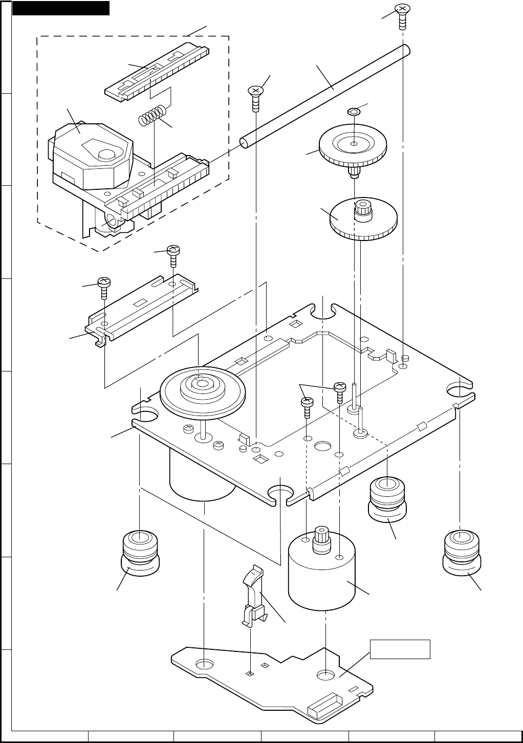
CD-C5H,CP-C5H
A
B
C
D
E
F
G
H
123456
Figure 12 CD MECHANISM EXPLODED VIEW
– 12 –
CD-C5H
701 304
701
302
301
702
702
303
M701
703x2
305x2
SW702A
M702 308
PWB-E
704
307
306-2
306
306-1
306-3
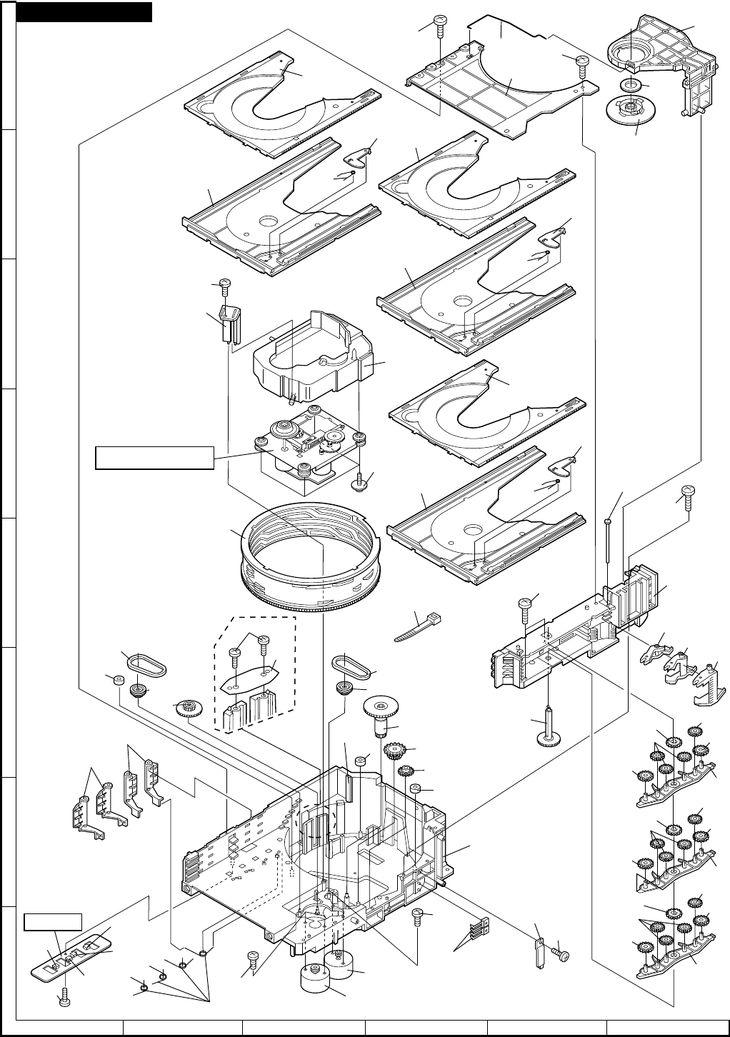
CD-C5H,CP-C5H
A
B
C
D
E
F
G
H
123456
Figure 13 CHANGER MECHANISM EXPLODED VIEWCD-CIW
– 13 –
CD-C5H
804x2
802
802 125
102
120
119
112
124
805x4
CD Mechanism
109
116
804
113
120
119
114
128
115
122
133
139
138
137
108
108x3
134 135
136
135
804
112
124
108
108x3
134 135
136
135
108
108x3
134 135
136
135
132
120
119
112
124
803
129
80mm
123x4
MOB1
121
SWB101~104
MOB2
801x2
801
x2
127
104
105
106
108
126
104
103
101
111x2
110x2 103
130
103
107
803x2
131
802
PWB-F
SWB
106
SWB
105 SWB
108
SWB
107
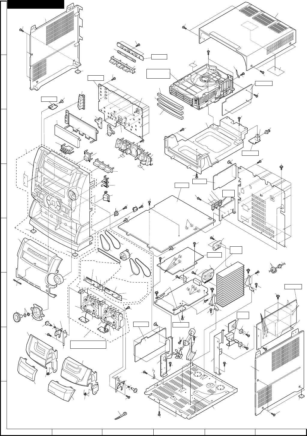
CD-C5H,CP-C5H
Figure 14 CABINET EXPLODED VIEW
– 14 –
CD-C5H
Note: Only the unit and consumale parts are supplied as aprts supply for the Tape mechanism.
A
B
C
D
E
F
G
H
123456
CD Changer
Block
PWB-C3
PWB-B PWB-K
PWB-A2
PWB-L
PWB-C1
PWB-D
PWB-C2
Silicon
Grease
Silicon
Grease
Silicon
Grease
612x3
214
223
606x3
240
203 260
239
209
206
207
208
606x12
614x2
238
237
FL701
SW702
204
604
604
224
225
222
PWB-A3
604
609
615
615
241
201-3
241
615x2
609x3 Q820
Q822
Q824
235
609x3
258
259
609
609x2
612x2
612x2
611x15
609
603x2 603
213
252
201
201-1
201-2
201-2
251
266x2
610x2IC901
603
x2
609
x2
608 226
227
608
609
x2
603
603
603x2
603x2
M901
605x2
261
248
608
229
228
608
x2
232 608x2
250
D850
D851
265
610
610
220
211
217
212
218
244
602x4
267x2
266
x2
266x6
215
611x3
234
609x2
249
249
263
245
300-3
(MM1)
300-6
300-6
300-9
300-9
300-7
300-1
300-2
300-8
300
TAPE MECHANISM
ASSEMBLY
300-8
300-7
300-10
231
230
243
242
247
246
601
601
607x2
607x2
613x6
608
254
SWE7 SWE8
SWE2
SWE1
300-4
(TAPE2 MECHANISM
PWB-H)
300-5
(TAPE1 MECHANISM
PWB-G)
253
233
603x2
T851
SW701
614
SWE5
SWE4
205
PWB-A1
PWB-C4
260x2
609
with
IC95
IC95
With
SW702
221
219
216
202
274
274
236
ICH01
610x2
609
603
266
x4
210
268x2
266x4
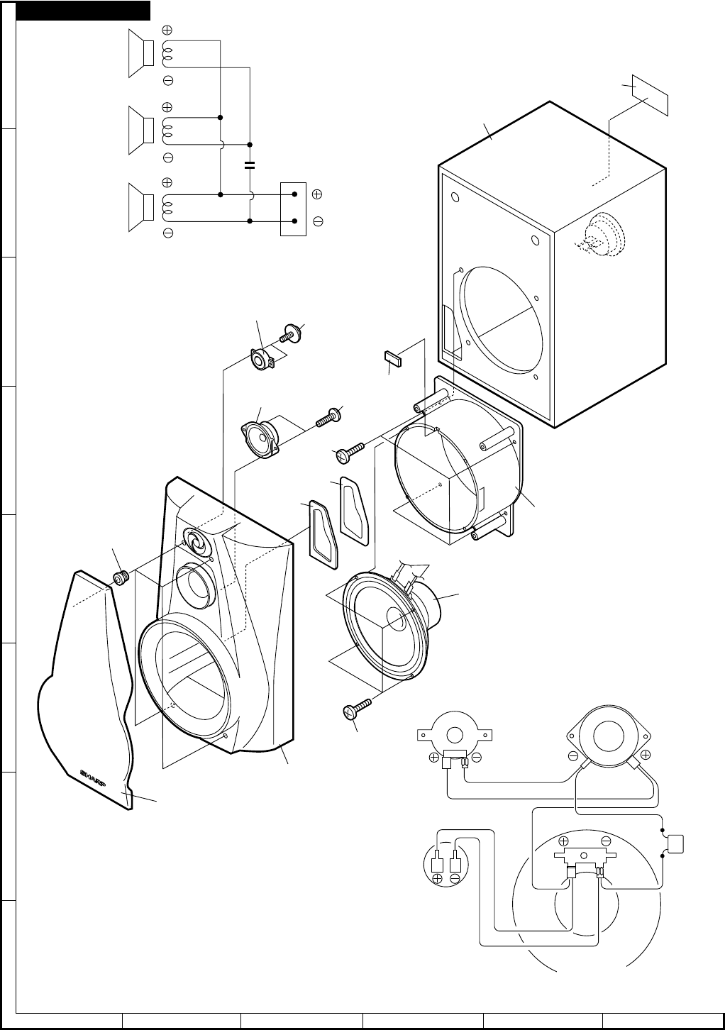
CD-C5H,CP-C5H
A
B
C
D
E
F
G
H
123456
Figure 15 FRONT SPEAKER EXPLODED VIEW
– 15 –
CP-C5H
SUPER
TWEETER
SP5(L-CH)
SP6(R-CH)
TWEETER
SP3(L-CH)
SP4(R-CH)
SP3(L-CH)
SP4(R-CH)
WOOFER
SP1(L-CH)
SP2(R-CH)
C1
2.2µ,100V,
Film Capacitor
C1
2.2µF,
100V
SPERKER
TERMINAL
SPEAKER
TERMINAL
SUPER
TWEETER
SP5(L-CH)
SP6(R-CH)
TWEETER
SP3(L-CH)
SP4(R-CH)
BK YL
BK
RED
BK
RED
SP5(L-CH)
SP6(R-CH)
SP1(L-CH)
SP2(R-CH)
903
914x4
901
902
WOOFER
SP1(L-CH)
SP2(R-CH)
904x4
913x4
907
905
908
912x2
911x2
906
909
910
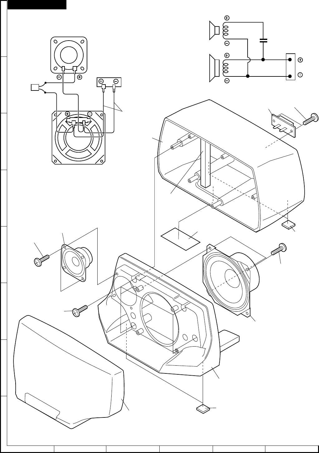
CD-C5H,CP-C5H
A
B
C
D
E
F
G
H
123456
Figure 16 CENTER SPEAKER EXPLODED VIEW
– 16 –
GBOXS0008AWM2
C1
2.7µF, 100V Film
Capacitor
C1
2.7µF, 100V
WOOFER
SP7
WOOFER
SP7
SPEAKER
TERMINAL(906)
SPEAKER
TERMINAL(906)
TWEETER
SP8 TWEETER
SP8
YL
BK
BK
YL
RD
909x2
904
906
907
x2
908
910x3
SP7
902
907x2
901
910x6
910x2 SP8
905
903
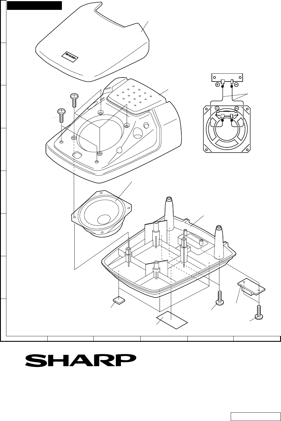
CD-C5H,CP-C5H
A
B
C
D
E
F
G
H
123456
Figure 17 SURROUND SPEAKER EXPLODED VIEW
(SURROUND)
GBOXS0009AWM2
COPYRIGHT 1998 BY SHARP COPORATION
ALL RIGHTS RESERVED.
No part of this publication may be reproduced,
stored in a retrieval system, or transmitted in
any from or by any means, electronic, mechanical,
photocopying, recording, or otherwise, without
prior written permission of the publisher. A9804-1793NS•HA•M
SG
SHARP CORPORATION
Communication Systems Group
Quality & Reliability Control Center
Higashihiroshima, Hiroshima 739-0192, Japan
Printed in Japan
©
FULL-RANGE
SP9 (L-CH)
SP10 (R-CH)
SPEAKER
TERMINAL(905)
901
909x4
902
SP9(L-CH)
SP10(R-CH)
905
908x2
909x2
906x4
903
907
904
908x2
RD BK
