CL SH351_High_Perf_Sync_Async_Integrated_SCSI_Disk_Ctlr_Product_Bulletin_Jan91 SH351 High Perf Sync Async Integrated SCSI Disk Ctlr Product Bulletin Jan91
User Manual: CL-SH351_High_Perf_Sync_Async_Integrated_SCSI_Disk_Ctlr_Product_Bulletin_Jan91
Open the PDF directly: View PDF ![]() .
.
Page Count: 6
[
~J
CIRRUS
LOGIC
FEATURES
Microcontrol/er Interface:
• Supports high-speed microcontroller interfaces (e.g.,
16-MHz 8051, 12-MHz 68HC11, 30-MHz HPC460X3)
SCSI
Interface:
• Supports SCSI-2 Initiation and Target modes
• Supports asynchronous DMAIPIO transfers up to 3
MBytes/sec.
• Supports synchronous DMAIPIO transfers up to 10
MBytes/sec.
• Supports up
to
15-byte synchronous transfer offsets
and 13 programmable transfer periods
• Controls synchronous transfer overrun/underrun
• Controls arbitration, selection, and reselection
in
hardware
•
Detects
selected
and
reselected
conditions
automatically
• Integrates 48-mA SCSI bus drivers
in
the interface
• Provides control for the external differential driver
option
Sector Formatter:
• Programmable Format Sequencer Writable Control
Store (WCS-31 x 4 bytes)
• Supports
up
to 32-MHz NRZ data rates (cont.)
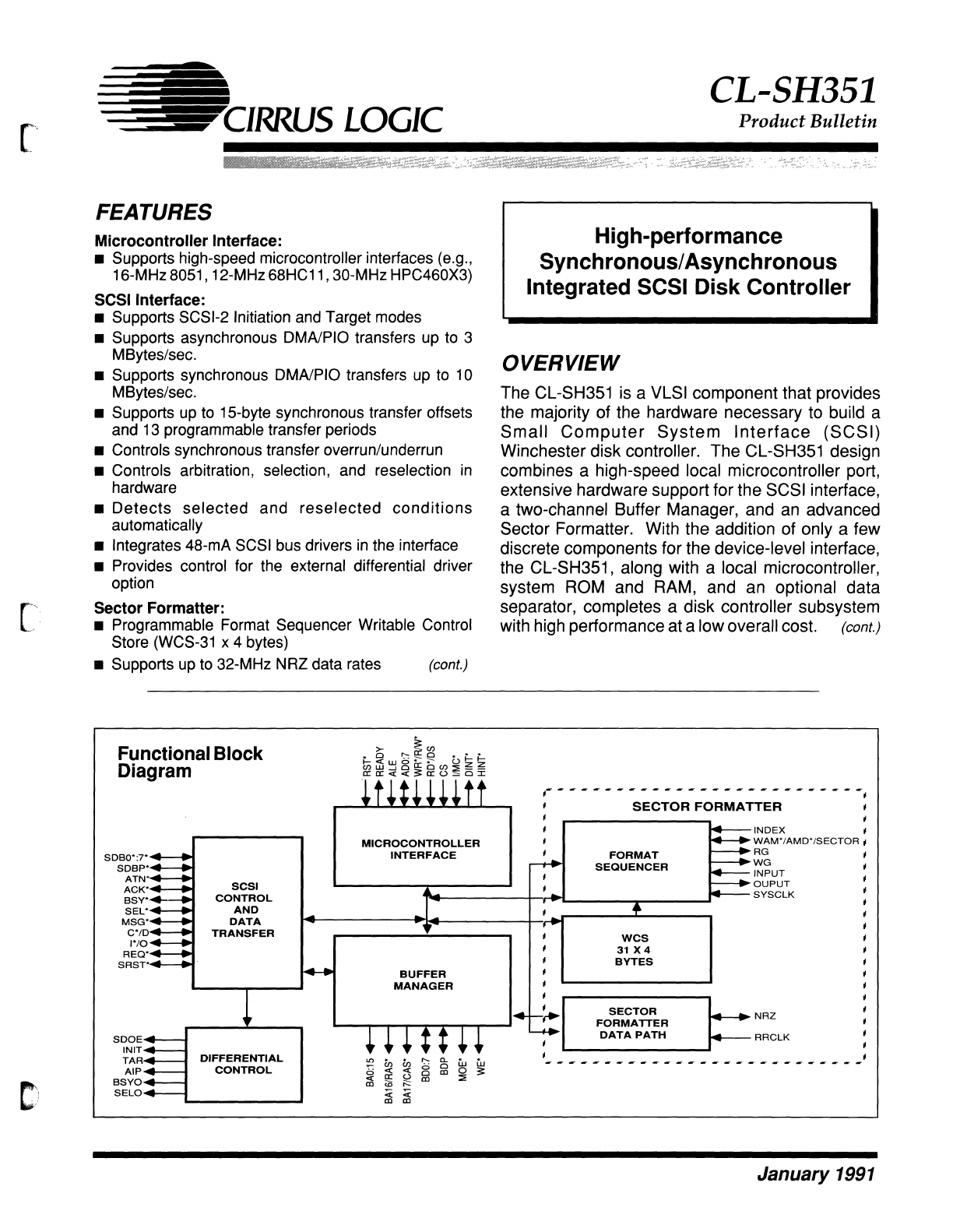
Functional Block
Diagram
SOBO':7'
MICROCONTROLLER
INTERFACE
SOBp·'--
.....
ATW'4-
.....
ACK·'----
BSY··--
.....
SEL'
MSG··----
C'/~---4~
1'/0
REO'
SRSP
SDOE
INIT
TAR
AlP
BSYO
SELO
SCSI
CONTROL
AND
DATA
TRANSFER
DIFFERENTIAL
CONTROL
...,
~
In
<C
a:
Ul
~
BUFFER
MANAGER
In
.....
D-
.:;
Cl
(3
Cl
'"
al
;::::
:;:
al
lu lu
0
==
::;:
CL-SH351
Product Bulletin
High-performance
Synchronous/Asynchronous
Integrated
SCSI
Disk Controller
OVERVIEW
The CL-SH351 is a VLSI component that provides
the majority of the hardware necessary to build a
Small
Computer
System
Interface
(SCSI)
Winchester disk controller. The CL-SH351 design
combines a high-speed local microcontroller port,
extensive hardware support for the SCSI interface,
a two-channel Buffer Manager, and
an
advanced
Sector Formatter. With the addition of only a few
discrete components for the device-level interface,
the CL-SH351, along with a local microcontroller,
system ROM and RAM, and an optional data
separator, completes a disk controller subsystem
with high performance at a low overall cost. (cont.)
1-
-------------------------
-I
SECTOR
FORMATTER
1
FORMAT
SEQUENCER
WCS
31
X4
BYTES
SECTOR
FORMATTER
DATA
PATH
INOEX
I
WAM'/AMO'/SECTOR
1
RG
WG
INPUT
OUPUT
SYSCLK
NRZ
RRCLK
I
---------------------------
January 1991
LOGIC
FEATURES (cont.)
• Allows split data field processing for embedded servo
and zoned designs
• Provides selectable 16-bit CRC or 32/56-bit ECC with
proprietary error correction hardware t
Buffer Manager:
• Dual-channel, circular buffer control with priority
resolution
• Direct buffer addressing up to 256 KBytes of SRAM
and 1 MByte of DRAM
OVERVIEW (cont.)
A local microcontroller provides the CL-SH351 with
initial operating parameters that include disk sector
format, the type and size of buffer memory, and
SCSI Host control. During data transfer operations,
the CL-SH351 requires only minimal intervention
from the local microcontroller. The microcontroller-
to-CL-SH351 communication path
is
a multiplexed
address and data bus similar to that provided by the
Intel®
8051- and the Motorola® 68HC11-class of
controllers. (There is a configuration signal
available to allow for either family of data control
Signal methods). The CL-SH351 has centralized
status registers with interrupt capability. These
features allow firmware designers flexibility
in
writing polled loops or interrupt handlers that
provide
real-time
process
control critical in
embedded controller drive applications.
The SCSI Host interface
is
designed for compliance
with the proposed SCSI-2 specification and
supports synchronous transfer capability of up to
10
Mbytes/sec. This ensures long-term compatibility
for both the hardware and the firmware developed
around the CL-SH351. The SCSI interface logic
includes integrated high-current (48-mA) drivers for
the single-ended option, as well as signals for
control of the external logic necessary to implement
the differential transceiver option. Both the asynch-
ronous and synchronous transfer protocols are
supported
in
either Initiator or Target mode. Routine
bus control operations, such as arbitration,
selection and reselection, are
automatically
sequenced
in
hardware.
This
method
of
implementing the SCSI interface makes the SCSI
protocol firmware extr:8mely flexible and very
efficient.
t A
u.s.
patent has been issued on Cirrus Logic's proprietary 56-bit ECC.
CL-SH351
Product
Bulletin
• Permits concurrent buffer memory throughput up to 14
MBytes/sec. in DRAM page mode and 15 MBytes/sec.
for SRAM
• Odd-parity data verification between the SCSI bus and
the Sector Formatter
Technology:
• 1
~O-pin
Quad Flat Pack (QFP) package
• Advanced, low-power, double-metal CMOS
technology
The Sector Formatter provides the disk data and
control functions. The Sector Formatter
is
capable
of handling NRZ data rates up to 32 Mbits/sec. The
Sector Formatter
is
subdivided into a Format
Sequencer and the Sector Formatter Data path.
The Format Sequencer uses a 31-word-by-4-byte
Writable Control Store (WCS) to hold a user-written
program. This program contains the control
information for the disk track and sector format. The
Sector Formatter Data path consists of the NRZ
data handling circuitry that includes the serializerl
deserializer (SERDES), the ECC and CRC error
control logic, the SERDES parity logic, and the data
signals to the Buffer Manager interface.
The Buffer Manager controls the flow of data
between the host and disk interfaces. These
interfaces store and retrieve data from the buffer
memory using interleaved access cycles. The
actual buffer memory may
be
implemented with
static or dynamic
RAM
devices. The CL-SH351
Buffer Manager
is
programmable to provide all of
the necessary address and control signals for
RAM
devices of varying access times. Up to 256 KBytes
of SRAM can be directly addressed by the
CL-SH351. Asmuchas1 MByteofDRAMisdirectly
supported by the CL -SH351 , with specific control for
64K, 256K, and 1-Mbit devices.
In
DRAM mode,
refresh
is
generated automatically through a third
channel to the buffer memory,
in
addition to the
concurrent disk and host accesses.
c
c
CL-SH351
Product Bulletin
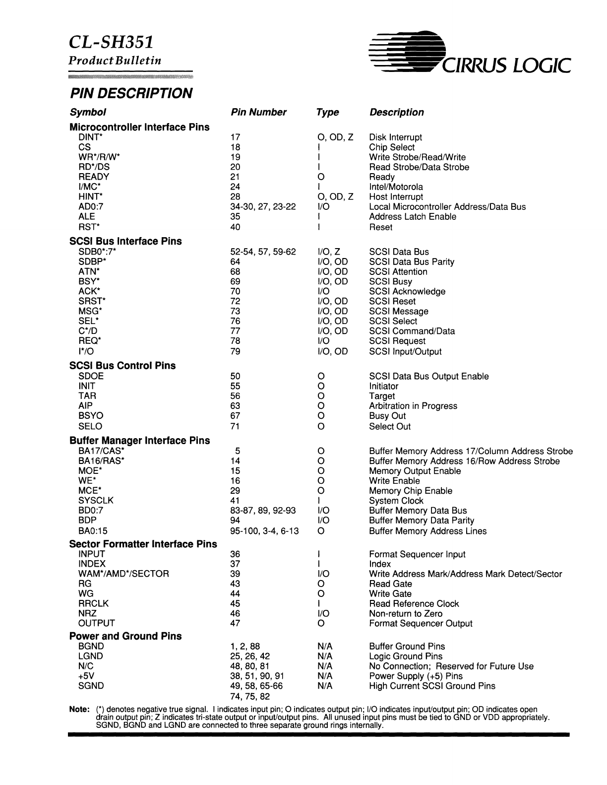
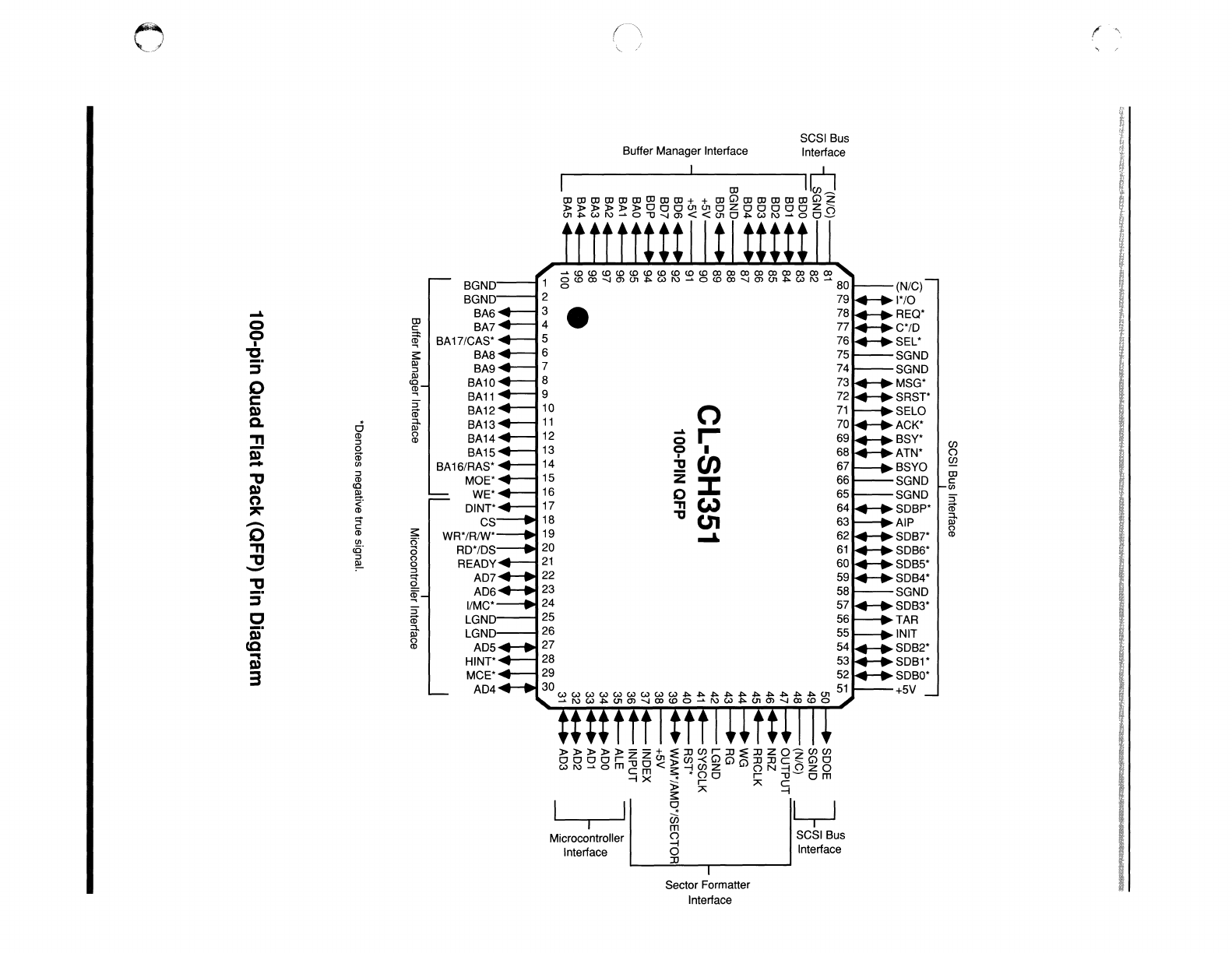
PIN DESCRIPTION
Symbol
Microcontroller
Interface
Pins
DINT"
CS
WR*/R/w*
RD*/DS
READY
I/MC*
HINT"
ADO:7
ALE
RST*
SCSI
Bus
Interface
Pins
SDBO*:7*
SDBP*
ATN*
BSY*
ACK*
SRST"
MSG*
SEL*
C*/D
REO*
1*/0
SCSI
Bus
Control
Pins
SDOE
INIT
TAR
AlP
BSYO
SELO
Buffer
Manager
Interface
Pins
BA17/CAS*
BA16/RAS*
MOE*
WE*
MCE*
SYSCLK
BDO:7
BOP
BAO:15
Sector
Formatter
Interface
Pins
INPUT
INDEX
WAM*/AMD*/SECTOR
RG
WG
RRCLK
NRl
OUTPUT
Power
and
Ground
Pins
BGND
LGND
N/C
+5V
SGND
Pin Number
17
18
19
20
21
24
28
34-30,27,23-22
35
40
52-54,57,59-62
64
68
69
70
72
73
76
77
78
79
50
55
56
63
67
71
5
14
15
16
29
41
83-87,89,92-93
94
95-100,3-4,6-13
36
37
39
43
44
45
46
47
1,2,88
25,26,42
48,80,81
38,51,90,91
49,58,65-66
74,75,82
Type
O,OD,l
I
I
I
o
I
O,OD,l
I/O
I
I
I/O,
l
1/0,00
1/0,00
1/0,00
I/O
1/0,00
1/0,00
1/0,00
1/0,00
I/O
1/0,00
o
o
o
o
o
o
o
o
o
o
o
I
I/O
I/O
o
I
I
I/O
o
o
I
I/O
o
N/A
N/A
N/A
N/A
N/A
Description
Disk Interrupt
Chip Select
Write Strobe/Read/Write
Read Strobe/Data Strobe
Ready
Intel/Motorola
Host Interrupt
LOGIC
Local Microcontroller Address/Data Bus
Address Latch Enable
Reset
SCSI Data Bus
SCSI Data Bus Parity
SCSI Attention
SCSI Busy
SCSI Acknowledge
SCSI Reset
SCSI Message
SCSI Select
SCSI Command/Data
SCSI Request
SCSI Input/Output
SCSI Data Bus Output Enable
Initiator
Target
Arbitration
in
Progress
Busy Out
Select Out
Buffer Memory Address 17/Column Address Strobe
Buffer Memory Address 16/Row Address Strobe
Memory Output Enable
Write Enable
Memory Chip Enable
System Clock
Buffer Memory Data Bus
Buffer Memory Data Parity
Buffer Memory Address Lines
Format Sequencer Input
Index
Write Address Mark/Address Mark Detect/Sector
Read Gate
Write Gate
Read Reference Clock
Non-return to Zero
Format Sequencer Output
Buffer Ground Pins
Logic Ground Pins
No Connection; Reserved for Future Use
Power Supply (+5) Pins
High Current SCSI Ground Pins
Note:
(*)
denotes negative true signal. I indicates input pin; 0 indicates output pin;
1/0
indicates inpuVoutput pin;
OD
indicates open
drain output pin; Z indicates tri-state output or inpuVoutput pins. All unused input pins must be tied to GND or
VDD
appropriately.
SGND, BGND
and
LGND are connected to three separate ground rings internally.
CL-SH351
Product
Bulletin
ADVANTAGES
Unique Features
• Programmable wait states for microcontrol/er
• Pin-configurable microcontrol/er data control
interface
• Separate disk
and
host microcontrol/er interrupts
• 15-byte offset in synchronous mode
• 16-byte FIFO for automatic
PIa
transfers
• External differential SCSI bus support
• Two Buffer Manager DMA channels
• Direct
256K
SRAM
and
1M
DRAM
addressing
•
Odd
through parity buffer verification
• Variable buffer segmentation logic
• Advanced-programmable branch conditions in
the Writable Control Store (WCS) program
• Conditional Format Sequencer execution
of
up to four paths
• Programmable read synchronization timeout
• ECC hardware correction circuitry
• Multiple data field processing within the ECC
LOGIC
Benefits
Allows the fastest microcontrollers to operate without
degrading bus performance.
Allows for direct connect to Intel- or Motorola-style
microcontrollers.
Supports faster, more direct interrupt processing by
microcontroller.
Greater flexibility for synchronous data transfer
negotiations.
Decreases command and information transfer
overhead.
Allows connection to any SCSI system with longer
cable lengths.
Enables read-look-ahead for high performance.
Increases buffer size alternatives to support caching.
Improves data integrity between host and disk data
transfers.
Allows protected data segments
in
buffer.
Supports flexible, automated defect management and
retry algorithms.
Supports end-of-track, retry and defect management
code.
Simplifies
ID
and Data Field searches.
Enables high-speed ECC correction within a sector
time period.
Provides support for embedded servo drives, zoned
drives and large defect skipping.
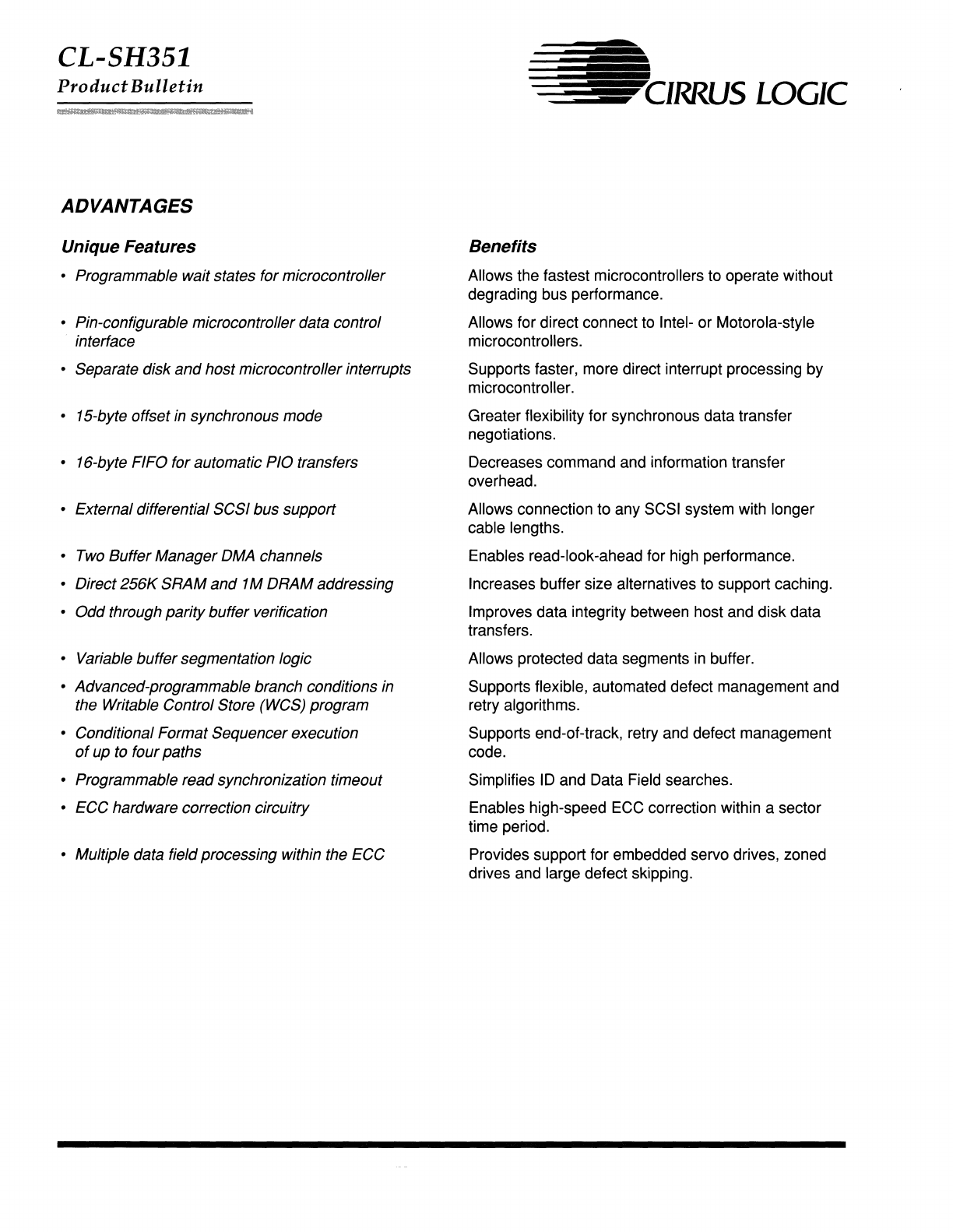
o
BGND
BGND
...a.
BA6
0
tD
BA7
c:
0
:::::
BA17ICAS"
I
~
"2,
s::
BA8
III
j
:>
BA9
III BA10
" <0
CD
~
BA11
C
:,-
I»
CD
BA12
a.
ci
::;j, BA13
III
CD
(')
BA14
"T1
:>
CD
i"
~
BA15
-
CJ)
BA16/RAS"
"0
:>
MOE"
CD
I» <0
!!l.
WE"
()
<"
DINT"
~
CD
-2 CS
"
s::
CD
WR"/R/W"
CJ)
(')"
"T1
cO"
a RD"/DS
"0
:>
(')
READY
!!!-
0
-
:>
::2
a AD7
ro
AD6
j
~
IIMC"
:,-
C
CD
LGND
ii)' ::;j, LGND III
(')
CQ
CD
AD5
""I
HINT"
I»
3 MCE"
AD4
1
2
3
4
5
6
7
8
9
10
11
12
13
14
15
16
17
18
19
20
21
22
23
24
25
26
27
28
29
30
(\
~'-
,/
Buffer Manager Interface SCSI Bus
Interface
tD
IbJ
tDtDtDtDtDtDtDtDtD++tDQtDtDtDtDtDQ~
~~~~~~~~~~~~~~82~g~g
~~~~~~~~~~~oooooooooooooooooo
g~oo~m~.wN~o~oo~m~.wN~M
•
0
.....
r-
0
0 I
:!!(J)
Z:::t
~W
"C
Ul
......
~..
....
....
.... ....
..... ..... ..... .....
....
....
.... ....
.... ....
.... ....
...
~~~~~zz~~~(IJ~~~~ZOz(IJ(IJ
oooorm~o<~(IJ~~'QQ~~e~QO
WN~O
em
s::~(lJZ
ON~OZO
~x
•
'00
r
~~om
» r
;>;
e
~
;>;~
IL.-J
Microcontrolier
~
SCSI Bus
Interface 0 Interface
~
Sector Formatter
Interface
1"
I
4
(N/C)
1"/0
REO"
COlD
SEL"
SGND
SGND
MSG"
SRST*
SELO
ACK"
BSY"
(IJ
ATN" 0
BSYO
~
SGND
tD
c:
CJ)
SGND
~
SDBP" ::;j,
AlP III
(')
SDB7"
CD
SDB6"
SDB5"
SDB4"
SGND
SDB3"
TAR
INIT
SDB2"
SDB1"
SDBO"
+5V
CL-SH351
RRUSLOGIC
Product
Bulletin
Direct Sb/es Offices
Domestic International
N. CALIFORNIA NORTH CENTRAL NORTHEASTERN
JAPAN
San Jose AREA AREA Kanagawa-Ken
TEL: 408/436-7110 Westchester,
IL
Andover, MA TEL: 81/462-76-0601
FAX: 408/437-8960 TEL: 708/449-7715 TEL: 508/474-9300 FAX: 81/462-76-0291
FAX: 708/449-7804 FAX: 508/474-9149
S. CALIFORNIA SINGAPORE
Laguna Hills SOUTH CENTRAL Philadelphia, PA TEL: 65/3532122
TEL: 714/472-3939 AREA TEL: 215/251-6881 FAX: 65/3532166
FAX: 714/472-4804 Austin, TX FAX: 215/651-0147
TEL: 512/794-8490 TAIWAN
Thousand Oaks FAX: 512/794-8069 SOUTH EASTERN Taipei
TEL: 805/371-5381 AREA TEL: 886/2-718-4533
FAX: 805/371-5382 Boca Raton, FL FAX: 886/2-718-4526
TEL: 407/994-9883
ROCKY MOUNTAIN FAX: 407/994-9887 GERMANY
AREA Herrsching
Boulder, CO Atlanta, GA TEL: 49/8152-2030
TEL: 303/939-9739 TEL: 404/263-7601 FAX: 49/8152-6211
FAX: 303/440-5712 FAX: 404n29-6942
The Company
Cirrus Logic, Inc., is a leading supplier of high-integration peripheral controller circuits for
mass storage, graphics,
and
data communications. The company also produces state-of-the-art
software
and
firmware to complement its
product
lines. Cirrus Logic technology is used
in
leading-edge personal computers, engineering workstations,
and
office automation.
The Cirrus Logic formula combines proprietary
S/LATMt
IC design automation
with
system
design expertise. The
S/LA
design system is a proven tool for developing high-performance
logic circuits
in
half the time of most semiconductor companies. The results are better
VLSI
products, on-time, that help
you
win
in the marketplace.
Cirrus Logic's extensive quality assurance
program
-one of the industry's most stringent -
ensures the
utmost
in
product
reliability. Talk to
our
systems
and
applications specialists; see
how
you can benefit from a
new
kind of semiconductor company -Cirrus Logic.
t U.S. Patent No. 4,293,783
© Copyright, Cirrus Logic, Inc., 1990
Cirrus Logic, Inc. believes the information contained in this document is acCurate and reliable. However, it is subject to change
without notice. No responsibility is assumed by Cirrus Logic, Inc. for its use, nor for infringements of patents or other rights of
third parties. This document implies no license under patents or copyrights. Trademarks
in
this document belong to their
respective companies. Cirrus Logic, Inc. products are covered under one or more of the following U.S. patents: 4,293,783; Re.
31,287; 4,763,332; 4,777,635; 4,839,896; 4,931,946; 4,979,173.
CIRRUS LOGIC, Inc., 3100 West Warren Ave. Fremont, CA 94538
TEL: 415/623-8300 FAX: 415/226-2160 215351-001
C
()
