Sm0321_e CPSX635W
User Manual: CPSX635W
Open the PDF directly: View PDF ![]() .
.
Page Count: 102 [warning: Documents this large are best viewed by clicking the View PDF Link!]
SM0321
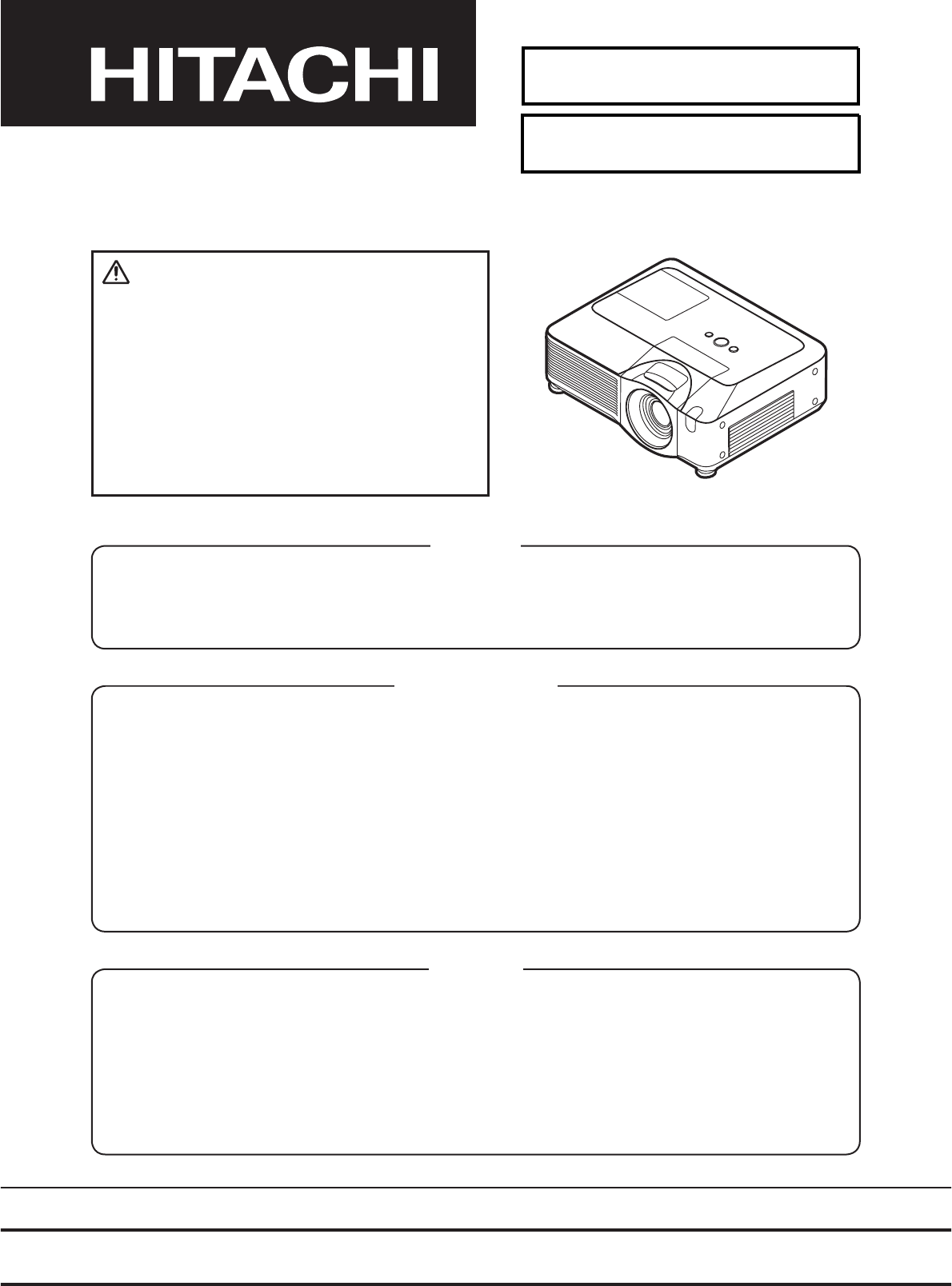
CP-SX635W(ED3SX40N)
SERVICE MANUAL
Be sure to read this manual before servicing. To assure safety from fi re, electric shock, injury, harmful
radiation and materials, various measures are provided in this Hitachi Multimedia LCD Projector.
Be sure to read cautionary items described in the manual to maintain safety before servicing.
Caution
1. When replacing the lamp, avoid burns to your fi ngers, the lamp becomes very hot.
2. Never touch the lamp bulb with a fi nger or anything else. Never drop it or give it a shock as this may
cause bursting of the bulb.
3. This projector is provided with a high voltage circuit for the lamp. Do not touch the electric parts of
power unit (circuit) and power unit (ballast) after turning on the projector.
4. Do not touch the exhaust fan during operation.
5. The LCD module assembly is likely to be damaged. When replacing the LCD LENS/PRISM
assembly, do not hold the FPC of the LCD module assembly.
6. Use the cables which are included with the projector or as specifi ed.
Service Warning
Warning
The technical information and parts shown in this
manual are not to be used for the development,
design, production, storage or use of nuclear, chemical,
biological or missile weapons or other weapons of
mass destruction or military purposes or purposes that
endanger global safety and peace. Moreover, do not
sell, give, or export these items, or grant permission for
use to parties with such objectives. Forward all inquiries
to Hitachi Ltd.
1. Features ------------------------------------------------------ 2
2. Specifi cations ----------------------------------------------- 2
3. Controls ------------------------------------------------------ 3
4. Adjustment --------------------------------------------------- 6
5. Troubleshooting ------------------------------------------ 13
6. Servicing ---------------------------------------------------- 20
7. Wiring diagrams------------------------------------------- 37
8. Disassembly diagram ----------------------------------- 49
9. Replacement parts list ---------------------------------- 60
10. RS-232C communication ------------------------------ 61
11. Block diagram--------------------------------------------- 70
12. Connector connection diagram ----------------------- 71
13.Schematic diagrams------------------------------------ 72
Contents
SPECIFICATIONS AND PARTS ARE SUBJECT TO CHANGE FOR IMPROVEMENT.
Multimedia LCD Projector
January 2009

2
CP-SX635(ED3SX40N)
1. Features
• High Brightness • Remote Control Via Your Web Browser
• Low Noise • Rich Connectivity
2. Specifications
Liquid
crystal
panel
Drive system TFT active matrix
Panel size 2.0cm(0.79 type)
Number of pixels 1400 (H) x 1050 (V)
Lamp 275W UHB
Digital
signal HDMI
Type:T.M.D.S
Signal level : DC : 3.3V±5%
AC : 0.15-1.56Vp-p
RGB
signal
RGB IN D-sub 15pin Video : Analog 0.7Vp-p(75 termination)
H/V. sync. : TTL level (positive/negative)
Composite sync. : TTL level
BNC
RGB OUT
Video:Analog 0.7Vp-p, 75 output impedance (positive)
H/V. sync.: TTL level (positive/negative)
Composite sync.: TTL level
VIDEO
signal
VIDEO IN 1.0Vp-p (75 termination)
S-VIDEO IN
Y signal: 1.0±0.1Vp-p, (75 termination)
C signal: 0.286±0.1Vp-p (NTSC burst signal, 75 termination)
0.3±0.1Vp-p (PAL/SECAM burst signal, 75 termination)
COMPONENT
VIDEO
Y 1.0±0.1Vp-p, 75 termination (positive)
CB/PB0.7±0.1Vp-p, 75 termination (positive)
CR/PR0.7±0.1Vp-p, 75 termination (positive)
AUDIO
signal
AUDIO IN 1 500mVrms, 47k or more (max. 2Vrms)
AUDIO IN 2
AUDIO IN 3/4 L/R 500mVrms, 47k or more (max. 2Vrms)
HDMI Linear PCM format
Sampling frequency : 48kHz, 44.1kHz, 32kHz
AUDIO OUT 0~500mVrms, output impedance 1k (max. 2Vrms)
RS232C INPUT Hi: Max. 20V, Min. 2.6V Lo: Typ. –20.0V, Max. 0.8V
OUTPUT Hi: Typ. 8.0V, Min. 5.0V Lo: Typ. –7.0V, Max. –5.0V
USB
(Mouse)
I/O Level
(differential)
Amplitude of
differential signal
| (D+) - (D–) | > 0.2V
D+>2.8V, D–<0.3V or D+>2.8V, D–<0.3V
Amplitude of
signal
INPUT: “L”=0.8V or less, “H”=2.0V or more
OUTPUT: “L”=0.3V or less, “H”=2.8V~3.6V
NETWORK
100Base-TX/10Base-T Differential output: 1.9~2.1V (100 termination)
Speaker 4W x 2
Power supply AC100~120V/5.0A, AC220~240V/2.1A
Power consumption 460W
Dimensions 418 (W) x 139 (H) x 319 (D) mm (Not including protruding parts)
Weight 7.1kg
Temperature range Operation : 5~35°C
Storage : -20~60°C
Accessories
Remote control x1
RGB cable x 1
Power cords x 3
Batteries x 2
User’s manuals x 1
LENS CAP x 1
3
CP-SX635(ED3SX40N)
3. Names of each part
Projector
(1) Speakers (x 2)
(2) Focus ring
(3) Zoom ring
(4) Lamp cover
The lamp unit is inside.
(5) Lens shift cover
(6) Horizontal lens shift dial
(7) Vertical lens shift dial
(8) Front cover
(9) Lens
(10) Lens cover
(11) Remote sensors (x 3)
(12) Elevator feet (x 2)
(13) Elevator knobs (x 2)
(14) Filter cover
The air filter and intake vent are
inside.
(15) Exhaust vents
(16) Intake vents
(17) Rivet hole
(18) Handle
(19) Battery cover
(20) Control panel
(21) Rear panel
ŹHOT! : Do not touch around the lamp cover and the exhaust
vents during use or just after use, since it is too hot.
ŹDo not look into the lens or vents while the lamp is on, since the strong light is
not good for your eyes.
ŹDo not grab the front cover to hold the projector up, since the projector may
drop down.
ŹDo not handle the elevator knobs without holding the projector, since the
projector may drop down.
WARNING
ŹMaintain normal ventilation to prevent the projector from
heating up. Do not cover, block or plug up the vents. Do not place anything that
can stick or be sucked to the vents, around the intake vents. Clean the air filter
periodically.
CAUTION
(2)
(3)
(8)
(15)
(12)
(10) (9) (11)
(12) (13)
(14)
(11)
(20)
(4)
HOT!
HOT!
(7)
(6)
(5)
(12)
(12)
(13)
(17)
(19)
(16)
(20)
(11)
(1)
(1)
(21)
(18)
4
CP-SX635(ED3SX40N)
Control panel
(1) STANDBY/ON button
(2) MENU button
It consists of four cursor buttons.
(3) INPUT button
(4) POWER indicator
(5) TEMP indicator
(6) LAMP indicator
Rear panel
(1) Shutdown switch
(2) Security slot
(3) Security bar
(4) AC IN (AC inlet)
(5) Power switch
(6) RGB1 port
(7) RGB2(G/Y, B/CB/PB, R/CR/PR, H, V)
port
(8) CONTROL port
(9) HDMI port
(10) VIDEO port
(11) S-VIDEO port
(12) COMPONENT (Y, CB/PB, CR/PR)
ports
(13) AUDIO IN1 port
(14) AUDIO IN2 port
(15) AUDIO IN3 (R/L) ports
(16) AUDIO IN4 (R/L) ports
(17) RGB OUT port
(18) AUDIO OUT port
(19) REMOTE CONTROL port
(20) LAN port
(21) USB port
(6)
(5)
(4)
(1) (2) (3)
ŹDo not use the security bar and the security slot to prevent the
projector from falling down, since it is not designed for it.
ŹUse the shutdown switch only when the projector is not turned off by normal
procedure, since pushing this switch stops operation of the projector without
cooling it down.
CAUTION
LAN
AC IN
I O
VIDEO
CONTROL
AUDIO IN1
AUDIO IN2
AUDIO OUT
RGB
OUT
RGB1
RGB2
HDMI
R L R L
AUDIO IN3 AUDIO IN4
CB/PB
Y
CR/PR
B/CB/PBR/CR/PR
G/Y
HV
USB
REMOTE
CONTROL
S-VIDEO
(14) (13) (17) (6) (7)(20)(18)(9) (19) (8)
(2)(1)
(10) (11) (15) (16) (12)
(5) (4) (3)
(21)
5
CP-SX635(ED3SX40N)
Remote control
(1) Laser pointer
It is a beam outlet.
(2) LASER INDICATOR
(3) LASER button
(4) STANDBY/ON button
(5) VOLUME+/- buttons
(6) MUTE button
(7) VIDEO button
(8) RGB button
(9) SEARCH button
(10) AUTO button
(11) ASPECT button
(12) POSITION button
(13) KEYSTONE button
(14) MY SOURCE/DOC.CAMERA button
(15) MAGNIFY - ON/- OFF buttons
(16) FREEZE button
(17) BLANK button
(18) MY BUTTON - 1 button
(19) MY BUTTON - 2 button
(20) MENU button
(21) Lever switch : acting 3 functions as below.
Cursor button Ÿ : to slide toward the side marked Ÿ.
Cursor button ź : to slide toward the side marked ź.
ENTER button : to push down the center point.
(22) Cursor buttons Ż/Ź
(23) RESET button
(24) ESC button
(25) Mouse left button
(26) Mouse right button
(27) PAGE UP button
(28) PAGE DOWN button
(29) Wired remote control port
(30) Battery cover
(31) Battery holder
(32) Frequency switch
ŹDo not look into the beam outlet and
point the beam at people and pets while pressing the
LASER button, since the beam is not good for eyes.
WARNING
ŹNote that the laser beam may result
in hazardous radiation exposure. Use the laser pointer
only for pointing on the screen.
CAUTION
BLANK LASER
ASPECT
PUSH
ENTER
PAGE UP
LASER
INDICATOR
MY SOURCE/
DOC.CAMERA
SEARCH
STANDBY/ON VIDEO RGB
PAGE DOWN
ESC MENU RESET
POSITION AUTO
MAGNIFY
ON
OFF
MY BUTTON
1
2
VOLUME
+
-
FREEZE KEYSTONE MUTE
(11)
(22)
(27)
(20)
(24)
(12)
(15)
(16)
(13)
(29)
(26)
(21)
(28)
(23)
(10)
(18)
(5)
(6)
(19)
(25)
(17)
(4)
(7)
(2) (1)
(3)
(8)
Back of
the remote control
(31)
(32)
(30)
(14)
(9)
6
CP-SX635(ED3SX40N)
4. Adjustment
4-1 Before adjusting
4-1-1 Selection of adjustment
When any parts in the table 4-1 are changed, choose the proper adjusting items with the chart.
Table 4-1: Relation between the replaced part and adjustment
Replaced
part
Adjustment
Flicker
(Chap.4-2)
Ghost
(Chap.4-3)
PSIG
(Chap.4-4)
White
balance
(Chap.4-5)
Color
uniformity
(Chap.4-6)
Dichroic
optics unit
LCD/LENS
prism
assembly
PWB
assembly
Main
Lamp
unit
assembly
: means need for adjustment. : means not need for adjustment.
: means recommended.
4-1-2 Setting of condition before adjustments
1. Before starting adjustments, warm up projector
for about 10 minutes.Turn off the automatic
keystone function in OPTION Menu. If you
changed [AUTO KEYSTONE] from [TURN ON]
to [TURN OFF], set to [TURN ON] after adjustment.
2. Set Zoom Wide to Max. And project an image
with more than 1m (40 inches) in diagonal size.
3. Normalizing the video adjustments
Press the [MENU] button to display the EASY
menu. If Advanced menu comes up, move to the
Easy menu.
Select the RESET in the EASY menu and press
the [ ] or [ENTER] button to open the RESET dia-
log. Choose the EXECUTE with the [ ] button.
Note that the projector will not allow you to reset
its adjustment values with no signal input.
4. Perform all adjustments from the FACTORY
MENU. Operate as follows to display the FAC-
TORY MENU.
When you use the remote control...
a. Press the [MENU] button of the remote con-
trol to display the Easy menu. (If the Ad-
vanced menu appears, move to the Easy
menu.)
b. Select the RESET in the Easy menu, and
then press the [ ] or [ENTER] button.
c. Next, press the [RESET] button one time. And
hold the [RESET] button for 3 seconds or lon-
ger (the FACTORY MENU will appear).
When you use the keypad of the projector...
a. Press the
[ ],
[ ],
[ ]
or [
] button of the pro-
jector to display the Easy menu. (If the Ad-
vanced menu appears, move to the Easy
menu.)
b. Select the RESET in the Easy menu, and
then press the [ ] or [ENTER] button.
c. Next, press the [ ] button one time. And re-
press and hold the [ ] button together with
the [INPUT] button for 3 seconds or more (the
FACTORY MENU will appear).

7
CP-SX635(ED3SX40N)
4-3 Ghost adjustment
Test pattern for the adjustment Adjustment procedure
1. Make this adjustment after completing the ad-
justment in the section 4-2.
Set 0 to the GHOST R, G, B in OPTION - SERVICE
Menu.
2.
Use DAC-P - GHOST - R: in the FACTORY MENU
to adjust so that R color ghost is at a minimum.
(Set the adjustment value to default, and then
raise the value. When a ghost appears to the left
of a vertical line, reduce the value by 6 steps.)
3. In the same way, use DAC-P - GHOST-G: in
the FACTORY MENU to adjust so that G color
ghost is at a minimum.
4. In the same way, use DAC-P - GHOST-B: in
the FACTORY MENU to adjust so that B color
ghost is at a minimum.
4-2 Flicker adjustment
(V.COM adjustment)
Test pattern for the adjustment
Adjustment procedure
1.
Use DAC-P - V.COM - R: in the FACTORY
MENU to adjust so that the flicker at the center of
the screen is less than the flicker at the periphery.
(When the flicker is about the same across the
whole screen, adjust so that the flicker at the center
of the screen is somewhat less than elsewhere.)
2. In the same way, use DAC-P - V.COM-G: in the
FACTORY MENU to adjust the G color flicker.
3. In the same way, use DAC-P - V.COM-B: in the
FACTORY MENU to adjust the B color flicker.
NOTE: The test pattern shown on the left some-
times has a horizontal line across the screen.
4-4
PSIG adjustment
(vertical bars adjustment)
Test pattern for the adjustment Adjustment procedure
1. Make this adjustment after completing the ad-
justment in the section 4-3.
2.
Use DAC - P_PSIG - R : in the FACTORY MENU
and use it so that vertical bars are minimized.
3. In the same way, use
DAC - P_PSIG - G
: in the
FACTORY MENU and use it so that vertical
bars
are minimized.
4. In the same way, use
DAC - P_PSIG - B
: in the
FACTORY MENU and use it so that vertical
bars
are minimized.
Press ENTER key
0/255
30%
112/255
30%
128/255
64
/255
88
/255
112
/255
136
/255
160
/255
160
/255
136
/255
112
/255
88
/255
64
/255

8
CP-SX635(ED3SX40N)
4-5
White balance adjustment
(visual inspection)
Preparations
1. Perform these adjustments after the adjust-
ments described in Section 4-4.
2. Reset gamma correction before adjustment.
Place the cursor on [GAMMA] in the FACTORY
MENU, press the [RESET] key and select RESET.
Adjustment procedure
1. First, adjust the G color.
2.
Select GAMMA, SUB-CNT, and G: in the FACTORY
MENU. If the background is white solid, press the
[ENTER] key on the Remote control transmitter to
change to [G] monochrome in the 33-tone grayscale.
3. Adjust GAMMA, SUB-CNT, and G: in the FAC-
TORY MENU so that brightness of 33 steps is
best.
4. Don’t adjust GAMMA, SUB-BRT, and G: in the
FACTORY MENU because we want to keep the
best contrast ratio.
5. Then adjust colors R and B.
6.
Select GAMMA, SUB-CNT, and G: in the FACTORY
MENU. If the background is white solid, press the
[ENTER] key on the remote control to change to [W]
monochrome in the 33-tone grayscale.
7. Adjust GAMMA, SUB-BRT, R: and B: in the
FACTORY MENU so that low-brightness white
balance is best.
8. Adjust GAMMA, SUB-CNT, R: and B: in the
FACTORY MENU so that middle-brightness
white balance is best.
9. Repeat steps 7 to 8 above, and adjust so that
brightness white balance of 33 steps is best.
9
CP-SX635(ED3SX40N)
VID-AD
MIN
MID-1
MID-2 ... 6
MAX
DAC-P
GAMMA
C. UNIF.
No. 1 R 0
STRIPE
OPTION
C.UNIF
ON/OFF ON
OFF
G 0 B 0
Major adjustment lattice point No.
4-6 Color uniformity adjustments
Preparations
1.
Perform these adjustments after the adjustments
described in the section 4-5.
2. Make a color uniformity adjustments for the fol-
lowing tones.
MIN tone (approx. 7% input signal)
MID-1 tone (approx. 14% input signal)
MID-2 tone (approx. 21% input signal)
MID-3 tone (approx. 29% input signal)
MID-4 tone (approx. 36% input signal)
MID-5 tone (approx. 50% input signal)
MID-6 tone (approx. 61% input signal)
MAX tone (approx. 75% input signal)
NOTE: The brightness level of the test patterns
in MID-4 and MID-6 is selectable.
3. Select the [C.UNIF.] in the FACTORY MENU
and press the [ ] key. This operation displays
the Adjust Tone menu (shown below) on the
bottom of the screen.
To choose the tone to be adjusted, press the [
] key and then use the [ ] or [ ] key.
Select the major adjustment lattice point No.
and color, and then adjust them.
4. The major adjustment lattice point numbers (a
total of 17 points) corresponds to the major ad-
justment lattice point positions in the diagram
on the right. The color uniformity of the entire
screen can be adjusted by adjusting the white
balance for each of the points starting in order
from the low numbers.
5. Adjustment point No.1 should not be adjusted,
because it controls the brightness of the entire
screen.
6.
To temporarily turn correction off, place the cur-
sor on [C.UNIF.] in the Adjust Tone menu and
press the [ ] key. The ON/OFF menu appears.
Place the cursor on [ON] with the [ ] key and
press the [ ] key. To turn it on again, place the
cursor on [OFF] and press the [ ] key.
7. Although this adjustment can also be made us-
ing internal signals, we will here use the [EN-
TER] key on the remote control to select the fol-
lowing two signals.
Solid monochrome adjustment color (use G
color adjustment when a color differential me-
ter is used).
Solid white (use for adjustment other than
above).
8. Reset color-shading correction before adjust-
ment.
When resetting all values of 8 tones and all
colors, place the cursor on [C.UNIF.] in the
FACTORY MENU, press the [RESET] key and
select RESET in the dialog.
When resetting only 1 tone, place the cursor
on the tone such as MID-1 to be reset, press
the [RESET] key and select RESET in the di-
alog.
Single tone and monochrome resets cannot
be performed.
FACTORY MENU
Major adjustment lattice point position
14 12
13
16
15 17
6 4 8
2 1 3
7 5 9
10 11
V/6
H/6 H/3 H/3 H/6
V/3
V/3
V/6
Adjust tone menu
10
CP-SX635(ED3SX40N)
Adjustment procedure 1
(When a color differential meter is used)
1. First adjust the [MID-1] tone [G:].
2. Select adjustment point [No.2][G:].
When the background is not [G] monochrome,
press the [ENTER] key on the remote control to
switch to solid [G] monochrome.
3. Measure the illumination at adjustment points
No. 2, No.3, No.10 and No.11.
The values should be:
No.2 = Y2 [lx] No.10 = Y10 [lx]
No.3 = Y3 [lx] No.11 = Y11 [lx]
4. No.2 and No.3 adjustment points have the aver-
age of Y2 and Y3.
Y2 = ( Y2 + Y3 ) / 2 ± 2 [%]
Y3 = ( Y2 + Y3 ) / 2 ± 2 [%]
5. No.10 and No.11 adjustment points have the
average of Y10 and Y11.
Y10 = ( Y10 + Y11 ) / 2 ± 2 [%]
Y11 = ( Y10 + Y11 ) / 2 ± 2 [%]
6. Then adjust the [MID-1] tone [R] and [B].
When the background is [G] monochrome,
press the [ENTER] key on the remote control to
switch to solid white.
7. Measure the color coordinates of adjustment
point [No.1] and make a note of them.
Assume that they are x = x1, y = y1.
Note: When the CL-100 color and color differ-
ence meter is used, the [¨](delta) mode
is convenient. When adjustment point
[No.1] color coordinate has been select-
ed, set the slide switch on the side to
[¨](delta) while holding down the [F] but-
ton on the front panel. The measurement
shown after this displays the deviation
from measurement point 1.
8. Measure the color coordinates of measurement
point [No.2] and adjust [No.2][R:] and [B:] so
that the coordinates are as follows.
x = x1 ± 0.005 , y = y1 ± 0.010
9. Similarly, measure adjustment points [No.3] to
[No.17] and adjust their color coordinates start-
ing in order from the small number points.
This completes adjustments required for
[MID-1].
Note: Since excessive correction may lead to a
correction data overview during internal
calculations, use the following values for
reference.
[No.2] to [No.5] ± 40 or less
[No.6] to [No.9] ± 50 or less
[No.10] to [No.13] ± 70 or less
[No.14] to [No.17] ± 120 or less
10.Then adjust the [MIN] tone [G] so that the ad-
justment values are two times as much as
MID-1] tone [G] values.
This completes [G] color adjustments.
11.Then adjust [MIN] tone [R] and [B].
Select [No.2] [B:] and press the [ENTER] key
on the Remote control transmitter to change to
solid white.
12.Measure the color coordinates of adjustment
point [No.1] and make a note of them.
Assume that they are x = x1, y = y1.
13.Now measure the color coordinates of mea-
surement point [No.2] and adjust [No.2][R:] and
[B:] so that the coordinates are as follows.
x = x1 ± 0.005 , y = y1 ± 0.010 (Target)
x = x1 ± 0.020 , y = y1 ± 0.040
14.Similarly, measure adjustment points [No.3] to
[No.17] and adjust their color coordinates start-
ing in order from the small number points.
This completes [MIN] tone adjustments.
15.Now make similar adjustments for [MID-2] tone.
(Adjust [MID-2] tone [G] so that the adjustment
data set half as many as [MID-1] tone [G].)
16.Now make similar adjustments for [MID-3],
[MID-5], [MAX] tones. (It is not necessary to ad-
just the [G] data in these tones.)
17. After completing the step 16, set the value of
the [MID-4] tone [R]: [No.2] to the mean of the
values of the [R]: [No.2] in the [MID-3] and
[MID-4] tones.
18. Set all the values for the [No.2] to [No.17] of
the [MID-4] tone [R] and [B] in the same way as
the step 17.
19. Finally, set the data of the [MID-6] tone [R] and
[B] using the values of the [MID-5] and [MAX]
tones in the same way as the [MID-4] tone [R]
and [B] adjustments in the step 17 and 18.
11
CP-SX635(ED3SX40N)
Adjustment procedure 2
(visual inspection)
1. First adjust [MIN] tone [G:].
2. Select [No.2] [G:].
If the background is [G] monochrome, press the
[ENTER] key on the remote control to switch to
solid white.
3. View measurement point [No.2] and [No.3].
Lower the [G] color intensity only of the color
point whose [G] color is more intense than
measurement point [No.1].
4. View measurement point [No.10] and [No.11].
Lower the [G] color intensity only of the color
point whose [G] color is more intense than
measurement point [No.1], and raise the inten-
sity of the point whose color intensity is lower
than measurement point [No.1].
5. Now adjust the [MIN] tone for colors [R] and
[B].
6. View measurement points [No.2], [No.3],
[No.10] and [No.11]. Adjust the [R] and [B] of
each measurement point so that they have the
same color as measurement point [No.1].
Adjustment technique:
First, adjust [B:] of the point whose color is to
be adjusted so that it approximates that of
[No.1]. If [R:] is low at this time, the image will
have cyan cast, in which case [R:] is increased.
On the other hand, if [R:] is excessive, the im-
age will have a magenta cast, in which case
[R:] is decreased.
Overall, a cyan cast makes it easy to see color
shading.
7. Next, view measurement points [No.4], [No.5],
[No.12], [No.13] and make similar adjustments.
8.
Then adjust measurement points [No.6], [No.7],
[No.8], [No.9], [No.14], [No.15], [No.16] and [No.17].
This completes the [MIN] tone adjustments.
9. Make similar adjustments for other tones, ex-
cept the [MID-4] and [MID-6] tones, as de-
scribed in steps 1 to 8 above.
8
3
16
17
9
11
6
14
2
12
15 13
10
7
4
1
5
8
3
16
17
9
11
14 12
15 13
10
4
1
5
6
2
7
8
3
16
17
9
11
6
2
12
13
14
15
10
7
4
1
5
14 12
15 13
10
4
1
5
6
2
7
8
3
16
17
9
11
17
9
15 13
75
3
17
9
11
15 13
10 1
5
6
2
7
8
16
17
9
6
12
13
7
4
5
14 12
10
4
1
6
2
8
3
16
17
9
11311210 1
1614 12
86 4 84
1614 12
3112
14
15
10 1
5
7
15 13
17
9
15 13
75
3
17
9
11
6
17
9
6
13
75
14 12
10
46
2
8
16
311210 1
1614 12
86 4 84
1614 12
3112
14
15
10
5
7
15
10 12
1315
5
7
12
4
1
8
17
13
1 3 11
16
95
17
9
15 13
75
3
17
9
11
6
17
9
6
13
75
14 12
10
46
2
8
16
3112 1
1614 12
84 84
1614 12
32
14
15
10
5
7
15
10 12
13
5
7
12
4
1
17
13
1 3
5
11
9
11
8
16
15
10
6
No. 2 deviation range No. 10 deviation range No. 3 deviation range No. 11 deviation range
No. 4 deviation range No. 12 deviation range No. 5 deviation range No. 13 deviation range
No. 6 deviation range No. 7 deviation range No. 8 deviation range No. 9 deviation range
No. 14 deviation range No. 15 deviation range No. 16 deviation range No. 17 deviation range
12
CP-SX635(ED3SX40N)
4-7 Adjusting the zoom and focus
1. Use the zoom ring to adjust the screen size.
2. Use the focus ring to focus the picture.
Focus ring
Zoom ring
Top
4-8 Adjusting the lens shift
1. Use the vertical lens shift knob to shift the picture
upward or downward.
2. Use the horizontal lens shift knob to shift the pic-
ture left or right.
1/2
1/10
1/10
UP
DOWN
RIGHT
Lens shift cover
LEFT
NOTE
When the vertical lens shift is adjusted, it is recom-
mended to shift the picture upward for fine adjustment
13
CP-SX635(ED3SX40N)
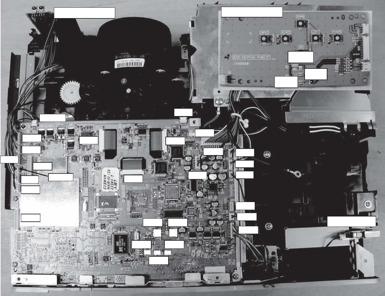
5. Troubleshooting
Check points
PW assembly KEYPAD
DK03
(
LAMP
)
DK02
(
TEMP
)
DK01
(
POWER
)
PW assembly REMOTE
E302
(
E1
)
E807
EE02
E800
P701
E804
EW51
EA02
EA03
E802
E808
E
805
P501
P601
PW assembly SW
E806
E305
EE01
E310
E
803
E301
(
E2
)
EA04
E801
IM04
IM05
IM01
IM02
IM03
14
CP-SX635(ED3SX40N)
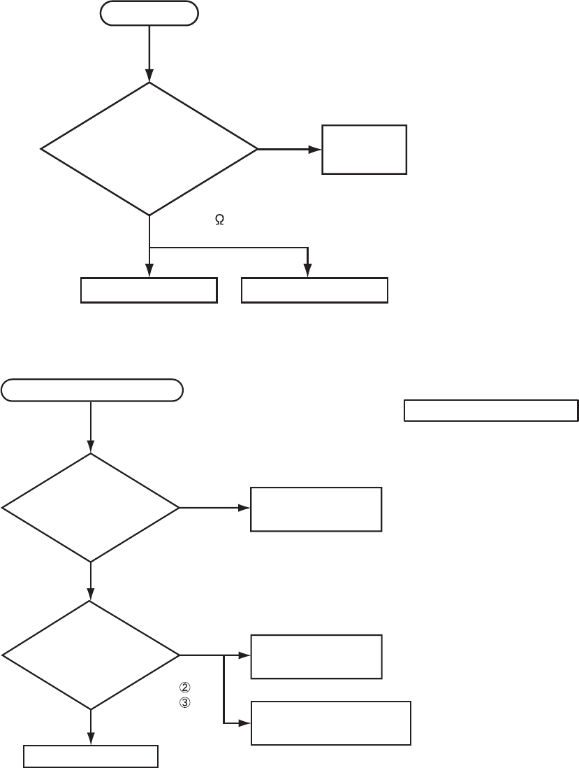
Power can not be turned on
Are
voltage
supplied at pins
(9),(12) and (14) of E800 on
the PWB assembly MAIN in
standby mode?
Are
voltage supplied
at pins (2) and (7) of E800
on the PWB assembly
MAIN in standby
mode?
NO
YES
(9): +6.0V
(12): +4.0V
(14): GND
Does
LAMP (DK03) or
TEMP (DK02) indicator light
or blink?
YES
(2): +15V
(4): GND(for +15V)
(7): +17V
(11): GND(for +17V)
*: Be sure to unplug the power cord before measuring resistance.
Measure
resistance* between
pins (9) and (14), and
between pins (12) and
(14) of E800.
Disconnect TSW
from power unit circuit, and
measure resistance of
TSW.
Open
0
PWB assembly MAIN
Power unit (circuit)
Thermal switch (TSW)
Open
Power unit (circuit) Fuse on the power unit
(circuit)
NO
Measure
resistance* between
pins (2) and (4), and between
pins (7) and (11) of
E800.
0
PWB assembly MAIN
Power unit (circuit)
Power unit (circuit)
Short
Open
Go to the next page
YES
PWB assembly SW
E808, E941
Open
Lamp door Re-attach lamp
door
Measure
resistance*
between pins (1) and
(2) of E808 when the
S941 is pushed.
PWB assembly MAIN
0
15
CP-SX635(ED3SX40N)
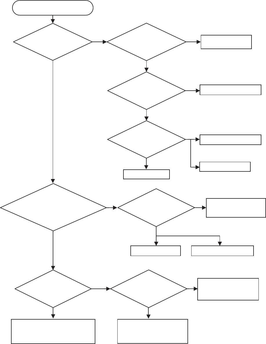
Lamp does not light
What
is the state of
LAMP indicator DK03
during operation?
Is the
LAMP installation
correct?
Light
install the Lamp
PWB assembly
MAIN
Is the
voltage at the
(4) of E807 on the
PWB assembly MAIN fi xed
to "1V~5V" during
warming-up?
NG
Change the
lamp. Does lamp
light?
Lamp
Light
YES
Yes
Power unit (ballast) Power unit (circuit)
No
What
is the state of
TEMP indicator
DK02?
Thermistor
(E1/E2)
Is
the voltage
at the (1) of E807 on the
PWB assembly MAIN set to
"L" during warming-
up?
Not light
PWB assembly MAIN
YES
“L” = 0V
Power unit (ballast)
No
Are
the voltage
supplied to the pin
(2) of connectors** for
DC fans soon after
the button is
pressed?
Is
the
voltage supplied
to the pin (4) of E805
and E804 soon after
the button is
pressed?
Observe
the voltage
waveforms at pin (1) of
connectors for DC fans**
soon after the button
is pressed.
Blinks
DC fan
(failed in above check)
Correct waveform is drawn below.
f 40Hz
PWB assembly
MAIN
NO (0V)
PWB assembly
MAIN
PWB assembly
MAIN
Correct
YES
YES
incorrect
*: Be sure to unplug the power cord
before measuring resistance.
Not light
**: DC fan connectors are E801,
E802, E803, E804 and E805.
(1V ~ 5V)
(5V or higher)
Lights
Measure
resistance
of E1 and E2 after
disconnecting them
from MAIN
board.
OK
PWB assembly
MAIN
E2: 5 to 20k
E1: 0.5 to 2k
NG (open / short)
Not light
No
(<1V or > 5V)
16
CP-SX635(ED3SX40N)
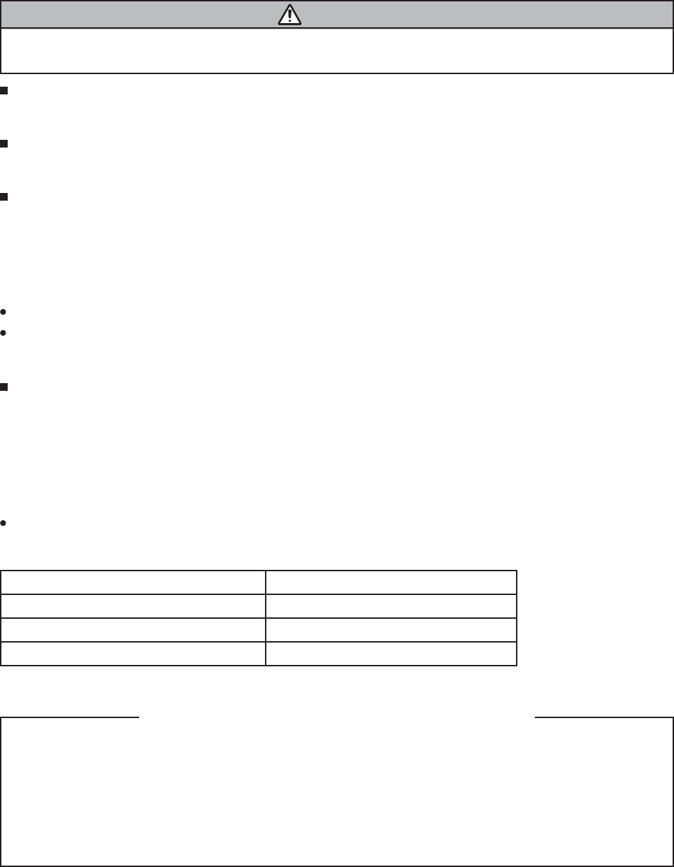
Picture is not displayed when the RGB signal is input
Are
the splash screen
and the user menu displayed
correctly?
YES
YES
Is the
picture from RGB
out port displayed correctly
on another monitor
display?
YES
Confirm
the LCD Panels
connection to the MAIN
board.
No
CPC40 connector
PWB assembly MAIN LCD/Lens prism assembly
OK
PWB assembly MAIN
No
THS7327PHPR
(IM04:D_sub, IM05:BNC)
PWB assembly MAIN
No
NG
Picture is not displayed when the Video, S-Video or component signal is input
Are
the splash
screen and the user menu
displayed correctly?
YES
Confirm
the LCD Panels
connection to the MAIN
board.
No
CPC40 connector
PWB assembly MAIN LCD/Lens prism assembly
OK
NG
PWB assembly MAIN PWB assembly INPUT
EL8302IUZ
(IM01:D_sub, IM02:BNC,
IM03:Component)
17
CP-SX635(ED3SX40N)
PWB assembly Main PWB assembly INPUT
Check at operating mode
(Make sure the state of MUTE , Volume and AUDIO-SPEAKER)
No sound
infinity
about 24
Speaker
Disconnect
the speaker from the
PWB assembly Main, and
measure its
resistance.
The check after parts change
1. PC power supply OFF
2. Connection of cable
3. Projector starting
4. PC starting
*When not operating :
PC set up change of cable.
Can not control to RS-232C
NO
YES
Use cross cable
Check the
RS-232C cable.
Are pin No. 2 and 3
crossed?
Make sure PC setup
YES
NO
PWB assembly MAIN
PWB assembly CONTROL
Are the
signals input at each
pins on the CONTROL
Port?
: RX
: TX
Pin
Pin
18
CP-SX635(ED3SX40N)
NO
Does the Lamp
on lower right of the
Network connector light
in green?
Can’t communicate with computer
via NETWORK terminal.
Check at operating mode
Make sure NETWORK
hardware
Set IP address and Subnet
Mask in the
NETWORK-SETUP menu with
manual operation.
Is IP Address in
the Network > Information menu
set to “0.0.0.0” after waiting
more than 1 minute?
YES
YES
NO
Are
both IP Address
and Subnet mask in the
Network > Information menu set to
"0.0.0.0" after waiting more than
1 minute?
PWB assembly MAIN
Use new LAN cable
YES
Set IP address and Subnet Mask
in the Advanced Menu > Network
> SETUP menu with manual operation.
Is
the DHCP in the
Advanced Menu > Network
> Setup > DHCP is on?
NO
Is the computer
connected with the
projector directly?
If
Subnet Mask is
"255.255.255.0", are
"xxx.yyy.zzz" portion of IP address
setting of computer and
projector
same?
PWB assembly MAIN
YES
Is there
DHCP server on
the network which the
projector is connected
to?
Make sure those settings
of the projector and
computer are correct.
PWB assembly NETWORK
PWB assembly NETWORK
PWB assembly NETWORK
NO
YES
NO
YES
NO
Use the same IP address
setting except for "N" on
computer and projector.
YES YES
NO
IP address: xxx.yyy.zzz.N
NO
Are there
any damage to the cable
between computer and
projector?

19
CP-SX635(ED3SX40N)
YES
YES
YES
NO
NO
2.5V or more
YES
Set the time in
DATE AND TIME on
NETWORK menu.
NO
NO
Is voltage
input at pin 11 of
EE01 on PWB assembly
MAIN when power switch
was turned
off.
Was the time set before?
DATE
AND TIME is
displayed as 2000/1/1 0:00
in INFORMATION on
NETWORK
menu.
YES
YES
NO
NO Configure the Daylight
Saving Time in web
setting.
Is the
time adjusted by
Daylight Savings Time ?
Is TIME
DIFFERENCE on
INFORMATION correct ?
Set the time.
Is internal clock battery
old ?
Time is not correctly displayed.
PWB assembly
MAIN
PWB assembly
NETWORK
•
PWB assembly NETWORK
• Cables (CNNET)
Use new battery.
(see 6.4)
20
CP-SX635(ED3SX40N)
6. Service points
6-1 Lead free solder [CAUTION]
This product uses lead free solder (unleaded) to help preserve the environment. Please read these
instructions before attempting any soldering work.
Lead free solder indicator
Printed circuit boards using lead free solder are engraved with an "F" or "LF".
Properties of lead free solder
The melting point of lead free solder is 40-50˚C higher than leaded solder.
Servicing solder
Solder with an alloy composition of Sn-3.0Ag-0.5Cu or Sn-0.7Cu is recommended.
Although servicing with leaded solder is possible, there are a few precautions that have to be taken. (Not
taking these precautions may cause the solder to not harden properly, and lead to consequent malfunctions.)
Precautions when using leaded solder
Remove all lead free solder from soldered joints when replacing components.
If leaded solder should be added to existing lead free joints, mix in the leaded solder thoroughly after the
lead free solder has been completely melted (do not apply the soldering iron without solder).
Servicing soldering iron
A soldering iron with a temperature setting capability (temperature control function) is recommended.
The melting point of lead free solder is higher than leaded solder. Use a soldering iron that maintains a high
stable temperature (large heat capacity), and that allows temperature adjustment according to the part being
serviced, to avoid poor servicing performance.
Recommended soldering iron:
Soldering iron with temperature control function (temperature range: 320-450˚C)
Recommended temperature range per part:
Part Soldering iron temperature
Mounting (chips) on mounted PCB 320˚C±30˚C
Mounting (chips) on empty PCB 380˚C±30˚C
Chassis, metallic shield, etc. 420˚C±30˚C
PWB assembly MAIN
PWB assembly REMOTE
PWB assembly CONTROL
PWB assembly KEYPAD
PWB assembly BATTERY
PWB assembly INPUT
PWB assembly SW
PWB assembly NETWORK
POWER UNIT (BALLAST)
POWER UNIT (CIRCUIT)
The PWB assembly which has used lead free solder
CAUTION
Always wear safety glasses to prevent fumes or molten solder from getting into the eyes. Lead free solder
can splatter at high temperatures (600˚C).
21
CP-SX635(ED3SX40N)
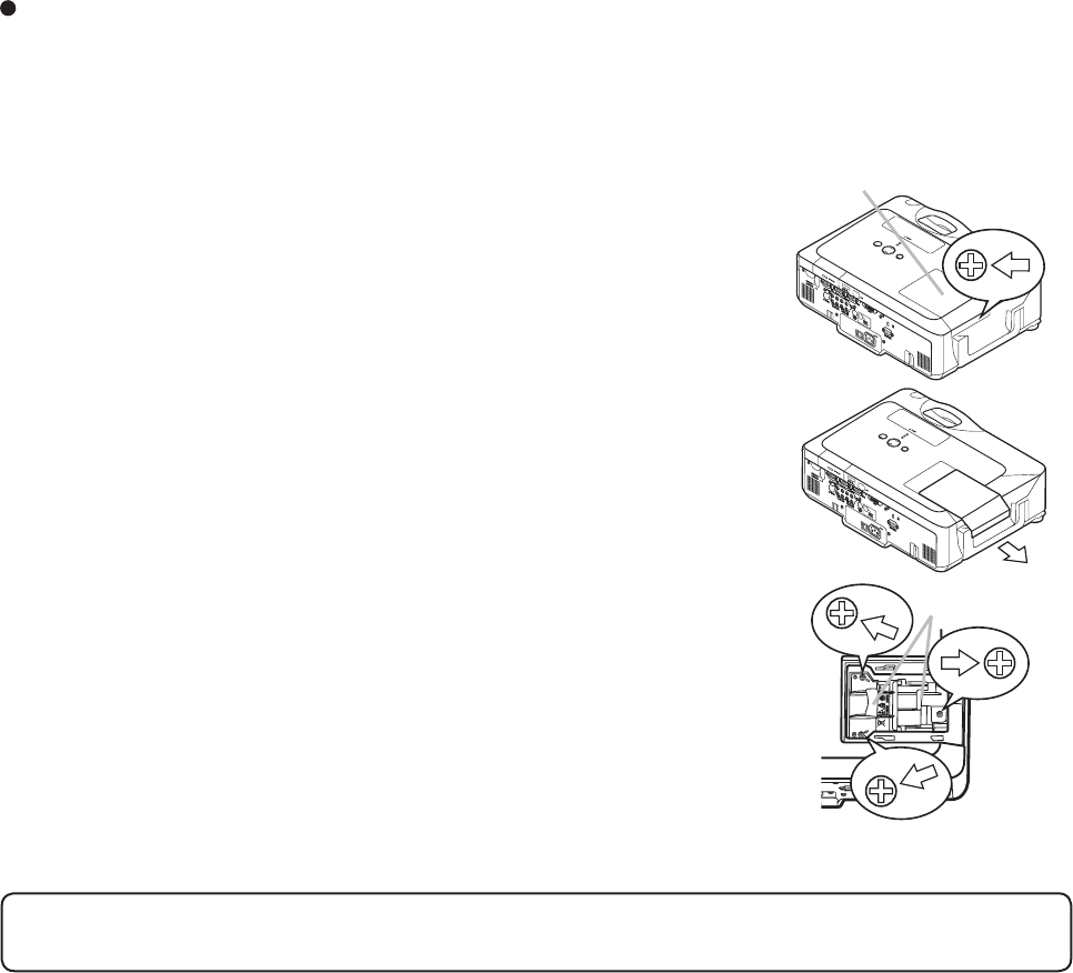
6-2 Before Replacing The LCD/Lens Prism
You should not replace separately the parts of the liquid crystal LCD/Lens prism because it works properly
only when used together. Therefore, regarding these parts, you can either replace part, LCD/Lens prism
assembly, or send the whole unit LCD/Lens prism assembly back to HITACHI, where we will replace the
malfunctioning part, recondition the device and send it back to you.
DISTRIBUTOR HITACHI
G Panel
Do not disassemble the unit
because replacement of separate
parts is not possible.
Return
Replacement of G Panel Reconditioning
1. Preparation
Please prepare cleaning tools and materials as follows. And prepare relatively clean room not to work in
additional dust, while removing operation.
(1) Swab for cleaning : P#: NX05742, "Cotton stick L70"
(2) Air duster (Dust blower, spray can)
(3) Vacuum cleaner
2. Disassemble and setting up.
(1) Turn off the projector, and unplug the power cord.
(2) Remove the lamp cover and upper case, according to the disassembling diagram of chapter 8.
(3) Unscrew the shield bracket of PWB assembly MAIN to make it free.
6-3 Cleaning up dust from panels and optical filters
WARNING
Wear sunglasses to protect your eyes when you maintain the projector with its lamp on.
CAUTION
Make sure to remove the shield
bracket before removing the PWB
assembly MAIN.
Otherwise, fl exible cables will be
damaged.
Remove these screws
22
CP-SX635(ED3SX40N)
(4) Unscrew PWB assembly MAIN to make it free and disconnect the LCD panel flexible cables.
(5) Press and hold the switch S941 using an insulator during maintenance.
(6) Keep the unscrewed wires away from all of electric parts.
Flexible cables of LCD panel
Remove these screws
Remove these 6 screws
23
CP-SX635(ED3SX40N)
3. Maintenance point
Each color part has same construction.
By using swab and air duster, you can
easily remove dust from panel and opti-
cal filter.
4. Cleaning the panels and optical filters
(1) Turn on the set and lit on the lamp.
(2) By using swab and air duster, remove the dust. Focusing dust makes you check the dust on screen.
• While removing the dust, separated dust will
be blown off by air cooling system.
• Please pay attention not to damage panels
and optical filters.
5. Re-assembly
(1) Turn off the set and unplug the power cord.
(2) Remove an insulator from S941.
(3)
Screw down the PWB assembly MAIN and connect the LCD panel flexible cables to the PWB assembly MAIN.
(4) Re-assemble the set.
(5)
While re-assembling, please clean the intake filter by using a vacuum cleaner.
Swab
Panel
Holder
Optical filter Air
Swab
Panel
Holder
Optical filter
24
CP-SX635(ED3SX40N)
6-4 Battery
6-4-1 Replacing Internal Clock Battery
If the battery is placed in the battery holder upside-down, follow the procedure below to remove and
reload it properly.
1. Remove the battery cover as described in steps 1 through 3 above.
2. While lifting the side of the projector closest to the lens, press the metal claw of the battery holder. The
battery will fall out of the holder, so be careful not to lose it.
NOTE
• The internal clock’s time will be reset when the battery is removed. Please reconfigure the time via the
menu or a web browser after replacing the battery.
WARNING
Always handle the batteries with care and use them only as directed. Battery may explode if mistreated.
Do not recharge, disassemble or dispose of in fire.
And also improper use may result in cracking or leakage, which could result in fire, injury and/or pollution
of the surrounding environment.
• Be sure to use only the batteries specified. Do not use batteries of different types at the same time. Do
not mix a new battery with used one.
• Make sure the plus and minus terminals are correctly aligned when loading a battery.
If the battery is placed in the battery holder upside-down, it may be hard to remove.
• Keep a battery away from children and pets. If swallowed consult a physician immediately for emergency
treatment.
• Do not short circuit or solder a battery.
• Do not allow a battery in a fire or water. Keep batteries in a dark, cool and dry place.
• If you observe a leakage of a battery, wipe out the flower and then replace a battery. If the liquid adheres
to your body or clothes, rinse well with water immediately.
• Obey the local laws on disposing the battery.
Consumption of the battery makes the clock not to work correctly. When the clock is wrong
or it has stopped, please replace the battery according to the following procedures.
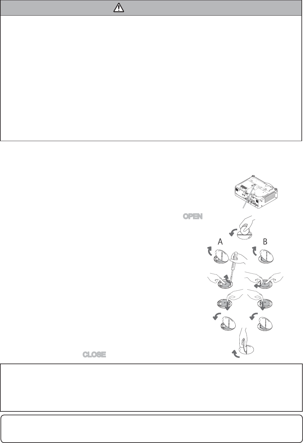
1. Turn the projector off, and unplug the power cord. Allow the
projector to cool sufficiently.
2. After making sure that the projector has cooled adequately,
slowly turn over the projector, so that the bottom is facing.
3. Turn the battery cover fully in the direction indicated “OPEN”
using a coin or the like, and pick the cover up to remove it.
4. One of two kinds of clock battery holder, A or B shown to the
right, is inside the battery cover.
For A holder:
Pry up the battery using a flathead screwdriver or the like
to take it out. While prying it up, put a finger lightly on the
battery since it may pop out of the holder.
For B holder:
Press the metal claw of the battery holder putting a finger
lightly on the battery since it may pop out of the holder.
Then the battery will come up. Remove the battery.
5. Replace the battery with a new HITACHI MAXELLL, Part
No. CR2032 or CR2032H.
Slide the battery in under the plastic claw, and push it into
the holder until it clicks.
6. Replace the battery cover in place, then turn it in the
direction indicated “CLOSE” using such as coins, to fix.
Battery Cover
OPEN
CLOSE
OPEN
CLOSE
OPEN
CLOSE
OPEN
CLOSE
OPEN
CLOSE
90°
OPEN
CLOSE
90°
25
CP-SX635(ED3SX40N)
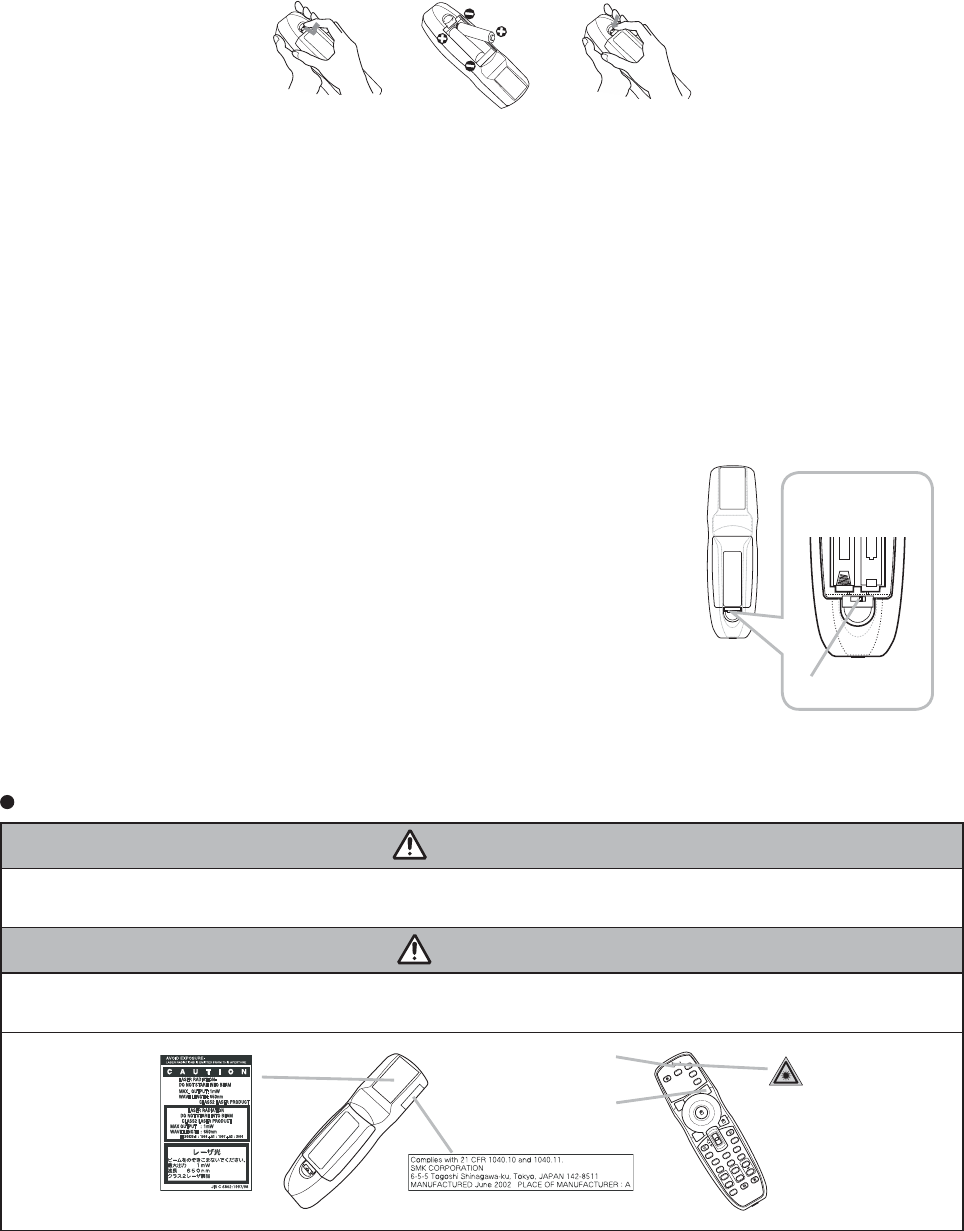
6-4-2 Potting batteries into the remote control
•Use the batteries included in this product or two new batteries of the specified type: HITACHI MAXELL,
part number LR6 or R6P.
1. Remove the battery cover.
Slide back and remove the battery cover in the direction of the arrow.
2. Insert the batteries.
Align and insert the two AA batteries according to their plus and minus terminals as indicated in the
remote control.
3. Close the battery cover.
Replace the battery cover in the direction of the arrow and snap it back into place.
Changing the frequency of remote control signal
The accessory remote control has the choice of the mode 1 or the
mode 2, in the frequency of its signal.
If the remote control does not function properly, attempt to change the
signal frequency. Please remember that the “REMOTE FREQ.” in SER-
VICE item of OPTION menu of the projector to be controlled should be
set to the same mode as the remote control.
To set the mode of the remote control, slide the knob of the frequency
switch inside the battery cover into the position indicated by the mode
number to choose.
21
Back of the
remote control
Inside of
the battery cover
Frequency switch
About the Laser pointer
WARNING
• The laser pointer of the remote control is used in place of a fi nger or rod. Never look directly into the laser
beam outlet or point the laser beam at other people. The laser beam can cause vision problems.
CAUTION
• Use of controls or adjustments or performance of procedures other than those specifi ed herein may result
in hazardous radiation exposure.
BLANK LASER
ASPECT
PUSH
ENTER
PAGE UP
LASER
INDICATOR
MY SOURCE/
DOC.CAMERA
SEARCH
STANDBY/ON VIDEO RGB
PAGE DOWN
ESC MENU RESET
POSITIONAUTO PbyP
MAGNIFY
ON
OFF
MY BUTTON
1
2
VOLUME
FREEZE KEYSTONE MUTE
LASER INDICATOR
LASER button
This remote control has a laser pointer in place of a fi nger or rod. The laser beam works and the LASER
INDICATOR lights while the LASER button is pressed.
26
CP-SX635(ED3SX40N)
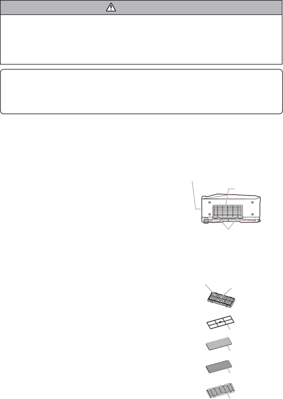
6-5 Air filter
WARNING
• Before caring, make sure the power switch is off and the power cable is not plugged in, then allow the
projector to cool suffi ciently. The care in a high temperature state of the projector could cause an electric
shock, a burn and/or malfunction to the projector.
• Use only the air fi lter of the specifi ed type. Do not use the projector with the air fi lter and the fi lter cover
removed. It could result in a fi re and/or malfunction to the projector.
• The air fi lter should be cleaned periodically. If the air fi lter becomes clogged by dust or the like, internal
temperatures rise and could cause a fi re, a burn and/or malfunction to the projector.
NOTE
• Please replace the air fi lter when it is damaged or too soiled, and also when you replace the lamp.
• Please reset the fi lter time only when you have cleaned or replaced the air fi lter, for a suitable indication
about the air fi lter.
• The projector may display the message such as “CHECK THE AIR FLOW” or turn itself off, to prevent the
internal heat level rising.
If the air fi lter becomes clogged by dust or the like, internal temperatures rise and could cause a fi re, a burn
and/or malfunction to the projector. When the indicators or a message prompts to clean the air fi lter, clean
the air fi lter as soon as possible.
Please check and clean the air fi lter periodically, even if there is no message.Please replace the air fi lter
when it is damaged or too soiled.
And also when you replace the lamp, please replace the air filter. An air filter of specified type will come
together with a replacement lamp for this projector.
1. Turn the projector off, and unplug the power cord. Allow the lamp
to cool for at least 45 minutes.
2. When the projector is suspended from the ceiling, apply the
vacuum cleaner to and around the fi lter cover fi rst, to prevent
penetration of dust or the like.
3. Hold the filter cover knobs while lifting it.The filter unit made up
the filter cover and others will come off.
4. Use a vacuum cleaner for the filter vent of the projector and the
filter frame side of the filter unit.
If the air filter is damaged or too soiled, replace it according to the following procedure number 5 to 7.
Otherwise, please jump to the procedure number 8.
5. To remove the filter frame, hold the filter cover while holding and pulling the filter frame’s knob by another
hand.
6. Set new fi lters where former fi lters were. Put the larger meshed
fi lter into a fi lter cover fi rst. Then put the fi ner meshed fi lter on the
larger meshed one.
7. Put the filter frame back.
8. Put the filter unit back into the projector.
9. Turn the projector on and reset the fi lter time using the FILTER
TIME function.
(1) Press the MENU button to display a menu. When the EASY
MENU has appeared, please skip the next step (2).
(2) Point at the “OPTION” in the left column of the menu using ź/Ÿ
button, then press the Ź button.
(3) Point at the “FILTER TIME” using ź/Ÿ button, then press the Ź
button. A dialog will appear.
(4) Press the Ÿ button to select “RESET” on the dialog. It performs
resetting the fi lter time.
The front side of the projector
The filter cover
The filter cover knobs
The filter unit
The filter frame knob
Filter cover
Filter frame
Filter (finer meshed)
Filter (larger meshed)
27
CP-SX635(ED3SX40N)
6-6 Lamp
WARNING
ƔThe projector uses a high-pressure mercury glass lamp. The lamp can break with a loud bang, or burn
out, if jolted or scratched, handled while hot, or worn over time. Note that each lamp has a different life-
time, and some may burst or burn out soon after you start using them. In addition, when the bulb bursts, it
is possible for shards of glass to fly into the lamp housing, and for gas containing mercury to escape
from the projector’s vent holes.
ƔAbout disposal of a lamp • This product contains a mercury lamp; do not put it in the trash. Dispose of
in accord with environmental laws.
For lamp recycling, go to www.lamprecycle.org. (in the US) For product disposal, contact your local gov-
ernment agency or www.eiae.org (in the US) or www.epsc.ca (in Canada).
• If the lamp should break (it will make a loud bang when it does), unplug the power cord from
the outlet. Note that shards of glass could damage the projector’s internals, or cause injury
during handling.
• If the lamp should break (it will make a loud bang when it does), ventilate the room well, and
make sure not to breathe the gas that comes out of the projector vents, or get it in your eyes
or mouth.
• Before replacing the lamp, turn the projector off and unplug the power cord, then wait at least
45 minutes for the lamp to cool suffi ciently. Handling the lamp while hot can cause burns, as
well as damaging the lamp.
• Never unscrew except the appointed (marked by an arrow) screws.
• Do not open the lamp cover while the projector is suspended from above. This is dangerous,
since if the lamp’s bulb has broken, the shards will fall out when the cover is opened.
• Do not use the projector with the lamp cover removed. At the lamp replacing, make sure that
the screws are screwed in fi rmly. Loose screws could result in damage or injury.
• Use only the lamp of the specifi ed type.
• If the lamp breaks soon after the fi rst time it is used, it is possible that there are electrical
problems elsewhere besides the lamp.
• Handle with care: jolting or scratching could cause the lamp bulb to burst during use.
• Using the lamp for long periods of time could cause it dark, not to light up or to burst. When
the pictures appear dark, or when the color tone is poor, please replace the lamp as soon as
possible. Do not use old (used) lamps; this is a cause of breakage.
HIGH VOLTAGE HIGH TEMPERATURE HIGH PRESSURE
Disconnect
the plug
from the
power
outlet
28
CP-SX635(ED3SX40N)
NOTE
• Please reset the lamp time only when you have replaced the lamp, for a suitable indication about the lamp.
Replacing the Lamp
A lamp has a fi nite product life. Using the lamp for long periods of time could cause the pictures darker or
the color tone poor. Note that each lamp has a different lifetime, and some may burst or burn out soon after
being started using.
1. Turn the projector off, and unplug the power cord. Allow the projector to
cool for at least 45 minutes.
2. Prepare a new lamp.
3. Loosen the screw (marked by arrow) of the lamp cover and then slide the
lamp cover to the side to remove it.
4. Loosen the 3 screws (marked by arrow) of the lamp, and slowly pick up the
lamp by the handles.
5. Insert the new lamp, and retighten firmly the 3 screws of the lamp that are
loosened in the previous process to lock it in place.
6. Slide the lamp cover back in place and firmly fasten the screw of the lamp
cover.
7. Turn the projector on and reset the lamp time using the LAMP TIME
function in the OPTION menu.
(1) Press the MENU button to display a menu. Only when the EASY MENU
has appeared, please perform the next step (2).
(2) Point at the “Go to Advanced Menu …” in the menu using ź/Ÿ button,
then press the Ź button.
(3) Point at the “OPTION” in the left column of the menu using ź/Ÿ button,
then press the Ź button.
(4) Point at the ”LAMP TIME” using ź/Ÿ button, then press the Ź button. A
dialog will appear.
(5) Press the Ÿ button to select “RESET” on the dialog. It performs resetting
the lamp time.
The handles
The lamp cover
29
CP-SX635(ED3SX40N)
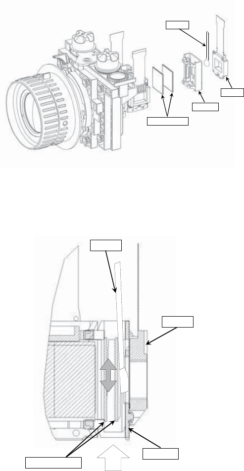
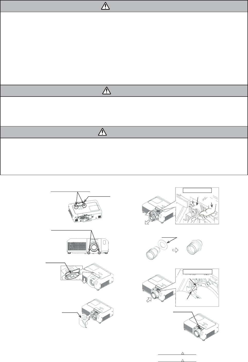
6-7 Lens
WARNING
• Before replacing the projector lens, be sure to read this manual, the “User's Manual-Safety Guide” and the
“Optional Lens User's Manual” of the LCD projector for use with this lens.
• Do not place the lens in a location subject to direct sunlight or other strong lighting or near heat-radiating
equipment.
• Do not subject the lens to shocks.
• Be sure to unplug the LCD projector before replacing the lens.
• Do not touch the fan of the LCD projector during operation.
• Before replacing the lens, be sure to turn off and unplug the LCD projector, and allow at least 45 minutes
for the projector to fully cool.
• When attaching, take care so that dust not enter inside.
CAUTION
• When replacing the lens, do not touch the LCD panels or polarizing plates of the LCD projector or subject
them to shocks.
• When replacing the lens, be careful not to damage the connectors or wires inside the LCD projector.
• After replacing the lens, part of the lens may stick out from the LCD projector.
ATTENTION
• Do not touch the lens directly with your hands or fi ngers.
This can dirty the lens and cause deterioration in image quality.
•
The lens is a precision optical device. Carefully handle the lens without subjecting it to shocks or vibrations.
• When resting the lens on a surface, place the lens face down on a soft cloth.
• Select Lens type in OPTION-SERVICE-LENS TYPE Menu after changing the Lens.
Replacing the Lens
1.Remove the front cover.
(1) Remove the 2 screws marked U(triangle) from the inside of
the lens knob cover. Lens knob cover
(2) Remove the 2 screws marked U(triangle) from the front of
the projector.
(3)Turn the lens shift dial, and lower the projection lens to the
lowest position.
2.Insert your finger from the side, turn the lens to the left
and remove while pulling up on the lens lock lever, as
shown in the illustration. Lens lock lever detail
Lens lock lever
3.Attach the replacement projection lens.
(2) Line up the notched tab on the lens mount with the hole
(2) Re-fasten the 2 screws marked (triangle) that were
removed in step 1.(2).
(3) Re-fasten the 2 screws marked (triangle) that were
removed in step 1.(1).
on the upper-left part of the holder, and insert the lens.
Lens mount tab detail
Hole on upper-left of holder
Notched tab on lens mount
※
The other two tabs are not notched.
(3) Turn the lens to the right until it "clicks" into place to ensure
that the lens is locked in place.
4.Reattach the front cover to complete lens replacement.
(1) Attach the lens blinder to the rear of the projection lens while
(1) Reattach the included front cover.
holding open the lens blinder hole.
Projection lens with lens
blinder attached.
※Caution when removing lens
Be sure not to touch the prism
behind the lens.
Finger
(4) Remove the front cover.
Front cover
30
CP-SX635(ED3SX40N)
6-8 Other care
WARNING
Before caring, make sure the power switch is off and the power cable is not plugged in, and then allow the
projector to cool suffi ciently. The care in a high temperature state of the projector could cause a burn and/
or malfunction to the projector.
Avoid wetting the projector or inserting liquids in the projector. It could result in a fi re, an electric shock, and
and/or malfunction to the projector.
• Don’t put a container containing water , cleaner or chemicals near the projector.
• Don’t use aerosols or sprays.
CAUTION
Please take right care of the projector according to the following. Incorrect care could cause not only an
injury but adverse influence such as discoloration, peeling paint, etc.
• Do not use cleaner or chemicals other than those listed below.
• Do not polish or wipe with hard objects.
Inside of the projector
In order to ensure the safe use of the projector, it needs to clean and inspect the projector about once a year.
Caring for the lens
If the lens is flawed, soiled or fogged, it could cause deterioration of display quality. Please take care of the
lens, being cautions of the handling.
1. Turn the projector off, and unplug the power cord. Allow the projector to cool sufficiently.
2. After making sure that the projector is cool adequately, lightly wipe the lens with a commercially available
lens-cleaning wipe. Do not touch the lens directly with your hand.
Caring for the cabinet and remote control
Incorrect care could have adverse influence such as discoloration, peeling paint, etc.
1. Turn the projector off, and unplug the power cord. Allow the projector to cool sufficiently.
2. After making sure that the projector is cool adequately, lightly wipe with gauze or a soft cloth.
If soiling is severe, dip soft cloth in water or a neutral cleaner dilute in water, and wipe lightly after wringing
well. Then, wipe lightly with a soft, dry cloth.

31
CP-SX635(ED3SX40N)
6-9 Notice of AUTO adjustment
Use of AUTO adjustment with the image through RGB input optimizes V_POSI, H_POSI, and H_PHASE
automatically.
In case that projected image has dark tone around its peripheral, AUTO operation sometimes makes artifacts
in the image, shifts capture area and so on. Those failures are caused by period of image data is not exactly
distinguished to period of blanking on signal processing.
To avoid such phenomena, AUTO function should be used with the full size picture that has bright tone on its
peripheral.
Note
1) The phenomenon at the failure of AUTO adjustment depends on resolution of input source, scene of
picture etc.
2) There is no failure above in AUTO with video source through VIDEO, S-VIDEO or COMPONENT input. The
reason is why recognition of input signal’s standard does not need to search the capture range from input
signal itself.
Image when AUTO fails.
Noting image of top or bottom lines.
Shift of the image to East or West.
Artifacts on image. Etc.
Image when AUTO operates correctly

32
CP-SX635(ED3SX40N)
This projector is equipped with security functions.
(1)MyScreen PASSWORD
The MyScreen PASSWORD function can be used to prohibit access to the MyScreen function and pre-
vent the currently registered MyScreen image from being overwritten.
(2)PIN LOCK
PIN LOCK is a function which prevents the projector from being used unless a registered Code is input.
(3)Transition detector
Transition detector is a function which prevents the projector from being used if vertical angle of the pro-
jector and mirror setting is not same with recorded.
(4)MY TEXT
This item allows you to display your own message (MY TEXT) on the START UP screen and INPUT-IN-
FORMATION. It can be protected by a password to prevent it from being overwritten.
It is possible to deactivate all security functions temporarily with the following procedures.
(1) Go to “SECURITY” on OPTION Menu and press the Ź button.
Then, ENTER PASSWORD box will be displayed.
(The BOX will be displayed by pressing the [MENU] button (remote) or [Ÿ/ź/Ż/Ź] button (keypad) when
Transition Detector Alarm is displayed.)
(2) Press the [Magnify off] button once, then press [Magnify off] button of remote for 3 second or more to dis-
play SERVICE PASSWORD box.
(3) Enter the Life Key (MENU, ź, KEYSTONE, Ÿ). Then all security functions will be deactivated temporarily.
Note: • The Life key can be used up to 30 times. The key cannot be used thereafter. If the Life key cannot be
used, see the paragraph of SECURITY in the User’s Manual.
The frequency in which Life key is input will be set to 0 after the registered code is input.
•
The SECURITY Menu can not be operated if the SECURITY PASSWORD was released by Life key.
• The Mirror, Keystone and Auto keystone are not memorized though they are possible to operate if
Transition Detector was released by Life key.
• The MyScreen Lock on SCREEN Menu keeps “TURN ON” if MyScreen PASSWORD was set when
SECURITY PASSWORD was released by Life key.
5'%74+6;
'06'42#55914&
㪇㩷㩷㩷㪇㩷㩷㩷㪇㩷㩷㩷㪇
37+6 0':6
ENTER PASSWORD box
5'48+%'
'06'42#55914&
㪄㩷㩷㩷㪄㩷㩷㩷㪄㩷㩷㩷㪄
SERVICE PASSWORD box
Transition Detector
Alarm
2+0$1:
64#05+6+10&'6'%61410
6JGRTQLGEVQTJCUDGGPVTCPUHGTTGF
HTQORTGXKQWUN[KPUVCNNGFRQUKVKQP
+H[QWYKUJVQJCXGCUSWCTGKOCIG
QPUETGGPCICKP
FKUCDNG6TCPUKVKQP&GVGEVQTQP/GPW
6-10 How to deactivate the security functions
33
CP-SX635(ED3SX40N)
6-11 PIN LOCK System
If the following PIN BOX menu appears after power on the projector, the PIN LOCK system has been
activated. Under such a condition, key operations and signal displaying are inhibited. To open the PIN LOCK
system, we need to input the correct 4 digits PIN CODE. If correct PIN CODE is not input in 5 min., the lamp
will be automatically turned off.
PIN BOX
Returning repaired unit
Use the Master PIN code. See the paragraph of Releasing the PIN LOCK system deactivation.
Swap unit/Returned unit
Release all security systems. See the paragraph of the PIN LOCK system deactivation.
Releasing the PIN LOCK System
When the PIN BOX menu is displayed, sequentially enter the codes with remote controller as follows. In
accordance with remote controller button entry, “” mark appears in the PIN BOX menu.
Master PIN codes
1st entry code: Press the “MENU” button.
2nd entry code: Press the “ ” button.
3rd entry code: Press the “KEYSTONE” button.
4th entry code: Press the “ ” button.
Note: The Master PIN codes can be used up to 30 times. The codes cannot be used thereafter. If the Master
PIN codes cannot be used, see the paragraph of the PIN LOCK system deactivation.
The PIN LOCK System deactivation
1. When the PIN BOX menu is displayed, press “RESET” for 3 seconds or more in order to get the ID
Inquiring Code.
PIN BOX (ID Inquiring Code)
2. Send HITACHI sales company the Inquiring code (10 digits) to inquire the correct PIN code.
3. With the PIN BOX menu displayed, input the correct PIN code. Enter the correct PIN CODE that HITACHI
sales company informed.
4. Open menu and select “TURN OFF” from the PIN LOCK items in the SECURITY menu. Then the PIN
BOX menu appears.
Password is required to display the Security Menu.
See the Security in OPTION menu: User’s Manual - Operating Guide.
5. Input the correct PIN code in the PIN BOX menu.
6.Then, PIN LOCK will be set to “TURN OFF”.
7.Deactivate the MyScreen PASSWORD and Transition Detector too.
Reset the Security Password to the [1500].
See the Security in OPTION menu: User’s Manual - Operating Guide.
PIN BOX
Inquiring Code
Inquiring Code
12 1234 1234

34
CP-SX635(ED3SX40N)
When the unit’s power is on, messages such as those shown below may be displayed. When any such message
is displayed on the screen, please respond as described below.
Although these messages will be automatically disappeared around several minutes, it will be reappeared every
time the power is turned on.
Message Description
NO INPUT IS DETECTED
***
There is no input signal.
Please confi rm the signal input connection, and the status of the signal source.
SYNC IS OUT OF RANGE
***
fH
*****kHz
fV
*****Hz
The horizontal or vertical frequency of the inputted signal is outside of the
response parameters of this unit.
Please confi rm the specs for this unit or the signal source specs.
INVALID SCAN FREQ.
***
An improper signal is input.
Please confi rm the specs for your projector or the signal source specs.
CHECK THE AIR FLOW
The internal portion temperature is rising.
Please turn the power OFF, and allow the unit to cool down at least 20 minutes.
After having confi rmed the following items, please turn the power ON again.
• Is there blockage of the air passage aperture?
• Is the air fi lter dirty?
• Does the peripheral temperature exceed 35°C?
If the same indication is displayed after the remedy, please set FAN SPEED of the
SERVICE item in the OPTION menu to HIGH.
REMINDER
***HRS PASSED AFTER THE
LAST FILTER CHECK.
FILTER MAINTENANCE IS ESSENTIAL
TO REMOVE WARNING MESSAGE,
RESET FILTER TIMER.
SEE MANUAL FURTHER INFO.
A note of precaution when cleaning the air fi lter.
Please immediately turn the power OFF, and clean or change the air filter by
referring to the “Air Filter” section of this manual. After you have cleaned or
changed the air fi lter, please be sure to reset the fi lter timer.
6-12 Related Messages
35
CP-SX635(ED3SX40N)
6-13 HIDDEN SERVICE MENU
By the control panel By the remote control transmitter
1. Display the Advanced menu by the
“MENU” button.(If EASY MENU
appears, choose “Go to Advanced
menu” to display ADVANCED MENU.)
2. Select the “OPTION” on the menu.
3. Continue press the button [ ] fi rst,
then press the button [ ] together
with “INPUT”, and hold for 3 seconds.
1. Display the menu by the “MENU”
button. (If EASY MENU appears,
choose “Go to Advanced menu” to
display ADVANCED MENU.)
2. Select the “OPTION” on the menu.
3. Press the “MAGNIFY OFF” button.
Next hold the “MAGNIFY OFF”
button for 3 seconds.
To display the OSD for “HIDDEN SERVICE MENU” set up.
HIDDEN SERVICE
AIR-SENSOR EXECUTE
LAMP ALARM NONE
STARTUP TYPE 1
BNC TERMINATION TTL
SYNC SLICE LEVEL-1 4
SYNC SLICE LEVEL-2 4
PJLink TURN OFF
PANEL TIME 1234h
LONG KEY NORMAL
NETWORK RESET
SOFT RESET
6-14 RUN TIME window
AIR - SENSOR
Execute this item to adjust the air sensor.
LAMP ALARM
Select the lamp alarm level. 3 Level ļ 1 Level ļ None
“3 Level” shows three kinds of lamp-messages according to the LAMP TIME count.
“1 Level” shows one kind of lamp-message according to the LAMP TIME count.
“None” shows no lamp-messages. It is the factory default setting.
Set operating time display method (accumulated lamp time display method)
1. Select “ OPTION” from the Advanced menu, then place the cursor on the “LAMP TIME”.
2. Press the [ ], [ENTER] or [RESET] button.
3. Press the [Reset] button once, then press [KEYSTONE] button of the remote control for 3 seconds or more to display
the screen shown below. (The menu will close after 10 seconds if there are no further operations.)
4. Use [ ] or [ ] to select the usage status number. (The usage status is as shown below.)
Usage status number
0 ..... Total usage status
1 ..... Current usage status
2 ..... Usage status before first reset
3 ..... Usage status before second reset
||
9 ..... Usage status before eighth reset
RUN TIME
LAMP Lamp time1234h
h
h
h
NORMAL Lamp time(Normal)1000
WHISPER Lamp time(Whisper)234
AC 2000 AC energizing time
On Number of times on1
Off Number of times off
No.0 Usage status number(See below)
0
LONG KEY
Select the remote control button operation mode.
NORMAR LONGThe LONG allows to control the pro-
jector with the remote control unit when you hold a
button of it for about 3seconds, and makes MY
BUTTON 1/2 function as LONG KEY DISABLE/LONG
KEY ENABLE compulsorily. If you use these buttons to
control the projector as you assigned with the MY
BUTTON menu, set to the NORMAL.
NETWORK RESET
If this is executed, all of the network setting are initial-
ized.
SOFT RESET
If this is executed, all of the user data is initialized.
Never use it when not required.
STARTUP TYPE
Select the startup screen type. 1 : shows Hitachi Logo
2 : No Hitachi Logo
BNC TERMINATION
Select the RGB2 (BNC) Terminator. 75 ohm ļ TTL
SYNC SLICE LEVEL-1
Set the Sync separation slice level of the RGB1. (1~7)
SYNC SLICE LEVEL-2
Set the Sync separation slice level of the RGB2 (BNC). (1~7)
PJLink
Select the PJLink. Turn off ļ Turn on
PANEL TIME
Use time of LCD panel. Reset the PANEL TIME when-
ever you changed the LCD/LENS prism assembly.
36
CP-SX635(ED3SX40N)
6-15 Reset of the Network Web password / User ID, Network Control password
ATTENTION : Performing this operation initializes the network settings. If the projector has
the customized settings in the network, make a note of the network settings to restore
them before this operation.
1. Display the SETUP in the NETWORK menu.
2. Select “TURN OFF” in the item of DHCP.
3. Enter “255.255.255.255” in the item of IP ADDRESS.
4. Enter “255.255.255.255” in the item of SUBNET MASK.
5. Enter “255.255.255.255” in the item of DEFAULT
GATEWAY.
6. While NETWORK menu is displayed, press the RESET button of the remote control.
7. Press Ÿ button to execute reset.
The operation described above resets not only Web password but also NETWORK settings.
NOTE:
When you execute this reset operation with any other settings than above (described in the
step 2 to 5), the WEB password, SNTP server address, DATE AND TIME and other sched-
ule settings are not initialized, but the network settings (DHCP, IP ADDRESS, SUBNET
MASK and DEFAULT GATEWAY) are initialized.
8. If the network settings had been customized, restore them by manual operation.
Press RESET button
/'07=4)$?
+/#)'
5'672
#7&+1
2+%674'
+0276
126+10
5%4''0
5'.'%6
0'6914-
%%
'#5;/'07
241,'%6140#/'
/;+/#)'
5'672
+0(14/#6+10
5'48+%'
5'672
&*%2
+2#&&4'55
57$0'6/#5-
&'(#7.6)#6'9#;
&055'48'4
6+/'&+(('4'0%'
'#0&6+/'
10
HITACHI
SM0321
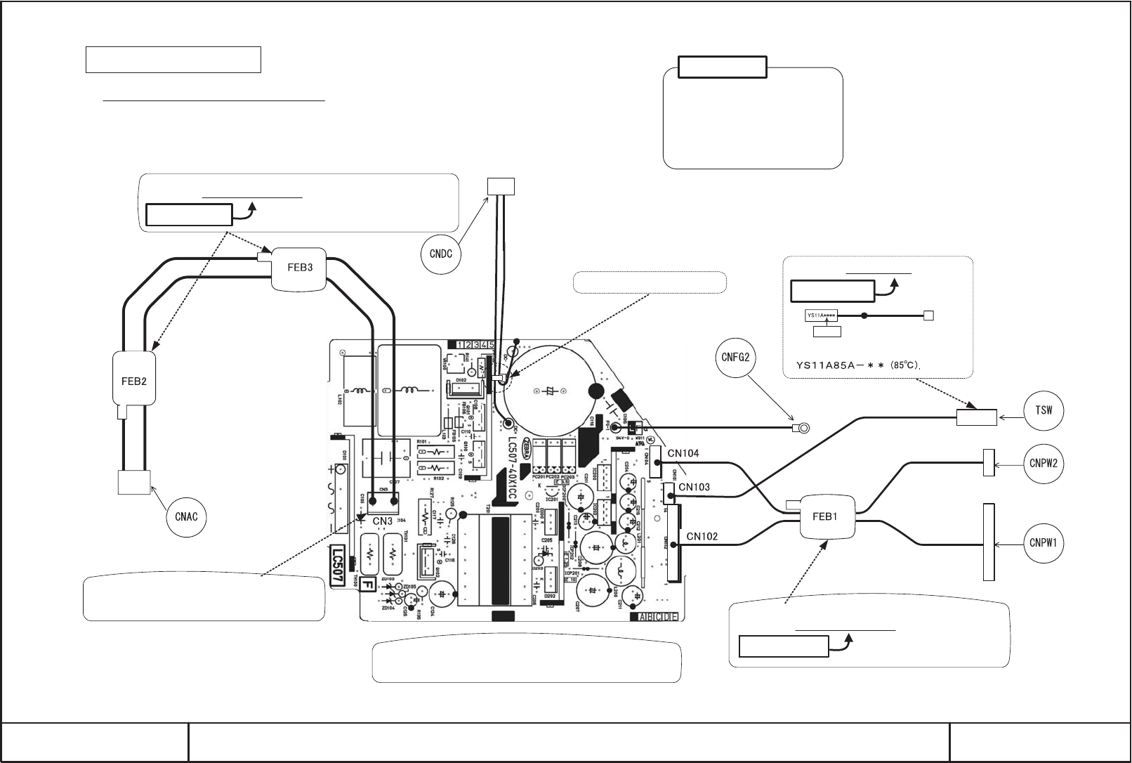
WIRING DIAGRAM 1
Wiring of the circuit power supply
Wiring of the circuit power supply main board
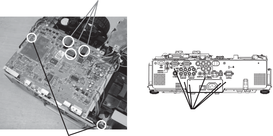
(1) Connect the TSW. Make sure to confirm the seal (based on the diagram below) when attaching the TSW.
(2) Connect the CNPW1 and CNPW2, Attach the FEB1.
(3) Connect the CNAC, Attach the FEB2 and FEB3 to the CNAC.
Attach the FEB2 and FEB3 (ferrite core) to CNAC.
Make sure to completely lock the hook when attaching the FEB2 and FEB3.
Area of Importance
Area of Importance
Area of Importance
Make sure to completely lock the hook when connecting
the CNAC (as it can not be confirmed whether they are
securely connected in later processes).
Make sure to securely connect the TSW, CNPW1 and CNPW2 to the
circuit power supply (as it cannot be confirmed whether they are securely
connected in later processes).
Attach the FEB1(ferrite core) to CNPW2 and CNPW1.
Make sure to completely lock the hook when attaching the FEB1.
Make sure to confirm the print of the TSW.
Make sure that cables are bound.
The operations with this symbol have
implications with laws/standards.
It is possible to be in violation of these
laws/standards in the case that these
operations are not carried out according
to the instructions. Assemble according
to the operation instructions.
Confirm that the print indicates
Seal
Area of Importance
HITACHI
SM0321
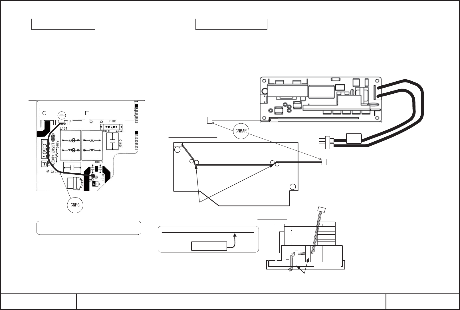
WIRING DIAGRAM 2
Wiring of the noise filter board
Wiring of the noise filter board
(1) Style the CNFG.
Wiring of the ballast power supply
Wiring of the ballast power supply
(1) Attach the CNBAR to the standing board.
(2) Pass the CNBAR through the ballast holder’s hole. Then, put the CNBAR along the back.
Pinch the CNBAR with the two bosses.
(3) Pass the CNBAR through the two hooks at the side of the ballast holder.
Style the CNFG cable like above diagram.
It is to prevent to lift the engine when attaching the engine.
Pass the CNBAR through the ballast
holder’s hole. Then, pinch the CNBAR
with the two bosses.
Make sure there is no cable loosening from the standing
board to the hook.
Area of Importance
hole
ballast holder
(reverse)
ballast
hook
ballast holder
The back of the ballast holder
Side of the ballast
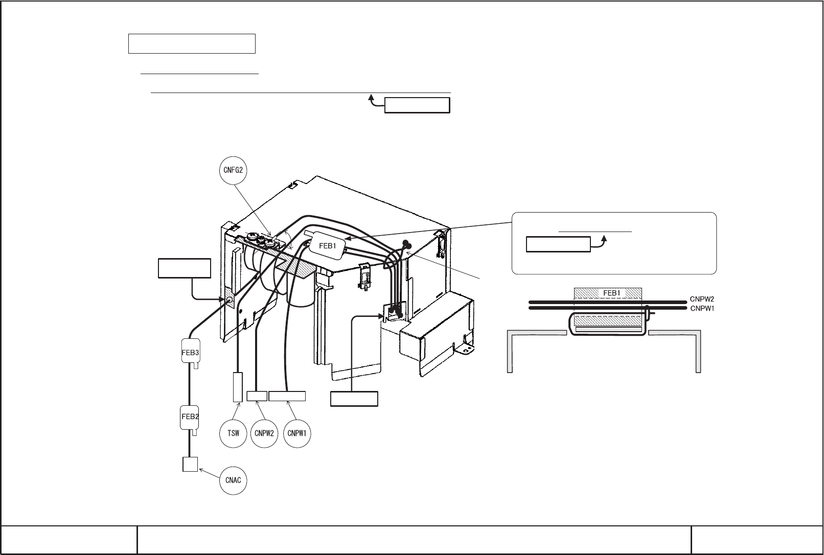
HITACHI
SM0321
WIRING DIAGRAM 3
Wiring of the power supply block
Wiring of the power supply block
(1) Pass the CNPW1, CNPW2, TSW and CNFG2 through the wiring clamp of power supply case.
Do not make excessive length of the cables in power supply case. Make sure not to touch the primary.
(2) Attach the FEB1 to the CNPW1 and CNPW2.
(3) Attach the FEB1 to the upper surface of power supply case with cable tie.
(4) Bundle the CNPW1, CNPW2, TSW and CNFG2 with clamp.
(5) Attach the CNFG2 to the power supply case with screw.
(6) Pass the CNAC through the incision of insulation sheet.
Area of Importance
Area of Importance
about 90
degrees
Incision of
Insulation sheet
Wiring clamp
Clamp
Cross section
Power supply case
Attach the FEB1(ferrite core) to CNPW1 and CNPW2.
Make sure to completely lock the hook when attaching the FEB1.
Attach the FEB1 to the power supply case with cable tie.
Cut the excessive length of cable tie.
cable tie
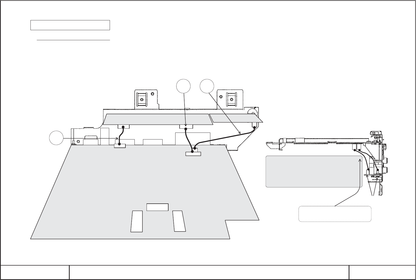
HITACHI
SM0321
WIRING DIAGRAM 4
CNAU CNCNT
CNVID
EV01 EA06EW04
ET02
EC02EC01
Preparation for attaching the main board
Wiring when attaching the control board.
(1) Connect the control board to the main board with CNCNT.
(2) Connect the input board to the main board with CNAU and CNVID.
Input board Control board
I/O Metal
Main board
(reverse)
<Side view>
Main board
Optics unit
Input board
Control board
Prevention of hooking the cables.
Prevent hooking the cables to the optics unit
when installing the main board.
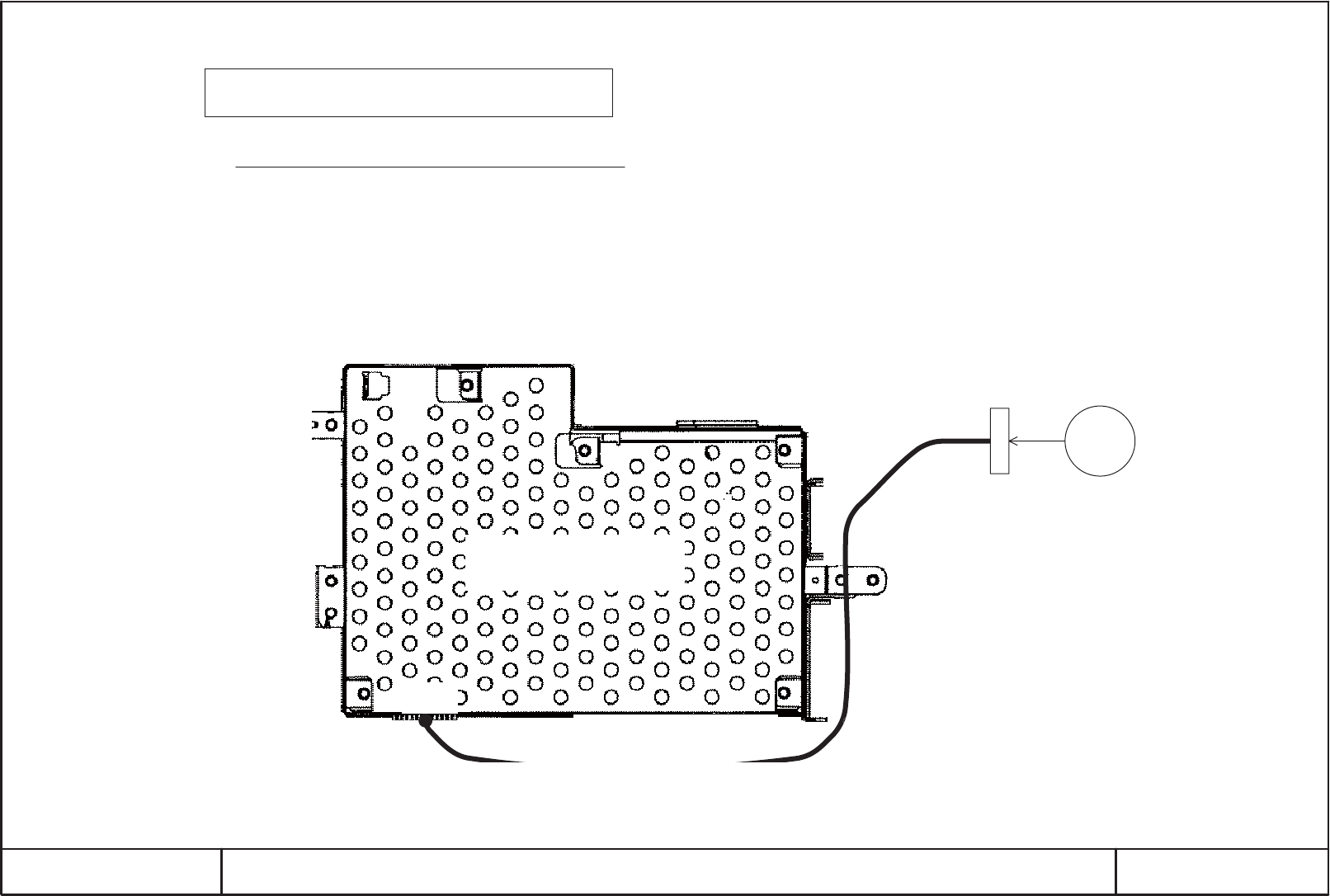
HITACHI
SM0321
WIRING DIAGRAM 5
CNNET
EL01
Preparation for attaching the network board
Preparation for attaching the network board
(1) Connect the CNNET.
Network unit
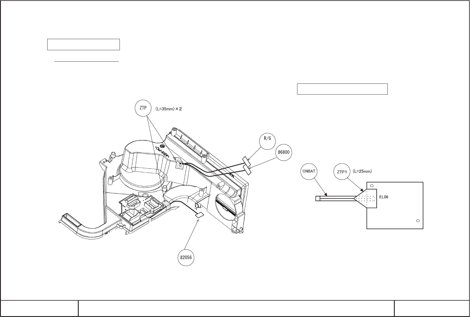
HITACHI
SM0321
WIRING DIAGRAM 6
Preparation for attaching the duct
Wiring when attaching the duct
(1) Pass the #2056 through the incision of duct, and attach it to the duct absorbing the excessive
length with tape. #2056 have to be along the side of duct.
(2) Pass the cable of #6800 and R/G fan through the duct hole, and attach them to the duct
absorbing the excessive length with tape.
(Cable is fixed with tape, so it is impossible to draw out the cable even if the cable length becomes insufficient at the later procedure.)
Preparation for attaching the battery board
Connect the CNBAT to the battery board first.
Unit the connector with tape (L25=mm) to prevent
being come off. (Bends the corner of the tape)
fan
Battery board
(EL06 mounted surface)
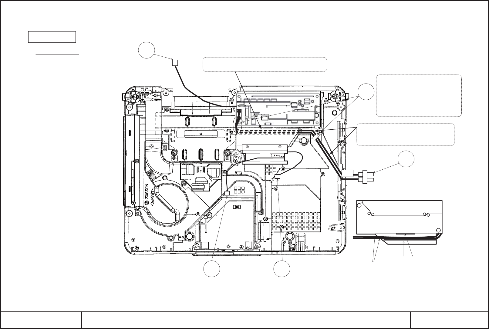
HITACHI
SM0321
WIRING DIAGRAM 7
#2200
CNBAR
CNBAT
Attaching the ballast
Wiring of the ballast
(1) Wire the igniter lead, and attach to the lamp house. Pass the cable under the ballast holder along the side of the ballast.
(Make sure not to pinch the cable.)
Ballast
Ballast holder
Wire the igniter lead cables under the
ballast holder making no excessive length.
Bind the cables with clip.
Before you bind the cables, confirm that
the cables are not pinched by ballast holder.
Move the cables around the clip right and left,
the cables around dotted circle will not move
if the cables are pinched.
Wire the igniter leads between the bottom case ribs,
and minimize the lifting.
Otherwise, you will pinch the leads when you attach
the lamp duct.
igniter
lead
<back side of ballast holder>
Pass the igniter leads between the rib1 and the rib2 at the back
of the ballast holder.
Make sure not to cross the cables, and put cables to the rib1 side.
Otherwise, bottom case will pinch the cables.
rib1 rib2
Power
fan
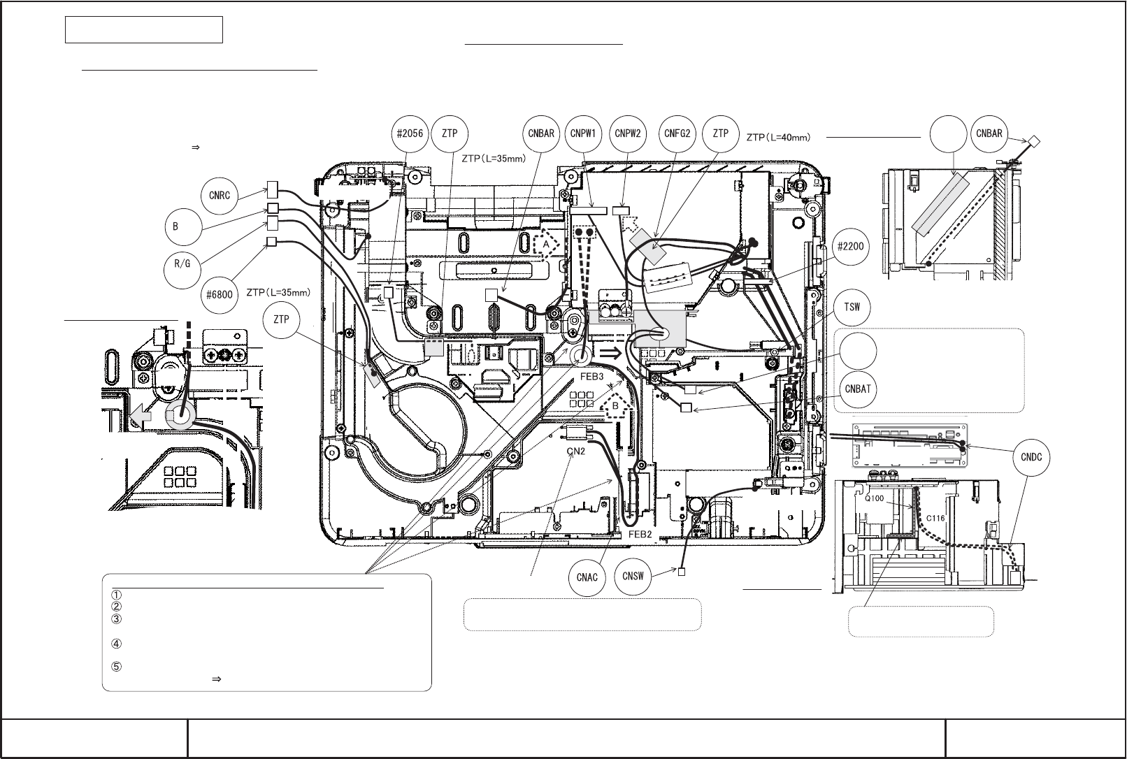
HITACHI
SM0321
WIRING DIAGRAM 8
Attaching the power unit block
Wiring when assembling the power supply block
Closeup arround FEB3
(1) Connect the circuit power supply and noice filter board with CNAC.
Connect the circuit power supply and the ballast power supply with CNDC.
(2) Pass the TSW, lamp fan lead, power supply fan lead and CNBAT
through the incision of insulation seat.
(3) Put the FEB2 and FEB3, and make them to fix.
(4) Wiring of the CNBAR. Fix the insulation seat with tape.
(5) Style the TSW cable to direction and fix it with the tape.
Wiring except for the power unit
(1) Attach the igniter lead to bottom case with wire clamp #2200.
(2) Connect the CNRM to the remote board.
(3) Connect the CNSW to the switch board.
(4) Connect the CNBAT to the battery board.
Power unit case
Viewpoint from arrow
The side of power
unit case B
Protection
sheet
Insert the CNBAR between case and sheet.
Fix the protection sheet with tape.
See the above diagram.
Style the CNBAT and power unit
fan cable being along the side of
power unit fan.
Wire the CNDC connector cable
near the center of C116 board.
Make sure to completely lock the hook when attaching
the CNAC. (It is impossible to check later.)
Put the boss of FEB3 to the bottom case side.
Turn it to the left.
Direction of
the FEB3 boss
remote board
fan
fan
boss
Work to prevent the cable slack.(To make it easy when assembling)
No cable stack between FEB2 and CN2.
Push the cable from FEB2 to FEB3 into the ditch to prevent the slack.
Make sure the FEB3 is not floating.
FEB3 interferce the engine when it is floating.
Put the excessive length of CNAC(from FEB3 to power unit case) to
the space between fan and boss.
If the engine was lifted when attaching it, FEB3 sometimes lifts the engine.
Push the FEB3 to the direction.
Switch board
ballast
ballast
heat sink
Power unit
(circuit)
POWER
fan
ZTP(L=75mm)
ZTP
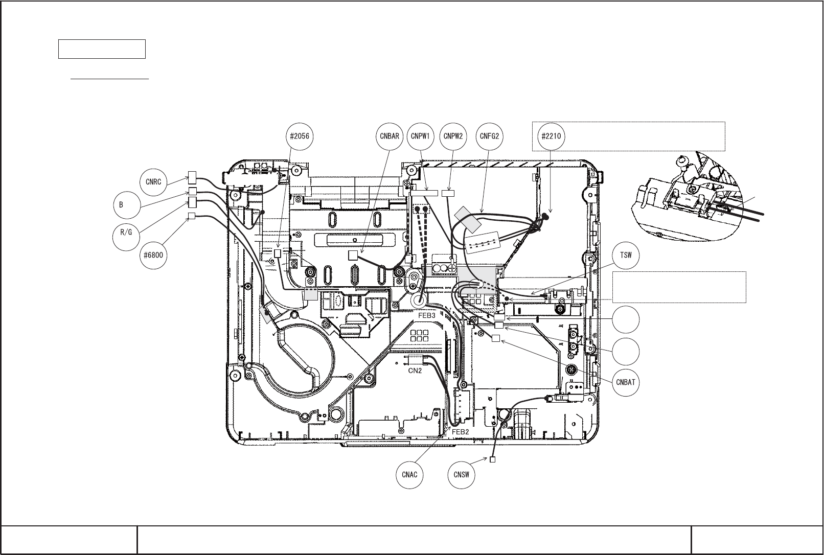
HITACHI
SM0321
WIRING DIAGRAM 9
Attaching the fan duct
Wiring of the fan duct
(1) Attach the TSW to the upper part of fan duct.
(2) Pass the lamp fan lead through the incision of the insulation sheet.
(3) Fix the purse lock (#2210) at the exit surrounding. See diagram below.
Twisting part of Purse lock have to be towards head.
Make sure not to be floating from bracket.
Rib
Attach the TSW cable.
Make sure to place the exhaust duct
rib between two lines of TSW cable.
switch board Make sure there is no slack of
CNBAT and power unit cable
between power fan and exhaust
duct.
Style the lamp fan cable like dotted line
part to prevent touching to the upper case
rib (shaded area).
lamp
fan
power
fan
remote board
fan
fan
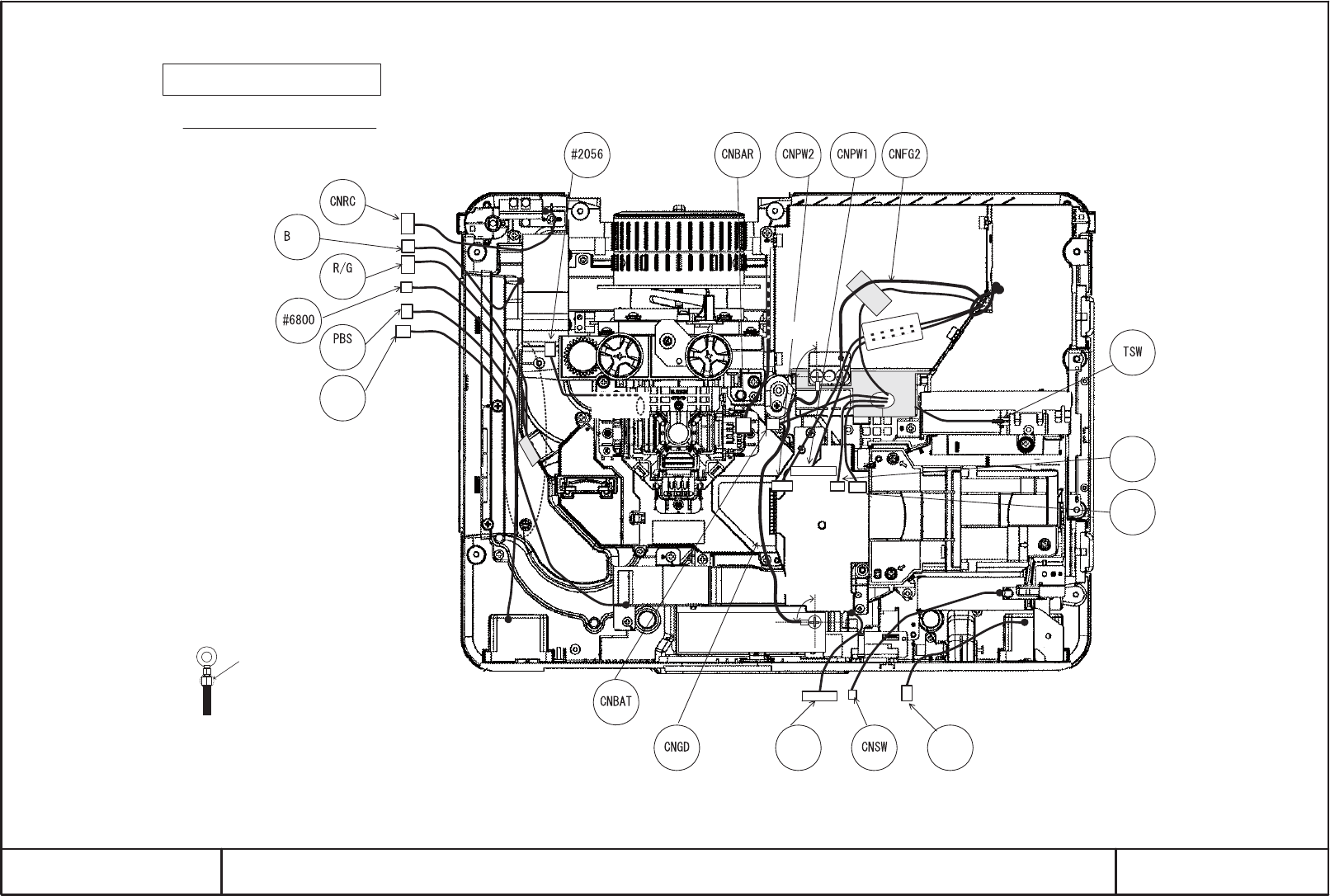
HITACHI
SM0321
WIRING DIAGRAM 10
fan
fan
speaker
Iris speaker
Inlet bracket
(Filter board)
About 90
degrees
power
fan
lamp
fan
About 90
degrees
fan
Preparation for attaching the engine
Wiring when attaching the engine
(1) Connect the power unit case to the inlet bracket with CNGD.
About attaching degree and styling the round terminal, see the diagram.
When you attach CNGD by screw on the power box case, tighten screw having round terminal
part by your hand. Otherwise, a tightening point of round terminal will suffer pressure.
Remove a CNGD before you detach a power unit.
Otherwise, a tightening point of round terminal will be damaged.
A tightening point of round terminal
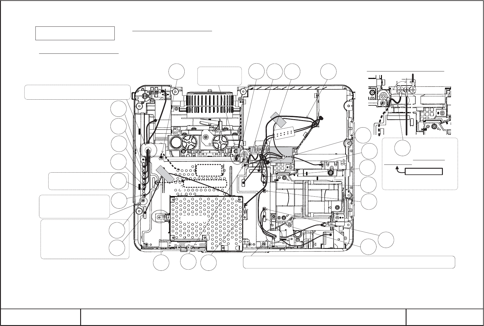
HITACHI
SM0321
WIRING DIAGRAM 11
Preparation for attaching main board
and shield case
Wiring when attaching the main board
(1) Connect the flexible cable.
(Three places under shield)
(2) Connect the #2056, CNBAT and CNBAR completly.
It is hard to connect after shield was attached.
(3) Connect the CNPW1, CNPW2, lamp fan and power
unit fan to the main board.
Connect the CNRC, B fan, #6800, PBS fans and speaker
cable to the main board passing through the incision of
insulation sheet.
CNRC
#6800
CNNET
ZTP
B fan
PBS
fan
speaker
Never put the speaker cable on the
boss.
Otherwise, the cable will be damaged
by screw.
Attach the CNNET cable with ZTP2
(L=50mm) to the position shown in
diagram.
Make sure there is no excessive
length of CNNET.
R/G
fan
Do not pass the R/G fan cable
through the incision of insulation
sheet.
CNBAT CNGD2CNKEY
Put CNKEY cable near shield case.
Otherwise, customer will find CNKEY
cable around lens shift dials.
Shield case
from keypad board
panel FPC
x3
Iris
speaker
Connect the iris cable, speaker cable and CNSW to the main board passing through the incision of the insulation sheet.
Never put the CNSW cable near the lamp holder. Otherwise, upper case will pinch the cable.
CNSW
TSW
#2210
lamp
fan
power
fan
Style the CNGD inserting it into the
concave portion of the upper part of fan.
To prevent touching with the rotating
parts of fan.
Area of Importance
CNGD
Closeup of power supply case screw.
About 90
degrees
main
board
fan
CNFG2CNPW1CNPW2
CNBAR
#2056 Style the CNBAR and
keep it away from the
boss. See diagram.
Wiring when attaching the shield case
(1) Connect power unit case and Network shield case with CNGD2.
(2) Connect the CNRC, B fan, R/G fan, #6800, PBS fan and speaker cable to the main board.
(3) Connect the iris cable, speaker cable and CNSW to the main board.
(4) Bundle the CNPW1, CNPM2, lamp fan and power unit fan cable on the power with #2210.
(5) Connect the CNNET to the main board.
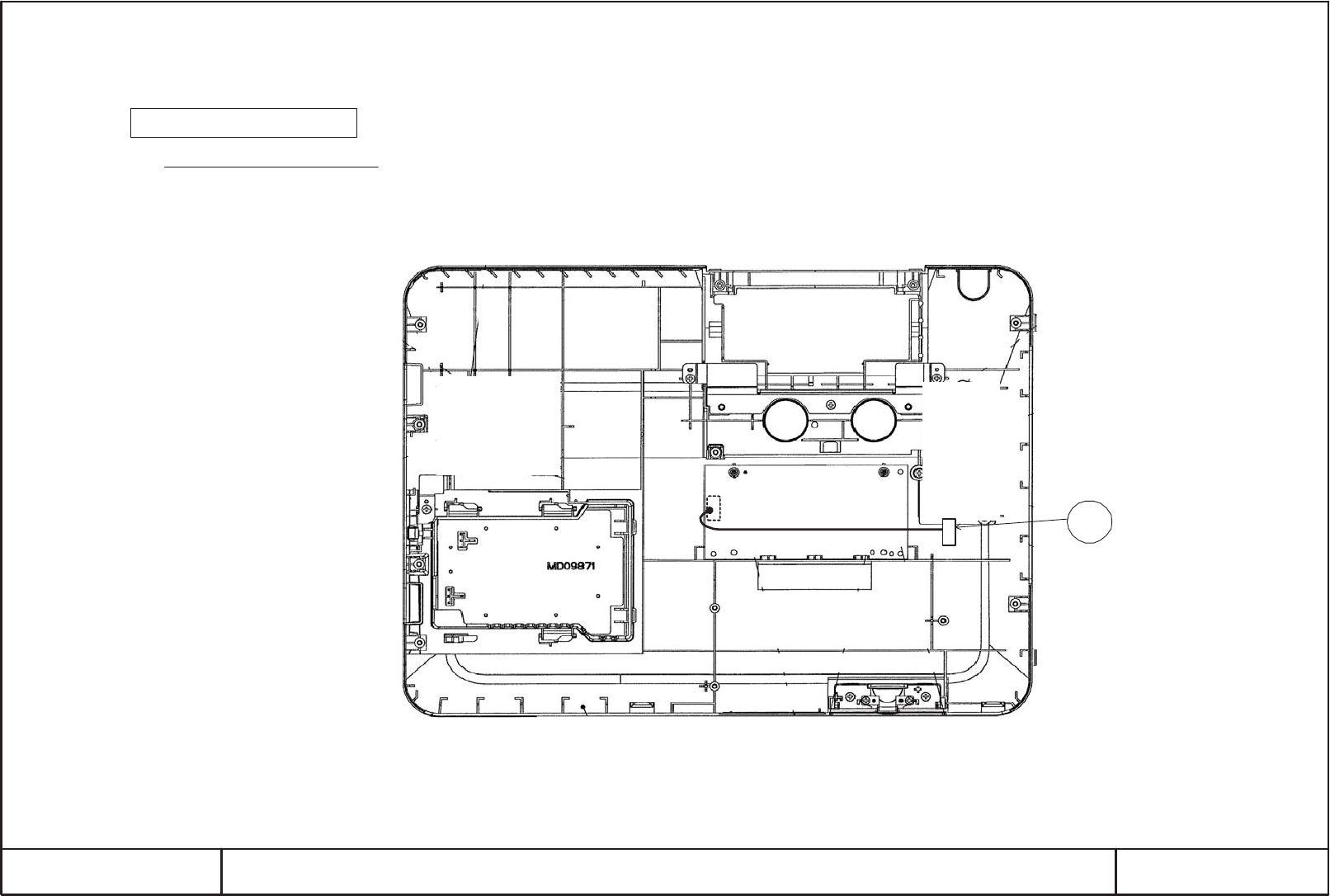
HITACHI
SM0321
WIRING DIAGRAM 12
Wiring when attaching the keypad board
(1) Connect CNKEY to keypad board.
(2) Connect CNKEY to main board.
Preparation for attaching upper case
Keypad board
CNKEY
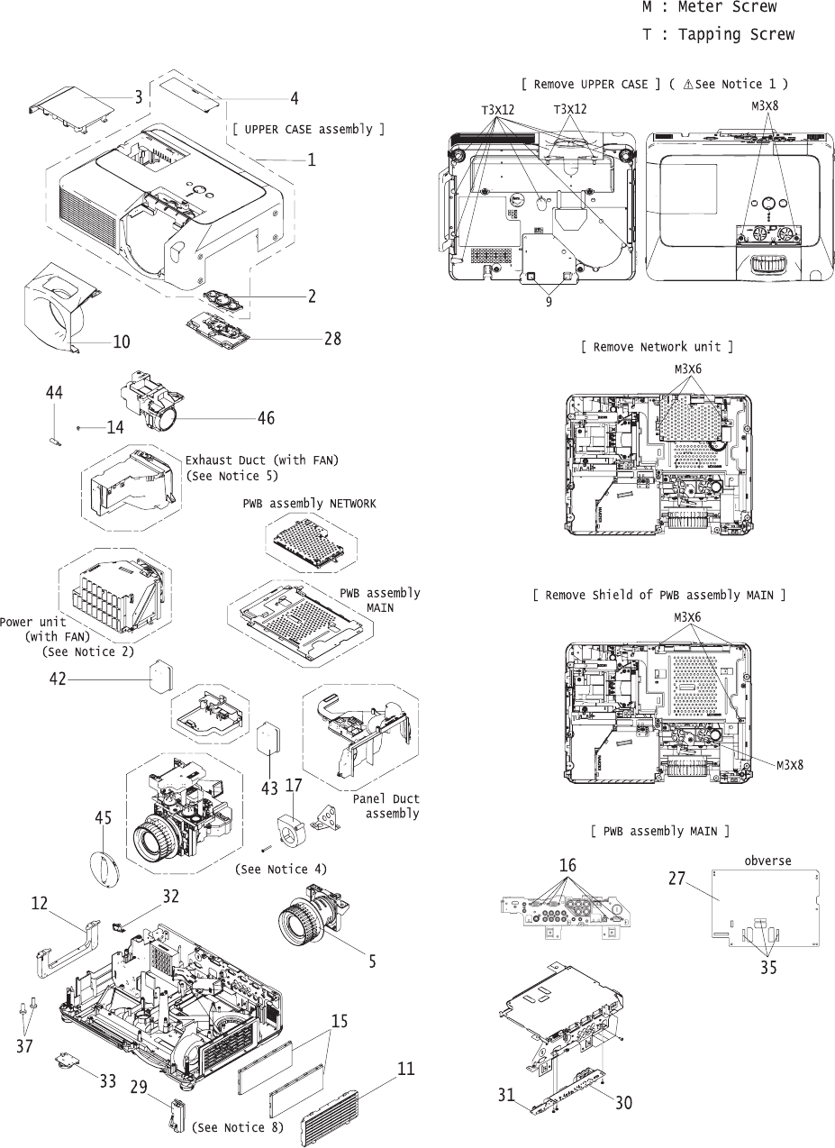
49
CP-SX635(ED3SX40N)
8. Disassembly diagram
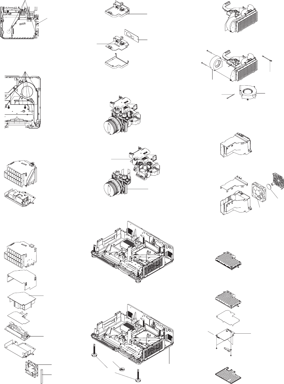
50
CP-SX635(ED3SX40N)
- Disassembly -
[ BOTTOM CASE ]
- assembly -
[ LCD/LENS/PRISM/
DICHROIC OPTICS UNIT ]
- assembly -
- Disassembly -
41
13
8
7
[ FILTER UNIT ]
- assembly -
36
26
- Disassembly -
- Disassembly -
( See Notice 7 )
- assembly -
[ POWER UNIT ]
T3X12
[ Remove Panel Duct assembly ]
( See Notice 3 )
39
38
[ Remove Duct and Power unit ]
T3X12
M3X6
- Disassembly -
- assembly -
- Disassembly -
[ PANEL DUCT ]
- assembly -
[ EXHAUST DUCT ]
6
M : Meter Screw
T : Tapping Screw
40
21
18
24
25
20
19
23
22
- Disassembly -
- assembly -
[ NETWORK UNIT ]
M3X6
M3X6
( See Notice 6 )
34
(See Notice 5)
(See Notice 5)
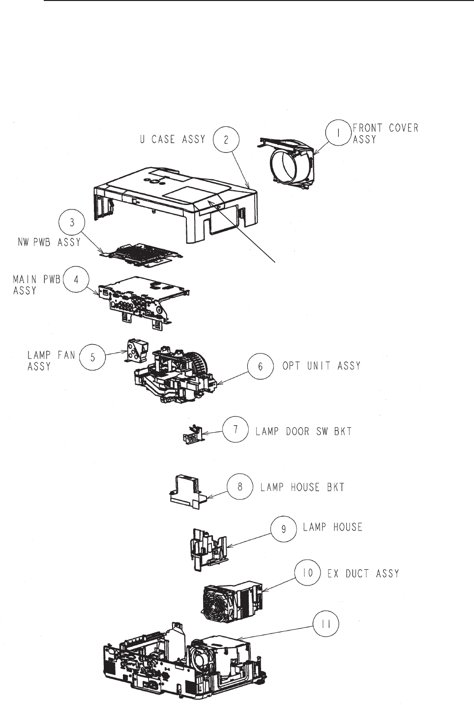
51
CP-SX635(ED3SX40N)
Notice
The step of the disassembly / The step of the assembly.
Disassemble the projector in order of 1, 2, 3, 4, 5, 6, 7, 8, 9, 10 and 11 as shown in
the diagram.
Assemble the projector in order of 11, 10, 9, 8, 7, 6, 5, 4, 3, 2 and 1 as shown in the
diagram.
(See Notice 9)
POWER UNIT
(BALLAST)
(See Notice 10)
Remove lamp door before
detach upper case
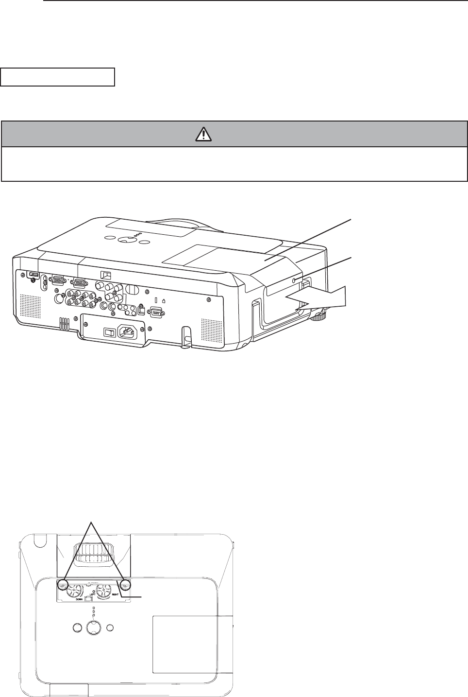
52
CP-SX635(ED3SX40N)
Notice
1. Detach and attach the upper case.
Follow the procedure below to detach and attach the upper case.
When disassembling
CAUTION
The lamp door must be removed before the upper case when disassembling the machine. If the upper
case is detached with the lamp door installed, the MAIN board might be damaged.
a. Remove the Lamp door.
b. Remove 2 screws on the front and 2 screws on the upper case.
(1) Before remove 2 screws on the upper case, open the Lens shift cover.
2 screws
Lens shift cover
Loosen this screw
Lamp door
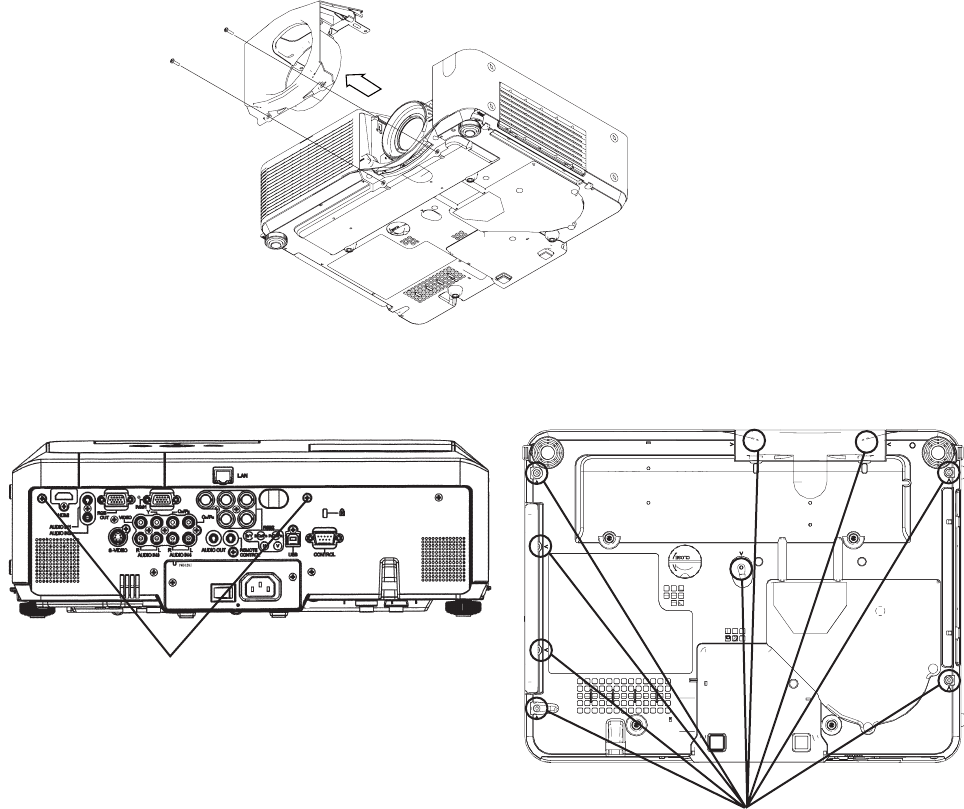
53
CP-SX635(ED3SX40N)
c. Remove 9 screws on the bottom and 2 screws on the rear to detach the upper case.
2 screws
9 screws
(2) Remove 2 screws on the front.
(3) Remove the front cover.
2 screws
front cover
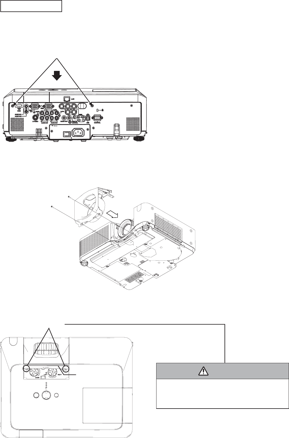
54
CP-SX635(ED3SX40N)
a. Tighten 9 screws on the bottom and 2 screws on the rear after attaching the upper case with the lamp
door separated.
In order not to make a gap between the upper and the bottom cases, tighten these screws while pressing
down the upper case in the direction of the arrow. Be careful not to bend the outside casing.(Torque:0.39-
0.59N•m)
When assembling
b. Attach the Front cover.
(1) Attach the Front cover.
(2) Tighten 2 screws on the front.
(3) Open the Lens shift cover.
(4) Tighten 2 screws on the upper case.
CAUTION
When re-assembling, tighten these screw at
the torque of 0.49±0.1 N•䏐䎃䏖䏒䎃䏗䏋䏄䏗䎃䏗䏋䏈䎃䏖䏆䏕䏈䏚䎃
䏋䏒䏏䏈䏖䎃䏄䏕䏈䎃䏑䏒䏗䎃䏇䏄䏐䏄䏊䏈䏇䎑
2 screws
Lens shift cover
2 screws
front cover
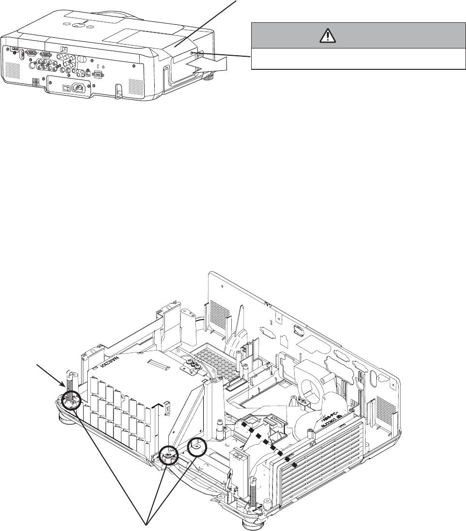
55
CP-SX635(ED3SX40N)
c. Attach the Lamp door.
2. Replacing the power units.
Remove the screw to take off the duct.
Remove the 3 screws to take off the power unit.
NOTE : One of screws is behind the duct.
Lamp door
CAUTION
Tighten this screw using a manual screwdriver.
3 screws
Behind this duct
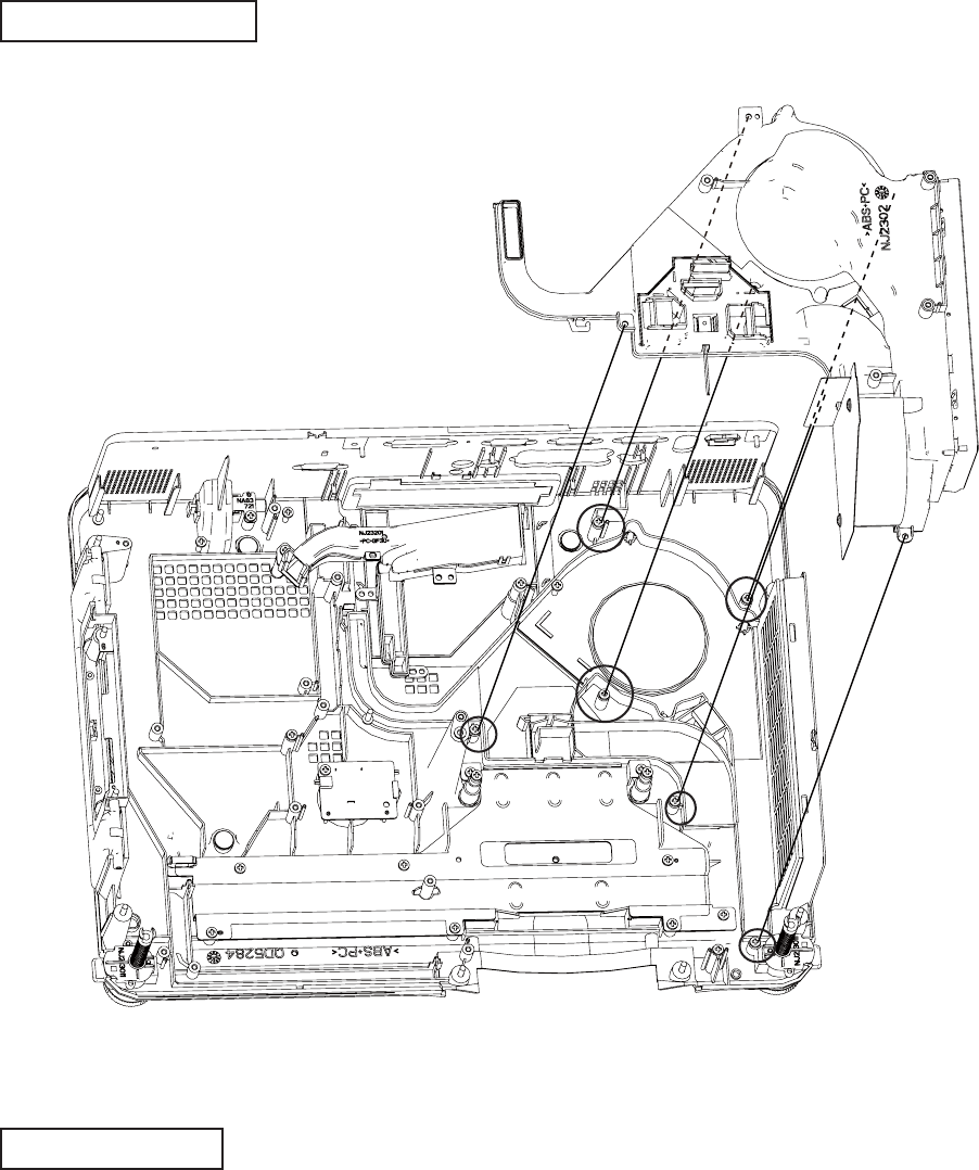
56
CP-SX635(ED3SX40N)
3. Detaching and attaching the Panel Fan Duct assembly
Tighten 6 screws and hook the panel fan duct assembly.
When assembling
Remove 6 screws and unhook the panel fan duct assembly as shown in the diagram.
When disassembling
Panel fan duct assembly
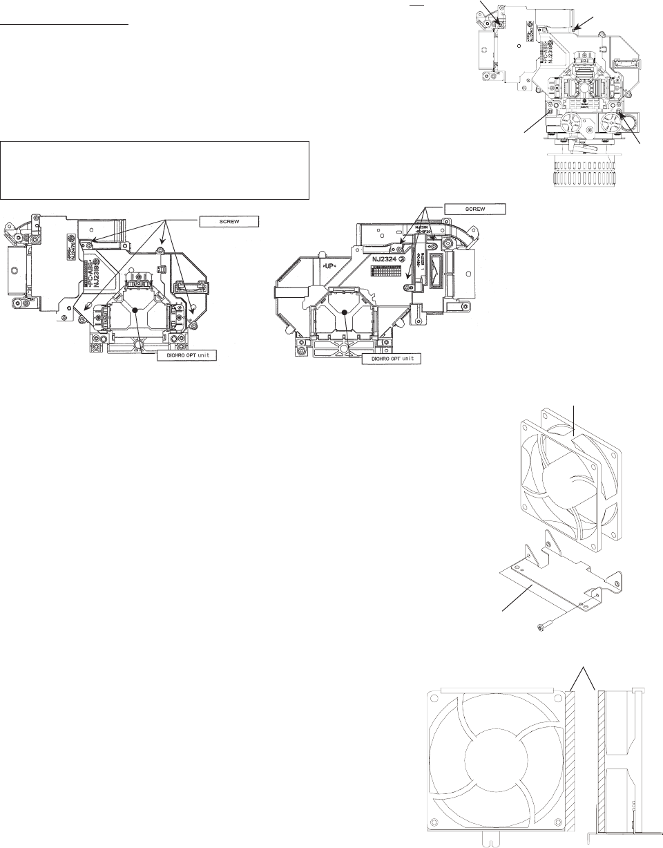
57
CP-SX635(ED3SX40N)
4. Attaching the dichroic optics unit
Put the dichroic optics unit on the bottom case, and tighten screws in
order of 1, 2, 3 and 4 as shown in the diagram.
5. Replacing the power unit fan
Be sure to do the following works before changing the power unit fan.
a. Assemble the power unit fan and fan cushion as described below.
1) Attach the fan bracket to the new power unit fan using 2 screws.
2) Stick the Fan cushion along the right side of the fan as
shown in the diagram.
Note:
• If you install the new fan without the fan cushion, the
fan vibration in operating might make noise.
• Be careful not to invert the fan when assembling the
exhaust fan assembly.
6. Replacing the PWB assembly NETWORK
Attach the bracket to the PWB assembly NETWORK covering the LAN Jack completely.
Ԙ
ԛ
ԙ
Ԛ
power unit fan
FAN bracket
Fan cushion
Never remove the 7 screws (4 screws on the obverse,
3 screws on the reverse) from DICHRO OPT unit.
Otherwise, the screw holes will be damaged.
reverse
obverse
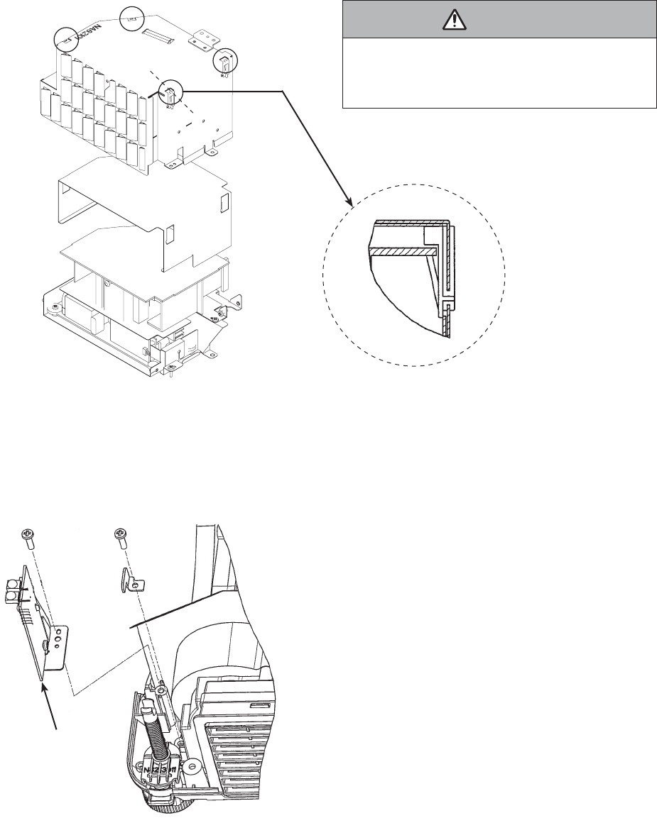
58
CP-SX635(ED3SX40N)
7. Assembling the power unit
FOOT MTL
8. Assembling the FOOT MTL
Remove the remote board first when assembling the FOOT MTL.
This is necessary when replacing the FAN and so on.
CAUTION
Make sure that power unit board was fi xed by 4
hooks of PWB HOLDER.
Make sure that it is hard to remove.
Remote board
Cross Section
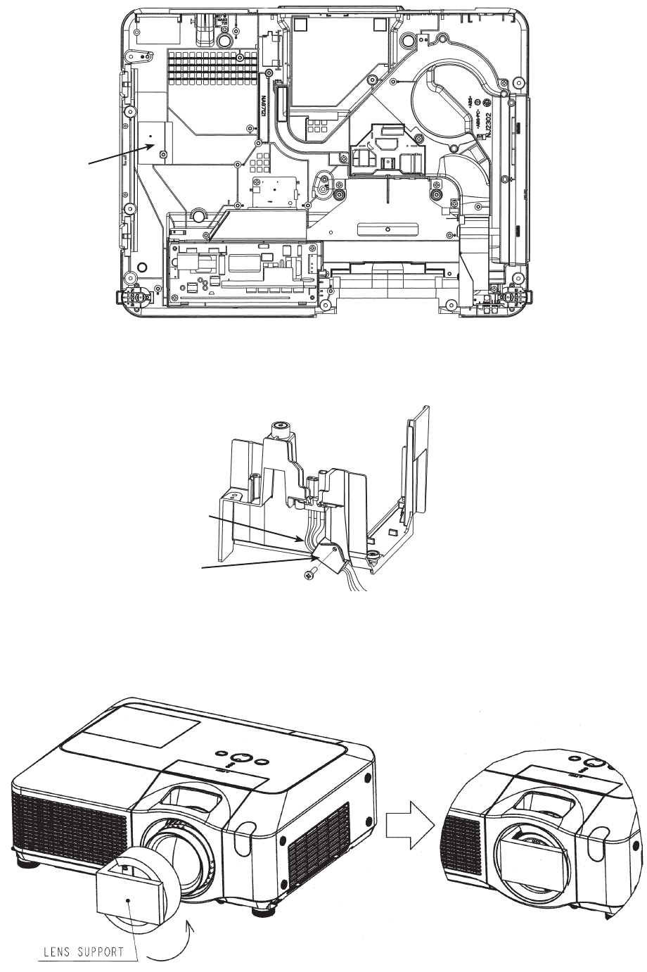
59
CP-SX635(ED3SX40N)
9. Attaching the LAMP HOUSE
Never forget the insulation sheet when you attach the LAMP HOUSE.
insulation sheet
10. Replacing the BALLAST
Bundle the igniter leads with trigger box when you attach the BALLAST.
igniter leads
trigger box
11. Attach the LENS SUPPORT
Attach the LENS SUPPORT (SU03921) to the projector when you transport the projrctor.
Otherwise, the mechanical parts for the lens shift function might be damaged.
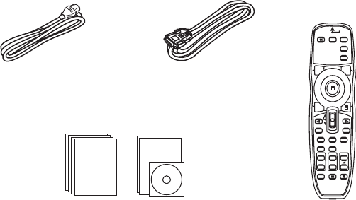
60
CP-SX635(ED3SX40N)
9. Replacement Parts list
Power Cord RGB Cable
Remote Control
or
Instruction manual
BLANK LASER
ASPECT
PUSH
ENTER
PAGE UP
LASER
INDICATOR
MY SOURCE/
DOC.CAMERA
SEARCH
STANDBY/ON VIDEO RGB
PAGE DOWN
ESC MENU RESET
POSITION AUTO
MAGNIFY
ON
OFF
MY BUTTON
1
2
VOLUME
FREEZE KEYSTONE MUTE
THE UPDATED PARTS LIST
FOR THIS MODEL IS
AVAILABLE ON ESTA
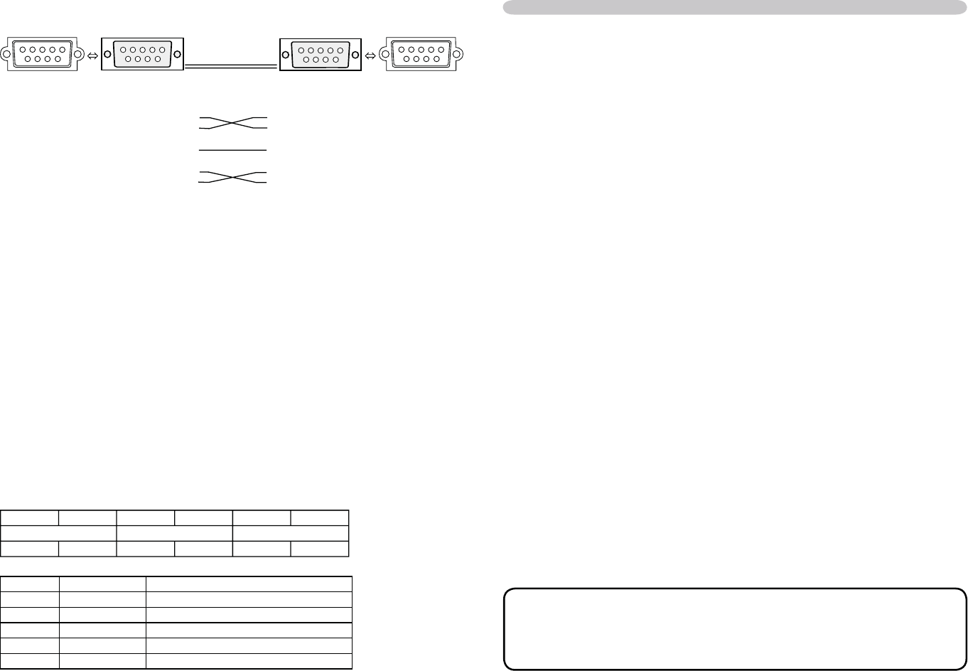
61
CP-SX635(ED3SX40N)
10. RS-232C communication
6789
12345
6789
12345
CONTROL port RS-232C cable (Cross) RS-232C port
of the projector of the computer
- (1) (1) CD
RD (2) (2) RD
TD (3) (3) TD
- (4) (4) DTR
GND (5) (5) GND
- (6) (6) DSR
RTS (7) (7) RTS
CTS (8) (8) DTS
- (9) (9) RI
Connecting the cable
1. Turn off the projector and the computer.
2. Connect the CONTROL port of the projector with a RS-232C port of
the computer by a RS-232C cable (cross). Use the cable that fulfills the
speci¿ cation shown in the previous page.
3. Turn the computer on, and after the computer has started up turn the
projector on.
Communications setting
19200bps, 8N1
1. Protocol
Consist of header (7 bytes) + command data (6 bytes).
2. Header
BE + EF + 03 + 06 + 00 + CRC_low + CRC_high
CRC_low : Lower byte of CRC À ag for command data
CRC_high : Upper byte of CRC À ag for command data
3. Command data
Command data chart
byte_0 byte_1 byte_2 byte_3 byte_4 byte_5
Action Type Setting code
low high low high low high
Action (byte_0 - 1)
Action Classi¿ cation Content
1 SET Change setting to desired value.
2 GET Read projector internal setup value.
4 INCREMENT Increment setup value by 1.
5 DECREMENT Decrement setup value by 1.
6 EXECUTE Run a command.
RS-232C Communication (continued)
Requesting projector status (Get command)
(1) Send the request code Header + Command data (‘02H’+‘00H’+ type (2
bytes)+‘00H’ +‘00H’) from the computer to the projector.
(2) The projector returns the response code ‘1DH’+ data (2 bytes) to the computer.
Changing the projector settings (Set command)
(1) Send the setting code Header + Command data (‘01H’+‘00H’+ type (2 bytes) +
setting code (2 bytes)) from the computer to the projector.
(2) The projector changes the setting based on the above setting code.
(3) The projector returns the response code ‘06H’ to the computer.
Using the projector default settings (Reset Command)
(1) The computer sends the default setting code Header + Command data
(‘06H’+‘00H’ + type (2 bytes) +‘00H’+‘00H’) to the projector.
(2) The projector changes the speci¿ ed setting to the default value.
(3) The projector returns the response code ‘06H’ to the computer.
Increasing the projector setting value (Increment command)
(1) The computer sends the increment code Header + Command data
(‘04H’+‘00H’+ type (2 bytes) +‘00H’+‘00H’) to the projector.
(2) The projector in creases the setting value on the above setting code.
(3) The projector returns the response code ‘06H’ to the computer.
Decreasing the projector setting value (Decrement command)
(1) The computer sends the decrement code Header + Command data
(‘05H’+‘00H’+ type (2 bytes) +‘00H’ + ‘00H’) to the projector.
(2) The projector decreases the setting value on the above setting code.
(3) The projector returns the response code ‘06H’ to the computer.
When the projector cannot understand the received command
When the projector cannot understand the received command, the error code ‘15H’
is sent back to the computer.
Sometimes the projector cannot properly receive the command. In such a
case, the command is not executed and the error code ‘15H’ is sent back to the
computer. If this error code is returned, send the same command again.
When the projector cannot execute the received command.
When the projector cannot execute the received command, the error code ‘1CH’
+ ‘xxxxH’ is sent back to the computer. When the data length is greater than
indicated by the data length code, the projector ignore the excess data code.
Conversely when the data length is shorter than indicated by the data length
code, an error code will be returned to the computer.
NOTE • Operation cannot be guaranteed when the projector receives an
unde¿ ned command or data.
• Provide an interval of at least 40ms between the response code and any other code.
• The projector outputs test data when the power supply is switched ON, and when the
lamp is lit. Ignore this data.
• Commands are not accepted during warm-up.
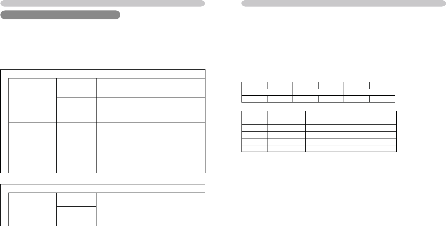
62
CP-SX635(ED3SX40N)
Command Control via the Network
Command Control via the Network
Communication Port
The following two ports are assigned for the command control.
TCP #23
TCP #9715
Command Control Settings
Con¿ gure the following items form a web browser when command control is used.
When the authentication setting is enabled, the following settings are required.
Command Control via the Network
Port Settings
Network Control
Port1 (Port: 23)
Port open
Click the [Enable] check box to open [Network
Control Port1 (Port: 23)] to use TCP #23.
Default setting is “Enable”.
Authentication
Click the [Enable] check box for the
[Authentication] setting when authentication
is required.
Default setting is “Disable”.
Network Control
Port2 (Port: 9715)
Port open
Click the [Enable] check box to open [Network
Control Port2 (Port: 9715)] to use TCP
#9715.
Default setting is “Enable”.
Authentication
Click the [Enable] check box for the
[Authentication] setting when authentication
is required.
Default setting is “Enable”.
Security Settings
Network Control
Authentication
Password Enter the desired authentication password.
This setting will be the same for [Network
Control Port1 (Port: 23)] and [Network
Control Port2 (Port: 9715)].
Default setting is blank.
Re-enter
Authentication
Password
Command Control via the Network (continued)
Command Format
[TCP #23]
1. Protocol
Consist of header (7 bytes) + command data (6 bytes)
2. Header
BE + EF + 03 + 06 + 00 + CRC_low + CRC_high
CRC_low: Lower byte of CRC À ag for command data
CRC_high: Upper byte of CRC À ag for command data
3. Command data
Command data chart
byte_0 byte_1 byte_2 byte_3 byte_4 byte_5
Action Type Setting code
low high low high low high
Action (byte_0 - 1)
Action Classi¿ cation Content
1 Set Change setting to desired value.
2 Get Read projector internal setup value.
4 Increment Increment setup value by 1.
5 Decrement Decrement setup value by 1.
6 Execute Run a command.
Requesting projector status (Get command)
(1) Send the following request code from the PC to the projector.
Header + Command data (‘02H’ + ‘00H’ + type (2 bytes) + ‘00H’ + ‘00H’)
(2) The projector returns the response code ‘1DH’ + data (2 bytes) to the PC.
Changing the projector settings (Set command)
(1) Send the following setting code from the PC to the projector.
Header + Command data (‘01H’ + ‘00H’ + type (2 bytes) + setting code (2 bytes))
(2) The projector changes the setting based on the above setting code.
(3) The projector returns the response code ‘06H’ to the PC.
Using the projector default settings (Reset Command)
(1) The PC sends the following default setting code to the projector.
Header + Command data (‘06H’ + ‘00H’ + type (2 bytes) + ‘00H’ + ‘00H’)
(2) The projector changes the speci¿ ed setting to the default value.
(3) The projector returns the response code ‘06H’ to the PC.
Increasing the projector setting value (Increment command)
(1) The PC sends the following increment code to the projector.
Header + Command data (‘04H’ + ‘00H’ + type (2 bytes) + ‘00H’ + ‘00H’)
(2) The projector increases the setting value on the above setting code.
(3) The projector returns the response code ‘06H’ to the PC.

63
CP-SX635(ED3SX40N)
Command Control via the Network (continued)
Decreasing the projector setting value (Decrement command)
(1) The PC sends the following decrement code to the projector.
Header + Command data (‘05H’ + ‘00H’ + type (2 bytes) + ‘00H’ + ‘00H’)
(2) The projector decreases the setting value on the above setting code.
(3) The projector returns the response code ‘06H’ to the PC.
When the projector cannot understand the received command
When the projector cannot understand the received command, the error code ‘15H’
is sent back to the PC.
Sometimes the projector cannot properly receive the command. In such a case,
the command is not executed and the error code ‘15H’ is sent back to the PC. If
this error code is returned, send the same command again.
When the projector cannot execute the received command.
When the projector cannot execute the received command, the error code ‘1CH’ +
‘xxxxH’ is sent back to the PC.
When the data length is greater than indicated by the data length code, the
projector ignore the excess data code. Conversely when the data length is shorter
than indicated by the data length code, an error code will be returned to the PC.
When authentication error occurred.
When authentication error occurred, the error code the ‘1FH’ + ‘0400H’ is sent
back to the PC.
[TCP #9715]
1. Protocol
Consist of header (1 byte) + data length (1 byte) + command data (13 bytes) +
check sum (1 bytes) + connection ID (1 byte).
2. Header
02, Fixed
3. Data Length
Network control commands byte length (0D, Fixed)
4. Command data
Network control commands that start with BE EF (13bytes).
5. Check Sum
This is the value to make zero on the addition of the lower 8 bits from the header
to the checksum.
6. Connection ID
Random value from 0 to 255 (This value is attached to the reply data).
NOTE • Operation cannot be guaranteed when the projector receives an
unde¿ ned command or data.
• Provide an interval of at least 40ms between the response code and any other code.
• Commands are not accepted during warm-up.
7. Reply Data
The connection ID (the data is same as the connection ID data on the sending
data format) is attached to the Network control commands reply data.
ACK reply: ‘06H’ + ‘xxH’
NAK reply: ‘15H’ + ‘xxH’
Error reply: ‘1CH’ + ‘xxxxH’ + ‘xxH’
Data reply: ‘1DH’ + ‘xxxxH’ + ‘xxH’
Projector busy reply: ‘1FH’ + ‘xxxxH’ + ‘xxH’
Authentication error reply: ‘1FH’ + ‘0400H’ + ‘xxH’
(‘xxH’ : connection ID)
Automatic Connection Break
The TCP connection will be automatically disconnected after there is no
communication for 30 seconds after being established.
Authentication
The projector does not accept commands without authentication success
when authentication is enabled. The projector uses a challenge response type
authentication with an MD5 (Message Digest 5) algorithm. When the projector is
using a LAN, a random 8 bytes will be returned if authentication is enabled. Bind
this received 8 bytes and the authentication password and digest this data with
the MD5 algorithm and add this in front of the commands to send.
Following is a sample if the authentication password is set to “password” and the
random 8 bytes are “a572f60c”.
1) Select the projector.
2) Receive the random 8 bytes “a572f60c” from the projector.
3) Bind the random 8 bytes “a572f60c” and the authentication password
“password” and it becomes “a572f60cpassword”.
4) Digest this bind “a572f60cpassword” with MD5 algorithm.
It will be “e3d97429adffa11bce1f7275813d4bde”.
5) Add this “e3d97429adffa11bce1f7275813d4bde” in front of the commands and
send the data.
Send “e3d97429adffa11bce1f7275813d4bde”+command.
6) When the sending data is correct, the command will be performed and the
reply data will be returned. Otherwise, an authentication error will be returned.
NOTE • As for the transmission of the second or subsequent commands, the
authentication data can be omitted when the same connection.
Command Control via the Network (continued)
64
CP-SX635(ED3SX40N)
RS-232C Communication / Network command table
Names Operation Type Header Command Data
CRC Action Type Setting Code
Power Set TURN OFF BE EF 03 06 00 2A D3 01 00 00 60 00 00
TURN ON BE EF 03 06 00 BA D2 01 00 00 60 01 00
Get BE EF 03 06 00 19 D3 02 00 00 60 00 00
(Example Return)
00 00 01 00 02 00
(Off) (On) (Cool Down)
Input Source Set RGB1 BE EF 03 06 00 FE D2 01 00 00 20 00 00
RGB2 BE EF 03 06 00 3E D0 01 00 00 20 04 00
HDMI BE EF 03 06 00 0E D2 01 00 00 20 03 00
COMPONENT BE EF 03 06 00 AE D1 01 00 00 20 05 00
S-VIDEO BE EF 03 06 00 9E D3 01 00 00 20 02 00
VIDEO BE EF 03 06 00 6E D3 01 00 00 20 01 00
Get BE EF 03 06 00 CD D2 02 00 00 20 00 00
Error Status Get BE EF 03 06 00 D9 D8 02 00 20 60 00 00
(Example Return)
00 00 01 00 02 00 03 00
(Normal) (Cover error) (Fan error) (Lamp error)
04 00 05 00 07 00 08 00
(Temp error) (Air À ow error) (Cold error) (Filter error)
BRIGHTNESS Get BE EF 03 06 00 89 D2 02 00 03 20 00 00
Increment BE EF 03 06 00 EF D2 04 00 03 20 00 00
Decrement BE EF 03 06 00 3E D3 05 00 03 20 00 00
BRIGHTNESS Reset Execute BE EF 03 06 00 58 D3 06 00 00 70 00 00
CONTRAST Get BE EF 03 06 00 FD D3 02 00 04 20 00 00
Increment BE EF 03 06 00 9B D3 04 00 04 20 00 00
Decrement BE EF 03 06 00 4A D2 05 00 04 20 00 00
CONTRAST Reset Execute BE EF 03 06 00 A4 D2 06 00 01 70 00 00
PICTURE MODE Set NORMAL BE EF 03 06 00 23 F6 01 00 BA 30 00 00
CINEMA BE EF 03 06 00 B3 F7 01 00 BA 30 01 00
DYNAMIC BE EF 03 06 00 E3 F4 01 00 BA 30 04 00
BOARD (BLACK) BE EF 03 06 00 E3 EF 01 00 BA 30 20 00
BOARD (GREEN) BE EF 03 06 00 73 EE 01 00 BA 30 21 00
WHITE BOARD BE EF 03 06 00 83 EE 01 00 BA 30 22 00
DAY TIME BE EF 03 06 00 E3 C7 01 00 BA 30 40 00
Get BE EF 03 06 00 10 F6 02 00 BA 30 00 00
(Example Return)
00 00 01 00 04 00 10 00
(Normal) (CINEMA) (DYNAMIC) (CUSTOM)
20 00 21 00 22 00 40 00
(BOARD(BLACK)) (BOARD(GREEN)) (WHITEBOARD) (DAY TIME)
RS-232C Communication / Network command table
RS-232C Communication / Network command table Names Operation Type Header Command Data
CRC Action Type Setting Code
RS-232C Communication / Network command table
GAMMA Set #1 DEFAULT BE EF 03 06 00 07 E9 01 00 A1 30 20 00
#2 DEFAULT BE EF 03 06 00 97 E8 01 00 A1 30 21 00
#3 DEFAULT BE EF 03 06 00 67 E8 01 00 A1 30 22 00
#4 DEFAULT BE EF 03 06 00 F7 E9 01 00 A1 30 23 00
#5 DEFAULT BE EF 03 06 00 C7 EB 01 00 A1 30 24 00
#6 DEFAULT BE EF 03 06 00 57 EA 01 00 A1 30 25 00
#1 CUSTOM BE EF 03 06 00 07 FD 01 00 A1 30 10 00
#2 CUSTOM BE EF 03 06 00 97 FC 01 00 A1 30 11 00
#3 CUSTOM BE EF 03 06 00 67 FC 01 00 A1 30 12 00
#4 CUSTOM BE EF 03 06 00 F7 FD 01 00 A1 30 13 00
#5 CUSTOM BE EF 03 06 00 C7 FF 01 00 A1 30 14 00
#6 CUSTOM BE EF 03 06 00 57 FE 01 00 A1 30 15 00
Get BE EF 03 06 00 F4 F0 02 00 A1 30 00 00
User Gamma Pattern Set Off BE EF 03 06 00 FB FA 01 00 80 30 00 00
9step Gray Scale BE EF 03 06 00 6B FB 01 00 80 30 01 00
15step Gray Scale BE EF 03 06 00 9B FB 01 00 80 30 02 00
Ramp BE EF 03 06 00 0B FA 01 00 80 30 03 00
Get BE EF 03 06 00 C8 FA 02 00 80 30 00 00
User Gamma Point 1 Get BE EF 03 06 00 08 FE 02 00 90 30 00 00
Increment BE EF 03 06 00 6E FE 04 00 90 30 00 00
Decrement BE EF 03 06 00 BF FF 05 00 90 30 00 00
User Gamma Point 2 Get BE EF 03 06 00 F4 FF 02 00 91 30 00 00
Increment BE EF 03 06 00 92 FF 04 00 91 30 00 00
Decrement BE EF 03 06 00 43 FE 05 00 91 30 00 00
User Gamma Point 3 Get BE EF 03 06 00 B0 FF 02 00 92 30 00 00
Increment BE EF 03 06 00 D6 FF 04 00 92 30 00 00
Decrement BE EF 03 06 00 07 FE 05 00 92 30 00 00
User Gamma Point 4 Get BE EF 03 06 00 4C FE 02 00 93 30 00 00
Increment BE EF 03 06 00 2A FE 04 00 93 30 00 00
Decrement BE EF 03 06 00 FB FF 05 00 93 30 00 00
User Gamma Point 5 Get BE EF 03 06 00 38 FF 02 00 94 30 00 00
Increment BE EF 03 06 00 5E FF 04 00 94 30 00 00
Decrement BE EF 03 06 00 8F FE 05 00 94 30 00 00
User Gamma Point 6 Get BE EF 03 06 00 C4 FE 02 00 95 30 00 00
Increment BE EF 03 06 00 A2 FE 04 00 95 30 00 00
Decrement BE EF 03 06 00 73 FF 05 00 95 30 00 00
User Gamma Point 7 Get BE EF 03 06 00 80 FE 02 00 96 30 00 00
Increment BE EF 03 06 00 E6 FE 04 00 96 30 00 00
Decrement BE EF 03 06 00 37 FF 05 00 96 30 00 00
User Gamma Point 8 Get BE EF 03 06 00 7C FF 02 00 97 30 00 00
Increment BE EF 03 06 00 1A FF 04 00 97 30 00 00
Decrement BE EF 03 06 00 CB FE 05 00 97 30 00 00
65
CP-SX635(ED3SX40N)
RS-232C Communication / Network command table
Names Operation Type Header Command Data
CRC Action Type Setting Code
COLOR TEMP Set #1 HIGH BE EF 03 06 00 0B F5 01 00 B0 30 03 00
#2 MID BE EF 03 06 00 9B F4 01 00 B0 30 02 00
#3 LOW BE EF 03 06 00 6B F4 01 00 B0 30 01 00
#4 Hi-BRIGHT-1 BE EF 03 06 00 3B F2 01 00 B0 30 08 00
#5 Hi-BRIGHT-2 BE EF 03 06 00 AB F3 01 00 B0 30 09 00
#6 Hi-BRIGHT-3 BE EF 03 06 00 5B F3 01 00 B0 30 0A 00
#1 CUSTOM (HIGH) BE EF 03 06 00 CB F8 01 00 B0 30 13 00
#2 CUSTOM (MID) BE EF 03 06 00 5B F9 01 00 B0 30 12 00
#3 CUSTOM (LOW) BE EF 03 06 00 AB F9 01 00 B0 30 11 00
#4 CUSTOM
(Hi-BRIGHT-1)
BE EF 03 06 00 FB FF 01 00 B0 30 18 00
#5 CUSTOM
(Hi-BRIGHT-2)
BE EF 03 06 00 6B FE 01 00 B0 30 19 00
#6 CUSTOM
(Hi-BRIGHT-3)
BE EF 03 06 00 9B FE 01 00 B0 30 1A 00
Get BE EF 03 06 00 C8 F5 02 00 B0 30 00 00
COLOR TEMP GAIN R Get BE EF 03 06 00 34 F4 02 00 B1 30 00 00
Increment BE EF 03 06 00 52 F4 04 00 B1 30 00 00
Decrement BE EF 03 06 00 83 F5 05 00 B1 30 00 00
COLOR TEMP GAIN G Get BE EF 03 06 00 70 F4 02 00 B2 30 00 00
Increment BE EF 03 06 00 16 F4 04 00 B2 30 00 00
Decrement BE EF 03 06 00 C7 F5 05 00 B2 30 00 00
COLOR TEMP GAIN B Get BE EF 03 06 00 8C F5 02 00 B3 30 00 00
Increment BE EF 03 06 00 EA F5 04 00 B3 30 00 00
Decrement BE EF 03 06 00 3B F4 05 00 B3 30 00 00
COLOR TEMP OFFSET
R
Get BE EF 03 06 00 04 F5 02 00 B5 30 00 00
Increment BE EF 03 06 00 62 F5 04 00 B5 30 00 00
Decrement BE EF 03 06 00 B3 F4 05 00 B5 30 00 00
COLOR TEMP OFFSET
G
Get BE EF 03 06 00 40 F5 02 00 B6 30 00 00
Increment BE EF 03 06 00 26 F5 04 00 B6 30 00 00
Decrement BE EF 03 06 00 F7 F4 05 00 B6 30 00 00
COLOR TEMP OFFSET
B
Get BE EF 03 06 00 BC F4 02 00 B7 30 00 00
Increment BE EF 03 06 00 DA F4 04 00 B7 30 00 00
Decrement BE EF 03 06 00 0B F5 05 00 B7 30 00 00
COLOR Get BE EF 03 06 00 B5 72 02 00 02 22 00 00
Increment BE EF 03 06 00 D3 72 04 00 02 22 00 00
Decrement BE EF 03 06 00 02 73 05 00 02 22 00 00
COLOR Reset Execute BE EF 03 06 00 80 D0 06 00 0A 70 00 00
TINT Get BE EF 03 06 00 49 73 02 00 03 22 00 00
Increment BE EF 03 06 00 2F 73 04 00 03 22 00 00
Decrement BE EF 03 06 00 FE 72 05 00 03 22 00 00
TINT Reset Execute BE EF 03 06 00 7C D1 06 00 0B 70 00 00
SHARPNESS Get BE EF 03 06 00 F1 72 02 00 01 22 00 00
Increment BE EF 03 06 00 97 72 04 00 01 22 00 00
Decrement BE EF 03 06 00 46 73 05 00 01 22 00 00
SHARPNESS Reset Execute BE EF 03 06 00 C4 D0 06 00 09 70 00 00
Names Operation Type Header Command Data
CRC Action Type Setting Code
RS-232C Communication / Network command table
MY MEMORY Load Set 1 BE EF 03 06 00 0E D7 01 00 14 20 00 00
2 BE EF 03 06 00 9E D6 01 00 14 20 01 00
3 BE EF 03 06 00 6E D6 01 00 14 20 02 00
4 BE EF 03 06 00 FE D7 01 00 14 20 03 00
MY MEMORY Save Set 1 BE EF 03 06 00 F2 D6 01 00 15 20 00 00
2 BE EF 03 06 00 62 D7 01 00 15 20 01 00
3 BE EF 03 06 00 92 D7 01 00 15 20 02 00
4 BE EF 03 06 00 02 D6 01 00 15 20 03 00
PROGRESSIVE Set TURN OFF BE EF 03 06 00 4A 72 01 00 07 22 00 00
TV BE EF 03 06 00 DA 73 01 00 07 22 01 00
FILM BE EF 03 06 00 2A 73 01 00 07 22 02 00
Get BE EF 03 06 00 79 72 02 00 07 22 00 00
3D-YCS Set TURN OFF BE EF 03 06 00 E6 70 01 00 0A 22 00 00
MOVIE BE EF 03 06 00 76 71 01 00 0A 22 01 00
STILL IMAGE BE EF 03 06 00 86 71 01 00 0A 22 02 00
Get BE EF 03 06 00 D5 70 02 00 0A 22 00 00
VIDEO NR Set LOW BE EF 03 06 00 26 72 01 00 06 22 01 00
MIDDLE BE EF 03 06 00 D6 72 01 00 06 22 02 00
HIGH BE EF 03 06 00 46 73 01 00 06 22 03 00
Get BE EF 03 06 00 85 73 02 00 06 22 00 00
ASPECT Set NORMAL BE EF 03 06 00 5E DD 01 00 08 20 10 00
4:3 BE EF 03 06 00 9E D0 01 00 08 20 00 00
16:9 BE EF 03 06 00 0E D1 01 00 08 20 01 00
16:10 BE EF 03 06 00 3E D6 01 00 08 20 0A 00
14:9 BE EF 03 06 00 CE D6 01 00 08 20 09 00
REAL BE EF 03 06 00 5E D7 01 00 08 20 08 00
Get BE EF 03 06 00 AD D0 02 00 08 20 00 00
OVER SCAN Get BE EF 03 06 00 91 70 02 00 09 22 00 00
Increment BE EF 03 06 00 F7 70 04 00 09 22 00 00
Decrement BE EF 03 06 00 26 71 05 00 09 22 00 00
OVER SCAN Reset Execute BE EF 03 06 00 EC D9 06 00 27 70 00 00
V POSITION Get BE EF 03 06 00 0D 83 02 00 00 21 00 00
Increment BE EF 03 06 00 6B 83 04 00 00 21 00 00
Decrement BE EF 03 06 00 BA 82 05 00 00 21 00 00
V POSITION Reset Execute BE EF 03 06 00 E0 D2 06 00 02 70 00 00
H POSITION Get BE EF 03 06 00 F1 82 02 00 01 21 00 00
Increment BE EF 03 06 00 97 82 04 00 01 21 00 00
Decrement BE EF 03 06 00 46 83 05 00 01 21 00 00
H POSITION Reset Execute BE EF 03 06 00 1C D3 06 00 03 70 00 00
H PHASE Get BE EF 03 06 00 49 83 02 00 03 21 00 00
Increment BE EF 03 06 00 2F 83 04 00 03 21 00 00
Decrement BE EF 03 06 00 FE 82 05 00 03 21 00 00
H SIZE Get BE EF 03 06 00 B5 82 02 00 02 21 00 00
Increment BE EF 03 06 00 D3 82 04 00 02 21 00 00
Decrement BE EF 03 06 00 02 83 05 00 02 21 00 00
H SIZE Reset Execute BE EF 03 06 00 68 D2 06 00 04 70 00 00
AUTO ADJUST Execute BE EF 03 06 00 91 D0 06 00 0A 20 00 00
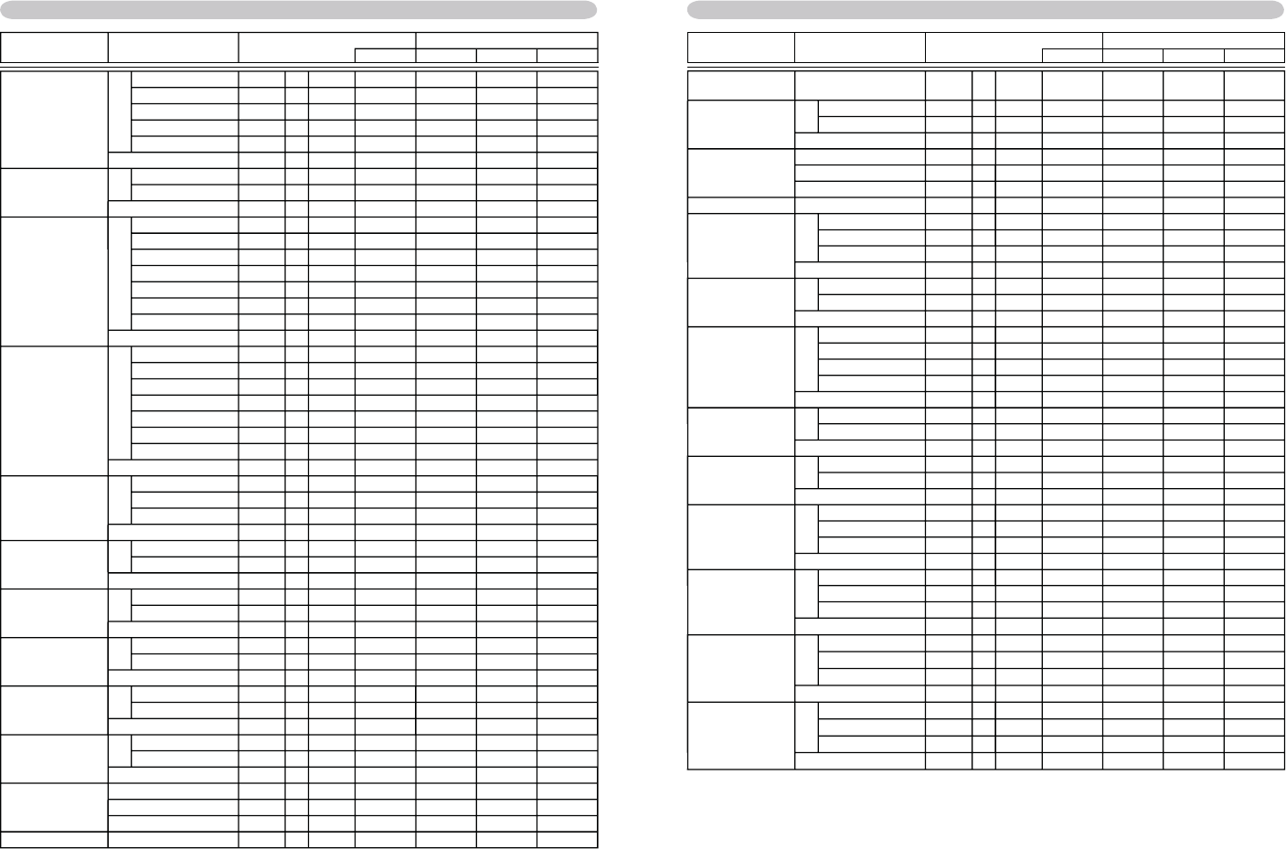
66
CP-SX635(ED3SX40N)
RS-232C Communication / Network command table
Names Operation Type Header Command Data
CRC Action Type Setting Code
COLOR SPACE Set AUTO BE EF 03 06 00 0E 72 01 00 04 22 00 00
RGB BE EF 03 06 00 9E 73 01 00 04 22 01 00
SMPTE240 BE EF 03 06 00 6E 73 01 00 04 22 02 00
REC709 BE EF 03 06 00 FE 72 01 00 04 22 03 00
REC601 BE EF 03 06 00 CE 70 01 00 04 22 04 00
Get BE EF 03 06 00 3D 72 02 00 04 22 00 00
COMPONENT Set COMPONENT BE EF 03 06 00 4A D7 01 00 17 20 00 00
SCART RGB BE EF 03 06 00 DA D6 01 00 17 20 01 00
Get BE EF 03 06 00 79 D7 02 00 17 20 00 00
S-VIDEO FORMAT Set AUTO BE EF 03 06 00 E6 70 01 00 12 22 0A 00
NTSC BE EF 03 06 00 86 74 01 00 12 22 04 00
PAL BE EF 03 06 00 16 75 01 00 12 22 05 00
SECAM BE EF 03 06 00 16 70 01 00 12 22 09 00
NTSC4.43 BE EF 03 06 00 26 77 01 00 12 22 02 00
M-PAL BE EF 03 06 00 86 71 01 00 12 22 08 00
N-PAL BE EF 03 06 00 76 74 01 00 12 22 07 00
Get BE EF 03 06 00 75 76 02 00 12 22 00 00
C-VIDEO FORMAT Set AUTO BE EF 03 06 00 A2 70 01 00 11 22 0A 00
NTSC BE EF 03 06 00 C2 74 01 00 11 22 04 00
PAL BE EF 03 06 00 52 75 01 00 11 22 05 00
SECAM BE EF 03 06 00 52 70 01 00 11 22 09 00
NTSC4.43 BE EF 03 06 00 62 77 01 00 11 22 02 00
M-PAL BE EF 03 06 00 C2 71 01 00 11 22 08 00
N-PAL BE EF 03 06 00 32 74 01 00 11 22 07 00
Get BE EF 03 06 00 31 76 02 00 11 22 00 00
HDMI Set AUTO BE EF 03 06 00 86 D8 01 00 22 20 00 00
NORMAL BE EF 03 06 00 16 D9 01 00 22 20 01 00
ENHANCED BE EF 03 06 00 E6 D9 01 00 22 20 02 00
Get BE EF 03 06 00 B5 D8 02 00 22 20 00 00
FRAME LOCK - RGB1 Set TURN OFF BE EF 03 06 00 3B C2 01 00 50 30 00 00
TURN ON BE EF 03 06 00 AB C3 01 00 50 30 01 00
Get BE EF 03 06 00 08 C2 02 00 50 30 00 00
FRAME LOCK - RGB2 Set TURN OFF BE EF 03 06 00 0B C3 01 00 54 30 00 00
TURN ON BE EF 03 06 00 9B C2 01 00 54 30 01 00
Get BE EF 03 06 00 38 C3 02 00 54 30 00 00
FRAME LOCK - HDMI Set TURN OFF BE EF 03 06 00 7F C2 01 00 53 30 00 00
TURN ON BE EF 03 06 00 EF C3 01 00 53 30 01 00
Get BE EF 03 06 00 4C C2 02 00 53 30 00 00
RGB IN1 Set SYNC ON G OFF BE EF 03 06 00 5E D7 01 00 10 20 02 00
AUTO BE EF 03 06 00 CE D6 01 00 10 20 03 00
Get BE EF 03 06 00 0D D6 02 00 10 20 00 00
RGB IN2 Set SYNC ON G OFF BE EF 03 06 00 A2 D6 01 00 11 20 02 00
AUTO BE EF 03 06 00 32 D7 01 00 11 20 03 00
Get BE EF 03 06 00 F1 D7 02 00 11 20 00 00
KEYSTONE V Get BE EF 03 06 00 B9 D3 02 00 07 20 00 00
Increment BE EF 03 06 00 DF D3 04 00 07 20 00 00
Decrement BE EF 03 06 00 0E D2 05 00 07 20 00 00
KEYSTONE V Reset Execute BE EF 03 06 00 08 D0 06 00 0C 70 00 00
Names Operation Type Header Command Data
CRC Action Type Setting Code
RS-232C Communication / Network command table
AUTO KEYSTONE V
EXECUTE
Execute BE EF 03 06 00 E5 D1 06 00 0D 20 00 00
AUTO KEYSTONE V Set TURN OFF BE EF 03 06 00 EA D1 01 00 0F 20 00 00
TURN ON BE EF 03 06 00 7A D0 01 00 0F 20 01 00
Get BE EF 03 06 00 D9 D1 02 00 0F 20 00 00
KEYSTONE H Get BE EF 03 06 00 E9 D0 02 00 0B 20 00 00
Increment BE EF 03 06 00 8F D0 04 00 0B 20 00 00
Decrement BE EF 03 06 00 5E D1 05 00 0B 20 00 00
KEYSTONE H Reset Execute BE EF 03 06 00 98 D8 06 00 20 70 00 00
ACTIVE IRIS Set TURN OFF BE EF 03 06 00 0B 22 01 00 04 33 00 00
THEATER BE EF 03 06 00 CB 2F 01 00 04 33 10 00
PRESENTATION BE EF 03 06 00 5B 2E 01 00 04 33 11 00
Get BE EF 03 06 00 38 22 02 00 04 33 00 00
WHISPER Set NORMAL BE EF 03 06 00 3B 23 01 00 00 33 00 00
WHISPER BE EF 03 06 00 AB 22 01 00 00 33 01 00
Get BE EF 03 06 00 08 23 02 00 00 33 00 00
MIRROR Set NORMAL BE EF 03 06 00 C7 D2 01 00 01 30 00 00
H:INVERT BE EF 03 06 00 57 D3 01 00 01 30 01 00
V:INVERT BE EF 03 06 00 A7 D3 01 00 01 30 02 00
H&V:INVERT BE EF 03 06 00 37 D2 01 00 01 30 03 00
Get BE EF 03 06 00 F4 D2 02 00 01 30 00 00
MONITOR OUT - RGB1 Set RGB2 BE EF 03 06 00 FE F6 01 00 B0 20 04 00
TURN OFF BE EF 03 06 00 CE B5 01 00 B0 20 FF 00
Get BE EF 03 06 00 0D F4 02 00 B0 20 00 00
MONITOR OUT - RGB2 Set RGB1 BE EF 03 06 00 0E F5 01 00 B4 20 00 00
TURN OFF BE EF 03 06 00 FE B4 01 00 B4 20 FF 00
Get BE EF 03 06 00 3D F5 02 00 B4 20 00 00
MONITOR OUT - HDMI Set RGB1 BE EF 03 06 00 7A F4 01 00 B3 20 00 00
RGB2 BE EF 03 06 00 BA F6 01 00 B3 20 04 00
TURN OFF BE EF 03 06 00 8A B5 01 00 B3 20 FF 00
Get BE EF 03 06 00 49 F4 02 00 B3 20 00 00
MONITOR OUT -
COMPONENT
Set RGB1 BE EF 03 06 00 F2 F4 01 00 B5 20 00 00
RGB2 BE EF 03 06 00 32 F6 01 00 B5 20 04 00
TURN OFF BE EF 03 06 00 02 B5 01 00 B5 20 FF 00
Get BE EF 03 06 00 C1 F4 02 00 B5 20 00 00
MONITOR OUT -
S-VIDEO
Set RGB1 BE EF 03 06 00 86 F5 01 00 B2 20 00 00
RGB2 BE EF 03 06 00 46 F7 01 00 B2 20 04 00
TURN OFF BE EF 03 06 00 76 B4 01 00 B2 20 FF 00
Get BE EF 03 06 00 B5 F5 02 00 B2 20 00 00
MONITOR OUT -
VIDEO
Set RGB1 BE EF 03 06 00 C2 F5 01 00 B1 20 00 00
RGB2 BE EF 03 06 00 02 F7 01 00 B1 20 04 00
TURN OFF BE EF 03 06 00 32 B4 01 00 B1 20 FF 00
Get BE EF 03 06 00 F1 F5 02 00 B1 20 00 00
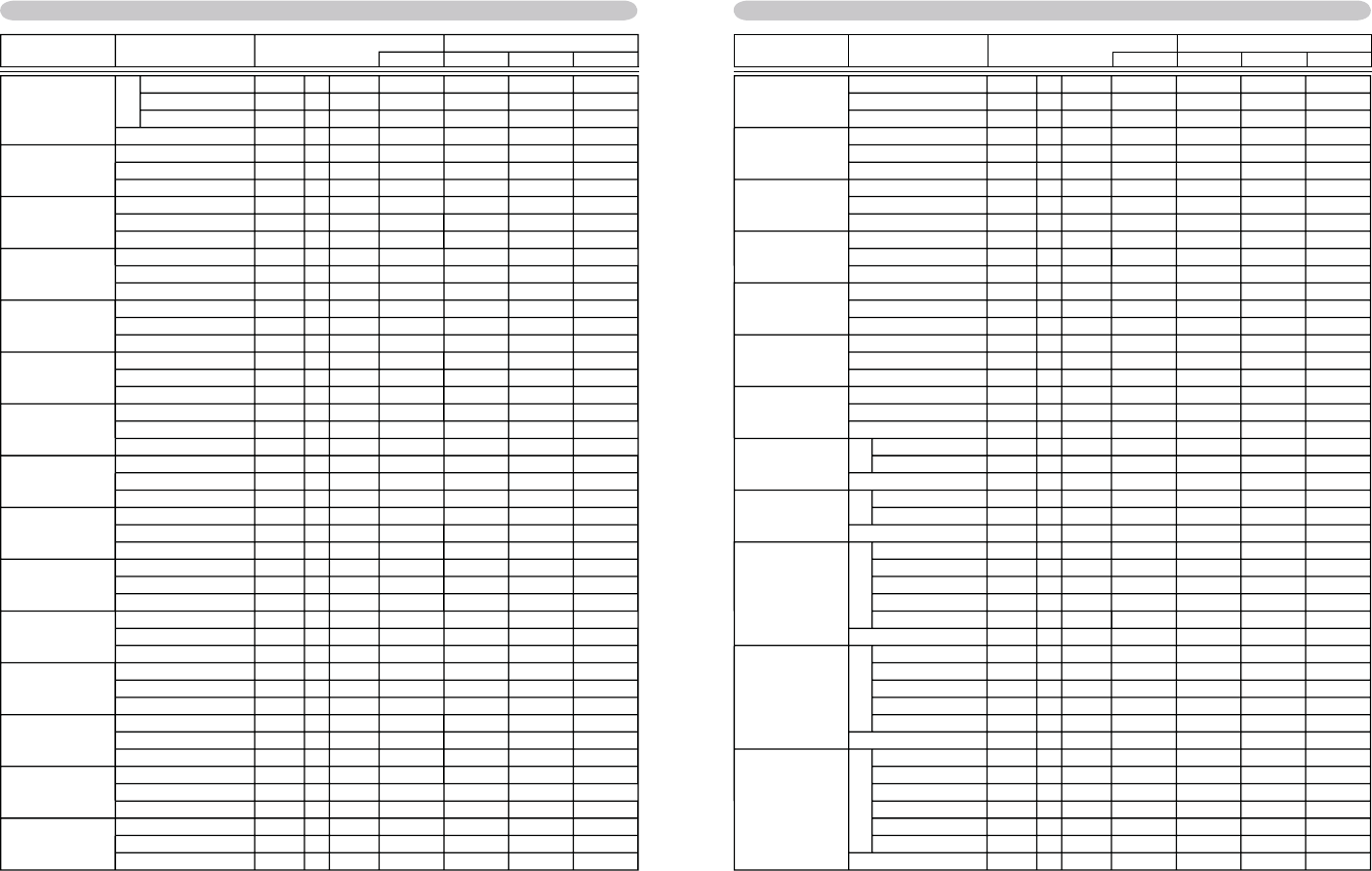
67
CP-SX635(ED3SX40N)
RS-232C Communication / Network command table
Names Operation Type Header Command Data
CRC Action Type Setting Code
MONITOR OUT -
STANDBY
Set RGB1 BE EF 03 06 00 2A F7 01 00 BF 20 00 00
RGB2 BE EF 03 06 00 EA F5 01 00 BF 20 04 00
TURN OFF BE EF 03 06 00 DA B6 01 00 BF 20 FF 00
Get BE EF 03 06 00 19 F7 02 00 BF 20 00 00
VOLUME - RGB1 Get BE EF 03 06 00 CD CC 02 00 60 20 00 00
Increment BE EF 03 06 00 AB CC 04 00 60 20 00 00
Decrement BE EF 03 06 00 7A CD 05 00 60 20 00 00
VOLUME - RGB2 Get BE EF 03 06 00 FD CD 02 00 64 20 00 00
Increment BE EF 03 06 00 9B CD 04 00 64 20 00 00
Decrement BE EF 03 06 00 4A CC 05 00 64 20 00 00
VOLUME - HDMI Get BE EF 03 06 00 89 CC 02 00 63 20 00 00
Increment BE EF 03 06 00 EF CC 04 00 63 20 00 00
Decrement BE EF 03 06 00 3E CD 05 00 63 20 00 00
VOLUME -
COMPONENT
Get BE EF 03 06 00 01 CC 02 00 65 20 00 00
Increment BE EF 03 06 00 67 CC 04 00 65 20 00 00
Decrement BE EF 03 06 00 B6 CD 05 00 65 20 00 00
VOLUME - S-VIDEO Get BE EF 03 06 00 75 CD 02 00 62 20 00 00
Increment BE EF 03 06 00 13 CD 04 00 62 20 00 00
Decrement BE EF 03 06 00 C2 CC 05 00 62 20 00 00
VOLUME - VIDEO Get BE EF 03 06 00 31 CD 02 00 61 20 00 00
Increment BE EF 03 06 00 57 CD 04 00 61 20 00 00
Decrement BE EF 03 06 00 86 CC 05 00 61 20 00 00
VOLUME - AUDIO OUT
STANDBY
Get BE EF 03 06 00 D9 CF 02 00 6F 20 00 00
Increment BE EF 03 06 00 BF CF 04 00 6F 20 00 00
Decrement BE EF 03 06 00 6E CE 05 00 6F 20 00 00
TREBLE - RGB1 Get BE EF 03 06 00 0D C8 02 00 70 20 00 00
Increment BE EF 03 06 00 6B C8 04 00 70 20 00 00
Decrement BE EF 03 06 00 BA C9 05 00 70 20 00 00
TREBLE -RGB2 Get BE EF 03 06 00 3D C9 02 00 74 20 00 00
Increment BE EF 03 06 00 5B C9 04 00 74 20 00 00
Decrement BE EF 03 06 00 8A C8 05 00 74 20 00 00
TREBLE - HDMI Get BE EF 03 06 00 49 C8 02 00 73 20 00 00
Increment BE EF 03 06 00 2F C8 04 00 73 20 00 00
Decrement BE EF 03 06 00 FE C9 05 00 73 20 00 00
TREBLE -
COMPONENT
Get BE EF 03 06 00 C1 C8 02 00 75 20 00 00
Increment BE EF 03 06 00 A7 C8 04 00 75 20 00 00
Decrement BE EF 03 06 00 76 C9 05 00 75 20 00 00
TREBLE - S-VIDEO Get BE EF 03 06 00 B5 C9 02 00 72 20 00 00
Increment BE EF 03 06 00 D3 C9 04 00 72 20 00 00
Decrement BE EF 03 06 00 02 C8 05 00 72 20 00 00
TREBLE - VIDEO Get BE EF 03 06 00 F1 C9 02 00 71 20 00 00
Increment BE EF 03 06 00 97 C9 04 00 71 20 00 00
Decrement BE EF 03 06 00 46 C8 05 00 71 20 00 00
TREBLE - AUDIO OUT
STANDBY
Get BE EF 03 06 00 19 CB 02 00 7F 20 00 00
Increment BE EF 03 06 00 7F CB 04 00 7F 20 00 00
Decrement BE EF 03 06 00 AE CA 05 00 7F 20 00 00
Names Operation Type Header Command Data
CRC Action Type Setting Code
RS-232C Communication / Network command table
BASS - RGB1 Get BE EF 03 06 00 0D FB 02 00 80 20 00 00
Increment BE EF 03 06 00 6B FB 04 00 80 20 00 00
Decrement BE EF 03 06 00 BA FA 05 00 80 20 00 00
BASS - RGB2 Get BE EF 03 06 00 3D FA 02 00 84 20 00 00
Increment BE EF 03 06 00 5B FA 04 00 84 20 00 00
Decrement BE EF 03 06 00 8A FB 05 00 84 20 00 00
BASS - HDMI Get BE EF 03 06 00 49 FB 02 00 83 20 00 00
Increment BE EF 03 06 00 2F FB 04 00 83 20 00 00
Decrement BE EF 03 06 00 FE FA 05 00 83 20 00 00
BASS - COMPONENT Get BE EF 03 06 00 C1 FB 02 00 85 20 00 00
Increment BE EF 03 06 00 A7 FB 04 00 85 20 00 00
Decrement BE EF 03 06 00 76 FA 05 00 85 20 00 00
BASS - S-VIDEO Get BE EF 03 06 00 B5 FA 02 00 82 20 00 00
Increment BE EF 03 06 00 D3 FA 04 00 82 20 00 00
Decrement BE EF 03 06 00 02 FB 05 00 82 20 00 00
BASS - VIDEO Get BE EF 03 06 00 F1 FA 02 00 81 20 00 00
Increment BE EF 03 06 00 97 FA 04 00 81 20 00 00
Decrement BE EF 03 06 00 46 FB 05 00 81 20 00 00
BASS - AUDIO OUT
STANDBY
Get BE EF 03 06 00 19 F8 02 00 8F 20 00 00
Increment BE EF 03 06 00 7F F8 04 00 8F 20 00 00
Decrement BE EF 03 06 00 AE F9 05 00 8F 20 00 00
MUTE Set TURN OFF BE EF 03 06 00 46 D3 01 00 02 20 00 00
TURN ON BE EF 03 06 00 D6 D2 01 00 02 20 01 00
Get BE EF 03 06 00 75 D3 02 00 02 20 00 00
SPEAKER Set TURN OFF BE EF 03 06 00 6E D5 01 00 1C 20 00 00
TURN ON BE EF 03 06 00 FE D4 01 00 1C 20 01 00
Get BE EF 03 06 00 5D D5 02 00 1C 20 00 00
AUDIO - RGB1 Set TURN OFF BE EF 03 06 00 FE DD 01 00 30 20 00 00
AUDIO1 BE EF 03 06 00 6E DC 01 00 30 20 01 00
AUDIO2 BE EF 03 06 00 9E DC 01 00 30 20 02 00
AUDIO3 BE EF 03 06 00 0E DD 01 00 30 20 03 00
AUDIO4 BE EF 03 06 00 3E DF 01 00 30 20 04 00
Get BE EF 03 06 00 CD DD 02 00 30 20 00 00
AUDIO - RGB2 Set TURN OFF BE EF 03 06 00 CE DC 01 00 34 20 00 00
AUDIO1 BE EF 03 06 00 5E DD 01 00 34 20 01 00
AUDIO2 BE EF 03 06 00 AE DD 01 00 34 20 02 00
AUDIO3 BE EF 03 06 00 3E DC 01 00 34 20 03 00
AUDIO4 BE EF 03 06 00 0E DE 01 00 34 20 04 00
Get BE EF 03 06 00 FD DC 02 00 34 20 00 00
AUDIO - HDMI Set TURN OFF BE EF 03 06 00 BA DD 01 00 33 20 00 00
AUDIO1 BE EF 03 06 00 2A DC 01 00 33 20 01 00
AUDIO2 BE EF 03 06 00 DA DC 01 00 33 20 02 00
AUDIO3 BE EF 03 06 00 4A DD 01 00 33 20 03 00
AUDIO4 BE EF 03 06 00 7A DF 01 00 33 20 04 00
AUDIO_HDMI BE EF 03 06 00 7A C4 01 00 33 20 20 00
Get BE EF 03 06 00 89 DD 02 00 33 20 00 00
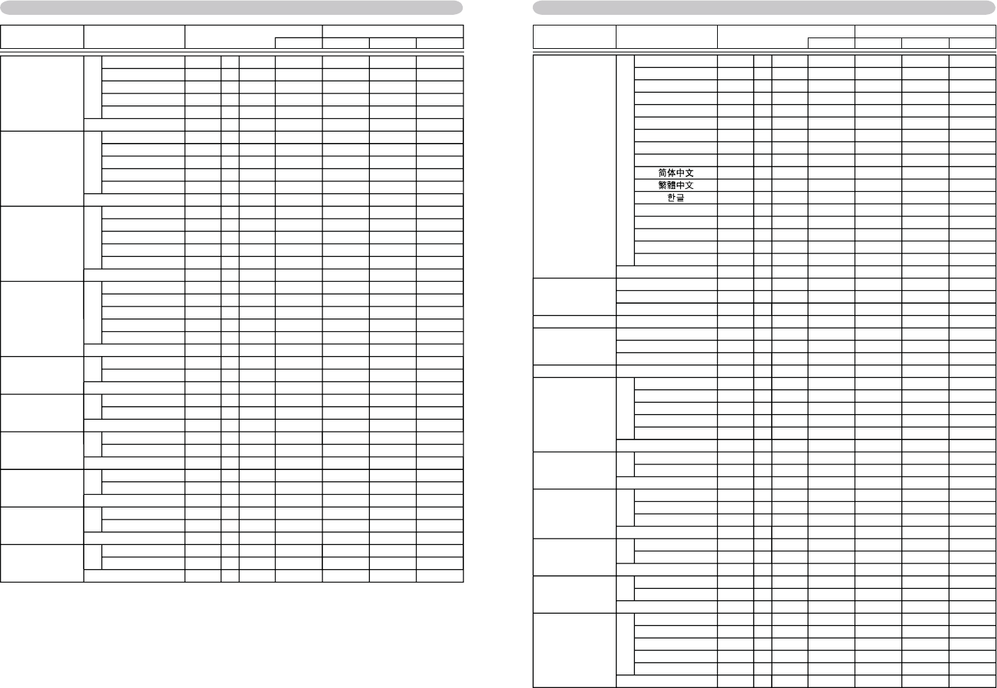
68
CP-SX635(ED3SX40N)
RS-232C Communication / Network command table
Names Operation Type Header Command Data
CRC Action Type Setting Code
AUDIO - COMPONENT Set TURN OFF BE EF 03 06 00 32 DD 01 00 35 20 00 00
AUDIO1 BE EF 03 06 00 A2 DC 01 00 35 20 01 00
AUDIO2 BE EF 03 06 00 52 DC 01 00 35 20 02 00
AUDIO3 BE EF 03 06 00 C2 DD 01 00 35 20 03 00
AUDIO4 BE EF 03 06 00 F2 DF 01 00 35 20 04 00
Get BE EF 03 06 00 01 DD 02 00 35 20 00 00
AUDIO - S-VIDEO Set TURN OFF BE EF 03 06 00 46 DC 01 00 32 20 00 00
AUDIO1 BE EF 03 06 00 D6 DD 01 00 32 20 01 00
AUDIO2 BE EF 03 06 00 26 DD 01 00 32 20 02 00
AUDIO3 BE EF 03 06 00 B6 DC 01 00 32 20 03 00
AUDIO4 BE EF 03 06 00 86 DE 01 00 32 20 04 00
Get BE EF 03 06 00 75 DC 02 00 32 20 00 00
AUDIO - VIDEO Set TURN OFF BE EF 03 06 00 02 DC 01 00 31 20 00 00
AUDIO1 BE EF 03 06 00 92 DD 01 00 31 20 01 00
AUDIO2 BE EF 03 06 00 62 DD 01 00 31 20 02 00
AUDIO3 BE EF 03 06 00 F2 DC 01 00 31 20 03 00
AUDIO4 BE EF 03 06 00 C2 DE 01 00 31 20 04 00
Get BE EF 03 06 00 31 DC 02 00 31 20 00 00
AUDIO OUT STANDBY Set TURN OFF BE EF 03 06 00 EA DE 01 00 3F 20 00 00
AUDIO1 BE EF 03 06 00 7A DF 01 00 3F 20 01 00
AUDIO2 BE EF 03 06 00 8A DF 01 00 3F 20 02 00
AUDIO3 BE EF 03 06 00 1A DE 01 00 3F 20 03 00
AUDIO4 BE EF 03 06 00 2A DC 01 00 3F 20 04 00
Get BE EF 03 06 00 D9 DE 02 00 3F 20 00 00
HDMI AUDIO Set 1 BE EF 03 06 00 AE C6 01 00 40 20 01 00
2 BE EF 03 06 00 5E C6 01 00 40 20 02 00
Get BE EF 03 06 00 0D C7 02 00 40 20 00 00
REMOTE FRONT Set Off BE EF 03 06 00 FF 32 01 00 00 26 00 00
On BE EF 03 06 00 6F 33 01 00 00 26 01 00
Get BE EF 03 06 00 CC 32 02 00 00 26 00 00
REMOTE REAR Set Off BE EF 03 06 00 03 33 01 00 01 26 00 00
On BE EF 03 06 00 93 32 01 00 01 26 01 00
Get BE EF 03 06 00 30 33 02 00 01 26 00 00
REMOTE TOP Set Off BE EF 03 06 00 47 33 01 00 02 26 00 00
On BE EF 03 06 00 D7 32 01 00 02 26 01 00
Get BE EF 03 06 00 74 33 02 00 02 26 00 00
REMOTE FREQUENCY
NORMAL
Set Disable BE EF 03 06 00 FF 3D 01 00 30 26 00 00
Enable BE EF 03 06 00 6F 3C 01 00 30 26 01 00
Get BE EF 03 06 00 CC 3D 02 00 30 26 00 00
REMOTE FREQUENCY
HIGH
Set Disable BE EF 03 06 00 03 3C 01 00 31 26 00 00
Enable BE EF 03 06 00 93 3D 01 00 31 26 01 00
Get BE EF 03 06 00 30 3C 02 00 31 26 00 00
Names Operation Type Header Command Data
CRC Action Type Setting Code
RS-232C Communication / Network command table
LANGUAGE Set ENGLISH BE EF 03 06 00 F7 D3 01 00 05 30 00 00
FRANCAIS BE EF 03 06 00 67 D2 01 00 05 30 01 00
DEUTSCH BE EF 03 06 00 97 D2 01 00 05 30 02 00
ESPANOL BE EF 03 06 00 07 D3 01 00 05 30 03 00
ITALIANO BE EF 03 06 00 37 D1 01 00 05 30 04 00
NORSK BE EF 03 06 00 A7 D0 01 00 05 30 05 00
NEDERLANDS BE EF 03 06 00 57 D0 01 00 05 30 06 00
PORTUGUESE BE EF 03 06 00 C7 D1 01 00 05 30 07 00
日本語 BE EF 03 06 00 37 D4 01 00 05 30 08 00
BE EF 03 06 00 A7 D5 01 00 05 30 09 00
BE EF 03 06 00 37 DE 01 00 05 30 10 00
BE EF 03 06 00 57 D5 01 00 05 30 0A 00
SVENSKA BE EF 03 06 00 C7 D4 01 00 05 30 0B 00
PYCCKNN BE EF 03 06 00 F7 D6 01 00 05 30 0C 00
SUOMI BE EF 03 06 00 67 D7 01 00 05 30 0D 00
POLSKI BE EF 03 06 00 97 D7 01 00 05 30 0E 00
TÜRKÇE BE EF 03 06 00 07 D6 01 00 05 30 0F 00
Get BE EF 03 06 00 C4 D3 02 00 05 30 00 00
MENU POSITION V Get BE EF 03 06 00 40 D7 02 00 16 30 00 00
Increment BE EF 03 06 00 26 D7 04 00 16 30 00 00
Decrement BE EF 03 06 00 F7 D6 05 00 16 30 00 00
MENU POSITION V Reset
Execute BE EF 03 06 00 A8 C7 06 00 44 70 00 00
MENU POSITION H Get BE EF 03 06 00 04 D7 02 00 15 30 00 00
Increment BE EF 03 06 00 62 D7 04 00 15 30 00 00
Decrement BE EF 03 06 00 B3 D6 05 00 15 30 00 00
MENU POSITION H Reset
Execute BE EF 03 06 00 DC C6 06 00 43 70 00 00
BLANK Set MyScreen BE EF 03 06 00 FB CA 01 00 00 30 20 00
ORIGINAL BE EF 03 06 00 FB E2 01 00 00 30 40 00
BLUE BE EF 03 06 00 CB D3 01 00 00 30 03 00
WHITE BE EF 03 06 00 6B D0 01 00 00 30 05 00
BLACK BE EF 03 06 00 9B D0 01 00 00 30 06 00
Get BE EF 03 06 00 08 D3 02 00 00 30 00 00
BLANK On/Off Set TURN OFF BE EF 03 06 00 FB D8 01 00 20 30 00 00
TURN ON BE EF 03 06 00 6B D9 01 00 20 30 01 00
Get BE EF 03 06 00 C8 D8 02 00 20 30 00 00
START UP Set MyScreen BE EF 03 06 00 CB CB 01 00 04 30 20 00
ORIGINAL BE EF 03 06 00 0B D2 01 00 04 30 00 00
TURN OFF BE EF 03 06 00 9B D3 01 00 04 30 01 00
Get BE EF 03 06 00 38 D2 02 00 04 30 00 00
MyScreen LOCK Set TURN OFF BE EF 03 06 00 3B EF 01 00 C0 30 00 00
TURN ON BE EF 03 06 00 AB EE 01 00 C0 30 01 00
Get BE EF 03 06 00 08 EF 02 00 C0 30 00 00
MESSAGE Set TURN OFF BE EF 03 06 00 8F D6 01 00 17 30 00 00
TURN ON BE EF 03 06 00 1F D7 01 00 17 30 01 00
Get BE EF 03 06 00 BC D6 02 00 17 30 00 00
TEMPLATE Set TEST PATTERN BE EF 03 06 00 43 D9 01 00 22 30 00 00
DOT-LINE1 BE EF 03 06 00 D3 D8 01 00 22 30 01 00
DOT-LINE2 BE EF 03 06 00 23 D8 01 00 22 30 02 00
DOT-LINE3 BE EF 03 06 00 B3 D9 01 00 22 30 03 00
DOT-LINE4 BE EF 03 06 00 83 DB 01 00 22 30 04 00
Get BE EF 03 06 00 70 D9 02 00 22 30 00 00
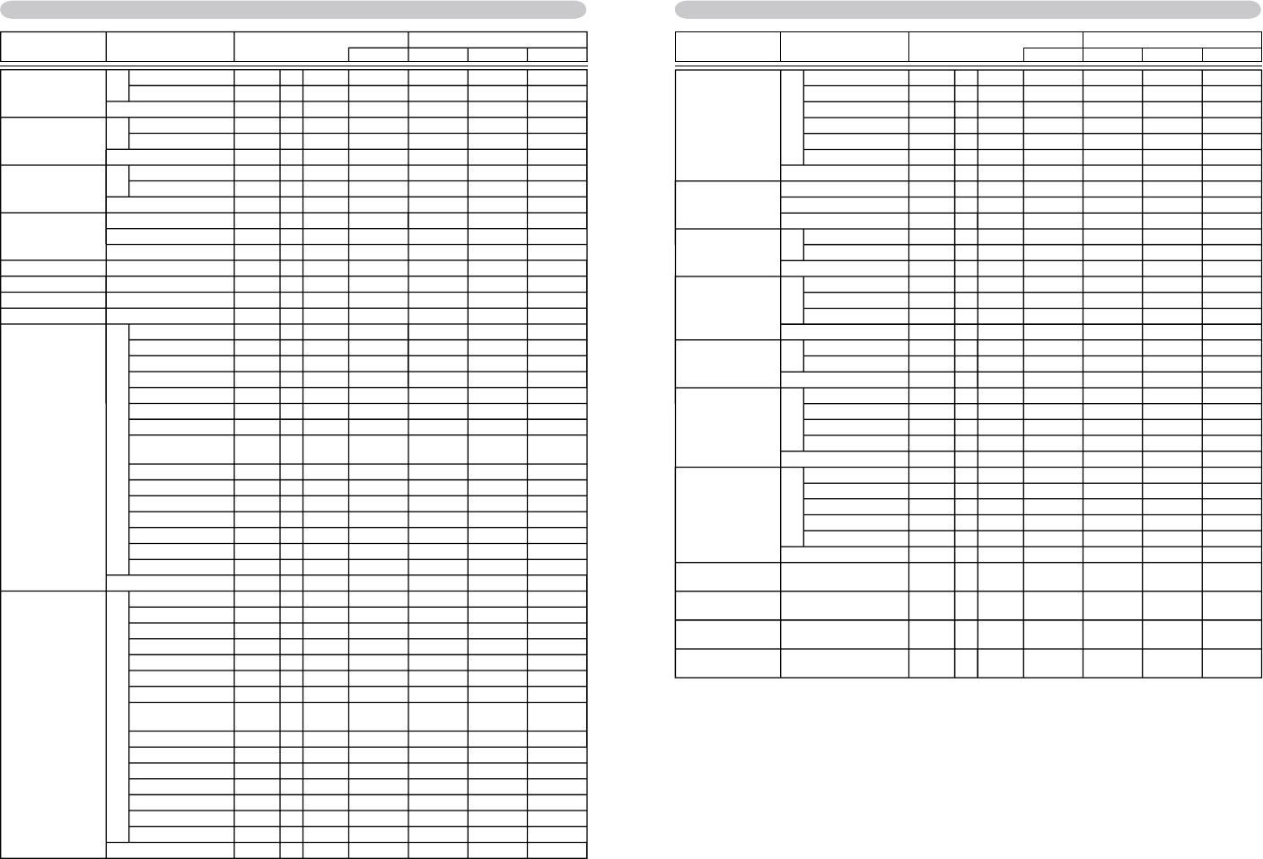
69
CP-SX635(ED3SX40N)
RS-232C Communication / Network command table
Names Operation Type Header Command Data
CRC Action Type Setting Code
TEMPLATE On/Off Set TURN OFF BE EF 03 06 00 BF D8 01 00 23 30 00 00
TURN ON BE EF 03 06 00 2F D9 01 00 23 30 01 00
Get BE EF 03 06 00 8C D8 02 00 23 30 00 00
AUTO SEARCH Set TURN OFF BE EF 03 06 00 B6 D6 01 00 16 20 00 00
TURN ON BE EF 03 06 00 26 D7 01 00 16 20 01 00
Get BE EF 03 06 00 85 D6 02 00 16 20 00 00
AUTO ON Set TURN OFF BE EF 03 06 00 3B 89 01 00 20 31 00 00
TURN ON BE EF 03 06 00 AB 88 01 00 20 31 01 00
Get BE EF 03 06 00 08 89 02 00 20 31 00 00
AUTO OFF Get BE EF 03 06 00 08 86 02 00 10 31 00 00
Increment BE EF 03 06 00 6E 86 04 00 10 31 00 00
Decrement BE EF 03 06 00 BF 87 05 00 10 31 00 00
LAMP TIME Get BE EF 03 06 00 C2 FF 02 00 90 10 00 00
LAMP TIME Reset Execute BE EF 03 06 00 58 DC 06 00 30 70 00 00
FILTER TIME Get BE EF 03 06 00 C2 F0 02 00 A0 10 00 00
FILTER TIME Reset Execute BE EF 03 06 00 98 C6 06 00 40 70 00 00
MY BUTTON-1 Set RGB1 BE EF 03 06 00 3A 33 01 00 00 36 00 00
RGB2 BE EF 03 06 00 FA 31 01 00 00 36 04 00
HDMI BE EF 03 06 00 CA 33 01 00 00 36 03 00
COMPONENT BE EF 03 06 00 6A 30 01 00 00 36 05 00
S-VIDEO BE EF 03 06 00 5A 32 01 00 00 36 02 00
VIDEO BE EF 03 06 00 AA 32 01 00 00 36 01 00
INFORMATION BE EF 03 06 00 FA 3E 01 00 00 36 10 00
AUTO KEYSTONE
EXECUTE
BE EF 03 06 00 6A 3F 01 00 00 36 11 00
MY MEMORY BE EF 03 06 00 9A 3F 01 00 00 36 12 00
PICTURE MODE BE EF 03 06 00 0A 3E 01 00 00 36 13 00
FILTER RESET BE EF 03 06 00 3A 3C 01 00 00 36 14 00
ACTIVE IRIS BE EF 03 06 00 AA 3D 01 00 00 36 15 00
MY IMAGE BE EF 03 06 00 5A 3D 01 00 00 36 16 00
AV MUTE BE EF 03 06 00 AA 38 01 00 00 36 19 00
TEMPLATE BE EF 03 06 00 CA 39 01 00 00 36 1B 00
Get BE EF 03 06 00 09 33 02 00 00 36 00 00
MY BUTTON-2 Set RGB1 BE EF 03 06 00 C6 32 01 00 01 36 00 00
RGB2 BE EF 03 06 00 06 30 01 00 01 36 04 00
HDMI BE EF 03 06 00 36 32 01 00 01 36 03 00
COMPONENT BE EF 03 06 00 96 31 01 00 01 36 05 00
S-VIDEO BE EF 03 06 00 A6 33 01 00 01 36 02 00
VIDEO BE EF 03 06 00 56 33 01 00 01 36 01 00
INFORMATION BE EF 03 06 00 06 3F 01 00 01 36 10 00
AUTO KEYSTONE
EXECUTE
BE EF 03 06 00 96 3E 01 00 01 36 11 00
MY MEMORY BE EF 03 06 00 66 3E 01 00 01 36 12 00
PICTURE MODE BE EF 03 06 00 F6 3F 01 00 01 36 13 00
FILTER RESET BE EF 03 06 00 C6 3D 01 00 01 36 14 00
ACTIVE IRIS BE EF 03 06 00 56 3C 01 00 01 36 15 00
MY IMAGE BE EF 03 06 00 A6 3C 01 00 01 36 16 00
AV MUTE BE EF 03 06 00 56 39 01 00 01 36 19 00
TEMPLATE BE EF 03 06 00 36 38 01 00 01 36 1B 00
Get BE EF 03 06 00 F5 32 02 00 01 36 00 00
Names Operation Type Header Command Data
CRC Action Type Setting Code
RS-232C Communication / Network command table
MY SOURCE Set RGB1 BE EF 03 06 00 FA 38 01 00 20 36 00 00
RGB2 BE EF 03 06 00 3A 3A 01 00 20 36 04 00
HDMI BE EF 03 06 00 0A 38 01 00 20 36 03 00
COMPONENT BE EF 03 06 00 AA 3B 01 00 20 36 05 00
S-VIDEO BE EF 03 06 00 9A 39 01 00 20 36 02 00
VIDEO BE EF 03 06 00 6A 39 01 00 20 36 01 00
Get BE EF 03 06 00 C9 38 02 00 20 36 00 00
MAGNIFY Get BE EF 03 06 00 7C D2 02 00 07 30 00 00
Increment BE EF 03 06 00 1A D2 04 00 07 30 00 00
Decrement BE EF 03 06 00 CB D3 05 00 07 30 00 00
FREEZE Set NORMAL BE EF 03 06 00 83 D2 01 00 02 30 00 00
FREEZE BE EF 03 06 00 13 D3 01 00 02 30 01 00
Get BE EF 03 06 00 B0 D2 02 00 02 30 00 00
CLOSED CAPTION
DISPLAY
Set TURN OFF BE EF 03 06 00 FA 62 01 00 00 37 00 00
TURN ON BE EF 03 06 00 6A 63 01 00 00 37 01 00
AUTO BE EF 03 06 00 9A 63 01 00 00 37 02 00
Get BE EF 03 06 00 C9 62 02 00 00 37 00 00
CLOSED CAPTION
MODE
Set CAPTIONS BE EF 03 06 00 06 63 01 00 01 37 00 00
TEXT BE EF 03 06 00 96 62 01 00 01 37 01 00
Get BE EF 03 06 00 35 63 02 00 01 37 00 00
CLOSED CAPTION
CHANNEL
Set 1 BE EF 03 06 00 D2 62 01 00 02 37 01 00
2 BE EF 03 06 00 22 62 01 00 02 37 02 00
3 BE EF 03 06 00 B2 63 01 00 02 37 03 00
4 BE EF 03 06 00 82 61 01 00 02 37 04 00
Get BE EF 03 06 00 71 63 02 00 02 37 00 00
MY IMAGE Set OFF BE EF 03 06 00 3A C3 01 00 00 35 00 00
IMAGE-1 BE EF 03 06 00 AA C2 01 00 00 35 01 00
IMAGE-2 BE EF 03 06 00 5A C2 01 00 00 35 02 00
IMAGE-3 BE EF 03 06 00 CA C3 01 00 00 35 03 00
IMAGE-4 BE EF 03 06 00 FA C1 01 00 00 35 04 00
Get BE EF 03 06 00 09 C3 02 00 00 35 00 00
MY IMAGE
IMAGE-1 Delete
Execute BE EF 03 06 00 71 C3 06 00 01 35 00 00
MY IMAGE
IMAGE-2 Delete
Execute BE EF 03 06 00 35 C3 06 00 02 35 00 00
MY IMAGE
IMAGE-3 Delete
Execute BE EF 03 06 00 C9 C2 06 00 03 35 00 00
MY IMAGE
IMAGE-4 Delete
Execute BE EF 03 06 00 BD C3 06 00 04 35 00 00
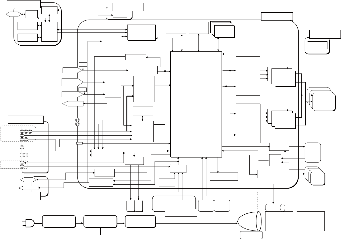
70
CP-SX635(ED3SX40N)
11. Block diagram
㪚㪦㪥㪫㪩㪦㪣㩷㪧㪮㪙
㪘㫌㪻㫀㫆㪶㫀㫅㪈
㪘㫌㪻㫀㫆㪶㫀㫅㪉
㪝㫃㪸㫊㪿㩷㪩㪦㪤
㪊㪉㪤㪹㫀㫋
㪦㪧㪫㪠㪚㪘㪣
㪬㪥㪠㪫
㪣㪸㫄㫇
㪈㪉㪏㪢
㪜㪜㪧㪩㪦㪤
㪫㪜㪤㪧
㪪㪜㪥㪪㪦㪩
㪘㪬㪛㪠㪦㪶㪘㪤㪧
䌄䌃㩷䌐䌏䌗䌅䌒
䌒䌅䌇䌕䌒䌁䌔䌏䌒
㪠㪤㪘㪞㪜㩷㪧㪩㪦㪚㪜㪪㪪㪦㪩
㪛㪜㪠㪥㪫㪜㪩㪣㪘㪚㪜㪩
㪤㪘㪠㪥㩷㪚㪧㪬
㪧㪮㪊㪏㪏㪙㪄㪊㪇㪣
㪣㪆㪪
㪸㫅㪻
㪪㪆㪟
㪚㪯㪘㪎㪇㪇㪐㪩
㪚㪦㪥㪫㪩㪦㪣
㪙㪬㪫㪫㪦㪥
㪝㪘㪥
㪧㪩㪦㪡㪜㪚㪫㪠㪦㪥
㪣㪜㪥㪪
㩷㪪㪯㪞㪘
㪣㪚㪛㩷㪧㪘㪥㪜㪣
㩿㪈㪋㪇㪇㪁㪈㪇㪌㪇㪀
㪩㪪㪄㪉㪊㪉㪚
㪣㪸㫄㫇㩷㪛㫆㫆㫉
㪪㪮
㪜㫏㪿㪸㫌㫊㫋㩷㪽㪸㫅㩷㩿㪸㫏㫀㪸㫃㪀
㪚㪦㪣㪦㪩
㪬㪥㪠㪝㪦㪩㪤㪠㪫㪰㪃
㪫㪠㪤㪠㪥㪞
㪞㪜㪥㪜㪩㪘㪫㪦㪩㪃
㪞㪘㪤㪤㪘
㪚㪦㪩㪩㪜㪚㪫㪠㪦㪥
㪚㪯㪛㪊㪌㪋㪇
㪙㪘㪫㪫㪜㪩㪰㩷㪧㪮㪙
㪙㪸㫋㫋㪼㫉㫐
㪪㪮
㪧㪦㪮㪜㪩㩷㪬㪥㪠㪫
㩿㪺㫀㫉㪺㫌㫀㫋㪀
㪩㪜㪤㪦㪫㪜㩷㪧㪮㪙
㪠㪩
㪩㪜㪚㪜㪠㪭㪜㪩
㪪㪮
㪘㪆㪛
㪚㫆㫅㫍㪼㫉㫋㪼㫉
㪤㪪㪫㪊㪌㪍㪇㪤
㪮㫀㫉㪼㪻㩷㪩㪼㫄㫆㫋㪼
㪚㫊㩷㪭㫀㪻㪼㫆
㪪㪄㪭㫀㪻㪼㫆
㪘㫌㪻㫀㫆㪶㫀㫅㪊
㪚㫆㫄㫇㫆㫅㪼㫅㫋
㪭㫀㪻㪼㫆
㪘㫌㪻㫀㫆㪶㫀㫅㪋
㪣 㪩
㪣 㪩
㪘㫌㪻㫀㫆㪶㪦㪬㪫
㪠㪥㪧㪬㪫㩷㪧㪮㪙
㪘㪆㪛㩷㪚㫆㫅㫍㪼㫉㫋㪼㫉
㪸㫅㪻
㪭㫀㪻㪼㫆㩷㪛㪼㪺㫆㫉㪻㪼㫉
㪘㪛㪭㪎㪏㪇㪇
㪩㪼㫊㪼㫋㩷㪪㪮
㪬㪪㪙㪶㪤㪦㪬㪪㪜
㪫㪜㪤㪧
㪪㪜㪥㪪㪦㪩
㪘㪚
㪠㪥㪧㪬㪫
㪠㪩㪠㪪
㪤㪦㪫㪜㪩
㪤㫆㫋㫆㫉㩷㪛㫉㫀㫍㪼㫉
㫌㪧㪛㪈㪍㪏㪈㪈㪇
㪢㪜㪰㪧㪘㪛㩷㪧㪮㪙
㪚㫆㫄㫇㫌㪼㫉㩷㫀㫅㪉
㩿㪙㪥㪚㪀
㪛㪛㪚
㪭㫀㪻㪼㫆
㪘㪤㪧
㪫㪟㪪㪎㪊㪉㪎
㪛㪛㪚
㪠㪩
㪩㪜㪚㪜㪠㪭㪜㪩
㪤㪘㪠㪥㩷㪧㪮㪙
㪚㪫㪣
㪛㪛㪩㩷㪪㪛㪩㪘㪤
㪉㪌㪍㪤㩷㬍㪋
㪣㪸㫄㫇㩷㩿㫊㫀㫉㫆㪺㪺㫆㪀
㪩㪆㪞㩷㪧㪸㫅㪼㫃㩷㪽㪸㫅㩷㩿㫊㫀㫉㫆㪺㪺㫆㪀
㪝㪘㪥
㪝㪘㪥
㪝㪘㪥
㪝㪘㪥
㪧㫆㫎㪼㫉㩷㪽㪸㫅㩷㩿㪸㫏㫀㪸㫃㪀
㪙㩷㪧㪸㫅㪼㫃㩷㪽㪸㫅㩷㩿㪸㫏㫀㪸㫃㪀
Audio DAC
㪬㪪㪙㩷㪤㫆㫌㫊㪼
㪪㪧
㪋㪮
㪪㪧
㪋㪮
㪛㪛㪩㩷㪪㪛㪩㪘㪤
㪈㪉㪏㪤
㪚㪦㪣㪦㪩
㪬㪥㪠㪝㪦㪩㪤㪠㪫㪰㪃
㪫㪠㪤㪠㪥㪞
㪞㪜㪥㪜㪩㪘㪫㪦㪩㪃
㪞㪘㪤㪤㪘
㪚㪦㪩㪩㪜㪚㪫㪠㪦㪥
㪚㪯㪛㪊㪌㪋㪇
㪣㪆㪪
㪸㫅㪻
㪪㪆㪟
㪚㪯㪘㪎㪇㪇㪐㪩
㪚㪦㪤㪧㪘㪥㪠㪦㪥㩷㪚㪟㪠㪧
TE7783
㪬㪪㪙㪶㪟㪬㪙
㪫㪬㪪㪙㪉㪇㪊㪍
㪟㪛㪤㪠㩷㪩㪼㪺㪼㫀㫍㪼㫉
㪪㫀㪠㪐㪈㪉㪌
㪭㫆㫃㪅㩷㪚㫆㫅㫋
㫎㫀㫋㪿㩷㪪㪮
㪠㪩
㪩㪜㪚㪜㪠㪭㪜㪩
PHY
Flash ROM
32Mbi
t
SDRAM
64Mbi
t
NETWORK PWB
Timer
㪜㫋㪿㪼㫉
㪫㪟㪜㪩㪤㪘㪣㩷㪪㪮
㩿㪫㪪㪮㪀
㪧㪦㪮㪜㪩㩷㪬㪥㪠㪫
㩿㪹㪸㫃㫃㪸㫊㫋㪀
㪧㪦㪮㪜㪩㩷㪬㪥㪠㪫
㩿㪽㫀㫃㫋㪼㫉㪀
NIC_CPU
NS7520
㪚㫆㫄㫇㫌㫋㪼㫉㩷㫀㫅㪈
㪟㪛㪤㪠
㪤㫆㫅㫀㫋㫆㫉㩷㫆㫌㫋
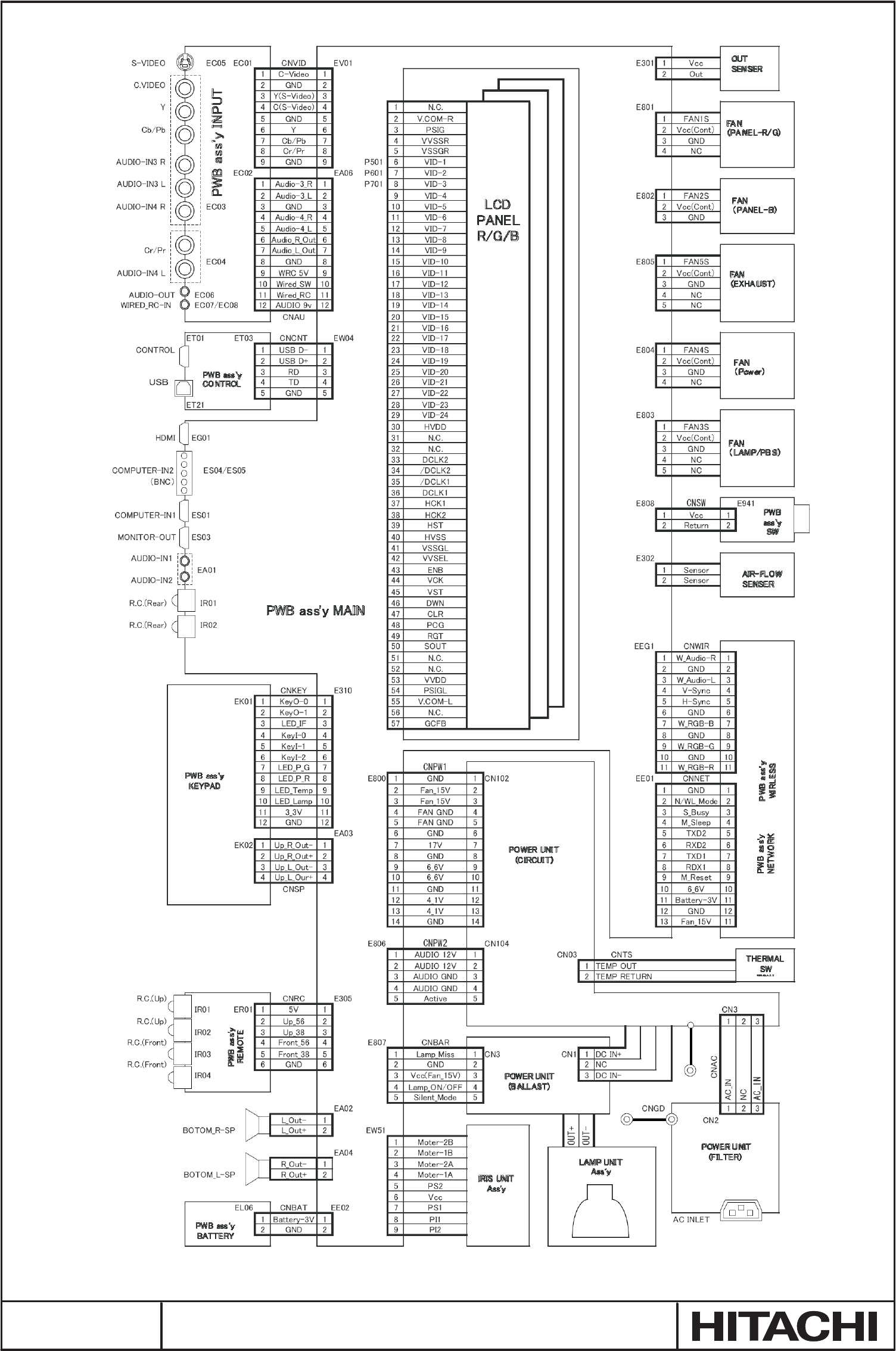
SM0321
CONNECTOR CONNECTION DIAGRAM
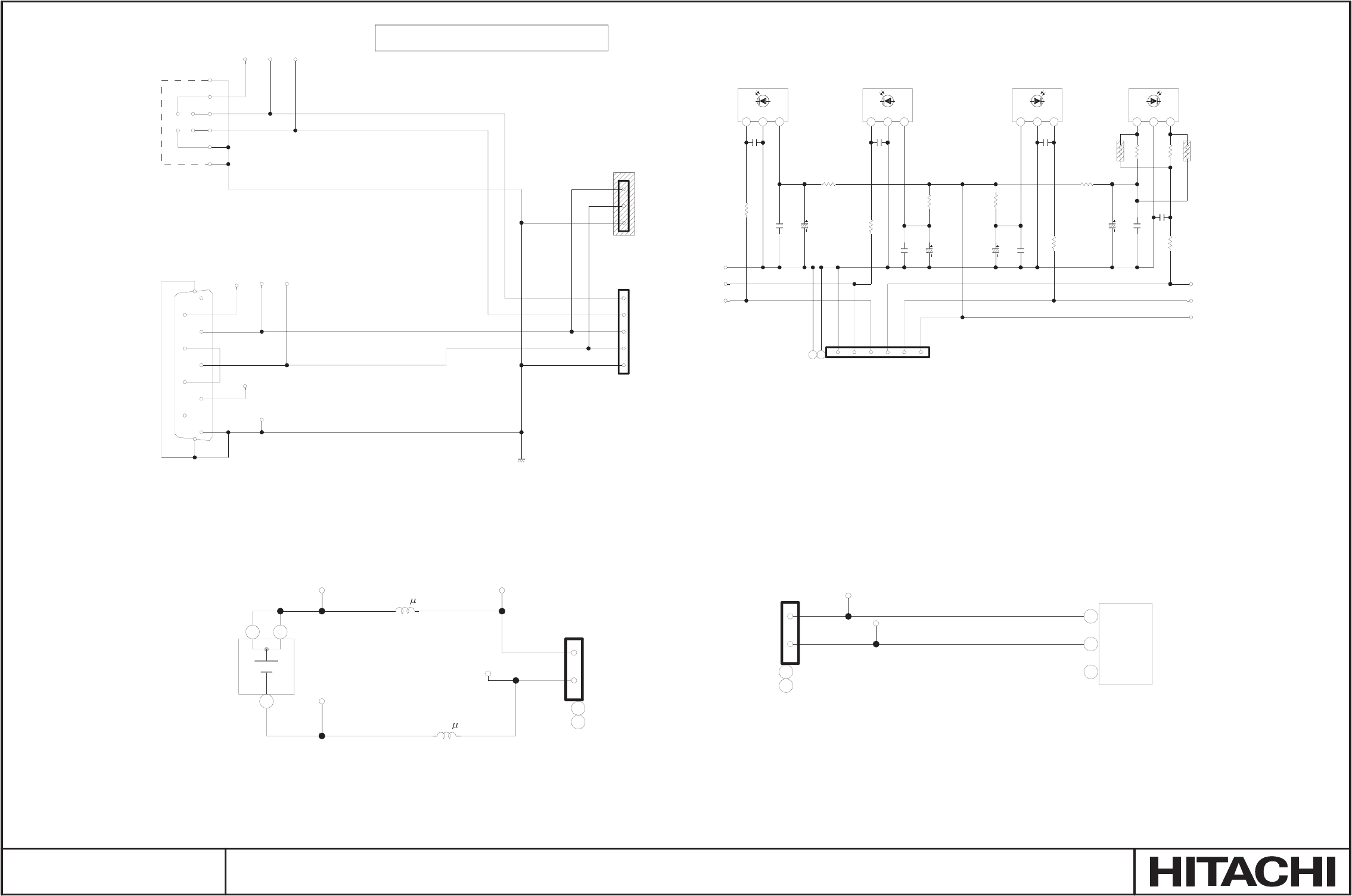
SM0321
MISCELLANEOUS CIRCUITS
PWB assembly SW
PWB assembly REMOTE
1
3
2
S941
AV34423
1
C
2
NO
3
NC
E941
ZH-02H
1
2
G1
G2
AP91
1
AP92
1
TO-SW
COVER
321 321321321
2125
RR06
47
2125
*RR04
4747
APR1APR2
APR3
APR4
CR09
47/6.3
MVK/SKV
CR08
4.7/6.3
*CR05
4.7/6.3
CR07
100p-C
*CR04
100p-C
RR05
100
*CR06
47/6.3
MVK/SKV
IR03
KSM-2003LM2EL
Vout GND VCC
*RR03
100
ER01
ZH-06H
1
2
3
4
5
6
G1
G2
CR01
100p-C
IR01
KSM-2003LM2EL
VoutGNDVCC
2125
RR02
47
CR03
47/6.3
MVK/SKV
CR02
4.7/6.3
RR01
100
2125
*RR08
47
*CR10
100p-C
*CR12
47/6.3
MVK/SKV
*CR11
4.7/6.3
*RR07
100
APR5APR6
*RR10
0
*RR11
0
*RR12
0
*RR13
0
*IR02
VoutGNDVCC
*IR04
Vout GND VCC
VCC
FRONT_38
UP-38
FRONT_56
UP_38
UP_56
UP-56FRONT-38FRONT-56
GND
GP1UX317RKGP1UX317RK
Parts with hatching are not mounted.
PWB assembly BATTERY
PWB assembly CONTROL
1-+
EL05
CR2032BH
1
1
2
2
33
1608
LL37
600 H
12
1608
LL36
600 H
12
EL06
SH-02H
1
2
G1
G2
APL1
1
APL2
1
APL3
1
APL4
1
APTDAPRD
ET01
3175-09M
1
2
3
4
5
6
7
8
9
G1
G2
APSG
GND1
APU5
ET21
UBB-4R-D14C
1
2
3
4
G1
G2
APUM APUP
APT6
APT4
ET02
PH-05V-D
1
2
3
4
5
ET03
PH-03V-D
1
2
3
RD
TD
RS232C
RD
TD
GND
USB
USB D+
USB D-
RD
GND
TD
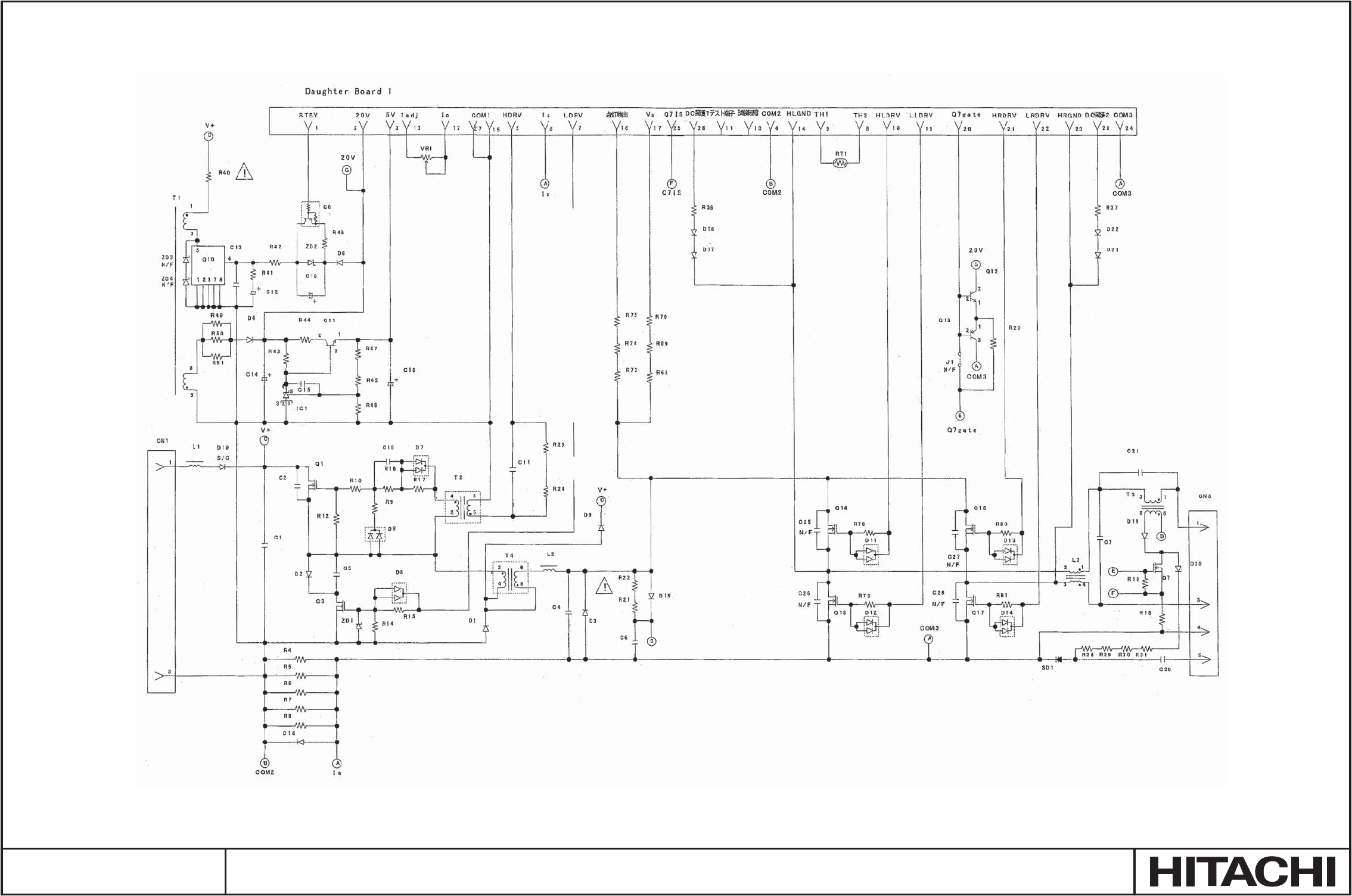
SM0321 POWER UNIT (BALLAST) 1
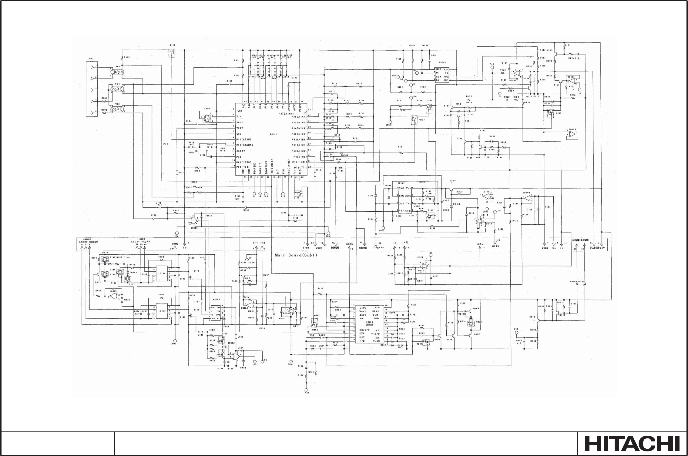
SM0321 POWER UNIT (BALLAST) 2
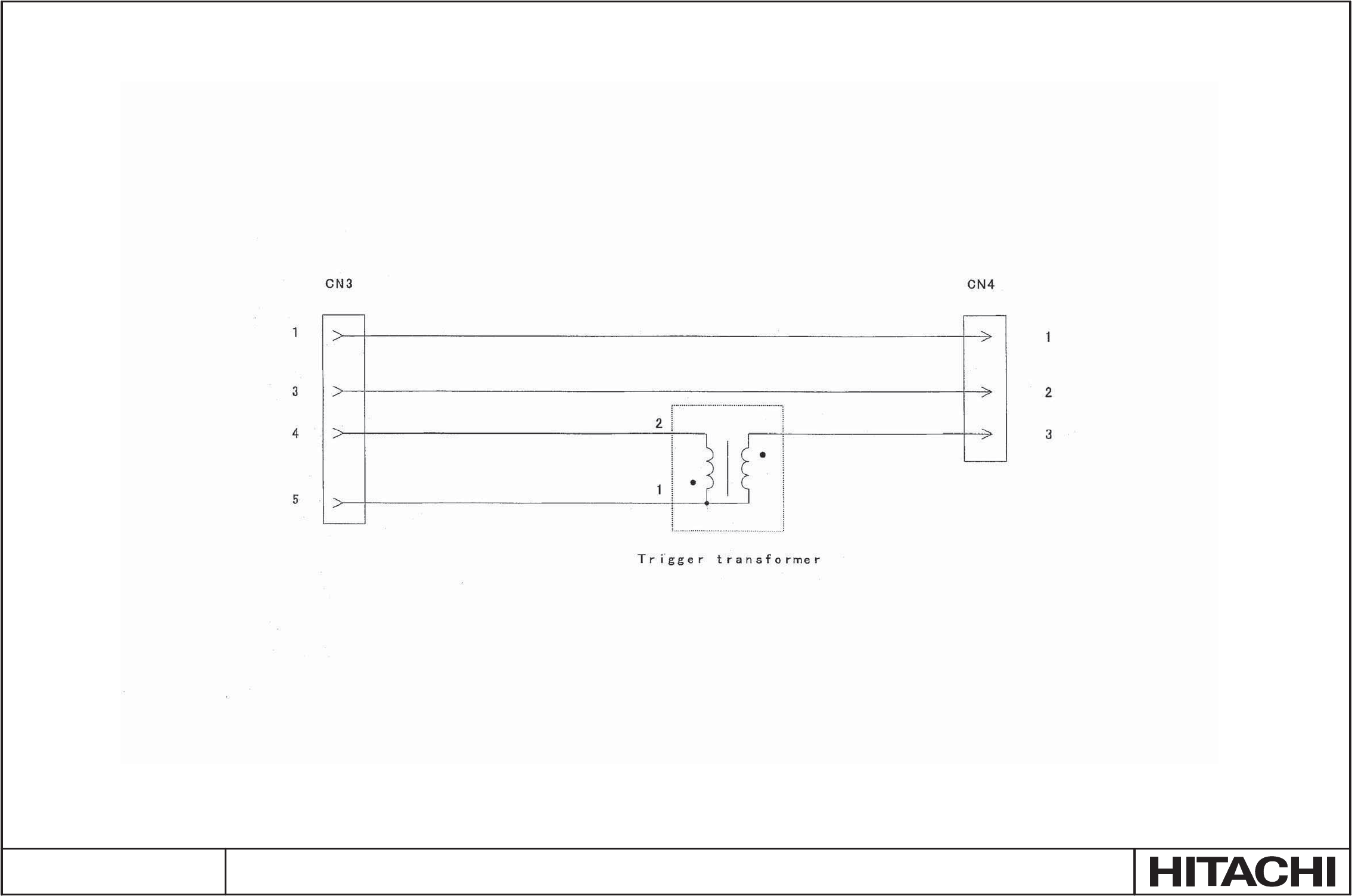
SM0321 POWER UNIT (BALLAST) 3
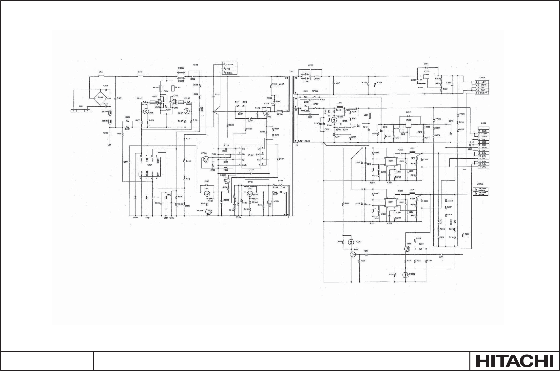
SM0321 POWER UNIT (CIRCUIT)
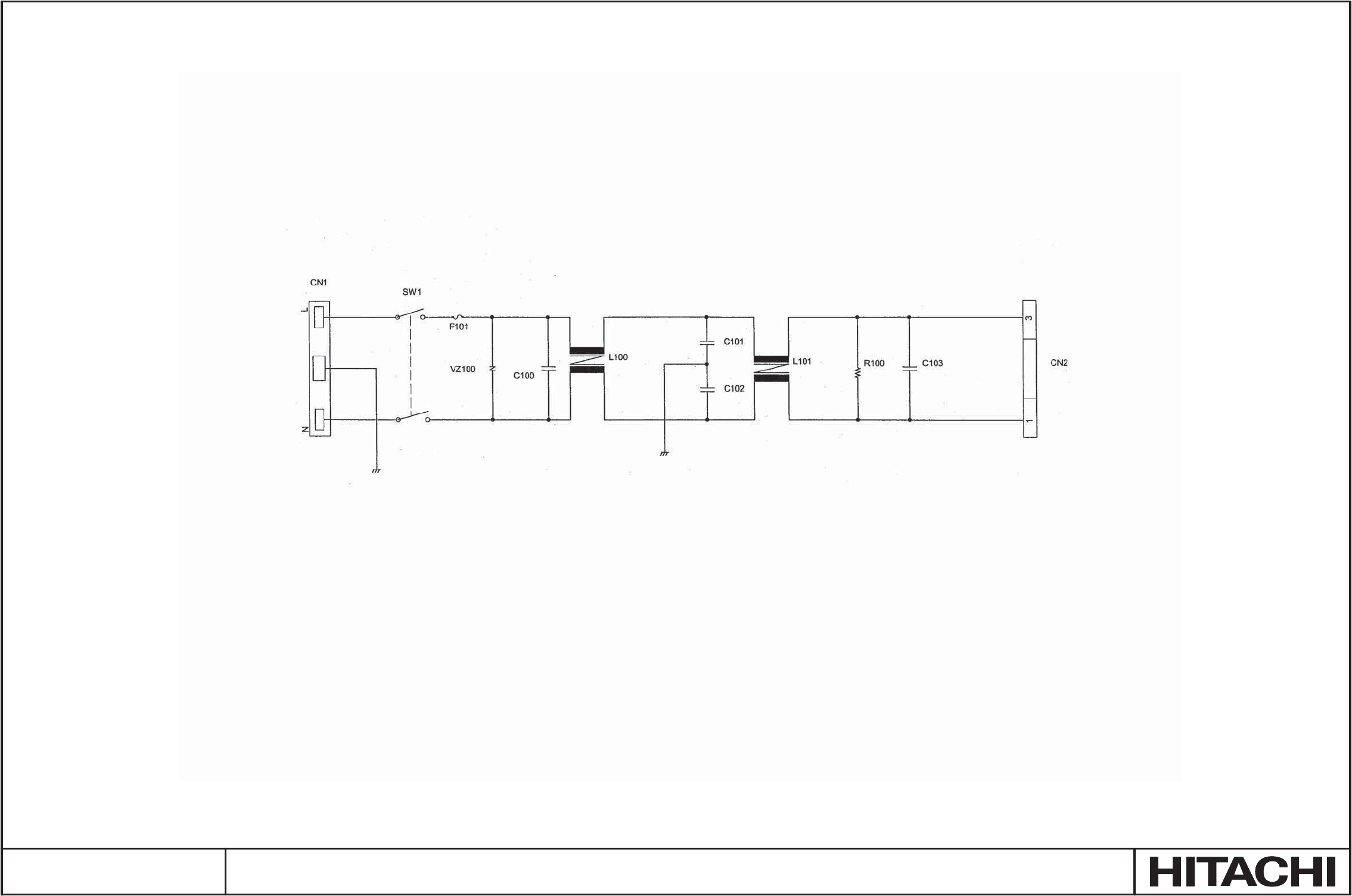
SM0321 POWER UNIT (FILTER)
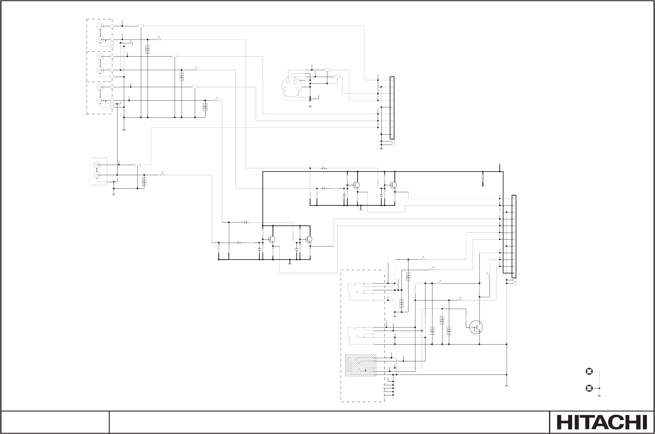
SM0321
PWB ASSEMBLY INPUTS
YC
GG
G
R
Y
Bl
W
R
5
2
4
3
1
4.4V
4.4V
4.4V
4.4V
4.4V
4.4V
0V
EC05
JY-5040G*040
11
22
33
44
G1G1
G2G2
G3G3
EC06
JY-3542*01-250
1
2
3
4
5
*EC07
JY-3542*01-250
1
2
3
4
5
GND1
GND1
GND1
EC01
ZH-09V
1
2
3
4
5
6
7
8
9
G1
G2
GND1
EC04
YKC21-4112
1
1
2
2
3
3
GND1
GND1
CC03
1005
100p-C
12
CC01
1005
100p-C
12
CC02
1005
100p-C
12
CC04
1005
100p-C
12
CC06
1005
100p-C
12
CC05
1005
100p-C
12
CC07
1005
100p-C
12
CC08
1005
100p-C
12
CC09
1005
100p-C
12
APC1
1
APC2
1
APC3
1
APC4
1
APC5
1
APC6
1
APC7
1
APC01
1
APC02
1
APC03
1
APC05
1
APC06
1
APC07
1
APC08
1
APC09
1
APC10
1
APC04
1
EC03
YKC21-4673V
1
1
2
2
3
3
4
4
5
5
6
6
7
7
8
8
9
9
10
10
11
11
1005
RC02
10K
12
2125
RC01
47 1
2
1005
RC03
10K
1
2
QC01
DTC114EE
1
2
3
1005
RC04
10K
12
KIKU1S
1
KIKU2S
1
GND1
#2390
G1
G2
G3
G4
G5
1005
RC07 100
12
1005
RC08 100
1
2
1005
RC22
150K 12
1005
RC19
120K
12
QC04 2SC5343E
1
2
3
1005
RC15 180K
12
CC15
2125
4.7/16
1
2
1005
RC16 180K
12
CC10
2125
4.7/16
1
2
CC12
1005
220P
12
QC03
2SC5343E
1
2
3
1005
RC23 10K
1
2
1005
RC24 10K
1
2
CC13
1005
220P
1
2
1005
RC05
180K
12
1005
RC12
150K 1
2
1005
RC09
120K
1
2
CC11
2125
4.7/16
1
2
CC14
2125
4.7/16
1
2
1005
RC20 120K
12
CC16
1005
220P
12
1005
RC14 10K
1
2
QC02
2SC5343E
1
2
3
1005
RC17 100
1
2
1005
RC21
150K 12
QC05
2SC5343E
1
2
3
1005
RC18
100
1
2
CC17
1005
220P 1
2
1005
RC13 10K
12
1005
RC11
150K 1
2
1005
RC10
120K
1
2
1005
RC06
180K
12
GND1
EC02
ZH-12V
1
2
3
4
5
6
7
8
9
10
11
12
G1
G2
GND1
APC11
1
CC25
2125
4.7/16
1
2
GND1
*EC08
JY-2522-h1-355
1
2
3
4
5
APC20
1
APC21
1
APC22
1
APC23
1
APC24
1
APC25
1
APC26
1
APC27
1
APC28
1
APC29
1
APC30
1
APC31
1
APC32
1
APC33
1
APC34
1
APC35
1
APC36
1
APC38
1
APC37
1
APC39
1
APC40
1
APC41
1
APC51
1
APC52
1
APC53
1
2125
LC07
NFL21SP407X1C3
123
2125
LC03
NFL21SP407X1C3
123
2125
LC05
NFL21SP407X1C3
123
2125
LC09
NFL21SP407X1C3
123
2125
LC01
NFL21SP407X1C3
123
2125
LC10
NFL21SP407X1C3
123
1608
LC02
600 H
12
1608
LC06
600 H
12
1608
LC14
600 H
12
1608
LC15
600 H
12
1608
LC08
600 H
12
1608
LC13
600 H
12
1608
LC12
600 H
12
1608
LC11
600 H
12
1608
LC04
600 H
12
CVBS
GND
C_S
Y_S
GND
Cr
Y
Cb
Video-R1
Video-L1
GND
Video-R2
OUT-R
Video-L2
+5Vin
OUT-L
Wired_RM_SW
GND
Wired_RM
Wired-RM-3.5
Audio-OUT
Wired-RM-2.5
GND
Cr
L2(WHITE)
Y
Cb
R2(SW)
R1(SW)
L1(WHITE)
CVBS
+8.5V
SM0321
PWB ASSEMBLY KEYPAD
43
21
43
21
43
21
43
21
43
21
43
21
43
21
DK02
SML-210VT
1
2
RK11
0
12
APY12
1
RK02
0
12
SK11
SKRAAAE010
12
34
SK12
SKRAAAE010
12
34
APY11
1
1005
RK21
220
1
2
RK08
0
12
RK09
0
12
APY10
1
APY08
1
RK10
0
12
SK05
SKRAAAE010
12
34
RK12
0
12
RK01
0
12
SK10
SKRAAAE010
12
34
EK03
PH-02H
1
2
G1
G2
EK01
ZH-12H
1
2
3
4
5
6
7
8
9
10
11
12
G1
G2
APY07
1
QK21
DTC114EUA
1
2
3
1005
RK22
100
12
RK07
0
12
APY09
1
APY01
1
APY05
1
QK23
DTC114EUA
1
2
3
RK05
0
12
APY02
1
DK03
SML-210VT
1
2
RK06
0
12
1005
RK23
220
1
2
QK22
DTC114EUA
1
2
3
QK24
DTC114EUA
1
2
3
SK06
SKRAAAE010
12
34
SK04
SKRAAAE010
12
34
DK01
SML-020MVT86
12
34
APY03
1
RK04
0
12
APY06
1
EK02
ZH-04H
1
2
3
4
G1
G2
EK04
PH-02H
1
2
G1
G2
1005
RK24
220
1
2
GND1
APY04
1
CK32
1005
100p-C
12
CK31
1005
100p-C
12
CK44
1005
100p-C
12
CK43
1005
100p-C
12
CK41
1005
100p-C
12
CK42
1005
100p-C
12
CK29
1005
100p-C
12
CK30
1005
100p-C
12CK28
1005
100p-C
12
CK27
1005
100p-C
12
CK40
1005
100p-C
12
CK39
1005
100p-C
12
UP_SP-L-P
UP UP_SP-R-N
RED
LAMP
GREEN
INPUT
TEMP
RIGHT
DOWN
LEFT
POW
N.C
KEYO-1
LED RED
LED GREEN
GND
KEYI-2
KEYO-0
+3.3V
LED LAMP
LED TEMP
KEYI-1
KEYI-0
KEYO-0
KEYO-1
KEYI-0
KEYI-1
KEYI-2
UP_SP-L-P
UP_SP-R-N
UP_SP-R-P
UP_SP-L-N
UP_SP-R-P
UP_SP-L-N
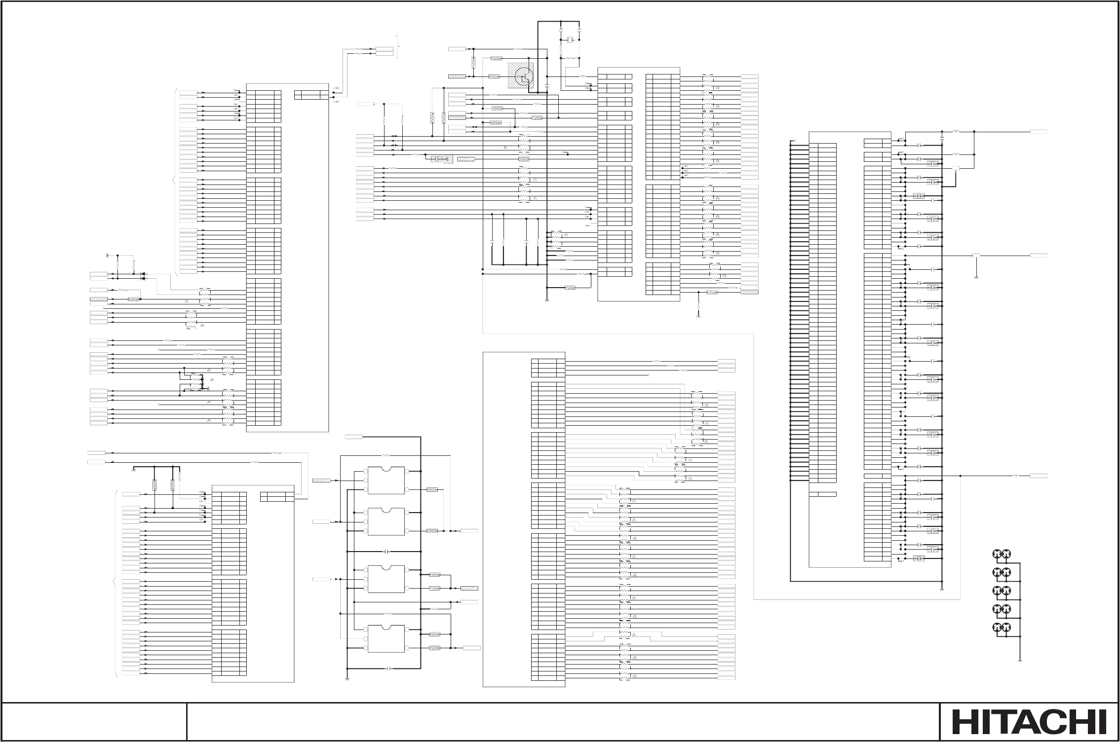
SM0321
PWB ASSEMBLY MAIN 1
I
I
I
I
I
I
I
I
I
I
I
I
I
I
I/O
I/O
I/O
I/O
I/O
I/O
I/O
I/O
I/O
I/O
I/O
I/O
I/O
I/O
I/O
I/O
I/O
I/O
I/O
I/O
I/O
I/O
I/O
I/O
I
I
I
I
I
I
I
I
I
I
I
I
I
I
I
I
I
I
I
I
I
I
I
I
I
I
I
I
I
I
I
N2
N5
L1
L2
L4
M4
K1
L3
K2
K3
J3
K4
J1
M5
J4
J2
H1
L6
H2
H3
H4
K5
G1
G2
G3
L5
F1
G4
E1
J5
F2
F3
F4
H6
G5
D1
F5
H5
E2
C2
E3
E4
D2
C1
B2
F6
B1
D3
D4
E5
C3
D5
C4
E6
A2
B4
F8
C5
D6
E7
A1
A3
P2
M1
M3
P1
N3
M2
N1
INPUT PORT 0
I
I
I
I
I
I
INPUT PORT 1
T1
R1
Y4
AB1
U4
AA3
W4
T5
AA2
AA1
Y3
R4
Y2
Y1
V4
R5
W3
W2
W1
V3
V2
P6
V1
T4
T3
U3
R3
U2
R2
P5
P4
P3
T2
AB2
AB3
U1
N4
U5
AA4 I
I
I/O
I/O
I/O
I/O
I/O
I/O
I/O
I/O
I
I
I
I
I
I
I
I
I/O
I/O
I/O
I/O
I/O
I/O
I/O
I/O
I
I
I
I
I
I
I
AE12
AE8
AD8
AF8
AF5
AC5
Y6
AC8
AF9
AB8
AE9
AB10
AD9
AC9
AF10
AC11
AE10
AD10
AC10
AF11
AE11
AD11
AF12
U6
AC1
AC2
AD1
V5
AD2
AC3
AB4
AD3
AA5
AE1
AF1
W5
AE2
AC4
AF2
Y5
AB5
AE3
AD4
AF3
AF4
AE4
AE7
Y23
V26
Y22
W22
W26
W25
W24
W23
AE5
AA6
AD5
AF6
AE16
AF18
AF17
AF16
AE15
AF15
AC12
AD14
AE14
AF14
AC13
AD13
AE13
AF13
AB11
AD12
AD15
AB12
AF19
AE17
AB9
AD7
AC7
I
I/O
I/O
O
O
I/O
I/O
I/O
I/O
I/O
I/O
I/O
I/O
I/O
I/O
I/O
I/O
I/O
I/O
I/O
I/O
I/O
I/O
I/O
I/O
I/O
I/O
I/O
I/O
I/O
I/O
I/O
I/O
I/O
I/O
I/O
I/O
I/O
I/O
I/O
I/O
I/O
I/O
I/O
I/O
I/O
I
I
I
I
I
I
I
I/O
I
I
I
I
I
I/O
I/O
I/O
I/O
I/O
I/O
I/O
I/O
I/O
I/O
I/O
I/O
I/O
I/O
I/O
I/O
I
I
O
O
O
I
I/O
MISC
AA22
Y26
AA21
AA23
AA24
AA25
AA26
AB23
AA19
AB24
AB22
AB25
AB26
AC25
AC26
AC24
AB19
AB21
AD26
AD25
AE26
AB20
AB18
AC23
AD24
AC22
AB16
AC21
AE25
AF26
AD23
AB17
AC20
AE24
AF25
AD21
AC19
AB15
AE23
AF24
AE22
AD20
AC17
AF23
AE21
AF22
AB14
AD19
AE20
AC16
AF21
AD17
AC15
AD18
AE19
AF20
AB13
AD16
AC14
AE18
AC18
Y25
Y24
AD22
I/O
I/O
I/O
I/O
I/O
I/O
I/O
I/O
I/O
I/O
I/O
I/O
I/O
I/O
I/O
I/O
I/O
I/O
I/O
I/O
I/O
I/O
I/O
I/O
I/O
I/O
I/O
I/O
I/O
I/O
O
O
O
O
O
O
O
O
O
O
O
O
O
O
O
O
O
O
O
O
O
O
O
O
O
O
O
O
O
O
O
O
O
O
DISPLAY PORT
POWER AND GROUND
AA20
AA17
AA16
AA14
AA13
AA11
AA10
AA8
Y21
Y7
W21
W6
T6
N6
K6
G6
F7
AB6
V22
V21
U23
U22
T22
T21
R22
R21
P22
N22
N21
M21
L22
K26
K21
J22
H25
H22
H21
G22
G21
F25
F24
F20
F18
F17
F15
F14
F13
F11
F10
E20
E19
E18
E16
E15
E12
E9
D17
D15
D13
D10
D8
C22
B10
A23
A19
AA18
AA15
AA12
AA9
Y20
V6
U21
R6
P21
M6
L21
J21
J6
G7
F19
F16
F12
F9
V25
D7
AF7
AD6
AC6
AE6
AB7
AA7
V24
U17
U16
U15
U14
U13
U12
U11
U10
T17
T16
T15
T14
T13
T12
T11
T10
R23
R17
R16
R15
R14
R13
R12
R11
R10
P17
P16
P15
P14
P13
P12
P11
P10
N17
N16
N15
N14
N13
N12
N11
N10
M17
M16
M15
M14
M13
M12
M11
M10
L17
L16
L15
L14
L13
L12
L11
L10
K17
K16
K15
K14
K13
K12
K11
K10
G23
G20
D19
C11
B3
4
5
3
2
1
4
5
3
2
1
4
5
3
2
1
4
5
3
2
1
C247
1005
15p-C
12
C235
1005
1.0/6.3
12
C249
1005
0.01/16
12
C204
1005
1.0/6.3
12
C221
1005
1.0/6.3
12
C233
1005
1.0/6.3
12
C205
1005
1.0/6.3
12
C239
1005
1.0/6.3
12
C201
1005
1.0/6.3
12
C202
1005
1.0/6.3
12
C227
1005
1.0/6.3
12
C243
1005
1.0/6.3
12
C250
1005
0.01/16
12
C217
1005
1.0/6.3
12
C231
1005
1.0/6.3
12
C248
1005
0.01/16
12
C215
1005
1.0/6.3
12
C241
1005
1.0/6.3
12
C208
1005
1.0/6.3
12
C210
1005
1.0/6.3
12
C225
1005
1.0/6.3
12
C246
1005
18p-C
12
GND1
GND1
GND1
GND1
GND1
1608
L201 600
12
1608
L206
600
12
1608
L202
600
12
1608
L203
600
12
CHXTI 1
CH1PE 1
CHP18
1
CHA22
1
CH0AH 1
CH0VB 1
CH0331
CHAD3 1
CH0CT
1
CHAD0 1
CH0PE 1
CH1FL 1
CHDEN
1
CH0CP
1
CHA21
1
CH1AH 1
CH0251
CHAD1 1
CH1VS 1
CHGND
1
CH0HS 1
CHAD2 1
CH0FL 1
CHXTO 1
CH1HS 1
CH1CK 1
CH018
1
CHA23
1
CHM18
1
CH0CK 1
CH1VB 1
1005
*R213
1.0k1.0k
12
1005
*R214
0
12
1005
R235
4.7k
12
10k
1005
R259
10k
12
1005
R234
10k
12
10k
1005
R237
12
1005
R210
10k 12
1005
R256
0
12
1005
R232
10k
12
1005
R222
33
12
1005
R220
4.7k
12
1005
*R258
0
12
1005
R219
4.7k
12
1005
R233
10k
12
1005
R211
4.7k
12
1005
R236
4.7k4.7k
1
2
33
1005
R221
33
12
1005
R257
0
12
100
1005
R216
100
12
100
1005
R215
100
12
1005
R260
56
12
1005
R285
1.0M
12
1005
R230
8.2k
12
1005
R228
8.2k
12
1005
R218
0
12
0
1005
R217
0
12
1005
R212
0
12
R244
2010
33
12
34
56
78
R277
2010
56
12
34
56
78
R240
2010
33
78
56
34
12
R231
2010
10k
1
2
7
8
5
6
3
4
R245
2010
33
12
34
56
78
R247
2010
100
78
56
34
12
R278
2010
56
12
78
56
34
R241
2010
33
78
56
34
12
R276
2010
56
56
34
12
78
R274
2010
56
34
12
56
78
R243
2010
33
78
56
34
12
R273
2010
56
12
34
56
78
R242
2010
33
12
78
56
34
R238
2010
33
12
34
56
78
R275
2010
56
12
78
56
34
R246
2010
33
12
34
56
78
R239
2010
33
12
34
56
78
IN1R2
D8
IN1VS
A7
+2.5V
DGE7
D5
IN1R3
FAN_FG
IN1R4
D0
NMI
IN0HS
DRE9
DGE5
A6
A1
D9
D7OUTTEMP
A8
+3.3V
DGE9
PCS1
IN1R6
D11
A20
IN1B3
D3
EMU-RESET
A19
IN1R7
DRE4
DGE4
DVS
A5
A9
ROMWE
DGE2
+1.8VCPU
D14
DRE1
IN1B7
DBE0
D13
IN1G7
IN1B4
IRIS_RST
DRE3
DBE3
A15
WRN
DHS
IN0VS
A14
A18
IN1HS
DGE3
DBE7
DGE8
IN1G3
DGE1
A4
D12
DBE5
IN1B2
D2
DRE6
DBE2
A10
I2CDAT
DBE6
A17
ROMOE
IN1G2
DRE0
AIRSPD
PCS0
DBE9
DGE6
IN1B6
IN1G5
A3
DRE5
A16
DBE8
D6
GSENSOR
IN1G6
DGE0
DCLK
D15
TXD0
D10
IN1B5
RXD0
A13
INT_ADV
IN1R5
DRE8
A11
DBE4
IN1G4
DBE1
RDN
A12
D1
RESETN
D4
PWRC
DRE2
A2
DRE7
I2CCLK
X201 14.31818MHz
SMD-49
1
2
*Q201
DTC114EE
1
2
3
1005
R261
1010
12
1005
R262
1010
12
R227
2010
33
1
2
34
5
6
7
8
R226
2010
33
1
2
34
5
6
7
8
IRIS_CW
IRIS_CLK
1005
R202
33
12
1005
*R204
1.0k
12
KIKU1C
1
KIKU1S
1
KIKU2C
1
KIKU2S
1
KIKU3C
1
KIKU3S
1
KIKU4C
1
KIKU4S
1
KIKU5C
1
KIKU5S
1
GND1
C244
2125
10/6.3
12
C234
2125
10/6.3
12
C245
2125
10/6.3
12
1005
R284
820
12
A21
1005
R254
100
12
IN1R8
IN1R9
IN1G8
IN1G9
IN1B8
IN1B9
I2CCLKP
I2CDATP
IN1G0
R223
2010
33
7
8
56
3
4
1
2
1005
R272
0
12
1005
R271
0
12HPD_RST
HDMI_RST
IN0GE5
IN0BE4
IN0RE7
IN0GE7
IN0GE2
IN0CLK
IN0BE3
IN0RE3
IN0RE2
IN0GE4
IN0GE3
IN0BE7
IN0RE4
IN0BE2
IN0RE5
IN0BE5
IN0BE6
IN0GE6
IN0RE6
1005
R201
1.0k1.0k
12
1005
R288
1.0k1.0k
12
+3.3VP
IN0RE8
IN0RE9
IN0BE8
IN0BE9
IN0GE8
IN0GE9
1005
R209
10k 1
2
IN0FLD
IN0PEN
IN0AHS
C256
2125
10/6.3
12
C211
2125
4.7/6.3
12
C203
1005
0.1/10
12
C207
1005
0.1/10
12
C206
1.0/10
12
C209
1005
0.1/10
12
C213
4.7/6.3
12
C223
4.7/6.3
12
C229
1.0/10
12
C219
1.0/10
12
C214
1005
0.1/10
12
C216
1005
0.1/10
12
C220
1005
0.1/10
12
C224
1005
0.1/10
12
C226
1005
0.1/10
12
C230
1005
0.1/10
12
C232
1005
0.1/10
12
C237
4.7/6.3
12
C242
4.7/6.3
12
C236
1005
0.1/10
12
C238
1005
0.1/10
12
C240
1005
0.1/10
12
1005
R253 33
12
CH0VS 1
R2M8
2010
33
1
2
34
5
6
7
8
VDDMNT
RESETP R2M9
2010
10k
1
2
34
7
8
5
6
GND1
1005
R2M6
33
12
R2M1
2010
100
1
2
34
5
6
7
8
1005
R2M5
33
12
IN1AHS
IN1FLD
IN1CLK
2125
L204
SGM20F1C104-4A
123
2125
L205
SGM20F1C104-4A
123
VD_VSEN 1005
R2K6
33
12
R263
2010
56
12
78
34
56
R264
2010
56
12
34
56
78
R265
2010
56
12
34
56
78
R266
2010
56
12
34
56
78
R267
2010
56
12
56
78
34
R268
2010
56
12
34
56
78
R269
2010
56
12
78
56
34
R270
2010
56
12
34
56
78
1005
R206
4.7k
12
1005
R207
4.7k
12
C212
1005
0.01/16
12
1005
R2K4
100
12
1005
R2K5
100
12
MONI_SEL
1005
*R2K9
33
12
IN1R1
IN1R0
IN1G1
IN1B0
IN1B1
I201
PW388B-10L
N1 IN0CLK
M2 IN0PEN
N3 IN0VBI
P1 IN0AHS
M3 IN0HS
M1 IN0VS
P2 IN0FLD
A3 IN0RE0
A1 IN0RE1
E7 IN0RE2
D6 IN0RE3
C5 IN0RE4
F8 IN0RE5
B4 IN0RE6
A2 IN0RE7
E6 IN0RE8
C4 IN0RE9
D5 IN0GE0
C3 IN0GE1
E5 IN0GE2
D4 IN0GE3
D3 IN0GE4
B1 IN0GE5
F6 IN0GE6
B2 IN0GE7
C1 IN0GE8
D2 IN0GE9
E4 IN0BE0
E3 IN0BE1
C2 IN0BE2
E2 IN0BE3
H5 IN0BE4
F5 IN0BE5
D1 IN0BE6
G5 IN0BE7
H6 IN0BE8
F4 IN0BE9
F3 IN0RO0
F2 IN0RO1
J5 IN0RO2
E1 IN0RO3
G4 IN0RO4
F1 IN0RO5
L5 IN0RO6
G3 IN0RO7
G2 IN0RO8
G1 IN0RO9
K5 IN0GO0
H4 IN0GO1
H3 IN0GO2
H2 IN0GO3
L6 IN0GO4
H1 IN0GO5
J2 IN0GO6
J4 IN0GO7
M5 IN0GO8
J1 IN0GO9
K4 IN0BO0
J3 IN0BO1
K3 IN0BO2
K2 IN0BO3
L3 IN0BO4
K1 IN0BO5
M4 IN0BO6
L4 IN0BO7
L2 IN0BO8
L1 IN0BO9
N5
IN0CLP
N2
IN0CST
I201
PW388B-10L
AA4 IN1CLK
U5 IN1PEN
N4 IN1VBI
U1 IN1AHS
AB3 IN1HS
AB2 IN1VS
T2 IN1FLD
P3 IN1R0
P4 IN1R1
P5 IN1R2
R2 IN1R3
U2 IN1R4
R3 IN1R5
U3 IN1R6
T3 IN1R7
T4 IN1R8
V1 IN1R9
P6 IN1G0
V2 IN1G1
V3 IN1G2
W1 IN1G3
W2 IN1G4
W3 IN1G5
R5 IN1G6
V4 IN1G7
Y1 IN1G8
Y2 IN1G9
R4 IN1B0
Y3 IN1B1
AA1 IN1B2
AA2 IN1B3
T5 IN1B4
W4 IN1B5
AA3 IN1B6
U4 IN1B7
AB1 IN1B8
Y4 IN1B9
R1
IN1CLP
T1
IN1CST
I201
PW388B-10L
AC7 RESETB
AD7 XI
AB9 XO
AE17 RXD
AF19 TXD
AB12 IRRCVR0
AD15 IRRCVR1
AD12 PORTA0
AB11 PORTA1
AF13 PORTA2
AE13 PORTA3
AD13 PORTA4
AC13 PORTA5
AF14 PORTA6
AE14 PORTA7
AD14 PORTB0
AC12 PORTB1
AF15 PORTB2
AE15 PORTB3
AF16 PORTB4
AF17 PORTB5
AF18 PORTB6
AE16 PORTB7
AF6 ADC0
AD5 ADC1
AA6 ADC2
AE5 ADC3
W23 TMS
W24 TDO
W25 TDI
W26 TRSTN
W22 TCK
Y22 JTAGSEL
V26 TESTMODE
Y23 ADR24B
AE7 EXRSTEN
AE4
A1
AF4
A2
AF3
A3
AD4
A4
AE3
A5
AB5
A6
Y5
A7
AF2
A8
AC4
A9
AE2
A10
W5
A11
AF1
A12
AE1
A13
AA5
A14
AD3
A15
AB4
A16
AC3
A17
AD2
A18
V5
A19
AD1
A20
AC2
A21
AC1
A22
U6
A23
AF12
D0
AD11
D1
AE11
D2
AF11
D3
AC10
D4
AD10
D5
AE10
D6
AC11
D7
AF10
D8
AC9
D9
AD9
D10
AB10
D11 AE9
D12
AB8
D13
AF9
D14
AC8
D15
Y6
RD
AC5
WR
AF5
ROMOE
AF8
ROMWE
AD8
CS0
AE8
CS1
AE12
NMI
I201
PW388B-10L
AD22
DCLK
Y24
DVS
Y25
DHS
AC18
DEN
AE18
DRE0
AC14
DRE1
AD16
DRE2
AB13
DRE3
AF20
DRE4
AE19
DRE5
AD18
DRE6
AC15
DRE7
AD17
DRE8
AF21
DRE9
AC16
DGE0
AE20
DGE1
AD19
DGE2
AB14
DGE3
AF22
DGE4
AE21
DGE5
AF23
DGE6
AC17
DGE7
AD20
DGE8
AE22
DGE9
AF24
DBE0
AE23
DBE1
AB15
DBE2
AC19
DBE3
AD21
DBE4
AF25
DBE5
AE24
DBE6
AC20
DBE7
AB17
DBE8
AD23
DBE9
AF26
DRO0 AE25
DRO1 AC21
DRO2 AB16
DRO3 AC22
DRO4 AD24
DRO5 AC23
DRO6 AB18
DRO7 AB20
DRO8 AE26
DRO9
AD25
DGO0 AD26
DGO1 AB21
DGO2 AB19
DGO3 AC24
DGO4 AC26
DGO5 AC25
DGO6 AB26
DGO7 AB25
DGO8 AB22
DGO9
AB24
DBO0 AA19
DBO1 AB23
DBO2 AA26
DBO3 AA25
DBO4 AA24
DBO5 AA23
DBO6 AA21
DBO7 Y26
DBO8 AA22
DBO9
I201
PW388B-10L
B3 GND1
C11 GND2
D19 GND3
G20 GND4
G23 GND5
K10 GND6
K11 GND7
K12 GND8
K13 GND9
K14 GND10
K15 GND11
K16 GND12
K17 GND13
L10 GND14
L11 GND15
L12 GND16
L13 GND17
L14 GND18
L15 GND19
L16 GND20
L17 GND21
M10 GND22
M11 GND23
M12 GND24
M13 GND25
M14 GND26
M15 GND27
M16 GND28
M17 GND29
N10 GND30
N11 GND31
N12 GND32
N13 GND33
N14 GND34
N15 GND35
N16 GND36
N17 GND37
P10 GND38
P11 GND39
P12 GND40
P13 GND41
P14 GND42
P15 GND43
P16 GND44
P17 GND45
R10 GND46
R11 GND47
R12 GND48
R13 GND49
R14 GND50
R15 GND51
R16 GND52
R17 GND53
R23 GND54
T10 GND55
T11 GND56
T12 GND57
T13 GND58
T14 GND59
T15 GND60
T16 GND61
T17 GND62
U10 GND63
U11 GND64
U12 GND65
U13 GND66
U14 GND67
U15 GND68
U16 GND69
U17 GND70
V24 GND71
AA7 GND72
AB7 GND73
AE6 GND74
AC6 NC
AD6
VPPM18
AF7
VPPD18
D7
VAAK18
V25
VAAM18
F9
VDD18-1
F12
VDD18-2
F16
VDD18-3
F19
VDD18-4
G7
VDD18-5
J6
VDD18-6
J21
VDD18-7
L21
VDD18-8
M6
VDD18-9
P21
VDD18-10
R6
VDD18-11
U21
VDD18-12
V6
VDD18-13
Y20
VDD18-14
AA9
VDD18-15
AA12
VDD18-16
AA15
VDD18-17
AA18
VDD18-18
A19
VDD25-1
A23
VDD25-2
B10
VDD25-3
C22
VDD25-4
D8
VDD25-5
D10
VDD25-6
D13
VDD25-7
D15
VDD25-8
D17
VDD25-9
E9
VDD25-10
E12
VDD25-11
E15
VDD25-12
E16
VDD25-13
E18
VDD25-14
E19
VDD25-15
E20
VDD25-16
F10
VDD25-17
F11
VDD25-18
F13
VDD25-19
F14
VDD25-20
F15
VDD25-21
F17
VDD25-22
F18
VDD25-23
F20
VDD25-24
F24
VDD25-25
F25
VDD25-26
G21
VDD25-27
G22
VDD25-28
H21
VDD25-29
H22
VDD25-30
H25
VDD25-31
J22
VDD25-32
K21
VDD25-33
K26
VDD25-34
L22
VDD25-35
M21
VDD25-36
N21
VDD25-37
N22
VDD25-38
P22
VDD25-39
R21
VDD25-40
R22
VDD25-41
T21
VDD25-42
T22
VDD25-43
U22
VDD25-44
U23
VDD25-45
V21
VDD25-46
V22
VDD25-47
AB6
VADC33
F7
VDD33-1
G6
VDD33-2
K6
VDD33-3
N6
VDD33-4
T6
VDD33-5
W6
VDD33-6
W21
VDD33-7
Y7
VDD33-8
Y21
VDD33-9
AA8
VDD33-10
AA10
VDD33-11
AA11
VDD33-12
AA13
VDD33-13
AA14
VDD33-14
AA16
VDD33-15
AA17
VDD33-16
AA20
VDD33-17
IN0RE1
IN0RE0
IN0GE1
IN0GE0
IN0BE1
IN0BE0
CLK1
DATA1
I2CCLK_CC
I2CDAT_CC
PCS2
1005
R208
0
12
1005
R224
100
12
1005
R225 33
12
PWM_G
GND1
DGO5
DGO0
DGO9
DGO1
DRO5
DRO4
DGO6
DRO1
DRO2
DRO7
DGO7
DGO3
DRO6
DGO2
DRO0
DRO3
DRO9
DGO4
DGO8
DRO8
DBO8
DBO9
DBO7
DBO1
DBO0
DBO2
DBO3
DBO4
DBO6
DBO5
R279
2010
56
34
56
12
78
CHPWM2 1
*C2A2
1005
0.1/10
1
2
1005
*R2L5
10k
12
1005
*R2L4
100
12
ES_RXD
RXD
1005
*R2L7
33
12
1005
*R2L8
33
12
ES_TXD
*I203
TC7SZ126FU
G
IN_A
GND OUT_Y
VCC
+3.3V
UART_SEL
1005
*R2L3
10k
12
TXD0
*I204
TC7SZ125FU
G
IN_A
GND OUT_Y
VCC
*I205
TC7SZ126FU
G
IN_A
GND OUT_Y
VCC
RXD0
1005
*R2L2
100
12
*I202
TC7SZ125FU
G
IN_A
GND OUT_Y
VCC
1005
*R2L1
100
12
*C2A3
1005
0.1/10
1
2
TXD
1005
*R2L6
100
12
GND1
VOL_SEL
CS_DAC
LED-P-R
LED-P-G
KEYO1
KEYO0
LCONT_IN
LAMP_ON
1005
*R2M2
0
12
1005
*R2M3
0
12
WHISPER
FG_SEL1
FG_SEL0
FG_SEL2
VD_SOG
MUTE_COMP_ADC
MUTE_COMP_VDC
RESETX
RESETSH
BNCTRM
DEEMPH
PW_MUTE
CH1_CUT
SP_OFF
INT_TE 0
1005
R203
0
12
1005
R255 100
12
10k
1005
R2K7
10k
12
10k
1005
R2K8
10k
12
D201 1SS355
1
2
GND1
D202 1SS355
1
2
R2M4
2010
1.0k
1
2
34
5
6
7
8
R2P1
2010
33
5
6
78
3
4
1
2
R2P2
2010
100
3
4
12
5
6
7
8
1005
R2M7
33
12
CHOR6 1
LED-TEMP
LED-LAMP
CHOG4 1
CHOB5 1
1005
R2L9
10k
12
Sheet10 VIDEO DECODER AND Sheet12 HDMI Rx
Sheet12 HDMI Rx
Sheet009 ADC
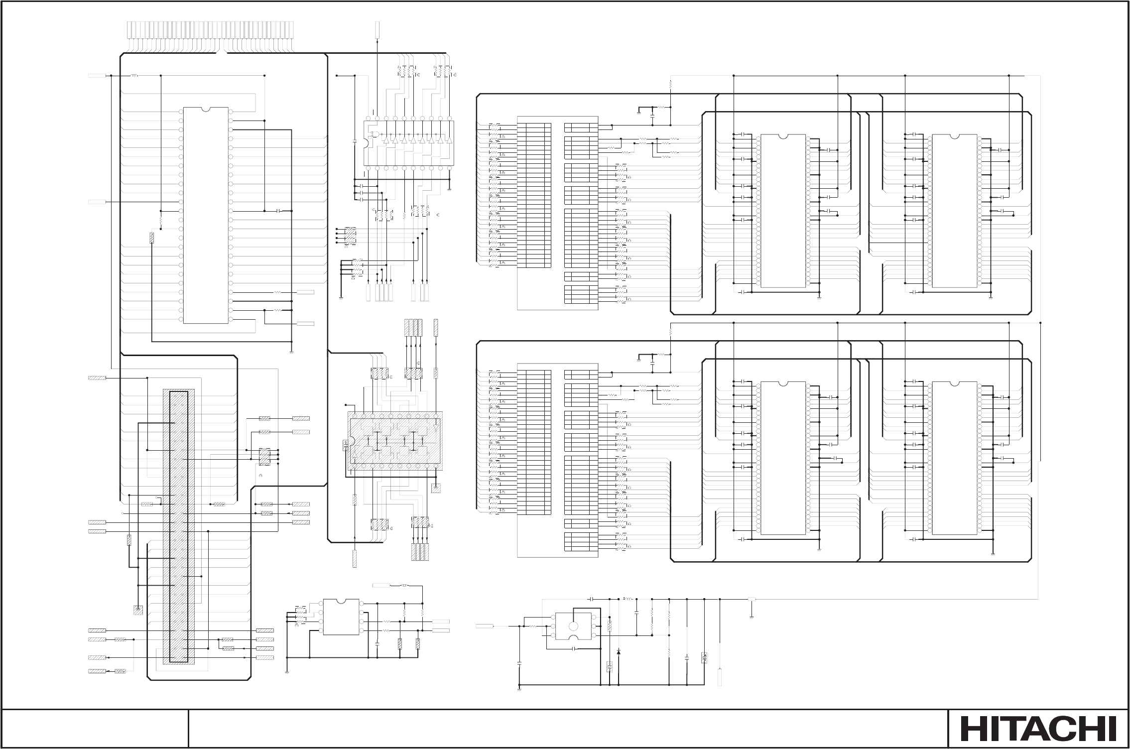
11
12
13
14
15
16
17
18
19
20
10
9
8
7
6
5
4
3
2
1
CK
Q
D
CLR
CK
CLR
D
Q
CK
Q
D
CLR
CK
CLR
D
Q
CK
Q
D
CLR
CK
CLR
D
Q
D
Q
CK
CLR
D
CK
CLR
Q
11
12
13
14
15
16
17
18
19
20
10
9
8
7
6
5
4
3
2
1
28
29
30
31
32
33
34
35
36
37
38
39
40
41
42
43
44
45
46
47
48
26
27
2524
23
22
21
20
19
18
17
16
15
14
13
12
11
10
9
8
7
6
5
4
3
2
1
65
66
33
61
34
35
36
37
38
39
40
41
42
43
44
45
46
47
48
49
50
51
52
53
54
55
56
57
58
59
60
62
63
64
32
31
30
29
28
27
26
25
24
23
22
21
20
19
18
17
16
15
14
13
12
11
10
9
8
7
6
5
4
3
2
1
65
66
33
61
34
35
36
37
38
39
40
41
42
43
44
45
46
47
48
49
50
51
52
53
54
55
56
57
58
59
60
62
63
64
32
31
30
29
28
27
26
25
24
23
22
21
20
19
18
17
16
15
14
13
12
11
10
9
8
7
6
5
4
3
2
1
65
66
33
61
34
35
36
37
38
39
40
41
42
43
44
45
46
47
48
49
50
51
52
53
54
55
56
57
58
59
60
62
63
64
32
31
30
29
28
27
26
25
24
23
22
21
20
19
18
17
16
15
14
13
12
11
10
9
8
7
6
5
4
3
2
1
65
66
33
61
34
35
36
37
38
39
40
41
42
43
44
45
46
47
48
49
50
51
52
53
54
55
56
57
58
59
60
62
63
64
32
31
30
29
28
27
26
25
24
23
22
21
20
19
18
17
16
15
14
13
12
11
10
9
8
7
6
5
4
3
2
1
5
6
7
8
4
3
2
1
A25
D24
E23
C24
G26
K24
H24
K23
M23
E26
E25
J23
D26
K22
D25
F26
G25
J24
M22
N25
N26
M25
M26
L24
J25
H26
N23
L23
U24
V23
U25
U26
B26
R24
C23
F21
E22
B23
A24
F22
B24
D23
F23
B25
A26
C25
C26
E24
H23
G24
J26
M24
P23
K25
N24
P24
L25
L26
T23
T24
P25
P26
R25
R26
T25
T26
I/O
I/O
O
O
O
O
O
O
O
O
O
O
O
O
O
O
O
O
O
O
O
I/O
I/O
O
O
O
O
O
I
I
O
O
I
I
I/O
I/O
I/O
I/O
I/O
I/O
I/O
I/O
I/O
I/O
I/O
I/O
I/O
I/O
I/O
I/O
I/O
I/O
I/O
I/O
I/O
I/O
I/O
I/O
I/O
I/O
I/O
I/O
I/O
I/O
I/O
I/O
MAIN MEMORY PORT
A7
E11
B8
A6
A15
D16
E14
A13
B15
B13
C13
A12
B12
E13
C12
C14
B14
A14
C15
B20
A20
D20
C20
C16
C17
A16
B16
D14
E8
C7
C6
B5
A9
C19
B6
A4
A5
C8
D9
B7
E10
C9
A8
C10
D11
B9
D12
A10
B11
A11
B17
E17
A17
D18
C18
B18
A18
B19
D21
C21
B21
A21
E21
B22
A22
D22
I/O
I/O
O
O
O
O
O
O
O
O
O
O
O
O
O
O
O
O
O
I/O
I/O
O
O
O
O
O
O
O
I
I
O
O
I
I
I/O
I/O
I/O
I/O
I/O
I/O
I/O
I/O
I/O
I/O
I/O
I/O
I/O
I/O
I/O
I/O
I/O
I/O
I/O
I/O
I/O
I/O
I/O
I/O
I/O
I/O
I/O
I/O
I/O
I/O
I/O
I/O
KEYSTONE MEMORY PORT
G1
4
5
6
3
2
1
A4
A6
A9
A11
A12
A14
A17
A2 A1
A3
A5
A7
A8
A10
A13
A20
A15
A16
A18A19
D7
D6
D13
D12
D11
D10
D1
D0
D15
D14
D5
D4
D3
D2
D9
D8
A1
A2
A3
A4
A5
A6
A7
A8
A9
A11
A10
A12
A13
A14
A15
A16
A17
A18
A19
A20
D0
D1
D2
D3
D4
D5
D6
D7
D8
D9
D10
D11
D12
D13
D14
D15
D7
D6
D5
D4
D3
D2
D1
D0
A16
A15
A14
A13
A12
A11
A10
A9
A20
A17 A17
D15
D7
D14
D6
D13
D5
D12
D4
D11
D3
D10
D2
D9
D1
D8
D0
A1
A2
A3
A4
A5
A6
A7
A8
A18
A19
KD29
MCS
KA8
KCK0
MA12
KD27
MA4
KA4
MD14
KD29
MCK0
MRAS
KA9
KDM3
MA6
MD23
MD15
KD9
KCK0N
MD27
KD6
KCAS
MCAS
KD8
MCK0N
MA8
KD26
KD17
MD20
KDQS3
MD18
MCK1
MDQS3
KVREF
MA2
MD8
MA6
KD3
KD16
MD0
KD1
MD3 1
MCK1N
KA9
KBNK1
MD2
MA12
MA7
KRAS
KA7
KD15
MD15
MD1
KA4
MVREF
MDM0
KDQS3
MD25
MCKE
MA8
KA5
KD16
KDQS1
KD14
MDM3
MDM1
KDM0
KA6
MD30
MD2
KD0
KRAS
MA9
KA11
MD13
KD13
MCK1N
MDQS0
KA12
MD22
MD30
KA10
MDQS1
MA10
KCK0
KD12
MCK1
KD28
MA2
MBNK1
KA8
MD31
KBNK1
MCKE
KCK1N
MD11
MA11
KD11
KD27
KD11
MD28
MDM2
KD10
KWE
MD29
KCK1
MVREF
MD10
MA12
KA5
KA9
KD10
MD7
KD20
KCS
MDM3
KD18
KD26
KD5
MA8
KWE
KA6
MA1
KA0
MD9
MD28
MDQS1
KD9
MDQS2
KVREF
KD25
KA4
KD25
KA12
MD21
KCKE
KDQS0
KD13
KDM1
MD27
MDQS3
KCAS
MDM1
MD3
KD8
KD2
KDM2
KD24
KA1
KWE
KA1
MCKE
KA11
MD7
KD14 KD17
MD26
KCAS
MD29
KD7
KD0
KA6
MD4
KBNK1
KBNK0
KD23
MBNK0
MVREF
KD23
KBNK0
KCK0N
KA12
MA0
MD25
MA11
KCS
KD6
KDQS2
MDQS0
MD9
KD22
MD8
MA5
KD22
KD31
KA0
MD24
MA10
KD5
KDM3
MDM0
MD24
MA1
KD7
KD21
MD14
KA3
KCS
KD28KD19
KA7
MD23
MD0
MA9
MDM2
KD4
MA6
KA10
MA2
MD11
MCS
KD20
KA0
KA8
MDQS2
MA7
MD22
KA5
MA3
KCKE
KD3
MA7
MBNK1
KA3
MA11
KVREF
KA1
MA3
MD10
KD19
KDQS1
KDM1
MA0
MD21
MCAS
MBNK0
KD2
KDQS0
MA5
MA0
MA4
MD12
KCK1N
KA3
KD18
KBNK0
KRAS
MD16
KA2
MD12
MD13
MD20
MCS
MWE
KDQS2
KD31
KD1
MA3MA4
MD26
KDM2
MA5
KCK1
KCKE
KA10
MWE
KDM0
MD19
MCAS
KA11
MCK0N
KD21
MD5
MD19
MD17
MD5
MD6
MRAS
KD12
KD24
MD18
MRAS
MCK0
MD16
MD1
MBNK0
MA9
MD4
KA7
KD4
KA2
MWE
MD17
MBNK1
MD3
MA10
KA2
MA1
MD6
KD30
KD30
D1
D2
D3
D7
D6
D5
D4
D0
A21
A21
A21
KD15
*E251
WR-60S-VF1-1
1
2
3
4
5
6
7
8
9
10
11
12
13
14
15
16
17
18
19
20
21
22
23
24
25
26
27
28
29
30 31
32
33
34
35
36
37
39
40
41
42
43
44
45
46
47
48
49
50
51
52
53
54
55
56
57
58
59
60
38
I2T1
SN74LVC541APW
OE1
A1
A2
A3
A4
A5
A6
A7
A8
GND Y8
Y7
Y6
Y5
Y4
Y3
Y2
Y1
OE2
VCC
C291
1005
0.01/16
1
2
C293
1005
0.01/16
12
C290
1005
0.01/16
12
GND1
GND1
GND1
GND1
1608
L251
600
12
CHBHEN
1
CHPD15
1
1005
R2H3
0
12
1005
R2F7
820820
12
1005
R291
0
12
1005
*R2G3
1.8k
12
1005
R2G1
4.7k
12
1005
*R2G5
0
12
1005
*R2H4
0
12
1005
R292
10k
12
1005
R2F9
820820
12
1005
R2F5
100
12
1005
R2G4
0
12
1005
R2G6
100
1
2
1005
R2G7
100
12
1005
R2F6
100
12
1005
R2H1
0
12
1005
*R2G9
0
12
1005
R2F8
4.7k
12
1005
*R2H2
0
12
1005
R290
10k
12
R2J3
2010
0
7
8
56
3
4
1
2
R2J5
2010
100
1
2
34
5
6
7
8
R2J1
2010
10k
7
8
56
3
4
1
2
R2J4
2010
100
1
2
34
5
6
7
8
R2H9
2010
10k
1
2
34
5
6
7
8
R2F4
0
2010
12
34
56
78
R2G8
2010
3.3k
78
34
56
12
KEYI2
A17
A5
D2
CPU-RESET
FLASH_CE
ROMWE
D1
A20
A2
D9
A6
I2CCLK
A8
A18
KEYI0
D10
D3
D6
LAMP-S
LCONT_IN
I2CDAT
NMI
A1
D15
COVER-S
ROMOE
A10
A7
TXD0
D7
A9
A19
ROMOE
KEYI1
EMU-RESET
D14
PCS1
RDN
D12
+3.3V
A14
RDN
PCS1
RESETN
WRN
A4
D8
A15
FLASH_CE
A16
LAMP_ON
D13
D11
PCS0
+5V
A11
D5
A13
RXD0
A12
ROMWE
D0
A3
D4
R296
2010
22
12
34
56
78
1005
R2C9
47
12
C262
1005
0.1/10
12
1005
R2H8
47
12
C298
1005
0.1/10
12
C274
1005
0.1/10
12
R2B9
2010
22
12
34
56
78
C296
1005
0.1/10
12
R299
2010
22
78
56
34
12
C273
1005
0.1/10
12
R2C3
2010
22
12
34
56
78
1005
R2E1
47
12
R2E8
2010
22
78
56
34
12
R2E7
2010
22
12
34
56
78
R2F1
2010
22
12
34
78
56
GND1
R2B4
2010
22
12
34
56
78
1005
R2E3
0
12
C297
1005
0.1/10
12
R2A1
2010
22
78
56
34
12
1005
R2A7
0
12
C260
1005
0.1/10
12
C280
1005
0.1/10
12
R297
2010
22
12
34
56
78
C282
1005
0.1/10
12
R295
2010
22
12
34
56
78
C289
1005
0.1/10
12
C281
1005
0.1/10
12
+2.5V
R294
2010
22
12
34
56
78
1005
R2A2
1.0k-1%
12
C267
1005
0.1/10
12
C277
1005
0.1/10
12
GND1
C269
1005
0.1/10
12
R2B1
2010
22
34
56
78
12
C288
1005
0.1/10
12
GND1
C271
1005
0.1/10
1
2
C272
1005
0.1/10
12
1005
R2H5
47
12
R2C1
2010
22
12
34
56
78
R2B8
2010
22
12
34
56
78
C265
1005
0.1/10
12
GND1
C261
1005
0.1/10
12
1005
R2C8
1.0k-1%
12
1005
R2A4
47
12
C279
1005
0.1/10
12
GND1
R2C6
2010
22
78
56
34
12
R2F3
2010
22
12
34
56
78
C270
1005
0.1/10
12
R2B5
2010
22
12
34
78
56
R2E6
2010
22
34
56
78
12
1005
R2H7
47
12
1005
R2A9
0
12
C287
1005
0.1/10
12
C264
1005
0.1/10
12
C285
1005
0.1/10 12
1005
R2A6
0
12
GND1
R2C5
2010
22
78
56
34
12
R2B2
2010
22
12
34
56
78
1005
R2E2
0
12
1005
R2C7
1.0k-1%
12
R293
2010
22
12
34
56
78
R2B6
2010
22
78
34
56
12
1005
R2A5
47
12
C294
1005
0.1/10
1
2
C268
1005
0.1/10
12
C278
1005
0.1/10
12
1005
R2E4
0
12
1005
R2A8
0
12
R2C2
2010
22
12
34
56
78
C295
1005
0.1/10
12
C258
1005
0.1/10
12
C266
1005
0.1/10
12
C276
1005
0.1/10
12
1005
R2H6
47
12
R2B7
2010
22
12
34
56
78
R2E9
2010
22
12
34
56
78
R2F2
2010
22
78
34
56
12
C284
1005
0.1/10
12
1005
R2E5
0
12
R298
2010
22
12
34
56
78
C263
1005
0.1/10
12
1005
R2A3
1.0k-1%
12
C259
1005
0.1/10
12
C286
1005
0.1/10
12
R2C4
2010
22
12
34
56
78
C257
1005
0.1/10
12
R2B3
2010
22
78
56
34
12
C275
1005
0.1/10
12
C283
1005
0.1/10
12
I2U1
SN74LV273APW
CLR
1Q
1D
2D
2Q
3Q
3D
4D
4Q
GND CLK
5Q
5D
6D
6Q
7Q
7D
8D
8Q
VCC
R2J6
2010
07
8
56
3
4
1
2
R2J7
2010
07
8
56
3
4
1
2
GND1
C292 1005
0.01/16
1
2
PCS2
RESETN
IRIS_PI1
IRIS_PI2
1005
R2K2
0
12
1005
R2K1
0
12
R2J8
2010
100 1
2
34
5
6
7
8
A21
1005
R2G2
0
12
GND1
R2J2
2010
1.0k 1
2
34
5
6
7
8
I251
S29AL032D70TFI030
A15
A14
A13
A12
A11
A10
A9
A8
A19
A20
WE#
RESET#
NC-13
WP#
RY/BY#
A18
A17
A7
A6
A5
A4
A3
A2
A1 A0
CE#
Vss-27
OE#
DQ0
DQ8
DQ1
DQ9
DQ2
DQ10
DQ3
DQ11
Vcc
DQ4
DQ12
DQ5
DQ13
DQ6
DQ14
DQ7
DQ15/A-1
Vss-46
BYTE#
A16
I252
K4H561638H-UCB30
1VDD1
2DQ0
3VDDQ1
4DQ1
5DQ2
6VSSQ1
7DQ3
8DQ4
9VDDQ2
10 DQ5
11 DQ6
12 VSSQ2
13 DQ7
14 NC1
15 VDDQ3
16 LDQS
17 NC2
18 VDD2
19 NC3
20 LDM
21 /WE
22 /CAS
23 /RAS
24 /CS
25 NC4
26 BA0
27 BA1
28 A10
29 A0
30 A1
31 A2
32 A3
33 VDD3 34
VSS1
35
A4
36
A5
37
A6
38
A7
39
A8
40
A9
41
A11
42
A12
43
NC5
44
CKE
45
CK
46
/CK
47
UDM
48
VSS2
49
VREF
50
NC6
51
UDQS
52
VSSQ3
53
NC7
54
DQ8
55
VDDQ4
56
DQ9
57
DQ10
58
VSSQ4
59
DQ11
60
DQ12
61
VDDQ5
62
DQ13
63
DQ14
64
VSSQ5
65
DQ15
66
VSS3
I253
K4H561638H-UCB30
1VDD1
2DQ0
3VDDQ1
4DQ1
5DQ2
6VSSQ1
7DQ3
8DQ4
9VDDQ2
10 DQ5
11 DQ6
12 VSSQ2
13 DQ7
14 NC1
15 VDDQ3
16 LDQS
17 NC2
18 VDD2
19 NC3
20 LDM
21 /WE
22 /CAS
23 /RAS
24 /CS
25 NC4
26 BA0
27 BA1
28 A10
29 A0
30 A1
31 A2
32 A3
33 VDD3 34
VSS1
35
A4
36
A5
37
A6
38
A7
39
A8
40
A9
41
A11
42
A12
43
NC5
44
CKE
45
CK
46
/CK
47
UDM
48
VSS2
49
VREF
50
NC6
51
UDQS
52
VSSQ3
53
NC7
54
DQ8
55
VDDQ4
56
DQ9
57
DQ10
58
VSSQ4
59
DQ11
60
DQ12
61
VDDQ5
62
DQ13
63
DQ14
64
VSSQ5
65
DQ15
66
VSS3
I255
K4H561638H-UCB30
1VDD1
2DQ0
3VDDQ1
4DQ1
5DQ2
6VSSQ1
7DQ3
8DQ4
9VDDQ2
10 DQ5
11 DQ6
12 VSSQ2
13 DQ7
14 NC1
15 VDDQ3
16 LDQS
17 NC2
18 VDD2
19 NC3
20 LDM
21 /WE
22 /CAS
23 /RAS
24 /CS
25 NC4
26 BA0
27 BA1
28 A10
29 A0
30 A1
31 A2
32 A3
33 VDD3 34
VSS1
35
A4
36
A5
37
A6
38
A7
39
A8
40
A9
41
A11
42
A12
43
NC5
44
CKE
45
CK
46
/CK
47
UDM
48
VSS2
49
VREF
50
NC6
51
UDQS
52
VSSQ3
53
NC7
54
DQ8
55
VDDQ4
56
DQ9
57
DQ10
58
VSSQ4
59
DQ11
60
DQ12
61
VDDQ5
62
DQ13
63
DQ14
64
VSSQ5
65
DQ15
66
VSS3
I2 54
K4H561638H-UCB30
1VDD1
2DQ0
3VDDQ1
4DQ1
5DQ2
6VSSQ1
7DQ3
8DQ4
9VDDQ2
10 DQ5
11 DQ6
12 VSSQ2
13 DQ7
14 NC1
15 VDDQ3
16 LDQS
17 NC2
18 VDD2
19 NC3
20 LDM
21 /WE
22 /CAS
23 /RAS
24 /CS
25 NC4
26 BA0
27 BA1
28 A10
29 A0
30 A1
31 A2
32 A3
33 VDD3 34
VSS1
35
A4
36
A5
37
A6
38
A7
39
A8
40
A9
41
A11
42
A12
43
NC5
44
CKE
45
CK
46
/CK
47
UDM
48
VSS2
49
VREF
50
NC6
51
UDQS
52
VSSQ3
53
NC7
54
DQ8
55
VDDQ4
56
DQ9
57
DQ10
58
VSSQ4
59
DQ11
60
DQ12
61
VDDQ5
62
DQ13
63
DQ14
64
VSSQ5
65
DQ15
66
VSS3
1005
R289
10k
12
*I256
R1EX24256ASA00A
A0
A1
A2
VSS SDA
SCL
WP
VCC
I201
PW388B-10L
T26 MD0
T25 MD1
R26 MD2
R25 MD3
P26 MD4
P25 MD5
T24 MD6
T23 MD7
L26 MD8
L25 MD9
P24 MD10
N24 MD11
K25 MD12
P23 MD13
M24 MD14
J26 MD15
G24 MD16
H23 MD17
E24 MD18
C26 MD19
C25 MD20
A26 MD21
B25 MD22
F23 MD23
D23 MD24
B24 MD25
F22 MD26
A24 MD27
B23 MD28
E22 MD29
F21 MD30
C23 MD31
R24
MREFIN0
B26
MREFIN1
U26
MCK
U25
MCKN
V23
MCKFBK
U24
MCKFBKN
L23
MCKE
N23
MRAS
H26
MCAS
J25
MWE
L24
MCS
M26
MDM0
M25
MDM1
N26
MDQS0
N25
MDQS1
M22
MA0
J24
MA1
G25
MA2
F26
MA3
D25
MA4
K22
MA5
D26
MA6
J23
MA7
E25
MA8
E26
MA9
M23
MA10
K23
MA11
H24
MA12
K24
MBNK0
G26
MBNK1
C24
MDM2
E23
MDM3
D24
MDQS2
A25
MDQS3
I201
PW388B-10L
D22 KD0
A22 KD1
B22 KD2
E21 KD3
A21 KD4
B21 KD5
C21 KD6
D21 KD7
B19 KD8
A18 KD9
B18 KD10
C18 KD11
D18 KD12
A17 KD13
E17 KD14
B17 KD15
A11 KD16
B11 KD17
A10 KD18
D12 KD19
B9 KD20
D11 KD21
C10 KD22
A8 KD23
C9 KD24
E10 KD25
B7 KD26
D9 KD27
C8 KD28
A5 KD29
A4 KD30
B6 KD31
C19
KREFIN0
A9
KREFIN1
B5
KCK
C6
KCKN
C7
KCKFBK
E8
KCKFBKN
D14
KCKE
B16
KRAS
A16
KCAS
C17
KWE
C16
KCS
C20
KDM0
D20
KDM1
A20
KDQS0
B20
KDQS1
C15
KA0
A14
KA1
B14
KA2
C14
KA3
C12
KA4
E13
KA5
B12
KA6
A12
KA7
C13
KA8
B13
KA9
B15
KA10
A13
KA11
E14
KA12
D16
KBNK0
A15
KBNK1
A6
KDM2
B8
KDM3
E11
KDQS2
A7
KDQS3
R2J9
2010
100
7
8
56
3
4
1
2
RC_REAR
RC_UPPER
38_RC
56_RC
RC_FRONT
IRIS_OE
IRIS_SAV
IRIS_LED
+6.6V
2125
X251
SGM20F1C104-4A
123
GND1
C2B1
1005
100p-C
12
C2B2
1005
100p-C
12
C2B3
1005
100p-C
12
1005
R2P5
100
12
+3.3V
1608
L253
600
12
I257
TPS40222DR
FB
GND
SEPVIN
AVIN
BOOSTG1
1005
R2N6
27k-1%
12
C2A1
1005
680p
12
1005
R2N5
33k-1%
12
C2A5
1.0/10
12
C2A7
1005
680p
12
C2A4
1005
0.033/16
12
1005
R2N3
0
12
C2A6
2125
22/6.3
12
1005
R2N1
10
12
C2A9
2125
10/10
12
1005
R2N7
10k-1%
12
D251
RSX201L-30
12
4.7
L252
7E06NG
4.7
12
C2A0
100/6.3
MVK/SKV
1
2
1005
R2N4
33k-1%
12
GND1
1.8V-CPU
MAX:1.6A
SM0321 PWB ASSEMBLY MAIN 2
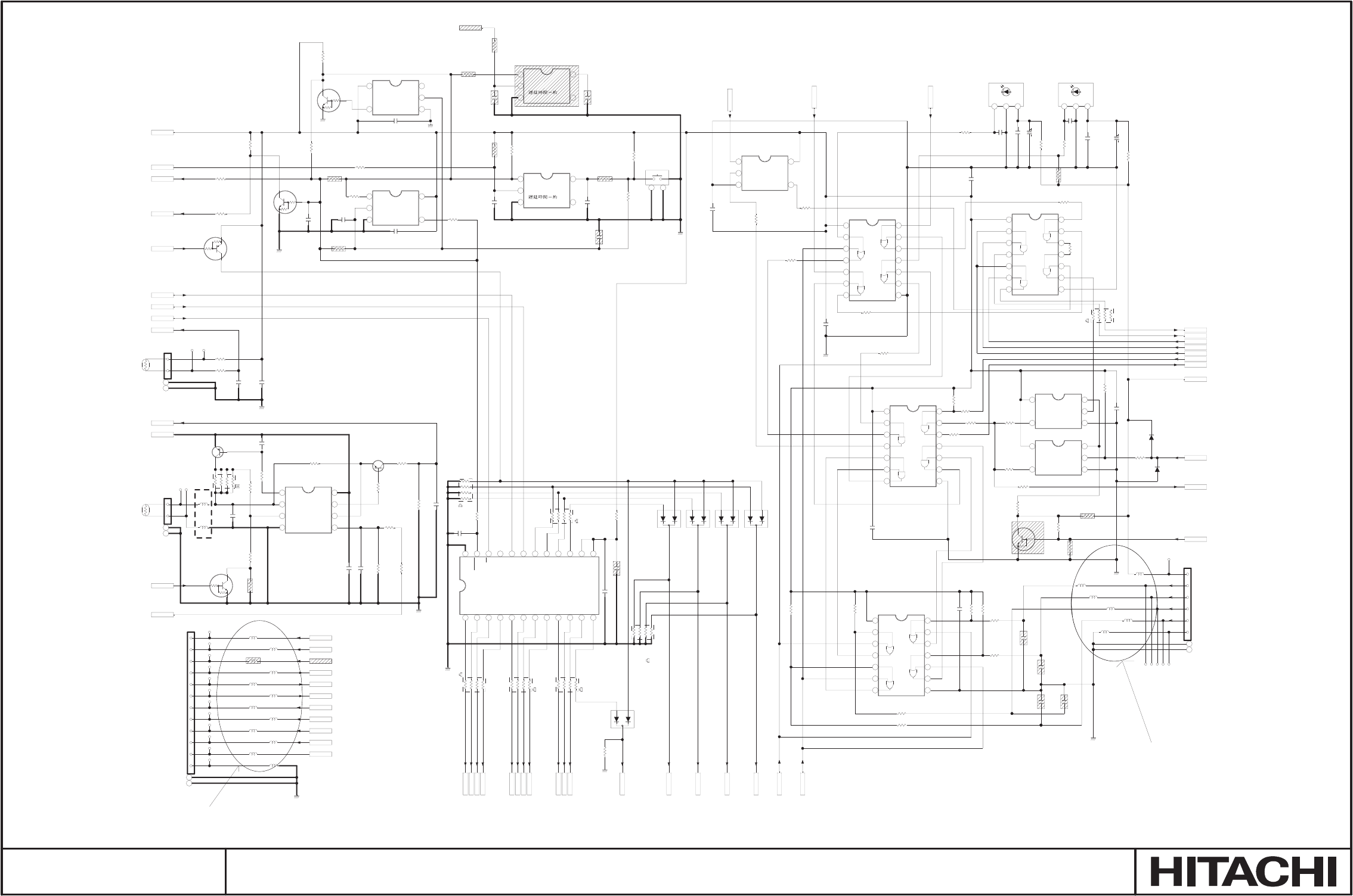
5
6
7
8
4
3
2
1
8
9
10
11
12
13
14
7
6
5
4
3
2
1
4
5
3
2
1
8
9
10
11
12
13
14
7
6
5
4
3
2
1
4
5
3
2
1
8
9
10
11
12
13
14
7
6
5
4
3
2
1
4
5
3
2
1
321
4
5
3
2
1
24
23
22
21
20
19
18
17
16
15
14
1312
11
10
9
8
7
6
5
4
3
2
1
4
5
3
2
1
321
8
9
10
11
12
13
14
7
6
5
4
3
2
1
G2G1
4
5
3
2
1
4
5
3
2
1
APT2
1
+5V
D304
DAN202U
1
2
3
1005
R347
47k
12
POWER5
E305
ZH-06V
1
2
3
4
5
6
G1
G2
1005
R342
47k
12
C341
1005
0.01/16
12
I333
LM358AD
1OUT
1IN-
1IN+
GND 2IN+
2IN-
2OUT
VCC
FAN-CNT5
C305
1005
0.01/16
12
1005
R394
100
12
I314
SN74LV08APW
1A
1B
1Y
2A
2B
2Y
GND
3Y
3A
3B
4Y
4A
4B
VCC
1608
L315
600
1
2
+3.3V
C325
1005
0.01/16
1
2
C328
1005
0.01/16
1
2
R359
2010
100
12
56
34
78
1005
R355
100 12
1005
R001
100100
12
1005
R398
0
12
1005
R309
100
12
1005
R302
1.0k
12
2125
R002
47
12
1005
R387
0
12
1608
*L322
600 1
2
I301
S-80950CNMC-G9LT2G
OUT
VDD
VSS NC
CD
POWER1
E310
ZH-12V
1
2
3
4
5
6
7
8
9
10
11
12
G1
G2
1005
R343
47k
12
1005
R397
22k-1%
12
APK7
1
1005
R358
100
12
KEYI2
1005
R324
0
12
GND1
*C006
47/6.3
MVK/SKV
1
2
1005
*R340
100
1
2
FAN15V
I311
SN74LV08APW
1A
1B
1Y
2A
2B
2Y
GND
3Y
3A
3B
4Y
4A
4B
VCC
1005
R381
100
12
C395
0.1/16
12
C323
100p-C
12
1005
R352
100 1
2
1005
R365
100
12
C340
1005
0.01/16
12
1005
R310
10k
12
APT1
1
LAMP-S
C393
0.1/25
12
*C004
100p-C
12
56_RC
I302
TC7SZ08FU
IN_B
IN_A
GND OUT_Y
VCC
1005
R308
0
12
I310
SN74LV32APW
1A
1B
1Y
2A
2B
2Y
GND
3Y
3A
3B
4Y
4A
4B
VCC
APK3
1
W_RC_SW
C312
2125
10/6.3
12
C304
1005
0.01/16
1
2
AIRSPD
C327
1005
0.01/16
12
PWRC
Q392
2SA1576A
1
2
3
POWER0
FAN-CNT2
MOUSE
GND1
I317
TC7SZ126FU
G
IN_A
GNDOUT_Y
VCC
1005
R312
220
12
C392
2125
10/10
1
2
DATA1
APK2
1
1005
R315
33
1
2
C321
100p-C
12
FAN-CNT3
1005
*R344
100
1
2
E301
ZH-02V
1
2
G1
G2
1005
R392
1.0k
12
R389
3216
270
12
34
56
78
1005
R307
100
12
FAN-CNT1
LED-TEMP
APRC4 1
RC_UPPER
I001
KSM-2003LM2EL
1
Vout
2
GND
3
VCC
2125
*R004
47
12
I316
TC7SZ125FU
G
IN_A
GNDOUT_Y
VCC
1608
L329
600 1
2
C322
100p-C
12
+3.3V
Q310
DTC114EE
1
2
3
1005
R353
100 1
2
1608
L326
600 1
2
Q320
DTC114EE 1
2
3
CLK1
KEYO0
MOUSE
D305
1SS355
12
C329
1005
0.01/16
12
1608
L351
600
12
R323
2010
100
12
34
56
78
1005
R395
680-1%1
2
C310
1005
0.01/16
1
2
CPU-RESET
+6.6V
1005
R356
100 12
DATA1
APK5
1
I305
M62376GP-60AD
A1
A2
A3
A4
D11/A5
D10/A6
D9/A7
D8/A8
D7/A9
D6/A10
D5/A11
D4/A12 VDD
Vcc
D3
D2
D1
D0
CLK
SI
S0
EN
RESET
GND
CLK1
R326
2010
100
12
34
56
78
R327
2010
100
12
34
56
78
1005
R396
1.5k-1%
12
C001
100p-C
12
LED-IF
*C005
4.7/6.3
12
1005
R311
0
12
1005
R368
100
12
GND1
C308
1005
0.01/16
1
2
KEYI0
1005
*R003
100
12
GND1
LED-LAMP
C301
0.039/16
12
1005
R349
100
1
2
CLK-A
1608
L312
600
1
2
KEYI1
POWER2
1005
R301
10k
12
APK9
1
APRC6 1
C324
1005
0.01/16
12
GND1
APK6
1
1005
R354
100 1
2
APRC5 1
AP351
1
OUTTEMP
1608
L328
600 1
2
VOL_SEL
R328
2010
10k
12
34
56
78
AP352
1
1005
R345
100
12
RC_REAR
1005
R361
100 1
2
1608
*L313
600
1
2
1005
R348
10k
12
POWER3
REMOTE
C302
1005
0.01/16
1
2
1608
L321
600 1
2
1005
R363
47k
12
GND1
C311
1005
0.01/16 1
2
APRC3 1
C320
100p-C
12
I313
TC7SZ32FU
IN_B
IN_A
GND OUT_Y
VCC
1005
R346
47k
12
D306
1SS355
12
RC_FRONT
C391
2125
10/10
1
2
APRC1
1
+5V
C003
47/6.3MVK/SKV
1
2
1005
R303
0
12
APK8
1
1005
R393
2.0k-1%
12
1608
L324
600 1
2
1005
R362
33 1
2
1005
R399
3.3k-1%
12
1005
*R3A1
47k
12
R321
2010
10k
5
6
34
1
2
7
8
APK1
1
1005
R390
3.3k-1%
12
GND1
GND1
1608
L325
600 1
2
FAN-CNT4
APRC2 1
1608
L352
600
12
D302
DAN202U
1
2
3
38_RC
1005
R367
100
12
1005
R304
10k
12
1005
R350
100
12
*I002
1
Vout
2
GND
3
VCC
C002
4.7/6.3
12
C394
0.1/16
12
APK11
1
DATA-A
GND1
1005
R322
1.0k
12
1005
R357
100 12
WIRED_RC
APK4
1
1005
R366
01
2
D301
DAN202U
1
2
3
1005
R341
100 12
Q302
DTC114EE
1
2
3
LED-P-R
I312
SN74LV32APW
1A
1B
1Y
2A
2B
2Y
GND
3Y
3A
3B
4Y
4A
4B
VCC
1608
*L311
600
1
2
1608
L327
600 1
2
1608
L320
600 1
2
APK12
1
1608
L310
600
1
2
1608
L323
600 1
2
1005
R360
10k 12
1608
L314
600
1
2
E302
ZH-02H
1
2
G1
G2
1005
R364
10k 12
1005
R306
100
12
1005
R380
100
12
LED-P-G
1608
L330
600 1
2
1005
R391
5.1k-1%
12
Q301
DTA114YKA
1
2
3
1608
L331
600 1
2
Q391
2SB1132
1
2
3
APK10
1
C326
1005
0.01/16
12
R325
2010
100
12
34
56
78
1005
R305
0
12
KEYO1
CS_DAC
S310
SKHHLMA010
12
G1 G2
RESETN
C303
2125
10/6.3
12
1005
R351
33
12
D303
DAN202U
1
2
3
POWER7
POWER5
POWER4
POWER6
POWER8
POWERA
D307
DAN202U
1
2
3
1005
R005
10k
12
GND1
C306
0.039/16
12
1005
R316
0
12
C307
1005
0.01/16
1
2
+4.0V
1005
R317
0
12
I303
S-80927CNMC-G8XT2G
OUT
VDD
VSS NC
CD
I304
TC7SZ14FU
NC
IN_A
GNDOUT_Y
VCC
Q303
DTC114EE
1
2
3
GND1
GND1
1005
R313
1.0k
12
1005
R314
100
12
C309
1005
0.01/16
1
2
KEYO-0
KEYO-1
LED-IF
KEYI-0
KEYI-1
KEYI-2
LED GREEN
LED RED
OUT-SIDE
SENSOR
(10K)
LED TEMP
LED LAMP
+3.3V
GND
56_REAR38_REAR
L320-331
Mounted jumper
L310-315
+5V VCC
UP_38
UP_56
GND
FRONT_56
FRONT_38
FRONT
UPPER
REAR
REAR
FRONT
UPPER
REARFRONT
MOUSEUPPER
WIRED
SELECT
VOL_DATA/CLK
(SELECT)
REAR
(OR)
AIR SPEED
SENSOR
(1K)
WIRED
(SELECT)
20ms
JUMPER R
GP1UX317QS
20ms
Mounted jumper
SM0321 PWB ASSEMBLY MAIN 3
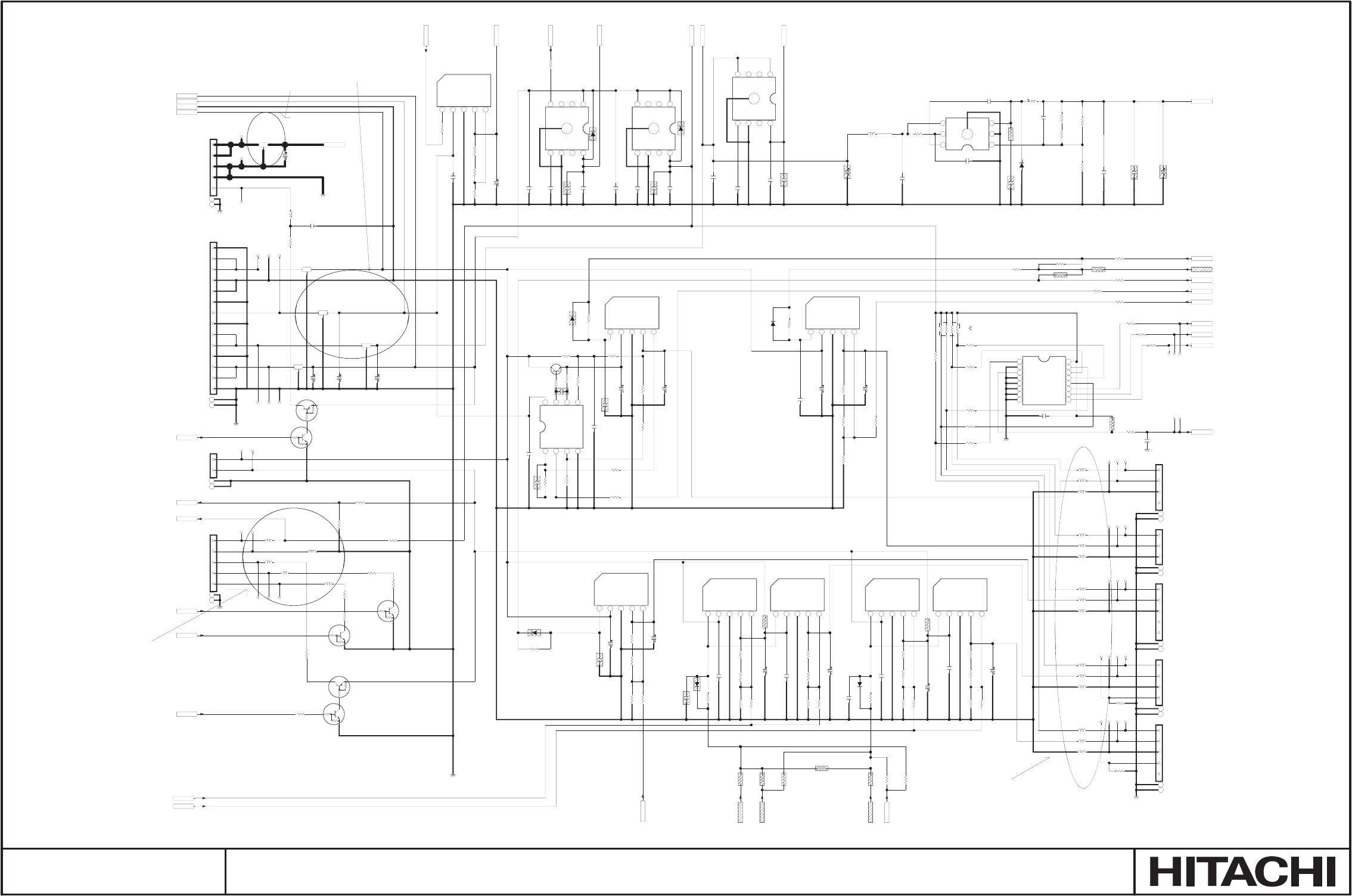
G1
5
6
7
8
4
3
2
1
G1
5
6
7
8
4
3
2
1
54321
54321
54321
54321
54321
54321
5
6
7
8
4
3
2
1
9
10
11
12
13
14
15
16
8
7
6
5
4
3
2
1
5432154321
G1
5
6
7
8
4
3
2
1
G1
4
5
6
3
2
1
+6.6V
0V
C820
1.0/10
12
C814
1005470p
12
C807
1005470p
12
C806
1.0/10
12
C821
2125
10/6.3
12
C805
1.0/10
12
C8E1
1005
0.01/16
1
2
C863
47/16
MVK/SKV
1
2
C812
100/16
MVK/SKV
1
2
C801
47/25
MVK/SKV
1
2
C869
47/16
MVK/SKV
1
2
C802
47/10
MVK/SKV
1
2
C873
47/16
MVK/SKV
1
2
C803
100/6.3
MVK/SKV
1
2
C854
100/16
MVK/SKV
1
2
C874
100/16
MVK/SKV
1
2
C853
47/16
MVK/SKV
1
2
C867
47/16
MVK/SKV
1
2
C864
100/16
MVK/SKV
1
2
E808
ZH-02V
1
2
G1
G2
E804
ZH-04V
1
2
3
4
G1
G2
E807
SH-05H
2
3
4
5
1
G1
G2
I803
MM1663DHBE
Vout
NC-2
GND
Cn Cont
NC-6
NC-7
Vin
I802
MM1663DHBE
Vout
NC-2
GND
Cn Cont
NC-6
NC-7
Vin
3216
L804
C1V222-2A
123
3216
L803
C1V222-2A
123
3216
L8A1
C1V222-2A
123
GND1
P_GND
GND1
GND1
GND1
GND1
2125
L862 600
12
3216
L853
BLM31PG601SN1L
12
2125
L883 600
12
2125
L873
600
12
1608
L822
600
12
1608
L871
600
12
3216L852
BLM31PG601SN1L
12
2125
L872 600
12
1608
L861
600
12
3216L892
BLM31PG601SN1L
12
1608
L851
600
12
1608
L825
600
12
3216L893
BLM31PG601SN1L
12
1608
L881
600
12
2125
L863
600
12
1608
L824
600
12
1608
L823
600
12
2125
L882 600
12
1608
L821
600
12
1608
L891
600
12
APF14
1
APF3
1
AP-FG
1AP-FS0 1
APP11
1
CH-FG
1
APF4
1
APP13
1
APP10
1
APF15
1
APF16
1
APP12
1
APF7
1
APP8
1
APF10
1
APP2
1
APF9
1
APF5
1
APP6
1
AP-FS2 1
APF2
1
APP1
1
APF12
1
APP7
1
APP16
1
APP15
1APP5
1
APF8
1
APF17
1
APF1
1
APF13
1
APF11
1
APP14
1
APF6
1
AP-FS1 1
APP3
1
1005
R816
100
12
1005
R8E2
100
12
1005
R896
0
12
1005
R849
10k
12
1005
R811
100
1
2
R846
100
1005
12
R847
100
1005
12
1005
R8E1
100
12
1005
R813
4.7k-1%
12
1005
R812
27k-1%
12
1005
R806
2.7k
12
1005
R8E4
100
12
1005
R804
10k
12
1005
R8A3
1.0k
12
1005
R844
0
12
1005
R843
0
12
1005
R805
12k
12
R845
100
1005
12
1005
R814
2.2k-1%
12
1005
R803
1.2k 1
2
1005
R8E0
100
12
1005
R897
0
12
R848
2010
10k
78
12
34
56
LAMP_ON
POWER3
POWER1
FAN-CNT4
FAN-CNT2
+4.0V
POWER2
+17V
+14.5V
POWER6
+5V
FG_SEL2
POWER0
FG_SEL0
LAMP-S
+3.3V
FG_SEL1
FANGND
FAN15V
POWER7
FAN-CNT1
+15.5V
WHISPER
FAN_FG
+6.6V
POWER5
+3.3VP
COVER-S
FAN-CNT5
I851
SI-3010KM
Vc
Vin
GND
Vout
ADJ
I874
SI-3010KM
Vc
Vin
GND
Vout
ADJ
I801
SI-3010KM
Vc
Vin
GND
Vout
ADJ
I861
SI-3010KM
Vc
Vin
GND
Vout
ADJ
I871
SI-3010KM
Vc
Vin
GND
Vout
ADJ
I873
SI-3010KM
Vc
Vin
GND
Vout
ADJ
I852
LM358AD
1OUT
1IN-
1IN+
GND 2IN+
2IN-
2OUT
VCC
Q803
DTC114EE
1
2
3
Q862
DTC114EE
1
2
3
Q863
DTC114EE
1
2
3
C841
47/25
MVK/SKV
1
2
POWER3
1005
R8J7
0
12
1005
R8J6
0
12
1005
R8J4
0
12
POWER2
1005
R8C4
10k
12
1005
R8H1
10k
12
1005
R841
0
121005
R840
0
12
1005
R842
0
12
1005
R899
0
12
1005
R8J1
10k
12
1005
R8J2
10k
12
1005
R8J3
10k
12
1005
R898
0
12
E800
PH-14V
1
2
3
4
5
6
7
8
9
10
11
12
13
14
G1
G2
GND1
E806
PH-05V
2
3
4
5
1
G1
G2
APP9 1
Q802
DTA114YKA
1
2
3
1005
R801
100 1
21608
L801
600 1
2
APP4
1
D823
1SS355
1
2
D824
1SS355
1
2
D821
1SS355
12
D825
1SS355
1
2
D822
1SS355
12
1005
R852
22k
12
1005
R856
100
12
Q851
2SD1760
1
2
3
1005
R853
12k
12
E805
ZH-05V
2
3
4
5
1
G1
G2
E803
ZH-05V
2
3
4
5
1
G1
G2
1005
R8J8
0
12
1005
R8J9
0
12
E802
ZH-03V
1
2
3
G1
G2
E801
ZH-04V
1
2
3
4
G1
G2
1005
R875
10k-1%
12
1005
R854
15k-1%
12
1005
R874
30k-1%
12
1005
R865
10k-1%
12
1005
R855
2.7k-1%
12
1005
R8A1
12k-1%
12
1005
R8A2
2.2k-1%
12
1005
R8A4
12k-1%
12
1005
R8A5
51k-1%
12
1005
R8A6
47k-1%
12
1005
R869
30k-1%
12
1005
R8C1
51k-1%
12
1005
R8C2
47k-1%
12
1005
R8E9
100
12
1005
R8E3
100
12
C891
2125
4.7/6.3
12
C892
2125
4.7/6.3
12
C895
2125
4.7/6.3
12
C894
2125
4.7/6.3
12
C893
2125
4.7/6.3
12
3216
L805
123
3216
L802
123
D831
SFPB-66
12
D830
SFPB-66
12
1005
R8J5
0
12
POWER4
1005
R802
1.2k 1
21005
R807
1.0k 12
I830
SN74LV4051APWR
Y4
Y6
COM
Y7
Y5
Inhibit
GND1
GND2 C
B
A
Y3
Y0
Y1
Y2
VCC
1005
R850
10k
12
I875
SI-3010KM
Vc
Vin
GND
Vout
ADJ
C878
100/16
MVK/SKV
1
2
2125
R8H0
0
12
I872
SI-3010KM
Vc
Vin
GND
Vout
ADJ
C876
100/16
MVK/SKV
1
2
2125
R8C0
0
12
1005
R839
10k
1
2
1005
R838
10k
1
2
1005
R857
10k
12
1005
R858
470
12
C856
0.22/25-X5R
1
2
C855
0.22/25-X5R
12
1005
R8H5
30k-1%
12
1005
R8C8
30k-1%
12
1005
R8H4
10k-1%
12
1005
R8C7
10k-1%
12
1005
R8H3
47k-1%
12
1005
R8C6
47k-1%
12
1005
R8H2
51k-1%
12
1005
R8C5
51k-1%
12
1005
R8H9
68k-1%
12
1005
R876
68k-1%
12
1005
R8H8
10k-1%
12
1005
R873
10k-1%
12
1005
R8H7
100k-1%
12
1005
R872
100k-1%
12
1005
R8H6
18k-1%
12
1005
R871
18k-1%
12
C811
0.1/25
12
C851
0.1/25
12
C852
0.1/25
12
C866
0.1/25
12
C875
0.1/25
12
C868
0.1/25
12
C877
0.1/25
12
C819
1.0/10
12
C818 2125
10/6.3
12
C816
1.0/10
12
C813
2125
10/6.3
12
C804
1005
0.01/16
12
I805
MM1665AHBE
Vout
NC-2
GND
Cn Cont
NC-6
NC-7
Vin
C831
1.0/10
12
C830
1005
470p
12
+1.8VCPU
2125
L817
600
12
C822
47/10
MVK/SKV
1
2
1005
R808
1.0k 1
2
C8E2
1005
100p-C
12
GND1
FAN-CNT3
I807
TPS40222DR
FB
GND
SEPVIN
AVIN
BOOSTG1
C833
2125
10/10
12
1005
R836
18k-1%
12
1005
R833
18k-1%
12
C832
1005 680p
12
4.7
L815
7E06NG
4.7
12
C835
2125
22/6.3
12
C823
1005
0.033/16
12
D812
RSX201L-30
12
C828
47/6.3
MVK/SKV
1
2
C840
1.0/10
12
1005
R832
27k-1%
12
1005
R830
0
12
C827
1005
680p
12
1005
R834
10
12
1005
R831
10k-1%
12
C836
2125
22/6.3
12
Q804
DTA114YKA
1
2
3
Q805
DTC114EE
1
2
3
RESETN
1005
R809
100
12
1005
R821
012
3.3V-CPU
5V
3.3V-Panel
15.5V-Panel
VCC
VCC
GND
FAN4S
GND
VCC
VCC
GND
FAN3S
(PANEL R/G FAN)
(POWER/BALLAST FAN)
(PANEL B FAN)
(LAMP/PBS FAN)
FAN1S
CONT
GND
FAN2S
(PANEL B FAN)
(PANEL R/G FAN)
(LAMP/PBS FAN)
(PANEL R/G FAN)
VLD.c
VLD.e
CMN
ACT
DIM
FAN GND
GND
FAN GND
+15.0V FAN
AUDIO +14.5V
AUDIO +14.5V
AUDIO GND
AUDIO GND
COVER
TO-SW
CONT
VCC
GND
FAN5S
(PANEL B FAN)
(LAMP FAN)
(POWER/BALLAST FAN)
(LAMP FAN)
(LAMP DOOR SW)
(BALLAST)
(POWER SUPPLY)
(AUDIO POWER SUPPLY)
(POWER/BALLAST FAN)
(POWER/BALLAST FAN) (LAMP FAN)
(PANEL R/G FAN)
(PANEL B FAN)
(LAMP/PBS FAN)
L8A1,L803,804
L821-825
L851-853,L861-863,L871-873,L881-884,L891-894
+15.0V FAN
GND
+17V
GND
+6.6V
GND
+4.1V
+4.1V
GND
+6.6V
ACTIVE
(LAMP FAN)
Analog SW
(LAMP FAN)(POWER/BALLAST FAN)
MAX:1W/1A
MAX:1.8W/1A MAX:1.8W/1A
MAX:1.8W/1A
MAX:1W/1A
MAX:1W/1A
MAX:1W/1AMAX:1W/1A
MAX:1W/1A
MAX:1W/1A
MAX:1W/1A
(LAMP/PBS FAN)
1.8V-CPU
MAX:1.6A
Mounted jumper
Mounted jumper
Mounted jumper
SM0321 PWB ASSEMBLY MAIN 4
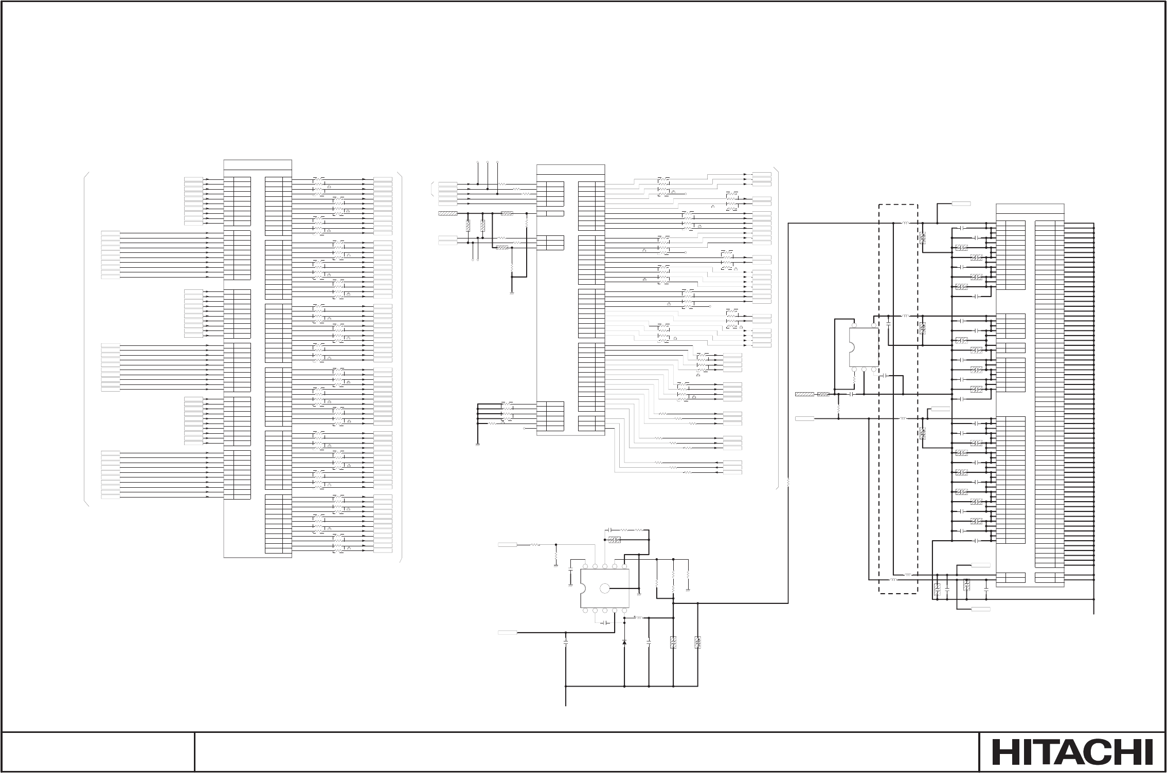
A5
A6
B6
B5
A4
C5
B3
A3
C4
B4
F3
C3
D3
G3
C2
B2
G2
F2
E2
D2
P3
L3
M3
R3
M2
L2
T2
R2
P2
N2
D1
E1
F1
U2
V2
G1
H1
C1
C6
E3
N3
N22
AB20
AB10
U3
V3
W3M19
N1
U1
M1
L1
K1
P1
T1
R1
W2
V1
W1
T3
B8
A8
CXD3540GB 2/3
CXD3540GB 1/3
N20
N21
P20
P21
P22
R20
R21
R22
T20
T21
T22
U22
U20
U21
V20
V21
V22
W20
W21
W22
Y20
Y21
Y22
AA21
AA16
Y17
AB16
AA17
Y18
AB17
AA18
Y19
AB18
AA19
AB19
AA20
AA12
Y13
AB12
AA13
Y14
AB13
AA14
Y15
AB14
AA15
Y16
AB15
Y6
AA6
AB6
Y7
AA7
AB7
Y8
AA8
AB8
Y9
AA9
AB9
Y1
Y2
AA2
Y3
AA3
AB3
Y4
AA4
AB4
Y5
AA5
AB5
C9
B9
A9
C10
B10
A10
C11
B11
A11
C12
B12
A12
C13
B13
A13
C14
B14
A14
C15
B15
A15
C16
B16
A16
C17
B17
A17
C18
B18
A18
C19
B19
A19
D20
C20
B20
A20
C21
B21
C22
G21
G22
F20
F21
F22
E20
E21
E22
D21
D22
K20
K21
K22
J20
J21
J22
H20
H21
H22
G20
CXD3540GB 3/3
A1
A2
A7
A21
A22
B1
B7
B22
C7
C8
H2
H3
J1
J2
J3
J10
J11
J12
J13
J14
K2
K3
K9
K10
K11
K12
K13
K14
K19
L9
L10
L11
L12
L13
L14
L20
L21
L22
M9
M10
M11
M12
M13
M14
M20
M21
M22
N9
N10
N11
N12
N13
N14
P9
P10
P11
P12
P13
P14
Y10
Y11
Y12
AA1
AA10
AA11
AA22
AB1
AB2
AB11
AB21
AB22
L4
N4M4
K4
W17
W16
W14
W13
W10
W9
W6
U19
U4
T19
T4
P19
P4
N19
J19
H19
G4
F19
F4
D17
D16
D14
D13
D10
D9
D6
W19
V19
R19
L19
G19
E19
D19
W18
D18
W5
V4
J4
E4
D5
W15
W12
W11
W8
W7
W4
R4
H4
D15
D12
D11
D8
D7
D4
4
5
3
2
1
G1
65
7
8
9
10
4
3
2
1
0V
DGO6
C404
1005
1000p
12
GND1
DCK3_R
C424
1005
1000p
12
GCFB_B
DRE4
C414
1005
1000p
12
R437
2010
56
56
12
34
78
DBO7
1005
R429
0
12
C401
2125
10/6.3
1
2
HCK2_G
GD2-9
BD2-7
GD1-7
C447
1.0/10
1
2
C403
1005
0.1/10
12
CH410
1
DRE1
C421
2125
10/6.3
1
2
I2CCLKP
DRE7
VCK_R
CHSTR
1
DGO7
DGE5
DCK3_B
GD1-3
DBE1
DBE6
R411
2010
22
34
12
56
78
DBE9
R436
2010
56
78
56
34
12
1005
R4A2
56
12
DBE2
DBO3
RD2-9
DRO9
DGO9
CLR
DCK4_B
C407
1005
0.1/10
12
1005
R444
56
12
GD2-11
C434
47/6.3
MVK/SKV
1
2
GD2-2
GD1-5
I401
CXD3540AGB
A8 HDIN
B8 VDIN
T3 CLK
W1 XCLR
V1 XPLLSTB
W2 CTRL
R1 HSCL
T1 HSDA
P1 HSEL
K1 TEST1
L1 TEST2
M1 TEST3
U1 TEST4
N1 TRST
M19 NC W3
GCFB_B
V3
GCFB_G
U3
GCFB_R
AB10
CLKOUT3
AB20
CLKOUT2
N22
CLKOUT1
N3
PRG_B
E3
PRG_G
C6
PRG_R
C1
VD
H1
FRP
G1
XSCAN
V2
SCAN
U2
DWN
F1
CLR
E1
PCG
D1
ENB
N2
DCK1_B
P2
DCK2_B
R2
DCK3_B
T2
DCK4_B
L2
HCK1_B
M2
HCK2_B
R3
PST_B
M3
VCK_B
L3
VST_B
P3
HST_B
D2
DCK1_G
E2
DCK2_G
F2
DCK3_G
G2
DCK4_G
B2
HCK1_G
C2
HCK2_G
G3
PST_G
D3
VCK_G
C3
VST_G
F3
HST_G
B4
DCK1_R
C4
DCK2_R
A3
DCK3_R
B3
DCK4_R
C5
HCK1_R
A4
HCK2_R
B5
PST_R
B6
VCK_R
A6
VST_R
A5
HST_R
DGO8
BD1-11
GD2-4
BD1-2
DVS
2518
L402
10
12
1005
R4A1
56
12
HCK1_B
C443
2125
10/6.3
1
2
R428
2010
0
12
34
56
78
RD2-8
DGO0
RD1-3
HCK1_R
R404
2010
22
78
56
34
12
DRO5
DGO1
R417
2010
10
78
56
34
12
RD1-10
GD2-0
C406
2125
10/6.3
1
2
RD2-0
R407
2010
22
34
78
12
56
R431
2010
56
12
78
56
34
1608
L404
600
1
2
BD2-6
C402
1005
1000p
12
1005
R422
01
2
R418
2010
10
78
56
34
12
RD1-7
DGO3
DRE2
DRE9
GD1-4
BD2-10
GND1
FRP
GCFB_G
BD2-5
GD2-6
1005
R446
33
12
R414
2010
10
12
34
56
78
RD2-6
R405
2010
22
78
56
34
12
DBE3
R412
2010
22
12
56
78
34
C415
1005
0.1/10
12
1005
R426
0
12
DRO7
1005
R430
1.0k
12
DRO1
2518
L401
2.2
12
1608
L405
600
1
2
DBE0
DRO2
C432
1005
0.1/10
12
BD1-5
C423
1005
0.1/10
12
RD1-11
SHCLK_B
GD2-8
BD1-0
DBO8
GD2-3
R435
2010
56
12
34
56
78
DBO5
DRO3
R406
2010
22
78
56
34
12
BD1-4
BD1-8
1005
R443
56
12
RD2-7
R432
2010
56
12
34
56
78
R438
2010
56
12
34
56
78
DBO2
RD2-1
GD1-1
C409
47/6.3
MVK/SKV
1
2
RD1-4
DBO6
DRE6
C416
2125
10/6.3
1
2
1005
R427
10k
12
RD2-3
CH414
1
DRE5
GD1-6
C418
1005
0.1/10
12
CH412
1
GD2-5
I401
CXD3540AGB
G20 R1IN9
H22 R1IN8
H21 R1IN7
H20 R1IN6
J22 R1IN5
J21 R1IN4
J20 R1IN3
K22 R1IN2
K21 R1IN1
K20 R1IN0
D22 R2IN9
D21 R2IN8
E22 R2IN7
E21 R2IN6
E20 R2IN5
N21
R1OUT10
N20
R1OUT11
F20 R2IN2
G22 R2IN1
G21 R2IN0
C22 G1IN9
B21 G1IN8
C21 G1IN7
A20 G1IN6
B20 G1IN5
C20 G1IN4
D20 G1IN3
A19 G1IN2
B19 G1IN1
C19 G1IN0
A18 G2IN9
B18 G2IN8
C18 G2IN7
A17 G2IN6
B17 G2IN5
C17 G2IN4
A16 G2IN3
B16 G2IN2
C16 G2IN1
A15 G2IN0
B15 B1IN9
C15 B1IN8
A14 B1IN7
B14 B1IN6
C14 B1IN5
A13 B1IN4
B13 B1IN3
C13 B1IN2
A12 B1IN1
B12 B1IN0
C12 B2IN9
A11 B2IN8
B11 B2IN7
C11 B2IN6
A10 B2IN5
B10 B2IN4
C10 B2IN3
A9 B2IN2
B9 B2IN1
C9 B2IN0
AB5
B2OUT0
AA5
B2OUT1
Y5
B2OUT2
AB4
B2OUT3
AA4
B2OUT4
Y4
B2OUT5
AB3
B2OUT6
AA3
B2OUT7
Y3
B2OUT8
AA2
B2OUT9
Y2
B2OUT10
Y1
B2OUT11
AB9
B1OUT0
AA9
B1OUT1
Y9
B1OUT2
AB8
B1OUT3
AA8
B1OUT4
Y8
B1OUT5
AB7
B1OUT6
AA7
B1OUT7
Y7
B1OUT8
AB6
B1OUT9
AA6
B1OUT10
Y6
B1OUT11
AB15
G2OUT0
Y16
G2OUT1
AA15
G2OUT2
AB14
G2OUT3
Y15
G2OUT4
AA14
G2OUT5
AB13
G2OUT6
Y14
G2OUT7
AA13
G2OUT8
AB12
G2OUT9
Y13
G2OUT10
AA12
G2OUT11
AA20
G1OUT0
AB19
G1OUT1
AA19
G1OUT2
AB18
G1OUT3
Y19
G1OUT4
AA18
G1OUT5
AB17
G1OUT6
Y18
G1OUT7
AA17
G1OUT8
AB16
G1OUT9
Y17
G1OUT10
AA16
G1OUT11
AA21
R2OUT0
Y22
R2OUT1
Y21
R2OUT2
Y20
R2OUT3
W22
R2OUT4
W21
R2OUT5
W20
R2OUT6
V22
R2OUT7
V21
R2OUT8
V20
R2OUT9
U21
R2OUT10
U20
R2OUT11
U22
R1OUT0
T22
R1OUT1
T21
R1OUT2
T20
R1OUT3
R22
R1OUT4
R21
R1OUT5
R20
R1OUT6
P22
R1OUT7
P21
R1OUT8
P20
R1OUT9
F22 R2IN4
F21 R2IN3
RD1-6
C430
1005
0.1/10
12
DGE7
GD1-9
RD1-5
R402
2010
22
78
56
34
12
C431
1005
1000p
12
DBE8
RD2-11
DRO8
BD2-2
ENB
VD
DCLK
RD1-1
DBE7
C433
2125
10/6.3
1
2
BD2-8
RESETX
1005
R4C2
56
12
GD1-11
C429
1005
1000p
12
GD2-7
BD2-3
C427
1005
1000p
12
R413
2010
10
12
34
56
78
1005
R424
33
12
R441
2010
56
12
56
34
78
I401
CXD3540AGB
D4
VDDI-D4
D7
VDDI-D7
D8
VDDI-D8
D11
VDDI-D11
D12
VDDI-D12
D15
VDDI-D15
H4
VDDI-H4
R4
VDDI-R4
W4
VDDI-W4
W7
VDDI-W7
W8
VDDI-W8
W11
VDDI-W11
W12
VDDI-W12
W15
VDDI-W15
D5
VDE2-D5
E4
VDE2-E4
J4
VDE2-J4
V4
VDE2-V4
W5
VDE2-W5
D18
VDE2-D18
W18
VDE2-W18
D19
VDE2-D19
E19
VDE2-E19
G19
VDE2-G19
L19
VDE2-L19
R19
VDE2-R19
V19
VDE2-V19
W19
VDE2-W19
D6
VDE3-D6
D9
VDE3-D9
D10
VDE3-D10
D13
VDE3-D13
D14
VDE3-D14
D16
VDE3-D16
D17
VDE3-D17
F4
VDE3-F4
F19
VDE3-F19
G4
VDE3-G4
H19
VDE3-H19
J19
VDE3-J19
N19
VDE3-N19
P4
VDE3-P4
P19
VDE3-P19
T4
VDE3-T4
T19
VDE3-T19
U4
VDE3-U4
U19
VDE3-U19
W6
VDE3-W6
W9
VDE3-W9
W10
VDE3-W10
W13
VDE3-W13
W14
VDE3-W14
W16
VDE3-W16
W17
VDE3-W17
K4
VDDA1
M4
VDDA3
N4
VSSA3
L4
VSSA1
AB22
VSS-AB22
AB21
VSS-AB21
AB11
VSS-AB11
AB2
VSS-AB2
AB1
VSS-AB1
AA22
VSS-AA22
AA11
VSS-AA11
AA10
VSS-AA10
AA1
VSS-AA1
Y12
VSS-Y12
Y11
VSS-Y11
Y10
VSS-Y10
P14
VSS-P14
P13
VSS-P13
P12
VSS-P12
P11
VSS-P11
P10
VSS-P10
P9
VSS-P9
N14
VSS-N14
N13
VSS-N13
N12
VSS-N12
N11
VSS-N11
N10
VSS-N10
N9
VSS-N9
M22
VSS-M22
M21
VSS-M21
M20
VSS-M20
M14
VSS-M14
M13
VSS-M13
M12
VSS-M12
M11
VSS-M11
M10
VSS-M10
M9
VSS-M9
L22
VSS-L22
L21
VSS-L21
L20
VSS-L20
L14
VSS-L14
L13
VSS-L13
L12
VSS-L12
L11
VSS-L11
L10
VSS-L10
L9
VSS-L9
K19
VSS-K19
K14
VSS-K14
K13
VSS-K13
K12
VSS-K12
K11
VSS-K11
K10
VSS-K10
K9
VSS-K9
K3
VSS-K3
K2
VSS-K2
J14
VSS-J14
J13
VSS-J13
J12
VSS-J12
J11
VSS-J11
J10
VSS-J10
J3
VSS-J3
J2
VSS-J2
J1
VSS-J1
H3
VSS-H3
H2
VSS-H2
C8
VSS-C8
C7
VSS-C7
B22
VSS-B22
B7
VSS-B7
B1
VSS-B1
A22
VSS-A22
A21
VSS-A21
A7
VSS-A7
A2
VSS-A2
A1
VSS-A1
DCK3_G
RD1-8
DGE0
PRG_B
C419
1.0/10
1
2
C449
1005
1000p
12
GND1
DBO9
+3.3VP
BD2-9
SHCLK_R
HST_B
HST_G
C426
2125
10/6.3
1
2
BD1-9
BD2-1
CHSTG
1
C417
1005
1000p
12
DGO4
VST_G
DRO6
BD1-6
DGO2
C444
1.0/10
1
2
VST_B
DCK1_B
DCK4_R
C412
1005
1000p
12
R409
2010
22
78
34
56
12
VCK_B
1005
R4C1
56
12
DRE0
DRO4
DGE8
DGE3
C428
1005
0.1/10
12
1005
R448
33
12
R433
2010
56
12
34
56
78
R439
2010
56
78
56
34
12
DCK2_R
DGE6
R408
2010
22
34
56
12
78
C441
2125
10/6.3
1
2
RD2-2
C405
1005
0.1/10
12
C420
47/6.3
MVK/SKV
1
2
GD1-10
DGE2
1005
R447
33
12
DCK2_B
RD2-4
R401
2010
22
78
34
56
12
DCK4_G
1005
R445
56
12
RD1-9
RESETP
I2CDATP
1005
R425
10k
12
C411
2125
10/6.3
1
2
HCK2_B
C422
1005
1000p
12
VST_R
CH413
1
DCK1_G
PCG
RD1-2
HCK1_G
BD2-0
HST_R
GCFB_R
+4.0V
BD2-4
RD1-0
BD1-7
DCK2_G
R403
2010
22
78
56
34
12
DBO1
RD2-10
SCAN
PRG_G
DBO0
DBE5
1005
R4A3
56
12
CHSTB
1
R416
2010
10
34
56
12
78
DHS
GD1-0
VCK_G
HCK2_R
DGE4
R440
2010
56
78
56
34
12
2518
L403
10
12
PRG_R
R410
2010
22
12
56
34
78
C408
1.0/10
1
2
GD1-8
GD2-10
BD1-3
DRE3
BD1-10
DBO4
DRE8
CH415
1
SHCLK_G
1005
R421
56
12
1005
R420
1.0k
12
DGE9
CH4NC
1
GD1-2
RD2-5
DGO5
C413
1005
0.1/10
12
R415
2010
10
12
34
56
78
1005
R423
33
12
GD2-1
XSCAN
DBE4
DRO0
C425
1005
0.1/10
12
DCK1_R
DWN
1005
R449
1.0k
12
BD2-11
DGE1
BD1-1
R434
2010
56
78
12
34
56
C442
1.0/10 1
2
GND1
1005
R4B1
0
12
1005
R4B3
0
12
1005
R450
0
12
C448
1.0/10
12
I402
TK11125CSC
Vcont
GND
Np Vout
Vin
+3.3VP
+1.8VP2
+1.8VP3
+3.3VP2
+3.3VP3
C488
0.01
12
1005
R4C5
10k-1%
12
1005
R4C0
10k
12
POWER8
1005
R4C6
10k-1%
12
C4A4
1000p
12
4.7
L481
7E06NG
4.7
12
C4A6
2125
22/6.3
12
C4A1
2125
10/10
12
GND1
I403
MP2361DQ-LF-Z
NC-1
BS
NC-3
IN
SW GND
FB
COMP
EN
SS
1005
R4C4
100
12
1005
R4C8
10k-1%
12
1005
R4C7
3.6k-1%
12
GND1
+6.6V
C4A7
47/6.3
MVK/SKV
1
2
C4A2
0.01
12
1005
R4C3
18k-1%
12
GND1
C4A3
0.01
12
D4A1
RSX201L-30
12
1005
R4C9
18k-1%
12
C4A5
2125
22/6.3
12
GND1
PW TWOWSD0
controlled by POWER6
TG(Master) Part
for 0.79" SXGA
to S/H partfrom PW
PW TWOWSC0
PW PORTA5
to S/H part
PW PORTA7
from PW
JUMPER R
from I802
TG(slave),R/B_S/H,R/B_Panel
G_S/H,G_Panel
Fixed 1.4MHz SW Freq. 1.8V-VP2
SM0321 PWB ASSEMBLY MAIN 5
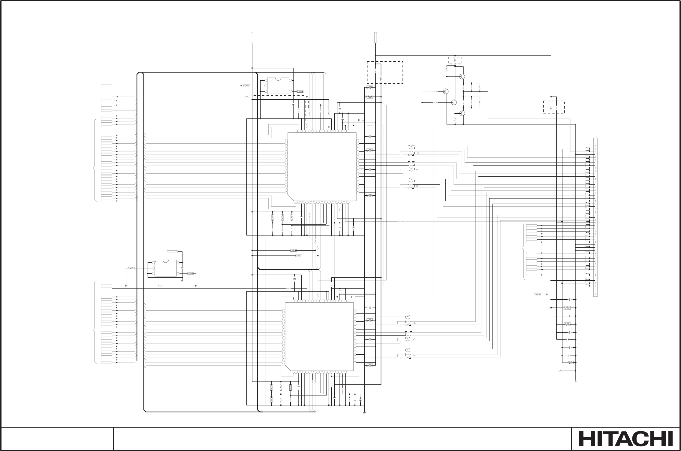
4
5
3
2
1
4
5
3
2
1
65
64
63
62
44 43 42 41
26
25
24
23
22
21
61
60 55 575859 54 56 53
40
39
38
37
36
35
34
33
32
31
30
29
28
2774
79
76
78
75
80
77
13 20 1714 1916 1815364119725 121081
52
73
72
71
70
69
68
67
66
51 50 49 48 47 46 45
65
64
63
62
44 43 42 41
26
25
24
23
22
21
61
60 55 575859 54 56 53
40
39
38
37
36
35
34
33
32
31
30
29
28
2774
79
76
78
75
80
77
13 20 1714 1916 1815364119725 121081
52
73
72
71
70
69
68
67
66
51 50 49 48 47 46 45
RD4-2
RD1-11 RD1-11
RD4-0
RD4-11
RD3-4
RD1-4
RD2-10
RD3-11
RD4-7
VDDMNT
RD1-3
GCFB_R
RD3-0
RD2-3
RD2-8
RD2-0
FRP SCAN
RESETSH
RD3-10
I2CDATP
RD3-1
VDDMNT
I2CCLKP
RESETSH
RD4-3
SCAN
RD3-9
RD4-11
FRP
RD1-7
RD1-2
RD1-8
RD1-0
RD4-10
RD2-2
RD2-9
RD1-5
RD1-4
RD1-0
RD3-8
RD4-10
RD1-1
RD4-9
RD1-10
RD2-6
VDDMNT
I2CCLKP
RD2-11
RD3-6
RESETSH
RD3-7
RD4-9
RD1-7
RD3-2
SCAN
RD3-6
RD4-8
I2CDATP
RD4-1
RD4-5
RD3-5
RD4-7
RD1-9
RD3-7
RD2-5
RD2-4
PRG_R
RD3-4
RD4-6
RD3-3
RD3-8
RD3-3
GCFB_R
RD4-5
RD4-0
RD3-5
RD1-5
PRG_R
RD3-2
I2CDATP
RD4-4
RD3-11
RD1-1
RD1-2
VD
FRP
RD4-4
RD2-7
RD3-1
RD4-3
RD2-1
I2CCLKP
RD4-6
RD1-3
RD3-0
RD4-2
RD3-10
VD
RD1-6 RD1-6
RD4-8
RD1-8
RD1-10
RD4-1
RD3-9
VD
RD1-9
RD2-11
RD2-10
RD2-9
RD2-8
RD2-7
RD2-6
RD2-5
RD2-4
RD2-3
RD2-2
RD2-1
RD2-0
APR44 1
VD
APR54 1
2518
L502
22
1
2
APR05 1
1005
R541
1.0k
12
1005
R521
4.7k
12
C569
0.1/25
12
RD4-1
C511
470p
12
1005
R526
10
1
2
APR28 1
1005
R594
0
12
RD1-9
RD1-5
1005
R528
4.7k
12
1005
R545
0
12
C508
0.1/25
12
C506
0.1/25
12
1005
R539
0
12
APR22 1
1005
R535
6.8
12
1005
R5620
12
APR18 1
C559
3225
10/25
12
RD2-1
RD2-8
C551
10/16
MVK/SKV
12
C515
0.1/25
1
2
Q531
2SA1577
1
2
3
GND1
HCK2_R
RD4-3
RD1-6
APR30 1
C507
0.1/25
1
2
1005
R525
1.0k
1
2
APR11 1
APR26 1
HCK1_R
RD1-8
1005
R515
0
21
RD2-6
Q533
2SC5734
1
2
3
CLR
APR35 1
1005
R587
4.7k
12
APR38 1
RD4-7
I2CDATP
RD2-5
C568
0.1/25
1
2
APR31 1
R563
2010
10
12
34
56
78
C571
470p
1
2
APR20 1
RD1-4
GND1
1005
R546
56
1
2
1005
R581
4.7k
12
RD2-11
DCK1_R
APR17 1
1005
R593
100
12
RD1-0
GND1
APR16 1
APR09 1
RD3-7
RD4-10
RD1-1
VST_R
RD1-11
1005
R561 0
12
+15.5V
RD4-9
C560
3225
10/25
12
C516
10/16
MVK/SKV
1
2
SCAN
RD3-1
1005
R544
0
12
APR13 1
C521
10/16
MVK/SKV
1
2
APR50 1
Q532
2SC5734
1
2
3
APR37 1
1005
R536
6.8
12
1005
R507
0
12
APR23 1
RD2-4
1005
R523
4.7k
12
1005
R595
56
12
RD2-10
APR19 1
APR48 1
R565
2010
10
12
34
56
78
DWN
APR27 1
1005
R522
4.7k
12
APR53 1
C556
100/16
MVK/SKV
12
1005
R584
4.7k
1
2
RD3-5
ENB
C566
0.1/25
12
RD2-2
1005
R501
0
1
2
C504
0.1/25
12
PCG
1005
R542
1.0k
12
C502
0.47/10
12
RD3-9
APR12 1
R503
2010
10
12
34
56
78
C555
0.1/25
1
2
1005
R583
4.7k
12
DCK4_R
APR21 1
C592
1005
0.1/10
12
C501
1.0/10
12
RD4-8
FRP
SCAN
RD3-6
RD1-2
1005
R517 10k
12
APR47 1
C553
10/16
MVK/SKV
12
APR33 1
RD2-7
P501
FF22D-57HUp
1
2
3
4
5
6
7
8
9
10
11
12
13
14
15
16
17
18
19
20
21
22
23
24
25
26
27
28
29
30
31
32
33
34
35
36
37
38
39
40
41
42
43
44
45
46
47
48
49
50
51
52
53
54
55
56
57
I2CCLKP
SHCLK_R
C509
0.1/25
12
1005
R502
0
1
2
2518
L551
10
12
1005
R513
0
12
RD4-4
1005
R524
4.7k
12
C561
1.0/10
12
APR14 1
RD4-2
2518
L501
22
1
2
1005
R540
0
12
1005
R599
0
12
GCFB_R
C554
0.1/25
12
1005
R543
100
12
C567
0.1/25
12
DCK2_R
1005
R533
3.3k
12
1005
R511
0
12
VDDMNT
C565
0.1/25
12
+3.3VP
RD1-3
1005
R589
4.7k
1
2
RD3-2
APR46 1
APR34 1
APR24 1
C562
0.47/10
12
RD3-8
RD4-0
C503
0.1/25
12
APR32 1
APR40 1
SHCLK2_R
C505
0.1/25
12
2518
L563
22
1
2
RD3-10
1005
R537
3.3k
12
R505
2010
10
12
34
56
78
I562
TC7SG125FU
G
IN_A
GND OUT_Y
VCC
I502
TC7SG125FU
G
IN_A
GND OUT_Y
VCC
R504
2010
10
12
34
56
78
APR15 1
1005
R512
0
12
C510
1005
0.1/10
12
APR52 1
RD4-5
APR08 1
RD1-10
RD3-3
1005
R527
4.7k
12
RESETSH
R564
2010
10
12
34
56
78
RD3-11
I501
CXA7009R
DB_IN1
DB_IN0
VDD-3
DGND-4
DGND-5
RET
DIRC
SCL
SDA
XCLR
ADDR0
ADDR1
ADDR2
AGND-14
REF_IN
VCC-16
REF_OUT
AGND-18
VCOM_OUT
PGND-20
PVCC-21
SIG_OUT12
SIG_OUT11
PGND-24
SIG_OUT10
SIG_OUT9
PVCC-27
SIG_OUT8
SIG_OUT7
PGND-30
SIG_OUT6
SIG_OUT5
PVCC-33
SIG_OUT4
SIG_OUT3
PGND-36
SIG_OUT2
SIG_OUT1
PVCC-39
SID_OUT
PGND-41
CAL_OUT
PVCC-43
CAL_IN
VCC-45
AGND-46
DGND-47
GCFB_I
GCFB_O
VDDMNT
SHT_I
SHT_O
FRP
VD
PRG
CLK
VDD-57
DGND-58
DA_IN11
DA_IN10
DA_IN9
DA_IN8
DA_IN7
DA_IN6
DA_IN5
DA_IN4
DA_IN3
DA_IN2
DA_IN1
DA_IN0
DB_IN11
DB_IN10
DB_IN9
DB_IN8
DB_IN7
DB_IN6
DB_IN5
DB_IN4
DB_IN3
DB_IN2
PRG2_R
C522
10/16
MVK/SKV
1
2
APR45 1
RD2-0
APR04 1
APR36 1
RD4-6
APR07 1
HST_R
C558
3225
10/25
12
APR29 1
Q534
2SA1577
1
2
3
APR10 1
RD2-3
C564
0.1/25
12
DCK3_R
1005
R506
3.0k-1%
12
RD1-7
1005
R586
10
12
C563
0.1/25
12
2518
L552
10
12
RD4-11
1005
R531
10
12
RD3-4
PRG_R
C557
1005
0.1/10
12
I561
CXA7009R
DB_IN1
DB_IN0
VDD-3
DGND-4
DGND-5
RET
DIRC
SCL
SDA
XCLR
ADDR0
ADDR1
ADDR2
AGND-14
REF_IN
VCC-16
REF_OUT
AGND-18
VCOM_OUT
PGND-20
PVCC-21
SIG_OUT12
SIG_OUT11
PGND-24
SIG_OUT10
SIG_OUT9
PVCC-27
SIG_OUT8
SIG_OUT7
PGND-30
SIG_OUT6
SIG_OUT5
PVCC-33
SIG_OUT4
SIG_OUT3
PGND-36
SIG_OUT2
SIG_OUT1
PVCC-39
SID_OUT
PGND-41
CAL_OUT
PVCC-43
CAL_IN
VCC-45
AGND-46
DGND-47
GCFB_I
GCFB_O
VDDMNT
SHT_I
SHT_O
FRP
VD
PRG
CLK
VDD-57
DGND-58
DA_IN11
DA_IN10
DA_IN9
DA_IN8
DA_IN7
DA_IN6
DA_IN5
DA_IN4
DA_IN3
DA_IN2
DA_IN1
DA_IN0
DB_IN11
DB_IN10
DB_IN9
DB_IN8
DB_IN7
DB_IN6
DB_IN5
DB_IN4
DB_IN3
DB_IN2
RD2-9
+3.3VP
APR25 1
VCK_R
C552
0.1/25
12
C591
1005
0.1/10
12
1005
R532
10
12
1005
R582
4.7k
1
2
RD3-0
APR42 1
1005
R534
6.8
12
1005
R571
6.8
12
1005
R538
6.8
12
1005
R572
6.8
12
R Panel Part
for 0.79" SXGA+
JUMPER R
PW PORTA6
PSIG
TG
PW TWOWSC0
from master TG
PW TWOWSD0
N.C.
from I801
from TG part
TG
from I802
V.COMR
JUMPER R
JUMPER R
PW PORTC1
controlled by POWER7
from slave TG
controlled by POWER6
N.C.
N.C.
VID2
VID13
VID10
VID1
VID11
VID19
VID12
VSSGR
VID3
VID17
VID18
VID14
VID6
VID9
VID21
VID16
VID7
VID20
VID4
VID15
VID8
VID5
/DCLK2
HVDD
VCK
PCG
VID23
VID24
DWN
RGT
VID22
HST
HCK
VVSS
CLR
DCLK1
VST
VSSGL
/HCK
DCLK2
HVSS
ENB
/DCLK1
GCFB
N.C.
N.C.
V.COML
VVDD
TEST
N.C.
N.C.
N.C.
SM0321 PWB ASSEMBLY MAIN 6
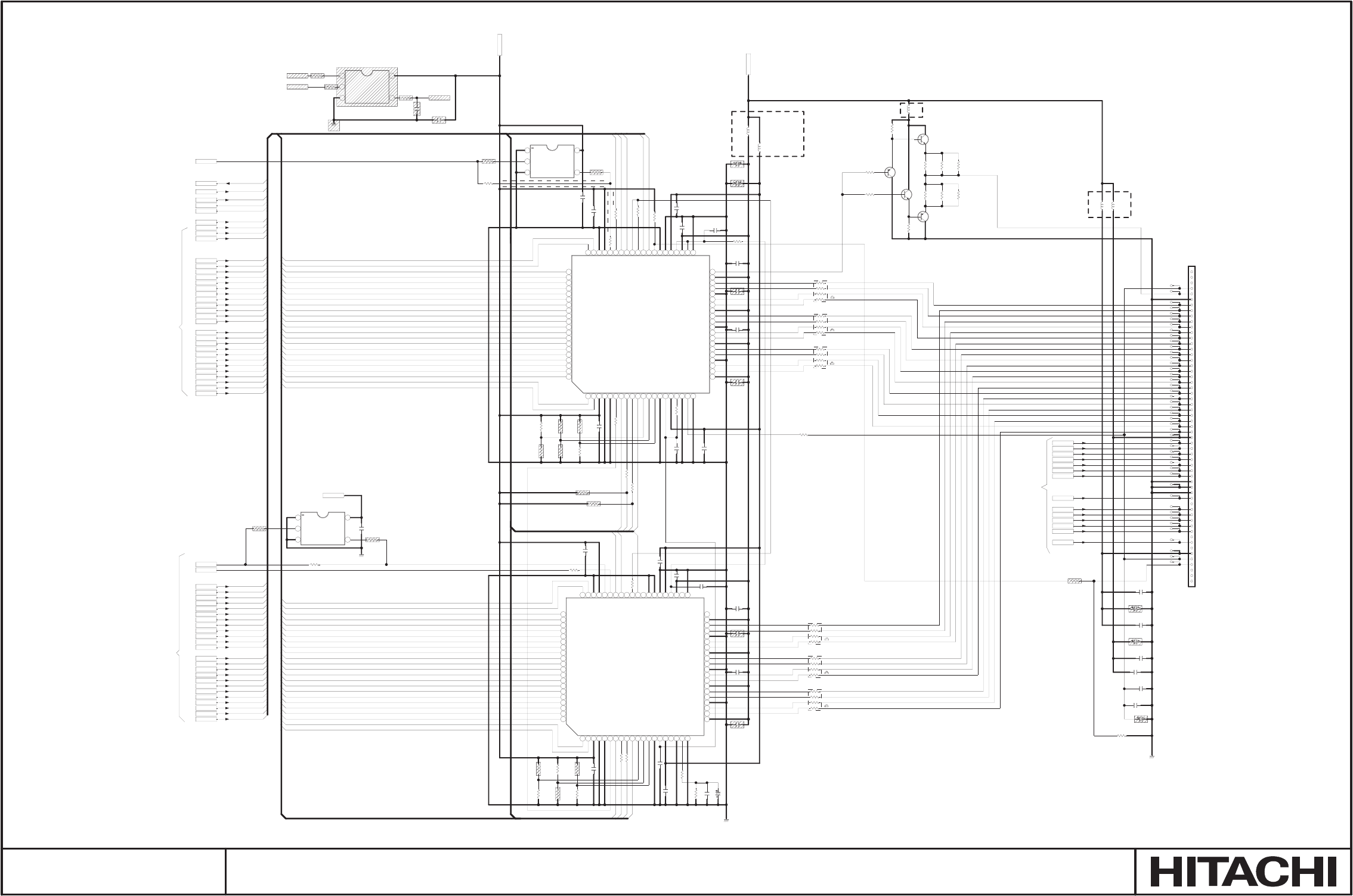
65
64
63
62
44 43 42 41
26
25
24
23
22
21
61
60 55 575859 54 56 53
40
39
38
37
36
35
34
33
32
31
30
29
28
2774
79
76
78
75
80
77
13 20 1714 1916 1815364119725 121081
52
73
72
71
70
69
68
67
66
51 50 49 48 47 46 45
65
64
63
62
44 43 42 41
26
25
24
23
22
21
61
60 55 575859 54 56 53
40
39
38
37
36
35
34
33
32
31
30
29
28
2774
79
76
78
75
80
77
13 20 1714 1916 1815364119725 121081
52
73
72
71
70
69
68
67
66
51 50 49 48 47 46 45
4
5
3
2
1
4
5
3
2
1
4
5
3
2
1
XSCAN
GD1-11
GD4-5
GD3-8
GD4-10
GD3-10
GD4-4
GD1-8
GD3-2
GD1-10
GD4-8
GD4-8
GD3-4
GD4-5
GD4-6
GD3-3
VD
GD4-1
I2CDATP
GD1-10
XSCAN
GD3-7
I2CCLKP
GD2-4
GD2-5
FRP
GD4-1
RESETSH
GD1-3
GD4-0
VD
GD2-2
PRG_G
VD
GD1-1
GD1-7
GD4-7
GD3-5
GD4-9
VDDMNT
GD1-6
I2CCLKP
GD3-6
RESETSH
I2CDATP
GD3-0
GD3-9
GD4-11
GD3-11
GD1-1
GD3-7
GD1-9
GD2-6
GD1-11
GD2-10
GD2-7
GD3-11
RESETSH
VDDMNT
FRP
GD1-8
GD1-5
GD3-1
GD2-3
GD2-1
GD4-6
GD1-2
GD4-4
GD4-0 GD4-2
GD1-3
GD1-4
GD4-3
GCFB_G
GD1-0
GD3-0
PRG_G
GD3-6
GD2-8
GD4-7
GD3-4
GD1-4
FRP
GD3-5
VDDMNT
GD4-3
GD4-9
GD3-8
GD1-2
GD3-1
GD1-6
I2CCLKP
GD1-5
GD1-0
GD4-2
GD1-7
GD3-10
GD3-9
GD2-11
GCFB_G
I2CDATP
GD2-9
GD4-11
GD4-10
GD2-0
GD3-3
XSCAN
GD3-2
GD1-9
GD2-11
GD2-10
GD2-9
GD2-8
GD2-7
GD2-6
GD2-5
GD2-4
GD2-3
GD2-2
GD2-1
GD2-0
APG12 1GD2-11
1005
R639
0
12
APG33 1
C609
0.1/25
12
2518
L652
10
12
DCK3_G
Q633
2SC5734
1
2
3
GD1-4
GD3-1
APG45 1
PCG
C663
0.1/25
12
FRP_COM
Q631
2SA1577
1
2
3
C611
470p
12
APG46 1
PRG_G
1005
R684
4.7k
12
1005
R637
3.3k
12
APG24 1
C657
1005
0.1/10
12
GD2-1
APG29 1
APG27 1
APG04 1
2518
L601
22
1
2
GD3-4
GD3-11
C691
1005
0.1/10
12
C694
1005
0.1/10
12
GD4-5
GD1-2
1005
R661 0
12
1005
R681
4.7k
12
C671
470p
1
2
1005
R695
56
12
GD4-2
APG28 1
Q632
2SC5734
1
2
3
APG18 1
+3.3VP
C693
1005
1.0/6.3
12
GD3-0
GD2-6
1005
R690
18k
1
2
1005
R607
0
12
APG23 1
APG53 1
1005
R643
100
12
GD1-1
GD1-9
1005
R645
0
12
HCK1_G
APG22 1
FRP
R664
2010
10
12
34
56
78
1005
R641
1.0k
12
GD4-8
GD1-11
APG37 1
C655
0.1/25
1
2
1005
R621
4.7k
12
APG08 1
APG17 1
DCK2_G
APG31 1
C659
3225
10/25
12
APG35 1
GD2-5
1005
R617
10k
12
GD1-0
I661
CXA7009R
DB_IN1
DB_IN0
VDD-3
DGND-4
DGND-5
RET
DIRC
SCL
SDA
XCLR
ADDR0
ADDR1
ADDR2
AGND-14
REF_IN
VCC-16
REF_OUT
AGND-18
VCOM_OUT
PGND-20
PVCC-21
SIG_OUT12
SIG_OUT11
PGND-24
SIG_OUT10
SIG_OUT9
PVCC-27
SIG_OUT8
SIG_OUT7
PGND-30
SIG_OUT6
SIG_OUT5
PVCC-33
SIG_OUT4
SIG_OUT3
PGND-36
SIG_OUT2
SIG_OUT1
PVCC-39
SID_OUT
PGND-41
CAL_OUT
PVCC-43
CAL_IN
VCC-45
AGND-46
DGND-47
GCFB_I
GCFB_O
VDDMNT
SHT_I
SHT_O
FRP
VD
PRG
CLK
VDD-57
DGND-58
DA_IN11
DA_IN10
DA_IN9
DA_IN8
DA_IN7
DA_IN6
DA_IN5
DA_IN4
DA_IN3
DA_IN2
DA_IN1
DA_IN0
DB_IN11
DB_IN10
DB_IN9
DB_IN8
DB_IN7
DB_IN6
DB_IN5
DB_IN4
DB_IN3
DB_IN2
APG32 1
GD3-6
GD4-0
APG54 1
Q634
2SA1577
1
2
3
GD2-2
VD
APG15 1
GD2-7
1005
R687
4.7k
12
GD4-10
1005
R640
0
12
1005
R601
0
1
2
2518
L663
22
1
2
HCK2_G
GND1
I601
CXA7009R
DB_IN1
DB_IN0
VDD-3
DGND-4
DGND-5
RET
DIRC
SCL
SDA
XCLR
ADDR0
ADDR1
ADDR2
AGND-14
REF_IN
VCC-16
REF_OUT
AGND-18
VCOM_OUT
PGND-20
PVCC-21
SIG_OUT12
SIG_OUT11
PGND-24
SIG_OUT10
SIG_OUT9
PVCC-27
SIG_OUT8
SIG_OUT7
PGND-30
SIG_OUT6
SIG_OUT5
PVCC-33
SIG_OUT4
SIG_OUT3
PGND-36
SIG_OUT2
SIG_OUT1
PVCC-39
SID_OUT
PGND-41
CAL_OUT
PVCC-43
CAL_IN
VCC-45
AGND-46
DGND-47
GCFB_I
GCFB_O
VDDMNT
SHT_I
SHT_O
FRP
VD
PRG
CLK
VDD-57
DGND-58
DA_IN11
DA_IN10
DA_IN9
DA_IN8
DA_IN7
DA_IN6
DA_IN5
DA_IN4
DA_IN3
DA_IN2
DA_IN1
DA_IN0
DB_IN11
DB_IN10
DB_IN9
DB_IN8
DB_IN7
DB_IN6
DB_IN5
DB_IN4
DB_IN3
DB_IN2
GD3-3
1005
R689
4.7k
12
C661
1.0/10
12
C692
1005
0.1/10
12
1005
R699
0
12
APG13 1
GND1
APG47 1
GD2-8
C622
10/16
MVK/SKV
1
2
GD3-5
APG16 1
1005
R662 0
12
APG09 1
APG11 1
VCK_G
C666
0.1/25
12
APG20 1
1005
R636
6.8
12
APG38 1
APG21 1
GD1-7
APG34 1
1005
R627
4.7k
12
GD4-9
HST_G
DWN
GD2-3
R604
2010
10
12
34
56
78
XSCAN
GD2-10
C656
100/16
MVK/SKV
12
R663
2010
10
12
34
56
78
1005
R626
10
12
C654
0.1/25
12
C664
0.1/25
12
GD1-3
APG19 1
GD4-6
1005
R622
4.7k
12
1005
R631
10
12
C603
0.1/25
12
+3.3VP
1005
R642
1.0k
12
APG10 1
R603
2010
10
12
34
56
78
1005
R615
0
12
1005
R606
3.0k-1%
12
GD2-9 APG14 1
APG36 1
I662
TC7SG125FU
G
IN_A
GND OUT_Y
VCC
DCK4_G
C607
0.1/25
12
C660
3225
10/25
12
APG25 1
APG40 1
1005
R683
4.7k
12
APG44 1
GD4-3
GD4-4
1005
R686
10
12
I2CDATP
1005
R602
0
12
XSCAN
GD1-5
GND1
C606
0.1/25
12
GD2-0
C669
0.1/25
12
C602
0.47/10
12
APG48 1
C605
0.1/25
12
C610
1005
0.1/10
12
R605
2010
10
12
34
56
78
2518
L602
22
1
2
ENB
VST_G
1005
R612
0
1
2
C615
0.1/25
1
2
GD1-6
C653
10/16
MVK/SKV
12
GD2-4
APG07 1
APG42 1
I691
TC7SZ86FU
IN_B
IN_A
GND OUT_Y
VCC
+15.5V
XSCAN
1005
R694
0
12
SHCLK2_G
C616
10/16
MVK/SKV
1
2
C601
1.0/10
12
C668
0.1/25
12
VDDMNT
1005
R613
0
1
2
1005
R682
4.7k
12
CLR
GD3-8
C651
10/16
MVK/SKV
12
P601
FF22D-57HUp
1
2
3
4
5
6
7
8
9
10
11
12
13
14
15
16
17
18
19
20
21
22
23
24
25
26
27
28
29
30
31
32
33
34
35
36
37
38
39
40
41
42
43
44
45
46
47
48
49
50
51
52
53
54
55
56
57
SHCLK_G
FRP
C665
0.1/25
12
GND1
APG30 1
C604
0.1/25
12
1005
R691
0
1
2
R665
2010
10
12
34
56
78
GD4-11
1005
R628
4.7k
12
GD3-10
GD4-1
C658
3225
10/25
12
1005
R632
10
12
C662
0.47/10
12
GD1-10
1005
R633
3.3k
12
APG05 1
DCK1_G
C608
0.1/25
12
2518
L651
10
12
1005
R644
0
12
C652
0.1/25
12
GD3-2
GD3-9
RESETSH
1005
R611
0
12
1005
R624
4.7k
12
GD3-7
GD1-8
1005
R692
0
1
2
1005
R646
56
1
2
GD4-7
I2CCLKP
1005
R635
6.8
12
1005
R625
1.0k
1
2
APG52 1
1005
R623
4.7k
12
GCFB_G
1005
R693
100
12
APG26 1
APG50 1
PRG2_G
C621
10/16
MVK/SKV
1
2
I602
TC7SG125FU
G
IN_A
GND OUT_Y
VCC
C667
0.1/25
12
1005
R671
6.8
12
1005
R638
6.8
12
1005
R634
6.8
12
1005
R672
6.8
12
PW TWOWSC0
PW TWOWSD0
from I801
from master TG
PW PORTA6
TG
controlled by POWER7
TG
JUMPER R
JUMPER R
from slave TG
from I802
controlled by POWER6
N.C.
PW PORTC1
JUMPER R
from TG part
G Panel Part
for 0.79" SXGA+
N.C.
N.C.
N.C.
VID2
RGT
VID22
VID13
VID10
HST
VID1
VID11
HCK
VVSS
VID19
VSSGR
VID17
VID12
VID3
VID18
VID14
VID6
VID9
VID21
VID8
VID5
PSIG
HVSS
/DCLK2
HVDD
VCK
ENB
/DCLK1
VID16
VID7
VID20
VID4
VID15
N.C.
N.C.
PCG
VID23
V.COML
CLR
VID24
DCLK1
DWN
VST
VVDD
VSSGL
GCFB
/HCK
N.C.
TEST
N.C.
V.COMR
DCLK2
SM0321 PWB ASSEMBLY MAIN 7
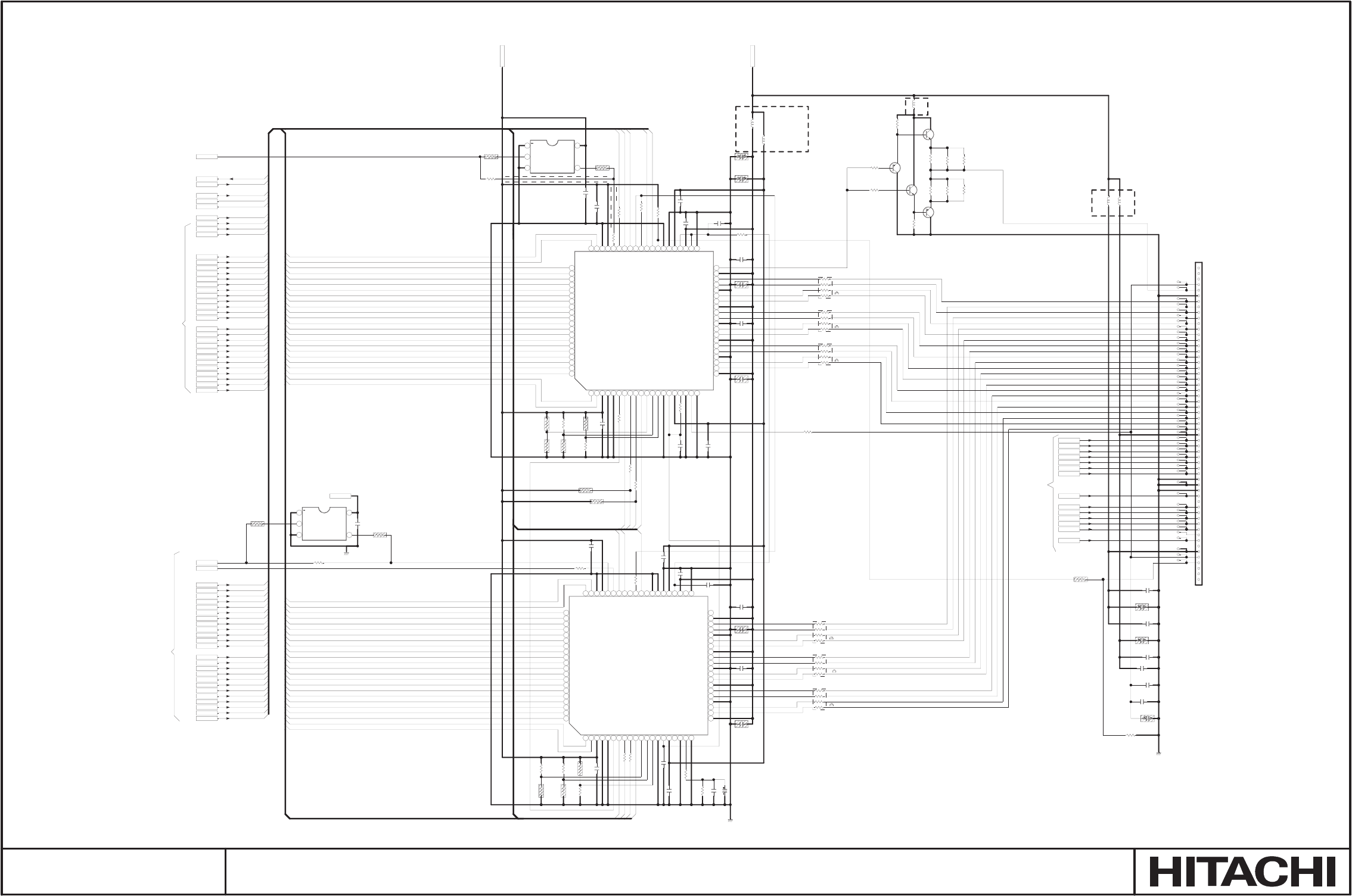
65
64
63
62
44 43 42 41
26
25
24
23
22
21
61
60 55 575859 54 56 53
40
39
38
37
36
35
34
33
32
31
30
29
28
2774
79
76
78
75
80
77
13 20 1714 1916 1815364119725 121081
52
73
72
71
70
69
68
67
66
51 50 49 48 47 46 45
4
5
3
2
1
4
5
3
2
1
65
64
63
62
44 43 42 41
26
25
24
23
22
21
61
60 55 575859 54 56 53
40
39
38
37
36
35
34
33
32
31
30
29
28
2774
79
76
78
75
80
77
13 20 1714 1916 1815364119725 121081
52
73
72
71
70
69
68
67
66
51 50 49 48 47 46 45
SCAN
I2CCLKP
BD4-10
BD1-11
BD2-1
BD3-9
BD4-7
BD4-1
I2CCLKP
FRP
BD3-0
BD2-2
BD1-6
BD4-6
BD3-11
BD4-8
BD1-0
BD3-8
I2CCLKP
BD4-7
I2CDATP
BD4-8
BD3-5
BD4-0
SCAN VD
VDDMNT
BD1-4
BD1-8
BD2-7
RESETSH
I2CDATP
PRG_B
GCFB_B
BD4-2
GCFB_B
BD4-5
BD1-9
FRP
BD2-8
BD3-10
BD1-10BD1-10
VDDMNT
RESETSH
BD2-4
BD2-11
BD4-11
BD3-3
FRP
BD1-3
BD4-3
BD2-5
VD
BD1-1
BD2-0
BD4-9
BD1-3
BD1-1
BD3-1
BD4-0
BD3-2
RESETSH
BD4-4
BD4-10
BD4-9
SCAN
BD3-6
BD4-11
BD1-9
BD1-0
VD
BD2-9
BD3-4
BD1-2
BD1-7
BD4-4
PRG_B
BD1-7
BD2-10
BD4-2
BD1-8
VDDMNT
BD1-2
BD4-6
I2CDATP
BD1-6
BD4-5
BD1-5
BD2-6
BD3-7
BD4-1
BD2-3
BD1-4
BD1-5
BD4-3
BD1-11
BD2-11
BD2-10
BD2-9
BD2-8
BD2-7
BD2-6
BD2-5
BD2-4
BD2-2
BD2-1
BD2-0
BD2-3
BD3-11
BD3-10
BD3-9
BD3-8
BD3-7
BD3-6
BD3-5
BD3-4
BD3-3
BD3-2
BD3-1
BD3-0
I701
CXA7009R
DB_IN1
DB_IN0
VDD-3
DGND-4
DGND-5
RET
DIRC
SCL
SDA
XCLR
ADDR0
ADDR1
ADDR2
AGND-14
REF_IN
VCC-16
REF_OUT
AGND-18
VCOM_OUT
PGND-20
PVCC-21
SIG_OUT12
SIG_OUT11
PGND-24
SIG_OUT10
SIG_OUT9
PVCC-27
SIG_OUT8
SIG_OUT7
PGND-30
SIG_OUT6
SIG_OUT5
PVCC-33
SIG_OUT4
SIG_OUT3
PGND-36
SIG_OUT2
SIG_OUT1
PVCC-39
SID_OUT
PGND-41
CAL_OUT
PVCC-43
CAL_IN
VCC-45
AGND-46
DGND-47
GCFB_I
GCFB_O
VDDMNT
SHT_I
SHT_O
FRP
VD
PRG
CLK
VDD-57
DGND-58
DA_IN11
DA_IN10
DA_IN9
DA_IN8
DA_IN7
DA_IN6
DA_IN5
DA_IN4
DA_IN3
DA_IN2
DA_IN1
DA_IN0
DB_IN11
DB_IN10
DB_IN9
DB_IN8
DB_IN7
DB_IN6
DB_IN5
DB_IN4
DB_IN3
DB_IN2
APB16 1
APB35 1
DWN
BD4-3
BD2-6
R705
2010
10
12
34
56
78
APB26 1
APB33 1
BD1-5
BD1-7
APB25 1
BD2-2
HCK1_B
1005
R728
4.7k
1
2
APB49 1
APB50 1
SHCLK_B
BD4-8
1005
R723
4.7k
12
C708
0.1/25
12
1005
R784
4.7k
12
BD2-8
APB28 1
APB07 1
1005
R725
1.0k
1
2
2518
L701
22
1
2
BD1-4
APB47 1
1005
R733
3.3k
12
C701
1.0/10
12
C765
0.1/25
12
RESETSH
+15.5V
FRP
C752
0.1/25
12
1005
R781
4.7k
12
1005
R741
1.0k
12
BD3-6
CLR
VDDMNT
BD2-11
C707
0.1/25
12
2518
L752
10
12
Q731
2SA1577
1
2
3
C704
0.1/25
12
C766
0.1/25
12
C759
3225
10/25
12
I2CCLKP
1005
R782
4.7k
12
C716
10/16
MVK/SKV
1
2
SCAN
R764
2010
10
12
34
56
78
1005
R712
0
1
2
BD2-4
APB53 1
1005
R794
0
12
APB30 1
Q734
2SA1577
1
2
3
BD4-0
BD4-7
BD2-10
1005
R793
100
12
PRG2_B
APB18 1
C767
0.1/25
12
BD3-7
BD1-0
APB29 1
BD4-1
C761
1.0/10
12
1005
R783
4.7k
12
APB24 1
BD3-10
APB17 1
APB37 1
1005
R707
0
12
1005
R745
0
12
C764
0.1/25
12
BD4-9
APB20 1
1005
R726
10
1
2
BD1-2
C755
0.1/25
1
2
BD2-1
1005
R722
4.7k
1
2
1005
R762 0
12
2518
L763
22
1
2
1005
R713
0
1
2
APB31 1
APB23 1
APB14 1
1005
R761 0
12
1005
R789
4.7k
12
APB34 1
BD2-3
APB44 1
APB52 1
BD3-0
GND1
APB40 1
R703
2010
10
12
34
56
78
BD3-3
C757
1005
0.1/10
12
PRG_B
1005
R735
6.8
12
1005
R787
4.7k
12
C703
0.1/25
1
2
1005
R742
1.0k
12
C791
1005
0.1/10
12
APB36 1
2518
L702
22
1
2
1005
R724
4.7k
1
2
APB15 1
BD4-5
BD4-11
DCK4_B
BD3-9
C792
1005
0.1/10
12
VD
R763
2010
10
12
34
56
78
BD2-7
BD1-11
BD1-8
C702
0.47/10
1
2
APB19 1
BD2-9
C710
1005
0.1/10
12
SCAN
APB22 1
APB10 1
BD4-4
SHCLK2_B
C768
0.1/25
12
DCK3_B
P701
FF22D-57HUp
1
2
3
4
5
6
7
8
9
10
11
12
13
14
15
16
17
18
19
20
21
22
23
24
25
26
27
28
29
30
31
32
33
34
35
36
37
38
39
40
41
42
43
44
45
46
47
48
49
50
51
52
53
54
55
56
57
Q732
2SC5734
1
2
3
1005
R721
4.7k
12
BD3-8
1005
R739
0
12
BD2-5
+3.3VP
APB27 1
DCK2_B
C715
0.1/25 1
2
1005
R711
0
12
I702
TC7SG125FU
G
IN_A
GND OUT_Y
VCC
GND1
BD1-10
1005
R740
0
12
C709
0.1/25
12
GND1
C754
0.1/25
12
1005
R715
0
12
C711
470p
12
1005
R736
6.8
12
BD2-0
C758
3225
10/25
12
C771
470p
12
1005
R799
0
12
1005
R786
10
12
1005
R732
10
12
1005
R717
10k
12
APB45 1
BD3-4
APB11 1
1005
R795
56
12
APB42 1
DCK1_B
1005
R727
4.7k
12
I2CDATP
BD3-1
I762
TC7SG125FU
G
IN_A
GND OUT_Y
VCC
APB21 1
APB13 1
C762
0.47/10
12
C753
10/16
MVK/SKV
12
APB46 1
BD4-10
BD3-2
1005
R701
0
1
2
C706
0.1/25
12
2518
L751
10
12
APB54 1
APB12 1
1005
R702
0
12
1005
R706
3.0k-1%
12
C763
0.1/25
12
C722
10/16
MVK/SKV 1
2
1005
R731
10
12
1005
R737
3.3k
12
BD4-6
BD1-3
VCK_B
C760
3225
10/25
12
PCG
APB38 1
APB09 1
1005
R744
0
12
BD3-5
GCFB_B
HCK2_B
ENB
C705
0.1/25
12
C756
100/16
MVK/SKV
12
BD3-11
I761
CXA7009R
DB_IN1
DB_IN0
VDD-3
DGND-4
DGND-5
RET
DIRC
SCL
SDA
XCLR
ADDR0
ADDR1
ADDR2
AGND-14
REF_IN
VCC-16
REF_OUT
AGND-18
VCOM_OUT
PGND-20
PVCC-21
SIG_OUT12
SIG_OUT11
PGND-24
SIG_OUT10
SIG_OUT9
PVCC-27
SIG_OUT8
SIG_OUT7
PGND-30
SIG_OUT6
SIG_OUT5
PVCC-33
SIG_OUT4
SIG_OUT3
PGND-36
SIG_OUT2
SIG_OUT1
PVCC-39
SID_OUT
PGND-41
CAL_OUT
PVCC-43
CAL_IN
VCC-45
AGND-46
DGND-47
GCFB_I
GCFB_O
VDDMNT
SHT_I
SHT_O
FRP
VD
PRG
CLK
VDD-57
DGND-58
DA_IN11
DA_IN10
DA_IN9
DA_IN8
DA_IN7
DA_IN6
DA_IN5
DA_IN4
DA_IN3
DA_IN2
DA_IN1
DA_IN0
DB_IN11
DB_IN10
DB_IN9
DB_IN8
DB_IN7
DB_IN6
DB_IN5
DB_IN4
DB_IN3
DB_IN2
R765
2010
10
12
34
56
78
APB05 1
BD1-6
C721
10/16
MVK/SKV
1
2
C751
10/16
MVK/SKV
12
APB08 1
VST_B
APB32 1
R704
2010
10
12
34
56
78
BD4-2
BD1-9
Q733
2SC5734
1
2
3
1005
R743
100
12
1005
R746
56
1
2
BD1-1
C769
0.1/25
12
HST_B
+3.3VP
APB48 1
APB04 1
1005
R738
6.8
12
1005
R772
6.8
12
1005
R771
6.8
12
1005
R734
6.8
12
PW TWOWSD0
JUMPER R
from slave TG
B Panel Part
for 0.79" SXGA
JUMPER R
PW PORTA6
from I802
TG
PW TWOWSC0
controlled by POWER6
JUMPER R
PW PORTC1
from TG part
from I801
TG
controlled by POWER7
from master TG
VID11
VID7
/DCLK1
VID16
VID21
VID14
DCLK1
DWN
VID8
VID4
VID22
VST
/HCK
VVDD
N.C.
VVSS
VSSGR
VID15
HVSS
N.C.
HCK
ENB
VID13
HST
VSSGL
PSIG
GCFB
VCK
VID9
N.C.
N.C.
VID3
VID12
VID6
CLR
VID23
VID24
V.COML
VID20
N.C.
N.C.
HVDD
PCG
TEST
N.C.
RGT
VID10
VID19
VID1
V.COMR
VID18
DCLK2
VID2
VID17
/DCLK2
N.C.
VID5
SM0321 PWB ASSEMBLY MAIN 8
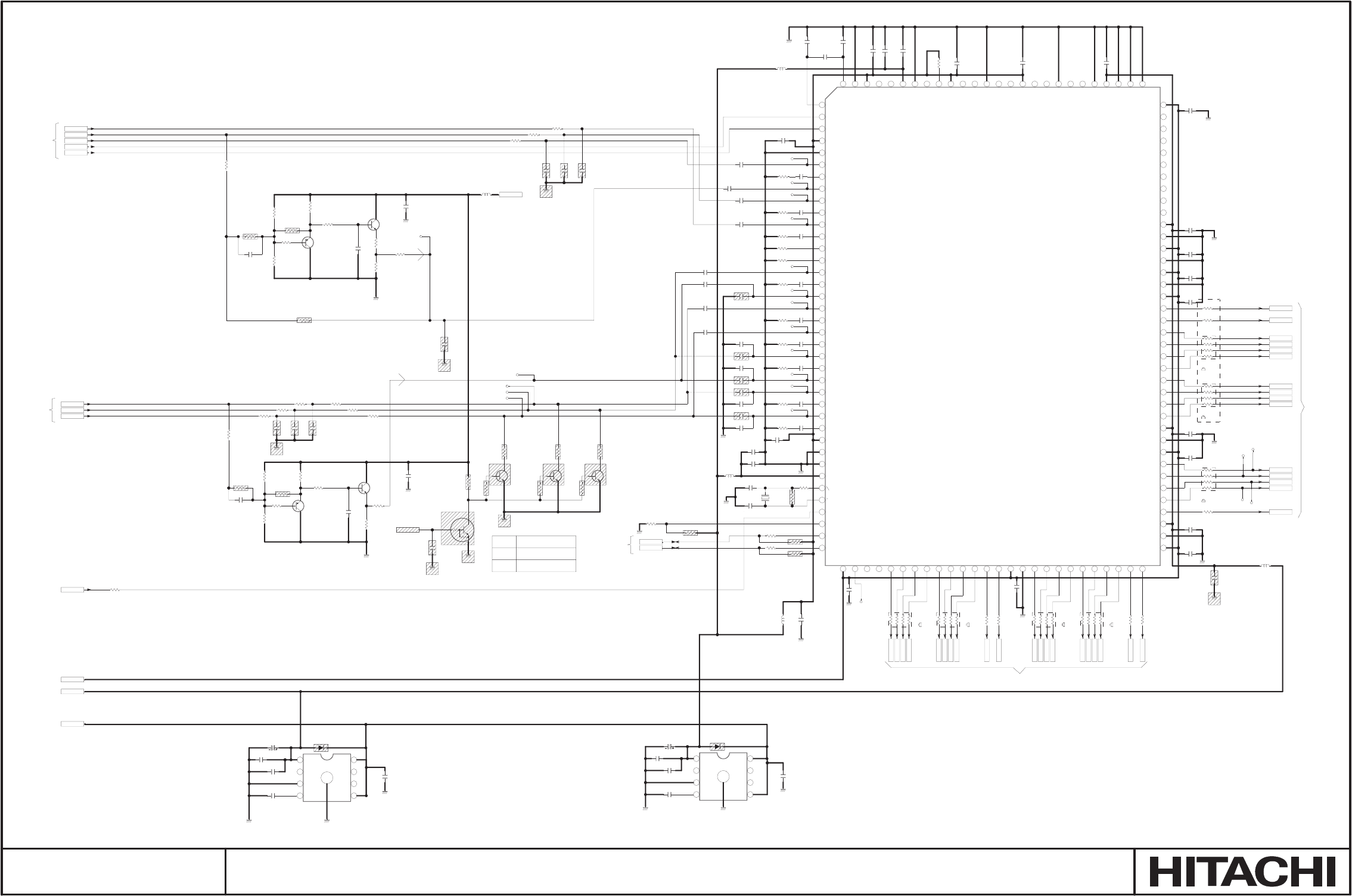
G1
5
6
7
8
4
3
2
1
128
73 69 6577 76 74 70 6671 677275 68
64
29 3830 3526 343127 3733 3628 32
102
103
97 9299101 949596 9198 93100 90
63
62
61
60
59
58
57
56
55
54
53
52
51
50
49
48
47
46
45
44
43
42
41
40
39
25
126
116
121
118
123
125
127
120
117
122
119
124
13 20 22 241714 19 21 2316 1815364119725 121081
89
115
114
113
112
111
110
109
108
107
106
105
104
88 87 86 85 84 83 82 81 80 79 78
G1
5
6
7
8
4
3
2
1
IN1B4
1005
R113
56
12
1005
R138
10k
12
C124
1005
0.1/10
1
2
IN1FLD
IN1R4
C150
2125
22/6.3
12
C109
1005
22p-C
12
56
1C
5001
01
/1.0
1
2
C141
1005
1000p
1
2
IN1R8
C135
1005
0.1/10
12
GND1
1005
R147
1.0M
12
C128
1005
0.1/10
12
1005
R106
2.2k
12
1005
R126
220
12
IN1R7
I2CDAT
C154
2125
10/6.3
12
1005
R141
390-1%
12
Q108
2SC4617
1
2
3
IN1G8
C147
1005
0.047/10
12
C133
1005
0.1/10
1
2
Q106
2SA1774
1
2
3
1005
R136 01
2
1005
R124
56
12
IN1HS
IN1R9
C125
1005
0.1/10
12
1005
R139
100
12
+5V
C149
2125
10/6.3
12
C110
1005
22p-C
12
IN1VS
IN1R6
IN1B6
GND1
C137
1005
0.1/10
12
1005
R116
0
12
IN1B2
IN1G9
IN1B5
CHINT
1
C129
1005
0.1/10
12
1005
R105
2.2k
12
2518
L102
2.2 1
2
IN1B3
1005
R157
0
12
C119
1005
0.1/10
12
IN1CLK
R102
2010
33 1
2
34
5
6
7
8
IN1B7
GND1
C167
1005
0.1/10
1
2
C155
2125
10/6.3
12
X101
14.31818MHz
SMD-49
1
2
1005
R110
0
12
Q110
2SC4617
1
2
3
1005
R144
4.7k 1
2
C134
1005
0.1/10
1
2
IN1AHS
C166
1005
0.1/10
1
2
1005
R115
0
12
C126
1005
0.1/10
12
Q103
2SA1774
1
2
3
1005
R140
100
12
IN1G2
2518
L103
4.7 1
2
2125
R107
0
1
2
1005
R127
0
1
2
C112
2125
22/6.3
1
2
C138
1005
0.1/10
12
GND1
C130
1005
0.1/10
1
2
MUTE_COMP_ADC
IN1G3
1005
R104
2.2k
1
2
1005
R158
0
12
1005
R128
470
1
2
C120
1005
0.1/10
12
C148
1005
0.1/10
1
2
1005
R156
100
1
2
GND1
IN1G4
I2CCLK
R101
2010
33 1
2
34
5
6
7
8
1005
R145
4.7k
1
2
1005
R155
1.0k 12
C136
1005
0.1/10
12
2518
L104
4.7
12
Q109
2SC4617
1
2
3
1005
R137
33
12
C121
1005
0.1/10
12
GND1
GND1
C114
1005
22p-C
12
2125
R159
0
1
2
C152
1005
0.047/10
1
2
IN1G5
C116
18p-C
12
GND1
L105
4.7 1
2
Q107
DTC114EE
1
2
3
Q105
2SC4617
1
2
3
C104
1005
22p-C
12
C131
1005
0.1/10
1
2
1005
R154
220
12
IN1B9
C122
1005
0.1/10
1
2
Q102
2SC4617
1
2
3
IN1R2
*C139
1005
1000p
1
2
IN1G6
C108
1005
22p-C
12
GND1
+4.0V
IN1B8
C123
1005
0.1/10
1
2
GND1
1005
R146
1.5k
1
2
IN1R3
C127
1005
0.1/10
12
2125
R160
0
12
IN1G7
C142
1005
0.047/10
1
2
GND1
C153
1005
0.1/10
12
C143
12
IN1R5
C102
2125
22/6.3
1
2
1005
R121
0
12
C132
1005
0.1/10
1
2
*C163
1005
0.047/10
12
*C164
1005
0.047/10
12
*C162
1005
0.047/10
1
2
*C158
1005
1000p
1
2
GND1
GND1
MUX1OUT_B
MUX1OUT_H
MUX1OUT_R
MUX1OUT_G
MUX1OUT_V
3RCA2_R
3RCA2_B
3RCA2_G
C101
1005
0.047/10
1
2
1005
R162
68
12
1005
R163
68
12
C105
1005
0.047/10
1
2
1005
R164
68
12 C106
1005
0.047/10
1
2
1005
R165
68
12
C107
1005
0.047/10
1
2
1005
R166
68
12
C115
1005
0.047/10
1
2
1005
R167
68
12
C117
1005
0.047/10
1
2
1005
R168
68
12
C118
1005
0.047/10
1
2
1005
R169
68
12
C144
1005
0.047/10
1
2
1005
R170
68
12
C145
1005
0.047/10
1
2
GND1
2518
L101
4.7
12
C172
100/6.3
MVK/SKV
1
2
I103
MM1663DHBE
Vout
NC-2
GND
Cn Cont
NC-6
NC-7
Vin
C156
1.0/10
1
2
C173
2125
1.0/10
12
GND1
GND1GND1
C157
1005
470p
12
C171
0.33/10
12
D101
SFPB-66
12
GND1
CPU-RESET
1005
R148
390
12
R153
2010
33
1
2
34
5
6
7
8
GND1
GND1
GND1
GND1
CHGI0 1
CHRI0
1
CHBI1
1
CHGI1 1
CHRI1
1
CHGI2
1
CHRI2
1
CHSG0
1
CHSG0C 1
CHBI0 1
CHGI1C 1
CHBI1C 1
CHRI1C 1
CHBI2
1
CHSG1C 1
CHSG1
1
R103
2010
33 1
2
34
5
6
7
8
R131
2010
33 1
2
34
5
6
7
8
R143
2010
33
1
2
3
4
5
6
7
8
R142
2010
33
1
2
34
5
6
7
8
CHSG2
1
*C174
1005
0.047/10
12
*C175
1005
1000p
12
GND1
*C179
1005
0.047/10
12
*C178
1005
0.047/10
12
*C180
1005
1000p
12
*C181
1005
0.047/10
12
*C177
1005
0.047/10
12
*C176
1005
0.047/10
12
GND1
GND1
C185
1005
33p-C
12
*I101
MST3566M
VREFN
HSYNC0
VSYNC0
AVDD_ADC-4
GND-5
BIN0P
BIN0N
SOGIN0
GIN0P
GIN0N
RIN0P
RIN0N
HSYNC1
VSYNC1
BIN1P
BIN1N
SOGIN1
GIN1P
GIN1N
RIN1P
RIN1N
NC-22
NC-23
NC-24
NC-25
NC-26
NC-27
NC-28
AVDD_ADC-29
GND-30
GND-31
AVDD_MPLL
XOUT
XIN
HWRESET
A0
SCL
SDA
VDDP-39
INT
NC-44
NC-42
DATA[29]
DATA[28]
DATA[27]
DATA[26]
DATA[25]
DATA[24]
DATA[23]
DATA[22]
DATA[21]
DATA[20]
VDDP-53
GND-54
DATA[19]
DATA[18]
DATA[17]
DATA[16]
DATA[15]
DATA[14]
DATA[13]
DATA[12]
DATA[11]
DATA[10]
VDDP-65
GND-66
VDDC-67
DATACK
SOGOUT
HSOUT
VSOUT
FIELD/GPO
VDDP-73
GND-74
VDDC-75
DATA[9]
DATA[8]
DATA[7]
DATA[6]
DATA[5]
DATA[4]
DATA[3]
DATA[2]
DATA[1]
DATA[0]
VDDP-86
GND-87
VDDP-88
GND-89
VDDP-90
GND-91
VDDC-92
NC-93
NC-94
NC-95
NC-96
NC-97
NC-98
NC-99
NC-100
NC-101
VDDP-102
GND-103
GND-104
GND-105
VDDC-106
GND-107
NC-108
NC-109
GND-110
NC-111
NC-112
AVDD_ADC-113
NC-114
NC-115
GND-116
NC-117
NC-118
AVDD_ADC-119
REXT
NC-121
GND-122
AVDD_PLL
NC-124
NC-125
AVDD_ADC-126
GND-127
VREFP
1005
R172
33
12
1005
R171
33
12
IN1R1
IN1R0
1005
R174
33
12
IN1G0
IN1G1
1005
R173
33
12
1005
R175
33
12
1005
R176
33
12
IN1B0
IN1B1
GND1GND1
C160
1005
470p
12
C188
2125
1.0/10
12
I102
MM1662FHBE
Vout
NC-2
GND
Cn Cont
NC-6
NC-7
Vin
C161
0.33/10
12
C187
47/6.3
MVK/SKV
1
2
C159
1.0/10
1
2
D102
SFPB-66
12
GND1
ADD2.5V
ADD3.3V
1005
R177
10k
12
1005
R178
10k
12
CHVSO
1
CHAHS
1
CHFLD
1
CHHSO
1
1005
R161
2.2k
12
1005
R111
100k
12
1005
R112
68k
12
1005
R114
3.3k
12
1005
R117
270
12
1005
R125
3.3k
12
1005
R122
100k
12
1005
R123
68k
12
1005
R108
2.2k
12
C182
1005
22p-C
12
C184
1005
22p-C
12
C183
1005
18p-C
12
1005
R152
0
121005
R151
0
12
1005
R150
0
12
1005
R118
10
12
1005
R119
10
12
1005
R120
10
12
1005
R132
0
12
1005
R133
0
12
1005
R134
0
12
SOY
SOG
1
MUTE_COMP_ADC
MUTE ON
MUTE OFF
0
DE/
I2C SLAVE ADDR.
9Ch
A/D Convertor
3.3V/1A/1800mW
Sheet1 PW288B INPUT PORT 1
Sheet1 PW288B INPUT PORT 1
Sheet16 Analog MUX
Sheet16 Analog MUX
from Sheet3
Sheet1
PW288B MISC
/BIN2P
/BIN2N
/SOGIN2
/GIN2P
/GIN2N
/RIN2P
/RIN2N
2.5V/1A/1800mW
SM0321 PWB ASSEMBLY MAIN 9
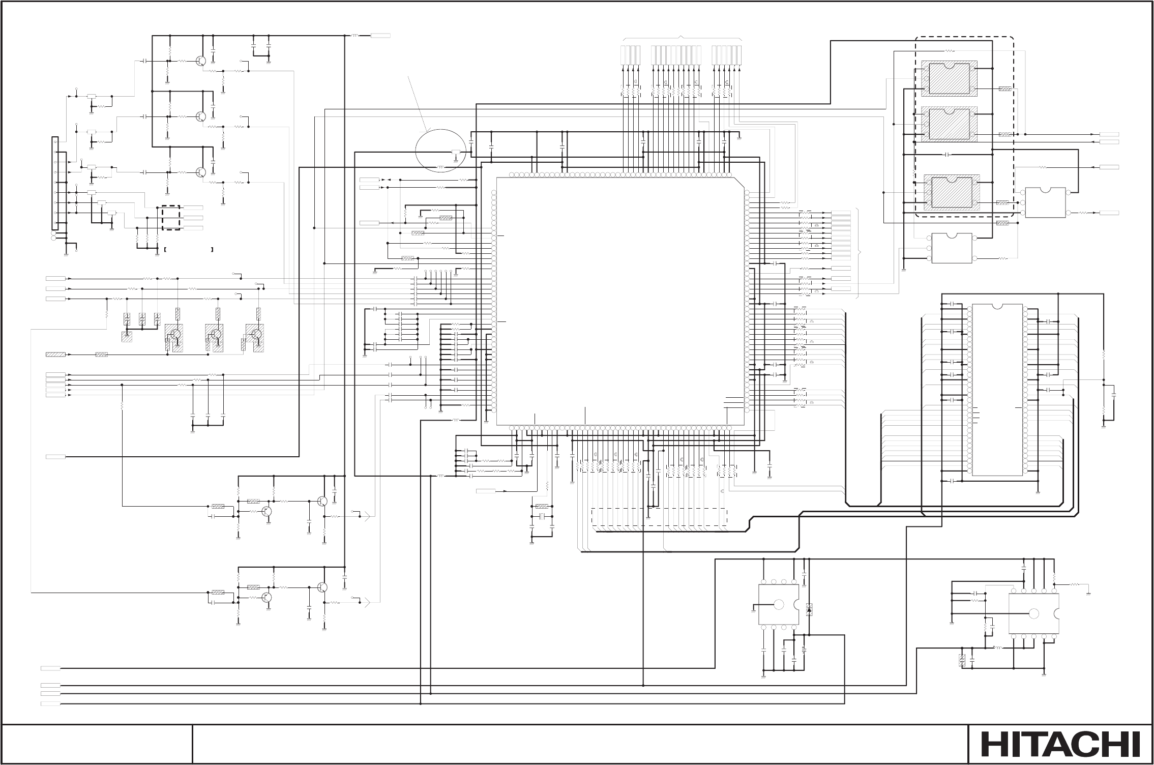
G1
5
6
7
8
4
3
2
1
137
135
133
136
140
139
134
138
131125 132
129128127126 130
86
81
82
85
83
88
84
87
43 3944 41 3842 40 37
143
147
146
144
150
145
148
149
141
142
151
120115114 119117116 123121 122 124118
77
75
79
70
72
74
76
78
80
71
73
30 2833 2627323536 293134
113
152
108103 110 11 2105 106 107102 109104 1 11101
69
68
67
66
65
64
63
62
61
60
59
58
57
56
55
54
53
52
51
50
49
48
47
46
45
25
175
165
170
167
172
174
176
169
166
171
168
173
13
20
2224 17 14
19
2123 16
18 15 36411 9 7 2512 10 8 1
100
164
163
162
161
160
159
158
157
156
155
154
153
99
98979695949392919089
4
5
3
2
1
4
5
3
2
1
4
5
3
2
1
4
5
3
2
1
4
5
3
2
1
65
66
33
61
34
35
36
37
38
39
40
41
42
43
44
45
46
47
48
49
50
51
52
53
54
55
56
57
58
59
60
62
63
64
32
31
30
29
28
27
26
25
24
23
22
21
20
19
18
17
16
15
14
13
12
11
10
9
8
7
6
5
4
3
2
1
G1
65
7
8
9
10
4
3
2
1
SDRLDQS
SDRCLKN
SDRDQ13
SDRA0
SDRCKE
SDRDQ9
SDRLDM
SDRCLK
SDRDQ14
SDRWE
SDRDQ10
SDRCLKN
SDRA8
SDRCKE
SDRUDM
SDRDQ12
SDRA9
SDRUDQS
SDRBA1
SDRA6
SDRDQ11
SDRDQ8
SDRBA0
SDRA6
SDRDQ4
SDRA9
SDRDQ7
SDRDQ15
SDRRAS SDRLDM
SDRA8
SDRDQ6
SDRA2
SDRDQ0
SDRLDQS
SDRCS
SDRDQ5
SDRDQ3
SDRA0
SDRA5
SDRDQ4
SDRBA0
SDRDQ5
SDRDQ3
SDRBA1
SDRA3
SDRA7
SDRDQ7
SDRDQ2
SDRA10
SDRDQ1
SDRA10
SDRDQ2
SDRDQ0
SDRA7
SDRDQ6
SDRA11
SDRA5
SDRA11
SDRDQ8
SDRA2
SDRDQ9
SDRA1
SDRDQ10
SDRVREF
SDRA1
SDRA4
SDRDQ11
SDRCAS
SDRDQ12
SDRA4
SDRUDM
SDRDQ13
SDRUDQS
SDRDQ14
SDRCS
SDRDQ15
SDRA3
SDRCLK
SDRRAS
SDRDQ1
SDRCAS
SDRWE
SDRVREF
CV47
1005
0.1/10
1
2
CV96
1005470p
12
CV14
1005
0.1/10
1
2
TVC-S
1
GND1
GND1
CV22 10050.01/16
1
2
1005
RV96
33
12
GND1
CV86
1005
0.1/10
1
2
1005
RV25
150-1%
12
CV49
1005
0.1/10
1
2
1005
RV24 2.7k-1%
12
GND1
3RCA1_B
CV04
1005
0.1/10
12
CV42
1005
0.1/10
1
2
1005
RV23
2.7k-1%
12
RV06
2010
33
7
8
56
3
4
1
2
CV29 10050.1/10
1
2
DV02
SFPB-66
12
RV13
2010
22
78
56
34
12
CV39
1005
0.1/10
1
2
2518
LV03
4.7
12
TVCb
1
TVGND
1
CV35 212510/10
1
2
CV54
0.082/16
1
2
GND1
CV07
1005
0.1/10
12
CV55
1005
0.01/16 1
2
CV18 10050.1/10
1
2
CV06
1005
0.1/10
12
CV98
100/6.3
MVK/SKV
1
2
CV17 1005330p
1
2
CV19 1005
0.1/10
1
2
CV30 10050.01/16
1
2
GND1
CV11
1005
0.1/10
1
2
CV89 1005
0.1/10
12
CV10
1005
0.1/10
1
2
CV23 2125
10/10
1
2
GND1
CV51
1005
0.1/10
1
2
CV12
1005
0.1/10
1
2
2125
LV06
SC200JT
123
RV11
2010
22
7
8
56
3
4
1
2
CV36 1005
0.1/10
1
2
IV06
MM1663DHBE
Vout
NC-2
GND
Cn Cont
NC-6
NC-7
Vin
2518
LV04
4.7
12
CV34 2125
10/10
1
2
2125
LV07
SC200JT
123
1005
RV21
1.0k-1%
12
CV93
9.0p-C1
2
IV02
ADV7802
P13
P12
P11
P10
P9
P8
P7
P6
P5
P4
P3
P2
P1
P0
DVDDIO-15
DGND-16
LLC
CS/HS_OUT
SFL/SYNC_OUT
FLD_DE_OUT
VS_OUT
DGND-22
DVDD-23
SDRAM_A11
SDRAM_A9
SDRAM_A8
SDRAM_A7
SDRAM_A6
SDRAM_A5
SDRAM_A4
SDRAM_A3
SDRAM_A2
SDRAM_A1
SDRAM_A0
DGND-35
DVDD-36
DVDDIO_SDRAM-37
DGND_SDRAM-38
SDRAM_A10
SDRAM_BA1
SDRAM_BA0
SDRAM_CS
SDRAM_RAS
SDRAM_CAS
SDRAM_WE
SDRAM_LDM
DVDDIO_SDRAM-47
DGND_SDRAM-48
SDRAM_LDQS
SDRAM_DQ7
SDRAM_DQ6
SDRAM_DQ5
SDRAM_DQ4
SDRAM_DQ3
SDRAM_DQ2
SDRAM_DQ1
SDRAM_DQ0
SDRAM_VREF
DGND-59
DVDD-60
DVDDIO_SDRAM-61
DGND_SDRAM-62
SDRAM_DQ15
SDRAM_DQ14
SDRAM_DQ13
SDRAM_DQ12
SDRAM_DQ11
SDRAM_DQ10
SDRAM_DQ9
SDRAM_DQ8
SDRAM_UDQS
SDRAM_UDM
SDRAM_CK
SDRAM_CK
SDRAM_CKE
DVDD-76
DGND-77
CLKIN
DVDDIO-79
XTAL
XTAL1
DGND-82
RESET
PVDD-84
AGND-85
ELPF1
PVDD-87
ELPF2
AGND-89
FB
SOY
SOG
AIN7
AIN1
AIN8
AIN2
AIN9
AIN3
AGND-99
AGND-100
AVDD-101
REFOUT
CML
AGND-104
AVDD-105
BIAS
CAPY1
CAPC1
CAPC2
AIN10
AIN4
AIN11
AIN5
AIN12
AIN6
AOUT
FUNCT1
HS_IN1
HS_IN2
ALSB
SDA
ACLK
INT
VS_IN2
VS_IN1
DE_IN
P53
P52
P51
P50
P49
P48
P47
P46
P45
P44
DVDD-137
DGND-138
P43
P42
P41
P40
DVDDIO-143
DGND-144
P39
P38
P37
P36
P35
P34
P33
P32
P31
P30
P29
P28
P27
P26
DVDD-159
DGND-160
P25
P24
P23
P22
P21
P20
P19
P18
P17
DVDDIO-170
DGND-171
P16
P15
P14
DVDD-175
DGND-176
GND1
TVC-Y
1
RV01
2010
33
78
56
34
12
RV18
2010
22
78
56
34
12
RV02
2010
33
78
56
34
12
CV56
2125
10/10
12
CV50
1005
0.1/10
1
2
RV17
2010
22
78
56
34
12
2125
LV09
SC200JT
123
CV21 10050.1/10
1
2
1005
RV97
470
12
1005
RV22
1.0k-1%
12
CV24
1005
0.1/10
1
2
CV44
1005
0.1/10
1
2
CV28 1005
0.1/10
1
2
CV41
1005
0.1/10
1
2
CV08
1005
0.1/10
12
2125
LV10
SC200JT
123
XV01
28.63636MHz
SMD-49
1
2
+5V
CV31 2125
10/10
1
2
GND1
RV07
2010
33
7
8
56
3
4
1
2
1005
RV99
1.5k 1
2
QV13
2SC4617
1
2
3
CV33
1005
0.1/10
1
2
CV26 1005
0.1/10
1
2
RV05
2010
33
7
8
56
3
4
1
2
CV13
1005
0.1/10
1
2
GND1
2125
LV08
SC200JT
123
RV10
2010
22
78
56
34
12
CV27 1005
0.1/10
1
2
CV48
1005
0.1/10
1
2
GND1
TVY
1
CV09
1005
0.1/10
12
RV15
2010
22
78
56
34
12
CV01
1005
0.1/10
12
1005
RV26
1.5k-1%
12
2518
LV02
4.7
12
CV99
2125
1.0/10
12
GND1
TVVBS
1
TVCr
1
GND1
CV25 1005
0.1/10
1
2
GND1
CV02
1005
0.1/10
12
GND1
GND1
RV12
2010
22
78
56
34
12
3RCA1_G
+4.0V
CV05
1005
0.1/10
12
CV88 1005
0.1/10
12
2125
LV11
SC200JT
123
EV01
ZH-09V
1
2
3
4
5
6
7
8
9
G1
G2
CV43
1005
0.1/10
1
2
CV53 0.039/16
1
2
CV16 1005
0.1/10
1
2
GND1
CV87
2125
10/10
12
CV91
1005
0.1/10
1
2
RV16
2010
22
78
56
34
12
CV03
1005
0.1/10
12
CV38 1005
0.1/10
1
2
GND1
CV94
1005
0.1/10
1
2
1005
RVA0
0
1
2
CV95
1.0/10
12
GND1
CV40
1005
0.1/10
1
2
RV08
2010
33
78
56
34
12
RV09
2010
22
78
56
34
12
CV97
0.33/10
12
CV45
1005
0.1/10
1
2
3RCA1_R
CV57
2125
10/10
12
CV20 1005
0.1/10
1
2
CV37 1005
0.1/10
1
2
1005
RV27
10k
12
RV14
2010
22
78
56
34
12
GND1
CV92
9.0p-C
1
2
CV90
1005
0.1/10
1
2
GND1
2518
LV05
47
12
CV32
1005
0.1/10
1
2
1005
RV19 100
12
CV46
1005
0.1/10
1
2
3RCA3_G
3RCA3_B
3RCA3_R
MUX2OUT_V
MUX2OUT_R
MUX2OUT_G
MUX2OUT_H
MUX2OUT_B
1005
RV56
470
12
GND1
1005
RV57
0
12
CV58
1005
0.1/10
1
2
QV01
2SC4617
1
2
3
GND1
GND1
CV59
1005
0.1/10
1
2
QV02
2SC4617
1
2
3
GND1
QV04
2SC4617
1
2
3
1005
RV66
470
12
CV60
2125
22/6.3
1
2
1005
RV64
220
12
1005
RV67
0
12
GND1
1005
RV62
56
12
1005
RV59
0
12
CV63
1005
0.1/10
1
2
1005
RV65
0
1
2
QV05
2SA1774
1
2
3
CV62
1005
22p-C
12
GND1
1005
RV75
470
12
1005
RV71
56
12
1005
RV76
0
12
QV08
2SA1774
1
2
3
QV07
2SC4617
1
2
3
CV64
2125
22/6.3
1
2
CV66
1005
22p-C
12
GND1
1005
RV68
0
12 GND1
CV67
1005
0.1/10
1
2
1005
RV73
220
12
1005
RV74
0
12
1005
RV78
2.2k
12
1005
RV81
0
1
2
2125
RVC4
0
12
2125
RVC6
0
1
2
GND1GND1
QV10
2SC4617
1
2
3
1005
RV79
2.2k
12
QV11
2SC4617
1
2
3QV12
2SC4617
1
2
3
2125
RVC5
0
1
2
1005
RV80
2.2k
12
GND1
GND1
CV80
1005
33p-C
12
CV81
1005
33p-C
12
CV82
1005
33p-C
12
IN0BE7
IN0BE8
IN0BE9
IN0BE5
IN0BE4
IN0BE6
IN0GE7
IN0GE8
IN0GE9
IN0GE3
IN0GE5
IN0GE4
IN0GE6
IN0GE2
RV84
2010
33
7
8
56
3
4
1
2
MUTE_COMP_VDC
RV41
75-1%
12
GND1
RV49
75-1%
12
RV51
75-1%
12
GND1
RV53
75-1%
12
1005
RV98
0
12
1005
RV58
100
12
1005
RV40
100
12
1005
RV42
100
12
RV45
75-1%
12
RV46
75-1%
12
1005
RV47
100
1
2
1005
RV50
0
12
1005
RV54
470
12
1005
RV48
100
12
GND1
GND1
GND1
GND1
GND1
GND1
GND1
GND1
GND1
RESETN
1005
RVA1
10k
12
GND1
1005
RVA2
10k
12
1005
RVA3
180-1%
12
1005
RVA4
10-1%
12
1005
RVA5
10-1%
12
CV52 0.47/10
1
2
CVA1 0.33/10
1
2
CVA2 0.022/16
1
2
CHAI6
1
CHAI10C
1
CHAI11C
1
CHAI12C
1
CHAI12
1
CHAI5
1
CHAI11
1
CHAI4
1
CHAI10
1
CHAI1
1
CHAI2
1
CHSOY
1
CHSOG
1
CHAI3
1
CHAI6C 1
CHAI5C 1
CHAI4C 1
CHSOGC
1
CHSOYC
1
IN0BE2
IN0BE3
IN0RE3
IN0RE4
IN0RE6
IN0RE9
IN0RE5
IN0RE2
IN0RE8
IN0RE7
IN0CLK
IN0HS
IN0FLD
GND1
CVA6
2125
10/10
12
GND1
1005
RVA6
56k
12
1005
RVA7
68k
12
CVA7
2125
10/10
12
1005
RVA9
68k
12
1005
RVA8
56k
12
GND1
1005
RVC1
56k
12
1005
RVC2
68k
12
CVA8
2125
10/10
12
GND1
I2CCLK_CC
I2CDAT_CC
1005
RV03
100
12
1005
RV04
100
12
1005
RV20
4.7k
1
2
1005
RV38
4.7k
12
1005
RV39
100
12
1005
RV43
100
12
1005
RVC3
100
12
IV08
TC7SZ126FU
G
IN_A
GND OUT_Y
VCC
1005
RVB1
100
12
1005
RVB2
100
12
IV07
TC7SZ125FU
G
IN_A
GND OUT_Y
VCC
CVA9
1005
0.1/10
1
2
1005
RVB0
33
12
IN0AHS
IN0VS
GND1
VD_SOG
VD_VSEN
1005
RVB5
0
12
IV09
TC7SZ125FU
G
IN_A
GND OUT_Y
VCC IV11
TC7SZ125FU
G
IN_A
GND OUT_Y
VCC
IV10
TC7SZ126FU
G
IN_A
GND OUT_Y
VCC
1005
RVB7
33
12
1005
RVB4
100
12
1005
RVB3
100
12
1005
RVB6
33
12
1005
RVB8
100
12
IV01
W9412G6CH-6
1VDD-1
2DQ0
3VDDQ-3
4DQ1
5DQ2
6VSSQ-6
7DQ3
8DQ4
9VDDQ-9
10 DQ5
11 DQ6
12 VSSQ-12
13 DQ7
14 NC1-14
15 VDDQ-15
16 LDQS
17 NC1-17
18 VDD-18
19 NC1-19
20 LDM
21 WE
22 CAS
23 RAS
24 CS
25 NC1-25
26 BS0
27 BS1
28 A10/AP
29 A0
30 A1
31 A2
32 A3
33 VDD-33 34
VSS-34
35
A4
36
A5
37
A6
38
A7
39
A8
40
A9
41
A11
42
NC1-42
43
NC1-43
44
CKE
45
CLK
46
CLK
47
UDM
48
VSS-48
49
VREF
50
NC1-50
51
UDQS
52
VSSQ-52
53
NC1-53
54
DQ8
55
VDDQ-55
56
DQ9
57
DQ10
58
VSSQ-58
59
DQ11
60
DQ12
61
VDDQ-61
62
DQ13
63
DQ14
64
VSSQ-64
65
DQ15
66
VSS-66
3216
LV01
123
GND1
1005
RV52
100
1
2
CV15 1005330p
1
2
1005
RVC7
100
12
1005
RVD0
4.7k
12
GND1
1005
RVD1
4.7k
12
GND1
1005
RV85
33
12
1005
RV86
33
12
IN0GE0
IN0GE1
IN0BE0
IN0BE1
1005
RV88 33
12
1005
RV87
33
12
1005
RV89 33
12
1005
RV90 33
12
IN0RE0
IN0RE1
INT_ADV
1005
RVC9
4.7k
12
ADD2.5V
ADD3.3V
ADA3.3V
IV03
TPS62040DGQR
EN
VIN-2
VIN-3
GND
FBMODE
SW-7
SW-8
PGND-9
PGND-10
GND1
CV83
2125
22/6.3
12
CV85
1005
100p-C
12
1005
RV92
10k
12
CV84
1005
33p-C
1
2
1005
RV93
10k
12
GND1
CV79
2125
22/6.3
12
GND1
ADD1.8V
4.7
LV12
7E06NG
4.7
12
1005
RV94
470k-1%
12
1005
RV95
180k-1%
12
CV77
2125
10/10
12
CVA3
1005
22p-C
12
CVA4
1005
22p-C
12
1005
RV35
33
12
1005
RV36
33
12
1005
RV37
33
12
1005
RV60
100k
12
1005
RV61
68k
12
1005
RV63
3.3k
12
1005
RV72
3.3k
12
1005
RV70
68k
12
1005
RV69
100k
12
1005
RV77
2.2k
12
1005
RV82
2.2k
12
1005
RVD2
56
12
1005
RVD3
56
12
1005
RVD4
56
12
1005
RV34
68
12
1005
RV33
68
12
1005
RV32
68
12
CVA5
1005
22p-C
12
Cb
Y
Cr
GND
Y_S
C_S
GND
GND
CVBS
MM1663DHBE
SOG
SOY
3.3V/1A/1800mW
I2C SLAVE ADDR.
42h/82h/62h/22h
AnalogLine
Video Decoder
Sheet1 PW388B INPUT PORT 0
Sheet1 PW388B INPUT PORT 0
(Input)
(Output)
LV01-LV02
Mounted jumper
1.8V/1.2A/DC-DC
Vo=0.5*(1+RV94/RV95)
=0.5*(1+470/180)=1.806V
SM0321 PWB ASSEMBLY MAIN 10
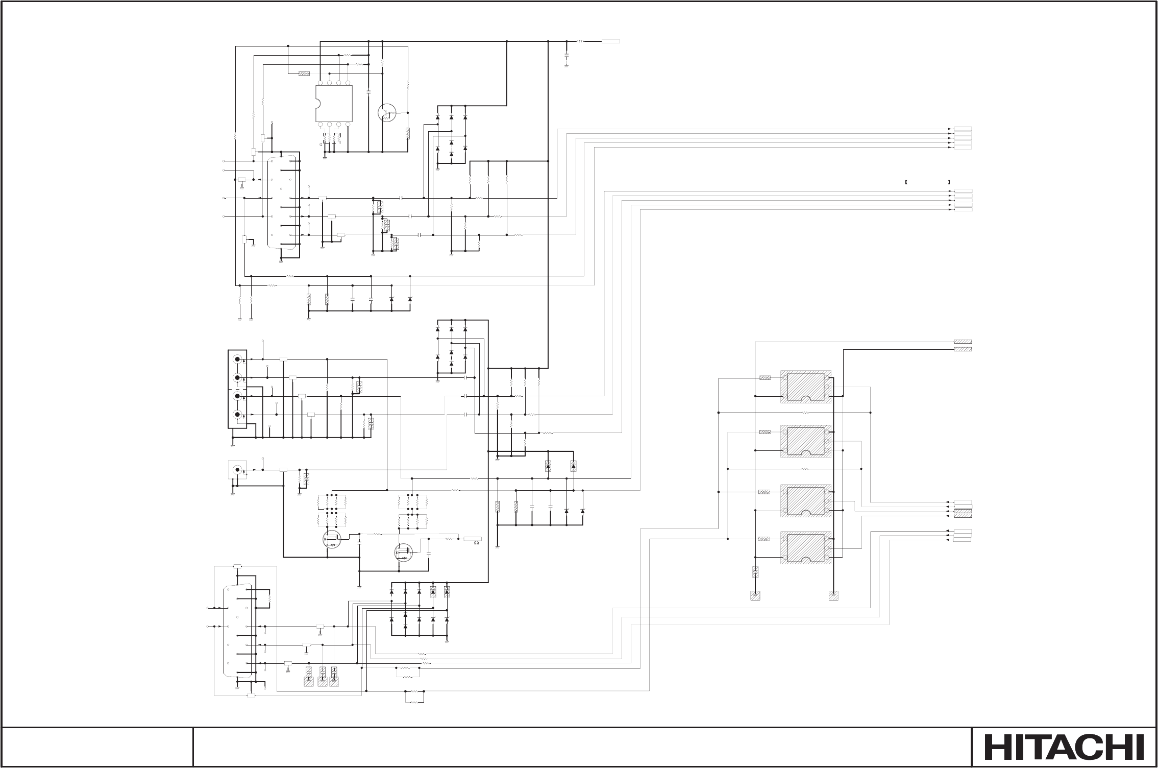
5
6
7
8
4
3
2
1
4
5
3
2
1
4
5
3
2
1
4
5
3
2
1
4
5
3
2
1
0.6V
CS10
2125
10/6.3
12
CS12
2125
10/6.3
12
CS09
2125
10/6.3
12
CS11
2125
10/6.3
12
CS08
2125
10/6.3
12
CS07
2125
10/6.3
12
DS12
1SS355
12
DS01
1SS355
12
DS11
1SS355
12
DS02
1SS355
12DS05
1SS355
12
DS07
1SS355
12DS04
1SS355
12
DS09
1SS355
12DS06
1SS355
12
DS03
1SS355
12
DS10
1SS355
12
DS08
1SS355
12
ES03
3114-15FABNS1XN
1
2
3
4
5
6
7
8
9
10
11
12
13
14
15
G1
G2
ES01
3114-15FA
1
2
3
4
5
6
7
8
9
10
11
12
13
14
15
G1
G2
2125
LS01
SC200JT
123
2125
LS14
SC200JT
1
2
3
2125
LS10
SC200JT
123
2125
LS06
SC200JT
123
2125
LS13
SC200JT
1
2
3
2125
LS03
SC200JT
1
2
3
2125
LS15
SC200JT
1
2
3
2125
LS04
SC200JT
123
2125
LS11
SC200JT
123
2125
LS02
SC200JT
1
2
3
2125
LS16
SC200JT
1
2
3
2125
LS17
SC200JT
1
2
3
2125
LS05
SC200JT
123
2125
LS12
SC200JT
123
GND1
GND1
GND1
GND1
GND1
GND1
GND1
GND1
2518
LS18
10
12
APV0
1
APIH2
1
APG0
1
APIB2
1
APH0
1
APIDA1
1
APIV1
1
APIG2
1
APIGD2
1
APGD0
1
APIR1
1
APB0
1
APIR2
1
APICK1
1
APIH1
1
APR0
1
APIV21
APIGD1
1
APIB1
1
APIG1
1
RS08
10k
12
RS03
75-1%
12
RS16
10k
12
1005
RS01
56 1
2
1005
RS30
0
12
RS20
012
RS21
220
12
1005
RS41
0
12
1005
RS42
0
12
RS05
75-1%
12
RS19
220
12
1005
RS29
0
12
RS13
75-1%
12
1005
RS31
0
12
1005
RS43
0
12
RS04
75-1%
12
1005
RS02
56 1
2
RS12
75-1%
12
RS22
220
12
RS18
220
12
1005
RS10
56
12
RS17
10k
12
RS09
10k
12
RS11
75-1%
12
+5V
2125
LS07
SC200JT
123
1005
RS26
33k
12
1005
RS27
33k
12
1005
RS28
33k
12
1005
RS37
33k
12
1005
RS36
33k
12
1005
RS35
33k
12
1005
RS40
100k
12
1005
RS39
100k
12
1005
RS38
100k
121005
RS25
100k
12
1005
RS24
100k
12
1005
RS23
100k
12
RS14
220
12
RS15
220
12
RS06
220
12
RS07
220
12
RS32 0
12
RS33 0
12
RS34 0
12
CS16
1005
47p-C
1
2
CS15
1005
47p-C
12
CS14
1005
47p-C
1
2
CS13
1005
47p-C
12
CS18
56p-c
1
2
CS19
56p-c
1
2
CS20
56p-c
1
2
ES04
BNC-04H
E-1
H1-2
NC1-3
H2-4
NC2-5
E-6
H1-7
NC1-8
H2-9
NC2-10
S
ES05
BNC-01H
1
E
2H
3
NC
4
S
2125
LS08
SC200JT
123
2125
LS09
SC200JT
123
GND1
IS01
S-24CS02AFJ-TB-G
A0
A1
A2
GND SDA
SCL
WP
VCC
QS01
DTC114EE
1
2
3
RS48
2010
0
78
56
34
12
1005
RS45
47k
12
1005
RS46
47k
12
1005
RS50
47k
12
1005
RS47
10k
12
1005
RS44
0
12
1005
RS49
100 12
3
2
SC
5
001
01/
1.0
1
2
GND1
DS15
1SS355
12
DS16
1SS355
12
DS17
1SS355
12
DS18
1SS355
12
DS19
UDZS6.2B
12
DS20
UDZS6.2B
12
GND1
BNCTRM
RS60
1.0k
1005
12
CS22
1.0/10
1
2
CS21
1.0/10
1
2
RS56
150-1%
12
RS55
150-1%
12
RS58
150-1%
12
RS57
150-1%
12
RS54
150-1%
12
RS53
150-1%
12
RS52
150-1%
12
RS51
150-1%
12
RS61
150-1%
12
RS62
150-1%
12
RS63
150-1%
12
RS64
150-1%
12
RS65
150-1%
12
RS66
150-1%
12
RS67
150-1%
12
RS68
150-1%
12
QS03
SSM3K116TU
SS
DD
G
G
QS02
SSM3K116TU
SS
DD
G
G
DS21
UDZS6.2B
12
DS22
UDZS6.2B
12
RS71
10k
12
RS72
10k
12
RS69
10k
12
GND1GND1
RS70
10k
12
DSUB1_R
DSUB1_H
DSUB1_V
DSUB1_G
DSUB1_B
MONOUT1_R
MONOUT1_V
MONOUT1_B
MONOUT1_H
MONOUT1_G
GND1
GND1
GND1
GND1GND1GND1
GND1
5BNC1_H
5BNC1_B
5BNC1_V
5BNC1_G
5BNC1_R
10S
C
500
1
01/1
.
01
2
20SC
5001
01/
1.
0
1
2
3
0
SC
5001
01/1.
0
1
2
4
0
SC
5001
01/
1.0
1
2
50SC
5
001
01
/1.0
1
2
6
0SC
500
1
0
1
/1.
0
1
2
GND1
GND1
GND1
GND1
GND1 GND1
DS23
1SS355
12
DS24
1SS355
12
DS25
UDZS6.2B
12
DS26
UDZS6.2B
12
DS31
1SS355
12DS28
1SS355
12
DS30
1SS355
12
DS32
1SS355
12DS29
1SS355
12
DS27
1SS355
12
DS33
1SS355
12
GND1
IS02
TC7SZ125FU
G
IN_A
GNDOUT_Y
VCC
IS03
TC7SZ126FU
G
IN_A
GNDOUT_Y
VCC
IS04
TC7SZ125FU
G
IN_A
GNDOUT_Y
VCC
IS05
TC7SZ126FU
G
IN_A
GNDOUT_Y
VCC
MONOUT2_V
MONOUT2_H
+3.3V
GND1
1005
RS73
0
12
1005
RS74
0
12
CS24
1005
0.1/10
12
GND1
1005
RS59
1.0k
12
MONI_SEL
1005
RS75
100
12
1005
RS76
100
12
1005
RS77
100
12
1005
RS78
100
12
CS17
2125
10/10
12
RGB IN 1(D-Sub)
NC
GND-B
GND-R
GND-B
H
R
RGB OUT
G
NC
SCL GND
B
Hsync
G
GND-R
B
SYNC
V
GND-G
GND-G/Y
R
NC
SDA
GND
NC
B
PLUG
R
Vsync
RGB IN 2(BNC)
(+5V)
G/Y
NC
Hsync
GND
Mounted jumper(LS01-LS17)
H1(D-Sub)
V1(D-Sub)
G1(D-Sub)
B1(D-Sub)
R1(D-Sub)
GOut
B Out
R Out
V1 Out
H1 Out
B2(BNC)
R2(BNC)
G2(BNC)
G/Y B/Cb,H,R/Cr,V
Vsync
B/Cb/Pb
R/Cr/Pr
G/Y
DDC for RGB1(D-Sub)
H:75 CLOSE
I2C SLAVE ADDR.
A0/A1h
AnalogLine
MON_H
MON_H
MON_V
MON_V
V2 Out
H2 Out
SM0321 PWB ASSEMBLY MAIN 11
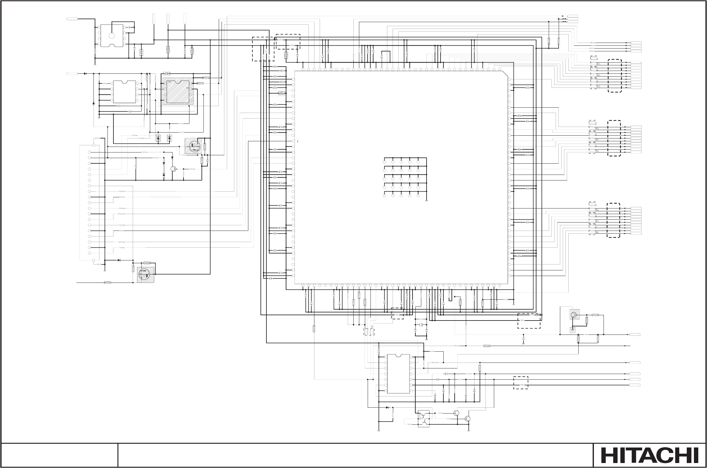
5
6
7
8
4
3
2
1
G2
19 18 17 16 15 14 13 12 11 10 9
G1
12345678
8
9
10
11
12
13
14
7
6
5
4
3
2
1
G5G1 G4G3G2
G17 G18 G19G16 G6
G7G15 G20G25G24
G23 G22 G21G14 G8
G9G10G11G12G13
111
115
114
112
118
113
116
117
109
110
119
104
99 98
103 10 1 100107 105106108 102
69
67
71
62
64
66
68
70
72
63
65
3028 3326 27 32 35 3629 31 34
97
120
92 879496 899091 8693 8895 85
61
60
59
58
57
56
55
54
53
52
51
50
49
48
47
46
45
44
43
42
41
40
39
38
37
25
143
133
138
135
140
142
144
137
134
139
136
141
13 20 22 241714 1 9 21 23161815364119725 121081
84
132
131
130
129
128
127
126
125
124
123
122
121
83 82 81 80 79 78 77 76 75 74 73
5
6
7
8
4
3
2
1
G1
5
6
7
8
4
3
2
1
IN0VS
HD_L_IN
CG35
1005
0.1/10
12
CG54
1005
1000p
12
1005
RG11
33
12
1005
RG62
0
12
CG63
2125
10/6.3
12
CG84
1005
0.01/16
12
RG78
0
12
1005
RG16
4.7k
12
GND1
GND1
GND1
IN0BE8
CG13 1005
0.1/10
12
1005
RG10
0
12
1005
RG32
10k
12
CG37
1005
1000p
12
1005
RG13
0
12
IN0RE9
RG21
2010
0
12
34
56
78
DG11
1SS355
12
IN0RE5
GND1
2125
LG03
600
12
1005
RG38
47k
12
CHHDINT
1
CG32
1005
1000p
1
2
CG61
2125
10/6.3
12
CG71
2125
10/6.3
12
IN0RE2
CG21
1005
0.1/10
12
CG06
1005
0.1/10
12
1005
RG51
47
12
QG13
2SD2114K
1
2
3
1005
RG84
10k
12
1005
RG19
4.7k
12
2125
LG02
600
12
+4.0V
RG12
2010
33
1
2
3
4
5
6
7
8
CG31
1005
0.1/10
12
1005
RG09
0
12
IN0BE4
CG02
1005
0.1/10
12
IN0GE7
1608
LG09
600
12
1005
RG36
10k
12
IN0GE3
CG19
1005
0.1/10
12
CG16
1005
0.1/10
12
IN0GE6
I2CCLK
CG27
2125
10/6.3
12
CG41 1005
0.1/10
12
DG03
1SS355
1
2
1005
RG95
100
12
GND1
1005
RG37
10k
12
1005
RG05
33
12
CG10
1005
0.1/10
12
1005
RG98
47k
12
CG96
1.0/10
1
2
1005
RG97
10k
1
2
1608
LG06
600
12
GND1
IG05
S-24CS02AFJ-TB-G
A0
A1
A2
GND SDA
SCL
WP
VCC
RG24
2010
0
12
34
56
78
IN0RE6
1005
RGA4
470k
12
IN0BE2
1005
RG57
0
12
CG11
1005
0.1/10
12
1608
LG04
600
12
1005
RG90
33
12
RG22
2010
0
12
34
56
78
CG77
1005
4700p
12
CG53
1005
1000p
12
1005
RG39
47k
12
1005
RG31
0
12
DG05
RB521G-30
1
2
CG33
1005
0.1/10
12
1005
RG20 10
12
RG77
0
12
I2CDAT
1005
RG85
10k
12
CG44 1005
1000p
12
RG23
2010
0
12
34
56
78
CG14
1005
1000p
12
1608
LG08
600
12
IN0BE9
1005
RG94
0
1
2
CG52
1005
0.1/10
12
CG43 1005
0.1/10
12
CG08
1005
0.1/10
12
CG48
1005
18p-C
12
IN0CLK
1005
RG02 33
12
CG62
2125
10/6.3
12
1005
RG82
470k 12
1005
RG54
1.0k
12
GND1
QG01
2SC4081
1
2
3
CG99
1005
0.1/10
12
EG01
DC1R019HBA
9101 2 3 4 5 6 7 8 11 12 13 14 15 16 17 18 19
G1G1 G2G2
CG09 1005
1000p
12
IG02
WM8520-SP6
DGND
LRCLK
DIN
BCLK
MUTE
VOUTR
AGND CAP
AVDD
VOUTL
DEEMPH
RESET
MCLK
DVDD
IN0RE4
IN0GE5
IN0BE6
RG29
2010
0
78
56
34
12
QG11
IMD10A
1
1
2
2
3
3
4
4
5
5
6
6
CG04
1005
0.1/10
12
2125
LG05
600
12
CG57
1005
1000p
1
2
QG03
2SK3018
1
S
2D
3
G
CG94
2125
10/6.3
12
CG34
1005
1000p
12
1005
RG01 33
12
IN0RE7
CG55
1005
1000p
12
CG18
1005
1000p
12
IG01
SiI9125
Q10
Q9
Q8
IOGND-4
ODCK
IOVCC33-6
Q7
Q6
Q5
Q4
CGND-11
CVCC18-12
Q3
Q2
Q1
Q0
IOGND-17
IOVCC33-18
DE
HSYNC
VSYNC
EVNODD
CGND-23
CVCC18-24
CVCC18-25
CSDA
CSCL
DSDA1
DSCL1
R1PWR5V
IOGND-31
IOVCC33-32
DSDA0
DSCL0
R0PWR5V
AGND-36
AVCC18-37
AVCC33-38
R0XC-
R0XC+
AGND-41
AVCC33-42
R0X0-
R0X0+
AGND-45
AVCC33-46
R0X1-
R0X1+
AGND-49
AVCC33-50
R0X2-
R0X2+
AGND-53
AVCC18-54
RSVDNC-55
AVCC33-56
R1XC-
R1XC+
AGND-59
AVCC33-60
R1X0-
R1X0+
AGND-63
AVCC33-64
R1X1-
R1X1+
AGND-67
AVCC33-68
R1X2-
R1X2+
AGND-71
AVCC18-72
IOGND-73
IOVCC33-74
MUTEOUT
RSVDNC-76
RSVDNC-77
SPDIF
CGND-79
CVCC18-80
SD
RSVDNC-82
RSVDNC-83
RSVDNC-84
WS
SCK
IOGND-87
IOVCC33-88
MCLK
CGND-90
CVCC18-91
DVCC18
DGND
XTALOUT
XTALIN
XTALVCC
REGVCC
RSVDNC-98
RSVDL
RESET#
SCDT
INT
IOGND-103
IOVCC33-104
CI2CA
CGND-106
CVCC18-107
Q35
Q34
Q33
Q32
IOGND-112
IOVCC33-113
Q31
Q30
Q29
Q28
CGND-118
CVCC18-119
Q27
Q26
Q25
Q24
IOGND-124
IOVCC33-125
Q23
Q22
Q21
Q20
CGND-130
CVCC18-131
Q19
Q18
Q17
Q16
IOGND-136
IOVCC33-137
Q15
Q14
Q13
Q12
CGND-142
CVCC18-143
Q11
GND1
IN0RE8
CG56
1005
0.1/10
12
CG17
1005
1000p
1
2
CG03
1005
0.1/10
12
1005
RG56
10k
12
1005
RG81
15k
12
CG91
1.0/10
12
CG39
1005
0.1/10
12
IN0BE1
1608
LG07
600
12
DG06
UDZS15B
12
1005
RG86
33
12
CG75
2125
10/6.3
12
CG74
2125
10/6.3
12
IN0BE3
IN0RE0
DG04
UDZS15B
12
CG85
1005
0.01/16
12
CG92
1005
470p
12
IN0HS
1005
RGA3
470k
12
CG58
1005
0.1/10
12
GND1
IN0BE7
1005
RG14
1.5k
12
1005
RG33
1.0k
12
1005
RG35
470
12
CHHDCEC 1
IN0GE2
1005
RG15
1.0M
12
IG06
SN74CB3T3306DCU
1OE
1A
1B
GND 2A
2B
2OE
Vcc
1005
RG03 33
12
CGA2
1005
0.1/10
12
RG25
2010
0
78
56
34
12
1005
RG55
10k
12
CG12
1005
1000p
12
IN0GE8
IN0BE5
QG02
2SK3018
1
S
2
D
3
G
IN0RE1
IN0GE9
CG46
1005
1000p
12
IN0RE3
CG25
1005
1000p
12
1005
RG80
1.0k
12
HPD_RST
1005
RG93
5.6k
12
CGA3
1005
0.1/10
12
1005
RG04
33
12
IN0GE0
CG59
1005
1000p
12
HDMI_RST
CG38
1005
1000p
12
CG93
1.0/10
1
2
1005
RG52
47
12
CG42
1005
1000p
12
CG49
1005
1000p
12
CG51
1005
1000p
12
QG12
2SD2114K
1
2
3
DEEMPH
IN0GE4
CG36
1005
1000p
12
1005
RG34
470
12
RG28
2010
0
12
34
56
78
CG26
1005
1000p
12
1005
RG61
10k
12
CG97
2125
10/6.3
12
1005
RG58
10k
12
CG23
1005
1000p
12
GND1
1005
RG63
0
12
DG12
RB521G-30
12
DG13
RB521G-30
12
1005
RG17
33
1
2
IN0GE1
CG22
1005
1000p
12
CG15
1005
1000p
12
1005
RG18
4.7k
1
2
QG14
2SC4081
1
23
CG45
1005
0.1/10
12
+5V
1005
RG79
1.0k
12
CG01
1005
1000p
12
CG07
1005
1000p
12
CG40
1005
1000p
12
CG24
1005
0.1/10
12
CG47
1005
22p-C
12
CG72
2125
10/6.3
12
CG76
1005
4700p
12
1005
RGA1
47k
12
XG01
27.000MHz
DSX530GA
1
2
1005
RG89
10k
12
CG20
1005
1000p
12
CGA1
2125
10/6.3
12
1005
RG88
10k
1
2
1005
RG53
100
12
1005
RG83
0
12
HD_R_IN
RG27
2010
0
12
34
56
78
2125
LG01
600
12
1005
RG59
470k
12
IG11
MM1663DHBE
Vout
NC-2
GND
CnCont
NC-6
NC-7
Vin
IN0PEN
1005
RG96
10k
12
1005
RG87
33
12
CG73
2125
4.7/16
12
CG05
1005
1000p
12
RG26
2010
0
78
56
34
12
1005
RG08
0
12
IN0BE0
+8.5V
ADA3.3V
ADD3.3V
ADD1.8V
CG95
2125
10/6.3
12
1005
RGA5
4.7k
12
1005
RG67
6.8
12
1005
RG68
6.8
12
1005
RG69
6.8
12
1005
RG70
6.8
12
1005
RG71
6.8
12
1005
RG72
6.8
12
1005
RG73
6.8
12
1005
RG74
6.8
12
1005
RGA6
0
1
2
1005
RGA7
01
2
DG07
UDZS5.6B
12
DG08
UDZS5.6B
12
JUMPER
HTPLUG
GND
+5V
GND
RX0-
GND
GND
JUMPER
JUMPER
RXC-
SCL
NC
(HDMI-1)
(HDMI-2)
(HDMI-3)
RX2-
RX1-
I2C SLAVE ADDR.
JUMPER
I2C SLAVE ADDR.
A0/A1h
HDMI Rx
CEC
RX1+
RXC+
SDA
RX2+
3.3V-HDMI
RX0+
60h/68h
GND
SM0321 PWB ASSEMBLY MAIN 12
9
10
11
12
13
14
15
16
8
7
6
5
4
3
2
1
24
23
22
21
20
19
18
17
16
15
14
1312
11
10
9
8
7
6
5
4
3
2
1
5
6
7
8
4
3
2
1
54321
8
9
10
11
12
13
14
7
6
5
4
3
2
1
12
813
11
7
4
G1
15
14
16
1
10 9
6
5
32
CW
OE
RESETB
RESETB
CW
CLK
CLK
MOB
OE
1005
*RWA8
6.8k-1%
12
APUSB-
1
1005
*RWA9
15k-1%
12
IRIS_SAV
GND1
1005
RW46
0
12
APUSB+
1
APARD
1
*CW87
2125
4.7/6.3
12
IRIS_LED
CW53
47/16
MVK/SKV
1
2
APW10
1
CW61
1005
1000p
12
APATD
1
1005
RW44
0
12
*CW83
1005
0.1/10
12
1005
RW85
0
12
1005
RW61
10k
12
IW02
ADM202EARNZ
C1+
V+
C1-
C2+
C2-
V-
T2OUT
R2IN R2OUT
T2IN
T1IN
R1OUT
R1IN
T1OUT
GND
VCC
1608
LW54
600
12
IW53
uPD168110
MODE
CLK
LGND
C_OSC
MOB
PGND2
OUT2B
V_M2
OUT2A
FB2
PS
OE STOP
MOBSEL
PGND1
OUT1A
V_M1
OUT1B
FB1
FIL1
FIL2
VDD
CW
RESETB
IRIS_OE
1005
*RWA7
3.6k-1%
12
+6.6V
QW07
2SK3018
1
S
2
D
3
G
APW14
1
+5V
*CW88
1005
0.1/10
12
1005
*RWC0
6.2k-1%
12
1005
RW60
10k
12
CW11
1.0/16
1
2
IRIS_CLK
1005
RW16
3.3k
12
1608
LW55
600
12
*CW86
1005
0.01/16
12
1005
*RWA1
100-1%
12
1005
RW20
2.2k 12
1005
*RWC2
10k-1%12
QW06
DTC114EE
1
2
3
1005
RW83
560
12
GND1
CW08
1.0/16
12
PWM_G
APW7
1
GND1
1005
RW75
56k
12
CW54
100/6.3
MVK/SKV
1
2
2125
LW52
600
12
EW04
PH-05V
2
3
4
5
1
G1
G2
1005
*RWC3
10k-1%
1
2
*CW84
1.0/10
1
2
1005
RW59
0
12
*CW81
2125
4.7/6.3
12
CW63
1.0/10
12
1005
*RWA3
0
1
2
CW62
1005
1000p
12
1005
RW70
220
12
1005
RW04
100
12
CW24
1005
0.1/10
12
1005
RW72
0
12
1608
LW58
600
12
1005
RW74
56k
12
IRIS_PI1
+3.3V
1005
RW82
2.7k-1%
12
*CW85
1.0/10
1
2
CW57
1005
0.1/10
12
1005
RW81
560
12
2125
LW50
600
12
*CW80
1005
0.1/10
12
*CW82
2125
4.7/6.3
12
IRIS_PI2
1005
RW71
220
12
+3.3V
1005
*RWA0
100
12 APW8
1
1608
LW56
600
12
EW51
ZH-09V
1
2
3
4
5
6
7
8
9
G1
G2
1005
RW45
0
12
1005
*RWA6
0
12
*IW03
LM358AD
1OUT
1IN-
1IN+
GND 2IN+
2IN-
2OUT
VCC
CW10
1.0/16
12
1005
RW80
2.7k-1%
12
GND1
CW58
330p-C
12
1608
LW61
600
12
IW61
SI-3050KM
Vc
Vin
GND
Vout
Sense
1005
*RWA2
0
12
RW41
2010
0
78
12
56
34
APW9
1
1005
*RWA5
0
12
+3.3V
*DW31
1SS355
12
+5V
2125
LW22
SC200JT
123
IW22
SN74LV14APW
1A
1Y
2A
2Y
3A
3Y
GND 4Y
4A
5Y
5A
6Y
6A
Vcc
GSENSOR 2125
LW53
600
12
GND1
1005
RW97
10k
12
1005
*RWA4
2.7k-1%
12
APW6
1
APW13
1
FANGND
APAGD
1
1005
*RWC1
10k-1%1
2
CW60
1005
0.01/16
12
1005
RW17
100 1
2
USB_D-
1005
RW96
33
12
2125
LW51
600
12
IRIS_CW
QW08
2SK3018
1
S
2
D
3
G
CW09
1.0/16
12
APW12
1
APW11
1
USB_D+
*IW01
ADXL323
1
NC-1
2
ST
3
COM-3
4
NC-4
5COM-5
6COM-6
7COM-7
8NC-8
9
NC-9
10
YOUT
11
NC-11
12
XOUT
13
NC-13 14
VS-14 15
VS-15 16
NC-16
G1
CW59
1005
0.01/16
12
1608
LW57
600
12
IRIS_RST
1005
RW05
100
12
RXD
TXD
1005
RW86
10k
12
MOTER2A
MOTER1A
PS2
VCC
PS1
PI1
PI2
RD
TD
MOTER2B
5.0V
LW50-58
Mounted jumper
USB D-
USB D+
GND
RD
TD
Gravity Sensor
RS232C Controller
MOTER1B
SM0321 PWB ASSEMBLY MAIN 13
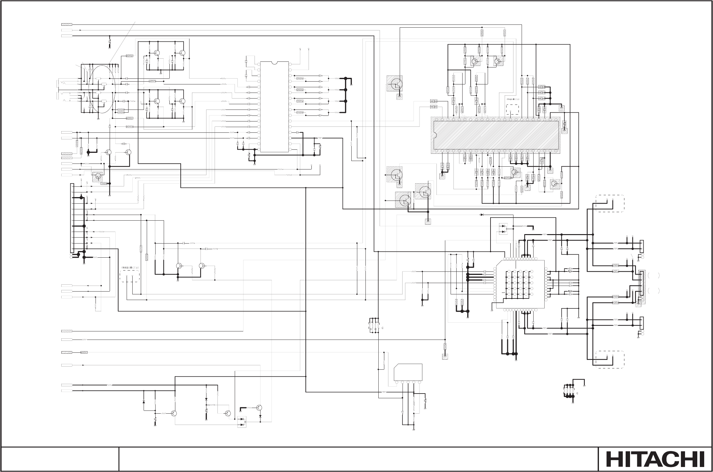
17
18
19
20
21
22
23
24
25
26
27
28
29
30
31
32
16
15
14
13
12
11
10
9
8
7
6
5
4
3
2
1
4
6
5
2
8
7
3
1
G7
G8
G10 G9
G23G14
G15
G11
G24
G6
G13
G22
G19G18
G12
G21
G5
G17
G3 G4G2G1
G25 G20
G16
1
36
48
47
46
45
44
43
42
41
40
39
38
37
35 34 33 32 31 30 29 28 27 26 25
24
23
22
21
20
19
17
18
16
15
14
13
12111098765432
25
28
29
30
31
32
33
34
35
36
37
38
39
40
41
42
43
44
26
27
24
2322
21
20
19
18
17
16
15
14
13
12
11
10
9
8
7
6
5
4
3
2
1
54321
0.0V
8.5V
8.5V
8.5V
0.0V
8.5V
0.0V
8.5V
8.5V
0.0V
8.5V
0.0V
8.5V
8.5V
8.5V
0.0V
0.0V
0.0V
8.5V
0.0V
8.5V
8.5V
0.0V
0.0V
0.0V
0.0V
4.5V
0.0V
16.0V
16.0V
16.0V
16.0V
16.0V
16.0V
14.5V
14.5V
14.5V
0V
5.0V
5.0V
7.3V
3.3V
0V
0V
0V
0V
15.5V
0V
17.0V
0V
14.5V
14.5V
14.5V
14.5V
16.0V 16.0V
14.5V
14.5V
16.0V 14.5V
0V
0V
0.0V
0.0V
3.3V
3.3V
3.3V
0V
4.5V
16.6V
14.9V
15.0V
8.5V
8.1V
8.1V
15.9V
15.9V
8.5V
8.5V
0.0V
0.0V
0.0V
0.0V
0V
0V
14.5V
14.5V
14.5V
14.5V
0V
0V
0V
17.0V17.0V
0V
3.3V
0V
16.0V
3.3V
3.3V
3.3V
16.0V
0.0V
0.0V
0.0V
0.0V
0.0V
0.0V
0.0V
0.0V
0V
4.4V
4.4V
4.4V
4.4V
0V
8.5V
8.5V
3.0V
3.0V
3.0V
3.3V
0V
8.5V
8.3V
8.3V
8.0V
8.5V
7.7V
8.4V 8.4V
7.4V
7.4V
8.5V
7.4V
7.1V 7.1V
8.5V
4.5V
0.0V
3.7V 8.5V
4.5V0V
8.5V 8.5V
8.5V
8.5V
8.5V
8.5V
4.7V
7.1V 7.1V
4.5V
4.5V
4.5V
4.5V
0V
0V 4.5V
4.5V
0V
8.5V
7.7V
8.5V
8.2V
8.5V
7.7V
8.5V
8.2V
8.5V
0.0V
0.0V
8.5V
0.0V
0.0V
16.0V
16.0V 14.5V
0V
0.0V
0.0V
0.0V
0.0V
0.0V
4.4V
0.0V
0.0V
17.0V
3.3V
3.3V
5.0V
0.0V
8.5V
0.0V
0.0V
0.0V
0.0V
0.0V
0.0V0.0V
3.3V
2.6V
0V
0.0V
0V
0V
4.4V
0.0V
4.4V
0.0V
0V
0.0V
0.0V
8.5V
0.0V
8.5V
0.0V
3.3V
14.5V
8.5V
3.3V
3.3V
CA06
1.0/16
12
CA10 1.0/16
12
CA40 1.0/16
1
2
CA15 1.0/16
12
CA28
0.33/10
12
CAA7
2125
4.7/161
2
CA27
10050.1/16
12
CA03
1005
100p-C 12
CA51
3216
1.0/25
1
2
CA22 1005
0.01/16
12
CA49
0.22/25-X5R
1
2
CA48
3216
1.0/25
1
2
CA36
1.0/16
12
CA09 1.0/16
12
CA04
1005
100p-C
12CA02
1005
100p-C
12
CA42
0.22/25-X5R
1
2
CA13 1.0/16
12
CA20 1005
0.01/16
12
CA45
3216
1.0/25
1
2
CAB2 1005
220p 12
CA01
1005
100p-C
12
CAA5
2125
4.7/16
1
2
CA30
1005
0.1/16
12
CAB3 1005
220p 1
2
CA50
0.22/25-X5R
1
2
CA21
10050.01/16
12
CA12 1.0/16
12
CA26 1005
0.1/16
12
CA25
10050.1/16
12
CA43
3216
1.0/25
1
2
CA16
1.0/16
12
CAA6
2125
4.7/16
1
2
CA37
1.0/16
12
CA24 1005
0.1/16
12
CA07 1.0/16
12
CA23
10050.01/16
12
CAB4
1005
220p
12
CA14 1.0/16
12
CA31
1.0/10
12
CA46
3216
1.0/25
1
2
CAB5
1005
220p
1
2
CA41
0.22/25-X5R
1
2
CA08 1.0/16
12
CA11 1.0/16
12
CAA4
2125
4.7/16
1
2
CA32
1.0/10
12
CA05
1.0/16
12
CA29
47/16
MVK/SKV
1
2
CA57
47/25
MVK/SKV
1
2
CA58
47/25
MVK/SKV
1
2
CA19 47/6.3
MVK/SKV
1
2
EA02
PH-02V
1
2
G1
G2
EA04
PH-02V
1
2
G1
G2
*EA03
ZH-04V
1
2
3
4
G1
G2
DA05
1SS355
1
2
DA04
DAN202U
1
2
3
DA01
DAN202U
1
2
3
IA01
BD3883FS
VIN1
SEL1
VIN2
SEL2
A1
A2
B1
B2
C1
C2
D1
D2
E1
E2
FILTER
GND SC
SI
VCC
CAP
OUT2
OUT1
BOUT2
BNF2
BOUT1
BNF1
MOUT2
MNF2
MOUT1
MNF1
REC2
REC1
2125
LA02
SC200JT
123
2125
LA03
SC200JT
123
2125
LA01
SC200JT
123
2125
LA04
SC200JT
123
GND1
P_GND
GND1
P_GND
GND1
GND1
GND1
GND1
GND1
P_GND
GND1
GND1
GND1
GND1
GND1
GND1
GND1
GND1
GND1
GND1
GND1
P_GND
EA01
HSJ1003-01-010
1
2
3
4
5
6
7
8
2125
LA08
MPZ2012S101A
12
2125
LA07
MPZ2012S101A
12
2125
LA09 MPZ2012S101A
12
1608
LA16 30
12
1608
*LA12 30
12
2125
LA06
MPZ2012S101A
12
1608
LA17 30
12
1608
*LA15 30
12
2518
LA05
100
12
1608
LA11 30
12
1608
*LA13 30
12
1608
*LA14 30
12
1608
LA10 30
12
L_rutn
1
APAR3
1
APL2+
1
APAL3
1
APAL1
1
APAG2
1
APL1-
1
APWR5
1
R_SP_N
1
APAG1
1
APWRC
1
APR2+
1
APAR4
1
R_SP_P
1
APR1-
1
L_SP_N
1
L_SP_P
1
APR1+
1
R_rtun
1
APAR2
1
APAL2
1
APWRS
1
APAR5
1
TP007
1
APAL4
1
APAL5
1
APL2-
1
TP001
1
APAR1
1
APR2-
1
APL1+
1
QA03
2SA1774
1
2
3
QA04
2SA1774
1
2
3
QA22
2SA1774
1
2
3
QA16
2SC4617
1
2
3
QA17
2SC4617
1
2
3
QA15
2SC4617
1
2
3
QA14 2SC4617
1
2
3
IA02
TPA3100D2
NC-1
RINN
RINP
AGND-4
LINP
LINN
NC-7
GAIN0
GAIN1
MSTR/SLV
SYNC
NC-12
NC-13
ROSC
VREG
VBYP
AGND-17
BSLP
LOUTP-19
LOUTP-20
LOUTN-21
LOUTN-22
BSLN
NC-24
NC-25
PVCCL-26
PVCCL-27
PGNDL-28
PGNDL-29
VCLAMPL
VCLAMPR
PGNDR-32
PGNDR-33
PVCCR-34
PVCCR-35
NC-36
NC-37
BSRN
ROUTN-39
ROUTN-40
ROUTP-41
ROUTP-42
BSRP
SHUTDOWN
MUTE
FAULT
NC-47
AVCC
G1G2G3G4G5
G6
G7
G8
G9 G10 G11 G12 G13
G14
G15
G16G17G18G19
G20
G21 G22 G23
G24G25
1005RAB9 100
12
1005
RA40 120k
12
1005
RAC6 10k
1
2
1005
RA01 180k
12
1005
RA48
4.7k
12
1005
RAC1
150k 1
2
1005
RA11
0
12
1005
RA26
5.6k
12
1005
RAB6
120k
12
1005
RA46
120k
12
1005
RA36
100
12
1005
RA04 180k
12
1005
RAB1 100
1
2
1005
RA50
22k
12
1005
RA97
2.2k
12
1005
RAC0
120k
12
1005
RA44 100k-1%
12
1005
RA15 0
12
1005
RAC2 10k
1
2
1005
RAB8 10k
1
2
1005
RA14 0
12
1005
RA42
120k 1
2
1005
RA16 0
12
1005
RAC4
120k
1
2
1005
RA24
0
12
1005
RA51
0
1
2
1005
RAE3
0
12
1005
RA39 120k
12
1005
RA43 120k
1
2
1005
RAE4
0
12
1005
RA03 180k
12
1005
RA13 0
12
1005
RA41 120k
1
2
1005
RA18 0
12
1005
RA17 0
12
1005
RA22
0
12
1005
RA28
5.6k
12
1005
RAE5
10k
1
2
1005
RAB7
150k 12
1005
RAB2
120k
12
1005
RA31
4.7k
12
1005
RAB4 10k
1
2
1005
RA21
0
12
1005
RA27
5.6k
12
1005
RA49
1.0k
12
1005
RA25
5.6k
12
1005
RA33
100k 12
1005
RA35
100
12
1005
RA32
4.7k
12
1005
RA29
1.0k
12
1005
RA12 0
12
1005
RA47
47k
1
2
1005
RA02 180k
12
2125
RA93
47
12
1005
RA23
0
12
1005
RAC5
150k
1
2
1005
RAA8
0
12
1005
RA30
1.0k
12
1005
RA34
100k 1
2
1005
RAB3
150k 1
2
1005
RAB5 100
12
RA96
2010
0
12
34
56
78
+5V
W_RC_SW
WIRED_RC
PW_MUTE
SP_OFF
CLK-A
+17V
+14.5V
DATA-A
1005
*RAF0 130k-1%
12
1005
*RAF1 82k-1%
12
1005
*RAF2
47k-1%
12
1005
*RAF4
9.1k-1%
12
1005
*RAF3
36k-1%
12
1005
*RAF5
6.2k-1%
12
*CAC9
1.0/16
12
*CAD0
2125
10/10
1
2
GND1
*CAD1
1005
0.033/16
12
*CAD2
1005
0.01/16
1
2
*CAD3
0.47/10
1
2
*CAD4
0.33/10
1
2
GND1
*CAD7
2125
10/10
1
2
*CAD8
2125
10/10
1
2
GND1
1005
*RAG510k
1
2
1005
*RAG610k
12
1005
*RAG710k
1
2
*CAE4
2125
10/10
12
*CAE5
2125
10/10
12
1005
*RAH8 100k
12
1005
*RAH7 100k
12
1005
*RAG9 100k
12
1005
*RAG8 100k
12
1005
*RAH9 10k
1
2
1005
*RAJ0 10k
12
1005
*RAH0 10k
1
2
1005
*RAH1 10k
12
1005
*RAJ1 2.2k
1
2
1005
*RAH2 2.2k
12
*CAE0
2125
10/10
1
2
*CAE1
2125
10/10
1
2
*CAD9
2125
10/10
1
2
WOW
GND1
1005
*RAJ6
0
1
2
1005
*RAJ7
0
12
CA99
47/25
MVK/SKV
1
2
GND1
*QA23
2SA1576A
1
2
3
1005
*RAG0 100k
12
1005
*RAF9
1.0k
12
1005
*RAG1
3.9k
12
*QA24
2SA1576A
1
2
3
1005
*RAG2
5.6k
1
2
*CAD5
1005
220p
1
2
1005
*RAG3
1.0k
12
*QA26
2SA1576A
1
2
3
*QA25
2SA1576A
1
2
3
1005
*RAJ4
1.0k
12
1005
*RAH5
1.0k
12
1005
*RAH6
100k
12
*QA27
DTC114EE
1
2
3
*QA28
DTC114EE
1
2
3
GND1
*QA29
DTC114EE
1
2
3
1005
*RAG4
100k
12
WOW_Hi_Md
TRUBASS
1
CA39
1005
0.1/16
1
2
1005
RAK6
0
12
1005
RAK7
0
12
1005
RAK5
0
1
2
1005
RAK4
0
12
1005
RAK3 0
1
2
1005
RAK0
0
12
1005
RAK2 0
1
2
1005
RAK1 0
1
2
DA02
1SS355
12
DA03
1SS355
1
2
*IA08
NJM2195V
NC-1
C4
FILOUT
FIL1
FIL2
FIL3
FIL4
FIL5
FIL6
FIL7
PCOUT
PCIN
C1
C2
SFIL1
SFIL2
SFIL3
SVOL2
SVOL1
GND-21
NC-22 NC-23
V+
VREFIN
VREF
MODE3
MODE2
MODE1
TP1
BASSOUT
OUTR
OUTL
TP2
FFR3
FFR2
FFR1
TP3
FFL3
FFL2
FFL1
INR
INL
NC-44
C3
GND1
POWER5
DA10
1SS355
12
1005
RA45 1.0k
12
VR_CLK
1
VR_DATA
1
1005
RA94
82k
12
1005
RA95
82k
12
EA06
ZH-12V
1
2
3
4
5
6
7
8
9
10
11
12
G1
G2
CA47
47/25
MVK/SKV
12
CA4447/25
MVK/SKV
12
CA52
47/25
MVK/SKV
1
2
*CAD6 47/16
MVK/SKV
1
2
*QA30
DTC114EE
1
2
3
GND1
GND1
1005
*RAK9
22k
1
2
1005
RAL0
100
12
GND1
CH1_CUT
QA31
2SC4617
1
2
3
QA32
2SC4617
1
2
3
1005
RAL1
4.7k 12
1005
RAL2
4.7k 1
2
CAE6
2125
2.2/10
12
CAE7
2125
2.2/10
12
1005
RAL3 0
12
1005
RAL4
0
12
1005
RAL5
100k 12
GND1
QA01
2SC4617
1
23
QA02
2SC4617
1
23
1005
RAL6
0
12
QA33
2SA1774
1
2
3
1005
RAL7
10k
12
1005
RA37
1.8k
12
1005
RA38
1.8k
12
AP85V
1
1005
*RAF6 5.6k
12
1005
*RAF7
5.6k
12
1005
*RAF8
3.3k
1
2
1005
*RAJ5
100k
12
*CAC3
1005
0.047/16
12
*CAC4
1005
0.047/16
12
*CAC5
1005
0.047/16
12
*CAC6
1005
0.047/16
12
*CAC7
1005
0.047/16
12
*CAC8
1005
0.047/16
12
*CAE3
0.1/16
1
2
*CAE2
0.1/16
1
2
1005
*RAJ3
0
12
1005
*RAH4
0
12
1005
*RAJ2
560
12
1005
*RAH3
560
12
1005
RAL8
1.0k
1
2
1005
RAL9
1.0k
1
2
1005
RA52 1.8k
12
1005
RA53 1.8k
12
CA17
3300p
1
2
1005
RA19 4.7k
12
1005
RA09
180k
12
1005
RA10
180k
1
2
CA18
3300p
1
2
POWERA
1005
RAM1
01
2
1005
RAM0
01
2
*CAC1
0.1/16
12
CA53
1005
1000p
1
2
CA54
1005
1000p
1
2
CA56
1005
1000p
1
2
CA55
1005
1000p
1
2
1005
RA20 4.7k
12
+8.5V
*CAC2
0.01
12
RAM2
2010
68
12
34
56
78
1005
RAM6
10k-1%
12
1005
RAM4
75k-1%
12
IA09
SI-3010KM
Vc
Vin
GND
Vout
ADJ
CAE8
0.1/25
12
1005
RAM5
0
12
CAE9
47/16
MVK/SKV
1
2
GND1
GND1
2518
LA18
4.7
12
*CA38
0.033/16
12
*CA35 0.033/16
12
1005
RAM7
1.0k
12
HD_L_IN
HD_R_IN
WL_R_in
WL_L_in
1005
RA54
0
12
1005
RA55
0
12
RGB Audio IN2
Connects with
a Speaker
R - out
L - out
RGB Audio IN1
RGB AudioR-in2
RGB AudioL-in2
Speaker Monitor R
Speaker Monitor L
Audio Power GND
Video AudioR-in1
Video AudioL-in1
Video AudioR-in2
Video AudioL-in2
To R1
Speaker
To R2
Speaker
To L1
Speaker
To L2
Speaker
Connects with
a Input PCB
4W x 4 Audio Amplifier
Sheet 4
Sheet 1
Sheet 3
Sheet 3
Sheet 3
Sheet 3
Sheet 4
Sheet 4
HDMI Audio R
HDMI Audio L
Audio Monitor
Audio Volume
9.8Vrms
To
KEYPAD PWB
RGB AudioR-in1
RGB AudioL-in1
Sheet 1
LA01-04
Mounted jumper
TruBass OUT
Sheet 1
Sheet 1
Sheet 1
Sheet 1
Sheet 14
Sheet 12
8.5V
MAX:1W/1A
Sheet 12
Sheet 12
SM0321 PWB ASSEMBLY MAIN 14
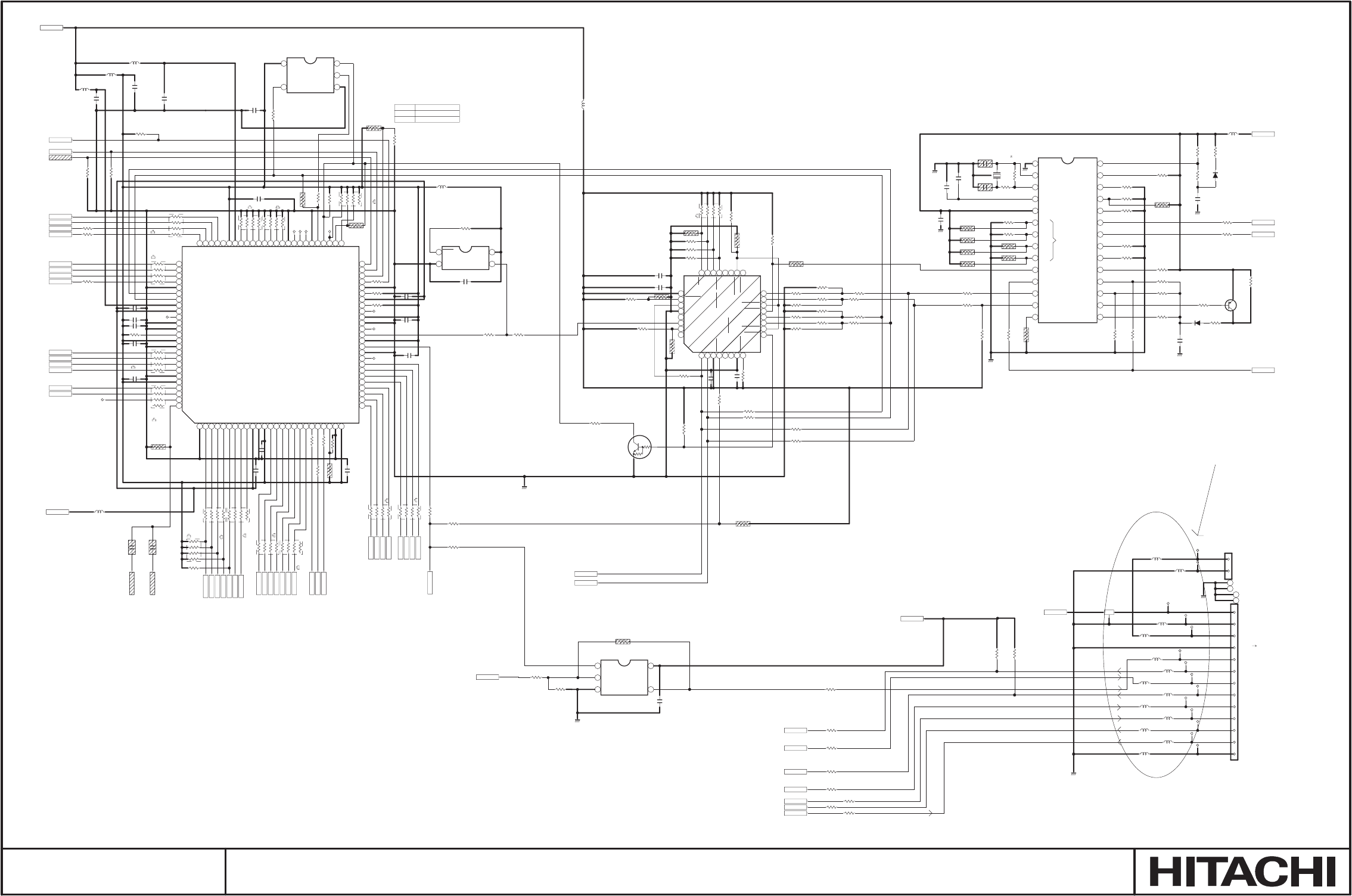
28
31
27
29
26
25
32
30
1
24 23 22 21 20 19 18 17
16
14
15
13
12
11
10
9
8765432
75
76
70 657274 6768
69 6471 6673 63
50
49
48
47
46
45
44
43
42
41
40
39
38
37
36
35
34
33
32
31
30
29
28
27
26
25
99
89
94
91
96
98
100
93
90
95
92
97
13 20 22 241714 19 21 2316 1815364119725 121081
62
88
87
86
85
84
83
82
81
80
79
78
77
61 60 59 58 57 56 55 54 53 52 51
4
32
1
28
27
26
25
24
23
22
21
20
19
18
17
16
15
1
2
3
4
5
6
7
8
9
10
11
12
13
14
4
5
3
2
1
4
5
3
2
1
DP_2
DM_2
DM_1
DP_1
CE05
1005
0.1/10
1
2
*CE30
1005
330p
12
CE02
2125
10/6.3
12
CE09
1005
0.01/16
12
CE08
1005
0.01/16
12
CE39
1005
0.01/16
12
CE13 1005
0.01/16
12
CE01
2125
10/6.3
12
CE34 1005
0.01/16
12
CE07
1005
0.01/16
12
CE03
2125
10/6.3
12
*CE31
1005
330p
12
CE14 1005
0.01/16
12
*CE12
1005
0.1/10
12
CE35
1005
0.01/16
12
CE06
1005
0.01/16
12
CE04
1005
0.1/10
1
2
CE15 1005
0.01/16
12
EE02
SH-02H
1
2
G1
G2
EE01
ZH-13V
1
2
3
4
5
6
7
8
9
10
11
12
13
G1
G2
3216
LE25
123
GND1
GND1
1608
LE09
600
12
1608
LE23
600
12
1608
LE19
600
12
1608
LE18
600
12
2125
LE30
1000
12
1608
*LE07
600
12
2125
LE15
1000
12
2125
LE16
1000
12
1608
LE17
600
12
1608
*LE20
600
12
1608
LE22
600
12
2125
LE32
1000
12
1608
*LE21
600
12
2125
LE13
1000
12
1608
LE24
600
12
CHKE04
1
APE07
1
APE01
1
APE11
1
CHKE05
1
APE12
1
APE05
1
CHKE02
1
APE14
1
CHKE03
1
APE03
1
CHKE07
1
CHKE08
1
CHKE06
1
APE15
1
APE04
1
APE06
1
APE09
1
APE13
1
APE02
1
APE08
1
*IE02
TUSB2036VF
1
DP0
2
DM0
3
Vcc-3
4
RESET
5
EECLK
6
EEDATA/GANGED
7
GND-7
8
BUSPWR
9
PWRON1
10
OVRCUR1
11
DM1
12
DP1
13
PWRON2
14
OVRCUR2
15
DM2
16
DP2
17
PWRON3
18
OVRCUR3
19
DM3
20
DP3
21
OCPROT/PWRSW
22
NPINT0
23
NPINT1
24
NP3
25 Vcc-25
26 EXTMEM
27 DP0PUR
28 GND-28
29 XTAL2
30 XTAL1/CLK48
31 MODE
32 SUSPND
IE01
TE7783PF
DVSS-1
P1
P2
P3
P4
P5
P6
P7
P8
DVDD25-10
DVSS-11
DVDD33-12
A6
A5
A4
A3
A2
A1
A0
XCS
XRD
XWR
RSTPLO
DVSS-24
DVDD33-25
D7
D6
D5
D4
D3
D2
D1
D0
WAKEUP
DVSS-35
RST
DVDD33-37
XI
XO
VSS-40
DVDD33-41
XCS1
XSTDBYEN
DVDD25-44
XINVALID
DVSS-46
XINT
P21
P22
P23
P24
P25
P26
P27
P28
DVSS-56
VREFN
VCOM
VREFP
AVSS
AIN1
AIN2
AIN3
AIN4
AIN5
AIN6
AIN7
AIN8
AVDD33
DVDD33-70
XCS2
P31
P32
P33
P34
P35
P36
P37
P38
UVSS
DMINUS
DPLUS
UVDD33
DVDD25-84
XCS3
DVSS-86
DVSS-87
RSTMSK
DVDD33-89
DVSS-90
P11
P12
P13
P14
DVSS-95
DVDD33-96
P15
P16
P17
P18
1005
*RE95 0
12
1005
REH3 4.7k
12
1005
*RE92
012
1005
REA4
100 12
1005
RE99
3.3k
12
1005
*RE60
10
12
1005
RE15
100
12
1005
RE05 22
12
1005
REC6
100 12
1005
RE71
10k
12
1005
RE18
33 12
1005
RE04
22
12
1005
RE76
100 1
2
1005
*RE91
012
1005
RE34
0
12
1005
RE62
100
1
2
1005
*RE13
33
12
1005
REA1
100 1
2
1005
*RE96
3.3k
12
1005
RE98 0
12
1005
RE16
3.3k
12
1005
*RE93
012
1005
*RE19
33
12
1005
*REF8
0
12
1005
RE36 0
12
1005
RE12
33 12
1005
*RE94
3.3k
12
1005
*RE77
100
1
2
1005
RE07 10k
12
1005
RE63
3.3k
12
1005
RE37 0
12
1005
RE33
10k
12
1005
RE22
1.5k
12
1005
RE35
0
12
1005
*RE44 1.5k
12
1005
*RE17
3.3k
12
1005
RE06 0
12
1005
RE27 10k
12
1005
*RE97
10k
12
1005
RE61
100 12
1005
RE43
0
12
1005
RE38
10
12
1005
*REC7 0
12
1005
*REC8 0
12
1005
RE14
10k
12
1005
RE03 22
12
1005
*RE42
3.3k
12
1005
RE39
10k
12
1005
REA3
100 1
2
RE26
2010
100
12
34
56
78
RE09
2010
22
12
34
56
78
*RE89
2010
3.3k
7
8
5
6
3
4
1
2
RE29
2010
100
12
34
56
78
RE11
2010
22
12
34
56
78
RE08
2010
22
12
34
56
78
RE23
2010
10k
12
34
56
78
RE24 2010
10k
12
34
56
78
RE10
2010
22
12
34
56
78
A5
RESETN
+3.3V
D3
WL_L_in
PCS0
ESBUSY
ES_TXD
A4
A3
WL_R_in
A7
WRN
A1
MSLEEP
D0
+2.5V
TXD1
FAN15V
D6
A2
ES_RXD
RDN
INT_TE
D7
D5
SBUSY
D2
USB_D-
+3.3V
RXD1
USB_D+
A6
D1
D4
*XE01
DSO751SV48.000MHz
1CONT
2GND 3
OUT
4
VDD
QE01
DTC114EE
1
2
3
1005
*REF9
0
12
1005
*REA6 10k
12
1005
REA9 10k
12
1005
REM4 10k
12
1005
REA8 10k
12
GND1
1005
REM2
0
12
1005
RE55
10k 1
2
1005
*RE48 10k
12
1005
*RE49 10k
12
1005
*RE47
100
12
1005
REK1 10k
12
1005
*REA7 10k
12
1005
*REM3 10k
12
1005
*REM6 10k
12
1005
*RE87 0
12
GND1
ANTISLEEP
*QE04
2SA1576A
1
2
3
1005
*REM1
1.0k
12
MOUSE
1005
RE83 10k
12
1005
*REE2
10k
12
1005
*RE81 10k
12
1005
RE85
100
12
*DE01
1SS355
1
2
1005
*REK7 100
12
GND1
1005
*RE82 10k
12
DE03
1SS355
12
1005
RE51
1.0M
12
1005
*REM5 10k
12
1005
RE79 100
12
1005
RE75
100 1
2
REMOTE
1005
*RE50 10k
12
1005
*REK3
47k
12
1005
*RE80 100
12
1005
REM7 0
12
1005
REM8 0
12
1005
RE88
10 12
1005
RE46 10k
12
1005
RE86 100
12
+5V
CE42
22p-C
12
CE43
22p-C
12
6.00MH
XE03
CSTCR_G
1
2
3
1005
REH1
4.7k
12
CE46
1005
0.1/16
1
2
CE45
1005
0.1/16
1
2
CE16
1005
0.1/10
1
2
1005
RE31
1.5k
12
RE21
2010
10k
12
34
56
78
1005
RE32
100
12
1005
RE45
100
12
1005
REF5
100
12
1005
*REF3
15k
12
1005
*REF1
15k 12
1005
*REF2
15k
1
2
1005
*REF4
15k
1
2
RXD1
TXD1
ES_TXD
ES_RXD
REP5
2010
33
78
56
34
12
*CE18 1005
0.1/10
12
*CE19
1005
0.1/10
12
CE22
1005
0.1/10
1
2
*CE25
1005
0.1/10
12
CE33
1.0/10
12
REP8
2010
33
12
34
56
78
CHKE09
1
2125
LE03
600
12
2125
*LE01
600
12
2125
LE04
600
12
2125
*LE05
600
12
2125
LE06
600
1
2
1005
REM9
0
1
2
*IE04
RRX6000-0702L
VSS1
OSC1
OSC2
VREG
VDD
PTD0
PTD1
PTD2
PT03
PTD4
PTE1/TCH0
PTE3/D+
PTE4/D-
PTC0 /IRQ
PTD6
PTD5
PTA7
PTA6
PTA5
PTA4
PTE2/TCH1
PTE0/TCLK
PTA3
PTA2
PTA1
PTA0
/RST
CE47
2125
10/10
1
2
CE48
1005
0.1/10
1
2
GND1
GND1
1005
*REK4
0
12
1005
*REK5
0
12
1005
*REK9
0
12
1005
*REK6
0
12
1005
*REK8 3.3k
12
GND1
1005
*RE78 10k
12
WOW
WOW_Hi_Md
SBUSY
REG7
2010
100
78
56
34
12
REP1
2010
100
78
56
34
12
1005
REC1
3.3k
12
1005
REC2
3.3k
12
LED-IF
ANTISLEEP
ESBUSY
MSLEEP
NW_RST_PW
UART_SEL
56_RC
RC_UPPER
RC_FRONT
RC_REAR
38_RC
FAN_FG
IRIS_SAV
IRIS_OE
IRIS_LED
1005
RE72
0
12
CHKE10 1
1005
REP2 0
12
1005
REP3 0
12
1005
REP4 0
12
FRP_COM
1005
REH2
47k
12
1005
REH9 47k
12
1005
RE90
012
IE03
TC7SZ08FU
IN_B
IN_A
GNDOUT_Y
VCC
GND1
REG6
2010
10k
78
56
34
12
1005
REG5
10k 12
IE05
TC7SZ08FU
IN_B
IN_A
GND OUT_Y
VCC
NW_RST_PW
1005
REA2
33
12
1005
REA5
33
12
GND1
1005
REC3
4.7k
12
CE11
1005
0.1/10
12
1005
*REC4 0
12
+15V
GND
GND
Chassis GND
CHassis GND
ES_BUSY[N model]
SBUSY
MSLEEP
TXD2
RXD2
TXD1
RXD1
M_RESET (actice low)
GND ( N NC)
Battery 3V
Mount Jumper wire
LE13,LE15-24,LE30,LE32
OEMID
InFocus
START UP SCREEN
OEMID
ASK_Proxima
H
L
SM0321 PWB ASSEMBLY MAIN 15
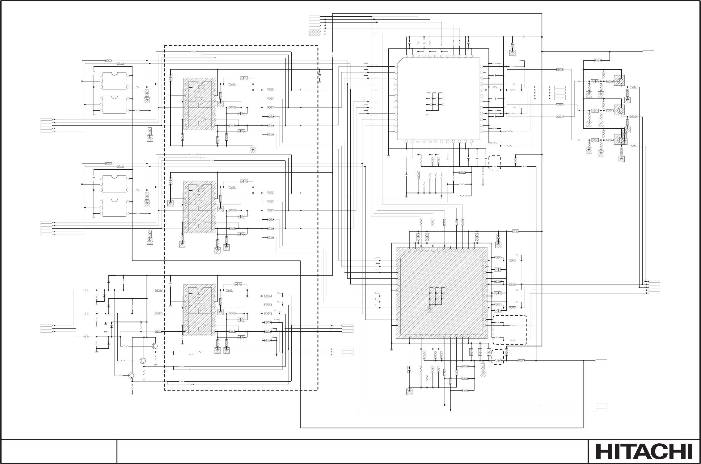
4
5
3
2
1
4
5
3
2
1
G7 G6 G5
G4G9G8
G3G2G1
1
36
48
47
46
45
44
43
42
41
40
39
38
37
35 34 33 32 31 30 29 28 27 26 25
24
23
22
21
20
19
17
18
16
15
14
13
12111098765432
-
+
-
+
+
-
9
10
11
12
13
14
15
16
8
7
6
5
4
3
2
1
4
5
3
2
1
-
+
-
+
+
-
9
10
11
12
13
14
15
16
8
7
6
5
4
3
2
1
-
+
-
+
+
-
9
10
11
12
13
14
15
16
8
7
6
5
4
3
2
1
4
5
3
2
1
G7 G6 G5
G4G9G8
G3G2G1
1
36
48
47
46
45
44
43
42
41
40
39
38
37
35 34 33 32 31 30 29 28 27 26 25
24
23
22
21
20
19
17
18
16
15
14
13
12111098765432
1005
RM75
10k
12
1005
RM13
560-1%
12
1005
RM97
75-1%
12
GND1
04M
C
500
1
0
1/1.0
1
2
1005
RM35
75-1%
12
GND1
CHBIG3
1
MONOUT1_B
1005
RM84
75-1%
12
3RCA3_G
CM46
2125
10/6.3
1
2
DSUB1_R
1005
RM38
100
12
CM61
1005
33p-C
12
1608
LM01
600
12
IM07
TC7SG17FU
NC
IN
GND OUT
VCC
6
3MC
5001
01
/
1.0
1
2
GND1
CHBIR1
1
1005
RM29
560-1%
12
DSUB1_H
1005
RMA1
10k-1%
12
1005
RMF7
0
12
1005
RML1
012
MUX2OUT_R
1608
LM05
600
12
GND1
CM56
1005
1.0p-C
1
2
CM47
1005
1.0p-C
12
CM28
1.0/10
12
1005
RM07
100
12
MONOUT1_R
1005
RM08
0
12
3RCA3_B
RMN1
75-1%
12
CM22
2125
10/6.3
12
GND1
CHBOB2 1
MUX2OUT_V
1005
RM53
0
12
1005
RMF5
10k-1%
12
1005
RM49
0
12
GND1
CHBOR1
1
+3.3V
CM21
2125
10/6.3
12
1005
RMM3
10k
12
1005
RMN7
0
12
CHBIB3
1
3RCA3_R
1005
RML7
4.7k
12
1005
RMM1
10k
12
CM09
2125
10/6.3
12
MUX1OUT_R
1005
RMM2
10k
12
MUX2OUT_B
1005
RM81
100
12
CHBIG1
1
GND1
1005
RMN8
100
12
CM30
2125
10/6.3
12
GND1
MONOUT1_H
GND1
CM62
1005
33p-C
12
CHBOB3
1
1005
RM04
100
12
1005
RMK8
10k
12
1005
RM36
75-1%
12
53M
C
50
01
01/1.
0
1
2
CM38
2125
10/6.3
12
32M
C
5001
6
1/10.0 1
2
1005
RMK5
10k
12
1005
RM32
560-1%
12
GND1
RMP3
100
12
MONOUT1_V
RMN4
75-1%
12
CHBIR4
1
GND1
1005
RMC2
10k-1%
12
GND1
1005
RM48
0
12
5001
21MR
%1-065
12
1005
RM33
560-1%
12
1005
RMK4
10k 1
2
52M
C
5001
01
/1.0 1
2
CM34
1005
0.1/10
1
2
1005
RMN9
0
12
MUX1OUT_V
1005
RM62
75-1%
12
IM09
TC7SG17FU
NC
IN
GND OUT
VCC
CHBIB1
1
1005
RM09
0
12
CM55
1005
1.0p-C
12
GND1
1005
RM17
75-1%
12
1005
RM96
75-1%
12
1005
RML5
4.7k
12
RMN5
75-1%
12
1005
RMG5 10k
12
GND1
RMP4
100
12
CHBOB4
1
CM48
1005
1.0p-C
1
2
DSUB1_V
1005
RM85
75-1%
12
CM01
100/6.3
MVK/SKV
1
2
5BNC1_G
CM54
2125
10/6.3
1
2
1005
RM95
75-1%
12
MUX1OUT_H
1005
RMJ4
012
14M
C
5001
01/
1.0
1
2
GND1
IM05
THS7327PHP
CH_1-INPUT_A
CH_2-INPUT_A
CH_3-INPUT_A
H-SYNC-INPUT_A
V-SYNC-INPUT_A
AGND-6
CH_1-INPUT_B
CH_2-INPUT_B
CH_3-INPUT_B
H-SYNC-INPUT_B
V-SYNC-INPUT_B
AGND-12
AGND-13
SCHMITT-TRIGGER_ADJ
MUX_MODE
MUX_SELECT
I2C-A1
I2C-A0
I2C-SDA
I2C-SCL
PCU
VDD
DGND
V-SYNC_BUFFER_OUTPUT
H-SYNC_BUFFER_OUTPUT
AGND-26
CH_3-BUFFER_OUTPUT-27
CH_3-BUFFER_OUTPUT-28
+VA-29
AGND-30
CH_2-BUFFER_OUTPUT-31
CH_2-BUFFER_OUTPUT-32
+VA-33
AGND-34
CH_1-BUFFER_OUTPUT-35
CH_1-BUFFER_OUTPUT-36
AGND-37
+VA-38
V-SYNC_MON_OUTPUT
H-SYNC_MON_OUTPUT
CH_3-SAG
CH_3-MONITOR_OUTPUT
CH_2-SAG
CH_2-MONITOR_OUTPUT
CH_1-SAG
CH_1-MONITOR_OUTPUT
AGND-47
+VA-48
1005
RM83
75-1%
12
GND1
1005
RMF8
0
12
1005
RM02
0
12
CHBIG4
1
1005
RM11
560-1%
12
1005
RME9
75-1%
12
DSUB1_G
5BNC1_H
CM32
1005
0.1/10
1
2
62M
C
500
1
0
1/1.0
1
2
CM33
1005
0.1/10
1
2
5BNC1_R
RMP5
100
12
CHBIR2
1
93M
C
5001
0
1/
1.0
1
2
CM50
2125
10/6.3
1
2
CM49
1005
1.0p-C
12
1005
RMJ1
0
12
MUX1OUT_G
1005
RM05
100
12
1005
RMG3
10k
12
1005
RM79
10k
12
DSUB1_B
5BNC1_V
CHBOG3
1
5BNC1_B
GND1
1005
RMF3
10k-1%
12
1005
RMJ2
0
12
RMP2
100
12
GND1
I2CCLK
RMN6
75-1%
12
CHBOG1 1
1005
RM15
560-1%
12
1005
RML6
4.7k
12
CM53
1005
1.0p-C
12
CHBIB4
1
CM10
2125
10/6.3
12
MUX2OUT_G
GND1
CM02
1005
0.1/10
12
3RCA1_G
1608
LM02
600
12
1005
RM99
10k-1%
12
1005
RM34
75-1%
12
1005
RM60
75-1%
12
CM52
1005
1.0p-C
1
2
CHBIG2
1
1005
RM18
75-1%
12
CM29
2125
10/6.3
12
1005
RMG6
10k 1
2
CM08
2125
10/6.3
12
RMN3
75-1%
12
CM63
1005
33p-C
12
IM03
EL8302IUZ-T7
INA+
CEA
VS-
CEB
INB+
NC-6
CEC
INC+ INC-
OUTC
NC-11
INB-
OUTB
VS+
OUTA
INA-
1005
RML9
10k
12
CHBOG4
1
3RCA1_R
MUX1OUT_B
GND1
CM51
1005
1.0p-C
12
RMN2
75-1%
12
1005
RM10
560-1%
12
1005
RM03
0
12
1005
RM78
10k
12
1005
RMF2
75-1%
12
I2CDAT
GND1
1005
RMF1
75-1%
12
1005
RMJ3
0
12
1608
LM03
600
12
GND1
1005
RMK9
10k
12
1005
RMF6
10k-1%
12
3RCA1_B
CM31
1005
0.1/10
1
2
MONOUT2_V
+5V
1005
RM16
75-1%
12
GND1
GND1
GND1
CHBIB2
1
MUX2OUT_H
1005
RM80
10k
12
1005
RM28
560-1%
12
1005
RMK7
10k
12
1005
RMF4
10k-1%
12
IM10
TC7SG17FU
NC
IN
GND OUT
VCC
5001
03MR
%1-065
12
CM27
1.0/10
12
1005
RML4
012
GND1
CHBOR3
1
1005
RMP1
100
12
CM37
2125
10/6.3
12
1005
RM14
560-1%
12
GND1
1005
RM01
10k
12
CM60
1005
0.1/10
12
CHBOB1
1
IM02
EL8302IUZ-T7
INA+
CEA
VS-
CEB
INB+
NC-6
CEC
INC+ INC-
OUTC
NC-11
INB-
OUTB
VS+
OUTA
INA-
3RCA2_G
GND1
GND1
1608
LM04
600
12
GND1
CHBOR2
1
1005
RM06
100
12
1005
RML2
01
2
1005
RM61
75-1%
12
GND1
1005
RMA2
10k-1%
12
1005
RMG4
10k
12
1005
RM37
100
12
CHBIR3
1
1005
RM76
100
12
IM01
EL8302IUZ-T7
INA+
CEA
VS-
CEB
INB+
NC-6
CEC
INC+ INC-
OUTC
NC-11
INB-
OUTB
VS+
OUTA
INA-
GND1
3RCA2_R
1005
RM58
560-1%
12
1005
RM54
560-1%
12
IM08
TC7SG17FU
NC
IN
GND OUT
VCC
42M
C
5001
6
1/10.0
1
2
CM57
1005
1.0p-C
12
CHBOR4
1
MONOUT2_H
1005
RMK6
10k
12
1005
RM31
560-1%
12
MONOUT1_G
1005
RM71
100
12
3RCA2_B
1005
RML8
4.7k
12
5001
65MR
%1-065
12
GND1
CM64
1005
33p-C
12
CHBOG2 1
1005
RML3
01
2
IM04
THS7327PHP
CH_1-INPUT_A
CH_2-INPUT_A
CH_3-INPUT_A
H-SYNC-INPUT_A
V-SYNC-INPUT_A
AGND-6
CH_1-INPUT_B
CH_2-INPUT_B
CH_3-INPUT_B
H-SYNC-INPUT_B
V-SYNC-INPUT_B
AGND-12
AGND-13
SCHMITT-TRIGGER_ADJ
MUX_MODE
MUX_SELECT
I2C-A1
I2C-A0
I2C-SDA
I2C-SCL
PCU
VDD
DGND
V-SYNC_BUFFER_OUTPUT
H-SYNC_BUFFER_OUTPUT
AGND-26
CH_3-BUFFER_OUTPUT-27
CH_3-BUFFER_OUTPUT-28
+VA-29
AGND-30
CH_2-BUFFER_OUTPUT-31
CH_2-BUFFER_OUTPUT-32
+VA-33
AGND-34
CH_1-BUFFER_OUTPUT-35
CH_1-BUFFER_OUTPUT-36
AGND-37
+VA-38
V-SYNC_MON_OUTPUT
H-SYNC_MON_OUTPUT
CH_3-SAG
CH_3-MONITOR_OUTPUT
CH_2-SAG
CH_2-MONITOR_OUTPUT
CH_1-SAG
CH_1-MONITOR_OUTPUT
AGND-47
+VA-48
DM01
1SS355
12
DM04
1SS355
12DM02
1SS355
12
DM05
1SS355
12
DM07
1SS355
12
DM06
1SS355
12
GND1
GND1
CM03
100/6.3
MVK/SKV
1
2
GND1
CM04
100/6.3
MVK/SKV
1
2
24MC
5
001
01/
1.
0
1
2
1005
RMM4
33
12
1005
RMM6
33
12
1005
RMM8
33
12
1005
RM55
0
12
1005
RM57
0
12
1005
RM59
0
12
1608
*LM06
600
12
GND1
1005
*RMC9
22k
12
1005
*RME5
22k
12
GND1
1005
*RMG8
47
12
GND1
GND1
1005
*RME1
33k
12
1005
*RMC5
33k
12
1005
*RMH2
47
12
RMC7
75-1%
12
*QM04
2SC4617
1
2
3
1005
*RME2
100
12
1005
*RME6
33k
12
1005
*RMC4
22k
12
1005
*RMG9
47
12
1005
*RMH3
47
12
*CM18
2125
22/6.3
12
1005
*RMC6
100
12
RME4
75-1%
12
1005
*RME8
360-1%
12
GND1
1005
*RMH1
47
12
GND1
GND1
RMC3
75-1%
12
*QM05
2SC4617
1
2
3
GND1
GND1
GND1
*CM17
2125
22/6.3
12
1005
*RME7
100
12
1005
*RMG7
47
12
*CM19
2125
22/6.3
12
1005
*RME3
360-1%
12
*QM06
2SC4617
1
2
3
*CM20
1005
0.1/10
1
2
1005
*RMC8
360-1%
12
1005
RM50
33
12
1005
RM51
33
12
1005
RM52
33
12
1005
RM39
33
12
1005
RM40
33
12
1005
RM41
33
12
1005
RM44
10k
12
1005
RM43
10k
12
1005
RM42
10k
12
1005
RM47
18k
12
1005
RM46
18k
12
1005
RM45
18k
12
1005
RM73
220
12
1005
RM77
220
12
1005
RM82
220
12
QM01
STC-2SC4726
1
2
3
QM02
STC-2SC4726
1
2
3
QM03
STC-2SC4726
1
2
3
1005
RM66
100
12
1005
RM65
100
12
1005
RM64
100
12
1005
RM67
33
12
1005
RM68
33
12
1005
RM69
33
12
1005
RMM5
68
12
1005
RMM7
68
12
1005
RMM9
68
12
JUMPER R
R
H
G
B
I2C SLAVE ADDR.
V
5Ah/5Bh
B
R
G
I2C SLAVE ADDR.
V
58h/59h
H
G
B
R
B
G
R
SM0321 PWB ASSEMBLY MAIN 16
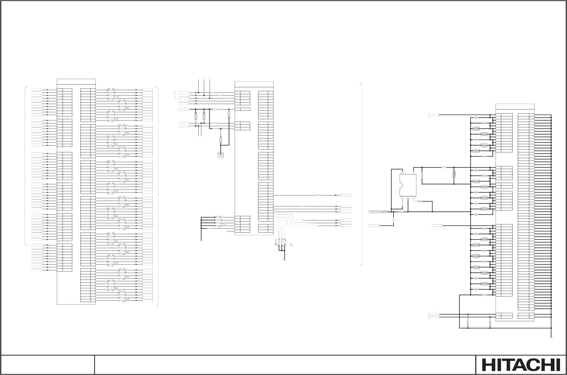
A5
A6
B6
B5
A4
C5
B3
A3
C4
B4
F3
C3
D3
G3
C2
B2
G2
F2
E2
D2
P3
L3
M3
R3
M2
L2
T2
R2
P2
N2
D1
E1
F1
U2
V2
G1
H1
C1
C6
E3
N3
N22
AB20
AB10
U3
V3
W3M19
N1
U1
M1
L1
K1
P1
T1
R1
W2
V1
W1
T3
B8
A8
CXD3540GB 2/3
CXD3540GB 1/3
N20
N21
P20
P21
P22
R20
R21
R22
T20
T21
T22
U22
U20
U21
V20
V21
V22
W20
W21
W22
Y20
Y21
Y22
AA21
AA16
Y17
AB16
AA17
Y18
AB17
AA18
Y19
AB18
AA19
AB19
AA20
AA12
Y13
AB12
AA13
Y14
AB13
AA14
Y15
AB14
AA15
Y16
AB15
Y6
AA6
AB6
Y7
AA7
AB7
Y8
AA8
AB8
Y9
AA9
AB9
Y1
Y2
AA2
Y3
AA3
AB3
Y4
AA4
AB4
Y5
AA5
AB5
C9
B9
A9
C10
B10
A10
C11
B11
A11
C12
B12
A12
C13
B13
A13
C14
B14
A14
C15
B15
A15
C16
B16
A16
C17
B17
A17
C18
B18
A18
C19
B19
A19
D20
C20
B20
A20
C21
B21
C22
G21
G22
F20
F21
F22
E20
E21
E22
D21
D22
K20
K21
K22
J20
J21
J22
H20
H21
H22
G20
CXD3540GB 3/3
A1
A2
A7
A21
A22
B1
B7
B22
C7
C8
H2
H3
J1
J2
J3
J10
J11
J12
J13
J14
K2
K3
K9
K10
K11
K12
K13
K14
K19
L9
L10
L11
L12
L13
L14
L20
L21
L22
M9
M10
M11
M12
M13
M14
M20
M21
M22
N9
N10
N11
N12
N13
N14
P9
P10
P11
P12
P13
P14
Y10
Y11
Y12
AA1
AA10
AA11
AA22
AB1
AB2
AB11
AB21
AB22
L4
N4M4
K4
W17
W16
W14
W13
W10
W9
W6
U19
U4
T19
T4
P19
P4
N19
J19
H19
G4
F19
F4
D17
D16
D14
D13
D10
D9
D6
W19
V19
R19
L19
G19
E19
D19
W18
D18
W5
V4
J4
E4
D5
W15
W12
W11
W8
W7
W4
R4
H4
D15
D12
D11
D8
D7
D4
4
5
3
2
1
C477
1005
1000p
12
R452
2010
22
78
56
34
12
I451
CXD3540AGB
A8 HDIN
B8 VDIN
T3 CLK
W1 XCLR
V1 XPLLSTB
W2 CTRL
R1 HSCL
T1 HSDA
P1 HSEL
K1 TEST1
L1 TEST2
M1 TEST3
U1 TEST4
N1 TRST
M19 NC W3
GCFB_B
V3
GCFB_G
U3
GCFB_R
AB10
CLKOUT3
AB20
CLKOUT2
N22
CLKOUT1
N3
PRG_B
E3
PRG_G
C6
PRG_R
C1
VD
H1
FRP
G1
XSCAN
V2
SCAN
U2
DWN
F1
CLR
E1
PCG
D1
ENB
N2
DCK1_B
P2
DCK2_B
R2
DCK3_B
T2
DCK4_B
L2
HCK1_B
M2
HCK2_B
R3
PST_B
M3
VCK_B
L3
VST_B
P3
HST_B
D2
DCK1_G
E2
DCK2_G
F2
DCK3_G
G2
DCK4_G
B2
HCK1_G
C2
HCK2_G
G3
PST_G
D3
VCK_G
C3
VST_G
F3
HST_G
B4
DCK1_R
C4
DCK2_R
A3
DCK3_R
B3
DCK4_R
C5
HCK1_R
A4
HCK2_R
B5
PST_R
B6
VCK_R
A6
VST_R
A5
HST_R
DBE9
DRO3
DRO5
R453
2010
22
12
34
56
78
BD3-2
R467
2010
10
12
34
56
78
RD4-5
DRO6
BD3-0
BD4-3
I451
CXD3540AGB
G20 R1IN9
H22 R1IN8
H21 R1IN7
H20 R1IN6
J22 R1IN5
J21 R1IN4
J20 R1IN3
K22 R1IN2
K21 R1IN1
K20 R1IN0
D22 R2IN9
D21 R2IN8
E22 R2IN7
E21 R2IN6
E20 R2IN5
N21
R1OUT10
N20
R1OUT11
F20 R2IN2
G22 R2IN1
G21 R2IN0
C22 G1IN9
B21 G1IN8
C21 G1IN7
A20 G1IN6
B20 G1IN5
C20 G1IN4
D20 G1IN3
A19 G1IN2
B19 G1IN1
C19 G1IN0
A18 G2IN9
B18 G2IN8
C18 G2IN7
A17 G2IN6
B17 G2IN5
C17 G2IN4
A16 G2IN3
B16 G2IN2
C16 G2IN1
A15 G2IN0
B15 B1IN9
C15 B1IN8
A14 B1IN7
B14 B1IN6
C14 B1IN5
A13 B1IN4
B13 B1IN3
C13 B1IN2
A12 B1IN1
B12 B1IN0
C12 B2IN9
A11 B2IN8
B11 B2IN7
C11 B2IN6
A10 B2IN5
B10 B2IN4
C10 B2IN3
A9 B2IN2
B9 B2IN1
C9 B2IN0
AB5
B2OUT0
AA5
B2OUT1
Y5
B2OUT2
AB4
B2OUT3
AA4
B2OUT4
Y4
B2OUT5
AB3
B2OUT6
AA3
B2OUT7
Y3
B2OUT8
AA2
B2OUT9
Y2
B2OUT10
Y1
B2OUT11
AB9
B1OUT0
AA9
B1OUT1
Y9
B1OUT2
AB8
B1OUT3
AA8
B1OUT4
Y8
B1OUT5
AB7
B1OUT6
AA7
B1OUT7
Y7
B1OUT8
AB6
B1OUT9
AA6
B1OUT10
Y6
B1OUT11
AB15
G2OUT0
Y16
G2OUT1
AA15
G2OUT2
AB14
G2OUT3
Y15
G2OUT4
AA14
G2OUT5
AB13
G2OUT6
Y14
G2OUT7
AA13
G2OUT8
AB12
G2OUT9
Y13
G2OUT10
AA12
G2OUT11
AA20
G1OUT0
AB19
G1OUT1
AA19
G1OUT2
AB18
G1OUT3
Y19
G1OUT4
AA18
G1OUT5
AB17
G1OUT6
Y18
G1OUT7
AA17
G1OUT8
AB16
G1OUT9
Y17
G1OUT10
AA16
G1OUT11
AA21
R2OUT0
Y22
R2OUT1
Y21
R2OUT2
Y20
R2OUT3
W22
R2OUT4
W21
R2OUT5
W20
R2OUT6
V22
R2OUT7
V21
R2OUT8
V20
R2OUT9
U21
R2OUT10
U20
R2OUT11
U22
R1OUT0
T22
R1OUT1
T21
R1OUT2
T20
R1OUT3
R22
R1OUT4
R21
R1OUT5
R20
R1OUT6
P22
R1OUT7
P21
R1OUT8
P20
R1OUT9
F22 R2IN4
F21 R2IN3
BD4-4
1005
R4G2
56
12
GD4-1
C456
2125
10/6.3
1
2
BD3-9
BD4-1
CHK454
1
RD4-11
C454
1005
1000p
12
RD4-2
DGO8
SHCLK2_B
DGO5
DBO2
R462
2010
22
12
34
56
78
BD3-3
C470
47/6.3
MVK/SKV
1
2
1005
R4G3
56
12
R478
2010
0
78
56
34
12
DBO9
DGE5
DGO1
1005
R472
012
I2CCLKP
DRE6
C467
1005
1000p
12
DBO1
DGO3
CHK450
1
DGO2
R455
2010
22
78
56
34
12
RD3-8
DGE1
BD4-2
DRE3
BD4-5
PRG2_R
DBO4
1005
R495
56
12
DBE3
GND1
DBE0
R457
2010
22
12
34
56
78
DBO5
1005
R474
33
12
GD4-8
DRE8 R451
2010
22
78
56
34
12
C468
1005
0.1/10
12
GND1
DGO7
C457
1005
0.1/10
12
C494
1.0/101
2
DRE5
1005
R475
10k
12
GND1
RD4-4
DGO9
R496
2010
10
1
2
56
3
4
7
8
C471
2125
10/6.3
1
2
DGO6
BD3-11
BD3-4
DGE0
+3.3VP
BD3-6
I2CDATP
C472
1005
1000p
12
DBO6
C451
2125
10/6.3
1
2
BD4-10
CHK455
1
RD3-10 1005
R4F1
56
12
C475
1005
0.1/10
12
DBE7
DGE7
DRO7
GD4-3
DBE8
DRE7
DGE3
R464
2010
10
12
34
56
78
PRG2_B
DRE1
GD4-7
1005
R473
33
12
1005
R4G1
56
12
1005
R471
56
12
GD4-11
DBE2
R466
2010
10
12
34
56
78
RD3-11
C473
1005
0.1/10
12
RD4-6
GD3-5
RD3-1
RESETX
CHK4NC2
1
RD4-1
RD3-4
RD3-0
BD4-11
C465
1005
0.1/10
12
DRO4
GD4-0
RD4-7
C480
1005
0.1/10
12
2518
L452
10
12
BD3-10
GD3-0
1005
R499
1.0k
12
DGE4
1005
R493
56
12
C455
1005
0.1/10
12
DGE8
DBE1
BD3-5
SHCLK2_G
RD3-2
BD4-6
RESETP
R461
2010
22
12
34
56
78
C453
1005
0.1/10
12
CHK453
1
DGO4
DGE6
GND1
GD4-2
DBE5
GD4-5
RD3-3
C481
1005
1000p
12
RD4-3
DGE2
C476
2125
10/6.3
1
2
DRO1
R459
2010
22
12
34
56
78
DRE4
DBO7
DBE6
GD3-10
RD4-8
PRG2_G
BD4-8
1005
R491
22
12
C474
1005
1000p
12
BD3-1
DGO0
GD3-8
RD4-10
C482
1005
0.1/10
12
BD4-9
GD3-7
DRE0
RD4-0
RD3-9
C452
1005
1000p
12
DRE2
DRE9
BD3-8
C458
1.0/10
1
2
R454
2010
22
78
56
34
12
DRO0
DBO8
1005
R479
0
12
BD4-7
DBE4
GD4-4
CHK452
1
DBO0
GD4-10
GD4-9
DVS
GD3-2
DRO9
RD3-7 I451
CXD3540AGB
D4
VDDI-D4
D7
VDDI-D7
D8
VDDI-D8
D11
VDDI-D11
D12
VDDI-D12
D15
VDDI-D15
H4
VDDI-H4
R4
VDDI-R4
W4
VDDI-W4
W7
VDDI-W7
W8
VDDI-W8
W11
VDDI-W11
W12
VDDI-W12
W15
VDDI-W15
D5
VDE2-D5
E4
VDE2-E4
J4
VDE2-J4
V4
VDE2-V4
W5
VDE2-W5
D18
VDE2-D18
W18
VDE2-W18
D19
VDE2-D19
E19
VDE2-E19
G19
VDE2-G19
L19
VDE2-L19
R19
VDE2-R19
V19
VDE2-V19
W19
VDE2-W19
D6
VDE3-D6
D9
VDE3-D9
D10
VDE3-D10
D13
VDE3-D13
D14
VDE3-D14
D16
VDE3-D16
D17
VDE3-D17
F4
VDE3-F4
F19
VDE3-F19
G4
VDE3-G4
H19
VDE3-H19
J19
VDE3-J19
N19
VDE3-N19
P4
VDE3-P4
P19
VDE3-P19
T4
VDE3-T4
T19
VDE3-T19
U4
VDE3-U4
U19
VDE3-U19
W6
VDE3-W6
W9
VDE3-W9
W10
VDE3-W10
W13
VDE3-W13
W14
VDE3-W14
W16
VDE3-W16
W17
VDE3-W17
K4
VDDA1
M4
VDDA3
N4
VSSA3
L4
VSSA1
AB22
VSS-AB22
AB21
VSS-AB21
AB11
VSS-AB11
AB2
VSS-AB2
AB1
VSS-AB1
AA22
VSS-AA22
AA11
VSS-AA11
AA10
VSS-AA10
AA1
VSS-AA1
Y12
VSS-Y12
Y11
VSS-Y11
Y10
VSS-Y10
P14
VSS-P14
P13
VSS-P13
P12
VSS-P12
P11
VSS-P11
P10
VSS-P10
P9
VSS-P9
N14
VSS-N14
N13
VSS-N13
N12
VSS-N12
N11
VSS-N11
N10
VSS-N10
N9
VSS-N9
M22
VSS-M22
M21
VSS-M21
M20
VSS-M20
M14
VSS-M14
M13
VSS-M13
M12
VSS-M12
M11
VSS-M11
M10
VSS-M10
M9
VSS-M9
L22
VSS-L22
L21
VSS-L21
L20
VSS-L20
L14
VSS-L14
L13
VSS-L13
L12
VSS-L12
L11
VSS-L11
L10
VSS-L10
L9
VSS-L9
K19
VSS-K19
K14
VSS-K14
K13
VSS-K13
K12
VSS-K12
K11
VSS-K11
K10
VSS-K10
K9
VSS-K9
K3
VSS-K3
K2
VSS-K2
J14
VSS-J14
J13
VSS-J13
J12
VSS-J12
J11
VSS-J11
J10
VSS-J10
J3
VSS-J3
J2
VSS-J2
J1
VSS-J1
H3
VSS-H3
H2
VSS-H2
C8
VSS-C8
C7
VSS-C7
B22
VSS-B22
B7
VSS-B7
B1
VSS-B1
A22
VSS-A22
A21
VSS-A21
A7
VSS-A7
A2
VSS-A2
A1
VSS-A1
R463
2010
10
12
34
56
78
R456
2010
22
34
56
78
12
1005
R477
10k
12
R465
2010
10
12
34
56
78
RD3-6
C466
2125
10/6.3
1
2
1005
R476
0
12
GD3-9
GD3-6
GD3-3
RD4-9
GD4-6
C463
1005
0.1/10
12
RD3-5
C461
2125
10/6.3
1
2
R458
2010
22
12
34
56
78
R468
2010
10
12
34
56
78
BD3-7
GD3-4
1005
R4F2
56
12
1005
R498
1.0k
12
DRO8
C483
2125
10/6.3
1
2
C469
1.0/10
1
2
GD3-11
DBO3
BD4-0
C464
1005
1000p
12
C478
1005
0.1/10
12
C492
1.0/10 1
2
C462
1005
1000p
12
GD3-1
R460
2010
22
12
34
56
78
SCAN
DCLK
1005
R494
56
12
C479
1005
1000p
12
DHS
DGE9
SHCLK2_R
DRO2
C497
1.0/10
1
2
1005
R470
1.0k
12
1005
R4F4
0
12
C486
1005
1000p
12
+4.0V
I452
TK11125CSC
Vcont
GND
Np Vout
Vin
C485
1.0/10
1
2
1005
R4F3
0
12
+3.3VP
+1.8VP2
+3.3VP2
+1.8VP3
+3.3VP3
TG(Slave) Part
for 0.79" SXGA
from PW
from PW
PW TWOWSC0
PW TWOWSD0
controlled by POWER6
from I802
controlled by POWER5
from I403
JUMPER R
to S/H part
to S/H part
PW PORTA7
PW PORTA5
SM0321 PWB ASSEMBLY MAIN 17
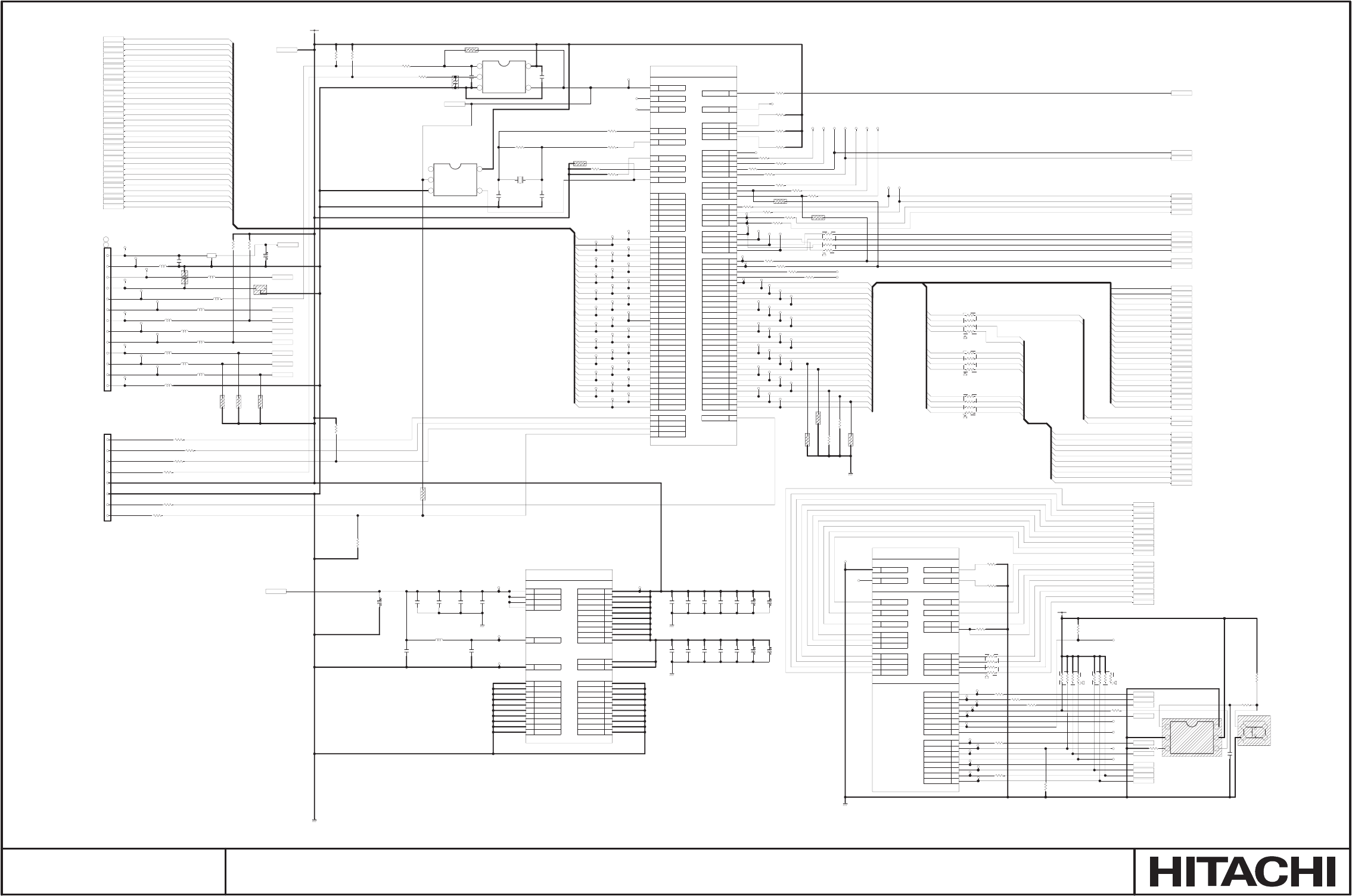
4
5
3
2
1
4
5
3
2
1
E5
NS7520
M13
P1
R1
N2
M3
R2
M4
R3
N4
P5
R4
M5
N5
P6
R6
N6
M6
R7
P8
N7
M7
R9
N8
N9
M9
P10
R10
N10
M10
A2
A1
B3
C4
A9
D9
C9
B9
D6
C6
B6
D5
B5
C5
A4
B4
C8
D8
A8
C7
A6
M14
C2
N14
P15
M12
D3
E2
D1
B1
D4
C1
E3
G2
F2
E1
F3
F4
G3
H3
H1
G4
G1
H2
H4
K2
J2
J1
J3
K1
K3
N1
L3
L4
L1
L2
M11
P11
R12
P13
R14
N11
M11
N15
M15
L13
K14
K12
B7
D7
A10
D14
B15
B13
A15
NS7520
E15
E14
F13
E12
G14
F12
G13
F15
G12
H15
H13
H12
J14
J12
J13
J15
D11
A11
B11
A12
A13
B12
B10
D10
R13
P12
D12
D15
C15
C12
A14
C10
R15
N12
A5
A7
C3
N13
A3
K4
N3
F14
K15
G15
R11
P7
P9
M8
L14
C13
P4
D2
J4
F1
NS7520
C11
E13
B14
D13
P14
P2
K13
B2
R5
P3
B8
H14
M2
E4
L12
L15
C14
R8
4
5
6
3
2
1
43
21
D31
D28
D25
D22
D19
TPL13
D30
D29
D27
D26
D24
D23
D21
D20
D18
D17
NA0
NA9
NA10
NA11
NA12
NA13
NA14
NA15
NA16
NA17
NA18
NA19
NA20
NA21
NA22
P_MDC
P_MDIO
P_TXEN
P_TXD3
P_TXD2
P_TXD1
P_TXD0
NA22
NA21
NA20
NA19
NA18
NA17
NA16
NA15
NA14
NA13
NA12
NA11
NA10
NA9
NA8
NA7
NA6
NA5
NA4
NA3
NA2
NA1
NA0
SD_BA0
SD_A9
SD_A8
SD_A7
SD_A6
SD_A5
SD_A4
SD_A3
SD_A2
SD_A1
SD_A0
NA23
SD_BA1
D16
D0
D2
D1
D3
D5
D8
D11
D15
D14
D12
D9
D6
D7
D4
D13
D10
D14
D3
D10
D6
D13
D2
D9
D5
D12
D1
D8
D15
D4
D11
D0
D7
D31
D30
D29
D28
D27
D26
D25
D24
D23
D22
D21
D20
D19
D18
D17
D16
NA10
NA21
NA22
NA11
NA9
NA8
NA7
NA6
NA5
NA4
NA3
NA2
SD_A3
SD_A2
SD_A1
SD_A0
SD_A4
SD_A5
SD_A6
SD_A7
SD_A8
SD_A9
SD_BA0
SD_BA1
P_TXCLK
P_RXCLK
P_COL
P_RXER
P_CRS
P_RXDV
P_RXD3
P_RXD2
P_RXD1
P_RXD0
NA3
NA4
NA2
NA1
NA5
NA6
NA7
NA8
APL01
NW_RXD1
IL02
SN74LVC1G08DCK
A
B
GND Y
Vcc
TPL22
1005
RL05
0
1005
RL07
330-1%
1005
RL06
1.0M
CL02
1005
10p-C
TPL27 TPL24TPL30TPL33TPL36TPL39
TPL40
CL06
1005
0.1/16
CL07
1005
0.1/16
CL08
1005
0.1/16
CL09
1005
0.1/16
2125
LL22
1000
CL11
1005
0.1/16
CL10
1005
0.1/16
1005
RL10
10
1005
RL11
820
1005
RL12
820
1005
RL13
820
CL13
1005
0.1/16
1005
RL23
15k-1%
1005
RL24
15k-1%
TPLA2
RL25
2010
33
TPLA4
APL02
2125
LL03
600
APL03
APL04
APL05
APL06APL09
APL10
APL11
APL12
2125
LL13
600
APL13
NW_TXD1
NW_RXD2
NW_TXD2
MSLEEP
SBUSY
ERR
GND1
GND1
CL12
1005
0.1/16
CL14
1005
0.1/16
CL15
1005
0.1/16
CL16
1005
0.1/16
GND1
GND1
CL19
1005
0.1/16
CL20
1005
0.1/16
CL23
1005
0.1/16
CL21
1005
0.1/16
CL22
1005
0.1/16
1005
RL02
10k
+3.3V
NW_RESET
TPL25TPL34TPL37 TPL31
TPL26TPL35TPL38 TPL29TPL32
TPL28
TPL41
TPL42
TPL43
TPL44
TPL45
TPL46
TPL47
TPL48
TPL49
TPL50
TPL51
TPL52
TPL53
TPL54
TPL55
1005
RL26
10k
TPL56
TPL57
SD_CLK
SD_CS
F_CS
BE3
BE2
TPL58
TPL60
TPL61
TPL62
TPL64
TPL63
TPL65
TPL66
RL15
2010
33
TPL69
TPL70
TPL71 TPL72
TPL75
TPL76
RL19
2010
33
RL20
2010
33
RL21
2010
33
TPL79
TPL80
TPL81
TPL78
TPL82
TPL85
TPL84
TPL83
TPL86
TPL89
TPL88
TPL87
TPL90
TPL93
TPL92
TPL91
TPL94
TPL97
TPL96
TPL95
TPL98
TPLA1
TPL99
TPLA3
GND1
NW_RXD1
NW_I2C_DAT
NW_I2C_CLK
SBUSY
NW_TXD1
ERR
MSLEEP
NW_RXD2
NW_TXD2
TPLA6
TPLA7
TPLA9 TPLC1
1005
RL01
10k
1005
RL03
10k
TPL23
3216
HL01
C1V222-2A
3216
HL02
C1V222-2A
D15
D14
D13
D12
D11
D10
D9
D7
D8
D6
D5
D4
D3
D2
D1
D0
SD_RAS
SD_CAS
SD_WE
SD_A10
NA22
NA21
NA20
NA19
NA18
NA17
NA16
NA15
NA14
NA13
NA12
NA11
NA10
NA9
NA8
NA7
NA6
NA5
NA4
NA3
NA2
NA1
NA0
SD_A5
SD_A9
SD_A8
SD_A3
SD_A4
SD_A7
SD_A2
SD_A1
SD_BA0
SD_A6
SD_A0
P_CRS
P_TXD3
P_RXD3
P_RXER
P_COL
P_RXCLK
P_RXD2
P_RXD1
P_RXD0
P_MDIO
P_TXD2
P_TXD1
P_TXCLK
P_TXEN
P_MDC
P_TXD0
P_RXDV
CL01
1005
0.1/16
APL07
APL08
1005
RL82
10k
1005
RL83
10k
RL84
2010
10k
RL85
2010
10k
+3.3V
1005
RL27
2.7k 1005
RLE1
2.7k
1005
RLE2
33
1005
RLE3
33
1005
RLE4
33
F_OE
F_WE
1005
RLE5
33
1005
RLE7
33
1005
RLE6
33
1005
RLE0
33
1005
RLF1
33
1005
RLF2
33
1005
RLF3
33
GND1
1005
RLF6
10k
1005
RLF7
10k
1005
RLF8
10k
IL12
SN74LVC1G14DCK
NC
A
GND Y
Vcc
BE1
BE0
1608
LL06
600
1608
LL10
600
1608
LL07
600
1608
LL11
600
1608
LL08
600
1608
LL05
600
1608
LL09
600
1608
LL12
600
SD_BA1
D20
D29
D19
D28
D18
D27
D17
D26
D16
D25
D23
D24
D22
D31
D21
D30
1005
RLG4
33
1005
RLG5
33
1005
RLG6
33
1005
RLG9
2.7k
1005
RLG0
0
1005
RLH1
0
1005
RLF0
56
1005
RLE8
56
1005
RLE9
56
1005
RLF9
56
XL01
18.432MHz
SMD-49
CL05
10/16
MVK/SKV
CL24
10/16
MVK/SKV
CL25
10/16
MVK/SKV
CL17
10/16
MVK/SKV
CL18 10/16
MVK/SKV
1005
RLH2
10
1005
RLH3
10
1005
RLH4
10
1005
RLH5
10
1005
RLH6
10
1005
RLH7
10
TPL01
TPL02
TPL03
TPL04
TPL05
TPL06
TPL07 TPL08
TPL09
TPL10
TPL11
TPL12
TPL13
TPL14
TPL15
TPL16
TPL17
TPL18
TPL19
TPL20
TPLB1
EL02
ZH-08V
1
2
3
4
5
6
7
8
RTC_INTR
TPLA8
1005
RLJ8
100
1005
RLJ9
100
1005
RLK1
100
1005
RLK2
100
1005
RLK3
100
IL01
NS7520B-1-C36
RESET_
BR_
BUSY_
XTALA1
XTALA2
PLLTST_
BISTEN_
SCANEN_
NC1
NC2
NC3
NC4
NC5
NC6
D31
D30
D29
D28
D27
D26
D25
D24
D22
D21
D20
D19
D18
D17
D16
D15
D14
D13
D12
D11
D10
D9
D23
D7
D6
D5
D4
D3
D2
D1
D0
TDI
TMS
TCK
TRST_
TDO
A0
A1
A2
A3
A4
A5
A6
A7
A8
A9
A10
A11
A12
A13
A14
A15
A16
A17
A18
A19
A20
A21
A22
A23
A24
A25/BLAST_
A26/CS0WE_
A27/CS0OE_
CAS0_
CAS1_
CAS2_
CAS3_
D8
BE0_
BE1_
BE2_
BE3_
OE_
WE_
RW_
CS0_
CS1_
CS2_
CS3_
CS4_
TEA_
TA_
TS_
BG_
BCLK
NC7
IL01
NS7520B-1-C36
XTALB1
XTALB2
TXCLK
RXCLK
TXCOL
RXER
RXCRS
RXDV
RXD3
RXD2
RXD1
RXD0
C0/TXCKB
C1/CTSB_
C2/DSRB_
C3/RXDB
C4/RXCKB
C5/RTSB_
C6/DTRB_
C7/TXDB
A0/TXCKA
A1/CTSA_
A3/RXDA
A4/RXCKA
A5/RTSA_
A6/DTRA_
A7/TXDA
TXD0
TXD1
TXD2
TXD3
TXER
TXEN
MDIO
MDC
NC-R13
A2/DSRA_
NC-P12
IL01
NS7520B-1-C36
VDD1
VDD2
VDD3
VDD4
PLLVDD
PLLVSS
GND1
GND2
GND3
GND4
GND5
GND6
GND7
GND8
GND9
GND10 GND11
GND12
GND13
GND14
GND15
GND16
GND18
GND19
GND20
OSCVDD2
OSCVDD1
OVDD6
OVDD5
OVDD4
OVDD3
OVDD2
GND17
OVDD1
OVDD7
OVDD10
OVDD9
OVDD8
1005
RLK4
10k
IL14
SN74LVC1G97DCK
In1
GND
In0 Y
VCC
In2
1005
RLM2
100
1005
RLM3
0
1005
RLK8
470
1005
RLK9
10k
SL01
SKRAAAE010
CLA1
1.0/10-F
1005
RLM1
0
CL03
1005
12p-C
CLF6
1005
0.01/16
1005
RLF5
2.7k 1005
RLF4
2.7k
1005
RLM4
2.7k 1005
RLM5
2.7k
1005
RLM6
2.7k
CLF0
1005
0.1/16
1005
RLM8
100
1005
RLM7
100
CLA6
1005
1000p
2125
LL01
600
EL01
ZH-13H
1
2
3
4
5
6
7
8
9
10
11
12
13
G1
G2
BAT3V
TPLA0
+15V
+1.5V
CL04
47/25
MVK/SKV
1005
RL22 10k
P_TXER
TPL59
+3.3V
CLF5
1005
0.01/25
TDI
TMS
TCK
ICE_RST
3.3V
GND
TD0
ICE_TRST
RLM1 mount:19.2kbps
not mount:14.4kbps
+15V
M_RESET
ES_BUSY
MSLEEP
GND
RXD2
TXD1
Battery
TXD2
RXD1
SBUSY
GND
+6.6V
3V
SM0321 PWB ASSEMBLY NETWORK 1
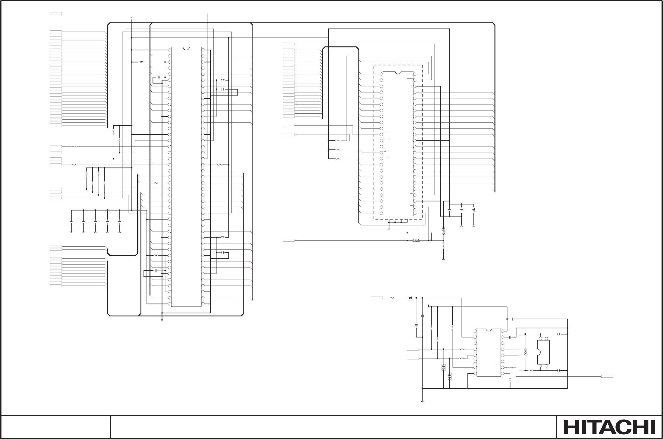
28
29
30
31
32
33
34
35
36
37
38
39
40
41
42
43
44
45
46
47
48
26
27
2524
23
22
21
20
19
18
17
16
15
14
13
12
11
10
9
8
7
6
5
4
3
2
1
54
53
51
52
50
49
47
48
46
45
4443
42
41
40
39
38
36
37
35
34
33
83
55
56
57
58
59
60
61
62
63
64
65
66
67
68
69
70
71
72
73
74
75
76
77
78
79
80
81
82
84
85
86
32
31
30
29
28
27
26
25
24
23
22
21
20
19
18
17
16
15
14
13
12
11
10
9
8
7
6
5
4
3
2
1
4
32
1
9
10
11
12
13
14
15
16
8
7
6
5
4
3
2
1
NA16
NA15
NA14
NA13
NA12
NA11
NA10
NA9
NA20
NA19
NA18
NA8
NA7
NA6
NA5
NA4
NA3
NA2
D23
D30
D22
D29
D21
D28
D19
D26
D18
D25
D17
D24
D16
NA17
NA17
D20
NA21
D27
D15
D14
D13
D12
D11
D10
D9
D8
D7
D6
D5
D4
D3
D2
D1
D0
SD_BA0
SD_A9
SD_A8
SD_A7
SD_A6
SD_A5
SD_A4
SD_A3
SD_A2
SD_A1
SD_A0
NA22
NA0
NA1
NA2
NA3
NA4
NA5
NA6
NA7
NA8
NA9
NA10
NA11
NA12
NA13
NA14
NA15
NA16
NA17
NA18
NA19
NA20
NA21
D0
D1
D2
D3
D4
D5
D6
D7
D16
D17
D18
D19
D20
D21
D22
D23 D24
D25
D26
D27
D28
D29
D30
D31
SD_A3
SD_A4
SD_A5
SD_A6
SD_A7
SD_A8
SD_A9
D8
D9
D10
D11
D12
D13
D14
D15
SD_BA0
SD_BA1
SD_BA1
D16
D17
D18
D19
D20
D21
D22
D23
D24
D25
D26
D27
D28
D29
D30
D31
NA1
SD_A0
SD_A1
SD_A2
D31
GND1
+3.3V
CL30
1005
0.1/16
CL29
1005
0.1/16
CL28
1005
0.1/16
CL27
1005
0.1/16
CL26
1005
0.1/16
GND1 GND1 GND1 GND1
GND1
CL31
1005
0.1/16
CL32
1005
0.01-F
GND1GND1
F_WE
F_OE
NW_RESET
F_CS
1005
RL31
2.7k
1005
RL32
2.7k
1005
RL33
2.7k
1005
RL80
10k
GND1
1005
RL34
0
TPLE6
TPLE5
D12
D11
D7
D2
D1
D14
D0
D13
D8
D10
D9
D6
D15
D5
D4
D3
SD_RAS
SD_CAS
SD_A10
SD_A2
SD_A1
SD_A9
SD_BA0
SD_A3
SD_A4
SD_A0
SD_A5
SD_A6
SD_A8
SD_A7
NA17
NA5
NA9
NA19
NA16
NA15
NA14
NA20
NA21
NA22
NA11
NA8
NA3
NA4
NA7
NA13
NA2
NA10
NA1
NA12
NA6
NA0
NA18
BE0
BE1
BE2
BE3
1005
RLA5
2.4k-1%
1005
RLA6
2.4k-1%
1005
RLA7
2.4k-1%
1005
RLA8
2.4k-1%
1005
RLC1
0
1005
RLC2
1.0k
1005
RLC4
2.4k-1% 1005
RLC3
2.4k-1%
SD_BA1
SD_WE
SD_CS
D16
D17
D18
D19
D20
D21
D22
D23
D24
D25
D26
D27
D28
D29
D30
D31
1608
LL30
600
1608
LL31
600
1608
LL32
600
1608
LL33
600
CL57
1005
0.1/10
CL58
1005
0.1/10
CL59
1005
0.1/10
CL62
1005
0.1/10
SD_CLK
1005
RL81
0
IL05
S29JL032H70TFI020D
A15
A14
A13
A12
A11
A10
A9
A8
A19
A20
WE
RESET
NC-13
WP/ACC
RY/BY
A18
A17
A7
A6
A5
A4
A3
A2
A1 A0
CE
VSS-27
OE
DQ0
DQ8
DQ1
DQ9
DQ2
DQ10
DQ3
DQ11
VCC
DQ4
DQ12
DQ5
DQ13
DQ6
DQ14
DQ7
DQ15/A-1
VSS-46
BYTE
A16
CL33
10/16
MVK/SKV
1005
RLG3
56
1005
RLG2
56
IL04
EDS6432AFTA-6B-E
VDD-1
DQ0
VDDQ-3
DQ1
DQ2
VSSQ-6
DQ3
DQ4
VDDQ-9
DQ5
DQ6
VSSQ-12
DQ7
NC-14
VDD-15
DQM0
/WE
/CAS
/RAS
/CS
NC-21
BA0
BA1
A10_AP
A0
A1
A2
DQM2
VDD-29
NC-30
DQ16
VSSQ-32
DQ17
DQ18
VDDQ-35
DQ19
DQ20
VSSQ-38
DQ21
DQ22
VDDQ-41
DQ23
VDD-43 VSS-44
DQ24
VSSQ-46
DQ25
DQ26
VDDQ-49
DQ27
DQ28
VSSQ-52
DQ29
DQ30
VDDQ-55
DQ31
NC-57
VSS-58
DQM3
A3
A4
A5
A6
A7
A8
A9
CKE
CLK
NC-69
NC-70
DQM1
VSS-72
NC-73
DQ8
VDDQ-75
DQ9
DQ10
VSSQ-78
DQ11
DQ12
VDDQ-81
DQ13
DQ14
VSSQ-84
DQ15
VSS-86
1005
RLJ4
10k
1005
RLJ7
100
XL03
DMX-26S32.768kHz
A
NC-2 NC-3
B
DL07
1SS355
NW_I2C_DAT
CLF3
1005
0.01/16
IL13
R2051S02-E2
NC-1
VSB
CLKOUT
SCL
SDA
NC-6
VDCC
VSS CIN
INTR
NC-11
OSCOUT
OSCIN
NC-14
VDD
VCC
CL34
1005
0.1/16
CLE7
1005
3.0p-C
1005
RLJ6
4.7k
CL38
4.7/50
MVK/SKV
CLE8
1005
0.1/16
1005
RLH9
100
1005
RLH8
100
CLE9
1005
0.1/16
GND1
1005
RLJ2
0
1005
RLJ1
1.0M
NW_I2C_CLK
1005
RLJ5
4.7k
CLF1
1005
0.1/16
CLE6
1005
3.0p-C
+3.3V
BAT3V
CLF2
1005
0.01/16
RTC_INTR
NL05
GND1
1005
RL36
680
SM0321 PWB ASSEMBLY NETWORK 2
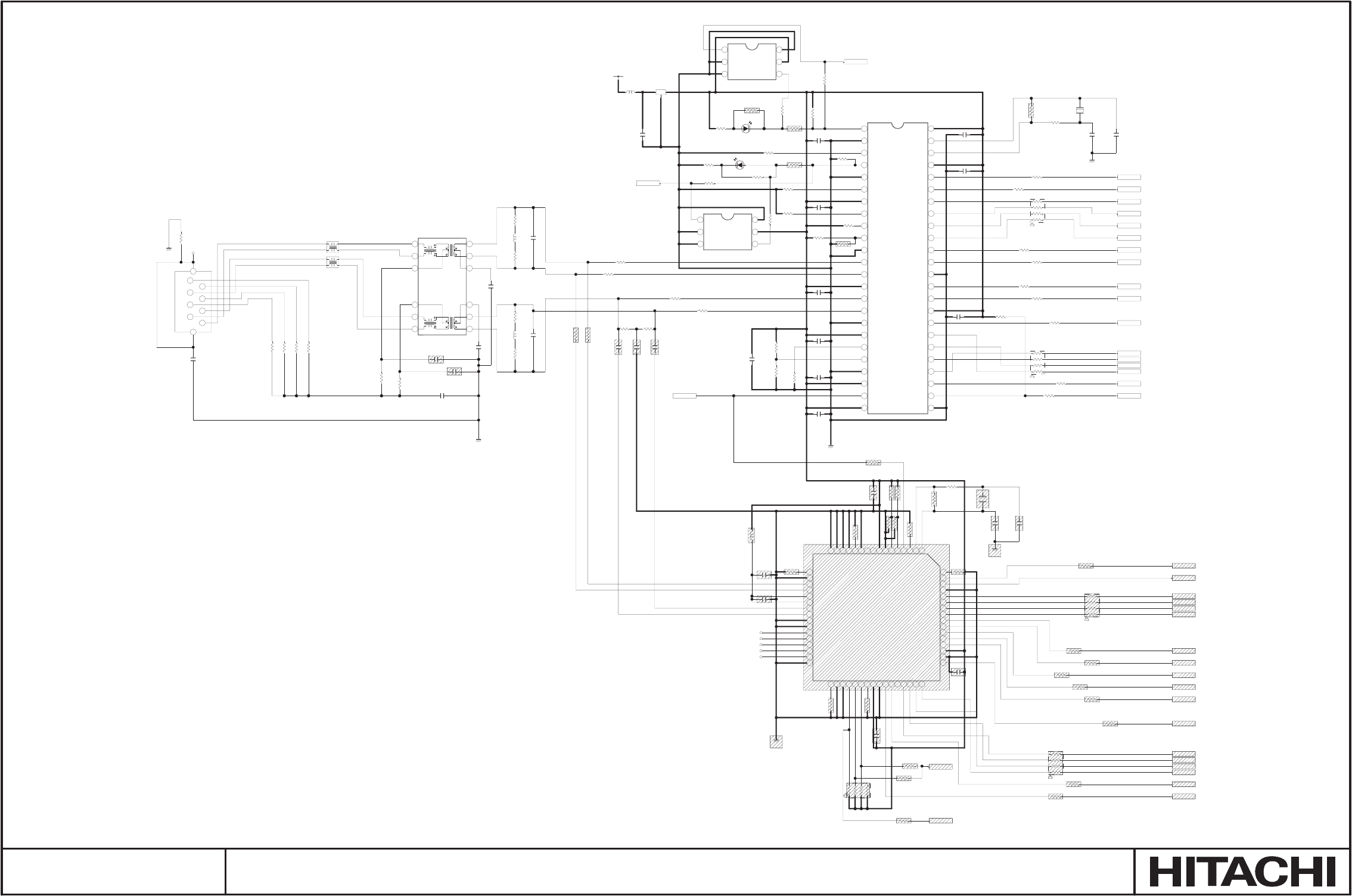
28
29
30
31
32
33
34
35
36
37
38
39
40
41
42
43
44
45
46
47
48
26
27
2524
23
22
21
20
19
18
17
16
15
14
13
12
11
10
9
8
7
6
5
4
3
2
1
4
5
6
3
2
1
4
5
6
3
2
1
53
52
51
50
36 35 34 33
22
21
20
19
18
17
49
47 4648 45
32
31
30
29
28
27
26
25
24
23
62
64
63
13 14 1615364119725 121081
44
61
60
59
58
57
56
55
54
43 42 41 40 39 38 37
G2 G1
8
7
6
5
4
3
2
1
91011141516
876321
DL04
SML-210MT
RL45
75-1%
1005
RL63
1.0M
1005
RLS1
0
P_TXEN
CL49
1005
0.1/10
1005
RL55
10k
CL48
1005
0.1/10
LED_ACT
1005
RL59
1.0k
P_CRS
IL06
ICS1893BF
POAC
VSS-2
P1CL
P2LI
VSS-5
P3TD
VDD-7
P4RD
10/100
AMDIX_EN
VSS-11
TP_AP
TP_AN
VDD-14
TP_BN
TP_BP
VSS-17
VDD-18
10TCSR
100TCSR
VSS-21
VDD-22
RESET_N
VDD-24 VSS-25
MDIO
MDC
RXD3
RXD2
RXD1
RXD0
RXDV
VDD-33
RXCLK
RXER
VSS-36
TXCLK
TXEN
TXD0
TXD1
TXD2
TXD3
COL
CRS
VDD-45
REF_OUT
REF_IN
VDD-48
P_RXDV
1005
RL51
10k
P_TXD2
RL48
62-1%
P_COL
1005
RLP7
3.3k
P_RXD1
1005
RL54
10k
+3.3V
CL46
1005
0.1/10
P_MDIO
P_RXCLK
CL50
3.0p-C
1005
RL57
10k
P_RXER
P_RXD3
1005
RLL1
0
P_TXCLK
P_MDC
CL54
0.01-F
RL47
62-1%
1005
RL61
1.5k-1%
1005
RL58
1.0k
1005
RL62
2.0k-1%
1005
RL60
12k-1%
RL39
75-1%
CL43
1005
0.1/10
CL44
1005
0.1/10
1005
RL56
10k
RL38
75-1%
CL40
1005
8.0p-C
CL41
1005
8.0p-C
P_RXD2
RL46
62-1%
1005
RL65
33
P_TXD3
CL42
1005
0.1/10
CL55
4520
1000p/2k-X7R
CL56
4520
1000p/2k-X7R
RL68
2010
33
RL49
62-1%
CL52
1005
0.1/10
GND1
P_RXD0
CL51
3.0p-C
DL03
SML-210DT
CL53
0.01-F
P_TXD0
NW_RESET
RL44
75-1%
P_TXD1
GND1
RL41
75-1%
GND1
3216
HL03
C1V222-2A
1005
RL64
0
2125
LL25
0.12
CL45
1005
0.1/10
XL02
25.000MHz
DSX840GA
CL47
1005
0.1/10
RL40
75-1%
1005
RL66
33
APLF1
2125
LL26
0.12
CL74
1005
8.0p-C
GND1
1005
RL42
1.0M
XL71
25.000MHz
DSX840GA
CL73
1005
8.0p-C
1005
RL99
0
CL66
4520
1000p/2k-X7R
CL67
4520
1000p/2k-X7R
1005
RLN1
0
1005
RLN2 4.7k
1005
RLN3 4.7k
1005
RLS4 0
1005
RLS3 0
1005
RLS2 0
1005
RL71
2.2k-1%
1005
RLN8 0
1005
RLN7 0
CL61
2125
10/10
2518
LL42
22
1005
RLP1
0
1005
RLP2
0
RLP3
2010
0
1005
RLP4
0
1005
RLP5
0
1005
RLP6
0
1005
RLP8
0
1005
RLP9
0
1005
RLN4
0
RLR1
51-1%
RLR2
51-1%
CL64
270p-C
CL63
270p-C
CL65
0.01-F
CL71
1005
0.1/10
CL72
0.01-F
1005
RLR8
10k
1005
RL50
390
IL08
SN74LVC1G97DCK
In1
GND
In0 Y
VCC
In2
IL09
SN74LVC1G97DCK
In1
GND
In0 Y
VCC
In2
1005
RLR7
0
1005
RLR9
0
LED_LNK
1005
RL52
390 1005
RLR3
10k
1005
RL72 0
RL74
2010
10k
1005
RL76 0
1005
RL75 0
LED_ACT
LED_LNK
1005
RL77
0
1005
RL73 0
P_RXER
P_TXD0
P_RXCLK
P_RXD2
P_RXD3
1005
RL91
0
P_RXD0
P_COL
1005
RL92
33
1005
RL95
33
P_RXDV
1005
RL78
0
RL97
2010
0
P_TXCLK
P_TXEN
P_RXD1
RL90
2010
33
P_TXD1
1005
RL79
0P_MDC
P_TXD3
P_TXD2
P_MDIO
1005
RL93
0
1005
RL96
0
P_TXER
1005
RL94
0
1005
RL98
0P_CRS
1005
RL43
0
CL77
1005
0.1/10
CL76
1005
0.1/10
CL75
1005
0.1/10
1005
RLR4
0
1005
RLR5
0
2125
LL41
600
CL60
2.2/6.3
1005
RLR6
0
TPLP1
TPLP2
TPLP3
TPLP4
TPLP5
IL07
LXT972A
REFCLK/XI
XO
MDDIS
RESET_L
TxSLEW0
TxSLEW1
GND-7
VCCIO-8
NC-9
NC-10
GND-11
ADDR0
GND-13
GND-14
GND-15
GND-16
RBIAS
GND-18
TPOP
TPON
VCCA-21
VCCA-22
TPIP
TPIN
GND-25
GND-26
TDI
TDO
TMS
TCK
TRST_L
GND-32
PAUSE
GND-34
GND-35
LED3/CFG3
LED2/CFG2
LED1/CFG1
PWEDWN
VCCIO-40
GND-41
MDIO
MDC
NC-44
RXD3
RXD2
RXD1
RXD0
RX_DV
GND-50
VCCD
RX_CLK
RX_ER
TX_ER
TX_CLK
TX_EN
TXD0
TXD1
TXD2
TXD3
GND-61
COL
CRS
MDINT_L
EL03
43860-1010
GND1
1005
RLS5
0
1005
RLS6
0
1005
RLS7
0
1005
RLS8
0
LL27
TLA-6T214ALF-T
BC00181R
LL28
ACM3225-102-2P
1
23
4
LL29
ACM3225-102-2P
1
23
4
GND1
2125
RL37
0
ACT
LINK
SM0321 PWB ASSEMBLY NETWORK 3
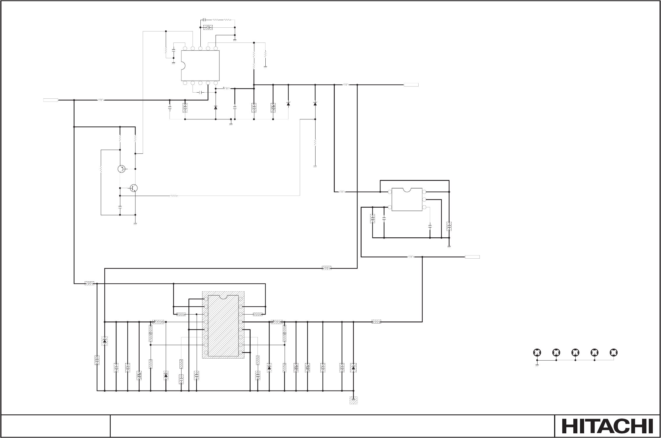
9
10
11
12
13
14
15
16
8
7
6
5
4
3
2
1
65
7
8
9
10
4
3
2
1
4
5
3
2
1
0V
DLT4
UDZ2.0B
1005
RLT6
10k
1005
RLT3
1.0k-1%
1005
RLT9
330-1%
1005
RLU1
1.0k-1%
CLT2
220/6.3
MVK/SKV
+1.5V
CLT5
1005
1.0/6.3-F
CLT6
220/6.3
MVK/SKV
1005
RLT7
1.0k
CLT3
1005
1.0/6.3-F
CLT7
220/6.3
MVK/SKV
1005
RLT4
1.0k
IL15
SPI-8001TW
ADND
Vin1
VCC
SWout1
DGND1
SS1
Vref1
NC-8 AGND
Vref2
SS2
DGND2
SWout2
C/E
Vin2
NC-16
1005
RLT5
100
1005
RLT8
180-1%
+15V
1005
RLT2
100-1%
1005
RLT1
2.2k-1%
GND1
DLT1
UDZS3.9B
CLT4
3216
4.7/25
CLT1
0.1/25-F
DLT3
SFPB-66
DLT2
SFPB-66
CLT8
2125
10/6.3
CLT9
2125
10/6.3
CLU3
0.01
GND1
CLU1
3225
10/25
1005
RLU3
10k
GND1
CLU2
3225
10/25
GND1
CLU8
0.01
GND1
IL16
MP2361DK
NC-1
BS
NC-3
IN
SW GND
FB
COMP
EN
SS
1005
RLU8
10k-1%
+3.3V
1VLC
5212
3
.
6
/
01
CLV4
1.0/6.3
GND1
CLV3
1005
0.1/10
CLV2
2125
10/6.3
IL17
TK11115CSC
Vcont
GND
NpVout
Vin
DLT6
UDZS3.9B
1005
RLU6
3.9k-1%
1005
RLU7
22k-1%
CLU4
2125
22/6.3
CLU6
220/6.3
MVK/SKV
2125
LLT3
600
2125
LLT4
600
2125
LLT6
600
2125
LLT7
600
2125
LLT8
600
2125
LLT9
600
CLV5
0.01
CLV6
0.01
CLU5
2125
22/6.3
DLT5
RSX201L-30
CLU7
0.01
2125
LLU1
600
KIKU1C KIKU2C KIKU3C KIKU4C KIKU5C
GND1
CLU9
1000p
1005
RLU4
10k-1%
1005
RLU5
10k-1%
GND1
1005
RLV1
10k
1005
RLV4
1.0k
1005
RLV3
1.0k
QLT2
2SC5343E
QLT1
2SA1980UFG
DLT7
UDZS3.9B
CLV7
1.0/16
GND1
1005
RLU2
22k
1005
RLV2
2.2k
47
LLT1
SLF6028
47 47
LLT2
SLF6028
47
4.7
LLT5
7E06NG
4.7
Fixed 1.4MHz SW Freq.
1.5V
SM0321 PWB ASSEMBLY NETWORK 4

CP-SX635(ED3SX40N)
PWB assembly CONTROL
PWB assembly BATTERY
PWB assembly REMOTE
PWB assembly SW
POWER UNIT BALLAST 1
POWER UNIT BALLAST 2
POWER UNIT BALLAST 3
POWER UNIT CIRCUIT
POWER UNIT (FILTER)
PWB assembly INPUT
PWB assembly KEYPAD
PWB assembly MAIN 1
PWB assembly MAIN 2
PWB assembly MAIN 3
PWB assembly MAIN 4
PWB assembly MAIN 5
PWB assembly MAIN 6
PWB assembly MAIN 7
PWB assembly MAIN 8
PWB assembly MAIN 9
PWB assembly MAIN 10
PWB assembly MAIN 11
PWB assembly MAIN 12
PWB assembly MAIN 13
PWB assembly MAIN 14
PWB assembly MAIN 15
PWB assembly MAIN 16
PWB assembly MAIN 17
PWB assembly NETWORK 1
PWB assembly NETWORK 2
PWB assembly NETWORK 3
PWB assembly NETWORK 4
Basic circuit diagram list

Hitachi, Ltd. Tokyo, Japan
International Sales Division
THE HITACHI ATAGO BUILDING,
No. 15 –12 Nishi Shinbashi, 2 – Chome,
Minato – Ku, Tokyo 105-8430, Japan.
Tel: 03 35022111
HITACHI EUROPE LTD,
Whitebrook Park
Lower Cookham Road
Maidenhead
Berkshire
SL6 8YA
UNITED KINGDOM
Tel: 01628 643000
Fax: 01628 643400
Email: consumer-service@hitachi-eu.com
HITACHI EUROPE S.A.
364 Kifissias Ave. & 1, Delfon Str.
152 33 Chalandri
Athens
GREECE
Tel: 1-6837200
Fax: 1-6835964
Email: service.hellas@hitachi-eu.com
HITACHI EUROPE GmbH
Munich Office
Dornacher Strasse 3
D-85622 Feldkirchen bei München
GERMANY
Tel: +49-89-991 80-0
Fax: +49-89-991 80-224
Hotline: +49-180-551 25 51 (12ct/min)
Email: HSE-DUS.service@hitachi-eu.com
HITACHI EUROPE S.A.
Gran Via Carlos III, 86, planta 5
Edificios Trade - Torre Este
08028 Barcelona
SPAIN
Tel: +34 93 409 2550
Fax: +34 93 491 3513
Email: atencion.cliente@hitachi-eu.com
HITACHI EUROPE srl
Via Tommaso Gulli N.39, 20147
Milano, Italia
ITALY
Tel: +39 02 487861
Tel: +39 02 38073415 Servizio Clienti
Fax: +39 02 48786381/2
Email: customerservice.italy@hitachi-eu.com
HITACHI Europe AB
Box 77 S-164 94 Kista
SWEDEN
Tel: +46 (0) 8 562 711 00
Fax: +46 (0) 8 562 711 13
Email: csgswe@hitachi-eu.com
HITACHI EUROPE S.A.S
Lyon Office
B.P. 45, 69671 BRON CEDEX
FRANCE
Tel: +33 04 72 14 29 70
Fax: +33 04 72 14 29 99
Email: france.consommateur@hitachi-eu.com
HITACHI EUROPE LTD (Norway) AB
STRANDVEIEN 18
1366 Lysaker
NORWAY
Tel: 67 5190 30
Fax: 67 5190 32
Email: csgnor@hitachi-eu.com
HITACH EUROPE AB
Egebækgård
Egebækvej 98
DK-2850 Nærum
DENMARK
Tel: +45 43 43 6050
Fax: +45 43 60 51
Email: csgnor@hitachi-eu.com
HITACHI EUROPE AB
Neopoli / Niemenkatu 73
FIN-15140 Lahti
FINLAND
Tel : +358 3 8858 271
Fax: +358 3 8858 272
Email: csgnor@hitachi-eu.com
Hitachi Europe Ltd
Bergensesteenweg 421
1600 Sint- Pieters-Leeuw
BELGIUM
Tel: +32 2 363 99 01
Fax: +32 2 363 99 00
Email: sofie.van.bom@hitachi-eu.com
HITACHI EUROPE LTD
Na Sychrove 975/8
101 27 Pr aha 10 – Bohdalec
CZECH REPUBLIC
Tel: +420 267 212 383
Fax: +420 267 212 385
Email: csgnor@hitachi-eu.com
www.hitachidigitalmedia.com
