6500άÐÞÊÖ²á ÖÐÎÄ CS3000 Service Manual
User Manual: CS3000 Service Manual
Open the PDF directly: View PDF ![]() .
.
Page Count: 47
PROFESSIONAL
TWO-WAY RADIO
PT6500
V071208
FM PORTABLE RADIO
SERVICE MANOAL
Welcome

1
DANGEROUS!!
WARNING
STATEMENT
Do not connect the AC power or DC power over 7.4V with
any connector or terminals of the radio. Otherwise it will
cause fire, electric shock or damage to the radio.
Do not reverse power connection.
It may cause harm to the radio if signal input on the antenna
connector is bigger than 20 dBm (100mW).
Do not turn on the power before the antenna or load
connection is completed.
If the antenna has been damaged, do not use the radio.
Damaged antenna may cause lightly burning on skin.
Though the radio is waterproof, it's better to avoid putting it
in rain or snow, or any other liquid to ensure its life and
performance.
Kirisun Electronic (Shenzhen) Co., Ltd owns the copyright of
KSP6500 software.
Unauthorized Duplication of KSP6500 software is strictly
prohibited.
Kirisun Electronic (Shenzhen) Co., Ltd owns the copyright of
the MCU software.
Kirisun Electronic (Shenzhen) Co., Ltd owns the copyright of
the radio outward/structure/circuit design.
Kirisun Electronic (Shenzhen) Co., Ltd owns the copyright of
this service manual. Unauthorized publication is prohibited.
Kirisun Electronic (Shenzhen) Co., Ltd owns the trademarks
KIRISUN , , .
PT6500 SERVICE MANUAL
CONTENTS
Chapter 1 Introduction.......................................................................2
Chapter 2 Radio Overview and Function Keys.................................2
Chapter 3 Electrocircuit.....................................................................3
Chapter 4 Function Description and Parameter Setting....................7
Chapter 5 Service Assemble and Disassemble..............................12
Chapter 6 Radio Debugging............................................................14
Chapter 7 Major Specifications.......................................................18
Chapter 8 Trouble Shooting............................................................18
Appendix 1 Abbreviations................................................................19
Appendix 2 Spare List.....................................................................19
Appendix 3 Electronic Component List...........................................20
Appendix 4 Framework Component List.........................................20
Appendix5 Accessory List...............................................................31
Figure 1 PT6500 Top Main Board Position Number Diagram.........32
Figure2 PT6500 Bottom Main Board Position Number Diagram....33
Figure 5 .........36
Figure 6 ....37
Figure 7 38
Figure 8 ....38
Figure 9 PT6500 Schematic Circuit Diagram(136-174MHZ) .........39
Figure 10 PT6500 Schematic Circuit Diagram(400-470MHZ) ...... 40
Figure 11 PT6500 Main Board Schematic Circuit Diagram ...........41
Figure 12 PT6500 Keyboard Schematic Circuit Diagram...............42
Figure 13 PT6500 PTT Board Schematic Circuit Diagram.............43
Figure 3 PT6500 Top Main Board Position Number Diagram.........34
Figure4 PT6500 Bottom Main Board Position Number Diagram....35
PT6500 PTT Top Board Position Number Diagram
PT6500 PTT Bottom Board Position Number Diagram
PT6500 Top Keyboard Schematic Circuit Diagram..........
PT6500 Bottom Keyboard Schematic Circuit Diagram
2
Chapter 1 Introduction
1.1 Introduction
This manual applies to the service and maintenance of PT6500
series of FM portable radios, and is designed for the engineers and
professional technicians that have been trained by Kirisun. In this
manual you can find all the information of product service. Kirisun
reserves the rights to modify the product structure and specification
without notice in order to enhance product performance and quality.
You can also log on our website www.kirisun.com to download the
latest service manual or contact your local dealer or us.
Read this manual before repairing the product.
1.2 Service Precautions
Safety
Avoid skin contacting with the antenna connector and PCB.
Do not reverse the power polarities.
If signal input at antenna connector is bigger than 20dBm(100mW),
it may cause damage to the radio.
Do not turn on the power before the antenna and load connection is
completed.
Do not use the radio if the antenna has been damaged. Contacting
the damaged antenna will cause slightly burning on the skin.
Electromagnetism Interference
It's prohibited to use or repair the radio in the following places:
Hospital, health center, air port
Any area with a potentially explosive atmosphere (where the air
contains gas, dust and smog, etc.), such as the storage or
transportation facilities of fuel or chemicals.
Any area of dynamite or exploder.
It's recommended to avoid using or repairing the radio in the
following places:
It's recommended to avoid using the radio in a car that is moving.
The radio wave might interfere the auto engine and cause it to stop
working.
Component Replacement
All the components used in repair service should be supplied by
Kirisun.
Other components of the same models available on the market are
not surely able to use in this product and we do not guarantee the
quality of the product using such components.
Please fill in a component application forms if you want to apply for
any components from Kirisun.
The following is one sample form that might be used to apply for
any components from Kirisun.
Component Application
1.3 Service
All the Kirisun products are subject to the service warranty.
The main unit of the radio is guaranteed for free service of 24
months. Accessories (such as battery pack, power adapter, antenna
or charger) are guaranteed for free service of 6 months. Earphones
are wearing parts and out of warranty.
In one of the following situations, charge free service will not be
available.
No valid service warranty or original invoice.
Malfunction caused by disassembling, repairing or reconstructing
the radio by the users without permission.
Wearing and tearing or any man-made damage such as
mechanical damage, burning or water leaking.
Product serial number has been damaged or the product trademark
is difficult to identify.
After the warranty expires, lifetime service is still available. And we
also provide service components to service stations and service
staff.
Chapter 2 Radio Overview and Function Keys
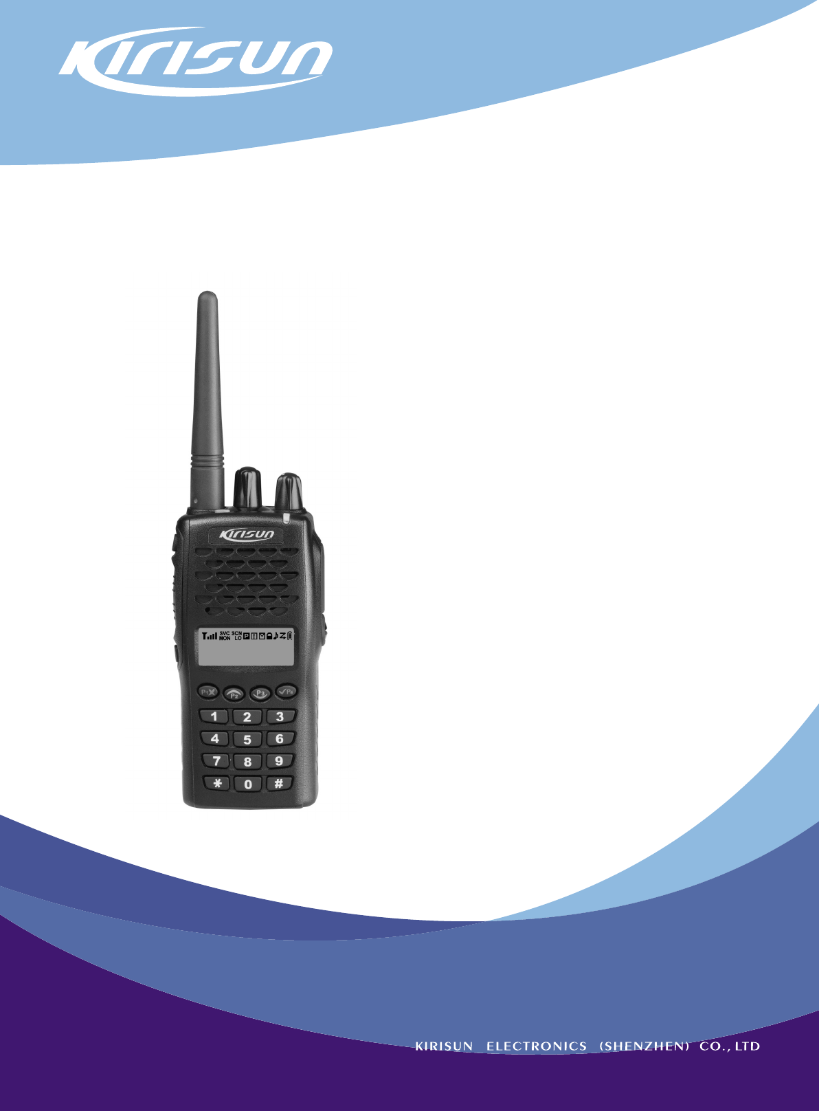
2.1 Radio Overview
The functions of the components are as follows:
A. LED Indicator
Lights red while transmitting;
Lights green while receiving.
123
456
789
*0#
P
1P
2P
3P
4
B. Power/Volume Switch Knob
Turn clockwise till a click is heard to switch on the radio.
Turn counterclockwise till a click is heard to switch off the radio.
Rotate to adjust the volume after turning on the radio.
C. Channel Selector
Rotate to select the channel 1-128.
D. Antenna
E. Top Button (programmable button)
It is recommended to be set as the emergency warning Button.
F. Side button 1 (programmable button)
G. PTT PUSH-TO-TALK :
To make a call, press and hold the PTT button, then speak into the
microphone with normal voice. Release the PTT button to receive
signals.
H. Side button 2 (programmable button)
I. Button
Return and delete button in the menu.
J. Button
Select Button.
K. Button
Select Button.
L. Button
Enter and Confirm Button.
M. Numeric keypad
N. Microphone/speaker jacks
P1
P2
PT6500 SERVICE MANUAL
Parts and Spare Parts Requisition
Radio
ModelComp
onent Position
Mark Model/
Specifications Material
Serial number Qty
PT-6500(400
-470MHz)
Field eff-
-ect tube Q3 RD01MUS1 105-RD01MU-R01 1
1
PT-6500(400
-470MHz) Triode Q49 2SC5108(Y) 104-SC5108-R01
P3
P4
1
1
2
2
3
3
4
4
D D
C C
B B
A A
Title
Number RevisionSize
A4
Date: 2007-7-26 Sheet of
File: X:\PT6500\.. \PLL.SchDoc Drawn By:
PLL-LE
PLL-CLK
PLL-DA
PLL-UL
PLL IC
IC2
QT TCXO
5C
LOOP FILTER
RIPPLE
FILTER
VCO
Q6
BUFF
Q5 Q4
RF AMP
5C Q14
ADF4111
MOD
12.8MHz
X1
TCXO
5C
TX
VCO
Q11
RX
Q8
BUFF
5C
1
1
2
2
3
3
4
4
DD
CC
BB
AA
Title
Number Revisio nSize
A4
Date: 2007-7-26 Sheet of
File: X:\PT6500\..\Receiver.SchDoc Drawn By:
MCF
51.65MHz IF SY STEM
CF1
450KHz H
CF2
450KHz F
X3 multiply
AF AMP
TCXO
12.8MHz
AK2346
BPF
RF AMP
BPF
ANT SW
ANT
IC7
MCU 1st Local OSC
D1 D39 D7 D8 Q18 Q19
IC4
IC6
IC9 TDA8541
3
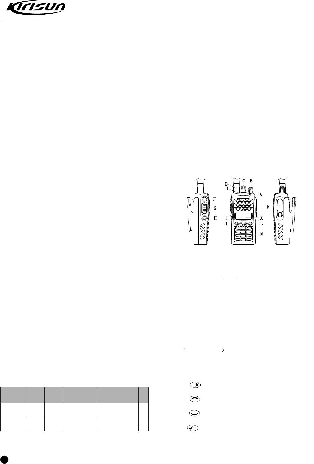
The receiver's first local oscillation is generated by the frequency
synthesizer. The second local oscillation adopts the 4th harmonic
51.2MHZ of TCXO.
The transmitter signals are generated by frequency synthesizer.
The reference frequency of frequency synthesizer is generated by
TCXO.
3.2 Receiver (RX) Illustration
Figure 3.2 Receiver Illustration
The Receiver Front Terminal
Signals from the antenna pass through the RX/TX switch (D1, D39,
D7, D8); and then undesirable out-of-band signals will be filtered
out at the band pass filter (BPF) consisting of two-stage LC; then
signals are amplified at the low noise amplifier (LNA) consisting of
Q18 and its peripheral components.
The output from the LNA passes the BPF consisting of three-stage
LC for filtering and then is sent to the first grade frequency mixer
(Q19).
AGC Circuit
The AGC circuit consists of Q17 and its peripheral components.
Only when the input signal is too large can the AGC functions to
reduce the Q18 plus.
The First Frequency Mixer
After mixing the receiving signals for LNA and the first local
st
oscillation signals from the frequency synthesizer, the 1 IF signals
(51.65MHz) are generated.
IF Circuit
st
Signals of adjacent channel and those out of band of the 1 IF
signals are filtered via the crystal filter (XF1).
st
The 1 IF signals from the crystal filter are amplified at the first
IF amplifier (Q20), and then are sent to the IF processing IC
(IC4, TA31136).
nd nd
The IF IC consists of the 2 frequency mixer, the 2 local oscillator,
IF amplifier, limiter, phase frequency detector, and noise amplifier.
nd
The 2 local oscillation is obtained after 12.8MHz signals from X1
are amplified via Q15 and external circuit. The 2nd local oscillation
st
(51.2 MHz) and the 1 IF signal (51.65 MHz) are mixed at IC5 to
generate the 2nd IF (450 kHz). After the 2nd IF signal is amplified
and its amplitude is limited at IC4, and then filtered at porcelain filter
(CF1 or CF2, 450 kHz), IC5 demodulates and sends out audio
signals.
nd
The 2 IF filter selector circuit consists of CF1, CF2, D18, D19 and
peripheral circuits, when the radio is set to broad band, CF2 is open,
CF1 is closed and CF2 functions; when the radio is set to narrow
band, CF1 is open, CF2 is closed and CF1 functions.
Squelch Circuit
Demodulation output from IC4 is sent to the noise amplifier in Ic4.
After being amplified, noise signal is sent to D21 for further
amplification and to D22 for wave checking and then sent to MCU,
which determines the noise volume to control the squelch. This
voltage is inversely proportional to the input signals.
3.3Transmitter (TX) Illustration
Transmitter Power Amplifier
The modulated signals from VCO are amplified at Q2, Q4, Q59, Q5,
Q3, and then sent to Q1 for power amplification. Q1 output power:
4W.
The Q1 and Q3 gate offset is controlled by APC circuit. Transmitter
output power can be controlled conveniently by changing the gate-
offset.
APC (Auto Power Control) Circuit
R57, R65 and R66 are the amplifier current checker, IC3A is the
sample amplifier of the amplification current; .IC3B is the power
comparison amplifier.
If the transmitter output power is too big, the amplifier current will
increase, IC3A output will mount, IC3B output voltage decrease, the
offset voltage added to Q1 and Q3 will decrease, and then the
transmitter output power will decrease. Vice versa, such can ensure
steady transmitter output power in different working circumstances.
MCU changes the input power to IC3B to set the power.
3.4 Frequency Combiner Illustration
Figure 3.4 Frequency Combiner Illustrations
This radio adopts phase locked loop (PLL) type frequency combiner.
The frequency combiner consists of the reference oscillator, voltage
controlled oscillator (VCO), programmable frequency divider, phase
PT6500 SERVICE MANUAL
1
1
2
2
3
3
4
4
D D
C C
B B
A A
Title
Number Revisi onSize
A4
Date: 2007-7-26 Sheet of
File: X:\PT6500\.. \Frequency confi guration.SchDocDrawn By:
ANT
ANT SW RF AMP MCF
51.65MHz IF SYSTEM
CF1
450KHz H
CF2
450KHz F
X3 multi ply
AK2346
AF AMP
TCXO
12.8MHz
MIC AMPPLL VCOTX AMPPA AMP
RX
TX
Chapter 3 Electrocircuit
3.1 Frequency Configuration
Figure 3.1 Frequency Structure
This radio adopts the 2nd Mixer, the 1st IF 51.65MHz, the 2nd IF
450kHz.
1
1
2
2
3
3
4
4
D D
C C
B B
A A
Title
Number RevisionSize
A4
Date: 2007-7-26 Sheet of
File: X:\PT6500\..\T X.SchDoc Drawn By:
RF AMP
5T 5R
Q4 Q5 Q3
DRIVE
DRIVE
PRE
5T 5T
APC
Q12
ANT SW LPF
APC CONTROL
IC3
TX/RX SW
Q1
RF POWER
APC
5T
SW
BATTARY
7.5V
VCO
ANT
Figure 3.3 Power amplifier and antenna switch schematic diagram
4
comparator, and the upper limiting filter.
Q6, D2, D4, D5 and D6 constitute the transmitting VCO unit. D9 is
the modulating circuit of the transmitting VCO.
Q11, D11, D12, D13 and D14 etc. constitute the receiving VCO
unit.
IC2 (ADF4111) is the PLL integrated circuit, which can comprise
the programmable reference frequency divider, programmable
frequency divider, phase comparator and charge pump, etc.
The upper limiting filter consists of R43 and C96 etc.
The frequency reference is provided by X1 (TCXO, 12.8MHz).
The frequency reference from TCXO (temperature control crystal
oscillator) receives frequency division by the programmable
reference frequency divider in IC2 to generate the frequency
reference of 5kHz or 6.25kHz (according to the frequency of the
channel, controlled by MCU).
The oscillation frequency from VCO is sent to IC2, after frequency
division by the programmable frequency divider, it is compared
with the frequency reference to get the error signal, which is, after
wave filtering by the upper limiting filter, sent to VCO to change
the oscillation frequency of VCO, which allows the VCO frequency
to achieve the set value and the VCO to be locked.Detection of
loss of lock: if PLL loses lock, IC2 pin14 outputs low level signal to
MCU, which prevents the transmitter from transmitting and
generates alert.
Q13 and related circuits are used for switching the upper limiting
filter.
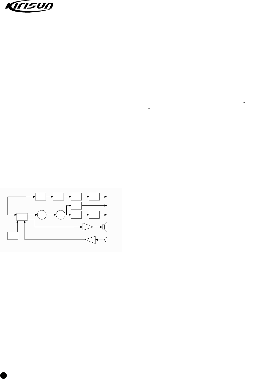
3.5 Audio Processing Circuit:
I
C6 (AK2346) is a special voice processing chip provided with
functions like amplification, wave filtering, preemphasis,
deemphasis, scrambling, companding and MSK MODEM etc. Most
voice processing tasks of the radio are completed by it.
MIC Signal Processing:
Voice signals from MIC are controlled by AGC circuit, and then
reach IC24, one group of signals are amplified at IC24B (VOX
circuit) and are processed into direct current by D35 and sent to
MCU for processing; the other group of circuits are amplified at
IC24A and then receive amplification, wave filtering, companding
(optional), preemphasis, scrambling and amplitude limit at IC6 pin3,
after that, they are exported from IC6 pin7 and sent along with
CTCSS/DCS to VCO for modulation.
2T/5T signals are imported from IC6 pin6, and after amplitude limit
and amplification, they are exported form IC6 pin7 and sent to VCO
for modulation.
Receiver Audio Signal Processing:
Voice signals exported from IC4 are divided into two channels, one
comes to the low pass circuit (voice signals filtered) consisting of
IC5, etc for amplification and wave filtering to get comparatively
pure CTCSS/DCS signals, which are then sent to MCU for
processing; the other comes to IC6 pin23, after amplification and
wave filtering, one channel is exported from IC6 pin21 (DTMF/2T/5T
signals etc.), DTMF/2T/5T signals etc. come through the high pass
circuit (sub-audio signals filtered) consisting of Q30 and Q31 etc.,
DTMF signals come to IC10 (special chip for HT9172 DTMF
decoding) for decoding and then sent to MCU for processing, 2T/5T
signals are sent to MCU for processing after wave filtering and
waveform modification by IC1; the other channel of signals (voice
signals) are exported form IC6 pin18 after scrambling, preemphasis,
deemphasis and companding and then imported from IC6 pin19 for
amortizing and amplification before being exported form IC6 pin20.
IC13 is a voice storage chip, which stores voices including channel
prompt etc., each time the channel is changed, the speaker will
prompt the current channel number by voice. Press the voice
prompt key to prompt the current channel number again.
Receiver audio signals, voice prompt signals, 2T/5T/DTMF signals,
prompt voice signals, emergent alert signals are gathered to be
amplified by the audio frequency amplifier IC9 to drive the speaker.
Speaker impedance: 16Ù.
Note: None of the terminals of the speaker can be grounded!
The volume of emergent alerts cannot be controlled.
3.6 Power Supply:
The radio is equipped with 7.4V battery as power supply, which
directly supply power to transmitter power amplifier circuits (Q1, Q3)
and receiver audio power amplifier (IC9), other circuits adopts
regulated 5V power supply.
Q40, Q45: 5V low voltage difference, micro power regulator.
Q43: 5T switch, controlled by MCU.
5T: Supplies power for the front terminal of the transmitter.
Q39: 5R switch, controlled by MCU.
5R: Supplies power for the receiver RF amplification, mixing, IF
processing, audio signal processing..
Q44: 5C switch, controlled by MCU.
5C: The 5V power controlled by power saving supplies power for
the frequency synthesizer.
3.7 MCU:
MCU controls the working of each unit of the radio to realize
all the radio functions.
Connects with the PC
Accesses the current channel status data
Controls the PLL to generate receiver and transmitting local
oscillation frequency
Acquires current channel status
Controls the LED status indication
Controls the power supply of each location
Checks the action of each function key
Generates CTCSS signals
Generates DCS signals
Generates power control signals
CTCSS decoding
DCS decoding
Squelch check and control
Controls the content of voice indication
Memorizes the radio channel data, CTCSS/DCS data, and other
data of function setting and parameter adjustment.
CTCSS/DCS Encoding and Decoding:
2
Memorier (E PROM, AT24C256)
PT6500 SERVICE MANUAL
1
1
2
2
3
3
4
4
D D
C C
B B
A A
Titl e
Number Revi sionSiz e
A4
Date: 2007-7-26 Sheet of
Fil e: X:\ PT6500\..\ AUDI O.SchDoc Drawn By:
pin 7 Q30
HP Q31
HP
IC1A
HP AMP
IC1B
IC10
HT9172
IC5A IC5BIC5CIC5D
AMP LP LP AMP CTCSS/ DCS
DTMF
2T
AK2346
IC6
IC4 pi n 9
AF AMP
IC9 TDA 8541
pin 20
MIC AMP
MCU
IC7
pin 23
pin6
pin3
MIC
SP
Figure 3.5 Audio Processing Diagram
5
047 134 245 365 516 712
051 143 251 371 532 723
054 152 261 411 546 731
065 155 263 412 565 732
071 156 265 413 606 734
072 162 271 423 612 743
073 165 306 431 624 754
074 172 311 432 627
PT6500 SERVICE MANUAL
No. Fr q [Hz] No. Frq [Hz] No. Frq [Hz] No. Frq[Hz]
186.2
1 67.0 11 94.8 21 131.8 31
192.8
2 69.3 12 97.4 22 136.5 32
203.5
3 71.9 13 100.0 23 141.3 33
210.7
4 74.4 14 103.5 24 146.2 34
218.1
5 77.0 15 107.2 25 151.4 35
225.7
6 79.7 16 110.9 26 156.7 36
233.6
7 82.5 17 114.8 27 162.2 37
241.8
8 85.4 18 118.8 28 167.9 38
250.3
9 88.5 19 123.0 29 173.8 39
10 91.5 20 127.3 30 179.9
DCS signaling:
DCS (Digital code squelch) is a kind of continuous digital code
modulated with voice signals on carrier wave to control squelch. If
DCS function is enabled, only in case the same DCS code is
received can the speaker be turned on so as to avoid interference
from useless signals.
83 groups of standard codes (positive and inverse code) are
available. See table 2.
DCS signals generated by MCU (PWM wave shape) pass the low
pass filter to be filtered off the high frequency over 300Hz and then
are sent to VCO and TCXO for modulation. VCO modulates the
high frequency of DCS signals; TCXO modulates the low frequency
of DCS signals.
CTCSS/DCS signals from the receiver are sent to MCU for
modulation. MCU determines whether the DCS encoding of the
receiving signals is identical with that set on the radio and decides
whether to turn on the speaker.
CTCSS/DCS signals generated by MCU (output form pin24 and
pin28, PWM wave), are respectively sent to VCO and TCXO for
modulation.
CTCSS/DCS signals from the receiver are sent to MCU (pin1) for
demodulation. MCU determines whether the signals contain the
same CTCSS/DCS as that set on the radio and decides whether to
turn on the speaker.
CTCSS
CTCSS(continuous tone control squelch system, sub-audio for abbr.)
is a squelch control system modulated on carrier wave with
continuous sub-audio frequency as pilot frequency. If a channel is
set with CTCSS, only when both the CTCSS of the receiver and
that of the transmitter are identical, communication is available,
which avoids interference of other signals.
This radio is equipped with 39 groups of standard sub-audio
frequencies for your selection as shown in
Table 1
CTCSS signals are generated by MCU (PWM waveform) and are
sent to VCO for modulation via upper limiting filter consisting of RC,
which filters high-frequency components over 300Hz.
Table 3.1 CTCSS Frequencies
3.8 Semiconductor Components
MCU Description
Table 3.3 Microprocessor (M30620) Port Description
I/O
O
O
I
O
O
-
-
O
O
I
O
-
I
-
-
I
O
O
O
O
O
O
-
O
O
O
-
O
O
O
-
-
-
O
O
O
O
O
-
I
Port Name
VCCN
TONEO
TONEI
E-SDA
E-SCL
C-BYTE
C-CNVSS
SHIFT
E-TEST
RESET
XOUT
VSS
XIN
VCC
CMMI
INTO
A-RDT
A-TCLK
A-SCLK
A-DI/O
A-TDATA
A-DIR
NC
QT VCO
PLL-LP
PC/TV
NC
QT TCXO
C-TXD1
C-RXD1
C-CLK1
NC
ICA
PABC
APC2 SW
APC1 SW
RX SW
TX SW
C-HOLD
PLL-UL
Function
PLL frequency reference adjustment
2T/5T/DTMF/BEEP signals inout
2T/5 signals input
EEPROM data cable
EEPROM clock cable
Grounding
Grounding
Clock offset H: Clock offset
EEPROM write-protection pin
H: Unwriteable L: Writeable
Reset pin
Clock output pin
Grounding
Clock input pin
Connects to 5V power supply
Grounding
AC dump detecting pin
AK2346 control pin
AK2346 control pin
AK2346 control pin
AK2346 control pin
AK2346 control pin
AK2346 control pin
Blank
CTCSS/DCS output pin (to VCO modulation)
Phase locked loop upper limiting filter switch
H: switching over medium frequency points
Power control or receiver band pass tuning
voltage control
Blank
CTCSS/DCS output pin (to TCXO modulation)
Serial data output, communicates with PC
Serial data input, communicates with PC
Grounding
Blank
Upstage power amplifier power supply control
H: Transmitting
power amplifier control switch
H:transmission
power amplifier control switch L:transmission
Receiver VCO power switch L: Receiving
Transmission VCO power switch L:transmitting
Grounding
Phase locked loop unlocked detection pin
PIN
1
2
3
4
5
6
7
8
9
10
11
12
13
14
15
16
17
18
19
20
21
22
23
24
25
26
27
28
29
30
31
32
33
34
35
36
37
38
39
40
Table 3.2 DCS Encoding List
023 1 1 4 1 7 4 315 445 631
025 115 2 0 5 331 464 632
026 1 1 6 2 2 3 343 465 654
031 1 2 5 2 2 6 346 466 662
032 1 3 1 2 4 3 351 503 664
043 1 3 2 2 4 4 364 506 703
6
Type
Ht9172
PST9140NR
TC75W51FU
ADF4111
NJM2904
Ta31136
NJM2902
AK2346
M30620
AT24C256
TDA8541
RQA0002
DTC144EUA
2SK508NV
DTA144EE
DTA144EE
2SC4116
2SC4617
2SC5108
DTC144EE
2SK1829
3SK318
3SK318
2SC5108
2SC5108
2SC4617
DTC144EE
DTC144EE
DTC144EE
DTA144EE
DTA123JE
2SK1824
RD01MUS1
2SC4617
2SC4617
DTC144EE
2SK1824
2SK1824
DTC144EE
DTA144EE
2SK1824
2SA1586
ST2301
2SC5108
XC6024B502MR
2SC4116
DTC144EE
ST2301
DTA123JE
XC6024B502MR
2SA1586
ST2302
2SC5108
2SC3356
2SK1824
2SK508NV
DTA143TE
2SC5108
DTA143TE
Function Description
DTMF decoding chip
MCU reset circuit
MIC amplification, amplitude limit and filtering
Frequency combiner
APC, voltage comparison, driving
nd nd
Receiver 2 local oscillation, 2 IF amplification,
Amplitude limit, demodulation, noise amplification
Receiver demodulation signal amplification, filtering
Audio processing chip
MCU
2
E PROM, storage channel frequency data, function
setting parameters, debugging status parameters
Receiver's audio power amplifier
Remitter's upstage power amplifier
APC control switch
Receives VCO oscillation circuit
APC output switch
APC control switch
PLL low pass switch
VCO power filter
nd
Receiver's 2 local oscillation doubling circuit
APC control switch
Receiver's HF amplification gain control switch
Receiver's HF amplification
st
1 frequency mixer
VCO buffer amplifier
st
1 IF amplifier
Receiver's noise amplifier
Red LED drive
Wide and narrow band noise switch
Green LED drive
Wide and narrow band frequency discrimination switch
2T high pass filter control switch
2T high pass filter control switch
Transmitter power amplifier pushing
2T high pass filter circuit
2T high pass filter circuit
Beat frequency control switch
Receiver's mute switch
Receiver's audio output switch, off upon emergent alert.
Audio power amplifier control switch
MIC amplification unit power switch
Voice prompt switch
External PTT detection switch
5R switch
VCO buffer amplifier
5V regulated voltage output
MIC AGC control switch
External PTT detection switch
5T switch
5C switch
5V regulated voltage output
MIC AGC control switch
External horn control switch
Transmitter's 1st amplification
nd
Transmitter's 2 amplification
Receiver's audio output switch, on upon emergent alert.
Remitter's VCO oscillation circuit
Remitter's VCO control switch
VCO buffer amplifier
Receiver's VCO control switch
3.4Semiconductor Function Description
PT6500 SERVICE MANUAL
Position
IC10
IC11
IC14
IC2
IC3
IC4
IC5
IC6
IC7
IC8
IC9
Q1
Q10
Q11
Q12
Q12
Q13
Q14
Q15
Q16
Q17
Q18
Q19
Q2
Q20
Q21
Q22
Q23
Q24
Q25
Q26
Q29
Q3
Q30
Q31
Q32
Q33
Q34
Q35
Q36
Q37
Q38
Q39
Q4
Q40
Q41
Q42
Q43
Q44
Q45
Q47
Q48
Q49
Q5
Q51
Q6
Q7
Q8
Q9
41
42
43
44
45
46
47
48
49
50
51
52
53
54
55
56
57
58
59
60
61
62
63
64
65
66
67
68
69
70
71
72
73
74
75
76
77
78
79
80
81
82
83
84
85
86
87
88
89
90
91
92
93
94
95
96
97
98
99
100
O
O
O
-
O
O
O
O
O
O
O
O
O
O
I
O
O
O
O
-
O
-
O
O
-
I
I
I
I
I
I
I
I
O
O
O
O
O
I/O
I/O
I/O
I/O
I/O
I/O
I/O
I/O
O
I
I
I
I
I
I
-
I
-
-
O
O
O
PLL-STB
PLL-DATA
PLL-CLK
C-VCC
MAX AF SW
GREEN
RED
5TC
5RC
5CC
W/N N
W/N W
AFCO
RX MUTE
W-BUSY
W-DATA
W-SCLK
W-MUTE
S-SCK
ACC
S-SI
VSS
S-SO
S-CS
-
PTT
H-D3
H-D2
H-D1
H-D0
H-DV
DN
UP
L-AO
L-AO
L-AO
L-AO
L-AO
K1
K1
K1
K1
K1
K1
K1
K1
LAMP
BATT
RSSI
BUSY
VOX
QT/DQT IN
PF
AVSS
MANDOWN
VREF
AVCC
VOX SW
MIC MUTE
HPF PC
Phase locked loop enabled pin
Phase locked loop data pin
Phase locked loop clock pin
Connects the power supply
Max volume control L: Max. volume
Green indicator H: Lights on
Red indicator H: Lights on
5T control switch L: 5V for 5T
5R control switch L: 5V for 5R
Power-saving control switch L: 5V for 5C
Band selection-Narrow band H: narrow band
Band selection-Wide band H: wide band
Audio power amplifier control
H: power amplifier operates
Receives mute control L: mute
Voice reporting chip busy, signal detection
H: reporting
Voice reporting data signals
Voice reporting clock signals
Voice reporting mute control L: mute
-
Connects 5V power supply
-
Grounding
-
-
-
PTT key input L: transmitting
DTMF data input
DTMF data input
DTMF data input
DTMF data input
DTMF data input
Encoding switch signals
Encoding switch signals
LCD control signals
LCD control signals
LCD control signals
LCD control signals
LCD control signals
Keypad signals
Keypad signals
Keypad signals
Keypad signals
Keypad signals
Keypad signals
Keypad signals
Keypad signals
Backlight control signals H: lights on
Battery voltage detection
Receives field strength indication detection
Noise level detection
Acoustic control level detection
CTCSS/DCS signal input
Customized keypad input
Grounding
MANDOWN signal input L: valid
Connects to the power supply
Connects to the power supply
VOX power control L: VOX set H: VOX not set
MIC mute switch L: Mute
High pass power control
L: Scrambling set H: Scrambling not set
7
Table 3.8 CF1 LTWC450F Features
Chapter 4 Function Description and Parameter Setting
Major Functions
4.1.1 128 channels
The radio stores 128 channels and can allocate there channels in 8
different zones Zone 0 cannot be programmed and includes
all channels
8 Zones
There are 8 zones numbered from Except Zone0
all other zones can be freely allocated with up to 16 channels.
Zone0 includes all channels and cannot be programmed. Only
when the previous zone is allocated with at least 1 channel can the
following zone be allocated.
4.1.3 Channel scanning (this feature can be disabled by
programming software)
There are 16 scanning lists, each of which can be allocated with up
to 16 channels, which can be from the same or different channels.
In channel setting, you can select a scanning list for the channel. If
the channel is chosen by using the channel selection key, the
chosen scanning list for the channel can be started by the
programmable key set to scanning or Manu operation.
a. Activate the scanning function by pressing the key set as the
Scan function or Manu operation to scan the specified
scanning list.
When scanning, the radio will search signals of each channel till
signals are found, if the time delay between the disappearance of
signals and the resumption of scanning is set, if any signal is
received during the time delay, the radio will still stay in this channel.
Note: The current channel must be provided with a scanning list or it
cannot be activated. Scanning is available only when there're at
least 2 channels programmed in the scanning list and the scanning
is valid.
b. Revert channel (the transmitting channel when scanning) during
the scanning set by the dealer has the following options:
In the Scan mode, the radio can be set as to return to a specified
channel when pressing the [PTT] key.
With this function, the radio can be customized so as to meet the
requirements of the user when using the scanning function.
Revert channel has the following types: Fixed channel ,
Selected channel , Selected+Current Channel , Priority
1+ Current Channel , Priority 2 + Current Channel , Priority
1 and Priority channel 2 . In all cases, the user can manually
select one channel for transmitting. (This will resume the revert
channel to the selected channel)
Fixed channel: The channel specified for programming.
Selected channel: The channel selected by the scanning selector
4.1
.
4.1.2
0~7.
PT6500 SERVICE MANUAL
Specified Value
450kHz
6.0kHz or bigger
12.5kHz or smaller
2.0dB or smaller within f0 4kHz
6.0dB or smaller
47.0dB or bigger within f0 100kHz
1.5k
Item
Nominal center frequency
6dB bandwidth
50dB bandwidth
Pulse
Insertion loss
Guarantee attenuation
Terminal resistance
Table 3.5 Diode Function Description
Position
D1
D10
D11
D12
D13
D14
D15
D16
D17
D18
D19
D2
D21
D22
D23
D26
D27
D28
D28
D29
D3
D30
D31
D35
D36
D37
D39
D4
D40
D5
D6
D7
D9
Type
HVC131
MA2S111
HVC376
HVC376
HVC376
HVC376
HZU5ALL
MA2S111
HSC277
DAN222
DAN222
HVC376
HVC355B
MA742
HVC355B
LED green
HVC376B
LED red
HVC376B
HVC376B
HSC277
HVC376B
LED green
MA742
MA742
MA742
HVC131
HVC376
HVC376B
HVC376
HVC376
HSC277
1SV278
Function Description
Transmitter antenna switch diode
Loss of lock detection diode
Receiver's VCO oscillation variode
Receiver's VCO oscillation variode
Receiver's VCO oscillation variode
Receiver's VCO oscillation variode
APC output voltage limiting diode
VCO power filtering acceleration diode
VCO output switch
nd
Receiver's 2 IF filter band switch
nd
Receiver's 2 IF filter band switch
Remitter's VCO oscillation variode
Receiver's band pass filter oscillation variode
Noise demodulation
Receiver band pass filter oscillation variode
Receiving indication
Receiver band pass filter variode
Transmitting indication
Receiver band pass filter variode
Receiver band pass filter variode
VCO output switch
Receiver band pass filter variode
Receiving indication
VOX detection diode
MIC AGC detection diode
MIC AGC detection diode
Transmitter's antenna switch diode
Transmitter's VCO oscillation variode
Receiver's band pass filter variode
Transmitter's VCO oscillation variode
Transmitter's VCO oscillation variode
Antenna switch
Remitter's VCO modulation diode
Table 3.6: Features of XF1 Crystal Filter
Item
Nominal center frequency
Transmitting bandwidth
40dB Barrage bandwidth
Pulse
Insertion loss
Guarantee attenuation
Terminal resistance
Specified Value
51.65MHz
7.5kHz or bigger within 3dB
20.0kHz or smaller
1.0dB or smaller
3.0dB or smaller
80dB or bigger within fo-910kHz
330
Table 3.7 CF1 LTWC450H Features
Specified Value
450kHz
3.0kHz or bigger
9.5kHz or smaller
2.0dB or smaller within f0 4kHz
6.0dB or smaller
47.0dB or bigger within f0 100kHz
1.5k
Item
Nominal center frequency
6dB bandwidth
50dB bandwidth
Pulse
Insertion loss
Guarantee attenuation
Terminal resistance

8
the radio will stop transmitting.
4.1.8 Monitoring
When receiving a signal which doesn't matches the signaling, the
mute circuit will prevent the speaker from producing any sound.
Press the MONI key to cut off the squelch control circuit, and you
will hear noise from speaker (no mater whether there are signals).
Such operation is very useful when you want to adjust voice volume
or receive weak signals (to avoid voice intermittence when in weak
signals). When you press the MONI key, the green indicator lights,
and the radio is in the state of monitoring.
4.1.9 Busy Channel Lockout
If busy channel lockout has been activated, transmitting signals is
prohibited on the busy channel. If you press the PTT to transmit on
the busy channel, the speaker will sound busy channel lockout
tone, and you cannot transmit signals.
Options:
Carrier wave: If there's carrier wave in the channel, transmitting
is prohibited.
Carrier wave + QT/DQT: If there's carrier wave in the channel
while the QT/DQT matches, transmitting is allowed.
4.1.10 2TONE Signaling
The dealer may set this function at enabled or disabled by
programming.
2 Tone Decoding
When the radio receives correct 2-tone signals, it will operate
according to the decoding call response set by the dealer, when the
orange LED will flash and sound the decoding tone you selected.
2 Tone Encoding
When you press the programmable keys programmed at Call1 ,
Call2 , Call3 or Call4 , and the keys are provided with
corresponding 2 tone signaling sequence, 2-tone signaling will be
transmitted. This function should be set by the dealer by
programming.
Or you can select the 2-tone signaling sequence you want to call
from the call list and press PTT twice to transmit 2-tone sequences.
4.1.11 DTMF Signaling
The dealer may set this function at enabled or disabled by
programming.
DTMF Decoding
After the radio receives the correct DTMF signaling, it will operate
the according to the decoding call response set by the dealer. The
orange LED will flash and transmit the decoding tone you selected.
DTMF Encoding
When you press the programmable keys programmed at Call1 ,
Call2 , Call3 or Call4 , and the keys are provided with
corresponding DTMF signaling sequence, DTMF signaling will be
transmitted. This function should be set by the dealer by
programming.
Or you can select the DTMF signaling sequence you want to call
from the call list and press PTT twice to transmit DTMF sequences.
4.1.12 Call list
The 2-tone list and DTMF list being set will be automatically added
to the call list. Enter the Call list menu by menu operation and
select the sequence you want to call and press PTT for calling.
PT6500 SERVICE MANUAL
knob.
Selected + current channel: The channel for holding call when
receiving signals or the channel selected by the channel selection
knob.
Priority 1 + current channel: The channel for Priority channel 1
or for holding call when receiving signals.
Priority 2 + current channel: The channel for Priority channel 2
or for holding call when receiving signals..
Priority channel 1
Priority channel 2
Priority channels can be set at Fixed or Selected .
4.1.4 Sub-audio (QT) and Digital Sub-Audio (DQT)
The dealer may have programmed QT or DQT signals in channels
of the radio, which may ignore calls from other irrelevant stations in
the same channel. If a certain channel is provided with QT or DQT
signals, only when the correct QT or DQT signals are received can
the squelch be activated. Similarly, only when the QT/DQT signals
are in accordance with your radio can the signals you transmitted by
heard.
4.1.5 TOT Transmitting Time Limit
a.
warning tone, and
2. The
4.1.6 Auto Power Saving
The dealer can set the power-saving mode of the battery by
programming.
If this function is enabled, 10 seconds after no signal is received or
no operation is carried out, the radio will be in the power-saving
mode. When any signal is received or any operation is carried out,
the radio can automatically quit this mode.
Power-saving modes: 1: 1, 1: 2, 1: 4 and off.
Setting the power-saving function of a battery can reduce the power
consumption of the battery.
4.1.7 Low Power Warning
When the battery power appears low, the indicator flashes. If the
battery power is lower than the preset value during transmitting, the
status indicator flashes red. When the speaker sounds warning tone,
.
countdown will go on if the time after releasing the PTT key
is shorter than the reset time.
TOT timer:
1. Time-out timer can prevent any caller from occupying one certain
channel for an extended period of the time.
2. The radio is set with a continuously transmitting limit. If the radio
is continuously transmitting longer than the time preset by the dealer,
the radio will stop transmitting and warning
b. TOT forbidden period:
1. A period in which the radio is forbidden to transmit after its
overtime activity.
2. During the period, if the PTT key is pressed, there will be a
transmitting is forbidden.
c. TOT pre-warning:
1. The pre-warning will sound before the TOT action.
2. After the sound of the warning, the timer will take action when the
transmitting time has gone beyond the limit.
d. TOT reset:
1. The time delay from releasing the PTT key to the resetting of the
timer is limited.
PT6500 SERVICE MANUAL
4.1.13 PC Programming
You can program the radio functions and adjust some parameters
by PC programming software KSP6500.
4.1.14 Wired Clone
The radio can transfer the stored data to another radio of the same
mode by a specified cable.
4.1.15 Squelch Level Selection
The purpose of the squelch is to mute the speaker noise when no
signals are received or the signals are weak. When the squelch is
activated, you can hear noise from the speaker; when the squelch
is inactivated, you will not hear noise form the speaker. Selecting
the squelch level is to select which the signal strength level is
strong enough to enable the squelch or weak enough to disable the
squelch. Over high squelch level will make the radio unable to
receive signals efficiently when signals are weak; over low squelch
level will make the radio communication affected by noise or other
irrelevant signals. The squelch level has 0-9 options.
4.1.16 Beep Tone
This option controls power on tone, channel busy tone and TOT
tone.
4.2The operations are as follows:
Set scanning:
1. As shown: in CH 1 , press , then Utilities
is shown;
2. Press , then Scan is shown;
3. Press , then enter selecting Scan ;
P4
P4
P4
4. Select Scan On or Scan OFF with / , then press to
confirm it.
If can not enter that way, you have to set in PC communications;
Set back light:
1. As shown: in CH 1 , press , Utilities is shown.
2. Press to enter select mode,
3. Press / , and Back Light is shown,
4. Press to select On or OFF ,
5. Select On or OFF with / , press to confirm.
Set the squelch level:
1. As shown: in CH 1 , press , Utilities is shown.
2. Press to enter select mode,
3. Press / , then Squelch Level is shown,
4. Press to select squelch level, e.g., Level 0
5. Change the squelch level with / , then press to
confirm.
Set power level (high/middle/low):
1. As shown: in CH 1 , press , utilities is shown.
2. Press to enter select mode,
3. Press / , then Power Level is shown,
4. Press to select, e.g., Power Low ,
5. Change the power level with / , then press to
confirm.
Set Companding
1 As shown: in CH 1 , press , Utilities is shown.
2. Press to enter select mode,
3. Press / , and Companding is shown,
4. Press to select Companding ,
5. Select On or OFF by / , press to confirm.
P4
P2
P3
P4
P4
P2
P3
P2
P3
P4
P4
P4
P4
P2
P3
P2
P3
P4
P4
P4
P4
P2
P3
P2
P3
P4
P4
P4
P4
P2
P3
P2
P3
P4
P4
Set saving
1 As shown: in CH 1 , press , Utilities is shown.
2. Press to enter select mode,
3. Press / , and Save is shown,
4. Press to select Save 1 4 ,
5. Chang the save percentage with / , press to
confirm.
Set scrambler
1 As shown: in CH 1 , press , Utilities is
shown.
2. Press to enter select mode,
3. Press / , and Scrambler is shown,
4. Press to select, e.g., Scrambler OFF ,
5. Select On or OFF by / , press to confirm.
Set key tone
1 As shown: in CH 1 , press , Utilities is shown.
2. Press to enter select mode,
3. Press / , and Key Tone is shown,
4. Press to select OFF or On ,
5. Select On or OFF with / , press to confirm.
Set Rptr/Talkarnd
1 As shown: in CH 1 , press to enter select mode,
2. Press / , and Rptr/Talkarnd is shown,
3. Press to select the mode,
4. Select Repeater Mode or Talkarnd mode with / ,
Press to confirm.
Set speak On mode
1 As shown: in CH 1 , press to enter select mode,
2. Press / , and Speak Mode is shown,
P4
P2P3
P2P3
P4
P4
P4
P4
P2P3
P2P3
P4
P4
P4
P4
P2P3
P2P3
P4
P4
P4
P2P3
P2P3
P4
P4
P4
P2P3
P4
3. Press to select the speak on mode,
4. Select with / , press to confirm.
Set zone mode
1 As shown: in CH 1 , press to enter select mode,
2. Press / , and Zone Edit is shown,
3. Press to select the zone mode,
4. Select Zone No with / , press to confirm.
Set call list
1 As shown: in CH 1 , press to enter select mode,
2. Press / , and Call is shown,
3. Press to select the call list,
4. Select with / , press PTT to transmit.
Set Rx FRQ
1 As shown: in CH 1 , press to enter select mode,
2. Press / , and Ch Edit is shown,
3. Press to select
4. Press , is shown, enter the set of Rx FRQ,
P4
P2P3P4
P4
P2P3
P4
P2P3P4
P4
P2P3
P4
P2P3
P4
P2P3
P4
P3Rx FRQ
401.660000
Ch alias
CHANNEL 1
9
10
PT6500 SERVICE MANUAL
5 Set the Rx FRQ value with the keypad,
6. Press to delete, and press to confirm.
Set Tx FRQ
1 As shown: in CH 1 , press to enter select mode,
2. Press / , and Ch Edit is shown,
3. Press to select
P4
P1
P4
P2P3
Ch alias
CHANNEL 1
4. Press , is shown, enter the set of Tx FRQ,
5 Set the Tx FRQ value with the keypad,
6. Press to delete, and press to confirm.
Set Rx CTCSS/DCS
1 As shown: in CH 1 , press to enter select mode,
2. Press / , and Ch Edit is shown,
3. Press to select
4. Press , is shown, enter the set of Rx
CTCSS/DCS FRQ
5 Set the Rx FRQ value with the keypad,
6. Press to delete, and press to confirm.
7. Stands for the radix point, press to convert among
CTCSS DCS and reverse DCS.
Set Tx CTCSS/DCS
1 As shown: in CH 1 , press to enter select mode,
2. Press / , and Ch Edit is shown,
3. Press to select
4. Press , is shown, enter the set of Tx
CTCSS/DCS FRQ,
5. Set the Tx FRQ value with the keypad,
6. Press to delete, and press to confirm.
7. Stands for the radix point, press to convert among
CTCSS DCS and reverse DCS.
Set contact list
1 As shown: in CH 1 , press to enter select mode,
2. Press / , and Contact List is shown,
3. Press to select,
4. Select the address cable of the call to be made with / ,
5 Check the alias or address code by turning the knob,
6. Key in the address code of the person you are calling,
7. Press to transmit the current contact list.
Set status:
1 As shown: in CH 1 , press to enter select mode,
2. Press / , and Status is shown,
3. Press to select,
4.Select the needed status with / ,
5. Check the alias or address code of the status by turning the
knob,
6. Press to select the current status.
PROGRAMMABLE BUTTON FUNCTIONS
The dealer can program the 2 Side Buttons and 1 top Button with
one of the following auxiliary functions.
None
OFF ( do not set the functions )
Scan
lone working
Contact list
Power selector
Show or hide the channel alias
Busy Channel Lockout (BCL)
Tx FRQ
401.660000
P3
P4
P1
Ch alias
CHANNEL 1
P2
P3
P4
P4
Rx CTCSS
401.660000
P3
P4
P1
*
Ch alias
CHANNEL 1
P2
P3
P4
P4
Tx CTCSS
XXXX
P3
P4
P1
*
P2
P3
P4
P4
P4
P2
P3
P2
P3
P4
P4
P4
P2
P3
Key lock
Squelch level selector
Companding
Scrambler
Battery power
Zone
Monitoring
Cancel Squelch
Emergency Alert
Back light
Rptr/Talkarnd
Express select channel 1
Express select channel 2
Call 1, 2, 3 or 4
Channel lock
Adjust display contrast
Notes:
Programmable key can be set as short press or long press.
The following functions can be programmed by the dealer:
None
Set of None
Scan
Press the button set as Scan to start scanning. When carrier wave
scan is enabled. While in scanning, the radio checks every channel
(any channel in any zone) and stops on the channel on which a
signal is detected until that signal disappears. If interval between
signal disappearing and continuing scanning has been preset, the
radio will remain on that channel. Only when there are two channels
added in the scan list and the scan function has been activated, the
radio can start scanning.
start scanning.
It can be set as: short press: scan, long press OFF.
1. Press the programmable key once to start scanning (it should be
effective in the channel scan list).
2. Press once to quit.
Notes:
there are 8 zones from 0 (default zone) to 7; and there can be as
many as 128 channels in each zone. There are totally 16 scan lists;
you can select any scan list. Every scan list can scan any channels
in different zones (16 channels to the most).
Lone working
Press the button set as lone working to start lone working. This
mode is to ensure the safety of the user while using the transceiver
separately.
It can be set as: short press : personal working, long press OFF.
1. Press the programmable key once to start personal working;
11
PT6500 SERVICE MANUAL
P2
P3
P1
start scanning.
It can be set as: short press: scan, long press OFF.
1. Press the programmable key once to start scanning (it should be
effective in the channel scan list).
2. Press once to quit.
Notes:
there are 8 zones from 0 (default zone) to 7; and there can be as
many as 128 channels in each zone. There are totally 16 scan lists;
you can select any scan list. Every scan list can scan any channels
in different zones (16 channels to the most).
Lone working
Press the button set as lone working to start lone working. This
mode is to ensure the safety of the user while using the transceiver
separately.
It can be set as: short press : personal working, long press OFF.
1. Press the programmable key once to start personal working;
2. Press once again to quit.
Notes:
The lone working is connected with the automotive checking in the
programming software, and will be effective when both are set.
Contact list
Enter the Contact list quickly:
It can be set as: short press: contact list, long press OFF.
1. Press the programmable key once to enter the contact list
Call
2. Press again to enter the content interface of the contact list,
3. Select the options in the contact list with /
4. Press PTT to transmit
5. Press to quit.
It can be set as: short press: instantly select channel 1, long
press OFF.
1. Press the key once to instantaneously select the channel, e.g.
CHANNEL 15
2. Press again to return.
Call 1, 2, 3, or 4
Press the side button programmed as Call 1, 2, 3, or 4 to transmit
the specified code stored in the contact list. Release Call
button, and speak to the microphone to call with the PTT button still
pressed.
It can be set as: short press: Call 1, long press OFF.
1. Press the key once to make a call (within the current channel),
and will quit automatically after the call.
Channel Annunciation
Select or delete the voice annunciation function.
Adjust display contrast
You can adjust the display contrast as per your need.
It can be set as: short press: display contrast, long press OFF.
1. Press the key once, Contrast will be shown,
2. Press / to select the character you need,
3. Press to confirm.
Manual programming
The dealer can open the manual programming rights of channel
frequency set, CTCSS DCS.
Basic operations of programmable keys:
You can set the programmable keys with the key set in PC
software, as follows:
It can be set as: short press: display channel frequency, channel
alias and channel No., long press OFF.
1. Press the key once, display the channel alias, e.g.: CHANNEL 1
,
2. Press it again, the channel frequency will be shown, e.g.:
401.66500
3. Press it a third time the channel alias will be shown, e.g.:
CH 1
It can be set as: short press: Zone, long press OFF.
1. Press the key once, Zone No will be shown,
2. Select zone No. with / ,
3. Press to confirm.
It can be set as: short press: channel lock, long press OFF.
1. Press the key once to perform channel lock, then you can not
choose the channel, CHANNEL 1 will be shown.
2. Press it again to cancel channel lock, CHANNEL 1 will be
shown.
P2P3
P4
P2P3
P4
4.3 Parameter Setting (PC Mode)
The radio parameters have been programmed in the factory. The
user can program the radio parameters such as working frequency,
channels, QT/ DQT, auto scanning. We designed a user-friendly
and convenient Chinese/English programming software KSP6500
for users to set parameters on the radio. The programming steps
are as follows:
a Install the programming software KSP6500.
b Connect the radio to the computer serial port with the specified
programming cable (KSPL-09), See Figure 4.1.
RS232serial port
Programming cable
KSPL09
Figure4-1
PC
c Turn on the computer power.
d Turn on the radio power.
e Click the KSP65000 program to run the programming software.
f Click on Read in the KSP65000 main menu to read the radio
parameters into the computer; click on Write to transfer the PC
programming parameters into the radio.
g You can program the following parameters with the KSP6500
software:
1) The RX and TX frequency of each channel;
2) The receiving and transmitting signaling of each channel;
3) Busy channel lockout option;
4) TOT;
5) Squelch level option;
6) Power saving option;
7) 2-tone setting;
8) DTMF setting;
9) Beep tone option;
PT6500 SERVICE MANUAL
10) Monitor mode option;
11) Scan mode option;
12) Scan the reverting channel option;
13) Scan the priority channel selection;
14) Call list setting;
15) Customized tones;
For more details, please refer to the Help document of
KSP6500 software.
Note: 1. Turn off the radio before connection.
2. When the radio is being read data, the indicator lights orange and
it's prohibited to press the PTT button; when the radio is being
written data, the indicator lights orange.
3. Before the first time editing, you should read data form the radio
and backup the data.
4 If the radio cannot work normally after being written in with the
editing data, open the data backup and rewrite the backup into the
radio.
5 Model information is important radio data and is prohibited to
modify.
4.4 Computer Test Mode:
Connect the radio to the radio communication port with the
specified programming cable (KSPL-09). See Figure 4.1.
Warning: Before enter the computer test mode, connect a HF
load of 50Ù to the radio antenna connector or connect the
radio to a comprehensive test device.
Under the computer test mode, you can modify the following
parameters with KSP6500 programming
software:
1) Frequency stability
2) Transmitting H/I/L power;
3) Max audio frequency deviation;
4) DTMF frequency deviation;
5) MSK frequency deviation;
6) QT frequency deviation;
7) DQT balancing;
8) DQT frequency deviation;
9) TX low voltage;
10) Receiving sensitivity;
11) SQL 1/9(OPEN/SQUELCH) ;
12) Max RX volume
13) VOX plus
14) RX low voltage
Chapter 5 Service Assemble and Disassemble
The radio is precision communication equipment. Please be careful when
assemble or disassemble the radio during service.
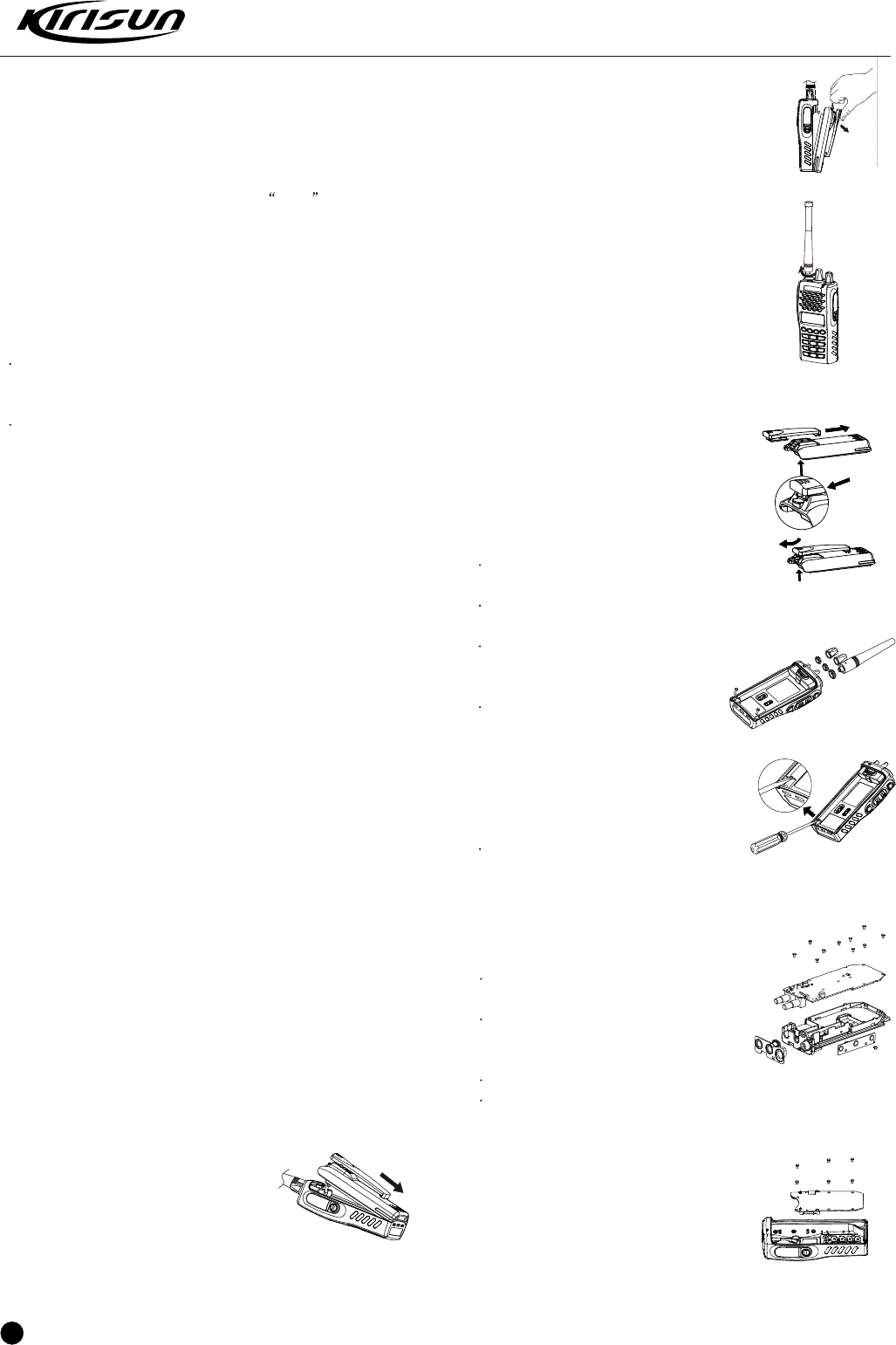
5.1 Installing/Removing the battery
pack
Match the 3 bulges of the battery pack
with the corresponding at the rear
of the transceiver.
To install the battery pack:
slots
bottom Figure 5.1-1
Removing the Battery Pack
To remove the battery pack, use your
thumb to press the belt clip, one side of
your index finger to press the release
button and then pull the battery away
from the radio.
5.2 INSTALLING THE ANTENNA
Screw the antenna into the connector at
the top of the transceiver by holding the
Button of the antenna and turn it
clockwise until secure.
5. 3 INSTALLING THE BELT CLIP
Match the grooves of the belt clip with
those on the rear of the battery. Then
press belt clip downwards to lock it in
place. Push the card by inserting your
nail or tool into the groove at the upper
part of the clip to remove the belt clip.
5. 4 Removing the Casing from the
Chassis
1 Remove the antenna and two
knobs;
2 Remove the two knob screws and a
antenna head screw;
3 Remove the two inner hexangular
aluminum alloy socket head screw
fixed at the bottom;
4 Insert the slotted screwdriver into
the groove at the bottom of the chassis
and apply force upwards to release the
aluminum alloy frame; and then hold
the aluminum alloy frame and draw it
out properly to remove it out of the
casing;
5 Plug the PCB winding displacement
connecting the main PCB and the
keyboard from the main PCB.
As shown in Figure 5.4-1
5. 5 Removing the main board from
the aluminum alloy frame
1 Remove the waterproof washer
at the top;
2 Remove the screws of the PTT
keypad and then remove the PTT
keypad;
3 Remove the screws on the PCB;
4 Melt the solder at the antenna
point with an electric soldering iron and
take off the main board.
As shown in Figure 5.4-1
5.6 Removing the keypad from the
surface casing
Remove the screws of the keypad to
detach the keypad from the surface
casing. As shown in Figure 5.6-1
Figure 5.1-2
Figure 5.2-1
Figure 5.3-1
Figure 5.4-1
Figure 5.5-1
Figure 5.6-1
12
13
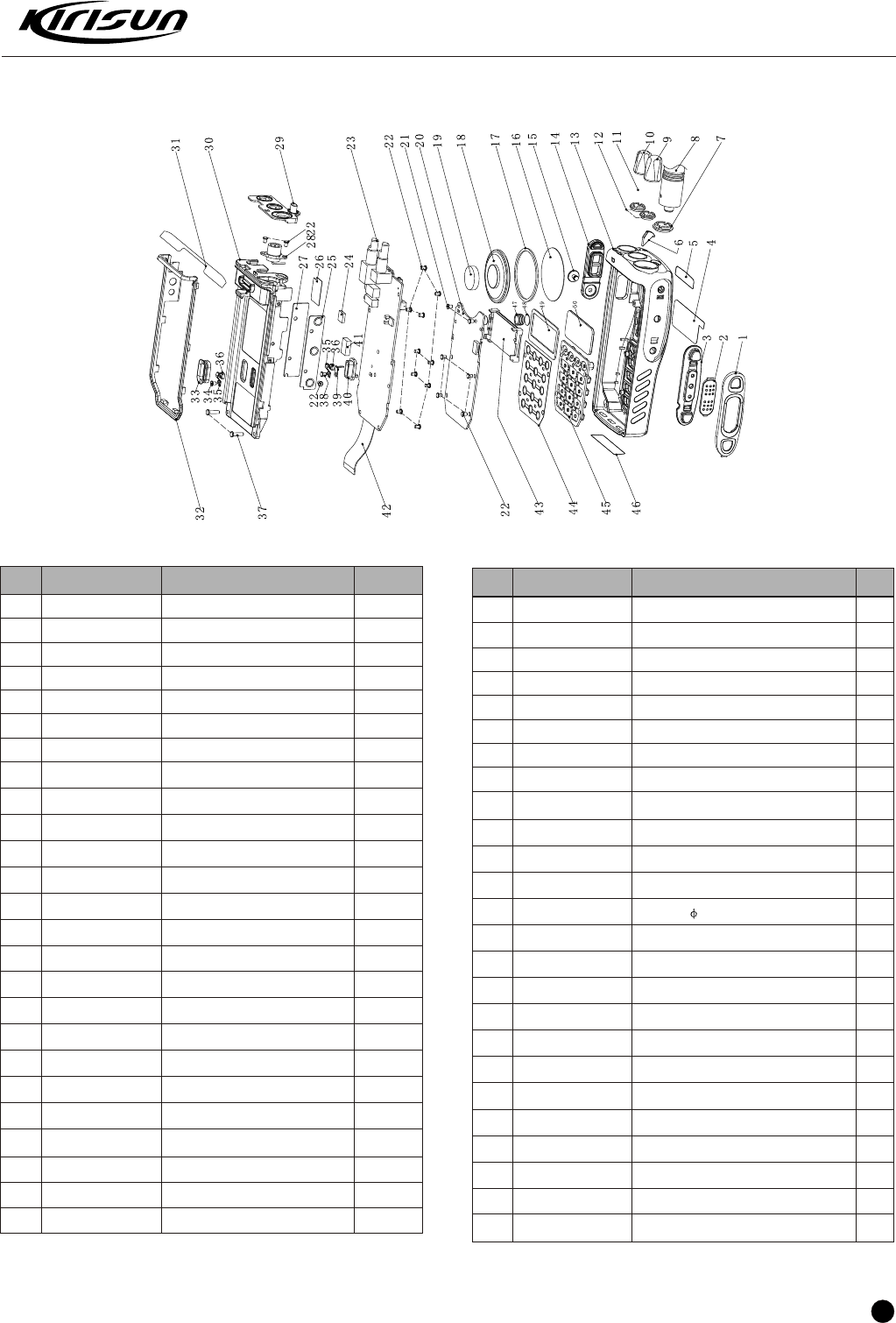
5.7 Exploded View
1
2
3
4
5
6
7
8
9
10
11
12
13
14
15
16
17
18
19
20
21
22
32
33
34
35
36
37
38
39
40
41
42
43
44
24
30
31
1
1
1
1
1
1
1
1
2
2
1
1
1
1
1
1
2
17
1
1
1
2
1
1
1
1
1
1
1
1
COVER PTT KEY
KEY PTT
RUBBER KEY PTT
LABEL LCD LENS
204-006800-R01
202-006500-R01
201-006500-R05
201-006500-R02
1
LABEL LOGO
LENS LED
201-006500-R09
NUT ANTENNA
203-000558-R11
1
ANTENNA
KNOB CHANNEL
201-006500-R04
KNOB VOLUME
201-006500-R03
SPRING PLATE KNOB
203-006800-R26
NUT KNOB
305-108020-R01
CASE FRONT201-006500-R01
1
1
COVER EARPHONE
201-006500-R07
SCREW EARPHONE COVER304-30040G-R01
WATERPROOF NET SPEAKER
204-003208-R02
204-003208-R07 CUSHION SPEAKER
121-100000-R17 SPEAKER
CUSHION SPACE SPEAKER204-006200-R09
PCB ASSEBIED FUNCTION KEY
..
302-20060G-R01
SCREW,M2X4
301-20040G-R01
23 1
PCB ASSEBIED FUNCTION KEY
202-003208-R07 SPACE TRASCALENT
25
26
27
28
29
203-006500-R06 PTT KEYMETALDOME
204-006500-R02
203-000558-R07
202-006500-R03
1
1
1
1
1
2
2
1
1
1
203-006500-R01
204-006800-R11
45
46
47
48
49
50
1
1
1
1
1
202-006500-R02
202-006500-R05
301-20030G-R01
203-006500-R04
202-000558-R08
301-20080G-R02
302-17040G-R01
203-006500-R02
201-006500-R06
204-006200-R04
120-400000-R13
102-6800CN-R01
203-006500-R03
202-006500-R04
204-006800-R12
202-000558-R09
204-006800-R06
204-006500-R01
201-006500-R08
PT6500 SERVICE MANUAL
ITEM ITEM
PART NUMBER PART NUMBER
DESCRIPTION QTY. QTY.
M2 0X60
SCREW
SPACE EARPHONE
PCB ASSEMBIEDPTT
BASE ANTENNA
WATERPROOF PART TOP
CASE AL
LABEL
WATERPROOF LOOP MAIN
WATERPROOF PART POSITIVE BKT
SCREW M2X3.0
SPRING PLATE POSIT.AND NEGAT.
RUBBER CUSHION
SCREW,M2X8
SCREW, 1.7x4.0
PLATE POSITIVE
BKT POSITIVE
CUSHION
LCM
RUBBER KEY FUNCTION
LABBEL CASE FRONT BOTTOM
COVER MIC
CUSHION MIC
CUSHION LCD LENS
LENS LCD
DESCRIPTION
LINE
METAL DOME FUNCTION KEY
Chapter 6 Radio Debugging
Before test/debugging, make sure all the equipments have
been well connected to the ground!
Before test/debugging, make sure the antenna output terminal has
been connected properly to the corresponding devices and load!
The transmitter output must pass RF power attenuator before being
connected to the standard signal source/ frequency
deviator/frequency spectrum!
When testing the receiver, make sure not to conduct transmitting
operation!
When in debugging/testing/service, make sure static free measures
for human body and equipments.
6.1 Service Equipment and Software
The following equipments and software in Table 6.1 are necessary
for the service and test of the radio.
NO
1
2
3
4
5
6
7
8
9
10
11
12
13
14
Name
Computer
Programming
software
Programming
Cable
Cloning cable
DC regulated
power
Therefore Power
meter
Frequency meter
Frequency
Deviator
Digital Multimeter
Audio Signal
Generator
RF Power
attenuator
Standard signal
source
Oscillograph
Audio voltmeter
KSP6500
KSPL-09
KCL01
5A
SWR 1.2
-6
110
0-- 5kHz
Specifications
Above P2, compatible with IBM PC,
WINDOWS 98/ME/2000/XP
Output voltage: 7.5V, output current:
Measuring rang: 0.5---10W
Frequency range: 100MHz500MHz
Impedance: 50Ù
Frequency range: 0.1600MHz
Frequency precision: higher than
Sensitivity: higher than 100mV
Frequency range: DC600MHz
Measuring range:
Input impedance: higher than 10MÙ/V DC,
with the ability of testing voltage, current,
impedance
Frequency range: 2---3000Hz
output level: 1---500mV
Attenuation: 40dB or 50dB
Supporting power: Bigger than 10W
Frequency range: 10MHz---1000MHz
Output level: 0.1uV~32mV (-127dBm~-
17dBm)
Frequency range: DC~20MHz
Test range: 10mV~20V
Test range: 10mV~10V
6.2 Debugging Items
During the course of maintenance, the radio needs to be
tested and debugged after replacing components. Brief
description of circuits is as follows.
Some certain radio parameters can be modified (computer
mode) with our KSP6500 programming software. The
modifiable parameters are as follows:
1) Receiving and transmitting frequencies of different
channels;
2) Receiving and transmitting signaling of different
channels;
3) Busy-lock selection of channels;
4) TOT transmitting time limit;
5) Squelch level;
6) Power-saving function selection;
7) 2-tone settings;
8) DTMF settings;
9) Voice alert function selection;
10) Monitoring mode selection;
11) Scanning mode selection;
12) Scanning reply channel selection;
13) Scanning channel priority selection;
14) Call list settings;
15) Customized alert;
Debugging Procedures:
A, Enter the computer test mode. Access method refers to
the instruction in 4.2.1 for entering the computer mode.
b, Select the Test Mode option in KPS6500 programming
software to enter the computer test mode.
c, Select the options that you want to adjust and adjust the
parameters on the computer.
d, After adjustment, exit the computer test mode.
6.3 Debugging
6.3.1 VCO Modification
Turn off the power saving mode. Set the frequency at the
low frequency (see Table 6.2). In receiving status, test the PD
power with the digital multimeter. Adjust the trimming capacitor
C117 to make the PD power at 4.2V 0.1V
In the transmitting status, test the PD power with the digital
multimeter and adjust the micro capacity C52 to make the
voltage at PD point at 4.2V 0.1V
PT6500 SERVICE MANUAL
Recommendation: Equipment in item 6, 7, 8, 10, 11, and 12
can be replaced by a comprehensive test instrument.
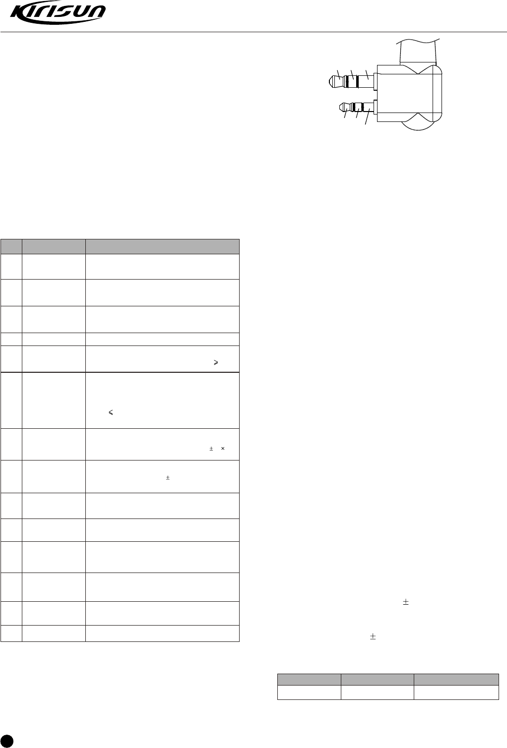
Figure 6.1 External Speaker/Mic. Connector Definition
MIC JACK
MIC RXD
SPEAKER JACK
SP+ SP-TXD
GND
400.125MHz 435.125MHz 469.975MHz
Table 6.2Radio H/I/L Frequency
Low Frequency Center frequency Hi gh Fr eq ue nc y
14

15
6. 3.5 Frequency Deviation Adjustment
A. Max frequency deviation (HP8920 set at the TX status, filter
set at 50Hz~15kHz): input the audio signal of 160mV,1000Hz at the
MIC port of the radio. Under the computer test mode, select Max
frequency deviation to and adjust the digits within 0~64 at the
max, high, medium, low and min frequencies to make the RF
frequency deviation at 4.5kHz.
Adjust the frequency deviation of narrow band in the
method above to make the transmitting frequency deviation at
2.2kHz.
B. 5_Tone frequency deviation (HP8920 set at the TX status,
filter set at 50Hz~15kHz): Under the computer test mode, select
5_Tone frequency deviation to enter, select broadband and
adjust the digits within 0~255 range to set the frequency deviation
at 4.0kHz.
Adjust the frequency deviation of narrow band in the
method above to make the transmitting frequency deviation at
2.0kHz.
C. DTMF frequency deviation (HP8920 set at the TX status,
filter set at 50Hz~15kHz): Under the computer test mode, select
DTMF frequency deviation to enter, select broadband and
adjust the digits within 0~64 range to set the frequency deviation
at 4.0kHz.
Adjust the frequency deviation of narrow band in the
method above to make the transmitting frequency deviation at
2.0kHz.
D. CTCSS (67Hz) frequency deviation (HP892 set at the TX
status, filter set at 20Hz~300Hz): Under the computer test mode,
select CTCSS(67Hz) frequency deviation to enter, select
broadband and adjust the digits within 0~255 range to set the
frequency deviation at 0.75kHz.
Adjust the frequency deviation of narrow band in the
method above to make the transmitting frequency deviation at
0.35kHz.
E. CTCSS (150Hz) frequency deviation (HP8920 set at the TX
status, filter set at 20Hz~300Hz): Under the computer test mode,
select CTCSS(150Hz) frequency deviation to enter, select
broadband and adjust the digits within 0~255 range to set the
frequency deviation at 0.75kHz.
Adjust the frequency deviation of narrow band in the
method above to make the transmitting frequency deviation at
0.35kHz
F. CTCSS (254.1Hz) frequency deviation (HP8920 set at the TX
status, filter set at 20Hz~300Hz): Under the computer test mode,
select CTCSS(254.1Hz) frequency deviation to enter, select
roadband and adjust the digits within 0~255 range to set the
frequency deviation at 0.75kHz.
Adjust the frequency deviation of narrow band in the
method above to make the transmitting frequency deviatio5
6.3.6 Transmitting Low Voltage Alert (HP8920 set at the TX
status)
Set the voltage of the power supply at 5.8V.
Under the computer test mode, select transmitting low
voltage and press adjustment to enter, when the digits are stable,
press Confirm.
6.3.7 Receiver Sensitivity (HP8920 set at the RX status)
Under the computer test mode, select Receiver Sensitivity
to enter and respectively adjust 5 frequencies of max. high, medium,
low and min, adjust within 0~255 range to make the frequencies at
the highest sensitivity.
6.3.8 Receiver Squelch Setting
A. Level 9 broadband squelch (HP8920 set at the RX status):
input the RF signal with adjusted frequency and the amplitude at -
116dBm at the antenna port of the radio. Under the computer test
mode, select Level 9 broadband squelch to enter and
respectively adjust f frequencies of max, high, medium, low and min
and make the green LED on when adjusting within the range of
0~255 range.
B. Level 9 narrowband squelch level (HP8920 set at the RX
status): input the RF signal with adjusted frequency and the
amplitude at -116dBm at the antenna port of the radio. Under the
computer test mode, select Level 9 narrowband squelch to
enter and respectively adjust f frequencies of max, high, medium,
low and min and make the green LED on when adjusting within the
range of 0~255 range.
C. Level 1 broadband squelch (HP8920 set at the RX status):
input the RF signal with adjusted frequency and the amplitude at -
123dBm at the antenna port of the radio. Under the computer test
mode, select Level 1 broadband squelch to enter and
respectively adjust f frequencies of max, high, medium, low and min
and make the green LED on when adjusting within the range of
0~255 range.
D. Level 1 narrowband squelch level (HP8920 set at the RX
Status): input the RF signal with adjusted frequency and the
amplitude at -123dBm at the antenna port of the radio. Under the
computer test mode, select Level 1 narrowband Squelch to
enter and respectively adjust f frequencies of max, high, medium,
low and min and make the green LED on when Adjusting within the
PT6500 SERVICE MANUAL
6.3.2 PLL Frequency Adjustment (HP8920 set at the TX
status)
Under the computer test mode, select frequency stability to
enter, Adjust the TX frequency among 0~255 to the specified value.
(Frequency error less than 200Hz.).
6.3.3 TX Frequency Adjustment (HP8920 set at the TX status)
A. Under the computer test mode, select high power to
enter and Adjust the TX power among 0~255 to 4W. And watch the
working current and make sure it not higher than 1.7A.
And adjust the max, high, low, min. frequencies in the method
above to make the TX power at 4W for all.
B. Under the computer test mode, select medium power to
enter and Adjust the TX power among 0~255 to 2W. And watch the
working current and make sure it not higher than 1.2A.And adjust
the max, high, low, min. frequencies in the method above to make
the TX power at 2W for all.
C. Under the computer test mode, select low power to
enter and Adjust the TX power among 0~255 to 0.5W. And watch
the working current and make sure it not higher than 1A.And adjust
the max, high, low, min frequencies in the method above to make
the TX power at 0.5W for all.
6.3.4 DCS Transmitted Signal Waveform
(HP8920 set at the TX status, filter set at 20Hz~300Hz)
Under the computer test mode, select DCS balancing to
enter, select broadband and adjust the digits within the range of
0~255, and watch the signals to make sure the waveforms are
smooth (near square wave) .
16
PT6500 SERVICE MANUAL
range of 0~255 range.
6.3.9 Receiver volume (HP8920 set at the RX status, filter set
at 50Hz~15kHz)
A. Max broadband receiver volume: input the RF signal with
adjusted frequency and the amplitude at -47dBm and the
modulation frequency deviation at 3kHz at the antenna port of the
radio. Under
the computer test mode, select Max broadband receiver
volume to enter and adjust the audio power at 1.8W within the
range of 0~64 range.
B. Max narrowband receiver volume: input the RF signal with
adjusted frequency and the amplitude at -47dBm and the
modulation frequency deviation at 1.5 kHz at the antenna port of the
radio. Under the computer test mode, select Max narrowband
receiver volume to enter and adjust the audio power at 1.8W
within the range of 0~64 range..
Item
Setting
Locked
voltage
Test
Condition
Battery
7.5V
CH: RX High
Frequency
CH: RX Low
Frequency
CH: TX High
Frequency
CH:TX Low
Frequency
cap
Acity:
Test
Equipment
Digital
Multimeter
Test
Point
PD
Adjustm
ent
Part
C117
C52
Require
ment
4.2V 0.1V
>0.6V
4.2V 0.1V
>0.6V
Note
Adjust
ment
Watch
ing
Adjust
ment
Watch
ing
Table 6.3 Voltage Controlled Oscillator
Table 6.4 Receiver
Item
Band pass
filter
Audiopower
Sensitivity
Squelch
activation
Test Condition
Test frequency intermediate
frequency
Antenna port
input
RF OUT -47dBm(1ìV)
MOD 1kHz
DEV 3.0kHz/ 1.5kHz
Audio load 16Ù
CH: center frequency
CH:low frequency
CH:high frequency
RF OUT:
-119dBm(0.25ìV)
MOD: 1kHz
DEV: 3.0kHz/ 1.5kHz
CH: RX center frequency
th
9
RF OUT:-117dBm
rd
3
RF OUT:-124dBm
Test Point
Before
mixing
Speaker
connector
Adjustment Part
Computer test
Computer test
Computer test
Computer test
Requirement
Smooth wave
(Turn the volume
knob clockwise)
audio power >1.5W
SINAD:
12dB or higher
After adjustment,
squelch activation
is normal
After adjustment
squelch activation
is normal
Note
No adjustment is
recommended
Inner speaker
power >
1.2W
Test Equipment
Frequency spectrum Analyzer /
comprehensive test Device
RF Signal
generator
Oscillator
Audio Voltmeter
DistortIon test
device
/Comprehensive
test
device
6.4 Debugging
The above debugging refers to Table3, Table4, and Table 5.
17
PT6500 SERVICE MANUAL
Table 6.5 Transmitter
Item
Tx
Frequency
DCS wave
(smooth)
Power
Max
modulation
frequency
deviation
Battery
power
warning
5-Tone
DEV
DTMF
DEV
CTCSS
DEV
CTCSS
DEV
CTCSS
DEV
DCS
DEV
Test
Condition
TXcenter
frequency
Battery terminal:
5.8V
Ch
AG:1kHz/320mV
CTCSS 67Hz
CTCSS
150Hz
CTCSS
254.1Hz
DCS 023N
Test Equipment
Frequency counter/
comprehensive test device
Oscillator/comprehensive
test device
Wattmeter/comprehensive
test device ammeter
Frequency deviation meter/
comprehensive test device
Frequency deviation meter/
comprehensive test device
Frequency deviation meter/
comprehensive test device
Frequency deviation meter/
comprehensive test device
Frequency deviation meter/
comprehensive test device
Frequency deviation meter/
comprehensive test device
Frequency deviation meter/
comprehensive test device
Adjustment Part
Computer test mode
Computer test mode
Computer test mode
Computer test mode
Computer test mode
Computer test mode
Computer test mode
Computer test mode
Computer test mode
Computer test mode
Computer test mode
Requirement
Within 200Hz
Waveform is close to smooth
square wave
Adjust to 4W/2W/0.5W
Adjust to 4.5kHz/2.2kHz
Adjust to 4kHz/2 kHz
Adjust to 4kHz/2 kHz
Adjust to 0.75kHz /0.35 kHz
Adjust to 0.75kHz /0.35 kHz
Adjust to 0.75kHz /0.35 kHz
Adjust to 0.9kHz /0.45 kHz
After adjustment, the indicator
flashes
Note
Within 0.2W 200Hz
50Hz
Test Point
Antenn a
Chapter 7 Major Specifications
7.1 General Specification
7.3 Receiver
7.2 Transmitter
PT6500
Frenquency
range(mhz)
Channel
capacity 128
Channel
spacing(khz)
Frenquency
stability(ppm)
operating
temperature( )
operating
voltage(v)
power supply
requirement
dimension
(h*w*d)(mm)
(with battery,
without antenna)
weight(g)(with
antenna&
battery)
battery (mah)
12.5KHz/20KHz/25KHz
2.5ppm
(1) 136~174MHz (2) 400~470 MHz
(3) 450~520MHz (4) 350~400 Mhz
-25 ~ + 55
7.5V DC 20%
0.5~4W/5W
56 mm 120 mm 35 mm
310g
1700mAh
RF Power (w) 4W/2W/0.5W(UHF)
5W/2W/0.5W(VHF)
Frenquency modulation 16K F3E/ 11K F3E/8K F3E
Antenna Impedance( ) 50
Modulation Limiting(KHz) 2.5KHz@12.5KHz,
4KHz@20KHz, 5KHz@25KHz
Modulation Distortion(%) 5%
Radiated Spurious Emission -36dBm < 1GHz, -30dBm > 1GHz
FM Noise(dB) -40dB@25KHz -35dB@12.5KHz
Adjacent Channel Power(dB) -60dB @ 12.5KHz, -70dB
@ 20/25KHz,
Reference Sensitivity( V) . 35 V
Operating Bandwidth(KHz) 7/ 3.5
First IF of Receiver (MHz) 51.65
second IF of Receiver(khz) 450
Adjacent channel
Selectivity(dB)
intermodulation Rejection(dB) 65 dB
Spurious Response Rejection(dB) 70 dB
Rated Audio Power(w) 0.5W
rated Audio Distortion(%) 10%
FM Hum&Noise(dB) 40/35
60 dB@12.5KHz,
70 dB@20/25KHz
18
PT6500 SERVICE MANUAL
Chapter 8 Trouble Shooting
No.
1
2
3
4
5
Problems
No display
after
switched
on.
Phase
locked loop
unlocked
Cannot
transmit.
No
signal
The
transmitting
red light is
on, but no
voice is
heard
Solution
A Battery power may be insufficient. Recharge or
replace the battery pack.
B The power switch may be broken, replace the switch.
C CPU may be broken, replace the IC.
D Regulator tube Q45 may be broken replace the IC.
A Phase locked loop Crystal Oscillator X1 may be
broken, replace it.
B Oscillator tube may be broken, replace it.
C. Phase locked loop IC2 may be broken, replace the IC.
A The frequencies of both users are not the same,
select the same frequency channel again.
B The CTCSS/DCS signaling of both users are not the
same, set it with PC.
C Beyond the efficient communication range.
A Make sure the antenna is well connected.
B Low sensibility, trimming computer test mode .
C HF amplifier may be broken, replace it.
D The squelch level is too high, which makes the
squelch unable to switch on, reset it by PC.
E Mixer tube Q19 may be broken, replace the tube.
F Frequency Modulation IC4 may be broken, replace
the IC.
A Power-amplifier tube no power output, replace the
tube.
B Replace the microphone if it is broken.
C Operational Amplifier IC14 may be broken, replace it.
6
7
Receiving
green light
is on, but
no voice is
heard
Abnormal
programmi
ng
A Replace the speaker if it is broken.
B Audio power amplifier IC9 may be broken, replace it.
C Switch Tube Q48 may be broken, replace it.
D Operational Amplifier IC6 may be broken, replace it.
A Make sure the wires are well connected.
B Abnormal output of the RS-232 serial port of the
computer, check the computer .
C Abnormal connection of MIC and SPK jack, check the
jack.
Appendix 1 Abbreviations
AMP amplify, amplifier
ANT antenna
APC automatic power control
BPF band pass filter
CTCSS continuous tone control squelch system
DCS Digital code squelch
DEMOD demodulation
EEPROM EEPROM
HPF high pass filter
IDC instantaneous deviation control
IF intermediate frequency
LED Light-Emitting Diode
LNA low noise amplifier
LPF low pass filter
MCU micro control unit
MIC microphone
MOD modulation
MONI monitor
PLL phase lock loop
PTT push-to-talk
RX receiver
SPK speaker
TCXO Temperature Compensated Crystal Oscillators
TX transmitter
UL un-lock
VCO voltage control oscillator
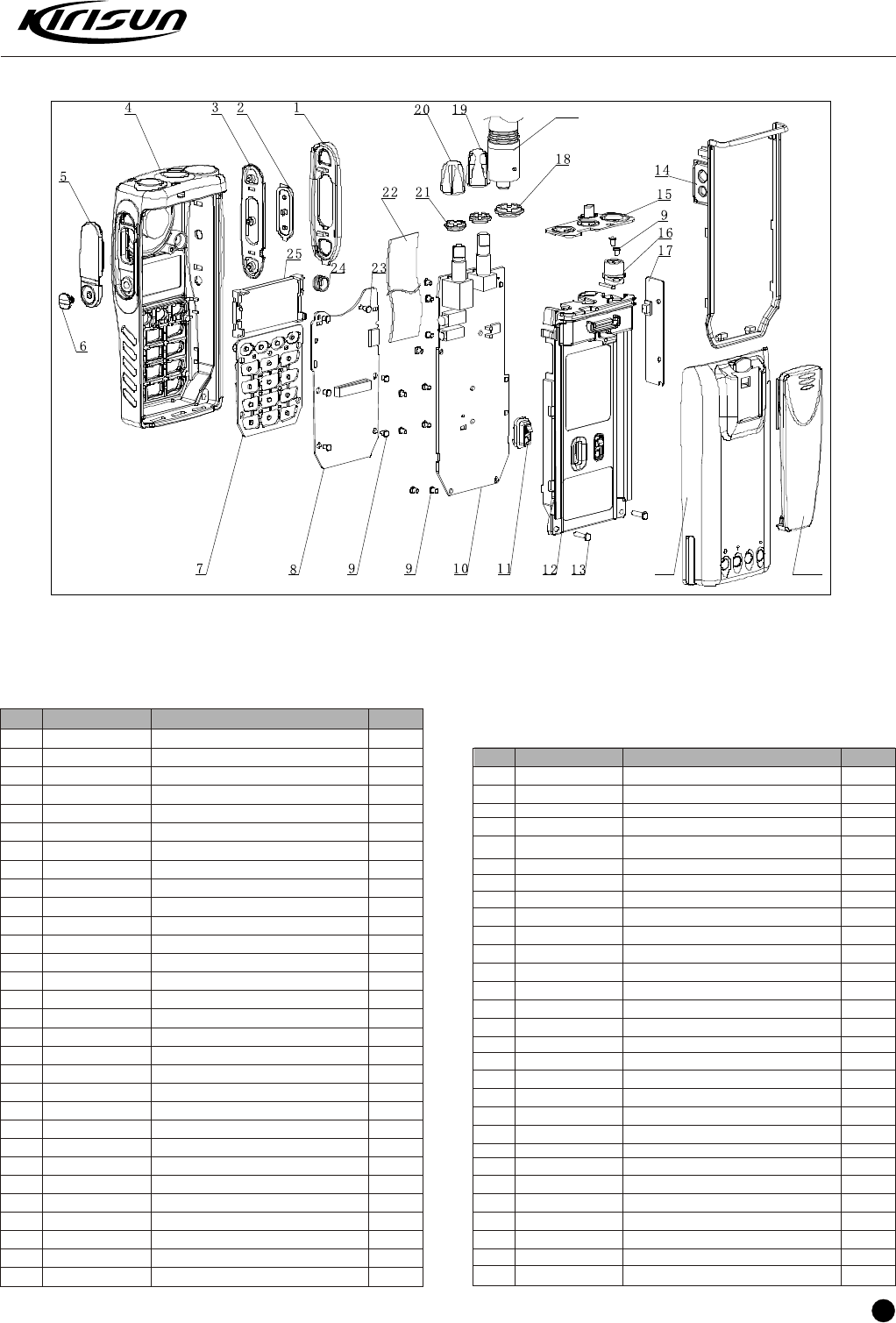
19
Appendix 2: Spare List
ITEM PART NUMBER DESCRIPTION QTY
COVER PTT KEY
KEY PTT
RUBBER KEY PTT
CASE FRONT SUBASSEMBLY
COVER EARPHONE
SCREW EARPHONE COVER
RUBBER KEY FUNCTION
PCB FUNCTION KEY SUBASSEMBLY
SCREW M2.0*4.0
PCB MAIN SUBASSEMBLY
BKT POSITIVER SUBASSEMBILY
CASE AL SUBASSEMB
SCREW M2.0*8.0
WATERPROOF LOOP MAIN
WATERPROOF PLATE TOP
BASE ANTENNA
PCB PTT KEY SUBASSEMBLY
NUT ANTENNA
KNOB CHANNEL SUBASSEMBLY
KNOB VOLUME SUBASSEMB
NUT KONB
LINE
SCREW M2.0*6.0
COVER MIC
LCM
CASE FRONT
WATERPROOF NUT SPEAKER
CUSHION SPEAKER
SPEAKER
SPACE CUSHION SPEAKER
1 201-006500-R02 1
2 201-006500-R05 1
3 202-006500-R01 1
4 604-065000-R01 1
5 201-006500-R07 1
6 304-30040G-R01 1
7 202-006500-R04 1
8 604-065000-R06 1
9 301-20040G-R01 17
10 1
11 604-065000-R02 1
12 604-065000-R03 1
13 301-20080G-R02 2
14 202-006500-R02 1
15 202-006500-R03 1
16 203-000558-R07 1
17 604-06500-R07 1
18 203-000558-R11 1
19 604-06500-R04 1
20 604-06500-R05 1
21 305-108020-R01 2
22 120-400000-R13 1
23 302-20060G-R01 2
24 202-000558-R09 1
25 102-6800CN-R01 1
26 201-006500-R01 1
27 204-003208-R02 1
28 204-003208-R07 1
29 121-100000-R17 1
30 204-006200-R09 1
PT6500 SERVICE MANUAL
Battery Pack
Belt Clip
Antenna
31 204-006800-R01 1
32 204-006800-R06 1
33 201-006500-R09 1
34 201-006500-R08 1
35 204-006500-R01 1
36 204-006800-R12 1
37 1
38 201-006500-R06 1
39 203-006500-R02 1
40 203-006500-R04 1
41 202-000558-R08 1
42 302-17040G-R01 1
43 203-006500-R01 1
44 204-006500-R02 1
45 202-006500-R05 1
46 204-006200-R04 1
47 204-006800-R11 1
48 203-006500-R04 1
49 202-000558-R08 1 1
50 301-20030G-R03 1
51 202-003208-R07 1
52 201-006500-R04 1
53 203-006800-R26 1
54 201-006500-R03 1
55 203-006800-R26 1
56 1
57 203-006500-R03 1
58 1
59 203-006500-R06 1
LABEL LCD
CUSHION MIC
LENS LED
LENS LCD
CUSHION LCD
LABEL CASE FRONT BOTTOM
LABEL LOGO
BKT POSITIVE
PLATE POSITIVE
SPRING PLATE
RUBBER CUSHION SPRING PLATE
SCREW M1.7*4.0
CASE AL
SPACE EARPHON
WATERPROOF PART POSITIVE BKT
SPACE
LABEL
SPRING PLATE
RUBBER CUSHION SPRING PLATE
SCREW M2.0*3.0
SPACE TRANSCALENT
KNOB CHANNEL
SPRING PLATE KNOB
KNOB VOLUME
SPRING PLATE KNOB
PCB FUNCTION KEY SUBASSEMBLY
METAL DOME FUNCTION KEY
PCB PTT KEY SUBASSEMBLY
METAL DOME PTT KEY
ITEM PART NUMBER DESCRIPTION QTY
20
Appendix 3 STRUCTURE PART LIST
Appendix 4 Electronic Component List(136-174MHz)
PT6500 SERVICE MANUAL
101-06500V-R04
102-1509GV-R01
102-24C256-R02
102-9140NR-R01
102-A31136-R01
102-AK2346-R01
102-B502MR-R01
PT6500PCB / VHF PCB,6 LAYER,FR4,1.2mm,PT6500V-071115.PCB,Rohs
DIVIDER / UPB1509GV,Rohs
EEPROM / 24LC256I/SN,Rohs
Reset IC / PST9140NR,Rohs
FM DETECTOR IC / TA31136FN,SSOP,Rohs
Audio Processor IC / AK2346 Rohs
LDO / XC6204B502MR Rohs
1
2
3
4
5
6
7
No Material Serial No Component Name/Specification No Material Serial No Component Name/Specification
1
1
1
1
1
1
2
QTY.
IC1
IC8
IC11
IC4
IC6
Q40, Q45
1
2
3
4
5
6
7
8
9
10
11
12
13
14
15
16
17
18
19
20
21
22
23
24
25
26
27
28
29
30
31
32
33
34
35
36
37
38
39
40
41
42
43
44
45
PART NUMBER
102-6800CN-R01
120-100000-R07
120-100000-R08
120-400000-R13
121-100000-R17
201-006500-R01C
201-006500-R02B
201-006500-R03
201-006500-R04
201-006500-R05
201-006500-R06B
201-006500-R07
201-006500-R08
201-006500-R09
202-000558-R08
202-000558-R09
202-003208-R07
202-006500-R01
202-006500-R02
202-006500-R03
202-006500-R04
202-006500-R05
203-000558-R07B
203-000558-R11
203-006500-R01B
203-006500-R02
203-006500-R03
203-006500-R04
203-006500-R06
203-006500-R07A
203-006800-R26
203-007200-R08
204-006500-R01
204-006500-R02
204-006800-R01
204-006800-R05
204-006800-R06
204-0KB36L-R03
301-20020G-R01
301-20030G-R03
301-20040G-R01
301-20080G-R02
302-17040G-R01
302-20060G-R01
304-30040G-R02B
DESCRIBER
LCD
LINE COLOR RED
LINE COLOR BLACK
CABLE 38PIN
SPEAKER
CASE FRONT
COVER PTT KEY
KNOB VOLUME
KNOB CHANNEL
KEY PTT
BKT POSITIVE
COVER EARPHONE
LENS LCD WINDOW
LENS LED
CUSHION RUBBER POSIT AND NEGAT
COVER MIC RUBBER
SPACE TRASCALENT
RUBBER KEY PTT
WATERPROOF LOOP MAIN
WATERPROOF TOP
RUBBER KEY FUNCTION
WATERPROOF POSITIVE BKT
BASE ANTENNA
NUT ANTENNA
CASE AL
PLATE POSITIVE
METAL DOME FUNCTION KEY
SPRING PLATE POSIT AND NEGAT
METAL DOME PTT KEY
SPRRING PLATE FUNCTION KEY PCB
SPRINT PLATE KNOB
NUT KNOB
CUSHION LCD LENS
SPACE MIC
LABEL LCD LENS
WATERPROOF NET SPEAKER
WATERPROOF NET MIC
CUSHION KB36L
SCREW M2.0*2.0
SCREW M2.0*3.0
SCREW M2.0*4.0
SCREW M2.0*8.0
SCREW M1.7*4.0
SCREW M2.0*6.0
SCREW M3.0*4.0
.
1
1
1
1
1
1
1
1
1
1
1
1
1
1
2
1
1
1
1
1
1
1
1
1
1
1
1
2
1
2
2
2
1
1
1
1
1
1
4
1
13
2
1
2
1
QUTY
ITEM
21
PT6500 SERVICE MANUAL
No Material Serial No Component Name/Specification QTY.
8
9
10
11
12
13
14
15
16
17
18
19
20
21
22
23
24
25
26
27
28
29
30
31
32
33
34
35
36
37
38
39
40
41
42
43
44
45
46
47
48
49
50
51
52
53
54
55
102-C75W51-R01
102-DA8541-R01
102-DF4111-R01
102-FP3502-R01
102-HT9172-R01
102-M2902V-R01
102-M2904V-R01
102-M30620-R01
103-0MA742-R01
103-1SR154-R01
103-1SV278-R01
103-1SV305-R01
103-1SV325-R01
103-A2S111-R01
103-DAN222-R01
103-HSC277-R01
103-HVC131-R01
103-HZU5AL-R01
103-L190YG-R01
103-MHC190-R02
104-A123JE-R01
104-A143TE-R01
104-A144EE-R01
104-C144EE-R01
104-C144EU-R01
104-SA1586-R01
104-SC3356-R01
104-SC4116-R01
104-SC4617-R01
104-SC5108-R01
104-TC4082-R01
105-2SK508-R01
105-3SK318-R01
105-RD01MU-R01
105-RD07MV-R01
105-SK1824-R01
105-ST2301-R01
106-LBE010-R01
106-RY6472-R01
108-450C24-R02
108-CF450F-R02
108-CF450G-R02
108-XF5165-R01
109-040000-R01
109-040100-R01
109-040101-R01
109-040102-R01
109-040103-R01
Operational Amplifier / TC75W51FU,SSOP8-P-0.65,Rohs
POWER AMPLIFIER / TDA8541,SO8,Rohs
RF PLL Frequency Synthesizers / ADF4111,TSSOP Rohs
Positive Voltage Regulator / XC62FP3502PR,SOT-89,Rohs
DTMF Receiver / HT9172,SOP,Rohs
Operational Amplifier / NJM2902V,OP-AMP,Rohs
Operational Amplifier / NJM2904V,OP-AMP,Rohs
MCU / CPU,M16C-M30620FCPGP,FLASH,Rohs
Chip switch diode / MA742(PANASONIC),Rohs
Chip diode / 1SR154-400(ROHM),Rohs
Chip varialble capacitor diode / 1SV278,Rohs
Chip varialble capacitor diode / 1SV305,Rohs
Chip varialble capacitor diode / 1SV325,Rohs
Chip switch diode / 0603,MA2S111(PANASONIC),Rohs
Chip switch diode / DAN222,(ROHM),Rohs
Chip diode / Waveband switch,HSC277(HITACHI),Rohs
Chip HF switch diode / 0603,HVC131(HITACHI),Rohs
Chip regulator diode / HZU5ALL(HITACHI),Rohs
Chip LED / 0603,green,H19-213SYGC,Rohs
Chip LED / 0603,red,19-21SURC/S530-A2/TR8,Rohs
Chip triode / DTA123JE(ROHM),Rohs
Chip triode / DTA143TE,Rohs
Chip triode / DTA144EE(ROHM),Rohs
Chip triode / DTC144EE(ROHM),Rohs
Chip triode / DTC144EUA(ROHM),Rohs
Chip triode / 2SA1586,Rohs
Chip triode / 2SC3356,R24,Rohs
Chip triode / 2SC4116-GR Rohs
Chip triode / 2SC4617(S)(ROHM),Rohs
Chip triode / 2SC5108Y(TOSHIBA),Rohs
Chip triode / KTC4082,(KEC),Rohs
Chip FET / 2SK508NV(K52),Rohs
Chip FET / 3SK318,Rohs
Chip FET / RD01MUS2,Rohs
Chip FET / RD07MVS1,Rohs
Chip FET / 2SK1824,Rohs
Chip FET / ST2301,Rohs
Switch / SKRTLBE010,Rohs
Carbon encoder switch / RY-6472,Rohs
Plug-in phase frequency detector / JTBM450CX24,Rohs
Plug-in porcelain filter / LTWC450F,450kHz 7kHz,Rohs
Plug-in porcelain filter / LTWC450G,450kHz 3kHz,Rohs
chip IF filter / DSF753SBF,51.65MHz 4kHz/3dB,
(7.0x5.0x1.3)mm,Rohs
Chip resistor / 0402,0R 5%,Rohs
Chip resistor / 0402,10R 5%,Rohs
Chip resistor / 0402,100R 5%,Rohs
Chip resistor / 0402,1K 5%,Rohs
Chip resistor / 0402,10K 5%,Rohs
IC14, IC18
IC9
IC2
IC16
IC10
IC5
IC3
IC7
D22, D35, D36, D37
D33
D9
D27, D28, D29, D30
D2, D6, D11, D14
D10, D16, D20, D38
D18, D19
D3, D17
D1, D7, D8, D39
D15
D26, D31
D25
Q26, Q44
Q7, Q9
Q12, Q25, Q36
Q13, Q16, Q22, Q24, Q32, Q35, Q42, Q23, Q52
Q10
Q38, Q47
Q5
Q41
Q21, Q30, Q31, Q53, Q14
Q2, Q8, Q20, Q4
Q15
Q6, Q11
Q18, Q19
Q3
Q1
Q27, Q29, Q34, Q50, Q51, Q54, Q33, Q46
Q39, Q43
SW3
SW2
CD1
CF2
Cf1
Xf1
C255, C271, R31, R54, R152, R178, R187, R227, R240,
R245, R258, R262, R264, R269, R291, R298, R304,
R307, R308, R310, R319
R2, R47, R49, R69
R20, R108
R7, R11, R40, R76, R118, R132, R148, R154, R160,
R167, R168, R192, R198, R202, R205, R208, R217,
R221, R225, R226, R241, R251, R253, R277, R294,
R297, R299, R301, R316, R320, R321, R322, R323,
R324, R325, R326, R327, R328, R329, R330, R331,
R332, R333, R334, R335, R336, R337, R338, R339,
R340, R341, R342, R343, R344, R345, R346, R347,
R348, R349, R350, R351
R59, R73, R79, R80, R126, R144, R172, R199, R211,
2
1
1
1
1
1
1
1
4
1
1
4
4
4
2
2
4
1
2
1
2
2
3
9
1
2
1
1
5
4
1
2
2
1
1
8
2
1
1
1
1
1
1
21
4
2
61
15
22
PT6500 SERVICE MANUAL
No Material Serial No Component Name/Specification QTY.
56
57
58
59
60
61
62
63
64
65
66
67
68
69
70
71
72
73
74
75
76
77
78
79
80
81
82
83
84
85
86
87
88
89
90
91
92
93
94
95
96
97
98
99
100
101
102
103
104
105
106
107
108
109
110
109-040104-R01
109-040105-R01
109-040123-R01
109-040124-R01
109-040152-R01
109-040153-R01
109-040154-R01
109-040180-R01
109-040181-R01
109-040182-R01
109-040183-R01
109-040184-R01
109-040202-R01
109-040220-R01
109-040221-R01
109-040222-R01
109-040223-R01
109-040224-R01
109-040271-R01
109-040272-R01
109-040273-R01
109-040274-R01
109-040331-R01
109-040332-R01
109-040333-R01
109-040334-R01
109-040361-R01
109-040393-R01
109-040470-R01
109-040471-R01
109-040472-R01
109-040473-R01
109-040474-R01
109-040512-R01
109-040513-R01
109-040560-R01
109-040561-R01
109-040562-R01
109-040563-R01
109-040564-R01
109-040681-R01
109-040683-R01
109-040823-R01
109-040824-R01
109-040913-R01
109-060000-R01
109-060101-R01
109-060104-R01
109-060124-R01
109-060150-R01
109-060153-R01
109-060154-R02
109-060182-R01
109-060221-R01
109-060273-R01
Chip resistor / 0402,100K 5%,Rohs
Chip resistor / 0402,1M 5%,Rohs
Chip resistor / 0402,12K 5%,Rohs
Chip resistor / 0402,120K 5%,Rohs
Chip resistor / 0402,1.5K 5%,Rohs
Chip resistor / 0402,15K 5%,Rohs
Chip resistor / 0402,150K 5%,Rohs
Chip resistor / 0402,18R 5%,Rohs
Chip resistor / 0402,180R 5%,Rohs
Chip resistor / 0402,1.8K 5%,Rohs
Chip resistor / 0402,18K 5%,Rohs
Chip resistor / 0402,180K 1%,Rohs
Chip resistor / 0402,2K 5%,Rohs
Chip resistor / 0402,22R 5%,Rohs
Chip resistor / 0402,220R 5%,Rohs
Chip resistor / 0402,2.2K 5%,Rohs
Chip resistor / 0402,22K 5%,Rohs
Chip resistor / 0402,220K 5%,Rohs
Chip resistor / 0402,270R 5%,Rohs
Chip resistor / 0402,2.7K 5%,Rohs
Chip resistor / 0402,27K 5%,Rohs
Chip resistor / 0402,270K 5%,Rohs
Chip resistor / 0402,330R 5%,Rohs
Chip resistor / 0402,3.3K 5%,Rohs
Chip resistor / 0402,33K 5%,Rohs
Chip resistor / 0402,330K 5%,Rohs
Chip resistor / 0402,360R 5%,Rohs
Chip resistor / 0402,39K 5%,Rohs
Chip resistor / 0402,47R 5%,Rohs
Chip resistor / 0402,470R 5%,Rohs
Chip resistor / 0402,4.7K 5%,Rohs
Chip resistor / 0402,47K 5%,Rohs
Chip resistor / 0402,470K 5%,Rohs
Chip resistor / 0402,5.1K 5%,Rohs
Chip resistor / 0402,51K 5%,Rohs
Chip resistor / 0402,56R 5%,Rohs
Chip resistor / 0402,560R 5%,Rohs
Chip resistor / 0402,5.6K 5%,Rohs
Chip resistor / 0402,56K 5%,Rohs
Chip resistor / 0402,560K 5%,Rohs
Chip resistor / 0402,680R 5%,Rohs
Chip resistor / 0402,68K 5%,Rohs
Chip resistor / 0402,82K 5%,Rohs
Chip resistor / 0402,820K 5%,Rohs
Chip resistor / 0402,91K 5%,Rohs
Chip resistor / 0603,0R 5%,Rohs
Chip resistor / 0603,100R 5%,Rohs
Chip resistor / 0603,100K 5%,Rohs
Chip resistor / 0603,120K 5%,Rohs
Chip resistor / 0603,15R 5%,Rohs
Chip resistor / 0603,15K 5%,Rohs
Chip resistor / 0603,150K 1%,Rohs
Chip resistor / 0603,1.8K 5%,Rohs
Chip resistor / 0603,220R 5%,Rohs
Chip resistor / 0603,27K 5%,Rohs
R252, R255, R266, R284, R287, R288
R186, R213, R279, R300
R60, R114, R115, R116, R120, R127, R234, R237, R243, R270
R16, R140, R191, R209, R231
R15, R88, R193, R204
R10, R45, R180, R238
R50, R233, R281
R6, R25, R42, R121, R157, R159, R179, R182
R5
R52
R22, R87
R184, R185, R278
R81, R110, R139, R147, R174, R194, R196, R210
R257
R36, R92, R230
R43, R100
R1, R51, R77, R93, R135, R189
R74, R75, R82, R83, R102, R103, R166, R244, R273
R161, R203
R19
R24, R133, R181, R200, R212, R254, R295
R101, R153, R195, R280, R283
R34, R38
R14, R17, R23, R90, R107, R119, R150
R12, R21, R112, R123, R128, R177
R171, R215, R247, R248, R311
R61, R97, R232, R239
R33
R35, R86
R8, R13, R28, R68
R263
R4, R37, R48, R62, R98, R99, R125, R134, R136, R137, R145, R173,
R197, R207, R216
R30, R32, R183, R206, R214, R224, R228, R229, R235, R242, R274,
R275, R276, R286, R292, R317, R318
R29, R85, R156, R265, R271
R176
R151
R117
R26, R44
R303
R71, R142, R220
R146, R218, R219
R41
C162, R141, R246
R169
R285
R175
C12, R94, R95, R170, R201, R222, R282
R9, R39
R106, R124, R250
R78, R105
R27
R305
R53, R55, R58, R63, R67, R72
L48
R104
R70
4
10
5
4
4
3
8
1
1
2
3
8
1
3
2
6
9
2
1
7
5
2
7
6
5
4
1
2
4
1
15
17
5
1
1
1
2
1
3
3
1
3
1
1
1
7
2
3
2
1
1
6
1
1
1
23
PT6500 SERVICE MANUAL
No Material Serial No Component Name/Specification QTY.
111
112
113
114
115
116
117
118
119
120
121
122
123
124
125
126
127
128
129
130
131
132
133
134
135
136
137
138
139
140
141
142
143
144
145
146
147
148
149
150
151
152
153
154
109-060331-R01
109-060470-R01
109-060472-R01
109-060823-R01
109-070000-R01
109-100000-R01
109-100R47-R01
110-220103-R01
111-030000-R01
112-042214-R01
112-043100-R01
112-043101-R01
112-043102-R01
112-043103-R01
112-043104-R02
112-043105-R01
112-043110-R01
112-043120-R01
112-043121-R01
112-043123-R01
112-043130-R01
112-043150-R01
112-043153-R01
112-043180-R01
112-043182-R01
112-0431R5-R01
112-043200-R01
112-043220-R01
112-043221-R01
112-043222-R01
112-043223-R01
112-043224-R02
112-043270-R01
112-043271-R01
112-043330-R01
112-043332-R01
112-043333-R01
112-043390-R01
112-043392-R01
112-043393-R01
112-0433R0-R01
112-0433R5-R01
112-043470-R01
112-043471-R01
Chip resistor / 0603,330R 5%,Rohs
Chip resistor / 0603,47R 5%,Rohs
Chip resistor / 0603,4.7K 5%,Rohs
Chip resistor / 0603,82K 5%,Rohs
Chip resistor / 0805,0R 5%,Rohs
Chip resistor / 1206,0R 5%,Rohs
Chip resistor / 1206,0.47R 5%,Rohs
Volume switch / 10K,RY-6473,Rohs
Chip FUSE / 433003,3A/32V,1206 Rohs
Chip capacitor / 220P*4,0402,Rohs
Chip capacitor / 0402,10P 0.5P,50V,C0G,Rohs
Chip capacitor / 0402,100P 5%,50V,C0G,Rohs
Chip capacitor / 0402,1000P 10%,50V,X7R,Rohs
Chip capacitor / 0402,0.01uF 10%,50V,X7R,Rohs
Chip capacitor / 0402,0.1uF 10%,10V,X5R,Rohs
Chip capacitor / 0402,1uF 10%,6.3V,X5R,Rohs
Chip capacitor / 0402,11P 5%,50V,C0G,Rohs
Chip capacitor / 0402,12P 5%,50V,C0G,Rohs
Chip capacitor / 0402,120P 5%,50V,C0G,Rohs
Chip capacitor / 0402,0.012uF 10%,50V,X7R,Rohs
Chip capacitor / 0402,13P 5%,50V,C0G,Rohs
Chip capacitor / 0402,15P 5%,50V,C0G,Rohs
Chip capacitor / 0402,0.015uF 10%,50V,X7R,Rohs
Chip capacitor / 0402,18P 5%,50V,C0G,Rohs
Chip capacitor / 0402,1800P 10%,50V,X7R,Rohs
Chip capacitor / 0402,1.5P 0.25P,50V,C0G,Rohs
Chip capacitor / 0402,20P 5%,50V,C0G,Rohs
Chip capacitor / 0402,22P 5%,50V,C0G,Rohs
Chip capacitor / 0402,220P 5%,50V,C0G,Rohs
Chip capacitor / 0402,2200P 10%,50V,X7R,Rohs
Chip capacitor / 0402,0.022uF 10%,50V,X7R,Rohs
Chip capacitor / 0402,0.22uF 10%,16V,X7R,Rohs
Chip capacitor / 0402,27P 5%,50V,C0G,Rohs
Chip capacitor / 0402,270P 10%,50V,X7R,Rohs
Chip capacitor / 0402,33P 5%,50V,C0G,Rohs
Chip capacitor / 0402,3300P 10%,50V,X7R,Rohs
Chip capacitor / 0402,0.033uF 10%,16V,X7R,Rohs
Chip capacitor / 0402,39P 5%,50V,C0G,Rohs
Chip capacitor / 0402,3900P 10%,50V,X7R,Rohs
Chip capacitor / 0402,0.039uF 10%,50V,X7R,Rohs
Chip capacitor / 0402,3P 0.25P,50V,C0G,Rohs
Chip capacitor / 0402,3.5P 0.25P,50V,C0G,Rohs
Chip capacitor / 0402,47P 5%,50V,C0G,Rohs
Chip capacitor / 0402,470P 10%,50V,X7R,Rohs
R3, R18, R91
L52
R138
R84, R111
L54
C294
R57, R65, R66
SW1
F1
C288, C345, C346
C11, C70, C142, C143
C144, C153, C84, C104, C105, C106, C121
C6, C7, C21, C23, C31, C34, C37, C43, C46, C49, C56, C57,
C62, C63, C65, C67, C73, C77, C78, C79, C80, C81, C82, C85,
C88, C92, C94, C97, C98, C100, C109, C110, C113, C119, C126,
C131, C133, C136, C146, C150, C154, C175, C179, C180, C192,
C193, C202, C203, C205, C210, C211, C212, C235, C247, C253,
C270, C272, C279, C282, C283, C290, C301, C306, C311, C314,
C318, C323, C329, C332, C333, C334, C335, C347, C348, C350,
C352, C360, C363, C365, C366, C367, C368, C369, C370, C376,
C377, C134
C44, C54, C91, C95, C115, C152, C158, C164, C181, C196,
C207, C219, C232, C234, C256, C268, C275, C362, C374, C220
C33, C83, C99, C114, C151, C159, C166, C167, C177, C178,
C199, C209, C216, C231, C233, C248, C251, C257, C274, C276,
C280, C285, C293, C303, C310, C319, C359, C532
C45, C87, C217, C263, C289, C299, C304, C315, C330, C339,
C353, C354, C371, C372, C373, C375
C174
C145
C101
C249
C176
C22, C59
C239
C155
C218, C267, C201
C68, C69
C250
C64, C242
C230, C364
C241, C246
C140, C161, C214, C226, C325
C313
C260
C258
C10, C50, C188, C190, C191, C194, C297, C298
C286
C157, C240, C265, C328, C331
C38
C320, C337
C243, C277
C124, C170
C123
C128, C252, C309
C58, C71, C76, C86, C127, C137, C198, C204, C223, C224,
C244, C266, C281, C312, C316, C321, C324, C327, C338, C356,
C125, C168, C342
3
1
1
2
1
1
3
1
1
3
4
7
87
20
28
16
1
1
1
1
1
2
1
1
3
2
1
2
2
2
5
1
1
1
8
1
5
1
2
2
2
1
3
23
24
PT6500 SERVICE MANUAL
No Material Serial No Component Name/Specification QTY.
155
156
157
158
159
160
161
162
163
164
165
166
167
168
169
170
171
172
173
174
175
176
177
178
179
180
181
182
183
184
185
186
187
188
189
190
191
192
193
194
195
196
197
198
199
200
201
202
203
204
205
206
207
208
112-043473-R01
112-043474-R01
112-0434R0-R01
112-0434R7-R01
112-043560-R01
112-043561-R01
112-0435R0-R01
112-043680-R01
112-043682-R01
112-043683-R01
112-0436R0-R01
112-043820-R01
112-0439R0-R01
112-063100-R01
112-063101-R01
112-063102-R01
112-063103-R01
112-063110-R01
112-063120-R01
112-063150-R01
112-063180-R01
112-063181-R01
112-0631R0-R01
112-063220-R01
112-063270-R01
112-063334-R01
112-063390-R01
112-0633R0-R01
112-063471-R01
112-0634R0-R01
112-0635R0-R01
112-063680-R01
112-0636R0-R01
112-0637R0-R01
112-0638R0-R01
112-0639R0-R01
112-063R50-R01
112-072105-R01
112-072475-R01
112-073474-R01
112-102104-R01
112-102105-R02
112-102106-R02
112-102156-R01
112-102334-R01
112-102335-R02
113-010100-R01
114-06E180-R01
114-06G101-R03
114-06G181-R01
114-06G221-R02
114-06G270-R01
114-06G330-R01
114-06G332-R01
Chip capacitor / 0402,0.047uF 10%,16V,X7R,Rohs
Chip capacitor / 0402,0.47uF 10%,10V,X5R,Rohs
Chip capacitor / 0402,4P 0.25P,50V,C0G,Rohs
Chip capacitor / 0402,4.5P/4.7P 0.25P,50V,C0G,Rohs
Chip capacitor / 0402,56P 5%,50V,C0G,Rohs
Chip capacitor / 0402,560P 10%,16V,X7R,Rohs
Chip capacitor / 0402,5P 0.25P,50V,C0G,Rohs
Chip capacitor / 0402,68P 5%,50V,C0G,Rohs
Chip capacitor / 0402,6800P 10%,16V,X7R,Rohs
Chip capacitor / 0402,0.068uF 10%,16V,X7R,Rohs
Chip capacitor / 0402,6P 0.5P,50V,C0G,Rohs
Chip capacitor / 0402,82P 5%,50V,C0G,Rohs
Chip capacitor / 0402,9P 0.5P,50V,C0G,Rohs
Chip capacitor / 0603,10P 5%,50V,C0G,Rohs
Chip capacitor / 0603,100P 5%,50V,C0G,Rohs
Chip capacitor / 0603,1000P 10%,50V,X7R,Rohs
Chip capacitor / 0603,0.01uF 10%,50V,X7R,Rohs
Chip capacitor / 0603,11P 5%,50V,C0G,Rohs
Chip capacitor / 0603,12P 5%,50V,C0G,Rohs
Chip capacitor / 0603,15P 5%,50V,C0G,Rohs
Chip capacitor / 0603,18P 5%,50V,C0G,Rohs
Chip capacitor / 0603,180P 10%,50V,X7R,Rohs
Chip capacitor / 0603,1P 0.25P,50V,C0G,Rohs
Chip capacitor / 0603,22P 5%,50V,C0G,Rohs
Chip capacitor / 0603,27P 5%,50V,C0G,Rohs
Chip capacitor / 0603,0.33uF 10%,50V,X7R,Rohs
Chip capacitor / 0603,39P 5%,50V,C0G,Rohs
Chip capacitor / 0603,3P 0.25P,50V,C0G,Rohs
Chip capacitor / 0603,470P 10%,50V,X7R,Rohs
Chip capacitor / 0603,4P 0.25P,50V,C0G,Rohs
Chip capacitor / 0603,5P 0.25P,50V,C0G,Rohs
Chip capacitor / 0603,68P 5%,50V,C0G,Rohs
Chip capacitor / 0603,6P 0.5P,50V,C0G,Rohs
Chip capacitor / 0603,7P 0.5P,50V,C0G,Rohs
Chip capacitor / 0603,8P 0.5P,50V,C0G,Rohs
Chip capacitor / 0603,9P 0.5P,50V,C0G,Rohs
Chip capacitor / 0603,0.5P 0.1P,50V,C0G,Rohs
Chip Ta capacitor / TP Model,SIZE P,1uF 20%,10V,Rohs
Chip Ta capacitor / TPModel,SIZE P,4.7uF 20%,10V,Rohs
Chip capacitor / 0805,0.47uF+80%--20%,16V,Y5V,Rohs
Chip Ta capacitor / TSModel,SIZE A,0.1uF 20%,35V,Rohs
Chip Ta capacitor / TSModel,SIZE A,1uF 20%,10V,Rohs
Chip Ta capacitor / TSModel,SIZE A,10uF 20%,10V,Rohs
Chip Ta capacitor / TSModel,SIZE A,15uF 20%,6.3V,Rohs
Chip Ta capacitor / TSModel,SIZE A,0.33uF 20%,35V,Rohs
Chip Ta capacitor / TSModel,SIZE A,3.3uF 20%,10V,Rohs
Chip trimming capacitor / TZV2Z100A110,3~10p+100,Rohs
Chip wire inductor / C1608CB-18NJ,ceramic core18NH 5%,
0603,Rohs
Chip inductor / MLG1608BR10J,100nH 5%,0603,Rohs
Chip inductor / LGHK1608R18J-T,180nH 5%,0603,Rohs
Chip inductor / LGHK1608R22J-T,220nH 5%,0603,Rohs
Chip inductor / MLG1608B27NJ,27nH 5%,0603,Rohs
Chip inductor / MLG1608B33NJT,33nH 5%,0603,Rohs
Chip inductor / MLF1608A3R3K,3.3uH 5%,0603,Rohs
C238
C237
C48, C187, C189, C195, C349
C186
C4
C245
C103, C254
C55
C264
C269
C74, C75, C108, C135, C169
C215
C129
C16, C27, C29, C47, C156
C30, C111
C5, C13, C32, C72, C132, C160, C183, C184, C200, C206,
C213
C165
C2
C1
C18, C28
C17, C182
C8
C9, C90
C19
C25, C36
C163
C291, C295
C139
C171
C24, C41, C138
C14, C42
C26
C148
C3
C149
C39, C147
C107
C229, C236, C322, C355
C20, C89, C93, C120, C122, C130, C173, C197, C208, C225,
C261, C262, C273, C278, C284, C305, C307, C308, C317,
C336, C344, C361
C172
C102
C118
C227
C141
C96
C112
C52, C117
L24
L23, L35, L44, L45
L7
L20, L25, L31, L38
L11, L16
L21, L39
L10, L37
1
1
5
1
1
1
2
1
1
1
5
1
1
5
2
11
1
1
1
2
2
1
2
1
2
1
2
1
1
3
2
1
1
1
1
2
1
4
22
1
1
1
1
1
1
1
2
1
4
1
4
2
2
2
25
PT6500 SERVICE MANUAL
No Material Serial No Component Name/Specification QTY.
209
210
211
212
213
214
215
216
217
218
219
220
221
222
223
224
225
226
227
228
229
230
231
232
233
234
235
236
237
238
239
114-06G390-R01
114-06G470-R01
114-06G472-R01
114-06G820-R01
114-06GR15-R01
114-07E220-R01
114-07E221-R01
114-07E390-R01
114-07E470-R01
114-07E560-R02
114-08E331-R01
114-08E821-R01
115-1R04R0-R02
115-1R07R0-R01
115-1R08R0-R01
115-1R23R0-R01
115-1R25R0-R01
115-1R57R0-R01
115-1R58R0-R03
117-000000-R05
117-000000-R08
119-060104-R01
122-112M80-R01
122-13M580-R01
122-13M686-R01
122-19M830-R01
124-020000-R15
124-030000-R01
124-050000-R13
124-050000-R14
204-006500-R04A
Chip inductor / MLG1608B39NJ,39nH 5%,0603,Rohs
Chip inductor / MLG1608B47NJ,47nH 5%,0603,Rohs
Chip inductor / MLF1608A4R7K,4.7uH 5%,0603,Rohs
Chip inductor / MLG1608B82N,82nH 5%,0603,Rohs
Chip inductor / MLG1608BR15J,150nH 5%,0603,Rohs
Chip wire inductor / C2012C-22NJ,22nH 5%,0805,Rohs
Chip wire inductor / LQW2BHNR22NJ03L / LQN21AR22J,
220nH 5%,0805,Rohs
Chip wire inductor / C2012C-39NJ,39nH 5%,0805,Rohs
Chip wire inductor / C2012C-47NJ,47nH 5%,0805,Rohs
Chip wire inductor / C2012C-56NJ,56nH 5%,0805,Rohs
Chip inductor / FSLM2520-R33K,330nH 10%,1008,Rohs
Chip inductor / FSLM2520-R82K,820nH 10%,1008,Rohs
Chip air-cored coil / 0.3*1.0*4TR,positive, high pin,Rohs
Chip air-cored coil / 0.3*1.0*7TR,positive, high pin,Rohs
Chip air-cored coil / 0.3*1.0*8TR,positive, high pin,Rohs
Chip air-cored coil / 0.4*1.2*3TR,positive, high pin,Rohs
Chip air-cored coil / 0.3*1.2*5TR,positive, high pin,Rohs
Chip air-cored coil / 0.4*1.5*7TR,positive, high pin,Rohs
Chip air-cored coil / 0.4*1.5*8TR,positive, high pin,Rohs
Chip bead / EMI,FILTER, SMT,BLM21P300S,0805,Rohs
Chip bead / EMI,FILTER, SMT,BLM11A601S,0603,Rohs
Thermistor / NTH5G16P42B104K07TH,100K,0603,Rohs
Chip transistor / NT5032SC,12.8 2.5PPM,5.0*3.2*1.6mm,Rohs
Chip crystal resonator/ ZTACC3.58MG,Rohs
Chip crystal resonator/ 3.6864MHz,Rohs
Chip crystal resonator / 9.8304MHZ-NX5032GA,Rohs
Chip connector / BL112-38RU,38PIN Rohs
Chip connector / 532680670,6PIN,Rohs
2.5mm Earphone connector / MOTOROLA Model,Rohs
3.5mm mic connector / MOTOROLA Model,Rohs
PT6500 Volume switch cushion / PVC,white,thickness 0.3mm,Rohs
1
2
1
1
2
1
1
1
2
3
1
1
1
1
1
1
1
2
1
5
26
1
1
1
1
1
1
1
1
1
1
L17
L40, L43
L42
L15
L19, L47
L36
L14
L8
L22, L57
L53, L55, L58
L50
L51
L2
L4
L12
L1
L3
L5, L6
L18
L27, L28, L32, L65, R143
L9, L26, L29, L30, L33, L34, L41, L49, L59, L60, L61,
L62, L63, L64, L66, L68, L69, L70, L71, L72, L73, L74,
L75, L76, L79, L67
TH188
X1
X4
X3
X2
CN3
CN2
J1
J2
Appendix 4 Electronic Component List(400-470MHz)
No Material Serial No Component Name/Specification
1
2 101-06500U-R04 PT6500PCB / PT6500U-070928.PCB
3 102-24C256-R02
4 102-9140NR-R01
5 102-A31136-R01
6 102-AK2346-R01
7 102-B502MR-R01
8 102-C75W51-R01
9 102-DA8541-R01
10 102-DF4111-R01
11 102-FP3502-R01
12 102-HT9172-R01
13 102-M2902V-R01
14 102-M2904V-R01
15 102-M3062L-R01
16 103-0MA742-R01
17 103-1SR154-R01
18 103-1SV278-R01
Memory IC / 24LC256I/SN
Reset IC / PST9140NR
IF MF modulation IC / TA31136FN,SSOP
IC / AK2346
Voltage regulator IC / XC6204B502MR
Operational amplifier / TC75W51FU,SSOP8-P-0.65
AUDIO,AMP / TDA8541,SO8
PLL IC / ADF4111,TSSOP
Voltage regulator IC / XC62FP3502PR,SOT-89
DTMF decode IC / HT9172,SOP
Operational amplifier / NJM2902V,OP-AMP
Operational amplifier / NJM2904V,OP-AMP
CPU / M16C-M3062LFGPGP,FLASH,100P6Q-A
Chip variable capacitor diode / MA742(PANASONIC)
Chip diode / 1SR154-400(ROHM)
Chip variable capacitor diode / 1SV278
QTY.
1
1
1
1
1
1
2
2
1
1
1
1
1
1
1
4
1
1
IC8
IC11
IC4
IC6
Q40, Q45
IC1, IC14
IC9
IC2
IC16
IC10
IC5
IC3
IC7
D22, D35, D36, D37
D33
D9

No Material Serial No Component Name/Specification
26
19 103-A2S111-R01
20 103-DAN222-R01
21 103-HSC277-R01
22 103-HVC131-R01
23 103-HVC355-R02
24 103-HVC376-R01
25 103-HZU5AL-R01
26 103-L190YG-R01
27 103-MHC190-R02
28 104-A123JE-R01
29 104-A143TE-R01
30 104-A144EE-R01
31 104-C144EE-R01
32 104-C144EU-R01
33 104-SA1586-R01
34 104-SC3356-R01
35 104-SC4116-R01
36 104-SC4617-R01
37 104-SC5108-R01
38 105-2SK508-R01
39 105-3SK318-R01
40 105-RD01MU-R01
41 105-RD07MV-R01
42 105-SK1824-R01
43 105-SK1829-R01
44 105-ST2301-R01
45 106-LBE010-R01
46 106-RY6472-R01
47 108-450C24-R02
48 108-CF450F-R02
49 108-CF450H-R02
50 108-XF5165-R01
51 109-040000-R01
52 109-040100-R01
53 109-040101-R01
54 109-040102-R01
55 109-040103-R01
56 109-040104-R01
57 109-040105-R01
58 109-040123-R01
59 109-040124-R01
60 109-040151-R01
61 109-040152-R01
62 109-040153-R01
63 109-040154-R01
64 109-040162-R01
65 109-040181-R01
66 109-040183-R01
67 109-040184-R01
Chip switch diode / 0603,MA2S111(PANASONIC)
Chip switch diode / DAN222,(ROHM)
Chip diode / Waveband switch,HSC277(HITACHI)
Chip HF switch diode / 0603,HVC131(HITACHI)
Chip variable capacitor diode/0603,HVC355B(HITACHI)
Chip variable capacitor diode / HVC376B
Chip regulator diode / HZU5ALL(HITACHI)
Chip LBD / 0603,green,H19-213SYGC
Chip LBD / 0603,red,19-21SURC/S530-A2/TR8
Chip triode / DTA123JE(ROHM)
Chip triode / DTA143TE
Chip triode / DTA144EE(ROHM)
Chip triode / DTC144EE(ROHM)
Chip triode / DTC144EUA(ROHM)
Chip triode / 2SA1586
Chip triode / 2SC3356
Chip triode / 2SC4116-GR
Chip triode / 2SC4617(S)(ROHM)
Chip triode / 2SC5108Y(TOSHIBA)
Chip FET field-effect transitor / 2SK508NV(K52)
Chip FET field-effect transitor / 3SK318
Chip FET field-effect transitor / RD01MUS2
Chip FET field-effect transitor / RD07MVS1
Chip FET field-effect transitor / 2SK1824
Chip FET field-effect transitor / 2SK1829
Chip FET field-effect transitor / ST2301
Chip touch switch / SKRTLBE010
encoder switch / RY-6472
Plug-in phase frequency detector / JTBM450CX24
Plug-in porcelain filter/ LTWC450F,450kHz 7kHz
Plug-in porcelain filter / LTWC450H,450kHz 3kHz
chip IF filter / DSF753SBF,51.65MHz
4kHz/3dB,(7.0x5.0x1.3)mm
Chip Resitor / 0402,0R 5%
Chip Resitor / 0402,10R 5%
Chip Resitor / 0402,100R 5%
Chip Resitor / 0402,1K 5%
Chip Resitor / 0402,10K 5%
Chip Resitor / 0402,100K 5%
Chip Resitor / 0402,1M 5%
Chip Resitor / 0402,12K 5%
Chip Resitor / 0402,120K 5%
Chip Resitor / 0402,150R 5%
Chip Resitor / 0402,1.5K 5%
Chip Resitor / 0402,15K 5%
Chip Resitor / 0402,150K 5%
Chip Resitor / 0402,1.6K 5%
Chip Resitor / 0402,180R 5%
Chip Resitor / 0402,18K 5%
Chip Resitor / 0402,180K 1%
D10, D16, D20, D38
D18, D19
D3, D7, D17
D1, D39
D21, D23
D2, D4, D5, D6, D11, D12, D13, D14, D27, D28, D29, D30, D40
D15
D26, D31
D25
Q26, Q44
Q7, Q9
Q12, Q25, Q36, Q50
Q13, Q16, Q22, Q23, Q24, Q32, Q35, Q42, Q52
Q10
Q38, Q47
Q5
Q41
Q14, Q21, Q30, Q31, Q53
Q2, Q4, Q8, Q15, Q20, Q49
Q6, Q11
Q18, Q19
Q3
Q1
Q29, Q33, Q34, Q37, Q46, Q51, Q54
Q17
Q39, Q43
SW3
SW2
CD1
CF2
CF1
Xf1
C135, C136, C255, C330, R54, R94, R152, R175, R178, R187,
R227, R240, R258, R264, R269, R272, R291, R298, R307, R308,
R317
R2, R47, R49, R69, R77, R267, R290
R20, R22, R108, R268
R11, R12, R40, R51, R68, R76, R118, R129, R130, R131, R148,
R154, R160, R162, R163, R164, R165, R167, R192, R198, R217,
R221, R225, R226, R238, R241, R245, R277, R289, R294, R297,
R299, R301, R310, R316, R318, R320, R321, R322, R323, R324,
R325, R326, R327, R328, R329, R330, R331, R332, R333
R21, R59, R126, R139, R144, R172, R199, R211, R266, R284,
R287, R288
R186, R213, R279, R300, R304
R8, R60, R109, R113, R114, R115, R116, R120, R127, R234,
R237, R243, R270
R140, R191, R209, R231
R193, R204
R100
R13, R28, R180
R50, R233, R281
R6, R25, R42, R121, R157, R159, R179, R182, R293
R135
R52
R184, R185, R278
R174, R194, R196, R210
4
2
3
2
2
13
1
2
1
2
2
4
9
1
2
1
1
5
6
2
2
1
1
7
1
2
1
1
1
1
1
1
21
7
4
50
12
5
13
4
2
1
3
3
9
1
1
3
4
PT6500 SERVICE MANUAL
QTY.
27
68 109-040184-R02
69 109-040204-R01
70 109-040220-R01
71 109-040222-R01
72 109-040223-R01
73 109-040224-R01
74 109-040271-R01
75 109-040272-R01
76 109-040273-R01
77 109-040274-R01
78 109-040302-R01
79 109-040331-R01
80 109-040332-R01
81 109-040333-R01
82 109-040334-R01
83 109-040363-R01
84 109-040393-R01
85 109-040471-R01
86 109-040472-R01
87 109-040473-R01
88 109-040474-R01
89 109-040513-R01
90 109-040560-R01
91 109-040561-R01
92 109-040562-R01
93 109-040563-R01
94 109-040564-R01
95 109-040682-R01
96 109-040683-R01
97 109-040753-R01
98 109-040823-R01
99 109-040824-R01
100 109-060000-R01
101 109-060100-R01
102 109-060101-R01
103 109-060102-R01
104 109-060104-R01
105 109-060151-R01
106 109-060154-R02
107 109-060184-R01
108 109-060220-R01
109 109-060221-R01
110 109-060222-R01
111 109-060273-R01
112 109-060274-R01
113 109-060330-R01
114 109-060471-R01
115 109-060472-R01
116 109-060560-R01
117 109-060563-R01
118 109-060683-R01
119 109-070000-R01
120 109-100000-R01
121 109-100R47-R01
122 110-220103-R01
123 111-030000-R01
Chip Resitor / 0402,180K 5%
Chip Resitor / 0402,200K 5%
Chip Resitor / 0402,22R 5%
Chip Resitor / 0402,2.2K 5%
Chip Resitor / 0402,22K 5%
Chip Resitor / 0402,220K 5%
Chip Resitor / 0402,270R 5%
Chip Resitor / 0402,2.7K 5%
Chip Resitor / 0402,27K 5%
Chip Resitor / 0402,270K 5%
Chip Resitor / 0402,3K 5%
Chip Resitor / 0402,330R 5%
Chip Resitor / 0402,3.3K 5%
Chip Resitor / 0402,33K 5%
Chip Resitor / 0402,330K 5%
Chip Resitor / 0402,36K 5%
Chip Resitor / 0402,39K 5%
Chip Resitor / 0402,470R 5%
Chip Resitor / 0402,4.7K 5%
Chip Resitor / 0402,47K 5%
Chip Resitor / 0402,470K 5%
Chip Resitor / 0402,51K 5%
Chip Resitor / 0402,56R 5%
Chip Resitor / 0402,560R 5%
Chip Resitor / 0402,5.6K 5%
Chip Resitor / 0402,56K 5%
Chip Resitor / 0402,560K 5%
Chip Resitor / 0402,6.8K 5%
Chip Resitor / 0402,68K 5%
Chip Resitor / 0402,75K 5%
Chip Resitor / 0402,82K 5%
Chip Resitor / 0402,820K 5%
Chip Resitor / 0603,0R 5%
Chip Resitor / 0603,10R 5%
Chip Resitor / 0603,100R 5%
Chip Resitor / 0603,1K 5%
Chip Resitor / 0603,100K 5%
Chip Resitor / 0603,150R 5%
Chip Resitor / 0603,150K 1%
Chip Resitor / 0603,180K 5%
Chip Resitor / 0603,22R 5%
Chip Resitor / 0603,220R 5%
Chip Resitor / 0603,2.2K 5%
Chip Resitor / 0603,27K 5%
Chip Resitor / 0603,270K 5%
Chip Resitor / 0603,33R 5%
Chip Resitor / 0603,470R 5%
Chip Resitor / 0603,4.7K 5%
Chip Resitor / 0603,56R 5%
Chip Resitor / 0603,56K 5%
Chip Resitor / 0603,68K 5%
Chip Resitor / 0805,0R 5%
Chip Resitor / 1206,0R 5%
Chip Resitor / 1206,0.47R 5%
Volume switch / 10K,RY-6473
Chip FUSE / 433003,3A/32V,1206
R81
R61
R31, R36, R92, R230
R189
R79, R80, R82, R83, R86, R102, R103, R141, R166, R244, R273, R313
R146, R161, R203
R19
R24, R45, R46, R181, R295
R101, R125, R147, R153, R195, R275, R280
R34, R38
R133
R14, R107, R119
R112, R123, R128, R177
R171, R215, R247, R248, R311
R97, R232, R239
R87
R35
C164, R263
R4,R16,R37,R48,R62,R73,R74,R75,R89,R134,R136,R137,R145,R173,R176,R197,
R207,R216
R7,R30,R32,R183,R206, R214, R224, R228, R229, R235, R242, R274, R276, R286, R292
R29, R85, R156, R265, R271, R342, R343
R151
R117
R41, R43, R44
R10, R303
R71, R220
R88, R218, R219
R98, R99
R246
R283
R15, R142, R169
R285
C139, L52, R95, R170, R201, R222, R282, R305, R314
L61
R39
R18
R78, R105, R110, R250
R9
R53, R55, R58, R63, R67, R72
R124
R27
R104
R1
R70
R122
R33
C165
R138
L59
R84, R111
R106
L22, L54
C294
R57, R65, R66
SW1
F1
1
1
4
1
12
3
1
5
7
2
1
3
4
5
3
1
1
2
18
15
7
1
1
3
2
2
3
2
1
1
3
1
9
1
1
1
4
1
6
1
1
1
1
1
1
1
1
1
1
2
1
2
1
3
1
1
PT6500 SERVICE MANUAL
No Material Serial No Component Name/Specification QTY.
28
124 112-043100-R01
125 112-043101-R01
126 112-043102-R01
127 112-043103-R01
128 112-043104-R02
129 112-043105-R01
130 112-043120-R01
131 112-043123-R01
132 112-043150-R01 Chip Capacitor / 0402,15P 5%,50V,C0G
133 112-043151-R01 Chip Capacitor / 0402,150P 5%,50V,C0G
134 112-043180-R01 Chip Capacitor / 0402,18P 5%,50V,C0G
135 112-043181-R01 Chip Capacitor / 0402,180P 10%,50V,X7R
136 112-043182-R01 Chip Capacitor / 0402,1800P 10%,50V,X7R
137 112-0431R0-R01
138 112-0431R5-R01
139 112-043200-R01
140 112-043220-R01
141 112-043221-R01
142 112-043222-R01
143 112-043223-R01
144 112-043224-R02
145 112-043270-R01
146 112-0432R0-R01
147 112-0432R5-R01
148 112-043300-R01
149 112-043330-R01
150 112-043331-R01
151 112-043332-R01
152 112-043333-R01
153 112-043392-R01
154 112-043393-R01
155 112-0433R0-R01
156 112-043470-R01
157 112-043471-R01
158 112-043473-R01
159 112-0434R0-R01
160 112-043561-R01
161 112-0435R0-R01
162 112-043682-R01
163 112-043683-R01
164 112-0437R0-R01
165 112-043R50-R01
166 112-063100-R01
167 112-063101-R01
168 112-063102-R01
169 112-063103-R01
170 112-063110-R01
Chip Capacitor / 0402,10P 0.5P,50V,C0G
Chip Capacitor / 0402,100P 5%,50V,C0G
Chip Capacitor / 0402,1000P 10%,50V,X7R
Chip Capacitor / 0402,0.01uF 10%,50V,X7R
Chip Capacitor / 0402,0.1uF 10%,10V,X5R
Chip Capacitor / 0402,1uF 10%,6.3V,X5R
Chip Capacitor / 0402,12P 5%,50V,C0G
Chip Capacitor/0402,0.012uF 10%,50V,X7R
Chip Capacitor / 0402,1P 0.25P,50V,C0G
Chip Capacitor / 0402,1.5P 0.25P,50V,C0G
Chip Capacitor / 0402,20P 5%,50V,C0G
Chip Capacitor / 0402,22P 5%,50V,C0G
Chip Capacitor / 0402,220P 5%,50V,C0G
Chip Capacitor / 0402,2200P 10%,50V,X7R
Chip Capacitor /0402,0.022uF 10%,50V,X7R
Chip Capacitor / 0402,0.22uF 10%,16V,X7R
Chip Capacitor / 0402,27P 5%,50V,C0G
Chip Capacitor / 0402,2P 0.25P,50V,C0G
Chip Capacitor / 0402,2.5P 0.1P,50V,C0G
Chip Capacitor / 0402,30P 5%,50V,C0G
Chip Capacitor / 0402,33P 5%,50V,C0G
Chip Capacitor / 0402,330P 10%,50V,X7R
Chip Capacitor / 0402,3300P 10%,50V,X7R
Chip Capacitor /0402,0.033uF 10%,16V,X7R
Chip Capacitor / 0402,3900P 10%,50V,X7R
Chip Capacitor /0402,0.039uF 10%,50V,X7R
Chip Capacitor / 0402,3P 0.25P,50V,C0G
Chip Capacitor / 0402,47P 5%,50V,C0G
Chip Capacitor / 0402,470P 10%,50V,X7R
Chip Capacitor/ 0402,0.047uF 10%,16V,X7R
Chip Capacitor / 0402,4P 0.25P,50V,C0G
Chip Capacitor / 0402,560P 10%,16V,X7R
Chip Capacitor / 0402,5P 0.25P,50V,C0G
Chip Capacitor / 0402,6800P 10%,16V,X7R
Chip Capacitor / 0402,0.068uF 10%,16V,X7R
Chip Capacitor / 0402,7P 0.5P,50V,C0G
Chip Capacitor / 0402,0.5P 0.1P,50V,C0G
Chip Capacitor / 0603,10P 5%,50V,C0G
Chip Capacitor / 0603,100P 5%,50V,C0G
Chip Capacitor / 0603,1000P 10%,50V,X7R
Chip Capacitor / 0603,0.01uF 10%,50V,X7R
Chip Capacitor / 0603,11P 5%,50V,C0G
C11, C59, C70, C142, C143
C84, C104, C105, C106, C121, C296
C179, C180, C192, C198, C204, C211, C212, C283, C363
C44, C54, C91, C95, C115, C134, C152, C181, C196, C207, C232, C234,
C256, C268, C275, C352, C362, R90
C33, C167, C83, C99, C114, C151, C166, C177, C178, C199, C209, C216,
C231, C233, C248, C251, C257, C274, C276, C280, C285, C293, C303,
C310, C319, C326, C328, C331, C351, C359
C45, C87, C217, C218, C227, C237, C263, C271, C289, C299, C302, C304,
C315, C339, C353, C354, C358, C371, C372
C190, C194, C347
C249
C22, C108
C264
C38, C176
C215
C201, C267
C68, C69, C169
C170
C250
C242, C297, C298
C66, C162, C230, C288, C340, C345, C346, C364, C375, C377, C378, C379
C241, C246
C140, C161, C214, C226, C325
C313
C260, C342
C123
C334
C101
C10, C129, C154, C258
C144
C286
C157, C159, C219, C240, C265
C320, C337
C239, C243, C277
C48
C128, C252, C309
C6, C7, C21, C23, C31, C34, C43, C46, C49, C56, C57, C58, C62, C63, C65,
C67, C71, C73, C76, C77, C78, C79, C80, C81, C82, C85, C86, C92, C94,
C97, C98, C100, C109, C110, C113, C119, C125, C126, C127, C131, C133,
C137, C146, C150, C173, C175, C193, C202, C203, C205, C210, C223,
C235, C244, C247, C253, C266, C270, C272, C279, C281, C282, C290,
C301, C306, C311, C312, C316, C318, C321, C323, C324, C327, C329,
C332, C333, C335, C338, C341, C356, C360, C365, C366, C367, C368,
C369, C370, C376
C238
C186
C245
C74, C75, C254
C287
C158, C220, C269
C103, C124
C88
C191
C30, C111, C374
C12, C13, C132, C160, C183, C184, C200
R91
C25, C188
5
6
9
18
30
19
3
1
2
1
2
1
2
3
1
1
3
12
2
5
1
2
1
1
1
4
1
1
5
2
3
1
3
88
1
1
1
3
1
3
2
1
1
3
7
1
2
PT6500 SERVICE MANUAL
No Material Serial No Component Name/Specification QTY.
29
171 112-063130-R01
172 112-063150-R01
173 112-063180-R01
174 112-0631R0-R01
175 112-0631R5-R01
176 112-063220-R01
177 112-063270-R01
178 112-0632R0-R01
179 112-063300-R01
180 112-063330-R01
181 112-063390-R01
182 112-0633R0-R01
183 112-0633R5-R01
184 112-063471-R01
185 112-0634R0-R01
186 112-0635R0-R01
187 112-0636R0-R01
188 112-0638R0-R01
189 112-063R50-R01
190 112-072105-R01
191 112-072475-R01
192 112-073334-R01
193 112-102104-R01
194 112-102105-R01
195 112-102156-R01
196 113-010100-R01
197 114-06E102-R02
198 114-06E180-R01
199 114-06E331-R02
200 114-06E560-R01
201 114-06E680-R01
202 114-06G101-R03
203 114-06G120-R01
204 114-06G180-R01
205 114-06G181-R01
206 114-06G220-R01
207 114-06G221-R02
208 114-06G270-R01
209 114-06G332-R01
210 114-06G471-R01
211 114-06G561-R01
212 114-07E220-R01
213 114-07E221-R01
214 114-07E270-R01
215 114-08E103-R01
216 114-08E821-R01
217 115-1R53R0-R04
218 115-1R54R0-R04
219 115-1R55R0-R01
220 115-1R58R0-R02
221 117-000000-R04
222 117-000000-R05
223 119-060104-R01
224 122-112M80-R01
Chip Capacitor / 0603,13P 5%,50V,C0G
Chip Capacitor / 0603,15P 5%,50V,C0G
Chip Capacitor / 0603,18P 5%,50V,C0G
Chip Capacitor / 0603,1P 0.25P,50V,C0G
Chip Capacitor / 0603,1.5P 0.25P,50V,C0G
Chip Capacitor / 0603,22P 5%,50V,C0G
Chip Capacitor / 0603,27P 5%,50V,C0G
Chip Capacitor / 0603,2P 0.25P,50V,C0G
Chip Capacitor / 0603,30P 5%,50V,C0G
Chip Capacitor / 0603,33P 5%,50V,C0G
Chip Capacitor / 0603,39P 5%,50V,C0G
Chip Capacitor / 0603,3P 0.25P,50V,C0G
Chip Capacitor / 0603,3.5P 0.25P,50V,C0G
Chip Capacitor / 0603,470P 10%,50V,X7R
Chip Capacitor / 0603,4P 0.25P,50V,C0G
Chip Capacitor / 0603,5P 0.25P,50V,C0G
Chip Capacitor / 0603,6P 0.5P,50V,C0G
Chip Capacitor / 0603,8P 0.5P,50V,C0G
Chip Capacitor / 0603,0.5P 0.1P,50V,C0G
Chip Ta capacitor / TP model,SIZE P,1uF 20%,10V
Chip Ta capacitor / TP model,SIZE P,4.7uF 20%,10V
Chip Capacitor / 0805,0.33uF+80%--20%,10V,Y5V
Chip Ta capacitor / TS model,SIZE A,0.1uF 20%,35V
Chip Ta capacitor / TS model,SIZE A,1uF 20%,16V
Chip Ta capacitor / TS model,SIZE A,15uF 20%,6.3V
Chip trimming capacitor / TZV2Z100A110,3~10p+100
Chip inductor / LQG11N1R0K00,1uH,0603(0141-05)
Chip wire inductor / C1608CB-18NJ,ceramic core 18NH 5%,0603
Chip inductor / MLF1608R33K,330nH 10%,0603
Chip wire inductor / C1608CB-56NJ,ceramic core 56nH 5%,0603
Chip wire inductor / C1608CB-68NJ,ceramic core 68nH 5%,0603
Chip inductor / MLG1608BR10J,100nH 5%,0603
Chip inductor / MLG1608B12NJT,12nH 5%,0603
Chip inductor / MLG1608B18NJT,18nH 5%,0603
Chip stacked inductor / LGHK1608R18J-T,180nH 5%,0603
Chip inductor / MLG1608B22NJT,22nH 5%,0603
Chip stacked inductor / LGHK1608R22J-T,220nH 5%,0603
Chip inductor / MLG1608B27NJ,27nH 5%,0603
Chip inductor / MLF1608A3R3K,3.3uH 5%,0603
Chip inductor / MLF1608DR47K,470nH 10%,0603
Chip inductor / MLF1608DR56K,560nH 10%,0603
Chip wire inductor / C2012C-22NJ,22nH 5%,0805
Chip wire inductor / LQW2BHNR22NJ03L / LQN21AR22J,220nH 5%,0805
Chip wire inductor / C2012C-27NJ,27nH 5%,0805
Chip inductor / FSLM2520-100J,10uH 5%,1008
Chip inductor / FSLM2520-R82K,820nH 10%,1008
Chip air-cored coil / 0.4*1.5*3TL,negative,high pin
Chip air-cored coil / 0.4*1.5*4TL,negative,high pin
Chip air-cored coil / 0.5*1.5*5T,positive,high pin
Chip air-cored coil / 0.4*1.5*8TL,negative,high pin
Chip bead / EMI,FILTER, SMT,BLM11A221S,0603
Chip bead / EMI,FILTER, SMT,BLM21P300S,0805
thermistor / NTH5G16P42B104K07TH,100K,0603
Chip transistor / NT5032SC,12.8 2.5PPM,5.0*3.2*1.6mm
C29
C24, C26
C37
C9, C55, C90
C2
C291, C295
C4
C1, C16, C41, C138
C8
C213
C36
C189
C3
C5, C72, C168, C171, C206
C18, C60
C14, C17, C19, C42, C156, C174
C28, C50
C182
C40, C107
C229, C236, C322, C355
C20, C89, C93, C120, C122, C130, C163, C197, C208,
C225, C261, C262, C273, C278, C284, C305, C307, C308,
C317, C336, C344, C350, C361
C172
C96, C102
C112, C118
C141
C52, C117
L48
L24, L39
L50
L78
L47, L53
L35
L23
L21
L7
L15, L17
L20, L25, L31, L38, L46
L26
L10, L37
L43
L44
L8
L14
L36
L42
L51
L1, L2, L3, L4, L6, L12, L55, L57, L58
L5
L19
L18
L9, L29, L30, L33, L34, L41, L49, L60, L62, L63, L64, L66,
L68, L69, L70, L71, L72, L73, L74, L75, L76, L79
L27, L28, L32, L65, L67, R143
R188
X1
1
2
1
3
1
2
1
4
1
1
1
1
1
5
2
6
2
1
2
4
23
1
2
2
1
2
1
2
1
1
2
1
1
1
1
2
5
1
2
1
1
1
1
1
1
1
9
1
1
1
22
6
1
1
PT6500 SERVICE MANUAL
No Material Serial No Component Name/Specification QTY.
30
225 122-13M580-R01
226 122-13M686-R01
227 122-19M830-R01
228 124-020000-R15
229 124-030000-R01
230 124-050000-R13
231 124-050000-R14
232 203-006500-R05
233 603-0W558A-R01
234 101-005582-R03
235 102-0W558A-R01 Voice recorder IC / W588A080-5750H,unbinding,ROHS
236 602-06500K-H01 PT6500KEY BOM / PT6500KEY BOM ROHS
237 101-06500K-R03 PT6500PCB / PT6500KEY-070928.PCB,ROHS
238 103-Y2CANQ-R01 Chip LED / 0603,green,19-213/Y2C-ANQB/3T
239 104-C144EE-R01 Chip Triode / DTC144EE(ROHM)
240 104-T591TA-R01 Chip FET / FMMT591TA,SOT-23,PNP( ZETEX)
241 109-040000-R01
242 109-040101-R01
243 109-040102-R01
244 109-040182-R01
245 109-040272-R01
246 109-040471-R01
247 109-060000-R01
248 112-042214-R01
249 112-043102-R01
250 112-043103-R01
251 112-043104-R02
252 112-043105-R01
253 112-043221-R01
254 112-072475-R01
255 117-000000-R04
256 121-200000-R01 Microphone/ B6027AP402-88(:B6027AP402-65),ROHS
257 124-020000-R11 Chip connector / 10PIN,P1.25-10PIN,ROHS
258 124-020000-R15 Chip connector / BL112-38RU,38PIN,ROHS
259 602-06500P-H01 PT6500PTT BOM / PT6500PTT BOM,ROHS
260 101-065002-R02
261 109-040203-R01 Chip Resitor / 0402,20K 5%,ROHS
262 109-040472-R01 Chip Resitor / 0402,4.7K 5%,ROHS
263 124-030000-R02 Chip PTT Connector/ 523650671,6PIN,ROHS
Chip crystal resonator / ZTACC3.58MG
Chip crystal resonator / 3.6864MHz
Chip crystal resonator / 9.8304MHZ-NX5032GA
Chip connector / BL112-38RU,38PIN
Chip connector / 532680670,6PIN
2.5mm Earphone socket / MOTOROLA port
3.5mm Mic socket / MOTOROLA port
PT6500Speaker contact spring, / SUS301,wire 0.3mm,gilt
Voice recorder IC / W588A080,binding
W588PCB / PT558 Voice recorder IC,
binding,W588-051108.PCB,1.0mm
Chip Resitor / 0402,0R 5%
Chip Resitor / 0402,100R 5%
Chip Resitor / 0402,1K 5%
Chip Resitor / 0402,1.8K 5%
Chip Resitor / 0402,2.7K 5%
Chip Resitor / 0402,470R 5%
Chip Resitor / 0603,0R 5%
Chip Network Capacitor / 220P*4,0402
Chip Capacitor / 0402,1000P 10%,50V,X7R
Chip Capacitor / 0402,0.01uF 10%,50V,X7R
Chip Capacitor / 0402,0.1uF 10%,10V,X5R
Chip Capacitor / 0402,1uF 10%,6.3V,X5R
Chip Capacitor / 0402,220P 5%,50V,C0G
Chip Ta Capacitor / TP,SIZE P,4.7uF 20%,10V
Chip bead / EMI,FILTER, SMT,BLM11A221S,0603
PT6500PCB / PT6500-PTT-070226.PCB
X4
X3
X2
CN3
CN2
J2
J1
1, 2
IC13
D2, D3, D4, D5, D6, D7
Q2
Q1
C41, C42, R4, R27, R29
R17, R18, R19
R9, R10, R11, R12, R13, R14, R15, R16
R22
R1, R2, R3, R5, R6, R7
R20
R24
C6, C7, C11
C12, C14, C18, C19, C21, C22
C13, C15
C17
C20
C1, C2, C8, C9, C23, C24, C25, C26, C27, C28, C36, C37
C16
L1, L2, L3, L4
MIC1
CN2
CN3
R1
R2
CN1
1
1
1
1
1
1
1
2
1
1
1
1
1
6
1
1
5
3
8
1
6
1
1
3
6
2
1
1
12
1
4
1
1
1
1
1
1
1
1
PT6500 SERVICE MANUAL
No Material Serial No Component Name/Specification QTY.
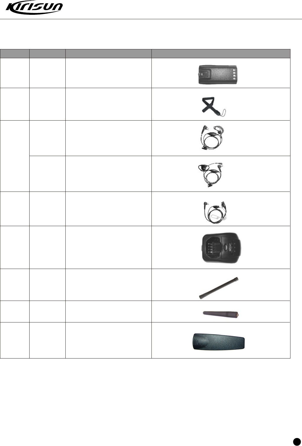
31
Appendix 5: Accessory List
Name Type Specification Accessories
Battery
Li-Poly battery
Hanging
loop
Earphone
Charger 7-hour standard charger
Antenna long antenna
Short antenna
K B -
3
6
C
7.4V 1750mAH
KGS-03
KME-014
KME-015
KME-016
KBC - 3 6 C
Belt Clip KBJ-04
PT6500 SERVICE MANUAL
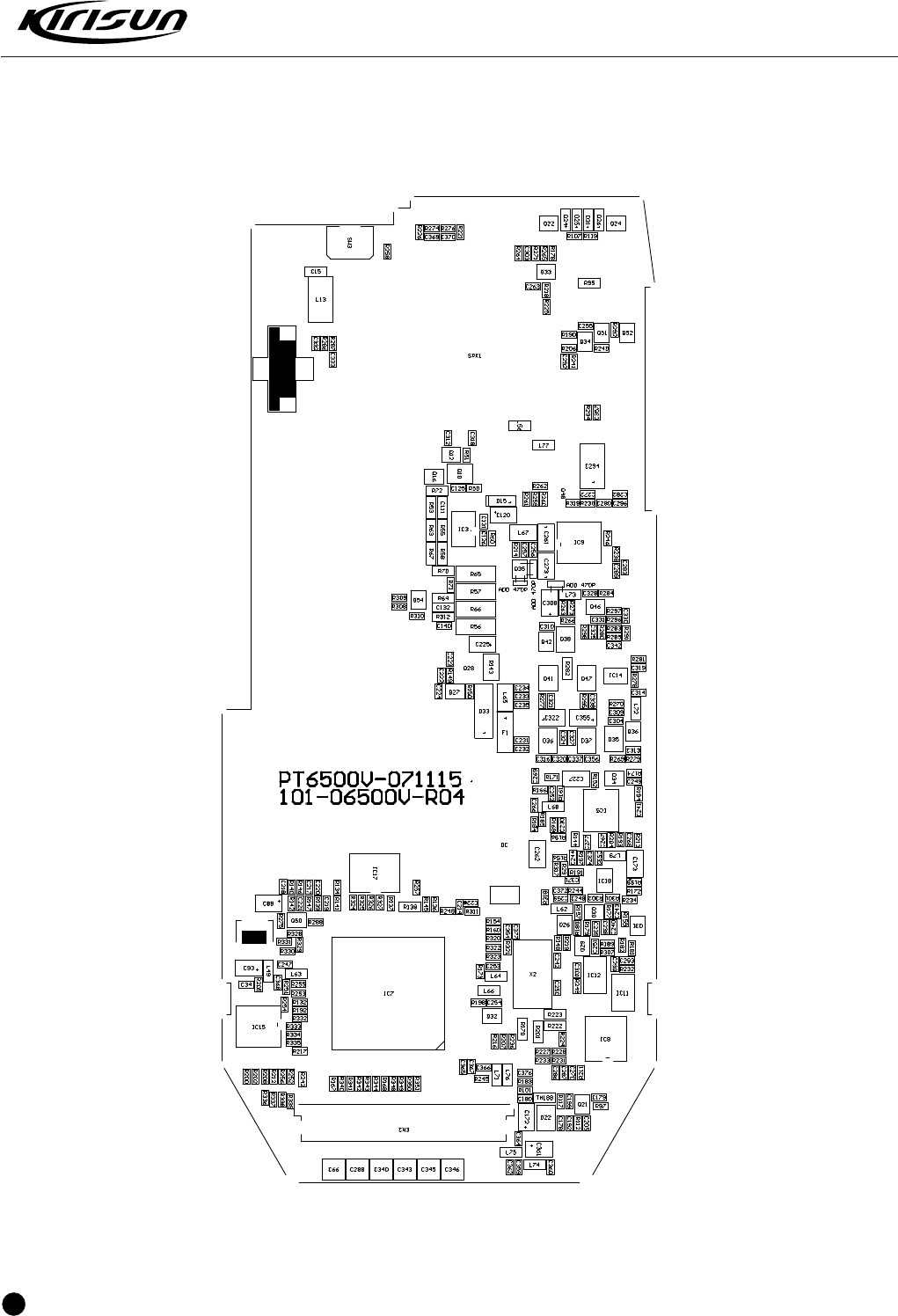
PT6500 SERVICE MANUAL
Figure 1 PT6500 Top Main Board Position Number Diagram(136-174MHz)
32
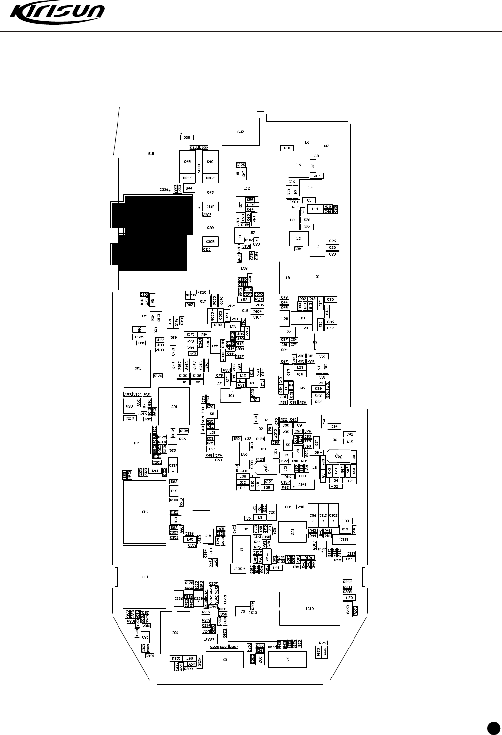
PT6500 SERVICE MANUAL
Figure2 PT6500 Bottom Main Board Position Number Diagram(136-174MHz)
33
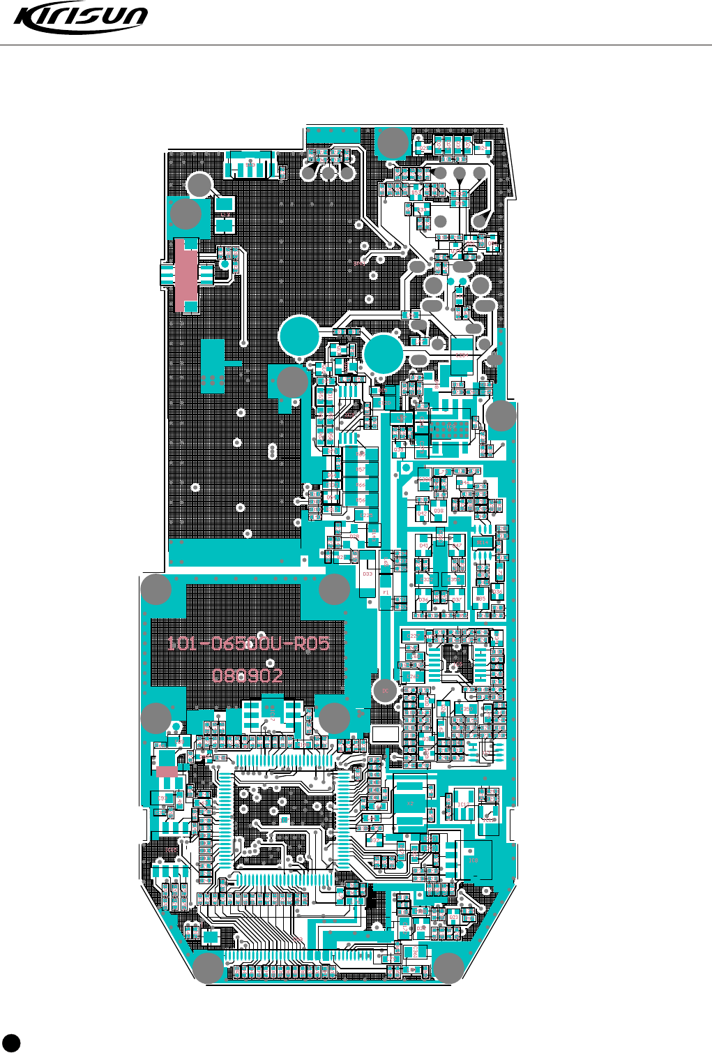
Figure 3 (400-470MHz)PT6500 Top Main Board Position Number Diagram
34
PT6500 SERVICE MANUAL
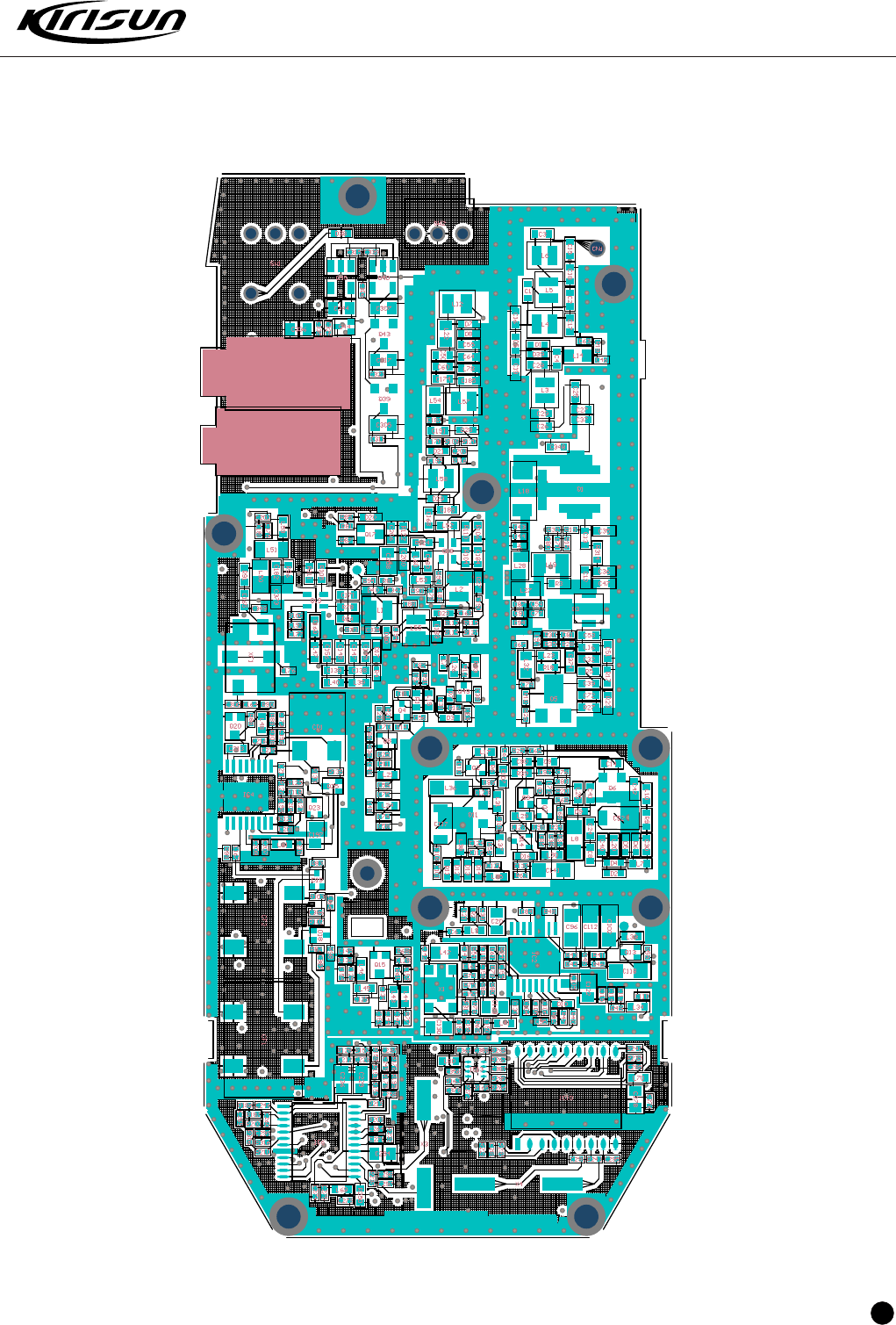
35
PT6500 SERVICE MANUAL
Figure 4 (400-470MHz)PT6500 Bottom Main Board Position Number Diagram
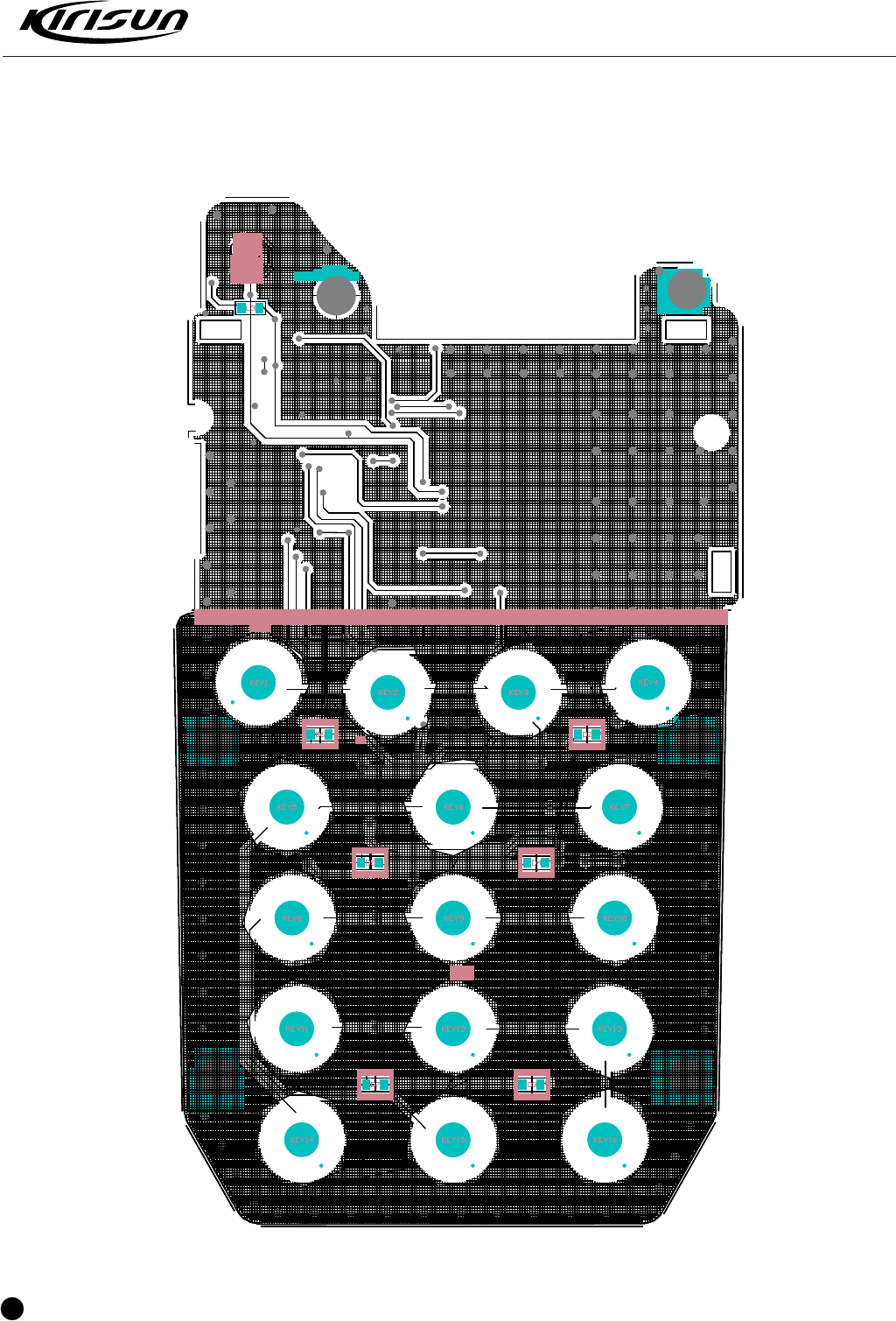
Figure 5 PT6500 PTT Top Board Position Number Diagram
36
PT6500 SERVICE MANUAL
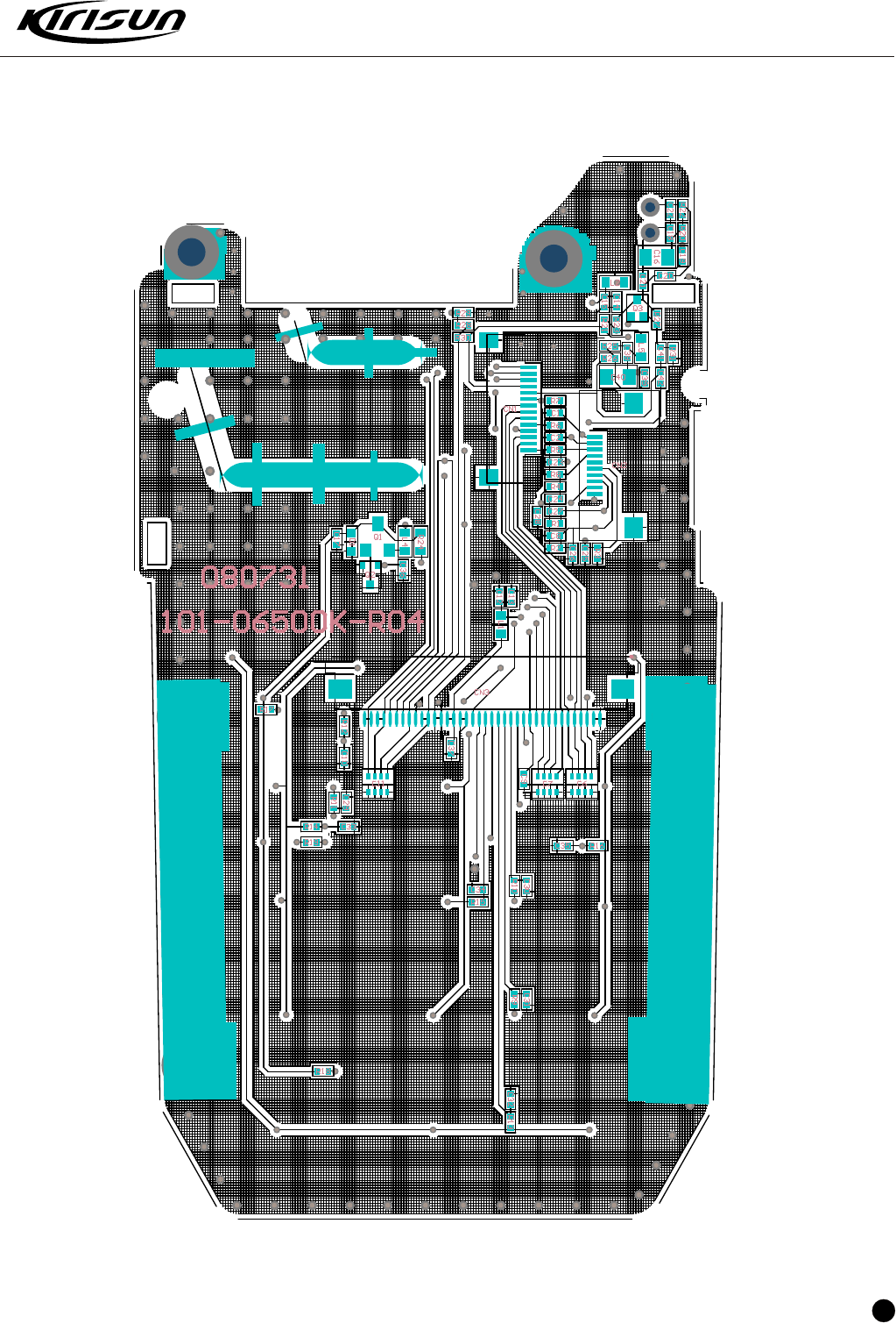
37
PT6500 SERVICE MANUAL
Figure 6 PT6500 PTT BOTTOM Board Position Number Diagram
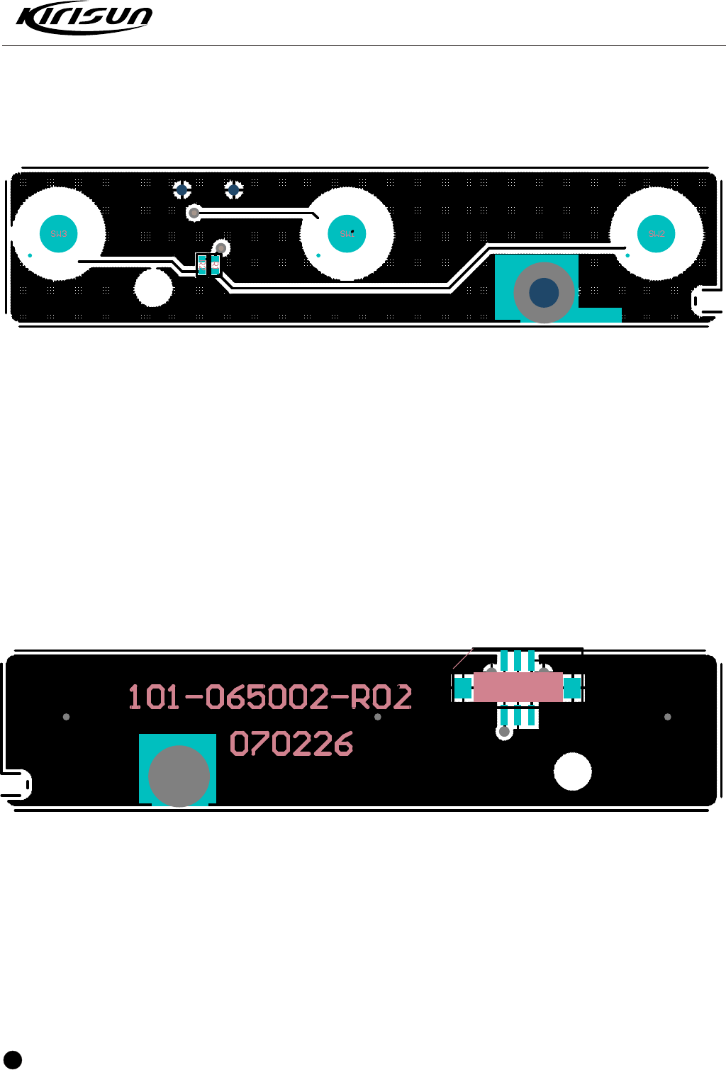
38
PT6500 SERVICE MANUAL
Figure 7 PT6500 Top Keyboard Schematic Circuit Diagram
Figure 8 PT6500 Bottom Keyboard Schematic Circuit Diagram
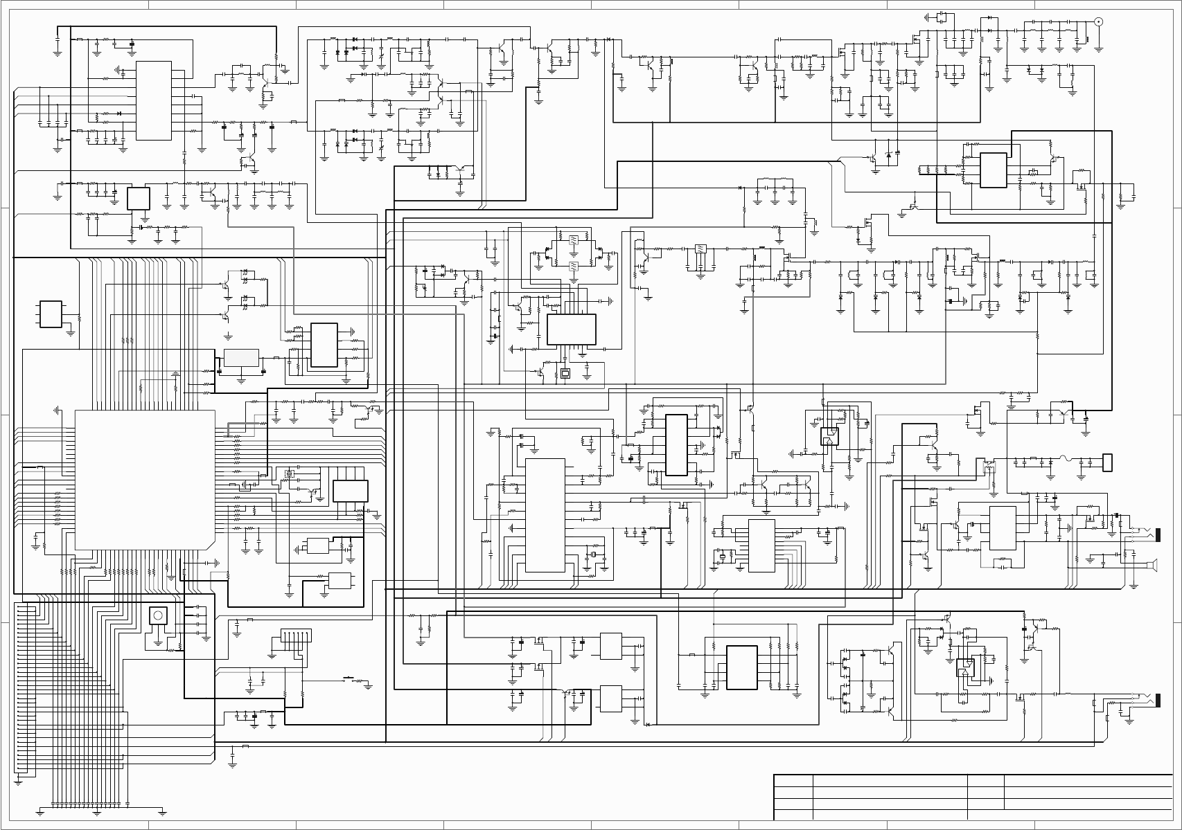
1
1
2
2
3
3
4
4
5
5
6
6
7
7
8
8
D D
C C
B B
A A
VCCN 1
TONEO 2
TONEI 3
E-SDA 4
E-SCL 5
C-BYTE 6
C-CNVSS 7
SHIFT 8
E-TEST 9
RESET 10
XOUT 11
VSS 12
XIN 13
VCC 14
C-NMI 15
INTO 16
A-RDT 17
A-TCLK 18
A-SCLK 19
A-DI/O 20
A-TDATA 21
A-DIR 22
LCD-SEL 23
QT VCO 24
PLL T/R 25
PC/TV 26
EXTPTT 27
QT TCXO 28
C-TXD1 29
C-RXD1 30
C-CLK1 31
NC 32
NC 33
PABC 34
APC2 SW 35
APC1 SW 36
RX SW 37
TX SW 38
C-HOLD 39
PLL-UL 40
PLL-STB 41
PLL-DATA 42
PLL-CLK 43
C-VCC 44
MAX AF SW 45
GREEN 46
RED 47
5TC 48
5RC 49
5CC 50
W/N-N
51
W/N-W
52
AFCO
53
RX MUTE
54
NC
55
NC
56
NC
57
NC
58
S-SCK
59
ACC
60
S-SI
61
VSS
62
S-SO
63
S-CS
64
NC
65
PTT
66
H-D3
67
H-D2
68
H-D1
69
H-D0
70
H-DV
71
DN
72
UP
73
L-AO
74
L-RES
75
L-SLD
76
L-SLK
77
L-CS
78
K1
79
K2
80
K3
81
K4
82
K5
83
K6
84
K7
85
K8
86
LAMP
87
BATT
88
RSSI
89
BUSY
90
VOX
91
QT/DQT IN
92
PF
93
AVSS
94
MANDOWN
95
VREF
96
AVCC
97
VOX SW
98
MIC MUTE
99
HPF PC
100
IC7
M30620
Q5
2SC3356
D3
HSC277
R16
4.7K
C31
471 R10
5.6K
R27
22R
C72
471
C67
471
R18
1K
L23
12nH
L32
BLM21P300S
C79
471
C39 *
R23 *
L16
*
R5
*
R17
*
Q3
RD01MUS1
Q1
RD07
R28
1.5K
R35
39K
R30
47K
C92 471
C81
471
L19
5T
C80
471
C12
102
C36
39P
R13 1.5K
R32 47K
R15
82K
C71
471
C13
102
L18
8T
C29
13P
L28 BLM21P300S
C43
471 C44
103
C25 11P
C26 15P
L3
3T
C28 6P
C4
27P D1
HVC131
L14
220nH
R19
270R
C46
471
C63
471
C19
5P
C5
471
L12
3T C16
2P
C1
2P C2
1.5P C3
3.5P
L4
3T
L5
4T
L6
3T
C17
5P C18
4P
CN1
L13
*
D7
HSC277 D8
*
C55
1P
C174
5P
C185 *
L54 0R
L57 3T
C170
1.5P
C191 10P
C187 *
L58 3T
C188
11P
C168
471
L52
0R
R106
68K
R122
270K
C206
471
L53
68nH
R92
22R
R93
*
R104
220R
C184
102
C183
102
R124
180K
L55
3T
C169
1P
C186 4P
C189 3P
Q18
3SK318
Q19
3SK318 C171
471
R111
56K
L47
68nH
C193
471
R100
150R
L50
0.33uH
L51
0.82uH
C182
8P
R96
*
C175
471
Q20
2SC5108
R88
560K
R89
4.7K
C196
103
D17HSC277
R73
4.7K
Aout
1
A-in
2
A+in
3
GND
4B+in 5
B-in 6
Bout 7
V+ 8
IC3 NJM2904
R66
0.47R
R56
*
R65
0.47R
C125
471
R58
150K
R67
150K
R63
150K
R72
150K
R55
150K
R53
150K
C111
101
R5015K
R70
27K
C131
471
R71
56K
R60
1M
C126
471 C132
102 R64
*
Q12
DTA144EE
C156
5P
Q10
DTC144EUA C120
4.7uF/10V
D15
HZU5ALL
R51
1K
C200
102
C15
*
C140
223
C202
471
R57 0.47R
TO ANT
C214
223
C45
105
C35
*
R110 100K
C160
102
R78
100K
R84
56K
R105
100K
D29
HVC376B
D27
HVC376B D28
HVC376B
D30
HVC376B C194
12P
C190 12P
R116 1M
R120 1M
R115
1M C203
471
R127
1M
C195 *
R114
1M
C149
*
C138
2P
C147
*
C139
0R
C148
*
L39
18nH L40
*
L22
0R
C50
6P C60
4P
L78
56nH
R94
0R
L48 1uH
C38
18P
R26
*
C32
*
C51
*
C47 *
R314
0R
R3
*
C27 *
C64
*
+
-
DC
7.5V
F1 3A
D33
1SR154-400
C232
103
C231
104
C235
471
C234
103
C233
104
SW1
10K
L65
BLM21P300S
Q27
*
Q28
*
R150
*
R149
*C222
*
C224
*
C223
471
R143 BLM21P300S
C225
4.7uF/10V
J1 SPK
J2
MIC
R294
1K
C357
*
L73 BLM11A221S
+
-
-
+
1
2
3
4 5
6
7
8
IC14
TC75W51FU
C331
104
R283
75K
R285
820K
C342 27P
R278
18K
R281
15K
C319
104
C314
*
L72 BLM11A221S
C325
223
R280
27K
R296
*
C330
0R R290
0R
R270 1M
C309 47P
Q36
DTA144EE R263 470R
C310
104
Q38
2SA1586
C308
4.7uF/10V
R162 10K
R273
22K
Q42
DTC144EE
L75
BLM11A221S
AGNDIN
1
AGND
2
TXIN
3
TXINO
4
LIMLV
5
EXIT
6
MOD
7
VSS
8
TCLK
9
TDATA
10
DI/O
11
RDF/FD
12 SCLK 13
DIR 14
XOUT 15
XIN 16
VDD 17
EXFOUT 18
RXAFIN 19
RXAF 20
RXLPFO 21
RXINO 22
RXIN 23
TEST 24
IC6
AK2346
R237 1M
X3
3.6MHz
C297 22P
C298 22P
C284
4.7uF/10V
C275
103
C274
104 L69
BLM11A221S
R215 33K
R153
27K
C236
1uF/10V
C229 1uF/10V
R151 51K
C260
27P
R187
0R
R203
220K
R186
100K
C265
333
C328
104
R284
10K
D36
MA742
D37
MA742
C316 471
C324
471
C327
471
C356 471
C337
392
C320
392
C355
1uF/10V
C322
1uF/10V
R295
2.7K
R277
1K C321
471
C338
471
Q41
2SC4116
Q47
2SA1586
R282
0R
R298
0R
XIN 1
XOUT 2
MIXOUT 3
VCC 4
IFI 5
DEC 6
FILO 7
FILI 8
AF
9
QUAD
10
IFO
11
RSSI
12
NDET
13
NREC
14
GND
15
MIXI
16
IC4
TA31136
CF1 450H
CF2 450F
D18
DAN222 D19
DAN222
R82 22K R83 22K
R102 22K R103 22K
R98 6.8K R99 6.8K
C166
104
C167
104
C201
182
R108 100R
C213
33P
R121150K
C198 102
C204 102
Q23
DTC144EE
R123
3.3K
R126 10K
R118
1K
L61
10R
C210 471
C207
103
C209 104
C197
4.7uF/10V
C215
181
R133
3K
R135
1.6K
Q25
DTA144EE
CD1
C24450
C179
102
Q21
2SC4617 R97
330K
R112
3.3K
R117
56R
C199
104
C192
102
C178
104
D22
MA742
C180
102
C172
334
C205
471
C211
102
R125
27K
R128
3.3K
C212
102
C258
33P
R175
0R
R195
27K
R176
4.7K
R155
*
C237
105
R152
0R
C245
561
C246
222
C228
*
C271
105
R220
56K
C264 151
R209
12K
Q30
2SC4617
R157
150K
R180
1.5K
R179
150K
R177
3.3K
C239
393
C238
473
C243
393
Q31
2SC4617
R159 150K
R189 2.2K
R182
150K
R181
2.7K
C240
333
C248
104
R169
82K
C241 222
C249
123
Aout
1
A-in
2
A+in
3
V+
4
B+in
5
B-in
6
Bout
7Cout 8
C-in 9
C+in 10
GND 11
D+in 12
D-in 13
Dout 14
IC5 NJM2902V
R172
10K
R185
18K
R166
22K
R161
220K
C230 221
C227
105 R156
470K
R174 180K
R171
33K
R204 120K
R184
18K
C262
4.7uF/10V
R194 180K
C259
*
R199 10K
R193
120K
R213
100K
C267 182 R219
560K
C277 393 R191
12K
R197
4.7K
C252
47P
R196
180K
C268 103
C269
683
VP
1
VN
2
GS
3
VREF
4
INH
5
PWDN
6
X1
7
X2
8
VSS
9OE 10
D0 11
D1 12
D2 13
D3 14
DV 15
EST 16
RT/GT 17
VDD 18
IC10
HT9172
R235 47K
C281
471
X4
3.58MHz
R243
1M
C291 22P
C295
22P
R229
47K
C278
4.7uF/10V
C276 104
L70 BLM11A221S
R239 330K
C285 104
R247
33K
L68 BLM11A221S
C266
471
MODE
1
SVR
2
IN+
3
IN-
4OUT- 5
VCC 6
GND 7
OUT+ 8
IC9 TDA8541
C273 4.7uF/10V
R238
1K
R246 68K
C296
101
C289
105
R240
0R
C283
102
Q33 2SK1824
R218
560K
C279
471
R225
1K
C263 105
R230
22R
C280
104
C261
4.7uF/10V
C257
104
C256
103
L67
BLM11A300S
SPK1
*
C272
471
C282
471
R241 1K
C292
*
Q35
DTC144EE
R214
47K
R178
0R
Q34
2SK1824
R206
47K
R190
*
C255
0R
VIN 1
VSS 2
CE 3
NC
4
OUT
5Q40
XC6204B502MR
VIN 1
VSS 2
CE 3
NC
4
OUT
5Q45
XC6204B502MR
D38
MA2S111
C315
105
C339
105
C307
4.7uF/10V
C344
4.7uF/10V
C306
471
C329 471
Q44
DTA123JE
Q39
ST2301
Q43
ST2301
C305
4.7uF/10V
C317
4.7uF/10V
C311
471
C323
471
C336
4.7uF/10V
C335
471
Rset 1
CP 2
CPGND 3
AGND 4
RFinB 5
RFinA 6
AVDD 7
REFin 8
DGND
9
CE
10
CLK
11
DATA
12
LE
13
MUXOUT
14
DVDD
15
Vp
16
IC2 ADF4111
R48
4.7K
C84
101
R43
560R
C96
0.1uF/35V
R44
560R R45
2.7K
C112
1uF/16V
R41
560R
C102
0.1uF/35V
R46
2.7K
C118
1uF/16V
L33
BLM11A221S
C20
4.7uF/10V
C33
104
L9
BLM11A221S
C21
471
R2 10R
R24
2.7K
C61
*
R47 10R
C110
471
C122
4.7uF/10V
C115
103
C114
104
L34
BLM11A221S
C113
471
R49
10R C109
471
D10
MA2S111
R40 1K
R42 150K
C95
103
C106
101
C105
101
C104
101
Q13
DTC144EE
C133
471
C130
4.7uF/10V
C152
103
C151
104
L41
BLM11A221S
C150
471
R69
10R
VC
1
GND
2
VCC 4
OUT 3
X1
12.8MHz
L42
10uH
C142
10P C143
10P
R54
0R
C119
471
R68
1K
C128
47P
C155
*
Q15
2SC5108
R61
200K
L44
560nH
C146
471
R77 10R
C153 *
C135 0R
L45
*C145
*
C136
0R
L43
470nH
C144
331
C134 103 C129
33P
L46
220nH
C154 33P
L35
100nH
C121 101
D14
HVC376B
D11
HVC376B
C108
15P
L36
27nH
Q11
2SK508NV(K52)
C123
2P C124
7P
C103
7P L37
3.3uH
R52
180R
C107 0.5P
R39 100R
L31
220nH
C101
30P
C116
*
L38 220nH
C117
10P
D12
HVC376B
D13
HVC376B
C97
471
C99
104
Q9
DTA143TE
C100
471
Q7
DTA143TE
L29 BLM11A221S
C98
471
L7
180nH
C30
101
D6
HVC376B
D2
HVC376B
C24
15P
L8
22nH
Q6
2SK508NV(K52)
C41
2P C42 5P
C14 5P L10
3.3uH
R9
150R
C9
1P
C8
30P
C40 0.5P
L20 220nH
C5210P
D4
HVC376B
D5
HVC376B R20 100R
C83
104
C73
471
C76
471
L25
220nH
C69
1P
C68
1P
D9
1SV278
R34
270K
R38
270K
R37
4.7K
L30
BLM11A221S
Q14
2SC4617(S)
C137
471 D16
MA2S111
R62
4.7K
C141
15uF/6.3V
C127 471
Q2
2SC5108
R6
150K
C62
471 R22
100R
L17
22nH
C10
33P
C65
471
Q8
2SC5108
C70
10P
R25
150K
L21
18nH
C49 471
R11
1K
R36
22R C86
471
C48 3P
C59
10P
C75 5P
L24
18nH
C74 5P
C58
471
C22 15P
R21 10K
R31
22R
Q4
2SC5108
R14
330R
C56
471
R1
2.2K
L15
22nH
C57
471
C82
471
C11 10P
R4
4.7K
C53
*
L27
BLM21P300S
C77 471
C54
103
C87
105
C94
471
C91
103
Q16
DTC144EE
D21
HVC355B
R109
1M
D23
HVC355B
R113 1M
Q17
2SK1829
R87
36K
R85
470K
D20
MA2S111
R81
180K
R80
22K
R79
22K
C158
683 C159
333
R74
4.7K
R76 1KR75 4.7K
C157
333
R233
15K
R231 12K
C286
332 C287
682
A0 1
A1 2
A2 3
GND 4
SDA
5
SCL
6
TEST
7
VCC
8
IC8
24LC256
R222 0R
R227 0R
R201 0R
R228 47K
R211 10K
R223 *
R216 4.7K
R207 4.7K
R236
*
C270 471
X2
9.8304MHz
C250 20P
C242 22P
R198
1K
C254 5P
Q32 DTC144EE
NC
1
VEE1
2
VEE2
3OUT 4
VCC 5
IC11
PST9140NR
R232 330K
C293
104
C290
471
OUT
1
VDD
2
GND
3NC 4
NC 5
IC12
*
C301
471
R249
*
R160 1K
R154 1K
L64 BLM11A221S
C253
471
R173
4.7K
R141
22K
R139
10K
C219
333 C220
683
C217
105
R146
220K
R140
12K
C218
105 R142 82K
R147
27K
C221
*
R86
22K
C163
4.7uF/10V
R313
22K
C161 223
R145
4.7K
R136
4.7K
R1384.7K
R137 4.7K
R134
4.7K
D24 *
D25 RED
D26 GREEN
D31 GREEN
R107
330R
R119
330R
Q24
DTC144EE
Q22
DTC144EE
L66 BLM11A221S
L63
BLM11A221S
C247
471 R242
47K
R265
470K
R264
0R
R271
470K
C303
104
C216
104
L71
BLM11A221S
C361
4.7uF/10V
C359 104
C362 103
L74
BLM11A221S
C360
471
R210
180K
C299 105
R234
1M
Q29
2SK1824
C251 104
R307 0R
R144
10K
Q26
DTA123JE
L62
BLM11A221S
R148
1K
C85
471
L60BLM11A221S
C208
4.7uF/10V
C177
104
C181
103 L59
56R
XF1 51.65MHz R91
103
R90
103
C165
470R
C164
470R
C176
18P
C173
471
R244
22K
D34 *
C304
105
D35
MA742
R269
0R
R279 100K
C313 224
R217 1K
R221 1K
R226 1K
R101
27K
R224 47K
1 VCCN
1 VCCN
2 TO
2 TO
2 TO
3 TI
3 TI
4 A-RDT
4 A-RDT
5 A-TCLK
5 A-TCLK
6 A-SCLK
6 A-SCLK
R250 100K
7 A-DI/O
7 A-DI/O
8 A-TDATA
8 A-TDATA
9 A-DIR
9 A-DIR
10 PLL T/R
10 PLL T/R
11 PC/TV
11 PC/TV
12 TXD
12 TXD
13 RXD
13 RXD
14 PABC
14 PABC
15 APC2
15 APC2
16 APC1
16 APC1
17 RX SW
17 RX SW
18 TX SW
18 TX SW
19 P-UL
19 P-UL
20 P-STB
20 P-STB
21 P-DT
21 P-DT
22 P-CLK
22 P-CLK
23 5TC
23 5TC
24 5RC
24 5RC
25 SAVE
25 SAVE
26 MAXAF
26 MAXAF
27 W/N N
27 W/N N
28 W/N W
28 W/N W
29 AFCO
29 AFCO
30 RX MUTE
30 RX MUTE
38 PTT
39 H-D3
39 H-D3
40 H-D2
40 H-D2
41 H-D1
41 H-D1
42 H-D0
42 H-D0
43 H-DV
43 H-DV
44 DN
UP DN
GND
SW2 ENCODER
R274
47K
R276
47K
44 DN
45 UP
45 UP
46 BATT
46 BATT
47 RSSI
47 RSSI
47 RSSI
48 BUSY
48 BUSY
49 VOX
49 VOX
50 QT IN
50 QT IN
Q46
2SK1824
R297
1K
51 MIC MUTE
51 MIC MUTE
52 HPF PC
52 HPF PC
EXT PTT
54 VOX SW
54 VOX SW
55 MICOUT
55 MICOUT
58 RX AF OUT
58 RX AF OUT
R59
10K
SW3 PF3
R287
10K
R286
47K
35 PF
38 PTT
1
2
3
4
5
6
7
CN2 CN6
C332
471 C333
471
C90
1P
D39 HVC131
C364
221
R167 1K
R170 0R
C365
471
C367 471
C368 471
C369 471
C370 471
C6
471
R183
47K
T
R188 100K
S-SCK
S-SI
S-SO
S-CS
R192 1K
CS 1
SO 2
WPD 3
GND 4
SI
5
SCK
6
HOLDB
7
VCC
8
IC15 *
OUTIN
GND
IC16 XC62FP3602
C89
4.7uF/10V C93
4.7uF/10V
L49
BLM11A221S R253*
R202
*
R208
*
R251*
R205*
C34
471
R212*
R200*
R255
*
R254
*
R252
*
R256
*
S-SCK
S-SI
S-SO
S-CS
GND 1
A1 2
A2 3
A3
4
A4
5
A5
6
IC17
*
R257
*
ICA
R258
0R
1
2
3
4
5
6
7
8
9
10
11
12
13
14
15
16
17
18
19
20
21
22
23
24
39
25
26
27
28
29
30
31
32
33
34
35
36
37
38
CN3
CN38
CNVSS
L56
*
Q48 *
R261
*R259
*
R260
*
R262
*
EXT SW
EXT SW
SP+
SP+
SP-
SP-
L76
BLM11A221S
C376
471
L77
*
主板电原理图名称
文件号
设计
批准
机型
版本
审核
第张 张共
PT6500-02(400-470MHz)
11
/
CNVSS
13 RXD
12 TXD
35 PF
38 PTT
ICA
Q49
2SC5108(Y)
C23
471
R7
47K
R12
1K
C7
471
L26
27nH
R33
33R
C37 18P
C78
471
L1
3T
C334 *
D40
HVC376B C347
12P
R8
1M
C88
0.5P
C348 *
L2
3T
C294 0R
C318
471
C312
471
R95
0R
R245
1K
35 PF
R275
27K
Q50
DTA144EE
28 W/N W
R288
10K
Q51
2SK1824
Q52
DTC144EE
R292
47K
C300
*C349
*
R248
33K
+
-
-
+
1
2
3
4 5
6
7
8
IC1
TC75W51FU
C372
105
C371
105
C352
103
C351
104
L79 BLM11A221S
C244
471 R29
470K
C350 4.7uF/10V
R301
1K
R302
*
Q53
2SC4617
R304
100K
C354
105
R299
1K
R300
100K
R303
5.6K
C363
102 C353
105 R305
0R
R306
*
R311
33K C226
223
Q54
2SK1824
R3080R
R309
*
R310
1K
C373
*
R312
*
C374
101
R316 1K
R317 0R
CNCSS
RXD
TXD
5V
PF
PTT
MIC
SP-
SP+
SP SW
C288 221
C345 221
C346 221
C375 221
C377 221
C379 221
R330 1K
R331 1K
R332 1K
R333 1K
R326
1K
R3271K
R3211K
R3201K
R3181K
R1641K
R131 1K
R130 1K
R129 1K
R322 1K
R323 1K
R324 1K
R325 1K
R343
470K
R342
470K
R132 1K
R158 1K
R168 1K
R319 1K
R334 1K
R335 1K
R336 1K
R337 1K
C343 221
C380 221
C381 221
C382 221
C383 221
C384 221
C386
105
C385
105
EXT PTT
L11
*
R339
*
C66
105
C302 221
C162 221
C326 221
C340 221
C341 221
VDD
1
VSS
2
VDD
3
VOUTZ
4PD 5
RANGE 6
VOUTX 7
VOUTY 8
IC13 *
C378
*
C387
*
C366
*
C388
*
R272
*R266 *
R289
*
R165
*
R163
*
R267 *
R268 *
L80
*
C358
*
R291
*
MANDOWN
MANDOWN
Figure 9 PT6500 Schematic Circuit Pane Diagram(136-174MHz)
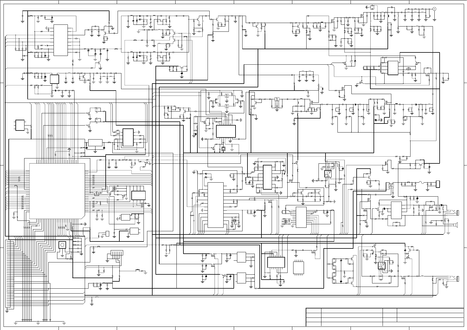
PT6500 Schematic Circuit Pane Diagram(350-390MHz)
1
1
2
2
3
3
4
4
5
5
6
6
7
7
8
8
D D
C C
B B
A A
VCCN 1
TONEO 2
TONEI 3
E-SDA 4
E-SCL 5
C-BYTE 6
C-CNVSS 7
SHIFT 8
E-TEST 9
RESET 10
XOUT 11
VSS 12
XIN 13
VCC 14
C-NMI 15
INTO 16
A-RDT 17
A-TCLK 18
A-SCLK 19
A-DI/O 20
A-TDATA 21
A-DIR 22
NC 23
QT VCO 24
PLL T/R 25
PC/TV 26
NC 27
QT TCXO 28
C-TXD1 29
C-RXD1 30
C-CLK1 31
NC 32
NC 33
PABC 34
APC2 SW 35
APC1 SW 36
RX SW 37
TX SW 38
C-HOLD 39
PLL-UL 40
PLL-STB 41
PLL-DATA 42
PLL-CLK 43
C-VCC 44
MAX AF SW 45
GREEN 46
RED 47
5TC 48
5RC 49
5CC 50
W/N-N
51
W/N-W
52
AFCO
53
RX MUTE
54
W-BUSY
55
W-DATA
56
W-SCLK
57
W-MUTE
58
S-SCK
59
ACC
60
S-SI
61
VSS
62
S-SO
63
S-CS
64
NC
65
PTT
66
H-D3
67
H-D2
68
H-D1
69
H-D0
70
H-DV
71
DN
72
UP
73
L-AO
74
L-RES
75
L-SLD
76
L-SLK
77
L-CS
78
K1
79
K2
80
K3
81
K4
82
K5
83
K6
84
K7
85
K8
86
LAMP
87
BATT
88
RSSI
89
BUSY
90
VOX
91
QT/DQT IN
92
PF
93
AVSS
94
MANDOWN
95
VREF
96
AVCC
97
VOX SW
98
MIC MUTE
99
HPF PC
100
IC7
M30620
Q5
2SC3356
D3
HSC277
R16
4.7K
C31
471 R10
5.6K
R27
22R
C72
471
C67
471
R18
1K
L23
12nH
L32
BLM21P300S
C79
471
C39 102
R23 270R
L16
0R
R5
15R
R17
270R
Q3
RD01MUS1
Q1
RD07
R28
1.5K
R35
39K
R30
47K
C92 471
C81
471
L19
5T
C80
471
C12
102
C36
47P
R13 1.5K
R32 47K
R15
82K
C71
471
C13
102
L18
8T
C29
27P
L28 BLM21P300S
C43
471 C44
103
C25 15P
C26 *
L3
3T
C28 5P
C4
27P D1
HVC131
L14
220nH
R19
270R
C46
471
C63
471
C19
6P
C5
471
L12
4T C16
5P
C1
2.5P C2
3.5P C3
2.5P
L4
4T
L5
4T
L6
4T
C17
4P C18
5P
CN1
L13
*
D7
HSC277 D8
*
C55
1P
C174
5P
C185 2.5P
L54 0R
L57 3T
C170
1.5P
C191 27P
C187 *
L58 3T
C188
27P
C168
471
L52
0R
R106
68K
R122
270K
C206
471
L53
68nH
R92
22R
R93
*
R104
220R
C184
102
C183
102
R124
180K
L55
3T
C169
1.5P
C186 8P
C189 5P
Q18
3SK318
Q19
3SK318 C171
471
R111
56K
L47
39nH
C193
471
R100
150R
L50
0.82uH
L51
0.82uH
C182
8P
R96
*
C175
471
Q20
2SC5108
R88
560K
R89
4.7K
C196
103
D17HSC277
R73
4.7K
Aout
1
A-in
2
A+in
3
GND
4B+in 5
B-in 6
Bout 7
V+ 8
IC3 NJM2904
R66
0.47R
R56
*
R65
0.47R
C125
471
R58
150K
R67
150K
R63
150K
R72
150K
R55
150K
R53
150K
C111
101
R5015K
R70
27K
C131
471
R71
56K
R60
1M
C126
471 C132
102 R64
*
Q12
DTA144EE
C156
5P
Q10
DTC144EUA C120
4.7uF/10V
D15
HZU5ALL
R51
1K
C200
102
C15
*
C140
223
C202
471
R57 0.47R
TO ANT
C214
223
C45
105
C35
*
R110 100K
C160
102
R78
100K
R84
56K
R105
100K
D29
HVC355B
D27
HVC355B D28
HVC355B
D30
HVC355B C194
27P
C190 27P
R116 1M
R120 1M
R115
1M C203
471
R127
1M
VSS1 1
SPK 2
VDD1 3
PWM- 4
VSS 5
SCLK 6
NC 7
SDATA 8
NC
9VDD
10 OSC
11 BUSY1
12 NC
13 NC
14 NC
15 RST
16
IC13
W588A080
R290
10R
C341
471
C358 105
R289
1K
R293
150K
C302
105
R267
10R R268
100R Q37
2SK1824
356810
11121612
C195 2.5P
R114
1M
C149
*
C138
*
C147
9P
C139
0R
C148
*
L39
18nH L40
*
L22
0R
C50
6P C60
5P
L78
56nH
R94
0R
L48 1uH
C38
18P
R26
*
C32
100P
C51
*
C47 *
R314
2.2nH
R3
*
C27 36P
C64
*
+
-
DC
7.5V
F1 3A
D33
1SR154-400
C232
103
C231
104
C235
471
C234
103
C233
104
SW1
10K
L65
BLM21P300S
Q27
*
Q28
*
R150
*
R149
*C222
*
C224
*
C223
471
R143 BLM21P300S
C225
4.7uF/10V
J1 SPK
J2
MIC
R294
1K
C357
*
L73 BLM11A221S
+
-
-
+
1
2
3
4 5
6
7
8
IC14
TC75W51FU
C331
104
R283
75K
R285
820K
C342 27P
R278
18K
R281
15K
C319
104
C314
*
L72 BLM11A221S
C325
223
R280
27K
R296
*
C330
0R R291
0R
R270 1M
C309 47P
Q36
DTA144EE R263 470R
C310
104
Q38
2SA1586
C308
4.7uF/10V
R266 10K
R273
22K
Q42
DTC144EE
L75
BLM11A221S
AGNDIN
1
AGND
2
TXIN
3
TXINO
4
LIMLV
5
EXIT
6
MOD
7
VSS
8
TCLK
9
TDATA
10
DI/O
11
RDF/FD
12 SCLK 13
DIR 14
XOUT 15
XIN 16
VDD 17
EXFOUT 18
RXAFIN 19
RXAF 20
RXLPFO 21
RXINO 22
RXIN 23
TEST 24
IC6
AK2346
R237 1M
X3
3.6MHz
C297 22P
C298 22P
C284
4.7uF/10V
C275
103
C274
104 L69
BLM11A221S
R215 33K
R153
27K
C236
1uF/10V
C229 1uF/10V
R151 51K
C260
27P
R187
0R
R203
220K
R186
100K
C265
333
C328
104
R284
10K
D36
MA742
D37
MA742
C316 471
C324
471
C327
471
C356 471
C337
392
C320
392
C355
1uF/10V
C322
1uF/10V
R295
2.7K
R277
1K C321
471
C338
471
Q41
2SC4116
Q47
2SA1586
R282
0R
R298
0R
XIN 1
XOUT 2
MIXOUT 3
VCC 4
IFI 5
DEC 6
FILO 7
FILI 8
AF
9
QUAD
10
IFO
11
RSSI
12
NDET
13
NREC
14
GND
15
MIXI
16
IC4
TA31136
CF1 450H
CF2 450F
D18
DAN222 D19
DAN222
R82 22K R83 22K
R102 22K R103 22K
R98 6.8K R99 6.8K
C166
104
C167
104
C201
182
R108 100R
C213
33P
R121150K
C198 102
C204 102
Q23
DTC144EE
R123
3.3K
R126 10K
R118
1K
L61
10R
C210 471
C207
103
C209 104
C197
4.7uF/10V
C215
82P
R133
2.7K
R135
2.2K
Q25
DTA144EE
CD1
C24450
C179
102
Q21
2SC4617 R97
330K
R112
3.3K
R117
56R
C199
104
C192
102
C178
104
D22
MA742
C180
102
C172
334
C205
471
C211
102
R125
27K
R128
3.3K
C212
102
C258
33P
R175
0R
R195
27K
R176
5.6K
R155
*
C237
105
R152
0R
C245
561
C246
222
C228
*
C271
105
R220
56K
C264 151
R209
12K
Q30
2SC4617
R157
150K
R180
1.5K
R179
150K
R177
3.3K
C239
393
C238
473
C243
393
Q31
2SC4617
R159 150K
R189 2.2K
R182
150K
R181
2.7K
C240
333
C248
104
R169
82K
C241 222
C249
123
Aout
1
A-in
2
A+in
3
V+
4
B+in
5
B-in
6
Bout
7Cout 8
C-in 9
C+in 10
GND 11
D+in 12
D-in 13
Dout 14
IC5 NJM2902V
R172
10K
R185
18K
R166
22K
R161
220K
C230 221
C227
105 R156
470K
R174 180K
R171
33K
R204 120K
R184
18K
C262
4.7uF/10V
R194 180K
C259
*
R199 10K
R193
120K
R213
100K
C267 182 R219
560K
C277 393 R191
12K
R197
4.7K
C252
47P
R196
180K
C268 103
C269
683
VP
1
VN
2
GS
3
VREF
4
INH
5
PWDN
6
X1
7
X2
8
VSS
9OE 10
D0 11
D1 12
D2 13
D3 14
DV 15
EST 16
RT/GT 17
VDD 18
IC10
HT9172
R235 47K
C281
471
X4
3.58MHz
R243
1M
C291 22P
C295
22P
R229
47K
C278
4.7uF/10V
C276 104
L70 BLM11A221S
R239 330K
C285 104
R247
33K
L68 BLM11A221S
C266
471
MODE
1
SVR
2
IN+
3
IN-
4OUT- 5
VCC 6
GND 7
OUT+ 8
IC9 TDA8541
C273 4.7uF/10V
R238
1K
R246 68K
C296
101
C289
105
R240
0R
C283
102
Q33 2SK1824
R218
560K
C279
471
R225
1K
C263 105
R230
22R
C280
104
C261
4.7uF/10V
C257
104
C256
103
L67
BLM11A300S
SPK1
*
C272
471
C282
471
R241 1K
C292
*
Q35
DTC144EE
R214
47K
R178
0R
Q34
2SK1824
R206
47K
R190
*
C255
0R
C326
104
R272 0R
VIN 1
VSS 2
CE 3
NC
4
OUT
5Q40
XC6204B502MR
VIN 1
VSS 2
CE 3
NC
4
OUT
5Q45
XC6204B502MR
D38
MA2S111
C315
105
C339
105
C307
4.7uF/10V
C344
4.7uF/10V
C306
471
C329 471
Q44
DTA123JE
Q39
ST2301
Q43
ST2301
C305
4.7uF/10V
C317
4.7uF/10V
C311
471
C323
471
C336
4.7uF/10V
C335
471
Rset 1
CP 2
CPGND 3
AGND 4
RFinB 5
RFinA 6
AVDD 7
REFin 8
DGND
9
CE
10
CLK
11
DATA
12
LE
13
MUXOUT
14
DVDD
15
Vp
16
IC2 ADF4111
R48
4.7K
C84
101
R43
560R
C96
0.1uF/35V
R44
560R R45
2.7K
C112
1uF/16V
R41
560R
C102
0.1uF/35V
R46
2.7K
C118
1uF/16V
L33
BLM11A221S
C20
4.7uF/10V
C33
104
L9
BLM11A221S
C21
471
R2 10R
R24
2.7K
C61
*
R47 10R
C110
471
C122
4.7uF/10V
C115
103
C114
104
L34
BLM11A221S
C113
471
R49
10R C109
471
D10
MA2S111
R40 1K
R42 150K
C95
103
C106
101
C105
101
C104
101
Q13
DTC144EE
C133
471
C130
4.7uF/10V
C152
103
C151
104
L41
BLM11A221S
C150
471
R69
10R
VC
1
GND
2
VCC 4
OUT 3
X1
12.8MHz
L42
10uH
C142
10P C143
10P
R54
0R
C119
471
R68
1K
C128
47P
C155
*
Q15
2SC5108
R61
200K
L44
560nH
C146
471
R77 10R
C153 *
C135 0R
L45
*C145
*
C136
0R
L43
470nH
C144
331
C134 103 C129
33P
L46
220nH
C154 33P
L35
100nH
C121 101
D14
HVC376B
D11
HVC376B
C108
10P
L36
39nH
Q11
2SK508NV(K52)
C123
4P C124
8P
C103
8P L37
3.3uH
R52
180R
C107 0.5P
R39 100R
L31
220nH
C101
22P
C116
*
L38 220nH
C117
10P
D12
HVC376B
D13
HVC376B
C97
471
C99
104
Q9
DTA143TE
C100
471
Q7
DTA143TE
L29 BLM11A221S
C98
471
L7
180nH
C30
101
D6
HVC376B
D2
HVC376B
C24
8P
L8
33nH
Q6
2SK508NV(K52)
C41
3P C42 6P
C14 6P L10
3.3uH
R9
150R
C9
1P
C8
13P
C40 0.5P
L20 220nH
C5210P
D4
HVC376B
D5
HVC376B R20 100R
C83
104
C73
471
C76
471
L25
220nH
C69
1P
C68
1P
D9
1SV278
R34
270K
R38
270K
R37
4.7K
L30
BLM11A221S
Q14
2SC4617(S)
C137
471 D16
MA2S111
R62
4.7K
C141
15uF/6.3V
C127 471
Q2
2SC5108
R6
150K
C62
471 R22
100R
L17
22nH
C10
33P
C65
471
Q8
2SC5108
C70
10P
R25
150K
L21
18nH
C49 471
R11
1K
R36
22R C86
471
C48 3P
C59
10P
C75 5P
L24
18nH
C74 5P
C58
471
C22 15P
R21 10K
R31
22R
Q4
2SC5108
R14
330R
C56
471
R1
2.2K
L15
22nH
C57
471
C82
471
C11 10P
R4
4.7K
C53
*
L27
BLM21P300S
C77 471
C54
103
C87
105
C94
471
C91
103
Q16
DTC144EE
D21
HVC355B
R109
1M
D23
HVC355B
R113 1M
Q17
2SK1829
R87
36K
R85
470K
D20
MA2S111
R81
*
R80
15K
R79
22K
C158
183 C159
153
R74
4.7K
R76 1KR75 4.7K
C157
333
R233
15K
R231 12K
C286
332 C287
682
A0 1
A1 2
A2 3
GND 4
SDA
5
SCL
6
TEST
7
VCC
8
IC8
24LC256
R222 0R
R227 0R
R201 0R
R228 47K
R211 10K
R223 *
R216 4.7K
R207 4.7K
R236
*
C270 471
X2
9.8304MHz
C250 20P
C242 22P
R198
1K
C254 5P
Q32 DTC144EE
NC
1
VEE1
2
VEE2
3OUT 4
VCC 5
IC11
PST9140NR
R232 330K
C293
104
C290
471
OUT
1
VDD
2
GND
3NC 4
NC 5
IC12
*
C301
471
R249
*
R160 1K
R154 1K
L64 BLM11A221S
C253
471
R173
4.7K
R141
15K
R139
22K
C219
333 C220
223
C217
105
R146
270K
R140
12K
C218
105 R142 43K
R147
27K
C221
*
R86
22K
C163
4.7uF/10V
R313
68K
C161 223
R145
4.7K
R136
4.7K
R1384.7K
R137 4.7K
R134
4.7K
D24 *
D25 RED
D26 GREEN
D31 GREEN
R107
330R
R119
330R
Q24
DTC144EE
Q22
DTC144EE
L66 BLM11A221S
L63
BLM11A221S
C247
471 R242
47K
R265
470K
R264
0R
R271
470K
C303
104
C216
104
L71
BLM11A221S
C361
4.7uF/10V
C359 104
C362 103
L74
BLM11A221S
C360
471
R210
180K
C299 105
R234
1M
Q29
2SK1824
C251 104
R307 0R
R144
10K
Q26
DTA123JE
L62
BLM11A221S
R148
1K
C85
471
L60BLM11A221S
C208
4.7uF/10V
C177
104
C181
103 L59
56R
XF1 51.65MHz R91
103
R90
103
C165
270R
C164
270R
C176
18P
C173
471
R244
22K
D34 *
C304
105
D35
MA742
R269
0R
R279 100K
C313 224
R217 1K
R221 1K
R226 1K
R101
27K
R224 47K
1 VCCN
1 VCCN
2 TO
2 TO
2 TO
3 TI
3 TI
4 A-RDT
4 A-RDT
5 A-TCLK
5 A-TCLK
6 A-SCLK
6 A-SCLK
R250 100K
7 A-DI/O
7 A-DI/O
8 A-TDATA
8 A-TDATA
9 A-DIR
9 A-DIR
10 PLL T/R
10 PLL T/R
11 PC/TV
11 PC/TV
12 TXD
12 TXD
13 RXD
13 RXD
14 PABC
14 PABC
15 APC2
15 APC2
16 APC1
16 APC1
17 RX SW
17 RX SW
18 TX SW
18 TX SW
19 P-UL
19 P-UL
20 P-STB
20 P-STB
21 P-DT
21 P-DT
22 P-CLK
22 P-CLK
23 5TC
23 5TC
24 5RC
24 5RC
25 SAVE
25 SAVE
26 MAXAF
26 MAXAF
27 W/N N
27 W/N N
28 W/N W
28 W/N W
29 AFCO
29 AFCO
30 RX MUTE
30 RX MUTE
31 W-BUSY
31 W-BUSY
32 W-DATA
32 W-DATA
33 W-SCLK
33 W-SCLK
34 W-MUTE
34 W-MUTE
38 PTT
39 H-D3
39 H-D3
40 H-D2
40 H-D2
41 H-D1
41 H-D1
42 H-D0
42 H-D0
43 H-DV
43 H-DV
44 DN
UP DN
GND
SW2 ENCODER
R274
47K
R276
47K
44 DN
45 UP
45 UP
46 BATT
46 BATT
47 RSSI
47 RSSI
47 RSSI
48 BUSY
48 BUSY
49 VOX
49 VOX
50 QT IN
50 QT IN
Q46
2SK1824
R297
1K
51 MIC MUTE
51 MIC MUTE
52 HPF PC
52 HPF PC
38 PTT
54 VOX SW
54 VOX SW
55 MICOUT
55 MICOUT
56 AGC
56 AGC
57 W588
57 W588
58 RX AF OUT
58 RX AF OUT
R59
10K
SW3 PF3
R287
10K
R286
47K
35 PF
38 PTT
1
2
3
4
5
6
7
CN2 CN6
C332
471 C333
471
C90
1P
D39 HVC131
C364
221
R167 1K
R170 0R
C365
471
C366 471
C367 471
C368 471
C369 471
C370 471
C6
471
R183
47K
T
R188 100K
S-SCK
S-SI
S-SO
S-CS
R192 1K
CS 1
SO 2
WPD 3
GND 4
SI
5
SCK
6
HOLDB
7
VCC
8
IC15 *
OUTIN
GND
IC16 XC62FP3502
C89
4.7uF/10V C93
4.7uF/10V
L49
BLM11A221S R253 *
R202
*
R2081K
R251*
R205 *
C34
471
R212*
R200*
R255
NC
R254
*
R252
*
R256
*
S-SCK
S-SI
S-SO
S-CS
GND 1
A1 2
A2 3
A3
4
A4
5
A5
6
IC17
*
R257
*
ICA
R258
0R
1
2
3
4
5
6
7
8
9
10
11
12
13
14
15
16
17
18
19
20
21
22
23
24
39
25
26
27
28
29
30
31
32
33
34
35
36
37
38
CN3
CN38
CNVSS
L56
*
Q48 *
R261
*
R259
*
R260
*
R262
*
EXT SW
EXT SW
SP+
SP+
SP-
SP-
L76
BLM11A221S
C376
471
L77
*
主板电原理图名称
文件号
设计
批准
机型
版本
审核
第张 张共
PT6500-05(350-390MHz)
11
/
CNVSS
13 RXD
12 TXD
35 PF
38 PTT
ICA
Q49
2SC5108(Y)
C23
471
R7
47K
R12
1K
C7
471
L26
27nH
R33
33R
C37 *
C78
471
L1
3T
C334 3P
D40
HVC355B C347
27P
R8
1M
C88
1P
C348 *
L2
3T
C294 0R
C318
471
C312
471
R95
0R
R245
1K
35 PF
R275
27K
Q50
DTA144EE
28 W/N W
R288
10K
Q51
2SK1824
Q52
DTC144EE
R292
47K
C300
*C349
*
1
2
J3
MANDOWN
MANDOWN
MANDOWN
R248
33K
+
-
-
+
1
2
3
4 5
6
7
8
IC1
TC75W51FU
C372
105
C371
105
C352
103
C351
104
L79BLM11A221S
C244
471 R29
470K
C350 4.7uF/10V
R301
1K
R302
*
Q53
2SC4617
R304
100K
C354
105
R299
1K
R300
100K
R303
5.6K
C363
102 C353
105 R305
0R
R306
*
R311
33K C226
223
Q54
2SK1824
R3080R
R309
*
R310
1K
C373
*
R312
*
C374
NC
R315
*
R316 1K
R317 0R
CNCSS
RXD
TXD
5V
PF
PTT
MIC
SP-
SP+
SP SW
C162 221
C288 221
C345 221
C346 221
C375 221
C377 221
C378 221
C379 221
R330 1K
R331 1K
R332 1K
R333 1K
R326
1K
R3271K
R3281K
R3291K
R3211K
R3201K
R3181K
R1641K
R131 1K
R130 1K
R129 1K
R165 1K
R163 1K
R162 1K
R322 1K
R323 1K
R324 1K
R325 1K
C66 221
C340 221
R343
470K
R342
470K
C381
105
C380
105
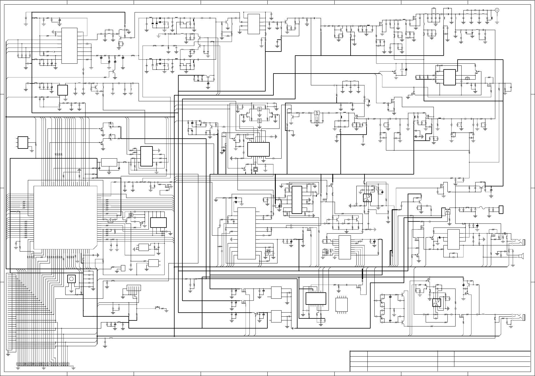
1
1
2
2
3
3
4
4
5
5
6
6
7
7
8
8
D D
C C
B B
A A
VCCN 1
TONEO 2
TONEI 3
E-SDA 4
E-SCL 5
C-BYTE 6
C-CNVSS 7
SHIFT 8
E-TEST 9
RESET 10
XOUT 11
VSS 12
XIN 13
VCC 14
C-NMI 15
INTO 16
A-RDT 17
A-TCLK 18
A-SCLK 19
A-DI/O 20
A-TDATA 21
A-DIR 22
NC 23
QT VCO 24
PLL T/R 25
PC/TV 26
NC 27
QT TCXO 28
C-TXD1 29
C-RXD1 30
C-CLK1 31
NC 32
NC 33
PABC 34
APC2 SW 35
APC1 SW 36
RX SW 37
TX SW 38
C-HOLD 39
PLL-UL 40
PLL-STB 41
PLL-DATA 42
PLL-CLK 43
C-VCC 44
MAX AF SW 45
GREEN 46
RED 47
5TC 48
5RC 49
5CC 50
W/N-N
51
W/N-W
52
AFCO
53
RX MUTE
54
W-BUSY
55
W-DATA
56
W-SCLK
57
W-MUTE
58
S-SCK
59
S-SI
60
NC
61
VSS
62
S-SO
63
S-CS
64
PF
65
PTT
66
H-D3
67
H-D2
68
H-D1
69
H-D0
70
H-DV
71
DN
72
UP
73
L-AO
74
L-RES
75
L-SLD
76
L-SLK
77
L-CS
78
K1
79
K2
80
K3
81
K4
82
K5
83
K6
84
K7
85
K8
86
LAMP
87
BATT
88
RSSI
89
BUSY
90
VOX
91
QT/DQT IN
92
NC
93
AVSS
94
NC
95
VREF
96
AVCC
97
VOX SW
98
MIC MUTE
99
HPF PC
100
IC7
M30620
Q5
2SC3356
D3
HSC277
R16
12K
C31
102 R10
1.5K
R27
15R
C72
102
C67
102
R18
330R
L23
100nH
L32
BLM21P300S
C79
102
C39
9P
R23
330R
L16
27nH
R5
18R
R17
330R
Q3
RD01MUS1
Q1
RD07MVS1
R28
47R
R35
39K
R30
47K
C92 102
C81
102
L19
150nH
C80
102
C36
27P
R13 47R
R32 47K
R15
120K
C71
471
L11
27nH
L18
0.4*1.5*8T
C29
10P
L28 BLM21P300S
C43
102 C44
103
C25 27P
C26 68P
L3
0.3*1.2*5T
C28 15P
C4 56P
D1
HVC131
L14
220nH
R19
270R
C46
102
C63
102
C19
22P
C5
102
L12
0.3*1.0*8T
C16
10P
C1
12P C2
11P C3
7P
L4
0.3*1.0*7T
L5
0.4*1.5*7T
L6
0.4*1.5*7T
C17
18P C18
15P
CN1
L13
*
D7
HVC131 D8
HVC131
C55
68P
C174
11P
C185 *
L57 47nH
C170
3P
C191 33P
C187 4P
L58 56nH
C188 33P
C168
470P
R106
100K
R122
*
C206
102
L53
56nH
R92
22R
R93
2.2K
R104
220R
C184
102
C183
102
R124
100K
L55
56nH
C169
6P
C186 4.7P
C189 4P
Q18
3SK318
Q19
3SK318 C171
471
L47
150nH
C193
102
R100
220R
L50
330NH
L51
0.82uH
C182
18P
R96
*
C175
102
Q20
2SC5108
R88
120K
R89
*
C196
103
D17 HSC277
R73
10K
Aout
1
A-in
2
A+in
3
GND
4B+in 5
B-in 6
Bout 7
V+ 8
IC3 NJM2904
R66
0.47R
R56
*
R65
0.47R
C125
470P
R58
150K
R67
150K
R63
150K
R72
150K
R55
150K
R53
150K
C111
101
R50 15K
R70
27K
C131
102
R71
56K
R60
1M
C126
102
C132
102 R64
*
Q12
DTA144EE
C156
10P
Q10
DTC144EUA C120
4.7uF/10V
D15
HZU5ALL
R51
2.2K
C200
102
C15
*
C202
102
R57 0.47R
TO ANT
C45
105
C35
*
R110 180K
C160
102
R78
120K
D29
1SV305
D27
1SV305
D28
1SV305
D30
1SV305 C194
33P
C190 33P
R116 1M R120 1MR115
1M
C203 102
R127
1M
VSS1 1
SPK 2
VDD1 3
PWM- 4
VSS 5
SCLK 6
NC 7
SDATA 8
NC
9VDD
10 OSC
11 BUSY1
12 NC
13 NC
14 NC
15 RST
16
IC13
*
R290
*
C341
*
C358 *
R289
*R293
*
C302
*
R267
*R268
*Q37
*
356810
11121612
C195 4P
R114
1M
C149
8P
C138
4P
C147
9P
C139
3P
C148
6P
L39
33nH L40
47nH
L22
47nH C50
33P
C60
*
L46
*
R94
0R
L48 1.8K
R31
0R C38
39P
R26
560R
C32
102
C51
*
C47 10P
C13
102
R3
330R
L1
0.4*1.2*3T L2
0.3*1.0*4T
C27 10P
C64
22P
+
-
DC
7.5V
F1 3A
D33
1SR154-400
C232
103
C231
104
C235
102
C234
103
C233
104
SW1
10K
L65
BLM21P300S
Q27
2SK1824
Q28
*
R150
330R
R149
*
C222
*
C224
471
C223
471
R143 BLM21P300S
C225
4.7uF/10V
J1 SPK
J2
MIC
R294
1K
C357
*
L73
BLM11A601S
+
-
-
+
1
2
3
4 5
6
7
8
IC14
TC75W51FU
C331
333
R283
27K
R285
820K
C342 470P
R278
18K
R281
15K
C319
104
C314
102
L72 BLM11A601S
C325
223
R280
27K
R296
*
C330
105 R291
0R
R270 1M
C309 47P
Q36
DTA144EE R263 470R
C310
104
Q38
2SA1586
C308
4.7uF/10V
R266 10K
R273
22K
Q42
DTC144EE
L75
BLM11A601S
AGNDIN
1
AGND
2
TXIN
3
TXINO
4
LIMLV
5
EXIT
6
MOD
7
VSS
8
TCLK
9
TDATA
10
DI/O
11
RDF/FD
12 SCLK 13
DIR 14
XOUT 15
XIN 16
VDD 17
EXFOUT 18
RXAFIN 19
RXAF 20
RXLPFO 21
RXINO 22
RXIN 23
TEST 24
IC6
AK2346
R237 1M
X3
3.6864MHz
C297 33P
C298 33P
C284
4.7uF/10V
C275
103
C274
104
L69
BLM11A601S
R215 33K
R153
27K
C236
1uF/10V
C229 1uF/10V
R151
51K
C260
27P
R187
0R
R203
220K
R186
100K
C265
333
C328
333
R284
10K
D36
MA742
D37
MA742
C316 471
C324
471
C327
471
C356 471
C337
392
C320
392
C355
1uF/10V
C322
1uF/10V
R295
2.7K
R277
1K
C321
471
C338
471
Q41
2SC4116
Q47
2SA1586
R282
0R
R298
0R
XIN 1
XOUT 2
MIXOUT 3
VCC 4
IFI 5
DEC 6
FILO 7
FILI 8
AF
9
QUAD
10
IFO
11
RSSI
12
NDET
13
NREC
14
GND
15
MIXI
16
IC4
TA31136
CF1 C50G
CF2 C50F
D18
DAN222 D19
DAN222
R82 22K R83 22K
R102 22K R103 22K
R98 4.7K R99
4.7K
C166
104
C167
104
C201
182
R108 100R
C213
102
R121
150K
C198 471
C204
471
Q23
DTC144EE
R123
3.3K
R126 10K
R118
1K
L61
BLM11A601S
C210
102
C207
103
C209
104
C197
4.7uF/10V
C215
82P
R133
2.7K
R135
2.2K
Q25
DTA144EE
CD1
50C24
C179
102
Q21
2SC4617 R97
330K
R112
3.3K
R117
56R
C199
104
C192
102
C178
104
D22
MA742
C180
102
C172
0.47uF/10V
C205
102
C211
102
R125
4.7K
R128
3.3K
C212
102
C258
33P
R175
91K
R195
27K
R176
5.1K
R155
*
C237
474
R152 0R
C245
561
C246
222
C228
*
C271
0R
R220
56K
C264
6800P R209
12K
VP
1
VN
2
GS
3
VREF
4
INH
5
PWDN
6
X1
7
X2
8
VSS
9OE 10
D0 11
D1 12
D2 13
D3 14
DV 15
EST 16
RT/GT 17
VDD 18
IC10
HT9172
R235
47K
C281
471
X4
3.58MHz
R243
1M
C291
39P
C295
39P
R229
47K
C278
4.7uF/10V
C276 104
L70 BLM11A601S
R239 330K
C285 104
R247
33K
MODE
1
SVR
2
IN+
3
IN-
4OUT- 5
VCC 6
GND 7
OUT+ 8
IC9 TDA8541
C273 4.7uF/10V
R238
1.5K
R246 68K
C296
*
C289
105
R240
0R
C283
102
Q33 2SK1824
R218
560K
C279
102
R225
1K
C263105
R230
22R
C280
104
C261
4.7uF/10V
C257
104
C256
103
L67
BLM11A601S
SPK1
*
C272
102
C282
102
R241 1K
Q35
DTC144EE
R214
47K
R178
0R
Q34
2SK1824
R206
47K
R190
*
C255
0R
C326
*
R272 *
VIN 1
VSS 2
CE 3
NC
4
OUT
5
Q40
XC6204B502MR
VIN 1
VSS 2
CE 3
NC
4
OUT
5
Q45
XC6204B502MR
D38
MA2S111
C315
105
C339
105
C307
4.7uF/10V
C344
4.7uF/10V
C306
102
C329 102
Q44
DTA123JE
Q39
ST2301
Q43
ST2301
C305
4.7uF/10V
C317
4.7uF/10V
C311
102
C323
102
C336
4.7uF/10V
C335
102
Rset 1
CP 2
CPGND 3
AGND 4
RFinB 5
RFinA 6
AVDD 7
REFin 8
DGND
9
CE
10
CLK
11
DATA
12
LE
13
MUXOUT
14
DVDD
15
Vp
16
IC2 ADF4111
R48
4.7K
C84
101
R43
220R
C96
0.33uF/35V
R44
560R R45
1.5K
C112
3.3uF/10V
R41
680R
C102
0.1uF/35V
R46
*
C118
1uF/10V
L33
BLM11A601S
C20
4.7uF/10V
C33
104
L9
BLM11A601S
C21
102
R2 10R
R24
2.7K
C61
*
R47 10R
C110
102
C122
4.7uF/10V
C115
103
C114
104
L34
BLM11A601S
C113
102
R49
10R C109
102
D10
MA2S111
R40 1K
R42 150K
C95
103
C106
101
C105
101
C104
101
Q13
DTC144EE
C133
102
C130
4.7uF/10V
C152
103
C151
104
L41
BLM11A601S
C150
102
R69
10R
VC
1
GND
2
VCC 4
OUT 3
X1
12.8MHz
L42
4.7uH
C142
10P
C143
10P
R54
0R
C119
102
R68
47R
C128
47P
C155
18P
Q15
KTC4082
R61
330K
L44
100nH
C146
102 R77
2.2K
L45
100nH
C136
102
C144
100P
L35
100nH
C121 101
D14
1SV325
D11
1SV325
C108
6P
L36
22nH
Q11
2SK508NV(K52)
C123
3.5P
C124
3P
C103 5P L37
3.3uH
R52
180R
C107 0.5P
R39 100R
L31
220nH
C101
120P
C116
*
L38 220nH
C117
10P
D12 *
D13
*
C97
102
C99
104
Q9
DTA143TE
C100
102
Q7
DTA143TE
L29 BLM11A601S
C98
102
L7
180nH
C30
101
D6
1SV325
D2
1SV325
C24
4P
L8
39nH
Q6
2SK508NV(K52)
C41
4P
C42
5P
C14 5P L10
3.3uH
R9
100R
C9
1P
C8
180P
C40
*
L20 220nH
C52 10P
D4 *
D5
*
R20 100R
C83
104
C73
102
C76
471
L25
220nH
C69
1.5P
C68
1.5P
D9
1SV278
R34
270K
R38
270K
R37
4.7K
L30
BLM11A601S
Q14
2SC4617(S)
C137
471 D16
MA2S111
R62
4.7K
C141
15uF/6.3V
C127 471
Q2
2SC5108
R6
150K
C62
102 R22
1.8K
L17
39nH
C10
33P
C65
102
Q8
2SC5108
C70
10P
R25
150K
L21
33nH
C49 102
R11
1K
R36
22R
C86
471
C48 4P
C59
15P
C75 6P
L24
18nH
C74 6P
C58
471
VCC1
1
IN
2
IN-
3
GND
4SW1 5
SW2 6
OUT 7
VCC2 8
IC1
UPB1509GV
C22 15P
C37
102
C7
102
L26
BLM11A601S
R33
360R
C78
102
R7
1K
C23 102
R12
3.3K
R21 3.3K
R8
47R
Q4
2SC5108
R14
330R
C56
102
R1
2.2K
L15
82nH
C57
102
C82
102
C11 10P
R4
4.7K
C53
*
L27
BLM21P300S
C77 102
C54
103
C87
105
C94
102
C91
103
Q16
DTC144EE
Q17
*
R87
1.8K
R85
470K
D20
MA2S111
R81
180K
R80
10K
R79
10K
C158
103 C159
104
R74
22K
R76 1KR75 22K
C157
333
R233
15K
R231 12K
C286
332
C287
*
A0 1
A1 2
A2 3
GND 4
SDA
5
SCL
6
TEST
7
VCC
8
IC8
AT24C256
R222 0R
R227 0R
R201 0R
R228 47K
R211 10K
R223 *
R216 4.7K
R207 4.7K
R236
*
C270 102
X2 9.8304MHz
C250 20P
C242 22P
R198
1K
C254 5P
Q32 DTC144EE
NC
1
VEE1
2
VEE2
3OUT 4
VCC 5
IC11
PST9140NR
R232 330K
C293
104
C290
102
OUT
1
VDD
2
GND
3NC 4
NC 5
IC12
*
C301
102
R249
*
R160 1K
R154 1K
L64 BLM11A601S
C253
102
R173
4.7K
R141
68K
R139
180K
C219
103
C220
10nF
C217
105
R146
560K
R140
12K C218
1800P R142 56K
R147
180K
C221
*
R86
39K
C163
0.33uF
C162
68K
C161 223
R145
4.7K
R136
4.7K
R138 4.7K
R137 4.7K
R134
4.7K
D25 RED
D26 GREEN
D31 GREEN
R107
330R
R119
330R
Q24
DTC144EE
Q22
DTC144EE
L66 BLM11A601S
L63
BLM11A601S
C247
102 R242
47K
R265
470K
R264
0R
R271
470K
C303
104
C216
104
L71
BLM11A601S
C361
4.7uF/10V
C359 104
C362 103
L74
BLM11A601S
C360
102
R210
180K
C299 105
C251 104
C85
102
L60 BLM11A601S
C208
4.7uF/10V
C177
104
C181
103
L59
BLM11A601S
XF1 51.65MHz R91
330R
R90
330R
C165
103
C164
103
C176
13P
C304
105
D35
MA742
R269
0R
R279
100K
C313
224
R217 1K
R221 1K
R226 1K
R101
27K
R224 47K
1 VCCN
1 VCCN
2 TO
2 TO
3 TI
3 TI
4 A-RDT
4 A-RDT
5 A-TCLK
5 A-TCLK
6 A-SCLK
6 A-SCLK
R250 100K
7 A-DI/O
7 A-DI/O
8 A-TDATA
8 A-TDATA
9 A-DIR
9 A-DIR
10 PLL T/R
10 PLL T/R
11 PC/TV
11 PC/TV
12 TXD
12 TXD
13 RXD
13 RXD
14 PABC
14 PABC
15 APC2
15 APC2
16 APC1
16 APC1
17 RX SW
17 RX SW
18 TX SW
18 TX SW
19 P-UL
19 P-UL
20 P-STB
20 P-STB
21 P-DT
21 P-DT
22 P-CLK
22 P-CLK
23 5TC
23 5TC
24 5RC
24 5RC
25 SAVE
25 SAVE
26 MAXAF
26 MAXAF
27 W/N N
27 W/N N
28 W/N W
28 W/N W
29 AFCO
29 AFCO
30 RX MUTE
30 RX MUTE
31 W-BUSY
31 W-BUSY
32 W-DATA
32 W-DATA
33 W-SCLK
33 W-SCLK
34 W-MUTE
34 W-MUTE
35 PF
38 PTT
39 H-D3
39 H-D3
40 H-D2
40 H-D2
41 H-D1
41 H-D1
42 H-D0
42 H-D0
43 H-DV
43 H-DV
44 DN
UP DN
GND
SW2 ENCODER
R274
47K
R276
47K
44 DN
45 UP
45 UP
46 BATT
46 BATT
47 RSSI
47 RSSI
47 RSSI
48 BUSY
48 BUSY
49 VOX
49 VOX
50 QT IN
Q46
2SK1824
R297
1K
51 MIC MUTE
51 MIC MUTE
52 HPF PC
52 HPF PC
38 PTT
54 VOX SW
54 VOX SW
55 MICOUT
55 MICOUT
56 AGC
56 AGC
57 W588
58 RX AF OUT
58 RX AF OUT
R59
10K
SW3 PF3
R287
10K
R286
47K
35 PF
38 PTT
1
2
3
4
5
6
7
CN2 CN6
C332
102
C333
102
C90
1P
D39 HVC131
C364
221
R167 1K
R168 1K
R170 0R
C365
102
C366 102
C367 102
C368 102
C369 102
C370 102
C6
102
R183
47K
T
TH188 100K
S-SCK
S-SI
S-SO
S-CS
R192 1K
R132 1K
CS 1
SO 2
WPD 3
GND 4
SI
5
SCK
6
HOLDB
7
VCC
8
IC15 *
OUTIN
GND
IC16 XC62FP3502PR,SOT-89
C89
4.7uF/10V C93
4.7uF/10V
L49
BLM11A601S R253 1K
R202
1K
R208
1K
R251 1K
R205 1K
C34
102
R212 2.7K
R2002.7K
R255
10K
R254
2.7K
R252
10K
R256
*
S-SCK
S-SI
S-SO
S-CS
GND 1
A1 2
A2 3
A3
4
A4
5
A5
6
IC17
*
R257
2K
ICA
R258
0R
1
2
3
4
5
6
7
8
9
10
11
12
13
14
15
16
17
18
19
20
21
22
23
24
39
25
26
27
28
29
30
31
32
33
34
35
36
37
38
CN3
CN38
CNVSS
L56
*
Q48 *
R261
*R259
*
R260
*
R262
0R
EXT SW
EXT SW
SP+
SP+
SP-
SP-
L76
BLM11A601S
C376
102
L77
*
主板电原理图名称
文件号
设计
批准
机型
版本
审核
第张 张共
PT6500-01(136-174MHz)
11
/
CNVSS
13 RXD
12 TXD
35 PF
38 PTT
C288
221
C345
221
C346
221
ICA
C294 0R
C292
*
C318
102
C312
471
L43
47nH
C129
9P
GND
C347
102
C348
102
C350
102
GND
GND
R245
0R
35 PF
MANDOWN
1
2
J3 MANDOWN
GND
MANDOWN
Q50
2SK1824
R275
47K
R288 10K
GND
27 W/N N
C300
*C349
4P
C88
102
C334
102
C154
102
C145
12P L54
0R
GND
R292
47K
R95 0R
2 TO
57 W588
L52
47R
C12
0R
C351
*
Q51
2SK1824
Q52
DTC144EE
C134
1000P
C153
100P
R105
120K
C135
6P
R111
82K
R84
82K
C354
105
C352
102 C353
105
C377
102
GND
GND
R306
*
C227
10u/10V
R171
33K
C252
47P R161
220K
R166
22K
C269
683 R174180K R194
180KC241222
C249
123 D34 *
C2671800P
R204 120K
R193
120K
C268
103
R213
100K
C277 393
R196
180K
R169
82K
C230 221
R184
18K
C262
4.7uF/10V
C266
471
R144
10K
50 QT IN
L68
BLM11A601S
R219
560K
Q30
2SC4617
R157
150K
R180
1.5K
R179
150K
R177
3.3K
C239
153 C243
393
Q31
2SC4617
R159 150K
R189 2.2K
R182
150K
R181
2.7K
C240
333
R172
10K R156
470K
C259
*
R199 10K
R191
12K
R197
4.7K
R234
1M
R3070R
Q26
DTA123JE
L62
BLM11A601S
R148
1K
R244
22K
+
-
-
+
1
2
3
4 5
6
7
8
IC18
TC75W51FU
C372
105
C371
105
C374
103
L79
BLM11A601S
C244
471
R29
470K
C173
4.7uF/10V
R301
1K
R302
*
C238
473
Q29
2SK1824
C248
104
Q53
2SC4617
C373
105
R299
1K
R300
100K
R303
5.6K
C363
102
C375
105
R305
15K
R304
0R
R316 1K
Aout
1
A-in
2
A+in
3
V+
4
B+in
5
B-in
6
Bout
7Cout 8
C-in 9
C+in 10
GND 11
D+in 12
D-in 13
Dout 14
IC5 NJM2902V
C214
223
R248
33K R311
33K
C226
223
R308
0R
C140
223
R309
*
Q54
2SK1824
R310
0R
R312
*
R315
*
C66
*
C340
*
C343
*
C532
104
R185
18K
D24 *
R317
47K
R318
47K
R319
0R
R320 1K
R321 1K
R322 1K
R323 1K
R324 1K
R325 1K
R326 1K
R327 1K
R328 1K
R329 1K
R330 1K
R331 1K
R332 1K
R333 1K
R334 1K
R335 1K
R336 1K
R337 1K
R338 1K
R339 1K
R340 1K
R341 1K
R342 1K
R343 1K
R344 1K
R345 1K
R346 1K
R347 1K
R348 1K
R349 1K
R350 1K
R351 1K
V00
DATA : 2008.05.13 LiuXue
LiuXue
Figure 10 PT6500 Schematic Circuit Pane Diagram(400-470MHz)
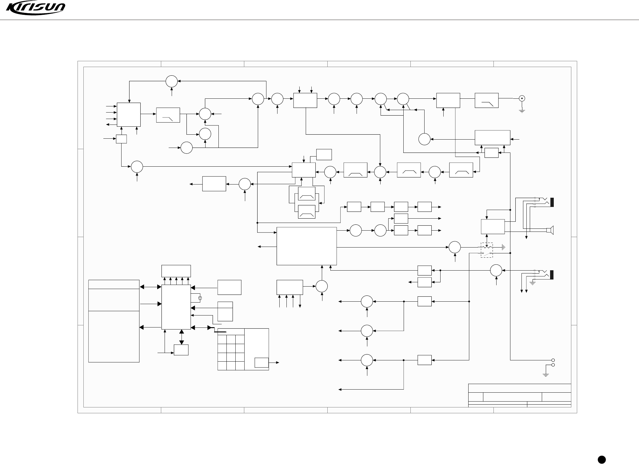
41
Figure 11 PT6500 Main Board Schematic Circuit Diagram
PT6500 SERVICE MANUAL
1
1
2
2
3
3
4
4
5
5
6
6
D D
C C
B B
A A
T i t
N u m R e v i S i
A
D a t 2 0 0 8 S h e e t
F i l X : \ P T 6 5 0 0 \ . . \ P T 6 5 0 0 D r a w n
S P E A
A - D
E - S
C P
M 3 0
2 4 C
E E P
E N C O
P L L
P L L -
P L L
P L L
P L L
I C
Q T T
5
L O O P F
R I P
F I L
V C
Q
B U
Q Q
R F R F
5 5
Q Q Q
D R I
D R I
P R
5 5
A P
Q 1
A N T L P
A P C C O
I C
B P
B P
R F
Q 1
Q 1
M I
X F
5 1 . 6
I F
Q 2
I F D E M O
I C
Q 2
N O I
A M
D 2
D E
B U
C F
4 5 0
Q 3
S
A F P O W
I C
B A T T
5 T
5
I C
S W
I C
5 Q 1
T X / R
5
5
5
5
T O
A F
C D
D E T
S
7 .
X
9 . 8 3 0
S W
P O W &
Q 4
S
A D F 4
M O
Q
R F P
A P
5
4 5 0
M U
T D A 8
S C
S D A
B U S
Q 3
S
W 5 8
5
1 2 . 8
X
T C
I C
W 5 8 8
5
T
V C
Q 1
R
5
Q 1
* 4 2 N D L
S
C F
4 5 0
I C
A K 2
p i n
p i n
M O
p i n Q 3
H Q 3
H
I C
H A M
I C
I C
H T 9
I C I C I C I C
A M L L A M
p i n T X
C T C S S
D T
2
M I C
I C 1
A M
I C 1
Q 4
S
M U
M I R X
V O
p i n
5
5 R
Q 3
S
5
S A
Q 4
S
5
X C 6 2 0 4
Q 4
Q 4
X C 6 2 0 4
5
5
p i n
P F
P F
P F
P T
123
456
789
0*#
K E
M I M I
L C
T O N
R E S
P L L
W - B
A - T
A - R
C - R
H -
H -
H -
H -
H -
B A
R S
B U
V O
Q T / D Q
M A N D
V C
T O N
E - S
S H I
E - T
A - S
A - T D
A - D
Q T V
P L L
P C /
Q T T
C - T
P A
A P C 2
A P C 1
R X
V O X
M I C
T X
P L L -
P L L -
P L L -
M A X A
G R E
R E
5 T
5 R
5 C
W / N
W / N
A F
R X M
W - D
W - S
W - M
L A
H P C
Q
B U
5
P T T B
K E Y B
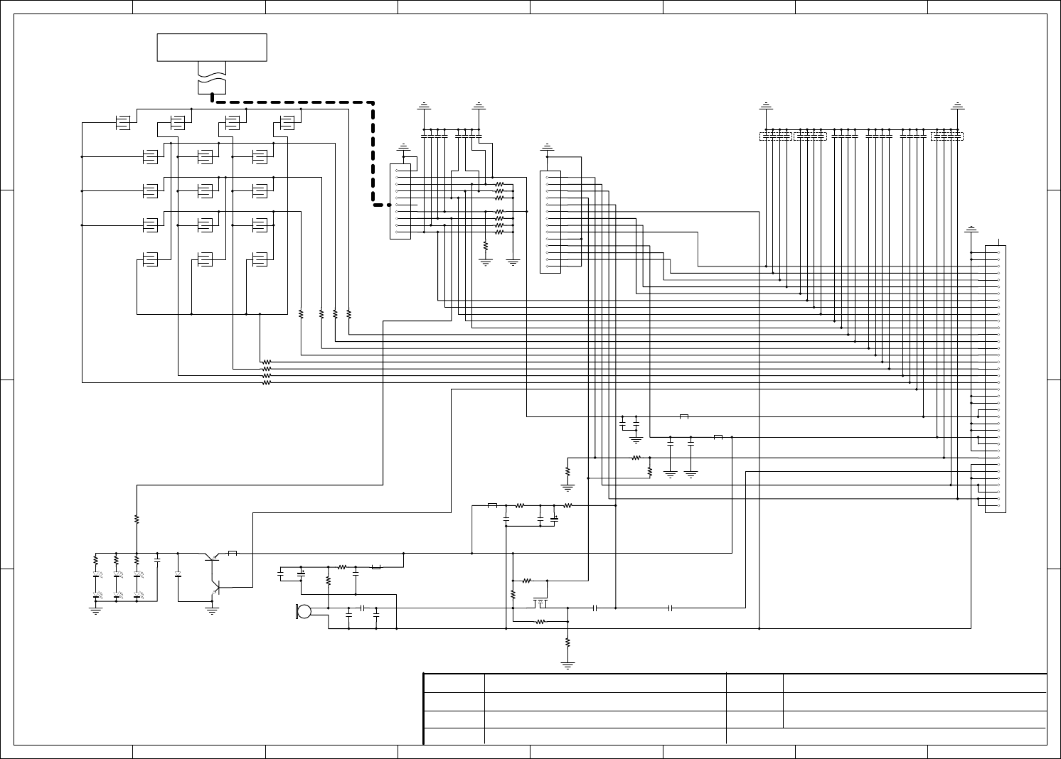
1
1
2
2
3
3
4
4
5
5
6
6
7
7
8
8
D D
C C
B B
A A
MIC1
MIC
C20 105
R22
1.8K
R20
470R
C16
4.7uF/10V
C22
102
L3
BLM11A221S
C19
102
C18
102
C21
102
KEY1
F1
KEY2
F2
KEY3
F3
KEY4
F4
KEY5
1
KEY6
2
KEY7
3
KEY8
4
KEY9
5
KEY10
6
KEY11
7
KEY12
8
KEY13
9
KEY15
0
KEY14
*
KEY16
#
L4
BLM11A221S
Q1
FMMT591
Q2
DTC144EE
D1
*
C17
104
R19
100R
D4
YELLOW
D5
YELLOW
D3
YELLOW
D7
YELLOW
D2
YELLOW
D6
YELLOW
R18
100R
R17
100R
R12
1K
R11
1K
R10
1K
R9
1K
R13 1K
R14 1K
R15 1K
R16 1K
1
2
3
4
5
6
7
8
9
10
CN2
CN10
1
2
3
4
5
6
7
8
9
10
11
12
13
14
15
16
17
18
19
20
21
22
23
24
39
25
26
27
28
29
30
31
32
33
34
35
36
37
38
CN3
CN38
C11
221
C7
221
C6
221
1
2
3
4
5
6
7
8
9
10
11
12
13
14
15
CN1
CN14
L1 BLM11A221S
C13
103 C12
102
R4 0R
R8
*
R7 2.7K
R6 2.7K
R3 2.7K
R2 2.7K
R1 2.7K
L2 BLM11A221S
C15
103
C14
102
按键板电原理图名称
文件号
设计
批准
机型
版本
审核
第张 张共
PT6500-KEY
。集群
11
/
Q3
2SK1824
R23
*
R21
100K
R5 2.7K
C1
221
C2
221C23
221 C24
221 C25
221 C26
221 C27
221
C28
221
C8
221C9
221C10
*C29
*C30
*C31
*C32
*C33
*C34
*C35
*C36
221 C37
221
R24
0R
R27 *
C41
104
C42
104
L5
BLM11A221S
C38
470P C39
470P
C40
4.7uF/10V
R25
470R
R26
1.8k
LCD
CNCSS
RXD
TXD
GND
RXD
TXD
5V
GND
CN
PF
PTT
ME
MIC
M SW
SP-
SP+
GND
5V
PF
PTT
MIC
SP-
SP+
SP SW
R30
*
R28
0R
R29
NC
R31
36K
Figure 12 PT6500 Keyboard Schematic Circuit Diagram
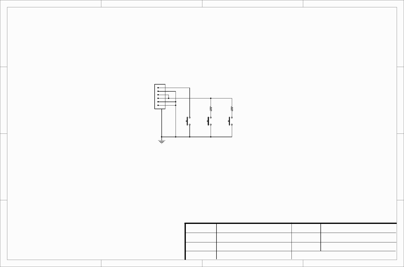
1
1
2
2
3
3
4
4
D D
C C
B B
A A
1
2
3
4
5
6
7
CN1
CN6 SW1
*SW2
*SW3
*
R1
20K R2
4.7K
电原理图名称
文件号
设计
批准
机型
版本
审核
第张 张共
PT6500-PTT
11/
Figure 13 PT6500 PTT Board Schematic Circuit Diagram
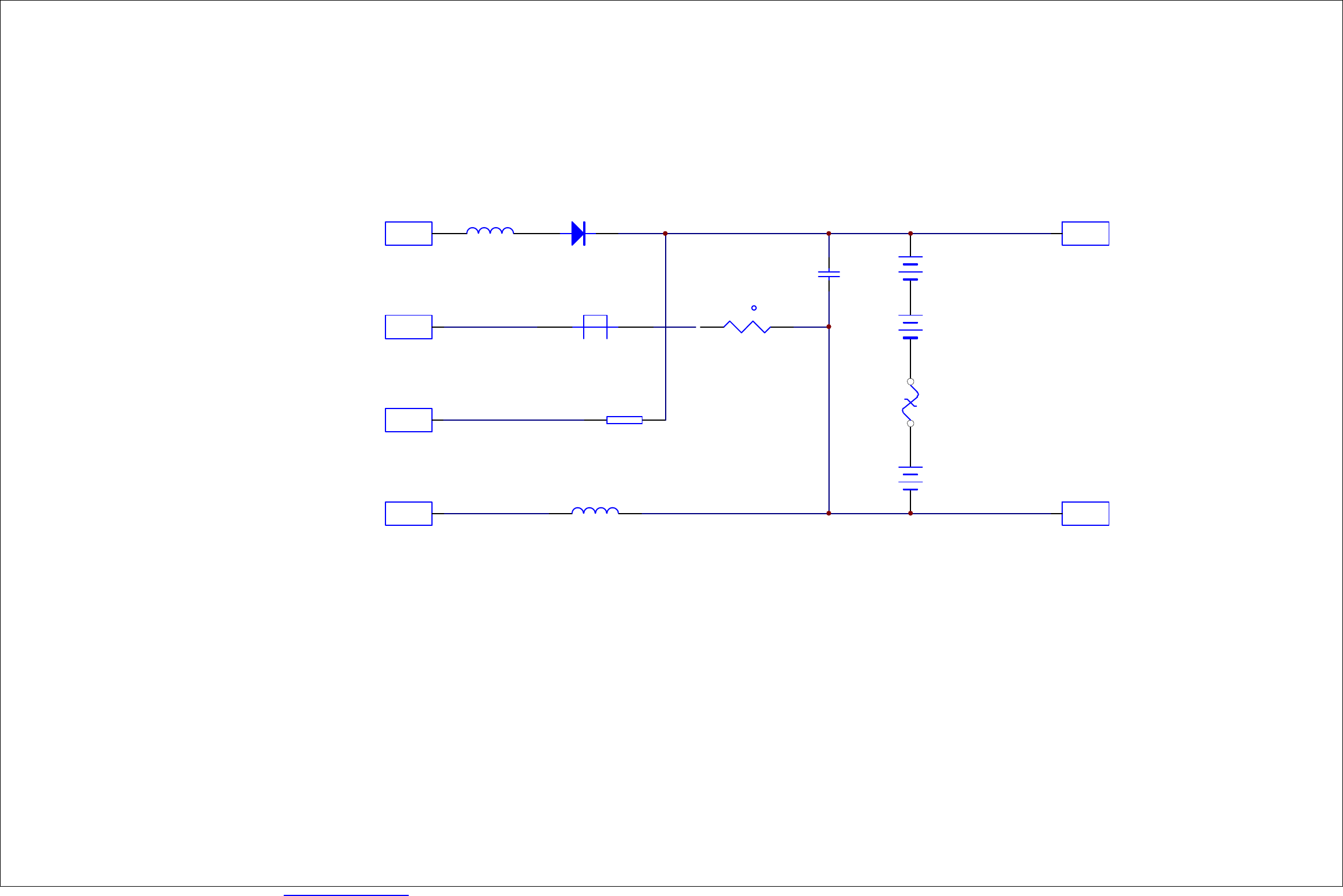
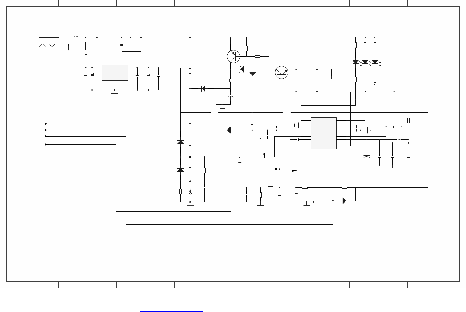
1
1
2
2
3
3
4
4
5
5
6
6
7
7
8
8
D D
C C
B B
A A
D9 GREEN
R16
100K
C14
104
C15
104
R6 51K
Q1 2N5551
PA0
4PA1
3PA2
2PA3
1PA4 18
PA5 17
PA6 16
PA7 15
PB0
8PB1
7PB2
6PB3
5
VSS
9PD0 10
RST 11
VDD 12
Osc0 13
Osc1 14
U2
HT46R47
R10
1R/2w
Vin
3
GND
2
+5V 1
U1 78L05
R7
10k
Q2
2SB772
R4
100K
R5
1K
R2
68K 1%
C8
104
R3
68K 1%
+C7
100uF/25V
D8 RED
R11
470R
R13 10K
C9
104
1
2
3
J1
DC INPUT
C2
104
A1
K
2D1
SB140
D2 SB140
R8
1K
D7 YELLOW
R1
4.7K 1%
C6
104
C11
104
R9
100k
D3
IN4148
D4
IN4148
B+
B-
C4
470P
R12
1k
D6 IN4148
+5V
C16 470P
R17 82K
C117
102
C18
104
D5
IN4148
R19
100R
R18
NC
R20
10K
C19
104
C21
104
C20
104
R25
470R
R14
470R
R21
470R
R23
470R
R22
470R
R26
0
L2 L
C22
470P
C25 102
C24 102
C23 102
DETCDETC
B+
TEMP
B-
TEMP
+
C28
10uF/25V
J2
J3
J4
J5
L1
330uH 3A
+5V
+5V
C17
47uF/25V
C3
10uF/25V
C1
0.1uF
D11
IN5819
D12
IN4148
C5
470P
R15 100R
R24 10K
C12
104
VDD
R27
*
TX1
10mm
TX2
10mm
+5V
+5V +5V
R30
0R
+5V
TX4
10mm
C30
470P
C31
104
C32
104 C33 104
C34 104
C35 104
C36
104
T1
T2
T3 T4
L11
PDF created with pdfFactory Pro trial version www.pdffactory.com
Figure 15 KBC-36C
