User Manual: 3rd Generation EPS Range No Inhibits Clyde Space Manual 1335 Rev D
User Manual:
Open the PDF directly: View PDF ![]() .
.
Page Count: 60

SOLUTIONS FOR A NEW AGE IN SPACE
Clyde Space Ltd.
SkyPark 5
45 Finnieston Street
Glasgow G3 8JU, U.K.
t: + 44 (0) 141 946 4440
e: enquiries@clyde.space
w: www.clyde.space
Registered in Scotland No. SC285287
at 123 St Vincent Street Glasgow G2 5EA
User Manual: 3rd Generation EPS Range - No Inhibits
Document No.: USM-1335
Issue: D
Date: 11 Oct 2017
Name Date Signed
Author
Alec Wright
5 May 2016
Updated
Colin Waddell
2 Aug 2017
Approved
Thomas Parry
11 Oct 2017

USM-1335
User Manual: 3rd Generation EPS Range - No Inhibits
Issue: D
Date: 11/10/2017
Page: 2 of 60
Skypark 5, 45 Finnieston
Street, Glasgow G3 8JU, UK
SOLUTIONS FOR A NEW AGE IN SPACE
www.clyde.space
PROPRIETARY & CONFIDENTIAL INFORMATION
Copyright ©2017 Clyde Space Ltd. All rights reserved.
Document Control
Issue
Date
Section
Description of Change
Reason for Change
A
05/04/2016
All
Information from USM-25-
01309, USM-25-01311 RevF,
USM-01-01317 RevE, USM-25-
02452 RevC, USM-01-02453
RevB combined to create
family user manual
B
13/06/2017
2
3
9
Updating the table in section
Update figure 3.1
Adding section for 5V USB
Charge
DCR039
C
20/06/2017
9.8
11.4
Updated the trip current for
switches 3 and 4 in Table 9-1.
Updated the telemetry
equations (ISW3, ISW4,
VBCR1, VBCR2, VBCR4, VBCR5,
VBCR6, VBCR7, VBCR8 and
VBCR9) in tables 11-7, 11-9 &
11-10)
DCR044
D
2/08/2017
11.2
11.3
Get Version+Revision is now
split into two separate
commands for devices running
firmware version 18-02012
Rev E + 18-2013 Rev C and
above
DCR73
Revision Control
Product
Part Number
Notes
3rd Generation EPS (1UB) No Inhibits
25-02451
N/A
3rd Generation EPS (3UA) No Inhibits
25-02452
H
3rd Generation EPS (XUA) No Inhibits
01-02453
N/A
Acronyms and Abbreviations
1U
1 Unit (Cubesat standard size)
2s1p
Battery configuration – 2 cells in series, 1 string in parallel
2s2p
Battery configuration – 2 cells in series, 2 string in parallel
2s3p
Battery configuration – 2 cells in series, 3 string in parallel
3U
3 Unit (Cubesat standard size)
ADC
Analogue to Digital Converter
Ah
Ampere Hour
AIT
Assembly, Integration and Testing
AMUX
Analogue Multiplexer
BCR
Battery Charge Regulator
DoD
Depth of Discharge
EoC
End of Charge
EPS
Electrical Power System

USM-1335
User Manual: 3rd Generation EPS Range - No Inhibits
Issue: D
Date: 11/10/2017
Page: 3 of 60
Skypark 5, 45 Finnieston
Street, Glasgow G3 8JU, UK
SOLUTIONS FOR A NEW AGE IN SPACE
www.clyde.space
PROPRIETARY & CONFIDENTIAL INFORMATION
Copyright ©2017 Clyde Space Ltd. All rights reserved.
ESD
Electro Static Discharge
FleXU/XU
FleXible Unit (suitable for various satellite configurations)
Isc
Short Circuit Current
Kbits-1
Kilobits per second
MPPT
Maximum Power Point Tracker
PCM
Power Conditioning Module
PDM
Power Distribution Module
rh
Relative Humidity
TLM
Telemetry
USB
Universal Serial Bus
Voc
Open Circuit Voltage
Wh
Watt Hour
Related Documents
No.
Document Name
Doc Ref.
RD-1
3rd Generation CubeSat Battery Family
Rev B User Manual
USM-1192
RD-2
CubeSat Design Specification
CubeSat Design Specification Rev. 12
RD-3
NASA General Environmental
Verification Standard
GSFC-STD-7000 April 2005
RD-4
CubeSat Kit Manual
UM-3
RD-5
Solar Panel User Document
TBC
RD-6
Power System Design and
Performance on the World’s Most
Advanced In-Orbit Nanosatellite
As named
Warning
Risk
Ensure headers H1 and H2 are correctly aligned before
mating boards
If misaligned, battery positive can short to ground,
causing failure of the battery and EPS
Ensure switching configuration is implemented
correctly before applying power to EPS
If power is applied with incorrect switch configuration,
the output of the BCR can be blown, causing failure of
the EPS
Observe ESD precautions at all times
The EPS is a static sensitive system. Failure to observe
ESD precautions can result in failure of the EPS.
Ensure not to exceed the maximum stated limits
Exceeding any of the stated maximum limits can result
in failure of the EPS
Ensure batteries are fully isolated during storage
If not fully isolated (by switch configuration or
separation) the battery may over-discharge, resulting
in failure of the battery
No connection should be made to H2.35-36 or H2.41-
44
These pins are used to connect the battery to the EPS.
Any connections to the unregulated battery bus should
be made to pins H2.45-46
H1 and H2 pins should not be shorted at any time
These headers have exposed live pins which should not
be shorted at any time. Particular care should be taken
regarding the surfaces these are placed on.


USM-1335
User Manual: 3rd Generation EPS Range - No Inhibits
Issue: D
Date: 11/10/2017
Page: 5 of 60
Skypark 5, 45 Finnieston
Street, Glasgow G3 8JU, UK
SOLUTIONS FOR A NEW AGE IN SPACE
www.clyde.space
PROPRIETARY & CONFIDENTIAL INFORMATION
Copyright ©2017 Clyde Space Ltd. All rights reserved.
Table of Contents
1. Introduction .......................................................................................................................... 7
1.1 Additional Information Available Online ............................................................................................ 7
1.2 Continuous Improvement .................................................................................................................. 7
1.3 Document Revisions........................................................................................................................... 7
2. Overview ............................................................................................................................... 8
2.1 Applicable Products ........................................................................................................................... 8
3. Maximum Ratings ................................................................................................................. 9
3.1 BCR Safe Operating Area .................................................................................................................. 10
4. Electrical Characteristics ..................................................................................................... 11
5. Handling and storage .......................................................................................................... 12
5.1 Electro Static Discharge (ESD) Protection ........................................................................................ 12
5.2 General Handling ............................................................................................................................. 12
5.3 Shipping and Storage ....................................................................................................................... 12
6. Materials and Processes ..................................................................................................... 13
6.1 Materials Used ................................................................................................................................. 13
6.2 Processes and Procedures ............................................................................................................... 13
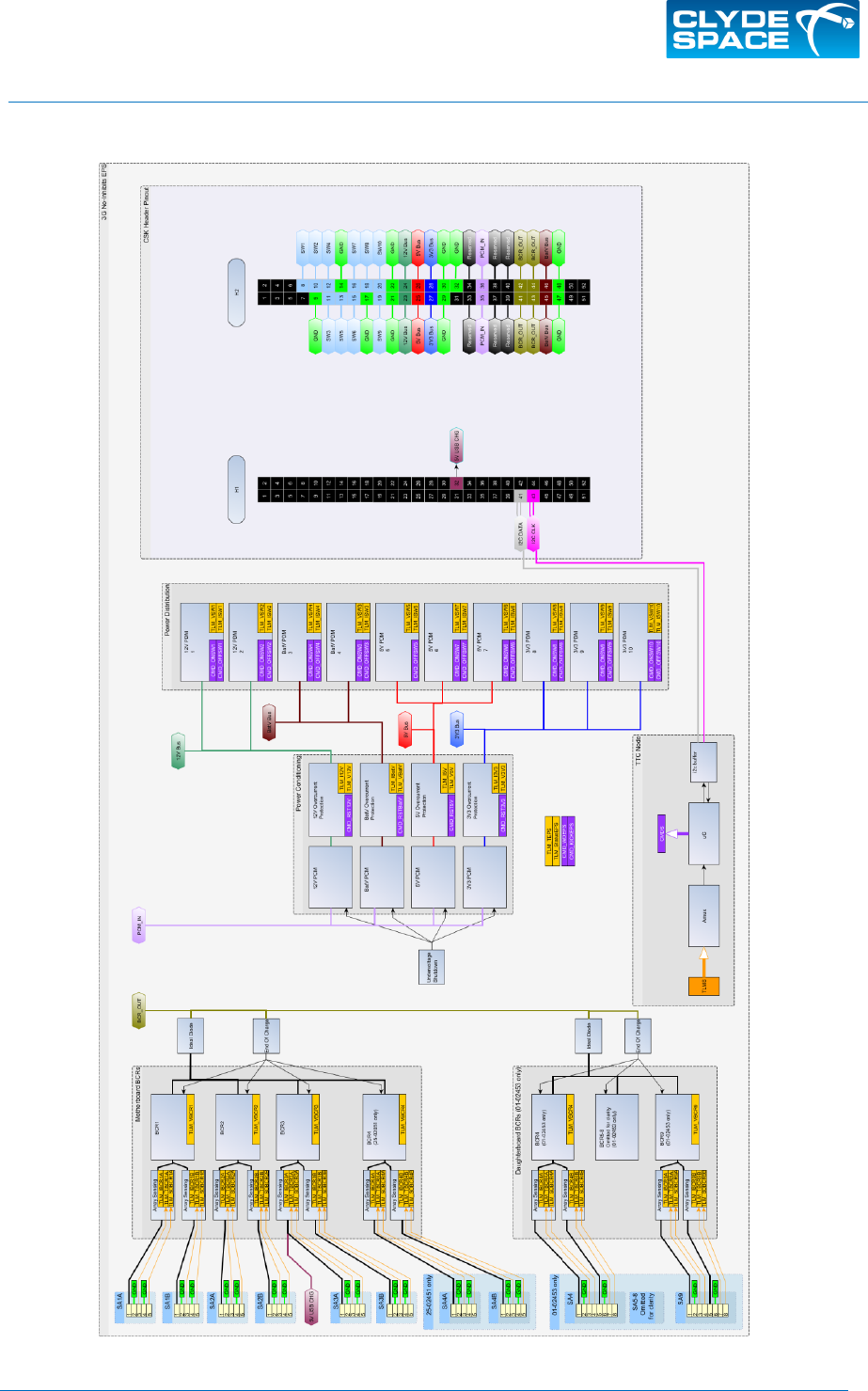
7. System Description ............................................................................................................. 14
7.1 System Overview ............................................................................................................................. 17
7.2 Autonomy and Redundancy ............................................................................................................. 18
7.3 Quiescent Power Consumption ....................................................................................................... 18
7.4 Mass and Mechanical Configuration ................................................................................................ 18
8. Interfacing ........................................................................................................................... 20
8.1 Solar Array Connection .................................................................................................................... 22
8.2 Solar Array Harness .......................................................................................................................... 24
8.3 Temperature Sensing Interface ........................................................................................................ 24
8.4 Sun Detector Interface ..................................................................................................................... 24
8.5 Non-Clyde Space Solar Arrays .......................................................................................................... 24
8.6 CubeSat Kit Compatible Headers ..................................................................................................... 24
8.7 Cubesat Kit Header Pin Out .............................................................................................................. 26
8.8 Flight Switches ................................................................................................................................. 27
8.9 Battery connection........................................................................................................................... 27
9. Technical description .......................................................................................................... 28
9.1 Charge Method ................................................................................................................................ 28
9.2 BCR Power Stage Overview .............................................................................................................. 29
9.3 MPPT ................................................................................................................................................ 29
9.4 5V USB Charge ................................................................................................................................. 30
9.5 5V and 3.3V PCMs with Latching Current Limiter ............................................................................ 30

USM-1335
User Manual: 3rd Generation EPS Range - No Inhibits
Issue: D
Date: 11/10/2017
Page: 6 of 60
Skypark 5, 45 Finnieston
Street, Glasgow G3 8JU, UK
SOLUTIONS FOR A NEW AGE IN SPACE
www.clyde.space
PROPRIETARY & CONFIDENTIAL INFORMATION
Copyright ©2017 Clyde Space Ltd. All rights reserved.
9.6 12V PCM with Latching Current Limiter ........................................................................................... 32
9.7 BatV PCM with Latching Current Limiter ......................................................................................... 32
9.8 PDMs with Latching Current Limiter ................................................................................................ 32
10. General Protection ............................................................................................................. 35
10.1 Over-Current Bus Protection (LCL) ................................................................................................... 35
10.2 Battery Under-Voltage Protection ................................................................................................... 36
11. Telemetry and Telecommand ............................................................................................. 37
11.1 Communications .............................................................................................................................. 37
11.2 List of Available Commands ............................................................................................................. 39
11.3 Housekeeping and Status Commands .............................................................................................. 40
11.4 Telemetry ......................................................................................................................................... 43
11.5 Watchdogs and Reset Counters ....................................................................................................... 48
11.6 PDM Control .................................................................................................................................... 50
11.7 PDM Timers ...................................................................................................................................... 53
11.8 PCM Control ..................................................................................................................................... 55
12. Test ..................................................................................................................................... 55
12.1 Required Equipment ........................................................................................................................ 55
12.2 Standalone Test Setup ..................................................................................................................... 57
12.3 Testing with Clyde Space Battery ..................................................................................................... 58
13. Compatible Systems ........................................................................................................... 59
13.1 Compatible Batteries ....................................................................................................................... 60
USM-1335
User Manual: 3rd Generation EPS Range - No Inhibits
Issue: D
Date: 11/10/2017
Page: 7 of 60
Skypark 5, 45 Finnieston
Street, Glasgow G3 8JU, UK
SOLUTIONS FOR A NEW AGE IN SPACE
www.clyde.space
PROPRIETARY & CONFIDENTIAL INFORMATION
Copyright ©2017 Clyde Space Ltd. All rights reserved.
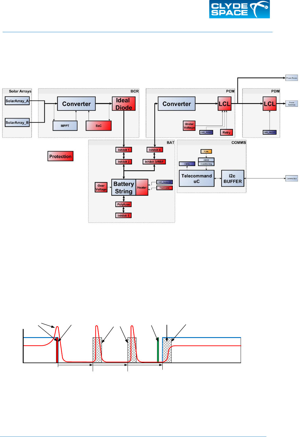
1. INTRODUCTION
This document provides information on the features, operation, handling and storage of the 25-02451,
25-02452 and 01-02453 EPS products, designed to integrate with a suitable battery and solar arrays
to form a complete power system for use on a CubeSat.
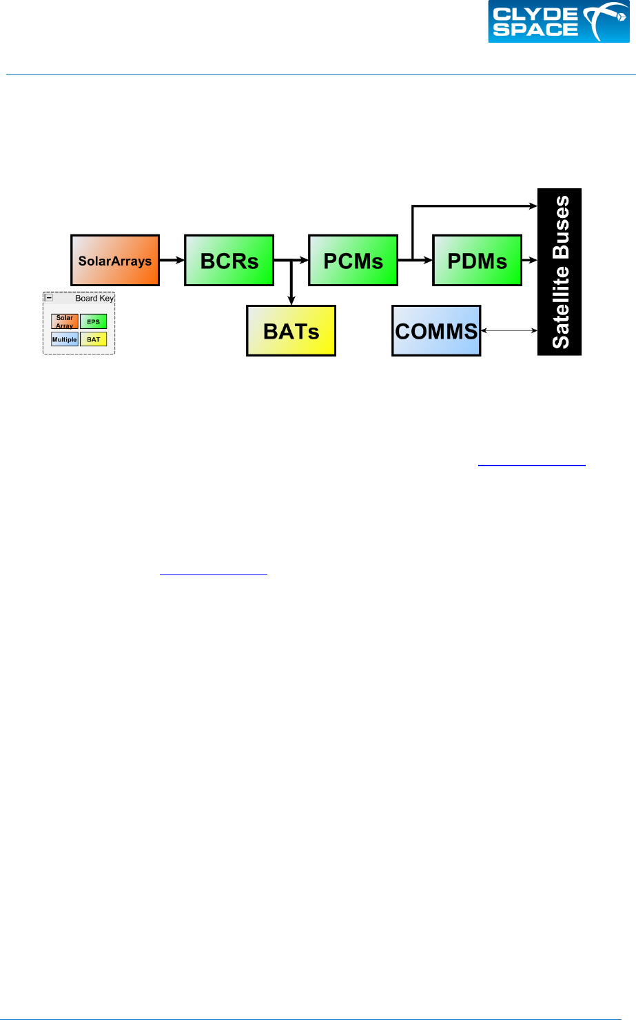
Figure 1-1 System Diagram
1.1 Additional Information Available Online
Additional information on CubeSats and Clyde Space Systems can be found at www.clyde.space. You
will need to log in to our website to access certain documents.
1.2 Continuous Improvement
At Clyde Space we are continuously improving our processes and products. We aim to provide full
visibility of the changes and updates that we make, and information of these changes can be found by
logging in to our website: www.clyde.space
1.3 Document Revisions
In addition to hardware and software updates, we also update make regular updates to our
documentation and online information.

USM-1335
User Manual: 3rd Generation EPS Range - No Inhibits
Issue: D
Date: 11/10/2017
Page: 8 of 60
Skypark 5, 45 Finnieston
Street, Glasgow G3 8JU, UK
SOLUTIONS FOR A NEW AGE IN SPACE
www.clyde.space
PROPRIETARY & CONFIDENTIAL INFORMATION
Copyright ©2017 Clyde Space Ltd. All rights reserved.
2. OVERVIEW
The Clyde Space 3rd Generation (3G) EPS range is the latest incarnation of Clyde Space's highly
successful CubeSat power system range, which has powered almost half of all CubeSat missions to
date. Our 3G range is our most capable and compact CubeSat EPS range to date, providing robust,
high-performance mission capability. The main features include:
• 3.3V, 5V, and 12V regulated power buses
• Unregulated battery bus
• 10 Latching Current Limit (LCL) power distribution modules
• Maximum Power-Point Tracking (MPPT) Battery Charge Regulators (BCRs)
• Over-current, over- and under-voltage protection
• Watchdog timer
As a result of the new features added in the 3rd Generation there is a requirement to alter the
interfaces to the main CubeSat Kit header. Further detail on the new features and interfaces can be
found in this user manual.
Clyde Space is a world-leading provider of spacecraft power systems, from CubeSats through to Small
GEO satellites. Since establishment in 2006 Clyde Space has provided thousands of spacecraft
subsystems, and has grown to be a leading provider of nanosatellite spacecraft platforms as well. Our
heritage and experience mean you can be sure a Clyde Space component comes with performance
and quality assured.
2.1 Applicable Products
This user manual describes three variants of the 3rd Generation No Inhibits EPS. The differences
between these variants are summarised below
3G 1U EPS (25-02451)
3G 3U EPS (25-02452)
3G FlexU EPS (01-02453)
Intended Use
1U CubeSats
2U and 3U CubeSats with
body panels
3U CubeSats with deployable
panels, and larger nanosatellites
Number of SEPIC BCRs
4 BCRs
1 BCR
1 BCR
Number of Buck BCRs
None
2 BCRs
8 BCRs

USM-1335
User Manual: 3rd Generation EPS Range - No Inhibits
Issue: D
Date: 11/10/2017
Page: 9 of 60
Skypark 5, 45 Finnieston
Street, Glasgow G3 8JU, UK
SOLUTIONS FOR A NEW AGE IN SPACE
www.clyde.space
PROPRIETARY & CONFIDENTIAL INFORMATION
Copyright ©2017 Clyde Space Ltd. All rights reserved.
3. MAXIMUM RATINGS
Stresses beyond those listed under maximum ratings may cause permanent damage to the EPS.
Operation of the EPS at conditions beyond those indicated is not recommended. Exposure to absolute
maximum ratings for extended periods may affect EPS reliability. De-rating of power critical
components is in accordance with ECSS guidelines.
OVER OPERATING TEMPERATURE RANGE (UNLESS OTHERWISE STATED)
Value
Unit
Input Voltage(2)
Buck BCRs
30
V
SEPIC BCRs
9.5
V
Battery
8.3
V
Value
Unit
Input Current
Buck BCRs
Refer to Section 3.1
SEPIC BCRs
Value
Unit
Operating Temperature
-40 to 85
°C
Storage Temperature
-50 to 100
°C
Vacuum
10-5
torr
Radiation Tolerance
10
kRad
Vibration
To [RD-3]
Table 3-1 Max Ratings of the EPS products
USM-1335
User Manual: 3rd Generation EPS Range - No Inhibits
Issue: D
Date: 11/10/2017
Page: 10 of 60
Skypark 5, 45 Finnieston
Street, Glasgow G3 8JU, UK
SOLUTIONS FOR A NEW AGE IN SPACE
www.clyde.space
PROPRIETARY & CONFIDENTIAL INFORMATION
Copyright ©2017 Clyde Space Ltd. All rights reserved.
3.1 BCR Safe Operating Area
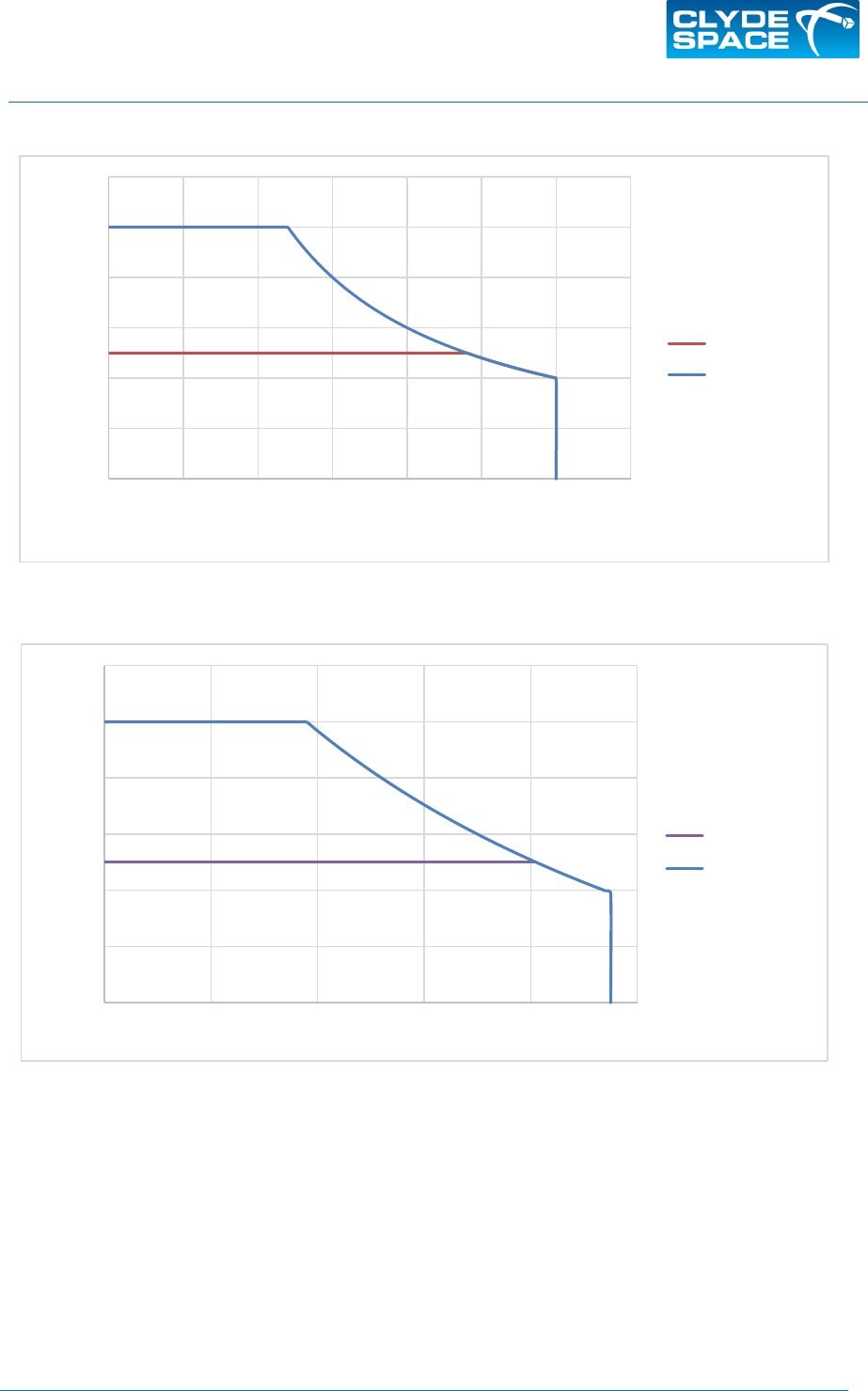
Figure 3-1 Safe Operating Range for Buck BCRs
Figure 3-2 Safe Operating Range for SEPIC BCRs at TBRD=60°C
The safe operating ranges of the BCRs are shown above. Single Channel refers to the maximum current
which can be applied to a single pin (e.g. SA1.1). Dual Channel refers to the limit on the sum of the
currents which can be applied to two pins connecting to the same BCR (e.g. SA1A.1 and SA1B.1 or
SA5.1 and SA5.5). For BCR allocations, see Section 9.2. It is important to ensure that the limits of the
BCRs given above are not exceeded either at open circuit or at maximum power point.
0
0.2
0.4
0.6
0.8
1
1.2
0 5 10 15 20 25 30 35
Solar Array Current/A
Solar Array Voltage/V
Single Channel
Dual Channel
0
0.2
0.4
0.6
0.8
1
1.2
0 2 4 6 8 10
Solar Array Current/A
Solar Array Voltage/V
Single Channel
Dual Channel

USM-1335
User Manual: 3rd Generation EPS Range - No Inhibits
Issue: D
Date: 11/10/2017
Page: 11 of 60
Skypark 5, 45 Finnieston
Street, Glasgow G3 8JU, UK
SOLUTIONS FOR A NEW AGE IN SPACE
www.clyde.space
PROPRIETARY & CONFIDENTIAL INFORMATION
Copyright ©2017 Clyde Space Ltd. All rights reserved.
4. ELECTRICAL CHARACTERISTICS
Description
Conditions
Min
Typical
Max
Unit
Buck BCRs
Input Voltage
7.41
--
30
V
End of Charge Voltage
8.165
8.265
8.365
V
Switching Frequency
150
175
200
kHz
Efficiency
@16.5V input, Full
Load
85%
90%
92%
SEPIC BCRs
Conditions
Min
Typical
Max
Unit
Input Voltage
3.0
--
9.5
V
End of Charge Voltage
8.165
8.265
8.365
V
Operating Frequency
145
170
200
kHz
Efficiency
@6V input, Full Load
77%
79%
80%
Unregulated Battery Bus
Conditions
Min
Typical
Max
Unit
Output Voltage
--
Battery Voltage
--
LCL Trip Point
4.55
4.7
4.85
A
Efficiency
@8.26V input, Full
Load
98.5%
99%
99.5%
5V Bus
Conditions
Min
Typical
Max
Unit
Output Voltage
4.95
5
5.05
V
LCL Trip Point
4.4
4.5
4.6
A
Operating Frequency
400
480
560
kHz
Efficiency
@5V, Full Load
--
93%
--
3.3V Bus
Conditions
Min
Typical
Max
Unit
Output Voltage
3.267
3.3
3.333
V
LCL Trip Point
4.4
4.5
4.6
A
Operating Frequency
400
480
560
kHz
Efficiency
@3.3V, Full Load
--
90%
--
12V Bus
Conditions
Min
Typical
Max
Unit
Output Voltage
11.88
12
12.12
V
LCL Trip Point
1.4
1.5
1.6
A
Operating Frequency
670
800
930
kHz
Efficiency
@3.3V input, Full Load
--
92%
--
Communications
Min
Typical
Max
Unit
Protocol
--
I2C
--
Transmission speed
--
100
--
kbits-1
Bus voltage
3.26V
3.3V
3.33V
Node address
--
0x2B
--
Address scheme
--
7 bit
--
Node operating frequency
--
27MHz
--
Quiescent Operation
Conditions
Max
Unit
Power Draw
Flight Configuration of
Activation Switches
25-02451:
0.2
W
25-02452:
0.2
01-02453:
0.4
Table 4-1 Performance Characteristics of the EPS
1
If VMPP is below 9.4V, the converter will deviate from the maximum power point during taper charge and will charge less efficiently

USM-1335
User Manual: 3rd Generation EPS Range - No Inhibits
Issue: D
Date: 11/10/2017
Page: 12 of 60
Skypark 5, 45 Finnieston
Street, Glasgow G3 8JU, UK
SOLUTIONS FOR A NEW AGE IN SPACE
www.clyde.space
PROPRIETARY & CONFIDENTIAL INFORMATION
Copyright ©2017 Clyde Space Ltd. All rights reserved.
5. HANDLING AND STORAGE
The EPS requires specific guidelines to be observed for handling, transportation and storage. These
are stated below. Failure to follow these guidelines may result in damage to the units or degradation
in performance.
5.1 Electro Static Discharge (ESD) Protection
The EPS incorporates static sensitive devices and care should be taken during handling. Do not touch
the EPS without proper electrostatic protection in place. All handling of the system should be done in
a static dissipative environment.
5.2 General Handling
The EPS is robust and designed to withstand flight conditions. However, care must be taken when
handling the device. Do not drop the device as this can damage the EPS. There are live connections
between the battery systems and the EPS on the CubeSat Kit headers. All metal objects (including
probes) should be kept clear of these headers.
Gloves should be worn when handling all flight hardware.
Flight hardware will be delivered conformally coated, and should only be removed from packaging in
a class 100000 (or better) clean room environment.
5.3 Shipping and Storage
The devices are shipped in anti-static packaging, enclosed in a hard protective case. This case should
be used for storage. All hardware should be stored in anti-static containers at temperatures between
20°C and 40°C and in a humidity-controlled environment of 40-60%rh.
The shelf-life of this product is estimated at 5 years when stored appropriately.

USM-1335
User Manual: 3rd Generation EPS Range - No Inhibits
Issue: D
Date: 11/10/2017
Page: 13 of 60
Skypark 5, 45 Finnieston
Street, Glasgow G3 8JU, UK
SOLUTIONS FOR A NEW AGE IN SPACE
www.clyde.space
PROPRIETARY & CONFIDENTIAL INFORMATION
Copyright ©2017 Clyde Space Ltd. All rights reserved.
6. MATERIALS AND PROCESSES
6.1 Materials Used
Material
Manufacturer
%TML
%CVCM
%WVR
Application
Applicable
Products
Araldite 2014 Epoxy
Huntsman
0.97
0.05
0.33
Adhesive fixing
All
1B31 Acrylic
Humiseal
3.89
0.11
0.09
Conformal Coating
All
DC 6-1104
Dow Corning
0.17
0.02
0.06
Adhesive fixing on
modifications
All
Stycast 2850
Emerson &
Cuming
0.25
0.01
0.05
Adhesive fixing
All
PCB material
FR4
0.62
0
0.1
Note: worst case on NASA
out-gassing list
All
Solder Resist
CARAPACE
EMP110 or
XV501T-4
0.95
or 0.995
0.02
Or 0.001
0.31
-
All
Solder
Sn62 or Sn63
(Tin/Lead)
-
-
-
-
All
Flux
Alpha Rosin Flux,
RF800, ROL 0
-
-
-
Low activity flux to avoid
corrosion
All
300 Series Stainless
Steel
Pemnet
-
-
-
PEMs
01-02453
A4 Stainless Steel
(316L)
PTS-UK
-
-
-
M3 Fasteners
01-02453
Table 6-1 Materials List
Table 6-2 Connector Headers
6.2 Processes and Procedures
All assembly is inspected to ESA Workmanship Standards; ECSS-Q-ST-70-08C and ECSS-Q-ST-70-38C.
Part Used
Manufacturer
Contact
Insulator
Type
Use
Required mating
Connector
Applicable
Products
DF13-6P-
1.25DSA(50)
Hirose
Gold Plated
Polyamide
PTH
Programming Header –
not for customer use
DF13-6S-1.25C and
DF13-2630SCFA(04)
All
DF13-5P-
1.25DSA(50)
Hirose
Gold Plated
Polyamide
PTH
Solar Array Connectors
DF13-5S-1.25C and
DF13-2630SCFA(04)
All
ESQ-126-
39-G-D
Samtec
Gold Plated
Black Glass
Filled
Polyester
PTH
CubeSat Kit Compatible
Headers
ESQ-126 range
All
FTSH-110-
01-F-DV
Samtec
Gold Plated
Beryllium
Copper
Black Liquid
Crystal
Polymer
SMT
Expansion Header for
daughterboard
connection
TFM-110-22-L-D-A
25-02451
SFM-110-
02-L-D-A
Samtec
Gold Plated
Beryllium
Copper
Black Liquid
Crystal
Polymer
SMT
Expansion Header for
daughterboard
connection
TFM-110-22-L-D-A
25-02452,
01-02453
TFM-110-
22-L-D-A
Samtec
Gold Plated
Beryllium
Copper
Black Liquid
Crystal
Polymer
SMT
Daughterboard to
motherboard
connection header
SFM-110-02-L-D-A
01-02453
DF13-8P-
1.25DSA(50)
Hirose
Gold Plated
Polyamide
PTH
Solar Array Connectors
(Daughter Board)
DF13-8s-1.25C and
DF13-2630SCFA(04)
01-02453

USM-1335
User Manual: 3rd Generation EPS Range - No Inhibits
Issue: D
Date: 11/10/2017
Page: 14 of 60
Skypark 5, 45 Finnieston
Street, Glasgow G3 8JU, UK
SOLUTIONS FOR A NEW AGE IN SPACE
www.clyde.space
PROPRIETARY & CONFIDENTIAL INFORMATION
Copyright ©2017 Clyde Space Ltd. All rights reserved.
7. SYSTEM DESCRIPTION
The Clyde Space EPS products are optimised for Low Earth Orbit (LEO). They are designed for
integration with spacecraft that have six body mounted solar panels or fewer (i.e. one on each
spacecraft facet), or potentially other configurations involving deployable panels. The EPS can
accommodate various solar panel configurations, and has been designed to be versatile; please
consult our support team if you have specific requirements for connecting the EPS to your spacecraft.
The Clyde Space EPS connects to the solar panels via a number of independent Battery Charge
Regulators (BCRs). These are connected with panels on opposing faces of the satellite connected to
the same BCR. Additional BCRs (not applicable to 25-02452) allow deployable panels to be used. In
this configuration only one panel per pair can be directly illuminated at any given time, with the second
panel providing a limited amount of energy due to albedo illumination. Each of the BCRs has an inbuilt
Maximum Power Point Tracker (MPPT). This MPPT will track the dominant panel of the connected
pair (the directly illuminated panel).
The output of the BCRs are then connected together and supply charge to the battery, Power
Conditioning Modules (PCMs) and Power Distribution Modules (PDMs).
The PCM network has an unregulated Battery Voltage Bus, a regulated 5V supply, a regulated 3.3V
supply and a regulated 12V supply, each with a separate Latching Current Limiter (LCL) with automatic
retry. In addition to the main buses there are 10 commandable PDMs – 2x12V, 2xBATV, 3x5V and
3x3.3V. The EPS also has multiple inbuilt protection methods to ensure safe operation during the
mission and a full range of EPS telemetry via the I2C network. These are discussed in detail in Sections
10 and 11.
USM-1335
User Manual: 3rd Generation EPS Range - No Inhibits
Issue: D
Date: 11/10/2017
Page: 15 of 60
Skypark 5, 45 Finnieston
Street, Glasgow G3 8JU, UK
SOLUTIONS FOR A NEW AGE IN SPACE
www.clyde.space
PROPRIETARY & CONFIDENTIAL INFORMATION
Copyright ©2017 Clyde Space Ltd. All rights reserved.
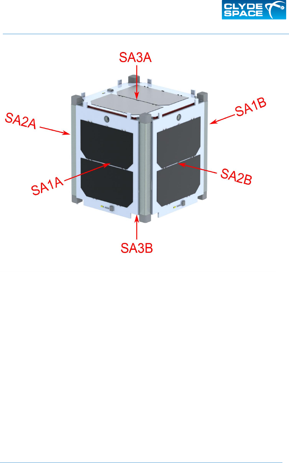
Figure 7-1 Typical Array Configuration for 25-02452 with Example Allocations (for 01-02453, deployed panels
can additionally interface to BCRs 4-9)
SA1A Array
SA1B Array
SA3B Array
SA3A Array
SA2B Array
SA2A Array
USM-1335
User Manual: 3rd Generation EPS Range - No Inhibits
Issue: D
Date: 11/10/2017
Page: 16 of 60
Skypark 5, 45 Finnieston
Street, Glasgow G3 8JU, UK
SOLUTIONS FOR A NEW AGE IN SPACE
www.clyde.space
PROPRIETARY & CONFIDENTIAL INFORMATION
Copyright ©2017 Clyde Space Ltd. All rights reserved.
Figure 7-2 Typical Array Configuration for 25-02451 with Example Allocations.
Fourth BCR interface not shown in image.
USM-1335
User Manual: 3rd Generation EPS Range - No Inhibits
Issue: D
Date: 11/10/2017
Page: 17 of 60
Skypark 5, 45 Finnieston
Street, Glasgow G3 8JU, UK
SOLUTIONS FOR A NEW AGE IN SPACE
www.clyde.space
PROPRIETARY & CONFIDENTIAL INFORMATION
Copyright ©2017 Clyde Space Ltd. All rights reserved.
7.1 System Overview
Figure 7-3 Functional Diagram
USM-1335
User Manual: 3rd Generation EPS Range - No Inhibits
Issue: D
Date: 11/10/2017
Page: 18 of 60
Skypark 5, 45 Finnieston
Street, Glasgow G3 8JU, UK
SOLUTIONS FOR A NEW AGE IN SPACE
www.clyde.space
PROPRIETARY & CONFIDENTIAL INFORMATION
Copyright ©2017 Clyde Space Ltd. All rights reserved.
7.2 Autonomy and Redundancy
All BCR power stages feature full system autonomy, operating solely from the solar array input and
not requiring any power from the battery systems. This feature offers graceful degradation of the
system as none of the BCRs depend on any other circuitry to operate correctly. Failure of all strings
of the battery (any of the Clyde Space battery range) will not damage the BCRs but, due to the MPPT,
will result in an intermittent interruption on all power buses (approximately every 2.5 seconds).
The rest of the power system is a robustly designed single string.
7.3 Quiescent Power Consumption
All power system efficiencies detailed (for BCRs and PCMs) take into consideration the associated low
level control electronics. As such, these numbers are not included in the quiescent power
consumption figures.
The quiescent current draw covers the power required to run the TTC node, PDMs and other
monitoring and safety features of the EPS, and values are given in Table 4-1.
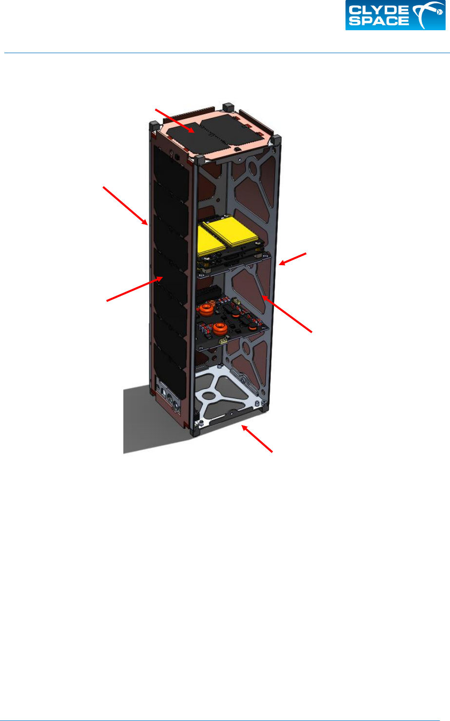
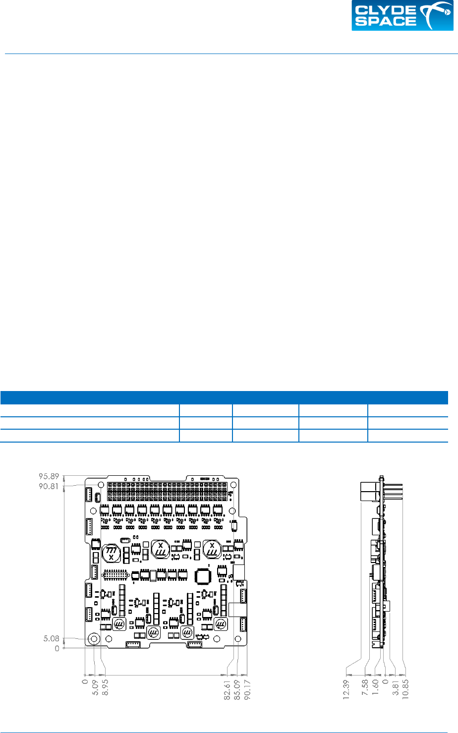
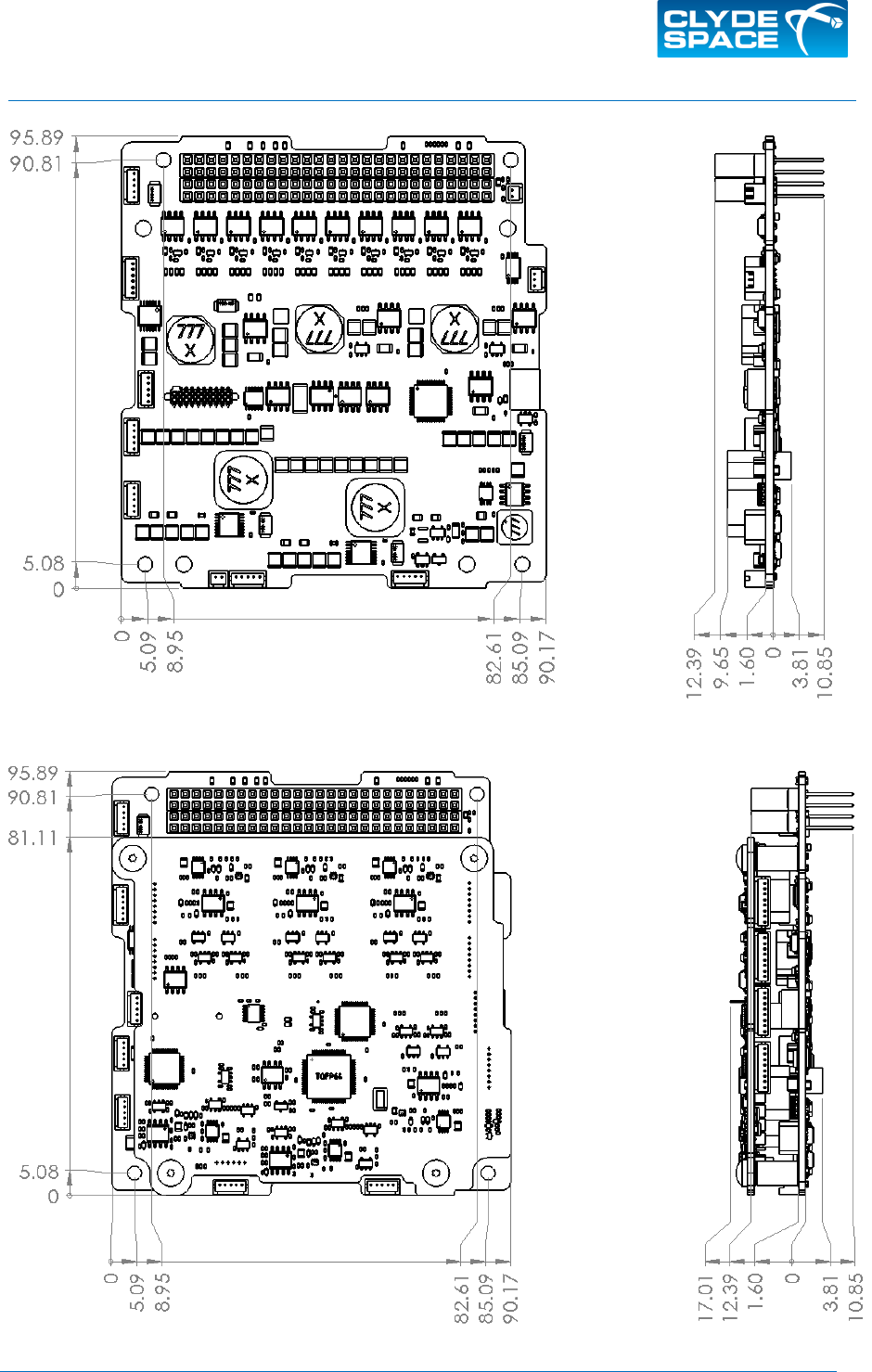
7.4 Mass and Mechanical Configuration
The system is contained on a single PC/104 size card, compatible with the Cubesat Kit bus. The 01-
02453 FlexU EPS also includes a daughterboard. The 25-02451 1U EPS can be used as the motherboard
for a CubeSat power system with an integrated battery. This will be documented in the battery user
manual [RD-1]. The 25-02452 and 01-02453 EPS products are expected to be used with a standalone
battery.
The masses of the EPS products are specified in Table 7-1 and dimensioned drawings are given in
Figure 7-4 through Figure 7-6.
Part number
Min
Typical
Max
Unit
25-02451
84
86
88
g
25-02452
84
86
88
g
01-02453
145
148
150
g
Table 7-1 Mass of EPS Products
Figure 7-4 Dimensioned Drawing of 25-02451 1UB EPS
USM-1335
User Manual: 3rd Generation EPS Range - No Inhibits
Issue: D
Date: 11/10/2017
Page: 19 of 60
Skypark 5, 45 Finnieston
Street, Glasgow G3 8JU, UK
SOLUTIONS FOR A NEW AGE IN SPACE
www.clyde.space
PROPRIETARY & CONFIDENTIAL INFORMATION
Copyright ©2017 Clyde Space Ltd. All rights reserved.
Figure 7-5 Dimensioned Drawing of 25-02452 3UA EPS
Figure 7-6 Dimensioned Drawing of 01-02453 XUA EPS
USM-1335
User Manual: 3rd Generation EPS Range - No Inhibits
Issue: D
Date: 11/10/2017
Page: 20 of 60
Skypark 5, 45 Finnieston
Street, Glasgow G3 8JU, UK
SOLUTIONS FOR A NEW AGE IN SPACE
www.clyde.space
PROPRIETARY & CONFIDENTIAL INFORMATION
Copyright ©2017 Clyde Space Ltd. All rights reserved.
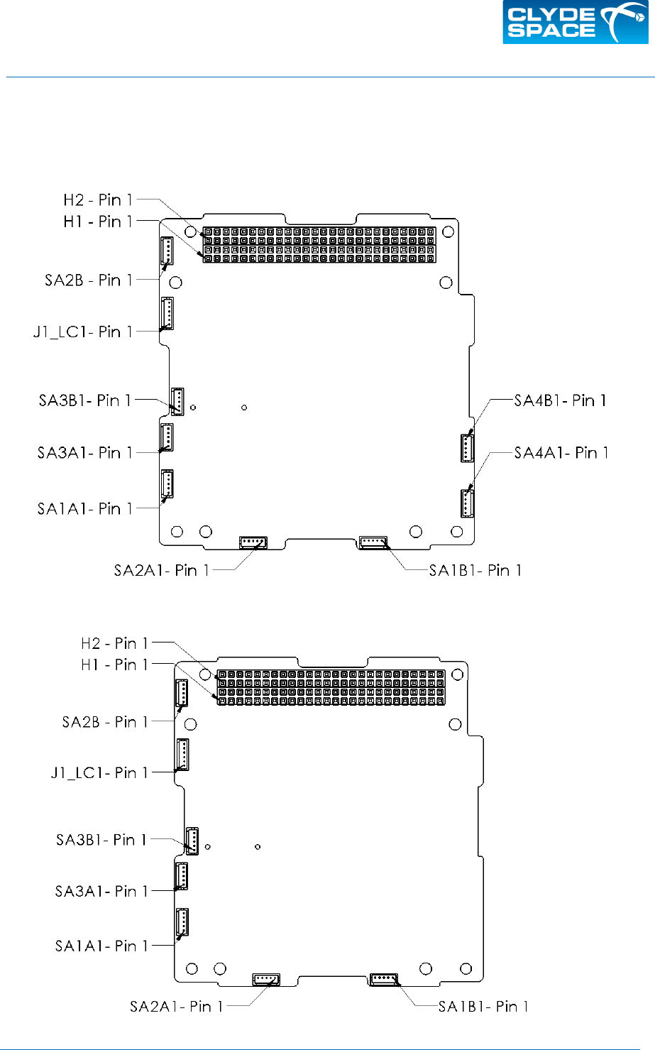
8. INTERFACING
The connector interfaces of the EPS are outlined in Figure 8-1, including the solar array inputs, output
of the power buses and communication to the I2C node. In the following section, it is assumed that
the EPS will be integrated with a Clyde Space Battery.
Figure 8-1 Connector Location Diagram for 25-02451 1UB EPS
Figure 8-2 Connector Location Diagram for 25-02452 and 01-02453 Motherboard

USM-1335
User Manual: 3rd Generation EPS Range - No Inhibits
Issue: D
Date: 11/10/2017
Page: 21 of 60
Skypark 5, 45 Finnieston
Street, Glasgow G3 8JU, UK
SOLUTIONS FOR A NEW AGE IN SPACE
www.clyde.space
PROPRIETARY & CONFIDENTIAL INFORMATION
Copyright ©2017 Clyde Space Ltd. All rights reserved.
Figure 8-3 Additional Daughterboard Connections for 01-02453 XUA EPS
The connector positions and functions are described in Table 8-1.
Connector
Function
Location
Applicable
Products
SA1A
Solar Array connector, BCR1 channel A
Motherboard
All
SA1B
Solar Array connector, BCR1 channel B
Motherboard
All
SA2A
Solar Array connector, BCR2 channel A
Motherboard
All
SA2B
Solar Array connector, BCR2 channel B
Motherboard
All
SA3A
Solar Array connector, BCR3 channel A
Motherboard
All
SA3B
Solar Array connector, BCR3 channel B
Motherboard
All
SA4A
Solar Array connector, BCR4 channel A
Motherboard
25-02451
SA4B
Solar Array connector, BCR4 channel B
Motherboard
25-02451
SA4
Solar Array connector, BCR4 both channels
Daughterboard
01-02453
SA5
Solar Array connector, BCR5 both channels
Daughterboard
01-02453
SA6
Solar Array connector, BCR6 both channels
Daughterboard
01-02453
SA7
Solar Array connector, BCR7 both channels
Daughterboard
01-02453
SA8
Solar Array connector, BCR8 both channels
Daughterboard
01-02453
SA9
Solar Array connector, BCR9 both channels
Daughterboard
01-02453
J1_IC1
Programming header – Clyde Space use only
Motherboard
All
H1
CubeSat Kit bus compatible Header 1
Motherboard
All
H2
CubeSat Kit bus compatible Header 2
Motherboard
All
Table 8-1 Connector functions
USM-1335
User Manual: 3rd Generation EPS Range - No Inhibits
Issue: D
Date: 11/10/2017
Page: 22 of 60
Skypark 5, 45 Finnieston
Street, Glasgow G3 8JU, UK
SOLUTIONS FOR A NEW AGE IN SPACE
www.clyde.space
PROPRIETARY & CONFIDENTIAL INFORMATION
Copyright ©2017 Clyde Space Ltd. All rights reserved.
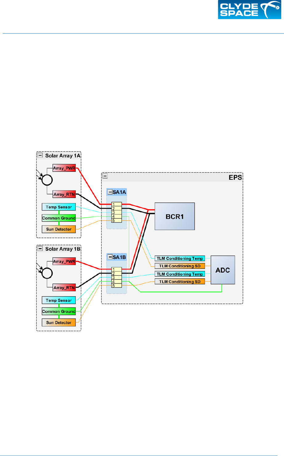
8.1 Solar Array Connection
The EPS motherboard has eight (25-02451) or six (25-02452, 01-02453) connectors for the attachment
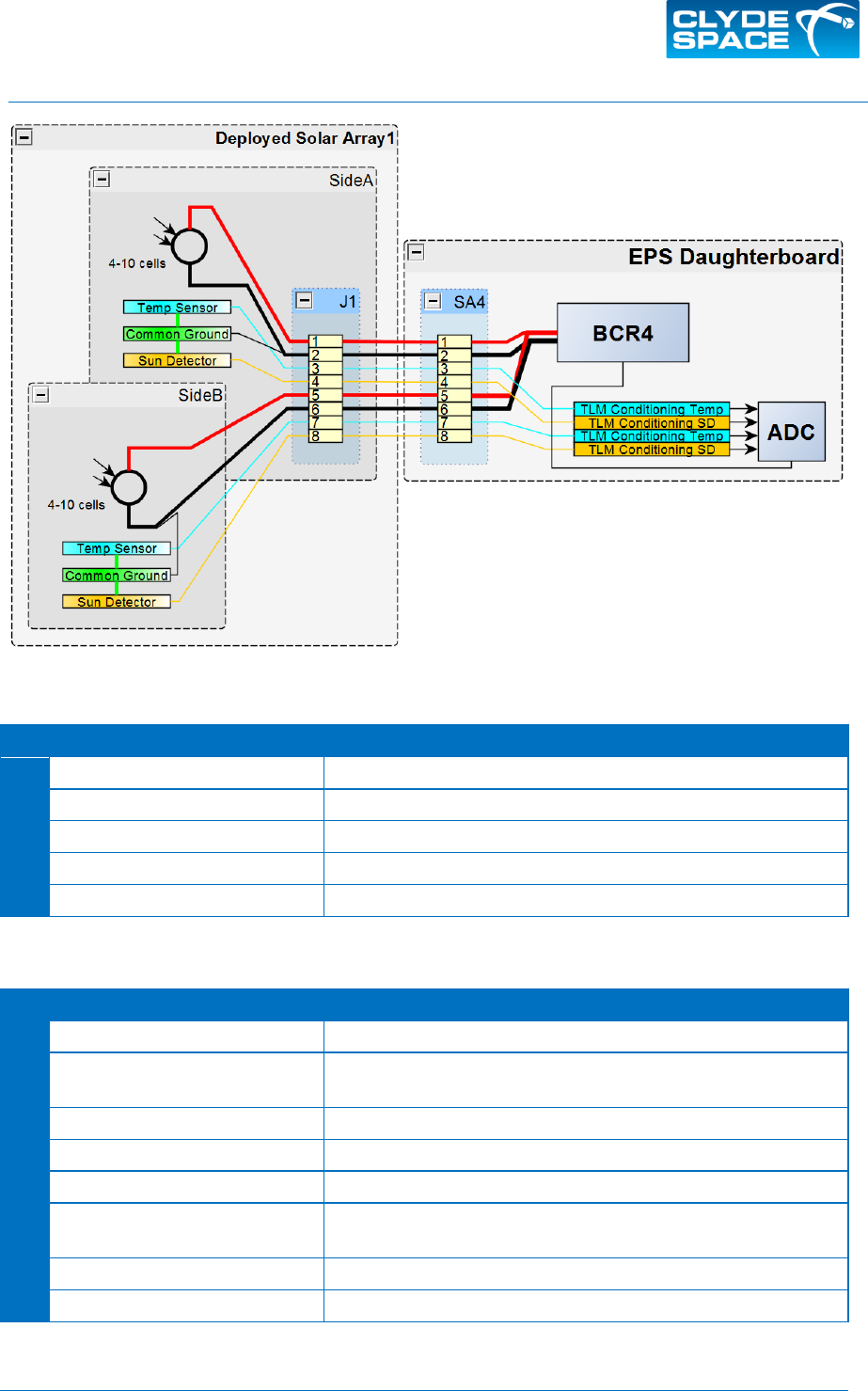
of solar arrays. The EPS daughterboard (01-02453 only) has a further six such connectors. This
interface accommodates inputs from the arrays with temperature and sun detector telemetry for
each.
HIROSE DP13-5P-1.25DSA(50) connector sockets are used for motherboard solar array inputs. Inputs
labelled as A and B are always connected to the BCR in parallel with one another. An example
configuration is shown in Figure 8-4. HIROSE DP13-8P-1.25DSA(50) connector sockets are used for
daughterboard solar array inputs. An example configuration is shown in Figure 8-5.
All arrays which are connected in parallel should have the same number of cells.
Figure 8-4 Example Solar Array Configuration SA1-3 and (25-02451 only) SA4
USM-1335
User Manual: 3rd Generation EPS Range - No Inhibits
Issue: D
Date: 11/10/2017
Page: 23 of 60
Skypark 5, 45 Finnieston
Street, Glasgow G3 8JU, UK
SOLUTIONS FOR A NEW AGE IN SPACE
www.clyde.space
PROPRIETARY & CONFIDENTIAL INFORMATION
Copyright ©2017 Clyde Space Ltd. All rights reserved.
Figure 8-5 Example Solar Array Configuration SA4-9 (01-02453 only)
Pin
Use
Notes
1
Array Power
Connection to positive of solar cell string
2
Array Return
Negative of solar cell string – connected to ground within the EPS
3
Temperature Telemetry
Telemetry
4
Ground Line
Ground connection for Sensors
5
Sun Detector Telemetry
Telemetry
Table 8-2 Pinout for motherboard solar array connectors
Pin
Use
Notes
1
Array A Power
Connection to positive of solar cell string
2
Ground
Negative of solar cell string and ground connection for sensors –
connected to ground within the EPS
3
Array A Temperature Telemetry
Telemetry
4
Array A Sun Detector Telemetry
Telemetry
5
Array B Power
Connection to positive of solar cell string
6
Ground
Negative of solar cell string and ground connection for sensors –
connected to ground within the EPS
7
Array B Temperature Telemetry
Telemetry
8
Array B Sun Detector Telemetry
Telemetry
Table 8-3 Pinout for daughterboard solar array connectors

USM-1335
User Manual: 3rd Generation EPS Range - No Inhibits
Issue: D
Date: 11/10/2017
Page: 24 of 60
Skypark 5, 45 Finnieston
Street, Glasgow G3 8JU, UK
SOLUTIONS FOR A NEW AGE IN SPACE
www.clyde.space
PROPRIETARY & CONFIDENTIAL INFORMATION
Copyright ©2017 Clyde Space Ltd. All rights reserved.
8.2 Solar Array Harness
Clyde Space supply harnesses (sold separately) to connect the solar panels to the EPS Motherboard,
comprising one Hirose DF13-5S-1.25C connected at the panel and one connector at the other
connected at the EPS. Similarly, harnesses to connect the solar panels to the EPS Daughterboard (01-
02453 only) comprise one Hirose DF13-8S-1.25C connected at the panel and one connector at the
other connected at the EPS.
8.3 Temperature Sensing Interface
A temperature sensor is included on each Clyde Space solar panel and can be connected to the EPS to
provide panel temperature telemetry. The output from the sensor is then passed to the telemetry
system via on board signal conditioning. The formula for calculating solar array temperature from ADC
counts can be found in Section 11.4.
8.4 Sun Detector Interface
A photodiode-based coarse sun detector is included on each Clyde Space solar panel and can be
connected to each BCR channel to provide panel illumination telemetry. On-board signal
conditioning converts this signal to an ADC count which can be translated into an illumination level
using the equations in section 11.4.
8.5 Non-Clyde Space Solar Arrays
When connecting non-Clyde Space solar arrays care must be taken with the polarity. Cells used
should be of triple junction type. If other manufacturer’s panels are to be interfaced, please contact
Clyde Space.
8.6 CubeSat Kit Compatible Headers
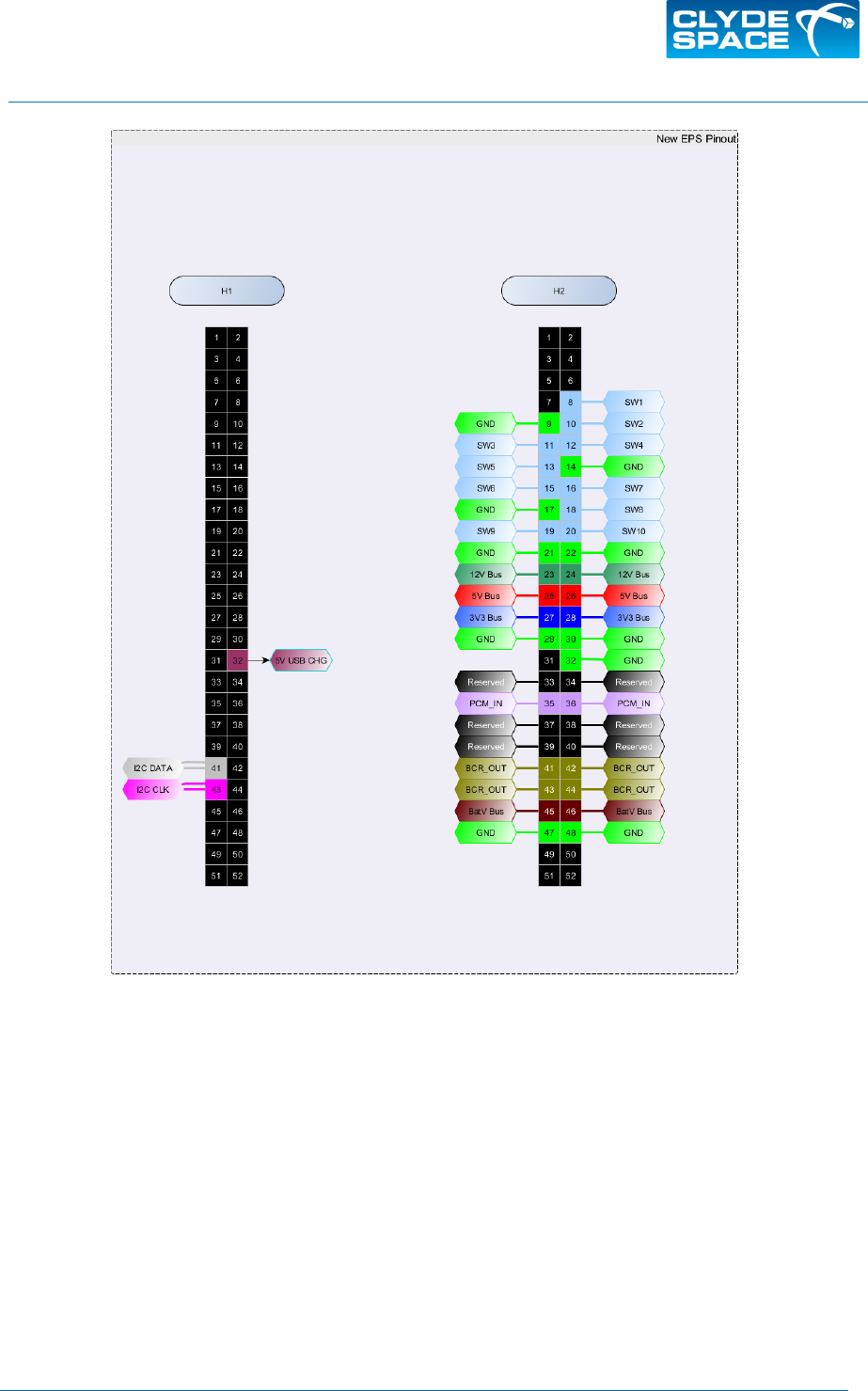
Connections from the EPS to the bus of the satellite are made via the CubeSat Kit compatible headers
H1 and H2, as shown in Figure 8-6.
USM-1335
User Manual: 3rd Generation EPS Range - No Inhibits
Issue: D
Date: 11/10/2017
Page: 25 of 60
Skypark 5, 45 Finnieston
Street, Glasgow G3 8JU, UK
SOLUTIONS FOR A NEW AGE IN SPACE
www.clyde.space
PROPRIETARY & CONFIDENTIAL INFORMATION
Copyright ©2017 Clyde Space Ltd. All rights reserved.
Figure 8-6 CubeSat Kit Header Schematic

USM-1335
User Manual: 3rd Generation EPS Range - No Inhibits
Issue: D
Date: 11/10/2017
Page: 26 of 60
Skypark 5, 45 Finnieston
Street, Glasgow G3 8JU, UK
SOLUTIONS FOR A NEW AGE IN SPACE
www.clyde.space
PROPRIETARY & CONFIDENTIAL INFORMATION
Copyright ©2017 Clyde Space Ltd. All rights reserved.
8.7 Cubesat Kit Header Pin Out
HEADER 1
HEADER 2
Pin
Name
Use
Notes
Pin
Name
Use
Notes
1
NC
-
-
1
NC
-
-
2
NC
-
-
2
NC
-
-
3
NC
-
-
3
NC
-
-
4
NC
-
-
4
NC
-
-
5
NC
-
-
5
NC
-
-
6
NC
-
-
6
NC
-
-
7
NC
-
-
7
NC
-
-
8
NC
-
-
8
SW1
PDM 1 Output
12V PDM
9
NC
-
-
9
GND
Ground
System Ground
10
NC
-
-
10
SW2
PDM 2 Output
12V PDM
11
NC
-
-
11
SW3
PDM 3 Output
BAT PDM
12
NC
-
-
12
SW4
PDM 4 Output
BAT PDM
13
NC
-
-
13
SW5
PDM 5 Output
5V PDM
14
NC
-
-
14
GND
Ground
System Ground
15
NC
-
-
15
SW6
PDM 6 Output
5V PDM
16
NC
-
-
16
SW7
PDM 7 Output
5V PDM
17
NC
-
-
17
GND
Ground
System Ground
18
NC
-
-
18
SW8
PDM 8 Output
3V3 PDM
19
NC
-
-
19
SW9
PDM 9 Output
3V3 PDM
20
NC
-
-
20
SW10
PDM 10 Output
3V3 PDM
21
NC
-
-
21
GND
Ground
System Ground
22
NC
-
-
22
GND
Ground
System Ground
23
NC
-
-
23
12VBUS
12V Bus
Power Bus
24
NC
-
-
24
12VBUS
12V Bus
Power Bus
25
NC
-
-
25
5VBUS
5V Bus
Power Bus
26
NC
-
-
26
5VBUS
5V Bus
Power Bus
27
NC
-
-
27
3V3BUS
3.3V Bus
Power Bus
28
NC
-
-
28
3V3BUS
3.3V Bus
Power Bus
29
NC
-
-
29
GND
Ground
System Ground
30
NC
-
-
30
GND
Ground
System Ground
31
NC
-
-
31
NC
-
-
32
5VUSB_CHG
5V USB Charge
Battery Top up
Charge
32
GND
Ground
System Ground
33
NC
-
-
33
Reserved
Do not use
Reserved
34
NC
-
-
34
Reserved
Do not use
Reserved
35
NC
-
-
35
PCM_IN
PCM Input
Reserved
36
NC
-
-
36
PCM_IN
PCM Input
Reserved
37
NC
-
-
37
Reserved
Do not use
Reserved
38
NC
-
-
38
Reserved
Do not use
Reserved
39
NC
-
-
39
Reserved
Do not use
Reserved
40
NC
-
-
40
Reserved
Do not use
Reserved
41
I2C_DATA
I2C Data
-
41
BCR_OUT
BCR Output
Reserved
42
NC
-
-
42
BCR_OUT
BCR Output
Reserved
43
I2C_CLK
I2C Clock
-
43
BCR_OUT
BCR Output
Reserved
44
NC
-
-
44
BCR_OUT
BCR Output
Reserved
45
NC
-
-
45
BatVBUS
Unregulated Battery
Bus
Power Bus
46
NC
-
-
46
BatVBUS
Unregulated Battery
Bus
Power Bus
47
NC
-
-
47
GND
Ground
System Ground
48
NC
-
-
48
GND
Ground
System Ground
49
NC
-
-
49
NC
-
-
50
NC
-
-
50
NC
-
-
51
NC
-
-
51
NC
-
-
52
NC
-
-
52
NC
-
-
Table 8-4 Pin Descriptions for Header H1 and H2

USM-1335
User Manual: 3rd Generation EPS Range - No Inhibits
Issue: D
Date: 11/10/2017
Page: 27 of 60
Skypark 5, 45 Finnieston
Street, Glasgow G3 8JU, UK
SOLUTIONS FOR A NEW AGE IN SPACE
www.clyde.space
PROPRIETARY & CONFIDENTIAL INFORMATION
Copyright ©2017 Clyde Space Ltd. All rights reserved.
8.8 Flight Switches
The Flight Switches provide a method of isolating the BCRs and battery from the satellite power buses
during storage, transportation and launch.
This EPS does not have flight switches populated as it is designed to be used with a compatible battery
which contains the inhibits. Refer to User manual: 3rd Generation CubeSat Battery Family [RD-1] for
information on flight switches, Sections 10.1 Protection Overview and 10.7 Inhibit Operation.
8.9 Battery connection
Connection of the battery systems on the EPS is via the CubeSat kit bus or via an integrated battery
(25-02451 only). Ensure that the pins are aligned, and located in the correct position, as any offset
can cause the battery to be shorted to ground, leading to catastrophic failure of the battery and
damage to the EPS. It is also important that the EPS is only used with compatible battery products; see
Section 13.1 for information.
Failure to observe these precautions will result in the voiding of any warranty.
When a battery board is connected to the CubeSat Kit header and the battery inhibits are not
activated, there are live unprotected battery pins accessible (H2.35-36 and H2.41-44). These pins
should not be routed to any connections other than the Clyde Space EPS, otherwise all EPS-based
protections will be bypassed and significant battery damage can be sustained.
USM-1335
User Manual: 3rd Generation EPS Range - No Inhibits
Issue: D
Date: 11/10/2017
Page: 28 of 60
Skypark 5, 45 Finnieston
Street, Glasgow G3 8JU, UK
SOLUTIONS FOR A NEW AGE IN SPACE
www.clyde.space
PROPRIETARY & CONFIDENTIAL INFORMATION
Copyright ©2017 Clyde Space Ltd. All rights reserved.
9. TECHNICAL DESCRIPTION
This section gives a complete overview of the operational modes of the EPS. It is assumed that a
complete Clyde Space power system (EPS, Batteries and Solar panels) is in operation for the following
sections.
9.1 Charge Method
The BCR charging system has two modes of operation: Maximum Power Point Tracking (MPPT) mode
and End of Charge (EoC) mode. These modes are governed by the state of charge of the battery.
MPPT Mode
If the battery voltage is below the EoC voltage the system is in MPPT mode. This is based on constant
current charge method, operating at the maximum power point of the solar panel for maximum power
transfer.
EoC Mode
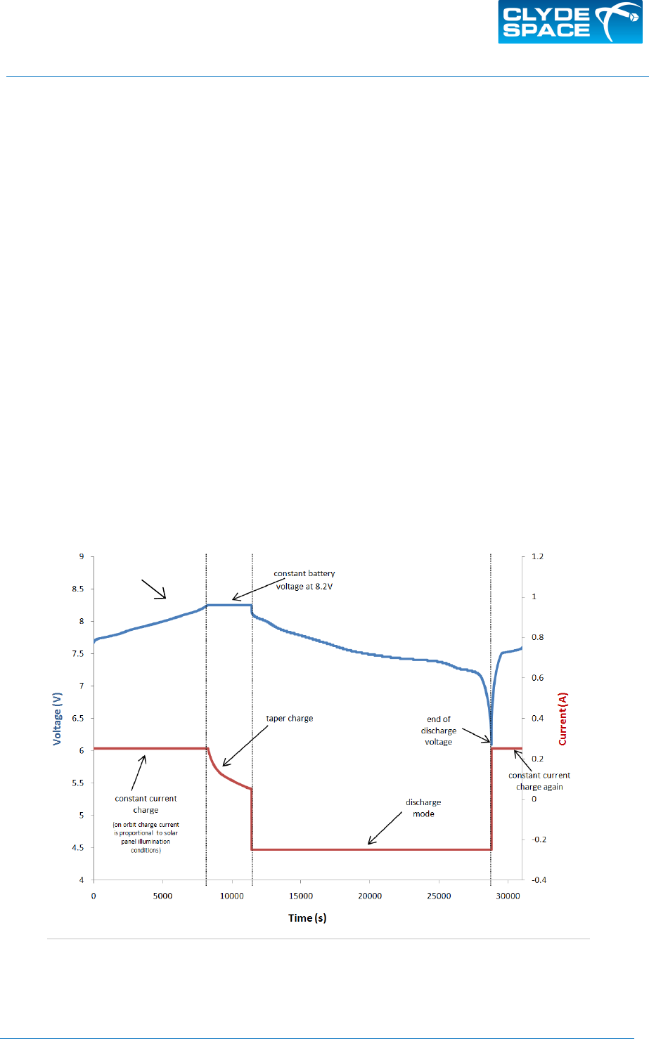
Once the EoC voltage has been reached, the BCR changes to EoC mode, which is a constant voltage
charging regime. The EoC voltage is held constant and a tapering current from the panels is supplied
to top up the battery until at full capacity. In EoC mode the MPPT circuitry moves the solar array
operation point away from the maximum power point of the array, drawing only the required power
from the panels. The excess power is left on the arrays as heat, which is transferred to the structure
via the array’s thermal dissipation methods incorporated in Clyde Space panels.
The operation of these two modes can be seen in Figure 9-1.
Figure 9-1 Tapered charging method
end of charge voltage

USM-1335
User Manual: 3rd Generation EPS Range - No Inhibits
Issue: D
Date: 11/10/2017
Page: 29 of 60
Skypark 5, 45 Finnieston
Street, Glasgow G3 8JU, UK
SOLUTIONS FOR A NEW AGE IN SPACE
www.clyde.space
PROPRIETARY & CONFIDENTIAL INFORMATION
Copyright ©2017 Clyde Space Ltd. All rights reserved.
The application of constant current/constant voltage charge method on a spacecraft is described in
more detail in RD-6. In this document, there is on-orbit data showing the operation and how the
current fluctuates with changing illumination conditions and orientation of the spacecraft with respect
to the Sun.
9.2 BCR Power Stage Overview
The EPS has several separate, independent BCRs, each designed to interface to two parallel solar
arrays on opposing faces of the satellite.
Each design offers a highly reliable system that can deliver 90% (Buck BCRs) or 80% (SEPIC BCRs) of
the power delivered from the solar array network at full load.
BCR Allocation
The EPS has Buck and SEPIC BCRs as listed below.
BCR Type
25-02451
25-02452
01-02453
Buck BCR
N/A
1, 2
1, 2, 4, 5, 6, 7, 8, 9
SEPIC BCR
1,2,3,4
3
3
Buck BCR Power Stage
The Buck BCRs allow the EPS to interface to strings of four to eight cells in series. This will deliver up
to 90% output at full load. The design will operate with input voltages between 7.4V and 30V. If the
maximum power point is below 9.4V, the MPPT will drift away from the maximum power point of the
array at end of charge, sacrificing power system efficiency.
SEPIC BCR Power Stage
The SEPIC BCRs allow the EPS to interface to solar arrays of two triple junction cells in series. This will
deliver up to 80% output at full load. The BCR will operate with an input of between 3.0V and 9.5V.
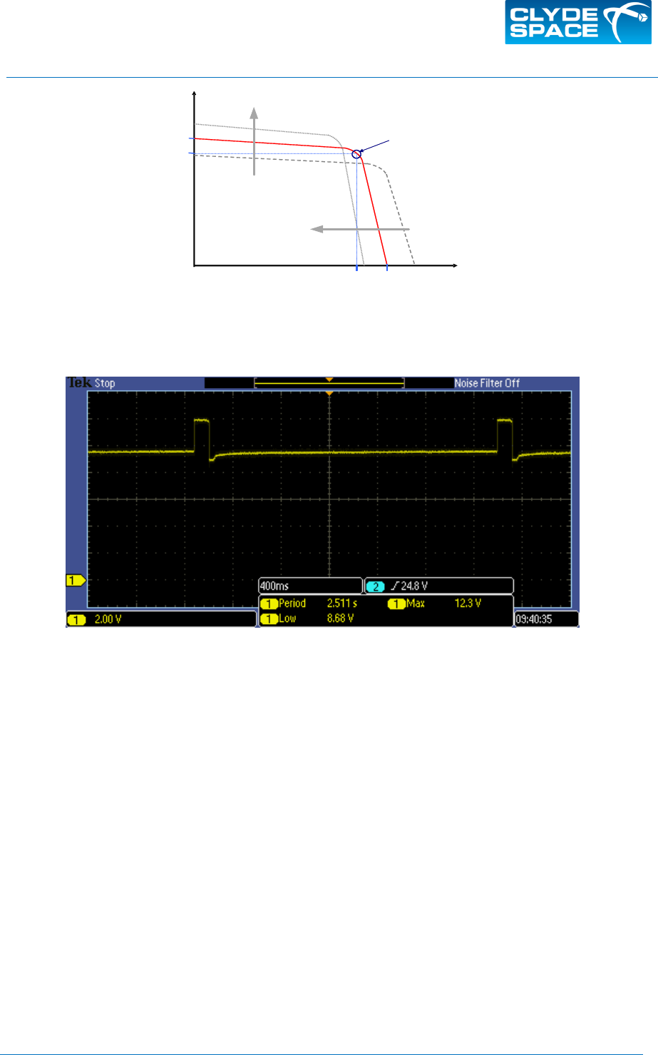
9.3 MPPT
Each of the BCRs can have two solar arrays connected at any given time; only one array can be
illuminated by sunlight, although the other may receive illumination by albedo reflection from earth.
The dominant array is in sunlight and this will operate the MPPT for that BCR string. The MPPT
monitors the power supplied from the solar array. This measurement is used to calculate the
maximum power point of the array. The system tracks this point by periodically adjusting the BCRs to
maintain the maximum power derived from the arrays. This technique ensures that the solar arrays
can deliver much greater usable power, increasing the overall system performance.
USM-1335
User Manual: 3rd Generation EPS Range - No Inhibits
Issue: D
Date: 11/10/2017
Page: 30 of 60
Skypark 5, 45 Finnieston
Street, Glasgow G3 8JU, UK
SOLUTIONS FOR A NEW AGE IN SPACE
www.clyde.space
PROPRIETARY & CONFIDENTIAL INFORMATION
Copyright ©2017 Clyde Space Ltd. All rights reserved.
Array Voltage
Array Current
Increasing
Temperature
Maximum Power Point
Increasing
Temperature
VMPP Vo/c
IMPP
Is/c
Figure 9-2 Solar Array Maximum Power Point
The monitoring of the MPP is done approximately every 2.5 seconds. During this tracking, the input
of the array will step to o/c voltage, as shown in Figure 9-3.
Figure 9-3 Input waveform with Maximum Power Point Tracking
9.4 5V USB Charge
The EPS offers a method of trickle charging the battery by connecting a power supply directly to the
5V USB Charge pin on the header. The 5V USB Charge will operate with an input of between 3.0V and
6V. This charge connection utilises BCR3 to charge the battery and provides a parallel input to the 3W
BCR. It should be noted that the 5V USB is designed for trickle charging the battery and as such will
provide a maximum of 2.1W when operated at 6V input.
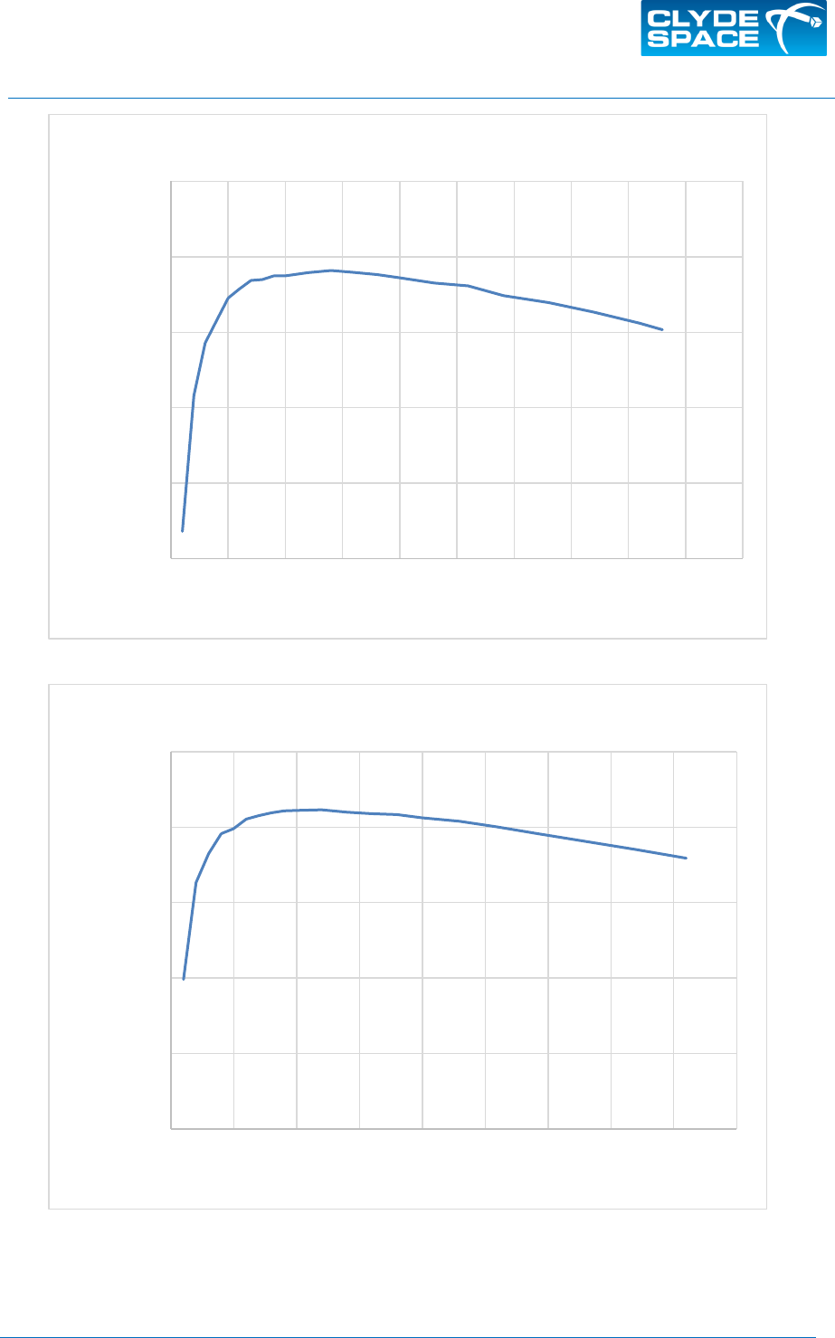
9.5 5V and 3.3V PCMs with Latching Current Limiter
The 5V and 3.3V regulators both use buck switching topology regulators as their main converter stage.
The regulator maintains the output voltage within +/- 1% of nominal. Efficiency curves are given in
Figure 9-4 and Figure 9-5. The current limit of each regulator is nominally 4.5A. Each regulator
operates at a frequency of 480 kHz. The Latching Current Limiter is described in Section 9.8. If an over-
current event triggers the Latching Current Limiter a retry circuit will attempt to re-enable the bus as
described in Section 10.1.
USM-1335
User Manual: 3rd Generation EPS Range - No Inhibits
Issue: D
Date: 11/10/2017
Page: 31 of 60
Skypark 5, 45 Finnieston
Street, Glasgow G3 8JU, UK
SOLUTIONS FOR A NEW AGE IN SPACE
www.clyde.space
PROPRIETARY & CONFIDENTIAL INFORMATION
Copyright ©2017 Clyde Space Ltd. All rights reserved.
Figure 9-4 Efficiency Curve for 3V3 PCM, Vbat=7.6v, Tbrd=23°C
Figure 9-5 Efficiency Curve for 5V PCM, Vbat=7.6v, Tbrd=23°C
75.00%
80.00%
85.00%
90.00%
95.00%
100.00%
0 0.5 1 1.5 2 2.5 3 3.5 4 4.5 5
Efficiency
Load Current (A)
3V3 PCM Efficiency Over Load
75.00%
80.00%
85.00%
90.00%
95.00%
100.00%
0 0.5 1 1.5 2 2.5 3 3.5 4 4.5
Efficiency
Load Current (A)
5V PCM Efficiency Over Load
USM-1335
User Manual: 3rd Generation EPS Range - No Inhibits
Issue: D
Date: 11/10/2017
Page: 32 of 60
Skypark 5, 45 Finnieston
Street, Glasgow G3 8JU, UK
SOLUTIONS FOR A NEW AGE IN SPACE
www.clyde.space
PROPRIETARY & CONFIDENTIAL INFORMATION
Copyright ©2017 Clyde Space Ltd. All rights reserved.
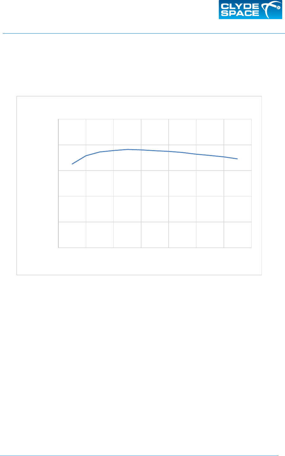
9.6 12V PCM with Latching Current Limiter
The 12V regulator uses a boost switching topology regulator as the main converter stage. The
regulator maintains the output voltage within +/- 1% of nominal. Efficiency is plotted in Figure 9-6.
The current limit on the regulator is nominally 1.5A. The regulator operates at a frequency of 800 kHz.
The Latching Current Limiter is described in Section 9.8. If an over-current event triggers the Latching
Current Limiter, a retry circuit will attempt to re-enable the bus as described in Section 10.1.
Figure 9-6 Efficiency Curve for 12V PCM, Vbat=7.6v, Tbrd=23°C
9.7 BatV PCM with Latching Current Limiter
The unregulated battery voltage regulator provides safe access to the battery bus of the satellite. The
voltage supplied will vary directly with the battery voltage (between 6.144V and 8.26V). The current
limit is nominally 4.7A. The Latching Current Limiter is described in Section 9.8. If an over-current event
triggers the Latching Current Limiter, a retry circuit will attempt to re-enable the bus as described in
Section 10.1.
9.8 PDMs with Latching Current Limiter
Ten independently commandable power distribution modules (PDM) are included on the EPS. Each
PDM has inbuilt overcurrent protection in the form of a latching current limiter (LCL). By utilising an
LCL each PDM is capable of driving loads with large inrush currents without compromising safety
throughout the duration of the mission (this is of particular interest for applications such as
transceivers). Once the LCL has activated, turning off the supply of power, the PDM will remain off
until commanded to switch on again. The PDMs cover the range of regulated and unregulated
voltages provided by the EPS.
75.00%
80.00%
85.00%
90.00%
95.00%
100.00%
0 0.2 0.4 0.6 0.8 1 1.2 1.4
Efficiency
Load Current (A)
12V PCM Efficiency Over Load
USM-1335
User Manual: 3rd Generation EPS Range - No Inhibits
Issue: D
Date: 11/10/2017
Page: 33 of 60
Skypark 5, 45 Finnieston
Street, Glasgow G3 8JU, UK
SOLUTIONS FOR A NEW AGE IN SPACE
www.clyde.space
PROPRIETARY & CONFIDENTIAL INFORMATION
Copyright ©2017 Clyde Space Ltd. All rights reserved.
LCL Operation Description
Figure 9-7 Latching Current Limiter Example Operation
In the example system shown above the events are as follows:
1. The payload demands a 3A initial current, however the PDM limits the current to 2A. The time
this demand is present is less than the latch time of the PDM (tlatch), so the PDM does not
switch off.
2. The payload demand drops to 0.5A. This is below the current limit of the PDM (ilatch).
3. A fault condition occurs resulting in a demand of 4A. The PDM only allows 2A to pass,
preventing high current damage to the PDM or the payload.
4. The fault remains for longer than tlatch so the PDM turns off preventing any current flow.
0
0.5
1
1.5
2
2.5
3
3.5
4
4.5
010 20 30 40 50
Current (A)
Time (ms)
Current Demand (A)
Current Supplied (A)
(1)
(2)
(3)
(4)
ilatch
tlatch

USM-1335
User Manual: 3rd Generation EPS Range - No Inhibits
Issue: D
Date: 11/10/2017
Page: 34 of 60
Skypark 5, 45 Finnieston
Street, Glasgow G3 8JU, UK
SOLUTIONS FOR A NEW AGE IN SPACE
www.clyde.space
PROPRIETARY & CONFIDENTIAL INFORMATION
Copyright ©2017 Clyde Space Ltd. All rights reserved.
LCL Characteristics
The following characteristics are specified at 25°C:
• ilatch: The latching current limit is set to allow the maximum safe current the EPS can
deliver. This value has been selected based on the fact that, if the current limit is set high to
allow a high inrush it will result in a high current limit during normal operation too.
• tlatch: The latching has been set to allow for the maximum safe length of time before shutting
down the bus, allowing capacitive loads to be charged safely.
• clatch: This is the maximum capacitance that can be charged via the LCL before the PDM
automatically disables.
• ton: Time delay from PDM being commanded to turn on via I2C node to actual PDM turn on.
PDM#
Pin
Voltage (V)
ilatch (A)
tlatch (h)
clatch (µF)
ton (ms)
1
H2.08
12
1 - 1.1
2-3
240
0.140
2
H2.10
12
1 - 1.1
2-3
240
0.140
3
H2.11
BAT
4.2 - 4.3
8-9
800
0.140
4
H2.13
BAT
4.2 – 4.3
8-9
800
0.140
5
H2.13
5
1 - 1.1
8-9
1600
0.140
6
H2.15
5
1 - 1.1
8-9
1600
0.140
7
H2.16
5
1 - 1.1
8-9
1600
0.140
8
H2.18
3.3
1 - 1.1
13-14
4000
0.140
9
H2.19
3.3
1 - 1.1
13-14
4000
0.140
10
H2.20
3.3
1 - 1.1
13-14
4000
0.140
Table 9-1 PDM Switch Configuration
USM-1335
User Manual: 3rd Generation EPS Range - No Inhibits
Issue: D
Date: 11/10/2017
Page: 35 of 60
Skypark 5, 45 Finnieston
Street, Glasgow G3 8JU, UK
SOLUTIONS FOR A NEW AGE IN SPACE
www.clyde.space
PROPRIETARY & CONFIDENTIAL INFORMATION
Copyright ©2017 Clyde Space Ltd. All rights reserved.
10. GENERAL PROTECTION
The EPS (and wider power system) has a number of inbuilt protections and safety features designed
to maintain safe operation of the EPS, battery and all subsystems supplied by the EPS buses.
Figure 10-1 Protection Systems (When used with Manned Flight battery)
10.1 Over-Current Bus Protection (LCL)
The EPS features bus protection systems to safeguard the battery, EPS and attached satellite sub-
systems. This is achieved using current monitors and a shutdown network within the PCMs.
Over-current shutdowns are present on all buses for sub system protection. These are solid state
switches that monitor the current and shut down at predetermined load levels. The bus protection
will then monitor the fault periodically and reset when the fault clears. The fault detection and clear
is illustrated in the waveform in Figure 10-2.
NORMAL
OPERATION
OVER CURRENT
EVENT
EVENT
CLEARS
SYSTEM
SHUTDOWN
NORMAL
OPERATION
SYSTEM
RESUME
TEST PERIOD
Shutdown period
TEST
PERIOD
CURRENT
NORMAL
LEVEL
BUS VOLTAGE
Shutdown periodShutdown period
Figure 10-2 Current protection system diagram
The length of time of the test period will depend on the demand caused by the fault condition. Higher
current demand results in a shorter test period. All PDMs and buses are protected against a short
circuit fault.

USM-1335
User Manual: 3rd Generation EPS Range - No Inhibits
Issue: D
Date: 11/10/2017
Page: 36 of 60
Skypark 5, 45 Finnieston
Street, Glasgow G3 8JU, UK
SOLUTIONS FOR A NEW AGE IN SPACE
www.clyde.space
PROPRIETARY & CONFIDENTIAL INFORMATION
Copyright ©2017 Clyde Space Ltd. All rights reserved.
10.2 Battery Under-Voltage Protection
In order to prevent the over-discharge of the battery, the EPS has in-built under-voltage shutdown.
This is controlled by a comparator circuit with hysteresis. In the event of the battery discharging to
~6.144V (slightly above the level that results in significant battery degradation) the EPS will shut down
the supply buses. This will also result in the I2C node shutting down. When a power source is applied
to the EPS (e.g. an illuminated solar panel) the battery will begin charging immediately. The buses,
however, will not reactivate until the battery voltage has risen to ~7V. This allows the battery to
charge to a level capable of sustaining the power lines once a load is applied.
It is recommended that the battery state of charge is monitored and loading adjusted appropriately
(turning off of non-critical systems) when the battery capacity is approaching the lower limit. This will
prevent the hard shutdown provided by the EPS.
Once the under-voltage protection is activated there is a monitoring circuit used to monitor the
voltage of the battery. This will draw approximately 2mA for the duration of shutdown. As the EPS is
designed for low earth orbit, the maximum expected period in under-voltage is estimated to be
approximately 40mins – after this time, the illuminated panels should bring the battery back above
the 7V switch-on voltage. When ground testing this should be taken into consideration, and the
battery should be recharged as soon as possible after reaching under-voltage, otherwise permanent
damage may be sustained.

USM-1335
User Manual: 3rd Generation EPS Range - No Inhibits
Issue: D
Date: 11/10/2017
Page: 37 of 60
Skypark 5, 45 Finnieston
Street, Glasgow G3 8JU, UK
SOLUTIONS FOR A NEW AGE IN SPACE
www.clyde.space
PROPRIETARY & CONFIDENTIAL INFORMATION
Copyright ©2017 Clyde Space Ltd. All rights reserved.
11. TELEMETRY AND TELECOMMAND
The telemetry node allows the satellite on board computer (OBC) to monitor the operation of the EPS,
control switchable buses and reset the power supplies if this is required for payload or platform
recovery operations.
The telemetry node consists of a microcontroller which interfaces to the various telemetry sensing
circuits on the EPS through an analogue multiplexer and ADC. The microcontroller is configured to
connect through a buffer circuit to the I2C bus of the satellite as a slave node. In response to I2C
telemetry requests the microcontroller will sample the desired channel and allowing it to be read back
over the I2C bus. In response to a telecommand, the telemetry node will decode the incoming message
and reset the desired power bus.
11.1 Communications
All communications to the Telemetry and Telecommand (TTC) node are made using an I²C interface
which is configured as a slave and only responds to direct commands from a master I²C node - no
unsolicited telemetry is transmitted. The 7-bit I2C address of the TTC node is factory set at 0x2B and
the I2C node will operate at a 100kHz bus clock.
Command Protocol
Two message structures are available to the master; a write command and a read command. The
write command is used to initiate an event and the read command returns the result. All commands
start with the 7-bit slave address and are followed by the data bytes. When reading responses, all data
bytes should be read out together. Each command has a delay associated with it, this is required to
allow the microcontroller time to process each request. During this delay, the correct response may
not be returned, and commands sent during the period may be ignored.
For a write command the first data byte will determine the command to be initiated. The second byte
contains the parameters associated with that command. For commands which have no specific
requirement for a parameter the second data byte should be set to 0x00.
For a read command, the first data byte represents the most significant byte of the result and the
second data byte represents the least significant byte.
Before sending a command, the master is required to set a start condition on the I2C bus. Between
each byte the receiving device is required to acknowledge receipt of the previous byte in accordance
with the I2C protocol. This will often be accommodated within the driver hardware or software of the
I2C master however the user should ensure that this is the case.
The read and write command definitions are illustrated in Figure 11-1.

USM-1335
User Manual: 3rd Generation EPS Range - No Inhibits
Issue: D
Date: 11/10/2017
Page: 38 of 60
Skypark 5, 45 Finnieston
Street, Glasgow G3 8JU, UK
SOLUTIONS FOR A NEW AGE IN SPACE
www.clyde.space
PROPRIETARY & CONFIDENTIAL INFORMATION
Copyright ©2017 Clyde Space Ltd. All rights reserved.
Write
Command
S
7 bit node address
W
A
Command
A
Data Parameter
A
Read
Command
S
7 bit node address
R
A
Data[1]
A
Data[0]
N
P
S
Start Condition
P
Stop Condition
Transmitted from Master (OBC)
A
Acknowledge
W
Write bit
N
Not Acknowledged
R
Read bit
Transmitted from Slave (TTC node)
Figure 11-1 I2C Write and Read of 2 byte command packet
If an error has been generated from a command, then the return value will be 0xFFFF. If this value is
returned, it is recommended to either inspect the status bytes or to request the code representing
the last error generated on the board as described in Section 11.3.

USM-1335
User Manual: 3rd Generation EPS Range - No Inhibits
Issue: D
Date: 11/10/2017
Page: 39 of 60
Skypark 5, 45 Finnieston
Street, Glasgow G3 8JU, UK
SOLUTIONS FOR A NEW AGE IN SPACE
www.clyde.space
PROPRIETARY & CONFIDENTIAL INFORMATION
Copyright ©2017 Clyde Space Ltd. All rights reserved.
11.2 List of Available Commands
25-02451, 25-02452
01-02453
Name
Command
Data[1]2
Data[0]
Bytes Returned
W/R Delay
Bytes Returned
W/R Delay
Board Status
0x01
NA
0x00
2
1
4
2
Get Last Error
0x03
NA
0x00
2
1
4
2
Get Version
0x04
NA
0x00
2
1
4
2
Get Checksum
0x05
NA
0x00
2
35
4
70
Get Revision
0x06
NA
0x00
2
1
4
2
Get Telemetry
0x10
Table 11-8
2
5
2
15
Get Communications Watchdog Period
0x20
NA
0x00
2
1
2
1
Set Communications Watchdog Period
0x21
NA
Period
0
-
0
-
Reset Communications Watchdog
0x22
NA
0x00
0
-
0
-
Get Number of Brown-out Resets
0x31
NA
0x00
2
1
4
2
Get Number of Auto Software Resets
0x32
NA
0x00
2
1
4
2
Get Number of Manual Resets
0x33
NA
0x00
2
1
4
2
Get Number of Comms Watchdog Resets
0x34
NA
0x00
2
1
2
1
Switch On All PDMs
0x40
NA
0x00
0
-
0
-
Switch Off All PDMs
0x41
NA
0x00
0
-
0
-
Get Actual State of All PDMs
0x42
NA
0x00
4
20
4
20
Get Expected State of All PDMs
0x43
NA
0x00
4
1
4
1
Get Initial State of All PDMs
0x44
NA
0x00
4
20
4
20
Set All PDMs to Initial State
0x45
NA
0x00
4
20
4
20
Switch PDM-N “On"
0x50
NA
N
0
-
0
-
Switch PDM-N “Off”
0x51
NA
N
0
-
0
-
Set PDM-N’s Initial State to “On”
0x52
NA
N
0
200
0
200
Set PDM-N’s Initial State to “Off”
0x53
NA
N
0
200
0
200
Get PDM-N’s Actual Status
0x54
NA
N
2
2
2
2
Set PDM-N’s Timer Limit
0x60
N
Limit
0
200
0
150
Get PDM-N’s Timer Limit
0x61
NA
N
0
5
0
5
Get PDM-N’s Current Timer Value
0x62
NA
N
0
1
0
1
PCM Reset
0x70
NA
Table 11-14
0
1
0
1
Manual Reset
0x80
NA
0x00
0
-
0
-
2
Where a command has Data[1] listed as NA, the command only requires a single data byte to be transmitted.
This will be given by Data[0].

USM-1335
User Manual: 3rd Generation EPS Range - No Inhibits
Issue: D
Date: 11/10/2017
Page: 40 of 60
Skypark 5, 45 Finnieston
Street, Glasgow G3 8JU, UK
SOLUTIONS FOR A NEW AGE IN SPACE
www.clyde.space
PROPRIETARY & CONFIDENTIAL INFORMATION
Copyright ©2017 Clyde Space Ltd. All rights reserved.
11.3 Housekeeping and Status Commands
Board Status (0x01)
Command
Data[0]
Bytes Returned
Delay, ms
25-02451, 25-02452
0x01
0x00
2
1
01-02453
0x01
0x00
4
2
The status bytes are designed to supply operational data about the I2C Node. To retrieve the data that
represent the status, the command 0x01 should be sent followed by 0x00. The meaning of each bit of
the returned status bytes is shown below. Please note that Data[1] is the first byte returned from the
EPS and Data[0] is the last, this is shown in detail by Figure 11-1. The first two bytes returned represent
the status of the motherboard and, in the case of 01-02453, a further two bytes are returned to reflect
the status for the daughterboard.
Data[n]
Bit
Description
0
0
Set HIGH if last command not recognised
1
Set HIGH if a watchdog error occurred, resetting the device
2
Set HIGH if the data sent along with the last command was incorrect
3
Set HIGH if the channel passed with the last command was incorrect
4
Set HIGH if there has been an error reading the EEPROM
5
Set HIGH if a Power On Reset error occurred
6
Set HIGH if a Brown Out Reset occurred
7
Unused
1
0
Unused
…
7
Table 11-2 Status bits for EPS

USM-1335
User Manual: 3rd Generation EPS Range - No Inhibits
Issue: D
Date: 11/10/2017
Page: 41 of 60
Skypark 5, 45 Finnieston
Street, Glasgow G3 8JU, UK
SOLUTIONS FOR A NEW AGE IN SPACE
www.clyde.space
PROPRIETARY & CONFIDENTIAL INFORMATION
Copyright ©2017 Clyde Space Ltd. All rights reserved.
Get Last Error (0x03)
Command
Data[0]
Bytes Returned
Delay, ms
25-02451, 25-02452
0x03
0x00
2
1
01-02453
0x03
0x00
4
2
If an error has been generated after attempting to execute a user’s command the value 0xFFFF is
returned. To retrieve the details of the last error, send the command 0x03 followed by the data byte
0x00. This will return the code of the last error generated. Details of each error code are given by Table
11-3. The first two bytes returned represent the Motherboard’s error code and, in the case of 01-
02453, the second two bytes represent the Daughterboard’s.
Code
Description
0x10
CRC code does not match data
0x01
Unknown command received
0x02
Supplied data incorrect when processing command
0x03
Selected channel does not exist
0x04
Selected channel is currently inactive
0x13
A reset had to occur
0x14
There was an error with the ADC acquisition
0x20
Reading from EEPROM generated an error
0x30
Generic warning about an error on the internal SPI bus (only if daughterboard is connected)
Table 11-3 List of Clyde Space Error Codes
Get Version (0x04)
Command
Data[0]
Bytes Returned
Delay, ms
25-02451, 25-02452
0x04
0x00
2
1
01-02453
0x04
0x00
4
2
The version number of the firmware will be returned on this command.
Data[1]
Data[0]
Bit
15
14
13
12
11
10
9
8
7
6
5
4
3
2
1
0
Value
Board Firmware Number
Table 11-4 Returned Firmware Version Number
USM-1335
User Manual: 3rd Generation EPS Range - No Inhibits
Issue: D
Date: 11/10/2017
Page: 42 of 60
Skypark 5, 45 Finnieston
Street, Glasgow G3 8JU, UK
SOLUTIONS FOR A NEW AGE IN SPACE
www.clyde.space
PROPRIETARY & CONFIDENTIAL INFORMATION
Copyright ©2017 Clyde Space Ltd. All rights reserved.
Get Checksum (0x05)
Command
Data[0]
Bytes Returned
Delay, ms
25-02451, 25-02452
0x05
0x00
2
35
01-02453
0x05
0x00
4
70
This command instructs the node to self-inspect its ROM contents in order to generate a checksum.
The value retrieved can be used to determine whether the contents of the ROM have changed during
the operation of the device. The first two bytes returned represent the motherboard checksum and,
in the case of 01-02453, a further two bytes are returned to for the daughterboard checksum.
Data[1]
Data[0]
Bit
7
6
5
4
3
2
1
0
7
6
5
4
3
2
1
0
Value
Board Checksum
Get Firmware Revision (0x06)
Command
Data[0]
Bytes Returned
Delay, ms
25-02451, 25-02452
0x06
0x00
2
1
01-02453
0x06
0x00
4
2
The revision version number of the firmware will be returned on this command.
Data[1]
Data[0]
Bit
15
14
13
12
11
10
9
8
7
6
5
4
3
2
1
0
Value
Board Firmware Revision Number
Table 11-5 Returned Firmware Revision Number
Manual Reset (0x80)
Command
Data[0]
Bytes Returned
Delay, ms
0x80
0x00
0
-
If required, the user can reset the TTC node using this command. When issued, the board will reset
within 1 second. This command will result in the board being brought up in its defined initial condition.
Resetting the board in this fashion will increment the Manual Reset Counter. More details about this
counter are found in section 11.5.
USM-1335
User Manual: 3rd Generation EPS Range - No Inhibits
Issue: D
Date: 11/10/2017
Page: 43 of 60
Skypark 5, 45 Finnieston
Street, Glasgow G3 8JU, UK
SOLUTIONS FOR A NEW AGE IN SPACE
www.clyde.space
PROPRIETARY & CONFIDENTIAL INFORMATION
Copyright ©2017 Clyde Space Ltd. All rights reserved.
11.4 Telemetry
The node telemetries allow the satellite’s on board computer (OBC) to monitor the operation of the
EPS.
Each available telemetry is represented by a two-byte code. These codes consist of:
• What type of telemetry is requested, i.e. PDM or PCM, analogue inputs, or some other form
of sensor.
• The channel being requested.
• The reading to take: voltage, current, temperature etc.
A break-down of the telemetry structure and commands is given below. If a telemetry is requested
which is not available, a Channel Error will be generated.
Get Telemetry (0x10)
Command
Data[1]
Data[0]
Bytes Returned
Delay, ms
Table 11-11 Telemetries
0x10
0xE?
0x??
2
15
All other telemetries
0x10
0xE?
0x??
2
5
As described above, requesting telemetry involves sending the command 0x10 plus a 2 byte telemetry
code to the node. Once transmitted, the node will configure itself to read the requested value. The
general format for telemetry codes is shown in Table 11-6, and an exhaustive list of commands in
Table 11-8 through Table 11-11 – refer to the table annotations for applicability to particular products.
The data returned will be in the format shown in Table 11-7.
Data[1]
Data[0]
Nibble 3
Nibble 2
Nibble 1
Nibble 0
Family
Code
TLM Type
Code
Channel
Code
Attribute
Code
EPS
E
BCR
1
Channel Number N
N
Voltage
0
Current A
4
Current B
5
Temperature A
8
Temperature B
9
EPS
E
Main Power
2
Core Bus
Miscellaneous
0 to 7
8 to F
Voltage
0
Current
A
EPS
E
Temperature
3
Motherboard
0 to 7
Temperature
8
EPS
E
PDM
4 to 7
Switch Number N
N mod 16
Voltage
0
Current
4
Table 11-6 Breakdown of Clyde Space telemetry code structure.

USM-1335
User Manual: 3rd Generation EPS Range - No Inhibits
Issue: D
Date: 11/10/2017
Page: 44 of 60
Skypark 5, 45 Finnieston
Street, Glasgow G3 8JU, UK
SOLUTIONS FOR A NEW AGE IN SPACE
www.clyde.space
PROPRIETARY & CONFIDENTIAL INFORMATION
Copyright ©2017 Clyde Space Ltd. All rights reserved.
Data[1]
Data[0]
Bit
15
14
13
12
11
10
9
8
7
6
5
4
3
2
1
0
Value
0
0
0
0
0
0
ADC Result
Table 11-7 ADC result return format
The result should then be converted to physical units via the conversion equations in Table 11-8. The
equations provided in Table 11-8 are the theoretical equations for the system. If more accurate
telemetry results are required, tailored equations are available from the test report for the individual
product which will be supplied with the hardware. The advantage of using tailored equations is that
they compensate for component tolerances and parasitic losses in an individual build of an EPS,
however the tailored equations will vary slightly for every EPS manufactured and therefore may be
different between flight and engineering model hardware.
Name
TLE Code
Description
Uncalibrated Conversion Equation
Units
IIDIODE_OUT
0xE284
BCR output current
14.662757 x ADC Count
mA
VIDIODE_OUT
0xE280
BCR output voltage
0.008993157 x ADC Count
V
I3V3_DRW
0xE205
3V3 Current Draw of EPS
0.001327547 x ADC Count
A
I5V_DRW
0xE215
5V Current Draw of EPS
0.001327547 x ADC Count
A
IPCM12V
0xE234
Output Current of 12V Bus
0.00207 x ADC Count
A
VPCM12V
0xE230
Output Voltage of 12V Bus
0.01349 x ADC Count
V
IPCMBATV
0xE224
Output Current of Battery Bus
0.005237 x ADC Count
A
VPCMBATV
0xE220
Output Voltage of Battery Bus
0.008978 x ADC Count
V
IPCM5V
0xE214
Output Current of 5V Bus
0.005237 x ADC Count
A
VPCM5V
0xE210
Output Voltage of 5V Bus
0.005865 x ADC Count
V
IPCM3V3
0xE204
Output Current of 3.3V Bus
0.005237 x ADC Count
A
VPCM3V3
0xE200
Output Voltage of 3.3V Bus
0.004311 x ADC Count
V
VSW1
0xE410
Output Voltage Switch 1
0.01349 x ADC Count
V
ISW1
0xE414
Output Current Switch 1
0.001328 x ADC Count
A
VSW2
0xE420
Output Voltage Switch 2
0.01349 x ADC Count
V
ISW2
0xE424
Output Current Switch 2
0.001328 x ADC Count
A
VSW3
0xE430
Output Voltage Switch 3
0.008993 x ADC Count
V
ISW3
0xE434
Output Current Switch 3
0.006239 x ADC Count
A
VSW4
0xE440
Output Voltage Switch 4
0.008993 x ADC Count
V
ISW4
0xE444
Output Current Switch 4
0.006239 x ADC Count
A
VSW5
0xE450
Output Voltage Switch 5
0.005865 x ADC Count
V
ISW5
0xE454
Output Current Switch 5
0.001328 x ADC Count
A
VSW6
0xE460
Output Voltage Switch 6
0.005865 x ADC Count
V
ISW6
0xE464
Output Current Switch 6
0.001328 x ADC Count
A
VSW7
0xE470
Output Voltage Switch 7
0.005865 x ADC Count
V
ISW7
0xE474
Output Current Switch 7
0.001328 x ADC Count
A
VSW8
0xE480
Output Voltage Switch 8
0.004311 x ADC Count
V
ISW8
0xE484
Output Current Switch 8
0.001328 x ADC Count
A
VSW9
0xE490
Output Voltage Switch 9
0.004311 x ADC Count
V
ISW9
0xE494
Output Current Switch 9
0.001328 x ADC Count
A
VSW10
0xE4A0
Output Voltage Switch 10
0.004311 x ADC Count
V
ISW10
0xE4A4
Output Current Switch 10
0.001328 x ADC Count
A
TBRD
0xE308
Motherboard Temperature
(0.372434 x ADC Count) -273.15
°C
Table 11-8 List of Telemetry Codes Common to All Products

USM-1335
User Manual: 3rd Generation EPS Range - No Inhibits
Issue: D
Date: 11/10/2017
Page: 45 of 60
Skypark 5, 45 Finnieston
Street, Glasgow G3 8JU, UK
SOLUTIONS FOR A NEW AGE IN SPACE
www.clyde.space
PROPRIETARY & CONFIDENTIAL INFORMATION
Copyright ©2017 Clyde Space Ltd. All rights reserved.
Name
TLE Code
Description
Uncalibrated Conversion Equation
Units
VBCR1
0xE110
Voltage feeding BCR1
0.009971 x ADC Count
V
IBCR1A
0xE114
Current BCR1, Connector SA1A
0.977517107 x ADC Count
A
IBCR1B
0xE115
Current BCR1, Connector SA1B
0.977517107x ADC Count
A
TBCR1A
0xE118
Array Temp, Connector SA1A
0.4963 x ADC Count
°C
TBCR1B
0xE119
Array Temp, Connector SA1B
0.4963 x ADC Count
°C
SDBCR1A
0xE11C
Sun Detector, Connector SA1A
1.59725 x ADC Count
W/m2
SDBCR1B
0xE11D
Sun Detector, Connector SA1B
1.59725 x ADC Count
W/m2
VBCR2
0xE120
Voltage feeding BCR2
0.009971 x ADC Count
V
IBCR2A
0xE124
Current BCR1, Connector SA2A
0.977517107x ADC Count
A
IBCR2B
0xE125
Current BCR1, Connector SA2B
0.977517107x ADC Count
A
TBCR2A
0xE128
Array Temp, Connector SA2A
0.4963 x ADC Count
°C
TBCR2B
0xE129
Array Temp, Connector SA2B
0.4963 x ADC Count
°C
SDBCR2A
0xE12C
Sun Detector, Connector SA2A
1.59725 x ADC Count
W/m2
SDBCR2B
0xE12D
Sun Detector, Connector SA2B
0.571428571 x ADC Count
W/m2
VBCR33
0xE130
Voltage feeding BCR3
0.009971 x ADC Count
V
IBCR3A4
0xE134
Current BCR1, Connector SA3A
0.977517107x ADC Count
A
IBCR3B
0xE135
Current BCR1, Connector SA3B
0.977517107x ADC Count
A
TBCR3A
0xE138
Array Temp, Connector SA3A
0.4963 x ADC Count
°C
TBCR3B
0xE139
Array Temp, Connector SA3B
0.4963 x ADC Count
°C
SDBCR3A
0xE13C
Sun Detector, Connector SA3A
1.59725 x ADC Count
W/m2
SDBCR3B
0xE13D
Sun Detector, Connector SA3B
1.59725 x ADC Count
W/m2
VBCR4
0xE140
Voltage feeding BCR4
0.009971 x ADC Count
V
IBCR4A
0xE144
Current BCR1, Connector SA4A
0.977517107x ADC Count
A
IBCR4B
0xE145
Current BCR1, Connector SA4B
0.977517107x ADC Count
A
TBCR4A
0xE148
Array Temp, Connector SA4A
0.4963 x ADC Count
°C
TBCR4B
0xE149
Array Temp, Connector SA4B
0.4963 x ADC Count
°C
SDBCR4A
0xE14C
Sun Detector, Connector SA4A
1.59725 x ADC Count
W/m2
SDBCR4B
0xE14D
Sun Detector, Connector SA4B
1.59725 x ADC Count
W/m2
Table 11-9 List of Telemetry Codes Unique to 25-02451
3
Telemetry VBCR3 can be used to monitor the input voltage from 5V USB CHG
4
Telemetry IBCR3A can be used to monitor the current draw from 5V USB CHG

USM-1335
User Manual: 3rd Generation EPS Range - No Inhibits
Issue: D
Date: 11/10/2017
Page: 46 of 60
Skypark 5, 45 Finnieston
Street, Glasgow G3 8JU, UK
SOLUTIONS FOR A NEW AGE IN SPACE
www.clyde.space
PROPRIETARY & CONFIDENTIAL INFORMATION
Copyright ©2017 Clyde Space Ltd. All rights reserved.
Name
TLE Code
Description
Uncalibrated Conversion Equation
Units
VBCR1
0xE110
Voltage feeding BCR1
0.0322581 x ADC Count
V
IBCR1A
0xE114
Current BCR1, Connector SA1A
0.0009775 x ADC Count
A
IBCR1B
0xE115
Current BCR1, Connector SA1B
0.0009775 x ADC Count
A
TBCR1A
0xE118
Array Temp, Connector SA1A
(0.4963 x ADC Count) - 273.15
°C
TBCR1B
0xE119
Array Temp, Connector SA1B
(0.4963 x ADC Count) - 273.15
°C
SDBCR1A
0xE11C
Sun Detector, Connector SA1A
1.59725 x ADC Count
W/m2
SDBCR1B
0xE11D
Sun Detector, Connector SA1B
1.59725 x ADC Count
W/m2
VBCR2
0xE120
Voltage feeding BCR2
0.0322581 x ADC Count
V
IBCR2A
0xE124
Current BCR2, Connector SA2A
0.0009775 x ADC Count
A
IBCR2B
0xE125
Current BCR2, Connector SA2B
0.0009775 x ADC Count
A
TBCR2A
0xE128
Array Temp, Connector SA2A
(0.4963 x ADC Count) - 273.15
°C
TBCR2B
0xE129
Array Temp, Connector SA2B
(0.4963 x ADC Count) - 273.15
°C
SDBCR2A
0xE12C
Sun Detector, Connector SA2A
1.59725 x ADC Count
W/m2
SDBCR2B
0xE12D
Sun Detector, Connector SA2B
1.59725 x ADC Count
W/m2
VBCR35
0xE130
Voltage feeding BCR3
0.0099706 x ADC Count
V
IBCR3A6
0xE134
Current BCR3, Connector SA3A
0.0009775 x ADC Count
A
IBCR3
0xE135
Current BCR3, Connector SA3B
0.0009775 x ADC Count
A
TBCR3
0xE138
Array Temp, Connector SA3A
(0.4963 x ADC Count) - 273.15
°C
TBCR3B
0xE139
Array Temp, Connector SA3B
(0.4963 x ADC Count) - 273.15
°C
SDBCR3A
0xE13C
Sun Detector, Connector SA3A
1.59725 x ADC Count
W/m2
SDBCR3B
0xE13D
Sun Detector, Connector SA3B
1.59725 x ADC Count
W/m2
Table 11-10 List of Telemetry Codes Common to 25-02452 and 01-02453
5
Telemetry VBCR3 can be used to monitor the input voltage from 5V USB CHG
6
Telemetry IBCR3A can be used to monitor the current draw from 5V USB CHG

USM-1335
User Manual: 3rd Generation EPS Range - No Inhibits
Issue: D
Date: 11/10/2017
Page: 47 of 60
Skypark 5, 45 Finnieston
Street, Glasgow G3 8JU, UK
SOLUTIONS FOR A NEW AGE IN SPACE
www.clyde.space
PROPRIETARY & CONFIDENTIAL INFORMATION
Copyright ©2017 Clyde Space Ltd. All rights reserved.
Name
TLE Code
Description
Uncalibrated Conversion Equation
Units
VBCR4
0xE140
Voltage feeding BCR4
0.0322581 x ADC Count
V
IBCR4A
0xE144
Current BCR4, Connector SA4A
0.0009775 x ADC Count
mA
IBCR4B
0xE145
Current BCR4, Connector SA4B
0.0009775 x ADC Count
mA
TBCR4A
0xE148
Array Temp, Connector SA4A
(0.4963 x ADC Count) -273.15
°C
TBCR4B
0xE149
Array Temp, Connector SA4B
(0.4963 x ADC Count) -273.15
°C
SDBCR4A
0xE14C
Sun Detector, Connector SA4A
1.59725 x ADC Count
W/m2
SDBCR4B
0xE14D
Sun Detector, Connector SA4B
1.59725 x ADC Count
W/m2
VBCR5
0xE150
Voltage feeding BCR5
0.0322581 x ADC Count
V
IBCR5A
0xE154
Current BCR5, Connector SA5A
0.0009775 x ADC Count
mA
IBCR5B
0xE155
Current BCR5, Connector SA5B
0.0009775 x ADC Count
mA
TBCR5A
0xE158
Array Temp, Connector SA5A
(0.4963 x ADC Count) -273.15
°C
TBCR5B
0xE159
Array Temp, Connector SA5B
(0.4963 x ADC Count) -273.15
°C
SDBCR5A
0xE15C
Sun Detector, Connector SA5A
1.59725 x ADC Count
W/m2
SDBCR5B
0xE15D
Sun Detector, Connector SA5B
1.59725 x ADC Count
W/m2
VBCR6
0xE160
Voltage feeding BCR6
0.0322581 x ADC Count
V
IBCR6A
0xE164
Current BCR6, Connector SA6A
0.0009775 x ADC Count
mA
IBCR6B
0xE165
Current BCR6, Connector SA6B
0.0009775 x ADC Count
mA
TBCR6A
0xE168
Array Temp, Connector SA6A
(0.4963 x ADC Count) -273.15
°C
TBCR6B
0xE169
Array Temp, Connector SA6B
(0.4963 x ADC Count) -273.15
°C
SDBCR6A
0xE16C
Sun Detector, Connector SA6A
1.59725 x ADC Count
W/m2
SDBCR6B
0xE16D
Sun Detector, Connector SA6B
1.59725 x ADC Count
W/m2
VBCR7
0xE170
Voltage feeding BCR7
0.0322581 x ADC Count
V
IBCR7A
0xE174
Current BCR7, Connector SA7A
0.0009775 x ADC Count
mA
IBCR7B
0xE175
Current BCR7, Connector SA7B
0.0009775 x ADC Count
mA
TBCR7A
0xE178
Array Temp, Connector SA7A
(0.4963 x ADC Count) -273.15
°C
TBCR7B
0xE179
Array Temp, Connector SA7B
(0.4963 x ADC Count) -273.15
°C
SDBCR7A
0xE17C
Sun Detector, Connector SA7A
1.59725 x ADC Count
W/m2
SDBCR7B
0xE17D
Sun Detector, Connector SA7B
1.59725 x ADC Count
W/m2
VBCR8
0xE180
Voltage feeding BCR8
0.0322581 x ADC Count
V
IBCR8A
0xE184
Current BCR8, Connector SA8A
0.0009775 x ADC Count
mA
IBCR8B
0xE185
Current BCR8, Connector SA8B
0.0009775 x ADC Count
mA
TBCR8A
0xE188
Array Temp, Connector SA8A
(0.4963 x ADC Count) -273.15
°C
TBCR8B
0xE189
Array Temp, Connector SA8B
(0.4963 x ADC Count) -273.15
°C
SDBCR8A
0xE18C
Sun Detector, Connector SA8A
1.59725 x ADC Count
W/m2
SDBCR8B
0xE18D
Sun Detector, Connector SA8B
1.59725 x ADC Count
W/m2
VBCR9
0xE190
Voltage feeding BCR9
0.0322581 x ADC Count
V
IBCR9A
0xE194
Current BCR9, Connector SA9A
0.0009775 x ADC Count
mA
IBCR9B
0xE195
Current BCR9, Connector SA9B
0.0009775 x ADC Count
mA
TBCR9A
0xE198
Array Temp, Connector SA9A
(0.4963 x ADC Count) -273.15
°C
TBCR9B
0xE199
Array Temp, Connector SA9B
(0.4963 x ADC Count) -273.15
°C
SDBCR9A
0xE19C
Sun Detector, Connector SA9A
1.59725 x ADC Count
W/m2
SDBCR9B
0xE19D
Sun Detector, Connector SA9B
1.59725 x ADC Count
W/m2
TLM_TBRD_DB
0xE388
Daughterboard Temperature
(0.372434 x ADC Count) -273.15
°C
Table 11-11 List of Telemetry Codes Unique to 01-02453

USM-1335
User Manual: 3rd Generation EPS Range - No Inhibits
Issue: D
Date: 11/10/2017
Page: 48 of 60
Skypark 5, 45 Finnieston
Street, Glasgow G3 8JU, UK
SOLUTIONS FOR A NEW AGE IN SPACE
www.clyde.space
PROPRIETARY & CONFIDENTIAL INFORMATION
Copyright ©2017 Clyde Space Ltd. All rights reserved.
11.5 Watchdogs and Reset Counters
Two on-board watchdog timers are used to restart the device if it becomes non-operational due to an
error in the microcontroller. The Communications Watchdog is used to reset the device if a designated
period passes during which the device receives no data on the I2C bus. The second watchdog is the
on-board Software Watchdog which is used to reset the device if the microcontroller has
malfunctioned. If the node determines that an error has occurred, the device is rebooted into its pre-
defined initial state.
Both watchdogs have associated counters which can be queried to determine the number of times
the device has reset itself through either a lack of communications or a software error. A third counter
is also available which maintains a record of how many times the device is reset from a Brown-Out
condition.
Get Communications Watchdog Period (0x20)
Command
Data[0]
Bytes Returned
Delay, ms
0x20
0x00
2
1
This command provides the user with the current communications watchdog timeout that has been
set. The returned value is indicated in minutes.
Set Communications Watchdog Period (0x21)
Command
Data[0]
Bytes Returned
Delay, ms
0x21
Period
0
-
The Communications Watchdog by default has a value of 4 minutes set as its timeout period. If 4
minutes pass without a command being received, then the device will reboot into its pre-defined initial
state. This value of 4 minutes can be changed using the Set Communications Watchdog Period
command, 0x21. The data byte specifies the number of minutes the communications watchdog will
wait before timing out.
A minimum value of 1 minute or a maximum of 90 minutes can be set. The device will always reboot
with a timeout value of 4 minutes set. If an invalid value is specified, the device will generate a Data
Error.
Reset Communications Watchdog (0x22)
Command
Data[0]
Bytes Returned
Delay, ms
0x22
0x00
0
1
Any valid command will reset the communications watchdog timer. If the user does not require any
telemetry from the board, this command can be sent to reset the communications watchdog.
USM-1335
User Manual: 3rd Generation EPS Range - No Inhibits
Issue: D
Date: 11/10/2017
Page: 49 of 60
Skypark 5, 45 Finnieston
Street, Glasgow G3 8JU, UK
SOLUTIONS FOR A NEW AGE IN SPACE
www.clyde.space
PROPRIETARY & CONFIDENTIAL INFORMATION
Copyright ©2017 Clyde Space Ltd. All rights reserved.
Get Number of Brown-out Resets (0x31)
Command
Data[0]
Bytes Returned
Delay, ms
25-02451, 25-02452
0x31
0x00
2
1
01-02453
0x31
0x00
4
2
This counter is designed to keep track of the number of brown-out resets that have occurred. This
counter will roll over at 255 to 0. The first two bytes outputted represent the Motherboard’s value,
the second two (01-02453 only) represent the Daughterboard’s.
Get Number of Automatic Software Resets (0x32)
Command
Data[0]
Bytes Returned
Delay, ms
25-02451, 25-02452
0x32
0x00
2
1
01-02453
0x32
0x00
4
2
If the on-board microcontroller has experienced a malfunction, such as being stuck in a loop, it will
reset itself into a pre-defined initial state. Using this command, 0x32, it is possible to retrieve the
number of times this reset has occurred. The first two bytes outputted represent the Motherboard’s
value, the second two (01-02453 only) represent the Daughterboard’s. This counter will roll over at
255 to 0.
Get Number of Manual Resets (0x33)
Command
Data[0]
Bytes Returned
Delay, ms
25-02451, 25-02452
0x33
0x00
2
1
01-02453
0x33
0x00
4
2
A count is kept of the number of times the device has been manually reset using the Reset command.
Sending the command 0x33 with data byte 0x00 will return the number of times the device has been
reset in this fashion. The first two bytes outputted represent the Motherboard’s value, the second
two (01-02453 only) represent the Daughterboard’s. This counter will roll over at 255 to 0.
Get Number of Communications Watchdog Resets
Command
Data[0]
Bytes Returned
Delay, ms
0x34
0x00
2
1
As described previously, the device will reset itself if it does not receive any data via I2C for a pre-
defined length of time. The communications node keeps a count of the number of times such an event
has taken place. Sending the command 0x34 along with the data byte 0x00 will return the number of
communication watchdog resets. This counter will roll over at 255 to 0.
USM-1335
User Manual: 3rd Generation EPS Range - No Inhibits
Issue: D
Date: 11/10/2017
Page: 50 of 60
Skypark 5, 45 Finnieston
Street, Glasgow G3 8JU, UK
SOLUTIONS FOR A NEW AGE IN SPACE
www.clyde.space
PROPRIETARY & CONFIDENTIAL INFORMATION
Copyright ©2017 Clyde Space Ltd. All rights reserved.
11.6 PDM Control
On-board power distribution modules can either be controlled via commands which address them
individually or all at once. Associated with each module is its expected status, its actual status and the
state it will be initialised with when the EPS is powered on or reset.
Switch On All PDMs (0x40)
Command
Data[0]
Bytes Returned
Delay, ms
0x40
0x00
0
-
When this command is issued, all PDMs switch on.
Switch Off All PDMs (0x41)
Command
Data[0]
Bytes Returned
Delay, ms
0x41
0x00
0
-
When this command is issued, all PDMs switch off.
Get Actual State of All PDMs (0x42)
Command
Data[0]
Bytes Returned
Delay, ms
0x42
0x00
4
20
The PDMs have over-current protection built in. As a result, a PDM that is expected to be on may have
tripped. This command returns the actual state of all the PDMs. The bits within the bytes returned
represent the state of each PDM, with 0 representing off and 1 representing on. The order of bits is
shown in Table 11-12.
Bit
7
6
5
4
3
2
1
0
Data[3]
-
-
-
-
-
-
-
Data[2]
-
-
-
-
-
-
-
-
Data[1]
-
-
-
-
-
PDM 10
PDM 9
PDM 8
Data[0]
PDM 7
PDM 6
PDM 5
PDM 4
PDM 3
PDM 2
PDM 1
-
Table 11-12 PDM Byte Codes.
Get Expected State of All PDMs (0x43)
Command
Data[0]
Bytes Returned
Delay, ms
0x43
0x00
4
1
This command returns the expected state of all the PDMs – that is, whether they have been
commanded on or off, regardless of whether overcurrent protection has tripped. The format of the
returned data is given by Table 11-12, with 0 representing OFF and 1 representing ON.

USM-1335
User Manual: 3rd Generation EPS Range - No Inhibits
Issue: D
Date: 11/10/2017
Page: 51 of 60
Skypark 5, 45 Finnieston
Street, Glasgow G3 8JU, UK
SOLUTIONS FOR A NEW AGE IN SPACE
www.clyde.space
PROPRIETARY & CONFIDENTIAL INFORMATION
Copyright ©2017 Clyde Space Ltd. All rights reserved.
Get Initial State of All PDMs (0x44)
Command
Data[0]
Bytes Returned
Delay, ms
0x44
0x00
4
20
The initial state of the PDMs is returned using this command. The initial state for all the PDMs is
returned in response to this command. The bit indication is the same as that in Table 11-12, with a 1
indicating the PDM is selected to be ON at power up or reset
Set All PDMs to Initial State
Command
Data[0]
Bytes Returned
Delay, ms
0x45
0x00
0
20
This command sets the initial state of the PDMs after power on or reset. This includes resetting all
timers associated with each PDM (See Section 11.7 for more information about PDM Timers).
Switch PDM-N “On" (0x50)
Command
Data[0]
Bytes Returned
Delay, ms
0x50
Channel #
0
-
This command turns on an individual PDM defined in the data byte, PDM 1 is 0x01, PDM2 is 0x02 etc.
If an invalid channel is specified, 0xFFFF is returned and the device will generate an Invalid Channel
error.
Switch PDM-N “Off” (0x51)
Command
Data[0]
Bytes Returned
Delay, ms
0x51
Channel #
0
-
This command turns off an individual PDM defined in the data byte, PDM 1 is 0x01, PDM2 is 0x02 etc.
If an invalid channel is specified, 0xFFFF will be returned and the device will generate an Invalid
Channel error.
Set PDM-N’s Initial State to “On” (0x52)
Command
Data[0]
Bytes Returned
Delay, ms
0x52
Channel #
0
200
Using the command 0x52 allows a PDM’s initial status to be set to ON. After a reset or reboot, this
PDM channel will be enabled. The channel is specified in the data byte, PDM 1 is 0x01, PDM2 is 0x02
etc. If an invalid channel is specified, 0xFFFF will be returned and the device will generate an Invalid
Channel error.

USM-1335
User Manual: 3rd Generation EPS Range - No Inhibits
Issue: D
Date: 11/10/2017
Page: 52 of 60
Skypark 5, 45 Finnieston
Street, Glasgow G3 8JU, UK
SOLUTIONS FOR A NEW AGE IN SPACE
www.clyde.space
PROPRIETARY & CONFIDENTIAL INFORMATION
Copyright ©2017 Clyde Space Ltd. All rights reserved.
Set PDM-N’s Initial State to “Off” (0x53)
Command
Data[0]
Bytes Returned
Delay, ms
0x53
Channel #
0
200
Using command 0x53 allows a PDM’s initial status to be set to OFF. After a reset or reboot, this PDM
channel will be disabled. The channel is specified in the data byte, PDM 1 is 0x01, PDM2 is 0x02 etc. If
an invalid channel is specified, 0xFFFF will be returned and the device will generate an Invalid Channel
error.
Get PDM-N’s Actual Status (0x54)
Command
Data[0]
Bytes Returned
Delay, ms
0x54
Channel #
2
2
The PDMs have overcurrent protection; as a result, a PDM that is expected to be on may have tripped.
This command returns the actual state of the requested PDM specified in the data byte, PDM 1 is 0x01,
PDM2 is 0x02 etc. A returned value of 1 indicates the PDM is ON and a returned value of 0 indicates
the PDM is OFF.
USM-1335
User Manual: 3rd Generation EPS Range - No Inhibits
Issue: D
Date: 11/10/2017
Page: 53 of 60
Skypark 5, 45 Finnieston
Street, Glasgow G3 8JU, UK
SOLUTIONS FOR A NEW AGE IN SPACE
www.clyde.space
PROPRIETARY & CONFIDENTIAL INFORMATION
Copyright ©2017 Clyde Space Ltd. All rights reserved.
11.7 PDM Timers
Each Power Distribution Module has a user configurable timer associated which allows the maximum
time the PDM can be ON for to be set. Unless there is user intervention, the PDM will switch OFF after
this period. This feature can be useful for high power circuitry which could drain a craft’s power supply
if not monitored correctly. A minimum duration of 30 seconds can be set and a maximum of 127
minutes.
Through the PDM Timer Control each PDM can be in one of three states:
• Permanently Disabled: Any attempt to enable the PDM will fail.
• Enabled without timer restrictions: Once switched on, the PDM will remain enabled
indefinitely.
• Enabled with timer restrictions: Once switched on, the PDM will only remain on for a
predefined period of time.
Out of the box, each PDM is set up without timer restrictions. Once configured the timer settings are
stored in EEPROM and remain in effect even after a reboot.
Theory of Operation
Each PDM timer has two values associated with its control:
PDM Timer Limit: This is the maximum length of time the PDM will remain on for. When set to 0xFF,
the timer will remain on indefinitely when enabled. If set to 0x00 the timer will always remain off,
regardless of any attempt to enable it. If a command is sent to switch on a disabled channel, the error
INACTIVE CHANNEL (0x04) will be generated.
The timer limit is set in multiples of 30 Seconds;
therefore, supplying a value of 0x0A will set the PDM’s
enabled duration to 5 minutes.
Associated Commands: Set PDM Timer Limit (0x60) and
Get PDM Timer Limit (0x61)
PDM Timer Current Value: The Current Value of the
timer is the length of time the timer has been enabled
for. Again, its values are in multiples of 30 seconds.
Returned values are always rounded down. Therefore,
if the PDM has been on for 7 minutes and 20 seconds
the expected Timer Current Value of 0x0E would be
returned.
Associated Commands: Get PDM Current Value (0x62)
If a PDM is enabled and its timer is active, sending a Set
PDM On command to the PDM will set its current value
to zero, effectively resetting the timer count. This
means that from the moment a Set PDM On command
is received the PDM will remain active for its full Timer
Limit duration.
The diagram in Figure 11-12 shows the operation of the
timer as a Set PDM On command is received.
Independant, non-locking thread
Set PDM N ON
Check PDM N's
'Timer Limit'
Set PDM N's Current
Timer Value to 0
Is PDM N's current timer
value less than PDM N's
Timer Limit?
PDM N OFF
PDM N On
Increment PDM N's
current timer value
PDM N On
Other
No
0x00
Yes
Timer Tick
0xFF
Figure 11-13 Operation of the PDM Timer State Machine

USM-1335
User Manual: 3rd Generation EPS Range - No Inhibits
Issue: D
Date: 11/10/2017
Page: 54 of 60
Skypark 5, 45 Finnieston
Street, Glasgow G3 8JU, UK
SOLUTIONS FOR A NEW AGE IN SPACE
www.clyde.space
PROPRIETARY & CONFIDENTIAL INFORMATION
Copyright ©2017 Clyde Space Ltd. All rights reserved.
Set PDM-N’s Timer Limit (0x60)
Command
Data[1]
Data[0]
Bytes Returned
Delay, ms
0x60
Channel #
Period
0
150
Set the length of time a channel can remain enabled for. The value supplied gives the duration in
increments of 30 seconds, e.g. duration=0x0A would enable the PDM for 5 minutes.
Supplying a value of period=0xFF sets the PDM to remain enabled indefinitely. A value of period=0x00
will permanently disable the PDM until such time that the timer is set to a value greater than 0x00.
If an invalid channel is specified, 0xFFFF will be returned and the device will generate an Invalid
Channel error.
If an invalid period is specified, 0xFFFF will be returned and the device will generate an Invalid Data
error.
Get PDM-N’s Timer Limit (0x61)
Command
Data[0]
Bytes Returned
Delay, ms
0x61
Channel #
2
5
Returns the maximum timer value currently set for the PDM. Durations are returned in increments of
30 seconds, e.g. duration=0x0A would mean the PDM was enabled for a total of 5 minutes.
Get PDM-N’s Current Timer Value (0x62)
Command
Data[0]
Bytes Returned
Delay, ms
0x62
Channel #
2
1
Returns the time passed since the PDMs timer was enabled. Durations are returned in increments of
30 seconds, e.g. duration=0x0A would mean the PDM has been enabled for a total of 5 minutes

USM-1335
User Manual: 3rd Generation EPS Range - No Inhibits
Issue: D
Date: 11/10/2017
Page: 55 of 60
Skypark 5, 45 Finnieston
Street, Glasgow G3 8JU, UK
SOLUTIONS FOR A NEW AGE IN SPACE
www.clyde.space
PROPRIETARY & CONFIDENTIAL INFORMATION
Copyright ©2017 Clyde Space Ltd. All rights reserved.
11.8 PCM Control
PCM Reset (0x70)
Command
Data[0]
Bytes Returned
Delay, ms
0x70
PCM Channels
0
1
The individual power buses on the EPS can be reset using this command. Table 11-14 provides the
breakdown of the data bits to reset a power bus.
Power Bus
Bit String
Battery V
0x01
5 V
0x02
3.3 V
0x04
12 V
0x08
Table 11-14 Power bus Breakdown
A combination of the bit strings can also be used. For example, to reset the 5V and the Battery V bus,
send the data 0x03.
When this command is used, the chosen power bus, or buses, will be held in reset for a period of
approximately 500ms. This has the effect of turning off the power bus for this period of time.
It should be noted that when the 3.3V power bus is reset, communication to the TTC node will be lost
for the period of time the bus is held in reset. The TTC node will power up in its initial configuration.
12. TEST
All EPS units are fully tested prior to shipping, and test reports are supplied. In order to verify the
operation of the EPS please use the following outlined instructions.
12.1 Required Equipment
• Solar Arrays (or simulated solar array supply)
• EPS
• Battery (or simulated battery)
• Oscilloscope
• Multimeter
• Electronic Load
• Method to communicate with TTC node, eg. USB-I2C adaptor
USM-1335
User Manual: 3rd Generation EPS Range - No Inhibits
Issue: D
Date: 11/10/2017
Page: 56 of 60
Skypark 5, 45 Finnieston
Street, Glasgow G3 8JU, UK
SOLUTIONS FOR A NEW AGE IN SPACE
www.clyde.space
PROPRIETARY & CONFIDENTIAL INFORMATION
Copyright ©2017 Clyde Space Ltd. All rights reserved.
Figure 12-1 Full System Required for Test
Solar Arrays
During test phases it is not always possible to use solar arrays for testing. Other options for testing
include solar array simulators or (for approximation testing) a PSU and an inline resistor.
If using a solar array simulator, it is important to ensure that the setup does not exceed the operating
limits of the EPS. Table 12-1 shows the characteristics of the different compatible panel setups for the
arrays.
Series
Cells
Voc (V)
Vmpp (V)
Isc (mA)
Impp (mA)
Compatible BCRs
2
5.32
4.70
453.871
433.906
SEPIC BCRs
3
7.98
7.05
453.871
433.906
SEPIC BCRs
4
10.64
9.40
453.871
433.906
Buck BCRs
5
13.30
11.75
453.871
433.906
Buck BCRs
6
15.96
14.10
453.871
433.906
Buck BCRs
7
18.62
16.45
453.871
433.906
Buck BCRs
8
21.28
18.80
453.871
433.906
Buck BCRs
Table 12-1 Examples of Solar Array Configurations – Spectrolab UTJ cells @ BOL, 28ºC
If a solar array simulator is not available, it is possible to approximate solar array operation with a
power supply and an inline power resistor.
Figure 12-2 Simulated Solar Array Setup
The value of the resistor will set the current supplied and can be calculated as follows:
USM-1335
User Manual: 3rd Generation EPS Range - No Inhibits
Issue: D
Date: 11/10/2017
Page: 57 of 60
Skypark 5, 45 Finnieston
Street, Glasgow G3 8JU, UK
SOLUTIONS FOR A NEW AGE IN SPACE
www.clyde.space
PROPRIETARY & CONFIDENTIAL INFORMATION
Copyright ©2017 Clyde Space Ltd. All rights reserved.
𝑅𝑖𝑛 =0.17 × 𝑉
𝑜𝑐
𝐼𝑖𝑛
Iin = the current required (normally the maximum power point current)
Rin = the resistance of the inline resistor selected
Voc = the expected open circuit voltage of the solar array.
Iin is normally set, using Rin, to match the maximum power point current (Impp) of the expected array,
but can be adjusted to simulate lower illumination conditions.
The PSU should be set using Voc as the voltage setting and 2x Iin as the current limit (Ipsua)
Battery
During test phases it is not always possible or advisable to use a battery. For example, to test End of
Charge or undervoltage shutdown operation you may want to alter the battery voltage manually
rather than wait for a battery to charge/discharge. Also testing with a power supply avoids
unnecessary stress on the battery from testing at high currents.
When testing without a battery, the system requires a simulated battery to be attached. This can be
achieved by using a PSU (to set the battery and supply current when required/discharging) and an
electronic load (to simulate the battery taking current/charging) connected in parallel.
Figure 12-3 Simulated Battery Setup
The PSU should be set using the voltage as the required battery voltage (Vpsub) and a current limit of
2C (Ipsub) (the highest recommended discharge rate of the battery). The electronic load current (Ieloadb)
setting should be set to approximately 1C of the battery to be used. You must also ensure the eLoad
setting is higher than the supplied BCR current, otherwise the BCR will be pushed into EoC.
12.2 Standalone Test Setup
The following instructions detail how to perform a test of the EPS using a simulated battery.
Before any testing commences all equipment described above should be configured with limits set up
appropriately.
All PSUs should be switched off.
1. Connect the simulated battery between GND (H2.32) and PCM_IN (H2.36)
2. Place another wire between BCR_OUT (H2.42) and PCM_IN (H2.36) (make sure that the wire
has enough current carrying capability).
3. Connect the solar array (or simulated solar array).
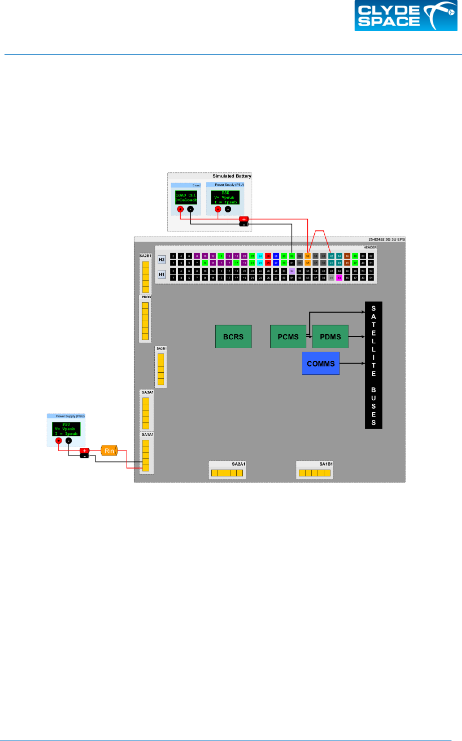
USM-1335
User Manual: 3rd Generation EPS Range - No Inhibits
Issue: D
Date: 11/10/2017
Page: 58 of 60
Skypark 5, 45 Finnieston
Street, Glasgow G3 8JU, UK
SOLUTIONS FOR A NEW AGE IN SPACE
www.clyde.space
PROPRIETARY & CONFIDENTIAL INFORMATION
Copyright ©2017 Clyde Space Ltd. All rights reserved.
4. Switch on the simulated battery.
5. Switch on the solar array power.
6. Check that the system is operational (all power buses at expected voltages).
7. Once this has been set up it is possible to test all functions of the EPS.
For more detail on the individual tests performed on the EPS, refer to the test report which
includes test setups and processes.
Figure 12-4 Testing a standalone EPS 25-02452. Refer to Section 8 for connection of solar array connection
when testing 25-02451 or 01-02453.
12.3 Testing with Clyde Space Battery
Refer to User manual: 3rd Generation Battery Family (USM-1192), Section 13 Test for testing with a
Manned Flight/ISS Compatible battery.

USM-1335
User Manual: 3rd Generation EPS Range - No Inhibits
Issue: D
Date: 11/10/2017
Page: 59 of 60
Skypark 5, 45 Finnieston
Street, Glasgow G3 8JU, UK
SOLUTIONS FOR A NEW AGE IN SPACE
www.clyde.space
PROPRIETARY & CONFIDENTIAL INFORMATION
Copyright ©2017 Clyde Space Ltd. All rights reserved.
13. COMPATIBLE SYSTEMS
Compatibility
Notes
Stacking Connector
CubeSat Kit Bus
Batteries
Clyde Space Battery Systems
As listed in section 13.1.
Other Batteries
Please contact Clyde Space
Solar Arrays
Clyde Space 2-3 cell solar array
Connects to SEPIC BCR(s)
Clyde Space 4-8 cell solar array
Connects to Buck BCRs (not 25-02451)
Other array technologies
Please contact Clyde Space
Structure
Clyde Space
CubeSat 1/2/3U standard structure
Pumpkin
ISIS
Other structures
Please contact Clyde Space
Table 13-1 Compatibilities

USM-1335
User Manual: 3rd Generation EPS Range - No Inhibits
Issue: D
Date: 11/10/2017
Page: 60 of 60
Skypark 5, 45 Finnieston
Street, Glasgow G3 8JU, UK
SOLUTIONS FOR A NEW AGE IN SPACE
www.clyde.space
PROPRIETARY & CONFIDENTIAL INFORMATION
Copyright ©2017 Clyde Space Ltd. All rights reserved.
13.1 Compatible Batteries
Standalone Batteries
This EPS is expected to be integrated with one of the following Clyde Space battery products. It is not
compatible with Clyde Space 3G No Inhibits or 2G battery ranges.
Battery
Product Code
10Wh Standalone
Manned Flight
01-02683
20Wh Standalone
Manned Flight
01-02684
30Wh Standalone
Manned Flight
01-02685
40Wh Standalone
Manned Flight
01-02686
Figure 13-1 Standalone Battery Compatibility
Integrated Batteries
The 1U EPS (25-02451) is also compatible with the following integrated batteries – the battery will be
integrated onto the EPS as a daughterboard, rather than having a separate PC104 header. These are
not compatible with the 3U or FlexU variants.
Battery
Product Code
10Wh Integrated
Manned Flight
01-02681
20Wh Integrated
Manned Flight
01-02682
Figure 13-2 Integrated Battery Compatibility
