Coffee Lake FSP Integration Guide
User Manual:
Open the PDF directly: View PDF ![]() .
.
Page Count: 235 [warning: Documents this large are best viewed by clicking the View PDF Link!]
- 1 INTRODUCTION
- 2 FSP OVERVIEW
- 3 FSP INTEGRATION
- 4 FSP PORTING RECOMMENDATION
- 5 UPD PORTING GUIDE
- 6 FSP OUTPUT
- 7 FSP POSTCODE
- 8 Todo List
- 9 Deprecated List
- 10 Class Index
- 11 File Index
- 12 Class Documentation
- 12.1 AUDIO_AZALIA_VERB_TABLE Struct Reference
- 12.2 AZALIA_HEADER Struct Reference
- 12.3 CHIPSET_INIT_INFO Struct Reference
- 12.4 DIMM_INFO Struct Reference
- 12.5 FIRMWARE_VERSION Struct Reference
- 12.6 FIRMWARE_VERSION_INFO Struct Reference
- 12.7 FIRMWARE_VERSION_INFO_HOB Struct Reference
- 12.8 FSP_M_CONFIG Struct Reference
- 12.8.1 Detailed Description
- 12.8.2 Member Data Documentation
- 12.8.2.1 ActiveCoreCount
- 12.8.2.2 ApertureSize
- 12.8.2.3 ApStartupBase
- 12.8.2.4 Avx2RatioOffset
- 12.8.2.5 Avx3RatioOffset
- 12.8.2.6 BclkAdaptiveVoltage
- 12.8.2.7 BiosAcmBase
- 12.8.2.8 BiosAcmSize
- 12.8.2.9 BiosGuard
- 12.8.2.10 BistOnReset
- 12.8.2.11 BootFrequency
- 12.8.2.12 ChHashEnable
- 12.8.2.13 ChHashInterleaveBit
- 12.8.2.14 ChHashMask
- 12.8.2.15 CkeRankMapping
- 12.8.2.16 CleanMemory
- 12.8.2.17 CmdRanksTerminated
- 12.8.2.18 CoreMaxOcRatio
- 12.8.2.19 CorePllVoltageOffset
- 12.8.2.20 CoreVoltageAdaptive
- 12.8.2.21 CoreVoltageMode
- 12.8.2.22 CoreVoltageOverride
- 12.8.2.23 CpuRatio
- 12.8.2.24 CpuTraceHubMemReg0Size
- 12.8.2.25 CpuTraceHubMemReg1Size
- 12.8.2.26 CpuTraceHubMode
- 12.8.2.27 DciUsb3TypecUfpDbg
- 12.8.2.28 Ddr4MixedUDimm2DpcLimit
- 12.8.2.29 DdrFreqLimit
- 12.8.2.30 DisableDimmChannel0
- 12.8.2.31 DisableDimmChannel1
- 12.8.2.32 DisableMtrrProgram
- 12.8.2.33 DmiDeEmphasis
- 12.8.2.34 DmiGen3EndPointHint
- 12.8.2.35 DmiGen3EndPointPreset
- 12.8.2.36 DmiGen3ProgramStaticEq
- 12.8.2.37 DmiGen3RootPortPreset
- 12.8.2.38 DpSscMarginEnable
- 12.8.2.39 DualDimmPerChannelBoardType
- 12.8.2.40 EnableC6Dram
- 12.8.2.41 EnableSgx
- 12.8.2.42 EnBER
- 12.8.2.43 EnCmdRate
- 12.8.2.44 EpgEnable
- 12.8.2.45 FClkFrequency
- 12.8.2.46 FivrEfficiency
- 12.8.2.47 FivrFaults
- 12.8.2.48 ForceOltmOrRefresh2x
- 12.8.2.49 FreqSaGvLow
- 12.8.2.50 FreqSaGvMid
- 12.8.2.51 GdxcEnable
- 12.8.2.52 GmAdr
- 12.8.2.53 GtPllVoltageOffset
- 12.8.2.54 GtPsmiSupport
- 12.8.2.55 GttMmAdr
- 12.8.2.56 HobBufferSize
- 12.8.2.57 HotThresholdCh0Dimm0
- 12.8.2.58 HotThresholdCh0Dimm1
- 12.8.2.59 HotThresholdCh1Dimm0
- 12.8.2.60 HotThresholdCh1Dimm1
- 12.8.2.61 Idd3n
- 12.8.2.62 Idd3p
- 12.8.2.63 IgdDvmt50PreAlloc
- 12.8.2.64 ImrRpSelection
- 12.8.2.65 InitPcieAspmAfterOprom
- 12.8.2.66 InternalGfx
- 12.8.2.67 IsvtIoPort
- 12.8.2.68 JtagC10PowerGateDisable
- 12.8.2.69 LpddrDramOdt
- 12.8.2.70 McPllVoltageOffset
- 12.8.2.71 MemoryTrace
- 12.8.2.72 MmioSize
- 12.8.2.73 OcLock
- 12.8.2.74 PcdDebugInterfaceFlags
- 12.8.2.75 PcdIsaSerialUartBase
- 12.8.2.76 PcdSerialDebugBaudRate
- 12.8.2.77 PcdSerialDebugLevel
- 12.8.2.78 PcdSerialIoUartNumber
- 12.8.2.79 PchLpcEnhancePort8xhDecoding
- 12.8.2.80 PchNumRsvdSmbusAddresses
- 12.8.2.81 PchPort80Route
- 12.8.2.82 PchSmbAlertEnable
- 12.8.2.83 PchTraceHubMemReg0Size
- 12.8.2.84 PchTraceHubMemReg1Size
- 12.8.2.85 PchTraceHubMode
- 12.8.2.86 PcieImrSize
- 12.8.2.87 PcieRpEnableMask
- 12.8.2.88 PeciC10Reset
- 12.8.2.89 PeciSxReset
- 12.8.2.90 PegDataPtr
- 12.8.2.91 PegDisableSpreadSpectrumClocking
- 12.8.2.92 PlatformDebugConsent
- 12.8.2.93 ProbelessTrace
- 12.8.2.94 PwdwnIdleCounter
- 12.8.2.95 RankInterleave
- 12.8.2.96 Ratio
- 12.8.2.97 RcompResistor
- 12.8.2.98 RcompTarget
- 12.8.2.99 RealtimeMemoryTiming
- 12.8.2.100 RefClk
- 12.8.2.101 RhSolution
- 12.8.2.102 RingDownBin
- 12.8.2.103 RingMaxOcRatio
- 12.8.2.104 RingPllVoltageOffset
- 12.8.2.105 RingVoltageAdaptive
- 12.8.2.106 RingVoltageMode
- 12.8.2.107 RingVoltageOffset
- 12.8.2.108 RingVoltageOverride
- 12.8.2.109 RMT
- 12.8.2.110 RMTLoopCount
- 12.8.2.111 RmtPerTask
- 12.8.2.112 SafeMode
- 12.8.2.113 SaGv
- 12.8.2.114 SaPllVoltageOffset
- 12.8.2.115 ScramblerSupport
- 12.8.2.116 SinitMemorySize
- 12.8.2.117 SkipMpInit
- 12.8.2.118 SmbusArpEnable
- 12.8.2.119 SmbusEnable
- 12.8.2.120 SpdAddressTable
- 12.8.2.121 SpdProfileSelected
- 12.8.2.122 TgaSize
- 12.8.2.123 ThrtCkeMinTmr
- 12.8.2.124 ThrtCkeMinTmrLpddr
- 12.8.2.125 TjMaxOffset
- 12.8.2.126 TrainTrace
- 12.8.2.127 tRTP
- 12.8.2.128 TsegSize
- 12.8.2.129 TsodAlarmwindowLockBit
- 12.8.2.130 TsodCriticalEventOnly
- 12.8.2.131 TsodCriticaltripLockBit
- 12.8.2.132 TsodEventMode
- 12.8.2.133 TsodEventOutputControl
- 12.8.2.134 TsodEventPolarity
- 12.8.2.135 TsodManualEnable
- 12.8.2.136 TsodShutdownMode
- 12.8.2.137 TsodTcritMax
- 12.8.2.138 TvbRatioClipping
- 12.8.2.139 TvbVoltageOptimization
- 12.8.2.140 Txt
- 12.8.2.141 TxtDprMemoryBase
- 12.8.2.142 TxtDprMemorySize
- 12.8.2.143 TxtHeapMemorySize
- 12.8.2.144 TxtImplemented
- 12.8.2.145 TxtLcpPdBase
- 12.8.2.146 TxtLcpPdSize
- 12.8.2.147 UserBudgetEnable
- 12.8.2.148 UserThresholdEnable
- 12.8.2.149 VddVoltage
- 12.8.2.150 VmxEnable
- 12.8.2.151 WarmThresholdCh0Dimm0
- 12.8.2.152 WarmThresholdCh0Dimm1
- 12.8.2.153 WarmThresholdCh1Dimm0
- 12.8.2.154 WarmThresholdCh1Dimm1
- 12.9 FSP_M_TEST_CONFIG Struct Reference
- 12.9.1 Detailed Description
- 12.9.2 Member Data Documentation
- 12.9.2.1 BdatEnable
- 12.9.2.2 BdatTestType
- 12.9.2.3 BiosSize
- 12.9.2.4 BypassPhySyncReset
- 12.9.2.5 DeltaT12PowerCycleDelayPreMem
- 12.9.2.6 DisableHeciRetry
- 12.9.2.7 DisableMessageCheck
- 12.9.2.8 DmiGen3EqPh2Enable
- 12.9.2.9 DmiGen3EqPh3Method
- 12.9.2.10 Gen3SwEqAlwaysAttempt
- 12.9.2.11 Gen3SwEqEnableVocTest
- 12.9.2.12 Gen3SwEqJitterDwellTime
- 12.9.2.13 Gen3SwEqJitterErrorTarget
- 12.9.2.14 Gen3SwEqNumberOfPresets
- 12.9.2.15 Gen3SwEqVocDwellTime
- 12.9.2.16 Gen3SwEqVocErrorTarget
- 12.9.2.17 HeciCommunication2
- 12.9.2.18 KtDeviceEnable
- 12.9.2.19 LockPTMregs
- 12.9.2.20 PanelPowerEnable
- 12.9.2.21 Peg0Gen3EqPh2Enable
- 12.9.2.22 Peg0Gen3EqPh3Method
- 12.9.2.23 Peg1Gen3EqPh2Enable
- 12.9.2.24 Peg1Gen3EqPh3Method
- 12.9.2.25 Peg2Gen3EqPh2Enable
- 12.9.2.26 Peg2Gen3EqPh3Method
- 12.9.2.27 Peg3Gen3EqPh2Enable
- 12.9.2.28 Peg3Gen3EqPh3Method
- 12.9.2.29 PegGen3EndPointHint
- 12.9.2.30 PegGen3EndPointPreset
- 12.9.2.31 PegGen3ProgramStaticEq
- 12.9.2.32 PegGen3RootPortPreset
- 12.9.2.33 PegGenerateBdatMarginTable
- 12.9.2.34 PegRxCemLoopbackLane
- 12.9.2.35 PegRxCemNonProtocolAwareness
- 12.9.2.36 ScanExtGfxForLegacyOpRom
- 12.9.2.37 SkipMbpHob
- 12.9.2.38 SmbusDynamicPowerGating
- 12.9.2.39 SmbusSpdWriteDisable
- 12.9.2.40 TotalFlashSize
- 12.9.2.41 tRd2RdDD
- 12.9.2.42 tRd2RdDG
- 12.9.2.43 tRd2RdDR
- 12.9.2.44 tRd2RdSG
- 12.9.2.45 tRd2WrDD
- 12.9.2.46 tRd2WrDG
- 12.9.2.47 tRd2WrDR
- 12.9.2.48 tRd2WrSG
- 12.9.2.49 tRRD_L
- 12.9.2.50 tRRD_S
- 12.9.2.51 tWr2RdDD
- 12.9.2.52 tWr2RdDG
- 12.9.2.53 tWr2RdDR
- 12.9.2.54 tWr2RdSG
- 12.9.2.55 tWr2WrDD
- 12.9.2.56 tWr2WrDG
- 12.9.2.57 tWr2WrDR
- 12.9.2.58 tWr2WrSG
- 12.9.2.59 tWTR_L
- 12.9.2.60 tWTR_S
- 12.9.2.61 TxtAcheckRequest
- 12.9.2.62 WdtDisableAndLock
- 12.10 FSP_S_CONFIG Struct Reference
- 12.10.1 Detailed Description
- 12.10.2 Member Data Documentation
- 12.10.2.1 AcLoadline
- 12.10.2.2 AcousticNoiseMitigation
- 12.10.2.3 AmtEnabled
- 12.10.2.4 AmtKvmEnabled
- 12.10.2.5 AmtSolEnabled
- 12.10.2.6 AsfEnabled
- 12.10.2.7 CpuMpHob
- 12.10.2.8 DcLoadline
- 12.10.2.9 DebugInterfaceEnable
- 12.10.2.10 DevIntConfigPtr
- 12.10.2.11 DmiSuggestedSetting
- 12.10.2.12 DmiTS0TW
- 12.10.2.13 DmiTS1TW
- 12.10.2.14 DmiTS2TW
- 12.10.2.15 DmiTS3TW
- 12.10.2.16 EcCmdLock
- 12.10.2.17 EcCmdProvisionEav
- 12.10.2.18 Enable8254ClockGating
- 12.10.2.19 Enable8254ClockGatingOnS3
- 12.10.2.20 EnableTcoTimer
- 12.10.2.21 EsataSpeedLimit
- 12.10.2.22 FastPkgCRampDisableFivr
- 12.10.2.23 FastPkgCRampDisableGt
- 12.10.2.24 FastPkgCRampDisableIa
- 12.10.2.25 FastPkgCRampDisableSa
- 12.10.2.26 FivrRfiFrequency
- 12.10.2.27 FivrSpreadSpectrum
- 12.10.2.28 ForcMebxSyncUp
- 12.10.2.29 FwProgress
- 12.10.2.30 GpioIrqRoute
- 12.10.2.31 Heci3Enabled
- 12.10.2.32 IccMax
- 12.10.2.33 ImonOffset1
- 12.10.2.34 ImonSlope
- 12.10.2.35 ImonSlope1
- 12.10.2.36 IslVrCmd
- 12.10.2.37 ManageabilityMode
- 12.10.2.38 McivrRfiFrequencyAdjust
- 12.10.2.39 McivrRfiFrequencyPrefix
- 12.10.2.40 McivrSpreadSpectrum
- 12.10.2.41 MeUnconfigOnRtcClear
- 12.10.2.42 NumOfDevIntConfig
- 12.10.2.43 PchCnviMode
- 12.10.2.44 PchCrid
- 12.10.2.45 PchDmiAspm
- 12.10.2.46 PchDmiAspmCtrl
- 12.10.2.47 PchDmiTsawEn
- 12.10.2.48 PchEnableComplianceMode
- 12.10.2.49 PchEnableDbcObs
- 12.10.2.50 PchHdaAudioLinkDmic0
- 12.10.2.51 PchHdaAudioLinkDmic1
- 12.10.2.52 PchHdaAudioLinkHda
- 12.10.2.53 PchHdaAudioLinkSndw1
- 12.10.2.54 PchHdaAudioLinkSndw2
- 12.10.2.55 PchHdaAudioLinkSndw3
- 12.10.2.56 PchHdaAudioLinkSndw4
- 12.10.2.57 PchHdaAudioLinkSsp0
- 12.10.2.58 PchHdaAudioLinkSsp1
- 12.10.2.59 PchHdaAudioLinkSsp2
- 12.10.2.60 PchHdaDspEnable
- 12.10.2.61 PchHdaDspUaaCompliance
- 12.10.2.62 PchHdaIDispCodecDisconnect
- 12.10.2.63 PchHdaIDispLinkFrequency
- 12.10.2.64 PchHdaIDispLinkTmode
- 12.10.2.65 PchHdaLinkFrequency
- 12.10.2.66 PchHdaPme
- 12.10.2.67 PchHdaSndwBufferRcomp
- 12.10.2.68 PchHdaVcType
- 12.10.2.69 PchHotEnable
- 12.10.2.70 PchIoApicEntry24_119
- 12.10.2.71 PchIoApicId
- 12.10.2.72 PchIshGp0GpioAssign
- 12.10.2.73 PchIshGp1GpioAssign
- 12.10.2.74 PchIshGp2GpioAssign
- 12.10.2.75 PchIshGp3GpioAssign
- 12.10.2.76 PchIshGp4GpioAssign
- 12.10.2.77 PchIshGp5GpioAssign
- 12.10.2.78 PchIshGp6GpioAssign
- 12.10.2.79 PchIshGp7GpioAssign
- 12.10.2.80 PchIshI2c0GpioAssign
- 12.10.2.81 PchIshI2c1GpioAssign
- 12.10.2.82 PchIshI2c2GpioAssign
- 12.10.2.83 PchIshPdtUnlock
- 12.10.2.84 PchIshSpiGpioAssign
- 12.10.2.85 PchIshUart0GpioAssign
- 12.10.2.86 PchIshUart1GpioAssign
- 12.10.2.87 PchLanEnable
- 12.10.2.88 PchLanLtrEnable
- 12.10.2.89 PchLegacyIoLowLatency
- 12.10.2.90 PchLockDownBiosLock
- 12.10.2.91 PchLockDownRtcMemoryLock
- 12.10.2.92 PchMemoryThrottlingEnable
- 12.10.2.93 PchPcieDeviceOverrideTablePtr
- 12.10.2.94 PchPmDeepSxPol
- 12.10.2.95 PchPmDisableDsxAcPresentPulldown
- 12.10.2.96 PchPmDisableNativePowerButton
- 12.10.2.97 PchPmLanWakeFromDeepSx
- 12.10.2.98 PchPmLpcClockRun
- 12.10.2.99 PchPmMeWakeSts
- 12.10.2.100 PchPmPciePllSsc
- 12.10.2.101 PchPmPcieWakeFromDeepSx
- 12.10.2.102 PchPmPmeB0S5Dis
- 12.10.2.103 PchPmPwrBtnOverridePeriod
- 12.10.2.104 PchPmPwrCycDur
- 12.10.2.105 PchPmSlpAMinAssert
- 12.10.2.106 PchPmSlpLanLowDc
- 12.10.2.107 PchPmSlpS0Enable
- 12.10.2.108 PchPmSlpS0Vm070VSupport
- 12.10.2.109 PchPmSlpS0Vm075VSupport
- 12.10.2.110 PchPmSlpS0VmRuntimeControl
- 12.10.2.111 PchPmSlpS3MinAssert
- 12.10.2.112 PchPmSlpS4MinAssert
- 12.10.2.113 PchPmSlpStrchSusUp
- 12.10.2.114 PchPmSlpSusMinAssert
- 12.10.2.115 PchPmVrAlert
- 12.10.2.116 PchPmWolEnableOverride
- 12.10.2.117 PchPmWolOvrWkSts
- 12.10.2.118 PchPmWoWlanDeepSxEnable
- 12.10.2.119 PchPmWoWlanEnable
- 12.10.2.120 PchPwrOptEnable
- 12.10.2.121 PchScsEmmcHs400DllDataValid
- 12.10.2.122 PchScsEmmcHs400DriverStrength
- 12.10.2.123 PchScsEmmcHs400TuningRequired
- 12.10.2.124 PchSerialIoI2cPadsTermination
- 12.10.2.125 PchSirqEnable
- 12.10.2.126 PchSirqMode
- 12.10.2.127 PchStartFramePulse
- 12.10.2.128 PchTsmicLock
- 12.10.2.129 PchTTEnable
- 12.10.2.130 PchTTLock
- 12.10.2.131 PchTTState13Enable
- 12.10.2.132 PchUsbHsioFilterSel
- 12.10.2.133 PchUsbHsioRxTuningEnable
- 12.10.2.134 PcieComplianceTestMode
- 12.10.2.135 PcieDisableRootPortClockGating
- 12.10.2.136 PcieEnablePeerMemoryWrite
- 12.10.2.137 PcieEqPh3LaneParamCm
- 12.10.2.138 PcieEqPh3LaneParamCp
- 12.10.2.139 PcieRpAspm
- 12.10.2.140 PcieRpCompletionTimeout
- 12.10.2.141 PcieRpDpcExtensionsMask
- 12.10.2.142 PcieRpDpcMask
- 12.10.2.143 PcieRpFunctionSwap
- 12.10.2.144 PcieRpGen3EqPh3Method
- 12.10.2.145 PcieRpImrEnabled
- 12.10.2.146 PcieRpL1Substates
- 12.10.2.147 PcieRpPcieSpeed
- 12.10.2.148 PcieRpPhysicalSlotNumber
- 12.10.2.149 PcieRpPtmMask
- 12.10.2.150 PcieSwEqCoeffListCm
- 12.10.2.151 PcieSwEqCoeffListCp
- 12.10.2.152 PmcCpuC10GatePinEnable
- 12.10.2.153 PmcDbgMsgEn
- 12.10.2.154 PmcModPhySusPgEnable
- 12.10.2.155 PmcPowerButtonDebounce
- 12.10.2.156 PortUsb20Enable
- 12.10.2.157 PortUsb30Enable
- 12.10.2.158 PreWake
- 12.10.2.159 Psi1Threshold
- 12.10.2.160 Psi2Threshold
- 12.10.2.161 Psi3Enable
- 12.10.2.162 Psi3Threshold
- 12.10.2.163 PsOnEnable
- 12.10.2.164 PsysOffset
- 12.10.2.165 PsysSlope
- 12.10.2.166 PxRcConfig
- 12.10.2.167 RemoteAssistance
- 12.10.2.168 SataEnable
- 12.10.2.169 SataLedEnable
- 12.10.2.170 SataMode
- 12.10.2.171 SataP0TDispFinit
- 12.10.2.172 SataP1TDispFinit
- 12.10.2.173 SataPortsDevSlp
- 12.10.2.174 SataPortsDmVal
- 12.10.2.175 SataPortsEnable
- 12.10.2.176 SataPwrOptEnable
- 12.10.2.177 SataRstHddUnlock
- 12.10.2.178 SataRstInterrupt
- 12.10.2.179 SataRstIrrt
- 12.10.2.180 SataRstIrrtOnly
- 12.10.2.181 SataRstLedLocate
- 12.10.2.182 SataRstOromUiBanner
- 12.10.2.183 SataRstPcieDeviceResetDelay
- 12.10.2.184 SataRstRaid0
- 12.10.2.185 SataRstRaid1
- 12.10.2.186 SataRstRaid10
- 12.10.2.187 SataRstRaid5
- 12.10.2.188 SataRstRaidDeviceId
- 12.10.2.189 SataRstSmartStorage
- 12.10.2.190 SataSalpSupport
- 12.10.2.191 SataThermalSuggestedSetting
- 12.10.2.192 SciIrqSelect
- 12.10.2.193 ScsEmmcEnabled
- 12.10.2.194 ScsEmmcHs400Enabled
- 12.10.2.195 ScsSdCardEnabled
- 12.10.2.196 ScsUfsEnabled
- 12.10.2.197 SendEcCmd
- 12.10.2.198 SendVrMbxCmd
- 12.10.2.199 SerialIoDebugUartNumber
- 12.10.2.200 SerialIoDevMode
- 12.10.2.201 SerialIoEnableDebugUartAfterPost
- 12.10.2.202 SerialIoUart0PinMuxing
- 12.10.2.203 ShowSpiController
- 12.10.2.204 SiCsmFlag
- 12.10.2.205 SiNumberOfSsidTableEntry
- 12.10.2.206 SiSsidTablePtr
- 12.10.2.207 SkipMpInitDeprecated
- 12.10.2.208 SlowSlewRateForFivr
- 12.10.2.209 SlowSlewRateForGt
- 12.10.2.210 SlowSlewRateForIa
- 12.10.2.211 SlowSlewRateForSa
- 12.10.2.212 SlpS0DisQForDebug
- 12.10.2.213 SlpS0Override
- 12.10.2.214 SlpS0WithGbeSupport
- 12.10.2.215 TcoIrqSelect
- 12.10.2.216 TdcPowerLimit
- 12.10.2.217 TdcTimeWindow
- 12.10.2.218 TetonGlacierMode
- 12.10.2.219 TTSuggestedSetting
- 12.10.2.220 TurboMode
- 12.10.2.221 TxtEnable
- 12.10.2.222 Usb2AfePehalfbit
- 12.10.2.223 Usb2AfePetxiset
- 12.10.2.224 Usb2AfePredeemp
- 12.10.2.225 Usb2AfeTxiset
- 12.10.2.226 Usb3HsioTxDeEmph
- 12.10.2.227 Usb3HsioTxDeEmphEnable
- 12.10.2.228 Usb3HsioTxDownscaleAmp
- 12.10.2.229 Usb3HsioTxDownscaleAmpEnable
- 12.10.2.230 Usb3HsioTxRate0UniqTran
- 12.10.2.231 Usb3HsioTxRate0UniqTranEnable
- 12.10.2.232 Usb3HsioTxRate1UniqTran
- 12.10.2.233 Usb3HsioTxRate1UniqTranEnable
- 12.10.2.234 Usb3HsioTxRate2UniqTran
- 12.10.2.235 Usb3HsioTxRate2UniqTranEnable
- 12.10.2.236 Usb3HsioTxRate3UniqTran
- 12.10.2.237 Usb3HsioTxRate3UniqTranEnable
- 12.10.2.238 UsbPdoProgramming
- 12.10.2.239 VrPowerDeliveryDesign
- 12.10.2.240 VrVoltageLimit
- 12.10.2.241 WatchDog
- 12.10.2.242 WatchDogTimerBios
- 12.10.2.243 WatchDogTimerOs
- 12.10.2.244 XdciEnable
- 12.11 FSP_S_TEST_CONFIG Struct Reference
- 12.11.1 Detailed Description
- 12.11.2 Member Data Documentation
- 12.11.2.1 ApIdleManner
- 12.11.2.2 AutoThermalReporting
- 12.11.2.3 C1e
- 12.11.2.4 C1StateAutoDemotion
- 12.11.2.5 C1StateUnDemotion
- 12.11.2.6 C3StateAutoDemotion
- 12.11.2.7 C3StateUnDemotion
- 12.11.2.8 ConfigTdpBios
- 12.11.2.9 CpuWakeUpTimer
- 12.11.2.10 CStatePreWake
- 12.11.2.11 CstCfgCtrIoMwaitRedirection
- 12.11.2.12 Custom1ConfigTdpControl
- 12.11.2.13 Custom1PowerLimit1
- 12.11.2.14 Custom1PowerLimit1Time
- 12.11.2.15 Custom1PowerLimit2
- 12.11.2.16 Custom1TurboActivationRatio
- 12.11.2.17 Custom2ConfigTdpControl
- 12.11.2.18 Custom2PowerLimit1
- 12.11.2.19 Custom2PowerLimit1Time
- 12.11.2.20 Custom2PowerLimit2
- 12.11.2.21 Custom2TurboActivationRatio
- 12.11.2.22 Custom3ConfigTdpControl
- 12.11.2.23 Custom3PowerLimit1
- 12.11.2.24 Custom3PowerLimit1Time
- 12.11.2.25 Custom3PowerLimit2
- 12.11.2.26 Custom3TurboActivationRatio
- 12.11.2.27 Cx
- 12.11.2.28 DebugInterfaceEnable
- 12.11.2.29 DebugInterfaceLockEnable
- 12.11.2.30 DisableProcHotOut
- 12.11.2.31 DisableVrThermalAlert
- 12.11.2.32 EightCoreRatioLimit
- 12.11.2.33 Eist
- 12.11.2.34 EnableItbm
- 12.11.2.35 EndOfPostMessage
- 12.11.2.36 EnergyEfficientPState
- 12.11.2.37 EnergyEfficientTurbo
- 12.11.2.38 FiveCoreRatioLimit
- 12.11.2.39 FourCoreRatioLimit
- 12.11.2.40 HdcControl
- 12.11.2.41 Hwp
- 12.11.2.42 HwpInterruptControl
- 12.11.2.43 MachineCheckEnable
- 12.11.2.44 MaxRingRatioLimit
- 12.11.2.45 MctpBroadcastCycle
- 12.11.2.46 MinRingRatioLimit
- 12.11.2.47 MlcStreamerPrefetcher
- 12.11.2.48 MonitorMwaitEnable
- 12.11.2.49 NumberOfEntries
- 12.11.2.50 OneCoreRatioLimit
- 12.11.2.51 PchHdaResetWaitTimer
- 12.11.2.52 PchLockDownBiosInterface
- 12.11.2.53 PchLockDownGlobalSmi
- 12.11.2.54 PchPmDisableEnergyReport
- 12.11.2.55 PchSbAccessUnlock
- 12.11.2.56 PchUnlockGpioPads
- 12.11.2.57 PchXhciOcLock
- 12.11.2.58 PcieEnablePort8xhDecode
- 12.11.2.59 PcieRpDptp
- 12.11.2.60 PcieRpSlotPowerLimitScale
- 12.11.2.61 PcieRpSlotPowerLimitValue
- 12.11.2.62 PcieRpUptp
- 12.11.2.63 PkgCStateDemotion
- 12.11.2.64 PkgCStateLimit
- 12.11.2.65 PkgCStateUnDemotion
- 12.11.2.66 PmgCstCfgCtrlLock
- 12.11.2.67 PowerLimit1
- 12.11.2.68 PowerLimit1Time
- 12.11.2.69 PowerLimit2
- 12.11.2.70 PowerLimit2Power
- 12.11.2.71 PowerLimit3
- 12.11.2.72 PowerLimit4
- 12.11.2.73 ProcessorTraceEnable
- 12.11.2.74 ProcessorTraceMemBase
- 12.11.2.75 ProcessorTraceMemLength
- 12.11.2.76 ProcessorTraceOutputScheme
- 12.11.2.77 ProcHotResponse
- 12.11.2.78 PsysPmax
- 12.11.2.79 PsysPowerLimit1
- 12.11.2.80 PsysPowerLimit1Power
- 12.11.2.81 PsysPowerLimit1Time
- 12.11.2.82 PsysPowerLimit2
- 12.11.2.83 PsysPowerLimit2Power
- 12.11.2.84 RaceToHalt
- 12.11.2.85 SataTestMode
- 12.11.2.86 SevenCoreRatioLimit
- 12.11.2.87 SixCoreRatioLimit
- 12.11.2.88 StateRatio
- 12.11.2.89 StateRatioMax16
- 12.11.2.90 TccActivationOffset
- 12.11.2.91 TccOffsetClamp
- 12.11.2.92 TccOffsetLock
- 12.11.2.93 TccOffsetTimeWindowForRatl
- 12.11.2.94 ThreeCoreRatioLimit
- 12.11.2.95 ThreeStrikeCounterDisable
- 12.11.2.96 TimedMwait
- 12.11.2.97 TStates
- 12.11.2.98 TwoCoreRatioLimit
- 12.12 FSP_T_CONFIG Struct Reference
- 12.13 FSPM_UPD Struct Reference
- 12.14 FSPS_UPD Struct Reference
- 12.15 FSPT_CORE_UPD Struct Reference
- 12.16 FSPT_UPD Struct Reference
- 12.17 GPIO_CONFIG Struct Reference
- 12.18 HOB_USAGE_DATA_HOB Struct Reference
- 12.19 MEMORY_PLATFORM_DATA Struct Reference
- 12.20 SI_PCH_DEVICE_INTERRUPT_CONFIG Struct Reference
- 12.21 SMBIOS_CACHE_INFO Struct Reference
- 12.22 SMBIOS_PROCESSOR_INFO Struct Reference
- 12.23 SMBIOS_STRUCTURE Struct Reference
- 13 File Documentation
- 13.1 FirmwareVersionInfoHob.h File Reference
- 13.2 FspFixedPcds.h File Reference
- 13.3 FspInfoHob.h File Reference
- 13.4 FspmUpd.h File Reference
- 13.5 FspsUpd.h File Reference
- 13.6 FsptUpd.h File Reference
- 13.7 FspUpd.h File Reference
- 13.8 GpioConfig.h File Reference
- 13.9 GpioSampleDef.h File Reference
- 13.10 HobUsageDataHob.h File Reference
- 13.11 MemInfoHob.h File Reference
- 13.12 SmbiosCacheInfoHob.h File Reference
- 13.13 SmbiosProcessorInfoHob.h File Reference
- Index

CoffeeLake Intel(R) Firmware Support Package (FSP) Integration Guide
Wed Apr 17 2019 18:20:44

ii
By using this document, in addition to any agreements you have with Intel, you accept the terms set forth below.
You may not use or facilitate the use of this document in connection with any infringement or other legal analysis
concerning Intel products described herein. You agree to grant Intel a non-exclusive, royalty-free license to any
patent claim thereafter drafted which includes subject matter disclosed herein.
INFORMATION IN THIS DOCUMENT IS PROVIDED IN CONNECTION WITH INTEL PRODUCTS. NO LICENSE,
EXPRESS OR IMPLIED, BY ESTOPPEL OR OTHERWISE, TO ANY INTELLECTUAL PROPERTY RIGHTS IS
GRANTED BY THIS DOCUMENT.
Intel may make changes to specifications and product descriptions at any time, without notice. Designers must
not rely on the absence or characteristics of any features or instructions marked "reserved" or "undefined." Do not
finalize a design with this information.
The products described in this document may contain design defects or errors known as errata which may cause
the product to deviate from published specifications. Current characterized errata are available on request.
Contact your local Intel sales office or your distributor to obtain the latest specifications and before placing your
product order.
Copies of documents which have an order number and are referenced in this document, or other Intel literature, may
be obtained by calling 1-800-548-4725, or go to: http://www.intel.com/design/literature.htm
Any software source code reprinted in this document is furnished for informational purposes only and may only be
used or copied and no license, express or implied, by estoppel or otherwise, to any of the reprinted source code is
granted by this document.
[When the doc contains software source code for a special or limited purpose (such as informational purposes only),
use the conditionalized Software Disclaimer tag. Otherwise, use the generic software source code disclaimer from
the Legal page and include a copy of the software license or a hyperlink to its permanent location.]
This document contains information on products in the design phase of development. Intel processor numbers are
not a measure of performance. Processor numbers differentiate features within each processor family, not across
different processor families. Go to: http://www.intel.com/products/processor_number/
Code Names are only for use by Intel to identify products, platforms, programs, services, etc. ("products") in
development by Intel that have not been made commercially available to the public, i.e., announced, launched or
shipped. They are never to be used as "commercial" names for products. Also, they are not intended to function as
trademarks.
Intel, Intel Atom, [include any Intel trademarks which are used in this document] and the Intel logo are trademarks
of Intel Corporation in the U.S. and/or other countries.
*Other names and brands may be claimed as the property of others.
Copyright ©Intel Corporation. All rights reserved.
Contents
1 INTRODUCTION 1
2 FSP OVERVIEW 3
3 FSP INTEGRATION 5
4 FSP PORTING RECOMMENDATION 11
5 UPD PORTING GUIDE 13
6 FSP OUTPUT 15
7 FSP POSTCODE 19
8 Todo List 29
9 Deprecated List 31
10 Class Index 33
10.1 Class List ............................................... 33
11 File Index 35
11.1 File List . . . . . . . . . . . . . . . . . . . . . . . . . . . . . . . . . . . . . . . . . . . . . . . . 35
12 Class Documentation 37
12.1 AUDIO_AZALIA_VERB_TABLE Struct Reference . . . . . . . . . . . . . . . . . . . . . . . . . . 37
12.1.1 Detailed Description . . . . . . . . . . . . . . . . . . . . . . . . . . . . . . . . . . . . . 37
12.2 AZALIA_HEADER Struct Reference . . . . . . . . . . . . . . . . . . . . . . . . . . . . . . . . . 38
12.2.1 Detailed Description . . . . . . . . . . . . . . . . . . . . . . . . . . . . . . . . . . . . . 38
12.3 CHIPSET_INIT_INFO Struct Reference . . . . . . . . . . . . . . . . . . . . . . . . . . . . . . . 38
12.3.1 Detailed Description . . . . . . . . . . . . . . . . . . . . . . . . . . . . . . . . . . . . . 39
12.4 DIMM_INFO Struct Reference . . . . . . . . . . . . . . . . . . . . . . . . . . . . . . . . . . . . 39
12.4.1 Detailed Description . . . . . . . . . . . . . . . . . . . . . . . . . . . . . . . . . . . . . 39
12.5 FIRMWARE_VERSION Struct Reference . . . . . . . . . . . . . . . . . . . . . . . . . . . . . . . 39
12.5.1 Detailed Description . . . . . . . . . . . . . . . . . . . . . . . . . . . . . . . . . . . . . 40
12.6 FIRMWARE_VERSION_INFO Struct Reference . . . . . . . . . . . . . . . . . . . . . . . . . . . 40

iv CONTENTS
12.6.1 Detailed Description . . . . . . . . . . . . . . . . . . . . . . . . . . . . . . . . . . . . . 40
12.7 FIRMWARE_VERSION_INFO_HOB Struct Reference . . . . . . . . . . . . . . . . . . . . . . . . 40
12.7.1 Detailed Description . . . . . . . . . . . . . . . . . . . . . . . . . . . . . . . . . . . . . 41
12.7.2 Member Data Documentation . . . . . . . . . . . . . . . . . . . . . . . . . . . . . . . . . 41
12.7.2.1 Count . . . . . . . . . . . . . . . . . . . . . . . . . . . . . . . . . . . . . . . . 41
12.8 FSP_M_CONFIG Struct Reference . . . . . . . . . . . . . . . . . . . . . . . . . . . . . . . . . . 41
12.8.1 Detailed Description . . . . . . . . . . . . . . . . . . . . . . . . . . . . . . . . . . . . . 59
12.8.2 Member Data Documentation . . . . . . . . . . . . . . . . . . . . . . . . . . . . . . . . . 60
12.8.2.1 ActiveCoreCount . . . . . . . . . . . . . . . . . . . . . . . . . . . . . . . . . . 60
12.8.2.2 ApertureSize . . . . . . . . . . . . . . . . . . . . . . . . . . . . . . . . . . . . 60
12.8.2.3 ApStartupBase . . . . . . . . . . . . . . . . . . . . . . . . . . . . . . . . . . . 60
12.8.2.4 Avx2RatioOffset . . . . . . . . . . . . . . . . . . . . . . . . . . . . . . . . . . 60
12.8.2.5 Avx3RatioOffset . . . . . . . . . . . . . . . . . . . . . . . . . . . . . . . . . . 60
12.8.2.6 BclkAdaptiveVoltage . . . . . . . . . . . . . . . . . . . . . . . . . . . . . . . . 60
12.8.2.7 BiosAcmBase . . . . . . . . . . . . . . . . . . . . . . . . . . . . . . . . . . . 60
12.8.2.8 BiosAcmSize . . . . . . . . . . . . . . . . . . . . . . . . . . . . . . . . . . . . 61
12.8.2.9 BiosGuard . . . . . . . . . . . . . . . . . . . . . . . . . . . . . . . . . . . . . 61
12.8.2.10 BistOnReset . . . . . . . . . . . . . . . . . . . . . . . . . . . . . . . . . . . . 61
12.8.2.11 BootFrequency . . . . . . . . . . . . . . . . . . . . . . . . . . . . . . . . . . . 61
12.8.2.12 ChHashEnable . . . . . . . . . . . . . . . . . . . . . . . . . . . . . . . . . . . 61
12.8.2.13 ChHashInterleaveBit . . . . . . . . . . . . . . . . . . . . . . . . . . . . . . . . 61
12.8.2.14 ChHashMask . . . . . . . . . . . . . . . . . . . . . . . . . . . . . . . . . . . . 61
12.8.2.15 CkeRankMapping . . . . . . . . . . . . . . . . . . . . . . . . . . . . . . . . . 62
12.8.2.16 CleanMemory . . . . . . . . . . . . . . . . . . . . . . . . . . . . . . . . . . . 62
12.8.2.17 CmdRanksTerminated . . . . . . . . . . . . . . . . . . . . . . . . . . . . . . . 62
12.8.2.18 CoreMaxOcRatio . . . . . . . . . . . . . . . . . . . . . . . . . . . . . . . . . . 62
12.8.2.19 CorePllVoltageOffset . . . . . . . . . . . . . . . . . . . . . . . . . . . . . . . . 62
12.8.2.20 CoreVoltageAdaptive . . . . . . . . . . . . . . . . . . . . . . . . . . . . . . . 62
12.8.2.21 CoreVoltageMode . . . . . . . . . . . . . . . . . . . . . . . . . . . . . . . . . 62
12.8.2.22 CoreVoltageOverride . . . . . . . . . . . . . . . . . . . . . . . . . . . . . . . . 63
12.8.2.23 CpuRatio . . . . . . . . . . . . . . . . . . . . . . . . . . . . . . . . . . . . . . 63
12.8.2.24 CpuTraceHubMemReg0Size . . . . . . . . . . . . . . . . . . . . . . . . . . . . 63
12.8.2.25 CpuTraceHubMemReg1Size . . . . . . . . . . . . . . . . . . . . . . . . . . . . 63
12.8.2.26 CpuTraceHubMode . . . . . . . . . . . . . . . . . . . . . . . . . . . . . . . . 63
12.8.2.27 DciUsb3TypecUfpDbg . . . . . . . . . . . . . . . . . . . . . . . . . . . . . . . 63
12.8.2.28 Ddr4MixedUDimm2DpcLimit . . . . . . . . . . . . . . . . . . . . . . . . . . . . 63
12.8.2.29 DdrFreqLimit . . . . . . . . . . . . . . . . . . . . . . . . . . . . . . . . . . . . 64
12.8.2.30 DisableDimmChannel0 . . . . . . . . . . . . . . . . . . . . . . . . . . . . . . 64
12.8.2.31 DisableDimmChannel1 . . . . . . . . . . . . . . . . . . . . . . . . . . . . . . 64
12.8.2.32 DisableMtrrProgram . . . . . . . . . . . . . . . . . . . . . . . . . . . . . . . . 64

CONTENTS v
12.8.2.33 DmiDeEmphasis . . . . . . . . . . . . . . . . . . . . . . . . . . . . . . . . . . 64
12.8.2.34 DmiGen3EndPointHint . . . . . . . . . . . . . . . . . . . . . . . . . . . . . . . 64
12.8.2.35 DmiGen3EndPointPreset . . . . . . . . . . . . . . . . . . . . . . . . . . . . . 64
12.8.2.36 DmiGen3ProgramStaticEq . . . . . . . . . . . . . . . . . . . . . . . . . . . . . 65
12.8.2.37 DmiGen3RootPortPreset . . . . . . . . . . . . . . . . . . . . . . . . . . . . . 65
12.8.2.38 DpSscMarginEnable . . . . . . . . . . . . . . . . . . . . . . . . . . . . . . . . 65
12.8.2.39 DualDimmPerChannelBoardType . . . . . . . . . . . . . . . . . . . . . . . . . 65
12.8.2.40 EnableC6Dram . . . . . . . . . . . . . . . . . . . . . . . . . . . . . . . . . . . 65
12.8.2.41 EnableSgx . . . . . . . . . . . . . . . . . . . . . . . . . . . . . . . . . . . . . 65
12.8.2.42 EnBER . . . . . . . . . . . . . . . . . . . . . . . . . . . . . . . . . . . . . . . 66
12.8.2.43 EnCmdRate . . . . . . . . . . . . . . . . . . . . . . . . . . . . . . . . . . . . 66
12.8.2.44 EpgEnable . . . . . . . . . . . . . . . . . . . . . . . . . . . . . . . . . . . . . 66
12.8.2.45 FClkFrequency . . . . . . . . . . . . . . . . . . . . . . . . . . . . . . . . . . . 66
12.8.2.46 FivrEfficiency . . . . . . . . . . . . . . . . . . . . . . . . . . . . . . . . . . . . 66
12.8.2.47 FivrFaults . . . . . . . . . . . . . . . . . . . . . . . . . . . . . . . . . . . . . . 66
12.8.2.48 ForceOltmOrRefresh2x . . . . . . . . . . . . . . . . . . . . . . . . . . . . . . 66
12.8.2.49 FreqSaGvLow . . . . . . . . . . . . . . . . . . . . . . . . . . . . . . . . . . . 67
12.8.2.50 FreqSaGvMid . . . . . . . . . . . . . . . . . . . . . . . . . . . . . . . . . . . 67
12.8.2.51 GdxcEnable . . . . . . . . . . . . . . . . . . . . . . . . . . . . . . . . . . . . 67
12.8.2.52 GmAdr . . . . . . . . . . . . . . . . . . . . . . . . . . . . . . . . . . . . . . . 67
12.8.2.53 GtPllVoltageOffset . . . . . . . . . . . . . . . . . . . . . . . . . . . . . . . . . 67
12.8.2.54 GtPsmiSupport . . . . . . . . . . . . . . . . . . . . . . . . . . . . . . . . . . . 67
12.8.2.55 GttMmAdr . . . . . . . . . . . . . . . . . . . . . . . . . . . . . . . . . . . . . 67
12.8.2.56 HobBufferSize . . . . . . . . . . . . . . . . . . . . . . . . . . . . . . . . . . . 68
12.8.2.57 HotThresholdCh0Dimm0 . . . . . . . . . . . . . . . . . . . . . . . . . . . . . . 68
12.8.2.58 HotThresholdCh0Dimm1 . . . . . . . . . . . . . . . . . . . . . . . . . . . . . . 68
12.8.2.59 HotThresholdCh1Dimm0 . . . . . . . . . . . . . . . . . . . . . . . . . . . . . . 68
12.8.2.60 HotThresholdCh1Dimm1 . . . . . . . . . . . . . . . . . . . . . . . . . . . . . . 68
12.8.2.61 Idd3n . . . . . . . . . . . . . . . . . . . . . . . . . . . . . . . . . . . . . . . . 68
12.8.2.62 Idd3p . . . . . . . . . . . . . . . . . . . . . . . . . . . . . . . . . . . . . . . . 68
12.8.2.63 IgdDvmt50PreAlloc . . . . . . . . . . . . . . . . . . . . . . . . . . . . . . . . 69
12.8.2.64 ImrRpSelection . . . . . . . . . . . . . . . . . . . . . . . . . . . . . . . . . . . 69
12.8.2.65 InitPcieAspmAfterOprom . . . . . . . . . . . . . . . . . . . . . . . . . . . . . . 69
12.8.2.66 InternalGfx . . . . . . . . . . . . . . . . . . . . . . . . . . . . . . . . . . . . . 69
12.8.2.67 IsvtIoPort . . . . . . . . . . . . . . . . . . . . . . . . . . . . . . . . . . . . . . 69
12.8.2.68 JtagC10PowerGateDisable . . . . . . . . . . . . . . . . . . . . . . . . . . . . 69
12.8.2.69 LpddrDramOdt . . . . . . . . . . . . . . . . . . . . . . . . . . . . . . . . . . . 69
12.8.2.70 McPllVoltageOffset . . . . . . . . . . . . . . . . . . . . . . . . . . . . . . . . . 70
12.8.2.71 MemoryTrace . . . . . . . . . . . . . . . . . . . . . . . . . . . . . . . . . . . 70
12.8.2.72 MmioSize . . . . . . . . . . . . . . . . . . . . . . . . . . . . . . . . . . . . . 70

vi CONTENTS
12.8.2.73 OcLock . . . . . . . . . . . . . . . . . . . . . . . . . . . . . . . . . . . . . . . 70
12.8.2.74 PcdDebugInterfaceFlags . . . . . . . . . . . . . . . . . . . . . . . . . . . . . . 70
12.8.2.75 PcdIsaSerialUartBase . . . . . . . . . . . . . . . . . . . . . . . . . . . . . . . 70
12.8.2.76 PcdSerialDebugBaudRate . . . . . . . . . . . . . . . . . . . . . . . . . . . . . 70
12.8.2.77 PcdSerialDebugLevel . . . . . . . . . . . . . . . . . . . . . . . . . . . . . . . 70
12.8.2.78 PcdSerialIoUartNumber . . . . . . . . . . . . . . . . . . . . . . . . . . . . . . 71
12.8.2.79 PchLpcEnhancePort8xhDecoding . . . . . . . . . . . . . . . . . . . . . . . . . 71
12.8.2.80 PchNumRsvdSmbusAddresses . . . . . . . . . . . . . . . . . . . . . . . . . . 71
12.8.2.81 PchPort80Route . . . . . . . . . . . . . . . . . . . . . . . . . . . . . . . . . . 71
12.8.2.82 PchSmbAlertEnable . . . . . . . . . . . . . . . . . . . . . . . . . . . . . . . . 71
12.8.2.83 PchTraceHubMemReg0Size . . . . . . . . . . . . . . . . . . . . . . . . . . . . 71
12.8.2.84 PchTraceHubMemReg1Size . . . . . . . . . . . . . . . . . . . . . . . . . . . . 71
12.8.2.85 PchTraceHubMode . . . . . . . . . . . . . . . . . . . . . . . . . . . . . . . . . 72
12.8.2.86 PcieImrSize . . . . . . . . . . . . . . . . . . . . . . . . . . . . . . . . . . . . 72
12.8.2.87 PcieRpEnableMask . . . . . . . . . . . . . . . . . . . . . . . . . . . . . . . . 72
12.8.2.88 PeciC10Reset . . . . . . . . . . . . . . . . . . . . . . . . . . . . . . . . . . . 72
12.8.2.89 PeciSxReset . . . . . . . . . . . . . . . . . . . . . . . . . . . . . . . . . . . . 72
12.8.2.90 PegDataPtr . . . . . . . . . . . . . . . . . . . . . . . . . . . . . . . . . . . . . 72
12.8.2.91 PegDisableSpreadSpectrumClocking . . . . . . . . . . . . . . . . . . . . . . . 73
12.8.2.92 PlatformDebugConsent . . . . . . . . . . . . . . . . . . . . . . . . . . . . . . 73
12.8.2.93 ProbelessTrace . . . . . . . . . . . . . . . . . . . . . . . . . . . . . . . . . . 73
12.8.2.94 PwdwnIdleCounter . . . . . . . . . . . . . . . . . . . . . . . . . . . . . . . . . 73
12.8.2.95 RankInterleave . . . . . . . . . . . . . . . . . . . . . . . . . . . . . . . . . . . 73
12.8.2.96 Ratio . . . . . . . . . . . . . . . . . . . . . . . . . . . . . . . . . . . . . . . . 73
12.8.2.97 RcompResistor . . . . . . . . . . . . . . . . . . . . . . . . . . . . . . . . . . . 73
12.8.2.98 RcompTarget . . . . . . . . . . . . . . . . . . . . . . . . . . . . . . . . . . . . 74
12.8.2.99 RealtimeMemoryTiming . . . . . . . . . . . . . . . . . . . . . . . . . . . . . . 74
12.8.2.100RefClk . . . . . . . . . . . . . . . . . . . . . . . . . . . . . . . . . . . . . . . 74
12.8.2.101RhSolution . . . . . . . . . . . . . . . . . . . . . . . . . . . . . . . . . . . . . 74
12.8.2.102RingDownBin . . . . . . . . . . . . . . . . . . . . . . . . . . . . . . . . . . . 74
12.8.2.103RingMaxOcRatio . . . . . . . . . . . . . . . . . . . . . . . . . . . . . . . . . . 74
12.8.2.104RingPllVoltageOffset . . . . . . . . . . . . . . . . . . . . . . . . . . . . . . . . 74
12.8.2.105RingVoltageAdaptive . . . . . . . . . . . . . . . . . . . . . . . . . . . . . . . . 75
12.8.2.106RingVoltageMode . . . . . . . . . . . . . . . . . . . . . . . . . . . . . . . . . 75
12.8.2.107RingVoltageOffset . . . . . . . . . . . . . . . . . . . . . . . . . . . . . . . . . 75
12.8.2.108RingVoltageOverride . . . . . . . . . . . . . . . . . . . . . . . . . . . . . . . . 75
12.8.2.109RMT . . . . . . . . . . . . . . . . . . . . . . . . . . . . . . . . . . . . . . . . 75
12.8.2.110RMTLoopCount . . . . . . . . . . . . . . . . . . . . . . . . . . . . . . . . . . 75
12.8.2.111RmtPerTask . . . . . . . . . . . . . . . . . . . . . . . . . . . . . . . . . . . . 75
12.8.2.112SafeMode . . . . . . . . . . . . . . . . . . . . . . . . . . . . . . . . . . . . . 76

CONTENTS vii
12.8.2.113SaGv . . . . . . . . . . . . . . . . . . . . . . . . . . . . . . . . . . . . . . . . 76
12.8.2.114SaPllVoltageOffset . . . . . . . . . . . . . . . . . . . . . . . . . . . . . . . . . 76
12.8.2.115ScramblerSupport . . . . . . . . . . . . . . . . . . . . . . . . . . . . . . . . . 76
12.8.2.116SinitMemorySize . . . . . . . . . . . . . . . . . . . . . . . . . . . . . . . . . . 76
12.8.2.117SkipMpInit . . . . . . . . . . . . . . . . . . . . . . . . . . . . . . . . . . . . . 76
12.8.2.118SmbusArpEnable . . . . . . . . . . . . . . . . . . . . . . . . . . . . . . . . . 76
12.8.2.119SmbusEnable . . . . . . . . . . . . . . . . . . . . . . . . . . . . . . . . . . . 77
12.8.2.120SpdAddressTable . . . . . . . . . . . . . . . . . . . . . . . . . . . . . . . . . 77
12.8.2.121SpdProfileSelected . . . . . . . . . . . . . . . . . . . . . . . . . . . . . . . . . 77
12.8.2.122TgaSize . . . . . . . . . . . . . . . . . . . . . . . . . . . . . . . . . . . . . . 77
12.8.2.123ThrtCkeMinTmr . . . . . . . . . . . . . . . . . . . . . . . . . . . . . . . . . . 77
12.8.2.124ThrtCkeMinTmrLpddr . . . . . . . . . . . . . . . . . . . . . . . . . . . . . . . 77
12.8.2.125TjMaxOffset . . . . . . . . . . . . . . . . . . . . . . . . . . . . . . . . . . . . 77
12.8.2.126TrainTrace . . . . . . . . . . . . . . . . . . . . . . . . . . . . . . . . . . . . . 78
12.8.2.127tRTP . . . . . . . . . . . . . . . . . . . . . . . . . . . . . . . . . . . . . . . . 78
12.8.2.128TsegSize . . . . . . . . . . . . . . . . . . . . . . . . . . . . . . . . . . . . . . 78
12.8.2.129TsodAlarmwindowLockBit . . . . . . . . . . . . . . . . . . . . . . . . . . . . . 78
12.8.2.130TsodCriticalEventOnly . . . . . . . . . . . . . . . . . . . . . . . . . . . . . . . 78
12.8.2.131TsodCriticaltripLockBit . . . . . . . . . . . . . . . . . . . . . . . . . . . . . . . 78
12.8.2.132TsodEventMode . . . . . . . . . . . . . . . . . . . . . . . . . . . . . . . . . . 78
12.8.2.133TsodEventOutputControl . . . . . . . . . . . . . . . . . . . . . . . . . . . . . . 79
12.8.2.134TsodEventPolarity . . . . . . . . . . . . . . . . . . . . . . . . . . . . . . . . . 79
12.8.2.135TsodManualEnable . . . . . . . . . . . . . . . . . . . . . . . . . . . . . . . . 79
12.8.2.136TsodShutdownMode . . . . . . . . . . . . . . . . . . . . . . . . . . . . . . . . 79
12.8.2.137TsodTcritMax . . . . . . . . . . . . . . . . . . . . . . . . . . . . . . . . . . . 79
12.8.2.138TvbRatioClipping . . . . . . . . . . . . . . . . . . . . . . . . . . . . . . . . . . 79
12.8.2.139TvbVoltageOptimization . . . . . . . . . . . . . . . . . . . . . . . . . . . . . . 79
12.8.2.140Txt . . . . . . . . . . . . . . . . . . . . . . . . . . . . . . . . . . . . . . . . . 80
12.8.2.141TxtDprMemoryBase . . . . . . . . . . . . . . . . . . . . . . . . . . . . . . . . 80
12.8.2.142TxtDprMemorySize . . . . . . . . . . . . . . . . . . . . . . . . . . . . . . . . 80
12.8.2.143TxtHeapMemorySize . . . . . . . . . . . . . . . . . . . . . . . . . . . . . . . 80
12.8.2.144TxtImplemented . . . . . . . . . . . . . . . . . . . . . . . . . . . . . . . . . . 80
12.8.2.145TxtLcpPdBase . . . . . . . . . . . . . . . . . . . . . . . . . . . . . . . . . . . 80
12.8.2.146TxtLcpPdSize . . . . . . . . . . . . . . . . . . . . . . . . . . . . . . . . . . . 80
12.8.2.147UserBudgetEnable . . . . . . . . . . . . . . . . . . . . . . . . . . . . . . . . . 81
12.8.2.148UserThresholdEnable . . . . . . . . . . . . . . . . . . . . . . . . . . . . . . . 81
12.8.2.149VddVoltage . . . . . . . . . . . . . . . . . . . . . . . . . . . . . . . . . . . . . 81
12.8.2.150VmxEnable . . . . . . . . . . . . . . . . . . . . . . . . . . . . . . . . . . . . . 81
12.8.2.151WarmThresholdCh0Dimm0 . . . . . . . . . . . . . . . . . . . . . . . . . . . . 81
12.8.2.152WarmThresholdCh0Dimm1 . . . . . . . . . . . . . . . . . . . . . . . . . . . . 81

viii CONTENTS
12.8.2.153WarmThresholdCh1Dimm0 . . . . . . . . . . . . . . . . . . . . . . . . . . . . 81
12.8.2.154WarmThresholdCh1Dimm1 . . . . . . . . . . . . . . . . . . . . . . . . . . . . 82
12.9 FSP_M_TEST_CONFIG Struct Reference . . . . . . . . . . . . . . . . . . . . . . . . . . . . . . 82
12.9.1 Detailed Description . . . . . . . . . . . . . . . . . . . . . . . . . . . . . . . . . . . . . 85
12.9.2 Member Data Documentation . . . . . . . . . . . . . . . . . . . . . . . . . . . . . . . . . 85
12.9.2.1 BdatEnable . . . . . . . . . . . . . . . . . . . . . . . . . . . . . . . . . . . . . 85
12.9.2.2 BdatTestType . . . . . . . . . . . . . . . . . . . . . . . . . . . . . . . . . . . . 86
12.9.2.3 BiosSize . . . . . . . . . . . . . . . . . . . . . . . . . . . . . . . . . . . . . . 86
12.9.2.4 BypassPhySyncReset . . . . . . . . . . . . . . . . . . . . . . . . . . . . . . . 86
12.9.2.5 DeltaT12PowerCycleDelayPreMem . . . . . . . . . . . . . . . . . . . . . . . . 86
12.9.2.6 DisableHeciRetry . . . . . . . . . . . . . . . . . . . . . . . . . . . . . . . . . 86
12.9.2.7 DisableMessageCheck . . . . . . . . . . . . . . . . . . . . . . . . . . . . . . 86
12.9.2.8 DmiGen3EqPh2Enable . . . . . . . . . . . . . . . . . . . . . . . . . . . . . . 86
12.9.2.9 DmiGen3EqPh3Method . . . . . . . . . . . . . . . . . . . . . . . . . . . . . . 87
12.9.2.10 Gen3SwEqAlwaysAttempt . . . . . . . . . . . . . . . . . . . . . . . . . . . . . 87
12.9.2.11 Gen3SwEqEnableVocTest . . . . . . . . . . . . . . . . . . . . . . . . . . . . . 87
12.9.2.12 Gen3SwEqJitterDwellTime . . . . . . . . . . . . . . . . . . . . . . . . . . . . 87
12.9.2.13 Gen3SwEqJitterErrorTarget . . . . . . . . . . . . . . . . . . . . . . . . . . . . 87
12.9.2.14 Gen3SwEqNumberOfPresets . . . . . . . . . . . . . . . . . . . . . . . . . . . 87
12.9.2.15 Gen3SwEqVocDwellTime . . . . . . . . . . . . . . . . . . . . . . . . . . . . . 88
12.9.2.16 Gen3SwEqVocErrorTarget . . . . . . . . . . . . . . . . . . . . . . . . . . . . . 88
12.9.2.17 HeciCommunication2 . . . . . . . . . . . . . . . . . . . . . . . . . . . . . . . 88
12.9.2.18 KtDeviceEnable . . . . . . . . . . . . . . . . . . . . . . . . . . . . . . . . . . 88
12.9.2.19 LockPTMregs . . . . . . . . . . . . . . . . . . . . . . . . . . . . . . . . . . . 88
12.9.2.20 PanelPowerEnable . . . . . . . . . . . . . . . . . . . . . . . . . . . . . . . . . 88
12.9.2.21 Peg0Gen3EqPh2Enable . . . . . . . . . . . . . . . . . . . . . . . . . . . . . . 88
12.9.2.22 Peg0Gen3EqPh3Method . . . . . . . . . . . . . . . . . . . . . . . . . . . . . 89
12.9.2.23 Peg1Gen3EqPh2Enable . . . . . . . . . . . . . . . . . . . . . . . . . . . . . . 89
12.9.2.24 Peg1Gen3EqPh3Method . . . . . . . . . . . . . . . . . . . . . . . . . . . . . 89
12.9.2.25 Peg2Gen3EqPh2Enable . . . . . . . . . . . . . . . . . . . . . . . . . . . . . . 89
12.9.2.26 Peg2Gen3EqPh3Method . . . . . . . . . . . . . . . . . . . . . . . . . . . . . 89
12.9.2.27 Peg3Gen3EqPh2Enable . . . . . . . . . . . . . . . . . . . . . . . . . . . . . . 89
12.9.2.28 Peg3Gen3EqPh3Method . . . . . . . . . . . . . . . . . . . . . . . . . . . . . 90
12.9.2.29 PegGen3EndPointHint . . . . . . . . . . . . . . . . . . . . . . . . . . . . . . . 90
12.9.2.30 PegGen3EndPointPreset . . . . . . . . . . . . . . . . . . . . . . . . . . . . . 90
12.9.2.31 PegGen3ProgramStaticEq . . . . . . . . . . . . . . . . . . . . . . . . . . . . . 90
12.9.2.32 PegGen3RootPortPreset . . . . . . . . . . . . . . . . . . . . . . . . . . . . . . 90
12.9.2.33 PegGenerateBdatMarginTable . . . . . . . . . . . . . . . . . . . . . . . . . . . 90
12.9.2.34 PegRxCemLoopbackLane . . . . . . . . . . . . . . . . . . . . . . . . . . . . . 91
12.9.2.35 PegRxCemNonProtocolAwareness . . . . . . . . . . . . . . . . . . . . . . . . 91

CONTENTS ix
12.9.2.36 ScanExtGfxForLegacyOpRom . . . . . . . . . . . . . . . . . . . . . . . . . . . 91
12.9.2.37 SkipMbpHob . . . . . . . . . . . . . . . . . . . . . . . . . . . . . . . . . . . . 91
12.9.2.38 SmbusDynamicPowerGating . . . . . . . . . . . . . . . . . . . . . . . . . . . 91
12.9.2.39 SmbusSpdWriteDisable . . . . . . . . . . . . . . . . . . . . . . . . . . . . . . 91
12.9.2.40 TotalFlashSize . . . . . . . . . . . . . . . . . . . . . . . . . . . . . . . . . . . 91
12.9.2.41 tRd2RdDD . . . . . . . . . . . . . . . . . . . . . . . . . . . . . . . . . . . . . 92
12.9.2.42 tRd2RdDG . . . . . . . . . . . . . . . . . . . . . . . . . . . . . . . . . . . . . 92
12.9.2.43 tRd2RdDR . . . . . . . . . . . . . . . . . . . . . . . . . . . . . . . . . . . . . 92
12.9.2.44 tRd2RdSG . . . . . . . . . . . . . . . . . . . . . . . . . . . . . . . . . . . . . 92
12.9.2.45 tRd2WrDD . . . . . . . . . . . . . . . . . . . . . . . . . . . . . . . . . . . . . 92
12.9.2.46 tRd2WrDG . . . . . . . . . . . . . . . . . . . . . . . . . . . . . . . . . . . . . 92
12.9.2.47 tRd2WrDR . . . . . . . . . . . . . . . . . . . . . . . . . . . . . . . . . . . . . 92
12.9.2.48 tRd2WrSG . . . . . . . . . . . . . . . . . . . . . . . . . . . . . . . . . . . . . 92
12.9.2.49 tRRD_L . . . . . . . . . . . . . . . . . . . . . . . . . . . . . . . . . . . . . . 93
12.9.2.50 tRRD_S . . . . . . . . . . . . . . . . . . . . . . . . . . . . . . . . . . . . . . 93
12.9.2.51 tWr2RdDD . . . . . . . . . . . . . . . . . . . . . . . . . . . . . . . . . . . . . 93
12.9.2.52 tWr2RdDG . . . . . . . . . . . . . . . . . . . . . . . . . . . . . . . . . . . . . 93
12.9.2.53 tWr2RdDR . . . . . . . . . . . . . . . . . . . . . . . . . . . . . . . . . . . . . 93
12.9.2.54 tWr2RdSG . . . . . . . . . . . . . . . . . . . . . . . . . . . . . . . . . . . . . 93
12.9.2.55 tWr2WrDD . . . . . . . . . . . . . . . . . . . . . . . . . . . . . . . . . . . . . 93
12.9.2.56 tWr2WrDG . . . . . . . . . . . . . . . . . . . . . . . . . . . . . . . . . . . . . 94
12.9.2.57 tWr2WrDR . . . . . . . . . . . . . . . . . . . . . . . . . . . . . . . . . . . . . 94
12.9.2.58 tWr2WrSG . . . . . . . . . . . . . . . . . . . . . . . . . . . . . . . . . . . . . 94
12.9.2.59 tWTR_L . . . . . . . . . . . . . . . . . . . . . . . . . . . . . . . . . . . . . . 94
12.9.2.60 tWTR_S . . . . . . . . . . . . . . . . . . . . . . . . . . . . . . . . . . . . . . 94
12.9.2.61 TxtAcheckRequest . . . . . . . . . . . . . . . . . . . . . . . . . . . . . . . . . 94
12.9.2.62 WdtDisableAndLock . . . . . . . . . . . . . . . . . . . . . . . . . . . . . . . . 94
12.10FSP_S_CONFIG Struct Reference . . . . . . . . . . . . . . . . . . . . . . . . . . . . . . . . . . 95
12.10.1 Detailed Description . . . . . . . . . . . . . . . . . . . . . . . . . . . . . . . . . . . . . 113
12.10.2 Member Data Documentation . . . . . . . . . . . . . . . . . . . . . . . . . . . . . . . . . 113
12.10.2.1 AcLoadline . . . . . . . . . . . . . . . . . . . . . . . . . . . . . . . . . . . . . 113
12.10.2.2 AcousticNoiseMitigation . . . . . . . . . . . . . . . . . . . . . . . . . . . . . . 113
12.10.2.3 AmtEnabled . . . . . . . . . . . . . . . . . . . . . . . . . . . . . . . . . . . . 113
12.10.2.4 AmtKvmEnabled . . . . . . . . . . . . . . . . . . . . . . . . . . . . . . . . . . 113
12.10.2.5 AmtSolEnabled . . . . . . . . . . . . . . . . . . . . . . . . . . . . . . . . . . 113
12.10.2.6 AsfEnabled . . . . . . . . . . . . . . . . . . . . . . . . . . . . . . . . . . . . . 113
12.10.2.7 CpuMpHob . . . . . . . . . . . . . . . . . . . . . . . . . . . . . . . . . . . . . 114
12.10.2.8 DcLoadline . . . . . . . . . . . . . . . . . . . . . . . . . . . . . . . . . . . . . 114
12.10.2.9 DebugInterfaceEnable . . . . . . . . . . . . . . . . . . . . . . . . . . . . . . . 114
12.10.2.10DevIntConfigPtr . . . . . . . . . . . . . . . . . . . . . . . . . . . . . . . . . . 114

x CONTENTS
12.10.2.11DmiSuggestedSetting . . . . . . . . . . . . . . . . . . . . . . . . . . . . . . . 114
12.10.2.12DmiTS0TW . . . . . . . . . . . . . . . . . . . . . . . . . . . . . . . . . . . . . 114
12.10.2.13DmiTS1TW . . . . . . . . . . . . . . . . . . . . . . . . . . . . . . . . . . . . . 114
12.10.2.14DmiTS2TW . . . . . . . . . . . . . . . . . . . . . . . . . . . . . . . . . . . . . 115
12.10.2.15DmiTS3TW . . . . . . . . . . . . . . . . . . . . . . . . . . . . . . . . . . . . . 115
12.10.2.16EcCmdLock . . . . . . . . . . . . . . . . . . . . . . . . . . . . . . . . . . . . 115
12.10.2.17EcCmdProvisionEav . . . . . . . . . . . . . . . . . . . . . . . . . . . . . . . . 115
12.10.2.18Enable8254ClockGating . . . . . . . . . . . . . . . . . . . . . . . . . . . . . . 115
12.10.2.19Enable8254ClockGatingOnS3 . . . . . . . . . . . . . . . . . . . . . . . . . . . 115
12.10.2.20EnableTcoTimer . . . . . . . . . . . . . . . . . . . . . . . . . . . . . . . . . . 115
12.10.2.21EsataSpeedLimit . . . . . . . . . . . . . . . . . . . . . . . . . . . . . . . . . . 116
12.10.2.22FastPkgCRampDisableFivr . . . . . . . . . . . . . . . . . . . . . . . . . . . . 116
12.10.2.23FastPkgCRampDisableGt . . . . . . . . . . . . . . . . . . . . . . . . . . . . . 116
12.10.2.24FastPkgCRampDisableIa . . . . . . . . . . . . . . . . . . . . . . . . . . . . . 116
12.10.2.25FastPkgCRampDisableSa . . . . . . . . . . . . . . . . . . . . . . . . . . . . . 116
12.10.2.26FivrRfiFrequency . . . . . . . . . . . . . . . . . . . . . . . . . . . . . . . . . . 116
12.10.2.27FivrSpreadSpectrum . . . . . . . . . . . . . . . . . . . . . . . . . . . . . . . . 117
12.10.2.28ForcMebxSyncUp . . . . . . . . . . . . . . . . . . . . . . . . . . . . . . . . . 117
12.10.2.29FwProgress . . . . . . . . . . . . . . . . . . . . . . . . . . . . . . . . . . . . 117
12.10.2.30GpioIrqRoute . . . . . . . . . . . . . . . . . . . . . . . . . . . . . . . . . . . . 117
12.10.2.31Heci3Enabled . . . . . . . . . . . . . . . . . . . . . . . . . . . . . . . . . . . 117
12.10.2.32IccMax . . . . . . . . . . . . . . . . . . . . . . . . . . . . . . . . . . . . . . . 117
12.10.2.33ImonOffset1 . . . . . . . . . . . . . . . . . . . . . . . . . . . . . . . . . . . . 117
12.10.2.34ImonSlope . . . . . . . . . . . . . . . . . . . . . . . . . . . . . . . . . . . . . 118
12.10.2.35ImonSlope1 . . . . . . . . . . . . . . . . . . . . . . . . . . . . . . . . . . . . 118
12.10.2.36IslVrCmd . . . . . . . . . . . . . . . . . . . . . . . . . . . . . . . . . . . . . . 118
12.10.2.37ManageabilityMode . . . . . . . . . . . . . . . . . . . . . . . . . . . . . . . . 118
12.10.2.38McivrRfiFrequencyAdjust . . . . . . . . . . . . . . . . . . . . . . . . . . . . . 118
12.10.2.39McivrRfiFrequencyPrefix . . . . . . . . . . . . . . . . . . . . . . . . . . . . . . 118
12.10.2.40McivrSpreadSpectrum . . . . . . . . . . . . . . . . . . . . . . . . . . . . . . . 118
12.10.2.41MeUnconfigOnRtcClear . . . . . . . . . . . . . . . . . . . . . . . . . . . . . . 119
12.10.2.42NumOfDevIntConfig . . . . . . . . . . . . . . . . . . . . . . . . . . . . . . . . 119
12.10.2.43PchCnviMode . . . . . . . . . . . . . . . . . . . . . . . . . . . . . . . . . . . 119
12.10.2.44PchCrid . . . . . . . . . . . . . . . . . . . . . . . . . . . . . . . . . . . . . . 119
12.10.2.45PchDmiAspm . . . . . . . . . . . . . . . . . . . . . . . . . . . . . . . . . . . 119
12.10.2.46PchDmiAspmCtrl . . . . . . . . . . . . . . . . . . . . . . . . . . . . . . . . . . 119
12.10.2.47PchDmiTsawEn . . . . . . . . . . . . . . . . . . . . . . . . . . . . . . . . . . 119
12.10.2.48PchEnableComplianceMode . . . . . . . . . . . . . . . . . . . . . . . . . . . . 120
12.10.2.49PchEnableDbcObs . . . . . . . . . . . . . . . . . . . . . . . . . . . . . . . . . 120
12.10.2.50PchHdaAudioLinkDmic0 . . . . . . . . . . . . . . . . . . . . . . . . . . . . . . 120

CONTENTS xi
12.10.2.51PchHdaAudioLinkDmic1 . . . . . . . . . . . . . . . . . . . . . . . . . . . . . . 120
12.10.2.52PchHdaAudioLinkHda . . . . . . . . . . . . . . . . . . . . . . . . . . . . . . . 120
12.10.2.53PchHdaAudioLinkSndw1 . . . . . . . . . . . . . . . . . . . . . . . . . . . . . . 120
12.10.2.54PchHdaAudioLinkSndw2 . . . . . . . . . . . . . . . . . . . . . . . . . . . . . . 120
12.10.2.55PchHdaAudioLinkSndw3 . . . . . . . . . . . . . . . . . . . . . . . . . . . . . . 121
12.10.2.56PchHdaAudioLinkSndw4 . . . . . . . . . . . . . . . . . . . . . . . . . . . . . . 121
12.10.2.57PchHdaAudioLinkSsp0 . . . . . . . . . . . . . . . . . . . . . . . . . . . . . . 121
12.10.2.58PchHdaAudioLinkSsp1 . . . . . . . . . . . . . . . . . . . . . . . . . . . . . . 121
12.10.2.59PchHdaAudioLinkSsp2 . . . . . . . . . . . . . . . . . . . . . . . . . . . . . . 121
12.10.2.60PchHdaDspEnable . . . . . . . . . . . . . . . . . . . . . . . . . . . . . . . . . 121
12.10.2.61PchHdaDspUaaCompliance . . . . . . . . . . . . . . . . . . . . . . . . . . . . 121
12.10.2.62PchHdaIDispCodecDisconnect . . . . . . . . . . . . . . . . . . . . . . . . . . 122
12.10.2.63PchHdaIDispLinkFrequency . . . . . . . . . . . . . . . . . . . . . . . . . . . . 122
12.10.2.64PchHdaIDispLinkTmode . . . . . . . . . . . . . . . . . . . . . . . . . . . . . . 122
12.10.2.65PchHdaLinkFrequency . . . . . . . . . . . . . . . . . . . . . . . . . . . . . . . 122
12.10.2.66PchHdaPme . . . . . . . . . . . . . . . . . . . . . . . . . . . . . . . . . . . . 122
12.10.2.67PchHdaSndwBufferRcomp . . . . . . . . . . . . . . . . . . . . . . . . . . . . 122
12.10.2.68PchHdaVcType . . . . . . . . . . . . . . . . . . . . . . . . . . . . . . . . . . . 122
12.10.2.69PchHotEnable . . . . . . . . . . . . . . . . . . . . . . . . . . . . . . . . . . . 123
12.10.2.70PchIoApicEntry24_119 . . . . . . . . . . . . . . . . . . . . . . . . . . . . . . 123
12.10.2.71PchIoApicId . . . . . . . . . . . . . . . . . . . . . . . . . . . . . . . . . . . . 123
12.10.2.72PchIshGp0GpioAssign . . . . . . . . . . . . . . . . . . . . . . . . . . . . . . . 123
12.10.2.73PchIshGp1GpioAssign . . . . . . . . . . . . . . . . . . . . . . . . . . . . . . . 123
12.10.2.74PchIshGp2GpioAssign . . . . . . . . . . . . . . . . . . . . . . . . . . . . . . . 123
12.10.2.75PchIshGp3GpioAssign . . . . . . . . . . . . . . . . . . . . . . . . . . . . . . . 123
12.10.2.76PchIshGp4GpioAssign . . . . . . . . . . . . . . . . . . . . . . . . . . . . . . . 123
12.10.2.77PchIshGp5GpioAssign . . . . . . . . . . . . . . . . . . . . . . . . . . . . . . . 124
12.10.2.78PchIshGp6GpioAssign . . . . . . . . . . . . . . . . . . . . . . . . . . . . . . . 124
12.10.2.79PchIshGp7GpioAssign . . . . . . . . . . . . . . . . . . . . . . . . . . . . . . . 124
12.10.2.80PchIshI2c0GpioAssign . . . . . . . . . . . . . . . . . . . . . . . . . . . . . . . 124
12.10.2.81PchIshI2c1GpioAssign . . . . . . . . . . . . . . . . . . . . . . . . . . . . . . . 124
12.10.2.82PchIshI2c2GpioAssign . . . . . . . . . . . . . . . . . . . . . . . . . . . . . . . 124
12.10.2.83PchIshPdtUnlock . . . . . . . . . . . . . . . . . . . . . . . . . . . . . . . . . . 124
12.10.2.84PchIshSpiGpioAssign . . . . . . . . . . . . . . . . . . . . . . . . . . . . . . . 125
12.10.2.85PchIshUart0GpioAssign . . . . . . . . . . . . . . . . . . . . . . . . . . . . . . 125
12.10.2.86PchIshUart1GpioAssign . . . . . . . . . . . . . . . . . . . . . . . . . . . . . . 125
12.10.2.87PchLanEnable . . . . . . . . . . . . . . . . . . . . . . . . . . . . . . . . . . . 125
12.10.2.88PchLanLtrEnable . . . . . . . . . . . . . . . . . . . . . . . . . . . . . . . . . . 125
12.10.2.89PchLegacyIoLowLatency . . . . . . . . . . . . . . . . . . . . . . . . . . . . . 125
12.10.2.90PchLockDownBiosLock . . . . . . . . . . . . . . . . . . . . . . . . . . . . . . 125

xii CONTENTS
12.10.2.91PchLockDownRtcMemoryLock . . . . . . . . . . . . . . . . . . . . . . . . . . 126
12.10.2.92PchMemoryThrottlingEnable . . . . . . . . . . . . . . . . . . . . . . . . . . . . 126
12.10.2.93PchPcieDeviceOverrideTablePtr . . . . . . . . . . . . . . . . . . . . . . . . . . 126
12.10.2.94PchPmDeepSxPol . . . . . . . . . . . . . . . . . . . . . . . . . . . . . . . . . 126
12.10.2.95PchPmDisableDsxAcPresentPulldown . . . . . . . . . . . . . . . . . . . . . . 126
12.10.2.96PchPmDisableNativePowerButton . . . . . . . . . . . . . . . . . . . . . . . . . 126
12.10.2.97PchPmLanWakeFromDeepSx . . . . . . . . . . . . . . . . . . . . . . . . . . . 126
12.10.2.98PchPmLpcClockRun . . . . . . . . . . . . . . . . . . . . . . . . . . . . . . . . 127
12.10.2.99PchPmMeWakeSts . . . . . . . . . . . . . . . . . . . . . . . . . . . . . . . . 127
12.10.2.100PchPmPciePllSsc . . . . . . . . . . . . . . . . . . . . . . . . . . . . . . . . . 127
12.10.2.101PchPmPcieWakeFromDeepSx . . . . . . . . . . . . . . . . . . . . . . . . . . . 127
12.10.2.102PchPmPmeB0S5Dis . . . . . . . . . . . . . . . . . . . . . . . . . . . . . . . . 127
12.10.2.103PchPmPwrBtnOverridePeriod . . . . . . . . . . . . . . . . . . . . . . . . . . . 127
12.10.2.104PchPmPwrCycDur . . . . . . . . . . . . . . . . . . . . . . . . . . . . . . . . . 127
12.10.2.105PchPmSlpAMinAssert . . . . . . . . . . . . . . . . . . . . . . . . . . . . . . . 128
12.10.2.106PchPmSlpLanLowDc . . . . . . . . . . . . . . . . . . . . . . . . . . . . . . . 128
12.10.2.107PchPmSlpS0Enable . . . . . . . . . . . . . . . . . . . . . . . . . . . . . . . . 128
12.10.2.108PchPmSlpS0Vm070VSupport . . . . . . . . . . . . . . . . . . . . . . . . . . . 128
12.10.2.109PchPmSlpS0Vm075VSupport . . . . . . . . . . . . . . . . . . . . . . . . . . . 128
12.10.2.110PchPmSlpS0VmRuntimeControl . . . . . . . . . . . . . . . . . . . . . . . . . . 128
12.10.2.111PchPmSlpS3MinAssert . . . . . . . . . . . . . . . . . . . . . . . . . . . . . . 128
12.10.2.112PchPmSlpS4MinAssert . . . . . . . . . . . . . . . . . . . . . . . . . . . . . . 128
12.10.2.113PchPmSlpStrchSusUp . . . . . . . . . . . . . . . . . . . . . . . . . . . . . . . 129
12.10.2.114PchPmSlpSusMinAssert . . . . . . . . . . . . . . . . . . . . . . . . . . . . . . 129
12.10.2.115PchPmVrAlert . . . . . . . . . . . . . . . . . . . . . . . . . . . . . . . . . . . 129
12.10.2.116PchPmWolEnableOverride . . . . . . . . . . . . . . . . . . . . . . . . . . . . . 129
12.10.2.117PchPmWolOvrWkSts . . . . . . . . . . . . . . . . . . . . . . . . . . . . . . . 129
12.10.2.118PchPmWoWlanDeepSxEnable . . . . . . . . . . . . . . . . . . . . . . . . . . 129
12.10.2.119PchPmWoWlanEnable . . . . . . . . . . . . . . . . . . . . . . . . . . . . . . . 129
12.10.2.120PchPwrOptEnable . . . . . . . . . . . . . . . . . . . . . . . . . . . . . . . . . 130
12.10.2.121PchScsEmmcHs400DllDataValid . . . . . . . . . . . . . . . . . . . . . . . . . 130
12.10.2.122PchScsEmmcHs400DriverStrength . . . . . . . . . . . . . . . . . . . . . . . . 130
12.10.2.123PchScsEmmcHs400TuningRequired . . . . . . . . . . . . . . . . . . . . . . . 130
12.10.2.124PchSerialIoI2cPadsTermination . . . . . . . . . . . . . . . . . . . . . . . . . . 130
12.10.2.125PchSirqEnable . . . . . . . . . . . . . . . . . . . . . . . . . . . . . . . . . . . 130
12.10.2.126PchSirqMode . . . . . . . . . . . . . . . . . . . . . . . . . . . . . . . . . . . . 130
12.10.2.127PchStartFramePulse . . . . . . . . . . . . . . . . . . . . . . . . . . . . . . . . 131
12.10.2.128PchTsmicLock . . . . . . . . . . . . . . . . . . . . . . . . . . . . . . . . . . . 131
12.10.2.129PchTTEnable . . . . . . . . . . . . . . . . . . . . . . . . . . . . . . . . . . . 131
12.10.2.130PchTTLock . . . . . . . . . . . . . . . . . . . . . . . . . . . . . . . . . . . . . 131

CONTENTS xiii
12.10.2.131PchTTState13Enable . . . . . . . . . . . . . . . . . . . . . . . . . . . . . . . 131
12.10.2.132PchUsbHsioFilterSel . . . . . . . . . . . . . . . . . . . . . . . . . . . . . . . . 131
12.10.2.133PchUsbHsioRxTuningEnable . . . . . . . . . . . . . . . . . . . . . . . . . . . 131
12.10.2.134PcieComplianceTestMode . . . . . . . . . . . . . . . . . . . . . . . . . . . . . 132
12.10.2.135PcieDisableRootPortClockGating . . . . . . . . . . . . . . . . . . . . . . . . . 132
12.10.2.136PcieEnablePeerMemoryWrite . . . . . . . . . . . . . . . . . . . . . . . . . . . 132
12.10.2.137PcieEqPh3LaneParamCm . . . . . . . . . . . . . . . . . . . . . . . . . . . . . 132
12.10.2.138PcieEqPh3LaneParamCp . . . . . . . . . . . . . . . . . . . . . . . . . . . . . 132
12.10.2.139PcieRpAspm . . . . . . . . . . . . . . . . . . . . . . . . . . . . . . . . . . . . 132
12.10.2.140PcieRpCompletionTimeout . . . . . . . . . . . . . . . . . . . . . . . . . . . . 132
12.10.2.141PcieRpDpcExtensionsMask . . . . . . . . . . . . . . . . . . . . . . . . . . . . 133
12.10.2.142PcieRpDpcMask . . . . . . . . . . . . . . . . . . . . . . . . . . . . . . . . . . 133
12.10.2.143PcieRpFunctionSwap . . . . . . . . . . . . . . . . . . . . . . . . . . . . . . . 133
12.10.2.144PcieRpGen3EqPh3Method . . . . . . . . . . . . . . . . . . . . . . . . . . . . 133
12.10.2.145PcieRpImrEnabled . . . . . . . . . . . . . . . . . . . . . . . . . . . . . . . . . 133
12.10.2.146PcieRpL1Substates . . . . . . . . . . . . . . . . . . . . . . . . . . . . . . . . 133
12.10.2.147PcieRpPcieSpeed . . . . . . . . . . . . . . . . . . . . . . . . . . . . . . . . . 133
12.10.2.148PcieRpPhysicalSlotNumber . . . . . . . . . . . . . . . . . . . . . . . . . . . . 134
12.10.2.149PcieRpPtmMask . . . . . . . . . . . . . . . . . . . . . . . . . . . . . . . . . . 134
12.10.2.150PcieSwEqCoeffListCm . . . . . . . . . . . . . . . . . . . . . . . . . . . . . . . 134
12.10.2.151PcieSwEqCoeffListCp . . . . . . . . . . . . . . . . . . . . . . . . . . . . . . . 134
12.10.2.152PmcCpuC10GatePinEnable . . . . . . . . . . . . . . . . . . . . . . . . . . . . 134
12.10.2.153PmcDbgMsgEn . . . . . . . . . . . . . . . . . . . . . . . . . . . . . . . . . . 134
12.10.2.154PmcModPhySusPgEnable . . . . . . . . . . . . . . . . . . . . . . . . . . . . . 134
12.10.2.155PmcPowerButtonDebounce . . . . . . . . . . . . . . . . . . . . . . . . . . . . 135
12.10.2.156PortUsb20Enable . . . . . . . . . . . . . . . . . . . . . . . . . . . . . . . . . 135
12.10.2.157PortUsb30Enable . . . . . . . . . . . . . . . . . . . . . . . . . . . . . . . . . 135
12.10.2.158PreWake . . . . . . . . . . . . . . . . . . . . . . . . . . . . . . . . . . . . . . 135
12.10.2.159Psi1Threshold . . . . . . . . . . . . . . . . . . . . . . . . . . . . . . . . . . . 135
12.10.2.160Psi2Threshold . . . . . . . . . . . . . . . . . . . . . . . . . . . . . . . . . . . 135
12.10.2.161Psi3Enable . . . . . . . . . . . . . . . . . . . . . . . . . . . . . . . . . . . . . 135
12.10.2.162Psi3Threshold . . . . . . . . . . . . . . . . . . . . . . . . . . . . . . . . . . . 136
12.10.2.163PsOnEnable . . . . . . . . . . . . . . . . . . . . . . . . . . . . . . . . . . . . 136
12.10.2.164PsysOffset . . . . . . . . . . . . . . . . . . . . . . . . . . . . . . . . . . . . . 136
12.10.2.165PsysSlope . . . . . . . . . . . . . . . . . . . . . . . . . . . . . . . . . . . . . 136
12.10.2.166PxRcConfig . . . . . . . . . . . . . . . . . . . . . . . . . . . . . . . . . . . . 136
12.10.2.167RemoteAssistance . . . . . . . . . . . . . . . . . . . . . . . . . . . . . . . . . 136
12.10.2.168SataEnable . . . . . . . . . . . . . . . . . . . . . . . . . . . . . . . . . . . . . 136
12.10.2.169SataLedEnable . . . . . . . . . . . . . . . . . . . . . . . . . . . . . . . . . . . 137
12.10.2.170SataMode . . . . . . . . . . . . . . . . . . . . . . . . . . . . . . . . . . . . . 137

xiv CONTENTS
12.10.2.171SataP0TDispFinit . . . . . . . . . . . . . . . . . . . . . . . . . . . . . . . . . 137
12.10.2.172SataP1TDispFinit . . . . . . . . . . . . . . . . . . . . . . . . . . . . . . . . . 137
12.10.2.173SataPortsDevSlp . . . . . . . . . . . . . . . . . . . . . . . . . . . . . . . . . . 137
12.10.2.174SataPortsDmVal . . . . . . . . . . . . . . . . . . . . . . . . . . . . . . . . . . 137
12.10.2.175SataPortsEnable . . . . . . . . . . . . . . . . . . . . . . . . . . . . . . . . . . 137
12.10.2.176SataPwrOptEnable . . . . . . . . . . . . . . . . . . . . . . . . . . . . . . . . . 137
12.10.2.177SataRstHddUnlock . . . . . . . . . . . . . . . . . . . . . . . . . . . . . . . . . 138
12.10.2.178SataRstInterrupt . . . . . . . . . . . . . . . . . . . . . . . . . . . . . . . . . . 138
12.10.2.179SataRstIrrt . . . . . . . . . . . . . . . . . . . . . . . . . . . . . . . . . . . . . 138
12.10.2.180SataRstIrrtOnly . . . . . . . . . . . . . . . . . . . . . . . . . . . . . . . . . . 138
12.10.2.181SataRstLedLocate . . . . . . . . . . . . . . . . . . . . . . . . . . . . . . . . . 138
12.10.2.182SataRstOromUiBanner . . . . . . . . . . . . . . . . . . . . . . . . . . . . . . 138
12.10.2.183SataRstPcieDeviceResetDelay . . . . . . . . . . . . . . . . . . . . . . . . . . 138
12.10.2.184SataRstRaid0 . . . . . . . . . . . . . . . . . . . . . . . . . . . . . . . . . . . 139
12.10.2.185SataRstRaid1 . . . . . . . . . . . . . . . . . . . . . . . . . . . . . . . . . . . 139
12.10.2.186SataRstRaid10 . . . . . . . . . . . . . . . . . . . . . . . . . . . . . . . . . . . 139
12.10.2.187SataRstRaid5 . . . . . . . . . . . . . . . . . . . . . . . . . . . . . . . . . . . 139
12.10.2.188SataRstRaidDeviceId . . . . . . . . . . . . . . . . . . . . . . . . . . . . . . . 139
12.10.2.189SataRstSmartStorage . . . . . . . . . . . . . . . . . . . . . . . . . . . . . . . 139
12.10.2.190SataSalpSupport . . . . . . . . . . . . . . . . . . . . . . . . . . . . . . . . . . 139
12.10.2.191SataThermalSuggestedSetting . . . . . . . . . . . . . . . . . . . . . . . . . . 139
12.10.2.192SciIrqSelect . . . . . . . . . . . . . . . . . . . . . . . . . . . . . . . . . . . . 140
12.10.2.193ScsEmmcEnabled . . . . . . . . . . . . . . . . . . . . . . . . . . . . . . . . . 140
12.10.2.194ScsEmmcHs400Enabled . . . . . . . . . . . . . . . . . . . . . . . . . . . . . 140
12.10.2.195ScsSdCardEnabled . . . . . . . . . . . . . . . . . . . . . . . . . . . . . . . . 140
12.10.2.196ScsUfsEnabled . . . . . . . . . . . . . . . . . . . . . . . . . . . . . . . . . . . 140
12.10.2.197SendEcCmd . . . . . . . . . . . . . . . . . . . . . . . . . . . . . . . . . . . . 140
12.10.2.198SendVrMbxCmd . . . . . . . . . . . . . . . . . . . . . . . . . . . . . . . . . . 140
12.10.2.199SerialIoDebugUartNumber . . . . . . . . . . . . . . . . . . . . . . . . . . . . . 141
12.10.2.200SerialIoDevMode . . . . . . . . . . . . . . . . . . . . . . . . . . . . . . . . . . 141
12.10.2.201SerialIoEnableDebugUartAfterPost . . . . . . . . . . . . . . . . . . . . . . . . 141
12.10.2.202SerialIoUart0PinMuxing . . . . . . . . . . . . . . . . . . . . . . . . . . . . . . 141
12.10.2.203ShowSpiController . . . . . . . . . . . . . . . . . . . . . . . . . . . . . . . . . 141
12.10.2.204SiCsmFlag . . . . . . . . . . . . . . . . . . . . . . . . . . . . . . . . . . . . . 141
12.10.2.205SiNumberOfSsidTableEntry . . . . . . . . . . . . . . . . . . . . . . . . . . . . 141
12.10.2.206SiSsidTablePtr . . . . . . . . . . . . . . . . . . . . . . . . . . . . . . . . . . . 142
12.10.2.207SkipMpInitDeprecated . . . . . . . . . . . . . . . . . . . . . . . . . . . . . . . 142
12.10.2.208SlowSlewRateForFivr . . . . . . . . . . . . . . . . . . . . . . . . . . . . . . . 142
12.10.2.209SlowSlewRateForGt . . . . . . . . . . . . . . . . . . . . . . . . . . . . . . . . 142
12.10.2.210SlowSlewRateForIa . . . . . . . . . . . . . . . . . . . . . . . . . . . . . . . . 142

CONTENTS xv
12.10.2.211SlowSlewRateForSa . . . . . . . . . . . . . . . . . . . . . . . . . . . . . . . . 142
12.10.2.212SlpS0DisQForDebug . . . . . . . . . . . . . . . . . . . . . . . . . . . . . . . . 142
12.10.2.213SlpS0Override . . . . . . . . . . . . . . . . . . . . . . . . . . . . . . . . . . . 143
12.10.2.214SlpS0WithGbeSupport . . . . . . . . . . . . . . . . . . . . . . . . . . . . . . . 143
12.10.2.215TcoIrqSelect . . . . . . . . . . . . . . . . . . . . . . . . . . . . . . . . . . . . 143
12.10.2.216TdcPowerLimit . . . . . . . . . . . . . . . . . . . . . . . . . . . . . . . . . . . 143
12.10.2.217TdcTimeWindow . . . . . . . . . . . . . . . . . . . . . . . . . . . . . . . . . . 143
12.10.2.218TetonGlacierMode . . . . . . . . . . . . . . . . . . . . . . . . . . . . . . . . . 143
12.10.2.219TTSuggestedSetting . . . . . . . . . . . . . . . . . . . . . . . . . . . . . . . . 144
12.10.2.220TurboMode . . . . . . . . . . . . . . . . . . . . . . . . . . . . . . . . . . . . . 144
12.10.2.221TxtEnable . . . . . . . . . . . . . . . . . . . . . . . . . . . . . . . . . . . . . 144
12.10.2.222Usb2AfePehalfbit . . . . . . . . . . . . . . . . . . . . . . . . . . . . . . . . . . 144
12.10.2.223Usb2AfePetxiset . . . . . . . . . . . . . . . . . . . . . . . . . . . . . . . . . . 144
12.10.2.224Usb2AfePredeemp . . . . . . . . . . . . . . . . . . . . . . . . . . . . . . . . . 144
12.10.2.225Usb2AfeTxiset . . . . . . . . . . . . . . . . . . . . . . . . . . . . . . . . . . . 144
12.10.2.226Usb3HsioTxDeEmph . . . . . . . . . . . . . . . . . . . . . . . . . . . . . . . . 145
12.10.2.227Usb3HsioTxDeEmphEnable . . . . . . . . . . . . . . . . . . . . . . . . . . . . 145
12.10.2.228Usb3HsioTxDownscaleAmp . . . . . . . . . . . . . . . . . . . . . . . . . . . . 145
12.10.2.229Usb3HsioTxDownscaleAmpEnable . . . . . . . . . . . . . . . . . . . . . . . . 145
12.10.2.230Usb3HsioTxRate0UniqTran . . . . . . . . . . . . . . . . . . . . . . . . . . . . 145
12.10.2.231Usb3HsioTxRate0UniqTranEnable . . . . . . . . . . . . . . . . . . . . . . . . 145
12.10.2.232Usb3HsioTxRate1UniqTran . . . . . . . . . . . . . . . . . . . . . . . . . . . . 145
12.10.2.233Usb3HsioTxRate1UniqTranEnable . . . . . . . . . . . . . . . . . . . . . . . . 146
12.10.2.234Usb3HsioTxRate2UniqTran . . . . . . . . . . . . . . . . . . . . . . . . . . . . 146
12.10.2.235Usb3HsioTxRate2UniqTranEnable . . . . . . . . . . . . . . . . . . . . . . . . 146
12.10.2.236Usb3HsioTxRate3UniqTran . . . . . . . . . . . . . . . . . . . . . . . . . . . . 146
12.10.2.237Usb3HsioTxRate3UniqTranEnable . . . . . . . . . . . . . . . . . . . . . . . . 146
12.10.2.238UsbPdoProgramming . . . . . . . . . . . . . . . . . . . . . . . . . . . . . . . 146
12.10.2.239VrPowerDeliveryDesign . . . . . . . . . . . . . . . . . . . . . . . . . . . . . . 146
12.10.2.240VrVoltageLimit . . . . . . . . . . . . . . . . . . . . . . . . . . . . . . . . . . . 147
12.10.2.241WatchDog . . . . . . . . . . . . . . . . . . . . . . . . . . . . . . . . . . . . . 147
12.10.2.242WatchDogTimerBios . . . . . . . . . . . . . . . . . . . . . . . . . . . . . . . . 147
12.10.2.243WatchDogTimerOs . . . . . . . . . . . . . . . . . . . . . . . . . . . . . . . . . 147
12.10.2.244XdciEnable . . . . . . . . . . . . . . . . . . . . . . . . . . . . . . . . . . . . . 147
12.11FSP_S_TEST_CONFIG Struct Reference . . . . . . . . . . . . . . . . . . . . . . . . . . . . . . 147
12.11.1 Detailed Description . . . . . . . . . . . . . . . . . . . . . . . . . . . . . . . . . . . . . 155
12.11.2 Member Data Documentation . . . . . . . . . . . . . . . . . . . . . . . . . . . . . . . . . 155
12.11.2.1 ApIdleManner . . . . . . . . . . . . . . . . . . . . . . . . . . . . . . . . . . . 155
12.11.2.2 AutoThermalReporting . . . . . . . . . . . . . . . . . . . . . . . . . . . . . . . 155
12.11.2.3 C1e . . . . . . . . . . . . . . . . . . . . . . . . . . . . . . . . . . . . . . . . . 155

xvi CONTENTS
12.11.2.4 C1StateAutoDemotion . . . . . . . . . . . . . . . . . . . . . . . . . . . . . . . 156
12.11.2.5 C1StateUnDemotion . . . . . . . . . . . . . . . . . . . . . . . . . . . . . . . . 156
12.11.2.6 C3StateAutoDemotion . . . . . . . . . . . . . . . . . . . . . . . . . . . . . . . 156
12.11.2.7 C3StateUnDemotion . . . . . . . . . . . . . . . . . . . . . . . . . . . . . . . . 156
12.11.2.8 ConfigTdpBios . . . . . . . . . . . . . . . . . . . . . . . . . . . . . . . . . . . 156
12.11.2.9 CpuWakeUpTimer . . . . . . . . . . . . . . . . . . . . . . . . . . . . . . . . . 156
12.11.2.10CStatePreWake . . . . . . . . . . . . . . . . . . . . . . . . . . . . . . . . . . 156
12.11.2.11CstCfgCtrIoMwaitRedirection . . . . . . . . . . . . . . . . . . . . . . . . . . . 157
12.11.2.12Custom1ConfigTdpControl . . . . . . . . . . . . . . . . . . . . . . . . . . . . . 157
12.11.2.13Custom1PowerLimit1 . . . . . . . . . . . . . . . . . . . . . . . . . . . . . . . 157
12.11.2.14Custom1PowerLimit1Time . . . . . . . . . . . . . . . . . . . . . . . . . . . . . 157
12.11.2.15Custom1PowerLimit2 . . . . . . . . . . . . . . . . . . . . . . . . . . . . . . . 157
12.11.2.16Custom1TurboActivationRatio . . . . . . . . . . . . . . . . . . . . . . . . . . . 157
12.11.2.17Custom2ConfigTdpControl . . . . . . . . . . . . . . . . . . . . . . . . . . . . . 157
12.11.2.18Custom2PowerLimit1 . . . . . . . . . . . . . . . . . . . . . . . . . . . . . . . 158
12.11.2.19Custom2PowerLimit1Time . . . . . . . . . . . . . . . . . . . . . . . . . . . . . 158
12.11.2.20Custom2PowerLimit2 . . . . . . . . . . . . . . . . . . . . . . . . . . . . . . . 158
12.11.2.21Custom2TurboActivationRatio . . . . . . . . . . . . . . . . . . . . . . . . . . . 158
12.11.2.22Custom3ConfigTdpControl . . . . . . . . . . . . . . . . . . . . . . . . . . . . . 158
12.11.2.23Custom3PowerLimit1 . . . . . . . . . . . . . . . . . . . . . . . . . . . . . . . 158
12.11.2.24Custom3PowerLimit1Time . . . . . . . . . . . . . . . . . . . . . . . . . . . . . 158
12.11.2.25Custom3PowerLimit2 . . . . . . . . . . . . . . . . . . . . . . . . . . . . . . . 159
12.11.2.26Custom3TurboActivationRatio . . . . . . . . . . . . . . . . . . . . . . . . . . . 159
12.11.2.27Cx . . . . . . . . . . . . . . . . . . . . . . . . . . . . . . . . . . . . . . . . . 159
12.11.2.28DebugInterfaceEnable . . . . . . . . . . . . . . . . . . . . . . . . . . . . . . . 159
12.11.2.29DebugInterfaceLockEnable . . . . . . . . . . . . . . . . . . . . . . . . . . . . 159
12.11.2.30DisableProcHotOut . . . . . . . . . . . . . . . . . . . . . . . . . . . . . . . . 159
12.11.2.31DisableVrThermalAlert . . . . . . . . . . . . . . . . . . . . . . . . . . . . . . . 159
12.11.2.32EightCoreRatioLimit . . . . . . . . . . . . . . . . . . . . . . . . . . . . . . . . 160
12.11.2.33Eist . . . . . . . . . . . . . . . . . . . . . . . . . . . . . . . . . . . . . . . . . 160
12.11.2.34EnableItbm . . . . . . . . . . . . . . . . . . . . . . . . . . . . . . . . . . . . . 160
12.11.2.35EndOfPostMessage . . . . . . . . . . . . . . . . . . . . . . . . . . . . . . . . 160
12.11.2.36EnergyEfficientPState . . . . . . . . . . . . . . . . . . . . . . . . . . . . . . . 160
12.11.2.37EnergyEfficientTurbo . . . . . . . . . . . . . . . . . . . . . . . . . . . . . . . . 160
12.11.2.38FiveCoreRatioLimit . . . . . . . . . . . . . . . . . . . . . . . . . . . . . . . . . 160
12.11.2.39FourCoreRatioLimit . . . . . . . . . . . . . . . . . . . . . . . . . . . . . . . . 161
12.11.2.40HdcControl . . . . . . . . . . . . . . . . . . . . . . . . . . . . . . . . . . . . . 161
12.11.2.41Hwp . . . . . . . . . . . . . . . . . . . . . . . . . . . . . . . . . . . . . . . . 161
12.11.2.42HwpInterruptControl . . . . . . . . . . . . . . . . . . . . . . . . . . . . . . . . 161
12.11.2.43MachineCheckEnable . . . . . . . . . . . . . . . . . . . . . . . . . . . . . . . 161

CONTENTS xvii
12.11.2.44MaxRingRatioLimit . . . . . . . . . . . . . . . . . . . . . . . . . . . . . . . . . 161
12.11.2.45MctpBroadcastCycle . . . . . . . . . . . . . . . . . . . . . . . . . . . . . . . . 161
12.11.2.46MinRingRatioLimit . . . . . . . . . . . . . . . . . . . . . . . . . . . . . . . . . 162
12.11.2.47MlcStreamerPrefetcher . . . . . . . . . . . . . . . . . . . . . . . . . . . . . . 162
12.11.2.48MonitorMwaitEnable . . . . . . . . . . . . . . . . . . . . . . . . . . . . . . . . 162
12.11.2.49NumberOfEntries . . . . . . . . . . . . . . . . . . . . . . . . . . . . . . . . . 162
12.11.2.50OneCoreRatioLimit . . . . . . . . . . . . . . . . . . . . . . . . . . . . . . . . . 162
12.11.2.51PchHdaResetWaitTimer . . . . . . . . . . . . . . . . . . . . . . . . . . . . . . 162
12.11.2.52PchLockDownBiosInterface . . . . . . . . . . . . . . . . . . . . . . . . . . . . 162
12.11.2.53PchLockDownGlobalSmi . . . . . . . . . . . . . . . . . . . . . . . . . . . . . . 163
12.11.2.54PchPmDisableEnergyReport . . . . . . . . . . . . . . . . . . . . . . . . . . . 163
12.11.2.55PchSbAccessUnlock . . . . . . . . . . . . . . . . . . . . . . . . . . . . . . . . 163
12.11.2.56PchUnlockGpioPads . . . . . . . . . . . . . . . . . . . . . . . . . . . . . . . . 163
12.11.2.57PchXhciOcLock . . . . . . . . . . . . . . . . . . . . . . . . . . . . . . . . . . 163
12.11.2.58PcieEnablePort8xhDecode . . . . . . . . . . . . . . . . . . . . . . . . . . . . 163
12.11.2.59PcieRpDptp . . . . . . . . . . . . . . . . . . . . . . . . . . . . . . . . . . . . 163
12.11.2.60PcieRpSlotPowerLimitScale . . . . . . . . . . . . . . . . . . . . . . . . . . . . 164
12.11.2.61PcieRpSlotPowerLimitValue . . . . . . . . . . . . . . . . . . . . . . . . . . . . 164
12.11.2.62PcieRpUptp . . . . . . . . . . . . . . . . . . . . . . . . . . . . . . . . . . . . 164
12.11.2.63PkgCStateDemotion . . . . . . . . . . . . . . . . . . . . . . . . . . . . . . . . 164
12.11.2.64PkgCStateLimit . . . . . . . . . . . . . . . . . . . . . . . . . . . . . . . . . . 164
12.11.2.65PkgCStateUnDemotion . . . . . . . . . . . . . . . . . . . . . . . . . . . . . . 164
12.11.2.66PmgCstCfgCtrlLock . . . . . . . . . . . . . . . . . . . . . . . . . . . . . . . . 164
12.11.2.67PowerLimit1 . . . . . . . . . . . . . . . . . . . . . . . . . . . . . . . . . . . . 164
12.11.2.68PowerLimit1Time . . . . . . . . . . . . . . . . . . . . . . . . . . . . . . . . . . 165
12.11.2.69PowerLimit2 . . . . . . . . . . . . . . . . . . . . . . . . . . . . . . . . . . . . 165
12.11.2.70PowerLimit2Power . . . . . . . . . . . . . . . . . . . . . . . . . . . . . . . . . 165
12.11.2.71PowerLimit3 . . . . . . . . . . . . . . . . . . . . . . . . . . . . . . . . . . . . 165
12.11.2.72PowerLimit4 . . . . . . . . . . . . . . . . . . . . . . . . . . . . . . . . . . . . 165
12.11.2.73ProcessorTraceEnable . . . . . . . . . . . . . . . . . . . . . . . . . . . . . . . 165
12.11.2.74ProcessorTraceMemBase . . . . . . . . . . . . . . . . . . . . . . . . . . . . . 165
12.11.2.75ProcessorTraceMemLength . . . . . . . . . . . . . . . . . . . . . . . . . . . . 166
12.11.2.76ProcessorTraceOutputScheme . . . . . . . . . . . . . . . . . . . . . . . . . . 166
12.11.2.77ProcHotResponse . . . . . . . . . . . . . . . . . . . . . . . . . . . . . . . . . 166
12.11.2.78PsysPmax . . . . . . . . . . . . . . . . . . . . . . . . . . . . . . . . . . . . . 166
12.11.2.79PsysPowerLimit1 . . . . . . . . . . . . . . . . . . . . . . . . . . . . . . . . . . 166
12.11.2.80PsysPowerLimit1Power . . . . . . . . . . . . . . . . . . . . . . . . . . . . . . 166
12.11.2.81PsysPowerLimit1Time . . . . . . . . . . . . . . . . . . . . . . . . . . . . . . . 166
12.11.2.82PsysPowerLimit2 . . . . . . . . . . . . . . . . . . . . . . . . . . . . . . . . . . 167
12.11.2.83PsysPowerLimit2Power . . . . . . . . . . . . . . . . . . . . . . . . . . . . . . 167

xviii CONTENTS
12.11.2.84RaceToHalt . . . . . . . . . . . . . . . . . . . . . . . . . . . . . . . . . . . . . 167
12.11.2.85SataTestMode . . . . . . . . . . . . . . . . . . . . . . . . . . . . . . . . . . . 167
12.11.2.86SevenCoreRatioLimit . . . . . . . . . . . . . . . . . . . . . . . . . . . . . . . 167
12.11.2.87SixCoreRatioLimit . . . . . . . . . . . . . . . . . . . . . . . . . . . . . . . . . 167
12.11.2.88StateRatio . . . . . . . . . . . . . . . . . . . . . . . . . . . . . . . . . . . . . 167
12.11.2.89StateRatioMax16 . . . . . . . . . . . . . . . . . . . . . . . . . . . . . . . . . . 168
12.11.2.90TccActivationOffset . . . . . . . . . . . . . . . . . . . . . . . . . . . . . . . . 168
12.11.2.91TccOffsetClamp . . . . . . . . . . . . . . . . . . . . . . . . . . . . . . . . . . 168
12.11.2.92TccOffsetLock . . . . . . . . . . . . . . . . . . . . . . . . . . . . . . . . . . . 168
12.11.2.93TccOffsetTimeWindowForRatl . . . . . . . . . . . . . . . . . . . . . . . . . . . 168
12.11.2.94ThreeCoreRatioLimit . . . . . . . . . . . . . . . . . . . . . . . . . . . . . . . . 168
12.11.2.95ThreeStrikeCounterDisable . . . . . . . . . . . . . . . . . . . . . . . . . . . . 169
12.11.2.96TimedMwait . . . . . . . . . . . . . . . . . . . . . . . . . . . . . . . . . . . . 169
12.11.2.97TStates . . . . . . . . . . . . . . . . . . . . . . . . . . . . . . . . . . . . . . . 169
12.11.2.98TwoCoreRatioLimit . . . . . . . . . . . . . . . . . . . . . . . . . . . . . . . . . 169
12.12FSP_T_CONFIG Struct Reference . . . . . . . . . . . . . . . . . . . . . . . . . . . . . . . . . . 169
12.12.1 Detailed Description . . . . . . . . . . . . . . . . . . . . . . . . . . . . . . . . . . . . . 170
12.12.2 Member Data Documentation . . . . . . . . . . . . . . . . . . . . . . . . . . . . . . . . . 170
12.12.2.1 PcdSerialIoUart0PinMuxing . . . . . . . . . . . . . . . . . . . . . . . . . . . . 170
12.12.2.2 PcdSerialIoUartDebugEnable . . . . . . . . . . . . . . . . . . . . . . . . . . . 170
12.12.2.3 PcdSerialIoUartNumber . . . . . . . . . . . . . . . . . . . . . . . . . . . . . . 170
12.13FSPM_UPD Struct Reference . . . . . . . . . . . . . . . . . . . . . . . . . . . . . . . . . . . . . 170
12.13.1 Detailed Description . . . . . . . . . . . . . . . . . . . . . . . . . . . . . . . . . . . . . 171
12.14FSPS_UPD Struct Reference . . . . . . . . . . . . . . . . . . . . . . . . . . . . . . . . . . . . . 171
12.14.1 Detailed Description . . . . . . . . . . . . . . . . . . . . . . . . . . . . . . . . . . . . . 172
12.15FSPT_CORE_UPD Struct Reference . . . . . . . . . . . . . . . . . . . . . . . . . . . . . . . . . 172
12.15.1 Detailed Description . . . . . . . . . . . . . . . . . . . . . . . . . . . . . . . . . . . . . 173
12.16FSPT_UPD Struct Reference . . . . . . . . . . . . . . . . . . . . . . . . . . . . . . . . . . . . . 173
12.16.1 Detailed Description . . . . . . . . . . . . . . . . . . . . . . . . . . . . . . . . . . . . . 173
12.17GPIO_CONFIG Struct Reference . . . . . . . . . . . . . . . . . . . . . . . . . . . . . . . . . . . 174
12.17.1 Detailed Description . . . . . . . . . . . . . . . . . . . . . . . . . . . . . . . . . . . . . 174
12.17.2 Member Data Documentation . . . . . . . . . . . . . . . . . . . . . . . . . . . . . . . . . 174
12.17.2.1 Direction . . . . . . . . . . . . . . . . . . . . . . . . . . . . . . . . . . . . . . 174
12.17.2.2 ElectricalConfig . . . . . . . . . . . . . . . . . . . . . . . . . . . . . . . . . . 175
12.17.2.3 HostSoftPadOwn . . . . . . . . . . . . . . . . . . . . . . . . . . . . . . . . . . 175
12.17.2.4 InterruptConfig . . . . . . . . . . . . . . . . . . . . . . . . . . . . . . . . . . . 175
12.17.2.5 LockConfig . . . . . . . . . . . . . . . . . . . . . . . . . . . . . . . . . . . . . 175
12.17.2.6 OutputState . . . . . . . . . . . . . . . . . . . . . . . . . . . . . . . . . . . . 175
12.17.2.7 PadMode . . . . . . . . . . . . . . . . . . . . . . . . . . . . . . . . . . . . . . 175
12.17.2.8 PowerConfig . . . . . . . . . . . . . . . . . . . . . . . . . . . . . . . . . . . . 175

CONTENTS xix
12.18HOB_USAGE_DATA_HOB Struct Reference . . . . . . . . . . . . . . . . . . . . . . . . . . . . . 176
12.18.1 Detailed Description . . . . . . . . . . . . . . . . . . . . . . . . . . . . . . . . . . . . . 176
12.19MEMORY_PLATFORM_DATA Struct Reference . . . . . . . . . . . . . . . . . . . . . . . . . . . 176
12.19.1 Detailed Description . . . . . . . . . . . . . . . . . . . . . . . . . . . . . . . . . . . . . 176
12.20SI_PCH_DEVICE_INTERRUPT_CONFIG Struct Reference . . . . . . . . . . . . . . . . . . . . . 176
12.20.1 Detailed Description . . . . . . . . . . . . . . . . . . . . . . . . . . . . . . . . . . . . . 177
12.21SMBIOS_CACHE_INFO Struct Reference . . . . . . . . . . . . . . . . . . . . . . . . . . . . . . 177
12.21.1 Detailed Description . . . . . . . . . . . . . . . . . . . . . . . . . . . . . . . . . . . . . 178
12.22SMBIOS_PROCESSOR_INFO Struct Reference . . . . . . . . . . . . . . . . . . . . . . . . . . . 178
12.22.1 Detailed Description . . . . . . . . . . . . . . . . . . . . . . . . . . . . . . . . . . . . . 179
12.23SMBIOS_STRUCTURE Struct Reference . . . . . . . . . . . . . . . . . . . . . . . . . . . . . . 179
12.23.1 Detailed Description . . . . . . . . . . . . . . . . . . . . . . . . . . . . . . . . . . . . . 179
13 File Documentation 181
13.1 FirmwareVersionInfoHob.h File Reference . . . . . . . . . . . . . . . . . . . . . . . . . . . . . . 181
13.1.1 Detailed Description . . . . . . . . . . . . . . . . . . . . . . . . . . . . . . . . . . . . . 181
13.2 FspFixedPcds.h File Reference . . . . . . . . . . . . . . . . . . . . . . . . . . . . . . . . . . . . 182
13.2.1 Detailed Description . . . . . . . . . . . . . . . . . . . . . . . . . . . . . . . . . . . . . 182
13.3 FspInfoHob.h File Reference . . . . . . . . . . . . . . . . . . . . . . . . . . . . . . . . . . . . . 182
13.3.1 Detailed Description . . . . . . . . . . . . . . . . . . . . . . . . . . . . . . . . . . . . . 182
13.4 FspmUpd.h File Reference . . . . . . . . . . . . . . . . . . . . . . . . . . . . . . . . . . . . . . 183
13.4.1 Detailed Description . . . . . . . . . . . . . . . . . . . . . . . . . . . . . . . . . . . . . 184
13.5 FspsUpd.h File Reference . . . . . . . . . . . . . . . . . . . . . . . . . . . . . . . . . . . . . . . 184
13.5.1 Detailed Description . . . . . . . . . . . . . . . . . . . . . . . . . . . . . . . . . . . . . 185
13.5.2 Enumeration Type Documentation . . . . . . . . . . . . . . . . . . . . . . . . . . . . . . 186
13.5.2.1 SI_PCH_INT_PIN . . . . . . . . . . . . . . . . . . . . . . . . . . . . . . . . . 186
13.6 FsptUpd.h File Reference . . . . . . . . . . . . . . . . . . . . . . . . . . . . . . . . . . . . . . . 186
13.6.1 Detailed Description . . . . . . . . . . . . . . . . . . . . . . . . . . . . . . . . . . . . . 187
13.7 FspUpd.h File Reference . . . . . . . . . . . . . . . . . . . . . . . . . . . . . . . . . . . . . . . 187
13.7.1 Detailed Description . . . . . . . . . . . . . . . . . . . . . . . . . . . . . . . . . . . . . 188
13.8 GpioConfig.h File Reference . . . . . . . . . . . . . . . . . . . . . . . . . . . . . . . . . . . . . 188
13.8.1 Detailed Description . . . . . . . . . . . . . . . . . . . . . . . . . . . . . . . . . . . . . 189
13.8.2 Enumeration Type Documentation . . . . . . . . . . . . . . . . . . . . . . . . . . . . . . 190
13.8.2.1 GPIO_DIRECTION . . . . . . . . . . . . . . . . . . . . . . . . . . . . . . . . 190
13.8.2.2 GPIO_ELECTRICAL_CONFIG . . . . . . . . . . . . . . . . . . . . . . . . . . 190
13.8.2.3 GPIO_HARDWARE_DEFAULT . . . . . . . . . . . . . . . . . . . . . . . . . . 190
13.8.2.4 GPIO_HOSTSW_OWN . . . . . . . . . . . . . . . . . . . . . . . . . . . . . . 190
13.8.2.5 GPIO_INT_CONFIG . . . . . . . . . . . . . . . . . . . . . . . . . . . . . . . . 191
13.8.2.6 GPIO_LOCK_CONFIG . . . . . . . . . . . . . . . . . . . . . . . . . . . . . . 191
13.8.2.7 GPIO_OTHER_CONFIG . . . . . . . . . . . . . . . . . . . . . . . . . . . . . . 192

xx CONTENTS
13.8.2.8 GPIO_OUTPUT_STATE . . . . . . . . . . . . . . . . . . . . . . . . . . . . . . 192
13.8.2.9 GPIO_PAD_MODE . . . . . . . . . . . . . . . . . . . . . . . . . . . . . . . . 192
13.8.2.10 GPIO_RESET_CONFIG . . . . . . . . . . . . . . . . . . . . . . . . . . . . . . 193
13.9 GpioSampleDef.h File Reference . . . . . . . . . . . . . . . . . . . . . . . . . . . . . . . . . . . 193
13.9.1 Detailed Description . . . . . . . . . . . . . . . . . . . . . . . . . . . . . . . . . . . . . 194
13.10HobUsageDataHob.h File Reference . . . . . . . . . . . . . . . . . . . . . . . . . . . . . . . . . 194
13.10.1 Detailed Description . . . . . . . . . . . . . . . . . . . . . . . . . . . . . . . . . . . . . 194
13.11MemInfoHob.h File Reference . . . . . . . . . . . . . . . . . . . . . . . . . . . . . . . . . . . . . 195
13.11.1 Detailed Description . . . . . . . . . . . . . . . . . . . . . . . . . . . . . . . . . . . . . 196
13.12SmbiosCacheInfoHob.h File Reference . . . . . . . . . . . . . . . . . . . . . . . . . . . . . . . . 196
13.12.1 Detailed Description . . . . . . . . . . . . . . . . . . . . . . . . . . . . . . . . . . . . . 196
13.13SmbiosProcessorInfoHob.h File Reference . . . . . . . . . . . . . . . . . . . . . . . . . . . . . . 197
13.13.1 Detailed Description . . . . . . . . . . . . . . . . . . . . . . . . . . . . . . . . . . . . . 197
Index 199

Chapter 1
INTRODUCTION
1 Introduction
1.1 Purpose
The purpose of this document is to describe the steps required to integrate the Intel® Firmware Support Package
(FSP) into a boot loader solution. It supports CoffeeLake platforms with CoffeeLake processor and CoffeeLake
Platform Controller Hub (PCH).
1.2 Intended Audience
This document is targeted at all platform and system developers who need to consume FSP binaries in their boot
loader solutions. This includes, but is not limited to: system BIOS developers, boot loader developers, system
integrators, as well as end users.
1.3 Related Documents
•Platform Initialization (PI) Specification v1.4 located at http://www.uefi.org/specifications
•Intel® Firmware Support Package: External Architecture Specification (EAS) v2.0 located at http←-
://www.intel.com/content/dam/www/public/us/en/documents/technical-specifications/fsp-architecture-spec-v2.←-
pdf
•Boot Setting File Specification (BSF) v1.0 https://firmware.intel.com/sites/default/files/←-
BSF_1_0.pdf
•Binary Configuration Tool for Intel® Firmware Support Package available at http://www.intel.←-
com/fsp
1.4 Acronyms and Terminology
Acronym Definition
BCT Binary Configuration Tool
BSF Boot Setting File
BSP Boot Strap Processor
BWG BIOS Writer's Guide

2 INTRODUCTION
CAR Cache As Ram
CRB Customer Reference Board
FIT Firmware Interface Table
FSP Firmware Support Package
FSP API Firmware Support Package Interface
FW Firmware
PCH Platform Controller Hub
PMC Power Management Controller
SBSP System BSP
SMI System Management Interrupt
SMM System Management Mode
SPI Serial Peripheral Interface
TSEG Memory Reserved at the Top of Memory to be used
as SMRAM
UPD Updatable Product Data
IED Intel Enhanced Debug
GTT Graphics Translation Table
BDSM Base Data Of Stolen Memory
PMRR Protected Memory Range Reporting
IOT Internal Observation Trace
MOT Memory Observation Trace
DPR DMA Protected Range
REMAP Remapped Memory Area
TOLUD Top of Low Usable Memory
TOUUD Top of Upper Usable Memory
Chapter 2
FSP OVERVIEW
FSP Overview
2.1 Technical Overview
The Intel® Firmware Support Package (FSP) provides chipset and processor initialization in a format that can easily
be incorporated into many existing boot loaders.
The FSP will perform the necessary initialization steps as documented in the BWG including initialization of the
CPU, memory controller, chipset and certain bus interfaces, if necessary.
FSP is not a stand-alone boot loader; therefore it needs to be integrated into a host boot loader to carry out other
boot loader functions, such as: initializing non-Intel components, conducting bus enumeration, and discovering
devices in the system and all industry standard initialization.
The FSP binary can be integrated easily into many different boot loaders, such as Coreboot, EDKII etc. and also
into the embedded OS directly.
Below are some required steps for the integration:
•Customizing The static FSP configuration parameters are part of the FSP binary and can be customized by
external tools that will be provided by Intel.
•Rebasing The FSP is not Position Independent Code (PIC) and the whole FSP has to be rebased if it is
placed at a location which is different from the preferred address during build process.
•Placing Once the FSP binary is ready for integration, the boot loader build process needs to be modified to
place this FSP binary at the specific rebasing location identified above.
•Interfacing The boot loader needs to add code to setup the operating environment for the FSP, call the FSP
with correct parameters and parse the FSP output to retrieve the necessary information returned by the FSP.
2.2 FSP Distribution Package
• The FSP distribution package contains the following:
–FSP Binary
–FSP Integration Guide
–BSF Configuration File
–Data Structure Header File
• The FSP configuration utility called BCT is available as a separate package. It can be downloaded from link
mentioned in Section 1.3.

4 FSP OVERVIEW
2.2.1 Package Layout
•Docs (Auto generated)
–CoffeeLake_FSP_Integration_Guide.pdf
–CoffeeLake_FSP_Integration_Guide.chm
•Include
–FsptUpd.h,FspmUpd.h and FspsUpd.h (FSP UPD structure and related definitions)
–GpioSampleDef.h (Sample enum definitions for Gpio table)
• CoffeeLakeFspBinPkg.dec (EDKII declaration file for package)
• Fsp.bsf (BSF file for configuring the data using BCT tool)
• Fsp.fd (FSP Binary)
Chapter 3
FSP INTEGRATION
3 FSP Integration
3.1 Assumptions Used in this Document
The FSP for the CoffeeLake platform is built with a preferred base address given by PcdFspAreaBaseAddress and
so the reference code provided in the document assumes that the FSP is placed at this base address during the
final boot loader build. Users may rebase the FSP binary at a different location with Intel's Binary Configuration Tool
(BCT) before integrating to the boot loader.
For other assumptions and conventions, please refer section 8 in the FSP External Architecture Specification version
2.0.
3.2 Boot Flow
Please refer Chapter 7 in the FSP External Architecture Specification version 2.0 for Boot flow chart.
3.3 FSP INFO Header
The FSP has an Information Header that provides critical information that is required by the bootloader to suc-
cessfully interface with the FSP. The structure of the FSP Information Header is documented in the FSP External
Architecture Specification version 2.0 with a HeaderRevision of 3.
3.4 FSP Image ID and Revision
FSP information header contains an Image ID field and an Image Revision field that provide the identification and
revision information of the FSP binary. It is important to verify these fields while integrating the FSP as AP←-
I parameters could change over different FSP IDs and revisions. All the FSP FV segments(FSP-T, FSP-M and
FSP-S) must have same FSP Image ID and revision number, using FV segments with different revision numbers in
a single FSP image is not valid. The FSP API parameters documented in this integration guide are applicable for
the Image ID and Revision specified as below.
The FSP ImageId string in the FSP information header is given by PcdFspImageIdString and the ImageRevision
field is given by SiliconInitVersionMajor|Minor|FspVersionRevision|FspVersionBuild (Ex:0x07020110).
3.5 FSP Global Data
FSP uses some amount of TempRam area to store FSP global data which contains some critical data like pointers to
FSP information headers and UPD configuration regions, FSP/Bootloader stack pointers required for stack switching

6 FSP INTEGRATION
etc. HPET Timer register(2) PcdGlobalDataPointerAddress is reserved to store address of this global data, and
hence boot loader should not use this register for any other purpose. If TempRAM initialization is done by boot
loader, then HPET has to be initialized to the base so that access to the register will work fine.
3.6 FSP APIs
This release of the CoffeeLake FSP supports the all APIs required by the FSP External Architecture Specification
version 2.0. The FSP information header contains the address offset for these APIs. Register usage is described in
the FSP External Architecture Specification version 2.0. Any usage not described by the specification is described
in the individual sections below.
The below sections will highlight any changes that are specific to this FSP release.
3.6.1 TempRamInit API
Please refer Chapter 8.5 in the FSP External Architecture Specification version 2.0 for complete details including
the prototype, parameters and return value details for this API.
TempRamInit does basic early initialization primarily setting up temporary RAM using cache. It returns ECX point-
ing to beginning of temporary memory and EDX pointing to end of temporary memory + 1. The total temporary
ram currently available is given by PcdTemporaryRamSize starting from the base address of PcdTemporaryRam←-
Base. Out of total temporary memory avaiable, last PcdFspReservedBufferSize bytes of space reserved by FSP for
TempRamInit if temporary RAM initialization is done by FSP and remaining space from TemporaryRamBase(ECX)
to TemporaryRamBase+TemporaryRamSize-FspReservedBufferSize (EDX) is avaiable for both bootloader and
FSP binary.
TempRamInit∗∗ also sets up the code caching of the region passed CodeCacheBase and CodeCacheLength, which
are input parameters to TempRamInitApi. if 0 is passed in for CodeCacheBase, the base used will be 4 GB - 1 -
length to be code cached instead of starting from CodeCacheBase.
Note
: when programming MTRR CodeCacheLength will be reduced, if SKU LLC size is smaller than the requested.
It is a requirement for Firmware to have Firmware Interface Table (FIT), which contains pointers to each microcode
update. The microcode update is loaded for all logical processors before reset vector. If more than microcode
update for the CPU is present, the microcode update with the latest revision is loaded.
FSPT_UPD.MicrocodeRegionBase∗∗ and FSPT_UPD.MicrocodeRegionLength are input parameters to Temp←-
RamInit API. If these values are 0, FSP will not attempt to update microcode. If a region is passed, then if a newer
microcode update revision is in the region, it will be loaded by the FSP.
MTRRs are programmed to the default values to have the following memory map:
Memory range Cache Attribute
0xFEF00000 - 0x00040000 Write back
CodeCacheBase - CodeCacheLength Write protect
3.6.2 FspMemoryInit API
Please refer to Chapter 8.6 in the FSP external Architecture Specification version 2.0 for the prototype, parameters
and return value details for this API.
The FspmUpdPtr is pointer to FSPM_UPD structure which is described in header file FspmUpd.h.
Boot Loader must pass valid CAR region for FSP stack use through FSPM_UPD.FspmArchUpd.StackBase and
FSPM_UPD.FspmArchUpd.StackSize UPDs.
The minimum FSP stack size required for this revision of FSP is 160KB, stack base is 0xFEF17F00 by default.
The base address of HECI device (Bus 0, Device 22, Function 0) is required to be initialized prior to perform Fsp←-
MemoryInit flow. The default address is programmed to 0xFED1A000.

7
Calculate memory map determining memory regions TSEG, IED, GTT, BDSM, ME stolen, Uncore PMRR, IOT,
MOT, DPR, REMAP, TOLUD, TOUUD. Programming will be done at a different time.
3.6.3 TempRamExit API
Please refer to Chapter 8.7 in the FSP external Architecture Specification version 2.0 for the prototype, parameters
and return value details for this API.
If Boot Loader initializes the Temporary RAM (CAR) and skip calling TempRamInit API, it is expected that boot-
loader must skip calling this API and bootloader will tear down the temporary memory area setup in the cache and
bring the cache to normal mode of operation.
This revision of FSP doesn't have any fields/structure to pass as parameter for this API. Pass Null for TempRam←-
ExitParamPtr.
At the end of TempRamExit the original code and data caching are disabled. FSP will reconfigure all MTRRs as
described in the table below for performance optimization.
Memory range Cache Attribute
0x00000000 - 0x0009FFFF Write back
0x000C0000 - Top of Low Memory Write back
0xFF000000 - 0xFFFFFFFF (Flash region) Write protect
Todo program 0x1000000000 - Top of High Memory |Write back
If the boot loader wish to reconfigure the MTRRs differently, it can be overridden immediately after this API call.
3.6.4 FspSiliconInit API
Please refer to Chapter 8.8 in the FSP external Architecture Specification version 2.0 for the prototype, parameters
and return value details for this API.
The FspsUpdPtr is pointer to FSPS_UPD structure which is described in header file FspsUpd.h.
It is expected that boot loader will program MTRRs for SBSP as needed after TempRamExit but before entering
FspSiliconInit. If MTRRs are not programmed properly, the boot performance might be impacted.
The region of 0x5_8000 - 0x5_8FFF is used by FspSilicionInit for starting APs. If this data is important to bootloader,
then bootloader needs to preserve it before calling FspSilicionInit.
It is a requirement for bootloader to have Firmware Interface Table (FIT), which contains pointers to each microcode.
The microcode is loaded for all cores before reset vector. If more than one microcode update for the CPU is present,
the latest revision is loaded.
MicrocodeRegionBase and MicrocodeRegionLength are both input parameters to TempRamInit and UPD for
SiliconInit API. UPD has priority and will be searched for a later revision than TempRamInit. If MicrocodeRegion←-
Base and MicrocodeRegionLength values are 0, FSP will not attempt to update the microcode. If a microcode
region is passed, and if a later revision of microcode is present in this region, FSP will load it.
FSP initializes PCH audio including selecting HD Audio verb table and initializes Codec.
PCH required initialization is done for the following HECI, USB, HSIO, Integrated Sensor Hub, Camera, PCI Express,
Vt-d.
FSP initializes CPU features: XD, VMX, AES, IED, HDC, x(2)Apic, Intel® Processor Trace, Three strike counter,
Machine check, Cache pre-fetchers, Core PMRR, Power management.
Initializes HECI, DMI, Internal Graphics. Publish EFI_PEI_GRAPHICS_INFO_HOB during normal boot but this
HOB will not be published during S3 resume as FSP will not launch the PEI Graphics PEIM during S3 resume.
Programs SA Bars: MchBar, DmiBar, EpBar, GdxcBar, EDRAM (if supported). Please refer to section 2.←-
8 (MemoryMap) for the corresponding Bar values. GttMmadr (0xDF000000) and GmAdr(0xC0000000) are tem-
porarily programmed and cleared after use in FSP.
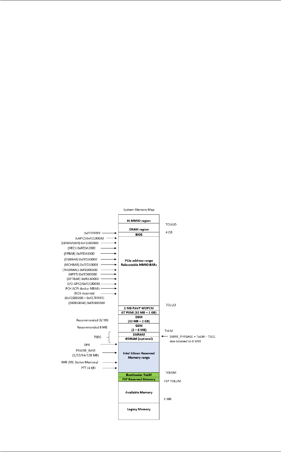
8 FSP INTEGRATION
3.6.5 NotifyPhase API
Please refer Chapter 8.9 in the FSP External Architecture Specification version 2.0 for the prototype, parameters
and return value details for this API.
3.6.5.1 PostPciEnumeration Notification
This phase EnumInitPhaseAfterPciEnumeration is to be called after PCI enumeration but before execution of third
party code such as option ROMs. Currently, nothing is done in this phase, but in the future updates, programming
may be done in this phase.
3.6.5.2 ReadyToBoot Notification
This phase EnumInitPhaseReadyToBoot is to be called before giving control to boot. It includes some final initial-
ization steps recommended by the BWG, including power management settings, Send ME Message EOP (End of
Post).
3.6.5.3 EndOfFirmware Notification
This phase EnumInitEndOfFirmware is to be called before the firmware/preboot environment transfers management
of all system resources to the OS or next level execution environment. It includes final locking of chipset registers
3.7 Memory Map
Below diagram represents the memory map allocated by FSP including the FSP specific regions.
Figure 3.1: System Memory Map

9
/∗∗

10 FSP INTEGRATION
Chapter 4
FSP PORTING RECOMMENDATION
4 FSP Porting Recommendation
Here listed some notes or recommendation when porting with FSP.
4.1 Locking PAM register
FSP 2.0 introduced EndOfFirmware Notify phase callback which is a recommended place for locking PAM registers
so FSP by default implemented this way. If it is still too early to lock PAM registers then the PAM locking code inside
FSP can be disabled by UPD ->FSP_S_TEST_CONFIG ->SkipPamLock or SA policy ->_SI_PREMEM_PO←-
LICY_STRUCT ->SA_MISC_PEI_CONFIG ->SkipPamLock, and platform or wrapper code should do the PAM
locking right before booting OS (so do it outside FSP instead) by programming one PCI config space register as
below.
This PAM locking step has to been applied in all boot paths including S3 resume. To lock PAM regsiter:
MmioOr32 (B0: D0: F0: Register 0x80, BIT0)
4.2 Locking SMRAM register
Since SMRAM locking is recommended to be locked before any 3rd party OpROM execution and highly depending
on platform code implementation, the FSP code by default will not lock it. The platform or FSP Wrapper code
should lock SMRAM by below programming step before any 3rd partiy OpRom execution (and should be locked in
S3 resume right before OS waking vector).
PciOr8 (B0: D0: F0: Register 0x88, BIT4); Note: it must be programmed by CF8/CFC Standard PCI access
mechanism. (MMIO access will not work)
4.3 Locking SMI register
Global SMI bit is recommended to be locked before any 3rd party OpROM execution and highly depending on
platform code implementation after SMM configuration. FSP by default will not lock it. Boot loader is responsible for
locking below regsiters after SMM configuration. Set AcpiBase + 0x30[0] to 1b to enable global SMI. Set PMC PCI
offset A0h[4] = 1b to lock SMI.
4.4 Verify below settings are correct for your platforms
PMC PciCfgSpace is not PCI compliant.FSP will hide the PMC controller to avoid external software or OS from
corrupting the BAR addresses. FSP will program the PMC controller IO and MMIO BAR's with below addresses.
Please use this addrerss in the wrapper code instead of reading from PMC controller.

12 FSP PORTING RECOMMENDATION
Register Values
ABASE 0x1800
PWRMBASE 0xFE000000
PCIEXBAR_BASE_ADDRESS 0xE0000000
Note
:
• Boot Loader can use different value for PCIEXBAR_BASE_ADDRESS either by modifying the UPD
(under FSP-T) or by overriding the PCIEXBAR (B0:D0:F0:R60h) before calling FspMemoryInit Api.
• Boot Loader should avoid using conflicting address when reprogramming PCIEXBAR_BASE_ADDR←-
ESS than the recommended one.
4.5 FSP_STATUS_RESET_REQUIRED
As per FSP External Architecture Specification version 2.0, Any reset required in the FSP flow will be reported as
return status FSP_STATUS_RESET_REQUIREDx by the API.It is the bootloader responsibility to reset the system
according to the reset type requested.
Below table specifies the return status returned by FSP API and the requested reset type.
FSP_STATUS_RESET_REQUIRED Code Reset Type requested
0x40000001 Cold Reset
0x40000002 Warm Reset
0x40000003 Global Reset - Puts the system to Global reset
through Heci or Full Reset through PCH
0x40000004 Reserved
0x40000005 Reserved
0x40000006 Reserved
0x40000007 Reserved
0x40000008 Reserved

Chapter 5
UPD PORTING GUIDE
5 UPD porting guide
UPD porting guide:
UPD Dependency Description Value
EnableSgx CoffeeLake Platform Temporary workaround 2
PchTraceHubMode CoffeeLake Pch A0 BIOS workaround for
TraceHub power gating
issue on PCH A0
2
PchTraceHubMem←-
Reg0Size
CoffeeLake Pch A0 BIOS workaround for
TraceHub power gating
issue on PCH A0
3
PchTraceHubMem←-
Reg1Size
CoffeeLake Pch A0 BIOS workaround for
TraceHub power gating
issue on PCH A0
3
CstateLatencyControl1←-
Irtl
Server platform Server platform should
has different setting
0x6B
PchPcieHsioRxSetCtle←-
Enable
Board design Different board requires
different value
tune
PchPcieHsioRxSetCtle Board design Different board requires
different value
tune
PchSataHsioRxGen3←-
EqBoostMagEnable
Board design Different board requires
different value
tune
PchSataHsioRxGen3←-
EqBoostMag
Board design Different board requires
different value
tune
PchSataHsioTxGen1←-
DownscaleAmpEnable
Board design Different board requires
different value
tune
PchSataHsioTxGen1←-
DownscaleAmp
Board design Different board requires
different value
tune
PchSataHsioTxGen2←-
DownscaleAmpEnable
Board design Different board requires
different value
tune
PchSataHsioTxGen2←-
DownscaleAmp
Board design Different board requires
different value
tune
PchNumRsvdSmbus←-
Addresses
Board design Different board requires
different value
tune
RsvdSmbusAddress←-
TablePtr
Board design Different board requires
different value
tune

14 UPD PORTING GUIDE
BiosSize Board design Different board requires
different value
tune
Chapter 6
FSP OUTPUT
6 FSP Output
The FSP builds a series of data structures called the Hand-Off-Blocks (HOBs) as it progresses through initializing
the silicon.
Please refer to the Platform Initialization (PI) Specification - Volume 3: Shared Architectural Elements specification
for PI Architectural HOBs. Please refer Chapter 9 in the FSP External Architecture Specification version 2.0 for
details about FSP Architectural HOBs.
Below section describe the HOBs not covered in the above two specifications.
6.1 SMRAM Resource Descriptor HOB
The FSP will report the system SMRAM T-SEG range through a generic resource HOB if T-SEG is enabled. The
owner field of the HOB identifies the owner as T-SEG.
#define FSP_HOB_RESOURCE_OWNER_TSEG_GUID \
{ 0xd038747c, 0xd00c, 0x4980, { 0xb3, 0x19, 0x49, 0x01, 0x99, 0xa4, 0x7d, 0x55 } }
6.2 SMBIOS INFO HOB
The FSP will report the SMBIOS through a HOB with below GUID. This information can be consumed by the
bootloader to produce the SMBIOS tables. These structures are included as part of MemInfoHob.h ,Smbios←-
CacheInfoHob.h,SmbiosProcessorInfoHob.h &FirmwareVersionInfoHob.h
#define SI_MEMORY_INFO_DATA_HOB_GUID \
{ 0x9b2071d4, 0xb054, 0x4e0c, { 0x8d, 0x09, 0x11, 0xcf, 0x8b, 0x9f, 0x03, 0x23 } };
typedef struct {
MrcDimmStatus Status; ///< See MrcDimmStatus for the definition of this field.
UINT8 DimmId;
UINT32 DimmCapacity; ///< DIMM size in MBytes.
UINT16 MfgId;
UINT8 ModulePartNum[20]; ///< Module part number for DDR3 is 18 bytes however for DRR4
20 bytes as per JEDEC Spec, so reserving 20 bytes
UINT8 RankInDimm; ///< The number of ranks in this DIMM.
UINT8 SpdDramDeviceType; ///< Save SPD DramDeviceType information needed for SMBIOS
structure creation.
UINT8 SpdModuleType; ///< Save SPD ModuleType information needed for SMBIOS
structure creation.
UINT8 SpdModuleMemoryBusWidth; ///< Save SPD ModuleMemoryBusWidth information needed for
SMBIOS structure creation.
UINT8 SpdSave[MAX_SPD_SAVE_DATA]; ///< Save SPD Manufacturing information needed for SMBIOS
structure creation.
}DIMM_INFO;
typedef struct {
UINT8 Status; ///< Indicates whether this channel should be used.
UINT8 ChannelId;

16 FSP OUTPUT
UINT8 DimmCount; ///< Number of valid DIMMs that exist in the channel.
MRC_CH_TIMING Timing[MAX_PROFILE]; ///< The channel timing values.
DIMM_INFO Dimm[MAX_DIMM]; ///< Save the DIMM output characteristics.
} CHANNEL_INFO;
typedef struct {
UINT8 Status; ///< Indicates whether this controller should be used.
UINT16 DeviceId; ///< The PCI device id of this memory controller.
UINT8 RevisionId; ///< The PCI revision id of this memory controller.
UINT8 ChannelCount; ///< Number of valid channels that exist on the controller.
CHANNEL_INFO Channel[MAX_CH]; ///< The following are channel level definitions.
} CONTROLLER_INFO;
typedef struct {
EFI_HOB_GUID_TYPE EfiHobGuidType;
UINT8 Revision;
UINT16 DataWidth;
/// As defined in SMBIOS 3.0 spec
/// Section 7.18.2 and Table 75
UINT8 DdrType; ///< DDR type: DDR3, DDR4, or LPDDR3
UINT32 Frequency; ///< The system’s common memory controller frequency in MT/s.
/// As defined in SMBIOS 3.0 spec
/// Section 7.17.3 and Table 72
UINT8 ErrorCorrectionType;
SiMrcVersion Version;
UINT32 FreqMax;
BOOLEAN EccSupport;
UINT8 MemoryProfile;
UINT32 TotalPhysicalMemorySize;
BOOLEAN XmpProfileEnable;
UINT8 Ratio;
UINT8 RefClk;
UINT32 VddVoltage[MAX_PROFILE];
CONTROLLER_INFO Controller[MAX_NODE];
} MEMORY_INFO_DATA_HOB;
#define SI_MEMORY_PLATFORM_DATA_HOB \
{ 0x6210d62f, 0x418d, 0x4999, { 0xa2, 0x45, 0x22, 0x10, 0x0a, 0x5d, 0xea, 0x44 } }
typedef struct {
UINT8 Revision;
UINT8 Reserved[3];
UINT32 BootMode;
UINT32 TsegSize;
UINT32 TsegBase;
UINT32 PrmrrSize;
UINT32 PrmrrBase;
UINT32 GttBase;
UINT32 MmioSize;
UINT32 PciEBaseAddress;
}MEMORY_PLATFORM_DATA;
typedef struct {
EFI_HOB_GUID_TYPE EfiHobGuidType;
MEMORY_PLATFORM_DATA Data;
UINT8 *Buffer;
} MEMORY_PLATFORM_DATA_HOB;
#define SMBIOS_CACHE_INFO_HOB_GUID \
{ 0xd805b74e, 0x1460, 0x4755, {0xbb, 0x36, 0x1e, 0x8c, 0x8a, 0xd6, 0x78, 0xd7} }
///
/// SMBIOS Cache Info HOB Structure
///
typedef struct {
UINT16 ProcessorSocketNumber;
UINT16 NumberOfCacheLevels; ///< Based on Number of Cache Types L1/L2/L3
UINT8 SocketDesignationStrIndex; ///< String Index in the string Buffer. Example "L1-CACHE"
UINT16 CacheConfiguration; ///< Format defined in SMBIOS Spec v3.0 Section7.8 Table36
UINT16 MaxCacheSize; ///< Format defined in SMBIOS Spec v3.0 Section7.8.1
UINT16 InstalledSize; ///< Format defined in SMBIOS Spec v3.0 Section7.8.1
UINT16 SupportedSramType; ///< Format defined in SMBIOS Spec v3.0 Section7.8.2
UINT16 CurrentSramType; ///< Format defined in SMBIOS Spec v3.0 Section7.8.2
UINT8 CacheSpeed; ///< Cache Speed in nanoseconds. 0 if speed is unknown.
UINT8 ErrorCorrectionType; ///< ENUM Format defined in SMBIOS Spec v3.0 Section 7.8.3
UINT8 SystemCacheType; ///< ENUM Format defined in SMBIOS Spec v3.0 Section 7.8.4
UINT8 Associativity; ///< ENUM Format defined in SMBIOS Spec v3.0 Section 7.8.5
///String Buffer - each string terminated by NULL "0x00"
///String buffer terminated by double NULL "0x0000"
}SMBIOS_CACHE_INFO;
#define SMBIOS_PROCESSOR_INFO_HOB_GUID \
{ 0xe6d73d92, 0xff56, 0x4146, {0xaf, 0xac, 0x1c, 0x18, 0x81, 0x7d, 0x68, 0x71} }
///
/// SMBIOS Processor Info HOB Structure

17
///
typedef struct {
UINT16 TotalNumberOfSockets;
UINT16 CurrentSocketNumber;
UINT8 ProcessorType; ///< ENUM defined in SMBIOS Spec v3.0 Section 7.5.1
///This info is used for both ProcessorFamily and ProcessorFamily2 fields
///See ENUM defined in SMBIOS Spec v3.0 Section 7.5.2
UINT16 ProcessorFamily;
UINT8 ProcessorManufacturerStrIndex; ///< Index of the String in the String Buffer
UINT64 ProcessorId; ///< ENUM defined in SMBIOS Spec v3.0 Section 7.5.3
UINT8 ProcessorVersionStrIndex; ///< Index of the String in the String Buffer
UINT8 Voltage; ///< Format defined in SMBIOS Spec v3.0 Section 7.5.4
UINT16 ExternalClockInMHz; ///< External Clock Frequency. Set to 0 if unknown.
UINT16 CurrentSpeedInMHz; ///< Snapshot of current processor speed during boot
UINT8 Status; ///< Format defined in the SMBIOS Spec v3.0 Table 21
UINT8 ProcessorUpgrade; ///< ENUM defined in SMBIOS Spec v3.0 Section 7.5.5
///This info is used for both CoreCount & CoreCount2 fields
/// See detailed description in SMBIOS Spec v3.0 Section 7.5.6
UINT16 CoreCount;
///This info is used for both CoreEnabled & CoreEnabled2 fields
///See detailed description in SMBIOS Spec v3.0 Section 7.5.7
UINT16 EnabledCoreCount;
///This info is used for both ThreadCount & ThreadCount2 fields
/// See detailed description in SMBIOS Spec v3.0 Section 7.5.8
UINT16 ThreadCount;
UINT16 ProcessorCharacteristics; ///< Format defined in SMBIOS Spec v3.0 Section 7.5.9
/// String Buffer - each string terminated by NULL "0x00"
/// String buffer terminated by double NULL "0x0000"
}SMBIOS_PROCESSOR_INFO;
#define SMBIOS_FIRMWARE_VERSION_INFO_HOB_GUID \
{ 0x798e722e, 0x15b2, 0x4e13, { 0x8a, 0xe9, 0x6b, 0xa3, 0x0f, 0xf7, 0xf1, 0x67 }}
///
/// Firmware Version Structure
///
typedef struct {
UINT8 MajorVersion;
UINT8 MinorVersion;
UINT8 Revision;
UINT16 BuildNumber;
}FIRMWARE_VERSION;
///
/// Firmware Version Information Structure
///
typedef struct {
UINT8 ComponentNameIndex; ///< Offset 0 Index of Component Name
UINT8 VersionStringIndex; ///< Offset 1 Index of Version String
FIRMWARE_VERSION Version; ///< Offset 2-6 Firmware
version
}FIRMWARE_VERSION_INFO;
///
/// The Smbios structure header.
///
typedef struct {
UINT8 Type;
UINT8 Length;
UINT16 Handle;
}SMBIOS_STRUCTURE;
///
/// Firmware Version Information HOB Structure
///
typedef struct {
EFI_HOB_GUID_TYPE Header; ///< Offset 0-23 The header of FVI HOB
SMBIOS_STRUCTURE SmbiosData; ///< Offset 24-27 The SMBIOS
header of FVI HOB
UINT8 Count; ///< Offset 28 Number of FVI elements
included.
///
/// FIRMWARE_VERSION_INFO structures followed by the null terminated string buffer
///
}FIRMWARE_VERSION_INFO_HOB;
6.3 CHIPSETINIT INFO HOB
The FSP will report the ChipsetInit CRC through a HOB with below GUID. This information can be consumed by the
bootloader to check if ChipsetInit CRC is matched between BIOS and ME. These structures are included as part of
FspsUpd.h

18 FSP OUTPUT
#define CHIPSETINIT_INFO_HOB_GUID \
{ 0xc1392859, 0x1f65, 0x446e, { 0xb3, 0xf5, 0x84, 0x35, 0xfc, 0xc7, 0xd1, 0xc4 }}
///
/// The ChipsetInit Info structure provides the information of ME ChipsetInit CRC and BIOS ChipsetInit CRC.
///
typedef struct {
UINT8 Revision;
UINT8 Rsvd[3];
UINT16 MeChipInitCrc;
UINT16 BiosChipInitCrc;
}CHIPSET_INIT_INFO;
6.4 HOB USAGE INFO HOB
The FSP will report the Hob memory usage through a HOB with below GUID. This information can be consumed by
the bootloader to check how many the temporary ram left.
#define HOB_USAGE_DATA_HOB_GUID \
{0xc764a821, 0xec41, 0x450d, { 0x9c, 0x99, 0x27, 0x20, 0xfc, 0x7c, 0xe1, 0xf6 }}
typedef struct {
EFI_PHYSICAL_ADDRESS EfiMemoryTop;
EFI_PHYSICAL_ADDRESS EfiMemoryBottom;
EFI_PHYSICAL_ADDRESS EfiFreeMemoryTop;
EFI_PHYSICAL_ADDRESS EfiFreeMemoryBottom;
UINTN FreeMemory;
}HOB_USAGE_DATA_HOB;
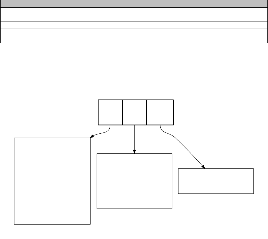
Chapter 7
FSP POSTCODE
7 FSP PostCode
The FSP outputs 16 bit postcode to indicate which API and in which module the execution is happening.
Bit Range Description
Bit15 - Bit12 (X) used to indicate the phase/api under which the code
is executing
Bit11 - Bit8 (Y) used to indicate the module
Bit7 (ZZ bit 7) reserved for error
Bit6 - Bit0 (ZZ) individual codes
7.1 PostCode Info
Below diagram represents the 16 bit PostCode usage in FSP.
X Y ZZ
FSP API - 4 BITS (one Digit)
F - Tempraminit /SEC
E - Reserved
D - MemoryInit /Pre-Memory
C - Reserved
B - Tempramexit
A - Reserved
9 - SiliconInit /Post Memory
8 - Reserved
7 - Reserved
6 - Notify / Post PCIE Enumeration
5 - Reserved
4 - Notify / Ready To Boot
3 - Reserved
2 - Notify / End Of Firmware
1-0 - Reserved
Module - 4 BITS (one digit)
7 - Gfx PEIM
8 - FSP Common Code
9 - Silicon Common Code
A - System Agent
B - PCH
C - CPU
D - MRC
E - ME-BIOS
F - Reserved
Individual Codes
0x00 - API Entry
0x7F - API Exit
(Bit7 reserved for error)
7.1.1 TempRamInit API Status Codes (0xFxxx)

20 FSP POSTCODE
PostCode Module Description
0x0000 FSP TempRamInit API Entry (The
change in upper byte is due to not
enabling of the Port81 early in the
boot)
0x007F FSP TempRamInit API Exit
7.1.2 FspMemoryInit API Status Codes (0xDxxx)
PostCode Module Description
0xD800 FSP FspMemoryInit API Entry
0xD87F FSP FSpMemoryInit API Exit
0xDA00 SA Pre-Mem SaInit Entry
0xDA02 SA OverrideDev0Did Start
0xDA04 SA OverrideDev2Did Start
0xDA06 SA Programming SA Bars
0xDA08 SA Install SA HOBs
0xDA0A SA Reporting SA PCIe code version
0xDA0C SA SaSvInit Start
0xDA10 SA Initializing DMI
0xDA15 SA Initialize TCSS PreMem
0xDA1F SA Initializing DMI/OPI Max PayLoad
Size
0xDA20 SA Initializing SwitchableGraphics
0xDA30 SA Initializing SA PCIe
0xDA3F SA Programming PEG credit values
Start
0xDA40 SA Initializing DMI Tc/Vc mapping
0xDA42 SA CheckOffboardPcieVga
0xDA44 SA CheckAndInitializePegVga
0xDA50 SA Initializing Graphics
0xDA52 SA Initializing System Agent
Overclocking
0xDA7F SA Pre-Mem SaInit Exit
0xDB00 PCH Pre-Mem PchInit Entry
0xDB02 PCH Pre-Mem Disable PCH fused
controllers
0xDB15 PCH Pre-Mem SMBUS configuration
0xDB48 PCH Pre-Mem PchOnPolicyInstalled
Entry
0xDB49 PCH Pre-Mem Program HSIO
0xDB4A PCH Pre-Mem DCI configuration
0xDB4C PCH Pre-Mem Host DCI enabled
0xDB4D PCH Pre-Mem Trace Hub - Early
configuration
0xDB4E PCH Pre-Mem Trace Hub - Device
disabled
0xDB4F PCH Pre-Mem TraceHub -
Programming MSR

21
0xDB50 PCH Pre-Mem Trace Hub - Power
gating configuration
0xDB51 PCH Pre-Mem Trace Hub - Power
gating Trace Hub device and
locking HSWPGCR1 register
0xDB52 PCH Pre-Mem Initialize HPET timer
0xDB55 PCH Pre-Mem PchOnPolicyInstalled
Exit
0xDB7F PCH Pre-Mem PchInit Exit
0xDC00 CPU CPU Pre-Mem Entry
0xDC0F CPU CpuAddPreMemConfigBlocks
Done
0xDC20 CPU CpuOnPolicyInstalled Start
0xDC2F CPU XmmInit Start
0xDC3F CPU TxtInit Start
0xDC4F CPU Init CPU Straps
0xDC5F CPU Init Overclocking
0xDC6F CPU CPU Pre-Mem Exit
0x∗∗55 SA MRC_MEM_INIT_DONE
0x∗∗D5 SA MRC_MEM_INIT_DONE_WITH←-
_ERRORS
0xDD00 SA MRC_INITIALIZATION_START
0xDD10 SA MRC_CMD_PLOT_2D
0xDD1B SA MRC_FAST_BOOT_PERMITTED
0xDD1C SA MRC_RESTORE_NON_TRAINI←-
NG
0xDD1D SA MRC_PRINT_INPUT_PARAMS
0xDD1E SA MRC_SET_OVERRIDES_PSPD
0xDD20 SA MRC_SPD_PROCESSING
0xDD21 SA MRC_SET_OVERRIDES
0xDD22 SA MRC_MC_CAPABILITY
0xDD23 SA MRC_MC_CONFIG
0xDD24 SA MRC_MC_MEMORY_MAP
0xDD25 SA MRC_JEDEC_INIT_LPDDR3
0xDD26 SA MRC_RESET_SEQUENCE
0xDD27 SA MRC_PRE_TRAINING
0xDD28 SA MRC_EARLY_COMMAND
0xDD29 SA MRC_SENSE_AMP_OFFSET
0xDD2A SA MRC_READ_MPR
0xDD2B SA MRC_RECEIVE_ENABLE
0xDD2C SA MRC_JEDEC_WRITE_LEVELI←-
NG
0xDD2D SA MRC_LPDDR_LATENCY_SET_B
0xDD2E SA MRC_WRITE_TIMING_1D
0xDD2F SA MRC_READ_TIMING_1D
0xDD30 SA MRC_DIMM_ODT
0xDD31 SA MRC_EARLY_WRITE_TIMING←-
_2D

22 FSP POSTCODE
0xDD32 SA MRC_WRITE_DS
0xDD33 SA MRC_WRITE_EQ
0xDD34 SA MRC_EARLY_READ_TIMING_←-
2D
0xDD35 SA MRC_READ_ODT
0xDD36 SA MRC_READ_EQ
0xDD37 SA MRC_READ_AMP_POWER
0xDD38 SA MRC_WRITE_TIMING_2D
0xDD39 SA MRC_READ_TIMING_2D
0xDD3A SA MRC_CMD_VREF
0xDD3B SA MRC_WRITE_VREF_2D
0xDD3C SA MRC_READ_VREF_2D
0xDD3D SA MRC_POST_TRAINING
0xDD3E SA MRC_LATE_COMMAND
0xDD3F SA MRC_ROUND_TRIP_LAT
0xDD40 SA MRC_TURN_AROUND
0xDD41 SA MRC_CMP_OPT
0xDD42 SA MRC_SAVE_MC_VALUES
0xDD43 SA MRC_RESTORE_TRAINING
0xDD44 SA MRC_RMT_TOOL
0xDD45 SA MRC_WRITE_SR
0xDD46 SA MRC_DIMM_RON
0xDD47 SA MRC_RCVEN_TIMING_1D
0xDD48 SA MRC_MR_FILL
0xDD49 SA MRC_PWR_MTR
0xDD4A SA MRC_DDR4_MAPPING
0xDD4B SA MRC_WRITE_VOLTAGE_1D
0xDD4C SA MRC_EARLY_RDMPR_TIMING←-
_2D
0xDD4D SA MRC_FORCE_OLTM
0xDD50 SA MRC_MC_ACTIVATE
0xDD51 SA MRC_RH_PREVENTION
0xDD52 SA MRC_GET_MRC_DATA
0xDD53 SA Reserved
0xDD58 SA MRC_RETRAIN_CHECK
0xDD5A SA MRC_SA_GV_SWITCH
0xDD5B SA MRC_ALIAS_CHECK
0xDD5C SA MRC_ECC_CLEAN_START
0xDD5D SA MRC_DONE
0xDD5F SA MRC_CPGC_MEMORY_TEST
0xDD60 SA MRC_TXT_ALIAS_CHECK
0xDD61 SA MRC_ENG_PERF_GAIN
0xDD68 SA MRC_MEMORY_TEST
0xDD69 SA MRC_FILL_RMT_STRUCTURE
0xDD70 SA MRC_SELF_REFRESH_EXIT
0xDD71 SA MRC_NORMAL_MODE
0xDD7D SA MRC_SSA_PRE_STOP_POINT
0xDD7F SA MRC_SSA_STOP_POINT,
MRC_INITIALIZATION_END

23
0xDD90 SA MRC_CMD_PLOT_2D_ERROR
0xDD9B SA MRC_FAST_BOOT_PERMITTE←-
D_ERROR
0xDD9C SA MRC_RESTORE_NON_TRAINI←-
NG_ERROR
0xDD9D SA MRC_PRINT_INPUT_PARAMS←-
_ERROR
0xDD9E SA MRC_SET_OVERRIDES_PSP←-
D_ERROR
0xDDA0 SA MRC_SPD_PROCESSING_ER←-
ROR
0xDDA1 SA MRC_SET_OVERRIDES_ERR←-
OR
0xDDA2 SA MRC_MC_CAPABILITY_ERROR
0xDDA3 SA MRC_MC_CONFIG_ERROR
0xDDA4 SA MRC_MC_MEMORY_MAP_ER←-
ROR
0xDDA5 SA MRC_JEDEC_INIT_LPDDR3_E←-
RROR
0xDDA6 SA MRC_RESET_ERROR
0xDDA7 SA MRC_PRE_TRAINING_ERROR
0xDDA8 SA MRC_EARLY_COMMAND_ER←-
ROR
0xDDA9 SA MRC_SENSE_AMP_OFFSET_←-
ERROR
0xDDAA SA MRC_READ_MPR_ERROR
0xDDAB SA MRC_RECEIVE_ENABLE_ERR←-
OR
0xDDAC SA MRC_JEDEC_WRITE_LEVELI←-
NG_ERROR
0xDDAD SA MRC_LPDDR_LATENCY_SET_←-
B_ERROR
0xDDAE SA MRC_WRITE_TIMING_1D_ER←-
ROR
0xDDAF SA MRC_READ_TIMING_1D_ERR←-
OR
0xDDB0 SA MRC_DIMM_ODT_ERROR
0xDDB1 SA MRC_EARLY_WRITE_TIMING←-
_ERROR
0xDDB2 SA MRC_WRITE_DS_ERROR
0xDDB3 SA MRC_WRITE_EQ_ERROR
0xDDB4 SA MRC_EARLY_READ_TIMING_←-
ERROR
0xDDB5 SA MRC_READ_ODT_ERROR
0xDDB6 SA MRC_READ_EQ_ERROR
0xDDB7 SA MRC_READ_AMP_POWER_E←-
RROR
0xDDB8 SA MRC_WRITE_TIMING_2D_ER←-
ROR
0xDDB9 SA MRC_READ_TIMING_2D_ERR←-
OR

24 FSP POSTCODE
0xDDBA SA MRC_CMD_VREF_ERROR
0xDDBB SA MRC_WRITE_VREF_2D_ERR←-
OR
0xDDBC SA MRC_READ_VREF_2D_ERROR
0xDDBD SA MRC_POST_TRAINING_ERROR
0xDDBE SA MRC_LATE_COMMAND_ERR←-
OR
0xDDBF SA MRC_ROUND_TRIP_LAT_ERR←-
OR
0xDDC0 SA MRC_TURN_AROUND_ERROR
0xDDC1 SA MRC_CMP_OPT_ERROR
0xDDC2 SA MRC_SAVE_MC_VALUES_ER←-
ROR
0xDDC3 SA MRC_RESTORE_TRAINING_E←-
RROR
0xDDC4 SA MRC_RMT_TOOL_ERROR
0xDDC5 SA MRC_WRITE_SR_ERROR
0xDDC6 SA MRC_DIMM_RON_ERROR
0xDDC7 SA MRC_RCVEN_TIMING_1D_ER←-
ROR
0xDDC8 SA MRC_MR_FILL_ERROR
0xDDC9 SA MRC_PWR_MTR_ERROR
0xDDCA SA MRC_DDR4_MAPPING_ERROR
0xDDCB SA MRC_WRITE_VOLTAGE_1D_E←-
RROR
0xDDCC SA MRC_EARLY_RDMPR_TIMING←-
_2D_ERROR
0xDDCD SA MRC_FORCE_OLTM_ERROR
0xDDD0 SA MRC_MC_ACTIVATE_ERROR
0xDDD1 SA MRC_RH_PREVENTION_ERR←-
OR
0xDDD2 SA MRC_GET_MRC_DATA_ERROR
0xDDD3 SA Reserved
0xDDD8 SA MRC_RETRAIN_CHECK_ERR←-
OR
0xDDDA SA MRC_SA_GV_SWITCH_ERROR
0xDDDB SA MRC_ALIAS_CHECK_ERROR
0xDDDC SA MRC_ECC_CLEAN_ERROR
0xDDDD SA MRC_DONE_WITH_ERROR
0xDDDF SA MRC_CPGC_MEMORY_TEST_←-
ERROR
0xDDE0 SA MRC_TXT_ALIAS_CHECK_ER←-
ROR
0xDDE1 SA MRC_ENG_PERF_GAIN_ERR←-
OR
0xDDE8 SA MRC_MEMORY_TEST_ERROR
0xDDE9 SA MRC_FILL_RMT_STRUCTURE←-
_ERROR
0xDDF0 SA MRC_SELF_REFRESH_EXIT_←-
ERROR

25
0xDDF1 SA MRC_MRC_NORMAL_MODE_←-
ERROR
0xDDFD SA MRC_SSA_PRE_STOP_POINT←-
_ERROR
0xDDFE SA MRC_NO_MEMORY_DETECT←-
ED
7.1.3 TempRamExit API Status Codes (0xBxxx)
PostCode Module Description
0xB800 FSP TempRamExit API Entry
0xB87F FSP TempRamExit API Exit
7.1.4 FspSiliconInit API Status Codes (0x9xxx)
PostCode Module Description
0x9800 FSP FspSiliconInit API Entry
0x987F FSP FspSiliconInit API Exit
0x9A00 SA PostMem SaInit Entry
0x9A01 SA DeviceConfigure Start
0x9A02 SA UpdateSaHobPostMem Start
0x9A03 SA Initializing Pei Display
0x9A04 SA PeiGraphicsNotifyCallback Entry
0x9A05 SA CallPpiAndFillFrameBuffer
0x9A06 SA GraphicsPpiInit
0x9A07 SA GraphicsPpiGetMode
0x9A08 SA FillFrameBufferAndShowLogo
0x9A0F SA PeiGraphicsNotifyCallback Exit
0x9A14 SA Initializing SA IPU device
0x9A16 SA Initializing SA GNA device
0x9A1A SA SaProgramLlcWays Start
0x9A20 SA Initializing PciExpressInitPostMem
0x9A22 SA Initializing
ConfigureNorthIntelTraceHub
0x9A30 SA Initializing Vtd
0x9A31 SA Initializing TCSS
0x9A32 SA Initializing Pavp
0x9A34 SA PeiInstallSmmAccessPpi Start
0x9A36 SA EdramWa Start
0x9A4F SA Post-Mem SaInit Exit
0x9A50 SA SaSecurityLock Start
0x9A5F SA SaSecurityLock End
0x9A60 SA SaSResetComplete Entry
0x9A61 SA Set BIOS_RESET_CPL to indicate
all configurations complete
0x9A62 SA SaSvInit2 Start
0x9A63 SA GraphicsPmInit Start
0x9A64 SA SaPciPrint Start

26 FSP POSTCODE
0x9A6F SA SaSResetComplete Exit
0x9A70 SA SaS3ResumeAtEndOfPei Callback
Entry
0x9A7F SA SaS3ResumeAtEndOfPei Callback
Exit
0x9B00 PCH Post-Mem PchInit Entry
0x9B03 PCH Post-Mem Tune the USB 2.0
high-speed signals quality
0x9B04 PCH Post-Mem Tune the USB 3.0
signals quality
0x9B05 PCH Post-Mem Configure PCH xHCI
0x9B06 PCH Post-Mem Performs configuration
of PCH xHCI SSIC
0x9B07 PCH Post-Mem Configure PCH xHCI
after init
0x9B08 PCH Post-Mem Configures PCH USB
device (xDCI)
0x9B0A PCH Post-Mem DMI/OP-DMI
configuration
0x9B0B PCH Post-Mem Initialize P2SB
controller
0x9B0C PCH Post-Mem IOAPIC initialization
0x9B0D PCH Post-Mem PCH devices interrupt
configuration
0x9B0E PCH Post-Mem HD Audio initizalization
0x9B0F PCH Post-Mem HD Audio Codec
enumeration
0x9B10 PCH Post-Mem HD Audio Codec not
detected
0x9B13 PCH Post-Mem SCS initizalization
0x9B14 PCH Post-Mem ISH initizalization
0x9B15 PCH Post-Mem Configure SMBUS
power management
0x9B16 PCH Post-Mem Reserved
0x9B17 PCH Post-Mem Performing global reset
0x9B18 PCH Post-Mem Reserved
0x9B19 PCH Post-Mem Reserved
0x9B40 PCH Post-Mem OnEndOfPEI Entry
0x9B41 PCH Post-Mem Initialize Thermal
controller
0x9B42 PCH Post-Mem Configure Memory
Throttling
0x9B47 PCH Post-Mem OnEndOfPEI Exit
0x9B4D PCH Post-Mem Trace Hub - Memory
configuration
0x9B4E PCH Post-Mem Trace Hub - MSC0
configured
0x9B4F PCH Post-Mem Trace Hub - MSC1
configured
0x9B7F PCH Post-Mem PchInit Exit
0x9C00 CPU CPU Post-Mem Entry

27
0x9C09 CPU CpuAddConfigBlocks Done
0x9C0A CPU SetCpuStrapAndEarlyPowerOn←-
Config
Start
0x9C13 CPU SetCpuStrapAndEarlyPowerOn←-
Config
Reset
0x9C14 CPU SetCpuStrapAndEarlyPowerOn←-
Config
Done
0x9C15 CPU CpuInit Start
0x9C16 CPU SgxInitializationPrePatchLoad
Start
0x9C17 CPU CollectProcessorFeature Start
0x9C18 CPU ProgramProcessorFeature Start
0x9C19 CPU ProgramProcessorFeature Done
0x9C20 CPU CpuInitPreResetCpl Start
0x9C21 CPU ProcessorsPrefetcherInitialization
Start
0x9C22 CPU InitRatl Start
0x9C23 CPU ConfigureSvidVrs Start
0x9C24 CPU ConfigurePidSettings Start
0x9C25 CPU SetBootFrequency Start
0x9C26 CPU CpuOcInitPreMem Start
0x9C27 CPU CpuOcInit Reset
0x9C28 CPU BiosGuardInit Start
0x9C29 CPU BiosGuardInit Reset
0x9C3F CPU CpuInitPreResetCpl Done
0x9C42 CPU SgxActivation Start
0x9C43 CPU InitializeCpuDataHob Start
0x9C44 CPU InitializeCpuDataHob Done
0x9C4F CPU CpuInit Done
0x9C50 CPU S3InitializeCpu Start
0x9C55 CPU MpRendezvousProcedure Start
0x9C56 CPU MpRendezvousProcedure Done
0x9C69 CPU S3InitializeCpu Done
0x9C6A CPU CpuPowerMgmtInit Start
0x9C71 CPU InitPpm
0x9C7F CPU CPU Post-Mem Exit
0x9C80 CPU ReloadMicrocodePatch Start
0x9C81 CPU ReloadMicrocodePatch Done
0x9C82 CPU ApSafePostMicrocodePatchInit
Start
0x9C83 CPU ApSafePostMicrocodePatchInit
Done
7.1.5 NotifyPhase API Status Codes (0x6xxx)
PostCode Module Description
0x6800 FSP NotifyPhase API Entry
0x687F FSP NotifyPhase API Exit

28 FSP POSTCODE

30 Todo List

32 Deprecated List
Chapter 10
Class Index
10.1 Class List
Here are the classes, structs, unions and interfaces with brief descriptions:
AUDIO_AZALIA_VERB_TABLE
Audio Azalia Verb Table structure . . . . . . . . . . . . . . . . . . . . . . . . . . . . . . . . . 37
AZALIA_HEADER
Azalia Header structure . . . . . . . . . . . . . . . . . . . . . . . . . . . . . . . . . . . . . . 38
CHIPSET_INIT_INFO
The ChipsetInit Info structure provides the information of ME ChipsetInit CRC and BIO←-
S ChipsetInit CRC . . . . . . . . . . . . . . . . . . . . . . . . . . . . . . . . . . . . . . . . 38
DIMM_INFO
Memory SMBIOS & OC Memory Data Hob . . . . . . . . . . . . . . . . . . . . . . . . . . . 39
FIRMWARE_VERSION
Firmware Version Structure . . . . . . . . . . . . . . . . . . . . . . . . . . . . . . . . . . . . 39
FIRMWARE_VERSION_INFO
Firmware Version Information Structure . . . . . . . . . . . . . . . . . . . . . . . . . . . . . 40
FIRMWARE_VERSION_INFO_HOB
Firmware Version Information HOB Structure . . . . . . . . . . . . . . . . . . . . . . . . . . 40
FSP_M_CONFIG
Fsp M Configuration . . . . . . . . . . . . . . . . . . . . . . . . . . . . . . . . . . . . . . . 41
FSP_M_TEST_CONFIG
Fsp M Test Configuration . . . . . . . . . . . . . . . . . . . . . . . . . . . . . . . . . . . . . 82
FSP_S_CONFIG
Fsp S Configuration . . . . . . . . . . . . . . . . . . . . . . . . . . . . . . . . . . . . . . . . 95
FSP_S_TEST_CONFIG
Fsp S Test Configuration . . . . . . . . . . . . . . . . . . . . . . . . . . . . . . . . . . . . . 147
FSP_T_CONFIG
Fsp T Configuration . . . . . . . . . . . . . . . . . . . . . . . . . . . . . . . . . . . . . . . . 169
FSPM_UPD
Fsp M UPD Configuration . . . . . . . . . . . . . . . . . . . . . . . . . . . . . . . . . . . . 170
FSPS_UPD
Fsp S UPD Configuration . . . . . . . . . . . . . . . . . . . . . . . . . . . . . . . . . . . . . 171
FSPT_CORE_UPD
Fsp T Core UPD . . . . . . . . . . . . . . . . . . . . . . . . . . . . . . . . . . . . . . . . . 172
FSPT_UPD
Fsp T UPD Configuration . . . . . . . . . . . . . . . . . . . . . . . . . . . . . . . . . . . . . 173
GPIO_CONFIG
GPIO configuration structure used for pin programming . . . . . . . . . . . . . . . . . . . . . 174
HOB_USAGE_DATA_HOB
Hob Usage Data Hob . . . . . . . . . . . . . . . . . . . . . . . . . . . . . . . . . . . . . . . 176

34 Class Index
MEMORY_PLATFORM_DATA
Memory Platform Data Hob . . . . . . . . . . . . . . . . . . . . . . . . . . . . . . . . . . . . 176
SI_PCH_DEVICE_INTERRUPT_CONFIG
The PCH_DEVICE_INTERRUPT_CONFIG block describes interrupt pin, IRQ and interrupt
mode for PCH device . . . . . . . . . . . . . . . . . . . . . . . . . . . . . . . . . . . . . . . 176
SMBIOS_CACHE_INFO
SMBIOS Cache Info HOB Structure . . . . . . . . . . . . . . . . . . . . . . . . . . . . . . . 177
SMBIOS_PROCESSOR_INFO
SMBIOS Processor Info HOB Structure . . . . . . . . . . . . . . . . . . . . . . . . . . . . . 178
SMBIOS_STRUCTURE
The Smbios structure header . . . . . . . . . . . . . . . . . . . . . . . . . . . . . . . . . . . 179
Chapter 11
File Index
11.1 File List
Here is a list of all documented files with brief descriptions:
FirmwareVersionInfoHob.h
Header file for Firmware Version Information . . . . . . . . . . . . . . . . . . . . . . . . . . . 181
FspFixedPcds.h
This file lists all FixedAtBuild PCDs referenced in FSP integration guide . . . . . . . . . . . . 182
FspInfoHob.h
Header file for FSP Information HOB . . . . . . . . . . . . . . . . . . . . . . . . . . . . . . . 182
FspmUpd.h
Copyright (c) 2019, Intel Corporation . . . . . . . . . . . . . . . . . . . . . . . . . . . . . . . 183
FspsUpd.h
Copyright (c) 2019, Intel Corporation . . . . . . . . . . . . . . . . . . . . . . . . . . . . . . . 184
FsptUpd.h
Copyright (c) 2019, Intel Corporation . . . . . . . . . . . . . . . . . . . . . . . . . . . . . . . 186
FspUpd.h
Copyright (c) 2019, Intel Corporation . . . . . . . . . . . . . . . . . . . . . . . . . . . . . . . 187
GpioConfig.h
Header file for GpioConfig structure used by GPIO library . . . . . . . . . . . . . . . . . . . . 188
GpioSampleDef.h
Sample enum definitions for GPIO table . . . . . . . . . . . . . . . . . . . . . . . . . . . . . 193
HobUsageDataHob.h
Definitions for Hob Usage data HOB . . . . . . . . . . . . . . . . . . . . . . . . . . . . . . . 194
MemInfoHob.h
This file contains definitions required for creation of Memory S3 Save data, Memory Info data
and Memory Platform data hobs . . . . . . . . . . . . . . . . . . . . . . . . . . . . . . . . . 195
SmbiosCacheInfoHob.h
Header file for SMBIOS Cache Info HOB . . . . . . . . . . . . . . . . . . . . . . . . . . . . . 196
SmbiosProcessorInfoHob.h
Header file for SMBIOS Processor Info HOB . . . . . . . . . . . . . . . . . . . . . . . . . . . 197

36 File Index
Chapter 12
Class Documentation
12.1 AUDIO_AZALIA_VERB_TABLE Struct Reference
Audio Azalia Verb Table structure.
#include <FspsUpd.h>
Collaboration diagram for AUDIO_AZALIA_VERB_TABLE:
AUDIO_AZALIA_VERB_TABLE
AZALIA_HEADER
Header
Public Attributes
•AZALIA_HEADER Header
AZALIA PCH header.
• UINT32 ∗Data
Pointer to the data buffer. Its length is specified in the header.
12.1.1 Detailed Description
Audio Azalia Verb Table structure.
Definition at line 34 of file FspsUpd.h.
The documentation for this struct was generated from the following file:
•FspsUpd.h

38 Class Documentation
12.2 AZALIA_HEADER Struct Reference
Azalia Header structure.
#include <FspsUpd.h>
Public Attributes
• UINT16 VendorId
Codec Vendor ID.
• UINT16 DeviceId
Codec Device ID.
• UINT8 RevisionId
Revision ID of the codec. 0xFF matches any revision.
• UINT8 SdiNum
SDI number, 0xFF matches any SDI.
• UINT16 DataDwords
Number of data DWORDs pointed by the codec data buffer.
• UINT32 Reserved
Reserved for future use. Must be set to 0.
12.2.1 Detailed Description
Azalia Header structure.
Definition at line 22 of file FspsUpd.h.
The documentation for this struct was generated from the following file:
•FspsUpd.h
12.3 CHIPSET_INIT_INFO Struct Reference
The ChipsetInit Info structure provides the information of ME ChipsetInit CRC and BIOS ChipsetInit CRC.
#include <FspmUpd.h>
Public Attributes
• UINT8 Revision
Chipset Init Info Revision.
• UINT8 Rsvd [3]
Reserved.
• UINT16 MeChipInitCrc
16 bit CRC value of MeChipInit Table
• UINT16 BiosChipInitCrc
16 bit CRC value of PchChipInit Table

12.4 DIMM_INFO Struct Reference 39
12.3.1 Detailed Description
The ChipsetInit Info structure provides the information of ME ChipsetInit CRC and BIOS ChipsetInit CRC.
Definition at line 24 of file FspmUpd.h.
The documentation for this struct was generated from the following file:
•FspmUpd.h
12.4 DIMM_INFO Struct Reference
Memory SMBIOS & OC Memory Data Hob.
#include <MemInfoHob.h>
Public Attributes
• UINT8 Status
See MrcDimmStatus for the definition of this field.
• UINT32 DimmCapacity
DIMM size in MBytes.
• UINT8 ModulePartNum [20]
Module part number for DDR3 is 18 bytes however for DRR4 20 bytes as per JEDEC Spec, so reserving 20 bytes.
• UINT8 RankInDimm
The number of ranks in this DIMM.
• UINT8 SpdDramDeviceType
Save SPD DramDeviceType information needed for SMBIOS structure creation.
• UINT8 SpdModuleType
Save SPD ModuleType information needed for SMBIOS structure creation.
• UINT8 SpdModuleMemoryBusWidth
Save SPD ModuleMemoryBusWidth information needed for SMBIOS structure creation.
• UINT8 SpdSave [MAX_SPD_SAVE]
Save SPD Manufacturing information needed for SMBIOS structure creation.
• UINT16 Speed
The maximum capable speed of the device, in MHz.
12.4.1 Detailed Description
Memory SMBIOS & OC Memory Data Hob.
Definition at line 170 of file MemInfoHob.h.
The documentation for this struct was generated from the following file:
•MemInfoHob.h
12.5 FIRMWARE_VERSION Struct Reference
Firmware Version Structure.
#include <FirmwareVersionInfoHob.h>
40 Class Documentation
12.5.1 Detailed Description
Firmware Version Structure.
Definition at line 22 of file FirmwareVersionInfoHob.h.
The documentation for this struct was generated from the following file:
•FirmwareVersionInfoHob.h
12.6 FIRMWARE_VERSION_INFO Struct Reference
Firmware Version Information Structure.
#include <FirmwareVersionInfoHob.h>
Collaboration diagram for FIRMWARE_VERSION_INFO:
FIRMWARE_VERSION_INFO
FIRMWARE_VERSION
Version
Public Attributes
• UINT8 ComponentNameIndex
Offset 0 Index of Component Name.
• UINT8 VersionStringIndex
Offset 1 Index of Version String.
•FIRMWARE_VERSION Version
Offset 2-6 Firmware version.
12.6.1 Detailed Description
Firmware Version Information Structure.
Definition at line 32 of file FirmwareVersionInfoHob.h.
The documentation for this struct was generated from the following file:
•FirmwareVersionInfoHob.h
12.7 FIRMWARE_VERSION_INFO_HOB Struct Reference
Firmware Version Information HOB Structure.

12.8 FSP_M_CONFIG Struct Reference 41
#include <FirmwareVersionInfoHob.h>
Collaboration diagram for FIRMWARE_VERSION_INFO_HOB:
FIRMWARE_VERSION_INFO_HOB
SMBIOS_STRUCTURE
SmbiosData
Public Attributes
• EFI_HOB_GUID_TYPE Header
Offset 0-23 The header of FVI HOB.
•SMBIOS_STRUCTURE SmbiosData
Offset 24-27 The SMBIOS header of FVI HOB.
• UINT8 Count
Offset 28 Number of FVI elements included.
12.7.1 Detailed Description
Firmware Version Information HOB Structure.
Definition at line 52 of file FirmwareVersionInfoHob.h.
12.7.2 Member Data Documentation
12.7.2.1 UINT8 FIRMWARE_VERSION_INFO_HOB::Count
Offset 28 Number of FVI elements included.
Definition at line 55 of file FirmwareVersionInfoHob.h.
The documentation for this struct was generated from the following file:
•FirmwareVersionInfoHob.h
12.8 FSP_M_CONFIG Struct Reference
Fsp M Configuration.
#include <FspmUpd.h>

42 Class Documentation
Public Attributes
• UINT64 PlatformMemorySize
Offset 0x0040 - Platform Reserved Memory Size The minimum platform memory size required to pass control into
DXE.
• UINT32 MemorySpdPtr00
Offset 0x0048 - Memory SPD Pointer Channel 0 Dimm 0 Pointer to SPD data, will be used only when SpdAddress←-
Table SPD Address are marked as 00.
• UINT32 MemorySpdPtr01
Offset 0x004C - Memory SPD Pointer Channel 0 Dimm 1 Pointer to SPD data, will be used only when SpdAddress←-
Table SPD Address are marked as 00.
• UINT32 MemorySpdPtr10
Offset 0x0050 - Memory SPD Pointer Channel 1 Dimm 0 Pointer to SPD data, will be used only when SpdAddress←-
Table SPD Address are marked as 00.
• UINT32 MemorySpdPtr11
Offset 0x0054 - Memory SPD Pointer Channel 1 Dimm 1 Pointer to SPD data, will be used only when SpdAddress←-
Table SPD Address are marked as 00.
• UINT16 MemorySpdDataLen
Offset 0x0058 - SPD Data Length Length of SPD Data 0x100:256 Bytes, 0x200:512 Bytes.
• UINT8 DqByteMapCh0 [12]
Offset 0x005A - Dq Byte Map CH0 Dq byte mapping between CPU and DRAM, Channel 0: board-dependent.
• UINT8 DqByteMapCh1 [12]
Offset 0x0066 - Dq Byte Map CH1 Dq byte mapping between CPU and DRAM, Channel 1: board-dependent.
• UINT8 DqsMapCpu2DramCh0 [8]
Offset 0x0072 - Dqs Map CPU to DRAM CH 0 Set Dqs mapping relationship between CPU and DRAM, Channel 0:
board-dependent.
• UINT8 DqsMapCpu2DramCh1 [8]
Offset 0x007A - Dqs Map CPU to DRAM CH 1 Set Dqs mapping relationship between CPU and DRAM, Channel 1:
board-dependent.
• UINT16 RcompResistor [3]
Offset 0x0082 - RcompResister settings Indicates RcompReister settings: CNL - 0's means MRC auto configured
based on Design Guidelines, otherwise input an Ohmic value per segment.
• UINT16 RcompTarget [5]
Offset 0x0088 - RcompTarget settings RcompTarget settings: CNL - 0's mean MRC auto configured based on Design
Guidelines, otherwise input an Ohmic value per segment.
• UINT8 DqPinsInterleaved
Offset 0x0092 - Dqs Pins Interleaved Setting Indicates DqPinsInterleaved setting: board-dependent $EN_DIS.
• UINT8 CaVrefConfig
Offset 0x0093 - VREF_CA CA Vref routing: board-dependent 0:VREF_CA goes to both CH_A and CH_B, 1: VRE←-
F_CA to CH_A and VREF_DQ_A to CH_B, 2:VREF_CA to CH_A and VREF_DQ_B to CH_B.
• UINT8 SmramMask
Offset 0x0094 - Smram Mask The SMM Regions AB-SEG and/or H-SEG reserved 0: Neither, 1:AB-SEG, 2:H-SEG,
3: Both.
• UINT8 MrcFastBoot
Offset 0x0095 - MRC Fast Boot Enables/Disable the MRC fast path thru the MRC $EN_DIS.
• UINT8 RmtPerTask
Offset 0x0096 - Rank Margin Tool per Task This option enables the user to execute Rank Margin Tool per major
training step in the MRC.
• UINT8 TrainTrace
Offset 0x0097 - Training Trace This option enables the trained state tracing feature in MRC.
• UINT32 IedSize
Offset 0x0098 - Intel Enhanced Debug Intel Enhanced Debug (IED): 0=Disabled, 0x400000=Enabled and 4MB S←-
MRAM occupied 0 : Disable, 0x400000 : Enable.
• UINT32 TsegSize

12.8 FSP_M_CONFIG Struct Reference 43
Offset 0x009C - Tseg Size Size of SMRAM memory reserved.
• UINT16 MmioSize
Offset 0x00A0 - MMIO Size Size of MMIO space reserved for devices.
• UINT8 ProbelessTrace
Offset 0x00A2 - Probeless Trace Probeless Trace: 0=Disabled, 1=Enable.
• UINT8 GdxcIotSize
Offset 0x00A3 - GDXC IOT SIZE Size of IOT and MOT is in 8 MB chunks.
• UINT8 GdxcMotSize
Offset 0x00A4 - GDXC MOT SIZE Size of IOT and MOT is in 8 MB chunks.
• UINT8 SmbusEnable
Offset 0x00A5 - Enable SMBus Enable/disable SMBus controller.
• UINT8 SpdAddressTable [4]
Offset 0x00A6 - Spd Address Tabl Specify SPD Address table for CH0D0/CH0D1/CH1D0&CH1D1.
• UINT8 PlatformDebugConsent
Offset 0x00AA - Platform Debug Consent To 'opt-in' for debug, please select 'Enabled' with the desired debug probe
type.
• UINT8 DciUsb3TypecUfpDbg
Offset 0x00AB - USB3 Type-C UFP2DFP Kernel/Platform Debug Support This BIOS option enables kernel and plat-
form debug for USB3 interface over a UFP Type-C receptacle, select 'No Change' will do nothing to UFP2DFP setting.
• UINT8 PchTraceHubMode
Offset 0x00AC - PCH Trace Hub Mode Select 'Host Debugger' if Trace Hub is used with host debugger tool or 'Target
Debugger' if Trace Hub is used by target debugger software or 'Disable' trace hub functionality.
• UINT8 PchTraceHubMemReg0Size
Offset 0x00AD - PCH Trace Hub Memory Region 0 buffer Size Specify size of Pch trace memory region 0 buffer, the
size can be 0, 1MB, 8MB, 64MB, 128MB, 256MB, 512MB.
• UINT8 PchTraceHubMemReg1Size
Offset 0x00AE - PCH Trace Hub Memory Region 1 buffer Size Specify size of Pch trace memory region 1 buffer, the
size can be 0, 1MB, 8MB, 64MB, 128MB, 256MB, 512MB.
• UINT8 PchPreMemRsvd [9]
Offset 0x00AF - PchPreMemRsvd Reserved for PCH Pre-Mem Reserved $EN_DIS.
• UINT8 IgdDvmt50PreAlloc
Offset 0x00B8 - Internal Graphics Pre-allocated Memory Size of memory preallocated for internal graphics.
• UINT8 InternalGfx
Offset 0x00B9 - Internal Graphics Enable/disable internal graphics.
• UINT8 ApertureSize
Offset 0x00BA - Aperture Size Select the Aperture Size.
• UINT8 UserBd
Offset 0x00BB - Board Type MrcBoardType, Options are 0=Mobile/Mobile Halo, 1=Desktop/DT Halo, 5=ULT/ULX/←-
Mobile Halo, 7=UP Server 0:Mobile/Mobile Halo, 1:Desktop/DT Halo, 5:ULT/ULX/Mobile Halo, 7:UP Server.
• UINT8 SaGv
Offset 0x00BC - SA GV System Agent dynamic frequency support and when enabled memory will be training at two
different frequencies.
• UINT8 UnusedUpdSpace0
Offset 0x00BD.
• UINT16 DdrFreqLimit
Offset 0x00BE - DDR Frequency Limit Maximum Memory Frequency Selections in Mhz.
• UINT16 FreqSaGvLow
Offset 0x00C0 - Low Frequency SAGV Low Frequency Selections in Mhz.
• UINT16 FreqSaGvMid
Offset 0x00C2 - Mid Frequency SAGV Mid Frequency Selections in Mhz.
• UINT8 RMT
Offset 0x00C4 - Rank Margin Tool Enable/disable Rank Margin Tool.

44 Class Documentation
• UINT8 DisableDimmChannel0
Offset 0x00C5 - Channel A DIMM Control Channel A DIMM Control Support - Enable or Disable Dimms on Channel
A.
• UINT8 DisableDimmChannel1
Offset 0x00C6 - Channel B DIMM Control Channel B DIMM Control Support - Enable or Disable Dimms on Channel
B.
• UINT8 ScramblerSupport
Offset 0x00C7 - Scrambler Support This option enables data scrambling in memory.
• UINT8 SkipMpInit
Offset 0x00C8 - Skip Multi-Processor Initialization When this is skipped, boot loader must initialize processors before
SilicionInit API.
• UINT8 UnusedUpdSpace1 [15]
Offset 0x00C9.
• UINT8 SpdProfileSelected
Offset 0x00D8 - SPD Profile Selected Select DIMM timing profile.
• UINT8 RefClk
Offset 0x00D9 - Memory Reference Clock 100MHz, 133MHz.
• UINT16 VddVoltage
Offset 0x00DA - Memory Voltage Memory Voltage Override (Vddq).
• UINT8 Ratio
Offset 0x00DC - Memory Ratio Automatic or the frequency will equal ratio times reference clock.
• UINT8 OddRatioMode
Offset 0x00DD - QCLK Odd Ratio Adds 133 or 100 MHz to QCLK frequency, depending on RefClk $EN_DIS.
• UINT8 tCL
Offset 0x00DE - tCL CAS Latency, 0: AUTO, max: 31.
• UINT8 tCWL
Offset 0x00DF - tCWL Min CAS Write Latency Delay Time, 0: AUTO, max: 34.
• UINT8 tRCDtRP
Offset 0x00E0 - tRCD/tRP RAS to CAS delay time and Row Precharge delay time, 0: AUTO, max: 63.
• UINT8 tRRD
Offset 0x00E1 - tRRD Min Row Active to Row Active Delay Time, 0: AUTO, max: 15.
• UINT16 tFAW
Offset 0x00E2 - tFAW Min Four Activate Window Delay Time, 0: AUTO, max: 63.
• UINT16 tRAS
Offset 0x00E4 - tRAS RAS Active Time, 0: AUTO, max: 64.
• UINT16 tREFI
Offset 0x00E6 - tREFI Refresh Interval, 0: AUTO, max: 65535.
• UINT16 tRFC
Offset 0x00E8 - tRFC Min Refresh Recovery Delay Time, 0: AUTO, max: 1023.
• UINT8 tRTP
Offset 0x00EA - tRTP Min Internal Read to Precharge Command Delay Time, 0: AUTO, max: 15.
• UINT8 tWR
Offset 0x00EB - tWR Min Write Recovery Time, 0: AUTO, legal values: 5, 6, 7, 8, 10, 12, 14, 16, 18, 20, 24, 30, 34,
40 0:Auto, 5:5, 6:6, 7:7, 8:8, 10:10, 12:12, 14:14, 16:16, 18:18, 20:20, 24:24, 30:30, 34:34, 40:40.
• UINT8 tWTR
Offset 0x00EC - tWTR Min Internal Write to Read Command Delay Time, 0: AUTO, max: 28.
• UINT8 NModeSupport
Offset 0x00ED - NMode System command rate, range 0-2, 0 means auto, 1 = 1N, 2 = 2N.
• UINT8 DllBwEn0
Offset 0x00EE - DllBwEn[0] DllBwEn[0], for 1067 (0..7)
• UINT8 DllBwEn1

12.8 FSP_M_CONFIG Struct Reference 45
Offset 0x00EF - DllBwEn[1] DllBwEn[1], for 1333 (0..7)
• UINT8 DllBwEn2
Offset 0x00F0 - DllBwEn[2] DllBwEn[2], for 1600 (0..7)
• UINT8 DllBwEn3
Offset 0x00F1 - DllBwEn[3] DllBwEn[3], for 1867 and up (0..7)
• UINT8 IsvtIoPort
Offset 0x00F2 - ISVT IO Port Address ISVT IO Port Address.
• UINT8 CpuTraceHubMode
Offset 0x00F3 - CPU Trace Hub Mode Select 'Target Debugger' if Trace Hub is used by target debugger software or
'Disable' trace hub functionality.
• UINT8 CpuTraceHubMemReg0Size
Offset 0x00F4 - CPU Trace Hub Memory Region 0 CPU Trace Hub Memory Region 0, The avaliable memory size is
: 0MB, 1MB, 8MB, 64MB, 128MB, 256MB, 512MB.
• UINT8 CpuTraceHubMemReg1Size
Offset 0x00F5 - CPU Trace Hub Memory Region 1 CPU Trace Hub Memory Region 1.
• UINT8 PeciC10Reset
Offset 0x00F6 - Enable or Disable Peci C10 Reset command Enable or Disable Peci C10 Reset command.
• UINT8 PeciSxReset
Offset 0x00F7 - Enable or Disable Peci Sx Reset command Enable or Disable Peci Sx Reset command; 0: Disable;
1: Enable.
• UINT8 UnusedUpdSpace2 [4]
Offset 0x00F8.
• UINT8 PchHdaEnable
Offset 0x00FC - Enable Intel HD Audio (Azalia) 0: Disable, 1: Enable (Default) Azalia controller $EN_DIS.
• UINT8 PchIshEnable
Offset 0x00FD - Enable PCH ISH Controller 0: Disable, 1: Enable (Default) ISH Controller $EN_DIS.
• UINT8 HeciTimeouts
Offset 0x00FE - HECI Timeouts 0: Disable, 1: Enable (Default) timeout check for HECI $EN_DIS.
• UINT8 UnusedUpdSpace3
Offset 0x00FF.
• UINT32 Heci1BarAddress
Offset 0x0100 - HECI1 BAR address BAR address of HECI1.
• UINT32 Heci2BarAddress
Offset 0x0104 - HECI2 BAR address BAR address of HECI2.
• UINT32 Heci3BarAddress
Offset 0x0108 - HECI3 BAR address BAR address of HECI3.
• UINT16 SgDelayAfterPwrEn
Offset 0x010C - SG dGPU Power Delay SG dGPU delay interval after power enabling: 0=Minimal, 1000=Maximum,
default is 300=300 microseconds.
• UINT16 SgDelayAfterHoldReset
Offset 0x010E - SG dGPU Reset Delay SG dGPU delay interval for Reset complete: 0=Minimal, 1000=Maximum,
default is 100=100 microseconds.
• UINT16 MmioSizeAdjustment
Offset 0x0110 - MMIO size adjustment for AUTO mode Positive number means increasing MMIO size, Negative value
means decreasing MMIO size: 0 (Default)=no change to AUTO mode MMIO size.
• UINT8 DmiGen3ProgramStaticEq
Offset 0x0112 - Enable/Disable DMI GEN3 Static EQ Phase1 programming Program DMI Gen3 EQ Phase1 Static
Presets.
• UINT8 Peg0Enable
Offset 0x0113 - Enable/Disable PEG 0 Disabled(0x0): Disable PEG Port, Enabled(0x1): Enable PEG Port (If Silicon
SKU permits it), Auto(0x2)(Default): If an endpoint is present, enable the PEG Port, Disable otherwise 0:Disable,
1:Enable, 2:AUTO.
• UINT8 Peg1Enable

46 Class Documentation
Offset 0x0114 - Enable/Disable PEG 1 Disabled(0x0): Disable PEG Port, Enabled(0x1): Enable PEG Port (If Silicon
SKU permits it), Auto(0x2)(Default): If an endpoint is present, enable the PEG Port, Disable otherwise 0:Disable,
1:Enable, 2:AUTO.
• UINT8 Peg2Enable
Offset 0x0115 - Enable/Disable PEG 2 Disabled(0x0): Disable PEG Port, Enabled(0x1): Enable PEG Port (If Silicon
SKU permits it), Auto(0x2)(Default): If an endpoint is present, enable the PEG Port, Disable otherwise 0:Disable,
1:Enable, 2:AUTO.
• UINT8 Peg3Enable
Offset 0x0116 - Enable/Disable PEG 3 Disabled(0x0): Disable PEG Port, Enabled(0x1): Enable PEG Port (If Silicon
SKU permits it), Auto(0x2)(Default): If an endpoint is present, enable the PEG Port, Disable otherwise 0:Disable,
1:Enable, 2:AUTO.
• UINT8 Peg0MaxLinkSpeed
Offset 0x0117 - PEG 0 Max Link Speed Auto (Default)(0x0): Maximum possible link speed, Gen1(0x1): Limit Link to
Gen1 Speed, Gen2(0x2): Limit Link to Gen2 Speed, Gen3(0x3):Limit Link to Gen3 Speed 0:Auto, 1:Gen1, 2:Gen2,
3:Gen3.
• UINT8 Peg1MaxLinkSpeed
Offset 0x0118 - PEG 1 Max Link Speed Auto (Default)(0x0): Maximum possible link speed, Gen1(0x1): Limit Link to
Gen1 Speed, Gen2(0x2): Limit Link to Gen2 Speed, Gen3(0x3):Limit Link to Gen3 Speed 0:Auto, 1:Gen1, 2:Gen2,
3:Gen3.
• UINT8 Peg2MaxLinkSpeed
Offset 0x0119 - PEG 2 Max Link Speed Auto (Default)(0x0): Maximum possible link speed, Gen1(0x1): Limit Link to
Gen1 Speed, Gen2(0x2): Limit Link to Gen2 Speed, Gen3(0x3):Limit Link to Gen3 Speed 0:Auto, 1:Gen1, 2:Gen2,
3:Gen3.
• UINT8 Peg3MaxLinkSpeed
Offset 0x011A - PEG 3 Max Link Speed Auto (Default)(0x0): Maximum possible link speed, Gen1(0x1): Limit Link to
Gen1 Speed, Gen2(0x2): Limit Link to Gen2 Speed, Gen3(0x3):Limit Link to Gen3 Speed 0:Auto, 1:Gen1, 2:Gen2,
3:Gen3.
• UINT8 Peg0MaxLinkWidth
Offset 0x011B - PEG 0 Max Link Width Auto (Default)(0x0): Maximum possible link width, (0x1): Limit Link to x1,
(0x2): Limit Link to x2, (0x3):Limit Link to x4, (0x4): Limit Link to x8 0:Auto, 1:x1, 2:x2, 3:x4, 4:x8.
• UINT8 Peg1MaxLinkWidth
Offset 0x011C - PEG 1 Max Link Width Auto (Default)(0x0): Maximum possible link width, (0x1): Limit Link to x1,
(0x2): Limit Link to x2, (0x3):Limit Link to x4 0:Auto, 1:x1, 2:x2, 3:x4.
• UINT8 Peg2MaxLinkWidth
Offset 0x011D - PEG 2 Max Link Width Auto (Default)(0x0): Maximum possible link width, (0x1): Limit Link to x1,
(0x2): Limit Link to x2 0:Auto, 1:x1, 2:x2.
• UINT8 Peg3MaxLinkWidth
Offset 0x011E - PEG 3 Max Link Width Auto (Default)(0x0): Maximum possible link width, (0x1): Limit Link to x1,
(0x2): Limit Link to x2 0:Auto, 1:x1, 2:x2.
• UINT8 Peg0PowerDownUnusedLanes
Offset 0x011F - Power down unused lanes on PEG 0 (0x0): Do not power down any lane, (0x1): Bios will power down
unused lanes based on the max possible link width 0:No power saving, 1:Auto.
• UINT8 Peg1PowerDownUnusedLanes
Offset 0x0120 - Power down unused lanes on PEG 1 (0x0): Do not power down any lane, (0x1): Bios will power down
unused lanes based on the max possible link width 0:No power saving, 1:Auto.
• UINT8 Peg2PowerDownUnusedLanes
Offset 0x0121 - Power down unused lanes on PEG 2 (0x0): Do not power down any lane, (0x1): Bios will power down
unused lanes based on the max possible link width 0:No power saving, 1:Auto.
• UINT8 Peg3PowerDownUnusedLanes
Offset 0x0122 - Power down unused lanes on PEG 3 (0x0): Do not power down any lane, (0x1): Bios will power down
unused lanes based on the max possible link width 0:No power saving, 1:Auto.
• UINT8 InitPcieAspmAfterOprom
Offset 0x0123 - PCIe ASPM programming will happen in relation to the Oprom Select when PCIe ASPM programming
will happen in relation to the Oprom.
• UINT8 PegDisableSpreadSpectrumClocking

12.8 FSP_M_CONFIG Struct Reference 47
Offset 0x0124 - PCIe Disable Spread Spectrum Clocking PCIe Disable Spread Spectrum Clocking.
• UINT8 UnusedUpdSpace4 [3]
Offset 0x0125.
• UINT8 DmiGen3RootPortPreset [8]
Offset 0x0128 - DMI Gen3 Root port preset values per lane Used for programming DMI Gen3 preset values per lane.
• UINT8 DmiGen3EndPointPreset [8]
Offset 0x0130 - DMI Gen3 End port preset values per lane Used for programming DMI Gen3 preset values per lane.
• UINT8 DmiGen3EndPointHint [8]
Offset 0x0138 - DMI Gen3 End port Hint values per lane Used for programming DMI Gen3 Hint values per lane.
• UINT8 DmiGen3RxCtlePeaking [4]
Offset 0x0140 - DMI Gen3 RxCTLEp per-Bundle control Range: 0-15, 0 is default for each bundle, must be specified
based upon platform design.
• UINT8 TvbRatioClipping
Offset 0x0144 - Thermal Velocity Boost Ratio clipping 0(Default): Disabled, 1: Enabled.
• UINT8 TvbVoltageOptimization
Offset 0x0145 - Thermal Velocity Boost voltage optimization 0: Disabled, 1: Enabled(Default).
• UINT8 UnusedUpdSpace5 [2]
Offset 0x0146.
• UINT8 PegGen3RxCtlePeaking [10]
Offset 0x0148 - PEG Gen3 RxCTLEp per-Bundle control Range: 0-15, 12 is default for each bundle, must be specified
based upon platform design.
• UINT32 PegDataPtr
Offset 0x0152 - Memory data pointer for saved preset search results The reference code will store the Gen3 Preset
Search results in the SaDataHob's PegData structure (SA_PEG_DATA) and platform code can save/restore this data
to skip preset search in the following boots.
• UINT8 PegGpioData [28]
Offset 0x0156 - PEG PERST# GPIO information The reference code will use the information in this structure in order
to reset PCIe Gen3 devices during equalization, if necessary.
• UINT8 PegRootPortHPE [4]
Offset 0x0172 - PCIe Hot Plug Enable/Disable per port 0(Default): Disable, 1: Enable.
• UINT8 DmiDeEmphasis
Offset 0x0176 - DeEmphasis control for DMI DeEmphasis control for DMI.
• UINT8 PrimaryDisplay
Offset 0x0177 - Selection of the primary display device 0=iGFX, 1=PEG, 2=PCIe Graphics on PCH, 3(Default)=AUTO,
4=Switchable Graphics 0:iGFX, 1:PEG, 2:PCIe Graphics on PCH, 3:AUTO, 4:Switchable Graphics.
• UINT16 GttSize
Offset 0x0178 - Selection of iGFX GTT Memory size 1=2MB, 2=4MB, 3=8MB, Default is 3 1:2MB, 2:4MB, 3:8MB.
• UINT32 GmAdr
Offset 0x017A - Temporary MMIO address for GMADR The reference code will use this as Temporary MMIO address
space to access GMADR Registers.Platform should provide conflict free Temporary MMIO Range: GmAdr to (GmAdr
+ ApertureSize).
• UINT32 GttMmAdr
Offset 0x017E - Temporary MMIO address for GTTMMADR The reference code will use this as Temporary MM←-
IO address space to access GTTMMADR Registers.Platform should provide conflict free Temporary MMIO Range:
GttMmAdr to (GttMmAdr + 2MB MMIO + 6MB Reserved + GttSize).
• UINT8 PsmiRegionSize
Offset 0x0182 - Selection of PSMI Region size 0=32MB, 1=288MB, 2=544MB, 3=800MB, 4=1024MB Default is 0
0:32MB, 1:288MB, 2:544MB, 3:800MB, 4:1024MB.
• UINT8 SaRtd3Pcie0Gpio [24]
Offset 0x0183 - Switchable Graphics GPIO information for PEG 0 Switchable Graphics GPIO information for PEG 0,
for Reset, power and wake GPIOs.
• UINT8 SaRtd3Pcie1Gpio [24]

48 Class Documentation
Offset 0x019B - Switchable Graphics GPIO information for PEG 1 Switchable Graphics GPIO information for PEG 1,
for Reset, power and wake GPIOs.
• UINT8 SaRtd3Pcie2Gpio [24]
Offset 0x01B3 - Switchable Graphics GPIO information for PEG 2 Switchable Graphics GPIO information for PEG 2,
for Reset, power and wake GPIOs.
• UINT8 SaRtd3Pcie3Gpio [24]
Offset 0x01CB - Switchable Graphics GPIO information for PEG 3 Switchable Graphics GPIO information for PEG 3,
for Reset, power and wake GPIOs.
• UINT8 TxtImplemented
Offset 0x01E3 - Enable/Disable MRC TXT dependency When enabled MRC execution will wait for TXT initialization
to be done first.
• UINT8 SaOcSupport
Offset 0x01E4 - Enable/Disable SA OcSupport Enable: Enable SA OcSupport, Disable(Default): Disable SA Oc←-
Support $EN_DIS.
• UINT8 GtVoltageMode
Offset 0x01E5 - GT slice Voltage Mode 0(Default): Adaptive, 1: Override 0: Adaptive, 1: Override.
• UINT8 GtMaxOcRatio
Offset 0x01E6 - Maximum GTs turbo ratio override 0(Default)=Minimal/Auto, 60=Maximum.
• UINT16 GtVoltageOffset
Offset 0x01E7 - The voltage offset applied to GT slice 0(Default)=Minimal, 1000=Maximum.
• UINT16 GtVoltageOverride
Offset 0x01E9 - The GT slice voltage override which is applied to the entire range of GT frequencies 0(De-
fault)=Minimal, 2000=Maximum.
• UINT16 GtExtraTurboVoltage
Offset 0x01EB - adaptive voltage applied during turbo frequencies 0(Default)=Minimal, 2000=Maximum.
• UINT16 SaVoltageOffset
Offset 0x01ED - voltage offset applied to the SA 0(Default)=Minimal, 1000=Maximum.
• UINT8 RootPortIndex
Offset 0x01EF - PCIe root port Function number for Switchable Graphics dGPU Root port Index number to indicate
which PCIe root port has dGPU.
• UINT8 RealtimeMemoryTiming
Offset 0x01F0 - Realtime Memory Timing 0(Default): Disabled, 1: Enabled.
• UINT8 SaIpuEnable
Offset 0x01F1 - Enable/Disable SA IPU Enable(Default): Enable SA IPU, Disable: Disable SA IPU $EN_DIS.
• UINT8 SaIpuImrConfiguration
Offset 0x01F2 - IPU IMR Configuration 0:IPU Camera, 1:IPU Gen Default is 0 0:IPU Camera, 1:IPU Gen.
• UINT8 GtPsmiSupport
Offset 0x01F3 - Selection of PSMI Support On/Off 0(Default) = FALSE, 1 = TRUE.
• UINT8 GtusVoltageMode
Offset 0x01F4 - GT unslice Voltage Mode 0(Default): Adaptive, 1: Override 0: Adaptive, 1: Override.
• UINT16 GtusVoltageOffset
Offset 0x01F5 - voltage offset applied to GT unslice 0(Default)=Minimal, 2000=Maximum.
• UINT16 GtusVoltageOverride
Offset 0x01F7 - GT unslice voltage override which is applied to the entire range of GT frequencies 0(Default)=Minimal,
2000=Maximum.
• UINT16 GtusExtraTurboVoltage
Offset 0x01F9 - adaptive voltage applied during turbo frequencies 0(Default)=Minimal, 2000=Maximum.
• UINT8 GtusMaxOcRatio
Offset 0x01FB - Maximum GTus turbo ratio override 0(Default)=Minimal, 60=Maximum.
• UINT8 SaPreMemProductionRsvd [4]
Offset 0x01FC - SaPreMemProductionRsvd Reserved for SA Pre-Mem Production $EN_DIS.
• UINT8 BistOnReset

12.8 FSP_M_CONFIG Struct Reference 49
Offset 0x0200 - BIST on Reset Enable or Disable BIST on Reset; 0: Disable; 1: Enable.
• UINT8 SkipStopPbet
Offset 0x0201 - Skip Stop PBET Timer Enable/Disable Skip Stop PBET Timer; 0: Disable; 1: Enable $EN_DIS.
• UINT8 EnableC6Dram
Offset 0x0202 - C6DRAM power gating feature This policy indicates whether or not BIOS should allocate PRMRR
memory for C6DRAM power gating feature.
• UINT8 OcSupport
Offset 0x0203 - Over clocking support Over clocking support; 0: Disable; 1: Enable $EN_DIS.
• UINT8 OcLock
Offset 0x0204 - Over clocking Lock Over clocking Lock Enable/Disable; 0: Disable; 1: Enable.
• UINT8 CoreMaxOcRatio
Offset 0x0205 - Maximum Core Turbo Ratio Override Maximum core turbo ratio override allows to increase CPU core
frequency beyond the fused max turbo ratio limit.
• UINT8 CoreVoltageMode
Offset 0x0206 - Core voltage mode Core voltage mode; 0: Adaptive; 1: Override.
• UINT8 DisableMtrrProgram
Offset 0x0207 - Program Cache Attributes Program Cache Attributes; 0: Program; 1: Disable Program.
• UINT8 RingMaxOcRatio
Offset 0x0208 - Maximum clr turbo ratio override Maximum clr turbo ratio override allows to increase CPU clr fre-
quency beyond the fused max turbo ratio limit.
• UINT8 HyperThreading
Offset 0x0209 - Hyper Threading Enable/Disable Enable or Disable Hyper Threading; 0: Disable; 1: Enable $EN_←-
DIS.
• UINT8 CpuRatio
Offset 0x020A - CPU ratio value CPU ratio value.
• UINT8 BootFrequency
Offset 0x020B - Boot frequency Sets the boot frequency starting from reset vector.
• UINT8 ActiveCoreCount
Offset 0x020C - Number of active cores Number of active cores(Depends on Number of cores).
• UINT8 FClkFrequency
Offset 0x020D - Processor Early Power On Configuration FCLK setting 0: 800 MHz (ULT/ULX).
• UINT8 JtagC10PowerGateDisable
Offset 0x020E - Set JTAG power in C10 and deeper power states False: JTAG is power gated in C10 state.
• UINT8 VmxEnable
Offset 0x020F - Enable or Disable VMX Enable or Disable VMX; 0: Disable; 1: Enable.
• UINT8 Avx2RatioOffset
Offset 0x0210 - AVX2 Ratio Offset 0(Default)= No Offset.
• UINT8 Avx3RatioOffset
Offset 0x0211 - AVX3 Ratio Offset 0(Default)= No Offset.
• UINT8 BclkAdaptiveVoltage
Offset 0x0212 - BCLK Adaptive Voltage Enable When enabled, the CPU V/F curves are aware of BCLK frequency
when calculated.
• UINT8 CorePllVoltageOffset
Offset 0x0213 - Core PLL voltage offset Core PLL voltage offset.
• UINT16 CoreVoltageOverride
Offset 0x0214 - core voltage override The core voltage override which is applied to the entire range of cpu core
frequencies.
• UINT16 CoreVoltageAdaptive
Offset 0x0216 - Core Turbo voltage Adaptive Extra Turbo voltage applied to the cpu core when the cpu is operating in
turbo mode.
• UINT16 CoreVoltageOffset

50 Class Documentation
Offset 0x0218 - Core Turbo voltage Offset The voltage offset applied to the core while operating in turbo mode.Valid
Range 0 to 1000.
• UINT8 RingDownBin
Offset 0x021A - Ring Downbin Ring Downbin enable/disable.
• UINT8 RingVoltageMode
Offset 0x021B - Ring voltage mode Ring voltage mode; 0: Adaptive; 1: Override.
• UINT16 RingVoltageOverride
Offset 0x021C - Ring voltage override The ring voltage override which is applied to the entire range of cpu ring
frequencies.
• UINT16 RingVoltageAdaptive
Offset 0x021E - Ring Turbo voltage Adaptive Extra Turbo voltage applied to the cpu ring when the cpu is operating in
turbo mode.
• UINT16 RingVoltageOffset
Offset 0x0220 - Ring Turbo voltage Offset The voltage offset applied to the ring while operating in turbo mode.
• UINT8 TjMaxOffset
Offset 0x0222 - TjMax Offset TjMax offset.Specified value here is clipped by pCode (125 - TjMax Offset) to support
TjMax in the range of 62 to 115 deg Celsius.
• UINT8 BiosGuard
Offset 0x0223 - BiosGuard Enable/Disable.
• UINT8 BiosGuardToolsInterface
Offset 0x0224.
• UINT8 EnableSgx
Offset 0x0225 - EnableSgx Enable/Disable.
• UINT8 Txt
Offset 0x0226 - Txt Enable/Disable.
• UINT8 DpSscMarginEnable
Offset 0x0227 - DpSscMarginEnable TYPE:{Combo Enable/Disable.
• UINT32 PrmrrSize
Offset 0x0228 - PrmrrSize 0=Invalid, 32MB=0x2000000, 64MB=0x4000000, 128MB=0x8000000, 256M←-
B=0x10000000.
• UINT32 SinitMemorySize
Offset 0x022C - SinitMemorySize Enable/Disable.
• UINT32 TxtHeapMemorySize
Offset 0x0230 - TxtHeapMemorySize Enable/Disable.
• UINT32 TxtDprMemorySize
Offset 0x0234 - TxtDprMemorySize Enable/Disable.
• UINT64 TxtDprMemoryBase
Offset 0x0238 - TxtDprMemoryBase Enable/Disable.
• UINT32 BiosAcmBase
Offset 0x0240 - BiosAcmBase Enable/Disable.
• UINT32 BiosAcmSize
Offset 0x0244 - BiosAcmSize Enable/Disable.
• UINT32 ApStartupBase
Offset 0x0248 - ApStartupBase Enable/Disable.
• UINT32 TgaSize
Offset 0x024C - TgaSize Enable/Disable.
• UINT64 TxtLcpPdBase
Offset 0x0250 - TxtLcpPdBase Enable/Disable.
• UINT64 TxtLcpPdSize
Offset 0x0258 - TxtLcpPdSize Enable/Disable.
• UINT8 IsTPMPresence
Offset 0x0260 - IsTPMPresence IsTPMPresence default values.

12.8 FSP_M_CONFIG Struct Reference 51
• UINT8 ReservedSecurityPreMem [3]
Offset 0x0261 - ReservedSecurityPreMem Reserved for Security Pre-Mem $EN_DIS.
• UINT32 VtdBaseAddress [3]
Offset 0x0264 - Base addresses for VT-d function MMIO access Base addresses for VT-d MMIO access per VT-d
engine.
• UINT8 PchPcieHsioRxSetCtleEnable [24]
Offset 0x0270 - Enable PCH HSIO PCIE Rx Set Ctle Enable PCH PCIe Gen 3 Set CTLE Value.
• UINT8 PchPcieHsioRxSetCtle [24]
Offset 0x0288 - PCH HSIO PCIE Rx Set Ctle Value PCH PCIe Gen 3 Set CTLE Value.
• UINT8 PchPcieHsioTxGen1DownscaleAmpEnable [24]
Offset 0x02A0 - Enble PCH HSIO PCIE TX Gen 1 Downscale Amplitude Adjustment value override 0: Disable; 1:
Enable.
• UINT8 PchPcieHsioTxGen1DownscaleAmp [24]
Offset 0x02B8 - PCH HSIO PCIE Gen 2 TX Output Downscale Amplitude Adjustment value PCH PCIe Gen 2 TX
Output Downscale Amplitude Adjustment value.
• UINT8 PchPcieHsioTxGen2DownscaleAmpEnable [24]
Offset 0x02D0 - Enable PCH HSIO PCIE TX Gen 2 Downscale Amplitude Adjustment value override 0: Disable; 1:
Enable.
• UINT8 PchPcieHsioTxGen2DownscaleAmp [24]
Offset 0x02E8 - PCH HSIO PCIE Gen 2 TX Output Downscale Amplitude Adjustment value PCH PCIe Gen 2 TX
Output Downscale Amplitude Adjustment value.
• UINT8 PchPcieHsioTxGen3DownscaleAmpEnable [24]
Offset 0x0300 - Enable PCH HSIO PCIE TX Gen 3 Downscale Amplitude Adjustment value override 0: Disable; 1:
Enable.
• UINT8 PchPcieHsioTxGen3DownscaleAmp [24]
Offset 0x0318 - PCH HSIO PCIE Gen 3 TX Output Downscale Amplitude Adjustment value PCH PCIe Gen 3 TX
Output Downscale Amplitude Adjustment value.
• UINT8 PchPcieHsioTxGen1DeEmphEnable [24]
Offset 0x0330 - Enable PCH HSIO PCIE Gen 1 TX Output De-Emphasis Adjustment Setting value override 0: Disable;
1: Enable.
• UINT8 PchPcieHsioTxGen1DeEmph [24]
Offset 0x0348 - PCH HSIO PCIE Gen 1 TX Output De-Emphasis Adjustment value PCH PCIe Gen 1 TX Output
De-Emphasis Adjustment Setting.
• UINT8 PchPcieHsioTxGen2DeEmph3p5Enable [24]
Offset 0x0360 - Enable PCH HSIO PCIE Gen 2 TX Output -3.5dB De-Emphasis Adjustment Setting value override 0:
Disable; 1: Enable.
• UINT8 PchPcieHsioTxGen2DeEmph3p5 [24]
Offset 0x0378 - PCH HSIO PCIE Gen 2 TX Output -3.5dB De-Emphasis Adjustment value PCH PCIe Gen 2 TX
Output -3.5dB De-Emphasis Adjustment Setting.
• UINT8 PchPcieHsioTxGen2DeEmph6p0Enable [24]
Offset 0x0390 - Enable PCH HSIO PCIE Gen 2 TX Output -6.0dB De-Emphasis Adjustment Setting value override 0:
Disable; 1: Enable.
• UINT8 PchPcieHsioTxGen2DeEmph6p0 [24]
Offset 0x03A8 - PCH HSIO PCIE Gen 2 TX Output -6.0dB De-Emphasis Adjustment value PCH PCIe Gen 2 TX
Output -6.0dB De-Emphasis Adjustment Setting.
• UINT8 PchSataHsioRxGen1EqBoostMagEnable [8]
Offset 0x03C0 - Enable PCH HSIO SATA Receiver Equalization Boost Magnitude Adjustment Value override 0←-
: Disable; 1: Enable.
• UINT8 PchSataHsioRxGen1EqBoostMag [8]
Offset 0x03C8 - PCH HSIO SATA 1.5 Gb/s Receiver Equalization Boost Magnitude Adjustment value PCH HSIO
SATA 1.5 Gb/s Receiver Equalization Boost Magnitude Adjustment value.
• UINT8 PchSataHsioRxGen2EqBoostMagEnable [8]
Offset 0x03D0 - Enable PCH HSIO SATA Receiver Equalization Boost Magnitude Adjustment Value override 0←-
: Disable; 1: Enable.

52 Class Documentation
• UINT8 PchSataHsioRxGen2EqBoostMag [8]
Offset 0x03D8 - PCH HSIO SATA 3.0 Gb/s Receiver Equalization Boost Magnitude Adjustment value PCH HSIO
SATA 3.0 Gb/s Receiver Equalization Boost Magnitude Adjustment value.
• UINT8 PchSataHsioRxGen3EqBoostMagEnable [8]
Offset 0x03E0 - Enable PCH HSIO SATA Receiver Equalization Boost Magnitude Adjustment Value override 0←-
: Disable; 1: Enable.
• UINT8 PchSataHsioRxGen3EqBoostMag [8]
Offset 0x03E8 - PCH HSIO SATA 6.0 Gb/s Receiver Equalization Boost Magnitude Adjustment value PCH HSIO
SATA 6.0 Gb/s Receiver Equalization Boost Magnitude Adjustment value.
• UINT8 PchSataHsioTxGen1DownscaleAmpEnable [8]
Offset 0x03F0 - Enable PCH HSIO SATA 1.5 Gb/s TX Output Downscale Amplitude Adjustment value override 0:
Disable; 1: Enable.
• UINT8 PchSataHsioTxGen1DownscaleAmp [8]
Offset 0x03F8 - PCH HSIO SATA 1.5 Gb/s TX Output Downscale Amplitude Adjustment value PCH HSIO SATA 1.5
Gb/s TX Output Downscale Amplitude Adjustment value.
• UINT8 PchSataHsioTxGen2DownscaleAmpEnable [8]
Offset 0x0400 - Enable PCH HSIO SATA 3.0 Gb/s TX Output Downscale Amplitude Adjustment value override 0:
Disable; 1: Enable.
• UINT8 PchSataHsioTxGen2DownscaleAmp [8]
Offset 0x0408 - PCH HSIO SATA 3.0 Gb/s TX Output Downscale Amplitude Adjustment value PCH HSIO SATA 3.0
Gb/s TX Output Downscale Amplitude Adjustment value.
• UINT8 PchSataHsioTxGen3DownscaleAmpEnable [8]
Offset 0x0410 - Enable PCH HSIO SATA 6.0 Gb/s TX Output Downscale Amplitude Adjustment value override 0:
Disable; 1: Enable.
• UINT8 PchSataHsioTxGen3DownscaleAmp [8]
Offset 0x0418 - PCH HSIO SATA 6.0 Gb/s TX Output Downscale Amplitude Adjustment value PCH HSIO SATA 6.0
Gb/s TX Output Downscale Amplitude Adjustment value.
• UINT8 PchSataHsioTxGen1DeEmphEnable [8]
Offset 0x0420 - Enable PCH HSIO SATA 1.5 Gb/s TX Output De-Emphasis Adjustment Setting value override 0:
Disable; 1: Enable.
• UINT8 PchSataHsioTxGen1DeEmph [8]
Offset 0x0428 - PCH HSIO SATA 1.5 Gb/s TX Output De-Emphasis Adjustment Setting PCH HSIO SATA 1.5 Gb/s
TX Output De-Emphasis Adjustment Setting.
• UINT8 PchSataHsioTxGen2DeEmphEnable [8]
Offset 0x0430 - Enable PCH HSIO SATA 3.0 Gb/s TX Output De-Emphasis Adjustment Setting value override 0:
Disable; 1: Enable.
• UINT8 PchSataHsioTxGen2DeEmph [8]
Offset 0x0438 - PCH HSIO SATA 3.0 Gb/s TX Output De-Emphasis Adjustment Setting PCH HSIO SATA 3.0 Gb/s
TX Output De-Emphasis Adjustment Setting.
• UINT8 PchSataHsioTxGen3DeEmphEnable [8]
Offset 0x0440 - Enable PCH HSIO SATA 6.0 Gb/s TX Output De-Emphasis Adjustment Setting value override 0:
Disable; 1: Enable.
• UINT8 PchSataHsioTxGen3DeEmph [8]
Offset 0x0448 - PCH HSIO SATA 6.0 Gb/s TX Output De-Emphasis Adjustment Setting PCH HSIO SATA 6.0 Gb/s
TX Output De-Emphasis Adjustment Setting.
• UINT8 PchLpcEnhancePort8xhDecoding
Offset 0x0450 - PCH LPC Enhance the port 8xh decoding Original LPC only decodes one byte of port 80h.
• UINT8 PchPort80Route
Offset 0x0451 - PCH Port80 Route Control where the Port 80h cycles are sent, 0: LPC; 1: PCI.
• UINT8 SmbusArpEnable
Offset 0x0452 - Enable SMBus ARP support Enable SMBus ARP support.
• UINT8 PchNumRsvdSmbusAddresses
Offset 0x0453 - Number of RsvdSmbusAddressTable.
• UINT16 PchSmbusIoBase

12.8 FSP_M_CONFIG Struct Reference 53
Offset 0x0454 - SMBUS Base Address SMBUS Base Address (IO space).
• UINT16 PcieImrSize
Offset 0x0456 - Size of PCIe IMR.
• UINT32 RsvdSmbusAddressTablePtr
Offset 0x0458 - Point of RsvdSmbusAddressTable Array of addresses reserved for non-ARP-capable SMBus devices.
• UINT32 PcieRpEnableMask
Offset 0x045C - Enable PCIE RP Mask Enable/disable PCIE Root Ports.
• UINT8 PcieImrEnabled
Offset 0x0460 - Enable PCIe IMR 0:Disable, 1:Enable $EN_DIS.
• UINT8 ImrRpSelection
Offset 0x0461 - Root port number for IMR.
• UINT8 PchSmbAlertEnable
Offset 0x0462 - Enable SMBus Alert Pin Enable SMBus Alert Pin.
• UINT8 ReservedPchPreMem [13]
Offset 0x0463 - ReservedPchPreMem Reserved for Pch Pre-Mem $EN_DIS.
• UINT8 PcdDebugInterfaceFlags
Offset 0x0470 - Debug Interfaces Debug Interfaces.
• UINT8 PcdSerialIoUartNumber
Offset 0x0471 - PcdSerialIoUartNumber Select SerialIo Uart Controller for debug.
• UINT8 PcdIsaSerialUartBase
Offset 0x0472 - ISA Serial Base selection Select ISA Serial Base address.
• UINT8 GtPllVoltageOffset
Offset 0x0473 - GT PLL voltage offset Core PLL voltage offset.
• UINT8 RingPllVoltageOffset
Offset 0x0474 - Ring PLL voltage offset Core PLL voltage offset.
• UINT8 SaPllVoltageOffset
Offset 0x0475 - System Agent PLL voltage offset Core PLL voltage offset.
• UINT8 McPllVoltageOffset
Offset 0x0476 - Memory Controller PLL voltage offset Core PLL voltage offset.
• UINT8 MrcSafeConfig
Offset 0x0477 - MRC Safe Config Enables/Disable MRC Safe Config $EN_DIS.
• UINT8 PcdSerialDebugBaudRate
Offset 0x0478 - PcdSerialDebugBaudRate Baud Rate for Serial Debug Messages.
• UINT8 HobBufferSize
Offset 0x0479 - HobBufferSize Size to set HOB Buffer.
• UINT8 ECT
Offset 0x047A - Early Command Training Enables/Disable Early Command Training $EN_DIS.
• UINT8 SOT
Offset 0x047B - SenseAmp Offset Training Enables/Disable SenseAmp Offset Training $EN_DIS.
• UINT8 ERDMPRTC2D
Offset 0x047C - Early ReadMPR Timing Centering 2D Enables/Disable Early ReadMPR Timing Centering 2D $E←-
N_DIS.
• UINT8 RDMPRT
Offset 0x047D - Read MPR Training Enables/Disable Read MPR Training $EN_DIS.
• UINT8 RCVET
Offset 0x047E - Receive Enable Training Enables/Disable Receive Enable Training $EN_DIS.
• UINT8 JWRL
Offset 0x047F - Jedec Write Leveling Enables/Disable Jedec Write Leveling $EN_DIS.
• UINT8 EWRTC2D
Offset 0x0480 - Early Write Time Centering 2D Enables/Disable Early Write Time Centering 2D $EN_DIS.
• UINT8 ERDTC2D

54 Class Documentation
Offset 0x0481 - Early Read Time Centering 2D Enables/Disable Early Read Time Centering 2D $EN_DIS.
• UINT8 WRTC1D
Offset 0x0482 - Write Timing Centering 1D Enables/Disable Write Timing Centering 1D $EN_DIS.
• UINT8 WRVC1D
Offset 0x0483 - Write Voltage Centering 1D Enables/Disable Write Voltage Centering 1D $EN_DIS.
• UINT8 RDTC1D
Offset 0x0484 - Read Timing Centering 1D Enables/Disable Read Timing Centering 1D $EN_DIS.
• UINT8 DIMMODTT
Offset 0x0485 - Dimm ODT Training Enables/Disable Dimm ODT Training $EN_DIS.
• UINT8 DIMMRONT
Offset 0x0486 - DIMM RON Training Enables/Disable DIMM RON Training $EN_DIS.
• UINT8 WRDSEQT
Offset 0x0487 - Write Drive Strength/Equalization 2D Enables/Disable Write Drive Strength/Equalization 2D $EN_←-
DIS.
• UINT8 WRSRT
Offset 0x0488 - Write Slew Rate Training Enables/Disable Write Slew Rate Training $EN_DIS.
• UINT8 RDODTT
Offset 0x0489 - Read ODT Training Enables/Disable Read ODT Training $EN_DIS.
• UINT8 RDEQT
Offset 0x048A - Read Equalization Training Enables/Disable Read Equalization Training $EN_DIS.
• UINT8 RDAPT
Offset 0x048B - Read Amplifier Training Enables/Disable Read Amplifier Training $EN_DIS.
• UINT8 WRTC2D
Offset 0x048C - Write Timing Centering 2D Enables/Disable Write Timing Centering 2D $EN_DIS.
• UINT8 RDTC2D
Offset 0x048D - Read Timing Centering 2D Enables/Disable Read Timing Centering 2D $EN_DIS.
• UINT8 WRVC2D
Offset 0x048E - Write Voltage Centering 2D Enables/Disable Write Voltage Centering 2D $EN_DIS.
• UINT8 RDVC2D
Offset 0x048F - Read Voltage Centering 2D Enables/Disable Read Voltage Centering 2D $EN_DIS.
• UINT8 CMDVC
Offset 0x0490 - Command Voltage Centering Enables/Disable Command Voltage Centering $EN_DIS.
• UINT8 LCT
Offset 0x0491 - Late Command Training Enables/Disable Late Command Training $EN_DIS.
• UINT8 RTL
Offset 0x0492 - Round Trip Latency Training Enables/Disable Round Trip Latency Training $EN_DIS.
• UINT8 TAT
Offset 0x0493 - Turn Around Timing Training Enables/Disable Turn Around Timing Training $EN_DIS.
• UINT8 MEMTST
Offset 0x0494 - Memory Test Enables/Disable Memory Test $EN_DIS.
• UINT8 ALIASCHK
Offset 0x0495 - DIMM SPD Alias Test Enables/Disable DIMM SPD Alias Test $EN_DIS.
• UINT8 RCVENC1D
Offset 0x0496 - Receive Enable Centering 1D Enables/Disable Receive Enable Centering 1D $EN_DIS.
• UINT8 RMC
Offset 0x0497 - Retrain Margin Check Enables/Disable Retrain Margin Check $EN_DIS.
• UINT8 WRDSUDT
Offset 0x0498 - Write Drive Strength Up/Dn independently Enables/Disable Write Drive Strength Up/Dn independently
$EN_DIS.
• UINT8 EccSupport
Offset 0x0499 - ECC Support Enables/Disable ECC Support $EN_DIS.

12.8 FSP_M_CONFIG Struct Reference 55
• UINT8 RemapEnable
Offset 0x049A - Memory Remap Enables/Disable Memory Remap $EN_DIS.
• UINT8 RankInterleave
Offset 0x049B - Rank Interleave support Enables/Disable Rank Interleave support.
• UINT8 EnhancedInterleave
Offset 0x049C - Enhanced Interleave support Enables/Disable Enhanced Interleave support $EN_DIS.
• UINT8 MemoryTrace
Offset 0x049D - Memory Trace Enable Memory Trace of Ch 0 to Ch 1 using Stacked Mode.
• UINT8 ChHashEnable
Offset 0x049E - Ch Hash Support Enable/Disable Channel Hash Support.
• UINT8 EnableExtts
Offset 0x049F - Extern Therm Status Enables/Disable Extern Therm Status $EN_DIS.
• UINT8 EnableCltm
Offset 0x04A0 - Closed Loop Therm Manage Enables/Disable Closed Loop Therm Manage $EN_DIS.
• UINT8 EnableOltm
Offset 0x04A1 - Open Loop Therm Manage Enables/Disable Open Loop Therm Manage $EN_DIS.
• UINT8 EnablePwrDn
Offset 0x04A2 - DDR PowerDown and idle counter Enables/Disable DDR PowerDown and idle counter $EN_DIS.
• UINT8 EnablePwrDnLpddr
Offset 0x04A3 - DDR PowerDown and idle counter - LPDDR Enables/Disable DDR PowerDown and idle counter(For
LPDDR Only) $EN_DIS.
• UINT8 UserPowerWeightsEn
Offset 0x04A4 - Use user provided power weights, scale factor, and channel power floor values Enables/Disable Use
user provided power weights, scale factor, and channel power floor values $EN_DIS.
• UINT8 RaplLim2Lock
Offset 0x04A5 - RAPL PL Lock Enables/Disable RAPL PL Lock $EN_DIS.
• UINT8 RaplLim2Ena
Offset 0x04A6 - RAPL PL 2 enable Enables/Disable RAPL PL 2 enable $EN_DIS.
• UINT8 RaplLim1Ena
Offset 0x04A7 - RAPL PL 1 enable Enables/Disable RAPL PL 1 enable $EN_DIS.
• UINT8 SrefCfgEna
Offset 0x04A8 - SelfRefresh Enable Enables/Disable SelfRefresh Enable $EN_DIS.
• UINT8 ThrtCkeMinDefeatLpddr
Offset 0x04A9 - Throttler CKEMin Defeature - LPDDR Enables/Disable Throttler CKEMin Defeature(For LPDDR Only)
$EN_DIS.
• UINT8 ThrtCkeMinDefeat
Offset 0x04AA - Throttler CKEMin Defeature Enables/Disable Throttler CKEMin Defeature $EN_DIS.
• UINT8 RhPrevention
Offset 0x04AB - Enable RH Prevention Enables/Disable RH Prevention $EN_DIS.
• UINT8 ExitOnFailure
Offset 0x04AC - Exit On Failure (MRC) Enables/Disable Exit On Failure (MRC) $EN_DIS.
• UINT8 DdrThermalSensor
Offset 0x04AD - LPDDR Thermal Sensor Enables/Disable LPDDR Thermal Sensor $EN_DIS.
• UINT8 Ddr4DdpSharedClock
Offset 0x04AE - Select if CLK0 is shared between Rank0 and Rank1 in DDR4 DDP Select if CLK0 is shared between
Rank0 and Rank1 in DDR4 DDP $EN_DIS.
• UINT8 Ddr4DdpSharedZq
Offset 0x04AF - Select if ZQ pin is shared between Rank0 and Rank1 in DDR4 DDP ESelect if ZQ pin is shared
between Rank0 and Rank1 in DDR4 DDP $EN_DIS.
• UINT16 ChHashMask
Offset 0x04B0 - Ch Hash Mask Set the BIT(s) to be included in the XOR function.
• UINT32 BClkFrequency

56 Class Documentation
Offset 0x04B2 - Base reference clock value Base reference clock value, in Hertz(Default is 125Hz) 100000000:100Hz,
125000000:125Hz, 167000000:167Hz, 250000000:250Hz.
• UINT8 ChHashInterleaveBit
Offset 0x04B6 - Ch Hash Interleaved Bit Select the BIT to be used for Channel Interleaved mode.
• UINT8 EnergyScaleFact
Offset 0x04B7 - Energy Scale Factor Energy Scale Factor, Default is 4.
• UINT16 Idd3n
Offset 0x04B8 - EPG DIMM Idd3N Active standby current (Idd3N) in milliamps from datasheet.
• UINT16 Idd3p
Offset 0x04BA - EPG DIMM Idd3P Active power-down current (Idd3P) in milliamps from datasheet.
• UINT8 CMDSR
Offset 0x04BC - CMD Slew Rate Training Enable/Disable CMD Slew Rate Training $EN_DIS.
• UINT8 CMDDSEQ
Offset 0x04BD - CMD Drive Strength and Tx Equalization Enable/Disable CMD Drive Strength and Tx Equalization
$EN_DIS.
• UINT8 CMDNORM
Offset 0x04BE - CMD Normalization Enable/Disable CMD Normalization $EN_DIS.
• UINT8 EWRDSEQ
Offset 0x04BF - Early DQ Write Drive Strength and Equalization Training Enable/Disable Early DQ Write Drive
Strength and Equalization Training $EN_DIS.
• UINT8 RhActProbability
Offset 0x04C0 - RH Activation Probability RH Activation Probability, Probability value is 1/2∧(inputvalue)
• UINT8 RaplLim2WindX
Offset 0x04C1 - RAPL PL 2 WindowX Power PL 2 time window X value, (1/1024)∗(1+(x/4))∗(2∧y) (1=Def)
• UINT8 RaplLim2WindY
Offset 0x04C2 - RAPL PL 2 WindowY Power PL 2 time window Y value, (1/1024)∗(1+(x/4))∗(2∧y) (1=Def)
• UINT8 RaplLim1WindX
Offset 0x04C3 - RAPL PL 1 WindowX Power PL 1 time window X value, (1/1024)∗(1+(x/4))∗(2∧y) (0=Def)
• UINT8 RaplLim1WindY
Offset 0x04C4 - RAPL PL 1 WindowY Power PL 1 time window Y value, (1/1024)∗(1+(x/4))∗(2∧y) (0=Def)
• UINT16 RaplLim2Pwr
Offset 0x04C5 - RAPL PL 2 Power range[0;2∧14-1]= [2047.875;0]in W, (222= Def)
• UINT16 RaplLim1Pwr
Offset 0x04C7 - RAPL PL 1 Power range[0;2∧14-1]= [2047.875;0]in W, (0= Def)
• UINT8 WarmThresholdCh0Dimm0
Offset 0x04C9 - Warm Threshold Ch0 Dimm0 range[255;0]=[31.875;0] in W for OLTM, [127.5;0] in C for CLTM.
• UINT8 WarmThresholdCh0Dimm1
Offset 0x04CA - Warm Threshold Ch0 Dimm1 range[255;0]=[31.875;0] in W for OLTM, [127.5;0] in C for CLTM.
• UINT8 WarmThresholdCh1Dimm0
Offset 0x04CB - Warm Threshold Ch1 Dimm0 range[255;0]=[31.875;0] in W for OLTM, [127.5;0] in C for CLTM.
• UINT8 WarmThresholdCh1Dimm1
Offset 0x04CC - Warm Threshold Ch1 Dimm1 range[255;0]=[31.875;0] in W for OLTM, [127.5;0] in C for CLTM.
• UINT8 HotThresholdCh0Dimm0
Offset 0x04CD - Hot Threshold Ch0 Dimm0 range[255;0]=[31.875;0] in W for OLTM, [127.5;0] in C for CLTM.
• UINT8 HotThresholdCh0Dimm1
Offset 0x04CE - Hot Threshold Ch0 Dimm1 range[255;0]=[31.875;0] in W for OLTM, [127.5;0] in C for CLTM.
• UINT8 HotThresholdCh1Dimm0
Offset 0x04CF - Hot Threshold Ch1 Dimm0 range[255;0]=[31.875;0] in W for OLTM, [127.5;0] in C for CLTM.
• UINT8 HotThresholdCh1Dimm1
Offset 0x04D0 - Hot Threshold Ch1 Dimm1 range[255;0]=[31.875;0] in W for OLTM, [127.5;0] in C for CLTM.
• UINT8 WarmBudgetCh0Dimm0

12.8 FSP_M_CONFIG Struct Reference 57
Offset 0x04D1 - Warm Budget Ch0 Dimm0 range[255;0]=[31.875;0] in W for OLTM, [127.5;0] in C for CLTM.
• UINT8 WarmBudgetCh0Dimm1
Offset 0x04D2 - Warm Budget Ch0 Dimm1 range[255;0]=[31.875;0] in W for OLTM, [127.5;0] in C for CLTM.
• UINT8 WarmBudgetCh1Dimm0
Offset 0x04D3 - Warm Budget Ch1 Dimm0 range[255;0]=[31.875;0] in W for OLTM, [127.5;0] in C for CLTM.
• UINT8 WarmBudgetCh1Dimm1
Offset 0x04D4 - Warm Budget Ch1 Dimm1 range[255;0]=[31.875;0] in W for OLTM, [127.5;0] in C for CLTM.
• UINT8 HotBudgetCh0Dimm0
Offset 0x04D5 - Hot Budget Ch0 Dimm0 range[255;0]=[31.875;0] in W for OLTM, [127.5;0] in C for CLTM.
• UINT8 HotBudgetCh0Dimm1
Offset 0x04D6 - Hot Budget Ch0 Dimm1 range[255;0]=[31.875;0] in W for OLTM, [127.5;0] in C for CLTM.
• UINT8 HotBudgetCh1Dimm0
Offset 0x04D7 - Hot Budget Ch1 Dimm0 range[255;0]=[31.875;0] in W for OLTM, [127.5;0] in C for CLTM.
• UINT8 HotBudgetCh1Dimm1
Offset 0x04D8 - Hot Budget Ch1 Dimm1 range[255;0]=[31.875;0] in W for OLTM, [127.5;0] in C for CLTM.
• UINT8 IdleEnergyCh0Dimm0
Offset 0x04D9 - Idle Energy Ch0Dimm0 Idle Energy Consumed for 1 clk w/dimm idle/cke on, range[63;0],(10= Def)
• UINT8 IdleEnergyCh0Dimm1
Offset 0x04DA - Idle Energy Ch0Dimm1 Idle Energy Consumed for 1 clk w/dimm idle/cke on, range[63;0],(10= Def)
• UINT8 IdleEnergyCh1Dimm0
Offset 0x04DB - Idle Energy Ch1Dimm0 Idle Energy Consumed for 1 clk w/dimm idle/cke on, range[63;0],(10= Def)
• UINT8 IdleEnergyCh1Dimm1
Offset 0x04DC - Idle Energy Ch1Dimm1 Idle Energy Consumed for 1 clk w/dimm idle/cke on, range[63;0],(10= Def)
• UINT8 PdEnergyCh0Dimm0
Offset 0x04DD - PowerDown Energy Ch0Dimm0 PowerDown Energy Consumed w/dimm idle/cke off, range[63;0],(5=
Def)
• UINT8 PdEnergyCh0Dimm1
Offset 0x04DE - PowerDown Energy Ch0Dimm1 PowerDown Energy Consumed w/dimm idle/cke off, range[63;0],(5=
Def)
• UINT8 PdEnergyCh1Dimm0
Offset 0x04DF - PowerDown Energy Ch1Dimm0 PowerDown Energy Consumed w/dimm idle/cke off, range[63;0],(5=
Def)
• UINT8 PdEnergyCh1Dimm1
Offset 0x04E0 - PowerDown Energy Ch1Dimm1 PowerDown Energy Consumed w/dimm idle/cke off, range[63;0],(5=
Def)
• UINT8 ActEnergyCh0Dimm0
Offset 0x04E1 - Activate Energy Ch0Dimm0 Activate Energy Contribution, range[255;0],(172= Def)
• UINT8 ActEnergyCh0Dimm1
Offset 0x04E2 - Activate Energy Ch0Dimm1 Activate Energy Contribution, range[255;0],(172= Def)
• UINT8 ActEnergyCh1Dimm0
Offset 0x04E3 - Activate Energy Ch1Dimm0 Activate Energy Contribution, range[255;0],(172= Def)
• UINT8 ActEnergyCh1Dimm1
Offset 0x04E4 - Activate Energy Ch1Dimm1 Activate Energy Contribution, range[255;0],(172= Def)
• UINT8 RdEnergyCh0Dimm0
Offset 0x04E5 - Read Energy Ch0Dimm0 Read Energy Contribution, range[255;0],(212= Def)
• UINT8 RdEnergyCh0Dimm1
Offset 0x04E6 - Read Energy Ch0Dimm1 Read Energy Contribution, range[255;0],(212= Def)
• UINT8 RdEnergyCh1Dimm0
Offset 0x04E7 - Read Energy Ch1Dimm0 Read Energy Contribution, range[255;0],(212= Def)
• UINT8 RdEnergyCh1Dimm1
Offset 0x04E8 - Read Energy Ch1Dimm1 Read Energy Contribution, range[255;0],(212= Def)

58 Class Documentation
• UINT8 WrEnergyCh0Dimm0
Offset 0x04E9 - Write Energy Ch0Dimm0 Write Energy Contribution, range[255;0],(221= Def)
• UINT8 WrEnergyCh0Dimm1
Offset 0x04EA - Write Energy Ch0Dimm1 Write Energy Contribution, range[255;0],(221= Def)
• UINT8 WrEnergyCh1Dimm0
Offset 0x04EB - Write Energy Ch1Dimm0 Write Energy Contribution, range[255;0],(221= Def)
• UINT8 WrEnergyCh1Dimm1
Offset 0x04EC - Write Energy Ch1Dimm1 Write Energy Contribution, range[255;0],(221= Def)
• UINT8 ThrtCkeMinTmr
Offset 0x04ED - Throttler CKEMin Timer Timer value for CKEMin, range[255;0].
• UINT8 CkeRankMapping
Offset 0x04EE - Cke Rank Mapping Bits [7:4] - Channel 1, bits [3:0] - Channel 0.
• UINT8 RaplPwrFlCh0
Offset 0x04EF - Rapl Power Floor Ch0 Power budget ,range[255;0],(0= 5.3W Def)
• UINT8 RaplPwrFlCh1
Offset 0x04F0 - Rapl Power Floor Ch1 Power budget ,range[255;0],(0= 5.3W Def)
• UINT8 EnCmdRate
Offset 0x04F1 - Command Rate Support CMD Rate and Limit Support Option.
• UINT8 Refresh2X
Offset 0x04F2 - REFRESH_2X_MODE 0- (Default)Disabled 1-iMC enables 2xRef when Warm and Hot 2- iMC en-
ables 2xRef when Hot 0:Disable, 1:Enabled for WARM or HOT, 2:Enabled HOT only.
• UINT8 EpgEnable
Offset 0x04F3 - Energy Performance Gain Enable/disable(default) Energy Performance Gain.
• UINT8 RhSolution
Offset 0x04F4 - Row Hammer Solution Type of method used to prevent Row Hammer.
• UINT8 UserThresholdEnable
Offset 0x04F5 - User Manual Threshold Disabled: Predefined threshold will be used.
• UINT8 UserBudgetEnable
Offset 0x04F6 - User Manual Budget Disabled: Configuration of memories will defined the Budget value.
• UINT8 TsodTcritMax
Offset 0x04F7 - TcritMax Maximum Critical Temperature in Centigrade of the On-DIMM Thermal Sensor.
• UINT8 TsodEventMode
Offset 0x04F8 - Event mode Disable:Comparator mode.
• UINT8 TsodEventPolarity
Offset 0x04F9 - EVENT polarity Disable:Active LOW.
• UINT8 TsodCriticalEventOnly
Offset 0x04FA - Critical event only Disable:Trips on alarm or critical.
• UINT8 TsodEventOutputControl
Offset 0x04FB - Event output control Disable:Event output disable.
• UINT8 TsodAlarmwindowLockBit
Offset 0x04FC - Alarm window lock bit Disable:Alarm trips are not locked and can be changed.
• UINT8 TsodCriticaltripLockBit
Offset 0x04FD - Critical trip lock bit Disable:Critical trip is not locked and can be changed.
• UINT8 TsodShutdownMode
Offset 0x04FE - Shutdown mode Disable:Temperature sensor enable.
• UINT8 TsodThigMax
Offset 0x04FF - ThighMax Thigh = ThighMax (Default is 93)
• UINT8 TsodManualEnable
Offset 0x0500 - User Manual Thig and Tcrit Disabled(Default): Temperature will be given by the configuration of
memories and 1x or 2xrefresh rate.
• UINT8 ForceOltmOrRefresh2x

12.8 FSP_M_CONFIG Struct Reference 59
Offset 0x0501 - Force OLTM or 2X Refresh when needed Disabled(Default): = Force OLTM.
• UINT8 PwdwnIdleCounter
Offset 0x0502 - Pwr Down Idle Timer The minimum value should = to the worst case Roundtrip delay + Burst_Length.
• UINT8 CmdRanksTerminated
Offset 0x0503 - Bitmask of ranks that have CA bus terminated Offset 225 LPDDR4: Bitmask of ranks that have CA
bus terminated.
• UINT8 GdxcEnable
Offset 0x0504 - GDXC MOT enable GDXC MOT enable.
• UINT8 PcdSerialDebugLevel
Offset 0x0505 - PcdSerialDebugLevel Serial Debug Message Level.
• UINT8 FivrFaults
Offset 0x0506 - Fivr Faults Fivr Faults; 0: Disabled; 1: Enabled.
• UINT8 FivrEfficiency
Offset 0x0507 - Fivr Efficiency Fivr Efficiency Management; 0: Disabled; 1: Enabled.
• UINT8 SafeMode
Offset 0x0508 - Safe Mode Support This option configures the varous items in the IO and MC to be more conservative.
• UINT8 CleanMemory
Offset 0x0509 - Ask MRC to clear memory content Ask MRC to clear memory content 0: Do not Clear Memory; 1:
Clear Memory.
• UINT8 LpDdrDqDqsReTraining
Offset 0x050A - LpDdrDqDqsReTraining Enables/Disable LpDdrDqDqsReTraining $EN_DIS.
• UINT16 PostCodeOutputPort
Offset 0x050B - Post Code Output Port This option configures Post Code Output Port.
• UINT8 RMTLoopCount
Offset 0x050D - RMTLoopCount Specifies the Loop Count to be used during Rank Margin Tool Testing.
• UINT8 EnBER
Offset 0x050E - BER Support Enable/Disable the Rank Margin Tool interpolation/extrapolation.
• UINT8 DualDimmPerChannelBoardType
Offset 0x050F - Dual Dimm Per-Channel Board Type Option to indicate if Board Layout includes One/Two DIMMs per
channel.
• UINT8 Ddr4MixedUDimm2DpcLimit
Offset 0x0510 - DDR4 Mixed U-DIMM 2DPC Limitation Enable/Disable 2667 Frequency Limitation for DDR4 U-DIMM
Mixed Dimm 2DPC population.
• UINT8 ReservedFspmUpdCfl [2]
Offset 0x0511 - CFL Reserved Reserved FspmConfig CFL $EN_DIS.
• UINT8 MemTestOnWarmBoot
Offset 0x0513 - Memory Test on Warm Boot Run Base Memory Test on Warm Boot 0:Disable, 1:Enable.
• UINT8 ThrtCkeMinTmrLpddr
Offset 0x0514 - Throttler CKEMin Timer - LPDDR Timer value for CKEMin (For LPDDR Only), range[255;0].
• UINT8 X2ApicOptOut
Offset 0x0515 - State of X2APIC_OPT_OUT bit in the DMAR table 0=Disable/Clear, 1=Enable/Set $EN_DIS.
• UINT8 MrcTrainOnWarm
Offset 0x0516 - MRC Force training on Warm Enables/Disable the MRC training on warm boot $EN_DIS.
• UINT8 LpddrDramOdt
Offset 0x0517 - Lpddr Dram Odt Override Enable/Disable for the ODT logic for LPDDR3 memory.
• UINT8 ReservedFspmUpd [7]
Offset 0x0518.
12.8.1 Detailed Description
Fsp M Configuration.
Definition at line 34 of file FspmUpd.h.

60 Class Documentation
12.8.2 Member Data Documentation
12.8.2.1 UINT8 FSP_M_CONFIG::ActiveCoreCount
Offset 0x020C - Number of active cores Number of active cores(Depends on Number of cores).
0: All;1: 1 ;2: 2 ;3: 3 0:All, 1:1, 2:2, 3:3
Definition at line 985 of file FspmUpd.h.
12.8.2.2 UINT8 FSP_M_CONFIG::ApertureSize
Offset 0x00BA - Aperture Size Select the Aperture Size.
0:128 MB, 1:256 MB, 2:512 MB
Definition at line 245 of file FspmUpd.h.
12.8.2.3 UINT32 FSP_M_CONFIG::ApStartupBase
Offset 0x0248 - ApStartupBase Enable/Disable.
0: Disable, define default value of BiosAcmBase , 1: enable
Definition at line 1152 of file FspmUpd.h.
12.8.2.4 UINT8 FSP_M_CONFIG::Avx2RatioOffset
Offset 0x0210 - AVX2 Ratio Offset 0(Default)= No Offset.
Range 0 - 31. Specifies number of bins to decrease AVX ratio vs. Core Ratio. Uses Mailbox MSR 0x150, cmd
0x1B.
Definition at line 1011 of file FspmUpd.h.
12.8.2.5 UINT8 FSP_M_CONFIG::Avx3RatioOffset
Offset 0x0211 - AVX3 Ratio Offset 0(Default)= No Offset.
Range 0 - 31. Specifies number of bins to decrease AVX ratio vs. Core Ratio. Uses Mailbox MSR 0x150, cmd
0x1B.
Definition at line 1017 of file FspmUpd.h.
12.8.2.6 UINT8 FSP_M_CONFIG::BclkAdaptiveVoltage
Offset 0x0212 - BCLK Adaptive Voltage Enable When enabled, the CPU V/F curves are aware of BCLK frequency
when calculated.
0: Disable;1: Enable $EN_DIS
Definition at line 1024 of file FspmUpd.h.
12.8.2.7 UINT32 FSP_M_CONFIG::BiosAcmBase
Offset 0x0240 - BiosAcmBase Enable/Disable.
0: Disable, define default value of BiosAcmBase , 1: enable
Definition at line 1142 of file FspmUpd.h.

12.8 FSP_M_CONFIG Struct Reference 61
12.8.2.8 UINT32 FSP_M_CONFIG::BiosAcmSize
Offset 0x0244 - BiosAcmSize Enable/Disable.
0: Disable, define default value of BiosAcmSize , 1: enable
Definition at line 1147 of file FspmUpd.h.
12.8.2.9 UINT8 FSP_M_CONFIG::BiosGuard
Offset 0x0223 - BiosGuard Enable/Disable.
0: Disable, Enable/Disable BIOS Guard feature, 1: enable $EN_DIS
Definition at line 1088 of file FspmUpd.h.
12.8.2.10 UINT8 FSP_M_CONFIG::BistOnReset
Offset 0x0200 - BIST on Reset Enable or Disable BIST on Reset; 0: Disable; 1: Enable.
$EN_DIS
Definition at line 909 of file FspmUpd.h.
12.8.2.11 UINT8 FSP_M_CONFIG::BootFrequency
Offset 0x020B - Boot frequency Sets the boot frequency starting from reset vector.
• 0: Maximum battery performance.- 1: Maximum non-turbo performance.- 2: Turbo performance.
Note
If Turbo is selected BIOS will start in max non-turbo mode and switch to Turbo mode. 0:0, 1:1, 2:2
Definition at line 978 of file FspmUpd.h.
12.8.2.12 UINT8 FSP_M_CONFIG::ChHashEnable
Offset 0x049E - Ch Hash Support Enable/Disable Channel Hash Support.
NOTE: ONLY if Memory interleaved Mode $EN_DIS
Definition at line 1691 of file FspmUpd.h.
12.8.2.13 UINT8 FSP_M_CONFIG::ChHashInterleaveBit
Offset 0x04B6 - Ch Hash Interleaved Bit Select the BIT to be used for Channel Interleaved mode.
NOTE: BIT7 will interlave the channels at a 2 cacheline granularity, BIT8 at 4 and BIT9 at 8. Default is BIT8 0:BIT6,
1:BIT7, 2:BIT8, 3:BIT9, 4:BIT10, 5:BIT11, 6:BIT12, 7:BIT13
Definition at line 1813 of file FspmUpd.h.
12.8.2.14 UINT16 FSP_M_CONFIG::ChHashMask
Offset 0x04B0 - Ch Hash Mask Set the BIT(s) to be included in the XOR function.
NOTE BIT mask corresponds to BITS [19:6
Definition at line 1800 of file FspmUpd.h.

62 Class Documentation
12.8.2.15 UINT8 FSP_M_CONFIG::CkeRankMapping
Offset 0x04EE - Cke Rank Mapping Bits [7:4] - Channel 1, bits [3:0] - Channel 0.
0xAA=Default Bit [i] specifies which rank CKE[i] goes to.
Definition at line 2081 of file FspmUpd.h.
12.8.2.16 UINT8 FSP_M_CONFIG::CleanMemory
Offset 0x0509 - Ask MRC to clear memory content Ask MRC to clear memory content 0: Do not Clear Memory;
1: Clear Memory.
$EN_DIS
Definition at line 2256 of file FspmUpd.h.
12.8.2.17 UINT8 FSP_M_CONFIG::CmdRanksTerminated
Offset 0x0503 - Bitmask of ranks that have CA bus terminated Offset 225 LPDDR4: Bitmask of ranks that have CA
bus terminated.
0x01=Default, Rank0 is terminating and Rank1 is non-terminating
Definition at line 2217 of file FspmUpd.h.
12.8.2.18 UINT8 FSP_M_CONFIG::CoreMaxOcRatio
Offset 0x0205 - Maximum Core Turbo Ratio Override Maximum core turbo ratio override allows to increase CPU
core frequency beyond the fused max turbo ratio limit.
0: Hardware defaults. Range: 0-255
Definition at line 941 of file FspmUpd.h.
12.8.2.19 UINT8 FSP_M_CONFIG::CorePllVoltageOffset
Offset 0x0213 - Core PLL voltage offset Core PLL voltage offset.
0: No offset. Range 0-63
Definition at line 1029 of file FspmUpd.h.
12.8.2.20 UINT16 FSP_M_CONFIG::CoreVoltageAdaptive
Offset 0x0216 - Core Turbo voltage Adaptive Extra Turbo voltage applied to the cpu core when the cpu is operating
in turbo mode.
Valid Range 0 to 2000
Definition at line 1041 of file FspmUpd.h.
12.8.2.21 UINT8 FSP_M_CONFIG::CoreVoltageMode
Offset 0x0206 - Core voltage mode Core voltage mode; 0: Adaptive; 1: Override.
$EN_DIS
Definition at line 947 of file FspmUpd.h.

12.8 FSP_M_CONFIG Struct Reference 63
12.8.2.22 UINT16 FSP_M_CONFIG::CoreVoltageOverride
Offset 0x0214 - core voltage override The core voltage override which is applied to the entire range of cpu core
frequencies.
Valid Range 0 to 2000
Definition at line 1035 of file FspmUpd.h.
12.8.2.23 UINT8 FSP_M_CONFIG::CpuRatio
Offset 0x020A - CPU ratio value CPU ratio value.
Valid Range 0 to 63. CPU Ratio is 0 when disabled.
Definition at line 970 of file FspmUpd.h.
12.8.2.24 UINT8 FSP_M_CONFIG::CpuTraceHubMemReg0Size
Offset 0x00F4 - CPU Trace Hub Memory Region 0 CPU Trace Hub Memory Region 0, The avaliable memory size
is : 0MB, 1MB, 8MB, 64MB, 128MB, 256MB, 512MB.
Note : Limitation of total buffer size (CPU + PCH) is 512MB. 0:0, 1:1MB, 2:8MB, 3:64MB, 4:128MB, 5:256MB,
6:512MB
Definition at line 457 of file FspmUpd.h.
12.8.2.25 UINT8 FSP_M_CONFIG::CpuTraceHubMemReg1Size
Offset 0x00F5 - CPU Trace Hub Memory Region 1 CPU Trace Hub Memory Region 1.
The avaliable memory size is : 0MB, 1MB, 8MB, 64MB, 128MB, 256MB, 512MB. Note : Limitation of total buffer
size (CPU + PCH) is 512MB. 0:0, 1:1MB, 2:8MB, 3:64MB, 4:128MB, 5:256MB, 6:512MB
Definition at line 464 of file FspmUpd.h.
12.8.2.26 UINT8 FSP_M_CONFIG::CpuTraceHubMode
Offset 0x00F3 - CPU Trace Hub Mode Select 'Target Debugger' if Trace Hub is used by target debugger software or
'Disable' trace hub functionality.
0: Disable, 1:Target Debugger Mode
Definition at line 450 of file FspmUpd.h.
12.8.2.27 UINT8 FSP_M_CONFIG::DciUsb3TypecUfpDbg
Offset 0x00AB - USB3 Type-C UFP2DFP Kernel/Platform Debug Support This BIOS option enables kernel and
platform debug for USB3 interface over a UFP Type-C receptacle, select 'No Change' will do nothing to UFP2DFP
setting.
0:Disabled, 1:Enabled, 2:No Change
Definition at line 200 of file FspmUpd.h.
12.8.2.28 UINT8 FSP_M_CONFIG::Ddr4MixedUDimm2DpcLimit
Offset 0x0510 - DDR4 Mixed U-DIMM 2DPC Limitation Enable/Disable 2667 Frequency Limitation for DDR4 U-D←-
IMM Mixed Dimm 2DPC population.

64 Class Documentation
Disable=0, Enable(Default)=1 $EN_DIS
Definition at line 2292 of file FspmUpd.h.
12.8.2.29 UINT16 FSP_M_CONFIG::DdrFreqLimit
Offset 0x00BE - DDR Frequency Limit Maximum Memory Frequency Selections in Mhz.
Valid values should match the refclk, i.e. divide by 133 or 100 1067:1067, 1333:1333, 1400:1400, 1600:1600,
1800:1800, 1867:1867, 2000:2000, 2133:2133, 2200:2200, 2400:2400, 2600:2600, 2667:2667, 2800:2800, 2933←-
:2933, 3000:3000, 3200:3200, 0:Auto
Definition at line 272 of file FspmUpd.h.
12.8.2.30 UINT8 FSP_M_CONFIG::DisableDimmChannel0
Offset 0x00C5 - Channel A DIMM Control Channel A DIMM Control Support - Enable or Disable Dimms on Channel
A.
0:Enable both DIMMs, 1:Disable DIMM0, 2:Disable DIMM1, 3:Disable both DIMMs
Definition at line 298 of file FspmUpd.h.
12.8.2.31 UINT8 FSP_M_CONFIG::DisableDimmChannel1
Offset 0x00C6 - Channel B DIMM Control Channel B DIMM Control Support - Enable or Disable Dimms on Channel
B.
0:Enable both DIMMs, 1:Disable DIMM0, 2:Disable DIMM1, 3:Disable both DIMMs
Definition at line 304 of file FspmUpd.h.
12.8.2.32 UINT8 FSP_M_CONFIG::DisableMtrrProgram
Offset 0x0207 - Program Cache Attributes Program Cache Attributes; 0: Program; 1: Disable Program.
$EN_DIS
Definition at line 953 of file FspmUpd.h.
12.8.2.33 UINT8 FSP_M_CONFIG::DmiDeEmphasis
Offset 0x0176 - DeEmphasis control for DMI DeEmphasis control for DMI.
0=-6dB, 1(Default)=-3.5 dB 0: -6dB, 1: -3.5dB
Definition at line 743 of file FspmUpd.h.
12.8.2.34 UINT8 FSP_M_CONFIG::DmiGen3EndPointHint[8]
Offset 0x0138 - DMI Gen3 End port Hint values per lane Used for programming DMI Gen3 Hint values per lane.
Range: 0-6, 2 is default for each lane
Definition at line 690 of file FspmUpd.h.
12.8.2.35 UINT8 FSP_M_CONFIG::DmiGen3EndPointPreset[8]
Offset 0x0130 - DMI Gen3 End port preset values per lane Used for programming DMI Gen3 preset values per lane.

12.8 FSP_M_CONFIG Struct Reference 65
Range: 0-9, 7 is default for each lane
Definition at line 685 of file FspmUpd.h.
12.8.2.36 UINT8 FSP_M_CONFIG::DmiGen3ProgramStaticEq
Offset 0x0112 - Enable/Disable DMI GEN3 Static EQ Phase1 programming Program DMI Gen3 EQ Phase1 Static
Presets.
Disabled(0x0): Disable EQ Phase1 Static Presets Programming, Enabled(0x1)(Default): Enable EQ Phase1 Static
Presets Programming $EN_DIS
Definition at line 544 of file FspmUpd.h.
12.8.2.37 UINT8 FSP_M_CONFIG::DmiGen3RootPortPreset[8]
Offset 0x0128 - DMI Gen3 Root port preset values per lane Used for programming DMI Gen3 preset values per
lane.
Range: 0-9, 8 is default for each lane
Definition at line 680 of file FspmUpd.h.
12.8.2.38 UINT8 FSP_M_CONFIG::DpSscMarginEnable
Offset 0x0227 - DpSscMarginEnable TYPE:{Combo Enable/Disable.
0: Disable, Use default DisplayPort SSC modulation range 0.5% down spread, 1: Enable DisplayPort SSC range
reduction. Note this should only be used on systems that exceeds allowed SSC modulation range as defined in
VESA's spec $EN_DIS
Definition at line 1112 of file FspmUpd.h.
12.8.2.39 UINT8 FSP_M_CONFIG::DualDimmPerChannelBoardType
Offset 0x050F - Dual Dimm Per-Channel Board Type Option to indicate if Board Layout includes One/Two DIMMs
per channel.
This is used to limit maximum frequency for some SKUs. 0:1DPC, 1:2DPC
Definition at line 2285 of file FspmUpd.h.
12.8.2.40 UINT8 FSP_M_CONFIG::EnableC6Dram
Offset 0x0202 - C6DRAM power gating feature This policy indicates whether or not BIOS should allocate PRMRR
memory for C6DRAM power gating feature.
• 0: Don't allocate any PRMRR memory for C6DRAM power gating feature.- 1: Allocate PRMRR memory for
C6DRAM power gating feature. $EN_DIS
Definition at line 923 of file FspmUpd.h.
12.8.2.41 UINT8 FSP_M_CONFIG::EnableSgx
Offset 0x0225 - EnableSgx Enable/Disable.
0: Disable, Enable/Disable SGX feature, 1: enable, 2: Software Control 0: Disable, 1: Enable, 2: Software Control
Definition at line 1098 of file FspmUpd.h.

66 Class Documentation
12.8.2.42 UINT8 FSP_M_CONFIG::EnBER
Offset 0x050E - BER Support Enable/Disable the Rank Margin Tool interpolation/extrapolation.
0:Disable, 1:Enable
Definition at line 2278 of file FspmUpd.h.
12.8.2.43 UINT8 FSP_M_CONFIG::EnCmdRate
Offset 0x04F1 - Command Rate Support CMD Rate and Limit Support Option.
NOTE: ONLY supported in 1N Mode, Default is 3 CMDs 0:Disable, 1:1 CMD, 2:2 CMDS, 3:3 CMDS, 4:4 CMDS, 5:5
CMDS, 6:6 CMDS, 7:7 CMDS
Definition at line 2097 of file FspmUpd.h.
12.8.2.44 UINT8 FSP_M_CONFIG::EpgEnable
Offset 0x04F3 - Energy Performance Gain Enable/disable(default) Energy Performance Gain.
$EN_DIS
Definition at line 2109 of file FspmUpd.h.
12.8.2.45 UINT8 FSP_M_CONFIG::FClkFrequency
Offset 0x020D - Processor Early Power On Configuration FCLK setting 0: 800 MHz (ULT/ULX).
1: 1 GHz (DT/Halo). Not supported on ULT/ULX.- 2: 400 MHz. - 3: Reserved 0:800 MHz, 1: 1 GHz, 2: 400 MHz,
3: Reserved
Definition at line 992 of file FspmUpd.h.
12.8.2.46 UINT8 FSP_M_CONFIG::FivrEfficiency
Offset 0x0507 - Fivr Efficiency Fivr Efficiency Management; 0: Disabled; 1: Enabled.
$EN_DIS
Definition at line 2244 of file FspmUpd.h.
12.8.2.47 UINT8 FSP_M_CONFIG::FivrFaults
Offset 0x0506 - Fivr Faults Fivr Faults; 0: Disabled; 1: Enabled.
$EN_DIS
Definition at line 2238 of file FspmUpd.h.
12.8.2.48 UINT8 FSP_M_CONFIG::ForceOltmOrRefresh2x
Offset 0x0501 - Force OLTM or 2X Refresh when needed Disabled(Default): = Force OLTM.
Enabled: = Force 2x Refresh. $EN_DIS
Definition at line 2205 of file FspmUpd.h.

12.8 FSP_M_CONFIG Struct Reference 67
12.8.2.49 UINT16 FSP_M_CONFIG::FreqSaGvLow
Offset 0x00C0 - Low Frequency SAGV Low Frequency Selections in Mhz.
Options are 1067, 1333, 1600, 1867, 2133, 2400, 2667, 2933 and 0 for Auto. 1067:1067, 1333:1333, 1600:1600,
1867:1867, 2133:2133, 2400:2400, 2667:2667, 2933:2933, 0:Auto
Definition at line 279 of file FspmUpd.h.
12.8.2.50 UINT16 FSP_M_CONFIG::FreqSaGvMid
Offset 0x00C2 - Mid Frequency SAGV Mid Frequency Selections in Mhz.
Options are 1067, 1333, 1600, 1867, 2133, 2400, 2667, 2933 and 0 for Auto. 1067:1067, 1333:1333, 1600:1600,
1867:1867, 2133:2133, 2400:2400, 2667:2667, 2933:2933, 0:Auto
Definition at line 286 of file FspmUpd.h.
12.8.2.51 UINT8 FSP_M_CONFIG::GdxcEnable
Offset 0x0504 - GDXC MOT enable GDXC MOT enable.
$EN_DIS
Definition at line 2223 of file FspmUpd.h.
12.8.2.52 UINT32 FSP_M_CONFIG::GmAdr
Offset 0x017A - Temporary MMIO address for GMADR The reference code will use this as Temporary MMIO address
space to access GMADR Registers.Platform should provide conflict free Temporary MMIO Range: GmAdr to (Gm←-
Adr + ApertureSize).
Default is (PciExpressBaseAddress - ApertureSize) to (PciExpressBaseAddress
• 0x1) (Where ApertureSize = 256MB)
Definition at line 763 of file FspmUpd.h.
12.8.2.53 UINT8 FSP_M_CONFIG::GtPllVoltageOffset
Offset 0x0473 - GT PLL voltage offset Core PLL voltage offset.
0: No offset. Range 0-63
Definition at line 1433 of file FspmUpd.h.
12.8.2.54 UINT8 FSP_M_CONFIG::GtPsmiSupport
Offset 0x01F3 - Selection of PSMI Support On/Off 0(Default) = FALSE, 1 = TRUE.
When TRUE, it will allow the PSMI Support $EN_DIS
Definition at line 871 of file FspmUpd.h.
12.8.2.55 UINT32 FSP_M_CONFIG::GttMmAdr
Offset 0x017E - Temporary MMIO address for GTTMMADR The reference code will use this as Temporary MMIO
address space to access GTTMMADR Registers.Platform should provide conflict free Temporary MMIO Range:
GttMmAdr to (GttMmAdr + 2MB MMIO + 6MB Reserved + GttSize).

68 Class Documentation
Default is (GmAdr - (2MB MMIO
• 6MB Reserved + GttSize)) to (GmAdr - 0x1) (Where GttSize = 8MB)
Definition at line 771 of file FspmUpd.h.
12.8.2.56 UINT8 FSP_M_CONFIG::HobBufferSize
Offset 0x0479 - HobBufferSize Size to set HOB Buffer.
0:Default, 1: 1 Byte, 2: 1 KB, 3: Max value(assuming 63KB total HOB size). 0:Default, 1: 1 Byte, 2: 1 KB, 3: Max
value
Definition at line 1467 of file FspmUpd.h.
12.8.2.57 UINT8 FSP_M_CONFIG::HotThresholdCh0Dimm0
Offset 0x04CD - Hot Threshold Ch0 Dimm0 range[255;0]=[31.875;0] in W for OLTM, [127.5;0] in C for CLTM.
Default is 255
Definition at line 1914 of file FspmUpd.h.
12.8.2.58 UINT8 FSP_M_CONFIG::HotThresholdCh0Dimm1
Offset 0x04CE - Hot Threshold Ch0 Dimm1 range[255;0]=[31.875;0] in W for OLTM, [127.5;0] in C for CLTM.
Default is 255
Definition at line 1919 of file FspmUpd.h.
12.8.2.59 UINT8 FSP_M_CONFIG::HotThresholdCh1Dimm0
Offset 0x04CF - Hot Threshold Ch1 Dimm0 range[255;0]=[31.875;0] in W for OLTM, [127.5;0] in C for CLTM.
Default is 255
Definition at line 1924 of file FspmUpd.h.
12.8.2.60 UINT8 FSP_M_CONFIG::HotThresholdCh1Dimm1
Offset 0x04D0 - Hot Threshold Ch1 Dimm1 range[255;0]=[31.875;0] in W for OLTM, [127.5;0] in C for CLTM.
Default is 255
Definition at line 1929 of file FspmUpd.h.
12.8.2.61 UINT16 FSP_M_CONFIG::Idd3n
Offset 0x04B8 - EPG DIMM Idd3N Active standby current (Idd3N) in milliamps from datasheet.
Must be calculated on a per DIMM basis. Default is 26
Definition at line 1824 of file FspmUpd.h.
12.8.2.62 UINT16 FSP_M_CONFIG::Idd3p
Offset 0x04BA - EPG DIMM Idd3P Active power-down current (Idd3P) in milliamps from datasheet.
Must be calculated on a per DIMM basis. Default is 11

12.8 FSP_M_CONFIG Struct Reference 69
Definition at line 1830 of file FspmUpd.h.
12.8.2.63 UINT8 FSP_M_CONFIG::IgdDvmt50PreAlloc
Offset 0x00B8 - Internal Graphics Pre-allocated Memory Size of memory preallocated for internal graphics.
0x00:0 MB, 0x01:32 MB, 0x02:64 MB
Definition at line 233 of file FspmUpd.h.
12.8.2.64 UINT8 FSP_M_CONFIG::ImrRpSelection
Offset 0x0461 - Root port number for IMR.
Root port number for IMR.
Definition at line 1398 of file FspmUpd.h.
12.8.2.65 UINT8 FSP_M_CONFIG::InitPcieAspmAfterOprom
Offset 0x0123 - PCIe ASPM programming will happen in relation to the Oprom Select when PCIe ASPM program-
ming will happen in relation to the Oprom.
Before(0x0)(Default): Do PCIe ASPM programming before Oprom, After(0x1): Do PCIe ASPM programming after
Oprom, requires an SMI handler to save/restore ASPM settings during S3 resume 0:Before, 1:After
Definition at line 664 of file FspmUpd.h.
12.8.2.66 UINT8 FSP_M_CONFIG::InternalGfx
Offset 0x00B9 - Internal Graphics Enable/disable internal graphics.
$EN_DIS
Definition at line 239 of file FspmUpd.h.
12.8.2.67 UINT8 FSP_M_CONFIG::IsvtIoPort
Offset 0x00F2 - ISVT IO Port Address ISVT IO Port Address.
0=Minimal, 0xFF=Maximum, 0x99=Default
Definition at line 443 of file FspmUpd.h.
12.8.2.68 UINT8 FSP_M_CONFIG::JtagC10PowerGateDisable
Offset 0x020E - Set JTAG power in C10 and deeper power states False: JTAG is power gated in C10 state.
True: keeps the JTAG power up during C10 and deeper power states for debug purpose. 0: False; 1: True. 0:
False, 1: True
Definition at line 999 of file FspmUpd.h.
12.8.2.69 UINT8 FSP_M_CONFIG::LpddrDramOdt
Offset 0x0517 - Lpddr Dram Odt Override Enable/Disable for the ODT logic for LPDDR3 memory.
Default is 2 (AUTO) 0:Disable, 1:Enable, 2:AUTO
Definition at line 2328 of file FspmUpd.h.

70 Class Documentation
12.8.2.70 UINT8 FSP_M_CONFIG::McPllVoltageOffset
Offset 0x0476 - Memory Controller PLL voltage offset Core PLL voltage offset.
0: No offset. Range 0-63
Definition at line 1448 of file FspmUpd.h.
12.8.2.71 UINT8 FSP_M_CONFIG::MemoryTrace
Offset 0x049D - Memory Trace Enable Memory Trace of Ch 0 to Ch 1 using Stacked Mode.
Both channels must be of equal size. This option may change TOLUD and REMAP values as needed. $EN_DIS
Definition at line 1685 of file FspmUpd.h.
12.8.2.72 UINT16 FSP_M_CONFIG::MmioSize
Offset 0x00A0 - MMIO Size Size of MMIO space reserved for devices.
0(Default)=Auto, non-Zero=size in MB
Definition at line 154 of file FspmUpd.h.
12.8.2.73 UINT8 FSP_M_CONFIG::OcLock
Offset 0x0204 - Over clocking Lock Over clocking Lock Enable/Disable; 0: Disable; 1: Enable.
$EN_DIS
Definition at line 935 of file FspmUpd.h.
12.8.2.74 UINT8 FSP_M_CONFIG::PcdDebugInterfaceFlags
Offset 0x0470 - Debug Interfaces Debug Interfaces.
BIT0-RAM, BIT1-UART, BIT3-USB3, BIT4-Serial IO, BIT5-TraceHub, BIT2 - Not used.
Definition at line 1416 of file FspmUpd.h.
12.8.2.75 UINT8 FSP_M_CONFIG::PcdIsaSerialUartBase
Offset 0x0472 - ISA Serial Base selection Select ISA Serial Base address.
Default is 0x3F8. 0:0x3F8, 1:0x2F8
Definition at line 1428 of file FspmUpd.h.
12.8.2.76 UINT8 FSP_M_CONFIG::PcdSerialDebugBaudRate
Offset 0x0478 - PcdSerialDebugBaudRate Baud Rate for Serial Debug Messages.
3:9600, 4:19200, 6:56700, 7:115200. 3:9600, 4:19200, 6:56700, 7:115200
Definition at line 1460 of file FspmUpd.h.
12.8.2.77 UINT8 FSP_M_CONFIG::PcdSerialDebugLevel
Offset 0x0505 - PcdSerialDebugLevel Serial Debug Message Level.

12.8 FSP_M_CONFIG Struct Reference 71
0:Disable, 1:Error Only, 2:Error & Warnings, 3:Load, Error, Warnings & Info, 4:Load, Error, Warnings, Info & Event,
5:Load, Error, Warnings, Info & Verbose. 0:Disable, 1:Error Only, 2:Error and Warnings, 3:Load Error Warnings and
Info, 4:Load Error Warnings and Info, 5:Load Error Warnings Info and Verbose
Definition at line 2232 of file FspmUpd.h.
12.8.2.78 UINT8 FSP_M_CONFIG::PcdSerialIoUartNumber
Offset 0x0471 - PcdSerialIoUartNumber Select SerialIo Uart Controller for debug.
0:SerialIoUart0, 1:SerialIoUart1, 2:SerialIoUart2
Definition at line 1422 of file FspmUpd.h.
12.8.2.79 UINT8 FSP_M_CONFIG::PchLpcEnhancePort8xhDecoding
Offset 0x0450 - PCH LPC Enhance the port 8xh decoding Original LPC only decodes one byte of port 80h.
$EN_DIS
Definition at line 1349 of file FspmUpd.h.
12.8.2.80 UINT8 FSP_M_CONFIG::PchNumRsvdSmbusAddresses
Offset 0x0453 - Number of RsvdSmbusAddressTable.
The number of elements in the RsvdSmbusAddressTable.
Definition at line 1366 of file FspmUpd.h.
12.8.2.81 UINT8 FSP_M_CONFIG::PchPort80Route
Offset 0x0451 - PCH Port80 Route Control where the Port 80h cycles are sent, 0: LPC; 1: PCI.
$EN_DIS
Definition at line 1355 of file FspmUpd.h.
12.8.2.82 UINT8 FSP_M_CONFIG::PchSmbAlertEnable
Offset 0x0462 - Enable SMBus Alert Pin Enable SMBus Alert Pin.
$EN_DIS
Definition at line 1404 of file FspmUpd.h.
12.8.2.83 UINT8 FSP_M_CONFIG::PchTraceHubMemReg0Size
Offset 0x00AD - PCH Trace Hub Memory Region 0 buffer Size Specify size of Pch trace memory region 0 buffer,
the size can be 0, 1MB, 8MB, 64MB, 128MB, 256MB, 512MB.
Note : Limitation of total buffer size (PCH + CPU) is 512MB. 0:0, 1:1MB, 2:8MB, 3:64MB, 4:128MB, 5:256MB,
6:512MB
Definition at line 214 of file FspmUpd.h.
12.8.2.84 UINT8 FSP_M_CONFIG::PchTraceHubMemReg1Size
Offset 0x00AE - PCH Trace Hub Memory Region 1 buffer Size Specify size of Pch trace memory region 1 buffer,
the size can be 0, 1MB, 8MB, 64MB, 128MB, 256MB, 512MB.

72 Class Documentation
Note : Limitation of total buffer size (PCH + CPU) is 512MB. 0:0, 1:1MB, 2:8MB, 3:64MB, 4:128MB, 5:256MB,
6:512MB
Definition at line 221 of file FspmUpd.h.
12.8.2.85 UINT8 FSP_M_CONFIG::PchTraceHubMode
Offset 0x00AC - PCH Trace Hub Mode Select 'Host Debugger' if Trace Hub is used with host debugger tool or
'Target Debugger' if Trace Hub is used by target debugger software or 'Disable' trace hub functionality.
0: Disable, 1: Target Debugger Mode, 2: Host Debugger Mode
Definition at line 207 of file FspmUpd.h.
12.8.2.86 UINT16 FSP_M_CONFIG::PcieImrSize
Offset 0x0456 - Size of PCIe IMR.
Size of PCIe IMR in megabytes
Definition at line 1376 of file FspmUpd.h.
12.8.2.87 UINT32 FSP_M_CONFIG::PcieRpEnableMask
Offset 0x045C - Enable PCIE RP Mask Enable/disable PCIE Root Ports.
0: disable, 1: enable. One bit for each port, bit0 for port1, bit1 for port2, and so on.
Definition at line 1387 of file FspmUpd.h.
12.8.2.88 UINT8 FSP_M_CONFIG::PeciC10Reset
Offset 0x00F6 - Enable or Disable Peci C10 Reset command Enable or Disable Peci C10 Reset command.
If Enabled, BIOS will send the CPU message to disable peci reset on C10 exit. The default value is 0: Disable for
CNL, and 1: Enable for all other CPU's $EN_DIS
Definition at line 472 of file FspmUpd.h.
12.8.2.89 UINT8 FSP_M_CONFIG::PeciSxReset
Offset 0x00F7 - Enable or Disable Peci Sx Reset command Enable or Disable Peci Sx Reset command; 0: Disable;
1: Enable.
$EN_DIS
Definition at line 478 of file FspmUpd.h.
12.8.2.90 UINT32 FSP_M_CONFIG::PegDataPtr
Offset 0x0152 - Memory data pointer for saved preset search results The reference code will store the Gen3 Preset
Search results in the SaDataHob's PegData structure (SA_PEG_DATA) and platform code can save/restore this
data to skip preset search in the following boots.
Range: 0-0xFFFFFFFF, default is 0
Definition at line 726 of file FspmUpd.h.

12.8 FSP_M_CONFIG Struct Reference 73
12.8.2.91 UINT8 FSP_M_CONFIG::PegDisableSpreadSpectrumClocking
Offset 0x0124 - PCIe Disable Spread Spectrum Clocking PCIe Disable Spread Spectrum Clocking.
Normal Operation(0x0)(Default) - SSC enabled, Disable SSC(0X1) - Disable SSC per platform design or for compli-
ance testing 0:Normal Operation, 1:Disable SSC
Definition at line 671 of file FspmUpd.h.
12.8.2.92 UINT8 FSP_M_CONFIG::PlatformDebugConsent
Offset 0x00AA - Platform Debug Consent To 'opt-in' for debug, please select 'Enabled' with the desired debug probe
type.
Enabling this BIOS option may alter the default value of other debug-related BIOS options. Note: DCI OOB (aka
BSSB) uses CCA probe; [DCI OOB+DbC] and [USB2 DbC] have the same setting 0:Disabled, 1:Enabled (DCI
OOB+[DbC]), 2:Enabled (DCI OOB), 3:Enabled (USB3 DbC), 4:Enabled (XDP/MIPI60), 5:Enabled (USB2 DbC)
Definition at line 193 of file FspmUpd.h.
12.8.2.93 UINT8 FSP_M_CONFIG::ProbelessTrace
Offset 0x00A2 - Probeless Trace Probeless Trace: 0=Disabled, 1=Enable.
Enabling Probeless Trace will reserve 128MB. This also requires IED to be enabled. $EN_DIS
Definition at line 161 of file FspmUpd.h.
12.8.2.94 UINT8 FSP_M_CONFIG::PwdwnIdleCounter
Offset 0x0502 - Pwr Down Idle Timer The minimum value should = to the worst case Roundtrip delay + Burst_←-
Length.
0 means AUTO: 64 for ULX/ULT, 128 for DT/Halo
Definition at line 2211 of file FspmUpd.h.
12.8.2.95 UINT8 FSP_M_CONFIG::RankInterleave
Offset 0x049B - Rank Interleave support Enables/Disable Rank Interleave support.
NOTE: RI and HORI can not be enabled at the same time. $EN_DIS
Definition at line 1672 of file FspmUpd.h.
12.8.2.96 UINT8 FSP_M_CONFIG::Ratio
Offset 0x00DC - Memory Ratio Automatic or the frequency will equal ratio times reference clock.
Set to Auto to recalculate memory timings listed below. 0:Auto, 4:4, 5:5, 6:6, 7:7, 8:8, 9:9, 10:10, 11:11, 12:12,
13:13, 14:14, 15:15
Definition at line 348 of file FspmUpd.h.
12.8.2.97 UINT16 FSP_M_CONFIG::RcompResistor[3]
Offset 0x0082 - RcompResister settings Indicates RcompReister settings: CNL - 0's means MRC auto configured
based on Design Guidelines, otherwise input an Ohmic value per segment.
CFL will need to provide the appropriate values.

74 Class Documentation
Definition at line 92 of file FspmUpd.h.
12.8.2.98 UINT16 FSP_M_CONFIG::RcompTarget[5]
Offset 0x0088 - RcompTarget settings RcompTarget settings: CNL - 0's mean MRC auto configured based on
Design Guidelines, otherwise input an Ohmic value per segment.
CFL will need to provide the appropriate values.
Definition at line 98 of file FspmUpd.h.
12.8.2.99 UINT8 FSP_M_CONFIG::RealtimeMemoryTiming
Offset 0x01F0 - Realtime Memory Timing 0(Default): Disabled, 1: Enabled.
When enabled, it will allow the system to perform realtime memory timing changes after MRC_DONE. 0: Disabled,
1: Enabled
Definition at line 853 of file FspmUpd.h.
12.8.2.100 UINT8 FSP_M_CONFIG::RefClk
Offset 0x00D9 - Memory Reference Clock 100MHz, 133MHz.
0:133MHz, 1:100MHz
Definition at line 334 of file FspmUpd.h.
12.8.2.101 UINT8 FSP_M_CONFIG::RhSolution
Offset 0x04F4 - Row Hammer Solution Type of method used to prevent Row Hammer.
Default is Hardware RHP 0:Hardware RHP, 1:2x Refresh
Definition at line 2115 of file FspmUpd.h.
12.8.2.102 UINT8 FSP_M_CONFIG::RingDownBin
Offset 0x021A - Ring Downbin Ring Downbin enable/disable.
When enabled, CPU will ensure the ring ratio is always lower than the core ratio.0: Disable; 1: Enable. $EN_DIS
Definition at line 1053 of file FspmUpd.h.
12.8.2.103 UINT8 FSP_M_CONFIG::RingMaxOcRatio
Offset 0x0208 - Maximum clr turbo ratio override Maximum clr turbo ratio override allows to increase CPU clr
frequency beyond the fused max turbo ratio limit.
0: Hardware defaults. Range: 0-255
Definition at line 959 of file FspmUpd.h.
12.8.2.104 UINT8 FSP_M_CONFIG::RingPllVoltageOffset
Offset 0x0474 - Ring PLL voltage offset Core PLL voltage offset.
0: No offset. Range 0-63
Definition at line 1438 of file FspmUpd.h.

12.8 FSP_M_CONFIG Struct Reference 75
12.8.2.105 UINT16 FSP_M_CONFIG::RingVoltageAdaptive
Offset 0x021E - Ring Turbo voltage Adaptive Extra Turbo voltage applied to the cpu ring when the cpu is operating
in turbo mode.
Valid Range 0 to 2000
Definition at line 1071 of file FspmUpd.h.
12.8.2.106 UINT8 FSP_M_CONFIG::RingVoltageMode
Offset 0x021B - Ring voltage mode Ring voltage mode; 0: Adaptive; 1: Override.
$EN_DIS
Definition at line 1059 of file FspmUpd.h.
12.8.2.107 UINT16 FSP_M_CONFIG::RingVoltageOffset
Offset 0x0220 - Ring Turbo voltage Offset The voltage offset applied to the ring while operating in turbo mode.
Valid Range 0 to 1000
Definition at line 1076 of file FspmUpd.h.
12.8.2.108 UINT16 FSP_M_CONFIG::RingVoltageOverride
Offset 0x021C - Ring voltage override The ring voltage override which is applied to the entire range of cpu ring
frequencies.
Valid Range 0 to 2000
Definition at line 1065 of file FspmUpd.h.
12.8.2.109 UINT8 FSP_M_CONFIG::RMT
Offset 0x00C4 - Rank Margin Tool Enable/disable Rank Margin Tool.
$EN_DIS
Definition at line 292 of file FspmUpd.h.
12.8.2.110 UINT8 FSP_M_CONFIG::RMTLoopCount
Offset 0x050D - RMTLoopCount Specifies the Loop Count to be used during Rank Margin Tool Testing.
0 - AUTO
Definition at line 2272 of file FspmUpd.h.
12.8.2.111 UINT8 FSP_M_CONFIG::RmtPerTask
Offset 0x0096 - Rank Margin Tool per Task This option enables the user to execute Rank Margin Tool per major
training step in the MRC.
$EN_DIS
Definition at line 130 of file FspmUpd.h.

76 Class Documentation
12.8.2.112 UINT8 FSP_M_CONFIG::SafeMode
Offset 0x0508 - Safe Mode Support This option configures the varous items in the IO and MC to be more conser-
vative.
(def=Disable) $EN_DIS
Definition at line 2250 of file FspmUpd.h.
12.8.2.113 UINT8 FSP_M_CONFIG::SaGv
Offset 0x00BC - SA GV System Agent dynamic frequency support and when enabled memory will be training at
two different frequencies.
Only effects ULX/ULT CPUs. 0=Disabled, 1=FixedLow, 2=FixedHigh, and 3=Enabled. 0:Disabled, 1:FixedLow,
2:FixedHigh, 3:Enabled
Definition at line 260 of file FspmUpd.h.
12.8.2.114 UINT8 FSP_M_CONFIG::SaPllVoltageOffset
Offset 0x0475 - System Agent PLL voltage offset Core PLL voltage offset.
0: No offset. Range 0-63
Definition at line 1443 of file FspmUpd.h.
12.8.2.115 UINT8 FSP_M_CONFIG::ScramblerSupport
Offset 0x00C7 - Scrambler Support This option enables data scrambling in memory.
$EN_DIS
Definition at line 310 of file FspmUpd.h.
12.8.2.116 UINT32 FSP_M_CONFIG::SinitMemorySize
Offset 0x022C - SinitMemorySize Enable/Disable.
0: Disable, define default value of SinitMemorySize , 1: enable
Definition at line 1122 of file FspmUpd.h.
12.8.2.117 UINT8 FSP_M_CONFIG::SkipMpInit
Offset 0x00C8 - Skip Multi-Processor Initialization When this is skipped, boot loader must initialize processors before
SilicionInit API.
0: Initialize; 1: Skip $EN_DIS
Definition at line 317 of file FspmUpd.h.
12.8.2.118 UINT8 FSP_M_CONFIG::SmbusArpEnable
Offset 0x0452 - Enable SMBus ARP support Enable SMBus ARP support.
$EN_DIS
Definition at line 1361 of file FspmUpd.h.

12.8 FSP_M_CONFIG Struct Reference 77
12.8.2.119 UINT8 FSP_M_CONFIG::SmbusEnable
Offset 0x00A5 - Enable SMBus Enable/disable SMBus controller.
$EN_DIS
Definition at line 177 of file FspmUpd.h.
12.8.2.120 UINT8 FSP_M_CONFIG::SpdAddressTable[4]
Offset 0x00A6 - Spd Address Tabl Specify SPD Address table for CH0D0/CH0D1/CH1D0&CH1D1.
MemorySpdPtr will be used if SPD Address is 00
Definition at line 183 of file FspmUpd.h.
12.8.2.121 UINT8 FSP_M_CONFIG::SpdProfileSelected
Offset 0x00D8 - SPD Profile Selected Select DIMM timing profile.
Options are 0=Default profile, 1=Custom profile, 2=XMP Profile 1, 3=XMP Profile 2 0:Default profile, 1:Custom
profile, 2:XMP profile 1, 3:XMP profile 2
Definition at line 328 of file FspmUpd.h.
12.8.2.122 UINT32 FSP_M_CONFIG::TgaSize
Offset 0x024C - TgaSize Enable/Disable.
0: Disable, define default value of TgaSize , 1: enable
Definition at line 1157 of file FspmUpd.h.
12.8.2.123 UINT8 FSP_M_CONFIG::ThrtCkeMinTmr
Offset 0x04ED - Throttler CKEMin Timer Timer value for CKEMin, range[255;0].
Req'd min of SC_ROUND_T + BYTE_LENGTH (4). Default is 0x30
Definition at line 2075 of file FspmUpd.h.
12.8.2.124 UINT8 FSP_M_CONFIG::ThrtCkeMinTmrLpddr
Offset 0x0514 - Throttler CKEMin Timer - LPDDR Timer value for CKEMin (For LPDDR Only), range[255;0].
Req'd min of SC_ROUND_T + BYTE_LENGTH (4). Default is 0x40
Definition at line 2310 of file FspmUpd.h.
12.8.2.125 UINT8 FSP_M_CONFIG::TjMaxOffset
Offset 0x0222 - TjMax Offset TjMax offset.Specified value here is clipped by pCode (125 - TjMax Offset) to support
TjMax in the range of 62 to 115 deg Celsius.
Valid Range 10 - 63
Definition at line 1082 of file FspmUpd.h.

78 Class Documentation
12.8.2.126 UINT8 FSP_M_CONFIG::TrainTrace
Offset 0x0097 - Training Trace This option enables the trained state tracing feature in MRC.
This feature will print out the key training parameters state across major training steps. $EN_DIS
Definition at line 137 of file FspmUpd.h.
12.8.2.127 UINT8 FSP_M_CONFIG::tRTP
Offset 0x00EA - tRTP Min Internal Read to Precharge Command Delay Time, 0: AUTO, max: 15.
DDR4 legal values: 5, 6, 7, 8, 9, 10, 12
Definition at line 400 of file FspmUpd.h.
12.8.2.128 UINT32 FSP_M_CONFIG::TsegSize
Offset 0x009C - Tseg Size Size of SMRAM memory reserved.
0x400000 for Release build and 0x1000000 for Debug build 0x0400000:4MB, 0x01000000:16MB
Definition at line 149 of file FspmUpd.h.
12.8.2.129 UINT8 FSP_M_CONFIG::TsodAlarmwindowLockBit
Offset 0x04FC - Alarm window lock bit Disable:Alarm trips are not locked and can be changed.
Enable:Alarm trips are locked and cannot be changed $EN_DIS
Definition at line 2171 of file FspmUpd.h.
12.8.2.130 UINT8 FSP_M_CONFIG::TsodCriticalEventOnly
Offset 0x04FA - Critical event only Disable:Trips on alarm or critical.
Enable:Trips only if criticaal temperature is reached $EN_DIS
Definition at line 2157 of file FspmUpd.h.
12.8.2.131 UINT8 FSP_M_CONFIG::TsodCriticaltripLockBit
Offset 0x04FD - Critical trip lock bit Disable:Critical trip is not locked and can be changed.
Enable:Critical trip is locked and cannot be changed $EN_DIS
Definition at line 2178 of file FspmUpd.h.
12.8.2.132 UINT8 FSP_M_CONFIG::TsodEventMode
Offset 0x04F8 - Event mode Disable:Comparator mode.
Enable:Interrupt mode $EN_DIS
Definition at line 2143 of file FspmUpd.h.

12.8 FSP_M_CONFIG Struct Reference 79
12.8.2.133 UINT8 FSP_M_CONFIG::TsodEventOutputControl
Offset 0x04FB - Event output control Disable:Event output disable.
Enable:Event output enabled $EN_DIS
Definition at line 2164 of file FspmUpd.h.
12.8.2.134 UINT8 FSP_M_CONFIG::TsodEventPolarity
Offset 0x04F9 - EVENT polarity Disable:Active LOW.
Enable:Active HIGH $EN_DIS
Definition at line 2150 of file FspmUpd.h.
12.8.2.135 UINT8 FSP_M_CONFIG::TsodManualEnable
Offset 0x0500 - User Manual Thig and Tcrit Disabled(Default): Temperature will be given by the configuration of
memories and 1x or 2xrefresh rate.
Enabled: User Input will define for Thigh and Tcrit. $EN_DIS
Definition at line 2198 of file FspmUpd.h.
12.8.2.136 UINT8 FSP_M_CONFIG::TsodShutdownMode
Offset 0x04FE - Shutdown mode Disable:Temperature sensor enable.
Enable:Temperature sensor disable $EN_DIS
Definition at line 2185 of file FspmUpd.h.
12.8.2.137 UINT8 FSP_M_CONFIG::TsodTcritMax
Offset 0x04F7 - TcritMax Maximum Critical Temperature in Centigrade of the On-DIMM Thermal Sensor.
TCRITMax has to be greater than THIGHMax .
Critical temperature will be TcritMax
Definition at line 2136 of file FspmUpd.h.
12.8.2.138 UINT8 FSP_M_CONFIG::TvbRatioClipping
Offset 0x0144 - Thermal Velocity Boost Ratio clipping 0(Default): Disabled, 1: Enabled.
This service controls Core frequency reduction caused by high package temperatures for processors that implement
the Intel Thermal Velocity Boost (TVB) feature 0: Disabled, 1: Enabled
Definition at line 703 of file FspmUpd.h.
12.8.2.139 UINT8 FSP_M_CONFIG::TvbVoltageOptimization
Offset 0x0145 - Thermal Velocity Boost voltage optimization 0: Disabled, 1: Enabled(Default).

80 Class Documentation
This service controls thermal based voltage optimizations for processors that implement the Intel Thermal Velocity
Boost (TVB) feature. 0: Disabled, 1: Enabled
Definition at line 710 of file FspmUpd.h.
12.8.2.140 UINT8 FSP_M_CONFIG::Txt
Offset 0x0226 - Txt Enable/Disable.
0: Disable, Enable/Disable Txt feature, 1: enable $EN_DIS
Definition at line 1104 of file FspmUpd.h.
12.8.2.141 UINT64 FSP_M_CONFIG::TxtDprMemoryBase
Offset 0x0238 - TxtDprMemoryBase Enable/Disable.
0: Disable, define default value of TxtDprMemoryBase , 1: enable
Definition at line 1137 of file FspmUpd.h.
12.8.2.142 UINT32 FSP_M_CONFIG::TxtDprMemorySize
Offset 0x0234 - TxtDprMemorySize Enable/Disable.
0: Disable, define default value of TxtDprMemorySize , 1: enable
Definition at line 1132 of file FspmUpd.h.
12.8.2.143 UINT32 FSP_M_CONFIG::TxtHeapMemorySize
Offset 0x0230 - TxtHeapMemorySize Enable/Disable.
0: Disable, define default value of TxtHeapMemorySize , 1: enable
Definition at line 1127 of file FspmUpd.h.
12.8.2.144 UINT8 FSP_M_CONFIG::TxtImplemented
Offset 0x01E3 - Enable/Disable MRC TXT dependency When enabled MRC execution will wait for TXT initialization
to be done first.
Disabled(0x0)(Default): MRC will not wait for TXT initialization, Enabled(0x1): MRC will wait for TXT initialization
$EN_DIS
Definition at line 804 of file FspmUpd.h.
12.8.2.145 UINT64 FSP_M_CONFIG::TxtLcpPdBase
Offset 0x0250 - TxtLcpPdBase Enable/Disable.
0: Disable, define default value of TxtLcpPdBase , 1: enable
Definition at line 1162 of file FspmUpd.h.
12.8.2.146 UINT64 FSP_M_CONFIG::TxtLcpPdSize
Offset 0x0258 - TxtLcpPdSize Enable/Disable.
0: Disable, define default value of TxtLcpPdSize , 1: enable

12.8 FSP_M_CONFIG Struct Reference 81
Definition at line 1167 of file FspmUpd.h.
12.8.2.147 UINT8 FSP_M_CONFIG::UserBudgetEnable
Offset 0x04F6 - User Manual Budget Disabled: Configuration of memories will defined the Budget value.
Enabled: User Input will be used. $EN_DIS
Definition at line 2129 of file FspmUpd.h.
12.8.2.148 UINT8 FSP_M_CONFIG::UserThresholdEnable
Offset 0x04F5 - User Manual Threshold Disabled: Predefined threshold will be used.
Enabled: User Input will be used. $EN_DIS
Definition at line 2122 of file FspmUpd.h.
12.8.2.149 UINT16 FSP_M_CONFIG::VddVoltage
Offset 0x00DA - Memory Voltage Memory Voltage Override (Vddq).
Default = no override 0:Default, 1200:1.20 Volts, 1250:1.25 Volts, 1300:1.30 Volts, 1350:1.35 Volts, 1400:1.40 Volts,
1450:1.45 Volts, 1500:1.50 Volts, 1550:1.55 Volts, 1600:1.60 Volts, 1650:1.65 Volts
Definition at line 341 of file FspmUpd.h.
12.8.2.150 UINT8 FSP_M_CONFIG::VmxEnable
Offset 0x020F - Enable or Disable VMX Enable or Disable VMX; 0: Disable; 1: Enable.
$EN_DIS
Definition at line 1005 of file FspmUpd.h.
12.8.2.151 UINT8 FSP_M_CONFIG::WarmThresholdCh0Dimm0
Offset 0x04C9 - Warm Threshold Ch0 Dimm0 range[255;0]=[31.875;0] in W for OLTM, [127.5;0] in C for CLTM.
Default is 255
Definition at line 1894 of file FspmUpd.h.
12.8.2.152 UINT8 FSP_M_CONFIG::WarmThresholdCh0Dimm1
Offset 0x04CA - Warm Threshold Ch0 Dimm1 range[255;0]=[31.875;0] in W for OLTM, [127.5;0] in C for CLTM.
Default is 255
Definition at line 1899 of file FspmUpd.h.
12.8.2.153 UINT8 FSP_M_CONFIG::WarmThresholdCh1Dimm0
Offset 0x04CB - Warm Threshold Ch1 Dimm0 range[255;0]=[31.875;0] in W for OLTM, [127.5;0] in C for CLTM.
Default is 255
Definition at line 1904 of file FspmUpd.h.

82 Class Documentation
12.8.2.154 UINT8 FSP_M_CONFIG::WarmThresholdCh1Dimm1
Offset 0x04CC - Warm Threshold Ch1 Dimm1 range[255;0]=[31.875;0] in W for OLTM, [127.5;0] in C for CLTM.
Default is 255
Definition at line 1909 of file FspmUpd.h.
The documentation for this struct was generated from the following file:
•FspmUpd.h
12.9 FSP_M_TEST_CONFIG Struct Reference
Fsp M Test Configuration.
#include <FspmUpd.h>
Public Attributes
• UINT32 Signature
Offset 0x0520.
• UINT8 SkipExtGfxScan
Offset 0x0524 - Skip external display device scanning Enable: Do not scan for external display device, Disable
(Default): Scan external display devices $EN_DIS.
• UINT8 BdatEnable
Offset 0x0525 - Generate BIOS Data ACPI Table Enable: Generate BDAT for MRC RMT or SA PCIe data.
• UINT8 ScanExtGfxForLegacyOpRom
Offset 0x0526 - Detect External Graphics device for LegacyOpROM Detect and report if external graphics device only
support LegacyOpROM or not (to support CSM auto-enable).
• UINT8 LockPTMregs
Offset 0x0527 - Lock PCU Thermal Management registers Lock PCU Thermal Management registers.
• UINT8 DmiMaxLinkSpeed
Offset 0x0528 - DMI Max Link Speed Auto (Default)(0x0): Maximum possible link speed, Gen1(0x1): Limit Link to
Gen1 Speed, Gen2(0x2): Limit Link to Gen2 Speed, Gen3(0x3):Limit Link to Gen3 Speed 0:Auto, 1:Gen1, 2:Gen2,
3:Gen3.
• UINT8 DmiGen3EqPh2Enable
Offset 0x0529 - DMI Equalization Phase 2 DMI Equalization Phase 2.
• UINT8 DmiGen3EqPh3Method
Offset 0x052A - DMI Gen3 Equalization Phase3 DMI Gen3 Equalization Phase3.
• UINT8 Peg0Gen3EqPh2Enable
Offset 0x052B - Phase2 EQ enable on the PEG 0:1:0.
• UINT8 Peg1Gen3EqPh2Enable
Offset 0x052C - Phase2 EQ enable on the PEG 0:1:1.
• UINT8 Peg2Gen3EqPh2Enable
Offset 0x052D - Phase2 EQ enable on the PEG 0:1:2.
• UINT8 Peg3Gen3EqPh2Enable
Offset 0x052E - Phase2 EQ enable on the PEG 0:1:3.
• UINT8 Peg0Gen3EqPh3Method
Offset 0x052F - Phase3 EQ method on the PEG 0:1:0.
• UINT8 Peg1Gen3EqPh3Method
Offset 0x0530 - Phase3 EQ method on the PEG 0:1:1.
• UINT8 Peg2Gen3EqPh3Method
Offset 0x0531 - Phase3 EQ method on the PEG 0:1:2.

12.9 FSP_M_TEST_CONFIG Struct Reference 83
• UINT8 Peg3Gen3EqPh3Method
Offset 0x0532 - Phase3 EQ method on the PEG 0:1:3.
• UINT8 PegGen3ProgramStaticEq
Offset 0x0533 - Enable/Disable PEG GEN3 Static EQ Phase1 programming Program PEG Gen3 EQ Phase1 Static
Presets.
• UINT8 Gen3SwEqAlwaysAttempt
Offset 0x0534 - PEG Gen3 SwEq Always Attempt Gen3 Software Equalization will be executed every boot.
• UINT8 Gen3SwEqNumberOfPresets
Offset 0x0535 - Select number of TxEq presets to test in the PCIe/DMI SwEq Select number of TxEq presets to test
in the PCIe/DMI SwEq.
• UINT8 Gen3SwEqEnableVocTest
Offset 0x0536 - Enable use of the Voltage Offset and Centering Test in the PCIe SwEq Enable use of the Voltage
Offset and Centering Test in the PCIe Software Equalization Algorithm.
• UINT8 PegRxCemTestingMode
Offset 0x0537 - PCIe Rx Compliance Testing Mode Disabled(0x0)(Default): Normal Operation - Disable PCIe Rx
Compliance testing, Enabled(0x1): PCIe Rx Compliance Test Mode - PEG controller is in Rx Compliance Testing
Mode; it should only be set when doing PCIe compliance testing $EN_DIS.
• UINT8 PegRxCemLoopbackLane
Offset 0x0538 - PCIe Rx Compliance Loopback Lane When PegRxCemTestingMode is Enabled the specificied Lane
(0 - 15) will be used for RxCEMLoopback.
• UINT8 PegGenerateBdatMarginTable
Offset 0x0539 - Generate PCIe BDAT Margin Table Set this policy to enable the generation and addition of PCIe
margin data to the BDAT table.
• UINT8 PegRxCemNonProtocolAwareness
Offset 0x053A - PCIe Non-Protocol Awareness for Rx Compliance Testing Set this policy to enable the generation
and addition of PCIe margin data to the BDAT table.
• UINT8 PegGen3RxCtleOverride
Offset 0x053B - PCIe Override RxCTLE Disable(0x0)(Default): Normal Operation - RxCTLE adaptive behavior en-
abled, Enable(0x1): Override RxCTLE - Disable RxCTLE adaptive behavior to keep the configured RxCTLE peak
values unmodified $EN_DIS.
• UINT8 PegGen3Rsvd
Offset 0x053C - Rsvd Disable(0x0)(Default): Normal Operation - RxCTLE adaptive behavior enabled, Enable(0x1)←-
: Override RxCTLE - Disable RxCTLE adaptive behavior to keep the configured RxCTLE peak values unmodified
$EN_DIS.
• UINT8 PegGen3RootPortPreset [20]
Offset 0x053D - PEG Gen3 Root port preset values per lane Used for programming PEG Gen3 preset values per
lane.
• UINT8 PegGen3EndPointPreset [20]
Offset 0x0551 - PEG Gen3 End port preset values per lane Used for programming PEG Gen3 preset values per lane.
• UINT8 PegGen3EndPointHint [20]
Offset 0x0565 - PEG Gen3 End port Hint values per lane Used for programming PEG Gen3 Hint values per lane.
• UINT8 UnusedUpdSpace7
Offset 0x0579.
• UINT16 Gen3SwEqJitterDwellTime
Offset 0x057A - Jitter Dwell Time for PCIe Gen3 Software Equalization Range: 0-65535, default is 1000.
• UINT16 Gen3SwEqJitterErrorTarget
Offset 0x057C - Jitter Error Target for PCIe Gen3 Software Equalization Range: 0-65535, default is 1.
• UINT16 Gen3SwEqVocDwellTime
Offset 0x057E - VOC Dwell Time for PCIe Gen3 Software Equalization Range: 0-65535, default is 10000.
• UINT16 Gen3SwEqVocErrorTarget
Offset 0x0580 - VOC Error Target for PCIe Gen3 Software Equalization Range: 0-65535, default is 2.
• UINT8 PanelPowerEnable
Offset 0x0582 - Panel Power Enable Control for enabling/disabling VDD force bit (Required only for early enabling of
eDP panel).

84 Class Documentation
• UINT8 BdatTestType
Offset 0x0583 - BdatTestType Indicates the type of Memory Training data to populate into the BDAT ACPI table.
• UINT8 VtdDisable
Offset 0x0584 - Disable VT-d 0=Enable/FALSE(VT-d enabled), 1=Disable/TRUE (VT-d disabled) $EN_DIS.
• UINT16 DeltaT12PowerCycleDelayPreMem
Offset 0x0585 - Delta T12 Power Cycle Delay required in ms Select the value for delay required.
• UINT8 SaPreMemTestRsvd [9]
Offset 0x0587 - SaPreMemTestRsvd Reserved for SA Pre-Mem Test $EN_DIS.
• UINT16 TotalFlashSize
Offset 0x0590 - TotalFlashSize Enable/Disable.
• UINT16 BiosSize
Offset 0x0592 - BiosSize Enable/Disable.
• UINT8 TxtAcheckRequest
Offset 0x0594 - TxtAcheckRequest Enable/Disable.
• UINT8 SecurityTestRsvd [3]
Offset 0x0595 - SecurityTestRsvd Reserved for SA Pre-Mem Test $EN_DIS.
• UINT8 SmbusDynamicPowerGating
Offset 0x0598 - Smbus dynamic power gating Disable or Enable Smbus dynamic power gating.
• UINT8 WdtDisableAndLock
Offset 0x0599 - Disable and Lock Watch Dog Register Set 1 to clear WDT status, then disable and lock WDT registers.
• UINT8 SmbusSpdWriteDisable
Offset 0x059A - SMBUS SPD Write Disable Set/Clear Smbus SPD Write Disable.
• UINT8 ChipsetInitMessage
Offset 0x059B - ChipsetInit HECI message DEPRECATED $EN_DIS.
• UINT8 BypassPhySyncReset
Offset 0x059C - Bypass ChipsetInit sync reset.
• UINT8 DidInitStat
Offset 0x059D - Force ME DID Init Status Test, 0: disable, 1: Success, 2: No Memory in Channels, 3: Memory Init
Error, Set ME DID init stat value $EN_DIS.
• UINT8 DisableCpuReplacedPolling
Offset 0x059E - CPU Replaced Polling Disable Test, 0: disable, 1: enable, Setting this option disables CPU replace-
ment polling loop $EN_DIS.
• UINT8 SendDidMsg
Offset 0x059F - ME DID Message Test, 0: disable, 1: enable, Enable/Disable ME DID Message (disable will prevent
the DID message from being sent) $EN_DIS.
• UINT8 DisableHeciRetry
Offset 0x05A0 - Retry mechanism for HECI APIs Test, 0: disable, 1: enable, Enable/Disable HECI retry.
• UINT8 DisableMessageCheck
Offset 0x05A1 - Check HECI message before send Test, 0: disable, 1: enable, Enable/Disable message check.
• UINT8 SkipMbpHob
Offset 0x05A2 - Skip MBP HOB Test, 0: disable, 1: enable, Enable/Disable MOB HOB.
• UINT8 HeciCommunication2
Offset 0x05A3 - HECI2 Interface Communication Test, 0: disable, 1: enable, Adds or Removes HECI2 Device from
PCI space.
• UINT8 KtDeviceEnable
Offset 0x05A4 - Enable KT device Test, 0: disable, 1: enable, Enable or Disable KT device.
• UINT8 tRd2RdSG
Offset 0x05A5 - tRd2RdSG Delay between Read-to-Read commands in the same Bank Group.
• UINT8 tRd2RdDG
Offset 0x05A6 - tRd2RdDG Delay between Read-to-Read commands in different Bank Group for DDR4.
• UINT8 tRd2RdDR

12.9 FSP_M_TEST_CONFIG Struct Reference 85
Offset 0x05A7 - tRd2RdDR Delay between Read-to-Read commands in different Ranks.
• UINT8 tRd2RdDD
Offset 0x05A8 - tRd2RdDD Delay between Read-to-Read commands in different DIMMs.
• UINT8 tWr2RdSG
Offset 0x05A9 - tWr2RdSG Delay between Write-to-Read commands in the same Bank Group.
• UINT8 tWr2RdDG
Offset 0x05AA - tWr2RdDG Delay between Write-to-Read commands in different Bank Group for DDR4.
• UINT8 tWr2RdDR
Offset 0x05AB - tWr2RdDR Delay between Write-to-Read commands in different Ranks.
• UINT8 tWr2RdDD
Offset 0x05AC - tWr2RdDD Delay between Write-to-Read commands in different DIMMs.
• UINT8 tWr2WrSG
Offset 0x05AD - tWr2WrSG Delay between Write-to-Write commands in the same Bank Group.
• UINT8 tWr2WrDG
Offset 0x05AE - tWr2WrDG Delay between Write-to-Write commands in different Bank Group for DDR4.
• UINT8 tWr2WrDR
Offset 0x05AF - tWr2WrDR Delay between Write-to-Write commands in different Ranks.
• UINT8 tWr2WrDD
Offset 0x05B0 - tWr2WrDD Delay between Write-to-Write commands in different DIMMs.
• UINT8 tRd2WrSG
Offset 0x05B1 - tRd2WrSG Delay between Read-to-Write commands in the same Bank Group.
• UINT8 tRd2WrDG
Offset 0x05B2 - tRd2WrDG Delay between Read-to-Write commands in different Bank Group for DDR4.
• UINT8 tRd2WrDR
Offset 0x05B3 - tRd2WrDR Delay between Read-to-Write commands in different Ranks.
• UINT8 tRd2WrDD
Offset 0x05B4 - tRd2WrDD Delay between Read-to-Write commands in different DIMMs.
• UINT8 tRRD_L
Offset 0x05B5 - tRRD_L Min Row Active to Row Active Delay Time for Same Bank Group, DDR4 Only.
• UINT8 tRRD_S
Offset 0x05B6 - tRRD_S Min Row Active to Row Active Delay Time for Different Bank Group, DDR4 Only.
• UINT8 tWTR_L
Offset 0x05B7 - tWTR_L Min Internal Write to Read Command Delay Time for Same Bank Group, DDR4 Only.
• UINT8 tWTR_S
Offset 0x05B8 - tWTR_S Min Internal Write to Read Command Delay Time for Different Bank Group, DDR4 Only.
• UINT8 ReservedFspmTestUpd [3]
Offset 0x05B9.
12.9.1 Detailed Description
Fsp M Test Configuration.
Definition at line 2337 of file FspmUpd.h.
12.9.2 Member Data Documentation
12.9.2.1 UINT8 FSP_M_TEST_CONFIG::BdatEnable
Offset 0x0525 - Generate BIOS Data ACPI Table Enable: Generate BDAT for MRC RMT or SA PCIe data.
Disable (Default): Do not generate it $EN_DIS
Definition at line 2354 of file FspmUpd.h.

86 Class Documentation
12.9.2.2 UINT8 FSP_M_TEST_CONFIG::BdatTestType
Offset 0x0583 - BdatTestType Indicates the type of Memory Training data to populate into the BDAT ACPI table.
0:Rank Margin Tool, 1:Margin2D
Definition at line 2590 of file FspmUpd.h.
12.9.2.3 UINT16 FSP_M_TEST_CONFIG::BiosSize
Offset 0x0592 - BiosSize Enable/Disable.
0: Disable, define default value of BiosSize , 1: enable
Definition at line 2619 of file FspmUpd.h.
12.9.2.4 UINT8 FSP_M_TEST_CONFIG::BypassPhySyncReset
Offset 0x059C - Bypass ChipsetInit sync reset.
DEPRECATED $EN_DIS
Definition at line 2662 of file FspmUpd.h.
12.9.2.5 UINT16 FSP_M_TEST_CONFIG::DeltaT12PowerCycleDelayPreMem
Offset 0x0585 - Delta T12 Power Cycle Delay required in ms Select the value for delay required.
0(Default)= No delay, 0xFFFF = Auto calculate T12 Delay to max 500ms 0 : No Delay, 0xFFFF : Auto Calulate T12
Delay
Definition at line 2603 of file FspmUpd.h.
12.9.2.6 UINT8 FSP_M_TEST_CONFIG::DisableHeciRetry
Offset 0x05A0 - Retry mechanism for HECI APIs Test, 0: disable, 1: enable, Enable/Disable HECI retry.
$EN_DIS
Definition at line 2688 of file FspmUpd.h.
12.9.2.7 UINT8 FSP_M_TEST_CONFIG::DisableMessageCheck
Offset 0x05A1 - Check HECI message before send Test, 0: disable, 1: enable, Enable/Disable message check.
$EN_DIS
Definition at line 2694 of file FspmUpd.h.
12.9.2.8 UINT8 FSP_M_TEST_CONFIG::DmiGen3EqPh2Enable
Offset 0x0529 - DMI Equalization Phase 2 DMI Equalization Phase 2.
(0x0): Disable phase 2, (0x1): Enable phase 2, (0x2)(Default): AUTO - Use the current default method 0:Disable
phase2, 1:Enable phase2, 2:Auto
Definition at line 2381 of file FspmUpd.h.

12.9 FSP_M_TEST_CONFIG Struct Reference 87
12.9.2.9 UINT8 FSP_M_TEST_CONFIG::DmiGen3EqPh3Method
Offset 0x052A - DMI Gen3 Equalization Phase3 DMI Gen3 Equalization Phase3.
Auto(0x0)(Default): Use the current default method, HwEq(0x1): Use Adaptive Hardware Equalization, Sw←-
Eq(0x2): Use Adaptive Software Equalization (Implemented in BIOS Reference Code), Static(0x3): Use the Static
EQs provided in DmiGen3EndPointPreset array for Phase1 AND Phase3 (Instead of just Phase1), Disabled(0x4):
Bypass Equalization Phase 3 0:Auto, 1:HwEq, 2:SwEq, 3:StaticEq, 4:BypassPhase3
Definition at line 2391 of file FspmUpd.h.
12.9.2.10 UINT8 FSP_M_TEST_CONFIG::Gen3SwEqAlwaysAttempt
Offset 0x0534 - PEG Gen3 SwEq Always Attempt Gen3 Software Equalization will be executed every boot.
Disabled(0x0)(Default): Reuse EQ settings saved/restored from NVRAM whenever possible, Enabled(0x1): Re-test
and generate new EQ values every boot, not recommended 0:Disable, 1:Enable
Definition at line 2474 of file FspmUpd.h.
12.9.2.11 UINT8 FSP_M_TEST_CONFIG::Gen3SwEqEnableVocTest
Offset 0x0536 - Enable use of the Voltage Offset and Centering Test in the PCIe SwEq Enable use of the Voltage
Offset and Centering Test in the PCIe Software Equalization Algorithm.
Disabled(0x0): Disable VOC Test, Enabled(0x1): Enable VOC Test, Auto(0x2)(Default): Use the current default
0:Disable, 1:Enable, 2:Auto
Definition at line 2492 of file FspmUpd.h.
12.9.2.12 UINT16 FSP_M_TEST_CONFIG::Gen3SwEqJitterDwellTime
Offset 0x057A - Jitter Dwell Time for PCIe Gen3 Software Equalization Range: 0-65535, default is 1000.
Warning
Do not change from the default
Definition at line 2562 of file FspmUpd.h.
12.9.2.13 UINT16 FSP_M_TEST_CONFIG::Gen3SwEqJitterErrorTarget
Offset 0x057C - Jitter Error Target for PCIe Gen3 Software Equalization Range: 0-65535, default is 1.
Warning
Do not change from the default
Definition at line 2567 of file FspmUpd.h.
12.9.2.14 UINT8 FSP_M_TEST_CONFIG::Gen3SwEqNumberOfPresets
Offset 0x0535 - Select number of TxEq presets to test in the PCIe/DMI SwEq Select number of TxEq presets to test
in the PCIe/DMI SwEq.
P7,P3,P5(0x0): Test Presets 7, 3, and 5, P0-P9(0x1): Test Presets 0-9, Auto(0x2)(Default): Use the current default
method (Default)Auto will test Presets 7, 3, and 5. It is possible for this default to change over time;using Auto will
ensure Reference Code always uses the latest default settings 0:P7 P3 P5, 1:P0 to P9, 2:Auto
Definition at line 2484 of file FspmUpd.h.

88 Class Documentation
12.9.2.15 UINT16 FSP_M_TEST_CONFIG::Gen3SwEqVocDwellTime
Offset 0x057E - VOC Dwell Time for PCIe Gen3 Software Equalization Range: 0-65535, default is 10000.
Warning
Do not change from the default
Definition at line 2572 of file FspmUpd.h.
12.9.2.16 UINT16 FSP_M_TEST_CONFIG::Gen3SwEqVocErrorTarget
Offset 0x0580 - VOC Error Target for PCIe Gen3 Software Equalization Range: 0-65535, default is 2.
Warning
Do not change from the default
Definition at line 2577 of file FspmUpd.h.
12.9.2.17 UINT8 FSP_M_TEST_CONFIG::HeciCommunication2
Offset 0x05A3 - HECI2 Interface Communication Test, 0: disable, 1: enable, Adds or Removes HECI2 Device from
PCI space.
$EN_DIS
Definition at line 2706 of file FspmUpd.h.
12.9.2.18 UINT8 FSP_M_TEST_CONFIG::KtDeviceEnable
Offset 0x05A4 - Enable KT device Test, 0: disable, 1: enable, Enable or Disable KT device.
$EN_DIS
Definition at line 2712 of file FspmUpd.h.
12.9.2.19 UINT8 FSP_M_TEST_CONFIG::LockPTMregs
Offset 0x0527 - Lock PCU Thermal Management registers Lock PCU Thermal Management registers.
Enable(Default)=1, Disable=0 $EN_DIS
Definition at line 2367 of file FspmUpd.h.
12.9.2.20 UINT8 FSP_M_TEST_CONFIG::PanelPowerEnable
Offset 0x0582 - Panel Power Enable Control for enabling/disabling VDD force bit (Required only for early enabling
of eDP panel).
0=Disable, 1(Default)=Enable $EN_DIS
Definition at line 2584 of file FspmUpd.h.
12.9.2.21 UINT8 FSP_M_TEST_CONFIG::Peg0Gen3EqPh2Enable
Offset 0x052B - Phase2 EQ enable on the PEG 0:1:0.

12.9 FSP_M_TEST_CONFIG Struct Reference 89
Phase2 EQ enable on the PEG 0:1:0. Disabled(0x0): Disable phase 2, Enabled(0x1): Enable phase 2,
Auto(0x2)(Default): Use the current default method 0:Disable, 1:Enable, 2:Auto
Definition at line 2398 of file FspmUpd.h.
12.9.2.22 UINT8 FSP_M_TEST_CONFIG::Peg0Gen3EqPh3Method
Offset 0x052F - Phase3 EQ method on the PEG 0:1:0.
PEG Gen3 Equalization Phase3. Auto(0x0)(Default): Use the current default method, HwEq(0x1): Use Adaptive
Hardware Equalization, SwEq(0x2): Use Adaptive Software Equalization (Implemented in BIOS Reference Code),
Static(0x3): Use the Static EQs provided in DmiGen3EndPointPreset array for Phase1 AND Phase3 (Instead of just
Phase1), Disabled(0x4): Bypass Equalization Phase 3 0:Auto, 1:HwEq, 2:SwEq, 3:StaticEq, 4:BypassPhase3
Definition at line 2429 of file FspmUpd.h.
12.9.2.23 UINT8 FSP_M_TEST_CONFIG::Peg1Gen3EqPh2Enable
Offset 0x052C - Phase2 EQ enable on the PEG 0:1:1.
Phase2 EQ enable on the PEG 0:1:0. Disabled(0x0): Disable phase 2, Enabled(0x1): Enable phase 2,
Auto(0x2)(Default): Use the current default method 0:Disable, 1:Enable, 2:Auto
Definition at line 2405 of file FspmUpd.h.
12.9.2.24 UINT8 FSP_M_TEST_CONFIG::Peg1Gen3EqPh3Method
Offset 0x0530 - Phase3 EQ method on the PEG 0:1:1.
PEG Gen3 Equalization Phase3. Auto(0x0)(Default): Use the current default method, HwEq(0x1): Use Adaptive
Hardware Equalization, SwEq(0x2): Use Adaptive Software Equalization (Implemented in BIOS Reference Code),
Static(0x3): Use the Static EQs provided in DmiGen3EndPointPreset array for Phase1 AND Phase3 (Instead of just
Phase1), Disabled(0x4): Bypass Equalization Phase 3 0:Auto, 1:HwEq, 2:SwEq, 3:StaticEq, 4:BypassPhase3
Definition at line 2439 of file FspmUpd.h.
12.9.2.25 UINT8 FSP_M_TEST_CONFIG::Peg2Gen3EqPh2Enable
Offset 0x052D - Phase2 EQ enable on the PEG 0:1:2.
Phase2 EQ enable on the PEG 0:1:0. Disabled(0x0): Disable phase 2, Enabled(0x1): Enable phase 2,
Auto(0x2)(Default): Use the current default method 0:Disable, 1:Enable, 2:Auto
Definition at line 2412 of file FspmUpd.h.
12.9.2.26 UINT8 FSP_M_TEST_CONFIG::Peg2Gen3EqPh3Method
Offset 0x0531 - Phase3 EQ method on the PEG 0:1:2.
PEG Gen3 Equalization Phase3. Auto(0x0)(Default): Use the current default method, HwEq(0x1): Use Adaptive
Hardware Equalization, SwEq(0x2): Use Adaptive Software Equalization (Implemented in BIOS Reference Code),
Static(0x3): Use the Static EQs provided in DmiGen3EndPointPreset array for Phase1 AND Phase3 (Instead of just
Phase1), Disabled(0x4): Bypass Equalization Phase 3 0:Auto, 1:HwEq, 2:SwEq, 3:StaticEq, 4:BypassPhase3
Definition at line 2449 of file FspmUpd.h.
12.9.2.27 UINT8 FSP_M_TEST_CONFIG::Peg3Gen3EqPh2Enable
Offset 0x052E - Phase2 EQ enable on the PEG 0:1:3.

90 Class Documentation
Phase2 EQ enable on the PEG 0:1:0. Disabled(0x0): Disable phase 2, Enabled(0x1): Enable phase 2,
Auto(0x2)(Default): Use the current default method 0:Disable, 1:Enable, 2:Auto
Definition at line 2419 of file FspmUpd.h.
12.9.2.28 UINT8 FSP_M_TEST_CONFIG::Peg3Gen3EqPh3Method
Offset 0x0532 - Phase3 EQ method on the PEG 0:1:3.
PEG Gen3 Equalization Phase3. Auto(0x0)(Default): Use the current default method, HwEq(0x1): Use Adaptive
Hardware Equalization, SwEq(0x2): Use Adaptive Software Equalization (Implemented in BIOS Reference Code),
Static(0x3): Use the Static EQs provided in DmiGen3EndPointPreset array for Phase1 AND Phase3 (Instead of just
Phase1), Disabled(0x4): Bypass Equalization Phase 3 0:Auto, 1:HwEq, 2:SwEq, 3:StaticEq, 4:BypassPhase3
Definition at line 2459 of file FspmUpd.h.
12.9.2.29 UINT8 FSP_M_TEST_CONFIG::PegGen3EndPointHint[20]
Offset 0x0565 - PEG Gen3 End port Hint values per lane Used for programming PEG Gen3 Hint values per lane.
Range: 0-6, 2 is default for each lane
Definition at line 2553 of file FspmUpd.h.
12.9.2.30 UINT8 FSP_M_TEST_CONFIG::PegGen3EndPointPreset[20]
Offset 0x0551 - PEG Gen3 End port preset values per lane Used for programming PEG Gen3 preset values per
lane.
Range: 0-9, 7 is default for each lane
Definition at line 2548 of file FspmUpd.h.
12.9.2.31 UINT8 FSP_M_TEST_CONFIG::PegGen3ProgramStaticEq
Offset 0x0533 - Enable/Disable PEG GEN3 Static EQ Phase1 programming Program PEG Gen3 EQ Phase1 Static
Presets.
Disabled(0x0): Disable EQ Phase1 Static Presets Programming, Enabled(0x1)(Default): Enable EQ Phase1 Static
Presets Programming $EN_DIS
Definition at line 2466 of file FspmUpd.h.
12.9.2.32 UINT8 FSP_M_TEST_CONFIG::PegGen3RootPortPreset[20]
Offset 0x053D - PEG Gen3 Root port preset values per lane Used for programming PEG Gen3 preset values per
lane.
Range: 0-9, 8 is default for each lane
Definition at line 2543 of file FspmUpd.h.
12.9.2.33 UINT8 FSP_M_TEST_CONFIG::PegGenerateBdatMarginTable
Offset 0x0539 - Generate PCIe BDAT Margin Table Set this policy to enable the generation and addition of PCIe
margin data to the BDAT table.
Disabled(0x0)(Default): Normal Operation - Disable PCIe BDAT margin data generation, Enable(0x1): Generate
PCIe BDAT margin data $EN_DIS
Definition at line 2513 of file FspmUpd.h.

12.9 FSP_M_TEST_CONFIG Struct Reference 91
12.9.2.34 UINT8 FSP_M_TEST_CONFIG::PegRxCemLoopbackLane
Offset 0x0538 - PCIe Rx Compliance Loopback Lane When PegRxCemTestingMode is Enabled the specificied
Lane (0 - 15) will be used for RxCEMLoopback.
Default is Lane 0
Definition at line 2505 of file FspmUpd.h.
12.9.2.35 UINT8 FSP_M_TEST_CONFIG::PegRxCemNonProtocolAwareness
Offset 0x053A - PCIe Non-Protocol Awareness for Rx Compliance Testing Set this policy to enable the generation
and addition of PCIe margin data to the BDAT table.
Disabled(0x0)(Default): Normal Operation - Disable non-protocol awareness, Enable(0x1): Non-Protocol Aware-
ness Enabled - Enable non-protocol awareness for compliance testing $EN_DIS
Definition at line 2522 of file FspmUpd.h.
12.9.2.36 UINT8 FSP_M_TEST_CONFIG::ScanExtGfxForLegacyOpRom
Offset 0x0526 - Detect External Graphics device for LegacyOpROM Detect and report if external graphics device
only support LegacyOpROM or not (to support CSM auto-enable).
Enable(Default)=1, Disable=0 $EN_DIS
Definition at line 2361 of file FspmUpd.h.
12.9.2.37 UINT8 FSP_M_TEST_CONFIG::SkipMbpHob
Offset 0x05A2 - Skip MBP HOB Test, 0: disable, 1: enable, Enable/Disable MOB HOB.
$EN_DIS
Definition at line 2700 of file FspmUpd.h.
12.9.2.38 UINT8 FSP_M_TEST_CONFIG::SmbusDynamicPowerGating
Offset 0x0598 - Smbus dynamic power gating Disable or Enable Smbus dynamic power gating.
$EN_DIS
Definition at line 2637 of file FspmUpd.h.
12.9.2.39 UINT8 FSP_M_TEST_CONFIG::SmbusSpdWriteDisable
Offset 0x059A - SMBUS SPD Write Disable Set/Clear Smbus SPD Write Disable.
0: leave SPD Write Disable bit; 1: set SPD Write Disable bit. For security recommendations, SPD write disable bit
must be set. $EN_DIS
Definition at line 2650 of file FspmUpd.h.
12.9.2.40 UINT16 FSP_M_TEST_CONFIG::TotalFlashSize
Offset 0x0590 - TotalFlashSize Enable/Disable.
0: Disable, define default value of TotalFlashSize , 1: enable
Definition at line 2614 of file FspmUpd.h.

92 Class Documentation
12.9.2.41 UINT8 FSP_M_TEST_CONFIG::tRd2RdDD
Offset 0x05A8 - tRd2RdDD Delay between Read-to-Read commands in different DIMMs.
0-Auto, Range 4-54.
Definition at line 2733 of file FspmUpd.h.
12.9.2.42 UINT8 FSP_M_TEST_CONFIG::tRd2RdDG
Offset 0x05A6 - tRd2RdDG Delay between Read-to-Read commands in different Bank Group for DDR4.
All other DDR technologies should set this equal to SG. 0-Auto, Range 4-54.
Definition at line 2723 of file FspmUpd.h.
12.9.2.43 UINT8 FSP_M_TEST_CONFIG::tRd2RdDR
Offset 0x05A7 - tRd2RdDR Delay between Read-to-Read commands in different Ranks.
0-Auto, Range 4-54.
Definition at line 2728 of file FspmUpd.h.
12.9.2.44 UINT8 FSP_M_TEST_CONFIG::tRd2RdSG
Offset 0x05A5 - tRd2RdSG Delay between Read-to-Read commands in the same Bank Group.
0-Auto, Range 4-54.
Definition at line 2717 of file FspmUpd.h.
12.9.2.45 UINT8 FSP_M_TEST_CONFIG::tRd2WrDD
Offset 0x05B4 - tRd2WrDD Delay between Read-to-Write commands in different DIMMs.
0-Auto, Range 4-54.
Definition at line 2796 of file FspmUpd.h.
12.9.2.46 UINT8 FSP_M_TEST_CONFIG::tRd2WrDG
Offset 0x05B2 - tRd2WrDG Delay between Read-to-Write commands in different Bank Group for DDR4.
All other DDR technologies should set this equal to SG. 0-Auto, Range 4-54.
Definition at line 2786 of file FspmUpd.h.
12.9.2.47 UINT8 FSP_M_TEST_CONFIG::tRd2WrDR
Offset 0x05B3 - tRd2WrDR Delay between Read-to-Write commands in different Ranks.
0-Auto, Range 4-54.
Definition at line 2791 of file FspmUpd.h.
12.9.2.48 UINT8 FSP_M_TEST_CONFIG::tRd2WrSG
Offset 0x05B1 - tRd2WrSG Delay between Read-to-Write commands in the same Bank Group.
0-Auto, Range 4-54.

12.9 FSP_M_TEST_CONFIG Struct Reference 93
Definition at line 2780 of file FspmUpd.h.
12.9.2.49 UINT8 FSP_M_TEST_CONFIG::tRRD_L
Offset 0x05B5 - tRRD_L Min Row Active to Row Active Delay Time for Same Bank Group, DDR4 Only.
0: AUTO, max: 31
Definition at line 2801 of file FspmUpd.h.
12.9.2.50 UINT8 FSP_M_TEST_CONFIG::tRRD_S
Offset 0x05B6 - tRRD_S Min Row Active to Row Active Delay Time for Different Bank Group, DDR4 Only.
0: AUTO, max: 31
Definition at line 2807 of file FspmUpd.h.
12.9.2.51 UINT8 FSP_M_TEST_CONFIG::tWr2RdDD
Offset 0x05AC - tWr2RdDD Delay between Write-to-Read commands in different DIMMs.
0-Auto, Range 4-54.
Definition at line 2754 of file FspmUpd.h.
12.9.2.52 UINT8 FSP_M_TEST_CONFIG::tWr2RdDG
Offset 0x05AA - tWr2RdDG Delay between Write-to-Read commands in different Bank Group for DDR4.
All other DDR technologies should set this equal to SG. 0-Auto, Range 4-54.
Definition at line 2744 of file FspmUpd.h.
12.9.2.53 UINT8 FSP_M_TEST_CONFIG::tWr2RdDR
Offset 0x05AB - tWr2RdDR Delay between Write-to-Read commands in different Ranks.
0-Auto, Range 4-54.
Definition at line 2749 of file FspmUpd.h.
12.9.2.54 UINT8 FSP_M_TEST_CONFIG::tWr2RdSG
Offset 0x05A9 - tWr2RdSG Delay between Write-to-Read commands in the same Bank Group.
0-Auto, Range 4-86.
Definition at line 2738 of file FspmUpd.h.
12.9.2.55 UINT8 FSP_M_TEST_CONFIG::tWr2WrDD
Offset 0x05B0 - tWr2WrDD Delay between Write-to-Write commands in different DIMMs.
0-Auto, Range 4-54.
Definition at line 2775 of file FspmUpd.h.

94 Class Documentation
12.9.2.56 UINT8 FSP_M_TEST_CONFIG::tWr2WrDG
Offset 0x05AE - tWr2WrDG Delay between Write-to-Write commands in different Bank Group for DDR4.
All other DDR technologies should set this equal to SG. 0-Auto, Range 4-54.
Definition at line 2765 of file FspmUpd.h.
12.9.2.57 UINT8 FSP_M_TEST_CONFIG::tWr2WrDR
Offset 0x05AF - tWr2WrDR Delay between Write-to-Write commands in different Ranks.
0-Auto, Range 4-54.
Definition at line 2770 of file FspmUpd.h.
12.9.2.58 UINT8 FSP_M_TEST_CONFIG::tWr2WrSG
Offset 0x05AD - tWr2WrSG Delay between Write-to-Write commands in the same Bank Group.
0-Auto, Range 4-54.
Definition at line 2759 of file FspmUpd.h.
12.9.2.59 UINT8 FSP_M_TEST_CONFIG::tWTR_L
Offset 0x05B7 - tWTR_L Min Internal Write to Read Command Delay Time for Same Bank Group, DDR4 Only.
0: AUTO, max: 60
Definition at line 2813 of file FspmUpd.h.
12.9.2.60 UINT8 FSP_M_TEST_CONFIG::tWTR_S
Offset 0x05B8 - tWTR_S Min Internal Write to Read Command Delay Time for Different Bank Group, DDR4 Only.
0: AUTO, max: 28
Definition at line 2819 of file FspmUpd.h.
12.9.2.61 UINT8 FSP_M_TEST_CONFIG::TxtAcheckRequest
Offset 0x0594 - TxtAcheckRequest Enable/Disable.
When Enabled, it will forcing calling TXT Acheck once. $EN_DIS
Definition at line 2625 of file FspmUpd.h.
12.9.2.62 UINT8 FSP_M_TEST_CONFIG::WdtDisableAndLock
Offset 0x0599 - Disable and Lock Watch Dog Register Set 1 to clear WDT status, then disable and lock WDT
registers.
$EN_DIS
Definition at line 2643 of file FspmUpd.h.
The documentation for this struct was generated from the following file:
•FspmUpd.h

12.10 FSP_S_CONFIG Struct Reference 95
12.10 FSP_S_CONFIG Struct Reference
Fsp S Configuration.
#include <FspsUpd.h>
Public Attributes
• UINT32 LogoPtr
Offset 0x0020 - Logo Pointer Points to PEI Display Logo Image.
• UINT32 LogoSize
Offset 0x0024 - Logo Size Size of PEI Display Logo Image.
• UINT32 GraphicsConfigPtr
Offset 0x0028 - Graphics Configuration Ptr Points to VBT.
• UINT8 Device4Enable
Offset 0x002C - Enable Device 4 The Device 4 default value is 1: Enable for WHL, and 0: disable for all other CPU's
$EN_DIS.
• UINT8 PchHdaDspEnable
Offset 0x002D - Enable HD Audio DSP Enable/disable HD Audio DSP feature.
• UINT8 UnusedUpdSpace0 [3]
Offset 0x002E.
• UINT8 ScsEmmcEnabled
Offset 0x0031 - Enable eMMC Controller Enable/disable eMMC Controller.
• UINT8 ScsEmmcHs400Enabled
Offset 0x0032 - Enable eMMC HS400 Mode Enable eMMC HS400 Mode.
• UINT8 ScsSdCardEnabled
Offset 0x0033 - Enable SdCard Controller Enable/disable SD Card Controller.
• UINT8 ShowSpiController
Offset 0x0034 - Show SPI controller Enable/disable to show SPI controller.
• UINT8 UnusedUpdSpace1 [3]
Offset 0x0035.
• UINT32 MicrocodeRegionBase
Offset 0x0038 - MicrocodeRegionBase Memory Base of Microcode Updates.
• UINT32 MicrocodeRegionSize
Offset 0x003C - MicrocodeRegionSize Size of Microcode Updates.
• UINT8 TurboMode
Offset 0x0040 - Turbo Mode Enable/Disable Turbo mode.
• UINT8 SataSalpSupport
Offset 0x0041 - Enable SATA SALP Support Enable/disable SATA Aggressive Link Power Management.
• UINT8 SataPortsEnable [8]
Offset 0x0042 - Enable SATA ports Enable/disable SATA ports.
• UINT8 SataPortsDevSlp [8]
Offset 0x004A - Enable SATA DEVSLP Feature Enable/disable SATA DEVSLP per port.
• UINT8 PortUsb20Enable [16]
Offset 0x0052 - Enable USB2 ports Enable/disable per USB2 ports.
• UINT8 PortUsb30Enable [10]
Offset 0x0062 - Enable USB3 ports Enable/disable per USB3 ports.
• UINT8 XdciEnable
Offset 0x006C - Enable xDCI controller Enable/disable to xDCI controller.
• UINT8 UnusedUpdSpace2 [2]
Offset 0x006D.

96 Class Documentation
• UINT8 SerialIoDevMode [12]
Offset 0x006F - Enable SerialIo Device Mode 0:Disabled, 1:PCI Mode, 2:Acpi mode, 3:Hidden mode (Legacy UA←-
RT mode) - Enable/disable SerialIo I2C0,I2C1,I2C2,I2C3,I2C4,I2C5,SPI0,SPI1,SPI2,UART0,UART1,UART2 device
mode respectively.
• UINT32 DevIntConfigPtr
Offset 0x007B - Address of PCH_DEVICE_INTERRUPT_CONFIG table.
• UINT8 NumOfDevIntConfig
Offset 0x007F - Number of DevIntConfig Entry Number of Device Interrupt Configuration Entry.
• UINT8 PxRcConfig [8]
Offset 0x0080 - PIRQx to IRQx Map Config PIRQx to IRQx mapping.
• UINT8 GpioIrqRoute
Offset 0x0088 - Select GPIO IRQ Route GPIO IRQ Select.
• UINT8 SciIrqSelect
Offset 0x0089 - Select SciIrqSelect SCI IRQ Select.
• UINT8 TcoIrqSelect
Offset 0x008A - Select TcoIrqSelect TCO IRQ Select.
• UINT8 TcoIrqEnable
Offset 0x008B - Enable/Disable Tco IRQ Enable/disable TCO IRQ $EN_DIS.
• UINT8 PchHdaVerbTableEntryNum
Offset 0x008C - PCH HDA Verb Table Entry Number Number of Entries in Verb Table.
• UINT32 PchHdaVerbTablePtr
Offset 0x008D - PCH HDA Verb Table Pointer Pointer to Array of pointers to Verb Table.
• UINT8 PchHdaCodecSxWakeCapability
Offset 0x0091 - PCH HDA Codec Sx Wake Capability Capability to detect wake initiated by a codec in Sx.
• UINT8 SataEnable
Offset 0x0092 - Enable SATA Enable/disable SATA controller.
• UINT8 SataMode
Offset 0x0093 - SATA Mode Select SATA controller working mode.
• UINT8 Usb2AfePetxiset [16]
Offset 0x0094 - USB Per Port HS Preemphasis Bias USB Per Port HS Preemphasis Bias.
• UINT8 Usb2AfeTxiset [16]
Offset 0x00A4 - USB Per Port HS Transmitter Bias USB Per Port HS Transmitter Bias.
• UINT8 Usb2AfePredeemp [16]
Offset 0x00B4 - USB Per Port HS Transmitter Emphasis USB Per Port HS Transmitter Emphasis.
• UINT8 Usb2AfePehalfbit [16]
Offset 0x00C4 - USB Per Port Half Bit Pre-emphasis USB Per Port Half Bit Pre-emphasis.
• UINT8 Usb3HsioTxDeEmphEnable [10]
Offset 0x00D4 - Enable the write to USB 3.0 TX Output -3.5dB De-Emphasis Adjustment Enable the write to USB 3.0
TX Output -3.5dB De-Emphasis Adjustment.
• UINT8 Usb3HsioTxDeEmph [10]
Offset 0x00DE - USB 3.0 TX Output -3.5dB De-Emphasis Adjustment Setting USB 3.0 TX Output -3.5dB De-←-
Emphasis Adjustment Setting, HSIO_TX_DWORD5[21:16], Default = 29h (approximately -3.5dB De-Emphasis).
• UINT8 Usb3HsioTxDownscaleAmpEnable [10]
Offset 0x00E8 - Enable the write to USB 3.0 TX Output Downscale Amplitude Adjustment Enable the write to USB
3.0 TX Output Downscale Amplitude Adjustment, Each value in arrary can be between 0-1.
• UINT8 Usb3HsioTxDownscaleAmp [10]
Offset 0x00F2 - USB 3.0 TX Output Downscale Amplitude Adjustment USB 3.0 TX Output Downscale Amplitude
Adjustment, HSIO_TX_DWORD8[21:16], Default = 00h.
• UINT8 PchLanEnable
Offset 0x00FC - Enable LAN Enable/disable LAN controller.
• UINT8 PchHdaAudioLinkHda
Offset 0x00FD - Enable HD Audio Link Enable/disable HD Audio Link.

12.10 FSP_S_CONFIG Struct Reference 97
• UINT8 PchHdaAudioLinkDmic0
Offset 0x00FE - Enable HD Audio DMIC0 Link Enable/disable HD Audio DMIC0 link.
• UINT8 PchHdaAudioLinkDmic1
Offset 0x00FF - Enable HD Audio DMIC1 Link Enable/disable HD Audio DMIC1 link.
• UINT8 PchHdaAudioLinkSsp0
Offset 0x0100 - Enable HD Audio SSP0 Link Enable/disable HD Audio SSP0/I2S link.
• UINT8 PchHdaAudioLinkSsp1
Offset 0x0101 - Enable HD Audio SSP1 Link Enable/disable HD Audio SSP1/I2S link.
• UINT8 PchHdaAudioLinkSsp2
Offset 0x0102 - Enable HD Audio SSP2 Link Enable/disable HD Audio SSP2/I2S link.
• UINT8 PchHdaAudioLinkSndw1
Offset 0x0103 - Enable HD Audio SoundWire#1 Link Enable/disable HD Audio SNDW1 link.
• UINT8 PchHdaAudioLinkSndw2
Offset 0x0104 - Enable HD Audio SoundWire#2 Link Enable/disable HD Audio SNDW2 link.
• UINT8 PchHdaAudioLinkSndw3
Offset 0x0105 - Enable HD Audio SoundWire#3 Link Enable/disable HD Audio SNDW3 link.
• UINT8 PchHdaAudioLinkSndw4
Offset 0x0106 - Enable HD Audio SoundWire#4 Link Enable/disable HD Audio SNDW4 link.
• UINT8 PchHdaSndwBufferRcomp
Offset 0x0107 - Soundwire Clock Buffer GPIO RCOMP Setting 0: non-ACT - 50 Ohm driver impedance, 1: ACT - 8
Ohm driver impedance.
• UINT32 PcieRpPtmMask
Offset 0x0108 - PTM for PCIE RP Mask Enable/disable Precision Time Measurement for PCIE Root Ports.
• UINT32 PcieRpDpcMask
Offset 0x010C - DPC for PCIE RP Mask Enable/disable Downstream Port Containment for PCIE Root Ports.
• UINT32 PcieRpDpcExtensionsMask
Offset 0x0110 - DPC Extensions PCIE RP Mask Enable/disable DPC Extensions for PCIE Root Ports.
• UINT8 UsbPdoProgramming
Offset 0x0114 - USB PDO Programming Enable/disable PDO programming for USB in PEI phase.
• UINT32 PmcPowerButtonDebounce
Offset 0x0115 - Power button debounce configuration Debounce time for PWRBTN in microseconds.
• UINT8 PchEspiBmeMasterSlaveEnabled
Offset 0x0119 - PCH eSPI Master and Slave BME enabled PCH eSPI Master and Slave BME enabled $EN_DIS.
• UINT8 SataRstLegacyOrom
Offset 0x011A - PCH SATA use RST Legacy OROM Use PCH SATA RST Legacy OROM when CSM is Enabled
$EN_DIS.
• UINT32 TraceHubMemBase
Offset 0x011B - Trace Hub Memory Base If Trace Hub is enabled and trace to memory is desired, BootLoader needs
to allocate trace hub memory as reserved and uncacheable, set the base to ensure Trace Hub memory is configured
properly.
• UINT8 PmcDbgMsgEn
Offset 0x011F - PMC Debug Message Enable When Enabled, PMC HW will send debug messages to trace hub;
When Disabled, PMC HW will never send debug meesages to trace hub.
• UINT32 ChipsetInitBinPtr
Offset 0x0120 - Pointer of ChipsetInit Binary ChipsetInit Binary Pointer.
• UINT32 ChipsetInitBinLen
Offset 0x0124 - Length of ChipsetInit Binary ChipsetInit Binary Length.
• UINT8 PchDmiCwbEnable
Offset 0x0128 - PchDmiCwbEnable Central Write Buffer feature configurable and disabled by default $EN_DIS.
• UINT8 PchPostMemRsvd [28]
Offset 0x0129 - PchPostMemRsvd Reserved for PCH Post-Mem $EN_DIS.
• UINT8 ScsUfsEnabled

98 Class Documentation
Offset 0x0145 - Enable Ufs Controller Enable/disable Ufs 2.0 Controller.
• UINT8 PchCnviMode
Offset 0x0146 - CNVi Configuration This option allows for automatic detection of Connectivity Solution.
• UINT8 SdCardPowerEnableActiveHigh
Offset 0x0147 - SdCard power enable polarity Choose SD_PWREN# polarity 0: Active low, 1: Active high.
• UINT8 PchUsb2PhySusPgEnable
Offset 0x0148 - PCH USB2 PHY Power Gating enable 1: Will enable USB2 PHY SUS Well Power Gating, 0: Will not
enable PG of USB2 PHY Sus Well PG $EN_DIS.
• UINT8 PchUsbOverCurrentEnable
Offset 0x0149 - PCH USB OverCurrent mapping enable 1: Will program USB OC pin mapping in xHCI controller
memory, 0: Will clear OC pin mapping allow for NOA usage of OC pins $EN_DIS.
• UINT8 UnusedUpdSpace3
Offset 0x014A.
• UINT8 PchCnviMfUart1Type
Offset 0x014B - CNVi MfUart1 Type This option configures Uart type which connects to MfUart1 0:ISH Uart0, 1←-
:SerialIO Uart2, 2:Uart over external pads.
• UINT8 PchEspiLgmrEnable
Offset 0x014C - Espi Lgmr Memory Range decode This option enables or disables espi lgmr $EN_DIS.
• UINT8 Heci3Enabled
Offset 0x014D - HECI3 state The HECI3 state from Mbp for reference in S3 path or when MbpHob is not installed.
• UINT8 UnusedUpdSpace4
Offset 0x014E.
• UINT8 PchHotEnable
Offset 0x014F - PCHHOT# pin Enable PCHHOT# pin assertion when temperature is higher than PchHotLevel.
• UINT8 SataLedEnable
Offset 0x0150 - SATA LED SATA LED indicating SATA controller activity.
• UINT8 PchPmVrAlert
Offset 0x0151 - VRAlert# Pin When VRAlert# feature pin is enabled and its state is '0', the PMC requests throttling to
a T3 Tstate to the PCH throttling unit.
• UINT8 PchPmSlpS0VmRuntimeControl
Offset 0x0152 - SLP_S0 VM Dynamic Control SLP_S0 Voltage Margining Runtime Control Policy.
• UINT8 PchPmSlpS0Vm070VSupport
Offset 0x0153 - SLP_S0 VM 0.70V Support SLP_S0 Voltage Margining 0.70V Support Policy.
• UINT8 PchPmSlpS0Vm075VSupport
Offset 0x0154 - SLP_S0 VM 0.75V Support SLP_S0 Voltage Margining 0.75V Support Policy.
• UINT8 AmtEnabled
Offset 0x0155 - AMT Switch Enable/Disable.
• UINT8 WatchDog
Offset 0x0156 - WatchDog Timer Switch Enable/Disable.
• UINT8 AsfEnabled
Offset 0x0157 - ASF Switch Enable/Disable.
• UINT8 ManageabilityMode
Offset 0x0158 - Manageability Mode set by Mebx Enable/Disable.
• UINT8 FwProgress
Offset 0x0159 - PET Progress Enable/Disable.
• UINT8 AmtSolEnabled
Offset 0x015A - SOL Switch Enable/Disable.
• UINT16 WatchDogTimerOs
Offset 0x015B - OS Timer 16 bits Value, Set OS watchdog timer.
• UINT16 WatchDogTimerBios
Offset 0x015D - BIOS Timer 16 bits Value, Set BIOS watchdog timer.

12.10 FSP_S_CONFIG Struct Reference 99
• UINT8 RemoteAssistance
Offset 0x015F - Remote Assistance Trigger Availablilty Enable/Disable.
• UINT8 AmtKvmEnabled
Offset 0x0160 - KVM Switch Enable/Disable.
• UINT8 ForcMebxSyncUp
Offset 0x0161 - MEBX execution Enable/Disable.
• UINT8 UnusedUpdSpace5 [1]
Offset 0x0162.
• UINT8 PcieRpSlotImplemented [24]
Offset 0x0163 - PCH PCIe root port connection type 0: built-in device, 1:slot.
• UINT8 PcieClkSrcUsage [16]
Offset 0x017B - Usage type for ClkSrc 0-23: PCH rootport, 0x40-0x43: PEG port, 0x70:LAN, 0x80: unspecified but
in use (free running), 0xFF: not used.
• UINT8 PcieClkSrcClkReq [16]
Offset 0x018B - ClkReq-to-ClkSrc mapping Number of ClkReq signal assigned to ClkSrc.
• UINT8 PcieRpAcsEnabled [24]
Offset 0x019B - PCIE RP Access Control Services Extended Capability Enable/Disable PCIE RP Access Control
Services Extended Capability.
• UINT8 PcieRpEnableCpm [24]
Offset 0x01B3 - PCIE RP Clock Power Management Enable/Disable PCIE RP Clock Power Management, even if
disabled, CLKREQ# signal can still be controlled by L1 PM substates mechanism.
• UINT16 PcieRpDetectTimeoutMs [24]
Offset 0x01CB - PCIE RP Detect Timeout Ms The number of milliseconds within 0∼65535 in reference code will wait
for link to exit Detect state for enabled ports before assuming there is no device and potentially disabling the port.
• UINT8 PmcModPhySusPgEnable
Offset 0x01FB - ModPHY SUS Power Domain Dynamic Gating Enable/Disable ModPHY SUS Power Domain Dynamic
Gating.
• UINT8 SlpS0WithGbeSupport
Offset 0x01FC - SlpS0WithGbeSupport Enable/Disable SLP_S0 with GBE Support.
• UINT8 UnusedUpdSpace6 [3]
Offset 0x01FD.
• UINT8 CridEnable
Offset 0x0200 - Enable/Disable SA CRID Enable: SA CRID, Disable (Default): SA CRID $EN_DIS.
• UINT8 DmiAspm
Offset 0x0201 - DMI ASPM 0=Disable, 1:L0s, 2:L1, 3(Default)=L0sL1 0:Disable, 1:L0s, 2:L1, 3:L0sL1.
• UINT8 PegDeEmphasis [4]
Offset 0x0202 - PCIe DeEmphasis control per root port 0: -6dB, 1(Default): -3.5dB 0:-6dB, 1:-3.5dB.
• UINT8 PegSlotPowerLimitValue [4]
Offset 0x0206 - PCIe Slot Power Limit value per root port Slot power limit value per root port.
• UINT8 PegSlotPowerLimitScale [4]
Offset 0x020A - PCIe Slot Power Limit scale per root port Slot power limit scale per root port 0:1.0x, 1:0.1x, 2:0.01x,
3:0x001x.
• UINT16 PegPhysicalSlotNumber [4]
Offset 0x020E - PCIe Physical Slot Number per root port Physical Slot Number per root port.
• UINT8 PavpEnable
Offset 0x0216 - Enable/Disable PavpEnable Enable(Default): Enable PavpEnable, Disable: Disable PavpEnable $←-
EN_DIS.
• UINT8 CdClock
Offset 0x0217 - CdClock Frequency selection 0=337.5 Mhz, 1=450 Mhz, 2=540 Mhz, 3(Default)=675 Mhz 0: 337.5
Mhz, 1: 450 Mhz, 2: 540 Mhz, 3: 675 Mhz.
• UINT8 PeiGraphicsPeimInit
Offset 0x0218 - Enable/Disable PeiGraphicsPeimInit Enable: Enable PeiGraphicsPeimInit, Disable(Default): Disable
PeiGraphicsPeimInit $EN_DIS.

100 Class Documentation
• UINT8 UnusedUpdSpace7
Offset 0x0219.
• UINT8 GnaEnable
Offset 0x021A - Enable or disable GNA device 0=Disable, 1(Default)=Enable $EN_DIS.
• UINT8 X2ApicOptOutDeprecated
Offset 0x021B - State of X2APIC_OPT_OUT bit in the DMAR table 0=Disable/Clear, 1=Enable/Set $EN_DIS.
• UINT32 VtdBaseAddressDeprecated [3]
Offset 0x021C - Base addresses for VT-d function MMIO access Base addresses for VT-d MMIO access per VT-d
engine.
• UINT8 DdiPortEdp
Offset 0x0228 - Enable or disable eDP device 0=Disable, 1(Default)=Enable $EN_DIS.
• UINT8 DdiPortBHpd
Offset 0x0229 - Enable or disable HPD of DDI port B 0=Disable, 1(Default)=Enable $EN_DIS.
• UINT8 DdiPortCHpd
Offset 0x022A - Enable or disable HPD of DDI port C 0=Disable, 1(Default)=Enable $EN_DIS.
• UINT8 DdiPortDHpd
Offset 0x022B - Enable or disable HPD of DDI port D 0=Disable, 1(Default)=Enable $EN_DIS.
• UINT8 DdiPortFHpd
Offset 0x022C - Enable or disable HPD of DDI port F 0=Disable, 1(Default)=Enable $EN_DIS.
• UINT8 DdiPortBDdc
Offset 0x022D - Enable or disable DDC of DDI port B 0=Disable, 1(Default)=Enable $EN_DIS.
• UINT8 DdiPortCDdc
Offset 0x022E - Enable or disable DDC of DDI port C 0=Disable, 1(Default)=Enable $EN_DIS.
• UINT8 DdiPortDDdc
Offset 0x022F - Enable or disable DDC of DDI port D 0=Disable, 1(Default)=Enable $EN_DIS.
• UINT8 DdiPortFDdc
Offset 0x0230 - Enable or disable DDC of DDI port F 0(Default)=Disable, 1=Enable $EN_DIS.
• UINT8 SkipS3CdClockInit
Offset 0x0231 - Enable/Disable SkipS3CdClockInit Enable: Skip Full CD clock initializaton, Disable(Default): Initialize
the full CD clock in S3 resume due to GOP absent $EN_DIS.
• UINT16 DeltaT12PowerCycleDelay
Offset 0x0232 - Delta T12 Power Cycle Delay required in ms DEPRECATED 0 : No Delay, 0xFFFF : Auto Calulate
T12 Delay.
• UINT32 BltBufferAddress
Offset 0x0234 - Blt Buffer Address Address of Blt buffer.
• UINT32 BltBufferSize
Offset 0x0238 - Blt Buffer Size Size of Blt Buffer, is equal to PixelWidth ∗PixelHeight ∗4 bytes (the size of EFI_G←-
RAPHICS_OUTPUT_BLT_PIXEL)
• UINT8 ProgramGtChickenBits
Offset 0x023C - Program GT Chickent bits Progarm the GT chicken bits in GTTMMADR + 0xD00 BITS [3:1].
• UINT8 SaPostMemProductionRsvd [34]
Offset 0x023D - SaPostMemProductionRsvd Reserved for SA Post-Mem Production $EN_DIS.
• UINT8 PcieRootPortGen2PllL1CgDisable [24]
Offset 0x025F - PCIE RP Disable Gen2PLL Shutdown and L1 Clock Gating Enable PCIE RP Disable Gen2PLL
Shutdown and L1 Clock Gating Enable Workaround needed for Alpine ridge.
• UINT8 AesEnable
Offset 0x0277 - Advanced Encryption Standard (AES) feature Enable or Disable Advanced Encryption Standard
(AES) feature; 0: Disable; 1: Enable $EN_DIS.
• UINT8 Psi3Enable [5]
Offset 0x0278 - Power State 3 enable/disable PCODE MMIO Mailbox: Power State 3 enable/disable; 0: Disable; 1:
Enable.
• UINT8 Psi4Enable [5]

12.10 FSP_S_CONFIG Struct Reference 101
Offset 0x027D - Power State 4 enable/disable PCODE MMIO Mailbox: Power State 4 enable/disable; 0: Disable; 1:
Enable.For all VR Indexes.
• UINT8 ImonSlope [5]
Offset 0x0282 - Imon slope correction PCODE MMIO Mailbox: Imon slope correction.
• UINT8 ImonOffset [5]
Offset 0x0287 - Imon offset correction DEPRECATED.
• UINT8 VrConfigEnable [5]
Offset 0x028C - Enable/Disable BIOS configuration of VR Enable/Disable BIOS configuration of VR; 0: Disable; 1:
Enable.For all VR Indexes.
• UINT8 TdcEnable [5]
Offset 0x0291 - Thermal Design Current enable/disable PCODE MMIO Mailbox: Thermal Design Current en-
able/disable; 0: Disable; 1: Enable.For all VR Indexes.
• UINT8 TdcTimeWindow [5]
Offset 0x0296 - HECI3 state PCODE MMIO Mailbox: Thermal Design Current time window.
• UINT8 TdcLock [5]
Offset 0x029B - Thermal Design Current Lock PCODE MMIO Mailbox: Thermal Design Current Lock; 0: Disable; 1:
Enable.For all VR Indexes.
• UINT8 PsysSlope
Offset 0x02A0 - Platform Psys slope correction PCODE MMIO Mailbox: Platform Psys slope correction.
• UINT8 PsysOffset
Offset 0x02A1 - Platform Psys offset correction PCODE MMIO Mailbox: Platform Psys offset correction.
• UINT8 AcousticNoiseMitigation
Offset 0x02A2 - Acoustic Noise Mitigation feature Enable or Disable Acoustic Noise Mitigation feature.
• UINT8 FastPkgCRampDisableIa
Offset 0x02A3 - Disable Fast Slew Rate for Deep Package C States for VR IA domain Disable Fast Slew Rate for
Deep Package C States based on Acoustic Noise Mitigation feature enabled.
• UINT8 SlowSlewRateForIa
Offset 0x02A4 - Slew Rate configuration for Deep Package C States for VR IA domain Slew Rate configuration for
Deep Package C States for VR IA domain based on Acoustic Noise Mitigation feature enabled.
• UINT8 SlowSlewRateForGt
Offset 0x02A5 - Slew Rate configuration for Deep Package C States for VR GT domain Slew Rate configuration for
Deep Package C States for VR GT domain based on Acoustic Noise Mitigation feature enabled.
• UINT8 SlowSlewRateForSa
Offset 0x02A6 - Slew Rate configuration for Deep Package C States for VR SA domain Slew Rate configuration for
Deep Package C States for VR SA domain based on Acoustic Noise Mitigation feature enabled.
• UINT16 TdcPowerLimit [5]
Offset 0x02A7 - Thermal Design Current current limit PCODE MMIO Mailbox: Thermal Design Current current limit.
• UINT16 AcLoadline [5]
Offset 0x02B1 - AcLoadline PCODE MMIO Mailbox: AcLoadline in 1/100 mOhms (ie.
• UINT8 UnusedUpdSpace8 [10]
Offset 0x02BB.
• UINT16 DcLoadline [5]
Offset 0x02C5 - DcLoadline PCODE MMIO Mailbox: DcLoadline in 1/100 mOhms (ie.
• UINT16 Psi1Threshold [5]
Offset 0x02CF - Power State 1 Threshold current PCODE MMIO Mailbox: Power State 1 current cuttof in 1/4 Amp
increments.
• UINT16 Psi2Threshold [5]
Offset 0x02D9 - Power State 2 Threshold current PCODE MMIO Mailbox: Power State 2 current cuttof in 1/4 Amp
increments.
• UINT16 Psi3Threshold [5]
Offset 0x02E3 - Power State 3 Threshold current PCODE MMIO Mailbox: Power State 3 current cuttof in 1/4 Amp
increments.
• UINT16 IccMax [5]

102 Class Documentation
Offset 0x02ED - Icc Max limit PCODE MMIO Mailbox: VR Icc Max limit.
• UINT16 VrVoltageLimit [5]
Offset 0x02F7 - VR Voltage Limit PCODE MMIO Mailbox: VR Voltage Limit.
• UINT8 FastPkgCRampDisableGt
Offset 0x0301 - Disable Fast Slew Rate for Deep Package C States for VR GT domain Disable Fast Slew Rate for
Deep Package C States based on Acoustic Noise Mitigation feature enabled.
• UINT8 FastPkgCRampDisableSa
Offset 0x0302 - Disable Fast Slew Rate for Deep Package C States for VR SA domain Disable Fast Slew Rate for
Deep Package C States based on Acoustic Noise Mitigation feature enabled.
• UINT8 SendVrMbxCmd
Offset 0x0303 - Enable VR specific mailbox command VR specific mailbox commands.
• UINT8 Reserved2
Offset 0x0304 - Reserved Reserved.
• UINT8 TxtEnable
Offset 0x0305 - Enable or Disable TXT Enable or Disable TXT; 0: Disable; 1: Enable.
• UINT8 UnusedUpdSpace9 [6]
Offset 0x0306.
• UINT8 SkipMpInitDeprecated
Offset 0x030C - Deprecated DO NOT USE Skip Multi-Processor Initialization.
• UINT8 McivrRfiFrequencyPrefix
Offset 0x030D - McIVR RFI Frequency Prefix PCODE MMIO Mailbox: McIVR RFI Frequency Adjustment Prefix.
• UINT8 McivrRfiFrequencyAdjust
Offset 0x030E - McIVR RFI Frequency Adjustment PCODE MMIO Mailbox: Adjust the RFI frequency relative to the
nominal frequency in increments of 100KHz.
• UINT16 FivrRfiFrequency
Offset 0x030F - FIVR RFI Frequency PCODE MMIO Mailbox: Set the desired RFI frequency, in increments of 100←-
KHz.
• UINT8 McivrSpreadSpectrum
Offset 0x0311 - McIVR RFI Spread Spectrum PCODE MMIO Mailbox: McIVR RFI Spread Spectrum.
• UINT8 FivrSpreadSpectrum
Offset 0x0312 - FIVR RFI Spread Spectrum PCODE MMIO Mailbox: FIVR RFI Spread Spectrum, in 0.1% increments.
• UINT8 FastPkgCRampDisableFivr
Offset 0x0313 - Disable Fast Slew Rate for Deep Package C States for VR FIVR domain Disable Fast Slew Rate for
Deep Package C States based on Acoustic Noise Mitigation feature enabled.
• UINT8 SlowSlewRateForFivr
Offset 0x0314 - Slew Rate configuration for Deep Package C States for VR FIVR domain Slew Rate configuration for
Deep Package C States for VR FIVR domain based on Acoustic Noise Mitigation feature enabled.
• UINT32 CpuBistData
Offset 0x0315 - CpuBistData Pointer CPU BIST Data.
• UINT8 IslVrCmd
Offset 0x0319 - Activates VR mailbox command for Intersil VR C-state issues.
• UINT16 ImonSlope1 [5]
Offset 0x031A - Imon slope1 correction PCODE MMIO Mailbox: Imon slope correction.
• UINT32 VrPowerDeliveryDesign
Offset 0x0324 - CPU VR Power Delivery Design Used to communicate the power delivery design capability of the
board.
• UINT8 PreWake
Offset 0x0328 - Pre Wake Randomization time PCODE MMIO Mailbox: Acoustic Migitation Range.Defines the maxi-
mum pre-wake randomization time in micro ticks.This can be programmed only if AcousticNoiseMigitation is enabled.
• UINT8 RampUp
Offset 0x0329 - Ramp Up Randomization time PCODE MMIO Mailbox: Acoustic Migitation Range.Defines the
maximum Ramp Up randomization time in micro ticks.This can be programmed only if AcousticNoiseMigitation is
enabled.Range 0-255 0.

12.10 FSP_S_CONFIG Struct Reference 103
• UINT8 RampDown
Offset 0x032A - Ramp Down Randomization time PCODE MMIO Mailbox: Acoustic Migitation Range.Defines the
maximum Ramp Down randomization time in micro ticks.This can be programmed only if AcousticNoiseMigitation is
enabled.Range 0-255 0.
• UINT32 CpuMpPpi
Offset 0x032B - CpuMpPpi Pointer for CpuMpPpi.
• UINT32 CpuMpHob
Offset 0x032F - CpuMpHob Pointer for CpuMpHob.
• UINT8 DebugInterfaceEnable
Offset 0x0333 - Enable or Disable processor debug features Enable or Disable processor debug features; 0: Disable;
1: Enable.
• UINT16 ImonOffset1 [5]
Offset 0x0334 - Imon offset 1 correction PCODE MMIO Mailbox: Imon offset correction.
• UINT8 ReservedCpuPostMemProduction [8]
Offset 0x033E - ReservedCpuPostMemProduction Reserved for CPU Post-Mem Production $EN_DIS.
• UINT8 PchDmiAspm
Offset 0x0346 - Enable DMI ASPM Deprecated.
• UINT8 PchPwrOptEnable
Offset 0x0347 - Enable Power Optimizer Enable DMI Power Optimizer on PCH side.
• UINT8 PchWriteProtectionEnable [5]
Offset 0x0348 - PCH Flash Protection Ranges Write Enble Write or erase is blocked by hardware.
• UINT8 PchReadProtectionEnable [5]
Offset 0x034D - PCH Flash Protection Ranges Read Enble Read is blocked by hardware.
• UINT16 PchProtectedRangeLimit [5]
Offset 0x0352 - PCH Protect Range Limit Left shifted address by 12 bits with address bits 11:0 are assumed to be
FFFh for limit comparison.
• UINT16 PchProtectedRangeBase [5]
Offset 0x035C - PCH Protect Range Base Left shifted address by 12 bits with address bits 11:0 are assumed to be 0.
• UINT8 PchHdaPme
Offset 0x0366 - Enable Pme Enable Azalia wake-on-ring.
• UINT8 UnusedUpdSpace10
Offset 0x0367.
• UINT8 PchHdaVcType
Offset 0x0368 - VC Type Virtual Channel Type Select: 0: VC0, 1: VC1.
• UINT8 PchHdaLinkFrequency
Offset 0x0369 - HD Audio Link Frequency HDA Link Freq (PCH_HDAUDIO_LINK_FREQUENCY enum): 0: 6MHz,
1: 12MHz, 2: 24MHz.
• UINT8 PchHdaIDispLinkFrequency
Offset 0x036A - iDisp-Link Frequency iDisp-Link Freq (PCH_HDAUDIO_LINK_FREQUENCY enum): 4: 96MHz, 3:
48MHz.
• UINT8 PchHdaIDispLinkTmode
Offset 0x036B - iDisp-Link T-mode iDisp-Link T-Mode (PCH_HDAUDIO_IDISP_TMODE enum): 0: 2T, 1: 1T.
• UINT8 PchHdaDspUaaCompliance
Offset 0x036C - Universal Audio Architecture compliance for DSP enabled system 0: Not-UAA Compliant (Intel SST
driver supported only), 1: UAA Compliant (HDA Inbox driver or SST driver supported).
• UINT8 PchHdaIDispCodecDisconnect
Offset 0x036D - iDisplay Audio Codec disconnection 0: Not disconnected, enumerable, 1: Disconnected SDI, not
enumerable.
• UINT8 PchUsbHsioFilterSel [10]
Offset 0x036E - USB LFPS Filter selection For each byte bits 2:0 are for p, bits 4:6 are for n.
• UINT8 UnusedUpdSpace11 [5]
Offset 0x0378.

104 Class Documentation
• UINT8 PchIoApicEntry24_119
Offset 0x037D - Enable PCH Io Apic Entry 24-119 0: Disable; 1: Enable.
• UINT8 PchIoApicId
Offset 0x037E - PCH Io Apic ID This member determines IOAPIC ID.
• UINT8 UnusedUpdSpace12
Offset 0x037F.
• UINT8 PchIshSpiGpioAssign
Offset 0x0380 - Enable PCH ISH SPI GPIO pins assigned 0: Disable; 1: Enable.
• UINT8 PchIshUart0GpioAssign
Offset 0x0381 - Enable PCH ISH UART0 GPIO pins assigned 0: Disable; 1: Enable.
• UINT8 PchIshUart1GpioAssign
Offset 0x0382 - Enable PCH ISH UART1 GPIO pins assigned 0: Disable; 1: Enable.
• UINT8 PchIshI2c0GpioAssign
Offset 0x0383 - Enable PCH ISH I2C0 GPIO pins assigned 0: Disable; 1: Enable.
• UINT8 PchIshI2c1GpioAssign
Offset 0x0384 - Enable PCH ISH I2C1 GPIO pins assigned 0: Disable; 1: Enable.
• UINT8 PchIshI2c2GpioAssign
Offset 0x0385 - Enable PCH ISH I2C2 GPIO pins assigned 0: Disable; 1: Enable.
• UINT8 PchIshGp0GpioAssign
Offset 0x0386 - Enable PCH ISH GP_0 GPIO pin assigned 0: Disable; 1: Enable.
• UINT8 PchIshGp1GpioAssign
Offset 0x0387 - Enable PCH ISH GP_1 GPIO pin assigned 0: Disable; 1: Enable.
• UINT8 PchIshGp2GpioAssign
Offset 0x0388 - Enable PCH ISH GP_2 GPIO pin assigned 0: Disable; 1: Enable.
• UINT8 PchIshGp3GpioAssign
Offset 0x0389 - Enable PCH ISH GP_3 GPIO pin assigned 0: Disable; 1: Enable.
• UINT8 PchIshGp4GpioAssign
Offset 0x038A - Enable PCH ISH GP_4 GPIO pin assigned 0: Disable; 1: Enable.
• UINT8 PchIshGp5GpioAssign
Offset 0x038B - Enable PCH ISH GP_5 GPIO pin assigned 0: Disable; 1: Enable.
• UINT8 PchIshGp6GpioAssign
Offset 0x038C - Enable PCH ISH GP_6 GPIO pin assigned 0: Disable; 1: Enable.
• UINT8 PchIshGp7GpioAssign
Offset 0x038D - Enable PCH ISH GP_7 GPIO pin assigned 0: Disable; 1: Enable.
• UINT8 PchIshPdtUnlock
Offset 0x038E - PCH ISH PDT Unlock Msg 0: False; 1: True.
• UINT8 PchLanLtrEnable
Offset 0x038F - Enable PCH Lan LTR capabilty of PCH internal LAN 0: Disable; 1: Enable.
• UINT8 UnusedUpdSpace13 [3]
Offset 0x0390.
• UINT8 PchLockDownBiosLock
Offset 0x0393 - Enable LOCKDOWN BIOS LOCK Enable the BIOS Lock feature and set EISS bit (D31:F5:RegD←-
Ch[5]) for the BIOS region protection.
• UINT8 PchCrid
Offset 0x0394 - PCH Compatibility Revision ID This member describes whether or not the CRID feature of PCH
should be enabled.
• UINT8 PchLockDownRtcMemoryLock
Offset 0x0395 - RTC CMOS MEMORY LOCK Enable RTC lower and upper 128 byte Lock bits to lock Bytes 38h-3Fh
in the upper and and lower 128-byte bank of RTC RAM.
• UINT8 PcieRpHotPlug [24]
Offset 0x0396 - Enable PCIE RP HotPlug Indicate whether the root port is hot plug available.

12.10 FSP_S_CONFIG Struct Reference 105
• UINT8 PcieRpPmSci [24]
Offset 0x03AE - Enable PCIE RP Pm Sci Indicate whether the root port power manager SCI is enabled.
• UINT8 PcieRpExtSync [24]
Offset 0x03C6 - Enable PCIE RP Ext Sync Indicate whether the extended synch is enabled.
• UINT8 PcieRpTransmitterHalfSwing [24]
Offset 0x03DE - Enable PCIE RP Transmitter Half Swing Indicate whether the Transmitter Half Swing is enabled.
• UINT8 PcieRpClkReqDetect [24]
Offset 0x03F6 - Enable PCIE RP Clk Req Detect Probe CLKREQ# signal before enabling CLKREQ# based power
management.
• UINT8 PcieRpAdvancedErrorReporting [24]
Offset 0x040E - PCIE RP Advanced Error Report Indicate whether the Advanced Error Reporting is enabled.
• UINT8 PcieRpUnsupportedRequestReport [24]
Offset 0x0426 - PCIE RP Unsupported Request Report Indicate whether the Unsupported Request Report is enabled.
• UINT8 PcieRpFatalErrorReport [24]
Offset 0x043E - PCIE RP Fatal Error Report Indicate whether the Fatal Error Report is enabled.
• UINT8 PcieRpNoFatalErrorReport [24]
Offset 0x0456 - PCIE RP No Fatal Error Report Indicate whether the No Fatal Error Report is enabled.
• UINT8 PcieRpCorrectableErrorReport [24]
Offset 0x046E - PCIE RP Correctable Error Report Indicate whether the Correctable Error Report is enabled.
• UINT8 PcieRpSystemErrorOnFatalError [24]
Offset 0x0486 - PCIE RP System Error On Fatal Error Indicate whether the System Error on Fatal Error is enabled.
• UINT8 PcieRpSystemErrorOnNonFatalError [24]
Offset 0x049E - PCIE RP System Error On Non Fatal Error Indicate whether the System Error on Non Fatal Error is
enabled.
• UINT8 PcieRpSystemErrorOnCorrectableError [24]
Offset 0x04B6 - PCIE RP System Error On Correctable Error Indicate whether the System Error on Correctable Error
is enabled.
• UINT8 PcieRpMaxPayload [24]
Offset 0x04CE - PCIE RP Max Payload Max Payload Size supported, Default 128B, see enum PCH_PCIE_MAX_←-
PAYLOAD.
• UINT8 PchUsbHsioRxTuningParameters [10]
Offset 0x04E6 - PCH USB3 RX HSIO Tuning parameters Bits 7:3 are for Signed Magnatude number added to the
CTLE code, Bits 2:0 are for controlling the input offset.
• UINT8 PchUsbHsioRxTuningEnable [10]
Offset 0x04F0 - PCH USB3 HSIO Rx Tuning Enable Mask for enabling tuning of HSIO Rx signals of USB3 ports.
• UINT8 UnusedUpdSpace14 [4]
Offset 0x04FA.
• UINT8 PcieRpPcieSpeed [24]
Offset 0x04FE - PCIE RP Pcie Speed Determines each PCIE Port speed capability.
• UINT8 PcieRpGen3EqPh3Method [24]
Offset 0x0516 - PCIE RP Gen3 Equalization Phase Method PCIe Gen3 Eq Ph3 Method (see PCH_PCIE_EQ_ME←-
THOD).
• UINT8 PcieRpPhysicalSlotNumber [24]
Offset 0x052E - PCIE RP Physical Slot Number Indicates the slot number for the root port.
• UINT8 PcieRpCompletionTimeout [24]
Offset 0x0546 - PCIE RP Completion Timeout The root port completion timeout(see: PCH_PCIE_COMPLETION_←-
TIMEOUT).
• UINT8 PchUsbLtrOverrideEnable
Offset 0x055E - Enable xHCI LTR override Enables override of recommended LTR values for xHCI $EN_DIS.
• UINT32 PchUsbLtrHighIdleTimeOverride
Offset 0x055F - xHCI High Idle Time LTR override Value used for overriding LTR recommendation for xHCI High Idle
Time LTR setting.

106 Class Documentation
• UINT32 PchUsbLtrMediumIdleTimeOverride
Offset 0x0563 - xHCI Medium Idle Time LTR override Value used for overriding LTR recommendation for xHC←-
I Medium Idle Time LTR setting.
• UINT32 PchUsbLtrLowIdleTimeOverride
Offset 0x0567 - xHCI Low Idle Time LTR override Value used for overriding LTR recommendation for xHCI Low Idle
Time LTR setting.
• UINT8 Usb3HsioTxRate3UniqTranEnable [10]
Offset 0x056B - Enable the write to USB 3.0 TX Output Unique Transition Bit Mode for rate 3 Enable the write to USB
3.0 TX Output Unique Transition Bit Mode for rate 3, Each value in array can be between 0-1.
• UINT8 Usb3HsioTxRate3UniqTran [10]
Offset 0x0575 - USB 3.0 TX Output Unique Transition Bit Scale for rate 3 USB 3.0 TX Output Unique Transition Bit
Scale for rate 3, HSIO_TX_DWORD9[6:0], Default = 4Ch.
• UINT8 Usb3HsioTxRate2UniqTranEnable [10]
Offset 0x057F - Enable the write to USB 3.0 TX Output Unique Transition Bit Mode for rate 2 Enable the write to USB
3.0 TX Output Unique Transition Bit Mode for rate 2, Each value in array can be between 0-1.
• UINT8 Usb3HsioTxRate2UniqTran [10]
Offset 0x0589 - USB 3.0 TX Output Unique Transition Bit Scale for rate 2 USB 3.0 TX Output Unique Transition Bit
Scale for rate 2, HSIO_TX_DWORD9[14:8], Default = 4Ch.
• UINT8 Usb3HsioTxRate1UniqTranEnable [10]
Offset 0x0593 - Enable the write to USB 3.0 TX Output Unique Transition Bit Mode for rate 1 Enable the write to USB
3.0 TX Output Unique Transition Bit Mode for rate 1, Each value in array can be between 0-1.
• UINT8 Usb3HsioTxRate1UniqTran [10]
Offset 0x059D - USB 3.0 TX Output Unique Transition Bit Scale for rate 1 USB 3.0 TX Output Unique Transition Bit
Scale for rate 1, HSIO_TX_DWORD9[22:16], Default = 4Ch.
• UINT8 Usb3HsioTxRate0UniqTranEnable [10]
Offset 0x05A7 - Enable the write to USB 3.0 TX Output Unique Transition Bit Mode for rate 0 Enable the write to USB
3.0 TX Output Unique Transition Bit Mode for rate 0, Each value in array can be between 0-1.
• UINT8 Usb3HsioTxRate0UniqTran [10]
Offset 0x05B1 - USB 3.0 TX Output Unique Transition Bit Scale for rate 0 USB 3.0 TX Output Unique Transition Bit
Scale for rate 0, HSIO_TX_DWORD9[30:24], Default = 4Ch.
• UINT8 UnusedUpdSpace15 [13]
Offset 0x05BB.
• UINT8 PcieRpAspm [24]
Offset 0x05C8 - PCIE RP Aspm The ASPM configuration of the root port (see: PCH_PCIE_ASPM_CONTROL).
• UINT8 PcieRpL1Substates [24]
Offset 0x05E0 - PCIE RP L1 Substates The L1 Substates configuration of the root port (see: PCH_PCIE_L1SUB←-
STATES_CONTROL).
• UINT8 PcieRpLtrEnable [24]
Offset 0x05F8 - PCIE RP Ltr Enable Latency Tolerance Reporting Mechanism.
• UINT8 PcieRpLtrConfigLock [24]
Offset 0x0610 - PCIE RP Ltr Config Lock 0: Disable; 1: Enable.
• UINT8 PcieEqPh3LaneParamCm [24]
Offset 0x0628 - PCIE Eq Ph3 Lane Param Cm PCH_PCIE_EQ_LANE_PARAM.
• UINT8 PcieEqPh3LaneParamCp [24]
Offset 0x0640 - PCIE Eq Ph3 Lane Param Cp PCH_PCIE_EQ_LANE_PARAM.
• UINT8 PcieSwEqCoeffListCm [5]
Offset 0x0658 - PCIE Sw Eq CoeffList Cm PCH_PCIE_EQ_PARAM.
• UINT8 PcieSwEqCoeffListCp [5]
Offset 0x065D - PCIE Sw Eq CoeffList Cp PCH_PCIE_EQ_PARAM.
• UINT8 PcieDisableRootPortClockGating
Offset 0x0662 - PCIE Disable RootPort Clock Gating Describes whether the PCI Express Clock Gating for each root
port is enabled by platform modules.
• UINT8 PcieEnablePeerMemoryWrite

12.10 FSP_S_CONFIG Struct Reference 107
Offset 0x0663 - PCIE Enable Peer Memory Write This member describes whether Peer Memory Writes are enabled
on the platform.
• UINT8 UnusedUpdSpace16
Offset 0x0664.
• UINT8 PcieComplianceTestMode
Offset 0x0665 - PCIE Compliance Test Mode Compliance Test Mode shall be enabled when using Compliance Load
Board.
• UINT8 PcieRpFunctionSwap
Offset 0x0666 - PCIE Rp Function Swap Allows BIOS to use root port function number swapping when root port of
function 0 is disabled.
• UINT8 TetonGlacierSupport
Offset 0x0667 - Teton Glacier Support Deprecated $EN_DIS.
• UINT8 TetonGlacierCR
Offset 0x0668 - Teton Glacier Cycle Router Deprecated.
• UINT8 PchPmPmeB0S5Dis
Offset 0x0669 - PCH Pm PME_B0_S5_DIS When cleared (default), wake events from PME_B0_STS are allowed in
S5 if PME_B0_EN = 1.
• UINT8 SerialIoSpiCsPolarity [3]
Offset 0x066A - SPI ChipSelect signal polarity Selects SPI ChipSelect signal polarity.
• UINT8 PcieRpImrEnabled
Offset 0x066D - PCIE IMR Enables Isolated Memory Region for PCIe.
• UINT8 PcieRpImrSelection
Offset 0x066E - PCIE IMR port number Selects PCIE root port number for IMR feature.
• UINT8 TetonGlacierMode
Offset 0x066F - Teton Glacier Detection and Configuration Mode Enables support for Teton Glacier hybrid storage
device.
• UINT8 PchPmWolEnableOverride
Offset 0x0670 - PCH Pm Wol Enable Override Corresponds to the WOL Enable Override bit in the General PM
Configuration B (GEN_PMCON_B) register.
• UINT8 PchPmPcieWakeFromDeepSx
Offset 0x0671 - PCH Pm Pcie Wake From DeepSx Determine if enable PCIe to wake from deep Sx.
• UINT8 PchPmWoWlanEnable
Offset 0x0672 - PCH Pm WoW lan Enable Determine if WLAN wake from Sx, corresponds to the HOST_WLAN_P←-
P_EN bit in the PWRM_CFG3 register.
• UINT8 PchPmWoWlanDeepSxEnable
Offset 0x0673 - PCH Pm WoW lan DeepSx Enable Determine if WLAN wake from DeepSx, corresponds to the
DSX_WLAN_PP_EN bit in the PWRM_CFG3 register.
• UINT8 PchPmLanWakeFromDeepSx
Offset 0x0674 - PCH Pm Lan Wake From DeepSx Determine if enable LAN to wake from deep Sx.
• UINT8 PchPmDeepSxPol
Offset 0x0675 - PCH Pm Deep Sx Pol Deep Sx Policy.
• UINT8 PchPmSlpS3MinAssert
Offset 0x0676 - PCH Pm Slp S3 Min Assert SLP_S3 Minimum Assertion Width Policy.
• UINT8 PchPmSlpS4MinAssert
Offset 0x0677 - PCH Pm Slp S4 Min Assert SLP_S4 Minimum Assertion Width Policy.
• UINT8 PchPmSlpSusMinAssert
Offset 0x0678 - PCH Pm Slp Sus Min Assert SLP_SUS Minimum Assertion Width Policy.
• UINT8 PchPmSlpAMinAssert
Offset 0x0679 - PCH Pm Slp A Min Assert SLP_A Minimum Assertion Width Policy.
• UINT8 SlpS0Override
Offset 0x067A - SLP_S0# Override Select 'Auto', it will be auto-configured according to probe type.
• UINT8 SlpS0DisQForDebug

108 Class Documentation
Offset 0x067B - S0ix Override Settings Select 'Auto', it will be auto-configured according to probe type.
• UINT8 PchEnableDbcObs
Offset 0x067C - USB Overcurrent Override for DbC This option overrides USB Over Current enablement state that
USB OC will be disabled after enabling this option.
• UINT8 PchLegacyIoLowLatency
Offset 0x067D - PCH Legacy IO Low Latency Enable Set to enable low latency of legacy IO.
• UINT8 UnusedUpdSpace17 [2]
Offset 0x067E.
• UINT8 PchPmLpcClockRun
Offset 0x0680 - PCH Pm Lpc Clock Run This member describes whether or not the LPC ClockRun feature of PCH
should be enabled.
• UINT8 PchPmSlpStrchSusUp
Offset 0x0681 - PCH Pm Slp Strch Sus Up Enable SLP_X Stretching After SUS Well Power Up.
• UINT8 PchPmSlpLanLowDc
Offset 0x0682 - PCH Pm Slp Lan Low Dc Enable/Disable SLP_LAN# Low on DC Power.
• UINT8 PchPmPwrBtnOverridePeriod
Offset 0x0683 - PCH Pm Pwr Btn Override Period PCH power button override period.
• UINT8 PchPmDisableDsxAcPresentPulldown
Offset 0x0684 - PCH Pm Disable Dsx Ac Present Pulldown When Disable, PCH will internal pull down AC_PRESENT
in deep SX and during G3 exit.
• UINT8 UnusedUpdSpace18
Offset 0x0685.
• UINT8 PchPmDisableNativePowerButton
Offset 0x0686 - PCH Pm Disable Native Power Button Power button native mode disable.
• UINT8 PchPmSlpS0Enable
Offset 0x0687 - PCH Pm Slp S0 Enable Indicates whether SLP_S0# is to be asserted when PCH reaches idle state.
• UINT8 PchPmMeWakeSts
Offset 0x0688 - PCH Pm ME_WAKE_STS Clear the ME_WAKE_STS bit in the Power and Reset Status (PRSTS)
register.
• UINT8 PchPmWolOvrWkSts
Offset 0x0689 - PCH Pm WOL_OVR_WK_STS Clear the WOL_OVR_WK_STS bit in the Power and Reset Status
(PRSTS) register.
• UINT8 PchPmPwrCycDur
Offset 0x068A - PCH Pm Reset Power Cycle Duration Could be customized in the unit of second.
• UINT8 PchPmPciePllSsc
Offset 0x068B - PCH Pm Pcie Pll Ssc Specifies the Pcie Pll Spread Spectrum Percentage.
• UINT8 UnusedUpdSpace19
Offset 0x068C.
• UINT8 SataPwrOptEnable
Offset 0x068D - PCH Sata Pwr Opt Enable SATA Power Optimizer on PCH side.
• UINT8 EsataSpeedLimit
Offset 0x068E - PCH Sata eSATA Speed Limit When enabled, BIOS will configure the PxSCTL.SPD to 2 to limit the
eSATA port speed.
• UINT8 SataSpeedLimit
Offset 0x068F - PCH Sata Speed Limit Indicates the maximum speed the SATA controller can support 0h: Pch←-
SataSpeedDefault.
• UINT8 SataPortsHotPlug [8]
Offset 0x0690 - Enable SATA Port HotPlug Enable SATA Port HotPlug.
• UINT8 SataPortsInterlockSw [8]
Offset 0x0698 - Enable SATA Port Interlock Sw Enable SATA Port Interlock Sw.
• UINT8 SataPortsExternal [8]
Offset 0x06A0 - Enable SATA Port External Enable SATA Port External.

12.10 FSP_S_CONFIG Struct Reference 109
• UINT8 SataPortsSpinUp [8]
Offset 0x06A8 - Enable SATA Port SpinUp Enable the COMRESET initialization Sequence to the device.
• UINT8 SataPortsSolidStateDrive [8]
Offset 0x06B0 - Enable SATA Port Solid State Drive 0: HDD; 1: SSD.
• UINT8 SataPortsEnableDitoConfig [8]
Offset 0x06B8 - Enable SATA Port Enable Dito Config Enable DEVSLP Idle Timeout settings (DmVal, DitoVal).
• UINT8 SataPortsDmVal [8]
Offset 0x06C0 - Enable SATA Port DmVal DITO multiplier.
• UINT16 SataPortsDitoVal [8]
Offset 0x06C8 - Enable SATA Port DmVal DEVSLP Idle Timeout (DITO), Default is 625.
• UINT8 SataPortsZpOdd [8]
Offset 0x06D8 - Enable SATA Port ZpOdd Support zero power ODD.
• UINT8 SataRstRaidDeviceId
Offset 0x06E0 - PCH Sata Rst Raid Device Id Enable RAID Alternate ID.
• UINT8 SataRstRaid0
Offset 0x06E1 - PCH Sata Rst Raid0 RAID0.
• UINT8 SataRstRaid1
Offset 0x06E2 - PCH Sata Rst Raid1 RAID1.
• UINT8 SataRstRaid10
Offset 0x06E3 - PCH Sata Rst Raid10 RAID10.
• UINT8 SataRstRaid5
Offset 0x06E4 - PCH Sata Rst Raid5 RAID5.
• UINT8 SataRstIrrt
Offset 0x06E5 - PCH Sata Rst Irrt Intel Rapid Recovery Technology.
• UINT8 SataRstOromUiBanner
Offset 0x06E6 - PCH Sata Rst Orom Ui Banner OROM UI and BANNER.
• UINT8 SataRstOromUiDelay
Offset 0x06E7 - PCH Sata Rst Orom Ui Delay 00b: 2 secs; 01b: 4 secs; 10b: 6 secs; 11: 8 secs (see: PCH_SAT←-
A_OROM_DELAY).
• UINT8 SataRstHddUnlock
Offset 0x06E8 - PCH Sata Rst Hdd Unlock Indicates that the HDD password unlock in the OS is enabled.
• UINT8 SataRstLedLocate
Offset 0x06E9 - PCH Sata Rst Led Locate Indicates that the LED/SGPIO hardware is attached and ping to locate
feature is enabled on the OS.
• UINT8 SataRstIrrtOnly
Offset 0x06EA - PCH Sata Rst Irrt Only Allow only IRRT drives to span internal and external ports.
• UINT8 SataRstSmartStorage
Offset 0x06EB - PCH Sata Rst Smart Storage RST Smart Storage caching Bit.
• UINT8 SataRstPcieEnable [3]
Offset 0x06EC - PCH Sata Rst Pcie Storage Remap enable Enable Intel RST for PCIe Storage remapping.
• UINT8 SataRstPcieStoragePort [3]
Offset 0x06EF - PCH Sata Rst Pcie Storage Port Intel RST for PCIe Storage remapping - PCIe Port Selection (1-
based, 0 = autodetect).
• UINT8 SataRstPcieDeviceResetDelay [3]
Offset 0x06F2 - PCH Sata Rst Pcie Device Reset Delay PCIe Storage Device Reset Delay in milliseconds.
• UINT8 PchScsEmmcHs400TuningRequired
Offset 0x06F5 - Enable eMMC HS400 Training Deprecated.
• UINT8 PchScsEmmcHs400DllDataValid
Offset 0x06F6 - Set HS400 Tuning Data Valid Set if HS400 Tuning Data Valid.
• UINT8 PchScsEmmcHs400RxStrobeDll1
Offset 0x06F7 - Rx Strobe Delay Control Rx Strobe Delay Control - Rx Strobe Delay DLL 1 (HS400 Mode).

110 Class Documentation
• UINT8 PchScsEmmcHs400TxDataDll
Offset 0x06F8 - Tx Data Delay Control Tx Data Delay Control 1 - Tx Data Delay (HS400 Mode).
• UINT8 PchScsEmmcHs400DriverStrength
Offset 0x06F9 - I/O Driver Strength Deprecated.
• UINT8 PchSerialIoI2cPadsTermination [6]
Offset 0x06FA - PCH SerialIo I2C Pads Termination 0x0: Hardware default, 0x1: None, 0x13: 1kOhm weak pull-up,
0x15: 5kOhm weak pull-up, 0x19: 20kOhm weak pull-up - Enable/disable SerialIo I2C0,I2C1,I2C2,I2C3,I2C4,I2C5
pads termination respectively.
• UINT8 UnusedUpdSpace20
Offset 0x0700.
• UINT8 SerialIoUart0PinMuxing
Offset 0x0701 - PcdSerialIoUart0PinMuxing Select SerialIo Uart0 pin muxing.
• UINT8 UnusedUpdSpace21 [1]
Offset 0x0702.
• UINT8 SerialIoUartHwFlowCtrl [3]
Offset 0x0703 - Enables UART hardware flow control, CTS and RTS lines Enables UART hardware flow control, CTS
and RTS linesh.
• UINT8 SerialIoDebugUartNumber
Offset 0x0706 - UART Number For Debug Purpose UART number for debug purpose.
• UINT8 SerialIoEnableDebugUartAfterPost
Offset 0x0707 - Enable Debug UART Controller Enable debug UART controller after post.
• UINT8 PchSirqEnable
Offset 0x0708 - Enable Serial IRQ Determines if enable Serial IRQ.
• UINT8 PchSirqMode
Offset 0x0709 - Serial IRQ Mode Select Serial IRQ Mode Select, 0: quiet mode, 1: continuous mode.
• UINT8 PchStartFramePulse
Offset 0x070A - Start Frame Pulse Width Start Frame Pulse Width, 0: PchSfpw4Clk, 1: PchSfpw6Clk, 2: PchSfpw8←-
Clk.
• UINT8 ReservedForFuture1
Offset 0x070B - Reserved Reserved $EN_DIS.
• UINT8 PchTsmicLock
Offset 0x070C - Thermal Device SMI Enable This locks down SMI Enable on Alert Thermal Sensor Trip.
• UINT16 PchT0Level
Offset 0x070D - Thermal Throttling Custimized T0Level Value Custimized T0Level value.
• UINT16 PchT1Level
Offset 0x070F - Thermal Throttling Custimized T1Level Value Custimized T1Level value.
• UINT16 PchT2Level
Offset 0x0711 - Thermal Throttling Custimized T2Level Value Custimized T2Level value.
• UINT8 PchTTEnable
Offset 0x0713 - Enable The Thermal Throttle Enable the thermal throttle function.
• UINT8 PchTTState13Enable
Offset 0x0714 - PMSync State 13 When set to 1 and the programmed GPIO pin is a 1, then PMSync state 13 will
force at least T2 state.
• UINT8 PchTTLock
Offset 0x0715 - Thermal Throttle Lock Thermal Throttle Lock.
• UINT8 TTSuggestedSetting
Offset 0x0716 - Thermal Throttling Suggested Setting Thermal Throttling Suggested Setting.
• UINT8 TTCrossThrottling
Offset 0x0717 - Enable PCH Cross Throttling Enable/Disable PCH Cross Throttling $EN_DIS.
• UINT8 PchDmiTsawEn
Offset 0x0718 - DMI Thermal Sensor Autonomous Width Enable DMI Thermal Sensor Autonomous Width Enable.
• UINT8 DmiSuggestedSetting

12.10 FSP_S_CONFIG Struct Reference 111
Offset 0x0719 - DMI Thermal Sensor Suggested Setting DMT thermal sensor suggested representative values.
• UINT8 DmiTS0TW
Offset 0x071A - Thermal Sensor 0 Target Width DMT thermal sensor suggested representative values.
• UINT8 DmiTS1TW
Offset 0x071B - Thermal Sensor 1 Target Width Thermal Sensor 1 Target Width.
• UINT8 DmiTS2TW
Offset 0x071C - Thermal Sensor 2 Target Width Thermal Sensor 2 Target Width.
• UINT8 DmiTS3TW
Offset 0x071D - Thermal Sensor 3 Target Width Thermal Sensor 3 Target Width.
• UINT8 SataP0T1M
Offset 0x071E - Port 0 T1 Multipler Port 0 T1 Multipler.
• UINT8 SataP0T2M
Offset 0x071F - Port 0 T2 Multipler Port 0 T2 Multipler.
• UINT8 SataP0T3M
Offset 0x0720 - Port 0 T3 Multipler Port 0 T3 Multipler.
• UINT8 SataP0TDisp
Offset 0x0721 - Port 0 Tdispatch Port 0 Tdispatch.
• UINT8 SataP1T1M
Offset 0x0722 - Port 1 T1 Multipler Port 1 T1 Multipler.
• UINT8 SataP1T2M
Offset 0x0723 - Port 1 T2 Multipler Port 1 T2 Multipler.
• UINT8 SataP1T3M
Offset 0x0724 - Port 1 T3 Multipler Port 1 T3 Multipler.
• UINT8 SataP1TDisp
Offset 0x0725 - Port 1 Tdispatch Port 1 Tdispatch.
• UINT8 SataP0Tinact
Offset 0x0726 - Port 0 Tinactive Port 0 Tinactive.
• UINT8 SataP0TDispFinit
Offset 0x0727 - Port 0 Alternate Fast Init Tdispatch Port 0 Alternate Fast Init Tdispatch.
• UINT8 SataP1Tinact
Offset 0x0728 - Port 1 Tinactive Port 1 Tinactive.
• UINT8 SataP1TDispFinit
Offset 0x0729 - Port 1 Alternate Fast Init Tdispatch Port 1 Alternate Fast Init Tdispatch.
• UINT8 SataThermalSuggestedSetting
Offset 0x072A - Sata Thermal Throttling Suggested Setting Sata Thermal Throttling Suggested Setting.
• UINT8 PchMemoryThrottlingEnable
Offset 0x072B - Enable Memory Thermal Throttling Enable Memory Thermal Throttling.
• UINT8 PchMemoryPmsyncEnable [2]
Offset 0x072C - Memory Thermal Throttling Enable Memory Thermal Throttling.
• UINT8 PchMemoryC0TransmitEnable [2]
Offset 0x072E - Enable Memory Thermal Throttling Enable Memory Thermal Throttling.
• UINT8 PchMemoryPinSelection [2]
Offset 0x0730 - Enable Memory Thermal Throttling Enable Memory Thermal Throttling.
• UINT16 PchTemperatureHotLevel
Offset 0x0732 - Thermal Device Temperature Decides the temperature.
• UINT8 PchEnableComplianceMode
Offset 0x0734 - Enable xHCI Compliance Mode Compliance Mode can be enabled for testing through this option but
this is disabled by default.
• UINT8 Usb2OverCurrentPin [16]
Offset 0x0735 - USB2 Port Over Current Pin Describe the specific over current pin number of USB 2.0 Port N.
• UINT8 Usb3OverCurrentPin [10]

112 Class Documentation
Offset 0x0745 - USB3 Port Over Current Pin Describe the specific over current pin number of USB 3.0 Port N.
• UINT8 Enable8254ClockGating
Offset 0x074F - Enable 8254 Static Clock Gating Set 8254CGE=1 is required for SLP_S0 support.
• UINT8 SataRstOptaneMemory
Offset 0x0750 - PCH Sata Rst Optane Memory Optane Memory $EN_DIS.
• UINT8 SataRstCpuAttachedStorage
Offset 0x0751 - PCH Sata Rst CPU Attached Storage CPU Attached Storage $EN_DIS.
• UINT8 Enable8254ClockGatingOnS3
Offset 0x0752 - Enable 8254 Static Clock Gating On S3 This is only applicable when Enable8254ClockGating is
disabled.
• UINT8 UnusedUpdSpace22
Offset 0x0753.
• UINT32 PchPcieDeviceOverrideTablePtr
Offset 0x0754 - Pch PCIE device override table pointer The PCIe device table is being used to override PCIe device
ASPM settings.
• UINT8 EnableTcoTimer
Offset 0x0758 - Enable TCO timer.
• UINT64 BgpdtHash [4]
Offset 0x0759 - BgpdtHash[4] BgpdtHash values.
• UINT32 BiosGuardAttr
Offset 0x0779 - BiosGuardAttr BiosGuardAttr default values.
• UINT64 BiosGuardModulePtr
Offset 0x077D - BiosGuardModulePtr BiosGuardModulePtr default values.
• UINT64 SendEcCmd
Offset 0x0785 - SendEcCmd SendEcCmd function pointer.
• UINT8 EcCmdProvisionEav
Offset 0x078D - EcCmdProvisionEav Ephemeral Authorization Value default values.
• UINT8 EcCmdLock
Offset 0x078E - EcCmdLock EcCmdLock default values.
• UINT64 SgxEpoch0
Offset 0x078F - SgxEpoch0 SgxEpoch0 default values.
• UINT64 SgxEpoch1
Offset 0x0797 - SgxEpoch1 SgxEpoch1 default values.
• UINT8 SgxSinitNvsData
Offset 0x079F - SgxSinitNvsData SgxSinitNvsData default values.
• UINT8 SiCsmFlag
Offset 0x07A0 - Si Config CSM Flag.
• UINT32 SiSsidTablePtr
Offset 0x07A1 - SVID SDID table Poniter.
• UINT16 SiNumberOfSsidTableEntry
Offset 0x07A5 - Number of ssid table.
• UINT8 SataRstInterrupt
Offset 0x07A7 - SATA RST Interrupt Mode Allowes to choose which interrupts will be implemented by SATA controller
in RAID mode.
• UINT8 MeUnconfigOnRtcClear
Offset 0x07A8 - ME Unconfig on RTC clear 0: Disable ME Unconfig On Rtc Clear.
• UINT8 PsOnEnable
Offset 0x07A9 - Enable PS_ON.
• UINT8 PmcCpuC10GatePinEnable
Offset 0x07AA - Pmc Cpu C10 Gate Pin Enable Enable/Disable platform support for CPU_C10_GATE# pin to control
gating of CPU VccIO and VccSTG rails instead of SLP_S0# pin.

12.10 FSP_S_CONFIG Struct Reference 113
• UINT8 PchDmiAspmCtrl
Offset 0x07AB - Pch Dmi Aspm Ctrl ASPM configuration on the PCH side of the DMI/OPI Link.
• UINT8 ReservedFspsUpd [1]
Offset 0x07AC.
12.10.1 Detailed Description
Fsp S Configuration.
Definition at line 64 of file FspsUpd.h.
12.10.2 Member Data Documentation
12.10.2.1 UINT16 FSP_S_CONFIG::AcLoadline[5]
Offset 0x02B1 - AcLoadline PCODE MMIO Mailbox: AcLoadline in 1/100 mOhms (ie.
1250 = 12.50 mOhm); Range is 0-6249. Intel Recommended Defaults vary by domain and SKU.
Definition at line 957 of file FspsUpd.h.
12.10.2.2 UINT8 FSP_S_CONFIG::AcousticNoiseMitigation
Offset 0x02A2 - Acoustic Noise Mitigation feature Enable or Disable Acoustic Noise Mitigation feature.
This has to be enabled to program slew rate configuration for all VR domains, Pre Wake, Ramp Up and, Ramp
Down times.0: Disabled; 1: Enabled $EN_DIS
Definition at line 917 of file FspsUpd.h.
12.10.2.3 UINT8 FSP_S_CONFIG::AmtEnabled
Offset 0x0155 - AMT Switch Enable/Disable.
0: Disable, 1: enable, Enable or disable AMT functionality. $EN_DIS
Definition at line 559 of file FspsUpd.h.
12.10.2.4 UINT8 FSP_S_CONFIG::AmtKvmEnabled
Offset 0x0160 - KVM Switch Enable/Disable.
0: Disable, 1: enable, KVM enable/disable state by Mebx $EN_DIS
Definition at line 614 of file FspsUpd.h.
12.10.2.5 UINT8 FSP_S_CONFIG::AmtSolEnabled
Offset 0x015A - SOL Switch Enable/Disable.
0: Disable, 1: enable, Serial Over Lan enable/disable state by Mebx $EN_DIS
Definition at line 590 of file FspsUpd.h.
12.10.2.6 UINT8 FSP_S_CONFIG::AsfEnabled
Offset 0x0157 - ASF Switch Enable/Disable.

114 Class Documentation
0: Disable, 1: enable, Enable or disable ASF functionality. $EN_DIS
Definition at line 571 of file FspsUpd.h.
12.10.2.7 UINT32 FSP_S_CONFIG::CpuMpHob
Offset 0x032F - CpuMpHob Pointer for CpuMpHob.
This is optional data buffer for CpuMpPpi usage.
Definition at line 1135 of file FspsUpd.h.
12.10.2.8 UINT16 FSP_S_CONFIG::DcLoadline[5]
Offset 0x02C5 - DcLoadline PCODE MMIO Mailbox: DcLoadline in 1/100 mOhms (ie.
1250 = 12.50 mOhm); Range is 0-6249.Intel Recommended Defaults vary by domain and SKU.
Definition at line 967 of file FspsUpd.h.
12.10.2.9 UINT8 FSP_S_CONFIG::DebugInterfaceEnable
Offset 0x0333 - Enable or Disable processor debug features Enable or Disable processor debug features; 0←-
: Disable; 1: Enable.
$EN_DIS
Definition at line 1141 of file FspsUpd.h.
12.10.2.10 UINT32 FSP_S_CONFIG::DevIntConfigPtr
Offset 0x007B - Address of PCH_DEVICE_INTERRUPT_CONFIG table.
The address of the table of PCH_DEVICE_INTERRUPT_CONFIG. For FSP default setting, the IRQ 16∼23 are
shared with internal PCI devices, and IRQ24 is assinged to SerialIo SPI2 (0:18:6), IRQ32 is assigned to SerialIo
I2C4 (0:25:0), IRQ33 is assigned to SerialIo I2C4 (0:25:1), IRQ34 is assigned to SerialIo UART2 (0:25:2).
Definition at line 196 of file FspsUpd.h.
12.10.2.11 UINT8 FSP_S_CONFIG::DmiSuggestedSetting
Offset 0x0719 - DMI Thermal Sensor Suggested Setting DMT thermal sensor suggested representative values.
$EN_DIS
Definition at line 2145 of file FspsUpd.h.
12.10.2.12 UINT8 FSP_S_CONFIG::DmiTS0TW
Offset 0x071A - Thermal Sensor 0 Target Width DMT thermal sensor suggested representative values.
0:x1, 1:x2, 2:x4, 3:x8, 4:x16
Definition at line 2151 of file FspsUpd.h.
12.10.2.13 UINT8 FSP_S_CONFIG::DmiTS1TW
Offset 0x071B - Thermal Sensor 1 Target Width Thermal Sensor 1 Target Width.
0:x1, 1:x2, 2:x4, 3:x8, 4:x16

12.10 FSP_S_CONFIG Struct Reference 115
Definition at line 2157 of file FspsUpd.h.
12.10.2.14 UINT8 FSP_S_CONFIG::DmiTS2TW
Offset 0x071C - Thermal Sensor 2 Target Width Thermal Sensor 2 Target Width.
0:x1, 1:x2, 2:x4, 3:x8, 4:x16
Definition at line 2163 of file FspsUpd.h.
12.10.2.15 UINT8 FSP_S_CONFIG::DmiTS3TW
Offset 0x071D - Thermal Sensor 3 Target Width Thermal Sensor 3 Target Width.
0:x1, 1:x2, 2:x4, 3:x8, 4:x16
Definition at line 2169 of file FspsUpd.h.
12.10.2.16 UINT8 FSP_S_CONFIG::EcCmdLock
Offset 0x078E - EcCmdLock EcCmdLock default values.
Locks Ephemeral Authorization Value sent previously
Definition at line 2360 of file FspsUpd.h.
12.10.2.17 UINT8 FSP_S_CONFIG::EcCmdProvisionEav
Offset 0x078D - EcCmdProvisionEav Ephemeral Authorization Value default values.
Provisions an ephemeral shared secret to the EC
Definition at line 2355 of file FspsUpd.h.
12.10.2.18 UINT8 FSP_S_CONFIG::Enable8254ClockGating
Offset 0x074F - Enable 8254 Static Clock Gating Set 8254CGE=1 is required for SLP_S0 support.
However, set 8254CGE=1 in POST time might fail to boot legacy OS using 8254 timer. Make sure it is disabled to
support boot legacy OS using 8254 timer. Also enable this while S0ix is enabled. $EN_DIS
Definition at line 2288 of file FspsUpd.h.
12.10.2.19 UINT8 FSP_S_CONFIG::Enable8254ClockGatingOnS3
Offset 0x0752 - Enable 8254 Static Clock Gating On S3 This is only applicable when Enable8254ClockGating is
disabled.
FSP will do the 8254 CGE programming on S3 resume when Enable8254ClockGatingOnS3 is enabled. This avoids
the SMI requirement for the programming. $EN_DIS
Definition at line 2308 of file FspsUpd.h.
12.10.2.20 UINT8 FSP_S_CONFIG::EnableTcoTimer
Offset 0x0758 - Enable TCO timer.
When FALSE, it disables PCH ACPI timer, and stops TCO timer. NOTE: This will have huge power impact when
it's enabled. If TCO timer is disabled, uCode ACPI timer emulation must be enabled, and WDAT table must not be
exposed to the OS. $EN_DIS

116 Class Documentation
Definition at line 2328 of file FspsUpd.h.
12.10.2.21 UINT8 FSP_S_CONFIG::EsataSpeedLimit
Offset 0x068E - PCH Sata eSATA Speed Limit When enabled, BIOS will configure the PxSCTL.SPD to 2 to limit
the eSATA port speed.
$EN_DIS
Definition at line 1852 of file FspsUpd.h.
12.10.2.22 UINT8 FSP_S_CONFIG::FastPkgCRampDisableFivr
Offset 0x0313 - Disable Fast Slew Rate for Deep Package C States for VR FIVR domain Disable Fast Slew Rate for
Deep Package C States based on Acoustic Noise Mitigation feature enabled.
0: False; 1: True $EN_DIS
Definition at line 1073 of file FspsUpd.h.
12.10.2.23 UINT8 FSP_S_CONFIG::FastPkgCRampDisableGt
Offset 0x0301 - Disable Fast Slew Rate for Deep Package C States for VR GT domain Disable Fast Slew Rate for
Deep Package C States based on Acoustic Noise Mitigation feature enabled.
0: False; 1: True $EN_DIS
Definition at line 999 of file FspsUpd.h.
12.10.2.24 UINT8 FSP_S_CONFIG::FastPkgCRampDisableIa
Offset 0x02A3 - Disable Fast Slew Rate for Deep Package C States for VR IA domain Disable Fast Slew Rate for
Deep Package C States based on Acoustic Noise Mitigation feature enabled.
0: False; 1: True $EN_DIS
Definition at line 924 of file FspsUpd.h.
12.10.2.25 UINT8 FSP_S_CONFIG::FastPkgCRampDisableSa
Offset 0x0302 - Disable Fast Slew Rate for Deep Package C States for VR SA domain Disable Fast Slew Rate for
Deep Package C States based on Acoustic Noise Mitigation feature enabled.
0: False; 1: True $EN_DIS
Definition at line 1006 of file FspsUpd.h.
12.10.2.26 UINT16 FSP_S_CONFIG::FivrRfiFrequency
Offset 0x030F - FIVR RFI Frequency PCODE MMIO Mailbox: Set the desired RFI frequency, in increments of
100KHz.
0: Auto. Range varies based on XTAL clock: 0-1918 (Up to 191.8HMz) for 24MHz clock; 0-1535 (Up to 153.5MHz)
for 19MHz clock.
Definition at line 1054 of file FspsUpd.h.

12.10 FSP_S_CONFIG Struct Reference 117
12.10.2.27 UINT8 FSP_S_CONFIG::FivrSpreadSpectrum
Offset 0x0312 - FIVR RFI Spread Spectrum PCODE MMIO Mailbox: FIVR RFI Spread Spectrum, in 0.1% incre-
ments.
0: 0%; Range: 0.0% to 10.0% (0-100).
Definition at line 1066 of file FspsUpd.h.
12.10.2.28 UINT8 FSP_S_CONFIG::ForcMebxSyncUp
Offset 0x0161 - MEBX execution Enable/Disable.
0: Disable, 1: enable, Force MEBX execution $EN_DIS
Definition at line 620 of file FspsUpd.h.
12.10.2.29 UINT8 FSP_S_CONFIG::FwProgress
Offset 0x0159 - PET Progress Enable/Disable.
0: Disable, 1: enable, Enable/Disable PET Events Progress to receive PET Events. $EN_DIS
Definition at line 584 of file FspsUpd.h.
12.10.2.30 UINT8 FSP_S_CONFIG::GpioIrqRoute
Offset 0x0088 - Select GPIO IRQ Route GPIO IRQ Select.
The valid value is 14 or 15.
Definition at line 214 of file FspsUpd.h.
12.10.2.31 UINT8 FSP_S_CONFIG::Heci3Enabled
Offset 0x014D - HECI3 state The HECI3 state from Mbp for reference in S3 path or when MbpHob is not installed.
0: disable, 1: enable $EN_DIS
Definition at line 512 of file FspsUpd.h.
12.10.2.32 UINT16 FSP_S_CONFIG::IccMax[5]
Offset 0x02ED - Icc Max limit PCODE MMIO Mailbox: VR Icc Max limit.
0-255A in 1/4 A units. 400 = 100A
Definition at line 987 of file FspsUpd.h.
12.10.2.33 UINT16 FSP_S_CONFIG::ImonOffset1[5]
Offset 0x0334 - Imon offset 1 correction PCODE MMIO Mailbox: Imon offset correction.
Value is a 2's complement signed integer. Units 1/1000, Range 0-63999. For an offset = 12.580, use 12580. 0:
Auto
Definition at line 1147 of file FspsUpd.h.

118 Class Documentation
12.10.2.34 UINT8 FSP_S_CONFIG::ImonSlope[5]
Offset 0x0282 - Imon slope correction PCODE MMIO Mailbox: Imon slope correction.
Specified in 1/100 increment values. Range is 0-200. 125 = 1.25. 0: Auto.For all VR Indexes
Definition at line 868 of file FspsUpd.h.
12.10.2.35 UINT16 FSP_S_CONFIG::ImonSlope1[5]
Offset 0x031A - Imon slope1 correction PCODE MMIO Mailbox: Imon slope correction.
Specified in 1/100 increment values. Range is 0-200. 125 = 1.25. 0: Auto.For all VR Indexes
Definition at line 1097 of file FspsUpd.h.
12.10.2.36 UINT8 FSP_S_CONFIG::IslVrCmd
Offset 0x0319 - Activates VR mailbox command for Intersil VR C-state issues.
Intersil VR mailbox command. 0 - no mailbox command sent. 1 - VR mailbox command sent for IA/GT rails only.
2 - VR mailbox command sent for IA/GT/SA rails.
Definition at line 1091 of file FspsUpd.h.
12.10.2.37 UINT8 FSP_S_CONFIG::ManageabilityMode
Offset 0x0158 - Manageability Mode set by Mebx Enable/Disable.
0: Disable, 1: enable, Enable or disable Manageability Mode. $EN_DIS
Definition at line 577 of file FspsUpd.h.
12.10.2.38 UINT8 FSP_S_CONFIG::McivrRfiFrequencyAdjust
Offset 0x030E - McIVR RFI Frequency Adjustment PCODE MMIO Mailbox: Adjust the RFI frequency relative to the
nominal frequency in increments of 100KHz.
For subtraction, change McivrRfiFrequencyPrefix. 0: Auto.
Definition at line 1047 of file FspsUpd.h.
12.10.2.39 UINT8 FSP_S_CONFIG::McivrRfiFrequencyPrefix
Offset 0x030D - McIVR RFI Frequency Prefix PCODE MMIO Mailbox: McIVR RFI Frequency Adjustment Prefix.
0: Plus (+); 1: Minus (-).
Definition at line 1041 of file FspsUpd.h.
12.10.2.40 UINT8 FSP_S_CONFIG::McivrSpreadSpectrum
Offset 0x0311 - McIVR RFI Spread Spectrum PCODE MMIO Mailbox: McIVR RFI Spread Spectrum.
0: 0%; 1: +/- 0.5%; 2: +/- 1%; 3: +/- 1.5%; 4: +/- 2%; 5: +/- 3%; 6: +/- 4%; 7: +/- 5%; 8: +/- 6%.
Definition at line 1060 of file FspsUpd.h.

12.10 FSP_S_CONFIG Struct Reference 119
12.10.2.41 UINT8 FSP_S_CONFIG::MeUnconfigOnRtcClear
Offset 0x07A8 - ME Unconfig on RTC clear 0: Disable ME Unconfig On Rtc Clear.
1: Enable ME Unconfig On Rtc Clear. 2: Cmos is clear, status unkonwn. 3: Reserved 0: Disable ME Unconfig
On Rtc Clear, 1: Enable ME Unconfig On Rtc Clear, 2: Cmos is clear, 3: Reserved
Definition at line 2405 of file FspsUpd.h.
12.10.2.42 UINT8 FSP_S_CONFIG::NumOfDevIntConfig
Offset 0x007F - Number of DevIntConfig Entry Number of Device Interrupt Configuration Entry.
If this is not zero, the DevIntConfigPtr must not be NULL.
Definition at line 202 of file FspsUpd.h.
12.10.2.43 UINT8 FSP_S_CONFIG::PchCnviMode
Offset 0x0146 - CNVi Configuration This option allows for automatic detection of Connectivity Solution.
[Auto Detection] assumes that CNVi will be enabled when available, [Disable] allows for disabling CNVi. 0:Disable,
1:Auto
Definition at line 469 of file FspsUpd.h.
12.10.2.44 UINT8 FSP_S_CONFIG::PchCrid
Offset 0x0394 - PCH Compatibility Revision ID This member describes whether or not the CRID feature of PCH
should be enabled.
$EN_DIS
Definition at line 1371 of file FspsUpd.h.
12.10.2.45 UINT8 FSP_S_CONFIG::PchDmiAspm
Offset 0x0346 - Enable DMI ASPM Deprecated.
$EN_DIS
Definition at line 1159 of file FspsUpd.h.
12.10.2.46 UINT8 FSP_S_CONFIG::PchDmiAspmCtrl
Offset 0x07AB - Pch Dmi Aspm Ctrl ASPM configuration on the PCH side of the DMI/OPI Link.
Default is PchPcieAspmAutoConfig 0:Disabled, 1:L0s, 2:L1, 3:L0sL1, 4:Auto
Definition at line 2426 of file FspsUpd.h.
12.10.2.47 UINT8 FSP_S_CONFIG::PchDmiTsawEn
Offset 0x0718 - DMI Thermal Sensor Autonomous Width Enable DMI Thermal Sensor Autonomous Width Enable.
$EN_DIS
Definition at line 2139 of file FspsUpd.h.

120 Class Documentation
12.10.2.48 UINT8 FSP_S_CONFIG::PchEnableComplianceMode
Offset 0x0734 - Enable xHCI Compliance Mode Compliance Mode can be enabled for testing through this option
but this is disabled by default.
$EN_DIS
Definition at line 2270 of file FspsUpd.h.
12.10.2.49 UINT8 FSP_S_CONFIG::PchEnableDbcObs
Offset 0x067C - USB Overcurrent Override for DbC This option overrides USB Over Current enablement state that
USB OC will be disabled after enabling this option.
Enable when DbC is used to avoid signaling conflicts. $EN_DIS
Definition at line 1756 of file FspsUpd.h.
12.10.2.50 UINT8 FSP_S_CONFIG::PchHdaAudioLinkDmic0
Offset 0x00FE - Enable HD Audio DMIC0 Link Enable/disable HD Audio DMIC0 link.
Muxed with SNDW4. $EN_DIS
Definition at line 323 of file FspsUpd.h.
12.10.2.51 UINT8 FSP_S_CONFIG::PchHdaAudioLinkDmic1
Offset 0x00FF - Enable HD Audio DMIC1 Link Enable/disable HD Audio DMIC1 link.
Muxed with SNDW3. $EN_DIS
Definition at line 329 of file FspsUpd.h.
12.10.2.52 UINT8 FSP_S_CONFIG::PchHdaAudioLinkHda
Offset 0x00FD - Enable HD Audio Link Enable/disable HD Audio Link.
Muxed with SSP0/SSP1/SNDW1. $EN_DIS
Definition at line 317 of file FspsUpd.h.
12.10.2.53 UINT8 FSP_S_CONFIG::PchHdaAudioLinkSndw1
Offset 0x0103 - Enable HD Audio SoundWire#1 Link Enable/disable HD Audio SNDW1 link.
Muxed with HDA. $EN_DIS
Definition at line 353 of file FspsUpd.h.
12.10.2.54 UINT8 FSP_S_CONFIG::PchHdaAudioLinkSndw2
Offset 0x0104 - Enable HD Audio SoundWire#2 Link Enable/disable HD Audio SNDW2 link.
Muxed with SSP1. $EN_DIS
Definition at line 359 of file FspsUpd.h.

12.10 FSP_S_CONFIG Struct Reference 121
12.10.2.55 UINT8 FSP_S_CONFIG::PchHdaAudioLinkSndw3
Offset 0x0105 - Enable HD Audio SoundWire#3 Link Enable/disable HD Audio SNDW3 link.
Muxed with DMIC1. $EN_DIS
Definition at line 365 of file FspsUpd.h.
12.10.2.56 UINT8 FSP_S_CONFIG::PchHdaAudioLinkSndw4
Offset 0x0106 - Enable HD Audio SoundWire#4 Link Enable/disable HD Audio SNDW4 link.
Muxed with DMIC0. $EN_DIS
Definition at line 371 of file FspsUpd.h.
12.10.2.57 UINT8 FSP_S_CONFIG::PchHdaAudioLinkSsp0
Offset 0x0100 - Enable HD Audio SSP0 Link Enable/disable HD Audio SSP0/I2S link.
Muxed with HDA. $EN_DIS
Definition at line 335 of file FspsUpd.h.
12.10.2.58 UINT8 FSP_S_CONFIG::PchHdaAudioLinkSsp1
Offset 0x0101 - Enable HD Audio SSP1 Link Enable/disable HD Audio SSP1/I2S link.
Muxed with HDA/SNDW2. $EN_DIS
Definition at line 341 of file FspsUpd.h.
12.10.2.59 UINT8 FSP_S_CONFIG::PchHdaAudioLinkSsp2
Offset 0x0102 - Enable HD Audio SSP2 Link Enable/disable HD Audio SSP2/I2S link.
$EN_DIS
Definition at line 347 of file FspsUpd.h.
12.10.2.60 UINT8 FSP_S_CONFIG::PchHdaDspEnable
Offset 0x002D - Enable HD Audio DSP Enable/disable HD Audio DSP feature.
$EN_DIS
Definition at line 92 of file FspsUpd.h.
12.10.2.61 UINT8 FSP_S_CONFIG::PchHdaDspUaaCompliance
Offset 0x036C - Universal Audio Architecture compliance for DSP enabled system 0: Not-UAA Compliant (Intel SST
driver supported only), 1: UAA Compliant (HDA Inbox driver or SST driver supported).
$EN_DIS
Definition at line 1227 of file FspsUpd.h.

122 Class Documentation
12.10.2.62 UINT8 FSP_S_CONFIG::PchHdaIDispCodecDisconnect
Offset 0x036D - iDisplay Audio Codec disconnection 0: Not disconnected, enumerable, 1: Disconnected SDI, not
enumerable.
$EN_DIS
Definition at line 1233 of file FspsUpd.h.
12.10.2.63 UINT8 FSP_S_CONFIG::PchHdaIDispLinkFrequency
Offset 0x036A - iDisp-Link Frequency iDisp-Link Freq (PCH_HDAUDIO_LINK_FREQUENCY enum): 4: 96MHz, 3:
48MHz.
4: 96MHz, 3: 48MHz
Definition at line 1214 of file FspsUpd.h.
12.10.2.64 UINT8 FSP_S_CONFIG::PchHdaIDispLinkTmode
Offset 0x036B - iDisp-Link T-mode iDisp-Link T-Mode (PCH_HDAUDIO_IDISP_TMODE enum): 0: 2T, 1: 1T.
0: 2T, 1: 1T
Definition at line 1220 of file FspsUpd.h.
12.10.2.65 UINT8 FSP_S_CONFIG::PchHdaLinkFrequency
Offset 0x0369 - HD Audio Link Frequency HDA Link Freq (PCH_HDAUDIO_LINK_FREQUENCY enum): 0: 6MHz,
1: 12MHz, 2: 24MHz.
0: 6MHz, 1: 12MHz, 2: 24MHz
Definition at line 1208 of file FspsUpd.h.
12.10.2.66 UINT8 FSP_S_CONFIG::PchHdaPme
Offset 0x0366 - Enable Pme Enable Azalia wake-on-ring.
$EN_DIS
Definition at line 1192 of file FspsUpd.h.
12.10.2.67 UINT8 FSP_S_CONFIG::PchHdaSndwBufferRcomp
Offset 0x0107 - Soundwire Clock Buffer GPIO RCOMP Setting 0: non-ACT - 50 Ohm driver impedance, 1: ACT - 8
Ohm driver impedance.
$EN_DIS
Definition at line 377 of file FspsUpd.h.
12.10.2.68 UINT8 FSP_S_CONFIG::PchHdaVcType
Offset 0x0368 - VC Type Virtual Channel Type Select: 0: VC0, 1: VC1.
0: VC0, 1: VC1
Definition at line 1202 of file FspsUpd.h.

12.10 FSP_S_CONFIG Struct Reference 123
12.10.2.69 UINT8 FSP_S_CONFIG::PchHotEnable
Offset 0x014F - PCHHOT# pin Enable PCHHOT# pin assertion when temperature is higher than PchHotLevel.
0: disable, 1: enable $EN_DIS
Definition at line 522 of file FspsUpd.h.
12.10.2.70 UINT8 FSP_S_CONFIG::PchIoApicEntry24_119
Offset 0x037D - Enable PCH Io Apic Entry 24-119 0: Disable; 1: Enable.
$EN_DIS
Definition at line 1249 of file FspsUpd.h.
12.10.2.71 UINT8 FSP_S_CONFIG::PchIoApicId
Offset 0x037E - PCH Io Apic ID This member determines IOAPIC ID.
Default is 0x02.
Definition at line 1254 of file FspsUpd.h.
12.10.2.72 UINT8 FSP_S_CONFIG::PchIshGp0GpioAssign
Offset 0x0386 - Enable PCH ISH GP_0 GPIO pin assigned 0: Disable; 1: Enable.
$EN_DIS
Definition at line 1300 of file FspsUpd.h.
12.10.2.73 UINT8 FSP_S_CONFIG::PchIshGp1GpioAssign
Offset 0x0387 - Enable PCH ISH GP_1 GPIO pin assigned 0: Disable; 1: Enable.
$EN_DIS
Definition at line 1306 of file FspsUpd.h.
12.10.2.74 UINT8 FSP_S_CONFIG::PchIshGp2GpioAssign
Offset 0x0388 - Enable PCH ISH GP_2 GPIO pin assigned 0: Disable; 1: Enable.
$EN_DIS
Definition at line 1312 of file FspsUpd.h.
12.10.2.75 UINT8 FSP_S_CONFIG::PchIshGp3GpioAssign
Offset 0x0389 - Enable PCH ISH GP_3 GPIO pin assigned 0: Disable; 1: Enable.
$EN_DIS
Definition at line 1318 of file FspsUpd.h.
12.10.2.76 UINT8 FSP_S_CONFIG::PchIshGp4GpioAssign
Offset 0x038A - Enable PCH ISH GP_4 GPIO pin assigned 0: Disable; 1: Enable.
$EN_DIS

124 Class Documentation
Definition at line 1324 of file FspsUpd.h.
12.10.2.77 UINT8 FSP_S_CONFIG::PchIshGp5GpioAssign
Offset 0x038B - Enable PCH ISH GP_5 GPIO pin assigned 0: Disable; 1: Enable.
$EN_DIS
Definition at line 1330 of file FspsUpd.h.
12.10.2.78 UINT8 FSP_S_CONFIG::PchIshGp6GpioAssign
Offset 0x038C - Enable PCH ISH GP_6 GPIO pin assigned 0: Disable; 1: Enable.
$EN_DIS
Definition at line 1336 of file FspsUpd.h.
12.10.2.79 UINT8 FSP_S_CONFIG::PchIshGp7GpioAssign
Offset 0x038D - Enable PCH ISH GP_7 GPIO pin assigned 0: Disable; 1: Enable.
$EN_DIS
Definition at line 1342 of file FspsUpd.h.
12.10.2.80 UINT8 FSP_S_CONFIG::PchIshI2c0GpioAssign
Offset 0x0383 - Enable PCH ISH I2C0 GPIO pins assigned 0: Disable; 1: Enable.
$EN_DIS
Definition at line 1282 of file FspsUpd.h.
12.10.2.81 UINT8 FSP_S_CONFIG::PchIshI2c1GpioAssign
Offset 0x0384 - Enable PCH ISH I2C1 GPIO pins assigned 0: Disable; 1: Enable.
$EN_DIS
Definition at line 1288 of file FspsUpd.h.
12.10.2.82 UINT8 FSP_S_CONFIG::PchIshI2c2GpioAssign
Offset 0x0385 - Enable PCH ISH I2C2 GPIO pins assigned 0: Disable; 1: Enable.
$EN_DIS
Definition at line 1294 of file FspsUpd.h.
12.10.2.83 UINT8 FSP_S_CONFIG::PchIshPdtUnlock
Offset 0x038E - PCH ISH PDT Unlock Msg 0: False; 1: True.
$EN_DIS
Definition at line 1348 of file FspsUpd.h.

12.10 FSP_S_CONFIG Struct Reference 125
12.10.2.84 UINT8 FSP_S_CONFIG::PchIshSpiGpioAssign
Offset 0x0380 - Enable PCH ISH SPI GPIO pins assigned 0: Disable; 1: Enable.
$EN_DIS
Definition at line 1264 of file FspsUpd.h.
12.10.2.85 UINT8 FSP_S_CONFIG::PchIshUart0GpioAssign
Offset 0x0381 - Enable PCH ISH UART0 GPIO pins assigned 0: Disable; 1: Enable.
$EN_DIS
Definition at line 1270 of file FspsUpd.h.
12.10.2.86 UINT8 FSP_S_CONFIG::PchIshUart1GpioAssign
Offset 0x0382 - Enable PCH ISH UART1 GPIO pins assigned 0: Disable; 1: Enable.
$EN_DIS
Definition at line 1276 of file FspsUpd.h.
12.10.2.87 UINT8 FSP_S_CONFIG::PchLanEnable
Offset 0x00FC - Enable LAN Enable/disable LAN controller.
$EN_DIS
Definition at line 311 of file FspsUpd.h.
12.10.2.88 UINT8 FSP_S_CONFIG::PchLanLtrEnable
Offset 0x038F - Enable PCH Lan LTR capabilty of PCH internal LAN 0: Disable; 1: Enable.
$EN_DIS
Definition at line 1354 of file FspsUpd.h.
12.10.2.89 UINT8 FSP_S_CONFIG::PchLegacyIoLowLatency
Offset 0x067D - PCH Legacy IO Low Latency Enable Set to enable low latency of legacy IO.
0: Disable, 1: Enable $EN_DIS
Definition at line 1762 of file FspsUpd.h.
12.10.2.90 UINT8 FSP_S_CONFIG::PchLockDownBiosLock
Offset 0x0393 - Enable LOCKDOWN BIOS LOCK Enable the BIOS Lock feature and set EISS bit (D31:F5:RegD←-
Ch[5]) for the BIOS region protection.
$EN_DIS
Definition at line 1365 of file FspsUpd.h.

126 Class Documentation
12.10.2.91 UINT8 FSP_S_CONFIG::PchLockDownRtcMemoryLock
Offset 0x0395 - RTC CMOS MEMORY LOCK Enable RTC lower and upper 128 byte Lock bits to lock Bytes 38h-3Fh
in the upper and and lower 128-byte bank of RTC RAM.
$EN_DIS
Definition at line 1378 of file FspsUpd.h.
12.10.2.92 UINT8 FSP_S_CONFIG::PchMemoryThrottlingEnable
Offset 0x072B - Enable Memory Thermal Throttling Enable Memory Thermal Throttling.
$EN_DIS
Definition at line 2243 of file FspsUpd.h.
12.10.2.93 UINT32 FSP_S_CONFIG::PchPcieDeviceOverrideTablePtr
Offset 0x0754 - Pch PCIE device override table pointer The PCIe device table is being used to override PCIe device
ASPM settings.
This is a pointer points to a 32bit address. And it's only used in PostMem phase. Please refer to PCH_PCIE_DE←-
VICE_OVERRIDE structure for the table. Last entry VendorId must be 0.
Definition at line 2320 of file FspsUpd.h.
12.10.2.94 UINT8 FSP_S_CONFIG::PchPmDeepSxPol
Offset 0x0675 - PCH Pm Deep Sx Pol Deep Sx Policy.
$EN_DIS
Definition at line 1708 of file FspsUpd.h.
12.10.2.95 UINT8 FSP_S_CONFIG::PchPmDisableDsxAcPresentPulldown
Offset 0x0684 - PCH Pm Disable Dsx Ac Present Pulldown When Disable, PCH will internal pull down AC_PRE←-
SENT in deep SX and during G3 exit.
$EN_DIS
Definition at line 1796 of file FspsUpd.h.
12.10.2.96 UINT8 FSP_S_CONFIG::PchPmDisableNativePowerButton
Offset 0x0686 - PCH Pm Disable Native Power Button Power button native mode disable.
$EN_DIS
Definition at line 1806 of file FspsUpd.h.
12.10.2.97 UINT8 FSP_S_CONFIG::PchPmLanWakeFromDeepSx
Offset 0x0674 - PCH Pm Lan Wake From DeepSx Determine if enable LAN to wake from deep Sx.
$EN_DIS
Definition at line 1702 of file FspsUpd.h.

12.10 FSP_S_CONFIG Struct Reference 127
12.10.2.98 UINT8 FSP_S_CONFIG::PchPmLpcClockRun
Offset 0x0680 - PCH Pm Lpc Clock Run This member describes whether or not the LPC ClockRun feature of PCH
should be enabled.
Default value is Disabled $EN_DIS
Definition at line 1773 of file FspsUpd.h.
12.10.2.99 UINT8 FSP_S_CONFIG::PchPmMeWakeSts
Offset 0x0688 - PCH Pm ME_WAKE_STS Clear the ME_WAKE_STS bit in the Power and Reset Status (PRSTS)
register.
$EN_DIS
Definition at line 1818 of file FspsUpd.h.
12.10.2.100 UINT8 FSP_S_CONFIG::PchPmPciePllSsc
Offset 0x068B - PCH Pm Pcie Pll Ssc Specifies the Pcie Pll Spread Spectrum Percentage.
The default is 0xFF: AUTO - No BIOS override.
Definition at line 1836 of file FspsUpd.h.
12.10.2.101 UINT8 FSP_S_CONFIG::PchPmPcieWakeFromDeepSx
Offset 0x0671 - PCH Pm Pcie Wake From DeepSx Determine if enable PCIe to wake from deep Sx.
$EN_DIS
Definition at line 1683 of file FspsUpd.h.
12.10.2.102 UINT8 FSP_S_CONFIG::PchPmPmeB0S5Dis
Offset 0x0669 - PCH Pm PME_B0_S5_DIS When cleared (default), wake events from PME_B0_STS are allowed
in S5 if PME_B0_EN = 1.
$EN_DIS
Definition at line 1648 of file FspsUpd.h.
12.10.2.103 UINT8 FSP_S_CONFIG::PchPmPwrBtnOverridePeriod
Offset 0x0683 - PCH Pm Pwr Btn Override Period PCH power button override period.
000b-4s, 001b-6s, 010b-8s, 011b-10s, 100b-12s, 101b-14s.
Definition at line 1790 of file FspsUpd.h.
12.10.2.104 UINT8 FSP_S_CONFIG::PchPmPwrCycDur
Offset 0x068A - PCH Pm Reset Power Cycle Duration Could be customized in the unit of second.
Please refer to EDS for all support settings. 0 is default, 1 is 1 second, 2 is 2 seconds, ...
Definition at line 1830 of file FspsUpd.h.

128 Class Documentation
12.10.2.105 UINT8 FSP_S_CONFIG::PchPmSlpAMinAssert
Offset 0x0679 - PCH Pm Slp A Min Assert SLP_A Minimum Assertion Width Policy.
Default is PchSlpA2s.
Definition at line 1728 of file FspsUpd.h.
12.10.2.106 UINT8 FSP_S_CONFIG::PchPmSlpLanLowDc
Offset 0x0682 - PCH Pm Slp Lan Low Dc Enable/Disable SLP_LAN# Low on DC Power.
$EN_DIS
Definition at line 1785 of file FspsUpd.h.
12.10.2.107 UINT8 FSP_S_CONFIG::PchPmSlpS0Enable
Offset 0x0687 - PCH Pm Slp S0 Enable Indicates whether SLP_S0# is to be asserted when PCH reaches idle state.
$EN_DIS
Definition at line 1812 of file FspsUpd.h.
12.10.2.108 UINT8 FSP_S_CONFIG::PchPmSlpS0Vm070VSupport
Offset 0x0153 - SLP_S0 VM 0.70V Support SLP_S0 Voltage Margining 0.70V Support Policy.
0: disable, 1: enable $EN_DIS
Definition at line 547 of file FspsUpd.h.
12.10.2.109 UINT8 FSP_S_CONFIG::PchPmSlpS0Vm075VSupport
Offset 0x0154 - SLP_S0 VM 0.75V Support SLP_S0 Voltage Margining 0.75V Support Policy.
0: disable, 1: enable $EN_DIS
Definition at line 553 of file FspsUpd.h.
12.10.2.110 UINT8 FSP_S_CONFIG::PchPmSlpS0VmRuntimeControl
Offset 0x0152 - SLP_S0 VM Dynamic Control SLP_S0 Voltage Margining Runtime Control Policy.
0: disable, 1: enable $EN_DIS
Definition at line 541 of file FspsUpd.h.
12.10.2.111 UINT8 FSP_S_CONFIG::PchPmSlpS3MinAssert
Offset 0x0676 - PCH Pm Slp S3 Min Assert SLP_S3 Minimum Assertion Width Policy.
Default is PchSlpS350ms.
Definition at line 1713 of file FspsUpd.h.
12.10.2.112 UINT8 FSP_S_CONFIG::PchPmSlpS4MinAssert
Offset 0x0677 - PCH Pm Slp S4 Min Assert SLP_S4 Minimum Assertion Width Policy.
Default is PchSlpS44s.

12.10 FSP_S_CONFIG Struct Reference 129
Definition at line 1718 of file FspsUpd.h.
12.10.2.113 UINT8 FSP_S_CONFIG::PchPmSlpStrchSusUp
Offset 0x0681 - PCH Pm Slp Strch Sus Up Enable SLP_X Stretching After SUS Well Power Up.
$EN_DIS
Definition at line 1779 of file FspsUpd.h.
12.10.2.114 UINT8 FSP_S_CONFIG::PchPmSlpSusMinAssert
Offset 0x0678 - PCH Pm Slp Sus Min Assert SLP_SUS Minimum Assertion Width Policy.
Default is PchSlpSus4s.
Definition at line 1723 of file FspsUpd.h.
12.10.2.115 UINT8 FSP_S_CONFIG::PchPmVrAlert
Offset 0x0151 - VRAlert# Pin When VRAlert# feature pin is enabled and its state is '0', the PMC requests throttling
to a T3 Tstate to the PCH throttling unit.
. 0: disable, 1: enable $EN_DIS
Definition at line 535 of file FspsUpd.h.
12.10.2.116 UINT8 FSP_S_CONFIG::PchPmWolEnableOverride
Offset 0x0670 - PCH Pm Wol Enable Override Corresponds to the WOL Enable Override bit in the General PM
Configuration B (GEN_PMCON_B) register.
$EN_DIS
Definition at line 1677 of file FspsUpd.h.
12.10.2.117 UINT8 FSP_S_CONFIG::PchPmWolOvrWkSts
Offset 0x0689 - PCH Pm WOL_OVR_WK_STS Clear the WOL_OVR_WK_STS bit in the Power and Reset Status
(PRSTS) register.
$EN_DIS
Definition at line 1824 of file FspsUpd.h.
12.10.2.118 UINT8 FSP_S_CONFIG::PchPmWoWlanDeepSxEnable
Offset 0x0673 - PCH Pm WoW lan DeepSx Enable Determine if WLAN wake from DeepSx, corresponds to the
DSX_WLAN_PP_EN bit in the PWRM_CFG3 register.
$EN_DIS
Definition at line 1696 of file FspsUpd.h.
12.10.2.119 UINT8 FSP_S_CONFIG::PchPmWoWlanEnable
Offset 0x0672 - PCH Pm WoW lan Enable Determine if WLAN wake from Sx, corresponds to the HOST_WLAN_←-
PP_EN bit in the PWRM_CFG3 register.
$EN_DIS

130 Class Documentation
Definition at line 1689 of file FspsUpd.h.
12.10.2.120 UINT8 FSP_S_CONFIG::PchPwrOptEnable
Offset 0x0347 - Enable Power Optimizer Enable DMI Power Optimizer on PCH side.
$EN_DIS
Definition at line 1165 of file FspsUpd.h.
12.10.2.121 UINT8 FSP_S_CONFIG::PchScsEmmcHs400DllDataValid
Offset 0x06F6 - Set HS400 Tuning Data Valid Set if HS400 Tuning Data Valid.
$EN_DIS
Definition at line 2001 of file FspsUpd.h.
12.10.2.122 UINT8 FSP_S_CONFIG::PchScsEmmcHs400DriverStrength
Offset 0x06F9 - I/O Driver Strength Deprecated.
0:33 Ohm, 1:40 Ohm, 2:50 Ohm
Definition at line 2017 of file FspsUpd.h.
12.10.2.123 UINT8 FSP_S_CONFIG::PchScsEmmcHs400TuningRequired
Offset 0x06F5 - Enable eMMC HS400 Training Deprecated.
$EN_DIS
Definition at line 1995 of file FspsUpd.h.
12.10.2.124 UINT8 FSP_S_CONFIG::PchSerialIoI2cPadsTermination[6]
Offset 0x06FA - PCH SerialIo I2C Pads Termination 0x0: Hardware default, 0x1: None, 0x13: 1kOhm weak pull-up,
0x15: 5kOhm weak pull-up, 0x19: 20kOhm weak pull-up - Enable/disable SerialIo I2C0,I2C1,I2C2,I2C3,I2C4,I2C5
pads termination respectively.
One byte for each controller, byte0 for I2C0, byte1 for I2C1, and so on.
Definition at line 2025 of file FspsUpd.h.
12.10.2.125 UINT8 FSP_S_CONFIG::PchSirqEnable
Offset 0x0708 - Enable Serial IRQ Determines if enable Serial IRQ.
$EN_DIS
Definition at line 2063 of file FspsUpd.h.
12.10.2.126 UINT8 FSP_S_CONFIG::PchSirqMode
Offset 0x0709 - Serial IRQ Mode Select Serial IRQ Mode Select, 0: quiet mode, 1: continuous mode.
$EN_DIS
Definition at line 2069 of file FspsUpd.h.

12.10 FSP_S_CONFIG Struct Reference 131
12.10.2.127 UINT8 FSP_S_CONFIG::PchStartFramePulse
Offset 0x070A - Start Frame Pulse Width Start Frame Pulse Width, 0: PchSfpw4Clk, 1: PchSfpw6Clk, 2: Pch←-
Sfpw8Clk.
0: PchSfpw4Clk, 1: PchSfpw6Clk, 2: PchSfpw8Clk
Definition at line 2075 of file FspsUpd.h.
12.10.2.128 UINT8 FSP_S_CONFIG::PchTsmicLock
Offset 0x070C - Thermal Device SMI Enable This locks down SMI Enable on Alert Thermal Sensor Trip.
$EN_DIS
Definition at line 2087 of file FspsUpd.h.
12.10.2.129 UINT8 FSP_S_CONFIG::PchTTEnable
Offset 0x0713 - Enable The Thermal Throttle Enable the thermal throttle function.
$EN_DIS
Definition at line 2108 of file FspsUpd.h.
12.10.2.130 UINT8 FSP_S_CONFIG::PchTTLock
Offset 0x0715 - Thermal Throttle Lock Thermal Throttle Lock.
$EN_DIS
Definition at line 2121 of file FspsUpd.h.
12.10.2.131 UINT8 FSP_S_CONFIG::PchTTState13Enable
Offset 0x0714 - PMSync State 13 When set to 1 and the programmed GPIO pin is a 1, then PMSync state 13 will
force at least T2 state.
$EN_DIS
Definition at line 2115 of file FspsUpd.h.
12.10.2.132 UINT8 FSP_S_CONFIG::PchUsbHsioFilterSel[10]
Offset 0x036E - USB LFPS Filter selection For each byte bits 2:0 are for p, bits 4:6 are for n.
0h:1.6ns, 1h:2.4ns, 2h:3.2ns, 3h:4.0ns, 4h:4.8ns, 5h:5.6ns, 6h:6.4ns.
Definition at line 1239 of file FspsUpd.h.
12.10.2.133 UINT8 FSP_S_CONFIG::PchUsbHsioRxTuningEnable[10]
Offset 0x04F0 - PCH USB3 HSIO Rx Tuning Enable Mask for enabling tuning of HSIO Rx signals of USB3 ports.
Bits: 0 - HsioCtrlAdaptOffsetCfgEnable, 1 - HsioFilterSelNEnable, 2 - HsioFilterSelPEnable, 3 - HsioOlfpsCfgPull←-
UpDwnResEnable
Definition at line 1460 of file FspsUpd.h.

132 Class Documentation
12.10.2.134 UINT8 FSP_S_CONFIG::PcieComplianceTestMode
Offset 0x0665 - PCIE Compliance Test Mode Compliance Test Mode shall be enabled when using Compliance Load
Board.
$EN_DIS
Definition at line 1624 of file FspsUpd.h.
12.10.2.135 UINT8 FSP_S_CONFIG::PcieDisableRootPortClockGating
Offset 0x0662 - PCIE Disable RootPort Clock Gating Describes whether the PCI Express Clock Gating for each root
port is enabled by platform modules.
0: Disable; 1: Enable. $EN_DIS
Definition at line 1608 of file FspsUpd.h.
12.10.2.136 UINT8 FSP_S_CONFIG::PcieEnablePeerMemoryWrite
Offset 0x0663 - PCIE Enable Peer Memory Write This member describes whether Peer Memory Writes are enabled
on the platform.
$EN_DIS
Definition at line 1614 of file FspsUpd.h.
12.10.2.137 UINT8 FSP_S_CONFIG::PcieEqPh3LaneParamCm[24]
Offset 0x0628 - PCIE Eq Ph3 Lane Param Cm PCH_PCIE_EQ_LANE_PARAM.
Coefficient C-1.
Definition at line 1586 of file FspsUpd.h.
12.10.2.138 UINT8 FSP_S_CONFIG::PcieEqPh3LaneParamCp[24]
Offset 0x0640 - PCIE Eq Ph3 Lane Param Cp PCH_PCIE_EQ_LANE_PARAM.
Coefficient C+1.
Definition at line 1591 of file FspsUpd.h.
12.10.2.139 UINT8 FSP_S_CONFIG::PcieRpAspm[24]
Offset 0x05C8 - PCIE RP Aspm The ASPM configuration of the root port (see: PCH_PCIE_ASPM_CONTROL).
Default is PchPcieAspmAutoConfig.
Definition at line 1565 of file FspsUpd.h.
12.10.2.140 UINT8 FSP_S_CONFIG::PcieRpCompletionTimeout[24]
Offset 0x0546 - PCIE RP Completion Timeout The root port completion timeout(see: PCH_PCIE_COMPLETIO←-
N_TIMEOUT).
Default is PchPcieCompletionTO_Default.
Definition at line 1486 of file FspsUpd.h.

12.10 FSP_S_CONFIG Struct Reference 133
12.10.2.141 UINT32 FSP_S_CONFIG::PcieRpDpcExtensionsMask
Offset 0x0110 - DPC Extensions PCIE RP Mask Enable/disable DPC Extensions for PCIE Root Ports.
0: disable, 1: enable. One bit for each port, bit0 for port1, bit1 for port2, and so on.
Definition at line 395 of file FspsUpd.h.
12.10.2.142 UINT32 FSP_S_CONFIG::PcieRpDpcMask
Offset 0x010C - DPC for PCIE RP Mask Enable/disable Downstream Port Containment for PCIE Root Ports.
0: disable, 1: enable. One bit for each port, bit0 for port1, bit1 for port2, and so on.
Definition at line 389 of file FspsUpd.h.
12.10.2.143 UINT8 FSP_S_CONFIG::PcieRpFunctionSwap
Offset 0x0666 - PCIE Rp Function Swap Allows BIOS to use root port function number swapping when root port of
function 0 is disabled.
$EN_DIS
Definition at line 1631 of file FspsUpd.h.
12.10.2.144 UINT8 FSP_S_CONFIG::PcieRpGen3EqPh3Method[24]
Offset 0x0516 - PCIE RP Gen3 Equalization Phase Method PCIe Gen3 Eq Ph3 Method (see PCH_PCIE_EQ_M←-
ETHOD).
0: DEPRECATED, hardware equalization; 1: hardware equalization; 4: Fixed Coeficients.
Definition at line 1476 of file FspsUpd.h.
12.10.2.145 UINT8 FSP_S_CONFIG::PcieRpImrEnabled
Offset 0x066D - PCIE IMR Enables Isolated Memory Region for PCIe.
$EN_DIS
Definition at line 1659 of file FspsUpd.h.
12.10.2.146 UINT8 FSP_S_CONFIG::PcieRpL1Substates[24]
Offset 0x05E0 - PCIE RP L1 Substates The L1 Substates configuration of the root port (see: PCH_PCIE_L1SU←-
BSTATES_CONTROL).
Default is PchPcieL1SubstatesL1_1_2.
Definition at line 1571 of file FspsUpd.h.
12.10.2.147 UINT8 FSP_S_CONFIG::PcieRpPcieSpeed[24]
Offset 0x04FE - PCIE RP Pcie Speed Determines each PCIE Port speed capability.
0: Auto; 1: Gen1; 2: Gen2; 3: Gen3 (see: PCH_PCIE_SPEED).
Definition at line 1470 of file FspsUpd.h.

134 Class Documentation
12.10.2.148 UINT8 FSP_S_CONFIG::PcieRpPhysicalSlotNumber[24]
Offset 0x052E - PCIE RP Physical Slot Number Indicates the slot number for the root port.
Default is the value as root port index.
Definition at line 1481 of file FspsUpd.h.
12.10.2.149 UINT32 FSP_S_CONFIG::PcieRpPtmMask
Offset 0x0108 - PTM for PCIE RP Mask Enable/disable Precision Time Measurement for PCIE Root Ports.
0: disable, 1: enable. One bit for each port, bit0 for port1, bit1 for port2, and so on.
Definition at line 383 of file FspsUpd.h.
12.10.2.150 UINT8 FSP_S_CONFIG::PcieSwEqCoeffListCm[5]
Offset 0x0658 - PCIE Sw Eq CoeffList Cm PCH_PCIE_EQ_PARAM.
Coefficient C-1.
Definition at line 1596 of file FspsUpd.h.
12.10.2.151 UINT8 FSP_S_CONFIG::PcieSwEqCoeffListCp[5]
Offset 0x065D - PCIE Sw Eq CoeffList Cp PCH_PCIE_EQ_PARAM.
Coefficient C+1.
Definition at line 1601 of file FspsUpd.h.
12.10.2.152 UINT8 FSP_S_CONFIG::PmcCpuC10GatePinEnable
Offset 0x07AA - Pmc Cpu C10 Gate Pin Enable Enable/Disable platform support for CPU_C10_GATE# pin to
control gating of CPU VccIO and VccSTG rails instead of SLP_S0# pin.
$EN_DIS
Definition at line 2420 of file FspsUpd.h.
12.10.2.153 UINT8 FSP_S_CONFIG::PmcDbgMsgEn
Offset 0x011F - PMC Debug Message Enable When Enabled, PMC HW will send debug messages to trace hub;
When Disabled, PMC HW will never send debug meesages to trace hub.
Noted: When Enabled, may not enter S0ix $EN_DIS
Definition at line 434 of file FspsUpd.h.
12.10.2.154 UINT8 FSP_S_CONFIG::PmcModPhySusPgEnable
Offset 0x01FB - ModPHY SUS Power Domain Dynamic Gating Enable/Disable ModPHY SUS Power Domain Dy-
namic Gating.
Setting not supported on PCH-H. 0: disable, 1: enable $EN_DIS
Definition at line 665 of file FspsUpd.h.

12.10 FSP_S_CONFIG Struct Reference 135
12.10.2.155 UINT32 FSP_S_CONFIG::PmcPowerButtonDebounce
Offset 0x0115 - Power button debounce configuration Debounce time for PWRBTN in microseconds.
For values not supported by HW, they will be rounded down to closest supported on. 0: disable, 250-1024000us:
supported range
Definition at line 408 of file FspsUpd.h.
12.10.2.156 UINT8 FSP_S_CONFIG::PortUsb20Enable[16]
Offset 0x0052 - Enable USB2 ports Enable/disable per USB2 ports.
One byte for each port, byte0 for port0, byte1 for port1, and so on.
Definition at line 164 of file FspsUpd.h.
12.10.2.157 UINT8 FSP_S_CONFIG::PortUsb30Enable[10]
Offset 0x0062 - Enable USB3 ports Enable/disable per USB3 ports.
One byte for each port, byte0 for port0, byte1 for port1, and so on.
Definition at line 170 of file FspsUpd.h.
12.10.2.158 UINT8 FSP_S_CONFIG::PreWake
Offset 0x0328 - Pre Wake Randomization time PCODE MMIO Mailbox: Acoustic Migitation Range.Defines the
maximum pre-wake randomization time in micro ticks.This can be programmed only if AcousticNoiseMigitation is
enabled.
Range 0-255 0.
Definition at line 1111 of file FspsUpd.h.
12.10.2.159 UINT16 FSP_S_CONFIG::Psi1Threshold[5]
Offset 0x02CF - Power State 1 Threshold current PCODE MMIO Mailbox: Power State 1 current cuttof in 1/4 Amp
increments.
Range is 0-128A.
Definition at line 972 of file FspsUpd.h.
12.10.2.160 UINT16 FSP_S_CONFIG::Psi2Threshold[5]
Offset 0x02D9 - Power State 2 Threshold current PCODE MMIO Mailbox: Power State 2 current cuttof in 1/4 Amp
increments.
Range is 0-128A.
Definition at line 977 of file FspsUpd.h.
12.10.2.161 UINT8 FSP_S_CONFIG::Psi3Enable[5]
Offset 0x0278 - Power State 3 enable/disable PCODE MMIO Mailbox: Power State 3 enable/disable; 0: Disable; 1:
Enable.
For all VR Indexes
Definition at line 856 of file FspsUpd.h.

136 Class Documentation
12.10.2.162 UINT16 FSP_S_CONFIG::Psi3Threshold[5]
Offset 0x02E3 - Power State 3 Threshold current PCODE MMIO Mailbox: Power State 3 current cuttof in 1/4 Amp
increments.
Range is 0-128A.
Definition at line 982 of file FspsUpd.h.
12.10.2.163 UINT8 FSP_S_CONFIG::PsOnEnable
Offset 0x07A9 - Enable PS_ON.
PS_ON is a new C10 state from the CPU on desktop SKUs that enables a lower power target that will be required
by the California Energy Commission (CEC). When FALSE, PS_ON is to be disabled. $EN_DIS
Definition at line 2413 of file FspsUpd.h.
12.10.2.164 UINT8 FSP_S_CONFIG::PsysOffset
Offset 0x02A1 - Platform Psys offset correction PCODE MMIO Mailbox: Platform Psys offset correction.
0 - Auto Units 1/4, Range 0-255. Value of 100 = 100/4 = 25 offset
Definition at line 909 of file FspsUpd.h.
12.10.2.165 UINT8 FSP_S_CONFIG::PsysSlope
Offset 0x02A0 - Platform Psys slope correction PCODE MMIO Mailbox: Platform Psys slope correction.
0 - Auto Specified in 1/100 increment values. Range is 0-200. 125 = 1.25
Definition at line 903 of file FspsUpd.h.
12.10.2.166 UINT8 FSP_S_CONFIG::PxRcConfig[8]
Offset 0x0080 - PIRQx to IRQx Map Config PIRQx to IRQx mapping.
The valid value is 0x00 to 0x0F for each. First byte is for PIRQA, second byte is for PIRQB, and so on. The setting
is only available in Legacy 8259 PCI mode.
Definition at line 209 of file FspsUpd.h.
12.10.2.167 UINT8 FSP_S_CONFIG::RemoteAssistance
Offset 0x015F - Remote Assistance Trigger Availablilty Enable/Disable.
0: Disable, 1: enable, Remote Assistance enable/disable state by Mebx $EN_DIS
Definition at line 608 of file FspsUpd.h.
12.10.2.168 UINT8 FSP_S_CONFIG::SataEnable
Offset 0x0092 - Enable SATA Enable/disable SATA controller.
$EN_DIS
Definition at line 251 of file FspsUpd.h.

12.10 FSP_S_CONFIG Struct Reference 137
12.10.2.169 UINT8 FSP_S_CONFIG::SataLedEnable
Offset 0x0150 - SATA LED SATA LED indicating SATA controller activity.
0: disable, 1: enable $EN_DIS
Definition at line 528 of file FspsUpd.h.
12.10.2.170 UINT8 FSP_S_CONFIG::SataMode
Offset 0x0093 - SATA Mode Select SATA controller working mode.
0:AHCI, 1:RAID
Definition at line 257 of file FspsUpd.h.
12.10.2.171 UINT8 FSP_S_CONFIG::SataP0TDispFinit
Offset 0x0727 - Port 0 Alternate Fast Init Tdispatch Port 0 Alternate Fast Init Tdispatch.
$EN_DIS
Definition at line 2220 of file FspsUpd.h.
12.10.2.172 UINT8 FSP_S_CONFIG::SataP1TDispFinit
Offset 0x0729 - Port 1 Alternate Fast Init Tdispatch Port 1 Alternate Fast Init Tdispatch.
$EN_DIS
Definition at line 2231 of file FspsUpd.h.
12.10.2.173 UINT8 FSP_S_CONFIG::SataPortsDevSlp[8]
Offset 0x004A - Enable SATA DEVSLP Feature Enable/disable SATA DEVSLP per port.
0 is disable, 1 is enable. One byte for each port, byte0 for port0, byte1 for port1, and so on.
Definition at line 158 of file FspsUpd.h.
12.10.2.174 UINT8 FSP_S_CONFIG::SataPortsDmVal[8]
Offset 0x06C0 - Enable SATA Port DmVal DITO multiplier.
Default is 15.
Definition at line 1892 of file FspsUpd.h.
12.10.2.175 UINT8 FSP_S_CONFIG::SataPortsEnable[8]
Offset 0x0042 - Enable SATA ports Enable/disable SATA ports.
One byte for each port, byte0 for port0, byte1 for port1, and so on.
Definition at line 152 of file FspsUpd.h.
12.10.2.176 UINT8 FSP_S_CONFIG::SataPwrOptEnable
Offset 0x068D - PCH Sata Pwr Opt Enable SATA Power Optimizer on PCH side.
$EN_DIS

138 Class Documentation
Definition at line 1846 of file FspsUpd.h.
12.10.2.177 UINT8 FSP_S_CONFIG::SataRstHddUnlock
Offset 0x06E8 - PCH Sata Rst Hdd Unlock Indicates that the HDD password unlock in the OS is enabled.
$EN_DIS
Definition at line 1955 of file FspsUpd.h.
12.10.2.178 UINT8 FSP_S_CONFIG::SataRstInterrupt
Offset 0x07A7 - SATA RST Interrupt Mode Allowes to choose which interrupts will be implemented by SAT←-
A controller in RAID mode.
0:Msix, 1:Msi, 2:Legacy
Definition at line 2397 of file FspsUpd.h.
12.10.2.179 UINT8 FSP_S_CONFIG::SataRstIrrt
Offset 0x06E5 - PCH Sata Rst Irrt Intel Rapid Recovery Technology.
$EN_DIS
Definition at line 1938 of file FspsUpd.h.
12.10.2.180 UINT8 FSP_S_CONFIG::SataRstIrrtOnly
Offset 0x06EA - PCH Sata Rst Irrt Only Allow only IRRT drives to span internal and external ports.
$EN_DIS
Definition at line 1968 of file FspsUpd.h.
12.10.2.181 UINT8 FSP_S_CONFIG::SataRstLedLocate
Offset 0x06E9 - PCH Sata Rst Led Locate Indicates that the LED/SGPIO hardware is attached and ping to locate
feature is enabled on the OS.
$EN_DIS
Definition at line 1962 of file FspsUpd.h.
12.10.2.182 UINT8 FSP_S_CONFIG::SataRstOromUiBanner
Offset 0x06E6 - PCH Sata Rst Orom Ui Banner OROM UI and BANNER.
$EN_DIS
Definition at line 1944 of file FspsUpd.h.
12.10.2.183 UINT8 FSP_S_CONFIG::SataRstPcieDeviceResetDelay[3]
Offset 0x06F2 - PCH Sata Rst Pcie Device Reset Delay PCIe Storage Device Reset Delay in milliseconds.
Default value is 100ms
Definition at line 1989 of file FspsUpd.h.

12.10 FSP_S_CONFIG Struct Reference 139
12.10.2.184 UINT8 FSP_S_CONFIG::SataRstRaid0
Offset 0x06E1 - PCH Sata Rst Raid0 RAID0.
$EN_DIS
Definition at line 1914 of file FspsUpd.h.
12.10.2.185 UINT8 FSP_S_CONFIG::SataRstRaid1
Offset 0x06E2 - PCH Sata Rst Raid1 RAID1.
$EN_DIS
Definition at line 1920 of file FspsUpd.h.
12.10.2.186 UINT8 FSP_S_CONFIG::SataRstRaid10
Offset 0x06E3 - PCH Sata Rst Raid10 RAID10.
$EN_DIS
Definition at line 1926 of file FspsUpd.h.
12.10.2.187 UINT8 FSP_S_CONFIG::SataRstRaid5
Offset 0x06E4 - PCH Sata Rst Raid5 RAID5.
$EN_DIS
Definition at line 1932 of file FspsUpd.h.
12.10.2.188 UINT8 FSP_S_CONFIG::SataRstRaidDeviceId
Offset 0x06E0 - PCH Sata Rst Raid Device Id Enable RAID Alternate ID.
0:Client, 1:Alternate, 2:Server
Definition at line 1908 of file FspsUpd.h.
12.10.2.189 UINT8 FSP_S_CONFIG::SataRstSmartStorage
Offset 0x06EB - PCH Sata Rst Smart Storage RST Smart Storage caching Bit.
$EN_DIS
Definition at line 1974 of file FspsUpd.h.
12.10.2.190 UINT8 FSP_S_CONFIG::SataSalpSupport
Offset 0x0041 - Enable SATA SALP Support Enable/disable SATA Aggressive Link Power Management.
$EN_DIS
Definition at line 146 of file FspsUpd.h.
12.10.2.191 UINT8 FSP_S_CONFIG::SataThermalSuggestedSetting
Offset 0x072A - Sata Thermal Throttling Suggested Setting Sata Thermal Throttling Suggested Setting.
$EN_DIS

140 Class Documentation
Definition at line 2237 of file FspsUpd.h.
12.10.2.192 UINT8 FSP_S_CONFIG::SciIrqSelect
Offset 0x0089 - Select SciIrqSelect SCI IRQ Select.
The valid value is 9, 10, 11, and 20, 21, 22, 23 for APIC only.
Definition at line 219 of file FspsUpd.h.
12.10.2.193 UINT8 FSP_S_CONFIG::ScsEmmcEnabled
Offset 0x0031 - Enable eMMC Controller Enable/disable eMMC Controller.
$EN_DIS
Definition at line 102 of file FspsUpd.h.
12.10.2.194 UINT8 FSP_S_CONFIG::ScsEmmcHs400Enabled
Offset 0x0032 - Enable eMMC HS400 Mode Enable eMMC HS400 Mode.
$EN_DIS
Definition at line 108 of file FspsUpd.h.
12.10.2.195 UINT8 FSP_S_CONFIG::ScsSdCardEnabled
Offset 0x0033 - Enable SdCard Controller Enable/disable SD Card Controller.
$EN_DIS
Definition at line 114 of file FspsUpd.h.
12.10.2.196 UINT8 FSP_S_CONFIG::ScsUfsEnabled
Offset 0x0145 - Enable Ufs Controller Enable/disable Ufs 2.0 Controller.
$EN_DIS
Definition at line 462 of file FspsUpd.h.
12.10.2.197 UINT64 FSP_S_CONFIG::SendEcCmd
Offset 0x0785 - SendEcCmd SendEcCmd function pointer.
typedef EFI_STATUS (EFIAPI *PLATFORM_SEND_EC_COMMAND) (IN EC_COMMAND_TYPE
EcCmdType, IN UINT8 EcCmd, IN UINT8 SendData, IN OUT UINT8 *ReceiveData);
Definition at line 2350 of file FspsUpd.h.
12.10.2.198 UINT8 FSP_S_CONFIG::SendVrMbxCmd
Offset 0x0303 - Enable VR specific mailbox command VR specific mailbox commands.
00b - no VR specific command sent. 01b - A VR mailbox command specifically for the MPS IMPV8 VR will be
sent. 10b - VR specific command sent for PS4 exit issue. 11b - Reserved. $EN_DIS

12.10 FSP_S_CONFIG Struct Reference 141
Definition at line 1014 of file FspsUpd.h.
12.10.2.199 UINT8 FSP_S_CONFIG::SerialIoDebugUartNumber
Offset 0x0706 - UART Number For Debug Purpose UART number for debug purpose.
0:UART0, 1: UART1, 2:UART2. Note: If UART0 is selected as CNVi BT Core interface, it cannot be used for debug
purpose. 0:UART0, 1:UART1, 2:UART2
Definition at line 2051 of file FspsUpd.h.
12.10.2.200 UINT8 FSP_S_CONFIG::SerialIoDevMode[12]
Offset 0x006F - Enable SerialIo Device Mode 0:Disabled, 1:PCI Mode, 2:Acpi mode, 3:Hidden mode (Legacy UAR←-
T mode) - Enable/disable SerialIo I2C0,I2C1,I2C2,I2C3,I2C4,I2C5,SPI0,SPI1,SPI2,UART0,UART1,UART2 device
mode respectively.
One byte for each controller, byte0 for I2C0, byte1 for I2C1, and so on.
Definition at line 188 of file FspsUpd.h.
12.10.2.201 UINT8 FSP_S_CONFIG::SerialIoEnableDebugUartAfterPost
Offset 0x0707 - Enable Debug UART Controller Enable debug UART controller after post.
$EN_DIS
Definition at line 2057 of file FspsUpd.h.
12.10.2.202 UINT8 FSP_S_CONFIG::SerialIoUart0PinMuxing
Offset 0x0701 - PcdSerialIoUart0PinMuxing Select SerialIo Uart0 pin muxing.
Setting applicable only if SerialIO UART0 is enabled. 0:default pins, 1:pins muxed with CNV_BRI/RGI
Definition at line 2035 of file FspsUpd.h.
12.10.2.203 UINT8 FSP_S_CONFIG::ShowSpiController
Offset 0x0034 - Show SPI controller Enable/disable to show SPI controller.
$EN_DIS
Definition at line 120 of file FspsUpd.h.
12.10.2.204 UINT8 FSP_S_CONFIG::SiCsmFlag
Offset 0x07A0 - Si Config CSM Flag.
Platform specific common policies that used by several silicon components. CSM status flag. $EN_DIS
Definition at line 2381 of file FspsUpd.h.
12.10.2.205 UINT16 FSP_S_CONFIG::SiNumberOfSsidTableEntry
Offset 0x07A5 - Number of ssid table.
SiNumberOfSsidTableEntry should match the table entries created in SiSsidTablePtr.
Definition at line 2391 of file FspsUpd.h.

142 Class Documentation
12.10.2.206 UINT32 FSP_S_CONFIG::SiSsidTablePtr
Offset 0x07A1 - SVID SDID table Poniter.
The address of the table of SVID SDID to customize each SVID SDID entry.
Definition at line 2386 of file FspsUpd.h.
12.10.2.207 UINT8 FSP_S_CONFIG::SkipMpInitDeprecated
Offset 0x030C - Deprecated DO NOT USE Skip Multi-Processor Initialization.
Deprecated SkipMpInit has been moved to FspmUpd $EN_DIS
Definition at line 1035 of file FspsUpd.h.
12.10.2.208 UINT8 FSP_S_CONFIG::SlowSlewRateForFivr
Offset 0x0314 - Slew Rate configuration for Deep Package C States for VR FIVR domain Slew Rate configuration
for Deep Package C States for VR FIVR domain based on Acoustic Noise Mitigation feature enabled.
0: Fast/2; 1: Fast/4; 2: Fast/8; 3: Fast/16 0: Fast/2, 1: Fast/4, 2: Fast/8, 3: Fast/16
Definition at line 1080 of file FspsUpd.h.
12.10.2.209 UINT8 FSP_S_CONFIG::SlowSlewRateForGt
Offset 0x02A5 - Slew Rate configuration for Deep Package C States for VR GT domain Slew Rate configuration for
Deep Package C States for VR GT domain based on Acoustic Noise Mitigation feature enabled.
0: Fast/2; 1: Fast/4; 2: Fast/8; 3: Fast/16 0: Fast/2, 1: Fast/4, 2: Fast/8, 3: Fast/16
Definition at line 938 of file FspsUpd.h.
12.10.2.210 UINT8 FSP_S_CONFIG::SlowSlewRateForIa
Offset 0x02A4 - Slew Rate configuration for Deep Package C States for VR IA domain Slew Rate configuration for
Deep Package C States for VR IA domain based on Acoustic Noise Mitigation feature enabled.
0: Fast/2; 1: Fast/4; 2: Fast/8; 3: Fast/16 0: Fast/2, 1: Fast/4, 2: Fast/8, 3: Fast/16
Definition at line 931 of file FspsUpd.h.
12.10.2.211 UINT8 FSP_S_CONFIG::SlowSlewRateForSa
Offset 0x02A6 - Slew Rate configuration for Deep Package C States for VR SA domain Slew Rate configuration for
Deep Package C States for VR SA domain based on Acoustic Noise Mitigation feature enabled.
0: Fast/2; 1: Fast/4; 2: Fast/8; 3: Fast/16 0: Fast/2, 1: Fast/4, 2: Fast/8, 3: Fast/16
Definition at line 945 of file FspsUpd.h.
12.10.2.212 UINT8 FSP_S_CONFIG::SlpS0DisQForDebug
Offset 0x067B - S0ix Override Settings Select 'Auto', it will be auto-configured according to probe type.
'No Change' will keep PMC default settings. Or select the desired debug probe type for S0ix Override settings.
Reminder: DCI OOB (aka BSSB) uses CCA probe.

12.10 FSP_S_CONFIG Struct Reference 143
Note: This BIOS option should keep 'Auto', other options are intended for advanced configuration only. 0:No
Change, 1:DCI OOB, 2:USB2 DbC, 3:Auto
Definition at line 1749 of file FspsUpd.h.
12.10.2.213 UINT8 FSP_S_CONFIG::SlpS0Override
Offset 0x067A - SLP_S0# Override Select 'Auto', it will be auto-configured according to probe type.
Select 'Enabled' will disable SLP_S0# assertion whereas 'Disabled' will enable SLP_S0# assertion when debug is
enabled.
Note: This BIOS option should keep 'Auto', other options are intended for advanced configuration only. 0:Disabled,
1:Enabled, 2:Auto
Definition at line 1738 of file FspsUpd.h.
12.10.2.214 UINT8 FSP_S_CONFIG::SlpS0WithGbeSupport
Offset 0x01FC - SlpS0WithGbeSupport Enable/Disable SLP_S0 with GBE Support.
Default is 0 when paired with WHL V0 stepping CPU and 1 for all other CPUs. 0: Disable, 1: Enable $EN_DIS
Definition at line 672 of file FspsUpd.h.
12.10.2.215 UINT8 FSP_S_CONFIG::TcoIrqSelect
Offset 0x008A - Select TcoIrqSelect TCO IRQ Select.
The valid value is 9, 10, 11, 20, 21, 22, 23.
Definition at line 224 of file FspsUpd.h.
12.10.2.216 UINT16 FSP_S_CONFIG::TdcPowerLimit[5]
Offset 0x02A7 - Thermal Design Current current limit PCODE MMIO Mailbox: Thermal Design Current current limit.
Specified in 1/8A units. Range is 0-4095. 1000 = 125A. 0: Auto. For all VR Indexes
Definition at line 951 of file FspsUpd.h.
12.10.2.217 UINT8 FSP_S_CONFIG::TdcTimeWindow[5]
Offset 0x0296 - HECI3 state PCODE MMIO Mailbox: Thermal Design Current time window.
Defined in milli seconds. Valid Values 1 - 1ms , 2 - 2ms , 3 - 3ms , 4 - 4ms , 5 - 5ms , 6 - 6ms , 7 - 7ms , 8 - 8ms ,
10 - 10ms.For all VR Indexe
Definition at line 891 of file FspsUpd.h.
12.10.2.218 UINT8 FSP_S_CONFIG::TetonGlacierMode
Offset 0x066F - Teton Glacier Detection and Configuration Mode Enables support for Teton Glacier hybrid storage
device.
0: Disabled; 1: Deprecated 2: Dynamic Configuration. Default is 0: Disabled 0: Disabled, 1: Static Configuration,
2: Dynamic Configuration
Definition at line 1671 of file FspsUpd.h.

144 Class Documentation
12.10.2.219 UINT8 FSP_S_CONFIG::TTSuggestedSetting
Offset 0x0716 - Thermal Throttling Suggested Setting Thermal Throttling Suggested Setting.
$EN_DIS
Definition at line 2127 of file FspsUpd.h.
12.10.2.220 UINT8 FSP_S_CONFIG::TurboMode
Offset 0x0040 - Turbo Mode Enable/Disable Turbo mode.
0: disable, 1: enable $EN_DIS
Definition at line 140 of file FspsUpd.h.
12.10.2.221 UINT8 FSP_S_CONFIG::TxtEnable
Offset 0x0305 - Enable or Disable TXT Enable or Disable TXT; 0: Disable; 1: Enable.
$EN_DIS
Definition at line 1025 of file FspsUpd.h.
12.10.2.222 UINT8 FSP_S_CONFIG::Usb2AfePehalfbit[16]
Offset 0x00C4 - USB Per Port Half Bit Pre-emphasis USB Per Port Half Bit Pre-emphasis.
1b - half-bit pre-emphasis, 0b - full-bit pre-emphasis. One byte for each port.
Definition at line 281 of file FspsUpd.h.
12.10.2.223 UINT8 FSP_S_CONFIG::Usb2AfePetxiset[16]
Offset 0x0094 - USB Per Port HS Preemphasis Bias USB Per Port HS Preemphasis Bias.
000b-0mV, 001b-11.25mV, 010b-16.9mV, 011b-28.15mV, 100b-28.15mV, 101b-39.35mV, 110b-45mV, 111b-56.←-
3mV. One byte for each port.
Definition at line 263 of file FspsUpd.h.
12.10.2.224 UINT8 FSP_S_CONFIG::Usb2AfePredeemp[16]
Offset 0x00B4 - USB Per Port HS Transmitter Emphasis USB Per Port HS Transmitter Emphasis.
00b - Emphasis OFF, 01b - De-emphasis ON, 10b - Pre-emphasis ON, 11b - Pre-emphasis & De-emphasis ON.
One byte for each port.
Definition at line 275 of file FspsUpd.h.
12.10.2.225 UINT8 FSP_S_CONFIG::Usb2AfeTxiset[16]
Offset 0x00A4 - USB Per Port HS Transmitter Bias USB Per Port HS Transmitter Bias.
000b-0mV, 001b-11.25mV, 010b-16.9mV, 011b-28.15mV, 100b-28.15mV, 101b-39.35mV, 110b-45mV, 111b-56.←-
3mV, One byte for each port.
Definition at line 269 of file FspsUpd.h.

12.10 FSP_S_CONFIG Struct Reference 145
12.10.2.226 UINT8 FSP_S_CONFIG::Usb3HsioTxDeEmph[10]
Offset 0x00DE - USB 3.0 TX Output -3.5dB De-Emphasis Adjustment Setting USB 3.0 TX Output -3.5dB De-←-
Emphasis Adjustment Setting, HSIO_TX_DWORD5[21:16], Default = 29h (approximately -3.5dB De-Emphasis).
One byte for each port.
Definition at line 293 of file FspsUpd.h.
12.10.2.227 UINT8 FSP_S_CONFIG::Usb3HsioTxDeEmphEnable[10]
Offset 0x00D4 - Enable the write to USB 3.0 TX Output -3.5dB De-Emphasis Adjustment Enable the write to USB
3.0 TX Output -3.5dB De-Emphasis Adjustment.
Each value in arrary can be between 0-1. One byte for each port.
Definition at line 287 of file FspsUpd.h.
12.10.2.228 UINT8 FSP_S_CONFIG::Usb3HsioTxDownscaleAmp[10]
Offset 0x00F2 - USB 3.0 TX Output Downscale Amplitude Adjustment USB 3.0 TX Output Downscale Amplitude
Adjustment, HSIO_TX_DWORD8[21:16], Default = 00h.
One byte for each port.
Definition at line 305 of file FspsUpd.h.
12.10.2.229 UINT8 FSP_S_CONFIG::Usb3HsioTxDownscaleAmpEnable[10]
Offset 0x00E8 - Enable the write to USB 3.0 TX Output Downscale Amplitude Adjustment Enable the write to USB
3.0 TX Output Downscale Amplitude Adjustment, Each value in arrary can be between 0-1.
One byte for each port.
Definition at line 299 of file FspsUpd.h.
12.10.2.230 UINT8 FSP_S_CONFIG::Usb3HsioTxRate0UniqTran[10]
Offset 0x05B1 - USB 3.0 TX Output Unique Transition Bit Scale for rate 0 USB 3.0 TX Output Unique Transition Bit
Scale for rate 0, HSIO_TX_DWORD9[30:24], Default = 4Ch.
One byte for each port.
Definition at line 1555 of file FspsUpd.h.
12.10.2.231 UINT8 FSP_S_CONFIG::Usb3HsioTxRate0UniqTranEnable[10]
Offset 0x05A7 - Enable the write to USB 3.0 TX Output Unique Transition Bit Mode for rate 0 Enable the write to
USB 3.0 TX Output Unique Transition Bit Mode for rate 0, Each value in array can be between 0-1.
One byte for each port.
Definition at line 1549 of file FspsUpd.h.
12.10.2.232 UINT8 FSP_S_CONFIG::Usb3HsioTxRate1UniqTran[10]
Offset 0x059D - USB 3.0 TX Output Unique Transition Bit Scale for rate 1 USB 3.0 TX Output Unique Transition Bit
Scale for rate 1, HSIO_TX_DWORD9[22:16], Default = 4Ch.
One byte for each port.

146 Class Documentation
Definition at line 1543 of file FspsUpd.h.
12.10.2.233 UINT8 FSP_S_CONFIG::Usb3HsioTxRate1UniqTranEnable[10]
Offset 0x0593 - Enable the write to USB 3.0 TX Output Unique Transition Bit Mode for rate 1 Enable the write to
USB 3.0 TX Output Unique Transition Bit Mode for rate 1, Each value in array can be between 0-1.
One byte for each port.
Definition at line 1537 of file FspsUpd.h.
12.10.2.234 UINT8 FSP_S_CONFIG::Usb3HsioTxRate2UniqTran[10]
Offset 0x0589 - USB 3.0 TX Output Unique Transition Bit Scale for rate 2 USB 3.0 TX Output Unique Transition Bit
Scale for rate 2, HSIO_TX_DWORD9[14:8], Default = 4Ch.
One byte for each port.
Definition at line 1531 of file FspsUpd.h.
12.10.2.235 UINT8 FSP_S_CONFIG::Usb3HsioTxRate2UniqTranEnable[10]
Offset 0x057F - Enable the write to USB 3.0 TX Output Unique Transition Bit Mode for rate 2 Enable the write to
USB 3.0 TX Output Unique Transition Bit Mode for rate 2, Each value in array can be between 0-1.
One byte for each port.
Definition at line 1525 of file FspsUpd.h.
12.10.2.236 UINT8 FSP_S_CONFIG::Usb3HsioTxRate3UniqTran[10]
Offset 0x0575 - USB 3.0 TX Output Unique Transition Bit Scale for rate 3 USB 3.0 TX Output Unique Transition Bit
Scale for rate 3, HSIO_TX_DWORD9[6:0], Default = 4Ch.
One byte for each port.
Definition at line 1519 of file FspsUpd.h.
12.10.2.237 UINT8 FSP_S_CONFIG::Usb3HsioTxRate3UniqTranEnable[10]
Offset 0x056B - Enable the write to USB 3.0 TX Output Unique Transition Bit Mode for rate 3 Enable the write to
USB 3.0 TX Output Unique Transition Bit Mode for rate 3, Each value in array can be between 0-1.
One byte for each port.
Definition at line 1513 of file FspsUpd.h.
12.10.2.238 UINT8 FSP_S_CONFIG::UsbPdoProgramming
Offset 0x0114 - USB PDO Programming Enable/disable PDO programming for USB in PEI phase.
Disabling will allow for programming during later phase. 1: enable, 0: disable $EN_DIS
Definition at line 402 of file FspsUpd.h.
12.10.2.239 UINT32 FSP_S_CONFIG::VrPowerDeliveryDesign
Offset 0x0324 - CPU VR Power Delivery Design Used to communicate the power delivery design capability of the
board.

12.11 FSP_S_TEST_CONFIG Struct Reference 147
This value is an enum of the available power delivery segments that are defined in the Platform Design Guide.
Definition at line 1104 of file FspsUpd.h.
12.10.2.240 UINT16 FSP_S_CONFIG::VrVoltageLimit[5]
Offset 0x02F7 - VR Voltage Limit PCODE MMIO Mailbox: VR Voltage Limit.
Range is 0-7999mV.
Definition at line 992 of file FspsUpd.h.
12.10.2.241 UINT8 FSP_S_CONFIG::WatchDog
Offset 0x0156 - WatchDog Timer Switch Enable/Disable.
0: Disable, 1: enable, Enable or disable WatchDog timer. $EN_DIS
Definition at line 565 of file FspsUpd.h.
12.10.2.242 UINT16 FSP_S_CONFIG::WatchDogTimerBios
Offset 0x015D - BIOS Timer 16 bits Value, Set BIOS watchdog timer.
$EN_DIS
Definition at line 602 of file FspsUpd.h.
12.10.2.243 UINT16 FSP_S_CONFIG::WatchDogTimerOs
Offset 0x015B - OS Timer 16 bits Value, Set OS watchdog timer.
$EN_DIS
Definition at line 596 of file FspsUpd.h.
12.10.2.244 UINT8 FSP_S_CONFIG::XdciEnable
Offset 0x006C - Enable xDCI controller Enable/disable to xDCI controller.
$EN_DIS
Definition at line 176 of file FspsUpd.h.
The documentation for this struct was generated from the following file:
•FspsUpd.h
12.11 FSP_S_TEST_CONFIG Struct Reference
Fsp S Test Configuration.
#include <FspsUpd.h>
Public Attributes
• UINT32 Signature
Offset 0x07AD.

148 Class Documentation
• UINT8 ChapDeviceEnable
Offset 0x07B1 - Enable/Disable Device 7 Enable: Device 7 enabled, Disable (Default): Device 7 disabled $EN_DIS.
• UINT8 SkipPamLock
Offset 0x07B2 - Skip PAM register lock Enable: PAM register will not be locked by RC, platform code should lock it,
Disable(Default): PAM registers will be locked by RC $EN_DIS.
• UINT8 EdramTestMode
Offset 0x07B3 - EDRAM Test Mode Enable: PAM register will not be locked by RC, platform code should lock it,
Disable(Default): PAM registers will be locked by RC 0: EDRAM SW disable, 1: EDRAM SW Enable, 2: EDRAM HW
mode.
• UINT8 DmiExtSync
Offset 0x07B4 - DMI Extended Sync Control Enable: Enable DMI Extended Sync Control, Disable(Default): Disable
DMI Extended Sync Control $EN_DIS.
• UINT8 DmiIot
Offset 0x07B5 - DMI IOT Control Enable: Enable DMI IOT Control, Disable(Default): Disable DMI IOT Control $E←-
N_DIS.
• UINT8 PegMaxPayload [4]
Offset 0x07B6 - PEG Max Payload size per root port 0xFF(Default):Auto, 0x1: Force 128B, 0x2: Force 256B 0xFF:
Auto, 0x1: Force 128B, 0x2: Force 256B.
• UINT8 RenderStandby
Offset 0x07BA - Enable/Disable IGFX RenderStandby Enable(Default): Enable IGFX RenderStandby, Disable: Dis-
able IGFX RenderStandby $EN_DIS.
• UINT8 PmSupport
Offset 0x07BB - Enable/Disable IGFX PmSupport Enable(Default): Enable IGFX PmSupport, Disable: Disable IGFX
PmSupport $EN_DIS.
• UINT8 CdynmaxClampEnable
Offset 0x07BC - Enable/Disable CdynmaxClamp Enable(Default): Enable CdynmaxClamp, Disable: Disable
CdynmaxClamp $EN_DIS.
• UINT8 VtdDisableDeprecated
Offset 0x07BD - Disable VT-d 0=Enable/FALSE(VT-d enabled), 1=Disable/TRUE (VT-d disabled) $EN_DIS.
• UINT8 GtFreqMax
Offset 0x07BE - GT Frequency Limit 0xFF: Auto(Default), 2: 100 Mhz, 3: 150 Mhz, 4: 200 Mhz, 5: 250 Mhz, 6: 300
Mhz, 7: 350 Mhz, 8: 400 Mhz, 9: 450 Mhz, 0xA: 500 Mhz, 0xB: 550 Mhz, 0xC: 600 Mhz, 0xD: 650 Mhz, 0xE: 700
Mhz, 0xF: 750 Mhz, 0x10: 800 Mhz, 0x11: 850 Mhz, 0x12:900 Mhz, 0x13: 950 Mhz, 0x14: 1000 Mhz, 0x15: 1050
Mhz, 0x16: 1100 Mhz, 0x17: 1150 Mhz, 0x18: 1200 Mhz 0xFF: Auto(Default), 2: 100 Mhz, 3: 150 Mhz, 4: 200 Mhz,
5: 250 Mhz, 6: 300 Mhz, 7: 350 Mhz, 8: 400 Mhz, 9: 450 Mhz, 0xA: 500 Mhz, 0xB: 550 Mhz, 0xC: 600 Mhz, 0xD:
650 Mhz, 0xE: 700 Mhz, 0xF: 750 Mhz, 0x10: 800 Mhz, 0x11: 850 Mhz, 0x12:900 Mhz, 0x13: 950 Mhz, 0x14: 1000
Mhz, 0x15: 1050 Mhz, 0x16: 1100 Mhz, 0x17: 1150 Mhz, 0x18: 1200 Mhz.
• UINT8 DisableTurboGt
Offset 0x07BF - Disable Turbo GT 0=Disable: GT frequency is not limited, 1=Enable: Disables Turbo GT frequency
$EN_DIS.
• UINT8 SaPostMemTestRsvd [11]
Offset 0x07C0 - SaPostMemTestRsvd Reserved for SA Post-Mem Test $EN_DIS.
• UINT8 OneCoreRatioLimit
Offset 0x07CB - 1-Core Ratio Limit 1-Core Ratio Limit: LFM to Fused, For overclocking part: LFM to 255.
• UINT8 TwoCoreRatioLimit
Offset 0x07CC - 2-Core Ratio Limit 2-Core Ratio Limit: LFM to Fused, For overclocking part: LFM to 255.
• UINT8 ThreeCoreRatioLimit
Offset 0x07CD - 3-Core Ratio Limit 3-Core Ratio Limit: LFM to Fused, For overclocking part: LFM to 255.
• UINT8 FourCoreRatioLimit
Offset 0x07CE - 4-Core Ratio Limit 4-Core Ratio Limit: LFM to Fused, For overclocking part: LFM to 255.
• UINT8 Hwp
Offset 0x07CF - Enable or Disable HWP Enable or Disable HWP(Hardware P states) Support.
• UINT8 HdcControl
Offset 0x07D0 - Hardware Duty Cycle Control Hardware Duty Cycle Control configuration.

12.11 FSP_S_TEST_CONFIG Struct Reference 149
• UINT8 PowerLimit1Time
Offset 0x07D1 - Package Long duration turbo mode time Package Long duration turbo mode time window in seconds.
• UINT8 PowerLimit2
Offset 0x07D2 - Short Duration Turbo Mode Enable or Disable short duration Turbo Mode.
• UINT8 TurboPowerLimitLock
Offset 0x07D3 - Turbo settings Lock Lock all Turbo settings Enable/Disable; 0: Disable , 1: Enable $EN_DIS.
• UINT8 PowerLimit3Time
Offset 0x07D4 - Package PL3 time window Package PL3 time window range for this policy from 0 to 64ms.
• UINT8 PowerLimit3DutyCycle
Offset 0x07D5 - Package PL3 Duty Cycle Package PL3 Duty Cycle; Valid Range is 0 to 100.
• UINT8 PowerLimit3Lock
Offset 0x07D6 - Package PL3 Lock Package PL3 Lock Enable/Disable; 0: Disable ; 1: Enable $EN_DIS.
• UINT8 PowerLimit4Lock
Offset 0x07D7 - Package PL4 Lock Package PL4 Lock Enable/Disable; 0: Disable ; 1: Enable $EN_DIS.
• UINT8 TccActivationOffset
Offset 0x07D8 - TCC Activation Offset TCC Activation Offset.
• UINT8 TccOffsetClamp
Offset 0x07D9 - Tcc Offset Clamp Enable/Disable Tcc Offset Clamp for Runtime Average Temperature Limit (RATL)
allows CPU to throttle below P1.For Y SKU, the recommended default for this policy is 1: Enabled, For all other SKUs
the recommended default are 0: Disabled.
• UINT8 TccOffsetLock
Offset 0x07DA - Tcc Offset Lock Tcc Offset Lock for Runtime Average Temperature Limit (RATL) to lock temperature
target; 0: Disabled; 1: Enabled.
• UINT8 NumberOfEntries
Offset 0x07DB - Custom Ratio State Entries The number of custom ratio state entries, ranges from 0 to 40 for a valid
custom ratio table.Sets the number of custom P-states.
• UINT8 Custom1PowerLimit1Time
Offset 0x07DC - Custom Short term Power Limit time window Short term Power Limit time window value for custom
CTDP level 1.
• UINT8 Custom1TurboActivationRatio
Offset 0x07DD - Custom Turbo Activation Ratio Turbo Activation Ratio for custom cTDP level 1.
• UINT8 Custom1ConfigTdpControl
Offset 0x07DE - Custom Config Tdp Control Config Tdp Control (0/1/2) value for custom cTDP level 1.
• UINT8 Custom2PowerLimit1Time
Offset 0x07DF - Custom Short term Power Limit time window Short term Power Limit time window value for custom
CTDP level 2.
• UINT8 Custom2TurboActivationRatio
Offset 0x07E0 - Custom Turbo Activation Ratio Turbo Activation Ratio for custom cTDP level 2.
• UINT8 Custom2ConfigTdpControl
Offset 0x07E1 - Custom Config Tdp Control Config Tdp Control (0/1/2) value for custom cTDP level 1.
• UINT8 Custom3PowerLimit1Time
Offset 0x07E2 - Custom Short term Power Limit time window Short term Power Limit time window value for custom
CTDP level 3.
• UINT8 Custom3TurboActivationRatio
Offset 0x07E3 - Custom Turbo Activation Ratio Turbo Activation Ratio for custom cTDP level 3.
• UINT8 Custom3ConfigTdpControl
Offset 0x07E4 - Custom Config Tdp Control Config Tdp Control (0/1/2) value for custom cTDP level 1.
• UINT8 ConfigTdpLock
Offset 0x07E5 - ConfigTdp mode settings Lock Lock the ConfigTdp mode settings from runtime changes; 0: Disable;
1: Enable $EN_DIS.
• UINT8 ConfigTdpBios
Offset 0x07E6 - Load Configurable TDP SSDT Configure whether to load Configurable TDP SSDT; 0: Disable; 1:
Enable.

150 Class Documentation
• UINT8 PsysPowerLimit1
Offset 0x07E7 - PL1 Enable value PL1 Enable value to limit average platform power.
• UINT8 PsysPowerLimit1Time
Offset 0x07E8 - PL1 timewindow PL1 timewindow in seconds.
• UINT8 PsysPowerLimit2
Offset 0x07E9 - PL2 Enable Value PL2 Enable activates the PL2 value to limit average platform power.
• UINT8 MlcStreamerPrefetcher
Offset 0x07EA - Enable or Disable MLC Streamer Prefetcher Enable or Disable MLC Streamer Prefetcher; 0: Disable;
1: Enable.
• UINT8 MlcSpatialPrefetcher
Offset 0x07EB - Enable or Disable MLC Spatial Prefetcher Enable or Disable MLC Spatial Prefetcher; 0: Disable; 1:
Enable $EN_DIS.
• UINT8 MonitorMwaitEnable
Offset 0x07EC - Enable or Disable Monitor /MWAIT instructions Enable or Disable Monitor /MWAIT instructions; 0:
Disable; 1: Enable.
• UINT8 MachineCheckEnable
Offset 0x07ED - Enable or Disable initialization of machine check registers Enable or Disable initialization of machine
check registers; 0: Disable; 1: Enable.
• UINT8 DebugInterfaceEnable
Offset 0x07EE - Deprecated DO NOT USE Enable or Disable processor debug features.
• UINT8 DebugInterfaceLockEnable
Offset 0x07EF - Lock or Unlock debug interface features Lock or Unlock debug interface features; 0: Disable; 1:
Enable.
• UINT8 ApIdleManner
Offset 0x07F0 - AP Idle Manner of waiting for SIPI AP Idle Manner of waiting for SIPI; 1: HALT loop; 2: MWAIT loop;
3: RUN loop.
• UINT8 ProcessorTraceOutputScheme
Offset 0x07F1 - Control on Processor Trace output scheme Control on Processor Trace output scheme; 0: Single
Range Output; 1: ToPA Output.
• UINT8 ProcessorTraceEnable
Offset 0x07F2 - Enable or Disable Processor Trace feature Enable or Disable Processor Trace feature; 0: Disable; 1:
Enable.
• UINT64 ProcessorTraceMemBase
Offset 0x07F3 - Base of memory region allocated for Processor Trace Base address of memory region allocated for
Processor Trace.
• UINT32 ProcessorTraceMemLength
Offset 0x07FB - Memory region allocation for Processor Trace Length in bytes of memory region allocated for Pro-
cessor Trace.
• UINT8 VoltageOptimization
Offset 0x07FF - Enable or Disable Voltage Optimization feature Enable or Disable Voltage Optimization feature 0:
Disable; 1: Enable $EN_DIS.
• UINT8 Eist
Offset 0x0800 - Enable or Disable Intel SpeedStep Technology Enable or Disable Intel SpeedStep Technology.
• UINT8 EnergyEfficientPState
Offset 0x0801 - Enable or Disable Energy Efficient P-state Enable or Disable Energy Efficient P-state will be applied
in Turbo mode.
• UINT8 EnergyEfficientTurbo
Offset 0x0802 - Enable or Disable Energy Efficient Turbo Enable or Disable Energy Efficient Turbo, will be applied in
Turbo mode.
• UINT8 TStates
Offset 0x0803 - Enable or Disable T states Enable or Disable T states; 0: Disable; 1: Enable.
• UINT8 BiProcHot
Offset 0x0804 - Enable or Disable Bi-Directional PROCHOT# Enable or Disable Bi-Directional PROCHOT#; 0←-
: Disable; 1: Enable $EN_DIS.

12.11 FSP_S_TEST_CONFIG Struct Reference 151
• UINT8 DisableProcHotOut
Offset 0x0805 - Enable or Disable PROCHOT# signal being driven externally Enable or Disable PROCHOT# signal
being driven externally; 0: Disable; 1: Enable.
• UINT8 ProcHotResponse
Offset 0x0806 - Enable or Disable PROCHOT# Response Enable or Disable PROCHOT# Response; 0: Disable; 1:
Enable.
• UINT8 DisableVrThermalAlert
Offset 0x0807 - Enable or Disable VR Thermal Alert Enable or Disable VR Thermal Alert; 0: Disable; 1: Enable.
• UINT8 AutoThermalReporting
Offset 0x0808 - Enable or Disable Thermal Reporting Enable or Disable Thermal Reporting through ACPI tables; 0:
Disable; 1: Enable.
• UINT8 ThermalMonitor
Offset 0x0809 - Enable or Disable Thermal Monitor Enable or Disable Thermal Monitor; 0: Disable; 1: Enable $E←-
N_DIS.
• UINT8 Cx
Offset 0x080A - Enable or Disable CPU power states (C-states) Enable or Disable CPU power states (C-states).
• UINT8 PmgCstCfgCtrlLock
Offset 0x080B - Configure C-State Configuration Lock Configure C-State Configuration Lock; 0: Disable; 1: Enable.
• UINT8 C1e
Offset 0x080C - Enable or Disable Enhanced C-states Enable or Disable Enhanced C-states.
• UINT8 PkgCStateDemotion
Offset 0x080D - Enable or Disable Package Cstate Demotion Enable or Disable Package Cstate Demotion.
• UINT8 PkgCStateUnDemotion
Offset 0x080E - Enable or Disable Package Cstate UnDemotion Enable or Disable Package Cstate UnDemotion.
• UINT8 CStatePreWake
Offset 0x080F - Enable or Disable CState-Pre wake Enable or Disable CState-Pre wake.
• UINT8 TimedMwait
Offset 0x0810 - Enable or Disable TimedMwait Support.
• UINT8 CstCfgCtrIoMwaitRedirection
Offset 0x0811 - Enable or Disable IO to MWAIT redirection Enable or Disable IO to MWAIT redirection; 0: Disable;
1: Enable.
• UINT8 PkgCStateLimit
Offset 0x0812 - Set the Max Pkg Cstate Set the Max Pkg Cstate.
• UINT8 CstateLatencyControl0TimeUnit
Offset 0x0813 - TimeUnit for C-State Latency Control0 TimeUnit for C-State Latency Control0; Valid values 0 - 1ns ,
1 - 32ns , 2 - 1024ns , 3 - 32768ns , 4 - 1048576ns , 5 - 33554432ns.
• UINT8 CstateLatencyControl1TimeUnit
Offset 0x0814 - TimeUnit for C-State Latency Control1 TimeUnit for C-State Latency Control1;Valid values 0 - 1ns , 1
- 32ns , 2 - 1024ns , 3 - 32768ns , 4 - 1048576ns , 5 - 33554432ns.
• UINT8 CstateLatencyControl2TimeUnit
Offset 0x0815 - TimeUnit for C-State Latency Control2 TimeUnit for C-State Latency Control2;Valid values 0 - 1ns , 1
- 32ns , 2 - 1024ns , 3 - 32768ns , 4 - 1048576ns , 5 - 33554432ns.
• UINT8 CstateLatencyControl3TimeUnit
Offset 0x0816 - TimeUnit for C-State Latency Control3 TimeUnit for C-State Latency Control3;Valid values 0 - 1ns , 1
- 32ns , 2 - 1024ns , 3 - 32768ns , 4 - 1048576ns , 5 - 33554432ns.
• UINT8 CstateLatencyControl4TimeUnit
Offset 0x0817 - TimeUnit for C-State Latency Control4 Time - 1ns , 1 - 32ns , 2 - 1024ns , 3 - 32768ns , 4 - 1048576ns
, 5 - 33554432ns.
• UINT8 CstateLatencyControl5TimeUnit
Offset 0x0818 - TimeUnit for C-State Latency Control5 TimeUnit for C-State Latency Control5;Valid values 0 - 1ns , 1
- 32ns , 2 - 1024ns , 3 - 32768ns , 4 - 1048576ns , 5 - 33554432ns.
• UINT8 PpmIrmSetting

152 Class Documentation
Offset 0x0819 - Interrupt Redirection Mode Select Interrupt Redirection Mode Select.0: Fixed priority; 1: Round
robin;2: Hash vector;4: PAIR with fixed priority;5: PAIR with round robin;6: PAIR with hash vector;7: No change.
• UINT8 ProcHotLock
Offset 0x081A - Lock prochot configuration Lock prochot configuration Enable/Disable; 0: Disable; 1: Enable $EN←-
_DIS.
• UINT8 ConfigTdpLevel
Offset 0x081B - Configuration for boot TDP selection Configuration for boot TDP selection; 0: TDP Nominal; 1: TDP
Down; 2: TDP Up;0xFF : Deactivate.
• UINT8 RaceToHalt
Offset 0x081C - Race To Halt Enable/Disable Race To Halt feature.
• UINT8 MaxRatio
Offset 0x081D - Max P-State Ratio Max P-State Ratio, Valid Range 0 to 0x7F.
• UINT8 StateRatio [40]
Offset 0x081E - P-state ratios for custom P-state table P-state ratios for custom P-state table.
• UINT8 StateRatioMax16 [16]
Offset 0x0846 - P-state ratios for max 16 version of custom P-state table P-state ratios for max 16 version of custom
P-state table.
• UINT16 PsysPmax
Offset 0x0856 - Platform Power Pmax PCODE MMIO Mailbox: Platform Power Pmax.
• UINT16 CstateLatencyControl0Irtl
Offset 0x0858 - Interrupt Response Time Limit of C-State LatencyContol0 Interrupt Response Time Limit of C-State
LatencyContol0.Range of value 0 to 0x3FF.
• UINT16 CstateLatencyControl1Irtl
Offset 0x085A - Interrupt Response Time Limit of C-State LatencyContol1 Interrupt Response Time Limit of C-State
LatencyContol1.Range of value 0 to 0x3FF.
• UINT16 CstateLatencyControl2Irtl
Offset 0x085C - Interrupt Response Time Limit of C-State LatencyContol2 Interrupt Response Time Limit of C-State
LatencyContol2.Range of value 0 to 0x3FF.
• UINT16 CstateLatencyControl3Irtl
Offset 0x085E - Interrupt Response Time Limit of C-State LatencyContol3 Interrupt Response Time Limit of C-State
LatencyContol3.Range of value 0 to 0x3FF.
• UINT16 CstateLatencyControl4Irtl
Offset 0x0860 - Interrupt Response Time Limit of C-State LatencyContol4 Interrupt Response Time Limit of C-State
LatencyContol4.Range of value 0 to 0x3FF.
• UINT16 CstateLatencyControl5Irtl
Offset 0x0862 - Interrupt Response Time Limit of C-State LatencyContol5 Interrupt Response Time Limit of C-State
LatencyContol5.Range of value 0 to 0x3FF.
• UINT32 PowerLimit1
Offset 0x0864 - Package Long duration turbo mode power limit Package Long duration turbo mode power limit.
• UINT32 PowerLimit2Power
Offset 0x0868 - Package Short duration turbo mode power limit Package Short duration turbo mode power limit.
• UINT32 PowerLimit3
Offset 0x086C - Package PL3 power limit Package PL3 power limit.
• UINT32 PowerLimit4
Offset 0x0870 - Package PL4 power limit Package PL4 power limit.
• UINT32 TccOffsetTimeWindowForRatl
Offset 0x0874 - Tcc Offset Time Window for RATL Package PL4 power limit.
• UINT32 Custom1PowerLimit1
Offset 0x0878 - Short term Power Limit value for custom cTDP level 1 Short term Power Limit value for custom cTDP
level 1.
• UINT32 Custom1PowerLimit2
Offset 0x087C - Long term Power Limit value for custom cTDP level 1 Long term Power Limit value for custom cTDP
level 1.

12.11 FSP_S_TEST_CONFIG Struct Reference 153
• UINT32 Custom2PowerLimit1
Offset 0x0880 - Short term Power Limit value for custom cTDP level 2 Short term Power Limit value for custom cTDP
level 2.
• UINT32 Custom2PowerLimit2
Offset 0x0884 - Long term Power Limit value for custom cTDP level 2 Long term Power Limit value for custom cTDP
level 2.
• UINT32 Custom3PowerLimit1
Offset 0x0888 - Short term Power Limit value for custom cTDP level 3 Short term Power Limit value for custom cTDP
level 3.
• UINT32 Custom3PowerLimit2
Offset 0x088C - Long term Power Limit value for custom cTDP level 3 Long term Power Limit value for custom cTDP
level 3.
• UINT32 PsysPowerLimit1Power
Offset 0x0890 - Platform PL1 power Platform PL1 power.
• UINT32 PsysPowerLimit2Power
Offset 0x0894 - Platform PL2 power Platform PL2 power.
• UINT8 ThreeStrikeCounterDisable
Offset 0x0898 - Set Three Strike Counter Disable False (default): Three Strike counter will be incremented and True:
Prevents Three Strike counter from incrementing; 0: False; 1: True.
• UINT8 HwpInterruptControl
Offset 0x0899 - Set HW P-State Interrupts Enabled for for MISC_PWR_MGMT Set HW P-State Interrupts Enabled
for for MISC_PWR_MGMT; 0: Disable; 1: Enable.
• UINT8 FiveCoreRatioLimit
Offset 0x089A - 5-Core Ratio Limit 5-Core Ratio Limit: LFM to Fused, For overclocking part: LFM to 255.
• UINT8 SixCoreRatioLimit
Offset 0x089B - 6-Core Ratio Limit 6-Core Ratio Limit: LFM to Fused, For overclocking part: LFM to 255.
• UINT8 SevenCoreRatioLimit
Offset 0x089C - 7-Core Ratio Limit 7-Core Ratio Limit: LFM to Fused, For overclocking part: LFM to 255.
• UINT8 EightCoreRatioLimit
Offset 0x089D - 8-Core Ratio Limit 8-Core Ratio Limit: LFM to Fused, For overclocking part: LFM to 255.
• UINT8 EnableItbm
Offset 0x089E - Intel Turbo Boost Max Technology 3.0 Intel Turbo Boost Max Technology 3.0.
• UINT8 EnableItbmDriver
Offset 0x089F - Intel Turbo Boost Max Technology 3.0 Driver Intel Turbo Boost Max Technology 3.0 Driver 0←-
: Disabled; 1: Enabled $EN_DIS.
• UINT8 C1StateAutoDemotion
Offset 0x08A0 - Enable or Disable C1 Cstate Demotion Enable or Disable C1 Cstate Demotion.
• UINT8 C1StateUnDemotion
Offset 0x08A1 - Enable or Disable C1 Cstate UnDemotion Enable or Disable C1 Cstate UnDemotion.
• UINT8 CpuWakeUpTimer
Offset 0x08A2 - CpuWakeUpTimer Enable long CPU Wakeup Timer.
• UINT8 MinRingRatioLimit
Offset 0x08A3 - Minimum Ring ratio limit override Minimum Ring ratio limit override.
• UINT8 MaxRingRatioLimit
Offset 0x08A4 - Minimum Ring ratio limit override Maximum Ring ratio limit override.
• UINT8 C3StateAutoDemotion
Offset 0x08A5 - Enable or Disable C3 Cstate Demotion Enable or Disable C3 Cstate Demotion.
• UINT8 C3StateUnDemotion
Offset 0x08A6 - Enable or Disable C3 Cstate UnDemotion Enable or Disable C3 Cstate UnDemotion.
• UINT8 ReservedCpuPostMemTest [19]
Offset 0x08A7 - ReservedCpuPostMemTest Reserved for CPU Post-Mem Test $EN_DIS.
• UINT8 SgxSinitDataFromTpm

154 Class Documentation
Offset 0x08BA - SgxSinitDataFromTpm SgxSinitDataFromTpm default values.
• UINT8 EndOfPostMessage
Offset 0x08BB - End of Post message Test, Send End of Post message.
• UINT8 DisableD0I3SettingForHeci
Offset 0x08BC - D0I3 Setting for HECI Disable Test, 0: disable, 1: enable, Setting this option disables setting D0I3 bit
for all HECI devices $EN_DIS.
• UINT16 PchHdaResetWaitTimer
Offset 0x08BD - HD Audio Reset Wait Timer The delay timer after Azalia reset, the value is number of microseconds.
• UINT8 PchLockDownGlobalSmi
Offset 0x08BF - Enable LOCKDOWN SMI Enable SMI_LOCK bit to prevent writes to the Global SMI Enable bit.
• UINT8 PchLockDownBiosInterface
Offset 0x08C0 - Enable LOCKDOWN BIOS Interface Enable BIOS Interface Lock Down bit to prevent writes to the
Backup Control Register.
• UINT8 PchUnlockGpioPads
Offset 0x08C1 - Unlock all GPIO pads Force all GPIO pads to be unlocked for debug purpose.
• UINT8 PchSbiUnlock
Offset 0x08C2 - PCH Unlock SBI access Deprecated $EN_DIS.
• UINT8 PchSbAccessUnlock
Offset 0x08C3 - PCH Unlock SideBand access The SideBand PortID mask for certain end point (e.g.
• UINT16 PcieRpLtrMaxSnoopLatency [24]
Offset 0x08C4 - PCIE RP Ltr Max Snoop Latency Latency Tolerance Reporting, Max Snoop Latency.
• UINT16 PcieRpLtrMaxNoSnoopLatency [24]
Offset 0x08F4 - PCIE RP Ltr Max No Snoop Latency Latency Tolerance Reporting, Max Non-Snoop Latency.
• UINT8 PcieRpSnoopLatencyOverrideMode [24]
Offset 0x0924 - PCIE RP Snoop Latency Override Mode Latency Tolerance Reporting, Snoop Latency Override
Mode.
• UINT8 PcieRpSnoopLatencyOverrideMultiplier [24]
Offset 0x093C - PCIE RP Snoop Latency Override Multiplier Latency Tolerance Reporting, Snoop Latency Override
Multiplier.
• UINT16 PcieRpSnoopLatencyOverrideValue [24]
Offset 0x0954 - PCIE RP Snoop Latency Override Value Latency Tolerance Reporting, Snoop Latency Override
Value.
• UINT8 PcieRpNonSnoopLatencyOverrideMode [24]
Offset 0x0984 - PCIE RP Non Snoop Latency Override Mode Latency Tolerance Reporting, Non-Snoop Latency
Override Mode.
• UINT8 PcieRpNonSnoopLatencyOverrideMultiplier [24]
Offset 0x099C - PCIE RP Non Snoop Latency Override Multiplier Latency Tolerance Reporting, Non-Snoop Latency
Override Multiplier.
• UINT16 PcieRpNonSnoopLatencyOverrideValue [24]
Offset 0x09B4 - PCIE RP Non Snoop Latency Override Value Latency Tolerance Reporting, Non-Snoop Latency
Override Value.
• UINT8 PcieRpSlotPowerLimitScale [24]
Offset 0x09E4 - PCIE RP Slot Power Limit Scale Specifies scale used for slot power limit value.
• UINT16 PcieRpSlotPowerLimitValue [24]
Offset 0x09FC - PCIE RP Slot Power Limit Value Specifies upper limit on power supplie by slot.
• UINT8 PcieRpUptp [24]
Offset 0x0A2C - PCIE RP Upstream Port Transmiter Preset Used during Gen3 Link Equalization.
• UINT8 PcieRpDptp [24]
Offset 0x0A44 - PCIE RP Downstream Port Transmiter Preset Used during Gen3 Link Equalization.
• UINT8 PcieEnablePort8xhDecode
Offset 0x0A5C - PCIE RP Enable Port8xh Decode This member describes whether PCIE root port Port 8xh Decode
is enabled.
• UINT8 PchPciePort8xhDecodePortIndex

12.11 FSP_S_TEST_CONFIG Struct Reference 155
Offset 0x0A5D - PCIE Port8xh Decode Port Index The Index of PCIe Port that is selected for Port8xh Decode (0
Based).
• UINT8 PchPmDisableEnergyReport
Offset 0x0A5E - PCH Energy Reporting Disable/Enable PCH to CPU energy report feature.
• UINT8 SataTestMode
Offset 0x0A5F - PCH Sata Test Mode Allow entrance to the PCH SATA test modes.
• UINT8 PchXhciOcLock
Offset 0x0A60 - PCH USB OverCurrent mapping lock enable If this policy option is enabled then BIOS will program
OCCFDONE bit in xHCI meaning that OC mapping data will be consumed by xHCI and OC mapping registers will be
locked.
• UINT8 UnusedUpdSpace23 [17]
Offset 0x0A61.
• UINT8 SkipPostBootSai
Offset 0x0A72 - Skip POSTBOOT SAI Deprecated $EN_DIS.
• UINT8 MctpBroadcastCycle
Offset 0x0A73 - Mctp Broadcast Cycle Test, Determine if MCTP Broadcast is enabled 0: Disable; 1: Enable.
• UINT8 ReservedFspsTestUpd [12]
Offset 0x0A74.
12.11.1 Detailed Description
Fsp S Test Configuration.
Definition at line 2435 of file FspsUpd.h.
12.11.2 Member Data Documentation
12.11.2.1 UINT8 FSP_S_TEST_CONFIG::ApIdleManner
Offset 0x07F0 - AP Idle Manner of waiting for SIPI AP Idle Manner of waiting for SIPI; 1: HALT loop; 2: MWAIT
loop; 3: RUN loop.
1: HALT loop, 2: MWAIT loop, 3: RUN loop
Definition at line 2758 of file FspsUpd.h.
12.11.2.2 UINT8 FSP_S_TEST_CONFIG::AutoThermalReporting
Offset 0x0808 - Enable or Disable Thermal Reporting Enable or Disable Thermal Reporting through ACPI tables;
0: Disable; 1: Enable.
$EN_DIS
Definition at line 2844 of file FspsUpd.h.
12.11.2.3 UINT8 FSP_S_TEST_CONFIG::C1e
Offset 0x080C - Enable or Disable Enhanced C-states Enable or Disable Enhanced C-states.
0: Disable; 1: Enable $EN_DIS
Definition at line 2868 of file FspsUpd.h.

156 Class Documentation
12.11.2.4 UINT8 FSP_S_TEST_CONFIG::C1StateAutoDemotion
Offset 0x08A0 - Enable or Disable C1 Cstate Demotion Enable or Disable C1 Cstate Demotion.
Disable; 1: Enable $EN_DIS
Definition at line 3160 of file FspsUpd.h.
12.11.2.5 UINT8 FSP_S_TEST_CONFIG::C1StateUnDemotion
Offset 0x08A1 - Enable or Disable C1 Cstate UnDemotion Enable or Disable C1 Cstate UnDemotion.
Disable; 1: Enable $EN_DIS
Definition at line 3166 of file FspsUpd.h.
12.11.2.6 UINT8 FSP_S_TEST_CONFIG::C3StateAutoDemotion
Offset 0x08A5 - Enable or Disable C3 Cstate Demotion Enable or Disable C3 Cstate Demotion.
Disable; 1: Enable $EN_DIS
Definition at line 3191 of file FspsUpd.h.
12.11.2.7 UINT8 FSP_S_TEST_CONFIG::C3StateUnDemotion
Offset 0x08A6 - Enable or Disable C3 Cstate UnDemotion Enable or Disable C3 Cstate UnDemotion.
Disable; 1: Enable $EN_DIS
Definition at line 3197 of file FspsUpd.h.
12.11.2.8 UINT8 FSP_S_TEST_CONFIG::ConfigTdpBios
Offset 0x07E6 - Load Configurable TDP SSDT Configure whether to load Configurable TDP SSDT; 0: Disable; 1:
Enable.
$EN_DIS
Definition at line 2697 of file FspsUpd.h.
12.11.2.9 UINT8 FSP_S_TEST_CONFIG::CpuWakeUpTimer
Offset 0x08A2 - CpuWakeUpTimer Enable long CPU Wakeup Timer.
When enabled, the cpu internal wakeup time is increased to 180 seconds. 0: Disable; 1: Enable $EN_DIS
Definition at line 3173 of file FspsUpd.h.
12.11.2.10 UINT8 FSP_S_TEST_CONFIG::CStatePreWake
Offset 0x080F - Enable or Disable CState-Pre wake Enable or Disable CState-Pre wake.
0: Disable; 1: Enable $EN_DIS
Definition at line 2886 of file FspsUpd.h.

12.11 FSP_S_TEST_CONFIG Struct Reference 157
12.11.2.11 UINT8 FSP_S_TEST_CONFIG::CstCfgCtrIoMwaitRedirection
Offset 0x0811 - Enable or Disable IO to MWAIT redirection Enable or Disable IO to MWAIT redirection; 0: Disable;
1: Enable.
$EN_DIS
Definition at line 2898 of file FspsUpd.h.
12.11.2.12 UINT8 FSP_S_TEST_CONFIG::Custom1ConfigTdpControl
Offset 0x07DE - Custom Config Tdp Control Config Tdp Control (0/1/2) value for custom cTDP level 1.
Valid Range is 0 to 2
Definition at line 2653 of file FspsUpd.h.
12.11.2.13 UINT32 FSP_S_TEST_CONFIG::Custom1PowerLimit1
Offset 0x0878 - Short term Power Limit value for custom cTDP level 1 Short term Power Limit value for custom
cTDP level 1.
Units are based on POWER_MGMT_CONFIG.CustomPowerUnit.Valid Range 0 to 4095875 in Step size of 125
Definition at line 3059 of file FspsUpd.h.
12.11.2.14 UINT8 FSP_S_TEST_CONFIG::Custom1PowerLimit1Time
Offset 0x07DC - Custom Short term Power Limit time window Short term Power Limit time window value for custom
CTDP level 1.
Valid Range 0 to 128, 0 = AUTO
Definition at line 2643 of file FspsUpd.h.
12.11.2.15 UINT32 FSP_S_TEST_CONFIG::Custom1PowerLimit2
Offset 0x087C - Long term Power Limit value for custom cTDP level 1 Long term Power Limit value for custom cTDP
level 1.
Units are based on POWER_MGMT_CONFIG.CustomPowerUnit.Valid Range 0 to 4095875 in Step size of 125
Definition at line 3065 of file FspsUpd.h.
12.11.2.16 UINT8 FSP_S_TEST_CONFIG::Custom1TurboActivationRatio
Offset 0x07DD - Custom Turbo Activation Ratio Turbo Activation Ratio for custom cTDP level 1.
Valid Range 0 to 255
Definition at line 2648 of file FspsUpd.h.
12.11.2.17 UINT8 FSP_S_TEST_CONFIG::Custom2ConfigTdpControl
Offset 0x07E1 - Custom Config Tdp Control Config Tdp Control (0/1/2) value for custom cTDP level 1.
Valid Range is 0 to 2
Definition at line 2669 of file FspsUpd.h.

158 Class Documentation
12.11.2.18 UINT32 FSP_S_TEST_CONFIG::Custom2PowerLimit1
Offset 0x0880 - Short term Power Limit value for custom cTDP level 2 Short term Power Limit value for custom
cTDP level 2.
Units are based on POWER_MGMT_CONFIG.CustomPowerUnit.Valid Range 0 to 4095875 in Step size of 125
Definition at line 3071 of file FspsUpd.h.
12.11.2.19 UINT8 FSP_S_TEST_CONFIG::Custom2PowerLimit1Time
Offset 0x07DF - Custom Short term Power Limit time window Short term Power Limit time window value for custom
CTDP level 2.
Valid Range 0 to 128, 0 = AUTO
Definition at line 2659 of file FspsUpd.h.
12.11.2.20 UINT32 FSP_S_TEST_CONFIG::Custom2PowerLimit2
Offset 0x0884 - Long term Power Limit value for custom cTDP level 2 Long term Power Limit value for custom cTDP
level 2.
Units are based on POWER_MGMT_CONFIG.CustomPowerUnit.Valid Range 0 to 4095875 in Step size of 125
Definition at line 3077 of file FspsUpd.h.
12.11.2.21 UINT8 FSP_S_TEST_CONFIG::Custom2TurboActivationRatio
Offset 0x07E0 - Custom Turbo Activation Ratio Turbo Activation Ratio for custom cTDP level 2.
Valid Range 0 to 255
Definition at line 2664 of file FspsUpd.h.
12.11.2.22 UINT8 FSP_S_TEST_CONFIG::Custom3ConfigTdpControl
Offset 0x07E4 - Custom Config Tdp Control Config Tdp Control (0/1/2) value for custom cTDP level 1.
Valid Range is 0 to 2
Definition at line 2685 of file FspsUpd.h.
12.11.2.23 UINT32 FSP_S_TEST_CONFIG::Custom3PowerLimit1
Offset 0x0888 - Short term Power Limit value for custom cTDP level 3 Short term Power Limit value for custom
cTDP level 3.
Units are based on POWER_MGMT_CONFIG.CustomPowerUnit.Valid Range 0 to 4095875 in Step size of 125
Definition at line 3083 of file FspsUpd.h.
12.11.2.24 UINT8 FSP_S_TEST_CONFIG::Custom3PowerLimit1Time
Offset 0x07E2 - Custom Short term Power Limit time window Short term Power Limit time window value for custom
CTDP level 3.
Valid Range 0 to 128, 0 = AUTO
Definition at line 2675 of file FspsUpd.h.

12.11 FSP_S_TEST_CONFIG Struct Reference 159
12.11.2.25 UINT32 FSP_S_TEST_CONFIG::Custom3PowerLimit2
Offset 0x088C - Long term Power Limit value for custom cTDP level 3 Long term Power Limit value for custom cTDP
level 3.
Units are based on POWER_MGMT_CONFIG.CustomPowerUnit.Valid Range 0 to 4095875 in Step size of 125
Definition at line 3089 of file FspsUpd.h.
12.11.2.26 UINT8 FSP_S_TEST_CONFIG::Custom3TurboActivationRatio
Offset 0x07E3 - Custom Turbo Activation Ratio Turbo Activation Ratio for custom cTDP level 3.
Valid Range 0 to 255
Definition at line 2680 of file FspsUpd.h.
12.11.2.27 UINT8 FSP_S_TEST_CONFIG::Cx
Offset 0x080A - Enable or Disable CPU power states (C-states) Enable or Disable CPU power states (C-states).
0: Disable; 1: Enable $EN_DIS
Definition at line 2856 of file FspsUpd.h.
12.11.2.28 UINT8 FSP_S_TEST_CONFIG::DebugInterfaceEnable
Offset 0x07EE - Deprecated DO NOT USE Enable or Disable processor debug features.
Deprecated Enable or Disable processor debug features; 0: Disable; 1: Enable. $EN_DIS
Definition at line 2746 of file FspsUpd.h.
12.11.2.29 UINT8 FSP_S_TEST_CONFIG::DebugInterfaceLockEnable
Offset 0x07EF - Lock or Unlock debug interface features Lock or Unlock debug interface features; 0: Disable; 1:
Enable.
$EN_DIS
Definition at line 2752 of file FspsUpd.h.
12.11.2.30 UINT8 FSP_S_TEST_CONFIG::DisableProcHotOut
Offset 0x0805 - Enable or Disable PROCHOT# signal being driven externally Enable or Disable PROCHOT# signal
being driven externally; 0: Disable; 1: Enable.
$EN_DIS
Definition at line 2826 of file FspsUpd.h.
12.11.2.31 UINT8 FSP_S_TEST_CONFIG::DisableVrThermalAlert
Offset 0x0807 - Enable or Disable VR Thermal Alert Enable or Disable VR Thermal Alert; 0: Disable; 1: Enable.
$EN_DIS
Definition at line 2838 of file FspsUpd.h.

160 Class Documentation
12.11.2.32 UINT8 FSP_S_TEST_CONFIG::EightCoreRatioLimit
Offset 0x089D - 8-Core Ratio Limit 8-Core Ratio Limit: LFM to Fused, For overclocking part: LFM to 255.
This 8-Core Ratio Limit Must be Less than or equal to 1-Core Ratio Limit.Range is 0 to 255 0x0:0xFF
Definition at line 3142 of file FspsUpd.h.
12.11.2.33 UINT8 FSP_S_TEST_CONFIG::Eist
Offset 0x0800 - Enable or Disable Intel SpeedStep Technology Enable or Disable Intel SpeedStep Technology.
0: Disable; 1: Enable $EN_DIS
Definition at line 2794 of file FspsUpd.h.
12.11.2.34 UINT8 FSP_S_TEST_CONFIG::EnableItbm
Offset 0x089E - Intel Turbo Boost Max Technology 3.0 Intel Turbo Boost Max Technology 3.0.
0: Disabled; 1: Enabled $EN_DIS
Definition at line 3148 of file FspsUpd.h.
12.11.2.35 UINT8 FSP_S_TEST_CONFIG::EndOfPostMessage
Offset 0x08BB - End of Post message Test, Send End of Post message.
Disable(0x0): Disable EOP message, Send in PEI(0x1): EOP send in PEI, Send in DXE(0x2)(Default): EOP send
in PEI 0:Disable, 1:Send in PEI, 2:Send in DXE, 3:Reserved
Definition at line 3215 of file FspsUpd.h.
12.11.2.36 UINT8 FSP_S_TEST_CONFIG::EnergyEfficientPState
Offset 0x0801 - Enable or Disable Energy Efficient P-state Enable or Disable Energy Efficient P-state will be applied
in Turbo mode.
Disable; 1: Enable $EN_DIS
Definition at line 2801 of file FspsUpd.h.
12.11.2.37 UINT8 FSP_S_TEST_CONFIG::EnergyEfficientTurbo
Offset 0x0802 - Enable or Disable Energy Efficient Turbo Enable or Disable Energy Efficient Turbo, will be applied
in Turbo mode.
Disable; 1: Enable $EN_DIS
Definition at line 2808 of file FspsUpd.h.
12.11.2.38 UINT8 FSP_S_TEST_CONFIG::FiveCoreRatioLimit
Offset 0x089A - 5-Core Ratio Limit 5-Core Ratio Limit: LFM to Fused, For overclocking part: LFM to 255.
This 5-Core Ratio Limit Must be Less than or equal to 1-Core Ratio Limit.Range is 0 to 255 0x0:0xFF
Definition at line 3121 of file FspsUpd.h.

12.11 FSP_S_TEST_CONFIG Struct Reference 161
12.11.2.39 UINT8 FSP_S_TEST_CONFIG::FourCoreRatioLimit
Offset 0x07CE - 4-Core Ratio Limit 4-Core Ratio Limit: LFM to Fused, For overclocking part: LFM to 255.
This 4-Core Ratio Limit Must be Less than or equal to 1-Core Ratio Limit.Range is 0 to 255
Definition at line 2554 of file FspsUpd.h.
12.11.2.40 UINT8 FSP_S_TEST_CONFIG::HdcControl
Offset 0x07D0 - Hardware Duty Cycle Control Hardware Duty Cycle Control configuration.
0: Disabled; 1: Enabled 2-3:Reserved $EN_DIS
Definition at line 2567 of file FspsUpd.h.
12.11.2.41 UINT8 FSP_S_TEST_CONFIG::Hwp
Offset 0x07CF - Enable or Disable HWP Enable or Disable HWP(Hardware P states) Support.
0: Disable; 1: Enable; 2-3:Reserved $EN_DIS
Definition at line 2561 of file FspsUpd.h.
12.11.2.42 UINT8 FSP_S_TEST_CONFIG::HwpInterruptControl
Offset 0x0899 - Set HW P-State Interrupts Enabled for for MISC_PWR_MGMT Set HW P-State Interrupts Enabled
for for MISC_PWR_MGMT; 0: Disable; 1: Enable.
$EN_DIS
Definition at line 3114 of file FspsUpd.h.
12.11.2.43 UINT8 FSP_S_TEST_CONFIG::MachineCheckEnable
Offset 0x07ED - Enable or Disable initialization of machine check registers Enable or Disable initialization of machine
check registers; 0: Disable; 1: Enable.
$EN_DIS
Definition at line 2740 of file FspsUpd.h.
12.11.2.44 UINT8 FSP_S_TEST_CONFIG::MaxRingRatioLimit
Offset 0x08A4 - Minimum Ring ratio limit override Maximum Ring ratio limit override.
0: Hardware defaults. Range: 0 - Max turbo ratio limit
Definition at line 3185 of file FspsUpd.h.
12.11.2.45 UINT8 FSP_S_TEST_CONFIG::MctpBroadcastCycle
Offset 0x0A73 - Mctp Broadcast Cycle Test, Determine if MCTP Broadcast is enabled 0: Disable; 1: Enable.
$EN_DIS
Definition at line 3365 of file FspsUpd.h.

162 Class Documentation
12.11.2.46 UINT8 FSP_S_TEST_CONFIG::MinRingRatioLimit
Offset 0x08A3 - Minimum Ring ratio limit override Minimum Ring ratio limit override.
0: Hardware defaults. Range: 0 - Max turbo ratio limit
Definition at line 3179 of file FspsUpd.h.
12.11.2.47 UINT8 FSP_S_TEST_CONFIG::MlcStreamerPrefetcher
Offset 0x07EA - Enable or Disable MLC Streamer Prefetcher Enable or Disable MLC Streamer Prefetcher; 0←-
: Disable; 1: Enable.
$EN_DIS
Definition at line 2722 of file FspsUpd.h.
12.11.2.48 UINT8 FSP_S_TEST_CONFIG::MonitorMwaitEnable
Offset 0x07EC - Enable or Disable Monitor /MWAIT instructions Enable or Disable Monitor /MWAIT instructions; 0:
Disable; 1: Enable.
$EN_DIS
Definition at line 2734 of file FspsUpd.h.
12.11.2.49 UINT8 FSP_S_TEST_CONFIG::NumberOfEntries
Offset 0x07DB - Custom Ratio State Entries The number of custom ratio state entries, ranges from 0 to 40 for a
valid custom ratio table.Sets the number of custom P-states.
At least 2 states must be present
Definition at line 2637 of file FspsUpd.h.
12.11.2.50 UINT8 FSP_S_TEST_CONFIG::OneCoreRatioLimit
Offset 0x07CB - 1-Core Ratio Limit 1-Core Ratio Limit: LFM to Fused, For overclocking part: LFM to 255.
This 1-Core Ratio Limit Must be greater than or equal to 2-Core Ratio Limit, 3-Core Ratio Limit, 4-Core Ratio Limit,
5-Core Ratio Limit, 6-Core Ratio Limit, 7-Core Ratio Limit, 8-Core Ratio Limit. Range is 0 to 255
Definition at line 2536 of file FspsUpd.h.
12.11.2.51 UINT16 FSP_S_TEST_CONFIG::PchHdaResetWaitTimer
Offset 0x08BD - HD Audio Reset Wait Timer The delay timer after Azalia reset, the value is number of microseconds.
Default is 600.
Definition at line 3227 of file FspsUpd.h.
12.11.2.52 UINT8 FSP_S_TEST_CONFIG::PchLockDownBiosInterface
Offset 0x08C0 - Enable LOCKDOWN BIOS Interface Enable BIOS Interface Lock Down bit to prevent writes to the
Backup Control Register.
$EN_DIS
Definition at line 3239 of file FspsUpd.h.

12.11 FSP_S_TEST_CONFIG Struct Reference 163
12.11.2.53 UINT8 FSP_S_TEST_CONFIG::PchLockDownGlobalSmi
Offset 0x08BF - Enable LOCKDOWN SMI Enable SMI_LOCK bit to prevent writes to the Global SMI Enable bit.
$EN_DIS
Definition at line 3233 of file FspsUpd.h.
12.11.2.54 UINT8 FSP_S_TEST_CONFIG::PchPmDisableEnergyReport
Offset 0x0A5E - PCH Energy Reporting Disable/Enable PCH to CPU energy report feature.
$EN_DIS
Definition at line 3336 of file FspsUpd.h.
12.11.2.55 UINT8 FSP_S_TEST_CONFIG::PchSbAccessUnlock
Offset 0x08C3 - PCH Unlock SideBand access The SideBand PortID mask for certain end point (e.g.
PSFx) will be locked before 3rd party code execution. 0: Lock SideBand access; 1: Unlock SideBand access.
$EN_DIS
Definition at line 3258 of file FspsUpd.h.
12.11.2.56 UINT8 FSP_S_TEST_CONFIG::PchUnlockGpioPads
Offset 0x08C1 - Unlock all GPIO pads Force all GPIO pads to be unlocked for debug purpose.
$EN_DIS
Definition at line 3245 of file FspsUpd.h.
12.11.2.57 UINT8 FSP_S_TEST_CONFIG::PchXhciOcLock
Offset 0x0A60 - PCH USB OverCurrent mapping lock enable If this policy option is enabled then BIOS will program
OCCFDONE bit in xHCI meaning that OC mapping data will be consumed by xHCI and OC mapping registers will
be locked.
$EN_DIS
Definition at line 3349 of file FspsUpd.h.
12.11.2.58 UINT8 FSP_S_TEST_CONFIG::PcieEnablePort8xhDecode
Offset 0x0A5C - PCIE RP Enable Port8xh Decode This member describes whether PCIE root port Port 8xh Decode
is enabled.
0: Disable; 1: Enable. $EN_DIS
Definition at line 3325 of file FspsUpd.h.
12.11.2.59 UINT8 FSP_S_TEST_CONFIG::PcieRpDptp[24]
Offset 0x0A44 - PCIE RP Downstream Port Transmiter Preset Used during Gen3 Link Equalization.
Used for all lanes. Default is 7.
Definition at line 3318 of file FspsUpd.h.

164 Class Documentation
12.11.2.60 UINT8 FSP_S_TEST_CONFIG::PcieRpSlotPowerLimitScale[24]
Offset 0x09E4 - PCIE RP Slot Power Limit Scale Specifies scale used for slot power limit value.
Leave as 0 to set to default.
Definition at line 3303 of file FspsUpd.h.
12.11.2.61 UINT16 FSP_S_TEST_CONFIG::PcieRpSlotPowerLimitValue[24]
Offset 0x09FC - PCIE RP Slot Power Limit Value Specifies upper limit on power supplie by slot.
Leave as 0 to set to default.
Definition at line 3308 of file FspsUpd.h.
12.11.2.62 UINT8 FSP_S_TEST_CONFIG::PcieRpUptp[24]
Offset 0x0A2C - PCIE RP Upstream Port Transmiter Preset Used during Gen3 Link Equalization.
Used for all lanes. Default is 5.
Definition at line 3313 of file FspsUpd.h.
12.11.2.63 UINT8 FSP_S_TEST_CONFIG::PkgCStateDemotion
Offset 0x080D - Enable or Disable Package Cstate Demotion Enable or Disable Package Cstate Demotion.
0: Disable; 1: Enable $EN_DIS
Definition at line 2874 of file FspsUpd.h.
12.11.2.64 UINT8 FSP_S_TEST_CONFIG::PkgCStateLimit
Offset 0x0812 - Set the Max Pkg Cstate Set the Max Pkg Cstate.
Default set to Auto which limits the Max Pkg Cstate to deep C-state. Valid values 0 - C0/C1 , 1 - C2 , 2 - C3 , 3 - C6
,4-C7,5-C7S,6-C8,7-C9,8-C10,254-CPUDefault,255-Auto
Definition at line 2905 of file FspsUpd.h.
12.11.2.65 UINT8 FSP_S_TEST_CONFIG::PkgCStateUnDemotion
Offset 0x080E - Enable or Disable Package Cstate UnDemotion Enable or Disable Package Cstate UnDemotion.
0: Disable; 1: Enable $EN_DIS
Definition at line 2880 of file FspsUpd.h.
12.11.2.66 UINT8 FSP_S_TEST_CONFIG::PmgCstCfgCtrlLock
Offset 0x080B - Configure C-State Configuration Lock Configure C-State Configuration Lock; 0: Disable; 1: Enable.
$EN_DIS
Definition at line 2862 of file FspsUpd.h.
12.11.2.67 UINT32 FSP_S_TEST_CONFIG::PowerLimit1
Offset 0x0864 - Package Long duration turbo mode power limit Package Long duration turbo mode power limit.

12.11 FSP_S_TEST_CONFIG Struct Reference 165
Units are based on POWER_MGMT_CONFIG.CustomPowerUnit. Valid Range 0 to 4095875 in Step size of 125
Definition at line 3029 of file FspsUpd.h.
12.11.2.68 UINT8 FSP_S_TEST_CONFIG::PowerLimit1Time
Offset 0x07D1 - Package Long duration turbo mode time Package Long duration turbo mode time window in sec-
onds.
0 = AUTO, uses 28 seconds. Valid values(Unit in seconds) 1 to 8 , 10 , 12 ,14 , 16 , 20 , 24 , 28 , 32 , 40 , 48 , 56 ,
64 , 80 , 96 , 112 , 128
Definition at line 2574 of file FspsUpd.h.
12.11.2.69 UINT8 FSP_S_TEST_CONFIG::PowerLimit2
Offset 0x07D2 - Short Duration Turbo Mode Enable or Disable short duration Turbo Mode.
0 : Disable; 1: Enable $EN_DIS
Definition at line 2580 of file FspsUpd.h.
12.11.2.70 UINT32 FSP_S_TEST_CONFIG::PowerLimit2Power
Offset 0x0868 - Package Short duration turbo mode power limit Package Short duration turbo mode power limit.
Units are based on POWER_MGMT_CONFIG.CustomPowerUnit.Valid Range 0 to 4095875 in Step size of 125
Definition at line 3035 of file FspsUpd.h.
12.11.2.71 UINT32 FSP_S_TEST_CONFIG::PowerLimit3
Offset 0x086C - Package PL3 power limit Package PL3 power limit.
Units are based on POWER_MGMT_CONFIG.CustomPowerUnit.Valid Range 0 to 4095875 in Step size of 125
Definition at line 3041 of file FspsUpd.h.
12.11.2.72 UINT32 FSP_S_TEST_CONFIG::PowerLimit4
Offset 0x0870 - Package PL4 power limit Package PL4 power limit.
Units are based on POWER_MGMT_CONFIG.CustomPowerUnit.Valid Range 0 to 1023875 in Step size of 125
Definition at line 3047 of file FspsUpd.h.
12.11.2.73 UINT8 FSP_S_TEST_CONFIG::ProcessorTraceEnable
Offset 0x07F2 - Enable or Disable Processor Trace feature Enable or Disable Processor Trace feature; 0: Disable;
1: Enable.
$EN_DIS
Definition at line 2770 of file FspsUpd.h.
12.11.2.74 UINT64 FSP_S_TEST_CONFIG::ProcessorTraceMemBase
Offset 0x07F3 - Base of memory region allocated for Processor Trace Base address of memory region allocated for
Processor Trace.

166 Class Documentation
Processor Trace requires 2∧N alignment and size in bytes per thread, from 4KB to 128MB. 0: Disable
Definition at line 2776 of file FspsUpd.h.
12.11.2.75 UINT32 FSP_S_TEST_CONFIG::ProcessorTraceMemLength
Offset 0x07FB - Memory region allocation for Processor Trace Length in bytes of memory region allocated for
Processor Trace.
Processor Trace requires 2∧N alignment and size in bytes per thread, from 4KB to 128MB. 0: Disable
Definition at line 2782 of file FspsUpd.h.
12.11.2.76 UINT8 FSP_S_TEST_CONFIG::ProcessorTraceOutputScheme
Offset 0x07F1 - Control on Processor Trace output scheme Control on Processor Trace output scheme; 0: Single
Range Output; 1: ToPA Output.
0: Single Range Output, 1: ToPA Output
Definition at line 2764 of file FspsUpd.h.
12.11.2.77 UINT8 FSP_S_TEST_CONFIG::ProcHotResponse
Offset 0x0806 - Enable or Disable PROCHOT# Response Enable or Disable PROCHOT# Response; 0: Disable;
1: Enable.
$EN_DIS
Definition at line 2832 of file FspsUpd.h.
12.11.2.78 UINT16 FSP_S_TEST_CONFIG::PsysPmax
Offset 0x0856 - Platform Power Pmax PCODE MMIO Mailbox: Platform Power Pmax.
0 - Auto Specified in 1/8 Watt increments. Range 0-1024 Watts. Value of 800 = 100W
Definition at line 2993 of file FspsUpd.h.
12.11.2.79 UINT8 FSP_S_TEST_CONFIG::PsysPowerLimit1
Offset 0x07E7 - PL1 Enable value PL1 Enable value to limit average platform power.
0: Disable; 1: Enable. $EN_DIS
Definition at line 2703 of file FspsUpd.h.
12.11.2.80 UINT32 FSP_S_TEST_CONFIG::PsysPowerLimit1Power
Offset 0x0890 - Platform PL1 power Platform PL1 power.
Units are based on POWER_MGMT_CONFIG.CustomPowerUnit.Valid Range 0 to 4095875 in Step size of 125
Definition at line 3095 of file FspsUpd.h.
12.11.2.81 UINT8 FSP_S_TEST_CONFIG::PsysPowerLimit1Time
Offset 0x07E8 - PL1 timewindow PL1 timewindow in seconds.

12.11 FSP_S_TEST_CONFIG Struct Reference 167
0 = AUTO, uses 28 seconds. Valid values(Unit in seconds) 1 to 8 , 10 , 12 ,14 , 16 , 20 , 24 , 28 , 32 , 40 , 48 , 56 ,
64 , 80 , 96 , 112 , 128
Definition at line 2709 of file FspsUpd.h.
12.11.2.82 UINT8 FSP_S_TEST_CONFIG::PsysPowerLimit2
Offset 0x07E9 - PL2 Enable Value PL2 Enable activates the PL2 value to limit average platform power.
0: Disable; 1: Enable. $EN_DIS
Definition at line 2716 of file FspsUpd.h.
12.11.2.83 UINT32 FSP_S_TEST_CONFIG::PsysPowerLimit2Power
Offset 0x0894 - Platform PL2 power Platform PL2 power.
Units are based on POWER_MGMT_CONFIG.CustomPowerUnit.Valid Range 0 to 4095875 in Step size of 125
Definition at line 3101 of file FspsUpd.h.
12.11.2.84 UINT8 FSP_S_TEST_CONFIG::RaceToHalt
Offset 0x081C - Race To Halt Enable/Disable Race To Halt feature.
RTH will dynamically increase CPU frequency in order to enter pkg C-State faster to reduce overall power. (RTH is
controlled through MSR 1FC bit 20)Disable; 1: Enable $EN_DIS
Definition at line 2966 of file FspsUpd.h.
12.11.2.85 UINT8 FSP_S_TEST_CONFIG::SataTestMode
Offset 0x0A5F - PCH Sata Test Mode Allow entrance to the PCH SATA test modes.
$EN_DIS
Definition at line 3342 of file FspsUpd.h.
12.11.2.86 UINT8 FSP_S_TEST_CONFIG::SevenCoreRatioLimit
Offset 0x089C - 7-Core Ratio Limit 7-Core Ratio Limit: LFM to Fused, For overclocking part: LFM to 255.
This 7-Core Ratio Limit Must be Less than or equal to 1-Core Ratio Limit.Range is 0 to 255 0x0:0xFF
Definition at line 3135 of file FspsUpd.h.
12.11.2.87 UINT8 FSP_S_TEST_CONFIG::SixCoreRatioLimit
Offset 0x089B - 6-Core Ratio Limit 6-Core Ratio Limit: LFM to Fused, For overclocking part: LFM to 255.
This 6-Core Ratio Limit Must be Less than or equal to 1-Core Ratio Limit.Range is 0 to 255 0x0:0xFF
Definition at line 3128 of file FspsUpd.h.
12.11.2.88 UINT8 FSP_S_TEST_CONFIG::StateRatio[40]
Offset 0x081E - P-state ratios for custom P-state table P-state ratios for custom P-state table.
NumberOfEntries has valid range between 0 to 40. For no. of P-States supported(NumberOfEntries) , State←-
Ratio[NumberOfEntries] are configurable. Valid Range of each entry is 0 to 0x7F

168 Class Documentation
Definition at line 2978 of file FspsUpd.h.
12.11.2.89 UINT8 FSP_S_TEST_CONFIG::StateRatioMax16[16]
Offset 0x0846 - P-state ratios for max 16 version of custom P-state table P-state ratios for max 16 version of custom
P-state table.
This table is used for OS versions limited to a max of 16 P-States. If the first entry of this table is 0, or if Number of
Entries is 16 or less, then this table will be ignored, and up to the top 16 values of the StateRatio table will be used
instead. Valid Range of each entry is 0 to 0x7F
Definition at line 2987 of file FspsUpd.h.
12.11.2.90 UINT8 FSP_S_TEST_CONFIG::TccActivationOffset
Offset 0x07D8 - TCC Activation Offset TCC Activation Offset.
Offset from factory set TCC activation temperature at which the Thermal Control Circuit must be activated. TCC will
be activated at TCC Activation Temperature, in volts.For Y SKU, the recommended default for this policy is 15, For
all other SKUs the recommended default are 0
Definition at line 2616 of file FspsUpd.h.
12.11.2.91 UINT8 FSP_S_TEST_CONFIG::TccOffsetClamp
Offset 0x07D9 - Tcc Offset Clamp Enable/Disable Tcc Offset Clamp for Runtime Average Temperature Limit (RATL)
allows CPU to throttle below P1.For Y SKU, the recommended default for this policy is 1: Enabled, For all other
SKUs the recommended default are 0: Disabled.
$EN_DIS
Definition at line 2624 of file FspsUpd.h.
12.11.2.92 UINT8 FSP_S_TEST_CONFIG::TccOffsetLock
Offset 0x07DA - Tcc Offset Lock Tcc Offset Lock for Runtime Average Temperature Limit (RATL) to lock temperature
target; 0: Disabled; 1: Enabled.
$EN_DIS
Definition at line 2631 of file FspsUpd.h.
12.11.2.93 UINT32 FSP_S_TEST_CONFIG::TccOffsetTimeWindowForRatl
Offset 0x0874 - Tcc Offset Time Window for RATL Package PL4 power limit.
Units are based on POWER_MGMT_CONFIG.CustomPowerUnit.Valid Range 0 to 1023875 in Step size of 125
Definition at line 3053 of file FspsUpd.h.
12.11.2.94 UINT8 FSP_S_TEST_CONFIG::ThreeCoreRatioLimit
Offset 0x07CD - 3-Core Ratio Limit 3-Core Ratio Limit: LFM to Fused, For overclocking part: LFM to 255.
This 3-Core Ratio Limit Must be Less than or equal to 1-Core Ratio Limit.Range is 0 to 255
Definition at line 2548 of file FspsUpd.h.

12.12 FSP_T_CONFIG Struct Reference 169
12.11.2.95 UINT8 FSP_S_TEST_CONFIG::ThreeStrikeCounterDisable
Offset 0x0898 - Set Three Strike Counter Disable False (default): Three Strike counter will be incremented and
True: Prevents Three Strike counter from incrementing; 0: False; 1: True.
0: False, 1: True
Definition at line 3108 of file FspsUpd.h.
12.11.2.96 UINT8 FSP_S_TEST_CONFIG::TimedMwait
Offset 0x0810 - Enable or Disable TimedMwait Support.
Enable or Disable TimedMwait Support. 0: Disable; 1: Enable $EN_DIS
Definition at line 2892 of file FspsUpd.h.
12.11.2.97 UINT8 FSP_S_TEST_CONFIG::TStates
Offset 0x0803 - Enable or Disable T states Enable or Disable T states; 0: Disable; 1: Enable.
$EN_DIS
Definition at line 2814 of file FspsUpd.h.
12.11.2.98 UINT8 FSP_S_TEST_CONFIG::TwoCoreRatioLimit
Offset 0x07CC - 2-Core Ratio Limit 2-Core Ratio Limit: LFM to Fused, For overclocking part: LFM to 255.
This 2-Core Ratio Limit Must be Less than or equal to 1-Core Ratio Limit.Range is 0 to 255
Definition at line 2542 of file FspsUpd.h.
The documentation for this struct was generated from the following file:
•FspsUpd.h
12.12 FSP_T_CONFIG Struct Reference
Fsp T Configuration.
#include <FsptUpd.h>
Public Attributes
• UINT8 PcdSerialIoUartDebugEnable
Offset 0x0040 - PcdSerialIoUartDebugEnable Enable SerialIo Uart debug library with/without initializing SerialIo Uart
device in FSP.
• UINT8 PcdSerialIoUartNumber
Offset 0x0041 - PcdSerialIoUartNumber - FSPT Select SerialIo Uart Controller for debug.
• UINT8 PcdSerialIoUart0PinMuxing
Offset 0x0042 - PcdSerialIoUart0PinMuxing - FSPT Select SerialIo Uart0 pin muxing.
• UINT8 UnusedUpdSpace0
Offset 0x0043.
• UINT32 PcdSerialIoUartInputClock
Offset 0x0044.
• UINT64 PcdPciExpressBaseAddress

170 Class Documentation
Offset 0x0048 - Pci Express Base Address Base address to be programmed for Pci Express.
• UINT32 PcdPciExpressRegionLength
Offset 0x0050 - Pci Express Region Length Region Length to be programmed for Pci Express.
• UINT8 ReservedFsptUpd1 [44]
Offset 0x0054.
12.12.1 Detailed Description
Fsp T Configuration.
Definition at line 46 of file FsptUpd.h.
12.12.2 Member Data Documentation
12.12.2.1 UINT8 FSP_T_CONFIG::PcdSerialIoUart0PinMuxing
Offset 0x0042 - PcdSerialIoUart0PinMuxing - FSPT Select SerialIo Uart0 pin muxing.
Setting valid only if PcdSerialIoUartNumber is set to UART0. 0:default pins, 1:pins muxed with CNV_BRI/RGI
Definition at line 66 of file FsptUpd.h.
12.12.2.2 UINT8 FSP_T_CONFIG::PcdSerialIoUartDebugEnable
Offset 0x0040 - PcdSerialIoUartDebugEnable Enable SerialIo Uart debug library with/without initializing SerialIo
Uart device in FSP.
0:Disable, 1:Enable and Initialize, 2:Enable without Initializing
Definition at line 52 of file FsptUpd.h.
12.12.2.3 UINT8 FSP_T_CONFIG::PcdSerialIoUartNumber
Offset 0x0041 - PcdSerialIoUartNumber - FSPT Select SerialIo Uart Controller for debug.
Note: If UART0 is selected as CNVi BT Core interface, it cannot be used for debug purpose. 0:SerialIoUart0,
1:SerialIoUart1, 2:SerialIoUart2
Definition at line 59 of file FsptUpd.h.
The documentation for this struct was generated from the following file:
•FsptUpd.h
12.13 FSPM_UPD Struct Reference
Fsp M UPD Configuration.
#include <FspmUpd.h>
12.14 FSPS_UPD Struct Reference 171
Collaboration diagram for FSPM_UPD:
FSPM_UPD
FSP_M_TEST_CONFIG
FspmTestConfig
FSP_M_CONFIG
FspmConfig
Public Attributes
• FSP_UPD_HEADER FspUpdHeader
Offset 0x0000.
• FSPM_ARCH_UPD FspmArchUpd
Offset 0x0020.
•FSP_M_CONFIG FspmConfig
Offset 0x0040.
• UINT8 UnusedUpdSpace6
Offset 0x051F.
•FSP_M_TEST_CONFIG FspmTestConfig
Offset 0x0520.
• UINT32 UpdTerminator
Offset 0x05BC.
12.13.1 Detailed Description
Fsp M UPD Configuration.
Definition at line 2828 of file FspmUpd.h.
The documentation for this struct was generated from the following file:
•FspmUpd.h
12.14 FSPS_UPD Struct Reference
Fsp S UPD Configuration.
#include <FspsUpd.h>
172 Class Documentation
Collaboration diagram for FSPS_UPD:
FSPS_UPD
FSP_S_CONFIG
FspsConfig
FSP_S_TEST_CONFIG
FspsTestConfig
Public Attributes
• FSP_UPD_HEADER FspUpdHeader
Offset 0x0000.
•FSP_S_CONFIG FspsConfig
Offset 0x0020.
•FSP_S_TEST_CONFIG FspsTestConfig
Offset 0x07AD.
• UINT16 UpdTerminator
Offset 0x0A80.
12.14.1 Detailed Description
Fsp S UPD Configuration.
Definition at line 3374 of file FspsUpd.h.
The documentation for this struct was generated from the following file:
•FspsUpd.h
12.15 FSPT_CORE_UPD Struct Reference
Fsp T Core UPD.
#include <FsptUpd.h>
Public Attributes
• UINT32 MicrocodeRegionBase
Offset 0x0020.
• UINT32 MicrocodeRegionSize
Offset 0x0024.
• UINT32 CodeRegionBase
Offset 0x0028.
12.16 FSPT_UPD Struct Reference 173
• UINT32 CodeRegionSize
Offset 0x002C.
• UINT8 Reserved [16]
Offset 0x0030.
12.15.1 Detailed Description
Fsp T Core UPD.
Definition at line 21 of file FsptUpd.h.
The documentation for this struct was generated from the following file:
•FsptUpd.h
12.16 FSPT_UPD Struct Reference
Fsp T UPD Configuration.
#include <FsptUpd.h>
Collaboration diagram for FSPT_UPD:
FSPT_UPD
FSP_T_CONFIG
FsptConfig
FSPT_CORE_UPD
FsptCoreUpd
Public Attributes
• FSP_UPD_HEADER FspUpdHeader
Offset 0x0000.
•FSPT_CORE_UPD FsptCoreUpd
Offset 0x0020.
•FSP_T_CONFIG FsptConfig
Offset 0x0040.
• UINT16 UpdTerminator
Offset 0x0080.
12.16.1 Detailed Description
Fsp T UPD Configuration.
Definition at line 93 of file FsptUpd.h.

174 Class Documentation
The documentation for this struct was generated from the following file:
•FsptUpd.h
12.17 GPIO_CONFIG Struct Reference
GPIO configuration structure used for pin programming.
#include <GpioConfig.h>
Public Attributes
• UINT32 PadMode: 5
Pad Mode Pad can be set as GPIO or one of its native functions.
• UINT32 HostSoftPadOwn: 2
Host Software Pad Ownership Set pad to ACPI mode or GPIO Driver Mode.
• UINT32 Direction: 6
GPIO Direction Can choose between In, In with inversion, Out, both In and Out, both In with inversion and out or
disabling both.
• UINT32 OutputState: 2
Output State Set Pad output value.
• UINT32 InterruptConfig: 9
GPIO Interrupt Configuration Set Pad to cause one of interrupts (IOxAPIC/SCI/SMI/NMI).
• UINT32 PowerConfig: 8
GPIO Power Configuration.
• UINT32 ElectricalConfig: 9
GPIO Electrical Configuration This setting controls pads termination.
• UINT32 LockConfig: 4
GPIO Lock Configuration This setting controls pads lock.
• UINT32 OtherSettings: 9
Additional GPIO configuration Refer to definition of GPIO_OTHER_CONFIG for supported settings.
• UINT32 RsvdBits: 10
Reserved bits for future extension.
12.17.1 Detailed Description
GPIO configuration structure used for pin programming.
Structure contains fields that can be used to configure pad.
Definition at line 31 of file GpioConfig.h.
12.17.2 Member Data Documentation
12.17.2.1 UINT32 GPIO_CONFIG::Direction
GPIO Direction Can choose between In, In with inversion, Out, both In and Out, both In with inversion and out or
disabling both.
Refer to definition of GPIO_DIRECTION for supported settings.
Definition at line 52 of file GpioConfig.h.

12.17 GPIO_CONFIG Struct Reference 175
12.17.2.2 UINT32 GPIO_CONFIG::ElectricalConfig
GPIO Electrical Configuration This setting controls pads termination.
Refer to definition of GPIO_ELECTRICAL_CONFIG for supported settings.
Definition at line 78 of file GpioConfig.h.
12.17.2.3 UINT32 GPIO_CONFIG::HostSoftPadOwn
Host Software Pad Ownership Set pad to ACPI mode or GPIO Driver Mode.
Refer to definition of GPIO_HOSTSW_OWN.
Definition at line 46 of file GpioConfig.h.
12.17.2.4 UINT32 GPIO_CONFIG::InterruptConfig
GPIO Interrupt Configuration Set Pad to cause one of interrupts (IOxAPIC/SCI/SMI/NMI).
This setting is applicable only if GPIO is in GpioMode with input enabled. Refer to definition of GPIO_INT_CONFIG
for supported settings.
Definition at line 66 of file GpioConfig.h.
12.17.2.5 UINT32 GPIO_CONFIG::LockConfig
GPIO Lock Configuration This setting controls pads lock.
Refer to definition of GPIO_LOCK_CONFIG for supported settings.
Definition at line 84 of file GpioConfig.h.
12.17.2.6 UINT32 GPIO_CONFIG::OutputState
Output State Set Pad output value.
Refer to definition of GPIO_OUTPUT_STATE for supported settings. This setting takes place when output is en-
abled.
Definition at line 59 of file GpioConfig.h.
12.17.2.7 UINT32 GPIO_CONFIG::PadMode
Pad Mode Pad can be set as GPIO or one of its native functions.
When in native mode setting Direction (except Inversion), OutputState, InterruptConfig, Host Software Pad Owner-
ship and OutputStateLock are unnecessary. Refer to definition of GPIO_PAD_MODE. Refer to EDS for each native
mode according to the pad.
Definition at line 40 of file GpioConfig.h.
12.17.2.8 UINT32 GPIO_CONFIG::PowerConfig
GPIO Power Configuration.
This setting controls Pad Reset Configuration. Refer to definition of GPIO_RESET_CONFIG for supported settings.
Definition at line 72 of file GpioConfig.h.
The documentation for this struct was generated from the following file:

176 Class Documentation
•GpioConfig.h
12.18 HOB_USAGE_DATA_HOB Struct Reference
Hob Usage Data Hob.
#include <HobUsageDataHob.h>
12.18.1 Detailed Description
Hob Usage Data Hob.
Revision 1:
• Initial version.
Definition at line 25 of file HobUsageDataHob.h.
The documentation for this struct was generated from the following file:
•HobUsageDataHob.h
12.19 MEMORY_PLATFORM_DATA Struct Reference
Memory Platform Data Hob.
#include <MemInfoHob.h>
12.19.1 Detailed Description
Memory Platform Data Hob.
Revision 1:
• Initial version. Revision 2:
• Added TsegBase, PrmrrSize, PrmrrBase, Gttbase, MmioSize, PciEBaseAddress fields
Definition at line 242 of file MemInfoHob.h.
The documentation for this struct was generated from the following file:
•MemInfoHob.h
12.20 SI_PCH_DEVICE_INTERRUPT_CONFIG Struct Reference
The PCH_DEVICE_INTERRUPT_CONFIG block describes interrupt pin, IRQ and interrupt mode for PCH device.
#include <FspsUpd.h>
Public Attributes
• UINT8 Device
Device number.

12.21 SMBIOS_CACHE_INFO Struct Reference 177
• UINT8 Function
Device function.
• UINT8 IntX
Interrupt pin: INTA-INTD (see SI_PCH_INT_PIN)
• UINT8 Irq
IRQ to be set for device.
12.20.1 Detailed Description
The PCH_DEVICE_INTERRUPT_CONFIG block describes interrupt pin, IRQ and interrupt mode for PCH device.
Definition at line 52 of file FspsUpd.h.
The documentation for this struct was generated from the following file:
•FspsUpd.h
12.21 SMBIOS_CACHE_INFO Struct Reference
SMBIOS Cache Info HOB Structure.
#include <SmbiosCacheInfoHob.h>
Public Attributes
• UINT16 NumberOfCacheLevels
Based on Number of Cache Types L1/L2/L3.
• UINT8 SocketDesignationStrIndex
String Index in the string Buffer. Example "L1-CACHE".
• UINT16 CacheConfiguration
Format defined in SMBIOS Spec v3.1 Section7.8 Table36.
• UINT16 MaxCacheSize
Format defined in SMBIOS Spec v3.1 Section7.8.1.
• UINT16 InstalledSize
Format defined in SMBIOS Spec v3.1 Section7.8.1.
• UINT16 SupportedSramType
Format defined in SMBIOS Spec v3.1 Section7.8.2.
• UINT16 CurrentSramType
Format defined in SMBIOS Spec v3.1 Section7.8.2.
• UINT8 CacheSpeed
Cache Speed in nanoseconds. 0 if speed is unknown.
• UINT8 ErrorCorrectionType
ENUM Format defined in SMBIOS Spec v3.1 Section 7.8.3.
• UINT8 SystemCacheType
ENUM Format defined in SMBIOS Spec v3.1 Section 7.8.4.
• UINT8 Associativity
ENUM Format defined in SMBIOS Spec v3.1 Section 7.8.5.
• UINT32 MaximumCacheSize2
Format defined in SMBIOS Spec v3.1 Section7.8.1.
• UINT32 InstalledSize2
Format defined in SMBIOS Spec v3.1 Section7.8.1.

178 Class Documentation
12.21.1 Detailed Description
SMBIOS Cache Info HOB Structure.
Definition at line 24 of file SmbiosCacheInfoHob.h.
The documentation for this struct was generated from the following file:
•SmbiosCacheInfoHob.h
12.22 SMBIOS_PROCESSOR_INFO Struct Reference
SMBIOS Processor Info HOB Structure.
#include <SmbiosProcessorInfoHob.h>
Public Attributes
• UINT8 ProcessorType
ENUM defined in SMBIOS Spec v3.1 Section 7.5.1.
• UINT16 ProcessorFamily
This info is used for both ProcessorFamily and ProcessorFamily2 fields See ENUM defined in SMBIOS Spec v3.1
Section 7.5.2.
• UINT8 ProcessorManufacturerStrIndex
Index of the String in the String Buffer.
• UINT64 ProcessorId
ENUM defined in SMBIOS Spec v3.1 Section 7.5.3.
• UINT8 ProcessorVersionStrIndex
Index of the String in the String Buffer.
• UINT8 Voltage
Format defined in SMBIOS Spec v3.1 Section 7.5.4.
• UINT16 ExternalClockInMHz
External Clock Frequency. Set to 0 if unknown.
• UINT16 CurrentSpeedInMHz
Snapshot of current processor speed during boot.
• UINT8 Status
Format defined in the SMBIOS Spec v3.1 Table 21.
• UINT8 ProcessorUpgrade
ENUM defined in SMBIOS Spec v3.1 Section 7.5.5.
• UINT16 CoreCount
This info is used for both CoreCount & CoreCount2 fields See detailed description in SMBIOS Spec v3.1 Section
7.5.6.
• UINT16 EnabledCoreCount
This info is used for both CoreEnabled & CoreEnabled2 fields See detailed description in SMBIOS Spec v3.1 Section
7.5.7.
• UINT16 ThreadCount
This info is used for both ThreadCount & ThreadCount2 fields See detailed description in SMBIOS Spec v3.1 Section
7.5.8.
• UINT16 ProcessorCharacteristics
Format defined in SMBIOS Spec v3.1 Section 7.5.9.

12.23 SMBIOS_STRUCTURE Struct Reference 179
12.22.1 Detailed Description
SMBIOS Processor Info HOB Structure.
Definition at line 24 of file SmbiosProcessorInfoHob.h.
The documentation for this struct was generated from the following file:
•SmbiosProcessorInfoHob.h
12.23 SMBIOS_STRUCTURE Struct Reference
The Smbios structure header.
#include <FirmwareVersionInfoHob.h>
12.23.1 Detailed Description
The Smbios structure header.
Definition at line 42 of file FirmwareVersionInfoHob.h.
The documentation for this struct was generated from the following file:
•FirmwareVersionInfoHob.h

180 Class Documentation
Chapter 13
File Documentation
13.1 FirmwareVersionInfoHob.h File Reference
Header file for Firmware Version Information.
#include <Uefi/UefiMultiPhase.h>
#include <Pi/PiBootMode.h>
#include <Pi/PiHob.h>
Include dependency graph for FirmwareVersionInfoHob.h:
FirmwareVersionInfoHob.h
Uefi/UefiMultiPhase.h Pi/PiBootMode.h Pi/PiHob.h
Classes
• struct FIRMWARE_VERSION
Firmware Version Structure.
• struct FIRMWARE_VERSION_INFO
Firmware Version Information Structure.
• struct SMBIOS_STRUCTURE
The Smbios structure header.
• struct FIRMWARE_VERSION_INFO_HOB
Firmware Version Information HOB Structure.
13.1.1 Detailed Description
Header file for Firmware Version Information.

182 File Documentation
Copyright
Copyright (c) 2015 - 2019, Intel Corporation. All rights reserved.
SPDX-License-Identifier: BSD-2-Clause-Patent
13.2 FspFixedPcds.h File Reference
This file lists all FixedAtBuild PCDs referenced in FSP integration guide.
Macros
• #define PcdFspAreaBaseAddress 0xFFF30000
FspAreaBaseAddress.
• #define PcdFspImageIdString $CFLFSP$
FspImageIdString.
• #define PcdSiliconInitVersionMajor 0x07
SiliconInitVersionMajor.
• #define PcdSiliconInitVersionMinor 0x00
SiliconInitVersionMinor.
• #define PcdSiliconInitVersionRevision 0x60
SiliconInitVersionRevision.
• #define PcdSiliconInitVersionBuild 0x20
SiliconInitVersionBuild.
• #define PcdGlobalDataPointerAddress 0xFED00148
GlobalDataPointerAddress.
• #define PcdTemporaryRamBase 0xFEF00000
TemporaryRamBase.
• #define PcdTemporaryRamSize 0x00040000
TemporaryRamSize.
• #define PcdFspReservedBufferSize 0x100
FspReservedBufferSize.
13.2.1 Detailed Description
This file lists all FixedAtBuild PCDs referenced in FSP integration guide.
Those value may vary in different FSP revision to meet different requirements.
13.3 FspInfoHob.h File Reference
Header file for FSP Information HOB.
13.3.1 Detailed Description
Header file for FSP Information HOB.
13.4 FspmUpd.h File Reference 183
Copyright
Copyright (c) 2017 - 2019, Intel Corporation. All rights reserved.
SPDX-License-Identifier: BSD-2-Clause-Patent
Specification Reference:
13.4 FspmUpd.h File Reference
Copyright (c) 2019, Intel Corporation.
#include <FspUpd.h>
#include <MemInfoHob.h>
Include dependency graph for FspmUpd.h:
FspmUpd.h
FspUpd.h MemInfoHob.h
FspEas.h Uefi/UefiMultiPhase.h Pi/PiBootMode.h Pi/PiHob.h
This graph shows which files directly or indirectly include this file:
FspmUpd.h
GpioSampleDef.h
Classes
• struct CHIPSET_INIT_INFO
The ChipsetInit Info structure provides the information of ME ChipsetInit CRC and BIOS ChipsetInit CRC.
• struct FSP_M_CONFIG
184 File Documentation
Fsp M Configuration.
• struct FSP_M_TEST_CONFIG
Fsp M Test Configuration.
• struct FSPM_UPD
Fsp M UPD Configuration.
13.4.1 Detailed Description
Copyright (c) 2019, Intel Corporation.
All rights reserved.
SPDX-License-Identifier: BSD-2-Clause-Patent
This file is automatically generated. Please do NOT modify !!!
13.5 FspsUpd.h File Reference
Copyright (c) 2019, Intel Corporation.
#include <FspUpd.h>
Include dependency graph for FspsUpd.h:
FspsUpd.h
FspUpd.h
FspEas.h

13.5 FspsUpd.h File Reference 185
This graph shows which files directly or indirectly include this file:
FspsUpd.h
GpioSampleDef.h
Classes
• struct AZALIA_HEADER
Azalia Header structure.
• struct AUDIO_AZALIA_VERB_TABLE
Audio Azalia Verb Table structure.
• struct SI_PCH_DEVICE_INTERRUPT_CONFIG
The PCH_DEVICE_INTERRUPT_CONFIG block describes interrupt pin, IRQ and interrupt mode for PCH device.
• struct FSP_S_CONFIG
Fsp S Configuration.
• struct FSP_S_TEST_CONFIG
Fsp S Test Configuration.
• struct FSPS_UPD
Fsp S UPD Configuration.
Macros
• #define SI_PCH_MAX_DEVICE_INTERRUPT_CONFIG 64
Number of all PCH devices.
Enumerations
• enum SI_PCH_INT_PIN
Refer to the definition of PCH_INT_PIN.
13.5.1 Detailed Description
Copyright (c) 2019, Intel Corporation.
All rights reserved.
SPDX-License-Identifier: BSD-2-Clause-Patent
This file is automatically generated. Please do NOT modify !!!
186 File Documentation
13.5.2 Enumeration Type Documentation
13.5.2.1 enum SI_PCH_INT_PIN
Refer to the definition of PCH_INT_PIN.
Enumerator
SiPchNoInt No Interrupt Pin.
Definition at line 42 of file FspsUpd.h.
13.6 FsptUpd.h File Reference
Copyright (c) 2019, Intel Corporation.
#include <FspUpd.h>
Include dependency graph for FsptUpd.h:
FsptUpd.h
FspUpd.h
FspEas.h
This graph shows which files directly or indirectly include this file:
FsptUpd.h
GpioSampleDef.h

13.7 FspUpd.h File Reference 187
Classes
• struct FSPT_CORE_UPD
Fsp T Core UPD.
• struct FSP_T_CONFIG
Fsp T Configuration.
• struct FSPT_UPD
Fsp T UPD Configuration.
13.6.1 Detailed Description
Copyright (c) 2019, Intel Corporation.
All rights reserved.
SPDX-License-Identifier: BSD-2-Clause-Patent
This file is automatically generated. Please do NOT modify !!!
13.7 FspUpd.h File Reference
Copyright (c) 2019, Intel Corporation.
#include <FspEas.h>
Include dependency graph for FspUpd.h:
FspUpd.h
FspEas.h
188 File Documentation
This graph shows which files directly or indirectly include this file:
FspUpd.h
FspmUpd.h FspsUpd.h FsptUpd.h
GpioSampleDef.h
13.7.1 Detailed Description
Copyright (c) 2019, Intel Corporation.
All rights reserved.
SPDX-License-Identifier: BSD-2-Clause-Patent
This file is automatically generated. Please do NOT modify !!!
13.8 GpioConfig.h File Reference
Header file for GpioConfig structure used by GPIO library.
Classes
• struct GPIO_CONFIG
GPIO configuration structure used for pin programming.
Macros
• #define B_GPIO_INT_CONFIG_INT_SOURCE_MASK 0x1F
Mask for GPIO_INT_CONFIG for interrupt source.
• #define B_GPIO_INT_CONFIG_INT_TYPE_MASK 0xE0
Mask for GPIO_INT_CONFIG for interrupt type.
• #define B_GPIO_ELECTRICAL_CONFIG_TERMINATION_MASK 0x1F
Mask for GPIO_ELECTRICAL_CONFIG for termination value.
• #define B_GPIO_LOCK_CONFIG_PAD_CONF_LOCK_MASK 0x3
Mask for GPIO_LOCK_CONFIG for Pad Configuration Lock.
• #define B_GPIO_LOCK_CONFIG_OUTPUT_LOCK_MASK 0xC
Mask for GPIO_LOCK_CONFIG for Pad Output Lock.

13.8 GpioConfig.h File Reference 189
• #define B_GPIO_OTHER_CONFIG_RXRAW_MASK 0x3
Mask for GPIO_OTHER_CONFIG for RxRaw1 setting.
Typedefs
• typedef UINT32 GPIO_PAD
For any GpioPad usage in code use GPIO_PAD type.
• typedef UINT32 GPIO_GROUP
For any GpioGroup usage in code use GPIO_GROUP type.
Enumerations
• enum GPIO_HARDWARE_DEFAULT
• enum GPIO_PAD_MODE
GPIO Pad Mode Refer to GPIO documentation on native functions available for certain pad.
• enum GPIO_HOSTSW_OWN
Host Software Pad Ownership modes This setting affects GPIO interrupt status registers.
• enum GPIO_DIRECTION
GPIO Direction.
• enum GPIO_OUTPUT_STATE
GPIO Output State This field is relevant only if output is enabled.
• enum GPIO_INT_CONFIG
GPIO interrupt configuration This setting is applicable only if pad is in GPIO mode and has input enabled.
• enum GPIO_RESET_CONFIG
GPIO Power Configuration GPIO_RESET_CONFIG allows to set GPIO Reset type (PADCFG_DW0.PadRstCfg)
which will be used to reset certain GPIO settings.
• enum GPIO_ELECTRICAL_CONFIG
GPIO Electrical Configuration Configuration options for GPIO termination setting.
• enum GPIO_LOCK_CONFIG
GPIO LockConfiguration Set GPIO configuration lock and output state lock.
• enum GPIO_OTHER_CONFIG
Other GPIO Configuration GPIO_OTHER_CONFIG is used for less often settings and for future extensions Supported
settings:
13.8.1 Detailed Description
Header file for GpioConfig structure used by GPIO library.
Copyright
Copyright (c) 2014 - 2019, Intel Corporation. All rights reserved.
SPDX-License-Identifier: BSD-2-Clause-Patent
Specification Reference:

190 File Documentation
13.8.2 Enumeration Type Documentation
13.8.2.1 enum GPIO_DIRECTION
GPIO Direction.
Enumerator
GpioDirDefault Leave pad direction setting unmodified.
GpioDirInOut Set pad for both output and input.
GpioDirInInvOut Set pad for both output and input with inversion.
GpioDirIn Set pad for input only.
GpioDirInInv Set pad for input with inversion.
GpioDirOut Set pad for output only.
GpioDirNone Disable both output and input.
Definition at line 144 of file GpioConfig.h.
13.8.2.2 enum GPIO_ELECTRICAL_CONFIG
GPIO Electrical Configuration Configuration options for GPIO termination setting.
Enumerator
GpioTermDefault Leave termination setting unmodified.
GpioTermNone none
GpioTermWpd5K 5kOhm weak pull-down
GpioTermWpd20K 20kOhm weak pull-down
GpioTermWpu1K 1kOhm weak pull-up
GpioTermWpu2K 2kOhm weak pull-up
GpioTermWpu5K 5kOhm weak pull-up
GpioTermWpu20K 20kOhm weak pull-up
GpioTermWpu1K2K 1kOhm & 2kOhm weak pull-up
GpioTermNative Native function controls pads termination This setting is applicable only to some native
modes. Please check EDS to determine which native functionality can control pads termination
Definition at line 259 of file GpioConfig.h.
13.8.2.3 enum GPIO_HARDWARE_DEFAULT
Enumerator
GpioHardwareDefault Leave setting unmodified.
Definition at line 94 of file GpioConfig.h.
13.8.2.4 enum GPIO_HOSTSW_OWN
Host Software Pad Ownership modes This setting affects GPIO interrupt status registers.
Depending on chosen ownership some GPIO Interrupt status register get updated and other masked. Please refer
to EDS for HOSTSW_OWN register description.

13.8 GpioConfig.h File Reference 191
Enumerator
GpioHostOwnDefault Leave ownership value unmodified.
GpioHostOwnAcpi Set HOST ownership to ACPI. Use this setting if pad is not going to be used by GPIO
OS driver. If GPIO is configured to generate SCI/SMI/NMI then this setting must be used for interrupts to
work
GpioHostOwnGpio Set HOST ownership to GPIO Driver mode. Use this setting only if GPIO pad should be
controlled by GPIO OS Driver. GPIO OS Driver will be able to control the pad if appropriate entry in ACPI
exists (refer to ACPI specification for GpioIo and GpioInt descriptors)
Definition at line 123 of file GpioConfig.h.
13.8.2.5 enum GPIO_INT_CONFIG
GPIO interrupt configuration This setting is applicable only if pad is in GPIO mode and has input enabled.
GPIO_INT_CONFIG allows to choose which interrupt is generated (IOxAPIC/SCI/SMI/NMI) and how it is triggered
(edge or level). Refer to PADCFG_DW0 register description in EDS for details on this settings. Field from Gpio←-
IntNmi to GpioIntApic can be OR'ed with GpioIntLevel to GpioIntBothEdge to describe an interrupt e.g. GpioIntApic
|GpioIntLevel If GPIO is set to cause an SCI then also GPI_GPE_EN is enabled for this pad. If GPIO is set to
cause an NMI then also GPI_NMI_EN is enabled for this pad. Not all GPIO are capable of generating an SMI or
NMI interrupt. When routing GPIO to cause an IOxAPIC interrupt care must be taken, as this interrupt cannot be
shared and its IRQn number is not configurable. Refer to EDS for GPIO pads IRQ numbers (PADCFG_DW1.Int←-
Sel) If GPIO is under GPIO OS driver control and appropriate ACPI GpioInt descriptor exist then use only trigger
type setting (from GpioIntLevel to GpioIntBothEdge). This type of GPIO Driver interrupt doesn't have any additional
routing setting required to be set by BIOS. Interrupt is handled by GPIO OS Driver.
Enumerator
GpioIntDefault Leave value of interrupt routing unmodified.
GpioIntDis Disable IOxAPIC/SCI/SMI/NMI interrupt generation.
GpioIntNmi Enable NMI interrupt only.
GpioIntSmi Enable SMI interrupt only.
GpioIntSci Enable SCI interrupt only.
GpioIntApic Enable IOxAPIC interrupt only.
GpioIntLevel Set interrupt as level triggered.
GpioIntEdge Set interrupt as edge triggered (type of edge depends on input inversion)
GpioIntLvlEdgDis Disable interrupt trigger.
GpioIntBothEdge Set interrupt as both edge triggered.
Definition at line 184 of file GpioConfig.h.
13.8.2.6 enum GPIO_LOCK_CONFIG
GPIO LockConfiguration Set GPIO configuration lock and output state lock.
GpioPadConfigUnlock/Lock and GpioOutputStateUnlock can be OR'ed. By default GPIO pads will be locked unless
GPIO lib is explicitly informed that certain pad is to be left unlocked. Lock settings reset is in Powergood domain.
Care must be taken when using this setting as fields it locks may be reset by a different signal and can be controlled
by what is in GPIO_RESET_CONFIG (PADCFG_DW0.PadRstCfg). GPIO library provides functions which allow to
unlock a GPIO pad. If possible each GPIO lib function will try to unlock an already locked pad upon request for
reconfiguration
Enumerator
GpioLockDefault Perform default action.

192 File Documentation
• if pad is an GPO, lock configuration but leave output unlocked
• if pad is an GPI, lock everything
• if pad is in native, lock everything
GpioPadConfigUnlock Leave Pad configuration unlocked.
GpioPadConfigLock Lock Pad configuration.
GpioOutputStateUnlock Leave Pad output control unlocked.
GpioPadUnlock Leave both Pad configuration and output control unlocked.
GpioPadLock Lock both Pad configuration and output control.
Definition at line 292 of file GpioConfig.h.
13.8.2.7 enum GPIO_OTHER_CONFIG
Other GPIO Configuration GPIO_OTHER_CONFIG is used for less often settings and for future extensions Sup-
ported settings:
• RX raw override to '1' - allows to override input value to '1' This setting is applicable only if in input mode (both
in GPIO and native usage). The override takes place at the internal pad state directly from buffer and before
the RXINV.
Enumerator
GpioRxRaw1Default Use default input override value.
GpioRxRaw1Dis Don't override input.
GpioRxRaw1En Override input to '1'.
Definition at line 318 of file GpioConfig.h.
13.8.2.8 enum GPIO_OUTPUT_STATE
GPIO Output State This field is relevant only if output is enabled.
Enumerator
GpioOutDefault Leave output value unmodified.
GpioOutLow Set output to low.
GpioOutHigh Set output to high.
Definition at line 158 of file GpioConfig.h.
13.8.2.9 enum GPIO_PAD_MODE
GPIO Pad Mode Refer to GPIO documentation on native functions available for certain pad.
If GPIO is set to one of NativeX modes then following settings are not applicable and can be skipped:
• Interrupt related settings
• Host Software Ownership
• Output/Input enabling/disabling
• Output lock
Definition at line 108 of file GpioConfig.h.

13.9 GpioSampleDef.h File Reference 193
13.8.2.10 enum GPIO_RESET_CONFIG
GPIO Power Configuration GPIO_RESET_CONFIG allows to set GPIO Reset type (PADCFG_DW0.PadRstCfg)
which will be used to reset certain GPIO settings.
Refer to EDS for settings that are controllable by PadRstCfg.
Enumerator
GpioResetDefault Leave value of pad reset unmodified.
GpioResumeReset Resume Reset (RSMRST) GPP: PadRstCfg = 00b = "Powergood" GPD: PadRstCfg =
11b = "Resume Reset" Pad setting will reset on:
• DeepSx transition
• G3 Pad settings will not reset on:
• S3/S4/S5 transition
• Warm/Cold/Global reset
GpioHostDeepReset Host Deep Reset PadRstCfg = 01b = "Deep GPIO Reset" Pad settings will reset on:
• Warm/Cold/Global reset
• DeepSx transition
• G3 Pad settings will not reset on:
• S3/S4/S5 transition
GpioPlatformReset Platform Reset (PLTRST) PadRstCfg = 10b = "GPIO Reset" Pad settings will reset on:
• S3/S4/S5 transition
• Warm/Cold/Global reset
• DeepSx transition
• G3
GpioDswReset Deep Sleep Well Reset (DSW_PWROK) GPP: not applicable GPD: PadRstCfg = 00b = "←-
Powergood" Pad settings will reset on:
• G3 Pad settings will not reset on:
• S3/S4/S5 transition
• Warm/Cold/Global reset
• DeepSx transition
Definition at line 206 of file GpioConfig.h.
13.9 GpioSampleDef.h File Reference
Sample enum definitions for GPIO table.
#include <FsptUpd.h>
#include <FspmUpd.h>
#include <FspsUpd.h>
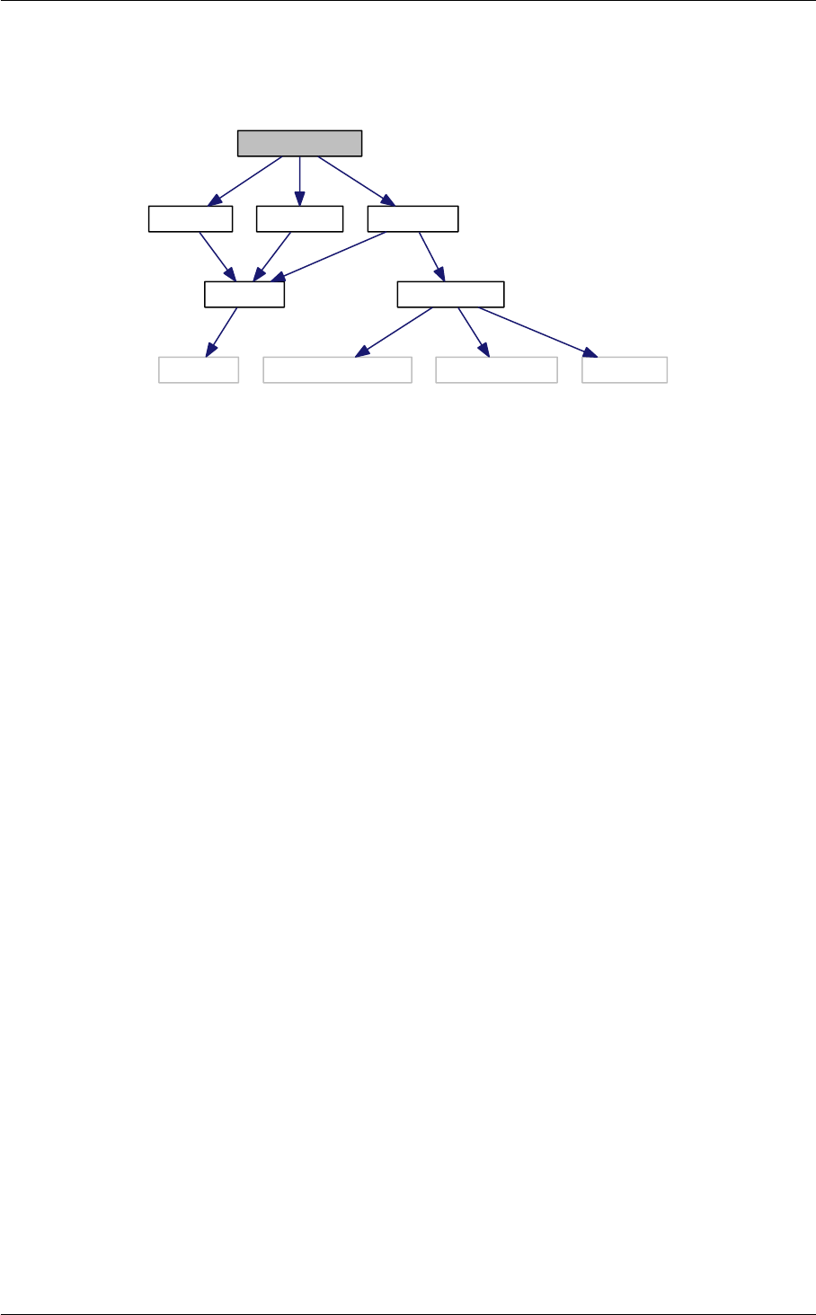
194 File Documentation
Include dependency graph for GpioSampleDef.h:
GpioSampleDef.h
FsptUpd.h FspmUpd.hFspsUpd.h
FspUpd.h
FspEas.h
MemInfoHob.h
Uefi/UefiMultiPhase.h Pi/PiBootMode.h Pi/PiHob.h
13.9.1 Detailed Description
Sample enum definitions for GPIO table.
Copyright
Copyright (c) 2014 - 2019, Intel Corporation. All rights reserved.
SPDX-License-Identifier: BSD-2-Clause-Patent
Specification Reference:
13.10 HobUsageDataHob.h File Reference
Definitions for Hob Usage data HOB.
Classes
• struct HOB_USAGE_DATA_HOB
Hob Usage Data Hob.
13.10.1 Detailed Description
Definitions for Hob Usage data HOB.
Copyright
Copyright (c) 2017 - 2019, Intel Corporation. All rights reserved.
SPDX-License-Identifier: BSD-2-Clause-Patent
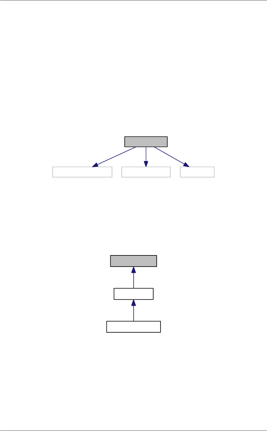
13.11 MemInfoHob.h File Reference 195
Specification Reference:
13.11 MemInfoHob.h File Reference
This file contains definitions required for creation of Memory S3 Save data, Memory Info data and Memory Platform
data hobs.
#include <Uefi/UefiMultiPhase.h>
#include <Pi/PiBootMode.h>
#include <Pi/PiHob.h>
Include dependency graph for MemInfoHob.h:
MemInfoHob.h
Uefi/UefiMultiPhase.h Pi/PiBootMode.h Pi/PiHob.h
This graph shows which files directly or indirectly include this file:
MemInfoHob.h
FspmUpd.h
GpioSampleDef.h
Classes
• struct DIMM_INFO
Memory SMBIOS & OC Memory Data Hob.
• struct MEMORY_PLATFORM_DATA
Memory Platform Data Hob.

196 File Documentation
Macros
• #define WARM_BOOT 2
Host reset states from MRC.
• #define MAX_SPD_SAVE 29
Defines taken from MRC so avoid having to include MrcInterface.h.
13.11.1 Detailed Description
This file contains definitions required for creation of Memory S3 Save data, Memory Info data and Memory Platform
data hobs.
Copyright
Copyright (c) 1999 - 2019, Intel Corporation. All rights reserved.
SPDX-License-Identifier: BSD-2-Clause-Patent
Specification Reference:
13.12 SmbiosCacheInfoHob.h File Reference
Header file for SMBIOS Cache Info HOB.
#include <Uefi.h>
#include <Pi/PiHob.h>
Include dependency graph for SmbiosCacheInfoHob.h:
SmbiosCacheInfoHob.h
Uefi.h Pi/PiHob.h
Classes
• struct SMBIOS_CACHE_INFO
SMBIOS Cache Info HOB Structure.
13.12.1 Detailed Description
Header file for SMBIOS Cache Info HOB.
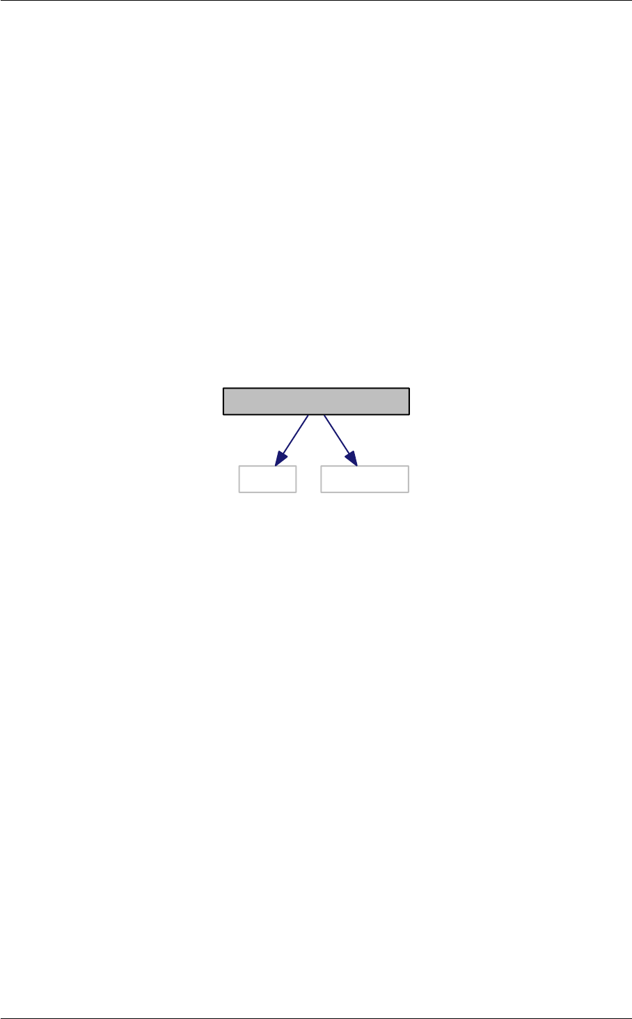
13.13 SmbiosProcessorInfoHob.h File Reference 197
Copyright
Copyright (c) 2015 - 2019, Intel Corporation. All rights reserved.
SPDX-License-Identifier: BSD-2-Clause-Patent
System Management BIOS (SMBIOS) Reference Specification v3.1.0 dated 2016-Nov-16 (DSP0134) http←-
://www.dmtf.org/sites/default/files/standards/documents/DSP0134_3.1.0.pdf
13.13 SmbiosProcessorInfoHob.h File Reference
Header file for SMBIOS Processor Info HOB.
#include <Uefi.h>
#include <Pi/PiHob.h>
Include dependency graph for SmbiosProcessorInfoHob.h:
SmbiosProcessorInfoHob.h
Uefi.h Pi/PiHob.h
Classes
• struct SMBIOS_PROCESSOR_INFO
SMBIOS Processor Info HOB Structure.
13.13.1 Detailed Description
Header file for SMBIOS Processor Info HOB.
Copyright
Copyright (c) 2015 - 2019, Intel Corporation. All rights reserved.
SPDX-License-Identifier: BSD-2-Clause-Patent
System Management BIOS (SMBIOS) Reference Specification v3.1.0 dated 2016-Nov-16 (DSP0134) http←-
://www.dmtf.org/sites/default/files/standards/documents/DSP0134_3.1.0.pdf

198 File Documentation
Index
AUDIO_AZALIA_VERB_TABLE, 37
AZALIA_HEADER, 38
AcLoadline
FSP_S_CONFIG, 113
AcousticNoiseMitigation
FSP_S_CONFIG, 113
ActiveCoreCount
FSP_M_CONFIG, 60
AmtEnabled
FSP_S_CONFIG, 113
AmtKvmEnabled
FSP_S_CONFIG, 113
AmtSolEnabled
FSP_S_CONFIG, 113
ApIdleManner
FSP_S_TEST_CONFIG, 155
ApStartupBase
FSP_M_CONFIG, 60
ApertureSize
FSP_M_CONFIG, 60
AsfEnabled
FSP_S_CONFIG, 113
AutoThermalReporting
FSP_S_TEST_CONFIG, 155
Avx2RatioOffset
FSP_M_CONFIG, 60
Avx3RatioOffset
FSP_M_CONFIG, 60
BclkAdaptiveVoltage
FSP_M_CONFIG, 60
BdatEnable
FSP_M_TEST_CONFIG, 85
BdatTestType
FSP_M_TEST_CONFIG, 85
BiosAcmBase
FSP_M_CONFIG, 60
BiosAcmSize
FSP_M_CONFIG, 60
BiosGuard
FSP_M_CONFIG, 61
BiosSize
FSP_M_TEST_CONFIG, 86
BistOnReset
FSP_M_CONFIG, 61
BootFrequency
FSP_M_CONFIG, 61
BypassPhySyncReset
FSP_M_TEST_CONFIG, 86
C1StateAutoDemotion
FSP_S_TEST_CONFIG, 155
C1StateUnDemotion
FSP_S_TEST_CONFIG, 156
C1e
FSP_S_TEST_CONFIG, 155
C3StateAutoDemotion
FSP_S_TEST_CONFIG, 156
C3StateUnDemotion
FSP_S_TEST_CONFIG, 156
CHIPSET_INIT_INFO, 38
CStatePreWake
FSP_S_TEST_CONFIG, 156
ChHashEnable
FSP_M_CONFIG, 61
ChHashInterleaveBit
FSP_M_CONFIG, 61
ChHashMask
FSP_M_CONFIG, 61
CkeRankMapping
FSP_M_CONFIG, 61
CleanMemory
FSP_M_CONFIG, 62
CmdRanksTerminated
FSP_M_CONFIG, 62
ConfigTdpBios
FSP_S_TEST_CONFIG, 156
CoreMaxOcRatio
FSP_M_CONFIG, 62
CorePllVoltageOffset
FSP_M_CONFIG, 62
CoreVoltageAdaptive
FSP_M_CONFIG, 62
CoreVoltageMode
FSP_M_CONFIG, 62
CoreVoltageOverride
FSP_M_CONFIG, 62
Count
FIRMWARE_VERSION_INFO_HOB, 41
CpuMpHob
FSP_S_CONFIG, 114
CpuRatio
FSP_M_CONFIG, 63
CpuTraceHubMemReg0Size
FSP_M_CONFIG, 63
CpuTraceHubMemReg1Size
FSP_M_CONFIG, 63
CpuTraceHubMode
FSP_M_CONFIG, 63

200 INDEX
CpuWakeUpTimer
FSP_S_TEST_CONFIG, 156
CstCfgCtrIoMwaitRedirection
FSP_S_TEST_CONFIG, 156
Custom1ConfigTdpControl
FSP_S_TEST_CONFIG, 157
Custom1PowerLimit1
FSP_S_TEST_CONFIG, 157
Custom1PowerLimit1Time
FSP_S_TEST_CONFIG, 157
Custom1PowerLimit2
FSP_S_TEST_CONFIG, 157
Custom1TurboActivationRatio
FSP_S_TEST_CONFIG, 157
Custom2ConfigTdpControl
FSP_S_TEST_CONFIG, 157
Custom2PowerLimit1
FSP_S_TEST_CONFIG, 157
Custom2PowerLimit1Time
FSP_S_TEST_CONFIG, 158
Custom2PowerLimit2
FSP_S_TEST_CONFIG, 158
Custom2TurboActivationRatio
FSP_S_TEST_CONFIG, 158
Custom3ConfigTdpControl
FSP_S_TEST_CONFIG, 158
Custom3PowerLimit1
FSP_S_TEST_CONFIG, 158
Custom3PowerLimit1Time
FSP_S_TEST_CONFIG, 158
Custom3PowerLimit2
FSP_S_TEST_CONFIG, 158
Custom3TurboActivationRatio
FSP_S_TEST_CONFIG, 159
Cx
FSP_S_TEST_CONFIG, 159
DIMM_INFO, 39
DcLoadline
FSP_S_CONFIG, 114
DciUsb3TypecUfpDbg
FSP_M_CONFIG, 63
Ddr4MixedUDimm2DpcLimit
FSP_M_CONFIG, 63
DdrFreqLimit
FSP_M_CONFIG, 64
DebugInterfaceEnable
FSP_S_CONFIG, 114
FSP_S_TEST_CONFIG, 159
DebugInterfaceLockEnable
FSP_S_TEST_CONFIG, 159
DeltaT12PowerCycleDelayPreMem
FSP_M_TEST_CONFIG, 86
DevIntConfigPtr
FSP_S_CONFIG, 114
Direction
GPIO_CONFIG, 174
DisableDimmChannel0
FSP_M_CONFIG, 64
DisableDimmChannel1
FSP_M_CONFIG, 64
DisableHeciRetry
FSP_M_TEST_CONFIG, 86
DisableMessageCheck
FSP_M_TEST_CONFIG, 86
DisableMtrrProgram
FSP_M_CONFIG, 64
DisableProcHotOut
FSP_S_TEST_CONFIG, 159
DisableVrThermalAlert
FSP_S_TEST_CONFIG, 159
DmiDeEmphasis
FSP_M_CONFIG, 64
DmiGen3EndPointHint
FSP_M_CONFIG, 64
DmiGen3EndPointPreset
FSP_M_CONFIG, 64
DmiGen3EqPh2Enable
FSP_M_TEST_CONFIG, 86
DmiGen3EqPh3Method
FSP_M_TEST_CONFIG, 86
DmiGen3ProgramStaticEq
FSP_M_CONFIG, 65
DmiGen3RootPortPreset
FSP_M_CONFIG, 65
DmiSuggestedSetting
FSP_S_CONFIG, 114
DmiTS0TW
FSP_S_CONFIG, 114
DmiTS1TW
FSP_S_CONFIG, 114
DmiTS2TW
FSP_S_CONFIG, 115
DmiTS3TW
FSP_S_CONFIG, 115
DpSscMarginEnable
FSP_M_CONFIG, 65
DualDimmPerChannelBoardType
FSP_M_CONFIG, 65
EcCmdLock
FSP_S_CONFIG, 115
EcCmdProvisionEav
FSP_S_CONFIG, 115
EightCoreRatioLimit
FSP_S_TEST_CONFIG, 159
Eist
FSP_S_TEST_CONFIG, 160
ElectricalConfig
GPIO_CONFIG, 174
EnBER
FSP_M_CONFIG, 65
EnCmdRate
FSP_M_CONFIG, 66
Enable8254ClockGating
FSP_S_CONFIG, 115
Enable8254ClockGatingOnS3
FSP_S_CONFIG, 115

INDEX 201
EnableC6Dram
FSP_M_CONFIG, 65
EnableItbm
FSP_S_TEST_CONFIG, 160
EnableSgx
FSP_M_CONFIG, 65
EnableTcoTimer
FSP_S_CONFIG, 115
EndOfPostMessage
FSP_S_TEST_CONFIG, 160
EnergyEfficientPState
FSP_S_TEST_CONFIG, 160
EnergyEfficientTurbo
FSP_S_TEST_CONFIG, 160
EpgEnable
FSP_M_CONFIG, 66
EsataSpeedLimit
FSP_S_CONFIG, 116
FClkFrequency
FSP_M_CONFIG, 66
FIRMWARE_VERSION, 39
FIRMWARE_VERSION_INFO, 40
FIRMWARE_VERSION_INFO_HOB, 40
Count, 41
FSP_M_CONFIG, 41
ActiveCoreCount, 60
ApStartupBase, 60
ApertureSize, 60
Avx2RatioOffset, 60
Avx3RatioOffset, 60
BclkAdaptiveVoltage, 60
BiosAcmBase, 60
BiosAcmSize, 60
BiosGuard, 61
BistOnReset, 61
BootFrequency, 61
ChHashEnable, 61
ChHashInterleaveBit, 61
ChHashMask, 61
CkeRankMapping, 61
CleanMemory, 62
CmdRanksTerminated, 62
CoreMaxOcRatio, 62
CorePllVoltageOffset, 62
CoreVoltageAdaptive, 62
CoreVoltageMode, 62
CoreVoltageOverride, 62
CpuRatio, 63
CpuTraceHubMemReg0Size, 63
CpuTraceHubMemReg1Size, 63
CpuTraceHubMode, 63
DciUsb3TypecUfpDbg, 63
Ddr4MixedUDimm2DpcLimit, 63
DdrFreqLimit, 64
DisableDimmChannel0, 64
DisableDimmChannel1, 64
DisableMtrrProgram, 64
DmiDeEmphasis, 64
DmiGen3EndPointHint, 64
DmiGen3EndPointPreset, 64
DmiGen3ProgramStaticEq, 65
DmiGen3RootPortPreset, 65
DpSscMarginEnable, 65
DualDimmPerChannelBoardType, 65
EnBER, 65
EnCmdRate, 66
EnableC6Dram, 65
EnableSgx, 65
EpgEnable, 66
FClkFrequency, 66
FivrEfficiency, 66
FivrFaults, 66
ForceOltmOrRefresh2x, 66
FreqSaGvLow, 66
FreqSaGvMid, 67
GdxcEnable, 67
GmAdr, 67
GtPllVoltageOffset, 67
GtPsmiSupport, 67
GttMmAdr, 67
HobBufferSize, 68
HotThresholdCh0Dimm0, 68
HotThresholdCh0Dimm1, 68
HotThresholdCh1Dimm0, 68
HotThresholdCh1Dimm1, 68
Idd3n, 68
Idd3p, 68
IgdDvmt50PreAlloc, 69
ImrRpSelection, 69
InitPcieAspmAfterOprom, 69
InternalGfx, 69
IsvtIoPort, 69
JtagC10PowerGateDisable, 69
LpddrDramOdt, 69
McPllVoltageOffset, 69
MemoryTrace, 70
MmioSize, 70
OcLock, 70
PcdDebugInterfaceFlags, 70
PcdIsaSerialUartBase, 70
PcdSerialDebugBaudRate, 70
PcdSerialDebugLevel, 70
PcdSerialIoUartNumber, 71
PchLpcEnhancePort8xhDecoding, 71
PchNumRsvdSmbusAddresses, 71
PchPort80Route, 71
PchSmbAlertEnable, 71
PchTraceHubMemReg0Size, 71
PchTraceHubMemReg1Size, 71
PchTraceHubMode, 72
PcieImrSize, 72
PcieRpEnableMask, 72
PeciC10Reset, 72
PeciSxReset, 72
PegDataPtr, 72
PegDisableSpreadSpectrumClocking, 72

202 INDEX
PlatformDebugConsent, 73
ProbelessTrace, 73
PwdwnIdleCounter, 73
RMT, 75
RMTLoopCount, 75
RankInterleave, 73
Ratio, 73
RcompResistor, 73
RcompTarget, 74
RealtimeMemoryTiming, 74
RefClk, 74
RhSolution, 74
RingDownBin, 74
RingMaxOcRatio, 74
RingPllVoltageOffset, 74
RingVoltageAdaptive, 74
RingVoltageMode, 75
RingVoltageOffset, 75
RingVoltageOverride, 75
RmtPerTask, 75
SaGv, 76
SaPllVoltageOffset, 76
SafeMode, 75
ScramblerSupport, 76
SinitMemorySize, 76
SkipMpInit, 76
SmbusArpEnable, 76
SmbusEnable, 76
SpdAddressTable, 77
SpdProfileSelected, 77
tRTP, 78
TgaSize, 77
ThrtCkeMinTmr, 77
ThrtCkeMinTmrLpddr, 77
TjMaxOffset, 77
TrainTrace, 77
TsegSize, 78
TsodAlarmwindowLockBit, 78
TsodCriticalEventOnly, 78
TsodCriticaltripLockBit, 78
TsodEventMode, 78
TsodEventOutputControl, 78
TsodEventPolarity, 79
TsodManualEnable, 79
TsodShutdownMode, 79
TsodTcritMax, 79
TvbRatioClipping, 79
TvbVoltageOptimization, 79
Txt, 80
TxtDprMemoryBase, 80
TxtDprMemorySize, 80
TxtHeapMemorySize, 80
TxtImplemented, 80
TxtLcpPdBase, 80
TxtLcpPdSize, 80
UserBudgetEnable, 81
UserThresholdEnable, 81
VddVoltage, 81
VmxEnable, 81
WarmThresholdCh0Dimm0, 81
WarmThresholdCh0Dimm1, 81
WarmThresholdCh1Dimm0, 81
WarmThresholdCh1Dimm1, 81
FSP_M_TEST_CONFIG, 82
BdatEnable, 85
BdatTestType, 85
BiosSize, 86
BypassPhySyncReset, 86
DeltaT12PowerCycleDelayPreMem, 86
DisableHeciRetry, 86
DisableMessageCheck, 86
DmiGen3EqPh2Enable, 86
DmiGen3EqPh3Method, 86
Gen3SwEqAlwaysAttempt, 87
Gen3SwEqEnableVocTest, 87
Gen3SwEqJitterDwellTime, 87
Gen3SwEqJitterErrorTarget, 87
Gen3SwEqNumberOfPresets, 87
Gen3SwEqVocDwellTime, 87
Gen3SwEqVocErrorTarget, 88
HeciCommunication2, 88
KtDeviceEnable, 88
LockPTMregs, 88
PanelPowerEnable, 88
Peg0Gen3EqPh2Enable, 88
Peg0Gen3EqPh3Method, 89
Peg1Gen3EqPh2Enable, 89
Peg1Gen3EqPh3Method, 89
Peg2Gen3EqPh2Enable, 89
Peg2Gen3EqPh3Method, 89
Peg3Gen3EqPh2Enable, 89
Peg3Gen3EqPh3Method, 90
PegGen3EndPointHint, 90
PegGen3EndPointPreset, 90
PegGen3ProgramStaticEq, 90
PegGen3RootPortPreset, 90
PegGenerateBdatMarginTable, 90
PegRxCemLoopbackLane, 90
PegRxCemNonProtocolAwareness, 91
ScanExtGfxForLegacyOpRom, 91
SkipMbpHob, 91
SmbusDynamicPowerGating, 91
SmbusSpdWriteDisable, 91
tRRD_L, 93
tRRD_S, 93
tRd2RdDD, 91
tRd2RdDG, 92
tRd2RdDR, 92
tRd2RdSG, 92
tRd2WrDD, 92
tRd2WrDG, 92
tRd2WrDR, 92
tRd2WrSG, 92
tWTR_L, 94
tWTR_S, 94
tWr2RdDD, 93

INDEX 203
tWr2RdDG, 93
tWr2RdDR, 93
tWr2RdSG, 93
tWr2WrDD, 93
tWr2WrDG, 93
tWr2WrDR, 94
tWr2WrSG, 94
TotalFlashSize, 91
TxtAcheckRequest, 94
WdtDisableAndLock, 94
FSP_S_CONFIG, 95
AcLoadline, 113
AcousticNoiseMitigation, 113
AmtEnabled, 113
AmtKvmEnabled, 113
AmtSolEnabled, 113
AsfEnabled, 113
CpuMpHob, 114
DcLoadline, 114
DebugInterfaceEnable, 114
DevIntConfigPtr, 114
DmiSuggestedSetting, 114
DmiTS0TW, 114
DmiTS1TW, 114
DmiTS2TW, 115
DmiTS3TW, 115
EcCmdLock, 115
EcCmdProvisionEav, 115
Enable8254ClockGating, 115
Enable8254ClockGatingOnS3, 115
EnableTcoTimer, 115
EsataSpeedLimit, 116
FastPkgCRampDisableFivr, 116
FastPkgCRampDisableGt, 116
FastPkgCRampDisableIa, 116
FastPkgCRampDisableSa, 116
FivrRfiFrequency, 116
FivrSpreadSpectrum, 116
ForcMebxSyncUp, 117
FwProgress, 117
GpioIrqRoute, 117
Heci3Enabled, 117
IccMax, 117
ImonOffset1, 117
ImonSlope, 117
ImonSlope1, 118
IslVrCmd, 118
ManageabilityMode, 118
McivrRfiFrequencyAdjust, 118
McivrRfiFrequencyPrefix, 118
McivrSpreadSpectrum, 118
MeUnconfigOnRtcClear, 118
NumOfDevIntConfig, 119
PchCnviMode, 119
PchCrid, 119
PchDmiAspm, 119
PchDmiAspmCtrl, 119
PchDmiTsawEn, 119
PchEnableComplianceMode, 119
PchEnableDbcObs, 120
PchHdaAudioLinkDmic0, 120
PchHdaAudioLinkDmic1, 120
PchHdaAudioLinkHda, 120
PchHdaAudioLinkSndw1, 120
PchHdaAudioLinkSndw2, 120
PchHdaAudioLinkSndw3, 120
PchHdaAudioLinkSndw4, 121
PchHdaAudioLinkSsp0, 121
PchHdaAudioLinkSsp1, 121
PchHdaAudioLinkSsp2, 121
PchHdaDspEnable, 121
PchHdaDspUaaCompliance, 121
PchHdaIDispCodecDisconnect, 121
PchHdaIDispLinkFrequency, 122
PchHdaIDispLinkTmode, 122
PchHdaLinkFrequency, 122
PchHdaPme, 122
PchHdaSndwBufferRcomp, 122
PchHdaVcType, 122
PchHotEnable, 122
PchIoApicEntry24_119, 123
PchIoApicId, 123
PchIshGp0GpioAssign, 123
PchIshGp1GpioAssign, 123
PchIshGp2GpioAssign, 123
PchIshGp3GpioAssign, 123
PchIshGp4GpioAssign, 123
PchIshGp5GpioAssign, 124
PchIshGp6GpioAssign, 124
PchIshGp7GpioAssign, 124
PchIshI2c0GpioAssign, 124
PchIshI2c1GpioAssign, 124
PchIshI2c2GpioAssign, 124
PchIshPdtUnlock, 124
PchIshSpiGpioAssign, 124
PchIshUart0GpioAssign, 125
PchIshUart1GpioAssign, 125
PchLanEnable, 125
PchLanLtrEnable, 125
PchLegacyIoLowLatency, 125
PchLockDownBiosLock, 125
PchLockDownRtcMemoryLock, 125
PchMemoryThrottlingEnable, 126
PchPcieDeviceOverrideTablePtr, 126
PchPmDeepSxPol, 126
PchPmDisableDsxAcPresentPulldown, 126
PchPmDisableNativePowerButton, 126
PchPmLanWakeFromDeepSx, 126
PchPmLpcClockRun, 126
PchPmMeWakeSts, 127
PchPmPciePllSsc, 127
PchPmPcieWakeFromDeepSx, 127
PchPmPmeB0S5Dis, 127
PchPmPwrBtnOverridePeriod, 127
PchPmPwrCycDur, 127
PchPmSlpAMinAssert, 127

204 INDEX
PchPmSlpLanLowDc, 128
PchPmSlpS0Enable, 128
PchPmSlpS0Vm070VSupport, 128
PchPmSlpS0Vm075VSupport, 128
PchPmSlpS0VmRuntimeControl, 128
PchPmSlpS3MinAssert, 128
PchPmSlpS4MinAssert, 128
PchPmSlpStrchSusUp, 129
PchPmSlpSusMinAssert, 129
PchPmVrAlert, 129
PchPmWoWlanDeepSxEnable, 129
PchPmWoWlanEnable, 129
PchPmWolEnableOverride, 129
PchPmWolOvrWkSts, 129
PchPwrOptEnable, 130
PchScsEmmcHs400DllDataValid, 130
PchScsEmmcHs400DriverStrength, 130
PchScsEmmcHs400TuningRequired, 130
PchSerialIoI2cPadsTermination, 130
PchSirqEnable, 130
PchSirqMode, 130
PchStartFramePulse, 130
PchTTEnable, 131
PchTTLock, 131
PchTTState13Enable, 131
PchTsmicLock, 131
PchUsbHsioFilterSel, 131
PchUsbHsioRxTuningEnable, 131
PcieComplianceTestMode, 131
PcieDisableRootPortClockGating, 132
PcieEnablePeerMemoryWrite, 132
PcieEqPh3LaneParamCm, 132
PcieEqPh3LaneParamCp, 132
PcieRpAspm, 132
PcieRpCompletionTimeout, 132
PcieRpDpcExtensionsMask, 132
PcieRpDpcMask, 133
PcieRpFunctionSwap, 133
PcieRpGen3EqPh3Method, 133
PcieRpImrEnabled, 133
PcieRpL1Substates, 133
PcieRpPcieSpeed, 133
PcieRpPhysicalSlotNumber, 133
PcieRpPtmMask, 134
PcieSwEqCoeffListCm, 134
PcieSwEqCoeffListCp, 134
PmcCpuC10GatePinEnable, 134
PmcDbgMsgEn, 134
PmcModPhySusPgEnable, 134
PmcPowerButtonDebounce, 134
PortUsb20Enable, 135
PortUsb30Enable, 135
PreWake, 135
PsOnEnable, 136
Psi1Threshold, 135
Psi2Threshold, 135
Psi3Enable, 135
Psi3Threshold, 135
PsysOffset, 136
PsysSlope, 136
PxRcConfig, 136
RemoteAssistance, 136
SataEnable, 136
SataLedEnable, 136
SataMode, 137
SataP0TDispFinit, 137
SataP1TDispFinit, 137
SataPortsDevSlp, 137
SataPortsDmVal, 137
SataPortsEnable, 137
SataPwrOptEnable, 137
SataRstHddUnlock, 138
SataRstInterrupt, 138
SataRstIrrt, 138
SataRstIrrtOnly, 138
SataRstLedLocate, 138
SataRstOromUiBanner, 138
SataRstPcieDeviceResetDelay, 138
SataRstRaid0, 138
SataRstRaid1, 139
SataRstRaid10, 139
SataRstRaid5, 139
SataRstRaidDeviceId, 139
SataRstSmartStorage, 139
SataSalpSupport, 139
SataThermalSuggestedSetting, 139
SciIrqSelect, 140
ScsEmmcEnabled, 140
ScsEmmcHs400Enabled, 140
ScsSdCardEnabled, 140
ScsUfsEnabled, 140
SendEcCmd, 140
SendVrMbxCmd, 140
SerialIoDebugUartNumber, 141
SerialIoDevMode, 141
SerialIoEnableDebugUartAfterPost, 141
SerialIoUart0PinMuxing, 141
ShowSpiController, 141
SiCsmFlag, 141
SiNumberOfSsidTableEntry, 141
SiSsidTablePtr, 141
SkipMpInitDeprecated, 142
SlowSlewRateForFivr, 142
SlowSlewRateForGt, 142
SlowSlewRateForIa, 142
SlowSlewRateForSa, 142
SlpS0DisQForDebug, 142
SlpS0Override, 143
SlpS0WithGbeSupport, 143
TTSuggestedSetting, 143
TcoIrqSelect, 143
TdcPowerLimit, 143
TdcTimeWindow, 143
TetonGlacierMode, 143
TurboMode, 144
TxtEnable, 144

INDEX 205
Usb2AfePehalfbit, 144
Usb2AfePetxiset, 144
Usb2AfePredeemp, 144
Usb2AfeTxiset, 144
Usb3HsioTxDeEmph, 144
Usb3HsioTxDeEmphEnable, 145
Usb3HsioTxDownscaleAmp, 145
Usb3HsioTxDownscaleAmpEnable, 145
Usb3HsioTxRate0UniqTran, 145
Usb3HsioTxRate0UniqTranEnable, 145
Usb3HsioTxRate1UniqTran, 145
Usb3HsioTxRate1UniqTranEnable, 146
Usb3HsioTxRate2UniqTran, 146
Usb3HsioTxRate2UniqTranEnable, 146
Usb3HsioTxRate3UniqTran, 146
Usb3HsioTxRate3UniqTranEnable, 146
UsbPdoProgramming, 146
VrPowerDeliveryDesign, 146
VrVoltageLimit, 147
WatchDog, 147
WatchDogTimerBios, 147
WatchDogTimerOs, 147
XdciEnable, 147
FSP_S_TEST_CONFIG, 147
ApIdleManner, 155
AutoThermalReporting, 155
C1StateAutoDemotion, 155
C1StateUnDemotion, 156
C1e, 155
C3StateAutoDemotion, 156
C3StateUnDemotion, 156
CStatePreWake, 156
ConfigTdpBios, 156
CpuWakeUpTimer, 156
CstCfgCtrIoMwaitRedirection, 156
Custom1ConfigTdpControl, 157
Custom1PowerLimit1, 157
Custom1PowerLimit1Time, 157
Custom1PowerLimit2, 157
Custom1TurboActivationRatio, 157
Custom2ConfigTdpControl, 157
Custom2PowerLimit1, 157
Custom2PowerLimit1Time, 158
Custom2PowerLimit2, 158
Custom2TurboActivationRatio, 158
Custom3ConfigTdpControl, 158
Custom3PowerLimit1, 158
Custom3PowerLimit1Time, 158
Custom3PowerLimit2, 158
Custom3TurboActivationRatio, 159
Cx, 159
DebugInterfaceEnable, 159
DebugInterfaceLockEnable, 159
DisableProcHotOut, 159
DisableVrThermalAlert, 159
EightCoreRatioLimit, 159
Eist, 160
EnableItbm, 160
EndOfPostMessage, 160
EnergyEfficientPState, 160
EnergyEfficientTurbo, 160
FiveCoreRatioLimit, 160
FourCoreRatioLimit, 160
HdcControl, 161
Hwp, 161
HwpInterruptControl, 161
MachineCheckEnable, 161
MaxRingRatioLimit, 161
MctpBroadcastCycle, 161
MinRingRatioLimit, 161
MlcStreamerPrefetcher, 162
MonitorMwaitEnable, 162
NumberOfEntries, 162
OneCoreRatioLimit, 162
PchHdaResetWaitTimer, 162
PchLockDownBiosInterface, 162
PchLockDownGlobalSmi, 162
PchPmDisableEnergyReport, 163
PchSbAccessUnlock, 163
PchUnlockGpioPads, 163
PchXhciOcLock, 163
PcieEnablePort8xhDecode, 163
PcieRpDptp, 163
PcieRpSlotPowerLimitScale, 163
PcieRpSlotPowerLimitValue, 164
PcieRpUptp, 164
PkgCStateDemotion, 164
PkgCStateLimit, 164
PkgCStateUnDemotion, 164
PmgCstCfgCtrlLock, 164
PowerLimit1, 164
PowerLimit1Time, 165
PowerLimit2, 165
PowerLimit2Power, 165
PowerLimit3, 165
PowerLimit4, 165
ProcHotResponse, 166
ProcessorTraceEnable, 165
ProcessorTraceMemBase, 165
ProcessorTraceMemLength, 166
ProcessorTraceOutputScheme, 166
PsysPmax, 166
PsysPowerLimit1, 166
PsysPowerLimit1Power, 166
PsysPowerLimit1Time, 166
PsysPowerLimit2, 167
PsysPowerLimit2Power, 167
RaceToHalt, 167
SataTestMode, 167
SevenCoreRatioLimit, 167
SixCoreRatioLimit, 167
StateRatio, 167
StateRatioMax16, 168
TStates, 169
TccActivationOffset, 168
TccOffsetClamp, 168

206 INDEX
TccOffsetLock, 168
TccOffsetTimeWindowForRatl, 168
ThreeCoreRatioLimit, 168
ThreeStrikeCounterDisable, 168
TimedMwait, 169
TwoCoreRatioLimit, 169
FSP_T_CONFIG, 169
PcdSerialIoUart0PinMuxing, 170
PcdSerialIoUartDebugEnable, 170
PcdSerialIoUartNumber, 170
FSPM_UPD, 170
FSPS_UPD, 171
FSPT_CORE_UPD, 172
FSPT_UPD, 173
FastPkgCRampDisableFivr
FSP_S_CONFIG, 116
FastPkgCRampDisableGt
FSP_S_CONFIG, 116
FastPkgCRampDisableIa
FSP_S_CONFIG, 116
FastPkgCRampDisableSa
FSP_S_CONFIG, 116
FirmwareVersionInfoHob.h, 181
FiveCoreRatioLimit
FSP_S_TEST_CONFIG, 160
FivrEfficiency
FSP_M_CONFIG, 66
FivrFaults
FSP_M_CONFIG, 66
FivrRfiFrequency
FSP_S_CONFIG, 116
FivrSpreadSpectrum
FSP_S_CONFIG, 116
ForcMebxSyncUp
FSP_S_CONFIG, 117
ForceOltmOrRefresh2x
FSP_M_CONFIG, 66
FourCoreRatioLimit
FSP_S_TEST_CONFIG, 160
FreqSaGvLow
FSP_M_CONFIG, 66
FreqSaGvMid
FSP_M_CONFIG, 67
FspFixedPcds.h, 182
FspInfoHob.h, 182
FspUpd.h, 187
FspmUpd.h, 183
FspsUpd.h, 184
SI_PCH_INT_PIN, 186
SiPchNoInt, 186
FsptUpd.h, 186
FwProgress
FSP_S_CONFIG, 117
GPIO_CONFIG, 174
Direction, 174
ElectricalConfig, 174
HostSoftPadOwn, 175
InterruptConfig, 175
LockConfig, 175
OutputState, 175
PadMode, 175
PowerConfig, 175
GPIO_DIRECTION
GpioConfig.h, 190
GPIO_ELECTRICAL_CONFIG
GpioConfig.h, 190
GPIO_HARDWARE_DEFAULT
GpioConfig.h, 190
GPIO_HOSTSW_OWN
GpioConfig.h, 190
GPIO_INT_CONFIG
GpioConfig.h, 191
GPIO_LOCK_CONFIG
GpioConfig.h, 191
GPIO_OTHER_CONFIG
GpioConfig.h, 192
GPIO_OUTPUT_STATE
GpioConfig.h, 192
GPIO_PAD_MODE
GpioConfig.h, 192
GPIO_RESET_CONFIG
GpioConfig.h, 192
GdxcEnable
FSP_M_CONFIG, 67
Gen3SwEqAlwaysAttempt
FSP_M_TEST_CONFIG, 87
Gen3SwEqEnableVocTest
FSP_M_TEST_CONFIG, 87
Gen3SwEqJitterDwellTime
FSP_M_TEST_CONFIG, 87
Gen3SwEqJitterErrorTarget
FSP_M_TEST_CONFIG, 87
Gen3SwEqNumberOfPresets
FSP_M_TEST_CONFIG, 87
Gen3SwEqVocDwellTime
FSP_M_TEST_CONFIG, 87
Gen3SwEqVocErrorTarget
FSP_M_TEST_CONFIG, 88
GmAdr
FSP_M_CONFIG, 67
GpioConfig.h, 188
GPIO_DIRECTION, 190
GPIO_ELECTRICAL_CONFIG, 190
GPIO_HARDWARE_DEFAULT, 190
GPIO_HOSTSW_OWN, 190
GPIO_INT_CONFIG, 191
GPIO_LOCK_CONFIG, 191
GPIO_OTHER_CONFIG, 192
GPIO_OUTPUT_STATE, 192
GPIO_PAD_MODE, 192
GPIO_RESET_CONFIG, 192
GpioDirDefault, 190
GpioDirIn, 190
GpioDirInInv, 190
GpioDirInInvOut, 190
GpioDirInOut, 190

INDEX 207
GpioDirNone, 190
GpioDirOut, 190
GpioDswReset, 193
GpioHardwareDefault, 190
GpioHostDeepReset, 193
GpioHostOwnAcpi, 191
GpioHostOwnDefault, 191
GpioHostOwnGpio, 191
GpioIntApic, 191
GpioIntBothEdge, 191
GpioIntDefault, 191
GpioIntDis, 191
GpioIntEdge, 191
GpioIntLevel, 191
GpioIntLvlEdgDis, 191
GpioIntNmi, 191
GpioIntSci, 191
GpioIntSmi, 191
GpioLockDefault, 191
GpioOutDefault, 192
GpioOutHigh, 192
GpioOutLow, 192
GpioOutputStateUnlock, 192
GpioPadConfigLock, 192
GpioPadConfigUnlock, 192
GpioPadLock, 192
GpioPadUnlock, 192
GpioPlatformReset, 193
GpioResetDefault, 193
GpioResumeReset, 193
GpioRxRaw1Default, 192
GpioRxRaw1Dis, 192
GpioRxRaw1En, 192
GpioTermDefault, 190
GpioTermNative, 190
GpioTermNone, 190
GpioTermWpd20K, 190
GpioTermWpd5K, 190
GpioTermWpu1K, 190
GpioTermWpu1K2K, 190
GpioTermWpu20K, 190
GpioTermWpu2K, 190
GpioTermWpu5K, 190
GpioDirDefault
GpioConfig.h, 190
GpioDirIn
GpioConfig.h, 190
GpioDirInInv
GpioConfig.h, 190
GpioDirInInvOut
GpioConfig.h, 190
GpioDirInOut
GpioConfig.h, 190
GpioDirNone
GpioConfig.h, 190
GpioDirOut
GpioConfig.h, 190
GpioDswReset
GpioConfig.h, 193
GpioHardwareDefault
GpioConfig.h, 190
GpioHostDeepReset
GpioConfig.h, 193
GpioHostOwnAcpi
GpioConfig.h, 191
GpioHostOwnDefault
GpioConfig.h, 191
GpioHostOwnGpio
GpioConfig.h, 191
GpioIntApic
GpioConfig.h, 191
GpioIntBothEdge
GpioConfig.h, 191
GpioIntDefault
GpioConfig.h, 191
GpioIntDis
GpioConfig.h, 191
GpioIntEdge
GpioConfig.h, 191
GpioIntLevel
GpioConfig.h, 191
GpioIntLvlEdgDis
GpioConfig.h, 191
GpioIntNmi
GpioConfig.h, 191
GpioIntSci
GpioConfig.h, 191
GpioIntSmi
GpioConfig.h, 191
GpioIrqRoute
FSP_S_CONFIG, 117
GpioLockDefault
GpioConfig.h, 191
GpioOutDefault
GpioConfig.h, 192
GpioOutHigh
GpioConfig.h, 192
GpioOutLow
GpioConfig.h, 192
GpioOutputStateUnlock
GpioConfig.h, 192
GpioPadConfigLock
GpioConfig.h, 192
GpioPadConfigUnlock
GpioConfig.h, 192
GpioPadLock
GpioConfig.h, 192
GpioPadUnlock
GpioConfig.h, 192
GpioPlatformReset
GpioConfig.h, 193
GpioResetDefault
GpioConfig.h, 193
GpioResumeReset
GpioConfig.h, 193
GpioRxRaw1Default

208 INDEX
GpioConfig.h, 192
GpioRxRaw1Dis
GpioConfig.h, 192
GpioRxRaw1En
GpioConfig.h, 192
GpioSampleDef.h, 193
GpioTermDefault
GpioConfig.h, 190
GpioTermNative
GpioConfig.h, 190
GpioTermNone
GpioConfig.h, 190
GpioTermWpd20K
GpioConfig.h, 190
GpioTermWpd5K
GpioConfig.h, 190
GpioTermWpu1K
GpioConfig.h, 190
GpioTermWpu1K2K
GpioConfig.h, 190
GpioTermWpu20K
GpioConfig.h, 190
GpioTermWpu2K
GpioConfig.h, 190
GpioTermWpu5K
GpioConfig.h, 190
GtPllVoltageOffset
FSP_M_CONFIG, 67
GtPsmiSupport
FSP_M_CONFIG, 67
GttMmAdr
FSP_M_CONFIG, 67
HOB_USAGE_DATA_HOB, 176
HdcControl
FSP_S_TEST_CONFIG, 161
Heci3Enabled
FSP_S_CONFIG, 117
HeciCommunication2
FSP_M_TEST_CONFIG, 88
HobBufferSize
FSP_M_CONFIG, 68
HobUsageDataHob.h, 194
HostSoftPadOwn
GPIO_CONFIG, 175
HotThresholdCh0Dimm0
FSP_M_CONFIG, 68
HotThresholdCh0Dimm1
FSP_M_CONFIG, 68
HotThresholdCh1Dimm0
FSP_M_CONFIG, 68
HotThresholdCh1Dimm1
FSP_M_CONFIG, 68
Hwp
FSP_S_TEST_CONFIG, 161
HwpInterruptControl
FSP_S_TEST_CONFIG, 161
IccMax
FSP_S_CONFIG, 117
Idd3n
FSP_M_CONFIG, 68
Idd3p
FSP_M_CONFIG, 68
IgdDvmt50PreAlloc
FSP_M_CONFIG, 69
ImonOffset1
FSP_S_CONFIG, 117
ImonSlope
FSP_S_CONFIG, 117
ImonSlope1
FSP_S_CONFIG, 118
ImrRpSelection
FSP_M_CONFIG, 69
InitPcieAspmAfterOprom
FSP_M_CONFIG, 69
InternalGfx
FSP_M_CONFIG, 69
InterruptConfig
GPIO_CONFIG, 175
IslVrCmd
FSP_S_CONFIG, 118
IsvtIoPort
FSP_M_CONFIG, 69
JtagC10PowerGateDisable
FSP_M_CONFIG, 69
KtDeviceEnable
FSP_M_TEST_CONFIG, 88
LockConfig
GPIO_CONFIG, 175
LockPTMregs
FSP_M_TEST_CONFIG, 88
LpddrDramOdt
FSP_M_CONFIG, 69
MEMORY_PLATFORM_DATA, 176
MachineCheckEnable
FSP_S_TEST_CONFIG, 161
ManageabilityMode
FSP_S_CONFIG, 118
MaxRingRatioLimit
FSP_S_TEST_CONFIG, 161
McPllVoltageOffset
FSP_M_CONFIG, 69
McivrRfiFrequencyAdjust
FSP_S_CONFIG, 118
McivrRfiFrequencyPrefix
FSP_S_CONFIG, 118
McivrSpreadSpectrum
FSP_S_CONFIG, 118
MctpBroadcastCycle
FSP_S_TEST_CONFIG, 161
MeUnconfigOnRtcClear
FSP_S_CONFIG, 118
MemInfoHob.h, 195

INDEX 209
MemoryTrace
FSP_M_CONFIG, 70
MinRingRatioLimit
FSP_S_TEST_CONFIG, 161
MlcStreamerPrefetcher
FSP_S_TEST_CONFIG, 162
MmioSize
FSP_M_CONFIG, 70
MonitorMwaitEnable
FSP_S_TEST_CONFIG, 162
NumOfDevIntConfig
FSP_S_CONFIG, 119
NumberOfEntries
FSP_S_TEST_CONFIG, 162
OcLock
FSP_M_CONFIG, 70
OneCoreRatioLimit
FSP_S_TEST_CONFIG, 162
OutputState
GPIO_CONFIG, 175
PadMode
GPIO_CONFIG, 175
PanelPowerEnable
FSP_M_TEST_CONFIG, 88
PcdDebugInterfaceFlags
FSP_M_CONFIG, 70
PcdIsaSerialUartBase
FSP_M_CONFIG, 70
PcdSerialDebugBaudRate
FSP_M_CONFIG, 70
PcdSerialDebugLevel
FSP_M_CONFIG, 70
PcdSerialIoUart0PinMuxing
FSP_T_CONFIG, 170
PcdSerialIoUartDebugEnable
FSP_T_CONFIG, 170
PcdSerialIoUartNumber
FSP_M_CONFIG, 71
FSP_T_CONFIG, 170
PchCnviMode
FSP_S_CONFIG, 119
PchCrid
FSP_S_CONFIG, 119
PchDmiAspm
FSP_S_CONFIG, 119
PchDmiAspmCtrl
FSP_S_CONFIG, 119
PchDmiTsawEn
FSP_S_CONFIG, 119
PchEnableComplianceMode
FSP_S_CONFIG, 119
PchEnableDbcObs
FSP_S_CONFIG, 120
PchHdaAudioLinkDmic0
FSP_S_CONFIG, 120
PchHdaAudioLinkDmic1
FSP_S_CONFIG, 120
PchHdaAudioLinkHda
FSP_S_CONFIG, 120
PchHdaAudioLinkSndw1
FSP_S_CONFIG, 120
PchHdaAudioLinkSndw2
FSP_S_CONFIG, 120
PchHdaAudioLinkSndw3
FSP_S_CONFIG, 120
PchHdaAudioLinkSndw4
FSP_S_CONFIG, 121
PchHdaAudioLinkSsp0
FSP_S_CONFIG, 121
PchHdaAudioLinkSsp1
FSP_S_CONFIG, 121
PchHdaAudioLinkSsp2
FSP_S_CONFIG, 121
PchHdaDspEnable
FSP_S_CONFIG, 121
PchHdaDspUaaCompliance
FSP_S_CONFIG, 121
PchHdaIDispCodecDisconnect
FSP_S_CONFIG, 121
PchHdaIDispLinkFrequency
FSP_S_CONFIG, 122
PchHdaIDispLinkTmode
FSP_S_CONFIG, 122
PchHdaLinkFrequency
FSP_S_CONFIG, 122
PchHdaPme
FSP_S_CONFIG, 122
PchHdaResetWaitTimer
FSP_S_TEST_CONFIG, 162
PchHdaSndwBufferRcomp
FSP_S_CONFIG, 122
PchHdaVcType
FSP_S_CONFIG, 122
PchHotEnable
FSP_S_CONFIG, 122
PchIoApicEntry24_119
FSP_S_CONFIG, 123
PchIoApicId
FSP_S_CONFIG, 123
PchIshGp0GpioAssign
FSP_S_CONFIG, 123
PchIshGp1GpioAssign
FSP_S_CONFIG, 123
PchIshGp2GpioAssign
FSP_S_CONFIG, 123
PchIshGp3GpioAssign
FSP_S_CONFIG, 123
PchIshGp4GpioAssign
FSP_S_CONFIG, 123
PchIshGp5GpioAssign
FSP_S_CONFIG, 124
PchIshGp6GpioAssign
FSP_S_CONFIG, 124
PchIshGp7GpioAssign

210 INDEX
FSP_S_CONFIG, 124
PchIshI2c0GpioAssign
FSP_S_CONFIG, 124
PchIshI2c1GpioAssign
FSP_S_CONFIG, 124
PchIshI2c2GpioAssign
FSP_S_CONFIG, 124
PchIshPdtUnlock
FSP_S_CONFIG, 124
PchIshSpiGpioAssign
FSP_S_CONFIG, 124
PchIshUart0GpioAssign
FSP_S_CONFIG, 125
PchIshUart1GpioAssign
FSP_S_CONFIG, 125
PchLanEnable
FSP_S_CONFIG, 125
PchLanLtrEnable
FSP_S_CONFIG, 125
PchLegacyIoLowLatency
FSP_S_CONFIG, 125
PchLockDownBiosInterface
FSP_S_TEST_CONFIG, 162
PchLockDownBiosLock
FSP_S_CONFIG, 125
PchLockDownGlobalSmi
FSP_S_TEST_CONFIG, 162
PchLockDownRtcMemoryLock
FSP_S_CONFIG, 125
PchLpcEnhancePort8xhDecoding
FSP_M_CONFIG, 71
PchMemoryThrottlingEnable
FSP_S_CONFIG, 126
PchNumRsvdSmbusAddresses
FSP_M_CONFIG, 71
PchPcieDeviceOverrideTablePtr
FSP_S_CONFIG, 126
PchPmDeepSxPol
FSP_S_CONFIG, 126
PchPmDisableDsxAcPresentPulldown
FSP_S_CONFIG, 126
PchPmDisableEnergyReport
FSP_S_TEST_CONFIG, 163
PchPmDisableNativePowerButton
FSP_S_CONFIG, 126
PchPmLanWakeFromDeepSx
FSP_S_CONFIG, 126
PchPmLpcClockRun
FSP_S_CONFIG, 126
PchPmMeWakeSts
FSP_S_CONFIG, 127
PchPmPciePllSsc
FSP_S_CONFIG, 127
PchPmPcieWakeFromDeepSx
FSP_S_CONFIG, 127
PchPmPmeB0S5Dis
FSP_S_CONFIG, 127
PchPmPwrBtnOverridePeriod
FSP_S_CONFIG, 127
PchPmPwrCycDur
FSP_S_CONFIG, 127
PchPmSlpAMinAssert
FSP_S_CONFIG, 127
PchPmSlpLanLowDc
FSP_S_CONFIG, 128
PchPmSlpS0Enable
FSP_S_CONFIG, 128
PchPmSlpS0Vm070VSupport
FSP_S_CONFIG, 128
PchPmSlpS0Vm075VSupport
FSP_S_CONFIG, 128
PchPmSlpS0VmRuntimeControl
FSP_S_CONFIG, 128
PchPmSlpS3MinAssert
FSP_S_CONFIG, 128
PchPmSlpS4MinAssert
FSP_S_CONFIG, 128
PchPmSlpStrchSusUp
FSP_S_CONFIG, 129
PchPmSlpSusMinAssert
FSP_S_CONFIG, 129
PchPmVrAlert
FSP_S_CONFIG, 129
PchPmWoWlanDeepSxEnable
FSP_S_CONFIG, 129
PchPmWoWlanEnable
FSP_S_CONFIG, 129
PchPmWolEnableOverride
FSP_S_CONFIG, 129
PchPmWolOvrWkSts
FSP_S_CONFIG, 129
PchPort80Route
FSP_M_CONFIG, 71
PchPwrOptEnable
FSP_S_CONFIG, 130
PchSbAccessUnlock
FSP_S_TEST_CONFIG, 163
PchScsEmmcHs400DllDataValid
FSP_S_CONFIG, 130
PchScsEmmcHs400DriverStrength
FSP_S_CONFIG, 130
PchScsEmmcHs400TuningRequired
FSP_S_CONFIG, 130
PchSerialIoI2cPadsTermination
FSP_S_CONFIG, 130
PchSirqEnable
FSP_S_CONFIG, 130
PchSirqMode
FSP_S_CONFIG, 130
PchSmbAlertEnable
FSP_M_CONFIG, 71
PchStartFramePulse
FSP_S_CONFIG, 130
PchTTEnable
FSP_S_CONFIG, 131
PchTTLock

INDEX 211
FSP_S_CONFIG, 131
PchTTState13Enable
FSP_S_CONFIG, 131
PchTraceHubMemReg0Size
FSP_M_CONFIG, 71
PchTraceHubMemReg1Size
FSP_M_CONFIG, 71
PchTraceHubMode
FSP_M_CONFIG, 72
PchTsmicLock
FSP_S_CONFIG, 131
PchUnlockGpioPads
FSP_S_TEST_CONFIG, 163
PchUsbHsioFilterSel
FSP_S_CONFIG, 131
PchUsbHsioRxTuningEnable
FSP_S_CONFIG, 131
PchXhciOcLock
FSP_S_TEST_CONFIG, 163
PcieComplianceTestMode
FSP_S_CONFIG, 131
PcieDisableRootPortClockGating
FSP_S_CONFIG, 132
PcieEnablePeerMemoryWrite
FSP_S_CONFIG, 132
PcieEnablePort8xhDecode
FSP_S_TEST_CONFIG, 163
PcieEqPh3LaneParamCm
FSP_S_CONFIG, 132
PcieEqPh3LaneParamCp
FSP_S_CONFIG, 132
PcieImrSize
FSP_M_CONFIG, 72
PcieRpAspm
FSP_S_CONFIG, 132
PcieRpCompletionTimeout
FSP_S_CONFIG, 132
PcieRpDpcExtensionsMask
FSP_S_CONFIG, 132
PcieRpDpcMask
FSP_S_CONFIG, 133
PcieRpDptp
FSP_S_TEST_CONFIG, 163
PcieRpEnableMask
FSP_M_CONFIG, 72
PcieRpFunctionSwap
FSP_S_CONFIG, 133
PcieRpGen3EqPh3Method
FSP_S_CONFIG, 133
PcieRpImrEnabled
FSP_S_CONFIG, 133
PcieRpL1Substates
FSP_S_CONFIG, 133
PcieRpPcieSpeed
FSP_S_CONFIG, 133
PcieRpPhysicalSlotNumber
FSP_S_CONFIG, 133
PcieRpPtmMask
FSP_S_CONFIG, 134
PcieRpSlotPowerLimitScale
FSP_S_TEST_CONFIG, 163
PcieRpSlotPowerLimitValue
FSP_S_TEST_CONFIG, 164
PcieRpUptp
FSP_S_TEST_CONFIG, 164
PcieSwEqCoeffListCm
FSP_S_CONFIG, 134
PcieSwEqCoeffListCp
FSP_S_CONFIG, 134
PeciC10Reset
FSP_M_CONFIG, 72
PeciSxReset
FSP_M_CONFIG, 72
Peg0Gen3EqPh2Enable
FSP_M_TEST_CONFIG, 88
Peg0Gen3EqPh3Method
FSP_M_TEST_CONFIG, 89
Peg1Gen3EqPh2Enable
FSP_M_TEST_CONFIG, 89
Peg1Gen3EqPh3Method
FSP_M_TEST_CONFIG, 89
Peg2Gen3EqPh2Enable
FSP_M_TEST_CONFIG, 89
Peg2Gen3EqPh3Method
FSP_M_TEST_CONFIG, 89
Peg3Gen3EqPh2Enable
FSP_M_TEST_CONFIG, 89
Peg3Gen3EqPh3Method
FSP_M_TEST_CONFIG, 90
PegDataPtr
FSP_M_CONFIG, 72
PegDisableSpreadSpectrumClocking
FSP_M_CONFIG, 72
PegGen3EndPointHint
FSP_M_TEST_CONFIG, 90
PegGen3EndPointPreset
FSP_M_TEST_CONFIG, 90
PegGen3ProgramStaticEq
FSP_M_TEST_CONFIG, 90
PegGen3RootPortPreset
FSP_M_TEST_CONFIG, 90
PegGenerateBdatMarginTable
FSP_M_TEST_CONFIG, 90
PegRxCemLoopbackLane
FSP_M_TEST_CONFIG, 90
PegRxCemNonProtocolAwareness
FSP_M_TEST_CONFIG, 91
PkgCStateDemotion
FSP_S_TEST_CONFIG, 164
PkgCStateLimit
FSP_S_TEST_CONFIG, 164
PkgCStateUnDemotion
FSP_S_TEST_CONFIG, 164
PlatformDebugConsent
FSP_M_CONFIG, 73
PmcCpuC10GatePinEnable

212 INDEX
FSP_S_CONFIG, 134
PmcDbgMsgEn
FSP_S_CONFIG, 134
PmcModPhySusPgEnable
FSP_S_CONFIG, 134
PmcPowerButtonDebounce
FSP_S_CONFIG, 134
PmgCstCfgCtrlLock
FSP_S_TEST_CONFIG, 164
PortUsb20Enable
FSP_S_CONFIG, 135
PortUsb30Enable
FSP_S_CONFIG, 135
PowerConfig
GPIO_CONFIG, 175
PowerLimit1
FSP_S_TEST_CONFIG, 164
PowerLimit1Time
FSP_S_TEST_CONFIG, 165
PowerLimit2
FSP_S_TEST_CONFIG, 165
PowerLimit2Power
FSP_S_TEST_CONFIG, 165
PowerLimit3
FSP_S_TEST_CONFIG, 165
PowerLimit4
FSP_S_TEST_CONFIG, 165
PreWake
FSP_S_CONFIG, 135
ProbelessTrace
FSP_M_CONFIG, 73
ProcHotResponse
FSP_S_TEST_CONFIG, 166
ProcessorTraceEnable
FSP_S_TEST_CONFIG, 165
ProcessorTraceMemBase
FSP_S_TEST_CONFIG, 165
ProcessorTraceMemLength
FSP_S_TEST_CONFIG, 166
ProcessorTraceOutputScheme
FSP_S_TEST_CONFIG, 166
PsOnEnable
FSP_S_CONFIG, 136
Psi1Threshold
FSP_S_CONFIG, 135
Psi2Threshold
FSP_S_CONFIG, 135
Psi3Enable
FSP_S_CONFIG, 135
Psi3Threshold
FSP_S_CONFIG, 135
PsysOffset
FSP_S_CONFIG, 136
PsysPmax
FSP_S_TEST_CONFIG, 166
PsysPowerLimit1
FSP_S_TEST_CONFIG, 166
PsysPowerLimit1Power
FSP_S_TEST_CONFIG, 166
PsysPowerLimit1Time
FSP_S_TEST_CONFIG, 166
PsysPowerLimit2
FSP_S_TEST_CONFIG, 167
PsysPowerLimit2Power
FSP_S_TEST_CONFIG, 167
PsysSlope
FSP_S_CONFIG, 136
PwdwnIdleCounter
FSP_M_CONFIG, 73
PxRcConfig
FSP_S_CONFIG, 136
RMT
FSP_M_CONFIG, 75
RMTLoopCount
FSP_M_CONFIG, 75
RaceToHalt
FSP_S_TEST_CONFIG, 167
RankInterleave
FSP_M_CONFIG, 73
Ratio
FSP_M_CONFIG, 73
RcompResistor
FSP_M_CONFIG, 73
RcompTarget
FSP_M_CONFIG, 74
RealtimeMemoryTiming
FSP_M_CONFIG, 74
RefClk
FSP_M_CONFIG, 74
RemoteAssistance
FSP_S_CONFIG, 136
RhSolution
FSP_M_CONFIG, 74
RingDownBin
FSP_M_CONFIG, 74
RingMaxOcRatio
FSP_M_CONFIG, 74
RingPllVoltageOffset
FSP_M_CONFIG, 74
RingVoltageAdaptive
FSP_M_CONFIG, 74
RingVoltageMode
FSP_M_CONFIG, 75
RingVoltageOffset
FSP_M_CONFIG, 75
RingVoltageOverride
FSP_M_CONFIG, 75
RmtPerTask
FSP_M_CONFIG, 75
SI_PCH_DEVICE_INTERRUPT_CONFIG, 176
SI_PCH_INT_PIN
FspsUpd.h, 186
SMBIOS_CACHE_INFO, 177
SMBIOS_PROCESSOR_INFO, 178
SMBIOS_STRUCTURE, 179

INDEX 213
SaGv
FSP_M_CONFIG, 76
SaPllVoltageOffset
FSP_M_CONFIG, 76
SafeMode
FSP_M_CONFIG, 75
SataEnable
FSP_S_CONFIG, 136
SataLedEnable
FSP_S_CONFIG, 136
SataMode
FSP_S_CONFIG, 137
SataP0TDispFinit
FSP_S_CONFIG, 137
SataP1TDispFinit
FSP_S_CONFIG, 137
SataPortsDevSlp
FSP_S_CONFIG, 137
SataPortsDmVal
FSP_S_CONFIG, 137
SataPortsEnable
FSP_S_CONFIG, 137
SataPwrOptEnable
FSP_S_CONFIG, 137
SataRstHddUnlock
FSP_S_CONFIG, 138
SataRstInterrupt
FSP_S_CONFIG, 138
SataRstIrrt
FSP_S_CONFIG, 138
SataRstIrrtOnly
FSP_S_CONFIG, 138
SataRstLedLocate
FSP_S_CONFIG, 138
SataRstOromUiBanner
FSP_S_CONFIG, 138
SataRstPcieDeviceResetDelay
FSP_S_CONFIG, 138
SataRstRaid0
FSP_S_CONFIG, 138
SataRstRaid1
FSP_S_CONFIG, 139
SataRstRaid10
FSP_S_CONFIG, 139
SataRstRaid5
FSP_S_CONFIG, 139
SataRstRaidDeviceId
FSP_S_CONFIG, 139
SataRstSmartStorage
FSP_S_CONFIG, 139
SataSalpSupport
FSP_S_CONFIG, 139
SataTestMode
FSP_S_TEST_CONFIG, 167
SataThermalSuggestedSetting
FSP_S_CONFIG, 139
ScanExtGfxForLegacyOpRom
FSP_M_TEST_CONFIG, 91
SciIrqSelect
FSP_S_CONFIG, 140
ScramblerSupport
FSP_M_CONFIG, 76
ScsEmmcEnabled
FSP_S_CONFIG, 140
ScsEmmcHs400Enabled
FSP_S_CONFIG, 140
ScsSdCardEnabled
FSP_S_CONFIG, 140
ScsUfsEnabled
FSP_S_CONFIG, 140
SendEcCmd
FSP_S_CONFIG, 140
SendVrMbxCmd
FSP_S_CONFIG, 140
SerialIoDebugUartNumber
FSP_S_CONFIG, 141
SerialIoDevMode
FSP_S_CONFIG, 141
SerialIoEnableDebugUartAfterPost
FSP_S_CONFIG, 141
SerialIoUart0PinMuxing
FSP_S_CONFIG, 141
SevenCoreRatioLimit
FSP_S_TEST_CONFIG, 167
ShowSpiController
FSP_S_CONFIG, 141
SiCsmFlag
FSP_S_CONFIG, 141
SiNumberOfSsidTableEntry
FSP_S_CONFIG, 141
SiPchNoInt
FspsUpd.h, 186
SiSsidTablePtr
FSP_S_CONFIG, 141
SinitMemorySize
FSP_M_CONFIG, 76
SixCoreRatioLimit
FSP_S_TEST_CONFIG, 167
SkipMbpHob
FSP_M_TEST_CONFIG, 91
SkipMpInit
FSP_M_CONFIG, 76
SkipMpInitDeprecated
FSP_S_CONFIG, 142
SlowSlewRateForFivr
FSP_S_CONFIG, 142
SlowSlewRateForGt
FSP_S_CONFIG, 142
SlowSlewRateForIa
FSP_S_CONFIG, 142
SlowSlewRateForSa
FSP_S_CONFIG, 142
SlpS0DisQForDebug
FSP_S_CONFIG, 142
SlpS0Override
FSP_S_CONFIG, 143

214 INDEX
SlpS0WithGbeSupport
FSP_S_CONFIG, 143
SmbiosCacheInfoHob.h, 196
SmbiosProcessorInfoHob.h, 197
SmbusArpEnable
FSP_M_CONFIG, 76
SmbusDynamicPowerGating
FSP_M_TEST_CONFIG, 91
SmbusEnable
FSP_M_CONFIG, 76
SmbusSpdWriteDisable
FSP_M_TEST_CONFIG, 91
SpdAddressTable
FSP_M_CONFIG, 77
SpdProfileSelected
FSP_M_CONFIG, 77
StateRatio
FSP_S_TEST_CONFIG, 167
StateRatioMax16
FSP_S_TEST_CONFIG, 168
tRRD_L
FSP_M_TEST_CONFIG, 93
tRRD_S
FSP_M_TEST_CONFIG, 93
tRTP
FSP_M_CONFIG, 78
tRd2RdDD
FSP_M_TEST_CONFIG, 91
tRd2RdDG
FSP_M_TEST_CONFIG, 92
tRd2RdDR
FSP_M_TEST_CONFIG, 92
tRd2RdSG
FSP_M_TEST_CONFIG, 92
tRd2WrDD
FSP_M_TEST_CONFIG, 92
tRd2WrDG
FSP_M_TEST_CONFIG, 92
tRd2WrDR
FSP_M_TEST_CONFIG, 92
tRd2WrSG
FSP_M_TEST_CONFIG, 92
TStates
FSP_S_TEST_CONFIG, 169
TTSuggestedSetting
FSP_S_CONFIG, 143
tWTR_L
FSP_M_TEST_CONFIG, 94
tWTR_S
FSP_M_TEST_CONFIG, 94
tWr2RdDD
FSP_M_TEST_CONFIG, 93
tWr2RdDG
FSP_M_TEST_CONFIG, 93
tWr2RdDR
FSP_M_TEST_CONFIG, 93
tWr2RdSG
FSP_M_TEST_CONFIG, 93
tWr2WrDD
FSP_M_TEST_CONFIG, 93
tWr2WrDG
FSP_M_TEST_CONFIG, 93
tWr2WrDR
FSP_M_TEST_CONFIG, 94
tWr2WrSG
FSP_M_TEST_CONFIG, 94
TccActivationOffset
FSP_S_TEST_CONFIG, 168
TccOffsetClamp
FSP_S_TEST_CONFIG, 168
TccOffsetLock
FSP_S_TEST_CONFIG, 168
TccOffsetTimeWindowForRatl
FSP_S_TEST_CONFIG, 168
TcoIrqSelect
FSP_S_CONFIG, 143
TdcPowerLimit
FSP_S_CONFIG, 143
TdcTimeWindow
FSP_S_CONFIG, 143
TetonGlacierMode
FSP_S_CONFIG, 143
TgaSize
FSP_M_CONFIG, 77
ThreeCoreRatioLimit
FSP_S_TEST_CONFIG, 168
ThreeStrikeCounterDisable
FSP_S_TEST_CONFIG, 168
ThrtCkeMinTmr
FSP_M_CONFIG, 77
ThrtCkeMinTmrLpddr
FSP_M_CONFIG, 77
TimedMwait
FSP_S_TEST_CONFIG, 169
TjMaxOffset
FSP_M_CONFIG, 77
TotalFlashSize
FSP_M_TEST_CONFIG, 91
TrainTrace
FSP_M_CONFIG, 77
TsegSize
FSP_M_CONFIG, 78
TsodAlarmwindowLockBit
FSP_M_CONFIG, 78
TsodCriticalEventOnly
FSP_M_CONFIG, 78
TsodCriticaltripLockBit
FSP_M_CONFIG, 78
TsodEventMode
FSP_M_CONFIG, 78
TsodEventOutputControl
FSP_M_CONFIG, 78
TsodEventPolarity
FSP_M_CONFIG, 79
TsodManualEnable
FSP_M_CONFIG, 79

INDEX 215
TsodShutdownMode
FSP_M_CONFIG, 79
TsodTcritMax
FSP_M_CONFIG, 79
TurboMode
FSP_S_CONFIG, 144
TvbRatioClipping
FSP_M_CONFIG, 79
TvbVoltageOptimization
FSP_M_CONFIG, 79
TwoCoreRatioLimit
FSP_S_TEST_CONFIG, 169
Txt
FSP_M_CONFIG, 80
TxtAcheckRequest
FSP_M_TEST_CONFIG, 94
TxtDprMemoryBase
FSP_M_CONFIG, 80
TxtDprMemorySize
FSP_M_CONFIG, 80
TxtEnable
FSP_S_CONFIG, 144
TxtHeapMemorySize
FSP_M_CONFIG, 80
TxtImplemented
FSP_M_CONFIG, 80
TxtLcpPdBase
FSP_M_CONFIG, 80
TxtLcpPdSize
FSP_M_CONFIG, 80
Usb2AfePehalfbit
FSP_S_CONFIG, 144
Usb2AfePetxiset
FSP_S_CONFIG, 144
Usb2AfePredeemp
FSP_S_CONFIG, 144
Usb2AfeTxiset
FSP_S_CONFIG, 144
Usb3HsioTxDeEmph
FSP_S_CONFIG, 144
Usb3HsioTxDeEmphEnable
FSP_S_CONFIG, 145
Usb3HsioTxDownscaleAmp
FSP_S_CONFIG, 145
Usb3HsioTxDownscaleAmpEnable
FSP_S_CONFIG, 145
Usb3HsioTxRate0UniqTran
FSP_S_CONFIG, 145
Usb3HsioTxRate0UniqTranEnable
FSP_S_CONFIG, 145
Usb3HsioTxRate1UniqTran
FSP_S_CONFIG, 145
Usb3HsioTxRate1UniqTranEnable
FSP_S_CONFIG, 146
Usb3HsioTxRate2UniqTran
FSP_S_CONFIG, 146
Usb3HsioTxRate2UniqTranEnable
FSP_S_CONFIG, 146
Usb3HsioTxRate3UniqTran
FSP_S_CONFIG, 146
Usb3HsioTxRate3UniqTranEnable
FSP_S_CONFIG, 146
UsbPdoProgramming
FSP_S_CONFIG, 146
UserBudgetEnable
FSP_M_CONFIG, 81
UserThresholdEnable
FSP_M_CONFIG, 81
VddVoltage
FSP_M_CONFIG, 81
VmxEnable
FSP_M_CONFIG, 81
VrPowerDeliveryDesign
FSP_S_CONFIG, 146
VrVoltageLimit
FSP_S_CONFIG, 147
WarmThresholdCh0Dimm0
FSP_M_CONFIG, 81
WarmThresholdCh0Dimm1
FSP_M_CONFIG, 81
WarmThresholdCh1Dimm0
FSP_M_CONFIG, 81
WarmThresholdCh1Dimm1
FSP_M_CONFIG, 81
WatchDog
FSP_S_CONFIG, 147
WatchDogTimerBios
FSP_S_CONFIG, 147
WatchDogTimerOs
FSP_S_CONFIG, 147
WdtDisableAndLock
FSP_M_TEST_CONFIG, 94
XdciEnable
FSP_S_CONFIG, 147
