Solutions COA8e Computer Organization And Architecture Designing For Performance, 8th Edition Solution Manual
Solution%20Manual%20Computer%20Organization%20And%20Architecture%208th%20Edition
Solution_Manual_Computer_Organization_And_Architecture_8th_Edition
Solution%20Manual%20Computer%20Organization%20And%20Architecture%208th%20Edition
User Manual:
Open the PDF directly: View PDF ![]() .
.
Page Count: 134 [warning: Documents this large are best viewed by clicking the View PDF Link!]

SOLUTIONS MANUAL
COMPUTER ORGANIZATION AND
ARCHITECTURE
DESIGNING FOR PERFORMANCE
EIGHTH EDITION
WILLIAM STALLINGS
Originally Shared for
http://www.mashhoood.webs.com
Mashhood's Web Family
-4-
Chapter 1 Introduction...........................................................................................5
Chapter 2 Computer Evolution and Performance .............................................6
Chapter 3 Computer Function and Interconnection........................................14
Chapter 4 Cache Memory....................................................................................19
Chapter 5 Internal Memory.................................................................................32
Chapter 6 External Memory................................................................................38
Chapter 7 Input/Output......................................................................................43
Chapter 8 Operating System Support................................................................50
Chapter 9 Computer Arithmetic.........................................................................57
Chapter 10 Instruction Sets: Characteristics and Functions ...........................69
Chapter 11 Instruction Sets: Addressing Modes and Formats.......................80
Chapter 12 Processor Structure and Function ..................................................85
Chapter 13 Reduced Instruction Set Computers..............................................92
Chapter 14 Instruction-Level Parallelism and Superscalar Processors.........97
Chapter 15 Control Unit Operation..................................................................103
Chapter 16 Microprogrammed Control...........................................................106
Chapter 17 Parallel Processing..........................................................................109
Chapter 18 Multicore Computers.....................................................................118
Chapter 19 Number Systems.............................................................................121
Chapter 20 Digital Logic ....................................................................................122
Chapter 21 The IA-64 Architecture ..................................................................126
Appendix B Assembly Language and Related Topics ..................................130
TABLE OF CONTENTS
Originally Shared for
http://www.mashhoood.webs.com
Mashhood's Web Family

-5-
CHAPTER 1 INTRODUCTION
A
ANSWERS TO
NSWERS TO Q
QUESTIONS
UESTIONS
1.1 Computer architecture refers to those attributes of a system visible to a
programmer or, put another way, those attributes that have a direct impact on the
logical execution of a program. Computer organization refers to the operational
units and their interconnections that realize the architectural specifications.
Examples of architectural attributes include the instruction set, the number of bits
used to represent various data types (e.g., numbers, characters), I/O mechanisms,
and techniques for addressing memory. Organizational attributes include those
hardware details transparent to the programmer, such as control signals;
interfaces between the computer and peripherals; and the memory technology
used.
1.2 Computer structure refers to the way in which the components of a computer are
interrelated. Computer function refers to the operation of each individual
component as part of the structure.
1.3 Data processing; data storage; data movement; and control.
1.4 Central processing unit (CPU): Controls the operation of the computer and
performs its data processing functions; often simply referred to as processor.
Main memory: Stores data.
I/O: Moves data between the computer and its external environment.
System interconnection: Some mechanism that provides for communication
among CPU, main memory, and I/O. A common example of system
interconnection is by means of a system bus, consisting of a number of conducting
wires to which all the other components attach.
1.5 Control unit: Controls the operation of the CPU and hence the computer
Arithmetic and logic unit (ALU): Performs the computer’s data processing
functions
Registers: Provides storage internal to the CPU
CPU interconnection: Some mechanism that provides for communication among
the control unit, ALU, and registers

-6-
CHAPTER 2 COMPUTER EVOLUTION AND
PERFORMANCE
A
ANSWERS TO
NSWERS TO Q
QUESTIONS
UESTIONS
2.1 In a stored program computer, programs are represented in a form suitable for
storing in memory alongside the data. The computer gets its instructions by reading
them from memory, and a program can be set or altered by setting the values of a
portion of memory.
2.2 A main memory, which stores both data and instructions: an arithmetic and logic
unit (ALU) capable of operating on binary data; a control unit, which interprets
the instructions in memory and causes them to be executed; and input and output
(I/O) equipment operated by the control unit.
2.3 Gates, memory cells, and interconnections among gates and memory cells.
2.4 Moore observed that the number of transistors that could be put on a single chip
was doubling every year and correctly predicted that this pace would continue
into the near future.
2.5 Similar or identical instruction set: In many cases, the same set of machine
instructions is supported on all members of the family. Thus, a program that
executes on one machine will also execute on any other. Similar or identical
operating system: The same basic operating system is available for all family
members. Increasing speed: The rate of instruction execution increases in going
from lower to higher family members. Increasing Number of I/O ports: In going
from lower to higher family members. Increasing memory size: In going from
lower to higher family members. Increasing cost: In going from lower to higher
family members.
2.6 In a microprocessor, all of the components of the CPU are on a single chip.
A
ANSWERS TO
NSWERS TO P
PROBLEMS
ROBLEMS
2.1 This program is developed in [HAYE98]. The vectors A, B, and C are each stored
in 1,000 contiguous locations in memory, beginning at locations 1001, 2001, and
3001, respectively. The program begins with the left half of location 3. A counting
variable N is set to 999 and decremented after each step until it reaches –1. Thus,
the vectors are processed from high location to low location.
-7-
Location
Instruction
Comments
0
999
Constant (count N)
1
1
Constant
2
1000
Constant
3L
LOAD M(2000)
Transfer A(I) to AC
3R
ADD M(3000)
Compute A(I) + B(I)
4L
STOR M(4000)
Transfer sum to C(I)
4R
LOAD M(0)
Load count N
5L
SUB M(1)
Decrement N by 1
5R
JUMP+ M(6, 20:39)
Test N and branch to 6R if nonnegative
6L
JUMP M(6, 0:19)
Halt
6R
STOR M(0)
Update N
7L
ADD M(1)
Increment AC by 1
7R
ADD M(2)
8L
STOR M(3, 8:19)
Modify address in 3L
8R
ADD M(2)
9L
STOR M(3, 28:39)
Modify address in 3R
9R
ADD M(2)
10L
STOR M(4, 8:19)
Modify address in 4L
10R
JUMP M(3, 0:19)
Branch to 3L
2.2 a.
Opcode
Operand
00000001
000000000010
b. First, the CPU must make access memory to fetch the instruction. The
instruction contains the address of the data we want to load. During the execute
phase accesses memory to load the data value located at that address for a total
of two trips to memory.
2.3 To read a value from memory, the CPU puts the address of the value it wants into
the MAR. The CPU then asserts the Read control line to memory and places the
address on the address bus. Memory places the contents of the memory location
passed on the data bus. This data is then transferred to the MBR. To write a value
to memory, the CPU puts the address of the value it wants to write into the MAR.
The CPU also places the data it wants to write into the MBR. The CPU then asserts
the Write control line to memory and places the address on the address bus and
the data on the data bus. Memory transfers the data on the data bus into the
corresponding memory location.

-8-
2.4
Address
Contents
08A
08B
08C
08D
LOAD M(0FA)
STOR M(0FB)
LOAD M(0FA)
JUMP +M(08D)
LOAD –M(0FA)
STOR M(0FB)
This program will store the absolute value of content at memory location 0FA into
memory location 0FB.
2.5 All data paths to/from MBR are 40 bits. All data paths to/from MAR are 12 bits.
Paths to/from AC are 40 bits. Paths to/from MQ are 40 bits.
2.6 The purpose is to increase performance. When an address is presented to a memory
module, there is some time delay before the read or write operation can be
performed. While this is happening, an address can be presented to the other
module. For a series of requests for successive words, the maximum rate is
doubled.
2.7 The discrepancy can be explained by noting that other system components aside from clock
speed make a big difference in overall system speed. In particular, memory systems and
advances in I/O processing contribute to the performance ratio. A system is only as fast as
its slowest link. In recent years, the bottlenecks have been the performance of memory
modules and bus speed.
2.8 As noted in the answer to Problem 2.7, even though the Intel machine may have a
faster clock speed (2.4 GHz vs. 1.2 GHz), that does not necessarily mean the system
will perform faster. Different systems are not comparable on clock speed. Other
factors such as the system components (memory, buses, architecture) and the
instruction sets must also be taken into account. A more accurate measure is to run
both systems on a benchmark. Benchmark programs exist for certain tasks, such as
running office applications, performing floating-point operations, graphics
operations, and so on. The systems can be compared to each other on how long
they take to complete these tasks. According to Apple Computer, the G4 is
comparable or better than a higher-clock speed Pentium on many benchmarks.
2.9 This representation is wasteful because to represent a single decimal digit from 0
through 9 we need to have ten tubes. If we could have an arbitrary number of
these tubes ON at the same time, then those same tubes could be treated as binary
bits. With ten bits, we can represent 210 patterns, or 1024 patterns. For integers,
these patterns could be used to represent the numbers from 0 through 1023.
2.10 CPI = 1.55; MIPS rate = 25.8; Execution time = 3.87 ns. Source: [HWAN93]

-9-
2.11 a.
€
CPIA=CPIi×Ii
∑
Ic
=8×1+4×3+2×4+4×3
( )
×106
8+4+2+4
( )
×106≈2.22
MIPSA=f
CPIA×106=200 ×106
2.22 ×106=90
CPUA=Ic×CPIA
f=18 ×106×2.2
200 ×106=0.2 s
CPIB=CPIi×Ii
∑
Ic
=10 ×1+8×2+2×4+4×3
( )
×106
10 +8+2+4
( )
×106≈1.92
MIPSB=f
CPIB×106=200 ×106
1.92 ×106=104
CPUB=Ic×CPIB
f=24 ×106×1.92
200 ×106=0.23 s
b. Although machine B has a higher MIPS than machine A, it requires a longer
CPU time to execute the same set of benchmark programs.
2.12 a. We can express the MIPs rate as: [(MIPS rate)/106] = Ic/T. So that:
Ic = T × [(MIPS rate)/106]. The ratio of the instruction count of the RS/6000 to
the VAX is [x × 18]/[12x × 1] = 1.5.
b. For the Vax, CPI = (5 MHz)/(1 MIPS) = 5.
For the RS/6000, CPI = 25/18 = 1.39.
2.13 From Equation (2.2), MIPS = Ic/(T × 106) = 100/T. The MIPS values are:
Computer A
Computer B
Computer C
Program 1
100
10
5
Program 2
0.1
1
5
Program 3
0.2
0.1
2
Program 4
1
0.125
1
Arithmetic
mean
Rank
Harmonic
mean
Rank
Computer A
25.325
1
0.25
2
Computer B
2.8
3
0.21
3
Computer C
3.26
2
2.1
1

-10-
2.14 a. Normalized to R:
Processor
Benchmark
R
M
Z
E
1.00
1.71
3.11
F
1.00
1.19
1.19
H
1.00
0.43
0.49
I
1.00
1.11
0.60
K
1.00
2.10
2.09
Arithmetic
mean
1.00
1.31
1.50
b. Normalized to M:
Processor
Benchmark
R
M
Z
E
0.59
1.00
1.82
F
0.84
1.00
1.00
H
2.32
1.00
1.13
I
0.90
1.00
0.54
K
0.48
1.00
1.00
Arithmetic
mean
1.01
1.00
1.10
c. Recall that the larger the ratio, the higher the speed. Based on (a) R is the
slowest machine, by a significant amount. Based on (b), M is the slowest
machine, by a modest amount.
d. Normalized to R:
Processor
Benchmark
R
M
Z
E
1.00
1.71
3.11
F
1.00
1.19
1.19
H
1.00
0.43
0.49
I
1.00
1.11
0.60
K
1.00
2.10
2.09
Geometric
mean
1.00
1.15
1.18

-11-
Normalized to M:
Processor
Benchmark
R
M
Z
E
0.59
1.00
1.82
F
0.84
1.00
1.00
H
2.32
1.00
1.13
I
0.90
1.00
0.54
K
0.48
1.00
1.00
Geometric
mean
0.87
1.00
1.02
Using the geometric mean, R is the slowest no matter which machine is used
for normalization.
2.15 a. Normalized to X:
Processor
Benchmark
X
Y
Z
1
1
2.0
0.5
2
1
0.5
2.0
Arithmetic
mean
1
1.25
1.25
Geometric
mean
1
1
1
Normalized to Y:
Processor
Benchmark
X
Y
Z
1
0.5
1
0.25
2
2.0
1
4.0
Arithmetic
mean
1.25
1
2.125
Geometric
mean
1
1
1
Machine Y is twice as fast as machine X for benchmark 1, but half as fast for
benchmark 2. Similarly machine Z is half as fast as X for benchmark 1, but
twice as fast for benchmark 2. Intuitively, these three machines have equivalent
performance. However, if we normalize to X and compute the arithmetic mean

-12-
of the speed metric, we find that Y and Z are 25% faster than X. Now, if we
normalize to Y and compute the arithmetic mean of the speed metric, we find
that X is 25% faster than Y and Z is more than twice as fast as Y. Clearly, the
arithmetic mean is worthless in this context.
b. When the geometric mean is used, the three machines are shown to have equal
performance when normalized to X, and also equal performance when
normalized to Y. These results are much more in line with our intuition.
2.16 a. Assuming the same instruction mix means that the additional instructions for
each task should be allocated proportionally among the instruction types. So
we have the following table:
Instruction Type
CPI
Instruction Mix
Arithmetic and logic
1
60%
Load/store with cache hit
2
18%
Branch
4
12%
Memory reference with cache
miss
12
10%
CPI = 0.6 + (2 × 0.18) + (4 × 0.12) + (12 × 0.1) = 2.64. The CPI has increased due
to the increased time for memory access.
b. MIPS = 400/2.64 = 152. There is a corresponding drop in the MIPS rate.
c. The speedup factor is the ratio of the execution times. Using Equation 2.2, we
calculate the execution time as T = Ic/(MIPS × 106). For the single-processor
case, T1 = (2 × 10⁶)/(178 × 106) = 11 ms. With 8 processors, each processor
executes 1/8 of the 2 million instructions plus the 25,000 overhead instructions.
For this case, the execution time for each of the 8 processors is
€
T8=
2×10⁶
8+0.025 ×10⁶
152 ×106=
1.8 ms
Therefore we have
€
Speedup =time to execute program on a single processor
time to execute program on N parallel processors =11
1.8 =6.11
d. The answer to this question depends on how we interpret Amdahl's' law. There
are two inefficiencies in the parallel system. First, there are additional
instructions added to coordinate between threads. Second, there is contention
for memory access. The way that the problem is stated, none of the code is
inherently serial. All of it is parallelizable, but with scheduling overhead. One
could argue that the memory access conflict means that to some extent memory
reference instructions are not parallelizable. But based on the information
given, it is not clear how to quantify this effect in Amdahl's equation. If we
assume that the fraction of code that is parallelizable is f = 1, then Amdahl's law
reduces to Speedup = N =8 for this case. Thus the actual speedup is only about
75% of the theoretical speedup.

-13-
2.17 a. Speedup = (time to access in main memory)/(time to access in cache) = T2/T1.
b. The average access time can be computed as T = H × T1 + (1 – H) × T2
Using Equation (2.8):
€
Speedup = Execution time before enhancement
Execution time after enhancement =T2
T=T2
H×T
1+1−H
( )
T2
=1
1−H
( )
+HT
1
T2
c. T = H × T1 + (1 – H) × (T1 + T2) = T1 + (1 – H) × T2)
This is Equation (4.2) in Chapter 4. Now,
€
Speedup = Execution time before enhancement
Execution time after enhancement =T2
T=T2
T
1+1−H
( )
T2
=1
1−H
( )
+T
1
T2
In this case, the denominator is larger, so that the speedup is less.

-14-
CHAPTER 3 COMPUTER FUNCTION AND
INTERCONNECTION
A
ANSWERS TO
NSWERS TO Q
QUESTIONS
UESTIONS
3.1 Processor-memory: Data may be transferred from processor to memory or from
memory to processor. Processor-I/O: Data may be transferred to or from a
peripheral device by transferring between the processor and an I/O module. Data
processing: The processor may perform some arithmetic or logic operation on
data. Control: An instruction may specify that the sequence of execution be
altered.
3.2 Instruction address calculation (iac): Determine the address of the next instruction
to be executed. Instruction fetch (if): Read instruction from its memory location
into the processor. Instruction operation decoding (iod): Analyze instruction to
determine type of operation to be performed and operand(s) to be used. Operand
address calculation (oac): If the operation involves reference to an operand in
memory or available via I/O, then determine the address of the operand. Operand
fetch (of): Fetch the operand from memory or read it in from I/O. Data operation
(do): Perform the operation indicated in the instruction. Operand store (os): Write
the result into memory or out to I/O.
3.3 (1) Disable all interrupts while an interrupt is being processed. (2) Define priorities
for interrupts and to allow an interrupt of higher priority to cause a lower-priority
interrupt handler to be interrupted.
3.4 Memory to processor: The processor reads an instruction or a unit of data from
memory. Processor to memory: The processor writes a unit of data to memory. I/O
to processor: The processor reads data from an I/O device via an I/O module.
Processor to I/O: The processor sends data to the I/O device. I/O to or from
memory: For these two cases, an I/O module is allowed to exchange data directly
with memory, without going through the processor, using direct memory access
(DMA).
3.5 With multiple buses, there are fewer devices per bus. This (1) reduces propagation
delay, because each bus can be shorter, and (2) reduces bottleneck effects.
3.6 System pins: Include the clock and reset pins. Address and data pins: Include 32
lines that are time multiplexed for addresses and data. Interface control pins:
Control the timing of transactions and provide coordination among initiators and
targets. Arbitration pins: Unlike the other PCI signal lines, these are not shared
lines. Rather, each PCI master has its own pair of arbitration lines that connect it
directly to the PCI bus arbiter. Error Reporting pins: Used to report parity and

-15-
other errors. Interrupt Pins: These are provided for PCI devices that must generate
requests for service. Cache support pins: These pins are needed to support a
memory on PCI that can be cached in the processor or another device. 64-bit Bus
extension pins: Include 32 lines that are time multiplexed for addresses and data
and that are combined with the mandatory address/data lines to form a 64-bit
address/data bus. JTAG/Boundary Scan Pins: These signal lines support testing
procedures defined in IEEE Standard 1149.1.
A
ANSWERS TO
NSWERS TO P
PROBLEMS
ROBLEMS
3.1 Memory (contents in hex): 300: 3005; 301: 5940; 302: 7006
Step 1: 3005 → IR; Step 2: 3 → AC
Step 3: 5940 → IR; Step 4: 3 + 2 = 5 → AC
Step 5: 7006 → IR; Step 6: AC → Device 6
3.2 1. a. The PC contains 300, the address of the first instruction. This value is loaded
in to the MAR.
b. The value in location 300 (which is the instruction with the value 1940 in
hexadecimal) is loaded into the MBR, and the PC is incremented. These two
steps can be done in parallel.
c. The value in the MBR is loaded into the IR.
2. a. The address portion of the IR (940) is loaded into the MAR.
b. The value in location 940 is loaded into the MBR.
c. The value in the MBR is loaded into the AC.
3. a. The value in the PC (301) is loaded in to the MAR.
b. The value in location 301 (which is the instruction with the value 5941) is
loaded into the MBR, and the PC is incremented.
c. The value in the MBR is loaded into the IR.
4. a. The address portion of the IR (941) is loaded into the MAR.
b. The value in location 941 is loaded into the MBR.
c. The old value of the AC and the value of location MBR are added and the
result is stored in the AC.
5. a. The value in the PC (302) is loaded in to the MAR.
b. The value in location 302 (which is the instruction with the value 2941) is
loaded into the MBR, and the PC is incremented.
c. The value in the MBR is loaded into the IR.
6. a. The address portion of the IR (941) is loaded into the MAR.
b. The value in the AC is loaded into the MBR.
c. The value in the MBR is stored in location 941.
3.3 a. 224 = 16 MBytes
b. (1) If the local address bus is 32 bits, the whole address can be transferred at
once and decoded in memory. However, because the data bus is only 16 bits, it
will require 2 cycles to fetch a 32-bit instruction or operand.
(2) The 16 bits of the address placed on the address bus can't access the whole
memory. Thus a more complex memory interface control is needed to latch the
first part of the address and then the second part (because the microprocessor
will end in two steps). For a 32-bit address, one may assume the first half will
decode to access a "row" in memory, while the second half is sent later to access

-16-
a "column" in memory. In addition to the two-step address operation, the
microprocessor will need 2 cycles to fetch the 32 bit instruction/operand.
c. The program counter must be at least 24 bits. Typically, a 32-bit microprocessor
will have a 32-bit external address bus and a 32-bit program counter, unless on-
chip segment registers are used that may work with a smaller program counter.
If the instruction register is to contain the whole instruction, it will have to be
32-bits long; if it will contain only the op code (called the op code register) then
it will have to be 8 bits long.
3.4 In cases (a) and (b), the microprocessor will be able to access 216 = 64K bytes; the
only difference is that with an 8-bit memory each access will transfer a byte, while
with a 16-bit memory an access may transfer a byte or a 16-byte word. For case (c),
separate input and output instructions are needed, whose execution will generate
separate "I/O signals" (different from the "memory signals" generated with the
execution of memory-type instructions); at a minimum, one additional output pin
will be required to carry this new signal. For case (d), it can support 28 = 256 input
and 28 = 256 output byte ports and the same number of input and output 16-bit
ports; in either case, the distinction between an input and an output port is defined
by the different signal that the executed input or output instruction generated.
3.5 Clock cycle =
1
8MHz =125 ns
Bus cycle = 4 × 125 ns = 500 ns
2 bytes transferred every 500 ns; thus transfer rate = 4 MBytes/sec
Doubling the frequency may mean adopting a new chip manufacturing technology
(assuming each instructions will have the same number of clock cycles); doubling
the external data bus means wider (maybe newer) on-chip data bus
drivers/latches and modifications to the bus control logic. In the first case, the
speed of the memory chips will also need to double (roughly) not to slow down
the microprocessor; in the second case, the "wordlength" of the memory will have
to double to be able to send/receive 32-bit quantities.
3.6 a. Input from the Teletype is stored in INPR. The INPR will only accept data from
the Teletype when FGI=0. When data arrives, it is stored in INPR, and FGI is
set to 1. The CPU periodically checks FGI. If FGI =1, the CPU transfers the
contents of INPR to the AC and sets FGI to 0.
When the CPU has data to send to the Teletype, it checks FGO. If FGO = 0,
the CPU must wait. If FGO = 1, the CPU transfers the contents of the AC to
OUTR and sets FGO to 0. The Teletype sets FGI to 1 after the word is printed.
b. The process described in (a) is very wasteful. The CPU, which is much faster
than the Teletype, must repeatedly check FGI and FGO. If interrupts are used,
the Teletype can issue an interrupt to the CPU whenever it is ready to accept or
send data. The IEN register can be set by the CPU (under programmer control)
3.7 a. During a single bus cycle, the 8-bit microprocessor transfers one byte while the
16-bit microprocessor transfers two bytes. The 16-bit microprocessor has twice
the data transfer rate.
b. Suppose we do 100 transfers of operands and instructions, of which 50 are one
byte long and 50 are two bytes long. The 8-bit microprocessor takes 50 + (2 x

-17-
50) = 150 bus cycles for the transfer. The 16-bit microprocessor requires 50 + 50
= 100 bus cycles. Thus, the data transfer rates differ by a factor of 1.5.
3.8 The whole point of the clock is to define event times on the bus; therefore, we wish
for a bus arbitration operation to be made each clock cycle. This requires that the
priority signal propagate the length of the daisy chain (Figure 3.26) in one clock
period. Thus, the maximum number of masters is determined by dividing the
amount of time it takes a bus master to pass through the bus priority by the clock
period.
3.9 The lowest-priority device is assigned priority 16. This device must defer to all the
others. However, it may transmit in any slot not reserved by the other SBI devices.
3.10 At the beginning of any slot, if none of the TR lines is asserted, only the priority 16
device may transmit. This gives it the lowest average wait time under most
circumstances. Only when there is heavy demand on the bus, which means that
most of the time there is at least one pending request, will the priority 16 device
not have the lowest average wait time.
3.11 a. With a clocking frequency of 10 MHz, the clock period is 10–9 s = 100 ns. The
length of the memory read cycle is 300 ns.
b. The Read signal begins to fall at 75 ns from the beginning of the third clock
cycle (middle of the second half of T3). Thus, memory must place the data on
the bus no later than 55 ns from the beginning of T3.
3.12 a. The clock period is 125 ns. Therefore, two clock cycles need to be inserted.
b. From Figure 3.19, the Read signal begins to rise early in T2. To insert two clock
cycles, the Ready line can be put in low at the beginning of T2 and kept low for
250 ns.
3.13 a. A 5 MHz clock corresponds to a clock period of 200 ns. Therefore, the Write
signal has a duration of 150 ns.
b. The data remain valid for 150 + 20 = 170 ns.
c. One wait state.
3.14 a. Without the wait states, the instruction takes 16 bus clock cycles. The
instruction requires four memory accesses, resulting in 8 wait states. The
instruction, with wait states, takes 24 clock cycles, for an increase of 50%.
b. In this case, the instruction takes 26 bus cycles without wait states and 34 bus
cycles with wait states, for an increase of 33%.
3.15 a. The clock period is 125 ns. One bus read cycle takes 500 ns = 0.5 µs. If the bus
cycles repeat one after another, we can achieve a data transfer rate of 2 MB/s.
b. The wait state extends the bus read cycle by 125 ns, for a total duration of 0.625
µs. The corresponding data transfer rate is 1/0.625 = 1.6 MB/s.
3.16 A bus cycle takes 0.25 µs, so a memory cycle takes 1 µs. If both operands are even-
aligned, it takes 2 µs to fetch the two operands. If one is odd-aligned, the time
required is 3 µs. If both are odd-aligned, the time required is 4 µs.
-18-
3.17 Consider a mix of 100 instructions and operands. On average, they consist of 20 32-
bit items, 40 16-bit items, and 40 bytes. The number of bus cycles required for the
16-bit microprocessor is (2 × 20) + 40 + 40 = 120. For the 32-bit microprocessor, the
number required is 100. This amounts to an improvement of 20/120 or about 17%.
3.18 The processor needs another nine clock cycles to complete the instruction. Thus,
the Interrupt Acknowledge will start after 900 ns.
3.19
Address
Bus Cmd
Address PhaseAddress Phase Address Phase Address Phase
Byte Enable Byte Enable Byte Enable
Data-1 Data-2 Data-3
CLK
123456789
FRAME#
AD
C/BE#
IRDY#
TRDY#
DEVSEL#
Wait State Wait State Wait State
Bus Transaction

-19-
CHAPTER 4 CACHE MEMORY
A
ANSWERS TO
NSWERS TO Q
QUESTIONS
UESTIONS
4.1 Sequential access: Memory is organized into units of data, called records. Access
must be made in a specific linear sequence. Direct access: Individual blocks or
records have a unique address based on physical location. Access is accomplished
by direct access to reach a general vicinity plus sequential searching, counting, or
waiting to reach the final location. Random access: Each addressable location in
memory has a unique, physically wired-in addressing mechanism. The time to
access a given location is independent of the sequence of prior accesses and is
constant.
4.2 Faster access time, greater cost per bit; greater capacity, smaller cost per bit; greater
capacity, slower access time.
4.3 It is possible to organize data across a memory hierarchy such that the percentage
of accesses to each successively lower level is substantially less than that of the
level above. Because memory references tend to cluster, the data in the higher-
level memory need not change very often to satisfy memory access requests.
4.4 In a cache system, direct mapping maps each block of main memory into only one
possible cache line. Associative mapping permits each main memory block to be
loaded into any line of the cache. In set-associative mapping, the cache is divided
into a number of sets of cache lines; each main memory block can be mapped into
any line in a particular set.
4.5 One field identifies a unique word or byte within a block of main memory. The
remaining two fields specify one of the blocks of main memory. These two fields
are a line field, which identifies one of the lines of the cache, and a tag field, which
identifies one of the blocks that can fit into that line.
4.6 A tag field uniquely identifies a block of main memory. A word field identifies a
unique word or byte within a block of main memory.
4.7 One field identifies a unique word or byte within a block of main memory. The
remaining two fields specify one of the blocks of main memory. These two fields
are a set field, which identifies one of the sets of the cache, and a tag field, which
identifies one of the blocks that can fit into that set.
4.8 Spatial locality refers to the tendency of execution to involve a number of memory
locations that are clustered. Temporal locality refers to the tendency for a
processor to access memory locations that have been used recently.

-20-
4.9 Spatial locality is generally exploited by using larger cache blocks and by
incorporating prefetching mechanisms (fetching items of anticipated use) into the
cache control logic. Temporal locality is exploited by keeping recently used
instruction and data values in cache memory and by exploiting a cache hierarchy.
A
ANSWERS TO
NSWERS TO P
PROBLEMS
ROBLEMS
4.1 The cache is divided into 16 sets of 4 lines each. Therefore, 4 bits are needed to
identify the set number. Main memory consists of 4K = 212 blocks. Therefore, the
set plus tag lengths must be 12 bits and therefore the tag length is 8 bits. Each
block contains 128 words. Therefore, 7 bits are needed to specify the word.
TAG
SET
WORD
Main memory address =
8
4
7
4.2 There are a total of 8 kbytes/16 bytes = 512 lines in the cache. Thus the cache
consists of 256 sets of 2 lines each. Therefore 8 bits are needed to identify the set
number. For the 64-Mbyte main memory, a 26-bit address is needed. Main memory
consists of 64-Mbyte/16 bytes = 222 blocks. Therefore, the set plus tag lengths must
be 22 bits, so the tag length is 14 bits and the word field length is 4 bits.
TAG
SET
WORD
Main memory address =
14
8
4
4.3
Address
111111
666666
BBBBBB
a. Tag/Line/Word
11/444/1
66/1999/2
BB/2EEE/3
b. Tag /Word
44444/1
199999/2
2EEEEE/3
c. Tag/Set/Word
22/444/1
CC/1999/2
177/EEE/3
4.4 a. Address length: 24; number of addressable units: 224; block size: 4; number of
blocks in main memory: 222; number of lines in cache: 214; size of tag: 8.
b. Address length: 24; number of addressable units: 224; block size: 4; number of
blocks in main memory: 222; number of lines in cache: 4000 hex; size of tag: 22.
c. Address length: 24; number of addressable units: 224; block size: 4; number of
blocks in main memory: 222; number of lines in set: 2; number of sets: 213;
number of lines in cache: 214; size of tag: 9.
4.5 Block frame size = 16 bytes = 4 doublewords
Number of block frames in cache =
16 KBytes
16 Bytes =1024
Number of sets =
Number of block frames
Associativity =1024
4=256 sets
-21-
.
Offset
SetTag
20 bits 8 4
Decoder
Comp1
Comp2
Comp3
Comp4
820
Set 0
Set 1
Set 255
•
•
•
•
•
•
Set
0
Set
1
Set
255
Tag (20) 4 DWs
Hit
4
Example: doubleword from location ABCDE8F8 is mapped onto: set 143, any
line, doubleword 2:
(1000)A B C D E (1111) (1000)
8 F 8
Set = 143
-22-
4.6
12 bits 10 bits
4.7 A 32-bit address consists of a 21-bit tag field, a 7-bit set field, and a 4-bit word
field. Each set in the cache includes 3 LRU bits and four lines. Each line consists of
4 32-bit words, a valid bit, and a 21-bit tag.
4.8 a. 8 leftmost bits = tag; 5 middle bits = line number; 3 rightmost bits = byte
number
b. slot 3; slot 6; slot 3; slot 21
c. Bytes with addresses 0001 1010 0001 1000 through 0001 1010 0001 1111 are
stored in the cache
d. 256 bytes
e. Because two items with two different memory addresses can be stored in the
same place in the cache. The tag is used to distinguish between them.

-23-
4.9 a. The bits are set according to the following rules with each access to the set:
1. If the access is to L0 or L1, B0 ← 1.
2. If the access is to L0, B1 ← 1.
3. If the access is to L1, B1 ← 0.
4. If the access is to L2 or L3, B0 ← 0.
5. If the access is to L2, B2 ← 1.
6. If the access is to L3, B2 ← 0.
The replacement algorithm works as follows (Figure 4.15): When a line must be
replaced, the cache will first determine whether the most recent use was from
L0 and L1 or L2 and L3. Then the cache will determine which of the pair of
blocks was least recently used and mark it for replacement. When the cache is
initialized or flushed all 128 sets of three LRU bits are set to zero.
b. The 80486 divides the four lines in a set into two pairs (L0, L1 and L2, L3). Bit
B0 is used to select the pair that has been least-recently used. Within each pair,
one bit is used to determine which member of the pair was least-recently used.
However, the ultimate selection only approximates LRU. Consider the case in
which the order of use was: L0, L2, L3, L1. The least-recently used pair is (L2,
L3) and the least-recently used member of that pair is L2, which is selected for
replacement. However, the least-recently used line of all is L0. Depending on
the access history, the algorithm will always pick the least-recently used entry
or the second least-recently used entry.
c. The most straightforward way to implement true LRU for a four-line set is to
associate a two bit counter with each line. When an access occurs, the counter
for that block is set to 0; all counters with values lower than the original value
for the accessed block are incremented by 1. When a miss occurs and the set is
not full, a new block is brought in, its counter is set to 0 and all other counters
are incremented by 1. When a miss occurs and the set is full, the block with
counter value 3 is replaced; its counter is set to 0 and all other counters are
incremented by 1. This approach requires a total of 8 bits.
In general, for a set of N blocks, the above approach requires 2N bits. A
more efficient scheme can be designed which requires only N(N–1)/2 bits. The
scheme operates as follows. Consider a matrix R with N rows and N columns,
and take the upper-right triangular portion of the matrix, not counting the
diagonal. For N = 4, we have the following layout:
R(1,2)
R(1,3)
R(1,4)
R(2,3)
R(2,4)
R(3,4)
When line I is referenced, row I of R(I,J) is set to 1, and column I of R(J,I) is set
to 0. The LRU block is the one for which the row is entirely equal to 0 (for those
bits in the row; the row may be empty) and for which the column is entirely 1
(for all the bits in the column; the column may be empty). As can be seen for N
= 4, a total of 6 bits are required.
-24-
4.10 Block size = 4 words = 2 doublewords; associativity K = 2; cache size = 4048
words; C = 1024 block frames; number of sets S = C/K = 512; main memory = 64K
× 32 bits = 256 Kbytes = 218 bytes; address = 18 bits.
.
Tag Set
Word bits
(6 bits) (9) (2) (1)
Compare
0
Compare
1
Decoder
Set 0
Set 511
•
•
•
Tag (6) 4 words
Set 0
(8 words)
Set 511
(8 words)
•
•
•
word select
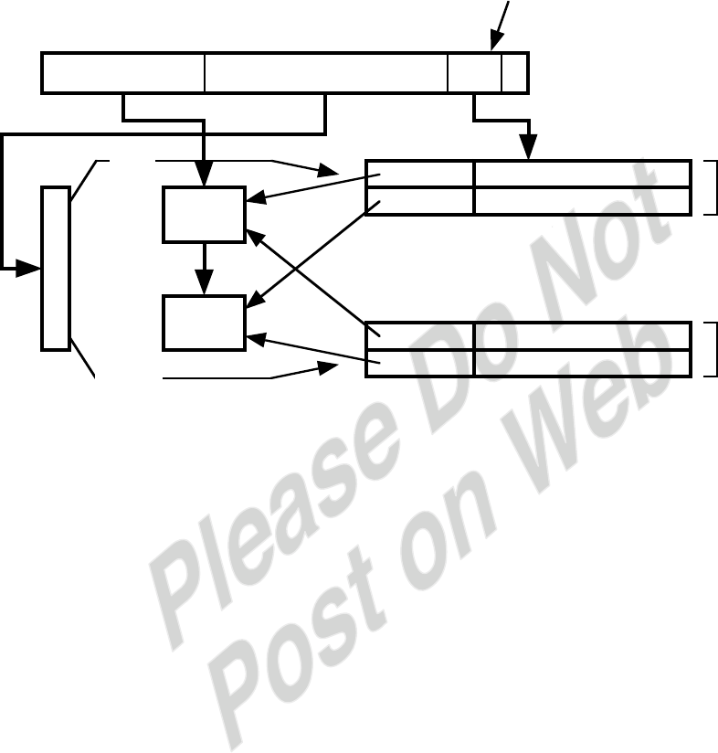
4.11 a. Address format: Tag = 20 bits; Line = 6 bits; Word = 6 bits
Number of addressable units = 2s+w = 232 bytes; number of blocks in main
memory = 2s = 226; number of lines in cache 2r = 26 = 64; size of tag = 20 bits.
b. Address format: Tag = 26 bits; Word = 6 bits
Number of addressable units = 2s+w = 232 bytes; number of blocks in main
memory = 2s = 226; number of lines in cache = undetermined; size of tag = 26
bits.
c. Address format: Tag = 9 bits; Set = 17 bits; Word = 6 bits
Number of addressable units = 2s+w = 232 bytes; Number of blocks in main
memory = 2s = 226; Number of lines in set = k = 4; Number of sets in cache = 2d
= 217; Number of lines in cache = k × 2d =219; Size of tag = 9 bits.
4.12 a. Because the block size is 16 bytes and the word size is 1 byte, this means there
are 16 words per block. We will need 4 bits to indicate which word we want
out of a block. Each cache line/slot matches a memory block. That means each
cache slot contains 16 bytes. If the cache is 64Kbytes then 64Kbytes/16 = 4096
cache slots. To address these 4096 cache slots, we need 12 bits (212 = 4096).
Consequently, given a 20 bit (1 MByte) main memory address:
Bits 0-3 indicate the word offset (4 bits)
Bits 4-15 indicate the cache slot (12 bits)
Bits 16-19 indicate the tag (remaining bits)
F0010 = 1111 0000 0000 0001 0000
Word offset = 0000 = 0
Slot = 0000 0000 0001 = 001
Tag = 1111 = F
01234 = 0000 0001 0010 0011 0100
Word offset = 0100 = 4
Slot = 0001 0010 0011 = 123

-25-
Tag = 0000 = 0
CABBE = 1100 1010 1011 1011 1110
Word offset = 1110 = E
Slot = 1010 1011 1011 = ABB
Tag = 1100 = C
b. We need to pick any address where the slot is the same, but the tag (and
optionally, the word offset) is different. Here are two examples where the slot
is 1111 1111 1111
Address 1:
Word offset = 1111
Slot = 1111 1111 1111
Tag = 0000
Address = 0FFFF
Address 2:
Word offset = 0001
Slot = 1111 1111 1111
Tag = 0011
Address = 3FFF1
c. With a fully associative cache, the cache is split up into a TAG and a
WORDOFFSET field. We no longer need to identify which slot a memory block
might map to, because a block can be in any slot and we will search each cache
slot in parallel. The word-offset must be 4 bits to address each individual word
in the 16-word block. This leaves 16 bits leftover for the tag.
F0010
Word offset = 0h
Tag = F001h
CABBE
Word offset = Eh
Tag = CABBh
d. As computed in part a, we have 4096 cache slots. If we implement a two -way
set associative cache, then it means that we put two cache slots into one set.
Our cache now holds 4096/2 = 2048 sets, where each set has two slots. To
address these 2048 sets we need 11 bits (211 = 2048). Once we address a set, we
will simultaneously search both cache slots to see if one has a tag that matches
the target. Our 20-bit address is now broken up as follows:
Bits 0-3 indicate the word offset
Bits 4-14 indicate the cache set
Bits 15-20 indicate the tag
F0010 = 1111 0000 0000 0001 0000
Word offset = 0000 = 0
Cache Set = 000 0000 0001 = 001
Tag = 11110 = 1 1110 = 1E
CABBE = 1100 1010 1011 1011 1110
Word offset = 1110 = E
Cache Set = 010 1011 1011 = 2BB
Tag = 11001 = 1 1001 = 19
4.13 Associate a 2-bit counter with each of the four blocks in a set. Initially, arbitrarily
set the four values to 0, 1, 2, and 3 respectively. When a hit occurs, the counter of
the block that is referenced is set to 0. The other counters in the set with values

-26-
originally lower than the referenced counter are incremented by 1; the remaining
counters are unchanged. When a miss occurs, the block in the set whose counter
value is 3 is replaced and its counter set to 0. All other counters in the set are
incremented by 1.
4.14 Writing back a line takes 30 + (7 × 5) = 65 ns, enough time for 2.17 single-word
memory operations. If the average line that is written at least once is written more
than 2.17 times, the write-back cache will be more efficient.
4.15 a. A reference to the first instruction is immediately followed by a reference to the
second.
b. The ten accesses to a[i] within the inner for loop which occur within a short
interval of time.
4.16 Define
Ci = Average cost per bit, memory level i
Si = Size of memory level i
Ti = Time to access a word in memory level i
Hi = Probability that a word is in memory i and in no higher-level memory
Bi = Time to transfer a block of data from memory level (i + 1) to memory level i
Let cache be memory level 1; main memory, memory level 2; and so on, for a total
of N levels of memory. Then
Cs=
CiSi
i=1
N
∑
Si
i=1
N
∑
The derivation of Ts is more complicated. We begin with the result from
probability theory that:
Expected Value of x = iPr x=1
[ ]
i=1
N
∑
We can write:
Ts = TiHi
i=1
N
∑
We need to realize that if a word is in M1 (cache), it is read immediately. If it is in
M2 but not M1, then a block of data is transferred from M2 to M1 and then read.
Thus:
T2 = B1 + T1

-27-
Further
T3 = B2 + T2 = B1 + B2 + T1
Generalizing:
Ti= Bj+T1
j=1
i−1
∑
So
Ts= BjHi
( )
j=1
i−1
∑
i=2
N
∑+T1Hi
i=1
N
∑
But
Hi
i=1
N
∑=1
Finally
Ts= BjHi
( )
j=1
i−1
∑
i=2
N
∑+T1
4.17 Main memory consists of 512 blocks of 64 words. Cache consists of 16 sets; each set
consists of 4 slots; each slot consists of 64 words. Locations 0 through 4351 in main
memory occupy blocks 0 through 67. On the first fetch sequence, block 0 through
15 are read into sets 0 through 15; blocks 16 through 31 are read into sets 0 through
15; blocks 32-47 are read into sets 0 through 15; blocks 48-63 are read into sets 0
through 15; and blocks 64-67 are read into sets 0 through 3. Because each set has 4
slots, there is no replacement needed through block 63. The last 4 groups of blocks
involve a replacement. On each successive pass, replacements will be required in
sets 0 through 3, but all of the blocks in sets 4 through 15 remain undisturbed.
Thus, on each successive pass, 48 blocks are undisturbed, and the remaining 20
must read in.
Let T be the time to read 64 words from cache. Then 10T is the time to read 64
words from main memory. If a word is not in the cache, then it can only be ready
by first transferring the word from main memory to the cache and then reading the
cache. Thus the time to read a 64-word block from cache if it is missing is 11T.
We can now express the improvement factor as follows. With no cache
Fetch time = (10 passes) (68 blocks/pass) (10T/block) = 6800T
With cache
Fetch time = (68) (11T) first pass
+ (9) (48) (T) + (9) (20) (11T) other passes
= 3160T
Improvement = 6800T
3160T = 2.15

-28-
4.18 a. Access 63 1 Miss Block 3 → Slot 3
Access 64 1 Miss Block 4 → Slot 0
Access 65-70 6 Hits
Access 15 1 Miss Block 0 → Slot 0 First Loop
Access 16 1 Miss Block 1 → Slot 1
Access 17-31 15 Hits
Access 32 1 Miss Block 2 → Slot 2
Access 80 1 Miss Block 5 → Slot 1
Access 81-95 15 Hits
Access 15 1 Hit Second Loop
Access 16 1 Miss Block 1 → Slot 1
Access 17-31 15 hits
Access 32 1 Hit
Access 80 1 Miss Block 5 → Slot 1
Access 81-95 15 hits
Access 15 1 Hit Third Loop
Access 16 1 Miss Block 1 → Slot 1
Access 17-31 15 hits
Access 32 1 Hit
Access 80 1 Miss Block 5 → Slot 1
Access 81-95 15 hits
Access 15 1 Hit Fourth Loop
… Pattern continues to the Tenth Loop
For lines 63-70 2 Misses 6 Hits
First loop 15-32, 80-95 4 Misses 30 Hits
Second loop 15-32, 80-95 2 Misses 32 Hits
Third loop 15-32, 80-95 2 Misses 32 Hits
Fourth loop 15-32, 80-95 2 Misses 32 Hits
Fifth loop 15-32, 80-95 2 Misses 32 Hits
Sixth loop 15-32, 80-95 2 Misses 32 Hits
Seventh loop 15-32, 80-95 2 Misses 32 Hits
Eighth loop 15-32, 80-95 2 Misses 32 Hits
Ninth loop 15-32, 80-95 2 Misses 32 Hits
Tenth loop 15-32, 80-95 2 Misses 32 Hits
Total: 24 Misses 324 Hits
Hit Ratio = 324/348 = 0.931
b. Access 63 1 Miss Block 3 → Set 1 Slot 2
Access 64 1 Miss Block 4 → Set 0 Slot 0
Access 65-70 6 Hits
Access 15 1 Miss Block 0 → Set 0 Slot 1 First Loop
Access 16 1 Miss Block 1 → Set 1 Slot 3
Access 17-31 15 Hits
Access 32 1 Miss Block 2 → Set 0 Slot 0
Access 80 1 Miss Block 5 → Set 1 Slot 2
Access 81-95 15 Hits
Access 15 1 Hit Second Loop
Access 16-31 16 Hits
Access 32 1 Hit
Access 80-95 16 Hits
… All hits for the next eight iterations

-29-
For lines 63-70 2 Misses 6 Hits
First loop 15-32, 80-95 4 Misses 30 Hits
Second loop 15-32, 80-95 0 Misses 34 Hits
Third loop 15-32, 80-95 0 Misses 34 Hits
Fourth loop 15-32, 80-95 0 Misses 34 Hits
Fifth loop 15-32, 80-95 0 Misses 34 Hits
Sixth loop 15-32, 80-95 0 Misses 34 Hits
Seventh loop 15-32, 80-95 0 Misses 34 Hits
Eighth loop 15-32, 80-95 0 Misses 34 Hits
Ninth loop 15-32, 80-95 0 Misses 34 Hits
Tenth loop 15-32, 80-95 0 Misses 34 Hits
Total = 6 Misses 342 Hits
Hit Ratio = 342/348 = 0.983
4.19 a. Cost = Cm × 8 × 106 = 8 × 10³ ¢ = $80
b. Cost = Cc × 8 × 106 = 8 × 10⁴ ¢ = $800
c. From Equation (4.1) : 1.1 × T1 = T1 + (1 – H)T2
(0.1)(100) = (1 – H)(1200)
H = 1190/1200
4.20 a. Under the initial conditions, using Equation (4.1), the average access time is
T1 + (1 - H) T2 = 1 + (0.05) T2
Under the changed conditions, the average access time is
1.5 + (0.03) T2
For improved performance, we must have
1 + (0.05) T2 > 1.5 + (0.03) T2
Solving for T2, the condition is T2 > 50
b. As the time for access when there is a cache miss become larger, it becomes
more important to increase the hit ratio.
4.21 a. First, 2.5 ns are needed to determine that a cache miss occurs. Then, the
required line is read into the cache. Then an additional 2.5 ns are needed to
read the requested word.
Tmiss = 2.5 + 50 + (15)(5) + 2.5 = 130 ns
b. The value Tmiss from part (a) is equivalent to the quantity (T1 + T2) in Equation
(4.1). Under the initial conditions, using Equation (4.1), the average access time
is
Ts = H × T1 + (1 – H) × (T1 + T2) = (0.95)(2.5) + (0.05)(130) = 8.875 ns
Under the revised scheme, we have:

-30-
Tmiss = 2.5 + 50 + (31)(5) + 2.5 = 210 ns
and
Ts = H × T1 + (1 – H) × (T1 + T2) = (0.97)(2.5) + (0.03)(210) = 8.725 ns
4.22 There are three cases to consider:
Location of referenced word
Probability
Total time for access in ns
In cache
0.9
20
Not in cache, but in main
memory
(0.1)(0.6) = 0.06
60 + 20 = 80
Not in cache or main memory
(0.1)(0.4) = 0.04
12ms + 60 + 20 = 12,000,080
So the average access time would be:
Avg = (0.9)(20) + (0.06)(80) + (0.04)(12000080) = 480026 ns
4.23 a. Consider the execution of 100 instructions. Under write-through, this creates
200 cache references (168 read references and 32 write references). On average,
the read references result in (0.03) × 168 = 5.04 read misses. For each read miss,
a line of memory must be read in, generating 5.04 × 8 = 40.32 physical words of
traffic. For write misses, a single word is written back, generating 32 words of
traffic. Total traffic: 72.32 words. For write back, 100 instructions create 200
cache references and thus 6 cache misses. Assuming 30% of lines are dirty, on
average 1.8 of these misses require a line write before a line read. Thus, total
traffic is (6 + 1.8) × 8 = 62.4 words. The traffic rate:
Write through = 0.7232 byte/instruction
Write back = 0.624 bytes/instruction
b. For write-through: [(0.05) × 168 × 8] + 32 = 99.2 → 0.992 bytes/instruction
For write-back: (10 + 3) × 8 = 104 → 0.104 bytes/instruction
c. For write-through: [(0.07) × 168 × 8] + 32 = 126.08 → 0.12608 bytes/instruction
For write-back: (14 + 4.2) × 8 = 145.6 → 0.1456 bytes/instruction
d. A 5% miss rate is roughly a crossover point. At that rate, the memory traffic is
about equal for the two strategies. For a lower miss rate, write-back is superior.
For a higher miss rate, write-through is superior.
4.24 a. One clock cycle equals 60 ns, so a cache access takes 120 ns and a main memory
access takes 180 ns. The effective length of a memory cycle is (0.9 × 120) + (0.1 ×
180) = 126 ns.
b. The calculation is now (0.9 × 120) + (0.1 × 300) = 138 ns. Clearly the
performance degrades. However, note that although the memory access time
increases by 120 ns, the average access time increases by only 12 ns.
4.25 a. For a 1 MIPS processor, the average instruction takes 1000 ns to fetch and
execute. On average, an instruction uses two bus cycles for a total of 600 ns, so
the bus utilization is 0.6
b. For only half of the instructions must the bus be used for instruction fetch. Bus
utilization is now (150 + 300)/1000 = 0.45. This reduces the waiting time for
other bus requestors, such as DMA devices and other microprocessors.

-31-
4.26 a. Ta = Tc + (1 – H)Tb + W(Tm – Tc)
b. Ta = Tc + (1 – H)Tb + Wb(1 – H)Tb = Tc + (1 – H)(1 + Wb)Tb
4.27 Ta = [Tc1 + (1 – H1)Tc2] + (1 – H2)Tm
4.28 a. miss penalty = 1 + 4 = 5 clock cycles
b. miss penalty = 4 × (1 + 4 ) = 20 clock cycles
c. miss penalty = miss penalty for one word + 3 = 8 clock cycles.
4.29 The average miss penalty equals the miss penalty times the miss rate. For a line
size of one word, average miss penalty = 0.032 x 5 = 0.16 clock cycles. For a line
size of 4 words and the nonburst transfer, average miss penalty = 0.011 x 20 = 0.22
clock cycles. For a line size of 4 words and the burst transfer, average miss penalty
= 0.011 x 8 = 0.132 clock cycles.

-32-
CHAPTER 5 INTERNAL MEMORY
A
ANSWERS TO
NSWERS TO Q
QUESTIONS
UESTIONS
5.1 They exhibit two stable (or semistable) states, which can be used to represent
binary 1 and 0; they are capable of being written into (at least once), to set the state;
they are capable of being read to sense the state.
5.2 (1) A memory in which individual words of memory are directly accessed through
wired-in addressing logic. (2) Semiconductor main memory in which it is possible
both to read data from the memory and to write new data into the memory easily
and rapidly.
5.3 SRAM is used for cache memory (both on and off chip), and DRAM is used for
main memory.
5.4 SRAMs generally have faster access times than DRAMs. DRAMS are less
expensive and smaller than SRAMs.
5.5 A DRAM cell is essentially an analog device using a capacitor; the capacitor can
store any charge value within a range; a threshold value determines whether the
charge is interpreted as 1 or 0. A SRAM cell is a digital device, in which binary
values are stored using traditional flip-flop logic-gate configurations.
5.6 Microprogrammed control unit memory; library subroutines for frequently
wanted functions; system programs; function tables.
5.7 EPROM is read and written electrically; before a write operation, all the storage
cells must be erased to the same initial state by exposure of the packaged chip to
ultraviolet radiation. Erasure is performed by shining an intense ultraviolet light
through a window that is designed into the memory chip. EEPROM is a read-
mostly memory that can be written into at any time without erasing prior contents;
only the byte or bytes addressed are updated. Flash memory is intermediate
between EPROM and EEPROM in both cost and functionality. Like EEPROM,
flash memory uses an electrical erasing technology. An entire flash memory can be
erased in one or a few seconds, which is much faster than EPROM. In addition, it is
possible to erase just blocks of memory rather than an entire chip. However, flash
memory does not provide byte-level erasure. Like EPROM, flash memory uses
only one transistor per bit, and so achieves the high density (compared with
EEPROM) of EPROM.
5.8 A0 - A1 = address lines:. CAS = column address select:. D1 - D4 = data lines. NC: =
no connect. OE: output enable. RAS = row address select:. Vcc: = voltage source.
Vss: = ground. WE: write enable.

-33-
5.9 A bit appended to an array of binary digits to make the sum of all the binary
digits, including the parity bit, always odd (odd parity) or always even (even
parity).
5.10 A syndrome is created by the XOR of the code in a word with a calculated version
of that code. Each bit of the syndrome is 0 or 1 according to if there is or is not a
match in that bit position for the two inputs. If the syndrome contains all 0s, no
error has been detected. If the syndrome contains one and only one bit set to 1,
then an error has occurred in one of the 4 check bits. No correction is needed. If the
syndrome contains more than one bit set to 1, then the numerical value of the
syndrome indicates the position of the data bit in error. This data bit is inverted for
correction.
5.11 Unlike the traditional DRAM, which is asynchronous, the SDRAM exchanges data
with the processor synchronized to an external clock signal and running at the full
speed of the processor/memory bus without imposing wait states.
A
ANSWERS TO
NSWERS TO P
PROBLEMS
ROBLEMS
5.1 The 1-bit-per-chip organization has several advantages. It requires fewer pins on
the package (only one data out line); therefore, a higher density of bits can be
achieved for a given size package. Also, it is somewhat more reliable because it has
only one output driver. These benefits have led to the traditional use of 1-bit-per-
chip for RAM. In most cases, ROMs are much smaller than RAMs and it is often
possible to get an entire ROM on one or two chips if a multiple-bits-per-chip
organization is used. This saves on cost and is sufficient reason to adopt that
organization.
5.2 In 1 ms, the time devoted to refresh is 64 × 150 ns = 9600 ns. The fraction of time
devoted to memory refresh is (9.6 × 10⁻⁶ s)/10–3 s = 0.0096, which is approximately
1%.
5.3 a. Memory cycle time = 60 + 40 = 100 ns. The maximum data rate is 1 bit every 100
ns, which is 10 Mbps.
b. 320 Mbps = 40 MB/s.
-34-
5.4
S0 S1
S2
S3
S4
S5
S6
S7
A0
A19
A20
A21
A22
Decoder
Chip select
1 Mb
Chip select
1 Mb
Chip select
1 Mb
Chip select
1 Mb
Chip select
1 Mb
Chip select
1 Mb
Chip select
1 Mb
Chip select
1 Mb
•
•
•
5.5 a. The length of a clock cycle is 100 ns. Mark the beginning of T1 as time 0.Address
Enable returns to a low at 75.
€
RAS
goes active 50 ns later, or time 125. Data
must become available by the DRAMs at time 300 – 60 = 240. Hence, access time
must be no more than 240 – 125 = 115 ns.
b. A single wait state will increase the access time requirement to 115 + 100 = 215
ns. This can easily be met by DRAMs with access times of 150 ns.
5.6 a. The refresh period from row to row must be no greater than
4000/256 = 15.625 µs.
b. An 8-bit counter is needed to count 256 rows (28 = 256).
5.7 a.
pulse a = write
pulse b = write
pulse c = write
pulse d = write
pulse e= write
pulse f = write
pulse g = store-disable outputs
pulse h = read
pulse i = read
pulse j = read
pulse k = read
pulse l = read
pulse m = read
pulse n = store-disable outputs
-35-
b. Data is read in via pins (D3, D2, D1, D0)
word 0 = 1111 (written into location 0 during pulse a)
word 1 = 1110 (written into location 0 during pulse b)
word 2 = 1101 (written into location 0 during pulse c)
word 3 = 1100 (written into location 0 during pulse d)
word 4 = 1011 (written into location 0 during pulse e)
word 5 = 1010 (written into location 0 during pulse f)
word 6 = random (did not write into this location 0)
c. Output leads are (O3, O2, O1, O0)
pulse h: 1111 (read location 0)
pulse i: 1110 (read location 1)
pulse j: 1101 (read location 2)
pulse k: 1100 (read location 3)
pulse l: 1011 (read location 4)
pulse m: 1010 (read location 5)
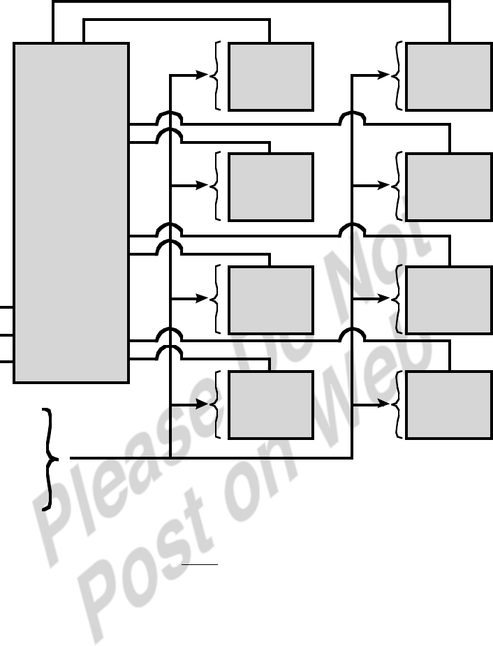
5.8 8192/64 = 128 chips; arranged in 8 rows by 64 columns:
.
• • •
• • •
•
•
•
•
•
•
•
•
•
01 7
112 113 119
Section 0 (even)
• • •
• • •
•
•
•
•
•
•
•
•
•
89 15
120 121 127
Section 1 (odd)
A0 = L A0 = H
Decoder
Row 0
Row 1
Row 7
•
•
•
8
Rows
All zeros
Ak-A10 A9-A7
3
A6-A1
6
AB
En
8
8
Depends on
type of
processor
5.9 Total memory is 1 megabyte = 8 megabits. It will take 32 DRAMs to construct the
memory (32 × 256 Kb = 8 Mb). The composite failure rate is 2000 × 32 = 64,000
FITS. From this, we get a MTBF = 109/64,000 = 15625 hours = 22 months.
5.10 The stored word is 001101001111, as shown in Figure 5.10. Now suppose that the
only error is in C8, so that the fetched word is 001111001111. Then the received
block results in the following table:
Position
12
11
10
9
8
7
6
5
4
3
2
1
Bits
D8
D7
D6
D5
C8
D4
D3
D2
C4
D1
C2
C1
Block
0
0
1
1
1
1
0
0
1
1
1
1
Codes
1010
1001
0111
0011

-36-
The check bit calculation after reception:
Position
Code
Hamming
1111
10
1010
9
1001
7
0111
3
0011
XOR = syndrome
1000
The nonzero result detects and error and indicates that the error is in bit position 8,
which is check bit C8.
5.11 Data bits with value 1 are in bit positions 12, 11, 5, 4, 2, and 1:
Position
12
11
10
9
8
7
6
5
4
3
2
1
Bits
D8
D7
D6
D5
C8
D4
D3
D2
C4
D1
C2
C1
Block
1
1
0
0
0
0
1
0
Codes
1100
1011
0101
The check bits are in bit numbers 8, 4, 2, and 1.
Check bit 8 calculated by values in bit numbers: 12, 11, 10 and 9
Check bit 4 calculated by values in bit numbers: 12, 7, 6, and 5
Check bit 2 calculated by values in bit numbers: 11, 10, 7, 6 and 3
Check bit 1 calculated by values in bit numbers: 11, 9, 7, 5 and 3
Thus, the check bits are: 0 0 1 0
5.12 The Hamming Word initially calculated was:
bit number:
12
11
10
9
8
7
6
5
4
3
2
1
0
0
1
1
0
1
0
0
1
1
1
1
Doing an exclusive-OR of 0111 and 1101 yields 1010 indicating an error in bit 10 of
the Hamming Word. Thus, the data word read from memory was 00011001.
5.13 Need K check bits such that 1024 + K ≤ 2K – 1.
The minimum value of K that satisfies this condition is 11.

-37-
5.14 As Table 5.2 indicates, 5 check bits are needed for an SEC code for 16-bit data
words. The layout of data bits and check bits:
Bit Position
Position Number
Check Bits
Data Bits
21
10101
M16
20
10100
M15
19
10011
M14
18
10010
M13
17
10001
M12
16
10000
C16
15
01111
M11
14
01110
M10
13
01101
M9
12
01100
M8
11
01011
M7
10
01010
M6
9
01001
M5
8
01000
C8
7
00111
M4
6
00110
M3
5
00101
M2
4
00100
C4
3
00011
M1
2
00010
C2
1
00001
C1
The equations are calculated as before, for example,
C1= M1 ⊕ M2 ⊕ M4 ⊕ M5 ⊕ M7 ⊕ M9 ⊕ M11 ⊕ M12 ⊕ M14 ⊕ M16.
For the word 0101000000111001, the code is
C16 = 1; C8 = 1; C 4 = 1; C2 = 1; C1 = 0.
If an error occurs in data bit 4:
C16 = 1 ; C8 =1; C4 = 0; C2 = 0; C1 = 1.
Comparing the two:
C16
C8
C4
C2
C1
1
1
1
1
0
1
1
0
0
1
0
0
1
1
1
The result is an error identified in bit position 7, which is data bit 4.

-38-
CHAPTER 6 EXTERNAL MEMORY
A
ANSWERS TO
NSWERS TO Q
QUESTIONS
UESTIONS
6.1 Improvement in the uniformity of the magnetic film surface to increase disk
reliability. A significant reduction in overall surface defects to help reduce
read/write errors. Ability to support lower fly heights (described subsequently).
Better stiffness to reduce disk dynamics. Greater ability to withstand shock and
damage
6.2 The write mechanism is based on the fact that electricity flowing through a coil
produces a magnetic field. Pulses are sent to the write head, and magnetic patterns
are recorded on the surface below, with different patterns for positive and negative
currents. An electric current in the wire induces a magnetic field across the gap,
which in turn magnetizes a small area of the recording medium. Reversing the
direction of the current reverses the direction of the magnetization on the
recording medium.
6.3 The read head consists of a partially shielded magnetoresistive (MR) sensor. The
MR material has an electrical resistance that depends on the direction of the
magnetization of the medium moving under it. By passing a current through the
MR sensor, resistance changes are detected as voltage signals.
6.4 For the constant angular velocity (CAV) system, the number of bits per track is
constant. An increase in density is achieved with multiple zoned recording, in
which the surface is divided into a number of zones, with zones farther from the
center containing more bits than zones closer to the center.
6.5 On a magnetic disk. data is organized on the platter in a concentric set of rings,
called tracks. Data are transferred to and from the disk in sectors. For a disk with
multiple platters, the set of all the tracks in the same relative position on the platter
is referred to as a cylinder.
6.6 512 bytes.
6.7 On a movable-head system, the time it takes to position the head at the track is
known as seek time. Once the track is selected, the disk controller waits until the
appropriate sector rotates to line up with the head. The time it takes for the
beginning of the sector to reach the head is known as rotational delay. The sum of
the seek time, if any, and the rotational delay equals the access time, which is the
time it takes to get into position to read or write. Once the head is in position, the
read or write operation is then performed as the sector moves under the head; this
is the data transfer portion of the operation and the time for the transfer is the
transfer time.

-39-
6.8 1. RAID is a set of physical disk drives viewed by the operating system as a single
logical drive. 2. Data are distributed across the physical drives of an array. 3.
Redundant disk capacity is used to store parity information, which guarantees
data recoverability in case of a disk failure.
6.9 0: Non-redundant 1: Mirrored; every disk has a mirror disk containing the same
data. 2: Redundant via Hamming code; an error-correcting code is calculated
across corresponding bits on each data disk, and the bits of the code are stored in
the corresponding bit positions on multiple parity disks. 3: Bit-interleaved parity;
similar to level 2 but instead of an error-correcting code, a simple parity bit is
computed for the set of individual bits in the same position on all of the data disks.
4: Block-interleaved parity; a bit-by-bit parity strip is calculated across
corresponding strips on each data disk, and the parity bits are stored in the
corresponding strip on the parity disk. 5: Block-interleaved distributed parity;
similar to level 4 but distributes the parity strips across all disks. 6: Block-
interleaved dual distributed parity; two different parity calculations are carried out
and stored in separate blocks on different disks.
6.10 The disk is divided into strips; these strips may be physical blocks, sectors, or some
other unit. The strips are mapped round robin to consecutive array members. A set
of logically consecutive strips that maps exactly one strip to each array member is
referred to as a stripe.
6.11 For RAID level 1, redundancy is achieved by having two identical copies of all
data. For higher levels, redundancy is achieved by the use of error-correcting
codes.
6.12 In a parallel access array, all member disks participate in the execution of every
I/O request. Typically, the spindles of the individual drives are synchronized so
that each disk head is in the same position on each disk at any given time. In an
independent access array, each member disk operates independently, so that
separate I/O requests can be satisfied in parallel.
6.13 For the constant angular velocity (CAV) system, the number of bits per track is
constant. At a constant linear velocity (CLV), the disk rotates more slowly for
accesses near the outer edge than for those near the center. Thus, the capacity of a
track and the rotational delay both increase for positions nearer the outer edge of
the disk.
6.14 1. Bits are packed more closely on a DVD. The spacing between loops of a spiral on
a CD is 1.6 µm and the minimum distance between pits along the spiral is 0.834
µm. The DVD uses a laser with shorter wavelength and achieves a loop spacing of
0.74 µm and a minimum distance between pits of 0.4 µm. The result of these two
improvements is about a seven-fold increase in capacity, to about 4.7 GB. 2. The
DVD employs a second layer of pits and lands on top of the first layer A dual-layer
DVD has a semireflective layer on top of the reflective layer, and by adjusting
focus, the lasers in DVD drives can read each layer separately. This technique
almost doubles the capacity of the disk, to about 8.5 GB. The lower reflectivity of
the second layer limits its storage capacity so that a full doubling is not achieved.

-40-
3. The DVD-ROM can be two sided whereas data is recorded on only one side of a
CD. This brings total capacity up to 17 GB.
6.15 The typical recording technique used in serial tapes is referred to as serpentine
recording. In this technique, when data are being recorded, the first set of bits is
recorded along the whole length of the tape. When the end of the tape is reached,
the heads are repositioned to record a new track, and the tape is again recorded on
its whole length, this time in the opposite direction. That process continues, back
and forth, until the tape is full.
A
ANSWERS TO
NSWERS TO P
PROBLEMS
ROBLEMS
6.1 It will be useful to keep the following representation of the N tracks of a disk in
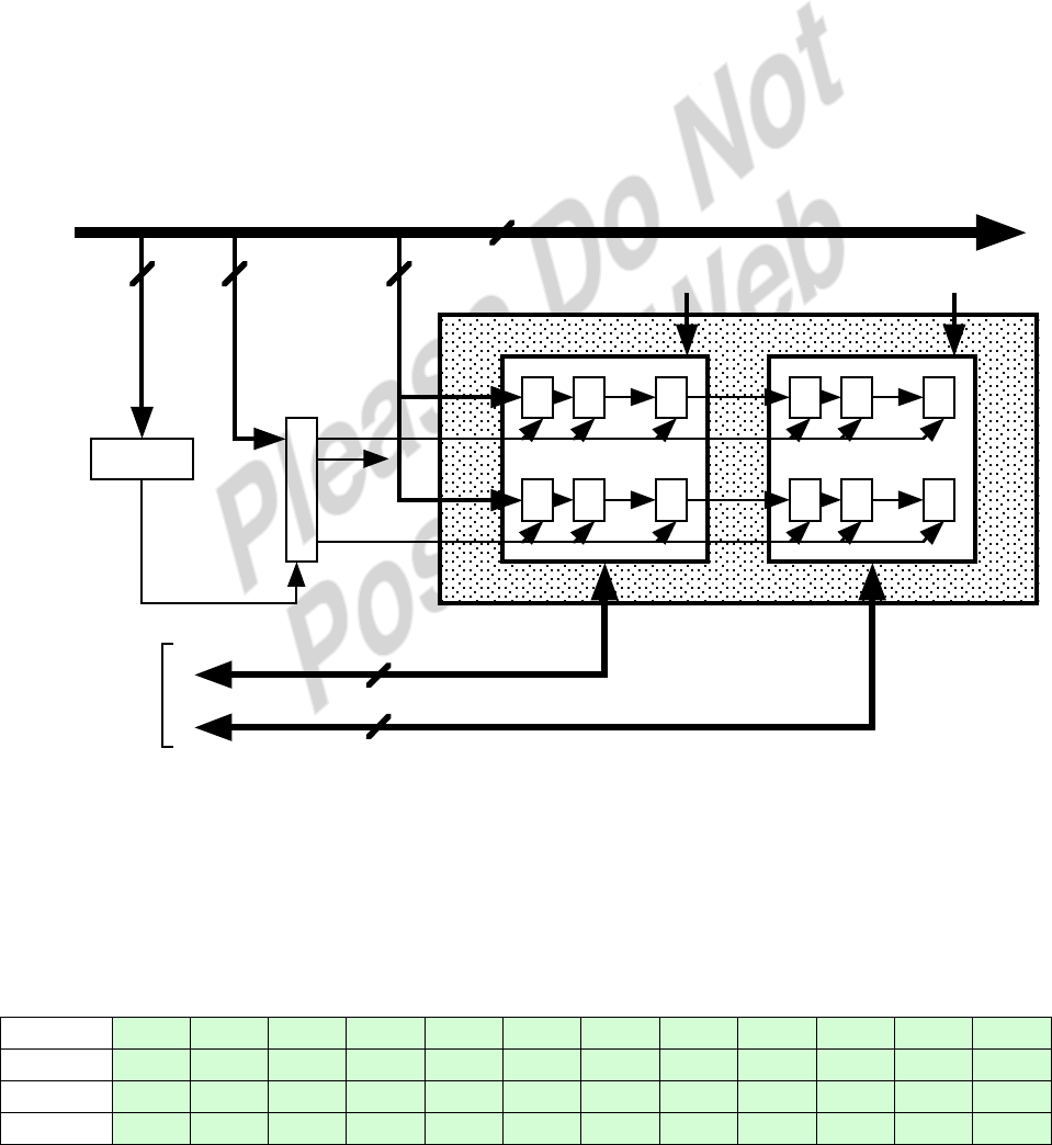
mind:
0
1
• • •
j – 1
• • •
N – j
• • •
N – 2
N – 1
a. Let us use the notation Ps [j/t] = Pr [seek of length j when head is currently
positioned over track t]. Recognize that each of the N tracks is equally likely to
be requested. Therefore the unconditional probability of selecting any
particular track is 1/N. We can then state:
Ps[j/t]=1
N
if t ≤ j – 1 OR t ≥ N – j
Ps[j/t]=2
N
if j – 1 < t < N – j
In the former case, the current track is so close to one end of the disk (track 0 or
track N – 1) that only one track is exactly j tracks away. In the second case,
there are two tracks that are exactly j tracks away from track t, and therefore
the probability of a seek of length j is the probability that either of these two
tracks is selected, which is just 2/N.
b. Let Ps [K] = Pr [seek of length K, independent of current track position]. Then:
Ps K
[ ]
=Ps K/t
[ ]
t=0
N−1
∑×Pr current track is track t
[ ]
=1
N
Ps K/t
[ ]
t=0
N−1
∑
From part (a), we know that Ps[K/t] takes on the value 1/N for 2K of the
tracks, and the value 2/N for (N – 2K) of the tracks. So
Ps K
[ ]
=1
N
2K
N+2N−2K
( )
N
= 2K+2N−2K
( )
N2=2
N−2K
N2

-41-
c.
EK
[ ]
=K×Ps K
[ ]
K=0
N−1
∑=2K
N−2K2
N2
K=0
N−1
∑=2
N
K
K=0
N−1
∑−2
N2K2
K=0
N−1
∑
=2
N
N−1
( )
N
2−2
N2
N−1
( )
N2N−1
( )
6=N−1
( )
−N−1
( )
2N−1
( )
3N
=3N N −1
( )
−N−1
( )
2N−1
( )
3N=N2−1
3N
d. This follows directly from the last equation.
6.2
tA=tS+1
2r+n
rN
tA=tS+1
2r+n
rN
6.3 a. Capacity = 8 × 512 × 64 × 1 KB = 256 MB
b. Rotational latency = rotation_time/2 = 60/(3600 × 2) = 8.3 ms.
Average access time = seek time + rotational latency = 16.3 ms
c. Each cylinder consists of 8 tracks × 64 sectors/track × 1 KB/sector = 512 KB, so
5 MB requires exactly 10 cylinders. The disk will need the seek time of 8 ms to
find cylinder i, 8.3 ms on average to find sector 0, and 8 × (60/3.6) = 133.3 ms to
read all 8 tracks on one cylinder. Then, the time needed to move to the next
adjoining cylinder is 1.5 ms, which is the track-to-track access time. Assume a
rotational latency before each track.
Access Time = 8 + 9 × (8.3 + 133.3 + 1.5) + (8.3 + 133.3) = 1425.5 ms
d.
€
Burst rate = revolutions
second ×sectors
revolution ×bytes
secter =3600
60 ×64 ×1 KB = 3.84 MB/s
6.4 a. If we assume that the head starts at track 0, then the calculations are simplified.
If the request track is track 0, then the seek time is 0; if the requested track is
track 29,999, then the seek time is the time to traverse 29,999 tracks. For a
random request, on average the number of tracks traversed is 29,999/2 =
14999.5 tracks. At one ms per 100 tracks, the average seek time is therefore
149.995 ms.
b. At 7200 rpm, there is one revolution every 8.333 ms. Therefore, the average
rotational delay is 4.167 ms.
c. With 600 sectors per track and the time for one complete revolution of 8.333 ms,
the transfer time for one sector is 8.333 ms/600 = 0.01389 ms.
d. The result is the sum of the preceding quantities, or approximately 154 ms.
6.5 Each sector can hold 4 logical records. The required number of sectors is 300,000/4
= 75,000 sectors. This requires 75,000/96 = 782 tracks, which in turn requires
782/110 = 8 surfaces.
6.6 a. The time consists of the following components: sector read time; track access
time; rotational delay; and sector write time. The time to read or write 1 sector
is calculated as follows: A single revolution to read or write an entire track
takes 60,000/360 = 16.7 ms. Time to read or write a single sector = 16.7/32 =

-42-
0.52 ms. Track access time = 2 ms, because the head moves between adjacent
tracks. The rotational delay is the time required for the head to line up with
sector 1 again. This is 16.7 × (31/32) = 16.2 ms. The head movement time of 2
ms overlaps the with the 16.2 ms of rotational delay, and so only the rotational
delay time is counted. Total transfer time = 0.52 + 16.2 + 0.52 = 17.24 ms.
b. The time to read or write an entire track is simply the time for a single
revolution, which is 16.7 ms. Between the read and the write there is a head
movement time of 2 ms to move from track 8 to track 9. During this time the
head moves past 3 sectors and most of a fourth sector. However, because the
entire track is buffered, sectors can be written back in a different sequence from
the read sequence. Thus, the write can start with sector 5 of track 9. This sector
is reached 0.52 × 4 = 2.08 ms after the completion of the read operation. Thus
the total transfer time = 16.7 + 2.08 + 16.7 = 35.48 ms.
6.8
RAID 0: 800 GB
RAID 1: 400 GB
RAID 3: 600 GB
RAID 4: 600 GB
RAID 5: 600 GB
RAID 6: 400 GB
6.9 With the CD scheme, bit density improves by a factor of 3, but there is an increase
in the number of bits by a factor of 14/8. Net improvement factor is 3 × (8/14) ≈
1.7. That is, the CD scheme has a data storage density 1.7 times greater than the
direct recording scheme.
6.10 a. 2 × 3 × $150 = $900
b. $2500 + (3 × 3 × $50) = $2950
c. Let Z = the number of GB at which the two approaches yield approximately the
same cost. For the disk, the cost is Cd = (Z/500) × 3 × $150. For tape, the cost is
Ct = 2500 + ((Z/400) × 3 × $50). If we set Cd = Ct and solve for Z, we get Z =
4762. So the size of the backup would have to be about 5 TB for tape to be less
expensive.
d. One where you keep a lot of backup sets.
6.7 It depends on the nature of the I/O request pattern. On one extreme, if only a
single process is doing I/O and is only doing one large I/O at a time, then disk
striping improves performance. If there are many processes making many small
I/O requests, then a nonstriped array of disks should give comparable
performance to RAID 0.

-43-
CHAPTER 7 INPUT/OUTPUT
A
ANSWERS TO
NSWERS TO Q
QUESTIONS
UESTIONS
7.1 Human readable: Suitable for communicating with the computer user. Machine
readable: Suitable for communicating with equipment. Communication: Suitable
for communicating with remote devices
7.2 The most commonly used text code is the International Reference Alphabet (IRA),
in which each character is represented by a unique 7-bit binary code; thus, 128
different characters can be represented.
7.3 Control and timing. Processor communication. Device communication. Data
buffering. Error detection.
7.4 Programmed I/O: The processor issues an I/O command, on behalf of a process, to
an I/O module; that process then busy-waits for the operation to be completed
before proceeding. Interrupt-driven I/O: The processor issues an I/O command on
behalf of a process, continues to execute subsequent instructions, and is
interrupted by the I/O module when the latter has completed its work. The
subsequent instructions may be in the same process, if it is not necessary for that
process to wait for the completion of the I/O. Otherwise, the process is suspended
pending the interrupt and other work is performed. Direct memory access
(DMA): A DMA module controls the exchange of data between main memory and
an I/O module. The processor sends a request for the transfer of a block of data to
the DMA module and is interrupted only after the entire block has been
transferred.
7.5 With memory-mapped I/O, there is a single address space for memory locations
and I/O devices. The processor treats the status and data registers of I/O modules
as memory locations and uses the same machine instructions to access both
memory and I/O devices. With isolated I/O, a command specifies whether the
address refers to a memory location or an I/O device. The full range of addresses
may be available for both.
7.6 Four general categories of techniques are in common use: multiple interrupt lines;
software poll; daisy chain (hardware poll, vectored); bus arbitration (vectored).
7.7 The processor pauses for each bus cycle stolen by the DMA module.
A
ANSWERS TO
NSWERS TO P
PROBLEMS
ROBLEMS

-44-
7.1 In the first addressing mode, 28 = 256 ports can be addressed. Typically, this would
allow 128 devices to be addressed. However, an opcode specifies either an input or
output operation, so it is possible to reuse the addresses, so that there are 256 input
port addresses and 256 output port addresses. In the second addressing mode, 216
= 64K port addresses are possible.
7.2 In direct addressing mode, an instruction can address up to 216 = 64K ports. In
indirect addressing mode, the port address resides in a 16-bit registers, so again,
the instruction can address up to 216 = 64K ports.
7.3 64 KB
7.4 Using non-block I/O instructions, the transfer takes 20 × 128 = 2560 clock cycles.
With block I/O, the transfer takes 5 × 128 = 640 clock cycles (ignoring the one-time
fetching of the iterative instruction and its operands). The speedup is
(2560 – 640)/2560 = 0.75, or 75%.
7.5 a. Each I/O device requires one output (from the point of view of the processor)
port for commands and one input port for status.
b. The first device requires only one port for data, while the second devices
requires and input data port and an output data port. Because each device
requires one command and one status port, the total number of ports is seven.
c. seven.
7.6 a. The printing rate is slowed to 5 cps.
b. The situation must be treated differently with input devices such as the
keyboard. It is necessary to scan the buffer at a rate of at least once per 60 ms.
Otherwise, there is the risk of overwriting characters in the buffer.
7.7 At 8 MHz, the processor has a clock period of 0.125 µs, so that an instruction cycle
takes 12 × 0.125 = 1.5 µs. To check status requires one input-type instruction to
read the device status register, plus at least one other instruction to examine the
register contents. If the device is ready, one output-type instruction is needed to
present data to the device handler. The total is 3 instructions, requiring 4.5 µs.
7.8 Advantages of memory mapped I/O:
1. No additional control lines are needed on the bus to distinguish memory
commands from I/O commands.
2. Addressing is more flexible. Examples: The various addressing modes of
the instruction set can be used, and various registers can be used to
exchange data with I/O modules.
Disadvantages of memory-mapped I/O:
1. Memory-mapped I/O uses memory-reference instructions, which in most
machines are longer than I/O instructions. The length of the program
therefore is longer.
2. The hardware addressing logic to the I/O module is more complex, because
the device address is longer.
7.9 a. The processor scans the keyboard 10 times per second. In 8 hours, the number
of times the keyboard is scanned is 10 × 60 × 60 × 8 = 288,000.

-45-
b. Only 60 visits would be required. The reduction is 1 – (60/288000) = 0.999, or
99.9%
7.10 a. The device generates 8000 interrupts per second or a rate of one every 125 µs. If
each interrupt consumes 100 µs, then the fraction of processor time consumed
is 100/125 = 0.8
b. In this case, the time interval between interrupts is 16 × 125 = 2000 µs. Each
interrupt now requires 100 µs for the first character plus the time for
transferring each remaining character, which adds up to 8 × 15 = 120 µs, for a
total of 220 µs. The fraction of processor time consumed is 220/2000 = 0.11
c. The time per byte has been reduced by 6 µs, so the total time reduction is 16 × 6
= 96 µs. The fraction of processor time consumed is therefore (220 – 96)/2000 =
0.062. This is an improvement of almost a factor of 2 over the result from part
(b).
7.11 If a processor is held up in attempting to read or write memory, usually no
damage occurs except a slight loss of time. However, a DMA transfer may be to or
from a device that is receiving or sending data in a stream (e.g., disk or tape), and
cannot be stopped. Thus, if the DMA module is held up (denied continuing access
to main memory), data will be lost.
7.12 Let us ignore data read/write operations and assume the processor only fetches
instructions. Then the processor needs access to main memory once every
microsecond. The DMA module is transferring characters at a rate of 1200
characters per second, or one every 833 µs. The DMA therefore "steals" every 833rd
cycle. This slows down the processor approximately
1
833 ×100% =0.12%
7.13 a. For the actual transfer, the time needed is (128 bytes)/(50 KBps) = 2.56 ms.
Added to this is the time to transfer bus control at the beginning and end of the
transfer, which is 250 + 250 = 500 ns. This additional time is negligible, so that
the transfer time can be considered as 2.56 ms.
b. The time to transfer one byte in cycle stealing mode is 250 + 500 + 250 = 1000 ns
= 1 µs. Total amount of time the bus is occupied for the transfer is 128 µs. This
is less than the result from part (a) by a factor of 20.
7.14 a. At 5 MHz, on clock cycle takes 0.2 µs. A transfer of one byte therefore takes 0.6
µs.
b. The data rate is 1/(0.6 × 10–6) = 1.67 MB/s
c. Two wait states add an addition 0.4 µs, so that a transfer of one byte takes 1 µs.
The resulting data rate is 1 MB/s.
7.15 A DMA cycle could take as long as 0.75 µs without the need for wait states. This
corresponds to a clock period of 0.75/3 = 0.25 µs, which in turn corresponds to a
clock rate of 4 MHz. This approach would eliminate the circuitry associated with
wait state insertion and also reduce power dissipation.
7.16 a. Telecommunications links can operate continuously, so burst mode cannot be
used, as this would tie up the bus continuously. Cycle-stealing is needed.
b. Because all 4 links have the same data rate, they should be given the same
priority.

-46-
7.17 Only one device at a time can be serviced on a selector channel. Thus,
Maximum rate = 800 + 800 + 2 × 6.6 + 2 × 1.2 + 10 × 1 = 1625.6 KBytes/sec
7.18 a. The processor can only devote 5% of its time to I/O. Thus the maximum I/O
instruction execution rate is 106 × 0.05 = 50,000 instructions per second. The I/O
transfer rate is therefore 25,000 words/second.
b. The number of machine cycles available for DMA control is
106(0.05 × 5 + 0.95 × 2) = 2.15 × 10⁶
If we assume that the DMA module can use all of these cycles, and ignore any
setup or status-checking time, then this value is the maximum I/O transfer
rate.
7.19 For each case, compute the fraction g of transmitted bits that are data bits. Then the
maximum effective data rate ER is
ER = gR
a. There are 7 data bits, 1 start bit, 1.5 stop bits, and 1 parity bit.
g = 7
1 + 7 + 1 + 1.5 = 7/10.5
ER = 0.67 × R
b. Each frame contains 48 + 128 = 176 bits. The number of characters is 128/8 = 16,
and the number of data bits is 16 × 7 = 112.
ER= 112
176 × R = 0.64 × R
c. Each frame contains 48 = 1024 bits. The number of characters is 1024/8 = 128,
and the number of data bits is 128 × 7 = 896.
ER= 896
1072 × R = 0.84 × R
d. With 9 control characters and 16 information characters, each frame contains
(9 + 16) × 8 = 200 bits. The number of data bits is 16 × 7 = 112 bits.
ER= 112
200 × R = 0.56 × R
e. With 9 control characters and 128 information characters, each frame contains
(9 + 128) × 8 = 1096 bits. The number of data bits is 128 × 7 = 896 bits.
ER= 896
1096 × R = 0.82 × R
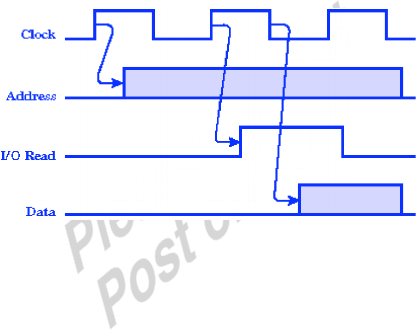
-47-
7.20 a. Assume that the women are working, or sleeping, or otherwise engaged. The
first time the alarm goes off, it alerts both that it is time to work on apples. The
next alarm signal causes apple-server to pick up an apple an throw it over the
fence. The third alarm is a signal to Apple-eater that he can pick up and eat the
apple. The transfer of apples is in strict synchronization with the alarm clock,
which should be set to exactly match Apple-eater's needs. This procedure is
analogous to standard synchronous transfer of data between a device and a
computer. It can be compared to an I/O read operation on a typical bus-based
system. The timing diagram is as follows:
On the first clock signal, the port address is output to the address bus. On the
second signal, the I/O Read line is activated, causing the selected port to place its
data on the data bus. On the third clock signal, the CPU reads the data.
A potential problem with synchronous I/O will occur if Apple-eater's
needs change. If he must eat at a slower or faster rate than the clock rate, he will
either have too many apples or too few.
b. The women agree that Apple-server will pick and throw over an apple
whenever he sees Apple-eater's flag waving. One problem with this approach
is that if Apple-eater leaves his flag up, Apple-server will see it all the time and
will inundate her friend with apples. This problem can be avoided by giving
Apple-server a flag and providing for the following sequence:
1. Apple-eater raises her "hungry" flag when ready for an apple.
2. Apple-server sees the flag and tosses over an apple.
3. Apple-server briefly waves her "apple-sent" flag
4. Apple-eater sees the "apple-sent" flag, takes down her "hungry" flag, and
grabs the apple.
5. Apple-eater keeps her "hungry" flag stays down until she needs another
apple.
This procedure is analogous to asynchronous I/O. Unfortunately, Apple-

-48-
server may be doing something other than watching for her friend's flag (like
sleeping!). In that case, she will not see the flag, and Apple-eater will go
hungry. One solution is to not permit apple-server to do anything but look for
her friend's flag. This is a polling, or wait-loop, approach, which is clearly
inefficient.
c. Assume that the string that goes over the fence and is tied to Apple-server's
wrist. Apple-eater can pull the string when she needs an apple. When Apple-
server feels a tug on the string, she stops what she is doing and throws over an
apple. The string corresponds to an interrupt signal and allows Apple-server to
use her time more efficiently. Moreover, if Apple-server is doing something
really important, she can temporarily untie the string, disabling the interrupt.
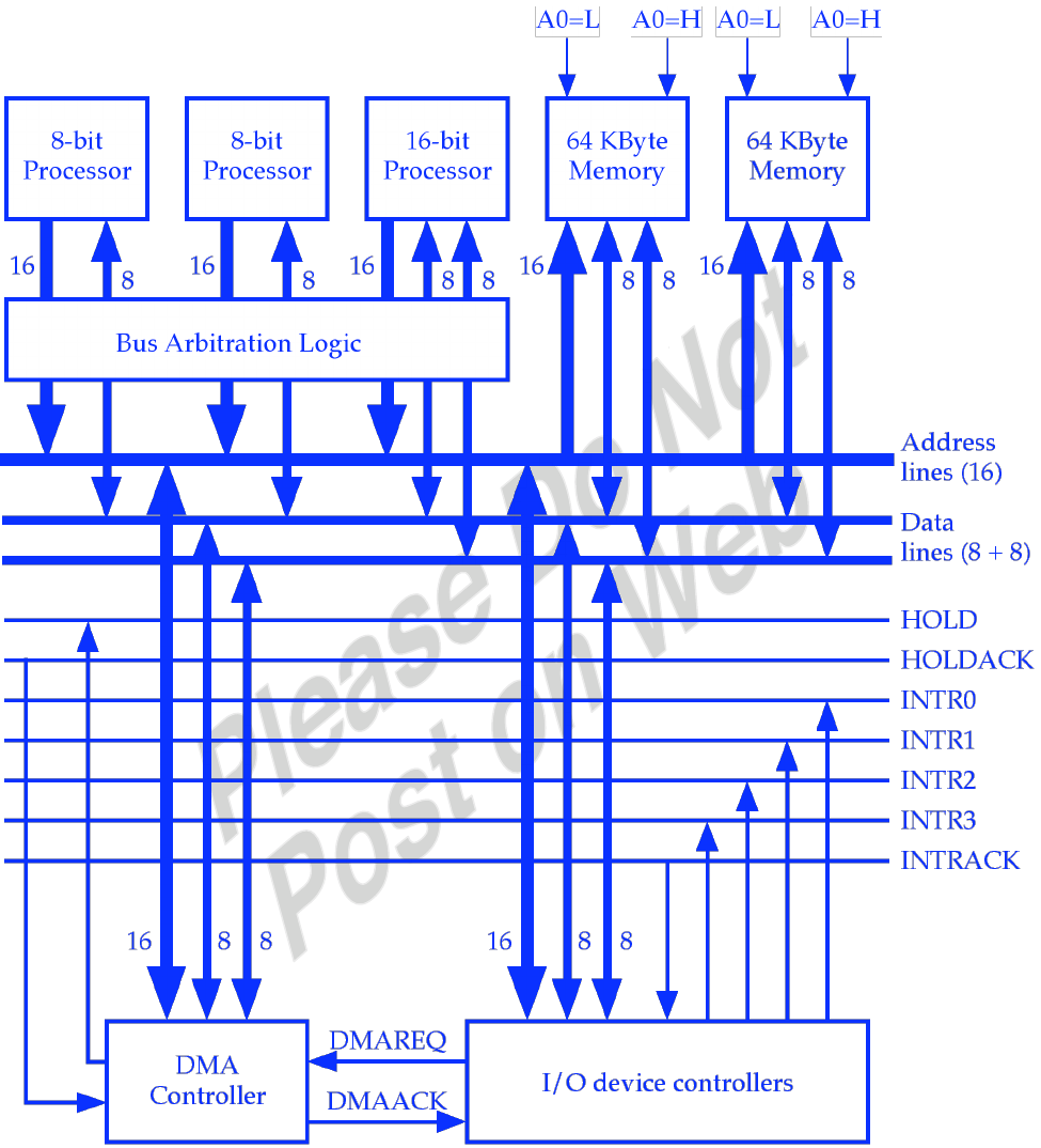
-49-
7.21

-50-
CHAPTER 8 OPERATING SYSTEM SUPPORT
A
ANSWERS TO
NSWERS TO Q
QUESTIONS
UESTIONS
8.1 The operating system (OS) is the software that controls the execution of programs
on a processor and that manages the processor's resources.
8.2 Program creation: The operating system provides a variety of facilities and
services, such as editors and debuggers, to assist the programmer in creating
programs. Program execution: A number of tasks need to be performed to execute
a program. Instructions and data must be loaded into main memory, I/O devices
and files must be initialized, and other resources must be prepared. Access to I/O
devices: Each I/O device requires its own peculiar set of instructions or control
signals for operation. Controlled access to files: In the case of files, control must
include an understanding of not only the nature of the I/O device (disk drive, tape
drive) but also the file format on the storage medium. System access: In the case of
a shared or public system, the operating system controls access to the system as a
whole and to specific system resources. Error detection and response: A variety of
errors can occur while a computer system is running. Accounting: A good
operating system will collect usage statistics for various resources and monitor
performance parameters such as response time.
8.3 Long-term scheduling: The decision to add to the pool of processes to be executed.
Medium-term scheduling: The decision to add to the number of processes that are
partially or fully in main memory. Short-term scheduling: The decision as to
which available process will be executed by the processor
8.4 A process is a program in execution, together with all the state information
required for execution.
8.5 The purpose of swapping is to provide for efficient use of main memory for
process execution.
8.6 Addresses must be dynamic in the sense that absolute addresses are only resolved
during loading or execution.
8.7 No, if virtual memory is used.
8.8 No.
8.9 No.

-51-
8.10 The TLB is a cache that contains those page table entries that have been most
recently used. Its purpose is to avoid, most of the time, having to go to disk to
retrieve a page table entry.
A
ANSWERS TO
NSWERS TO P
PROBLEMS
ROBLEMS
8.1 The answers are the same for (a) and (b). Assume that although processor
operations cannot overlap, I/O operations can.
1 Job: TAT = NT Processor utilization = 50%
2 Jobs: TAT = NT Processor utilization = 100%
4 Jobs: TAT = (2N – 1)NT Processor utilization = 100%
8.2 I/O-bound programs use relatively little processor time and are therefore favored
by the algorithm. However, if a processor-bound process is denied processor time
for a sufficiently long period of time, the same algorithm will grant the processor
to that process because it has not used the processor at all in the recent past.
Therefore, a processor-bound process will not be permanently denied access.
8.3 Main memory can hold 5 pages. The size of the array is 10 pages. If the array is
stored by rows, then each of the 10 pages will need to be brought into main
memory once. If it is stored by columns, then each row is scattered across all ten
pages, and each page will have to be brought in 100 times (once for each row
calculation).
8.4 The number of partitions equals the number of bytes of main memory divided by
the number of bytes in each partition: 224/216 = 28. Eight bits are needed to identify
one of the 28 partitions.
8.5 Let s and h denote the average number of segments and holes, respectively. The
probability that a given segment is followed by a hole in memory (and not by
another segment) is 0.5, because deletions and creations are equally probable in
equilibrium. so with s segments in memory, the average number of holes must be
s/2. It is intuitively reasonable that the number of holes must be less than the
number of segments because neighboring segments can be combined into a single
hole on deletion.
8.6 a. Split binary address into virtual page number and offset; use VPN as index into
page table; extract page frame number; concatenate offset to get physical
memory address
b. (i) 1052 = 1024 + 28 maps to VPN 1 in PFN 7, (7 × 1024+28 = 7196)
(ii) 2221 = 2 × 1024 + 173 maps to VPN 2, page fault
(iii) 5499 = 5 × 1024 + 379 maps to VPN 5 in PFN 0, (0 × 1024+379 = 379)
8.7 With very small page size, there are two problems: (1) Because very little data is
brought in with each page, there will need to be a lot of I/O to bring in the many
small pages. (2) The overhead (page table size, length of field for page number)
will be disproportionately high.
If pages are very large, main memory will be wasted because the principle of
locality suggests that only a small part of the large page will be used.

-52-
8.8 9 and 10 page transfers, respectively. This is referred to as "Belady's anomaly," and
was reported in "An Anomaly in Space-Time Characteristics of Certain Programs
Running in a Paging Machine," by Belady et al, Communications of the ACM, June
1969.
8.9 A total of fifteen pages are referenced, the hit ratios are:
N
1
2
3
4
5
6
7
8
Ratio
0/15
0/15
2/15
3/15
5/15
8/15
8/15
8/15
8.10 The principal advantage is a savings in physical memory space. This occurs for
two reasons: (1) a user page table can be paged in to memory only when it is
needed. (2) The operating system can allocate user page tables dynamically,
creating one only when the process is created.
Of course, there is a disadvantage: address translation requires extra work.
8.11 The machine language version of this program, loaded in main memory starting at
address 4000, might appear as:
4000 (R1) ← ONE Establish index register for i
4001 (R1) ← n Establish n in R2
4002 compare R1, R2 Test i > n
4003 branch greater 4009
4004 (R3) ← B(R1) Access B[i] using index register R1
4005 (R3) ← (R3) + C(R1) Add C[i] using index register R1
4006 A(R1) ← (R3) Store sum in A[i] using index register R1
4007 (R1) ← (R1) + ONE Increment i
4008 branch 4002
6000-6999 storage for A
7000-7999 storage for B
8000-8999 storage for C
9000 storage for ONE
9001 storage for n
The reference string generated by this loop is
494944(47484649444)1000
consisting of over 11,000 references, but involving only five distinct pages.
8.12 The S/370 segments are fixed in size and not visible to the programmer. Thus,
none of the benefits listed for segmentation are realized on the S/370, with the
exception of protection. The P bit in each segment table entry provides protection
for the entire segment.
8.13 On average, p/2 words are wasted on the last page. Thus the total overhead or
waste is w = p/2 + s/p. To find the minimum, set the first derivative to 0.
-53-
dw
dp =1
2−s
p2=0
p=2s
8.14 There are three cases to consider:
Location of referenced
word
Probability
Total time for access in ns
In cache
0.9
20
Not in cache, but in main
memory
(0.1)(0.6) = 0.06
60 + 20 = 80
Not in cache or main
memory
(0.1)(0.4) = 0.04
12ms + 60 + 20 = 12000080
So the average access time would be:
Avg = (0.9)(20) + (0.06)(80) + (0.04)(12000080) = 480026 ns
8.15
232 memory
211 page size =221 page frames
Segment: 0
1
2
3
0
7
Page descriptor
table
00021ABC
Main memory
(232 bytes)
232 memory
211 page size =221 page frames
a. 8 × 2K = 16K
b. 16K × 4 = 64K
c. 232 = 4 GBytes
8.16 •The starting physical address of a segment is always evenly divisible by 1048, i.e.,
its rightmost 11 bits are always 0.
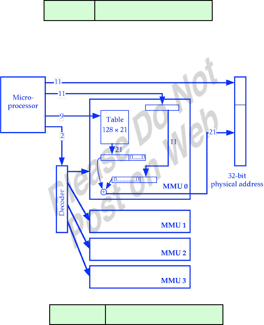
-54-
•Maximum logical address space = 29 = 512 segments (× 222 bytes/segment) = 231
bytes.
•Format of logical address:
segment
number (9)
offset (22)
•Entries in the mapping table: 29 = 512.
•Number of memory management units needed = 4.
•Each 9-bit segment number goes to an MMU; 7 bits are needed for the 128-entry
table, the other 2 most significant bits are decoded to select the MMU.
•Each entry in the table is 22 bits.
8.17 a.
page number
(5)
offset (11)
b. 32 entries, each entry is 9 bits wide.
c. If total number of entries stays at 32 and the page size does not change, then
each entry becomes 8 bits wide.

-55-
8.18 The system operator can review this quantity to determine the degree of "stress" on
the system. By reducing the number of active jobs allowed on the system, this
average can be kept high. A typical guideline is that this average should be kept
above 2 minutes. This may seem like a lot, but it isn't.
8.19
0192031
Section base address Section of fsetSection
0111231
Page base address Page of fset
Small
page
0151631
Large page base address Page offset
La rge
page
0232431
Supersection base address Supersection offset
Super
section
-56-
8.20
Main Memory
Virtual address
Level 1 (L1) section table
L1 index
section base addr
section index
0
0
4095
10
192031

-57-
CHAPTER 9 COMPUTER ARITHMETIC
A
ANSWERS TO
NSWERS TO Q
QUESTIONS
UESTIONS
9.1 Sign–Magnitude Representation: In an N-bit word, the left-most bit is the sign (0
= positive, 1 = negative) and the remaining N – 1 bits comprise the magnitude of
the number. Twos Complement Representation: A positive integer is represented
as in sign magnitude. A negative number is represented by taking the Boolean
complement of each bit of the corresponding positive number, then adding 1 to the
resulting bit pattern viewed as an unsigned integer. Biased representation: A
fixed value, called the bias, is added to the integer.
9.2 In sign-magnitude and twos complement, the left-most bit is a sign bit. In biased
representation, a number is negative if the value of the representation is less than
the bias.
9.3 Add additional bit positions to the left and fill in with the value of the original sign
bit.
9.4 Take the Boolean complement of each bit of the positive number, then adding 1 to
the resulting bit pattern viewed as an unsigned integer.
9.5 When the operation is performed on the n-bit integer –2n–1 (one followed by n – 1
zeros).
9.6 The twos complement representation of a number is the bit pattern used to
represent an integer. The twos complement of a number is the operation that
computes the negation of a number in twos complement representation.
9.7 The algorithm for performing twos complement addition involves simply adding
the two numbers in the same way as for ordinary addition for unsigned numbers,
with a test for overflow. For multiplication, if we treat the bit patterns as unsigned
numbers, their magnitude is different from the twos complement versions and so
the magnitude of the result will be different.
9.8 Sign, significand, exponent, base.
9.9 An advantage of biased representation is that nonnegative floating-point numbers
can be treated as integers for comparison purposes.
9.10 Positive overflow refers to integer representations and refers to a number that is
larger than can be represented in a given number of bits. Exponent overflow refers
to floating point representations and refers to a positive exponent that exceeds the
maximum possible exponent value. Significand overflow occurs when the

-58-
addition of two significands of the same sign result in a carry out of the most
significant bit.
9.11 1. Check for zeros. 2. Align the significands. 3. Add or subtract the significands.
4. Normalize the result.
9.12 To avoid unnecessary loss of the least significant bit.
9.13 Round to nearest: The result is rounded to the nearest representable number.
Round toward +∞: The result is rounded up toward plus infinity. Round toward –
∞: The result is rounded down toward negative infinity. Round toward 0: The
result is rounded toward zero.
A
ANSWERS TO
NSWERS TO P
PROBLEMS
ROBLEMS
9.1 Sign Magnitude: 512 = 0000 0010 0000 0000
–29 = 1000 0000 0001 1101
Two’s Complement: 512 = 0000 0010 0000 0000
–29 = 1111 1111 1110 0011
9.2 1101011: Because this starts with a leftmost 1, it is a negative number. The
magnitude of the negative number is determined by flipping the bits and adding 1:
0010100 + 1 = 0010101
This is 21, so the original value was –21.
0101101
Because this starts with a leftmost 0, it is a positive number and we just compute
the magnitude as an unsigned binary number, which is 45.
9.3 a.
A=−2n−1−1
( )
an−1+2iai
i=0
n−2
∑
b. From –(2n–1 – 1) through (2n–1 – 1)
c. (1) Add the two numbers as if they were unsigned integers. (2) If there is a carry
out of the sign position, then add that bit to the first bit position of the result and
propagate carries as necessary. This is known as the end-around carry rule. (3)
An overflow occurs if two positive numbers are added and the result is negative
of if two negative numbers are added and the result is positive.

-59-
9.4
sign-magnitude
ones complement
Range
–(2n–1 – 1) to (2 n–1 – 1)
–(2n–1 – 1) to (2n–1 – 1)
Number of
representations of 0
2
2
Negation
Complement the sign bit
Complement each bit
Expansion of bit
length
Move the sign bit to the new
leftmost bit; fill in with zeros
Fill all new bit
positions to the left
with the sign bit
Subtract B from A
Complement the sign bit of B and
add B to A using rules for addition
of sign-magnitude numbers
Take the ones
complement of B and
add it to A
Rules for adding two sign-magnitude numbers:
1. If A and B have the same sign, then add the two magnitudes. If there is a carry
out of the last magnitude bit, there is an overflow. If there is no carry the result
is the sum of the magnitudes with the same sign bit as A and B.
2. (a) If the magnitude of A equals the magnitude of B, the result is zero; (b) if the
magnitude of A is greater than the magnitude of B, then the sign bit of the
result is the sign of A, and the magnitude of the result is the magnitude of A
minus the magnitude of B. (b) Otherwise, the sign bit of the result is the sign of
B, and the magnitude of the result is the magnitude of B minus the magnitude
of A.
9.5 The twos complement of the original number.
9.6 a. We can express 2n as (1 + Z), where Z is an n-bit quantity of all 1 bits. Then,
treating all quantities as unsigned integers, we have (2n – X) = 1 + Z – X. But (Z
– X) results in the Boolean complement of each bit of X. Example:
11111111
–01110100
10001011
Therefore, (2n – X) adds one to the quantity formed by taking the Boolean
complement of each bit of X, which is how we defined the twos complement of
X.
b. In Figure 9.5a, notice that we can subtract X or (add –X) by moving 16 – X
positions clockwise. Similarly, in Figure 9.5b, we can subtract X or (add –X) by
moving 2n – X positions clockwise. But the quantity (2n – X) is what we just
defined as the twos complement of X, which is the twos complement
representation of –X. So we can subtract X by adding –X.
9.7 The tens complement is calculated as 105 – 13250 = 100000 -13250 = 86750.

-60-
9.8 We subtract M – N, where M = 72532 and N = 13250:
M = 72532
tens complement of N = +86750
sum = 159282
discard carry digit = –100000
result = 59282
9.9
xn–1
0
0
0
0
1
1
1
1
yn–1
0
0
1
1
0
0
1
1
Input
cn–2
0
1
0
1
0
1
0
1
zn–1
0
0
1
0
1
0
1
1
Output
v
0
1
0
0
0
0
1
0
9.10
+6 00000110
+13 00001101
+19 00010011
–6 11111010
+13 00001101
+7 00000111
+6 00000110
–13 11110011
–7 11111001
–6 11111010
–13 11110011
–19 11101101
9.11 Add the twos complement, and check for overflow. For b, we must first sign-
extend the second term.
a. 111000 b. 11001100 c. 111100001111 d. 11000011
+ 001101 + 00010010 + 001100001101 + 00011000
1 000101 11011110 1 001000011100 11011000
In all cases, the signs of the two numbers to be added are different, so there is no
overflow.
9.12 The overflow rule was stated as follows: If two numbers are added, and they are
both positive or both negative, then overflow occurs if and only if the result has
the opposite sign. There are four cases:
•Both numbers positive (sign bit = 0) and no carry into the leftmost bit position:
There is no carry out of the leftmost bit position, so the XOR is 0. The result has a
sign bit = 0, so there is no overflow.
•Both numbers positive and a carry into the leftmost bit position: There is no carry
out of the leftmost position, so the XOR is 1. The result has a sign bit = 1, so there
is overflow.
•Both numbers negative and no carry into the leftmost position: There is a carry
out of the leftmost position, so the XOR is 1. The result has a sign bit of 0, so there
is overflow.
•Both numbers negative and a carry into the leftmost position. There is a carry out
of the leftmost position, so the XOR is 0. The result has a sign bit of 1, so there is
no overflow.
Therefore, the XOR result always agrees with the presence or absence of overflow.
9.13 An overflow cannot occur because addition and subtraction alternate. As a
consequence, the two numbers that are added always have opposite signs, a
condition that excludes overflow.

-61-
9.14
A
Q
Q–1
M
0000
1010
0
0101
Initial
0000
0101
0
0101
Shift
1011
0101
0
0101
A ← A – M
1101
1010
1
0101
Shift
0010
1010
1
0101
A ← A + M
0001
0101
0
0101
Shift
1100
0101
0
0101
A ← A – M
1110
0010
1
0101
Shift
9.15 Using M=010111 (23) and Q = 010011 (19) we should get 437 as the result.
A
Q
Q–1
M
000000
010111
0
010011
Initial
101101
010111
0
010011
A ← A – M
110110
101011
1
010011
Shift
111011
010101
1
010011
Shift
111101
101010
1
010011
Shift
010000
101010
1
010011
A ← A + M
001000
010101
0
010011
Shift
110101
010101
0
010011
A ← A – M
111010
101010
1
010011
Shift
001101
101010
1
010011
A ← A + M
000110
110101
1
010011
Shift
Answer = 0001 1011 0101 (which is 437)
9.16 An n-digit number in base B has a maximum value of Bn – 1. We need to show that
the maximum product is less than B2n – 1.
(Bn – 1) (Bn – 1) = B2n – 2Bn + 1 ≤ B2n – 1.
The inequality is true if
–2Bn + 1 ≤ –1 or 1 ≤ Bn
This is always true for B ≥ 2 and n ≥ 1.

-62-
9.17
A
Q
M
00000000
10010011
1011
Initial
00000001
00100110
1011
Shift
11110110
1011
A ← A – M
00000001
00100110
1011
Restore
00000010
01001100
1011
Shift
11110111
1011
A ← A – M
00000010
01001100
1011
Restore
00000100
10011000
1011
Shift
11111001
1011
A ← A – M
00000100
10011000
1011
Restore
00001001
00110000
1011
Shift
11111100
1011
A ← A – M
00001001
00110000
1011
Restore
00010010
01100000
1011
Shift
00000111
1011
A ← A – M
00000111
01100001
1011
Q0 ← 1
00001110
11000010
1011
Shift
00000011
1011
A ← A – M
00000011
11000011
1011
Q0 ← 1
00000111
10000110
1011
Shift
11111100
1011
A ← A – M
00000111
10000110
1011
Restore
00001111
00001100
1011
Shift
00000100
1011
A ← A – M
00000100
00001101
1011
Q0 ← 1
9.18 The nonrestoring division algorithm is based on the observation that a restoration
in iteration I of the form A(I) ← A(I) + M is followed in iteration (I + 1) by the
subtraction A(I+1) ← 2A(I) – M. These two operations can be combined into a
single operation: A(I+1) ← 2A(I) + M.
9.19 False. For a negative quotient, truncation yields a larger number.

-63-
9.20 Divisor = 13 = (001101)2 is placed in M register.
Dividend = –145 = (111101101111)2 is placed in A and Q registers
A
Q
M
111101
101111
001101
Initial
111011
011110
Shift
001101
Add
001000
111011
011110
Restore
110110
111100
Shift
001101
Add
000011
110110
111100
Restore
101101
111000
Shift
001101
Add
111010
111001
Q0 ← 1
110101
110010
Shift
001101
Add
000110
110101
110010
Restore
101011
100100
Shift
001101
Add
111000
100101
Q0 ← 1
110001
001010
Shift
001101
Add
111110
001011
Q0 ← 1
Remainder = (111110)2 = –2
Quotient = twos complement of 001011 = (110101)2 = –11
9.21 a. Planck's constant:
6.63 × 10⁻²⁷ → 0.00000000000000000000000000663
29
b. Avogadro's number:
6.02 × 10²³ → 602000000000000000000000.0
24

-64-
To represent the approximation of Planck's constant 29 radix-10 fractional
digits are needed, while representing the approximation of Avogadro's number
requires 24 integer decimal digits. To represent the approximations of both
Planck's constant and Avogadro's number in a fixed-point number format, 29 +
54 = 53 radix-10 digits are needed.
b. In the considered radix-10 base-10 biased representation for the exponent (such
that Ebiased = E + 50), the exponent of both Planck's constant and Avogadro's
number can be represented using 2 digits, because 27+50 = 23 and 23+50 = 73.
To represent the significands, 3 radix-10 digits are needed. Therefore, to
represent the approximations of both Planck's constant and Avogadro's
number in a floating-point radix- 10 base-10 number format, 3 + 2 = 5 decimal
digits are needed. Source: [ERCE04]
9.22 a. bX–q(1 – b–p), b–q–p
b. bX–q(1 - b–p), b–q–1
9.23 a. 1 10000001 01000000000000000000000
b. 1 10000001 10000000000000000000000
c. 1 01111111 10000000000000000000000
d. 384 = 110000000 = 1.1 × 21000
Change binary exponent to biased exponent:
127 + 8 = 135 = 10000111
Format: 0 10000111 00000000000000000000000
e. 1/16 = 0.0001 = 1.0 × 2–100
127 – 4 = 123 = 01111011
Format: 0 01111011 00000000000000000000000
f. –1/32 = –0.00001 = –1.0 × 2–101
127 – 5 = 122 = 01111010
Format: 0 01111010 00000000000000000000000
9.24 a. –28 (don't forget the hidden bit)
b. 13/16 = 0.8125
c. 2
9.25 In this case, the exponent has a bias of 3. Special cases are shaded in the table. The
first shaded column contains the denormalized numbers. It is worthwhile to study
this table to get a feel for the distribution and spacing of numbers represented in
this format.

-65-
Exponent
sign bit
and
significand
000
001
010
011
100
101
110
111
0 000
0
0.25
0.5
1
2
4
8
+∞
0 001
0.03125
0.28125
0.5625
1.125
2.25
4.5
9
NaN
0 010
0.0625
0.3125
0.625
1.25
2.5
5
10
NaN
0 011
0.09375
0.34375
0.6875
1.375
2.75
5.5
11
NaN
0 100
0.125
0.375
0.75
1.5
3
6
12
NaN
0 101
0.15625
0.40625
0.8125
1.625
3.25
6.5
13
NaN
0 110
0.1875
0.4375
0.875
1.75
3.5
7
14
NaN
0 111
0.21875
0.46875
0.9375
1.875
3.75
7.5
15
NaN
1 000
–0
–0.25
–0.5
–1
–2
–4
–8
–∞
1 001
–
0.03125
–
0.28125
–
0.5625
–1.125
–2.25
–2.5
–9
NaN
1 010
–0.0625
–0.3125
–0.625
–1.25
–2.5
–5
–10
NaN
1 011
–
0.09375
–
0.34375
–
0.6875
–1.375
–2.75
–5.5
–11
NaN
1 100
–0.125
–0.375
–0.75
–1.5
–3
–6
–12
NaN
1 101
–
0.15625
–
0.40625
–
0.8125
–1.625
–3.25
–6.5
–13
NaN
1 110
–0.1875
–0.4375
–0.875
–1.75
–3.5
–7
–14
NaN
1 111
–
0.21875
–
0.46875
–
0.9375
–1.875
–3.75
–7.5
–15
NaN
9.26 a. 1.0 = +1/16 × 161 = 0 100 0001 0001 0000 0000 0000 0000 0000
b. 0.5 = +8/16 × 160 = 0 100 0000 1000 0000 0000 0000 0000 0000
c. 1/64 = +4/16 × 16–1 = 0 011 1111 0100 0000 0000 0000 0000 0000
d. 0.0 = +0 × 16–64 = 0 000 0000 0000 0000 0000 0000 0000 0000
e. –15.0 = –15/16 × 161 = 1 100 0001 1111 0000 0000 0000 0000 0000
f. 5.4 × 10–79 ≈ +1/16 × 16–64 = 0 000 0000 0000 0000 0000 0000 0000 0000
g. 7.2 × 1075 ≈ 1 × 1663 = 0 111 1111 1111 1111 1111 1111 1111 1111
h. 65535 = 164 –1 = 0 100 0100 1111 1111 1111 1111 0000 0000
9.27 Step 1: Sign positive
Step 2: Extract the exponent (5B)16 and subtract the bias (40)16, yielding
(1B)16 = 27
Step 3: The significand (CA 0000)16 = 12/16 + 10/256 = 0.7890625.
The decimal result is 0.7890625 × 1627.
9.28 The base is irrelevant
a. Bias = 26–1 = 25 = 32
b. Bias = 27–1 = 26 = 64

-66-
9.29
Expressible Negative
Numbers
Negative
Overflow
Positive
Overflow
Negative
Underflow
Zero
Positive
Underflow
Expressible Positive
Numbers
00.5 × 2–1022
– 0.5 × 2–1022
– (1 – 2–53
) × 21023 (1 – 2–53) × 21023
9.30 a. 1. Express the number in binary form: 1011010000 (normalize to 1.1bbbb)
2. Normalize the number into the form 0.1bbbbbbbbbbbbb
0.1011010000 × 2k where k = 10(base10) or 1010(base2)
0.1011010000 × 2(1010)
Once in normalized form every number will have a 1 after the decimal
point. We do not need to store this number; it is implicit. Therefore in the
Significand field we will store 01101000000000000000000.
3. For the 8-bit exponent field, a bias of 128 is used. Add the bias to the
exponent and store the answer: 1010 + 10000000 = 1001010
4. Sign bit = 1
5. Result = 1 1001010 01101000000000000000000
b. We have 0.645 = 0.101001...; therefore the significand is 01001 (the first 1 is
implicit). The sign = 0, and the exponent = 0.
Result: 0 0000000 01001000000000000000000
9.31 There are 232 different bit patterns available. However, because of special cases,
not all of these bit patterns represent unique numbers. In particular, an exponent
of all ones together with a nonzero fraction is given the value NaN, which means
Not a Number, and is used to signal various exception conditions. Because the
fraction field is 23 bits, the number of nonzero fractions is 223 – 1. The sign bit may
be 0 or 1 for this case, so the total number of NaN values is 224 – 2. Therefore, the
number of different numbers that can be represented is 232 – 224 + 2. This number
includes both plus and minus zero and plus and minus infinity. If we exclude
minus zero and plus and minus infinity, then the total is 232 – 224 –1.
9.32 We have 0.4 × 20. Because 0.4 is less than 0.5, this is not normalized. Thus, we
rewrite as
0.4 = 0.8 × 2–1
Next, convert 0.8 to binary, we have repeating binary number: 0.110011001100...
The closest we can get (7 bits) is 0.1100110. Converting this back to decimal, we
have
(1/2 + 1/4 + 1/32 + 1/64) × 2-1 = 0.3984375
The relative error is 0.4 - 0.3984375
0.4 = 0.0039

-67-
9.33 EA = A - A'
A
Truncation: EA = 1.427 - 1.42
1.427 = 0.0049
Rounding: EA = 1.427 -1.43
1.427 = –0.0021
9.34 Cancellation reveals previous errors in the computation of X and Y. For example, if
ε is small, we often get poor accuracy when computing f(x + ε) - f(x), because the
rounded calculation of f(x + ε) destroys much of the information about ε. It is
desirable to rewrite such formulas as ε × g(x,ε), where g(x,ε) =
f(x+
ε
)−f(x)
ε
is
first computed symbolically. Thus, if f(x) = x2, then g(x,ε) = 2x + ε; if f(x) = x ,
then g(x,ε) = 1
x + ε + x .
9.35 We have
EA = A - A'
A = 1 – A'
A
A' = A(1 – EA)
B' = B (1 – EB)
A'B' = AB (1 – EA)(1 -EB) = AB [1– (EA +EB) + EAEB ]
≈ AB [1– (EA + EB)]
The product term EAEB should be negligible in comparison to the sum.
Consequently
EAB = EA +EB.
9.36 a. EA = 0.22288 - 0.2228
0.2228 = 0.00036
EB = 0.22211 - 0.2221
0.22211 = 0.00045
b. C = A – B = 0.00077
C'= A' – B' = 0.0007
EC = 0.00077 - 0.0007
0.00077 = 0.09

-68-
9.37 a. (2.50000 × 10–60) × (3.50000 × 10–43) = 8.75000 × 10–103 → 0.00088 × 10–99
The otherwise exact product underflows and must be denormalized by
four digits. The number then requires rounding.
b. (2.50000 × 10–60) × (3.50000 × 10–60) = 8.75000 × 10–120 → 0.0
The intermediate result falls below the underflow threshold and must be
set to zero.
c. (5.67834 × 10–97) – (5.67812 × 10–97) = 2.20000 × 10–101 → 0.02200 × 10–99
This example illustrates how underflowed sums and differences of
numbers in the same format are always free from rounding errors.
9.38 a. The exponents are equal. Therefore the mantissas are added, keeping the
common exponent, and the sum is renormalized if necessary.
5.566 × 10³ + 7.777 × 103 = 1.3343 × 10³ ≈ 1.334 × 10³
b. The exponents must be equalized first.
3.344 × 101 + 8.877 × 10–2 = 3.344 × 101 + 0.008877 × 101 =
3.352877 × 101 ≈ 3.352 × 101
9.39 a. 7.744 × 10⁻³ – 6.666 × 10–3 = 1.078 × 10⁻³
b. 8.844 × 10⁻³ – 2.233 × 10–1 = 0.08844 × 10⁻¹ – 2.233 × 10–1 =
–2.14456 × 10⁻¹ ≈ –2.144 × 10⁻¹
9.40 a. 2.255 × 101 × 1.234 × 100 = 2.58267 × 101 ≈ 2.582 × 101
b. 8.833 × 10² ÷ 5.555 × 104 = 1.590 × 10⁻²

-69-
CHAPTER 10 INSTRUCTION SETS:
CHARACTERISTICS AND FUNCTIONS
A
ANSWERS TO
NSWERS TO Q
QUESTIONS
UESTIONS
10.1 The essential elements of a computer instruction are the opcode, which specifies
the operation to be performed, the source and destination operand references,
which specify the input and output locations for the operation, and a next
instruction reference, which is usually implicit.
10.2 Registers and memory.
10.3 Two operands, one result, and the address of the next instruction.
10.4 Operation repertoire: How many and which operations to provide, and how
complex operations should be. Data types: The various types of data upon which
operations are performed. Instruction format: Instruction length (in bits), number
of addresses, size of various fields, and so on. Registers: Number of CPU registers
that can be referenced by instructions, and their use. Addressing: The mode or
modes by which the address of an operand is specified.
10.5 Addresses, numbers, characters, logical data.
10.6 For the IRA bit pattern 011XXXX, the digits 0 through 9 are represented by their
binary equivalents, 0000 through 1001, in the right-most 4 bits. This is the same
code as packed decimal.
10.7 With a logical shift, the bits of a word are shifted left or right. On one end, the bit
shifted out is lost. On the other end, a 0 is shifted in. The arithmetic shift operation
treats the data as a signed integer and does not shift the sign bit. On a right
arithmetic shift, the sign bit is replicated into the bit position to its right. On a left
arithmetic shift, a logical left shift is performed on all bits but the sign bit, which is
retained.
10.8 1. In the practical use of computers, it is essential to be able to execute each
instruction more than once and perhaps many thousands of times. It may require
thousands or perhaps millions of instructions to implement an application. This
would be unthinkable if each instruction had to be written out separately. If a table
or a list of items is to be processed, a program loop is needed. One sequence of
instructions is executed repeatedly to process all the data. 2. Virtually all programs
involve some decision making. We would like the computer to do one thing if one
condition holds, and another thing if another condition holds. 3. To compose

-70-
correctly a large or even medium-size computer program is an exceedingly
difficult task. It helps if there are mechanisms for breaking the task up into smaller
pieces that can be worked on one at a time.
10.9 First, most machines provide a 1-bit or multiple-bit condition code that is set as the
result of some operations. Another approach that can be used with a three-address
instruction format is to perform a comparison and specify a branch in the same
instruction.
10.10 The term refers to the occurrence of a procedure call inside a procedure.
10.11 Register, start of procedure, top of stack.
10.12 A reentrant procedure is one in which it is possible to have several calls open to it
at the same time.
10.13 In this notation, the operator follows its two operands.
10.14 A multibyte numerical value stored with the most significant byte in the lowest
numerical address is stored in big-endian fashion. A multibyte numerical value
stored with the most significant byte in the highest numerical address is stored in
little-endian fashion.
A
ANSWERS TO
NSWERS TO P
PROBLEMS
ROBLEMS
10.1 a. 23
b. 32 33
10.2 a. 7309
b. 582
c. 1010 is not a valid packed decimal number, so there is an error
10.3 a. 0; 255
b. –127; 127
c. –127; 127
d. –128; 127
e. 0; 99
f. –9; +9

-71-
10.4 Perform the addition four bits at a time. If the 4-bit digit of the result of binary
addition is greater then 9 (binary 1001), then add 6 to get the correct result.
1698 0001 0110 1001 1000
+ 1798 0001 0111 1000 0110
0010 1100 1 0001 1110
1 1 1 0110
0011 1110 0110 1 0100
0110 1000
1 0100
3484 0011 0100 1000 0100
10.5 The tens complement of a number is formed by subtracting each digit from 9, and
adding 1 to the result, in a manner similar to twos complement. To subtract,
simply take the tens complement and add:
0736
9674
1 0410
10.6
PUSH A
PUSH B
PUSH C
MUL
ADD
PUSH D
PUSH E
PUSH F
MUL
SUB
DIV
POP X
LOAD E
MUL F
STORE T
LOAD D
SUB T
STORE T
LOAD B
MUL C
ADD A
DIV T
STO X
MOV R0, E
MUL RO, F
MOV R1, D
SUB R1, R0
MOV R0, B
MOV R0, C
ADD R0, A
DIV R0, R1
MOV X, R0
MUL R0, E, F
SUB R0, D, R0
MUL R1, B, C
ADD R1, A, R1
DIV X, R0, R1
Source: [TANE90]
10.7 a. A memory location whose initial contents are zero is needed for both X → AC
and AC → X. The program for X → AC, and its effects are shown below.
Assume AC initially contains the value a.
Instruction
AC
Effect on
M(0)
M(X)
SUBS 0
a
a
x
SUBS 0
0
0
x
SUBS X
–x
0
–x
SUBS 0
–x
–x
–x
SUBS 0
0
0
–x
SUBS X
x
0
x

-72-
b. For addition, we again need a location, M(0), whose initial value is 0. We also
need destination location, M(1). Assume the initial value in M(1) is y.
Instruction
AC
M(0)
M(1)
M(X)
SUBS 0
a
a
y
x
SUBS 1
a – y
a
a – y
x
SUBS 1
0
a
0
x
SUBS X
–x
a
0
–x
SUBS 0
–x – a
–x – a
0
–x
SUBS 1
–x – a
–x – a
–x – a
–x
SUBS 0
0
0
–x – a
–x
SUBS X
x
0
–x – a
x
SUBS 0
x
x
–x – a
x
SUBS 0
0
0
–x – a
x
SUBS 1
a + x
0
a + x
x
10.8 1. A NOOP can be useful for debugging. When it is desired to interrupt a program
at a particular point, the NOOP is replaced with a jump to a debug routine. When
temporarily patching or altering a program, instructions may be replaced with
NOOPs. 2. A NOOP introduces known delay into a program, equal to the
instruction cycle time for the NOOP. This can be used for measuring time or
introducing time delays. 3. NOOPs can be used to pad out portions of a program
to align instructions on word boundaries or subroutines on page boundaries. 4.
NOOPs are useful in RISC pipelining, examined in Chapter 13.

-73-
10.9
Bit pattern
Value
Arithmetic
left shift
Value
Logical left
shift
Value
00000
0
00000
0
00000
0
00001
1
00010
2
00010
2
00010
2
00100
4
00100
4
00011
3
00110
6
00110
6
00100
4
01000
8
01000
8
00101
5
01010
10
01010
10
00110
6
01100
12
01100
12
00111
7
01110
14
01110
14
01000
8
00000
overflow
10000
overflow
01001
9
00010
overflow
10010
overflow
01010
10
00100
overflow
10100
overflow
01011
11
00110
overflow
10110
overflow
01100
12
01000
overflow
11000
overflow
01101
13
01010
overflow
11010
overflow
01110
14
01100
overflow
11100
overflow
01111
15
01110
overflow
11110
overflow
10000
–16
10000
overflow
00000
overflow
10001
–15
00010
overflow
00010
overflow
10010
–14
10100
overflow
00100
overflow
10011
–13
10110
overflow
00110
overflow
10100
–12
11000
overflow
01000
overflow
10101
–11
11010
overflow
01010
overflow
10110
–10
11100
overflow
01100
overflow
10111
–9
11110
overflow
01110
overflow
11000
–8
10000
–16
10000
–16
11001
–7
10010
–14
10010
–14
11010
–6
10100
–12
10100
–12
11011
–5
10110
–10
10110
–10
11100
–4
11000
–8
11000
–8
11101
–3
11010
–6
11010
–6
11110
–2
11100
–4
11100
–4
11111
–1
11110
–2
11110
–2
10.10 Round toward –∞.
10.11 Yes, if the stack is only used to hold the return address. If the stack is also used to
pass parameters, then the scheme will work only if it is the control unit that
removes parameters, rather than machine instructions. In the latter case, the CPU
would need both a parameter and the PC on top of the stack at the same time.
10.12 The DAA instruction can be used following an ADD instruction to enable using
the add instruction on two 8-bit words that hold packed decimal digits. If there is
a decimal carry (i.e., result greater than 9) in the rightmost digit, then it shows up
either as the result digit being greater than 9, or by setting AF. If there is such a
carry, then adding 6 corrects the result. For example:
2 7

-74-
+ 4 6
6 D
+ 0 6
7 3
The second test similarly corrects a carry from the left digit of an 8-bit byte. A
multiple-digit packed decimal addition can thus be programmed using the
normal add-with-carry (ADC) instruction in a loop, with the insertion of a single
DAA instruction after each addition.
10.13 a.
CMP result
Z
C
destination < source
0
1
destination > source
0
0
destination = source
1
0
b.
CMP result
Flags
destination < source
S ≠ O
destination > source
S = O
destination = source
ZF = 1
c. •Equal: The two operands are equal, so subtraction produces a zero result (Z
= 1).
•Greater than: If A is greater than B, and A and B are both positive or both
negative, then the twos complement operation (A – B) will produce a
positive result (S = 0) with no overflow (O = 0). If A is greater than B with A
positive and B negative, then the result is either positive with no overflow
or negative (S = 1) with overflow (O = 1). In all these cases, the result is
nonzero (Z = 0)
•Greater than or equal: The same reasoning as for "Greater than" applies,
except that the result may be zero or nonzero.
•Less than: This condition is the opposite of "Greater than or equal" and so
the opposite set of conditions apply.
•Less than or equal: This condition is the opposite of "Greater than" and so
the opposite set of conditions apply.
•Not equal: The two operands are unequal, so subtraction produces a
nonzero result (Z = 0).
10.14 a. sign bit in the most significant position, then exponent, then significand
b. sign, exponent, and significand are all zero; that is, all 32 bits are zero
c. biased representation of the exponent
d. yes. However, note that the IEEE has a representation for minus zero, which
would yield results indicating that –0 < 0.
10.15 a. It might be convenient to have a word-length result for passing as a
parameter via a stack, to make it consistent with typical parameter passing.
This is an advantage of Scond. There doesn't seem to be any particular
advantage to the result value for true being integer one versus all binary ones.
b. The case for setting the flags: In general, instructions that operate on data
values will, as a side effect, set the condition codes according to the result of
the operation. Thus, the condition code should reflect the state of the machine
after the execution of each instruction that has altered a data value in some

-75-
way. These instructions violate this principle and are therefore inconsistent
with the remainder of the architecture.
The case against: These instructions are similar to branch on condition
instructions in that they operate on the result of another operation, which is
reflected in the condition codes. Because a branch on condition code
instruction does not itself set the condition codes, the fact that these other
instructions do not is not inconsistent.
For a further discussion, see "Should Scc Set Condition Codes?" by F.
Williams, Computer Architecture News, September 1988.
c. SUB CX, CX ;set register CX to 0
MOV AX, B ;move contents of location B to register AX
CMP AX, A ;compare contents of register AX and location A
SETGT CX ;CX = (a GT b)
TEST JCXZ OUT ;jump if contents of CX equal 0
THEN
OUT
d. MOV EAX, B ; move from location B to register EAX
CMP EAX, C
SETG BL ; BL = 0/1 depending on result
MOV EAX, D
CMP EAX, F
MOV BH, 0
SETE BH
OR BL, BH
10.16 a. Add one byte at a time: AB 08 90 C2
+ 45 98 EE 50
F0 A0 7E 12
b. Add 16 bits at a time: AB08 90C2
+ 4598 EE50
F0A0 7F12
10.17 If the processor makes use of a stack for subroutine handling, it only uses the
stack while executing CALL and RETURN instructions. No explicit stack-
oriented instructions are needed.
10.18 a. (A + B + C) * D
b. (A/B) + (C/D)
c. A/(B * C * (D + E))
d. A + (B * ((C + (D – E)/F) – G)/H)
10.19 a. AB + C + D + E +
b. AB + CD + * E +
c. AB * CD * + E +
d. AB - CDE * – F/G/ * H *
10.20 Postfix Notation: AB + C –
Equivalent to (A + B) – C
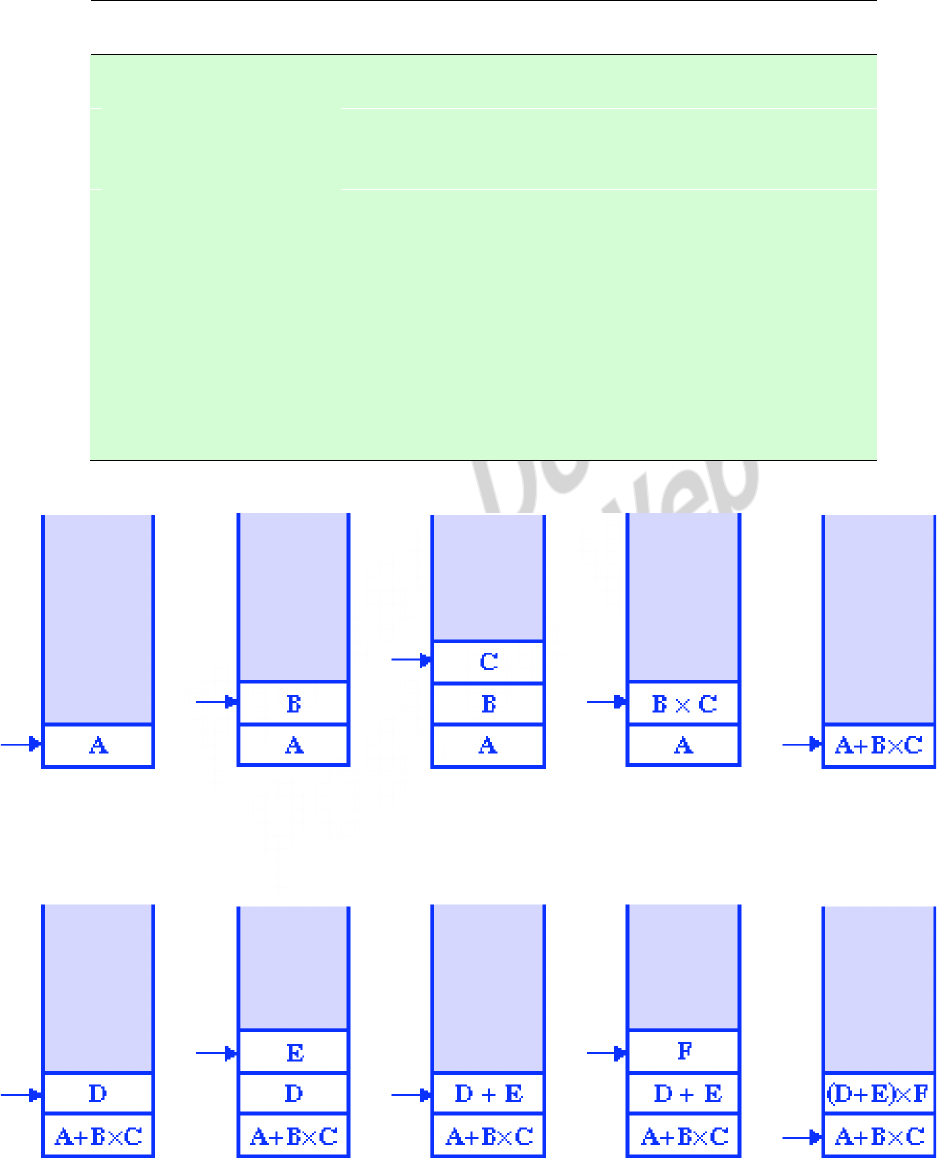
-76-
It matters because of rounding and truncation effects.
10.21
Input
Output
Stack (top on
right)
(A – B) / (C + D × E)
empty
empty
A – B) / (C + D × E)
empty
(
– B) / (C + D × E)
A
(
B) / (C + D × E)
A
( –
) / (C + D × E)
A B
( –
/ (C + D × E)
A B –
empty
(C + D × E)
A B –
/
C + D × E)
A B –
/ (
+ D × E)
A B – C
/ (
D × E)
A B – C
/ ( +
× E)
A B – C D
/ ( +
E)
A B – C D
/ ( + ×
)
A B – C D E
/ ( + ×
empty
A B – C D E × +
/
empty
A B – C D E × + /
empty
10.22
The final step combines the top two stack elements using the + operator.
10.23
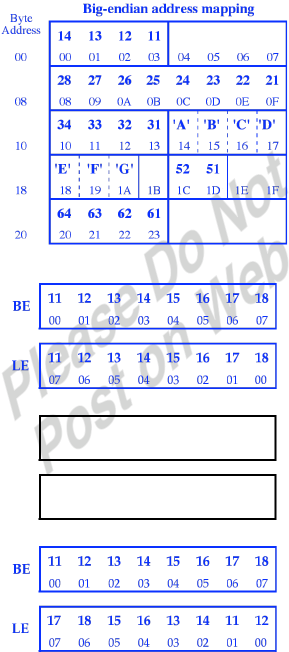
-77-
10.24 a.
b.
12 13 14
01 02 03 04 05 06 07
15 16 17 1811
00
BE
06 05 04 03 02 01 0007
LE 15 16 17 18 12 13 1411
c.

-78-
The purpose of this question is to compare halfword, word, and doubleword
integers as members of a data structure in Big- and Little-Endian form.
10.25 Figure 10.12 is not a "true" Little-Endian organization as usually defined. Rather,
it is designed to minimize the data manipulation required to convert from one
Endian to another. Note that 64-byte scalars are stored the same in both formats
on the PowerPC. To accommodate smaller scalars, a technique known as address
munging is used.
When the PowerPC is in Little-Endian mode, it transforms the three low-
order bits of an effective address for a memory access. These three bits are
XORed with a value that depends on the transfer size: 100b for 4-byte transfers;
110 for 2-byte transfers; and 111 for 1-byte transfers. The following are the
possible combinations:
4-Byte Transfers
(XOR with 100)
2-Byte Transfers
(XOR with 110)
1-Byte Transfers
(XOR with 111)
Original
Address
Munged
Address
Original
Address
Munged
Address
Original
Address
Munged
Address
000
100
000
110
000
111
001
101
001
111
001
110
010
110
010
100
010
101
011
111
011
101
011
100
100
000
100
010
100
011
101
001
101
011
101
010
110
010
110
000
110
001
111
011
111
001
111
000
For example, the two-byte value 5152h is stored at location 1C in Big-
Endian mode. In Little-Endian mode, it is viewed by the processor as still being
stored in location 1C but in Little-Endian mode. In fact, the value is still stored in
Big-Endian mode, but at location 1A. When a transfer occurs, the system must do
an address unmunging and a byte transfer to convert data to the form expected
by the processor. The processor generates effective addresses of 1C and 1D for
the two bytes. These addresses are munged (XOR with 110) to 1A and 1B. The
data bytes are retrieved, swapped, and presented as if found in the unmunged
addresses 1D and 1C.

-79-
10.26 There are a number of ways to do this. Here is one way that will work:
#include <stdio.h>
main()
{
int integer;
char *p;
integer = 0x30313233; /* ASCII for chars '0', '1', '2', '3' */
p = (char *)&integer
if (*p=='0' && *(p+1)=='1' && *(p+2)=='2' && *(p+3)=='3')
printf("This is a big endian machine.\n");
else if (*p=='3' && *(p+1)=='2' && *(p+2)=='1' && *(p+3)=='0')
printf("This is a little endian machine.\n");
else
printf("Error in logic to determine machine endian-ness.\n");
}
10.27 BigEndian
10.28 The documentation uses little-endian bit ordering, stating that the most
significant bit of a byte (leftmost bit) is bit 7. However, the instructions that
operate on bit fields operate in a big-endian manner. Thus, the leftmost bit of a
byte is bit 7 but has a bit offset of 0, and the rightmost bit of a byte is bit 0 but has
a bit offset of 7.

-80-
CHAPTER 11 INSTRUCTION SETS: ADDRESSING
MODES AND FORMATS
A
ANSWERS TO
NSWERS TO Q
QUESTIONS
UESTIONS
11.1 Immediate addressing: The value of the operand is in the instruction.
11.2 Direct addressing: The address field contents the effective address of the operand.
11.3 Indirect addressing: The address field refers to the address of a word in memory,
which in turn contains the effective address of the operand.
11.4 Register addressing: The address field refers to a register that contains the
operand.
11.5 Register indirect addressing: The address field refers to a register, which in turn
contains the effective address of the operand.
11.6 Displacement addressing: The instruction has two address fields, at least one of
which is explicit. The value contained in one address field (value = A) is used
directly. The other address field refers to a register whose contents are added to A
to produce the effective address.
11.7 Relative addressing: The implicitly referenced register is the program counter
(PC). That is, the current instruction address is added to the address field to
produce the EA.
11.8 It is typical that there is a need to increment or decrement the index register after
each reference to it. Because this is such a common operation, some systems will
automatically do this as part of the same instruction cycle, using autoindexing.
11.9 These are two forms of addressing, both of which involve indirect addressing and
indexing. With preindexing, the indexing is performed before the indirection.
With postindexing, the indexing is performed after the indirection.
11.10 Number of addressing modes: Sometimes an addressing mode can be indicated
implicitly. In other cases, the addressing modes must be explicit, and one or
more mode bits will be needed. Number of operands: Typical instructions on
today’s machines provide for two operands. Each operand address in the
instruction might require its own mode indicator, or the use of a mode indicator
could be limited to just one of the address fields. Register versus memory: The
more that registers can be used for operand references, the fewer bits are needed.

-81-
Number of register sets: One advantage of using multiple register sets is that, for
a fixed number of registers, a functional split requires fewer bits to be used in the
instruction. Address range: For addresses that reference memory, the range of
addresses that can be referenced is related to the number of address bits. Because
this imposes a severe limitation, direct addressing is rarely used. With
displacement addressing, the range is opened up to the length of the address
register. Address granularity: In a system with 16- or 32-bit words, an address
can reference a word or a byte at the designer’s choice. Byte addressing is
convenient for character manipulation but requires, for a fixed-size memory,
more address bits.
11.11 Advantages: It easy to provide a large repertoire of opcodes, with different
opcode lengths. Addressing can be more flexible, with various combinations of
register and memory references plus addressing modes. Disadvantages: an
increase in the complexity of the CPU.
A
ANSWERS TO
NSWERS TO P
PROBLEMS
ROBLEMS
11.1 a. 20 b. 40 c, 60 d. 30 e. 50 f.70
11.2 a. X3 = X2
b. X3 = (X2)
c. X3 = X1 + X2 + 1
d. X3 = X2 + X4
11.3 a. the address field
b. memory location 14
c. the memory location whose address is in memory location 14
d. register 14
e. the memory location whose address is in register 14
11.4
EA
Operand
EA
Operand
a.
500
1100
e.
600
1200
b.
201
500
f.
R1
400
c.
1100
1700
g.
400
1000
d.
702
1302
h.
400
1000
The autoindexing with increment is the same as the register indirect mode except
that R1 is incremented to 401 after the execution of the instruction.
11.5 Recall that relative addressing uses the contents of the program counter, which
points to the next instruction after the current instruction. In this case, the current
instruction is at decimal address 256028 and is 3 bytes long, so the PC contains
256031. With the displacement of –31, the effective address is 256000.
11.6 (PC + 1) + Relative Address = Effective Address
Relative Address = –621 + 530 = –91
Converting to twos-complement representation, we have: 1110100101.
11.7 a. 3 times: fetch instruction; fetch operand reference; fetch operand.

-82-
b. 2 times: fetch instruction; fetch operand reference and load into PC.
11.8 Load the address into a register. Then use displacement addressing with a
displacement of 0.
11.9 The PC-relative mode is attractive because it allows for the use of a relatively
small address field in the instruction format. For most instruction references, and
many data references, the desired address will be within a reasonably short
distance from the current PC address.
11.10 This is an example) of a special-purpose CISC instruction, designed to simplify
the compiler. Consider the case of indexing an array, where the elements of the
array are 32 bytes long. The following instruction is just what is needed:
IMUL EBX, I, 32
EBX is a 32-bit register that now contains the byte offset into the array whose
subscript is 1.
11.11 The three values are added together: 1970 + 48022 + 8 = 50000.
11.12 a. No, because the source operand is the contents of X, rather than the top of the
stack, which is in the location pointed to by X.
b. No, because address of the top of the stack is not changed until after the
fetching of the destination operand.
c. Yes. The stack grows away from memory location 0.
d. No, because the second element of the stack is fetched twice.
e. No, because the second element of the stack is fetched twice.
f. No, because the stack pointer is incremented twice, so that the result is
thrown away.
g. Yes. The stack grows toward memory location 0.
11.13
Instruction
Stack (top on left)
PUSH 4
4
PUSH 7
7, 4
PUSH 8
8, 7, 4
ADD
15, 4
PUSH 10
10, 15, 4
SUB
5, 4
MUL
20
11.14 The 32-bit instruction length yields incremental improvements. The 16-bit length
can already include the most useful operations and addressing modes. Thus,
relatively speaking, we don't have twice as much "utility".
11.15 With a different word length, programs written for older IBM models would not
execute on the newer models. Thus the huge investment in existing software was
lost by converting to the newer model. Bad for existing IBM customers, and
therefore bad for IBM.

-83-
11.16 Let X be the number of one-address instructions. The feasibility of having K two-
address, X one-address, and L zero-address instructions, all in a 16-bit instruction
word, requires that:
(K × 26 × 26) + (X × 26) + L = 216
Solving for X:
X = (216 – (K × 26 × 26) – L)/26
To verify this result, consider the case of no zero-address and no two-address
instructions; that is, L = K = 0. In this case, we have
X = 216/26 = 210
This is what it should be when 10 bits are used for opcodes and 6 bits for
addresses.
11.17 The scheme is similar to that for problem 11.16. Divide the 36-bit instruction into
4 fields: A, B, C, D. Field A is the first 3 bits; field B is the next 15 bits; field C is
the next 15 bits, and field D is the last 3 bits. The 7 instructions with three
operands use B, C, and D for operands and A for opcode. Let 000 through 110 be
opcodes and 111 be a code indicating that there are less than three operands. The
500 instructions with two operands are specified with 111 in field A and an
opcode in field B, with operands in D and C. The opcodes for the 50 instructions
with no operands can also be accommodated in B.
Source: [TANE90]
11.18 a. The zero-address instruction format consists of an 8-bit opcode and an
optional 16-bit address. The program has 12 instructions, 7 of which have an
address. Thus:
N0 = 12 × 8 + 7 × 16 = 208 bits
b. The one-address instruction format consists of an 8-bit opcode and a 16-bit
address. The program has 11 instructions.
N1 = 24 × 11 = 264 bits
c. For two-address instructions, there is an 8-bit opcode and two operands, each
of which is 4 bits (register) or 16 bits (memory).
N2 = 9 × 8 + 7 × 16 + 11 × 4 = 228 bits
d. For three-address instructions
N3 = 5 × 8 + 7 × 16 + 8 × 4 = 184 bits
11.19 No. If the two opcodes conflict, the instruction is meaningless. If one opcode
modifies the other or adds additional information, this can be viewed as a single

-84-
opcode with a bit length equal to that of the two opcode fields. However,
instruction bundles, such as seen on the IA-64 Itanium architecture, have
multiple opcodes.
11.20 a. The opcode field can take on one of 25 = 32 different values. Each value can be
interpreted to ways, depending on whether the Operand 2 field is all zeros,
for a total of 64 different opcodes.
b. We could gain an additional 32 opcodes by assigning another Operand 2
pattern to that purpose. For example, the pattern 0001 could be used to
specify more opcodes. The tradeoff is to limit programming flexibility,
because now Operand 2 cannot specify register R1. Source: [PROT88].

-85-
CHAPTER 12 PROCESSOR STRUCTURE AND
FUNCTION
A
ANSWERS TO
NSWERS TO Q
QUESTIONS
UESTIONS
12.1 User-visible registers: These enable the machine- or assembly language
programmer to minimize main-memory references by optimizing use of registers.
Control and status registers: These are used by the control unit to control the
operation of the CPU and by privileged, operating system programs to control the
execution of programs.
12.2 General purpose; Data; Address; Condition codes
12.3 Condition codes are bits set by the CPU hardware as the result of operations. For
example, an arithmetic operation may produce a positive, negative, zero, or
overflow result. In addition to the result itself being stored in a register or memory,
a condition code is also set. The code may subsequently be tested as part of a
conditional branch operation.
12.4 All CPU designs include a register or set of registers, often known as the program
status word (PSW), that contain status information. The PSW typically contains
condition codes plus other status information.
12.5 (1)The execution time will generally be longer than the fetch time. Execution will
involve reading and storing operands and the performance of some operation.
Thus, the fetch stage may have to wait for some time before it can empty its buffer.
(2) A conditional branch instruction makes the address of the next instruction to be
fetched unknown. Thus, the fetch stage must wait until it receives the next
instruction address from the execute stage. The execute stage may then have to
wait while the next instruction is fetched.
12.6 Multiple streams: A brute-force approach is to replicate the initial portions of the
pipeline and allow the pipeline to fetch both instructions, making use of two
streams. Prefetch branch target: When a conditional branch is recognized, the
target of the branch is prefetched, in addition to the instruction following the
branch. This target is then saved until the branch instruction is executed. If the
branch is taken, the target has already been prefetched. Loop buffer: A loop buffer
is a small, very-high-speed memory maintained by the instruction fetch stage of
the pipeline and containing the n most recently fetched instructions, in sequence. If
a branch is to be taken, the hardware first checks whether the branch target is
within the buffer. If so, the next instruction is fetched from the buffer. Branch
prediction: A prediction is made whether a conditional branch will be taken when

-86-
executed, and subsequent instructions are fetched accordingly. Delayed branch: It
is possible to improve pipeline performance by automatically rearranging
instructions within a program, so that branch instructions occur later than actually
desired.
12.7 One or more bits that reflect the recent history of the instruction can be associated
with each conditional branch instruction. These bits are referred to as a taken/not
taken switch that directs the processor to make a particular decision the next time
the instruction is encountered.
A
ANSWERS TO
NSWERS TO P
PROBLEMS
ROBLEMS
12.1 a. 00000010
00000011
00000101
Carry = 0; Zero = 0; Overflow = 0; Sign = 0; Even parity = 1; Half-carry= 0.
Even parity indicates that there is an even number of 1s in the result. The Half-
Carry flag is used in the addition of packed decimal numbers. When a carry
takes place out of the lower-order digit ( lower-order 4 bits), this flag is set. See
problem 10.1.
b. 11111111
00000001
100000000
Carry = 1; Zero = 1; Overflow = 1; Sign = 0; Even Parity = 1; Half-Carry = 1.
12.2 To perform A – B, the ALU takes the twos complement of B and adds it to A:
A: 11110000
€
B
+ 1: +11101100
A – B: 11011100
Carry = 1; Zero = 0; Overflow = 0; Sign = 1; Even parity = 0; Half-carry= 0.
12.3 a. 0.2 ns
b. 0.6 ns
12.4 a. The length of a clock cycle is 0.1 ns. The length of the instruction cycle for this
case is [10 + (15 × 64)] × 0.1 = 960 ns.
b. The worst-case delay is when the interrupt occurs just after the start of the
instruction, which is 960 ns.
c. In this case, the instruction can be interrupted after the instruction fetch,
which takes 10 clock cycles, so the delay is 1 ns. The instruction can be
interrupted between byte transfers, which results in a delay of no more than
15 clock cycles = 1.5 ns. Therefore, the worst-case delay is 1.5 ns.
12.5 a. A factor of 2.
b. A factor of 1.5. Source: [PROT88].

-87-
12.6 a. The occurrence of a program jump wastes up to 4 bus cycles (corresponding
to the 4 bytes in the instruction queue when the jump is encountered). For 100
instructions, the number of nonwasted bus cycles is, on average, 90 × 2 = 180.
The number wasted is as high as 10 × 4 = 40. Therefore the fraction of wasted
cycles is 40/(180 + 40) = 0.18.
b. If the capacity of the instruction queue is 8, then the fraction of wasted cycles
is 80/(180 + 80) = 0.3. Source: [PROT88].
12.7
1
Instruction 1
Time
F
Instruction 2
Instruction 3
Instruction 4
2345
E
F E
F E
F E
This diagram distorts the true picture. The execute stage will be much longer than
the fetch stage.

-88-
12.8
1
I1 FI
I2
I3
I4
I5
I6
I15
2345678910
DA FO EX
FI DA FO EX
FI
FI
DA FO
DA
FI
FI
DA
FO
EX
FI DA FO EX
12.9 a. We can ignore the initial filling up of the pipeline and the final emptying of
the pipeline, because this involves only a few instructions out of 1.5 million
instructions. Therefore the speedup is a factor of five.
b. One instruction is completed per clock cycle, for an throughput of 2500 MIPS.
12.10 a. Using Equation (12.2), we can calculate the speedup of the pipelined 2-GHz
processor versus a comparable 2-GHz processor without pipelining:
S = (nk)/[k + (n – 1) = 500/104 = 4.8
However, the unpipelined 2-GHz processor will have a reduced speed of a
factor of 0.8 compared to the 2.5-GHz processor. So the overall speedup is
4.8 × 0.8 = 3.8.
b. For the first processor, each instruction takes 4 clock cycle, so the MIPS rate is
2500 MHz/4 = 625 MIPS. For the second processor, instructions are
completed at the rate of one per clock cycle, so that the MIPS rate is 2000
MIPs.

-89-
12.11 The number of instructions causing branches to take place is pqn, and the
number that do not cause a branch is (1 – pq)n. As a good approximation, we can
replace Equation (12.1) with:
Tk = pqnkτ + (1 – pq)[k + (n - 1)]τ
Equation (12.2) then becomes
Sk=T1
Tk
=nk
τ
pq
( )
nk
τ
+1−pq
( )
k+n−1
( )
[ ]
τ
=nk
pq
( )
nk +1−pq
( )
k+n−1
( )
[ ]
12.12 (1) The branch target cannot be fetched until its address is determined, which
may require an address computation, depending on the addressing mode. This
causes a delay in loading one of the streams. The delay may be increased if a
component of the address calculation is a value that is not yet available, such as a
displacement value in a register that has not yet been stored in the register. Other
delays relate to contention for the register file and main memory. (2) The cost of
replicating significant parts of the pipeline is substantial, making this mechanism
of questionable cost-effectiveness.
12.13 a. Call the first state diagram Strategy A. Strategy A corresponds to the
following behavior. If both of the last two branches of the given instruction
have not taken the branch, then predict that the branch will not be taken;
otherwise, predict that the branch will be taken.
Call the second state diagram Strategy B. Strategy B corresponds to the
following behavior. Two errors are required to change a prediction. That is,
when the current prediction is Not Taken, and the last two branches were not
taken, then two taken branches are required to change the prediction to
Taken. Similarly, if the current prediction is Taken, and the last two branches
were taken, then two not-taken branches are required to change the
prediction to Not Taken. However, if there is a change in prediction followed
by an error, the previous prediction is restored.
b. Strategy A works best when it is usually the case that branches are taken. In
both Figure 12.17 and Strategy B, two wrong guesses are required to change
the prediction. Thus, for both a loop exit will not serve to change the
prediction. When most branches are part of a loop, these two strategies are
superior to Strategy A. The difference between Figure 12.17 and Strategy B is
that in the case of Figure 12.17, two wrong are also required to return to the
previous prediction, whereas in Strategy B, only one wrong guess is required
to return to the previous prediction. It is unlikely that either strategy is
superior to the other for most programs.
12.14 a. The comparison of memory addressed by A0 and A1 renders the BNE
condition false, because the data strings are the same. The program loops
between the first two lines until the contents of D1 are decremented below 0
(to -1). At that point, the DBNE loop is terminated. D1 is decremented from
255 ($FF) to -1; thus the loop runs a total of 256 times. Due to the longword
access and the postincrement addressing, the A0 and A1 registers are
incremented by 4 × $100 = $400, to $4400 and $5400, respectively.

-90-
b. The first comparison renders the BNE condition true, because the compared
data patterns are different. Therefore the DBNE loop is terminated at the first
comparison. However, the A0 and A1 registers are incremented to $4004 and
$5004, respectively. D1 still contains $FF.
12.15
Fetch D1 D2 EX WB
Fetch D1 D2 EX
Fetch D1 D2 EX Target
Jcc Target
CMP Reg1, Imm
12.16 We need to add the results for the three types of branches, weighted by the
fraction of each type that go to the target. For the scientific environment, the
result is:
[0.725 × (0.2 + 0.432)] + [0.098 × 0.91] + 0.177 = 0.724
For the commercial environment, the result is:
[0.725 × (0.4 + 0.243)] + [0.098 × 0.91] + 0.177 = 0.732
For the systems environment, the result is:
[0.725 × (0.35 + 0.325)] + [0.098 × 0.91] + 0.177 = 0.756
-91-
12.17
R
compare
exponents
by subtraction
R
choose exponentstage 2
stage 3
stage 4
stage 1
align significands
a b
exponents
R
R
R
RR
normalize
result
adjust
exponents
R
add or subtract
mantissas
A B
significands

-92-
CHAPTER 13 REDUCED INSTRUCTION SET
COMPUTERS
A
ANSWERS TO
NSWERS TO Q
QUESTIONS
UESTIONS
13.1 (1) a limited instruction set with a fixed format, (2) a large number of registers or
the use of a compiler that optimizes register usage, and (3) an emphasis on
optimizing the instruction pipeline.
13.2 Two basic approaches are possible, one based on software and the other on
hardware. The software approach is to rely on the compiler to maximize register
usage. The compiler will attempt to allocate registers to those variables that will
be used the most in a given time period. This approach requires the use of
sophisticated program-analysis algorithms. The hardware approach is simply to
use more registers so that more variables can be held in registers for longer
periods of time.
13.3 (1) Variables declared as global in an HLL can be assigned memory locations by
the compiler, and all machine instructions that reference these variables will use
memory-reference operands. (2) Incorporate a set of global registers in the
processor. These registers would be fixed in number and available to all
procedures
13.4 One instruction per cycle. Register-to-register operations. Simple addressing
modes. Simple instruction formats.
13.5 Delayed branch, a way of increasing the efficiency of the pipeline, makes use of a
branch that does not take effect until after execution of the following instruction.
A
ANSWERS TO
NSWERS TO P
PROBLEMS
ROBLEMS
13.1 a. Figure 4.16 shows the movement of the window for a size of five. Each
movement is an underflow or an overflow. Total = 18.
b. The results for W = 8 can easily be read from Figure 4.16. Each movement of a
window in the figure is by an increment of 1. Initially, the window covers 1
through 5, then 2 through 6, and so on. Only when the window reaches 5
through 9 have we reached a point at which a window of size 8 would have to
move. Total = 8.
c. The greatest call depth in the figure is 15, hence for W = 16, Total = 0.

-93-
13.2 The temporary registers of level J are the parameter registers of level J + 1. Hence,
those registers are saved and restored as part of the window for J + 1.
13.3 Two-way pipeline: The I and E phases can overlap; thus we use N rather than
2N. Each D phase adds delay, so that term still must be included. Finally, each
jump wastes the next instruction fetch opportunity. Hence
2-Way: N + D + J
Three-way pipeline: Because the D phase can overlap with the subsequent E
phase, it would appear that we can eliminate the D term. However, as can be
seen in Figure 13.6, the data fetch is not completed prior to the execution of the
following instruction. If this following instruction utilizes the fetched data as
one of its operands, it must wait one phase. If this data dependency occurs a
fraction α of the time, then:
3-Way: N + α D + J
Four-way pipeline: In this case, each jump causes a loss of two phases, and a data-
dependent D causes a delay of one phase. However, the phases may be
shorter.
4-Way: N + α D + 2J
13.4
Load!rA ← M I E1 E2 D
I E1 E2
I E1 E2
I E1 E2
I E1 E2
D
I E1 E2 D
Load!rB ← M
NOOP
Branch!X
Add!rC ← rA + rB
Store!M ← rC
13.5 If we replace I by 32 × I, we can generate the following code:
MOV ECX, 32 ; use register ECX to hold 32 × I
LP: MOV EBX, Q[ECX] ; load VAL field
ADD S, EBX ; add to S
ADD ECX, 32 ; add 32 to 32 × I
CMP ECX, 3200 ; test against adjusted limit
JNE LP ; loop until I × 32 = 100 × 32

-94-
13.6 LD R1, 0 ; keep value of S in R1
LD R2,1 ; keep value of K in R2
LP SUB R1, R1, R2 ; S := S – 1
LP1 BEQ R2, 100, EXIT ; done if K = 100
NOP
ADD R2, R2, 1 ; else increment K
JMP LP1 ; back to start of loop
SUB R1, R1, R2 ; execute SUB in JMP delay slot
13.7 a. LD MR1, A ;load A into machine register 1
LD MR2, B ;load B into machine register 2
ADD MR1, MR1, MR2 ;add contents of MR1 and MR2 and store in MR3
LD MR2, C
LD MR3, D
ADD MR2, MR2, MR3
A total of 3 machine registers are used, but now that the two additions use
the same register, we no longer have the opportunity to interleave the
calculations for scheduling purposes.
b. First we do instruction reordering from the original program:
LD SR1, A
LD SR2, B
LD SR4, C
LD SR5, D
ADD SR3, SR1, SR2
ADD SR6, SR4, SR5
This avoids the pipeline conflicts caused by immediately referencing loaded
data. Now we do the register assignment:
LD MR1, A
LD MR2, B
LD MR3, C
LD MR4, D
ADD MR5, MR1, MR2
ADD MR1, MR3, MR4
Five machine registers are used instead of three, but the scheduling is
improved.

-95-
13.8
Number of
instruction
sizes
Max
instruction
size in bytes
Number of
addressing
modes
Indirect
addressing
Load/store
combined with
arithmetic
Pentium II
12
12
15
no
yes
PowerPC
1
4
1
no
no
Max
number
of
memory
operands
Unaligned
addressing
allowed
Max
Number of
MMU uses
Number of bits
for integer
register
specifier
Number of bits for
FP register specifier
Pentium II
2
yes
2
2
4
PowerPC
1
no
1
5
5
13.9 Register-to-Register Move Rd ← Rs + R0
Increment, Decrement Use ADD with immediate constant of 1, –1
Complement Rs XOR (–1)
Negate R0 - Rs
Clear Rd ← R0 + R0
13.10 N = 8 + (16 × K)
13.11 a. OR src with Go and store the result in dst
b. SUBCC src2 from src1 and store the result in G0
c. ORCC src1 with G0 and store the result in G0
d. XNOR dst with G0
e. SUB dst from G0 and store in dst
f. ADD 1 to dst (immediate operand)
g. SUB 1 from dst (immediate operand)
h. OR G0 with G0 and store in dst
i. SETHI G0 with 0
j. JMPL %I7+8m %G0
Source: [TANE99]

-96-
13.12 a.
sethi %hi(K), %r8 ;load high-order 22 bits of address of location
;K into register r8
ld [%r8 + %lo(K)], %r8 ;load contents of location K into r8
cmp %r8, 10 ;compare contents of r8 with 10
ble L1 ;branch if (r8) ≤ 10
nop
inc %r8 ;add 1 to (r8)
b L2
nop
L1: dec %r8 ;subtract 1 from (r8)
L2: sethi %hi(L), %r10
st %r8, [%r10 + %lo(L)] ;store (r8) into location L
b.
sethi %hi(K), %r8 ;load high-order 22 bits of address of location
;K into register r8
ld [%r8 + %lo(K)], %r8 ;load contents of location K into r8
cmp %r8, 10 ;compare contents of r8 with 10
ble.a L1 ;branch if (r8) ≤ 10
dec %r8 ;subtract 1 from (r8)
inc %r8 ;add 1 to (r8)
b L2
nop
L1:
L2: sethi %hi(L), %r10
st %r8, [%r10 + %lo(L)] ;store (r8) into location L
c.
sethi %hi(K), %r8 ;load high-order 22 bits of address of location
;K into register r8
ld [%r8 + %lo(K)], %r8 ;load contents of location K into r8
cmp %r8, 10 ;compare contents of r8 with 10
ble.a L1 ;branch if (r8) ≤ 10
dec %r8 ;subtract 1 from (r8)
inc %r8 ;add 1 to (r8)
L2: sethi %hi(L), %r10
st %r8, [%r10 + %lo(L)] ;store (r8) into location L

-97-
CHAPTER 14 INSTRUCTION-LEVEL PARALLELISM
AND SUPERSCALAR PROCESSORS
A
ANSWERS TO
NSWERS TO Q
QUESTIO
UESTIONS
NS
14.1 A superscalar processor is one in which multiple independent instruction
pipelines are used. Each pipeline consists of multiple stages, so that each pipeline
can handle multiple instructions at a time. Multiple pipelines introduce a new
level of parallelism, enabling multiple streams of instructions to be processed at a
time.
14.2 Superpipelining exploits the fact that many pipeline stages perform tasks that
require less than half a clock cycle. Thus, a doubled internal clock speed allows the
performance of two tasks in one external clock cycle
14.3 Instruction-level parallelism refers to the degree to which the instructions of a
program can be executed in parallel.
14.4 True data dependency: A second instruction needs data produced by the first
instruction. Procedural dependency: The instructions following a branch (taken or
not taken) have a procedural dependency on the branch and cannot be executed
until the branch is executed. Resource conflicts: A resource conflict is a
competition of two or more instructions for the same resource at the same time.
Output dependency: Two instructions update the same register, so the later
instruction must update later. Antidependency: A second instruction destroys a
value that the first instruction uses.
14.5 Instruction-level parallelism exists when instructions in a sequence are
independent and thus can be executed in parallel by overlapping. Machine
parallelism is a measure of the ability of the processor to take advantage of
instruction-level parallelism. Machine parallelism is determined by the number of
instructions that can be fetched and executed at the same time (the number of
parallel pipelines) and by the speed and sophistication of the mechanisms that the
processor uses to find independent instructions.
14.6 In-order issue with in-order completion: Issue instructions in the exact order that
would be achieved by sequential execution and to write results in that same order.
In-order issue with out-of-order completion: Issue instructions in the exact order
that would be achieved by sequential execution but allow instructions to run to
completion out of order. Out-of-order issue with out-of-order completion: The
processor has a lookahead capability, allowing it to identify independent
instructions that can be brought into the execute stage. Instructions are issued with

-98-
little regard for their original program order. Instructions may also run to
completion out of order.
14.7 For an out-of-order issue policy, the instruction window is a buffer that holds
decoded instructions. These may be issued from the instruction window in the
most convenient order.
14.8 Registers are allocated dynamically by the processor hardware, and they are
associated with the values needed by instructions at various points in time. When
a new register value is created (i.e., when an instruction executes that has a register
as a destination operand), a new register is allocated for that value.
14.9 (1) Instruction fetch strategies that simultaneously fetch multiple instructions,
often by predicting the outcomes of, and fetching beyond, conditional branch
instructions. These functions require the use of multiple pipeline fetch and decode
stages, and branch prediction logic. (2) Logic for determining true dependencies
involving register values, and mechanisms for communicating these values to
where they are needed during execution. (3) Mechanisms for initiating, or issuing,
multiple instructions in parallel. (4) Resources for parallel execution of multiple
instructions, including multiple pipelined functional units and memory hierarchies
capable of simultaneously servicing multiple memory references. (5) Mechanisms
for committing the process state in correct order.
A
ANSWERS TO
NSWERS TO P
PROBLEMS
ROBLEMS
14.1 This problem is discussed in [JOHN91]. One approach to restarting after an
interrupt relies on processor hardware to maintain a simple, well-defined restart
state that is identical to the state of a processor having in-order completion. A
processor providing this form of restart state is said to support precise interrupts.
With precise interrupts, the interrupt return address indicates both the location of
the instruction that caused the interrupt and the location where the program
should be restarted. Without precise interrupts, the processor needs a mechanism
to indicate the exceptional instruction and another to indicate where the program
should be restarted. With out-of-order completion, providing precise interrupts is
harder than not providing them, because of the hardware required to give the
appearance of in-order completion.

-99-
14.2 a.
Instruction
Fetch
Decode
Execute
Writeback
0 ADD r3, r1, r2
0
1
2
3
1 LOAD r6, [r3]
1
2
4
9
2 AND r7, r5, 3
2
3
5
6
3 ADD r1, r6, r0
3
4
10
11
4 SRL r7, r0, 8
4
5
6
7
5 OR r2, r4, r7
5
6
8
10
6 SUB r5, r3, r4
6
7
9
12
7 ADD r0, r1, 10
7
8
12
13
8 LOAD r6, [r5]
8
9
13
18
9 SUB r2, r1, r6
9
10
19
20
10 AND r3, r7, 15
10
11
14
15
b.
Instruction
Fetch
Decode
Execute
Writeback
0 ADD r3, r1, r2
0
1
2
3
1 LOAD r6, [r3]
1
2
4
9
2 AND r7, r5, 3
2
3
5
10
3 ADD r1, r6, r0
3
4
11
12
4 SRL r7, r0, 8
4
5
12
13
5 OR r2, r4, r7
5
6
14
15
6 SUB r5, r3, r4
6
7
15
16
7 ADD r0, r1, 10
7
8
17
18
8 LOAD r6, [r5]
8
9
19
24
9 SUB r2, r1, r6
9
10
25
26
10 AND r3, r7, 15
10
11
26
27
c.
Instruction
Fetch
Decode
Execute
Writeback
0 ADD r3, r1, r2
0
1
2
3
1 LOAD r6, [r3]
0
1
4
9
2 AND r7, r5, 3
1
2
3
4
3 ADD r1, r6, r0
1
2
10
11
4 SRL r7, r0, 8
2
3
4
5
5 OR r2, r4, r7
2
3
6
7
6 SUB r5, r3, r4
3
4
5
6
7 ADD r0, r1, 10
3
4
12
13
8 LOAD r6, [r5]
4
5
11
16
9 SUB r2, r1, r6
4
5
17
18
10 AND r3, r7, 15
5
6
7
8

-100-
14.3 •write-write: I1, I3
•read-write: I2, I3
•write-read: I1. I2
14.4 a.
write-read
write-write
read-write
L2 – L4
L2 – L5
L1 – L4
L1 – L5
L1 – L2
L2 – L5
L1 – L5
L2 – L3
L2 – L4
L3 – L4
L4 – L5
b. L1: R1b = 100
L2: R1c = R2a + R4a
L3: R2b = R4a - 25
L4: R4b = R1c + R3a
L5: R1d = R1c + 30
14.5 a. Since I2 and I1 are in different columns of the execution unit, it is unlikely that
there is a resource conflict, i.e., I2 is not waiting for I1 to finish using one of the
CPU's resources. What is far more likely is that there is a true data dependency
here. In other words, the result of I1 is needed to execute I2. True data
dependencies cannot be fixed using out-of-order issue or out-of-order
completion. Therefore, there will be no speed up of I2 with respect to I1 by
changing the issue sequence or output sequence.
b. The in-order completion requirements of the system require I5 to be completed
before I6 can be written. The pair went into the pipe together and they must
come out together. This is not the case for out-of-order completion, so either
"in-order-issue/out-of-order completion" or "out-of-order-issue/out-of-order
completion" will fix this. As a side note, let's look at what happens to the
execution of these instructions if we do pass this through an "out-of-order
issue/out-of-order completion" machine. Assume that the only true data
dependency we have is between I1 and I2. and therefore, I2 must stay in the
instruction window until I1 is finished. The first benefit of going to "out-of-
order issue/out-of-order completion" is the ability to get instructions into the
execution stage as soon as the resource becomes available. The decode unit
takes one cycle to pull in a pair of instructions then pass them to the window.
As long as the window has room for the instruction, nothing should hold up
the decode stage. The instructions must stay in the window until either the
dependency is resolved (e.g., I1 – I2) or until the execute resource frees up
allowing the stage to execute.
• I2 waits in the window until I1 is completed to satisfy the dependency
• I3 comes out of the window as soon as I1 is finished with the resource that I3
needs
• I4 comes out of the window as soon as I2 is finished with the resource that I4
needs
• I5 doesn't need to stay in the window because its resource is free as soon as
it's done with decoding
• I6 has to wait until I4 is finished with the resource that I6 needs
The out-of-order completion allows instructions to enter the write cycle as
soon as they are completed. The only hiccup in this process is that I5, I4, and I3

-101-
are all completed at the same time, but since there are only two write pipes, I5
must wait until cycle 7 to be written. In the end, "out-of-order issue/out-of-
order completion" saves two cycles. This reduces the execution time by 2
cycles/9 cycles = 22%.
14.6 a. True data dependency: I1, I2; I5, I6
Antidependency: I3, I4
Output dependency: I5, I6
b.
I1
f1
d1
e2
s1
I2
f2
d2
a1
a2
s2
I3
f1
d1
a1
a2
s1
I4
f2
d2
m1
m2
m3
s2
I5
f1
d1
e1
s1
I6
f2
d2
m1
m2
m3
s2
c.
I1
f1
d1
e2
s1
I2
f2
d2
a1
a2
s2
I3
f1
d1
a1
a2
s1
I4
f2
d2
m1
m2
m3
s2
I5
f1
d1
e1
s1
I6
f2
d2
m1
m2
m3
s2
d.
I3
f1
d1
a1
a2
s1
I4
f2
d2
m1
m2
m3
s2
lookahead
window I5
f3
d3
e1
s1
I6
f1
d1
m1
m2
m3
s2
I1
f2
d2
e2
s2
I2
f1
d1
a1
a2
s1
14.7 The figure is from [SMIT95]. w = instruction dispatch; x = load/store units; y =
integer units; z = floating-point units. Part a is the single-queue method, with no
out of order issuing. Part b is a multiple-queue method; instructions issue from
each queue in order, but the queues may issue out of order with respect to one
another. Part c is a reservation station scheme; instructions may issue out of order.
14.8 a. Figure 14.16d is equivalent to Figure 12.19
Figure 14.16b is equivalent to Figure 12.28a
Figure 14.16c is equivalent to Figure 12.28b
Figure 14.16a: If the last branch was taken, predict that this branch will be
taken; if the last branch was not taken, predict that this branch will not be
taken.
Figure 14.7e: This is very close to Figure 14.7c. The difference is as follows. For
Figure 14.7c, if there is a change in prediction followed by an error, the previous
prediction is restored; this is true for either type of error. For Figure 14.7c, if there is a
change in prediction from taken to not taken followed by an error, the prediction of
taken is restored. However if there is a change in prediction from not taken to taken
followed by an error, the taken prediction is retained.

-102-
b. The rationale is summarized in [OMON99, page 114]: "Whereas in loop-closing
branches, the past history of an individual branch instruction is usually a good
guide to future behavior, with more complex control-flow structures, such as
sequences of IF-ELSE constructs or nestings of similar constructs, the direction
of a branch is frequently affected by the directions taken by related branches. If
we consider each of the possible paths that lead to a given nested branch, then
it is clear that prediction in such a case should be based on the subhistories
determined by such paths, i.e., how a particular branch is arrived at, rather
than just on the individual history of a branch instruction. And in sequences of
conditionals, there will be instances when the outcome of one condition-test
depends on that of a preceding condition if the conditions are related in some
way — for example, if part of the conditions are common."

-103-
CHAPTER 15 CONTROL UNIT OPERATION
A
ANSWERS TO
NSWERS TO Q
QUESTIONS
UESTIONS
15.1 The operation of a computer, in executing a program, consists of a sequence of
instruction cycles, with one machine instruction per cycle. This sequence of
instruction cycles is not necessarily the same as the written sequence of
instructions that make up the program, because of the existence of branching
instructions. The actual execution of instructions follows a time sequence of
instructions.
15.2 A micro-operation is an elementary CPU operation, performed during one clock
pulse. An instruction consists of a sequence of micro-operations.
15.3 The control unit of a processor performs two tasks: (1) It causes the processor to
execute micro-operations in the proper sequence, determined by the program
being executed, and (2) it generates the control signals that cause each micro-
operation to be executed.
15.4 1. Define the basic elements of the processor. 2. Describe the micro-operations that
the processor performs. 3. Determine the functions that the control unit must
perform to cause the micro-operations to be performed.
15.5 Sequencing: The control unit causes the processor to step through a series of
micro-operations in the proper sequence, based on the program being executed.
Execution: The control unit causes each micro-operation to be performed.
15.6 The inputs are: Clock: This is how the control unit “keeps time.” The control unit
causes one micro-operation (or a set of simultaneous micro-operations) to be
performed for each clock pulse. This is sometimes referred to as the processor
cycle time, or the clock cycle time. Instruction register: The opcode of the current
instruction is used to determine which micro-operations to perform during the
execute cycle. Flags: These are needed by the control unit to determine the status
of the processor and the outcome of previous ALU operations. Control signals
from control bus: The control bus portion of the system bus provides signals to the
control unit, such as interrupt signals and acknowledgments. The outputs are:
Control signals within the processor: These are two types: those that cause data to
be moved from one register to another, and those that activate specific ALU
functions. Control signals to control bus: These are also of two types: control
signals to memory, and control signals to the I/O modules.
15.7 (1) Those that activate an ALU function. (2) those that activate a data path. (3)
Those that are signals on the external system bus or other external interface

-104-
15.8 In a hardwired implementation, the control unit is essentially a combinatorial
circuit. Its input logic signals are transformed into a set of output logic signals,
which are the control signals.
A
ANSWERS TO
NSWERS TO P
PROBLEMS
ROBLEMS
15.1 Consider the instruction SUB R1, X, which subtracts the contents of location X
from the contents of register R1, and places the result in R1.
t1: MAR ← (IR(address))
t2: MBR ← Memory
t3: MBR ← Complement(MBR)
t4: MBR ← Increment(MBR)
t5: R1 ← (R1) + (MBR)
15.2 LOAD AC: t1: MAR ← (IR(address)) C8
t2: MBR ← Memory C5, CR
t3: AC ← (MBR) C10
STORE AC t1: MAR ← (IR(address)) C8
t2: MBR ← (AC) C11
t3: Memory ← (MBR) C12, CW
ADD AC t1: MAR ← (IR(address)) C8
t2: MBR ← Memory C5,CR
t3: AC ← (AC) + (MBR) CALU, C6, C7, C9
Note: There must be a delay between the activation of C8 and C9, and one or
more control signals must be sent to the ALU. All of this would be done during
one or more clock pulses, depending on control unit design.
AND AC t1: MAR ← (IR(address)) C8
t2: MBR ← Memory C5, CR
t3: AC ← (AC) AND (MBR) CALU, C6, C7, C9
JUMP t1: PC ← IR(address) C3
JUMP if AC= 0 Test AC and activate C3 if AC = 0
Complement AC t1: AC ← ( AC ) CALU, C6, C7, C9

-105-
15.3 a. Time required = propagation time + copy time
= 30 ns
b. Incrementing the program counter involves two steps:
(1) Z ← (PC) + 1
(2) PC ← (Z)
The first step requires 20 + 100 + 10 = 130 ns.
The second step requires 30 ns.
Total time = 160 ns.
15.4 a. t1: Y ← (IR(address))
t2: Z ← (AC) + (Y)
t3: AC ← (Z)
b. t1: MAR ← (IR(address))
t2: MBR ← Memory
t3: Y ← (MBR)
t4: Z ← (AC) + (Y)
t5: AC ← (Z)
c. t1: MAR ← (IR(address))
t2: MBR ← Memory
t3: MAR ← (MBR)
t4: MBR ← Memory
t5: Y ← (MBR)
t6: Z ← (AC) + (Y)
t7: AC ← (Z)
15.5 Assume configuration of Figure 10.14a. For the push operation, assume value to be
pushed is in register R1.
POP: t1: SP ← (SP) + 1
PUSH: t1: SP ← (SP) – 1
MBR ← (R1)
t2: MAR ← (SP)
t3: Memory ← (MBR)

-106-
CHAPTER 16 MICROPROGRAMMED CONTROL
A
ANSWERS TO
NSWERS TO Q
QUESTIONS
UESTIONS
16.1 A hardwired control unit is a combinatorial circuit, in which input logic signals
are transformed into a set of output logic signals that function as the control
signals. In a microprogrammed control unit, the logic is specified by a
microprogram. A microprogram consists of a sequence of instructions in a
microprogramming language. These are very simple instructions that specify
micro-operations.
16.2 1. To execute a microinstruction, turn on all the control lines indicated by a 1 bit;
leave off all control lines indicated by a 0 bit. The resulting control signals will
cause one or more micro-operations to be performed. 2. If the condition indicated
by the condition bits is false, execute the next microinstruction in sequence. 3. If
the condition indicated by the condition bits is true, the next microinstruction to be
executed is indicated in the address field.
16.3 The control memory contains the set of microinstructions that define the
functionality of the control unit.
16.4 The microinstructions in each routine are to be executed sequentially. Each routine
ends with a branch or jump instruction indicating where to go next.
16.5 In a horizontal microinstruction every bit in the control field attaches to a control
line. In a vertical microinstruction, a code is used for each action to be performed
and the decoder translates this code into individual control signals.
16.6 Microinstruction sequencing: Get the next microinstruction from the control
memory. Microinstruction execution: Generate the control signals needed to
execute the microinstruction.
16.7 The degree of packing relates to the degree of identification between a given
control task and specific microinstruction bits. As the bits become more packed, a
given number of bits contains more information. An unpacked microinstruction
has no coding beyond assignment of individual functions to individual bits.
16.8 Hard microprograms are generally fixed and committed to read-only memory.
Soft microprograms are more changeable and are suggestive of user
microprogramming.
16.9 Two approaches can be taken to organizing the encoded microinstruction into
fields: functional and resource. The functional encoding method identifies

-107-
functions within the machine and designates fields by function type. For example,
if various sources can be used for transferring data to the accumulator, one field
can be designated for this purpose, with each code specifying a different source.
Resource encoding views the machine as consisting of a set of independent
resources and devotes one field to each (e.g., I/O, memory, ALU).
16.10 Realization of computers. Emulation. Operating system support. Realization of
special-purpose devices. High-level language support. Microdiagnostics. User
Tailoring.
A
ANSWERS TO
NSWERS TO P
PROBLEMS
ROBLEMS
16.1 The multiply instruction is implemented by locations 27 through 37 of the
microprogram in Table 16.2. It involves repeated additions.
16.2 Assume that the microprogram includes a fetch routine that starts at location 0 and
a BRM macroinstruction that starts at location 40.
40: IF (AC0 = 1) THEN CAR ← 42; ELSE CAR ← (CAR) + 1
41: CAR ← 43; PC ← (PC) + 1
42: PC ← (IR(address))
43: CAR ← 0
16.3 a. These flags represent Boolean variables that are input to the control unit logic.
Together with the time input and other flags, they determine control unit
output.
b. The phase of the instruction cycle is implicit in the organization of the
microprogram. Certain locations in the microprogram memory correspond to
each of the four phases.
16.4 a. Three bits are needed to specify one of 8 flags.
b. 24 – 13 – 3 = 8
c. 28 = 256 words × 24 bits/word = 6144 bits.
16.5 Two of the codes in the address selection field must be dedicated to that purpose.
For example, a value of 000 could correspond to no branch, a value of 111 could
correspond to unconditional branch.
16.6 An address for control memory requires 10 bits (210 = 1024). A very simple
mapping would be this:
opcode XXXXX
control address 00XXXXX000
This allows 8 words between successive addresses.
16.7 A field of 5 bits yields 25 – 1 = 31 different combinations of control signals. A field
of 4 bits yields 24 – 1 = 15 different combinations, for a total of 46.

-108-
16.8 A 20-bit format consisting of the following fields:
A1 (4 bits): specify register to act as one of the inputs to ALU
A2 (4 bits): specifies other ALU input
A3 (4 bits): specifies register to store ALU result
AF (5 bits): specifies ALU function
SH (3 bits): specifies shift function
In addition, an address field for sequencing is needed.

-109-
CHAPTER 17 PARALLEL PROCESSING
A
ANSWERS TO
NSWERS TO Q
QUESTIONS
UESTIONS
17.1 Single instruction, single data (SISD) stream: A single processor executes a single
instruction stream to operate on data stored in a single memory. Single
instruction, multiple data (SIMD) stream: A single machine instruction controls
the simultaneous execution of a number of processing elements on a lockstep
basis. Each processing element has an associated data memory, so that each
instruction is executed on a different set of data by the different processors.
Multiple instruction, multiple data (MIMD) stream: A set of processors
simultaneously execute different instruction sequences on different data sets.
17.2 1. There are two or more similar processors of comparable capability. 2.These
processors share the same main memory and I/O facilities and are interconnected
by a bus or other internal connection scheme, such that memory access time is
approximately the same for each processor. 3. All processors share access to I/O
devices, either through the same channels or through different channels that
provide paths to the same device. 4. All processors can perform the same functions
(hence the term symmetric). 5. The system is controlled by an integrated operating
system that provides interaction between processors and their programs at the job,
task, file, and data element levels.
17.3 Performance: If the work to be done by a computer can be organized so that some
portions of the work can be done in parallel, then a system with multiple
processors will yield greater performance than one with a single processor of the
same type. Availability: In a symmetric multiprocessor, because all processors can
perform the same functions, the failure of a single processor does not halt the
machine. Instead, the system can continue to function at reduced performance.
Incremental growth: A user can enhance the performance of a system by adding
an additional processor. Scaling: Vendors can offer a range of products with
different price and performance characteristics based on the number of processors
configured in the system.
17.4 Simultaneous concurrent processes: OS routines need to be reentrant to allow
several processors to execute the same IS code simultaneously. With multiple
processors executing the same or different parts of the OS, OS tables and
management structures must be managed properly to avoid deadlock or invalid
operations. Scheduling: Any processor may perform scheduling, so conflicts must
be avoided. The scheduler must assign ready processes to available processors.
Synchronization: With multiple active processes having potential access to shared
address spaces or shared I/O resources, care must be taken to provide effective
synchronization. Synchronization is a facility that enforces mutual exclusion and

-110-
event ordering. Memory management: Memory management on a multiprocessor
must deal with all of the issues found on uniprocessor machines, as is discussed in
Chapter 8. In addition, the operating system needs to exploit the available
hardware parallelism, such as multiported memories, to achieve the best
performance. The paging mechanisms on different processors must be coordinated
to enforce consistency when several processors share a page or segment and to
decide on page replacement. Reliability and fault tolerance: The operating system
should provide graceful degradation in the face of processor failure. The scheduler
and other portions of the operating system must recognize the loss of a processor
and restructure management tables accordingly.
17.5 Software cache coherence schemes attempt to avoid the need for additional
hardware circuitry and logic by relying on the compiler and operating system to
deal with the problem. In hardware schemes, the cache coherence logic is
implemented in hardware.
17.6 Modified: The line in the cache has been modified (different from main memory)
and is available only in this cache. Exclusive: The line in the cache is the same as
that in main memory and is not present in any other cache. Shared: The line in the
cache is the same as that in main memory and may be present in another cache.
Invalid: The line in the cache does not contain valid data.
17.7 Absolute scalability: It is possible to create large clusters that far surpass the
power of even the largest standalone machines. Incremental scalability: A cluster
is configured in such a way that it is possible to add new systems to the cluster in
small increments. Thus, a user can start out with a modest system and expand it as
needs grow, without having to go through a major upgrade in which an existing
small system is replaced with a larger system. High availability: Because each
node in a cluster is a standalone computer, the failure of one node does not mean
loss of service. Superior price/performance: By using commodity building blocks,
it is possible to put together a cluster with equal or greater computing power than
a single large machine, at much lower cost.
17.8 The function of switching an applications and data resources over from a failed
system to an alternative system in the cluster is referred to as failover. A related
function is the restoration of applications and data resources to the original system
once it has been fixed; this is referred to as failback.
17.9 Uniform memory access (UMA): All processors have access to all parts of main
memory using loads and stores. The memory access time of a processor to all
regions of memory is the same. The access times experienced by different
processors are the same. Nonuniform memory access (NUMA): All processors
have access to all parts of main memory using loads and stores. The memory
access time of a processor differs depending on which region of main memory is
accessed. The last statement is true for all processors; however, for different
processors, which memory regions are slower and which are faster differ. Cache-
coherent NUMA (CC-NUMA): A NUMA system in which cache coherence is
maintained among the caches of the various processors.
A
ANSWERS TO
NSWERS TO P
PROBLEMS
ROBLEMS
-111-
17.1 a. MIPS rate = [nα + (1 – α)] x = (nα – α + 1)x
b. α = 0.6
17.2 a. If this conservative policy is used, at most 20/4 = 5 processes can be active
simultaneously. Because one of the drives allocated to each process can be idle
most of the time, at most 5 drives will be idle at a time. In the best case, none of
the drives will be idle.
b. To improve drive utilization, each process can be initially allocated with three
tape drives, with the fourth drive allocated on demand. With this policy, at
most
20/3
=6
processes can be active simultaneously. The minimum
number of idle drives is 0 and the maximum number is 2.
Source: [HWAN93]
17.3 Processor A has a block of memory in its cache. When A writes to the block the
first time, it updates main memory. This is a signal to other processors to
invalidate their own copy (if they have one) of that block of main memory.
Subsequent writes by A to that block only affect A's cache. If another processor
attempts to read the block from main memory, the block is invalid. Solution: If A
makes a second update, it must somehow tag that block in main memory as being
invalid. If another processor wants the block, it must request that A write the latest
version from its cache to main memory. All of this requires complex circuitry.
17.4
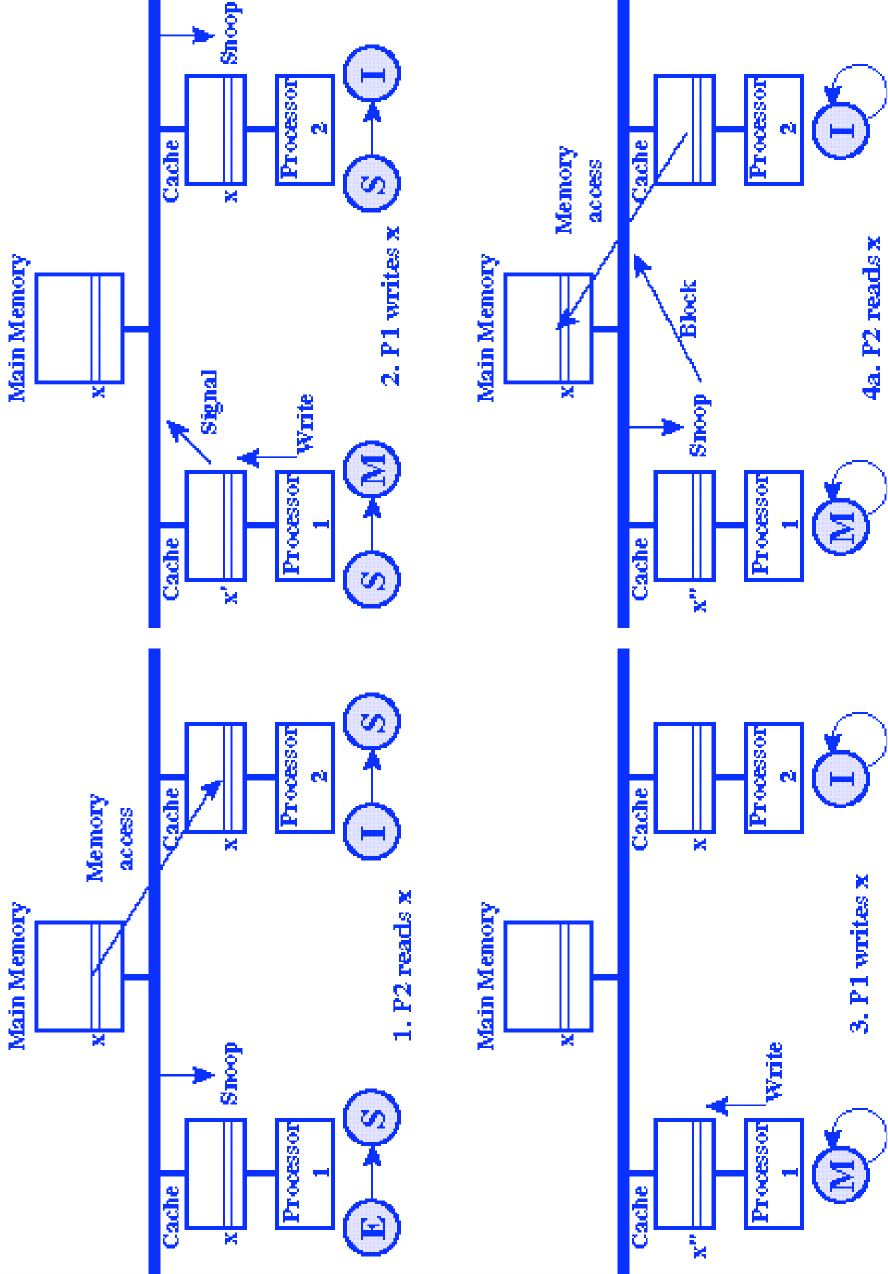
-112-
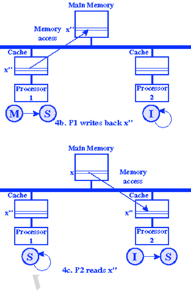
-113-
17.5 a. This is the simplest possible cache coherence protocol. It requires that all
processors use a write-through policy. If a write is made to a location cached in
remote caches, then the copies of the line in remote caches are invalidated. This
approach is easy to implement but requires more bus and memory traffic
because of the write-through policy.
b. This protocol makes a distinction between shared and exclusive states. When a
cache first loads a line, it puts it in the shared state. If the line is already in the
modified state in another cache, that cache must block the read until the line is
updated back to main memory, similar to the MESI protocol. The difference
between the two is that the shared state is split into the shared and exclusive
states for MESI. This reduces the number of write-invalidate operations on the
bus.
17.6 If the L1 cache uses a write-through policy, as is done on the S/390 described in
Section 17.2, then the L1 cache does not need to know the M state. If the L1 cache
uses a write-back policy, then a full MESI protocol is needed between L1 and L2.

-114-
17.7 If only the L1 cache is used, then 89% of the accesses are to L1 and the remaining
11% of the accesses are to main memory. Therefore, the average penalty is (1 ×
0.89) + (32 × 0.11) = 4.41. If both L1 and L2 are present, the average penalty is (1 ×
0.89) + (5 × 0.05) + (32 × 0.06) = 3.06. This normalizes to 3.06/4.41 = 0.69. Thus, with
the addition of the L2 cache, the average penalty is reduced to 69% of that with
only one cache. If all three caches are present, the average penalty is (1 × 0.89) + (5
× 0.05) + (14 × 0.03) + (32 × 0.03) = 2.52, and normalized average penalty is
2.52/4.41 = 0.57. The reduction of the average penalty from 0.69 to 0.57 would
seem to justify the inclusion of the L3 cache.
17.8 a. ta = fi[Hic + (1 – Hi)(b + c) + (1 – fi)(Hdc) + (1 – Hd)((b + c)(1 – fd) + (2b + c)fd)]
b.
€
′
t
a
= ta + (1 – fi)finvi Source: [HWAN93]
17.9 a. chip multiprocessor
b. interleaved multithreading superscalar
c. blocked multithreading superscalar
d. simultaneous multithreading
17.10 [UNGE03] refers to these as horizontal losses and vertical losses, respectively.
With a horizontal loss, full parallelism is not achieved; that is, fewer instructions
are dispatched than the hardware would allow. With a vertical loss, the
dispatching mechanism is stalled because no new instructions can be
accommodated due to latency issues.
17.11 a.
A1
A2
A3
A4
A5
A15
A16
B1
B2
B3
B4
B6
B5
B7
b. The two pipelines are operating independently on two separate processors on
the same chip. Therefore, the diagrams of Figure 17.25 and part (a) of this
solution apply.
c. We assume that the A thread requires a latency of two clock cycles before it is
able to execute instruction A15, and we assume that the interleaving
mechanism is able to use the same thread on two successive clock cycles if
necessary.

-115-
A1
B1
A3
B3
A5
A15
instruction
issue
diagram
pipeline execution diagram
B7
A2
B2
A4
B4
B5 B6
A16
A1
B1
A3
B3
B3
B3
B3
A5
A5
CO F0
A1
B1
A3
B5
B7
B6
B5 B6
A1
B1
B1A3
EI WO
A1
A3
A2
B2
A4
B4
B4
B4
B4
CO F0
A2
B2
A4
A2
B2
B2A4
EI WO
A2
A4
A5
A5B5 B6
B5 B6
B7
B7
B7
A15 A16
A15 A16
A15 A16
A15 A16
d.
A1
A3
A5
B1 B2
A15
instruction
issue
diagram
pipeline execution diagram
A2
A4
B3 B4
A16
B5 B6
B7
A1
A3
A5
B1
B1
CO F0
A1
A3
A5
B3 B4
B3 B4
A1
A3
A3A5
EI WO
A1
A5
A2
A4
CO F0
A2
A4 A2
A4
A4
EI WO
A2
B1
B1
B2
B2
B2
B2B3 B4
B3 B4
A15 A16
B5
B7
B7
B7
B7
B6
B5 B6
B5 B6
B5 B6
A15 A16
A15 A16
A15 A16
e.

-116-
A1
A3
A5
B5 B6
instruction
issue
diagram
A2
A4
A15 A16
B1
B3
B7
B2
B4
pipeline execution diagram
A1
A3
A5
B5
B5
CO F0
A1
A3
A5
A15 A16
A15 A16
A1
A3
A3A5
EI WO
A1
A5
A2
A4
CO F0
A2
A4 A2
A4
A4
EI WO
A2
B5
B5
B6
B6
B6
B6A15 A16
A15 A16
B1
B3
B7
B7
CO F0
B1
B3 B1
B3
B3
EI WO
B1
B2
B4
CO F0
B2
B4 B2
B4
B4
EI WO
B2
B7
B7
17.12 a. Sequential execution time = 1664 processor cycles.
b. SIMD execution time = 26 cycles.
c. Speedup factor = 64. Source: [HWAN93]
17.13 To begin, we can distribute the outer loop without affecting the computation.
DO 20A I = 1, N
B (I,1) = 0
20A CONTINUE
DO 20B I = 1, N
DO 10 J = 1, M
A(I) = A(I) + B (I, J) * C (I, J)
10 CONTINUE
20B CONTINUE
DO 20C I = 1, N
D (I) = E (I) + A (I)
20C CONTINUE
Using vectorized instructions:
B (I,1) = 0 (I = 1, N)
DO 20B I= 1, N
A(I) = A(I) + B(I, J) * C(I, J) (J = 1, M)
20B CONTINUE
D(I) = E(I0 + A(I) (I = 1, N)
17.14 a. One computer executes for a time T. Eight computers execute for a time T/4,
which would take a time 2T on a single computer. Thus the total required time
on a single computer is 3T. Effective speedup = 3. α = 0.75.
b. New speedup = 3.43

-117-
17.15 a. Sequential execution time = 1,051,628 cycles
b. Speedup = 16.28
c. Each computer is assigned 32 iterations balanced between the beginning and
end of the I-loop.
d. The ideal speedup of 32 is achieved.
Source: [HWAN93]
17.16 a. The I loop requires N cycles, as does the J loop. With the L4 statement, the
total is 2N + 1.
b. The sectioned I loop can be done in L cycles. The sectioned J loop produces M
partial sums in L cycles. Total = 2L + l(k + 1).
c. Sequential execution of the original program takes 2N = 221 cycles. Parallel
execution requires 213 + 1608 = 9800 cycles. This is a speedup factor of
approximately 214 (221/9800). Therefore, an efficiency of 214/256 = 83.6% is
achieved.

-118-
CHAPTER 18 MULTICORE COMPUTERS
A
ANSWERS TO
NSWERS TO Q
QUESTIONS
UESTIONS
18.1 •Pipelining: Individual instructions are executed through a pipeline of stages so
that while one instruction is executing in one stage of the pipeline, another
instruction is executing in another stage of the pipeline.
•Superscalar: Multiple pipelines are constructed by replicating execution
resources. This enables parallel execution of instructions in parallel pipelines, so
long as hazards are avoided.
•Simultaneous multithreading (SMT): Register banks are replicated so that
multiple threads can share the use of pipeline resources.
18.2 In the case of pipelining, simple 3-stage pipelines were replaced by pipelines with
5 stages, and then many more stages, with some implementations having over a
dozen stages. There is a practical limit to how far this trend can be taken, because
with more stages, there is the need for more logic, more interconnections, and
more control signals. With superscalar organization, performance increases can be
achieved by increasing the number of parallel pipelines. Again, there are
diminishing returns as the number of pipelines increases. More logic is required to
manage hazards and to stage instruction resources. Eventually, a single thread of
execution reaches the point where hazards and resource dependencies prevent the
full use of the multiple pipelines available. This same point of diminishing returns
is reached with SMT, as the complexity of managing multiple threads over a set of
pipelines limits the number of threads and number of pipelines that can be
effectively utilized.
18.3 Cache memory uses less power than logic .
18.4 • Multi-threaded native applications: Multi-threaded applications are
characterized by having a small number of highly threaded processes. Examples of
threaded applications include Lotus Domino or Siebel CRM (Customer
Relationship Manager).
• Multi-process applications: Multi-process applications are characterized by the
presence of many single-threaded processes. Examples of multi-process
applications include the Oracle database, SAP, and PeopleSoft.
• Java applications: Java applications embrace threading in a fundamental way.
Not only does the Java language greatly facilitate multithreaded applications, but
the Java Virtual Machine is a multi-threaded process that provides scheduling and
memory management for Java applications. Java applications that can benefit
directly from multicore resources include application servers such as Sun’s Java
Application Server, BEA’s Weblogic, IBM’s Websphere, and the open-source
Tomcat application server. All applications that use a Java 2 Platform, Enterprise

-119-
Edition (J2EE platform) application server can immediately benefit from multicore
technology.
• Multi-instance applications: Even if an individual application does not scale to
take advantage of a large number of threads, it is still possible to gain from
multicore architecture by running multiple instances of the application in parallel.
If multiple application instances require some degree of isolation, virtualization
technology (for the hardware of the operating system) can be used to provide each
of them with its own separate and secure environment.
18.5 • The number of core processors on the chip
• The number of levels of cache memory
• The amount of cache memory that is shared
18.6 1. Constructive interference can reduce overall miss rates. That is, if a thread on
one core accesses a main memory location, this brings the frame containing the
referenced location into the shared cache. If a thread on another core soon
thereafter accesses the same memory block, the memory locations will already be
available in the shared on-chip cache.
2. A related advantage is that data shared by multiple cores is not replicated at the
shared cache level.
3. With proper frame replacement algorithms, the amount of shared cache
allocated to each core is dynamic, so that threads that have a less locality can
employ more cache.
4. Interprocessor communication is easy to implement, via shared memory
locations.
5. The use of a shared L2 cache confines the cache coherency problem to the L1
cache level, which may provide some additional performance advantage.
A
ANSWERS TO
NSWERS TO P
PROBLEMS
ROBLEMS
18.1 a. The speedup is due to two factors: the performance gain perf(r) in each core
and the Amdahl performance gain from using multiple cores. Thus:
€
Speedup =perf r
( )
×1
1−f
( )
+f
k
=perf r
( )
×1
1−f
( )
+f×r
n
=1
1−f
( )
perf r
( )
+f×r
perf r
( )
×n
b, c. The conclusions are the same for both figures. The figures are from
"Amdahl's Law in the Multicore Era," by Hill and Marty, Computer, July 2008.
The article draws the following conclusions:
A value r = 1 says the chip has 16 base cores, while a value of r = 16 uses
all resources for a single core. Lines assume different values for the parallel
fraction (f = 0.5, 0.9, …, 0.999). The y-axis gives the symmetric multicore chip’s
speedup relative to its running on one core. The maximum speedup for f = 0.9,
for example, is 6.7 using eight cores.
Similarly, the second figure illustrates how tradeoffs change when
Moore’s law allows n = 256 cores per chip. With f = 0.975, for example, the
maximum speedup of 51.2 occurs with 36 cores of 7.1 core equivalents each.
-120-
Result 1. Amdahl’s law applies to multicore chips because achieving the best
speedups requires fs that are near 1. Thus, finding parallelism is still critical.
Implication 1. Researchers should target increasing f through architectural
support, compiler techniques, programming model improvements, and so on.
This implication is the most obvious and important. Recall, however, that a
system is cost-effective if speedup exceeds its costup.4 Multicore costup is the
multicore system cost divided by the single-core system cost. Because this
costup is often much less than n, speedups less than n can be cost-effective.
Result 2. Using more core equivalents per core, r > 1, can be optimal, even
when performance grows by only r . For a given f, the maximum speedup can
occur at one big core, n base cores, or with an intermediate number of
middlesized cores. Recall that for n = 256 and f = 0.975, the maximum speedup
occurs using 7.1 core equivalents per core.
Implication 2. Researchers should seek methods of increasing core
performance even at a high cost.
Result 3. Moving to denser chips increases the likelihood that cores will be
nonminimal. Even at f = 0.99, minimal base cores are optimal at chip size n =
16, but more powerful cores help at n = 256.
Implication 3. As Moore’s law leads to larger multicore chips, researchers
should look for ways to design more powerful cores.

-121-
CHAPTER 19 NUMBER SYSTEMS
A
ANSWERS TO
NSWERS TO P
PROBLEMS
ROBLEMS
19.1 a. 12 b. 3 c. 28 d. 60 e. 42
19.2 a. 28.375 b. 51.59375 c. 682.5
19.3 a. 1000000 b. 1100100 c. 1101111 d. 10010001 e. 11111111
19.4 a. 100010.11 b. 11001.01 c. 11011.0011
19.5 A BAD ADOBE FACADE FADED (Source: [KNUT98])
19.6 a. 12 b. 159 c. 3410 d. 1662 e. 43981
19.7 a. 15.25 b. 211.875 c. 4369.0625 d. 2184.5 e. 3770.75
19.8 a. 10 b. 50 c. A00 d. BB8 e. F424
19.9 a. CC.2 b. FF.E c. 277.4 d. 2710.01
19.10 a. 1110 b. 11100 c. 101001100100 d. 11111.11 e. 1000111001.01
19.11 a. 9.F b. 35.64 c. A7.EC
19.12 1/2k = 5k/10k
19.13 a. 1, 2, 3, 4, 5, 6, 7, 10, 11, 12, 13, 14, 15, 16, 17, 20, 21, 22, 23, 24
b. 1, 2, 3, 4, 5, 10, 11, 12, 13, 14, 15, 20, 21, 22, 23, 24, 25, 30, 31, 32
c. 1, 2, 3, 4, 10, 11, 12, 13, 14, 20, 21, 22, 23, 24, 30, 31, 32, 33, 34, 40
d. 1, 2, 10, 11, 12, 20, 21, 22, 100, 101, 102, 110, 111, 112, 120, 121, 122, 200, 201, 202
19.14 a. 134 b. 105 c. 363 d. 185
19.15 Given the representation of a number x in base n and base np, every p digits in
the base n representation can be converted to a single base np digit. For example,
the base 3 representation of 7710 is 2212 and the base 9 representation is 85. Thus
it is easy to convert between a base n representation and a base np representation
without the intermediate step of converting to base 10. In other cases, the
intermediate step facilitates conversion.

-122-
CHAPTER 20 DIGITAL LOGIC
A
ANSWERS TO
NSWERS TO P
PROBLEMS
ROBLEMS
20.1
A
B
C
a
b
c
d
0
0
0
1
1
0
0
0
0
1
0
0
0
0
0
1
0
0
0
0
0
0
1
1
0
0
0
1
1
0
0
0
1
0
1
1
0
1
0
0
1
1
1
1
0
0
0
1
0
1
1
1
1
1
0
0
20.2 Recall the commutative law: AB = BA; A + B = B + A
a. A B + CDE + C DE
b. AB + AC
c. (LMN) (AB) (CDE)
d. F (K + R) + SV + W X
20.3 a.
F=V •A •L
. This is just a generalization of DeMorgan's Theorem, and is easily
proved.
b.
F=ABCD
. Again, a generalization of DeMorgan's Theorem.
20.4 a. A = ST + VW
b. A = TUV + Y
c. A = F
d. A = ST
e. A = D + E
f. A = YZ (W + X +YZ) = YZ
g. A = C
20.5 A XOR B = A B + A B
20.6 ABC = NOR ( A , B , C )
20.7 Y = NAND (A, B, C, D) = ABCD

-123-
20.8 a.
X1
X2
X3
X4
Z1
Z2
Z3
Z4
Z5
Z6
Z7
0
0
0
0
1
1
1
0
1
1
1
0
0
0
1
0
0
1
0
0
1
0
0
0
1
0
1
0
1
1
1
0
1
0
0
1
1
1
0
1
1
0
1
1
0
1
0
0
0
1
1
1
0
1
0
0
1
0
1
1
1
0
1
0
1
1
0
1
1
0
0
1
0
1
1
1
1
0
1
1
1
1
0
1
0
0
1
0
1
0
0
0
1
1
1
1
1
1
1
1
0
0
1
1
1
1
1
0
1
0
1
0
1
0
0
0
0
0
0
0
0
1
0
1
1
0
0
0
0
0
0
0
1
1
0
0
0
0
0
0
0
0
0
1
1
0
1
0
0
0
0
0
0
0
1
1
1
0
0
0
0
0
0
0
0
1
1
1
1
0
0
0
0
0
0
0
b. All of the terms have the form illustrated as follows:
Z5 = X1X2X3X4 + X1X2 X3X4 + X1 X2X3X4 + X1 X2X3X4
c. Whereas the SOP form lists all combinations that produce an output of 1, the
POS lists all combinations that produce an output of 0.
For example,
Z3 = ( X1X2X3X4) ( X1X2X3X4)
= (X1X2 X3X4 ) (X1X2X3 X4)
20.9 Label the 8 inputs I0, ... , I7 and the select lines S0, S1, S2.
S1
F = I0 + I1
S0S1S2
+ I2
S0
S1 S2 + I3
S0
S1 S2
+ I4 S0
S1S2
+ I5 S0
S1
S2 + I6 S0
S1
S2 + I7 S0 S1 S2
20.10 Add a data input line and connect it to the input side of each AND gate.

-124-
20.11 Define the input leads as B2, B1, B0 and the output leads as G2, G1, G0. Then
G2 = B2
G1=B2B1+B2B1
G0=B1B0+B1
B0
20.12 The Input is A4A3A2A1A0. Use A2A1A0 as the input to each of the 3 × 8 decoders.
There are a total of 32 outputs from these four 3 × 8 decoders. Use A4A3 as input
to a 2 × 4 decoder and have the four outputs go to the enable leads of the four 3 ×
8 decoders. The result is that one and only one of the 32 outputs will have a value
of 1.
20.13 SUM = A ⊕ B ⊕ C
CARRY = AB ⊕ AC ⊕ BC
20.14 a. The carry to the second stage is available after 20 ns; the carry to the third
stage is available 20 ns after that, and so on. When the carry reaches the 32nd
stage, another 30 ns are needed to produce the final sum. Thus
T = 31 × 20 + 30 = 650 ns
b. Each 8-bit adder produces a sum in 30 ns and a carry in 20 ns. Therefore,
T = 3 × 20 + 30 = 90 ns
20.15 a.
Characteristic table
Simplified characteristic table
Current
input
SR
Current
state
Qn
Next state
Qn+1
S
R
Qn+1
00
0
—
0
0
—
00
1
—
0
1
1
01
0
1
1
0
0
01
1
1
1
1
Qn
10
0
0
10
1
0
11
0
0
11
1
1
b.
t
0
1
2
3
4
5
6
7
8
9
S
0
1
1
1
1
1
0
1
0
1
R
1
1
0
1
0
1
1
1
0
0
Qn
0
0
1
1
1
1
0
0
—
1

-125-
20.16
D
Data
Clock Ck
Q
Q
R
20.17
C
O3
B A
O1O0
O2
20.18 a. Use a PLA with 12-bit addresses and 96 8-bit locations. Each of the 96
locations is set to an ASCII code, and a character is converted by simply using
its original, 12-bit code as an address to the PLA. The content of that address
is the required ASCII code.
b. Yes. This would require a 4K×8 ROM where only 96 of the 4096 locations are
actually used.

-126-
CHAPTER 21 THE IA-64 ARCHITECTURE
A
ANSWERS TO
NSWERS TO Q
QUESTIONS
UESTIONS
21.1 I-unit: For integer arithmetic, shift-and-add, logical, compare, and integer
multimedia instructions. M-unit: Load and store between register and memory
plus some integer ALU operations. B-unit: Branch instructions. F-unit: Floating-
point instructions.
21.2 The template field contains information that indicates which instructions can be
executed in parallel.
21.3 A stop indicates to the hardware that one or more instructions before the stop may
have certain kinds of resource dependencies with one or more instructions after
the stop.
21.4 Predication is a technique whereby the compiler determines which instructions
may execute in parallel. With predicated execution, every IA-64 instruction
includes a reference to a 1-bit predicate register, and only executes if the predicate
value is 1 (true).
21.5 Predicates enable the processor to speculatively execute both branches of an if
statement and only commit after the condition is determined.
21.6 With control speculation, a load instruction is moved earlier in the program and its
original position replaced by a check instruction. The early load saves cycle time; if
the load produces an exception, the exception is not activated until the check
instruction determines if the load should have been taken.
21.7 Associated with each register is a NaT bit used to track deferred speculative
exceptions. If a ld.s detects an exception, it sets the NaT bit associated with the
target register. If the corresponding chk.s instruction is executed, and if the NaT bit
is set, the chk.s instruction branches to an exception-handling routine.
21.8 With data speculation, a load is moved before a store instruction that might alter
the memory location that is the source of the load. A subsequent check is made to
assure that the load receives the proper memory value.
21.9 Software pipelining is a technique in which instructions from multiple iterations
of a loop are enabled to execute in parallel. Parallelism is achieved by grouping
together instructions from different iterations. Hardware pipelining refers to the
use of a physical pipeline as part of the hardware

-127-
21.10 Rotating registers are used for software pipelining. During each iteration of a
software-pipeline loop, register references within these ranges are automatically
incremented. Stacked registers implement a stack.
A
ANSWERS TO
NSWERS TO P
PROBLEMS
ROBLEMS
21.1 Eight. The operands and result require 7 bits each, and the controlling predicate 6.
A major opcode is specified by 4 bits; 38 bits of the 41-bit syllable are committed,
leaving 3 bits to specify a suboperation. Source: [MARK00]
21.2 Table 21.3 reveals that any opcode can be interpreted as referring to on of 6
different execution units (M, B, I, L, F, X). So, the potential maximum number of
different major opcodes is 24 × 6 = 96.
21.3 16
21.4 a. Six cycles. The single floating-point unit is the limiting factor.
b. Three cycles.
21.5 The pairing must not exceed a sum of two M or two I slots with the two bundles.
For example, two bundles, both with template 00, or two bundles with templates
00 and 01 could not be paired because they require 4 I-units. Source: [EVAN03]
21.6 Yes. On IA-64s with fewer floating-point units, more cycles are needed to dispatch
each group. On an IA-64 with two FPUs, each group requires two cycles to
dispatch. A machine with three FPUs will dispatch the first three floating-point
instructions within a group in one cycle, and the remaining instruction in the next.
Source: [MARK00]
21.7
p1
comparison
p2
p3
not present
0
0
1
not present
1
1
0
0
0
0
0
0
1
0
0
1
0
0
1
1
1
1
0
21.8 a. (3) and (4); (5) and (6)
b. The IA-64 template field gives a great deal of flexibility, so that many
combinations are possible. One obvious combination would be (1), (2), and (3)
in the first instruction; (4), (5), and (6) in the second instruction; and (7) in the
third instruction.
21.9 Branching to label error should occur if and only if at least one of the 8 bytes in
register r16 contains a non-digit ASCII code. So the comments are not inaccurate
but are not as helpful as they could be. Source: [EVAN03]

-128-
21.10 a.
mov r1, 0
mov r2, 0
ld r3, addr(A)
L1: ld r4, mem(r3+r2)
bge r4, 50, L2
add r5, r5, 1
jump L3
L2: add r6, r6, 1
L3: add r1, r1, 1
add r2, r2, 4
blt r1, 100, L1
b.
mov r1, 0
mov r2, 0
ld r3, addr(A)
L1: ld r4, mem(r3+r2)
cmp.ge p1, p2 = r4. 50
(p2) add r5 = 1, r5
(p1) add r6 = 1, r6
add r1 = 1, r1
add r2 = 4, r2
blt r1, 100, L1
21.11 a.
fmpy t = p, q //floating-point multiply
ldf.a c = [rj];; //advanced floating point load
//load value stored in location specified by address
//in register rj; place value in floating-point register c
//assume rj points to a[j]
stf [ri] = t;; //store value in floating-point register t in location
//specified by address in register ri
//assume ri points to a[i]
ldf.c c = [rj];; //executes only if ri = rj
If the advanced load succeeded, the ldf.c will complete in one cycle, and c can be
used in the following instruction. The effective latency of the ldf.a instruction has
been reduced by the latency of the floating-point multiplication. The stf and ldf.c
cannot be in the same instruction group, because there may be a read-after -write
dependency.
b.
fmpy t = p, q
cmp.ne p8, p9 = ri, rj;;
(p8) ldf c = [rj];; //p8 ⇒ no conflict
stf [ri] = t;; //if ri = rj, then c = t
(p9) mov c = t;;
c. In the predicated version, the load begins one cycle later than with the
advanced load. Also, two predicated registers are required. Source: [MARK00]

-129-
21.12 a. The number of output registers is
SOO = SOF – SOL = 48 – 16 = 32
b. Because the stacked register group starts at r32, the local register and output
register groups consist of:
Local register group: r32 through r47
Output register group: r48 through r63
Source: [TRIE01]

-130-
APPENDIX B ASSEMBLY LANGUAGE AND
RELATED TOPICS
A
ANSWERS TO
NSWERS TO Q
QUESTIONS
UESTIONS
B.1 1. It clarifies the execution of instructions.
2. It shows how data is represented in memory.
3. It shows how a program interacts with the operating system, processor, and the
I/O system.
4. It clarifies how a program accesses external devices.
5. Understanding assembly language programmers makes students better high-
level language (HLL) programmers, by giving them a better idea of the target
language that the HLL must be translated into.
B.2 Assembly language is a programming language that is one step away from
machine language. Assembly language includes symbolic names for locations. It
also includes directives and macros.
B.3 1. Development time. Writing code in assembly language takes much longer time
than in a high level language.
2. Reliability and security. It is easy to make errors in assembly code. The
assembler is not checking if the calling conventions and register save conventions
are obeyed. Nobody is checking for you if the number of PUSH and POP
instructions is the same in all possible branches and paths. There are so many
possibilities for hidden errors in assembly code that it affects the reliability and
security of the project unless you have a very systematic approach to testing and
verifying.
3. Debugging and verifying. Assembly code is more difficult to debug and verify
because there are more possibilities for errors than in high-level code.
4. Maintainability. Assembly code is more difficult to modify and maintain
because the language allows unstructured spaghetti code and all kinds of dirty
tricks that are difficult for others to understand. Thorough documentation and a
consistent programming style are needed.
5. Portability. Assembly code is very platform-specific. Porting to a different
platform is difficult.
6. System code can use intrinsic functions instead of assembly. The best modern
C++ compilers have intrinsic functions for accessing system control registers and
other system instructions. Assembly code is no longer needed for device drivers
and other system code when intrinsic functions are available.
7. Application code can use intrinsic functions or vector classes instead of
assembly. The best modern C++ compilers have intrinsic functions for vector

-131-
operations and other special instructions that previously required assembly
programming.
8. Compilers have been improved a lot in recent years. The best compilers are now
quite good. It takes a lot of expertise and experience to optimize better than the
best C++ compiler.
B.4 1. Debugging and verifying. Looking at compiler-generated assembly code or the
disassembly window in a debugger is useful for finding errors and for checking
how well a compiler optimizes a particular piece of code.
2. Making compilers. Understanding assembly coding techniques is necessary for
making compilers, debuggers and other development tools.
3. Embedded systems. Small embedded systems have fewer resources than PCs
and mainframes. Assembly programming can be necessary for optimizing code
for speed or size in small embedded systems.
4. Hardware drivers and system code. Accessing hardware, system control
registers etc. may sometimes be difficult or impossible with high level code.
5. Accessing instructions that are not accessible from high level language. Certain
assembly instructions have no high-level language equivalent.
6. Self-modifying code. Self-modifying code is generally not profitable because it
interferes with efficient code caching. It may, however, be advantageous for
example to include a small compiler in math programs where a user-defined
function has to be calculated many times.
7. Optimizing code for size. Storage space and memory is so cheap nowadays that
it is not worth the effort to use assembly language for reducing code size.
However, cache size is still such a critical resource that it may be useful in some
cases to optimize a critical piece of code for size in order to make it fit into the
code cache.
8. Optimizing code for speed. Modern C++ compilers generally optimize code
quite well in most cases. But there are still many cases where compilers perform
poorly and where dramatic increases in speed can be achieved by careful
assembly programming.
9. Function libraries. The total benefit of optimizing code is higher in function
libraries that are used by many programmers.
10. Making function libraries compatible with multiple compilers and operating
systems. It is possible to make library functions with multiple entries that are
compatible with different compilers and different operating systems. This
requires assembly programming.
B.5 label, mnemonic, operand, and comment
B.6 Instructions: symbolic representations of machine language instructions
Directives: instruction to the assembler to perform specified actions doing the
assembly process
Macro definitions: A macro definition is a section of code that the programmer
writes once, and then can use many times. When the assembler encounters a
macro call, it replaces the macro call with the macro itself.
Comment: A statement consisting entirely of a comment.
B.7 A two-pass assembler takes a first pass through the assembly program to construct
a symbol table that contains a list of all labels and their associated location counter
values. It then takes a second pass to translate the assembly program into object

-132-
code. A one-pass assembler combines both operations in a single pass, and
resolves forward references on the fly.
A
ANSWERS TO
NSWERS TO P
PROBLEMS
ROBLEMS
B.1 a. When it executes, this instruction copies itself to the next location and the
program counter is incremented, thus pointing to the instruction just copied.
Thus, Imp marches through the entire memory, placing a copy of itself in each
location, and wiping out any rival program.
b. Dwarf "bombs" the core at regularly spaced locations with DATAs, while
making sure it won't hit itself. The ADD instruction adds the immediate value
4 to the contents of the location 3 locations down, which is the DATA location.
So the DATA location now has the value 4. Next, the COPY instruction copies
the location 2 locations down, which is the DATA location, to the address
contained in that location, which is a 4, so the COPY goes to the relative
location 4 words down from the DATA location. Then we jump back to the
ADD instruction, which adds 4 to the DATA location, bringing the value to 8.
This process continues, so that data is written out in every fourth location.
When memory wraps around, the data writes will miss the first three lines of
Dwarf, so that Dwarf can continue indefinitely. We assume that the memory
size is divisible by 4.
c. Loop ADD #4, MemoryPtr
COPY 2, @MemoryPtr
JUMP Loop
MemoryPtr DATA 0
B.2 The barrage of data laid down by Dwarf moves through the memory array faster
than Imp moves, but it does not necessarily follow that Dwarf has the advantage.
The question is: Will Dwarf hit Imp even if the barrage does catch up? If Imp
reaches Dwarf first, Imp will in all probability plow right through Dwarf's code.
When Dwarf's JUMP –2 instruction transfers execution back two steps, the
instruction found there will be Imp's COPY 0, 1. As a result Dwarf will be
subverted and become a second Imp endlessly chasing the first one around the
array. Under the rules of Core War the battle is a draw. (Note that this is the
outcome to be expected "in all probability." Students are invited to analyze other
possibilities and perhaps discover the bizarre result of one of them.)
B.3 Loop COPY #0, @MemoryPtr
ADD #1, MemoryPtr
JUMP Loop
MemoryPtr DATA 0
B.4 This program (call it P) is intended to thwart Imp, by overwriting location Loop –
1, thus terminating the march of Imp from lower memory levels. However, timing
is critical. Suppose Imp is currently located at Loop – 2 and P has just executed the
JUMP instruction. If it is now P's turn to execute, we have the following sequence:
1. P executes the COPY instruction, placing a 0 in Loop – 1.
2. Imp copies itself to location Loop – 1.
3. P executes the JUMP instruction, set its local program counter to Loop.
4. Imp copies itself to location Loop.

-133-
5. P executes the Imp instruction at Loop. The P program has been wiped out.
On the other hand, suppose that Imp is currently located at Loop – 2; P has just
executed the JUMP instruction; and it is now Imp's turn to execute. We have the
following sequence:
1. Imp copies itself to location Loop – 1.
2. P executes the COPY instruction, placing a 0 in Loop – 1.
3. Imp attempts to execute at location Loop – 1, but there is only a null instruction
there. Imp has been wiped out.
B.5 a. CF = 0
b. CF = 1
B.6 If there is no overflow, then the difference will have the correct value and must be
non-negative. Thus, SF = OF = 0. However, if there is an overflow, the difference
will not have the correct value (and in fact will be negative). Thus, SF = OF = 1.
B.7 jmp next
B.8 avg: resd 1 ; integer average
i1: dd 20 ; first number in the average
i2: dd 13 ; second number in the average
i3: dd 82 ; first number in the average
main: mov avg, i1
add avg, i2
add avg, i3
idiv avg, 3 ; get integer average
B.9 cmp eax, 0 ; sets ZF if eax = 0
je thenblock ; If ZF set, branch to thenblock
mov ebx, 2 ; ELSE part of IF statement
jmp next ; jump over THEN part of IF
thenblock: mov ebx, 1 ; THEN part of IF
next:
B.10 msglen is assigned the constant 12
B.11 V1: resw 1 ; values must be assigned
V2: resw 1 ; before program starts
V3: resw 1
main: mov ax, V1 ; load V1 for testing
cmp ax, V2 ; if ax <= V2 then
jbe L1 ; jump to L1
mov ax, V2 ; else move V1 to ax
L1: cmp ax, V3 ; if ax <= V2 then
jbe L2 ; jump to L2
mov ax, V3 ; else move V1 to ax
L2:
B.12 The compare instruction subtracts the second argument from the first argument,
but does not store the result; it only sets the status flags. The effect of this

-134-
instruction is to copy the zero flag to the carry flag. That is, the value of CF after
the cmp instruction is equal to the value of ZF just before the instruction.
B.13 a. push ax
push bx
pop ax
pop bx
b. xor ax,bx
xor bx,ax
xor ax,bx
B.14 IF X=A AND Y=B THEN
{ do something }
ELSE
{ do something else }
END IF
B.15 a. The algorithm makes repeated use of the equation gcd (a, b) = gcd (b, a mod b)
and begins by assuming a ≥ b. By definition, if both a and b are 0, then the gcd
is 1. Also by definition b = 0, then gcd = a. The remainder of the C program
implements the repeated application of the mod operator.

-135-
b. gcd: mov ebx,eax
mov eax,edx
test ebx,ebx ; bitwise AND to set CC bits
jne L1 ; jump if ebx not equal to 0
test edx,edx
jne L1
mov eax,1
ret ; return value in eax
L1: test eax,eax
jne L2
mov eax,ebx
ret
L2: test ebx,ebx
je L5 ; jump if ebx equal to 0
L3; cmp ebx,eax
je L5 ; jump if ebx = eax
jae L4 ; jump if ebx above/equal eax
sub eax,ebx
jmp L3
L4: sub ebx,eax
jmp L3
L5: ret
b. gcd: neg eax ; take twos complement of eax
je L3 ; jump if eax equal to 0
L1: neg eax
xchg eax,edx ; exchange contents of eax and edx
L2: sub eax,edx
jg L2 ; jump if eax greater than edx
jne L1 ; jump if eax not equal to edx
L3: add eax,edx
jne L4
inc eax
L4: ret

-136-
B.16 a. The reason is that instructions are assembled in pass 2, where all the symbols
are already in the symbol table; certain directives, however, are executed in
pass 1, where future symbols have not been found yet. Thus pass 1 directives
cannot use future symbols.
b. The simplest way is to add another pass. The directive ‘A EQU B+1’ can be
handled in three passes. In the first pass, label A cannot be defined, since label
B is not yet in the symbol table. However, later in the same pass, B is found and
is stored in the symbol table. In the second pass label A can be defined and, in
the third pass, the program can be assembled. This, of course, is not a general
solution, since it is possible to nest future symbols very deep. Imagine
something like:
A EQU B
-
B EQU C
-
C EQU D
-
-
D -
Such a program requires four passes just to collect all the symbol definitions,
followed by another pass to assemble instructions. Generally one could design
a percolative assembler that would perform as many passes as necessary, until
no more future symbols remain. This may be a nice theoretical concept but its
practical value is nil. Cases such as ‘A EQU B’, where B is a future symbol, are
not important and can be considered invalid.
B.17 It is executed in pass 1 since it affects the symbol table. It is executed by evaluating
and comparing the expressions in the operand field.
