Cortex R4 And R4F Technical Reference Manual DDI0363G R1p4 Trm
User Manual: Cortex R4
Open the PDF directly: View PDF ![]() .
.
Page Count: 436 [warning: Documents this large are best viewed by clicking the View PDF Link!]
- Cortex-R4 and Cortex-R4F Technical Reference Manual
- Contents
- Preface
- Introduction
- Functional Description
- Programmers Model
- System Control
- 4.1 About system control
- 4.2 Register summary
- 4.3 Register descriptions
- 4.3.1 Register allocation
- 4.3.2 c0, Main ID Register
- 4.3.3 c0, Cache Type Register
- 4.3.4 c0, TCM Type Register
- 4.3.5 c0, MPU Type Register
- 4.3.6 c0, Multiprocessor ID Register
- 4.3.7 The Processor Feature Registers
- 4.3.8 c0, Debug Feature Register 0
- 4.3.9 c0, Auxiliary Feature Register 0
- 4.3.10 Memory Model Feature Registers
- 4.3.11 Instruction Set Attributes Registers
- 4.3.12 c0, Current Cache Size Identification Register
- 4.3.13 c0, Current Cache Level ID Register
- 4.3.14 c0, Cache Size Selection Register
- 4.3.15 c1, System Control Register
- 4.3.16 c1, Auxiliary Control Register
- 4.3.17 c15, Secondary Auxiliary Control Register
- 4.3.18 c1, Coprocessor Access Register
- 4.3.19 Fault Status and Address Registers
- 4.3.20 c6, MPU memory region programming registers
- 4.3.21 Cache operations
- 4.3.22 c9, BTCM Region Register
- 4.3.23 c9, ATCM Region Register
- 4.3.24 c9, TCM Selection Register
- 4.3.25 c11, Slave Port Control Register
- 4.3.26 c13, FCSE PID Register
- 4.3.27 c13, Context ID Register
- 4.3.28 c13, Thread and Process ID Registers
- 4.3.29 Validation Registers
- 4.3.30 Correctable Fault Location Register
- 4.3.31 Build Options Registers
- Prefetch Unit
- Events and Performance Monitor
- 6.1 About the events
- 6.2 About the PMU
- 6.3 Performance monitoring registers
- 6.3.1 c9, Performance Monitor Control Register
- 6.3.2 c9, Count Enable Set Register
- 6.3.3 c9, Count Enable Clear Register
- 6.3.4 c9, Overflow Flag Status Register
- 6.3.5 c9, Software Increment Register
- 6.3.6 c9, Performance Counter Selection Register
- 6.3.7 c9, Cycle Count Register
- 6.3.8 c9, Event Type Selection Register
- 6.3.9 c9, Event Count Registers
- 6.3.10 c9, User Enable Register
- 6.3.11 c9, Interrupt Enable Set Register
- 6.3.12 c9, Interrupt Enable Clear Register
- 6.4 Event bus interface
- Memory Protection Unit
- Level One Memory System
- Level Two Interface
- Power Control
- FPU Programmers Model
- Debug
- 12.1 Debug systems
- 12.2 About the debug unit
- 12.3 Debug register interface
- 12.4 Debug register descriptions
- 12.4.1 Accessing debug registers
- 12.4.2 CP14 c0, Debug ID Register
- 12.4.3 CP14 c0, Debug ROM Address Register
- 12.4.4 CP14 c0, Debug Self Address Offset Register
- 12.4.5 CP14 c1, Debug Status and Control Register
- 12.4.6 Data Transfer Register
- 12.4.7 Watchpoint Fault Address Register
- 12.4.8 Vector Catch Register
- 12.4.9 Debug State Cache Control Register
- 12.4.10 Instruction Transfer Register
- 12.4.11 Debug Run Control Register
- 12.4.12 Breakpoint Value Registers
- 12.4.13 Breakpoint Control Registers
- 12.4.14 Watchpoint Value Registers
- 12.4.15 Watchpoint Control Registers
- 12.4.16 Operating System Lock Status Register
- 12.4.17 Authentication Status Register
- 12.4.18 Device Power-down and Reset Control Register
- 12.4.19 Device Power-down and Reset Status Register
- 12.5 Management registers
- 12.6 Debug events
- 12.7 Debug exception
- 12.8 Debug state
- 12.8.1 Entering debug state
- 12.8.2 Behavior of the PC and CPSR in debug state
- 12.8.3 Executing instructions in debug state
- 12.8.4 Writing to the CPSR in debug state
- 12.8.5 Privilege
- 12.8.6 Accessing registers and memory
- 12.8.7 Coprocessor instructions
- 12.8.8 Effect of debug state on non-invasive debug
- 12.8.9 Effects of debug events on processor registers
- 12.8.10 Exceptions in debug state
- 12.8.11 Leaving debug state
- 12.9 Cache debug
- 12.10 External debug interface
- 12.11 Using the debug functionality
- 12.12 Debugging systems with energy management capabilities
- Integration Test Registers
- Signal Descriptions
- A.1 About the processor signal descriptions
- A.2 Global signals
- A.3 Configuration signals
- A.4 Interrupt signals, including VIC interface signals
- A.5 L2 interface signals
- A.6 TCM interface signals
- A.7 Redundant processor signals
- A.8 Debug interface signals
- A.9 ETM interface signals
- A.10 Test signals
- A.11 MBIST signals
- A.12 Validation signals
- A.13 FPU signals
- AC Characteristics
- Cycle Timings and Interlock Behavior
- C.1 About cycle timings and interlock behavior
- C.2 Register interlock examples
- C.3 Data processing instructions
- C.4 QADD, QDADD, QSUB, and QDSUB instructions
- C.5 Media data-processing
- C.6 Sum of Absolute Differences (SAD)
- C.7 Multiplies
- C.8 Divide
- C.9 Branches
- C.10 Processor state updating instructions
- C.11 Single load and store instructions
- C.12 Load and Store Double instructions
- C.13 Load and Store Multiple instructions
- C.14 RFE and SRS instructions
- C.15 Synchronization instructions
- C.16 Coprocessor instructions
- C.17 SVC, BKPT, Undefined, and Prefetch Aborted instructions
- C.18 Miscellaneous instructions
- C.19 Floating-point register transfer instructions
- C.20 Floating-point load/store instructions
- C.21 Floating-point single-precision data processing instructions
- C.22 Floating-point double-precision data processing instructions
- C.23 Dual issue
- ECC Schemes
- Revisions

Copyright © 2006-2011 ARM Limited. All rights reserved.
ARM DDI 0363G (ID041111)
Cortex™-R4 and Cortex-R4F
Revision: r1p4
Technical Reference Manual

ARM DDI 0363G Copyright © 2006-2011 ARM Limited. All rights reserved. ii
ID041111 Non-Confidential
Cortex-R4 and Cortex-R4F
Technical Reference Manual
Copyright © 2006-2011 ARM Limited. All rights reserved.
Release Information
The following changes have been made to this book.
Proprietary Notice
Words and logos marked with ® or ™ are registered trademarks or trademarks of ARM® in the EU and other countries,
except as otherwise stated below in this proprietary notice. Other brands and names mentioned herein may be the
trademarks of their respective owners.
Neither the whole nor any part of the information contained in, or the product described in, this document may be
adapted or reproduced in any material form except with the prior written permission of the copyright holder.
The product described in this document is subject to continuous developments and improvements. All particulars of the
product and its use contained in this document are given by ARM in good faith. However, all warranties implied or
expressed, including but not limited to implied warranties of merchantability, or fitness for purpose, are excluded.
This document is intended only to assist the reader in the use of the product. ARM shall not be liable for any loss or
damage arising from the use of any information in this document, or any error or omission in such information, or any
incorrect use of the product.
Where the term ARM is used it means “ARM or any of its subsidiaries as appropriate”.
Some material in this document is based on ANSI/IEEE Std 754-1985, IEEE Standard for Binary Floating-Point
Arithmetic. The IEEE disclaims any responsibility or liability resulting from the placement and use in the described
manner.
Confidentiality Status
This document is Non-Confidential. The right to use, copy and disclose this document may be subject to license
restrictions in accordance with the terms of the agreement entered into by ARM and the party that ARM delivered this
document to.
Product Status
The information in this document is final, that is for a developed product.
Web Address
http://www.arm.com
Change history
Date Issue Confidentiality Change
15 May 2006 A Confidential First release for r0p1
22 October 2007 B Non-Confidential First release for r1p2
16 June 2008 C Non-Confidential Restricted Access First release for r1p3
11 September 2009 D Non-Confidential Second release for r1p3
20 November 2009 E Non-Confidential Documentation update for r1p3
12 February 2010 F Non-Confidential Documentation update for r1p3
04 April 2011 G Non-Confidential First release for r1p4

ARM DDI 0363G Copyright © 2006-2011 ARM Limited. All rights reserved. iii
ID041111 Non-Confidential
Contents
Cortex-R4 and Cortex-R4F Technical Reference
Manual
Preface
About this book .............................................................................................................. viii
Feedback ........................................................................................................................ xii
Chapter 1 Introduction
1.1 About the processor ...................................................................................................... 1-2
1.2 Compliance ................................................................................................................... 1-3
1.3 Features ........................................................................................................................ 1-4
1.4 Interfaces ...................................................................................................................... 1-5
1.5 Configurable options ..................................................................................................... 1-6
1.6 Test features ............................................................................................................... 1-10
1.7 Product documentation, architecture and design flow ................................................ 1-11
1.8 Product revisions ........................................................................................................ 1-13
Chapter 2 Functional Description
2.1 About the functions ....................................................................................................... 2-2
2.2 Interfaces ...................................................................................................................... 2-9
2.3 Clocking and resets .................................................................................................... 2-11
2.4 Operation .................................................................................................................... 2-15
Chapter 3 Programmers Model
3.1 About the programmers model ..................................................................................... 3-2
3.2 Modes of operation and execution ................................................................................ 3-3
3.3 Memory model .............................................................................................................. 3-4
3.4 Data structures ............................................................................................................. 3-5
3.5 Registers ....................................................................................................................... 3-6

ARM DDI 0363G Copyright © 2006-2011 ARM Limited. All rights reserved. iv
ID041111 Non-Confidential
3.6 Program status registers 3-9
3.7 Exceptions 3-14
3.8 Acceleration of execution environments 3-25
3.9 Unaligned and mixed-endian data access support 3-26
3.10 Big-endian instruction support 3-27
Chapter 4 System Control
4.1 About system control 4-2
4.2 Register summary 4-7
4.3 Register descriptions 4-9
Chapter 5 Prefetch Unit
5.1 About the prefetch unit 5-2
5.2 Branch prediction 5-3
5.3 Return stack 5-5
5.4 Controlling instruction prefetch and program flow prediction 5-6
Chapter 6 Events and Performance Monitor
6.1 About the events 6-2
6.2 About the PMU 6-6
6.3 Performance monitoring registers 6-7
6.4 Event bus interface 6-19
Chapter 7 Memory Protection Unit
7.1 About the MPU 7-2
7.2 Memory types 7-7
7.3 Region attributes 7-8
7.4 MPU interaction with memory system 7-9
7.5 MPU faults 7-10
7.6 MPU software-accessible registers 7-11
Chapter 8 Level One Memory System
8.1 About the L1 memory system 8-2
8.2 About the error detection and correction schemes 8-4
8.3 Fault handling 8-7
8.4 About the TCMs 8-13
8.5 About the caches 8-18
8.6 Internal exclusive monitor 8-34
8.7 Memory types and L1 memory system behavior 8-35
8.8 Error detection events 8-36
Chapter 9 Level Two Interface
9.1 About the L2 interface 9-2
9.2 AXI master interface 9-3
9.3 AXI master interface transfers 9-7
9.4 AXI slave interface 9-20
9.5 Enabling or disabling AXI slave accesses 9-23
9.6 Accessing RAMs using the AXI slave interface 9-24
Chapter 10 Power Control
10.1 About power control 10-2
10.2 Power management 10-3
Chapter 11 FPU Programmers Model
11.1 About the FPU programmers model 11-2
11.2 General-purpose registers 11-3
11.3 System registers 11-4
11.4 Modes of operation 11-11

ARM DDI 0363G Copyright © 2006-2011 ARM Limited. All rights reserved. v
ID041111 Non-Confidential
11.5 Compliance with the IEEE 754 standard 11-12
Chapter 12 Debug
12.1 Debug systems 12-2
12.2 About the debug unit 12-3
12.3 Debug register interface 12-5
12.4 Debug register descriptions 12-10
12.5 Management registers 12-35
12.6 Debug events 12-42
12.7 Debug exception 12-44
12.8 Debug state 12-47
12.9 Cache debug 12-53
12.10 External debug interface 12-54
12.11 Using the debug functionality 12-57
12.12 Debugging systems with energy management capabilities 12-74
Chapter 13 Integration Test Registers
13.1 About Integration Test Registers 13-2
13.2 Summary of the processor registers used for integration testing 13-3
13.3 Processor integration testing 13-4
Appendix A Signal Descriptions
A.1 About the processor signal descriptions A-2
A.2 Global signals A-3
A.3 Configuration signals A-4
A.4 Interrupt signals, including VIC interface signals A-7
A.5 L2 interface signals A-8
A.6 TCM interface signals A-13
A.7 Redundant processor signals A-16
A.8 Debug interface signals A-17
A.9 ETM interface signals A-19
A.10 Test signals A-20
A.11 MBIST signals A-21
A.12 Validation signals A-22
A.13 FPU signals A-23
Appendix B AC Characteristics
B.1 Processor timing B-2
B.2 Processor timing parameters B-3
Appendix C Cycle Timings and Interlock Behavior
C.1 About cycle timings and interlock behavior C-3
C.2 Register interlock examples C-6
C.3 Data processing instructions C-7
C.4 QADD, QDADD, QSUB, and QDSUB instructions C-9
C.5 Media data-processing C-10
C.6 Sum of Absolute Differences (SAD) C-11
C.7 Multiplies C-12
C.8 Divide C-14
C.9 Branches C-15
C.10 Processor state updating instructions C-16
C.11 Single load and store instructions C-17
C.12 Load and Store Double instructions C-20
C.13 Load and Store Multiple instructions C-21
C.14 RFE and SRS instructions C-24
C.15 Synchronization instructions C-25
C.16 Coprocessor instructions C-26
C.17 SVC, BKPT, Undefined, and Prefetch Aborted instructions C-27
C.18 Miscellaneous instructions C-28

ARM DDI 0363G Copyright © 2006-2011 ARM Limited. All rights reserved. vi
ID041111 Non-Confidential
C.19 Floating-point register transfer instructions C-29
C.20 Floating-point load/store instructions C-30
C.21 Floating-point single-precision data processing instructions C-32
C.22 Floating-point double-precision data processing instructions C-33
C.23 Dual issue C-34
Appendix D ECC Schemes
D.1 ECC scheme selection guidelines D-2
Appendix E Revisions


Preface
ARM DDI 0363G Copyright © 2006-2011 ARM Limited. All rights reserved. viii
ID041111 Non-Confidential
About this book
This book is for Cortex-R4 and Cortex-R4F processors.
Note
• The Cortex-R4F processor is a Cortex-R4 processor that includes the optional Floating
Point Unit (FPU) extension.
• In this book, references to the Cortex-R4 processor also apply to the Cortex-R4F
processor, unless the context makes it clear that this is not the case.
Product revision status
The rnpn identifier indicates the revision status of the product described in this book, where:
rn Identifies the major revision of the product.
pn Identifies the minor revision or modification status of the product.
Intended audience
This book is written for system designers, system integrators, and programmers who are
designing or programming a System-on-Chip (SoC) that uses the processor.
Using this book
This book is organized into the following chapters:
Chapter 1 Introduction
Read this for an introduction to the processor and descriptions of the major
functional blocks.
Chapter 2 Functional Description
Read this for a description of the functionality of the processor.
Chapter 3 Programmers Model
Read this for a description of the processor registers and programming
information.
Chapter 4 System Control
Read this for a description of the system control coprocessor registers and
programming information.
Chapter 5 Prefetch Unit
Read this for a description of the functions of the Prefetch Unit (PFU), including
dynamic branch prediction and the return stack.
Chapter 6 Events and Performance Monitor
Read this for a description of the Performance Monitoring Unit (PMU) and the
event bus.
Chapter 7 Memory Protection Unit
Read this for a description of the Memory Protection Unit (MPU) and the access
permissions process.

Preface
ARM DDI 0363G Copyright © 2006-2011 ARM Limited. All rights reserved. ix
ID041111 Non-Confidential
Chapter 8 Level One Memory System
Read this for a description of the Level One (L1) memory system.
Chapter 9 Level Two Interface
Read this for a description of the features of the Level Two (L2) interface not
covered in the AMBA® AXI Protocol Specification.
Chapter 10 Power Control
Read this for a description of the power control facilities.
Chapter 11 FPU Programmers Model
Read this for a description of the Floating Point Unit (FPU) support in the
Cortex-R4F processor.
Chapter 12 Debug
Read this for a description of the debug support.
Chapter 13 Integration Test Registers
Read this for a description of the Integration Test Registers, and of integration
testing of the processor with an ETM-R4 trace macrocell.
Appendix A Signal Descriptions
Read this for a description of the inputs and outputs of the processor.
Appendix B AC Characteristics
Read this for a description of the timing parameters applicable to the processor.
Appendix C Cycle Timings and Interlock Behavior
Read this for a description of the instruction cycle timing and instruction
interlocks.
Appendix D ECC Schemes
Read this for a description of how to select the Error Checking and Correction
(ECC) scheme depending on the Tightly-Coupled Memory (TCM) configuration.
Appendix E Revisions
Read this for a description of the technical changes between released issues of this
book.
Conventions
Conventions that this book can use are described in:
•Typographical
•Timing diagrams on page x
•Signals on page x.
Typographical
The typographical conventions are:
italic Introduces special terminology, denotes cross-references, and citations.
bold Highlights interface elements, such as menu names. Denotes signal
names. Also used for terms in descriptive lists, where appropriate.

Preface
ARM DDI 0363G Copyright © 2006-2011 ARM Limited. All rights reserved. x
ID041111 Non-Confidential
monospace
Denotes text that you can enter at the keyboard, such as commands, file
and program names, and source code.
monospace
Denotes a permitted abbreviation for a command or option. You can enter
the underlined text instead of the full command or option name.
monospace
italic
Denotes arguments to monospace text where the argument is to be
replaced by a specific value.
monospace
bold
Denotes language keywords when used outside example code.
< and > Enclose replaceable terms for assembler syntax where they appear in code
or code fragments. For example:
MRC p15, 0 <Rd>, <CRn>, <CRm>, <Opcode_2>
Timing diagrams
The figure named Key to timing diagram conventions explains the components used in timing
diagrams. Variations, when they occur, have clear labels. You must not assume any timing
information that is not explicit in the diagrams.
Shaded bus and signal areas are undefined, so the bus or signal can assume any value within the
shaded area at that time. The actual level is unimportant and does not affect normal operation.
Key to timing diagram conventions
Timing diagrams sometimes show single-bit signals as HIGH and LOW at the same time and
they look similar to the bus change shown in Key to timing diagram conventions. If a timing
diagram shows a single-bit signal in this way then its value does not affect the accompanying
description.
Signals
The signal conventions are:
Signal level The level of an asserted signal depends on whether the signal is
active-HIGH or active-LOW. Asserted means:
• HIGH for active-HIGH signals
• LOW for active-LOW signals.
Lower-case n At the start or end of a signal name denotes an active-LOW signal.
Additional reading
This section lists publications by ARM and by third parties.
Clock
HIGH to LOW
Transient
HIGH/LOW to HIGH
Bus stable
Bus to high impedance
Bus change
High impedance to stable bus

Preface
ARM DDI 0363G Copyright © 2006-2011 ARM Limited. All rights reserved. xi
ID041111 Non-Confidential
See Infocenter,
http://infocenter.arm.com
, for access to ARM documentation.
See the glossary,
http://infocenter.arm.com/help/topic/com.arm.doc.aeg0014-/index.html
, for
a list of terms and acronyms specific to ARM.
See onARM,
http://onarm.com
, for embedded software development resources including the
Cortex Microcontroller Software Interface Standard (CMSIS).
ARM publications
This book contains information that is specific to the Cortex-R4 processor. See the following
documents for other relevant information:
•AMBA AXI Protocol Specification (ARM IHI 0022)
•AMBA 3 APB Protocol Specification (ARM IHI 0024)
•ARM Architecture Reference Manual, ARMv7-A and ARMv7-R edition (ARM DDI 0406)
•ARM PrimeCell® Vectored Interrupt Controller (PL192) Technical Reference Manual
(ARM DDI 0273)
•Cortex-R4 and Cortex-R4F Integration Manual (ARM DII 0130)
•Cortex-R4 and Cortex-R4F Configuration and Sign-off Guide (ARM DII 0185)
•CoreSight™ Architecture Specification (ARM IHI 0029)
•CoreSight DAP-Lite Technical Reference Manual (ARM DDI 0316)
•CoreSight ETM-R4 Technical Reference Manual (ARM DII 0367)
•RealView® Compilation Tools Developer Guide (ARM DUI 0203)
•Application Note 98, VFP Support Code (ARM DAI 0098)
•ARM Synchronization Primitives (ARM DHT 0008).
Other publications
This section lists relevant documents published by third parties:
• ANSI/IEEE Std 754-1985, IEEE Standard for Binary Floating-Point Arithmetic
• JEP106M, Standard Manufacturer Identification Code, JEDEC Solid State Technology
Association.

Preface
ARM DDI 0363G Copyright © 2006-2011 ARM Limited. All rights reserved. xii
ID041111 Non-Confidential
Feedback
ARM welcomes feedback on this product and its documentation.
Feedback on this product
If you have any comments or suggestions about this product, contact your supplier and give:
• The product name.
• The product revision or version.
• An explanation with as much information as you can provide. Include symptoms and
diagnostic procedures if appropriate.
Feedback on content
If you have comments on content then send an e-mail to
errata@arm.com
. Give:
• the title
• the number, ARM DDI 0363G
• the page numbers to which your comments apply
• a concise explanation of your comments.
ARM also welcomes general suggestions for additions and improvements.

ARM DDI 0363G Copyright © 2006-2011 ARM Limited. All rights reserved. 1-1
ID041111 Non-Confidential
Chapter 1
Introduction
This chapter introduces the processor and its features. It contains the following sections:
•About the processor on page 1-2
•Compliance on page 1-3
•Features on page 1-4
•Interfaces on page 1-5
•Configurable options on page 1-6
•Test features on page 1-10
•Product documentation, architecture and design flow on page 1-11
•Product revisions on page 1-13
Introduction
ARM DDI 0363G Copyright © 2006-2011 ARM Limited. All rights reserved. 1-2
ID041111 Non-Confidential
1.1 About the processor
The Cortex-R4 processor is a mid-range processor for use in deeply-embedded, real-time
systems. It implements the ARMv7R architecture, and includes Thumb-2 technology for
optimum code density and processing throughput. The pipeline has a single Arithmetic Logic
Unit (ALU), but implements limited dual-issuing of instructions for efficient utilization of other
resources such as the register file.
The processor has Tightly-Coupled Memory (TCM) ports for low-latency and deterministic
accesses to local RAM, in addition to caches for higher performance to general memory.
Error Checking and Correction (ECC) is used on the Cortex-R4 processor ports and in Level 1
(L1) memories to provide improved reliability and address safety-critical applications.
Many of the features, including the caches, TCM ports, and ECC are configurable so that a given
processor implementation can be tailored to the application for efficient area usage.
Figure 1-1 shows the processor in a typical system.
Figure 1-1 Example Cortex-R4 system
DMA
Cortex-R4 processor
AXI-M
Peripherals
ROM RAM
AXI-S
CoreSight
debug sub-
system
JTAG

Introduction
ARM DDI 0363G Copyright © 2006-2011 ARM Limited. All rights reserved. 1-3
ID041111 Non-Confidential
1.2 Compliance
The Cortex-R4 processor complies with, or implements, the specifications described in:
•ARM architecture
•Trace macrocell
•Advanced Microcontroller Bus Architecture
•Debug architecture.
This TRM complements architecture reference manuals, architecture specifications, protocol
specifications, and relevant external standards. It does not duplicate information from these
sources.
1.2.1 ARM architecture
The Cortex-R4 processor implements the ARMv7-R architecture profile that includes the
following architecture extensions:
• Advanced Single Instruction Multiple Data (SIMD) architecture extension for integer and
floating-point vector operations
•Vector Floating-Point version 3 (VFPv3) architecture extension for floating-point
computation that is fully compliant with the IEEE 754 standard
See the ARM Architecture Reference Manual.
1.2.2 Trace macrocell
The Cortex-R4 processor implements the ETM v3.3 architecture profile. See the CoreSight
ETM-R4 Technical Reference Manual.
1.2.3 Advanced Microcontroller Bus Architecture
This Cortex-R4 processor complies with the AMBA 3 protocol. See AMBA AXI Protocol
Specification and AMBA 3 APB Protocol Specification.
1.2.4 Debug architecture
The Cortex-R4 processor implements the ARMv7 Debug architecture that includes support for
CoreSight. See the CoreSight Architecture Specification.

Introduction
ARM DDI 0363G Copyright © 2006-2011 ARM Limited. All rights reserved. 1-4
ID041111 Non-Confidential
1.3 Features
The features of the processor include:
• A dual-issue integer unit with integral CoreSight logic.
• High-speed Advanced Microprocessor Bus Architecture (AMBA) Advanced eXtensible
Interfaces (AXI) for master and slave interfaces.
• Dynamic branch prediction with a global history buffer, and a 4-entry return stack.
• Low interrupt latency.
• Non-maskable interrupt.
• Optional Floating Point Unit (FPU). The Cortex-R4F processor is a Cortex-R4 processor
that includes the FPU.
• A Harvard L1 memory system with:
— optional Tightly-Coupled Memory (TCM) interfaces with support for error
correction or parity checking memories
— optional caches with support for optional error correction schemes
— optional ARMv7-R architecture Memory Protection Unit (MPU)
— optional parity and Error Checking and Correction (ECC) on all RAM blocks.
• The ability to implement and use redundant core logic, for example, in fault detection.
• An L2 memory interface:
— single 64-bit master AXI interface
— 64-bit slave AXI interface to TCM RAM blocks and cache RAM blocks.
• A debug interface to a CoreSight Debug Access Port (DAP).
• A trace interface to a CoreSight ETM-R4.
•A Performance Monitoring Unit (PMU).
•A Vectored Interrupt Controller (VIC) port.

Introduction
ARM DDI 0363G Copyright © 2006-2011 ARM Limited. All rights reserved. 1-5
ID041111 Non-Confidential
1.4 Interfaces
The processor has the following interfaces:
• 64-bit AXI master interface, for instruction fetch and data access
• 64-bit AXI slave interface, for external access to TCMs and cache RAMs
• TCM interface, for access to local memory containing instructions and data
• VIC interface, for the connection of a PL192 VIC
• configuration signals for customizing the behavior of the processor, particularly from
reset
• interrupt outputs providing information about the behavior of the processor to the wider
system
• 32-bit APB slave interface and various debug handshake signals, for connection to
CoreSight components providing debug features
• ETM interface, for connection to a CoreSight ETM-R4 providing instruction and data
trace
•Memory Built-In Self Test (MBIST) interface and scan signals, enabling test during
manufacture of local RAMs and logic.
All the processor AMBA interfaces conform to one of the following AMBA 3 specifications:
•AMBA AXI Protocol Specification
•AMBA APB Protocol Specification.
The debug interfaces are CoreSight compliant, see the CoreSight Architecture Specification.

Introduction
ARM DDI 0363G Copyright © 2006-2011 ARM Limited. All rights reserved. 1-6
ID041111 Non-Confidential
1.5 Configurable options
Table 1-1 shows the features of the processor that can be configured using either
build-configuration or pin-configuration. See Product documentation, architecture and design
flow on page 1-11 for information about configuration of the processor. Many of these features,
if included, can also be enabled and disabled during software configuration.
Table 1-1 Configurable options
Feature Options Sub-options Build-configuration
or pin-configuration
Redundant core Single-core (no redundancy) - Build
Dual-core (redundant) In-phase clocks
Out-of-phase clocks
Build
Instruction cache No Icache - Build
Icache included No error checking
Parity error checking
64-bit ECC error checking
Build
4KB (4x1KB ways)
8KB (4x2KB ways)
16KB (4x4KB ways)
32KB (4x8KB ways)
64KB (4x16KB ways)
Pin
Data cache No Dcache - Build
Dcache included No error checking
Parity error checking
32-bit ECC error checking
Build
4KB (4x1KB ways)
8KB (4x2KB ways)
16KB (4x4KB ways)
32KB (4x8KB ways)
64KB (4x16KB ways)
Pin
ATCM No ATCM ports - Build and pin
One ATCM port No error checking
Parity error checking
32-bit ECC error checking
64-bit ECC error checking
Build
4KB, 8KB, 16KB, 32KB, 64KB,
128KB, 256KB, 512KB, 1MB, 2MB,
4MB, or 8MB
Pin

Introduction
ARM DDI 0363G Copyright © 2006-2011 ARM Limited. All rights reserved. 1-7
ID041111 Non-Confidential
BTCM No BTCM ports - Build and pin
One BTCM port (B0TCM) No error checking
Parity error checking
32-bit ECC error checking
64-bit ECC error checking
Build and pina
4KB, 8KB, 16KB, 32KB, 64KB,
128KB, 256KB, 512KB, 1MB, 2MB,
4MB, or 8MB
Pin
Two BTCM ports (B0TCM
and B1TCM)
No error checking
Parity error checking
32-bit ECC error checking
64-bit ECC error checking
Build
2x2KB, 2x4KB, 2x8KB, 2x16KB,
2x32KB, 2x64KB, 2x128KB,
2x256KB, 2x512KB, 2x1MB, 2x2MB,
or 2x4MB
Pin
Interleaved on 64-bit granularity in
memory
Adjacent in memory
Pin
Instruction
endianness
Little-endian - Build
Pin-configured Little-endian
Big-endian
Pin
Floating point
(VFP)
No FPU - Build
FPU includedb-
MPU No MPU - Build
MPU included 8 MPU regions
12 MPU regions
Build
TCM bus parity No TCM address and control
bus parity
- Build
TCM address and control
bus parity generated
-
AXI bus parity No AXI bus parity - Build
AXI bus parity generated/
checked
-
Breakpoints 2-8 breakpoint register pairs - Build
Watchpoints 1-8 watchpoint registers - Build
ATCM at reset Disabled - Pin
EnabledcBase address
0x0
Base address configured
Build and pin
Table 1-1 Configurable options (continued)
Feature Options Sub-options Build-configuration
or pin-configuration

Introduction
ARM DDI 0363G Copyright © 2006-2011 ARM Limited. All rights reserved. 1-8
ID041111 Non-Confidential
Table 1-2 describes the various features that can be pin-configured to be either enabled or
disabled at reset. It also shows which CP15 register field provides software configuration of the
feature when the processor is out of reset. All of these fields exist in either the SCTLR, or one
of the auxiliary control registers.
BTCM at reset Disabled - Pin
EnabledcBase address configured
Base address
0x0
Build and pin
Peripheral ID
RevAnd field
Any 4-bit value - Build
AXI slave
interface
No AXI slave - Build
AXI slave included -
TCM Hard Error
Cache
No TCM Hard Error Cache - Build
TCM Hard Error Cache
included d
-
Non-Maskable
FIQ Interrupt
Disabled. FIQ can be
masked by software.
-Pin
Enabled -
Parity typeeOdd parity - Pin
Even parity -
a. The error scheme is a build option only. The number of BTCM ports (none, one, two) is set by both build and pin configuration.
b. Only available with the Cortex-R4F processor.
c. Only if the relevant TCM port(s) are included.
d. Only if at least one TCM port is included and uses ECC error checking.
e. Only relevant if at least one TCM port is included and uses parity error checking, one of the caches includes parity checking,
or AXI or TCM bus parity is included.
Table 1-1 Configurable options (continued)
Feature Options Sub-options Build-configuration
or pin-configuration
Table 1-2 Configurable options at reset
Feature Options Register field
Exception endianness Little-endian/big-endian data for exception handling SCTLR.EE
Exception state ARM/Thumb state for exception handling SCTLR.TE
Exception vector table Base address for exception vectors:
0x00000000
/
0xFFFF0000
SCTLR.V
TCM error checking ATCM parity check enableaACTLR.ATCMPCEN
BTCM parity check enable, for B0TCM and B1TCM independently aACTLR.B0TCMPCEN/
ACTLR.B1TCMPCEN
ATCM ECC check enableaACTLR.ATCMPCEN
BTCM ECC check enabled, for B0TCM and B1TCM togetheraACTLR.B0TCMPCEN/
ACTLR.B1TCMPCEN

Introduction
ARM DDI 0363G Copyright © 2006-2011 ARM Limited. All rights reserved. 1-9
ID041111 Non-Confidential
1.5.1 Processor configurations
This section describes the processor arrangements supported and the functionality of each
arrangement. It contains the following sections:
•Single processor
•Redundant processor.
Single processor
This configuration includes a single processor.
Redundant processor
In this configuration, there is a single functional processor. The configuration also includes a
second redundant copy of the majority of the processor logic. The redundant logic is driven by
the same inputs as the functional logic. In particular, the redundant processor logic shares the
same cache RAMs as the functional processor. Therefore the processor requires only one set of
cache RAMs. The redundant logic operates in lock-step with the processor, but does not directly
affect the processor behavior in any way. The processor outputs to the rest of the system, and
the processor outputs to the cache RAMs, are driven exclusively by the functional processor.
During implementation, you can include comparison logic to compare the outputs of the
redundant logic and the functional logic. These comparators can detect a single fault that occurs
in either set of logic because of radiation or circuit failure. When used in conjunction with RAM
error detection schemes, you can protect the system from faults.
The input signals DCCMINP[7:0] and DCCMINP2[7:0] and the output signals
DCCMOUT[7:0] and DCCMOUT2[7:0] enable the comparators to communicate with the rest
of the SoC. Contact your system integrator for more information about these signals.
ARM provides example comparison logic, but you can change this during implementation. If
you are implementing a redundant processor configuration, contact ARM for more information.
TCM external errors ATCM external error enable ACTLR.ATCMECEN
BTCM external error enable, for B0TCM and B1TCM independently ACTLR.B0TCMECEN/
ACTLR.B1TCMECEN
TCM load/store-64
(read-modify-write) behavior
ATCM load/store-64 enablebACTLR2.ATCMRMW
BTCM load/store-64 enablebACTLR2.BTCMRMW
a. Can only be enabled if the appropriate TCM is configured with the appropriate error checking scheme, and the appropriate number of ports
b. Can only be enabled if the appropriate TCM is not configured with 32-bit ECC.
Table 1-2 Configurable options at reset (continued)
Feature Options Register field

Introduction
ARM DDI 0363G Copyright © 2006-2011 ARM Limited. All rights reserved. 1-10
ID041111 Non-Confidential
1.6 Test features
The processor is delivered as fully-synthesizable RTL and is a fully-static design. Scan chains
and test wrappers for production test can be inserted into the design by the synthesis tools during
implementation. See the relevant reference methodology documentation for more information.
If the AXI slave interface is included, production test of the processor cache and TCM RAMs
can be done through the dedicated, pipelined MBIST interface. This interface shares some of
the multiplexing present in the processor design.
In addition, you can use the AXI slave interface to read and write the cache RAMs and TCM.
You can use this feature to test the cache RAMs in a running system. This might be required in
a safety-critical system. The TCM can be read and written directly by the program running on
the processor. You can also use the AXI slave interface for swapping a test program in to the
TCMs for the processor to execute. See Accessing RAMs using the AXI slave interface on
page 9-24 for more information about how to access the RAMs using the AXI slave interface.

Introduction
ARM DDI 0363G Copyright © 2006-2011 ARM Limited. All rights reserved. 1-11
ID041111 Non-Confidential
1.7 Product documentation, architecture and design flow
This section describes the Cortex-R4 processor books, how they relate to the design flow, and
the relevant architectural standards and protocols. It contains the following sections:
•Documentation
•Design flow on page 1-12.
See Additional reading on page x for more information about the books described in this
section.
1.7.1 Documentation
The Cortex-R4 processor documentation is as follows:
Technical Reference Manual
The Technical Reference Manual (TRM) describes the functionality and the
effects of functional options on the behavior of the Cortex-R4 processor. It is
required at all stages of the design flow. The choices made in the design flow can
mean that some behavior described in the TRM is not relevant. If you are
programming the Cortex-R4 processor then contact:
• the implementer to determine:
— the build configuration of the implementation
— what integration, if any, was performed before implementing the
Cortex-R4 processor
• the integrator to determine the pin configuration of the device that you are
using.
Configuration and Sign-off Guide
The Configuration and Sign-off Guide (CSG) describes:
• the available build configuration options and related issues in selecting
them
• how to configure the Register Transfer Level (RTL) with the build
configuration options
• how to integrate RAM arrays
• how to run test vectors
• the processes to sign off the configured design.
The ARM product deliverables include reference scripts and information about
using them to implement your design. Reference methodology flows supplied by
ARM are example reference implementations. Contact your EDA vendor for
EDA tool support.
The CSG is a confidential book that is only available to licensees.
Integration Manual
The Integration Manual (IM) describes how to integrate the Cortex-R4 processor
into a SoC. It includes describing the pins that the integrator must tie off to
configure the macrocell for the required integration. Some of the integration is
affected by the configuration options used when implementing the Cortex-R4
processor.
The IM is a confidential book that is only available to licensees.

Introduction
ARM DDI 0363G Copyright © 2006-2011 ARM Limited. All rights reserved. 1-12
ID041111 Non-Confidential
1.7.2 Design flow
The Cortex-R4 processor is delivered as synthesizable RTL. Before it can be used in a product,
it must go through the following processes:
Implementation
The implementer configures and synthesizes the RTL to produce a hard
macrocell. This might include integrating RAMs into the design.
Integration The integrator connects the implemented design into a SoC. This includes
connecting it to a memory system and peripherals.
Programming
This is the last process. The system programmer develops the software required
to configure and initialize the Cortex-R4 processor, and tests the required
application software.
Each process:
• can be performed by a different party
• can include implementation and integration choices affect the behavior and features of the
Cortex-R4 processor.
The operation of the final device depends on:
Build configuration
The implementer chooses the options that affect how the RTL source files are
pre-processed. These options usually include or exclude logic that affects one or
more of the area, maximum frequency, and features of the resulting macrocell.
For example, define the DUAL_CORE parameter to synthesize a second,
redundant copy of the processor and compare logic.
Configuration inputs
The integrator configures some features of the Cortex-R4 processor by tying
inputs to specific values. These configurations affect the start-up behavior before
any software configuration is made. They can also limit the options available to
the software.
For example, tie PARLVRAM pin HIGH to specify odd parity.
Software configuration
The programmer configures the CortexR4 processor by programming particular
values into registers. This affects the behavior of the Cortex-R4 processor.
For example, set SCTLR.I HIGH to enable L1 instruction caching.
Note
This manual refers to implementation-defined features that are applicable to build configuration
options. Reference to a feature that is included means that the appropriate build and pin
configuration options are selected. Reference to an enabled feature means one that has also been
configured by software.

Introduction
ARM DDI 0363G Copyright © 2006-2011 ARM Limited. All rights reserved. 1-13
ID041111 Non-Confidential
1.8 Product revisions
This section describes the differences in functionality between product revisions:
r1p3-r1p4 Functional changes are:
• The Revision field of the MIDR register changes to
0x4
. See c0, Main ID
Register on page 4-14.
• The Revision field of the FPSID register changes to
0x8
. See Floating-Point
System ID Register on page 11-5.
• The Revision field of the Peripheral ID Register 2 changes to
0x8
. See
Peripheral ID Register 2 functions on page 12-40.
• Various engineering errata fixes.

ARM DDI 0363G Copyright © 2006-2011 ARM Limited. All rights reserved. 2-1
ID041111 Non-Confidential
Chapter 2
Functional Description
This chapter describes the functionality of the processor. It contains the following sections:
•About the functions on page 2-2
•Interfaces on page 2-9
•Clocking and resets on page 2-11
•Operation on page 2-15.
Functional Description
ARM DDI 0363G Copyright © 2006-2011 ARM Limited. All rights reserved. 2-2
ID041111 Non-Confidential
2.1 About the functions
This section describes the main components of the processor:
•Data Processing Unit on page 2-3
•Load/store unit on page 2-3
•Prefetch unit on page 2-3
•L1 memory system on page 2-3
•L2 AXI interfaces on page 2-5
•Debug on page 2-5
•System control coprocessor on page 2-6
•Interrupt handling on page 2-6
•Power management on page 2-7.
Figure 2-1 shows the structure of the processor.
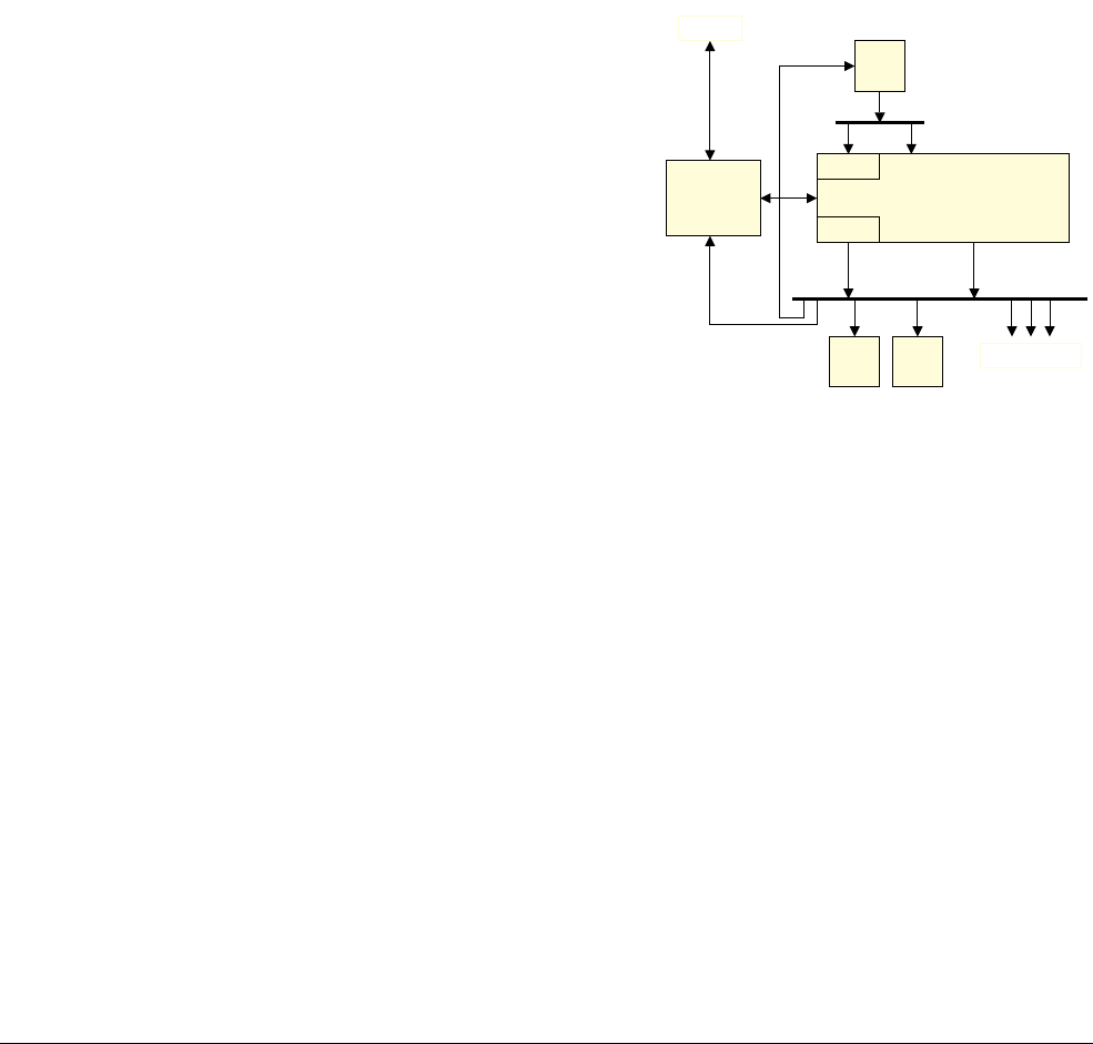
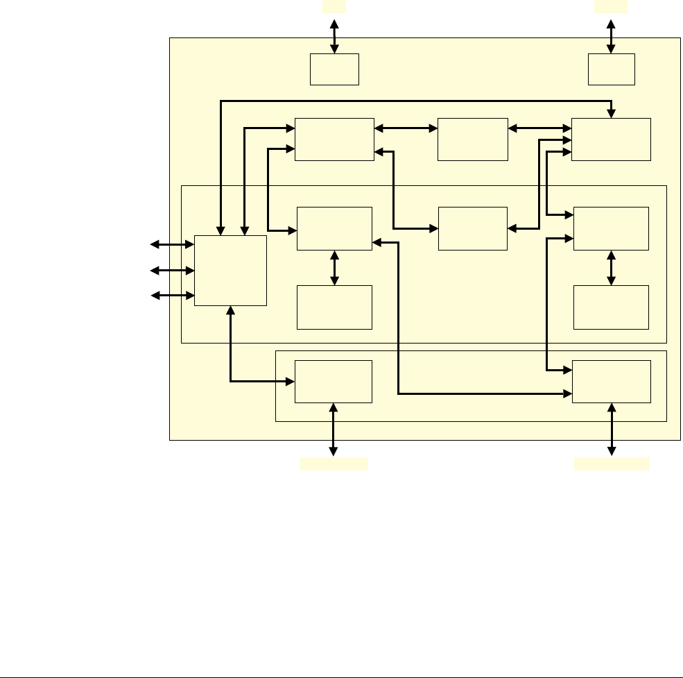
Figure 2-1 Processor block diagram
The PreFetch Unit (PFU) fetches instructions from the memory system, predicts branches, and
passes instructions to the Data Processing Unit (DPU). The DPU executes all instructions and
uses the Load/Store Unit (LSU) for data memory transfers. The PFU and LSU interface to the
L1 memory system that contains L1 instruction and data caches and an interface to a L2 system.
The L1 memory can also contain optional TCM interfaces.
Processor
Level two interface
Level one memory system
AXI master bus
AXI slave bus
L2 interface
AXI
master port
Data
Processing
Unit
Memory
Protection
Unit
Prefetch Unit Load/Store
Unit
L2 interface
AXI
slave port
Tightly-
Coupled
Memory
(TCM)
interface
B0TCM
B1TCM
ATCM
L1
instruction
cache control
L1
instruction
cache RAM
L1
data cache
control
L1
data
cache RAM
Debug
Debug
interface
ETM
ETM
interface

Functional Description
ARM DDI 0363G Copyright © 2006-2011 ARM Limited. All rights reserved. 2-3
ID041111 Non-Confidential
2.1.1 Data Processing Unit
The DPU holds most of the program-visible state of the processor, such as general-purpose
registers, status registers and control registers. It decodes and executes instructions, operating
on data held in the registers in accordance with the ARM architecture. Instructions are fed to the
DPU from the PFU through a buffer. The DPU performs instructions that require data to be
transferred to or from the memory system by interfacing to the LSU. See Chapter 3
Programmers Model for more information.
Floating Point Unit
The Floating Point Unit (FPU) is an optional part of the DPU that includes the VFP register file
and status registers. It performs floating-point operations on the data held in the VFP register
file. See Chapter 11 FPU Programmers Model for more information.
2.1.2 Load/store unit
The LSU manages all load and store operations, interfacing with the DPU to the TCMs, caches,
and L2 memory interfaces.
2.1.3 Prefetch unit
The PFU obtains instructions from the instruction cache, the TCMs, or from external memory
and predicts the outcome of branches in the instruction stream. See Chapter 5 Prefetch Unit for
more information.
Branch prediction
The branch predictor is a global type that uses history registers and a 256-entry pattern history
table.
Return stack
The PFU includes a 4-entry return stack to accelerate returns from procedure calls. For each
procedure call, the return address is pushed onto a hardware stack. When a procedure return is
recognized, the address held in the return stack is popped, and the prefetch unit uses it as the
predicted return address.
2.1.4 L1 memory system
The processor L1 memory system includes the following features:
• separate instruction and data caches
• flexible TCM interfaces
• 64-bit datapaths throughout the memory system
• MPU that supports configurable memory region sizes
• export of memory attributes for L2 memory system
• parity or ECC supported on local memories.
For more information about the blocks in the L1 memory system, see:
•Instruction and data caches on page 2-4
•Memory Protection Unit on page 2-4
•TCM interfaces on page 2-4
•Error correction and detection on page 2-4.

Functional Description
ARM DDI 0363G Copyright © 2006-2011 ARM Limited. All rights reserved. 2-4
ID041111 Non-Confidential
Instruction and data caches
You can configure the processor to include separate instruction and data caches. The caches
have the following features:
• Support for independent configuration of the instruction and data cache sizes between
4KB and 64KB.
• Pseudo-random cache replacement policy.
• 8-word cache line length. Cache lines can be either write-back or write-through,
determined by MPU region.
• Ability to disable each cache independently.
• Streaming of sequential data from
LDM
and
LDRD
operations, and sequential instruction
fetches.
• Critical word first filling of the cache on a cache miss.
• Implementation of all the cache RAM blocks and the associated tag and valid RAM
blocks using standard ASIC RAM compilers.
• Parity or ECC supported on local memories.
Memory Protection Unit
An optional MPU provides memory attributes for embedded control applications. You can
configure the MPU to have eight or twelve regions, each with a minimum resolution of 32 bytes.
MPU regions can overlap, and the highest numbered region has the highest priority.
The MPU checks for protection and memory attributes, and some of these can be passed to an
external L2 memory system.
For more information, see Chapter 7 Memory Protection Unit.
TCM interfaces
There are two Tightly-Coupled Memory (TCM) interfaces that permit connection to
configurable blocks of TCM (ATCM and BTCM). These ensure high-speed access to code or
data. As an option, the BTCM can have two memory ports for increased bandwidth.
An ATCM typically holds interrupt or exception code that must be accessed at high speed,
without any potential delay resulting from a cache miss.
A BTCM typically holds a block of data for intensive processing, such as audio or video
processing.
The TCMs are external to the processor. This provides flexibility in optimizing the TCM
subsystem for performance, power, and RAM type. The INITRAMA and INITRAMB pins
enable booting from the ATCM or BTCM, respectively. Both the ATCM and BTCM support
wait states.
For more information, see Chapter 8 Level One Memory System.
Error correction and detection
To increase the tolerance of the system to soft memory faults, you can configure the caches for
either:
• parity generation and error correction/detection

Functional Description
ARM DDI 0363G Copyright © 2006-2011 ARM Limited. All rights reserved. 2-5
ID041111 Non-Confidential
• ECC code generation, single-bit error correction, and two-bit error detection.
Similarly, you can configure the TCM interfaces for:
• parity generation and error detection
• ECC code generation, single-bit error correction, and two-bit error detection.
For more information, see Chapter 8 Level One Memory System.
2.1.5 L2 AXI interfaces
The L2 AXI interfaces enable the L1 memory system to have access to peripherals and to
external memory using an AXI master and AXI slave port.
AXI master interface
The AXI master interface provides a high bandwidth interface to second level caches, on-chip
RAM, peripherals, and interfaces to external memory. It consists of a single AXI port with a
64-bit read channel and a 64-bit write channel for instruction and data fetches.
The AXI master can run at the same frequency as the processor, or at a lower synchronous
frequency. If asynchronous clocking is required an external asynchronous AXI slice is required.
AXI slave interface
The AXI slave interface enables AXI masters, including the AXI master port of the processor,
to access data and instruction cache RAMs and TCMs through the AXI system bus. You can use
this for DMA into and out of the TCM RAMs and for software test of the cache RAMs.
The slave interface can run at the same frequency as the processor or at a lower, synchronous
frequency. If asynchronous clocking is required an external asynchronous AXI slice is required.
Bits in the Auxiliary Control Register and Slave Port Control Register can control access to the
AXI slave. Access to the TCM RAMs can be granted to any master, to only privileged masters,
or completely disabled. Access to the cache RAMs can be separately controlled in a similar way.
2.1.6 Debug
The processor has a CoreSight compliant Advanced Peripheral Bus version 3 (APBv3) debug
interface. This permits system access to debug resources, for example, the setting of
watchpoints and breakpoints.
The processor provides extensive support for real-time debug and performance profiling.
The following sections give an overview of debug:
•System performance monitoring
•ETM interface
•Real-time debug facilities on page 2-6.
System performance monitoring
This is a group of counters that you can configure to monitor the operation of the processor and
memory system. For more information, see About the PMU on page 6-6.
ETM interface
The Embedded Trace Macrocell (ETM) interface enables you to connect an external ETM unit
to the processor for real-time code tracing of the core in an embedded system.

Functional Description
ARM DDI 0363G Copyright © 2006-2011 ARM Limited. All rights reserved. 2-6
ID041111 Non-Confidential
The ETM interface collects various processor signals and drives these signals from the
processor. The interface is unidirectional and runs at the full speed of the processor. The ETM
interface connects directly to the external ETM unit without any additional glue logic. You can
disable the ETM interface for power saving. For more information, see the CoreSight ETM-R4
Technical Reference Manual.
Real-time debug facilities
The processor contains debug logic, that can be used in a CoreSight system to support the debug
operation. It supports:
• up to eight breakpoints
• up to eight watchpoints
•a Debug Communications Channel (DCC).
Note
The number of breakpoints and watchpoints is configured during implementation, see
Configurable options on page 1-6.
The debug logic monitors the internal address and data buses. You access the debug logic
through the memory-mapped APB interface.
The processor implements the ARMv7 Debug architecture.
See Chapter 12 Debug for more information on debug.
The debug logic supports two modes of debug operation:
Halting debug-mode
On a debug event, such as a breakpoint or watchpoint, the debug logic stops the
processor and forces it into debug state. This enables you to examine the internal
state of the processor, and the external state of the system, independently from
other system activity. When the debugging process completes, the processor and
system state are restored, and normal program execution resumes.
Monitor debug-mode
On a debug event, the processor generates a debug exception instead of entering
debug state, as in halting debug-mode. The exception entry enables a debug
monitor program to debug the processor while enabling critical interrupt service
routines to operate on the processor. The debug monitor program can
communicate with the debug host over the DCC or any other communications
interface in the system.
2.1.7 System control coprocessor
The system control coprocessor provides configuration and control of the memory system and
its associated functionality. Other system-level operations, such as cache maintenance
operations, are also managed through the system control coprocessor.
For more information, see System identification control and configuration on page 4-2.
2.1.8 Interrupt handling
Interrupt handling in the processor is compatible with previous ARM architectures, but has
several additional features to improve interrupt performance for real-time applications.

Functional Description
ARM DDI 0363G Copyright © 2006-2011 ARM Limited. All rights reserved. 2-7
ID041111 Non-Confidential
VIC port
The core has a dedicated port that enables an external interrupt controller, such as the ARM
PrimeCell Vectored Interrupt Controller (VIC), to supply a vector address along with an
Interrupt Request (IRQ) signal. This provides faster interrupt entry, but you can disable it for
compatibility with earlier interrupt controllers.
Note
If you do not have a VIC in your design, you must ensure the nIRQ and nFIQ signals are
asserted, held LOW, and remain LOW until the exception handler clears them.
Low interrupt latency
On receipt of an interrupt, the processor abandons any pending restartable memory operations.
Restartable memory operations are the multiword transfer instructions
LDM
,
LDRD
,
STRD
,
STM
,
PUSH
,
and
POP
that can access Normal memory.
To minimize the interrupt latency, ARM recommends that you do not perform:
• multiple accesses to areas of memory marked as Device or Strongly-ordered
• SWP operations to slow areas of memory.
Exception processing
The ARMv7-R architecture contains exception processing instructions to reduce interrupt
handler entry and exit time:
SRS Save return state to a specified stack frame.
RFE Return from exception using data from the stack.
CPS Change processor state, such as interrupt mask setting and clearing, and mode
changes.
2.1.9 Power management
The processor includes several microarchitectural features to reduce energy consumption:
• Accurate branch and return prediction, reducing the number of incorrect instruction fetch
and decode operations.
• The caches use sequential access information to reduce the number of accesses to the tag
RAMs and to unmatched data RAMs.
• Extensive use of gated clocks and gates to disable inputs to unused functional blocks.
Because of this, only the logic actively in use to perform a calculation consumes any
dynamic power.
The processor uses four levels of power management:
Run mode This mode is the normal mode of operation where all of the functionality
of the processor is available.
Dormant mode The processor can be implemented in such a way as to support Dormant
mode. Dormant mode is a power saving mode in which the processor
logic, but not the TCM and cache RAMs, is powered down. The processor
state, apart from the cache and TCM state, is stored to memory before
entry into Dormant mode, and restored after exit. For more information on
preparing the Cortex-R4 to support Dormant mode, contact ARM.

Functional Description
ARM DDI 0363G Copyright © 2006-2011 ARM Limited. All rights reserved. 2-8
ID041111 Non-Confidential
Shutdown mode This mode has the entire device powered down. All state, including cache
and TCM state, must be saved externally. After power-up, the assertion of
reset returns the processor to the run state.
Standby mode This mode disables most of the clocks of the device, while keeping the
device powered up. This reduces the power drawn to the static leakage
current and the minimal clock power overhead required to enable the
device to wake up from the Standby mode.
For more information on the power management features, see Chapter 10 Power Control.

Functional Description
ARM DDI 0363G Copyright © 2006-2011 ARM Limited. All rights reserved. 2-9
ID041111 Non-Confidential
2.2 Interfaces
The processor has the following interfaces for external access:
•AXI master interface
•AXI slave interface
•TCM interfaces
•Interrupt and VIC interface
•Configuration interface
•Interrupt and event outputs
•APB Debug interface
•ETM interface on page 2-10
•Test interface on page 2-10.
2.2.1 AXI master interface
AXI master interface on page 9-3 describes the AXI master interface. AXI master port on
page A-8 and AXI master port error detection signals on page A-10 describe the associated
signals. The AMBA AXI Protocol Specification describes the AXI protocol.
2.2.2 AXI slave interface
AXI slave interface on page 9-20 describes the AXI slave interface. AXI slave port on page A-11
and AXI slave port error detection signals on page A-12 describe the associated signals. The
AMBA AXI Protocol Specification describes the AXI protocol.
2.2.3 TCM interfaces
About the TCMs on page 8-13 describes the TCM interfaces. TCM interface signals on
page A-13 describes the associated signals.
2.2.4 Interrupt and VIC interface
Interrupts on page 3-16 describes the interrupts. Interrupt signals, including VIC interface
signals on page A-7 describes the associated signals.
2.2.5 Configuration interface
Configuration signals on page A-4 describes the configuration signals.
2.2.6 Interrupt and event outputs
Chapter 6 Events and Performance Monitor describes events and the interrupts they can
generate. Exceptions on page 11-14 describes the FPU exception outputs. Interrupt signals,
including VIC interface signals on page A-7, ETM interface signals on page A-19, Validation
signals on page A-22, and FPU signals on page A-23 describe the associated signals.
2.2.7 APB Debug interface
AMBA APBv3 is used for debugging purposes. CoreSight is the ARM architecture for
multi-processor trace and debug. CoreSight defines what debug and trace components are
required and how they are connected. See the CoreSight Architecture Specification for more
information. Debug interface signals on page A-17 describes the debug APB interface signals.

Functional Description
ARM DDI 0363G Copyright © 2006-2011 ARM Limited. All rights reserved. 2-10
ID041111 Non-Confidential
Note
The APB debug interface can also connect to a DAP-Lite. For more information on the
DAP-Lite, see the CoreSight DAP-Lite Technical Reference Manual.
2.2.8 ETM interface
You can connect an ETM-R4 to the processor through the ETM interface. The ETM-R4
provides instruction and data trace for the processor. The CoreSight ETM-R4 Technical
Reference Manual describes how the ETM-R4 connects to the processor.
The ETM interface includes these signals:
• an instruction interface
• a data interface
• an event interface
• other connections to the ETM.
ETM interface signals on page A-19 describes the associated signals. Event bus interface on
page 6-19 describes the event bus.
2.2.9 Test interface
The test interface provides support for test during manufacture of the processor using Memory
Built-In Self Test (MBIST). MBIST signals on page A-21 describes the test interface signals.

Functional Description
ARM DDI 0363G Copyright © 2006-2011 ARM Limited. All rights reserved. 2-11
ID041111 Non-Confidential
2.3 Clocking and resets
Before you can run application software on the processor, it must be reset and initialized,
including loading the appropriate software-configuration. This section describes the signals for
clocking and resetting the processor. It contains the following sections:
•Resets
•Reset modes
•Clocking on page 2-13.
See Initialization on page 2-15 for information on software initialization.
2.3.1 Resets
The processor has the following reset inputs:
nRESET This signal is the main processor reset that initializes the majority of the
processor logic.
PRESETDBGn This signal resets processor debug logic.
nSYSPORESET This signal is the reset that initializes the entire processor and all its
interfaces, including CP14 debug logic and the APB debug logic. See
CP14 registers reset on page 11-23 for information.
nCPUHALT This signal stops the processor from fetching instructions after reset.
All of these are active-LOW signals that reset logic in the processor. You must take care when
designing the logic to drive these reset signals.
The processor synchronizes the resets to the relevant clock domains internally.
2.3.2 Reset modes
The reset signals in the processor enable you to reset different parts of the design independently.
Table 2-1 shows the reset signals, and the combinations and possible applications that you can
use them in.
All reset signals are synchronized within the processor. You do not have to synchronize either
edge of any of the reset signals. Unless otherwise stated, whenever nRESET is asserted, it must
be held asserted for at least four CLKIN cycles to ensure correct reset operation.
Table 2-1 Reset modes
Reset mode nRESET PRESETDBGn nSYSPORESET nCPUHALT Application
Power-on reset 0 x 0 x Reset at power up, full system
reset. Hard reset or cold reset.
Processor reset 0 x 1 x Reset of processor only,
watchdog reset. Soft reset or
warm reset.
Normal 1 x 1 1 Normal run mode.
Halt 1 x 1 0 Halting debug-mode,
provided normal mode has
not been entered since reset.
Debug reset x 0 x x Resets all debug logic and the
debug APB interface.
Functional Description
ARM DDI 0363G Copyright © 2006-2011 ARM Limited. All rights reserved. 2-12
ID041111 Non-Confidential
Note
Whenever nSYSPORESET is asserted, nRESET must also be asserted. The processor will not
be correctly reset otherwise.
This section of the manual describes:
•Power-on reset
•Processor reset
•Normal operation
•Halt operation.
Power-on reset
You must apply power-on or cold reset to the processor when power is first applied to the
system. In the case of power-on reset, the leading, or falling, edge of the reset signals, nRESET
and nSYSPORESET, does not have to be synchronous to CLKIN. Because the nRESET and
nSYSPORESET signals are synchronized within the processor, you do not have to synchronize
these signals. Figure 2-2 shows the application of power-on reset.
Figure 2-2 Power-on reset
ARM recommends that you assert the nRESET signal for at least four CLKIN cycles to ensure
correct reset behavior.
It is not necessary to assert PRESETDBGn on power-up.
Processor reset
A processor or warm reset initializes the majority of the processor, excluding the CoreSight
logic. Processor reset is typically used for resetting a system that is operating for some time, for
example, watchdog reset.
Because the nRESET signal is synchronized within the processor, you do not have to
synchronize this signal. ARM recommends that you assert the nReset signal for at least four
CLKIN cycles to ensure correct reset behavior.
Normal operation
During normal operation, neither processor reset nor power-on reset is asserted. If CoreSight
logic is not used, the value of PRESETDBGn does not matter.
Halt operation
When nCPUHALT is asserted, and nSYSPORESET and nRESET deasserted, the processor
is out of reset, but the PFU is inhibited from fetching instructions. For example, you can use
nCPUHALT to enable DMA into the TCMs using the processor. You can then deassert
nCPUHALT and the PFU starts fetching instructions from TCMs. When the processor has
started fetching, nCPUHALT must not be asserted again except when the processor is reset.
CLKIN
nRESET
nSYSPORESET

Functional Description
ARM DDI 0363G Copyright © 2006-2011 ARM Limited. All rights reserved. 2-13
ID041111 Non-Confidential
2.3.3 Clocking
The processor has two functional clock inputs. Externally to the processor, you must connect
together CLKIN and FREECLKIN.
In addition, there is the PCLKDBG clock for the debug APB bus. This is asynchronous to the
main clock.
All clocks can be stopped indefinitely without loss of state.
Three additional clock inputs, CLKIN2, DUALCLKIN, and DUALCLKIN2, are related to
the dual-redundant core functionality, if included. If you are integrating a Cortex-R4 macrocell
with dual-redundant core, contact the implementer of that macrocell for information about how
to connect the clock inputs.
The following is described in this section:
•AMBA interface clocking
•Clock gating.
AMBA interface clocking
The AXI master and slave interfaces must be connected to AXI systems that are synchronous to
the processor clock, CLKIN, even if this might be at a lower frequency. This means that every
rising edge on the AXI system clock must be synchronous to a rising edge on CLKIN.
The AXI master interface clock enable signal ACLKENM and the AXI slave interface clock
enable signal ACLKENS must be asserted on every CLKIN rising edge for which there is a
simultaneous rising edge on the AXI system clock.
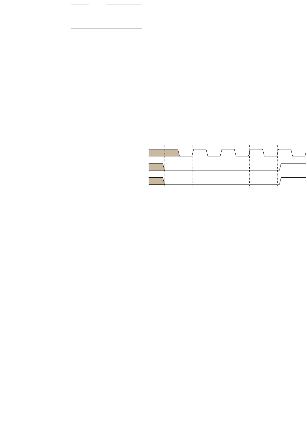
Figure 2-3 shows an example in which the processor is clocked at 400MHz (CLKIN), while the
AXI system connected to the AXI master interface is clocked at 200MHz (ACLKM). The
ACLKENM clock indicates the relationship between the two clocks.
Figure 2-3 AXI interface clocking
If the AMBA system connected to an interface is clocked at the same frequency as the processor,
then the corresponding clock enable signal must be tied HIGH.
Clock gating
In Standby mode the processor can gate its own clock to save power. See Chapter 10 Power
Control for more information about Standby mode. You can use the STANDBYWFI output to
gate the clock to the TCMs when the processor is gating its own clock in Standby mode. If you
do, you must design the logic so that the TCM clock starts running within four cycles of
STANDBYWFI going LOW.
Figure 2-4 on page 2-14 shows an example of an ATCM access occurring immediately after the
processor exits Standby mode. STANDBYWFI indicates when the processor internal clock,
shown as CPU_CLK, is restarted. The clock to the ATCM, shown as ATCM_CLK, is gated
off in Standby mode. It is restarted by the third cycle to enable the ATCM to assert ATCEN0 in
response to the access that the processor presents. This example shows the worst-case, that is,
the earliest TCM access that the processor can generate after exiting Standby mode.
ACLKM
ACLKENM
CLKIN

Functional Description
ARM DDI 0363G Copyright © 2006-2011 ARM Limited. All rights reserved. 2-14
ID041111 Non-Confidential
Figure 2-4 Standby, wake-up
STANDBYWFI
CPU_CLK
CLKIN
ATCEN0
ATCM_CLK

Functional Description
ARM DDI 0363G Copyright © 2006-2011 ARM Limited. All rights reserved. 2-15
ID041111 Non-Confidential
2.4 Operation
When you power-up the Cortex-R4 processor, you must first reset it. See Clocking and resets
on page 2-11. When it is out of reset, and no longer halted, it starts to fetch and execute
instructions from the reset vector and according to the instruction set. See Reset on page 3-16.
The processor initially fetches instructions from, and transfers data to and from either the TCM
interfaces or the L2 memory interfaces.
The processor also responds to stimulus received on its interfaces, for example interrupts, or
transactions received on the AXI slave interface.
2.4.1 Initialization
Most of the architectural registers in the processor, such as r0-r14, and s0-s31 and d0-d15 when
floating-point is included, are not reset. Because of this, you must initialize these for all modes
before they are used, using an immediate-MOV instruction, or a PC-relative load instruction.
The Current Program Status Register (CPSR) is given a known value on reset. See the ARM
Architecture Reference Manual for more information. The reset values for the CP15 registers
are described along with the registers in Chapter 4 System Control.
In addition, before you run the application, you might want to:
• program particular values into various registers, for example, stack pointers
• enable various processor features, for example, error correction
• program particular values into memory, for example, the TCMs.
The following sections describe other initialization requirements:
•MPU
•FPU
•Caches on page 2-16
•TCM on page 2-16.
MPU
If the processor is built with an MPU, before you can use it you must:
• program and enable at least one of the regions
• enable the MPU in the System Control Register, see c1, System Control Register on
page 4-37.
See c6, MPU memory region programming registers on page 4-51. Do not enable the MPU
unless at least one MPU region is programmed and active. If the MPU is enabled, before using
the TCM interfaces you must program MPU regions to cover the TCM regions to give access
permissions to them.
FPU
If the processor is built with a Floating Point Unit (FPU) you must enable it before VFP
instructions can be executed:
• enable access to the FPU in the coprocessor access control register, see c1, Coprocessor
Access Register on page 4-46
• enable the FPU by setting the EN-bit in the FPEXC register, see Floating-Point Exception
Register, FPEXC on page 11-8.

Functional Description
ARM DDI 0363G Copyright © 2006-2011 ARM Limited. All rights reserved. 2-16
ID041111 Non-Confidential
Note
Floating-point logic is only available with the Cortex-R4F processor.
Caches
If the processor is built with instruction or data caches, these must be invalidated before they are
enabled, otherwise unpredictable behavior can occur. See Cache operations on page 4-58.
If you are using an error checking scheme in the cache, you must enable this by programming
the Auxiliary Control Register, see c1, Auxiliary Control Register on page 4-40, before
invalidating the cache, to ensure that the correct error code or parity bits are calculated when the
cache is invalidated. An invalidate all operation never reports any ECC or parity errors.
TCM
The processor does not initialize the TCM RAMs. It is not essential to initialize all the memory
attached to the TCM interface but ARM recommends that you do. In addition, the main
application might require you to preload instructions or data into the TCM. This section
describes various ways that you can perform data preloading. You can also configure the
processor to use the TCMs from reset.
Preloading TCMs
You can write data to the TCMs using either store instructions or the AXI slave interface.
Depending on the method you choose, you might require:
• particular hardware on the SoC that you are using
• boot code
• a debugger connected to the processor.
Methods to preload TCMs include:
Memory copy with running boot code
The boot code includes a memory copy routine that reads data from a ROM, and
writes it into the appropriate TCM. You must enable the TCM to do this, and it
might be necessary to give the TCM one base address while the copy is occurring,
and a different base address when the application is being run.
Copy data from the debug communications channel
The boot code includes a routine to read data from the Debug Communications
Channel (DCC) and write it into the TCM. The debug host feeds the data for this
operation into the DCC by writing to the appropriate registers on the processor
APB debug port.
Execute code in debug halt state
The processor is put into debug halt state by the debug host, that then feeds
instructions into the processor through the Instruction Transfer Register
(DBGITR). The processor executes these instructions, that replace the boot code
in either of the two methods described previously in this list.
DMA into TCM
The SoC includes a Direct Memory Access (DMA) device that reads data from a
ROM, and writes it to the TCMs through the AXI slave interface.

Functional Description
ARM DDI 0363G Copyright © 2006-2011 ARM Limited. All rights reserved. 2-17
ID041111 Non-Confidential
Write to TCM directly from debugger
A Debug Access Port (DAP) in the system is used to generate AMBA
transactions to write data into the TCMs through the AXI slave interface. This
DAP is controlled from the debug host through a JTAG chain.
Preloading TCMs with parity or ECC
The error codes or parity bits in the TCM RAM, if configured with an error scheme, are not
initialized by the processor. Before a RAM location is read with ECC or parity checking
enabled, the error codes or parity bits must be initialized. To calculate the error code or parity
bits correctly, the logic must have all the data in the data chunk that those bits protect. Therefore,
when the TCM is being initialized, the writes must be of the same width and aligned to the data
chunk that the error scheme protects.
You can initialize the TCM RAM with error checking turned on or off, according to the
following rules. See c1, Auxiliary Control Register on page 4-40. The error code or parity bits
written to the TCM are valid for the data provided, even if the error checking is turned off.
If you initialize the TCM using the slave port, you must use write transactions to write to the
TCM memory as follows:
• If the error scheme is parity, any write transaction can be used.
• If the error scheme is 32-bit ECC, the write transaction must start at a 32-bit aligned
addresses and write a continuous block of memory, containing a multiple of 4 bytes. All
bytes in the block must be written, that is, have their byte lane strobe asserted.
• If the error scheme is 64-bit ECC, the write transaction must start at a 64-bit aligned
addresses and write a continuous block of memory, containing a multiple of 8 bytes. All
bytes in the block must be written, that is, have their byte lane strobe asserted.
If initialization is done by running code on the processor, this is best done by a loop of stores
that write to the whole of the TCM memory as follows:
• If the error scheme is parity, or no error scheme, any store instruction can be used.
• If the scheme is 32-bit ECC, use Store Word (STR), Store Two Words (STRD), or Store
Multiple Words (STM) instructions to 32-bit aligned addresses.
• If the scheme is 64-bit ECC, use
STRD
or
STM
that has an even number of registers in the
register list, with a 64-bit aligned starting address.
Note
You can use the alignment-checking features of the processor to help you ensure that memory
accesses are 32-bit aligned, but there is no checking for 64-bit alignment. If you are using
STRD
or
STM
, an alignment fault is generated if the address is not 32-bit aligned. For the same behavior
with
STR
instructions, enable strict-alignment-checking by setting the A-bit in the SCTLR. See
c1, System Control Register on page 4-37.
If the error scheme is 64-bit ECC, a simpler way to initialize the TCM is:
• Ensure error checking is off.
• Turn on 64-bit store behavior using CP15. See c15, Secondary Auxiliary Control Register
on page 4-43.
• Write to the TCM using any store instructions, or any AXI write transactions. The
processor performs read-modify-write accesses to ensure that all writes are to 64-bit
aligned quantities, even though error checking is turned off.

Functional Description
ARM DDI 0363G Copyright © 2006-2011 ARM Limited. All rights reserved. 2-18
ID041111 Non-Confidential
Note
You can enable error checking and 64-bit store behavior on a per-TCM interface basis.
References to these controls relate to whichever TCM is being initialized.
Using TCMs from reset
The processor can be pin-configured to enable the TCM interfaces from reset, and to select the
address at which each TCM appears from reset. See TCM initialization on page 8-16 for more
information. This enables you to configure the processor to boot from TCM but, to do this, the
TCM must first be preloaded with the boot code. The nCPUHALT pin can be asserted while
the processor is in reset to stop the processor from fetching and executing instructions after
coming out of reset. While the processor is halted in this way, the TCMs can be preloaded with
the appropriate data. When the nCPUHALT pin is deasserted, the processor starts fetching
instructions from the reset vector address in the normal way.
Note
When it is deasserted to start the processor fetching, nCPUHALT must not be asserted again
except when the processor is under processor or power-on reset, that is, nRESET asserted. The
processor does not halt if the nCPUHALT pin is asserted while the processor is running.

ARM DDI 0363G Copyright © 2006-2011 ARM Limited. All rights reserved. 3-1
ID041111 Non-Confidential
Chapter 3
Programmers Model
This chapter describes the processor registers and provides an overview for programming the
microprocessor. It contains the following sections:
•About the programmers model on page 3-2
•Modes of operation and execution on page 3-3
•Memory model on page 3-4
•Data structures on page 3-5
•Registers on page 3-6
•Program status registers on page 3-9
•Exceptions on page 3-14
•Acceleration of execution environments on page 3-25
•Unaligned and mixed-endian data access support on page 3-26
•Big-endian instruction support on page 3-27.

Programmers Model
ARM DDI 0363G Copyright © 2006-2011 ARM Limited. All rights reserved. 3-2
ID041111 Non-Confidential
3.1 About the programmers model
The processor implements the ARMv7-R architecture that provides:
• the 32-bit ARM instruction set
• the extended Thumb instruction set introduced in ARMv6T2, that uses Thumb-2
technology to provide a wide range of 32-bit instructions.
For more information on the ARM and Thumb instruction sets, see the ARM Architecture
Reference Manual. This chapter describes some of the main features of the architecture but, for
a complete description, see the ARM Architecture Reference Manual.
This chapter also makes reference to older versions of the ARM architecture that the processor
does not implement. These references are included to contrast the behavior of the Cortex-R4
processor with other processors you might have used that implement an older version of the
architecture.

Programmers Model
ARM DDI 0363G Copyright © 2006-2011 ARM Limited. All rights reserved. 3-3
ID041111 Non-Confidential
3.2 Modes of operation and execution
This section describes:
•Instruction set states
•Operating modes.
3.2.1 Instruction set states
The processor has two instruction set states:
ARM state The processor executes 32-bit, word-aligned ARM instructions in this
state.
Thumb state The processor executes 32-bit and 16-bit halfword-aligned Thumb
instructions in this state.
Note
Transition between ARM state and Thumb state does not affect the processor mode or the
register contents.
Switching state
The instruction set state of the processor can be switched between ARM state and Thumb state:
• Using the
BX
and
BLX
instructions, by a load to the PC, or with a data-processing instruction
that does not set flags, with the PC as the destination register. Switching state is described
in the ARM Architecture Reference Manual.
Note
When the
BXJ
instruction is used the processor invokes the
BX
instruction.
• Automatically on an exception. You can write an exception handler routine in ARM or
Thumb code. For more information, see Exceptions on page 3-14.
Interworking ARM and Thumb state
The processor enables you to mix ARM and Thumb code. For more information about
interworking ARM and Thumb, see the RealView Compilation Tools Developer Guide.
3.2.2 Operating modes
In each state there are seven modes of operation:
•User (USR) mode is the usual mode for the execution of ARM or Thumb programs. It is
used for executing most application programs.
•Fast interrupt (FIQ) mode is entered on taking a fast interrupt.
•Interrupt (IRQ) mode is entered on taking a normal interrupt.
•Supervisor (SVC) mode is a protected mode for the operating system and is entered on
taking a Supervisor Call (
SVC
), formerly
SWI
.
•Abort (ABT) mode is entered after a data or instruction abort.
•System (SYS) mode is a privileged user mode for the operating system.
•Undefined (UND) mode is entered when an Undefined Instruction exception occurs.
Modes other than User mode are collectively known as Privileged modes. Privileged modes are
used to service interrupts or exceptions, or access protected resources.
Programmers Model
ARM DDI 0363G Copyright © 2006-2011 ARM Limited. All rights reserved. 3-4
ID041111 Non-Confidential
3.3 Memory model
The processor views memory as a linear collection of bytes numbered in ascending order from
zero. For example, bytes 0-3 hold the first stored word, and bytes 4-7 hold the second stored
word.
The processor can treat words of data in memory as being stored in either:
•Byte-invariant big-endian format
•Little-endian format.
Additionally, the processor supports mixed-endian and unaligned data accesses. For more
information, see the ARM Architecture Reference Manual.
3.3.1 Byte-invariant big-endian format
In byte-invariant big-endian (BE-8) format, the processor stores the most significant byte of a
word at the lowest-numbered byte, and the least significant byte at the highest-numbered byte.
Figure 3-1 shows byte-invariant big-endian (BE-8) format.
Figure 3-1 Byte-invariant big-endian (BE-8) format
3.3.2 Little-endian format
In little-endian format, the lowest-numbered byte in a word is the least significant byte of the
word and the highest-numbered byte is the most significant. Figure 3-2 shows little-endian
format.
Figure 3-2 Little-endian format
Memory Register
Address
A[31:0]
+1
msbyte
lsbyte
+2
+3
B0
07
B1
B3B2B0 B1
31 24 23 16 15 8 7 0
B2
B3
Memory Register
Address
A[31:0]
+1
msbyte
lsbyte
+2
+3
b0
07
b1
b0b1b3 b2
31 24 23 16 15 8 7 0
b2
b3

Programmers Model
ARM DDI 0363G Copyright © 2006-2011 ARM Limited. All rights reserved. 3-5
ID041111 Non-Confidential
3.4 Data structures
The processor supports these data types:
• doubleword, 64-bit
• word, 32-bit
• halfword, 16-bit
• byte, 8-bit.
Note
• When any of these types are described as unsigned, the N-bit data value represents a
non-negative integer in the range 0 to +2N-1, using normal binary format.
• When any of these types are described as signed, the N-bit data value represents an integer
in the range -2N-1 to +2N-1-1, using two’s complement format.
For best performance you must align these data types in memory as follows:
• doubleword quantities aligned to 8-byte boundaries, doubleword aligned
• word quantities aligned to 4-byte boundaries, word aligned
• halfword quantities aligned to 2-byte boundaries halfword aligned
• byte quantities can be placed on any byte boundary.
The processor supports mixed-endian and unaligned access. For more information, see
Unaligned and mixed-endian data access support on page 3-26.
Note
You cannot use
LDRD
,
LDM
,
STRD
, or
STM
instructions to access 32-bit quantities if they are not
32-bit aligned.

Programmers Model
ARM DDI 0363G Copyright © 2006-2011 ARM Limited. All rights reserved. 3-6
ID041111 Non-Confidential
3.5 Registers
The processor has a total of 37 program registers:
• 31 general-purpose 32-bit registers
• six 32-bit status registers.
These registers are not all accessible at the same time. The processor state and operating mode
determine the registers that are available to the programmer.
3.5.1 The register set
In the processor the same register set is used in both the ARM and Thumb states. Sixteen general
registers and one or two status registers are accessible at any time. In Privileged modes,
alternative mode-specific banked registers become available. Figure 3-3 on page 3-8 shows the
registers that are available in each mode.
The register set contains 16 directly-accessible registers, R0-R15. Another register, the Current
Program Status Register (CPSR), contains condition code flags, status bits, and current mode
bits. Registers R0-R12 are general-purpose registers that hold either data or address values.
Registers R13, R14, R15, and the CPSR have these special functions:
Stack pointer Software normally uses register R13 as a Stack Pointer (SP). The
SRS
and
RFE
instructions use Register R13.
Link Register Register R14 is used as the subroutine Link Register (LR).
Register R14 receives the return address when a Branch with Link (
BL
or
BLX
) instruction is executed.
You can use R14 as a general-purpose register at all other times. The
corresponding banked registers R14_svc, R14_irq, R14_fiq, R14_abt, and
R14_und similarly hold the return values when interrupts and exceptions
are taken, or when
BL
or
BLX
instructions are executed within interrupt or
exception routines.
Program Counter Register R15 holds the PC:
• in ARM state this is word-aligned
• in Thumb state this is halfword-aligned.
Note
There are special cases for reading R15:
• reading the address of the current instruction plus, either:
— 4 in Thumb state
— 8 in ARM state.
• reading
0x00000000
(zero).
There are special cases for writing R15:
• causing a branch to the address that was written to R15
• ignoring the value that was written to R15
• writing bits [31:28] of the value that was written to R15 to the
condition flags in the CPSR, and ignoring bits [27:0] (used for the
MRC
instruction only).
You must not assume any of these special cases unless it is explicitly stated
in the instruction description. Instead, you must treat instructions with
register fields equal to R15 as Unpredictable.

Programmers Model
ARM DDI 0363G Copyright © 2006-2011 ARM Limited. All rights reserved. 3-7
ID041111 Non-Confidential
For more information, see the ARM Architecture Reference Manual.
In Privileged modes, another register, the Saved Program Status Register (SPSR), is accessible.
This contains the condition code flags, status bits, and current mode bits saved as a result of the
exception that caused entry to the current mode.
Banked registers have a mode identifier that indicates which mode they relate to. Table 3-1lists
these identifiers.
FIQ mode has seven banked registers mapped to R8–R14 (R8_fiq–R14_fiq). As a result, many
FIQ handlers do not have to save any registers.
The Supervisor, Abort, IRQ, and Undefined modes each have alternative mode-specific
registers mapped to R13 and R14, permitting a private stack pointer and link register for each
mode.
Figure 3-3 on page 3-8 shows the register set, and those registers that are banked.
Table 3-1 Register mode identifiers
Mode Mode identifier
User usra
a. The
usr
identifier is usually
omitted from register
names. It is only used in
descriptions where the User
or System mode register is
specifically accessed from
another operating mode.
Fast interrupt fiq
Interrupt irq
Supervisor svc
Abort abt
System usra
Undefined und

Programmers Model
ARM DDI 0363G Copyright © 2006-2011 ARM Limited. All rights reserved. 3-8
ID041111 Non-Confidential
Figure 3-3 Register organization
Note
For 16-bit Thumb instructions, the high registers, R8–R15, are not part of the standard register
set. You can use special variants of the
MOV
instruction to transfer a value from a low register, in
the range R0–R7, to a high register, and from a high register to a low register. The
CMP
instruction
enables you to compare high register values with low register values. The
ADD
instruction
enables you to add high register values to low register values. For more information, see the
ARM Architecture Reference Manual.
General registers and program counter
System and User
Program status registers
= banked register
Supervisor Abort IRQ Undefined
R0
R1
R2
R3
R4
R5
R6
R7
R8
R9
R10
R11
R12
R13
R14
R15
FIQ
R0
R1
R2
R3
R4
R5
R6
R7
R8_fiq
R9_fiq
R10_fiq
R11_fiq
R12_fiq
R13_fiq
R14_fiq
R15 (PC)
R0
R1
R2
R3
R4
R5
R6
R7
R8
R9
R10
R11
R12
R13_svc
R14_svc
R0
R1
R2
R3
R4
R5
R6
R7
R8
R9
R10
R11
R12
R13_abt
R14_abt
R0
R1
R2
R3
R4
R5
R6
R7
R8
R9
R10
R11
R12
R13_irq
R14_irq
R0
R1
R2
R3
R4
R5
R6
R7
R8
R9
R10
R11
R12
R13_und
R14_und
CPSR CPSR CPSR CPSR CPSR CPSR
SPSR_fiq SPSR_svc SPSR_abt SPSR_irq SPSR_und
R15 (PC) R15 (PC) R15 (PC) R15 (PC)
Programmers Model
ARM DDI 0363G Copyright © 2006-2011 ARM Limited. All rights reserved. 3-9
ID041111 Non-Confidential
3.6 Program status registers
The processor contains one CPSR and five SPSRs for exception handlers to use. The program
status registers:
• hold information about the most recently performed ALU operation
• control the enabling and disabling of interrupts
• set the processor operating mode.
Figure 3-4 shows the program status register bit assignments.
Figure 3-4 Program status register bit assignments
The following sections explain the meanings of these bits:
•The N, Z, C, and V bits
•The Q bit on page 3-10
•The IT bits on page 3-10
•The J bit on page 3-11
•The DNM bits on page 3-11
•The GE bits on page 3-11
•The E bit on page 3-12
•The A bit on page 3-12
•The I and F bits on page 3-12
•The T bit on page 3-12
•The M bits on page 3-13.
•Modification of PSR bits by MSR instructions on page 3-13.
3.6.1 The N, Z, C, and V bits
The N, Z, C, and V bits are the condition code flags. You can optionally set them with arithmetic
and logical operations, and also with
MSR
instructions and
MRC
instructions to R15. The processor
tests these flags in accordance with an instruction's condition code to determine whether to
execute that instruction.
In ARM state, most instructions can execute conditionally on the state of the N, Z, C, and V bits.
The exceptions are:
•
BKPT
•
CPS
•
LDC2
•
MCR2
•
MCRR2
M[4:0]TFIAEIT[7:2]GE[3:0]NJ
Greater than
or equal to
Java state bit
Sticky overflow
Overflow
Carry/Borrow/Extend
Zero
Negative/Less than
Mode bits
Thumb state bit
FIQ disable
IRQ disable
Imprecise abort
disable bit
Data endianness bit
31 30 29 28 27 26 25 24 23 20 19 16 15 10 9 8 7 6 5 4 0
ZCVQ
IT[1:0]
DNM

Programmers Model
ARM DDI 0363G Copyright © 2006-2011 ARM Limited. All rights reserved. 3-10
ID041111 Non-Confidential
•
MRC2
•
MRRC2
•
PLD
•
RFE
•
SETEND
•
SRS
•
STC2
.
In Thumb state, the processor can only execute the Branch instruction conditionally. Other
instructions can be made conditional by placing them in the If-Then (IT) block. For more
information about conditional execution in Thumb state, see the ARM Architecture Reference
Manual.
3.6.2 The Q bit
Certain multiply and fractional arithmetic instructions can set the Sticky Overflow, Q, flag:
•
QADD
•
QDADD
•
QSUB
•
QDSUB
•
SMLAD
•
SMLAxy
•
SMLAWy
•
SMLSD
•
SMUAD
•
SSAT
•
SSAT16
•
USAT
•
USAT16
.
The Q flag is sticky in that, when an instruction sets it, this bit remains set until an
MSR
instruction
writing to the CPSR explicitly clears it. Instructions cannot execute conditionally on the status
of the Q flag.
To determine the status of the Q flag you must read the PSR into a register and extract the Q flag
from this. For information of how the Q flag is set and cleared, see individual instruction
definitions in the ARM Architecture Reference Manual.
3.6.3 The IT bits
IT[7:5] encodes the base condition code for the current IT block, if any. It contains b000 when
no IT block is active.
IT[4:0] encodes the number of instructions that are to be conditionally executed, and whether
the condition for each is the base condition code or the inverse of the base condition code. It
contains b00000 when no IT block is active.
When an IT instruction is executed, these bits are set according to the condition in the
instruction, and the Then and Else (T and E) parameters in the instruction. During execution of
an IT block, IT[4:0] is shifted to:
• reduce the number of instructions to be conditionally executed by one
• move the next bit into position to form the least significant bit of the condition code.

Programmers Model
ARM DDI 0363G Copyright © 2006-2011 ARM Limited. All rights reserved. 3-11
ID041111 Non-Confidential
For more information on the operation of the IT execution state bits, see the ARM Architecture
Reference Manual.
3.6.4 The J bit
The J bit in the CPSR returns 0 when read.
Note
You cannot use an
MSR
to change the J bit in the CPSR.
3.6.5 The DNM bits
Software must not modify the Do Not Modify (DNM) bits. These bits are:
• Readable, to preserve the state of the processor, for example, during process context
switches.
• Writable, to enable the processor to restore its state. To maintain compatibility with future
ARM processors, and as good practice, use a read-modify-write strategy when you
change the CPSR.
3.6.6 The GE bits
Some of the SIMD instructions set GE[3:0] as greater-than-or-equal bits for individual
halfwords or bytes of the result, as Table 3-2 shows.
Table 3-2 GE[3:0] settings
GE[3] GE[2] GE[1] GE[0]
Instruction A op B greater than
or equal to C
A op B greater than
or equal to C
A op B greater
than or equal to C
A op B greater
than or equal to C
Signed
SADD16
[31:16] + [31:16] ≥ 0 [31:16] + [31:16] ≥ 0 [15:0] + [15:0] ≥ 0 [15:0] + [15:0] ≥ 0
SSUB16
[31:16] - [31:16] ≥ 0 [31:16] - [31:16] ≥ 0 [15:0] - [15:0] ≥ 0 [15:0] - [15:0] ≥ 0
SADDSUBX
[31:16] + [15:0] ≥ 0 [31:16] + [15:0] ≥ 0 [15:0] - [31:16] ≥ 0 [15:0] - [31:16] ≥ 0
SSUBADDX
[31:16] - [15:0] ≥ 0 [31:16] - [15:0] ≥ 0 [15:0] + [31:16] ≥ 0 [15:0] + [31:16] ≥ 0
SADD8
[31:24] + [31:24] ≥ 0 [23:16] + [23:16] ≥ 0 [15:8] + [15:8] ≥ 0 [7:0] + [7:0] ≥ 0
SSUB8
[31:24] - [31:24] ≥ 0 [23:16] - [23:16] ≥ 0 [15:8] - [15:8] ≥ 0 [7:0] - [7:0] ≥ 0
Unsigned
UADD16
[31:16] + [31:16] ≥ 216 [31:16] + [31:16] ≥ 216 [15:0] + [15:0] ≥ 216 [15:0] + [15:0] ≥ 216
USUB16
[31:16] - [31:16] ≥ 0 [31:16] - [31:16] ≥ 0 [15:0] - [15:0] ≥ 0 [15:0] - [15:0] ≥ 0
UADDSUBX
[31:16] + [15:0] ≥ 216 [31:16] + [15:0] ≥ 216 [15:0] - [31:16] ≥ 0 [15:0] - [31:16] ≥ 0
USUBADDX
[31:16] - [15:0] ≥ 0 [31:16] - [15:0] ≥ 0 [15:0] + [31:16] ≥ 216 [15:0] + [31:16] ≥216
UADD8
[31:24] + [31:24] ≥ 28[23:16] + [23:16] ≥ 28[15:8] + [15:8] ≥ 28[7:0] + [7:0] ≥ 28
USUB8
[31:24] - [31:24] ≥ 0 [23:16] - [23:16] ≥ 0 [15:8] - [15:8] ≥ 0 [7:0] - [7:0] ≥ 0

Programmers Model
ARM DDI 0363G Copyright © 2006-2011 ARM Limited. All rights reserved. 3-12
ID041111 Non-Confidential
Note
GE bit is 1 if A op B ≥ C, otherwise 0.
The
SEL
instruction uses GE[3:0] to select which source register supplies each byte of its result.
See the ARM Architecture Reference Manual, ARMv7-A and ARMv7-R edition for more
information.
3.6.7 The E bit
ARM and Thumb instructions are provided to set and clear the E bit. The E bit controls
load/store endianness. See the ARM Architecture Reference Manual for information on where
the E bit is used.
3.6.8 The A bit
The A bit is set automatically by certain exceptions and is written by privileged software. It
disables asynchronous Data Aborts. For more information on how to use the A bit, see
Asynchronous abort masking on page 3-21.
3.6.9 The I and F bits
The I and F bits are the interrupt disable bits:
• when the I bit is set, IRQ interrupts are disabled
• when the F bit is set, FIQ interrupts are disabled.
Software can use
MSR
,
CPS
,
MOVS pc
,
SUBS pc
,
LDM ..,{..pc}^
, or
RFE
instructions to change the
values of the I and F bits. They are also set automatically by some exceptions.
When NMFIs are enabled, updates to the F bit are restricted. For more information see
Non-maskable fast interrupts on page 3-17.
3.6.10 The T bit
The T bit reflects the instruction set state:
• when the T bit is set, the processor executes in Thumb state
• when the T bit is clear, the processor executes in ARM state.
Note
Never use an
MSR
instruction to force a change to the state of the T bit in the CPSR. The processor
ignores any attempt to modify the T bit using an
MSR
instruction.

Programmers Model
ARM DDI 0363G Copyright © 2006-2011 ARM Limited. All rights reserved. 3-13
ID041111 Non-Confidential
3.6.11 The M bits
M[4:0] are the mode bits. These bits determine the processor operating mode as Table 3-3
shows.
Note
• In Privileged mode an illegal value programmed into M[4:0] causes the processor to enter
System mode.
• In User mode M[4:0] can be read. Writes to M[4:0] are ignored.
3.6.12 Modification of PSR bits by MSR instructions
In the ARMv7-R architecture each CPSR bit falls into one of these categories:
• Bits that are freely modifiable from any mode, either directly by
MSR
instructions or by
other instructions whose side-effects include writing the specific bit or writing the entire
CPSR.
Bits in Figure 3-4 on page 3-9 that are in this category are N, Z, C, V, Q, GE[3:0], and E.
• Bits that an
MSR
instruction must never modify, and so must only be written as a side-effect
of another instruction. If an
MSR
instruction tries to modify these bits, the results are
architecturally Unpredictable. In the processor these bits are not affected.
The bits in Figure 3-4 on page 3-9 that are in this category are the execution state bits
[26:24], [15:10], and [5].
• Bits that can only be modified from Privileged modes, and that instructions completely
protect from modification while the processor is in User mode. Entering a processor
exception is the only way to modify these bits while the processor is in User mode, as
described in Exceptions on page 3-14.
Bits in Figure 3-4 on page 3-9 that are in this category are A, I, F, and M[4:0].
Table 3-3 PSR mode bit values
M[4:0] Mode
b10000 User
b10001 FIQ
b10010 IRQ
b10011 Supervisor
b10111 Abort
b11011 Undefined
b11111 System

Programmers Model
ARM DDI 0363G Copyright © 2006-2011 ARM Limited. All rights reserved. 3-14
ID041111 Non-Confidential
3.7 Exceptions
Exceptions are taken whenever the normal flow of a program must temporarily halt, for
example, to service an interrupt from a peripheral. Before attempting to handle an exception, the
processor preserves the critical parts of the current processor state so that the original program
can resume when the handler routine has finished.
This section provides information of the processor exception handling:
•Exception entry and exit summary
•Reset on page 3-16
•Interrupts on page 3-16
•Aborts on page 3-20
•Supervisor call instruction on page 3-22
•Undefined instruction on page 3-23
•Breakpoint instruction on page 3-23
•Exception vectors on page 3-24.
Note
When the processor is in debug halt state, and an exception occurs, it is handled differently to
normal. See Exceptions in debug state on page 12-50 for more information.
3.7.1 Exception entry and exit summary
Table 3-4 summarizes the PC value preserved in the relevant R14 on exception entry, and the
instruction that ARM recommends for exiting the exception handler.
Table 3-4 Exception entry and exit
Exception
or entry
Recommended
return instruction
Previous state
Notes
ARM R14_x Thumb R14_x
SVCa
MOVS PC, R14_svc
IA + 4 IA + 2 Where the IA is the address of the SVC or Undefined
instruction.
UNDEF Vari e sbIA + 4 IA + 2
PAB T
SUBS PC, R14_abt, #4
IA + 4 IA + 4 Where the IA is the address of instruction that had the
Prefetch Abort.
FIQ
SUBS PC, R14_fiq, #4
IA + 4 IA + 4 Where the IA is the address of the instruction that was
not executed because the FIQ or IRQ took priority.
IRQ
SUBS PC, R14_irq, #4
IA + 4 IA + 4
DABT
SUBS PC, R14_abt, #8
IA + 8 IA + 8 Where the IA is the address of the Load or Store
instruction that generated the Data Abort.
RESET
NA
- - The value saved in R14_svc on reset is Unpredictable.
BKPT
SUBS PC, R14_abt, #4
IA + 4 IA + 4 Software breakpoint.
a. Formerly SWI.
b. The return instruction you must use after an UNDEF exception is handled depends on whether you want to retry the undefined instruction
or not and, if not, on the size of the undefined instruction.

Programmers Model
ARM DDI 0363G Copyright © 2006-2011 ARM Limited. All rights reserved. 3-15
ID041111 Non-Confidential
Taking an exception
When taking an exception the processor:
1. Preserves the address of the next instruction in the appropriate R14 (LR). When the
exception is taken from:
ARM state
The processor writes the address of the instruction into the LR, offset by a value
(current IA + 4 or IA + 8 depending on the exception) that causes the program
to resume from the correct place on return.
Thumb state
The processor writes the address of the instruction into the LR, offset by a value
(current IA + 2, IA + 4 or IA + 8 depending on the exception) that causes the
program to resume from the correct place on return.
2. Copies the CPSR into the appropriate SPSR. Depending on the exception type, the
processor might modify the IT execution state bits of the CPSR prior to this operation to
facilitate a return from the exception.
3. Forces the CPSR mode bits to a value that depends on the exception and clears the IT
execution state bits in the CPSR.
4. Sets the E bit based on the state of the EE bit in the SCTLR, see c1, System Control
Register on page 4-37.
5. The T bit is set based on the state of the TE bit in the SCTLR.
6. Forces the PC to fetch the next instruction from the relevant exception vector.
The processor can also set the interrupt disable flags to prevent otherwise unmanageable nesting
of exceptions.
Leaving an exception
When an exception has completed, the exception handler must move the LR, minus an offset,
to the PC. The offset varies according to the type of exception, as Table 3-4 on page 3-14 shows.
Typically the return instruction is an arithmetic or logical operation with the S bit set and Rd =
R15, so the processor copies the SPSR back to the CPSR. Alternatively, an
LDM ..,{..pc}^
or
RFE
instruction can perform a similar operation if the return state is pushed onto a stack.
Note
The action of restoring the CPSR from the SPSR:
• Automatically restores the T, E, A, I, and F bits to the value they held immediately prior
to the exception.
• Normally resets the IT execution state bits to the values held immediately prior to the
exception. If the exception handler wants to return to the following instruction, these bits
might require to be manually advanced to avoid applying the incorrect condition codes to
that instruction. For more information about the IT instruction and Undefined instruction,
and an example of the exception handler code, see the ARM Architecture Reference
Manual.
Because SVC handlers are always expected to return after the
SVC
instruction, the IT
execution state bits are automatically advanced when an exception is taken prior to
copying the CPSR into the SPSR.

Programmers Model
ARM DDI 0363G Copyright © 2006-2011 ARM Limited. All rights reserved. 3-16
ID041111 Non-Confidential
3.7.2 Reset
When the nRESET signal is driven LOW a reset occurs, and the processor abandons the
executing instruction.
When nRESET and nCPUHALT are driven HIGH again the processor:
1. Forces CPSR M[4:0] to b10011 (Supervisor mode) and sets the A, I, and F bits in the
CPSR. The E bit is set based on the state of the CFGEE pin. Other bits in the CPSR are
indeterminate.
2. Forces the PC to fetch the next instruction from the reset vector address.
3. Reverts to ARM state or Thumb state depending on the state of the TEINIT pin, and
resumes execution.
After reset, all register values except the PC and CPSR are indeterminate.
See Resets on page 2-11 for more information on the reset behavior for the processor.
3.7.3 Interrupts
The processor has two interrupt inputs, for normal interrupts (nIRQ) and fast interrupts (nFIQ).
Each interrupt pin, when asserted and not masked, causes the processor to take the appropriate
type of interrupt exception. See Exceptions on page 3-14 for more information. The CPSR.F and
CPSR.I bits control masking of fast and normal interrupts respectively.
A number of features exist to improve the interrupt latency, that is, the time taken between the
assertion of the interrupt input and the execution of the interrupt handler. By default, the
processor uses the Low Interrupt Latency (LIL) behaviors introduced in version 6 and later of
the ARM architecture. The processor also has a port for connection of a Vectored Interrupt
Controller (VIC), and supports Non-Maskable Fast Interrupts (NMFI).
The following subsections describe interrupts:
•Interrupt request
•Fast interrupt request on page 3-17
•Non-maskable fast interrupts on page 3-17
•Low interrupt latency on page 3-17
•Interrupt controller on page 3-18.
Interrupt request
The IRQ exception is a normal interrupt caused by a LOW level on the nIRQ input. An IRQ
has a lower priority than an FIQ, and is masked on entry to an FIQ sequence. You must ensure
that the nIRQ input is held LOW until the processor acknowledges the interrupt request, either
from the VIC interface or the software handler.
Irrespective of whether the exception is taken from ARM state or Thumb state, an IRQ handler
returns from the interrupt by executing:
SUBS PC, R14_irq, #4
You can disable IRQ exceptions within a Privileged mode by setting the CPSR.I bit to b1. See
Program status registers on page 3-9. IRQ interrupts are automatically disabled when an IRQ
occurs, by setting the CPSR.I bit. You can use nested interrupts but it is up to you to save any
corruptible registers and to re-enable IRQs by clearing the CPSR.I bit.

Programmers Model
ARM DDI 0363G Copyright © 2006-2011 ARM Limited. All rights reserved. 3-17
ID041111 Non-Confidential
Fast interrupt request
The Fast Interrupt Request (FIQ) reduces the execution time of the exception handler relative
to a normal interrupt. FIQ mode has eight private registers to reduce, or even remove the
requirement for register saving (minimizing the overhead of context switching).
An FIQ is externally generated by taking the nFIQ input signal LOW. You must ensure that the
nFIQ input is held LOW until the processor acknowledges the interrupt request from the
software handler.
Irrespective of whether exception entry is from ARM state or Thumb state, an FIQ handler
returns from the interrupt by executing:
SUBS PC, R14_fiq, #4
If Non-Maskable Fast Interrupts (NMFIs) are not enabled, you can mask FIQ exceptions by
setting the CPSR.F bit to b1. For more information see:
•Program status registers on page 3-9
•Non-maskable fast interrupts.
FIQ and IRQ interrupts are automatically masked by setting the CPSR.F and CPSR.I bits when
an FIQ occurs. You can use nested interrupts but it is up to you to save any corruptible registers
and to re-enable interrupts.
Non-maskable fast interrupts
When NMFI behavior is enabled, FIQ interrupts cannot be masked by software. Enabling NMFI
behavior ensures that when the FIQ mask, that is, the CPSR.F bit, is cleared by the reset handler,
fast interrupts are always taken as quickly as possible, except during handling of a fast interrupt.
This makes the fast interrupt suitable for signaling critical events. NMFI behavior is controlled
by a configuration input signal CFGNMFI, that is asserted HIGH to enable NMFI operation.
There is no software control of NMFI.
Software can detect whether NMFI operation is enabled by reading the NMFI bit of the SCTLR:
NMFI == 0 Software can mask FIQs by setting the CPSR.F bit to b1.
NMFI == 1 Software cannot mask FIQs.
For more information see c1, System Control Register on page 4-37.
When the NMFI bit in the SCTLR is b1:
• an instruction writing b0 to the CPSR.F bit clears it to b0
• an instruction writing b1 to the CPSR.F bit leaves it unchanged
• the CPSR.F bit can be set to b1 only by an FIQ or reset exception entry.
Low interrupt latency
Low Interrupt Latency (LIL) is a set of behaviors that reduce the interrupt latency for the
processor, and is enabled by default. That is, the FI bit [21] in the SCTLR is Read-as-One.
LIL behavior enables accesses to Normal memory, including multiword accesses and external
accesses, to be abandoned part-way through execution so that the processor can react to a
pending interrupt faster than would otherwise be the case. When an instruction is abandoned in
this way, the processor behaves as if the instruction was not executed at all. If, after handling the
interrupt, the interrupt handler returns to the program in the normal way using instruction
SUBS
pc, r14, #4
, the abandoned instruction is re-executed. This means that some of the memory
accesses generated by the instruction are performed twice.

Programmers Model
ARM DDI 0363G Copyright © 2006-2011 ARM Limited. All rights reserved. 3-18
ID041111 Non-Confidential
Memory that is marked as Strongly-ordered or Device type is typically sensitive to the number
of reads or writes performed. Because of this, instructions that access Strongly-ordered or
Device memory are never abandoned when they have started accessing memory. These
instructions always complete either all or none of their memory accesses. Therefore, to
minimize the interrupt latency, you must avoid the use of multiword load/store instructions to
memory locations that are marked as Strongly-ordered or Device.
Interrupt controller
The processor includes a VIC port for connection of a Vectored Interrupt Controller (VIC). An
interrupt controller is a peripheral that handles multiple interrupt sources. Features usually
found in an interrupt controller are:
• multiple interrupt request inputs, one for each interrupt source, and one or more
amalgamated interrupt request outputs to the processor
• the ability to mask out particular interrupt requests
• prioritization of interrupt sources for interrupt nesting.
In a system with an interrupt controller with these features, software is still required to:
• determine from the interrupt controller which interrupt source is requesting service
• determine where the service routine for that interrupt source is loaded
• mask or clear that interrupt source, before re-enabling processor interrupts to permit
another interrupt to be taken.
A VIC does all these in hardware to reduce the interrupt latency. It supplies the starting address
of the service routine corresponding to the highest priority asserted interrupt source directly to
the processor. When the processor has accepted this address, it masks the interrupt so that the
processor can re-enable interrupts without clearing the source. The PL192 VIC is an AMBA
compliant, SoC peripheral that is developed, tested, and licensed by ARM.
You can use the VIC port to connect a PL192 VIC to the processor. See the ARM PrimeCell
Vectored Interrupt Controller (PL192) Technical Reference Manual for more information about
the PL192 VIC. You can enable the VIC port by setting the VE bit in the SCTLR. When the VIC
port is enabled and an IRQ occurs, the processor performs an handshake over the VIC interface
to obtain the address of the handling routine for the IRQ.
Interrupt entry flowchart
Figure 3-5 on page 3-19 is a flowchart for processor interrupt recognition. It shows all the
necessary decisions and actions for complete interrupt entry.
Programmers Model
ARM DDI 0363G Copyright © 2006-2011 ARM Limited. All rights reserved. 3-19
ID041111 Non-Confidential
Figure 3-5 Interrupt entry sequence
For information on the I and F bits that Figure 3-5 shows, see Program status registers on
page 3-9. For information on the V and VE bits that Figure 3-5 shows, see c1, System Control
Register on page 4-37.
LR_fiq = RA+4
CPSR[4:0] = FIQ mode
CPSR[5] = TE
CPSR[7] = 1, CPSR[6] = 1
SPSR_fiq = CPSR
V==1
FALSE
TRUE
FALSE
!((nFIQ||F)
&&
(nIRQ||I))
!(nFIQ||F)
VE==1
FALSE
V==1
TRUE
PC[31:0] = Handler address
provided by VIC
Acknowledge address to VIC
TRUE
FALSE
Is VIC ready to
provide handler
address?
FALSE
TRUE
TRUE
Start handshake with VIC
LR_irq = RA+4
SPSR_irq = CPSR
CPSR[4:0] = IRQ mode
FALSE
CPSR[7] = 1
CPSR[5] = TE
VE==1
PC[31:0] =
0x0000001C
PC[31:0] =
0xFFFF001C
PC[31:0] =
0xFFFF0018
PC[31:0] =
0x00000018
!VE || VIC
handshake
complete
FALSE
Start
TRUE
TRUE
TRUE
FALSE

Programmers Model
ARM DDI 0363G Copyright © 2006-2011 ARM Limited. All rights reserved. 3-20
ID041111 Non-Confidential
3.7.4 Aborts
When the processor's memory system cannot complete a memory access successfully, an abort
is generated. Aborts can occur for a number of reasons, for example:
• a permission fault indicated by the MPU
• an error response to a transaction on the AXI memory bus
• an error detected in the data by the ECC checking logic.
An error occurring on an instruction fetch generates a prefetch abort. Errors occurring on data
accesses generate data aborts. Aborts are also categorized as being either synchronous or
asynchronous.
When a prefetch or data abort occurs, the processor takes the appropriate type of exception. See
Exception entry and exit summary on page 3-14 for more information. Additional information
about the type of abort is stored in registers, and signaled as events. See Fault handling on
page 8-7 for more information about the types of fault that can cause an abort and the
information that the processor provides about these faults.
Prefetch aborts
When a Prefetch Abort (PABT) occurs, the processor marks the prefetched instruction as
invalid, but does not take the exception until the instruction is to be executed. If the instruction
is not executed, for example because a branch occurs while it is in the pipeline, the abort does
not take place.
All prefetch aborts are synchronous.
Data aborts
An error occurring on a data memory access can generate a data abort. If the instruction
generating the memory access is not executed, for example, because it fails its condition codes,
or is interrupted, the data abort does not take place.
A Data Abort (DABT) can be either synchronous or asynchronous, depending on the type of
fault that caused it.
The processor implements the base restored Data Abort model, as opposed to a base updated
Data Abort model.
With the base restored Data Abort model, when a Data Abort exception occurs during the
execution of a memory access instruction, the processor hardware always restores the base
register to the value it contained before the instruction was executed. This removes the
requirement for the Data Abort handler to unwind any base register update that the aborted
instruction might have specified. This simplifies the software Data Abort handler. For more
information, see the ARM Architecture Reference Manual.
Synchronous aborts
A synchronous abort is one for which the exception is guaranteed to be taken on the instruction
that generated the aborting memory access. The abort handler can use the value in the Link
Register (r14_abt) to determine which instruction generated the abort, and the value in the
Saved Program Status Register (SPSR_abt) to determine the state of the processor when the
abort occurred.

Programmers Model
ARM DDI 0363G Copyright © 2006-2011 ARM Limited. All rights reserved. 3-21
ID041111 Non-Confidential
Asynchronous aborts
An asynchronous abort is one for which the exception is taken on a later instruction than the
instruction that generated the aborting memory access. The abort handler cannot determine
which instruction generated the abort, or the state of the processor when the abort occurred.
Therefore, asynchronous aborts are normally fatal.
Asynchronous aborts can be generated by store instructions to Normal or Device memory.
When the store instruction is committed, the data is normally written into a buffer that holds the
data until the memory system has sufficient bandwidth to perform the write access. This gives
read accesses higher priority. The write data can be held in the buffer for a long period, during
which many other instructions can complete. If an error occurs when the write is finally
performed, this generates an asynchronous abort.
Asynchronous abort masking
The nature of asynchronous aborts means that they can occur while the processor is handling a
different abort. If an asynchronous abort generates a new exception in such a situation, the
r14_abt and SPSR_abt values are overwritten. If this occurs before the data is pushed to the
stack in memory, the state information about the first abort is lost. To prevent this from
happening, the CPSR contains a mask bit, the A-bit, to indicate that an asynchronous abort
cannot be accepted. When the A-bit is set, any asynchronous abort that occurs is held pending
by the processor until the A-bit is cleared, when the exception is actually taken. The A-bit is
automatically set when abort, IRQ or FIQ exceptions are taken, and on reset. You must only
clear the A-bit in an abort handler after the state information has either been stacked to memory,
or is no longer required.
Only one pending asynchronous abort of each asynchronous abort type is supported. The
processor supports the following pending asynchronous aborts:
• Asynchronous external abort
If a subsequent asynchronous external abort is signaled while another one is pending, the
later one is ignored and only one abort is taken.
• One TCM write external error for each TCM port.
• Cache write parity or ECC error.
If a subsequent cache parity or ECC error is signaled while another one is pending, the
later one is normally ignored and only one abort is taken. However, if the pending error
was correctable, and the later one is not correctable, the pending error is ignored, and one
abort is taken for the error that cannot be corrected.
Memory barriers
When a store instruction, or series of instructions is executed to normal-type or device-type
memory, it is sometimes necessary to determine whether any errors occurred because of these
instructions. Because most of these errors are reported imprecisely, they might not generate an
abort exception until some time after the instructions are executed. To ensure that all possible
errors have been reported, you must execute a
DSB
instruction. Abort exceptions are only taken
because of these errors if they are not masked, that is, the CPSR A-bit is clear. If the A-bit is set,
the aborts are held pending.

Programmers Model
ARM DDI 0363G Copyright © 2006-2011 ARM Limited. All rights reserved. 3-22
ID041111 Non-Confidential
Aborts in Strongly-ordered and Device memory
When a memory access generates an abort, the instruction generating that access is abandoned,
even if it has not completed all its memory accesses, and the abort exception is taken. The abort
handler can then do one of the following:
• fix the error and return to the instruction that was abandoned, to re-execute it
• perform the appropriate data transfers on behalf of the aborted instruction and return to
the instruction after the abandoned instruction
• treat the error as fatal and terminate the process.
If the abort handler returns to the abandoned instruction, some of the memory accesses
generated are repeated. The effect is that multiword load/store instructions can access the same
memory location twice. The first access occurs before the abort is detected, and the second when
the instruction is restarted.
In Strongly-ordered or Device type memory, repeating memory accesses might have
unacceptable side-effects. Therefore, if the abort handler can fix the error and re-execute the
aborted instruction, you must ensure that for all memory errors on multiword load/store
instructions, either:
• all side effects of repeating accesses are inconsequential
• the error must either occur on the first word accessed or not at all.
The instructions that this rule applies to are:
• All forms of ARM instructions
LDM
, and
LDRD
, all forms of
STM
,
STRD
including VFP
variants, and unaligned
LDR
,
STR
,
LDRH
, and
STRH
• Thumb instructions
LDMIA
,
LDRD
,
SDRD
,
PUSH
,
POP
, and
STMIA
including VFP variants, and
unaligned
LDR
,
STR
,
LDRH
, and
STRH
.
Abort handler
If you configure the processor with parity or ECC on the caches or the TCMs, and the abort
handler is in one of these memories, then it is possible for a parity or ECC error to occur in the
abort handler. If the error is not recoverable, then a synchronous abort occurs and the processor
loops until the next interrupt. The LR and SPSR values for the original abort are also lost.
Therefore, you must construct software that ensures that no synchronous aborts occur when in
the abort handler. This means the abort handler must be in external memory and not cached.
3.7.5 Supervisor call instruction
You can use the SuperVisor Call (SVC) instruction (formerly SWI) to enter Supervisor mode,
usually to request a particular supervisor function. The SVC handler reads the opcode to extract
the SVC function number. A SVC handler returns by executing the following instruction,
irrespective of the processor operating state:
MOVS PC, R14_svc
This action restores the PC and CPSR, and returns to the instruction following the SVC.
IRQs are disabled when a software interrupt occurs.

Programmers Model
ARM DDI 0363G Copyright © 2006-2011 ARM Limited. All rights reserved. 3-23
ID041111 Non-Confidential
The processor modifies the IT execution state bits on exception entry so that the values that the
processor writes into the SPSR are correct for the instruction following the SVC. This means
that the SVC handler does not have to perform any special action to accommodate the IT
instruction. For more information on the IT instruction, see the ARM Architecture Reference
Manual.
3.7.6 Undefined instruction
When an Undefined instruction is encountered, or a VFP instruction, when the VFP is not
enabled, the processor takes the Undefined Instruction exception. Software can use this
mechanism to extend the ARM instruction set by emulating Undefined instructions. Undefined
Instruction exceptions also occur when a
UDIV
or
SDIV
instruction is executed, when the value in
Rm is zero and the DZ bit in the SCTLR is set.
If the handler is required to return after the instruction that caused the Undefined Instruction
exception, it must:
• Advance the IT execution state bits in the SPSR before restoring SPSR to CPSR. This is
so that the correct condition codes are applied to the next instruction on return. The
pseudo-code for advancing the IT bits is:
Mask = SPSR[11,10,26,25];if (Mask != 0) { Mask = Mask <<
1; SPSR[12,11,10,26,25] = Mask; }if (Mask[3:0] == 0) { SPSR[15:12] = 0;}
• Obtain the instruction that caused the Undefined Instruction exception and return
correctly after it. Exception handlers must also be aware of the potential for both 16-bit
and 32-bit instructions in Thumb state.
After testing the SPSR and determining the instruction was executed in Thumb state, the
Undefined handler must use the following pseudo-code or equivalent to obtain this
information:
addr = R14_undef - 2
instr = Memory[addr,2]
if (instr >> 11) > 28 { /* 32-bit instruction */
instr = (instr << 16) | Memory[addr+2,2]
if (emulating) {/*so return after instruction wanted */
R14_undef += 2 //
} //
}
After this,
instr
holds the instruction (in the range
0x0000
-
0xE7FF
for a 16-bit instruction,
0xE8000000
-
0xFFFFFFFF
for a 32-bit instruction), and the exception can be returned from
using a
MOVS PC, R14
to return after it.
IRQs are disabled when an Undefined instruction trap occurs. For more information about
Undefined instructions, see the ARM Architecture Reference Manual.
3.7.7 Breakpoint instruction
A breakpoint (BKPT) instruction operates as though the instruction causes a Prefetch Abort.
A breakpoint instruction does not cause the processor to take the Prefetch Abort exception until
the instruction is to be executed. If the instruction is not executed, for example because a branch
occurs while it is in the pipeline, the breakpoint does not take place.
After dealing with the breakpoint, the handler executes the following instruction irrespective of
the processor operating state:
SUBS PC, R14_abt, #4
This action restores both the PC and the CPSR, and retries the breakpointed instruction.

Programmers Model
ARM DDI 0363G Copyright © 2006-2011 ARM Limited. All rights reserved. 3-24
ID041111 Non-Confidential
Note
If the debug logic is configured into Halting debug-mode, a breakpoint instruction causes the
processor to enter debug state. See Halting debug-mode debugging on page 12-3.
3.7.8 Exception vectors
You can configure the location of the exception vector addresses by setting the V bit in CP15 c1
SCTLR to enable HIVECS, as Table 3-5 shows.
Table 3-6 shows the exception vector addresses and entry conditions for the different exception
types.
Table 3-5 Configuration of exception vector address locations
Value of V bit Exception vector
base location
0
0x00000000
1 (HIVECS)
0xFFFF0000
Table 3-6 Exception vectors
Exception Offset from
vector base Mode on entry A bit on entry F bit on entry I bit on entry
Reset
0x00
Supervisor Set Set Set
Undefined instruction
0x04
Undefined Unchanged Unchanged Set
Software interrupt
0x08
Supervisor Unchanged Unchanged Set
Abort (prefetch)
0x0C
Abort Set Unchanged Set
Abort (data)
0x10
Abort Set Unchanged Set
IRQ
0x18
IRQ Set Unchanged Set
FIQ
0x1C
FIQ Set Set Set

Programmers Model
ARM DDI 0363G Copyright © 2006-2011 ARM Limited. All rights reserved. 3-25
ID041111 Non-Confidential
3.8 Acceleration of execution environments
Because the ARMv7-R architecture requires Jazelle® software compatibility, three Jazelle
registers are implemented in the processor.
Table 3-7 shows the Jazelle register instruction summary and the response to the instructions.
Note
Because no hardware acceleration is present in the processor, when the
BXJ
instruction is used,
the
BX
instruction is invoked.
Table 3-7 Jazelle register instruction summary
Register Instruction Response
Jazelle ID
MRC p14, 7, <Rd>, c0, c0, 0
MCR p14, 7, <Rd>, c0, c0, 0
Read as zero
Ignore writes
Jazelle main configuration
MRC p14, 7, <Rd>, c2, c0, 0
MCR p14, 7, <Rd>, c2, c0, 0
Read as zero
Ignore writes
Jazelle OS control
MRC p14, 7, <Rd>, c1, c0, 0
MCR p14, 7, <Rd>, c1, c0, 0
Read as zero
Ignore writes

Programmers Model
ARM DDI 0363G Copyright © 2006-2011 ARM Limited. All rights reserved. 3-26
ID041111 Non-Confidential
3.9 Unaligned and mixed-endian data access support
The processor supports unaligned memory accesses. Unaligned memory accesses was
introduced with ARMv6. Bit [22] of c1, Control Register is always 1.
The processor supports byte-invariant big-endianness BE-8 and little-endianness LE. The
processor does not support word-invariant big-endianness BE-32. Bit [7] of c1, Control Register
is always 0.
For more information on unaligned and mixed-endian data access support, see the ARM
Architecture Reference Manual.

Programmers Model
ARM DDI 0363G Copyright © 2006-2011 ARM Limited. All rights reserved. 3-27
ID041111 Non-Confidential
3.10 Big-endian instruction support
The processor supports little-endian or big-endian instruction format, and is dependent on the
setting of the CFGIE pin. This is reflected in bit [31] of the SCTLR. For more information, see
c1, System Control Register on page 4-37.
Note
The facility to use big-endian or little-endian instruction format is an implementation option,
and you can therefore remove it in specific implementations. If this facility is not present, the
CFGIE pin is still reflected in the SCTLR but the instruction format is always little-endian. The
Build Options Register indicates whether the processor is built with instruction endianness
control. See Build Options Registers on page 4-77.

ARM DDI 0363G Copyright © 2006-2011 ARM Limited. All rights reserved. 4-1
ID041111 Non-Confidential
Chapter 4
System Control
This chapter describes the purpose of the system control coprocessor, its structure, operation, and
how to use it. It contains the following sections:
•About system control on page 4-2
•Register summary on page 4-7
•Register descriptions on page 4-9.
System Control
ARM DDI 0363G Copyright © 2006-2011 ARM Limited. All rights reserved. 4-2
ID041111 Non-Confidential
4.1 About system control
This section gives an overview of the system control coprocessor. It contains the following
sections:
•System identification control and configuration
•MPU control and configuration on page 4-3
•Cache control and configuration on page 4-3
•Interface control and configuration on page 4-4
•System performance monitor on page 4-4
•System validation on page 4-5.
The purpose of the system control coprocessor, CP15, is to control and provide status
information for the functions implemented in the processor.
The system control coprocessor does not exist in a distinct physical block of logic.
4.1.1 System identification control and configuration
The system identification control and configuration registers provide overall management of:
• memory functionality
• interrupt behavior
• exception handling
• program flow prediction
• coprocessor access rights for CP0-CP13, including the VFP, CP10-11.
The system identification control and configuration registers also provide the processor ID and
information on configured options.
The system identification control and configuration registers consist of 18 read-only registers
and seven read/write registers. Figure 4-1 shows the arrangement of registers in this functional
group.
Figure 4-1 System control and configuration registers
Some of the functionality depends on how you set external signals at reset.
CRn
c1
Coprocessor Access Register
Auxiliary Control Register
System Control Register
1
0c00
c13 0
c0
Context ID Register
0
Opcode_2CRmOpcode_1
c0 Main ID Register
0
c00
Debug Feature Register 0
Auxiliary Feature Register 0
{0, 1} Processor Feature Registers 0, 1
Multiprocessor ID Affinity Register
Memory Model Feature Registers 0 - 3
Instruction Set Attributes Registers 0 - 5
c1
5
2
3
{4–7}
{0-5}
c2
2
Write-only Accessible in User mode
Read-only Read/write
FCSE PID Register
1
c15 00 c0
c2 0
1
Secondary Auxiliary Control Register
Build Options Register 1
Build Options Register 2
System Control
ARM DDI 0363G Copyright © 2006-2011 ARM Limited. All rights reserved. 4-3
ID041111 Non-Confidential
4.1.2 MPU control and configuration
The MPU control and configuration registers:
• control program access to memory
• designate areas of memory as either:
— Normal, non-cacheable
— Normal, cacheable
—Device
— Strongly-ordered.
• detect MPU faults and external aborts.
The MPU control and configuration registers consist of one read-only register and eleven
read/write registers. Figure 4-2 shows the arrangement of registers in this functional group.
Figure 4-2 MPU control and configuration registers
4.1.3 Cache control and configuration
The cache control and configuration registers:
• provide information on the size and architecture of the instruction and data caches
• control cache maintenance operations that include clean and invalidate caches, drain and
flush buffers, and address translation
• override cache behavior during debug or interruptible cache operations.
The cache control and configuration registers consist of three read-only registers, one read/write
register, and a number of write-only registers. Figure 4-3 on page 4-4 shows the arrangement of
the registers in this functional group.
4
c00
Opcode_2CRmCRn Opcode_1
1
Data Fault Address Register
Data Fault Status Register
0
0
c5
Region Size and Enable Register
Region Base Register
Region Access Control Register
Memory Region Number Register
Instruction Fault Address Register
Instruction Fault Status Register
1
Auxilary Data Fault Status Register
Auxilary Instruction Fault Status Register
0
c0
0 c0
c1
c6 0 c0
0
c1
2
4
0
c2
2
Write-only Accessible in User mode
Read-only Read/write
0Correctable Fault Location Registerc15 c30
MPU Type Register
System Control
ARM DDI 0363G Copyright © 2006-2011 ARM Limited. All rights reserved. 4-4
ID041111 Non-Confidential
Figure 4-3 Cache control and configuration registers
4.1.4 Interface control and configuration
The interface control and configuration registers:
• indicate the size, number and status of the TCM regions
• define and enable TCM regions
• indicate the size and address of the peripheral interface regions
• enable the peripheral interface regions
• control AXI slave interface permissions.
The interface control and configuration registers consist of two read-only registers and two
read/write registers. Figure 4-4 shows the arrangement of registers.
Figure 4-4 TCM control and configuration registers
4.1.5 System performance monitor
The performance monitor registers:
• control the monitoring operation
• count events.
The system performance monitor consists of 12 read/write registers. Figure 4-5 on page 4-5
shows the arrangement of registers in this functional group.
Opcode_2CRmOpcode_1
1
c0 0 c0 Cache Type Register
CRn
c7 † Cache Operations Registers ‡
‡ See description of cache operations
for operations with User mode access
Invalidate all Data Cache Registerc15 0
0
0 c5
Write-only Accessible in User mode
Read-only Read/write
Current Cache Size Identification Register
Current Cache Level Identification Register
Cache Size Selection Register
0
c01
1
0
2 c0
†
† See description of cache operations for
implemented CRm and Opcode_2 values
ATCM Region Register
1
c9 0
c0 2
0
0
c0
BTCM Region Register
TCM Type Register
CRn CRmOpcode_1 Opcode_2
TCM Selection Register
0
Write-only Accessible in User mode
Read-only Read/write
c1
c2
Slave Port Control Register
0
c11 0 c0
System Control
ARM DDI 0363G Copyright © 2006-2011 ARM Limited. All rights reserved. 4-5
ID041111 Non-Confidential
Figure 4-5 System performance monitor registers
System performance monitoring counts system events, such as cache misses, pipeline stalls, and
other related features to enable system developers to profile the performance of their systems.
It can generate interrupts when the number of events reaches a given value.
For more information on the programmers model of the performance counters see the ARM
Architecture Reference Manual. See Chapter 6 Events and Performance Monitor for more
information on the registers.
4.1.6 System validation
The system validation registers extend the use of the system performance monitor registers to
provide some functions for validation. You must not use them for other purposes. The system
validation registers schedule and clear:
• resets
• interrupts
• fast interrupts
• external debug requests.
The system validation registers consist of nine read/write registers and one write-only register.
Figure 4-6 shows the arrangement of registers.
Figure 4-6 System validation registers
Opcode_2CRmCRn Opcode_1
c9 00 c12
Overflow Flag Status Register †
Count Enable Set Register †
Count Enable Clear Register †
Performance Monitor Control Register †
Event Select Register †
Performance Counter Selection Register †
Cycle Count Register †
Software Increment Register †
Interrupt Enable Clear Register
User Enable Register
Interrupt Enable Set Register
Performance Count Register †
1
2
3
4
5
0
c13
1
2
0
0
1
2
c140
Write-only Accessible in User mode
Read-only Read/write
† If enabled in User
Enable Register
0
c15
Opcode_2Opcode_1 CRmCRn
0
1
nVAL IRQ Enable Set Register †
nVAL FIQ Enable Set Register †
nVAL Reset Enable Set Register †
nVAL Debug Request Enable Set Register †
nVAL IRQ Enable Clear Register †
nVAL FIQ Enable Clear Register †
nVAL Debug Request Enable Clear Register †
Cache size override register
nVAL Reset Enable Clear Register †
Write-only Accessible in User mode
Read-only Read/write
† If enabled in User
Enable Register
c1
2
3
4
5
6
7
c14
0
0

System Control
ARM DDI 0363G Copyright © 2006-2011 ARM Limited. All rights reserved. 4-6
ID041111 Non-Confidential
You can only change the cache size to a size supported by the cache RAMs implemented in your
design.

System Control
ARM DDI 0363G Copyright © 2006-2011 ARM Limited. All rights reserved. 4-7
ID041111 Non-Confidential
4.2 Register summary
The system control coprocessor appears as a set of registers that you can write to and read from.
Some of the registers permit more than one type of operation. The functional groups for the
registers are:
•System identification control and configuration on page 4-2
•MPU control and configuration on page 4-3
•Cache control and configuration on page 4-3
•Interface control and configuration on page 4-4
•System performance monitor on page 4-4
•System validation on page 4-5.
Table 4-1 shows the overall functionality for the system control coprocessor, provided through
the registers. The registers are listed in their functional groups.
Table 4-2 on page 4-9 lists the registers in the system control processor, in register order, and
gives the reset value for each register.
Table 4-1 System control coprocessor register functions
Function Register/operation Reference to description
System identification,
control and
configuration
Control c1, System Control Register on page 4-37
Auxiliary control c1, Auxiliary Control Register on page 4-40
Coprocessor Access Control c1, Coprocessor Access Register on page 4-46
Main IDac0, Main ID Register on page 4-14
Product Feature IDs • The Processor Feature Registers on page 4-18
•c0, Debug Feature Register 0 on page 4-20
•c0, Auxiliary Feature Register 0 on page 4-21
•Memory Model Feature Registers on page 4-21
•Instruction Set Attributes Registers on page 4-26
Multiprocessor ID c0, Multiprocessor ID Register on page 4-18
Context ID c13, Context ID Register on page 4-64
FCSE PID c13, FCSE PID Register on page 4-64
Build Options 1 c15, Build Options 1 Register on page 4-77
Build Options 2 c15, Build Options 2 Register on page 4-78
Software compatibility Thread And Process ID c13, Thread and Process ID Registers on page 4-65

System Control
ARM DDI 0363G Copyright © 2006-2011 ARM Limited. All rights reserved. 4-8
ID041111 Non-Confidential
MPU control and
configuration
Data Fault Status c5, Data Fault Status Register on page 4-48
Auxiliary Fault Status c5, Auxiliary Fault Status Registers on page 4-49
Instruction Fault Status c5, Instruction Fault Status Register on page 4-49
Instruction Fault Address c6, Instruction Fault Address Register on page 4-51
Data Fault Address c6, Data Fault Address Register on page 4-51
MPU Type c0, MPU Type Register on page 4-17
Region Base Address c6, MPU Region Base Address Registers on page 4-52
Region Size and Enable c6, MPU Region Size and Enable Registers on page 4-53
Region Access Control c6, MPU Region Access Control Registers on page 4-54
Memory Region Number c6, MPU Memory Region Number Register on page 4-57
Correctable Fault Location register Correctable Fault Location Register on page 4-75
Cache control and
configuration
Cache Type c0, Cache Type Register on page 4-15
Current Cache Size Identification c0, Current Cache Size Identification Register on page 4-34
Current Cache Level c0, Current Cache Level ID Register on page 4-35
Cache Size Selection c0, Cache Size Selection Register on page 4-36
c7, Cache Operations Cache operations on page 4-58
c15, Invalidate all data cache
Interface control and
configuration
TCM Status c0, TCM Type Register on page 4-16
Region • c9, BTCM Region Register on page 4-61
•c9, TCM Selection Register on page 4-63
Slave Port Control c11, Slave Port Control Register on page 4-63
System performance
monitoring
Performance monitoring Chapter 6 Events and Performance Monitor
Validation System validation Validation Registers on page 4-66
a. Known as the ID Code Register on previous designs. Returns the device ID code.
Table 4-1 System control coprocessor register functions (continued)
Function Register/operation Reference to description

System Control
ARM DDI 0363G Copyright © 2006-2011 ARM Limited. All rights reserved. 4-9
ID041111 Non-Confidential
4.3 Register descriptions
This section describes all of the registers in the system control coprocessor. The section provides
a summary of the registers and descriptions in register order of CRn, Opcode_1, CRm,
Opcode_2.
For more information on using the system control coprocessor and the general method of how
to access CP15 registers, see the ARM Architecture Reference Manual.
4.3.1 Register allocation
Table 4-2 shows a summary of address allocation and reset values for the registers in the system
control coprocessor where:
• CRn is the register number within CP15
• Op1 is the Opcode_1 value for the register
• CRm is the operational register
• Op2 is the Opcode_2 value for the register.
Table 4-2 Summary of CP15 registers and operations
CRn Op1 CRm Op2 Register or operation Type Reset value Page
c0 0 c0 {0, 3, 6-7} Main ID Read-only
0x41xFC14x
apage 4-14
1 Cache Type Read-only
0x8003C003
page 4-15
2 TCM Type Read-only
0x00010001
page 4-16
4 MPU Type Read-only -bpage 4-17
5 Multiprocessor Affinity Read-only
-
dpage 4-18
c1 0 Processor Feature 0 Read-only
0x00000131
page 4-18
1 Processor Feature 1 Read-only
0x00000001
page 4-19
2 Debug Feature 0 Read-only
0x00010400
page 4-20
3 Auxiliary Feature 0 Read-only
0x00000000
page 4-21
4 Memory Model Feature 0 Read-only
0x00210030
page 4-22
5 Memory Model Feature 1 Read-only
0x00000000
page 4-23
6 Memory Model Feature 2 Read-only
0x01200000
page 4-24
7 Memory Model Feature 3 Read-only
0x00000211
page 4-25
c2 0 Instruction Set Attributes 0 Read-only
0x01101111
page 4-27
c0 0 c2 1 Instruction Set Attributes 1 Read-only
0x13112111
page 4-28
2 Instruction Set Attributes 2 Read-only
0x21232131
page 4-29
3 Instruction Set Attributes 3 Read-only
0x01112131
page 4-31
4 Instruction Set Attributes 4 Read-only
0x00010142
page 4-32
5 Instruction Set Attributes 5 Read-only
0x00000000
page 4-33
6-7 Reserved, Read As Zero
(RAZ)
Read-only
0x00000000
page 4-33
c3-c7 0-7 Reserved, RAZ Read-only
0x00000000
-

System Control
ARM DDI 0363G Copyright © 2006-2011 ARM Limited. All rights reserved. 4-10
ID041111 Non-Confidential
c8-c15 0-7 Undefined - - -
1 c0 0 Current Cache Size ID Read-only -cd page 4-34
1 Current Cache Level ID Read-only
-
cpage 4-35
2-7 Undefined - - -
c1-c15 0-7 Undefined - - -
2 c0 0 Cache Size Selection Read/write Unpredictable page 4-36
c1 0 c0 0 System Control Read/write -dpage 4-37
1 Auxiliary Control Read/write -dpage 4-40
2 Coprocessor Access Read/write
0x00000000
page 4-46
3-7 Undefined - - -
c1-c15 0-7
c2-c4 0 c0-c15 0-7
c5 0 c0 0 Data Fault Status Read/write Unpredictable page 4-48
1 Instruction Fault Status Read/write Unpredictable page 4-49
2-7 Undefined - - -
c1 0 Auxiliary Data Fault Status Read/write Unpredictable page 4-49
c5 0 c1 1 Auxiliary Instruction Fault
Status
Read/write Unpredictable page 4-49
2-7 Undefined - - -
c2-c15 0-7
c6 0 c0 0 Data Fault Address Read/write Unpredictable page 4-51
1 Undefined - - -
2 Instruction Fault Address Read/write Unpredictable page 4-51
3-7 Undefined - - -
c1 0 MPU Region Base Address Read/write
0x00000000
page 4-52
1 Undefined - - -
2 MPU Region Size and
Enable
Read/write
0x00000000
page 4-53
3 Undefined - - -
4 MPU Region Access
Control
Read/write
0x00000000
page 4-54
5-7 Undefined - - -
c2 0 MPU Memory Region
Number
Read/write
0x00000000
page 4-57
Table 4-2 Summary of CP15 registers and operations (continued)
CRn Op1 CRm Op2 Register or operation Type Reset value Page

System Control
ARM DDI 0363G Copyright © 2006-2011 ARM Limited. All rights reserved. 4-11
ID041111 Non-Confidential
1-7 Undefined - - -
c3-c15 1-7
c7 0 c0 0-3 Undefined - - -
4 NOP, previously Wait For
Interrupt
Write-only - page 4-58
5-7 Undefined - - -
c1-c4 0-7
c5 0 Invalidate entire instruction
cache
Write-only - page 4-59
c7 0 c5 1 Invalidate instruction cache
line by address to
Point-of-Unification.
Write-only - page 4-59
2-3 Undefined - - -
4 Flush prefetch buffer Write-only - page 4-59
5 Undefined - - -
6 Invalidate entire branch
predictor array
Write-only - page 4-59
7 Invalidate address from
branch predictor array
Write-only - page 4-59
c6 0 Undefined - - -
1 Invalidate data cache line
by physical address
Write-only - page 4-59
2 Invalidate data cache line
by Set/Way
Write-only - page 4-59
3-7 Undefined - - -
c7-9 0-7
c10 0
1 Clean data cache line by
physical address
Write-only - page 4-59
2 Clean data cache line by
Set/Way
Write-only - page 4-59
3 Undefined - - -
4 Data Synchronization
Barrier
Write-only - page 4-61
5 Data Memory Barrier Write-only - page 4-61
6-7 Undefined - - -
c11 0
Table 4-2 Summary of CP15 registers and operations (continued)
CRn Op1 CRm Op2 Register or operation Type Reset value Page

System Control
ARM DDI 0363G Copyright © 2006-2011 ARM Limited. All rights reserved. 4-12
ID041111 Non-Confidential
c7 0 c11 1 Clean data cache line by
physical address to
Point-of-Unification
Write-only - page 4-59
2-7 Undefined - - -
c12-c13 0-7
c14 0
1 Clean and invalidate data
cache line by physical
address to
Point-of-Unification
Write-only - page 4-59
c14 2 Clean and invalidate data
cache line by Set/Way
Write-only - page 4-59
3-7 Undefined - - -
c15 0-7
c8 0 c0-c15 0-7 Undefined - - -
c9 0 c0 0-7 Undefined - - -
c1 0 BTCM Region Read/write -dpage 4-61
1 ATCM Region Read/write -dpage 4-61
2-7 Undefined - - -
c2 0 TCM selection Read/write
0x00000000
page 4-63
1-7 Undefined - - -
c3-c11 0-7
c12 0 Performance Monitor
Control
Read/write
0x41141800
page 6-7
1 Count Enable Set Read/write Unpredictable page 6-8
2 Count Enable Clear Read/write Unpredictable page 6-9
3 Overflow Flag Status Read/write Unpredictable page 6-11
4 Software Increment Write-only - page 6-12
c9 0 c12 5 Performance Counter
Selection
Read/write Unpredictable page 6-13
6-7 Undefined - - -
c13 0 Cycle Count Read/write
0x00000000
page 6-13
1 Event Select Read/write Unpredictable page 6-14
2 Performance Monitor
Count
Read/write
0x00000000
page 6-15
3-7 Undefined - - -
Table 4-2 Summary of CP15 registers and operations (continued)
CRn Op1 CRm Op2 Register or operation Type Reset value Page

System Control
ARM DDI 0363G Copyright © 2006-2011 ARM Limited. All rights reserved. 4-13
ID041111 Non-Confidential
c14 0 User Enable Read/write
0x00000000
page 6-15
1 Interrupt Enable Set Read/write Unpredictable page 6-16
c14 2 Interrupt Enable Clear Read/write Unpredictable page 6-17
3-7 Undefined - - -
c15 0-7
c10 0 c0-c15 0-7 Undefined - - -
c11 0 c0 0 Slave Port Control Read/write
0x00000000
page 4-63
c0 1-7 Undefined - - -
c1-c15 0-7
c12 0 c0-c15 0-7
c13 0 c0 0 FCSE PID RAZ, ignore
writes
0x00000000
page 4-64
1 Context ID Read/write
0x00000000
page 4-64
2 User read/write
Thread and Process ID
Read/write
0x00000000
page 4-65
3 User Read-only
Thread and Process ID
Read/write
0x00000000
page 4-65
4 Privileged Only
Thread and Process ID
Read/write
0x00000000
page 4-65
5-7 Undefined - - -
c13 0 c1-c15 0-7 Undefined - - -
c14 0 c0-c15 0-7
c15 0 c0 0 Secondary Auxiliary
Control
Read/write -dpage 4-43
1-7 Undefined - - -
c1 0 nVAL IRQ Enable Set Read/write Unpredictable page 4-66
1 nVAL FIQ Enable Set Read/write Unpredictable page 4-67
2nVAL Reset Enable SetRead/write Unpredictable page 4-68
3 nVAL Debug Request
Enable Set
Read/write Unpredictable page 4-69
4 nVAL IRQ Enable Clear Read/write Unpredictable page 4-70
c1 5 nVAL FIQ Enable Clear Read/write Unpredictable page 4-71
6 nVAL Reset Enable Clear Read/write Unpredictable page 4-72
7 nVAL Debug Request
Enable Clear
Read/write Unpredictable page 4-73
c2 0 Build Options 1 Read-only -dpage 4-77
Table 4-2 Summary of CP15 registers and operations (continued)
CRn Op1 CRm Op2 Register or operation Type Reset value Page

System Control
ARM DDI 0363G Copyright © 2006-2011 ARM Limited. All rights reserved. 4-14
ID041111 Non-Confidential
4.3.2 c0, Main ID Register
The MIDR Register characteristics are:
Purpose Returns the device ID code that contains information about the processor
Usage constraints The MIDR is:
• a read-only register
• accessible in Privileged mode only.
Configurations Available in all processor configurations.
Attributes See Table 4-3 on page 4-15.
Figure 4-7 shows the MIDR bit assignments.
Figure 4-7 MIDR Register bit assignments
1 Build Options 2 Read-only -dpage 4-78
2-7 Undefined - - -
c3 0 Correctable Fault Location Read/write Unpredictable page 4-75
1-7 Undefined - - -
c4 0-7
c5 0 Invalidate all data cache Write-only - page 4-59
1-7 Undefined - - -
c6-c13 0-7
c15 0 c14 0 Cache Size Override Write-only - page 4-74
1-7 Undefined - - -
c15 0-7
a. The value of bits [23:20,3:0] of the MIDR depend on product revision. See the register description for more information.
b. Reset value depends on number of MPU regions.
c. Reset value depends on which caches are implemented, and their sizes.
d. See register description for more information.
Table 4-2 Summary of CP15 registers and operations (continued)
CRn Op1 CRm Op2 Register or operation Type Reset value Page
VariantImplementer
31 23 20 19 16 15 4 3 0
Architecture Primary part number Revision
24

System Control
ARM DDI 0363G Copyright © 2006-2011 ARM Limited. All rights reserved. 4-15
ID041111 Non-Confidential
Table 4-3 shows the MIDR bit assignments.
Note
If an
MRC
instruction is executed with
CRn
= c0,
Opcode_1
= 0,
CRm
= c0, and an
Opcode_2
value
corresponding to an unimplemented or reserved ID register, the system control coprocessor
returns the value of the MIDR.
To access the MIDR Register, read CP15 with:
MRC p15, 0, <Rd>, c0, c0, 0 ; Read MIDR
For more information on the processor features, see The Processor Feature Registers on
page 4-18.
4.3.3 c0, Cache Type Register
The CTR characteristics are:
Purpose Determines the instruction and data minimum line length in bytes, to
enable a range of addresses to be invalidated.
Usage constraints The CTR is:
• a read-only register
• accessible in Privileged mode only.
Configurations Available in all processor configurations.
Attributes See Table 4-4 on page 4-16.
Figure 4-8 shows the CTR bit assignments.
Figure 4-8 CTR Register bit assignments
Table 4-3 MIDR Register bit assignments
Bits Name Function
[31:24] Implementer Indicates implementer:
0x41
= ARM Limited.
[23:20] Variant Identifies the major revision of the processor. This is the major revision number n in
the rn part of the rnpn description of the product revision status.
[19:16] Architecture Indicates the architecture version:
0xF
= see feature registers.
[15:4] Primary part number Indicates processor part number:
0xC14
= Cortex-R4.
[3:0] Revision Identifies the minor revision of the processor. This is the minor revision number n in
the pn part of the rnpn description of the product revision status.
1CWG ERG IMinLineReserved
31 0
DMinLine 1
3413141516192028 27
Reserved
24 23
System Control
ARM DDI 0363G Copyright © 2006-2011 ARM Limited. All rights reserved. 4-16
ID041111 Non-Confidential
Table 4-4 shows the CTR bit assignments.
To access the CTR, read CP15 with:
MRC p15, 0, <Rd>, c0, c0, 1 ; Read CTR
4.3.4 c0, TCM Type Register
The TCMTR characteristics are:
Purpose Informs the processor of the number of ATCMs and BTCMs in the system
Usage constraints The TCMTR is:
• a read-only register
• accessible in Privileged mode only.
Configurations Available in all processor configurations.
Attributes See Table 4-5 on page 4-17.
Figure 4-9 shows the TCMTR bit assignments.
Figure 4-9 TCMTR Register bit assignments
Table 4-4 CTR Register bit assignments
Bits Name Function
[31:28] - Always b1000.
[27:24] CWG Cache Write-back Granule:
0x0
= no information provided. See maximum cache line size in c0, Current Cache Size
Identification Register on page 4-34.
[23:20] ERG Exclusives Reservation Granule:
0x0
= no information provided.
[19:16] DMinLine Indicates log2 of the number of words in the smallest cache line of the data and unified caches
controlled by the processor:
0x3
= eight words in an L1 data cache line.
[15:14] - Always
0x3
.
[13: 4] - Always
0x000
.
[3: 0] IMinLine Indicates log2 of the number of words in the smallest cache line of the instruction caches
controlled by the processor:
0x3
= eight words in an L1 instruction cache line.
0
31 30 29 28 19 18 16 15 3 2 0
0 0 Reserved BTCM Reserved ATCM

System Control
ARM DDI 0363G Copyright © 2006-2011 ARM Limited. All rights reserved. 4-17
ID041111 Non-Confidential
Table 4-5 shows the TCMTR bit assignments.
To access the TCMTR, read CP15 with:
MRC p15, 0, <Rd>, c0, c0, 2 ; Returns TCMTR
Note
• The ATCM and BTCM fields in the TCMTR occupy the same space respectively as the
ITCM and DTCM fields as defined by the ARM architecture. These fields, and the
corresponding TCM interfaces, can be considered equivalent to those defined in the ARM
architecture.
• The ARM architecture requires only the ITCM to be accessible from both instruction and
data sides. In the Cortex-R4 processor, both ATCM and BTCM are accessible from both
instruction and data sides.
4.3.5 c0, MPU Type Register
The MPUIR characteristics are:
Purpose Holds the value for the number of instruction and data memory regions
implemented in the processor.
Usage constraints The MPUIR is:
• a read-only register
• accessible in Privileged mode only.
Configurations Available in all processor configurations.
Attributes See Table 4-6 on page 4-18.
Figure 4-10 shows the MPUIR bit assignments.
Figure 4-10 MPUIR Register bit assignments
Table 4-5 TCMTR Register bit assignments
Bits Name Function
[31:29] - Always 0, indicating v6 format TCMTR.
[28:19] - SBZ.
[18:16] BTCM Specifies the number of BTCMs implemented. This is always set to
b001
because the processor
has one BTCM.
[15:3] - SBZ.
[2:0] ATCM Specifies the number of ATCMs implemented. Always set to b001. The processor has one ATCM.
SReserved
31 16 8 7 1 0
ReservedDRegion

System Control
ARM DDI 0363G Copyright © 2006-2011 ARM Limited. All rights reserved. 4-18
ID041111 Non-Confidential
Table 4-6 shows the MPUIR bit assignments.
To access the MPUIR, read CP15 with:
MRC p15, 0, <Rd>, c0, c0, 4 ; Returns MPU information
4.3.6 c0, Multiprocessor ID Register
The MPIDR characteristics are:
Purpose Enables CPUs to be recognized and characterized within a multi-processor
system.
Usage constraints The MPIDR is:
• a read-only register
• accessible in Privileged mode only.
Configurations Available in all processor configurations.
Attributes Because this is a uniprocessor system, this register is Read-As-Zero.
To access the MPIDR, read CP15 with:
MRC p15, 0, <Rd>, c0, c0, 5 ; Returns Multiprocessor ID information
4.3.7 The Processor Feature Registers
The processor has two Processor Feature Registers, PFR0 and PFR1. This section describes:
•c0, Processor Feature Register 0
•c0, Processor Feature Register 1 on page 4-19.
c0, Processor Feature Register 0
The PFR0 characteristics are:
Purpose Provides information about the execution state support and programmers
model for the processor.
Usage constraints PFR0 is:
• a read-only register
• accessible in Privileged mode only.
Configurations Available in all processor configurations.
Attributes See Table 4-7 on page 4-19.
Figure 4-11 on page 4-19 shows the PFR0 bit assignments.
Table 4-6 MPUIR Register bit assignments
Bits Name Function
[31:16] - SBZ.
[15:8] DRegion Specifies the number of unified MPU regions. Set to 0, 8 or 12 data MPU regions.
[7:1] - SBZ.
[0] S Specifies the type of MPU regions, unified or separate, in the processor.
Always set to 0, the processor has unified memory regions.
System Control
ARM DDI 0363G Copyright © 2006-2011 ARM Limited. All rights reserved. 4-19
ID041111 Non-Confidential
Figure 4-11 PFR0 Register bit assignments
Table 4-7 shows the PFR0 bit assignments.
To access the PFR0 read CP15 with:
MRC p15, 0, <Rd>, c0, c1, 0 ; Read PFR0
c0, Processor Feature Register 1
The PFR1 characteristics are:
Purpose Provides information about the execution state support and programmers
model for the processor.
Usage constraints PFR1 is:
• a read-only register
• accessible in Privileged mode only.
Configurations Available in all processor configurations.
Attributes See Table 4-8 on page 4-20.
Figure 4-12 shows the PFR1 bit assignments.
Figure 4-12 PFR1 Register bit assignments
Reserved State3
31 16 15 8 7 3 0
State2 State1 State0
41112
Table 4-7 PFR0 Register bit assignments
Bits Name Function
[31:16] - SBZ.
[15:12] State3 Indicates support for Thumb Execution Environment (ThumbEE):
0x0
= no support.
[11:8] State2 Indicates support for acceleration of execution environments in hardware or software:
0x1
= the processor supports acceleration of execution environments in software.
[7:4] State1 Indicates type of Thumb encoding that the processor supports:
0x3
= the processor supports Thumb encoding with all Thumb instructions.
[3:0] State0 Indicates support for ARM instruction set:
0x1
= the processor supports ARM instructions.
31 12 11 8 7 4 3 0
Reserved
Microcontroller programmer’s model
Security extension
ARMv4 Programmer’s model
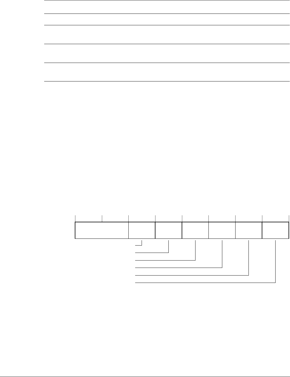
System Control
ARM DDI 0363G Copyright © 2006-2011 ARM Limited. All rights reserved. 4-20
ID041111 Non-Confidential
Table 4-8 shows the PFR1 bit assignments.Register
To access the PFR1 read CP15 with:
MRC p15, 0, <Rd>, c0, c1, 1 ; Read PFR1
4.3.8 c0, Debug Feature Register 0
The ID_DFR0 characteristics are:
Purpose Provides information about the debug system for the processor.
Usage constraints ID_DFR0 is:
• a read-only register
• accessible in Privileged mode only.
Configurations Available in all processor configurations.
Attributes See Table 4-9 on page 4-21.
Figure 4-13 shows the ID_DFR0 bit assignments.
Figure 4-13 ID_DFR0 Register bit assignments
Table 4-8 PFR1 bit assignments
Bits Name Function
[31:12] - SBZ.
[11:8] Microcontroller programmers model Indicates support for Microcontroller programmers model:
0x0
= no support.
[7:4] Security extension Indicates support for Security Extensions architecture:
0x0
= no support.
[3:0] ARMv4 Programmers model Indicates support for standard ARMv4 programmers model:
0x1
= the processor supports the ARMv4 model.
Reserved
Microcontroller debug model – memory mapped
Trace debug model – memory mapped
Trace debug model – coprocessor
Core debug model – memory mapped
Core debug model – coprocessor
Secure debug model
31 24 23 20 19 16 15 12 11 8 7 4 3 0

System Control
ARM DDI 0363G Copyright © 2006-2011 ARM Limited. All rights reserved. 4-21
ID041111 Non-Confidential
Table 4-9 shows the ID_DFR0 bit assignments.
To access the ID_DFR0 read CP15 with:
MRC p15, 0, <Rd>, c0, c1, 2 ; Read ID_DFR0
4.3.9 c0, Auxiliary Feature Register 0
The ID_AFR0 characteristics are:
Purpose Provides additional information about the features of the processor.
Usage constraints The ID_AFR0 is:
• a read-only register
• accessible in Privileged mode only.
Configurations Available in all processor configurations.
Attributes In this processor, the ID_AFR0 reads as
0x00000000
.
To access the ID_AFR0 read CP15 with:
MRC p15, 0, <Rd>, c0, c1, 3 ; Read ID_AFR0.
4.3.10 Memory Model Feature Registers
The processor has four Memory Model Feature Registers, MMFR0 to MMFR3. This section
describes:
•c0, Memory Model Feature Register 0 on page 4-22
•c0, Memory Model Feature Register 1 on page 4-23
•c0, Memory Model Feature Register 2 on page 4-24
•c0, Memory Model Feature Register 3 on page 4-25.
Table 4-9 ID_DFR0 Register bit assignments
Bits Name Function
[31:24] - SBZ.
[23:20] Microcontroller
Debug model -
memory mapped
Indicates support for the microcontroller debug model - memory mapped:
0x0
= no support.
[19:16] Trace debug model -
memory mapped
Indicates support for the trace debug model - memory mapped:
0x1
= trace supported, memory mapped access.
[15:12] Trace debug model -
coprocessor
Indicates support for the trace debug model - coprocessor:
0x0
= no support.
[11:8] Core debug model -
memory mapped
Indicates the type of embedded processor debug model that the processor supports:
0x4
= ARMv7 based model - memory mapped.
[7:4] Secure debug model Indicates the type of secure debug model that the processor supports:
0x0
= no support.
[3:0] Core debug model -
coprocessor
Indicates the type of applications processor debug model that the processor supports:
0x0
= no support.

System Control
ARM DDI 0363G Copyright © 2006-2011 ARM Limited. All rights reserved. 4-22
ID041111 Non-Confidential
c0, Memory Model Feature Register 0
The ID_MMFR0 characteristics are:
Purpose The ID_MMFR0 provides information about the memory model, memory
management, and cache support operations of the processor.
Usage constraints The ID_MMFR0 is:
• a read-only register
• accessible in Privileged mode only.
Configurations Available in all processor configurations.
Attributes See Table 4-10.
Figure 4-14 shows the ID_MMFR0 bit assignments.
Figure 4-14 ID_MMFR0 Register bit assignments
Table 4-10 shows the ID_MMFR0 bit assignments.
To access the ID_MMFR0 read CP15 with:
MRC p15, 0, <Rd>, c0, c1, 4 ; Read ID_MMFR0.
31 28 27 24 23 20 19 16 15 12 11 8 7 4 3 0
Innermost
shareability FCSE TCM
support PMSA VMSA
Auxiliary
Registers
Shareability
levels
Outermost
shareability
Table 4-10 ID_MMFR0 Register bit assignments
Bits Name Function
[31:28] Innermost shareability Indicates the innermost shareability domain implemented.
RAZ/UNK because only one shareability domain is implemented, see bits [15:12].
[27:24] FCSE Indicates support for Fast Context Switch Extension (FCSE):
0x0
= no support.
[23:20] Auxiliary Registers Indicates support for the auxiliary registers:
0x2
= the processor supports the Auxiliary Instruction and Data Fault Status
Registers (AIFSR and ADFSR) and the ACTLR.
[19:16] TCM support Indicates support for TCM and associated DMA:
0x1
= implementation defined.
[15:12] Shareability levels Indicates the number of shareability levels implemented:
0x0
= one level of shareability implemented.
[11:8] Outermost shareability Indicates the outermost shareability domain implemented:
0x0
= implemented as non-cacheable.
[7:4] PMSA Indicates support for Physical Memory System Architecture (PMSA):
0x3
= the processor supports PMSAv7 (subsection support).
[3:0] VMSA Indicates support for Virtual Memory System Architecture (VMSA):
0x0
= no support.
System Control
ARM DDI 0363G Copyright © 2006-2011 ARM Limited. All rights reserved. 4-23
ID041111 Non-Confidential
c0, Memory Model Feature Register 1
The ID_MMFR1 Register characteristics are:
Purpose Provides information about the memory model, memory management,
and cache support of the processor.
Usage constraints The ID_MMFR1 is:
• a read-only register
• accessible in Privileged mode only.
Configurations Available in all processor configurations.
Attributes See Table 4-11.
Figure 4-15 shows the ID_MMFR1 bit assignments.
Figure 4-15 ID_MMFR1 Register bit assignments
Table 4-11 shows the ID_MMFR1 bit assignments.
31 28 27 24 23 20 19 16 15 12 11 8 7 4 3 0
L1 test clean operations
L1 cache maintenance operations (unified)
L1 cache maintenance operations (Harvard)
L1 cache line maintenance operations - Set and Way (unified)
L1 cache line maintenance operations - Set and Way (Harvard)
L1 cache line maintenance operations - MVA (unified)
L1 cache line maintenance operations - MVA (Harvard)
Branch predictor
Table 4-11 ID_MMFR1 Register bit assignments
Bits Name Function
[31:28] Branch predictor Indicates Branch Predictor management requirements:
0x0
= no MMU present.
[27:24] L1 test clean operations Indicates support for test and clean operations on data cache, Harvard or unified
architecture:
0x0
= no support.
[23:20] L1 cache maintenance
operations (unified)
Indicates support for L1 cache, entire cache maintenance operations, unified
architecture:
0x0
= no support.
[19:16] L1 cache maintenance
operations (Harvard)
Indicates support for L1 cache, entire cache maintenance operations, Harvard
architecture:
0x0
= no support.
[15:12] L1 cache line maintenance
operations - Set and Way
(unified)
Indicates support for L1 cache line maintenance operations by Set and Way,
unified architecture:
0x0
= no support.
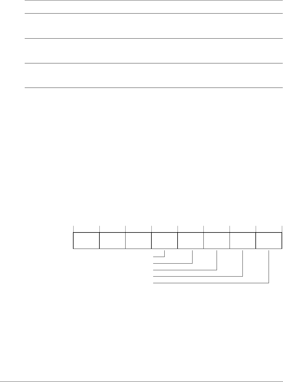
System Control
ARM DDI 0363G Copyright © 2006-2011 ARM Limited. All rights reserved. 4-24
ID041111 Non-Confidential
To access the ID_MMFR1 read CP15 with:
MRC p15, 0, <Rd>, c0, c1, 5 ; Read ID_MMFR1.
c0, Memory Model Feature Register 2
The ID_MMFR2 characteristics are:
Purpose The ID_MMFR2 provides information about the memory model, memory
management, and cache support operations of the processor.
Usage constraints The ID_MMFR2 is:
• a read-only register
• accessible in Privileged mode only.
Configurations Available in all processor configurations.
Attributes See Table 4-12 on page 4-25.
Figure 4-16 shows the ID_MMFR2 bit assignments.
Figure 4-16 ID_MMFR2 Register bit assignments
[11:8] L1 cache line maintenance
operations - Set and Way
(Harvard)
Indicates support for L1 cache line maintenance operations by Set and Way,
Harvard architecture.
0x0
= no support.
[7:4] L1 cache line maintenance
operations - MVA (unified)
Indicates support for L1 cache line maintenance operations by address, unified
architecture.
0x0
= no support.
[3:0] L1 cache line maintenance
operations - MVA (Harvard)
Indicates support for L1 cache line maintenance operations by address, Harvard
architecture.
0x0
= no support.
Table 4-11 ID_MMFR1 Register bit assignments (continued)
Bits Name Function
31 28 27 24 23 20 19 16 15 12 11 8 7 4 3 0
Hardware
access flag WFI Memory
barrier
TLB maintenance operations (unified)
TLB maintenance operations (Harward)
L1 cache maintenance range operations (Harward)
L1 background prefetch cache operations
L1 foreground prefetch cache operations

System Control
ARM DDI 0363G Copyright © 2006-2011 ARM Limited. All rights reserved. 4-25
ID041111 Non-Confidential
Table 4-12 shows the ID_MMFR2 bit assignments.
To access the ID_MMFR2 read CP15 with:
MRC p15, 0, <Rd>, c0, c1, 6 ; Read ID_MMFR2.
c0, Memory Model Feature Register 3
The ID_MMFR3 characteristics are:
Purpose Provides information about the two cache line maintenance operations for
the processor.
Usage constraints The ID_MMFR3 is:
• a read-only register
• accessible in Privileged mode only.
Configurations Available in all processor configurations.
Attributes See Table 4-13 on page 4-26.
Figure 4-17 on page 4-26 shows the ID_MMFR3 bit assignments.
Table 4-12 ID_MMFR2 bit assignments
Bits Name Function
[31:28] Hardware access flag Indicates support for Hardware Access Flag:
0x0
= no support.
[27:24] WFI Indicates support for Wait-For-Interrupt stalling:
0x1
= the processor supports Wait-For-Interrupt.
[23:20] Memory barrier Indicates support for memory barrier operations:
0x2
= the processor supports:
• DSB (formerly DWB)
• ISB (formerly Prefetch Flush)
•DMB.
[19:16] TLB maintenance
operations (unified)
Indicates support for TLB maintenance operations, unified architecture:
0x0
= no support.
[15:12] TLB maintenance
operations (Harvard)
Indicates support for TLB maintenance operations, Harvard architecture:
0x0
= no support.
[11:8] L1 cache
maintenance range
operations (Harvard)
Indicates support for cache maintenance range operations, Harvard architecture:
0x0
= no support.
[7:4] L1 background
prefetch cache
operations
Indicates support for background prefetch cache range operations, Harvard
architecture:
0x0
= no support.
[3:0] L1 foreground
prefetch cache
operations
Indicates support for foreground prefetch cache range operations, Harvard
architecture:
0x0
= no support.
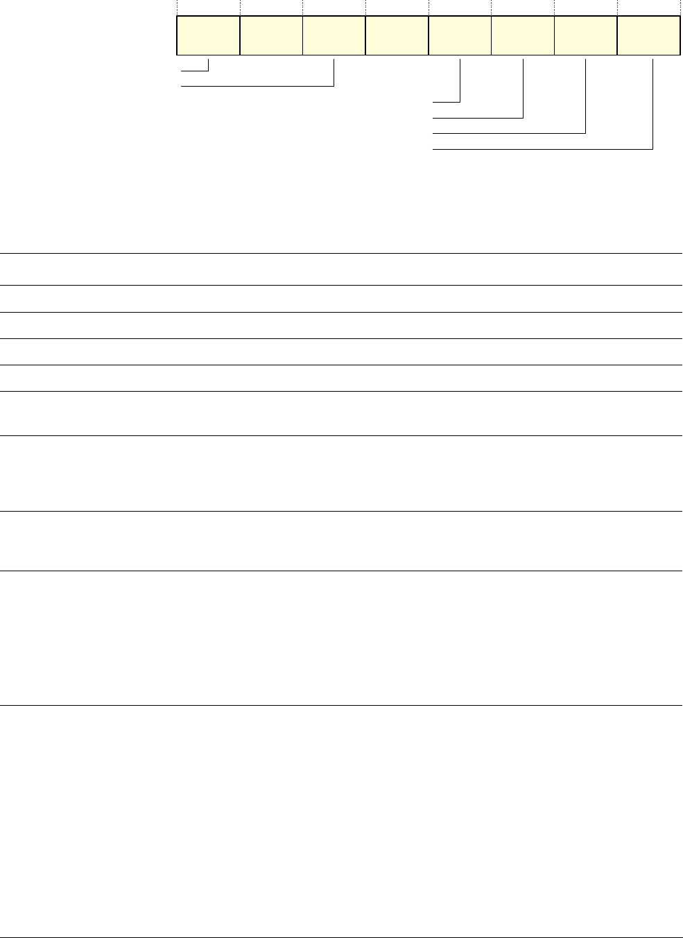
System Control
ARM DDI 0363G Copyright © 2006-2011 ARM Limited. All rights reserved. 4-26
ID041111 Non-Confidential
Figure 4-17 ID_MMFR3 bit assignments
Table 4-13 shows the ID_MMFR3 bit assignments.
To access the ID_MMFR3 read CP15 with:
MRC p15, 0, <Rd>, c0, c1, 7 ; Read ID_MMFR3.
4.3.11 Instruction Set Attributes Registers
The processor has eight Instruction Set Attributes Registers, ISAR0 to ISAR7, but three of these
are unused. This section describes:
•c0, Instruction Set Attributes Register 0 on page 4-27
•c0, Instruction Set Attributes Register 1 on page 4-28
Reserved Reserved
31 8 7 3 0412 11
Branch predictor maintenance operations
Hierarchical cache maintenance operations by Set and Way
Hierarchical cache maintenance operations by MVA
16 1520 1924 2328 27
Maintenance broadcast
Supersection support
Coherent walk
Table 4-13 ID_MMFR3 Register bit assignments
Bits Name Function
[31:28] Supersection support RAZ because this is a PMSA implementation.
[27:24] - SBZ
[23:20] Coherent walk RAZ because this is a PMSA implementation.
[19:16] - SBZ
[15:12] Maintenance broadcast Indicates whether cache maintenance operations are broadcast:
0x0
= cache maintenance operations only affect local structures.
[11:8] Branch predictor maintenance
operations
Indicates support for branch predictor maintenance operations in systems with hierar-
chical cache maintenance operations:
0x2
= supports invalidate entire branch predictor array and invalidate branch predictor
by MVAa.
[7:4] Hierarchical cache maintenance
operations by Set and Way
Indicates support for hierarchical cache maintenance operations by Set and Way:
0x1
= the processor supports invalidate cache, clean and invalidate, and clean by Set and
Way.
[3:0] Hierarchical cache maintenance
operations by MVA
Indicates support for hierarchical cache maintenance operations by address:
0x1
= the processor supports:
• Invalidate data cache by address
• Clean data cache by address
• Clean and invalidate data cache by address
• Invalidate instruction cache by address
• Invalidate all instruction cache entries.
a. Both of these operations are NOP on Cortex-R4.
System Control
ARM DDI 0363G Copyright © 2006-2011 ARM Limited. All rights reserved. 4-27
ID041111 Non-Confidential
•c0, Instruction Set Attributes Register 2 on page 4-29
•c0, Instruction Set Attributes Register 3 on page 4-31
•c0, Instruction Set Attributes Register 4 on page 4-32
•c0, Instruction Set Attributes Register 5 on page 4-33.
c0, Instruction Set Attributes Register 0
The ID_ISAR0 characteristics are:
Purpose Provides information about the instruction set that the processor supports,
beyond the basic set.
Usage constraints The ID_ISAR0 is:
• a read-only register
• accessible in Privileged mode only.
Configurations Available in all processor configurations.
Attributes See Table 4-14.
Figure 4-18 shows the ID_ISAR0 bit assignments.
Figure 4-18 ID_ISAR0 Register bit assignments
Table 4-14 shows the ID_ISAR0 bit assignments.
Reserved
31 28 27 24 23 20 19 16 15 12 11 8 7 4 3 0
Divide instructions
Debug instructions
Coprocessor instructions
Compare and branch instructions
Bitfield instructions
Bit count instructions
Atomic instructions
Table 4-14 ID_ISAR0 Register bit assignments
Bits Name Function
[31:28] - SBZ
[27:24] Divide instructions Indicates support for divide instructions:
0x1
= the processor supports
SDIV
and
UDIV
instructions.
[23:20] Debug instructions Indicates support for debug instructions:
0x1
= the processor supports
BKPT
.
[19:16] Coprocessor instructions Indicates support for coprocessor instructions other than separately attributed
feature registers, such as CP15 registers and VFP:
0x0
= no support.
[15:12] Compare and branch
instructions
Indicates support for combined compare and branch instructions:
0x1
= the processor supports combined compare and branch instructions,
CBNZ
and
CBZ
.
System Control
ARM DDI 0363G Copyright © 2006-2011 ARM Limited. All rights reserved. 4-28
ID041111 Non-Confidential
To access the ID_ISAR0, read CP15 with:
MRC p15, 0, <Rd>, c0, c2, 0 ; Read ID_ISAR0
c0, Instruction Set Attributes Register 1
The ID_ISAR1 characteristics are:
Purpose Provides information about the instruction set that the processor supports
beyond the basic set.
Usage constraints The ID_ISAR1 is:
• a read-only register
• accessible in Privileged mode only.
Configurations Available in all processor configurations.
Attributes See Table 4-15 on page 4-29.
Figure 4-19 shows the ID_ISAR1 bit assignments.
Figure 4-19 ID_ISAR1 Register bit assignments
[11:8] Bitfield instructions Indicates support for bitfield instructions.
0x1
= the processor supports bitfield instructions,
BFC
,
BFI
,
SBFX
, and
UBFX
.
[7:4] Bit counting instructions Indicates support for bit counting instructions.
0x1
= the processor supports
CLZ
.
[3:0] Atomic instructions Indicates support for atomic load and store instructions.
0x1
= the processor supports
SWP
and
SWPB
.
Table 4-14 ID_ISAR0 Register bit assignments (continued)
Bits Name Function
31 28 27 24 23 20 19 16 15 12 11 8 7 4 3 0
Jazelle instructions
Interworking instructions
Immediate instructions
ITE instructions
Extend instructions
Exception 2 instructions
Exception 1 instructions
Endian instructions

System Control
ARM DDI 0363G Copyright © 2006-2011 ARM Limited. All rights reserved. 4-29
ID041111 Non-Confidential
Table 4-15 shows the ID_ISAR1 bit assignments.
To access the ID_ISAR1 read CP15 with:
MRC p15, 0, <Rd>, c0, c2, 1 ; Read ID_ISAR1
c0, Instruction Set Attributes Register 2
The ID_ISAR2 is:
• a read-only register
• accessible in Privileged mode only.
The ID_ISAR2 characteristics are:
Purpose The ID_ISAR2 provides information about the instruction set that the
processor supports beyond the basic set.
Table 4-15 ID_ISAR1 Register bit assignments
Bits Name Function
[31:28] Jazelle
instructions
Indicates support for Jazelle instructions:
0x1
= the processor supports:
•
BXJ
instruction
• J bit in PSRs.
For more information see Program status registers on page 3-9 and Acceleration of execution
environments on page 3-25.
[27:24] Interworking
instructions
Indicates support for interworking instructions:
0x3
= the processor supports:
•
BX
, and T bit in PSRs
•
BLX
, and PC loads have BX behavior
• data-processing instructions in the ARM instruction set with the PC as the destination
and the S bit clear have BX-like behavior.
[23:20] Immediate
instructions
Indicates support for immediate instructions:
0x1
= the processor supports:
• the
MOVT
instruction
•
MOV
instruction encodings with 16-bit immediates
•Thumb
ADD
and
SUB
instructions with 12-bit immediates.
[19:16] ITE
instructions
Indicates support for If Then instructions:
0x1
= the processor supports
IT
instructions.
[15:12] Extend
instructions
Indicates support for sign or zero extend instructions:
0x2
= the processor supports:
•
SXTB
,
SXTB16
,
SXTH
,
UXTB
,
UXTB16
, and
UXTH
•
SXTAB
,
SXTAB16
,
SXTAH
,
UXTAB
,
UXTAB16
, and
UXTAH
.
[11:8] Exception 2
instructions
Indicates support for exception 2 instructions:
0x1
= the processor supports
RFE
,
SRS
, and
CPS
.
[7:4] Exception 1
instructions
Indicates support for exception 1 instructions:
0x1
= the processor supports
LDM
(exception return),
LDM
(user registers), and
STM
(user
registers).
[3:0] Endian
instructions
Indicates support for endianness control instructions:
0x1
= the processor supports
SETEND
and E bit in PSRs.
System Control
ARM DDI 0363G Copyright © 2006-2011 ARM Limited. All rights reserved. 4-30
ID041111 Non-Confidential
Usage constraints The ID_ISAR2 is:
• a read-only register
• accessible in Privileged mode only.
Configurations Available in all processor configurations.
Attributes See Table 4-16.
Figure 4-20 shows the ID_ISAR2 bit assignments.
Figure 4-20 ID_ISAR2 Register bit assignments
Table 4-16 shows the ID_ISAR2 bit assignments.
31 28 27 24 23 20 19 16 15 12 11 8 7 4 3 0
Reversal instructions
PSR instructions
Unsigned multiply instructions
Signed multiply instructions
Multiply instructions
Interruptible instructions
Memory hint instructions
Load/store instructions
Table 4-16 ID_ISAR2 Register bit assignments
Bits Name Function
[31:28] Reversal
instructions
Indicates support for reversal instructions:
0x2
= the processor supports
REV
,
REV16
,
REVSH
, and
RBIT
.
[27:24] PSR
instructions
Indicates support for
PSR
instructions:
0x1
= the processor supports
MRS
and
MSR
, and the exception return forms of data-processing
instructions.
[23:20] Unsigned
multiply
instructions
Indicates support for advanced unsigned multiply instructions:
0x2
= the processor supports:
•
UMULL
and
UMLAL
•
UMAAL
.
[19:16] Signed
multiply
instructions
Indicates support for advanced signed multiply instructions:
0x3
= the processor supports:
•
SMULL
and
SMLAL
•
SMLABB
,
SMLABT
,
SMLALBB
,
SMLALBT
,
SMLALTB
,
SMLALTT
,
SMLATB
,
SMLATT
,
SMLAWB
,
SMLAWT
,
SMULBB
,
SMULBT
,
SMULTB
,
SMULTT
,
SMULWB
,
SMULWT
, and Q flag in PSRs
•
SMLAD
,
SMLADX
,
SMLALD
,
SMLALDX
,
SMLSD
,
SMLSDX
,
SMLSLD
,
SMLSLDX
,
SMMLA
,
SMMLAR
,
SMMLS
,
SMMLSR
,
SMPUL
,
SMPULR
,
SMUAD
,
SMUADX
,
SMUSD
, and
SMUSDX
.
[15:12] Multiply
instructions
Indicates support for multiply instructions:
0x2
= the processor supports
MUL
,
MLA
, and
MLS
.
System Control
ARM DDI 0363G Copyright © 2006-2011 ARM Limited. All rights reserved. 4-31
ID041111 Non-Confidential
To access the ID_ISAR2 read CP15 with:
MRC p15, 0, <Rd>, c0, c2, 2 ; Read ID_ISAR2
c0, Instruction Set Attributes Register 3
The ID_ISAR3 characteristics are:
Purpose Provides information about the instruction set that the processor supports
beyond the basic set.
Usage constraints The ID_ISAR3 is:
• a read-only registers
• accessible in Privileged mode only.
Configurations Available in all processor configurations.
Attributes See Table 4-17 on page 4-32.
Figure 4-21 shows the ID_ISAR3 bit assignments.
Figure 4-21 ID_ISAR3 Register bit assignments
[11:8] Interruptible
instructions
Indicates support for multi-access interruptible instructions.
0x1
= the processor supports restartable
LDM
and
STM
.
[7:4] Memory hint
instructions
Indicates support for memory hint instructions.
0x3
= the processor supports
PLD
and
PLI
.
[3:0] Load/store
instructions
Indicates support for additional load and store instructions.
0x1
= the processor supports
LDRD
and
STRD
.
Table 4-16 ID_ISAR2 Register bit assignments (continued)
Bits Name Function
31 28 27 24 23 20 19 16 15 12 11 8 7 4 3 0
ThumbEE extension
True NOP instructions
Thumb copy instructions
Table branch instructions
Synchronization primitive instructions
SVC instructions
SIMD instructions
Saturate instructions

System Control
ARM DDI 0363G Copyright © 2006-2011 ARM Limited. All rights reserved. 4-32
ID041111 Non-Confidential
Table 4-17 shows the ID_ISAR3 bit assignments.
To access the ID_ISAR3 read CP15 with:
MRC p15, 0, <Rd>, c0, c2, 3 ; Read ID_ISAR3
c0, Instruction Set Attributes Register 4
The ID_ISAR4 characteristics are:
Purpose Provides information about the instruction set that the processor supports
beyond the basic set.
Usage constraints The ID_ISAR4 is:
• a read-only register
• accessible in Privileged mode only.
Configurations Available in all processor configurations.
Attributes See Table 4-18 on page 4-33.
Figure 4-22 on page 4-33 shows the ID_ISAR4 bit assignments.
Table 4-17 ID_ISAR3 Register bit assignments
Bits Name Function
[31:28] ThumbEE
extension
Indicates support for ThumbEE Execution Environment extension:
0x0
= no support.
[27:24] True NOP
instructions
Indicates support for true
NOP
instructions:
0x1
= the processor supports
NOP16
,
NOP32
and various
NOP
compatible hints in both the
ARM and Thumb instruction sets.
[23:20] Thumb copy
instructions
Indicates support for Thumb copy instructions:
0x1
= the processor supports Thumb
MOV(3)
low register to low register.
[19:16] Table branch
instructions
Indicates support for table branch instructions:
0x1
= the processor supports table branch instructions,
TBB
and
TBH
.
[15:12] Synchronization
primitive
instructions
Indicates support for synchronization primitive instructions:
0x2
= the processor supports:
•
LDREX
and
STREX
•
LDREXB
,
LDREXH
,
LDREXD
,
STREXB
,
STREXH
,
STREXD
, and
CLREX
.
[11:8] SVC instructions Indicates support for
SVC
(formerly
SWI
) instructions:
0x1
= the processor supports
SVC
.
[7:4] SIMD
instructions
Indicates support for Single Instruction Multiple Data (
SIMD
) instructions:
0x3
= the processor supports:
PKHBT
,
PKHTB
,
QADD16
,
QADD8
,
QASX
,
QSUB16
,
QSUB8
,
QSAX
,
SADD16
,
SADD8
,
SASX
,
SEL
,
SHADD16
,
SHADD8
,
SHASX
,
SHSUB16
,
SHSUB8
,
SHSAX
,
SSAT
,
SSAT16
,
SSUB16
,
SSUB8
,
SSAX
,
SXTAB16
,
SXTB16
,
UADD16
,
UADD8
,
UASX
,
UHADD16
,
UHADD8
,
UASX
,
UHSUB16
,
UHSUB8
,
USAX
,
UQADD16
,
UQADD8
,
UQASX
,
UQSUB16
,
UQSUB8
,
UQSAX
,
USAD8
,
USADA8
,
USAT
,
USAT16
,
USUB16
,
USUB8
,
USAX
,
UXTAB16
,
UXTB16
,
and the GE[3:0] bits in the PSRs.
[3:0] Saturate
instructions
Indicates support for saturate instructions:
0x1
= the processor supports
QADD
,
QDADD
,
QDSUB
,
QSUB
and Q flag in PSRs.

System Control
ARM DDI 0363G Copyright © 2006-2011 ARM Limited. All rights reserved. 4-33
ID041111 Non-Confidential
Figure 4-22 ID_ISAR4 Register bit assignments
Table 4-18 shows the ID_ISAR4 bit assignments.
To access the ID_ISAR4 read CP15 with:
MRC p15, 0, <Rd>, c0, c2, 4 ; Read ID_ISAR4
c0, Instruction Set Attributes Register 5
The ID_ISAR5 characteristics are:
Purpose Provides additional information about the properties of the processor.
Usage constraints ID_ISAR5 is:
• a read-only register
• accessible in Privileged mode only.
Configurations Available in all processor configurations.
Attributes In the processor, ID_ISAR5 is read as
0x00000000
.
To access the ID_ISAR5, read CP15 with:
SWP_frac Exclusive
instructions
Barrier
instructions
SMC
instructions
Write-back
instructions
With shift
instructions
Unprivileged
instructions
31 24 23 20 19 16 15 12 11 8 7 4 3 0
28 27
PSR_M_instrs
Table 4-18 ISAR4 Register bit assignments
Bits Name Function
[31:28] SWP_frac RAZ because SWP/SWPB instruction support is indicated in ID_ISAR0.
[27:24] PSR_M_instrs Indicates support for M-profile instructions for modifying the PSRs:
0x0
= no support.
[23:20] Exclusive instructions Indicates support for Exclusive instructions:
0x0
= Only supports synchronization primitive instructions as indicated by bits [15:12] in the
ISAR3 register. See c0, Instruction Set Attributes Register 3 on page 4-31 for more informa-
tion.
[19:16] Barrier instructions Indicates support for Barrier instructions:
0x1
= the processor supports
DMB
,
DSB
, and
ISB
instructions.
[15:12] SMC instructions Indicates support for Secure Monitor Call (
SMC
) (formerly
SMI
) instructions:
0x0
= no support.
[11:8] Write-back instructions Indicates support for write-back instructions:
0x1
= supports all the writeback addressing modes defined in ARMv7.
[7:4] With shift instructions Indicates support for with-shift instructions:
0x4
= the processor supports:
• the full range of constant shift options, on load/store and other instructions
• register-controlled shift options.
[3:0] Unprivileged instructions Indicates support for Unprivileged instructions:
0x2
= the processor supports
LDR{SB|B|SH|H}T
and
STR{B|H}T
.

System Control
ARM DDI 0363G Copyright © 2006-2011 ARM Limited. All rights reserved. 4-34
ID041111 Non-Confidential
MRC p15, 0, <Rd>, c0, c2, 5 ; Read ID_ISAR5
c0, Instruction Set Attributes Registers 6-7
ID_ISAR6 and ID_ISAR7 are not implemented, and their positions in the register map are
Reserved. They correspond to CP15 accesses with:
MRC p15, 0, <Rd>, c0, c2, 6 ; Read ID_ISAR6
MRC p15, 0, <Rd>, c0, c2, 7 ; Read ID_ISAR7
These registers are read-only, and are accessible in Privileged mode only.
4.3.12 c0, Current Cache Size Identification Register
The CCSIDR Register characteristics are:
Purpose Provides information about the size and behavior of the instruction or data
cache. Architecturally, there can be up to eight levels of cache, containing
instruction, data, or unified caches. This processor contains L1 instruction
and data caches only. The CSSELR determines which CCSIDR to select,
see c0, Cache Size Selection Register on page 4-36.
Usage constraints The CCSIDR is:
• a read-only register
• accessible in Privileged mode only.
Configurations Available in all processor configurations.
Attributes See Table 4-19.
Figure 4-23 shows the CCSIDR bit assignments.
Figure 4-23 CCSIDR Register bit assignments
Table 4-19 shows the CCSIDR bit assignments.
Line
Size
W
T
31 30 29 28 27 13 12 2 0
W
B
R
A
W
ANumSets Associativity
Table 4-19 CCSIDR Register bit assignments
Bits Name Function
[31] WT Indicates support available for write-through:
1
= write-through support availablea
[30] WB Indicates support available for write-back:
1
= write-back support availablea
[29] RA Indicates support available for read allocation:
1
= read allocation support availablea
[28] WA Indicates support available for write allocation:
1
= write allocation support availablea

System Control
ARM DDI 0363G Copyright © 2006-2011 ARM Limited. All rights reserved. 4-35
ID041111 Non-Confidential
The LineSize field is encoded as 2 less than log(2) of the number of words in the cache line. For
example, a value of
0x0
indicates there are four words in a cache line, that is the minimum size
for the cache. A value of
0x1
indicates there are eight words in a cache line.
Table 4-20 shows the individual bit field and complete register encodings for the CCSIDR. Use
this to match the cache size and level of cache set by the CSSELR. See c0, Cache Size Selection
Register on page 4-36.
To access the CCSIDR read CP15 with:
MRC p15, 1, <Rd>, c0, c0, 0 ; Read CCSIDR
4.3.13 c0, Current Cache Level ID Register
The CLIDR Register characteristics are:
Purpose • Indicates the cache levels that are implemented. Architecturally,
there can be a different number of cache levels on the instruction and
data side.
• Captures the point-of-coherency.
• Captures the point-of-unification.
Usage constraints The CLIDR is:
• a read-only register
• accessible in Privileged mode only.
Configurations Available in all processor configurations.
Attributes See Table 4-21 on page 4-36.
[27:13] NumSets Indicates the number of sets as
(number of sets) - 1a
[12:3] Associativity Indicates the number of ways as
(number of ways) - 1a
[2:0] LineSize Indicates the number of words in each cache linea
a. See Table 4-20 for valid bit field encodings.
Table 4-20 Bit field and register encodings for CCSIDR
Size
Complete
register
encoding
Register bit field encoding
WT WB RA WA NumSets Associativity LineSize
4KB
0xF003E019
1111
0x001F 0x3 0x1
8KB
0xF007E019
1111
0x003F
16KB
0xF00FE019
1111
0x007F
32KB
0xF01FE019
1111
0x00FF
64KB
0xF03FE019
1111
0x01FF
Table 4-19 CCSIDR Register bit assignments (continued)
Bits Name Function

System Control
ARM DDI 0363G Copyright © 2006-2011 ARM Limited. All rights reserved. 4-36
ID041111 Non-Confidential
Figure 4-24 shows the CLIDR bit assignments.
Figure 4-24 CLIDR Register bit assignments
Table 4-21 shows the CLIDR bit assignments.
To access the CLIDR, read CP15 with:
MRC p15, 1, <Rd>, c0, c0, 1 ; Read CLIDR
4.3.14 c0, Cache Size Selection Register
The CSSELR characteristics are:
Purpose Holds the value that the processor uses to select the CSSELR to use.
Usage constraints The CSSELR is:
• a read/write register
• accessible in Privileged mode only.
CL 8 CL 7 CL 6 CL 5 CL 4 CL 3 CL 2 CL 1
Reserved
31 30 29 27 26 24 23 21 20 18 17 15 14 12 11 10 8 6 5 3 2 0
LoU LoC
Table 4-21 CLIDR Register bit assignments
Bits Name Function
[31:30] - SBZ
[29:27] LoU Level of Unification:
0b001
= L2, if either cache is implemented
0b000
= L1, if neither instruction nor data cache is implemented.
[26:24] LoC Level of Coherency:
0b001
= L2, if either cache is implemented
0b000
= L1, if neither instruction nor data cache is implemented.
[23:21] CL 8
0b000
= no cache at Cache Level (CL) 8
[20:18] CL 7
0b000
= no cache at CL 7
[17:15] CL 6
0b000
= no cache at CL 6
[14:12] CL 5
0b000
= no cache at CL 5
[11:9] CL 4
0b000
= no cache at CL 4
[8:6] CL 3
0b000
= no cache at CL 3
[5:3] CL 2
0b000
= no cache at CL 2
[2] CL 1 RAZ. Indicates no unified cache at CL1
[1] CL 1
0b000
= no data cache is implemented
0b001
= data cache is implemented.
[0] CL 1
0b000
= no instruction cache is implemented.
0b001
= an instruction cache is implemented.

System Control
ARM DDI 0363G Copyright © 2006-2011 ARM Limited. All rights reserved. 4-37
ID041111 Non-Confidential
Configurations Available in all processor configurations.
Attributes See Table 4-22.
Figure 4-25 shows the CSSELR bit assignments.
Figure 4-25 CSSELR Register bit assignments
Table 4-22 shows the CSSELR bit assignments.
To access the CCSIDRs read or write CP15 with:
MRC p15, 2, <Rd>, c0, c0, 0 ; Read CSSELR
MCR p15, 2, <Rd>, c0, c0, 0 ; Write CSSELR
4.3.15 c1, System Control Register
The SCTLR characteristics are:
Purpose Provides control and configuration information for:
• memory alignment, endianness, protection, and fault behavior
• MPU and cache enables and cache replacement strategy
• interrupts and the behavior of interrupt latency
• the location for exception vectors
• program flow prediction.
Usage constraints The SCTLR is:
• a read/write register
• accessible in Privileged mode only
• attempts to read or write the SCTLR from User mode result in an
Undefined Instruction exception.
Configurations Available in all processor configurations.
Attributes See Table 4-23 on page 4-38.
Figure 4-26 on page 4-38 shows the SCTLR bit assignments.
Reserved Level
43 10
InD
31
Table 4-22 CSSELR Register bit assignments
Bits Name Function
[31: 4] - SBZ.
[3:1] Level Identifies which cache level to select:
b000
= L1 cache
This field is read only, writes are ignored.
[0] InD Identifies instruction or data cache to use:
1
= instruction
0
= data.
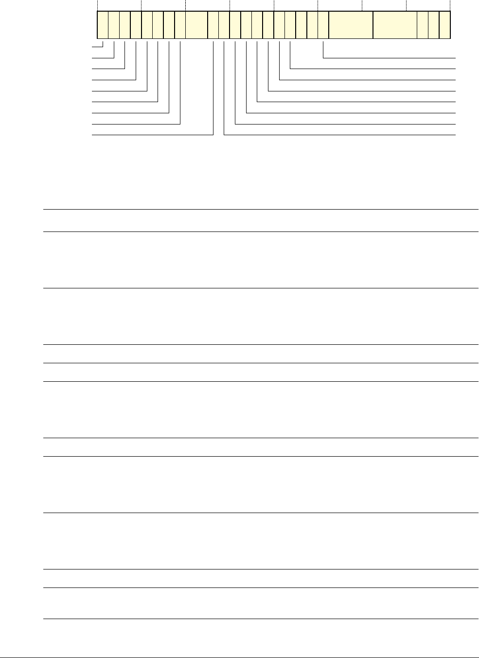
System Control
ARM DDI 0363G Copyright © 2006-2011 ARM Limited. All rights reserved. 4-38
ID041111 Non-Confidential
Figure 4-26 SCTLR Register bit assignments
Table 4-23 shows the SCTLR bit assignments.
TRE
IE
TE
AFE
NMFI
SBZ
EE
VE
Z
RR
SBZ
SBO
BR
SBO
FI
DZ
SBZ
M
31 30 29 28 27 26 25 24 23 22 21 20 19 18 17 16 15 14 13 12 11 10 7 6 3 2 1 0
SBO 1 V I SBZ SBO C A
Table 4-23 SCTLR Register bit assignments
Bits Name Function
[31] IE Identifies little or big instruction endianness in use:
0 = little-endianness
1 = big-endianness.
The primary input CFGIE defines the reset value. This bit is read-only.
[30] TE Thumb exception enable:
0 = enable ARM exception generation
1 = enable Thumb exception generation.
The primary input TEINIT defines the reset value.
[29] AFE Access Flag Enable. On the processor this bit is SBZ.
[28] TRE TEX Remap Enable. On the processor this bit is SBZ.
[27] NMFI NMFI, non-maskable fast interrupt enable:
0 = Software can disable FIQs
1 = Software cannot disable FIQs.
This bit is read-only. The configuration input CFGNMFI defines its value.
[26] - SBZ.
[25] EE Determines how the E bit in the CPSR is set on an exception:
0 = CPSR E bit is set to 0 on an exception
1 = CPSR E bit is set to 1 on an exception.
The primary input CFGEE defines the reset value.
[24] VE Configures vectored interrupt:
0 = exception vector address for IRQ is
0x00000018
or
0xFFFF0018
. See V bit.
1 = VIC controller provides handler address for IRQ.
The reset value of this bit is 0.
[23:22] - SBO.
[21] FI Fast Interrupts enable.
On the processor Fast Interrupts are always enabled. This bit is SBO.
[20] - SBZ.

System Control
ARM DDI 0363G Copyright © 2006-2011 ARM Limited. All rights reserved. 4-39
ID041111 Non-Confidential
To use the SCTLR, ARM recommends that you use a read-modify-write technique. To access
the SCTLR, read or write CP15 with:
MRC p15, 0, <Rd>, c1, c0, 0 ; Read SCTLR
MCR p15, 0, <Rd>, c1, c0, 0 ; Write SCTLR
[19] DZ Divide by zero:
0 = do not generate an Undefined Instruction exception
1 = generate an Undefined Instruction exception.
The reset value of this bit is 0.
[18] - SBO.
[17] BR MPU background region enable.
[16] - SBO.
[15] - SBZ.
[14] RR Round-robin bit, controls replacement strategy for instruction and data caches:
0 = random replacement strategy
1 = round-robin replacement strategy.
The reset value of this bit is 0. The processor always uses a random replacement strategy,
regardless of the state of this bit.
[13] V Determines the location of exception vectors:
0 = normal exception vectors selected, address range =
0x00000000
-
0x0000001C
1 = high exception vectors (HIVECS) selected, address range =
0xFFFF0000-0xFFFF001C
.
The primary input VINITHI defines the reset value.
[12] I Enables L1 instruction cache:
0 = instruction caching disabled. This is the reset value.
1 = instruction caching enabled.
If no instruction cache is implemented, then this bit is SBZ.
[11] Z Branch prediction enable bit.
The processor supports branch prediction. This bit is SBO. The ACTLR can control branch
prediction, see c1, Auxiliary Control Register on page 4-40.
[10:7] - SBZ.
[6:3] - SBO.
[2] C Enables L1 data cache:
0 = data caching disabled. This is the reset value.
1 = data caching enabled.
If no data cache is implemented, then this bit is SBZ.
[1] A Enables strict alignment of data to detect alignment faults in data accesses:
0 = strict alignment fault checking disabled. This is the reset value.
1 = strict alignment fault checking enabled.
[0] M Enables the MPU:
0 = MPU disabled. This is the reset value.
1 = MPU enabled.
If no MPU is implemented, this bit is SBZ.
Table 4-23 SCTLR Register bit assignments (continued)
Bits Name Function
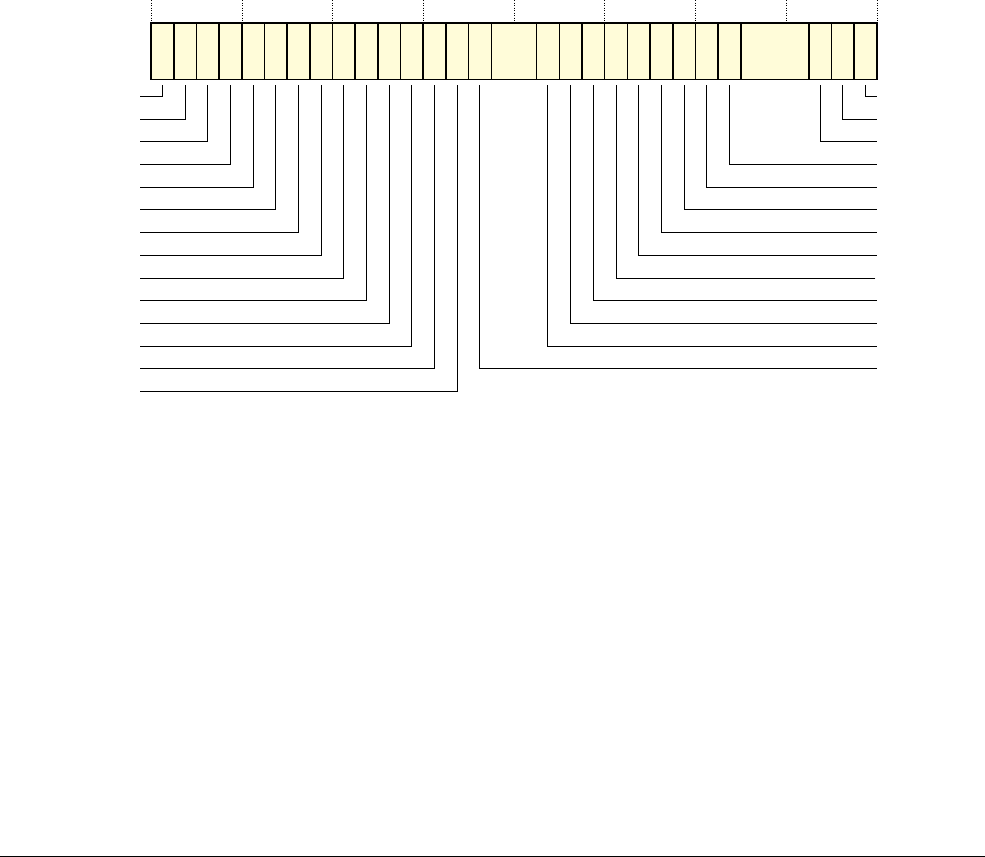
System Control
ARM DDI 0363G Copyright © 2006-2011 ARM Limited. All rights reserved. 4-40
ID041111 Non-Confidential
4.3.16 c1, Auxiliary Control Register
The ACTLR characteristics are:
Purpose Controls:
• branch prediction
• performance features
• error and parity logic.
Usage constraints The ACTLR is:
• a read/write register
• accessible in Privileged mode only
• ARM recommends that any instruction that changes bits [31:28] or
[7] is followed by an
ISB
instruction to ensure that the changes have
taken effect before any dependent instructions are executed.
Configurations Available in all processor configurations.
Attributes See Table 4-24 on page 4-41.
Figure 4-27 shows the ACTLR bit assignments.
Figure 4-27 ACTLR Register bit assignments
31 25 24 23 22 21 19 18 17 16 15 14 13 12 11 7 6 3 2 1 0
CEC
26272830 29
DIADI
1020
DICDI
DIB2DI
DIB1DI
B1TCMPCEN
B0TCMPCEN
ATCMPCEN
AXISCEN
9
BP
58
AXISCUEN
DILSM
DEOLP
DBHE
FRCDIS RSDIS
Reserved
ATCMECEN
B0TCMECEN
B1TCMECEN
DILS
sMOV
FDSnS
FWT
FORA
DNCH
ERPEG
DLFO
DBWR

System Control
ARM DDI 0363G Copyright © 2006-2011 ARM Limited. All rights reserved. 4-41
ID041111 Non-Confidential
Table 4-24 shows the ACTLR bit assignments.
Table 4-24 ACTLR Register bit assignments
Bits Name Function
[31] DICDIaCase C dual issue control:
0 = Enabled. This is the reset value.
1 = Disabled.
[30] DIB2DIaCase B2 dual issue control:
0 = Enabled. This is the reset value.
1 = Disabled.
[29] DIB1DIaCase B1 dual issue control:
0 = Enabled. This is the reset value.
1 = Disabled.
[28] DIADIaCase A dual issue control:
0 = Enabled. This is the reset value.
1 = Disabled.
[27] B1TCMPCEN B1TCM parity or ECC check enable:
0 = Disabled
1 = Enabled.
The primary input PARECCENRAM[2]b defines the reset value.
If the BTCM is configured with ECC, you must always set this bit to the same value as
B0TCMPCEN.
[26] B0TCMPCEN B0TCM parity or ECC check enable:
0 = Disabled
1 = Enabled.
The primary input PARECCENRAM[1]b defines the reset value.
If the BTCM is configured with ECC, you must always set this bit to the same value as
B1TCMPCEN.
[25] ATCMPCEN ATCM parity or ECC check enable:
0 = Disabled
1 = Enabled.
The primary input PARECCENRAM[0]b defines the reset value.
[24] AXISCEN AXI slave cache RAM access enable:
0 = Disabled. This is the reset value.
1 = Enabled.
Note
When AXI slave cache access is enabled, the caches are disabled and the processor cannot
run any cache maintenance operations. If the processor attempts a cache maintenance
operation, an Undefined Instruction exception is taken.
[23] AXISCUEN AXI slave cache RAM non-privileged access enable:
0 = Disabled. This is the reset value.
1 = Enabled.
[22] DILSM Disable Low Interrupt Latency (LIL) on load/store multiples:
0 = Enable LIL on load/store multiples. This is the reset value.
1 = Disable LIL on all load/store multiples.

System Control
ARM DDI 0363G Copyright © 2006-2011 ARM Limited. All rights reserved. 4-42
ID041111 Non-Confidential
[21] DEOLP Disable end of loop prediction:
0 = Enable loop prediction. This is the reset value.
1 = Disable loop prediction.
[20] DBHE Disable Branch History (BH) extension:
0 = Enable the extension. This is the reset value.
1 = Disable the extension.
[19] FRCDIS Fetch rate control disable:
0 = Normal fetch rate control operation. This is the reset value.
1 = Fetch rate control disabled.
[18] - SBZ.
[17] RSDIS Return stack disable:
0 = Normal return stack operation. This is the reset value.
1 = Return stack disabled.
[16:15] BP This field controls the branch prediction policy:
b00 = Normal operation. This is the reset value.
b01 = Branch always taken.
b10 = Branch always not taken.
b11 = Reserved. Behavior is Unpredictable if this field is set to b11.
[14] DBWR Disable write burst in the AXI master:
0 = Normal operation. This is the reset value.
1 = Disable write burst optimization.
[13] DLFO Disable linefill optimization in the AXI master:
0 = Normal operation. This is the reset value.
1 = Limits the number of outstanding data linefills to two.
[12] ERPEGcEnable random parity error generation:
0 = Random parity error generation disabled. This is the reset value.
1 = Enable random parity error generation in the cache RAMs.
Note
This bit controls error generation logic during system validation. A synthesized ASIC
typically does not have such models and this bit is therefore redundant for ASICs.
[11] DNCH Disable data forwarding for Non-cacheable accesses in the AXI master:
0 = Normal operation. This is the reset value.
1 = Disable data forwarding for Non-cacheable accesses.
[10] FORA Force outer read allocate (ORA) for outer write allocate (OWA) regions:
0 = No forcing of ORA. This is the reset value.
1 = ORA forced for OWA regions.
[9] FWT Force write-through (WT) for write-back (WB) regions:
0 = No forcing of WT. This is the reset value.
1 = WT forced for WB regions.
Table 4-24 ACTLR Register bit assignments (continued)
Bits Name Function

System Control
ARM DDI 0363G Copyright © 2006-2011 ARM Limited. All rights reserved. 4-43
ID041111 Non-Confidential
To access the ACTLR, read or write CP15 with:
MRC p15, 0, <Rd>, c1, c0, 1 ; Read ACTLR
MCR p15, 0, <Rd>, c1, c0, 1 ; Write ACTLR
4.3.17 c15, Secondary Auxiliary Control Register
The Secondary Auxiliary Control Register characteristics are:
Purpose Controls:
• branch prediction
• performance features
• error and parity logic.
Usage constraints The Secondary Auxiliary Control Register is:
• a read/write register
• accessible in Privileged mode only.
[8] FDSnS Force data side to not-shared when MPU is off:
0 = Normal operation. This is the reset value.
1 = Data side normal Non-cacheable forced to Non-shared when MPU is off.
[7] sMOV sMOV of a divide does not complete out of order. No other instruction is issued until the
divide is finished.
0 = Normal operation. This is the reset value.
1 = sMOV out of order disabled.
[6] DILS Disable low interrupt latency on all load/store instructions.
0 = Enable LIL on all load/store instructions. This is the reset value.
1 = Disable LIL on all load/store instructions.
[5:3] CEC Cache error control for cache parity and ECC errors.
See Table 8-2 on page 8-21 and Table 8-3 on page 8-22 for information about how these bits
are used. The reset value is b100.
[2] B1TCMECEN B1TCM external error enable:
0 = Disabled
1 = Enabled.
The primary input ERRENRAM[2] defines the reset value.
[1] B0TCMECEN B0TCM external error enable:
0 = Disabled
1 = Enabled.
The primary input ERRENRAM[1] defines the reset value.
[0] ATCMECEN ATCM external error enable:
0 = Disabled
1 = Enabled.
The primary input ERRENRAM[0] defines the reset value.
a. See Dual issue on page C-34
b. See Configuration signals on page A-4.
c. This bit is only supported if parity error generation is implemented in your design.
Table 4-24 ACTLR Register bit assignments (continued)
Bits Name Function
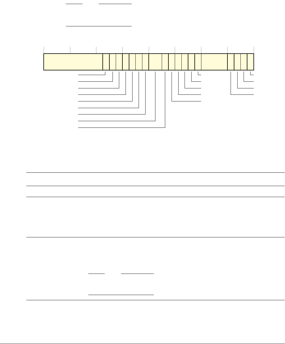
System Control
ARM DDI 0363G Copyright © 2006-2011 ARM Limited. All rights reserved. 4-44
ID041111 Non-Confidential
• ARM recommends that any instruction that changes bits [20:16] is
followed by an
ISB
instruction to ensure that the changes have taken
effect before any dependent instructions are executed.
Configurations Available in all processor configurations.
Attributes See Table 4-25.
Note
This register is implemented from the r1pn releases of the processor. Attempting to access this
register in r0pn releases of the processor results in an Undefined Instruction exception.
Figure 4-28 shows the Secondary Auxiliary Control Register bit assignments.
Figure 4-28 Secondary Auxiliary Control Register bit assignments
Table 4-25 shows the Secondary Auxiliary Control Register bit assignments.
ReservedReserved
31 22 21 19 18 17 16 15 14 13 12 11 7 3 2 1 01020 948
DR2B
DF6DI
DF2DI
DOODPFP
DDI
ATCMRMW
ATCMECC
IDC
DZC
IOC
UFC
OFC
IXC
DOOFMACS
BTCMRMW
B0TCMECC
Reserved
DCHE
23
Table 4-25 Secondary Auxiliary Control Register bit assignments
Bits Name Function
[31:23] - SBZ.
[22] DCHE Disable hard-error support in the caches:a
0
= Enabled. The cache logic recovers from some hard errors. You must not use this value on
revisions r1p2 or earlier of the processor.
1
= Disabled. Most hard errors in the caches are fatal. This is the reset value.
See Hard errors on page 8-5 for more information.
[21] DR2BbEnable random 2-bit error generation in cache RAMs. This bit has no effect unless ECC is
configured, see Configurable options on page 1-6:
0
= Disabled. This is the reset value.
1
= Enabled.
Note
This bit controls error generation logic during system validation. A synthesized ASIC
typically does not have such models and this bit is therefore redundant for ASICs.
[20] DF6DI F6 dual issue control:c
0
= Enabled. This is the reset value.
1
= Disabled.

System Control
ARM DDI 0363G Copyright © 2006-2011 ARM Limited. All rights reserved. 4-45
ID041111 Non-Confidential
[19] DF2DI F2_Id/F2_st/F2D dual issue control:c
0
= Enabled. This is the reset value.
1
= Disabled.
[18] DDI F1/F3/F4dual issue control:c
0
= Enabled. This is the reset value.
1
= Disabled.
[17] DOODPFP Out-of-order Double Precision Floating Point instruction control:c
0
= Enabled. This is the reset value.
1
= Disabled.
[16] DOOFMACS Out-of-order
FMACS
control:c
0
= Enabled. This is the reset value.
1
= Disabled.
[15:14] - SBZ.
[13] IXC Floating-point inexact exception output mask::c
0
= Mask floating-point inexact exception output. The output FPIXC is forced to zero. This
is the reset value.
1
= Propagate floating point inexact exception flag
FPSCR.IXC
to output FPIXC.
[12] OFC Floating-point overflow exception output mask:c
0
= Mask floating-point overflow exception output. The output FPOFC is forced to zero. This
is the reset value.
1 = Propagate floating-point overflow exception flag
FPSCR.OFC
to output FPOFC.
[11] UFC Floating-point underflow exception output mask:c
0
= Mask floating-point underflow exception output. The output FPUFC is forced to zero.
This is the reset value.
1
= Propagate floating-point underflow exception flag
FPSCR.UFC
to output FPUFC.
[10] IOC Floating-point invalid operation exception output mask:c
0
= Mask floating-point invalid operation exception output. The output FPIOC is forced to
zero. This is the reset value.
1
= Propagate floating-point invalid operation exception flag
FPSCR.IOC
to output FPIOC.
[9] DZC Floating-point divide-by-zero exception output mask:c
0
= Mask floating-point divide-by-zero exception output. The output FPDZC is forced to
zero. This is the reset value.
1
= Propagate floating-point divide-by-zero exception flag
FPSCR.DZC
to output FPDZC.
[8] IDC Floating-point input denormal exception output mask:c
0
= Mask floating-point input denormal exception output. The output FPIDC is forced to
zero. This is the reset value.
1
= Propagate floating-point input denormal exception flag
FPSCR.IDC
to output FPIDC.
[7:4] - SBZ.
[3] BTCMECC Correction for internal ECC logic on BTCM ports:d
0
= Enabled. This is the reset value.
1
= Disabled.
Table 4-25 Secondary Auxiliary Control Register bit assignments (continued)
Bits Name Function

System Control
ARM DDI 0363G Copyright © 2006-2011 ARM Limited. All rights reserved. 4-46
ID041111 Non-Confidential
To access the Secondary Auxiliary Control Register, read or write CP15 with:
MRC p15, 0, <Rd>, c15, c0, 0 ; Read Secondary Auxiliary Control Register
MCR p15, 0, <Rd>, c15, c0, 0 ; Write Secondary Auxiliary Control Register
4.3.18 c1, Coprocessor Access Register
The CPACR characteristics are:
Purpose Sets access rights for coprocessors.
Usage constraints The CPACR is:
• A read/write register.
• Accessible in Privileged mode only.
• Because this processor does not support coprocessors CP0-CP9,
CP12, and CP13, bits [27:24] and [19:0] in this register are
read-as-zero and ignore writes.
• CPACR has no effect on access to CP14, the debug control
coprocessor, or CP15, the system control coprocessor. The only
other coprocessor that the Cortex-R4F processor includes is the
FPU, CP10, and CP11. This register enables software to determine
if the FPU exists in the processor.
Configurations Available in all processor configurations.
Attributes See Table 4-26 on page 4-47.
Figure 4-29 on page 4-47 shows the CPACR bit assignments.
[2] ATCMECC Correction for internal ECC logic on ATCM port:d
0
= Enabled. This is the reset value.
1
= Disabled.
[1] BTCMRMW Enables 64-bit stores for the BTCMs. When enabled, the processor uses read-modify-write to
ensure that all reads and writes presented on the BTCM ports are 64 bits wide:e
0
= Disabled
1
= Enabled.
The primary input RMWENRAM[1] defines the reset value.
[0] ATCMRMW Enables 64-bit stores for the ATCM. When enabled, the processor uses read-modify-write to
ensure that all reads and writes presented on the ATCM port are 64 bits wide:e
0
= Disabled
1 = Enabled.
The primary input RMWENRAM[0] defines the reset value.
a. This bit is RAZ if both caches have neither ECC nor parity.
b. This bit is only supported if parity error generation is implemented in your design.
c. This bit has no effect unless the Floating Point Unit (FPU) is configured, see Configurable options on page 1-6.
d. This bit has no effect unless TCM ECC logic is configured for the respective TCM interface, see Configurable options on
page 1-6.
e. This feature is not available when the TCM interface is built with 32-bit ECC.
Table 4-25 Secondary Auxiliary Control Register bit assignments (continued)
Bits Name Function

System Control
ARM DDI 0363G Copyright © 2006-2011 ARM Limited. All rights reserved. 4-47
ID041111 Non-Confidential
Figure 4-29 CPACR Register bit assignments
Table 4-26 shows the CPACR bit assignments.
To access the CPACR, read or write CP15 with:
MRC p15, 0, <Rd>, c1, c0, 2 ; Read CPACR
MCR p15, 0, <Rd>, c1, c0, 2 ; Write CPACR
4.3.19 Fault Status and Address Registers
The processor reports the status and address of faults that occur during its operation. For both
data and instruction faults there are two Fault Status Registers (FSRs) and one Fault Address
Register (FAR).
Fields within the Data and Instruction FSRs indicate the priority and source of a fault and the
validity of the address in the corresponding FAR. Table 4-27 shows this encoding for the FSRs.
All other encodings for these FSR bits are Reserved.
Reserved
31 28 27 26 25 24 23 22 21 20 19 18 17 16 15 14 13 12 11 10 9 8 7 6 5 4 3 2 1 0
cp13 cp12 cp11 cp10 cp9 cp8 cp7 cp6 cp5 cp4 cp3 cp2 cp1 cp0
Table 4-26 CPACR Register bit assignments
Bits Name Function
[31:28] - SBZ.
[27:0] cp<n>aDefines access permissions for each coprocessor
Access denied is the reset condition, and is the behavior for non-existent coprocessors:
b00
= Access denied. Attempts to access generates an Undefined Instruction exception.
b01
= Privileged mode access only
b10
= Reserved
b11
= Privileged and User mode access.
Access permissions for the FPU are set by fields cp10 and cp11. For all other
coprocessor fields, the value is fixed to b00.
a. n is the coprocessor number between 0 and 13.
Table 4-27 Fault Status Register encodings
Priority Sources FSR [10,3:0] FAR
Highest Alignment 0b00001 Valid
Background 0b00000 Valid
Permission 0b01101 Valid
Synchronous External Abort 0b01000 Valid
Asynchronous External Abort 0b10110 Unpredictable
Synchronous Parity/ECC Error 0b11001 Valid
Asynchronous Parity/ECC Error 0b11000 Unpredictable
Lowest Debug Event 0b00010 Unchanged
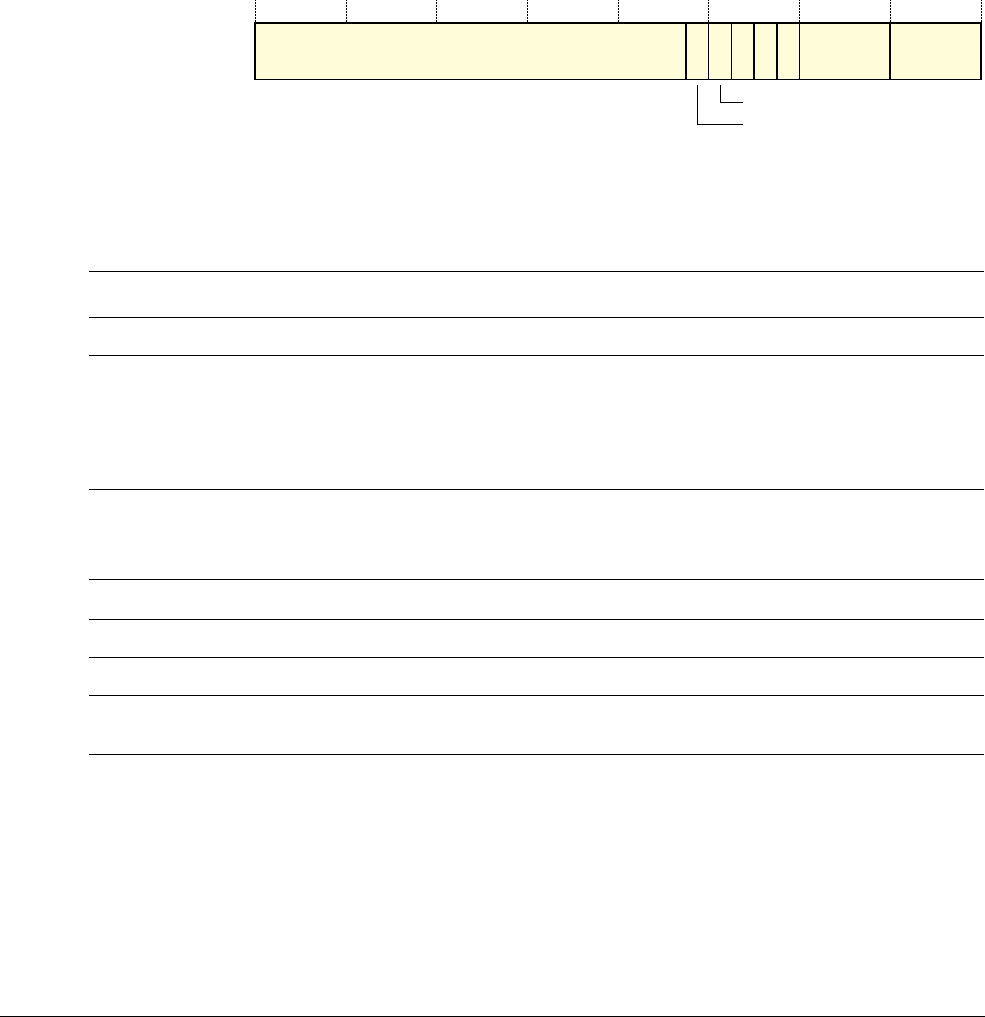
System Control
ARM DDI 0363G Copyright © 2006-2011 ARM Limited. All rights reserved. 4-48
ID041111 Non-Confidential
c5, Data Fault Status Register
The DFSR characteristics are:
Purpose Holds status information regarding the source of the last data abort.
Usage constraints The DFSR is:
• a read/write register
• accessible in Privileged mode only.
Configurations Available in all processor configurations.
Attributes See Table 4-28.
Figure 4-30 shows the DFSR bit assignments.
Figure 4-30 DFSR Register bit assignments
Table 4-28 shows the DFSR bit assignments.
To use the DFSR read or write CP15 with:
MRC p15, 0, <Rd>, c5, c0, 0 ; Read DFSR
MCR p15, 0, <Rd>, c5, c0, 0 ; Write DFSR
Domain
0
Reserved
31 8 7 4 3 0
Status
9
0S
10111213
RW
SD
Table 4-28 DFSR Register bit assignments
Bits Name Function
[31:13] - SBZ.
[12] SD Distinguishes between an AXI Decode or Slave error on an external abort. This bit is only valid
for external aborts. For all other aborts types of abort, this bit is set to zero:
0
= AXI Decode error (DECERR) caused the abort
1
= AXI Slave error (SLVERR, or OKAY in response to exclusive read transaction) caused the
abort.
[11] RW Indicates whether a read or write access caused an abort:
0
= read access caused the abort
1
= write access caused the abort.
[10]aS Part of the Status field.
[9:8] - Always RAZ. Writes ignored.
[7:4] Domain SBZ. This is because domains are not implemented in this processor.
[3:0]aStatus Indicates the type of fault generated. To determine the data fault, you must use bit [12] and bit [10]
in conjunction with bits [3:0].
a. For more information on how these bits are used in reporting faults, see Table 4-27 on page 4-47.
System Control
ARM DDI 0363G Copyright © 2006-2011 ARM Limited. All rights reserved. 4-49
ID041111 Non-Confidential
c5, Instruction Fault Status Register
The IFSR characteristics are:
Purpose Holds status information regarding the source of the last instruction abort.
Usage constraints The IFSR is:
• a read/write register
• accessible in Privileged mode only.
Configurations Available in all processor configurations.
Attributes See Table 4-29.
Figure 4-31 shows the IFSR bit assignments.
Figure 4-31 IFSR Register bit assignments
Table 4-29 shows the IFSR bit assignments.
To access the IFSR read or write CP15 with:
MRC p15, 0, <Rd>, c5, c0, 1 ; Read IFSR
MCR p15, 0, <Rd>, c5, c0, 1 ; Write IFSR
c5, Auxiliary Fault Status Registers
The processor has two auxiliary fault status registers:
• the Auxiliary Data Fault Status Register (ADFSR)
SReserved
31 30
StatusDomain
4
910111213
Reserved
SD
87
Reserved
Table 4-29 IFSR Register bit assignments
Bits Name Function
[31:13] - SBZ.
[12] SD Distinguishes between an AXI Decode or Slave error on an external abort. This bit is only valid for
external aborts. For all other aborts types of abort, this bit is set to zero:
0
= AXI Decode error (DECERR) caused the abort
1
= AXI Slave error (SLVERR) caused the abort.
[11] - SBZ.
[10]aS Part of the Status field.
[9:8] - SBZ.
[7:4] Domain SBZ. This is because domains are not implemented in this processor.
[3:0]aStatus Indicates the type of fault generated. To determine the instruction fault, bit [12] and bit [10] must
be used in conjunction with bits [3:0].
a. For more information on how these bits are used in reporting faults, see Table 4-27 on page 4-47.

System Control
ARM DDI 0363G Copyright © 2006-2011 ARM Limited. All rights reserved. 4-50
ID041111 Non-Confidential
• the Auxiliary Instruction Fault Status Register (AIFSR).
The auxiliary fault status registers characteristics are:
Purpose Provide additional information about data and instruction parity, ECC, and
external TCM errors.
Usage constraints The auxiliary fault status registers are:
• Read/write registers.
• Accessible in Privileged mode only.
• The contents of an auxiliary fault status register are only valid when
the corresponding Data or Instruction Fault Status Register indicates
that a parity or ECC error has occurred. At other times the contents
of the auxiliary fault status registers are Unpredictable.
Configurations Available in all processor configurations.
Attributes See Table 4-30.
Figure 4-32 shows the auxiliary fault status register bit assignments.
Figure 4-32 Auxiliary fault status register bit assignments
Table 4-30 shows the auxiliary fault status register bit assignments.
To access the auxiliary fault status registers, read or write CP15 with:
Reserved IndexReserved
31 0
Reserved
4
27 24 23 22 14 13 5
CacheWay
Side
28 21 20
Recoverable error
Table 4-30 Auxiliary fault status register bit assignments
Bits Name Function
[31:28] - SBZ.
[27:24] CacheWayaThe value returned in this field indicates the cache way or ways in which the error occurred.
[23:22] Side The value returned in this field indicates the source of the error. Possible values are:
b00
= Cache or AXI master interface
b01
= ATCM
b10
= BTCM
b11
= Reserved.
[21] Recoverable
error
The value returned in this field indicates if the error is recoverable:
0
= Unrecoverable error.
1
= Recoverable error. This includes all correctable parity/ECC errors and recoverable TCM
external errors.
[20:14] - SBZ.
[13:5] IndexbThis field returns the index value for the access giving the error.
[4:0] - SBZ.
a. This field is only valid for data cache store parity/ECC errors, otherwise it is Unpredictable.
b. This field is only valid for data cache store parity/ECC errors. On the AIFSR, and for TCM accesses, this field SBZ.

System Control
ARM DDI 0363G Copyright © 2006-2011 ARM Limited. All rights reserved. 4-51
ID041111 Non-Confidential
MCR p15, 0, <Rd>, c5, c1, 0 ; Write ADFSR
MRC p15, 0, <Rd>, c5, c1, 0 ; Read ADFSR
MCR p15, 0, <Rd>, c5, c1, 1 ; Write AIFSR
MRC p15, 0, <Rd>, c5, c1, 1 ; Read AIFSR
c6, Data Fault Address Register
The DFAR characteristics are:
Purpose Holds the address of the fault when a synchronous abort occurs.
Usage constraints The DFAR is:
• a read/write register
• accessible in Privileged mode only.
Configurations Available in all processor configurations.
Attributes The DFAR bits [31:0] contain the address where the synchronous abort
occurred.
To access the DFAR read or write CP15 with:
MRC p15, 0, <Rd>, c6, c0, 0 ; Read DFAR
MCR p15, 0, <Rd>, c6, c0, 0 ; Write DFAR
A write to this register sets the DFAR to the value of the data written. This is useful for a
debugger to restore the value of the DFAR.
The processor also updates the DFAR on debug exception entry because of watchpoints. See
Effect of debug exceptions on CP15 registers and DBGWFAR on page 12-45 for more
information.
c6, Instruction Fault Address Register
The IFAR characteristics are:
Purpose Holds the address of the instruction that caused a prefetch abort.
Usage constraints The IFAR is:
• a read/write register
• accessible in Privileged mode only.
Configurations Available in all processor configurations.
Attributes The IFAR bits [31:0] contain the Instruction Fault address.
To access the IFAR read or write CP15 with:
MRC p15, 0, <Rd>, c6, c0, 2 ; Read IFAR
MCR p15, 0, <Rd>, c6, c0, 2 ; Write IFAR
A write to this register sets the IFAR to the value of the data written. This is useful for a
debugger to restore the value of the IFAR.
4.3.20 c6, MPU memory region programming registers
The MPU memory region programming registers program the MPU regions.

System Control
ARM DDI 0363G Copyright © 2006-2011 ARM Limited. All rights reserved. 4-52
ID041111 Non-Confidential
There is one register that specifies which one of the sets of region registers is to be accessed.
See c6, MPU Memory Region Number Register on page 4-57. Each region has its own register
status to specify:
• region base address
• region size and enable
• region access control.
You can implement the processor with 12 or 16 regions, or without an MPU entirely. If you
implement the processor without an MPU, then there are no regions and no region programming
registers.
Note
• When the MPU is enabled:
— The MPU determines the access permissions for all accesses to memory, including
the TCMs. Therefore, you must ensure that the memory regions in the MPU are
programmed to cover the complete TCM address space with the appropriate access
permissions. You must define at least one of the regions in the MPU.
— An access to an undefined area of memory normally generates a background fault.
• For the TCM space the processor uses the access permissions but ignores the region
attributes from MPU.
CP15, c9 sets the location of the TCM base address. For more information see c9, BTCM
Region Register on page 4-61 and c9, ATCM Region Register on page 4-62.
c6, MPU Region Base Address Registers
The MPU Region Base Address Register characteristics are:
Purpose Describes the base address of the region specified by the Memory Region
Number Register.
Usage constraints The MPU Region Base Address Registers are:
• 32-bit read/write registers
• accessible in Privileged mode only.
• The region base address must always align to the region size.
Configurations Use these registers if the processor is configured with an MPU.
Attributes See Table 4-31 on page 4-53.
Figure 4-33 shows the MPU Region Base Address Registers bit assignments.
Figure 4-33 MPU Region Base Address Registers bit assignments
31 0
Base address
45
Reserved
System Control
ARM DDI 0363G Copyright © 2006-2011 ARM Limited. All rights reserved. 4-53
ID041111 Non-Confidential
Table 4-31 shows the MPU Region Base Address Registers bit assignments.
To access an MPU Region Base Address Register, read or write CP15 with:
MRC p15, 0, <Rd>, c6, c1, 0 ; Read MPU Region Base Address Register
MCR p15, 0, <Rd>, c6, c1, 0 ; Write MPU Region Base Address Register
c6, MPU Region Size and Enable Registers
The MPU Region Size and Enable Register characteristics are:
Purpose • Specifies the size of the region specified by the Memory Region
Number Register.
• Identifies the address ranges that are used for a particular region.
• Enables or disables the region, and its sub-regions, specified by the
Memory Region Number Register.
Usage constraints The MPU Region Size and Enable Registers are:
• 32-bit read/write registers
• accessible in Privileged mode only.
Configurations Use these registers if the processor is configured with an MPU.
Attributes See Table 4-32 on page 4-54.
Figure 4-34 shows the MPU Region Size and Enable Registers bit assignments.
Figure 4-34 MPU Region Size and Enable Registers bit assignments
Table 4-31 MPU Region Base Address Registers bit assignments
Bits Name Function
[31:5] Base address Defines bits [31:5] of the base address of a region.
[4:0] - SBZ
Reserved Sub-region disable
31 65 0
Region size
1781516
Reserved
Enable

System Control
ARM DDI 0363G Copyright © 2006-2011 ARM Limited. All rights reserved. 4-54
ID041111 Non-Confidential
Table 4-32 shows the MPU Region Size and Enable Registers bit assignments.
To access an MPU Region Size and Enable Register, read or write CP15 with:
MRC p15, 0, <Rd>, c6, c1, 2 ; Read Data MPU Region Size and Enable Register
MCR p15, 0, <Rd>, c6, c1, 2 ; Write Data MPU Region Size and Enable Register
Writing a region size that is outside the range results in Unpredictable behavior.
c6, MPU Region Access Control Registers
The MPU Region Access Control Register characteristics are:
Purpose Holds the region attributes and access permissions for the region specified
by the Memory Region Number Register.
Usage constraints The MPU Region Access Control Registers are:
• read/write registers
• accessible in Privileged mode only.
Configurations Use these registers if the processor is configured with an MPU.
Attributes See Table 4-33 on page 4-55.
Figure 4-35 on page 4-55 shows the MPU Region Access Control Registers bit assignments.
Table 4-32 Region Size MPU Region Size and Enable Registers bit assignments
Bits Name Function
[31:16] - SBZ.
[15:8] Sub-region disable Each bit position represents a sub-region, 0-7a.
Bit [8] corresponds to sub-region 0
...
Bit [15] corresponds to sub-region 7
The meaning of each bit is:
0
= address range is part of this region
1
= address range is not part of this region.
-SBZ.
[5:1] Region size Defines the region size:
b00000
-
b00011
=Unpredictable
b00100
= 32 bytes
b00101
= 64 bytes
b00110
= 128 bytes
b00111
= 256 bytes
b01000
= 512 bytes
b01001
= 1KB
b01010
= 2KB
b01011
= 4KB
b01100
= 8KB
b01101
= 16KB
b01110
= 32KB
b01111
= 64KB
b10000
= 128KB
b10001
= 256KB
b10010
= 512KB
b10011
= 1MB
b10100
= 2MB
b10101
= 4MB
b10110
= 8MB
b10111
= 16MB
b11000
= 32MB
b11001
= 64MB
b11010
= 128MB
b11011
= 256MB
b11100
= 512MB
b11101
= 1GB
b11110
= 2GB
b11111
= 4GB.
[0] Enable Enables or disables a memory region:
0
= Memory region disabled. Memory regions are disabled on reset.
1
= Memory region enabled. A memory region must be enabled before it is used.
a. Sub-region 0 covers the least significant addresses in the region, while sub-region 7 covers the most significant
addresses in the region. For more information, see Subregions on page 7-3.

System Control
ARM DDI 0363G Copyright © 2006-2011 ARM Limited. All rights reserved. 4-55
ID041111 Non-Confidential
Figure 4-35 MPU Region Access Control Register bit assignments
Table 4-33 shows the MPU Region Access Control Registers bit assignments.
Table 4-34 shows the encoding for the TEX[2:0], C, and B regions.
Reserved BC
31 30
TEX S
12567811 1012
XN AP
Reserved
13
Table 4-33 MPU Region Access Control Register bit assignments
Bits Name Function
[31:13] - SBZ.
[12] XN eXecute Never. Determines if a region of memory is executable:
0
= all instruction fetches enabled
1
= no instruction fetches enabled.
[11] - Reserved.
[10:8] AP Access permission. Defines the data access permissions. For more information on AP bit values
see, Table 4-36 on page 4-56.
[7:6] - SBZ.
[5:3] TEX Type extension. Defines the type extension attributea.
[2] S Share. Determines if the memory region is Shared or Non-shared:
0
= Non-shared.
1
= Shared.
This bit only applies to Normal, not Device or Strongly-ordered memory.
[1] C C bita:
[0] B B bita:
a. For more information on this region attribute, see Table 4-34.
Table 4-34 TEX[2:0], C, and B encodings
TEX[2:0] C B Description Memory Type Shareable?
000 0 0 Strongly-ordered. Strongly-ordered Shareable
000 0 1 Shareable Device. Device Shareable
000 1 0 Outer and Inner write-through, no write-allocate. Normal S bita
000 1 1 Outer and Inner write-back, no write-allocate.bNormal S bita
001 0 0 Outer and Inner Non-cacheable. Normal S bita
001 0 1 Reserved. - -
001 1 0
001 1 1 Outer and Inner write-back, write-allocate. Normal S bita

System Control
ARM DDI 0363G Copyright © 2006-2011 ARM Limited. All rights reserved. 4-56
ID041111 Non-Confidential
When TEX[2] == 1, the memory region is cacheable memory, and the rest of the encoding
defines the Inner and Outer cache policies:
TEX[1:0] Defines the Outer cache policy.
C,B Defines the Inner cache policy.
The same encoding is used for the Outer and Inner cache policies. Table 4-35 shows the
encoding.
Table 4-36 shows the AP bit values that determine the permissions for Privileged and User data
access.
010 0 0 Non-shareable Device. Device Non-shareable
010 0 1 Reserved. - -
010 1 X Reserved. - -
011 X X Reserved. - -
1BB A A Cacheable memory: AAc = Inner policy
BBc = Outer policy
Normal S bita
a. Region is Shareable if S == 1, and Non-shareable if S == 0.
b. If the memory region type is specified as Write back cacheable (no write-allocate), memory
accesses to this type of memory behave as Write Back Write Allocate behavior for a memory.
c. Table 4-35 shows the encoding for these bits.
Table 4-34 TEX[2:0], C, and B encodings (continued)
TEX[2:0] C B Description Memory Type Shareable?
Table 4-35 Inner and Outer cache policy encoding
Memory attribute encoding Cache policy
00 Non-cacheable
01 Write-back, write-allocate
10 Write-through, no write-allocate
11 Write-back, no write-allocate
Table 4-36 Access data permission bit encoding
AP bit values Privileged permissions User permissions Description
b000 No access No access All accesses generate a permission fault
b001 Read/write No access Privileged access only
b010 Read/write Read-only Writes in User mode generate permission faults
b011 Read/write Read/write Full access
b100 UNP UNP Reserved
b101 Read-only No access Privileged read-only
b110 Read-only Read-only Privileged/User read-only
b111 UNP UNP Reserved
System Control
ARM DDI 0363G Copyright © 2006-2011 ARM Limited. All rights reserved. 4-57
ID041111 Non-Confidential
To access the MPU Region Access Control Registers read or write CP15 with:
MRC p15, 0, <Rd>, c6, c1, 4 ; Read Region access control Register
MCR p15, 0, <Rd>, c6, c1, 4 ; Write Region access control Register
To execute instructions in User and Privileged modes:
• the region must have read access as defined by the AP bits
• the XN bit must be set to 0.
c6, MPU Memory Region Number Register
The RGNRs characteristics are:
Purpose Multiple registers with one register for each memory region implemented.
The value contained in the RGNR determines which of the multiple
registers is accessed.
Usage constraints The RGNRs are:
• Read/write register.
• Accessible in Privileged mode only.
• Writing this register with a value greater than or equal to the number
of regions from the MPUIR is Unpredictable. Associated MPU
Region Register accesses are also Unpredictable.
Configurations Use this register if the processor is configured with an MPU.
Attributes See Table 4-37.
Figure 4-36 shows the RGNR bit assignments.
Figure 4-36 RGNR Register bit assignments
Table 4-37 shows the RGNR bit assignments.
To access the RGNR, read or write CP15 with:
MRC p15, 0, <Rd>, c6, c2, 0 ; Read RGNR
MCR p15, 0, <Rd>, c6, c2, 0 ; Write RGNR
Writing this register with a value greater than or equal to the number of regions from the MPUIR
is Unpredictable. Associated MPU Region Register accesses are also Unpredictable.
31 40
Reserved Region
3
Table 4-37 RGNR Register bit assignments
Bits Name Function
[31:4] - SBZ.
[3:0] Region Defines the group of registers to be accessed. Read the MPUIR to determine the number of
supported regions, see c0, MPU Type Register on page 4-17.

System Control
ARM DDI 0363G Copyright © 2006-2011 ARM Limited. All rights reserved. 4-58
ID041111 Non-Confidential
4.3.21 Cache operations
The purpose of c7 is to manage the associated caches. The maintenance operations are formed
into two management groups:
• Set and Way:
— clean
— invalidate
— clean and invalidate.
• Address, usually labelled MVA for Modified Virtual Address, but on this processor all
addresses are identical:
— clean
— invalidate
— clean and invalidate.
In addition, the maintenance operations use these definitions:
Point of Coherency (PoC)
A point where all instruction and data walks are transparent to any processor in
the system.
Point of Unification (PoU)
A point where instruction and data become unified and self-modifying code can
function.
Figure 4-37 on page 4-59 shows the arrangement of the functions in this group that operate with
the
MCR
and
MRC
instructions.
Note
The following operations, as Figure 4-37 on page 4-59 shows, are implemented as No
Operation,
NOP
, on the processor:
• Wait For Interrupt, CRm= c0, Opcode_2 = 4
• Invalidate Entire Branch Predictor Array, CRm= c5, Opcode_2 = 6
• Invalidate Branch Predictor Array Line using MVA, CRm= c5, Opcode_2 = 7.
The Wait For Interrupt (
WFI
) instruction provides the Wait For Interrupt function. For more
information see the ARM Architecture Reference Manual.
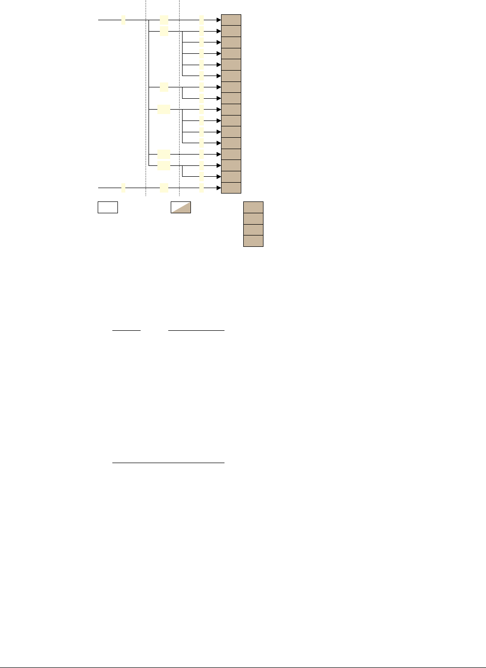
System Control
ARM DDI 0363G Copyright © 2006-2011 ARM Limited. All rights reserved. 4-59
ID041111 Non-Confidential
Figure 4-37 Cache operations
In addition to the register c7 cache management functions in this processor, an Invalidate all
data caches operation is provided as a c15 operation. For convenience, that c15 operation is also
described in this section.
Note
• Writing c7 with a combination of CRm and Opcode_2 not listed in Figure 4-37 results in
an Undefined Instruction exception.
• In this processor, reading from c7 causes an Undefined Instruction exception.
• All accesses to c7 can only be executed in a Privileged mode of operation, except for the
Flush Prefetch Buffer, Data Synchronization Barrier, and Data Memory Barrier
operations. These can be performed in User mode. Attempting to execute a Privileged
instruction in User mode results in an Undefined Instruction exception.
• This processor does not contain an address-based branch predictor array.
Invalidate and clean operations
The terms that describe the invalidate, clean, and prefetch operations are defined in the ARM
Architecture Reference Manual.
You can perform invalidate and clean operations on:
• single cache lines
• entire caches.
Set and Way format
Figure 4-38 on page 4-60 shows the Set and Way bit assignments.
c7 SBZ
SBZ
MVA
SBZ
MVA
Way
MVA
Way
SBZ
SBZ
MVA
Way
Invalidate data cache line by set/way
Invalidate data cache line to Point-of-Coherency by MVA
Invalidate entire branch predictor array (NOP)
Wait For Interrupt (NOP)
Flush Prefetch buffer
Invalidate VA from Branch Predictor Array (NOP)
Invalidate All Instruction Caches
Invalidate Instruction Cache Line to Point-of-Unification by MVA
Clean data cache line to Point-of-Unification by MVA
Clean data cache line to Point-of-Coherency by MVA
Clean data cache line by set/way
Data Synchronization Barrier
Data Memory Barrier
Clean and Invalidate data cache line to Point-of-Unification by MVA
Clean and Invalidate data cache line by set/way
Opcode_2CRmCRn Opcode_1
SBZ
MVA
SBZ Should Be Zero
MVA
Way
Using MVA
Using Set and Way
SBZ Invalidate all Data Caches0c15
Write-only Accessible in User modeRead-only Read/write
4
c0
0
1
4
6
7
c5
1
2
c6
1
c10
2
4
5
1
c11
0
1
c14
2
c50

System Control
ARM DDI 0363G Copyright © 2006-2011 ARM Limited. All rights reserved. 4-60
ID041111 Non-Confidential
Figure 4-38 Set and Way bit assignments
Table 4-38 shows the Set and Way bit assignments.
Table 4-39 shows the Set and Way bit assignments.
See c0, Cache Type Register on page 4-15 for more information on cache sizes.
Address format
Figure 4-39 shows the invalidate and clean operations bit assignments.
Figure 4-39 Invalidate and clean operations bit assignments
Table 4-40 shows the invalidate and clean operations bit assignments.
Way
0
Set ReservedReserved
54S+4S+531 2930
Table 4-38 Set and Way bit assignments
Bits Name Function
[31:30] Way Indicates the cache way to invalidate or clean.
[29:S+5] - SBZ.
[S+4:5] Set Indicates the cache set to invalidate or clean. Because the cache sizes are configurable, the width
of the Set field is unique to the cache size. See Table 4-39.
[4:0]] - SBZ.
Table 4-39 Widths of the set field for L1 cache sizes
Size Set
4KB [9:5]
8KB [10:5]
16KB [11:5]
32KB [12:5]
64KB [13:5]
Address
31 40
Reserved
5
Table 4-40 Invalidate and clean operations bit assignments
Bits Name Function
[31:5] Address Specifies the address to invalidate or clean
[4:0] - SBZ
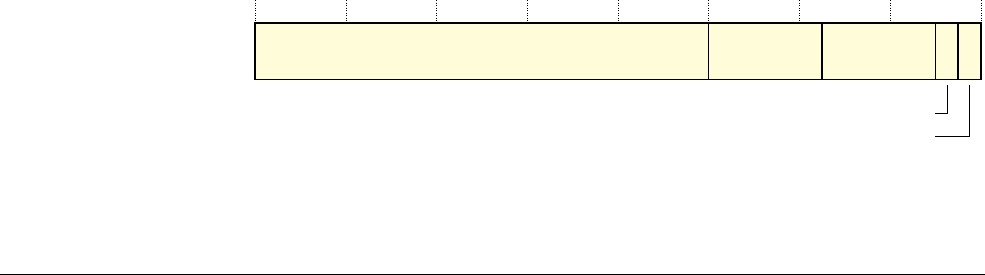
System Control
ARM DDI 0363G Copyright © 2006-2011 ARM Limited. All rights reserved. 4-61
ID041111 Non-Confidential
Data Synchronization Barrier operation
The purpose of the Data Synchronization Barrier operation is to ensure that all outstanding
explicit memory transactions complete before any following instructions begin. This ensures
that data in memory is up to date before the processor executes any more instructions.
The Data Synchronization Barrier Register is:
• a write-only operation
• accessible in both User and Privileged mode.
To access the Data Synchronization Barrier operation, write CP15 with:
MCR p15, 0, <Rd>, c7, c10, 4 ; Data Synchronization Barrier operation
For more information about memory barriers, see the ARM Architecture Reference Manual.
Data Memory Barrier operation
The purpose of the Data Memory Barrier operation is to ensure that all outstanding explicit
memory transactions complete before any following explicit memory transactions begin. This
ensures that data in memory is up to date before any memory transaction that depends on it.
The Data Memory Barrier operation is:
• write-only
• accessible in User and Privileged mode.
To access the Data Memory Barrier operation write CP15 with:
MCR p15, 0, <Rd>, c7, c10,5 ; Data Memory Barrier Operation.
For more information about memory barriers, see the ARM Architecture Reference Manual.
4.3.22 c9, BTCM Region Register
The BTCM Region Register characteristics are:
Purpose • Holds the base address and size of the BTCM.
• Determines if the BTCM is enabled.
Usage constraints The BTCM Region Register is:
• a read/write register
• accessible in Privileged mode only.
Configurations Available in all processor configurations.
Attributes See Table 4-41 on page 4-62.
Figure 4-40 shows the BTCM Region Register bit assignments.
Figure 4-40 BTCM Region Register bit assignments
Base address
31 12 11 7 6 2 1 0
Reserved Size
Reserved
Enable

System Control
ARM DDI 0363G Copyright © 2006-2011 ARM Limited. All rights reserved. 4-62
ID041111 Non-Confidential
Table 4-41 shows the BTCM Region Register bit assignments.
To access the BTCM Region Register, read or write CP15 with:
MRC p15, 0, <Rd>, c9, c1, 0 ; Read BTCM Region Register
MCR p15, 0, <Rd>, c9, c1, 0 ; Write BTCM Region Register
4.3.23 c9, ATCM Region Register
The ATCM Region Register characteristics are:
Purpose • Holds the base address and size of the ATCM.
• Determines if the ATCM is enabled.
Usage constraints The ATCM Region Register is:
• a read/write register
• accessible in Privileged mode only.
Configurations Available in all processor configurations.
Attributes See Table 4-42 on page 4-63.
Figure 4-41 shows the ATCM Region Register bit assignments.
Figure 4-41 ATCM Region Register bit assignments
Table 4-41 BTCM Region Register bit assignments
Bits Name Function
[31:12] Base
address
Base address. Defines the base address of the BTCM. The base address must be aligned to the
size of the BTCM. Any bits in the range [(log2(RAMSize)-1):12] are ignored.
At reset, if LOCZRAMA is set to:
0
=The initial base address is
0x0
.
1
=The initial base address is implementation-defined. See Configurable options on page 1-6.
[11:7] - UNP on reads, SBZ on writes.
[6:2] Size Size. Indicates the size of the BTCM on reads. On writes this field is ignored. See About the
TCMs on page 8-13:
b00000
= 0KB
b00011
= 4KB
b00100
= 8KB
b00101
= 16KB
b00110
= 32KB
b00111
= 64KB
b01000
= 128KB
b01001
= 256KB
b01010
= 512kB
b01011
= 1MB
b01100
= 2MB
b01101
= 4MB
b01110
= 8MB
[1] - SBZ.
[0] Enable Enables or disables the BTCM:
0
= Disabled
1
= Enabled. The reset value of this field is determined by the INITRAMB input pin.
Base address
31 12 11 7 6 2 1 0
Reserved Size
Reserved
Enable

System Control
ARM DDI 0363G Copyright © 2006-2011 ARM Limited. All rights reserved. 4-63
ID041111 Non-Confidential
Table 4-42 shows the ATCM Region Register bit assignments.
To access the ATCM Region Register, read or write CP15 with:
MRC p15, 0, <Rd>, c9, c1, 1 ; Read ATCM Region Register
MCR p15, 0, <Rd>, c9, c1, 1 ; Write ATCM Region Register
4.3.24 c9, TCM Selection Register
The TCM Selection Register determines the TCM region register that the processor writes to.
The processor only supports one TCM region for each TCM interface, and the TCM Selection
Register Reads-As-Zero and ignores writes. It is only accessible in Privileged mode.
4.3.25 c11, Slave Port Control Register
The Slave Port Control Register characteristics are:
Purpose • Enables or disables TCM access to the AXI slave port in Privileged
or User mode.
• Enables access to the cache RAMs through the AXI slave port. See
c1, Auxiliary Control Register on page 4-40.
Usage constraints The Slave Port Control Register is:
• a read/write register
• accessible in Privileged mode only.
Configurations Available in all processor configurations.
Attributes See Table 4-43 on page 4-64.
Figure 4-42 on page 4-64 shows the Slave Port Control Register bit assignments.
Table 4-42 ATCM Region Register bit assignments
Bits Name Function
[31:12] Base
address
Base address. Defines the base address of the ATCM. The base address must be aligned to the
size of the ATCM. Any bits in the range [(log2(RAMSize)-1):12] are ignored.
At reset, if LOCZRAMA is set to:
0 = The initial base address is implementation-defined. See Configurable options on page 1-6
1 = The initial base address is
0x0
.
[11:7] - UNP on reads, SBZ on writes.
[6:2] Size Size. Indicates the size of the ATCM on reads. On writes this field is ignored. See About the TCMs
on page 8-13.
b00000 = 0KB
b00011 = 4KB
b00100 = 8KB
b00101 = 16KB
b00110 = 32KB
b00111 = 64KB
b01000 = 128KB
b01001 = 256KB
b01010 = 512kB
b01011 = 1MB
b01100 = 2MB
b01101 = 4MB
b01110 = 8MB.
[1] - SBZ
[0] Enable Enables or disables the ATCM.
0 = Disabled
1 = Enabled. The reset value of this field is determined by the INITRAMA input pin.

System Control
ARM DDI 0363G Copyright © 2006-2011 ARM Limited. All rights reserved. 4-64
ID041111 Non-Confidential
Figure 4-42 Slave Port Control Register bit assignments
Table 4-43 shows the Slave Port Control Register bit assignments.
To access the Slave Port Control Register, read or write CP15 with:
MRC p15, 0, <Rd>, c11, c0, 0 ; Read Slave Port Control Register
MCR p15, 0, <Rd>, c11, c0, 0 ; Write Slave Port Control Register
4.3.26 c13, FCSE PID Register
This processor does not support Fast Context Switch Extension (FCSE).
The FCSE Process IDentifier (PID) Register is accessible in Privileged mode only. This register
reads as zero and ignores writes.
4.3.27 c13, Context ID Register
The CONTEXTIDR characteristics are:
Purpose • Holds a process IDentification (ID) value for the running process.
• The Embedded Trace Macrocell (ETM) and the debug logic use this
register. The ETM can broadcast its value to indicate the process that
is running. You must program each process with a unique number.
• Enables process dependent breakpoints and instructions.
Usage constraints The CONTEXTIDR is:
• a read/write register
• accessible in Privileged mode only.
Configurations Available in all processor configurations.
Attributes The CONTEXTIDR, bits [31:0] contain the process ID number.
To use the CONTEXTIDR, read or write CP15 with:
Reserved
31 210
Privileged access
AXI slave enable
Table 4-43 Slave Port Control Register bit assignments
Bits Name Function
[31:2] - RAZ/UNP
[1] Privileged access Defines level of access for TCM accesses:
0
= Non-privileged and privileged access. This is the reset value.
1
= Privileged access only.
[0] AXI slave enable Enables or disables the AXI slave port for TCM accesses:
0
= Enables AXI slave port. This is the reset value.
1
= Disables AXI slave port.

System Control
ARM DDI 0363G Copyright © 2006-2011 ARM Limited. All rights reserved. 4-65
ID041111 Non-Confidential
MRC p15, 0, <Rd>, c13, c0, 1 ; Read CONTEXTIDR
MCR p15, 0, <Rd>, c13, c0, 1 ; Write CONTEXTIDR
4.3.28 c13, Thread and Process ID Registers
The Thread and Process ID Registers provide locations to store the IDs of software threads and
processes for Operating System (OS) management purposes.
The Thread and Process ID Registers are:
• three read/write registers:
— User read/write Thread and Process ID Register
— User read-only Thread and Process ID Register
— Privileged-only Thread and Process ID Register.
• each accessible in different modes:
— The User read/write register can be read and written in User and Privileged modes.
— The User read-only register can only be read in User mode, but can be read and
written in Privileged modes.
— The Privileged-only register can be read and written in Privileged modes only.
To access the Thread and Process ID registers, read or write CP15 with:
MRC p15, 0, <Rd>, c13, c0, 2 ; Read User read/write Thread and Proc. ID Register
MCR p15, 0, <Rd>, c13, c0, 2 ; Write User read/write Thread and Proc. ID Register
MRC p15, 0, <Rd>, c13, c0, 3 ; Read User Read Only Thread and Proc. ID Register
MCR p15, 0, <Rd>, c13, c0, 3 ; Write User Read Only Thread and Proc. ID Register
MRC p15, 0, <Rd>, c13, c0, 4 ; Read Privileged Only Thread and Proc. ID Register
MCR p15, 0, <Rd>, c13, c0, 4 ; Write Privileged Only Thread and Proc. ID Register
Reading or writing the Thread and Process ID registers has no effect on processor state or
operation. These registers provide OS support, and the OS must manage them.
You must clear the contents of all Thread and Process ID registers on process switches to
prevent data leaking from one process to another. This is important to ensure the security of data.
The reset value of these registers is 0.
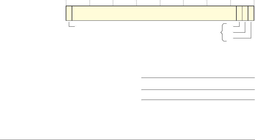
System Control
ARM DDI 0363G Copyright © 2006-2011 ARM Limited. All rights reserved. 4-66
ID041111 Non-Confidential
4.3.29 Validation Registers
The processor implements a set of validation registers. This section describes:
•c15, nVAL IRQ Enable Set Register
•c15, nVAL FIQ Enable Set Register on page 4-67
•c15, nVAL Reset Enable Set Register on page 4-68
•c15, VAL Debug Request Enable Set Register on page 4-69
•c15, nVAL IRQ Enable Clear Register on page 4-70
•c15, nVAL FIQ Enable Clear Register on page 4-71
•c15, nVAL Reset Enable Clear Register on page 4-72
•c15, VAL Debug Request Enable Clear Register on page 4-73
•c15, Cache Size Override Register on page 4-74.
c15, nVAL IRQ Enable Set Register
The nVAL IRQ Enable Set Register characteristics are:
Purpose Enables any of the PMXEVCNTR Registers,
PMXEVCNTR0-PMXEVCNTR2, and PMCCNTR, to generate an
interrupt request on overflow. If enabled, the interrupt request is signaled
by nVALIRQ being asserted LOW.
Usage constraints The nVAL IRQ Enable Set Register is:
• A read/write register.
• Always accessible in Privileged mode. The PMUSERENR Register
determines access in User mode, see c9, User Enable Register on
page 6-15.
Configurations Available in all processor configurations.
Attributes See Table 4-44.
Figure 4-43 shows the nVAL IRQ Enable Set Register bit assignments.
Figure 4-43 nVAL IRQ Enable Set Register bit assignments
Table 4-44 shows the nVAL IRQ Enable Set Register bit assignments.
C
31 3210
Reserved
P2
P1
P0
Performance monitor counter
overflow IRQ request enables
Cycle count overflow IRQ request enable
Table 4-44 nVAL IRQ Enable Set Register bit assignments
Bits Name Function
[31] C PMCCNTR overflow IRQ request
[30: 3] - UNP or SBZP

System Control
ARM DDI 0363G Copyright © 2006-2011 ARM Limited. All rights reserved. 4-67
ID041111 Non-Confidential
To access the nVAL IRQ Enable Set Register, read or write CP15 with:
MRC p15, 0, <Rd>, c15, c1, 0 ; Read nVAL IRQ Enable Set Register
MCR p15, 0, <Rd>, c15, c1, 0 ; Write nVAL IRQ Enable Set Register
On reads, this register returns the current setting. On writes, interrupt requests can be enabled
by writing a 1 to the appropriate bits. If an interrupt request is enabled it is disabled by writing
to the nVAL IRQ Enable Clear Register, see c15, nVAL IRQ Enable Clear Register on
page 4-70.
If one or more of the IRQ request fields (P2, P1, P0, and C) is enabled, and the corresponding
counter overflows, then an IRQ request is indicated by nVALIRQ being asserted LOW. This
signal might be passed to a system interrupt controller.
c15, nVAL FIQ Enable Set Register
The nVAL FIQ Enable Set Register characteristics are:
Purpose Enables any of the PMXEVCNTR Registers,
PMXEVCNTR0-PMXEVCNTR2, and PMCCNTR, to generate an fast
interrupt request on overflow. If enabled, the interrupt request is signaled
by nVALFIQ being asserted LOW.
Usage constraints The nVAL FIQ Enable Set Register is:
• A read/write register.
• Always accessible in Privileged mode. The PMUSERENR Register
determines access in User mode, see c9, User Enable Register on
page 6-15.
Configurations Available in all processor configurations.
Attributes See Table 4-45 on page 4-68.
Figure 4-44 shows the nVAL FIQ Enable Set Register bit assignments.
Figure 4-44 nVAL FIQ Enable Set Register bit assignments
[2] P2 PMC2 overflow IRQ request
[1] P1 PMC1 overflow IRQ request
[0] P0 PMC0 overflow IRQ request
Table 4-44 nVAL IRQ Enable Set Register bit assignments (continued)
Bits Name Function
C
31 3210
Reserved
P2
P1
P0
Performance monitor counter
overflow FIQ request enables
Cycle count overflow FIQ request enable

System Control
ARM DDI 0363G Copyright © 2006-2011 ARM Limited. All rights reserved. 4-68
ID041111 Non-Confidential
Table 4-45 shows the nVAL FIQ Enable Set Register bit assignments.
To access the FIQ Enable Set Register, read or write CP15 with:
MRC p15, 0, <Rd>, c15, c1, 1 ; Read FIQ Enable Set Register
MCR p15, 0, <Rd>, c15, c1, 1 ; Write FIQ Enable Set Register
On reads, this register returns the current setting. On writes, interrupt requests can be enabled
by writing a 1 to the appropriate bits. If an interrupt request is enabled it is disabled by writing
to the FIQ Enable Clear Register, see c15, nVAL FIQ Enable Clear Register on page 4-71.
If one or more of the FIQ request fields (P2, P1, P0, and C) is enabled, and the corresponding
counter overflows, then an FIQ request is indicated by nVALFIQ being asserted LOW. This
signal can be passed to a system interrupt controller.
c15, nVAL Reset Enable Set Register
The nVAL Reset Enable Set Register is:
• A read/write register.
• Always accessible in Privileged mode. The PMUSERENR Register determines access in
User mode, see c9, User Enable Register on page 6-15.
The nVAL Reset Enable Set Register characteristics are:
Purpose Enables any of the PMXEVCNTR Registers,
PMXEVCNTR0-PMXEVCNTR2, and PMCCNTR, to generate a reset
request on overflow. If enabled, the reset request is signaled by
nVALRESET being asserted LOW.
Usage constraints The nVAL Reset Enable Set Register is:
• A read/write register.
• Always accessible in Privileged mode. The PMUSERENR Register
determines access in User mode, see c9, User Enable Register on
page 6-15.
Configurations Available in all processor configurations.
Attributes See Table 4-46 on page 4-69.
Figure 4-45 on page 4-69 shows the nVAL Reset Enable Set Register bit assignments.
Table 4-45 nVAL FIQ Enable Set Register bit assignments
Bits Name Function
[31] C PMCCNTR overflow FIQ request
[30:3] - UNP or SBZP
[2] P2 PMC2 overflow FIQ request
[1] P1 PMC1 overflow FIQ request
[0] P0 PMC0 overflow FIQ request

System Control
ARM DDI 0363G Copyright © 2006-2011 ARM Limited. All rights reserved. 4-69
ID041111 Non-Confidential
Figure 4-45 nVAL Reset Enable Set Register bit assignments
Table 4-46 shows the nVAL Reset Enable Set Register bit assignments.
To access the nVAL Reset Enable Set Register, read or write CP15 with:
MRC p15, 0, <Rd>, c15, c1, 2 ; Read nVAL Reset Enable Set Register
MCR p15, 0, <Rd>, c15, c1, 2 ; Write nVAL Reset Enable Set Register
On reads, this register returns the current setting. On writes, interrupt requests can be enabled
by writing a 1 to the appropriate bits. If a reset request is enabled, it is disabled by writing to the
nVAL Reset Enable Clear Register. See c15, nVAL Reset Enable Clear Register on page 4-72.
If one or more of the reset request fields (P2, P1, P0, and C) is enabled, and the corresponding
counter overflows, then a reset request is indicated by nVALRESET being asserted LOW. This
signal can be passed to a system reset controller.
c15, VAL Debug Request Enable Set Register
The VAL Debug Request Enable Set Register characteristics are:
Purpose Enables any of the PMXEVCNTR Registers,
PMXEVCNTR0-PMXEVCNTR2, and PMCCNTR, to generate a debug
request on overflow. If enabled, the debug request is signaled by
VALEDBGRQ being asserted HIGH.
Usage constraints The VAL Debug Request Enable Set Register is:
• A read/write register.
• Always accessible in Privileged mode. The PMUSERENR Register
determines access in User mode, see c9, User Enable Register on
page 6-15.
Configurations Available in all processor configurations.
Attributes See Table 4-47 on page 4-70.
Figure 4-46 on page 4-70 shows the VAL Debug Request Enable Set Register bit assignments.
C
31 3210
Reserved
P2
P1
P0
Performance monitor counter
overflow reset request enables
Cycle count overflow reset request enable
Table 4-46 nVAL Reset Enable Set Register bit assignments
Bits Name Function
[31] C PMCCNTR overflow reset request
[30:3] - UNP or SBZP
[2] P2 PMC2 overflow reset request
[1] P1 PMC1 overflow reset request
[0] P0 PMC0 overflow reset request

System Control
ARM DDI 0363G Copyright © 2006-2011 ARM Limited. All rights reserved. 4-70
ID041111 Non-Confidential
Figure 4-46 VAL Debug Request Enable Set Register bit assignments
Table 4-47 shows the VAL Debug Request Enable Set Register bit assignments.
To access the nVAL Debug Request Enable Set Register, read or write CP15 with:
MRC p15, 0, <Rd>, c15, c1, 3 ; Read nVAL Debug Request Enable Set Register
MCR p15, 0, <Rd>, c15, c1, 3 ; Write nVAL Debug Request Enable Set Register
On reads, this register returns the current setting. On writes, interrupt requests can be enabled
by writing a 1 to the appropriate bits. If a debug request is enabled, it is disabled by writing to
the nVAL Debug Request Enable Clear Register. See c15, VAL Debug Request Enable Clear
Register on page 4-73.
If one or more of the reset request fields (P2, P1, P0, and C) is enabled, and the corresponding
counter overflows, then a debug reset request is indicated by VA L E D B G R Q being asserted
HIGH. This signal can be passed to an external debugger.
c15, nVAL IRQ Enable Clear Register
The nVAL IRQ Enable Clear Register characteristics are:
Purpose Disables overflow IRQ requests from any of the PMXEVCNTR Registers,
PMXEVCNTR0-PMXEVCNTR2, and PMCCNTR, for which they have
been enabled.
Usage constraints The nVAL IRQ Enable Clear Register is:
• A read/write register.
• Always accessible in Privileged mode. The PMUSERENR Register
determines access in User mode, see c9, User Enable Register on
page 6-15.
Configurations Available in all processor configurations.
Attributes See Table 4-48 on page 4-71.
Figure 4-47 on page 4-71 shows the nVAL IRQ Enable Clear Register bit assignments.
C
31 3210
Reserved
P2
P1
P0
Performance monitor counter
overflow debug request enables
Cycle count overflow debug request enable
Table 4-47 VAL Debug Request Enable Set Register bit assignments
Bits Name Function
[31] C PMCCNTR overflow debug request
[30:3] - UNP or SBZP
[2] P2 PMC2 overflow debug request
[1] P1 PMC1 overflow debug request
[0] P0 PMC0 overflow debug request

System Control
ARM DDI 0363G Copyright © 2006-2011 ARM Limited. All rights reserved. 4-71
ID041111 Non-Confidential
Figure 4-47 nVAL IRQ Enable Clear Register bit assignments
Table 4-48 shows the nVAL IRQ Enable Clear Register bit assignments.
To access the nVAL IRQ Enable Clear Register, read or write CP15 with:
MRC p15, 0, <Rd>, c15, c1, 4 ; Read nVAL IRQ Enable Clear Register
MCR p15, 0, <Rd>, c15, c1, 4 ; Write nVAL IRQ Enable Clear Register
On reads, this register returns the current setting. On writes, overflow interrupt requests that are
enabled can be disabled by writing a 1 to the appropriate bits.
For more information of how to enable IRQ requests on counter overflows, and how the requests
are signaled, see c15, nVAL IRQ Enable Set Register on page 4-66.
c15, nVAL FIQ Enable Clear Register
The nVAL FIQ Enable Clear Register characteristics are:
Purpose Disables overflow FIQ requests from any of the PMXEVCNTR Registers,
PMXEVCNTR0-PMXEVCNTR2, and PMCCNTR, that are enabled.
Usage constraints The nVAL FIQ Enable Clear Register is:
• A read/write register.
• Always accessible in Privileged mode. The PMUSERENR Register
determines access in User mode, see c9, User Enable Register on
page 6-15.
Configurations Available in all processor configurations.
Attributes See Table 4-49 on page 4-72.
Figure 4-48 on page 4-72 shows the nVAL FIQ Enable Clear Register bit assignments.
C
31 3210
Reserved
P2
P1
P0
Performance monitor counter
overflow IRQ request disables
Cycle count overflow
IRQ request disable
Table 4-48 nVAL IRQ Enable Clear Register bit assignments
Bits Name Function
[31] C PMCCNTR overflow IRQ request
[30:3] - UNP or SBZP
[2] P2 PMC2 overflow IRQ request
[1] P1 PMC1 overflow IRQ request
[0] P0 PMC0 overflow IRQ request

System Control
ARM DDI 0363G Copyright © 2006-2011 ARM Limited. All rights reserved. 4-72
ID041111 Non-Confidential
Figure 4-48 nVAL FIQ Enable Clear Register bit assignments
Table 4-49 shows the nVAL FIQ Enable Clear Register bit assignments.
To access the FIQ Enable Clear Register, read or write CP15 with:
MRC p15, 0, <Rd>, c15, c1, 5 ; Read FIQ Enable Clear Register
MCR p15, 0, <Rd>, c15, c1, 5 ; Write FIQ Enable Clear Register
On reads, this register returns the current setting. On writes, overflow interrupt requests that are
enabled can be disabled by writing a 1 to the appropriate bits.
For information on how to enable FIQ requests on counter overflows, and how the requests are
signaled, see c15, nVAL FIQ Enable Set Register on page 4-67.
c15, nVAL Reset Enable Clear Register
The nVAL Reset Enable Clear Register characteristics are:
Purpose Disables overflow reset requests from any of the PMXEVCNTR
Registers, PMXEVCNTR0-PMXEVCNTR2, and PMCCNTR, that are
enabled.
Usage constraints The nVAL Reset Enable Clear Register is:
• A read/write register.
• Always accessible in Privileged mode. The PMUSERENR Register
determines access in User mode, see c9, User Enable Register on
page 6-15.
Configurations Available in all processor configurations.
Attributes See Table 4-50 on page 4-73.
Figure 4-49 on page 4-73 shows the nVAL Reset Enable Clear Register bit assignments.
C
31 3210
Reserved
P2
P1
P0
Performance monitor counter
overflow FIQ request disables
Cycle count overflow
FIQ request disable
Table 4-49 nVAL FIQ Enable Clear Register bit assignments
Bits Name Function
[31] C PMCCNTR overflow FIQ request
[30:3] - UNP or SBZP
[2] P2 PMC2 overflow FIQ request
[1] P1 PMC1 overflow FIQ request
[0] P0 PMC0 overflow FIQ request

System Control
ARM DDI 0363G Copyright © 2006-2011 ARM Limited. All rights reserved. 4-73
ID041111 Non-Confidential
Figure 4-49 nVAL Reset Enable Clear Register bit assignments
Table 4-50 shows the nVAL Reset Enable Clear Register bit assignments.
To access the nVAL Reset Enable Clear Register, read or write CP15 with:
MRC p15, 0, <Rd>, c15, c1, 6 ; Read nVAL Reset Enable Clear Register
MCR p15, 0, <Rd>, c15, c1, 6 ; Write nVAL Reset Enable Clear Register
On reads, this register returns the current setting. On writes, overflow reset requests that are
enabled can be disabled by writing a 1 to the appropriate bits.
For more information of how to enable reset requests on counter overflows, and how the
requests are signaled, see c15, nVAL Reset Enable Set Register on page 4-68.
c15, VAL Debug Request Enable Clear Register
The VAL Debug Request Enable Clear Register characteristics are:
Purpose Disables overflow debug requests from any of the PMXEVCNTR
Registers, PMXEVCNTR0-PMXEVCNTR2, and PMCCNTR, that are
enabled.
Usage constraints The VAL Debug Request Enable Clear Register is:
• A read/write register.
• Always accessible in Privileged mode. The PMUSERENR Register
determines access in User mode, see c9, User Enable Register on
page 6-15.
Configurations Available in all processor configurations.
Attributes See Table 4-51 on page 4-74.
Figure 4-50 on page 4-74 shows the VAL Debug Request Enable Clear Register bit
assignments.
C
31 3210
Reserved
P2
P1
P0
Performance monitor counter overflow
reset request disables
Cycle count overflow
reset request disable
Table 4-50 nVAL Reset Enable Clear Register bit assignments
Bits Name Function
[31] C PMCCNTR overflow reset request
[30:3] - UNP or SBZP
[2] P2 PMC2 overflow reset request
[1] P1 PMC1 overflow reset request
[0] P0 PMC0 overflow reset request

System Control
ARM DDI 0363G Copyright © 2006-2011 ARM Limited. All rights reserved. 4-74
ID041111 Non-Confidential
Figure 4-50 VAL Debug Request Enable Clear Register bit assignments
Table 4-51 shows the VAL Debug Request Enable Clear Register bit assignments.
To access the nVAL Debug Request Enable Clear Register, read or write CP15 with:
MRC p15, 0, <Rd>, c15, c1, 7 ; Read nVAL Debug Request Enable Clear Register
MCR p15, 0, <Rd>, c15, c1, 7 ; Write nVAL Debug Request Enable Clear Register
On reads, this register returns the current setting. On writes, overflow debug requests that are
enabled can be disabled by writing a 1 to the appropriate bits.
For more information of how to enable debug requests on counter overflows, and how the
requests are signaled, see c15, VAL Debug Request Enable Set Register on page 4-69.
c15, Cache Size Override Register
The Cache Size Override Register characteristics are:
Purpose Overwrites the caches size fields in the main register. This enables you to
choose a smaller instruction and data cache size than is implemented.
Usage constraints The Cache Size Override Register is:
• a write-only register
• only accessible in Privileged mode.
Configurations Available in all processor configurations.
Attributes See Table 4-52 on page 4-75.
Figure 4-51 shows the Cache Size Override Register bit assignments.
Figure 4-51 Cache Size Override Register bit assignments
C
31 3210
Reserved
P2
P1
P0
Performance monitor counter overflow
debug request disables
Cycle count overflow
debug request disable
Table 4-51 VAL Debug Request Enable Clear Register bit assignments
Bits Name Function
[31] C PMCCNTR overflow debug request
[30:3] - UNP or SBZP
[2] P2 PMC2 overflow debug request
[1] P1 PMC1 overflow debug request
[0] P0 PMC0 overflow debug request
Icache
31 16 15 78430
Reserved Dcache

System Control
ARM DDI 0363G Copyright © 2006-2011 ARM Limited. All rights reserved. 4-75
ID041111 Non-Confidential
Table 4-52 shows the Cache Size Override Register bit assignments.
Table 4-53 shows the encodings for the instruction and data cache sizes.
To access the Cache Size Override Register, write CP15 with:
MCR p15, 0, <Rd>, c15, c14, 0 ; VAL Cache Size Override Register
Note
The Cache Size Override Register can only be used to select cache sizes for which the
appropriate RAM is integrated. Larger cache sizes require deeper data and tag RAMs, and
smaller cache sizes require wider tag RAMs. Therefore, it is unlikely that you can change the
cache size using this register except using a simulation model of the cache RAMs.
4.3.30 Correctable Fault Location Register
The CFLR characteristics are:
Purpose Indicates the location of the last correctable error that occurred during
cache or TCM operations.
Usage constraints The CFLR is:
• a read/write register
• accessible in Privileged mode only
• not updated on:
— speculative accesses, for example, an instruction fetch for an
instruction that is not executed because of a previous branch
— a TCM external error or external retry request.
• updated on:
— parity or ECC errors in the instruction cache
— single-bit ECC errors in the data cache
— parity or multi-bit errors in the data cache when write-through
behavior is forced
Table 4-52 Cache Size Override Register bit assignments
Bits Name Function
[31:8] - SBZ.
[7:4] Dcache Defines the data cache size override value. See Table 4-53.
[3:0] Icache Defines the instruction cache size override value. See Table 4-53.
Table 4-53 instruction and data cache size encodings
Encoding Instruction and data cache size
b0000 4kB
b0001 8kB
b0011 16kB
b0111 32kB
b1111 64kB
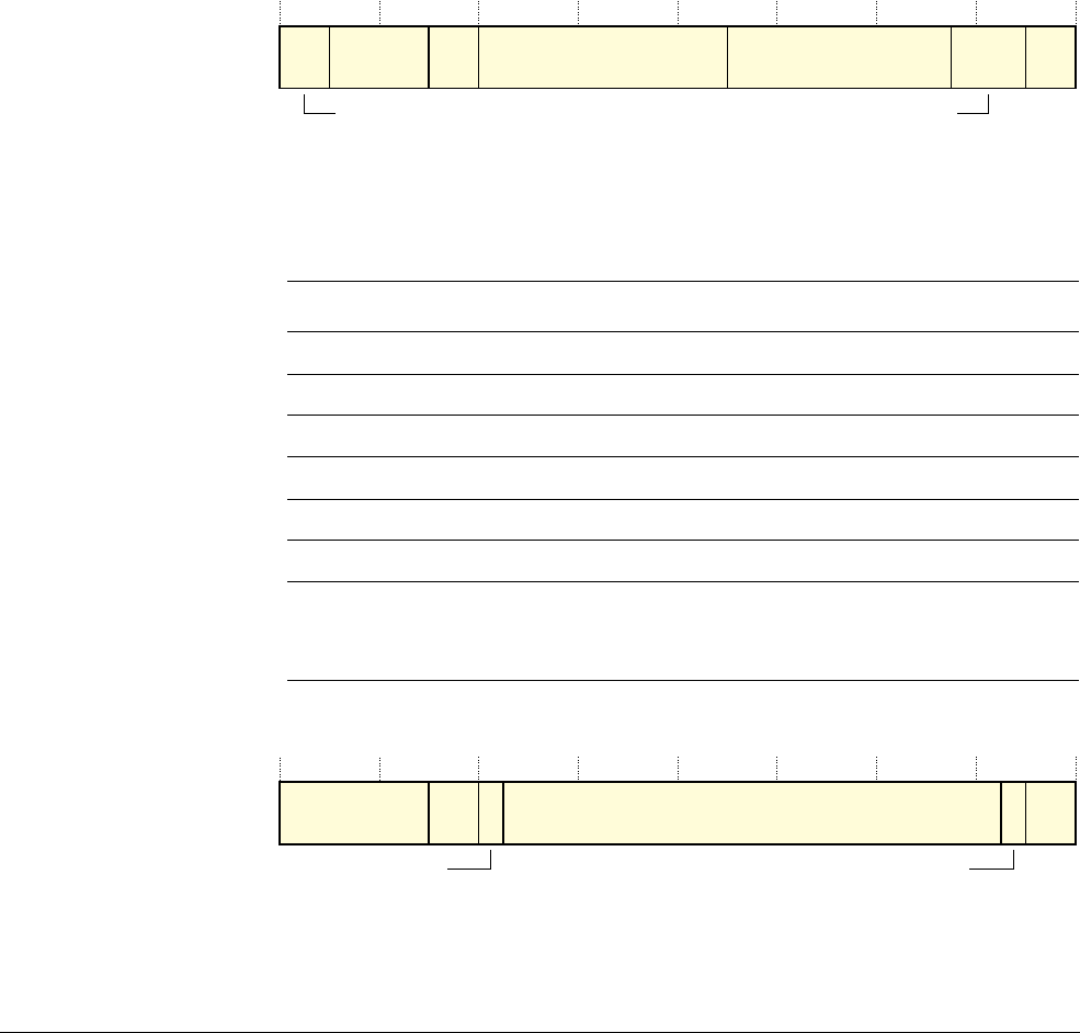
System Control
ARM DDI 0363G Copyright © 2006-2011 ARM Limited. All rights reserved. 4-76
ID041111 Non-Confidential
— single-bit TCM ECC errors.
• updated by the processor, regardless of whether an abort is taken or
an access is retried in response to the error.
Configurations Available in all processor configurations.
Attributes See Table 4-54.
Every correctable error that causes a CFLR update also has an associated event. See Table 6-1
on page 6-2 for the events that are related to CFLR updates. If two correctable errors occur
simultaneously, for example an AXI slave error and an LSU or PFU error, the LSU or PFU write
takes priority. If multiple errors occur, the value in the CFLR reflects the location of the latest
event.
The same register is updated by all correctable errors. You can read bits [25:24] to determine
whether the error was from a cache or TCM access.
Figure 4-52 shows the CFLR bit assignments, when it indicates a correctable cache error.
Figure 4-52 CFLR - cache, bit assignments
Table 4-54 shows the CFLR bit assignments, when it indicates a correctable cache error.
Figure 4-53 shows the CFLR bit assignments, when it indicates a correctable TCM error.
Figure 4-53 CFLR - TCM, bit assignments
Side Reserved Type
31 30 29 26 25 24 23 14 13 5 4 2 1 0
Way Index
Reserved Reserved
Table 4-54 CFLR - cache, bit assignments
Bits Name Function
[31:30] - RAZ
[29:26] Way Indicates the Way of the error.
[25:24] Side Indicates the source of the error. For cache errors, this value is always
0b00
.
[23:14] - RAZ
[13:5] Index Indicates the index of the location where the error occurred.
[4:2] - RAZ
[1:0] Type Indicates the type of access that caused the error:
0b00
= Instruction cache.
0b01
= Data cache.
Type
31 26 25 24 23 22 3210
Reserved Side Address[22:3]
Reserved Reserved

System Control
ARM DDI 0363G Copyright © 2006-2011 ARM Limited. All rights reserved. 4-77
ID041111 Non-Confidential
Table 4-55 shows the CFLR bit assignments, when it indicates a correctable TCM error.
To access the CFLR, read or write CP15 with:
MRC p15, 0, <Rd>, c15, c3, 0 : Read CFLR
MCR p15, 0, <Rd>, c15, c3, 0 : Write CFLR
4.3.31 Build Options Registers
Note
These registers are implemented from the r1pn releases of the processor. Attempting to access
these registers in r0pn releases of the processor results in an Undefined Instruction exception.
c15, Build Options 1 Register
The Build Options 1 Register characteristics are:
Purpose Reflects the build configuration options used to build the processor.
Usage constraints The Build Options 1 Register is:
• a read-only register
• accessible in Privileged mode only
Configurations Available in all processor configurations.
Attributes See Table 4-56 on page 4-78.
Figure 4-54 shows the Build Options 1 Register bit assignments.
Figure 4-54 Build Options 1 Register bit assignments
Table 4-55 CFLR - TCM, bit assignments
Bits Name Function
[31:26] - RAZ
[25:24] Side Indicates the source of the error:
0b01
= ATCM
0b10
= BTCM
[23] - RAZ
[22:3] Address Indicates the address in the TCM where the error occurred.
[2] - RAZ
[1:0] Type Indicates the type of access that caused the error:
0b00
= Instruction.
0b01
= Data.
0b10
= AXI slave
0b11
is unused.
31 11 012
ReservedTCM_HI_INIT_ADDR
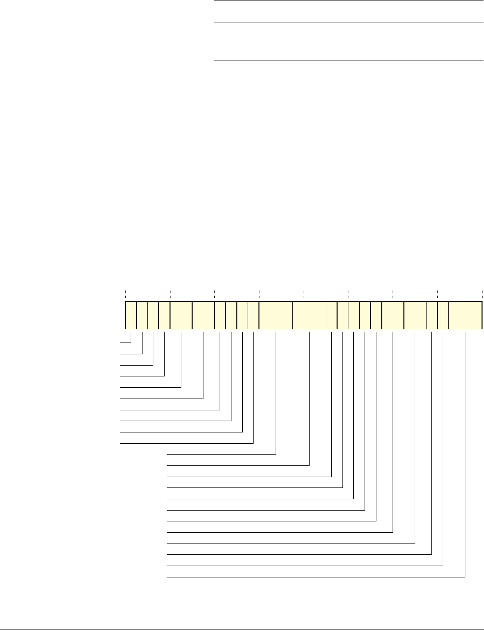
System Control
ARM DDI 0363G Copyright © 2006-2011 ARM Limited. All rights reserved. 4-78
ID041111 Non-Confidential
Table 4-56 shows the Build Options 1 Register bit assignments.
To access the Build Options 1 Register, read CP15 with:
MRC p15, 0, <Rd>, c15, c2, 0 ; read Build Options 1 Register
c15, Build Options 2 Register
The Build Options 2 Register characteristics are:
Purpose Reflects the build configuration options used to build the processor.
Usage constraints The Build Options 2 Register is:
• a read-only register
• accessible in Privileged mode only.
Configurations Available in all processor configurations.
Attributes See Table 4-57 on page 4-79.
Figure 4-55 shows the Build Options 2 Register bit assignments.
Figure 4-55 Build Options 2 Register bit assignments
Table 4-56 Build Options 1 Register bit assignments
Bits Name Function
[31:12] TCM_HI_INIT_ADDR Default high address for the TCM.
[11:0] - SBZ
31 25 24 23 22 21 19 17 16 14 13 12 11 7 6 3 026272830 29 1020 9458
DUAL_CORE
DUAL_NCLK
NO_ICACHE
NO_DCACHE
ATCM_ES
BTCM_ES
NO_IE
NO_FPU
NO_MPU
MPU_REGIONS
BREAK_POINTS
WATCH_POINTS
NO_A_TCM_INF
NO_B0_TCM_INF
NO_B1_TCM_INF
TCMBUSPARITY
NO_SLAVE
ICACHE_ES
DCACHE_ES
N0_HARD_ERROR_CACHE
AXIBUSPARITY
2
RESERVED

System Control
ARM DDI 0363G Copyright © 2006-2011 ARM Limited. All rights reserved. 4-79
ID041111 Non-Confidential
Table 4-57 shows the Build Options 2 Register bit assignments.
Table 4-57 Build Options 2 Register bit assignments
Bits Name Function
[31] DUAL_COREaIndicates whether a second, redundant, copy of the processor logic and
checking logic was instantiated:
0
= single core
1
= dual core.
[30] DUAL_NCLKaIndicates whether an inverted clock is used for the redundant core:
0
= inverted clock not used
1
= inverted clock used.
[29] NO_ICACHE Indicates whether the processor contains instruction cache:
0
= processor contains instruction cache
1
= processor does not contain instruction cache.
[28] NO_DCACHE Indicates whether the processor contains data cache:
0
= processor contains data cache
1
= processor does not contain data cache.
[27:26] ATCM_ES Indicates whether an error scheme is implemented on the ATCM interface:
00
= no error scheme
01
= 8-bit parity logic
10
= 32-bit error detection and correction
11
= 64-bit error detection and correction.
[25:24] BTCM_ES Indicates whether an error scheme is implemented on the BTCM
interface(s):
00
= no error scheme
01
= 8-bit parity logic
10
= 32-bit error detection and correction
11
= 64-bit error detection and correction.
[23] NO_IE Indicates whether the processor supports big-endian instructions:
0
= processor supports big-endian instructions
1
= processor does not support big-endian instructions.
[22] NO_FPU Indicates whether the processor contains a floating point unit:
0
= processor contains a floating point unit
1
= processor does not contain a floating point unit.
[21] NO_MPU Indicates whether the processor contains a Memory Protection Unit (MPU):
0
= processor contains an MPU
1
= processor does not contain an MPU.
[20] MPU_REGIONS Indicates the number of regions in the included MPU:
0
= 8
1
= 12.
If the processor does not contain an MPU (bit [21] set to 0), this bit is set to 0.
[19:17] BREAK_POINTS Indicates the number of break points implemented in the processor, minus 1.
[16:14] WATCH_POINTS Indicates the number of watch points implemented in the processor, minus 1.

System Control
ARM DDI 0363G Copyright © 2006-2011 ARM Limited. All rights reserved. 4-80
ID041111 Non-Confidential
To access the Build Options 2 Register, write CP15 with:
MRC p15, 0, <Rd>, c15, c2, 1 ; read Build Options 2 Register
[13] NO_A_TCM_INF Indicates whether the processor contains an ATCM port:
0 = processor contains ATCM port
1 = processor does not contain ATCM port.
[12] NO_B0_TCM_INF Indicates whether the processor contains a B0TCM port:
0 = processor contains B0TCM port
1 = processor does not contain B0TCM port.
[11] NO_B1_TCM_INF Indicates whether the processor contains a B1TCM port:
0 = processor contains B1TCM port
1 = processor does not contain B1TCM port.
[10] TCMBUSPARITY Indicates whether the processor contains TCM address bus parity logic:
0 = processor does not contain TCM address bus parity logic
1 = processor contains TCM address bus parity logic.
[9] NO_SLAVE Indicates whether the processor contains an AXI slave port:
0 = processor contains an AXI slave port
1 = processor does not contain an AXI slave port.
[8:7] ICACHE_ES Indicates whether an error scheme is implemented for the instruction cache:
00 = no error scheme
01 = 8-bit parity error detection
11 = 64-bit error detection and correction.
If the processor does not contain an Icache, these bits are set to 00.
[6:5] DCACHE_ES Indicates whether an error scheme is implemented for the data cache:
00 = no error scheme
01 = 8-bit parity error detection
10 = 32-bit error detection and correction.
If the processor does not contain a Dcache, these bits are set to0b00.
[4] NO_HARD_ERROR_CACHE Indicates whether the processor contains cache for corrected TCM errors:
0 = processor contains TCM error cache
1 = processor does not contain TCM error cache.
[3] AXIBUSPARITY Indicates whether the processor contains AXI bus parity logic.
0 = processor does not contain AXI bus parity logic
1 = processor contains AXI bus parity logic.
[2:0] - Undefined.
a. The value of this bit is Unpredictable in revision r1p0 of the processor.
Table 4-57 Build Options 2 Register bit assignments (continued)
Bits Name Function

ARM DDI 0363G Copyright © 2006-2011 ARM Limited. All rights reserved. 5-1
ID041111 Non-Confidential
Chapter 5
Prefetch Unit
This chapter describes how the PreFetch Unit (PFU), in conjunction with the DPU, uses program
flow prediction to locate branches in the instruction stream and the strategies used to determine if
a branch is likely to be taken or not. It contains the following sections:
•About the prefetch unit on page 5-2
•Branch prediction on page 5-3
•Return stack on page 5-5
•Controlling instruction prefetch and program flow prediction on page 5-6.

Prefetch Unit
ARM DDI 0363G Copyright © 2006-2011 ARM Limited. All rights reserved. 5-2
ID041111 Non-Confidential
5.1 About the prefetch unit
The purpose of the PFU is to:
• perform speculative fetch of instructions ahead of the DPU by predicting the outcome of
branch instructions
• format instruction data in a way that aids the DPU in efficient execution.
The PFU fetches instructions from the memory system under the control of the DPU, and the
internal coprocessors CP14 and CP15. In ARM state the memory system can supply up to two
instructions per cycle. In Thumb state the memory system can supply up to four instructions per
cycle.
The PFU buffers up to three instruction data fetches in its FIFO. There is an additional FIFO
between the PFU and the DPU that can normally buffer up to eight instructions. This reduces or
eliminates stall cycles after a branch instruction. This increases the performance of the
processor.
Program flow prediction occurs in the PFU by:
• predicting the outcome of conditional branches using the branch predictor and, for direct
branches, calculating their destination address using the offset encoded in the instruction
• predicting the destination of procedure returns using the return stack.
The DPU resolves the program flow predictions that the PFU makes.
The PFU fetches the instruction stream as dictated by:
• the Program Counter
• the branch predictor
• procedure returns signaled by the return stack
• exceptions including aborts and interrupts signaled by the DPU
• correction of mispredicted branches as indicated by the DPU.

Prefetch Unit
ARM DDI 0363G Copyright © 2006-2011 ARM Limited. All rights reserved. 5-3
ID041111 Non-Confidential
5.2 Branch prediction
The PFU normally fetches instructions from sequential addresses. If a branch instruction is
fetched, the next instruction to be fetched can only be determined with certainty after the
instruction has completed execution at the end of the pipeline in the DPU. If the branch is taken,
the next instruction to be executed is not sequential. The sequential instructions that the PFU
has fetched while the branch instruction was executing must be flushed from the pipeline and
the correct instruction fetched. This has the effect of reducing the performance of the processor.
The PFU can detect branches in the Pd-stage of the pipeline, predict whether or not the branch
is taken, and determine or predict the target address for a taken branch. This enables the PFU to
start fetching instructions at the destination of a taken branch before the branch has completed
execution in the DPU. The branch instruction is still executed in the DPU to determine the
accuracy of the prediction. If the branch was mispredicted, the pipeline must be flushed and the
correct instruction fetched. In general, more branches are correctly predicted than mispredicted
so fewer pipeline flushes occur and the performance of the processor is enhanced.
Two major classes of branch are addressed in the processor prediction scheme:
1. Direct branches, including
B
,
BL
,
CZB
, and
BLX
immediate, where the target address is a
fixed offset, encoded in the instruction, from the program counter. If such an instruction
is fetched, and the program counter is known, predicting the destination of the branch only
involves predicting whether the instruction passes or fails its condition code, that is,
whether the branch is taken or not taken.
2. Indirect branches such as load and Branch and eXchange (
BX
), instructions that write to
the PC, that can be identified as a likely return from a procedure call. Two identifiable
cases are:
• loads to the PC from an address derived from R13
•
BX
from R0-R14.
In these cases, if the calling operation can also be identified, the likely return address can
be stored in the return stack. Typical calling operations are
BL
and
BLX
instructions.
Note
Unconditional instructions of either class of program flow are always executed, and do not
affect prediction history. Unconditional return stack operations always affect the return stack.
This section describes:
•Branch predictor
•Incorrect predictions and correction on page 5-4.
5.2.1 Branch predictor
Branch prediction in the processor is dynamic and is based around a global history prediction
scheme. In addition, there is extra logic to handle predictions that thrash and to predict the end
of long loops.
The global history scheme is an adaptive predictor that learns the behavior of branches during
execution, identifying them based on the historical pattern of behavior of the preceding
branches. For each pattern of branch behavior, the history table holds a 2-bit hint value. The
2-bit hint indicates if the next branch must be predicted taken or predicted not-taken based on
the behavior of previous branches. The history table contains 256 entries.

Prefetch Unit
ARM DDI 0363G Copyright © 2006-2011 ARM Limited. All rights reserved. 5-4
ID041111 Non-Confidential
For loops beyond a certain number of iterations, the branch history is not large enough to learn
the history and predict the loop exit. The PFU includes logic to count the number of iterations
(up to 31) of a loop, and thereby predict the not-taken branch that exits the loop. If the number
of iterations taken exceeds 31, the loop branch is never predicted as not-taken.
If multiple branch histories index into the same hint value, this can cause thrashing in the history
table and reduce accuracy of the branch predictor. Logic in the branch predictor detects these
cases and provides some hysteresis for the hint value.
For direct branches, the target address is calculated statically from the instruction encoding and
the program counter. For indirect branches, the hint value predicts if the branch is taken or
not-taken, and the return stack can sometimes be used to predict the target address. When the
destination of a branch cannot be calculated statically, or popped from the return stack, PFU
assumes the branch to be not-taken.
The PFU updates the history for each occurrence of a branch when the DPU indicates how the
branch was resolved.
5.2.2 Incorrect predictions and correction
The DPU resolves branches that the dynamic branch predictor predicts at the Wr-stage of the
pipeline. A misprediction causes the PFU to flush the pipeline and fetch the correct instruction
stream.

Prefetch Unit
ARM DDI 0363G Copyright © 2006-2011 ARM Limited. All rights reserved. 5-5
ID041111 Non-Confidential
5.3 Return stack
The call-return stack predicts procedural returns that are program flow changes such as loads,
and branch register. The dynamic branch predictor determines if conditional procedure returns
are predicted as taken or not-taken, as described in Branch prediction on page 5-3. The return
stack predicts the target address for unconditional procedure returns, and conditional procedure
returns that have been predicted as taken by the branch predictor.
The return stack consists of a 4-entry circular buffer. When the PFU detects a taken procedure
call instruction, the PFU pushes the return address onto the return stack. The instructions that
the PFU recognizes as procedure calls are, in both the ARM and Thumb instruction sets:
•
BL
immediate
•
BLX
immediate
•
BLX Rm
.
When the return stack detects a taken return instruction, the PFU issues an instruction fetch from
the location at the top of the return stack, and pops the return stack. The instructions that the
PFU recognizes as procedure returns are, in both the ARM and Thumb instruction sets:
•
LDM Rn{!}, {..,pc}
•
POP {..,pc}
•
LDMIB Rn{!}, {..,pc}
•
LDMDA Rn{!}, {..,pc}
•
LDMDB Rn{!}, {..,pc}
•
LDR pc, [sp], #4
•
BX Rm
.
Return stack mispredictions can exist when:
• The prediction that a conditional return passed or failed its condition code is not correct.
• The return address of an unconditional or predicted-taken return is not correct.
The return stack has no underflow or overflow detection. Either scenario is likely to cause a
misprediction.
Note
The
MOV PC, LR
instruction is not decoded and is not predicted as a return.

Prefetch Unit
ARM DDI 0363G Copyright © 2006-2011 ARM Limited. All rights reserved. 5-6
ID041111 Non-Confidential
5.4 Controlling instruction prefetch and program flow prediction
In the Cortex-R4 processor, the Z-bit, bit [11] of the SCTLR, does not control the program flow
prediction. The Z-bit is read-as-one, writes-ignored and instead a number of control bits in the
ACTLR control the program flow and prefetch features. To disable the program flow prediction,
you must disable the return stack and set the branch prediction policy to always not-taken. See
c1, Auxiliary Control Register on page 4-40.
The fetch rate predictor can be disabled by setting FRCDIC in the ACTLR. When the predictor
is disabled, the PFU fetches instructions at the fastest rate possible.
The dynamic branch predictor is controlled with the BP field in the ACTLR. In normal
operation the branch prediction is taken from the global history table. You can also force the
prediction to be always taken, or always not-taken. The global history table is always updated
regardless of the prediction settings. You can also disable the loop prediction logic and the logic
for preventing thrashing, by setting DEOLP and DBHE respectively.
You can disable the return stack by setting RSDIS in the ACTLR. When disabled, pushes onto
the stack caused by call instructions are disabled, but the stack pointer is not frozen.

ARM DDI 0363G Copyright © 2006-2011 ARM Limited. All rights reserved. 6-1
ID041111 Non-Confidential
Chapter 6
Events and Performance Monitor
This chapter describes the Performance Monitoring Unit (PMU) and event bus interface. It
contains the following sections:
•About the events on page 6-2
•About the PMU on page 6-6
•Performance monitoring registers on page 6-7
•Event bus interface on page 6-19.

Events and Performance Monitor
ARM DDI 0363G Copyright © 2006-2011 ARM Limited. All rights reserved. 6-2
ID041111 Non-Confidential
6.1 About the events
The processor includes logic to detect various events that can occur, for example, a cache miss.
These events provide useful information about the behavior of the processor that you can use
when debugging or profiling code.
The events are made visible on an output bus, EVNTBUS, and can be counted using registers
in the Performance Monitoring Unit (PMU). See Event bus interface on page 6-19 for more
information about the event bus, and About the PMU on page 6-6 for more information about
the PMU. Table 6-1 lists the events that are generated, along with the bit position of each event
on the event bus, and the numbers that the PMU uses to refer the events. Event reference
numbers that are not listed are Reserved. See Error detection events on page 8-36 for more
information on the CFLR related events.
Table 6-1 Event bus interface bit functions
EVNTBUS
bit position Description CFLR
update
Event
Ref.
Value
N/A Software increment. The register is incremented only on writes to the
Software Increment Register. See c9, Software Increment Register on
page 6-12.
-
0x00
[0] Instruction cache miss.
Each instruction fetch from normal cacheable memory that causes a refill from
the L2 memory system generates this event. Accesses that do not cause a new
cache refill, but are satisfied from refilling data of a previous miss are not
counted. Where instruction fetches consist of multiple instructions, these
accesses count as single events. CP15 cache maintenance operations do not
count as events.
-
0x01
[1] Data cache miss.
Each data read from or write to normal cacheable memory that causes a refill
from the L2 memory system generates this event. Accesses that do not cause
a new cache refill, but are satisfied from refilling data of a previous miss are
not counted. Each access to a cache line to normal cacheable memory that
causes a new linefill is counted, including the multiple transactions of an
LDM
and
STM
. Write-through writes that hit in the cache do not cause a linefill and
so are not counted. CP15 cache maintenance operations do not count as
events.
-
0x03
[2] Data cache access.
Each access to a cache line is counted including the multiple transactions of
an
LDM
,
STM
, or other operations. CP15 cache maintenance operations do not
count as events.
-
0x04
[3] Data Read architecturally executed.
This event occurs for every instruction that explicitly reads data, including
SWP
.
-
0x06
[4] Data Write architecturally executed.
This event occurs for every instruction that explicitly writes data, including
SWP
.
-
0x07
[5] Instruction architecturally executed. -
0x08
[6] Dual-issued pair of instructions architecturally executed. -
0x5e
[7] Exception taken.
This event occurs on each exception taken.
-
0x09

Events and Performance Monitor
ARM DDI 0363G Copyright © 2006-2011 ARM Limited. All rights reserved. 6-3
ID041111 Non-Confidential
[8] Exception return architecturally executed.
This event occurs on every exception return, for example:
RFE
,
MOVS
PC
,
LDM Rn, {..,PC}^
-
0x0A
[9] Change to Context ID executed. -
0x0B
[10] Software change of PC, except by an exception, architecturally executed. -
0x0C
[11]
B
immediate,
BL
immediate or
BLX
immediate instruction architecturally
executed (taken or not taken).
-
0x0D
[12] Procedure return architecturally executed, other than exception returns, for
example,
BZ Rm, "LDM Rn, {..,PC}
.
MOV PC, LR
does not generate this event, because it is not predicted as a return.
-
0x0E
[13] Unaligned access architecturally executed.
This event occurs for each instruction that was to an unaligned address that
either triggered an alignment fault, or would have done so if the SCTLR A-bit
had been set.
-
0x0F
[14] Branch mispredicted or not predicted.
This event occurs for every pipeline flush caused by a branch.
-
0x10
N/A Cycle count. -
0x11
[15] Branches or other change in program flow that could have been predicted by
the branch prediction resources of the processor.
-
0x12
[16] Stall because instruction buffer cannot deliver an instruction.
This can indicate an instruction cache miss. This event occurs every cycle
where the condition is present.
-
0x40
[17] Stall because of a data dependency between instructions.
This event occurs every cycle where the condition is present.
-
0x41
[18] Data cache write-back.
This event occurs once for each line that is written back from the cache.
-
0x42
[19] External memory request.
Examples of this are cache refill, Non-cacheable accesses, write-through
writes, cache line evictions (write-back).
-
0x43
[20] Stall because of LSU being busy.
This event takes place each clock cycle where the condition is met. A high
incidence of this event indicates the pipeline is often waiting for transactions
to complete on the external bus.
-
0x44
[21] Store buffer was forced to drain completely.
Examples of this are
DMB
, Strongly-ordered memory access, or similar events.
-
0x45
N/A The number of cycles FIQ interrupts are disabled. -
0x46
N/A The number of cycles IRQ interrupts are disabled. -
0x47
N/A ETMEXTOUT[0]. -
0x48
N/A ETMEXTOUT[1]. -
0x49
Table 6-1 Event bus interface bit functions (continued)
EVNTBUS
bit position Description CFLR
update
Event
Ref.
Value

Events and Performance Monitor
ARM DDI 0363G Copyright © 2006-2011 ARM Limited. All rights reserved. 6-4
ID041111 Non-Confidential
[22] Instruction cache tag RAM parity or correctable ECC error. Yes
0x4A
[23] Instruction cache data RAM parity or correctable ECC error. Yes
0x4B
[24] Data cache tag or dirty RAM parity error or correctable ECC error. Yes
0x4C
[25] Data cache data RAM parity error or correctable ECC error Yes
0x4D
[26] TCM fatal ECC error reported from the prefetch unit. -
0x4E
[27] TCM fatal ECC error reported from the load/store unit. -
0x4F
N/A Store buffer merge. -
0x50
N/A LSU stall caused by full store buffer. -
0x51
N/A LSU stall caused by store queue full. -
0x52
N/A Integer divide instruction,
SDIV
or
UDIV
, executed. -
0x53
N/A Stall cycle caused by integer divide. -
0x54
N/A
PLD
instruction that initiates a linefill. -
0x55
N/A
PLD
instruction that did not initiate a linefill because of a resource shortage. -
0x56
N/A Non-cacheable access on AXI master bus. -
0x57
[28] Instruction cache access.
This is an analog to event
0x04
.
-
0x58
N/A Store buffer operation has detected that two slots have data in same cache line
but with different attributes.
-
0x59
[29] Dual issue case A (branch). -
0x5A
[30] Dual issue case B1, B2, F2 (load/store), F2D. -
0x5B
[31] Dual issue other case. -
0x5C
[32] Double precision floating point arithmetic or conversion instruction executed. -
0x5D
[33] Data cache data RAM fatal ECC error. -
0x60
[34] Data cache tag/dirty RAM fatal ECC error. -
0x61
[35] Processor livelock because of hard errors or exception at exception vector.a-
0x62
[36] Unused. -
0x63
[37] ATCM multi-bit ECC error. -
0x64
[38] B0TCM multi-bit ECC error. -
0x65
[39] B1TCM multi-bit ECC error. -
0x66
[40] ATCM single-bit ECC error. -
0x67
[41] B0TCM single-bit ECC error. -
0x68
[42] B1TCM single-bit ECC error. -
0x69
Table 6-1 Event bus interface bit functions (continued)
EVNTBUS
bit position Description CFLR
update
Event
Ref.
Value

Events and Performance Monitor
ARM DDI 0363G Copyright © 2006-2011 ARM Limited. All rights reserved. 6-5
ID041111 Non-Confidential
[43] TCM correctable ECC error reported by load/store unit. Yes
0x6A
[44] TCM correctable ECC error reported by prefetch unit. Yes
0x6B
[45] TCM fatal ECC error reported by AXI slave interface. -
0x6C
[46] TCM correctable ECC error reported by AXI slave interface. Yes
0x6D
N/A Cycle count -
0xFF
a. This event is only generated for by revisions r1p2 and later of the processor.
Table 6-1 Event bus interface bit functions (continued)
EVNTBUS
bit position Description CFLR
update
Event
Ref.
Value

Events and Performance Monitor
ARM DDI 0363G Copyright © 2006-2011 ARM Limited. All rights reserved. 6-6
ID041111 Non-Confidential
6.2 About the PMU
The PMU consists of three event counting registers, one cycle counting register and 12 CP15
registers, for controlling and interrogating the counters. The performance monitoring registers
are always accessible in Privileged mode. You can use the User Enable (PMUSERENR)
Register to make all of the performance monitoring registers, except for the PMUSERENR,
Interrupt Enable Set (PMINTENSET), and Interrupt Enable Clear (PMINTENCLR) Registers,
accessible in User mode.
All three event counters are read and written through the same CP15 register. The PMSELR
Register determines which counter is read or written. The three Event Selection registers, one
per counter, are read and written through one CP15 register in the same way.
Using the control registers, you can enable or disable each of the event counters individually,
and read and reset the overflow flag for each counter. Any or all of the counters can be enabled
to assert an interrupt request output, nPMUIRQ, on overflow.
When the processor is in Debug halt state:
• the PMU does not count events
• events are not visible on the ETM interface
• the Cycle CouNT (PMCCNTR) register is halted.
For more information on Debug halt state see Chapter 12 Debug.
The PMU only counts events when non-invasive debug is enabled, that is, when either DBGEN
or NIDEN inputs are asserted. The PMCCNTR Register is always enabled regardless of
whether non-invasive debug is enabled, unless the DP bit of the PMCR register is set. See c9,
Performance Monitor Control Register on page 6-7.
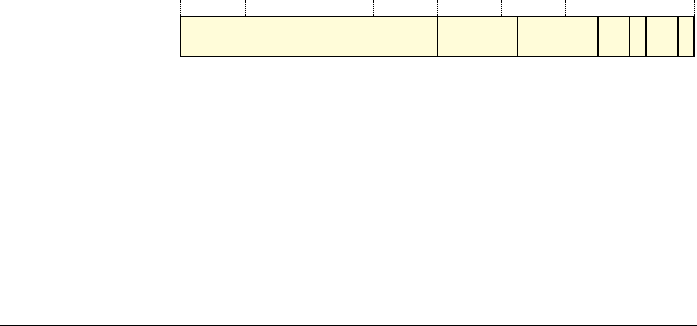
Events and Performance Monitor
ARM DDI 0363G Copyright © 2006-2011 ARM Limited. All rights reserved. 6-7
ID041111 Non-Confidential
6.3 Performance monitoring registers
The following sections describe the performance monitoring registers:
•c9, Performance Monitor Control Register
•c9, Count Enable Set Register on page 6-8
•c9, Count Enable Clear Register on page 6-9
•c9, Overflow Flag Status Register on page 6-11
•c9, Software Increment Register on page 6-12
•c9, Performance Counter Selection Register on page 6-13
•c9, Cycle Count Register on page 6-13
•c9, Event Type Selection Register on page 6-14
•c9, Event Count Registers on page 6-15
•c9, User Enable Register on page 6-15
•c9, Interrupt Enable Set Register on page 6-16
•c9, Interrupt Enable Clear Register on page 6-17.
6.3.1 c9, Performance Monitor Control Register
The PMCR Register characteristics are:
Purpose Controls the operation of the three count registers, and the PMCCNTR
Register.
Usage constraints The PMCR Register is:
• a read/write register
• accessible in:
— Privileged mode
— User mode only when the PMUSERENR.EN bit is set to 1,
see c9, User Enable Register on page 6-15.
Configurations Available in all processor configurations.
Attributes See Table 6-2 on page 6-8.
Figure 6-1 shows the PMCR bit assignments.
Figure 6-1 PMCR Register bit assignments
D C P EIMP
31 11 6 43210
IDCODE N
10
Reserved D
P
5
X
24 23 16 15

Events and Performance Monitor
ARM DDI 0363G Copyright © 2006-2011 ARM Limited. All rights reserved. 6-8
ID041111 Non-Confidential
Table 6-2 shows the PMCR bit assignments.
The PMCR Register is always accessible in Privileged mode. To access the register, read or
write CP15 with:
MRC p15, 0, <Rd>, c9, c12, 0 ; Read PMCR Register
MCR p15, 0, <Rd>, c9, c12, 0 ; Write PMCR Register
6.3.2 c9, Count Enable Set Register
The PMCNTENSET Register characteristics are:
Purpose Enables the Event Count Registers.
Usage constraints The PMCNTENSET Register is:
• accessible in:
— Privileged mode
— User mode only when the PMUSERENR.EN bit is set to 1,
see c9, User Enable Register on page 6-15.
Table 6-2 PMCR Register bit assignments
Bits Name Function
[31:24] IMP Implementer code:
0x41
= ARM
[23:16] IDCODE Identification code:
0x14
= Cortex-R4
[15:11] N Specifies the number of counters implemented:
0x3
= three counters implemented
[10: 6] - RAZ on reads, Should Be Zero or Preserved (SBZP) on writes
[5] DP Disable PMCCNTR when prohibited, that is, when non-invasive debug is not enabled:
0 = Count is enabled in prohibited regions. This is the reset value.
1 = Count is disabled in prohibited regions.
[4] X Enable export of the events to the event bus for an external monitoring block, for example the
ETM, to trace events:
0 = Export disabled. This is the reset value.
1 = Export enabled.
[3] D Cycle count divider:
0 = Counts every processor clock cycle. This is the reset value.
1 = Counts every 64th processor clock cycle.
[2] C Cycle counter reset:
Write one to this bit to reset the cycle counter, PMCCNTR, to zero.
This bit Reads-As-Zero.
[1] P Event counter reset:
Write one to this bit to reset all event counters to zero.
This bit Reads-As-Zero.
[0] E Enable:
0 = Disable all counters, including PMCCNTR. This is the reset value.
1 = Enable all counters including PMCCNTR.

Events and Performance Monitor
ARM DDI 0363G Copyright © 2006-2011 ARM Limited. All rights reserved. 6-9
ID041111 Non-Confidential
• The values in this register are ignored unless the E bit, bit [0], is set
in the PMCR Register, see c9, Performance Monitor Control
Register on page 6-7.
Configurations Available in all processor configurations.
Attributes See Table 6-3.
Figure 6-2 shows the PMCNTENSET bit assignments.
Figure 6-2 PMCNTENSET Register bit assignments
Table 6-3 shows the PMCNTENSET bit assignments.
To access the PMCNTENSET Register, read or write CP15 with:
MRC p15, 0, <Rd>, c9, c12, 1 ; Read PMCNTENSET Register
MCR p15, 0, <Rd>, c9, c12, 1 ; Write PMCNTENSET Register
When reading this register, any enable that reads as 0 indicates the corresponding counter is
disabled. Any enable that reads as 1 indicates the corresponding counter is enabled.
Writing a 1 to a particular count enable bit enables that counter. Writing a 0 to a count enable
bit has no effect. You must use the PMCNTENCLR to disable the counters. All counters are
disabled at reset.
The PMCNTENSET Register retains its value when the enable bit of the PMCR is clear, even
though its settings are ignored.
6.3.3 c9, Count Enable Clear Register
The PMCNTENCLR Register characteristics are:
Purpose Disables any of the Event Count Registers.
Usage constraints The PMCNTENCLR Register is:
• accessible in:
— Privileged mode
C
31 3210
Reserved
P2
P1
P0
Performance monitor
counter enables
Cycle count enable
Table 6-3 PMCNTENSET Register bit assignments
Bits Name Function
[31] C Cycle counter enable
[30:3] - UNP on reads, SBZP on writes
[2] P2 Counter 2 enable
[1] P1 Counter 1 enable
[0] P0 Counter 0 enable

Events and Performance Monitor
ARM DDI 0363G Copyright © 2006-2011 ARM Limited. All rights reserved. 6-10
ID041111 Non-Confidential
— User mode only when the PMUSERENR.EN bit is set to 1,
see c9, User Enable Register on page 6-15.
Configurations Available in all processor configurations.
Attributes See Table 6-4.
Figure 6-3 shows the PMCNTENCLR bit assignments.
Figure 6-3 PMCNTENCLR Register bit assignments
Table 6-4 shows the PMCNTENCLR bit assignments.
To access the PMCNTENCLR Register, read or write CP15 with:
MRC p15, 0, <Rd>, c9, c12, 2 ; Read PMCNTENCLR Register
MCR p15, 0, <Rd>, c9, c12, 2 ; Write PMCNTENCLR Register
When reading this register, any enable that reads as 0 indicates the corresponding counter is
disabled. Any enable that reads as 1 indicates the corresponding counter is enabled.
When writing this register, any enable written with a value of 0 is ignored, that is, not updated.
Any enable written with a value of 1 clears the counter enable. You must use the Count Enable
Set Register to enable the counters. All counters are disabled at reset.
Writing to bits in this register disables individual counters, and clears the corresponding bits in
the PMCNTENSET Register, see c9, Count Enable Set Register on page 6-8.
You can use the enable, EN, bit [0] of the PMCR Register to disable all performance counters
including PMCCNTR, see c9, Performance Monitor Control Register on page 6-7.
The PMCNTENCLR and PMCNTENSET Registers retain their values when the enable bit of
the PMCR is clear, even though their settings are ignored. The PMCNTENCLR Register can be
used to clear the enabled flags for individual counters even when all counters are disabled in the
PMCR Register.
C
31 3210
Reserved
P2
P1
P0
Performance monitor
counter disables
Cycle count disable
Table 6-4 PMCNTENCLR Register bit assignments
Bits Name Function
[31] C Cycle counter disable
[30:3] - UNP on reads, SBZP on writes
[2] P2 Counter 2 enable
[1] P1 Counter 1 enable
[0] P0 Counter 0 enable
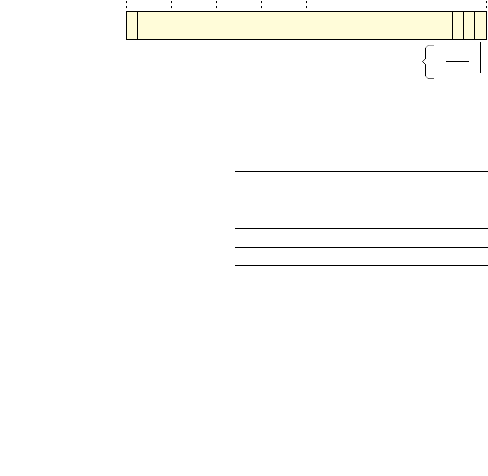
Events and Performance Monitor
ARM DDI 0363G Copyright © 2006-2011 ARM Limited. All rights reserved. 6-11
ID041111 Non-Confidential
6.3.4 c9, Overflow Flag Status Register
The PMOVSR Register characteristics are:
Purpose Indicates if event counters have overflowed. All overflow flags are reset
to zero.
Usage constraints The PMOVSR Register is accessible in:
• Privileged mode
• User mode only when the PMUSERENR.EN bit is set to 1, see c9,
User Enable Register on page 6-15.
Configurations Available in all processor configurations.
Attributes See Table 6-5.
Figure 6-4 shows the PMOVSR bit assignments.
Figure 6-4 PMOVSR Register bit assignments
Table 6-5 shows the PMOVSR bit assignments.
To access the PMOVSR, read or write CP15 with:
MRC p15, 0, <Rd>, c9, c12, 3 ; Read PMOVSR
MCR p15, 0, <Rd>, c9, c12, 3 ; Write PMOVSR
If an overflow flag is set to 1 in the PMOVSR it remains set until one of the following happens:
• writing 1 to the flag bit in the PMOVSR clears the flag
• the processor is reset.
The following operations do not clear the overflow flags:
• disabling the overflowed counter in the PMCNTENCLR Register
• disabling all counters in the PMCR Register
• resetting the overflowed counter using the PMCR Register.
C
31 3210
Reserved
P2
P1
P0
Performance monitor counters
overflow flags
Cycle count overflow
Table 6-5 PMOVSR Register bit assignments
Bits Name Function
[31] Cycle counter overflow Cycle counter overflow flag
[30:3] - UNP on reads, SBZP on writes
[2] P2 Counter 2 overflow flag
[1] P1 Counter 1 overflow flag
[0] P0 Counter 0 overflow flag

Events and Performance Monitor
ARM DDI 0363G Copyright © 2006-2011 ARM Limited. All rights reserved. 6-12
ID041111 Non-Confidential
6.3.5 c9, Software Increment Register
The PMSWINC Register characteristics are:
Purpose Increments the count of an Event Count Register.
Usage constraints The PMSWINC Register is:
• A write-only register that Reads-As-Zero
• Accessible in:
— Privileged mode
— User mode only when the PMUSERENR.EN bit is set to 1,
see c9, User Enable Register on page 6-15.
• You must only use the PMSWINC Register to increment Event
Count Registers when the counter event is set to
0x00
, software
count, in the Event Select Register, see c9, Event Type Selection
Register on page 6-14.
• If you attempt to use the PMSWINC Register to increment an Event
Count Register when the counter event is set to a value other than
0x00
the result is Unpredictable.
Configurations Available in all processor configurations.
Attributes See Table 6-6.
Figure 6-5 shows the PMSWINC bit assignments.
Figure 6-5 PMSWINC Register bit assignments
Table 6-6shows the PMSWINC bit assignments.
To access the PMSWINC Register, read or write CP15 with:
MRC p15, 0, <Rd>, c9, c12, 4 ; Read PMSWINC Register
MCR p15, 0, <Rd>, c9, c12, 4 ; Write PMSWINC Register
31 3210
Reserved
P2
P1
P0
Performance monitor counters
software increment bits
Table 6-6 PMSWINC Register bit assignments
Bits Name Function
[31:3] - RAZ on reads, SBZP on writes
[2] P2 Increment Counter 2
[1] P1 Increment Counter 1
[0] P0 Increment Counter 0

Events and Performance Monitor
ARM DDI 0363G Copyright © 2006-2011 ARM Limited. All rights reserved. 6-13
ID041111 Non-Confidential
6.3.6 c9, Performance Counter Selection Register
The PMSELR Register characteristics are:
Purpose • selects an Event Count Register.
• determines which count register is accessed or controlled by
accesses to the Event Type Selection Register and the Event Count
Register.
Usage constraints The PMSELR Register is:
• A read/write register.
• Accessible in:
— Privileged mode
— User mode only when the PMUSERENR.EN bit is set to 1,
see c9, User Enable Register on page 6-15.
Configurations Available in all processor configurations.
Attributes See Table 6-7.
Figure 6-6 shows the PMSELR bit assignments.
Figure 6-6 PMSELR Register bit assignments
Table 6-7 shows the PMSELR bit assignments.
Any values programmed in the PMSELR Register other than those specified in Table 6-7 are
Unpredictable.
To access the PMSELR Register, write CP15 with:
MCR p15, 0, <Rd>, c9, c12, 5 ; Write PMSELR Register
6.3.7 c9, Cycle Count Register
The PMCCNTR Register characteristics are:
Purpose Counts clock cycles.
Usage constraints The PMCCNTR Register:
• Is a 32-bit read/write register.
SEL
31 40
Reserved
5
Table 6-7 PMSELR Register bit assignments
Bits Name Function
[31:5] - RAZ on reads, SBZP on writes
[4:0] SEL Counter select:
b00000 = selects counter 0
b00001 = selects counter 1
b00010 = selects counter 2.
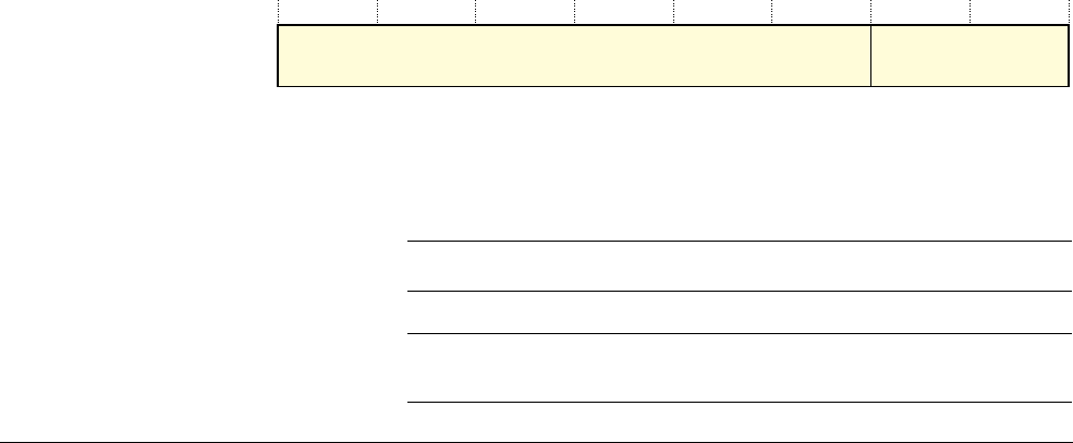
Events and Performance Monitor
ARM DDI 0363G Copyright © 2006-2011 ARM Limited. All rights reserved. 6-14
ID041111 Non-Confidential
• Is accessible in:
— Privileged mode
— User mode only when the PMUSERENR.EN bit is set to 1,
see c9, User Enable Register on page 6-15.
• Must be disabled before software can write to it. Any attempt by
software to write to this register when enabled is Unpredictable.
Configurations Available in all processor configurations.
To access the PMCCNTR read or write CP15 with:
MRC p15, 0, <Rd>, c9, c13, 0 ; Read PMCCNTR Register
MCR p15, 0, <Rd>, c9, c13, 0 ; Write PMCCNTR Register
The PMCCNTR register must be disabled before software can write to it. Any attempt by
software to write to this register when enabled is Unpredictable.
6.3.8 c9, Event Type Selection Register
The processor has three Event Type Select Registers, PMXEVTYPER0 to PMXEVTYPER2,
each corresponding to one of the Performance Monitor Count (PMXEVCNTR) Registers,
PMXEVCNTR0 to PMXEVCNTR2. The value in PMSELR determines access to these
registers.
The PMXEVTYPER Register characteristics are:
Purpose Selects the events you want a PMXEVCNTR Register to count.
Usage constraints The PMXEVTYPER Register is:
• A read/write register
• Accessible in:
— Privileged mode
— User mode only when the PMUSERENR.EN bit is set to 1,
see c9, User Enable Register on page 6-15.
Configurations Available in all processor configurations.
Attributes See Table 6-8.
Figure 6-7 shows the PMXEVTYPER bit assignments.
Figure 6-7 PMXEVTYPERx Register bit assignments
Table 6-8 shows the PMXEVTYPER bit assignments.
SEL
31 0
Reserved
87
Table 6-8 PMXEVTYPERx Register bit assignments
Bits Name Function
[31:8] - RAZ or SBZP.
[7:0] SEL Event number selected, see Table 6-1 on page 6-2 for values.
The reset value of this field is Unpredictable.

Events and Performance Monitor
ARM DDI 0363G Copyright © 2006-2011 ARM Limited. All rights reserved. 6-15
ID041111 Non-Confidential
To access the PMXEVTYPERx Register, read or write CP15 with:
MRC p15, 0, <Rd>, c9, c13, 1 ; Read PMXEVTYPERx Register
MCR p15, 0, <Rd>, c9, c13, 1 ; Write PMXEVTYPERx Register
The absolute counts of events recorded might vary because of pipeline effects. This has
negligible effect except in cases where the counters are enabled for a very short time.
In addition to the counters within the processor, most of the events that Table 6-1 on page 6-2
shows are available to the ETM unit or other external trace hardware to enable monitoring of
the events. For information on how to monitor these events, see the CoreSight ETM-R4
Technical Reference Manual.
6.3.9 c9, Event Count Registers
The processor has three Event Count Registers (PMC0-PMC2). Each PMC Register, as selected
by the PMSELR Register, counts instances of an event selected by the corresponding
PMXEVTYPER Register. The value in PMSELR determines access to these registers.
Each PMXEVCNTR Register is:
• A 32-bit read/write register.
• Accessible in:
— Privileged mode
— User mode only when the PMUSERENR.EN bit is set to 1, see c9, User Enable
Register.
To access the current Event Count Registers, read or write CP15 with:
MRC p15, 0, <Rd>, c9, c13, 2 ; Read current PMNx Register
MCR p15, 0, <Rd>, c9, c13, 2 ; Write current PMNx Register
6.3.10 c9, User Enable Register
The PMUSERENR Register characteristics are:
Purpose Enables User mode to have access to:
• the performance monitor registers, see Performance monitoring
registers on page 6-7
• the validation registers, see Validation Registers on page 4-66.
Usage constraints The PMUSERENR Register:
• is a read/write register
• is writable only in Privileged mode, readable in any processor mode
• does not provide access to the registers that control interrupt
generation.
Configurations Available in all processor configurations.
Attributes See Table 6-9 on page 6-16.
Figure 6-8 on page 6-16 shows the PMUSERENR bit assignments.

Events and Performance Monitor
ARM DDI 0363G Copyright © 2006-2011 ARM Limited. All rights reserved. 6-16
ID041111 Non-Confidential
Figure 6-8 PMUSERENR Register bit assignments
Table 6-9 shows the PMUSERENR bit assignments.
If the EN bit in the PMUSERENR register is not set, any attempt to access a performance
monitor register or a validation register from User mode causes an Undefined Instruction
exception.
Note
For more information on access permissions to the performance monitor registers and validation
registers, see the ARM Architecture Reference Manual.
To access the PMUSERENR register, read or write CP15 with:
MRC p15, 0, <Rd>, c9, c14, 0 ; Read PMUSERENR Register
MCR p15, 0, <Rd>, c9, c14, 0 ; Write PMUSERENR Register
6.3.11 c9, Interrupt Enable Set Register
The PMINTENSET Register characteristics are:
Purpose Determines if any of the PMXEVCNTR Registers,
PMXEVCNTR0-PMXEVCNTR2 and PMCCNTR, generate an interrupt
request on overflow.
Usage constraints The PMINTENSET Register is:
• a read/write register
• accessible in Privileged mode only.
Configurations Available in all processor configurations.
Attributes See Table 6-10 on page 6-17.
Figure 6-9 on page 6-17 shows the PMINTENSET bit assignments.
31 10
Reserved
EN
Table 6-9 PMUSERENR Register bit assignments
Bits Name Function
[31:1] - RAZ or SBZP.
[0] EN User mode access to performance monitor and validation registers:
0 = Disabled. This is the reset value.
1 = Enabled.

Events and Performance Monitor
ARM DDI 0363G Copyright © 2006-2011 ARM Limited. All rights reserved. 6-17
ID041111 Non-Confidential
Figure 6-9 PMINTENSET Register bit assignments
Table 6-10 shows the PMINTENSET bit assignments.
Reading this register returns the current setting, with a 1 in one of the counter bits indicating that
interrupts are enabled for that counter. Writing a 1 to a particular interrupt bit enables interrupt
generation on overflow of that counter. Writing a 0 has no effect. You can only disable interrupts
by writing to the PMINTENCLR Register.
To access the PMINTENSET Register, read or write CP15 with:
MRC p15, 0, <Rd>, c9, c14, 1 ; Read PMINTENSET Register
MCR p15, 0, <Rd>, c9, c14, 1 ; Write PMINTENSET Register
If this unit generates an interrupt, the processor asserts the pin nPMUIRQ. You can route this
pin to an external interrupt controller for prioritization and masking. This is the only mechanism
that signals this interrupt to the processor.
Note
ARM expects that the Performance Monitor interrupt request signal, nPMUIRQ, connects to a
system interrupt controller.
6.3.12 c9, Interrupt Enable Clear Register
The PMINTENCLR Register characteristics are:
Purpose Determines if any of the PMXEVCNTR Registers,
PMXEVCNTR0-PMXEVCNTR2 and PMCCNTR, generate an interrupt
request on overflow.
Usage constraints The PMINTENCLR Register is:
• a read/write register
• accessible in Privileged mode only.
Configurations Available in all processor configurations.
Attributes See Table 6-11 on page 6-18.
C
31 3210
Reserved
P2
P1
P0
Performance monitor counter
overflow interrupt enables
Cycle count overflow interrupt enable
Table 6-10 PMINTENSET Register bit assignments
Bits Name Function
[31] C PMCCNTR overflow interrupt
[30:3] - UNP on reads, SBZP on write
[2] P2 PMC2 overflow interrupt
[1] P1 PMC1 overflow interrupt
[0] P0 PMC0 overflow interrupt

Events and Performance Monitor
ARM DDI 0363G Copyright © 2006-2011 ARM Limited. All rights reserved. 6-18
ID041111 Non-Confidential
Figure 6-10 shows the PMINTENCLR bit assignments.
Figure 6-10 PMINTENCLR Register bit assignments
Table 6-11 shows the PMINTENCLR bit assignments.
Reading this register returns the current setting, with a 1 in one of the counter bits indicating that
interrupts are enabled for that counter. Writing a 1 to a particular interrupt disable bit disables
interrupt generation on overflow of that counter. Writing a 0 has no effect. You can only enable
interrupt requests by writing to the PMINTENSET Register.
To access the PMINTENCLR Register, read or write CP15 with:
MRC p15, 0, <Rd>, c9, c14, 2 ; Read PMINTENCLR Register
MCR p15, 0, <Rd>, c9, c14, 2 ; Write PMINTENCLR Register
C
31 3210
Reserved
P2
P1
P0
Performance monitor counter
overflow interrupt disables
Cycle count overflow interrupt disable
Table 6-11 PMINTENCLR Register bit assignments
Bits Name Function
[31] C PMCCNTR overflow interrupt
[30:3] - UNP on reads, SBZP on writes
[2] P2 PMC2 overflow interrupt
[1] P1 PMC1 overflow interrupt
[0] P0 PMC0 overflow interrupt

Events and Performance Monitor
ARM DDI 0363G Copyright © 2006-2011 ARM Limited. All rights reserved. 6-19
ID041111 Non-Confidential
6.4 Event bus interface
The event bus, EVNTBUS, is used to signal when an event has occurred. The event bus includes
most, but not all, of the events that can be counted by the performance monitoring unit. Each
individual event is assigned to an individual bit of this bus, and this bit is asserted for one cycle
each time the event occurs.
The event bus only signals events when it is enabled. Set the X bit in the Performance Monitor
Control Register to enable the event bus. See c9, Performance Monitor Control Register on
page 6-7.
If it is enabled, the event bus signals events regardless of whether or not non-invasive debug is
enabled. DBGEN and NIDEN do not affect the event bus. If you want to ensure that no events
are signalled, for example for protection reasons, use the X bit in the PMCR that can be
protected from User-mode modification, or include other logic in the system for that purpose.
See Table 6-1 on page 6-2 to see which bit of the event bus each event is signaled on.
Note
If an event is being counted in the PMU, the count might not be incremented in exactly the same
cycle that the event is signaled on the event bus.
6.4.1 Use of the event bus and counters
The event bus is designed to be connected to the ETM-R4, that enables processor events to
trigger tracing for debug purposes. You can also connect it to event counting registers external
to the processor, or to an interrupt generator.
Because each EVNTBUS pin is only asserted for one cycle for each occurrence of the event, it
is possible to create composite events by ORing various EVNTBUS pins together. A composite
event signal like this is asserted when any of the included events occur although, if multiple
events occur in the same cycle, the composite event only occurs once.
The processor also has two event input pins, ETMEXTOUT[1:0]. This bus is normally
intended for connection to the ETM, and enables the Cortex-R4 performance monitor to count
events generated by the ETM. These inputs can alternatively be used for composite events
generated external to the processor.

ARM DDI 0363G Copyright © 2006-2011 ARM Limited. All rights reserved. 7-1
ID041111 Non-Confidential
Chapter 7
Memory Protection Unit
This chapter describes the Memory Protection Unit (MPU). It contains the following sections:
•About the MPU on page 7-2
•Memory types on page 7-7
•Region attributes on page 7-8
•MPU interaction with memory system on page 7-9
•MPU faults on page 7-10
•MPU software-accessible registers on page 7-11.

Memory Protection Unit
ARM DDI 0363G Copyright © 2006-2011 ARM Limited. All rights reserved. 7-2
ID041111 Non-Confidential
7.1 About the MPU
The MPU works with the L1 memory system to control accesses to and from L1 and external
memory. For a full architectural description of the MPU, see the ARM Architecture Reference
Manual.
The MPU enables you to partition memory into regions and set individual protection attributes
for each region. The MPU supports zero, eight, or twelve memory regions.
Note
If the MPU has zero regions, you cannot enable or program the MPU. Attributes are only
determined from the default memory map when zero regions are implemented.
Each region is programmed with a base address and size, and the regions can be overlapped to
enable efficient programming of the memory map. To support overlapping, the regions are
assigned priorities, with region 0 having the lowest priority and region 11 having the highest.
The MPU returns access permissions and attributes for the highest priority enabled region where
the address hits.
The MPU is programmed with CP15 registers c1 and c6, see MPU control and configuration on
page 4-3. Memory region control read and write access is permitted only from Privileged
modes.
Table 7-1 shows the default memory map.
Table 7-1 Default memory map
Address
range
Instruction memory type Data memory type
eXecute Never
Instruction
cache enabled
Instruction
cache disabled Data cache enabled Data cache
disabled
0xFFFFFFFF
Normal
Non-cacheable
only if HIVECS is
TRUE
Normal
Non-cacheable
only if HIVECS is
TRUE
Strongly-ordered Strongly-
ordered
Instruction execution
only permitted if
HIVECS is TRUE
0xF0000000
0xEFFFFFFF
- - Strongly-ordered Strongly-
ordered
eXecute Never
0xC0000000
0xBFFFFFFF
- - Shared Device Shared
Device
eXecute Never
0xA0000000
0x9FFFFFFF
--Non-shared
Device
Non-shared
Device
eXecute Never
0x80000000
0x7FFFFFFF
Normal,
Cacheable,
Non-shared
Normal,
Non-cacheable,
Non-shared
Normal, Non-cacheable,
Shared
Normal,
Non-cacheable,
Shared
Instruction execution
permitted
0x60000000
0x5FFFFFF
Normal,
Cacheable,
Non-shared
Normal,
Non-cacheable,
Non-shared
Normal, WT Cacheable,
Non-shared
Normal,
Non-cacheable,
Shared
Instruction execution
permitted
0x40000000
0x3FFFFFFF
Normal,
Cacheable,
Non-shared
Normal,
Non-cacheable,
Non-shared
Normal, WBWA Cacheable,
Non-shared
Normal,
Non-cacheable,
Shared
Instruction execution
permitted
0x00000000

Memory Protection Unit
ARM DDI 0363G Copyright © 2006-2011 ARM Limited. All rights reserved. 7-3
ID041111 Non-Confidential
This section describes:
•Memory regions
•Overlapping regions on page 7-4
•Background regions on page 7-6
•TCM regions on page 7-6.
7.1.1 Memory regions
Before the MPU is enabled, you must program at least one valid protection region. If you do not
do this, the processor enters a state that only reset can recover.
When the MPU is disabled, no access permission checks are performed, and memory attributes
are assigned according to the default memory map. See Table 7-1 on page 7-2.
For more information on how to enable or disable the MPU, see MPU interaction with memory
system on page 7-9.
Depending on the implementation, the MPU has a maximum of eight or 12 regions. Using CP15
register c6 you can specify the following for each region:
• region base address
• region size
• subregion enables
• region attributes
• region access permissions
• region enable.
Region base address
The base address defines the start of the memory region. You must align this to a region-sized
boundary. For example, if a region size of 8KB is programmed for a given region, the base
address must be a multiple of 8KB.
Note
If the region is not aligned correctly, this results in Unpredictable behavior.
Region size
The region size is specified as a 5-bit value, encoding a range of values from 32 bytes, a
cache-line length, to 4GB. Table 4-32 on page 4-54 shows the encoding.
Subregions
Each region can be split into eight equal sized non-overlapping subregions. An access to a
memory address in a disabled subregion does not use the attributes and permissions defined for
that region. Instead, it uses the attributes and permissions of a lower priority region or generates
a background fault if no other regions overlap at that address. This enables increased protection
and memory attribute granularity.
All region sizes between 256 bytes and 4GB support eight subregions. Region sizes of less than
256 bytes do not support subregions, and the subregion disable field is SBZ/UNP for regions of
less than 256 bytes in size.

Memory Protection Unit
ARM DDI 0363G Copyright © 2006-2011 ARM Limited. All rights reserved. 7-4
ID041111 Non-Confidential
Region attributes
Each region has a number of attributes associated with it. These control how a memory access
is performed when the processor accesses an address that falls within a given region.
See Memory types on page 7-7 for more information about memory types, and Region attributes
on page 7-8 for a description of how to assign types and attributes to a region.
Region access permissions
Each region can be given no access, read-only access, or read/write access permissions for
Privileged or all modes. In addition, each region can be marked as eXecute Never (XN) to
prevent instructions being fetched from that region.
For example, if a User mode application attempts to access a Privileged mode access only region
a permission fault occurs.
The ARM architecture uses constants known as inline literals to perform address calculations.
The assembler and compiler automatically generate these constants and they are stored inline
with the instruction code. To ensure correct operation, only a memory region that has permission
for data read access can execute instructions. For more information, see the ARM Architecture
Reference Manual. For information about how to program access permissions, see Table 4-36
on page 4-56.
Instructions cannot be executed from regions with Device or Strongly-ordered memory type
attributes. The processor treats such regions as if they have XN permissions.
7.1.2 Overlapping regions
You can program the MPU with two or more overlapping regions. For overlapping regions, a
fixed priority scheme determines attributes and permissions for memory access to the
overlapping region. Attributes and permissions for region 11 take highest priority, those for
region 0 take lowest priority. For example:
Region 2 Is 4KB in size, starting from address
0x3000
. Privileged mode has full
access, and User mode has read-only access.
Region 1 Is 16KB in size, starting from address
0x0000
. Both Privileged and User
modes have full access.
When the processor performs a data write to address
0x3010
while in User mode, the address
falls into both region 1 and region 2, as Figure 7-1 shows. Because these regions have different
permissions, the permissions associated with region 2 are applied. Because User mode is read
access only for this region, a permission fault occurs, causing a data abort.
Figure 7-1 Overlapping memory regions
0x4000
0x0000
0x3000
0x3010
Region 1
Region 2
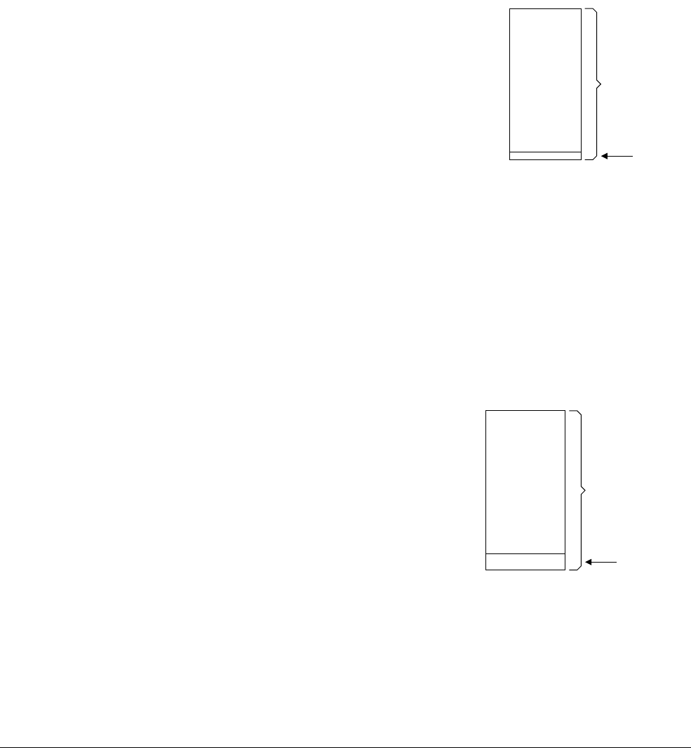
Memory Protection Unit
ARM DDI 0363G Copyright © 2006-2011 ARM Limited. All rights reserved. 7-5
ID041111 Non-Confidential
Example of using regions that overlap
You can use overlapping regions for stack protection, as shown in Figure 7-2. For example:
• allocate to region 1 the appropriate size for all stacks
• allocate to region 2 the minimum region size, 32 bytes, and position it at the end of the
stack for the current process
• set the region 2 access permissions to No Access.
If the current process overflows the stack it uses, a write access to region 2 by the processor
causes the MPU to raise a permission fault.
Figure 7-2 Overlay for stack protection
Example of using subregions
You can use subregions for stack protection, as shown in Figure 7-3. For example:
• Allocate to region 1 the appropriate size for all stacks.
• Set the least-significant subregion disable bit. That is, set the subregion disable field, bits
[15:8], of the CP15 MPU Region Size Register to
0x01
.
If the current process overflows the stack it uses, a write access by the processor to the disabled
subregion causes the MPU to raise a background fault.
Figure 7-3 Overlapping subregion of memory
0x4000
0x0000
Region 1
Region 2
0x4000
0x0000 Guard region
0x0800
Stack

Memory Protection Unit
ARM DDI 0363G Copyright © 2006-2011 ARM Limited. All rights reserved. 7-6
ID041111 Non-Confidential
7.1.3 Background regions
Overlapping regions increase the flexibility of how the regions can be mapped onto physical
memory devices in the system. You can also use the overlapping properties to specify a
background region. For example, you might have a number of physical memory areas sparsely
distributed across the 4GB address space. If a programming error occurs, the processor might
issue an address that does not fall into any defined region.
If the address that the processor issues falls outside any of the defined regions, and the MPU is
enabled, the MPU is hard-wired to abort the access. That is, all accesses for an address that is
not mapped to a region in the MPU generate a background fault. You can override this behavior
by programming region 0 as a 4GB background region. In this way, if the address does not fall
into any of the other 11 regions, the attributes and access permissions you specified for region
0 control the access.
In Privileged modes, you can also override this behavior by setting the BR bit, bit [17], of the
SCTLR. This causes Privileged accesses that fall outside any of the defined regions to use the
default memory map.
7.1.4 TCM regions
Any memory address that you configure to be accessed using a TCM interface is given Normal,
Non-shared type attributes, regardless of the attributes of any MPU region that the address also
belongs to. Access permissions for an address in a TCM region are preserved from the MPU
region that the address also belongs to. For more information, see About the TCMs on page 8-13.

Memory Protection Unit
ARM DDI 0363G Copyright © 2006-2011 ARM Limited. All rights reserved. 7-7
ID041111 Non-Confidential
7.2 Memory types
The ARM architecture defines a set of memory types with characteristics that are suited to
particular devices. There are three mutually exclusive memory type attributes:
• Strongly-ordered
•Device
• Normal.
MPU memory regions can each be assigned a memory type attribute. Table 7-2 shows a
summary of the memory types.
Note
The processor L1 cache does not cache shared normal regions.
For more information on memory attributes and types, memory barriers, and ordering
requirements for memory accesses, see the ARM Architecture Reference Manual.
7.2.1 Using memory types
The processor memory system contains a store buffer that helps to improve the throughput of
accesses to Normal type memory. See Store buffer on page 8-18 for more information. Because
of the ordering rules that they must follow, accesses to other types of memory typically have a
lower throughput or higher latency than accesses to Normal memory. In particular:
• reads from Device memory must first drain the store buffer of all writes to Device memory
• all accesses to Strongly-ordered memory must first drain the store buffer completely.
Similarly, when it accesses Strongly-ordered or Device type memory, the processor's response
to interrupts must be modified, and the interrupt response latency is longer. See Low interrupt
latency on page 3-17 for more information.
To ensure optimum performance, you must understand the architectural semantics of the
different memory types. Use Device memory type for appropriate memory regions, typically
peripherals, and only use Strongly-ordered memory type for memory regions where it is
essential.
Table 7-2 Memory attributes summary
Memory type
attribute
Shared or
Non-shared Description
Strongly-ordered - All memory accesses to Strongly-ordered memory occur in program order.
All Strongly-ordered accesses are assumed to be shared.
Device Shared For memory-mapped peripherals that several processors share.
Non-shared For memory-mapped peripherals that only a single processor uses.
Normal Shared For normal memory that is shared between several processors.
Non-shared For normal memory that only a single processor uses.

Memory Protection Unit
ARM DDI 0363G Copyright © 2006-2011 ARM Limited. All rights reserved. 7-8
ID041111 Non-Confidential
7.3 Region attributes
Each region has a number of attributes associated with it. These control how a memory access
is performed when the processor accesses an address that falls within a given region. The
attributes are:
• Memory type, see Memory types on page 7-7, one of:
— Strongly-ordered
—Device
—Normal.
• Shared or Non-shared
• Non-cacheable
• Write-through cacheable
• Write-back cacheable
• Read allocation
• Write allocation.
The Region Access Control Registers use five bits to encode the memory region type. These are
the TEX[2:0], C and B bits. Table 4-34 on page 4-55 shows the mapping of these bits to memory
region attributes.
Note
In earlier versions of the ARM architecture, the TEX, C, and B bits were known as the Type
Extension, Cacheable and Bufferable bits. These names no longer adequately describe the
function of the B, C, and TEX bits.
All memory attributes that are cacheable, write-back or write-through, are also implicitly
read-allocate. Table 4-35 on page 4-56 shows which attributes are write-allocate.
In addition, the Region Access Control Registers contain the shared bit, S. This bit only applies
to Normal memory, and determines whether the memory region is Shared (1) or Non-shared (0).
When the processor performs a memory access through its AXI bus master interface:
• the Inner attributes are indicated on the A*INNERM signals.
• the Outer attributes are indicated on the A*CACHEM signals.
For the encodings, see Table 9-2 on page 9-5.
Similarly, for memory accesses performed through the AXI peripheral port, the Outer attributes
are indicated on the A*CACHEP signals.
For more information on region attributes, see the ARM Architecture Reference Manual.

Memory Protection Unit
ARM DDI 0363G Copyright © 2006-2011 ARM Limited. All rights reserved. 7-9
ID041111 Non-Confidential
7.4 MPU interaction with memory system
This section describes how to enable and disable the MPU. After you enable or disable the
MPU, the pipeline must be flushed using
ISB
and
DSB
instructions to ensure that all subsequent
instruction fetches and data accesses see the effect of turning on or off the MPU.
Before you enable or disable the MPU you must:
1. Program all relevant CP15 registers. This includes setting up at least one memory region
that covers the executing code, and that the attributes and permissions of that region are
the same as the attributes and permissions of the region in the default memory map that
covers the code, and that the region is executable in Privileged mode.
2. Clean and invalidate the data caches.
3. Disable caches.
4. Invalidate the instruction cache.
The following code is an example of enabling the MPU:
MRC p15, 0, R1, c1, c0, 0 ; read CP15 register 1
ORR R1, R1, #0x1
DSB
MCR p15, 0, R1, c1, c0, 0 ; enable MPU
ISB
Fetch from programmed memory map
Fetch from programmed memory map
Fetch from programmed memory map
Fetch from programmed memory map
The following code is an example of disabling the MPU:
MRC p15, 0, R1, c1, c0, 0 ; read CP15 register 1
BIC R1, R1, #0x1
DSB
MCR p15, 0, R1, c1, c0, 0 ; disable MPU
ISB
Fetch from default memory map
Fetch from default memory map
Fetch from default memory map
Fetch from default memory map
Table 7-1 on page 7-2 shows the default memory map.

Memory Protection Unit
ARM DDI 0363G Copyright © 2006-2011 ARM Limited. All rights reserved. 7-10
ID041111 Non-Confidential
7.5 MPU faults
The MPU can generate three types of fault:
•Background fault
•Permission fault
•Alignment fault.
When a fault occurs, the memory access or instruction fetch is precisely aborted, and a prefetch
abort or data abort exception is taken as appropriate. No memory accesses are performed on the
AXI bus master interface. For more information about fault handling, see Fault handling on
page 8-7.
7.5.1 Background fault
A background fault is generated when the MPU is enabled and a memory access is made to an
address that is not within an enabled subregion of an MPU region. A background fault does not
occur if the background region is enabled and the access is Privileged. See Background regions
on page 7-6.
7.5.2 Permission fault
A permission fault is generated when a memory access does not meet the requirements of the
permissions defined for the memory region that it accesses. See Region access permissions on
page 7-4.
7.5.3 Alignment fault
An alignment fault is generated if a data access is performed to an address that is not aligned for
the size of the access, and strict alignment is required for the access. A number of instructions
that access memory, for example,
LDM
and
STC
, require strict alignment. See the ARM
Architecture Reference Manual for information. In addition, strict alignment can be required for
all data accesses by setting the A-bit in the SCTLR. See c1, System Control Register on
page 4-37.

Memory Protection Unit
ARM DDI 0363G Copyright © 2006-2011 ARM Limited. All rights reserved. 7-11
ID041111 Non-Confidential
7.6 MPU software-accessible registers
Figure 4-2 on page 4-3 shows the CP15 registers that control the MPU.
When the MPU is not present, the c6, MPU memory region programming registers on page 4-51
read as zero and ignore writes in Privileged mode. No Undefined Instruction exceptions are
taken.

ARM DDI 0363G Copyright © 2006-2011 ARM Limited. All rights reserved. 8-1
ID041111 Non-Confidential
Chapter 8
Level One Memory System
This chapter describes the processor Level one (L1) memory system. It contains the following
sections:
•About the L1 memory system on page 8-2
•About the error detection and correction schemes on page 8-4
•Fault handling on page 8-7
•About the TCMs on page 8-13
•About the caches on page 8-18
•Internal exclusive monitor on page 8-34
•Memory types and L1 memory system behavior on page 8-35
•Error detection events on page 8-36.

Level One Memory System
ARM DDI 0363G Copyright © 2006-2011 ARM Limited. All rights reserved. 8-2
ID041111 Non-Confidential
8.1 About the L1 memory system
The processor L1 memory system can be configured during implementation and integration. It
can consist of:
• separate instruction and data caches
• multiple Tightly-Coupled Memory (TCM) areas
•a Memory Protection Unit (MPU).
The instruction side and data side can each optionally have their own L1 caches. The cache
architecture is Harvard, that is, only instructions can be fetched from the Icache, and only data
can be fetched from the Dcache. In parallel with each of the caches are two areas of dedicated
RAM accessible to both the instruction and data sides. These are regions of TCM. You can
implement one TCM using the ATCM interface and up to two TCMs using the BTCM interface.
Figure 8-1 on page 8-3 shows this.
Each TCM and cache can be configured at implementation time to have an error detection and
correction scheme to protect the data stored in the memory from errors. Each TCM interface
also has support for logic external to the processor to tell the processor that an error has
occurred.
The MPU handles accesses to both the instruction and data sides. The MPU is responsible for
protection checking, address access permissions, and memory attributes for all accesses. Some
of these attributes can be passed to the L2 memory system through the AXI master. See
Chapter 7 Memory Protection Unit for more information about the MPU.
The L1 memory system includes a monitor for exclusive accesses. Exclusive load and store
instructions, for example
LDREX
and
STREX
, can be used with the appropriate memory monitoring
to provide inter-process or inter-processor synchronization and semaphores. See the ARM
Architecture Reference Manual for more information. The internal monitor can handle some
exclusive monitoring internally to the processor, see Internal exclusive monitor on page 8-34 for
more information.
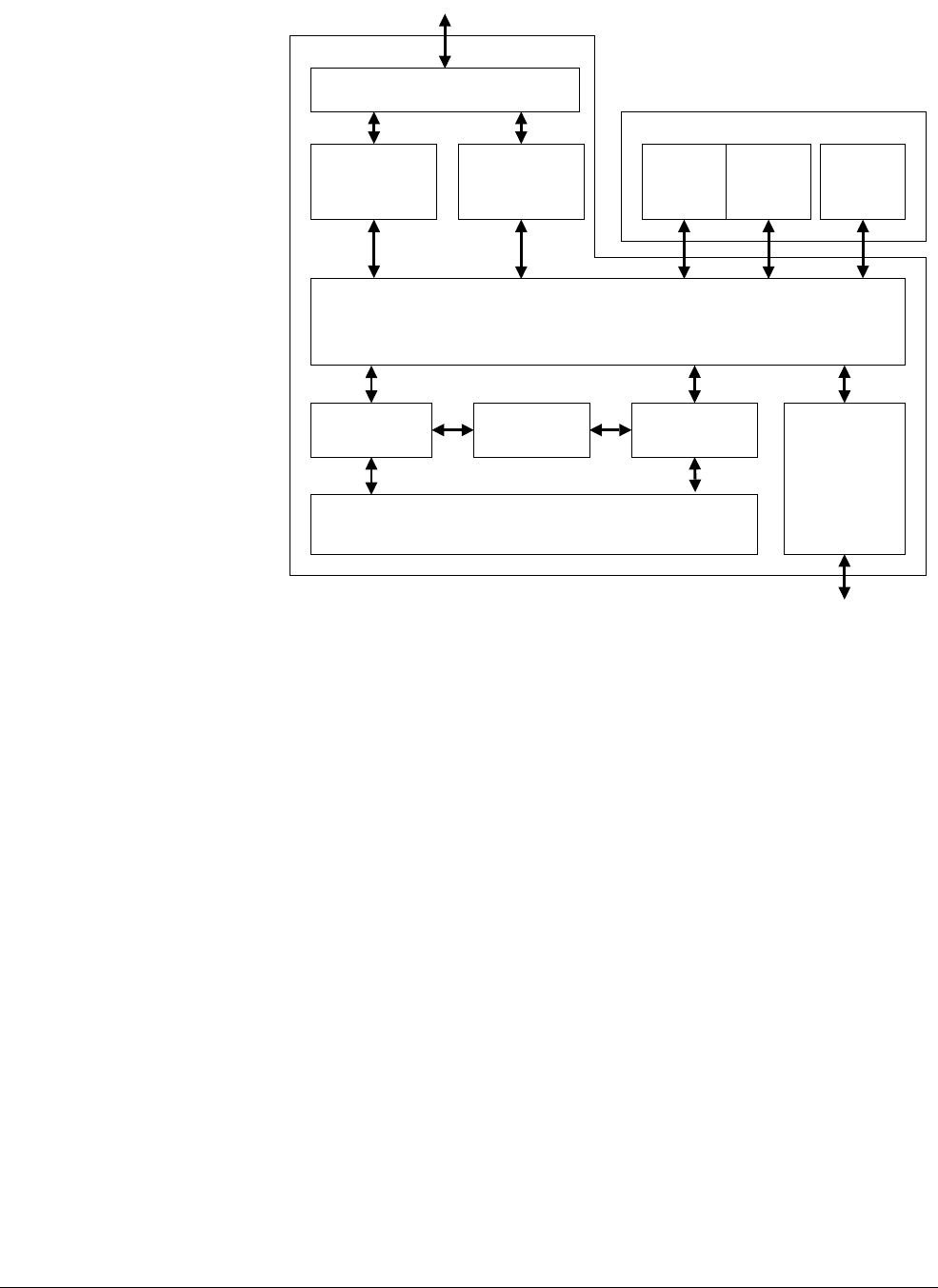
Level One Memory System
ARM DDI 0363G Copyright © 2006-2011 ARM Limited. All rights reserved. 8-3
ID041111 Non-Confidential
Figure 8-1 L1 memory system block diagram
AXI master
Instruction cache
controller and
RAMs
Data cache
controller and
RAMs
B0TCM
AXI bus
AXI bus
External Tightly-Coupled Memory (TCM)
AXI slave
Data Processing Unit (DPU)
Memory
Protection Unit
(MPU)
Prefetch Unit
(PFU)
Load Store Unit
(LSU)
Interconnect
ATCM B1TCM
Processor
Level One Memory System
ARM DDI 0363G Copyright © 2006-2011 ARM Limited. All rights reserved. 8-4
ID041111 Non-Confidential
8.2 About the error detection and correction schemes
In silicon devices, stray radiation and other effects can cause the data stored in a RAM to be
corrupted. The TCMs and caches on the Cortex-R4 processor can be configured to detect and
correct errors that can occur in the RAMs. Extra, redundant data is computed by the processor
and stored in the RAMs alongside the real data. When the processor reads data from the RAMs,
it checks that the redundant data is consistent with the real data and can either signal an error,
or attempt to correct the error.
A number of different error schemes are available:
•Parity
•64-bit ECC on page 8-5
•32-bit ECC on page 8-5.
Each has different properties in terms of the number of errors that can be detected, and corrected,
and the amount of extra RAM required to store the redundant data. Because different logic is
required for each scheme, the scheme must be chosen in the build configuration, although you
can enable or disable, or change the behavior of the error schemes using software-configuration.
This section describes the generic properties of each of the schemes. See Appendix D ECC
Schemes for more information about the advantages and disadvantages of each scheme to the
implementer. See Cache error detection and correction on page 8-20 for information about the
operation of the error schemes for the caches, and TCM internal error detection and correction
on page 8-14 for the TCMs.
The error schemes are each described in terms of their operation on a doubleword (64 bits) of
data, because this is the amount of data that the processor L1 memory system can transfer each
cycle. The tag and dirty RAMs associated with the caches are different sizes, but the principles
are the same. An error is considered to be a single bit of data that is inverted relative to its correct
value.
Figure 8-2 shows the error schemes. The shaded areas represent bits with errors.
Figure 8-2 Error detection and correction schemes
8.2.1 Parity
For each byte, a parity bit is computed and stored with that byte. This requires eight bits of
parity, or redundant data per doubleword. With a parity scheme, a single error in a byte or its
parity bit can be detected, but not corrected. This means that, provided they are all in different
bytes, eight errors can be detected per doubleword. However, if there are two errors in any
individual byte, this cannot be detected. Odd or even parity can be used, and this can be
pin-configured during integration.
Parity: one error per
byte detected
64-bit ECC: one error
per doubleword
corrected
64-bit ECC: two errors
per doubleword
detected
32-bit ECC: two errors
per word detected
32-bit ECC: one error
per word corrected

Level One Memory System
ARM DDI 0363G Copyright © 2006-2011 ARM Limited. All rights reserved. 8-5
ID041111 Non-Confidential
8.2.2 Error checking and correction
The processor supports Error Checking and Correction (ECC) schemes for either 64-bits or
32-bits of data, and these have similar properties, although though the size of the data chunk that
the ECC scheme applies to is different. For each data chunk, either 32-bits or 64-bits, aligned,
a number of redundant code bits are computed and stored with the data. This enables the
processor to detect up to two errors in the data chunk or its code bits, and correct any single error
in the data chunk or its associated code bits. This is sometimes referred to as a
Single-Error-Correction, Double-Error-Detection (SEC-DED) ECC scheme.
If there are more than two errors in a data chunk and its associated code bits, they might or might
not be detected. The error scheme might interpret such a condition as a single-error and make
an unsuccessful attempt at a correction.
64-bit ECC
Eight code bits are computed for each 64 bits of data. The scheme can correct any single error
occurring in any doubleword, and detect any two errors occurring in any doubleword.
32-bit ECC
Seven code bits are computed for each 32 bits of data, so 14 bits of redundant data are required
for each doubleword. The scheme can correct two errors per doubleword, if they are in different
words. Four errors can be detected per doubleword, if there are two in each word.
8.2.3 Read-Modify-Write
The smallest unit of data that the processor can write is a byte. However, both the ECC schemes
are computed on data chucks that are larger than this. To write any data to a RAM protected with
ECC requires the error code for that data to be recomputed and rewritten. If the entire data chunk
is not written, for example, a halfword, 16-bits, is written to address
0x4
of a RAM with a 32-bit
error scheme, the error code must be computed partly from the data being written, and partly
from data already stored in the RAM. In this example, the halfword in the RAM at address
0x6
.
To compute the error code for such a write, the processor must first read data from the RAM,
then merge the data to be written with it, to compute the error code, then write the data to the
RAM, along with the new error code. This process is referred to as read-modify-write.
8.2.4 Hard errors
The errors described in this chapter are all assumed to be soft errors, that is, one or more bits of
the data stored in a RAM chunk are inverted. A new value can still be written to the RAM and
read back correctly, unless another soft error occurs in the meantime.
If the error in the memory is a hard error, that is, a physical failure of the RAM circuit so that a
bit can never be read or written reliably, the processor might not be able to correct and recover
from the error. The processor contains features that enable it to recover from some hard errors.
If you are implementing the processor and require these features, contact ARM to discuss the
features and your requirements.

Level One Memory System
ARM DDI 0363G Copyright © 2006-2011 ARM Limited. All rights reserved. 8-6
ID041111 Non-Confidential
8.2.5 Error correction
When a correctable error is detected in data that is read from a RAM, the processor has various
ways of generating the correct data, that follow two schemes:
Correct inline
The error code bits are used to correct the data read from the RAM, and this data
is used. This is the simplest way of correcting the data.
Correct-and-retry
The error code bits are used to correct the data, and this data is then written back
to the RAM. The processor then repeats the read access by re-executing the
instruction that caused the read, and reads the corrected data from the RAM if no
more errors have occurred. This takes more clock cycles (at least nine) in the
event of an error, but has the side-effect of correcting the data in the RAM so that
the errors in the data cannot become worse.
Note
Because RAM errors generally occur infrequently, the extra cycles required to
perform correct-and-retry do not have a significant impact on average
performance.
The correction method that the processor uses depends on the individual error. The processor
uses correct inline error correction when it detects a correctable error on a TCM read made by
the AXI slave interface. The processor uses correct-and-retry correction when it detects a
correctable ECC error on a TCM read made by the instruction side or data side.

Level One Memory System
ARM DDI 0363G Copyright © 2006-2011 ARM Limited. All rights reserved. 8-7
ID041111 Non-Confidential
8.3 Fault handling
Faults can occur on instruction fetches for the following reasons:
• MPU background fault
• MPU permission fault
• External AXI slave error (SLVERR)
• External AXI decode error (DECERR)
• Cache parity or ECC error
• TCM parity or ECC error
• TCM external error
• TCM external retry request
• Breakpoints, and vector capture events.
Faults can occur on data accesses for the following reasons:
• MPU background fault
• MPU permission fault
• MPU alignment fault
• External AXI slave error (SLVERR)
• External AXI decode error (DECERR)
• Cache parity or ECC error
• TCM parity or ECC error
• TCM external error
• TCM external retry request
• Watchpoints.
Fault handling is described in:
•Faults
•Fault status information on page 8-9
•Correctable Fault Location Register on page 8-10
•Usage models on page 8-10.
8.3.1 Faults
The classes of fault that can occur are:
•MPU faults
•External faults on page 8-8
•Cache and TCM parity and ECC errors on page 8-8
•TCM external faults on page 8-8
•Debug events on page 8-9
•Synchronous and asynchronous aborts on page 8-9.
MPU faults
The MPU can generate an abort for various reasons. See MPU faults on page 7-10 for more
information. MPU faults are always synchronous, and take priority over other types of abort. If
an MPU fault occurs on an access that is not in the TCM, and is Non-cacheable, or has generated
a cache-miss, the AXI transactions for that access are not performed.

Level One Memory System
ARM DDI 0363G Copyright © 2006-2011 ARM Limited. All rights reserved. 8-8
ID041111 Non-Confidential
External faults
A memory access performed through the AXI master interface can generate two different types
of error response, a slave error (SLVERR) or decode error (DECERR). These are known as
external errors, because they are generated by the AXI system outside the processor.
Synchronous aborts are generated for instruction fetches, data loads, and data stores to
Strongly-ordered-type memory. Stores to normal-type or device-type memory generate
asynchronous aborts.
Note
An AXI slave that cannot handle exclusive transactions returns OKAY in response to an
exclusive read. This is also treated as an external error, and the processor behaves as if the
response was SLVERR.
Cache and TCM parity and ECC errors
If the processor is configured with the appropriate build options, it can detect data errors
occurring in the cache and TCM RAMs using parity or ECC logic. For more information on
cache errors, see Handling cache parity errors on page 8-21 and Handling cache ECC errors
on page 8-22. For more information on TCM errors, see Handling TCM parity errors on
page 8-15 and Handling TCM ECC errors on page 8-15. Depending on the software
configuration of the processor, these errors are either ignored, generate an abort, are
automatically corrected without generating an abort, or are corrected and generate an abort. If
the processor is in debug-halt-state, an error that is otherwise automatically corrected generates
an abort.
Parity and ECC errors can only occur on reads, although these reads might be a side-effect of
store instructions. Aborts generated by loads are always synchronous. Aborts generated by store
instructions to the TCM are also always synchronous, while those to the cache are always
asynchronous. These errors can also occur on some cache-maintenance operations, see Errors
on cache maintenance operations on page 8-23, and generate asynchronous aborts.
Many of the parity and ECC errors are also signaled by the generation of events. See Chapter 6
Events and Performance Monitor. Some of these events are generated when the error is
detected, regardless of whether or not an abort is taken. Aborts are only taken when a memory
access with an error is committed. Others are signaled when and only when the abort is taken.
Any parity or ECC error that can be corrected by the processor is considered to be a correctable
fault, regardless of whether or not the processor is configured to correct the fault.
TCM external faults
The TCM port includes signals that can be used to signal an error on a TCM transaction. If
enabled, this causes the processor to take the appropriate type of abort for instruction and data
accesses, or to generate a SLVERR response to an AXI slave transaction. Write transactions
always generate asynchronous aborts, while read transactions always generate synchronous
aborts.
An error signaled on a read transaction can also signal a retry request, that requests that the
processor retry the same operation rather than take an exception.
A retry request from the TCM port is considered to be a recoverable error. All correctable ECC
faults are also considered to be recoverable.

Level One Memory System
ARM DDI 0363G Copyright © 2006-2011 ARM Limited. All rights reserved. 8-9
ID041111 Non-Confidential
Debug events
The debug logic in the processor can be configured to generate breakpoints or vector capture
events on instruction fetches, and watchpoints on data accesses. If the processor is
software-configured for monitor-mode debugging, an abort is taken when one of these events
occurs, or when a
BKPT
instruction is executed. For more information, see Chapter 12 Debug.
Synchronous and asynchronous aborts
See Aborts on page 3-20 for more information about the differences between synchronous and
asynchronous aborts.
8.3.2 Fault status information
When an abort occurs, information about the cause of the fault is recorded in a number of
registers, depending on the type of abort:
•Abort exceptions
•Synchronous abort exceptions on page 8-10
•Asynchronous abort exceptions on page 8-10.
Abort exceptions
The following registers are updated when any abort exception is taken:
Link Register
The r14_abt register is updated to provide information about the address of the
instruction that the exception was taken on, in a similar way to other types of
exception. See Exceptions on page 3-14 for more information. This information
can be used to resume program execution after the abort is handled.
Note
When a prefetch abort has occurred, ARM recommends that you do not use the
link register value for determining the aborting address, because 32-bit Thumb
instructions do not have to be word aligned and can cause an abort on either
halfword. This applies even if all of the code in the system does not use the extra
32-bit Thumb instructions introduced in ARMv6T2, because the earlier
BL
and
BLX
instructions are both 32 bits long. Use the Fault Address Register instead, as
described in this section.
Saved Program Status Register
The SPSR_abt register is updated to record the state and mode of the processor
when the exception was taken, in a similar way to other types of exception. See
Exceptions on page 3-14 for more information.
Fault Status Register
There are two fault status registers, one for prefetch aborts (IFSR) and one for
data aborts (DFSR). These record the type of abort that occurred, and whether it
occurred on a read or a write. In particular, this enables the abort handler to
distinguish between synchronous aborts, asynchronous aborts, and debug events.
For information about the format of this register and the encodings used, see Fault
Status and Address Registers on page 4-47.

Level One Memory System
ARM DDI 0363G Copyright © 2006-2011 ARM Limited. All rights reserved. 8-10
ID041111 Non-Confidential
Synchronous abort exceptions
The following registers are updated when a synchronous abort exception is taken:
Fault Address Register
There are two fault address registers, one for prefetch aborts (IFAR) and one for
data aborts (DFAR). These indicate the address of the memory access that caused
the fault. See Fault Status and Address Registers on page 4-47.
Auxiliary Fault Status Register
There are two auxiliary fault status registers, one for prefetch aborts (AIFSR) and
one for data aborts (ADFSR). These record additional information about the
nature and location of the fault, including whether it was a recoverable error or
not, whether it occurred in the cache or AXI master interface, ATCM or BTCM
and, if appropriate, which cache way the error occurred in. The cache index is not
recorded on a synchronous abort, because this information can be derived from
the fault address. See Fault Status and Address Registers on page 4-47.
Asynchronous abort exceptions
The following register is updated when an asynchronous abort exception is taken:
Auxiliary Data Fault Status Register
The ADFSR is updated to indicate whether or not the fault was recoverable,
whether it occurred in the cache, ATCM or BTCM and, if appropriate, which
cache set and way the error occurred in. Because the DFAR is not updated on
asynchronous aborts, asynchronous aborts cannot normally be located, except
when the error occurred in the cache.
The effect of debug events on these registers is described in Debug exception on page 12-44.
8.3.3 Correctable Fault Location Register
Correctable faults are normally automatically corrected by the processor but, depending on the
configuration and on the access that generated the fault, an exception might not be generated,
and the fault status registers might not be updated. In all cases, information about the location
of the fault is recorded in the Correctable Fault Location Register (CFLR).
The CFLR also records information about ACP Dcache lookups that cause a correctable error.
All correctable faults are recorded in the same register, regardless of whether it was an
instruction-fetch, a data-access, an AXI slave access, that generated the fault, and whether the
fault occurred in the ATCM, BTCM or cache. The CFLR contains information to identify what
sort of access generated the fault, and which device it occurred in. See Correctable Fault
Location Register on page 4-75 for more information about the format of this register. Each time
the CFLR is updated, the information already in the CFLR is discarded and therefore the CFLR
can only contain information about the most recent correctable fault.
8.3.4 Usage models
This section describes some ways in which errors can be handled in a system. Exactly how you
program the processor to handle errors depends on the configuration of your processor and
system, and what you are trying to achieve.
If an abort exception is taken, the abort handler reads the information in the link register, SPSR,
and fault status registers to determine the type of abort. Some types of abort are fatal to the
system, and others can be fixed, and program execution resumed. For example, an MPU

Level One Memory System
ARM DDI 0363G Copyright © 2006-2011 ARM Limited. All rights reserved. 8-11
ID041111 Non-Confidential
background fault might indicate a stack overflow, and be rectified by allocating more stack and
reprogramming the MPU to reflect this. Alternatively, an asynchronous external abort might
indicate that a software error meant that a store instruction occurred to an unmapped memory
address. Such an abort is fatal to the system or process because no information is recorded about
the address the error occurred on, or the instruction that caused the error.
Table 8-1 shows which types of abort are typically fatal because either the location of the error
is not recorded or the error is unrecoverable. Some aborts that are marked as not fatal might turn
out to be fatal in some systems when the cause of the error is determined. For example, an MPU
background fault might indicate a stack overflow, that can be rectified, or it might indicate that,
because of a bug, the software has accessed a nonexistent memory location, that can be fatal.
These cases can be distinguished by determining the location where the error occurred. If an
error is unrecoverable, that is, it is not a correctable parity or ECC error, and it is not a TCM
external retry request, it is normally fatal regardless of whether or not the location of the error
is recorded. When an abort is taken on an external TCM, parity, or ECC error, the appropriate
Auxiliary Fault Status Register records whether the error was recoverable. See Fault Status and
Address Registers on page 4-47.
Correctable errors
In a system in which the processor is configured to automatically correct ECC errors without
taking an abort exception, you can still configure it to respond to such errors. Connect the event
output or outputs that indicate a correctable error to an interrupt controller. When such an event
occurs, the interrupt input to the processor is set, and the processor takes an interrupt exception.
When your interrupt handler has identified the source of the interrupt as a correctable error, it
can read the CFLR to determine where the ECC error occurred. You can examine this
information to identify trends in such errors. By masking the interrupt when necessary, your
software can ensure that when critical code is executing, the processor corrects the error
automatically, but delays examining information about the error until after the critical code has
completed.
Table 8-1 Types of aborts
Type Conditions Source Synchronous Fatal
MPU fault Access not permitted by MPUaMPU Yes No
Synchronous External Load using L2 memory interface AXI Yes No
Asynchronous External Store to Normal or Device memory using L2 memory
interface
AXI No Yes
Synchronous Parity/ECC Cache Load from cachebCache Yes Maybec
Synchronous Parity/ECC TCM Load/store from/to TCMdTCM Yes Maybec
Synchronous TCM external error Load/store from/to TCMeTCM Yes Yes
Asynchronous Parity/ECC Cache Store to cache or cache maintenance operationbCache No Maybec
Asynchronous TCM external error Store to TCMeTCM No Yes
a. See MPU faults on page 7-10 for more information about the types of MPU fault.
b. See Cache error detection and correction on page 8-20 for more information about parity/ECC errors from the cache.
c. These types of error can be correctable or uncorrectable. Uncorrectable errors are typically fatal. Correctable errors are automatically
corrected by the hardware and might not cause the abort handler to be called. See Cache error detection and correction on page 8-20 and
TCM internal error detection and correction on page 8-14.
d. See TCM internal error detection and correction on page 8-14 for more information about parity/ECC errors from the TCM.
e. Aborts generated by external TCM errors are always unrecoverable, and therefore fatal, see External TCM errors on page 8-16 for more
information about external errors from the TCM.

Level One Memory System
ARM DDI 0363G Copyright © 2006-2011 ARM Limited. All rights reserved. 8-12
ID041111 Non-Confidential
When the processor is in debug halt-state, any correctable error is corrected as appropriate, but
the memory access is not repeated to fetch the correct data, therefore the instruction generating
the error does not complete successfully. Instead, the sticky synchronous abort flag in the
DBGDSCR is set. See CP14 c1, Debug Status and Control Register on page 12-14.

Level One Memory System
ARM DDI 0363G Copyright © 2006-2011 ARM Limited. All rights reserved. 8-13
ID041111 Non-Confidential
8.4 About the TCMs
The processor has two TCM interfaces to support the connection of local memories. The ATCM
interface has one TCM port. The BTCM interface can support one or two TCM ports. Each
TCM port is a physical connection on the processor that is suitable for connection to SRAM
with minimal glue logic. These ports are optimized for low latency memory.
The TCM ports are designed to be connected to RAM, or RAM-like memory, that is,
Normal-type memory. The processor can issue speculative read accesses on these interfaces,
and interrupt store instructions that have issued some but not all of their write accesses.
Therefore, both read and write accesses through the TCM interfaces can be repeated. This
means that the TCM ports are generally not suitable for read- or write-sensitive devices such as
FIFOs. ROM can be connected to the TCM ports, but normally only if ECC is not used. See
Hard errors on page 8-5. If the access is speculative, the processor ignores any error or retry
signaled on the TCM port.
The TCM ports also have wait and error signals to support slow memories and external error
detection and correction. For more information, see External TCM errors on page 8-16.
The PFU can read data using the TCM interfaces. The LSU and AXI slave can each read and
write data using the TCM interfaces.
Each TCM interface has a dedicated base address that you can place anywhere in the physical
address map, and must not be backed by memory implemented externally. The ATCM and
BTCM interfaces must have separate base addresses and must not overlap.
This section describes:
•TCM attributes and permissions
•ATCM and BTCM configuration on page 8-14
•TCM internal error detection and correction on page 8-14
•TCM arbitration on page 8-15
•TCM initialization on page 8-16
•TCM port protocol on page 8-16
•External TCM errors on page 8-16
•AXI slave interfaces for TCMs on page 8-17.
8.4.1 TCM attributes and permissions
Accesses to the TCMs from the LSU and PFU are checked against the MPU for access
permission. Memory access attributes and permissions are not exported on this interface. Reads
that generate an MPU fault are broadcast on the TCM interface but the abort is taken before the
data is used, ensuring protection is maintained.
TCMs always behave as Non-cacheable Non-shared Normal memory, irrespective of the
memory type attributes defined in the MPU for a memory region containing addresses held in
the TCM. Access permissions for TCM accesses are the same as the permission attributes that
the MPU assigns to the same address. See Chapter 7 Memory Protection Unit for more
information about memory attributes, types, and permissions.
Note
Any address in an MPU region with device or Strongly-ordered memory type attributes is
implicitly given Execute-Never (XN) permissions. If such an address is also in a TCM region,
XN permissions are applied to TCM accesses to that address. None of the other device or
Strongly-ordered behaviors apply to an address in a TCM region.

Level One Memory System
ARM DDI 0363G Copyright © 2006-2011 ARM Limited. All rights reserved. 8-14
ID041111 Non-Confidential
8.4.2 ATCM and BTCM configuration
The TCM interfaces are configured during implementation and integration.
You can configure the ATCM interface to be removed, and not included in the processor design.
If implemented, the ATCM can have only a single port.
You can configure the BTCM interface to:
• be removed, and not included in the processor design
• have a single BTCM port
• have two banked BTCM ports, interleaved on either:
— Bit [3] of the address
— The most significant bit of the BTCM interface address. This depends on the size of
the BTCM.
During implementation, you can configure the ATCM and/or the BTCM to use an
error-protection scheme to protect the data stored in the TCM, see TCM internal error detection
and correction.
The size of each TCM interface is configured during integration. The permissible TCM sizes
are:
•0KB
•4KB
•8KB
• 16KB
• 32KB
• 64KB
• 128KB
• 256KB
• 512KB
•1MB
•2MB
•4MB
•8MB.
If the BTCM interface has two ports, the size of the RAM attached to each port is half the total
size for the BTCM interface.
The size of the TCM interfaces is visible to software in the TCM Region Registers, see c9,
BTCM Region Register on page 4-61 and c9, ATCM Region Register on page 4-62. All TCM
interface build configuration options can be read from the Build Options Registers, see c15,
Build Options 1 Register on page 4-77 and c15, Build Options 2 Register on page 4-78.
8.4.3 TCM internal error detection and correction
Each TCM interface can be configured with either parity, 32-bit ECC, or 64-bit ECC error
schemes. Both the BTCM ports must have the same error scheme. The following sections
describe these error schemes:
•Handling TCM parity errors on page 8-15
•Handling TCM ECC errors on page 8-15.

Level One Memory System
ARM DDI 0363G Copyright © 2006-2011 ARM Limited. All rights reserved. 8-15
ID041111 Non-Confidential
Handling TCM parity errors
If a TCM interface is built with parity error checking, you can enable this by setting the
appropriate bits in the ACTLR. See c1, Auxiliary Control Register on page 4-40. If the BTCM
interface is built with two ports, parity checking can be enabled for each port individually. You
can pin-configure the processor to set the enable bits and therefore enable parity checking on
reset, by tying off the PARECCENRAM input as required.
Parity bits for the data are generated on all TCM writes, regardless of whether or not the parity
bits are being checked on reads. When a parity error is detected on a TCM read, a synchronous
abort is generated. The type of the abort is shown in the appropriate Fault Status Register (FSR)
as being a synchronous parity error. The processor cannot correct parity errors in the TCM.
When you use the parity error detection scheme, the PARLVRAM input to the processor selects
between odd and even parity.
Handling TCM ECC errors
If a TCM interface is built with either 32-bit or 64-bit ECC error checking, you can enable this
by setting the appropriate bits in the ACTLR. See c1, Auxiliary Control Register on page 4-40.
On the BTCM interface, ECC checking can only be enabled for both ports or neither port. You
can pin-configure the processor to set the enable bits and therefore enable ECC checking on
reset, by tying off the PARECCENRAM input as required.
When a fatal error, that is, a 2-bit ECC error, is detected on a TCM read, an error is generated.
Instruction and data reads generate the appropriate type of synchronous abort, and the AXI slave
interface returns a SLVERR response to the AXI system.
When a correctable error, that is, a 1-bit ECC error, is detected on a TCM read made by the AXI
slave interface, the processor corrects the data inline before returning to the system.
When a correctable ECC error is detected on a TCM read made by the instruction side or data
side, the processor normally generates the correct data and writes it back to the TCM. In the
meantime, the processor retries the read to fetch the correct instruction or data. By setting the
appropriate bits in the Secondary Auxiliary Control Register, you can disable this behavior. See
c15, Secondary Auxiliary Control Register on page 4-43. Instead of correcting the error in the
TCM, the processor generates the appropriate type of synchronous abort.
All ECC code generation and ECC checking must be performed on a complete data chunk,
either 32-bits or 64-bits depending on the configuration. If a read access smaller than the data
chunk is required, the whole chunk is read. If a write smaller than the data chunk is required, the
processor must perform read-modify-write to generate the correct data and ECC code, but it
only does this when ECC error checking is enabled. The data read as part of the
read-modify-write sequence is checked for ECC errors, and the errors are handled in the same
way as for any other TCM read. The ECC code is generated and written to the TCM for every
write, regardless of whether error checking is enabled or not, but the code is only correct if the
write was of a complete data chunk or if the processor performed read-modify-write to generate
the complete data chunk. All data and instruction aborts generated by the ECC logic are
indicated in the appropriate FSR as being a synchronous parity error.
8.4.4 TCM arbitration
Each TCM port receives requests from the LSU, PFU, and AXI slave. In most cases, the LSU
has the highest priority, followed by the PFU, with the AXI slave having lowest priority.
When a higher-priority device is accessing a TCM port, an access from a lower-priority device
must stall.

Level One Memory System
ARM DDI 0363G Copyright © 2006-2011 ARM Limited. All rights reserved. 8-16
ID041111 Non-Confidential
When either the LSU or the AXI slave interface is performing a read-modify-write operation on
a TCM port, various internal data hazards exist for either the AXI slave interface or the LSU. In
these cases, additional stall cycles are generated, beyond those normally required for arbitration.
For optimum performance of the processor when configured with ECC, ensure that all write
bursts to the TCM from the AXI slave interface write an entire data chunk, that is, 32-bits or
64-bits, naturally aligned, depending on the error scheme.
8.4.5 TCM initialization
You can enable the processor to boot from the ATCM or the BTCM. The INITRAMA and
INITRAMB pins, when tied HIGH, enable the ATCM and the BTCM respectively on leaving
reset. The LOCZRAMA pin forces one of the TCMs to have its base address at
0x0
. If
LOCZRAMA is tied HIGH, the initial base address of the ATCM is
0x0
, otherwise the initial
base address of the BTCM is
0x0
. In both cases, the initial base address of the other TCM is
implementation-defined, see Configurable options on page 1-6.
The ATCM Region Register and BTCM Region Register respectively determine the base
address for the ATCM and BTCM. For information on how to read the TCM region registers,
see c9, BTCM Region Register on page 4-61 or c9, ATCM Region Register on page 4-62 as
appropriate. For information about pre-loading data into the TCMs, see TCM on page 2-16.
8.4.6 TCM port protocol
Each TCM port operates independently to read and write data to and from the memory attached
to it. Information about which memory location is to be accessed is passed on the TCM port
along with write data and associated error code or parity bits, if appropriate. In addition, the
TCM port provides information about whether the access results from an instruction fetch from
the PFU, a data access from the LSU, or a DMA transfer from the AXI slave interface. Each
TCM port can also be configured to have an associated parity bit, computed from the address
and control signals for that port.
Read data and associated error code or parity bits are read back from the TCM port. In addition,
the TCM memory controller can indicate that the processor must wait one or more cycles before
reading the response, or signal that an error has occurred and must be either aborted or retried.
For more information about TCM errors, see External TCM errors.
8.4.7 External TCM errors
Each TCM port has a number of features that support the integration of a TCM RAM with an
error checking scheme implemented in the RAM controller logic outside of the processor, that
is, by the integrator.
Errors can be signaled to each TCM port if the external error checking scheme detects one and,
if enabled, the processor generates an instruction or data abort or an AXI error response as
appropriate. On a TCM read from either the instruction side or data side, the TCM controller
can indicate that the read must be retried instead of generating an abort.
You can enable external errors for each TCM port individually by setting the appropriate bits in
the ACTLR. See c1, Auxiliary Control Register on page 4-40. If external errors are not enabled
for a TCM port, the processor ignores any error signaled on that port. You can pin-configure the
processor to set the enable bits, and therefore enable external error checking on reset, by tying
off the ERRENRAM input as required.
In addition, an external error detection scheme might require that data is read and written in
particular sized chunks. The load/store-64 feature, when enabled for a particular TCM interface,
causes all loads and stores to the TCM ports to be of 64-bits of data. This feature is also known
as Read-Modify-Write (RMW), because it causes the processor to generate read-modify-write

Level One Memory System
ARM DDI 0363G Copyright © 2006-2011 ARM Limited. All rights reserved. 8-17
ID041111 Non-Confidential
sequences for any store of less than 64-bits. You can enable RMW behavior for each TCM
interface individually by setting the appropriate bits in the Secondary Auxiliary Control
Register. See c1, Auxiliary Control Register on page 4-40. You can pin-configure the processor
to set the enable bits and therefore RMW behavior on reset, by tying off the RMWENRAM
input as required.
Note
The load/store-64 feature is not available on any TCM interface that is configured with 32-bit
ECC.
The error inputs on each TCM port can also be used to signal other types of error, for example,
when an address accessed is out of range for the RAM attached to the TCM port. Errors signaled
on writes from the data side generate an asynchronous abort. All other aborts generated by
external errors are synchronous. The type of abort is shown in the appropriate FSR as either
synchronous or asynchronous parity error.
8.4.8 AXI slave interfaces for TCMs
The processor has a 64-bit AXI slave interface that provides access to the TCM interfaces from
the AXI bus. This interface is included by default, but can be excluded during configuration of
the processor.
You can use the slave interface for access to the TCM memories. This also enables you to
construct a system with a consistent view of memory. That is, the TCMs can be available at the
same address to the processor and to the system bus.
The AXI slave interface accesses have lower priority than the LSU or PFU accesses.
The MPU does not check accesses from the AXI slave. You can configure the processor to
enable privileged or nonprivileged access to the TCM interfaces from the AXI slave port.
The AXI slave interface does not support locked and exclusive accesses. This means that AXI
masters, other than the processor, cannot safely use semaphores in the TCMs. Although the
Cortex-R4 processor can use semaphores in the TCMs for inter-process synchronization, you
must not use the AXI slave interface to write to TCM semaphores. The processor has no logic
to preserve its own exclusivity against such writes.
For more information on the AXI slave interface, see AXI slave interface on page 9-20.

Level One Memory System
ARM DDI 0363G Copyright © 2006-2011 ARM Limited. All rights reserved. 8-18
ID041111 Non-Confidential
8.5 About the caches
You can configure the L1 memory system to include instruction and data caches of varying
sizes. You can configure whether each cache controller is included and, if it is, configure the size
of each cache independently. The cached instructions or data are fetched from external memory
using the L2 memory interface. The cache controllers use RAMs that are integrated into the
Cortex-R4 macrocell during implementation.
Any access that is not for a TCM is handled by the appropriate cache controller. If the access is
to non-shared cacheable memory, and the cache is enabled, a lookup is performed in the cache
and, if found in the cache, that is, a cache hit, the data is fetched from or written into the cache.
When the cache is not enabled and for Non-cacheable or shared memory, the accesses are
performed using the L2 memory interface.
Both caches allocate a memory location to a cache line on a cache miss because of a read, that
is, all cacheable locations are Read-Allocate (RA). In addition, the data cache can allocate on a
write access if the memory location is marked as Write-Allocate (WA). When a cache line is
allocated, the appropriate memory is fetched into a linefill buffer by the L2 memory interface
before being written to the cache. See Linefill buffers and the AXI master interface on page 9-4.
The linefill buffers always fetch the requested data first, return it, and then fetch the rest of the
cache line. This enables the data read to be used by the pipeline without waiting for the linefill
to complete and is known as critical word first and non-blocking behavior. If subsequent
instructions require data from the same cache line, this can also be returned when it is fetched
without waiting for the linefill to complete, that is, the caches also support streaming. If an error
is reported to the L2 memory interface for a linefill, the linefill does not update the cache RAMs,
but an abort is only generated if the error was reported on the critical word.
If all the cache lines in a set are valid, to allocate a different address to the cache, the cache
controller must evict a line from the cache.
Writes accesses that hit in the cache are written into the cache RAMs. If the memory location is
marked as Write-Through (WT), the write is also performed on the L2 memory interface, so that
the data stored in the RAM remains coherent with the external memory system. If the memory
is Write-Back (WB), the cache line is marked as dirty, and the write is only performed on the L2
memory interface when the line is evicted. When a dirty cache line is evicted, the data is passed
to the Eviction Buffer in the L2 memory interface to be written to the external memory system.
See Eviction buffer on page 9-5 for more information.
The cache controllers also manage the cache maintenance operations described in Cache
maintenance operations on page 8-19.
Each cache can also be configured with either parity or ECC error checking schemes. If an error
checking scheme is implemented and enabled, then the tags associated with each line, and data
read from the cache are checked whenever a lookup is performed in the cache. See Cache error
detection and correction on page 8-20 for more information.
For more information on the general rules about memory attributes and behavior, see the ARM
Architecture Reference Manual.
8.5.1 Store buffer
The cache controller includes a store buffer to hold data before it is written to the cache RAMs
or passed to the AXI master interface. The store buffer has four entries. Each entry can contain
up to 64 bits of data and a 32-bit address. All write requests from the data side that are not to a
TCM interface are stored in the store buffer.

Level One Memory System
ARM DDI 0363G Copyright © 2006-2011 ARM Limited. All rights reserved. 8-19
ID041111 Non-Confidential
Store buffer merging
The store buffer has merging capabilities. If a previous write access has updated an entry, other
write accesses on the same line can merge into this entry. Merging is only possible for stores to
Normal memory.
Merging is possible between several entries that can be linked together if the data inside the
different entries belong to the same cache line.
No merging occurs for writes to Strongly-ordered or Device memory. The processor
automatically drains the store buffer as necessary, before performing Strongly-ordered accesses
or Device reads.
Store buffer behavior
The store buffer directs write requests to the following blocks:
• Cache controller for cacheable write hits:
The store buffer sends a cache lookup to check that the cache hits in the specified line, and
if so, the store buffer merges its data into the cache when the entry is drained.
• AXI master interface:
— For Non-cacheable stores or write-through cacheable stores, a write access is
performed on the AXI master interface.
— For write-back, write-allocate stores that miss in the data cache, a linefill is started
using either of the two linefill buffers. When the linefill data is returned from the L2
memory system, the data in the store buffer is merged into the linefill buffer, to be
subsequently written into the cache.
Store buffer draining
A store buffer entry is drained if:
• All bytes in the entry have been written. This might result from merging.
• The entry can be merged into a linefill buffer.
• The entry contains a store to Device or Strongly-ordered memory.
The store buffer is completely drained when:
• an explicit drain request is done for:
— system control coprocessor cache maintenance operations
—a
DMB
or
DSB
instruction
— a load or store to Strongly-ordered memory
— an exclusive load or store to Shared memory
—a
SWP
or
SWPB
to Non-cacheable memory.
• the store buffer is full or likely to become full.
The store buffer is drained of all stores to Device memory before a load is performed from
Device memory.
8.5.2 Cache maintenance operations
All cache maintenance operations are done through the system control coprocessor, CP15. The
system control coprocessor operations supported for the data cache are:
• Invalidate all
• Invalidate by address (MVA)

Level One Memory System
ARM DDI 0363G Copyright © 2006-2011 ARM Limited. All rights reserved. 8-20
ID041111 Non-Confidential
• Invalidate by Set/Way combination
• Clean by address (MVA)
• Clean by Set/Way combination
• Clean and Invalidate by address (MVA)
• Clean and Invalidate by Set/Way combination
•Data Memory Barrier (DMB) and Data Synchronization Barrier (DSB) operations.
The system control coprocessor operations supported for the instruction cache are:
• Invalidate all
• Invalidate by address.
For more information on cache operations, see Cache operations on page 4-58.
8.5.3 Cache error detection and correction
This section describes how the processor detects, handles, reports, and corrects cache memory
errors. Memory errors detected with parity or ECC have Fault Status Register (FSR) values to
distinguish them from other abort causes.
This section describes:
•Error build options
•Address decoder faults
•Handling cache parity errors on page 8-21
•Handling cache ECC errors on page 8-22
•Errors on instruction cache read on page 8-23
•Errors on data cache read on page 8-23
•Errors on data cache write on page 8-23
•Errors on evictions on page 8-23
•Errors on cache maintenance operations on page 8-23.
Error build options
The caches can detect and correct errors depending on the build options used in the
implementation. The build options for the instruction cache can be different to the data cache.
If the parity build option is enabled, the cache is protected by parity bits. For both the instruction
and data cache, the data RAMs include one parity bit per byte of data. The tag RAM contains
one parity bit to cover the tag and valid bit.
If the ECC build option is enabled:
• The instruction cache is protected by a 64-bit ECC scheme. The data RAMs include eight
bits of ECC code for every 64 bits of data. The tag RAMs include seven bits of ECC code
to cover the tag and valid bit.
• The data cache is protected by a 32-bit ECC scheme. The data RAMs include seven bits
of ECC code for every 32 bits of data. The tag RAMs include seven bits of ECC code to
cover the tag and valid bit. The dirty RAM includes four bits of ECC to cover the dirty bit
and the two outer attributes bits of each cache line.
Address decoder faults
The error detection schemes described in this section provide protection against errors that
occur in the data stored in the cache RAMs. Each RAM normally includes a decoder that enables
access to that data and, if an error occurs in this logic, it is not normally detected by these error

Level One Memory System
ARM DDI 0363G Copyright © 2006-2011 ARM Limited. All rights reserved. 8-21
ID041111 Non-Confidential
detection schemes. The processor includes features that enable it to detect some address decoder
faults. If you are implementing the processor and require these features, contact ARM to discuss
the features and your requirements.
Handling cache parity errors
Table 8-2 shows the behavior of the processor on a cache parity error, depending on bits [5:3]
of the ACTLR, see c1, Auxiliary Control Register on page 4-40.
See Disabling or enabling error checking on page 8-32 for information on how to safely change
these bits.
Hardware recovery
When parity checking is enabled, hardware recovery is always enabled. Memory marked as
write-back write-allocate behaves as write-though. This ensures that cache lines can never be
dirty, therefore the error can always be recovered from by invalidating the cache line that
contains the parity error. The processor automatically performs this invalidation when an error
is detected. The correct data can then be re-read from the L2 memory system.
Parity aborts
If aborts on parity errors are enabled, software is notified of the error by a data abort or prefetch
abort. The error is still automatically corrected by the hardware even if an abort is generated.
If abort generation is not enabled, the hardware recovery, including the access retry, is invisible
to software. If required, software can use events and the CFLR to monitor the errors that are
detected and corrected. See Error detection events on page 8-36 and Correctable Fault Location
Register on page 4-75.
Table 8-2 Cache parity error behavior
Value Behavior
b000 Generate abort on parity errorsa, force write-through, enable hardware recovery
a. Parity errors caused by ACP coherency maintenance operations do not generate aborts
b001
b010
b011 Reserved
b100 Disable parity checking
b101 Do not generate abort on parity errors, force write-through, enable hardware recovery
b110
b111 Reserved

Level One Memory System
ARM DDI 0363G Copyright © 2006-2011 ARM Limited. All rights reserved. 8-22
ID041111 Non-Confidential
Handling cache ECC errors
Table 8-3 shows the behavior of the processor on a cache ECC error, depending on bits [5:3] of
the ACTLR, see c1, Auxiliary Control Register on page 4-40.
See Disabling or enabling error checking on page 8-32 for information on how to safely change
these bits.
When ECC checking is enabled, hardware recovery is always enabled. When an ECC error is
detected, the processor tries to evict the cache line containing the error. If the line is clean, it is
invalidated, and the correct data is reloaded from the L2 memory system. If the line is dirty, the
eviction writes the dirty data out to the L2 memory system, and in the process it corrects any
1-bit errors. The corrected data is then reloaded from the L2 memory system.
If a 2-bit error is detected in a dirty line, the error is not correctable. If the 2-bit error is in the
tag or dirty RAM, no data is written to the L2 memory system. If the 2-bit error is in the data
RAM, the cache line is written to the L2 memory system, but the AXI master port WSTRBM
signal is LOW for the data that contains the error. If an uncorrectable error is detected, an abort
is always generated because data might have been lost. It is expected that such a situation can
be fatal to the software process running.
If one of the force write-though settings is enabled, memory marked as write-back write-allocate
behaves as write-though. This ensures that cache lines can never be dirty, therefore the error can
always be recovered from by invalidating the cache line that contains the ECC error.
All detectable errors in the instruction cache can always be recovered from because the
instruction cache can never contain dirty data.
ECC aborts
If aborts on ECC errors are enabled, software is notified of the error by a data abort or prefetch
abort. The error is still automatically corrected by the hardware even if an abort is generated.
If abort generation is not enabled, the hardware recovery, including the access retry of
correctable errors, is invisible to software. If required, software can use events and the CFLR to
monitor the errors that are detected and corrected. See Error detection events on page 8-36 and
Correctable Fault Location Register on page 4-75.
Table 8-3 Cache ECC error behavior
Value Behavior
b000 Generate abort on ECC errorsa, enable hardware recovery
a. ECC errors caused by ACP coherency maintenance operations do not generate aborts
b001
b010 Generate abort on ECC errorsa, force write-through, enable hardware recovery
b011 Reserved
b100 Disable ECC checking
b101 Do not generate abort on ECC errors, enable hardware recovery
b110 Do not generate abort on ECC errors, force write-through, enable hardware recovery
b111 Reserved

Level One Memory System
ARM DDI 0363G Copyright © 2006-2011 ARM Limited. All rights reserved. 8-23
ID041111 Non-Confidential
Errors on instruction cache read
All parity or ECC errors detected on instruction cache reads are correctable. If aborts are
enabled, a synchronous prefetch abort exception occurs. The instruction FAR gives the address
that caused the error to be detected. The instruction FSR indicates a parity error on a read. The
auxiliary FSR indicates that the error was in the cache and which cache Way the error was in.
Errors on data cache read
If parity or ECC aborts are enabled, or an uncorrectable ECC error is detected, a synchronous
data abort exception occurs. The data FAR gives the address that caused the error to be detected.
The data FSR indicates a synchronous read parity error. The auxiliary FSR indicates that the
error was in the cache and which cache Way the error was in.
Errors on data cache write
If parity or ECC aborts are enabled, or an uncorrectable ECC error is detected, an asynchronous
data abort exception occurs. Because the abort is asynchronous, the data FAR is Unpredictable.
The data FSR indicates an asynchronous write parity error. The auxiliary FSR indicates that the
error was in the cache and which cache Way and Index the error was in.
In write-through cache regions the store that caused the error is written to external memory
using the L2 memory interface so data is not lost and the error is not fatal.
Errors on evictions
If the cache controller has determined a cache miss has occurred, it might have to do an eviction
before a linefill can take place. This can occur on reads, and on writes if write-allocation is
enabled for the region. Certain cache maintenance operations also generate evictions. If it is a
data-cache line that is dirty, an ECC error might be detected on the line being evicted:
• if the error is correctable, it is corrected inline before the data is written to the external
memory using the L2 memory interface
• if there is an uncorrectable error in the tag or dirty RAM, the write is not done and an
asynchronous abort occurs
• if there is an uncorrectable error in the data RAM, the AXI master port WSTRBM signal
is deasserted for the word(s) with an error, and an asynchronous abort occurs.
An asynchronous abort can also occur on a correctable error depending on the ACTLR bits
[5:3], see c1, Auxiliary Control Register on page 4-40. Any detected error is signaled with the
appropriate event.
Note
When parity checking is enabled, force write-though is always enabled. Therefore the cache
lines can never be dirty, and so evictions are not required. Force write-through can also be
enabled with ECC checking.
Errors on cache maintenance operations
The following sections describe errors on cache maintenance operations:
•Invalidate all instruction cache on page 8-24
•Invalidate all data cache on page 8-24
•Invalidate instruction cache by address on page 8-24
•Invalidate data cache by address on page 8-24

Level One Memory System
ARM DDI 0363G Copyright © 2006-2011 ARM Limited. All rights reserved. 8-24
ID041111 Non-Confidential
•Invalidate data cache by set/way
•Clean data cache by address
•Clean data cache by set/way on page 8-25
•Clean and invalidate data cache by address on page 8-25
•Clean and invalidate data cache by set/way on page 8-25.
Invalidate all instruction cache
This operation ignores all errors in the cache and sets all instruction cache entries to invalid
regardless of error events. This operation cannot generate an asynchronous abort, and no error
events are signaled.
Invalidate all data cache
This operation ignores all errors in the cache and sets all data cache entries to invalid regardless
of errors. This operation cannot generate an asynchronous abort and no error events are
signaled.
Invalidate instruction cache by address
This operation requires a cache lookup. Any errors found in the set that was looked up are fixed
by invalidating that line and, if the address in question is found in the set, it is invalidated.
This operation cannot generate an asynchronous abort. Any detected error is signaled with the
appropriate event.
Invalidate data cache by address
This operation requires a cache lookup. Any correctable errors found in the set that was looked
up are fixed and, if the address in question is found in the set, it is invalidated.
Any uncorrectable errors cause an asynchronous abort. An asynchronous abort can also be
raised on a correctable error if aborts on RAM errors are enabled in the ACTLR.
Any detected error is signaled with the appropriate event.
Invalidate data cache by set/way
This operation does not require a cache lookup. It refers to a particular cache line.
The entry at the given set/way is marked as invalid regardless of any errors. This operation
cannot generate an asynchronous abort. Any detected error is signaled with the appropriate
event.
Clean data cache by address
This operation requires a cache lookup. Any correctable errors found in the set that was looked
up are fixed and, if the address in question is found in the set, the instruction carries on with the
clean operation. When the tag lookup is done, the dirty RAM is checked.
Note
When force write-through is enabled, the dirty bit is ignored.
If the tag or dirty RAM has an uncorrectable error, the data is not written to memory.
If the line is dirty, the data is written back to external memory. If the data has an uncorrectable
error, the words with the error have their WSTRBM AXI signal deasserted. If there is a
correctable error, the line has the error corrected inline before it is written back to memory.

Level One Memory System
ARM DDI 0363G Copyright © 2006-2011 ARM Limited. All rights reserved. 8-25
ID041111 Non-Confidential
Any uncorrectable errors cause an asynchronous abort. An asynchronous abort can also be
raised on a correctable error if aborts on RAM errors are enabled in the ACTLR.
Any detected error is signaled with the appropriate event.
Clean data cache by set/way
This operation does not require a cache lookup. It refers to a particular cache line.
The tag and dirty RAMs for the cache line are checked.
Note
When force write-through is enabled, the dirty bit is ignored.
If the tag or dirty RAM has an uncorrectable error, the data is not written to memory.
If the line is dirty, the data is written back to external memory. If the data has an uncorrectable
error, the words with the error have their WSTRBM AXI signal deasserted. If there is a
correctable error, the line has the error corrected inline before it is written back to memory.
Any uncorrectable errors found cause an asynchronous abort. An asynchronous abort can also
be raised on a correctable error if aborts on RAM errors are enabled in the ACTLR.
Any detected error is signaled with the appropriate event.
Clean and invalidate data cache by address
This operation requires a cache lookup. Any correctable errors found in the set that was looked
up are fixed and, if the address in question is found in the set, the instruction carries on with the
clean and invalidate operation. When the tag lookup is done, the dirty RAM is checked.
Note
When force write-through is enabled, the dirty bit is ignored.
If the tag or dirty RAM has an uncorrectable error, the data is not written to memory.
If the line is dirty, the data is written back to external memory. If the data has an uncorrectable
error, the words with the error have their WSTRBM AXI signal deasserted. If there is a
correctable error, the line has the error corrected inline before it is written back to memory.
Any uncorrectable errors found cause an asynchronous abort. An asynchronous abort can also
be raised on a correctable error if aborts on RAM errors are enabled in the ACTLR.
Any detected error is signaled with the appropriate event.
Clean and invalidate data cache by set/way
This operation does not require a cache lookup. It refers to a particular cache line.
The tag and dirty RAMs for the cache line are checked.
Note
When force write-through is enabled, the dirty bit is ignored.
If the tag or dirty RAM has an uncorrectable error, the data is not written to memory.

Level One Memory System
ARM DDI 0363G Copyright © 2006-2011 ARM Limited. All rights reserved. 8-26
ID041111 Non-Confidential
If the line is dirty, the data is written back to external memory. If the data has an uncorrectable
error, the words with the error have their WSTRBM AXI signal deasserted. If there is a
correctable error, the line has the error corrected inline before it is written back to memory.
Any uncorrectable errors found cause an asynchronous abort. An asynchronous abort can also
be raised on a correctable error if aborts on RAM errors are enabled in the ACTLR.
Any detected error is signaled with the appropriate event.
8.5.4 Cache RAM organization
This section describes RAM organization in the following sections:
•Tag RAM
•Dirty RAM on page 8-27
•Data RAM on page 8-27.
Tag RAM
The tag RAMs consist of four ways of up to 512 lines. The width of the RAM depends on the
build options selected, and the size of the cache. The following tables show the tag RAM bits:
•Table 8-4 shows the tag RAM bits when parity is implemented
•Table 8-5 shows the tag RAM bits when ECC is implemented
•Table 8-6 shows the tag RAM bits when neither parity nor ECC is implemented.
A cache line is marked as valid by bit [22] of the tag RAM. Each valid bit is associated with a
whole cache line, so evictions always occur on the entire line.
Table 8-4 Tag RAM bit descriptions, with parity
Bit in the tag cache line Description
Bit [23] Parity bit
Bit [22] Valid bit
Bits [21:0] Tag value
Table 8-5 Tag RAM bit descriptions, with ECC
Bit in the tag cache line Description
Bits [29:23] ECC code bits
Bit [22] Valid bit
Bits [21:0] Tag value
Table 8-6 Tag RAM bit descriptions, no parity or ECC
Bit in the tag cache line Description
Bit [22] Valid bit
Bits [21:0] Tag value

Level One Memory System
ARM DDI 0363G Copyright © 2006-2011 ARM Limited. All rights reserved. 8-27
ID041111 Non-Confidential
Table 8-7 shows the tag RAM cache sizes and associated RAM organization, assuming no parity
or ECC. For parity, the width of the tag RAMs must be increased by one bit. For ECC, the width
of the tag RAMs must be increased by seven bits.
Dirty RAM
For the data cache only, the dirty RAM stores the following information:
• two bits for line outer attributes for evictions
• one line dirty bit
• four ECC code bits if the ECC build option is selected.
The dirty RAM array consists of one bank of up to 512 12-bit lines, 4 ways x 3 bits. If ECC is
enabled, the dirty RAM is 28 bits wide. Each line of dirty RAM contains all the information of
the four ways for a given index.
Each time a dirty bit is written, the outer bits of the line and, if implemented, the ECC code bits,
are also written. The dirty RAM is bit-enabled. Table 8-8 shows the organization of a dirty RAM
line.
Data RAM
Data RAM is organized as eight banks of 32-bit wide lines, or in the instruction cache as four
banks of 64-bit wide lines. This RAM organization means that it is possible to:
• Perform a cache look-up with one RAM access, all banks selected together. This is done
for nonsequential read operations. Figure 8-3 on page 8-28 shows this.
• Select the appropriate bank RAM for sequential read operations. Figure 8-4 on page 8-28
shows this.
Table 8-7 Cache sizes and tag RAM organization
Cache size Tag RAM organization
4KB 4 banks 23 bits 32 lines
8KB 4 banks 22 bits 64 lines
16KB 4 banks 21 bits 128 lines
32KB 4 banks 20 bits 256 lines
64KB 4 banks 19 bits 512 lines
Table 8-8 Organization of a dirty RAM line
Bit in the dirty cache line Description
Bits [6:3] ECC bits, if implemented
Bits [2:1] Outer attributes that are re-encoded on AWCACHE when an eviction is sent to the AXI
bus:
01 = WB, WA
10 = WT
11 = WB, no WA
00 = Non-cacheable.
Bit [0] Dirty bit
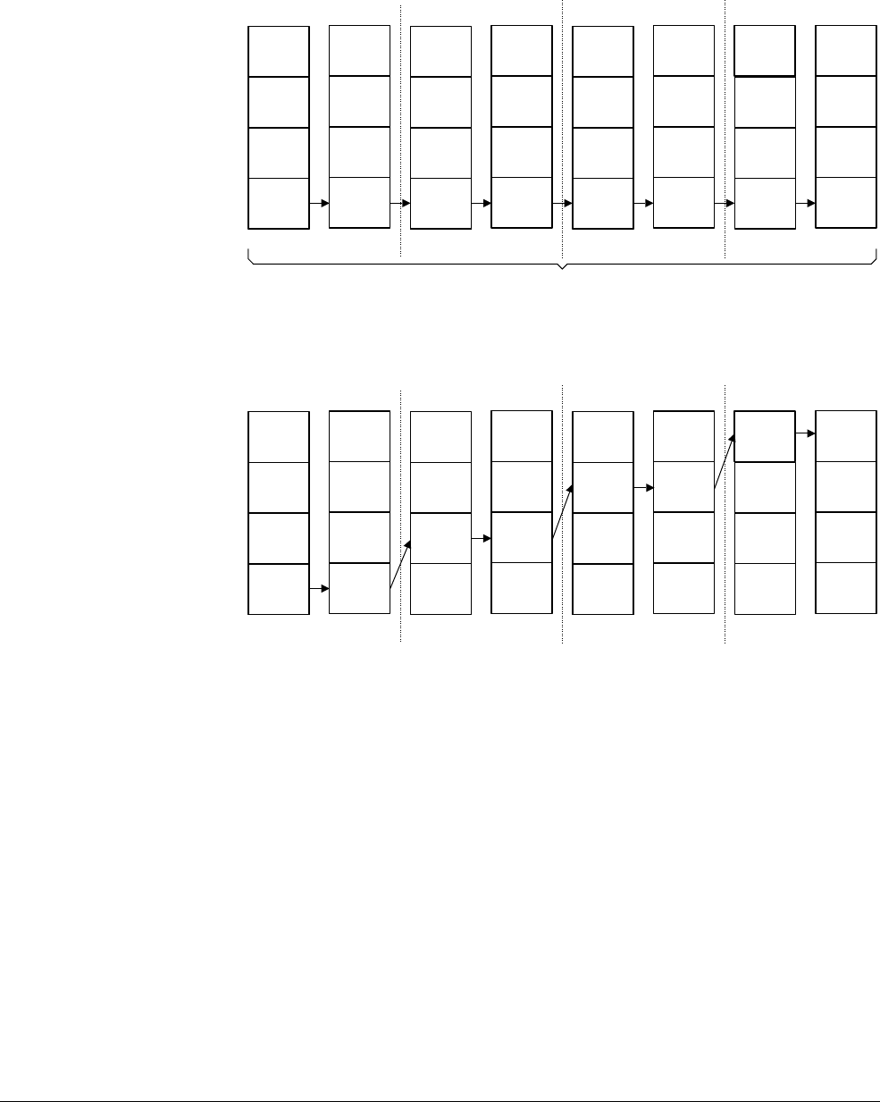
Level One Memory System
ARM DDI 0363G Copyright © 2006-2011 ARM Limited. All rights reserved. 8-28
ID041111 Non-Confidential
• Write a line to the eviction buffer in one cycle, a 256-bit read access.
• Fill a line in one cycle from the linefill buffer, a 256-bit write access.
Figure 8-3 shows a cache look-up being performed on all banks with one RAM access.
Figure 8-3 Nonsequential read operation performed with one RAM access.
Figure 8-4 shows the appropriate bank RAM being selected for a sequential read operation.
Figure 8-4 Sequential read operation performed with one RAM access
The data RAM organization is optimized for 64-bit read operations, because with the same
address, two words on the same way can be selected.
Data RAM sizes depend on the build option selected, and are described in:
•Data RAM sizes without parity or ECC implemented on page 8-29
•Data RAM sizes with parity implemented on page 8-29
•Data RAM sizes with ECC implemented on page 8-30.
RAM address
0
1
2
3Way 1
Word 6
Bank 0
Way 1
Word 7
Way 2
Word 4
Way 2
Word 5
Way 3
Word 2
Way 3
Word 3
Way 0
Word 0
Way 0
Word 1
Bank 1
Way 2
Word 6
Bank 2
Way 2
Word 7
Way 3
Word 4
Way 3
Word 5
Way 0
Word 2
Way 0
Word 3
Way 1
Word 0
Way 1
Word 1
Bank 3
Way 3
Word 6
Bank 4
Way 3
Word 7
Way 0
Word 4
Way 0
Word 5
Way 1
Word 2
Way 1
Word 3
Way 2
Word 0
Way 2
Word 1
Bank 5
Way 0
Word 7
Way 1
Word 4
Way 1
Word 5
Way 2
Word 2
Way 2
Word 3
Way 3
Word 0
Way 3
Word 1
Bank 7
Bank 6
Way 0
Word 6
256-bit wide
RAM address
0
1
2
3Way 1
Word 6
Bank 0
Way 1
Word 7
Way 2
Word 4
Way 2
Word 5
Way 3
Word 2
Way 3
Word 3
Way 0
Word 0
Way 0
Word 1
Bank 1
Way 2
Word 6
Bank 2
Way 2
Word 7
Way 3
Word 4
Way 3
Word 5
Way 0
Word 2
Way 0
Word 3
Way 1
Word 0
Way 1
Word 1
Bank 3
Way 3
Word 6
Bank 4
Way 3
Word 7
Way 0
Word 4
Way 0
Word 5
Way 1
Word 2
Way 1
Word 3
Way 2
Word 0
Way 2
Word 1
Bank 5
Way 0
Word 7
Way 1
Word 4
Way 1
Word 5
Way 2
Word 2
Way 2
Word 3
Way 3
Word 0
Way 3
Word 1
Bank 7
Bank 6
Way 0
Word 6

Level One Memory System
ARM DDI 0363G Copyright © 2006-2011 ARM Limited. All rights reserved. 8-29
ID041111 Non-Confidential
Data RAM sizes without parity or ECC implemented
Table 8-9 shows the organization for instruction and data caches when neither parity nor ECC
is implemented.
Data RAM sizes with parity implemented
Table 8-11 shows the organization for instruction and data caches when parity is implemented.
For parity error detection, one bit is added per byte, so four bits are added for each RAM bank.
Table 8-9 Instruction cache data RAM sizes, no parity or ECC
Cache size Data RAMs
4KB, 4 1KB ways 4 banks 64 bits 128 lines or
8 banks 32 bits 128 lines
8KB, 4 2KB ways 4 banks 64 bits 256 lines or
8 banks 32 bits 256 lines
16KB, 4 4KB ways 4 banks 64 bits 512 lines or
8 banks 32 bits 512 lines
32KB, 4 8KB ways 4 banks 64 bits 1024 lines or
8 banks 32 bits 1024 lines
64KB, 4 16KB ways 4 banks 64 bits 2048 lines or
8 banks 32 bits 2048 lines
Table 8-10 Data cache data RAM sizes, no parity or ECC
Cache size Data RAMs
4KB, 4 1KB ways 8 banks 32 bits 128 lines
8KB, 4 2KB ways 8 banks 32 bits 256 lines
16KB, 4 4KB ways 8 banks 32 bits 512 lines
32KB, 4 8KB ways 8 banks 32 bits 1024 lines
64KB, 4 16KB ways 8 banks 32 bits 2048 lines
Table 8-11 Instruction cache data RAM sizes, with parity
Cache size Data RAMs
4KB, 4 1KB ways 4 banks 72 bits 128 lines or
8 banks 36 bits 128 lines
8KB, 4 2KB ways 4 banks 72 bits 256 lines or
8 banks 36 bits 256 lines
16KB, 4 4KB ways 4 banks 72 bits 512 lines or
8 banks 36 bits 512 lines
32KB, 4 8KB ways 4 banks 72 bits 1024 lines or
8 banks 36 bits 1024 lines
64KB, 4 16KB ways 4 banks 72 bits 2048 lines or
8 banks 36 bits 2048 lines

Level One Memory System
ARM DDI 0363G Copyright © 2006-2011 ARM Limited. All rights reserved. 8-30
ID041111 Non-Confidential
Table 8-13 shows the organization of the data cache RAM bits when parity is implemented.
Parity bits are grouped together in bits[35:32] so that data and parity bits are easily
differentiated. With this design the parity bit is selected alongside the related data byte, so that
when data is updated, the parity bit is also updated.
Data RAM sizes with ECC implemented
Table 8-14 shows the organization for the instruction cache when ECC is implemented. For
ECC error detection, eight bits are added per 64 bits, so four bits are added for each RAM bank.
Table 8-12 Data cache data RAM sizes, with parity
Cache size Data RAMs
4KB, 4 1KB ways 8 banks 36 bits 128 lines
8KB, 4 2KB ways 8 banks 36 bits 256 lines
16KB, 4 4KB ways 8 banks 36 bits 512 lines
32KB, 4 8KB ways 8 banks 36 bits 1024 lines
64KB, 4 16KB ways 8 banks 36 bits 2048 lines
Table 8-13 Data cache RAM bits, with parity
RAM bits Description
Bit [35] Parity bit for byte[31:24]
Bit [34] Parity bit for byte[23:16]
Bit [33] Parity bit for byte[15:8]
Bit [32] Parity bit for byte[7:0]
Bits [31:0] Data[31:0]
Table 8-14 Instruction cache data RAM sizes with ECC
Cache size Data RAMs
4KB, 4 1KB ways 4 banks 72 bits 128 lines or
8 banks 36 bits 128 lines
8KB, 4 2KB ways 4 banks 72 bits 256 lines or
8 banks 36 bits 256 lines
16KB, 4 4KB ways 4 banks 72 bits 512 lines or
8 banks 36 bits 512 lines
32KB, 4 8KB ways 4 banks 72 bits 1024 lines or
8 banks 36 bits 1024 lines
64KB, 4 16KB ways 4 banks 72 bits 2048 lines or
8 banks 36 bits 2048 lines

Level One Memory System
ARM DDI 0363G Copyright © 2006-2011 ARM Limited. All rights reserved. 8-31
ID041111 Non-Confidential
Table 8-15 shows the organization for the data cache when ECC is implemented. For ECC error
detection, seven bits are added per 32 bits, so seven bits are added for each RAM bank.
Table 8-16 shows the organization of the data cache RAM bits when ECC is implemented.
8.5.5 Cache interaction with memory system
This section describes how to enable or disable the cache RAMs, and to enable or disable error
checking. After you enable or disable the instruction cache, you must issue an
ISB
instruction to
flush the pipeline. This ensures that all subsequent instruction fetches see the effect of enabling
or disabling the instruction cache.
After reset, you must invalidate each cache before enabling it.
When disabling the data cache, you must clean the entire cache to ensure that any dirty data is
flushed to L2 memory.
Before enabling the data cache, you must invalidate the entire data cache if L2 memory might
have changed since the cache was disabled.
Before enabling the instruction cache, you must invalidate the entire instruction cache if L2
memory might have changed since the cache was disabled.
See Enabling or disabling AXI slave accesses on page 9-23 and Accessing RAMs using the AXI
slave interface on page 9-24 for information about how to access the cache RAMs using the
AXI slave interface.
Disabling or enabling all of the caches
The following code is an example of enabling caches:
MRC p15, 0, r1, c1, c0, 0 ; Read SCTLR configuration data
ORR r1, r1, #0x1 <<12 ; instruction cache enable
ORR r1, r1, #0x1 <<2 ; data cache enable
DSB
MCR p15, 0, r0, c15, c5, 0 ; Invalidate entire data cache
MCR p15, 0, r0, c7, c5, 0 ; Invalidate entire instruction cache
MCR p15, 0, r1, c1, c0, 0 ; enabled cache RAMs
ISB
Table 8-15 Data cache data RAM sizes with ECC
Cache size Data RAMs
4KB, 4 1KB ways 8 banks 39 bits 128 lines
8KB, 4 2KB ways 8 banks 39 bits 256 lines
16KB, 4 4KB ways 8 banks 39 bits 512 lines
32KB, 4 8KB ways 8 banks 39 bits 1024 lines
64KB, 4 16KB ways 8 banks 39 bits 2048 lines
Table 8-16 Data cache RAM bits, with ECC
RAM bits Description
Bits [39:32] ECC code bits for data [31:0]
Bits [31:0] Data [31:0]

Level One Memory System
ARM DDI 0363G Copyright © 2006-2011 ARM Limited. All rights reserved. 8-32
ID041111 Non-Confidential
The following code is an example of disabling the caches:
MRC p15, 0, r1, c1, c0, 0 ; Read SCTLR configuration data
BIC r1,r1, #0x1 <<12 ; instruction cache disable
BIC r1, r1, #0x1 <<2 ; data cache disable
DSB
MCR p15, 0, r1, c1, c0, 0 ; disabled cache RAMs
ISB
; Clean entire data cache. This routine depends on the data cache size. It can be
omitted if it is known that the data cache has no dirty data
Disabling or enabling instruction cache
The following code is an example of enabling the instruction cache:
MRC p15, 0, r1, c1, c0, 0 ; Read SCTLR configuration data
ORR r1, r1, #0x1 <<12 ; instruction cache enable
MCR p15, 0, r0, c7, c5, 0 ; Invalidate entire instruction cache
MCR p15, 0, r1, c1, c0, 0 ; enabled instruction cache
ISB
The following code is an example of disabling the instruction cache:
MRC p15, 0, r1, c1, c0, 0 ; Read SCTLR configuration data
BIC r1, r1, #0x1 <<12 ; instruction cache enable
MCR p15, 0, r1, c1, c0, 0 ; disabled instruction cache
ISB
Disabling or enabling data cache
The following code is an example of enabling the data cache:
MRC p15, 0, R1, c1, c0, 0 ; Read SCTLR configuration data
ORR R1, R1, #0x1 <<2
DSB
MCR p15, 0, r0, c15, c5, 0 ; Invalidate entire data cache
MCR p15, 0, R1, c1, c0, 0 ; enabled data cache
The following code is an example of disabling the cache RAMs:
MRC p15, 0, r1, c1, c0, 0 ; Read SCTLR configuration data
BIC r1, r1, #0x1 <<2
DSB
MCR p15, 0, r1, c1, c0, 0 ; disabled data cache
; Clean entire data cache. This routine depends on the data cache size. It can be
omitted if it is known that the data cache has no dirty data.
Disabling or enabling error checking
Software must take care when changing the error checking bits in the ACTLR. If the bits are
changed when the caches contain data, the parity or ECC bits in the caches might not be correct
for the new setting, resulting in unexpected errors and data loss. Therefore the bits in the
ACTLR must only be changed when both caches are turned off and the entire cache must be
invalidated after the change.
ARM recommends the following code sequence to perform the change:
MRC p15, 0, r0, c1, c0, 0 ; Read SCTLR
BIC r0, r0, #0x1 << 2 ; Disable data cache bit
BIC r0, r0, #0x1 << 12 ; Disable instruction cache bit
DSB
MCR p15, 0, r0, c1, c0, 0 ; Write SCTLR
ISB ; Ensures following instructions are not executed from cache

Level One Memory System
ARM DDI 0363G Copyright © 2006-2011 ARM Limited. All rights reserved. 8-33
ID041111 Non-Confidential
; Clean entire data cache. This routine depends on the data cache size. It can be
omitted if it is known that the data cache has no dirty data (for example, if the cache
has not been enabled yet).
MRC p15, 0, r1, c1, c0, 1 ; Read ACTLR
; Change bits 5:3 as required
MCR p15, 0, r1, c1, c0, 1 ; Write ACTLR
MCR p15, 0, r0, c15, c5, 0 ; Invalidate entire data cache
MCR p15, 0, r0, c7, c5, 0 ; Invalidate entire instruction cache
MRC p15, 0, r0, c1, c0, 0 ; Read SCTLR
ORR r0, r0, #0x1 << 2 ; Enable data cache bit
ORR r0, r0, #0x1 << 12 ; Enable instruction cache bit
DSB
MCR p15, 0, r0, c1, c0, 0 ; Write SCTLR
ISB

Level One Memory System
ARM DDI 0363G Copyright © 2006-2011 ARM Limited. All rights reserved. 8-34
ID041111 Non-Confidential
8.6 Internal exclusive monitor
The processor L1 memory system has an internal exclusive monitor. This is a two state, open
and exclusive, state machine that manages load/store exclusive (
LDREXB
,
LDREXH
,
LDREX
,
LDREXD
,
STREXB
,
STREXH
,
STREX
and
STREXD
) accesses and clear exclusive (
CLREX
) instructions. You can use
these instructions, operating in the L1 memory system, to construct semaphores and ensure
synchronization between different processes. By adding an external exclusive monitor, you can
also use these instructions in the L2 memory system to construct semaphores and ensure
synchronization between different processors. See the ARM Architecture Reference Manual for
more information about how these instructions work.
When a load-exclusive access is performed, the internal exclusive monitor moves to the
exclusive state. It moves back to the open state when a store exclusive access or clear exclusive
instruction is performed. The internal exclusive monitor holds exclusivity state for the
Cortex-R4 processor only. It does not record the address of the memory that a load-exclusive
access was performed to. Any store exclusive access performed when the state is open fails. If
the state is exclusive, the access passes if it is to non-shared memory but, if it is to shared
memory, the access must be performed as an exclusive using the L2 memory interface. Whether
the shared store-exclusive access passes or fails depends on the state of an external exclusive
monitor that can track accesses made by other processors in the system.

Level One Memory System
ARM DDI 0363G Copyright © 2006-2011 ARM Limited. All rights reserved. 8-35
ID041111 Non-Confidential
8.7 Memory types and L1 memory system behavior
The behavior of the L1 memory system depends on the type attribute of the memory that is being
accessed:
• Only Normal, Non-shared memory can be cached in the RAMs.
• The store buffer can merge any stores to Normal memory. See Store buffer on page 8-18
for more information.
• Only Normal memory is considered restartable, that is, a multi-word transfer can be
abandoned part way through because of an interrupt, to be restarted after the interrupt is
handled. See Interrupts on page 3-16 for more information about interrupt behavior.
• Only the internal exclusive monitor is used for exclusive accesses to Non-shared memory.
Exclusive accesses to shared memory are checked using the internal monitor and also, if
necessary, any external monitor, using the L2 memory interface.
• Accesses resulting from
SWP
and
SWPB
instructions to Normal, non-shared memory are not
marked as locked when performed using the L2 memory interface.
Table 8-17 summarizes the processor memory types and associated behavior.
Table 8-17 Memory types and associated behavior
Memory type Can be cached Merging Restartable Internal
exclusives
Locked
swaps
Normal Shared No Yes Yes Partially Yes
Non-shared Yes Yes Yes Yes No
Device Shared No No No Partially Yes
Non-shared No No No Yes Yes
Strongly-ordered Shared No No No Partially Yes

Level One Memory System
ARM DDI 0363G Copyright © 2006-2011 ARM Limited. All rights reserved. 8-36
ID041111 Non-Confidential
8.8 Error detection events
The processor generates a number of events related to the internal error detection and correction
schemes in the TCMs and caches. For more information, see Table 6-1 on page 6-2. This section
describes:
•TCM error events
•Instruction-cache error events
•Data-cache error events
•Events and the CFLR.
8.8.1 TCM error events
TCM parity and ECC error events are only signaled for TCM reads, although this includes the
read-modify-write sequence performed for some stores. Most errors detected by the internal
parity or ECC logic are signaled twice:
• once on a TCM-centric event
• once on a processor-centric event.
The TCM-centric events consist of two events per TCM port, one for fatal, that is, 2-bit ECC or
parity errors and one for correctable, that is, 1-bit ECC errors. These events are generated three
clock cycles after the data read cycle. Consequently, these events are sometimes signaled on
speculative TCM reads, such as instructions that are prefetched but never executed because of
a branch earlier in the instruction sequence.
Note
When an external error is signaled on a TCM access, the TCM-centric events are still generated
as appropriate, based on the data returned, as if no external error had been signaled.
The processor-centric TCM events are only signaled for errors in data that would have otherwise
been used by the processor. Errors on purely speculative reads never generate these errors. They
consist of fatal and correctable events for:
• the prefetch unit, to signal errors on instruction fetches
• the load/store unit, to signal errors on data accesses
• the AXI slave interface, to signal errors on DMA accesses.
8.8.2 Instruction-cache error events
All parity and ECC errors are correctable in the Icache. Therefore there are only two events, to
indicate when an error is detected in a read from the tag RAM, or from the data RAM. These
events are only signaled for non-speculative instruction fetches and certain cache maintenance
operations. See Cache error detection and correction on page 8-20.
8.8.3 Data-cache error events
The Dcache can generate fatal and correctable errors, and therefore has four events, one for each
type of error in the data RAM and in the tag or dirty RAMs. These events are only signaled for
non-speculative data accesses, cache line evictions, and certain cache maintenance operations.
See Cache error detection and correction on page 8-20.
8.8.4 Events and the CFLR
The Correctable Fault Location Register (CFLR) records the location of the last correctable
error detected on a non-speculative access. See Correctable Fault Location Register on
page 4-75 for more information. Every correctable error that is recorded in the CFLR also

Level One Memory System
ARM DDI 0363G Copyright © 2006-2011 ARM Limited. All rights reserved. 8-37
ID041111 Non-Confidential
generates an event. See Table 6-1 on page 6-2 to see which events are CFLR-related. For
correctable cache errors, the CLFR does not record whether the error occurred in the data RAM
or tag/dirty RAM. This distinction is only made by the events.

ARM DDI 0363G Copyright © 2006-2011 ARM Limited. All rights reserved. 9-1
ID041111 Non-Confidential
Chapter 9
Level Two Interface
This chapter describes the features of the Level two (L2) interface not covered in the AMBA AXI
Protocol Specification. It contains the following sections:
•About the L2 interface on page 9-2
•AXI master interface on page 9-3
•AXI master interface transfers on page 9-7
•AXI slave interface on page 9-20
•Enabling or disabling AXI slave accesses on page 9-23
•Accessing RAMs using the AXI slave interface on page 9-24.

Level Two Interface
ARM DDI 0363G Copyright © 2006-2011 ARM Limited. All rights reserved. 9-2
ID041111 Non-Confidential
9.1 About the L2 interface
This section describes the processor L2 interface. The L2 interface consists of AXI master and
AXI slave interfaces.
The processor is designed for use in larger chip designs using the AMBA AXI protocol. The
processor uses the L2 interfaces as its interface to memory and peripheral devices.
External AXI masters, that can include the processor itself, can use the AXI slave interface to
access the processor RAMs. You can use the AXI slave interface for DMA access into and out
of the TCMs or to perform software test of the TCMs and cache RAMs.

Level Two Interface
ARM DDI 0363G Copyright © 2006-2011 ARM Limited. All rights reserved. 9-3
ID041111 Non-Confidential
9.2 AXI master interface
The processor has a single AXI master interface, with one port that is used for:
• Icache linefills
• Dcache linefills and evictions
•Non-cacheable (NC) Normal-type memory instruction fetches
• NC Normal-type memory data accesses
• Device and Strongly-ordered type data accesses, normally to peripherals.
The port is 64 bits wide, and conforms to the AXI standard as described in the AMBA AXI
Protocol Specification. Within the AXI standard, the master port uses the AW U S E R M and
ARUSERM signals to indicate inner memory attributes.
The master interface can run at the same frequency as the processor or at a lower synchronous
frequency. See AMBA interface clocking on page 2-13 for more information.
In addition, the AXI master interface produces or checks parity bits for each AXI channel. These
additional signals are not part of the AXI specification.
Note
In this section, AXI slave describes the AXI slave in the external system that is connected to the
Cortex-R4 AXI master port. This might not be the Cortex-R4 AXI slave port.
The following sections describe the attributes of the AXI master interface, and provide
information about the types of burst generated:
•Identifiers for AXI bus accesses on page 9-4
•Write response on page 9-4
•Linefill buffers and the AXI master interface on page 9-4
•Eviction buffer on page 9-5
•Memory attributes on page 9-5.
Table 9-1 shows the AXI master interface attributes.
Table 9-1 AXI master interface attributes
Attribute Value Comments
Write issuing capability 4 Made up of four outstanding writes that can be evictions, single writes, or write
bursts.a
Read issuing capability 7 Made up of five linefills on the data side, one NC read on the data side, and one
read on the instruction side, that can be NC or linefill.
Combined issuing capability 11a-
Write ID capability 2 -
Write interleave capability 1 The AXI master interface presents all write data in order.
Read ID capability 7 Made up of five linefills on the data side, one NC read on the data side, and one
linefill or NC read on the instruction side.
a. When there are three outstanding write transactions, only data is issued for the fourth. Only three outstanding write addresses
are issued.

Level Two Interface
ARM DDI 0363G Copyright © 2006-2011 ARM Limited. All rights reserved. 9-4
ID041111 Non-Confidential
9.2.1 Identifiers for AXI bus accesses
Accesses on the AXI bus use ID values as follows:
Outstanding write/read access on different IDs
This means, for example, that a Non-cacheable (NC) read and linefills can be
outstanding on the AXI bus simultaneously as long as the IDs are different.
At the same time, there can be:
• up to seven outstanding reads, each with one of seven different ID values,
that consists of:
— a data side read NC access, RID0
— an instruction side read NC access or an instruction side read
cacheable access, RID1
— five outstanding data side linefills on the AXI bus, RID3 - RID7.
• up to two IDs on outstanding writes, that consist of:
— single or burst NC writes or write-through (WT) writes, WID0
— evictions, WID1.
Outstanding write accesses with the same ID
When the address and data of the first write are both put on AXI bus, another write
request with same ID can be sent when the address or data channel is released.
For example, the new address can be sent with the same ID, before the target
accepts the data of the first write.
Note
• The AXI master does not generate two outstanding read accesses with the same ID.
• The AXI master does not interleave write data from two different bursts, even if the bursts
have different IDs.
9.2.2 Write response
The AXI master requires that the slave does not return a write response until it has received both
the write data and the write address.
9.2.3 Linefill buffers and the AXI master interface
On the data side there are two LineFill Buffers (LFBs), LFB0 and LFB1. Each request from the
data cache controller or from the STore Buffer (STB) can be allocated to either LFB0 or LFB1.
On the instruction side, there is one LFB. This is the Instruction LFB (ILFB), that treats
instruction linefill requests or Non-cacheable instruction reads in the same way.
The linefill buffers:
• get returned data from the AXI bus for linefill requests
• get returned data from the AXI bus for any Non-cacheable
LDR
or
LDM
s
• get data from the STB to write as a burst on the AXI bus (LFB0 and LFB1 only).
Single writes do not use LFBs.
The LFBs are 256 bits wide so that an entire cache line can be written to the cache RAMs in one
cycle. While the LFB is being filled from L2 memory, its bytes can be merged with write data
from the STB.

Level Two Interface
ARM DDI 0363G Copyright © 2006-2011 ARM Limited. All rights reserved. 9-5
ID041111 Non-Confidential
9.2.4 Eviction buffer
As soon as a linefill is requested, the selected evicted cache line is loaded into the EViction
Buffer (EVB). The EVB forwards this information to the AXI bus when possible.
The EVB has a structure of 256 bits for data and 32 bits for the address. See Cache line
write-back (eviction) on page 9-13 for information about the AXI transaction generated.
The EVB is removed if cache RAMs are not implemented for the processor.
9.2.5 Memory attributes
The Cortex-R4 AXI master interface uses the ARCACHEM, AWCACHEM, ARUSERM,
and AW U S E R M signals to indicate the memory attributes of the transfer, as returned by the
MPU. Table 9-2 Shows the encodings used for the signals ARCACHEM and AWCACHEM
of the master interface. These are generated from the memory type and outer region attributes.
Table 9-3 shows the encodings the master interface uses for the ARUSERM and AW U S E R M
signals. These are generated from the memory type and inner region attributes.
Table 9-2 ARCACHEM and AWCACHEM encodings
Encodinga
a. Encodings not shown in the table are reserved.
Meaning
b0000 Strongly-ordered
b0001 Device
b0011 Non-cacheable
b0110 Cacheable, write-through, allocate on reads only
b0111 Cacheable, write-back, allocate on reads only
b1111 Cacheable write-back, allocate on reads and writes
Table 9-3 ARUSERM and AWUSERM encodings
Encodinga
a. Encodings not shown in the table are reserved.
Meaning
b00001 Strongly-ordered
b00010 Device, Non-shared
b00011 Device, shared
b00110 Non-cacheable, Non-shared
b00111 Non-cacheable, shared
b01100 Cacheable, write-through, read-allocate only, Non-shared
b01101 Cacheable, write-through, read-allocate only, shared
b11110 Cacheable, write-back, read- and write-allocate, Non-shared
b11111 Cacheable, write-back, read- and write-allocate, shared

Level Two Interface
ARM DDI 0363G Copyright © 2006-2011 ARM Limited. All rights reserved. 9-6
ID041111 Non-Confidential
Memory system implications for AXI accesses
The attributes of the memory being accessed can affect an AXI access. The L1 memory system
can cache any Normal memory address that is marked as either:
• Cacheable, write-back, read- and write-allocate, non-shared
• Cacheable, write-through, read-allocate only, non-shared.
However, Device and Strongly-ordered memory is always Non-cacheable. Also, any unaligned
access to Device or Strongly-ordered memory generates an alignment fault and therefore does
not cause any AXI transfer. This means that the access examples given in this chapter never
show unaligned accesses to Device or Strongly-ordered memory.

Level Two Interface
ARM DDI 0363G Copyright © 2006-2011 ARM Limited. All rights reserved. 9-7
ID041111 Non-Confidential
9.3 AXI master interface transfers
The processor conforms to the AXI specification, but it does not generate all the AXI transaction
types that the specification permits. This section describes the types of AXI transaction that the
Cortex-R4 AXI master does not generate. If you are designing an AXI slave to work only with
the Cortex-R4 processor, and there are no other AXI masters in your system, you can take
advantage of these restrictions and the interface attributes described in AXI master interface on
page 9-3 to simplify the slave.
This section also contains tables that show some of the types of AXI burst that the processor
generates. However, because a particular type of transaction is not shown here does not mean
that the processor does not generate such a transaction.
Note
An AXI slave device connected to the Cortex-R4 AXI master port must be capable of handling
every kind of transaction permitted by the AXI specification, except where there is an explicit
statement in this chapter that such a transaction is not generated. You must not infer any
additional restrictions from the example tables given. Restrictions described here are applicable
to the r1p0, r1p1, and r1p2 revisions of the processor, and might not be true for future revisions.
Load and store instructions to Non-cacheable memory might not result in an AXI transfer
because the data might either be retrieved from, or merged into the internal store data buffers.
The exceptions to this are loads or stores to Strongly-ordered or Device memory. These always
result in AXI transfers. See Strongly-ordered and Device transactions on page 9-8.
Restrictions on AXI transfers on page 9-8 describes restrictions on the type of transfers that the
Cortex-R4 AXI master interface generates. The AXI master port never deasserts the buffered
write response and read data channel ready signals, BREADYM and RREADYM. You must
not make any other assumptions about the AXI handshaking signals, except that they conform
to the AMBA AXI Protocol Specification.
The following sections give examples of transfers generated by the AXI master interface:
•Restrictions on AXI transfers on page 9-8
•Strongly-ordered and Device transactions on page 9-8
•Linefills on page 9-13
•Cache line write-back (eviction) on page 9-13
•Non-cacheable reads on page 9-13
•Non-cacheable or write-through writes on page 9-15
•AXI transaction splitting on page 9-16
•Normal write merging on page 9-17.

Level Two Interface
ARM DDI 0363G Copyright © 2006-2011 ARM Limited. All rights reserved. 9-8
ID041111 Non-Confidential
9.3.1 Restrictions on AXI transfers
The Cortex-R4 AXI master interface applies the following restrictions to the AXI transactions
it generates:
• A burst never transfers more than 32 bytes.
• The burst length is never more than 8 transfers.
• No transaction ever crosses a 32-byte boundary in memory. See AXI transaction splitting
on page 9-16.
• FIXED bursts are never used.
• The write address channel always issues INCR type bursts, and never WRAP or FIXED.
• WRAP type read bursts, see Linefills on page 9-13:
— are used only for linefills (reads) of cacheable Normal non-shared memory
— always have a size of 64 bits, and a length of 4 transfers
— always have a start address that is 64-bit aligned.
• If the transfer size is 8 bits or 16 bits then the burst length is always 1 transfer.
• The transfer size is never greater than 64 bits, because it is a 64-bit AXI bus.
• Instruction fetches, identified by ARPROT[2], are always a 64 bit transfer size, and never
locked or exclusive.
• Transactions to Device and Strongly-ordered memory are always to addresses that are
aligned for the transfer size. See Strongly-ordered and Device transactions.
• Exclusive and Locked accesses are always to addresses that are aligned for the transfer
size.
• Write data is never interleaved.
• In addition, there are various limitations to the ID values that the AXI master interface
uses. See Identifiers for AXI bus accesses on page 9-4.
9.3.2 Strongly-ordered and Device transactions
A load or store instruction to or from Strongly-ordered or Device memory always generates AXI
transactions of the same size as implied by the instruction. All accesses using
LDM
,
STM
,
LDRD
, or
STRD
instructions to Strongly-ordered or Device memory occur as 32-bit transfers.
LDRB
Table 9-4 shows the values of ARADDRM, ARBURSTM, ARSIZEM, and ARLENM for a
Non-cacheable
LDRB
from bytes 0-7 in Strongly-ordered or Device memory.
Table 9-4 Non-cacheable LDRB
Address[2:0] ARADDRM ARBURSTM ARSIZEM ARLENM
0x0
(byte 0)
0x00
Incr 8-bit 1 data transfer
0x1
(byte 1)
0x01
Incr 8-bit 1 data transfer
0x2
(byte 2)
0x02
Incr 8-bit 1 data transfer
0x3
(byte 3)
0x03
Incr 8-bit 1 data transfer

Level Two Interface
ARM DDI 0363G Copyright © 2006-2011 ARM Limited. All rights reserved. 9-9
ID041111 Non-Confidential
LDRH
Table 9-5 shows the values of ARADDRM, ARBURSTM, ARSIZEM, and ARLENM for a
Non-cacheable
LDRH
from halfwords 0-3 in Strongly-ordered or Device memory.
Note
A load of a halfword from Strongly-ordered or Device memory addresses
0x1
,
0x3
,
0x5
, or
0x7
generates an alignment fault.
LDR or LDM that transfers one register
Table 9-6 shows the values of ARADDRM, ARBURSTM, ARSIZEM, and ARLENM for a
Non-cacheable
LDR
or an
LDM
that transfers one register, (an
LDM
1) in Strongly-ordered or Device
memory.
Note
A load of a word from Strongly-ordered or Device memory addresses
0x1
,
0x2
,
0x3
,
0x5
,
0x6
, or
0x7
generates an alignment fault.
0x4
(byte 4)
0x04
Incr 8-bit 1 data transfer
0x5
(byte 5)
0x05
Incr 8-bit 1 data transfer
0x6
(byte 6)
0x06
Incr 8-bit 1 data transfer
0x7
(byte 7)
0x07
Incr 8-bit 1 data transfer
Table 9-5 LDRH from Strongly-ordered or Device memory
Address[3:0] ARADDRM ARBURSTM ARSIZEM ARLENM
0x0
(halfword 0)
0x00
Incr 16-bit 1 data transfer
0x2
(halfword 1)
0x02
Incr 16-bit 1 data transfer
0x4
(halfword 2)
0x04
Incr 16-bit 1 data transfer
0x6
(halfword 3)
0x06
Incr 16-bit 1 data transfer
Table 9-6 LDR or LDM1 from Strongly-ordered or Device memory
Address[2:0] ARADDRM ARBURSTM ARSIZEM ARLENM
0x0
(word 0)
0x00
Incr 32-bit 1 data transfer
0x4
(word 1)
0x04
Incr 32-bit 1 data transfer
Table 9-4 Non-cacheable LDRB (continued)
Address[2:0] ARADDRM ARBURSTM ARSIZEM ARLENM

Level Two Interface
ARM DDI 0363G Copyright © 2006-2011 ARM Limited. All rights reserved. 9-10
ID041111 Non-Confidential
LDM that transfers five registers
Table 9-7 shows the values of ARADDRM, ARBURSTM, ARSIZEM, and ARLENM for a
Non-cacheable
LDM
that transfers five registers (an
LDM
5) in Strongly-ordered or Device memory.
Note
A load-multiple from address
0x1
,
0x2
,
0x3
,
0x5
,
0x6
,
0x7
,
0x9
,
0xA
,
0xB
,
0xD
,
0xE
, or
0xF
generates
an alignment fault.
Table 9-7 LDM5, Strongly-ordered or Device memory
Address[4:0] ARADDRM ARBURSTM ARSIZEM ARLENM
0x00
(word 0)
0x00
Incr 32-bit 5 data transfers
0x04
(word 1)
0x04
Incr 32-bit 5 data transfers
0x08
(word 2)
0x08
Incr 32-bit 5 data transfers
0x0C
(word 3)
0x0C
Incr 32-bit 5 data transfers

Level Two Interface
ARM DDI 0363G Copyright © 2006-2011 ARM Limited. All rights reserved. 9-11
ID041111 Non-Confidential
STRB
Table 9-8 shows the values of AWADDRM, AWBURSTM, AWSIZEM, and AW L E N M for
an
STRB
to Strongly-ordered or Device memory over the AXI master port.
STRH
Table 9-9 shows the values of AWADDRM, AWBURSTM, AWSIZEM, and AW L E N M for
an
STRH
over the AXI master port to Strongly-ordered or Device memory.
Note
A store of a halfword to Strongly-ordered or Device memory addresses
0x1
,
0x3
,
0x5
, or
0x7
generates an alignment fault.
Table 9-8 STRB to Strongly-ordered or Device memory
Address[4:0] AWADDRM AWBURSTM AWSIZEM AWLENM WSTRBM
0x00
(byte 0)
0x00
Incr 8-bit 1 data transfer b00000001
0x01
(byte 1)
0x01
Incr 8-bit 1 data transfer b00000010
0x02
(byte 2)
0x02
Incr 8-bit 1 data transfer b00000100
0x03
(byte 3)
0x03
Incr 8-bit 1 data transfer b00001000
0x04
(byte 4)
0x04
Incr 8-bit 1 data transfer b00010000
0x05
(byte 5)
0x05
Incr 8-bit 1 data transfer b00100000
0x06
(byte 6)
0x06
Incr 8-bit 1 data transfer b01000000
0x07
(byte 7)
0x07
Incr 8-bit 1 data transfer b10000000
Table 9-9 STRH to Strongly-ordered or Device memory
Address[2:0] AWADDRM AWBURSTM AWSIZEM AWLENM WSTRBM
0x0
(halfword 0)
0x00
Incr 16-bit 1 data transfer b00000011
0x2
(halfword 1)
0x02
Incr 16-bit 1 data transfer b00001100
0x4
(halfword 2)
0x04
Incr 16-bit 1 data transfer b00110000
0x6
(halfword 3)
0x06
Incr 16-bit 1 data transfer b11000000

Level Two Interface
ARM DDI 0363G Copyright © 2006-2011 ARM Limited. All rights reserved. 9-12
ID041111 Non-Confidential
STR or STM of one register
Table 9-10 shows the values of AWADDRM, AW B U R ST M , AWSIZEM, and AWLENM for
an
STR
or an
STM
that transfers one register (an
STM
1) over the AXI master port to
Strongly-ordered or Device memory.
Note
A store of a word to Strongly-ordered or Device memory addresses
0x1
,
0x2
,
0x3
,
0x5
,
0x6
, or
0x7
generates an alignment fault.
STM of seven registers
Table 9-11 shows the values of AWADDRM, AWBURSTM, AWSIZEM, and AWLENM for
an
STM
that writes seven registers (an
STM
7) over the AXI master port to Strongly-ordered or
Device memory.
Note
A store-multiple to address
0x1
,
0x2
,
0x3
,
0x5
,
0x6
, or
0x7
generates an alignment fault.
Table 9-10 STR or STM1 to Strongly-ordered or Device memory
Address[2:0] AWADDRM AWBURSTM AWSIZEM AWLENM WSTRBM
0x0
(word0)
0x00
Incr 32-bit 1 data transfer b00001111
0x4
(word 1)
0x04
Incr 32-bit 1 data transfer b11110000
Table 9-11 STM7 to Strongly-ordered or Device memory to word 0 or 1
Address[4:0] AWADDRM AWBURSTM AWSIZEM AWLENM First WSTRBM
0x00
(word 0)
0x00
Incr 32-bit 7 data transfers b00001111
0x04
(word 1)
0x04
Incr 32-bit 7 data transfers b11110000

Level Two Interface
ARM DDI 0363G Copyright © 2006-2011 ARM Limited. All rights reserved. 9-13
ID041111 Non-Confidential
9.3.3 Linefills
Loads and instruction fetches from Normal, cacheable memory that do not hit in the cache
generate a cache linefill when the appropriate cache is enabled. Table 9-12 shows the values of
ARADDRM, ARBURSTM, ARSIZEM, and ARLENM for cache linefills.
9.3.4 Cache line write-back (eviction)
When a valid and dirty cache line is evicted from the Dcache, a write-back of the data must
occur. Table 9-13 shows the values of AWADDRM, AWBURSTM, AW S I Z E M , and
AWLENM for cache line write-backs, over the AXI master interface.
9.3.5 Non-cacheable reads
Load instructions accessing Non-cacheable Normal memory generate AXI bursts that are not
necessarily the same size or length as the instruction implies. In addition, if the data to be read
is contained in the store buffer, the instruction might not generate an AXI read transaction at all.
The tables in this section give examples of the types of AXI transaction that might result from
various load instructions, accessing various addresses in Non-cacheable Normal memory. They
are provided as examples only, and are not an exhaustive description of the AXI transactions.
Depending on the state of the processor, and the timing of the accesses, the actual bursts
generated might have a different size and length to the examples shown, even for the same
instruction.
Table 9-14 shows possible values of ARADDRM, ARBURSTM, ARSIZEM, and ARLENM
for an
LDRH
from bytes 0-7 in Non-cacheable Normal memory.
Table 9-12 Linefill behavior on the AXI interface
Address[4:0]a
a. These are the bottom five bits of the address of the access that cause the linefill, that
is, the address of the critical word.
ARADDRM ARBURSTM ARSIZEM ARLENM
0x00
-
0x07 0x00
Wrap 64-bit 4 data transfers
0x08
-
0x0F 0x08
Wrap 64-bit 4 data transfers
0x10
-
0x17 0x10
Wrap 64-bit 4 data transfers
0x18
-
0x1F 0x18
Wrap 64-bit 4 data transfers
Table 9-13 Cache line write-back
AWADDRM[4:0] AWBURSTM AWSIZEM AWLENM
0x00
Incr 64-bit 4 data transfers
Table 9-14 LDRH from Non-cacheable Normal memory
Address[2:0] ARADDRM ARBURSTM ARSIZEM ARLENM
0x0
(byte 0)
0x00
Incr 16-bit 1 data transfer
0x1
(byte 1)
0x00
Incr 32-bit 1 data transfer
0x2
(byte 2)
0x00
Incr 64-bit 1 data transfer
0x3
(byte 3)
0x03
Incr 32-bit 2 data transfers

Level Two Interface
ARM DDI 0363G Copyright © 2006-2011 ARM Limited. All rights reserved. 9-14
ID041111 Non-Confidential
Table 9-15 shows possible values of ARADDRM, ARBURSTM, ARSIZEM, and ARLENM
for a Non-cacheable
LDR
or an
LDM
that transfers one register, an
LDM
1.
Table 9-16 show possible values of ARADDRM, ARBURSTM, ARSIZEM, and ARLENM
for a Non-cacheable
LDM
that transfers five registers (an
LDM
5).
0x4
(byte 4)
0x04
Incr 16-bit 1 data transfer
0x5
(byte 5)
0x04
Incr 32-bit 1 data transfer
0x6
(byte 6)
0x06
Incr 16-bit 1 data transfer
0x7
(byte 7)
0x07
Incr 32-bit 2 data transfers
Table 9-15 LDR or LDM1 from Non-cacheable Normal memory
Address[2:0] ARADDRM ARBURSTM ARSIZEM ARLENM
0x0
(byte 0) (word 0)
0x00
Incr 32-bit 1 data transfer
0x1
(byte 1)
0x01
Incr 64-bit 1 data transfer
0x2
(byte 2)
0x00
Incr 64-bit 1 data transfer
0x3
(byte 3)
0x00
Incr 64-bit 2 data transfers
0x4
(byte 4) (word 1)
0x04
Incr 32-bit 1 data transfer
0x5
(byte 5)
0x05
Incr 32-bit 2 data transfers
0x6
(byte 6)
0x06
Incr 16-bit 1 data transfer
0x08
Incr 16-bit 1 data transfer
0x7
(byte 7)
0x04
Incr 32-bit 2 data transfers
Table 9-16 LDM5, Non-cacheable Normal memory or cache disabled
Address[4:0] ARADDRM ARBURSTM ARSIZEM ARLENM
0x00
(word 0)
0x00
Incr 64-bit 3 data transfers
0x04
(word 1)
0x04
Incr 64-bit 3 data transfers
0x08
(word 2)
0x08
Incr 64-bit 3 data transfers
0x0C
(word 3)
0x0C
Incr 64-bit 3 data transfers
0x10
(word 4)
0x10
Incr 64-bit 2 data transfers
0x00
Incr 32-bit 1 data transfer
0x14
(word 5)
0x14
Incr 64-bit 2 data transfers
0x00
Incr 64-bit 1 data transfer
Table 9-14 LDRH from Non-cacheable Normal memory (continued)
Address[2:0] ARADDRM ARBURSTM ARSIZEM ARLENM

Level Two Interface
ARM DDI 0363G Copyright © 2006-2011 ARM Limited. All rights reserved. 9-15
ID041111 Non-Confidential
9.3.6 Non-cacheable or write-through writes
Store instructions to Non-cacheable or write-through Normal memory generate AXI bursts that
are not necessarily the same size or length as the instruction implies. The AXI master port
asserts byte-lane-strobes, WSTRBM[7:0], to ensure that only the bytes that were written by the
instruction are updated.
The tables in this section give examples of the types of AXI transaction that might result from
various store instructions, accessing various addresses in Non-cacheable Normal memory. They
are provided as examples only, and are not an exhaustive description of the AXI transactions.
Depending on the state of the processor, and the timing of the accesses, the actual bursts
generated might have a different size and length to the examples shown, even for the same
instruction.
In addition, write operations to Normal memory can be merged to create more complex AXI
transactions. See Normal write merging on page 9-17 for examples.
Table 9-17 shows possible values of AWADDRM, AW B U R ST M , AWSIZEM, and
AWLENM for an
STRH
to Normal memory.
0x18
(word 6)
0x18
Incr 64-bit 1 data transfer
0x00
Incr 64-bit 2 data transfers
0x1C
(word 7)
0x1C
Incr 32-bit 1 data transfer
0x00
Incr 64-bit 2 data transfers
Table 9-16 LDM5, Non-cacheable Normal memory or cache disabled (continued)
Address[4:0] ARADDRM ARBURSTM ARSIZEM ARLENM
Table 9-17 STRH to cacheable write-through or Non-cacheable Normal memory
Address[2:0] AWADDRM AWBURSTM AWSIZEM AWLENM WSTRBM
0x0
(byte 0)
0x00
Incr 32-bit 1 data transfer b00000011
0x1
(byte 1)
0x00
Incr 32-bit 1 data transfer b00000110
0x2
(byte 2)
0x02
Incr 64-bit 1 data transfer b00001100
0x3
(byte 3)
0x03
Incr 32-bit 2 data transfers b00001000
b00010000
0x4
(byte 4)
0x04
Incr 16-bit 1 data transfer b00110000
0x5
(byte 5)
0x05
Incr 32-bit 1 data transfer b01100000
0x6
(byte 6)
0x06
Incr 16-bit 1 data transfer b11000000
0x7
(byte 7)
0x07
Incr 8-bit 1 data transfer b10000000
0x08
Incr 8-bit 1 data transfer b00000001

Level Two Interface
ARM DDI 0363G Copyright © 2006-2011 ARM Limited. All rights reserved. 9-16
ID041111 Non-Confidential
Table 9-18 shows possible values of AWADDRM, AW B U R ST M , AWSIZEM, and
AWLENM for an
STR
or an
STM
that transfers one register, an
STM
1, to Normal memory through
the AXI master port.
9.3.7 AXI transaction splitting
The processor splits AXI bursts when it accesses addresses across a cache line boundary, that
is, a 32-byte boundary. An instruction that accesses memory across one or two 32-byte
boundaries generates two or three AXI bursts respectively. The following examples show this
behavior. They are provided as examples only, and are not an exhaustive description of the AXI
transactions. Depending on the state of the processor, and the timing of the accesses, the actual
bursts generated might have a different size and length to the examples shown, even for the same
instruction.
For example,
LDMIA R10, {R0-R5}
loads six words from memory. The number of AXI
transactions generated by this instruction depends on the base address, R10:
• If all six words are in the same cache line, there is a single AXI transaction. For example,
for
LDMIA R10, {R0-R5}
with
R10 = 0x1008
, the interface might generate a burst of three,
64-bit read transfers, as shown in Table 9-19.
Table 9-18 STR or STM1 to cacheable write-through or Non-cacheable Normal memory
Address[2:0] AWADDRM AWBURSTM AWSIZEM AWLENM WSTRBM
0x0
(byte 0) (word 0)
0x00
Incr 32-bit 1 data transfer b00001111
0x1
(byte 1)
0x01
Incr 64-bit 1 data transfer b00011110
0x2
(byte 2)
0x00
Incr 64-bit 1 data transfer b00111100
0x3
(byte 3)
0x03
Incr 64-bit 2 data transfers b01111000
b00000000
0x4
(byte 4) (word 1)
0x04
Incr 32-bit 1 data transfer b11110000
0x5
(byte 5)
0x05
Incr 32-bit 2 data transfers b11100000
b00000001
0x6
(byte 6)
0x06
0x08
Incr
Incr
16-bit
16-bit
1 data transfer
1 data transfer
b11000000
b00000011
0x7
(byte 7)
0x04
Incr 32-bit 2 data transfers b10000000
b00000111
Table 9-19 AXI transaction splitting, all six words in same cache line
ARADDRM ARBURSTM ARSIZEM ARLENM
0x1008
Incr 64-bit 3 data transfers

Level Two Interface
ARM DDI 0363G Copyright © 2006-2011 ARM Limited. All rights reserved. 9-17
ID041111 Non-Confidential
• If the data comes from two cache lines, then there are two AXI transactions. For example,
for
LDMIA R10, {R0-R5}
with
R10 = 0x1010
, the interface might generate one burst of two
64-bit reads, and one burst of a single 64-bit read, as shown in Table 9-20.
Table 9-21 shows possible values of ARADDRM, ARBURSTM, ARSIZEM, and ARLENM
for an
LDR
or
LDM
1 to Non-cacheable Normal memory that crosses a cache line boundary.
Table 9-22 shows possible values of ARADDRM, ARBURSTM, ARSIZEM, and ARLENM
for an
STRH
to Non-cacheable Normal memory that crosses a cache line boundary.
9.3.8 Normal write merging
A store instruction to Non-cacheable, or write-through Normal memory might not result in an
AXI transfer because of the merging of store data in the internal buffers.
The STB can detect when it contains more than one write request to the same cache line for
write-through cacheable or non-cacheable Normal memory. This means it can combine the data
from more than one instruction into a single write burst to improve the efficiency of the AXI
port. If the AXI master receives several write requests that do not form a single contiguous burst
it can choose to output a single burst, with the WSTRBW signal low for the bytes that do not
have any data.
For write accesses to Normal memory, the STB can perform writes out of order, if there are no
address dependencies. It can do this to best use its ability to merge accesses.
The instruction sequence in Example 9-1 on page 9-18 shows the merging of writes.
Table 9-20 AXI transaction splitting, data in two cache lines
ARADDRM ARBURSTM ARSIZEM ARLENM
0x1010
Incr 64-bit 2 data transfers
0x1020
Incr 64-bit 1 data transfer
Table 9-21 Non-cacheable LDR or LDM1 crossing a cache line boundary
Address[4:0] ARADDRM ARBURSTM ARSIZEM ARLENM
0x1D
(byte 29)
0x1C
Incr 32-bit 1 data transfer
0x00
Incr 32-bit 1 data transfer
0x1E
(byte 30)
0x1E
Incr 16-bit 1 data transfer
0x00
Incr 64-bit 1 data transfer
0x1F
(byte 31)
0x1F
Incr 8-bit 1 data transfer
0x00
Incr 32-bit 1 data transfer
Table 9-22 Cacheable write-through or Non-cacheable STRH crossing a cache line
boundary
Address[4:0] AWADDRM AWBURSTM AWSIZEM AWLENM WSTRBM
0x1F
(byte 31)
0x1F
Incr 8-bit 1 data transfer b10000000
0x00
Incr 16-bit 1 data transfer b00000001

Level Two Interface
ARM DDI 0363G Copyright © 2006-2011 ARM Limited. All rights reserved. 9-18
ID041111 Non-Confidential
Example 9-1 Write merging
MOV r0, #0x4000
STRH r1, [r0, #0x18]; Store a halfword at 0x4018
STR r2, [r0, #0xC] ; Store a word at 0x400C
STMIA r0, {r4-r7} ; Store four words at 0x4000
STRB r3, [r0, #0x1D]; Store a byte at 0x401D
If the memory at address
0x4000
is marked as Strongly-ordered or Device type memory, the AXI
transactions shown in Table 9-23 are generated.
In Example 9-1, each store instruction produces an AXI burst of the same size as the data written
by the instruction.
Table 9-24 shows a possible resulting transaction if the same memory is marked as
Non-cacheable Normal, or Cacheable write-through.
In this example:
• The store buffer has merged the
STRB
and
STRH
writes into one buffer entry, and therefore
a single AXI transfer, the fourth in the burst.
• The writes, that occupy three buffer entries, have been merged into a single AXI burst of
four transfers.
• The write generated by the
STR
instruction has not occurred, because it was overwritten by
the
STM
instruction.
• The write transfers have occurred out of order with respect to the original program order.
Table 9-23 AXI transactions for Strongly-ordered or Device type memory
AWADDRM AWBURSTM AWSIZEM AWLENM WSTRBM
0x4018
Incr 16-bit 1 data transfer 0b00000011
0x400C
Incr 32-bit 1 data transfer 0b11110000
0x4000
Incr 32-bit 4 data transfers 0b00001111
0b11110000
0b00001111
0b11110000
0x401D
Incr 8-bit 1 data transfer 0b00100000
Table 9-24 AXI transactions for Non-cacheable Normal or Cacheable write-through
memory
AWADDRM AWBURSTM AWSIZEM AWLENM WSTRBM
0x4000
Incr 64-bit 4 data transfers 0b11111111
0b11111111
0b00000000
0b00100011

Level Two Interface
ARM DDI 0363G Copyright © 2006-2011 ARM Limited. All rights reserved. 9-19
ID041111 Non-Confidential
The transactions shown in Table 9-24 on page 9-18 show this behavior. They are provided as
examples only, and are not an exhaustive description of the AXI transactions. Depending on the
state of the processor, and the timing of the accesses, the actual bursts generated might have a
different size and length to the examples shown, even for the same instruction.
If the same memory is marked as write-back cacheable, and the addresses are allocated into a
cache line, no AXI write transactions occur until the cache line is evicted and performs a
write-back transaction. See Cache line write-back (eviction) on page 9-13.

Level Two Interface
ARM DDI 0363G Copyright © 2006-2011 ARM Limited. All rights reserved. 9-20
ID041111 Non-Confidential
9.4 AXI slave interface
The processor has a single AXI slave interface, with one port. The port is 64 bits wide and
conforms to the AXI standard as described in the AMBA AXI Protocol Specification. Within the
AXI standard, the slave port uses the AW U S ER S and ARUSERS each as four separate chip
select input signals to enable access to:
•BTCM
•ATCM
• instruction cache RAMs
• data cache RAMs.
The external AXI system must generate the chip select signals. The slave interface routes the
access to the required RAM.
In addition, the AXI slave interface produces or checks parity bits for each AXI channel. These
additional signals are not part of the AXI specification.
The slave interface can run at the same frequency as the processor or at a lower, synchronous
frequency. See AMBA interface clocking on page 2-13 for more information. If asynchronous
clocking is required an external asynchronous AXI register slice is required.
The AXI slave provides access to the TCMs and competes for access to the TCMs with the LSU
and PFU. Both the LSU and PFU normally have a higher priority than the AXI slave.
If two BTCM ports are used, you can configure these to interleave in the address map, so any
AXI slave access that is denied access to the BTCM on the first cycle of the access gains access
on the second cycle when the LSU is using the other port, and can continue in lock-step with the
LSU, assuming both are accessing sequential data. Accesses to the ATCM are more likely to
encounter a conflict because there is only one port on the interface.
Memory BIST ports are routed through the AXI slave interface logic, to access the RAMs.
Memory BIST access is assumed only to occur when no other accesses are taking place, and
takes highest priority.
9.4.1 AXI slave interface for cache RAMs
You can use the AXI slave for software testing of the cache RAMs in functional mode. When
the AXI slave is enabled to access the RAMs, the processor considers the caches as cache-off,
so that the instruction and data requests cannot interact with AXI slave requests. AXI slave
requests access the cache RAMs. Instruction and data requests are considered as Non-cacheable
and do not perform any lookup in the caches.
The AXI slave interface accesses each cache RAM individually.
On the instruction cache side the AXI slave can access:
• data cache RAMs, data and parity or ECC code bits
• tag RAMs, tag and parity or ECC code bits.
On the data cache side, the AXI slave can access:
• data cache RAMs, data and parity or ECC code bits
• tag RAMs, tag and parity or ECC code bits
• dirty RAM, dirty bit and attributes, and ECC code bits.
A simple decode of two address bits and four way address bits determines which of the data,
tag, or dirty RAMs is accessed within the caches. The AXI access is given a SLVERR error
response when access to nonexistent cache RAM is indicated.

Level Two Interface
ARM DDI 0363G Copyright © 2006-2011 ARM Limited. All rights reserved. 9-21
ID041111 Non-Confidential
9.4.2 TCM parity and ECC support
The TCMs can support parity or ECC, as described in TCM internal error detection and
correction on page 8-14. If a write transaction is issued to the AXI slave, the slave interface
calculates the required parity or ECC bits to store to the TCM. ECC schemes require the AXI
slave to perform a read-modify-write sequence if the write data width is smaller than the ECC
chunk size.
If a read transaction is issued to the AXI slave, the slave interface reads the parity or ECC bits
and, if error checking is enabled for the appropriate TCM, checks the data for errors. If the
interface detects a correctable error, it corrects it inline and returns the correct data on the AXI
bus. It does not update the data in the TCM to correct it. If the interface detects an uncorrectable
error, it generates a SLVERR error response to the AXI transaction.
9.4.3 External TCM errors
If an error response is given to a TCM access from the AXI slave interface, and external errors
are enabled for the appropriate TCM port, the AXI slave returns a SLVERR response to the AXI
transaction.
The AXI slave ignores late-error and retry responses from the TCM.
9.4.4 Cache parity and ECC support
When the caches support parity or ECC, the AXI slave interface can read and write the parity
or ECC code bits directly. No errors are detected automatically, and on writes the AXI slave does
not automatically generate the correct parity or ECC code values.
Note
The AXI slave interface provides read/write access to the cache RAMs for functional test. It is
not suitable for preloading the caches.
9.4.5 AXI slave control
By default, both privileged and non-privileged accesses can be made to the Cortex-R4 TCM
RAMs through the AXI slave port. To disable non-privileged accesses, you can set bit [1] in the
Slave Port Control Register. You can disable all slave accesses by setting bit [0] of the register.
See c11, Slave Port Control Register on page 4-63.
Access to the cache RAMs can only be made when bit [24] of the ACTLR is set. By default,
only privileged accesses can be made to the cache RAMs, but you can enable non-privileged
accesses by setting bit [23] of the ACTLR. When cache RAM access is enabled, both caches are
treated as if they were not enabled. See c1, Auxiliary Control Register on page 4-40.
The AXI access is given a SLVERR error response when access is not permitted.

Level Two Interface
ARM DDI 0363G Copyright © 2006-2011 ARM Limited. All rights reserved. 9-22
ID041111 Non-Confidential
9.4.6 AXI slave characteristics
This section describes the capabilities of the AXI slave interface, and the attributes of its AXI
port. You must not make any other assumptions about the behavior of the AXI slave port except
that it conforms to the AMBA AXI Protocol Specification.
• The AXI slave interface supports merging of data within bursts. When handling an AXI
burst of data less than 64-bits wide, the AXI slave interface attempts to perform the
minimum number of TCM or cache accesses required to read or write the data. When an
ECC error scheme is in use, this sometimes reduces the number of read-modify-write
sequences that the AXI slave must perform.
• The AXI slave interface does not support:
— Security Extensions, all accesses are secure, so AxPROT[1] is not used.
— Data and instruction transaction signaling, so AxPROT[2] is not used.
— Memory type and cacheability, so AxCACHE is not used.
— Atomic accesses. The AXI slave accepts locked transactions but makes no use of
the locking information, that is, AxLOCK.
• The AXI slave interface has no exclusive access monitor. If there are any exclusive
accesses, the AXI slave interface responds with an OKAY response.
• The width of the ID signals for the AXI slave port is 8 bits.
You must avoid building the processor into an AXI system that requires more than 8 bits
of ID. The number of bits of ID required by a system can often be reduced by compressing
the encoding to remove unused values. The AXI master port does not use all possible
values. See Identifiers for AXI bus accesses on page 9-4 for information.
Table 9-25 shows the AXI slave port attributes.
Table 9-25 AXI slave interface attributes
Attribute Value Comments
Combined acceptance capability 7 Total number of transactions that the AXI slave interface can accept
Write interleave depth 1 All write data must be presented to the AXI slave interface in order
Read data reorder depth 1 The AXI slave interface returns all read data in order, even if the bursts
have different IDs

Level Two Interface
ARM DDI 0363G Copyright © 2006-2011 ARM Limited. All rights reserved. 9-23
ID041111 Non-Confidential
9.5 Enabling or disabling AXI slave accesses
This section describes how to enable or disable AXI slave accesses to the cache RAMs. When
caches are accessible by the AXI slave interface, the caches are considered to be cache-off from
the processor. After turning the interface on or off, an
ISB
instruction must flush the pipeline so
that all subsequent instruction fetches return valid data.
The following code is an example of enabling AXI slave accesses to the cache RAMs:
MRC p15, 0, R1, c1, c0, 1 ; Read ACTLR
ORR R1, R1, #0x1 <<24
DSB
MCR p15, 0, R1, c1, c0, 1 ; enabled AXI slave accesses to the cache RAMs
ISB
; Clean entire data cache. This routine depends on the data cache size. It can be
omitted if it is known that the data cache has no dirty data
Fetch from uncached memory
Fetch from uncached memory
Fetch from uncached memory
Fetch from uncached memory
The following code is an example of disabling AXI slave accesses to the cache RAMs. No cache
invalidation is performed because it is assumed that, after accessing the cache RAMs, the AXI
slave interface restored the previously valid data to them.
MRC p15, 0, R1, c1, c0, 1 ; Read ACTLR
BIC R1, R1, #0x1 <<24
DSB
MCR p15, 0, R1, c1, c0, 1 ; disabled AXI slave accesses to the cache RAMs
ISB
Fetch from cached memory
Fetch from cached memory
Fetch from cached memory
Fetch from cached memory

Level Two Interface
ARM DDI 0363G Copyright © 2006-2011 ARM Limited. All rights reserved. 9-24
ID041111 Non-Confidential
9.6 Accessing RAMs using the AXI slave interface
This section describes how to access the TCM and cache RAMs using the AXI slave interface.
Table 9-26 shows the bits of the ARUSERS or AW U S E R S inputs to use to access RAM or a
group of RAMs. Each bit is a one-hot 4-bit input, with each bit corresponding to a particular
RAM or group of RAMs.
For the caches and the BTCMs, more decoding is performed depending on the address of the
request, ARADDRS for reads and AWADDRS for writes. For more information see:
•TCM RAM access on page 9-25
•Cache RAM access on page 9-26.
Note
Because AW U S E R S and AWADDRS work in the same way as ARUSERS and ARADDRS,
the following sections only describe ARUSERS and ARADDRS.
Table 9-26 RAM region decode
AxUSERS bit One-hot RAM select
[3] Data cache RAMs
[2] Instruction cache RAMs
[1] B0TCM and B1TCM
[0] ATCM

Level Two Interface
ARM DDI 0363G Copyright © 2006-2011 ARM Limited. All rights reserved. 9-25
ID041111 Non-Confidential
9.6.1 TCM RAM access
Table 9-27 shows the decode of the ARUSERS[3:0] signal, and the state of the address signals
for accessing the TCM RAMs. The table also shows the SLBTCMSB configuration input signal
that determines the address bit that is used, either:
•ARADDRS[3]
•ARADDRS[MSB], see Table 9-28.
In Table 9-27 ARADDRS[MSB] means the most significant address bit for the TCM RAM, and
Table 9-28 shows the MSB bit for the different TCM RAM sizes.
ARADDRS[22:3] indicates the address of the doubleword within the TCM that you want to
access. If you are accessing a TCM that is smaller than the maximum 8MB, then it is possible
to address a doubleword that is outside of the physical size of the TCM.
An access to the TCM RAMs is given a SLVERR error response if:
• It is outside the physical size of the targeted TCM RAM, that is, bits of
ARADDRS[22:MSB+1] are non-zero.
Table 9-27 TCM chip-select decode
BTCM ports ARUSERS[3:0] ARADDRS[3] ARADDRS[MSB] SLBTCMSB RAM selected
Don’t care 0001 - - - ATCM
1 0010 - - - B0TCM
2 0010 0 - 0 B0TCM
2 0010 1 - 0 B1TCM
2 0010 - 0 1 B0TCM
2 0010 - 1 1 B1TCM
Table 9-28 MSB bit for the different TCM RAM sizes
TCM size ARADDRS[MSB]
4KB [11]
8KB [12]
16KB [13]
32KB [14]
64KB [15]
128KB [16]
256KB [17]
512KB [18]
1MB [19]
2MB [20]
4MB [21]
8MB [22]

Level Two Interface
ARM DDI 0363G Copyright © 2006-2011 ARM Limited. All rights reserved. 9-26
ID041111 Non-Confidential
• There is no TCM present. The mapping of bus addresses to ARUSERS and ARADDRS
is determined when the processor is integrated. You must understand this mapping to use
of the AXI slave interface within your system.
9.6.2 Cache RAM access
This section contains the following:
•Memory map when accessing the cache RAMs
•Data RAM access on page 9-27
•Tag RAM access on page 9-29
•Dirty RAM access on page 9-32
•Other examples of accessing cache RAMs on page 9-33.
Memory map when accessing the cache RAMs
The memory maps for the data and instruction caches have the same format. Because the
instruction cache does not have a dirty RAM, accesses to it generate the SLVERR error
response.
Table 9-29, Table 9-30, and Table 9-31 on page 9-27 show the chip-select decodes for selecting
the cache RAMs in the processor.
Table 9-29 Cache RAM chip-select decode
Inputs
RAM selected
ARUSERS[3:0] ARADDRS[22:19]
0100 0000 Instruction cache data RAM
0100 0001 Instruction cache tag RAM
0100 0010 Not used, generates an error
0100 0011 Not used, generates an error
0100 ARADDRS[22:21] != 00 Not used, generates an error
1000 0000 Data cache data RAM
1000 0001 Data cache tag RAM
1000 0010 Data cache dirty RAM
1000 0011 Not used, generates an error
1000 ARADDRS[22:21] != 00 Not used, generates an error
Table 9-30 Cache tag/valid RAM bank/address decode
Inputs RAM bank
selected
Cache
way
ARADDRS[18:15]
0001 Bank 0 0

Level Two Interface
ARM DDI 0363G Copyright © 2006-2011 ARM Limited. All rights reserved. 9-27
ID041111 Non-Confidential
Note
• You must access the cache RAMs using 32-bit or 64-bit AXI transfers. Using an 8-bit or
16-bit transfer size generates a SLVERR error response.
• For reads, the starting address, ARADDRS, must be word aligned, that is,
ARADDRS[1:0] =
00
.
• For writes, you must set all write-strobes for the size of transfer, or the operation is
Unpredictable. For example, for a 32-bit transfer, WSTRBS must be either
0x0F
or
0xF0
.
• For writes, the starting address, AWADDRS, must be double-word aligned, that is,
AWADDRS[2:0] =
000
.
• For writes to either the instruction cache data RAMs or the data cache data RAMs, the
transaction must write to a multiple of 64 bits of data. Therefore for 32-bit transfers, fixed
bursts are not permitted and the number of transfers per transaction must be even, that is,
if AWSIZES=
2
, AW B U R S T S must not be
0
and AWLENS must be odd.
Data RAM access
The following tables shows the data formats for cache data RAM accesses:
•Table 9-32 on page 9-28 shows the format when neither parity nor ECC is implemented
•Table 9-33 on page 9-28 shows the format when parity is implemented
•Table 9-34 on page 9-28 shows the instruction cache format when ECC is implemented
0010 Bank 1 1
0100 Bank 2 2
1000 Bank 3 3
Table 9-31 Cache data RAM bank/address decode
Inputs RAM bank
selected
ARADDRS[18:15] ARADDRS[3]
0001 0 Bank 0
0001 1 Bank 1
0010 0 Bank 2
0010 1 Bank 3
0100 0 Bank 4
0100 1 Bank 5
1000 0 Bank 6
1000 1 Bank 7
Table 9-30 Cache tag/valid RAM bank/address decode (continued)
Inputs RAM bank
selected
Cache
way
ARADDRS[18:15]

Level Two Interface
ARM DDI 0363G Copyright © 2006-2011 ARM Limited. All rights reserved. 9-28
ID041111 Non-Confidential
•Table 9-35 on page 9-29 shows the data cache format when ECC is implemented.
Table 9-32 Data format, instruction cache and data cache, no parity and no ECC
Data bit Description
[63:48] Not used, read-as-zero
[47:32] Data value, [31:16] or [63:48]
[31:16] Not used, read-as-zero
[15:0] Data value, [15:0] or [47:32]
Table 9-33 Data format, instruction cache and data cache, with parity
Data bit Description
[63:50] Not used, read-as-zero
[49] Parity bit for data value [31:24] or [63:56]
[48] Parity bit for data value [23:16] or [55:48]
[47:32] Data value, [31:16] or [63:48]
[31:18] Not used, read-as-zero
[17] Parity bit for data value [15:8] or [47:40]
[16] Parity bit for data value [7:0] or [39:32]
[15:0] Data value, [15:0] or [47:32]
Table 9-34 Data format, instruction cache, with ECC
Data bit Description
[63:52] Not used, read-as-zero
[51:48] Upper or lower half of the ECC 64 codea
a. If accessing bits [31:16] of the data, bits [51:48]
hold the lower half of the ECC code.
If accessing bits [63:48] of the data, bits
[51:48] hold the upper half of the ECC code.
[47:32] Data value, [31:16] or [63:48]
[31:20] Not used, read-as-zero
[19:16] Upper or lower half of the ECC 64 codeb
b. If accessing bits [15:0] of the data, bits [19:16]
hold the lower half of the ECC code.
If accessing bits [47:32] of the data, bits
[19:16] hold the upper half of the ECC code.
[15:0] Data value, [15:0] or [47:32]

Level Two Interface
ARM DDI 0363G Copyright © 2006-2011 ARM Limited. All rights reserved. 9-29
ID041111 Non-Confidential
Tag RAM access
The following tables show the data formats for tag RAM accesses:
•Table 9-36 shows the format for read accesses when neither parity nor ECC is
implemented
•Table 9-37 on page 9-30 shows the format for read accesses when parity is implemented
•Table 9-38 on page 9-30 shows the format for read accesses when ECC is implemented
•Table 9-39 on page 9-30 shows the format for write accesses when neither parity nor ECC
is implemented
•Table 9-40 on page 9-30 shows the format for write accesses when parity is implemented
•Table 9-41 on page 9-31 shows the format for write accesses when ECC is implemented.
Table 9-35 Data format, data cache, with ECC
Data bit Description
[63:55] Not used, read-as-zero
[54:48] ECC 32 codea
[47:32] Data value, [31:16] or [63:48]
[31:23] Not used, read-as-zero
[22:16] ECC 32 code
[15:0] Data value [15:0] or [47:32]
a. For a 64 bit access, the ECC bits are
duplicated in bits [22:16] and bits
[54:48], and the two copies are
identical. For a 32 bit access, the ECC
bits refer to the whole 32 bit data
value, even though only 16 bits of
data are accessed.
Table 9-36 Tag register format for reads, no parity or ECC
Data bit Description
[63:55] Not used, read-as-zero
[54] Valid, way 2/3
[53:32] Tag value, way 2/3
[31:23] Not used, read-as-zero
[22] Valid, way 0/1
[21:0] Tag value, way 0/1

Level Two Interface
ARM DDI 0363G Copyright © 2006-2011 ARM Limited. All rights reserved. 9-30
ID041111 Non-Confidential
Table 9-37 Tag register format for reads, with parity
Data bit Description
[63:56] Not used, read-as-zero
[55] Parity, way 2/3
[54] Valid, way 2/3
[53:32] Tag value, way 2/3
[31:24] Not used, read-as-zero
[23] Parity, way 0/1
[22] Valid, way 0/1
[21:0] Tag value, way 0/1
Table 9-38 Tag register format for reads, with ECC
Data bit Description
[63:62] Not used, read-as-zero
[61:55] ECC, way 2/3
[54] Valid, way 2/3
[53:32] Tag value, way 2/3
[31:30] Not used, read-as-zero
[29:23] ECC, way 0/1
[22] Valid, way 0/1
[21:0] Tag value, way 0/1
Table 9-39 Tag register format for writes, no parity or ECC
Data bit Description
[63:23] Not used, read-as-zero
[22] Valid, all ways
[21:0] Tag value, all ways
Table 9-40 Tag register format for writes, with parity
Data bit Description
[63:24] Not used, read-as-zero
[23] Parity. all ways
[22] Valid, all ways
[21:0] Tag value, all ways

Level Two Interface
ARM DDI 0363G Copyright © 2006-2011 ARM Limited. All rights reserved. 9-31
ID041111 Non-Confidential
Note
For tag RAM writes, only bits [23:0] of the data bus are used. If two tag RAMs are written at
the same time, they are both written with the same data. To write only one tag RAM using the
AXI Slave, select only one RAM with bits [18:15] of the address bus.
Table 9-41 Tag register format for writes, with ECC
Data bit Description
[63:30] Not used, read-as-zero
[29:23] ECC, all ways
[22] Valid, all ways
[21:0] Tag value, all ways

Level Two Interface
ARM DDI 0363G Copyright © 2006-2011 ARM Limited. All rights reserved. 9-32
ID041111 Non-Confidential
Dirty RAM access
The following tables show the data format for accessing the dirty RAM:
•Table 9-42 shows the format when parity is implemented, or no error scheme is
implemented
•Table 9-43 shows the format when ECC is implemented.
Note
When parity checking is enabled, all cacheable accesses are forced to write-through. Therefore
the dirty RAM is not used and does not require parity protection.
Table 9-42 Dirty register format, with parity or with no error scheme
Data bit Description
[63:27] Not used, read-as-zero
[26:25] Outer attributes, way 3
[24] Dirty value, way 3
[23:19] Not used, read-as-zero
[18:17] Outer attributes, way 2
[16] Dirty value, way 2
[15:11] Not used, read-as-zero
[10:9] Outer attributes, way 1
[8] Dirty value, way 1
[7:3] Not used, read-as-zero
[2:1] Outer attributes, way 0
[0] Dirty value, way 0
Table 9-43 Dirty register format, with ECC
Data bit Description
[63:31] Not used, read-as-zero
[30:27] ECC, way 3
[26:25] Outer attributes, way 3
[24] Dirty value, way 3
[23] Not used, read-as-zero
[22:19] ECC, way 2
[18:17] Outer attributes, way 2
[16] Dirty value, way 2
[15] Not used, read-as-zero

Level Two Interface
ARM DDI 0363G Copyright © 2006-2011 ARM Limited. All rights reserved. 9-33
ID041111 Non-Confidential
Other examples of accessing cache RAMs
Normally ARADDRS[18:15] is a one-hot field, and only accesses one RAM at a time.
However, if you want to access two tag RAMs, such as banks 0 and 2 or banks 1 and 3 at the
same time, use:
•ARADDRS[18:15] = 4'b0101 to access banks 0 and 2
•ARADDRS[18:15] = 4'b1010 to access banks 1 and 3.
This enables data to be read from two tag RAMs simultaneously, and the same data to be written
to two tag RAMs simultaneously. To write different data to each tag RAM, you must ensure only
one tag RAM is accessed at a time.
You can access any combination of dirty RAM banks simultaneously. For example, to access all
dirty RAM banks use:
ARADDRS[18:15] = 4'b1111.
The write must still be a word or doubleword write with all write strobes set.
ARADDRSm[18:15] determines which data is written. If you break these rules, for example if
you access tag RAM banks 0 and 1, no SLVERR response is generated, and any attempt to read
or write banks in other combinations or multiple banks of other RAMs is Unpredictable.
Note
If you attempt to read or write cache RAMs outside the physical cache size implemented, the
MSBs for that read or write access are ignored. For example, accessing
0x10000000
or
0x00000000
addresses in the cache RAM accesses the same physical location
0x0
. This means that such
accesses are aliased and no errors are generated.
[14:11] ECC, way 1
[10:9] Outer attributes, way 1
[8] Dirty value, way 1
[7] Not used, read-as-zero
[6:3] ECC, way 0
[2:1] Outer attributes, way 0
[0] Dirty value, way 0
Table 9-43 Dirty register format, with ECC (continued)
Data bit Description


Power Control
ARM DDI 0363G Copyright © 2006-2011 ARM Limited. All rights reserved. 10-2
ID041111 Non-Confidential
10.1 About power control
The features of the processor that improve energy efficiency include:
• branch and return prediction, reducing the number of incorrect instruction fetch and
decode operations
• the caches use sequential access information to reduce the number of accesses to the tag
RAMs and to unwanted data RAMs.
In the processor, extensive use is also made of gated clocks and gates to disable inputs to unused
functional blocks. Only the logic actively in use to perform a calculation consumes any dynamic
power.

Power Control
ARM DDI 0363G Copyright © 2006-2011 ARM Limited. All rights reserved. 10-3
ID041111 Non-Confidential
10.2 Power management
The processor supports four levels of power management. This section describes:
•Run mode
•Standby mode
•Dormant mode
•Shutdown mode
•Communication to the Power Management Controller on page 10-4.
10.2.1 Run mode
Run mode is the normal mode of operation where all of the functionality of the processor is
available.
10.2.2 Standby mode
Standby mode disables most of the clocks of the device, while keeping the design powered up.
This reduces the power drawn to the static leakage current, plus a tiny clock power overhead
required to enable the device to wake up from the Standby mode.
The transition from Standby mode to Run mode is caused by:
• the arrival of an interrupt, whether masked or unmasked
• a debug request, whether debug is enabled or disabled
•a reset.
The debug request can be generated by an externally generated debug request, using the
EDBGRQ pin on the processor, or from a Debug Halt instruction issued to the processor
through the debug Advanced Peripheral Bus (APB).
Entry into Standby mode is performed by executing the Wait For Interrupt (
WFI
) instruction. To
ensure that the entry into the Standby mode does not affect the memory system, the
WFI
automatically performs a Data Synchronization Barrier operation. This ensures that all explicit
memory accesses occur in program order before the
WFI
has completed.
Systems using the VIC interface must ensure that the VIC is not masking any interrupts that are
required for restarting the processor when in this mode of operation.
When the processor clocks are stopped the STANDBYWFI signal is asserted to indicate that
the processor is in Standby mode.
When the processor is in Standby mode and the AXI slave interface receives a transaction, the
processor clocks are temporarily restarted and STANDBYWFI is deasserted to enable it to
service the transaction, but it does not return to Run mode.
10.2.3 Dormant mode
Dormant mode ensures that only the processor logic, but not the processor TCM and cache
RAMs, is powered down. In dormant mode, the processor state, apart from the cache and TCM
state, is stored to memory before entry into this mode, and restored after exit. For more
information on how to implement and use dormant mode in your design, contact ARM.
10.2.4 Shutdown mode
Shutdown mode has the entire device powered down, and you must externally save all state,
including cache and TCM state. The processor is returned to Run mode by asserting and
deasserting nRESET. When you perform state saving, you must ensure that interrupts are

Power Control
ARM DDI 0363G Copyright © 2006-2011 ARM Limited. All rights reserved. 10-4
ID041111 Non-Confidential
disabled and finish with a Data Synchronization Barrier operation. When all the state of the
processor is saved the processor executes a
WFI
instruction. The STANDBYWFI signal is
asserted to indicate that the processor can enter Shutdown mode.
10.2.5 Communication to the Power Management Controller
You can use a Power Management Controller (PMC) to control the powering up and powering
down of the processor. The communication mechanism between the processor and the PMC is
a memory-mapped controller that is accessed by the processor performing Strongly-ordered
accesses to it.
The STANDBYWFI signal from the processor informs the PMC of the powerdown mode to
adopt.
The STANDBYWFI signal can also signal that the processor is ready to have its power state
changed. STANDBYWFI is asserted in response to a
WFI
operation.

ARM DDI 0363G Copyright © 2006-2011 ARM Limited. All rights reserved. 11-1
ID041111 Non-Confidential
Chapter 11
FPU Programmers Model
This chapter describes the programmers model of the Floating Point Unit (FPU). The Cortex-R4F
processor is a Cortex-R4 processor that includes the optional FPU. In this chapter, the generic term
processor means only the Cortex-R4F processor.
This chapter contains the following sections:
•About the FPU programmers model on page 11-2
•General-purpose registers on page 11-3
•System registers on page 11-4
•Modes of operation on page 11-11
•Compliance with the IEEE 754 standard on page 11-12.

FPU Programmers Model
ARM DDI 0363G Copyright © 2006-2011 ARM Limited. All rights reserved. 11-2
ID041111 Non-Confidential
11.1 About the FPU programmers model
The FPU implements the VFPv3-D16 architecture and the Common VFP Sub-architecture v2.
This includes the instruction set of the VFPv3 architecture. See the ARM Architecture Reference
Manual for information on the VFPv3 instruction set.
11.1.1 FPU functionality
The FPU is an implementation of the ARM Vector Floating Point v3 architecture, with 16
double-precision registers (VFPv3-D16). It provides floating-point computation functionality
that is compliant with the ANSI/IEEE Std 754-1985, IEEE Standard for Binary Floating-Point
Arithmetic, referred to as the IEEE 754 standard. The FPU supports all data-processing
instructions and data types in the VFPv3 architecture as described in the ARM Architecture
Reference Manual.
The FPU fully supports single-precision and double-precision add, subtract, multiply, divide,
multiply and accumulate, and square root operations. It also provides conversions between
fixed-point and floating-point data formats, and floating-point constant instructions. The FPU
does not support any data processing operations on vectors in hardware. Any data processing
instruction that operates on a vector generates an Undefined Instruction exception. The
operation can then be emulated in software if necessary.
11.1.2 About the VFPv3-D16 architecture
The VFPv3-D16 architecture only includes 16 double-precision registers. VFPv3 includes 32
double-precision registers by default. An instruction that attempts to access any of the registers
D16-D31 generates an Undefined Instruction exception.
FPU Programmers Model
ARM DDI 0363G Copyright © 2006-2011 ARM Limited. All rights reserved. 11-3
ID041111 Non-Confidential
11.2 General-purpose registers
The FPU implements a VFP register bank. This bank is distinct from the ARM register bank.
You can reference the VFP register bank using two explicitly aliased views. Figure 11-1 shows
the two views of the register bank and the way the word and doubleword registers overlap.
11.2.1 FPU views of the register bank
In the FPU, you can view the register bank as:
• Sixteen 64-bit doubleword registers,
D0-D15
.
• Thirty-two 32-bit single-word registers,
S0-S31
.
• A combination of 64-bit and 32-bit registers from these views.
Figure 11-1 FPU register bank
The mapping between the registers is as follows:
•
S<2n>
maps to the least significant half of
D<n>
•
S<2n+1>
maps to the most significant half of
D<n>
.
For example, you can access the least significant half of the value in
D6
by accessing
S12
, and
the most significant half of the elements by accessing
S13
.
...
D0
D1
D2
D3
D14
D15
S0
S1
S2
S3
S4
S5
S6
S7
S28
S29
S30
S31
...

FPU Programmers Model
ARM DDI 0363G Copyright © 2006-2011 ARM Limited. All rights reserved. 11-4
ID041111 Non-Confidential
11.3 System registers
The VFPv3 architecture describes the following system registers:
•Floating-Point System ID Register on page 11-5
•Floating-Point Status and Control Register, FPSCR on page 11-6
•Floating-Point Exception Register, FPEXC on page 11-8
•Media and VFP Feature Registers, MVFR0 and MVFR1 on page 11-8.
Table 11-1 shows the VFP system registers in the Cortex-R4F FPU.
Note
The FPSID, MVFR0, and MVFR1 Registers are read-only. Attempts to write these registers are
ignored.
Table 11-2 shows that some of the VFP system registers can only be accessed in Privileged
modes.
Table 11-2 shows that a Privileged mode is sometimes required to access a VFP system register.
When a Privileged mode is required, an instruction that attempts to access a register in a
nonprivileged mode takes the Undefined Instruction exception.
For a VFP system register to be accessible, it must follow the rules in Table 11-2 and the VFP
must also be accessible according to the CPACR. See c1, Coprocessor Access Register on
page 4-46 for more information.
Table 11-1 VFP system registers
Register FMXR/FMRX <reg> field Access type Reset state
Floating-Point System ID Register, FPSID b0000 Read-only
0x4102314x
a
Floating-Point Status and Control Register, FPSCR b0001 Read/write
0x00000000
Floating-Point Exception Register, FPEXC b1000 Read/write
0x00000000
VFP Feature Register 0, MVFR0 b0111 Read-only
0x10110221
VFP Feature Register 1, MVFR1 b0110 Read-only
0x00000011
a. Bits [3:0] of the FPSID depend on the product revision. See the FPSID register description for more information.
Table 11-2 Accessing VFP system registers
Register
Privileged access User access
FPEXC EN=0 FPEXC EN=1 FPEXC EN=0 FPEXC EN=1
FPSID Permitted Permitted Not permitted Not permitted
FPSCR Not permitted Permitted Not permitted Permitted
MVFR0, MVFR1 Permitted Permitted Not permitted Not permitted
FPEXC Permitted Permitted Not permitted Not permitted

FPU Programmers Model
ARM DDI 0363G Copyright © 2006-2011 ARM Limited. All rights reserved. 11-5
ID041111 Non-Confidential
Note
All hardware ID information is privileged access only:
FPSID is privileged access only
This is a change in VFPv3 compared to VFPv2.
MVFR registers are privileged access only
User code must issue a system call to determine the features that are supported.
The following sections describe the VFP system registers:
•Floating-Point System ID Register
•Floating-Point Status and Control Register, FPSCR on page 11-6
•Floating-Point Exception Register, FPEXC on page 11-8
•Media and VFP Feature Registers, MVFR0 and MVFR1 on page 11-8.
11.3.1 Floating-Point System ID Register
The FPSID Register characteristics are:
Purpose Indicates which VFP implementation is being used.
Usage constraints The FPSID Register:
• is a read-only register
• must be accessed in Privileged mode only.
Configurations Use this register if the device is configured as a Cortex-R4F processor.
Attributes See Table 11-3.
Figure 11-2 shows the FPSID bit assignments.
Figure 11-2 FPSID Register bit assignments
Table 11-3 shows the FPSID bit assignments.
HW
Sub architecture Variant Revision
4
Implementer Part number
31 24 23 22 16 15 8 7 4 3 0
Table 11-3 FPSID Register bit assignments
Bits Name Function
[31:24] Implementer ARM Limited:
0x41
= A
[23] Hardware or software 0 = hardware implementation
[22:16] Subarchitecture version VFP architecture v3 or later with Common VFP subarchitecture v2a:
0x02
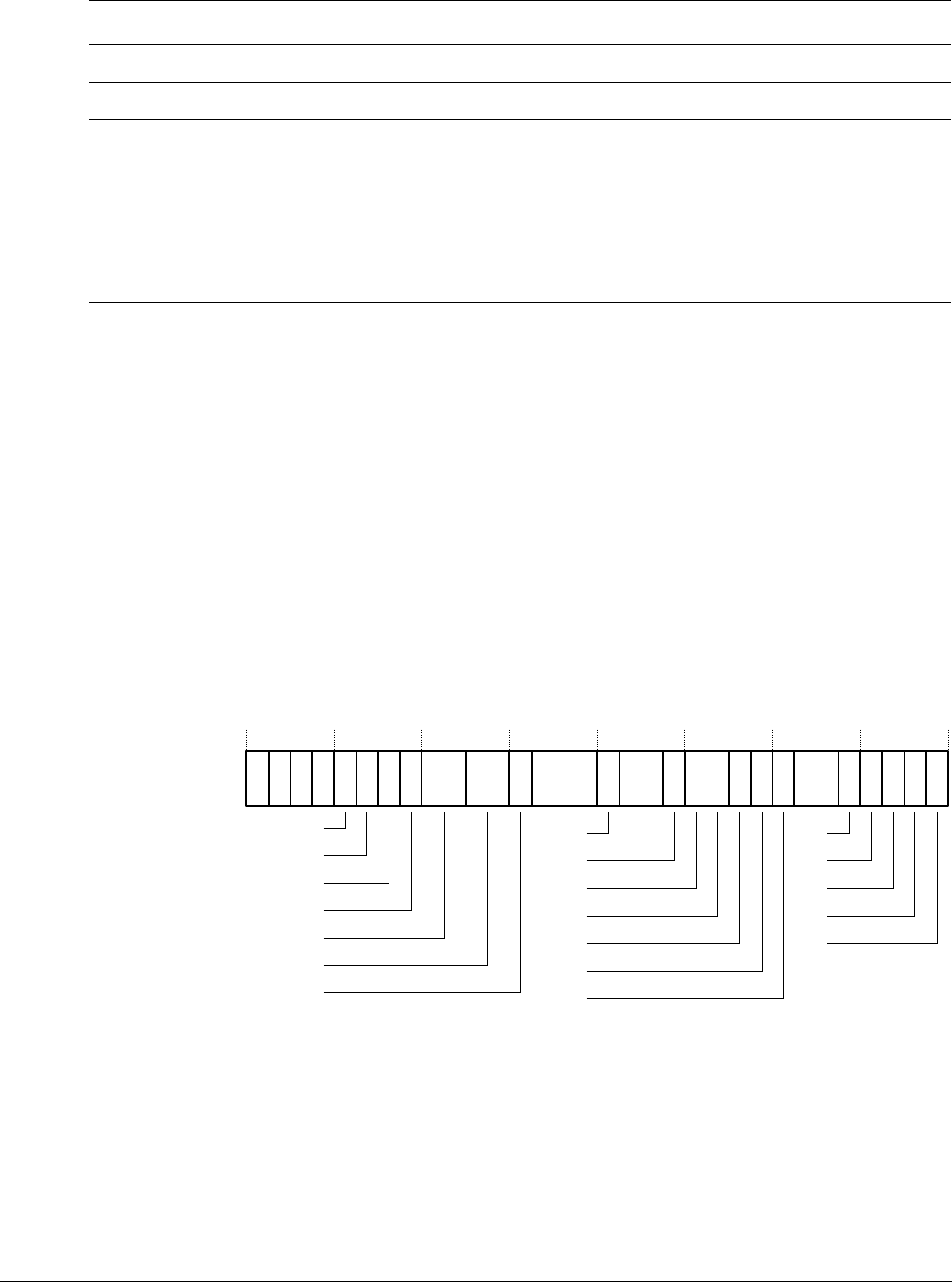
FPU Programmers Model
ARM DDI 0363G Copyright © 2006-2011 ARM Limited. All rights reserved. 11-6
ID041111 Non-Confidential
11.3.2 Floating-Point Status and Control Register, FPSCR
The FPSCR Register characteristics are:
Purpose Provides all necessary User level control of the floating-point system.
Usage constraints All bits described as DNM in Figure 11-3 are reserved for future
expansion. These bits must be initialized to zeros. To ensure that these bits
are not modified, any code other than initialization code must use
read-modify-write techniques when writing to FPSCR. Failure to observe
this rule can cause Unpredictable results in future systems.
Configurations Use this register if the device is configured as a Cortex-R4F processor.
Attributes See Table 11-4 on page 11-7.
Figure 11-3 shows the FPSCR bit assignments
Figure 11-3 FPSCR Register bit assignments
[15:8] Part number
0x31
= Cortex-R4F
[7:4] Variant
0x4
= Cortex-R4F
[3:0] Revision When the build-configuration includes the floating point unit, this register identifies
the revision number of the floating-point unit:
0x3
= r1p0
0x4
= r1p1
0x6
= r1p2
0x7
= r1p3
0x8
= r1p4
a. For information about the Common VFP subarchitecture see the ARM Architecture Reference Manual.
Table 11-3 FPSID Register bit assignments (continued)
Bits Name Function
IXC
IDC
DNM
DZE
IOE
UFE
OFE
DNM
IXE
IDE
LEN
DNM
NZCV
UFC
OFC
DZC
IOC
QC
RMODE
STRIDE
DN
FZ
DNM
31 30 29 28 27 26 25 24 23 22 21 20 19 18 16 15 14 13 12 11 10 9 8 7 6 5 4 3 2 1 0

FPU Programmers Model
ARM DDI 0363G Copyright © 2006-2011 ARM Limited. All rights reserved. 11-7
ID041111 Non-Confidential
Table 11-4 shows the FPSCR bit assignments.
Table 11-4 FPSCR Register bit assignments
Bits Name Function
[31] N Set if comparison produces a less than result, resets to zero
[30] Z Set if comparison produces an equal result, resets to zero
[29] C Set if comparison produces an equal, greater than, or unordered result, resets to zero
[28] V Set if comparison produces an unordered result, resets to zero
[27] QC Do Not Modify (DNM)/Read As Zero (RAZ)
[26] DNM DNM
[25] DN Default NaN mode enable bit:
0 = default NaN mode disabled, this is the reset value
1 = default NaN mode enabled.
[24] FZ Flush-to-zero mode enable bit:
0 = flush-to-zero mode disabled, this is the reset value
1 = flush-to-zero mode enabled.
[23:22] RMODE Rounding mode control field:
b00 = round to nearest (RN) mode, this is the reset value
b01 = round towards plus infinity (RP) mode
b10 = round towards minus infinity (RM) mode
b11 = round towards zero (RZ) mode.
[21:20] STRIDE Indicates the vector stride, the reset value is
0x0
[19] DNM DNM
[18:16] LEN Indicates the vector length, the reset value is
0x0
[15] IDE RAZ
[14:13] DNM DNM
[12] IXE RAZ
[11] UFE RAZ
[10] OFE RAZ
[9] DZE RAZ
[8] IOE RAZ
[7] IDC Input Subnormal cumulative flag, resets to zero
[6:5] DNM DNM
[4] IXC Inexact cumulative flag, resets to zero
[3] UFC Underflow cumulative flag, resets to zero
[2] OFC Overflow cumulative flag, resets to zero
[1] DZC Division by Zero cumulative flag, resets to zero
[0] IOC Invalid Operation cumulative flag, resets to zero

FPU Programmers Model
ARM DDI 0363G Copyright © 2006-2011 ARM Limited. All rights reserved. 11-8
ID041111 Non-Confidential
11.3.3 Floating-Point Exception Register, FPEXC
The FPEXC Register characteristics are:
Purpose Provides global enable and disable control of the VFP extension, and
indicate how the state of this extension is recorded.
Usage constraints • The FPEXC Register is accessible in Privileged modes only.
• Clearing EN disables VFP functionality, causing all VFP
instructions apart from privileged system register accesses to
generate an Undefined Instruction exception.
Configurations Use this register if the device is configured as a Cortex-R4F processor.
Attributes See Table 11-5.
Figure 11-4 shows the FPEXC bit assignments.
Figure 11-4 FPEXC Register bit assignments
Table 11-5 shows the FPEXC bit assignments.
11.3.4 Media and VFP Feature Registers, MVFR0 and MVFR1
The MVFR0 and MVFR1 Register characteristics are:
Purpose Describes the features supported by the FPU.
Usage constraints The MVFR0 and MVFR1 Registers:
• are read-only registers
• are accessible in Privileged modes only.
• ARM recommends that any software attempting to determine the
presence or absence of double-precision floating point hardware
support uses the MVFR1 register.
Configurations Use this register if the device is configured as a Cortex-R4F processor.
Attributes See Table 11-6 on page 11-9 and Table 11-7 on page 11-9.
Reserved
EN
Reserved
31 30 29 0
DEX
28
Table 11-5 FPEXC Register bit assignments
Bits Name Function
[31] - RAZ.
[30] EN VFP enable bit. Setting EN enables VFP functionality. Reset clears EN.
[29] DEX Set when an Undefined Instruction exception is taken because of a vector instruction that would
have been executed if the processor supported vectors. This field is cleared when an Undefined
Instruction exception is taken for any other reason. Resets to zero.
[28:0] - RAZ.

FPU Programmers Model
ARM DDI 0363G Copyright © 2006-2011 ARM Limited. All rights reserved. 11-9
ID041111 Non-Confidential
Figure 11-5 shows the MVFR0 Register bit assignments.
Figure 11-5 MVFR0 Register bit assignments
Table 11-6 shows the MVFR0 Register bit assignments.
Figure 11-6 shows the MVFR1 Register bit assignments.
Figure 11-6 MVFR1 Register bit assignments
Table 11-7 shows the MVFR1 Register bit assignments.
RB
SVRM TE SPSR D DP
31 28 27 24 23 20 19 16 15 12 11 8 7 4 3 0
Table 11-6 MVFR0 Register bit assignments
Bits Name Function
[31:28] RM All VFP rounding modes supported:
0x1
[27:24] SV VFP short vector unsupported:
0x0
[23:20] SR VFP hardware square root supported:
0x1
[19:16] D VFP hardware divide supported:
0x1
[15:12] TE Only untrapped exception handling can be selected:
0x0
[11:8] DP Double precision supported in VFPv3:
0x2
[7:4] SP Single precision supported in VFPv3:
0x2
[3:0] RB 16x64-bit media register bank supported:
0x1
FZ
Reserved I DNSP LS
31 20 19 16 15 12 11 8 7 4 3 0
Table 11-7 MVFR1 Register bit assignments
Bits Name Function
[31:20] - Reserved
[19:16] SP Single-precision floating-point operations supported for VFP:
0b0000
= not supported
[15:12] I Integer operations supported for VFP:
0b0000
= not supported

FPU Programmers Model
ARM DDI 0363G Copyright © 2006-2011 ARM Limited. All rights reserved. 11-10
ID041111 Non-Confidential
[11:8] LS Load and store instructions supported for VFP:
0b0000
= not supported
[7:4] DN Propagation of NaN values supported for VFP:
0x1
[3:0] FZ Full denormal arithmetic supported for VFP:
0x1
Table 11-7 MVFR1 Register bit assignments (continued)
Bits Name Function

FPU Programmers Model
ARM DDI 0363G Copyright © 2006-2011 ARM Limited. All rights reserved. 11-11
ID041111 Non-Confidential
11.4 Modes of operation
The FPU provides three modes of operation to accommodate a variety of applications:
•Full-compliance mode
•Flush-to-zero mode
•Default NaN mode.
11.4.1 Full-compliance mode
In full-compliance mode, the FPU processes all operations according to the IEEE 754 standard
in hardware.
11.4.2 Flush-to-zero mode
Setting the FZ bit, FPSCR[24], enables flush-to-zero mode. In this mode, the FPU treats all
subnormal input operands of arithmetic
CDP
operations as zeros in the operation. Exceptions that
result from a zero operand are signaled appropriately.
VABS
,
VNEG
, and
VMOV
are not considered
arithmetic
CDP
operations and are not affected by flush-to-zero mode. A result that is tiny, as
described in the IEEE 754 standard, for the destination precision is smaller in magnitude than
the minimum normal value before rounding and is replaced with a zero. The IDC flag,
FPSCR[7], indicates when an input flush occurs. The UFC flag, FPSCR[3], indicates when a
result flush occurs.
11.4.3 Default NaN mode
Setting the DN bit, FPSCR[25], enables default NaN mode. In this mode, the result of any
operation that involves an input NaN, or that generated a NaN result, returns the default NaN.
Propagation of the fraction bits is maintained only by
VABS
,
VNEG
, and
VMOV
operations. All other
CDP
operations ignore any information in the fraction bits of an input NaN.

FPU Programmers Model
ARM DDI 0363G Copyright © 2006-2011 ARM Limited. All rights reserved. 11-12
ID041111 Non-Confidential
11.5 Compliance with the IEEE 754 standard
When Default NaN (DN) and Flush-to-Zero (FZ) modes are disabled, the VFP functionality is
compliant with the IEEE 754 standard in hardware. No support code is required to achieve this
compliance.
See the ARM Architecture Reference Manual for information about VFP architecture
compliance with the IEEE 754 standard.
11.5.1 Complete implementation of the IEEE 754 standard
The following operations from the IEEE 754 standard are not supplied by the VFP instruction
set:
• remainder
• round floating-point number to integer-valued floating-point number
• binary-to-decimal conversions
• decimal-to-binary conversions
• direct comparison of single-precision and double-precision values.
For complete implementation of the IEEE 754 standard, VFP functionality must be augmented
with library functions that implement these operations. See Application Note 98, VFP Support
Code for information on the available library functions.
11.5.2 IEEE 754 standard implementation choices
Some of the implementation choices permitted by the IEEE 754 standard and used in the VFPv3
architecture are described in the ARM Architecture Reference Manual.
NaN handling
All single-precision and double-precision values with the maximum exponent field value and a
nonzero fraction field are valid NaNs. A most significant fraction bit of zero indicates a
Signaling NaN (SNaN). A one indicates a Quiet NaN (QNaN). Two NaN values are treated as
different NaNs if they differ in any bit. Table 11-8 shows the default NaN values in both
single-precision and double-precision.
Processing of input NaNs for ARM floating-point functionality and libraries is defined as
follows:
• In full-compliance mode, NaNs are handled as described in the ARM Architecture
Reference Manual. The hardware processes the NaNs directly for arithmetic
CDP
instructions. For data transfer operations, NaNs are transferred without raising the Invalid
Operation exception. For the non-arithmetic
CDP
instructions,
VABS
,
VNEG
, and
VMOV
, NaNs
are copied, with a change of sign if specified in the instructions, without causing the
Invalid Operation exception.
Table 11-8 Default NaN values
Single-precision Double-precision
Sign 0 0
Exponent
0xFF 0x7FF
Fraction bit [22] = 1
bits [21:0] are all zeros
bit [51] = 1
bits [50:0] are all zeros

FPU Programmers Model
ARM DDI 0363G Copyright © 2006-2011 ARM Limited. All rights reserved. 11-13
ID041111 Non-Confidential
• In default NaN mode, arithmetic
CDP
instructions involving NaN operands return the
default NaN regardless of the fractions of any NaN operands. SNaNs in an arithmetic
CDP
operation set the IOC flag, FPSCR[0]. NaN handling by data transfer and non-arithmetic
CDP
instructions is the same as in full-compliance mode.
Table 11-9 summarizes the effects of NaN operands on instruction execution.
Comparisons
Comparison results modify the flags in the FPSCR Register. You can use the
VMOV r15, FPSCR
instruction (formerly
FMSTAT
) to transfer the flags from the FPSCR Register to the CPSR
Register. See the ARM Architecture Reference Manual for mapping of IEEE 754 standard
predicates to ARM conditions. The flags used are chosen so that subsequent conditional
execution of ARM instructions can test the predicates defined in the IEEE 754 standard.
Underflow
The Cortex-R4F FPU uses the before rounding form of tininess and the inexact result form of
loss of accuracy as described in the IEEE 754 standard to generate Underflow exceptions.
In flush-to-zero mode, results that are tiny before rounding, as described in the IEEE 754
standard, are flushed to a zero, and the UFC flag, FPSCR[3], is set. See the ARM Architecture
Reference Manual for information on flush-to-zero mode.
When the FPU is not in flush-to-zero mode, operations are performed on subnormal operands.
If the operation does not produce a tiny result, it returns the computed result, and the UFC flag,
FPSCR[3], is not set. The IXC flag, FPSCR[4], is set if the operation is inexact. If the operation
produces a tiny result, the result is a subnormal or zero value, and the UFC flag, FPSCR[3], is
set if the result was also inexact.
Table 11-9 QNaN and SNaN handling
Instruction
type
Default
NaN mode With QNaN operand With SNaN operand
Arithmetic
CDP
Off The QNaN or one of the QNaN operands, if
there is more than one, is returned
according to the rules given in the ARM
Architecture Reference Manual.
IOCa set. The SNaN is quieted and the
result NaN is determined by the rules
given in the ARM Architecture
Reference Manual.
On Default NaN returns. IOCa set. Default NaN returns.
Non-arithmetic
CDP
Off
NaN passes to destination with sign changed as appropriate.
On
FCMP(Z)
- Unordered compare. IOC set. Unordered compare.
FCMPE(Z)
- IOC set. Unordered compare. IOC set. Unordered compare.
Load/store
Off
All NaNs transferred.
On
a. IOC is the Invalid Operation exception flag, FPSCR[0].

FPU Programmers Model
ARM DDI 0363G Copyright © 2006-2011 ARM Limited. All rights reserved. 11-14
ID041111 Non-Confidential
11.5.3 Exceptions
The FPU implements the VFPv3 architecture and sets the cumulative exception status flag in
the FPSCR register as required for each instruction. The FPU does not support user-mode traps.
The exception enable bits in the FPSCR read-as-zero, and cannot be written. The processor also
has six output pins, FPIXC, FPUFC, FPOFC, FPDZC, FPIDC, and FPIOC, that each reflect
the status of one of the cumulative exception flags. See FPU signals on page A-23 for a
description of these outputs. You can mask each of these outputs masked by setting the
corresponding bit in the Secondary Auxiliary Control Register.
See c1, Auxiliary Control Register on page 4-40 for more information.

ARM DDI 0363G Copyright © 2006-2011 ARM Limited. All rights reserved. 12-1
ID041111 Non-Confidential
Chapter 12
Debug
This chapter describes the processor debug unit. These features assist the development of
application software, operating systems, and hardware. This chapter contains the following
sections:
•Debug systems on page 12-2
•About the debug unit on page 12-3
•Debug register interface on page 12-5
•Debug register descriptions on page 12-10
•Management registers on page 12-35
•Debug events on page 12-42
•Debug exception on page 12-44
•Debug state on page 12-47
•Cache debug on page 12-53
•External debug interface on page 12-54
•Using the debug functionality on page 12-57
•Debugging systems with energy management capabilities on page 12-74.
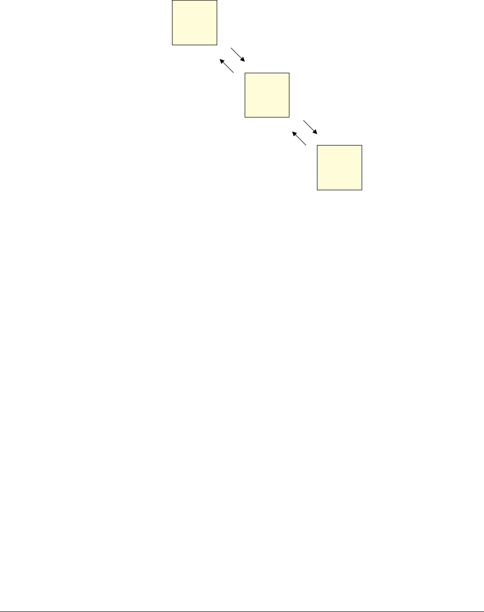
Debug
ARM DDI 0363G Copyright © 2006-2011 ARM Limited. All rights reserved. 12-2
ID041111 Non-Confidential
12.1 Debug systems
The Cortex-R4 processor is one component of a debug system. Figure 12-1 shows a typical
system.
Figure 12-1 Typical debug system
This typical system has three parts, described in the following sections:
•Debug host
•Protocol converter
•Debug target.
12.1.1 Debug host
The debug host is a computer, for example a personal computer, running a software debugger
such as RealView Debugger. The debug host enables you to issue high-level commands such as
setting breakpoint at a certain location, or examining the contents of a memory address.
12.1.2 Protocol converter
The debug host connects to the processor development system using an interface such as
Ethernet. The messages broadcast over this connection must be converted to the interface
signals of the debug target. A protocol converter performs this function, for example, RealView
ICE.
12.1.3 Debug target
The debug target is the lowest level of the system. An example of a debug target is a
development system with a Cortex-R4 test chip or a silicon part with a Cortex-R4 macrocell.
The debug target must implement some system support for the protocol converter to access the
processor debug unit using the Advanced Peripheral Bus (APB) slave port.
Host computer running RealView Debugger
Debug
host
For example, RealView ICE
Development system containing
Cortex-R4 processor
Debug
target
Protocol
converter

Debug
ARM DDI 0363G Copyright © 2006-2011 ARM Limited. All rights reserved. 12-3
ID041111 Non-Confidential
12.2 About the debug unit
The processor debug unit assists in debugging software running on the processor. You can use
the processor debug unit, in combination with a software debugger program, to debug:
• application software
• operating systems
• ARM processor-based hardware systems.
The debug unit enables you to:
• stop program execution
• examine and alter processor state
• examine and alter memory and peripheral state
• restart the processor.
You can debug software running on the processor in the following ways:
• Halting debug-mode debugging
• Monitor debug-mode debugging
• Trace debugging, see ETM interface on page 2-10.
The processor debug unit conforms to the ARMv7 debug architecture. For more information see
the ARM Architecture Reference Manual.
12.2.1 Halting debug-mode debugging
When the processor debug unit is in Halting debug-mode, the processor halts when a debug
event, such as a breakpoint, occurs. When the processor is halted, an external debugger can
examine and modify the processor state using the APB slave port. This debug mode is invasive
to program execution.
12.2.2 Monitor debug-mode debugging
When the processor debug unit is in Monitor debug-mode, the processor takes a debug
exception instead of halting. A special piece of software, a monitor target, can then take control
to examine or alter the processor state. Monitor debug-mode is essential in real-time systems
where the processor cannot be halted to collect information. Examples of these systems are
engine controllers and servo mechanisms in hard drive controllers that cannot stop the code
without physically damaging the components.
When debugging in Monitor debug-mode, the processor stops execution of the program and
starts execution of a monitor target. The state of the processor is preserved in the same manner
as all ARM exceptions. The monitor target communicates with the debugger to access processor
and coprocessor state, and to access memory contents and peripherals. Monitor debug-mode
requires a debug monitor program to interface between the debug hardware and the software
debugger.
12.2.3 Programming the debug unit
The processor debug unit is programmed using the APB slave interface. See Table 12-3 on
page 12-6 for a complete list of memory-mapped debug registers accessible using the APB slave
interface. Some features of the debug unit that you can access using the memory-mapped
registers are:
• instruction address comparators for triggering breakpoints, see Breakpoint Value
Registers on page 12-23 and Breakpoint Control Registers on page 12-24

Debug
ARM DDI 0363G Copyright © 2006-2011 ARM Limited. All rights reserved. 12-4
ID041111 Non-Confidential
• data address comparators for triggering watchpoints, see Watchpoint Value Registers on
page 12-27 and Watchpoint Control Registers on page 12-28
• a bidirectional Debug Communication Channel (DCC), see Debug communications
channel on page 12-58
• all other state information associated with the debug unit.

Debug
ARM DDI 0363G Copyright © 2006-2011 ARM Limited. All rights reserved. 12-5
ID041111 Non-Confidential
12.3 Debug register interface
You can access the processor debug register map using the APB slave port. This is the only way
to get full access to the processor debug capability. ARM recommends that if your system
requires the processor to access its own debug registers, you choose a system interconnect
structure that enables the processor to access the APB slave port by executing load and stores
to an appropriate area of physical memory.
This section describes:
•Coprocessor registers
•CP14 access permissions
•Coprocessor registers summary
•Memory-mapped registers on page 12-6
•Memory addresses for breakpoints and watchpoints on page 12-8
•Power domains on page 12-8
•Effects of resets on debug registers on page 12-8
•APB port access permissions on page 12-8.
12.3.1 Coprocessor registers
Although most of the processor debug registers are accessible through the memory-mapped
interface, there are several registers that you can access through a coprocessor interface. This is
important for boot-strap access to the register file. It enables software running on the processor
to identify the debug architecture version that the device implements.
12.3.2 CP14 access permissions
By default, you can access all CP14 debug registers from a nonprivileged mode. However, you
can program the processor to disable user-mode access to all coprocessor registers using bit [12]
of the DBGDSCR, see CP14 c1, Debug Status and Control Register on page 12-14 for more
information. CP14 debug registers accesses are always permitted when the processor is in debug
state regardless of the processor mode.
Table 12-1 shows access to the CP14 debug registers.
12.3.3 Coprocessor registers summary
Table 12-2 on page 12-6 shows a set of valid CP14 instructions for accessing the debug
registers. All CP14 instructions not listed are Undefined.
Table 12-1 Access to CP14 debug registers
Debug state Processor mode DBGDSCR[12] CP14 debug access
Yes X X Permitted
No User b0 Permitted
No User b1 Not permitteda
a. Instructions attempting to access CP14 registers cause the processor to take an
Undefined Instruction exception.
No Privileged X Permitted

Debug
ARM DDI 0363G Copyright © 2006-2011 ARM Limited. All rights reserved. 12-6
ID041111 Non-Confidential
Note
The CP14 debug instructions are defined as having Opcode_1 set to 0.
12.3.4 Memory-mapped registers
Table 12-3 shows the complete list of memory-mapped registers accessible at the APB slave
interface.
Note
You must ensure that the base address of this 4KB register map is aligned to a 4KB boundary in
physical memory.
Table 12-2 CP14 debug registers summary
Instruction Mnemonic Description
MRC p14, 0, <Rd>, c0, c0, 0
DBGDIDR Debug Identification Register.
See CP14 c0, Debug ID Register on page 12-10.
MRC p14, 0, <Rd>, c1, c0, 0
DBGDRAR Debug ROM Address Register.
See CP14 c0, Debug ROM Address Register on page 12-12.
MRC p14, 0, <Rd>, c2, c0, 0
DBGDSAR Debug Self Address Register.
See CP14 c0, Debug Self Address Offset Register on page 12-13.
MRC p14, 0, <Rd>, c0, c5, 0
STC p14, c5, <addressing mode>
DBGDTRRX Host to Target Data Transfer Register.
See Data Transfer Register on page 12-18.
MCR p14, 0, <Rd>, c0, c5, 0
LDC p14, c5, <addressing mode>
DBGDTRTX Target to Host Data Transfer Register.
See Data Transfer Register on page 12-18.
MRC p14, 0, <Rd>, c0, c1, 0
MRC p14, 0, PC, c0, c1, 0
DBGDSCR Debug Status and Control Register.
See CP14 c1, Debug Status and Control Register on page 12-14.
Table 12-3 Debug memory-mapped registers
Offset
(hex)
Register
number Access Mnemonic Description
0x000
c0 R DBGDIDR CP14 c0, Debug ID Register on page 12-10
0x004-0x014
c1-c5 R - RAZ
0x18
c6 RW DBGWFAR Watchpoint Fault Address Register on page 12-19
0x01C
c7 RW DBGVCR Vector Catch Register on page 12-20
0x020
c8 R - RAZ
0x024
c9 RW DBGECR Not implemented in this processor. Reads as zero.
0x028
c10 RW DBGDSCCR Debug State Cache Control Register on page 12-21.
0x02C
c11 R - RAZ
0x030-0x07C
c12-c31 R - RAZ

Debug
ARM DDI 0363G Copyright © 2006-2011 ARM Limited. All rights reserved. 12-7
ID041111 Non-Confidential
0x080
c32 RW DBGDTRRX Data Transfer Register on page 12-18
0x084
c33 W DBGITR Instruction Transfer Register on page 12-22
0x088
c34 RW DBGDSCR CP14 c1, Debug Status and Control Register on
page 12-14
0x08C
c35 RW DBGDTRTX Data Transfer Register on page 12-18
0x090
c36 W DBGDRCR Debug Run Control Register on page 12-22
0x094-0x0FC
c37-c63 R - RAZ
0x100-0x11C
c64-c71 RW DBGBVR Breakpoint Value Registers on page 12-23
0x120-0x13C
c72-c79 R - RAZ
0x140-0x15C
c80-c87 RW DBGBCR Breakpoint Control Registers on page 12-24
0x160-0x17C
c88-c95 R - RAZ
0x180-0x19C
c96-c103 RW DBGWVR Watchpoint Value Registers on page 12-27
0x1A0-0x1BC
c104-c111 R - RAZ
0x1C0-0x1DC
c112-c119 RW DBGWCR Watchpoint Control Registers on page 12-28
0x1E0-0x1FC
c120-c127 R - RAZ
0x200-0x2FC
c128-c191 R - RAZ
0x300
c192 R DBGOSLAR Not implemented in this processor. Reads as zero.
0x304
c193 R DBGOSLSR Operating System Lock Status Register on
page 12-30
0x308
c194 R DBGOSSRR Not implemented in this processor. Reads as zero.
0x30C
c195 R - RAZ
0x310
c196 RW DBGPRCR Device Power-down and Reset Control Register on
page 12-32
0x314
c197 R DBGPRSR Device Power-down and Reset Status Register on
page 12-33
0x318-0x7FC
c198-c511 R - RAZ
0x800-0x8FC
c512-575 R - RAZ
0x900-0xCFC
c576-c831 R - RAZ
0xD00
-
0xDFC
c832-c895 R - Processor ID Registers on page 12-35
0xE00
-
0xE7C
c896-c927 R - RAZ
0xE80
-
0xEFC
c928-c959 - - Chapter 13 Integration Test Registers
0xF00-0xFFC
c960-c1023 - - Management registers on page 12-35
Table 12-3 Debug memory-mapped registers (continued)
Offset
(hex)
Register
number Access Mnemonic Description

Debug
ARM DDI 0363G Copyright © 2006-2011 ARM Limited. All rights reserved. 12-8
ID041111 Non-Confidential
12.3.5 Memory addresses for breakpoints and watchpoints
The Vector Catch Register (DBGVCR) sets breakpoints on exception vectors as instruction
addresses.
The Watchpoint Fault Address Register (DBGWFAR) reads an address and a processor state
dependent offset, +8 for ARM and +4 for Thumb.
12.3.6 Power domains
The processor has a single power domain. Therefore, it does not support the Event Catch
Register, the OS Lock, or the OS Save and Restore functionality.
12.3.7 Effects of resets on debug registers
The processor has two reset signals that affect the debug registers in the following ways:
nSYSPORESET
You must assert this signal when powering up to set the non-debug processor
logic to a known state.
PRESETDBGn
You can assert this signal to set all of the debug logic to a known state, without
affecting the state of the remainder of the processor logic.
12.3.8 APB port access permissions
The restrictions for accessing the APB slave port are described as follows:
Privilege of memory access
You must configure the system to disable accesses to the memory-mapped
registers based on the privilege of the memory access.
Power down
The processor only supports a single power domain, therefore you must configure
the system to return an error response to all accesses made to the APB interface
while the processor is powered-down.
Privilege of memory access permission
When non-privileged software attempts to access the APB slave port, the system must ignore
the access or generate an error response to the access. You must implement this restriction at the
system level because the APB protocol does not have a privileged or user control signal. You
can choose to have the system either ignore the access or generate an error response.
You can place additional restrictions on memory transactions that are permitted to access the
APB port. However, ARM does not recommend this.

Debug
ARM DDI 0363G Copyright © 2006-2011 ARM Limited. All rights reserved. 12-9
ID041111 Non-Confidential
Locks permission
You can lock the APB slave port so that access to some debug registers is restricted. ARM
architecture v7 defines two locks:
Software lock
The external debugger can set this lock to prevent software from modifying the
debug registers settings. A debug monitor can also set this lock prior to returning
control to the application to reduce the chance of erratic code changing the debug
settings. When this lock is set, writes to all debug registers are ignored, except
those generated by the external debugger, that override the lock. For more
information, see Lock Access Register on page 12-38.
OS Lock The processor does not support OS Lock.
Note
• These locks are set to their reset values only on reset of the debug logic, provided by
PRESETDBGn.
• You must set the PADDRDBG31 input signal to 1 for accesses originated from the
external debugger for the Software Lock override feature to work.
Table 12-4 External debug interface access permissions
Registers
PADDRDBG31 Lock
DBGDRCR,
DBGPRCR,
DBGPRSR
Other Debug registers LAR Other registers
XXaNPOSSbNPOSSbNPOSSbNPOSSb
1XaOKcOKcOKcOKc
01dWIeWIeOKcWIe
00
OKcOKcOKcOKc
a. X indicates that the outcome does not depend on this condition.
b. Not possible. Accessing debug registers while the processor is powered down is not possible.
c. OK indicates that the access succeeds.
d. LSR[1] bit is set.
e. WI indicates that writes are ignored.

Debug
ARM DDI 0363G Copyright © 2006-2011 ARM Limited. All rights reserved. 12-10
ID041111 Non-Confidential
12.4 Debug register descriptions
Table 12-5 shows definitions of terms used in the register descriptions.
12.4.1 Accessing debug registers
To access the CP14 debug registers you set Opcode_1 and Opcode_2 to zero. The CRn and CRm
fields of the coprocessor instructions encode the CP14 debug register number, where the register
number is
{<Opcode2>, <CRm>}
. In addition, the CRn field can specify additional registers.
Table 12-6 shows the CP14 debug register map.
12.4.2 CP14 c0, Debug ID Register
The DBGDIDR Register characteristics are:
Purpose Identifies the debug architecture version and specifies the number of
debug resources that the processor implements.
Table 12-5 Terms used in register descriptions
Term Description
R Read-only. Written values are ignored.
W Write-only. This bit cannot be read. Reads return an Unpredictable value.
RW Read or write.
RAZ Read-As-Zero. Always zero when read.
RAO Read-As-One. Always one when read.
SBZP Should-Be-Zero (SBZ) or Preserved (P). Must be written as 0 or preserved by writing the same value previously
read from the same fields on the same processor. These bits are usually reserved for future expansion.
UNP A read from this bit returns an Unpredictable value.
Table 12-6 CP14 debug register map
CRn Op1 CRm Op2 CP14 debug register name Abbreviation Reference
c0 0 c0 0 Debug ID Register DBGDIDR CP14 c0, Debug ID Register
c1 0 c0 0 Debug ROM Address Register DBGDRAR CP14 c0, Debug ROM Address
Register on page 12-12
c2 0 c0 0 Debug Self Address Offset
Register
DBGDSAR CP14 c0, Debug Self Address
Offset Register on page 12-13
c3-c15 0 c0 0 Reserved - -
c0 0 c1 0 Debug Status and Control
Register
DBGDSCR CP14 c1, Debug Status and
Control Register on page 12-14
c1-c15 0 c1 0 Reserved - -
c0-c15 0 c2-c4 0 Reserved - -
c0 0 c5 0 Data Transfer Register DTR Data Transfer Register on
page 12-18

Debug
ARM DDI 0363G Copyright © 2006-2011 ARM Limited. All rights reserved. 12-11
ID041111 Non-Confidential
Usage constraints The DBGDIDR Register is:
• in CP14 c0
• a 32 bit read-only register
• accessible in User and Privileged modes.
Configurations Available in all processor configurations.
Attributes See Table 12-7.
Figure 12-2 shows the DBGDIDR bit assignments.
Figure 12-2 DBGDIDR Register bit assignments
Table 12-7 shows the DBGDIDR bit assignments.
The values of the following fields of the DBGDIDR Register agree with the values in CP15 c0,
MIDR:
• DBGDIDR[3:0] is the same as CP15 c0 bits [3:0]
• DBGDIDR[7:4] is the same as CP15 c0 bits [23:20].
See c0, Main ID Register on page 4-14 for more information of CP15 c0, MIDR.
Reserved
WRP
31 28 27 24 23 20 19 16 15 4 3 0
BRP Context ID Variant Revision
Debug architecture
version
87
Table 12-7 DBGDIDR Register bit assignments
Bits Name Function
[31:28] WRP Number of Watchpoint Register Pairs:
b0000 = 1 WRP
b0001 = 2 WRPs
...
b0111 = 8 WRPs.
[27: 24] BRP Number of Breakpoint Register Pairs:
b0001 = 2 BRPs
b0010 = 3 BRPs
...
b0111 = 8 BRPs.
[23:20] Context Number of Breakpoint Register Pairs with context ID comparison capability:
b0000 = 1 BRP has context ID comparison capability
[19:16] Debug architecture
version
Debug architecture version:
b0100 = ARMv7 Debug.
[15:8] - RAZ.
[7: 4] Variant Implementation-defined variant number.
[3: 0] Revision Implementation-defined revision number.

Debug
ARM DDI 0363G Copyright © 2006-2011 ARM Limited. All rights reserved. 12-12
ID041111 Non-Confidential
The reason for duplicating these fields here is that the DBGDIDR Register is also accessible
through the APB slave port. This enables an external debugger to determine the variant and
revision numbers without stopping the processor.
To use the DBGDIDR Register, read CP14 c0 with:
MRC p14, 0, <Rd>, c0, c0, 0 ; Read DBGDIDR Register
12.4.3 CP14 c0, Debug ROM Address Register
The DBGDRAR characteristics are:
Purpose Returns a 32-bit Debug ROM Address Register value. This is the address
that indicates where in memory a debug monitor can locate the debug bus
ROM specified by the CoreSight multiprocessor trace and debug
architecture. This ROM holds information about all the components in the
debug bus. You can configure the address read in this register during
integration using the DBGROMADDR[31:12] and DBGROMADDRV
inputs. DBGROMADDRV must be tied off to 1 if
DBGROMADDR[31:12] is tied off to a valid value.
Usage constraints The DBGDRAR Register is:
• in CP14 c0, sub-register c1
• a 32 bit read-only register
• accessible in User and Privileged modes.
Configurations Available in all processor configurations.
Attributes See Table 12-8.
Figure 12-3 shows the DBGDRAR bit assignments.
Figure 12-3 DBGDRAR Register bit assignments
Table 12-8 shows the DBGDRAR bit assignments.
To use the DBGDRAR Register, read CP14 c0 with:
MRC p14, 0, <Rd>, c1, c0, 0 ; Read DBGDRAR Register
Debug bus ROM physical address Reserved
Valid bits
31 12 11 2 1 0
Table 12-8 DBGDRAR Register bit assignments
Bits Name Function
[31:12] Debug bus
ROM address.
Indicates bits [31:12] of the debug bus ROM address.
[11: 2] - SBZ.
[1:0] Valid bits Indicates that the ROM address is valid.
Reads b11 if DBGROMADDRV is set to 1, otherwise reads b00. DBGROMADDRV must
be set to 1 if DBGROMADDR[31:12] is set to a valid value.

Debug
ARM DDI 0363G Copyright © 2006-2011 ARM Limited. All rights reserved. 12-13
ID041111 Non-Confidential
12.4.4 CP14 c0, Debug Self Address Offset Register
The DBGDSAR Register characteristics are:
Purpose Returns a 32-bit offset value from the Debug ROM Address Register to the
address of the processor debug registers.
Usage constraints The DBGDSAR Register is:
• in CP14 c0, sub-register c2
• a 32 bit read-only register
• accessible in User and Privileged modes.
Configurations Available in all processor configurations.
Attributes See Table 12-9.
Figure 12-4 shows the DBGDSAR bit assignments.
Figure 12-4 DBGDSAR Register bit assignments
Table 12-9 shows the DBGDSAR bit assignments.
You can configure the address read in this register during integration using the
DBGSELFADDR[31:12] and DBGSELFADDRV inputs. DBGSELFADDRV must be tied
off to 1 if DBGSELFADDR[31:12] is tied off to a valid value.
To use the DBGDSAR Register, read CP14 c0 with:
MRC p14, 0, <Rd>, c2, c0, 0 ; Read DBGDSAR Register
Debug bus self address offset value Reserved
Valid bits
31 12 11 2 1 0
Table 12-9 DBGDSAR Register bit assignments
Bits Name Function
[31:12] Debug bus self
address offset value
Indicates bits [31:12] of the two’s complement offset from the debug ROM physical
address to the physical address where the debug registers are mapped.
[11: 2] - UNP on reads, SBZP on writes.
[1:0] Valid bits Reads b11 if DBGSELFADDRV is set to 1, otherwise reads b00.
DBGSELFADDRV must be set to 1 if DBGSELFADDR[31:12] is set to a valid
value.
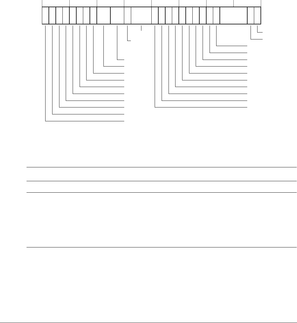
Debug
ARM DDI 0363G Copyright © 2006-2011 ARM Limited. All rights reserved. 12-14
ID041111 Non-Confidential
12.4.5 CP14 c1, Debug Status and Control Register
The DBGDSCR Register characteristics are:
Purpose Contains status and control information about the debug unit.
Usage constraints See DTR access mode on page 12-18.
Configurations Available in all processor configurations.
Attributes See Table 12-10.
Figure 12-5 shows the DBGDSCR bit assignments.
Figure 12-5 DBGDSCR Register bit assignments
Table 12-10 shows the DBGDSCR bit assignments.
31 30 29 28 16 15 14 13 12 11 10 6 5 2 1 0
MOE
978
Core halted
Core restarted
26 25 24 23
PipeAdv
InstrCompl-l
22 21 20 19 18
Monitor debug-mode
Halting debug-mode
ARM
DbgAck
IntDis
Comms
Sticky imprecise abort
Sticky Undefined
Reserved
Sticky precise abort
DTR access
Discard
imprecise
abort
27
Reserved
DTRTXfull
DTRRXfull
Reserved
Reserved
Reserved
DTRTXfull-l
DTRRXfull-l
Table 12-10 DBGDSCR Register bit assignments
Bits Name Function
[31] - RAZ on reads, SBZP on writes.
[30] DTRRXfull The DTRRXfull flag:
0 = Read-DTR, DBGDTRRX is empty. This is the reset value
1 = Read-DTR, DBGDTRRX is full.
When set, this flag indicates to the processor that there is data available to read from the
DBGDTRRX. It is automatically set on writes to the DBGDTRRX by the debugger, and
is cleared when the processor reads the DBGDTRRX over the CP14 interface. If the flag
is not set, reads from the DBGDTRRX return an Unpredictable value.
[29] DTRTXfull The DTRTXfull flag:
0 = Write-DTR, DBGDTRTX is empty. This is the reset value.
1 = Write-DTR, DBGDTRTX is full.
When clear, this flag indicates to the processor that the DBGDTRTX is ready to receive
data. It is automatically cleared on reads of the DBGDTRTX by the debugger, and is set
when the processor writes to the DBGDTRTX over the CP14 interface. If this bit is set and
the processor attempts to write to the DBGDTRTX, the register contents are overwritten
and the DTRRXfull flag remains set.

Debug
ARM DDI 0363G Copyright © 2006-2011 ARM Limited. All rights reserved. 12-15
ID041111 Non-Confidential
[28] - RAZ on reads, SBZP on writes.
[27] DTRRXfull_l The latched DTRRXfull flag. This is the last value of DTRRXfull that the debugger read.
It is set to the value of DTRRXfull on a debugger read of the DBGDSCR.
This flag controls how the DBGDTRRX is written by a debugger. See DTR access mode
on page 12-18 for more information.
The value read for this bit depends on the state of the locked bit in the DBGLSR and the
PADDRDBG31 value used for the read. If the locked bit is set, and PADDRDBG31 is 0,
then this bit reads as the DTRRXfull_l value. Otherwise it reads as the DTRRXfull value.
[26] DTRTXfull_l The latched DTRTXfull flag. This is the last value of DTRTXfull that the debugger read.
It is set to the value of DTRTXfull on a debugger read of the DBGDSCR.
This flag controls how the DBGDTRTX is read by the debugger. See DTR access mode
on page 12-18 for more information.
The value read for this bit depends on the state of the locked bit in the DBGLSR and the
PADDRDBG31 value used for the read. If the locked bit is set and PADDRDBG31 is 0,
then this bit reads as the DTRTXfull_l value. Otherwise it reads as the DTRTXfull value.
[25] PipeAdv Sticky pipeline advance read-only bit. This bit enables the debugger to detect whether the
processor is idle. In some situations, this might mean that the system bus port is
deadlocked. This bit is set to 1 when the processor pipeline retires one instruction. It is
cleared by a write to DBGDRCR[3].
0 = no instruction has completed execution since the last time this bit was cleared
1 = an instruction has completed execution since the last time this bit was cleared.
[24] InstrCompl_l The latched instruction complete read-only bit. This flag determines whether the processor
has completed execution of an instruction issued by the debugger, through the DBGITR.
0 = processor is executing an instruction fetched from the DBGITR Register
1 = processor is not executing an instruction fetched from the DBGITR Register.
Entry into halting debug state sets this flag to 1. When the processor is not in halting debug
state, the value of this flag is Unpredictable.
This flag controls debugger writes to the DBGITR:
• If DBGDSCR[21:20] is equal to 0, then writes to the DBGITR are ignored when
InstrCompl_l is 0.
• If DBGDSCR[21:20] is not equal to 0 then debugger writes to the DBGITR are
stalled until InstrCompl_l is 1.
[23:22] - RAZ on reads, SBZP on writes.
[21:20] DTR access DTR access mode. You can use this field to optimize DTR traffic between a debugger and
the processor.
b00 = Non-blocking mode. This is the default.
b01 = Stall mode
b10 = Fast mode
b11 = Reserved.
Note
• This field only affects the behavior of DBGDSCR, DTR, and DBGITR accesses
through the APB port, and not through CP14 debug instructions.
• Non-blocking mode is the default setting. Improper use of the other modes might
result in the debug access bus becoming deadlocked.
See DTR access mode on page 12-18 for more information.
Table 12-10 DBGDSCR Register bit assignments (continued)
Bits Name Function

Debug
ARM DDI 0363G Copyright © 2006-2011 ARM Limited. All rights reserved. 12-16
ID041111 Non-Confidential
[19] Discard
asynchronous
abort
This bit controls how the processor handles asynchronous data aborts when in halting
debug mode:
0 = aborts are handled as normal
1 = the sticky asynchronous abort bit is set on an asynchronous abort but no other action
is taken.
The processor automatically sets this bit on entry into halting debug state and clears it on
exit from halting debug state.
[18-16] - RAZ on reads, SBZP on writes.
[15] Monitor mode The Monitor debug-mode enable bit:
0 = Monitor debug-mode disabled, this is the reset value
1 = Monitor debug-mode enabled.
If Halting debug-mode is enabled through bit [14], then the processor is in Halting
debug-mode regardless of the value of bit [15]. If the external interface input DBGEN is
LOW, this bit reads as 0. The programmed value is masked until DBGEN is HIGH, and
at that time the read value reverts to the programmed value.
[14] Halting mode The Halting debug-mode enable bit:
0 = Halting debug-mode disabled, this is the reset value
1 = Halting debug-mode enabled.
If the external interface input DBGEN is LOW, this bit reads as 0. The programmed value
is masked until DBGEN is HIGH, and at that time the read value reverts to the
programmed value.
[13] ARM Execute ARM instruction enable bit:
0 = disabled, this is the reset value
1 = enabled.
If this bit is set and an DBGITR write succeeds, the processor fetches an instruction from
the DBGITR for execution. If this bit is set to 1 when the processor is not in debug state,
the behavior of the processor is Unpredictable.
[12] Comms CP14 debug user access disable control bit:
0 = CP14 debug user access enable, this is the reset value
1 = CP14 debug user access disable.
If this bit is set and a User mode process attempts to access any CP14 debug registers, an
Undefined Instruction exception is taken.
[11] IntDis Interrupts disable bit:
0 = interrupts enabled, this is the reset value
1 = interrupts disabled.
If this bit is set, the IRQ and FIQ input signals are inhibited. The external debugger can
optionally use this bit to execute pieces of code in normal state as part of the debugging
process to avoid having an interrupt taking control of the program flow. For example, the
debugger might use this bit to execute an OS service routine to bring a page from disk into
memory. It might be undesirable to service any interrupt during the routine execution.
[10] DbgAck DbgAck bit. If this bit is set to 1, the DBGACK output signal is forced HIGH, regardless
of the processor state. The external debugger can optionally use this bit to execute pieces
of code in normal state as part of the debugging process for the system to behave as if the
processor is in debug state. Some systems rely on DBGACK to determine whether data
accesses are application or debugger generated. This bit is 0 on reset.
[9] - RAZ on reads, SBZP on writes.
Table 12-10 DBGDSCR Register bit assignments (continued)
Bits Name Function

Debug
ARM DDI 0363G Copyright © 2006-2011 ARM Limited. All rights reserved. 12-17
ID041111 Non-Confidential
To use the Debug Status and Control Register, read or write CP14 c1 with:
[8] Sticky Undefined Sticky Undefined bit:
0 = no Undefined Instruction exception occurred in debug state since the last time this bit
was cleared
1 = an Undefined Instruction exception occurred while in debug state since the last time
this bit was cleared.
This flag detects Undefined Instruction exceptions generated by instructions issued to the
processor through the DBGITR. This bit is set to 1 when an Undefined Instruction
exception occurs while the processor is in debug state and is cleared by writing a 1 to
DBGDRCR[2].
[7] Sticky
asynchronous
abort
Sticky asynchronous Data Abort bit:
0 = no asynchronous Data Aborts occurred since the last time this bit was cleared
1 = an asynchronous Data Abort occurred since the last time this bit was cleared.
This flag detects asynchronous Data Aborts triggered by instructions issued to the
processor through the DBGITR. This bit is set to 1 when an asynchronous Data Abort
occurs while the processor is in debug state and is cleared by writing a 1 to DBGDRCR[2].
[6] Sticky
synchronous
abort
Sticky synchronous Data Abort bit:
0 = no synchronous Data Abort occurred since the last time this bit was cleared
1 = a synchronous Data Abort occurred since the last time this bit was cleared.
This flag detects synchronous Data Aborts generated by instructions issued to the
processor through the DBGITR. This bit is set to 1 when a synchronous Data Abort occurs
while the processor is in debug state and is cleared by writing to the DBGDRCR[2].
[5:2] MOE Method of entry bits:
b0000 = a DBGDRCR[0] halting debug event occurred
b0001 = a breakpoint occurred
b0100 = an EDBGRQ halting debug event occurred
b0011 = a BKPT instruction occurred
b1010 = a synchronous watchpoint occurred
others = reserved.
These bits are set to indicate any of:
• the cause of a debug exception
• the cause for entering debug state.
A Prefetch Abort or Data Abort handler must check the value of the CP15 Fault Status
Register to determine whether a debug exception occurred and then use these bits to
determine the specific debug event.
[1]aCore restarted Core restarted bit:
0 = the processor is exiting debug state
1 = the processor has exited debug state. This is the reset value.
The debugger can poll this bit to determine when the processor responds to a request to
leave debug state.
[0]aCore halted Core halted bit:
0 = the processor is in normal state. This is the reset value.
1 = the processor is in debug state.
The debugger can poll this bit to determine when the processor has entered debug state.
a. These bits always reflect the status of the processor, therefore they only have a reset value if the particular reset event affects
the processor. For example, a PRESETDBGn event leaves these bits unchanged and a processor reset event such as
nSYSPORESET sets DBGDSCR[18] to a 0 and DBGDSCR[1:0] to 10.
Table 12-10 DBGDSCR Register bit assignments (continued)
Bits Name Function

Debug
ARM DDI 0363G Copyright © 2006-2011 ARM Limited. All rights reserved. 12-18
ID041111 Non-Confidential
MRC p14, 0, <Rd>, c0, c1, 0 ; Read Debug Status and Control Register
MCR p14, 0, <Rd>, c0, c1, 0 ; Write Debug Status and Control Register
DTR access mode
You can use the DTR access mode field to optimize data transfer between a debugger and the
processor.
The DTR access mode can be one of the following:
• Non-blocking. This is the default mode.
•Stall.
•Fast.
In Non-blocking mode, reads from DBGDTRTX and writes to DBGDTRRX and DBGITR are
ignored if the appropriate latched ready flag is not in the ready state. These latched flags are
updated on DBGDSCR reads. The following applies:
• writes to DBGDTRRX are ignored if DTRRXfull_l is set to b1
• reads from DBGDTRTX are ignored, and return an Unpredictable value, if DTRTXfull_l
is set to b0
• writes to DBGITR are ignored if InstrCompl_l is set to b0
• following a successful write to DBGDTRRX, DTRRXfull and DTRRXfull_l are set to b1
• following a successful read from DBGDTRTX, DTRTXfull and DTRTXfull_l are cleared
to b0
• following a successful write to DBGITR, InstrCompl and InstrCompl_l are cleared to b0.
Debuggers accessing these registers must first read DBGDSCR. This has the side-effect of
copying DTRRXfull and DTRTXfull to DTRRXfull_l and DTRTXfull_l. The debugger must
then:
• write to the DBGDTRRX if the DTRRXfull flag was b0 (DTRRXfull_l is b0)
• read from the DBGDTRTX if the DTRTXfull flag was b1 (DTRTXfull_l is b1)
• write to the DBGITR if the InstrCompl_l flag was b1.
However, debuggers can issue both actions together and later determine from the read
DBGDSCR value whether the operations were successful.
In Stall mode, the APB accesses to DBGDTRRX, DBGDTRTX, and DBGITR stall under the
following conditions:
• writes to DBGDTRRX are stalled until DTRRXfull is cleared
• writes to DBGITR are stalled until InstrCompl is set
• reads from DBGDTRTX are stalled until DTRTXfull is set.
Fast mode is similar to Stall mode except that in Fast mode, the processor fetches an instruction
from the DBGITR when a DBGDTRRX write or DBGDTRTX read succeeds. In Stall mode and
Nonblocking mode, the processor fetches an instruction from the DBGITR when an DBGITR
write succeeds.
12.4.6 Data Transfer Register
The DTR consists of two separate physical registers:
• the DBGDTRRX (Read Data Transfer Register)
• the DBGDTRTX (Write Data Transfer Register).

Debug
ARM DDI 0363G Copyright © 2006-2011 ARM Limited. All rights reserved. 12-19
ID041111 Non-Confidential
The register accessed is dependent on the instruction used:
•writes,
MCR
and
LDC
instructions, access the DBGDTRTX
• reads,
MRC
and
STC
instructions, access the DBGDTRRX.
Note
Read and write are used with respect to the processor.
For information on the use of these registers with the DTRTXfull flag and DTRRXfull flag, see
Debug communications channel on page 12-58. The Data Transfer Register, bits [31:0] contain
the data to be transferred.
Table 12-11 shows the DTR bit assignments.
12.4.7 Watchpoint Fault Address Register
The DBGWFAR Register characteristics are:
Purpose Holds the address of the instruction that triggers the watchpoint.
Usage constraints There are no usage constraints.
Configurations Available in all processor configurations.
Attributes See Table 12-12 on page 12-20.
Figure 12-6 shows the DBGWFAR bit assignments.
Figure 12-6 DBGWFAR Register bit assignments
Table 12-11 Data Transfer Register functions
Bits Name Function
[31:0] Data Reads the Data Transfer Register. This is read-only for the CP14 interface.
Note
Reads of the DBGDTRRX through the coprocessor interface cause the DTRTXfull flag to be
cleared. However, reads of the DBGDTRRX through the APB port do not affect this flag.
[31:0] Data Writes the Data Transfer Register. This is write-only for the CP14 interface.
Note
Writes to the DBGDTRTX through the coprocessor interface cause the DTRRXfull flag to be set.
However, writes to the DBGDTRTX through the APB port do not affect this flag.
Address
31 0
1
Reserved
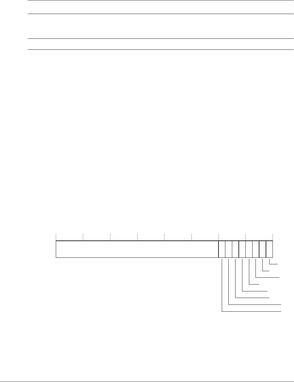
Debug
ARM DDI 0363G Copyright © 2006-2011 ARM Limited. All rights reserved. 12-20
ID041111 Non-Confidential
Table 12-12 shows the DBGWFAR bit assignments.
12.4.8 Vector Catch Register
The DBGVCR Register characteristics are:
Purpose Controls efficient exception vector catching.
Usage constraints • If one of the bits in this register is set and the instruction at the
corresponding vector is committed for execution, the processor
either enters debug state or takes a debug exception.
• Under this model, any prefetch from an exception vector can trigger
a vector catch, not only the ones because of exception entries. An
explicit branch to an exception vector might generate a vector catch
debug event.
• If any of the bits are set when the processor is in Monitor
debug-mode, then the processor ignores the setting and does not
generate a vector catch debug event. This prevents the processor
entering an unrecoverable state. The debugger must program these
bits to zero when Monitor debug-mode is selected and enabled to
ensure forward-compatibility.
Configurations Available in all processor configurations.
Attributes See Table 12-13 on page 12-21.
Figure 12-7 shows the DBGVCR bit assignments.
Figure 12-7 DBGVCR Register bit assignments
Table 12-12 DBGWFAR Register bit assignments
Bits Name Function
[31:1] Address This is the address of the watchpointed instruction. When a watchpoint occurs in ARM state, the
DBGWFAR contains the address of the instruction causing it plus an offset of
0x8
. When a
watchpoint occurs in Thumb state, the offset is plus
0x4
.
[0] - RAZ.
31 876543210
Reserved
Reset
Reserved
SVC
Prefetch abort
Data abort
Reserved
IRQ
FIQ

Debug
ARM DDI 0363G Copyright © 2006-2011 ARM Limited. All rights reserved. 12-21
ID041111 Non-Confidential
Table 12-13 shows the DBGVCR bit assignments.
12.4.9 Debug State Cache Control Register
The DBGDSCCR Register characteristics are:
Purpose Controls the L1 cache behavior when the processor is in debug state.
Usage constraints For information on the usage model of the DBGDSCCR register, see
Cache debug on page 12-53.
Configurations Available in all processor configurations.
Attributes See Table 12-14 on page 12-22.
Figure 12-8 shows the DBGDSCCR bit assignments.
Figure 12-8 DBGDSCCR Register bit assignments
For information on the usage model of the DBGDSCCR register, see Cache debug on
page 12-53.
Table 12-13 DBGVCR Register bit assignments
Bits Name Reset
value
Normal
address
High vectors
address Function Access
[31:8] - 0 -
-
Do not modify on writes. On reads,
the value returns zero.
RAZ or
SBZP
[7] FIQ 0
0x0000001C 0xFFFF001C
Vector catch enable. RW
[6] IRQ -
0x00000018
a
0xFFFF0018
aVector catch enable. -
[5] - 0 -
-
Do not modify on writes. On reads,
the value returns zero.
RAZ or
SBZP
[4] Data Abort 0
0x00000010 0xFFFF0010
Vector catch enable. RW
[3] Prefetch Abort 0
0x0000000C 0xFFFF000C
Vector catch enable. RW
[2] SVC 0
0x00000008 0xFFFF0008
Vector catch enable. RW
[1] - 0
0x00000004 0xFFFF0004
Vector catch enable, Undefined
instruction.
RW
[0] Reset 0
0x00000000 0xFFFF0000
Vector catch enable. RW
a. If the VIC interface is enabled, the address is the last IRQ handler address supplied by the VIC, whether or not high vectors
are in use.
31 2131 0
Not write-through
Reserved
3
Instruction cache line-fill
Data cache line-fill

Debug
ARM DDI 0363G Copyright © 2006-2011 ARM Limited. All rights reserved. 12-22
ID041111 Non-Confidential
Table 12-14 shows the DBGDSCCR bit assignments.
12.4.10 Instruction Transfer Register
The DBGITR enables the external debugger to feed instructions into the processor for execution
while in debug state. The DBGITR is a write-only register. Reads from the DBGITR return an
Unpredictable value.
The Instruction Transfer Register, bits [31:0] contain the ARM instruction for the processor to
execute while in debug state. The reset value of this register is Unpredictable.
Note
Writes to the DBGITR when the processor is not in debug state or the DBGDSCR[13] execute
instruction enable bit is cleared are Unpredictable. When an instruction is issued to the
processor, the debug unit prevents the next instruction from being issued until the
DBGDSCR[25] instruction complete bit is set.
12.4.11 Debug Run Control Register
The DBGDRCR Register characteristics are:
Purpose • Requests the processor to enter or leave debug state.
• Clears the sticky exception bits present in the DBGDSCR.
Usage constraints The DBGDRCR is a write-only register.
Configurations Available in all processor configurations.
Attributes See Table 12-15 on page 12-23.
Figure 12-9 on page 12-23 shows the DBGDRCR bit assignments.
Table 12-14 DBGDSCCR Register bit assignments
Bits Name Reset
value Description
[31:3] - 0 Reserved. Do not modify on writes. On reads, the value returns zero.
[2] nWT 0 Not write-through:
1 = normal operation of regions marked as write-back in debug state
0 = force write-through behavior for regions marked as write-back in debug state, this is
the reset value.
[1] nIL 0 Instruction cache line-fill:
1 = normal operation of L1 instruction cache in debug state
0 = L1 instruction cache line-fills disabled in debug state, this is the reset value.
[0] nDL 0 Data cache line-fill:
1 = normal operation of L1 data cache in debug state
0 = L1 data cache line-fills disabled in debug state, this is the reset value.

Debug
ARM DDI 0363G Copyright © 2006-2011 ARM Limited. All rights reserved. 12-23
ID041111 Non-Confidential
Figure 12-9 DBGDRCR Register bit assignments
Table 12-15 shows the DBGDRCR bit assignments.
12.4.12 Breakpoint Value Registers
Each DBGBVR is associated with a Breakpoint Control Register (DBGBCR). DBGBCRy is the
corresponding control register for DBGBVRy.
A pair of breakpoint registers, DBGBVRy/DBGBCRy, is called a Breakpoint Register Pair
(BRP). DBGBVR0-7 are paired with DBGBCR0-7 to make BRP0-7.
31 053
Reserved
Cancel memory request
214
Clear sticky pipeline advance
Clear sticky exceptions
Restart request
Halt request
Table 12-15 DBGDRCR Register bit assignments
Bits Name Function
[31:5] - RAZ.
[4] Cancel memory
requests
If 1 is written to this bit, the processor abandons any pending memory transactions until it
can enter debug state. Debug state entry is the acknowledge event that clears this request.
Abandoned transactions have the following behavior:
• abandoned stores might write an Unpredictable value to the target address
• abandoned loads return an Unpredictable value to the register bank.
An abandoned transaction does not cause any exception. Additional instruction fetches or
data accesses after the processor entered debug state have an Unpredictable behavior.
This bit enables the debugger to progress on a deadlock so the processor can enter debug
state. For a debug state entry to occur, a halting debug event must be requested before this
bit is set. If you write a 1 to this bit when DBGEN is LOW, the write has no effect.a
[3] Clear sticky
pipeline advance
Writing a 1 to this bit clears DBGDSCR[25].
[2] Clear sticky
exceptions
Writing a 1 to this bit clears DBGDSCR[8:6].
[1] Restart request Writing a 1 to this bit requests that the processor leaves debug state. This request is held
until the processor exits debug state. When the debugger makes this request, it polls
DBGDSCR[1] until it reads 1. This bit always reads as zero. Writes are ignored when the
processor is not in debug state.
[0] Halt request Writing a 1 to this bit triggers a halting debug event, that is, a request that the processor
enters debug state. This request is held until the debug state entry occurs. When the
debugger makes this request, it polls DBGDSCR[0] until it reads 1. This bit always reads
as zero. Writes are ignored when the processor is already in debug state.
a. Entry into debug state is not expected to be recoverable.
Debug
ARM DDI 0363G Copyright © 2006-2011 ARM Limited. All rights reserved. 12-24
ID041111 Non-Confidential
The breakpoint value contained in this register corresponds to either an instruction address or a
context ID. Breakpoints can be set on:
• an instruction address
• a context ID value
• an instruction address and context ID pair.
For an instruction address and context ID pair, two BRPs must be linked. A debug event is
generated when both the instruction address and the context ID pair match at the same time.
Table 12-16 shows the DBGBVR bit assignments.
Note
• Only BRPn supports context ID comparison, where n+1 is the number of breakpoint
register pairs implemented in the processor.
• Bits [1:0] of Registers DBGBVR0 to DBGBVR(n-1) are Do Not Modify on writes and
Read-As-Zero because these registers do not support context ID comparisons.
• The contents of the CP15 Context ID Register give the context ID value for a DBGBVR
to match. For information on the CONTEXTIDR, see Chapter 4 System Control.
12.4.13 Breakpoint Control Registers
The DBGBCR Register characteristics are:
Purpose Contains the necessary control bits for setting:
• breakpoints
• linked breakpoints.
Usage constraints There are no usage constraints.
Configurations Available in all processor configurations.
Attributes See Table 12-17 on page 12-25.
Figure 12-10 shows the DBGBCR bit assignments.
Figure 12-10 DBGBCR Register bit assignments
Table 12-16 Breakpoint Value Registers functions
Bits Reset value Description
[31:0]
0x0
Breakpoint value
Reserved
M Linked BRP Reserved
Byte
address
select
Secure state access control
Breakpoint
address mask
Reserved Reserved
B
31 29 28 24 23 22 20 19 16 15 14 13 9 8 5 4 3 2 1 0
S

Debug
ARM DDI 0363G Copyright © 2006-2011 ARM Limited. All rights reserved. 12-25
ID041111 Non-Confidential
Table 12-17 shows the DBGBCR bit assignments.
Table 12-17 DBGBCR Register bit assignments
Bits Name Function
[31:29] - Do not modify on writes. On reads, the value returns zero.
[28:24] Breakpoint
address mask
This field sets a breakpoint on a range of addresses by masking lower order address bits out
of the breakpoint comparison.a
b00000 = no mask
b00001 = Reserved
b00010 = Reserved
b00011 =
0x00000007
mask for instruction address
b00100 =
0x0000000F
mask for instruction address
b00101 =
0x0000001F
mask for instruction address
...
b11111 =
0x7FFFFFFF
mask for instruction address.
[23] - -
[22:20] M Meaning of DBGBVR:
b000 = instruction address match
b001 = linked instruction address match
b010 = unlinked context ID
b011 = linked context ID
b100 = instruction address mismatch
b101 = linked instruction address mismatch
b11x = Reserved.
For more information, see Table 12-18 on page 12-27.
[19:16] Linked BRP
number
The binary number encoded here indicates another BRP to link this one with.
Note
• if a BRP is linked with itself, it is Unpredictable whether a breakpoint debug event is
generated
• if this BRP is linked to another BRP that is not configured for linked context ID
matching, it is Unpredictable whether a breakpoint debug event is generated.
[15:14] Secure state
access control
RAZ or SBZP.
[13:9] - Do not modify on writes. On reads, the value returns zero.

Debug
ARM DDI 0363G Copyright © 2006-2011 ARM Limited. All rights reserved. 12-26
ID041111 Non-Confidential
[8:5] Byte address
select
For breakpoints programmed to match an instruction address, the debugger must write a
word-aligned address to the DBGBVR. You can then use this field to program the breakpoint
so it hits only if certain byte addresses are accessed.b
If the BRP is programmed for instruction address match:
b0000 = the breakpoint never hits
bxxx1 = the breakpoint hits if the byte at address (DBGBVR &
0xFFFFFFFC
) +0 is accessed
bxx1x = the breakpoint hits if the byte at address (DBGBVR &
0xFFFFFFFC
) +1 is accessed
bx1xx = the breakpoint hits if the byte at address (DBGBVR &
0xFFFFFFFC
) +2 is accessed
b1xxx = the breakpoint hits if the byte at address (DBGBVR &
0xFFFFFFFC
) +3 is accessed
b1111 = the breakpoint hits if any of the four bytes starting at address (DBGBVR &
0xFFFFFFFC
) +0 is accessed.
If the BRP is programmed for instruction address mismatch, the breakpoint hits where the
corresponding instruction address breakpoint does not hit, that is, the range of addresses
covered by an instruction address mismatch breakpoint is the negative image of the
corresponding instruction address breakpoint.
If the BRP is programmed for context ID comparison, this field must be set to b1111.
Otherwise, breakpoint and watchpoint debug events might not be generated as expected.
[4:3] - -
[2:1] S Supervisor access control. The breakpoint can be conditioned on the mode of the processor:
b00 = User, System, or Supervisor
b01 = Privileged
b10 = User
b11 = any.
[0] B Breakpoint enable:
0 = Breakpoint disabled. This is the reset value.
1 = Breakpoint enabled.
a. If DBGBCR[28:24] is not set to b00000, then DBGBCR[8:5] must be set to b1111. Otherwise the behavior is Unpredictable.
In addition, if DBGBCR[28:24] is not set to b00000, then the corresponding DBGBVR bits that are not being included in the
comparison Should Be Zero. Otherwise the behavior is Unpredictable. If this BRP is programmed for context ID comparison,
this field must be set to b00000. Otherwise the behavior is Unpredictable. There is no encoding for a full 32-bit mask but the
same effect of a break anywhere breakpoint can be achieved by setting DBGBCR[22] to 1 and DBGBCR[8:5] to b0000.
b. Writing a value to DBGBCR[8:5] so that DBGBCR[8] is not equal to DBGBCR[7] or DBGBCR[6] is not equal to
DBGBCR[5] has Unpredictable results.
Table 12-17 DBGBCR Register bit assignments (continued)
Bits Name Function

Debug
ARM DDI 0363G Copyright © 2006-2011 ARM Limited. All rights reserved. 12-27
ID041111 Non-Confidential
12.4.14 Watchpoint Value Registers
Each DBGDSWVR is associated with a Watchpoint Control Register (DBGWCR). DBGWCRy
is the corresponding register for WVRy.
A pair of watchpoint registers, DBGWVRy and DBGWCRy, is called a Watchpoint Register
Pair (WRP). DBGWVR0-7 are paired with DBGWCR0-7 to make WRP0-7.
The watchpoint value contained in the DBGDSWVR always corresponds to a data address and
can be set either on:
• a data address
• a data address and context ID pair.
For a data address and context ID pair, a WRP and a BRP with context ID comparison capability
must be linked. A debug event is generated when both the data address and the context ID pair
match simultaneously.
Table 12-18 Meaning of DBGBVR bits [22:20]
DBGBVR[2
2:20] Meaning
b000 The corresponding DBGBVR[31:2] is compared against the instruction address bus and the state of the
processor against this DBGBCR. It generates a breakpoint debug event on a joint instruction address and
state match.
b001 The corresponding DBGBVR[31:2] is compared against the instruction address bus and the state of the
processor against this DBGBCR. This BRP is linked with the one indicated by DBGBCR[19:16] linked
BRP field. They generate a breakpoint debug event on a joint instruction address, context ID, and state
match.
b010 The corresponding DBGBVR[31:0] is compared against CP15 Context ID Register, c13 and the state of
the processor against this DBGBCR. This BRP is not linked with any other one. It generates a breakpoint
debug event on a joint context ID and state match. For this BRP, DBGBCR[8:5] must be set to b1111.
Otherwise it is Unpredictable whether a breakpoint debug event is generated.
b011 The corresponding DBGBVR[31:0] is compared against CP15 Context ID Register, c13. This BRP links
another BRP (of the DBGBCR[21:20]=b01 type), or WRP (with DBGWCR[20]=b1). They generate a
breakpoint or watchpoint debug event on a joint instruction address or data address and context ID match.
For this BRP, DBGBCR[8:5] must be set to b1111, DBGBCR[15:14] must be set to b00, and
DBGBCR[2:1] must be set to b11. Otherwise it is Unpredictable whether a breakpoint debug event is
generated.
b100 The corresponding DBGBVR[31:2] and DBGBCR[8:5] are compared against the instruction address bus
and the state of the processor against this DBGBCR. It generates a breakpoint debug event on a joint
instruction address mismatch and state match.
b101 The corresponding DBGBVR[31:2] and DBGBCR[8:5] are compared against the instruction address bus
and the state of the processor against this DBGBCR. This BRP is linked with the one indicated by
DBGBCR[19:16] linked BRP field. It generates a breakpoint debug event on a joint instruction address
mismatch, state and context ID match.
b11x Reserved. The behavior is Unpredictable.
Debug
ARM DDI 0363G Copyright © 2006-2011 ARM Limited. All rights reserved. 12-28
ID041111 Non-Confidential
Table 12-19 shows the DBGDSWVR bit assignments.
12.4.15 Watchpoint Control Registers
The DBGWCR Register characteristics are:
Purpose Contains the necessary control bits for setting:
• watchpoints
• linked watchpoints.
Usage constraints There are no usage constraints.
Configurations Available in all processor configurations.
Attributes See Table 12-20 on page 12-29.
Figure 12-11 shows the DBGWCR bit assignments.
Figure 12-11 DBGWCR Register bit assignments
Table 12-19 Watchpoint Value Register bit assignments
Bits Description
[31:2] Watchpoint address.
[1:0] Reserved. Do not modify on writes. On reads, the value returns zero.
Reserved
Linked BRP Byte address select L/S P W
Reserved
Watchpoint
address mask
31 21 20 19 16 15 5 3 2 1
EL/S S
24 40
14 13
29 28 23
Secure state access control
12
Reserved

Debug
ARM DDI 0363G Copyright © 2006-2011 ARM Limited. All rights reserved. 12-29
ID041111 Non-Confidential
Table 12-20 shows the DBGWCR bit assignments.
Table 12-20 DBGWCR Register bit assignments
Bits Name Function
[31:29] - Do not modify on writes. On reads, the value returns zero.
[28:24] Watchpoint
address
mask
This field watches a range of addresses by masking lower order address bits out of the
watchpoint comparison.
b00000 = no mask
b00001 = Reserved
b00010 = Reserved
b00011 =
0x00000007
mask for data address
b00100 =
0x0000000F
mask for data address
b00101 =
0x0000001F
mask for data address
...
b11111 =
0x7FFFFFFF
mask for data address.
Note
• If DBGWCR[28:24] is not set to b00000, then DBGWCR[12:5] must be set to
b11111111. Otherwise the behavior is Unpredictable.
• If DBGWCR[28:24] is not set to b00000, then the corresponding DBGDSWVR bits that
are not being included in the comparison Should Be Zero. Otherwise the behavior is
Unpredictable.
• To watch for a write to any byte in an 8-byte aligned object of size 8 bytes, ARM
recommends that a debugger sets DBGWCR[28:24] to b00111, and DBGWCR[12:5] to
b11111111. This is compatible with both ARMv7 debug compliant implementations that
have an 8-bit DBGWCR[12:5] and with those that have a 4-bit DBGWCR[8:5] byte
address select field.
[23:21] - Do not modify on writes. On reads, the value returns zero.
[20] E Enable linking bit:
0 = linking disabled
1 = linking enabled.
When this bit is set, this watchpoint is linked with the context ID holding BRP selected by the
linked BRP field.
[19:16] Linked
BRP
Linked BRP number. The binary number encoded here indicates a context ID holding BRP to
link this WRP with. If this WRP is linked to a BRP that is not configured for linked context ID
matching, it is Unpredictable whether a watchpoint debug event is generated.
[15:14] Secure state
access
control
RAZ or SBZP.
[13] - Appear as zero when read. Do not modify on writes.

Debug
ARM DDI 0363G Copyright © 2006-2011 ARM Limited. All rights reserved. 12-30
ID041111 Non-Confidential
12.4.16 Operating System Lock Status Register
The DBGOSLSR contains status information about the locked debug registers.
Figure 12-12 on page 12-31 shows the DBGOSLSR bit assignments.
[12:5] Byte
address
select
The DBGDSWVR is programmed with word-aligned address. You can use this field to program
the watchpoint so it only hits if certain byte addresses are accessed:
b00000000 The watchpoint never hits.
bxxxxxxx1 The watchpoint hits if the byte at address (DBGDSWVR[31:0] &
0xFFFFFFFC
)
+0 is accessed.
bxxxxxx1x The watchpoint hits if the byte at address (DBGDSWVR[31:0] &
0xFFFFFFFC
)
+1 is accessed.
bxxxxx1xx The watchpoint hits if the byte at address (DBGDSWVR[31:0] &
0xFFFFFFFC
)
+2 is accessed.
bxxxx1xxx The watchpoint hits if the byte at address (DBGDSWVR[31:0] &
0xFFFFFFFC
)
+3 is accessed.
bxxx1xxxx The watchpoint hits if the byte at address (DBGDSWVR[31:0] &
0xFFFFFFF8
)
+4 is accessed.
bxx1xxxxx The watchpoint hits if the byte at address (DBGDSWVR[31:0] &
0xFFFFFFF8
)
+5 is accessed.
bx1xxxxxx The watchpoint hits if the byte at address (DBGDSWVR[31:0] &
0xFFFFFFF8
)
+6 is accessed.
b1xxxxxxx The watchpoint hits if the byte at address (DBGDSWVR[31:0] &
0xFFFFFFF8
)
+7 is accessed.
[4:3] L/S Load/store access. The watchpoint can be conditioned to the type of access:
b00 = Reserved
b01 = load, load exclusive, or swap
b10 = store, store exclusive or swap
b11 = either.
A
SWP
or
SWPB
triggers on load, store, or either. A load exclusive instruction triggers on load or
either. A store exclusive instruction triggers on store or either, whether it succeeds or not.
[2:1] S Privileged access control. The watchpoint can be conditioned to the privilege of the access:
b00 = reserved
b01 = Privileged, match if the processor does a privileged access to memory
b10 = User, match only on non-privileged accesses
b11 = either, match all accesses.
Note
For all cases, the match refers to the privilege of the access, not the mode of the processor.
[0] W Watchpoint enable:
0 = Watchpoint disabled. This is the reset value.
1 = Watchpoint enabled.
Table 12-20 DBGWCR Register bit assignments (continued)
Bits Name Function
Debug
ARM DDI 0363G Copyright © 2006-2011 ARM Limited. All rights reserved. 12-31
ID041111 Non-Confidential
Figure 12-12 DBGOSLSR Register bit assignments
Table 12-21 shows the DBGOSLSR bit assignments.
12.4.17 Authentication Status Register
The DBGAUTHSTATUS Register characteristics are:
Purpose Reads the current values of the configuration inputs that determine the
debug permission level.
Usage constraints The DBGAUTHSTATUS Register is read-only.
Configurations Available in all processor configurations.
Attributes See Table 12-22.
Figure 12-13 shows the DBGAUTHSTATUS bit assignments.
Figure 12-13 DBGAUTHSTATUS Register bit assignments
Table 12-22 shows the DBGAUTHSTATUS bit assignments.
31 0
Reserved
1
Lock implemented bit
Table 12-21 DBGOSLSR Register bit assignments
Bits Name Function
[31:1] - RAZ.
[0] Lock implemented bit Indicates that the OS lock functionality is not implemented. This bit always reads 0.
31 03
Reserved
45678
Secure non-invasive debug features implemented
Secure non-invasive debug features enabled
Secure invasive debug features implemented
Secure invasive debug features enabled
Non-secure debug features
Table 12-22 DBGAUTHSTATUS Register bit assignments
Bits Name Value Function
[31:8] - - RAZ
[7] Secure non-invasive debug
features implemented
0b1
Implemented
[6] Secure non-invasive debug
features enabled
DBGEN || NIDEN Non-invasive debug enable field

Debug
ARM DDI 0363G Copyright © 2006-2011 ARM Limited. All rights reserved. 12-32
ID041111 Non-Confidential
12.4.18 Device Power-down and Reset Control Register
The DBGPRCR Register characteristics are:
Purpose Controls reset and power-down related functionality.
Usage constraints The DBGPRCR Register is read-write with more restricted access to some
bits.
Configurations Available in all processor configurations.
Attributes See Table 12-23.
Figure 12-14 shows the DBGPRCR bit assignments.
Figure 12-14 DBGPRCR Register bit assignments
Table 12-23 shows the DBGPRCR bit assignments.
[5] Secure invasive debug
features implemented
0b1 Implemented
[4] Secure invasive debug
features enabled
DBGEN Invasive debug enable field
[3:0] Non-secure debug featuresa0x0 Not implemented
a. Cortex-R4 does not implement the Security Extensions, so all the debug features are considered
secure.
Table 12-22 DBGAUTHSTATUS Register bit assignments (continued)
Bits Name Value Function
31 03
Reserved
21
Hold internal reset
Force internal reset
No Power-down
Table 12-23 DBGPRCR Register bit assignments
Bits Name Function
[31:3] - Do not modify on writes. On reads, the value returns zero.
Debug
ARM DDI 0363G Copyright © 2006-2011 ARM Limited. All rights reserved. 12-33
ID041111 Non-Confidential
12.4.19 Device Power-down and Reset Status Register
The DBGPRSR Register characteristics are:
Purpose Provides information about the reset and power-down state of the
processor.
Usage constraints The DBGPRSR Register is a read-only register, with reads of the register
also resetting some register bits.
Configurations Available in all processor configurations.
Attributes See Table 12-24 on page 12-34.
Figure 12-15 shows the DBGPRSR bit assignments.
Figure 12-15 DBGPRSR Register bit assignments
Table 12-24 on page 12-34 shows the DBGPRSR bit assignments.
[2] Hold internal
reset
Hold internal reset bit. This bit can be used to prevent the processor from running again before
the debugger detects a power-down event and restores the state of the debug registers in the
processor. This bit does not have any effect on initial system power-up as nSYSPORESET
clears it.
0 = Do not hold internal reset on power-up or warm reset. This is the reset value.
1 = Hold the processor non-debug logic in reset on warm reset until this flag is cleared.
[1] Force
internal reset
When a 1 is written to this bit, the processor asserts the DBGRSTREQ output for four cycles.
You can connect this output to an external reset controller that, in turn, resets the processor.
[0] No
power-down
When set to 1, the DBGNOPWRDWN output signal is HIGH. This output connects to the
system power controller and is interpreted as a request to operate in emulate mode. In this mode,
the processor is not actually powered down when requested by software or hardware
handshakes. This mode is useful when debugging applications on top of working operating
systems.
0 = DBGNOPWRDWN is LOW. This is the reset value
1 = DBGNOPWRDWN is HIGH.
Table 12-23 DBGPRCR Register bit assignments (continued)
Bits Name Function
31 0
3
Reserved
214
Sticky reset status
Reset status
Sticky power-down status
Power-down status

Debug
ARM DDI 0363G Copyright © 2006-2011 ARM Limited. All rights reserved. 12-34
ID041111 Non-Confidential
Table 12-24 DBGPRSR Register bit assignments
Bits Name Function
[31:4] - Do not modify on writes. On reads, the value returns zero.
[3] Sticky reset status Sticky reset status bit. This bit is cleared on a read.
0 = the processor has not been reset since the last time this register was read.
1 = the processor has been reset since the last time this register was read. This is the reset value.
This sticky bit is set to 1 when nSYSPORESET is asserted.
[2] Reset status Reset status bit:
0 = the processor is not held in reset
1 = the processor is held in reset.
[1] Sticky power-down status Reserved. Always zero.
[0] Power-down status Reserved. Always one.

Debug
ARM DDI 0363G Copyright © 2006-2011 ARM Limited. All rights reserved. 12-35
ID041111 Non-Confidential
12.5 Management registers
The Management registers define the standardized set of registers that all CoreSight
components implement. This section describes these registers.
Table 12-25 shows the contents of the Management registers for the processor debug unit.
12.5.1 Processor ID Registers
The Processor ID Registers are read-only registers that return the same values as the
corresponding CP15 MIDR and Feature ID Registers. See Chapter 4 System Control for
information about the information contained in these registers.
Table 12-26 shows the offset value, register number, mnemonic, and description that are
associated with each Processor Identification Register.
Table 12-25 Management registers
Offset
(hex)
Register
number Access Mnemonic Description
0xD00-0xDFC
832-895 R - Processor Identification Registers.
See Processor ID Registers.
0xF00
960 RW ITCTRL Integration Mode Control Registers.
See Integration Mode Control Register on page 13-8.
0xFA0
1000 CLAIMSET Claim Tag Set Register.
See Claim Tag Set Register on page 12-36.
0xFA4
1001 CLAIMCLR Claim Tag Clear Register.
See Claim Tag Clear Register on page 12-37.
0xFB0
1004 W LOCKACCESS Lock Access Register.
See Lock Access Register on page 12-38.
0xFB4
1005 R LOCKSTATUS Lock Status Register.
See Lock Status Register on page 12-38.
0xFB8
1006 R AUTHSTATUS Authentication Status Register.
See Authentication Status Register on page 12-31.
0xFB8-0xFC4
1006-1009 R - Reserved.
0xFC8
1010 R DEVID Device Identifier. Reserved.
0xFCC
1011 R DEVTYPE Device Type Register.
See Device Type Register on page 12-38.
0xFD0-0xFFC
1012-1023 R - Identification Registers.
See Debug Identification Registers on page 12-39.
Table 12-26 Processor Identification Registers
Offset (hex) Register number Mnemonic Function
0xD00
832 MIDR Main ID Register
0xD04
833 CTR Cache Type Register
0xD08
834 TCMTR TCM Type Register
0xD0C
835 - Alias of MIDR

Debug
ARM DDI 0363G Copyright © 2006-2011 ARM Limited. All rights reserved. 12-36
ID041111 Non-Confidential
12.5.2 Claim Registers
The Claim Tag Set Register and the Claim Tag Clear Register enable an external debugger to
claim debug resources.
Claim Tag Set Register
The DBGCLAIMSET Register characteristics are:
Purpose Enables an external debugger to claim debug resources.
Usage constraints The DBGCLAIMSET Register is a read/write register, in which:
• the CLAIM bits are always RAO
• writing 0 to a CLAIM bit has no effect.
Configurations Available in all processor configurations.
Attributes See Table 12-27 on page 12-37.
Figure 12-16 on page 12-37 shows the DBGCLAIMSET bit assignments.
0xD10
836 MPUIR MPU Type Register
0xD14
837 MPIDR Multiprocessor Affinity Register
0xD18-0xD1C
838-839 - Alias of MIDR
0xD20
840 ID_PFR0 Processor Feature Register 0
0xD24
841 ID_PFR1 Processor Feature Register 1
0xD28
842 ID_DFR0 Debug Feature Register 0
0xD2C
843 ID_AFR0 Auxiliary Feature Register 0
0xD30
844 ID_MMFR0 Processor Feature Register 0
0xD34
845 ID_MMFR1 Memory Model Feature Register 1
0xD38
846 ID_MMFR2 Memory Model Feature Register 2
0xD3C
847 ID_MMFR3 Memory Model Feature Register 3
0xD40
848 ID_ISAR0 ISA Feature Register 0
0xD44
849 ID_ISAR1 ISA Feature Register 1
0xD48
850 ID_ISAR2 ISA Feature Register 2
0xD4C
851 ID_ISAR3 ISA Feature Register 3
0xD50
852 ID_ISAR4 ISA Feature Register 4
0xD54
853 ID_ISAR5 ISA Feature Register 5
Table 12-26 Processor Identification Registers (continued)
Offset (hex) Register number Mnemonic Function

Debug
ARM DDI 0363G Copyright © 2006-2011 ARM Limited. All rights reserved. 12-37
ID041111 Non-Confidential
Figure 12-16 DBGCLAIMSET Register bit assignments
Table 12-27 shows the DBGCLAIMSET bit assignments.
Writing b1 to a specific claim tag set bit sets that claim tag. Writing b0 to a specific claim tag
bit has no effect. This register always reads
0xFF
, indicating eight claim tags are implemented.
Claim Tag Clear Register
The DBGCLAIMCLR Register characteristics are:
Purpose Enables an external debugger to:
• read debug resources
• clear debug resources.
Usage constraints The DBGCLAIMCLR Register is a read/write register, in which:
• Reading this register returns the current claim tag value
• writing 0 to a CLAIM bit has no effect
• writing 1 to a specific claim tag clear bit clears that claim tag.
Configurations Available in all processor configurations.
Attributes See Table 12-28.
Figure 12-17 shows the DBGCLAIMCLR bit assignments.
Figure 12-17 DBGCLAIMCLR Register bit assignments
Table 12-28 shows the DBGCLAIMCLR bit assignments.
Writing b1 to a specific claim tag clear bit clears that claim tag. Writing b0 has no effect.
Reading this register returns the claim tag value.
31 0
Reserved
78
Claim tag set
Table 12-27 DBGCLAIMSET Register bit assignments
Bits Name Function
[31:8] - RAZ or SBZP.
[7:0] Claim tag set RAO. Sets claim tags on writes.
31 0
Reserved
78
Claim tag clear
Table 12-28 DBGCLAIMCLR Register bit assignments
Bit Name Description
[31:8] - RAZ or SBZP.
[7:0] Claim tag clear R/W. Reset value is
0x00
.

Debug
ARM DDI 0363G Copyright © 2006-2011 ARM Limited. All rights reserved. 12-38
ID041111 Non-Confidential
12.5.3 Lock Access Register
The DBGLAR is a write-only register that controls writes to the debug registers. The purpose
of the DBGLAR is to reduce the risk of accidental corruption to the contents of the debug
registers. It does not prevent all accidental or malicious damage. Because the state of the
DBGLAR is in the debug power domain, it is not lost when the processor powers down.
DBGLAR [31:0] contain a key that controls the lock status. To unlock the debug registers, write
a
0xC5ACCE55
key to this register. To lock the debug registers, write any other value. Accesses to
locked debug registers are ignored. The lock is set on reset.
12.5.4 Lock Status Register
The DBGLSR Register characteristics are:
Purpose Returns the current lock status of the debug registers.
Usage constraints The DBGLSR is:
• a read-only register
• only defined in the memory-mapped interface
Configurations Available in all processor configurations.
Attributes See Table 12-29.
Figure 12-18 shows the DBGLSR bit assignments.
Figure 12-18 DBGLSR Register bit assignments
Table 12-29 shows the DBGLSR bit assignments.
12.5.5 Device Type Register
The DBGDEVTYPE Register characteristics are:
Purpose Indicates the type of debug component.
31
31 0
Reserved
123
32-bit access
Locked bit
Lock implemented bit
Table 12-29 DBGLSR Register bit assignments
Bits Name Function
[31:3] - Do not modify on writes. On reads, the value returns zero.
[2] 32-bit access Indicates that a 32-bit access is required to write the key to the Lock Access Register.
This bit always reads 0.
[1] Locked bit Locked bit:
0 = Writes are permitted.
1 = Writes are ignored. This is the reset value.
[0] Lock implemented bit Indicates that the OS lock functionality is implemented. This bit always reads 1.

Debug
ARM DDI 0363G Copyright © 2006-2011 ARM Limited. All rights reserved. 12-39
ID041111 Non-Confidential
Usage constraints The DBGDEVTYPE Register is a read-only register.
Configurations Available in all processor configurations.
Attributes See Table 12-30.
Figure 12-19 shows the DBGDEVTYPE bit assignments.
Figure 12-19 DBGDEVTYPE Register bit assignments
Table 12-30 shows the DBGDEVTYPE bit assignments.
12.5.6 Debug Identification Registers
The Debug Identification Registers are read-only registers that consist of the Peripheral
Identification Registers and the Component Identification Registers. The Peripheral
Identification Registers provide standard information that all CoreSight components require.
Only bits [7:0] of each register are used. The remaining bits Read-As-Zero.
The Component Identification Registers identify the processor as a CoreSight component. Only
bits [7:0] of each register are used, the remaining bits Read-As-Zero. The values in these
registers are fixed.
Table 12-31 shows the offset value, register number, and description that are associated with
each Peripheral Identification Register.
31
31 0
Reserved
4
Sub type Main class
87 3
Table 12-30 DBGDEVTYPE Register bit assignments
Bits Name Function
[31:8] - Do not modify on writes. On reads, the value returns zero.
[7:4] Subtype
0x1
, indicates that the sub-type of the device is processor core.
[3:0] Main class
0x5
, indicates that the main class of the device is debug logic.
Table 12-31 Peripheral Identification Registers
Offset (hex) Register number Function
0xFD0
1012 Peripheral Identification Register 4
0xFD4
1013 Reserved
0xFD8
1014 Reserved
0xFDC
1015 Reserved
0xFE0
1016 Peripheral Identification Register 0
0xFE4
1017 Peripheral Identification Register 1
0xFE8
1018 Peripheral Identification Register 2
0xFEC
1019 Peripheral Identification Register 3

Debug
ARM DDI 0363G Copyright © 2006-2011 ARM Limited. All rights reserved. 12-40
ID041111 Non-Confidential
Table 12-32 shows fields that are in the Peripheral Identification Registers.
Table 12-33 shows how the bit values correspond with the Peripheral ID Register 0 functions.
Table 12-34 shows how the bit values correspond with the Peripheral ID Register 1 functions.
Table 12-35 shows how the bit values correspond with the Peripheral ID Register 2 functions.
Table 12-32 Fields in the Peripheral Identification Registers
Name Size Description
4KB Count 4 bits Indicates the Log2 of the number of 4KB blocks occupied by the debug device. The processor
debug registers occupy a single 4KB block, therefore this field is always
0x0
.
JEP106
Identity
Code
4+7 bits Identifies the designer of the processor. This field consists of a 4-bit continuation code and a
7-bit identity code. Because the processor is designed by ARM, the continuation code is
0x4
and the identity code is
0x3B
. For more information see JEP106M, Standard Manufacturer
Identification Code.
Part number 12 bits Indicates the part number of the processor. The part number for the processor is
0xC14
.
Revision 4 bits Indicates the major and minor revision of the product. The major revision contains
functionality changes and the minor revision contains bug fixes for the product. The revision
number starts at
0x0
and increments by 1 at both major and minor revisions.
RevAnd 4 bits Indicates the manufacturer revision number. This number starts at
0x0
and increments by the
integrated circuit manufacturer on metal fixes. For the Cortex-R4 processor, the initial value is
0x0
but this value can be changed by the manufacturer.
Customer
modified
4 bits Indicates an endorsed modification to the device. On this processor the value is always
0x0
.
Table 12-33 Peripheral ID Register 0 functions
Bits Value Description
[31:8] - Reserved
[7:0]
0x14
Indicates bits [7:0] of the Part number for the processor
Table 12-34 Peripheral ID Register 1 functions
Bits Value Description
[31:8] - Reserved
[7:4]
0xB
Indicates bits [3:0] of the JEDEC JEP106 Identity Code
[3:0]
0xC
Indicates bits [11:8] of the Part number for the processor
Table 12-35 Peripheral ID Register 2 functions
Bits Value Description
[31:8] - Reserved.
[7:4]
0x8
Indicates the revision number for the Cortex-R4 processor.
[3]
0x1
This field is always set to 1. It indicates that the processor uses a JEP 106 identity code.
[2:0]
0x3
Indicates bits [6:4] of the JEDEC JEP106 Identity Code.

Debug
ARM DDI 0363G Copyright © 2006-2011 ARM Limited. All rights reserved. 12-41
ID041111 Non-Confidential
Table 12-36 shows how the bit values correspond with the Peripheral ID Register 3 functions.
Table 12-37 shows how the bit values correspond with the Peripheral ID Register 4 functions.
Table 12-38 shows the offset value, register number, and value that are associated with each
Component Identification Register.
Table 12-36 Peripheral ID Register 3 functions
Bits Value Description
[31:8] - Reserved.
[7:4]
0x0
Indicates the manufacturer revision number. This value changes based on the metal fixes made by the
manufacturer.
[3:0]
0x0
Customer modified. See Table 12-32 on page 12-40.
Table 12-37 Peripheral ID Register 4 functions
Bits Value Description
[31:8] - Reserved.
[7:4]
0x0
Indicates the number of blocks the debug component occupies. This field is always set to 0.
[3:0]
0x4
Indicates the JEDEC JEP106 continuation code. For the processor, this value is 4.
Table 12-38 Component Identification Registers
Offset (hex) Register number Value Description
0xFF0
1020
0x0D
Component Identification Register 0
0xFF4
1021
0x90
Component Identification Register 1
0xFF8
1022
0x05
Component Identification Register 2
0xFFC
1023
0xB1
Component Identification Register 3

Debug
ARM DDI 0363G Copyright © 2006-2011 ARM Limited. All rights reserved. 12-42
ID041111 Non-Confidential
12.6 Debug events
A processor responds to a debug event in one of the following ways:
• ignores the debug event
• takes a debug exception
• enters debug state.
This section describes:
•Software debug event
•Halting debug event on page 12-43.
•Behavior of the processor on debug events on page 12-43
•Debug event priority on page 12-43
•Watchpoint debug events on page 12-43.
12.6.1 Software debug event
A software debug event is any of the following:
• A watchpoint debug event. This occurs when:
— The data address for a load or store matches the watchpoint value.
— All the conditions of the DBGWCR match.
— The watchpoint is enabled.
— The linked context ID-holding BRP, if any, is enabled and its value matches the
context ID in CP15 c13. See Chapter 4 System Control.
— The instruction that initiated the memory access is committed for execution.
Watchpoint debug events are only generated if the instruction passes its condition code.
• A breakpoint debug event. This occurs when:
— An instruction was fetched and the instruction address or the CP15 Context ID
register c13 matched the breakpoint value.
— At the same time the instruction was fetched, all the conditions of the DBGBCR for
unlinked context ID breakpoint generation matched the instruction side control
signals.
— The breakpoint is enabled.
— The instruction is committed for execution. These debug events are generated
whether the instruction passes or fails its condition code.
• A BKPT debug event. This occurs when a
BKPT
instruction is committed for execution.
BKPT
is an unconditional instruction.
• A vector catch debug event. This occurs when:
— An instruction was prefetched and the address matched a vector location address.
This includes any kind of prefetch, not only the ones because of exception entry.
— At the same time the instruction was fetched, the corresponding bit of the DBGVCR
was set, that is, the vector catch is enabled.
— The instruction is committed for execution. These debug events are generated
whether the instruction passes or fails its condition code.

Debug
ARM DDI 0363G Copyright © 2006-2011 ARM Limited. All rights reserved. 12-43
ID041111 Non-Confidential
12.6.2 Halting debug event
The debugger or the system can cause the processor to enter into debug state by triggering any
of the following halting debug events:
• assertion of the EDBGRQ signal, an External Debug Request
• write to the DBGDRCR[0] Halt Request control bit.
If EDBGRQ is asserted while DBGEN is HIGH but invasive debug is not permitted, the
devices asserting this signal must hold it until the processor enters debug state, that is, until
DBGACK is asserted. Otherwise, the behavior of the processor is Unpredictable. For
DBGDRCR[0] halting debug events, the processor records them internally until it is in a state
and mode so that they can be taken.
12.6.3 Behavior of the processor on debug events
This section describes how the processor behaves on debug events while not in debug state. See
Debug state on page 12-47 for information on how the processor behaves while in debug state.
When the processor is in Monitor debug-mode, Prefetch Abort and Data Abort vector catch
debug events are ignored. All other software debug events generate a debug exception such as
Data Abort for watchpoints, and Prefetch Abort for anything else.
When debug is disabled, the
BKPT
instruction generates a debug exception, Prefetch Abort. All
other software debug events are ignored.
When DBGEN is LOW, debug is disabled regardless of the value of DBGDSCR[15:14].
Table 12-39 shows the behavior of the processor on debug events.
12.6.4 Debug event priority
Breakpoint, instruction address or CID match, vector catch, and halting debug events have the
same priority. If more than one of these events occurs on the same instruction, it is
Unpredictable which event is taken.
Breakpoint, instruction address or CID match, vector catch cancel the instruction that they occur
on, therefore a watchpoint cannot be taken on such an instruction.
12.6.5 Watchpoint debug events
A synchronous watchpoint exception has similar behavior to a synchronous data abort
exception:
• the processor sets R14_abt to the address of the instruction to return to plus
0x08
.
• the processor does not complete the watchpointed instruction.
If the watchpointed access is subject to a synchronous data abort, then the synchronous abort
takes priority over the watchpoint because it is a higher priority exception.
Table 12-39 Processor behavior on debug events
DBGEN DBGDSCR[15:14] Debug mode Action on software debug event Action on halting
debug event
0 bxx Debug disabled Ignore or Prefetch Abort (for
BKPT
) Ignore
1 b00 None Ignore or Prefetch Abort (for
BKPT
) Debug state entry
1 bx1 Halting Debug state entry Debug state entry
1 b10 Monitor Debug exception Debug state entry

Debug
ARM DDI 0363G Copyright © 2006-2011 ARM Limited. All rights reserved. 12-44
ID041111 Non-Confidential
12.7 Debug exception
The processor takes a debug exception when a software debug event occurs while in Monitor
debug-mode. Prefetch Abort and Data Abort Vector catch debug events are ignored. The debug
software must carefully program certain debug events to prevent the processor from entering an
unrecoverable state. If the processor takes a debug exception because of a breakpoint, BKPT, or
vector catch debug event, the processor performs the following actions:
• sets the DBGDSCR[5:2] method-of-entry bits to indicate that a breakpoint occurred
• sets the CP15 IFSR and IFAR registers as described in Effect of debug exceptions on CP15
registers and DBGWFAR on page 12-45
• performs the same sequence of actions as in a Prefetch Abort exception by:
— updating the SPSR_abt with the saved CPSR
— changing the CPSR to abort mode and the state indicated by the TE bit with normal
interrupts and asynchronous aborts disabled
— setting R14_abt as for a regular Prefetch Abort exception, that is, this register holds
the address of the cancelled instruction plus
0x04
— setting the PC to the appropriate Prefetch Abort vector.
Note
The Prefetch Abort handler is responsible for checking the IFSR to determine if a debug
exception or other kind of Prefetch Abort exception caused the exception entry. If the cause is
a debug exception, the Prefetch Abort handler must branch to the debug monitor. The R14_abt
register holds the address of the instruction to restart.
If the processor takes a debug exception because of a watchpoint debug event, the processor
performs the following actions:
• sets the DBGDSCR[5:2] method-of-entry bits to indicate that a synchronous watchpoint
occurred
• sets the CP15 DFSR, DFAR, and DBGWFAR registers as described in Effect of debug
exceptions on CP15 registers and DBGWFAR on page 12-45
• performs the same sequence of actions as in a Data Abort exception by:
— updating the SPSR_abt with the saved CPSR
— changing the CPSR to the state indicated by the TE bit with normal interrupts and
asynchronous aborts disabled
— setting R14_abt as a regular Data Abort exception, that is, this register gets the
address of the cancelled instruction plus
0x08
— setting the PC to the appropriate Data Abort vector.
Note
The Data Abort handler must check the DFSR to determine if the exception entry was caused
by a Debug exception or other kind of Data Abort exception. If the cause is a Debug exception,
the Data Abort handler must branch to the debug monitor. The R14_abt register holds the
address of the instruction to restart.

Debug
ARM DDI 0363G Copyright © 2006-2011 ARM Limited. All rights reserved. 12-45
ID041111 Non-Confidential
Table 12-40 shows the values in the link register after exceptions.
The following sections describe:
•Effect of debug exceptions on CP15 registers and DBGWFAR
•Avoiding unrecoverable states.
12.7.1 Effect of debug exceptions on CP15 registers and DBGWFAR
The four CP15 registers that record abort information are:
1. c5, Data Fault Status Register on page 4-48
2. c5, Instruction Fault Status Register on page 4-49
3. c6, Data Fault Address Register on page 4-51
4. c6, Instruction Fault Address Register on page 4-51
If the processor takes a debug exception because of a watchpoint debug event, the processor
performs the following actions on these registers:
• it does not change the IFSR or IFAR
• it updates the DFSR with the debug event encoding
• it writes an Unpredictable value to the DFAR
• it updates the DBGWFAR with the address of the instruction that accessed the
watchpointed address, plus a processor state dependent offset:
— + 8 for ARM state
— + 4 for Thumb state.
If the processor takes a debug exception because of a breakpoint,
BKPT
, or vector catch debug
event, the processor performs the following actions on these registers:
• it updates the IFSR with the debug event encoding
• it writes an Unpredictable value to the IFAR
• it does not change the DFSR, DFAR, or DBGWFAR.
12.7.2 Avoiding unrecoverable states
The processor ignores vector catch debug events on the Prefetch or Data Abort vectors while in
Monitor debug-mode because these events would otherwise put the processor in an
unrecoverable state.
Table 12-40 Values in link register after exceptions
Cause of fault ARM Thumb Return address (RAa) meaning
a. This is the address of the instruction that the processor can execute first on debug exception return. The
address of the access that hit the watchpoint is in the DBGWFAR.
Breakpoint RA+4 RA+4 Breakpointed instruction address
Watchpoint RA+8 RA+8 Watchpointed instruction address
BKPT
instruction RA+4 RA+4
BKPT
instruction address
Vector catch RA+4 RA+4 Vector address
Prefetch Abort RA+4 RA+4 Address of the instruction where the execution can resume
Data Abort RA+8 RA+8 Address of the instruction where the execution can resume

Debug
ARM DDI 0363G Copyright © 2006-2011 ARM Limited. All rights reserved. 12-46
ID041111 Non-Confidential
The debuggers must avoid other similar cases by following these rules, that apply only if the
processor is in Monitor debug-mode:
• if DBGBCR[22:20] is set to b010, and unlinked context ID breakpoint is selected, then
the debugger must program DBGBCR[2:1] for the same breakpoint as stated in this
section
• if DBGBCR[22:20] is set to b100 or b101, and instruction address mismatch breakpoint
is selected, then the debugger must program DBGBCR[2:1] for the same breakpoint as
stated in this section.
The debugger must write DBGBCR[2:1] for the same breakpoint as either b00 or b10, that
selects either match in only USR, SYS, or SVC modes or match in only USR mode,
respectively. The debugger must not program either b01, that is, match in any Privileged mode,
or b11, that is, match in any mode.
You must only request the debugger to write b00 to DBGBCR[2:1] if you know that the abort
handler does not switch to one of the USR, SYS, or SVC mode before saving the context that
might be corrupted by a later debug event. You must also be careful about requesting the
debugger to set a breakpoint or BKPT debug event inside a Prefetch Abort or Data Abort
handler, or a watchpoint debug event on a data address that any of these handlers might access.
In general, you must only set breakpoint or BKPT debug events inside an abort handler after it
saves the abort context. You can avoid breakpoint debug events in abort handlers by setting
DBGBCR[2:1] as previously described.
If the code being debugged is not running in a Privileged mode, you can prevent watchpoint
debug events in abort handlers by setting DBGWCR[2:1] to b10 for match only non-privileged
accesses.
Failure to follow these guidelines can lead to debug events occurring before the handler is able
to save the context of the abort. This causes the corresponding registers to be overwritten, and
results in Unpredictable software behavior.

Debug
ARM DDI 0363G Copyright © 2006-2011 ARM Limited. All rights reserved. 12-47
ID041111 Non-Confidential
12.8 Debug state
The debug state enables an external agent, usually a debugger, to control the processor following
a debug event. While in debug state, the processor behaves as follows:
• The DBGDSCR[0] core halted bit is set.
•The DBGACK signal is asserted, see DBGACK on page 12-54.
• The DBGDSCR[5:2] method of entry bits are set appropriately.
• The processor is halted. The pipeline is flushed and no instructions are fetched.
• The processor does not change the execution mode. The CPSR is not altered.
• Exceptions are treated as described in Exceptions in debug state on page 12-50.
• Interrupts are ignored.
• New debug events are ignored.
The following sections describe:
•Entering debug state
•Behavior of the PC and CPSR in debug state on page 12-48
•Executing instructions in debug state on page 12-49
•Writing to the CPSR in debug state on page 12-49
•Privilege on page 12-49
•Accessing registers and memory on page 12-49
•Coprocessor instructions on page 12-50
•Effect of debug state on non-invasive debug on page 12-50
•Effects of debug events on processor registers on page 12-50
•Exceptions in debug state on page 12-50
•Leaving debug state on page 12-51.
12.8.1 Entering debug state
When a debug event occurs while the processor is in Halting debug-mode, it switches to a
special state called debug state so the debugger can take control. You can configure Halting
debug-mode by setting DBGDSCR[14].
If a halting debug event occurs, the processor enters debug state even when Halting debug-mode
is not configured. While the processor is in debug state, the PC does not increment on instruction
execution. If the PC is read at any point after the processor has entered debug state, but before
an explicit PC write, it returns a value as described in Table 12-41, depending on the previous
state and the type of debug event.
Table 12-41 shows the read PC value after debug state entry for different debug events.
Table 12-41 Read PC value after debug state entry
Debug event ARM Thumb Return address (RAa) meaning
Breakpoint RA+8 RA+4 Breakpointed instruction address.
Watchpoint RA+8 RA+4 Address of the instruction where the execution resumes. This
is several instructions after the one that hit the watchpoint.
BKPT
instruction RA+8 RA+4
BKPT
instruction address.

Debug
ARM DDI 0363G Copyright © 2006-2011 ARM Limited. All rights reserved. 12-48
ID041111 Non-Confidential
12.8.2 Behavior of the PC and CPSR in debug state
The behavior of the PC and CPSR registers while the processor is in debug state is as follows:
• The PC is frozen on entry to debug state. That is, it does not increment on the execution
of ARM instructions. However, the processor still updates the PC as a response to
instructions that explicitly modify the PC.
• If the PC is read after the processor has entered debug state, it returns a value as described
in Table 12-41 on page 12-47, depending on the previous state and the type of debug
event.
• If the debugger executes a sequence for writing a certain value to the PC and subsequently
it forces the processor to restart without any additional write to the PC or CPSR, the
execution starts at the address corresponding to the written value.
• If the debugger forces the processor to restart without having performed a write to the PC,
the restart address is Unpredictable.
• If the debugger writes to the CPSR, subsequent reads from the PC return an Unpredictable
value, and if it forces the processor to restart without having performed a write to the PC,
the restart address is Unpredictable. However, CPSR reads after a CPSR write return the
written value.
• If the debugger writes to the PC, subsequent reads from the PC return an Unpredictable
value.
• If the debugger forces the processor to execute an instruction that writes to the PC and this
instruction fails its condition codes, the PC is written with an Unpredictable value. That
is, if the debugger forces the processor to restart, the restart address is Unpredictable.
Also, if the debugger reads the PC, the read value is Unpredictable.
• While the processor is in debug state, the CPSR does not change unless written to by an
instruction. In particular, the CPSR IT execution state bits do not change on instruction
execution. The CPSR IT execution state bits do not have any effects on instruction
execution.
• If the processor executes a data processing instruction with Rd==R15 and S==0, then
alu-out[0] must equal the value of the CPSR T bit, otherwise the processor behavior is
Unpredictable.
Vector catch RA+8 RA+4 Vector address.
External debug request signal
activation
RA+8 RA+4 Address of the instruction where the execution resumes.
Debug state entry request command RA+8 RA+4 Address of the instruction where the execution resumes.
OS unlock event RA+8 RA+4 Address of the instruction where the execution resumes.
CTI debug request signal RA+8 RA+4 Address of the instruction where the execution resumes.
a. This is the address of the instruction that the processor can execute first on debug exception return. The address of the
instruction that hit the watchpoint is in the DBGWFAR.
Table 12-41 Read PC value after debug state entry (continued)
Debug event ARM Thumb Return address (RAa) meaning

Debug
ARM DDI 0363G Copyright © 2006-2011 ARM Limited. All rights reserved. 12-49
ID041111 Non-Confidential
12.8.3 Executing instructions in debug state
In debug state, the processor executes instructions issued through the Instruction Transfer
Register (DBGITR). Before the debugger can force the processor to execute any instruction, it
must enable this feature through DBGDSCR[13].
While the processor is in debug state, it always decodes instructions from the DBGITR as per
the ARM instruction set, regardless of the value of the T and J bits of the CPSR.
The following restrictions apply to instructions executed through the DBGITR while in debug
state:
• with the exception of branch instructions and instructions that modify the CPSR, the
processor executes any ARM instruction in the same manner as if it was not in debug state
• the branch instructions
B
,
BL
,
BLX(1)
, and
BLX(2)
are Unpredictable
• certain instructions that normally update the CPSR are Unpredictable
• instructions that load a value into the PC from memory are Unpredictable.
12.8.4 Writing to the CPSR in debug state
The only instruction that can update the CPSR while in debug state is the
MSR
instruction. All
other ARMv7 instructions that write to the CPSR are Unpredictable, that is, the
BX
,
BXJ
,
SETEND
,
CPS
,
RFE
,
LDM(3)
, and data processing instructions with Rd==R15 and S==1.
The behavior of the CPSR forms of the
MSR
and
MRS
instructions in debug state is different to their
behavior in normal state:
• When not in debug state, an
MSR
instruction that modifies the execution state bits in the
CPSR is Unpredictable. However, in debug state an MSR instruction can update the
execution state bits in the CPSR. An Instruction Synchronization Barrier (ISB) sequence
must follow a direct modification of the execution state bits in the CPSR by an
MSR
instruction.
• When not in debug state, an
MRS
instruction reads the CPSR execution state bits as zeros.
However, in debug state an
MRS
instruction returns the actual values of the execution state.
The debugger must execute an
ISB
sequence after it writes to the CPSR execution state bits using
an
MSR
instruction. If the debugger reads the CPSR using an
MRS
instruction after a write to any
of these bits, but before an
ISB
sequence, the value that
MRS
returns is Unpredictable. Similarly,
if the debugger forces the processor to leave debug state after an
MSR
writes to the execution state
bits, but before any
ISB
sequence, the behavior of the processor is Unpredictable.
12.8.5 Privilege
When the processor is in debug state, ARM instructions issued through the DBGITR are subject
to different rules about whether they can perform privileged actions. The general rule is that all
instructions and operations are permitted in debug state.
12.8.6 Accessing registers and memory
The processor always accesses register banks and memory as indicated by the CPSR mode bits,
in both normal and debug state. For example, if the CPSR mode bits indicate the processor is in
User mode, ARM register reads and returns the User mode banked registers, and memory
accesses are presented to the MPU as not privileged.

Debug
ARM DDI 0363G Copyright © 2006-2011 ARM Limited. All rights reserved. 12-50
ID041111 Non-Confidential
12.8.7 Coprocessor instructions
CP14 and CP15 instructions can always be executed in debug state regardless of processor
mode.
12.8.8 Effect of debug state on non-invasive debug
The processor non-invasive debug features are the ETM and Performance Monitoring Unit
(PMU). All of these non-invasive debug features are disabled when the processor is in debug
state. For more information, see Chapter 4 System Control and ETM interface on page 2-10.
When the processor is in debug state:
• the ETM ignores all instructions and data transfers
• PMU events are not counted
• events are not visible to the ETM
•the PMU Cycle Count Register (PMCCNTR) is stopped.
12.8.9 Effects of debug events on processor registers
On entry to debug state, the processor does not update any general-purpose or program status
register. This includes the SPSR_abt and R14_abt registers. In addition, the processor does not
update any coprocessor registers, including the CP15 IFSR, DFSR, DFAR, or IFAR registers,
except for CP14 DBGDSCR[5:2] method-of-entry bits. These bits indicate the type of debug
event that caused the entry into debug state.
Note
On entry to debug state, the processor updates the DBGWFAR register with the address of the
instruction accessing the watchpointed address plus:
• + 8 in ARM state
• + 4 in Thumb state.
12.8.10 Exceptions in debug state
While in debug state, exceptions are handled as follows:
Reset This exception is taken as in a normal processor state. This means the processor
leaves debug state because of the system reset.
Prefetch Abort
This exception cannot occur because the processor does not fetch any instructions
while in debug state.
Debug The processor ignores debug events, including BKPT instructions.
SVC The processor ignores SVC exceptions.
Undefined
When an Undefined Instruction exception occurs in debug state, the behavior of
the processor is as follows:
• PC, CPSR, SPSR_und, and R14_und are unchanged
• the processor remains in debug state
• DBGDSCR[8], sticky Undefined bit, is set.

Debug
ARM DDI 0363G Copyright © 2006-2011 ARM Limited. All rights reserved. 12-51
ID041111 Non-Confidential
Synchronous Data abort
When a synchronous Data Abort occurs in debug state, the behavior of the
processor is as follows:
• PC, CPSR, SPSR_abt, and R14_abt are unchanged
• the processor remains in debug state
• DBGDSCR[6], sticky synchronous data abort bit, is set
• DFSR and DFAR are set to the same values as if the abort had occurred in
normal state.
Asynchronous Data Abort
When an asynchronous Data Abort occurs in debug state, the behavior of the
processor is as follows, regardless of the setting of the CPSR A bit:
• PC, CPSR, SPSR_abt, and R14_abt are unchanged
• the processor remains in debug state
• DBGDSCR[7], sticky asynchronous data abort bit, is set
• the asynchronous Data Abort does not cause the processor to perform an
exception entry sequence so DFSR remains unchanged
• the processor does not act on this asynchronous Data Abort on exit from the
debug state, that is, the asynchronous abort is discarded.
Asynchronous Data Aborts on entry and exit from debug state
On entering debug state, the processor executes a Data Synchronization Barrier (DSB)
sequence to ensure that any outstanding asynchronous Data Aborts are detected, before starting
debug operations.
If the DSB operation detects an asynchronous Data Abort, the processor records this event and
its type as if the CPSR A bit was set. The purpose of latching this event is to ensure that it can
be taken on exit from the debug state.
Before forcing the processor to leave debug state, the debugger must execute a DSB sequence
to ensure that all debugger-generated asynchronous Data Aborts are detected, and therefore
discarded, while still in debug state. After exiting debug state, the processor acts on any
previously recorded asynchronous Data Aborts if permitted by the CPSR A bit.
12.8.11 Leaving debug state
The debugger can force the processor to leave debug state:
• by setting the restart request bit, DBGDRCR[1], to 1
• through the Cross Trigger Interface (CTI) external restart request mechanism.
When one of those restart requests occurs, the processor:
1. Clears the DBGDSCR[1] core restarted flag.
2. Leaves debug state.
3. Clears the DBGDSCR[0] core halted flag.
4. Drives the DBGACK signal LOW, unless the DBGDSCR[11] DbgAck bit is set to 1.
5. Starts executing instructions from the address last written to the PC in the processor mode
and state indicated by the value of the CPSR. The CPSR IT execution state bit is restarted
with the value applying to the first instruction on restart.

Debug
ARM DDI 0363G Copyright © 2006-2011 ARM Limited. All rights reserved. 12-52
ID041111 Non-Confidential
6. Sets the DBGDSCR[1] core restarted flag to 1.

Debug
ARM DDI 0363G Copyright © 2006-2011 ARM Limited. All rights reserved. 12-53
ID041111 Non-Confidential
12.9 Cache debug
This section describes cache debug. It consists of:
•Cache pollution in debug state
•Cache coherency in debug state
•Cache usage profiling.
12.9.1 Cache pollution in debug state
If bit [0] of the Debug State Cache Control Register (DBGDSCCR) is set to 0 while the
processor is in debug state, then the L1 data cache does not perform any line fill.
Note
No special feature is required to prevent L1 instruction cache pollution because instruction side
fetches cannot occur while in debug state.
12.9.2 Cache coherency in debug state
The debugger can update memory while in debug state:
• to replace an instruction with a
BKPT
, or to restore the original instruction
• to download code for the processor to execute on leaving debug state.
The debugger can maintain cache coherency in both these situations with the following features:
• If bit [2] of the DBGDSCCR is set to 0 while the processor is in debug state, then the
processor treats any memory access that hits in L1 data cache as write-through, regardless
of the memory region attributes. This guarantees that the L1 instruction cache can see the
changes to the code region without the debugger executing a time-consuming and
device-specific sequence of cache clean operations.
• After the code is written to memory, the debugger can execute either a CP15 instruction
cache invalidate all operation, or a CP15 instruction cache invalidate line operation.
Note
The processor can normally execute CP15 instruction cache invalidate all operation or CP15
instruction cache invalidate line operation only in Privileged mode. However, in debug state the
processor can execute these instructions even when invasive debug is not permitted in
Privileged mode. This exception to the rule enables the debugger to maintain coherency.
12.9.3 Cache usage profiling
You can obtain cache usage profiling information using the Performance Monitoring Unit
(PMU). The processor can count cache accesses and misses over a period of time. See Chapter 6
Events and Performance Monitor.

Debug
ARM DDI 0363G Copyright © 2006-2011 ARM Limited. All rights reserved. 12-54
ID041111 Non-Confidential
12.10 External debug interface
The system can access memory-mapped debug registers through the processor APB slave port.
This section describes the APB interface and the miscellaneous debug input and output signals:
•APB signals
•Miscellaneous debug signals
•Authentication signals on page 12-55.
12.10.1 APB signals
The APB slave port is compliant with the AMBA Advanced Peripheral Bus specification v3 and
can be connected to the Debug Access Port (DAP). This APB slave interface supports 32-bits
wide data, stalls, slave-generated aborts, and ten address bits [11:2] mapping 4KB of memory.
An extra PADDRDBG31 signal indicates to the processor the source of access.
Table A-12 on page A-17 shows the external debug interface signals.
12.10.2 Miscellaneous debug signals
This section describes the miscellaneous debug signals.
EDBGRQ
This signal generates a halting debug event, that is, it requests the processor to enter debug state.
When this occurs, the DBGDSCR[5:2] method-of-debug entry bits are set to b0100. When
EDBGRQ is asserted, it must be held until DBGACK is asserted. Failure to do so leads to
Unpredictable behavior of the processor.
DBGACK
The processor asserts DBGACK to indicate that the system has entered debug state. It serves as
a handshake for the EDBGRQ signal. The DBGACK signal is also driven HIGH when the
debugger sets the DBGDSCR[10] DbgAck bit to 1.
DBGNOPWRDWN
The processor asserts DBGNOPWRDWN when bit [0] of the Device Power down and Reset
Control Register is 1. The processor power controller must work in Emulate mode when this
signal is HIGH.
DBGROMADDR
The DBGROMADDR signal specifies bits [31:12] of the debug ROM physical address. This
is a configuration input and must be tied off or only change while the processor is in reset. In a
system with multiple debug ROMs, this address must be tied off to point to the top-level ROM
address.
DBGROMADDRV is the valid signal for DBGROMADDR. If the address cannot be
determined, DBGROMADDR must be tied off to zero and DBGROMADDRV must be tied
LOW. The value of these signals can be read from CP14 c0, Debug ROM Address Register on
page 12-12.

Debug
ARM DDI 0363G Copyright © 2006-2011 ARM Limited. All rights reserved. 12-55
ID041111 Non-Confidential
DBGSELFADDR
The DBGSELFADDR signal specifies bits [31:12] of the offset from the debug ROM physical
address to the physical address where the processor APB port is mapped to the base of the 4KB
debug register map. This is a configuration input and must be tied off or only change while the
processor is in reset.
DBGSELFADDRV is the valid signal for DBGSELFADDR. If the offset cannot be
determined, DBGSELFADDR must be tied off to zero and DBGSELFADDRV must be tied
LOW. The value of these signals can be read from the Debug Self Address Register
(DBGDSAR).
DBGRESTART
The DBGRESTART signal is used to bring the processor out of debug halt state. The processor
acknowledges DBGRESTART by asserting DBGRESTARTED, and then starts fetching
instructions when DBGRESTART is deasserted.
DBGRESTARTED
The processor asserts DBGRESTARTED in response to a DBGRESTART request, when it is
ready to exit debug halt state and return to normal run state.
DBGTRIGGER
The processor asserts DBGTRIGGER to indicate that the system has accepted a debug request
and attempts to enter debug state. It is not a handshake for the EDBGRQ signal. If DBGACK
does not go HIGH following DBGTRIGGER, the memory system has stopped responding and
the processor has not entered debug state.
Table A-13 on page A-17 shows the debug miscellaneous signals.
12.10.3 Authentication signals
Table 12-42 shows a list of the valid authentication signals and the associated debug
permissions. Authentication signals are used to configure the processor so its activity can only
be debugged or traced in a certain subset of processor modes.
Changing the authentication signals
The NIDEN, and DBGEN input signals are either tied off to some fixed value or controlled by
some external device.
Table 12-42 Authentication signal restrictions
DBGENa
a. When DBGEN is LOW, the processor behaves as if
DBGDSCR[15:14] equals b00 with the exception that
halting debug events are ignored when this signal is
LOW.
NIDEN Non-invasive debug permitted
in User and Privileged modes
00No
X1Yes
10Yes

Debug
ARM DDI 0363G Copyright © 2006-2011 ARM Limited. All rights reserved. 12-56
ID041111 Non-Confidential
If software running on the processor has control over an external device that drives the
authentication signals, it must make the change using a safe sequence:
1. Execute an implementation-specific sequence of instructions to change the signal value.
For example, this might be a single
STR
instruction that writes certain value to a control
register in a system peripheral.
2. If step1 involves any memory operation, issue a Data Synchronization Barrier (
DSB
)
instruction.
3. Poll the DBGDSCR or Authentication Status Register to check whether the processor has
already detected the changed value of these signals. This is required because the system
might not issue the signal change to the processor until several cycles after the
DSB
completes.
4. Issue an Instruction Synchronization Barrier (
ISB
) instruction.
The software cannot perform debug or analysis operations that depend on the new value of the
authentication signals until this procedure is complete. The same rules apply when the debugger
has control of the processor through the DBGITR while in debug state.
The values of the DBGEN and NIDEN signals can be determined by polling
DBGDSCR[17:16], DBGDSCR[15:14], or the Authentication Status Register.

Debug
ARM DDI 0363G Copyright © 2006-2011 ARM Limited. All rights reserved. 12-57
ID041111 Non-Confidential
12.11 Using the debug functionality
This section provides some examples of using the processor debug functionality, both from the
point of view of a software engineer writing code to run on an ARM processor and of a
developer creating debug tools for the processor. In the former case, examples are given in ARM
assembly language. In the latter case, the examples are in C pseudo-language, intended to
convey the algorithms to be used. These examples are not intended as source code for a
debugger.
The debugger examples use a pair of pseudo-functions such as the following:
uint32 ReadDebugRegister(int reg_num)
{
// read the value of the debug register reg_num at address reg_num << 2
}
WriteDebugRegister(int reg_num, uint32 val)
{
// write the value val to the debug register reg_num at address reg_num >> 2
}
A basic function for using the debug state is executing an instruction through the DBGITR.
Example 12-1 shows the sequence for executing an ARM instruction through the DBGITR.
Example 12-1 Executing an ARM instruction through the DBGITR
ExecuteARMInstruction(uint32 instr)
{
// Step 1. Poll DBGDSCR until InstrCompl is set.
repeat
{
dscr := ReadDebugRegister(34);
}
until (dscr & (1<<24));
// Step 2. Write the opcode to the DBGITR.
WriteDebugRegister(33, instr);
// Step 3. Poll DBGDSCR until InstrCompl is set.
repeat
{
dscr := ReadDebugRegister(34);
}
until (dscr & (1<<24);
}
This section describes:
•Debug communications channel on page 12-58
•Programming breakpoints and watchpoints on page 12-60
•Single-stepping on page 12-63
•Debug state entry on page 12-64
•Debug state exit on page 12-65
•Accessing registers and memory in debug state on page 12-66
•Emulating power down on page 12-74.

Debug
ARM DDI 0363G Copyright © 2006-2011 ARM Limited. All rights reserved. 12-58
ID041111 Non-Confidential
12.11.1 Debug communications channel
There are two ways that an external debugger can send data to or receive data from the
processor:
• The debug communications channel, when the processor is not in debug state. It is defined
as the set of resources used for communicating between the external debugger and
software running on the processor.
• The mechanism for forcing the processor to execute ARM instructions, when the
processor is in debug state. For more information, see Executing instructions in debug
state on page 12-49.
Rules for accessing the DCC
At the processor side, the debug communications channel resources are:
• CP14 Debug Register c5 (DTR)
• CP14 Debug Register c1 (DBGDSCR).
The ARMv7 debug architecture is implemented on the processor so that:
• If a read of the CP14 DBGDSCR returns 1 for the DTRTXfull flag:
— a following read of the CP14 DTR returns valid data and DTRTXfull is cleared. No
prefetch flush is required between these two CP14 instructions.
— a following write to the CP14 DTR is Unpredictable.
• If a read of the CP14 DBGDSCR returns 0 for the DTRTXfull flag:
— a following read of the CP14 DTR returns an Unpredictable value.
— a following write to the CP14 DTR writes the intended 32-bit word, and sets
DTRRXfull to 1. No prefetch flush is required between these two CP14
instructions.
When Nonblocking mode is selected for DTR accesses, the following conditions are true for
memory-mapped DBGDSCR, memory-mapped DBGDTRRX, and DBGDTRTX registers:
• If a read of the memory-mapped DBGDSCR returns 0 for the DTRTXfull flag:
— a following read of the memory-mapped DBGDTRTX is ignored. For example, the
content of DTRRXfull is unchanged and the read returns an Unpredictable value.
— a following write of the memory-mapped DBGDTRRX passes valid data to the
processor and sets DTRTXfull to 1.
• If a read of the memory-mapped DBGDSCR returns 1 for the DTRTXfull flag:
— a following read of the memory-mapped DBGDTRTX returns valid data and clears
DTRRXfull.
— a following write of the memory-mapped DBGDTRRX is ignored, that is, both
DTRTXfull and DBGDTRRX contents are unchanged.
The ARMv7 debug architecture does not support other uses of the DCC resources. In particular,
the processor does not support the following:
• CP14 DBGDSCR[30:29] flags to access the memory-mapped DBGDTRRX and
DBGDTRTX registers
• polling memory-mapped DBGDSCR[30:29] flags to access CP14 DTR.

Debug
ARM DDI 0363G Copyright © 2006-2011 ARM Limited. All rights reserved. 12-59
ID041111 Non-Confidential
Software access to the DCC
Software running on the processor that sends data to the debugger through the target-to-host
channel can use the sequence of instructions that Example 12-2 shows.
Example 12-2 Target to host data transfer (target end)
; r0 -> word to send to the debugger
WriteDCC MRC p14, 0, PC, c0, c1, 0
BEQ WriteDCC
MCR p14, 0, Rd, c0, c5, 0
BX lr
Example 12-3 shows the sequence of instructions for sending data to the debugger through the
host-to-target channel.
Example 12-3 Host to target data transfer (target end)
; r0 -> word sent by the debugger
ReadDCC MRC p14, 0, PC, c0, c1, 0
BCC ReadDCC
MRC p14, 0, Rd, c0, c5, 0
BX lr
Debugger access to the DCC
When not in debug state, a debugger can access the DCC through the external interface. The
following examples show the pseudo-code operations for these accesses.
Example 12-4 shows the code for target-to-host data transfer.
Example 12-4 Target to host data transfer (host end)
uint32 ReadDCC()
{
// Step 1. Poll DBGDSCR until DTRTXfull is set to 1.
repeat
{
dscr := ReadDebugRegister(34);
}
until (dscr & (1<<29));
// Step 2. Read the value from DBGDTRTX.
dtr_val := ReadDebugRegister(35);
return dtr_val;
}
Example 12-5 on page 12-60 shows the code for host-to-target data transfer.

Debug
ARM DDI 0363G Copyright © 2006-2011 ARM Limited. All rights reserved. 12-60
ID041111 Non-Confidential
Example 12-5 Host to target data transfer (host end)
WriteDCC(uint32 dtr_val)
{
// Step 1. Poll DBGDSCR until DTRRXfull is clear.
repeat
{
dscr := ReadDebugRegister(34);
}
until (!(dscr & (1<<30)));
// Step 2. Write the value to DBGDTRRX.
WriteDebugRegister(32, dtr_val);
}
While the processor is running, if the DCC is used as a data channel, it might be appropriate to
poll the DCC regularly.
Example 12-6 shows the code for polling the DCC.
Example 12-6 Polling the DCC (host end)
PollDCC
{
dscr := ReadDebugRegister(34);
if (dscr & (1<<29))
{
// DBGDTRTX (target -> host transfer register) full
dtr := ReadDebugRegister(35)
ProcessTargetToHostWord(dtr);
}
if (!(dscr & (1<<30)))
{
// DBGDTRRX (host -> target transfer register) empty
dtr := GetNextHostToTargetWord()
WriteDebugRegister(32, dtr);
}
}
12.11.2 Programming breakpoints and watchpoints
This section describes the following operations:
•Programming simple breakpoints and the byte address select
•Setting a simple aligned watchpoint on page 12-61
•Setting a simple unaligned watchpoint on page 12-62.
Programming simple breakpoints and the byte address select
When programming a simple breakpoint, you must set the byte address select bits in the control
register appropriately. For a breakpoint in ARM state, this is simple. For Thumb state, you must
calculate the value based on the address.

Debug
ARM DDI 0363G Copyright © 2006-2011 ARM Limited. All rights reserved. 12-61
ID041111 Non-Confidential
For a simple breakpoint, you can program the settings for the other control bits as Table 12-43
shows:
Example 12-7 shows the sequence of instructions for setting a simple breakpoint.
Example 12-7 Setting a simple breakpoint
SetSimpleBreakpoint(int break_num, uint32 address, iset_t isa)
{
// Step 1. Disable the breakpoint being set.
WriteDebugRegister(80 + break_num, 0x0);
// Step 2. Write address to the DBGBVR, leaving the bottom 2 bits zero.
WriteDebugRegister(64 + break_num, address & 0xFFFFFFC);
// Step 3. Determine the byte address select value to use.
case (isa) of
{
// Note: The processor does not support Jazelle or ThumbEE states,
// but the ARMv7 Debug architecture does
when JAZELLE:
byte_address_select := (1 << (address & 3));
when THUMB:
byte_address_select := (3 << (address & 2));
when ARM:
byte_address_select := 15;
}
// Step 4. Write the mask and control register to enable the breakpoint.
breakpoint
WriteDebugRegister(80 + break_num, 7 | (byte_address_select << 5));
}
Setting a simple aligned watchpoint
The simplest and most common type of watchpoint watches for a write to a given address in
memory. In practice, a data object spans a range of addresses but is aligned to a boundary
corresponding to its size, so you must set the byte address select bits in the same way as for a
breakpoint.
Table 12-43 Values to write to DBGBCR for a simple breakpoint
Bits Value to write Description
[31:29]
0b000
Reserved
[28:24]
0b00000
Breakpoint address mask
[23]
0b0
Reserved
[22:20]
0b000
Meaning of DBGBVR
[19:16]
0b0000
Linked BRP number
[15:9]
0b00
Reserved
[8:5] Derived from address Byte address select
[4:3]
0b00
Reserved
[2:1]
0b11
Supervisor access control
[0]
0b1
Breakpoint enable

Debug
ARM DDI 0363G Copyright © 2006-2011 ARM Limited. All rights reserved. 12-62
ID041111 Non-Confidential
For a simple watchpoint, you can program the settings for the other control bits as Table 12-44
shows:
Example 12-8 shows the code for setting a simple aligned watchpoint.
Example 12-8 Setting a simple aligned watchpoint
SetSimpleAlignedWatchpoint(int watch_num, uint32 address, int size)
{
// Step 1. Disable the watchpoint being set.
WriteDebugRegister(112 + watch_num, 0);
// (Step 2. Write address to the DBGDSWVR, leaving the bottom 3 bits zero.
WriteDebugRegister(96 + watch_num, address & 0xFFFFFF8);
// Step 3. Determine the byte address select value to use.
case (size) of
{
when 1:
byte_address_select := (1 << (address & 7));
when 2:
byte_address_select := (3 << (address & 6));
when 4:
byte_address_select := (15 << (address & 4));
when 8:
byte_address_select := 255;
}
// Step 4. Write the mask and control register to enable the watchpoint.
breakpoint
WriteDebugRegister(112 + watch_num, 23 | (byte_address_select << 5));
}
Setting a simple unaligned watchpoint
Using the byte address select bits, certain unaligned objects up to a doubleword (64 bits) can be
watched in a single watchpoint. However, this cannot cover all cases, and in many cases a
second watchpoint might be required.
Table 12-44 Values to write to DBGWCR for a simple watchpoint
Bits Value to write Description
[31:29]
0b000
Reserved
[28:24]
0b00000
Watchpoint address mask
[23:21]
0b000
Reserved
[20]
0b0
Enable linking
[19:16]
0b0000
Linked BRP number
[15:13]
0b00
Reserved
[12:5] Derived from address Byte address select
[4:3]
0b10
Load/Store access control
[2:1]
0b11
Privileged access control
[0]
0b1
Watchpoint enable

Debug
ARM DDI 0363G Copyright © 2006-2011 ARM Limited. All rights reserved. 12-63
ID041111 Non-Confidential
Table 12-45 shows some examples.
Example 12-9 shows the code for setting a simple unaligned watchpoint.
Example 12-9 Setting a simple unaligned watchpoint
bool SetSimpleWatchpoint(int watch_num, uint32 address, int size)
{
// Step 1. Disable the watchpoint being set.
WriteDebugRegister(112 + watch_num, 0x0);
// Step 2. Write addresses to the DBGWVRs, leaving the bottom 3 bits zero.
WriteDebugRegister(96 + watch_num, (address & 0xFFFFFF8));
// Step 3. Determine the byte address select value to use.
byte_address_select := (1 << size) - 1;
byte_address_select := (byte_address_select) << (address & 7);
// Step 4. Write the mask and control register to enable the breakpoint.
WriteDebugRegister (112 + watch_num, 5'b23 | ((byte_address_select & 0xFF) << 5));
// Step 5. Set second watchpoint if required. This is the case if the byte
// address mask is more than 8 bits.
if (byte_address_select >= 256)
{
WriteDebugRegister(112 + watch_num + 1, 0);
WriteDebugRegister(96 + watch_num + 1, (address & 0xFFFFFF8) + 8);
WriteDebugRegister(112 + watch_num + 1 23| ((byte_address_select & 0xFF00) >> 3));
}
// Step 6. Return flag to caller indicating if second watchpoint was used.
return (byte_address_select >= 256)
}
12.11.3 Single-stepping
You can use the breakpoint mismatch bit to implement single-stepping on the processor. Unlike
high-level stepping, single-stepping implements a low-level step that executes a single
instruction at a time. With high-level stepping, the instruction is decoded to determine the
address of the next instruction and a breakpoint is set at that address.
Table 12-45 Example byte address masks for watchpointed objects
Address of object Object size
in bytes
First address
value
First byte
address mask
Second address
value
Second byte
address mask
0x00008000
1
0x00008000 0b00000001
Not required -
0x00008007
1
0x00008000 0b10000000
Not required -
0x00009000
2
0x00009000 0b00000011
Not required -
0x0000900c
2
0x00009000 0b11000000
Not required -
0x0000900d
2
0x00009000 0b10000000 0x00009008 0b00000001
0x0000A000
4
0x0000A000 0b00001111
Not required -
0x0000A003
4
0x0000A000 0b01111000
Not required -
0x0000A005
4
0x0000A000 0b11100000 0x0000A008 0b00000001
0x0000B000
8
0x0000B000 0b11111111
Not required -
0x0000B001
8
0x0000B000 0b11111110 0x0000B008 0b00000001

Debug
ARM DDI 0363G Copyright © 2006-2011 ARM Limited. All rights reserved. 12-64
ID041111 Non-Confidential
Example 12-10 shows the code for single-stepping off an instruction.
Example 12-10 Single-stepping off an instruction
SingleStepOff(uint32 address)
{
bkpt := FindUnusedBreakpointWithMismatchCapability();
SetComplexBreakpoint(bkpt, address, 4 << 20);
}
Note
In Example 12-10, the third parameter of
SetComplexBreakpoint()
indicates the value to set
DBGBCR[22:20].
This method of single-stepping steps off the instruction that might not necessarily be the same
as stepping to the next instruction executed. In certain circumstances, the next instruction
executed might be the same instruction being stepped off.
The simplest example of this is a branch to a self instruction such as
(B .)
. In this case, the
wanted behavior is most likely to step off the branch to self because this is often used as a means
of waiting for an interrupt.
A more complex example is a return from function that returns to the same point. For example,
a simple recursive function might terminate with:
BL ThisFunction
POP {saved_registers, pc}
In this case, the POP instruction loads a link register that is saved at the start of the function, and
if that is the link register created by the BL instruction shown, it points back at the POP
instruction. Therefore, this single step code unwinds the entire call stack to the point of the
original caller, rather than stepping out a level at a time. It is not possible to single step this piece
of code using either the high-level or low-level stepping methods.
12.11.4 Debug state entry
On entry to debug state, the debugger can read the processor state, including all registers and
the PC, and determine the cause of the exception from the DBGDSCR method-of-entry bits.
Example 12-11 shows the code for entry to debug state.
Example 12-11 Entering debug state
OnEntryToDebugState(PROCESSOR_STATE *state)
{
// Step 1. Read the DBGDSCR to determine the cause of debug entry.
state->dscr := ReadDebugRegister(34);
// Step 2. Issue a DataSynchronizationBarrier instruction if required;
// this is not required by Cortex-R4 but is required for ARMv7
// debug.
if ((state->dscr & (1<<19)) == 0)
{
ExecuteARMInstruction(0xEE070F9A)
// Step 3. Poll the DBGDSCR for DBGDSCR[19] to be set.
repeat
{

Debug
ARM DDI 0363G Copyright © 2006-2011 ARM Limited. All rights reserved. 12-65
ID041111 Non-Confidential
dscr := ReadDebugRegister(34);
}
until (dscr & (1<<19));
}
// Step 4. Read the entire processor state. The function ReadAllRegisters
// reads all general-purpose registers for all processor mode, and saves
// the data in “state”.
ReadAllRegisters(state);
// Step 5. Based on the CPSR (processor state), determine the actual restart
// address
if (state->cpsr & (1<<5);
{
// set the T bit to Thumb state
state->pc := state->pc - 4;
}
elseif (state->cpsr & (1<<24))
{
// Set the J bit to Jazelle state. Note: ARM Cortex-R4 does not support
// Jazelle state but ARMv7 debug does.
state->pc := state->pc - IMPLEMENTATION DEFINED
value;
}
else
{
// ARM state
state->pc := state->pc - 8;
}
// Step 6. If the method of entry was Watchpoint Occurred, read the DBGWFAR
// register
method_of_debug_entry := ((state->dscr >> 2) & 0xF;
if (method_of_debug_entry == 2 || method_of_debug_entry == 10)
{
state->dbgwfar := ReadDebugRegister(6);
}
}
12.11.5 Debug state exit
When exiting debug state, the program counter must always be written. If the execution state or
CPSR must be changed, this must be done before writing to the PC because writing to the CPSR
can affect the PC.
Having restored the program state, the debugger can restart by writing to bit [1] of the Debug
Run Control Register. It must then poll bit [1] of the Debug Status and Control Register to
determine if the core has restarted.
Example 12-12 shows the code for exit from debug state.
Example 12-12 Leaving debug state
ExitDebugState(PROCESSOR_STATE *state)
{
// Step 1. Update the CPSR value
WriteCPSR(state->cpsr);
// Step 2. Restore any registers corrupted by debug state. The function
// WriteAllRegisters restores all general-purpose registers for all
// processor modes apart from R0.
WriteAllRegisters(state);
// Step 3. Write the return address.

Debug
ARM DDI 0363G Copyright © 2006-2011 ARM Limited. All rights reserved. 12-66
ID041111 Non-Confidential
WritePC(state->pc);
// Step 4. Writing the PC corrupts R0 therefore, restore R0 now.
WriteRegister(0, state->r0);
// Step 5. Write the restart request bit in the DBGDRCR.
WriteDebugRegister(36, 1<<1);
// Step 6. Poll the RESTARTED flag in the DBGDSCR.
repeat
{
dscr := ReadDebugRegister(34);
}
until (dscr & (1<<1));
}
12.11.6 Accessing registers and memory in debug state
This section describes the following:
•Reading and writing registers through the DCC
•Reading the PC in debug state on page 12-67
•Reading the CPSR in debug state on page 12-67
•Writing the CPSR in debug state on page 12-68
•Reading memory on page 12-68
•Fast register read/write on page 12-70
•Fast memory read/write on page 12-71
•Accessing coprocessor registers on page 12-72.
Reading and writing registers through the DCC
To read a single register, the debugger can use the sequence that Example 12-13 shows. This
sequence depends on two other sequences, Executing an ARM instruction through the DBGITR
on page 12-57 and Target to host data transfer (host end) on page 12-59.
Example 12-13 Reading an ARM register
uint32 ReadARMRegister(int Rd)
{
// Step 1. Execute instruction MCR p14, 0, Rd, c0, c5, 0 through the DBGITR.
ExecuteARMInstruction(0xEE000E15 + (Rd<<12));
// Step 2. Read the register value through DBGDTRTX.
reg_val := ReadDCC();
return reg_val;
}
Example 12-14 shows a similar sequence for writing an ARM register.
Example 12-14 Writing an ARM register
WriteRegister(int Rd, uint32 reg_val)
{
// Step 1. Write the register value to DBGDTRRX.
WriteDCC(reg_val);

Debug
ARM DDI 0363G Copyright © 2006-2011 ARM Limited. All rights reserved. 12-67
ID041111 Non-Confidential
// Step 2. Execute instruction MRC p14, 0, Rd, c0, c5, 0 to the DBGITR.
ExecuteARMInstruction(0xEE100E15 + (Rd<<12));
}
Reading the PC in debug state
Example 12-15 shows the code to read the PC.
Example 12-15 Reading the PC
ReadPC()
{
// Step 1. Save R0
saved_r0 := ReadRegister(0);
// Step 2. Execute the instruction MOV r0, pc through the DBGITR.
ExecuteARMInstruction(0xE1A0000F);
// Step 3. Read the value of R0 that now contains the PC.
pc := ReadRegister(0);
// Step 4. Restore the value of R0.
WriteRegister(0, saved_r0);
return pc;
}
Note
You can use a similar sequence to write to the PC to set the return address when leaving debug
state.
Reading the CPSR in debug state
Example 12-16 shows the code for reading the CPSR.
Example 12-16 Reading the CPSR
ReadCPSR()
{
// Step 1. Save R0.
saved_r0 := ReadRegister(0);
// Step 2. Execute instruction MRS R0, CPSR through the DBGITR.
ExecuteARMInstruction(0xE10F0000);
// Step 3. Read the value of R0 that now contains the CPSR
cpsr_val := ReadRegister(0);
// Step 4. Restore the value of R0.
WriteRegister(0, saved_r0);
return cpsr_val;
}
Note
You can use similar sequences to read the SPSR in Privileged modes.

Debug
ARM DDI 0363G Copyright © 2006-2011 ARM Limited. All rights reserved. 12-68
ID041111 Non-Confidential
Writing the CPSR in debug state
Example 12-17 shows the code for writing the CPSR.
Example 12-17 Writing the CPSR
WriteCPSR(uint32 cpsr_val)
{
// Step 1. Save R0.
saved_r0 := ReadRegister(0);
// Step 2. Write the new CPSR value to R0.
WriteRegister(0, cpsr_val);
// Step 3. Execute instruction MSR R0, CPSR through the DBGITR.
ExecuteARMInstruction(0xE12FF000);
// Step 4. Execute a PrefetchFlush instruction through the DBGITR.
ExecuteARMInstruction(9xEE070F95);
// Step 5. Restore the value of R0.
WriteRegister(0, saved_r0);
}
Reading memory
Example 12-18 shows the code for reading a byte of memory.
Example 12-18 Reading a byte of memory
uint8 ReadByte(uint32 address, bool &aborted)
{
// Step 1. Save the values of R0 and R1.
saved_r0 := ReadRegister(0);
saved_r1 := ReadRegister(1);
// Step 2. Write the address to R0.
WriteRegister(0, address);
// Step 3. Execute the instruction LDRB R1,[R0] through the DBGITR.
ExecuteARMInstruction(0xE5D01000);
// Step 4. Read the value of R1 that contains the data at the address.
datum := ReadRegister(1);
// Step 5. Restore the corrupted registers R0 and R1.
WriteRegister(0, saved_r0);
WriteRegister(1, saved_r1);
// Step 6. Check the DBGDSCR for a sticky abort.
aborted := CheckForAborts();
return datum;
}
Example 12-19 shows the code for checking for aborts after a memory access.
Example 12-19 Checking for an abort after memory access
bool CheckForAborts()
{
// Step 1. Check the DBGDSCR for a sticky abort.
dscr := ReadDebugRegister(34);
if (dscr & ((1<<6) + (1<<7))
{
// Step 2. Clear the sticky flag by writing DBGDRCR[2].

Debug
ARM DDI 0363G Copyright © 2006-2011 ARM Limited. All rights reserved. 12-69
ID041111 Non-Confidential
WriteDebugRegister(36, 1<<2);
return true;
}
else
{
return false;
}
}
Note
You can use a similar sequence to read a halfword of memory and to write to memory.
To read or write blocks of memory, substitute the data instruction with one that uses
post-indexed addressing. For example:
LDRB R1, [R0],1
This prevents reloading the address value for each sequential word.
Example 12-20 shows the code for reading a block of bytes of memory.
Example 12-20 Reading a block of bytes of memory
ReadBytes(uint32 address, bool &aborted, uint8 *data, int nbytes)
{
// Step 1. Save the value of R0 and R1.
saved_r0 := ReadRegister(0);
saved_r1 := ReadRegister(1);
// Step 2. Write the address to R0
WriteRegister(0, address);
while (nbytes > 0)
{
// Step 3. Execute instruction LDRB R1,[R0],1 through the DBGITR.
ExecuteARMInstruction(0xE4D01001);
// Step 4. Read the value of R1 that contains the data at the
// address.
*data++ := ReadRegister(1);
--nbytes;
}
// Step 5. Restore the corrupted registers R0 and R1.
WriteRegister(0, saved_r0);
WriteRegister(1, saved-r1);
// Step 6. Check the DBGDSCR for a sticky abort.
aborted := CheckForAborts();
return datum;
}
Example 12-21 on page 12-70 shows the sequence for reading a word of memory.
Note
A faster method is available for reading and writing words using the direct memory access
function of the DCC. See Fast memory read/write on page 12-71.

Debug
ARM DDI 0363G Copyright © 2006-2011 ARM Limited. All rights reserved. 12-70
ID041111 Non-Confidential
Example 12-21 Reading a word of memory
uint32 ReadWord(uint32 address, bool &aborted)
{
// Step 1. Save the value of R0.
saved_r0 := ReadRegister(0);
// Step 2. Write the address to R0.
WriteRegister(0, address);
// Step 3. Execute instruction LDC p14, c5, [R0] through the DBGITR.
ExecuteARMInstruction(0xED905E00);
// Step 4. Read the value from the DTR directly.
datum := ReadDCC();
// Step 5. Restore the corrupted register R0.
WriteRegister(0, saved_r0);
// Step 6. Check the DBGDSCR for a sticky abort.
aborted := CheckForAborts();
return datum;
}
Fast register read/write
When multiple registers must be read in succession, you can optimize the process by placing the
DCC into stall mode and by writing the value 1 to the DCC access mode bits. For more
information, see CP14 c1, Debug Status and Control Register on page 12-14.
Example 12-22 shows the sequence to change the DTR access mode.
Example 12-22 Changing the DTR access mode
SetDTRAccessMode(int mode)
{
// Step 1. Write the mode value to DBGDSCR[21:20].
dscr := ReadDebugRegister(34);
dscr := (dscr & ~(0x3<<20)) | (mode<<20);
WriteDebugRegister(34, dscr);
}
Example 12-23 shows the sequence to read registers in stall mode.
Example 12-23 Reading registers in stall mode
ReadRegisterStallMode(int Rd)
{
// Step 1. Write the opcode for MCR p14, 0, Rd, c5, c0 to the DBGITR.
// Write stalls until the DBGITR is ready.
WriteDebugRegister(33, 0xEE000E15 + (Rd<<12));
// Step 2. Read the register value through the DCC. Read stalls until
// DBGDTRTX is ready
reg_val := ReadDebugRegister(32);
return reg_val;
}
Example 12-24 on page 12-71 shows the sequence to write registers in stall mode.

Debug
ARM DDI 0363G Copyright © 2006-2011 ARM Limited. All rights reserved. 12-71
ID041111 Non-Confidential
Example 12-24 Writing registers in stall mode
WriteRegisterInStallMode(int Rd, uint32 value)
{
// Step 1. Write the value to the DBGDTRRX.
// Write stalls until the DBGDTRRX is ready.
WriteDebugRegister(32, value);
// Step 2. Write the opcode for MRC p14, 0, Rd, c5, c0 to the DBGITR.
// Write stalls until the DBGITR is ready.
WriteDebugRegister(33, 0xEE100E15 + (Rd<<12));
}
Note
To transfer a register to the processor when in stall mode, you are not required to poll the
DBGDSCR each time an instruction is written to the DBGITR and a value read from or written
to the DTR. The processor stalls using the signal PREADYDBG until the previous instruction
has completed or the DTR register is ready for the operation.
Fast memory read/write
This section provides example code to enable faster reads from memory by making use of the
DTR access mode.
Example 12-25 shows the sequence for reading a block of words of memory.
Example 12-25 Reading a block of words of memory
ReadWords(uint32 address, bool &aborted, uint32 *data, int nwords)
{
// Step 1. Write the value 0b01 to DBGDSCR[21:20] for stall mode.
SetDTRAccessMode(1);
// Step 2. Save the value of R0.
saved_r0 := ReadRegisterInStallMode(0);
// Step 3. Write the address to read from to the DBGDTRRX.
// Write stalls until the DBGDTRRX is ready.
WriteRegisterInStallMode(0, address);
// Step 4. Write the opcode for LDC p14, c5, [R0], 4 to the DBGITR.
// Write stalls until the DBGITR is ready.
WriteDebugRegister(33, 0xECB05E01);
// Step 5. Write the value 0b10 to DBGDSCR[21:20] for fast mode.
SetDCCAccessMode(2);
// Step 6. Loop reading out the data.
// Each time a word is read from the DBGDTRTX, the instruction is reissued.
while (nwords > 1)
{
*data++ = ReadDebugRegister(35);
--nwords;
}
// Step 7. Write the value 0b00 to DBGDSCR[21:20] for non-blocking mode.
SetDTRAccessMode(0);
// Step 8. Need to wait for the final instruction to complete. If there
// was an abort, this completes immediately.
do
{
dscr := ReadDebugRegister(34);
}
until (dscr & (1<<24));

Debug
ARM DDI 0363G Copyright © 2006-2011 ARM Limited. All rights reserved. 12-72
ID041111 Non-Confidential
// Step 9: Check for aborts.
aborted := CheckForAborts();
// Step 10: Read the final word from the DCC.
if (!aborted) *data := ReadDCC();
// Step 11. Restore the corrupted register r0.
WriteRegister(0, saved_r0);
}
Example 12-26 shows the sequence for writing a block of words to memory.
Example 12-26 Writing a block of words to memory (fast download)
WriteWords(uint32 address, bool &aborted, uint32 *data, int nwords)
{
// Step 1. Save the value of R0.
saved_r0 := ReadRegister(0);
// Step 2. Write the value 0b10 to DBGDSCR[21:20] for fast mode.
SetDTRAccessMode(2);
// Step 3. Write the opcode for MRC p14, 0, R0, c5, c0 to the DBGITR.
// Write stalls until the DBGITR is ready but the instruction is not issued.
WriteDebugRegister(33, 0xEE100E15);
// Step 4. Write the address to read from to the DBGDTRRX
// Write stalls until the DBGITR is ready, but the instruction is not reissued.
WriteDebugRegister(32, address);
// Step 5. Write the opcode for STC p14, c5, [R0], 4 to the DBGITR.
// Write stalls until the DBGITR is ready but the instruction is not issued.
WriteDebugRegister(33, 0xECA05E01);
// Step 6. Loop writing the data.
// Each time a word is written to the DBGDTRRX, the instruction is reissued.
while (nwords > 0)
{
WriteDebugRegister(35, *data++);
--nwords;
}
// Step 7. Write the value b00 to DBGDSCR[21:20] for normal mode.
SetDTRAccessMode(0);
// Step 8. Restore the corrupted register R0.
WriteRegister(0, saved_r0);
// Step 9. Check the DBGDSCR for a sticky abort.
aborted := CheckForAborts();
}
Note
As the amount of data transferred increases, these functions reach an optimum performance of
one debug register access per data word transferred.
After writing data to memory, you must execute a data synchronization barrier instruction to
ensure that the memory window updates properly.
Accessing coprocessor registers
The sequence for accessing coprocessor registers is the same for the PC and CPSR. That is, you
must first execute an instruction to transfer the register to an ARM register, then read the value
back through the DTR.
Example 12-27 on page 12-73 shows the sequence for reading a coprocessor register.

Debug
ARM DDI 0363G Copyright © 2006-2011 ARM Limited. All rights reserved. 12-73
ID041111 Non-Confidential
Example 12-27 Reading a coprocessor register
uint32 ReadCPReg(int CPnum, int opc1, int CRn, int CRm, int opc2)
{
// Step 1. Save R0.
saved_r0 := ReadRegister(0);
// Step 2. Execute instruction MCR p15, 0, R0, c0, c1, 0 through the DBGITR.
ExecuteARMInstruction(0xEE000010 + (CPnum<<8) + (opc1<<21) + (CRn<<16) + CRm + (opc2<<5));
// Step 3. Read the value of R0 that now contains the CP register.
CP15c1 := ReadRegister(0);
// Step 4. Restore the value of R0.
WriteRegister(0, saved_r0);
return CP15c1;
}

Debug
ARM DDI 0363G Copyright © 2006-2011 ARM Limited. All rights reserved. 12-74
ID041111 Non-Confidential
12.12 Debugging systems with energy management capabilities
The processor offers functionality for debugging systems with energy-management capabilities.
This section describes scenarios where the OS takes energy-saving measures when in an idle
state.
The different measures that the OS can take to save energy during an idle state are divided into
two groups:
Standby The OS takes measures that reduce energy consumption but maintain the
processor state.
Power down The OS takes measures that reduce energy consumption but do not maintain the
processor state. Recovery involves a reset of the processor after the power level
is restored, and reinstallation of the processor state.
Standby is the least invasive OS energy-saving state because it only implies that the core is
unavailable. It does not clear any of the debug settings. For this case, the processor offers the
following:
• If the processor is in standby and a halting debug event occurs, the processor:
— leaves standby
— retires the Wait-For-Interrupt (
WFI
) instruction
— enters debug state.
• If the processor is in standby and detects an APB port access, it temporarily leaves standby
state to complete the transaction. While the processor wakes up from standby, the APB
access is held by keeping the PREADYDBG signal LOW.
12.12.1 Emulating power down
By writing to bit [0] of the DBGPRCR, the debugger asserts the DBGNOPWRDWN output.
The expected usage model of this signal is that it connects to the system power controller and
that, when HIGH, it indicates that this controller must work in emulate mode.
On a power-down request from the processor, if the power controller is in emulate mode, it does
not remove processor power or ETM power. Otherwise, it behaves exactly the same as in normal
mode.
Emulating power down is ideal for debugging applications running on top of operating systems
that are free of errors because the debug register settings are not lost on a power-down event.
However, you must ensure that:
•nIRQ and nFIQ interrupts to the processor are externally masked as part of the emulation
to prevent them from retiring the
WFI
instruction from the pipeline.
• The reset controller asserts nRESET on power up, rather than nSYSPORESET.
Asserting nSYSPORESET on power up clears the debug registers inside the processor.
• The timing effects of power down and voltage stabilization are not factored in the
power-down emulation. This is the case for systems with voltage recovery controlled by
a closed loop system that monitors the processor supply voltage, rather than a fixed timed
for voltage recovery.
• The emulation does not model state lost during power down, making it possible to miss
errors in the state storage and recovery routines.

Debug
ARM DDI 0363G Copyright © 2006-2011 ARM Limited. All rights reserved. 12-75
ID041111 Non-Confidential
• Attaching the debugger for a postmortem debug session is not possible because setting the
DBGNOPWRDWN signal to 1 might not cause the processor to power up. The effect of
setting DBGNOPWRDWN to 1 when the processor is already powered down is
implementation-defined, and is up to the system designer.

ARM DDI 0363G Copyright © 2006-2011 ARM Limited. All rights reserved. 13-1
ID041111 Non-Confidential
Chapter 13
Integration Test Registers
This chapter describes how to use the Integration Test Registers in the processor. It contains the
following sections:
•About Integration Test Registers on page 13-2
•Summary of the processor registers used for integration testing on page 13-3
•Processor integration testing on page 13-4.

Integration Test Registers
ARM DDI 0363G Copyright © 2006-2011 ARM Limited. All rights reserved. 13-2
ID041111 Non-Confidential
13.1 About Integration Test Registers
The processor contains Integration Test Registers that enable you to verify integration of the
design and enable topology detection of the design using debug tools. The Integration Mode
Control Register (DBGITCTRL), that is also described in this chapter, controls the use of the
Integration Test Registers.
When programming the Integration Test Registers you must enable all the changes at the same
time.
For more information about the Integration Test Registers and the Integration Mode Control
Register, see the ARM Architecture Reference Manual.

Integration Test Registers
ARM DDI 0363G Copyright © 2006-2011 ARM Limited. All rights reserved. 13-3
ID041111 Non-Confidential
13.2 Summary of the processor registers used for integration testing
Table 13-1 lists the processor Integration Test Registers and the Integration Mode Control
Register, DBGITCTRL.
Table 13-1 Integration Test Registers summary
Register name Base
offset
Default
value Type Clock
domain Description
Integration Test Registers
DBGITETMIF
0xED8
-aWO CLK See DBGITETMIF Register (ETM interface) on
page 13-6
DBGITMISCOUT
0xEF8
n/a WO CLK See DBGITMISCOUT Register (Miscellaneous
Outputs) on page 13-7
DBGITMISCIN
0xEFC
-aRO CLK See DBGITMISCIN Register (Miscellaneous
Inputs) on page 13-7
Integration Mode Control Register
DBGITCTRL 0xF00 0 R/W CLK See Integration Mode Control Register on
page 13-8
a. See the register description for this value.

Integration Test Registers
ARM DDI 0363G Copyright © 2006-2011 ARM Limited. All rights reserved. 13-4
ID041111 Non-Confidential
13.3 Processor integration testing
This section describes the behavior and use of the Integration Test Registers that are in the
processor. It also describes the Integration Mode Control Register that controls the use of the
Integration Test Registers. For more information about the DBGITCTRL, see the ARM
Architecture Reference Manual.
If you want to access these registers you must first set bit [0] of the Integration Mode Control
Register to 1.
• You can use the write-only Integration Test Registers to set the outputs of some of the
processor signals. Table 13-2 shows the signals that you can write in this way.
• You can use the read-only Integration Test Registers to read the state of some of the
processor inputs. Table 13-3 on page 13-5 shows the signals that you can read in this way.
There are Integration Test Registers that you can use in conjunction with ETM-R4 integration.
For more information, see the ETM-R4 Technical Reference Manual.
Table 13-2 Output signals that can be controlled by the Integration Test Registers
Signal Register Bit Register description
DBGRESTARTED DBGITMISCOUT [9] See DBGITMISCOUT Register (Miscellaneous Outputs) on
page 13-7
DBGTRIGGER DBGITMISCOUT [8]
ETMWFIPENDING DBGITMISCOUT [5]
nPMUIRQ DBGITMISCOUT [4]
COMMTX DBGITMISCOUT [2]
COMMRX DBGITMISCOUT [1]
DBGACK DBGITMISCOUT [0]
EVNTBUS[46] DBGITETMIF [14] See DBGITETMIF Register (ETM interface) on page 13-6
EVNTBUS[28, 0] DBGITETMIF [13:12]
ETMCID[31, 0] DBGITETMIF [11:10]
ETMDA[31, 0] DBGITETMIF [7:6]
ETMDCTL[11, 0] DBGITETMIF [5:4]
ETMDD[63, 0] DBGITETMIF [9:8]
ETMIA[31, 1] DBGITETMIF [3:2]
ETMICTL[13, 0] DBGITETMIF [1:0]

Integration Test Registers
ARM DDI 0363G Copyright © 2006-2011 ARM Limited. All rights reserved. 13-5
ID041111 Non-Confidential
This section describes:
•Using the Integration Test Registers
•Performing integration testing
•DBGITETMIF Register (ETM interface) on page 13-6
•DBGITMISCOUT Register (Miscellaneous Outputs) on page 13-7
•DBGITMISCIN Register (Miscellaneous Inputs) on page 13-7
•Integration Mode Control Register on page 13-8.
13.3.1 Using the Integration Test Registers
When bit [0] of the Integration Mode Control Register, DBGITCTRL, is set to b1:
• Values written to the write-only Integration Test Registers map onto the specified outputs
of the macrocell. For example, writing
b1
to DBGITMISCOUT[0] causes DBGACK to
be asserted HIGH.
• Values read from the read-only Integration Test Registers correspond to the values of the
specified inputs of the macrocell. For example, if you read DBGITMISCIN[9:8] you
obtain the value of ETMEXTOUT[1:0].
13.3.2 Performing integration testing
When you perform integration testing or topology detection:
• You must ensure that the other ETM interface signals cannot change value during
integration testing.
• ARM strongly recommends that the processor is halted while in debug state, because
toggling input and output pins might have an unwanted effect on the operation of the
processor. You must not set the DBGITCTRL Register until the processor has halted.
When the DBGITCTRL Register is set, the ETM interface stops trace output, and outputs
the data written into the relevant integration registers.
After you perform integration testing or topology detection, that is, the Integration Mode
Control Register is set, the system must be reset. This is because the signals that are toggled can
have an unwanted effect on connected devices.
Table 13-3 Input signals that can be read by the Integration Test Registers
Signal Register Bit Register description
DBGRESTART DBGITMISCIN [11] See DBGITMISCIN Register (Miscellaneous Inputs) on page 13-7
ETMEXTOUT[1:0] DBGITMISCIN [9:8]
nETMWFIREADY DBGITMISCIN [5]
nIRQ DBGITMISCIN [2]
nFIQ DBGITMISCIN [1]
EDBGRQ DBGITMISCIN [0]

Integration Test Registers
ARM DDI 0363G Copyright © 2006-2011 ARM Limited. All rights reserved. 13-6
ID041111 Non-Confidential
13.3.3 DBGITETMIF Register (ETM interface)
The DBGITETMIF Register at offset
0xED8
is write-only. Figure 13-1 shows the register bit
assignments.
Figure 13-1 DBGITETMIF Register bit assignments
Table 13-4 shows the fields when writing the DBGITETMIF Register. When this register is
written the appropriate output pins take the value written.
Reserved
31 543 0
EVNTBUS[28]
6
14 13 12 11 10 9 8 7 2 1
EVNTBUS[0]
ETMCID[31]
ETMCID[0]
ETMDD[63]
ETMDD[0]
ETMDA[31]
ETMDA[0]
ETMICTL[0]
ETMICTL[13]
ETMIA[1]
ETMIA[31]
ETMDCTL[0]
ETMDCTL[11]
15
EVNTBUS[46]
Table 13-4 DBGITETMIF Register bit assignments
Bits Name Function
[31:15] - Reserved. Write as zero.
[14] EVNTBUS[46] Set value of the EVNTBUS[46] output pina.
a. Not available on r0px revisions of the processor.
[13] EVNTBUS[28] Set value of the EVNTBUS[28] output pin.
[12] EVNTBUS[0] Set value of the EVNTBUS[0] output pin.
[11] ETMCID[31] Set value of the ETMCID[31] output pin.
[10] ETMCID[0] Set value of the ETMCID[0] output pin.
[9] ETMDD[63] Set value of the ETMDD[63] output pin.
[8] ETMDD[0] Set value of the ETMDD[0] output pin.
[7] ETMDA[31] Set value of the ETMDA[31] output pin.
[6] ETMDA[0] Set value of the ETMDA[0] output pin.
[5] ETMDCTL[11] Set value of the ETMDCTL[11] output pin.
[4] ETMDCTL[0] Set value of the ETMDCTL[0] output pin.
[3] ETMIA[31] Set value of the ETMIA[31] output pin.
[2] ETMIA[1] Set value of the ETMIA[1] output pin.
[1] ETMICTL[13] Set value of the ETMICTL[13] output pin.
[0] ETMICTL[0] Set value of the ETMICTL[0] output pin.

Integration Test Registers
ARM DDI 0363G Copyright © 2006-2011 ARM Limited. All rights reserved. 13-7
ID041111 Non-Confidential
13.3.4 DBGITMISCOUT Register (Miscellaneous Outputs)
The DBGITMISCOUT Register at offset
0xEF8
is write-only. Figure 13-2 shows the register bit
assignments.
Figure 13-2 DBGITMISCOUT Register bit assignments
Table 13-5 shows the fields when writing the DBGITMISCOUT Register. When this register is
written the appropriate output pins take the value written.
13.3.5 DBGITMISCIN Register (Miscellaneous Inputs)
The DBGITMISCIN Register at offset
OxEFC
is read-only. Figure 13-3 on page 13-8 shows the
register bit assignments.
Reserved
31 543 0
nPMUIRQ
DBGTRIGGER
621
COMMTX
Reserved
DBGACK
COMMRX
78910
Reserved
DBGRESTARTED
ETMWFIPENDING
Table 13-5 DBGITMISCOUT Register bit assignments
Bits Name Function
[31:10] - Reserved. Write as zero.
[9] DBGRESTARTED Set value of the DBGRESTARTED output pin.
[8] DBGTRIGGER Set value of the DBGTRIGGER output pin.
[7:6] - Reserved. Write as zero.
[5] ETMWFIPENDING Set value of the ETMWFIPENDING output pin.
[4] nPMUIRQ Set value of nPMUIRQ output pin.
[3] - Reserved. Write as zero.
[2] COMMTX Set value of COMMTX output pin.
[1] COMMRX Set value of COMMRX output pin.
[0] DBGACK Set value of the DBGACK output pin.
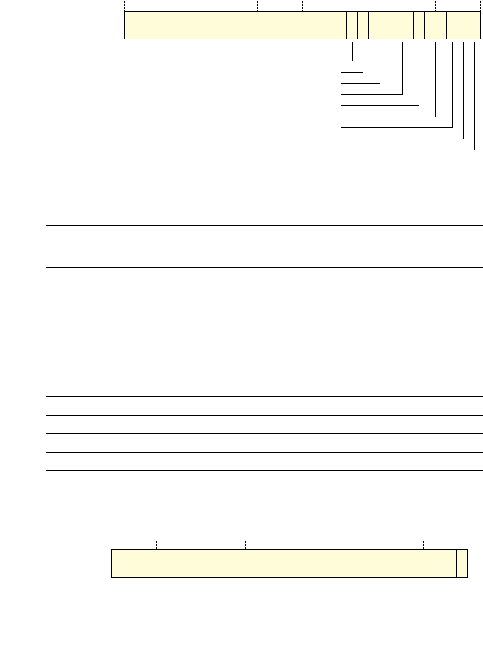
Integration Test Registers
ARM DDI 0363G Copyright © 2006-2011 ARM Limited. All rights reserved. 13-8
ID041111 Non-Confidential
Figure 13-3 DBGITMISCIN Register bit assignments
Table 13-6 lists the register bit assignments for the DBGITMISCIN Register.
13.3.6 Integration Mode Control Register
The DBGITCTRL Register, register
0x3C0
at offset
0xF00
, is read/write. Figure 13-4 shows the
register bit assignments.
Figure 13-4 DBGITCTRL Register bit assignments
Reserved
31 10 9 8 7 4 3 2 0
ETMEXTOUT[1:0]
65
Reserved
nETMWFIREADY
Reserved
nFIQ
nIRQ
EDBGRQ
Reserved
DBGRESTART
1112 1
Table 13-6 DBGITMISCIN Register bit assignments
Bits Name Function
[31:12] - Reserved. Read Undefined.
[11] DBGRESTART Read value of the DBGRESTART input pin.
[10] - Reserved. Read Undefined.
[9:8] ETMEXTOUT Read value of the ETMEXTOUT[1:0] input pins.
[7:6] - Reserved. Read Undefined.
[5] nETMWFIREADY Reads the nETMWFIREADY input pin. Although this pin is active LOW, the value of
this bit matches the physical state of the signal:
0 = input pin is LOW (asserted)
1 = input pin is HIGH (deasserted).
[4:3] - Reserved. Read Undefined.
[2] nFIQ Read value of nFIQ input pin.
[1] nIRQ Read value of nIRQ input pin.
[0] EDBGRQ Read value of EDBGRQ input pin.
Reserved
31 0
1
INTMODE

Integration Test Registers
ARM DDI 0363G Copyright © 2006-2011 ARM Limited. All rights reserved. 13-9
ID041111 Non-Confidential
Table 13-7 shows the fields of the DBGITCTRL Register.
Writing to the DBGITCTRL register controls whether the processor is in its default functional
mode, or in integration mode, where the inputs and outputs of the device can be directly
controlled for the purpose of integration testing or topology detection. For more information see
the ARM Architecture Reference Manual.
Table 13-7 DBGITCTRL Register bit assignments
Bits Access Reset value Name Function
[31:1] RAZ/SBZP - - Reserved.
[0] R/W 0 INTMODE Controls whether the processor is in normal operating mode or
integration mode:
b0 = normal operation
b1 = integration mode enabled.

ARM DDI 0363G Copyright © 2006-2011 ARM Limited. All rights reserved. A-1
ID041111 Non-Confidential
Appendix A
Signal Descriptions
This appendix describes the processor signals. It contains the following sections:
•About the processor signal descriptions on page A-2
•Global signals on page A-3
•Configuration signals on page A-4
•Interrupt signals, including VIC interface signals on page A-7
•L2 interface signals on page A-8
•TCM interface signals on page A-13
•Redundant processor signals on page A-16
•Debug interface signals on page A-17
•ETM interface signals on page A-19
•Test signals on page A-20
•MBIST signals on page A-21
•Validation signals on page A-22
•FPU signals on page A-23.

Signal Descriptions
ARM DDI 0363G Copyright © 2006-2011 ARM Limited. All rights reserved. A-2
ID041111 Non-Confidential
A.1 About the processor signal descriptions
The tables in this appendix list the processor signals, along with their dimensions and direction,
input or output, and a high-level description. Each table also has a clocking column, that
indicates by which clock a signal is sampled or driven. All signals are sampled on or driven from
the rising edge of the clock. The clocking column can also contain the following information:
Any Means the input is synchronised, inside the processor, so the input can be driven
from any clock.
Tie-off Means the input must be tied to a fixed value.
Reset Means the input must only be changed under reset.
Clocking is listed for all outputs, though some are typically synchronized into a different clock
before use.

Signal Descriptions
ARM DDI 0363G Copyright © 2006-2011 ARM Limited. All rights reserved. A-3
ID041111 Non-Confidential
A.2 Global signals
Table A-1 shows the processor global signals.
The free clock is ungated, with minimal insertion delay, because it clocks the clock gating
circuits. Therefore, you must ensure that incoming clocks are balanced with the free clock.
Table A-1 Global signals
Signal Direction Clocking Description
FREECLKIN Input - Free version of the core clock.
CLKIN Input - Core clock.
CLKIN2 Input - Core clock, in phase with DUALCKLIN, for configurations
with dual-redundant core.a
nRESET Input Any Core reset.
nSYSPORESET Input Any System power on reset.
nCPUHALT Input Any Processor halt after reset.
DBGNOCLKSTOP Input Any Processor does not stop the clocks when entering WFI state.a
DUALCLKIN Input - Clock for second, redundant, core.a
DUALCLKIN2 Input - Clock for second, redundant, core, in phase with CLKIN.a
STANDBYWFI Output FREECLKIN Indicates that the processor is in Standby mode and the
processor clock is stopped. You can use this signal for TCMs
RAM clock gating.
a. Not available in r0px revisions of the processor.

Signal Descriptions
ARM DDI 0363G Copyright © 2006-2011 ARM Limited. All rights reserved. A-4
ID041111 Non-Confidential
A.3 Configuration signals
Table A-2 shows the processor configuration signals.
Table A-2 Configuration signals
Signal Direction Clocking Description
VINITHI Input Tie-off,
Reset
Reset V-bit value. When HIGH indicates HIVECS mode at reset.
See c1, System Control Register on page 4-37 for more
information.
CFGEE Input Tie-off,
Reset
Reset EE-bit value. When HIGH indicates the implementation
uses BE-8 mode for exceptions at reset. See c1, System Control
Register on page 4-37 for more information.
CFGIE Input Tie-off,
Reset
Instruction side endianness, reflected in the IE-bit. When HIGH
indicates that big endian instruction fetch is used. See c1, System
Control Register on page 4-37 for more information.
INITRAMA Input Tie-off,
Reset
Reset value of ATCM enable bit. When HIGH indicates
Tightly-Coupled Memory A, ATCM, enabled at reset. See c9,
ATCM Region Register on page 4-62 for more information.
INITRAMB Input Tie-off,
Reset
Reset value of BTCM bit. When HIGH indicates
Tightly-Coupled Memory B, BTCM, enabled at reset. See c9,
BTCM Region Register on page 4-61 for more information.
LOCZRAMA Input Tie-off,
Reset
When HIGH indicates ATCM initial base address is zero and
BTCM base address is implementation-defined.
When LOW indicates BTCM initial base address is zero and
ATCM base address is implementation-defined.
TEINIT Input Tie-off,
Reset
Reset TE-bit value. Determines exception handling state at reset.
When set to:
0 = ARM
1 = Thumb.
See c1, System Control Register on page 4-37 for more
information.
CFGATCMSZ[3:0] Input Tie-off Selects the ATCM size. The encodings for the TCM sizes are:
b0000 = 0KB
b0011 = 4KB
b0100 = 8KB
b0101 = 16KB
b0110 = 32KB
b0111 = 64KB
b1000 = 128KB
b1001 = 256KB
b1010 = 512KB
b1011 = 1MB
b1100 = 2MB
b1101 = 4MB
b1110 = 8MB.

Signal Descriptions
ARM DDI 0363G Copyright © 2006-2011 ARM Limited. All rights reserved. A-5
ID041111 Non-Confidential
CFGBTCMSZ[3:0] Input Tie-off Selects the BTCM size. The encodings for the TCM sizes are:
b0000 = 0KB
b0011 = 4KB
b0100 = 8KB
b0101 = 16KB
b0110 = 32KB
b0111 = 64KB
b1000 = 128KB
b1001 = 256KB
b1010 = 512KB
b1011 = 1MB
b1100 = 2MB
b1101 = 4MB
b1110 = 8MB.
CFGNMFI Input Tie-off,
Reset
When HIGH, enable non-maskable Fast Interrupts. Reflected in
the NMFI bit. See c1, System Control Register on page 4-37 for
more information.
ENTCM1IF Input Tie-off Enable B1TCM interface.
Use B0TCM only if this signal not tied HIGH.
PARECCENRAM[2:0] Input Tie-off,
Reset
TCMs parity or ECC check enable. Tie each bit HIGH to enable
parity or ECC checking on the appropriate TCM at reset. Use
following values:
[2]:B1TCMa
[1]: B0TCMa
[0]: ATCM
See c1, Auxiliary Control Register on page 4-40 for more
information.
PARLVRAM Input Tie-off,
Reset
Selects between odd and even parity for caches, TCMs, and
buses. See Chapter 8 Level One Memory System:
Tie LOW for even parity
Tie HIGH for odd parity.
Table A-2 Configuration signals (continued)
Signal Direction Clocking Description

Signal Descriptions
ARM DDI 0363G Copyright © 2006-2011 ARM Limited. All rights reserved. A-6
ID041111 Non-Confidential
ERRENRAM[2:0] Input Tie-off,
Reset
TCMs external error enable. Tie each bit high to enable the
external error signals for each TCM at reset. Use the following
values:
[2]: B1TCM
[1]: B0TCM
[0]: ATCM
See c1, Auxiliary Control Register on page 4-40 for more
information.
RMWENRAM[1:0]bInput Tie-off,
Reset
RMW enable bits reset values. Tie each bit high to enable
read-modify-write for TCM interfaces at reset.c Use the
following values:
[1]: BTCM
[0]: ATCM
See c1, Auxiliary Control Register on page 4-40 for more
information.
SLBTCMSB Input Tie-off Use most significant bit of BTCM address to select B1TCM if
this signal is HIGH.
Use bit [3] of the BTCM address if this signal is LOW.
a. If the BTCM is configured with ECC, bit[2] and bit[1] must be the same value.
b. Not used if 32-bit ECC is included.
c. Not available in r0px revisions of the processor.
Table A-2 Configuration signals (continued)
Signal Direction Clocking Description

Signal Descriptions
ARM DDI 0363G Copyright © 2006-2011 ARM Limited. All rights reserved. A-7
ID041111 Non-Confidential
A.4 Interrupt signals, including VIC interface signals
Table A-3 shows the interrupt signals including signals used on the VIC interface.
Table A-3 Interrupt signals
Signal Direction Clocking Description
nFIQ Input CLKINa
Anyb
Fast interruptc.
nIRQ Input CLKINa
Anyb
Normal interruptc.
INTSYNCEN Input Tie-off Tie HIGH if the interrupt inputs are asynchronous to CLKIN.
Tie LOW if the interrupt inputs are synchronous to CLKIN.
IRQADDRV Input CLKINd
Anye
Indicates IRQADDR is valid.
IRQADDRVSYNCEN Input Tie-off Tie HIGH if the IRQADDRV input from the VIC is
asynchronous to CLKIN.
Tie HIGH if the IRQADDRV input from the VIC is
synchronous to CLKIN.
IRQADDR [31:2] Input - Address of the IRQ. This signal must be stable when
IRQADDRV is asserted.
IRQACK Output CLKIN Acknowledges interrupt.
nPMUIRQ Output CLKIN Interrupt request by Performance Monitor Unit (PMU).
a. When INTSYNCEN is tied LOW.
b. When INTSYNCEN is tied HIGH.
c. This signal is level-sensitive and must be held LOW until a suitable interrupt response is received from the processor.
d. When IRQADDRVSYNCEN is tied LOW.
e. When IRQADDRVSYCNEN is tied HIGH.

Signal Descriptions
ARM DDI 0363G Copyright © 2006-2011 ARM Limited. All rights reserved. A-8
ID041111 Non-Confidential
A.5 L2 interface signals
This section describes the processor L2 interface AXI signals. It contains the following sections:
•AXI master port
•AXI master port error detection signals on page A-10
•AXI slave port on page A-11
•AXI slave port error detection signals on page A-12.
For more information on AMBA AXI signals see the AMBA AXI Protocol Specification.
Note
All the outputs listed in this section have their reset values during standby.
A.5.1 AXI master port
Table A-4 shows the AXI master port signals for the L2 interface. With the exception of the
ACLKENM, all signals are only sampled or driven on CLKIN edges when ACLKENM is
asserted, see AMBA interface clocking on page 2-13 for more information.
Table A-4 AXI master port signals for the L2 interface
Signal Direction Clocking Description
ACLKENM Input CLKIN Clock enable for the AXI master port.
Write address channel
AWADDRM[31:0] Output CLKIN Transfer start address.
AWBURSTM[1:0] Output CLKIN Write burst type.
AWCACHEM[3:0] Output CLKIN Provides decode information for outer attributes:
b0000 = Strongly-ordered.
b0001 = Device.
b0011 = Normal, Non-cacheable.
b0110 = Normal, cacheable. write-through.
b1111 = Normal, cacheable. write-back, write allocation.
b0111 = Normal, cacheable. write-back, no write allocation.
Note
The AXI specification describes these encodings using the
pre-ARMv6 terms such as cacheable-bufferable. These terms
are equivalent to the ARMv6 memory-type descriptions such as
Normal, Non-cacheable used here.
AWIDM[3:0] Output CLKIN The identification tag for the write address group of signals.
AWLENM [3:0] Output CLKIN Write transfer burst length. The transfer burst length range is
from one to 16. A 4-bit binary value minus one determines the
transfer burst length.
AWLOCKM[1:0] Output CLKIN Lock signal.
AWPROTM[2:0] Output CLKIN Protection type. Only bit [0] is used from the 3-bit AXI bus.
AWREADYM Input CLKIN Address ready. The slave uses this signal to indicate that it can
accept the address.

Signal Descriptions
ARM DDI 0363G Copyright © 2006-2011 ARM Limited. All rights reserved. A-9
ID041111 Non-Confidential
AWSIZEM[2:0] Output CLKIN Indicates the size of the transfer.
AWUSERM[4:0] Output CLKIN Provides decode information for the write address channel. See
Table 9-3 on page 9-5 for information about the encoding of this
signal.
AW VA L I D M Output CLKIN Indicates address and control are valid.
Write data channel
WDATAM[63:0] Output CLKIN Write data.
WIDM[3:0] Output CLKIN The identification tag for the write data group of signals.
WLASTM Output CLKIN Indicates the last data transfer of a burst.
WREADYM Input CLKIN Indicates that the slave is ready to accept write data
WSTRBM[7:0] Output CLKIN Write strobes used to indicate which byte lanes must be updated.
WVALIDM Output CLKIN Indicates address and control are valid.
Write response channel
BIDM [3:0] Input CLKIN The identification tag for the write response signal.
BREADYM Output CLKIN Indicates that the core is ready to accept write response.
BRESPM[1:0] Input CLKIN Write response.
BVALIDM Input CLKIN Indicates that a valid write response is available.
Read address channel
ARADDRM[31:0] Output CLKIN Instruction fetch burst start address.
ARBURSTM[1:0] Output CLKIN Burst type.
ARCACHEM[3:0] Output CLKIN Provides decode information for outer attributes:
b0000 = Strongly-ordered.
b0001 = Device.
b0011 = Normal, Non-cacheable.
b0110 = Normal, cacheable. write-through.
b1111 = Normal, cacheable. write-back, write allocation.
b0111 = Normal, cacheable. write-back, no write allocation.
Note
The AXI specification describes these encodings using the
pre-ARMv6 terms such as cacheable-bufferable. These terms
are equivalent to the ARMv6 memory-type descriptions such as
Normal, Non-cacheable used here.
ARIDM[3:0] Output CLKIN Identification tag for the read address group of signals
ARLENM [3:0] Output CLKIN Instruction fetch burst length.
ARLOCKM[1:0] Output CLKIN Lock signal.
ARPROTM[2:0] Output CLKIN Protection signals provide addition information about a bus
access.
Table A-4 AXI master port signals for the L2 interface (continued)
Signal Direction Clocking Description

Signal Descriptions
ARM DDI 0363G Copyright © 2006-2011 ARM Limited. All rights reserved. A-10
ID041111 Non-Confidential
A.5.2 AXI master port error detection signals
Table A-5 shows the AXI master port error detection signals. these signals are only generated if
the processor is configured to include AXI bus parity. See Configurable options on page 1-6 for
more information.
ARREADYM Input CLKIN Address ready. The slave uses this signal to indicate that it can
accept the address.
ARSIZEM[2:0] Output CLKIN Indicates the size of the transfer.
ARUSERM[4:0] Output CLKIN Provides decode information for the read address channel. See
Table 9-3 on page 9-5 for information about the encoding of this
signal.
ARVALIDM Output CLKIN Indicates address and control are valid.
Read Data Channel
RDATAM[63:0] Input CLKIN Read data.
RIDM[3:0] Input CLKIN The identification tag for the read data group of signals.
RLASTM Input CLKIN Indicates the last transfer in a read burst.
RREADYM Output CLKIN Read ready signal indicating that the bus master can accept read
data and response information.
RRESPM[1:0] Input CLKIN Read response.
RVALIDM Input CLKIN Indicates that read data is available.
Table A-4 AXI master port signals for the L2 interface (continued)
Signal Direction Clocking Description
Table A-5 AXI master port error detection signals
Signal Direction Clocking Description
AWPARITYM Output CLKIN Parity bit for write address channel
WPARITYM Output CLKIN Parity bit for write data channel
BPARITYM Input CLKIN Parity bit for write response channel
ARPARITYM Output CLKIN Parity bit for read address channel
RPARITYM Input CLKIN Parity bit for read data channel
AXIMPARERR[1:0] Output CLKIN Parity error indication for read data, bit [1], and write response,
bit[0], channels

Signal Descriptions
ARM DDI 0363G Copyright © 2006-2011 ARM Limited. All rights reserved. A-11
ID041111 Non-Confidential
A.5.3 AXI slave port
Table A-6 shows the AXI slave port signals for the L2 interface. With the exception of the
ACLKENS, all signals are only sampled or driven on CLKIN edges when ACLKENS is
asserted, see AMBA interface clocking on page 2-13 for more information.
Table A-6 AXI slave port signals for the L2 interface
Signal Direction Clocking Description
ACLKENS Input CLKIN Clock enable for the AXI slave port.
Write Address Channel
AWADDRS[22:0] Input CLKIN Transfer start address.
AWBURSTS[1:0] Input CLKIN Write burst type.
AWIDS[7:0] Input CLKIN The identification tag for the write address group of signals.
AWLENS[3:0] Input CLKIN Write transfer burst length. The transfer burst length range is from
one to 16. A 4-bit binary value minus one determines the transfer
burst length.
AW P R O T S Input CLKIN Protection information, privileged or normal access. AWP ROT [ 0]
in AXI specification.
AWREADYS Output CLKIN Address ready. The slave uses this signal to indicate that it can
accept the address.
AWSIZES[2:0] Input CLKIN Indicates the size of the transfer.
AW U S E R S [ 3 : 0 ] Input CLKIN Memory type select data cache, instruction cache, BTCM or
ATCM, one hot. AW U S E R S [ 3 : 0 ] signal is not part of the standard
AXI specification.
AW VA L I D S Input CLKIN Indicates address and control are valid.
Write Data Channel
WDATAS[63:0] Input CLKIN Write data.
WLASTS Input CLKIN Indicates the last data transfer of a burst.
WREADYS Output CLKIN Indicates that the slave is ready to accept write data.
WSTRBS[7:0] Input CLKIN Write strobes used to indicate which byte lanes must be updated.
WVALIDS Input CLKIN Indicates address and control are valid.
Write Response Channel
BIDS[7:0] Output CLKIN The identification tag for the write response signal.
BREADYS Input CLKIN Indicates that the core is ready to accept write response.
BRESPS[1:0] Output CLKIN Write response.
BVALIDS Output CLKIN Indicates that a valid write response is available.
Read Address Channel
ARADDRS[22:0] Input CLKIN Instruction fetch burst start address.
ARBURSTS[1:0] Input CLKIN Burst type.
ARIDS[7:0] Input CLKIN Identification tag for the read address group of signals.

Signal Descriptions
ARM DDI 0363G Copyright © 2006-2011 ARM Limited. All rights reserved. A-12
ID041111 Non-Confidential
A.5.4 AXI slave port error detection signals
Table A-7 shows the AXI slave port error detection signals. These signals are only generated if
the processor is configured to include AXI bus parity. See Configurable options on page 1-6 for
more information.
ARLENS[3:0] Input CLKIN Instruction fetch burst length.
ARPROTS Input CLKIN Protection information, privileged or normal access. ARPROT[0]
in AXI specification.
ARREADYS Output CLKIN Address ready. The slave uses this signal to indicate that it can
accept the address.
ARSIZES[2:0] Input CLKIN Indicates the size of the transfer.
ARUSERS[3:0] Input CLKIN Memory type select {data cache, instruction cache, BTCM or
ATCM}, one hot. AW U S E R S [ 3 : 0 ] signal is not part of the
standard AXI specification.
ARVALIDS Input CLKIN Indicates address and control are valid.
Read Data Channel
RDATAS[63:0] Output CLKIN Read data.
RIDS[7:0] Output CLKIN The identification tag for the read data group of signals.
RLASTS Output CLKIN Indicates the last transfer in a read burst.
RREADYS Input CLKIN Read ready signal indicating that the bus master can accept read
data and response information.
RRESPS[1:0] Output CLKIN Read response.
RVALIDS Output CLKIN Indicates address and control are valid.
Table A-6 AXI slave port signals for the L2 interface (continued)
Signal Direction Clocking Description
Table A-7 AXI slave port error detection signals
Signal Direction Clocking Description
AWPARITYS Input CLKIN Parity bit for write address channel
WPARITYS Input CLKIN Parity bit for write data channel
BPARITYS Output CLKIN Parity bit for write response channel
ARPARITYS Input CLKIN Parity bit for read address channel
RPARITYS Output CLKIN Parity bit for read data channel
AXISPARERR[2:0] Output CLKIN Parity error indication for read address, bit [2], write data, bit [1], and
write address, bit [0], channels.

Signal Descriptions
ARM DDI 0363G Copyright © 2006-2011 ARM Limited. All rights reserved. A-13
ID041111 Non-Confidential
A.6 TCM interface signals
Table A-8 shows the ATCM port signals.
Table A-9 shows the B0TCM port signals.
Table A-8 ATCM port signals
Name Direction Clocking Description
ATCDATAIN [63:0] Input CLKIN Data from ATCM
ATCPARITYIN [13:0] Input CLKIN Parity or ECC code from ATCM
ATCERROR Input CLKIN Error detected by ATCMa
ATCWAIT Input CLKIN Wait from ATCM
ATCLATEERROR Input CLKIN Late error from ATCMa
ATCRETRY Input CLKIN Access to ATCM must be retrieda
ATCADDRPTY Output CLKIN Parity formed from ATCM address outputb
ATCEN0 Output CLKIN Enable for ATCM lower word, bit range [31:0]
ATCEN1 Output CLKIN Enable for ATCM upper word, bit range [63:32]
ATCWE Output CLKIN Write enable for ATCM
ATCADDR [22:3] Output CLKIN Address for ATCM data RAM
ATCBYTEWR [7:0] Output CLKIN Byte strobes for direct write
ATCSEQ Output CLKIN ATCM RAM access is sequential
ATCDATAOUT [63:0] Output CLKIN Write data for ATCM data RAM
ATCPARITYOUT [13:0] Output CLKIN Write parity or ECC code for ATCM
ATCACCTYPE[2:0] Output CLKIN Determines access type:
b001 = Load/Store
b010 = Fetch
b100 = DMA
b100 = MBISTc.
a. This signal is ignored when bit [0] of the Auxiliary Control Register is set to 0, see c1, Auxiliary Control
Register on page 4-40.
b. Only generated if the processor is configured to include TCM address bus parity.
c. The MBIST interface has no way of signaling a wait. If it is accessing the TCM, and the TCM signals a wait,
the AXI slave pipeline stalls and the data arrives later. However, no signal is sent to the MBIST controller to
indicate this.
Table A-9 B0TCM port signals
Name Direction Clocking Description
B0TCDATAIN [63:0] Input CLKIN Data from B0TCM
B0TCPARITYIN [13:0] Input CLKIN Parity or ECC code from B0TCM
B0TCERROR Input CLKIN Error detected by B0TCMa
B0TCWAIT Input CLKIN Wait from B0TCM

Signal Descriptions
ARM DDI 0363G Copyright © 2006-2011 ARM Limited. All rights reserved. A-14
ID041111 Non-Confidential
Table A-10 shows the B1TCM port signals.
B0TCLATEERROR Input CLKIN Late error from B0TCMa
B0TCRETRY Input CLKIN Access to B1TCM must be retrieda
B0TCADDRPTY Output CLKIN Parity formed from B0TCM address outputb
B0TCWE Output CLKIN Write enable for B0TCM
B0TCEN0 Output CLKIN Enable for B0TCM lower word, bit range [31:0]
B0TCEN1 Output CLKIN Enable for B0TCM upper word, bit range [64:32]
B0TCADDR [22:3] Output CLKIN Address for B0TCM data RAM
B0TCBYTEWR [7:0] Output CLKIN Byte strobes for direct write
B0TCSEQ Output CLKIN B0TCM RAM access is sequential
B0TCDATAOUT [63:0] Output CLKIN Write data for B0TCM data RAM
B0TCPARITYOUT [13:0] Output CLKIN Write parity or ECC code for B0TCM
B0TCACCTYPE[2:0] Output CLKIN Determines access type:
b001 = Load/Store
b010 = Fetch
b100 = DMA
b100 = MBISTc.
a. This signal is ignored when bit [1] of the Auxiliary Control Register is set to 0, see c1, Auxiliary Control Register
on page 4-40.
b. Only generated if the processor is configured to include TCM address bus parity.
c. The MBIST interface has no way of signaling a wait. If it is accessing the TCM, and the TCM signals a wait, the
AXI slave pipeline stalls and the data arrives later. However, no signal is sent to the MBIST controller to indicate
this.
Table A-9 B0TCM port signals (continued)
Name Direction Clocking Description
Table A-10 B1TCM port signals
Name Direction Clocking Description
B1TCDATAIN [63:0] Input CLKIN Data from B1TCM
B1TCPARITYIN [13:0] Input CLKIN Parity or ECC code from B1TCM
B1TCERROR Input CLKIN Error detected by B1TCMa
B1TCRETRY Input CLKIN Access to B1TCM must be retrieda
B1TCLATEERROR Input CLKIN Late error from B1TCMa
B1TCWAIT Input CLKIN Wait from B1TCM
B1TCADDRPTY Output CLKIN Parity formed from B1TCM address outputb
B1TCWE Output CLKIN Write enable for B1TCM
B1TCEN0 Output CLKIN Enable for B1TCM lower word, bit range [31:0]
B1TCEN1 Output CLKIN Enable for B1TCM upper word, bit range [64:32]

Signal Descriptions
ARM DDI 0363G Copyright © 2006-2011 ARM Limited. All rights reserved. A-15
ID041111 Non-Confidential
B1TCADDR [22:3] Output CLKIN Address for B1TCM data RAM
B1TCBYTEWR [7:0] Output CLKIN Byte strobes for direct write
B1TCSEQ Output CLKIN B1TCM RAM access is sequential
B1TCDATAOUT [63:0] Output CLKIN Write data for B1TCM data RAM
B1TCPARITYOUT [13:0] Output CLKIN Write parity or ECC code for B1TCM
B1TCACCTYPE[2:0] Output CLKIN Determines access type:
b001 = Load/Store
b010 = Fetch
b100 = DMA
b100 = MBISTc.
a. This signal is ignored when bit [2] of the Auxiliary Control Register is set to 0, see c1, Auxiliary Control Register
on page 4-40.
b. Only generated if the processor is configured to include TCM address bus parity.
c. The MBIST interface has no way of signaling a wait. If it is accessing the TCM, and the TCM signals a wait, the
AXI slave pipeline stalls and the data arrives later. However, no signal is sent to the MBIST controller to indicate
this.
Table A-10 B1TCM port signals (continued)
Name Direction Clocking Description

Signal Descriptions
ARM DDI 0363G Copyright © 2006-2011 ARM Limited. All rights reserved. A-16
ID041111 Non-Confidential
A.7 Redundant processor signals
Table A-11 shows the dual redundant core interface signals.
Table A-11 Dual core interface signals
Signal Direction Clocking Description
DCCMINP[7:0] Input -a
a. Implementation-defined.
Dual core compare logic input control bus
DCCMOUT[7:0] Output -aDual core compare logic output control bus
DCCMINP2[7:0] Input -aDual core compare logic extra input control busb
b. Not available in r0px revisions of the processor.
DCCMOUT2[7:0] Output -aDual core compare logic extra output control busb

Signal Descriptions
ARM DDI 0363G Copyright © 2006-2011 ARM Limited. All rights reserved. A-17
ID041111 Non-Confidential
A.8 Debug interface signals
Table A-12 shows the debug interface signals. With the exception of PCLKDBG,
PCLKENDBG and PRESETDBGn, all these signals are only sampled or driven on
PCLKDBG edges when PCLKENDBG is asserted.
Table A-13 shows the debug miscellaneous signals.
Table A-12 Debug interface signals
Signal Direction Clocking Description
PCLKDBG Input - Debug clock.
PCLKENDBG Input PCLKDBG Clock enable for PCLKDBG.
PSELDBG Input PCLKDBG Selects the external debug interface.
PADDRDBG[11:2] Input PCLKDBG Programming address.
PADDRDBG31 Input PCLKDBG Programming address.
PRDATADBG[31:0] Output PCLKDBG Read data bus.
PWDATADBG[31:0] Input PCLKDBG Write data bus.
PENABLEDBG Input PCLKDBG Indicates second, and subsequent, cycle of a transfer.
PREADYDBG Output PCLKDBG Extends a APB transfer by the inserting wait states.
PSLVERRDBG Output PCLKDBG Slave-generated error response.
PWRITEDBG Input PCLKDBG Indicates access is a write transfer.
Distinguishes between a read, LOW, and a write, HIGH.
PRESETDBGn Input Any Reset debug logic.
Table A-13 Debug miscellaneous signals
Name Direction Clocking Description
DBGEN Input Any Debug enable
NIDEN Input Any Non-invasive debug enable
EDBGRQ Input Any External debug request
DBGACK Output CLKIN Debug acknowledge
DBGRSTREQaOutput PCLKDBG Request for reset from debug logic
DBGTRIGGER Output CLKIN External debug request taken
COMMRX Output CLKIN DBGDTRRX full
COMMTX Output CLKIN DBGDTRTX empty
DBGRESTART Input External restart request
DBGRESTARTED Output CLKIN Handshake for DBGRESTART
DBGNOPWRDWN Output PCLKDBG No power-down request
DBGROMADDR[31:12] Input Tie-off Debug ROM physical address

Signal Descriptions
ARM DDI 0363G Copyright © 2006-2011 ARM Limited. All rights reserved. A-18
ID041111 Non-Confidential
DBGROMADDRV Input Tie-off Debug ROM physical address valid
DBGSELFADDR[31:12] Input Tie-off Debug self-address offset
DBGSELFADDRV Input Tie-off Debug self-address offset valid
a. Not available in r0px revisions of the processor.
Table A-13 Debug miscellaneous signals (continued)
Name Direction Clocking Description

Signal Descriptions
ARM DDI 0363G Copyright © 2006-2011 ARM Limited. All rights reserved. A-19
ID041111 Non-Confidential
A.9 ETM interface signals
Table A-14 shows the ETM interface signals.
Table A-14 ETM interface signals
Signal Direction Clocking Description
ETMICTL[13:0] Output CLKIN ETM instruction control bus
ETMIA[31:1] Output CLKIN ETM instruction address
ETMDCTL[11:0] Output CLKIN ETM data control bus
ETMDA[31:0] Output CLKIN ETM data address
ETMDD[63:0] Output CLKIN ETM data-data
ETMCID[31:0] Output CLKIN Value of processor CID register
ETMWFIPENDING Output CLKIN Core is attempting to enter WFI state
EVNTBUS[46:0] Output CLKIN Performance monitor unit output
ETMPWRUP Input CLKIN Power up ETM interface
nETMWFIREADY Input CLKIN ETM FIFO is empty, core can enter WFI state
ETMEXTOUT[1:0] Input CLKIN ETM detected events

Signal Descriptions
ARM DDI 0363G Copyright © 2006-2011 ARM Limited. All rights reserved. A-20
ID041111 Non-Confidential
A.10 Test signals
Table A-15 shows the test signals.
Table A-15 Test signals
Signal Direction Clocking Description
SE Input -a
a. Design for test only.
Scan Enable
RSTBYPASS Input -aBypass pipelined reset

Signal Descriptions
ARM DDI 0363G Copyright © 2006-2011 ARM Limited. All rights reserved. A-21
ID041111 Non-Confidential
A.11 MBIST signals
Table A-16 shows the MBIST signals.
Table A-16 MBIST signals
Signal Direction Clocking Description
MBTESTON Input CLKIN MBIST test is enabled
MBISTDIN[77:0] Input CLKIN MBIST data in
MBISTADDR[19:0] Input CLKIN MBIST address
MBISTCE Input CLKIN MBIST chip enable
MBISTSEL[4:0] Input CLKIN MBIST chip select
MBISTWE [7:0] Input CLKIN MBIST write enable
MBISTDOUT[77:0] Output CLKIN MBIST data out

Signal Descriptions
ARM DDI 0363G Copyright © 2006-2011 ARM Limited. All rights reserved. A-22
ID041111 Non-Confidential
A.12 Validation signals
Table A-17 shows the validation signals.
Table A-17 Validation signals
Signal Direction Clocking Description
VALEDBGRQ Output CLKIN Debug request
nVALIRQ Output CLKIN Request for an interrupt
nVALFIQ Output CLKIN Request for a Fast Interrupt
nVALRESET Output CLKIN Request for a reset

Signal Descriptions
ARM DDI 0363G Copyright © 2006-2011 ARM Limited. All rights reserved. A-23
ID041111 Non-Confidential
A.13 FPU signals
Table A-18 shows the FPU signals. These signals are only driven if the processor is configured
to include the floating-point logic.
Table A-18 FPU signals
Signal Direction Clocking Description
FPIXC Output CLKIN Masked floating-point inexact exception
FPOFC Output CLKIN Masked floating-point overflow exception
FPUFC Output CLKIN Masked floating-point underflow exception
FPIOC Output CLKIN Masked floating-point invalid operation exception
FPDZC Output CLKIN Masked floating-point divide-by-zero exception
FPIDC Output CLKIN Masked floating-point input denormal exception


AC Characteristics
ARM DDI 0363G Copyright © 2006-2011 ARM Limited. All rights reserved. B-2
ID041111 Non-Confidential
B.1 Processor timing
The AXI bus interface of the processor conforms to the AMBA AXI Specification. For the
relevant timing of the AXI write and read transfers, and the error response, see the AMBA AXI
Protocol Specification.
The APB debug interface of the processor conforms to the AMBA 3 APB Protocol Specification.
For the relevant timing of the APB write and read transfers, and the error response, see the
AMBA 3 APB Protocol Specification.

AC Characteristics
ARM DDI 0363G Copyright © 2006-2011 ARM Limited. All rights reserved. B-3
ID041111 Non-Confidential
B.2 Processor timing parameters
This section describes the input and output port timing parameters for the processor.
The maximum timing parameter or constraint delay for each processor signal applied to the SoC
is given as a percentage in Table B-1 to Table B-17 on page B-11. The input and output delay
columns provide the maximum and minimum time as a percentage of the processor clock cycle
given to the SoC for that signal.
This section describes:
•Input port timing parameters
•Output ports timing parameters on page B-8.
B.2.1 Input port timing parameters
Table B-1 shows the timing parameters for the miscellaneous input ports.
Table B-2 shows the timing parameters for the configuration input port.
Table B-1 Miscellaneous input ports timing parameters:
Input delay
minimum
Input delay
maximum Signal name
Clock uncertainty 10% nRESET
Clock uncertainty 10% nSYSPORESET
Clock uncertainty 10% PRESETDBGn
Clock uncertainty 50% nCPUHALT
Clock uncertainty 20% DBGNOCLKSTOP
Table B-2 Configuration input port timing parameters
Input delay
minimum
Input delay
maximum Signal name
Clock uncertainty 20% VINITHI
Clock uncertainty 20% CFGEE
Clock uncertainty 20% CFGIE
Clock uncertainty 20% INITRAMA
Clock uncertainty 20% INITRAMB
Clock uncertainty 20% LOCZRAMA
Clock uncertainty 20% TEINIT
Clock uncertainty 20% CFGNMFI
Clock uncertainty 20% CFGATCMSZ[3:0]
Clock uncertainty 20% CFGBTCMSZ[3:0]
Clock uncertainty 20% PARECCENRAM[2:0]
Clock uncertainty 20% ERRENRAM[2:0]

AC Characteristics
ARM DDI 0363G Copyright © 2006-2011 ARM Limited. All rights reserved. B-4
ID041111 Non-Confidential
Table B-3 shows the timing parameters for the interrupt input ports.
Table B-4 shows the input timing parameters for the AXI master port.
Clock uncertainty 20% PARLVRAM
Clock uncertainty 20% ENTCM1IF
Clock uncertainty 20% SLBTCMSB
Clock uncertainty 20% RMWENRAM[1:0]
Table B-3 Interrupt input ports timing parameters
Input delay
minimum
Input delay
maximum Signal name
Clock uncertainty 60% nFIQ
Clock uncertainty 60% nIRQ
Clock uncertainty 10% INTSYNCEN
Clock uncertainty 60% IRQADDRV
Clock uncertainty 60% IRQADDRVSYNCEN
Clock uncertainty 60% IRQADDR[31:2]
Table B-4 AXI master input port timing parameters
Input delay
minimum
Input
delay
maximum
Signal name
Clock uncertainty 50% ACLKENM
Clock uncertainty 60% AWREADYM
Clock uncertainty 60% WREADYM
Clock uncertainty 60% BIDM[3:0]
Clock uncertainty 60% BRESPM[1:0]
Clock uncertainty 60% BVALIDM
Clock uncertainty 60% ARREADYM
Clock uncertainty 60% RIDM[3:0]
Clock uncertainty 60% RDATAM[63:0]
Clock uncertainty 60% RRESPM[1:0]
Clock uncertainty 60% RLASTM
Table B-2 Configuration input port timing parameters (continued)
Input delay
minimum
Input delay
maximum Signal name

AC Characteristics
ARM DDI 0363G Copyright © 2006-2011 ARM Limited. All rights reserved. B-5
ID041111 Non-Confidential
Table B-5 shows the input timing parameters for the AXI slave port.
Clock uncertainty 60% RVALIDM
Clock uncertainty 60% BPARITYM
Clock uncertainty 60% RPARITYM
Table B-5 AXI slave input port timing parameters
Input delay
minimum
Input
delay
maximum
Signal name
Clock uncertainty 50% ACLKENS
Clock uncertainty 60% AW I D S [ 7 : 0 ]
Clock uncertainty 60% AWADDRS[22:0]
Clock uncertainty 60% AWLENS[3:0]
Clock uncertainty 60% AWSIZES[2:0]
Clock uncertainty 60% AWBURSTS[1:0]
Clock uncertainty 60% AW P R O T S
Clock uncertainty 60% AW U S E R S [ 3 : 0 ]
Clock uncertainty 60% AW VA L I D S
Clock uncertainty 60% WDATAS[63:0]
Clock uncertainty 60% WSTRBS[7:0]
Clock uncertainty 60% WLASTS
Clock uncertainty 60% WVALIDS
Clock uncertainty 60% BREADYS
Clock uncertainty 60% ARIDS[7:0]
Clock uncertainty 60% ARADDRS[22:0]
Clock uncertainty 60% ARLENS[3:0]
Clock uncertainty 60% ARSIZES[2:0]
Clock uncertainty 60% ARBURSTS[1:0]
Clock uncertainty 60% ARPROTS
Clock uncertainty 60% ARUSERS[3:0]
Clock uncertainty 60% ARVALIDS
Clock uncertainty 60% RREADYS
Table B-4 AXI master input port timing parameters (continued)
Input delay
minimum
Input
delay
maximum
Signal name

AC Characteristics
ARM DDI 0363G Copyright © 2006-2011 ARM Limited. All rights reserved. B-6
ID041111 Non-Confidential
Table B-6 shows the input timing parameters for the debug input ports.
Table B-7 shows the input timing parameters for the ETM input ports.
Clock uncertainty 60% AW PA R I T Y S
Clock uncertainty 60% WPARITYS
Clock uncertainty 60% ARPARITYS
Table B-6 Debug input ports timing parameters
Input delay
minimum
Input delay
maximum Signal name
Clock uncertainty 50% DBGEN
Clock uncertainty 50% NIDEN
Clock uncertainty 50% EDBGRQ
Clock uncertainty 50% PCLKENDBG
Clock uncertainty 50% PSELDBG
Clock uncertainty 50% PADDRDBG[11:2]
Clock uncertainty 50% PADDRDBG31
Clock uncertainty 50% PWDATADBG[31:0]
Clock uncertainty 50% PENABLEDBG
Clock uncertainty 50% PWRITEDBG
Clock uncertainty 10% DBGROMADDR[31:12]
Clock uncertainty 10% DBGROMADDRV
Clock uncertainty 10% DBGSELFADDR[31:12]
Clock uncertainty 10% DBGSELFADDRV
Clock uncertainty 50% DBGRESTART
Table B-7 ETM input ports timing parameters
Input delay
minimum
Input delay
maximum Signal name
Clock uncertainty 50% ETMPWRUP
Clock uncertainty 50% nETMWFIREADY
Clock uncertainty 50% ETMEXTOUT[1:0]
Table B-5 AXI slave input port timing parameters (continued)
Input delay
minimum
Input
delay
maximum
Signal name

AC Characteristics
ARM DDI 0363G Copyright © 2006-2011 ARM Limited. All rights reserved. B-7
ID041111 Non-Confidential
Table B-8 shows the timing parameters for the test input ports.
Table B-9 shows the timing parameters for the TCM interface input ports.
Table B-8 Test input ports timing parameters
Input delay
minimum
Input
delay
maximum
Signal name
Clock uncertainty 10% SE
Clock uncertainty 10% RSTBYPASS
Clock uncertainty 50% MBTESTON
Clock uncertainty 50% MBISTDIN[71:0]
Clock uncertainty 50% MBISTADDR[19:0]
Clock uncertainty 50% MBISTCE
Clock uncertainty 50% MBISTSEL[4:0]
Clock uncertainty 50% MBISTWE[7:0]
Table B-9 TCM interface input ports timing parameters
Input delay
minimum
Input
delay
maximum
Signal name
Clock uncertainty 65% ATCDATAIN[63:0]
Clock uncertainty 65% ATCPARITYIN[13:0]
Clock uncertainty 65% ATCERROR
Clock uncertainty 50% ATCWAIT
Clock uncertainty 40% ATCLATEERROR
Clock uncertainty 50% ATCRETRY
Clock uncertainty 65% B0TCDATAIN[63:0]
Clock uncertainty 65% B0TCPARITYIN[13:0]
Clock uncertainty 65% B0TCERROR
Clock uncertainty 50% B0TCWAIT
Clock uncertainty 40% B0TCLATEERROR
Clock uncertainty 50% B0TCRETRY
Clock uncertainty 65% B1TCDATAIN[63:0]
Clock uncertainty 65% B1TCPARITYIN[13:0]
Clock uncertainty 65% B1TCERROR

AC Characteristics
ARM DDI 0363G Copyright © 2006-2011 ARM Limited. All rights reserved. B-8
ID041111 Non-Confidential
The timing parameters for the dual-redundant core compare logic input control buses,
DCCMINP[7:0] and DCCMINP2[7:0], are implementation-defined. Contact the implementer
of the macrocell you are working with.
B.2.2 Output ports timing parameters
Most output ports have a maximum output delay of 60%, that is the SoC is enabled to use 60%
of the clock cycle.
Table B-10 shows the timing parameter for the miscellaneous output port.
Table B-11 shows the timing parameters for the interrupt output ports.
Table B-12 shows the timing parameters for the AXI master output port.
Clock uncertainty 50% B1TCWAIT
Clock uncertainty 40% B1TCLATEERROR
Clock uncertainty 50% B1TCRETRY
Table B-9 TCM interface input ports timing parameters (continued)
Input delay
minimum
Input
delay
maximum
Signal name
Table B-10 Miscellaneous output port timing parameter
Output delay
minimum
Output delay
maximum Signal name
Clock uncertainty 10% STANDBYWFI
Table B-11 Interrupt output ports timing parameters
Output delay
minimum
Output delay
maximum Signal name
Clock uncertainty 60% IRQACK
Clock uncertainty 60% nPMUIRQ
Table B-12 AXI master output port timing parameters
Output delay
minimum
Output delay
maximum Signal name
Clock uncertainty 60% AWIDM[3:0]
Clock uncertainty 60% AWADDRM[31:0]
Clock uncertainty 60% AWLENM[3:0]
Clock uncertainty 60% AWSIZEM[2:0]
Clock uncertainty 60% AWBURSTM[1:0]
Clock uncertainty 60% AWLOCKM[1:0]
Clock uncertainty 60% AWCACHEM[3:0]

AC Characteristics
ARM DDI 0363G Copyright © 2006-2011 ARM Limited. All rights reserved. B-9
ID041111 Non-Confidential
Table B-13 shows the timing parameters for the AXI slave output ports.
Clock uncertainty 60% AWPROTM[2:0]
Clock uncertainty 60% AWUSERM[4:0]
Clock uncertainty 60% AW VA L I D M
Clock uncertainty 60% WIDM[3:0]
Clock uncertainty 60% WDATAM[63:0]
Clock uncertainty 60% WSTRBM[7:0]
Clock uncertainty 60% WLASTM
Clock uncertainty 60% WVALIDM
Write response channel
Clock uncertainty 60% BREADYM
Clock uncertainty 60% ARIDM[3:0]
Clock uncertainty 60% ARADDRM[31:0]
Clock uncertainty 60% ARLENM[3:0]
Clock uncertainty 60% ARSIZEM[2:0]
Clock uncertainty 60% ARBURSTM[1:0]
Clock uncertainty 60% ARLOCKM[1:0]
Clock uncertainty 60% ARCACHEM[3:0]
Clock uncertainty 60% ARPROTM[2:0]
Clock uncertainty 60% ARUSERM[4:0]
Clock uncertainty 60% ARVALIDM
Clock uncertainty 60% RREADYM
Clock uncertainty 60% AWPARITYM
Clock uncertainty 60% WPARITYM
Clock uncertainty 60% ARPARITYM
Clock uncertainty 50% AXIMPARERR[1:0]
Table B-13 AXI slave output ports timing parameters
Output delay
minimum
Output delay
maximum Signal name
Clock uncertainty 60% AWREADYS
Clock uncertainty 60% WREADYS
Clock uncertainty 60% BIDS[7:0]
Table B-12 AXI master output port timing parameters (continued)
Output delay
minimum
Output delay
maximum Signal name

AC Characteristics
ARM DDI 0363G Copyright © 2006-2011 ARM Limited. All rights reserved. B-10
ID041111 Non-Confidential
Table B-14 shows the timing parameters for the debug interface output ports.
Clock uncertainty 60% BRESPS[1:0]
Clock uncertainty 60% BVALIDS
Clock uncertainty 60% ARREADYS
Clock uncertainty 60% RIDS[7:0]
Clock uncertainty 60% RDATAS[63:0]
Clock uncertainty 60% RRESPS[1:0]
Clock uncertainty 60% RLASTS
Clock uncertainty 60% RVALIDS
Clock uncertainty 60% BPARITYS
Clock uncertainty 60% RPARITYS
Clock uncertainty 50% AXISPARERR[2:0]
Table B-14 Debug interface output ports timing parameters
Output delay
minimum
Output delay
maximum Signal name
Clock uncertainty 50% PRDATADBG[31:0]
Clock uncertainty 50% PREADYDBG
Clock uncertainty 50% PSLVERRDBG
Clock uncertainty 50% DBGNOPWRDWN
Clock uncertainty 50% DBGACK
Clock uncertainty 50% DBGTRIGGER
Clock uncertainty 50% DBGRESTARTED
Clock uncertainty 50% DBGRSTREQ
Clock uncertainty 50% COMMTX
Clock uncertainty 50% COMMRX
Table B-13 AXI slave output ports timing parameters (continued)
Output delay
minimum
Output delay
maximum Signal name

AC Characteristics
ARM DDI 0363G Copyright © 2006-2011 ARM Limited. All rights reserved. B-11
ID041111 Non-Confidential
Table B-15 shows the timing parameters for the ETM interface output ports.
Table B-16 shows the timing parameters for the test output ports.
Table B-17 shows the timing parameters for the TCM interface output ports.
Table B-15 ETM interface output ports timing parameters
Output delay
minimum
Output delay
maximum Signal name
Clock uncertainty 50% ETMICTL[13:0]
Clock uncertainty 50% ETMIA[31:1]
Clock uncertainty 50% ETMDCTL[11:0]
Clock uncertainty 50% ETMDA[31:0]
Clock uncertainty 50% ETMDD[63:0]
Clock uncertainty 50% ETMCID[31:0]
Clock uncertainty 50% ETMWFIPENDING
Clock uncertainty 50% EVNTBUS[46:0]
Table B-16 Test output ports timing parameters
Output delay
minimum
Output delay
maximum Signal name
Clock uncertainty 50% MBISTDOUT[71:0]
Clock uncertainty 50% nVALIRQ
Clock uncertainty 50% nVALFIQ
Clock uncertainty 50% nVALRESET
Clock uncertainty 50% VALEDBGRQ
Table B-17 TCM interface output ports timing parameters
Output delay
minimum
Output delay
maximum Signal name
Clock uncertainty 45% ATCEN0
Clock uncertainty 45% ATCEN1
Clock uncertainty 45% ATCADDR[22:3]
Clock uncertainty 45% ATCBYTEWR[7:0]
Clock uncertainty 45% ATCSEQ
Clock uncertainty 45% ATCDATAOUT[63:0]
Clock uncertainty 45% ATCPARITYOUT[13:0]
Clock uncertainty 45% ATCACCTYPE[2:0]
Clock uncertainty 45% ATCWE

AC Characteristics
ARM DDI 0363G Copyright © 2006-2011 ARM Limited. All rights reserved. B-12
ID041111 Non-Confidential
Table B-18 shows the timing parameters for the FPU output signals.
Clock uncertainty 45% ATCADDRPTY
Clock uncertainty 45% B0TCEN0
Clock uncertainty 45% B0TCEN1
Clock uncertainty 45% B0TCADDR[22:3]
Clock uncertainty 45% B0TCBYTEWR[7:0]
Clock uncertainty 45% B0TCSEQ
Clock uncertainty 45% B0TCDATAOUT[63:0]
Clock uncertainty 45% B0TCPARITYOUT[13:0]
Clock uncertainty 45% B0TCACCTYPE[2:0]
Clock uncertainty 45% B0TCWE
Clock uncertainty 45% B0TCADDRPTY
Clock uncertainty 45% B1TCEN0
Clock uncertainty 45% B1TCEN1
Clock uncertainty 45% B1TCADDR[23:0]
Clock uncertainty 45% B1TCBYTEWR[7:0]
Clock uncertainty 45% B1TCSEQ
Clock uncertainty 45% B1TCDATAOUT[63:0]
Clock uncertainty 45% B1TCPARITYOUT[13:0]
Clock uncertainty 45% B1TCACCTYPE[2:0]
Clock uncertainty 45% B1TCWE
Clock uncertainty 45% B1TCADDRPTY
Table B-18 FPU output port timing parameters
Output delay
minimum
Output delay
maximum Signal name
Clock uncertainty 60% FPIXC
Clock uncertainty 60% FPOFC
Clock uncertainty 60% FPUFC
Clock uncertainty 60% FPIOC
Clock uncertainty 60% FPDZC
Clock uncertainty 60% FPIDC
Table B-17 TCM interface output ports timing parameters (continued)
Output delay
minimum
Output delay
maximum Signal name

AC Characteristics
ARM DDI 0363G Copyright © 2006-2011 ARM Limited. All rights reserved. B-13
ID041111 Non-Confidential
The timing parameters for the dual-redundant core compare logic output buses,
DCCMOUT[7:0] and DCCMOUT2[7:0], are implementation-defined. Contact the
implementer of the macrocell you are working with.

ARM DDI 0363G Copyright © 2006-2011 ARM Limited. All rights reserved. C-1
ID041111 Non-Confidential
Appendix C
Cycle Timings and Interlock Behavior
This chapter describes the cycle timings and interlock behavior of instructions on the processor. It
contains the following sections:
•About cycle timings and interlock behavior on page C-3
•Register interlock examples on page C-6
•Data processing instructions on page C-7
•QADD, QDADD, QSUB, and QDSUB instructions on page C-9
•Media data-processing on page C-10
•Sum of Absolute Differences (SAD) on page C-11
•Multiplies on page C-12
•Divide on page C-14
•Branches on page C-15
•Processor state updating instructions on page C-16
•Single load and store instructions on page C-17
•Load and Store Double instructions on page C-20
•Load and Store Multiple instructions on page C-21
•RFE and SRS instructions on page C-24
•Synchronization instructions on page C-25
•Coprocessor instructions on page C-26
•SVC, BKPT, Undefined, and Prefetch Aborted instructions on page C-27
•Miscellaneous instructions on page C-28
•Floating-point register transfer instructions on page C-29
•Floating-point load/store instructions on page C-30
•Floating-point single-precision data processing instructions on page C-32


Cycle Timings and Interlock Behavior
ARM DDI 0363G Copyright © 2006-2011 ARM Limited. All rights reserved. C-3
ID041111 Non-Confidential
C.1 About cycle timings and interlock behavior
Complex instruction dependencies and memory system interactions make it impossible to
describe briefly the exact cycle timing behavior for all instructions in all circumstances. The
timings described in this chapter are accurate in most cases. If precise timings are required, you
must use a cycle-accurate model of the processor.
Unless stated otherwise, cycle counts and result latencies that this chapter describes are
best-case numbers. They assume:
• no outstanding data dependencies between the current instruction and a previous
instruction
• the instruction does not encounter any resource conflicts
• all data accesses hit in the data cache, and do not cross protection region boundaries
• all instruction accesses hit in the instruction cache.
This section describes:
•Instruction execution overview
•Conditional instructions on page C-4
•Flag-setting instructions on page C-4
•Definition of terms on page C-4
•Assembler language syntax on page C-5.
C.1.1 Instruction execution overview
The instruction execution pipeline has four stages, Iss, Ex1, Ex2, and Wr.
Extensive forwarding to the end of the Iss, Ex1, and Ex2 stages enables many dependent
instruction sequences to run without pipeline stalls. General forwarding occurs from the end of
the Ex2 and Wr pipeline stages. In addition, the multiplier contains an internal multiply
accumulate forwarding path. The address generation unit also contains an internal forwarding
path.
Most instructions do not require a register until the Ex2 stage. All result latencies are given as
the number of cycles until the register is available for a following instruction in the Ex2 stage.
Most ALU operations require their source registers at the start of the Ex2 stage, and have a result
latency of one. For example, the following sequence takes two cycles:
ADD R1,R3,R4 ;Result latency one
ADD R5,R2,R1 ;Register R1 required by ALU
The PC is the only register that result latency does not affect. An instruction that alters the PC
never causes a pipeline stall because of interlocking with a subsequent instruction that reads the
PC.
Most loads have a result latency of two or higher as they do not forward their results until the
Wr stage. For example, the following sequence takes three cycles:
LDR R1, [R2] ;Result latency two
ADD R3, R3, R1 ;Register R1 required by ALU
If a subsequent instruction requires the register at the end of the Iss stage then an extra cycle
must be added to the result latency of the instruction producing the required register.
Instructions that require a register at the end of these stages are specified by describing that
register as an Early Reg. The following sequence, requiring an Early Reg, takes four cycles:

Cycle Timings and Interlock Behavior
ARM DDI 0363G Copyright © 2006-2011 ARM Limited. All rights reserved. C-4
ID041111 Non-Confidential
LDR R1, [R2] ;Result latency two
ADD R3, R3, R1 LSL#6 ;plus one because Register R1 is Early
The following sequence where R1 is a Late Reg takes two cycles:
LDR R1, [R2] ;Result latency two minus one cycles
STR R1, [R3] ;no penalty because R1 is a Late register
The following sequence where R1 is a Very Early Reg takes four cycles:
ADD R3, R1, R2 ;Result latency one plus two cycles
LDR R4, [R3] ;plus two because register R3 is Very Early
C.1.2 Conditional instructions
Most instructions do not take more or fewer cycles to execute if they fail their condition codes.
The exceptions to this are:
• instructions that alter the PC, such as branches
• integer divide instructions, that require only one execute cycle.
The result latency of most instructions that fail their condition codes is one. The exceptions to
this are:
• all load and store instructions, that have their result latency unaffected
• integer divide instructions, that have a result latency of three.
C.1.3 Flag-setting instructions
Most instructions do not take more or fewer cycles to execute if they are flag-setting. The
exceptions to this are certain multiply instructions.
C.1.4 Definition of terms
Table C-1 gives descriptions of cycle timing terms used in this chapter.
Table C-1 Definition of cycle timing terms
Term Description
Memory Cycles This is the number of cycles during which an instruction sends a memory access to the cache.
Cycles This is the minimum number of cycles required to issue an instruction. Issue cycles that produce
memory accesses to the cache are included, so Cycles is always greater than or equal to Memory
Cycles.
Result Latency This is the number of cycles before the result of this instruction is available to a Normal Reg of the
following instruction. When the Result Latency of an instruction is greater than Cycles and the
following instruction requires the result, the following instruction stalls for a number of cycles equal
to Result Latency minus Cycles.
Note
The Result Latency is counted from the first cycle of an instruction.
Normal Reg The specified registers are required at the start of the Ex2 stage.
Late Reg The specified registers are not required until the start of the Wr stage. Subtract one cycle from the
Result Latency of the instruction producing this register.

Cycle Timings and Interlock Behavior
ARM DDI 0363G Copyright © 2006-2011 ARM Limited. All rights reserved. C-5
ID041111 Non-Confidential
C.1.5 Assembler language syntax
The syntax used throughout this chapter is unified assembler and the timings apply to ARM and
Thumb instructions.
Early Reg The specified registers are required at the start of the Ex1 stage. Add one cycle to the Result Latency
of the instruction producing this register.
Very Early Reg The specified registers are required at the start of the Iss stage. Add two cycles to the Result Latency
of the instruction producing this register, or one cycle if the instruction producing this register is an
LDM
,
LDR
,
LDRD
,
LDREX
, or
LDRT
. The lower Result Latency does not apply if this register is the base register of
the load instruction producing this register, or if the load instruction is an
LDRB
,
LDRBT
,
LDRH
,
LDRSB
, or
LDRSH
.
Interlock There is a data dependency between two instructions in the pipeline, resulting in the Iss stage being
stalled until the processor resolves the dependency.
Table C-1 Definition of cycle timing terms (continued)
Term Description

Cycle Timings and Interlock Behavior
ARM DDI 0363G Copyright © 2006-2011 ARM Limited. All rights reserved. C-6
ID041111 Non-Confidential
C.2 Register interlock examples
Table C-2 shows register interlock examples using
LDR
and
ADD
instructions.
LDR
instructions take one cycle, have a result latency of two, and require their base register as a
Very Early Reg.
ADD
instructions take one cycle and have a result latency of one.
Table C-2 Register interlock examples
Instruction
sequence Behavior
LDR R1, [R2]
ADD R6, R5, R4
Takes two cycles because there are no register dependencies.
ADD R1, R2, R3
ADD R9, R6, R1
Takes two cycles because
ADD
instructions have a result latency of one.
LDR R1, [R2]
ADD R6, R5, R1
Takes three cycles because of the result latency of R1.
ADD R2, R5, R6
LDR R1, [R2]
Takes four cycles because of the use of the result of R2 as a Very Early Reg.
LDR R1, [R2]
LDR R5, [R1]
Takes four cycles because of the result latency of R1, the use of the result of R1 as a Very Early Reg,
and the use of an LDR to generate R1.

Cycle Timings and Interlock Behavior
ARM DDI 0363G Copyright © 2006-2011 ARM Limited. All rights reserved. C-7
ID041111 Non-Confidential
C.3 Data processing instructions
This section describes the cycle timing behavior for the
ADC
,
ADD
,
ADDW
,
AND
,
ASR
,
BIC
,
CLZ
,
CMN
,
CMP
,
EOR
,
LSL
,
LSR
,
MOV
,
MOVT
,
MOVW
,
MVN
,
ORN
,
ORR
,
ROR
,
RRX
,
RSB
,
RSC
,
SBC
,
SUB
,
SUBW
,
TEQ
, and
TST
instructions.
This section describes:
•Cycle counts if destination is not PC
•Cycle counts if destination is the PC
•Example interlocks on page C-8.
C.3.1 Cycle counts if destination is not PC
Table C-3 shows the cycle timing behavior for data processing instructions if their destination
is not the PC. You can substitute
ADD
with any of the data processing instructions identified in
the opening paragraph of this section.
C.3.2 Cycle counts if destination is the PC
Table C-4 shows the cycle timing behavior for data processing instructions if their destination
is the PC. You can substitute
ADD
with any data processing instruction except for a
CLZ
. A
CLZ
with the PC as the destination is an Unpredictable instruction.
For condition code failing cycle counts, the cycles for the non-PC destination variants must be
used.
Table C-3 Data Processing Instruction cycle timing behavior if destination is not PC
Example instruction Cycles Early
Reg
Late
Reg
Result
latency Comments
ADD <Rd>, <Rn>, #<immed>
1 - - 1 Normal cases.
ADD <Rd>, <Rn>, <Rm>
1- -1
ADD <Rd>, <Rn>, <Rm>, LSL #<immed>
1
<Rm>
- 1 Requires a shifted source register.
ADD <Rd>, <Rn>, <Rm>, LSL <Rs
>1
<Rm>
,
<Rs>
- 1 Requires a register controlled
shifted source register.
MOV <Rd>, <Rm>
1-
<Rm>
1Simple
MOV
case. Must not set the
flags or require a shifted source
register.
Table C-4 Data Processing instruction cycle timing behavior if destination is the PC
Example instruction Cycles Early
Reg
Late
Reg
Result
latency Comments
ADD pc, <Rn>, #<immed>
9 - - - Normal cases to PC
ADD pc, <Rn>, <Rm>
9---
ADD pc, <Rn>, <Rm>, LSL #<immed>
9
<Rm>
- - Requires a shifted source register
ADD pc, <Rn>, <Rm>, LSL <Rs
>9
<Rm>
,
<Rs>
-
- Requires a register controlled shifted
source register

Cycle Timings and Interlock Behavior
ARM DDI 0363G Copyright © 2006-2011 ARM Limited. All rights reserved. C-8
ID041111 Non-Confidential
C.3.3 Example interlocks
Most data processing instructions are single-cycle and can be executed back-to-back without
interlock cycles, even if there are data dependencies between them. The exceptions to this are
when shifts are used.
Shifter
The registers that the shifter requires are Early Regs and require an additional cycle of result
availability before use. For example, the following sequence introduces a 1-cycle interlock, and
takes three cycles to execute:
ADD R1,R2,R3
ADD R4,R5,R1 LSL #1
The second source register, that is not shifted, does not incur an extra data dependency check.
Therefore, the following sequence takes two cycles to execute:
ADD R1,R2,R3
ADD R4,R1,R9 LSL #1
Register controlled shifts
The register containing the shift distance is an Early Reg. For example, the following sequence
takes three cycles to execute:
ADD R1, R2, R3
ADD R4, R2, R4, LSL R1

Cycle Timings and Interlock Behavior
ARM DDI 0363G Copyright © 2006-2011 ARM Limited. All rights reserved. C-9
ID041111 Non-Confidential
C.4 QADD, QDADD, QSUB, and QDSUB instructions
This section describes the cycle timing behavior for the
QADD
,
QDADD
,
QSUB
, and
QDSUB
instructions.
These instructions perform saturating arithmetic. They have a result latency of two. The
QDADD
and
QDSUB
instructions must double and saturate the register
<Rn>
before the addition. This
register is an Early Reg.
Table C-5 shows the cycle timing behavior for
QADD
,
QDADD
,
QSUB
, and
QDSUB
instructions.
Table C-5 QADD, QDADD, QSUB, and QDSUB instruction cycle timing behavior
Instructions Cycles Early Reg Result latency
QADD
,
QSUB
1- 2
QDADD
,
QDSUB
1
<Rn>
2

Cycle Timings and Interlock Behavior
ARM DDI 0363G Copyright © 2006-2011 ARM Limited. All rights reserved. C-10
ID041111 Non-Confidential
C.5 Media data-processing
Table C-6 shows media data-processing instructions and gives their cycle timing behavior.
All media data-processing instructions are single-cycle issue instructions. These instructions
have result latencies of one or two cycles. Some of the instructions require an input register to
be shifted, or manipulated in some other way before use and therefore are marked as requiring
an Early Reg.
Table C-6 Media data-processing instructions cycle timing behavior
Instructions Cycles Early Reg Result latency
SADD16
,
SSUB16
,
SADD8
,
SSUB8
1- 1
UADD16
,
USUB16
,
UADD8
,
USUB8
1- 1
SEL
1- 1
QADD16
,
QSUB16
,
QADD8
,
QSUB8
1- 2
SHADD16
,
SHSUB16
,
SHADD8
,
SHSUB8
1- 1
UQADD16
,
UQSUB16
,
UQADD8
,
UQSUB8
1- 2
UHADD16
,
UHSUB16
,
UHADD8
,
UHSUB8
1- 1
SSAT16
,
USAT16
1
<Rn>
1
SASX
,
SSAX
1- 1
UASX
,
USAX
1- 1
SXTAB
,
SXTAB16
,
SXTAH
1
<Rm>
1
SXTB
,
SXTB16
,
SXTH
1
<Rm>
a
a. A shift of zero makes
<Rm>
a Normal Reg for these instructions.
1
UXTB
,
UXTB16
,
UXTH
1
<Rm>
a1
UXTAB
,
UXTAB16
,
UXTAH
1
<Rm>
1
REV
,
REV16
,
REVSH
,
RBIT
1
<Rm>
1
PKHBT
,
PKHTB
1
<Rm>
1
SSAT
,
USAT
1
<Rm>
1
QASX
,
QSAX
1- 2
SHASX
,
SHSAX
1- 1
UQASX
,
UQSAX
1- 2
UHASX
,
UHSAX
1- 1
BFC
1
<Rd>
1
SBFX
,
UBFX
1
<Rn>
1
BFI
1
<Rd>, <Rn>
1

Cycle Timings and Interlock Behavior
ARM DDI 0363G Copyright © 2006-2011 ARM Limited. All rights reserved. C-11
ID041111 Non-Confidential
C.6 Sum of Absolute Differences (SAD)
Table C-7 shows
SAD
instructions and gives their cycle timing behavior.
C.6.1 Example interlocks
Table C-8 shows interlock examples using
USAD8
and
USADA8
instructions.
Table C-7 Sum of absolute differences instruction timing behavior
Instructions Cycles Early Reg Result latency
USAD8
1
<Rn>, <Rm>
2a
a. Result latency is one fewer if the destination is the accumulate
for a subsequent
USADA8
.
USADA8
1<Rn>, <Rm>
2a
Table C-8 Example interlocks
Instruction sequence Behavior
USAD8 R1,R2,R3
ADD R5,R6,R1
Takes three cycles because
USAD8
has a Result Latency of two, and the
ADD
requires
the result of the
USAD8
instruction.
USAD8 R1,R2,R3
MOV R9,R9
ADD R5,R6,R1
Takes three cycles. The
MOV
instruction is scheduled during the Result Latency of
the USAD8 instruction.
USAD8 R1,R2,R3
USADA8 R1,R4,R5,R1
Takes two cycles. The Result Latency is one less because the result is used as the
accumulate for a subsequent
USADA8
instruction.

Cycle Timings and Interlock Behavior
ARM DDI 0363G Copyright © 2006-2011 ARM Limited. All rights reserved. C-12
ID041111 Non-Confidential
C.7 Multiplies
Most multiply operations cannot forward their result early, except as the accumulate value for a
subsequent multiply. For a subsequent multiply accumulate the result is available one cycle
earlier than for all other uses of the result.
Certain multiplies require:
• more than one cycle to execute
• more than one pipeline issue to produce a result.
The multiplicand and multiplier are required as Early Regs because they are both required at the
end of the Iss stage.
Flag-setting multiplies followed by a conditional instruction interlock the conditional
instruction for one cycle, or two cycles if the instruction is a conditional multiply. Flag-setting
multiplies followed by a flag-setting instruction interlock the flag-setting instruction for one
cycle, unless the instruction is a flag-setting multiply in which case there is no interlock.
Table C-9 shows the cycle timing behavior of example multiply instructions.
Table C-9 Example multiply instruction cycle timing behavior
Example
instruction Cycles Early Reg Late Reg Result latency
MUL(S)
2<Rn>, <Rm>- 3
MLA(S)
,
MLS
2
<Rn>, <Rm> <Ra>
3
SMULL(S)
2<Rn>, <Rm>- 3, 3
UMULL(S)
2<Rn>, <Rm>- 3, 3
SMLAL(S)
2<Rn>, <Rm>
<RdLo>, <RdHi>
3, 3
UMLAL(S)
2<Rn>, <Rm>
<RdLo>, <RdHi>
3, 3
SMULxy
1<Rn>, <Rm>- 2
SMLAxy
1<Rn>, <Rm>- 2
SMULWy
1<Rn>, <Rm>- 2
SMLAWy
1<Rn>, <Rm>- 2
SMLALxy
2<Rn>, <Rm>
<RdLo>, <RdHi>
3, 3
SMUAD
,
SMUADX
1<Rn>, <Rm>- 2
SMLAD
,
SMLADX
1<Rn>, <Rm>- 2
SMUSD
,
SMUSDX
1<Rn>, <Rm>- 2
SMLSD
,
SMLSDX
1<Rn>, <Rm>- 2
SMMUL
,
SMMULR
2<Rn>, <Rm>- 3
SMMLA
,
SMMLAR
2<Rn>, <Rm>
<Ra>
3
SMMLS
,
SMMLSR
2<Rn>, <Rm>
<Ra>
3

Cycle Timings and Interlock Behavior
ARM DDI 0363G Copyright © 2006-2011 ARM Limited. All rights reserved. C-13
ID041111 Non-Confidential
Note
Result Latency is one less if the result is used as the accumulate value for a subsequent multiply
accumulate. This only applies if the result is the same width as the accumulate value, that is 32
or 64 bits.
SMLALD
,
SMLALDX
1<Rn>, <Rm>- 2, 2
SMLSLD
,
SMLSLDX
1<Rn>, <Rm>- 2, 2
UMAAL
2<Rn>, <Rm>
<RdLo>, <RdHi>
3, 3
Table C-9 Example multiply instruction cycle timing behavior (continued)
Example
instruction Cycles Early Reg Late Reg Result latency

Cycle Timings and Interlock Behavior
ARM DDI 0363G Copyright © 2006-2011 ARM Limited. All rights reserved. C-14
ID041111 Non-Confidential
C.8 Divide
This section describes the cycle timing behavior of the
UDIV
and
SDIV
instructions.
The divider unit is separate to the main execute pipeline so the
UDIV
and
SDIV
instructions require
one cycle to issue. They execute out-of-order relative to the rest of the pipeline, and require an
additional issue cycle at the end of the divide operation to write the result to the destination
register. This additional cycle is not required if the divide instruction fails its condition code.
Result Latency for a
UDIV
instruction A divided by B is given by:
Result Latency for a
SDIV
instruction A divided by B is given by:
Note
• A divide instruction that fails its condition code or attempts to divide by zero has a Result
Latency of three.
• The value of the (clz(B) - clz(A) + 1)/2 component of these equations must be rounded
down.
• The clz(x) function counts the number of leading zeros in the 32-bit value x. If x is
negative, it is negated before this count occurs.
2
clz(B) - clz(A) + 1 ,0
Result latency = 3 +
max
())(
2
clz(B) - clz(A) + 1 ,0
Result latency = 4 +
max
())(

Cycle Timings and Interlock Behavior
ARM DDI 0363G Copyright © 2006-2011 ARM Limited. All rights reserved. C-15
ID041111 Non-Confidential
C.9 Branches
This section describes the cycle timing behavior for the
B
,
BL
,
BLX
,
BX
,
BXJ
,
CBNZ
,
CBZ
,
TBB
, and
TBH
instructions. Branches are subject to dynamic and return stack predictions. Table C-10 shows
example branch instructions and their cycle timing behavior.
Table C-10 Branch instruction cycle timing behavior
Example instruction Cycles Memory
cycles Comments
B<label>, BL<label>a,
BLX<label>
a
1 - Correct dynamic prediction
8 - Incorrect dynamic prediction
BX <Rm>
b1 - Correct return stack prediction
9 - Incorrect return stack prediction
BX <cond> <Rm>
b1 - Correct condition prediction and correct return stack prediction
8 - Incorrect condition prediction
9 - Correct condition prediction and incorrect return stack prediction
BXJ <cond> <Rm>
1 - Condition code fails
9 - Condition code passes
BLX <Rm>
9- -
BLX <cond> <Rm>
1 - Condition code fails
9 - Condition code passes
CBZ <Rn>, <label>
,
CBNZ
<Rn>, <label>
1 - Correct condition prediction
8 - Incorrectly predicted
TBB [<Rn>, <Rm>]
c9 1 Condition code fails
9 1 Condition code passes
TBH [<Rn>, <Rm>, LSL#1]
c9 1 Condition code fails
9 1 Condition code passes
a. Return stack push.
b. Return stack pop, if condition passes.
c.
<Rn>
and
<Rm>
are Very Early Regs.

Cycle Timings and Interlock Behavior
ARM DDI 0363G Copyright © 2006-2011 ARM Limited. All rights reserved. C-16
ID041111 Non-Confidential
C.10 Processor state updating instructions
This section describes the cycle timing behavior for the
MSR
,
MRS
,
CPS
, and
SETEND
instructions.
Table C-11 shows processor state updating instructions and their cycle timing behavior.
Table C-11 Processor state updating instructions cycle timing behavior
Instruction Cycles Comments
MRS
1All
MRS
instructions
MSR
5 All other
MSR
instructions to the CPSR
MSR SPSR
1All
MSR
instructions to the SPSR
CPS <effect> <iflags>
1 Interrupt masks only
CPS <effect> <iflags>, #<mode>
1 Mode changing
SETEND
1-

Cycle Timings and Interlock Behavior
ARM DDI 0363G Copyright © 2006-2011 ARM Limited. All rights reserved. C-17
ID041111 Non-Confidential
C.11 Single load and store instructions
This section describes the cycle timing behavior for
LDR
,
LDRHT
,
LDRSBT
,
LDRSHT
,
LDRT
,
LDRB
,
LDRBT
,
LDRSB
,
LDRH
,
LDRSH
,
STR
,
STRT
,
STRB
,
STRBT
,
STRH
, and
PLD
instructions.
Table C-12 shows the cycle timing behavior for stores and loads, other than loads to the PC. You
can replace
LDR
with any of these single load or store instructions. The following rules apply:
• They are normally single-cycle issue. Both the base and any offset register are Very Early
Regs.
• They are 3-cycle issue if pre-increment addressing with either a negative register offset or
a shift other than LSL #1, 2 or 3 is used. Both the base and any offset register are Very
Early Regs.
• If unaligned support is enabled then accesses to addresses not aligned to the access size
that cross a 64-bit aligned boundary generate two memory accesses, and require an
additional cycle to issue. This extra cycle is required if the final address is potentially
unaligned, even if the final address turns out to be aligned.
•
PLD
(data preload hint instructions) have cycle timing behavior as for load instructions.
Because they have no destination register, the result latency is not-applicable for such
instructions.
• For store instructions
<Rt>
is always a Late Reg.
Table C-13 shows the cycle timing behavior for loads to the PC.
Table C-12 Cycle timing behavior for stores and loads, other than loads to the PC
Example instruction Cycles Memory
cycles
Result latency
(LDR)
Result
latency
(base
register)
Comments
LDR <Rt>, <addr_md_1cycle>
a1 1 2 1 Aligned access
LDR <Rt>, <addr_md_3cycle>
a3 1 4 3 Aligned access
LDR <Rt>, <addr_md_1cycle>
a2 2 3 2 Potentially unaligned access
LDR <Rt>, <addr_md_3cycle>
a4 2 5 4 Potentially unaligned access
a. See Table C-14 on page C-18 for an explanation of
<addr_md_1cycle>
and
<addr_md_3cycle>
.
Table C-13 Cycle timing behavior for loads to the PC
Example instruction Cycles Memory
cycles
Result
latency Comments
LDR pc, [sp, #<imm>] (!)
1 1 - Correctly return stack predicted, or conditional
predicted correctly
LDR pc, [sp], #<imm>
11 -
LDR pc, [sp, #<imm>] (!)
9 1 - Return stack mispredicted, conditional
predicted correctly
LDR pc, [sp], #<imm>
91 -

Cycle Timings and Interlock Behavior
ARM DDI 0363G Copyright © 2006-2011 ARM Limited. All rights reserved. C-18
ID041111 Non-Confidential
Only cycle times for aligned accesses are given because Unaligned accesses to the PC are not
supported.
The processor includes a 4-entry return stack that can predict procedure returns. Any LDR
instruction to the PC with an immediate post-indexed offset of plus four, and the stack pointer
R13 as the base register is considered a procedure return.
Table C-14 shows the explanation of
<addr_md_1cycle>
and
<addr_md_3cycle>
used in
Table C-12 on page C-17 and Table C-13 on page C-17.
C.11.1 Base register update
The base register update for load or store instructions occurs in the ALU pipeline. To prevent an
interlock for back-to-back load or store instructions reusing the same base register, there is a
local forwarding path to recycle the updated base register around the address generator. This
only applies when the load or store instruction with base write-back uses pre-increment
addressing, and is a single load or store instruction that is not a load or store double instruction
or load or store multiple instruction.
For example, with
R2
aligned the following instruction sequence take three cycles to execute:
LDR <cond> pc, [sp, #<imm>] (!)
8 1 - Conditional predicted incorrectly, but return
stack predicted correctly
LDR <cond> pc, [sp], #cn
s8 1 -
LDR pc, <addr_md_1cycle>
a91 - -
LDR pc, <addr_md_3cycle>
a
11 1 - -
a. See Table C-14 for an explanation of
<addr_md_1cycle>
and
<addr_md_3cycle>
. For condition code failing cycle counts, you
must use the cycles for the non-PC destination variants.
Table C-13 Cycle timing behavior for loads to the PC (continued)
Example instruction Cycles Memory
cycles
Result
latency Comments
Table C-14 <addr_md_1cycle> and <addr_md_3cycle> LDR example instruction explanation
Example instruction Very Early Reg Comments
<addr_md_1cycle>
LDR <Rt>, [<Rn>, #<imm>] (!) <Rn>
If post-increment addressing or pre-increment
addressing with an immediate offset, or a
positive register offset with no shift or shift
LSL #1, 2 or 3, then 1-issue cycle
LDR <Rt>, [<Rn>, <Rm>] (!) <Rn>, <Rm>
LDR <Rt>, [<Rn>, <Rm>, LSL #1, 2 or 3] (!) <Rn>, <Rm>
LDR <Rt>, [<Rn>], #<imm> <Rn>
LDR <Rt>, [<Rn>], +/-<Rm> <Rn>, <Rm>
LDR <Rt>, [<Rn>], +/-<Rm> <shift> <cns> <Rn>, <Rm>
<addr_md_3cycle>
LDR <Rt>, [<Rn>, -<Rm>] (!) <Rn>,<Rm>
If pre-increment addressing with a negative
register offset or shift other than LSL #1, 2 or
3, then 3-issue cycles
LDR <Rt>, [Rn, +/-<Rm> <shift> <cns>] (!) <Rn>,<Rm>

Cycle Timings and Interlock Behavior
ARM DDI 0363G Copyright © 2006-2011 ARM Limited. All rights reserved. C-19
ID041111 Non-Confidential
LDR R5, [R2, #4]!
LDR R6, [R2, #0X10]!
LDR R7, [R2, #0X20]!

Cycle Timings and Interlock Behavior
ARM DDI 0363G Copyright © 2006-2011 ARM Limited. All rights reserved. C-20
ID041111 Non-Confidential
C.12 Load and Store Double instructions
This section describes the cycle timing behavior for the
LDRD
and
STRD
instructions.
The
LDRD
and
STRD
instructions:
• Are normally single-cycle issue. Both the base and any offset register are Very Early Regs.
• Are 3-cycle issue if offset or pre-increment addressing with a negative register offset is
used. Both the base and any offset register are Very Early Regs.
• Take only one memory cycle if the address is doubleword aligned.
• Take two memory cycles if the address is not doubleword aligned.
Table C-15 shows the cycle timing behavior for
LDRD
and
STRD
instructions.
Table C-16 shows the explanation of
<addr_md_1cycle>
and
<addr_md_3cycle>
used in
Table C-15.
Table C-15 Load and Store Double instructions cycle timing behavior
Example instruction Cycles Cycles with
base writeback
Memory
cycles
Result
latency
(LDRD)
Result latency
(base register)
Address is doubleword aligned
LDRD R0, R1, <addr_md_1cycle>
a12 1 2, 22
LDRD R0, R1, <addr_md_3cycle>
a34 1 4, 44
Address not doubleword aligned
LDRD R0, R1, <addr_md_1cycle>
a22 2 2, 32
LDRD R0, R1, <addr_md_3cycle>
a44 2 4, 54
a. See Table C-16 for an explanation of
<addr_md_1cycle>
and
<addr_md_3cycle>
.
Table C-16 <addr_md_1cycle> and <addr_md_3cycle> LDRD example instruction explanation
Example instruction Very Early
Reg Comments
<addr_md_1cycle>
LDRD <Rt>, <Rt2>, [<Rn>, #<imm>] (!) <Rn>
If post-increment addressing, pre-increment
addressing with an immediate offset or a positive
register offset, then 1-issue cycle
LDRD <Rt>, <Rt2>, [<Rn>, <Rm>] (!) <Rn>, <Rm>
LDRD <Rt>, <Rt2>, [<Rn>], #<imm> <Rn>
LDRD <Rt>, <Rt2>, [<Rn>], +/-<Rm> <Rn>, <Rm>
<addr_md_3cycle>
LDRD <Rt>, <Rt2>, [<Rn>, -<Rm>] (!) <Rn>,<Rm>
If pre-increment addressing with a negative
register offset, then 3-issue cycles

Cycle Timings and Interlock Behavior
ARM DDI 0363G Copyright © 2006-2011 ARM Limited. All rights reserved. C-21
ID041111 Non-Confidential
C.13 Load and Store Multiple instructions
This section describes the cycle timing behavior for the
LDM
,
STM
,
PUSH
, and
POP
instructions.
These instructions take multiple cycles to issue, and then use multiple memory cycles to load
and store all the registers. Because the memory datapath is 64-bits wide, two registers can be
loaded or stored on each cycle.
This section describes:
•Load and Store Multiples, other than load multiples including the PC
•Load Multiples, where the PC is in the register list on page C-22
•Example Interlocks on page C-22.
C.13.1 Load and Store Multiples, other than load multiples including the PC
In all cases the base register,
<Rn>
, is a Very Early Reg.
Table C-17 shows the cycle timing behavior of load and store multiples including the PC.
Note
The Cycle timing behavior that Table C-17 shows also covers
PUSH
and
POP
instructions that
behave like store and load multiple instructions with base register write-back.
Table C-17 Cycle timing behavior of Load and Store Multiples, other than load multiples including the PC
Example instruction Cycles
Cycles
with base
register
write-back
Memory
cycles
Result latency
(LDM)
Result latency
(base register)
First address 64-bit aligned
LDMIA <Rn>,{R1}
11 1 2 1
LDMIA <Rn>,{R1,R2}
12 1 2,2 2
LDMIA <Rn>,{R1,R2,R3}
22 2 2,2,3 2
LDMIA <Rn>,{R1,R2,R3,R4}
2 3 2 2,2,3,3 3
LDMIA <Rn>,{R1,R2,R3,R4,R5}
3 3 3 2,2,3,3,4 3
LDMIA <Rn>,{R1,R2,R3,R4,R5,R6}
3 4 3 2,2,3,3,4,4 4
LDMIA <Rn>,{R1,R2,R3,R4,R5,R6,R7}
4 4 4 2,2,3,3,4,4,5 4
First address not 64-bit aligned
LDMIA <Rn>,{R1}
12 1 2 2
LDMIA <Rn>,{R1,R2}
22 2 2,3 2
LDMIA <Rn>,{R1,R2,R3}
23 2 2,3,3 3
LDMIA <Rn>,{R1,R2,R3,R4}
3 3 3 2,3,3,4 3
LDMIA <Rn>,{R1,R2,R3,R4,R5}
3 4 3 2,3,3,4,4 4
LDMIA <Rn>,{R1,R2,R3,R4,R5,R6}
4 4 4 2,3,3,4,4,5 4
LDMIA <Rn>,{R1,R2,R3,R4,R5,R6,R7}
4 5 4 2,3,3,4,4,5,5 5

Cycle Timings and Interlock Behavior
ARM DDI 0363G Copyright © 2006-2011 ARM Limited. All rights reserved. C-22
ID041111 Non-Confidential
C.13.2 Load Multiples, where the PC is in the register list
The processor includes a 4-entry return stack that can predict procedure returns. Any
LDM
to the
PC that does not restore the SPSR to the CPSR, is predicted as a procedure return.
In all cases the base register,
<Rn>
, is a Very Early Reg.
Table C-18 shows the cycle timing behavior of Load Multiples, where the PC is in the register
list.
Note
The Cycle timing behavior that Table C-18 shows also covers
PUSH
and
POP
instructions that
behave like store and load multiple instructions with base register writeback.
C.13.3 Example Interlocks
The following sequence that has an
LDM
instruction takes six cycles to execute, because R7 has
a result latency of five cycles:
LDMIA R0, {R1-R7}
ADD R10, R10, R7
The following sequence that has an STM instruction takes five cycles to execute:
STMIA R0, {R1-R7}
ADD R7, R10, R11
The following sequence has a result latency hidden by issue cycles. It takes five cycles to
execute.
LDMIA R0, {R1-R7}
ADD R10, R10, R3
The following sequence that has a POP instruction takes seven cycles to execute, because R9
has a result latency of six cycles:
POP {R1-R9}
ADD R10, R10, R9
The following sequence that has a PUSH instruction takes five cycles to execute:
PUSH {R1-R7}
ADD R10,R10,R7
Table C-18 Cycle timing behavior of Load Multiples, with PC in the register list (64-bit aligned)
Example instruction Cycles Memory
cycles
Result
latency Comments
LDMIA <Rn>,{...,pc}
manb2,… Correct return stack prediction
LDMIA <Rn>,{...,pc}
ma + 8 nb2,… Incorrect return stack prediction
LDMIA <cond> <Rn>,{...,pc}
manb2,… Correct condition prediction and correct return stack prediction
LDMIA <cond> <Rn>,{...,pc}
ma + 7 nb2,… Incorrect condition prediction
LDMIA <cond> <Rn>,{...,pc}
ma + 8 nb2,… Correct condition prediction and incorrect return stack prediction
a. Where m is the number of cycles for this instruction if the PC were treated as a normal register.
b. Where n is the number of memory cycles for this instruction if the PC were treated as a normal register.

Cycle Timings and Interlock Behavior
ARM DDI 0363G Copyright © 2006-2011 ARM Limited. All rights reserved. C-23
ID041111 Non-Confidential
Note
In the examples, R0 and
sp
are 64-bit aligned addresses. The instructions
PUSH
and
POP
always
use the
sp
register for the base address.

Cycle Timings and Interlock Behavior
ARM DDI 0363G Copyright © 2006-2011 ARM Limited. All rights reserved. C-24
ID041111 Non-Confidential
C.14 RFE and SRS instructions
This section describes the cycle timing for the
RFE
and
SRS
instructions.
These instructions:
• return from an exception and save exception return state respectively
• take one or two memory cycles depending on doubleword alignment first address
location.
In all cases the base register is a Very Early Reg.
Table C-19 shows the cycle timing behavior for
RFE
and
SRS
instructions.
Table C-19 RFE and SRS instructions cycle timing behavior
Example instruction Cycles Memory cycles
Address doubleword aligned
RFEIA <Rn>
10 1
SRSIA #<mode>
11
Address not doubleword aligned
RFEIA <Rn>
11 2
SRSIA #<mode>
22

Cycle Timings and Interlock Behavior
ARM DDI 0363G Copyright © 2006-2011 ARM Limited. All rights reserved. C-25
ID041111 Non-Confidential
C.15 Synchronization instructions
This section describes the cycle timing behavior for the
CLREX
,
DMB
,
DSB
,
ISB
,
LDREX
,
LDREXB
,
LDREXD
,
LDREXH
,
STREX
,
STREXB
,
STREXD
,
STREXH
,
SWP
, and
SWPB
instructions.
In all cases the base register, Rn, is a Very Early Reg. Table C-20 shows the synchronization
instructions cycle timing behavior.
The synchronization instructions
DMB
,
DSB
, and
ISB
stall the pipeline for a variable number of
cycles, depending on the current state of the memory system.
Table C-20 Synchronization instructions cycle timing behavior
Instruction Cycles Memory cycles Result latency
CLREX
1- -
LDREX <Rt>, [Rn]
11 2
LDREXB <Rt>, [Rn]
11 2
LDREXH <Rt>, [Rn]
11 2
LDREXD <Rt>, [Rn]
a
a. Address must be 64-bit aligned.
11 2
STREX <Rd>, <Rt>, [Rn]
11 2
STREXB <Rd>, <Rt>, [Rn]
11 2
STREXH <Rd>, <Rt>, [Rn]
11 2
STREXD <Rd>, <Rt>, <Rt2>, [Rn]
a11 2
SWP <Rt>, <Rt2>, [Rn]
22 3
SWPB <Rt>, <Rt2>, [Rn]
22 3

Cycle Timings and Interlock Behavior
ARM DDI 0363G Copyright © 2006-2011 ARM Limited. All rights reserved. C-26
ID041111 Non-Confidential
C.16 Coprocessor instructions
This section describes the cycle timing behavior for the
MCR
and
MRC
instructions to CP14, the
debug coprocessor or CP15, the system control coprocessor.
The precise timing of coprocessor instructions is tightly linked with the behavior of the relevant
coprocessor. Table C-21 shows the coprocessor instructions cycle timing behavior. Table C-21
shows the best case numbers.
Note
Some instructions such as cache operations take more cycles.
Table C-21 Coprocessor instructions cycle timing behavior
Instruction Cycles Result latency Comments
MCR
6- -
MCR <cond>
6 - Condition code passes
4 - Condition code fails
MRC
66 -
MRC <cond>
6 6 Condition code passes
4 4 Condition code fails

Cycle Timings and Interlock Behavior
ARM DDI 0363G Copyright © 2006-2011 ARM Limited. All rights reserved. C-27
ID041111 Non-Confidential
C.17 SVC, BKPT, Undefined, and Prefetch Aborted instructions
This section describes the cycle timing behavior for
SVC
, Undefined instruction,
BKPT
and
Prefetch Abort.
In all cases the exception is taken in the Wr stage of the pipeline.
SVC
and most Undefined
instructions that fail their condition codes take one cycle. A small number of Undefined
instructions that fail their condition codes take two cycles. Table C-22 shows the
SVC
,
BKPT
,
Undefined, prefetch aborted instructions cycle timing behavior.
Table C-22 SVC, BKPT, Undefined, prefetch aborted instructions cycle timing behavior
Instruction Cycles
SVC
(formerly
SWI
)9
BKPT
9
Prefetch Abort 9
Undefined Instruction 9

Cycle Timings and Interlock Behavior
ARM DDI 0363G Copyright © 2006-2011 ARM Limited. All rights reserved. C-28
ID041111 Non-Confidential
C.18 Miscellaneous instructions
Table C-23 shows the cycle timing behavior for If-Then (IT) and No OPeration (NOP)
instructions.
The
DBG
,
PLI
,
SEV
,
WFE
, and
YIELD
instructions are all treated the same as
NOP
, and so have the same
cycle timing behavior.
The
WFI
instruction stalls the pipeline for a variable number of cycles, depending on the current
state of the memory system.
Table C-23 IT and NOP instructions cycle timing behavior
Example instructions Cycles Early Reg Late Reg Result latency Comments
IT{<v>{<w>{<z>}}} <cond>
1- - - -
NOP
1- - - -

Cycle Timings and Interlock Behavior
ARM DDI 0363G Copyright © 2006-2011 ARM Limited. All rights reserved. C-29
ID041111 Non-Confidential
C.19 Floating-point register transfer instructions
This section describes the cycle timing behavior for the various VFP instructions that transfer
data between the VFP register file and the integer register file, including the system registers.
All source operands are Normal Regs, and the result latency for non-system register transfers is
always 1 cycle.
Instructions that write data from the integer register file to the VFP system registers (
FMXR
) are
blocking, that is, no subsequent instruction can start execution before the
FMXR
has completed
execution. Consequently, the
FMXR
instructions take six cycles to execute.
All transfers to and from the VFP system registers are also serializing. This means that if there
are any outstanding out-of-order-completion VFP instructions, the system register transfer
instruction stalls in the iss-stage until these instructions are complete.
VFP instructions that complete out-of-order are
VMLA.F32
,
VMLS.F32
,
VNMLS.F32
,
VNMLA.F32
,
VDIV.F32
,
VSQRT.F32
,
VCVT.F64.F32
, and double-precision arithmetic and conversion instructions.
Table C-24 shows the floating-point register transfer instructions cycle timing behavior.
Table C-24 Floating-point register transfer instructions cycle timing behavior
Example instruction Cycles Result latency Comments
VMOV <Sn>, <Rt>
11 -
VMOV <Rt>, <Sn>
12 -
VMOV <Dn[x]>, <Rt>
11 -
VMOV.<dt> <Rt>, <Dn[x]>
12 -
VMOV <Sm>, <Sm1>, <Rt>, <Rt2>
11 -
VMOV <Rt>, <Rt2>, <Sm>, <Sm1>
12 -
VMOV <Dm>, <Rt>, <Rt2>
11 -
VMOV <Rt>, <Rt2>, <Dm>
12 -
VMSR <spec_reg>, <Rt>
6 - Blocking and serializing
VMRS <Rt>, <spec_reg>
12 Serializing
VMRS APSR_nzcv, FPSCR
1- Serializing

Cycle Timings and Interlock Behavior
ARM DDI 0363G Copyright © 2006-2011 ARM Limited. All rights reserved. C-30
ID041111 Non-Confidential
C.20 Floating-point load/store instructions
This section describes the cycle timing behavior for all load and store instructions that operate
on the VFP register file:
• The base address register, and any offset register are Very Early Regs for both loads and
stores.
• For store instructions, the data register (Sd or Dd), or registers are always Late Regs.
• The cycle timing of load and store instructions is affected by the starting address for the
transfer.
Note
The starting address is not always the same as the base address.
• The cycle timing of load and store multiple instructions is also affected by whether or not
the base address register is updated by the instruction, that is, base register writeback.
Table C-25 shows the number of cycles and result latencies for single load and store instructions
and load multiple instructions. Values are shown for each instruction with and without base
register writeback, and with different starting address alignments. Cycle counts and base
register result latencies for store multiple instructions are the same as for the equivalent load
multiple instruction.
Table C-25 Floating-point load/store instructions cycle timing behavior
Example instruction
Cycles/
memory
cycles
Cycles with
writeback (!)
Result
latency
(load)
Result
latency
(base
register,
<Rn>)
Comments
VLDR.32 <Sd>, [<Rn>{, #+/-<imm>}]
1- 1- -
VLDR.64 <Dd>, [<Rn>{, #+/-<imm>}]
1 - 1 - 64-bit aligned address
VLDR.64 <Dd>, [<Rn>{, #+/-<imm>}]
2 - 2 - Not aligned
VSTR.32 <Sd>, [<Rn>{, #+/-<imm>}]
1- -- -
VSTR.64 <Dd>, [<Rn>{, #+/-<imm>}]
1 - - - 64-bit aligned address
VSTR.64 <Dd>, [<Rn>{, #+/-<imm>}]
2 - - - Not aligned
First address 64-bit aligned
VLDM{mode}.32 <Rn>{!}, {s1}
11 11 -
VLDM{mode}.32 <Rn>{!}, {s1,s2}
1 2 1,1 2 -
VLDM{mode}.32 <Rn>{!}, {s1-s3}
2 2 1,1,2 2 -
VLDM{mode}.32 <Rn>{!}, {s1-s4}
2 3 1,1,2,2 3 -
VLDM{mode}.64 <Rn>{!}, {d1}
12 12 -
VLDM{mode}.64 <Rn>{!}, {d1,d2}
2 3 1,2 3 -
VLDM{mode}.64 <Rn>{!}, {d1-d3}
3 4 1,2,3 4 -
VLDM{mode}.64 <Rn>{!}, {d1-d4}
4 5 1,2,3,4 5 -

Cycle Timings and Interlock Behavior
ARM DDI 0363G Copyright © 2006-2011 ARM Limited. All rights reserved. C-31
ID041111 Non-Confidential
First address not 64-bit aligned
VLDM{mode}.32 <Rn>{!}, {s1}
11 11 -
VLDM{mode}.32 <Rn>{!}, {s1,s2}
2 2 1,2 2 -
VLDM{mode}.32 <Rn>{!}, {s1-s3}
2 3 1,2,2 3 -
VLDM{mode}.32 <Rn>{!}, {s1-s4}
3 3 1,2,2,3 3 -
VLDM{mode}.64 <Rn>{!}, {d1}
22 22 -
VLDM{mode}.64 <Rn>{!}, {d1,d2}
3 3 2,3 3 -
VLDM{mode}.64 <Rn>{!}, {d1-d3}
4 4 2,3,4 4 -
VLDM{mode}.64 <Rn>{!}, {d1-d4}
5 5 2,3,4,5 5 -
Table C-25 Floating-point load/store instructions cycle timing behavior (continued)
Example instruction
Cycles/
memory
cycles
Cycles with
writeback (!)
Result
latency
(load)
Result
latency
(base
register,
<Rn>)
Comments

Cycle Timings and Interlock Behavior
ARM DDI 0363G Copyright © 2006-2011 ARM Limited. All rights reserved. C-32
ID041111 Non-Confidential
C.21 Floating-point single-precision data processing instructions
This section describes the cycle timing behavior for all single-precision VFP
CDP
instructions.
This includes arithmetic instructions such as
VMUL.F32
, data and immediate moving instructions
such as
“VMOV.F32 <Sd>, #<imm>”
,
VABS.F32
,
VNEG.F32
, and
“VMOV <Sd>, <Sm>”
, and comparison
instructions and conversion instructions.
Table C-26 shows the floating-point single-precision data processing instructions cycle timing
behavior.
Table C-26 Floating-point single-precision data processing instructions cycle timing
behavior
Example instruction Cycles Early Reg Result latency
VMLA.F32 <Sd>, <Sn>, <Sm>
a
a. Also
VMLS.F32
,
VNMLS.F32
, and
VNMLA.F32
.
1b
b.
VMLA.F32
completes out-of-order, and can take an extra cycle (two in total) if an add
instruction (
VADD
) or certain dual-issued instruction pairs are in the iss-stage when the
instruction completes.
<Sn>
,
<Sm>
5c
c. Except when the instruction dependent on the result
<Sd>
is another
VMLA.F32
instruction, and the dependent operand is the accumulate operand,
<Sd>
. In this case, the
result latency is reduced to 3 cycles.
VADD.F32 <Sd>, <Sn>, <Sm>
d
d. Also
VSUB.F32
,
VMUL.F32
, and
VNMUL.F32
.
1
<Sn>
,
<Sm>
2
VDIV.F32 <Sd>, <Sn>, <Sm>
2
<Sn>
,
<Sm>
16
VSQRT.F32 <Sd>, <Sm>
2
<Sm>
16
VMOV.F32 <Sd>, #<imm>
1- 1
VMOV.F32 <Sd>, <Sm>
e
e. Also
VABS.F32
and
VNEG.F32
.
1- 1
VCMP.F32 <Sd>, <Sm>
f
f. Also
VCMPE.F32
.
1
<Sd>
,
<Sm>
-
VCMPE.F32 <Sd>, #0.0
f1
<Sd>
-
VCVT.F32.U32 <Sd>, <Sm>
g
g. Also
VCVT.F32.S32
.
1
<Sm>
2
VCVT.F32.U32 <Sd>, <Sd>, #<fbits>
h
h. Also
VCVT.F32.U16
,
VCVT.F32.S32
, and
VCVT.F32.S16
.
1
<Sd>
2
VCVTR.U32.F32 <Sd>, <Sm>
i
i. Also
VCVT.U32.F32
,
VCVTR.S32.F32
, and
VCVT.S32.F32
.
1
<Sm>
2
VCVT.U32.F32 <Sd>, <Sd>, #<fbits>
j
j. Also
VCVT.U16.F32
,
VCVT.S32.F32
, and
VCVT.S16.F32
.
1
<Sd>
2
VCVT.F64.F32 <Dd>, <Sn>
3
<Sm>
5

Cycle Timings and Interlock Behavior
ARM DDI 0363G Copyright © 2006-2011 ARM Limited. All rights reserved. C-33
ID041111 Non-Confidential
C.22 Floating-point double-precision data processing instructions
This section describes the cycle timing behavior for all double-precision VFP
CDP
instructions.
This includes arithmetic instructions such as
VMUL.F64
, data and immediate moving instructions
such as
“VMOV.F64 <Dd>, #<imm>
”,
VABS.F64
,
VNEG.F64
, and
“VMOV <Dd>, <Dm>”
, and comparison
instructions and conversion instructions.
Table C-27 shows the floating-point double-precision data processing instructions cycle timing
behavior.
Table C-27 Floating-point double-precision data processing instructions cycle timing
behavior
Example instruction Cycles Early Reg Result latency
VMLA.F64 <Dd>, <Dn>, <Dm>
a
a. Also
VMLS.F64
,
VNMLS.F64
, and
VNMLA.F64
.
13
<Dn>
,
<Dm>
19
VADD.F64 <Dd>, <Dn>, <Dm>
b
b. Also
VSUB.F64
,
VMUL.F64
, and
VNMUL.F64
.
3
<Dn>
,
<Dm>
9
VDIV.F64 <Dd>, <Dn>, <Dm>
3
<Dn>
,
<Dm>
96
VSQRT.F64 <Dd>, <Dm>
3
<Dm>
96
VMOV.F64 <Dd>, #<imm>
1-1
VMOV.F64 <Dd>, <Dm>
c
c. Also
VABS.F64
and
VNEG.F64
.
1-1
VCMP.F64 <Dd>, <Dm>
d
d. Also
VCMPE.F64
.
2
<Dd>
,
<Dm>
-
VCMPE.F64 <Dd>, #0.0
d2
<Dm>
-
VCVT.F64.U32 <Dd>, <Sm>
e
e. Also
VCVT.F64.S32
.
3
<Dm>
7
VCVT.F64.U32 <Dd>, <Dd>, #<fbits>
f
f. Also
VCVT.F64.U16
,
VCVT.F64.S32
, and
VCVT.F64.S16
.
3
<Dd>
7
VCVTR.U32.F64 <Sd>, <Dm>
g
g. Also
VCVT.U32.F64
,
VCVTR.S32.F64
, and
VCVT.S32.F64
.
3
<Dm>
7
VCVT.U32.F64 <Dd>, <Dd>, #<fbits>
h
h. Also
VCVT.U16.F64
,
VCVT.S32.F64
, and
VCVT.S16.F64
.
3
<Dd>
7
VCVT.F32.F64 <Sd>, <Dn>
3
<Dm>
7

Cycle Timings and Interlock Behavior
ARM DDI 0363G Copyright © 2006-2011 ARM Limited. All rights reserved. C-34
ID041111 Non-Confidential
C.23 Dual issue
To increase instruction throughput, the processor can issue certain pairs of instructions
simultaneously. This is called dual issue. When this happens, the instruction with the smaller
cycle count is assumed to execute in zero cycles. If a pair of instructions can be dual-issued, they
are always dual-issued unless dual-issuing is disabled, see c1, Auxiliary Control Register on
page 4-40. If one instruction of the pair is interlocked, both are interlocked.
This section describes:
•Dual issue rules
•Permitted combinations on page C-35.
C.23.1 Dual issue rules
The following rules apply to dual-issue instructions:
• Both instructions must be available to the issue stage at the same time. This is unlikely if
there are many branches.
• The second instruction must not use the PC as a source register unless it is B #immed.
• The first instruction must not use the PC as a destination register.
• Both instructions must belong to the same instruction set, ARM or Thumb.
• There must be no data dependency between the two instructions. That is, the second
instruction must not have any source registers that are destination registers of the first
instruction.

Cycle Timings and Interlock Behavior
ARM DDI 0363G Copyright © 2006-2011 ARM Limited. All rights reserved. C-35
ID041111 Non-Confidential
C.23.2 Permitted combinations
Table C-28 lists the permitted instruction combinations. Any instruction can be conditional or
flag-setting unless otherwise stated. Only the exact instruction combinations listed in
Table C-28 can be dual issued, provided you ensure the instruction combinations obey the rules
specified in Dual issue rules on page C-34.
Table C-28 Permitted instruction combinations
Dual issue
case First instruction Second instruction
Case A Any instruction other than load/store multiple/double,
flag-setting multiply, non-VFP coprocessor operations,
miscellaneous processor control instructionsa, or floating
point instructions if floating point logic is not included in
the processor
B #immed
IT
NOP
Case A-FbAny floating point instructions, excluding load/store
multiple, double precision
CDP
instructions,
VCVT.F64.F32
,
and
VMRS
and
VMSR
.
Case B1
LDR <Rt>, [<Rn>, #<imm>]
c
LDR <Rt>, [<Rn>, <Rm>]
c
LDR <Rt>, [<Rn>, <Rm>, LSL #1, 2 or 3]
c
Any data processing instruction that does not
require a shift by a register value.d
Any bitfield, saturate or bit-packing
instruction.e
Any signed or unsigned extend instruction.f
Any
SIMD
add or subtract instruction.g
Other miscellaneous instructions.h
Case B1-FbAny single-precision CDPi, excluding
"VMOV.F32 <Sd>, #<imm>"
,
VNEG.F32
,
VABS.F32
,
VCVT.F64.F32
,
VDIV.F32
, and
VSQRT.F32
.
32-bit transfers to and from the floating-point
register filel.
Case B2
STR <Rt>, [<Rn>, #<imm>]
cAs for Case B1.
Case B2-FbAs for Case B1-F
Case C
MOV <Rd>, #immed
jk
MOVW <Rd>, #immed
j
MOV <Rd>, <Rm>
j
Any data processing instruction.d
Any bitfield, saturate or bit-packing
instruction.e
Any signed or unsigned extend instruction.f
Any
SIMD
add or subtract instruction.g
Other miscellaneous instructions.h
Case C-Fb32-bit transfers to and from the floating-point
register filel.
Case F1b,mAny single-precision
CDP
i, excluding
"VMOV.S32 <Sd>,
#<imm>"
,
VCVT.F64.F32
,
VABS.F32
, and
VNEG.F32
.
As for case C or C-F.
Case F2_ldb
VLDR.F32
nAs for Case B1 or Case B1-F

Cycle Timings and Interlock Behavior
ARM DDI 0363G Copyright © 2006-2011 ARM Limited. All rights reserved. C-36
ID041111 Non-Confidential
Case F2_stb
VSTR.F32
nAs for Case B1.
Any single-precision CDPi, excluding
multiply-accumulate instructionso.
32-bit transfers to and from the floating-point
register filel.
Case F2Db
VLDR.F64
nAs for Case B1.
Case F3b32-bit transfers to and from the floating-point register
filel
"VMOV.F32 <Sd>, <Sd>, <Sm>"
,
VABS.F32
, and
VNEG.F32
.
As for Case F2_st.
Case F4bAny instruction that does not set flags, other than
load/store multiple/double, non-VFP coprocessor
operations, multi-cycle multiply instructionsp, double
precision floating point
CDP
instructions,
VCVT.F64.F32
, or
a miscellaneous processor control instructiona
Any single-precision CDPi, excluding
"VMOV.F32 <Sd>, #<imm>"
,
VNEG.F32
,
VABS.F32
,
VCVT.F64.F32
,
VDIV.F32
, and
VSQRT.F32
.
32-bit transfers to and from the floating-point
register filel.
Case F6b
VMRS r15, FPSCR
As for Case A.
a. These are processor state updating instructions, synchronization instructions,
SVC
,
BKPT
, prefetch abort and Undefined
instructions.
b. This case can only occur if floating-point functionality is configured for the Cortex-R4F processor, see Configurable options
on page 1-6.
c. You can substitute
LDR
with
LDRB
,
LDRH
,
LDRSB
, or
LDRSH
. You can also substitute
STR
with
STRB
or
STRH
.
d. Data processing instructions are
ADC
,
ADD
,
ADDW
,
AND
,
ASR
,
BIC
,
CLZ
,
CMN
,
CMP
,
EOR
,
LSL
,
LSR
,
MOV
,
MOVT
,
MOVW
,
MVN
,
ORN
,
ORR
,
ROR
,
RRX
,
RSB
,
SBC
,
SUB
,
SUBW
,
TEQ
, and
TST
.
e. Bitfield, saturate, and bit-packing instructions are
BFC
,
BFI
,
PKHBT
,
PKHTB
,
QADD
,
QDADD
,
QDSUB
,
QSUB
,
SBFX
,
SSAT
,
SSAT16
,
UBFX
,
USAT
,
and
USAT16
.
f. Signed or unsigned extend instructions are
SXTAB
,
SXTAB16
,
SXTAH
,
SXTB
,
SXTB16
,
SXTH
,
UXTAB
,
UXTAB16
,
UXTAH
,
UXTB
,
UXTB16
, and
UXTH
.
g.
SIMD
add and subtract instructions are
QADD16
,
QADD8
,
QASX
,
SQUB16
,
QSUB8
,
QSAX
,
SADD16
,
SADD8
,
SASX
,
SHADD16
,
SHADD8
,
SHASX
,
SHSUB16
,
SHSUB8
,
SHSAX
,
SSUB16
,
SSUB8
,
SSAX
,
UADD16
,
UADD8
,
UASX
,
UHADD16
,
UHADD8
,
UHASX
,
UHSUB16
,
UHSUB8
,
UHSAX
,
UQADD16
,
UQADD8
,
UQASX
,
UQSUB16
,
UQSUB8
,
UQSAX
,
USUB16
,
USUB8
, and
USAX
.
h. Other miscellaneous instructions are
RBIT
,
REV
,
REV16
,
REVSH
, and
SEL
.
i. Single-precision
CDPs
are
VABS.F32
,
VNEG.F32
,
"VMOV.F32 <Sd>, #<imm>"
,
VMLA.F32
,
VMLS.F32
,
VNMLS.F32
,
VNMLA.F32
,
VMUL.F32
,
VNMUL.F32
,
VADD.F32
,
VSUB.F32
,
VDIV.F32
,
VSQRT.F32
,
VCMP.F32
,
VCMPE.F32
,
VCVT.F64.F32
,
VCVT.F32.U32
,
VCVT.F32.S32
,
VCVT.F32.U16
,
VCVT.F32.S16
,
VCVTR.U32.F32
,
VCVT.U32.F32
,
VCVTR.S32.F32
,
VCVT.S32.F32
,
VCVT.U16.F32
, and
VCVT.S16.F32
.
j. Must not be flag-setting.
k. Immediate value must not require a shift.
l. 32-bit transfers to or from the floating point register file include single or half-double floating point register transfers, including
"VMOV <Sn>, <Rt>"
,
"VMOV <Dn[x]>, <Rt>"
,
"VMOV <Rt>, <Dn[x]>"
, and
"VMOV <Rt>, <Sn>"
, but excluding
VMRS
and
VMSR
.
m. When the first instruction is a floating point multiply-accumulate, and the second instruction is a 32-bit transfer to the
floating-point register file, case F1 can only occur if the two instructions have different destination registers.
n. Any addressing modes.
o. Single-precision floating-point multiply-accumulate instructions are
VMLA.F32
,
VMLS.F32
,
VNMLS.F32
, and
VNMLA.F32
.
p. Multi-cycle multiply instructions are
SMMUL
,
SMMLA
,
SMMLS
,
MUL
,
MLA
,
MLS
,
SMULL
,
SMLAL
,
UMAAL
,
UMULL
, and
UMLAL
.
Table C-28 Permitted instruction combinations (continued)
Dual issue
case First instruction Second instruction

ARM DDI 0363G Copyright © 2006-2011 ARM Limited. All rights reserved. D-1
ID041111 Non-Confidential
Appendix D
ECC Schemes
This appendix describes some of the advantages and disadvantages of the different Error Checking
and Correction (ECC) schemes for the TCMs. It contains the following section:
•ECC scheme selection guidelines on page D-2.

ECC Schemes
ARM DDI 0363G Copyright © 2006-2011 ARM Limited. All rights reserved. D-2
ID041111 Non-Confidential
D.1 ECC scheme selection guidelines
When deciding to implement a Cortex-R4 processor with an ECC scheme on one or both of the
TCM interfaces, give careful consideration between using 32-bit or 64-bit ECC. To calculate or
check the ECC code for data, the processor must know the value of all bytes in the data chunk
protected by the scheme. Therefore, when using these schemes, the processor must perform
additional read accesses to calculate and check the ECC code stored with the data.
For example, if the ATCM is implemented with 32-bit ECC and a program performs an aligned
STR
to the memory, the processor can calculate the error correction code using only the data
stored by the program.
If the same memory was implemented with 64-bit ECC, the processor cannot calculate the ECC
code for the doubleword memory chunk being written using only the data stored by the program.
To calculate the ECC code and store the data, the processor must first perform a read of the other
word in that memory chunk. This increases the number of memory accesses required to execute
the program. This increases power consumption, and can also lead to a decrease in performance.
Use the following guidelines to decide which scheme to use. If you are in any doubt, benchmark
your system running typical software to find the best balance between area, power, and
performance for your application.
• For a TCM interface that contains mainly instructions, use 64-bit ECC. The vast majority
of reads requested by the prefetch unit are doubleword.
• Use 64-bit ECC when a TCM contains data that is accessed using:
—
LDRD
or
STRD
instructions where the start address is doubleword aligned
—
LDM
or
STM
instructions where the start address is doubleword aligned and there are
an even number of registers in the register list.
64-bit ECC requires less RAM area, and does not provide any performance loss or
increased power consumption over 32-bit ECC in these cases.
• When
LDM
and
STM
instructions are used to access many registers, the majority of TCM
accesses do not require additional reads with 64-bit ECC.
• 32-bit ECC provides better power consumption and generally better performance
compared to 64-bit ECC when:
— a program performs many unaligned accesses to data in a TCM
— a program performs many byte, halfword, and word accesses to data in a TCM.
You might be able to obtain optimal results by using a different error detection scheme on each
TCM interface, and allocating instructions and data to each interface based on the guidelines in
this section.

ARM DDI 0363G Copyright © 2006-2011 ARM Limited. All rights reserved. E-1
ID041111 Non-Confidential
Appendix E
Revisions
This appendix describes the technical changes between released issues of this book.
Table E-1 Differences between issue B and issue C
Change Location
Added dormant mode description Power management on page 2-7
Clarified the description of Thumb-2 technology and Thumb instructions • About the programmers model on
page 3-2
•Abort exceptions on page 8-9
Clarified byte-invariant big-endian format Byte-invariant big-endian format on page 3-4
Clarified little-endian format Little-endian format on page 3-4
nCPUHALT removed from timing diagram Figure 4-1 on page 4-2
Added sections • AMBA interface clocking on page 2-13
•Clock gating on page 2-13

Revisions
ARM DDI 0363G Copyright © 2006-2011 ARM Limited. All rights reserved. E-2
ID041111 Non-Confidential
Updated reset value information for:
• Cache Type Register
•MPU Type Register
• Instruction Set Attributes Register 1
• Instruction Set Attributes Register 4
• Current Cache Size Identification Register
• Current Cache Level ID Register
• MPU Region Base Address Registers
• MPU Region Size and Enable Register
• MPU Region Access Control Register
• MPU Memory Region Number
• ATCM Region Register
• BTCM Region Register
• TCM selection Register
• Performance Monitor Control Register
• Software Increment Register
• User read/write Thread and Process ID Register
• User read-only Thread and Process ID Register
• Privileged-only Thread and Process ID Register
• Secondary Auxiliary Control Register
• Build Options 1 Register
• Build Options 2 Register
• Correctable Fault Location Register
Table 4-2 on page 4-9
Updated Type information for the CPACR Table 4-2 on page 4-9
Clarified the description of the Instruction Set Attributes Register 3 • Figure 4-21 on page 4-31
•Table 4-17 on page 4-32
Clarified functions for bits [31], [30], [29], and 28] Table 4-24 on page 4-41
Clarified functions for bits [20], [19], [18], [17], [16], [3], and [2] Table 4-25 on page 4-44
Clarified instructions that the PFU recognizes as procedure calls and
procedure returns
Return stack on page 5-5
Added reference to Application Note 204 Memory types on page 7-7
Added section Using memory types on page 7-7
Clarified the description of region attributes Region attributes on page 7-8
Clarified the description of store buffer draining Store buffer draining on page 8-19
Clarified the encodings for some signals AXI master interface on page 9-3
Clarified the number of Identifiers used for AXI bus accesses Identifiers for AXI bus accesses on page 9-4
Clarified the description of the handling of TCM external faults External TCM errors on page 9-21
Added section Dormant mode on page 10-3
Updated the permitted instruction combinations Table C-28 on page C-35
Updated the descriptions for COMMRX and COMMTX signals Table A-13 on page A-17
Table E-1 Differences between issue B and issue C (continued)
Change Location

Revisions
ARM DDI 0363G Copyright © 2006-2011 ARM Limited. All rights reserved. E-3
ID041111 Non-Confidential
Table E-2 Differences between issue C and issue D
Change Location
No technical changes. Removal of access restriction only. -
Table E-3 Differences between issue D and issue E
Change Location
Clarified the description of Abort Handler. Abort handler on page 3-22.
Updated reset value of cache type register. Table 4-2 on page 4-9.
Updated Cache Type Register bit [14]. Figure 4-8 on page 4-15.
Updated description of Cache Type Register bits [15:14]. Table 4-4 on page 4-16.
Updated System Control Register bit [21]. Figure 4-26 on page 4-38.
Clarified note about Auxiliary Control Register bit [12] and
description of bits [27:26].
Table 4-24 on page 4-41.
Clarified note about Secondary Auxiliary Control Register bit [21]. Table 4-25 on page 4-44.
Clarified function description of MPU Region Access Control
Register bits [1:0].
Table 4-33 on page 4-55.
Added paragraph to clarify the error correction method used. Error correction on page 8-6.
Clarified description of using semaphores. • AXI slave interfaces for TCMs on page 8-17
•Internal exclusive monitor on page 8-34.
Updated combined issuing capability value for AXI master interface. Table 9-1 on page 9-3.
Clarified description of ARADDRS[22:3].TCM RAM access on page 9-25.
Updated
ReadDCC()
code. Example 12-4 on page 12-59.
Updated
PollDCC()
code. Example 12-6 on page 12-60.
Updated reset value of MVFR1 Table 11-1 on page 11-4.
Updated instruction descriptions to comply with the ARM
Architecture Reference Manual.
Appendix C Cycle Timings and Interlock
Behavior.
Clarified configuration signal descriptions and added references
where appropriate.
Table A-2 on page A-4.
Revised value of ATCACCTYPE[2:0], B1TCACCTYPE[2:0], and
B0TCACCTYPE[2:0] signals for MBIST accesses. Also added
footnote to clarify MBIST TCM access behavior.
•Table A-8 on page A-13
•Table A-9 on page A-13
•Table A-10 on page A-14.
Table E-4 Differences between issue E and issue F
Change Location
No technical changes -

Revisions
ARM DDI 0363G Copyright © 2006-2011 ARM Limited. All rights reserved. E-4
ID041111 Non-Confidential
Table E-5 Differences between issue F and issue G
Change Location
Update introductory information Chapter 1 Introduction
Update register descriptions Chapter 3 Programmers Model
Chapter 4 System Control
Chapter 6 Events and Performance Monitor
Chapter 11 FPU Programmers Model
Chapter 12 Debug
Update debug register names Throughout book
Update undefined instruction example Undefined instruction on page 3-23
Update description of L1 memory access Table 4-34 on page 4-55
Update description of Slave Port Control Register c11, Slave Port Control Register on page 4-63
Update instruction prefetch description Controlling instruction prefetch and program flow
prediction on page 5-6
Update event bus interface description Event bus interface on page 6-19
Update description of store buffer draining Store buffer draining on page 8-19
Update AXI slave interface attributes AXI slave characteristics on page 9-22
Update Cache RAM access description Cache RAM access on page 9-26
Update the Revision field of the FPSID register Floating-Point System ID Register on page 11-5
Update the Revision field of the Peripheral ID Register 2 Peripheral ID Register 2 functions on page 12-40
Remove Programming and reading Integration Test Registers Chapter 13 Integration Test Registers
Update description of ATCEN1 signal Table A-6 on page A-11
Update description of COMMRX and COMMTX Table A-13 on page A-17
