EMEA DP Series DSM
User Manual: DP Series DSM
Open the PDF directly: View PDF ![]() .
.
Page Count: 159 [warning: Documents this large are best viewed by clicking the View PDF Link!]
- Foreword
- DP™Series Portable Radios
- Document History
- Section 1 Introduction 1-1
- 1.0 Notations Used in This Manual 1-1
- 2.0 Radio Description 1-1
- 1.0 Introduction 2-1
- 2.0 Preventive Maintenance 2-1
- 3.0 Repair Procedures and Techniques - General 2-4
- 4.0 Notes For All Schematics and Circuit Boards 2-6
- 1.0 Recommended Test Equipment 3-1
- 2.0 Service Aids 3-2
- 3.0 Programming, Testing and Alignment Cable 3-3
- 1.0 Power-Up Error Codes (Display Model only) 4-1
- 2.0 Operational Error Codes 4-2
- 1.0 General Controller Block 5-1
- 2.0 Controller Board 5-2
- 1.0 Transmitter 6-1
- 2.0 Receiver 6-4
- 3.0 Frequency Generation Circuitry 6-5
- 4.0 Global Positioning System (GPS) Receiver 6-7
- 5.0 Allocation of Schematics and Circuit Boards 6-8
- 6.0 Circuit Board/Schematic Diagrams and Parts List 6-9
- 1.0 Transmitter 7-1
- 2.0 Receiver 7-4
- 3.0 Frequency Generation Circuitry 7-5
- 4.0 Global Positioning System (GPS) Receiver 7-7
- 5.0 Allocation of Schematics and Circuit Boards 7-8
- 6.0 Circuit Board/Schematic Diagrams and Parts List 7-9
- 1.0 VHF and UHF1 Troubleshooting Charts 8-39
- 1.0 Option Board 9-1
- 2.0 Board Layout/Schematic for Option Board 9-1
- 1.0 Warranty and Service Support A-1
- 2.0 European Radio Support Centre (ERSC) A-1
- 3.0 Piece Parts A-2
- 4.0 Technical Support A-2
- 5.0 Further Assistance From Motorola A-2
- List of Figures
- List of Tables
- Maintenance
- 1.0 Introduction
- 2.0 Preventive Maintenance
- 2.1 Inspection
- 2.2 Cleaning Procedures
- 2.3 Safe Handling of CMOS and LDMOS Devices
- 3.0 Repair Procedures and Techniques - General
- 4.0 Notes For All Schematics and Circuit Boards
- Power Up Self-Test
- 1.0 Power-Up Error Codes (Display Model only)
- 2.0 Operational Error Codes
- Controller Information
- 1.0 General Controller Block
- 1.1 OMAP1710 Processor (U1000)
- 1.2 Flash Memory (U2000)
- 1.3 SDRAM (U2001)
- 1.4 MAKO IC (U3000)
- 2.0 Controller Board
- 2.1 Radio Power Distribution
- 2.2 Clocks
- 2.3 Serial Peripheral Interface (SPI)
- 2.4 Serial Synchronous Interface (SSI)
- 2.5 ACC_ID Interface
- 2.6 USB Interface
- 2.7 Universal Connector (Side Connector)
- 2.8 Keypad Module
- 2.9 Display Module
- 2.10 Audio
- 2.11 Troubleshooting Charts
- Troubleshooting Flow Chart for Controller (Sheet 1 of 2)
- Troubleshooting Flow Chart for Controller (Sheet 2 of 2)
- 2.12 Controller Schematics
- Complete Controller Schematic Diagram
- MAKO-Controller Schematic Diagram
- Complete Controller Microprocessor Schematic Diagram
- Controller Memory Schematic Diagram
- Controller Audio and Digital Interface Schematic Diagram (for 8486716Z04)
- Controller Audio and Digital Interface Schematic Diagram (for 8486716Z07, 8486716Z08 & 8415113H03)
- Controller Audio and Digital Interface Schematic Diagram (for 8415113H05)
- Controller Power Management Block Schematic Diagram (for 8486716Z04)
- Controller Power Management Block Schematic Diagram (for 8486716Z07)
- Controller Power Management Block Schematic Diagram (for 8486716Z08)
- Controller Power Management Block Schematic Diagram (for 8415113H03)
- Controller Power Management Block Schematic Diagram (for 8415113H05)
- Controller Line Regulators for GPS Schematic Diagram
- Controller LCD and Speaker Interface Schematic Diagram (for 8486716Z04, 8486716Z07 & 8486716Z08)
- Controller LCD and Speaker Interface Schematic Diagram (for 8415113H03 & 8415113H05)
- Controller UC Interface Schematic Diagram (for 8486716Z04 & 8486716Z07)
- Controller UC Interface Schematic Diagram (for 8486716Z08)
- Controller UC Interface Schematic Diagram (for 8415113H03 & 8415113H05)
- Controls and Switches Schematic Diagram (for 8486716Z04)
- Controls and Switches Schematic Diagram (for 8486716Z07 & 8486716Z08)
- Controls and Switches Schematic Diagram (for 8415113H03 & 8415113H05)
- UHF1 (403-470 MHz) Information
- 1.0 Transmitter
- 1.1 General
- 2.0 Receiver
- 2.1 Receiver Front-End
- 2.2 Receiver Back-End
- 3.0 Frequency Generation Circuitry
- 3.1 Synthesizer
- 3.2 VCO - Voltage Controlled Oscillator
- 4.0 Global Positioning System (GPS) Receiver
- 5.0 Allocation of Schematics and Circuit Boards
- 5.1 Controller Circuits
- 6.0 Circuit Board/Schematic Diagrams and Parts List
- UHF1 Radio Parts List (8486716Z04)
- UHF1 Radio Parts List (8486716Z07)
- UHF1 Radio Parts List (8486716Z08)
- UHF1 (403-470MHz) Main Board Top Side PCB No. 8486716Z04
- UHF1 Receiver Back End Schematic Diagram
- Complete UHF1 Frequency Generating Unit Schematic Diagram
- UHF1 Synthesizer Schematic Diagram
- UHF1 Voltage Controlled Oscillator Schematic Diagram
- UHF1 GPS Block Schematic Diagram
- UHF1 Harmonic Filter and Antenna Switch Schematic Diagram
- UHF1 (403-470MHz) Main Board Bottom Side PCB No. 8486716Z04
- UHF1 (403-470MHz) Main Board Top Side PCB No. 8486716Z08
- UHF1 (403-470MHz) Main Board Bottom Side PCB No. 8486716Z08
- Complete Radio Schematic Diagram
- Complete UHF1 RF Schematic Diagram
- Complete UHF1 Transmitter Schematic Diagram
- UHF1 Transmitter Schematic Diagram
- UHF1 Receiver Front End Schematic Diagram
- Complete UHF1 Receiver Schematic Diagram
- UHF1 (403-470MHz) Main Board Top Side PCB No. 8486716Z07
- UHF1 (403-470MHz) Main Board Bottom Side PCB No. 8486716Z07
- VHF (136-174 MHz) Information
- 1.0 Transmitter
- 1.1 General
- 2.0 Receiver
- 2.1 Receiver Front-End
- 2.2 Receiver Back-End
- 3.0 Frequency Generation Circuitry
- 3.1 Synthesizer
- 3.2 VCO - Voltage Controlled Oscillator
- 4.0 Global Positioning System (GPS) Receiver
- 5.0 Allocation of Schematics and Circuit Boards
- 5.1 Controller Circuits
- 6.0 Circuit Board/Schematic Diagrams and Parts List
- VHF Radio Parts List (8415113H03)
- VHF Radio Parts List (8415113H05)
- VHF (136-174MHz) Main Board Top Side PCB No. 8415113H03
- VHF Receiver Back End Schematic Diagram
- Complete VHF Frequency Generating Unit Schematic Diagram
- VHF Synthesizer Schematic Diagram
- VHF Voltage Controlled Oscillator Schematic Diagram
- VHF GPS Block Schematic Diagram
- VHF Harmonic Filter and Antenna Switch Schematic Diagram
- VHF (136-174MHz) Main Board Bottom Side PCB No. 8415113H03
- VHF (136-174MHz) Main Board Top Side PCB No. 8415113H05
- VHF (136-174MHz) Main Board Bottom Side PCB No. 8415113H05
- Complete Radio Schematic Diagram
- Complete VHF RF Schematic Diagram
- Complete VHF Transmitter Schematic Diagram
- VHF Transmitter Schematic Diagram
- VHF Receiver Front End Schematic Diagram
- Complete VHF Receiver Schematic Diagram
- Troubleshooting Charts
- 1.0 VHF and UHF1 Troubleshooting Charts
- Troubleshooting Flow Chart for VCO (Sheet 2 of 2)
- Troubleshooting Flow Chart for GPS Receiver (Sheet 1 of 3)
- Troubleshooting Flow Chart for GPS Receiver (Sheet 2 of 3)
- Troubleshooting Flow Chart for GPS Receiver (Sheet 3 of 3)
- Troubleshooting Flow Chart for Transmitter
- Troubleshooting Flow Chart for Receiver (Sheet 1 of 2)
- Troubleshooting Flow Chart for Receiver (Sheet 2 of 2)
- Troubleshooting Flow Chart for Synthesizer
- Troubleshooting Flow Chart for VCO (Sheet 1 of 2)
- Option Board Information
- 1.0 Option Board
- 2.0 Board Layout/Schematic for Option Board
- 2.1 Parts List for Option Board
- Appendix A EMEA Regional Warranty, Service and Technical Support

Portable
DP 3400 Non-Display Portable
DP 3401 Non-Display Portable (with GPS)
DP 3600 Display Portable
DP 3601 Display Portable (with GPS)
Professional Digital Two-Way Radio System
Detailed Service Manual

Foreword
This manual covers all models of the DP Series Portable Radios, unless otherwise specified. It includes all the
information necessary to maintain peak product performance and maximum working time, using levels 1 and 2
maintenance procedures. This level of service goes down to the board replacement level and is typical of some local
service centers, Motorola Authorized Dealers, self-maintained customers, and distributors.
Product Safety and RF Exposure Compliance
ATTENTION!
This radio is restricted to occupational use only to satisfy FCC RF energy exposure requirements.
Before using this product, read the RF energy awareness information and operating instructions in the
Product Safety and RF Exposure booklet enclosed with your radio (Motorola Publication part number
6864117B25 ) to ensure compliance with RF energy exposure limits.
For a list of Motorola-approved antennas, batteries, and other accessories, visit the following web site
which lists approved accessories: http://www.motorola.com/governmentandenterprise
Computer Software Copyrights
The Motorola products described in this manual may include copyrighted Motorola computer programs stored in
semiconductor memories or other media. Laws in the United States and other countries preserve for Motorola certain
exclusive rights for copyrighted computer programs, including, but not limited to, the exclusive right to copy or reproduce in
any form the copyrighted computer program. Accordingly, any copyrighted Motorola computer programs contained in the
Motorola products described in this manual may not be copied, reproduced, modified, reverse-engineered, or distributed in
any manner without the express written permission of Motorola. Furthermore, the purchase of Motorola products shall not
be deemed to grant either directly or by implication, estoppel, or otherwise, any license under the copyrights, patents or
patent applications of Motorola, except for the normal non-exclusive license to use that arises by operation of law in the
sale of a product.
Document Copyrights
No duplication or distribution of this document or any portion thereof shall take place without the express written permission
of Motorola. No part of this manual may be reproduced, distributed, or transmitted in any form or by any means, electronic
or mechanical, for any purpose without the express written permission of Motorola.
Disclaimer
The information in this document is carefully examined, and is believed to be entirely reliable. However, no responsibility is
assumed for inaccuracies. Furthermore, Motorola reserves the right to make changes to any products herein to improve
readability, function, or design. Motorola does not assume any liability arising out of the applications or use of any product
or circuit described herein; nor does it cover any license under its patent rights nor the rights of others.
Trademarks
MOTOROLA and the Stylized M logo are registered in the US Patent & Trademark Office. All other product or service
names are the property of their respective owners.
© Motorola, Inc. 2007, 2008.
Before using this product, read the operating instructions
for safe usage contained in the Product Safety and RF
Exposure booklet enclosed with your radio.
!
C a u t i o n

iii
Document History
The following major changes have been implemented in this manual since the previous edition:
Edition Description Date
6866574D35-A Initial Release June 2007
6866574D35-B Updated front cover.
Updated Maintenance chapter.
Oct. 2007
6866574D35-C Added Controller Power Management Block
schematic diagram for PCB 8486716Z08.
Updated VCO Theory of Operation sections for
UHF1 and VHF bands.
Added PCB and parts list for 8486716Z07 board.
Updated 8486716Z04 parts lists.
Moved UHF1 and VHF controller schematics from
RF section to Controller section.
Added additional schematics for UHF1 band.
Jan. 2008

iv
Notes

v
Table of Contents
Document History .......................................................................................................... iii
Section 1 Introduction ......................................................................... 1-1
1.0 Notations Used in This Manual............................................................................ 1-1
2.0 Radio Description ................................................................................................ 1-1
Section 2 Maintenance ........................................................................ 2-1
1.0 Introduction.......................................................................................................... 2-1
2.0 Preventive Maintenance ...................................................................................... 2-1
2.1 Inspection....................................................................................................... 2-1
2.2 Cleaning Procedures...................................................................................... 2-1
2.3 Safe Handling of CMOS and LDMOS Devices .............................................. 2-2
3.0 Repair Procedures and Techniques — General.................................................. 2-4
4.0 Notes For All Schematics and Circuit Boards...................................................... 2-6
Section 3 Test Equipment and Service Aids ..................................... 3-1
1.0 Recommended Test Equipment .......................................................................... 3-1
2.0 Service Aids......................................................................................................... 3-2
3.0 Programming, Testing and Alignment Cable ....................................................... 3-3
Section 4 Power Up Self-Test ............................................................. 4-1
1.0 Power-Up Error Codes (Display Model only)....................................................... 4-1
2.0 Operational Error Codes...................................................................................... 4-2
Section 5 Controller Information ........................................................ 5-1
1.0 General Controller Block...................................................................................... 5-1
1.1 OMAP1710 Processor (U1000)...................................................................... 5-1
1.2 Flash Memory (U2000)................................................................................... 5-2
1.3 SDRAM (U2001) ............................................................................................ 5-2
1.4 MAKO IC (U3000) .......................................................................................... 5-2
2.0 Controller Board................................................................................................... 5-2
2.1 Radio Power Distribution................................................................................ 5-2
2.2 Clocks............................................................................................................. 5-4
2.3 Serial Peripheral Interface (SPI)..................................................................... 5-5
2.4 Serial Synchronous Interface (SSI)................................................................ 5-6
2.5 ACC_ID Interface ........................................................................................... 5-7
2.6 USB Interface................................................................................................. 5-7
2.7 Universal Connector (Side Connector)...........................................................5-8

vi
2.8 Keypad Module...............................................................................................5-8
2.9 Display Module ...............................................................................................5-8
2.10 Audio...............................................................................................................5-9
2.11 Troubleshooting Charts ................................................................................5-11
Troubleshooting Flow Chart for Controller (Sheet 1 of 2) .....................................5-11
Troubleshooting Flow Chart for Controller (Sheet 2 of 2) .....................................5-12
2.12 Controller Schematics ..................................................................................5-13
Complete Controller Schematic Diagram..............................................................5-13
MAKO-Controller Schematic Diagram ..................................................................5-14
Complete Controller Microprocessor Schematic Diagram....................................5-15
Controller Memory Schematic Diagram................................................................5-16
Controller Audio and Digital Interface Schematic Diagram (for 8486716Z04) ......5-17
Controller Audio and Digital Interface Schematic Diagram (for 8486716Z07,
8486716Z08 & 8415113H03) .......................................................................5-18
Controller Audio and Digital Interface Schematic Diagram (for 8415113H05)......5-19
Controller Power Management Block Schematic Diagram (for 8486716Z04) .....5-20
Controller Power Management Block Schematic Diagram (for 8486716Z07) ......5-21
Controller Power Management Block Schematic Diagram (for 8486716Z08) ......5-22
Controller Power Management Block Schematic Diagram (for 8415113H03)......5-23
Controller Power Management Block Schematic Diagram (for 8415113H05)......5-24
Controller Line Regulators for GPS Schematic Diagram......................................5-25
Controller LCD and Speaker Interface Schematic Diagram (for 8486716Z04,
8486716Z07 & 8486716Z08)........................................................................5-26
Controller LCD and Speaker Interface Schematic Diagram (for 8415113H03 &
8415113H05) ................................................................................................5-27
Controller UC Interface Schematic Diagram (for 8486716Z04 & 8486716Z07) ...5-28
Controller UC Interface Schematic Diagram (for 8486716Z08) ............................5-29
Controller UC Interface Schematic Diagram (for 8415113H03 & 8415113H05)...5-30
Controls and Switches Schematic Diagram (for 8486716Z04).............................5-31
Controls and Switches Schematic Diagram (for 8486716Z07 & 8486716Z08) ....5-32
Controls and Switches Schematic Diagram (for 8415113H03 & 8415113H05)....5-33
Section 6 UHF1 (403-470 MHz) Information....................................... 6-1
1.0 Transmitter ...........................................................................................................6-1
1.1 General ...........................................................................................................6-1
2.0 Receiver ...............................................................................................................6-4
2.1 Receiver Front-End.........................................................................................6-4
2.2 Receiver Back-End .........................................................................................6-5
3.0 Frequency Generation Circuitry ...........................................................................6-5
3.1 Synthesizer .....................................................................................................6-6
3.2 VCO - Voltage Controlled Oscillator ...............................................................6-6
4.0 Global Positioning System (GPS) Receiver .........................................................6-7
5.0 Allocation of Schematics and Circuit Boards .......................................................6-8
5.1 Controller Circuits ...........................................................................................6-8

vii
6.0 Circuit Board/Schematic Diagrams and Parts List............................................... 6-9
UHF1 (403-470MHz) Main Board Top Side PCB No. 8486716Z04 ....................... 6-9
UHF1 (403-470MHz) Main Board Bottom Side PCB No. 8486716Z04................ 6-10
UHF1 (403-470MHz) Main Board Top Side PCB No. 8486716Z07 ..................... 6-11
UHF1 (403-470MHz) Main Board Bottom Side PCB No. 8486716Z07................ 6-12
UHF1 (403-470MHz) Main Board Top Side PCB No. 8486716Z08 ..................... 6-13
UHF1 (403-470MHz) Main Board Bottom Side PCB No. 8486716Z08................ 6-14
Complete Radio Schematic Diagram ................................................................... 6-15
Complete UHF1 RF Schematic Diagram ............................................................. 6-16
Complete UHF1 Transmitter Schematic Diagram ................................................ 6-17
UHF1 Transmitter Schematic Diagram ................................................................6-18
UHF1 Harmonic Filter and Antenna Switch Schematic Diagram ......................... 6-19
Complete UHF1 Receiver Schematic Diagram .................................................... 6-20
UHF1 Receiver Front End Schematic Diagram.................................................... 6-21
UHF1 Receiver Back End Schematic Diagram .................................................... 6-22
Complete UHF1 Frequency Generating Unit Schematic Diagram ....................... 6-23
UHF1 Synthesizer Schematic Diagram................................................................ 6-24
UHF1 Voltage Controlled Oscillator Schematic Diagram ..................................... 6-25
UHF1 GPS Block Schematic Diagram ................................................................. 6-26
UHF1 Radio Parts List (8486716Z04).................................................................. 6-27
UHF1 Radio Parts List (8486716Z07).................................................................. 6-33
UHF1 Radio Parts List (8486716Z08).................................................................. 6-39
Section 7 VHF (136-174 MHz) Information ......................................... 7-1
1.0 Transmitter........................................................................................................... 7-1
1.1 General........................................................................................................... 7-1
2.0 Receiver............................................................................................................... 7-4
2.1 Receiver Front-End ........................................................................................ 7-4
2.2 Receiver Back-End......................................................................................... 7-5
3.0 Frequency Generation Circuitry........................................................................... 7-5
3.1 Synthesizer.....................................................................................................7-6
3.2 VCO - Voltage Controlled Oscillator............................................................... 7-6
4.0 Global Positioning System (GPS) Receiver......................................................... 7-7
5.0 Allocation of Schematics and Circuit Boards ....................................................... 7-8
5.1 Controller Circuits........................................................................................... 7-8
6.0 Circuit Board/Schematic Diagrams and Parts List............................................... 7-9
VHF (136-174MHz) Main Board Top Side PCB No. 8415113H03......................... 7-9
VHF (136-174MHz) Main Board Bottom Side PCB No. 8415113H03.................. 7-10
VHF (136-174MHz) Main Board Top Side PCB No. 8415113H05....................... 7-11
VHF (136-174MHz) Main Board Bottom Side PCB No. 8415113H05.................. 7-12
Complete Radio Schematic Diagram ................................................................... 7-13
Complete VHF RF Schematic Diagram................................................................7-14
Complete VHF Transmitter Schematic Diagram ..................................................7-15
VHF Transmitter Schematic Diagram................................................................... 7-16
VHF Harmonic Filter and Antenna Switch Schematic Diagram ........................... 7-17

viii
Complete VHF Receiver Schematic Diagram.......................................................7-18
VHF Receiver Front End Schematic Diagram ......................................................7-19
VHF Receiver Back End Schematic Diagram.......................................................7-20
Complete VHF Frequency Generating Unit Schematic Diagram..........................7-21
VHF Synthesizer Schematic Diagram...................................................................7-22
VHF Voltage Controlled Oscillator Schematic Diagram........................................7-23
VHF GPS Block Schematic Diagram....................................................................7-24
VHF Radio Parts List (8415113H03) ....................................................................7-25
VHF Radio Parts List (8415113H05) ....................................................................7-31
Section 8 Troubleshooting Charts ................................................... 8-39
1.0 VHF and UHF1 Troubleshooting Charts ............................................................8-39
Troubleshooting Flow Chart for Receiver (Sheet 1 of 2).......................................8-39
Troubleshooting Flow Chart for Receiver (Sheet 2 of 2).......................................8-40
Troubleshooting Flow Chart for Transmitter .........................................................8-41
Troubleshooting Flow Chart for Synthesizer.........................................................8-42
Troubleshooting Flow Chart for VCO (Sheet 1 of 2).............................................8-43
Troubleshooting Flow Chart for VCO (Sheet 2 of 2).............................................8-44
Troubleshooting Flow Chart for GPS Receiver (Sheet 1 of 3) ..............................8-45
Troubleshooting Flow Chart for GPS Receiver (Sheet 2 of 3) ..............................8-46
Troubleshooting Flow Chart for GPS Receiver (Sheet 3 of 3) ..............................8-47
Section 9 Option Board Information .................................................. 9-1
1.0 Option Board ........................................................................................................9-1
2.0 Board Layout/Schematic for Option Board...........................................................9-1
2.1 Parts List for Option Board .............................................................................9-2
Appendix A EMEA Regional Warranty, Service and Technical Support ..
A-1
1.0 Warranty and Service Support ............................................................................ A-1
1.1 Warranty Period and Return Instructions....................................................... A-1
1.2 After Warranty Period .................................................................................... A-1
2.0 European Radio Support Centre (ERSC) ........................................................... A-1
3.0 Piece Parts.......................................................................................................... A-2
4.0 Technical Support ............................................................................................... A-2
5.0 Further Assistance From Motorola...................................................................... A-2
Glossary ..............................................................................................G-1

List of Figures ix
List of Figures
Figure 2-1: 12-Layer Circuit Board Detail Viewing ................................................................................. 2-6
Figure 5-1: Controller Block Diagram..................................................................................................... 5-1
Figure 5-2: DC Power Distribution Block Diagram ................................................................................. 5-2
Figure 5-3: Clock Connections............................................................................................................... 5-4
Figure 5-4: SPI Connections .................................................................................................................. 5-5
Figure 5-5: SSI Connections .................................................................................................................. 5-6
Figure 5-6: ACC_ID Interface Connections............................................................................................ 5-7
Figure 5-7: USB Interface Connections ................................................................................................. 5-7
Figure 5-8: Audio Block Diagram ........................................................................................................... 5-9
Figure 6-1: UHF Transmitter Block diagram........................................................................................... 6-1
Figure 6-2: Power Control Scheme Basic Block Diagram...................................................................... 6-3
Figure 6-3: UHF Receiver Block Diagram.............................................................................................. 6-4
Figure 6-4: Frequency Generating Unit Block Diagram ......................................................................... 6-5
Figure 6-5: GPS Receiver Block Diagram.............................................................................................. 6-7
Figure 7-1: VHF Transmitter Block diagram........................................................................................... 7-1
Figure 7-2: Power Control Scheme Basic Block Diagram...................................................................... 7-3
Figure 7-3: UHF Receiver Block Diagram.............................................................................................. 7-4
Figure 7-4: Frequency Generating Unit Block Diagram ......................................................................... 7-5
Figure 7-5: GPS Receiver Block Diagram.............................................................................................. 7-7
Figure 9-1: Option Board Layout............................................................................................................ 9-1
Figure 9-2: Option Board Schematic...................................................................................................... 9-2

xRelated Publications
List of Tables
Table 1-1. Radio Frequency Ranges and Power Levels....................................................................... 1-1
Table 2-2. Lead Free Solder Wire Part Number List ............................................................................. 2-4
Table 2-3. Lead Free Solder Paste Part Number List ........................................................................... 2-4
Table 3-1. Recommended Test Equipment ........................................................................................... 3-1
Table 3-2. Service Aids .........................................................................................................................3-2
Table 3-3. Pin Configuration of Side Connector....................................................................................3-4
Table 4-4. Power-Up Error Codes.........................................................................................................4-1
Table 4-5. Operational Error Codes ...................................................................................................... 4-2
Table 6-1. UHF1 Diagrams and Parts List............................................................................................. 6-8
Table 7-6. VHF Diagrams and Parts List...............................................................................................7-8

List of Tables xi
Related Publications
IMPRES Adaptive Single-Unit Charger User Manual ..................................................................6816787H01
IMPRES Adaptive Multi-Unit Charger User Manual ....................................................................6816789H01
IMPRES Adaptive Multi-Unit Charger Service Manual ................................................................ 6871357L01
Remote Speaker Microphone User Manual................................................................................. 6871003L01
IMPRES Remote Speaker Microphone User Manual .................................................................. 6871004L01
Factory Mutual Approval Manual ................................................................................................. 6871532L01

xii List of Tables
Notes
Section 1
INTRODUCTION
1.0 Notations Used in This Manual
Throughout the text in this publication, you will notice the use of note and caution notations. These
notations are used to emphasize that safety hazards exist, and due care must be taken and
observed.
NOTE: An operational procedure, practice, or condition that is essential to emphasize.
2.0 Radio Description
The DP series portable radios available in the following frequency ranges and power levels.
These digital radios are among the most sophisticated two-way radios available. They have a robust
design for radio users who need high performance, quality, and reliability in their daily
communications. This architecture provides the capability of supporting a multitude of legacy and
advanced features resulting in a more cost-effective two-way radio communications solution.
CAUTION indicates a potentially hazardous situation which, if
not avoided, might result in equipment damage.
Table 1-1. Radio Frequency Ranges and Power Levels
Frequency Band Bandwidth Power Level
UHF R1 403–470 MHz 1 or 4 Watt
VHF 136–174 MHz 1 or 5 Watt
!
C a u t i o n

Notes
1-2 Radio Description

Section 2
MAINTENANCE
1.0 Introduction
This chapter provides details about the following
•Preventive maintenance (inspection and cleaning).
•Safe handling of CMOS and LDMOS devices.
•Repair procedures and techniques
2.0 Preventive Maintenance
Periodic visual inspection and cleaning is recommended.
2.1 Inspection
Check that the external surfaces of the radio are clean, and that all external controls and switches
are functional. It is not recommended to inspect the interior electronic circuitry.
2.2 Cleaning Procedures
The following procedures describe the recommended cleaning agents and the methods to be used
when cleaning the external and internal surfaces of the radio. External surfaces include the front
cover, housing assembly and battery case. These surfaces should be cleaned whenever a periodic
visual inspection reveals the presence of smudges, grease, and/or grime.
The only recommended agent for cleaning the external radio surfaces is a 0.5% solution of a mild
dishwashing detergent in water. The only factory recommended liquid for cleaning the printed circuit
boards and their components is isopropyl alcohol (100% by volume).
Cleaning External Plastic Surfaces
Apply the 0.5% detergent-water solution sparingly with a stiff, non-metallic, short-bristled brush to
work all loose dirt away from the radio. Use a soft, absorbent, lintless cloth or tissue to remove the
NOTE Internal surfaces should be cleaned only when the radio is disassembled for service or
repair.
The effects of certain chemicals and their vapors can have harmful results on
certain plastics. Avoid using aerosol sprays, tuner cleaners and other
chemicals.
!
C a u t i o n

2-2 Preventive Maintenance
solution and dry the radio. Make sure that no water remains entrapped near the connectors, cracks,
or crevices.
Cleaning Internal Circuit Boards and Components
Isopropyl alcohol (100%) may be applied with a stiff, non-metallic, short-bristled brush to dislodge
embedded or caked materials located in hard-to-reach areas. The brush stroke should direct the
dislodged material out and away from the inside of the radio. Make sure that controls or tunable
components are not soaked with alcohol. Do not use high-pressure air to hasten the drying process
since this could cause the liquid to collect in unwanted places. After completing of the cleaning
process, use a soft, absorbent, lintless cloth to dry the area. Do not brush or apply any isopropyl
alcohol to the frame, front cover or back cover.
2.3 Safe Handling of CMOS and LDMOS Devices
Complementary metal-oxide semiconductor (CMOS) devices are used in this family of radios, and
are susceptible to damage by electrostatic or high voltage charges. Damage can be latent, resulting
in failures occurring weeks or months later. Therefore, special precautions must be taken to prevent
device damage during disassembly, troubleshooting, and repair.
Handling precautions are mandatory for CMOS circuits and are especially important in low humidity
conditions.
NOTE Always use a fresh supply of alcohol and a clean container to prevent contamination by
dissolved material (from previous usage).

Preventive Maintenance 2-3
DO NOT attempt to disassemble the radio without first referring to the following CAUTION
statement.
This radio contains static-sensitive devices. Do not open the radio unless you are
properly grounded. Take the following precautions when working on this unit:
• Store and transport all CMOS devices in conductive material so that
all exposed leads are shorted together. Do not insert CMOS devices
into conventional plastic “snow” trays used for storage and transpor-
tation of other semiconductor devices.
• Ground the working surface of the service bench to protect the
CMOS device. We recommend using a wrist strap, two ground
cords, a table mat, and a floor mat.
• Wear a conductive wrist strap in series with a 100k resistor to
ground. (Replacement wrist straps that connect to the bench top
covering are Motorola part number 4280385A59).
• Do not wear nylon clothing while handling CMOS devices.
• Do not insert or remove CMOS devices with power applied. Check
all power supplies used for testing CMOS devices to be certain that
there are no voltage transients present.
• When straightening CMOS pins, provide ground straps for the appa-
ratus used.
• When soldering, use a grounded soldering iron.
• If at all possible, handle CMOS devices by the package and not by
the leads. Prior to touching the unit, touch an electrical ground to
remove any static charge that you may have accumulated. The
package and substrate may be electrically common. If so, the reac-
tion of a discharge to the case would cause the same damage as
touching the leads.
!
C a u t i o n
2-4 Repair Procedures and Techniques — General
3.0 Repair Procedures and Techniques — General
Any rework or repair on Environmentally Preferred Products must be done using the appropriate
lead-free solder wire and lead-free solder paste as stated in the following table:
Parts Replacement and Substitution
When damaged parts are replaced, identical parts should be used. If the identical replacement part
is not locally available, check the parts list for the proper Motorola part number and order the part.
Rigid Circuit Boards
The family of radios uses bonded, multi-layer, printed circuit boards. Since the inner layers are not
accessible, some special considerations are required when soldering and unsoldering components.
The printed through holes may interconnect multiple layers of the printed circuit. Therefore, exercise
care to avoid pulling the plated circuit out of the hole.
When soldering near connector:
•Avoid accidentally getting solder in the connector.
•Be careful not to form solder bridges between the connector pins.
•Examine your work closely for shorts due to solder bridges.
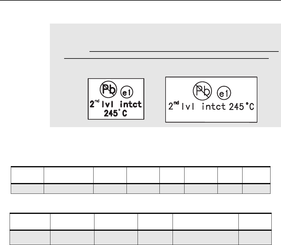
NOTE Environmentally Preferred Products (EPP) (refer to the marking on the printed circuit
boards — examples shown below) were developed and assembled using environmen-
tally preferred components and solder assembly techniques to comply with the Euro-
pean Union’s Restriction of Hazardous Substances (ROHS) Directive 2002/95/EC
and Waste Electrical and Electronic Equipment (WEEE) Directive 2002/96/EC. To
maintain product compliance and reliability, use only the Motorola specified parts in this
manual.
Table 2-2. Lead Free Solder Wire Part Number List
Motorola
Part Number Alloy Flux Type Flux Content
by Weight
Melting
Point
Supplier Part
number Diameter Weight
1088929Y01 95.5Sn/3.8Ag/0.7Cu RMA Version 2.7-3.2% 217C 52171 0.015” 1lb spool
Table 2-3. Lead Free Solder Paste Part Number List
Motorola Part
Number
Manufacturer Part
Number Viscosity Type Composition & Percent Metal Liquid
Temperature
1085674C03 NC-SMQ230 900-1000KCPs
Brookfield (5rpm)
Type 3
(-325/+500)
(95.5%Sn-3.8%Ag-0.7%Cu)
89.3%
217°C

Repair Procedures and Techniques — General 2-5
Chip Components
Use the RLN4062 Hot-Air Repair Station for chip component replacement. Adjust the temperature
control to 370°C (700°F), and adjust the airflow to a minimum setting. Airflow can vary due to
component density.
•To remove a chip component:
1. Use a hot-air hand piece and position the nozzle of the hand piece approximately 0.3 cm
(1/8") above the component to be removed.
2. Begin applying the hot air. Once the solder reflows, remove the component using a pair of
tweezers.
3. Using a solder wick and a soldering iron or a power desoldering station, remove the excess
solder from the pads.
•To replace a chip component using a soldering iron:
1. Select the appropriate micro-tipped soldering iron and apply fresh solder to one of the solder
pads.
2. Using a pair of tweezers, position the new chip component in place while heating the fresh
solder.
3. Once solder wicks onto the new component, remove the heat from the solder.
4. Heat the remaining pad with the soldering iron and apply solder until it wicks to the compo-
nent. If necessary, touch up the first side. All solder joints should be smooth and shiny.
•To replace a chip component using hot air:
1. Use the hot-air hand piece and reflow the solder on the solder pads to smooth it.
2. Apply a drop of solder paste flux to each pad.
3. Using a pair of tweezers, position the new component in place.
4. Position the hot-air hand piece approximately 0.3 cm (1/8”) above the component and begin
applying heat.
5. Once the solder wicks to the component, remove the heat and inspect the repair. All joints
should be smooth and shiny.

2-6 Notes For All Schematics and Circuit Boards
4.0 Notes For All Schematics and Circuit Boards
* Component is frequency sensitive. Refer to the Electrical Parts List for value and usage.
1. Unless otherwise stated, resistances are in Ohms (k = 1000), and capacitances are in picofarads
(pF) or microfarads (µF).
2. DC voltages are measured from point indicated to chassis ground using a Motorola DC multime-
ter or equivalent. Transmitter measurements should be made with a 1.2 µH choke in series with
the voltage probe to prevent circuit loading.
3. Reference Designators are assigned in the following manner:
700/900 Series = Transmitter
000/200 Series = Frequency Generation
400/600 Series = Receiver
1000/2000/3000 Series = Controller
6000 Series = Keypad Board
8000 Series = GPS
9000 Series = Switches and User Interfaces
4. Interconnect Tie Point Legend:
UNSWB+ = Unswitch Battery Voltage (7.5V)
SWB+ = Switch Battery Voltage (7.5V)
R5 = Receiver Five Volts
CLK = Clock
Vdda = Regulated 3.3 Volts (for analog)
Vddd = Regulated 3.3 Volts (for digital)
SYN = Synthesizer
DACRX = Digital to Analog Voltage (For Receiver Front End Filter)
VSF = Voltage Super Filtered (5 volts)
VR = Voltage Regulator
12-LAYER CIRCUIT BOARD DETAIL VIEWING
COPPER STEPS IN PROPER LAYER SEQUENCE
Figure 2-1: 12-Layer Circuit Board Detail Viewing
Solder mask
L1
copper foil + plated
Prepreg 1080x1
L2
copper foil + plated
Prepreg 1080x1
L3
copper foil + plated
Prepreg 1080x1
L4
0.5 oz
CORE 4mil(2116*1)
L5
0.5 oz
Prepreg 1080x1
L6
0.5 oz
CORE 4mil(2116*1)
L7
0.5 oz
Prepreg 1080x1
L8
0.5 oz
CORE 4mil(2116*1)
L9
0.5 oz
Prepreg 1080x1
L10
copper foil + plated
Prepreg 1080x1
L11
copper foil + plated
Prepreg 1080x1
L12
copper foil + plated
Solder mask
12-LAYER CIRCUIT BOARD DETAIL VIEWING
Buried
via
L3-
L10
PTH
1-12

Section 3
TEST EQUIPMENT AND SERVICE AIDS
1.0 Recommended Test Equipment
The list of equipment contained in Table 3-1 includes most of the standard test equipment required
for servicing Motorola portable radios.
Table 3-1. Recommended Test Equipment
Equipment Characteristics Example Application
Service
Monitor
Can be used as a substi-
tute for items marked with
an asterisk (*)
Aeroflex 2975
(www.aeroflex.com),
Motorola R2670, or equivalent
Frequency/deviation meter and
signal generator for wide-range
troubleshooting and alignment
Digital RMS
Multimeter *
100 µV to 300 V
5 Hz to 1 MHz
10 Mega Ohm Impedance
Fluke 179 or equivalent
(www.fluke.com)
AC/DC voltage and
current measurements. Audio
voltage measurements
RF Signal
Generator *
100 MHz to 1 GHz
-130 dBm to +10 dBm
FM Modulation 0 kHz to
10 kHz
Audio Frequency 100 Hz
to 10 kHz
Agilent N5181A
(www.agilent.com),
Ramsey RSG1000B
(www.ramseyelectronics.com), or
equivalent
Receiver measurements
Oscilloscope * 2 Channel
50 MHz Bandwidth
5 mV/div to 20 V/div
Leader LS8050
(www.leaderusa.com),
Tektronix TDS1001b
(www.tektronix.com),
or equivalent
Waveform measurements
Power Meter
and Sensor *
5% Accuracy
100 MHz to 500 MHz
50 Watts
Bird 43 Thruline Watt Meter
(www.bird-electronic.com) or
equivalent
Transmitter power output
measurements
RF Millivolt
Meter
100 mV to 3 V RF
10 kHz to 1 GHz
Boonton 92EA
(www.boonton.com) or equivalent
RF level measurements
Power Supply 0 V to 32 V
0 A to 20 A
B&K Precision 1790
(www.bkprecision.com)
or equivalent
Voltage supply
3-2 Service Aids
2.0 Service Aids
Table 3-2 lists the service aids recommended for working on the radio. While all of these items are
available from Motorola, most are standard workshop equipment items, and any equivalent item
capable of the same performance may be substituted for the item listed.
Table 3-2. Service Aids
Motorola
Part No. Description Application
RLN4460_ Portable Test Set Enables connection to the audio/accessory jack.
Allows switching for radio testing.
GMVN5141_ Customer Programming
Software on CD-ROM
Allows servicer to program radio parameters, tune
and troubleshoot radios.
PMKN4012_ Portable Programming Cable This cable connects the radio to a USB port for radio
programming and data applications.
PMKN4013_ Portable Programming, Testing &
Alignment Cable
This cable connects the radio to a USB port for radio
programming, testing and alignment.
PMNN4076_ 7.5V Universal Battery Eliminator Connects to radio via battery eliminator cable.
5880348B33 DMR SMA to BNC RF Adaptor Adapts radio’s antenna port to BNC cabling of test
equipment.
PMHN4085_ Bench Test Housing Eliminator Interconnects radio to power supply. Provides for
troubleshooting of the radio when the housing is
removed.
NLN9839_ Vacuum Pump Kit Allows servicer to test for leakages.
NTN4265_ Pressure Pump Kit Allows servicer to locate leakages.
5871134M01 Connector Fitting This connector allows the vacuum hose to be con-
nected to the radio chassis.
3271133M01 Fitting Seal This seal secures the connector fitting to the radio
chassis.
Programming, Testing and Alignment Cable 3-3
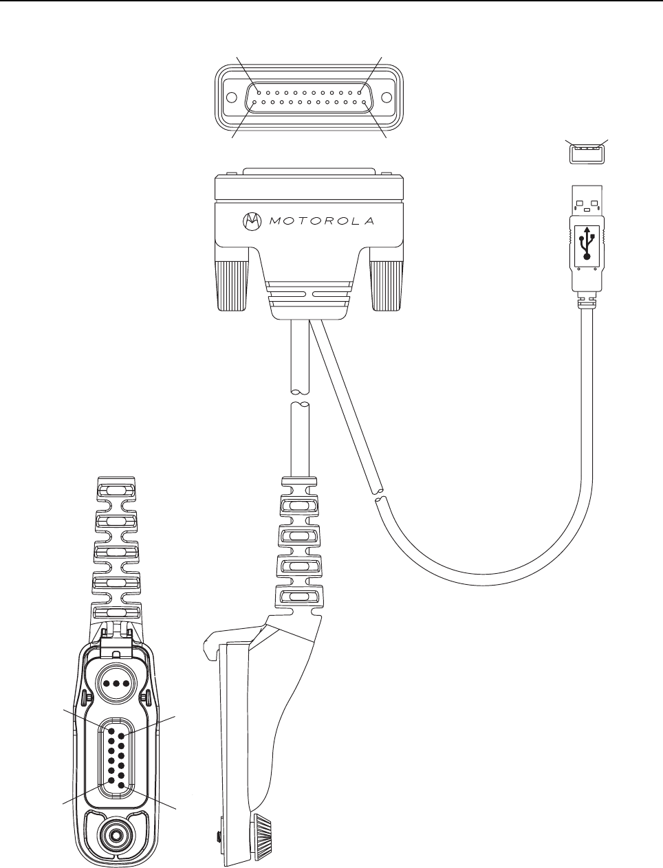
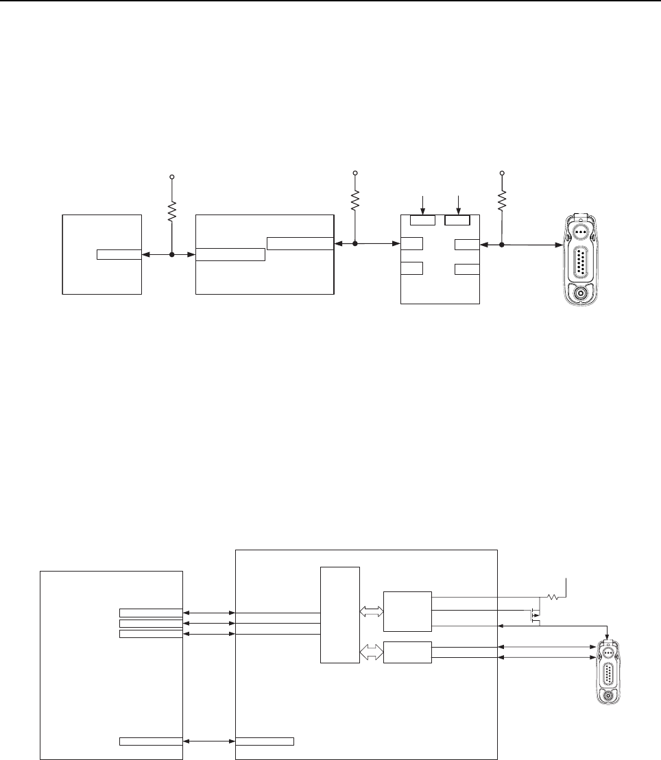
3.0 Programming, Testing and Alignment Cable
Figure 3-1. Programming, Testing and Alignment Cable
#1
#14
#25
#13
#4
#1
#2
#12
#11
#1
P1
P2
P3
3-4 Programming, Testing and Alignment Cable
Table 3-3. Pin Configuration of Side Connector
CONNECTION
P1 P2 P3
Pin Pin Pin Function
1 3 VCC (5V)
34DATA +
25DATA -
16 6 GROUND
78 SPEAKER -
17 10 EXTERNAL MIC +
16 11 EXTERNAL MIC -
20 9 EXTERNAL PTT
17 SPEAKER +
41
(Coax
Connector)
GROUND
Section 4
POWER UP SELF-TEST
1.0 Power-Up Error Codes (Display Model only)
Upon powering up, the radio performs certain tests to determine if its basic electronics and software
are in working order. Any error detected has an associated error code that is presented on the radio
display. These error codes are intended to be used by a service technician when the radio
generates the Self Test Fail Tone. If these tests are successfully completed, the radio will generate
the Self Test Tone.
There are two classes of detectable errors, fatal and non-fatal. If it is considered as a fatal error, then
the normal radio operation will be inhibited. Fatal errors include hardware errors detected by the
microprocessor and certain memory errors. These memory errors include incorrect ROM checksum,
incorrect RAM checksum, and incorrect checksums of codeplug (Persistent Storage) blocks that
contain operating parameters. If the codeplug block operating parameters are corrupted, operation
of the unit on the proper frequency, system, and group are in question. Attempts to use this
information could provide the user with a false sense of security that others are receiving his
messages. Corrupted codeplug blocks of call IDs, or their associated aliases are considered non-
fatal errors. While the user may be inconvenienced, normal communication is still possible.
Table 4-4. Power-Up Error Codes
Error Code Description Error Type Corrective Action
ERROR 01/02 Call ID or associated
aliases codeplug block
checksum is wrong.
Non-Fatal Normal communication is still possible, but the
user may be inconvenienced.
Reprogram codeplug.
ERROR 01/22 Tuning Codeplug block
checksum is wrong.
Non-Fatal Normal communication is still possible.
FAIL 01/82 External Codeplug block
checksum is wrong.
Fatal Reprogram codeplug.
FAIL 01/92 Secure Codeplug check-
sum error
Fatal Reprogram codeplug.
FAIL 01/A2 Tuning Codeplug block
checksum is wrong.
Fatal Reprogram codeplug.
FAIL 01/81 ROM Checksum is
wrong.
Fatal Reprogram FLASH Memory, then retest. If
message reoccurs, replace main board or
send radio to nearest Motorola Depot.
FAIL 01/88 Radio RAM Test Failure. Fatal Retest radio by turning it off and turning it on
again. If message reoccurs, replace main
board or send radio to nearest Motorola
Depot.
FAIL 01/90
or
FAIL 02/90
General hardware test
failure.
Fatal Retest radio by turning it off and turning it on
again. If message reoccurs, replace main
board or send radio to nearest Motorola
Depot.
4-2 Operational Error Codes
2.0 Operational Error Codes
During radio operation, the radio performs dynamic tests to determine if the radio is working properly.
Problems detected during these tests are presented as error codes on the radio’s display. The
presence of an error code should prompt a user that a problem exists and that a Motorola Authorized
MOTOTRBO dealer should be contacted. Use Table 4-5. to aid in understanding particular
operational error codes.
FAIL 02/81 DSP ROM Checksum is
wrong.
Fatal Reprogram FLASH Memory, then retest. If
message reoccurs, replace main board or
send radio to nearest Motorola Depot.
FAIL 02/82 DSP RAM1 test failure. Fatal Retest radio by turning it off and turning it on
again. If message reoccurs, replace main
board or send radio to nearest Motorola
Depot.
FAIL 02/84 DSP RAM2 test failure. Fatal Retest radio by turning it off and turning it on
again. If message reoccurs, replace main
board or send radio to nearest Motorola
Depot.
FAIL 02/88 DSP RAM test failure. Fatal Retest radio by turning it off and turning it on
again. If message reoccurs, replace main
board or send radio to nearest Motorola
Depot.
FAIL 02/C0 DSP ROM Checksum is
wrong.
Fatal Retest radio by turning it off and turning it on
again. If message reoccurs, replace main
board or send radio to nearest Motorola
Depot.
No Display Display module is not
connected properly.
Display module is dam-
aged.
Fatal Check connection between main board and
display module.
Replace with new display module.
NOTE A non-display radio emits only the Self Test Fail Tone if it fails the self-test.
Table 4-5. Operational Error Codes
Error Code Description Error Type Corrective Action
FAIL 001 Synthesizer Out-of-Lock NON-FATAL 1. Reprogram the codeplug.
2. Refer to Detailed Service
Manual.
FAIL 002 Personality checksum or
system block error
NON-FATAL Reprogram the codeplug.
Table 4-4. Power-Up Error Codes (Continued)
Error Code Description Error Type Corrective Action
Section 5
CONTROLLER INFORMATION
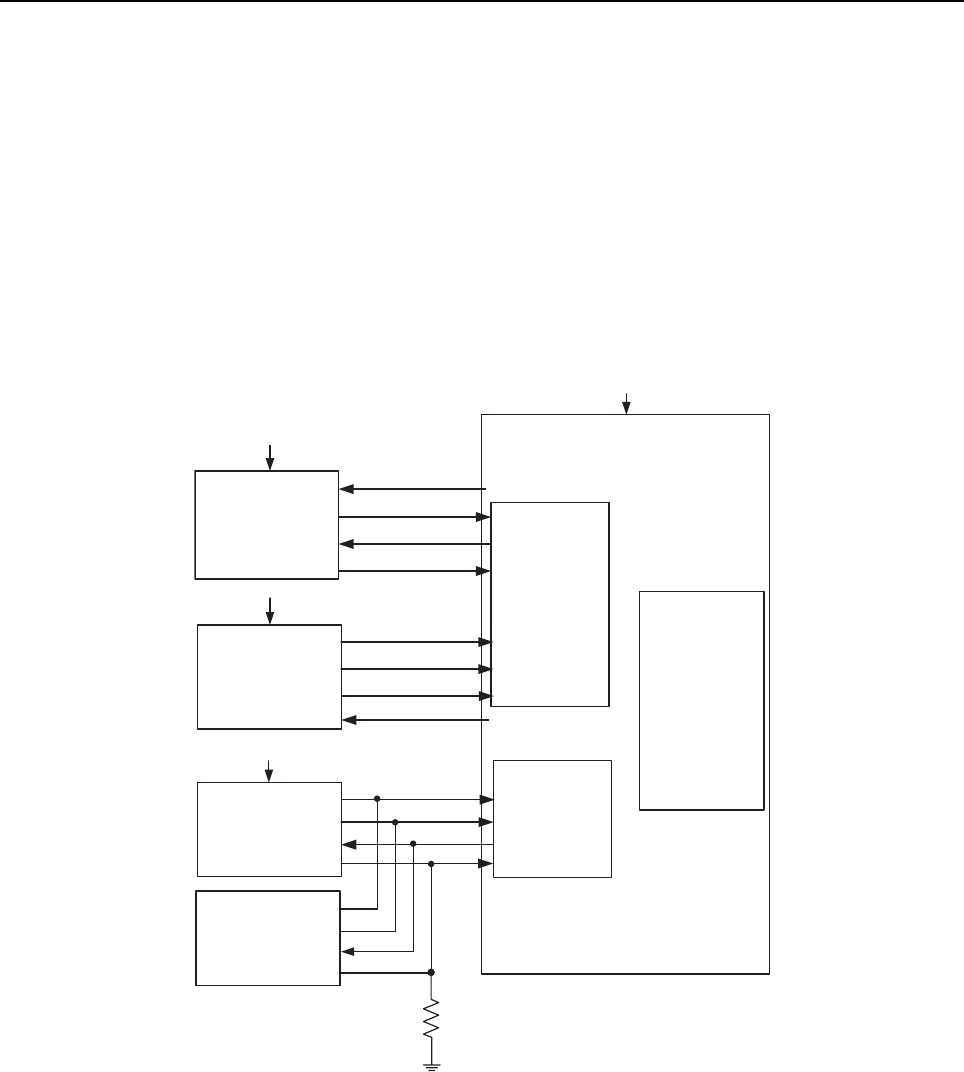
1.0 General Controller Block
The controller board is the central interface between the various subsystems of the radio. The
controller section consists of 4 main ICs. These are the OMAP1710 Host/DSP Processor, Flash,
SDRAM memories and the MAKO Audio/Power Management chip.
Figure 5-1 shows how the controller interfaces with the RF Section and the supporting controls,
switches and display. The Controller, RF sections, volume port, frequency selection switch and the
universal connector are placed on a single “Transceiver” board. LCD Display is mounted directly to
the Transceiver board and keypad is designed on the flex. The Option Board is a separate board that
hosts the line/connections to the flex keypad. The physical interface between the Transceiver board
and keypad board is via flex through board to board connector on the option board.
Figure 5-1: Controller Block Diagram
1.1 OMAP1710 Processor (U1000)
The OMAP processor (U1000) has a dual-core architecture which incorporates a TMS320C55x DSP
core and a high-performance ARM926EJS core. The OMAP is supplied with two voltages: 1.4V for
Core and 1.8V for Peripheral and I/O Interfaces.
OMAP1710
& ME MOR Y
DEVICE S
SPI SSI RF
LOGIC REF
CLK
MA K O
SPI
MCBSP2
LAYER 1
TIMER LIN
REG
SW
REG
CLOCK
PLL CODEC
MPUIO DAC
USB
TXCVR
MCBSP1
ON_OFF VOLUME
ON
Logic
ADC
AUD
AMP
MIC
AMP
OPTION BOARD
MCBSP1
INT_MIC
INT_SPK
TRANSDUCERS
ACCESSORY
INTER FACE
EXT_SPK
EXT_MIC
DATA
OPT. SEL
TUNE
OPT
SEL
LCD DISPLAY
LCD
CTRL
CONTROLLER
Numeric K eys
Navigation Keys
KEYPAD
USER BUTTONS & KNOBS
PTT & SIDE BUTTONS EMERGENCY
FREQ KNOB
VDD
SUPPLY
RF SECTION
B+ = 7.5V
MCBSP1
DATA
5-2 Controller Board
The OMAP processor controls the operation of the transmitter, receiver, synthesizer and MAKO IC. It
also uses Flash and SDRAM, both located externally.
1.2 Flash Memory (U2000)
The Flash memory IC is a 64Mbit CMOS device. It is supplied with 1.8V. The Flash memory has its 23
address lines and 16 data lines connected to the External Interface Module (EIM) of the OMAP IC
through the EMIFS_ADDR(23:1) and EMIFS_DATA(15:0) busses. The Flash memory contains host
firmware, DSP firmware, codeplug data, and tuning values.
1.3 SDRAM (U2001)
The Synchronous DRAM (SDRAM) is 128Mb high-speed CMOS device. It is designed to operate in
1.8V, low-power memory system. The SDRAM has 13 address lines and 16 data lines connected to
the EIM of OMAP IC through SDRAM_ADDR(12:0) and SDRAM_DATA(15:0) busses.
1.4 MAKO IC (U3000)
The MAKO IC handles DC power distribution and audio processing (i.e. audio amplification and
analog-to-digital/ digital-to-analog conversions). It contains Switching and Linear regulators, 1W audio
amplifiers, 16-bit Voice CODEC, 11-channel 10-bit A/D Converter, 10 bit D/A Converter, support
2xUSB “OTG” transceivers, One-Wire Option Detect, and GCAI ports.
2.0 Controller Board
2.1 Radio Power Distribution
Figure 5-2: DC Power Distribution Block Diagram
Figure 5-2 illustrates the DC distribution to various ICs and devices in the radio. The power
management architecture is centered on the MAKO IC (U3000). A battery supply is routed via a 3A
fuse (F9000) which goes directly to the electronic ON/OFF control (PMOS power FET Q3003) as
RF PA, RF DRIVER, ANTENNA SWITCH
LCD, 32kHz SQUARER CKTs, LEVEL
TRANSLATOR (GPS), TOMAHAWK DIG
CKTs
KEYPAD LEDS - 8x
DISPLAY BACKLIGHT LEDS - 2x
RED & GRN LEDs, OPTION BOARD
1.875V_DIG_V2
MAKO DC REGULATORS
RAW_B+
SIDE CONNECTOR PULL-UPs, RED & GRN
LEDs, VBUS SUPPLY ENABLED
V6 ( 50mA @ 2.9V )
(2.775, 2.9V)
V8 ( 25mA @ 5.0V )
2.8V_ANA_V7
CHARGE PUMP OF ABACUS &
TOMAHAWK, POWER CONTROL,
REGULATOR FOR TX_VCO, TX_BUFFER,
RX_VCO, RX_BUFFER
MAKO A/D REFERENCE VOLTAGE, VOL,
HW_ID, LEVEL TRANSLATOR (1-WIRE)
MOS
SW
V7 ( 100mA @ 2.8V )
OMAP EIMFS & EIMFF (FLASH & SDRAM),
LCD, OMAP1710 PERIPHERAL PLUS PTT/
EMERG_PB/ RED & GRN LEDs/ FREQ SW
PULL-UPs, 32kHz SCHMITT TRIGGER CKTs,
TOMAHAWK CORE & I/O, ABACUS I/O
TOMAHAWK ANALOG CKT, LNA, MIXER
ANALOG CKTs, ABACUS CORE & DIG
CKTs
2.775V_DIG_V4
5V_ANA_V8
FET_EN
SWB+
PGLDO3
PGLDO2
BAT_TYPE
BAT_7V5
5V_ANA_VBUS1
SW1 ( 800mA @ 3.6V )
(with External FETs + Drivers)
V3 (150mA @ 1.3V )
(1.1, 1.2, 1.3, 1.4, 1.5, 1.55, 1.6V)
SW2 (300mA @ 2.3V )
VBUS2 ( 500mA @ 5.0V )
(with External Pass xistor)
3.3V_DIG_V10
VSW5 ( 800mA @ 5.2V )
(with External FETs + Drivers)
SIDE ACCESSORY VBUS
5V_ANA_VBUS2
OMAP CORE
GPS RTC
GPS DIG
GPS RF
LEVEL TRANSLATOR (1-WIRE), TX
PRE_DRIVER
7.5V BATTERY
IGN_X
SW_TYPE
3.6V Switcher @ 600mA
V2 (120mA @ 1.875V )
(1.55, 1.7, 1.8, 1.875, 1.9V)
V4 ( 100mA @ 2.775V )
V10 ( 70mA @ 3.3V )
V9 ( 50mA @ 3.0V )
(2.8, 3.0, 3.3V)
VBUS1( 500mA @ 5.0V )
(with External Pass xistor)
ON_OFF Switch
1.4V Switcher @ 600mA
1.5V LDO @ 0.15A
2.8V LDO @ 0.1A
2.8V LDO @ 0.1A
5.6V LDO @ 1A
SWB+
2.9V_DIG_V6
2.3V LDO @ 0.32A
BPLUS
AUDIO_PA
VSAVE
3A FUSE
(MECH_SW)

Controller Board 5-3
RAWB+. When the radio is turned ON, MECH_SW (ON/OFF/volume control) will trigger the MAKO
FET_ENX to low thus turning ON the PMOSFET device, and SWB+ is then distributed as shown in
Figure 5-2. SWB+ will continue to support the whole board until the radio is turned OFF.
2.1.1 Voltage Regulation
• Switcher U3020
Switcher (U3020) in conjunction with the MAKO power management IC (U3000) is a highly efficient
dc-dc buck converter. External components L3020 and C3202 are needed to filter out the dc-dc
converter output. In this application, it is configured as a Pulse Skipping Mode (PSM) with maximum
output current of 600mA. It generates an accurate 3.6V output, which supplies directly to the MAKO
internal VSW2 switcher circuit as well as other MAKO internal LDOs.
• Switcher U3021
Switcher (U3021) is a highly efficient dc-dc buck converter and same as switcher U3020. It is used
solely for OMAP processor core.
• Low Drop Out (LDO) Regulator U3008
LDO regulator (U3008) is an adjustable output voltage regulator which can supply 200mA load
current. It has an excellent Ripple Rejection Ratio and Short Circuit Protection. In this application,
LDO U3008 output is 2.3V which is set by the resistor divider R3028 and R3029. It supplies directly to
MAKO internal LDOs.
• Low Drop Out (LDO) Regulator U3002
LDO regulator (U3002) is an adjustable output voltage regulator which can supply 1A load current. In
this application, LDO U3002 generates an accurate 5.6V output which is set by the resistor divider
R3017 and R3018. It supplies directly to both VBUS1 and VBUS2 supplies. Q3005 and Q3006
prevent internal voltage leakage onto VBUS_SUPPLY (U3002 pin 5).
• MAKO LDO VBUS1
VBUS1 is a voltage regulation module that can be used to provide 5V with either 50mA or 500mA
load current suited for accessory and USB supply. Q3001 and Q3002 are used to control the low
current limit (50mA) or high current limit (500mA) of Vbus1.
When USB_CONNECT is toggled LOW, the PMOSFET (Q3001) is disabled and this will limit the max
load supply to 50mA. If a high current limit is desired, i.e. USB HOST mode, USB_CONNECT is
toggled HIGH turning ON the PMOSFET (Q3001) through Q3002 inverter, and this will limit the max
load supply to 500mA.
• MAKO LDO VBUS2
VBUS2 is a voltage regulation module that can be used to provide 5V and with only 500mA load
current. This supply is used for PA Pre-driver.
• MAKO LDOs
The MAKO power management IC (U3000) provides eight more LDOs. Some LDOs are
programmable to meet the requirement of various ASIC devices. V2, V3, and V9 are programmable
via SPI while V4, V5, V6, V8, and V10 are fixed. See Figure 5-2 for details.
5-4 Controller Board
2.1.2 Power ON/OFF
The radio can be switched ON in only one condition:
1. MECH_SW turned ON
Turning the rotary switch (S9001) ON will cause MAKO (U3000) to turn ON SWB+. After application
of power to SWB+, MAKO regulators are sequenced to turn ON power to all MAKO internal blocks
and external system including OMAP processor (U1000), FLASH (U2000), SDRAM (U2001), and
radio RF section.
Radio can be turned OFF in one of the three conditions:
1. MECH_SW turned OFF
If the radio is manually turned OFF, MAKO (U3000) will start a 125ms watchdog timer. The OMAP
processor (U1000) may tickle the watchdog timer as needed to keep DC power ON as it shuts down
the radio. Once the watchdog timer expires, MAKO turns OFF the DC regulators and SWB+.
2. Low Battery
While the radio is ON, if battery voltage drops to low level threshold, OMAP processor (U1000) will
initiate a shutdown process. It will store the radio personality data to the FLASH (U2000) before
turning OFF.
3. Thermal Shutdown
Hard and Soft limits for thermal shutdown are implemented into MAKO IC (U3000). When MAKO die
temperature reaches Soft Thermal Limit (135 °C), microprocessor will be interrupted to begin
shutdown procedures. If Hard Thermal Limit (155 °C) is reached before OMAP processor (U1000)
can finish shutdown tasks, the radio will turn OFF immediately.
2.2 Clocks
Figure 5-3 illustrates the controller clocks used throughout the radio.
Figure 5-3: Clock Connections
MPU CLK
EXT_CLK (N18)
CLK32K_IN (P13)
OSC_IN (Y2)
OSC_OUT (W3)
OSC32K_IN (V13)
OSC32K_OUT (AA13)
SYS_CLK_IN (Y4)
DPLL1
General Pupose
TIMER
ARX DAC
XOSC BASE
CLK2 OUT
16.8 MHZ
TCXO
+0.5 ppm (GPS & CPHER)
+1.5 ppm (NONGPS)
FREF
24.576MHZ 32.768KHZ
XOUT XIN XTAL32_OUTXTAL32_IN
+20 ppm+30 ppm
TOMAHAWK
U001
ABACUS III
U600
MAKO
U3000
REF_CLK
LOW_REF_CLK
SiRF GPS
U8000
xN
DSP CLKxN
TC CLKxN
12MHZ
+20 ppm
1.4V
10K
OMAP1710
U1000
U1006
U3003
U3004
32.768 KHz
Y3000Y3001
VSS_11 (Y13)
OMAP 3.3 Core
Y1000
+20 ppm
Y8000
32.768KHZ
RTC_XO
RTC_XI
Controller Board 5-5
The OMAP processor (U1000), which consists of an ARM and DSP core, needs three clocks for
operation: a 32.768kHz square-wave, a 12MHz sine-wave, and a 16.8MHz square-wave clock.
The 16.8MHz clock source is provided from the Tomahawk TCXO routes to a squarer-circuit (U1006)
and feed to EXT_CLK (U1000 pin N18).
The 32.768kHz clock is generated by the MAKO crystal (Y3000) oscillator, converted to a gated clock
by U3003 and U3004 circuitry. It is then directly fed to OMAP CLK32_IN (U1000 pin P13). The OMAP
processor needs the 32.768kHz to determine the input reference clock applied to OSC_IN (U1000 pin
Y2). Without this 32kHz clock, the OMAP will potentially program all the wrong dividers for USB and
UART booting. External pull-up on OSC32K_IN (U1000 pin V13) and grounding both OSC32K_OUT
(pin AA13) and VSS_11 (pin Y13) indicates that an external 32kHz clock is used.
The 12MHz sine-wave is the main system reference clock for the OMAP which all the internal clocks
are derived from.
The 24.576MHz crystal (Y3001) oscillator is the reference clock for MAKO CODEC and SSI clock. `
2.3 Serial Peripheral Interface (SPI)
Figure 5-4 illustrates the controller SPI used throughout the radio.
Figure 5-4: SPI Connections
The OMAP processor (U1000) has two SPI busses that it uses to communicate with the various
peripheral IC’s. The first is the High Performance Data (HPD) SPI bus and the second is the multi-
media card (MMC) SPI.
HPD SPI
TOMAHAWK
U001
1.8V
CEX
SPI_DW
SPI_DR
SPI_CLK
ABACUS III
U600
PE
PD
DOUTB
PC
MAKO
U3000
SPI_CS
SPI_CLK
SPI_DO
GPIO_44 (P15)
SPIF.DOUT (W21)
SPIF.DIN (U18)
SPIF.SCK (U19)
GPIO_9 (Y8)
GPIO_58 (R11)
SPI_DI
OMAP1710
U1000
MMC1 SPI
SPI.CS1 (P19)
SPI.CLK (M14)
MMC.CMD (P11)
SPI.RDY (R18)
SPI.CS2 (P20)
SPI.CS3 (P18)
1.8V
1.8V
47K
1.8V
SPI_CLK
SPI_MOSI
SPI_MISO
THK_CE
MAKO_CE
ABACUS3_CE
R3023
5-6 Controller Board
The HPD SPI is a synchronous serial bus made up of four lines, SPI_CLK, SPI_MOSI, SPI_MISO,
and chip select. The SPI_CLK line is used to control the speed of the data to/from the peripheral IC’s
and the OMAP processor. This clock can be adjusted to different speed based on the IC’s
specification.
HPD SPI module is used to interface to Tomahawk (U001), Abacus III (U600), and the MAKO
(U3000). This interface operates at 1.875V logic level. SPI_MOSI, or commonly known as
TRANSMIT Data, is a data string from OMAP while SPI_MISO or RECEIVE Data is data string to the
OMAP.
The MMC SPI is not used in portable radio.
2.4 Serial Synchronous Interface (SSI)
Figure 5-5 illustrates the controller SSI used in the radio controller design.
Figure 5-5: SSI Connections
The OMAP processor (U1000) has a total of three SSI or multi-channel buffer serial ports (McBSP)
modules that are used to directly interface to the CODECs in the Tomahawk, Abacus, and MAKO, as
well as command/ data connections to the Option Board, and between Tx and Rx radios within a
Repeater.
As shown in Figure 5-5, McBSP1 is a 4-wire bus and interface to the MAKO CODEC as well as the
Option Board. McBSP2 is 6-wire bus; 3-wire dedicated to the Tomahawk Tx audio and the other 3-
McBSP2
TOMAHAWK
U001
1.8V
DMCS
SDTX
SFTX
TXCLK
ABACUS III
U600
DOUTA
FS
CLKOUT
MAKO
U3000
VC_TX
VC_DCLK
VC_FSYNC
GPIO_2 (D15)
McBSP2.DX (AA5)
McBSP2.FSX (W7)
McBSP2.CLKX (Y6)
VC_RX
OMAP1710
U1000
McBSP3.DR (T19)
McBSP3.CLKX (N14)
McBSP3.DX (P14)
McBSP3.FSX (AA17)
1.8V
1.8V
10K
1.8V
McBSP2.DR (P10)
McBSP2.FSR (W6)
McBSP2.CLKR (V7)
McBSP1
McBSP1.DX (H18)
McBSP1.CLKX (G21)
McBSP1.DR (H20)
McBSP1.FSX (H15)
McBSP3
OPTION
BOARD I/F
J9001
VC_TX
CLK
FSYNC
VC_RX
SYNCB GPIO_40 (W15)
R3010
Controller Board 5-7
wire to Abacus Rx audio. McBSP3 is a 4-wire bus, and used primarily to interface between Tx and Rx
radios within a Repeater.
2.5 ACC_ID Interface
Smart accessories use the Accessory ID (ACC_ID) Interface to help the radio determine which smart
accessory, if any, are attached to the radio. Figure 5-6 illustrate the ACC_ID connections used within
the radio.
Figure 5-6: ACC_ID Interface Connections
2.6 USB Interface
The OMAP processor (U1000) supports two USB ports. The radio makes use of one USB port to
communicate with smart accessories, and connection to a host computer for radio programming via
CPS and tuning via Tuner Tool.
Note: The USB ports are designed to support Motorola accessories only and will not support third
party “Plug-n-Play” USB devices.
Figure 5-7 shows the details of the HSSI connections within the radio.
Figure 5-7: USB Interface Connections
The OMAP processor USB host controller communicates with accessories at either 1.5 Mbps or 12
Mbps data rates depending on the accessory. The USB port can be used as a host or a device.
MAKO
U3000
ACC_ID (P9)
2-BitTranslator
U3009
2.9V
Vref1 Vref2
2.9V 5V
SCL1
SDA1
SCL2
SDA2
5V
OMAP1710
U1000
HDQ (N20) ACC_ID_UP (L7)
R3041
R3040
R3024
1.875V
Vbus1
Monitor
USB1
Transceiver
3/6 Wire
IF and
SPI
Registers
DP (N6)
DM (P7)
USB1_OE (B08)
USB1_SE0 (D08)
USB1_DAT_TXD (C08)
Mako
OMAP 1710
VBus1_Sens (E12)
VBus1 (H10)
VBus1_ Cmd (C14)
D+
D-
VBus
R3103 + R3102
USB1_TXEN (W16)
USB1_DAT (W14)
USB1_SE0 (R13)
USB_INT (L15) USB_INTX (C10)
Q3000
VBUS SUPPLY

5-8 Controller Board
In the portable radio, only one of the two MAKO USB transceivers is used to provide the physical
layer signaling for the USB port. The transceiver generates and receives the DP and DM differential
signals of the port. The MAKO transceiver interfaces to the OMAP processor through a three-wire
interface consisting of two bi-directional signals (SE0 and DAT), and one uni-directional signal
(TXEN). The MAKO also includes a Vbus monitor that senses the connection or removal of a device
and determines whether or not to supply current to that device via Q3000 up to a high current limit of
500mA.
The USB host/device mode assignment is determined when a user attaches a USB device to the port.
The accessory contains information about what the USB mode assignment should be, this
information is sent to the radio via the ACC_ID. See section 2.5 on page 5-7 for more details on the
ACC_ID implementation. When configured as a host, VBUS is turned ON by MAKO and set to high
current limit, when configured as a device, VBUS will be shut OFF and the external host supplies the
VBUS power.
2.7 Universal Connector (Side Connector)
The universal connector is located on the side of the radio. It is the external port of interface used for
programming and interfacing to external accessories. The universal connector is connected to the
main board via a flex through option board. This radio UC is a newly defined Motorola accessory port
that contains audio, digital I/O, serial interfaces, and accessory supply lines; and is similar in function
to Motorola’s legacy microphone connectors. The multiplexing of these functions is handled by
circuitry internal to the MAKO (U3000).
The UC includes 2 serial interfaces: an USB port and an ACC_ID interface. The USB port can be
used as either a device (radio is device) or as a host (radio is host). When configured as a device, the
radio can be programmed using the MOTOTRBO CPS or tuned using the Tuner software. When
configured as a host, various smart accessories can be used with the radio. See section 2.6 on page
5-7 for more information on the USB interface.
The ACC_ID interface is used by accessories to provide the radio with information needed to
configure the interface for that accessory. See section 2.5 on page 5-7 for more information on the
ACC_ID interface.
Note: The USB port is designed to support Motorola accessories only and will not support third
part “Plug-n-Play” USB devices.
2.8 Keypad Module
The keypad module is connected to the main board through option board. This unit is not considered
field-repairable. The keypad interface is a standard pulsed 4 row by 4 column configuration controlled
directly by the OMAP processor (U1000). Each of the 4 column output lines is toggled high in
sequence and the 4 row input lines are monitored to detect if a button has been pressed. The OMAP
processor then decodes which button was pressed using the appropriate column and row stimulus
and response information.
2.9 Display Module
This display is Film-compensated Super Twisted Nematic (FSTN), 132x34 pixel dot matrix with
transflective mode and yellow-green LEDs backlighting Liquid Crystal Display (LCD) module custom
to Motorola.
This display module is constructed of glass by sandwiched with polarizers, TAB (Tape Automated
Bonding) IC driver, LED backlighting, display control circuitry flex with 16-lines receptacle connector
connected to the main board display connector (P9000). The LED and backlights are controlled via
serial connection with OMAP processor (U1000). The serial interface consists of clock, data, and chip
select lines that are connected directly from the OMAP processor.
Controller Board 5-9
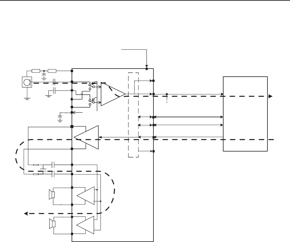
2.10 Audio
The audio circuitry consists of both analog and digital audio paths. Figure 5-8 shows the basic block
diagram of the audio interconnections.
Figure 5-8: Audio Block Diagram
2.10.1 Receive Audio
The receive audio data comes from the ABACUS III IC (U600) to the OMAP McBSP2 pin. The DSP
decodes the data and sends it out through SSI lines to MAKO SSI pin. The SSI bus is comprised of
four lines: clock, frame sync, Rx data, and Tx data. These four lines provide data to the MAKO
(U3000) using a packet frame structure consisting of four slots. The actual audio data is transferred to
the MAKO in the first slot of each frame using 16-bit pulse-code modulated PCM audio. The MAKO
codec filters and converts the digital data into an analog audio signal, and this signal is sent to a
programmable gain amplifier. The analog audio circuitry routes the audio to the internal or external
port.
PA
EXT_SPKR_P
PA_IN_P
PA_IN_M
C2
LSPKext
LSPKint
EXT_SPKR_M
INT_SPKR_P
INT_SPKR_M
Cf
Rf
Rf
INT_MIC_P
ADC
INT_MIC_M
EXT_MIC_P
EXT_MIC_M
VCM1
LESCIM
DAC
VC_OUT_P
VC_OUT_M
MIC BIAS
VC_DCLK
VC_FSYNC
VC_TX
VC_TX3V
VC_RX
MAKO
PA
INT_MIC_P
INT_MIC_M
MIC BIAS
1.0uF
1.0uF
0.1uF
68nF
22nF
330ohm
Base-Band
Processor
UCM_SS
D
D
V_
CI
G
OL
V02_O(1.875V) for OMAP
V06(2.9V) for Patriot
DIN
CLK
SYNC
DOUT
10k TX
RX

5-10 Controller Board
2.10.2 Transmit Audio
Transmit audio can be sourced from either internal or external microphone path. Both the internal and
external microphone carries a 5V bias through a resistor to MAKO MIC_BIAS pin. The MAKO,
through SPI, selects the appropriate microphone path to route to the necessary gain stages and
converter that will send 16-bit PCM audio to the OMAP for signal processing via the SSI bus.
The transmit gain stages in the MAKO is calibrated based on an 8mV input under standard test
conditions. The microphone sensitivity is programmable through the use of CPS.
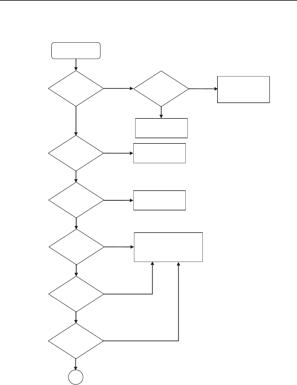
5-11
2.11 Troubleshooting Charts
MCU
Power Up
Alert Tone
OK?
YES Read Radio
OK?
Check USB
circuitry and
setup
Reprogram
correct data
Volume
knob
function?
NO
Speaker
OK?
Check volume
knob circuitry
NO
YES
Replace
Speaker
NO
Int & Ext
Spkr short to
Gnd?
YES
Check Speaker
circuitry, if no problem,
replace MAKO
YES
NO
Termination
short
together?
NO
YES
Spkr contact
voltage
=3V?
NO
YES
A
YES
NO
Troubleshooting Flow Chart for Controller
(Sheet 1 of 2)
5-12
A
YES
MAKO
regulator o/p
programmed?
1.4V at
R1020?
YES
Check regulator
U3201
NO
YES
16.8MHz at
C1032?
YES
C1018
=12MHz?
Check TOMAHAWK
16.8MHz circuitry
NO
C1019=
12MHz?
NO
C3001
=32.768KHz?
Replace
U3003
YES
C3000
=32.768KHz?
NO
Replace
Y3000
YES
NO
Replace
MAKO
Replace
Y1000
NO
YES
YES
Replace
OMAP
R1048=
32.768MHz?
YES
NO
NO
Troubleshooting Flow Chart for Controller
(Sheet 2 of 2)
Controller Schematics 5-13
2.12 Controller Schematics
RF
CONTROLLER
SYNCB
THK_CE
TX_CLK
TX_DAC
TX_DATA
TX_FSYNC
ADAPT_SW
ANT_EN
DEEP_SLEEP
DMCS
GPS_ANT
LOCK_DETECT
PA_TEMP
+BWAR
RESET_OUT
RX_CLK
RX_DATA
RX_FLTR_VCTRL
RX_FSYNC
SPI_CLK
SPI_MISO
SPI_MOSI
2V_GID_V578.1
16.8_MHZ_BUFF
16_8MHz_GPS
7V_ANA_V577.2
4V_GID_V577.2
8V_ANA_V5
2SUBV_ANA_V5
ABACUS3_CE
TX_DATA
TX_FSYNC
USB1_DM
USB1_DP
1SUBV
LOV
RX_CLK
RX_DATA
RX_FLTR_VCTRL
RX_FSYNC
SPI_CLK
SPI_MISO
SPI_MOSI
1WS
2WS
4WS
8WS
+
BWS
SYNCB
THK_CE
TX_CLK
TX_DAC
CNYSF_OKAM
XR_OKAM
XT_OKAM
WS_HCEM
ONE_WIRE_1
OPTA_SEL0
OPTA_SEL1
OPTA_SEL2
1_OIPG_TPO
2_OIPG_TPO
CNYS_ISS_TPO
PA_TEMPPTT
+BWAR
DEL_DER
RESET_OUT
JTAG_TCK
JTAG_TDI
JTAG_TDO
JTAG_TMS
KEYPAD_COL0
KEYPAD_COL1
KEYPAD_COL2
KEYPAD_COL3
KEYPAD_COL4
KEYPAD_ROW0
KEYPAD_ROW1
KEYPAD_ROW2
KEYPAD_ROW3
KEYPAD_ROW4
LOCK_DETECT
KLCD_OKAM
GPS_BOOT
GPS_ON_OFF
GPS_RFPWRUP
GPS_RX
GPS_TX
GPS_nRESET
GPS_nWAKEUP
DEL_NEERG
INT_MIC+
INT_MIC-
INT_SPKR+
INT_SPKR-
JTAG_NEMU0
JTAG_NEMU1
JTAG_NTRST
JTAG_RTCK
DISPLAY_CE
DISPLAY_CMD
DISPLAY_DATA0
DISPLAY_DATA1
DISPLAY_DATA2
DISPLAY_DATA3
DISPLAY_DATA4
DISPLAY_DATA5
DISPLAY_DATA6
DISPLAY_DATA7
DMCS
BP_GREME
EXT_MIC+
EXT_MIC-
EXT_SPKR+
EXT_SPKR-
16.8_MHZ_BUFF
7V_ANA_V577.2
4V_GID_V577.2
SPG_GID_V8.2
SPG_FR_V8.2
6V_GID_V9.2
01V_GID_V3.3
1WSV_GID_V6.3
8V_ANA_V5
2SUBV_A
NA_V5
ABACUS3_CE
ADAPT_SW
ANT_EN
ATAD_TTAB
BL_EN
DEEP_SLEEP
CTR_SPG_V5.1
2V_GID_V578.1
7
V
_
ANA_V577.2
2.775V_ANA_V7
16.8_MHZ_BUFF
2
V
_
GID_V578.1
1SUBV
GPS_ANT
RESET_OUT
RESET_OUT
C
TR_SPG_V5.1
GPS_BOOT
GPS_RFPWRUP
GPS_nWAKEUP
CNYS_ISS_TPO
SYNCB
S
P
G
_
G
I
D_V8.
2
SPG_FR_V8.2
+BW
S
5V_ANA_VBUS2
5V_ANA_VBUS2
DMCS
DISPLAY_DATA7
DISPLAY_DATA6
DISPLAY_DATA5
DISPLAY_DATA4
DISPLAY_DATA3
DISPLAY_DATA2
DISPLAY_DATA1
DISPLAY_DATA0
DISPLAY_CMD
DISPLAY_CE
DEEP_SLEEP
BL_EN
ATAD_TTAB
ANT_EN
ADAPT_SW
ABACUS3_CE
5V_ANA_V8
0
1
V
_
G
I
D_V3.
3
6V_GID_V9.2
4V_G
I
D_V577
.
2
KEYPAD_ROW4
KEYPAD_ROW3
KEYPAD_ROW2
KEYPAD_ROW1
KEYPAD_ROW0
KEYPAD_COL4
KEYPAD_COL3
KEYPAD_COL2
KEYPAD_COL1
KEYPAD_COL0
JTAG_TMS
JTAG_TDO
JTAG_TDI
JTAG_TCK
JTAG_RTCK
JTAG_NTRST
JTAG_NEMU1
JTAG_NEMU0
INT_SPKR-
INT_SPKR+
INT_MIC-
INT_MIC+
D
E
L
_
NE
ERG
GPS_TX
GPS_RX
GPS_nRESET
GPS_ON_OFF
EXT_SPKR-
EXT_SPKR+
EXT_MIC-
EXT_MIC+
BP_G
R
E
M
E
SPI_MISO
SPI_CLK
RX_FSYNC
RX_FLTR_VCTRL
RX_DATA
RX_CLK
D
EL
_DER
PTT
PA_TEMP
2_OI
P
G
_TP
O
1_OI
P
G
_TP
O
OPTA_SEL2
OPTA_SEL1
OPTA_SEL0
ONE_WIRE_1
W
S
_HC
E
M
LOCK_DETECT
16_8MHz_GPS
LOV
USB1_DP
USB1_DM
K
LCD
_O
KA
M
XT
_
OK
AM
XR
_
O
KAM
CNY
S
F_
O
K
A
M
RAWB+
TX_FSYNC
TX_DATA
TX_DAC
TX_CLK
THK_CE
8
W
S
4WS
2W
S
1WS
SPI_MOSI
Complete Controller Schematic Diagram
5-14 Controller Schematics
ROTINO
M
/ 4WS
TCA_LENNAHC / 8WS
ANE_CIM_DDA_CILBUP / 4LOC_DAPYEK
7_5PG /
N
E_LB
RED_LED / RX_ATTN_1
6_5PG / 4WOR_DAPYEK
A_LO
V
/
1
W
S
GREEN_LED / PA_ENABLE
MICROCONTROLLER
B_L
O
V /
2
WS
MAKO
draoB noitpO oT
USB2_TXEN
USB2_VM
USB2_VP
USB_INT
SYNCB
THK_CE
TX_CLK
TX_DATA
TX_FSYNC
USB0_DAT
USB0_SE0
USB0_TXEN
USB1_DAT
USB1_SE0
USB1_TXEN
USB2_DAT
USB2_RCV
USB2_SE0
USB2_SUSPEND
ONE_WIRE_UP
1_OIPG_TPO
2_OIPG_TPO
POR
PTT
RESET_OUT
RS232_RX
RS232_TX
RX_CLK
RX_DATA
RX_FSYNC
KLC_LAIRES
ATAD_LAIRES
SPI_CLK
SPI_MISO
SPI_MOSI
MAKO_DCLK
MAKO_FSYNC
MAKO_GPIO_RX
MAKO_GPIO_TX
MAKO_INT
0OIPG_TPO_OKAM
2OIPG_TPO_OKAM
3OIPG_TPO_OKAM
MAKO_OPT_INT
MAKO_RX
MAKO_TX
MCBSP3_DR
MCBSP3_DX
MCBSP3_FSX
DMC_YALPSID_HPROM
OMAP_CORE_LTC
KCT_GATJ
IDT_GATJ
ODT_GATJ
SMT_GATJ
0LOC_DAPYEK
1LOC_DAPYEK
2
LOC_DAPYEK
3LOC_DAPYEK
0WOR_DAPYEK
1WOR_DAPYEK
2WO
R_DAPYEK
3WOR_DAPYEK
SC_DEL
LOCK_DETECT
LOW_LEVEL_MUTE
MAKO_AD_TRIGGER
MAKO_CE
GPIO_45
GPIO_60
TOOB_SPG
FFO_NO_SPG
XR_SPG
NWODTUHS_SPG
XT_SPG
TESERn_SPG
PUEKAWn_SPG
I2C_CLK
I2C_DATA
0UMEN_GATJ
1
UM
E
N_GATJ
TSRTN_GATJ
KCTR_GATJ
2ATAD_YALPSID
3AT
A
D
_
Y
A
L
PSI
D
4AT
A
D
_
Y
A
L
PSI
D
5
A
TAD_YALPSID
6ATAD_YALP
SID
7ATAD_YALPSID
DMCS
EXT_MIC_ENA
PAMO_ZHK23_DETAG
8_5PG
GPIO_15
72_OIPG
3_OIPG
03_OIPG
13_OIPG
23_OIPG
33_OIPG
2.8V_DIG_GPS
3.3V_DIG_V10
ABACUS3_CE
ADAPT_SW
ANT_EN
51_OIMRA
ARMIO_2
3_OIMRA
AUDIO_PA_ENA
DEEP_SLEEP
LRTC_RID
EC_YALPSID
DMC_YALPSID
SC_YALPSID
0
ATA
D
_
Y
A
L
PSI
D
1ATAD_YALPSID
1.55V_DIG_V3
1.875V_DIG_V2
FFUB_ZHM_8.61
2.775V_DIG_V4
USB1_DM
USB1_DP
USB1_SE0
USB1_TXEN
USB_INT
1SUBV
VOL
OPTA_SEL2
PA_TEMP
POR
+BWAR
RS232_RX
RS232_TX
RX_FLTR_VCTRL
SPI_CLK
SPI_MISO
SPI_MOSI
+BWS
TX_DAC
USB0_DAT
USB0_SE0
USB0_TXEN
USB1_DAT
MAKO_FSYNC
MAKO_INT
0OIPG_TPO_OKAM
2OIPG_TPO_OKAM
3OIPG_TPO_OKAM
MAKO_OPT_INT
MAKO_RX
MAKO_TX
MECH_SW
MMP_GPIO1_INPUT
MMP_GPIO2_INPUT
OMAP_CORE_LTC
ONE_WIRE_1
ONE_WIRE_UP
OPTA_SEL0
OPTA_SEL1
EMERG_PB
EXT_MIC+
EXT_MIC-
EXT_SPKR+
EXT_SPKR-
GATED_32KHZ_OMAP
PURWPFR_SPG
NWODTUHS_SPG
PUEKAWn_SPG
INT_MIC+
INT_MIC-
INT_SPKR+
INT_SPKR-
MAKO_AD_TRIGGER
MAKO_CE
MAKO_DCLK
1.55V_DIG_V3
CTR_SPG_V5.1
1.875V_DIG_V2
7V_ANA_V577.2
2.775V_DIG_V4
SPG_GID_V8.2
SPG_FR_V8.2
6V_GID_V9.2
3.3V_DIG_V10
8V_ANA_V5
2SUBV_ANA_V5
BATT_DATA
+BWS
FF
U
B
_
ZHM_8.
6
1
SPG_GID_V8.2
PUR
WPFR_SP
G
GPS_SHUTDOWN
OPT_GPIO2
OPT_GPIO3
OPT_GPIO0
EMERG_PB
1WOR_DAPYEK
01V_GID_V3.3
SPI_CLK
SPI_CLK
SPI_MOSI
SPI_MOSI
XT_
O
KAM
MAKO_TX
SPI_MISO
SPI_MISO
MAKO_CE
OMAP_CORE_LTC
SPG_FR_V8.2
DEL_NEERG
4ATAD_YALPSID
2ATAD_YALPSID
3ATAD_YALPSID
1ATAD_YALPSID
0ATAD_YALPSID
GATED_32KHZ_OMAP
TOOB_SPG
GPS_nWAKEUP
PUEKAWn_SPG
CTR
_
S
PG
_
V
5
.1
OPT_SSI_SYNC
C
NYSF_O
K
AM
MAKO_FSYNC
KLC
D
_OKAM
MAKO_DCLK
XR
_
O
K
A
M
MAKO_RX
SYNCB
0WOR_DAPYEK
2WOR_DAPYEK
3WOR_DAPYEK
4WOR_DAPYEK
0LOC_DAPYEK
1LOC_DAPYEK
2LOC_DAPYEK
3LOC_DAPYEK
4LOC_DAPYEK
TS
RTN_GATJ
KCT_GATJ
ODT_GATJ
1UMEN_GATJ
IDT_GATJ
0UMEN_GATJ
SMT_GATJ
KCTR_GATJ
6ATAD_YALPSID
7ATAD_YALPSID
5ATAD_
YALPSID
INT_MIC-
INT_MIC+
EXT_MIC-
EXT_MIC+
EXT_SPKR-
EXT_SPKR+
INT_SPKR-
INT_SPKR+
OPTA_SEL0
OPTA_SEL1
OPTA_SEL2
ONE_WIRE_1
NE_LB
1WS
2
WS
4WS
8WS
USB1_SE0
USB1_TXEN
USB_INT
BATT_DATA
TX_DAC
1SUBV
2SUBV_ANA_V5
6V_GID_V9.2
7V_A
N
A_V5
7
7
.2
8
V
_
ANA_V5
+BWAR
MECH_SW
USB1_DP
USB1_DM
RX_FLTR_VCTRL
VOL
PA_TEMP
TX_CLK
TX_DATA
TX_FSYNC
1.55V_DIG_V3
2V_GID_V578.1
4
V
_G
I
D
_
V
57
7
.2
MAKO_AD_TRIGGER
MAKO_INT
MAKO_OPT_INT
ONE_WIRE_UP
POR
RS232_RX
RS232_TX
USB1_DAT
ABACUS3_CE
ADAPT_SW
ANT_EN
DEEP_SLEEP
EC_Y
A
L
P
SID
DMC_YALP
S
ID
DMCS
RED_LED
FFO_NO_SPG
TESERn_SPG
XR_SPG
XT_SPG
LOCK_DETECT
1_OIPG_TPO
2_OIPG_TPO
PTT
RESET_OUT
RX_CLK
RX_DATA
RX_FSYNC
THK_CE
MAKO-Controller Schematic Diagram
Controller Schematics 5-15
OMAP1610
USB#1
( INTERFACE WITH MAKO )
DNP
)nip cnyS ISS draoB noitpO rof
d
esu
y
rarop
m
eT(
GP DEVICE CONFIG
PLACE FOR GP DEVICE FAST BOOT
16.8MHz Squarer
PND
OMAP1710 / 1610
I2C
SERIAL FLASH SPI
Place for Place for
Y1001
BOOT FROM CS3
U1009
FREQ SWITCH
( RESET CIRCUIT PROVIDED BY MAKO )
USB#0
TOMAHAWK SSI
RS232
SDRAM
SPI
OPTION SELECT
Place for
ABACUS3 SSI
MAKO SSI
DISPLAY
OMAP1710
Place for
DECOUPLING CAPACITORS
DNP
(FROM MAKO )
MCBSP3
BOOT FROM CS0
( BUFFERRED 16.8 FROM TOMAHAWK )
USB#2
SSI
DNP
LEVEL TRANSLATORS
)KLC dna XSF 3PSBcM rof nip lanoitceriD(
KEYPAD ROW
(FROM MAKO )
OMAP1710
OMAP1710
LARGEST REF
DNP
DELETED REF
KEYPAD COLUMN
OMAP1610
Place for
GPS
R1072
NOT USED
RF CONTROLS
JTAG
FLASH
C1044
R1055
8
R1017
1
10K
1
10K
5201R
K01
C1012
0.10uF
C1031
0.10uF
0.10uF
C1010
TP_POR
1
2
03101R
0
R1020
9
1
02
R1070
10K
R1000
14
10
C1006
0.10uF
R1027
10K
R1034
12
1_ETATS_Z
61W
Z_STATE_2 P15
Z_STATE_3 N14
10
4
10K
VSS_2 B7
VSS_3 A13
VSS_4 B16
VSS_5 A21
VSS_6 F20
VSS_7 K20
VSS_8 R21
VSS_9 W20
VSS_12 AA7
VSS_13 Y3
VSS_14 AA1
VSS_15 U2
VSS_16 N1
VSS_17 K2
VSS_18 G1
VSS_19 B1
UART3_RX L14
TAD_0BSU
9P
8R 0ES_0BSU
UWIRE_SDI U18
W21
UWIRE_SDO
VSS_1 B5
VSS_10 AA21
VSS_11
Y13
TDI
Y19
AA19
TDO
V17 TMS
TRST
Y18
UART1_CTS
R14
V14 UART1_RX
UART2_CTS
Y5
UART2_RX
R9
9_ATADS 41D
SDDQS_H
C14
D4 SDDQS_L
SDRAM_CAS B4
C8
SDRAM_DQML
SDRAM_DQMU D10
SDRAM_RAS H7
TCK
W18
51_ATADS 21C
2_ATADS 5C
3_ATADS 7D
4_ATADS 5D
5_ATADS 7C
6
_ATADS 4C
7_A
T
A
D
S8D
8_ATADS 01C
SBANK_1 C3
0_ATADS 6D
1_ATADS 6C
0
1_
ATADS 1
1D
11_ATADS 31
C
21_
A
TADS 1
1C
3
1
_ATADS 31
D
41_ATADS
2
1D
SADD_3 A1
G10
SADD_4
SADD_5 B9
SADD_6 G12
SADD_7 G11
SADD_8 G9
SADD_9 B12
SBANK_0 B3
TNI_EKAW_CTR
31W
A2
SADD_0
SADD_1 B2
SADD_10 B8
SADD_11 H10
H9
SADD_12
SADD_13
H11
SADD_2 B6
OSC32K_IN
V13
OSC32K_OUT
AA13
R12 PWRON_RESET
5E DEVRESER
21P EDOM_TESER
TUO_TSR
02AA
KCTR
71Y
FFON_NO_CTR
21Y
3_OIUPM 8V
4_OIUPM 91T
5_OIUPM 02T
J20 MPU_BOOT
MPU_RST
U20 NC
L1
OSC1_IN
Y2
OSC1_OUT
W3
MCSI2_SYNC
V9
DMC_CMM
11P
0TAD_CMM 11R
1TAD_CMM 01V
2TAD_CMM 01W
3TAD_CMM 11W
1_OIUPM 91U
2_OIUPM 51N
AA5 MCBSP2_DX
W6 MCBSP2_FSR
W7 MCBSP2_FSX
MCSI1_DIN
V15
W14 MCSI1_DOUT
CNYS_1ISCM 71AA
AA9
MCSI2_DIN
9W TUOD_2ISCM
Y14 LOW_STATE_2
3_ETATS_WOL
6V
4_ETATS_WOL
5W
LOW_STATE_5 M18
MCBSP1_DR
H20
H18
MCBSP1_DX
MCBSP1_FSX
H15
MCBSP2_DR
P10
H13
LCD_PIXEL_4
LCD_PIXEL_5 A20
LCD_PIXEL_6
B19
LCD_PIXEL_7 C18
D17
LCD_PIXEL_8
LCD_PIXEL_9 D16
LCD_VSYNC B18
LOW_STATE_1
AA15
LCD_PIXEL_10 C17
LCD_PIXEL_11 B17
LCD_PIXEL_12 G13
LCD_PIXEL_13 A17
LCD_PIXEL_14 C16
LCD_PIXEL_15 D15
LCD_PIXEL_2 C19
LCD_PIXEL_3 G14
KBR_1
F19 KBR_2
H14 KBR_3
E20
E19 KBR_4
LCD_AC B15
LCD_HSYNC C20
D18
LCD_PIXEL_0
LCD_PIXEL_1 B21
ADS_C2I
02V
KBC_0 F18
KBC_1 D20
KBC_2 D19
KBC_3 E18
KBC_4 C21
KBC_5 G19
KBR_0
G18
3_OIPG 81P
4_OIPG 02P
6_OIPG 91P
26_OIPG
7M
7_OIPG 51M
8_OIPG 8Y
9_OIPG 8W
T18
I2C_SCL
0_OIPG 81R
1_OIPG 91R
11_OIPG 02N
21_OIPG
81N
31_OIPG 91N
41_OIPG 12N
51_OIPG 02M
2_OIPG
41M
V2 FRDY
1SC_F
3M
F_CS1U
Y1
2SC_F
4M
F_CS2U
P3
3SC_F
8N
PR_F
1W
PW_F
4V
FDATA_2
N7 FDATA_3
P2 FDATA_4
P4 FDATA_5
P7 FDATA_6
R2 FDATA_7
R3
R4 FDATA_8
FDATA_9
T2
FDATA_0
N4
N2 FDATA_1
FDATA_10
T3 FDATA_11
P8
U1
FDATA_12
FDATA_13
U3 FDATA_14
T4
V3 FDATA_15
3_DDAF
1C
4E 4_DDAF
5_D
D
A
F
2D
6_
D
D
A
F
4F
7_DDAF
3E
8
_
D
D
A
F
7J
9_DDAF
3F
VDAF
4L
91_DDAF
3
J
2_DDAF
3D
02_DDAF
2F
12_
D
DAF
8
L
4
K22
_DDAF
32_DDAF
3K
42_DDAF
7L
1E 52_DDAF
11_DDAF
3G
2G 21_DDAF
31_DDAF
8
K
4H 4
1
_
D
D
A
F
51_DDAF
3
H
61_DDAF
7K
71_DDAF
2J
4J 81_D
DAF
1_EB_F_NE
8
M
EO_F_NE
4U
EW_F_NE
2W
EN_SDCKE
H12
NEUP_BSU_NE
4W
EN_WE_SDRAM H8
1_DDAF
8J
01_DDAF
4
G
DVDD4_4
B14
DVDD5_1
R1
DVDD5_2
H2
DVDD5_3
C2
21V C
T
R
D
D
V
D
0UME 61V
1UME 71W
0_EB_F_NE
3L
DVDD1_4
Y16
L21 DVDD1_5
DVDD2_1
AA2
DVDD2_2
Y7
DVDD2_3
AA11
A5
DVDD4_1
DVDD4_2
A7
DVDD4_3
B10
2_DDVC 02Y
3
_
DDVC 9Y
4
_
DDVC 2M
LLD_DDVC 11A
2
1
W
CTR_DDVC
DVDD1_1
A19
DVDD1_2
E21
U21 DVDD1_3
2_2DDVC 2E
1_3DDVC 31B
2_3DDVC 02B
3_3DDVC 12J
4_3DDVC 02R
1J
4DDVC
A
DDVC 1
2Y
1_DDVC 51
A
C15
CLK_P_LCD
DS_KLC
9C
V19
CLK_S_UWIRE
CONF
V18
G8 CS_SDRAM
1DDVC 3AA
9A
2DDVC
1_2DDVC 3A
H19
CLK_EX_CAM
F_KLC 3N
MAC_L
_
KLC
51J
V5 CLK_M
CLK_MCSI1
P14
Y10 CLK_MCSI2
11V CMM_KLC
CLK_M_REQ
R10
V7 CLKR_MCBSP2
G20 CLKS_MCBSP1
G21 CLKX_MCBSP1
Y6 CLKX_MCBSP2
CLKX_SD
D9
Y15 CLK_B
CLK_B_REQ
W15
2TRAU_B_KLC
4Y
5_D_MAC 41J
6
_
D_M
A
C91J
7_D_MAC 81J
SH_MAC 51L
ZTSR_MAC 91M
SV_MAC 81L
P13 CLK32K_IN
31R
TUO_K23KLC
BFAIL
W19
0_D_MAC 91L
1_
D_
M
A
C4
1K
2
_D_
M
A
C5
1
K
3_
D
_MAC 9
1K
4
_D_
M
A
C81K
OMAP1710
U1000
6
1KR1041
R1068
24K
0
R1018
5
1UMEN_PT
1
Y1000
CX-91F
12MHz
DNG
2
1
D
NG
4
OUT
3IN 1
8
3
11
3
6
71
2
0
R1016
3
0
R1048
0
R1035
1
R1062
0
TP_MAKO_FSYNC
0.1uF
C1016
81
5
31
7
4
3
15
47K
31
1
0
R1026
R1051
0
18pF
C1030
0.10uF
C1013
R1046
0
4
21
11
0.10uF
C1015
6
2
10K
R1006
41
C1003
100pF
100pF
C1007
R1045
0.1uF
5
1
10K
C1044
0
R1063
C1002
0.10uF
1
.01uF
C1032
1
TP_MAKO_TX
TSRTN_PT
04101R
0
R1015
4
TP_MAKO_DCLK
1
4
3
9
21
9
C1014
0.10uF
R1067
1
12K
TX_RAMP
13
01
0.10uF
C1005
TP_MAKO_RX
1
6
1
0UMEN_PT
1
0
3
2
2
1.0uF
C1017
0.10uF
C1009
R1001
10K
C3
Y3 C4
Y4
0
R1022
A3 A3
A4 A4
B3 EN
4B DNG
2B
ACCV 1B
YCCV
C1
Y1 C2
Y2
1
U1005
A1 A1
A2 A2
0
ODT_PT
R1005
10
4.7K
10K
R1036
C1011
100pF
100pF
C1004
0.10uF
R1072
0
C1033
91
KC
T
R_PT
1
5
51
0
R1047
01
C1019
18pF
R1069
0
11
12
12
R1060
10
0.10uF
C1029
4.7K
R1054
0
9
0.10uF
C1001
18pF
C1018
1
2
7
7
51
4
5
SMT_PT
0
IDT_PT
1
R1021
C1008
R1028
0
100pF
3
8
0
R1052
7
11
KCT_PT
1
0
R1061
0
R1023
0
R1065
0
1A
1
2A
3
GND 2
VCC
5
1Y 6
2Y 4
5
6
U1006
NL27WZU04
0.10uF
2
C1028
8
10MEG
R1002
R1053
4.7K
22
61
41
R1019
5.1
C1000
100pF
CVDDA
OMAP_CORE
CVDDA
OMAP_CORE
GPS_ON_OFF_LS GPS_ON_OFF
2.775V_DIG_V4
GPS_BOOT
GPS_BOOT_LS
GPS_nWAKEUP_LS GPS_nWAKEUP
2.8V_DIG_GPS
1.875V
GPS_nRESET_LS GPS_nRESET
ANE_AP_OIDUA
RD_3PS
B
CM
3_OIMRA
SYNCB
2_OIMRA
SPI_CLK
SPI_MISO
SPI_MOSI
RX_FSYNC
TX_DATA
TX_CLK
TX_FSYNC
RX_DATA
RX_CLK
RESET_OUT
1.875V
DMCS
VCR_2BSU
SDRAM_CS
SL_TESERn_SPG
GP5_8
EXT_MIC_ENA
MAKO_OPT_GPIO2
LOCK_DETECT
TNI_BSU
OPT_GPIO_2
MAKO_OPT_GPIO3
MAKO_OPT_GPIO0
GPIO_33
SL_XT_SPG
SL_XR_SPG
GPIO_30
ANT_EN
ETUM_LEVEL_WOL
FLASH_CLK
GPIO_27
KEYPAD_COL3
KEYPAD_COL2
KEYPAD_COL1
KEYPAD_COL0
ADAPT_SW
ABACUS3_CE
TTP
SC_YALPSID
SC_DEL
3_OIPG
K
L
C_
L
A
I
R
E
S
51_OIPG
SL_FFO_NO_SPG
PU_ERIW_ENO
ATAD_LAIRES
NEXT_2BSU
PV_2
B
S
U
D
NEPSUS_
2
BSU
X
S
F_3PS
B
CM
TAD_1BSU
OPT_GPIO_1
XD_3PSBCM
NEXT_1BSU
MAKO_FSYNC
MAKO_RX
MAKO_TX
MAKO_INT
MAKO_DCLK
DISPLAY_DATA7
DISPLAY_DATA6
DISPLAY_DATA5
DISPLAY_DATA4
DISPLAY_DATA3
DISPLAY_DATA2
GPIO_32
GPIO_31
DISPLAY_DATA1
DISPLAY_DATA0
DISPLAY_CE
DISPLAY_CMD
ARMIO_15
KEYPAD_ROW3
KEYPAD_ROW2
KEYPAD_ROW1
KEYPAD_ROW0
DEEP_SLEEP
MAKO_GPIO_TX
MAKO_GPIO_RX
06_OIPG
MAKO_OPT_INT
1UMEN_GATJ
0UMEN_G
A
TJ
POR
LRTC_RID
MAKO_CE
MV_2BSU
RS232_RX
0ES_2BSU
KCTR_GAT
J
TSRTN_GATJ
A
T
A
D
_C2I
K
L
C_C
2
I
MAKO_AD_TRIGGER
DISPLAY_CMD
TAD_2BSU
RS232_TX
SMT_GATJ
O
D
T
_G
AT
J
IDT_GATJ
KCT_GATJ
SDRAM_CLK_EN
SDRAM_CLK
1.875V_DIG_V2
1.875V_DIG_V2
1.875V
GPS_TX
GPS_RX
1.875V
FLASH_WAIT
GATED_32KHZ_OMAP
54_OIPG
NWODTUHS_SPG
S
L
_PUEKA
W
n_SPG
S
L_TOOB_SPG
THK_CE
VDD_DLL
DVDD2
1.875V
LDO_FILTER
NEXT_0BSU
0ES_0BSU
TAD_0BSU
DVDD2
SDRAM_ADD(12:0)
SDRAM_CTL(6:0)
SDRAM_DATA(15:0)
1.875V
EMIFS_DATA(15:0)
EMIFS_ADD(23:1)
FLASH_CTL(5:0)
GPS_TX_LS
GPS_RX_LS
1.875V
1.875V
1.875V
16.8_MHZ_BUFF
2.775V_DIG_V42.775V_DIG_V4
1.875V
OMAP_CORE_LTC
OMAP_CORE
1.875V
OMAP_CORE
1.875V
OMAP_CORE
VDD_DLL
3.3V_DIG_V10
1.875V
0ES_1BSU
DVDD2LDO_FILTER
1.875V
OMAP_CORE
OMAP_CORE
Complete Controller Microprocessor Schematic Diagram
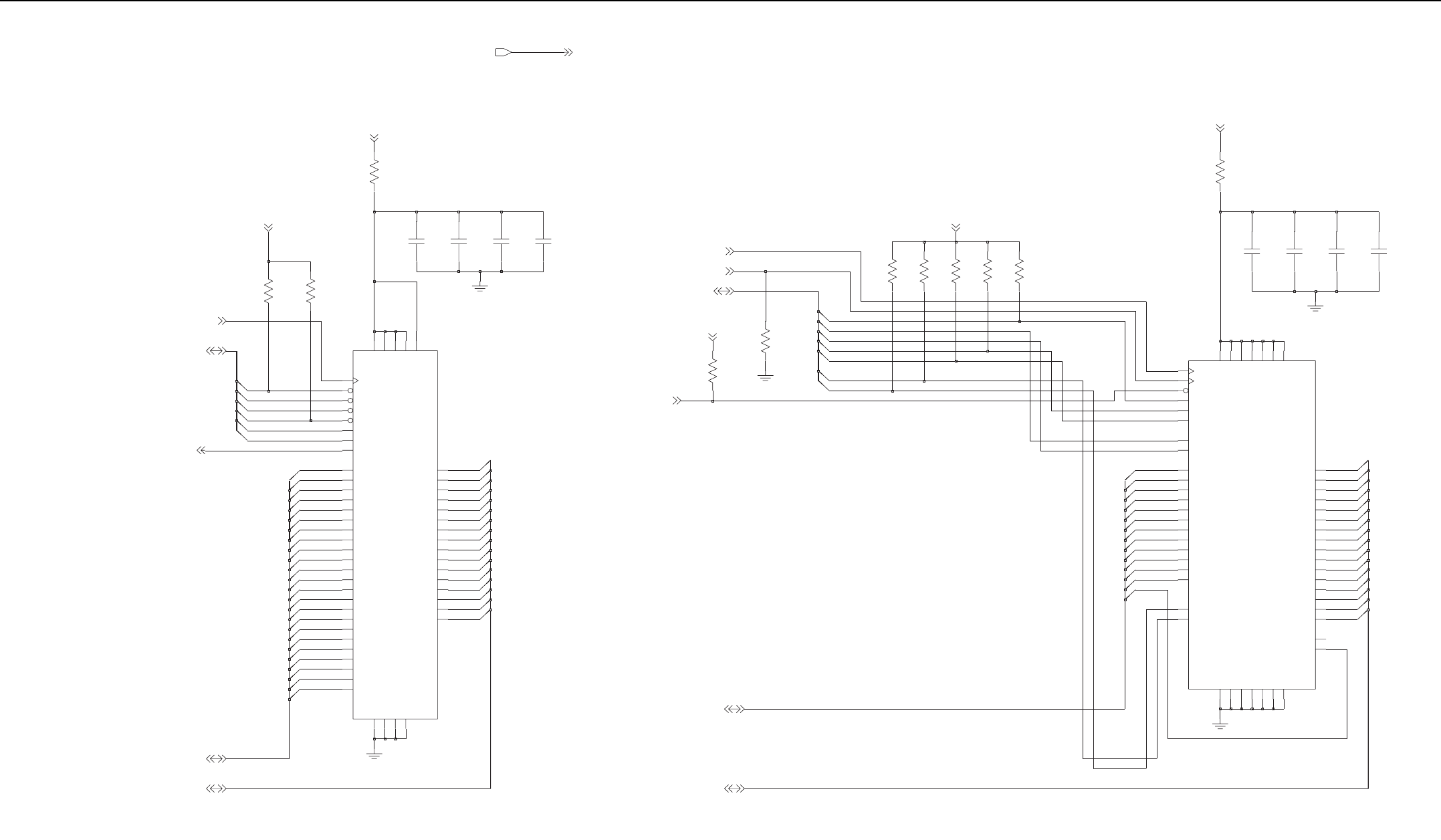
5-16 Controller Schematics
FLASH
61xM4 TS
SDRAM
61xM4 NORCIM
4
1
13
12
2
13
12
14
2
10
0
4
10K
R2010
2
R2007
10K
0
8
14
7
6
5
9
4
9
100pF
C2000
0.10uF
C2002
10K
R2012
7D 4QSSV
F9 WE
10
3
5
1
7C
3QDDV 3D
4QDDV
1
A1SSV
3E 2SSV
1J 3SSV
1QSSV
3A
7B 2Q
S
SV
3C 3
Q
S
SV
NC2 G1
F8 RAS
F1 UDQM
9A
1DDV 7
E
2DDV
3DDV 9J
7A
1QDDV 3B
2QDDV
C9
C8
DQ4 D9
DQ5 D8
DQ6 E9
DQ7 E1
DQ8 D2
DQ9
E8 LDQM
E2
NC1
B9
D1
DQ10 C2
DQ11 C1
DQ12 B2
DQ13
DQ14 B1
A2
DQ15
B8
DQ2
DQ3
G3
G7 BA0
BA1
G8
F7 CAS
F3 CKE
CLK
F2
G9 CS
A8
DQ0
DQ1
G2
J8 A2
A3
J7
J3 A4
J2 A5
A6
H3
H2 A7
H1 A8
A9
U2001
H7 A0
H8 A1
H9 A10
A11
R2004
0
2
R2005
9
4
10K
0
22
0
10K
R2008
5
R2013
10K
2
G
2Q
SS
V
8G
WAIT
D3
WP
D6
6
18
3
RP
4A
1DDV 4G
2DDV 1E
1QDDV 6
G
2QDDV
P
P
V5A
1SSV
3
A
1F 2SSV
1QSSV
G1
D8 G7
D9 F6
EN_E
E7
F8 EN_G
C4 EN_L
C5 EN_W
D7 NC
B5
F3
D14 F2
D15 E2
D2 E5
D3 G5
E4
D4
D5 G3
D6 E3
D7
A2
A9
B2
B4 CLK_K
D0 F7
D1 E6
F5
D10
D11 F4
D12 D5
D13
C8
A20
B3
A21
C3
A3
B8
A4
A8
A5
B7
A7 A6
A7
C7
A8
B1
A13
C1
A14
D2
A15
D1
A16
D4
A17
B6
A18
A6
C6 A19
A2
U2000
A0
E8
A1
D8
A10
C2
A1 A11
A12
R2006
4
R2009
10K10K
9
8
11
C2003
0.10uF
16
C2006
0.10uF
R2000
10K
15
11
10
1
23
3
6
1
12
8
C2004
100pF
3
13
4
5
10
17
0
R2011
11
5
21
15
19
11
1
20
0
6
3
3
5
15
12
0.10uF
C2007
1
8
2
7
7
.01uF
C2005
6
14
2
7
1.875V_DIG_V2
1.875V_DIG_V2
1.875V_DIG_V2
SDRAM_CS
SDRAM_CLK
SDRAM_CLK_EN
1.875V_DIG_V2
C2001
.01uF
1.875V_DIG_V2 1.875V_DIG_V2
FLASH_CLK
FLASH_CTL(5:0)
FLASH_WAIT
EMIFS_DATA(15:0)
EMIFS_ADD(23:1)
SDRAM_ADD(12:0)
SDRAM_DATA(15:0)
SDRAM_CTL(6:0)
1.875V_DIG_V2
Controller Memory Schematic Diagram

Controller Schematics 5-17
47KR3023
R3010 10K
1.875V_DIG_V2
1.875V_DIG_V2
R3024
51K 10K
R3036
R3033 15K
8.2K
R3032
R3034 8.2K
15KR3035
MMP_GPIO2_INPUT
MMP_GPIO1_INPUT
MAKO_OPT_GPIO0
MAKO_OPT_INT
ONE_WIRE_UP
MAKO_OPT_GPIO2
MAKO_OPT_GPIO3
MAKO OPTION SEL
MAKO ONE WIRE
MAKO UART
MAKO USB USB_INT
USB0_SE0
USB0_TXEN
USB0_DAT
USB1_SE0
USB1_TXEN
USB1_DAT
RS232_TX
RS232_RX
MAKO SPI
MAKO SSIMAKO_RX
MAKO_TX
MAKO_FSYNC
MAKO_DCLK
SPI_MISO
SPI_MOSI
MAKO_CE
SPI_CLK
NC
NC
NC
NC
NC
NC
NC
NC
NC
C9
C10
E7
D7
A7
B7
M4
B8
D8
B9
A9
C6
K6
J5
A10
E9
N3
C8
N2
N8
E6
D6
B6
F10
C11
G10
D11
A8
M3
P2
B12
B10
A6
L7
L5
A5
B5
C7
C12
E11
D10
NC
NC
NC
DNP
R3088
5.1K
MAKO_AD_TRIGGER
C3045
10uF
2.2KR3013
R3037
2KR3014
820
EXT_MIC-
INT_MIC-
EXT_MIC+
INT_MIC+
C3050
C3048
.033uF
1.0uF
1.0uFC3047
.033uFC3049
R3011
270R3012
2.2K
DNP
10
R3800
1.0uF
C3080
C3098
33pF
33pF
33pF
C3100
0.1uF
C3800
C3099
33pF
C3097
BLM18BD601SN1
E3033
BLM18BD601SN1
E3030
E3031
BLM18BD601SN1
E3032
BLM18BD601SN1
INT_SPKR
IF2
INT_SPKR+
INT_SPKR-
EXT_SPKR+
EXT_SPKR-
330R3027
0.1uFC3036
R3026 330
.068uF
C3095
NC
C3094
C3011 .022uF
.068uF
C3035 0.1uF
0.1uF
C3034
100KR3055
D3000
SWB+
VSAVE
RAWB+
VC_OUT_M
H2 VC_OUT_P
H3
A4 VREF
G3 PA_IN_M
G2 PA_IN_P
TX_RX
A11
VCM1
J3
H4 VCM2
INT_MIC_M
K1 INT_MIC_P
K2
F2 INT_SPKR_M
F1 INT_SPKR_P
MIC_BIAS
L2
E1 PA_BPLUS
BPLUS
E3
EXT_MIC_M
J1 EXT_MIC_P
J2
G1 EXT_SPKR_M
H1 EXT_SPKR_P
AD_TRIG
B11
PA_CODEC_A2D_BLOCK
U3000-3
VFUSE
VMES
PWR_CTRL
SCAN_EN
TEST
FE_TUNE1
FE_TUNE2
ATOD_6
ATOD_7
ATOD_8
ADC_VREF
ATOD_0
ATOD_1
ATOD_2
ATOD_3
ATOD_4
ATOD_5
E8
L10
NC
N1
C4
A3
L3
M2
K11
K12
K13
M12
N14
M13
L11
M14
L12
L13
.01uF
C3999
100
R3025R3060
2K
PA_TEMP
2.9V_DIG_V6
RX_FLTR_VCTRL
TX_DAC
HW_ID0
HW_ID1
HW_ID2
VOL
100pF
C3038
100pF
C3037
3.3K
R3098
NC
NC
NC
NC
NC
NC
NC
NC
NC
NC
NC
NC
L6
P7
N6
P8
N7
M10
N12
N9
N13
M11
K7
M9
N10
P11
K8
P12
N11
P13
P9
M8
L8
P10
USB_CONNECT
USB1_DM
USB1_DP
USB2_DM
USB2_DP
TXDO_BDI_5V
RXDIN_5V
SB96_BDO_KF_5V
SB96_BUS_BUSY
RTS_FILLSEN_5V
OPTA_SEL1
OPTA_SEL2
OPTA_SEL3
OPTB_SEL0
OPTB_SEL1
OPTB_SEL2
OPTB_SEL3
CTS_CABLE_DET_5V
ONE_WIRE_1
ONE_WIRE_2
ONE_WIRE_BATT
OPTA_SEL0
VC_TX3V
USB2_OE_RCV_RTS
USB2_SE0_VM_RXD
USB_INTX
VC_DCLK
VC_FSYNC
VC_RX
VC_TX
USB1_DAT_TXD
USB1_OE
USB1_SE0
USB2_DAT_VP
SPI_DI
SPI_DO
TXDO_BDI_ENC_3V
TXDO_BDI_UP_3V
UART2_RXD_OD
UART2_TXD
UCM_SS
RXDIN_3V
RXDIN_ENC_3V
SB96D_BDO_KF_3V
SPI_CLK
SPI_CS
OPT_GPIO0
OPT_GPIO1
OPT_GPIO2
OPT_GPIO3
RS232_USB_X
RTS_FILLSEN_3V
OPTION_INTX
CTS_X
LOGIC_VDD
ONE_WIRE_UP
APCO
BBP_CLK
BBP_SYNC
BOOT_NORM_X
BUSY_IN
BUSY_OUT
CABLE_DET_3V
DIGITAL_BLOCK
U3000-2
22K
R3054
22K
R3053
3.3V_DIG_V10
0.10uF
C3062
5V_ANA_V8
24R3020
24R3021 USB1_DP
USB1_DM
10K
R3041
4.7K
R3051
2.9V_DIG_V6
5V_ANA_V8
D2
A2
TS5A23166
B1
C2
D1
B2
C1
A1
U3007
NO2
V_POS
COM1
COM2
GND
IN1
IN2
NO1
0.10uF
C3025
R3043
200K
C3026
0.10uF
5V_ANA_VBUS2
5V_ANA_VBUS2
2.9V_DIG_V6
R3040
2.2K
EN
1GND
3SCL1 6
SCL2
4SDA1 5
SDA2
2
VREF1 7
VREF2
8
PCA9306
U3009
OPTA_SEL1
OPTA_SEL2
OPTA_SEL0
BATT_DATA
ONE_WIRE_1
HW_ID
R3006
R3008 1K
1K
1KR3004
HW_ID0
HW_ID1
HW_ID2
33K
R3007 R3009
33K33K
R3005
2.9V_DIG_V6
2.9V_DIG_V6
2.9V_DIG_V6
Controller Audio and Digital Interface Schematic Diagram (for 8486716Z04)

5-18 Controller Schematics
47KR3023
R3010 10K
1.875V_DIG_V2
1.875V_DIG_V2
R3024
51K 10K
R3036
8.2K
15K
15K
8.2K
R3034
R3035
R3033
R3032
MMP_GPIO2_INPUT
MMP_GPIO1_INPUT
C3045
10uF
R3037
820
2.2K
R3013
2KR3014
EXT_MIC-
INT_MIC-
EXT_MIC+
INT_MIC+
C3050
C3048
.033uF
1.0uF
1.0uFC3047
.033uFC3049
270
R3012
R3011
2.2K
DNP
10
C3080
1.0uF
INT_SPKR+
INT_SPKR-
EXT_SPKR+
EXT_SPKR-
INT_SPKR
IF2
BLM18BD601SN1
E3033
BLM18BD601SN1
E3030
BLM18BD601SN1
E3031
E3032
BLM18BD601SN1
R3800
0.1uF
C3800
C3098
C3100
C3099
33pF
33pF
33pF
33pF
C3097
D3000
C3035
0.1uF
0.1uF
C3034
100K
R3055
SWB+
VSAVE
RAWB+
C3094 .068uF
.068uF
C3095
C3011 .022uF
NC
330R3027
0.1uFC3036
R3026 330
MAKO_AD_TRIGGER
H2
H3
A4
G3
G2
A11
J3
H4
K1
K2
F2
F1
L2
E1
E3
J1
J2
G1
H1
B11
VC_OUT_M
VC_OUT_P
VFUSE
VMES
VREF
PA_IN_M
PA_IN_P
PWR_CTRL
SCAN_EN
TEST
TX_RX
VCM1
VCM2
FE_TUNE1
FE_TUNE2
INT_MIC_M
INT_MIC_P
INT_SPKR_M
INT_SPKR_P
MIC_BIAS
PA_BPLUS
ATOD_6
ATOD_7
ATOD_8
BPLUS
EXT_MIC_M
EXT_MIC_P
EXT_SPKR_M
EXT_SPKR_P
ADC_VREF
AD_TRIG
ATOD_0
ATOD_1
ATOD_2
ATOD_3
ATOD_4
ATOD_5
PA_CODEC_A2D_BLOCK
U3000-3
E8
L10
NC
N1
C4
A3
L3
M2
K11
K12
K13
M12
N14
M13
L11
M14
L12
L13
C3038
100pF
100pF
C3037
PA_TEMP
2.9V_DIG_V6
RX_FLTR_VCTRL
TX_DAC
HW_ID0
HW_ID1
HW_ID2
VOL
R3025
100
C3999
.01uF
R3060
2K
MAKO SPI
MAKO SSIMAKO_RX
MAKO_TX
MAKO_FSYNC
MAKO_DCLK
SPI_MISO
SPI_MOSI
MAKO_CE
SPI_CLK
NC
NC
NC
NC
NC
NC
NC
NC
NC
NC
NC
NC
DNP
R3088
5.1K
MAKO OPTION SEL
MAKO_OPT_GPIO0
MAKO_OPT_INT
MAKO_OPT_GPIO2
MAKO_OPT_GPIO3
MAKO ONE WIRE
ONE_WIRE_UP
MAKO UART
RS232_TX
RS232_RX
MAKO USB USB_INT
USB0_SE0
USB0_TXEN
USB0_DAT
USB1_SE0
USB1_TXEN
USB1_DAT
VC_TX3V
USB2_OE_RCV_RTS
USB2_SE0_VM_RXD
USB_INTX
VC_DCLK
VC_FSYNC
VC_RX
VC_TX
USB1_DAT_TXD
USB1_OE
USB1_SE0
USB2_DAT_VP
SPI_DI
SPI_DO
TXDO_BDI_ENC_3V
TXDO_BDI_UP_3V
UART2_RXD_OD
UART2_TXD
UCM_SS
RXDIN_3V
RXDIN_ENC_3V
SB96D_BDO_KF_3V
SPI_CLK
SPI_CS
OPT_GPIO0
OPT_GPIO1
OPT_GPIO2
OPT_GPIO3
RS232_USB_X
RTS_FILLSEN_3V
OPTION_INTX
CTS_X
LOGIC_VDD
ONE_WIRE_UP
APCO
BBP_CLK
BBP_SYNC
BOOT_NORM_X
BUSY_IN
BUSY_OUT
CABLE_DET_3V
USB_CONNECT
USB1_DM
USB1_DP
USB2_DM
USB2_DP
TXDO_BDI_5V
RXDIN_5V
SB96_BDO_KF_5V
SB96_BUS_BUSY
RTS_FILLSEN_5V
OPTA_SEL1
OPTA_SEL2
OPTA_SEL3
OPTB_SEL0
OPTB_SEL1
OPTB_SEL2
OPTB_SEL3
CTS_CABLE_DET_5V
ONE_WIRE_1
ONE_WIRE_2
ONE_WIRE_BATT
OPTA_SEL0
DIGITAL_BLOCK
U3000-2
M4
A9
C9
C10
E7
D7
A7
B7
C8
B8
D8
B9
B6
C6
J5
A10
E9
N3
P2
E6
D6
A8
B10
A6
L5
A5
B5
C7
K6
N2
N8
F10
C11
G10
D11
M3
B12
L7
C12
E11
D10
NC
NC
NC
NC
NC
NC
NC
NC
NC
NC
NC
USB_CONNECT
L6
P7
N6
P8
N7
M10
N12
N9
N13
M11
K7
M9
N10
P11
K8
P12
N11
P13
P9
M8
L8
P10
3.3K
R3098
OPTA_SEL1
OPTA_SEL2
OPTA_SEL0
BATT_DATA
R3041
10K
0.10uF
C3025
4.7K
R3051
2.9V_DIG_V6
5V_ANA_V8
22K
R3054
22K
R3053
5V_ANA_V8
3.3V_DIG_V10
24
24
R3020
R3021 USB1_DP
USB1_DM
A1 NO1
D2 NO2
V_POS A2
TS5A23166
B1 COM1
C2 COM2
GND
B2
IN1
C1
IN2
U3007
0.10uF
C3062
D1
2.9V_DIG_V6
R3043
200K
5V_ANA_VBUS2
R3040
2.2K
5V_ANA_VBUS2
ONE_WIRE_1
VREF2
8
EN
1GND
3SCL1 6
SCL2
4SDA1 5
SDA2
2
VREF1 7
PCA9306
U3009
C3026
0.10uF
R3007
10K
R3009
10K10K
R3005
2.9V_DIG_V6
2.9V_DIG_V6
2.9V_DIG_V6
HW_ID
HW_ID0
HW_ID1
HW_ID2
DNP DNP DNP
1K
R3006 R3008
1K
R3004
1K
Controller Audio and Digital Interface Schematic Diagram (for 8486716Z07, 8486716Z08 & 8415113H03)
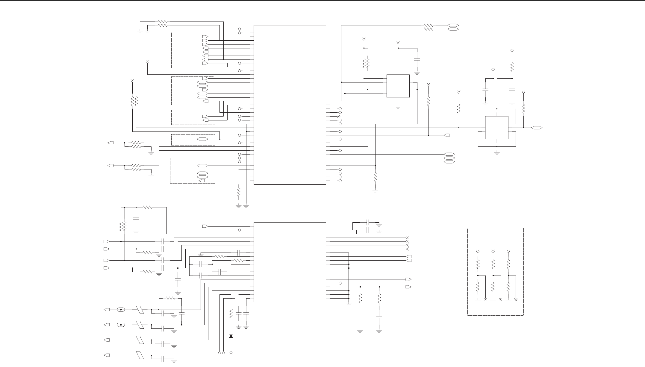
Controller Schematics 5-19
1.875V_DIG_V2
1.875V_DIG_V2
R3036
10K51K
R3024
MMP_GPIO2_INPUT
MMP_GPIO1_INPUT
8.2KR3034
R3032 8.2K
R3035 15K
15KR3033
820R3037
10uF
C3045
R3014
2.2K
R3013
2K
EXT_MIC-
INT_MIC-
EXT_MIC+
INT_MIC+
R3012
C3049
1.0uFC3047
.033uF
1.0uF
C3050
C3048
2.2KR3011
270
.033uF
DNP
C3800
0.1uF
1.0uF
R3800
C3080
10
E3032
BLM18BD601SN1
E3030
BLM18BD601SN1
BLM18BD601SN1
E3031
E3033
BLM18BD601SN1
C3097
33pF
C3099
33pF
33pF
33pF
C3098
C3100
IF2
INT_SPKR
INT_SPKR+
INT_SPKR-
EXT_SPKR+
EXT_SPKR-
D3000
C3034
0.1uF
0.1uF
R3055
SWB+
VSAVE
RAWB+
100K
C3035
0.1uFC3094
270R3027
C3036 0.1uF
R3026
C3011
270
.015uF
C3095
0.1uF
NC
MAKO_AD_TRIGGER
VREF
TX_RX
VCM1
VCM2
VC_OUT_M
VC_OUT_P
INT_MIC_P
INT_SPKR_M
INT_SPKR_P
MIC_BIAS
PA_BPLUS
PA_IN_M
PA_IN_P
BPLUS
EXT_MIC_M
EXT_MIC_P
EXT_SPKR_M
EXT_SPKR_P
INT_MIC_M
U3000-3
PA_CODEC_A2D_BLOCK
AD_TRIG
A4
A11
J3
H4
H2
H3
K2
F2
F1
L2
E1
G3
G2
E3
J1
J2
G1
H1
K1
B11
DNP
NC
NC
NC
R3088
5.1K
NC
NC
NC
NC
NC
MAKO OPTION SEL
MAKO_OPT_GPIO0
MAKO_OPT_INT
MAKO_OPT_GPIO2
MAKO_OPT_GPIO3
MAKO ONE WIRE
ONE_WIRE_UP
MAKO UART
MAKO USB USB_INT
USB0_SE0
USB0_TXEN
USB0_DAT
USB1_SE0
USB1_TXEN
USB1_DAT
RS232_TX
RS232_RX
MAKO SPI
MAKO SSIMAKO_RX
MAKO_TX
MAKO_FSYNC
MAKO_DCLK
SPI_MISO
SPI_MOSI
MAKO_CE
SPI_CLK
10KR3010
47KR3023
NC
NC
NC
NC
E7
D7
A7
B7
M4
B8
D8
B9
A9
C9
A10
E9
N3
C8
E6
D6
B6
C6
A6
A5
B5
C10
K6
J5
N8
G10
D11
A8
M3
P2
N2
B12
F10
C11
L7
C7
C12
E11
D10
B10
L5
USB_INTX
VC_DCLK
VC_FSYNC
VC_RX
VC_TX
VC_TX3V
USB1_OE
USB1_SE0
USB2_DAT_VP
USB2_DM
USB2_DP
USB2_OE_RCV_RTS
USB2_SE0_VM_RXD
USB_CONNECT
TXDO_BDI_ENC_3V
TXDO_BDI_UP_3V
UART2_RXD_OD
UART2_TXD
UCM_SS
USB1_DAT_TXD
USB1_DM
USB1_DP
SB96D_BDO_KF_3V
SB96_BDO_KF_5V
SB96_BUS_BUSY
SPI_CLK
SPI_CS
SPI_DI
SPI_DO
TXDO_BDI_5V
OPT_GPIO2
OPT_GPIO3
RS232_USB_X
RTS_FILLSEN_3V
RTS_FILLSEN_5V
RXDIN_3V
RXDIN_5V
RXDIN_ENC_3V
OPTA_SEL3
OPTB_SEL0
OPTB_SEL1
OPTB_SEL2
OPTB_SEL3OPTION_INTX
OPT_GPIO0
OPT_GPIO1
LOGIC_VDD
ONE_WIRE_1
ONE_WIRE_2
ONE_WIRE_BATT
ONE_WIRE_UP
OPTA_SEL0
OPTA_SEL1
OPTA_SEL2
BBP_CLK
BBP_SYNC
BOOT_NORM_X
BUSY_IN
BUSY_OUT
CABLE_DET_3V
CTS_CABLE_DET_5V
CTS_X
U3000-2
DIGITAL_BLOCK
APCO
NC
NC
NC
NC
NC
NC
NC
NC
NC
NC
NC
USB_CONNECT
P8
N7
L6
P7
N6
N9
N13
M10
M11
N12
N10
P11
K8
P12
N11
P9
M8
L8
P10
K7
M9
P13
R3098
3.3K
VMES
SCAN_EN
TEST
VFUSE
PWR_CTRL
FE_TUNE1
FE_TUNE2
ATOD_1
ATOD_2
ATOD_3
ATOD_4
ATOD_5
ATOD_6
ATOD_7
ATOD_8
ADC_VREF
ATOD_0
L10
C4
A3
E8
N1
L3
M2
M13
L11
M14
L12
L13
K11
K12
K13
M12
N14
R3060
2K
NC
R3025
100
C3999
.01uF
PA_TEMP
2.9V_DIG_V6
RX_FLTR_VCTRL
TX_DAC
HW_ID0
HW_ID1
HW_ID2
VOL
C3038 100pF
C3037 100pF
NO1
A1
NO2
D2
A2
V_POS
U3007
COM1
B1
COM2
C2
D1 GND
IN1 B2
IN2 C1
TS5A23166
10K
R3041
C3026
0.10uF
4.7K
R3051
0.10uF
C3025
2.9V_DIG_V6
2.9V_DIG_V6
5V_ANA_V8
R3021 24
0.10uF
C3062
24R3020
5V_ANA_V8
3.3V_DIG_V10
22K
R3053 R3054
22K
USB1_DP
USB1_DM
200K
R3043
5V_ANA_VBUS2
R3040
2.2K
5V_ANA_VBUS2
U3009
PCA9306
OPTA_SEL1
ONE_WIRE_1
OPTA_SEL2
OPTA_SEL0
BATT_DATA
VREF2 7
EN 8
GND
1
SCL1
3SCL2 6
SDA1
4SDA2 5
VREF1 2
DNP DNP DNP
10K
R3005
1K
R3004
10K
R3009
1K
R3008
10K
R3007
R3006
1K
2.9V_DIG_V6
2.9V_DIG_V6
2.9V_DIG_V6
HW_ID
HW_ID0
HW_ID1
HW_ID2
Controller Audio and Digital Interface Schematic Diagram (for 8415113H05)
5-20 Controller Schematics
Q3003
RAWB+
RAWB+
SWB+
SWB+
100K
R3050
C3093
2.2uF
4
5
8
1
2
3
6
7
VSAVE
13pF
C3001
13pF
C3000
21
32.768KHz
XTAL
Y3000
R3070
220K
220K
R3071
2.775V_DIG_V4 C3070
10pF
2.775V_DIG_V4 R3072
2MEG
R3073
2MEG
C3
C1
B1
B3
U3003-1
LMC6035ITLX
C2
A3
A1
B1
B3
A2
LMC6035ITLX
U3003-2
1NC
4
OUT
5
VCC
U3004
NL17SZ14
3GND
2IN
1K
R3074
GATED_32KHZ_OMAP
1.875V_DIG_V2
0.10uF
C3063
0.22uF
C3084 C3805
0.22uF
560nH
L3003
L3004
560nH
SWB+
C3200
0.1uF
C3201
10uF
4GND
2ITH
8PLLLPF
1RUN SW
7SYNC
3VFB
6
VIN
5
U3020
LTC1877
NC
L3020
10uH
47uF
C3202
.01uF
C3203
R3201
R3200
62K
220K
C3204
20pF
3.6V_DIG_VSW1
220pF
C3212
MAKO_SW1_VDD
0.1uF
C3206
10uF
C3207
0.22uF
C3208
SWB+ L3022
560nH
3
VIN6
GND
4
ITH
2
PLLLPF
8
RUN
1SW 5
SYNC
7
VFB
LTC1877
U3021
10uH
L3021
20pF
C3211
R3202
220K
R3203
300K
C3210
.01uF
C3209
47uF
OMAP_CORE_LTC
R3028
51.1K
C3015 100pF
R3029
41.2K
4
VCONT 3
VIN
1VOUT
2
FB
GND
6
NP
TK11100CSC
U3008
5
2.2uF
C3016 C3018
2.2uF
C3017
.01uF
Q3005
2
3
1
4
OUT
Q3006
R1
R2
GND
IN
47K
R3100
178K
R3017
51K
R3018
10uF
C3090
3.3V_DIG_V10
NC
VIN1 1
VIN2 6
VOUT
5
LP8340
U3002
4ADJ
GND1
2
7GND2
3NC C3091
10uF
SWB+
5V_ANA_VBUS2
0.2
Q3010
C3039 4.7uF
VBUS1
R3030
R3003 100nH
4
Q3000
2
3
1
1.55V_DIG_V3
2.775V_DIG_V4
2.9V_DIG_V6
2.775V_ANA_V7
SWB+
5V_ANA_V8
3V_ANA_V9
3.6V_DIG_VSW1
3.3V_DIG_V10
1.875V_DIG_V2
NC
NC
NC
NC
NC
NC
0.1uF
C3082
0.1
R3016
NC
C3083
0.1uF
NC
NC
NC
NC
0
R3031
DNP
R3038
SWB+
MAKO_SW1_VDD
0
E12
D12
C13
F11
B13
K3
K4
L1
L9
J10
M6
H10
C14
N4
P4
N5
P3
P6
K14
J13
G11
E13
D13
F13
F12
E14
G13
G12
H12
J11
H11
L14
J14
J12
C3
A2
H13
H14
F14
G14
XTAL32_IN
XTAL32_OUT
VBUS1_SENS
VBUS2
VBUS2_CMD
VBUS2_SENS
VBUS_SUPPLY
VSAVE
XIN
XOUT
V08_I
V08_O
V09_O
V10_GND
V10_I
V10_O
VBUS1
VBUS1_CMD
SW_TYPE
TCXO_IN
TCXO_SEL_16_24
V02_O
V03_O
V04_O
V06_O
V07_O
SW2_VCCS
SW2_VOUT
SW5_PHASE
SW5_SUMCOMP
SW5_VDD
SW5_VDDHV
SW5_VOUT
SW5_VSENSE
SW1_VDD
SW1_VDDHV
SW1_VOUT
SW1_VSEN_BST
SW1_VSEN_BUK
SW2_GND
SW2_LX
SW2_VCC
PGLDO2
PGLDO3
REG_3V6
RESETX
SW1_DH
SW1_GND
SW1_PHASE
SW1_SUMCOMP_DL
INT_X
MECH_SW
NC1
NC2
NC3
NC4
NC5
NC6
GND4
GND5
GND6
GND7
GND8
GND9
HV_BG
IGN_X
BAT_RTC
BAT_TYPE
EMERG_PB
FET_ENX
GATED_32K_CLK
GND1
GND2
GND3
PWR_MNGR_BLOCK
U3000-1
BAT_3V6
BAT_7V5
NC
NC
NC
NC
A1
A14
P1
P14
M5
B14
NC
NC
G5
K9
L4
D14
H5
D9
P5
M7
J4
C1
B1
C2
A13
A12
B3
M1
D4
D3
C5
D5
E4
G4
B4
F3
B2
F4
E2
F5
D2
D1
C3002 0.1uF
C3005 1000pF
C3003 2.2uF
2.2uFC3004
DNP
0R3888
NC
NC
NC
EMERG_PB
MAKO_INT
MECH_SW
POR
C3061
20pF
16-54MHz
CX-101F
Y3001
20pF
C3060
2GND1
GND2
4
HOT1 1
HOT2
3
C3081
4.7uF
2
3
1
4
C3019
1.0uF
C3028
2.2uF
C3014
2.2uF2.2uF
C3010
1.0uF
C3074
1.0uF
C3031
1.0uF
C3067
4.7uF
C3079 1.0uF
C3024
1.875V_DIG_V2
1.875V_DIG_V2
1.875V_DIG_V2
2.775V_DIG_V4
2.775V_DIG_V4
2.775V_DIG_V41.55V_DIG_V3
1.55V_DIG_V3
5V_ANA_VBUS2
5V_ANA_VBUS2
2.9V_DIG_V6
2.9V_DIG_V6
2.775V_ANA_V7
2.775V_ANA_V7
5V_ANA_V8
5V_ANA_V8
5V_ANA_V8
3V_ANA_V9
3.3V_DIG_V10
3.3V_DIG_V10
C3205
220pF
Controller Power Management Block Schematic Diagram (for 8486716Z04)
Controller Schematics 5-21
220K
R3071
10pF
C3070
220K
R3070
2.775V_DIG_V4
2.775V_DIG_V4
B1
B3
LMC6035ITLX
U3003-1
C2
C3
C1
2MEG
R3072
2MEG
R3073
B3
A2
A3
A1
B1
U3003-2
LMC6035ITLX
NC
NC
NC
NC
A1
A14
P1
P14
M5
B14 NC
NC
XTAL32_IN
XTAL32_OUT
VBUS2
VBUS2_CMD
VBUS2_SENS
VBUS_SUPPLY
VSAVE
XIN
XOUT
V08_O
V09_O
V10_GND
V10_I
V10_O
VBUS1
VBUS1_CMD
VBUS1_SENS
SW_TYPE
TCXO_IN
TCXO_SEL_16_24
V02_O
V03_O
V04_O
V06_O
V07_O
V08_I
SW2_VOUT
SW5_PHASE
SW5_SUMCOMP
SW5_VDD
SW5_VDDHV
SW5_VOUT
SW5_VSENSE
SW1_VDDHV
SW1_VOUT
SW1_VSEN_BST
SW1_VSEN_BUK
SW2_GND
SW2_LX
SW2_VCC
SW2_VCCS
PGLDO3
REG_3V6
RESETX
SW1_DH
SW1_GND
SW1_PHASE
SW1_SUMCOMP_DL
SW1_VDD
INT_X
MECH_SW
NC1
NC2
NC3
NC4
NC5
NC6
PGLDO2
GND5
GND6
GND7
GND8
GND9
HV_BG
IGN_X
BAT_RTC
BAT_TYPE
EMERG_PB
FET_ENX
GATED_32K_CLK
GND1
GND2
GND3
GND4
U3000-1
PWR_MNGR_BLOCK
BAT_3V6
BAT_7V5
NC
NC
B1
C2
A13
A12
C1
M1
D4
B3
D3
C5
E4
G5
K9
L4
D14
H5
D9
G4
B4
D5
B2
F4
E2
F5
P5
M7
J4
D2
D1
F3
NC
NC
NC
NC
NC
NC
NC
NC
NC
E12
D12
C13
F11
B13
K3
K4
L1
L9
J10
M6
H10
C14
N4
P4
N5
P3
P6
K14
J13
G11
E13
D13
F13
F12
E14
G13
G12
H12
J11
H11
L14
J14
J12
C3
A2
H13
H14
F14
G14 NC
NC
C3082
0.1uF
R3016
0.1uF
C3083
0.1
2.9V_DIG_V6
2.775V_ANA_V7
SWB+
5V_ANA_V8
3V_ANA_V9
3.6V_DIG_VSW1
3.3V_DIG_V10
1.875V_DIG_V2
1.55V_DIG_V3
2.775V_DIG_V4
Q3000
2
3
1
4
R3103
0.7
VBUS1
4.7uFC3039
0.2
R3030
Q3010
2
3
1
4
C3081
5V_ANA_VBUS2
4.7uF
1.0uF
C3019 C3079
4.7uF
C3010
2.2uF
C3067
1.0uF
2.2uF
C3014 C3031 C3024 C3074
1.0uF2.2uF
1.0uF
1.0uF
C3028
1.875V_DIG_V2
1.875V_DIG_V2
1.875V_DIG_V2
2.775V_DIG_V4
2.775V_DIG_V4
2.775V_DIG_V4
1.55V_DIG_V3
1.55V_DIG_V3
5V_ANA_VBUS2
2.9V_DIG_V6
5V_ANA_VBUS2
2.9V_DIG_V6
2.775V_ANA_V7
2.775V_ANA_V7
5V_ANA_V8
5V_ANA_V8
5V_ANA_V8
3V_ANA_V9
3.3V_DIG_V10
3.3V_DIG_V10
Q3006
R1
R2
GND
IN
OUT 3.3V_DIG_V10
2
3
1
4
47K
R3100
Q3005
51K
R3018
178K
R3017
C3090
10uF
ADJ
GND1
GND2
NC
VIN1
VIN2
VOUT
10uF
C3091
4
2
7
3
1
6
5
NC
SWB+
U3002
LP8340
IN
OUT
Q3002
R1
R2
GND
USB_CONNECT
Q3001
2
3
1
4
100K
R3102
2
R3101
C3015 100pF
51.1K
R3028
41.2K
R3029
2.2uF
C3016
2.2uF
C3018
TK11100CSC
FB 2
GND
5
NP 6
VCONT 4
VIN3
VOUT
1
U3008
.01uF
C3017
C3202
68uF
C3203
.01uF
3.6V_DIG_VSW1
C3204
20pF
62K
220K
R3201
R3200
7
VFB
3
VIN6
GND
4
ITH
2
PLLLPF
8
RUN
1SW 5
SYNC
LTC1877
U3020
10uH
L3020
220pF
C3205
NC
10uF
C3201
C3200
0.10uF
C3805
0.22uF
C3084
0.22uF
560nH
L3003 SWB+
C3208
0.22uF
L3022
560nH
MAKO_SW1_VDD
SWB+
C3207
10uF
C3206
0.10uF
5
SW
7SYNC
3VFB
6
VIN
U3021
LTC1877
GND
2ITH
8PLLLPF
1RUN
L3021
10uH
220pF
C3212
4
47uF
C3209 C3210
.01uF
OMAP_CORE_LTC
20pF
C3211
220K
R3202
300K
R3203
560nH
L3004
0.10uF
C3063
1.875V_DIG_V2
GND
3
IN
2
NC
1
OUT 4
VCC 5
NL17SZ14
U3004
1K
R3074
GATED_32KHZ_OMAP
MAKO_SW1_VDD
SWB+
DNP
0
R3038
R3031
0
Y3000
XTAL 32.768KHz
21
13pF
C3001 C3000
13pF
RAWB+
RAWB+
SWB+
SWB+
VSAVE
2
3
6
7
8
4
5
Q3003
1
C3093
2.2uF 100K
R3050
Y3001
CX-101F
16-54MHz
C3051
100pF
GND1
2
4GND2
1
HOT1
3HOT2
20pF
C3061
20pF
C3060
VSAVE
EMERG_PB
MAKO_INT
MECH_SW
POR
C3004 2.2uF
0.1uFC3002
1000pFC3005
2.2uFC3003
DNP
NC
0R3888
R3075 10K
Controller Power Management Block Schematic Diagram (for 8486716Z07)
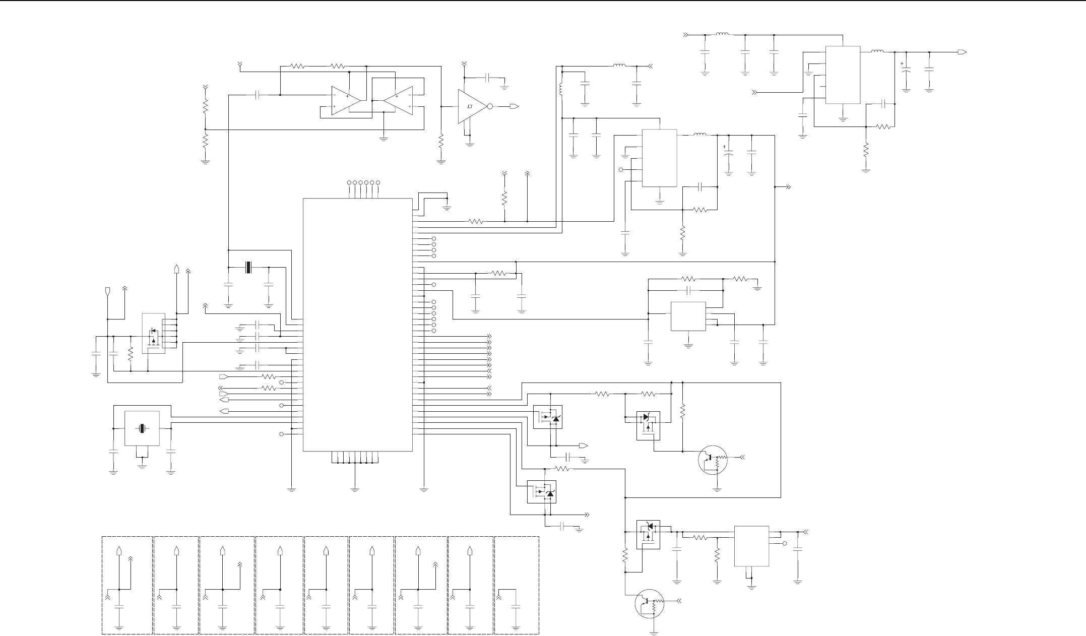
5-22 Controller Schematics
220K
R3070
C3070
10pF
220K
R3071
2.775V_DIG_V4
2.775V_DIG_V4 R3073
2MEG
C2
C3
C1
B1
B3
U3003-1
LMC6035ITLX
R3072
2MEG
A2
A3
A1
B1
B3
LMC6035ITLX
U3003-2
VCC
U3004
NL17SZ14
3GND
2IN
1NC
4
OUT
5
R3074
1K
1.875V_DIG_V2
0.10uF
C3063
GATED_32KHZ_OMAP
560nH
L3004 0.22uF
C3084
C3200
0.10uF
C3201
10uF
MAKO_SW1_VDD
SWB+
DNP
0
R3031
0
R3038
NC
NC
NC
NC
NC
NC
J13
D13
F13
E14
G12
H12
J11
H11
L14
J14
J12
K14
A2
H13
H14
F14
G14
G13
C3
NC
NC
NC
NC
NC
D12
C13
F11
B13
K4
L1
L9
J10
M6
H10
C14
E12
N4
P4
N5
P3
P6
K3
G11
E13
F12
2.9V_DIG_V6
2.775V_ANA_V7
SWB+
5V_ANA_V8
3V_ANA_V9
3.6V_DIG_VSW1
3.3V_DIG_V10
1.875V_DIG_V2
1.55V_DIG_V3
2.775V_DIG_V4
4
Q3000
2
3
1
R3103
0.7
C3039 4.7uF
VBUS1
R3102
2
Q3001
2
3
1
4
R3101
100K
GND
IN
OUT
Q3002
R1
R2
USB_CONNECT
47K
Q3005
2
3
1
4
R3100
C3081
5V_ANA_VBUS2
4.7uF
0.2
2
3
1
4
Q3010
R3030
K9
L4
D14
H5
D9
P5
M7
J4
G5
XTAL32_OUT
VBUS2
VBUS2_CMD
VBUS2_SENS
VBUS_SUPPLY
VSAVE
XIN
XOUT
XTAL32_IN
V08_O
V09_O
V10_GND
V10_I
V10_O
VBUS1
VBUS1_CMD
VBUS1_SENS
TCXO_IN
TCXO_SEL_16_24
V02_O
V03_O
V04_O
V06_O
V07_O
V08_I
SW2_VOUT
SW5_PHASE
SW5_SUMCOMP
SW5_VDD
SW5_VDDHV
SW5_VOUT
SW5_VSENSE
SW_TYPE
SW1_VDDHV
SW1_VOUT
SW1_VSEN_BST
SW1_VSEN_BUK
SW2_GND
SW2_LX
SW2_VCC
SW2_VCCS
PGLDO3
REG_3V6
RESETX
SW1_DH
SW1_GND
SW1_PHASE
SW1_SUMCOMP_DL
SW1_VDD
MECH_SW
NC1
NC2
NC3
NC4
NC5
NC6
PGLDO2
GND5
GND6
GND7
GND8
GND9
HV_BG
IGN_X
INT_X
BAT_TYPE
EMERG_PB
FET_ENX
GATED_32K_CLK
GND1
GND2
GND3
GND4
PWR_MNGR_BLOCK
U3000-1
BAT_3V6
BAT_7V5
BAT_RTC
0.1uF
C3082
0.1
R3016
0.1uF
C3083
A1
A14
P1
P14
M5
B14
NC
NC
NC
NC
NC
NC
21
32.768KHz
XTAL
Y3000
C3001
13pF 13pF
C3000
SWB+
SWB+
VSAVE
C3003 2.2uF
C3002 0.1uF
C3005 1000pF
2.2uFC3004
B1
C2
A13
A12
C1
M1
D4
B3
D3
C5
E4
G4
B4
D5
B2
F4
E2
F5
D2
D1
F3
NC
NC
NC
DNP
R3888 0
10KR3075
VSAVE
EMERG_PB
MAKO_INT
MECH_SW
POR
1
2
3
6
7
8
4
5
Q3003
RAWB+
RAWB+
100K
R3050
C3093
2.2uF
100pF
C3051
CX-101F
Y3001
2GND1
GND2
4
16-54MHz
C3061
20pF
HOT1 1
HOT2
3
20pF
C3060
560nH
L3003
0.22uF
C3805
SWB+
L3022
560nH
0.10uF
C3206
10uF
C3207
0.22uF
C3208
SWB+
220pF
C3212
MAKO_SW1_VDD
220K
R3200
C3203
.01uF
3
6
U3020
LTC1877
2
8
15
7
L3020
10uH
20pF
C3204
68uF
C3202
NC
VFB
VINGND
ITH
PLLLPF
RUN SW
SYNC
62K
R3201
4
680pF
C3205
R3028
51.1K
R3029
41.2K
C3015 100pF
1VOUT
2
FB
GND
6
NP 4
VCONT 3
VIN
5
TK11100CSC
U3008
C3016
2.2uF 2.2uF
C3018
.01uF
C3017
4ADJ
GND1
2
7GND2
3
NC
VIN1 1
VIN2 6
VOUT
5
LP8340
U3002
R3018
51K
R3017
178K
C3090
10uF
OUT
Q3006
R1
R2
GND
IN3.3V_DIG_V10
NC
10uF
C3091
SWB+
R3203
300K
3.6V_DIG_VSW1
C3211
20pF
R3202
220K
15
7
3
6
LTC1877
U3021
4
2
8
10uH
L3021
RUN SW
SYNC
VFB
VINGND
ITH
PLLLPF
C3209
47uF .01uF
C3210
OMAP_CORE_LTC
C3074
1.0uF
C3014
2.2uF
C3028
2.2uF
1.0uF
C3031
1.0uF
C3024
4.7uF
C3079
1.0uF
C3019
2.2uF
C3010
1.0uF
C3067
1.875V_DIG_V2
1.875V_DIG_V2
1.875V_DIG_V2
2.775V_DIG_V4
2.775V_DIG_V4
2.775V_DIG_V4
1.55V_DIG_V3
1.55V_DIG_V3
5V_ANA_VBUS2
2.9V_DIG_V6
5V_ANA_VBUS2
2.9V_DIG_V6
2.775V_ANA_V7
2.775V_ANA_V7
5V_ANA_V8
5V_ANA_V8
5V_ANA_V8
3V_ANA_V9
3.3V_DIG_V10
3.3V_DIG_V10
Controller Power Management Block Schematic Diagram (for 8486716Z08)
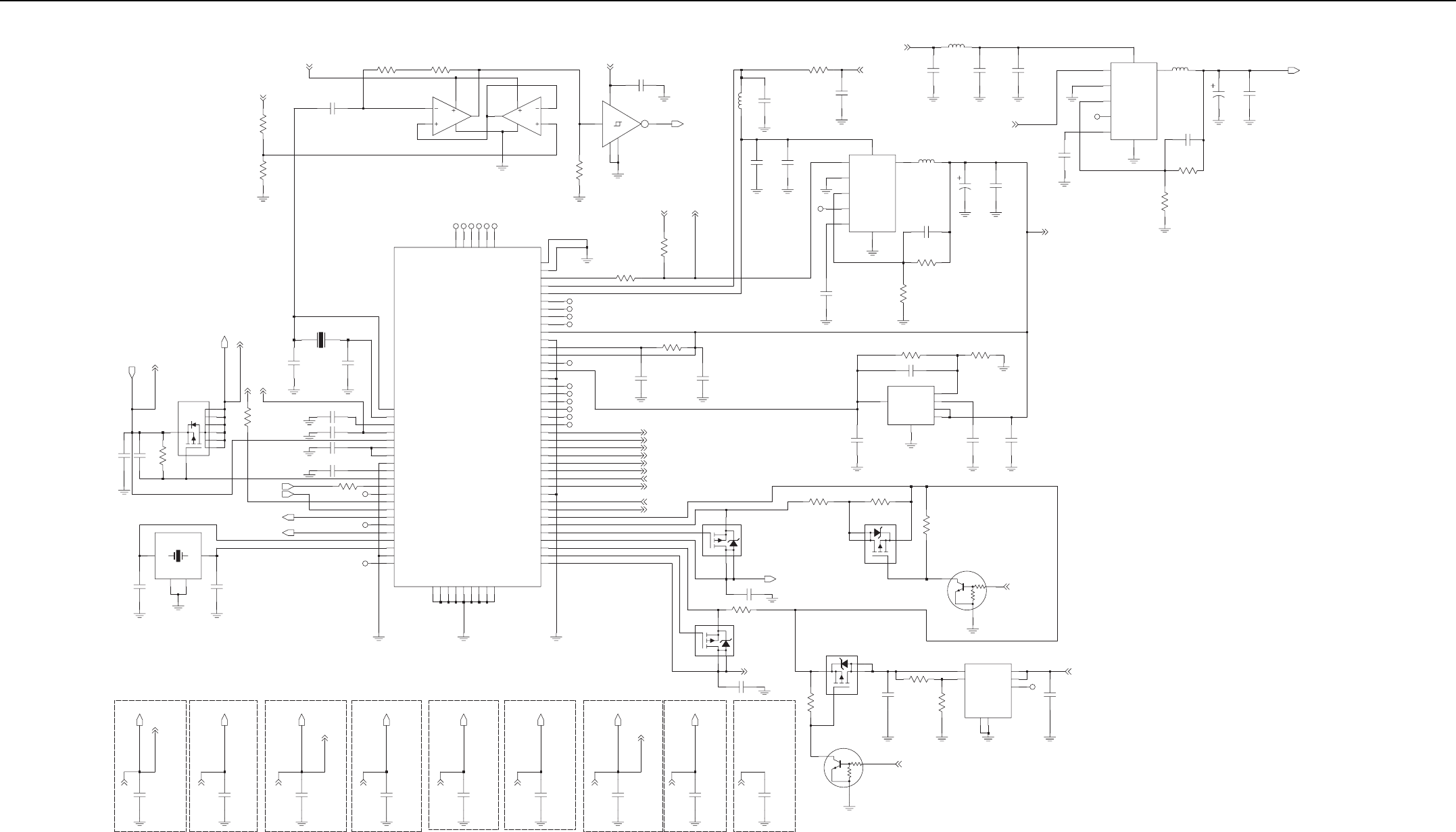
Controller Schematics 5-23
8
4
5
Q3003
1
2
3
6
7
RAWB+
RAWB+
100K
R3050
2.2uF
C3093
C3051
100pF
Y3001
CX-101F
16-54MHz
HOT1
3HOT2
GND1
GND2
1
20pF
C3061
C3060
20pF
2
4
MECH_SW
EMERG_PB
MAKO_INT
POR
C3005 1000pF
2.2uFC3003
0.1uFC3002
C3004 2.2uF
DNP
R3888 0
NC
NC
NC
B1
C2
A13
A12
C1
M1
D4
B3
D3
C5
E4
G4
B4
D5
B2
F4
E2
F5
D2
D1
F3
13pF
32.768KHz
21
C3000
Y3000
XTAL
C3001
13pF
VSAVE
SWB+
SWB+
VSAVE
R3075
10K
NC
NC
NC
NC1 A1
NC2 A14
NC3 P1
NC4 P14
M5
NC5
NC6 B14 NC
NC
NC
XTAL32_OUT
VBUS2
VBUS2_CMD
VBUS2_SENS
VBUS_SUPPLY
VSAVE
XIN
XOUT
XTAL32_IN
V08_O
V09_O
V10_GND
V10_I
V10_O
VBUS1
VBUS1_CMD
VBUS1_SENS
TCXO_IN
TCXO_SEL_16_24
V02_O
V03_O
V04_O
V06_O
V07_O
V08_I
SW2_VOUT
SW5_PHASE
SW5_SUMCOMP
SW5_VDD
SW5_VDDHV
SW5_VOUT
SW5_VSENSE
SW_TYPE
SW1_VDDHV
SW1_VOUT
SW1_VSEN_BST
SW1_VSEN_BUK
SW2_GND
SW2_LX
SW2_VCC
SW2_VCCS
PGLDO3
REG_3V6
RESETX
SW1_DH
SW1_GND
SW1_PHASE
SW1_SUMCOMP_DL
SW1_VDD
MECH_SW
PGLDO2
GND5
GND6
GND7
GND8
GND9
HV_BG
IGN_X
INT_X
BAT_TYPE
EMERG_PB
FET_ENX
GATED_32K_CLK
GND1
GND2
GND3
GND4
U3000-1
PWR_MNGR_BLOCK
BAT_3V6
BAT_7V5
BAT_RTC
K9
L4
D14
H5
D9
P5
M7
J4
G5
NC
NC
NC
NC
NC
NC
NC
NC
D12
C13
F11
B13
K4
L1
L9
J10
M6
H10
C14
E12
N4
P4
N5
P3
P6
K3
J13
G11
E13
D13
F13
F12
E14
G12
H12
J11
H11
L14
J14
J12
K14
A2
H13
H14
F14
G14
G13
C3
NC
NC
NC
C3082
0.10uF
R3031
0.10uF
C3083
R3016
0
0.1
DNP
0
R3038
SWB+
MAKO_SW1_VDD
NC
1
OUT
VCC
NL17SZ14
U3004
GND
3
IN
1K
R3074
24
5
GATED_32KHZ_OMAP
0.10uF
C3063
1.875V_DIG_V2
A2
A3
A1
B1
B3
U3003-2
LMC6035ITLX
2MEG
R3072
2MEG
R3073
LMC6035ITLX
U3003-1
C2
C3
C1
B1
B3
220K
R3070
R3071
220K
2.775V_DIG_V4
10pF
C3070
2.775V_DIG_V4
560nH
L3004
R3076
2
C3084
0.22uF
0.22uF
C3805
SWB+ C3207
10uF
560nH
L3022
C3208
0.22uF
C3206
0.10uF
SWB+
5
LTC1877
U3020
10uH
L3020
MAKO_SW1_VDD
0.10uF
C3200
10uF
C3201
PLLLPF
8
RUN
1SW
SYNC
7
VFB
3
VIN6
GND
4
ITH
2
NC
220pF
C3205 R3201
62K
R3200
220K
20pF
C3204
C3202
68uF
C3203
.01uF
3.6V_DIG_VSW1
U3021
LTC1877
10uH
L3021
220pF
C3212
SW
7SYNC
3VFB
6
VIN
4GND
2
8PLLLPF
1RUN 5
ITH
NC
300K
R3203
20pF
C3211
220K
R3202
.01uF
C3210
47uF
C3209
OMAP_CORE_LTC
2.775V_ANA_V7
SWB+
5V_ANA_V8
3V_ANA_V9
3.6V_DIG_VSW1
3.3V_DIG_V10
1.875V_DIG_V2
1.55V_DIG_V3
2.775V_DIG_V4
2.9V_DIG_V6
41.2K
R3029
51.1K
R3028
100pFC3015
FB 2
GND
NP 6
VCONT 4
VIN3
VOUT
1
U3008
TK11100CSC
5
2.2uF
C3018
.01uF
C3017
C3016
2.2uF
R3102
2
R3101
100K
Q3001
2
3
1
4
R3103
0.7
Q3002
R1
R2
GND
IN
OUT USB_CONNECT
NC C3091
10uF
SWB+
VOUT
U3002
LP8340
ADJ
GND1
GND2
NC 3
1
VIN1 6
VIN2
5
4
2
7
R3018
51K
178K
R3017
2
3
C3090
10uF
1
4
Q3005
3.3V_DIG_V10
R3100
47K
Q3006
R1
R2
GND
IN
OUT
3
1
4
Q3000
2
VBUS1
2
3
1
4
Q3010
R3030
0.2
4.7uFC3039
5V_ANA_VBUS2
DNP
C3081 4.7uF
C3024
1.0uF
C3067
1.0uF2.2uF
C3014
C3010
2.2uF
C3074
1.0uF
2.2uF
C3028
1.0uF
C3031C3019
1.0uF 4.7uF
C3079
1.875V_DIG_V2
1.875V_DIG_V2
1.875V_DIG_V2 1.55V_DIG_V3
1.55V_DIG_V3
2.775V_DIG_V4
2.775V_DIG_V4
2.775V_DIG_V4
2.9V_DIG_V6
5V_ANA_VBUS2
5V_ANA_VBUS2 2.9V_DIG_V6
2.775V_ANA_V7
2.775V_ANA_V7
5V_ANA_V8
5V_ANA_V8
5V_ANA_V8
3.3V_DIG_V10
3V_ANA_V9
3.3V_DIG_V10
Controller Power Management Block Schematic Diagram (for 8415113H03)
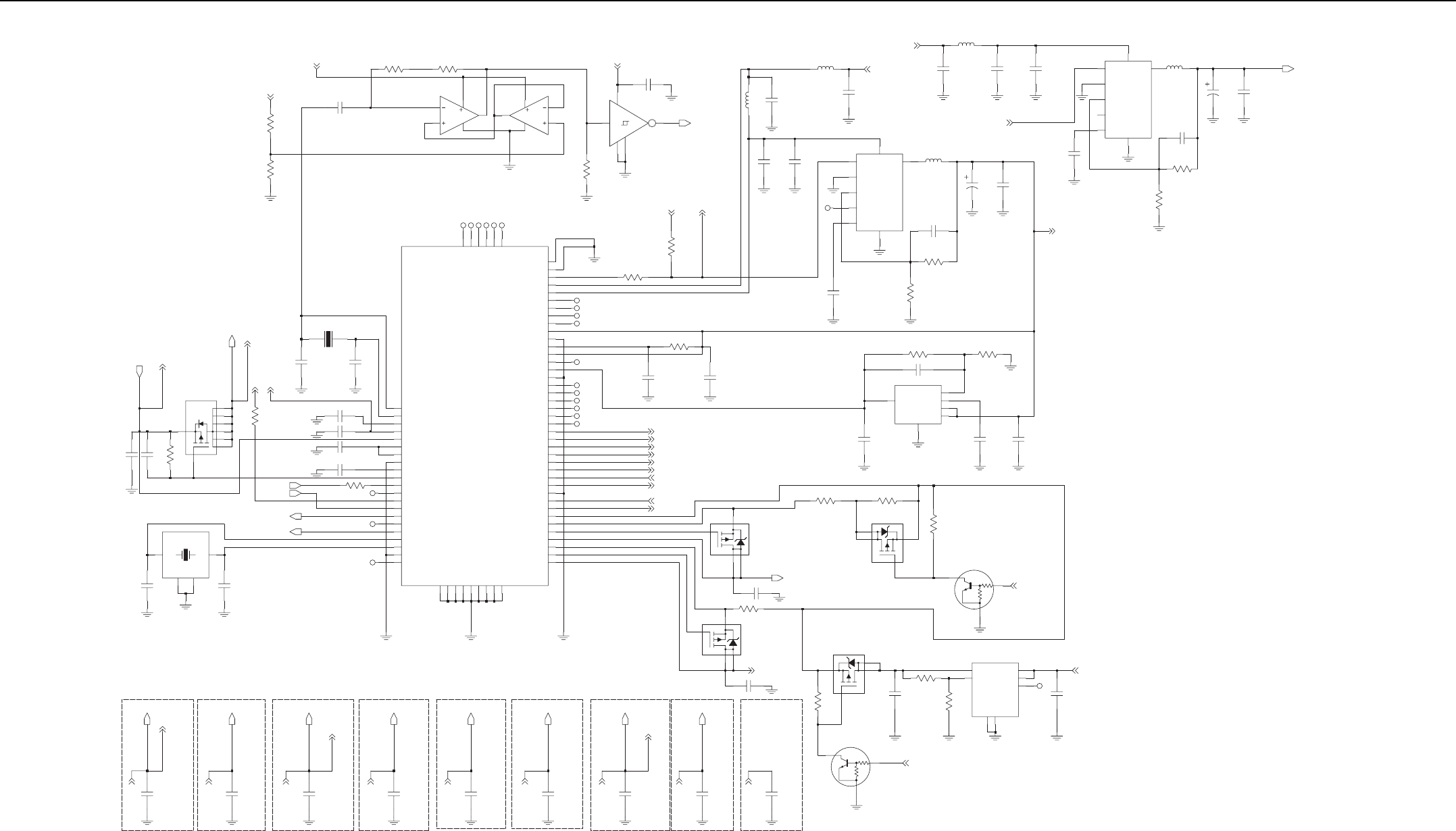
5-24 Controller Schematics
100pF
C3051
RAWB+
RAWB+
C3093
2.2uF 100K
R3050
Q3003
1
2
3
6
7
8
4
5
10K
R3075
VSAVE
SWB+
SWB+
VSAVE
C3001
13pF 13pF
C3000
1
32.768KHz
XTAL
Y3000
2
2.2uFC3004
C3002 0.1uF
2.2uFC3003
1000pFC3005
DNP
NC
NC
R3888 0
MECH_SW
EMERG_PB
MAKO_INT
POR
16-54MHz
CX-101F
Y3001
GND2
4
13
2GND1
C3060
20pF
C3061
20pF
HOT1HOT2
NC
C2
A13
A12
C1
B1
B3
M1
D4
D3
C5
G4
B4
D5
E4
D2
D1
F3
B2
F4
E2
F5
VSAVE
XIN
XOUT
XTAL32_IN
XTAL32_OUT
V10_O
VBUS1
VBUS1_CMD
VBUS1_SENS
VBUS2
VBUS2_CMD
VBUS2_SENS
VBUS_SUPPLY
V04_O
V06_O
V07_O
V08_I
V08_O
V09_O
V10_GND
V10_I
SW5_VDDHV
SW5_VOUT
SW5_VSENSE
SW_TYPE
TCXO_IN
TCXO_SEL_16_24
V02_O
V03_O
SW2_GND
SW2_LX
SW2_VCC
SW2_VCCS
SW2_VOUT
SW5_PHASE
SW5_SUMCOMP
SW5_VDD
SW1_GND
SW1_PHASE
SW1_SUMCOMP_DL
SW1_VDD
SW1_VDDHV
SW1_VOUT
SW1_VSEN_BST
SW1_VSEN_BUK
NC4
NC5
NC6
PGLDO2
PGLDO3
REG_3V6
RESETX
SW1_DH
GND9
HV_BG
IGN_X
INT_X
MECH_SW
NC1
NC2
NC3
GND1
GND2
GND3
GND4
GND5
GND6
GND7
GND8
BAT_3V6
BAT_7V5
BAT_RTC
BAT_TYPE
EMERG_PB
FET_ENX
GATED_32K_CLK
PWR_MNGR_BLOCK
U3000-1
D9
P5
M7
J4
G5
K9
L4
D14
H5
NC
NC
NC
NC
M6
H10
C14
E12
D12
C13
F11
B13
N5
P3
P6
K3
K4
L1
L9
J10
F13
F12
E14
N4
P4
L14
J14
J12
K14
J13
G11
E13
D13
H14
F14
G14
G13
G12
H12
J11
H11
A2
H13 NC
NC
NC
NC
NC
NC
NC
C3
0
R3031
NC
NC
NC
P14
M5
B14
A1
A14
P1 NC
NC
NC
DNP
R3038
SWB+
MAKO_SW1_VDD
0
U3004
NL17SZ14
3GND
2IN
1NC
4
OUT
5
VCC
R3074
1K
GATED_32KHZ_OMAP
0.10uF
C3063
1.875V_DIG_V2
A2
A3
A1
B1
B3
LMC6035ITLX
U3003-2
C2
C3
C1
B1
B3
U3003-1
LMC6035ITLX
R3072
2MEG
R3073
2MEG
10pF
C3070
2.775V_DIG_V4
220K
R3071
R3070
220K
2.775V_DIG_V4
C3084
0.22uF
560nH
L3004
C3805
0.22uF
560nH
L3003 SWB+ 0.22uF
C3208
SWB+ L3022
560nH
0.10uF
C3206 C3207
10uF
L3020
10uH
U3020
LTC1877
5
MAKO_SW1_VDD
68uF
C3202 .01uF
C3203
20pF
C3204
62K
R3201
220K
R3200
3VFB
6
VIN
4GND
2ITH
8PLLLPF
1RUN SW
7SYNC
C3201
10uF
NC
0.10uF
C3200
2200pF
C3205
220pF
C3212
22uH
L3021
3
VIN6
GND
ITH
2
PLLLPF
8
RUN
1SW 5
SYNC
7
VFB
LTC1877
U3021
220K
R3202
C3211
20pF
300K
R3203
4
22uF
C3209 C3210
.01uF
OMAP_CORE_LTC
3.6V_DIG_VSW1
C3017
.01uF 2.2uF
C3018
R3028
51.1K
C3015 100pF
R3029
41.2K
6
NP 4
VCONT 3
VIN
1VOUT
TK11100CSC
U3008
2
FB
5GND
C3016
2.2uF
0.7
R3103
R3102
2
2
3
1
4
Q3001
4
Q3000
2
3
1
VBUS1
2.775V_ANA_V7
SWB+
5V_ANA_V8
3V_ANA_V9
3.6V_DIG_VSW1
3.3V_DIG_V10
1.875V_DIG_V2
1.55V_DIG_V3
2.775V_DIG_V4
2.9V_DIG_V6
R3016
0.1
C3083
0.10uF
0.10uF
C3082
C3039 4.7uF
0.2
Q3010
2
3
1
4
R3030
4.7uFC3081
5V_ANA_VBUS2
47K
1
4
Q3005
2
3
R3100
Q3006
R1
R2
GND
IN
OUT 3.3V_DIG_V10
R3017
178K
10uF
C3090
3
NC
VIN1 1
VIN2 6
VOUT
5
LP8340
U3002
4ADJ
GND1
2
7GND2
R3018
51K
C3091
10uF
NC
SWB+
GND
IN
OUT
Q3002
R1
R2
USB_CONNECT
100K
R3101
1.0uF
C3031 C3028
2.2uF
2.2uF
C3010 C3074
1.0uF1.0uF
C3019
1.0uF
C3067
1.0uF
C3024C3014
2.2uF 4.7uF
C3079
1.875V_DIG_V2
1.875V_DIG_V2
1.875V_DIG_V2 1.55V_DIG_V3
1.55V_DIG_V3
2.775V_DIG_V4
2.775V_DIG_V4
2.775V_DIG_V4
2.9V_DIG_V6
5V_ANA_VBUS2
5V_ANA_VBUS2 2.9V_DIG_V6
2.775V_ANA_V7
2.775V_ANA_V7
5V_ANA_V8
5V_ANA_V8
5V_ANA_V8
3V_ANA_V9
3.3V_DIG_V10
3.3V_DIG_V10
Controller Power Management Block Schematic Diagram (for 8415113H05)
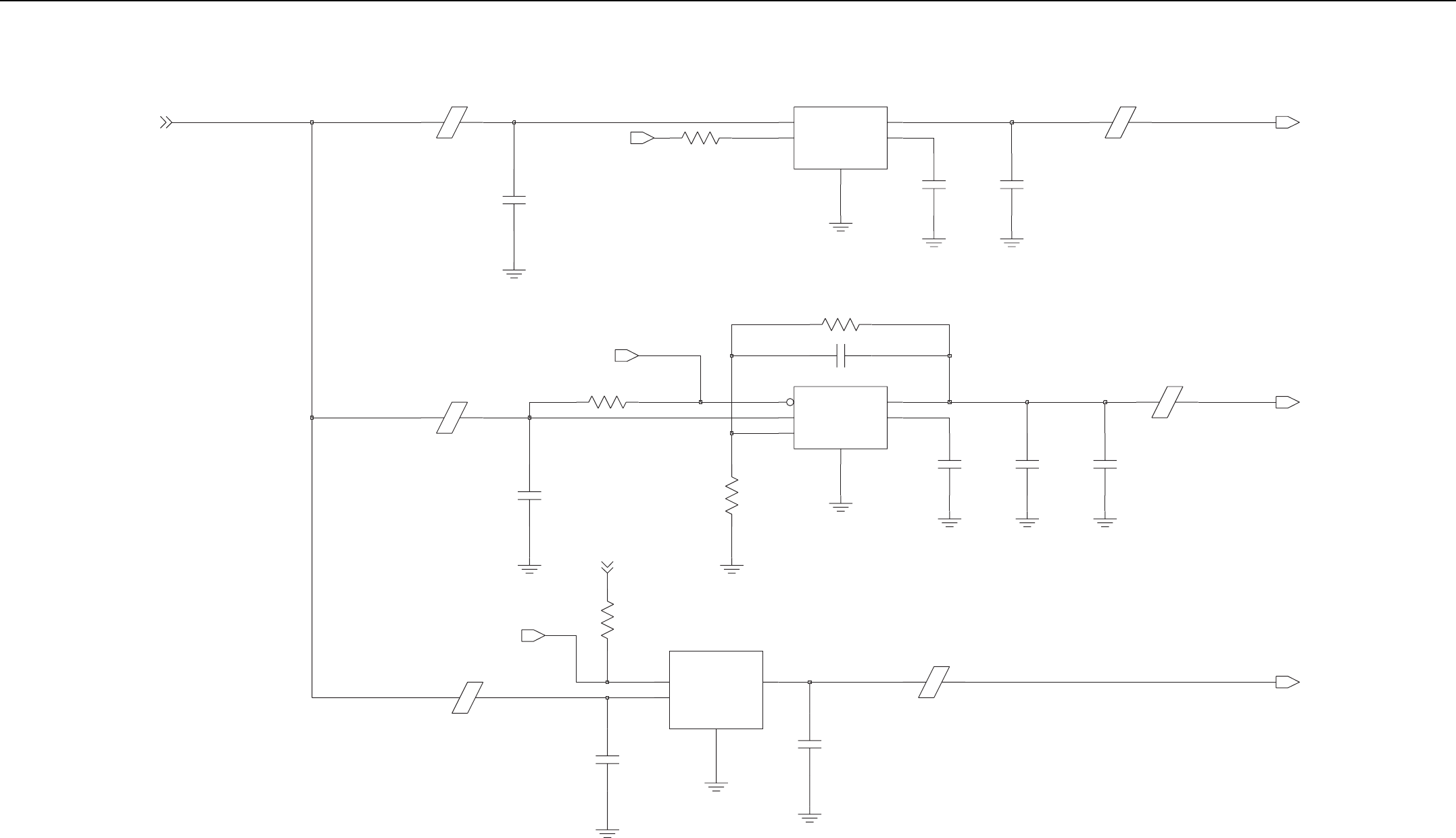
Controller Schematics 5-25
B2 VIN
B1
VOUT
U3006
LP3990
1A D
N
G
A2 VEN
R3700
IDCTR
E3701
21
1K
1.0uF
C3102
1.0uF
C3101
R3704
IDCTR
21
10K
E3705
21
E3704
R3701
2
1
IDCTR
C3700
1.0uF
10K
IDCTR
E3702
21
E3700
IDCTR
21
4
BYPASS
EN
3
FB
5
2DNG
1IN
6
OUT
4
EN
3
D
N
G
2
IN
1OUT 5
U3701
U3700
BYPASS
2
1
470pF
C3706
2.2uF
C3707
R3703
24K
R3702
30K
27pF
C3704
1.0uF
C3703
C3702
2
1
.01uF
C3701
2.2uF
.01uF
E3703
IDCTR
21
C3705
1.875V_DIG_V2
1.5V_GPS_RTC
GPS_SHUTDOWN
2.8V_RF_GPS
2.8V_DIG_GPS
GPS_RFPWRUP
GPS_nWAKEUP
3.6V_DIG_VSW1
Controller Line Regulators for GPS Schematic Diagram
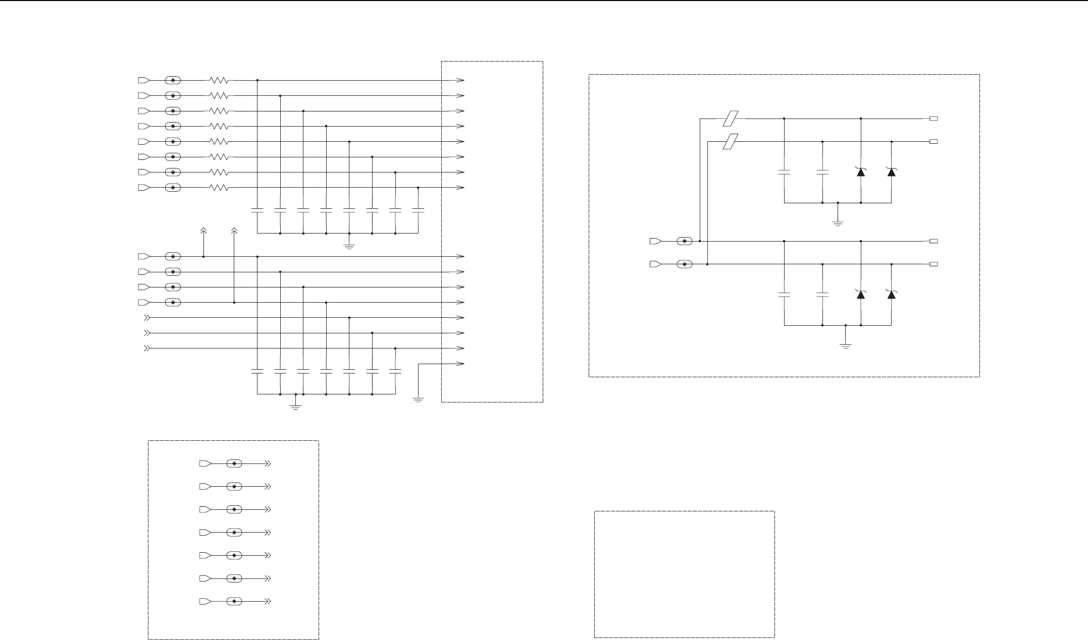
5-26 Controller Schematics
DISPLAY_DATA7
DISPLAY_DATA6
DISPLAY_DATA5
DISPLAY_DATA4
DISPLAY_DATA3
DISPLAY_DATA2
DISPLAY_DATA1
DISPLAY_DATA0 1K
1K
1K
1K
1K
1K
1K
1K
R9000
DISPLAY_DATA0_SW
R9002
R9005
DISPLAY_DATA7_SW
R9003
R9006
DISPLAY_DATA5_SW
DISPLAY_DATA6_SW
DISPLAY_DATA4_SW R9004
DISPLAY_DATA2_SW
R9001
DISPLAY_DATA1_SW
R9007
DISPLAY_DATA3_SW
DISPLAY_CMD_SW
BL_EN_SW
RESET_OUT_SW
DISPLAY_CE_SW
BL_EN
DISPLAY_CMD
DISPLAY_CE
RESET_OUT
SWB+
2.775V_DIG_V4
1.875V_DIG_V2
BL_EN
RESET_OUT
C9007
100pF
C9000
100pF 100pF
C9002 C9005
100pF
100pF
C9004
100pF
C9003
100pF
C9001
100pF
C9006
DISPLAY B2B 16 PINS CONNECTOR (2887818K02)
B2B_DISPLAY_DATA6
B2B_DISPLAY_DATA5
B2B_DISPLAY_DATA7
B2B_DISPLAY_DATA1
B2B_DISPLAY_DATA0
B2B_DISPLAY_DATA4
B2B_DISPLAY_DATA3
B2B_DISPLAY_DATA2
DISPLAY_DATA7
RESET_OUT
1.875V_DIG_V2
DISPLAY_CE
DISPLAY_DATA1
DISPLAY_CMD
GND
SWB+
DISPLAY_DATA2
DISPLAY_DATA3
BL_EN
DISPLAY_DATA5
2.775V_DIG_V4
DISPLAY_DATA6
DISPLAY_DATA4
DISPLAY_DATA0
P9000-9
P9000-16
P9000-12
P9000-14
P9000-11
P9000-8
P9000-7
P9000-3
P9000-15
P9000-1
P9000-5
P9000-2
P9000-4
P9000-6
P9000-13
P9000-10
C9012
100pF100pF
C9011 C9013
100pF100pF
C9010
100pF
C9009
100pF
C9014C9008
100pF
3.3V_DIG_V10_SW
3.3V_DIG_V103.3V_DIG_V10
2.9V_DIG_V6_SW
2.775V_DIG_V4_SW
5V_ANA_VBUS2_SW
1.875V_DIG_V2_SW
SWB_P_SW
VBUS1_SW
5V_ANA_VBUS2
1.875V_DIG_V21.875V_DIG_V2
5V_ANA_VBUS2
2.9V_DIG_V62.9V_DIG_V6
2.775V_DIG_V4 2.775V_DIG_V4
VBUS1VBUS1
SWB+SWB+
VR9018
Largest reference designator
C9068
D9000
FL9000
S9002
E9007 J9001
R9018
L9008
P9000
Q9003 M9007
INTERNAL SPEAKER CONTACT
INT_SPKR_P_SW
INT_SPKR_M_SW
INT_SPKR+
INT_SPKR-
DNP
DNP
DNP
DNP
BLM18BD601SN1
E9007
100pF
C9067
BLM18BD601SN1
E9006
C9068
100pF
INT_SPKR+_TOP
INT_SPKR-_TOP
DNP DNP
VR9016
10.0V
10.0V
VR9015
DNP
DNP
1M9003
M9004
1
M9006
1
M9005
1
10.0V
VR9018
VR9017
10.0V
100pF
C9061 C9062
100pF
INT_SPKR+
INT_SPKR-
Controller LCD and Speaker Interface Schematic Diagram (for 8486716Z04, 8486716Z07 & 8486716Z08)
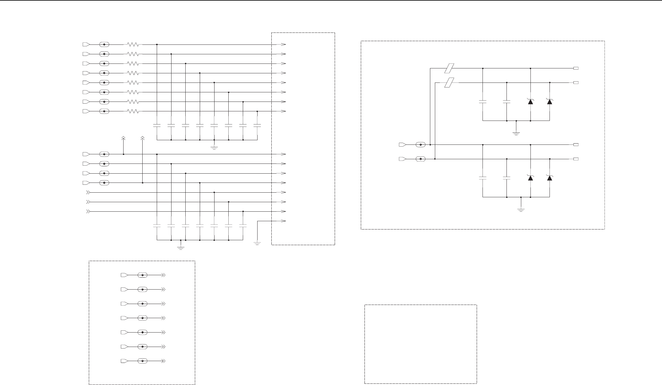
Controller Schematics 5-27
1K
1K
1K
1K
1K
1K
1K
1K
R9000
R9002
R9005
R9003
R9006
R9004
R9001
R9007
DISPLAY_DATA0_SW
DISPLAY_DATA7_SW
DISPLAY_DATA5_SW
DISPLAY_DATA6_SW
DISPLAY_DATA4_SW
DISPLAY_DATA2_SW
DISPLAY_DATA1_SW
DISPLAY_DATA3_SW
DISPLAY_DATA7
DISPLAY_DATA6
DISPLAY_DATA5
DISPLAY_DATA4
DISPLAY_DATA3
DISPLAY_DATA2
DISPLAY_DATA1
DISPLAY_DATA0
DISPLAY_CMD_SW
BL_EN_SW
RESET_OUT_SW
DISPLAY_CE_SW
BL_EN
BL_EN
DISPLAY_CMD
DISPLAY_CE
RESET_OUT
RESET_OUT
SWB+
2.775V_DIG_V4
1.875V_DIG_V2
C9007
330pF
C9000
330pF 330pF
C9002 C9005
330pF
330pF
C9004
330pF
C9003
330pF
C9001
330pF
C9006
B2B_DISPLAY_DATA6
B2B_DISPLAY_DATA5
B2B_DISPLAY_DATA7
B2B_DISPLAY_DATA1
B2B_DISPLAY_DATA0
B2B_DISPLAY_DATA4
B2B_DISPLAY_DATA3
B2B_DISPLAY_DATA2
DISPLAY B2B 16 PINS CONNECTOR (2887818K02)
DISPLAY_DATA4
DISPLAY_DATA0
DISPLAY_CMD
DISPLAY_DATA2
DISPLAY_DATA3
BL_EN
DISPLAY_DATA5
2.775V_DIG_V4
DISPLAY_DATA6
DISPLAY_DATA7
RESET_OUT
1.875V_DIG_V2
DISPLAY_CE
DISPLAY_DATA1
GND
SWB+
P9000-9
P9000-16
P9000-12
P9000-14
P9000-11
P9000-8
P9000-7
P9000-3
P9000-15
P9000-1
P9000-5
P9000-2
P9000-4
P9000-6
P9000-13
P9000-10
C9012
330pF330pF
C9011 C9013
330pF330pF
C9010
330pF
C9009
330pF
C9014C9008
330pF
3.3V_DIG_V103.3V_DIG_V10
2.775V_DIG_V4 2.775V_DIG_V4
5V_ANA_VBUS2
1.875V_DIG_V21.875V_DIG_V2
5V_ANA_VBUS2
2.9V_DIG_V62.9V_DIG_V6
VBUS1 VBUS1
SWB+SWB+
3.3V_DIG_V10_SW
2.9V_DIG_V6_SW
2.775V_DIG_V4_SW
5V_ANA_VBUS2_SW
1.875V_DIG_V2_SW
SWB_P_SW
VBUS1_SW
M9007
E9007 J9001
R9018
L9008
VR9018 P9000
Largest reference designator
Q9003
C9070
D9000
FL9000
S9002
INT_SPKR+
INT_SPKR-
INT_SPKR_M_SW
INT_SPKR_P_SW
INTERNAL SPEAKER CONTACT
DNP
DNP
M9006
M9005
M9003
M9004
1
1
1
1
INT_SPKR+
INT_SPKR-
INT_SPKR-_TOP
INT_SPKR+_TOP
DNP
BLM18BD601SN1
E9006
DNP
BLM18BD601SN1
E9007
DNP
10.0V
VR9015
DNP
VR9016
10.0V
DNP DNP
330pF
C9067 C9068
330pF
330pF
C9061 C9062
330pF
10.0V
VR9018
VR9017
10.0V
Controller LCD and Speaker Interface Schematic Diagram (for 8415113H03 & 8415113H05)
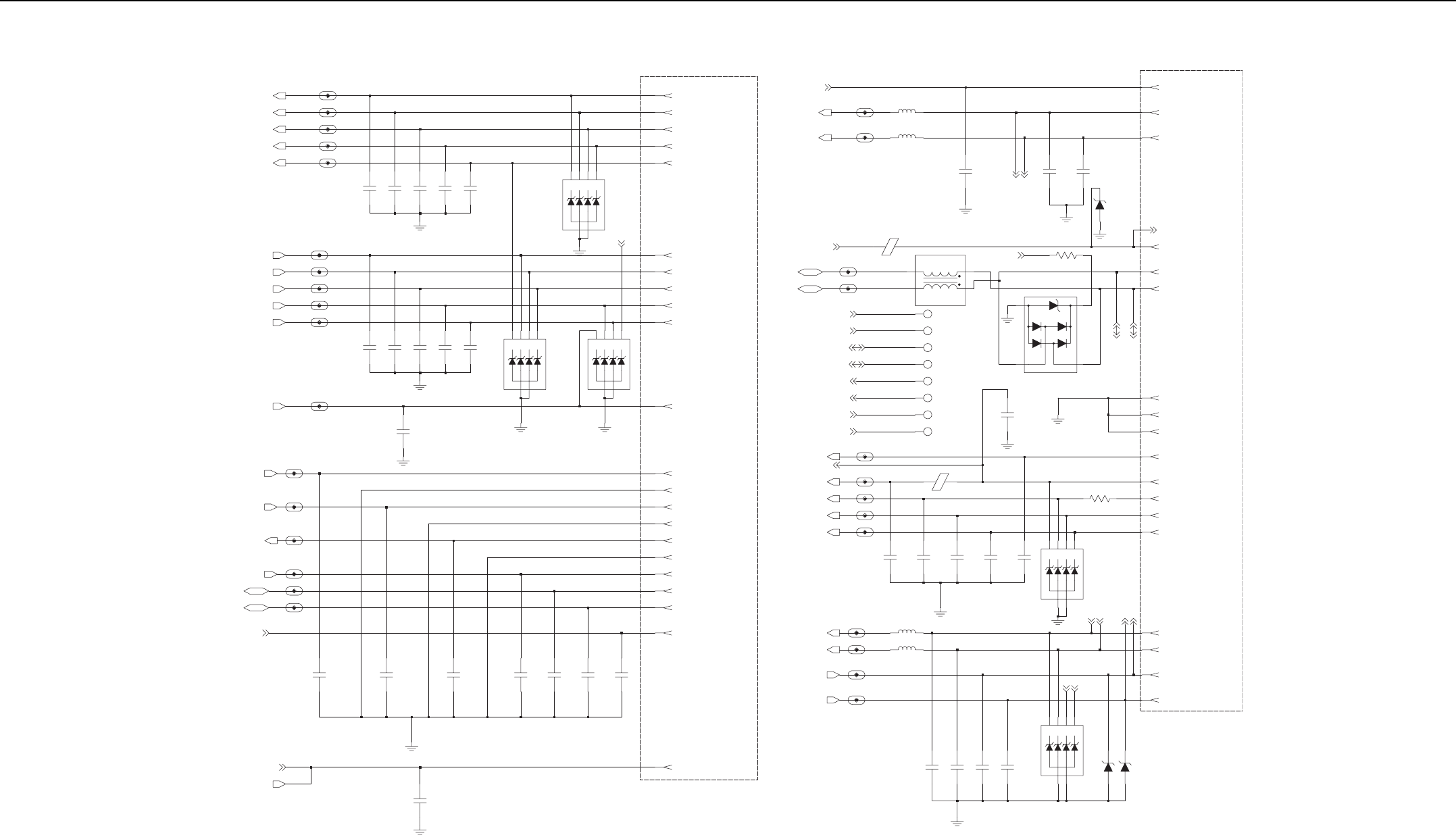
5-28 Controller Schematics
KEYPAD_ROW1_SW
KEYPAD_ROW2_SW
KEYPAD_ROW0_SW
KEYPAD_ROW4_SW
KEYPAD_ROW3_SW
KEYPAD_ROW0
KEYPAD_ROW1
KEYPAD_ROW2
KEYPAD_ROW3
KEYPAD_ROW4
C9040
100pF
C9042
100pF
C9044
100pF100pF
C9043
100pF
C9041
KEYPAD_COL0_SW
KEYPAD_COL3_SW
KEYPAD_COL4_SW
KEYPAD_COL1_SW
KEYPAD_COL2_SW
KEYPAD_COL4
KEYPAD_COL0
KEYPAD_COL1
KEYPAD_COL2
KEYPAD_COL3
100pF
C9045 C9046
100pF
C9048
100pF
C9049
100pF100pF
C9047
4
K3
6
K4
VR9021
5.6V
1
K1
3
K2
2
A1
5
A2
PTT_SW
100pF
C9050
PTT
OPT_GPIO_2_SW
MAKO_RX_SW
OPT_GPIO_1_SW
MAKO_FSYNC_SW
MAKO_TX_SW
MAKO_DCLK
MAKO_TX
MAKO_RX
MAKO_DCLK
MAKO_FSYNC
OPT_GPIO_1
OPT_GPIO_2
RESET_OUT
DNP DNPDNP DNP
C9053
100pF
100pF
C9051 C9058
100pF
100pF
C9055
100pF
C9057 C9060
100pF100pF
C9059
100pF
C9065
SWB+
SWB+
GND
KEYPAD_COL3
MAKO_RX
KEYPAD_COL2
RESET_OUT
KEYPAD_ROW4
KEYPAD_COL4
KEYPAD_ROW0
GND
MAKO_TX
KEYPAD_ROW2
MAKO_FSYNC
OPT_GPIO_2
KEYPAD_COL1
SWB+
KEYPAD_COL0
PTT
MAKO_DCLK
OPT_GPIO_1
KEYPAD_ROW3
KEYPAD_ROW1
GND
J9001-25
J9001-14
J9001-32
J9001-30
J9001-20
J9001-31
J9001-28
J9001-29
J9001-11
J9001-27
J9001-16
J9001-10
J9001-19
J9001-33
J9001-13
J9001-24
J9001-12
J9001-17
J9001-18
J9001-15
J9001-26
J9001-9
A1
5
A2
1
K1
3
K2
4
K3
6
K4
VR9020
5.6V
2
BL_EN
A1
2
A2
5
K1
1
K2
3
K3
4
K4
6
5.6V
VR9022
USB1_DM_SW
USB1_DP_SW
USB1_DP
USB1_DM
VBUS1
OPT-Trans B2B 40 PINS CONNECTOR (0970312L01)
INT_MIC+
INT_MIC-
BL_EN
INT_MIC_P_SW
L9008
270nH
L9007
INT_MIC_M_SW 270nH
100pF
C9066
OPT_INT_MIC_P
OPT_INT_MIC_M
VR9023
10.0V
100pF
100pF
C9063
C9064
1K
R9019
5V_ANA_VBUS2
E9000
BLM21PG221SN1
DLP11SN201HL2
FL9000
3
P2
1
S1
4
S2
2P1
TP_ONE_WIRE_1
1
TP_VBUS1
1
TP_EXT_MIC+
1
TP_USB1_DM
1
1TP_USB1_DP
1
TP_EXT_MIC
1
TP_EXT_SPKR+
TP_EXT_SPKR
1
MAKO_ONE_WIRE_1
OPT_VBUS1
OPT_EXT_MIC+
OPT_EXT_MIC-
OPT_USB1_DP
OPT_USB1_DM
EXT_SPKR+
EXT_SPKR-
OPT_SSI_SYNC_SW
OPTA_SEL1_SW
OPTA_SEL2_SW
OPTA_SEL0_SW
ONE_WIRE_1_SW
ONE_WIRE_1
OPTA_SEL1
OPTA_SEL2
OPT_SSI_SYNC
OPTA_SEL0
MAKO_ONE_WIRE_1 BK1005HM471
E9001
DNP
C9017
100pF 100pF
C9069
100pF
C9018
100pF
C9015 C9016
100pF
270nH
L9000
L9001
270nH
EXT_SPKR-
EXT_SPKR+
EXT_MIC+
EXT_MIC-
EXT_MIC_M_SW
EXT_SPKR_M_SW
EXT_MIC_P_SW
EXT_SPKR_P_SW
C9021
100pF 100pF
C9022
100pF
C9019
100pF
C9020
10.0V
VR9004
VR9003
10.0V
346 5.6V
VR9002
1
K1
K2
K3
K4
2
A1
5
A2
OPTA_SEL1
GND
OPTA_SEL0
VBUS1
GND
ONE_WIRE1
INT_MIC+
OPT_SSI_SYNC
OPTA_SEL2
INT_MIC-
EXT_SPKR-
EXT_SPKR+
EXT_MIC-
USB1_DP
EXT_MIC+
BL_EN
GND
USB1_DM
J9001-23
J9001-36
J9001-3
J9001-5
J9001-34
J9001-35
J9001-38
J9001-22
J9001-4
J9001-37
J9001-40
J9001-1
J9001-8
J9001-21
J9001-39
J9001-7
J9001-2
J9001-6
OPT_VBUS1
2
A1
5
A2
1346
VR9001
5.6V
EXT_SPKR-
EXT_SPKR+
OPT_EXT_MIC+
OPT_EXT_MIC-
R9052
470
C9033
100pF
OPT_USB1_DM
OPT_USB1_DP
4
VR9000
SR05
1
32
K1
K2
K3
K4
OPT_INT_MIC_M
OPT_INT_MIC_P
Controller UC Interface Schematic Diagram (for 8486716Z04 & 8486716Z07)
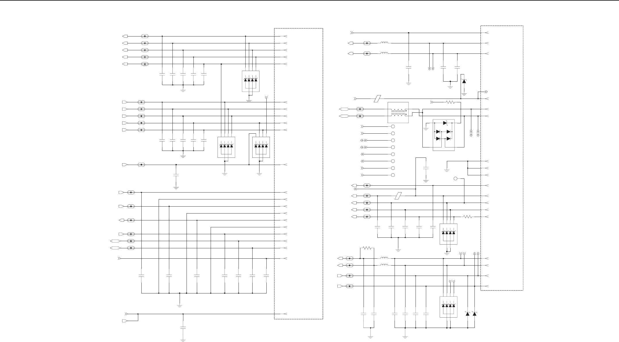
Controller Schematics 5-29
KEYPAD_ROW0
KEYPAD_ROW1
KEYPAD_ROW2
KEYPAD_ROW3
KEYPAD_COL4
KEYPAD_ROW4
KEYPAD_COL0
KEYPAD_COL1
KEYPAD_COL2
KEYPAD_COL3
KEYPAD_ROW2_SW
KEYPAD_ROW0_SW
KEYPAD_ROW3_SW
KEYPAD_COL2_SW
KEYPAD_COL3_SW
KEYPAD_COL4_SW
KEYPAD_COL1_SW
KEYPAD_COL0_SW
KEYPAD_ROW4_SW
KEYPAD_ROW1_SW
100pF
C9044C9043
100pF
100pF
C9040
100pF
C9042C9041
100pF
OPT-Trans B2B 40 PINS CONNECTOR (0970312L01)
K1
1
K2
3
K3
4
K4
6
2
A2
5
5.6V
VR9020
A1
BL_EN
VR9022
5.6V
1346
2
A1
5
A2
K1
K2
K3
K4
K1
1
K2
3
K3
4
K4
6
5.6V
VR9021
A1
2
A2
5
C9048
100pF
C9047
100pF
100pF
C9046 C9049
100pF
C9045
100pF
PTT_SW
100pF
C9050
PTT
MAKO_TX
MAKO_RX
MAKO_DCLK
MAKO_FSYNC
OPT_GPIO_1
OPT_GPIO_2
RESET_OUT
MAKO_RX_SW
MAKO_FSYNC_SW
MAKO_DCLK
MAKO_TX_SW
OPT_GPIO_1_SW
OPT_GPIO_2_SW
DNPDNP DNPDNP
100pF
C9051 C9055
100pF
C9059
100pF100pF
C9058C9057
100pF
C9053
100pF
C9060
100pF
C9065
100pF
SWB+
SWB+
KEYPAD_ROW0
GND
PTT
MAKO_DCLK
KEYPAD_COL1
KEYPAD_COL3
MAKO_RX
KEYPAD_COL2
KEYPAD_ROW4
KEYPAD_ROW1
GND
RESET_OUT
MAKO_TX
KEYPAD_ROW2
MAKO_FSYNC
OPT_GPIO_2
GND
KEYPAD_COL4
SWB+
KEYPAD_COL0
OPT_GPIO_1
KEYPAD_ROW3
J9001-19
J9001-24
J9001-29
J9001-18
J9001-12
J9001-30
J9001-32
J9001-15
J9001-26
J9001-16
J9001-28
J9001-17
J9001-9
J9001-14
J9001-10
J9001-33
J9001-27
J9001-13
J9001-31
J9001-20
J9001-11
J9001-25
EXT_SPKR_M_SW
EXT_MIC_P_SW
EXT_SPKR_P_SW
EXT_MIC_M_SW
EXT_MIC-
EXT_MIC+
EXT_SPKR-
EXT_SPKR+
DNP
R9020
4.7K
270nH
L9001
L9000
270nH
DNP DNP
C9020
100pF
C9071
100pF
C9072
100pF
C9019
100pF
C9022
100pF100pF
C9021
46 VR9002
5.6V
A1
2
A2
5
13
10.0V
VR9003 VR9004
10.0V
OPT_INT_MIC_M
OPT_INT_MIC_P
EXT_SPKR-
EXT_SPKR+
OPT_EXT_MIC+
OPT_EXT_MIC-
R9052
470
K3
K4
K1
K2
5.6V
VR9001
346
A1
2
A2
5
1
DNP
100pF
C9016
100pF
C9018C9017
100pF
C9015
100pF
C9069
100pF
ONE_WIRE_1
OPTA_SEL0
OPT_SSI_SYNC
OPTA_SEL1
MAKO_ONE_WIRE_1
OPTA_SEL2
ONE_WIRE_1_SW
OPTA_SEL0_SW
OPTA_SEL2_SW
OPTA_SEL1_SW
OPT_SSI_SYNC_SW
E9001
BK1005HM471
1TP_EXT_MIC+
TP_USB1_DM
1
1
1
TP_EXT_MIC
TP_USB1_DP
1
TP_EXT_SPKR+
1TP_ONE_WIRE_1
TP_EXT_SPKR
1
1TP_VBUS1
MAKO_ONE_WIRE_1
OPT_VBUS1
OPT_EXT_MIC+
OPT_EXT_MIC-
OPT_USB1_DP
OPT_USB1_DM
EXT_SPKR+
EXT_SPKR-
USB1_DP_SW
USB1_DM_SW
USB1_DP
USB1_DM
VBUS1 FL9000
DLP11SN201HL2
BLM21PG221SN1
E9000
P2
3
S1 1
S2
4
P1
2
5V_ANA_VBUS2
R9019
10.0V
VR9023
100pF
C9064
C9063
100pF
OPT_INT_MIC_P
OPT_INT_MIC_M
1K
100pF
C9066
INT_MIC+
INT_MIC-
BL_EN
INT_MIC_P_SW
L9007
270nH
L9008
INT_MIC_M_SW
270nH
OPTA_SEL2
INT_MIC-
OPTA_SEL1
GND
OPTA_SEL0
VBUS1
GND
ONE_WIRE1
GND
INT_MIC+
OPT_SSI_SYNC
USB1_DM
EXT_SPKR-
EXT_SPKR+
EXT_MIC-
USB1_DP
EXT_MIC+
BL_EN
J9001-5
J9001-39
J9001-2
J9001-38
J9001-34
J9001-21
J9001-1
J9001-7
J9001-6
J9001-35
J9001-36
J9001-22
J9001-23
J9001-40
J9001-4
J9001-3
J9001-8
J9001-37
OPT_VBUS1
VR9000
1
32
4
SR05
OPT_USB1_DM
OPT_USB1_DP
C9033
100pF
TP_GPIO0 1
K3
K4
K1
K2
Controller UC Interface Schematic Diagram (for 8486716Z08)
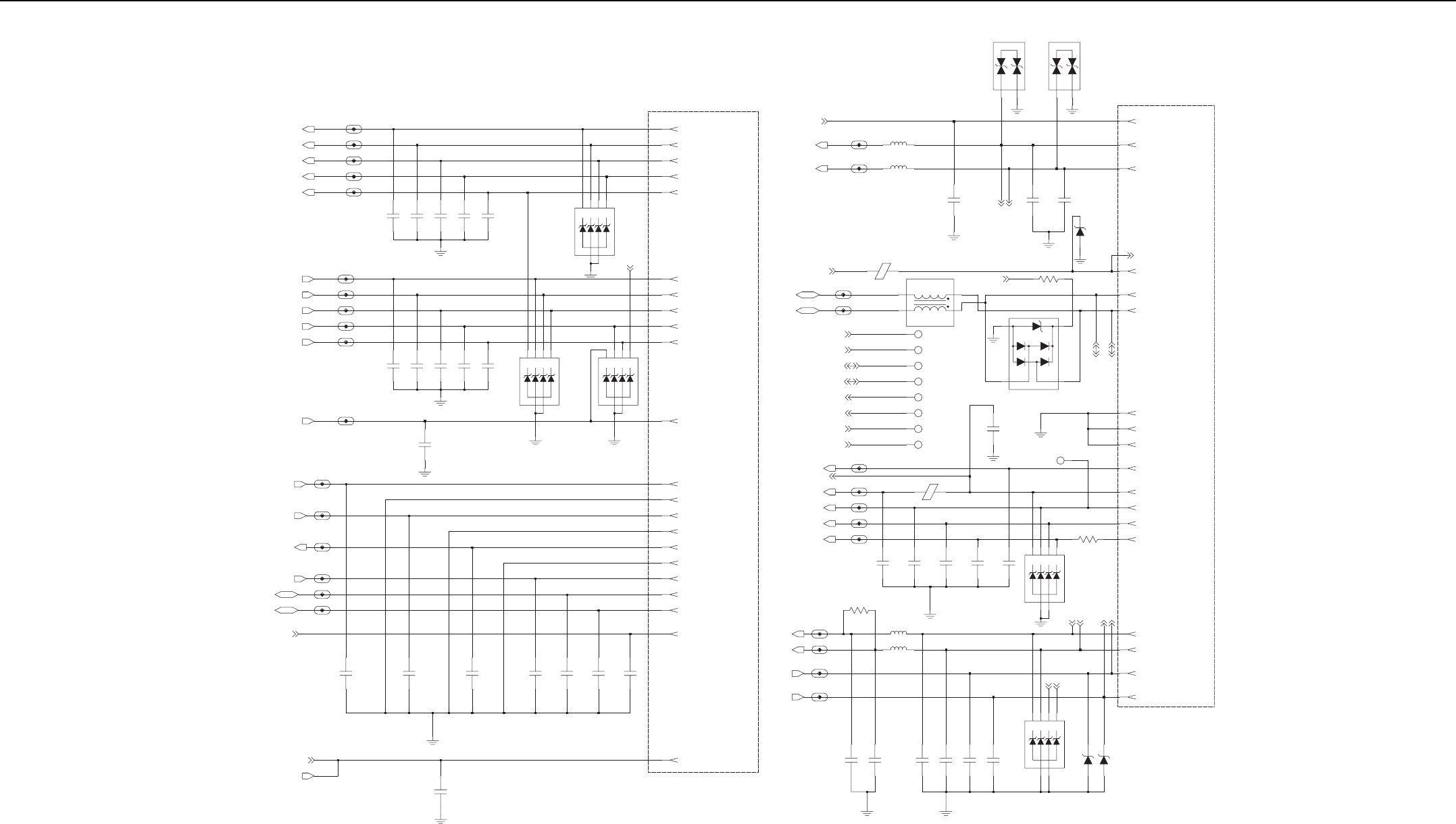
5-30 Controller Schematics
KEYPAD_ROW0
KEYPAD_ROW1
KEYPAD_ROW2
KEYPAD_ROW3
KEYPAD_COL4
KEYPAD_ROW4
KEYPAD_COL0
KEYPAD_COL1
KEYPAD_COL2
KEYPAD_COL3
KEYPAD_ROW0_SW
KEYPAD_COL1_SW
KEYPAD_ROW1_SW
KEYPAD_COL4_SW
KEYPAD_COL2_SW
KEYPAD_COL0_SW
KEYPAD_ROW2_SW
KEYPAD_ROW3_SW
KEYPAD_ROW4_SW
KEYPAD_COL3_SW
C9042
330pF
C9040
330pF
C9044
330pF
C9043
330pF
330pF
C9041
330pF
C9046
330pF
C9048
330pF
C9045 C9049
330pF330pF
C9047
3
K2
4
K3
6
K4
2
A1
5
A2
1
K1
VR9021
5.6V
PTT_SW
C9050
330pF
PTT
MAKO_TX_SW
OPT_GPIO_2_SW
MAKO_DCLK
MAKO_RX_SW
OPT_GPIO_1_SW
MAKO_FSYNC_SW
MAKO_TX
MAKO_RX
MAKO_DCLK
MAKO_FSYNC
OPT_GPIO_1
OPT_GPIO_2
RESET_OUT
SWB+
SWB+
330pF
C9065
DNP DNPDNP DNP
C9051
330pF 330pF
C9060
C9058
330pF330pF
C9053
330pF
C9057
330pF
C9055
330pF
C9059
MAKO_TX
KEYPAD_ROW2
MAKO_FSYNC
KEYPAD_COL4
KEYPAD_ROW1
GND
OPT_GPIO_1
KEYPAD_ROW3
GND
OPT_GPIO_2
PTT
MAKO_DCLK
RESET_OUT
KEYPAD_ROW4
SWB+
KEYPAD_COL0
KEYPAD_COL1
OPT-Trans B2B 40 PINS CONNECTOR (0970312L01)
MAKO_RX
KEYPAD_COL2
GND
KEYPAD_COL3
KEYPAD_ROW0
J9001-13
J9001-27
J9001-32
J9001-30
J9001-29
J9001-11
J9001-31
J9001-16
J9001-12
J9001-14
J9001-20
J9001-17
J9001-15
J9001-26
J9001-19
J9001-28
J9001-24
J9001-25
J9001-9
J9001-18
J9001-33
J9001-10
4
K3
6
K4
VR9020
5.6V
25
1
K1
3
K2
BL_EN
A1
A2
3
K3
4
K4
6
A1
2
A2
5
K1
1
K2
5.6V
VR9022
INT_MIC_M_SW
INT_MIC_P_SW
INT_MIC+
INT_MIC-
BL_EN
L9008
C9066
330pF
270nH
L9007
270nH
1
TP_USB1_DM
1TP_USB1_DP
1
TP_EXT_SPKR
TP_VBUS1
1
TP_ONE_WIRE_1
1
TP_EXT_MIC
1
TP_EXT_SPKR+
1
TP_EXT_MIC+
1
MAKO_ONE_WIRE_1
OPT_VBUS1
OPT_EXT_MIC+
OPT_EXT_MIC-
OPT_USB1_DP
OPT_USB1_DM
EXT_SPKR+
EXT_SPKR-
E9000
BLM21PG221SN1
2P1
3
P2
1
S1
4
S2
DLP11SN201HL2
FL9000
USB1_DP_SW
USB1_DM_SW
5V_ANA_VBUS2
USB1_DP
USB1_DM
VBUS1
OPT_INT_MIC_P
OPT_INT_MIC_M
330pF
C9063 C9064
VR9023
10.0V
330pF
D9001
POS1
POS2
POS1
POS2
D9002
GND
ONE_WIRE1
INT_MIC-
OPT_SSI_SYNC
OPTA_SEL2
EXT_SPKR+
USB1_DM
OPTA_SEL1
GND
EXT_SPKR-
OPTA_SEL0
EXT_MIC+
INT_MIC+
VBUS1
GND
EXT_MIC-
USB1_DP
BL_EN
J9001-1
J9001-4
J9001-37
J9001-23
J9001-36
J9001-6
J9001-34
J9001-40
J9001-22
J9001-2
J9001-38
J9001-35
J9001-21
J9001-39
J9001-7
J9001-3
J9001-8
J9001-5
OPT_VBUS1
1K
R9019
SR05
1
32
4
VR9000
OPT_USB1_DM
OPT_USB1_DP
330pF
C9033
1
TP_GPIO0
R9052
470
VR9001
5.6V
EXT_SPKR-
EXT_SPKR+
OPT_EXT_MIC+
OPT_EXT_MIC-
K1
K2
K3
K4
2
A1
5
A2
1346
DNP
330pF
C9015
330pF
C9069
C9018
330pF
330pF
C9017C9016
330pF
3.3uH
L9000
L9001
270nH
R9020
EXT_SPKR_P_SW
EXT_MIC_P_SW
EXT_MIC_M_SW
EXT_SPKR_M_SW
EXT_MIC+
EXT_MIC-
EXT_SPKR-
EXT_SPKR+
4.7K
ONE_WIRE_1_SW
OPTA_SEL0_SW
OPT_SSI_SYNC_SW
OPTA_SEL1_SW
OPTA_SEL2_SW
ONE_WIRE_1
OPTA_SEL2
OPT_SSI_SYNC
OPTA_SEL1
OPTA_SEL0
MAKO_ONE_WIRE_1 E9001
BK1005HM471
OPT_INT_MIC_M
OPT_INT_MIC_P
46
VR9002
25
13 5.6V
K2
K3
K4
A1
A2
K1
10.0V
VR9004VR9003
10.0V
DNP DNP
C9021
330pF
330pF
C9020
330pF
C9019
330pF
C9022
C9072
330pF
C9071
330pF
Controller UC Interface Schematic Diagram (for 8415113H03 & 8415113H05)
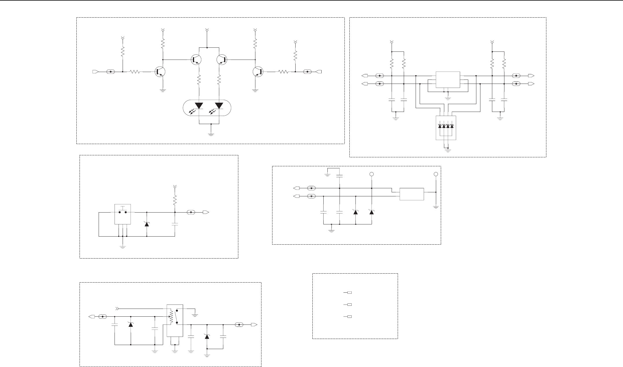
Controller Schematics 5-31
RED & GREEN LEDS
R9050
10K
47K
R9008
1.875V_DIG_V2
3.3V_DIG_V10
RED_LED_SW
RED_LED
R9009
10K
1
3
2
Q9000
MMBT3904
5
1
6
IMXFT110
Q9001-1
2
4
3
Q9001-2
IMXFT110
SWB+
R9013
180680
R9012
Q9003
MMBT3904
3
2
24
13
D9000
BRPY1204W
EMERGENCY BUTTON
EMERG_PB
GND1
4GND2
5GND3
1IN2
OUT
S9000
SWITCH
3
EMERG_PB_SW
R9014
10K
EMERG_PB
1.875V_DIG_V2
5.6V
VR9005
100pF
C9023
BATTERY CONTACT
RAWB+
BATT_DATA
4.7pF
C9032
RAWB_P_SW
TP_RAWB+
1
BATT_DATA_SW
13V
VR9010
C9039
100pF 13V
VR9009
100pF
C9038
1PIN1
2PIN2
3
PIN3
TP_GND
1
M9007 CONTACT
VOLUMN SWITCH
VOL_SW
VOL
2.9V_DIG_V6
5.6V
VR9006
C9024
100pF C9030
4.7pF
2
5
LOW
1
3HIGH
TAB1
6
TAB2
7
4
100pF
C9025
4.7pF
C9031 VR9007
5.6V
S9001
SWITCH
MECH_SW_SW MECH_SW
BOARD SPACER
BRD_SPACER
M9000
M9001
BRD_SPACER
BRD_SPACER
M9002
R9010
10K
1
47K
R9011
10K
R9051
1.875V_DIG_V2
3.3V_DIG_V10
GREEN_LED_SW
GREEN_LED
FREQUENCY SWITCH
10K
R9016
10K
SW1_SW
R9015
SW2_SW
1.875V_DIG_V2
SW1
SW2
100pF
C9027
C9026
100pF
5_4 2
_8 4
SWITCH
S9002
3C1 6
C2
GND1
7
GND2
8
_1
1
_2
A2
5
K1
1
K2
3
K3
4
K4
6
5.6V
VR9008
A1
2
R9017
10K 10K
R9018
1.875V_DIG_V2
SW4
SW8
SW4_SW
SW8_SW
100pF
C9029
C9028
100pF
Controls and Switches Schematic Diagram (for 8486716Z04)
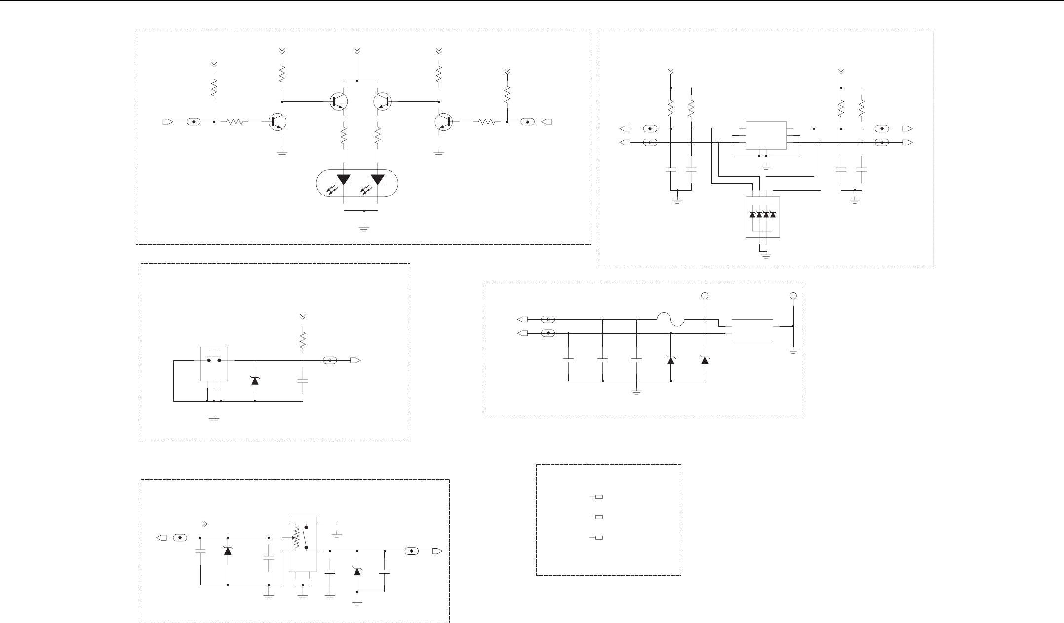
5-32 Controller Schematics
RED & GREEN LEDS
1.875V_DIG_V2
R9050
10K
R9008
47K
RED_LED_SW
RED_LED
10K
R9009
MMBT3904
Q9000
1
3
2
1
6
Q9001-1
IMXFT110
5
3.3V_DIG_V10 3.3V_DIG_V10
SWB+
4
3
IMXFT110
Q9001-2
2
R9010
10K
Q9003 1
3
2
MMBT3904
24
13
BRPY1204W
D9000
33
R9013
R9012
110
GREEN_LED_SW
R9011
47K
R9051
10K
1.875V_DIG_V2
GREEN_LED
FREQUENCY SWITCH
1.875V_DIG_V2
R9016
10K
R9015
10K
SW1_SW
SW2_SW
SW1
SW2
C9027
100pF
C9026
100pF
2
_4
4
_8
C1
3C2 6
7GND1
8GND2
1_1
5_2
K2
4
K3
6
K4
VR9008
5.6V
2
A1
5
A2
1
K1
3
S9002
SWITCH
10K
R9017 R9018
10K
1.875V_DIG_V2
SW8_SW
SW4_SW
SW4
SW8
100pF
C9029
C9028
100pF
TP_GND
1
PIN1
1
PIN2
2PIN3 3
CONTACTM9007
TP_RAWB+
1
F9000 3A
24V
VR9010
13V
100pF
C9039
C9032
4.7pF
13V
VR9009
C9038
100pF
BATTERY CONTACT
BATT_DATA_SW
RAWB_P_SW
RAWB+
BATT_DATA
BOARD SPACER
BRD_SPACER
M9001
M9002
BRD_SPACER
M9000
BRD_SPACER
MECH_SW_SW MECH_SW
C9025
100pF
C9031
4.7pF
VR9007
5.6V
51
HIGH
3
6TAB1
7TAB2
4
2
LOW
SWITCH
S9001
VOLUMN SWITCH
VOL_SW
VOL
100pF
C9024
2.9V_DIG_V6
4.7pF
C9030
VR9006
5.6V
EMERGENCY BUTTON
EMERG_PB
10K
R9014
EMERG_PB_SW
EMERG_PB
1.875V_DIG_V2
VR9005
5.6V
C9023
100pF
IN
1OUT 2
GND1
3
GND2
4
GND3
5
SWITCH
S9000
Controls and Switches Schematic Diagram (for 8486716Z07 & 8486716Z08)
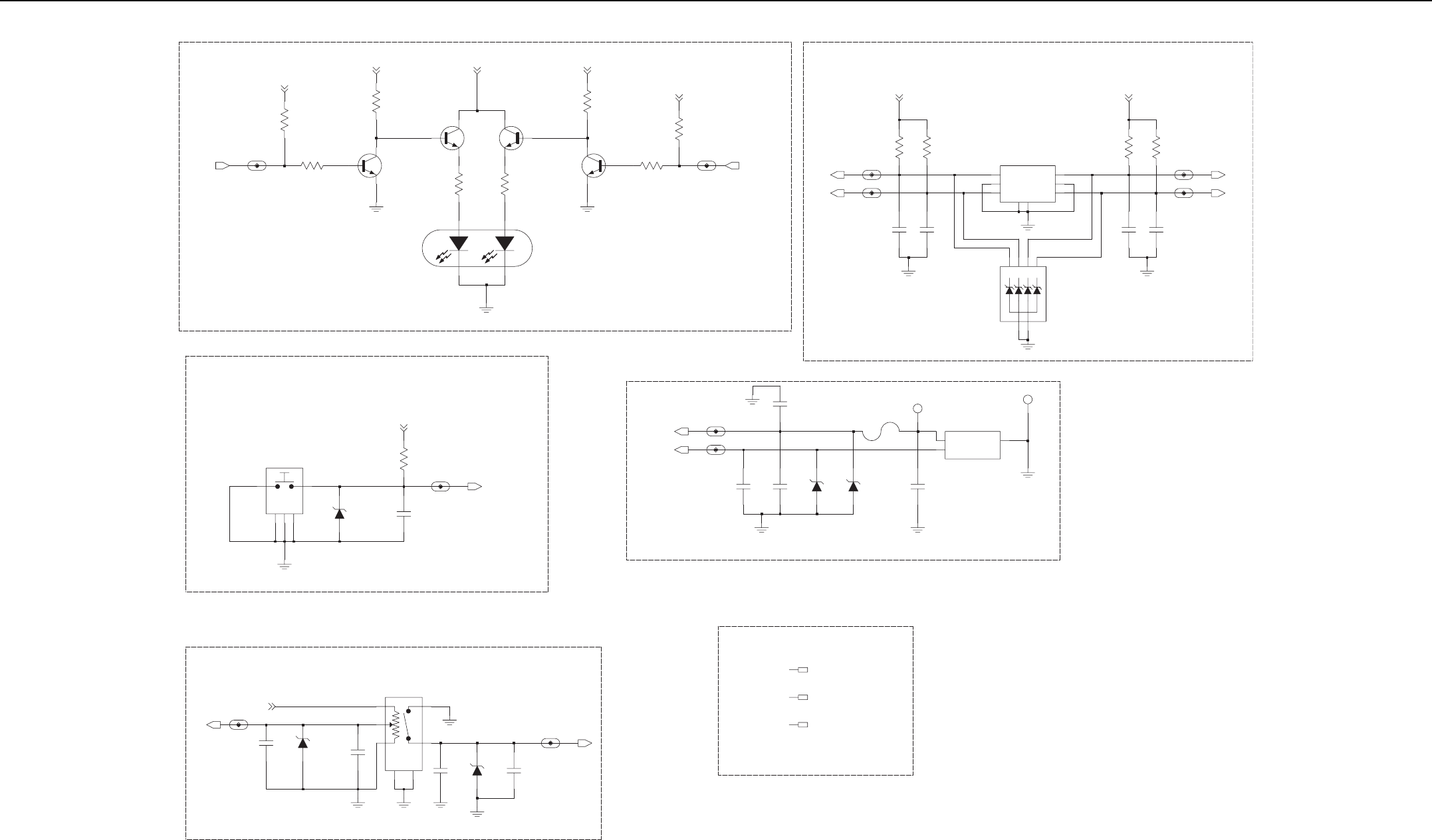
Controller Schematics 5-33
RED & GREEN LEDS
R9050
10K
47K
R9008
1.875V_DIG_V2
RED_LED_SW
RED_LED
2
Q9000
MMBT3904
1
3
R9009
10K
IMXFT110
Q9001-1
5
3.3V_DIG_V10
1
6
2
4
3
Q9001-2
IMXFT110
SWB+
R9013
33
R9012
110
24
13
D9000
BRPY1204W
Q9003
MMBT3904
1
3
2
R9010
10K
3.3V_DIG_V10
GREEN_LED_SW
10K
R9051
47K
R9011
1.875V_DIG_V2
GREEN_LED
FREQUENCY SWITCH
1.875V_DIG_V2
R9015
10K 10K
R9016
SW1_SW
SW2_SW
SW1
SW2
C9027
330pF
C9026
330pF
_8 4
3C1 6
C2
GND1
7
GND2
8
_1
1
_2
5_4 2
SWITCH
S9002
R9017
10K 10K
R9018
SW8_SW
1.875V_DIG_V2
SW4_SW
SW4
SW8
C9028
330pF
C9029
330pF
1
K2
3
K3
4
K4
6
5.6V
VR9008
A1
2
A2
5
K1
TP_GND
1
TP_RAWB+
1
M9007 CONTACT
1PIN1
2PIN2
3
PIN3
5A
24V
12
F9000
BATTERY CONTACT
BATT_DATA_SW
3.9pF
C9032
RAWB_P_SW
RAWB+
BATT_DATA
VR9009
13V
330pF
C9038
13V
VR9010
C9039
330pF 330pF
C9070
BOARD SPACER
M9001
BRD_SPACER
BRD_SPACER
M9002
M9000
BRD_SPACER
MECH_SW_SW MECH_SW
C9025
330pF
3.9pF
C9031 VR9007
5.6V
S9001
SWITCH
2
5
LOW
1
3HIGH
TAB1
6
TAB2
7
4
VOLUMN SWITCH
VOL_SW
5.6V
VR9006 C9030
3.9pF
330pF
C9024
VOL
2.9V_DIG_V6
EMERGENCY BUTTON
EMERG_PB
3GND1
4GND2
5GND3
1IN2
OUT
S9000
SWITCH
EMERG_PB_SW
C9023
330pF
R9014
10K
5.6V
VR9005
EMERG_PB
1.875V_DIG_V2
Controls and Switches Schematic Diagram (for 8415113H03 & 8415113H05)


Section 6
UHF1 (403-470 MHZ) INFORMATION
1.0 Transmitter
Figure 6-1: UHF Transmitter Block diagram
1.1 General
The UHF transmitter contains five basic circuits:
1. Power Amplifier
2. Antenna Switch
3. Harmonic Filter
4. Antenna Matching Network
5. Power Control
1.1.1 Power Amplifier
The power amplifier is a 3-stage discrete design consisting of:
1. Pre-driver, ADA4743 (U700)
2. Driver, RD01MUS1 (Q703)
3. Final PA, RD07MVS1 (Q704)
The pre-driver is a 50 Ohm gain block with a supply voltage of 5V. The supply is ramped to eliminate
feed-through power due to the fixed gain of the device. The pre-driver is biased in Class A region with
a typical current drain of 60mA and power gain of 16.5dB.
The driver is a 1W, LDMOS in a SOT-89 package. this stage typically drains 150mA of current at rated
output power, 4W. The driver is biased in Class AB region and has a power gain of 14dB.
The final PA is a 7W, LDMOS device. The gate threshold of this device is very close to the driver.
Hence, the traditional PA bias tuning is eliminated. The current drain would typically be 1400mA. The
final PA is biased in Class AB region and has a power gain of 10dB.
PA
Pre
-
Driver
PA
Drive
r
PA
F
inal
A
nten na Switch/
Harmonic Filter/
Matching Network
Powe
r
Control
A
ntenna
Jack
F
rom VCO
Vcontrol
Vcontrol

6-2 Transmitter
1.1.2 Antenna Switch
The antenna switch comprises of 2 ports: standard port and remote port.
The antenna switch consist of:
1. Four PIN diodes:
a. CR902 and CR903 biased during standard and remote port operation.
b. CR900 and CR901 biased during remote port operation.
2. Six current limiting resistors:
a. R904, R905 and R9053 for standard and remote port operation.
b. R902, R903 and R9054 for remote port operation.
3. Two pi networks:
a. C915, L908, C916 to determine TX or RX mode.
b. C911, L906, C912 to determine standard port or remote port operation.
In the transmit mode of standard port operation, ANT_EN signal (from MAKO) turns on Q702 (bias
Power Amplifier) and Q900(antenna switch circuit). RAWB+ bias is applied to the standard port
antenna switch circuit to bias CR902 and CR903 “ON”. Hence, the following occurs:
1. Shunt diode (CR903) shorts out the receiver port, and the pi network(C915, L908, C916), which
operates as a quarter wave transmission line, transforms low impedance of the shunt diode to a
high impedance at the input of the harmonic filter. In the receive mode, the diodes are “OFF” and
hence, there exists a low attenuation path between the antenna and the receiver ports.
2. Both CR900 and CR901 is biased “OFF”, and the pi network(C911, L906, C912), which operates
as a quarter wave transmission line, transfers the 50ohm impedance of the harmonic filter to
CR902 and hence, forces PA_OUT to take the standard port circuit path.
In the transmit mode of remote port operation, ANT_EN signal (from MAKO) turns on Q702(bias
Power Amplifier) and Q900(antenna switch circuit) and GP02 signal (from TOMAHAWK) turns on
Q901. RAWB+ bias is applied to the standard and remote port antenna switch circuit to bias CR900,
CR901, CR902 and CR903 “ON”. Hence, the following occurs:
1. Shunt diode(CR903) shorts out the receiver port, and the pi network(C915, L908, C916), which
operates as a quarter wave transmission line, transforms low impedance of the shunt diode to a
high impedance at the input of the harmonic filter. In the receive mode, the diodes are off and
hence, there exists a low attenuation path between the antenna and the receiver ports.
2. Shunt diode(CR901) shorts out the standard port, and the pi network(C911, L906, C912), which
operates as a quarter wave transmission line, transforms the low impedance of the shunt diode to
a high impedance at the input of the standard port circuit and hence, forces PA_OUT to take the
remote port circuit path.
1.1.3 Harmonic Filter
The harmonic filter consists of C906, C907, C908, L904 and L905. The design of the harmonic filter
for UHF is a five pole Chebyshev design using lumped LC elements in order to realize greater
attenuation in the stop band for a given ripple level. The harmonic filter insertion loss is typically less
than 1.3dB.
1.1.4 Antenna Matching Network
A matching network which is made up of L911 is used to match the antenna's impedance to the
harmonic filter. This will optimize the performance of the transmitter and receiver into an antenna.
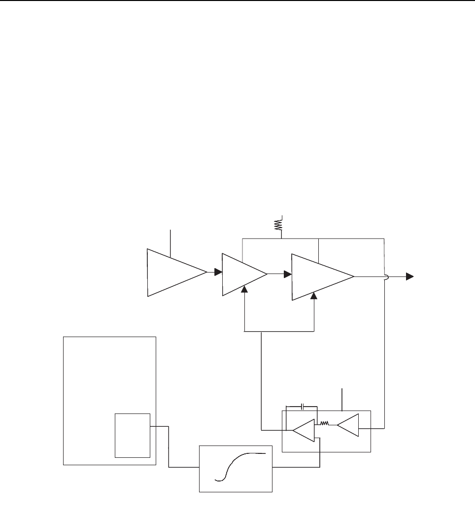
Transmitter 6-3
1.1.5 Power Control
The transmitter power control uses discrete integrator approach, the current is sensing both PA
stages namely, Driver Power Amplifier (Q703) and Final Power Amplifier (Q704).
The basic block diagram of the power control is shown in Figure 6-2. A single sensing resistor (R700)
is tied to sense both PA stages current. The power control consists of 2 comparators, U701-1 and
U701-2. U701 is a dual-package op-amp in SOT-8 package. The first stage is an I-V converter
converts current drained by Power Amplifier Driver (Q703) and Power Amplifier Final (Q704) across
R700 into a voltage drop and the second stage is an integrator used to shape the output Vcontrol to
bias both PAs. The slope of the Vcontrol is controlled by the RC time constant of the integrator and
also the ramping slope of reference signal, TX_DAC generated by MAKO IC. The final TX_DAC value
determines the transmit power level and is a factory tuned parameter which is stored inside the
codeplug.
Figure 6-2: Power Control Scheme Basic Block Diagram
B+
Current to
Voltage
Integrator
Sensing
resistor
Ramp
DAC
10bit
DAC 3
MAKO
SW 5V
SW B+
Shaped input
B+
PA Final
PA
Driver
PA
Current to
Voltage
Integrator
Sensing
resistor
Ramp
DAC
10bit
DAC 3
MAKO
SW 5V
Vcontrol
SW B+
Shaped input
B+
Current to
Voltage
Integrator
Sensing
resistor
Ramp
DAC
10bit
DAC 3
MAKO
SW 5V
SW B+
Shaped input
B+
PA Final
PA
Driver
PA
Pre-driver
Current to
Voltage
Integrator
Sensing
resistor
Ramp
DAC
10bit
DAC 3
MAKO
SW 5V
Vcontrol
SW B+
Shaped input
TX_DAC
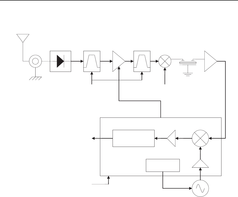
6-4 Receiver
2.0 Receiver
Figure 6-3: UHF Receiver Block Diagram
2.1 Receiver Front-End
The RF signal is received by the antenna and applied to a low-pass filter. For UHF, the filter consists
of C906, C907, C908, L904 and L905. The filtered RF signal is passed through the antenna switch
and then applied to a varactor tuned bandpass filter. The bandpass filter comprises of C400, C401,
C402, C403, C404, C405, L400, L401, R400, R499, D400 and D401. C400 and C405 are 50ohm
points. The bandpass filter is tuned by applying a control voltage to the varactor diodes D400 and
D401.
The bandpass filter is electronically tuned by the MAKO DAC. Depending on the carrier frequency, the
MAKO DAC will supply the tuned voltage to the varactor diodes in the filter. Wideband operation of
the filter is achieved by shifting the bandpass filter across the band.
The output of the bandpass filter is passed through a RF step attenuator (D402) to limit the amount
RF power fed into the LNA (U400). After being amplified, the RF signal is further filtered by a second
varactor tuned bandpass filter. This bandpass filter is electronically tuned by the MAKO DAC and
comprises of C419, C420, C421, C422, C423, C424, L408, L409, R405, R406, D403 and D404. C419
and C423 are 50 Ohm points.
The output of the second bandpass filter is passed to a mixer. The mixer is a passive double balanced
quad diode mixer (D405) comprising of 2 transformers (T400 and T401). The 50 Ohm matching for
Pin Diode
Antenna
Switch LNA
RF Jack
Varactor
Tuned
Filter
Varactor
Tuned
Filter Mixer
Crystal
Filter IF Am
p
SIGNAL
PROCESSING
Synthesizer
ABACUS IC
SSI TO OMAP
16.8MHz
Reference Clock
Control voltage
from MAKO
Antenna
First LO from
FGU
IF
AGC
Second LO VCO
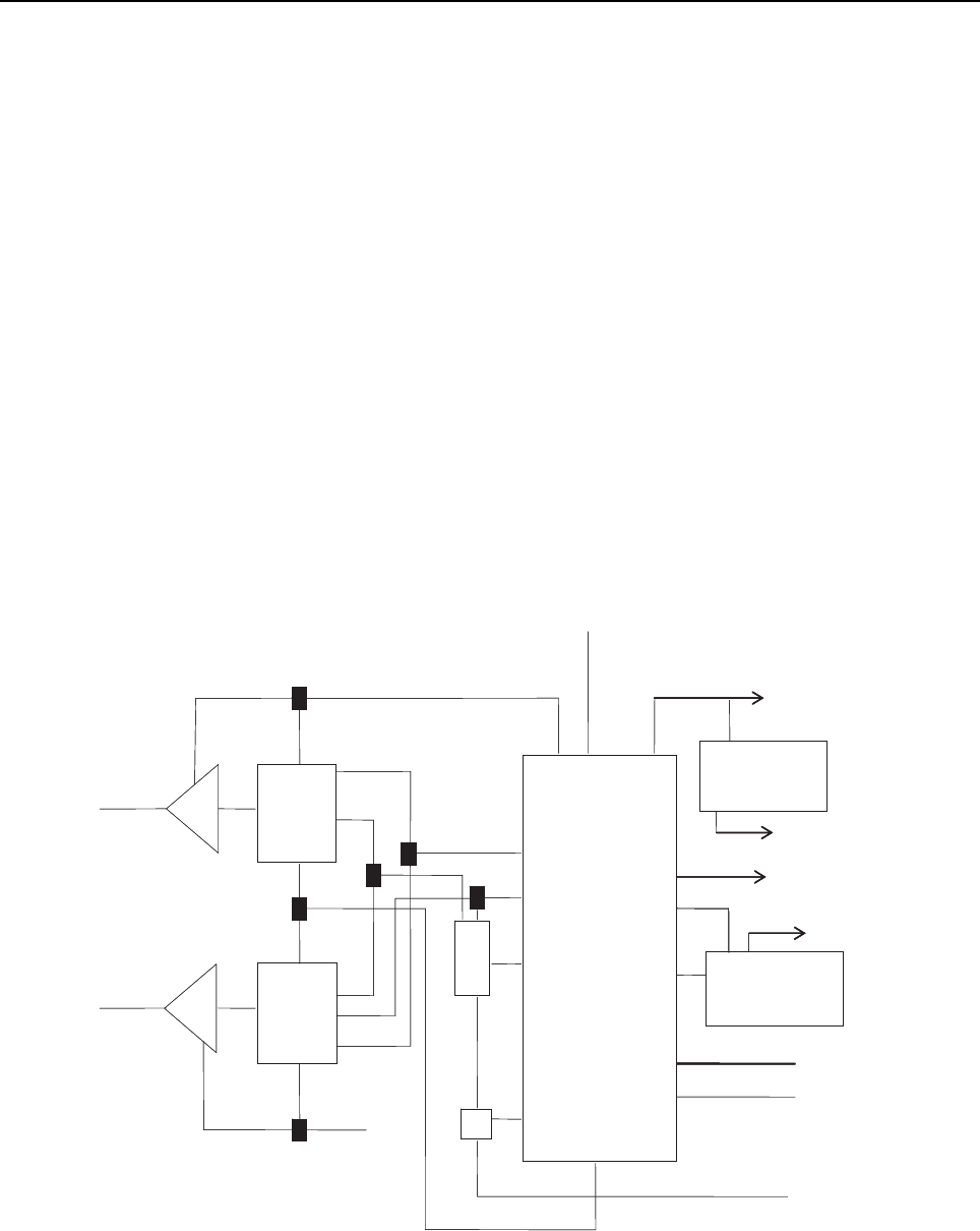
Frequency Generation Circuitry 6-5
the mixer is provided by C426 and L410. After mixing with the first LO signal from the voltage control
oscillator (VCO) using low side injection, the RF signal is down converted to the 73.35 MHz IF signal.
The IF signal coming out of the mixer is applied to the crystal filter (FL400) through a resistor pad and
a diplexer (L411 and C427). Matching to the input of the crystal filter is provided by L412 and C428.
The crystal filter provides the necessary adjacent channel selectivity and inter-modulation protection.
The output of the crystal filter (FL400) is matched to the input of the IF amplifier transistor by C432,
C433, L415 and L416. Voltage supply to the IF amplifier is 5V_RX, taken from RX VCO. The IF
amplifier provides a gain of 25 dB. The IF amplifier output is directly matched at the IF amplifier output
to ABACUS (U600) pin 47 via C601.
2.2 Receiver Back-End
ABACUS (U600) is tuned via software at radio start-up. The IF signal applied to pin 47 of U600 is
down-converted to a second IF of 2.25 MHz. The second IF of 2.25 MHz will then be fed into an ADC,
generating the Is and Qs data. This data is in the form of SSI (Serial Synchronous Interface) at pin 29
of U600, which will then be sent to the DSP (OMAP1710) for further processing.
The second VCO is a Colpitts oscillator built around transistor Q602. The VCO has a varactor diode,
D600 to adjust the VCO frequency. The second LO frequency could either be 71.1 MHz or 75.6 MHz,
depending on the system requirement. The control signal is derived from a loop filter consisting of
C617, C618, C619, R605 and R606. The RSSI circuitry is achieved via software programming.
3.0 Frequency Generation Circuitry
Figure 6-4: Frequency Generating Unit Block Diagram
The Frequency Generating Unit is centered on one main IC, Tomahawk (U001). The main synthesizer
on the Tomahawk functions as a modulation interface to the DSP area via the 3 TX SSI lines. The
16.8 MHz
TCXO
Tomahawk
DAC
Tx SSI
3 lines
DMCS
SW Adapt
CP
out
GPO1
GPO3
RX VCO EN
TX VCO EN
To Abacus
Adapt
SW
control
CLK 2 out
SF
HP
mod
Prescaler in
TX
VCO
TX VCO EN
RX LO
Lock Det
TEST1
16.8 MHz
Buffer
To Squarer IC
RX
VCO
AUX
DAC
3 lines
LF
TX LO
To GPS
16.8 MHz
TCXO
Tomahawk
DAC
Tx SSI
3 lines
DMCS
SW Adapt
CP
out
GPO1
GPO3
RX VCO EN
TX VCO EN
To Abacus
Adapt
SW
control
CLK 2 out
SF
HP
mod
Prescaler in
TX
VCO
TX VCO EN
RX LO
Lock Det
TEST1
16.8 MHz
Buffer
To Squarer IC
RX
VCO
AUX
DAC
3 lines
LF
TX LO
To GPS

6-6 Frequency Generation Circuitry
block diagram illustrates the interconnect and support circuitry used in the Frequency Generating
Unit. Refer to the relevant schematics for the reference designators.
The synthesizer is powered by 2.8V ANA, 2.8V DIG, 1.875V DIG and 5V ANA supplied from the
U3000-1. The synthesizer in turns generates a superfiltered 2.5V which powers up the TX VCO & RX
VCO.
In addition to the VCO, the synthesizer interfaces with the microcontroller. Programming of the
synthesizer is accomplished through the 4 lines; SPI_MISO, THK_CE, SPI_MOSI and SPI_CLK via
pin D10, D8, D9 and D11 respectively. A 1.875 dc signal from the synthesizer lock detect line
indicates to the microprocessor that the synthesizer is locked.
U001 has dual port modulation capability. The microprocessor supplies low port and high port words
to pin F11 of U001. For high port modulation, the audio runs through an internal attenuator for
modulation balancing purpose before it goes out to the VCO and loop filter via pin K8. For the low port
modulation, the audio is fed into the main synthesizer, where it is summed with the main_num
channel frequency word, then supplied to the accumulator of the Fractional-N synthesizer before
going out to the VCO.
3.1 Synthesizer
U001 uses a 16.8 MHz crystal (Y001) to provide a reference for the system. The synthesizer further
divides this to 8.4MHz for nominal frequencies and 5.6 MHz for alternate frequencies. Together with
R006, R007, R008, C013, C014, C015 and C016, they build up the reference oscillator which is
capable of 1.5ppm (non-GPS) / 0.5ppm (GPS) stability over temperature of -30ºC to 85 ºC. It also
provides 16.8MHz at pin J11 of U001 to be used by ABACUS.
The loop filter which consists of R013, R014, R016, C024, C025, C026 and C027 provides the
necessary dc steering voltage for the VCO and determines the amount of noise and spur passing
through.
In achieving fast locking for the synthesizer, an internal adapt charge pump provides higher current
(~10mA) at pin H1 and an additional 2mA from a current mirror (Q002, R010, R011 and R012). The
required frequency is then locked by normal mode charge pump at pin G3. An external adapt switch
(U002) is used to control the ON/OFF of the adapt mode. Both the normal and adapt charge pumps
get their supply from the 5V ANA supplied by U3000-1.
3.2 VCO - Voltage Controlled Oscillator
The VCO in conjunction with the synthesizer generates RF in both the receive and transmit modes of
operation.
The RX VCO comprises of a Colpitts oscillator built around Q200, a cascaded buffer, built up of a
buffer IC, U200 cascaded with a discrete buffer built around Q208 and a 3dB resistive pad (R220,
R221 and R222). Vcontrol is supplied to two pairs of back-to- back varactors (D200, D201, D202 and
D203). The LC tank comprises of C203 and L202. The oscillator is supplied with a 2.5V superfiltered
supply from the synthesizer, U001. The cascaded buffer is supplied with a 5V ANA supply from
MAKO, U3000-1. The buffer IC in conjunction with the resistive pad provides sufficient isolation from
the mixer whilst the discrete buffer provides sufficient gain for the first LO signal. The output of the
cascaded buffer is match to the mixer by C216, C217, C241 and L207. The output power level of
RX_1ST_LO_INJ is 6dB.
The TX VCO comprises of a Colpitts oscillator built around Q204 and a discrete buffer built around
Q205. Vcontrol is supplied to two pairs of back-to-back varactors (D204, D205, D206 and D207). The
LC tank comprises of C222 and L210. The oscillator is supplied with a 2.5V superfiltered supply from
the synthesizer, U001. The discrete buffer is supplied with a 5V ANA supply from MAKO, U3000-1.
The output of the discrete buffer is match to the mixer by C236, C237 and L215. The output power
level of TX_BUFF is 3dB.
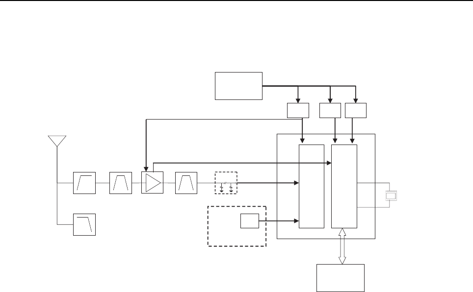
Global Positioning System (GPS) Receiver 6-7
4.0 Global Positioning System (GPS) Receiver
The GPS device is an embedded receiver that provides the location of the subscriber in terms of
latitude, longitude, velocity, direction and altitude.
Figure 6-5: GPS Receiver Block Diagram
The RF signal is received by the antenna and applied to a high-pass filter. The filter consists of C924,
C925, C926, L912 and L913. The filtered RF signal is then applied to a SAW filter, FL8001.
The output of the SAW filter is fed into the LNA (U8001). The LNA biasing is controlled by
SIRF_LNA_EN (pin A4 of the GPS IC, U8000). The LNA input match comprises of C8013, C8014 and
L8001. The LNA output match comprises of L8003 and C8017. After being amplified, the RF signal is
further filtered by a second SAW filter, FL8002.
The output of the second SAW filter is passed to pin P6 of the GPS IC. The input match for pin P6
comprises of C8018, C8019 and L8004. The control and data lines for the GPS IC are GPS_nRESET,
GPS_ON_OFF, GPS_TX, GPS_RX and GPS_BOOT. GPS_nWAKEUP line is fed into the
microcontroller to indicate the state (full power or hibernate state) of the GPS IC so that the
microcontroller will never trigger a GPS_ON_OFF when the GPS IC is in full power state.
A dedicated 32.768kHz quartz crystal oscillator (Y8000) is used to provide RTC clock to the RTC
circuit inside the GPS IC. The second input frequency is a 16.8MHz reference, used by the StarIII to
synthesize the internal LO. This reference will be supplied by a VCTCXO (Y001) located in the
synthesizer block, which will be shared by the TOMAHAWK and ABACUS ICs.
The GPS IC is powered by 2.8V_DIG_GPS, 2.8V_RF_GPS and 1.5V_GPS_RTC supplied from 3
discrete external regulators (U3701, U3700 & U3006). The input of these regulators is sourced from a
switching regulator (U3020) which regulates the SWB+ to 3.6V.
RF
Section
Digital
Section
TPS79228 TPS79101 LP3990
2.8V
2.8V
1.5V
LTC1877
3.6V
32.768kHz
XTAL
OMAP
16.8MHz
VCTCXO
FGU
SiRFStarIII, GSC3FLP
Optional
2dB resistive pad
HPF Pre-SAW LNA Post-SAW
Dual band antenna
LNA_EN
LNA_Supply
HF

6-8 Allocation of Schematics and Circuit Boards
5.0 Allocation of Schematics and Circuit Boards
5.1 Controller Circuits
The UHF circuits are contained on the Printed Circuit Board (PCB) which also contains the
Controller circuits. This Chapter shows the schematics for the UHF circuits only, refer to the
Controller section for details of the related Controller circuits. The PCB component layouts in this
Chapter show both the Controller and UHF circuit components. The UHF schematics and the
related PCB and parts list are shown in the tables below.
Table 6-1. UHF1 Diagrams and Parts List
PCB:
8486716Z04 Main Board Top Side
8486716Z04 Main Board Bottom Side
8486716Z07 Main Board Top Side
8486716Z07 Main Board Bottom Side
8486716Z08 Main Board Top Side
8486716Z08 Main Board Bottom Side
Page 6-9
Page 6-10
Page 6-11
Page 6-12
Page 6-13
Page 6-14
SCHEMATICS
Complete Radio
Complete UHF1 RF
Complete UHF1 Transmitter
UHF1 Transmitter
UHF1 Harmonic Filter and Antenna Switch
Complete UHF1 Receiver
UHF1 Receiver Front End
UHF1 Receiver Back End
Complete UHF1 Frequency Generating Unit
UHF1 Synthesizer
UHF1 Voltage Controlled Oscillator
UHF1 GPS Block
Page 6-15
Page 6-16
Page 6-17
Page 6-18
Page 6-19
Page 6-20
Page 6-21
Page 6-22
Page 6-23
Page 6-24
Page 6-25
Page 6-26
Parts List
8486716Z04
8486716Z07
8486716Z08
Page 6-27
Page 6-33
Page 6-39
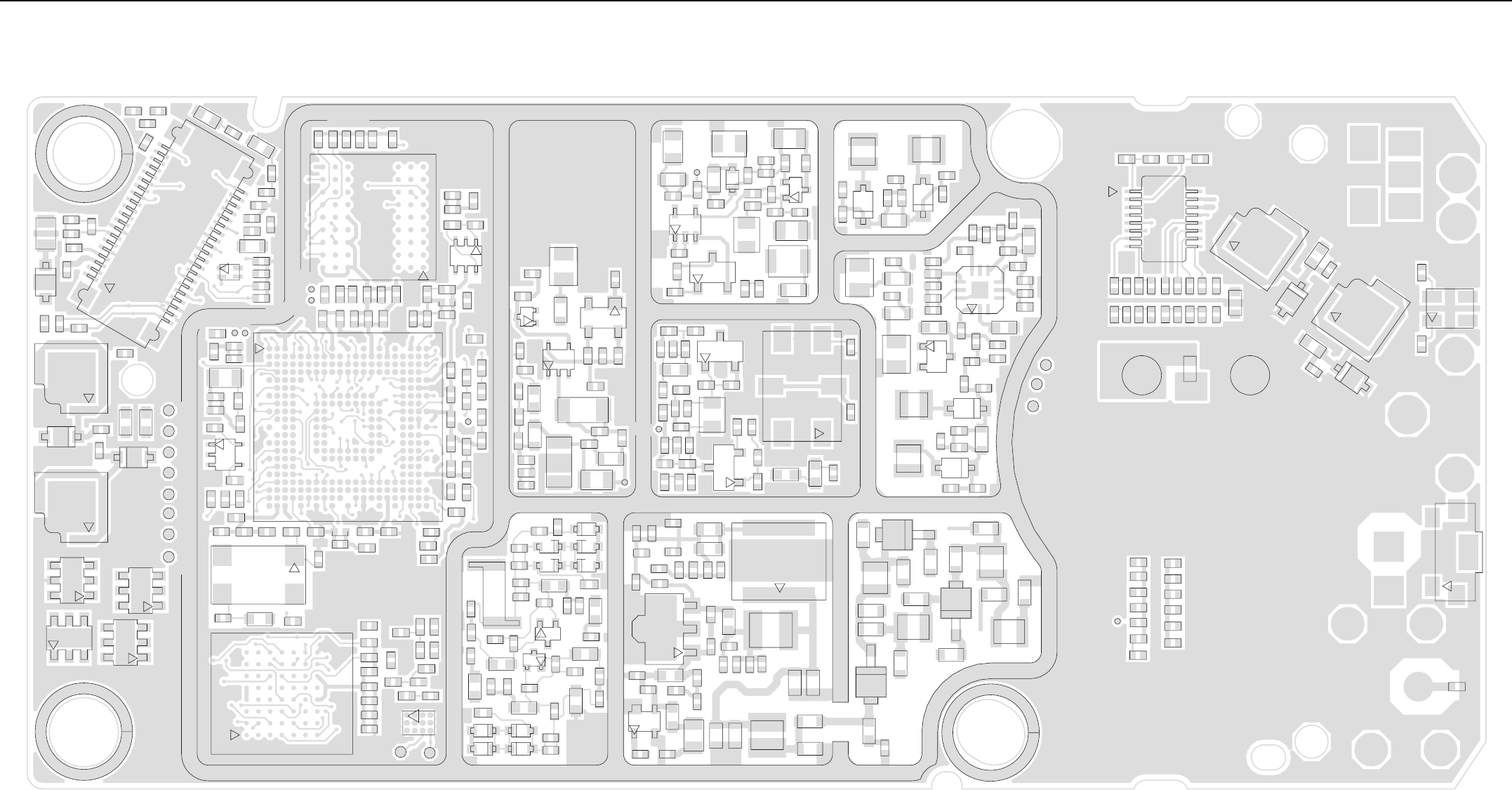
Circuit Board/Schematic Diagrams and Parts List 6-9
6.0 Circuit Board/Schematic Diagrams and Parts List
C009
C024
C025
C026
C027
C028
C031
C032
C033
C036
C037
C038
C200
C201
C202
C203
C204
C205
C206
C207
C208
C209
C219
C220
C221
C222
C223 C224
C225
C226
C227
C228
C243
C400
C401
C402
C403
C404
C405
C407
C408
C409
C410
C411
C412
C413
C414
C415
C416
C417
C418
C419
C420
C421
C422 C423
C424
C425 C428
C432
C433
C434
C435 C436
C437
C438
C439
C440
C441
C442
C444 C445
C446
C447
C448
C606
C609
C610
C611
C612
C613
C614
C615
C616
C617
C618
C619
C626
C638
C714
C715
C716
C717
C718
C719
C720
C722
C723
C724
C725
C726
C727
C728
C729
C730
C732
C733
C734
C735
C736
C737
C739
C740
C798
C799
C906
C907
C908
C909
C910
C911
C912
C913
C914
C915
C916
C917
C918
C1000
C1001
C1002C1003
C1004 C1005
C1006
C1007
C1008
C1009
C1010
C1011
C1012
C1013
C1014
C1015
C1016
C1017
C1018
C1019
C1028
C1029
C1030
C1031
C1032
C1033
C1044
C2000
C2001
C2002
C2003
C2004
C2005
C2006
C2007
C3063
C3800
C9000 C9001
C9002
C9003
C9004
C9005
C9006
C9007
C9008
C9009
C9010
C9011
C9012
C9013
C9014
C9015
C9019
C9020
C9021
C9022
C9033
C9047
C9048
C9049 C9050
C9051
C9053
C9055
C9057
C9058
C9059
C9060
C9061
C9062
C9063
C9064
C9066
C9067
C9068
C9069
CR901
CR902
CR903
D001
D200
D201 D202
D203
D204
D205
D206
D207
D400
D401
D402
D403
D404
D600
4
3
2
D9000
E002
E400
E401
E9000
E9001
E9006
E9007
F9000
2
3
4
5
6
FL400
FL9000
1
21
40
20
J9001
L002
L003
L200
L201
L202
L203
L205
L208
L209
L210
L211
L213
L400
L401
L402
L403
L404
L405
L406
L407
L408
L409
L415
L416
L417
L418
L419
L420
L602
L603
L604
L701
L702
L703
L706
L707
L904
L905
L906
L907 L908
L9000
L9001
L9007
L9008
M9000
M9001
M9002
1
M9003
1
M9004
1
M9005
1
M9006
16
81
9
P9000
Q002
Q003
Q200
Q204
Q400
Q401
Q600
Q601
Q602
Q703
1
3
Q704
R010
R011
R012
R013
R014
R016
R017
R018
R019
R020
R022
R025
R027
R203
R211
R400
R402
R403
R404
R405
R406
R409
R410
R411
R412
R413
R416
R417
R419
R420
R421
R422 R424
R425
R497
R499
R600
R601
R602
R603
R604
R605
R606
R612
R697
R699
R717
R718
R719
R721
R722
R723
R725
R726
R727
R907
R1000
R1001
R1002
R1005R1006
R1013
R1014
R1015
R1016
R1017
R1018
R1019
R1020
R1021
R1022
R1023
R1025
R1026
R1027
R1028
R1034 R1035
R1036
R1041
R1045
R1046
R1047
R1048
R1051
R1052
R1053
R1054
R1055
R1060
R1061
R1062
R1063
R1065
R1067
R1068
R1069
R1070
R1072
R2000
R2004
R2005
R2006
R2007
R2008
R2009
R2010
R2011
R2012
R2013
R3010
R3023
R3032R3033 R3034R3035
R3800
R3888
R8010
R8011
R8012
R8026
R8027
R8028
R8029
R8031
R8033
R8034
R8035
R8036
R8037
R9000 R9001
R9002
R9003
R9004
R9005
R9006
R9007
R9012 R9013
R9052
3
4
5
2
S9000
SH9001
TP200
TP400
TP401
TP402
TP403
TP601
TP_GND
TP_GPS_RX
TP_GPS_TX
TP_MAKO_DCLK
TP_MAKO_FSYNC
TP_MAKO_RX
TP_MAKO_TX
TP_NEMU0
TP_NEMU1
TP_NTRST
TP_RAWB+
TP_RTCK
TP_SIPI_DO
TP_TCK
TP_TDI
TP_TDO
TP_TMS
TX_RAMP
4
3
5
U002
3
4
6
79
10
12
U400
U700
A21AA21
AA1
U1000
U1005
43
6
U1006
G1A1
A8 G8
U2000
J9A9
J1A1
U2001
4
3
5
U3004
VR9002
VR9015
VR9016
VR9017
VR9018
VR9020
VR9021
VR9022
VR9023
2
34
Y1000
UHF1 (403-470MHz) Main Board Top Side PCB No. 8486716Z04
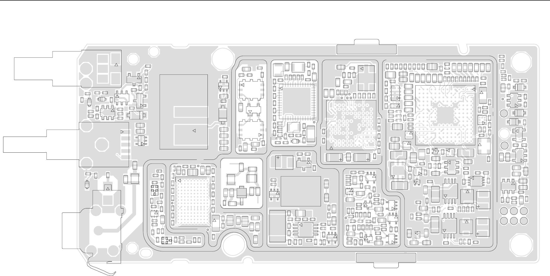
6-10 Circuit Board/Schematic Diagrams and Parts List
C001
C002
C003
C004
C005
C006
C007
C008
C013
C014
C015
C016
C017
C018
C019
C020
C022 C035
C039
C210
C211
C212
C213
C214
C215
C216
C217
C229
C230
C231
C232
C233
C234
C235
C236
C237
C238
C239
C240
C241
C426
C427
C429
C430
C431
C601
C602
C603
C604
C605
C607
C608
C620C621
C622
C623 C624C625C627C628C629
C630
C631
C632
C633
C634 C635
C636
C637
C639
C700
C703
C704
C705
C706
C708
C709
C710
C711
C712
C721
C731
C738
C900
C903
C904
C905
C920
C921
C922
C923
C924
C925
C926
C927
C3000
C3001
C3002
C3003
C3004
C3005
C3010 C3011
C3014
C3015
C3016
C3017
C3018
C3019
C3024
C3025
C3026
C3028
C3031
C3034
C3035
C3036
C3037
C3038
C3039
C3045
C3047
C3048
C3049
C3050
C3051
C3060
C3061
C3062
C3067
C3070
C3074
C3079
C3080
C3081
C3082
C3083
C3084
C3090
C3091
C3093
C3094
C3095
C3097
C3098
C3099
C3100
C3101
C3102
C3200
C3201
C3202
C3203
C3204
C3205
C3206
C3207
C3208
C3209
C3210
C3211
C3212
C3700
C3701
C3702
C3703
C3704
C3705
C3706
C3707
C3805
C3999
C8000
C8001
C8002
C8003
C8004
C8005
C8006
C8013
C8014
C8015
C8016
C8017
C8018
C8019
C8020
C8021
C8022
C8023
C8029
C8030
C8031
C8032
C8033
C8034 C8035
C8036
C9016
C9017C9018
C9023
C9024
C9025
C9026
C9027
C9028
C9029
C9030 C9031
C9032
C9038
C9039
C9040
C9041
C9042
C9043
C9044
C9045
C9046
C9065
CR900
D405
D601
D3000
E001
E003
E004
E600
E601
E602
E701
E3030
E3031
E3032
E3033
E3700
E3701
E3702
E3703
E3704
E3705
E8000
E8001
E8002
E8003
E8004
E8005
E8006
3
4
2
5
FL8000
3
4
2
5
FL8001
L204
L206
L207 L212
L214
L215
L217
L218
L410
L411
L412
L413
L414
L600
L601
L605
L700
L902
L903
L909
L910
L911
L912
L913
L3003
L3004
L3020
L3021
L3022
L8001
L8002
L8003
L8004
M1
M2
M700
23
M9007
1
2
3
4
5
6
7
P900
Q202
Q203
Q205
Q206
Q207
Q208
Q701
Q702
Q900
Q901
23
4
Q3000
23
4
Q3001
Q3002
4
58
Q3003
23
4
Q3005
Q3006
23
4
Q3010
Q9000
Q9001
Q9003
R006
R007
R008
R026
R052
R053
R054
R200 R201
R202
R205
R207
R208
R209
R210
R212
R213
R214
R215
R216
R217
R218
R220
R221
R222
R223
R224
R407
R607
R609
R610
R611
R696
R698
R700
R701
R702 R703
R704
R705
R706
R707
R708
R709
R710
R711
R712 R713
R714
R720
R728
R729
R730
R731
R732
R733
R902
R903
R904
R905
R906
R3004 R3005
R3006 R3007
R3008
R3009
R3011
R3012
R3013
R3014
R3016
R3017
R3018
R3020
R3021
R3024
R3025
R3026
R3027
R3028
R3029
R3030
R3031
R3036
R3037
R3038
R3040
R3041
R3043
R3050
R3051
R3053
R3054
R3055
R3060
R3070
R3071
R3072
R3073
R3074
R3075
R3088
R3098
R3100
R3101
R3102
R3103
R3200
R3201
R3202
R3203
R3700
R3701
R3702
R3703
R3704
R8002
R8003
R8004
R8015
R8016
R8017
R8020
R8023
R8024
R8025
R8030
R8032
R9008
R9009
R9010
R9011
R9014
R9015
R9016
R9017
R9018
R9019
R9050 R9051
R9053
R9054
7
2
3
4
5
6
S9001
7
8
2
3
4
5
6
S9002
SH9000
3
46
T400
3
4
6
T401
TP002
TP003
TP004
TP006
TP201
TP600
TP_CLK_ACQ
TP_EXT_MIC
TP_EXT_MIC+
TP_EXT_SPKR
TP_EXT_SPKR+
TP_IF
TP_ONE_WIRE_1
TP_POR
TP_SCLK
TP_USB1_DM
TP_USB1_DP
TP_VBUS1
L11A11
L1
U001
U200
1
37
25
13
U600
U701
U702
P1 A1
A14
P14
U3000
1
64
3
U3002
C1
C3
A3
U3003
U3006
U3007
U3008
85
4
U3009
U3020
U3021
5
3
4
U3700
U3701
P10 A10
P1
A1
U8000
U8001
VR9000
VR9001
VR9003
VR9004
VR9005
VR9006
VR9007
VR9008
VR9009
VR9010
43
2
Y001
Y3000
4
3
2
Y3001
Y8000
UHF1 (403-470MHz) Main Board Bottom Side PCB No. 8486716Z04
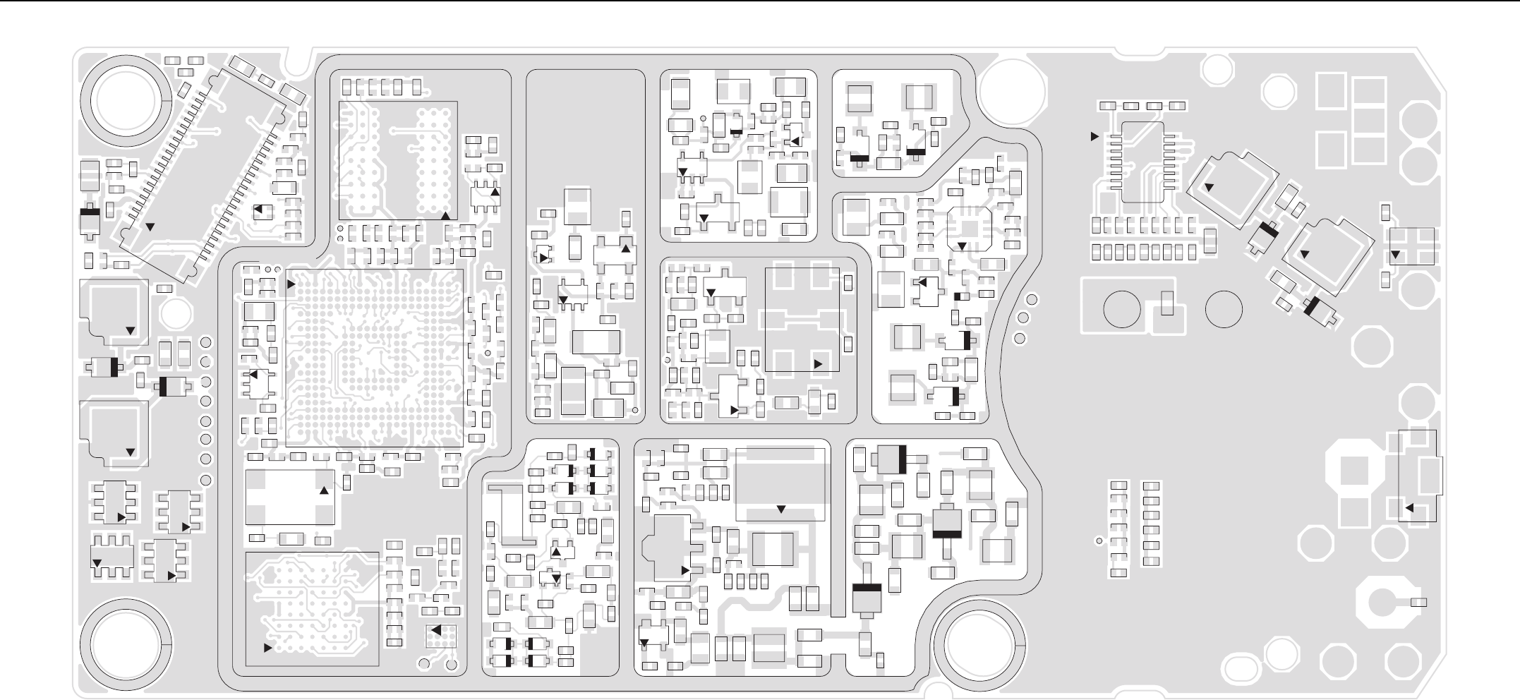
Circuit Board/Schematic Diagrams and Parts List 6-11
M9002
VR9002
VR9020
VR9021
VR9022
C9015
C9019
C9020
C9021
C9022
C9033
C9047
C9048
C9049 C9050
C9061
C9062
C9069
E9000
E9001
1
21
40
20
J9001
L9000
L9001
M9001
1
M9005
R9052
TP_NEMU0
TP_NEMU1
TP_NTRST
TP_RTCK
TP_TCK
TP_TDI
TP_TDO
TP_TMS
VR9017
VR9018
VR9023
1
M9006
C3800
C9051
C9053
C9055
C9057
C9058
C9059
C9060
C9063
C9064
C9066
FL9000
L9007
L9008
R3800
R2005
R2006
R2007
R2008
R2009
R2013
J9A9
J1
A1
U2001
C1007
C1010
C1013
C1014
C1015
C1016
C1032
C1033
C2004
C2005
C2006
C2007
R1000
R1015
R1016
R1021
R1026
R1027
R1028
R1061
R1072 R2010
R2011
R3010
TP_MAKO_DCLK
TP_MAKO_RX
43
6
U1006
C1000
C1001
C1004
C1008
C1009
C1011
C1012
C1017
C1018
C1019
C1031
C3063
R1002
R1005
R1006
R1013
R1014
R1018
R1019
R1020
R1022
R1023
R1025
R1041
R1046
R1048
R1054
R3023
TP_MAKO_FSYNC
TP_MAKO_TX
AA1
4
3
5
U3004
2
34
Y1000
C1005 C1044
R1045
R1060
A21
AA21
U1000
C1002
C1003 C1006
C1030
R1001
R1017
R1034
R1035
R1047
R1053
R1055 R3032
R3033 R3034
R3035
R3888
TX_RAMP
C009
E002
L003
Q002
Q003
R012
R025
C024
C025
C026
C027
C028
C031
C032
C033
C036
C038
L002
R010
R011
R013
R014
R016
R017
R018
R020
R022
R027
TP200
4
3
5
U002
G1A1
A8 G8
U2000
C1028
C1029
C2000
C2001
C2002
C2003
R1036
R1051
R1052
R1062
R1063
R1065
R1067
R1068
R1069
R1070
R2000
R2004
R2012
TP_GPS_RX
TP_GPS_TX
U1005
C037
C200
C201
C202
C203
C204
C205
C206
C207
C208
C209
C219
C220
C221
C222
C223 C224
C225
C226
C227
C228
C243
D001
D200
D201
D202
D203
D204 D205
D206
D207
L200
L201
L202
L203
L205
L208
L209
L210
L211
L213
Q200
Q204
R019
R203
R211
C718
C723
C724
C725
C726
C727
C728
C729
C730
C740
L703
L706
Q703
1
3
Q704
R718
R721
R722
R723
R726
R727
C714
C715
C716
C717
C719
C720
C722
C732
C733
C734
C735
C736
C737
C739
C798
C799
L701
L702
L707
R717
R719
R725
U700
C910
C912
C914
CR902
L907
M9000
C906
C907
C908
C909
C911
C913
C915
C916
C917
C918
CR901
CR903
L904
L905
L906
L908
R8010
R8011
R8012
R8026
R8027
R8028
R8029
R8031
R8033
R8034
R8035
R8036
R8037
TP_SIPI_DO
R907
3
4
5
2
S9000
4
3
2
D9000
R9012 R9013
1
M9004
C9067
C9068
E9006
E9007
VR9015
VR9016
TP_GND
1
M9003
C9014
F9000
TP_RAWB+
16
81
9
P9000
C9000
C9001R9000
R9001
C9002
C9003
C9004
C9005
C9006
C9007
C9008
C9009
C9010
C9011
C9012
C9013
R9002
R9003
R9004
R9005
R9006
R9007
TP400
TP401
TP402
SH9001
C400
C401
C402
C403
C404
C405
C407
C408
C409
C410
C411
C412
C413
C414
C415
C416
C417
C418
C439
C447
C448
D400
D401
D402
E400
E401
L400
L401
L402
L403
L404
L405
L406
L407
L419
L420
R400
R402
R403
R404 R416
R499
34
6
79
10
12
U400
C425 C428
C432
C433
C434
C435 C436
C437
C438
C440
C441
C442
C444 C445
C446
23
4
5
6
FL400
L415
L416
L417
L418
Q400
Q401
R409
R410
R411
R412
R413
R417
R419
R420
R421 R422 R424
R425
R497
TP403
C613
C618
C619
L604
C606 C609
C610
C611
C612
C614
C615
C616
C617
C626
C638
D600
L602
L603
Q600
Q601
Q602
R600
R601
R602
R603
R604
R605
R606 R612
R697
R699
TP601
C419
C420
C421
C422 C423
C424
D403
D404
L408
L409
R405
R406
UHF1 (403-470MHz) Main Board Top Side PCB No. 8486716Z07
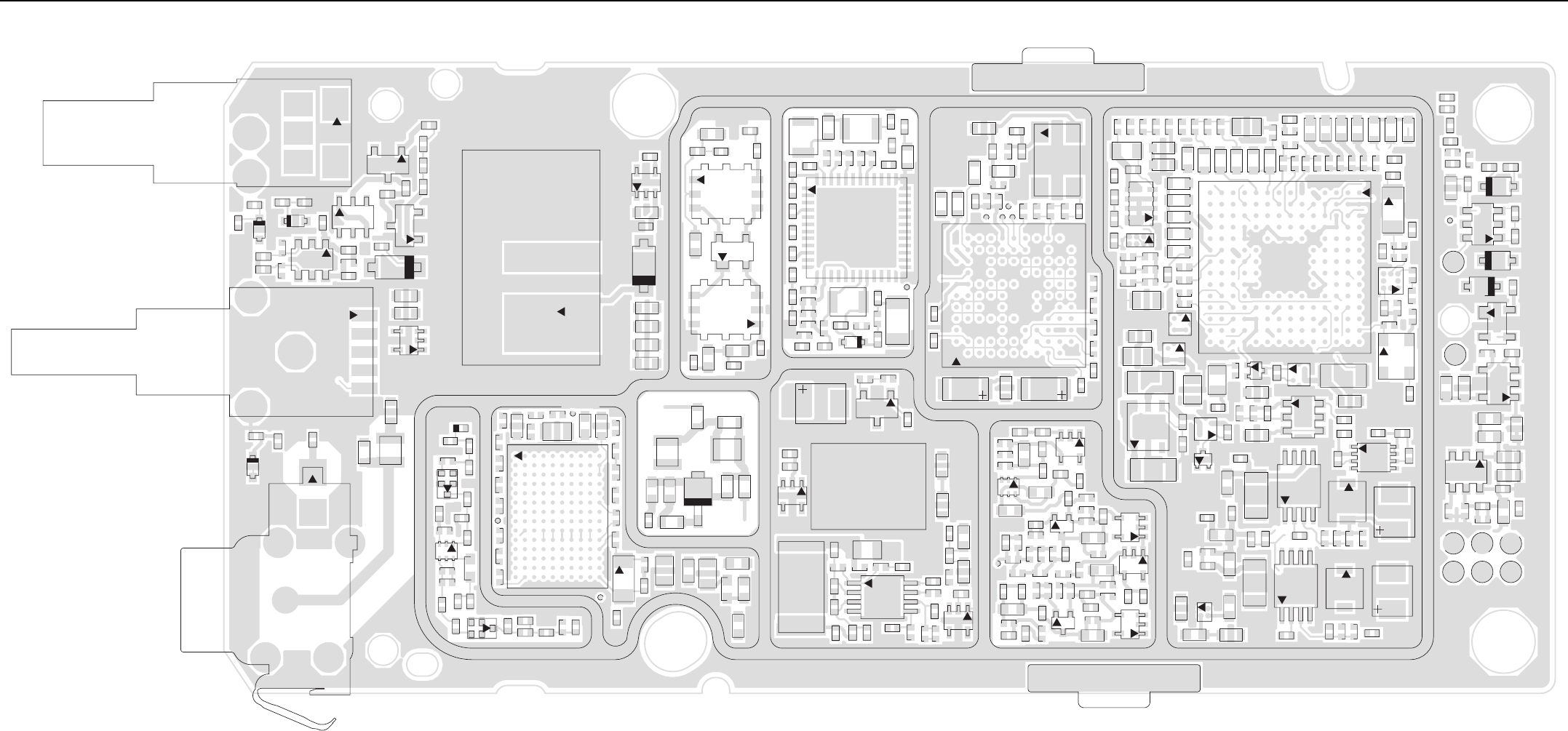
6-12 Circuit Board/Schematic Diagrams and Parts List
7
2
3
4
5
6
S9001
C9024
C9025
C9026
C9027
C9028
C9029
C9030 C9031
C9038
Q9000
Q9001
Q9003
R9008
R9009
R9010
R9011
R9015
R9016
R9017 R9018
R9050
R9051
VR9006
VR9007
VR9008 VR9009
Q901
R9053
R9054
7
8
2
3
4
5
6
C922
C923
C9023
L911
R906
R9014
VR9005
1
2
3
4
5
6
7
P900
C924
C925
C8006
C8013
C8014
C8015
C8016
C8017
C8018
C8019
C8030
E8006
3
4
2
5
FL8000
3
4
2
5
FL8001
L912
L913
L8001
L8002
L8003
L8004
R8004
R8015
R8016
R8017
R8020
TP_IF
U8001
Y8000
C926
C8000
C8001
C8002
C8004
C8020
C8021
C8022
C8023
C8029
C8031
C8032
C8033
C8036
E8000
R8002
R8003
R8023
R8024
R8025
R8030
R8032
TP_CLK_ACQ
TP_SCLK
P10 A10
P1 A1
U8000
C8003
C8005
C8034
C8035
E8001
E8002
E8003
E8004
E8005
C900
C903
C904
C905
C920
C921
CR900
L902
L903
L909
L910
R902
R903
R904
R905
VR9010
23
M9007
C927
C9032
C9039
Q900
S9002
C426
C427
L410
L411
R407
3
46
T400
D405
L412
3
4
6
T401
C429
C430
C431
L413
L414
1
37
25
13
U600
C601
C602
C603
C604
C605
C607
C608
C622
C631
E601
E602
L600
L601
R696
C620
C621
C623
C624C625
C627
C628
C629
C630
C632
C633
C634 C635
C636
C637
C639 D601
E600
L605
R607
R609
R610
R611
R698
TP600
C700
C703
C704
C705
C706
C708
C709
C710
C711
C712
C721
C731
E701
L700
M700
Q701
Q702
R700
R701
R702 R703
R704
R705
R706
R707
R708
R709
R710
R711
R712
R713
R714
R720
R731
R732
R733
U701
U702
C018
C019
C020
43
2
Y001
C001
C002
C004
C008
C013
C014
C015
C016
C039
E001
E004
R006
R007
R008
R026
R052
R053
R054
TP004
L11
TP002
TP003
TP006
A11
U001
C003 C007
C005
C006 C017
C022
C035 E003
L1
C215
C216
C217
C229
C230
C231
C232
C233
C234
C235
C236
C237
C241
C738
L207
L214
L215 Q205
Q207
R208
R209
R210
R212
R213
R214
R215
R221
R224
R728
R729
R730
TP201
C210
C211
C212
C213
C214 C238
C239
C240
L204
L206
L212
L217
L218
Q203
Q206
Q208
R205
R207
R216
R217
R218
R220
R222
R223
U200
Q202
R200 R201
R202
C3090
C3091
1
64
3
U3002
C3084
C3101
C3102
C3201
C3202
C3203
C3204
C3205
C3206
C3207
C3208
C3209
C3210
C3211
C3212
C3805
E3704
E3705
L3003
L3004
L3020
L3021
L3022
R3031
R3038
R3200
R3201
R3202
R3203
R3704
U3006
U3020
U3021
C3015
C3017
C3018 C3025
C3026
C3060
C3079
C3082
C3083
C3200
23
4
Q3001
Q3002
23
4
Q3005
Q3006
R3016
R3017
R3018
R3028
R3029
R3040
R3041
R3043
R3100
R3101
R3102
R3103
U3008
85
4
U3009
C3014
C3016
C3019
C3024
C3028
C3037
C3038
C3039
C3062
C3067
C3081
23
4
Q3000
4
58
Q3003
23
4
Q3010
R3004R3005
R3006R3007
R3008R3009
R3020
R3021
R3030
R3050
R3051
R3053
R3054
R3098
P1 A1
A14
P14
U3000
U3007
C3051
C3093
C3999
M1
R3011
R3013
R3014
R3024
R3025
R3037
R3060
C3000
C3001
C3002
C3003
C3004
C3011
C3034
C3035
C3036
C3045
C3061
C3070
E3030
E3031
E3032
E3033
R3012
R3036
R3070
R3071
R3072
R3073
R3074
R3088
C1
C3
A3
U3003
Y3000
4
3
2
Y3001
C3005
C3010
C3031
C3047
C3048
C3049
C3050
C3074
C3080
C3094
C3095
C3097
C3098
C3099
C3100
R3026
R3027
C3700
C3701
C3702
C3703
C3704
C3705
C3706
C3707
E3700
E3701
E3702
E3703
R3700
R3701
R3702
R3703
SH9000
TP_EXT_MIC
TP_EXT_MIC+
TP_EXT_SPKR
TP_EXT_SPKR+
TP_USB1_DM
TP_USB1_DP
TP_VBUS1
5
3
4
U3700
U3701
VR9000
C9017
C9018
D3000
R3075
R9019
TP_ONE_WIRE_1
VR9003
VR9004
C9016 C9040
C9041
C9042
C9043
C9044
C9045
C9046
C9065
R3055
TP_POR
VR9001
M2
UHF1 (403-470MHz) Main Board Bottom Side PCB No. 8486716Z07
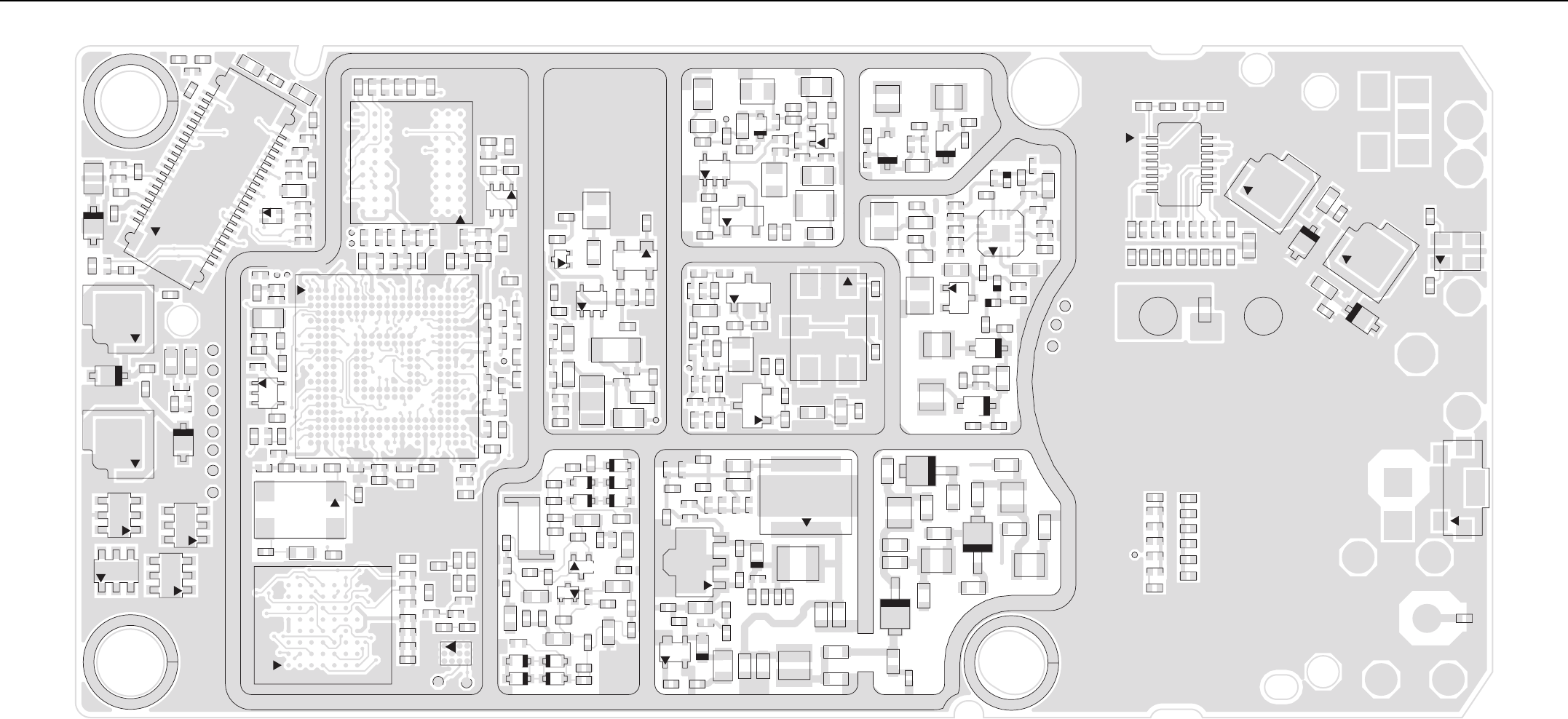
Circuit Board/Schematic Diagrams and Parts List 6-13
M9002
VR9002
VR9020
VR9021
VR9022
C9071
C9072
L9000
L9001
R9020
TP_NEMU0
TP_NEMU1
TP_NTRST
TP_RTCK
TP_TCK
TP_TDI
TP_TDO
TP_TMS
VR9018
C9015
C9019
C9020
C9021
C9022
C9033
C9061
C9062
C9069
E9000
E9001
140
J9001
1
M9005
1
M9006
R9052
VR9017
VR9023
C3800
C9047
C9048
C9049 C9050
C9051
C9053
C9055
C9057
C9058
C9059
C9060
C9063
C9064
C9066
FL9000
21
20
L9007
L9008
M9001
R3800
C1000
C1001
C1004
C1005
C1006
C1007
C1008
C1009
C1010
C1011
C1012
C1013
C1014
C1015
C1016
C1017
C1018
C1019
C1028
C1029
C1031
C1033
C1044
C2000
C2001
C2002
C2003
C2006
C2007
C3063
R1000
R1002
R1005
R1006
R1013
R1014
R1015
R1016
R1017
R1018
R1019
R1020
R1021
R1022
R1023
R1025
R1027
R1028
R1036
R1041
R1045
R1046
R1048
R1051
R1052
R1054
R1060
R1061
R1062
R1063
R1065
R1067
R1068
R1069
R1070
R1072
R2000
R2004
R2011
R2012
R3010
R3023
TP_GPS_RX
TP_GPS_TX
TP_MAKO_DCLK
TP_MAKO_FSYNC
TP_MAKO_RX
TP_MAKO_TX
A21
AA21
AA1
U1000
U1005
G1A1
A8 G8
U2000
A9
4
3
5
U3004
2
34
Y1000
C1002
C1003
C1030
C1032
C2004
C2005
R1001
R1026
R1034
R1035
R1047
R1053
R1055
R2005
R2006
R2007
R2008
R2009
R2010
R2013
R3032
R3033 R3034
R3035
R3888
TX_RAMP
43
6
U1006
J9
J1A1
U2001
C009
C024
C025
C026
C027
C028
C031
C032
C033
C036
C038
E002
L002
L003
Q002
Q003
R010
R011
R012
R013
R014
R016
R017
R018
R020
R022
R025
R027
TP200
4
3
5
U002
C037
C200
C201
C202
C203
C204
C205
C206
C207
C208
C209
C219
C220
C221
C222
C223 C224
C225
C226
C227
C228
C243
D001
D200
D201
D202
D203
D204 D205
D206
D207
L200
L201
L202
L203
L205
L208
L209
L210
L211
L213
Q200
Q204
R019
R203
R211
C613
C619
L604
C606 C609
C610
C611
C614
C615
C616
C617
C618
C626
C638
D600
L602
L603
Q600
Q601
Q602
R600
R601
R602
R603
R604
R605
R606 R612
R697
R699
TP601
C612
C419
C420
C421
C422 C423
C424
D403
D404
L408
L409
R405
R406
C400
C401
C402
C403
C404
C405
C407
C408
C409
C410
C411
C412
C413
C414
C415
C416
C417
C418
C439
C447
C448
D400
D401
D402
E400
E401
L400
L401
L402
L403
L404
L405
L406
L407
L419
L420
R400
R402
R403
R404 R416
R499
SH9001
34
6
79
10
12
U400
C425 C428
5
6
4
3
2
1
FL400
C432
C433
C434
C435 C436
C437
C438
C440
C441
C442
C444
C445
C446
L415
L416
L417
L418
Q400
Q401
R409
R410
R411
R412
R413
R419
R420
R421 R422 R424
R425
R497
TP403
R417
C9000
C9001
16
81
9
P9000
R9000
R9001
1
M9003
C9067
E9006
1
M9004
VR9015
C9068
E9007
VR9016
TP_GND
4
3
2
D9000
R9012 R9013
3
4
5
2
S9000
R907
R8010
R8011
R8012
R8026
R8027
R8028
R8029
R8031
R8033
R8034
R8035
R8036
R8037
TP_SIPI_DO
F9000
TP_RAWB+
C9002
C9003
C9004
C9005
C9013
C9014
R9002
R9003
R9004
R9005
C9006
C9007
C9008
C9009
C9010
C9011
C9012
R9006
R9007
TP400
TP401
TP402
C906
C907
C908
C909
C910
C911
C912
C913
C915
C916
C917
C918
CR901
CR902
CR903
L904
L905
L906
L908
L706
1
3
Q704
R721
R722
C719
C720
C722
C732
C733
C734
C735
C736
C737
C798
C799
L707
R717
R719
C714
C715
C716
C717
C718
C723
C724
C725
C726
C727
C728
C729
C730
C739
C740
L701
L702
L703
Q703
R718
R723
R725
R726
R727
U700
C914
L907
M9000
UHF1 (403-470MHz) Main Board Top Side PCB No. 8486716Z08
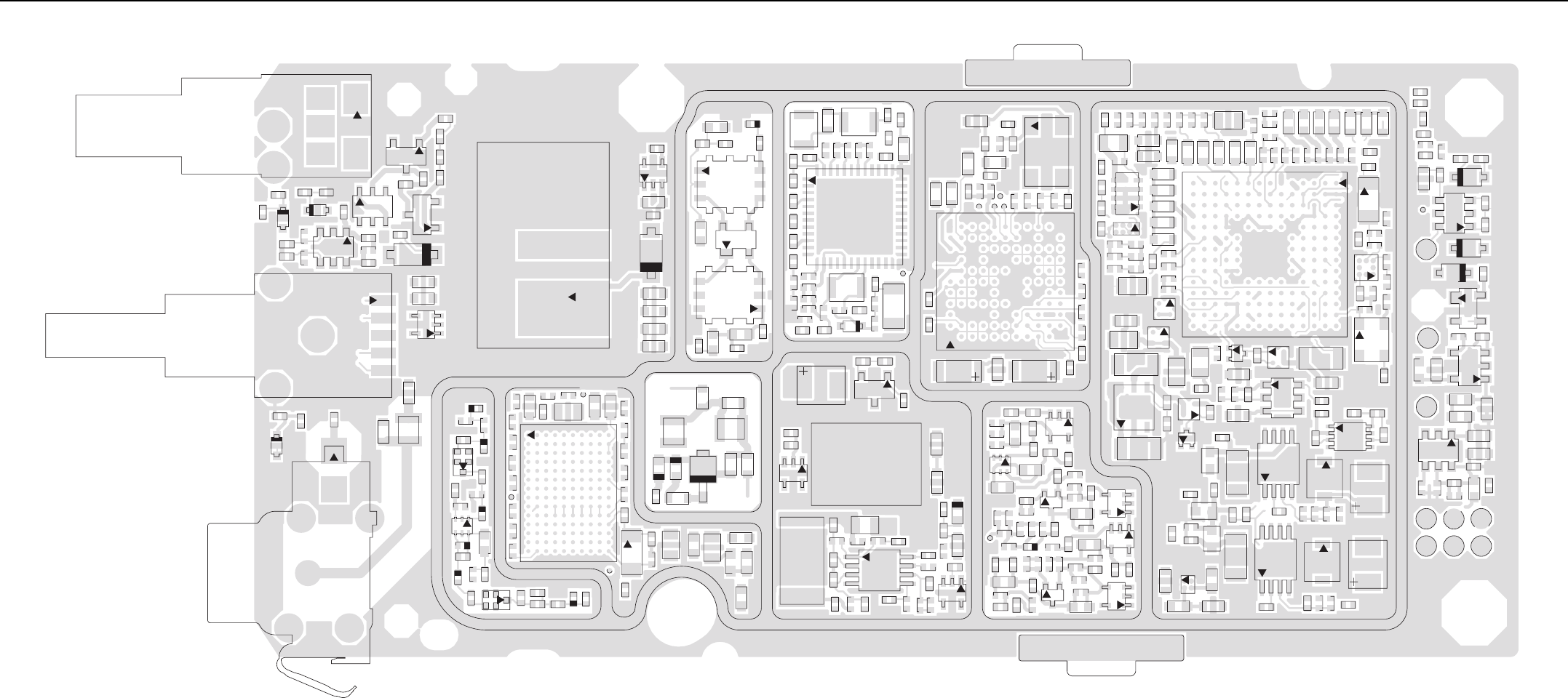
6-14 Circuit Board/Schematic Diagrams and Parts List
7
2
3
4
5
6
S9001
C9024
C9025
C9026
C9027
C9028
C9029
C9030 C9031
C9038
Q901 Q9000
Q9001
Q9003
R9008
R9009
R9010
R9011
R9015
R9016
R9017 R9018
R9050
R9051
R9053
R9054
VR9006
VR9007
VR9008 VR9009
7
8
2
3
4
5
6
S9002
C922
C923
C9023
L911
R906
R9014
VR9005
1
2
3
4
5
6
7
P900
C924
C925
C926
C8002
C8004
C8013
C8014
C8015
C8016
C8017
C8018
C8019
C8020
C8030 E8006
3
4
2
5
FL8000
3
4
2
5
FL8001
L912
L913
L8001
L8002
L8003
L8004
R8002
R8004
R8015
R8016
R8017
R8020
R8032
TP_CLK_ACQ
TP_IF
P10
P1
U8000
U8001
C8000
C8001
C8005
C8006 C8021
C8022
C8023
C8029
C8031
C8032
C8033
C8034
C8035
C8036
E8000
E8002
R8003
R8023
R8024
R8025
R8030
TP_SCLK
A1
Y8000
C8003
E8001
E8003
E8004
E8005
C900
C903
C904
C905
C920
C921
CR900
L902
L903
L909
L910
A10
23
M9007
R902
R903
R904
R905
VR9010
C927
C9032
C9039
Q900
C426
C427
L410
L411
R407
3
46
T400
D405
L412
3
4
6
T401
C429
C430
C431
L413
L414
C601
C602
C603
C604
C605
C607
C608
C620
C621
C622
C623 C624
C625C627
C628C629
C630
C631
C632
C633
C634
C635
C636
C637
C639 D601
E600
E601
E602
L600
L601
L605
R607
R609
R610 R611
R696
R698
TP600
1
37
25
13
U600
C700
C712
R712 R713
U702
M700
Q701
R731
R732
C721 R720
C703
C704
C705
C706
C708
C709
C710
C711
C731
E701
L700
Q702
R700
R701
R702
R703
R704
R705
R706
R707
R708
R709
R710
R711
R714
R733
U701
M2
C210
C211
C212
C213
C214
C215
C216
C217
C229
C230
C231
C232
C233
C234
C235
C236
C237
C238
C239
C240
C241
C738
L204
L206
L207 L212
L214
L215
L217
L218
Q202
Q203
Q205
Q206
Q207
Q208
R200 R201
R202
R205
R207
R208
R209
R210
R212
R213
R214
R215
R216 R217
R218
R220
R221
R222
R223
R224
R728
R729
R730
TP201 U200
M1
43
2
Y001
C001
C002
C004
C008
C013
C014
C015
C016
C039
E001
E004
R006
R007
R008
R026
R052
R053
R054
TP002
TP003
TP004
TP006
L11A11
C003
C005
C006
C007
C017
C018
C019
C020
C022 C035 E003
L1
U001
1
64
3
U3002
C3039
C3081
C3090
23
4
Q3000
23
4
Q3010
R3030
C3079
R3016
P14
C3091
C3084
C3101
C3102
C3201
C3205
C3206
C3207
C3208
C3209
C3210
C3211
C3212
C3805
E3704
E3705
L3003
L3004
L3021
L3022
R3031
R3038
R3202
R3203
R3704
U3006
U3021
C3015
C3017
C3018 C3025
C3026
C3200
C3202
C3203
C3204 L3020
R3028
R3029
R3040
R3041
R3043
R3100
R3102
R3103
R3200
R3201
U3008
8
5
4
U3009
U3020
C3060
SH9000
A14
4
3
2
Y3001
C3016
C3082
C3083
23
4
Q3001
Q3002
23
4
Q3005
R3017
R3018
R3101
U3000
Q3006
C3014
C3019
C3024
C3037
C3038
C3067
4
58
Q3003
R3004
R3005
R3006
R3007
R3008
R3009
R3020
R3021
R3051
R3053
R3054
R3098
P1
U3007
C3010
C3028
C3031
C3047
C3048
C3049
C3050
C3051
C3062
C3074
C3080
C3093
C3094
C3095
C3099
C3999
R3011
R3013
R3014
R3024
R3025
R3026
R3027
R3037
R3050
R3060
C3000
C3002
C3003
C3004
C3005
C3011
C3034
C3035
C3036
C3045
C3097
C3098
C3100 E3030
E3031
E3032
E3033
R3012
A1
Y3000
C9016
C9017
C9018
C9040
C9041
C9042
C9043
C9044
C9045
C9046
C9065
D3000
R3055 R3075
TP_POR
VR9001
C3700
C3701
C3702
C3703
C3704
C3705
C3706
C3707
E3700
E3701
E3702
E3703
R3700
R3701
R3702
R3703
TP_EXT_MIC
TP_EXT_MIC+
TP_EXT_SPKR
TP_EXT_SPKR+
TP_GPIO0
TP_USB1_DM
TP_USB1_DP
5
3
4
U3700
U3701
R9019
TP_ONE_WIRE_1
TP_VBUS1
VR9000
VR9003
VR9004
C3001
C3061
C3070
R3036
R3070
R3071
R3072
R3073
R3074
R3088
C1
C3
A3
U3003
UHF1 (403-470MHz) Main Board Bottom Side PCB No. 8486716Z08
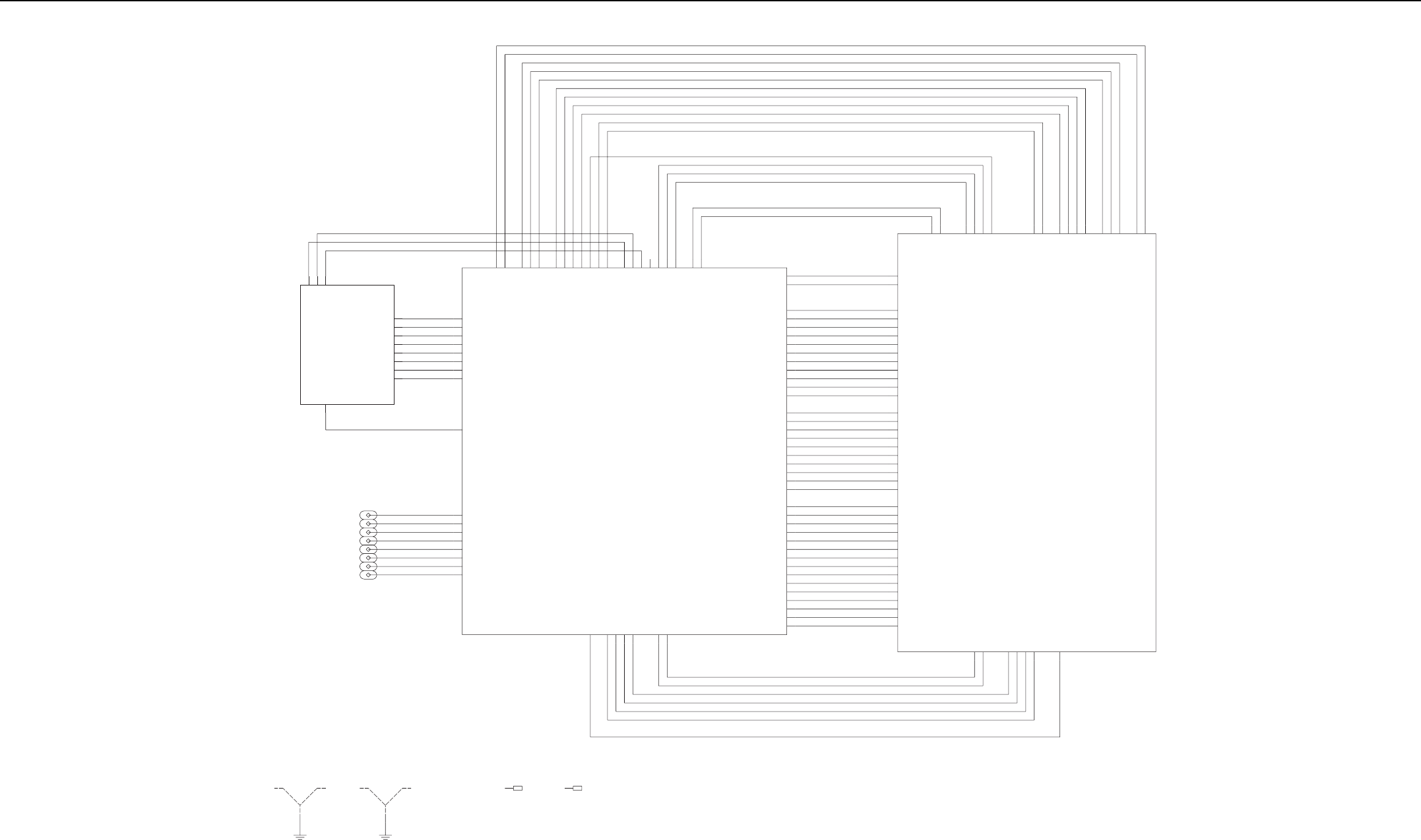
Circuit Board/Schematic Diagrams and Parts List 6-15
GPS
CORE
SW
CHOMERIC SHIELD
1
4W
S
8WS
+BWS
USB1_DM
USB1_DP
VBUS1
LOV
PT26PNGA23
SHIELD
SH9000
CNYSF
_O
KA
M
XR_OKAM
XT
_O
K
AM
WS_HCEM
ONE_WIRE_1
OPTA_SEL0
OPTA_SEL1
OPTA_SEL2
1_OI
PG
_TPO
2_OI
PG
_TPO
CNYS_ISS_TPO
PTT
+BWAR
DEL_DER
RESET_OUT
1W
S
2WS
INT_MIC+
INT_MIC-
INT_SPKR+
INT_SPKR-
KEYPAD_COL0
KEYPAD_COL1
KEYPAD_COL2
KEYPAD_COL3
KEYPAD_COL4
KEYPAD_ROW0
KEYPAD_ROW1
KEYPAD_ROW2
KEYPAD_ROW3
KEYPAD_ROW4
KLC
D
_O
K
AM
DISPLAY_CE
DISPLAY_CMD
DISPLAY_DATA0
DISPLAY_DATA1
DISPLAY_DATA2
DISPLAY_DATA3
DISPLAY_DATA4
DISPLAY_DATA5
DISPLAY_DATA6
DISPLAY_DATA7
B
P_GRE
M
E
EXT_MIC+
EXT_MIC-
EXT_SPKR+
EXT_SPKR-
DEL
_NE
E
RG
2
V
_G
ID
_
V
5
7
8
.1
4V_GID_
V
5
7
7.2
6V_GID_V9.2
01V_GID_V3.3
2SUBV_ANA_V5
ATAD_TTAB
BL_EN
M1 M2
2WS
4WS
8WS
+BWS
USB1_DM
USB1_DP
VBUS1
LOV
XR_OKAM
XT_OKAM
WS_HCEM
ONE_WIRE_1
OPTA_SEL0
OPTA_SEL1
OPTA_SEL2
1_OIPG_TPO
2_OIPG_TPO
CNYS_ISS_TPO
PTT
+BWAR
DEL_DER
RESET_OUT
1WS
JTAG_TCK
JTAG_TDI
JTAG_TDO
JTAG_TMS
KEYPAD_COL0
KEYPAD_COL1
KEYPAD_COL2
KEYPAD_COL3
KEYPAD_COL4
KEYPAD_ROW0
KEYPAD_ROW1
KEYPAD_ROW2
KEYPAD_ROW3
KEYPAD_ROW4
KLCD_OKAM
CNYSF_OKAM
GPS_ANT
GPS_BOOT
GPS_ON_OFF
GPS_RFPWRUP
GPS_RX
GPS_TX
GPS_nRESET
GPS_nWAKEUP
DEL_NEERG
INT_MIC+
INT_MIC-
INT_SPKR+
INT_SPKR-
JTAG_NEMU0
JTAG_NEMU1
JTAG_NTRST
JTAG_RTCK
DISPLAY_CE
DISPLAY_CMD
DISPLAY_DATA0
DISPLAY_DATA1
DISPLAY_DATA2
DISPLAY_DATA3
DISPLAY_DATA4
DISPLAY_DATA5
DISPLAY_DATA6
DISPLAY_DATA7
BP_GREME
EXT_MIC+
EXT_MIC-
EXT_SPKR+
EXT_SPKR-
CTR_SPG_V5.1
2V_GID_V578.1
16_8MHz_GPS
7V_ANA_V577.2
4V_GID_V577.2
SPG_GID_V8.2
S
PG
_F
R
_V8.2
6V_GID_V9.2
01V_GID_V3.3
2SUBV_ANA_V5
ATAD_TTAB
BL_EN
PT26PNGA24
SHIELD
SH9001
1
1.875V_DIG_V2
PTT
CTR_SPG_V5.1
16_8MHz_GPS
SPG_GID_V8.2
SPG_FR_V8.2
TNA_SPG
GPS_BOOT
GPS_ON_OFF
GPS_RFPWRUP
GPS_RX
GPS_TX
GPS_nRESET
GPS_nWAKEUP
RAWB+
3.3V_DIG_V10
BATT_DATA
EMERG_PB
SW8
SW4
SW2
SW1
MECH_SW
2.9V_DIG_V6
VOL
RED_LED
GREEN_LED
2.775V_DIG_V4
OPT_GPIO_1
MAKO_RX
MAKO_TX
MAKO_DCLK
MAKO_FSYNC
VBUS1
EXT_SPKR+
EXT_SPKR-
EXT_MIC+
5V_ANA_VBUS2
SWB+
DISPLAY_DATA3
DISPLAY_DATA2
DISPLAY_DATA1
DISPLAY_DATA0
DISPLAY_CMD
DISPLAY_CE
BL_EN
2.8V_RF_GPS
2.8V_DIG_GPS
16_8MHz_GPS
1.5V_GPS_RTC
OPT_SSI_SYNC
OPT_GPIO_2
GPS_nWAKEUP
GPS_nRESET
GPS_TX
GPS_RX
GPS_RFPWRUP
GPS_ON_OFF
GPS_BOOT
GPS_ANT
EXT_MIC-
DISPLAY_DATA7
DISPLAY_DATA6
DISPLAY_DATA5
DISPLAY_DATA4
KEYPAD_ROW1
KEYPAD_ROW0
KEYPAD_COL4
KEYPAD_COL3
KEYPAD_COL2
KEYPAD_COL1
KEYPAD_COL0
INT_SPKR-
INT_SPKR+
INT_MIC-
INT_MIC+
USB1_DP
USB1_DM
RESET_OUT
OPTA_SEL2
OPTA_SEL1
OPTA_SEL0
ONE_WIRE_1
KEYPAD_ROW4
KEYPAD_ROW3
KEYPAD_ROW2
Complete Radio Schematic Diagram
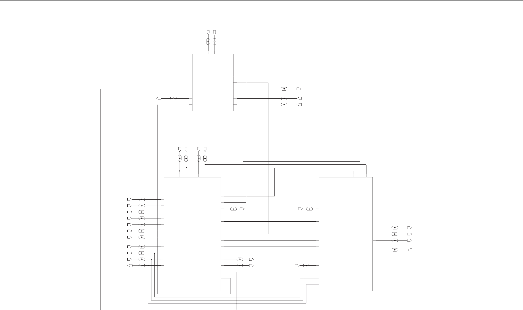
6-16 Circuit Board/Schematic Diagrams and Parts List
FGU
RX
TX
ANT_EN_RF
TX_DAC_RF
16.8_MHZ_BUFF_RF
SPI_CLK_RF
SPI_MISO_RF
TX_VCO_EN
RX_FLTR_VCTRL_RF
GPS_ANT_RF
GP02
LNA_AGC
LNA_ATTN
LNA_EN
LOCK_DETECT
RESET_OUT
RX_1ST_LO_INJ
RX_VCO_EN
SPI_CLK
SPI_MISO
SPI_MOSI
THK_CE
TX_BUFF
TX_CLK
TX_DATA
TX_FSYNC
2V_GID_V578.1
16.8_MHZ_BUFF
16_8MHZ
16_8MHZ_GPS
7V_ANA_V577.2
4V_GID_V577.2
8V_ANA_V5
5V_RX
ADAPT_SW
DEEP_SLEEP
DMCS
FR_
2
V
_
GID_V5
7
8.
1
TX_FSYNC_RF
FR_
4
V
_G
ID_V5
7
7.
2
FR_8V_ANA_V5
ADAPT_SW_RF
TX_CLK_RF
F
R
_
2
SU
B
V
_A
NA_V5
PA_TEMP_RF
FR_+BWAR
ABACUS3_CE_RF
LOCK_DETECT_RF
16_8MHz_GPS
RX_FSTNC_RF
2SUBV_ANA_V5
ANT_EN
GP02
GPS_ANT
PA_TEMP
+BWAR
RX_IN
TX_BUFF
TX_DAC
TX_VCO_EN
RX_DATA_RF
RX_DATA
RX_FLTR_VCTRL
RX_FSYNC
RX_IN
RX_VCO_EN
SPI_CLK
SPI_MISO
SPI_MOSI
SYNCB
SYNCB_RF
2V_GID_V
5
78.1
16_8MHZ
7
V
_
A
N
A_V57
7
.2
8
V
_
A
N
A
_
V5
XR_V5
ABACUS3_CE
LNA_AGC
LNA_ATTN
LNA_EN
RX_1ST_LO_INJ RX_CLK
THK_CE_RF
SPI_MOSI_RF
RX_CLK_RF
TX_DATA_RF
FR
_7V_AN
A_V5
7
7.
2
DEEP_SLEEP_RF
DMCS_RF
SYNCB
+
BW
AR
2
SUB
V
_
AN
A
_
V
5
8
V
_
A
NA
_
V
5
2
V
_GI
D_V5
7
8
.
1
16_8MHz_GPS
RESET_OUT_RF
LNA_ATTN
DMCS
DEEP_SLEEP
ADAPT_SW
4V_GID_V577.2
16.8_MHZ_BUFF
LOCK_DETECT
GPS_ANT
7
V
_
AN
A
_
V
5
77.
2
TX_DAC
PA_TEMP
ANT_EN
RX_FSYNC
RX_FLTR_VCTRL
RX_DATA
RX_CLK
ABACUS3_CE
TX_FSYNC
TX_DATA
TX_CLK
THK_CE
SPI_MOSI
SPI_MISO
SPI_CLK
RESET_OUT
Complete UHF1 RF Schematic Diagram
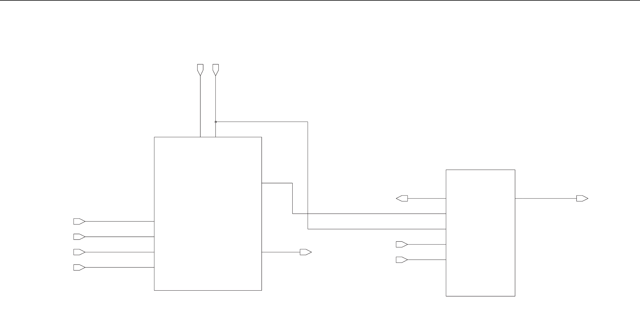
Circuit Board/Schematic Diagrams and Parts List 6-17
HF
PA_OUT
PA_TEMP
+BWAR
TX_BUFF
TX_DAC
TX_VCO_EN
PA_OUT
RAWB+
RX_IN
2SUBV_ANA_V5
ANT_EN
TX_BUFF
ANT_EN
TX_DAC
RX_IN
2SUBV_ANA_V5
PA_TEMP
+BWAR
GPS_ANT
GP02
ANT_EN
TX_VCO_EN
ANT_EN
GP02
GPS_ANT
PA
Complete UHF1 Transmitter Schematic Diagram
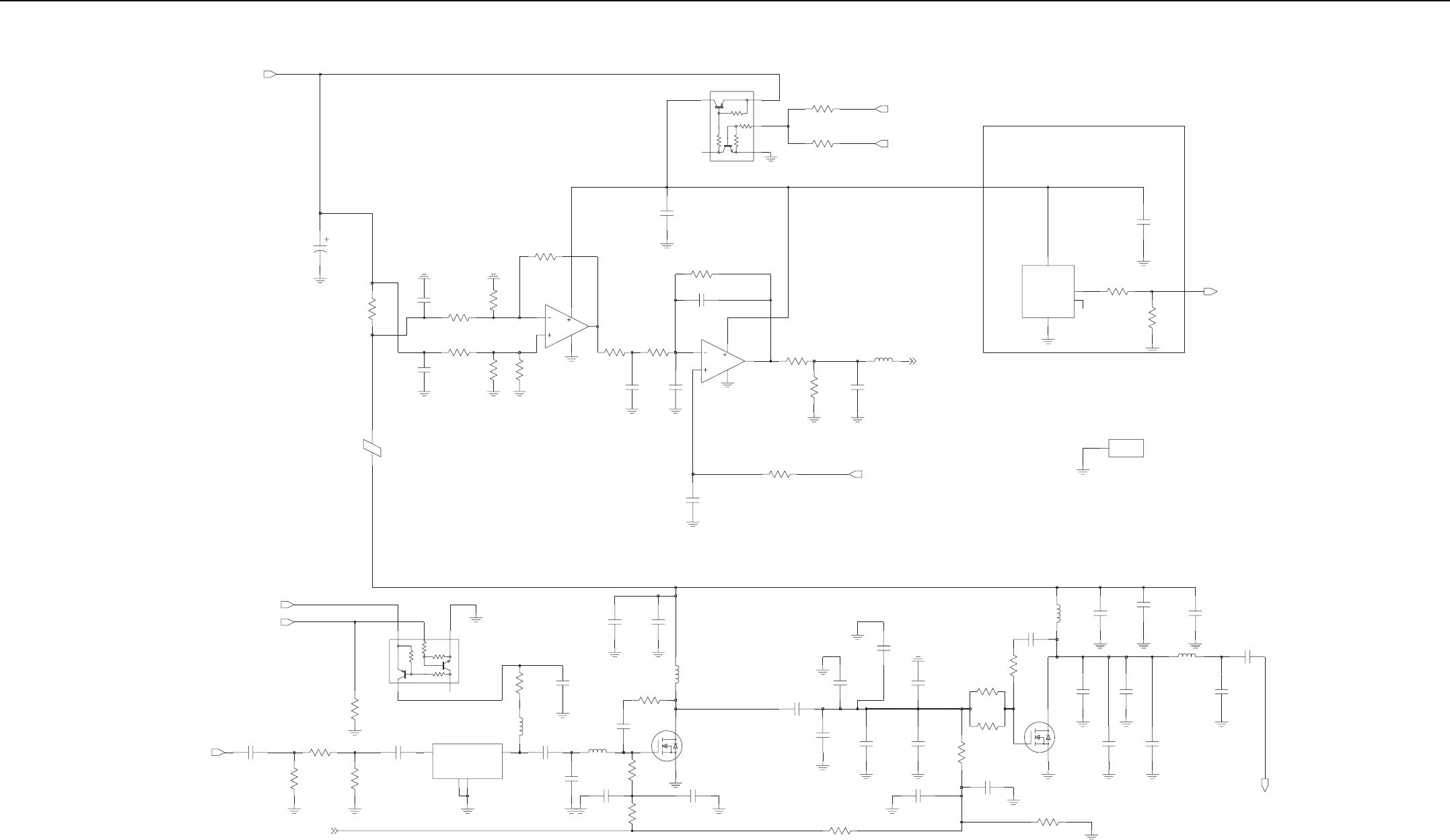
6-18 Circuit Board/Schematic Diagrams and Parts List
Near to heatsink
PW_CTRL
NU
PA
DNP
NU
NU
NU
NU
NU
NU
NU
C706
270pF
R706
2MEG
22
R729
R703
200K
C731
0.1uF
R704
200K
.022uF
C712
R719
43
0
R722
3
D
1G
2S
R732
Q703
0
Q701
0.10uF
C730
R730
300
R705
2MEG
9.1pF
C733
C739
0.10uF
30pF
C727
R712
0
7.66nH
L707
L702
9.5nH
DNG 1
S
O
P
2
VOUT
0
R709
U702
LM50
3
L703
120nH
C740
9.1pF
30pF
C734
R702
200K
C716
18pF
C738
270pF
270pF
C708
R710
10K
270pF
C724
9.1pF
C732
.01uF
C709
R723
43
.047uF
C705
270pF
C703
R727
43
C736
270pF
E701
41J949
6867
C737
1000pF
R718
200
270pF
C714
C729
270pF
120nH
L701
R717
9.1pF
22
C711
C799
C722
270pF
4.7pF
270pF
C715
0.1uF
C721
3.3K
R725
R708
R726
5.1K
R733
0
47K
C720
.022uF
200
R720
C704
270pF
2.2K
R707
30pF
C725
1DNG
2
2DNG
4
RF_IN
1VD_RF_OUT 3
6
5
7
8
4
U700
ADA4743
AD8566
U701-2
13.85nH
30pF
L706
C719
270
R714
10K
R713
C723
30pF
100pF
C735
2
07Q
R701
L700
200K
C798
120nH
9.1pF
.01uF
C710
C726
30pF
R731
0
Q704
D1
3G
S
2
270pF
C717
300
R728
C718
0.10uF
2
3
1
8
4
R700
AD8566
U701-1
0.1
C728
2.0pF R721
0
10uF
M700
HEATSINK
POS
1
C700
R711
20K
ANT_EN
5V_ANA_VBUS2
TX_BUFF
RAWB+
ANT_EN
TX_VCO_EN
TX_DAC
TX_VCTRL
PA_TEMP
TX_VCTRL
TU
O
_
A
P
4.7K
10K
47K
47K
47K
47K
4.7K
10K
UHF1 Transmitter Schematic Diagram
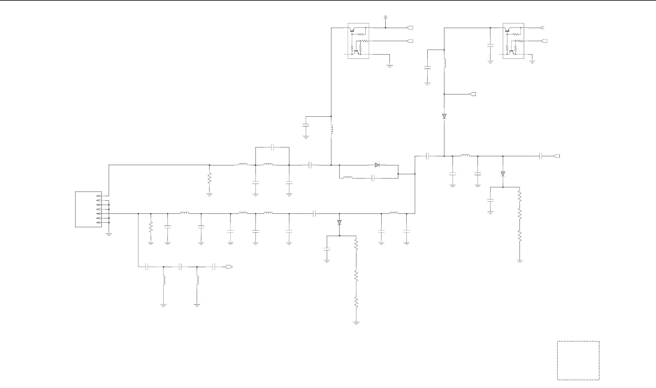
Circuit Board/Schematic Diagrams and Parts List 6-19
R907
L913
C927
LIVE
ANTENNA NUT
P900
DNPDNP
M901
RF CONNECTOR
LIVE
GND
Q901
P900
L913
5.6nH
C910
33pF
6.2pF
C922
3.9nH
L912
C915
4.7pF
100pF
C918
5.6pF
C908
L905
5.6pF
C906
19nH
82
R9053
R9054
82
L909
19nH
18.9nH
L906
18.9nH
10K
R906
L908
CR902
L902
120nH
P900-2
C921
P900-5
1
3
3.0pF
Q901
2
5
4
Q900
4.7pF
C912
C924
2.7pF
C920
8.2pF
19nH
L904
R905
82
82
R902
2.2pF
C903
R907
10K
C923
6.2pF
68pF
C909
L911
C911
19nH
3.3pF
C927
270pF
100pF
3.9pF
C913
120nH
C926
100pF
L903
C905
68pF
C904
33pF
C917
3.3pF
C916
C900
270pF
82
R903
C925
1.5pF
R904
82
C914
2
1
270pF
CR903
82nH
L907
P900-4
P900-6
CR900
19nH
L910
P900-3
6.8pF
C907
P900-1
P900-7
CR901
GP02
RAWB+
PA_OUT
RAWB+
ANT_EN
GPS_ANT
RX_IN
4.7K
47K
47K
10K
4.7K
47K
47K
10K
UHF1 Harmonic Filter and Antenna Switch Schematic Diagram
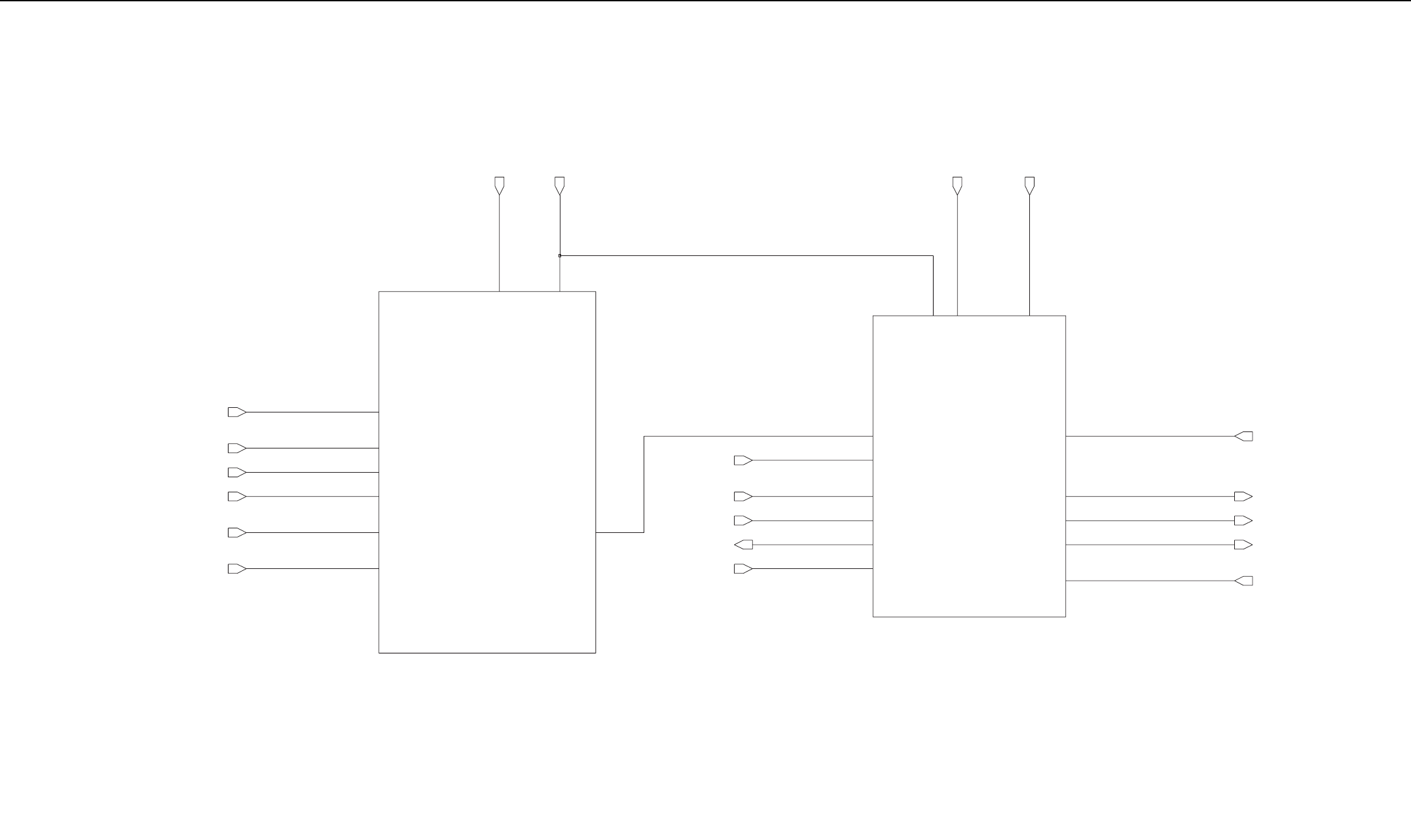
6-20 Circuit Board/Schematic Diagrams and Parts List
SPI_MOSI
SYNCB
2V_GID_V578.1
16_8MHZ
7V_ANA_V577.2
8V_ANA_V5
ABACUS3_CE
IF_AMP_OUT
RX_CLK
RX_DATA
RX_FSYNC
RX_VCO_EN
SPI_CLK
SPI_MISO
IF_AMP_OUT
LNA_AGC
LNA_ATTN
LNA_EN
RX_1ST_LO_INJ
RX_FLTR_VCTRL
RX_IN
RX_FLTR_VCTRL
LNA_EN
LNA_ATTN
LNA_AGC
RX_IN
RX_1ST_LO_INJ
XR_V5
SPI_MOSI
SPI_MISO
SPI_CLK
RX_VCO_EN
RX_FSYNC
RX_DATA
RX_CLK
ABACUS3_CE
8V_ANA_V5
7
V
_
A
N
A_V577
.
2
16_8MHZ
2V_GID_V578.1
SYNCB
7V_ANA_V577.2
XR_V5
RXFE
RXBE
Complete UHF1 Receiver Schematic Diagram
Circuit Board/Schematic Diagrams and Parts List 6-21
RX_EN
From TOMAHAWK
To MIXER Section
FROM TOMOHAWK GPO5
1 Shield
RXFE - Shield A
(MAKO)
RXFE - Shield A RXFE - Shield B
RXFE
RX_FLTR_VCTRL
IF_AMP_VCC
LNA_EN
RF_ATTN
DNP
1SV229
D403
6.8pF
C404
Q400
C418
4.3pF
3.9pF
24nH
C426
L413
R425
0
270nH
L416
D400
1SV229
042
794R
16nH
L408
51
R407
0
R417
100K
R405
R499
R413
100K
3K
1.0uF
C448
C427
82nH
L411
51pF
L410
39nH
470nH
L420
C428
16pF
L409
16nH
D401
1SV229
24nH
L414
C417
270pF
9.1K
R420
D404
1SV229
C420
TP403
6.8pF
.01uF
C437
R406
100K
100pF
L404
18nH
C435
30K
R422
560
R412
100
R421
L400
16nH
TP400
L406
R400
100K
10nH
C433
C422
6.2pF
8.2pF
9.1pF
C423
C414
R410
6.8pF
2.7K
C421
3.6pF
C438
C441
13pF
0.10uF
3
L405
30nH
T400
NC 5
6
1
4
2
TP402
XFMR
4.3pF
R402
C413
0
6.8pF
270pF
C410
16nH
C419
C408
L401
1pF
.01uF
C411
L402
82nH
C447
1.0uF
8.2pF
C429
C446
11pF
0.10uF
C444
750
R403
R404
270pF
750
C432
15pF
C412
8.2pF
TP401
C425
3.6pF
Q401
E401
C440
0.1uF
180nH
C409
0.5pF
L417
12K
R411
C407
2A
4A
1K
3
K
L418
D405
L403
27nH
390nH
E400
L412
330nH
470nH
L419
330nH
L415
270pF
C439
6.8pF
C401
914R
0
C424
100pF
LNA_IN
7
LNA_OUT
8
CCV_ANL
4RF_ATTN
CCV_FR 11
10
RSET
5AGC
9PYB_CGA
3EN_RX
21 DNG
1G 1DNG
2
LNA_E
6LNA_I
1
MAX2373
U400
C442
.01uF
30K
R409
9.1pF
C415
8pF
C400
C434
0.10uF
0
R416
6.8pF
C405
C445
D402
6
1
4
2
3
16pF
T401
XFMR
5
NC
C416
0.10uF
100pF
C403
C436
0.10uF
C430
12pF
6.8nH
L407
C431
8.2pF
12K
R424
C402
RX_FLTR_VCTRL
A
_V577.2
3.6pF
RX_1ST_LO_INJ
LNA_AGC
5V_RX
IF_AMP_OUT
LNA_EN
RX_IN
LNA_ATTN
OUT
GND1
GND2
1
4
5
2
36
FL 400
TS75
73.35MHz
CC1
CC2
IN
UHF1 Receiver Front End Schematic Diagram
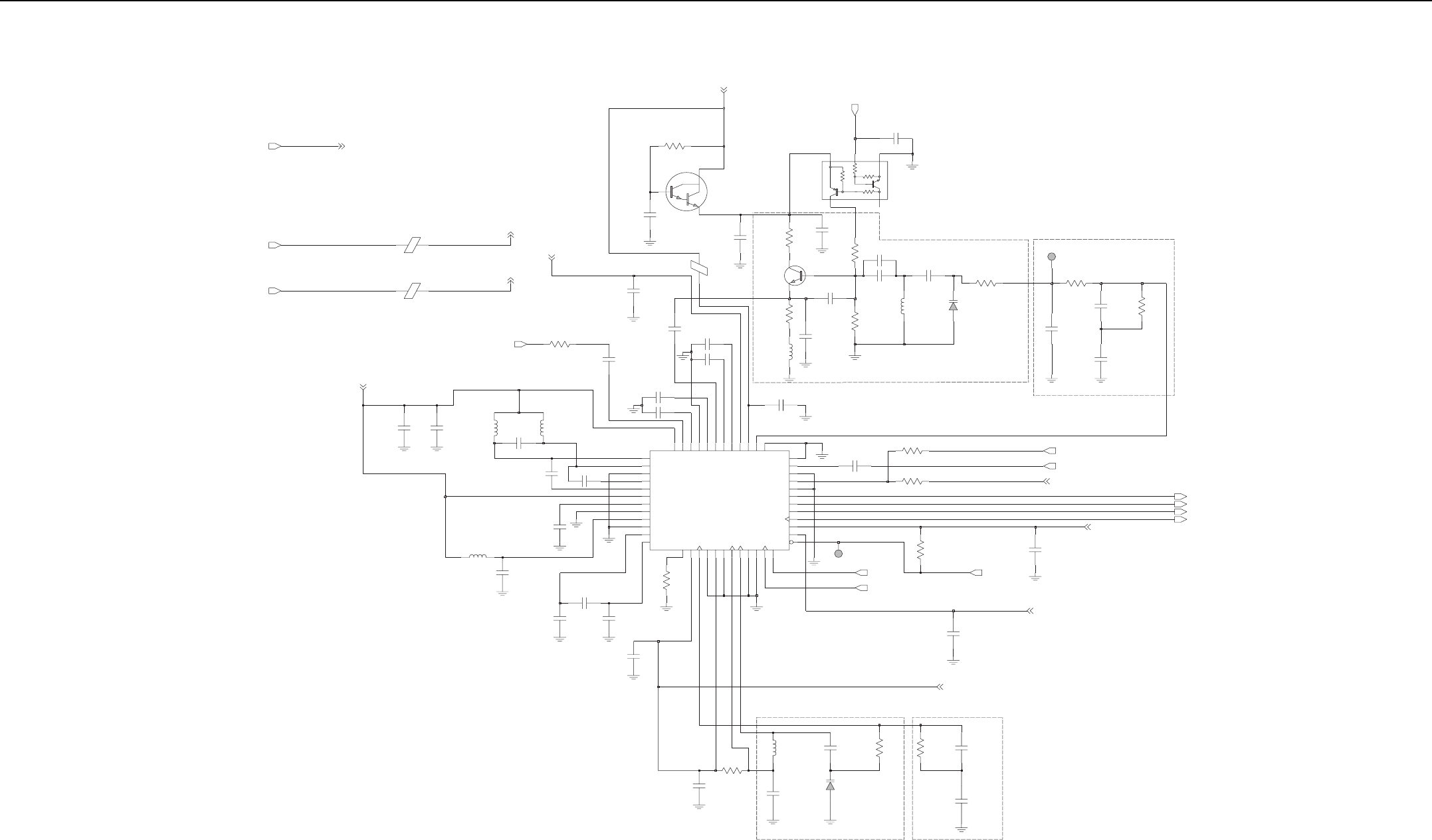
6-22 Circuit Board/Schematic Diagrams and Parts List
DNP
DNP
RXBE
CLOCK LFCLOCK VCO
10uH
C633
0.1uF
0
R696
L600
C608
C616
39pF
R612
.047uF
15K
R699
Q602
100K
D600
1SV305
R607
100K
C629
100pF
4.7uH
L605
Q601
C613
0.1uF
E601
18pF
C638
.01uF
0.1uF
C607
C602
C628
.01uF
L601
10uH
C604
.01uF
TP601
1SV305
C605
.01uF
D601
C632
0.1uF
C622
200pF
C612
5.1K
11pF
C635
51pF
R605
.047uF
C626
18pF
TP600
C611
100pF
C623
L602
4.7uH
E600
100pF
C614
1.0uF
C627
E602
C636
0.1uF
330
R602
C617
3300pF
.01uF
C601
10K
R698
0.1uF
390
R611
C620
15K
R603
R697 0
C618
30pF
C609
.012uF
5.1K
R604
K01
016R
C630
.01uF
04
LDD
V
9
3
PDDV
4
1
QDD
V
12
VREFN
FER
R
3
1
33
SYNCB
9
VDDA
71
CDD
V
26
VDDD
6
VDDF
27
VDDH
84
IDD
V
8
3
L
T
U
OI
24
N
OL
34
P
O
L
2
MXON
1
MXOP
32
C
P
42
D
P
25
PE
73
PD
N
G
6
1
QDNG
1
2
1SDNG
34
GNDS2
4
IF2N
5
IF2P
74
N
IFI
51
CT
U
OI
7
GCP
10
GNDA
81
CD
N
G
22
DDNG
3
GNDF
32
GNDH
5
4
IDNG
36
GNDL
6
4
FI
XC
44
LVXC
14
MV
XC
29
DOUTA
DOUTB
30
35
FREF
31
FS
8
GCN 5102495J14
U600
02
NKL
C
28
CLKOUT
PKL
C
91
AD9864
30pF
C610
C603
0.1uF
R609
10K
.01uF
C634
C606
39pF
L604
330nH
180
R601
0.1uF
C619
C615
0.1uF
2200pF
C625
Q600
C637
0.68uF
C631
1K
R606
.01uF
820nH
C624 100pF
L603
R600
.01uF
C621
10K
RX_CLK
BA
_A
NA
_
V
5
77.2
0.1uF
C639
E_OCV_XR
SYNCB
1.875V
1.875V_DIG_V2
BA_ANA_V577.2
1.875V
2.775V_ANA_AB
ABACUS3_CE
RX_FSYNC
SPI_MISO
RX_DATA
1.875V
2.775V_ANA_V7
2.775V_ANA_AB
2.775V_ANA_AB
SPI_MOSI
SPI_CLK
IF_AMP_OUT
5V_ANA_V85V_ANA_V8
16_8MHZ
5V_ANA_V8
VREFP
11
47K
47K
10K
4.7K
UHF1 Receiver Back End Schematic Diagram
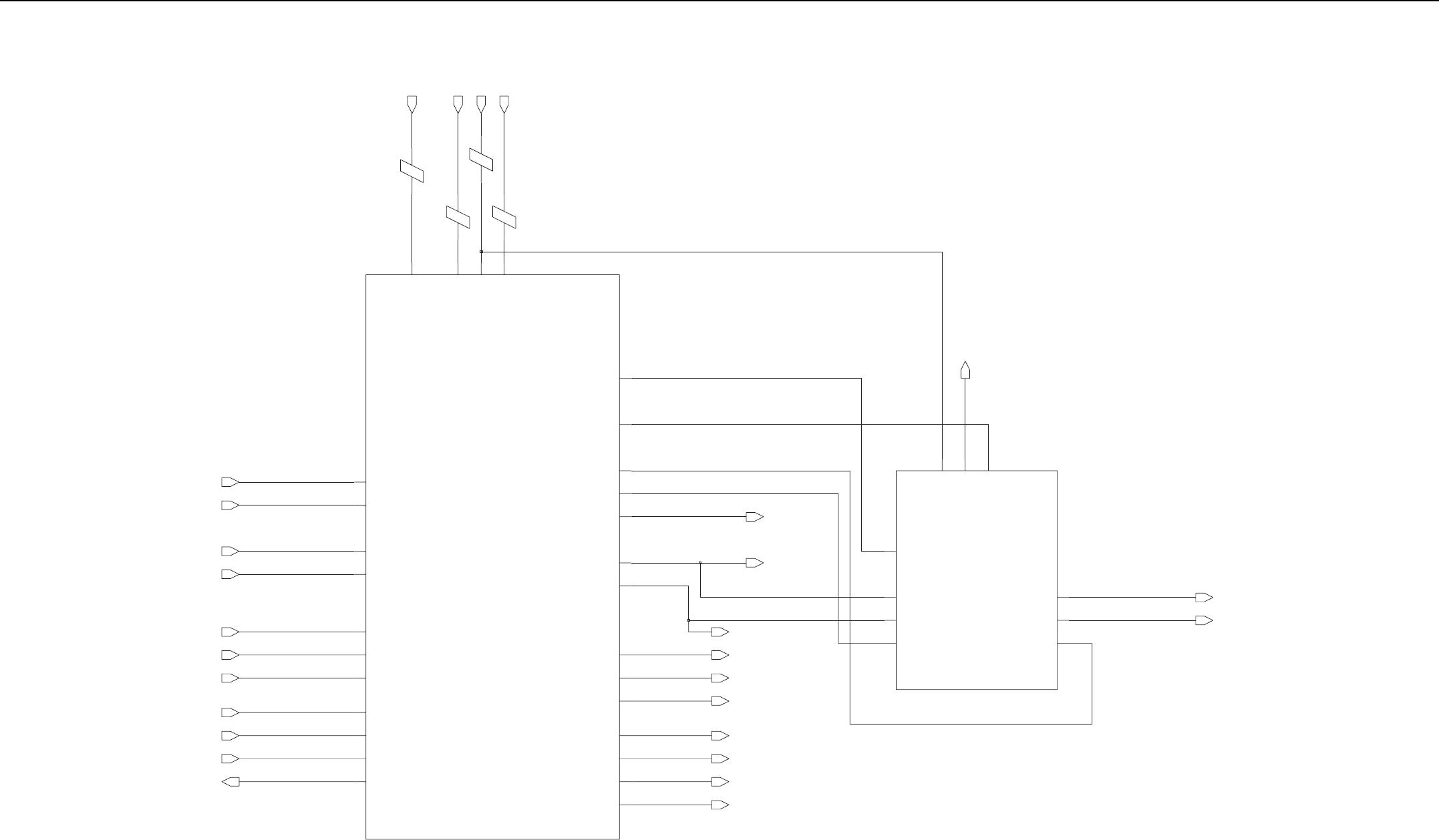
Circuit Board/Schematic Diagrams and Parts List 6-23
TOMAHAWK
LNA_EN
LOCK_DETECT
PRESCALER
RESET_OUT
RX_VCO_EN
SF_OUT
SPI_CLK
SPI_MISO
SPI_MOSI
THK_CE
TX_CLK
TX_DATA
TX_FSYNC
TX_VCO_EN
TX_VCO_TANK
VCTRL
KHT_2V_GID_V578.1
16.8_MHZ_BUFF
16_8MHZ
16_8MHz_GPS
KHT_7V_ANA_V577.2
KHT_4V_GID_V577.2
KHT_8V_ANA_V5
ADAPT_SW
DEEP_SLEEP
DMCS
GP02
LNA_AGC
LNA_ATTN
3
00E
2
0
0
E
4
00E
100E
TX_BUFFTX_VCO_EN
TX_VCO_TANK
VCTRL
SPI_CLK
SPI_MISO
2
V
_
GID_V5
7
8.
1
4V_G
I
D_V577
.
2
8V_AN
A
_
V
5
7V_ANA_V577.2
XR_V5
RX_1ST_LO_INJ
TX_BUFF
LOCK_DETECT
LNA_ATTN
LNA_AGC
LNA_EN
16_8MHZ
16.8_MHZ_BUFF
RX_VCO_EN
GP02
TX_VCO_TANK
16_8MHz_GPS
KHT_8V_ANA_
V
5
XR_V5
PRESCALER
RX_1ST_LO_INJRX_VCO_EN
TUO_FS
TX_VCO_EN
ADAPT_SW
DEEP_SLEEP
DMCS
RESET_OUT
TX_CLK
TX_FSYNC
TX_DATA
THK_CE
SPI_MOSI
VCO
Complete UHF1 Frequency Generating Unit Schematic Diagram
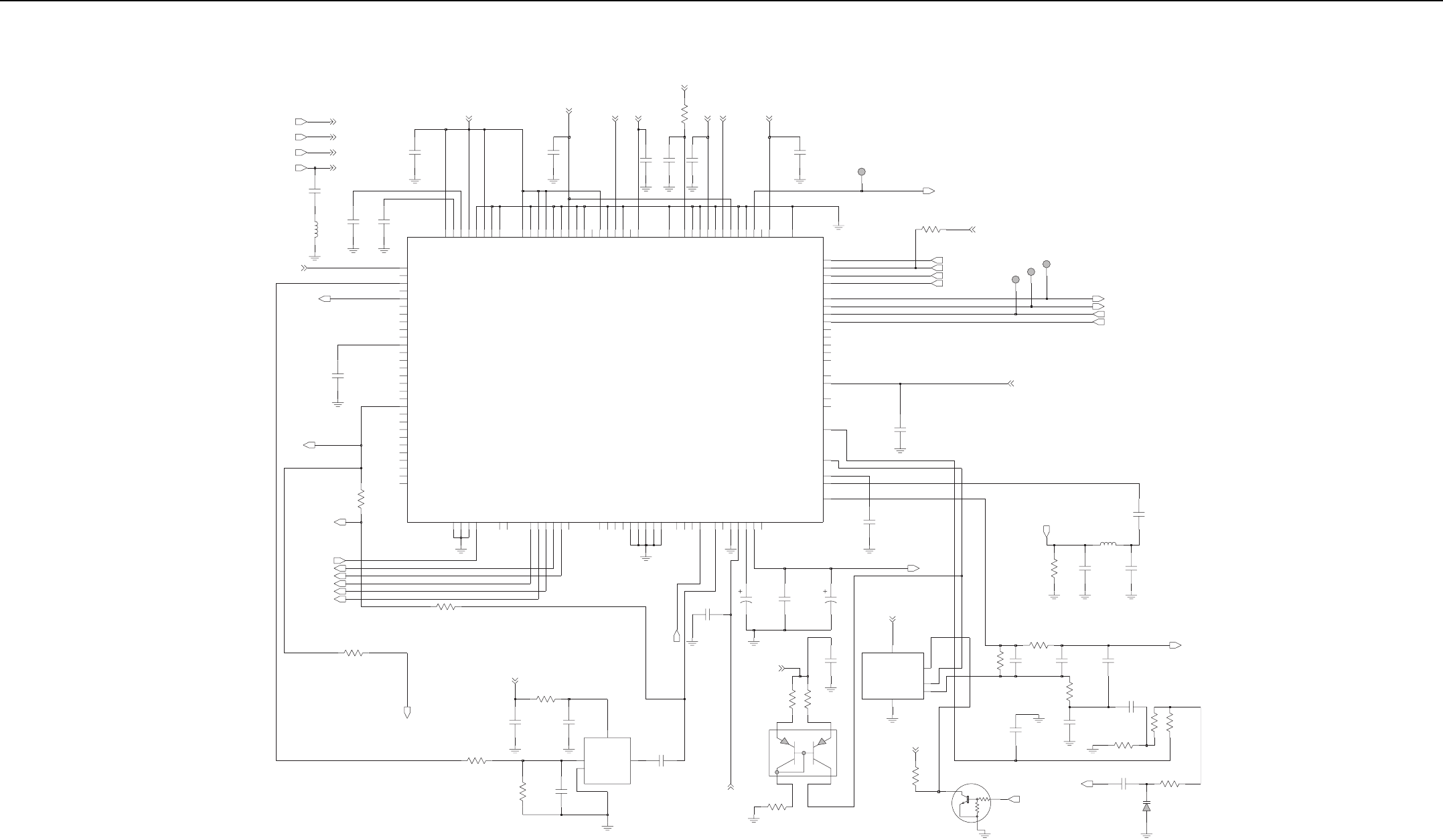
6-24 Circuit Board/Schematic Diagrams and Parts List
MN_ADAPT
TOMAHAWK
MOTOROLA INTERNAL USE ONLY
PC_NM
C016
1000pF
C001
1.0uF
0
R053
R016
22
0.15uF
C026
R010
C002
1.0uF
6.8K
9.1K
R025
33K
OUT
R018
DTC114YM
Q003
DNG
IN
.01uF
6.8K
R006
C019
4.7pF
C031
C032
100pF
L002
33nH
C039
C006
0.10uF
1.0uF
100K
R012
D001
600PT
0
R054
R022
30
4
CCV_SO
P
1VCONT
R007
10K
Y001
IVT5300B
16.8MHz
2COMM_CASE
3
OUT
DNG
3
INOUT 1
ONOFF_CONTROL 4
OUTIN 2
CCV 5
U002
C005
0.10uF
0
C036
0.10uF
R027
C003
0.10uF
1.5pF
C033
10uF
C020
C017
0.10uF
300PT
C007
0.10uF
R013
2
1
3
4
75
Q002
BCV62
10K
R026
R008
10
C004
0.10uF
C025
.033uF
R011
C008
0.10uF
100
C037
1.5pF
H
n
074
3
0
0L
1.0uF
C009
C028
.01uF
C027
1uF
1000pF
C038
400PT
200PT
R020
180
0
R052
R017
430
0.10uF
C035
C014
.01uF
C022
0.10uF
R014 51
R019
10K
10uF
C018
7
G
1DNG_XT
6F 2DNG_XT
6J
CCV_X
T
F1
VCO_DAC
5K ESAB_C
S
OX
5
LT
I
M
E
_CS
O
X
6G
DNG_CSOX
1TSET 7
C
2TS
E
T
3B
M
T
F10
TXCLK
K7 TXI
L7 TXQ
7H
DNG_CAD_XT 6
L
C
C
V
_
CAD_X
T
SPI_DR
D9
SPI_DW
DNG_ISS 8E
11E
CC
V
_I
S
S
1BUS
01K
5
F2BUS
3F 3
BU
S
G8 TCLK
7
D
9A
MFERV_MDS 8B
PFERV_MDS
D11
SDR
F11
SDTX
F9
SFTX
4K TUO_FS
9C DNG
_N
EG
_KLC_D
M
S
C11
SPI_CLK
D10
B1
3D
NE_NACS
F2 SCAN_IN
E9
SCLK_OUT
CCV_NE
G
_
K
LC_MDS 0
1
A
8A
DN
G_
F
ER_
M
DS
CCV_FER_MDS 9
B
B10 SDM_VAG
RXI
RXIX
C1
RXQ
D1
D2 RXQX
1DNGA_XR 3C
5D
2
DN
GA_X
R
2
B
1CCVA_XR
5A
2
CCV
A
_
XR
RX_EN_OUT
TUO_GERCSO
5H
4J YLPS_GER
C
SO
PABIAS_DAC
K11
L9 PHCLK
RFSTEPA
A3
6E BTS
R
E7
RXACQ
E10
RXFS
C2
1C
N
11A 2C
N
3C
N
1L
11L 4
C
N
NTXI
L8
NTXQ
K6
4
LPY
B
_GE
R
CSO
5J
DN
G
_GE
RC
SO
G2
1J
CCV_NIAM
H1
MN_ADAPT_CP
G3
MN_CP
5G
DN
G
_
P
C_
NM
C
CV_P
C
_N
M2H
J2
M_PRSC
H3
M_PRSCX
1A
6OPG
K8
HP_MOD_OUT
INCR_DECR
J9
8
F
1DNGL 8C
2DNG
L
01G
1C
CVL
7B
2CC
V
L
4G
DNG_NIAM
MAIN_PDET_VCC
CC
V
_
C
S
E
C6 FBI
B6 FBQ
4B 1
T
SE
T
_1OPG
4A 2
T
SE
T_
2OPG
3
T
SE
T
_3OPG
5
E
4D 4TSET_4OPG
9K 5OPG
8H
ESC_CP L3
2L
SAIB
P
C_CSE
3K
DNG_PC_CSE 3J
CCV_PC_CS
E
4H
DNG
_C
SE
K1
ESC_IN
1E
TSET_CSE
2K
TIM
E
_
K
LC
01H
DNG
_
K
LC
01J
CCV_KL
C
G1
DAC_ADAPT
A2 DC_CAL
01L P
E
E
L
SP
E
ED
F7
DMCS
M
TUO
_
F
E
8J
7J P
TUO_F
E
BP_IX
E2 BP_Q
E3 BP_QX
D8
CEX
H9 CLK1_OUT
J11 CLK2_OUT
11
GE
S
AB_KLC
9G PC_KLC
11H
B5
AGC_FLAG
C4 AGC_REF
C5
H6 ARX_DAC
0
1C KLC_IPSA
11B ATAD_IPSA
7A
CC
V
_IP
SA
E4 BP_I
F4
U001
SC51650VF
5104932K08
6A 1
EC
A
6D 2EC
A
AGC_DAC
C024
0.22uF
.01uF
C015
C013
270pF ADAPT_SW
2.775V_DIG_V4_THK
1.875V_DIG_V2_THK
2.775V_ANA_V7_THK2.775V_ANA_V7_THK
KH
T
_7V_A
NA
_
V
57
7.
2
THK_CE
16.8_MHZ_BUFF
16_8MHz_GPS
16_8MHZ
TX_DATA
TX_CLK
TX_FSYNC
LOCK_DETECT
5V_ANA_V8_THK 5V_ANA_V8_THK
KHT_2V_GID_V578.1
K
H
T
_
2
V
_GID
_
V
5
78.
1
5V_ANA_V8_THK
2.775V_DIG_V4_THK2.775V_DIG_V4_THK
1.875V_DIG_V2_THK1.875V_DIG_V2_THK
SF_OUT
KHT_8V_ANA_V5
RX_VCO_EN
TX_VCO_EN
RELACSERP
LNA_EN
LNA_ATTN
GP02
HP_MOD_OUT
TX_VCO_TANK
2.775V_ANA_V7_THK
KHT_7V_ANA_V577.2
2.775V_ANA_V7_THK
KHT_7V_A
N
A
_
V577
.
2
K
HT_
7
V
_
ANA_V5
7
7.2
KHT_2V_GID_V578.1
KHT_8V_ANA_V5
KH
T
_2V_G
I
D_V578
.
1
HT_8V_ANA_V5
VCTRL
LNA_AGC
DEEP_SLEEP
DMCS
TUO_TESER
SPI_MISO
SPI_MOSI
SPI_CLK
R1
R2
UHF1 Synthesizer Schematic Diagram
Circuit Board/Schematic Diagrams and Parts List 6-25
VCO
Rx_VCO_Ex_Supply
DNP
DNP
tuO_OCV_xT
Tx_VCO_Ex_Supply
DNP
DNP
5.6K
R209
D201
110
R211
R215
56
D207
390nH
L200 Q208
D206
18pF
C224
L206
390nH
C202
8.2pF
C206
62pF
D200
R201
5.6K
C203
6.8pF
L218
51nH
C216
2.4pF
0.1uF
C230
R221
18
C221
5.6pF
C214
100pF
1000nH
L217
D205
5.6K
R205
Q200
Q204
C211
0.1uF
L205
C222
3.3pF
100pF
390nH
12nH
C208
IDCTR
L210
IDCTR
L202
0
8.8nH
300
R222
R223
Q203
C225
C201 10pF
56pF
C227
100pF
C205
18pF
390nH
L212
390nH
L214
R202
100
5.6pF
C220
100
R210
C233
100pF
47nH
L207
5.6pF
L208
390nH
C223
R216
220
TP201
C213
2.7pF
D202
C200
D203
100pF
R208
8.2K
R214
240
100pF
C219
13pF
C207
390nH
L204
390nH
L203
L201
19nH
1.0pF
C232
100pF
C215
11pF
C243
13pF
C226
C209
0.1uF
8.2K
C239
R217
C210
100pF
100pF
2.0pF
C236
Q205
C241
0.5pF
C237
4.3pF
Q207
1.5pF
C212
R203
120
15nH
L209
Q202
R220
300
R218
510
2.0pF
C231
C238
L215
36nH
L213
100pF
C229
390nH
L211
100pF
R212
390nH
5.6K
D204
R207
56
Q206
0.1uF
C228
100pF
1DNG
2
32DNG
3
DN
G
5
1IN 4
OUT
CCV 6
C234
TP200
U200
11pF
R224
C204
0
100pF
C240
9.1pF
C217
R200
8.2K
7.5K
R213
KNAT_OCV_XT
C235
100pF
SF_OUTSF_OUT
TUO
_
FS
TUO_FS
KHT_8V_ANA_V5
KHT_8V_ANA_V5
RX_1ST_LO_INJ
PRESCALER
5V_RX
TX_VCO_EN
TX_BUFF
5V_ANA_V8_THK 5V_ANA_V8_THK
LRTCV
RX_VCO_EN
4.7K
47K
47K
10K
4.7K
47K
47K
10K
4.7K
47K
47K
10K
4.7K
47K
47K
10K
UHF1 Voltage Controlled Oscillator Schematic Diagram
6-26 Circuit Board/Schematic Diagrams and Parts List
Y8000
GPS Block
FL8001
GPIO[0] (A4)
U8004
2dB Pi Pad
Q8000
L8004
R8037
E8008
C8036
0_LLP_DDV 01A
4C
1_GER_DDV
2_GER_DDV 7F
CTR_DDV 4B
E7
WAKEUP
P2 XTAL_IN XTAL_OUT P3
1_BB_DDV 4D
2_BB_DDV 4
E
3_BB_DDV 4F
4_BB_DDV 2K
5_BB_DDV 2L
6_BB_DDV 3L
HSALF_DDV 3B
LLP_DDV 5C
6M
5_FR_CCV 7M
6_FR_CCV 8
M
7_FR_CCV 9M
8_FR_CCV 01M
9_FR_CCV 9P
CTR_CCV
1_KDDV 01B
2_KDDV 01C
P4
TP_IF
A6
TXA B7
TXB
8P
TXE_OI_CCV 2M
1_FR_CCV 3M
2_FR_CCV 4M
3_FR_CCV 5M
4_FR_CCV
SO J8
K8 SPI_DI
K6
SPI_DO
J10 SRESET
SS_0 J9
SS_1 H1
C6
TIMEMARK
D10 TMODE
K10
RTC_OUT
P10 RTC_XI
L10
RTC_XO
A5 RXA
C7 RXB
SI
J6
J5 SIGN_MAG_I
K5
SIGN_MAG_O
H9 RSRVD_32
J3 RSRVD_33
RSRVD_4
B9
RSRVD_5
C3
RSRVD_6
C8
RSRVD_7
C9
RSRVD_8
D2
RSRVD_9
D8
G9 RSRVD_25
H2 RSRVD_26
H3 RSRVD_27
H4 RSRVD_28
H5 RSRVD_29
RSRVD_3
B8
H7 RSRVD_30
H8 RSRVD_31
RSRVD_18
G2
RSRVD_19
G3
RSRVD_2
B6
RSRVD_20
G4
RSRVD_21
G5
RSRVD_22
G6
G7 RSRVD_23
G8 RSRVD_24
RSRVD_10
D9
RSRVD_11
E2
RSRVD_12
E3
RSRVD_13
E8
RSRVD_14
E9
RSRVD_15
E10
RSRVD_16
F8
RSRVD_17
F9
A2
ODO
G10 ON_OFF
H6
PLL_FILTER
H10
RESET
P6 RFIN
B1
RFPWRUP
F10 RIN
RSRVD_1
A9
C1
GPIO_14 E1
GPIO_15
P1 GRFRST
N1 JTCK
J1 JTDI
M1
JTDO
L1 JTMS
K1 JTRST
6
L3_FR_DNG
7
L4_FR_DNG
8L 5_FR_DNG
9
L6_FR_DNG
2N 7_FR_DNG
3N 8_FR_DNG
4N 9_FR_DNG
GPIO_0 A4
6N 11_FR_DNG
7N 21_FR_DNG
8
N31_FR_DNG
9N 41_FR_DNG
01N 51_FR_DNG
5P 61_FR_DNG
7P 71_FR_DNG
5
L2_FR_DNG
5D 2_BB_DNG
6D 3
_BB_DNG
5E 4_BB_DNG
6E 5
_
BB
_
D
N
G
5F 6
_
BB
_
D
N
G
6F 7_BB_DNG
4L 1_FR_DNG
5N 01_FR_DNG
ED_0 G1
ED_1 C2
ED_7 J2
EIT_0 B5
EN_MOE D1
EN_MWE B2
EN_SPI_CEB
K9
1A 1_BB_DNG
CLK_ED_3 F2
CLK_S A8
J7
CLK_SK
CLK_SPI
K7
D3
CS_0
CS_1 F1
A3 CS_F
EA_2 D7
U8000
GSC3F
5115831H01
AGCPWM K3
CLK_ACQ_I
J4
CLK_ACQ_O K4
CLK_E
A7
F3
CLK_ED_2
750
18pF
C8033
2
1
R8004
.01uF
NC
C8032
GPS_TX_GPS
L8001
5.6nH
21
NC
NC
5.6nH
L8004
1000pFC8029
18pF
C8030
1
10uF
C8000
2
1
R8027
100K
2
1
NC
C8036 1000pF
1
E8001
IDCTR
2
K0
10308R
10R2593
1
60
TPSM0_381
TP_IF
1
100KR8002
R8012
2
1
TP_SCLK
TPSM0_381
2
1
10K
IDCTR
E8003
21
100K
R8028
C8005
10uF
NC
1000pF10uF
C8002
21
QCA_KLC_PT
183_0MSPT
1
C8003
Y8000
XTAL
32.768KHz
C8017
18pF
C8004
18pF
2
1
NC
L8002
22nH
.01uF
GPS_nWAKEUP
C8023
R8003
10K
NC
0R8020
73
08
RK
01
10R2593160
63
08
R
K01
10R259
31
60
2.2uF
C8031
2
1
TP_GPS_RX
1
FL8001
2DNG
1D
N
G
3
2DNG
5
4IN 1
OUT
18pF
2
1
NC
B39162-B7829-C710
1
GPS_RESET_GPS
C8018
2
1
600
8
E
RTCDI
2
R8029
100K
NC
18pF
C8034
2
1
C8014
0.75pF
NC
C8006
18pF
NC
16_8MHz_GPS_GPS
C8019
2.7pF
2
1
C8015
NC
2.8V_DIG_GPS
NC
0.10uF
1
2.8V_RF_GPS
1.5V_GPS_RTC_GPS
TP_SIPI_DO
TPSM0_381
52
R
25931
6
0
GPS_ANT_GPS
1DNG
52D
N
G
IN
4OUT 1
33
08
R
K00
1
FL8000
B39162-B7829-C710
D
N
G
2
3
R8025
GPS_RFPWRUP
53
08
RK
01
10R25931
6
0
21DNG
52
D
N
G
1IN OUT 4
3PS
6
CCV
R8023
UPC8211TK
U8001
0
13
08
R
52
R
25931
6
0
52R2593160
2
308RK001
R8016
K00
1
0.10uF
C8021
12
IDCTR E8004
21
GPS_ON_OFF_GPS
C8035
C8013
2.0pF
R8015
33pF
430
GPS_RX_GPS
L8003
10nH
IDCTR
E8000
21
R8010 15K
1
0
R25
9
3160
430
8
RK0
1
R8017
430
2
1
NC
C8016
270pF
2
1
100K
R8026
1
100KR8011
21
TP_GPS_TX
C8020
2
1
IDCTR
E8002
C8001
2
1
1000pF
2.2uF
2
1
18pF
IDCTR
E8005
21
C8022
1
GPS_BOOT_GPS
R8024 100K
2
1.5V_RTC
1.5V_RTC
1.5V_RTC
2.8V_RF_GPS
2.8V_GPS_GSP
1.5V_GPS_RTC
2.8V_GPS_LNA
2.8V_GPS_RF
2.8V_GPS_IO
SiRF_SIGN_MAG
SiRF_SPI_DI
RTC_XI
SiRF_JTCK
SiRF_JTMS
SiRF_JTDI
SiRF_IF
SiRF_RTC_OUT
SiRF_RTC_OUT
2.8V_GPS_GSP
GPS_RFPWRUP
GPS_RFPWRUP
GPS_RFPWRUP
2.8V_DIG_GPS
GPS_nWAKEUP
GPS_nWAKEUP
SiRF_nWAKEUP
2.8V_GPS_GSP
SiRF_ED[13]
SiRF_ED[11]
SiRF_ED[9]
SiRF_ED[10]
SiRF_SPI_DO
2.8V_GPS_LNA
SiRF_BOOT
GPS_BOOT
SiRF_GPIO[0]
GPS_ANT
SiRF_EIT[0]
2.8V_GPS_GSP
SiRF_nGRFRST
SiRF_JTRST
SiRF_ED[2]
SiRF_ED[3]
2.8V_GPS_GSP
SiRF_ED[1]
SiRF_ED[12]
SiRF_CLK_ACQ
SiRF_CS_F
SiRF_ED[7]
SiRF_LNA_EN
GPS_nRESET
GPS_ON_OFF
SiRF_PLL_FILTER
SiRF_RF_IN
RTC_XO
GPS_TX
SiRF_SCLK
SiRF_CLK_SPI
SiRF_SPI_CEB
SiRF_TMODE
GPS_RX
2.8V_GPS_IO
2.8V_GPS_RF
2.8V_GPS_GSP
SiRF_VDD_PLL_O
SiRF_16_8
16_8MHz_GPS
BIAS
0
UHF1 GPS Block Schematic Diagram
Circuit Board/Schematic Diagrams and Parts List 6-27
UHF1 Radio Parts List (8486716Z04)
Circuit
Ref
Motorola
Part No. Description
C001 2113946D02 CAP, 1.0uF
C002 2113946D02 CAP, 1.0uF
C003 2113946K02 CAP, 0.10uF
C004 2113946K02 CAP, 0.10uF
C005 2113946K02 CAP, 0.10uF
C006 2113946K02 CAP, 0.10uF
C007 2113946K02 CAP, 0.10uF
C008 2113946K02 CAP, 0.10uF
C009 NOTPLACED NOTPLACED
C013 2113945A02 CAP, 270pF
C014 2113945L49 CAP,.01uF
C015 2113945L49 CAP,.01uF
C016 2113945A09 CAP, 1000pF
C017 2113946K02 CAP, 0.10uF
C018 2313960B57 CAPP, 10uF
C019 2113945L49 CAP,.01uF
C020 2313960B57 CAPP, 10uF
C022 2113946K02 CAP, 0.10uF
C024 2115358H17 CAP, 0.22uF
C025 2115358H07 CAP,.033uF
C026 2115358H15 CAP, 0.15uF
C027 2115358H25 CAP, 1uF
C028 2115358H01 CAP,.01uF
C031 2113944A40 CAP, 100pF
C032 2113944A17 CAP, 4.7pF
C033 2113944A05 CAP, 1.5pF
C035 2113946K02 CAP, 0.10uF
C036 2113946K02 CAP, 0.10uF
C037 2115153H08 CAP, 1.5pF
C038 NOTPLACED NOTPLACED
C039 2113946D02 CAP, 1.0uF
C200 2113944A40 CAP, 100pF
C201 2115153H27 CAP, 10pF
C202 2115153H25 CAP, 8.2pF
C203 2115153H23 CAP, 6.8pF
C204 2115153H34 CAP, 11pF
C205 2115153H39 CAP, 18pF
C206 2115153H52 CAP, 62pF
C207 2115153H36 CAP, 13pF
C208 2113944A40 CAP, 100pF
C209 2113946B04 CAP, 0.1uF
C210 2113944A40 CAP, 100pF
C211 2113946B04 CAP, 0.1uF
C212 2115153H08 CAP, 1.5pF
C213 2115153H13 CAP, 2.7pF
C214 2113944A40 CAP, 100pF
C215 2113944A40 CAP, 100pF
C216 2115153H12 CAP, 2.4pF
C217 2115153H26 CAP, 9.1pF
C219 2113944A40 CAP, 100pF
C220 2115153H21 CAP, 5.6pF
C221 2115153H21 CAP, 5.6pF
C222 2115153H15 CAP, 3.3pF
C223 NOTPLACED NOTPLACED
C224 2115153H39 CAP, 18pF
C225 2115153H51 CAP, 56pF
C226 2115153H36 CAP, 13pF
C227 2113944A40 CAP, 100pF
C228 2113946B04 CAP, 0.1uF
C229 2113944A40 CAP, 100pF
C230 2113946B04 CAP, 0.1uF
C231 2115153H10 CAP, 2.0pF
C232 2115153H03 CAP, 1.0pF
C233 2113944A40 CAP, 100pF
C234 2113944A40 CAP, 100pF
C235 2113944A40 CAP, 100pF
C236 2115153H10 CAP, 2.0pF
C237 2115153H18 CAP, 4.3pF
C238 2113944A40 CAP, 100pF
C239 2113944A40 CAP, 100pF
C240 2113944A40 CAP, 100pF
C241 NOTPLACED NOTPLACED
C243 2115153H34 CAP, 11pF
C400 2113944A73 CAP, 8pF
C401 2113944A21 CAP, 6.8pF
C402 2113944M07 CAP, 3.6pF
C403 2113944A40 CAP, 100pF
C404 2113944A21 CAP, 6.8pF
C405 2113944A21 CAP, 6.8pF
C407 2113944A61 CAP, 0.5pF
C408 NOTPLACED NOTPLACED
C409 2113946B04 CAP, 0.1uF
C410 2113945A02 CAP, 270pF
C411 2113945B02 CAP,.01uF
C412 2113945A02 CAP, 270pF
C413 2113944A16 CAP, 4.3pF
C414 2113944A24 CAP, 9.1pF
C415 2113944A24 CAP, 9.1pF
C416 2113946K02 CAP, 0.10uF
C417 2113945A02 CAP, 270pF
C418 2113944A16 CAP, 4.3pF
Circuit
Ref
Motorola
Part No. Description
C419 2113944A21 CAP, 6.8pF
C420 2113944A21 CAP, 6.8pF
C421 2113944M07 CAP, 3.6pF
C422 2113944A20 CAP, 6.2pF
C423 2113944A21 CAP, 6.8pF
C424 2113944A40 CAP, 100pF
C425 2113944A20 CAP, 6.2pF
C426 0613952R66 RES,0
C427 2113944A85 CAP, 51pF
C428 2113944A78 CAP,13pF
C429 2113944A23 CAP, 8.2pF
C430 2113944A26 CAP, 12pF
C431 2113944A23 CAP, 8.2pF
C432 2113944A78 CAP,13pF
C433 2113944A21 CAP,6.8pF
C434 2113946K02 CAP, 0.10uF
C435 2113944A40 CAP, 100pF
C436 2113946K02 CAP, 0.10uF
C437 2113945B02 CAP,.01uF
C438 2113946K02 CAP, 0.10uF
C439 2113945A02 CAP, 270pF
C440 2113944A11 CAP,2.7pF
C441 2113944A16 CAP,4.3pF
C442 2113945B02 CAP,.01uF
C444 2113946K02 CAP, 0.10uF
C445 NOTPLACED NOTPLACED
C446 2113944A77 CAP, 11pF
C447 NOTPLACED NOTPLACED
C448 2113946S35 CAP, 1.0uF
C601 2113945B02 CAP,.01uF
C602 2113946B04 CAP, 0.1uF
C603 2113946B04 CAP, 0.1uF
C604 2113945B02 CAP,.01uF
C605 2113945B02 CAP,.01uF
C606 2113944A32 CAP, 39pF
C607 2113945B02 CAP,.01uF
C608 2113945D02 CAP,.047uF
C609 2115153H44 CAP,30pF
C610 2115153H44 CAP,30pF
C611 NOTPLACED NOTPLACED
C612 2113944A25 CAP, 10pF
C613 2113945G91 CAP, 0.1uF
C614 2113946E02 CAP, 1.0uF
C615 2113946B04 CAP, 0.1uF
C616 2113944A32 CAP, 39pF
C617 2113945L37 CAP, 3300pF
Circuit
Ref
Motorola
Part No. Description
C618 2113945C18 CAP,.012uF
C619 2115358H13 CAP, 0.1uF
C620 2113946B04 CAP, 0.1uF
C621 2113945B02 CAP,.01uF
C622 2113944C89 CAP, 200pF
C623 2113944A40 CAP, 100pF
C624 2113944A40 CAP, 100pF
C625 2113945A11 CAP, 2200pF
C626 2113945D02 CAP,.047uF
C627 2113944A40 CAP, 100pF
C628 2113945B02 CAP,.01uF
C629 2113944A40 CAP, 100pF
C630 2113945B02 CAP,.01uF
C631 2113945B02 CAP,.01uF
C632 2113946B04 CAP, 0.1uF
C633 2113946B04 CAP, 0.1uF
C634 2113945B02 CAP,.01uF
C635 2113944A85 CAP, 51pF
C636 2113946B04 CAP, 0.1uF
C637 2113946G04 CAP, 0.68uF
C638 2115153H38 CAP, 16pF
C639 2113946B04 CAP, 0.1uF
C700 2316410H03 CAPP, 10uF
C703 2113945A02 CAP, 270pF
C704 2113945A02 CAP, 270pF
C705 2113946B02 CAP,.047uF
C706 2113945A02 CAP, 270pF
C708 2113945A02 CAP, 270pF
C709 2113945B02 CAP,.01uF
C710 2113945B02 CAP,.01uF
C711 2113945A02 CAP, 270pF
C712 2113945B04 CAP,.022uF
C714 2113945A02 CAP, 270pF
C715 2113945A02 CAP, 270pF
C716 2113944A28 CAP, 18pF
C717 2113945A02 CAP, 270pF
C718 2113946K02 CAP, 0.10uF
C719 NOTPLACED NOTPLACED
C720 2113945B04 CAP,.022uF
C721 2113945D04 CAP, 0.1uF
C722 2113944A17 CAP, 4.7pF
C723 NOTPLACED NOTPLACED
C724 2113945A02 CAP, 270pF
C725 NOTPLACED NOTPLACED
C726 2113944A82 CAP, 30pF
C727 2113944A82 CAP, 30pF
Circuit
Ref
Motorola
Part No. Description

6-28 Circuit Board/Schematic Diagrams and Parts List
C728 2113944A08 CAP, 2.0pF
C729 NOTPLACED NOTPLACED
C730 2113946K02 CAP, 0.10uF
C731 2113945D04 CAP, 0.1uF
C732 2116173H17 CAP,24pF
C733 2116636H04 CAP,20pF
C734 2116001H01 CAP,13pF
C735 2116173H17 CAP,24pF
C736 2113945A02 CAP, 270pF
C737 2113945A09 CAP, 1000pF
C738 2113945A02 CAP, 270pF
C739 2113946K02 CAP, 0.10uF
C740 NOTPLACED NOTPLACED
C798 2116173H17 CAP,24pF
C799 2116636H04 CAP,20pF
C900 2113945A02 CAP, 270pF
C903 2113944C14 CAP, 2.2pF
C904 2113944C41 CAP, 68pF
C905 2113944C45 CAP, 100pF
C906 2113944C71 CAP, 5.6pF
C907 2113944C73 CAP, 6.8pF
C908 2113944C71 CAP, 5.6pF
C909 2113944C41 CAP, 68pF
C910 2113944M30 CAP, 33pF
C911 2113944C18 CAP, 3.3pF
C912 2113944C22 CAP, 4.7pF
C913 2113944C45 CAP, 100pF
C914 2113945A02 CAP, 270pF
C915 2113944C22 CAP, 4.7pF
C916 2113944C18 CAP, 3.3pF
C917 2113944M30 CAP, 33pF
C918 2113944C45 CAP, 100pF
C920 2113944C28 CAP, 8.2pF
C921 2113944C17 CAP, 3.0pF
C922 NOTPLACED NOTPLACED
C923 NOTPLACED NOTPLACED
C924 2113944A11 CAP, 2.7pF
C925 2113944V07 CAP, 1.5pF
C926 2113944A15 CAP, 3.9pF
C927 2113945A02 CAP, 270pF
C1000 2113944A40 CAP, 100pF
C1001 2113946K02 CAP, 0.10uF
C1002 2113946K02 CAP, 0.10uF
C1003 2113944A40 CAP, 100pF
C1004 2113944A40 CAP, 100pF
C1005 2113946K02 CAP, 0.10uF
Circuit
Ref
Motorola
Part No. Description
C1006 2113946K02 CAP, 0.10uF
C1007 2113944A40 CAP, 100pF
C1008 2113944A40 CAP, 100pF
C1009 2113946K02 CAP, 0.10uF
C1010 2113946K02 CAP, 0.10uF
C1011 2113944A40 CAP, 100pF
C1012 2113946K02 CAP, 0.10uF
C1013 2113946K02 CAP, 0.10uF
C1014 2113946K02 CAP, 0.10uF
C1015 2113946K02 CAP, 0.10uF
C1016 2113946B04 CAP, 0.1uF
C1017 2113946E02 CAP, 1.0uF
C1018 2113944A28 CAP, 18pF
C1019 2113944A28 CAP, 18pF
C1028 2113946K02 CAP, 0.10uF
C1029 2113946K02 CAP, 0.10uF
C1030 2113944A28 CAP, 18pF
C1031 2113946K02 CAP, 0.10uF
C1032 2113945B02 CAP,.01uF
C1033 2113946K02 CAP, 0.10uF
C1044 2113946B04 CAP, 0.1uF
C2000 2113944A40 CAP, 100pF
C2001 2113945B02 CAP,.01uF
C2002 2113946K02 CAP, 0.10uF
C2003 2113946K02 CAP, 0.10uF
C2004 2113944A40 CAP, 100pF
C2005 2113945B02 CAP,.01uF
C2006 2113946K02 CAP, 0.10uF
C2007 2113946K02 CAP, 0.10uF
C3000 2113944A78 CAP, 13pF
C3001 2113944A78 CAP, 13pF
C3002 2113945D04 CAP, 0.1uF
C3003 2113946D05 CAP, 2.2uF
C3004 2113946D05 CAP, 2.2uF
C3005 2113945A09 CAP, 1000pF
C3010 2113946D05 CAP, 2.2uF
C3011 2113946A02 CAP,.022uF
C3014 2113946D05 CAP, 2.2uF
C3015 2115153H57 CAP, 100pF
C3016 2113946D05 CAP, 2.2uF
C3017 2113945B02 CAP,.01uF
C3018 2113946D05 CAP, 2.2uF
C3019 2113946D02 CAP, 1.0uF
C3024 2113946D02 CAP, 1.0uF
C3025 2113946K02 CAP, 0.10uF
C3026 2113946K02 CAP, 0.10uF
Circuit
Ref
Motorola
Part No. Description
C3028 2113946D05 CAP, 2.2uF
C3031 2113946D02 CAP, 1.0uF
C3034 2113946B04 CAP, 0.1uF
C3035 2113946B04 CAP, 0.1uF
C3036 2113946B04 CAP, 0.1uF
C3037 2113944A40 CAP, 100pF
C3038 2113944A40 CAP, 100pF
C3039 2113946F03 CAP, 4.7uF
C3045 2113946F05 CAP, 10uF
C3047 2113946D02 CAP, 1.0uF
C3048 2113946D02 CAP, 1.0uF
C3049 2113743E10 CAP, 0.033uF
C3050 2113743E10 CAP, 0.033uF
C3051 2113944A40 CAP, 100pF
C3060 2113944A80 CAP, 20pF
C3061 2113944A80 CAP, 20pF
C3062 2113946K02 CAP, 0.10uF
C3063 2113946K02 CAP, 0.10uF
C3067 2113946D02 CAP, 1.0uF
C3070 2113944A25 CAP, 10pF
C3074 2113946D02 CAP, 1.0uF
C3079 2113946F03 CAP, 4.7uF
C3080 NOTPLACED NOTPLACED
C3081 2113946F03 CAP, 4.7uF
C3082 2113946B04 CAP, 0.1uF
C3083 2113946B04 CAP, 0.1uF
C3084 2113946K03 CAP, 0.22uF
C3090 2113955D37 CAP, 10uF
C3091 2113955D37 CAP, 10uF
C3093 2113946N03 CAP, 2.2uF
C3094 2113946B03 CAP,.068uF
C3095 2113946B03 CAP,.068uF
C3097 2113944A31 CAP, 33pF
C3098 2113944A31 CAP, 33pF
C3099 2113944A31 CAP, 33pF
C3100 2113944A31 CAP, 33pF
C3101 2113946D02 CAP, 1.0uF
C3102 2113946D02 CAP, 1.0uF
C3200 2113945Y02 CAP, 0.10uF
C3201 2113955D37 CAP, 10uF
C3202 2371572L01 CAPP, 47uF
C3203 2113945B02 CAP,.01uF
C3204 2115153H40 CAP, 20pF
C3205 2113944A44 CAP, 220pF
C3206 2113945Y02 CAP, 0.10uF
C3207 2113955D37 CAP, 10uF
Circuit
Ref
Motorola
Part No. Description
C3208 2113946K03 CAP, 0.22uF
C3209 2371572L01 CAPP, 47uF
C3210 2113945B02 CAP,.01uF
C3211 2115153H40 CAP, 20pF
C3212 2113944A44 CAP, 220pF
C3700 2113946D02 CAP, 1.0uF
C3701 2113945B02 CAP,.01uF
C3702 2113946D05 CAP, 2.2uF
C3703 2113946D02 CAP, 1.0uF
C3704 2113944A30 CAP, 27pF
C3705 2113945B02 CAP,.01uF
C3706 2113945A05 CAP, 470pF
C3707 2113946D05 CAP, 2.2uF
C3800 2113945D04 CAP, 0.1uF
C3805 2113946K03 CAP, 0.22uF
C3999 2113945B02 CAP,.01uF
C8000 2113946F05 CAP, 10uF
C8001 2113944A28 CAP, 18pF
C8002 2113944A52 CAP, 1000pF
C8003 2113946F05 CAP, 10uF
C8004 2113944A28 CAP, 18pF
C8005 2113946F05 CAP, 10uF
C8006 2113944A28 CAP, 18pF
C8013 2113944A08 CAP, 2.0pF
C8014 2113944A62 CAP, 0.75pF
C8015 2113946K02 CAP, 0.10uF
C8016 2113945A02 CAP, 270pF
C8017 2113944A28 CAP, 18pF
C8018 2113944A28 CAP, 18pF
C8019 2113944A11 CAP, 2.7pF
C8020 2113944A52 CAP, 1000pF
C8021 2113946K02 CAP, 0.10uF
C8022 2113946D05 CAP, 2.2uF
C8023 2113945B02 CAP,.01uF
C8029 2113944A52 CAP, 1000pF
C8030 2113944A28 CAP, 18pF
C8031 2113946D05 CAP, 2.2uF
C8032 2113945B02 CAP,.01uF
C8033 2113944A28 CAP, 18pF
C8034 2113944A28 CAP, 18pF
C8035 2113944A31 CAP, 33pF
C8036 2113944A52 CAP, 1000pF
C9000 2113944A40 CAP, 100pF
C9001 2113944A40 CAP, 100pF
C9002 2113944A40 CAP, 100pF
C9003 2113944A40 CAP, 100pF
Circuit
Ref
Motorola
Part No. Description

Circuit Board/Schematic Diagrams and Parts List 6-29
C9004 2113944A40 CAP, 100pF
C9005 2113944A40 CAP, 100pF
C9006 2113944A40 CAP, 100pF
C9007 2113944A40 CAP, 100pF
C9008 2113944A40 CAP, 100pF
C9009 2113944A40 CAP, 100pF
C9010 2113944A40 CAP, 100pF
C9011 2113944A40 CAP, 100pF
C9012 2113944A40 CAP, 100pF
C9013 2113944A40 CAP, 100pF
C9014 2113944C45 CAP, 100pF
C9015 2113944A40 CAP, 100pF
C9016 2113944A40 CAP, 100pF
C9017 2113944A40 CAP, 100pF
C9018 2113944A40 CAP, 100pF
C9019 2113944A40 CAP, 100pF
C9020 2113944A40 CAP, 100pF
C9021 2113944A40 CAP, 100pF
C9022 2113944A40 CAP, 100pF
C9023 2113944A40 CAP, 100pF
C9024 2113944A40 CAP, 100pF
C9025 2113944A40 CAP, 100pF
C9026 2113944A40 CAP, 100pF
C9027 2113944A40 CAP, 100pF
C9028 2113944A40 CAP, 100pF
C9029 2113944A40 CAP, 100pF
C9030 2113944A17 CAP, 4.7pF
C9031 2113944A17 CAP, 4.7pF
C9032 2113944A17 CAP, 4.7pF
C9033 2113944A40 CAP, 100pF
C9038 2113944A40 CAP, 100pF
C9039 2113944C45 CAP, 100pF
C9040 2113944A40 CAP, 100pF
C9041 2113944A40 CAP, 100pF
C9042 2113944A40 CAP, 100pF
C9043 2113944A40 CAP, 100pF
C9044 2113944A40 CAP, 100pF
C9045 2113944A40 CAP, 100pF
C9046 2113944A40 CAP, 100pF
C9047 2113944A40 CAP, 100pF
C9048 2113944A40 CAP, 100pF
C9049 2113944A40 CAP, 100pF
C9050 2113944A40 CAP, 100pF
C9051 NOTPLACED NOTPLACED
C9053 NOTPLACED NOTPLACED
C9055 NOTPLACED NOTPLACED
Circuit
Ref
Motorola
Part No. Description
C9057 NOTPLACED NOTPLACED
C9058 2113944A40 CAP, 100pF
C9059 2113944A40 CAP, 100pF
C9060 2113944A40 CAP, 100pF
C9061 2113944A40 CAP, 100pF
C9062 2113944A40 CAP, 100pF
C9063 2113944A40 CAP, 100pF
C9064 2113944A40 CAP, 100pF
C9065 2113944C45 CAP, 100pF
C9066 2113944A40 CAP, 100pF
C9067 NOTPLACED NOTPLACED
C9068 NOTPLACED NOTPLACED
C9069 NOTPLACED NOTPLACED
CR900 4815897H01 UPP9401E3
CR901 4815897H01 UPP9401E3
CR902 4815897H01 UPP9401E3
CR903 4815897H01 UPP9401E3
D001 4815059H01 1SV325
D200 4815096H01 1SV305
D201 4815096H01 1SV305
D202 4815096H01 1SV305
D203 4815096H01 1SV305
D204 4815096H01 1SV305
D205 4815096H01 1SV305
D206 4815096H01 1SV305
D207 4815096H01 1SV305
D400 4885055Y01 1SV229
D401 4885055Y01 1SV229
D402 4813974A19 MMBD352
D403 4885055Y01 1SV229
D404 4885055Y01 1SV229
D405 4815923H01 HSMS2829
D600 4815096H01 1SV305
D601 4815096H01 1SV305
D3000 4813978A25 BAT54HT1G
D9000 4805729G49 BRPY1204W
E001 2480640Z01 BK1005HM471
E002 2480640Z01 BK1005HM471
E003 2480640Z01 BK1005HM471
E004 2480640Z01 BK1005HM471
E400 2480640Z01 BK1005HM471
E401 2480640Z01 BK1005HM471
E600 2480640Z01 BK1005HM471
E601 2480640Z01 BK1005HM471
E602 2480640Z01 BK1005HM471
E701 7686949J14 BLM21PG221SN1
Circuit
Ref
Motorola
Part No. Description
E3030 2409134J04 BLM18BD601SN1
E3031 2409134J04 BLM18BD601SN1
E3032 2409134J04 BLM18BD601SN1
E3033 2409134J04 BLM18BD601SN1
E3700 7686949J08 IDCTR
E3701 7686949J08 IDCTR
E3702 7686949J08 IDCTR
E3703 7686949J08 IDCTR
E3704 7686949J08 IDCTR
E3705 7686949J08 IDCTR
E8000 7686949J08 IDCTR
E8001 7686949J08 IDCTR
E8002 7686949J08 IDCTR
E8003 7686949J08 IDCTR
E8004 7686949J08 IDCTR
E8005 7686949J08 IDCTR
E8006 7686949J08 IDCTR
E9000 7686949J14 BLM21PG221SN1
E9001 2480640Z01 BK1005HM471
E9006 NOTPLACED NOTPLACED
E9007 NOTPLACED NOTPLACED
F9000 6515076H01 FUSE
FL400 9116854H01 -
FL8000 9180310L38 B39162-B7829-C710
FL8001 9180310L38 B39162-B7829-C710
FL9000 2515003H02 DLP11SN201HL2
J9001 0970312L02 CONN_J
L002 2415429H26 IDCTR, 33nH
L003 NOTPLACED NOTPLACED
L200 2415429H47 IDCTR, 390nH
L201 2415427H29 IDCTR, 19nH
L202 2416540H13 IDCTR, 12nH
L203 2415429H47 IDCTR, 390nH
L204 2415429H47 IDCTR, 390nH
L205 2415429H47 IDCTR, 390nH
L206 2415429H47 IDCTR, 390nH
L207 2415427H42 IDCTR,51nH
L208 2415429H47 IDCTR, 390nH
L209 2415427H26 IDCTR, 15nH
L210 2415428H07 IDCTR, 8.8nH
L211 2415429H47 IDCTR, 390nH
L212 2415429H47 IDCTR, 390nH
L213 2415429H47 IDCTR, 390nH
L214 2415429H47 IDCTR, 390nH
L215 2415429H27 IDCTR, 36nH
L217 2415347H01 IDCTR, 1000nH
Circuit
Ref
Motorola
Part No. Description
L218 2415429H31 IDCTR, 51nH
L400 2416201H01 IDCTR, 16nH
L401 2416201H01 IDCTR, 16nH
L402 2415429H35 IDCTR, 82nH
L403 2415427H34 IDCTR,27nH
L404 2415427H29 IDCTR,19nH
L405 2415429H25 IDCTR, 30nH
L406 2415429H10 IDCTR, 6.8nH
L407 2415427H16 IDCTR,7.5nH
L408 2416201H01 IDCTR, 16nH
L409 2416201H01 IDCTR, 16nH
L410 NOTPLACED NOTPLACED
L411 2415429H35 IDCTR, 82nH
L412 2414017N29 IDCTR, 270nH
L413 2415429H23 IDCTR, 24nH
L414 2415429H23 IDCTR, 24nH
L415 2415429H46 IDCTR, 330nH
L416 2414017N29 IDCTR, 270nH
L417 2415718H37 IDCTR, 820nH
L418 2415429H47 IDCTR, 390nH
L419 NOTPLACED NOTPLACED
L420 2414032F42 IDCTR, 470nH
L600 2466505A01 IDCTR, 10uH
L601 2466505A01 IDCTR, 10uH
L602 2415569H01 IDCTR, 4.7uH
L603 2415718H37 IDCTR, 820nH
L604 2414015B26 IDCTR, 330nH
L605 2415569H01 IDCTR, 4.7uH
L700 2414017N25 IDCTR, 120nH
L701 2414017N25 IDCTR, 120nH
L702 2415429H14 IDCTR, 9.5nH
L703 2414017N25 IDCTR, 120nH
L706 2460591E64 IDCTR, 30.51nH
L707 2471406L02 IDCTR, 11.03nH
L902 2414017N25 IDCTR, 120nH
L903 2414017N25 IDCTR, 120nH
L904 2416201H01 IDCTR,16nH
L905 2416201H01 IDCTR,16nH
L906 2416201H02 IDCTR,19nH
L907 2415429H35 IDCTR, 82nH
L908 2416201H02 IDCTR,19nH
L909 2416201H01 IDCTR,16nH
L910 2416201H01 IDCTR,16nH
L911 2416201H01 IDCTR,16nH
L912 2414017P08 IDCTR, 3.9nH
L913 2414017P10 IDCTR, 5.6nH
Circuit
Ref
Motorola
Part No. Description

6-30 Circuit Board/Schematic Diagrams and Parts List
L3003 2464675H01 IDCTR, 560nH
L3004 2464675H01 IDCTR, 560nH
L3020 2489846Y06 IDCTR, 10uH
L3021 2489846Y06 IDCTR, 10uH
L3022 2464675H01 IDCTR, 560nH
L8001 2414017P10 IDCTR, 5.6nH
L8002 2414017P17 IDCTR, 22nH
L8003 2414017P13 IDCTR, 10nH
L8004 2414017P10 IDCTR, 5.6nH
L9000 2415429H45 IDCTR, 270nH
L9001 2415429H45 IDCTR, 270nH
L9007 2415429H45 IDCTR, 270nH
L9008 2415429H45 IDCTR, 270nH
M1 4271321L01 RETAINER
M2 4271321L01 RETAINER
M700 2615193H01 HEATSINK
M9000 4371105L01 BRD_SPACER
M9001 4371105L01 BRD_SPACER
M9002 4371105L01 BRD_SPACER
M9003 NOTPLACED NOTPLACED
M9004 NOTPLACED NOTPLACED
M9005 3915478H01 CONTACT
M9006 3915478H01 CONTACT
M9007 0915184H01 CONTACT
P900 2815696H01 CONN_P
P9000 2887818K02 CONN_P
Q002 4815359H01 BCV62
Q003 4816134H01 DTC114YM
Q200 4815029H01 NE851M03
Q202 4815055H01 UMC5NT2G
Q203 4815055H01 UMC5NT2G
Q204 4885061Y01 NE68519
Q205 4885061Y01 NE68519
Q206 4815055H01 UMC5NT2G
Q207 4815055H01 UMC5NT2G
Q208 4885061Y01 NE68519
Q400 4816531H01 QSBT_0038
Q401 4816531H01 QSBT_0038
Q600 4813973A04 73A04
Q601 4815055H01 UMC5NT2G
Q602 4885061Y01 NE68519
Q701 4815055H01 UMC5NT2G
Q702 4815055H01 UMC5NT2G
Q703 4816547H01 RD01MUS1
Q704 4816548H01 RD07MVS1
Q900 4815055H01 UMC5NT2G
Circuit
Ref
Motorola
Part No. Description
Q901 4815055H01 UMC5NT2G
Q3000 4805585Q23 SI8401DB
Q3001 4805585Q23 SI8401DB
Q3002 4816134H01 DTC114YM
Q3003 4813970A62 NTHS5441T1
Q3005 4805585Q23 SI8401DB
Q3006 4816134H01 DTC114YM
Q3010 4805585Q23 SI8401DB
Q9000 4813973M07 MMBT3904
Q9001 4815154H01 IMXFT110
Q9003 4813973M07 MMBT3904
R006 0613952Q93 RES, 6.8K
R007 0613952R01 RES, 10K
R008 0613952Q25 RES, 10
R010 0613952Q93 RES, 6.8K
R011 0613952Q49 RES, 100
R012 0613952R25 RES, 100K
R013 0613952Q46 RES, 75
R014 0613952Q42 RES, 51
R016 0613952Q33 RES, 22
R017 0613952Q64 RES, 430
R018 0613952Q96 RES, 9.1K
R019 0613952R01 RES, 10K
R020 0613952Q55 RES, 180
R022 0613952Q36 RES, 30
R025 0613952R13 RES, 33K
R026 0613952R01 RES, 10K
R027 0613952R66 RES, 0
R052 NOTPLACED NOTPLACED
R053 0613952R66 RES, 0
R054 0613952R66 RES, 0
R200 0613952Q95 RES, 8.2K
R201 0613952Q91 RES, 5.6K
R202 0613952Q49 RES, 100
R203 0613952Q51 RES, 120
R205 0613952Q91 RES, 5.6K
R207 NOTPLACED NOTPLACED
R208 0613952Q95 RES, 8.2K
R209 0613952Q91 RES, 5.6K
R210 0613952Q49 RES, 100
R211 0613952Q50 RES, 110
R212 0613952Q91 RES, 5.6K
R213 0613952Q94 RES, 7.5K
R214 0613952Q58 RES, 240
R215 NOTPLACED NOTPLACED
R216 0613952Q57 RES, 220
Circuit
Ref
Motorola
Part No. Description
R217 0613952Q95 RES, 8.2K
R218 0613952Q66 RES, 510
R220 0613952Q60 RES, 300
R221 0613952Q31 RES, 18
R222 0613952Q60 RES, 300
R223 0613952R66 RES, 0
R224 0613952R66 RES, 0
R400 0613952R25 RES, 100K
R402 0613952R66 RES, 0
R403 0613952Q70 RES, 750
R404 0613952Q72 RES, 910
R405 0613952R25 RES, 100K
R406 0613952R25 RES, 100K
R407 0613952Q42 RES, 51
R409 0613952R05 RES,15K
R410 0613952Q83 RES, 2.7K
R411 0613952R19 RES,56K
R412 0613952Q63 RES,390
R413 0613952Q77 RES,1.5K
R416 0613952R66 RES, 0
R417 0613952R66 RES, 0
R419 0613952R66 RES, 0
R420 0613952Q95 RES,8.2K
R421 0613952Q49 RES, 100
R422 0613952R01 RES,10K
R424 0613952R01 RES,10K
R425 0613952R66 RES, 0
R497 NOTPLACED NOTPLACED
R499 0613952R25 RES, 100K
R600 0613952R01 RES, 10K
R601 0613952Q55 RES, 180
R602 0613952Q61 RES, 330
R603 0613952R05 RES, 15K
R604 0613952Q90 RES, 5.1K
R605 0613952Q90 RES, 5.1K
R606 0613952Q75 RES, 1.2K
R607 0613952R25 RES, 100K
R609 0613952R01 RES, 10K
R610 0613952R01 RES, 10K
R611 0613952Q63 RES, 390
R612 0613952R08 RES,20K
R696 0613952R66 RES, 0
R697 0613952R66 RES, 0
R698 0613952R01 RES, 10K
R699 0613952R25 RES, 100K
R700 0615043C01 RES, 0.1
Circuit
Ref
Motorola
Part No. Description
R701 NOTPLACED NOTPLACED
R702 0613952Z80 RES,330K
R703 0613952Z80 RES,330K
R704 NOTPLACED NOTPLACED
R705 0613952R56 RES, 2MEG
R706 0613952R56 RES, 2MEG
R707 0613952Q81 RES, 2.2K
R708 0613952Q90 RES, 5.1K
R709 0613952R66 RES, 0
R710 NOTPLACED NOTPLACED
R711 0613952R08 RES, 20K
R712 0613952R66 RES, 0
R713 NOTPLACED NOTPLACED
R714 0613952Q59 RES, 270
R717 0613958H33 RES, 22
R718 0613952Q56 RES, 200
R719 0613952Q40 RES, 43
R720 0613952H56 RES, 200
R721 0613952G67 RES, 0
R722 0613952G67 RES, 0
R723 0613952Q40 RES, 43
R725 0613952Q85 RES, 3.3K
R726 0613952R66 RES, 0
R727 NOTPLACED NOTPLACED
R728 0613952Q60 RES, 300
R729 0613952Q33 RES, 22
R730 0613952Q60 RES, 300
R731 NOTPLACED NOTPLACED
R732 0613952R66 RES, 0
R733 0613952R17 RES, 47K
R902 0613952H47 RES, 82
R903 0613952H47 RES, 82
R904 0613952H47 RES, 82
R905 0613952H47 RES, 82
R906 0613952R01 RES, 10K
R907 0613952R01 RES, 10K
R1000 0613952Q25 RES, 10
R1001 0613952R01 RES, 10K
R1002 0613952J73 RES, 10MEG
R1005 0613952Q89 RES, 4.7K
R1006 0613952R01 RES, 10K
R1013 NOTPLACED NOTPLACED
R1014 0613952R66 RES, 0
R1015 NOTPLACED NOTPLACED
R1016 0613952R66 RES, 0
R1017 NOTPLACED NOTPLACED
Circuit
Ref
Motorola
Part No. Description

Circuit Board/Schematic Diagrams and Parts List 6-31
R1018 0613952R66 RES, 0
R1019 0613952Q18 RES, 5.1
R1020 0613952R66 RES, 0
R1021 0613952R66 RES, 0
R1022 NOTPLACED NOTPLACED
R1023 0613952R66 RES, 0
R1025 0613952R01 RES, 10K
R1026 0613952R17 RES, 47K
R1027 NOTPLACED NOTPLACED
R1028 0613952R66 RES, 0
R1034 0613952R01 RES, 10K
R1035 NOTPLACED NOTPLACED
R1036 0613952R01 RES, 10K
R1041 0613952Q73 RES, 1K
R1045 0613952R01 RES, 10K
R1046 NOTPLACED NOTPLACED
R1047 0613952R66 RES, 0
R1048 0613952R66 RES, 0
R1051 0613952R66 RES, 0
R1052 0613952R66 RES, 0
R1053 0613952Q89 RES, 4.7K
R1054 0613952Q89 RES, 4.7K
R1055 NOTPLACED NOTPLACED
R1060 0613952Q25 RES, 10
R1061 0613952R66 RES, 0
R1062 0613952R66 RES, 0
R1063 NOTPLACED NOTPLACED
R1065 0613952R66 RES, 0
R1067 0613952R03 RES, 12K
R1068 0613952R10 RES, 24K
R1069 0613952R66 RES, 0
R1070 0613952R01 RES, 10K
R1072 0613952R66 RES, 0
R2000 0613952R01 RES, 10K
R2004 0613952R66 RES, 0
R2005 0613952R01 RES, 10K
R2006 0613952R01 RES, 10K
R2007 0613952R01 RES, 10K
R2008 0613952R01 RES, 10K
R2009 0613952R01 RES, 10K
R2010 0613952R01 RES, 10K
R2011 0613952R66 RES, 0
R2012 0613952R01 RES, 10K
R2013 0613952R01 RES, 10K
R3004 NOTPLACED NOTPLACED
R3005 0613952N01 RES, 10K
Circuit
Ref
Motorola
Part No. Description
R3006 NOTPLACED NOTPLACED
R3007 0613952N01 RES, 10K
R3008 NOTPLACED NOTPLACED
R3009 0613952N01 RES, 10K
R3010 0613952N01 RES, 10K
R3011 0613952Q81 RES, 2.2K
R3012 0613952Q59 RES, 270
R3013 0613952Q81 RES, 2.2K
R3014 0613952M30 RES, 2K
R3016 0616416H01 RES, 0.1
R3017 0613952P25 RES, 178K
R3018 0613952R18 RES, 51K
R3020 0613952Q34 RES, 24
R3021 0613952Q34 RES, 24
R3023 0613952R17 RES, 47K
R3024 0613952Z67 RES, 51K
R3025 0613952Q49 RES, 100
R3026 0613952Q61 RES, 330
R3027 0613952Q61 RES, 330
R3028 0613952N69 RES, 51.1K
R3029 0613952N60 RES, 41.2K
R3030 0686135Z02 RES, 0.2
R3031 0613952R66 RES, 0
R3032 0613952Q95 RES, 8.2K
R3033 0613952R05 RES, 15K
R3034 0613952Q95 RES, 8.2K
R3035 0613952R05 RES, 15K
R3036 0613952N01 RES, 10K
R3037 0613952Q71 RES, 820
R3038 NOTPLACED NOTPLACED
R3040 0613952Q81 RES, 2.2K
R3041 0613952N01 RES, 10K
R3043 0613952R32 RES, 200K
R3050 0613952R25 RES, 100K
R3051 0613952Q89 RES, 4.7K
R3053 0613952Z58 RES, 22K
R3054 0613952Z58 RES, 22K
R3055 0613952R25 RES, 100K
R3060 0613952M30 RES, 2K
R3070 0613952R33 RES, 220K
R3071 0613952R33 RES, 220K
R3072 0613952R56 RES, 2MEG
R3073 0613952R56 RES, 2MEG
R3074 0613952Q73 RES, 1K
R3075 0613952N01 RES, 10K
R3088 NOTPLACED NOTPLACED
Circuit
Ref
Motorola
Part No. Description
R3098 0613952Q85 RES, 3.3K
R3100 0613952R17 RES, 47K
R3101 0613952R25 RES, 100K
R3102 0613952A30 RES, 2
R3103 0615049H16 RES, 0.70
R3200 0613952R33 RES, 220K
R3201 0613952R20 RES, 62K
R3202 0613952R33 RES, 220K
R3203 0613952R36 RES, 300K
R3700 0613952Q73 RES, 1K
R3701 0613952R01 RES, 10K
R3702 0613952R12 RES, 30K
R3703 0613952R10 RES, 24K
R3704 0613952R01 RES, 10K
R3800 0613952Q25 RES, 10
R3888 NOTPLACED NOTPLACED
R8002 0613952R25 RES, 100K
R8003 0613952R01 RES, 10K
R8004 0613952Q70 RES, 750
R8010 0613952R05 RES, 15K
R8011 0613952R25 RES, 100K
R8012 0613952R01 RES, 10K
R8015 NOTPLACED NOTPLACED
R8016 0613952R66 RES, 0
R8017 NOTPLACED NOTPLACED
R8020 0613952R66 RES, 0
R8023 0613952R66 RES, 0
R8024 0613952R25 RES, 100K
R8025 0613952R66 RES, 0
R8026 0613952R25 RES, 100K
R8027 0613952R25 RES, 100K
R8028 0613952R25 RES, 100K
R8029 0613952R25 RES, 100K
R8030 0613952R01 RES, 10K
R8031 0613952R25 RES, 100K
R8032 0613952R25 RES, 100K
R8033 0613952R25 RES, 100K
R8034 0613952R01 RES, 10K
R8035 0613952R01 RES, 10K
R8036 0613952R01 RES, 10K
R8037 0613952R01 RES, 10K
R9000 0613952Q73 RES, 1K
R9001 0613952Q73 RES, 1K
R9002 0613952Q73 RES, 1K
R9003 0613952Q73 RES, 1K
R9004 0613952Q73 RES, 1K
Circuit
Ref
Motorola
Part No. Description
R9005 0613952Q73 RES, 1K
R9006 0613952Q73 RES, 1K
R9007 0613952Q73 RES, 1K
R9008 0613952R17 RES, 47K
R9009 0613952R01 RES, 10K
R9010 0613952R01 RES, 10K
R9011 0613952R17 RES, 47K
R9012 0613952Q50 RES, 110
R9013 0613952Q37 RES, 33
R9014 0613952R01 RES, 10K
R9015 0613952R01 RES, 10K
R9016 0613952R01 RES, 10K
R9017 0613952R01 RES, 10K
R9018 0613952R01 RES, 10K
R9019 0613952Q73 RES, 1K
R9050 0613952R01 RES, 10K
R9051 0613952R01 RES, 10K
R9052 0613952Q65 RES, 470
R9053 0613952H47 RES, 82
R9054 0613952H47 RES, 82
S9000 4086470Z01 SWITCH
S9001 4015186H01 SWITCH
S9002 4015203H01 SWITCH
SH9000 NOTPLACED NOTPLACED
SH9001 NOTPLACED NOTPLACED
T400 2515396H01 XFMR
T401 2515396H01 XFMR
U001 5104932K08 SC51650VF
U002 5114000B59 MC74VHC1GT66
U200 5116014H01 UPC8179TK
U400 5115443H01 MAX2373
U600 5102495J14 AD9864
U700 4802246J29 ADA4743
U701 5115147H01 AD8566
U702 5115022H01 LM50
U1000 5102495J13 OMAP1710
U1005 5116324H01 ADG3304
U1006 5115001H02 NL27WZU04
U2000 0104024J27 M58WR064FB
U2001 5171614M01 MT48H8M16LFB4-8
U3000 5185143E77 PWR_MNGR_BLOCK
U3002 5115616H01 LP8340
U3003 5115453H01 LMC6035ITLX
U3004 5114007A43 NL17SZ14
U3006 5115974H01 LP3990
U3007 5171395L01 TS5A23166
Circuit
Ref
Motorola
Part No. Description

6-32 Circuit Board/Schematic Diagrams and Parts List
U3008 5115391H01 TK11100CSC
U3009 5164852H47 PCA9306
U3020 5171428L01 LTC1877
U3021 5171428L01 LTC1877
U3700 5116282H01 TPS79228
U3701 5116283H01 TPS79101
U8000 0104024J41 GSC3F/LP
U8001 5164015H55 UPC8211TK
VR9000 4866544A01 SR05
VR9001 4813979P10 MMQA5V6T1
VR9002 4813979P10 MMQA5V6T1
VR9003 4815040H01 MM3Z12VT1G
VR9004 4815040H01 MM3Z12VT1G
VR9005 4805656W76 MM5Z5V6
VR9006 4805656W76 MM5Z5V6
VR9007 4805656W76 MM5Z5V6
VR9008 4813979P10 MMQA5V6T1
VR9009 4813977C23 MMSZ5243
VR9010 4813977C23 MMSZ5243
VR9015 NOTPLACED NOTPLACED
VR9016 NOTPLACED NOTPLACED
VR9017 4815040H01 MM3Z12VT1G
VR9018 4815040H01 MM3Z12VT1G
VR9020 4813979P10 MMQA5V6T1
VR9021 4813979P10 MMQA5V6T1
VR9022 4813979P10 MMQA5V6T1
VR9023 4815040H01 MM3Z12VT1G
Y001 5116032H01 IVT5300B
Y1000 4809612J45 CX-91F
Y3000 4802582S80 XTAL
Y3001 4815028H01 CX-101F
Y8000 4802582S80 XTAL
Circuit
Ref
Motorola
Part No. Description
Circuit Board/Schematic Diagrams and Parts List 6-33
UHF1 Radio Parts List (8486716Z07)
Circuit
Ref
Motorola
Part No. Description
C001 2113946D02 CAP,1.0uF
C002 2113946D02 CAP,1.0uF
C003 2113946K02 CAP,0.10uF
C004 2113946K02 CAP,0.10uF
C005 2113946K02 CAP,0.10uF
C006 2113946K02 CAP,0.10uF
C007 2113946K02 CAP,0.10uF
C008 2113946K02 CAP,0.10uF
C009 NOTPLACED NOTPLACED
C013 2113945A02 CAP,270pF
C014 2113945L49 CAP,.01uF
C015 2113945L49 CAP,.01uF
C016 2113945A09 CAP,1000pF
C017 2113946K02 CAP,0.10uF
C018 2313960B57 CAPP,10uF
C019 2113945L49 CAP,.01uF
C020 2313960B57 CAPP,10uF
C022 2113946K02 CAP,0.10uF
C024 2115358H17 CAP,0.22uF
C025 2115358H07 CAP,.033uF
C026 2115358H15 CAP,0.15uF
C027 2115358H25 CAP,1uF
C028 2115358H01 CAP,.01uF
C031 2113944A40 CAP,100pF
C032 2113944A17 CAP,4.7pF
C033 2113944A05 CAP,1.5pF
C035 2113946K02 CAP,0.10uF
C036 2113946K02 CAP,0.10uF
C037 2115153H08 CAP,1.5pF
C038 NOTPLACED NOTPLACED
C039 2113946D02 CAP,1.0uF
C200 2113944A40 CAP,100pF
C201 2115153H27 CAP,10pF
C202 2115153H25 CAP,8.2pF
C203 2115153H23 CAP,6.8pF
C204 2115153H34 CAP,11pF
C205 2115153H39 CAP,18pF
C206 2115153H52 CAP,62pF
C207 2115153H36 CAP,13pF
C208 2113944A40 CAP,100pF
C209 2113946B04 CAP,0.1uF
C210 2113944A40 CAP,100pF
C211 2113946B04 CAP,0.1uF
C212 2115153H08 CAP,1.5pF
C213 2115153H13 CAP,2.7pF
C214 2113944A40 CAP,100pF
C215 2113944A40 CAP,100pF
C216 2115153H12 CAP,2.4pF
C217 2115153H26 CAP,9.1pF
C219 2113944A40 CAP,100pF
C220 2115153H21 CAP,5.6pF
C221 2115153H21 CAP,5.6pF
C222 2115153H15 CAP,3.3pF
C223 NOTPLACED NOTPLACED
C224 2115153H39 CAP,18pF
C225 2115153H51 CAP,56pF
C226 2115153H36 CAP,13pF
C227 2113944A40 CAP,100pF
C228 2113946B04 CAP,0.1uF
C229 2113944A40 CAP,100pF
C230 2113946B04 CAP,0.1uF
C231 2115153H10 CAP,2.0pF
C232 2115153H03 CAP,1.0pF
C233 2113944A40 CAP,100pF
C234 2113944A40 CAP,100pF
C235 2113944A40 CAP,100pF
C236 2115153H10 CAP,2.0pF
C237 2115153H18 CAP,4.3pF
C238 2113944A40 CAP,100pF
C239 2113944A40 CAP,100pF
C240 2113944A40 CAP,100pF
C241 NOTPLACED NOTPLACED
C243 2115153H34 CAP,11pF
C400 2113944A73 CAP,8pF
C401 2113944A21 CAP,6.8pF
C402 2113944M07 CAP,3.6pF
C403 2113944A40 CAP,100pF
C404 2113944A21 CAP,6.8pF
C405 2113944A21 CAP,6.8pF
C407 2113944A61 CAP,0.5pF
C408 NOTPLACED NOTPLACED
C409 2113946B04 CAP,0.1uF
C410 2113945A02 CAP,270pF
C411 2113945B02 CAP,.01uF
C412 2113945A02 CAP,270pF
C413 2113944A16 CAP,4.3pF
C414 2113944A24 CAP,9.1pF
C415 2113944A24 CAP,9.1pF
C416 2113946K02 CAP,0.10uF
C417 2113945A02 CAP,270pF
C418 2113944A16 CAP,4.3pF
Circuit
Ref
Motorola
Part No. Description
C419 2113944A21 CAP,6.8pF
C420 2113944A21 CAP,6.8pF
C421 2113944M07 CAP,3.6pF
C422 2113944A20 CAP,6.2pF
C423 2113944A21 CAP,6.8pF
C424 2113944A40 CAP,100pF
C425 2113944A20 CAP,6.2pF
C426 0613952R66 RES,0
C427 2113944A85 CAP,51pF
C428 2113944A78 CAP,13pF
C429 2113944A23 CAP,8.2pF
C430 2113944A26 CAP,12pF
C431 2113944A23 CAP,8.2pF
C432 2113944A78 CAP,13pF
C433 2113944A21 CAP,6.8pF
C434 2113946K02 CAP,0.10uF
C435 2113944A40 CAP,100pF
C436 2113946K02 CAP,0.10uF
C437 2113945B02 CAP,.01uF
C438 2113946K02 CAP,0.10uF
C439 2113945A02 CAP,270pF
C440 2113944A11 CAP,2.7pF
C441 2113944A16 CAP,4.3pF
C442 2113945B02 CAP,.01uF
C444 2113946K02 CAP,0.10uF
C445 NOTPLACED NOTPLACED
C446 2113944A77 CAP,11pF
C447 2113946S35 CAP,1.0uF
C448 2113946S35 CAP,1.0uF
C601 2113945B02 CAP,.01uF
C602 2113946B04 CAP,0.1uF
C603 2113946B04 CAP,0.1uF
C604 2113945B02 CAP,.01uF
C605 2113945B02 CAP,.01uF
C606 2113944A32 CAP,39pF
C607 2113945B02 CAP,.01uF
C608 2113945D02 CAP,.047uF
C609 2115153H44 CAP,30pF
C610 2115153H44 CAP,30pF
C611 NOTPLACED NOTPLACED
C612 2113944A25 CAP,10pF
C613 2113945G91 CAP,0.1uF
C614 2113946E02 CAP,1.0uF
C615 2113946B04 CAP,0.1uF
C616 2113944A32 CAP,39pF
C617 2113945L37 CAP,3300pF
Circuit
Ref
Motorola
Part No. Description
C618 2113945C18 CAP,.012uF
C619 2115358H13 CAP,0.1uF
C620 2113946B04 CAP,0.1uF
C621 2113945B02 CAP,.01uF
C622 2113944C89 CAP,200pF
C623 2113944A40 CAP,100pF
C624 2113944A40 CAP,100pF
C625 2113945A11 CAP,2200pF
C626 2113945D02 CAP,.047uF
C627 2113944A40 CAP,100pF
C628 2113945B02 CAP,.01uF
C629 2113944A40 CAP,100pF
C630 2113945B02 CAP,.01uF
C631 2113945B02 CAP,.01uF
C632 2113946B04 CAP,0.1uF
C633 2113946B04 CAP,0.1uF
C634 2113945B02 CAP,.01uF
C635 2113944A85 CAP,51pF
C636 2113946B04 CAP,0.1uF
C637 2113946G04 CAP,0.68uF
C638 2115153H38 CAP,16pF
C639 2113946B04 CAP,0.1uF
C700 2316410H03 CAPP,10uF
C703 2113945A02 CAP,270pF
C704 2113945A02 CAP,270pF
C705 2113946B02 CAP,.047uF
C706 2113945A02 CAP,270pF
C708 2113945A02 CAP,270pF
C709 2113945B02 CAP,.01uF
C710 2113945B02 CAP,.01uF
C711 2113945A02 CAP,270pF
C712 2113945B04 CAP,.022uF
C714 2113945A02 CAP,270pF
C715 2113945A02 CAP,270pF
C716 2113944A28 CAP,18pF
C717 2113945A02 CAP,270pF
C718 2113946K02 CAP,0.10uF
C719 NOTPLACED NOTPLACED
C720 2113945B04 CAP,.022uF
C721 2113945D04 CAP,0.1uF
C722 2113944A17 CAP,4.7pF
C723 NOTPLACED NOTPLACED
C724 2113945A02 CAP,270pF
C725 NOTPLACED NOTPLACED
C726 2113944A82 CAP,30pF
C727 2113944A82 CAP,30pF
C728 2113944A08 CAP,2.0pF
Circuit
Ref
Motorola
Part No. Description

6-34 Circuit Board/Schematic Diagrams and Parts List
C729 NOTPLACED NOTPLACED
C730 2113946K02 CAP,0.10uF
C731 2113945D04 CAP,0.1uF
C732 2116173H17 CAP,24pF
C733 2116636H04 CAP,20pF
C734 2116001H01 CAP,13pF
C735 2116173H17 CAP,24pF
C736 2113945A02 CAP,270pF
C737 2113945A09 CAP,1000pF
C738 2113945A02 CAP,270pF
C739 2113946K02 CAP,0.10uF
C740 NOTPLACED NOTPLACED
C798 2116173H17 CAP,24pF
C799 2116636H04 CAP,20pF
C900 2113945A02 CAP,270pF
C903 2113944C14 CAP,2.2pF
C904 2113944C41 CAP,68pF
C905 2113944C45 CAP,100pF
C906 2113944C71 CAP,5.6pF
C907 2113944C73 CAP,6.8pF
C908 2113944C71 CAP,5.6pF
C909 2113944C41 CAP,68pF
C910 2113944M30 CAP,33pF
C911 2113944C18 CAP,3.3pF
C912 2113944C22 CAP,4.7pF
C913 2113944C45 CAP,100pF
C914 2113945A02 CAP,270pF
C915 2113944C22 CAP,4.7pF
C916 2113944C18 CAP,3.3pF
C917 2113944M30 CAP,33pF
C918 2113944C45 CAP,100pF
C920 2113944C28 CAP,8.2pF
C921 2113944C17 CAP,3.0pF
C922 NOTPLACED NOTPLACED
C923 NOTPLACED NOTPLACED
C924 2113944A11 CAP,2.7pF
C925 2113944V07 CAP,1.5pF
C926 2113944A15 CAP,3.9pF
C927 2113945A02 CAP,270pF
C1000 2113944A40 CAP,100pF
C1001 2113946K02 CAP,0.10uF
C1002 2113946K02 CAP,0.10uF
C1003 2113944A40 CAP,100pF
C1004 2113944A40 CAP,100pF
C1005 2113946K02 CAP,0.10uF
C1006 2113946K02 CAP,0.10uF
Circuit
Ref
Motorola
Part No. Description
C1007 2113944A40 CAP,100pF
C1008 2113944A40 CAP,100pF
C1009 2113946K02 CAP,0.10uF
C1010 2113946K02 CAP,0.10uF
C1011 2113944A40 CAP,100pF
C1012 2113946K02 CAP,0.10uF
C1013 2113946K02 CAP,0.10uF
C1014 2113946K02 CAP,0.10uF
C1015 2113946K02 CAP,0.10uF
C1016 2113946B04 CAP,0.1uF
C1017 2113946E02 CAP,1.0uF
C1018 2113944A28 CAP,18pF
C1019 2113944A28 CAP,18pF
C1028 2113946K02 CAP,0.10uF
C1029 2113946K02 CAP,0.10uF
C1030 2113944A28 CAP,18pF
C1031 2113946K02 CAP,0.10uF
C1032 2113945B02 CAP,.01uF
C1033 2113946K02 CAP,0.10uF
C1044 2113946B04 CAP,0.1uF
C2000 2113944A40 CAP,100pF
C2001 2113945B02 CAP,.01uF
C2002 2113946K02 CAP,0.10uF
C2003 2113946K02 CAP,0.10uF
C2004 2113944A40 CAP,100pF
C2005 2113945B02 CAP,.01uF
C2006 2113946K02 CAP,0.10uF
C2007 2113946K02 CAP,0.10uF
C3000 2113944A78 CAP,13pF
C3001 2113944A78 CAP,13pF
C3002 2113945D04 CAP,0.1uF
C3003 2113946D05 CAP,2.2uF
C3004 2113946D05 CAP,2.2uF
C3005 2113945A09 CAP,1000pF
C3010 2113946D05 CAP,2.2uF
C3011 2113946A02 CAP,.022uF
C3014 2113946D05 CAP,2.2uF
C3015 2115153H57 CAP,100pF
C3016 2113946D05 CAP,2.2uF
C3017 2113945B02 CAP,.01uF
C3018 2113946D05 CAP,2.2uF
C3019 2113946D02 CAP,1.0uF
C3024 2113946D02 CAP,1.0uF
C3025 2113946K02 CAP,0.10uF
C3026 2113946K02 CAP,0.10uF
C3028 2113946D05 CAP,2.2uF
Circuit
Ref
Motorola
Part No. Description
C3031 2113946D02 CAP,1.0uF
C3034 2113946B04 CAP,0.1uF
C3035 2113946B04 CAP,0.1uF
C3036 2113946B04 CAP,0.1uF
C3037 2113944A40 CAP,100pF
C3038 2113944A40 CAP,100pF
C3039 2113946F03 CAP,4.7uF
C3045 2113946F05 CAP,10uF
C3047 2113946D02 CAP,1.0uF
C3048 2113946D02 CAP,1.0uF
C3049 2113945C25 CAP,0.033uF
C3050 2113945C25 CAP,0.033uF
C3051 2113944A40 CAP,100pF
C3060 2113944A80 CAP,20pF
C3061 2113944A80 CAP,20pF
C3062 2113946K02 CAP,0.10uF
C3063 2113946K02 CAP,0.10uF
C3067 2113946D02 CAP,1.0uF
C3070 2113944A25 CAP,10pF
C3074 2113946D02 CAP,1.0uF
C3079 2113946F03 CAP,4.7uF
C3080 NOTPLACED NOTPLACED
C3081 2113946F03 CAP,4.7uF
C3082 2113946B04 CAP,0.1uF
C3083 2113946B04 CAP,0.1uF
C3084 2113946K03 CAP,0.22uF
C3090 2113955D37 CAP,10uF
C3091 2113955D37 CAP,10uF
C3093 2113946N03 CAP,2.2uF
C3094 2113946B03 CAP,.068uF
C3095 2113946B03 CAP,.068uF
C3097 2113944A31 CAP,33pF
C3098 2113944A31 CAP,33pF
C3099 2113944A31 CAP,33pF
C3100 2113944A31 CAP,33pF
C3101 2113946D02 CAP,1.0uF
C3102 2113946D02 CAP,1.0uF
C3200 2113945Y02 CAP,0.10uF
C3201 2113955D37 CAP,10uF
C3202 2371572L02 CAPP,68uF
C3203 2113945B02 CAP,.01uF
C3204 2115153H40 CAP,20pF
C3205 2113944A44 CAP,220pF
C3206 2113945Y02 CAP,0.10uF
C3207 2113955D37 CAP,10uF
C3208 2113946K03 CAP,0.22uF
Circuit
Ref
Motorola
Part No. Description
C3209 2371572L01 CAPP,47uF
C3210 2113945B02 CAP,.01uF
C3211 2115153H40 CAP,20pF
C3212 2113944A44 CAP,220pF
C3700 2113946D02 CAP,1.0uF
C3701 2113945B02 CAP,.01uF
C3702 2113946D05 CAP,2.2uF
C3703 2113946D02 CAP,1.0uF
C3704 2113944A30 CAP,27pF
C3705 2113945B02 CAP,.01uF
C3706 2113945A05 CAP,470pF
C3707 2113946D05 CAP,2.2uF
C3800 2113945D04 CAP,0.1uF
C3805 2113946K03 CAP,0.22uF
C3999 2113945B02 CAP,.01uF
C8000 2113946F05 CAP,10uF
C8001 2113944A28 CAP,18pF
C8002 2113944A52 CAP,1000pF
C8003 2113946F05 CAP,10uF
C8004 2113944A28 CAP,18pF
C8005 NOTPLACED NOTPLACED
C8006 NOTPLACED NOTPLACED
C8013 2113944A08 CAP,2.0pF
C8014 2113944A62 CAP,0.75pF
C8015 2113946K02 CAP,0.10uF
C8016 2113945A02 CAP,270pF
C8017 2113944A28 CAP,18pF
C8018 2113944A28 CAP,18pF
C8019 2113944A11 CAP,2.7pF
C8020 2113944A52 CAP,1000pF
C8021 2113946K02 CAP,0.10uF
C8022 2113946D05 CAP,2.2uF
C8023 2113945B02 CAP,.01uF
C8029 2113944A52 CAP,1000pF
C8030 2113944A28 CAP,18pF
C8031 2113946D05 CAP,2.2uF
C8032 2113945B02 CAP,.01uF
C8033 2113944A28 CAP,18pF
C8034 2113944A28 CAP,18pF
C8035 2113944A31 CAP,33pF
C8036 2113944A52 CAP,1000pF
C9000 2113944A40 CAP,100pF
C9001 2113944A40 CAP,100pF
C9002 2113944A40 CAP,100pF
C9003 2113944A40 CAP,100pF
C9004 2113944A40 CAP,100pF
Circuit
Ref
Motorola
Part No. Description

Circuit Board/Schematic Diagrams and Parts List 6-35
C9005 2113944A40 CAP,100pF
C9006 2113944A40 CAP,100pF
C9007 2113944A40 CAP,100pF
C9008 2113944A40 CAP,100pF
C9009 2113944A40 CAP,100pF
C9010 2113944A40 CAP,100pF
C9011 2113944A40 CAP,100pF
C9012 2113944A40 CAP,100pF
C9013 2113944A40 CAP,100pF
C9014 2113944C45 CAP,100pF
C9015 2113944A40 CAP,100pF
C9016 2113944A40 CAP,100pF
C9017 2113944A40 CAP,100pF
C9018 2113944A40 CAP,100pF
C9019 2113944A40 CAP,100pF
C9020 2113944A40 CAP,100pF
C9021 2113944A40 CAP,100pF
C9022 2113944A40 CAP,100pF
C9023 2113944A40 CAP,100pF
C9024 2113944A40 CAP,100pF
C9025 2113944A40 CAP,100pF
C9026 2113944A40 CAP,100pF
C9027 2113944A40 CAP,100pF
C9028 2113944A40 CAP,100pF
C9029 2113944A40 CAP,100pF
C9030 2113944A17 CAP,4.7pF
C9031 2113944A17 CAP,4.7pF
C9032 2113944A17 CAP,4.7pF
C9033 2113944A40 CAP,100pF
C9038 2113944A40 CAP,100pF
C9039 2113944C45 CAP,100pF
C9040 2113944A40 CAP,100pF
C9041 2113944A40 CAP,100pF
C9042 2113944A40 CAP,100pF
C9043 2113944A40 CAP,100pF
C9044 2113944A40 CAP,100pF
C9045 2113944A40 CAP,100pF
C9046 2113944A40 CAP,100pF
C9047 2113944A40 CAP,100pF
C9048 2113944A40 CAP,100pF
C9049 2113944A40 CAP,100pF
C9050 2113944A40 CAP,100pF
C9051 NOTPLACED NOTPLACED
C9053 NOTPLACED NOTPLACED
C9055 NOTPLACED NOTPLACED
C9057 NOTPLACED NOTPLACED
Circuit
Ref
Motorola
Part No. Description
C9058 2113944A40 CAP,100pF
C9059 2113944A40 CAP,100pF
C9060 2113944A40 CAP,100pF
C9061 2113944A40 CAP,100pF
C9062 2113944A40 CAP,100pF
C9063 2113944A40 CAP,100pF
C9064 2113944A40 CAP,100pF
C9065 2113944C45 CAP,100pF
C9066 2113944A40 CAP,100pF
C9067 NOTPLACED NOTPLACED
C9068 NOTPLACED NOTPLACED
C9069 NOTPLACED NOTPLACED
CR900 4815897H01 UPP9401E3
CR901 4815897H01 UPP9401E3
CR902 4815897H01 UPP9401E3
CR903 4815897H01 UPP9401E3
D001 4815059H01 1SV325
D200 4815096H01 1SV305
D201 4815096H01 1SV305
D202 4815096H01 1SV305
D203 4815096H01 1SV305
D204 4815096H01 1SV305
D205 4815096H01 1SV305
D206 4815096H01 1SV305
D207 4815096H01 1SV305
D400 4885055Y01 1SV229
D401 4885055Y01 1SV229
D402 4813974A19 MMBD352
D403 4885055Y01 1SV229
D404 4885055Y01 1SV229
D405 4815923H01 HSMS2829
D600 4815096H01 1SV305
D601 4815096H01 1SV305
D3000 4813978A25 BAT54HT1G
D9000 4805729G49 BRPY1204W
E001 2480640Z01 BK1005HM471
E002 2480640Z01 BK1005HM471
E003 2480640Z01 BK1005HM471
E004 2480640Z01 BK1005HM471
E400 2480640Z01 BK1005HM471
E401 2480640Z01 BK1005HM471
E600 2480640Z01 BK1005HM471
E601 2480640Z01 BK1005HM471
E602 2480640Z01 BK1005HM471
E701 7686949J14 BLM21PG221SN1
E3030 2409134J04 BLM18BD601SN1
Circuit
Ref
Motorola
Part No. Description
E3031 2409134J04 BLM18BD601SN1
E3032 2409134J04 BLM18BD601SN1
E3033 2409134J04 BLM18BD601SN1
E3700 7686949J08 IDCTR
E3701 7686949J08 IDCTR
E3702 7686949J08 IDCTR
E3703 7686949J08 IDCTR
E3704 7686949J08 IDCTR
E3705 7686949J08 IDCTR
E8000 7686949J08 IDCTR
E8001 7686949J08 IDCTR
E8002 NOTPLACED NOTPLACED
E8003 7686949J08 IDCTR
E8004 7686949J08 IDCTR
E8005 7686949J08 IDCTR
E8006 7686949J08 IDCTR
E9000 7686949J14 BLM21PG221SN1
E9001 2480640Z01 BK1005HM471
E9006 NOTPLACED NOTPLACED
E9007 NOTPLACED NOTPLACED
F9000 6515076H01 FUSE
FL400 9116854H01 -
FL8000 9180310L38 B39162-B7829-C710
FL8001 9180310L38 B39162-B7829-C710
FL9000 2515003H02 DLP11SN201HL2
J9001 0970312L02 CONN_J
L002 2415429H26 IDCTR,33nH
L003 NOTPLACED NOTPLACED
L200 2415429H47 IDCTR,390nH
L201 2415427H29 IDCTR,19nH
L202 2416540H13 IDCTR,12nH
L203 2415429H47 IDCTR,390nH
L204 2415429H47 IDCTR,390nH
L205 2415429H47 IDCTR,390nH
L206 2415429H47 IDCTR,390nH
L207 2415427H42 IDCTR,51nH
L208 2415429H47 IDCTR,390nH
L209 2415427H26 IDCTR,15nH
L210 2415428H07 IDCTR,8.8nH
L211 2415429H47 IDCTR,390nH
L212 2415429H47 IDCTR,390nH
L213 2415429H47 IDCTR,390nH
L214 2415429H47 IDCTR,390nH
L215 2415429H27 IDCTR,36nH
L217 2415347H01 IDCTR,1000nH
L218 2415429H31 IDCTR,51nH
Circuit
Ref
Motorola
Part No. Description
L400 2416201H01 IDCTR,16nH
L401 2416201H01 IDCTR,16nH
L402 2415429H35 IDCTR,82nH
L403 2415427H34 IDCTR,27nH
L404 2415427H29 IDCTR,19nH
L405 2415429H25 IDCTR,30nH
L406 2415429H10 IDCTR,6.8nH
L407 2415427H16 IDCTR,7.5nH
L408 2416201H01 IDCTR,16nH
L409 2416201H01 IDCTR,16nH
L410 NOTPLACED NOTPLACED
L411 2415429H35 IDCTR,82nH
L412 2414017N29 IDCTR,270nH
L413 2415429H23 IDCTR,24nH
L414 2415429H23 IDCTR,24nH
L415 2415429H46 IDCTR,330nH
L416 2414017N29 IDCTR,270nH
L417 2415718H37 IDCTR,820nH
L418 2415429H47 IDCTR,390nH
L419 2414032F42 IDCTR,470nH
L420 2414032F42 IDCTR,470nH
L600 2466505A01 IDCTR,10uH
L601 2466505A01 IDCTR,10uH
L602 2415569H01 IDCTR,4.7uH
L603 2415718H37 IDCTR,820nH
L604 2414015B26 IDCTR,330nH
L605 2415569H01 IDCTR,4.7uH
L700 2414017N25 IDCTR,120nH
L701 2414017N25 IDCTR,120nH
L702 2415429H14 IDCTR,9.5nH
L703 2414017N25 IDCTR,120nH
L706 2460591E64 IDCTR,30.51nH
L707 2471406L02 IDCTR,11.03nH
L902 2414017N25 IDCTR,120nH
L903 2414017N25 IDCTR,120nH
L904 2416201H01 IDCTR,16nH
L905 2416201H01 IDCTR,16nH
L906 2416201H02 IDCTR,19nH
L907 2415429H35 IDCTR,82nH
L908 2416201H02 IDCTR,19nH
L909 2416201H01 IDCTR,16nH
L910 2416201H01 IDCTR,16nH
L911 2416201H01 IDCTR,16nH
L912 2414017P08 IDCTR,3.9nH
L913 2414017P10 IDCTR,5.6nH
L3003 2464675H01 IDCTR,560nH
Circuit
Ref
Motorola
Part No. Description

6-36 Circuit Board/Schematic Diagrams and Parts List
L3004 2464675H01 IDCTR,560nH
L3020 2489846Y06 IDCTR,10uH
L3021 2489846Y06 IDCTR,10uH
L3022 2464675H01 IDCTR,560nH
L8001 2414017P10 IDCTR,5.6nH
L8002 2414017P17 IDCTR,22nH
L8003 2414017P13 IDCTR,10nH
L8004 2414017P10 IDCTR,5.6nH
L9000 2415429H45 IDCTR,270nH
L9001 2415429H45 IDCTR,270nH
L9007 2415429H45 IDCTR,270nH
L9008 2415429H45 IDCTR,270nH
M1 4271321L01 RETAINER
M2 4271321L01 RETAINER
M700 2615193H01 HEATSINK
M9000 4371105L01 BRD_SPACER
M9001 4371105L01 BRD_SPACER
M9002 4371105L01 BRD_SPACER
M9003 NOTPLACED NOTPLACED
M9004 NOTPLACED NOTPLACED
M9005 3915478H01 CONTACT
M9006 3915478H01 CONTACT
M9007 0915184H01 CONTACT
P900 2815696H01 CONN_P
P9000 2887818K02 CONN_P
Q002 4815359H01 BCV62
Q003 4816134H01 DTC114YM
Q200 4815029H01 NE851M03
Q202 4815055H01 UMC5NT2G
Q203 4815055H01 UMC5NT2G
Q204 4885061Y01 NE68519
Q205 4885061Y01 NE68519
Q206 4815055H01 UMC5NT2G
Q207 4815055H01 UMC5NT2G
Q208 4885061Y01 NE68519
Q400 4816531H01 QSBT_0038
Q401 4816531H01 QSBT_0038
Q600 4813973A04 73A04
Q601 4815055H01 UMC5NT2G
Q602 4885061Y01 NE68519
Q701 4815055H01 UMC5NT2G
Q702 4815055H01 UMC5NT2G
Q703 4816547H01 RD01MUS1
Q704 4816548H01 RD07MVS1
Q900 4815055H01 UMC5NT2G
Q901 4815055H01 UMC5NT2G
Circuit
Ref
Motorola
Part No. Description
Q3000 4805585Q23 SI8401DB
Q3001 4805585Q23 SI8401DB
Q3002 4816134H01 DTC114YM
Q3003 4813970A62 NTHS5441T1
Q3005 4805585Q23 SI8401DB
Q3006 4816134H01 DTC114YM
Q3010 4805585Q23 SI8401DB
Q9000 4813973M07 MMBT3904
Q9001 4815154H01 IMXFT110
Q9003 4813973M07 MMBT3904
R006 0613952Q93 RES,6.8K
R007 0613952R01 RES,10K
R008 0613952Q25 RES,10
R010 0613952Q93 RES,6.8K
R011 0613952Q49 RES,100
R012 0613952R25 RES,100K
R013 0613952Q46 RES,75
R014 0613952Q42 RES,51
R016 0613952Q33 RES,22
R017 0613952Q64 RES,430
R018 0613952Q96 RES,9.1K
R019 0613952R01 RES,10K
R020 0613952Q55 RES,180
R022 0613952Q36 RES,30
R025 0613952R13 RES,33K
R026 0613952R01 RES,10K
R027 0613952R66 RES,0
R052 NOTPLACED NOTPLACED
R053 0613952R66 RES,0
R054 0613952R66 RES,0
R200 0613952Q95 RES,8.2K
R201 0613952Q91 RES,5.6K
R202 0613952Q49 RES,100
R203 0613952Q51 RES,120
R205 0613952Q91 RES,5.6K
R207 NOTPLACED NOTPLACED
R208 0613952Q95 RES,8.2K
R209 0613952Q91 RES,5.6K
R210 0613952Q49 RES,100
R211 0613952Q50 RES,110
R212 0613952Q91 RES,5.6K
R213 0613952Q94 RES,7.5K
R214 0613952Q58 RES,240
R215 NOTPLACED NOTPLACED
R216 0613952Q57 RES,220
R217 0613952Q95 RES,8.2K
Circuit
Ref
Motorola
Part No. Description
R218 0613952Q66 RES,510
R220 0613952Q60 RES,300
R221 0613952Q31 RES,18
R222 0613952Q60 RES,300
R223 0613952R66 RES,0
R224 0613952R66 RES,0
R400 0613952R25 RES,100K
R402 0613952R66 RES,0
R403 0613952Q65 RES,470
R404 0613952Q72 RES,910
R405 0613952R25 RES,100K
R406 0613952R25 RES,100K
R407 0613952Q42 RES,51
R409 0613952R05 RES,15K
R410 0613952Q83 RES,2.7K
R411 0613952R19 RES,56K
R412 0613952Q63 RES,390
R413 0613952Q77 RES,1.5K
R416 0613952R66 RES,0
R417 0613952R66 RES,0
R419 0613952R66 RES,0
R420 0613952Q95 RES,8.2K
R421 0613952Q49 RES,100
R422 0613952R01 RES,10K
R424 0613952R01 RES,10K
R425 0613952R66 RES,0
R497 NOTPLACED NOTPLACED
R499 0613952R25 RES,100K
R600 0613952R01 RES,10K
R601 0613952Q55 RES,180
R602 0613952Q61 RES,330
R603 0613952R05 RES,15K
R604 0613952Q90 RES,5.1K
R605 0613952Q90 RES,5.1K
R606 0613952Q75 RES,1.2K
R607 0613952R25 RES,100K
R609 0613952R01 RES,10K
R610 0613952R01 RES,10K
R611 0613952Q63 RES,390
R612 0613952R08 RES,20K
R696 0613952R66 RES,0
R697 0613952R66 RES,0
R698 0613952R01 RES,10K
R699 0613952R25 RES,100K
R700 0615043C01 RES,0.1
R701 NOTPLACED NOTPLACED
Circuit
Ref
Motorola
Part No. Description
R702 0613952Z80 RES,330K
R703 0613952Z80 RES,330K
R704 NOTPLACED NOTPLACED
R705 0613952R56 RES,2MEG
R706 0613952R56 RES,2MEG
R707 0613952Q81 RES,2.2K
R708 0613952Q90 RES,5.1K
R709 0613952R66 RES,0
R710 NOTPLACED NOTPLACED
R711 0613952R08 RES,20K
R712 0613952R66 RES,0
R713 NOTPLACED NOTPLACED
R714 0613952Q59 RES,270
R717 0613958H33 RES,22
R718 0613952Q56 RES,200
R719 0613952Q40 RES,43
R720 0613952H56 RES,200
R721 0613952G67 RES,0
R722 0613952G67 RES,0
R723 0613952Q40 RES,43
R725 0613952Q85 RES,3.3K
R726 0613952R66 RES,0
R727 NOTPLACED NOTPLACED
R728 0613952Q60 RES,300
R729 0613952Q33 RES,22
R730 0613952Q60 RES,300
R731 NOTPLACED NOTPLACED
R732 0613952R66 RES,0
R733 0613952R17 RES,47K
R902 0613952H47 RES,82
R903 0613952H47 RES,82
R904 0613952H47 RES,82
R905 0613952H47 RES,82
R906 0613952R01 RES,10K
R907 0613952R01 RES,10K
R1000 0613952Q25 RES,10
R1001 0613952R01 RES,10K
R1002 0613952J73 RES,10MEG
R1005 0613952Q89 RES,4.7K
R1006 0613952R01 RES,10K
R1013 NOTPLACED NOTPLACED
R1014 0613952R66 RES,0
R1015 NOTPLACED NOTPLACED
R1016 0613952R66 RES,0
R1017 NOTPLACED NOTPLACED
R1018 0613952R66 RES,0
Circuit
Ref
Motorola
Part No. Description

Circuit Board/Schematic Diagrams and Parts List 6-37
R1019 0613952Q18 RES,5.1
R1020 0613952R66 RES,0
R1021 0613952R66 RES,0
R1022 NOTPLACED NOTPLACED
R1023 0613952R66 RES,0
R1025 0613952R01 RES,10K
R1026 0613952R17 RES,47K
R1027 NOTPLACED NOTPLACED
R1028 0613952R66 RES,0
R1034 0613952R01 RES,10K
R1035 NOTPLACED NOTPLACED
R1036 0613952R01 RES,10K
R1041 0613952Q73 RES,1K
R1045 0613952R01 RES,10K
R1046 NOTPLACED NOTPLACED
R1047 0613952R66 RES,0
R1048 0613952R66 RES,0
R1051 0613952R66 RES,0
R1052 0613952R66 RES,0
R1053 0613952Q89 RES,4.7K
R1054 0613952Q89 RES,4.7K
R1055 NOTPLACED NOTPLACED
R1060 0613952Q25 RES,10
R1061 0613952R66 RES,0
R1062 0613952R66 RES,0
R1063 NOTPLACED NOTPLACED
R1065 0613952R66 RES,0
R1067 0613952R03 RES,12K
R1068 0613952R10 RES,24K
R1069 0613952R66 RES,0
R1070 0613952R01 RES,10K
R1072 0613952R66 RES,0
R2000 0613952R01 RES,10K
R2004 0613952R66 RES,0
R2005 0613952R01 RES,10K
R2006 0613952R01 RES,10K
R2007 0613952R01 RES,10K
R2008 0613952R01 RES,10K
R2009 0613952R01 RES,10K
R2010 0613952R01 RES,10K
R2011 0613952R66 RES,0
R2012 0613952R01 RES,10K
R2013 0613952R01 RES,10K
R3004 NOTPLACED NOTPLACED
R3005 0613952N01 RES,10K
R3006 NOTPLACED NOTPLACED
Circuit
Ref
Motorola
Part No. Description
R3007 0613952N01 RES,10K
R3008 NOTPLACED NOTPLACED
R3009 0613952N01 RES,10K
R3010 0613952N01 RES,10K
R3011 0613952Q81 RES,2.2K
R3012 0613952Q59 RES,270
R3013 0613952Q81 RES,2.2K
R3014 0613952M30 RES,2K
R3016 0616416H01 RES,0.1
R3017 0613952P25 RES,178K
R3018 0613952R18 RES,51K
R3020 0613952Q34 RES,24
R3021 0613952Q34 RES,24
R3023 0613952R17 RES,47K
R3024 0613952Z67 RES,51K
R3025 0613952Q49 RES,100
R3026 0613952Q61 RES,330
R3027 0613952Q61 RES,330
R3028 0613952N69 RES,51.1K
R3029 0613952N60 RES,41.2K
R3030 0686135Z02 RES,0.2
R3031 0613952R66 RES,0
R3032 0613952Q95 RES,8.2K
R3033 0613952R05 RES,15K
R3034 0613952Q95 RES,8.2K
R3035 0613952R05 RES,15K
R3036 0613952N01 RES,10K
R3037 0613952Q71 RES,820
R3038 NOTPLACED NOTPLACED
R3040 0613952Q81 RES,2.2K
R3041 0613952N01 RES,10K
R3043 0613952R32 RES,200K
R3050 0613952R25 RES,100K
R3051 0613952Q89 RES,4.7K
R3053 0613952Z58 RES,22K
R3054 0613952Z58 RES,22K
R3055 0613952R25 RES,100K
R3060 0613952M30 RES,2K
R3070 0613952R33 RES,220K
R3071 0613952R33 RES,220K
R3072 0613952R56 RES,2MEG
R3073 0613952R56 RES,2MEG
R3074 0613952Q73 RES,1K
R3075 0613952N01 RES,10K
R3088 NOTPLACED NOTPLACED
R3098 0613952Q85 RES,3.3K
Circuit
Ref
Motorola
Part No. Description
R3100 0613952R17 RES,47K
R3101 0613952R25 RES,100K
R3102 0613952A30 RES,2
R3103 0615049H16 RES,0.70
R3200 0613952R33 RES,220K
R3201 0613952R20 RES,62K
R3202 0613952R33 RES,220K
R3203 0613952R36 RES,300K
R3700 0613952Q73 RES,1K
R3701 0613952R01 RES,10K
R3702 0613952R12 RES,30K
R3703 0613952R10 RES,24K
R3704 0613952R01 RES,10K
R3800 0613952Q25 RES,10
R3888 NOTPLACED NOTPLACED
R8002 0613952R25 RES,100K
R8003 0613952R01 RES,10K
R8004 0613952Q70 RES,750
R8010 0613952R05 RES,15K
R8011 0613952R25 RES,100K
R8012 0613952R01 RES,10K
R8015 NOTPLACED NOTPLACED
R8016 0613952R66 RES,0
R8017 NOTPLACED NOTPLACED
R8020 0613952R66 RES,0
R8023 0613952R66 RES,0
R8024 0613952R25 RES,100K
R8025 0613952R66 RES,0
R8026 0613952R25 RES,100K
R8027 0613952R25 RES,100K
R8028 0613952R25 RES,100K
R8029 0613952R25 RES,100K
R8030 0613952R01 RES,10K
R8031 0613952R25 RES,100K
R8032 0613952R25 RES,100K
R8033 0613952R25 RES,100K
R8034 0613952R01 RES,10K
R8035 0613952R01 RES,10K
R8036 0613952R01 RES,10K
R8037 0613952R01 RES,10K
R9000 0613952Q73 RES,1K
R9001 0613952Q73 RES,1K
R9002 0613952Q73 RES,1K
R9003 0613952Q73 RES,1K
R9004 0613952Q73 RES,1K
R9005 0613952Q73 RES,1K
Circuit
Ref
Motorola
Part No. Description
R9006 0613952Q73 RES,1K
R9007 0613952Q73 RES,1K
R9008 0613952R17 RES,47K
R9009 0613952R01 RES,10K
R9010 0613952R01 RES,10K
R9011 0613952R17 RES,47K
R9012 0613952Q50 RES,110
R9013 0613952Q37 RES,33
R9014 0613952R01 RES,10K
R9015 0613952R01 RES,10K
R9016 0613952R01 RES,10K
R9017 0613952R01 RES,10K
R9018 0613952R01 RES,10K
R9019 0613952Q73 RES,1K
R9050 0613952R01 RES,10K
R9051 0613952R01 RES,10K
R9052 0613952Q65 RES,470
R9053 0613952H47 RES,82
R9054 0613952H47 RES,82
S9000 4086470Z01 SWITCH
S9001 4015186H01 SWITCH
S9002 4015203H01 SWITCH
SH9000 NOTPLACED NOTPLACED
SH9001 NOTPLACED NOTPLACED
T400 2515396H01 XFMR
T401 2515396H01 XFMR
U001 5104932K08 SC51650VF
U002 5114000B59 MC74VHC1GT66
U200 5116014H01 UPC8179TK
U400 5115443H01 MAX2373
U600 5102495J14 AD9864
U700 4802246J29 ADA4743
U701 5115147H01 AD8566
U702 5115022H01 LM50
U1000 5102495J13 OMAP1710
U1005 5171209L01 TXB0104ZXUR
U1006 5115001H02 NL27WZU04
U2000 0104024J27 M58WR064FB
U2001 5185941F17 MT48H4M16LF
U3000 5185143E77 PWR_MNGR_BLOCK
U3002 5115616H01 LP8340
U3003 5115453H01 LMC6035ITLX
U3004 5114007A43 NL17SZ14
U3006 5115974H01 LP3990
U3007 5171395L01 TS5A23166
U3008 5115391H01 TK11100CSC
Circuit
Ref
Motorola
Part No. Description

6-38 Circuit Board/Schematic Diagrams and Parts List
U3009 5164852H47 PCA9306
U3020 5171428L01 LTC1877
U3021 5171428L01 LTC1877
U3700 5116282H01 TPS79228
U3701 5116283H01 TPS79101
U8000 0104024J41 GSC3F/LP
U8001 5164015H55 UPC8211TK
VR9000 4866544A01 SR05
VR9001 4813979P10 MMQA5V6T1
VR9002 4813979P10 MMQA5V6T1
VR9003 4815040H01 MM3Z12VT1G
VR9004 4815040H01 MM3Z12VT1G
VR9005 4805656W76 MM5Z5V6
VR9006 4805656W76 MM5Z5V6
VR9007 4805656W76 MM5Z5V6
VR9008 4813979P10 MMQA5V6T1
VR9009 4813977C23 MMSZ5243
VR9010 4813977C23 MMSZ5243
VR9015 NOTPLACED NOTPLACED
VR9016 NOTPLACED NOTPLACED
VR9017 4815040H01 MM3Z12VT1G
VR9018 4815040H01 MM3Z12VT1G
VR9020 4813979P10 MMQA5V6T1
VR9021 4813979P10 MMQA5V6T1
VR9022 4813979P10 MMQA5V6T1
VR9023 4815040H01 MM3Z12VT1G
Y001 5116032H01 IVT5300B
Y1000 4809612J45 CX-91F
Y3000 4802582S80 XTAL
Y3001 4815028H01 CX-101F
Y8000 4802582S80 XTAL
Circuit
Ref
Motorola
Part No. Description

Circuit Board/Schematic Diagrams and Parts List 6-39
UHF1 Radio Parts List (8486716Z08)
Circuit
Ref
Motorola
Part No. Description
C001 2113946D02 CAP, 1.0uF
C002 2113946D02 CAP, 1.0uF
C003 2113946K02 CAP, 0.10uF
C004 2113946K02 CAP, 0.10uF
C005 2113946K02 CAP, 0.10uF
C006 2113946K02 CAP, 0.10uF
C007 2113946K02 CAP, 0.10uF
C008 2113946K02 CAP, 0.10uF
C009 NOTPLACED NOTPLACED
C013 2113945A02 CAP, 270pF
C014 2113945L49 CAP, .01uF
C015 2113945L49 CAP, .01uF
C016 2113945A09 CAP, 1000pF
C017 2113946K02 CAP, 0.10uF
C018 2313960B57 CAPP, 10uF
C019 2113945L49 CAP, .01uF
C020 2313960B57 CAPP, 10uF
C022 2113946K02 CAP, 0.10uF
C024 2115358H17 CAP, 0.22uF
C025 2115358H07 CAP, .033uF
C026 2115358H15 CAP, 0.15uF
C027 2115358H25 CAP, 1uF
C028 2115358H01 CAP, .01uF
C031 2113944A40 CAP, 100pF
C032 2113944A17 CAP, 4.7pF
C033 2113944A05 CAP, 1.5pF
C035 2113946K02 CAP, 0.10uF
C036 2113946K02 CAP, 0.10uF
C037 2115153H08 CAP, 1.5pF
C038 NOTPLACED NOTPLACED
C039 2113946D02 CAP, 1.0uF
C200 2113944A40 CAP, 100pF
C201 2115153H27 CAP, 10pF
C202 2115153H25 CAP, 8.2pF
C203 2115153H23 CAP, 6.8pF
C204 2115153H34 CAP, 11pF
C205 2115153H39 CAP, 18pF
C206 2115153H52 CAP, 62pF
C207 2115153H36 CAP, 13pF
C208 2113944A40 CAP, 100pF
C209 2113946B04 CAP, 0.1uF
C210 2113944A40 CAP, 100pF
C211 2113946B04 CAP, 0.1uF
C212 2115153H08 CAP, 1.5pF
C213 2115153H13 CAP, 2.7pF
C214 2113944A40 CAP, 100pF
C215 2113944A40 CAP, 100pF
C216 2115153H12 CAP, 2.4pF
C217 2115153H26 CAP, 9.1pF
C219 2113944A40 CAP, 100pF
C220 2115153H21 CAP, 5.6pF
C221 2115153H21 CAP, 5.6pF
C222 2115153H15 CAP, 3.3pF
C223 NOTPLACED NOTPLACED
C224 2115153H39 CAP, 18pF
C225 2115153H51 CAP, 56pF
C226 2115153H36 CAP, 13pF
C227 2113944A40 CAP, 100pF
C228 2113946B04 CAP, 0.1uF
C229 2113944A40 CAP, 100pF
C230 2113946B04 CAP, 0.1uF
C231 2115153H10 CAP, 2.0pF
C232 2115153H03 CAP, 1.0pF
C233 2113944A40 CAP, 100pF
C234 2113944A40 CAP, 100pF
C235 2113944A40 CAP, 100pF
C236 2115153H10 CAP, 2.0pF
C237 2115153H18 CAP, 4.3pF
C238 2113944A40 CAP, 100pF
C239 2113944A40 CAP, 100pF
C240 2113944A40 CAP, 100pF
C241 NOTPLACED NOTPLACED
C243 2115153H34 CAP, 11pF
C400 2113944A73 CAP, 8pF
C401 2113944A21 CAP, 6.8pF
C402 2113944M07 CAP, 3.6pF
C403 2113944A40 CAP, 100pF
C404 2113944A21 CAP, 6.8pF
C405 2113944A21 CAP, 6.8pF
C407 2113944A61 CAP, 0.5pF
C408 NOTPLACED NOTPLACED
C409 2113946B04 CAP, 0.1uF
C410 2113945A02 CAP, 270pF
C411 2113945B02 CAP, .01uF
C412 2113945A02 CAP, 270pF
C413 2113944A16 CAP, 4.3pF
C414 2113944A24 CAP, 9.1pF
C415 2113944A24 CAP, 9.1pF
C416 2113946K02 CAP, 0.10uF
C417 2113945A02 CAP, 270pF
C418 2113944A16 CAP, 4.3pF
Circuit
Ref
Motorola
Part No. Description
C419 2113944A21 CAP, 6.8pF
C420 2113944A21 CAP, 6.8pF
C421 2113944M07 CAP, 3.6pF
C422 2113944A20 CAP, 6.2pF
C423 2113944A21 CAP, 6.8pF
C424 2113944A40 CAP, 100pF
C425 2113944A20 CAP, 6.2pF
C426 0613952R66 RES,0
C427 2113944A85 CAP, 51pF
C428 2113944A78 CAP,13pF
C429 2113944A23 CAP, 8.2pF
C430 2113944A26 CAP, 12pF
C431 2113944A23 CAP, 8.2pF
C432 2113944A78 CAP,13pF
C433 2113944A21 CAP,6.8pF
C434 2113946K02 CAP, 0.10uF
C435 2113944A40 CAP, 100pF
C436 2113946K02 CAP, 0.10uF
C437 2113945B02 CAP, .01uF
C438 2113946K02 CAP, 0.10uF
C439 2113945A02 CAP, 270pF
C440 2113944A11 CAP,2.7pF
C441 2113944A16 CAP,4.3pF
C442 2113945B02 CAP, .01uF
C444 2113946K02 CAP, 0.10uF
C445 NOTPLACED NOTPLACED
C446 2113944A77 CAP, 11pF
C447 2113946S35 CAP, 1.0uF
C448 2113946S35 CAP, 1.0uF
C601 2113945B02 CAP, .01uF
C602 2113946B04 CAP, 0.1uF
C603 2113946B04 CAP, 0.1uF
C604 2113945B02 CAP, .01uF
C605 2113945B02 CAP, .01uF
C606 2113944A32 CAP, 39pF
C607 2113945B02 CAP, .01uF
C608 2113945D02 CAP, .047uF
C609 2115153H44 CAP,30pF
C610 2115153H44 CAP,30pF
C611 NOTPLACED NOTPLACED
C612 2113944A25 CAP, 10pF
C613 2113945G91 CAP, 0.1uF
C614 2113946E02 CAP, 1.0uF
C615 2113946B04 CAP, 0.1uF
C616 2113944A32 CAP, 39pF
C617 2113945L37 CAP, 3300pF
Circuit
Ref
Motorola
Part No. Description
C618 2113945C18 CAP, .012uF
C619 2115358H13 CAP, 0.1uF
C620 2113946B04 CAP, 0.1uF
C621 2113945B02 CAP, .01uF
C622 2113944C89 CAP, 200pF
C623 2113944A40 CAP, 100pF
C624 2113944A40 CAP, 100pF
C625 2113945A11 CAP, 2200pF
C626 2113945D02 CAP, .047uF
C627 2113944A40 CAP, 100pF
C628 2113945B02 CAP, .01uF
C629 2113944A40 CAP, 100pF
C630 2113945B02 CAP, .01uF
C631 2113945B02 CAP, .01uF
C632 2113946B04 CAP, 0.1uF
C633 2113946B04 CAP, 0.1uF
C634 2113945B02 CAP, .01uF
C635 2113944A85 CAP, 51pF
C636 2113946B04 CAP, 0.1uF
C637 2113946G04 CAP, 0.68uF
C638 2115153H38 CAP, 16pF
C639 2113946B04 CAP, 0.1uF
C700 2316410H03 CAPP, 10uF
C703 2113945A02 CAP, 270pF
C704 2113945A02 CAP, 270pF
C705 2113946B02 CAP, .047uF
C706 2113945A02 CAP, 270pF
C708 2113945A02 CAP, 270pF
C709 2113945B02 CAP, .01uF
C710 2113945B02 CAP, .01uF
C711 2113945A02 CAP, 270pF
C712 2113945B04 CAP, .022uF
C714 2113945A02 CAP, 270pF
C715 2113945A02 CAP, 270pF
C716 2113944A28 CAP, 18pF
C717 2113945A02 CAP, 270pF
C718 2113946K02 CAP, 0.10uF
C719 NOTPLACED NOTPLACED
C720 2113945B04 CAP, .022uF
C721 2113945D04 CAP, 0.1uF
C722 2113944A17 CAP, 4.7pF
C723 NOTPLACED NOTPLACED
C724 2113945A02 CAP, 270pF
C725 NOTPLACED NOTPLACED
C726 2113944A82 CAP, 30pF
C727 2113944A82 CAP, 30pF
C728 2113944A08 CAP, 2.0pF
Circuit
Ref
Motorola
Part No. Description

6-40 Circuit Board/Schematic Diagrams and Parts List
C729 NOTPLACED NOTPLACED
C730 2113946K02 CAP, 0.10uF
C731 2113945D04 CAP, 0.1uF
C732 2116173H17 CAP,24pF
C733 2116636H04 CAP,20pF
C734 2116001H01 CAP,13pF
C735 2116173H17 CAP,24pF
C736 2113945A02 CAP, 270pF
C737 2113945A09 CAP, 1000pF
C738 2113945A02 CAP, 270pF
C739 2113946K02 CAP, 0.10uF
C740 NOTPLACED NOTPLACED
C798 2116173H17 CAP,24pF
C799 2116636H04 CAP,20pF
C900 2113945A02 CAP, 270pF
C903 2113944C14 CAP, 2.2pF
C904 2113944C41 CAP, 68pF
C905 2113944C45 CAP, 100pF
C906 2113944C71 CAP, 5.6pF
C907 2113944C73 CAP, 6.8pF
C908 2113944C71 CAP, 5.6pF
C909 2113944C41 CAP, 68pF
C910 2113944M30 CAP, 33pF
C911 2113944C18 CAP, 3.3pF
C912 2113944C22 CAP, 4.7pF
C913 2113944C45 CAP, 100pF
C914 2113945A02 CAP, 270pF
C915 2113944C22 CAP, 4.7pF
C916 2113944C18 CAP, 3.3pF
C917 2113944M30 CAP, 33pF
C918 2113944C45 CAP, 100pF
C920 2113944C28 CAP, 8.2pF
C921 2113944C17 CAP, 3.0pF
C922 NOTPLACED NOTPLACED
C923 NOTPLACED NOTPLACED
C924 2113944A11 CAP, 2.7pF
C925 2113944V07 CAP, 1.5pF
C926 2113944A15 CAP, 3.9pF
C927 2113945A02 CAP, 270pF
C1000 2113944A40 CAP, 100pF
C1001 2113946K02 CAP, 0.10uF
C1002 2113946K02 CAP, 0.10uF
C1003 2113944A40 CAP, 100pF
C1004 2113944A40 CAP, 100pF
C1005 2113946K02 CAP, 0.10uF
C1006 2113946K02 CAP, 0.10uF
Circuit
Ref
Motorola
Part No. Description
C1007 2113944A40 CAP, 100pF
C1008 2113944A40 CAP, 100pF
C1009 2113946K02 CAP, 0.10uF
C1010 2113946K02 CAP, 0.10uF
C1011 2113944A40 CAP, 100pF
C1012 2113946K02 CAP, 0.10uF
C1013 2113946K02 CAP, 0.10uF
C1014 2113946K02 CAP, 0.10uF
C1015 2113946K02 CAP, 0.10uF
C1016 2113946B04 CAP, 0.1uF
C1017 2113946E02 CAP, 1.0uF
C1018 2113944A28 CAP, 18pF
C1019 2113944A28 CAP, 18pF
C1028 2113946K02 CAP, 0.10uF
C1029 2113946K02 CAP, 0.10uF
C1030 2113944A28 CAP, 18pF
C1031 2113946K02 CAP, 0.10uF
C1032 2113945B02 CAP, .01uF
C1033 2113946K02 CAP, 0.10uF
C1044 2113946B04 CAP, 0.1uF
C2000 2113944A40 CAP, 100pF
C2001 2113945B02 CAP, .01uF
C2002 2113946K02 CAP, 0.10uF
C2003 2113946K02 CAP, 0.10uF
C2004 2113944A40 CAP, 100pF
C2005 2113945B02 CAP, .01uF
C2006 2113946K02 CAP, 0.10uF
C2007 2113946K02 CAP, 0.10uF
C3000 2113944A78 CAP, 13pF
C3001 2113944A78 CAP, 13pF
C3002 2113945D04 CAP, 0.1uF
C3003 2113946D05 CAP, 2.2uF
C3004 2113946D05 CAP, 2.2uF
C3005 2113945A09 CAP, 1000pF
C3010 2113946D05 CAP, 2.2uF
C3011 2113946A02 CAP, .022uF
C3014 2113946D05 CAP, 2.2uF
C3015 2115153H57 CAP, 100pF
C3016 2113946D05 CAP, 2.2uF
C3017 2113945B02 CAP, .01uF
C3018 2113946D05 CAP, 2.2uF
C3019 2113946D02 CAP, 1.0uF
C3024 2113946D02 CAP, 1.0uF
C3025 2113946K02 CAP, 0.10uF
C3026 2113946K02 CAP, 0.10uF
C3028 2113946D05 CAP, 2.2uF
Circuit
Ref
Motorola
Part No. Description
C3031 2113946D02 CAP, 1.0uF
C3034 2113946B04 CAP, 0.1uF
C3035 2113946B04 CAP, 0.1uF
C3036 2113946B04 CAP, 0.1uF
C3037 2113944A40 CAP, 100pF
C3038 2113944A40 CAP, 100pF
C3039 2113946F03 CAP, 4.7uF
C3045 2113946F05 CAP, 10uF
C3047 2113946D02 CAP, 1.0uF
C3048 2113946D02 CAP, 1.0uF
C3049 2113945C25 CAP, 0.033uF
C3050 2113945C25 CAP, 0.033uF
C3051 2113944A40 CAP, 100pF
C3060 2113944A80 CAP, 20pF
C3061 2113944A80 CAP, 20pF
C3062 2113946K02 CAP, 0.10uF
C3063 2113946K02 CAP, 0.10uF
C3067 2113946D02 CAP, 1.0uF
C3070 2113944A25 CAP, 10pF
C3074 2113946D02 CAP, 1.0uF
C3079 2113946F03 CAP, 4.7uF
C3080 NOTPLACED NOTPLACED
C3081 2113946F03 CAP, 4.7uF
C3082 2113946B04 CAP, 0.1uF
C3083 2113946B04 CAP, 0.1uF
C3084 2113946K03 CAP, 0.22uF
C3090 2113955D37 CAP, 10uF
C3091 2113955D37 CAP, 10uF
C3093 2113946N03 CAP, 2.2uF
C3094 2113946B03 CAP, .068uF
C3095 2113946B03 CAP, .068uF
C3097 2113944A31 CAP, 33pF
C3098 2113944A31 CAP, 33pF
C3099 2113944A31 CAP, 33pF
C3100 2113944A31 CAP, 33pF
C3101 2113946D02 CAP, 1.0uF
C3102 2113946D02 CAP, 1.0uF
C3200 2113945Y02 CAP, 0.10uF
C3201 2113955D37 CAP, 10uF
C3202 2371572L02 CAPP, 68uF
C3203 2113945B02 CAP, .01uF
C3204 2115153H40 CAP, 20pF
C3205 2113944A50 CAP, 680pF
C3206 2113945Y02 CAP, 0.10uF
C3207 2113955D37 CAP, 10uF
C3208 2113946K03 CAP, 0.22uF
Circuit
Ref
Motorola
Part No. Description
C3209 2371572L01 CAPP, 47uF
C3210 2113945B02 CAP, .01uF
C3211 2115153H40 CAP, 20pF
C3212 2113944A44 CAP, 220pF
C3700 2113946D02 CAP, 1.0uF
C3701 2113945B02 CAP, .01uF
C3702 2113946D05 CAP, 2.2uF
C3703 2113946D02 CAP, 1.0uF
C3704 2113944A30 CAP, 27pF
C3705 2113945B02 CAP, .01uF
C3706 2113945A05 CAP, 470pF
C3707 2113946D05 CAP, 2.2uF
C3800 2113945D04 CAP, 0.1uF
C3805 2113946K03 CAP, 0.22uF
C3999 2113945B02 CAP, .01uF
C8000 2113946F05 CAP, 10uF
C8001 2113944A28 CAP, 18pF
C8002 2113944A52 CAP, 1000pF
C8003 2113946F05 CAP, 10uF
C8004 2113944A28 CAP, 18pF
C8005 2113946F05 CAP, 10uF
C8006 2113944A28 CAP, 18pF
C8013 2113944A08 CAP, 2.0pF
C8014 2113944A62 CAP, 0.75pF
C8015 2113946K02 CAP, 0.10uF
C8016 2113945A02 CAP, 270pF
C8017 2113944A28 CAP, 18pF
C8018 2113944A28 CAP, 18pF
C8019 2113944A11 CAP, 2.7pF
C8020 2113944A52 CAP, 1000pF
C8021 2113946K02 CAP, 0.10uF
C8022 2113946D05 CAP, 2.2uF
C8023 2113945B02 CAP, .01uF
C8029 2113944A52 CAP, 1000pF
C8030 2113944A28 CAP, 18pF
C8031 2113946D05 CAP, 2.2uF
C8032 2113945B02 CAP, .01uF
C8033 2113944A28 CAP, 18pF
C8034 2113944A28 CAP, 18pF
C8035 2113944A31 CAP, 33pF
C8036 2113944A52 CAP, 1000pF
C9000 2113944A40 CAP, 100pF
C9001 2113944A40 CAP, 100pF
C9002 2113944A40 CAP, 100pF
C9003 2113944A40 CAP, 100pF
C9004 2113944A40 CAP, 100pF
Circuit
Ref
Motorola
Part No. Description

Circuit Board/Schematic Diagrams and Parts List 6-41
C9005 2113944A40 CAP, 100pF
C9006 2113944A40 CAP, 100pF
C9007 2113944A40 CAP, 100pF
C9008 2113944A40 CAP, 100pF
C9009 2113944A40 CAP, 100pF
C9010 2113944A40 CAP, 100pF
C9011 2113944A40 CAP, 100pF
C9012 2113944A40 CAP, 100pF
C9013 2113944A40 CAP, 100pF
C9014 2113944C45 CAP, 100pF
C9015 2113944A40 CAP, 100pF
C9016 2113944A40 CAP, 100pF
C9017 2113944A40 CAP, 100pF
C9018 2113944A40 CAP, 100pF
C9019 2113944A40 CAP, 100pF
C9020 2113944A40 CAP, 100pF
C9021 2113944A40 CAP, 100pF
C9022 2113944A40 CAP, 100pF
C9023 2113944A40 CAP, 100pF
C9024 2113944A40 CAP, 100pF
C9025 2113944A40 CAP, 100pF
C9026 2113944A40 CAP, 100pF
C9027 2113944A40 CAP, 100pF
C9028 2113944A40 CAP, 100pF
C9029 2113944A40 CAP, 100pF
C9030 2113944A17 CAP, 4.7pF
C9031 2113944A17 CAP, 4.7pF
C9032 2113944A17 CAP, 4.7pF
C9033 2113944A40 CAP, 100pF
C9038 2113944A40 CAP, 100pF
C9039 2113944C45 CAP, 100pF
C9040 2113944A40 CAP, 100pF
C9041 2113944A40 CAP, 100pF
C9042 2113944A40 CAP, 100pF
C9043 2113944A40 CAP, 100pF
C9044 2113944A40 CAP, 100pF
C9045 2113944A40 CAP, 100pF
C9046 2113944A40 CAP, 100pF
C9047 2113944A40 CAP, 100pF
C9048 2113944A40 CAP, 100pF
C9049 2113944A40 CAP, 100pF
C9050 2113944A40 CAP, 100pF
C9051 NOTPLACED NOTPLACED
C9053 NOTPLACED NOTPLACED
C9055 NOTPLACED NOTPLACED
C9057 NOTPLACED NOTPLACED
Circuit
Ref
Motorola
Part No. Description
C9058 2113944A40 CAP, 100pF
C9059 2113944A40 CAP, 100pF
C9060 2113944A40 CAP, 100pF
C9061 2113944A40 CAP, 100pF
C9062 2113944A40 CAP, 100pF
C9063 2113944A40 CAP, 100pF
C9064 2113944A40 CAP, 100pF
C9065 2113944C45 CAP, 100pF
C9066 2113944A40 CAP, 100pF
C9067 NOTPLACED NOTPLACED
C9068 NOTPLACED NOTPLACED
C9069 NOTPLACED NOTPLACED
C9071 NOTPLACED NOTPLACED
C9072 NOTPLACED NOTPLACED
CR900 4815897H01 UPP9401E3
CR901 4815897H01 UPP9401E3
CR902 4815897H01 UPP9401E3
CR903 4815897H01 UPP9401E3
D001 4815059H01 1SV325
D200 4815096H01 1SV305
D201 4815096H01 1SV305
D202 4815096H01 1SV305
D203 4815096H01 1SV305
D204 4815096H01 1SV305
D205 4815096H01 1SV305
D206 4815096H01 1SV305
D207 4815096H01 1SV305
D400 4885055Y01 1SV229
D401 4885055Y01 1SV229
D402 4813974A19 MMBD352
D403 4885055Y01 1SV229
D404 4885055Y01 1SV229
D405 4815923H01 HSMS2829
D600 4815096H01 1SV305
D601 4815096H01 1SV305
D3000 4813978A25 BAT54HT1G
D9000 4805729G49 BRPY1204W
E001 2480640Z01 BK1005HM471
E002 2480640Z01 BK1005HM471
E003 2480640Z01 BK1005HM471
E004 2480640Z01 BK1005HM471
E400 2480640Z01 BK1005HM471
E401 2480640Z01 BK1005HM471
E600 2480640Z01 BK1005HM471
E601 2480640Z01 BK1005HM471
E602 2480640Z01 BK1005HM471
Circuit
Ref
Motorola
Part No. Description
E701 7686949J14 BLM21PG221SN1
E3030 2409134J04 BLM18BD601SN1
E3031 2409134J04 BLM18BD601SN1
E3032 2409134J04 BLM18BD601SN1
E3033 2409134J04 BLM18BD601SN1
E3700 7686949J08 IDCTR
E3701 7686949J08 IDCTR
E3702 7686949J08 IDCTR
E3703 7686949J08 IDCTR
E3704 7686949J08 IDCTR
E3705 7686949J08 IDCTR
E8000 7686949J08 IDCTR
E8001 7686949J08 IDCTR
E8002 7686949J08 IDCTR
E8003 7686949J08 IDCTR
E8004 7686949J08 IDCTR
E8005 7686949J08 IDCTR
E8006 7686949J08 IDCTR
E9000 7686949J14 BLM21PG221SN1
E9001 2480640Z01 BK1005HM471
E9006 NOTPLACED NOTPLACED
E9007 NOTPLACED NOTPLACED
F9000 6515076H01 FUSE
FL400 9116854H01 -
FL8000 9180310L38 B39162-B7829-C710
FL8001 9180310L38 B39162-B7829-C710
FL9000 2515003H02 DLP11SN201HL2
J9001 0970312L02 CONN_J
L002 2415429H26 IDCTR, 33nH
L003 NOTPLACED NOTPLACED
L200 2415429H47 IDCTR, 390nH
L201 2415427H29 IDCTR, 19nH
L202 2416540H13 IDCTR, 12nH
L203 2415429H47 IDCTR, 390nH
L204 2415429H47 IDCTR, 390nH
L205 2415429H47 IDCTR, 390nH
L206 2415429H47 IDCTR, 390nH
L207 2415427H42 IDCTR,51nH
L208 2415429H47 IDCTR, 390nH
L209 2415427H26 IDCTR, 15nH
L210 2415428H07 IDCTR, 8.8nH
L211 2415429H47 IDCTR, 390nH
L212 2415429H47 IDCTR, 390nH
L213 2415429H47 IDCTR, 390nH
L214 2415429H47 IDCTR, 390nH
L215 2415429H27 IDCTR, 36nH
Circuit
Ref
Motorola
Part No. Description
L217 2415347H01 IDCTR, 1000nH
L218 2415429H31 IDCTR, 51nH
L400 2416201H01 IDCTR, 16nH
L401 2416201H01 IDCTR, 16nH
L402 2415429H35 IDCTR, 82nH
L403 2415427H34 IDCTR,27nH
L404 2415427H29 IDCTR,19nH
L405 2415429H25 IDCTR, 30nH
L406 2415429H15 IDCTR, 10nH
L407 2415427H16 IDCTR,7.5nH
L408 2416201H01 IDCTR, 16nH
L409 2416201H01 IDCTR, 16nH
L410 NOTPLACED NOTPLACED
L411 2415429H35 IDCTR, 82nH
L412 2414017N29 IDCTR, 270nH
L413 2415429H23 IDCTR, 24nH
L414 2415429H23 IDCTR, 24nH
L415 2415429H46 IDCTR, 330nH
L416 2414017N29 IDCTR, 270nH
L417 2415718H37 IDCTR, 820nH
L418 2415429H47 IDCTR, 390nH
L419 2414032F42 IDCTR, 470nH
L420 2414032F42 IDCTR, 470nH
L600 2466505A01 IDCTR, 10uH
L601 2466505A01 IDCTR, 10uH
L602 2415569H01 IDCTR, 4.7uH
L603 2415718H37 IDCTR, 820nH
L604 2414015B26 IDCTR, 330nH
L605 2415569H01 IDCTR, 4.7uH
L700 2414017N25 IDCTR, 120nH
L701 2414017N25 IDCTR, 120nH
L702 2415429H14 IDCTR, 9.5nH
L703 2414017N25 IDCTR, 120nH
L706 2460591E64 IDCTR, 30.51nH
L707 2471406L02 IDCTR, 11.03nH
L902 2414017N25 IDCTR, 120nH
L903 2414017N25 IDCTR, 120nH
L904 2416201H01 IDCTR,16nH
L905 2416201H01 IDCTR,16nH
L906 2416201H02 IDCTR,19nH
L907 2415429H35 IDCTR, 82nH
L908 2416201H02 IDCTR,19nH
L909 2416201H01 IDCTR,16nH
L910 2416201H01 IDCTR,16nH
L911 2416201H01 IDCTR,16nH
L912 2414017P08 IDCTR, 3.9nH
Circuit
Ref
Motorola
Part No. Description

6-42 Circuit Board/Schematic Diagrams and Parts List
L913 2414017P10 IDCTR, 5.6nH
L3003 2464675H01 IDCTR, 560nH
L3004 2464675H01 IDCTR, 560nH
L3020 2489846Y06 IDCTR, 10uH
L3021 2489846Y06 IDCTR, 10uH
L3022 2464675H01 IDCTR, 560nH
L8001 2414017P10 IDCTR, 5.6nH
L8002 2414017P17 IDCTR, 22nH
L8003 2414017P13 IDCTR, 10nH
L8004 2414017P10 IDCTR, 5.6nH
L9000 2415429H45 IDCTR, 270nH
L9001 2415429H45 IDCTR, 270nH
L9007 2415429H45 IDCTR, 270nH
L9008 2415429H45 IDCTR, 270nH
M1 4271321L01 RETAINER
M2 4271321L01 RETAINER
M700 2615193H01 HEATSINK
M9000 4371105L01 BRD_SPACER
M9001 4371105L01 BRD_SPACER
M9002 4371105L01 BRD_SPACER
M9003 NOTPLACED NOTPLACED
M9004 NOTPLACED NOTPLACED
M9005 3915478H01 CONTACT
M9006 3915478H01 CONTACT
M9007 0915184H01 CONTACT
P900 2815696H01 CONN_P
P9000 2887818K02 CONN_P
Q002 4815359H01 BCV62
Q003 4816134H01 DTC114YM
Q200 4815029H01 NE851M03
Q202 4815055H01 UMC5NT2G
Q203 4815055H01 UMC5NT2G
Q204 4885061Y01 NE68519
Q205 4885061Y01 NE68519
Q206 4815055H01 UMC5NT2G
Q207 4815055H01 UMC5NT2G
Q208 4885061Y01 NE68519
Q400 4816531H01 QSBT_0038
Q401 4816531H01 QSBT_0038
Q600 4813973A04 73A04
Q601 4815055H01 UMC5NT2G
Q602 4885061Y01 NE68519
Q701 4815055H01 UMC5NT2G
Q702 4815055H01 UMC5NT2G
Q703 4816547H01 RD01MUS1
Q704 4816548H01 RD07MVS1
Circuit
Ref
Motorola
Part No. Description
Q900 4815055H01 UMC5NT2G
Q901 4815055H01 UMC5NT2G
Q3000 4805585Q23 SI8401DB
Q3001 4805585Q23 SI8401DB
Q3002 4816134H01 DTC114YM
Q3003 4813970A62 NTHS5441T1
Q3005 4805585Q23 SI8401DB
Q3006 4816134H01 DTC114YM
Q3010 4805585Q23 SI8401DB
Q9000 4813973M07 MMBT3904
Q9001 4815154H01 IMXFT110
Q9003 4813973M07 MMBT3904
R006 0613952Q93 RES, 6.8K
R007 0613952R01 RES, 10K
R008 0613952Q25 RES, 10
R010 0613952Q93 RES, 6.8K
R011 0613952Q49 RES, 100
R012 0613952R25 RES, 100K
R013 0613952Q46 RES, 75
R014 0613952Q42 RES, 51
R016 0613952Q33 RES, 22
R017 0613952Q64 RES, 430
R018 0613952Q96 RES, 9.1K
R019 0613952R01 RES, 10K
R020 0613952Q55 RES, 180
R022 0613952Q36 RES, 30
R025 0613952R13 RES, 33K
R026 0613952R01 RES, 10K
R027 0613952R66 RES, 0
R052 NOTPLACED NOTPLACED
R053 0613952R66 RES, 0
R054 0613952R66 RES, 0
R200 0613952Q95 RES, 8.2K
R201 0613952Q91 RES, 5.6K
R202 0613952Q49 RES, 100
R203 0613952Q51 RES, 120
R205 0613952Q91 RES, 5.6K
R207 NOTPLACED NOTPLACED
R208 0613952Q95 RES, 8.2K
R209 0613952Q91 RES, 5.6K
R210 0613952Q49 RES, 100
R211 0613952Q50 RES, 110
R212 0613952Q91 RES, 5.6K
R213 0613952Q94 RES, 7.5K
R214 0613952Q58 RES, 240
R215 NOTPLACED NOTPLACED
Circuit
Ref
Motorola
Part No. Description
R216 0613952Q57 RES, 220
R217 0613952Q95 RES, 8.2K
R218 0613952Q66 RES, 510
R220 0613952Q60 RES, 300
R221 0613952Q31 RES, 18
R222 0613952Q60 RES, 300
R223 0613952R66 RES, 0
R224 0613952R66 RES, 0
R400 0613952R25 RES, 100K
R402 0613952R66 RES, 0
R403 0613952Q70 RES, 750
R404 0613952Q72 RES, 910
R405 0613952R25 RES, 100K
R406 0613952R25 RES, 100K
R407 0613952Q42 RES, 51
R409 0613952R05 RES,15K
R410 0613952Q83 RES, 2.7K
R411 0613952R19 RES,56K
R412 0613952Q63 RES,390
R413 0613952Q77 RES,1.5K
R416 0613952R66 RES, 0
R417 0613952R66 RES, 0
R419 0613952R66 RES, 0
R420 0613952Q95 RES,8.2K
R421 0613952Q49 RES, 100
R422 0613952R01 RES,10K
R424 0613952R01 RES,10K
R425 0613952R66 RES, 0
R497 NOTPLACED NOTPLACED
R499 0613952R25 RES, 100K
R600 0613952R01 RES, 10K
R601 0613952Q55 RES, 180
R602 0613952Q61 RES, 330
R603 0613952R05 RES, 15K
R604 0613952Q90 RES, 5.1K
R605 0613952Q90 RES, 5.1K
R606 0613952Q75 RES, 1.2K
R607 0613952R25 RES, 100K
R609 0613952R01 RES, 10K
R610 0613952R01 RES, 10K
R611 0613952Q63 RES, 390
R612 0613952R08 RES,20K
R696 0613952R66 RES, 0
R697 0613952R66 RES, 0
R698 0613952R01 RES, 10K
R699 0613952R25 RES, 100K
Circuit
Ref
Motorola
Part No. Description
R700 0615043C01 RES, 0.1
R701 NOTPLACED NOTPLACED
R702 0613952Z80 RES,330K
R703 0613952Z80 RES,330K
R704 NOTPLACED NOTPLACED
R705 0613952R56 RES, 2MEG
R706 0613952R56 RES, 2MEG
R707 0613952Q81 RES, 2.2K
R708 0613952Q90 RES, 5.1K
R709 0613952R66 RES, 0
R710 NOTPLACED NOTPLACED
R711 0613952R08 RES, 20K
R712 0613952R66 RES, 0
R713 NOTPLACED NOTPLACED
R714 0613952Q59 RES, 270
R717 0613958H33 RES, 22
R718 0613952Q56 RES, 200
R719 0613952Q40 RES, 43
R720 0613952H56 RES, 200
R721 0613952G67 RES, 0
R722 0613952G67 RES, 0
R723 0613952Q40 RES, 43
R725 0613952Q85 RES, 3.3K
R726 0613952R66 RES, 0
R727 NOTPLACED NOTPLACED
R728 0613952Q60 RES, 300
R729 0613952Q33 RES, 22
R730 0613952Q60 RES, 300
R731 NOTPLACED NOTPLACED
R732 0613952R66 RES, 0
R733 0613952R17 RES, 47K
R902 0613952H47 RES, 82
R903 0613952H47 RES, 82
R904 0613952H47 RES, 82
R905 0613952H47 RES, 82
R906 0613952R01 RES, 10K
R907 0613952R01 RES, 10K
R1000 0613952Q25 RES, 10
R1001 0613952R01 RES, 10K
R1002 0613952J73 RES, 10MEG
R1005 0613952Q89 RES, 4.7K
R1006 0613952R01 RES, 10K
R1013 NOTPLACED NOTPLACED
R1014 0613952R66 RES, 0
R1015 NOTPLACED NOTPLACED
R1016 0613952R66 RES, 0
Circuit
Ref
Motorola
Part No. Description

Circuit Board/Schematic Diagrams and Parts List 6-43
R1017 NOTPLACED NOTPLACED
R1018 0613952R66 RES, 0
R1019 0613952Q18 RES, 5.1
R1020 0613952R66 RES, 0
R1021 0613952R66 RES, 0
R1022 NOTPLACED NOTPLACED
R1023 0613952R66 RES, 0
R1025 0613952R01 RES, 10K
R1026 0613952R17 RES, 47K
R1027 NOTPLACED NOTPLACED
R1028 0613952R66 RES, 0
R1034 0613952R01 RES, 10K
R1035 NOTPLACED NOTPLACED
R1036 0613952R01 RES, 10K
R1041 0613952Q73 RES, 1K
R1045 0613952R01 RES, 10K
R1046 NOTPLACED NOTPLACED
R1047 0613952R66 RES, 0
R1048 0613952R66 RES, 0
R1051 0613952R66 RES, 0
R1052 0613952R66 RES, 0
R1053 0613952Q89 RES, 4.7K
R1054 0613952Q89 RES, 4.7K
R1055 NOTPLACED NOTPLACED
R1060 0613952Q25 RES, 10
R1061 0613952R66 RES, 0
R1062 0613952R66 RES, 0
R1063 NOTPLACED NOTPLACED
R1065 0613952R66 RES, 0
R1067 0613952R03 RES, 12K
R1068 0613952R10 RES, 24K
R1069 0613952R66 RES, 0
R1070 0613952R01 RES, 10K
R1072 0613952R66 RES, 0
R2000 0613952R01 RES, 10K
R2004 0613952R66 RES, 0
R2005 0613952R01 RES, 10K
R2006 0613952R01 RES, 10K
R2007 0613952R01 RES, 10K
R2008 0613952R01 RES, 10K
R2009 0613952R01 RES, 10K
R2010 0613952R01 RES, 10K
R2011 0613952R66 RES, 0
R2012 0613952R01 RES, 10K
R2013 0613952R01 RES, 10K
R3004 NOTPLACED NOTPLACED
Circuit
Ref
Motorola
Part No. Description
R3005 0613952N01 RES, 10K
R3006 NOTPLACED NOTPLACED
R3007 0613952N01 RES, 10K
R3008 NOTPLACED NOTPLACED
R3009 0613952N01 RES, 10K
R3010 0613952N01 RES, 10K
R3011 0613952Q81 RES, 2.2K
R3012 0613952Q59 RES, 270
R3013 0613952Q81 RES, 2.2K
R3014 0613952M30 RES, 2K
R3016 0616416H01 RES, 0.1
R3017 0613952P25 RES, 178K
R3018 0613952R18 RES, 51K
R3020 0613952Q34 RES, 24
R3021 0613952Q34 RES, 24
R3023 0613952R17 RES, 47K
R3024 0613952Z67 RES, 51K
R3025 0613952Q49 RES, 100
R3026 0613952Q61 RES, 330
R3027 0613952Q61 RES, 330
R3028 0613952N69 RES, 51.1K
R3029 0613952N60 RES, 41.2K
R3030 0686135Z02 RES, 0.2
R3031 0613952R66 RES, 0
R3032 0613952Q95 RES, 8.2K
R3033 0613952R05 RES, 15K
R3034 0613952Q95 RES, 8.2K
R3035 0613952R05 RES, 15K
R3036 0613952N01 RES, 10K
R3037 0613952Q71 RES, 820
R3038 NOTPLACED NOTPLACED
R3040 0613952Q81 RES, 2.2K
R3041 0613952N01 RES, 10K
R3043 0613952R32 RES, 200K
R3050 0613952R25 RES, 100K
R3051 0613952Q89 RES, 4.7K
R3053 0613952Z58 RES, 22K
R3054 0613952Z58 RES, 22K
R3055 0613952R25 RES, 100K
R3060 0613952M30 RES, 2K
R3070 0613952R33 RES, 220K
R3071 0613952R33 RES, 220K
R3072 0613952R56 RES, 2MEG
R3073 0613952R56 RES, 2MEG
R3074 0613952Q73 RES, 1K
R3075 0613952N01 RES, 10K
Circuit
Ref
Motorola
Part No. Description
R3088 NOTPLACED NOTPLACED
R3098 0613952Q85 RES, 3.3K
R3100 0613952R17 RES, 47K
R3101 0613952R25 RES, 100K
R3102 0613952A30 RES, 2
R3103 0615049H16 RES, 0.70
R3200 0613952R33 RES, 220K
R3201 0613952R20 RES, 62K
R3202 0613952R33 RES, 220K
R3203 0613952R36 RES, 300K
R3700 0613952Q73 RES, 1K
R3701 0613952R01 RES, 10K
R3702 0613952R12 RES, 30K
R3703 0613952R10 RES, 24K
R3704 0613952R01 RES, 10K
R3800 0613952Q25 RES, 10
R3888 NOTPLACED NOTPLACED
R8002 0613952R25 RES, 100K
R8003 0613952R01 RES, 10K
R8004 0613952Q70 RES, 750
R8010 0613952R05 RES, 15K
R8011 0613952R25 RES, 100K
R8012 0613952R01 RES, 10K
R8015 NOTPLACED NOTPLACED
R8016 0613952R66 RES, 0
R8017 NOTPLACED NOTPLACED
R8020 0613952R66 RES, 0
R8023 0613952R66 RES, 0
R8024 0613952R25 RES, 100K
R8025 0613952R66 RES, 0
R8026 0613952R25 RES, 100K
R8027 0613952R25 RES, 100K
R8028 0613952R25 RES, 100K
R8029 0613952R25 RES, 100K
R8030 0613952R01 RES, 10K
R8031 0613952R25 RES, 100K
R8032 0613952R25 RES, 100K
R8033 0613952R25 RES, 100K
R8034 0613952R01 RES, 10K
R8035 0613952R01 RES, 10K
R8036 0613952R01 RES, 10K
R8037 0613952R01 RES, 10K
R9000 0613952Q73 RES, 1K
R9001 0613952Q73 RES, 1K
R9002 0613952Q73 RES, 1K
R9003 0613952Q73 RES, 1K
Circuit
Ref
Motorola
Part No. Description
R9004 0613952Q73 RES, 1K
R9005 0613952Q73 RES, 1K
R9006 0613952Q73 RES, 1K
R9007 0613952Q73 RES, 1K
R9008 0613952R17 RES, 47K
R9009 0613952R01 RES, 10K
R9010 0613952R01 RES, 10K
R9011 0613952R17 RES, 47K
R9012 0613952Q50 RES, 110
R9013 0613952Q37 RES, 33
R9014 0613952R01 RES, 10K
R9015 0613952R01 RES, 10K
R9016 0613952R01 RES, 10K
R9017 0613952R01 RES, 10K
R9018 0613952R01 RES, 10K
R9019 0613952Q73 RES, 1K
R9020 NOTPLACED NOTPLACED
R9050 0613952R01 RES, 10K
R9051 0613952R01 RES, 10K
R9052 0613952Q65 RES, 470
R9053 0613952H47 RES, 82
R9054 0613952H47 RES, 82
S9000 4086470Z01 SWITCH
S9001 4015186H01 SWITCH
S9002 4015203H01 SWITCH
SH9000 NOTPLACED NOTPLACED
SH9001 NOTPLACED NOTPLACED
T400 2515396H01 XFMR
T401 2515396H01 XFMR
U001 5104932K08 SC51650VF
U002 5114000B59 MC74VHC1GT66
U200 5116014H01 UPC8179TK
U400 5115443H01 MAX2373
U600 5102495J14 AD9864
U700 4802246J29 ADA4743
U701 5115147H01 AD8566
U702 5115022H01 LM50
U1000 5102495J13 OMAP1710
U1005 5116324H01 ADG3304
U1006 5115001H02 NL27WZU04
U2000 0104024J27 M58WR064FB
U2001 5171614M01 MT48H4M16LF
U3000 5185143E77 PWR_MNGR_BLOCK
U3002 5115616H01 LP8340
U3003 5115453H01 LMC6035ITLX
U3004 5114007A43 NL17SZ14
Circuit
Ref
Motorola
Part No. Description

6-44 Circuit Board/Schematic Diagrams and Parts List
U3006 5115974H01 LP3990
U3007 5171395L01 TS5A23166
U3008 5115391H01 TK11100CSC
U3009 5164852H47 PCA9306
U3020 5171428L01 LTC1877
U3021 5171428L01 LTC1877
U3700 5116282H01 TPS79228
U3701 5116283H01 TPS79101
U8000 0104024J41 GSC3F/LP
U8001 5164015H55 UPC8211TK
VR9000 4866544A01 SR05
VR9001 4813979P10 MMQA5V6T1
VR9002 4813979P10 MMQA5V6T1
VR9003 4815040H01 MM3Z12VT1G
VR9004 4815040H01 MM3Z12VT1G
VR9005 4805656W76 MM5Z5V6
VR9006 4805656W76 MM5Z5V6
VR9007 4805656W76 MM5Z5V6
VR9008 4813979P10 MMQA5V6T1
VR9009 4813977C23 MMSZ5243
VR9010 4813977C23 MMSZ5243
VR9015 NOTPLACED NOTPLACED
VR9016 NOTPLACED NOTPLACED
VR9017 4815040H01 MM3Z12VT1G
VR9018 4815040H01 MM3Z12VT1G
VR9020 4813979P10 MMQA5V6T1
VR9021 4813979P10 MMQA5V6T1
VR9022 4813979P10 MMQA5V6T1
VR9023 4815040H01 MM3Z12VT1G
Y001 5116032H01 IVT5300B
Y1000 4809612J45 CX-91F
Y3000 4802582S80 XTAL
Y3001 4815028H01 CX-101F
Y8000 4802582S80 XTAL
Circuit
Ref
Motorola
Part No. Description
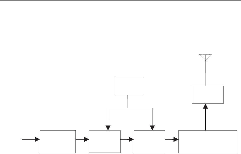
Section 7
VHF (136-174 MHZ) INFORMATION
1.0 Transmitter
Figure 7-1: VHF Transmitter Block diagram
1.1 General
The VHF transmitter contains five basic circuits:
1. Power Amplifier
2. Antenna Switch
3. Harmonic Filter
4. Antenna Matching Network
5. Power Control
1.1.1 Power Amplifier
The power amplifier is a 3-stage discrete design consisting of:
1. Pre-driver, ADA4743 (U700)
2. Driver, RD01MUS1 (Q703)
3. Final PA, RD07MVS1 (Q704)
The pre-driver is a 50 Ohm gain block with a supply voltage of 5V. the supply is ramped to eliminate
feed-through power due to the fixed gain of the device. The pre-driver is biased in Class A region with
a typical current drain of 60mA and power gain of 16.5dB.
The driver is a 1W, LDMOS in a SOT-89 package. this stage typically drains 110mA of current at rated
output power, 5W. The driver is biased in Class AB region and has a power gain of 14dB.
The final PA is a 7W, LDMOS device. The gate threshold of this device is very close to the driver.
Hence, the traditional PA bias tuning is eliminated. The current drain would typically be 1600mA. The
final PA is biased in Class AB region and has a power gain of 10dB.
PA
Pre
-
Driver
PA
Drive
r
PA
F
inal
A
nten na Switch/
Harmonic Filter/
Matching Network
Powe
r
Control
A
ntenna
Jack
F
rom VCO
Vcontrol
Vcontrol

6-2 Transmitter
1.1.2 Antenna Switch
The antenna switch comprises of 2 ports: standard port and remote port.
The antenna switch consist of:
1. Four PIN diodes:
c. CR902 and CR903 biased during standard port operation at transmit mode.
d. CR900 and CR901 biased during remote port operation at receive mode.
e. CR900, CR901, CR902 and CR903 biased during remote port operation at transmit
mode.
2. Six current limiting resistors:
a. R904, R905 and R909 for standard port operation at transmit mode.
b. R902, R903 and R906 for remote port operation at receive mode.
c. R902, R903, R906, R904, R905 and R909 for remote port operation at transmit mode.
3. Two pi networks:
a. C915, L908, C916 to determine TX or RX mode.
b. C911, L906, C912 to determine standard port or remote port operation.
In the transmit mode of standard port operation, ANT_EN signal (from MAKO) turns on Q702(bias
Power Amplifier) and Q900(antenna switch circuit). RAWB+ bias is applied to the standard port
antenna switch circuit to bias CR902 and CR903 “on”. Hence, the following occurs:
1. Shunt diode (CR903) shorts out the receiver port, and the pi network(C915, L908, C916), which
operates as a quarter wave transmission line, transforms low impedance of the shunt diode to a
high impedance at the input of the harmonic filter. In the receive mode, the diodes are “off” and
hence, there exists a low attenuation path between the antenna and the receiver ports.
2. Both CR900 and CR901 is biased “off”, and the pi network(C911, L906, C912), which operates as
a quarter wave transmission line, transfers the 50ohm impedance of the harmonic filter to C902
and hence, forces PA_OUT to take the standard port circuit path.
In the transmit mode of remote port operation, ANT_EN signal (from MAKO) turns on Q702(bias
Power Amplifier) and Q900(antenna switch circuit) and GP02 signal (from TOMAHAWK) turns on
Q901. RAWB+ bias is applied to the standard and remote port antenna switch circuit to bias CR900,
CR901, CR902 and CR903 “on”. Hence, the following occurs:
1. Shunt diode(CR903) shorts out the receiver port, and the pi network(C915, L908, C916), which
operates as a quarter wave transmission line, transforms low impedance of the shunt diode to a
high impedance at the input of the harmonic filter. In the receive mode, the diodes are off and
hence, there exists a low attenuation path between the antenna and the receiver ports.
2. Shunt diode(CR901) shorts out the standard port, and the pi network(C911, L906, C912), which
operates as a quarter wave transmission line, transforms the low impedance of the shunt diode to
a high impedance at the input of the standard port circuit and hence, forces PA_OUT to take the
remote port circuit path.
1.1.3 Harmonic Filter
The harmonic filter consists of C906, C907, C929, C931, L904 and L905. The design of the harmonic
filter for VHF is a fourpole Elliptical design using lumped LC elements in order to realize greater
attenuation in the stop band for a given ripple level. The harmonic filter insertion loss is typically less
than 1.3dB.

Transmitter 6-3
1.1.4 Power Control
The transmitter power control uses discrete integrator approach, the current is sensing both PA
stages namely, Driver Power Amplifier (Q703) and Final Power Amplifier (Q704).
The basic block diagram of the power control is shown in Figure 7-2. A single sensing resistor (R700)
is tied to sense both PA stages current. The power control consists of 2 comparators, U701-1 and
U701-2. U701 is a dual-package op-amp in SOT-8 package. The first stage is an I-V converter
converts current drained by Power Amplifier Driver (Q703) and Power Amplifier Final (Q704) across
R700 into a voltage drop and the second stage is an integrator used to shape the output Vcontrol to
bias both PAs. The slope of the Vcontrol is controlled by the RC time constant of the integrator and
also the ramping slope of reference signal, TX_DAC generated by MAKO IC. The final TX_DAC value
determines the transmit power level and is a factory tuned parameter which is stored inside the
codeplug.
Figure 7-2: Power Control Scheme Basic Block Diagram
B+
Current to
Voltage
Integrator
Sensing
resistor
Ramp
DAC
10bit
DAC 3
MAKO
SW 5V
SW B+
Shaped input
B+
PA Final
PA
Driver
PA
Current to
Voltage
Integrator
Sensing
resistor
Ramp
DAC
10bit
DAC 3
MAKO
SW 5V
Vcontrol
SW B+
Shaped input
B+
Current to
Voltage
Integrator
Sensing
resistor
Ramp
DAC
10bit
DAC 3
MAKO
SW 5V
SW B+
Shaped input
B+
PA Final
PA
Driver
PA
Pre-driver
Current to
Voltage
Integrator
Sensing
resistor
Ramp
DAC
10bit
DAC 3
MAKO
SW 5V
Vcontrol
SW B+
Shaped input
TX_DAC
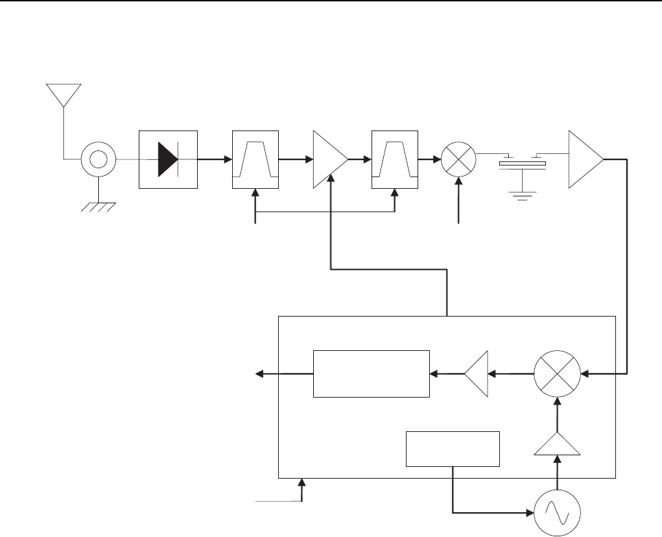
6-4 Receiver
2.0 Receiver
Figure 7-3: UHF Receiver Block Diagram
2.1 Receiver Front-End
The RF signal is received by the antenna and applied to a low-pass filter. For VHF, the filter consists
of C906, C907, C908, L904 and L905. The filtered RF signal is passed through the antenna switch
and then applied to a varactor tuned bandpass filter. The bandpass filter comprises of C400, C401,
C402, C403, C404, C405, L400, L401, R400, R499, D400 and D401. C400 and C405 are 50ohm
points. The bandpass filter is tuned by applying a control voltage to the varactor diodes D400 and
D401.
The bandpass filter is electronically tuned by the MAKO DAC. Depending on the carrier frequency, the
MAKO DAC will supply the tuned voltage to the varactor diodes in the filter. Wideband operation of
the filter is achieved by shifting the bandpass filter across the band.
The output of the bandpass filter is passed through a RF step attenuator (D402) to limit the amount
RF power fed into the LNA (U400). After being amplified, the RF signal is further filtered by a second
varactor tuned bandpass filter. This bandpass filter is electronically tuned by the MAKO DAC and
comprises of C419, C420, C421, C422, C423, C424, L408, L409, R405, R406, D403 and D404. C419
and C423 are 50 Ohm points.
The output of the second bandpass filter is passed to a mixer. The mixer is a passive double balanced
quad diode mixer (D405) comprising of 2 transformers (T400 and T401). The 50 Ohm matching for
the mixer is provided by C426 and L410. After mixing with the first LO signal from the voltage control
oscillator (VCO) using high side injection, the RF signal is down converted to the 44.85 MHz IF signal.
Pin Diode
Antenna
Switch LNA
RF Jack
Varactor
Tuned
Filter
Varactor
Tuned
Filter Mixer
Crystal
Filter IF Am
p
SIGNAL
PROCESSING
Synthesizer
ABACUS IC
SSI TO OMAP
16.8MHz
Reference Clock
Control voltage
from MAKO
Antenna
First LO from
FGU
IF
AGC
Second LO VCO
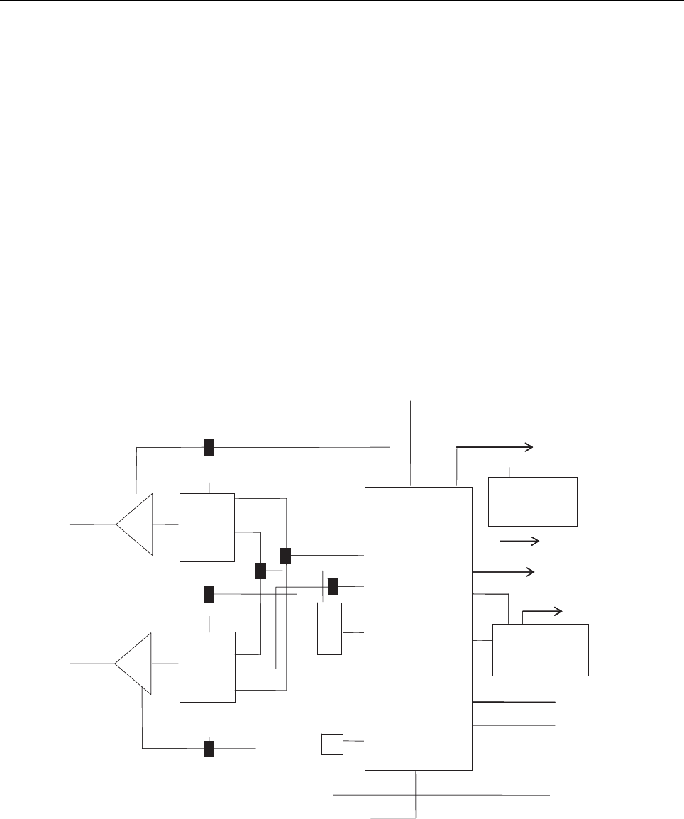
Frequency Generation Circuitry 6-5
The IF signal coming out of the mixer is applied to the crystal filter (FL400) through a resistor pad and
a diplexer (L411 and C427). Matching to the input of the crystal filter is provided by L412 and C428.
The crystal filter provides the necessary adjacent channel selectivity and inter-modulation protection.
The output of the crystal filter (FL400) is matched to the input of the IF amplifier transistor by C432,
C433, L415 and L416. Voltage supply to the IF amplifier is 5V_RX, taken from RX VCO. The IF
amplifier provides a gain of 19 dB minimum. The IF amplifier output is directly matched at the IF
amplifier output to ABACUS (U600) pin 47 via C601.
2.2 Receiver Back-End
ABACUS (U600) is tuned via software at radio start-up. The IF signal applied to pin 47 of U600 is
down-converted to a second IF of 2.25 MHz. The second IF of 2.25 MHz will then be fed into an ADC,
generating the Is and Qs data. This data is in the form of SSI (Serial Synchronous Interface) at pin 29
of U600, which will then be sent to the DSP (OMAP1710) for further processing.
The second VCO is a Colpitts oscillator built around transistor Q602. The VCO has a varactor diode,
D600 to adjust the VCO frequency. The second LO frequency could either be 42.6 MHz or 47.1 MHz,
depending on the system requirement. The control signal is derived from a loop filter consisting of
C617, C618, C619, R605 and R606. The RSSI circuitry is achieved via software programming.
3.0 Frequency Generation Circuitry
Figure 7-4: Frequency Generating Unit Block Diagram
The Frequency Generating Unit is centered on one main IC, Tomahawk (U001). The main synthesizer
on the Tomahawk eases modulation interface to the DSP area via the 3 TX SSI lines. The block
diagram illustrates the interconnect and support circuitry used in the Frequency Generating Unit.
Refer to the relevant schematics for the reference designators.
16.8 MHz
TCXO
Tomahawk
DAC
Tx SSI
3 lines
DMCS
SW Adapt
CP
out
GPO1
GPO3
RX VCO EN
TX VCO EN
To Abacus
Adapt
SW
control
CLK 2 out
SF
HP
mod
Prescaler in
TX
VCO
TX VCO EN
RX LO
Lock Det
TEST1
16.8 MHz
Buffer
To Squarer IC
RX
VCO
AUX
DAC
3 lines
LF
TX LO
To GPS
16.8 MHz
TCXO
Tomahawk
DAC
Tx SSI
3 lines
DMCS
SW Adapt
CP
out
GPO1
GPO3
RX VCO EN
TX VCO EN
To Abacus
Adapt
SW
control
CLK 2 out
SF
HP
mod
Prescaler in
TX
VCO
TX VCO EN
RX LO
Lock Det
TEST1
16.8 MHz
Buffer
To Squarer IC
RX
VCO
AUX
DAC
3 lines
LF
TX LO
To GPS

6-6 Frequency Generation Circuitry
The synthesizer is powered by 2.8V ANA, 2.8V DIG, 1.875V DIG and 5V ANA supplied from the
U3000-1. The synthesizer in turns generates a superfiltered 2.5V which powers up the TX VCO & RX
VCO.
In addition to the VCO, the synthesizer interfaces with the microcontroller. Programming of the
synthesizer is accomplished through the 4 lines; SPI_MISO, THK_CE, SPI_MOSI and SPI_CLK via
pin D10, D8, D9 and D11 respectively. A 1.875 dc signal from the synthesizer lock detect line
indicates to the microprocessor that the synthesizer is locked.
U001 has dual port modulation capability. The microprocessor supplies low port and high port words
to pin F11 of U001. For high port modulation, the audio runs through an internal attenuator for
modulation balancing purpose before it goes out to the VCO and loop filter via pin K8. For the low port
modulation, the audio is fed into the main synthesizer, where it is summed with the main_num
channel frequency word, then supplied to the accumulator of the Fractional-N synthesizer before
going out to the VCO.
3.1 Synthesizer
U001 uses a 16.8 MHz crystal (Y001) to provide a reference for the system. The synthesizer further
divides this to 4.2 MHz for nominal frequencies and 3.36 MHz for alternate frequencies. Together with
R006, R007, R008, C013, C014, C015 and C016, they build up the reference oscillator which is
capable of 1.5ppm (non-GPS) / 0.5ppm (GPS) stability over temperature of -30ºC to 85 ºC. It also
provides 16.8MHz at pin J11 of U001 to be used by ABACUS.
The loop filter which consists of R013, R014, R016, C024, C025, C026 and C027 provides the
necessary dc steering voltage for the VCO and determines the amount of noise and spur passing
through.
In achieving fast locking for the synthesizer, an internal adapt charge pump provides higher current
(~10mA) at pin H1 and an additional 2mA from a current mirror (Q002, R010, R011 and R012). The
required frequency is then locked by normal mode charge pump at pin G3. An external adapt switch
(U002) is used to control the on/off of the adapt mode. Both the normal and adapt charge pumps get
their supply from the 5V ANA supplied by U3000-1.
3.2 VCO - Voltage Controlled Oscillator
The VCO in conjunction with the synthesizer generates RF in both the receive and transmit modes of
operation.
The RX VCO comprises of a Colpitts oscillator built around Q200, a cascaded buffer, built up of a
buffer IC, U200 cascaded with a discrete buffer built around Q208 and a 3dB resistive pad (R220,
R221 and R222). Vcontrol is supplied to two pairs of back-to- back varactors (D200, D201, D202 and
D203). The LC tank comprises of C203 and L202. The oscillator is supplied with a 2.5V superfiltered
supply from the synthesizer, U001. The cascaded buffer is supplied with a 5V ANA supply from
MAKO, U3000-1. The buffer IC in conjunction with the resistive pad provides sufficient isolation from
the mixer whilst the discrete buffer provides sufficient gain for the first LO signal. The output of the
cascaded buffer is match to the mixer by C216, C217, C241 and L207. The output power level of
RX_1ST_LO_INJ is 6dBm.
The TX VCO comprises of a Colpitts oscillator built around Q204 and a discrete buffer built around
Q205. Vcontrol is supplied to two pairs of back-to-back varactors (D204, D205, D206 and D207). The
LC tank comprises of C222 and L210. The oscillator is supplied with a 2.5V superfiltered supply from
the synthesizer, U001. The discrete buffer is supplied with a 5V ANA supply from MAKO, U3000-1.
The output of the discrete buffer is match to the PA by C236, C237 and L215. The output power level
of TX_BUFF is 3dBm.

Global Positioning System (GPS) Receiver 6-7
4.0 Global Positioning System (GPS) Receiver
The GPS device is an embedded receiver that provides the location of the subscriber in terms of
latitude, longitude, velocity, direction and altitude.
Figure 7-5: GPS Receiver Block Diagram
The RF signal is received by the antenna and applied to a high-pass filter. The filter consists of C924,
C925, C926, L912 and L913. The filtered RF signal is then applied to a SAW filter, FL8001.
The output of the SAW filter is fed into the LNA (U8001). The LNA biasing is controlled by
SIRF_LNA_EN (pin A4 of the GPS IC, U8000). The LNA input match comprises of C8013, C8014 and
L8001. The LNA output match comprises of L8003 and C8017. After being amplified, the RF signal is
further filtered by a second SAW filter, FL8000.
The output of the second SAW filter is passed to pin P6 of the GPS IC. The input match for pin P6
comprises of C8018, C8019 and L8004. The control and data lines for the GPS IC are GPS_nRESET,
GPS_ON_OFF, GPS_TX, GPS_RX and GPS_BOOT. GPS_nWAKEUP line is fed into the
microcontroller to indicate the state (full power or hibernate state) of the GPS IC so that the
microcontroller will never trigger a GPS_ON_OFF when the GPS IC is in full power state.
A dedicated 32.768kHz quartz crystal oscillator (Y8000) is used to provide RTC clock to the RTC
circuit inside the GPS IC. The second input frequency is a 16.8MHz reference, used by the StarIII to
synthesize the internal LO. This reference will be supplied by a VCTCXO (Y001) located in the
synthesizer block, which will be shared by the TOMAHAWK and ABACUS ICs.
The GPS IC is powered by 2.8V_DIG_GPS, 2.8V_RF_GPS and 1.5V_GPS_RTC supplied from 3
discrete external regulators (U3701, U3700 & U3006). The input of these regulators is sourced from a
switching regulator (U3020) which regulates the SWB+ to 3.6V.
RF
Section
Digital
Section
TPS79228 TPS79101 LP3990
2.8V
2.8V
1.5V
LTC1877
3.6V
32.768kHz
XTAL
OMAP
16.8MHz
VCTCXO
FGU
SiRFStarIII, GSC3FLP
Optional
2dB resistive pad
HPF Pre-SAW LNA Post-SAW
Dual band antenna
LNA_EN
LNA_Supply
HF

6-8 Allocation of Schematics and Circuit Boards
5.0 Allocation of Schematics and Circuit Boards
5.1 Controller Circuits
The VHF circuits are contained on the Printed Circuit Board (PCB) which also contains the
Controller circuits. This Chapter shows the schematics for the VHF circuits only, refer to the
Controller section for details of the related Controller circuits. The PCB component layouts in this
Chapter show both the Controller and VHF circuit components. The VHF schematics and the related
PCB and parts list are shown in the tables below.
Table 7-6. VHF Diagrams and Parts List
PCB:
8415113H03 Main Board Top Side
8415113H03 Main Board Bottom Side
8415113H05 Main Board Top Side
8415113H05 Main Board Bottom Side
Page 7-9
Page 7-10
Page 7-11
Page 7-12
SCHEMATICS
Complete Radio
Complete VHF RF
Complete VHF Transmitter
VHF Transmitter
VHF Harmonic Filter and Antenna Switch
Complete UHF1 Receiver
VHF Receiver Front End
VHF Receiver Back End
Complete UHF1 Frequency Generating Unit
VHF Synthesizer
VHF Voltage Controlled Oscillator
VHF GPS Block
Page 7-13
Page 7-14
Page 7-15
Page 7-16
Page 7-17
Page 7-18
Page 7-19
Page 7-20
Page 7-21
Page 7-22
Page 7-23
Page 7-24
Parts List
8415113H03
8415113H05
Page 7-25
Page 7-31
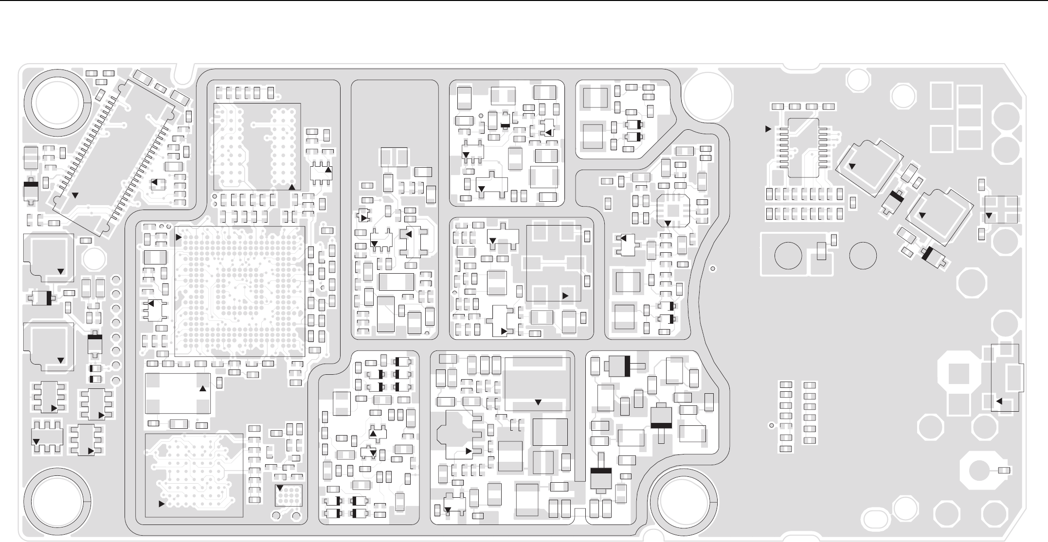
Circuit Board/Schematic Diagrams and Parts List 7-9
6.0 Circuit Board/Schematic Diagrams and Parts List
C3800
C9047
C9048
C9049 C9050
C9051
C9053
C9055
C9057
C9058
C9059
C9060
C9063
C9064
C9066
FL9000
21
20
J9001
L9007
L9008
M9001
R3800
C9015
C9021
C9022
C9033
E9000
E9001
VR9023
C9019
C9020
C9069
140
R9052
C9061
C9062
C9071
C9072
D9001
D9002
L9000
L9001
M9002 1
M9005
1
M9006
R9020
TP_NEMU0
TP_NEMU1
TP_NTRST
TP_RTCK
TP_TCK
TP_TDI
TP_TDO
TP_TMS
VR9002
VR9017
VR9018
VR9020
VR9021
VR9022
G1A1
A8 G8
U2000
C1000
C1001
C1002
C1003
C1004
C1005
C1006
C1007
C1008
C1009
C1010
C1011
C1012
C1013
C1014
C1015
C1016
C1017
C1018
C1019
C1028
C1029
C1030
C1031
C1032
C1033
C1044
C2000
C2001
C2002
C2003
C2004
C2005
C2006
C2007
C3063
R1000
R1001
R1002
R1005R1006
R1013
R1014
R1015
R1016
R1017
R1018
R1019
R1020
R1021
R1022
R1023
R1025
R1026
R1027
R1028
R1034 R1035
R1036
R1041
R1045
R1046
R1047
R1048
R1051
R1052
R1053
R1054
R1055
R1060
R1061
R1062
R1063
R1065
R1067
R1068
R1069
R1070
R1072
R2000
R2004
R2005
R2006
R2007
R2008
R2009
R2010
R2011
R2012
R2013
R3010
R3023
R3032R3033 R3034R3035
R3888
TP_GPS_RX
TP_GPS_TX
TP_MAKO_DCLK
TP_MAKO_FSYNC
TP_MAKO_RX
TP_MAKO_TX
TX_
RAMP
A21
AA21
AA1
U1000
C4 A4
U1005
43
6
U1006
J9A9
J1
A1
U2001
4
3
5
U3004
2
34
Y1000
C001
C002
C004
C006
C008
C009
C017
C022
C024
C025
C026
C027
C028
C031
C032
C033
C035
C036
C038
E001
E002
E003
E004
L002
L003
Q002
Q003
R010
R011
R012
R013
R014
R016
R017
R018
R020
R022
R025
R027
SH9001
TP200
4
3
5
U002
C428
C432
C433
C434
C435 C436
C437
C438
C439
C440
C441
C442
C444 C445
C446
23
4
5
6
FL400
L415
L416
L417
L418
Q400
Q401
R409
R410
R411
R412
R413
R417
R419
R420
R421
R424
R425
R497
TP403
R422
C606 C609
C610
C611
C612
C613
C614
C615
C616
C617
C618
C619
C626
C638
D600
L602
L603
L604
Q600
Q601
Q602
R600
R601
R602
R603
R604
R605
R606 R612
R697
R699
TP601
C423
C424
C425
C447
C448 C449
C450
C451
D403
D404
L408
L409
L421
R405
C400
C401
C402
C403
C404
C405
C406
C408
C409
C410
C411
C412
C413
C414
C415
C416
C417
C418
C419
C420
C421
C422
D400
D401
D402
L400
L401
L402
L403
L404
L405
L406
L407
L420
R400
R401
R402
R403
R404
R406
R430
R496
3
4
6
79
10
12
U400
C707
C714
C715
C717
C718
C719
C720
C722
C724
C726
C729
C730
C731
C732
C733
C734
C735
C736
C737
C739
C777
C778
C797
C798
C799
C906
C907
C909
C911
C912
C913
C914
C915
C916
C918
C928
C929
CR901
CR902
CR903
L701
L702
L703
L705
L707
L708
L709
L710
L712
L904
L905
L906
L907
L908
M9000
Q703
R717 R718
R719
R723
R725
R726
R727
U700
1
3
Q704
C037
C200
C201
C202
C203
C204
C205
C206
C207
C208
C209
C219
C220 C221
C222
C223
C224
C225
C226
C227
C228
C243
D001
D200
D201 D202
D203
D204
D205
D206
D207
L200
L201
L202
L203
L205
L208
L209
L210
L211
L213
Q200
Q204
R019
R203
R211
C9000
C9001
C9002
C9003
C9004
C9005
C9006
C9007
C9008
C9009
C9010
C9011
C9012C9013
C9014
C9067
C9068
C9070
4
3
2
D9000
E9006
E9007
F9000
1
M9003
1
M9004
16
81
9
P9000
R907
R8010
R8011
R8012
R8026
R8027
R8028
R8029
R8031
R8033
R8034
R8035
R8036
R8037
R9000
R9001
R9002
R9003
R9004
R9005
R9006
R9007
R9012 R9013
3
4
5
2
S9000
TP400
TP_GND
TP_RAWB+
TP_SIPI_DO
VR9015
VR9016
VHF (136-174MHz) Main Board Top Side PCB No. 8415113H03
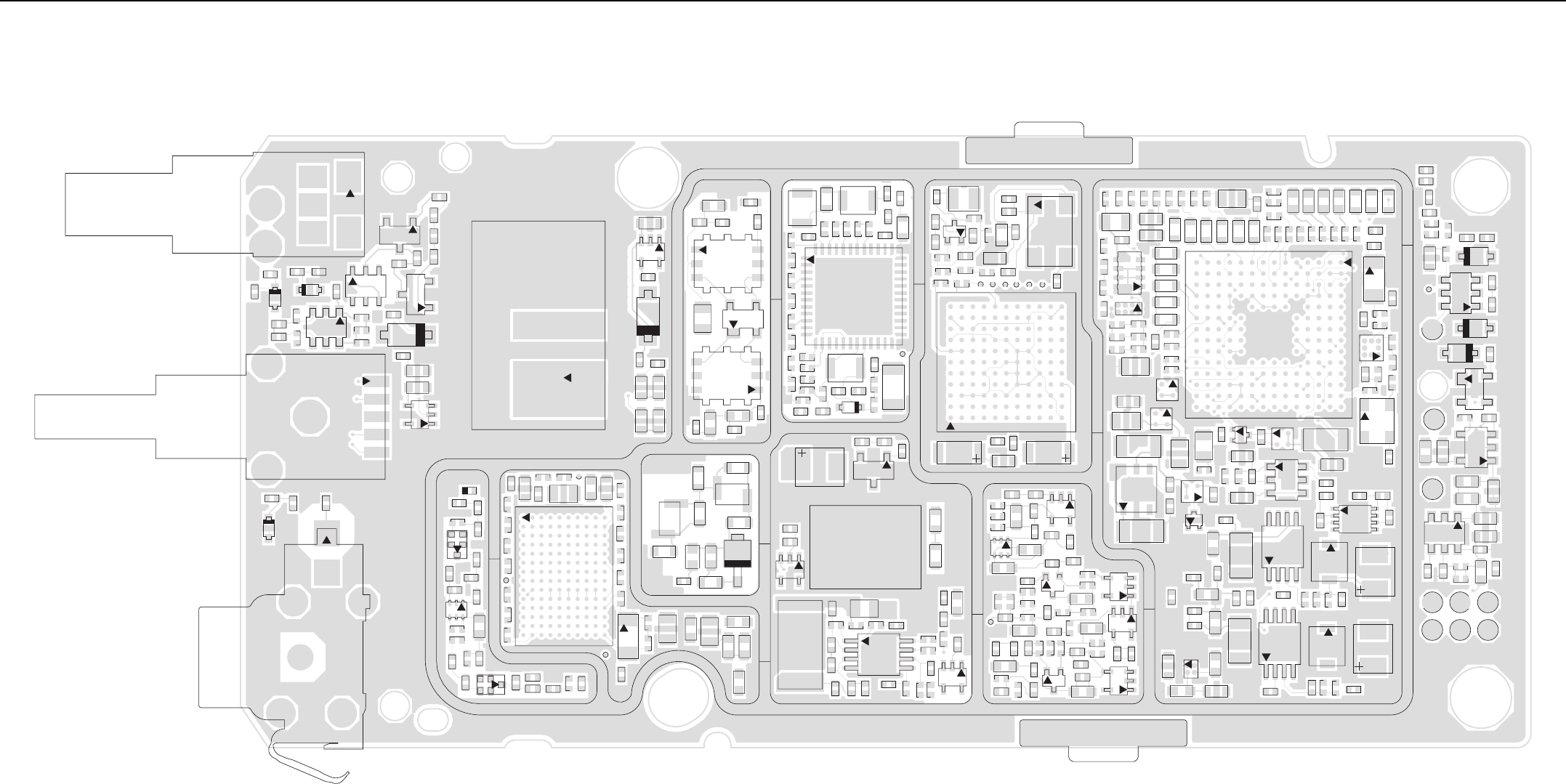
7-10 Circuit Board/Schematic Diagrams and Parts List
C9038
Q9000
Q9003
R9008
R9009
R9010
R9011
R9050
R9051
7
2
3
4
5
6
S9001
Q9001
C933
C9023
C9024
C9025
C9026
C9027
C9028
C9029
C9030 C9031
1
2
3
4
5
6
7
P900
Q901
R906
R908
R909
R9014
R9015
R9016
R9017 R9018
7
2
3
4
5
6
S9002
VR9005
VR9006
VR9007
VR9008 VR9009
C924
C925
C926
C8000
C8001
C8002
C8004
C8005
C8006
C8013
C8014
C8015
C8016
C8017
C8018
C8019
C8020
C8021
C8022
C8023
C8029
C8030
C8031
C8032
C8033
C8034
C8035
C8036
E8000
E8006
3
4
2
5
FL8000
3
4
2
5
FL8001
L912
L913
L8001
L8002
L8003
L8004
R8002
R8003
R8004
R8015
R8016
R8017
R8020
R8023
R8024
R8025
R8030
R8032
TP_CLK_ACQ
TP_IF
TP_SCLK
P10 A10
P1 A1
U8000
U8001
Y8000
C426
C427
C429
C430
C431
C900
C904
C905
C908
C919
C920
C927
C930
C931
C8003
C9032
C9039
CR900
D405
E8001
E8002
E8003
E8004
E8005
L410
L411
L412
L413
L414
L902
L903
L909
L910
23
M9007
Q701
Q900
R407
R700
R732
R733
R902
R903R904
R905
3
46
T400
3
4
6
T401
VR9010
C601
C602
C603
C604
C605 C607
C608
C620
C621
C622
C623
C624C625
C627
C628
C629
C630
C631
C632
C633
C634 C635
C636
C637
C639 D601
E600
E601
E602
L600
L601
L605
R607
R609
R610 R611
R696
R698
SH9000 TP600
1
37
25
13
U600
C700
C703
C704
C705
C706
C708
C709
C710
C711
C712
C721
E701
L700
M700
Q702
R701
R702 R703
R704
R705
R706
R707
R708
R709
R710
R711
R712 R713
R714
R720
R731
U701
U702
C210
C211
C212
C213
C214
C215
C216
C217
C229
C230
C231
C232
C233
C234
C235
C236
C237
C238
C239
C240
C241
C738
L204
L206
L207 L212
L214
L215
L217
L218
M2
Q202
Q203
Q205
Q206
Q207
Q208
R200 R201
R202
R205
R207
R208
R209
R210
R212
R213
R214
R215
R216
R217
R218
R220
R221
R222
R728
R729
R730
TP201 U200
C003
C005
C007
C010
C011
C012
C013
C014
C015
C016
C018
C019
C020
L001
Q001
R001
R002
R003
R004
R005
R006
R007
R008
R026
R052 R053
R054
TP001
TP002
TP003
TP004
TP005
TP006
L11A11
L1
U001
43
2
Y001
C3000
C3001
C3002
C3003
C3004
C3005
C3010 C3011
C3014
C3019
C3024
C3031
C3034
C3035
C3036
C3045
C3047
C3048
C3049
C3050
C3051
C3060
C3061
C3062
C3070
C3074
C3080
C3093
C3094
C3095
C3097
C3098
C3099
C3100
C3999
E3030
E3031
E3032
E3033
M1
4
5
8Q3003
R3011
R3012
R3013
R3014
R3024
R3025
R3026
R3027
R3036
R3037
R3050
R3053
R3054
R3060
R3070
R3071
R3072
R3073
R3074
R3088
P1 A1
A14
P14
U3000
C1
C3
A3
U3003
Y3000
4
3
2
Y3001
C3015
C3016
C3017
C3018 C3025
C3026
C3028
C3037
C3038
C3039
C3067
C3079
C3081
C3082
C3083
C3084
C3090
C3091
C3101
C3102
C3200
C3201
C3202
C3203
C3204
C3205
C3206
C3207
C3208
C3209
C3210
C3211
C3212
C3805
E3704
E3705
R3076
L3004
L3020
L3021
L3022
23
4
Q3000
2
3
4
Q3001
Q3002
23
4
Q3005
Q3006
23
4
Q3010
R3004R3005
R3006
R3007
R3008R3009
R3016
R3017
R3018
R3020
R3021
R3028
R3029
R3030
R3031
R3038
R3040
R3041
R3043
R3051
R3098
R3100
R3101
R3102
R3103
R3200
R3201
R3202
R3203
R3704
1
64
3
U3002
U3006
U3007
U3008
85
4
U3009
U3020
U3021
C3700
C3701
C3702
C3703
C3704
C3705
C3706
C3707
C9016
C9017
C9018
C9040
C9041
C9042
C9043
C9044
C9045
C9046
C9065
D3000
E3700
E3701
E3702
E3703
R3055
R3075
R3700
R3701
R3702
R3703
R9019
TP_EXT_MIC
TP_EXT_MIC+
TP_EXT_SPKR
TP_EXT_SPKR+
TP_GPIO0
TP_ONE_
WIRE_1
TP_POR
TP_USB1_DM
TP_USB1_DP
TP_VBUS1
3
4
U3700
U3701
VR9000
VR9001
VR9003
VR9004
5
8
VHF (136-174MHz) Main Board Bottom Side PCB No. 8415113H03
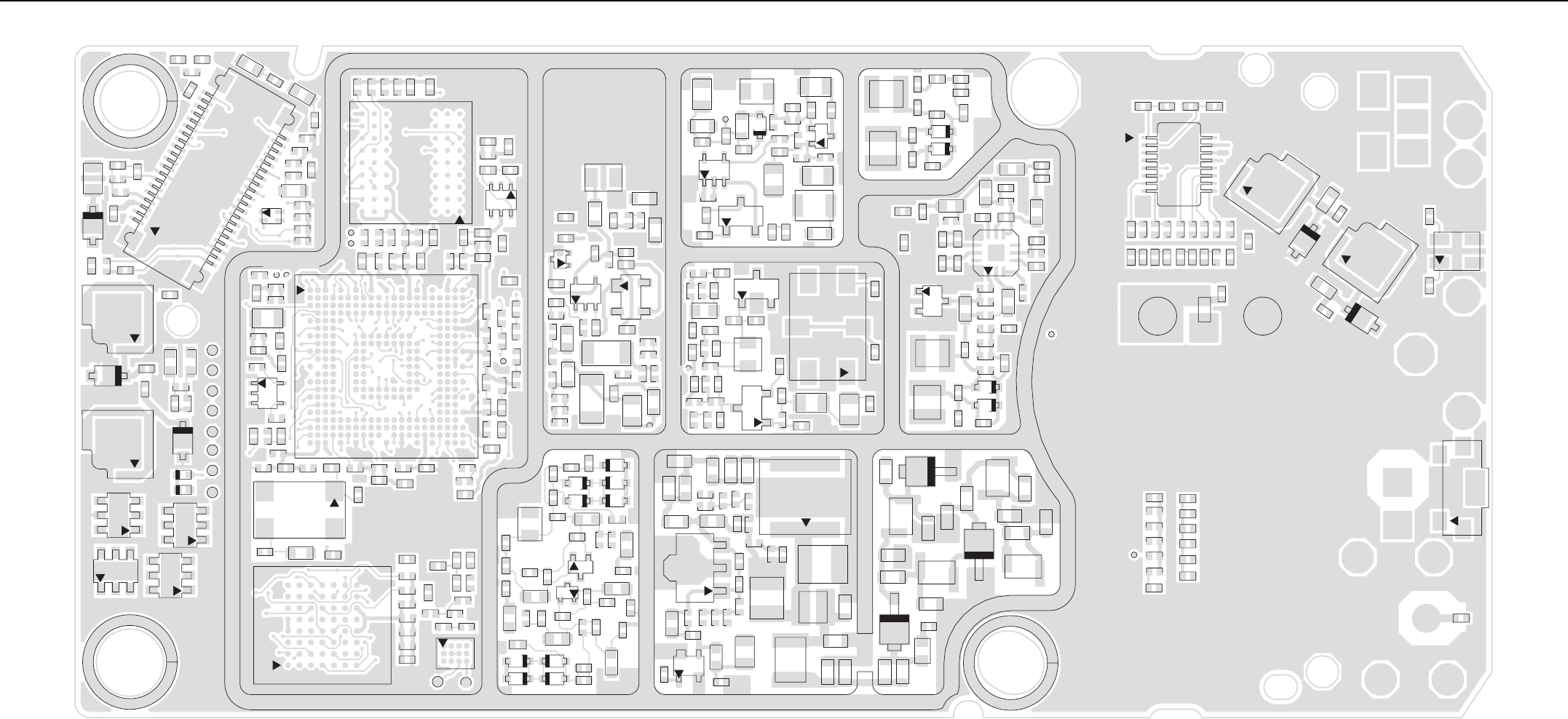
Circuit Board/Schematic Diagrams and Parts List 7-11
C9061
C9062
C9071
C9072
D9001
D9002
L9000
L9001
M9002
R9020
TP_NEMU0
TP_NEMU1
TP_NTRST
TP_RTCK
TP_TCK
TP_TDI
TP_TDO
TP_TMS
VR9002
VR9017
VR9018
VR9020
VR9021
VR9022
C9015
C9019
C9020
C9021
C9022
C9033
C9047
C9069
E9000
E9001
1
21
40
20
J9001
M9001
1
M9005
1
M9006
R9052 VR9023
C9048
C9049 C9050
C9063
C9064 L9007
L9008
C3800
C9051
C9053
C9055
C9057
C9058
C9059
C9060
C9066
FL9000
R3800
C2004
C2005
R2005
R2006
R2007
R2008
R2009
R2010
R2013
J9A9
J1A1
U2001
C1010
C1013
C1014
C1016
C1032
C2006
C2007
R1000R1015
R1016
R1021
R1026
R1027
R1028
R2011
R3010
TP_MAKO_DCLK
TP_MAKO_RX
43
6
U1006
C1007
C1015
C1033
R1061
R1072
A21
AA21
AA1
U1000
C1000
C1001
C1008
C1009
C1011
C1012
C1017
C1019
C1031
C3063
R1005
R1006
R1013
R1014
R1018
R1019
R1022
R1023
R1025
R1041
R1048
R1054 R3023
TP_MAKO_FSYNC
TP_MAKO_TX
4
3
5
U3004
2
34
Y1000
C1002C1003
C1004
C1005
C1006
C1030
C1044
R1001
R1017
R1020
R1034
R1035
R1045
R1047
R1053
R1055
R1060
R3032
R3033 R3034
R3035
R3888
TX_RAMP
C1018
R1002 R1046
G1A1
A8 G8
U2000 C1028
C1029
C2000
C2001
C2002
C2003
R1036
R1051
R1052
R1062
R1063
R1065
R1067
R1068
R1069
R1070
R2000
R2004
R2012
TP_GPS_RX
TP_GPS_TX
C4 A4
U1005
C037
C200
C201
C202
C203
C204
C205
C206
C207
C208
C209
C219
C220 C221
C222
C223
C224
C225
C226
C227
C228
C243
D001
D200
D201 D202
D203
D204 D205
D206
D207
L200
L201
L202
L203
L205
L208
L209
L210
L211
L213
Q200
Q204
R019
R203
R211
C001
C002
C004
C006
C008
C009
C017
C022
C024
C025
C026
C027
C028
C031
C032
C033
C035
C036
C038
E001
E002
E003
E004
L002
L003
Q002
Q003
R010
R011
R012
R013
R014
R016
R017
R018
R020
R022
R025
R027
TP200
4
3
5
U002
C707
C714
C715
C717
C718
C719
C731
C732
C733
C734
C736
C737
C797
C798
C799
L701
L702
L705
L707
L712
Q703
1
R717 R718
R719
R725
U700
C720
C722
C724
C726
C729
C730
C777
C778
L703
L708
L709
L710 3
Q704
R723
R726
R727
23
4
5
6
FL400
C428
C432
C433
C434
C435 C436
C437
C438
C439
C440
C441
C442
C444
C445
C446
L415
L416
L417
L418
Q400
Q401
R409
R410
R411
R412
R413
R417
R419
R420
R421 R422 R424
R425
R497
TP403
C606 C609
C610
C611
C612
C613
C614
C615
C616
C617
C618
C619
C626
C638
D600
L602
L603
L604
Q600
Q601
Q602
R600
R601
R602
R603
R604
R605
R606 R612
R697
R699
TP601
C423
C424
C425
C447
C448 C449
C450
C451
D403
D404
L408
L409
L421
R405
C400
C401
C402
C403
C404
C405
C406 C408
C409
C410
C411
C412
C413
C414
C415
C416
C417
C418
C419
C420
C421
C422
D400
D401
D402
L400
L401
L402
L403
L404
L405
L406
L407
L420
R400
R401
R402
R403
R404
R406
R430
R496
SH9001
TP400
34
6
79
10
12
U400
C906
C907
C909
C911
C912
C913
C914
C915
C916
C918
C928
C929
CR901
CR902
CR903
L904
L905
L906
L908
C735
C739
L907
M9000
R8010
R8011
R8012
R8026
R8027
R8028
R8029
R8031
R8033
R8034
R8035
R8036
R8037
TP_SIPI_DO
R907
3
4
5
2
S9000
4
3
2
D9000
R9012
R9013
C9067
C9068
E9006
E9007
1
M9004
VR9015
VR9016
C9070
F9000
TP_GND
TP_RAWB+
C9014
1
M9003
C9002
C9003
C9004
C9005
C9006
C9007
C9008
C9009
C9010
C9011
C9012
C9013
R9002
R9003
R9004
R9005
R9006
R9007
16
81
9
P9000
C9000
C9001
R9000
R9001
VHF (136-174MHz) Main Board Top Side PCB No. 8415113H05
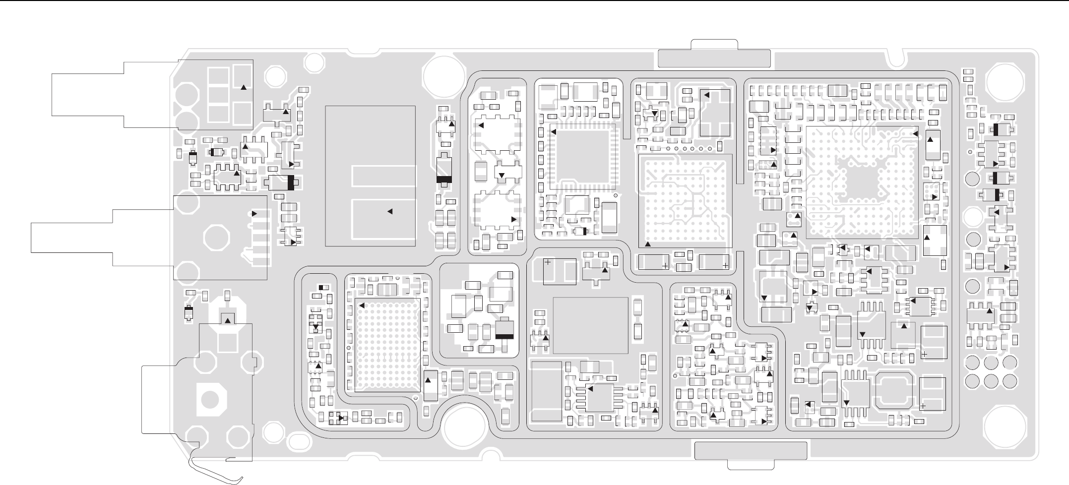
7-12 Circuit Board/Schematic Diagrams and Parts List
7
2
3
4
5
6
S9001
C9023
R906
R9014
7
8
2
3
4
5
6
S9002
VR9005
C9024
C9025
C9026
C9027
C9028
C9029
C9030 C9031
C9038
Q9000
Q9001
Q9003
R9008
R9009
R9010
R9011
R9015
R9016
R9017
R9018
R9050
R9051
VR9007
VR9008 VR9009
C933
Q901
R908
R909
VR9006
1
2
3
4
5
6
7
P900
C924
C925
C926
C8000
C8001
C8002
C8004
C8005
C8006
C8013
C8014
C8015
C8016
C8017
C8018
C8019
C8020
C8021
C8022
C8023
C8029
C8030
C8031
C8032
C8033
C8034
C8035
C8036
E8000
E8002
E8006
3
4
2
5
FL8000
3
4
2
5
FL8001
L912
L913
L8001
L8002
L8003
L8004
R8002
R8003
R8004
R8015
R8016
R8017
R8020
R8023
R8024
R8025
R8030
R8032
TP_CLK_ACQ
TP_IF
TP_SCLK
P10 A10
P1 A1
U8000
U8001
Y8000
C8003
E8001
E8003
E8004
E8005
R700
C900
C904
C905
C919
C920
C930
C931
CR900
L902
L903
L909
L910
23
M9007
C927
C9039
Q900
VR9010
C908
C9032
R902
R903
R904
R905
C429
C430
C431
L413
L414
3
4
6
T401
D405
L412 3
46
T400
C426
C427
L410
L411
R407
C622
L600
L601
C601
C602
C603
C604
C605
C607
C608
C620
C621C623 C624
C625
C627
C628C629
C630
C631
C632
C633
C634
C635
C636
C637
C639 D601
E600
E601
E602
L605
R607
R609
R610 R611
R696
R698
TP600
1
37
25
13
U600
C700
C712
M700
Q701
R712 R713
R732
R733
U702
C703
C704
C705
C706
C708
C709
C710
C711 C721
E701
L700
Q702
R701
R702
R703
R704
R705
R706
R707
R708
R709
R710
R711
R714
R720
R731
U701
C007
C010
C011
C012
C013
C014
C015
C016
L001
Q001
R001
R002
R003
R004
R005
R006
R007
R008
R026
R052 R053
R054
TP001
TP002
TP003
TP004
TP005
TP006
L11A11
43
2
Y001
L1
U001
C003
C005
C018
C019
C020
C210
C211
C212
C213
C214
C215
C216
C217
C229
C230
C231
C232
C233
C234
C235 C236
C237
C238
C239
C240
C241
C738
L204
L206
L207 L212
L214
L215
L217
L218
Q202
Q203
Q205
Q206
Q207
Q208
R200 R201
R202
R205
R207
R208
R209
R210
R212
R213
R214
R215
R216 R217
R218
R220
R221
R222
R728
R729
R730
TP201
U200
C3091
1
64
3
U3002
M1
C3010
C3014
C3019
C3024
C3031
C3045
C3047
C3048
C3049
C3050
C3051
C3062
C3067
C3074
C3080
C3093
C3999
4
58Q3003
R3011
R3012
R3013
R3014
R3024
R3025
R3037
R3050
R3053
R3054
R3060
R3098
P1
U3007
C3000
C3002
C3003
C3004
C3005
C3011
C3034
C3035
C3036
C3094
C3095
C3097
C3098
C3099
C3100 E3030
E3031
E3032
E3033
R3026
R3027
C3001
C3015
C3016
C3017
C3018
C3025 C3026
C3028
C3037
C3038
C3039
C3060
C3061
C3070
C3079
C3081
C3082
C3083
C3090
C3200
L3004
23
4
Q3000
23
4
Q3001
Q3002
23
4
Q3005
Q3006
23
4
Q3010
R3004
R3005
R3006
R3007
R3008
R3009
R3016
R3017
R3018
R3020
R3021
R3028
R3029
R3030
R3036
R3040
R3041
R3043
R3051
R3070
R3071
R3072
R3073
R3074
R3088
R3100
R3101
R3102
R3103
SH9000
A1
A14
P14
U3000
C1
C3
A3
U3003
U3008
8
5
4
U3009
Y3000
4
3
2
Y3001
C3084
C3101
C3102
C3201
C3205
C3206
C3207
C3208
C3212
C3805
E3704
E3705
L3003
L3022
R3031
R3038
R3704
U3006
U3020
U3021
C3202
C3203
C3204
C3209
C3210
C3211 L3020
L3021 R3200
R3201
R3202
R3203
M2
C3700
C3701
C3702
C3703
C3704
C3705
C3706
C3707
C9016
C9017
C9018
C9040
C9041
C9042
C9043
C9044
C9045
C9046
C9065
D3000
E3700
E3701
E3702
E3703
R3055 R3075
R3700
R3701
R3702
R3703
R9019
TP_EXT_MIC
TP_EXT_MIC+
TP_EXT_SPKR
TP_EXT_SPKR+
TP_GPIO0
TP_ONE_WIRE_1
TP_POR
TP_USB1_DM
TP_USB1_DP
TP_VBUS1
5
3
4
U3700
U3701
VR9000
VR9001
VR9003
VR9004
VHF (136-174MHz) Main Board Bottom Side PCB No. 8415113H05
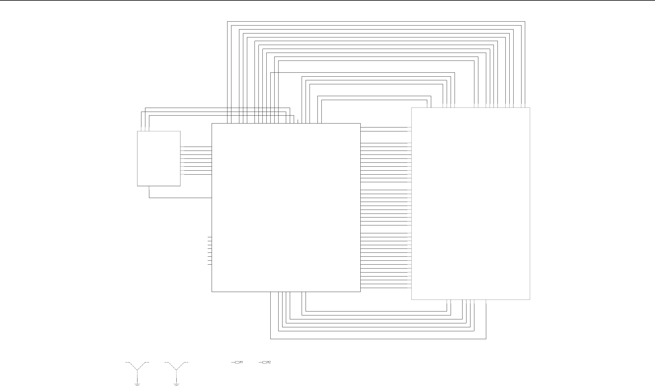
Circuit Board/Schematic Diagrams and Parts List 7-13
SW
CORE
GPS
CHOMERIC SHIELD
1
CTR_SPG_V5.1
16_8MHz_GPS
SPG_GID_V8.2
SPG_FR_V8.2
TNA_SPG
GPS_BOOT
GPS_ON_OFF
GPS_RFPWRUP
GPS_RX
GPS_TX
GPS_nRESET
GPS_nWAKEUP
+BWS
USB1_DM
USB1_DP
VBUS1
LOV
SH9001
SHIELD
PT26PNGA24
WS_HCEM
ONE_WIRE_1
OPTA_SEL0
OPTA_SEL1
OPTA_SEL2
1_OIPG_TPO
2_OIPG_TPO
CNYS_ISS_TPO
PTT
+BWAR
DEL_DER
RESET_OUT
1WS
2WS
4WS
8WS
JTAG_TDO
JTAG_TMS
KEYPAD_COL0
KEYPAD_COL1
KEYPAD_COL2
KEYPAD_COL3
KEYPAD_COL4
KEYPAD_ROW0
KEYPAD_ROW1
KEYPAD_ROW2
KEYPAD_ROW3
KEYPAD_ROW4
KLCD_OKAM
CNYSF_OKAM
XR
_O
K
A
M
XT_OKAM
GPS_RFPWRUP
GPS_RX
GPS_TX
GPS_nRESET
GPS_nWAKEUP
DEL_NEERG
INT_MIC+
INT_MIC-
INT_SPKR+
INT_SPKR-
JTAG_NEMU0
JTAG_NEMU1
JTAG_NTRST
JTAG_RTCK
JTAG_TCK
JTAG_TDI
DISPLAY_DATA0
DISPLAY_DATA1
DISPLAY_DATA2
DISPLAY_DATA3
DISPLAY_DATA4
DISPLAY_DATA5
DISPLAY_DATA6
DISPLAY_DATA7
BP_GREME
EXT_MIC+
EXT_MIC-
EXT_SPKR+
EXT_SPKR-
GPS_ANT
GPS_BOOT
GPS_ON_OFF
LOV
CTR_SPG_V5.1
2V_GID_V578.1
16_8MHz_GPS
7V_ANA_V577.2
4V_GID_V577.2
SPG_GID_V8.2
SPG_FR_V8.2
6V_GID_V9.2
01V_GID_V3.3
2SUBV_ANA_V5
ATAD_TTAB
BL_EN
DISPLAY_CE
DISPLAY_CMD
OPTA_SEL1
OPTA_SEL2
1_OIPG_TPO
2_OI
PG
_TPO
CNYS_ISS_TPO
PTT
+BWAR
DEL_DER
RESET_OUT
1WS
2WS
4WS
8WS
+BWS
USB1_DM
USB1_DP
VBUS1
KEYPAD_COL1
KEYPAD_COL2
KEYPAD_COL3
KEYPAD_COL4
KEYPAD_ROW0
KEYPAD_ROW1
KEYPAD_ROW2
KEYPAD_ROW3
KEYPAD_ROW4
KLCD_OKAM
CNY
SF
_O
K
A
M
XR_OKAM
XT
_O
KAM
WS_HCEM
ONE_WIRE_1
OPTA_SEL0
DISPLAY_DATA3
DISPLAY_DATA4
DISPLAY_DATA5
DISPLAY_DATA6
DISPLAY_DATA7
BP_GREME
EXT_MIC+
EXT_MIC-
EXT_SPKR+
EXT_SPKR-
DEL_NEERG
INT_MIC+
INT_MIC-
INT_SPKR+
INT_SPKR-
KEYPAD_COL0
1
2V_GID_V578.1
4V_GID_V5
7
7.2
6
V
_G
ID
_
V
9
.2
01V_GID_V3.3
2SUBV_ANA_V5
ATAD_TTAB
BL_EN
DISPLAY_CE
DISPLAY_CMD
DISPLAY_DATA0
DISPLAY_DATA1
DISPLAY_DATA2
SH9000
SHIELD
PT26PNGA23
2.775V_DIG_V4
1.875V_DIG_V2
PTT
SWB+
RAWB+
3.3V_DIG_V10
BATT_DATA
EMERG_PB
SW8
SW4
SW2
SW1
MECH_SW
2.9V_DIG_V6
VOL
RED_LED
GREEN_LED
OPT_SSI_SYNC
OPT_GPIO_2
OPT_GPIO_1
MAKO_RX
MAKO_TX
MAKO_DCLK
MAKO_FSYNC
VBUS1
EXT_SPKR+
EXT_SPKR-
EXT_MIC+
5V_ANA_VBUS2
DISPLAY_DATA3
DISPLAY_DATA2
DISPLAY_DATA1
DISPLAY_DATA0
DISPLAY_CMD
DISPLAY_CE
BL_EN
2.8V_RF_GPS
2.8V_DIG_GPS
16_8MHz_GPS
1.5V_GPS_RTC
GPS_nWAKEUP
GPS_nRESET
GPS_TX
GPS_RX
GPS_RFPWRUP
GPS_ON_OFF
GPS_BOOT
GPS_ANT
EXT_MIC-
DISPLAY_DATA7
DISPLAY_DATA6
DISPLAY_DATA5
DISPLAY_DATA4
KEYPAD_ROW1
KEYPAD_ROW0
KEYPAD_COL4
KEYPAD_COL3
KEYPAD_COL2
KEYPAD_COL1
KEYPAD_COL0
INT_SPKR-
INT_SPKR+
INT_MIC-
INT_MIC+
USB1_DP
USB1_DM
RESET_OUT
OPTA_SEL2
OPTA_SEL1
OPTA_SEL0
ONE_WIRE_1
KEYPAD_ROW4
KEYPAD_ROW3
KEYPAD_ROW2
Complete Radio Schematic Diagram
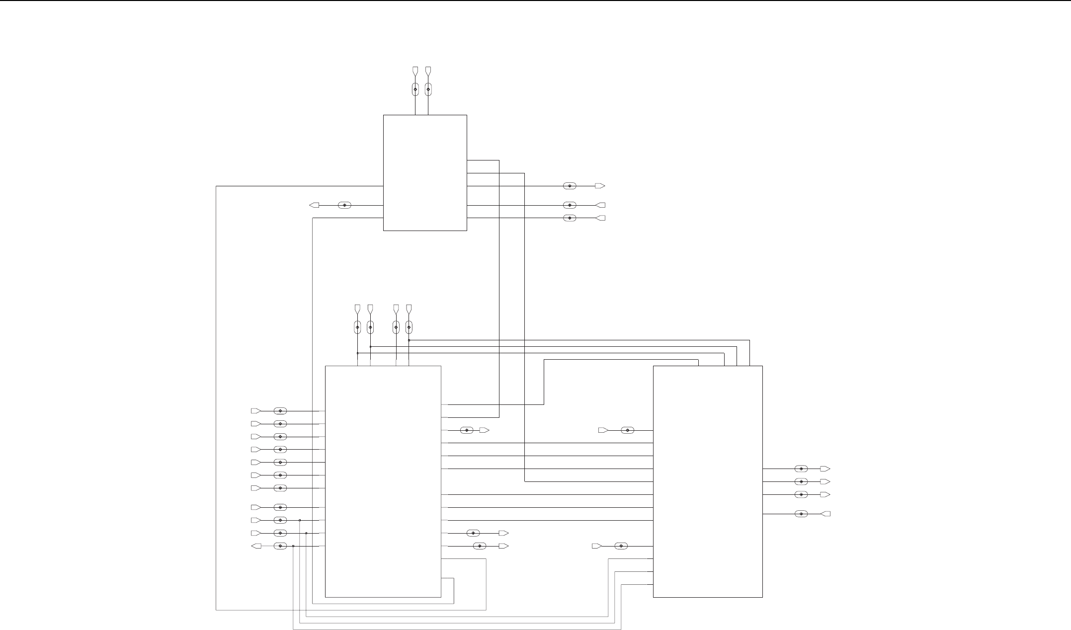
7-14 Circuit Board/Schematic Diagrams and Parts List
FGU
TX
RX
F
R_2V_GID
_
V
5
78
.
1
FR_4V_GID
_
V
5
77.2
DMCS_RF
SYNCB_RF
ADAPT_SW_RF
DEEP_SLEEP_RF
TX_CLK_RF
RX_CLK_RF
RX_DATA_RF
RESET_OUT_RF
ANT_EN_RF
PA_TEMP_RF
TX_DAC_RF
FR_+BWAR
FR_2SUBV_ANA_V5
16_8MHz_GPS
GPS_ANT_RF
GPS_ANT
PA_TEMP
+BWAR
RX_IN
TX_BUFF
TX_DAC
TX_VCO_EN
LNA_EN
LOCK_DETECT
RESET_OUT
RX_1ST_LO_INJ
RX_VCO_EN
SPI_CLK
SPI_MISO
SPI_MOSI
THK_CE
TX_BUFF
TX_CLK
TX_DATA
TX_FSYNC
TX_VCO_EN
2SUBV_ANA_V5
ANT_EN
GP02
2V_GID_V578.1
16.8_MHZ_BUFF
16_8MHZ
16_8MHz_GPS
7V_ANA_V577.2
4V_GID_V577.2
8V_ANA_V5
5V_RX
ADAPT_SW
DEEP_SLEEP
DMCS
GP02
LNA_AGC
LNA_ATTN
FR_7V_ANA_V577.2
FR_8V_ANA_V5
RX_FLTR_VCTRL_RF
RX_FSTNC_RF
LOCK_DETECT_RF
ABACUS3_CE_RFSPI_MISO_RF 16.8_MHZ_BUFF_RF
SPI_MOSI_RF
SPI_CLK_RF
THK_CE_RF
TX_FSYNC_RF
TX_DATA_RF
7V_
A
NA_V577.2
4V_GID_V577.2
2V_GID_V578.1
TX_DAC
PA_TEMP
ANT_EN
RX_FSYNC
RX_DATA
RX_CLK
16.8_MHZ_BUFFSPI_MISO
LOCK_DETECT
16_8MHz_GPS
GPS_ANT
SYNCB
SPI_CLK
+BWAR
2SUBV_ANA_V5
ADAPT_SW
DEEP_SLEEP
DMCS
RESET_OUT
TX_CLK
TX_FSYNC
TX_DATA
THK_CE
SPI_MOSI
RX_FLTR_VCTRL
ABACUS3_CE
8V_ANA_V5
RX_FLTR_VCTRL
LNA_EN
LNA_ATTN
LNA_AGC
RX_IN
RX_1ST_LO_INJ
RX_VCO_EN
16_8MHZ
RX_FSYNC
RX_DATA
RX_CLK
SYNCB
ABACUS3_CE
SPI_CLK
SPI_MOSI
SPI_MISO
5V_RX
5V_ANA_V8
2.775V_ANA_V7
1.875V_DIG_V2
Complete VHF RF Schematic Diagram
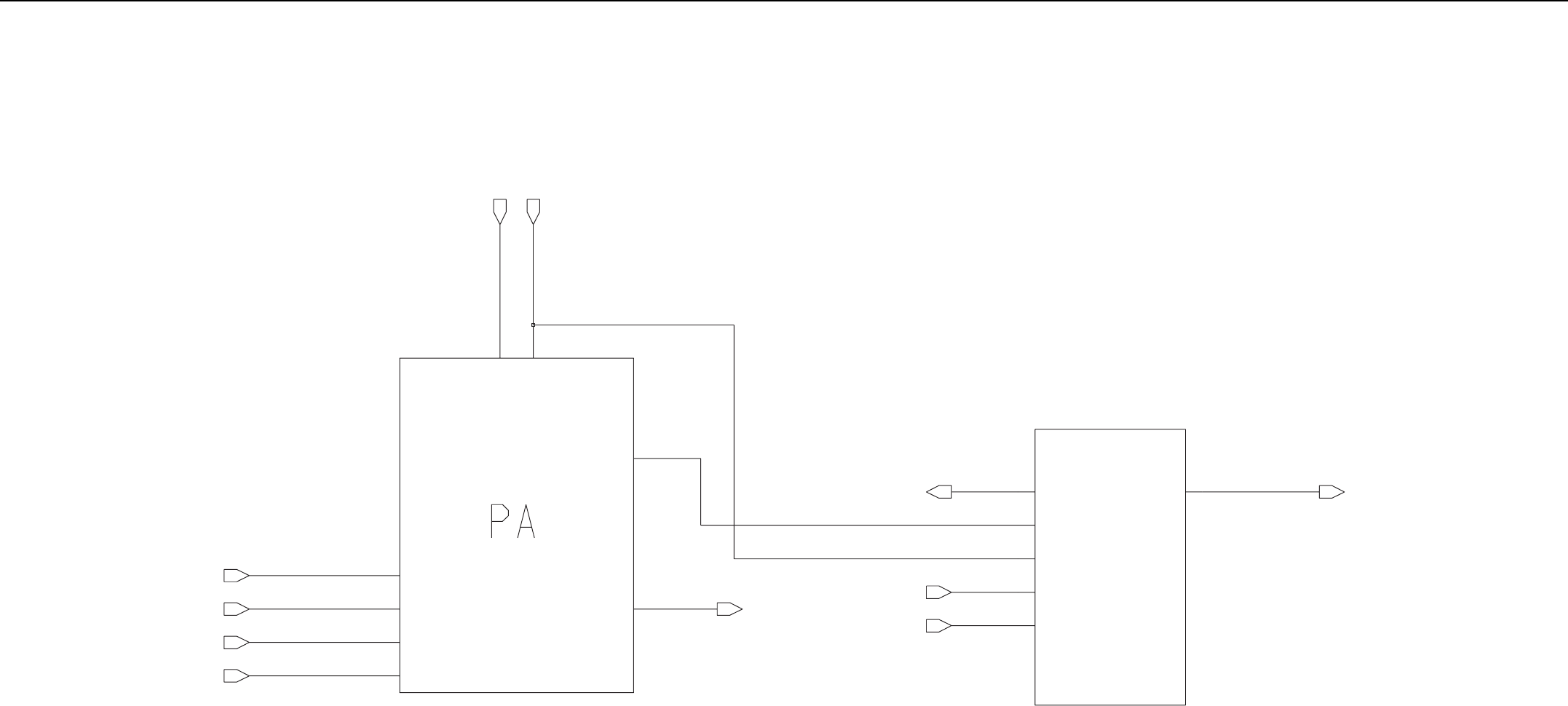
Circuit Board/Schematic Diagrams and Parts List 7-15
HF
PA_OUT
PA_TEMP
+BWAR
TX_BUFF
TX_DAC
TX_VCO_EN
PA_OUT
RAWB+
RX_IN
2SUBV_ANA_V5
ANT_EN
TX_BUFF
ANT_EN
TX_DAC
RX_IN
2
S
U
B
V_ANA_
V
5
PA_TEMP
+BWAR
GPS_ANT
GP02
ANT_EN
TX_VCO_EN
ANT_EN
GP02
GPS_ANT
Complete VHF Transmitter Schematic Diagram
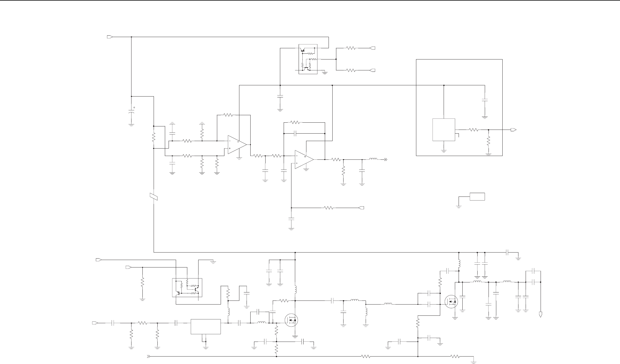
7-16 Circuit Board/Schematic Diagrams and Parts List
PA
PW_CTRL
Near to heatsink
RAWB+
Q701
10K
47K
47K
4.7K
4815055H01
ANT_EN
TX_VCO_EN
NU
0
R733
0613952R66
0613952R66
R732
0
2113944A52
C706
1000pF
5.1K
R708
0613952Q90
.01uF
C709
2113945B02
0
R709
0613952R66
6
5
7
8
4
5115147H01
AD8566
U701-2
2.2K
R707
0613952Q81
.047uF
C705
2113946B02
C708
2113944A52
1000pF
270
R714
0613952Q59
R705
2MEG
0613952R56
1
8
4
5115147H01
AD8566
U701-1
2
3
NU
0613952R56
R706
2MEG
330K
R701
0613952Z80
0613952Z80
R702
330K
2113944A52
C704
1000pF
0613952Z80
R703
330K
NU
0613952Z80
R704
330K
C703
2113944A52
1000pF
0615043C01
R700
0.1
2371878M01
C700
33uF
E701
7686949J14
BLM21PG221SN1
47K
R731
5V_ANA_VBUS2
ANT_EN
C738
2113945A03
330pF
C714
2113945A03
330pF
R729
22
0613952Q33
0613952Q60
R730
300
300
R728
0613952Q60
TX_BUFF
TX_VCTRL
2
5
4
1
3
10K
47K 47K
4.7K
GND1
2
GND2
4
RF_IN
1VD_RF_OUT 3
4802246J29
U700
ADA4743
0613952Q45
R719
68
.022uF
2113945B04
C731
D
G
S
Q703
4816547H01
5.6nH
2414017N09
L702
0613952Q85
3.3K
R725
2113944A31
C715
33pF
C719
2113944A52
1000pF
0.10uF
2113946K02
C718
33pF
C707
2113944A31
R717
0613958H33
22
1000pF
C722
2113945A09
2414017N22
68nH
L701
2113945B04
C720
2113945A03
330pF
C717
.022uF
R718
200
0613952Q56
Q702
4815055H01
12nH
2414017N13
L710
43pF
2113944C84
C726
30pF
C724
2113944C82 2414017N15
18nH
L708
2414017N22
L703
68nH
2414017N11
8.2nH
L709
2113944C41
C777
68pF
110
0613952Q50
R723
68pF
C778
2113944C41
L705
2479990C03
13.85nH
Q704
4816548H01
D1
G
3
S
2
0.1uF
C721
2113945D04
200
R720
0613952H56
C732
2111078B53
270pF
2479990A02
7.66nH
L707
82pF
C798
2113944C43
15pF
C799
2113944C32
2113944C43
C798
82pF
23.75nH
2479990E01
L712
C797
15pF
2113944C32
PA_OUT
2113944C82
30pF
C735
30pF
2113944C82
C739
2113945A03
C736
330pF
330pF
C734
2113945A03
2113945A09
C737
1000pF
0613952R66
0
R726
2113944A52
C729
1000pF
NU
.022uF
C730
2113945B04 43
0662057M41
R727
M700
HEATSINK
POS
1
DNP
0
0613952R66
R712
10K
R713
0613952R01
3GND 1
POS
2
VOUT
U702
LM50
5115022H01
.022uF
C712
2113945B04
PA_TEMP
20K
0613952R08
R711
.01uF
C710
2113945B02
TX_DAC
NU
C711
2113944A52
1000pF
0613952R01
R710
10K
TX_VCTRL
120nH
L700
2414017N22
VHF Transmitter Schematic Diagram
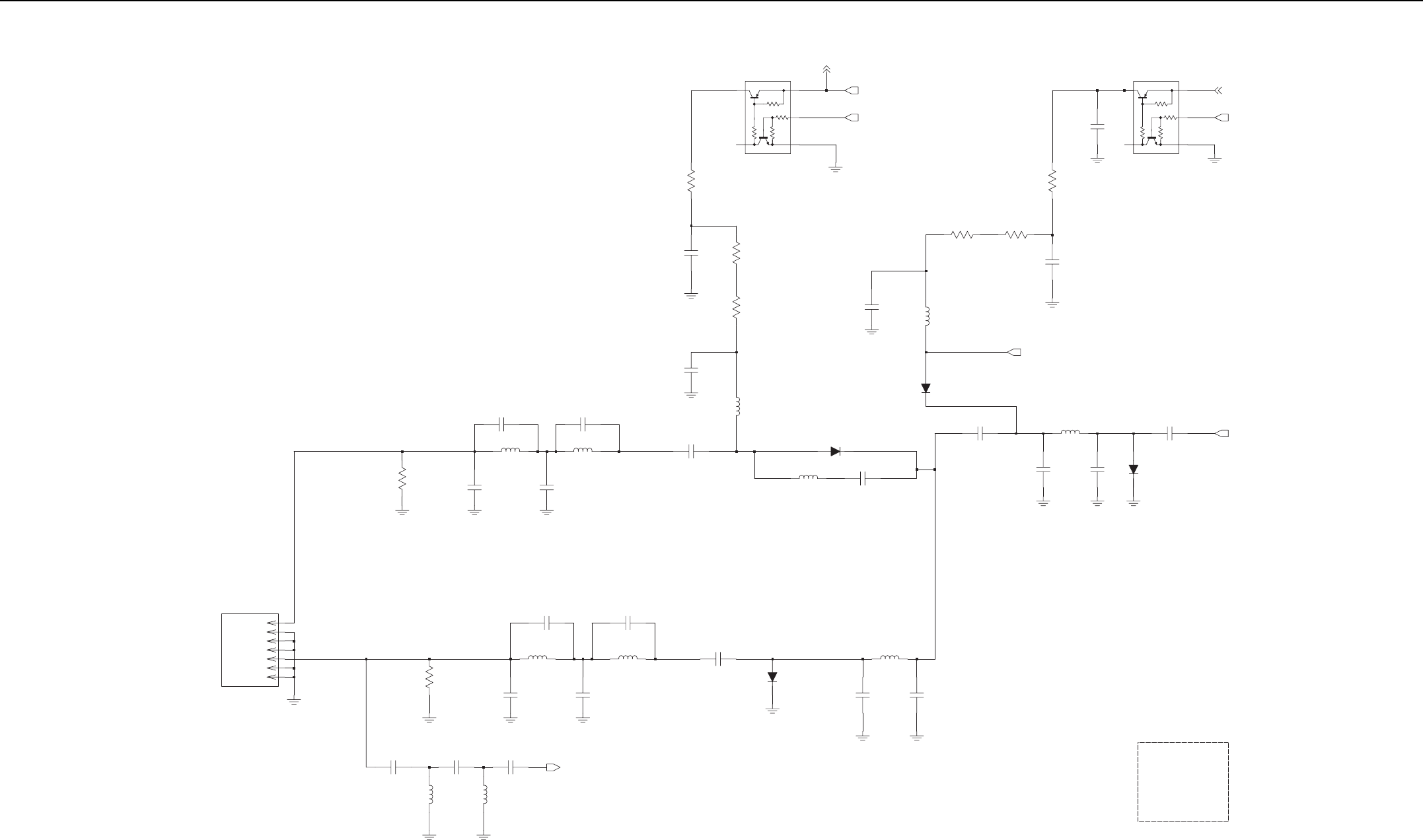
Circuit Board/Schematic Diagrams and Parts List 7-17
RF CONNECTOR
2
5
4
10K
47K
4.7K
1
3
4815055H01
Q901
GP02
RAWB+
RAWB+
47K
R903
0613952H47
82
82
0613952H47
R902
0613952H47
82
R908
2113945B04
C908
.022uF
C900
2113945B04
.022uF
2415347H05
1800nH
L903
3.9pF
C931
2113944C20 C930
2113944C28
8.2pF
2113944C80
C904
20pF
C919
2113944C33
18pF
43nH
2416066H01
L910
0613952R01
R906
10K C920
27pF
2113944C35
43nH
L909
2416066H01
P900-5
P900-1
P900-3
P900-7
P900-4
P900-6
P900-2
ANTENNA NUT
P900 LIVE
LIVE
2815696H01
R907
0613952R01
10K
C925
2113944V07
1.5pF
2414017P10
L913
5.6nH
3.9nH
L912
2414017P08
C906
7.5pF
2113944C74
43nH
2416066H01
L904
C924
2113944A20
43nH
6.2pF
L905
2416066H01
C907
2113944C81
24pF
2113944A15
C926
3.9pF
GPS_ANT
7.5pF
C928
2113944C74
4.7pF
C929
2113944C22
2113944C85
51pF
C909
4815897H01
CR901
L906
2416066H01
43nH
C912
2113944C29
9.1pF
2113944C33
18pF
C911
Q901
P900
M901
R907
L915
C927
C918
2113944C04
330pF
43nH
2416066H01
L908
RX_IN
CR903
4815897H01
2
1
47pF
C913
C915 C916
2113944C38
10pF
2113944C30
13pF
2113944C78
4815897H01
CR902
PA_OUT
1000nH
L902
2415347H01
C905
2113944C04
330pF
4815897H01
CR900
1800nH
2415347H05
L907
.022uF
2113945B04
C914
.022uF
C933
2113945B04
82
0613952H47
R904
0613952H47
R909
82
82
R905
0613952H47
220pF
C927
2113945A01
4815055H01
Q900
10K
47K
47K
4.7K
ANT_EN
RAWB+
VHF Harmonic Filter and Antenna Switch Schematic Diagram
7-18 Circuit Board/Schematic Diagrams and Parts List
SPI_MISO
2V_GID_V578.1
16_8MHZ
7V_ANA_V577.2
8V_ANA_V5
ABACUS3_CE
IF_AMP_OUT
RX_CLK
RX_DATA
RX_FSYNC
RX_VCO_EN
SPI_CLK
XR_V5
IF_AMP_OUT
LNA_AGC
LNA_ATTN
LNA_EN
RX_1ST_LO_INJ
RX_FLTR_VCTRL
RX_IN
RX_FLTR_VCTRL
LNA_EN
LNA_ATTN
LNA_AGC
RX_IN
RX_1ST_LO_INJ
X
R
_
V
5
SPI_MOSI
SPI_MISO
SPI_CLK
RX_VCO_EN
RX_FSYNC
RX_DATA
RX_CLK
ABACUS3_CE
8
V
_A
NA
_
V
5
7
V_
A
NA_V5
7
7.2
16_8MHZ
2V_GID_V578.1
SYNCB
7V_ANA_V577.2
RXFE
RXBE
Complete VHF Receiver Schematic Diagram
Circuit Board/Schematic Diagrams and Parts List 7-19
12pF
2113944A26
C402
C400
2113944A36
68pF
L400
2479990C01
13.9nH
RX_IN
4815059H01
D401
C401
2113944A30
27pF
D400
4815059H01
100nH
L402
2415429H36 2113946K02
0.10uF
C422
2113944A30
C403
27pF
68pF
2113944A36
C404
13.9nH
2479990C01
L401
C405
2113944A41
120pF
0613952R25
R400
100K
2113944A41
C406
120pF
1.55nH
L420
2113944A52
C408
1000pF
LNA_EN
LNA_ATTN
LNA_AGC
0613952R66
R403
0
0613952R66
0
R402
0
0613952R66
R401
C411
2113944A52
1000pF
2113944A63
C410 1pF
4.7pF
C409
2113944A17
4813974A19
D402
LNA_OUT
LNA_VCC
RF_ATTN
RF_VCC
RSET
RX_EN
AGC
AGC_BYP
GND
GND1
LNA_E
LNA_I
LNA_IN
17
8
4
11
10
3
U400
MAX2371
5
9
12
G1
2
6
2113945B02
.01uF
C421
C412
2113944A52
1000pF 1K
0613952Q73
R406
2113944A77
11pF
2113944A19
C418
5.6pF
C419
L403
2414017N22
68nH
0
R430
0613952R66
2113944A24
C420
9.1pF
TP400
RX_FLTR_VCTRL
2.2pF
C417
2113944A09
68pF
2113944A36
C423
2415429H38
L406
120nH 47nH
L407
2415429H30
4815059H01
D404
27pF
2113944A30
C424
L421
1.55nH
27pF
C447
2113944A30
D403
4815059H01
12pF
2113944A26
C425
2113944A36
68pF
C448
2479990C01
13.9nH
L409
13.9nH
2479990C01
L408
120pF
2113944A41
C450
2113944A41
120pF
C451
0613952R25
100K
R405
2113944A52
1000pF
C449
2.775V_ANA_V7
C414
2113944A52
1000pF
2113946K02
C415
0.10uF
C413
2113946K02
0.10uF
0613952R66
R496
0
330nH
2415429H46
L404
1.2K
0613952Q75
R404
2113944A52
C416
1000pF
330nH
2415429H46
L405
RXFE - Shield A
51
R407
0613952Q42
560nH
L412
2414017K32
2515396H01
XFMR
T400
C427
160pF
2113944A88
82nH
L411
C426
0613952R66
0
DNP
L410
2487319K20
36nH
NC 5
6
1
4
2
3
A2
A4
K1
K3
3
4
1
2
D405
4815923H01
11pF
C429
2113944A77
L413
51nH
2415429H31
2113944A77
C431
11pF
L414
2415429H31
51nH
22pF
C430
2113944A29
RX_1ST_LO_INJ
XFMR
5
NC
6
1
4
2
3
T401
2515396H01
C439
2113944A22
7.5pF
C428 18pF
2113944A28
44.85MHz
MXF45
FL400
OUT
2CC1
5CC2
1GND1
4
GND2
3IN 6
2113944A80
C432 20pF
2414017K33
680nH
L415
390nH
L418
2415429H47
C435
2113944A40
100pF
0
R497
0613952R66
DNP
150
R421
0613952Q53
C433
20pF
2113944A80
L417
270nH
0613952R66
R425 0
R419
0
0613952R66
R424
0613952Q74
1.1K
1.5K
R410
0613952Q77
C434
0.10uF
2113946K02
.01uF
2113945B02
C437
0613952Q49
100
R412
C442
2113945B02
.01uF
2113944A82
30pF
C440
15pF
Q401
2113944A27
C446
4816531H01
0613952R03
12K
R411
R417
0613952R66
C441
0
22pF
2113944A29
2113946K02
0.10uF
C444
10K
R409
0613952R01
360
R422
0613952Q62
0.10uF
2113946K02
C436
470nH
L416
2414017K31
C438
2113946K02
0.10uF
4816531H01
Q400
C445
2113944A82
30pF
IF_AMP_OUT
RXFE - Shield B
IF_AMP_VCC
1.5K
R413
0613952Q77
TP403
R420
0613952Q74
1.1K
5V_RX
RXFE
VHF Receiver Front End Schematic Diagram
7-20 Circuit Board/Schematic Diagrams and Parts List
RXBE
5V_ANA_V85V_ANA_V8
2480640Z01
E600
E602
2480640Z01
1.875V_DIG_V2
2.775V_ANA_V7
1.875V
2.775V_ANA_AB
2.775V_ANA_AB
2113945B02
C607
.01uF
C606
2113944A36
68pF
C605
2113945B02
.01uF
C604
2113945B02
.01uF
C603
2113946B04
0.1uF
2113946B04
C602 0.1uF
.01uF
2113945B02
C601
0
0613952R66
R696
IF_AMP_OUT
2.775V_ANA_AB
.01uF
C621
2113945B02
C620
0.1uF
2113946B04 2466505A01
L601
10uH
10uH
2466505A01
L600
C622 200pF
2113944C89
2113944A40
100pF
C623
100pF
C624
2113944A40
2200pF
2113945A11
C625
2415569H01
L602
4.7uH
2113945D02
.047uF
C626
100pF
C627
2113944A40
C628
2113945B02
.01uF
C629
2113944A40
100pF
C630
.01uF
2113945B02
R607
100K
0613952R25
0.1uF
C633
2113946B04
0613952R01
R609
10K
CLOCK VCO
D601
1SV305
4815096H01
51pF
2113944A85
C635
C634
2113945B02
.01uF
L605
4.7uH
2415569H01
10K
R610
0613952R01
CLOCK LF
2113946G04
C637
0.68uF
2113946B04
C636
0.1uF
390
R611
0613952Q63
2.775V_ANA_AB
0.1uF
2113946B04
C632
2.775V_ANA_AB
0.1uF
C639
2113946B04
10K
R698
0613952R01
ABACUS3_CE
TP600
SPI_MOSI
SPI_CLK
14
23
24
13
17
15
16
21
18
22
20
19
27
48
40
39
25
33
26
47
38
42
43
32
45
36
37
34
35
31
28
46
44
41
29
30
6
12
11
9
5
2
1
4
8
7
10
3
VDDF
VREFN
VREFP
VDDA
IF2P
MXON
MXOP
IF2N
GCN
GCP
GNDA
GNDF
VDDQ
PC
PD
RREF
VDDC
IOUTC
GNDQ
GNDS1
GNDC
GNDD
CLKN
CLKP
VDDH
PE
SYNCB
VDDD
GNDH
GNDL
GNDS2
FREF
FS
CLKOUT
DOUTA
DOUTB
VDDI
VDDL
VDDP
IFIN
IOUTL
LON
LOP
GNDI
GNDP
CXIF
CXVL
CXVM
AD9864
5102495J14
U600
C631
.01uF
2113945B02
100K
R699
0613952R25
R697
0613952R66
0
SYNCB
1.875V
1.875V
16_8MHZ
2115358H13
0.1uF
C619
R606
0613952Q73
1K
2113945L37
C617
3300pF
2113945C18
C618
.012uF
5.1K
0613952Q90
R605
TP601
1SV305
4815096H01
D600
5.1K
R604
0613952Q90
2115153H55
C612
82pF
2414015B27
L604
390nH
0613952R05
R603
15K
2115153H48
C611
43pF
20K
R612
0613952R08 DNP
18pF
C638
2113944A28
2113945G91
C613
0.1uF
4805793Y10
Q602
2115153H53
68pF
C610
2115153H57
100pF
C609
2414017Q51
L603
2.2uH
620
R602
0613952Q68
BK1005HM471
2480640Z01
E601
2113946E02
C614
1.0uF 360
R601
0613952Q62
C615
2113946B04
0.1uF
Q600
4813973A04
0613952R01
10K
R600
5V_ANA_V8
2113944A32
C616
39pF
RX_VCO_EN
Q601
47K
47K
4.7K
10K
RX_CLK
RX_FSYNC
SPI_MISO
RX_DATA
C608
2113945D02
.047uF
VHF Receiver Back End Schematic Diagram
Circuit Board/Schematic Diagrams and Parts List 7-21
TOMAHAWK
10Z0460842
300E
KHT_8V_ANA_V5
XR_V5
PRESCALER
RX_1ST_LO_INJRX_VCO_EN
TUO_FS
TX_BUFFTX_VCO_EN
TX_VCO_TANK
VCTRL
10Z0460842
1
0
Z
0460
842
200E
400E
10
0
E
10Z0460842
TX_DATA
TX_FSYNC
TX_VCO_EN
TX_VCO_TANK
VCTRL
DEEP_SLEEP
DMCS
GP02
LNA_AGC
LNA_ATTN
LNA_EN
LOCK_DETECT
PRESCALER
RESET_OUT
RX_VCO_EN
SF_OUT
SPI_CLK
SPI_MISO
SPI_MOSI
THK_CE
TX_CLK
KHT_2V_GID_V578.1
16.8_MHZ_BUFF
16_8MHZ
16_8MHz_GPS
KHT_7V_ANA_V577.2
KHT_4V_GID_V577.2
KHT_8V_ANA_V5
ADAPT_SW
SPI_CLK
SPI_MISO
2V_GID_V578.1
4
V
_
G
I
D_V5
7
7
.2
8V_
AN
A_V5
7V_A
N
A_V5
7
7
.2
XR_V5
RX_1ST_LO_INJ
TX_BUFF
LOCK_DETECT
LNA_ATTN
LNA_AGC
LNA_EN
16.8_MHZ_BUFF
RX_VCO_EN
GP02
TX_VCO_TANK
16_8MHZ
16_8MHz_GPS
TX_VCO_EN
ADAPT_SW
DEEP_SLEEP
DMCS
RESET_OUT
TX_CLK
TX_FSYNC
TX_DATA
THK_CE
SPI_MOSI
Complete VHF Frequency Generating Unit Schematic Diagram
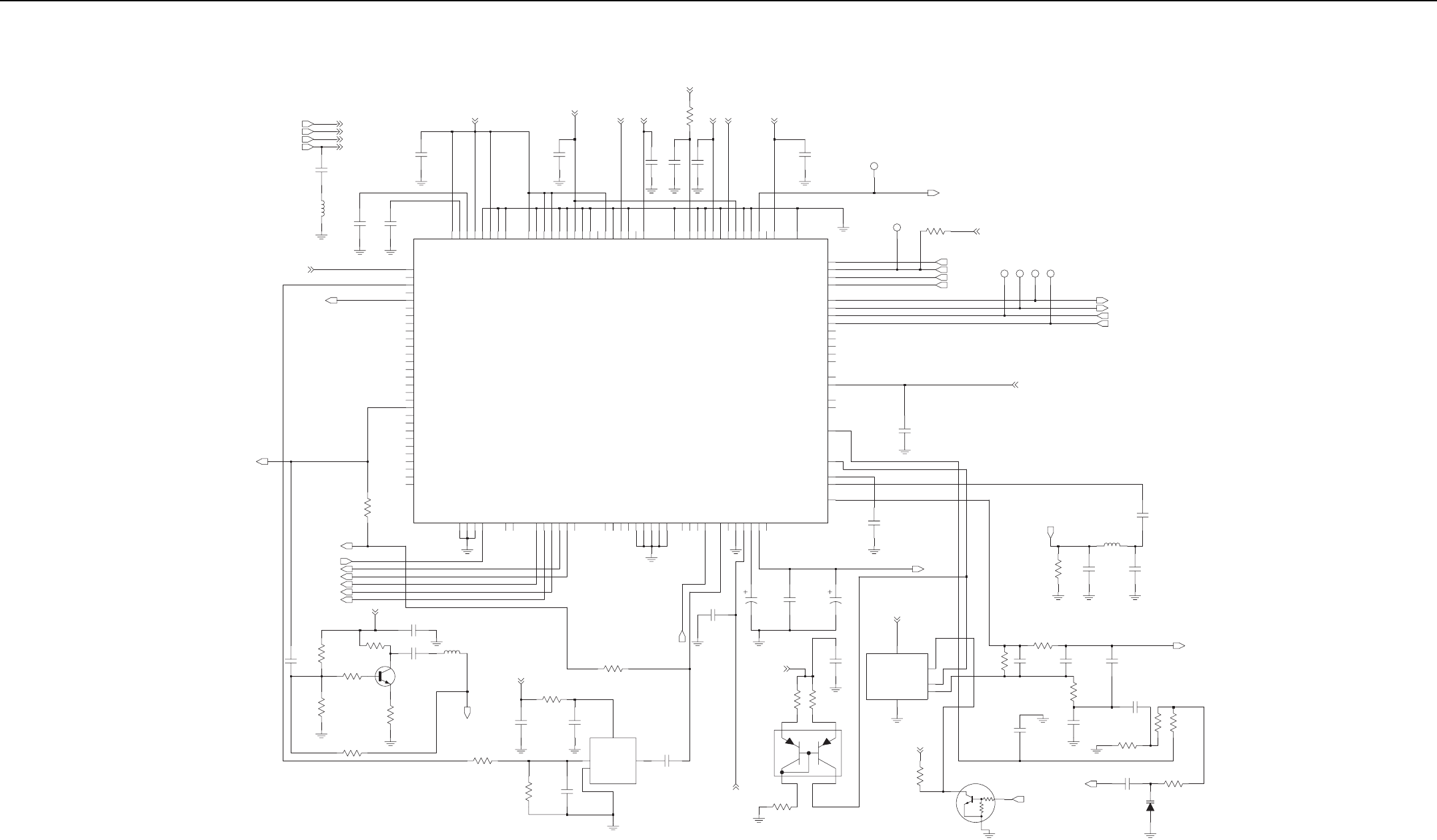
7-22 Circuit Board/Schematic Diagrams and Parts List
5V_ANA_V8_THK
2.775V_ANA_V7_THK
2.775V_DIG_V4_THK
1.875V_DIG_V2_THK
2.775V_ANA_V7_THK
5V_ANA_V8_THK
2.775V_DIG_V4_THK
1.875V_DIG_V2_THK
TOMAHAWK
1.0uF
2113946D02
C002
0.10uF
2113946K02
C003
1.0uF
C009
2113946S35
2414032F42
470nH
L003
2113946D02
C001
1.0uF
2.775V_ANA_V7_THK
1.875V_DIG_V2_THK
5V_ANA_V8_THK
1.875V_DIG_V2_THK
C004
2113946K02
0.10uF
2.775V_ANA_V7_THK
5V_ANA_V8_THK
1.875V_DIG_V2_THK
1.875V_DIG_V2_THK
0613952R66
R027
0
0.10uF
2113946K02
C006
0.10uF
2113946K02
C007C005
0.10uF
2113946K02
2113946K02
C008
0.10uF TP006
TP001
TP004 TP005
TP002 TP003
DMCS
TX_DATA
TX_FSYNC
TX_CLK
1.875V_DIG_V2_THK
LOCK_DETECT
DNP
10K
R026
0613952R01
SPI_MISO
THK_CE
SPI_MOSI
SPI_CLK
2.775V_ANA_V7_THK
F1
F10
C11
D10
D9
D11
F11
F9
E9
E10
E7
H3
G2
H1
G3
J2
K8
L3
K1
G1
F7
D8
0.10uF
C035
2113946K02
2113946K02
C022
0.10uF
SF_OUT
F6
K5
L5
K10
F5
F3
K4
C9
H5
J4
E6
A1
A11
L1
L11
L4
K9
H8
B4
A4
E5
D4
J8
J7
G9
H11
L10
G11
D6
C10
B11
A6
TX_GND2
XOSC_BASE
XOSC_EMIT
SUB1
SUB2
SUB3
SF_OUT
SMD_CLK_GEN_GND
OSCREG_OUT
OSCREG_SPLY
RSTB
NC1
NC2
NC3
NC4
OSCREG_BYP
GPO5
GPO6
GPO1_TEST1
GPO2_TEST2
GPO3_TEST3
GPO4_TEST4
EF_OUTM
EF_OUTP
CLK_CP
CLK_EMIT
DEEPSLEEP
CLK_BASE
ACE2
ASPI_CLK
ASPI_DATA
ACE1
VCO_DAC
TXCLK
SPI_CLK
SPI_DR
SPI_DW
SDR
SDTX
SFTX
SCLK_OUT
RXFS
RXACQ
M_PRSCX
MAIN_PDET_VCC
MN_ADAPT_CP
MN_CP
M_PRSC
HP_MOD_OUT
ESC_CP
ESC_IN
DAC_ADAPT
DMCS
CEX
TX_DAC_VCC
TX_GND1
TX_VCC
XOSC_GND
TEST1
TEST2
TM
TX_DAC_GND
SSI_GND
SSI_VCC
SDM_VREFM
SDM_VREFP
RX_AVCC2
SCAN_EN
SDM_CLK_GEN_VCC
SDM_REF_GND
SDM_REF_VCC
RX_AGND1
RX_AGND2
RX_AVCC1
OSCREG_GND
MAIN_GND
MAIN_VCC
MN_CP_GND
MN_CP_VCC
LGND1
LGND2
LVCC1
LVCC2
ESC_TEST
ESC_VCC
ESC_CPBIAS
ESC_CP_GND
ESC_CP_VCC
ESC_GND
CLK_GND
CLK_VCC
ASPI_VCC
U001
SC51650VF
5104932K08
TCLK
TXI
TXQ
SDM_VAG
RX_EN_OUT
SCAN_IN
RXI
RXIX
RXQ
RXQX
PABIAS_DAC
PHCLK
RFSTEPA
NTXI
NTXQ
INCR_DECR
FBI
FBQ
DC_CAL
BP_I
BP_IX
BP_Q
BP_QX
CLK1_OUT
CLK2_OUT
AGC_DAC
AGC_FLAG
AGC_REF
ARX_DAC
G8
K7
L7
B10
B1
F2
C2
C1
D1
D2
K11
L9
A3
L8
K6
J9
C6
B6
A2
E4
F4
E2
E3
H9
J11
B5
C4
C5
H6
DNP
0
R052
0613952R66
16_8MHz_GPS
RX_VCO_EN
TX_VCO_EN
LNA_EN
LNA_ATTN
GP02
DEEP_SLEEP
2.775V_DIG_V4_THK
DNP
0613952Q66
R004
510
0613952R66
R054
0
0613952Q96
R001
9.1K
L001
2.7uH
2415375H09
47
0613952Q41
R002
2113946K02
C012
0.10uF
2113946K02
C011
0.10uF
5.6K
0613952Q91
R003
Q001
NE68519
4805793Y10
0.10uF
C010
2113946K02
0613952Q56
R005
200
R006
0613952Q93
6.8K
16.8_MHZ_BUFF
2.775V_ANA_V7_THK
2113945L49
C014
.01uF
10
0613952Q25
R008
.01uF
C015
2113945L49
0613952R66
0
R053
1
VCONT
Y001
IVT5300B
16.8MHz
2
COMM_CASE
3
OUT
4
POS_VCC
1000pF
2113945A09
C016
R007
10K
0613952R01 270pF
2113945A02
C013
R012
0613952R25
100K
2.775V_ANA_V7_THK
2
1
3
4
Q002
BCV62
4815359H01
R010
0613952Q93
6.8K
0613952Q49
100
R011
5V_ANA_V8_THK
C017
0.10uF
2113946K02
C019
.01uF
2113945L49
10uF
C018
2313960B57
10uF
C020
2313960B57
5V_ANA_V8_THK
0.10uF
2113946K02
C036
INOUT 1
ONOFF_CONTROL 4
OUTIN 2
VCC 5
U002
MC74VHC1GT66
5114000B59
GND
3
OUT
4816134H01
DTC114YM
Q003
IN
R1
R2
33K
0613952R13
R025
HP_MOD_OUT
ADAPT_SW
2.775V_DIG_V4_THK
GND
2115358H15
C026
0.15uF
4.3K
R018
0613952Q88
2115358H01
.01uF
VCTRL
C028
4815059H01
D001
0613952Q42
R017
51
0613952Q58
R022 240
C027
1uF
2115358H25
1.3pF
2115153H06
C037
0613952R01
R019
10K
TX_VCO_TANK
22
0613952Q33
R016
2113945A09
C038
1000pF
C025
.033uF
2115358H07
MN_CP
MN_ADAPT
0.22uF
2115358H17
C024
R013
0613952Q46
75
R014
51
0613952Q42
2113945A09
1000pF
C031
6.8pF
C033
2113944A21
R020
180
0613952Q55
2415429H38
L002
120nH
C032
10pF
2113944A25
PRESCALER
L6
G7
J6
G6
D7
C7
B3
H7
E8
E11
A9
B8
A5
D3
A10
A8
B9
C3
D5
B2
J5
G4
J1
G5
H2
F8
C8
G10
B7
E1
K2
L2
K3
J3
H4
H10
J10
A7
2.775V_ANA_V7_THK
LNA_AGC
16_8MHZ
RESET_OUT
VHF Synthesizer Schematic Diagram
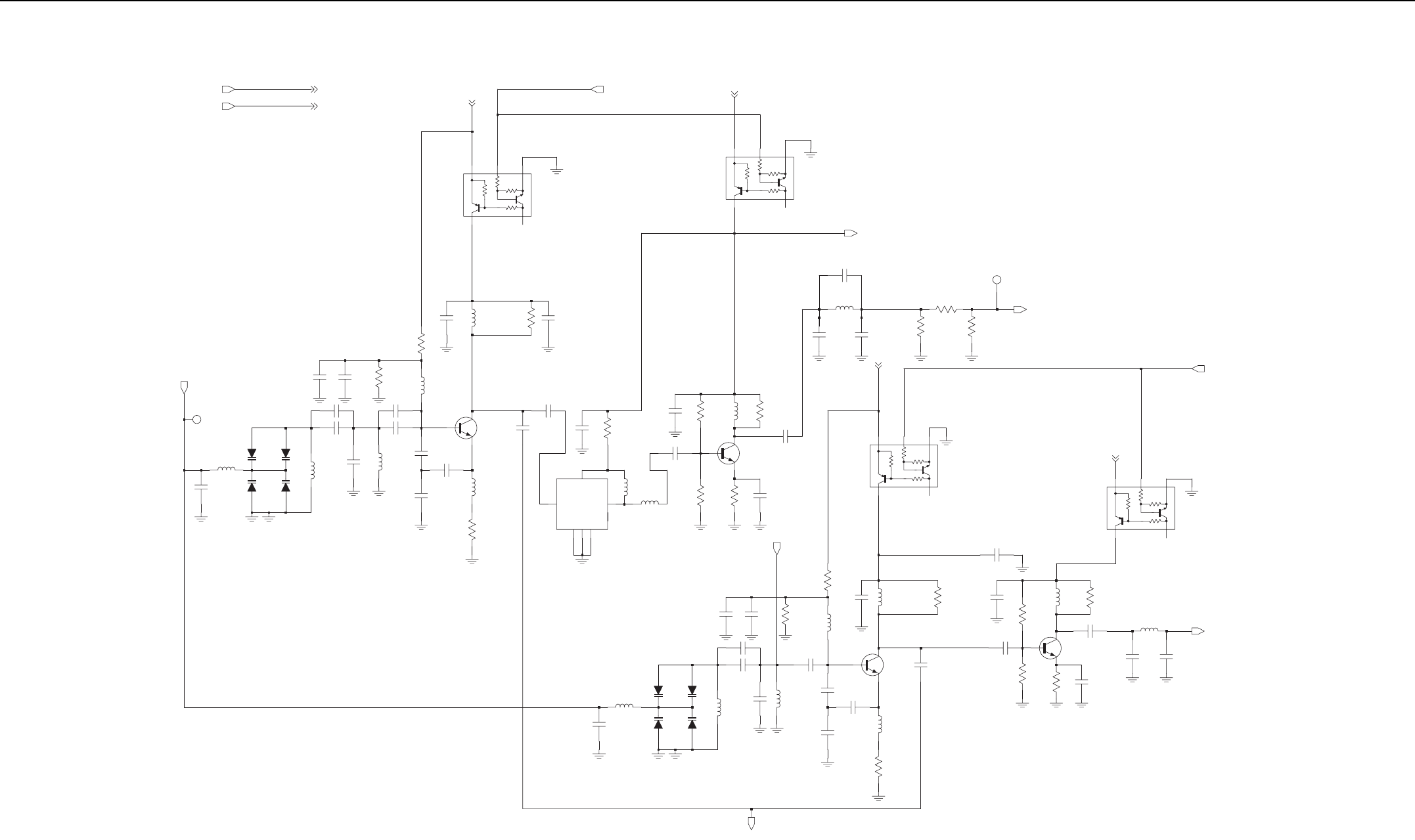
Circuit Board/Schematic Diagrams and Parts List 7-23
VCO
5V_ANA_V8_THK 5V_ANA_V8_THK
SF_OUTSF_OUT
Rx_VCO_Ex_Supply
UMC5NT2G
4815055H01
Q202
47K
47K
4.7K
10K
47K
47K
4.7K
10K
SF_OUT
RX_VCO_EN
UMC5NT2G
Q203
4815055H01
5V_ANA_V8_THK
1.5pF
C241
2113944A05
5V_RX
2415429H36
100nH
L207
2113944A05
C216
1.5pF
2113944A10
C217
2.4pF
SF_OUT
18
0613952Q31
R221
R222
0613952Q60
300
TP201
0613952Q60
R220
300
RX_1ST_LO
Tx_VCO_Ex_Supply
47K
47K
4.7K
10K
Tx_VCO_Out
4815055H01
UMC5NT2G
Q207
5V_ANA_V8_THK
L215
2415429H38
120nH
2113944A73
8pF
C237C236
2113944A72
7pF
TX_BUFF
DNP
56
0613952Q43
R215
L214
2415347H01
1000nH
7.5K
R213
0613952Q94
R214
0613952Q58
240
1000pF
C235
2113945A09
0613952Q90
R212
5.1K
Q205
4805793Y10
C234
2113945A09
1000pF
1000pF
2113945A09
C233
2.7pF
2113944A11
C232
R210
0613952Q49
100
0.1uF
C230
2113946B04
C231
2113944A05
1.5pF
2415347H01
1000nH
L213
R211
0613952Q50
110
4805793Y10
Q204
L212
1000nH
2415347H01
160pF
C225
2113944A88
30pF
C224
2113944A82
27pF
C226
2113944A30
L211
2415347H01
1000nH
1000pF
C229
2113945A09
L210
IDCTR
82nH
2415718H22
R208
0613952Q96
9.1K
C223
8pF
2113944A73
0613952Q89
4.7K
R209
2113946B04
0.1uF
C228
4815096H01
D204
1000pF
C219
2113945A09
4815096H01
D207
D206
4815059H01
4815059H01
D205
2415347H01
L208
1000nH
DNP
2113944A27
C220 15pF
100nH
L209
2415427H46
C221 15pF
2113944A27
C222
2113944A15
3.9pF
1000pF
2113945A09
C227
UMC5NT2G
Q206
47K
10K
47K
4.7K
4815055H01
C214
2113945A09
1000pF
2113944A40
100pF
C215
Q208
4805793Y10
TX_VCO_TANK
DNP
1000pF
2113945A09
C238 R207
56
0613952Q43
L206
1000nH
2415347H01
R217
0613952Q95
8.2K
R205
0613952Q91
5.6K 240
0613952Q58
R216
220nH
2415429H43
L218
U200
UPC8179TK
2.0pF
2113944A08
C240
2415347H01
L217
1000nH
2GND1
3GND2
GND3
5
IN
1OUT 4
VCC 6
R218
0613952Q66
510
C239
1000pF
2113945A09
C213
2113944A08
2.0pF
2.4pF
2113944A10
C212
Q200
4815029H01
130
R203
0613952Q52
1000nH
2415347H01
L205
160pF
2113944A88
C206
27pF
2113944A30
C205
24pF
2113944A81
C207
1000nH
2415347H01
L204
2113946B04
C211
0.1uF
2113945A09
C210
1000pF
0613952Q49
R202
100
1000nH
L203
2415347H01
0613952Q89
R201
4.7K
DNP
0613952Q96
R200
9.1K
2113944A25
10pF
C204
2416540H25
43nH
IDCTR
L202
3.9pF
C243
2113944A15
2113944A25
C201 10pF
C208
2113945A09
1000pF
C202 10pF
2113944A25
L201
68nH
2415427H44
0.1uF
2113946B04
C209
2113944A11
C203
2.7pF
D202
4815059H01
C200
1000pF
2113945A09
1000nH
L200
2415347H01
4815059H01
D201
4815096H01
D200
D203
4815096H01
TP200
VCTRL
PRESCALER
TX_VCO_EN
VHF Voltage Controlled Oscillator Schematic Diagram
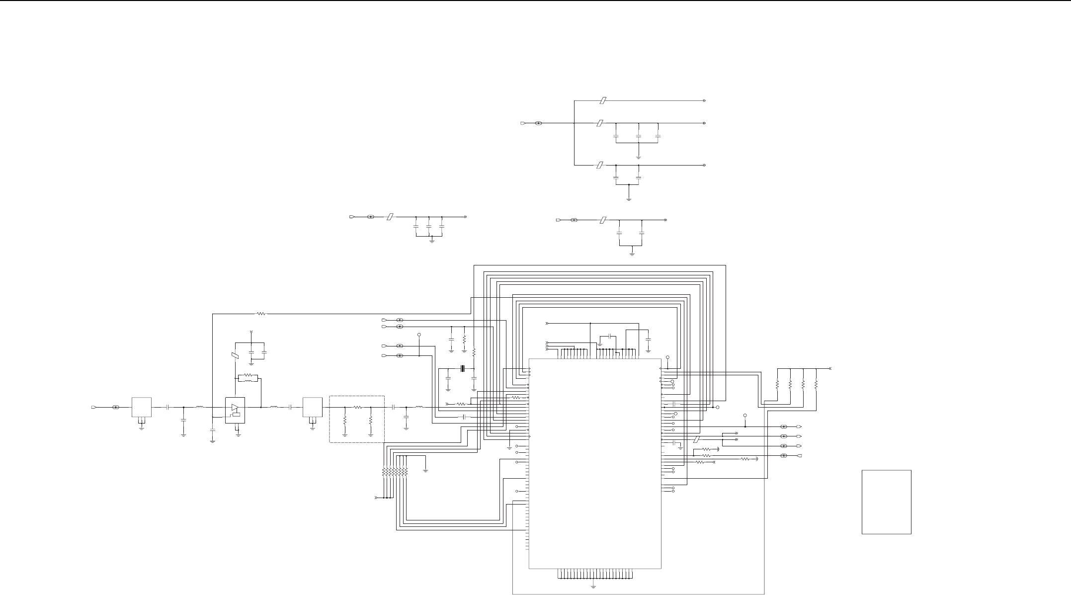
7-24 Circuit Board/Schematic Diagrams and Parts List
2113944A52
C8029
1000pF
0R8025 0613952R66
NC
SiRF_JTRST
SiRF_JTCK
SiRF_JTMS
SiRF_JTDI
SiRF_RF_IN
SiRF_TMODE
SiRF_16_8
GPS Block
2.8V_RF_GPS
2.8V_RF_GPS 21
E8003
7686949J08
IDCTR
IDCTR
7686949J08
E8001
21
2
1
2113946F05
10uF
C8003 C8002
2113944A52
1000pF
2113944A28
18pF
C8004
DNP
DNP DNP
1
7686949J08
E8002
IDCTR
2
2.8V_GPS_LNA
2.8V_GPS_RF
2.8V_GPS_IO
18pF
2113944A28
C8006
2
1
10uF
2113946F05
C8005
E8000
IDCTR
7686949J08
21
2.8V_DIG_GPS
2.8V_DIG_GPS
18pF
2
1
C8001
2113944A28
10uF
C8000
2113946F05
2.8V_GPS_GSP
MS LOO
MS LOO
MS LOO
MS LOO
MS LOO
MS LOO
MS LOO
MS LOO
MS LOO
2.8V_GPS_GSP
1.5V_RTC
1.5V_GPS_RTC 21
E8005
IDCTR
7686949J08
1.5V_GPS_RTC_GPS
2
1C8032
2113945B02
2113944A28
C8033
18pF .01uF
2
1
2113946D05
C8031
2.2uF
R8020
0
0613952R66
7686949J08
IDCTR
E8006
21
GPS_ANT_GPS
5GND2
IN
4OUT 1
GND
2
3GND1
GPS_ANT
0.75pF
C8014
2113944A62
5.6nH
L8001
2414017P10
2.0pF
C8013
2113944A08
9180310L38
FL8001
B39162-B7829-C710
0.10uF
2113946K02
C8015
GPIO[0] (A4)
GND1
2
GND2
5
IN 41 OUT
BIAS
PS
3
VCC 6
UPC8211TK
5164015H55
U8001
0613952Q70
750
R8004
2113945A09
C8016
1000pF
18pF
2113944A28
C8030
22nH
L8002
2414017P17
10nH
L8003
2414017P13
2113944A28
18pF
C8017
B39162-B7829-C710
FL8000
9180310L38
2GND
GND1
3
GND2
5
4IN 1
OUT
2dB Pi Pad
12
0613952Q27
R8016
430R8017
0613952Q64
0613952Q64
R8015 430
18pF
C8018
2113944A28
2
1
5.6nH
21
2414017P10
L8004
C8019
2113944A11
2
1
2.7pF
2.8V_GPS_GSP
0613952R01
0613952R25
0613952R25
0613952R01
0613952R01
0613952R01
0613952R25
0613952R01
R8035
R8031
R8037
R8036
R8033
R8030
R8032
R8034
10K
100K
100K
10K
10K
10K
100K
10K
L5
L6
L7
L8
L9
N2
N3
N4
N5
N6
N7
N8
N9
N10
P5
P7
A1
D5
D6
E5
E6
F5
F6
L4
GND_RF_2
GND_RF_3
GND_RF_4
GND_RF_5
GND_RF_6
GND_RF_7
GND_RF_8
GND_RF_9
GND_RF_10
GND_RF_11
GND_RF_12
GND_RF_13
GND_RF_14
GND_RF_15
GND_RF_16
GND_RF_17
GND_BB_1
GND_BB_2
GND_BB_3
GND_BB_4
GND_BB_5
GND_BB_6
GND_BB_7
GND_RF_1
2113944A28
C8034 18pF
21
32.768KHz
4802582S80
XTAL
Y8000
RTC_XI
2113944A31
C8035
33pF
2
1
2113944A52
C8020 1000pF
H4
G3
G2
H3
G4
J3
H2
G9
H5
F8
F9
H9
G8
H8
G7
H7
G6
G5
E10
B8
C8
E3
E2
D2
D9
E8
E9
C3
C9
B6
D8
A9
B9
5115831H01
GSC3F
U8000
VDD_PLL
VDD_REG_1
VDD_REG_2
VDD_RTC
VDDPLL_O
VDD_BB_1
VDD_BB_2
VDD_BB_3
VDD_BB_4
VDD_BB_5
VDD_BB_6
VDD_FLASH
VCC_RF_5
VCC_RF_6
VCC_RF_7
VCC_RF_8
VCC_RF_9
VCC_RTC
VDDK_1
VDDK_2
VCC_IO_EXT
VCC_RF_1
VCC_RF_2
VCC_RF_3
VCC_RF_4
C5
C4
F7
B4
A10
D4
E4
F4
K2
L2
L3
B3
B10
C10
M6
M7
M8
M9
M10
P9
P8
M2
M3
M4
M5
2.8V_GPS_IO
2.8V_GPS_RF
2.8V_GPS_GSP
1.5V_RTC
2113946D05
2
1
2.2uF
C8022 SiRF_VDD_PLL_O
TPSM0_381
TP_CLK_ACQ
.01uF
C8023
2113945B02
1
TPSM0_381
TP_SIPI_DO
1TP_GPS_RX
SiRF_RTC_OUT
GPS_nWAKEUP
GPS_RFPWRUP
0613952R25
2
1
100K
R8024
NC
NC
NC
NC
GPS_BOOT_GPS
GPS_RFPWRUP
GPS_RX_GPS
GPS_nWAKEUP
GPS_nWAKEUP
GPS_BOOT
GPS_RFPWRUP
GPS_RX
100K
R8029
0613952R25
2
11
0613952R25
R8028 100K
2
0613952R25
R8026 100K
2
1
100KR8027
0613952R25
2
1
C8036
Q8000
Y8000
FL8001
L8004
R8037
E8008
U8004
MS LOO
TK WAN
1st August 2005.
1. Changed the pullup for nRESET from 1.5V_GPS_RTC to 2.775V_GPS_GSP
9. Changed C8019 from 3.3pF to 2.7pF.
11. Changed C8016 from 0.1uF to 270pF.
13. Added E8006.
6th May 2005.
23rd November 2005.
1. Changed C8013 from 1.6pF to 2.0pF.
1. Pull down TDO.
1st December 2004
3. Renamed 2.775V_GPS_IO to 2.8V_GPS_IO.
2. Renamed 2.775V_GPS_GSP to 2.8V_GPS_GSP.
1. Changed from PGAM to SiRF
1. Changed R8023 from 180kohm to 0ohm.
6. Renamed 16_8_GPS to 16_8MHZ.
7. Removed R80000, R80001, R80002 and R80004.
3. Changed L8001 from 6.2nH to 5.6nH.
4. Changed R8004 from 620 to 750.
1. Changed the C8029 from 0.01uF to 1000pF.
2. Changed Y8000 from 4809995L15 to 4802582S80.
7. Changed C8017 from 2pF to 18pF.
8. Changed C8018 from 2.7pF to 18pF.
3. Replaced C8022 and C8031 from 2113946F01(0805) to 2178026A01(0603).
17th May 2005.
10. Changed L8004 from 4.3nH to 5.6nH.
12. Changed C8030 from 15pF tp 18pF.
5. Changed 16_8MHZ to 16_8_GPS.
1. Changed R8016 from 270pF to 1000pF for VHF bypass
6th October 2006
4. Removed L8003.
2. Changed C8010 from 2.7pF to 1pF.
2. Changed C8014 from 1pF to 0.75pF.
5. Added E8004.
5. Changed L8002 from 33nH to 22nH.
6. Changed L8003 from 12nH to 10nH.
3. Changed the L8004 from 5.6nH to 3.9nH.
21th June 2005.
1. Added R8009 (100 ohm).
1. Removed Q8000, Q8001, R8021, R8022 and R8018.
4. Renamed 2.8V_GPS_RF to 2.8V_GPS_RF.
11th March 2005.
2. Changed R8025 from 0ohm to 10kohm. Pull JTRST high.
16th June 2005.
2. Changed the R8002 from 10Mohm to 1Mohm.
1. Removed R8008 (0 ohm)
1. Changed the R8010 from 2.2kohm to 15kohm
22th November 2004
2. Changed the C8018 from 22pF to 3.6pF.
3. Replaced R8000 with C8012.
7th February 2006
8486716Z01_REV P12
8486716Z01_REV P10
8486716Z01_REVP17
8486716Z01_REV P9
8486716Z01_REV P10
8486716Z01_REV P19
8486716Z01_REV P8
8471405L01_4
8415113H01_REV P2
P2
GPS_nRESET
GPS_ON_OFF
GPS_TX
16_8MHz_GPS
GPS_RESET_GPS
GPS_TX_GPS
GPS_ON_OFF_GPS
16_8MHz_GPS_GPS
0.10uF
10KR8003
0613952R01
2113946K02
C8021
TP_GPS_TX
1
0
0613952R66
R8023
0613952R25
R8002
100K
2.8V_GPS_GSP
SiRF_SPI_DI
SiRF_SPI_CEB
SiRF_CS_F
SiRF_CLK_SPI
SiRF_CLK_ACQ
SiRF_SIGN_MAG
SiRF_nGRFRST
SiRF_RTC_OUT
SiRF_SPI_DO
1.5V_RTC
WAKEUP
XTAL_OUT
TP_IF
TXA
TXB
SO
SPI_DO
SS0*_GPIO3
SS1*_GPIO4
TIMEMARK_GPIO9
SCLK
SIGN_MAG_O
SK
RFPWRUP
RTC_OUT
RTC_XO
JTDO
PLL_FILTER
RESET
GPIO0_1
GPIO0_2
GPIO13_CTS*
GPIO14_RTS*
GPIO15_YCLK
GPIO1_ODO
ED_7
EIT_0_GPIO10
EN_MOE
EN_MWE
ED_2
ED_3
ED_0
ED_1
EA_2
AGCPWM_GPIO2
CLKACQ_O
K7
K9
A7
J4
J6
J5
F10
J9
H1
A4
F1
C1
E1
A2
J2
B5
G1
C2
D7
K3
P3
P4
A6
B7
K6
C6
K5
J8
K10
L10
E7
B1
H6
H10
A8
J7
M1
D3
D1
B2
F3
F2
K4
1
SiRF_ED[3]
SiRF_ED[2]
TPSM0_381TP_SCLK
1
NC
NC
SiRF_SCLK
2
1
RTC_XO
1000pFC8036
2113944A52
NC
NC
NC
TPSM0_381
1
TP_IF
SiRF_IF
2
1
E8004 IDCTR
7686949J08
SiRF_nWAKEUP
GPS_RFPWRUP
15K
R8010 0613952R05
0613952R25
R8011
2
1
100K
1
0613952R01
R8012
10K
2
2.8V_GPS_GSP
SiRF_GPIO[0]
SiRF_ED[1]
SiRF_EIT[0]
SiRF_BOOT
SiRF_ED[7]
SiRF_PLL_FILTER
SiRF_LNA_EN
2.8V_GPS_LNA
XTAL_IN
SPI_CLK
SPI_DI
SRESET
TMODE
RXA
RXB
SIGN_MAG_I
RIN
RSVD1
RSVD2
RSVD3
RTC_XI
JTDI
JTMS
JTRST
ON_OFF
RFIN
GRFRST
JTCK
EN_SPI_CEB
ED_6
ED_8
ED_9
ED_12
ED_13
ED_14
ED_15
ED_4
ED_5
EA_7
EA_8
EA_9
ECLK
ED_10
ED_11
EA_17
EA_18
EA_19
EA_3
EA_4
EA_5
EA_6
EA_1
EA_10
EA_11
EA_12
EA_13
EA_14
EA_15
EA_16
CLKACQ_I
CS_F
EA_0
P2
K8
J10
D10
A5
C7
SI
P10
J1
L1
K1
G10
P6
P1
N1
A3
NC
NC
NC
NC
SiRF_ED[9]
SiRF_ED[13]
SiRF_ED[12]
SiRF_ED[11]
SiRF_ED[10]
VHF GPS Block Schematic Diagram

7-25 Circuit Board/Schematic Diagrams and Parts List
VHF Radio Parts List (8415113H03)
Circuit
Ref
Motorola
Part No. Description
C001 2113946D02 CAP, 1.0uF
C002 2113946D02 CAP, 1.0uF
C003 2113946K02 CAP, 0.10uF
C004 2113946K02 CAP, 0.10uF
C005 2113946K02 CAP, 0.10uF
C006 2113946K02 CAP, 0.10uF
C007 2113946K02 CAP, 0.10uF
C008 2113946K02 CAP, 0.10uF
C009 NOTPLACED NOTPLACED
C010 2113946K02 CAP, 0.10uF
C011 2113946K02 CAP, 0.10uF
C012 2113946K02 CAP, 0.10uF
C013 2113945A02 CAP, 270pF
C014 2113945L49 CAP, .01uF
C015 2113945L49 CAP, .01uF
C016 2113945A09 CAP, 1000pF
C017 2113946K02 CAP, 0.10uF
C018 2313960B57 CAPP, 10uF
C019 2113945L49 CAP, .01uF
C020 2313960B57 CAPP, 10uF
C022 2113946K02 CAP, 0.10uF
C024 2115358H17 CAP, 0.22uF
C025 2115358H07 CAP, .033uF
C026 2115358H15 CAP, 0.15uF
C027 2115358H25 CAP, 1uF
C028 2115358H01 CAP, .01uF
C031 2113945A09 CAP, 1000pF
C032 2113944A25 CAP, 10pF
C033 2113944A21 CAP, 6.8pF
C035 2113946K02 CAP, 0.10uF
C036 2113946K02 CAP, 0.10uF
C037 2115153H06 CAP, 1.3pF
C038 NOTPLACED NOTPLACED
C1000 2113945A03 CAP, 330pF
C1001 2113946K02 CAP, 0.10uF
C1002 2113946K02 CAP, 0.10uF
C1003 2113945A03 CAP, 330pF
C1004 2113945A03 CAP, 330pF
C1005 2113946K02 CAP, 0.10uF
C1006 2113946K02 CAP, 0.10uF
C1007 2113945A03 CAP, 330pF
C1008 2113945A03 CAP, 330pF
C1009 2113946K02 CAP, 0.10uF
C1010 2113946K02 CAP, 0.10uF
C1011 2113945A03 CAP, 330pF
C1012 2113946K02 CAP, 0.10uF
C1013 2113946K02 CAP, 0.10uF
C1014 2113946K02 CAP, 0.10uF
C1015 2113946K02 CAP, 0.10uF
C1016 2113946B04 CAP, 0.1uF
C1017 2113946E02 CAP, 1.0uF
C1018 2113944A28 CAP, 18pF
C1019 2113944A28 CAP, 18pF
C1028 2113946K02 CAP, 0.10uF
C1029 2113946K02 CAP, 0.10uF
C1030 2113944A28 CAP, 18pF
C1031 2113946K02 CAP, 0.10uF
C1032 2113945B02 CAP, .01uF
C1033 2113946K02 CAP, 0.10uF
C1044 2113946B04 CAP, 0.1uF
C200 2113945A09 CAP, 1000pF
C2000 2113945A03 CAP, 330pF
C2001 2113945B02 CAP, .01uF
C2002 2113946K02 CAP, 0.10uF
C2003 2113946K02 CAP, 0.10uF
C2004 2113945A03 CAP, 330pF
C2005 2113945B02 CAP, .01uF
C2006 2113946K02 CAP, 0.10uF
C2007 2113946K02 CAP, 0.10uF
C201 2113944A25 CAP, 10pF
C202 2113944A25 CAP, 10pF
C203 2113944A11 CAP, 2.7pF
C204 2113944A25 CAP, 10pF
C205 2113944A30 CAP, 27pF
C206 2113944A88 CAP, 160pF
C207 2113944A81 CAP, 24pF
C208 2113945A09 CAP, 1000pF
C209 2113946B04 CAP, 0.1uF
C210 2113945A09 CAP, 1000pF
C211 2113946B04 CAP, 0.1uF
C212 2113944A10 CAP, 2.4pF
C213 2113944A08 CAP, 2.0pF
C214 2113945A09 CAP, 1000pF
C215 2113944A40 CAP, 100pF
C216 2113944A05 CAP, 1.5pF
C217 2113944A10 CAP, 2.4pF
C219 2113945A09 CAP, 1000pF
C220 2113944A27 CAP, 15pF
C221 2113944A27 CAP, 15pF
C222 NOTPLACED NOTPLACED
C223 2113944A73 CAP, 8pF
Circuit
Ref
Motorola
Part No. Description
C224 2113944A82 CAP, 30pF
C225 2113944A88 CAP, 160pF
C226 2113944A30 CAP, 27pF
C227 2113945A09 CAP, 1000pF
C228 2113946B04 CAP, 0.1uF
C229 2113945A09 CAP, 1000pF
C230 2113946B04 CAP, 0.1uF
C231 2113944A05 CAP, 1.5pF
C232 2113944A11 CAP, 2.7pF
C233 2113945A09 CAP, 1000pF
C234 2113945A09 CAP, 1000pF
C235 2113945A09 CAP, 1000pF
C236 2113944A72 CAP, 7pF
C237 2113944A73 CAP, 8pF
C238 2113945A09 CAP, 1000pF
C239 2113945A09 CAP, 1000pF
C240 2113944A08 CAP, 2.0pF
C241 2113944A05 CAP, 1.5pF
C243 NOTPLACED NOTPLACED
C3000 2113944A78 CAP, 13pF
C3001 2113944A78 CAP, 13pF
C3002 2113945D04 CAP, 0.1uF
C3003 2113946D05 CAP, 2.2uF
C3004 2113946D05 CAP, 2.2uF
C3005 2113945A09 CAP, 1000pF
C3010 2113946D05 CAP, 2.2uF
C3011 2113946A02 CAP, .022uF
C3014 2113946D05 CAP, 2.2uF
C3015 2115153H57 CAP, 100pF
C3016 2113946D05 CAP, 2.2uF
C3017 2113945B02 CAP, .01uF
C3018 2113946D05 CAP, 2.2uF
C3019 2113946D02 CAP, 1.0uF
C3024 2113946D02 CAP, 1.0uF
C3025 2113946K02 CAP, 0.10uF
C3026 2113946K02 CAP, 0.10uF
C3028 2113946D05 CAP, 2.2uF
C3031 2113946D02 CAP, 1.0uF
C3034 2113946B04 CAP, 0.1uF
C3035 2113946B04 CAP, 0.1uF
C3036 2113946B04 CAP, 0.1uF
C3037 2113944A40 CAP, 100pF
C3038 2113944A40 CAP, 100pF
C3039 2113946F03 CAP, 4.7uF
C3045 2113946F05 CAP, 10uF
C3047 2113946D02 CAP, 1.0uF
Circuit
Ref
Motorola
Part No. Description
C3048 2113946D02 CAP, 1.0uF
C3049 2113945C25 CAP, .033uF
C3050 2113945C25 CAP, .033uF
C3051 2113944A40 CAP, 100pF
C3060 2113944A80 CAP, 20pF
C3061 2113944A80 CAP, 20pF
C3062 2113946K02 CAP, 0.10uF
C3063 2113946K02 CAP, 0.10uF
C3067 2113946D02 CAP, 1.0uF
C3070 2113944A25 CAP, 10pF
C3074 2113946D02 CAP, 1.0uF
C3079 2113946F03 CAP, 4.7uF
C3080 NOTPLACED NOTPLACED
C3081 NOTPLACED NOTPLACED
C3082 2113945Y02 CAP, 0.10uF
C3083 2113945Y02 CAP, 0.10uF
C3084 2113946K03 CAP, 0.22uF
C3090 2113955D37 CAP, 10uF
C3091 2113955D37 CAP, 10uF
C3093 2113946N03 CAP, 2.2uF
C3094 2113946B03 CAP, .068uF
C3095 2113946B03 CAP, .068uF
C3097 2113944A31 CAP, 33pF
C3098 2113944A31 CAP, 33pF
C3099 2113944A31 CAP, 33pF
C3100 2113944A31 CAP, 33pF
C3101 2113946D02 CAP, 1.0uF
C3102 2113946D02 CAP, 1.0uF
C3200 2113945Y02 CAP, 0.10uF
C3201 2113955D37 CAP, 10uF
C3202 2371572L02 CAPP, 68uF
C3203 2113945B02 CAP, .01uF
C3204 2115153H40 CAP, 20pF
C3205 2113944A44 CAP, 220pF
C3206 2113945Y02 CAP, 0.10uF
C3207 2113955D37 CAP, 10uF
C3208 2113946K03 CAP, 0.22uF
C3209 2371572L01 CAPP, 47uF
C3210 2113945B02 CAP, .01uF
C3211 2115153H40 CAP, 20pF
C3212 2113944A44 CAP, 220pF
C3700 2113946D02 CAP, 1.0uF
C3701 2113945B02 CAP, .01uF
C3702 2113946D05 CAP, 2.2uF
C3703 2113946D02 CAP, 1.0uF
C3704 2113944A30 CAP, 27pF
Circuit
Ref
Motorola
Part No. Description

Circuit Board/Schematic Diagrams and Parts List 7-26
C3705 2113945B02 CAP, .01uF
C3706 2113945A05 CAP, 470pF
C3707 2113946D05 CAP, 2.2uF
C3800 2113945D04 CAP, 0.1uF
C3805 2113946K03 CAP, 0.22uF
C3999 2113945B02 CAP, .01uF
C400 2113944A36 CAP, 68pF
C401 2113944A30 CAP, 27pF
C402 2113944A26 CAP, 12pF
C403 2113944A30 CAP, 27pF
C404 2113944A36 CAP, 68pF
C405 2113944A41 CAP, 120pF
C406 2113944A41 CAP, 120pF
C408 2113944A52 CAP, 1000pF
C409 2113944A17 CAP, 4.7pF
C410 2113944A63 CAP, 1pF
C411 2113944A52 CAP, 1000pF
C412 2113944A52 CAP, 1000pF
C413 2113946K02 CAP, 0.10uF
C414 2113944A52 CAP, 1000pF
C415 2113946K02 CAP, 0.10uF
C416 2113944A52 CAP, 1000pF
C417 2113944A09 CAP, 2.2pF
C418 2113944A19 CAP, 5.6pF
C419 2113944A77 CAP, 11pF
C420 2113944A24 CAP, 9.1pF
C421 2113945B02 CAP, .01uF
C422 2113946K02 CAP, 0.10uF
C423 2113944A36 CAP, 68pF
C424 2113944A30 CAP, 27pF
C425 2113944A26 CAP, 12pF
C426 0613952R66 RES, 0
C427 2113944A88 CAP, 160pF
C428 2113944A28 CAP, 18pF
C429 2113944A77 CAP, 11pF
C430 2113944A29 CAP, 22pF
C431 2113944A77 CAP, 11pF
C432 2113944A80 CAP, 20pF
C433 2113944A80 CAP, 20pF
C434 2113946K02 CAP, 0.10uF
C435 2113944A40 CAP, 100pF
C436 2113946K02 CAP, 0.10uF
C437 2113945B02 CAP, .01uF
C438 2113946K02 CAP, 0.10uF
C439 2113944A22 CAP, 7.5pF
C440 2113944A82 CAP, 30pF
Circuit
Ref
Motorola
Part No. Description
C441 NOTPLACED NOTPLACED
C442 2113945B02 CAP, .01uF
C444 2113946K02 CAP, 0.10uF
C445 NOTPLACED NOTPLACED
C446 2113944A27 CAP, 15pF
C447 2113944A30 CAP, 27pF
C448 2113944A36 CAP, 68pF
C449 2113944A52 CAP, 1000pF
C450 2113944A41 CAP, 120pF
C451 2113944A41 CAP, 120pF
C601 2113945B02 CAP, .01uF
C602 2113946B04 CAP, 0.1uF
C603 2113946B04 CAP, 0.1uF
C604 2113945B02 CAP, .01uF
C605 2113945B02 CAP, .01uF
C606 2113944A36 CAP, 68pF
C607 2113945B02 CAP, .01uF
C608 2113945D02 CAP, .047uF
C609 2115153H57 CAP, 100pF
C610 2115153H53 CAP, 68pF
C611 2115153H48 CAP, 43pF
C612 2115153H55 CAP, 82pF
C613 2113945G91 CAP, 0.1uF
C614 2113946E02 CAP, 1.0uF
C615 2113946B04 CAP, 0.1uF
C616 2113944A32 CAP, 39pF
C617 2113945L37 CAP, 3300pF
C618 2113945C18 CAP, .012uF
C619 2115358H13 CAP, 0.1uF
C620 2113946B04 CAP, 0.1uF
C621 2113945B02 CAP, .01uF
C622 2113944C89 CAP, 200pF
C623 2113944A40 CAP, 100pF
C624 2113944A40 CAP, 100pF
C625 2113945A11 CAP, 2200pF
C626 2113945D02 CAP, .047uF
C627 2113944A40 CAP, 100pF
C628 2113945B02 CAP, .01uF
C629 2113944A40 CAP, 100pF
C630 2113945B02 CAP, .01uF
C631 2113945B02 CAP, .01uF
C632 2113946B04 CAP, 0.1uF
C633 2113946B04 CAP, 0.1uF
C634 2113945B02 CAP, .01uF
C635 2113944A85 CAP, 51pF
C636 2113946B04 CAP, 0.1uF
Circuit
Ref
Motorola
Part No. Description
C637 2113946G04 CAP, 0.68uF
C638 NOTPLACED NOTPLACED
C639 2113946B04 CAP, 0.1uF
C700 2371878M01 CAPP, 33uF
C703 2113944A52 CAP, 1000pF
C704 2113944A52 CAP, 1000pF
C705 2113946B02 CAP, .047uF
C706 2113944A52 CAP, 1000pF
C707 2113944A31 CAP, 33pF
C708 2113944A52 CAP, 1000pF
C709 2113945B02 CAP, .01uF
C710 2113945B02 CAP, .01uF
C711 2113944A52 CAP, 1000pF
C712 2113945B04 CAP, .022uF
C714 2113945A03 CAP, 330pF
C715 2113944A31 CAP, 33pF
C717 2113945A03 CAP, 330pF
C718 2113946K02 CAP, 0.10uF
C719 2113944A52 CAP, 1000pF
C720 2113945B04 CAP, .022uF
C721 2113945D04 CAP, 0.1uF
C722 2113945A09 CAP, 1000pF
C724 2113944C82 CAP, 30pF
C726 2113944C84 CAP, 43pF
C729 2113944A52 CAP, 1000pF
C730 2113945B04 CAP, .022uF
C731 2113945B04 CAP, .022uF
C732 2111078B53 CAP, 270pF
C733 2113944C43 CAP, 82pF
C734 2113945A03 CAP, 330pF
C735 2113944C82 CAP, 30pF
C736 2113945A03 CAP, 330pF
C737 2113945A09 CAP, 1000pF
C738 2113945A03 CAP, 330pF
C739 2113944C82 CAP, 30pF
C777 2113944C41 CAP, 68pF
C778 2113944C41 CAP, 68pF
C797 2113944C32 CAP, 15pF
C798 2113944C43 CAP, 82pF
C799 2113944C32 CAP, 15pF
C8000 2113946F05 CAP, 10uF
C8001 2113944A28 CAP, 18pF
C8002 2113944A52 CAP, 1000pF
C8003 2113946F05 CAP, 10uF
C8004 2113944A28 CAP, 18pF
C8005 NOTPLACED NOTPLACED
Circuit
Ref
Motorola
Part No. Description
C8006 NOTPLACED NOTPLACED
C8013 2113944A08 CAP, 2.0pF
C8014 2113944A62 CAP, 0.75pF
C8015 2113946K02 CAP, 0.10uF
C8016 2113945A09 CAP, 1000pF
C8017 2113944A28 CAP, 18pF
C8018 2113944A28 CAP, 18pF
C8019 2113944A11 CAP, 2.7pF
C8020 2113944A52 CAP, 1000pF
C8021 2113946K02 CAP, 0.10uF
C8022 2113946D05 CAP, 2.2uF
C8023 2113945B02 CAP, .01uF
C8029 2113944A52 CAP, 1000pF
C8030 2113944A28 CAP, 18pF
C8031 2113946D05 CAP, 2.2uF
C8032 2113945B02 CAP, .01uF
C8033 2113944A28 CAP, 18pF
C8034 2113944A28 CAP, 18pF
C8035 2113944A31 CAP, 33pF
C8036 2113944A52 CAP, 1000pF
C900 2113945B04 CAP, .022uF
C9000 2113945A03 CAP, 330pF
C9001 2113945A03 CAP, 330pF
C9002 2113945A03 CAP, 330pF
C9003 2113945A03 CAP, 330pF
C9004 2113945A03 CAP, 330pF
C9005 2113945A03 CAP, 330pF
C9006 2113945A03 CAP, 330pF
C9007 2113945A03 CAP, 330pF
C9008 2113945A03 CAP, 330pF
C9009 2113945A03 CAP, 330pF
C9010 2113945A03 CAP, 330pF
C9011 2113945A03 CAP, 330pF
C9012 2113945A03 CAP, 330pF
C9013 2113945A03 CAP, 330pF
C9014 2113945A03 CAP, 330pF
C9015 2113945A03 CAP, 330pF
C9016 2113945A03 CAP, 330pF
C9017 2113945A03 CAP, 330pF
C9018 2113945A03 CAP, 330pF
C9019 2113945A03 CAP, 330pF
C9020 2113945A03 CAP, 330pF
C9021 2113945A03 CAP, 330pF
C9022 2113945A03 CAP, 330pF
C9023 2113945A03 CAP, 330pF
C9024 2113945A03 CAP, 330pF
Circuit
Ref
Motorola
Part No. Description

7-27 Circuit Board/Schematic Diagrams and Parts List
C9025 2113945A03 CAP, 330pF
C9026 2113945A03 CAP, 330pF
C9027 2113945A03 CAP, 330pF
C9028 2113945A03 CAP, 330pF
C9029 2113945A03 CAP, 330pF
C9030 2113944A15 CAP, 3.9pF
C9031 2113944A15 CAP, 3.9pF
C9032 2113944A15 CAP, 3.9pF
C9033 2113945A03 CAP, 330pF
C9038 2113945A03 CAP, 330pF
C9039 2113945A03 CAP, 330pF
C904 2113944C80 CAP, 20pF
C9040 2113945A03 CAP, 330pF
C9041 2113945A03 CAP, 330pF
C9042 2113945A03 CAP, 330pF
C9043 2113945A03 CAP, 330pF
C9044 2113945A03 CAP, 330pF
C9045 2113945A03 CAP, 330pF
C9046 2113945A03 CAP, 330pF
C9047 2113945A03 CAP, 330pF
C9048 2113945A03 CAP, 330pF
C9049 2113945A03 CAP, 330pF
C905 2113944C04 CAP, 330pF
C9050 2113945A03 CAP, 330pF
C9051 NOTPLACED NOTPLACED
C9053 NOTPLACED NOTPLACED
C9055 NOTPLACED NOTPLACED
C9057 NOTPLACED NOTPLACED
C9058 2113945A03 CAP, 330pF
C9059 2113945A03 CAP, 330pF
C906 2113944C74 CAP, 7.5pF
C9060 2113945A03 CAP, 330pF
C9061 2113945A03 CAP, 330pF
C9062 2113945A03 CAP, 330pF
C9063 2113945A03 CAP, 330pF
C9064 2113945A03 CAP, 330pF
C9065 2113945A03 CAP, 330pF
C9066 2113945A03 CAP, 330pF
C9067 NOTPLACED NOTPLACED
C9068 NOTPLACED NOTPLACED
C9069 NOTPLACED NOTPLACED
C907 2113944C81 CAP, 24pF
C9070 2113945A03 CAP, 330pF
C9071 NOTPLACED NOTPLACED
C9072 NOTPLACED NOTPLACED
C908 2113945B04 CAP, .022uF
Circuit
Ref
Motorola
Part No. Description
C909 2113944C85 CAP, 51pF
C911 2113944C33 CAP, 18pF
C912 2113944C29 CAP, 9.1pF
C913 2113944C38 CAP, 47pF
C914 2113945B04 CAP, .022uF
C915 2113944C30 CAP, 10pF
C916 2113944C78 CAP, 13pF
C918 2113944C04 CAP, 330pF
C919 2113944C33 CAP, 18pF
C920 2113944C35 CAP, 27pF
C924 2113944A20 CAP, 6.2pF
C925 2113944V07 CAP, 1.5pF
C926 2113944A15 CAP, 3.9pF
C927 2113945A01 CAP, 220pF
C928 2113944C74 CAP, 7.5pF
C929 2113944C22 CAP, 4.7pF
C930 2113944C28 CAP, 8.2pF
C931 2113944C20 CAP, 3.9pF
C933 2113945B04 CAP, .022uF
CR900 4815897H01 UPP9401E3
CR901 4815897H01 UPP9401E3
CR902 4815897H01 UPP9401E3
CR903 4815897H01 UPP9401E3
D001 4815059H01 1SV325
D200 4815096H01 1SV305
D201 4815059H01 1SV325
D202 4815059H01 1SV325
D203 4815096H01 1SV305
D204 4815096H01 1SV305
D205 4815059H01 1SV325
D206 4815059H01 1SV325
D207 4815096H01 1SV305
D3000 4813978A25 BAT54HT1G
D400 4815059H01 1SV325
D401 4815059H01 1SV325
D402 4813974A19 MMBD352
D403 4815059H01 1SV325
D404 4815059H01 1SV325
D405 4815923H01 HSMS2829
D600 4815096H01 1SV305
D601 4815096H01 1SV305
D9000 4805729G49 BRPY1204W
D9001 4871232L01 0402ESDA
D9002 4871232L01 0402ESDA
E001 2480640Z01 BK1005HM471
E002 2480640Z01 BK1005HM471
Circuit
Ref
Motorola
Part No. Description
E003 2480640Z01 BK1005HM471
E004 2480640Z01 BK1005HM471
E3030 2409134J04 BLM18BD601SN1
E3031 2409134J04 BLM18BD601SN1
E3032 2409134J04 BLM18BD601SN1
E3033 2409134J04 BLM18BD601SN1
E3700 7686949J08 IDCTR
E3701 7686949J08 IDCTR
E3702 7686949J08 IDCTR
E3703 7686949J08 IDCTR
E3704 7686949J08 IDCTR
E3705 7686949J08 IDCTR
E600 2480640Z01 BK1005HM471
E601 2480640Z01 BK1005HM471
E602 2480640Z01 BK1005HM471
E701 7686949J14 BLM21PG221SN1
E8000 7686949J08 IDCTR
E8001 7686949J08 IDCTR
E8002 NOTPLACED NOTPLACED
E8003 7686949J08 IDCTR
E8004 7686949J08 IDCTR
E8005 7686949J08 IDCTR
E8006 7686949J08 IDCTR
E9000 7686949J14 BLM21PG221SN1
E9001 2480640Z01 BK1005HM471
E9006 NOTPLACED NOTPLACED
E9007 NOTPLACED NOTPLACED
F9000 6515076H02 FUSE
FL400 9180022M11 MXF45
FL8000 9180310L38 B39162-B7829-C710
FL8001 9180310L38 B39162-B7829-C710
FL9000 2515003H02 DLP11SN201HL2
J9001 0970312L02 CONN_J
L001 2415375H09 IDCTR, 2.7uH
L002 2415429H38 IDCTR, 120nH
L003 NOTPLACED NOTPLACED
L200 2415347H01 IDCTR, 1000nH
L201 2415427H44 IDCTR, 68nH
L202 2416540H25 IDCTR, 43nH
L203 2415347H01 IDCTR, 1000nH
L204 2415347H01 IDCTR, 1000nH
L205 2415347H01 IDCTR, 1000nH
L206 2415347H01 IDCTR, 1000nH
L207 2415429H36 IDCTR, 100nH
L208 2415347H01 IDCTR, 1000nH
L209 2415427H46 IDCTR, 100nH
Circuit
Ref
Motorola
Part No. Description
L210 2415718H22 IDCTR, 82nH
L211 2415347H01 IDCTR, 1000nH
L212 2415347H01 IDCTR, 1000nH
L213 2415347H01 IDCTR, 1000nH
L214 2415347H01 IDCTR, 1000nH
L215 2415429H38 IDCTR, 120nH
L217 2415347H01 IDCTR, 1000nH
L218 2415429H43 IDCTR, 220nH
R3076 0613952A30 RES, 2
L3004 2464675H01 IDCTR, 560nH
L3020 2489846Y06 IDCTR, 10uH
L3021 2489846Y06 IDCTR, 10uH
L3022 2464675H01 IDCTR, 560nH
L400 2479990C01 IDCTR, 13.9nH
L401 2479990C01 IDCTR, 13.9nH
L402 2415429H36 IDCTR, 100nH
L403 2414017N22 IDCTR, 68nH
L404 2415429H46 IDCTR, 330nH
L405 2415429H46 IDCTR, 330nH
L406 2415429H38 IDCTR, 120nH
L407 2415429H30 IDCTR, 47nH
L408 2479990C01 IDCTR, 13.9nH
L409 2479990C01 IDCTR, 13.9nH
L410 NOTPLACED NOTPLACED
L411 2415429H35 IDCTR, 82nH
L412 2414017K32 IDCTR, 560nH
L413 2415429H31 IDCTR, 51nH
L414 2415429H31 IDCTR, 51nH
L415 2414017K33 IDCTR, 680nH
L416 2414017K31 IDCTR, 470nH
L417 2415718H31 IDCTR, 270nH
L418 2415429H47 IDCTR, 390nH
L420 2415427H50 IDCTR, 1.55nH
L421 2415427H50 IDCTR, 1.55nH
L600 2466505A01 IDCTR, 10uH
L601 2466505A01 IDCTR, 10uH
L602 2415569H01 IDCTR, 4.7uH
L603 2414017Q51 IDCTR, 2.2uH
L604 2414015B27 IDCTR, 390nH
L605 2415569H01 IDCTR, 4.7uH
L700 2414017N22 IDCTR, 68nH
L701 2414017N22 IDCTR, 68nH
L702 2414017N09 IDCTR, 5.6nH
L703 2414017N22 IDCTR, 68nH
L705 2479990C03 IDCTR, 13.85nH
L707 2479990A02 IDCTR, 7.66nH
Circuit
Ref
Motorola
Part No. Description

Circuit Board/Schematic Diagrams and Parts List 7-28
L708 2414017N15 IDCTR, 18nH
L709 2414017N11 IDCTR, 8.2nH
L710 2414017N13 IDCTR, 12nH
L712 2479990E01 IDCTR, 23.75nH
L8001 2414017P10 IDCTR, 5.6nH
L8002 2414017P17 IDCTR, 22nH
L8003 2414017P13 IDCTR, 10nH
L8004 2414017P10 IDCTR, 5.6nH
L9000 2471698M01 IDCTR, 3.3uH
L9001 2415429H45 IDCTR, 270nH
L9007 2415429H45 IDCTR, 270nH
L9008 2415429H45 IDCTR, 270nH
L902 2415347H01 IDCTR, 1000nH
L903 2415347H05 IDCTR, 1800nH
L904 2416066H01 IDCTR, 43nH
L905 2416066H01 IDCTR, 43nH
L906 2416066H01 IDCTR, 43nH
L907 2415347H05 IDCTR, 1800nH
L908 2416066H01 IDCTR, 43nH
L909 2416066H01 IDCTR, 43nH
L910 2416066H01 IDCTR, 43nH
L912 2414017P08 IDCTR, 3.9nH
L913 2414017P10 IDCTR, 5.6nH
M1 4271321L01 RETAINER
M2 4271321L01 RETAINER
M700 2615193H01 HEATSINK
M9000 4371105L01 BRD_SPACER
M9001 4371105L01 BRD_SPACER
M9002 4371105L01 BRD_SPACER
M9003 NOTPLACED NOTPLACED
M9004 NOTPLACED NOTPLACED
M9005 3915478H01 CONTACT
M9006 3915478H01 CONTACT
M9007 0915184H01 CONTACT
P900 2815696H01 CONN_P
P9000 2887818K02 CONN_P
Q001 4885061Y01 NE68519
Q002 4815359H01 BCV62
Q003 4816134H01 DTC114YM
Q200 4815029H01 NE851M03
Q202 4815055H01 UMC5NT2G
Q203 4815055H01 UMC5NT2G
Q204 4885061Y01 NE68519
Q205 4885061Y01 NE68519
Q206 4815055H01 UMC5NT2G
Q207 4815055H01 UMC5NT2G
Circuit
Ref
Motorola
Part No. Description
Q208 4885061Y01 NE68519
Q3000 4805585Q23 SI8401DB
Q3001 4805585Q23 SI8401DB
Q3002 4816134H01 DTC114YM
Q3003 4813970A62 NTHS5441T1
Q3005 4805585Q23 SI8401DB
Q3006 4816134H01 DTC114YM
Q3010 4805585Q23 SI8401DB
Q400 4816531H01 QSBT_0038
Q401 4816531H01 QSBT_0038
Q600 4813973A04 73A04
Q601 4815055H01 UMC5NT2G
Q602 4885061Y01 NE68519
Q701 4815055H01 UMC5NT2G
Q702 4815055H01 UMC5NT2G
Q703 4816547H01 RD01MUS1
Q704 4816548H01 RD07MVS1
Q900 4815055H01 UMC5NT2G
Q9000 4813973M07 MMBT3904
Q9001 4815154H01 IMXFT110
Q9003 4813973M07 MMBT3904
Q901 4815055H01 UMC5NT2G
R001 0613952Q96 RES, 9.1K
R002 0613952Q41 RES, 47
R003 0613952Q91 RES, 5.6K
R004 0613952Q66 RES, 510
R005 0613952Q56 RES, 200
R006 0613952Q93 RES, 6.8K
R007 0613952R01 RES, 10K
R008 0613952Q25 RES, 10
R010 0613952Q93 RES, 6.8K
R011 0613952Q49 RES, 100
R012 0613952R25 RES, 100K
R013 0613952Q46 RES, 75
R014 0613952Q42 RES, 51
R016 0613952Q33 RES, 22
R017 0613952Q42 RES, 51
R018 0613952Q88 RES, 4.3K
R019 0613952R01 RES, 10K
R020 0613952Q55 RES, 180
R022 0613952Q58 RES, 240
R025 0613952R13 RES, 33K
R026 0613952R01 RES, 10K
R027 0613952R66 RES, 0
R052 NOTPLACED NOTPLACED
R053 0613952R66 RES, 0
Circuit
Ref
Motorola
Part No. Description
R054 NOTPLACED NOTPLACED
R1000 0613952Q25 RES, 10
R1001 0613952R01 RES, 10K
R1002 0613952J73 RES, 10MEG
R1005 0613952Q89 RES, 4.7K
R1006 0613952R01 RES, 10K
R1013 NOTPLACED NOTPLACED
R1014 0613952R66 RES, 0
R1015 NOTPLACED NOTPLACED
R1016 0613952R66 RES, 0
R1017 NOTPLACED NOTPLACED
R1018 0613952R66 RES, 0
R1019 0613952Q18 RES, 5.1
R1020 0613952R66 RES, 0
R1021 0613952R66 RES, 0
R1022 NOTPLACED NOTPLACED
R1023 0613952R66 RES, 0
R1025 0613952R01 RES, 10K
R1026 0613952R17 RES, 47K
R1027 NOTPLACED NOTPLACED
R1028 0613952R66 RES, 0
R1034 0613952R01 RES, 10K
R1035 NOTPLACED NOTPLACED
R1036 0613952R01 RES, 10K
R1041 0613952Q73 RES, 1K
R1045 0613952R01 RES, 10K
R1046 NOTPLACED NOTPLACED
R1047 0613952R66 RES, 0
R1048 0613952R66 RES, 0
R1051 0613952R66 RES, 0
R1052 0613952R66 RES, 0
R1053 0613952Q89 RES, 4.7K
R1054 0613952Q89 RES, 4.7K
R1055 NOTPLACED NOTPLACED
R1060 0613952Q25 RES, 10
R1061 0613952R66 RES, 0
R1062 0613952R66 RES, 0
R1063 NOTPLACED NOTPLACED
R1065 0613952R66 RES, 0
R1067 0613952R03 RES, 12K
R1068 0613952R10 RES, 24K
R1069 0613952R66 RES, 0
R1070 0613952R01 RES, 10K
R1072 0613952R66 RES, 0
R200 0613952Q96 RES, 9.1K
R2000 0613952R01 RES, 10K
Circuit
Ref
Motorola
Part No. Description
R2004 0613952R66 RES, 0
R2005 0613952R01 RES, 10K
R2006 0613952R01 RES, 10K
R2007 0613952R01 RES, 10K
R2008 0613952R01 RES, 10K
R2009 0613952R01 RES, 10K
R201 0613952Q89 RES, 4.7K
R2010 0613952R01 RES, 10K
R2011 0613952R66 RES, 0
R2012 0613952R01 RES, 10K
R2013 0613952R01 RES, 10K
R202 0613952Q49 RES, 100
R203 0613952Q52 RES, 130
R205 0613952Q91 RES, 5.6K
R207 NOTPLACED NOTPLACED
R208 0613952Q96 RES, 9.1K
R209 0613952Q89 RES, 4.7K
R210 0613952Q49 RES, 100
R211 0613952Q50 RES, 110
R212 0613952Q90 RES, 5.1K
R213 0613952Q94 RES, 7.5K
R214 0613952Q58 RES, 240
R215 NOTPLACED NOTPLACED
R216 0613952Q58 RES, 240
R217 0613952Q95 RES, 8.2K
R218 0613952Q66 RES, 510
R220 0613952Q60 RES, 300
R221 0613952Q31 RES, 18
R222 0613952Q60 RES, 300
R3004 NOTPLACED NOTPLACED
R3005 0613952N01 RES, 10K
R3006 NOTPLACED NOTPLACED
R3007 0613952N01 RES, 10K
R3008 NOTPLACED NOTPLACED
R3009 0613952N01 RES, 10K
R3010 0613952N01 RES, 10K
R3011 0613952Q81 RES, 2.2K
R3012 0613952Q59 RES, 270
R3013 0613952Q81 RES, 2.2K
R3014 0613952M30 RES, 2K
R3016 0616416H01 RES, 0.1
R3017 0613952P25 RES, 178K
R3018 0613952R18 RES, 51K
R3020 0613952Q34 RES, 24
R3021 0613952Q34 RES, 24
R3023 0613952R17 RES, 47K
Circuit
Ref
Motorola
Part No. Description

7-29 Circuit Board/Schematic Diagrams and Parts List
R3024 0613952Z67 RES, 51K
R3025 0613952Q49 RES, 100
R3026 0613952Q61 RES, 330
R3027 0613952Q61 RES, 330
R3028 0613952N69 RES, 51.1K
R3029 0613952N60 RES, 41.2K
R3030 0686135Z02 RES, 0.2
R3031 0613952R66 RES, 0
R3032 0613952Q95 RES, 8.2K
R3033 0613952R05 RES, 15K
R3034 0613952Q95 RES, 8.2K
R3035 0613952R05 RES, 15K
R3036 0613952N01 RES, 10K
R3037 0613952Q71 RES, 820
R3038 NOTPLACED NOTPLACED
R3040 0613952Q81 RES, 2.2K
R3041 0613952N01 RES, 10K
R3043 0613952R32 RES, 200K
R3050 0613952R25 RES, 100K
R3051 0613952Q89 RES, 4.7K
R3053 0613952Z58 RES, 22K
R3054 0613952Z58 RES, 22K
R3055 0613952R25 RES, 100K
R3060 0613952M30 RES, 2K
R3070 0613952R33 RES, 220K
R3071 0613952R33 RES, 220K
R3072 0613952R56 RES, 2MEG
R3073 0613952R56 RES, 2MEG
R3074 0613952Q73 RES, 1K
R3075 0613952N01 RES, 10K
R3088 NOTPLACED NOTPLACED
R3098 0613952Q85 RES, 3.3K
R3100 0613952R17 RES, 47K
R3101 0613952R25 RES, 100K
R3102 0613952A30 RES, 2
R3103 0615049H16 RES, 0.7
R3200 0613952R33 RES, 220K
R3201 0613952R20 RES, 62K
R3202 0613952R33 RES, 220K
R3203 0613952R36 RES, 300K
R3700 0613952Q73 RES, 1K
R3701 0613952R01 RES, 10K
R3702 0613952R12 RES, 30K
R3703 0613952R10 RES, 24K
R3704 0613952R01 RES, 10K
R3800 0613952Q25 RES, 10
Circuit
Ref
Motorola
Part No. Description
R3888 NOTPLACED NOTPLACED
R400 0613952R25 RES, 100K
R401 0613952R66 RES, 0
R402 0613952R66 RES, 0
R403 0613952R66 RES, 0
R404 0613952Q75 RES, 1.2K
R405 0613952R25 RES, 100K
R406 0613952Q73 RES, 1K
R407 0613952Q42 RES, 51
R409 0613952R01 RES, 10K
R410 0613952Q77 RES, 1.5K
R411 0613952R03 RES, 12K
R412 0613952Q49 RES, 100
R413 0613952Q77 RES, 1.5K
R417 0613952R66 RES, 0
R419 0613952R66 RES, 0
R420 0613952Q74 RES, 1.1K
R421 0613952Q53 RES, 150
R422 0613952Q62 RES, 360
R424 0613952Q74 RES, 1.1K
R425 0613952R66 RES, 0
R430 0613952R66 RES, 0
R496 0613952R66 RES, 0
R497 NOTPLACED NOTPLACED
R600 0613952R01 RES, 10K
R601 0613952Q62 RES, 360
R602 0613952Q68 RES, 620
R603 0613952R05 RES, 15K
R604 0613952Q90 RES, 5.1K
R605 0613952Q90 RES, 5.1K
R606 0613952Q73 RES, 1K
R607 0613952R25 RES, 100K
R609 0613952R01 RES, 10K
R610 0613952R01 RES, 10K
R611 0613952Q63 RES, 390
R612 0613952R08 RES, 20K
R696 0613952R66 RES, 0
R697 0613952R66 RES, 0
R698 0613952R01 RES, 10K
R699 0613952R25 RES, 100K
R700 0615043C01 RES, 0.1
R701 NOTPLACED NOTPLACED
R702 0613952Z80 RES, 330K
R703 0613952Z80 RES, 330K
R704 NOTPLACED NOTPLACED
R705 0613952R56 RES, 2MEG
Circuit
Ref
Motorola
Part No. Description
R706 0613952R56 RES, 2MEG
R707 0613952Q81 RES, 2.2K
R708 0613952Q90 RES, 5.1K
R709 0613952R66 RES, 0
R710 NOTPLACED NOTPLACED
R711 0613952R08 RES, 20K
R712 0613952R66 RES, 0
R713 NOTPLACED NOTPLACED
R714 0613952Q59 RES, 270
R717 0613958H33 RES, 22
R718 0613952Q56 RES, 200
R719 0613952Q45 RES, 68
R720 0613952H56 RES, 200
R723 0613952Q50 RES, 110
R725 0613952Q85 RES, 3.3K
R726 0613952R66 RES, 0
R727 NOTPLACED NOTPLACED
R728 0613952Q60 RES, 300
R729 0613952Q33 RES, 22
R730 0613952Q60 RES, 300
R731 0613952R17 RES, 47K
R732 NOTPLACED NOTPLACED
R733 0613952R66 RES, 0
R8002 0613952R25 RES, 100K
R8003 0613952R01 RES, 10K
R8004 0613952Q70 RES, 750
R8010 0613952R05 RES, 15K
R8011 0613952R25 RES, 100K
R8012 0613952R01 RES, 10K
R8015 NOTPLACED NOTPLACED
R8016 0613952R66 RES, 0
R8017 NOTPLACED NOTPLACED
R8020 0613952R66 RES, 0
R8023 0613952R66 RES, 0
R8024 0613952R25 RES, 100K
R8025 0613952R66 RES, 0
R8026 0613952R25 RES, 100K
R8027 0613952R25 RES, 100K
R8028 0613952R25 RES, 100K
R8029 0613952R25 RES, 100K
R8030 0613952R01 RES, 10K
R8031 0613952R25 RES, 100K
R8032 0613952R25 RES, 100K
R8033 0613952R25 RES, 100K
R8034 0613952R01 RES, 10K
R8035 0613952R01 RES, 10K
Circuit
Ref
Motorola
Part No. Description
R8036 0613952R01 RES, 10K
R8037 0613952R01 RES, 10K
R9000 0613952Q73 RES, 1K
R9001 0613952Q73 RES, 1K
R9002 0613952Q73 RES, 1K
R9003 0613952Q73 RES, 1K
R9004 0613952Q73 RES, 1K
R9005 0613952Q73 RES, 1K
R9006 0613952Q73 RES, 1K
R9007 0613952Q73 RES, 1K
R9008 0613952R17 RES, 47K
R9009 0613952R01 RES, 10K
R9010 0613952R01 RES, 10K
R9011 0613952R17 RES, 47K
R9012 0613952Q50 RES, 110
R9013 0613952Q37 RES, 33
R9014 0613952R01 RES, 10K
R9015 0613952R01 RES, 10K
R9016 0613952R01 RES, 10K
R9017 0613952R01 RES, 10K
R9018 0613952R01 RES, 10K
R9019 0613952Q73 RES, 1K
R902 0613952H47 RES, 82
R9020 0613952Q89 RES, 4.7K
R903 0613952H47 RES, 82
R904 0613952H47 RES, 82
R905 0613952H47 RES, 82
R9050 0613952R01 RES, 10K
R9051 0613952R01 RES, 10K
R9052 0613952Q65 RES, 470
R906 0613952R01 RES, 10K
R907 0613952R01 RES, 10K
R908 0613952H47 RES, 82
R909 0613952H47 RES, 82
S9000 4086470Z01 SWITCH
S9001 4015186H01 SWITCH
S9002 4015203H01 SWITCH
SH9000 NOTPLACED NOTPLACED
SH9001 NOTPLACED NOTPLACED
T400 2515396H01 XFMR
T401 2515396H01 XFMR
U001 5104932K08 SC51650VF
U002 5114000B59 MC74VHC1GT66
U1000 5102495J13 OMAP1710
U1005 5171209L01 TXB0104ZXUR
U1006 5115001H02 NL27WZU04
Circuit
Ref
Motorola
Part No. Description

Circuit Board/Schematic Diagrams and Parts List 7-30
U200 5116014H01 UPC8179TK
U2000 0104024J27 M58WR064FB
U2001 5171614M01 MT48H4M16LF
U3000 5185143E77 PWR_MNGR_BLOCK
U3002 5115616H01 LP8340
U3003 5115453H01 LMC6035ITLX
U3004 5114007A43 NL17SZ14
U3006 5115974H01 LP3990
U3007 5171395L01 TS5A23166
U3008 5115391H01 TK11100CSC
U3009 5164852H47 PCA9306
U3020 5171428L01 LTC1877
U3021 5171428L01 LTC1877
U3700 5116282H01 TPS79228
U3701 5116283H01 TPS79101
U400 5115442H01 MAX2371
U600 5102495J14 AD9864
U700 4802246J29 ADA4743
U701 5115147H01 AD8566
U702 5115022H01 LM50
U8000 0104024J41 GSC3F/LP
U8001 5164015H55 UPC8211TK
VR9000 4866544A01 SR05
VR9001 4813979P10 MMQA5V6T1
VR9002 4813979P10 MMQA5V6T1
VR9003 4815040H01 MM3Z12VT1G
VR9004 4815040H01 MM3Z12VT1G
VR9005 4805656W76 MM5Z5V6
VR9006 4805656W76 MM5Z5V6
VR9007 4805656W76 MM5Z5V6
VR9008 4813979P10 MMQA5V6T1
VR9009 4813977C23 MMSZ5243
VR9010 4813977C23 MMSZ5243
VR9015 NOTPLACED NOTPLACED
VR9016 NOTPLACED NOTPLACED
VR9017 4815040H01 MM3Z12VT1G
VR9018 4815040H01 MM3Z12VT1G
VR9020 4813979P10 MMQA5V6T1
VR9021 4813979P10 MMQA5V6T1
VR9022 4813979P10 MMQA5V6T1
VR9023 4815040H01 MM3Z12VT1G
Y001 5116032H01 IVT5300B
Y1000 4809612J45 CX-91F
Y3000 4802582S80 XTAL
Y3001 4815028H01 CX-101F
Y8000 4802582S80 XTAL
Circuit
Ref
Motorola
Part No. Description
7-31 Circuit Board/Schematic Diagrams and Parts List
VHF Radio Parts List (8415113H05)
Circuit
Ref
Motorola
Part No. Description
C001 2113946D02 CAP, 1.0uF
C002 2113946D02 CAP, 1.0uF
C003 2113946K02 CAP, 0.10uF
C004 2113946K02 CAP, 0.10uF
C005 2113946K02 CAP, 0.10uF
C006 2113946K02 CAP, 0.10uF
C007 2113946K02 CAP, 0.10uF
C008 2113946K02 CAP, 0.10uF
C009 NOTPLACED NOTPLACED
C010 2113946K02 CAP, 0.10uF
C011 2113946K02 CAP, 0.10uF
C012 2113946K02 CAP, 0.10uF
C013 2113945A02 CAP, 270pF
C014 2113945L49 CAP, .01uF
C015 2113945L49 CAP, .01uF
C016 2113945A09 CAP, 1000pF
C017 2113946K02 CAP, 0.10uF
C018 2313960B57 CAPP, 10uF
C019 2113945L49 CAP, .01uF
C020 2313960B57 CAPP, 10uF
C022 2113946K02 CAP, 0.10uF
C024 2115358H17 CAP, 0.22uF
C025 2115358H07 CAP, .033uF
C026 2115358H15 CAP, 0.15uF
C027 2115358H25 CAP, 1uF
C028 2115358H01 CAP, .01uF
C031 2113945A09 CAP, 1000pF
C032 2113944A25 CAP, 10pF
C033 2113944A21 CAP, 6.8pF
C035 2113946K02 CAP, 0.10uF
C036 2113946K02 CAP, 0.10uF
C037 2115153H06 CAP,1.3pF
C038 NOTPLACED NOTPLACED
C200 2113945A09 CAP, 1000pF
C201 2113944A25 CAP, 10pF
C202 2113944A25 CAP, 10pF
C203 2113944A11 CAP, 2.7pF
C204 2113944A25 CAP, 10pF
C205 2113944A30 CAP, 27pF
C206 2113944A88 CAP, 160pF
C207 2113944A81 CAP, 24pF
C208 2113945A09 CAP, 1000pF
C209 2113946B04 CAP, 0.1uF
C210 2113945A09 CAP, 1000pF
C211 2113946B04 CAP, 0.1uF
C212 2113944A10 CAP, 2.4pF
C213 2113944A08 CAP, 2.0pF
C214 2113945A09 CAP, 1000pF
C215 2113944A40 CAP, 100pF
C216 2113944A05 CAP, 1.5pF
C217 2113944A10 CAP, 2.4pF
C219 2113945A09 CAP, 1000pF
C220 2113944A27 CAP, 15pF
C221 2113944A27 CAP, 15pF
C222 NOTPLACED NOTPLACED
C223 2113944A73 CAP, 8pF
C224 2113944A82 CAP, 30pF
C225 2113944A88 CAP, 160pF
C226 2113944A30 CAP, 27pF
C227 2113945A09 CAP, 1000pF
C228 2113946B04 CAP, 0.1uF
C229 2113945A09 CAP, 1000pF
C230 2113946B04 CAP, 0.1uF
C231 2113944A05 CAP, 1.5pF
C232 2113944A11 CAP, 2.7pF
C233 2113945A09 CAP, 1000pF
C234 2113945A09 CAP, 1000pF
C235 2113945A09 CAP, 1000pF
C236 2113944A72 CAP, 7pF
C237 2113944A73 CAP, 8pF
C238 2113945A09 CAP, 1000pF
C239 2113945A09 CAP, 1000pF
C240 2113944A08 CAP, 2.0pF
C241 2113944A05 CAP, 1.5pF
C243 NOTPLACED NOTPLACED
C400 2113944A36 CAP, 68pF
C401 2113944A30 CAP, 27pF
C402 2113944A26 CAP, 12pF
C403 2113944A30 CAP, 27pF
C404 2113944A36 CAP, 68pF
C405 2113944A41 CAP, 120pF
C406 2113944A41 CAP, 120pF
C408 2113944A52 CAP, 1000pF
C409 2113944A17 CAP, 4.7pF
C410 2113944A63 CAP, 1pF
C411 2113944A52 CAP, 1000pF
C412 2113944A52 CAP, 1000pF
C413 2113946K02 CAP, 0.10uF
C414 2113944A52 CAP, 1000pF
C415 2113946K02 CAP, 0.10uF
C416 2113944A52 CAP, 1000pF
Circuit
Ref
Motorola
Part No. Description
C417 2113944A09 CAP, 2.2pF
C418 2113944A19 CAP, 5.6pF
C419 2113944A77 CAP, 11pF
C420 2113944A24 CAP, 9.1pF
C421 2113945B02 CAP, .01uF
C422 2113946K02 CAP, 0.10uF
C423 2113944A36 CAP, 68pF
C424 2113944A30 CAP, 27pF
C425 2113944A26 CAP, 12pF
C426 0613952R66 RES, 0
C427 2113944A88 CAP, 160pF
C428 2113944A28 CAP, 18pF
C429 2113944A77 CAP, 11pF
C430 2113944A29 CAP, 22pF
C431 2113944A77 CAP, 11pF
C432 2113944A80 CAP, 20pF
C433 2113944A80 CAP, 20pF
C434 2113946K02 CAP, 0.10uF
C435 2113944A40 CAP, 100pF
C436 2113946K02 CAP, 0.10uF
C437 2113945B02 CAP, .01uF
C438 2113946K02 CAP, 0.10uF
C439 2113944A22 CAP, 7.5pF
C440 2113944A82 CAP, 30pF
C441 NOTPLACED NOTPLACED
C442 2113945B02 CAP, .01uF
C444 2113946K02 CAP, 0.10uF
C445 NOTPLACED NOTPLACED
C446 2113944A27 CAP, 15pF
C447 2113944A30 CAP, 27pF
C448 2113944A36 CAP, 68pF
C449 2113944A52 CAP, 1000pF
C450 2113944A41 CAP, 120pF
C451 2113944A41 CAP, 120pF
C601 2113945B02 CAP, .01uF
C602 2113946B04 CAP, 0.1uF
C603 2113946B04 CAP, 0.1uF
C604 2113945B02 CAP, .01uF
C605 2113945B02 CAP, .01uF
C606 2113944A36 CAP, 68pF
C607 2113945B02 CAP, .01uF
C608 2113945D02 CAP, .047uF
C609 2115153H57 CAP, 100pF
C610 2115153H53 CAP, 68pF
C611 2115153H48 CAP, 43pF
C612 2115153H55 CAP, 82pF
Circuit
Ref
Motorola
Part No. Description
C613 2113945G91 CAP, 0.1uF
C614 2113946E02 CAP, 1.0uF
C615 2113946B04 CAP, 0.1uF
C616 2113944A32 CAP, 39pF
C617 2113945L37 CAP, 3300pF
C618 2113945C18 CAP, .012uF
C619 2115358H13 CAP, 0.1uF
C620 2113946B04 CAP, 0.1uF
C621 2113945B02 CAP, .01uF
C622 2113944C89 CAP, 200pF
C623 2113944A40 CAP, 100pF
C624 2113944A40 CAP, 100pF
C625 2113945A11 CAP, 2200pF
C626 2113945D02 CAP, .047uF
C627 2113944A40 CAP, 100pF
C628 2113945B02 CAP, .01uF
C629 2113944A40 CAP, 100pF
C630 2113945B02 CAP, .01uF
C631 2113945B02 CAP, .01uF
C632 2113946B04 CAP, 0.1uF
C633 2113946B04 CAP, 0.1uF
C634 2113945B02 CAP, .01uF
C635 2113944A85 CAP, 51pF
C636 2113946B04 CAP, 0.1uF
C637 2113946G04 CAP, 0.68uF
C638 NOTPLACED NOTPLACED
C639 2113946B04 CAP, 0.1uF
C700 2316410H03 CAPP, 10uF
C703 2113944A52 CAP, 1000pF
C704 2113944A52 CAP, 1000pF
C705 2113946B02 CAP, .047uF
C706 2113944A52 CAP, 1000pF
C707 2113944A31 CAP, 33pF
C708 2113944A52 CAP, 1000pF
C709 2113945B02 CAP, .01uF
C710 2113945B02 CAP, .01uF
C711 2113944A52 CAP, 1000pF
C712 2113945B04 CAP, .022uF
C714 2113945A03 CAP, 330pF
C715 2113944A31 CAP, 33pF
C717 2113945A03 CAP, 330pF
C718 2113946K02 CAP, 0.10uF
C719 2113944A52 CAP, 1000pF
C720 2113945B04 CAP, .022uF
C721 2113945D04 CAP, 0.1uF
C722 2113945A09 CAP, 1000pF
Circuit
Ref
Motorola
Part No. Description
Circuit Board/Schematic Diagrams and Parts List 7-32
C724 2113944C82 CAP, 30pF
C726 2113944C84 CAP, 43pF
C729 2113944A52 CAP, 1000pF
C730 2113945B04 CAP, .022uF
C731 2113945B04 CAP, .022uF
C732 2111078B53 CAP, 270pF
C733 2113944C43 CAP, 82pF
C734 2113945A03 CAP, 330pF
C735 2113944C82 CAP, 30pF
C736 2113945A03 CAP, 330pF
C737 2113945A09 CAP, 1000pF
C738 2113945A03 CAP, 330pF
C739 2113944C82 CAP, 30pF
C777 2113944C41 CAP, 68pF
C778 2113944C41 CAP, 68pF
C797 2113944C32 CAP, 15pF
C798 2113944C43 CAP, 82pF
C799 2113944C32 CAP, 15pF
C900 2113945B04 CAP, .022uF
C904 2113944C80 CAP, 20pF
C905 2113944C04 CAP, 330pF
C906 2113944C74 CAP, 7.5pF
C907 2113944C81 CAP, 24pF
C908 2113945B04 CAP, .022uF
C909 2113944C85 CAP, 51pF
C911 2113944C33 CAP, 18pF
C912 2113944C29 CAP, 9.1pF
C913 2113944C38 CAP, 47pF
C914 2113945B04 CAP, .022uF
C915 2113944C30 CAP, 10pF
C916 2113944C78 CAP, 13pF
C918 2113944C04 CAP, 330pF
C919 2113944C33 CAP, 18pF
C920 2113944C35 CAP, 27pF
C924 2113944A20 CAP, 6.2pF
C925 2113944V07 CAP, 1.5pF
C926 2113944A15 CAP, 3.9pF
C927 2113945A01 CAP, 220pF
C928 2113944C74 CAP, 7.5pF
C929 2113944C22 CAP, 4.7pF
C930 2113944C28 CAP, 8.2pF
C931 2113944C20 CAP, 3.9pF
C933 2113945B04 CAP, .022uF
C1000 2113945A03 CAP, 330pF
C1001 2113946K02 CAP, 0.10uF
C1002 2113946K02 CAP, 0.10uF
Circuit
Ref
Motorola
Part No. Description
C1003 2113945A03 CAP, 330pF
C1004 2113945A03 CAP, 330pF
C1005 2113946K02 CAP, 0.10uF
C1006 2113946K02 CAP, 0.10uF
C1007 2113945A03 CAP, 330pF
C1008 2113945A03 CAP, 330pF
C1009 2113946K02 CAP, 0.10uF
C1010 2113946K02 CAP, 0.10uF
C1011 2113945A03 CAP, 330pF
C1012 2113946K02 CAP, 0.10uF
C1013 2113946K02 CAP, 0.10uF
C1014 2113946K02 CAP, 0.10uF
C1015 2113946K02 CAP, 0.10uF
C1016 2113946B04 CAP, 0.1uF
C1017 2113946E02 CAP, 1.0uF
C1018 2113944A28 CAP, 18pF
C1019 2113944A28 CAP, 18pF
C1028 2113946K02 CAP, 0.10uF
C1029 2113946K02 CAP, 0.10uF
C1030 2113944A28 CAP, 18pF
C1031 2113946K02 CAP, 0.10uF
C1032 2113945B02 CAP, .01uF
C1033 2113946K02 CAP, 0.10uF
C1044 2113946B04 CAP, 0.1uF
C2000 2113945A03 CAP, 330pF
C2001 2113945B02 CAP, .01uF
C2002 2113946K02 CAP, 0.10uF
C2003 2113946K02 CAP, 0.10uF
C2004 2113945A03 CAP, 330pF
C2005 2113945B02 CAP, .01uF
C2006 2113946K02 CAP, 0.10uF
C2007 2113946K02 CAP, 0.10uF
C3000 2113944A78 CAP, 13pF
C3001 2113944A78 CAP, 13pF
C3002 2113945D04 CAP, 0.1uF
C3003 2113946D05 CAP, 2.2uF
C3004 2113946D05 CAP, 2.2uF
C3005 2113945A09 CAP, 1000pF
C3010 2113946D05 CAP, 2.2uF
C3011 2113946A01 CAP, .015uF
C3014 2113946D05 CAP, 2.2uF
C3015 2115153H57 CAP, 100pF
C3016 2113946D05 CAP, 2.2uF
C3017 2113945B02 CAP, .01uF
C3018 2113946D05 CAP, 2.2uF
C3019 2113946D02 CAP, 1.0uF
Circuit
Ref
Motorola
Part No. Description
C3024 2113946D02 CAP, 1.0uF
C3025 2113946K02 CAP, 0.10uF
C3026 2113946K02 CAP, 0.10uF
C3028 2113946D05 CAP, 2.2uF
C3031 2113946D02 CAP, 1.0uF
C3034 2113946B04 CAP, 0.1uF
C3035 2113946B04 CAP, 0.1uF
C3036 2113946B04 CAP, 0.1uF
C3037 2113944A40 CAP, 100pF
C3038 2113944A40 CAP, 100pF
C3039 2113946F03 CAP, 4.7uF
C3045 2113946F05 CAP, 10uF
C3047 2113946D02 CAP, 1.0uF
C3048 2113946D02 CAP, 1.0uF
C3049 2113945C25 CAP, .033uF
C3050 2113945C25 CAP, .033uF
C3051 2113944A40 CAP, 100pF
C3060 2113944A80 CAP, 20pF
C3061 2113944A80 CAP, 20pF
C3062 2113946K02 CAP, 0.10uF
C3063 2113946K02 CAP, 0.10uF
C3067 2113946D02 CAP, 1.0uF
C3070 2113944A25 CAP, 10pF
C3074 2113946D02 CAP, 1.0uF
C3079 2113946F03 CAP, 4.7uF
C3080 NOTPLACED NOTPLACED
C3081 2113946F03 CAP, 4.7uF
C3082 2113945Y02 CAP, 0.10uF
C3083 2113945Y02 CAP, 0.10uF
C3084 2113946K03 CAP, 0.22uF
C3090 2113955D37 CAP, 10uF
C3091 2113955D37 CAP, 10uF
C3093 2113946N03 CAP, 2.2uF
C3094 2113946B04 CAP, .1uF
C3095 2113946B04 CAP, .1uF
C3097 2113944A31 CAP, 33pF
C3098 2113944A31 CAP, 33pF
C3099 2113944A31 CAP, 33pF
C3100 2113944A31 CAP, 33pF
C3101 2113946D02 CAP, 1.0uF
C3102 2113946D02 CAP, 1.0uF
C3200 2113945Y02 CAP, 0.10uF
C3201 2113955D37 CAP, 10uF
C3202 2371572L02 CAPP, 68uF
C3203 2113945B02 CAP, .01uF
C3204 2115153H40 CAP, 20pF
Circuit
Ref
Motorola
Part No. Description
C3205 2113945A11 CAP, 2200pF
C3206 2113945Y02 CAP, 0.10uF
C3207 2113955D37 CAP, 10uF
C3208 2113946K03 CAP, 0.22uF
C3209 2316410H01 CAPP, 22uF
C3210 2113945B02 CAP, .01uF
C3211 2115153H40 CAP, 20pF
C3212 2113944A44 CAP, 220pF
C3700 2113946D02 CAP, 1.0uF
C3701 2113945B02 CAP, .01uF
C3702 2113946D05 CAP, 2.2uF
C3703 2113946D02 CAP, 1.0uF
C3704 2113944A30 CAP, 27pF
C3705 2113945B02 CAP, .01uF
C3706 2113945A05 CAP, 470pF
C3707 2113946D05 CAP, 2.2uF
C3800 2113945D04 CAP, 0.1uF
C3805 2113946K03 CAP, 0.22uF
C3999 2113945B02 CAP, .01uF
C8000 2113946F05 CAP, 10uF
C8001 2113944A28 CAP, 18pF
C8002 2113944A52 CAP, 1000pF
C8003 2113946F05 CAP, 10uF
C8004 2113944A28 CAP, 18pF
C8005 NOTPLACED NOTPLACED
C8006 NOTPLACED NOTPLACED
C8013 2113944A08 CAP, 2.0pF
C8014 2113944A62 CAP, 0.75pF
C8015 2113946K02 CAP, 0.10uF
C8016 2113945A09 CAP, 1000pF
C8017 2113944A28 CAP, 18pF
C8018 2113944A28 CAP, 18pF
C8019 2113944A11 CAP, 2.7pF
C8020 2113944A52 CAP, 1000pF
C8021 2113946K02 CAP, 0.10uF
C8022 2113946D05 CAP, 2.2uF
C8023 2113945B02 CAP, .01uF
C8029 2113944A52 CAP, 1000pF
C8030 2113944A28 CAP, 18pF
C8031 2113946D05 CAP, 2.2uF
C8032 2113945B02 CAP, .01uF
C8033 2113944A28 CAP, 18pF
C8034 2113944A28 CAP, 18pF
C8035 2113944A31 CAP, 33pF
C8036 2113944A52 CAP, 1000pF
C9000 2113945A03 CAP, 330pF
Circuit
Ref
Motorola
Part No. Description

7-33 Circuit Board/Schematic Diagrams and Parts List
C9001 2113945A03 CAP, 330pF
C9002 2113945A03 CAP, 330pF
C9003 2113945A03 CAP, 330pF
C9004 2113945A03 CAP, 330pF
C9005 2113945A03 CAP, 330pF
C9006 2113945A03 CAP, 330pF
C9007 2113945A03 CAP, 330pF
C9008 2113945A03 CAP, 330pF
C9009 2113945A03 CAP, 330pF
C9010 2113945A03 CAP, 330pF
C9011 2113945A03 CAP, 330pF
C9012 2113945A03 CAP, 330pF
C9013 2113945A03 CAP, 330pF
C9014 2113945A03 CAP, 330pF
C9015 2113945A03 CAP, 330pF
C9016 2113945A03 CAP, 330pF
C9017 2113945A03 CAP, 330pF
C9018 2113945A03 CAP, 330pF
C9019 2113945A03 CAP, 330pF
C9020 2113945A03 CAP, 330pF
C9021 2113945A03 CAP, 330pF
C9022 2113945A03 CAP, 330pF
C9023 2113945A03 CAP, 330pF
C9024 2113945A03 CAP, 330pF
C9025 2113945A03 CAP, 330pF
C9026 2113945A03 CAP, 330pF
C9027 2113945A03 CAP, 330pF
C9028 2113945A03 CAP, 330pF
C9029 2113945A03 CAP, 330pF
C9030 2113944A15 CAP, 3.9pF
C9031 2113944A15 CAP, 3.9pF
C9032 2113944A15 CAP, 3.9pF
C9033 2113945A03 CAP, 330pF
C9038 2113945A03 CAP, 330pF
C9039 2113945A03 CAP, 330pF
C9040 2113945A03 CAP, 330pF
C9041 2113945A03 CAP, 330pF
C9042 2113945A03 CAP, 330pF
C9043 2113945A03 CAP, 330pF
C9044 2113945A03 CAP, 330pF
C9045 2113945A03 CAP, 330pF
C9046 2113945A03 CAP, 330pF
C9047 2113945A03 CAP, 330pF
C9048 2113945A03 CAP, 330pF
C9049 2113945A03 CAP, 330pF
C9050 2113945A03 CAP, 330pF
Circuit
Ref
Motorola
Part No. Description
C9051 NOTPLACED NOTPLACED
C9053 NOTPLACED NOTPLACED
C9055 NOTPLACED NOTPLACED
C9057 NOTPLACED NOTPLACED
C9058 2113945A03 CAP, 330pF
C9059 2113945A03 CAP, 330pF
C9060 2113945A03 CAP, 330pF
C9061 2113945A03 CAP, 330pF
C9062 2113945A03 CAP, 330pF
C9063 2113945A03 CAP, 330pF
C9064 2113945A03 CAP, 330pF
C9065 2113945A03 CAP, 330pF
C9066 2113945A03 CAP, 330pF
C9067 NOTPLACED NOTPLACED
C9068 NOTPLACED NOTPLACED
C9069 NOTPLACED NOTPLACED
C9070 2113945A03 CAP, 330pF
C9071 2113945A03 CAP, 330pF
C9072 2113945A03 CAP, 330pF
CR900 4815897H01 UPP9401E3
CR901 4815897H01 UPP9401E3
CR902 4815897H01 UPP9401E3
CR903 4815897H01 UPP9401E3
D001 4815059H01 1SV325
D200 4815096H01 1SV305
D201 4815059H01 1SV325
D202 4815059H01 1SV325
D203 4815096H01 1SV305
D204 4815096H01 1SV305
D205 4815059H01 1SV325
D206 4815059H01 1SV325
D207 4815096H01 1SV305
D400 4815059H01 1SV325
D401 4815059H01 1SV325
D402 4813974A19 MMBD352
D403 4815059H01 1SV325
D404 4815059H01 1SV325
D405 4815923H01 HSMS2829
D600 4815096H01 1SV305
D601 4815096H01 1SV305
D3000 4813978A25 BAT54HT1G
D9000 4805729G49 BRPY1204W
D9001 4871232L01 0402ESDA
D9002 4871232L01 0402ESDA
E001 2480640Z01 BK1005HM471
E002 2480640Z01 BK1005HM471
Circuit
Ref
Motorola
Part No. Description
E003 2480640Z01 BK1005HM471
E004 2480640Z01 BK1005HM471
E600 2480640Z01 BK1005HM471
E601 2480640Z01 BK1005HM471
E602 2480640Z01 BK1005HM471
E701 7686949J14 BLM21PG221SN1
E3030 2409134J04 BLM18BD601SN1
E3031 2409134J04 BLM18BD601SN1
E3032 2409134J04 BLM18BD601SN1
E3033 2409134J04 BLM18BD601SN1
E3700 7686949J08 IDCTR
E3701 7686949J08 IDCTR
E3702 7686949J08 IDCTR
E3703 7686949J08 IDCTR
E3704 7686949J08 IDCTR
E3705 7686949J08 IDCTR
E8000 7686949J08 IDCTR
E8001 7686949J08 IDCTR
E8002 NOTPLACED NOTPLACED
E8003 7686949J08 IDCTR
E8004 7686949J08 IDCTR
E8005 7686949J08 IDCTR
E8006 7686949J08 IDCTR
E9000 7686949J14 BLM21PG221SN1
E9001 2480640Z01 BK1005HM471
E9006 NOTPLACED NOTPLACED
E9007 NOTPLACED NOTPLACED
F9000 6515076H02 FUSE
FL400 9180022M11 MXF45
FL8000 9180310L38 B39162-B7829-C710
FL8001 9180310L38 B39162-B7829-C710
FL9000 2515003H02 DLP11SN201HL2
J9001 0970312L02 CONN_J
L001 2415375H09 IDCTR, 2.7uH
L002 2415429H38 IDCTR, 120nH
L003 NOTPLACED NOTPLACED
L200 2415347H01 IDCTR, 1000nH
L201 2415427H44 IDCTR, 68nH
L202 2416540H25 IDCTR, 43nH
L203 2415347H01 IDCTR, 1000nH
L204 2415347H01 IDCTR, 1000nH
L205 2415347H01 IDCTR, 1000nH
L206 2415347H01 IDCTR, 1000nH
L207 2415429H36 IDCTR, 100nH
L208 2415347H01 IDCTR, 1000nH
L209 2415427H46 IDCTR, 100nH
Circuit
Ref
Motorola
Part No. Description
L210 2415718H22 IDCTR, 82nH
L211 2415347H01 IDCTR, 1000nH
L212 2415347H01 IDCTR, 1000nH
L213 2415347H01 IDCTR, 1000nH
L214 2415347H01 IDCTR, 1000nH
L215 2415429H38 IDCTR, 120nH
L217 2415347H01 IDCTR, 1000nH
L218 2415429H43 IDCTR, 220nH
L400 2479990C01 IDCTR, 13.9nH
L401 2479990C01 IDCTR, 13.9nH
L402 2415429H36 IDCTR, 100nH
L403 2414017N22 IDCTR, 68nH
L404 2415429H46 IDCTR, 330nH
L405 2415429H46 IDCTR, 330nH
L406 2415429H38 IDCTR, 120nH
L407 2415429H30 IDCTR, 47nH
L408 2479990C01 IDCTR, 13.9nH
L409 2479990C01 IDCTR, 13.9nH
L410 NOTPLACED NOTPLACED
L411 2415429H35 IDCTR, 82nH
L412 2414017K32 IDCTR, 560nH
L413 2415429H31 IDCTR, 51nH
L414 2415429H31 IDCTR, 51nH
L415 2414017K33 IDCTR, 680nH
L416 2414017K31 IDCTR, 470nH
L417 2415718H31 IDCTR, 270nH
L418 2415429H47 IDCTR, 390nH
L420 2415427H50 IDCTR, 1.55nH
L421 2415427H50 IDCTR, 1.55nH
L600 2466505A01 IDCTR, 10uH
L601 2466505A01 IDCTR, 10uH
L602 2415569H01 IDCTR, 4.7uH
L603 2414017Q51 IDCTR, 2.2uH
L604 2414015B27 IDCTR, 390nH
L605 2415569H01 IDCTR, 4.7uH
L700 2414017N22 IDCTR, 68nH
L701 2414017N22 IDCTR, 68nH
L702 2414017N09 IDCTR, 5.6nH
L703 2414017N22 IDCTR, 68nH
L705 2479990C04 IDCTR, 13.85nH
L707 2479990A04 IDCTR, 5.8nH
L708 2414017N15 IDCTR, 18nH
L709 2414017N11 IDCTR, 8.2nH
L710 2414017N13 IDCTR, 12nH
L712 2479990E02 IDCTR, 23.75nH
L902 2415347H01 IDCTR, 1000nH
Circuit
Ref
Motorola
Part No. Description

Circuit Board/Schematic Diagrams and Parts List 7-34
L903 2415347H05 IDCTR, 1800nH
L904 2416066H01 IDCTR, 43nH
L905 2416066H01 IDCTR, 43nH
L906 2416066H01 IDCTR, 43nH
L907 2415347H05 IDCTR, 1800nH
L908 2416066H01 IDCTR, 43nH
L909 2416066H01 IDCTR, 43nH
L910 2416066H01 IDCTR, 43nH
L912 2414017P08 IDCTR, 3.9nH
L913 2414017P10 IDCTR, 5.6nH
L3003 2464675H01 IDCTR, 560nH
L3004 2464675H01 IDCTR, 560nH
L3020 2489846Y06 IDCTR, 10uH
L3021 2471189M01 IDCTR, 22uH
L3022 2464675H01 IDCTR, 560nH
L8001 2414017P10 IDCTR, 5.6nH
L8002 2414017P17 IDCTR, 22nH
L8003 2414017P13 IDCTR, 10nH
L8004 2414017P10 IDCTR, 5.6nH
L9000 2471698M01 IDCTR, 3.3uH
L9001 2415429H45 IDCTR, 270nH
L9007 2415429H45 IDCTR, 270nH
L9008 2415429H45 IDCTR, 270nH
M1 4271321L01 RETAINER
M2 4271321L01 RETAINER
M700 2615193H01 HEATSINK
M9000 4371105L01 BRD_SPACER
M9001 4371105L01 BRD_SPACER
M9002 4371105L01 BRD_SPACER
M9003 NOTPLACED NOTPLACED
M9004 NOTPLACED NOTPLACED
M9005 3915478H01 CONTACT
M9006 3915478H01 CONTACT
M9007 0915184H01 CONTACT
P900 2815696H01 CONN_P
P9000 2887818K02 CONN_P
Q001 4885061Y01 NE68519
Q002 4815359H01 BCV62
Q003 4816134H01 DTC114YM
Q200 4815029H01 NE851M03
Q202 4815055H01 UMC5NT2G
Q203 4815055H01 UMC5NT2G
Q204 4885061Y01 NE68519
Q205 4885061Y01 NE68519
Q206 4815055H01 UMC5NT2G
Q207 4815055H01 UMC5NT2G
Circuit
Ref
Motorola
Part No. Description
Q208 4885061Y01 NE68519
Q400 4816531H01 QSBT_0038
Q401 4816531H01 QSBT_0038
Q600 4813973A04 73A04
Q601 4815055H01 UMC5NT2G
Q602 4885061Y01 NE68519
Q701 4815055H01 UMC5NT2G
Q702 4815055H01 UMC5NT2G
Q703 4816547H01 RD01MUS1
Q704 4816548H01 RD07MVS1
Q900 4815055H01 UMC5NT2G
Q901 4815055H01 UMC5NT2G
Q3000 4805585Q23 SI8401DB
Q3001 4805585Q23 SI8401DB
Q3002 4816134H01 DTC114YM
Q3003 4813970A62 NTHS5441T1
Q3005 4805585Q23 SI8401DB
Q3006 4816134H01 DTC114YM
Q3010 4805585Q23 SI8401DB
Q9000 4813973M07 MMBT3904
Q9001 4815154H01 IMXFT110
Q9003 4813973M07 MMBT3904
R001 0613952Q96 RES, 9.1K
R002 0613952Q41 RES, 47
R003 0613952Q91 RES, 5.6K
R004 0613952Q66 RES, 510
R005 0613952Q56 RES, 200
R006 0613952Q93 RES, 6.8K
R007 0613952R01 RES, 10K
R008 0613952Q25 RES, 10
R010 0613952Q93 RES, 6.8K
R011 0613952Q49 RES, 100
R012 0613952R25 RES, 100K
R013 0613952Q46 RES, 75
R014 0613952Q42 RES, 51
R016 0613952Q33 RES, 22
R017 0613952Q42 RES, 51
R018 0613952Q88 RES, 4.3K
R019 0613952R01 RES, 10K
R020 0613952Q55 RES, 180
R022 0613952Q58 RES, 240
R025 0613952R13 RES, 33K
R026 0613952R01 RES, 10K
R027 0613952R66 RES, 0
R052 NOTPLACED NOTPLACED
R053 0613952R66 RES, 0
Circuit
Ref
Motorola
Part No. Description
R054 NOTPLACED NOTPLACED
R200 0613952Q96 RES, 9.1K
R201 0613952Q89 RES, 4.7K
R202 0613952Q49 RES, 100
R203 0613952Q52 RES, 130
R205 0613952Q91 RES, 5.6K
R207 NOTPLACED NOTPLACED
R208 0613952Q96 RES, 9.1K
R209 0613952Q89 RES, 4.7K
R210 0613952Q49 RES, 100
R211 0613952Q50 RES, 110
R212 0613952Q90 RES, 5.1K
R213 0613952Q94 RES, 7.5K
R214 0613952Q58 RES, 240
R215 NOTPLACED NOTPLACED
R216 0613952Q58 RES, 240
R217 0613952Q95 RES, 8.2K
R218 0613952Q66 RES, 510
R220 0613952Q60 RES, 300
R221 0613952Q31 RES, 18
R222 0613952Q60 RES, 300
R400 0613952R25 RES, 100K
R401 0613952R66 RES, 0
R402 0613952R66 RES, 0
R403 0613952R66 RES, 0
R404 0613952Q75 RES, 1.2K
R405 0613952R25 RES, 100K
R406 0613952Q73 RES, 1K
R407 0613952Q42 RES, 51
R409 0613952R01 RES, 10K
R410 0613952Q77 RES, 1.5K
R411 0613952R03 RES, 12K
R412 0613952Q49 RES, 100
R413 0613952Q77 RES, 1.5K
R417 0613952R66 RES, 0
R419 0613952R66 RES, 0
R420 0613952Q74 RES, 1.1K
R421 0613952Q53 RES, 150
R422 0613952Q62 RES, 360
R424 0613952Q74 RES, 1.1K
R425 0613952R66 RES, 0
R430 0613952R66 RES, 0
R496 0613952R66 RES, 0
R497 NOTPLACED NOTPLACED
R600 0613952R01 RES, 10K
R601 0613952Q62 RES, 360
Circuit
Ref
Motorola
Part No. Description
R602 0613952Q68 RES, 620
R603 0613952R05 RES, 15K
R604 0613952Q90 RES, 5.1K
R605 0613952Q90 RES, 5.1K
R606 0613952Q73 RES, 1K
R607 0613952R25 RES, 100K
R609 0613952R01 RES, 10K
R610 0613952R01 RES, 10K
R611 0613952Q63 RES, 390
R612 0613952R08 RES, 20K
R696 0613952R66 RES, 0
R697 0613952R66 RES, 0
R698 0613952R01 RES, 10K
R699 0613952R25 RES, 100K
R700 0615043C01 RES,0.1
R701 NOTPLACED NOTPLACED
R702 0613952Z80 RES, 330K
R703 0613952Z80 RES, 330K
R704 NOTPLACED NOTPLACED
R705 0613952R56 RES, 2MEG
R706 0613952R56 RES, 2MEG
R707 0613952Q81 RES, 2.2K
R708 0613952Q90 RES, 5.1K
R709 0613952R66 RES, 0
R710 NOTPLACED NOTPLACED
R711 0613952R08 RES, 20K
R712 0613952R66 RES, 0
R713 NOTPLACED NOTPLACED
R714 0613952Q59 RES, 270
R717 0613958H33 RES, 22
R718 0613952Q56 RES, 200
R719 0613952Q45 RES, 68
R720 0613952H56 RES, 200
R723 0613952Q50 RES, 110
R725 0613952Q85 RES, 3.3K
R726 0613952R66 RES, 0
R727 NOTPLACED NOTPLACED
R728 0613952Q60 RES, 300
R729 0613952Q33 RES, 22
R730 0613952Q60 RES, 300
R731 0613952R17 RES, 47K
R732 NOTPLACED NOTPLACED
R733 0613952R66 RES, 0
R902 0613952H47 RES, 82
R903 0613952H47 RES, 82
R904 0613952H47 RES, 82
Circuit
Ref
Motorola
Part No. Description

7-35 Circuit Board/Schematic Diagrams and Parts List
R905 0613952H47 RES, 82
R906 0613952R01 RES, 10K
R907 0613952R01 RES, 10K
R908 0613952H47 RES, 82
R909 0613952H47 RES, 82
R1000 0613952Q25 RES, 10
R1001 0613952R01 RES, 10K
R1002 0613952J73 RES, 10MEG
R1005 0613952Q89 RES, 4.7K
R1006 0613952R01 RES, 10K
R1013 NOTPLACED NOTPLACED
R1014 0613952R66 RES, 0
R1015 NOTPLACED NOTPLACED
R1016 0613952R66 RES, 0
R1017 NOTPLACED NOTPLACED
R1018 0613952R66 RES, 0
R1019 0613952Q18 RES, 5.1
R1020 0613952R66 RES, 0
R1021 0613952R66 RES, 0
R1022 NOTPLACED NOTPLACED
R1023 0613952R66 RES, 0
R1025 0613952R01 RES, 10K
R1026 0613952R17 RES, 47K
R1027 NOTPLACED NOTPLACED
R1028 0613952R66 RES, 0
R1034 0613952R01 RES, 10K
R1035 NOTPLACED NOTPLACED
R1036 0613952R01 RES, 10K
R1041 0613952Q73 RES, 1K
R1045 0613952R01 RES, 10K
R1046 NOTPLACED NOTPLACED
R1047 0613952R66 RES, 0
R1048 0613952R66 RES, 0
R1051 0613952R66 RES, 0
R1052 0613952R66 RES, 0
R1053 0613952Q89 RES, 4.7K
R1054 0613952Q89 RES, 4.7K
R1055 NOTPLACED NOTPLACED
R1060 0613952Q25 RES, 10
R1061 0613952R66 RES, 0
R1062 0613952R66 RES, 0
R1063 NOTPLACED NOTPLACED
R1065 0613952R66 RES, 0
R1067 0613952R03 RES, 12K
R1068 0613952R10 RES, 24K
R1069 0613952R66 RES, 0
Circuit
Ref
Motorola
Part No. Description
R1070 0613952R01 RES, 10K
R1072 0613952R66 RES, 0
R2000 0613952R01 RES, 10K
R2004 0613952R66 RES, 0
R2005 0613952R01 RES, 10K
R2006 0613952R01 RES, 10K
R2007 0613952R01 RES, 10K
R2008 0613952R01 RES, 10K
R2009 0613952R01 RES, 10K
R2010 0613952R01 RES, 10K
R2011 0613952R66 RES, 0
R2012 0613952R01 RES, 10K
R2013 0613952R01 RES, 10K
R3004 NOTPLACED NOTPLACED
R3005 0613952N01 RES, 10K
R3006 NOTPLACED NOTPLACED
R3007 0613952N01 RES, 10K
R3008 NOTPLACED NOTPLACED
R3009 0613952N01 RES, 10K
R3010 0613952N01 RES, 10K
R3011 0613952Q81 RES, 2.2K
R3012 0613952Q59 RES, 270
R3013 0613952Q81 RES, 2.2K
R3014 0613952M30 RES, 2K
R3016 0616416H01 RES, 0.1
R3017 0613952P25 RES, 178K
R3018 0613952R18 RES, 51K
R3020 0613952Q34 RES, 24
R3021 0613952Q34 RES, 24
R3023 0613952R17 RES, 47K
R3024 0613952Z67 RES, 51K
R3025 0613952Q49 RES, 100
R3026 0613952Q59 RES, 270
R3027 0613952Q59 RES, 270
R3028 0613952N69 RES, 51.1K
R3029 0613952N60 RES, 41.2K
R3030 0686135Z02 RES, 0.2
R3031 0613952R66 RES, 0
R3032 0613952Q95 RES, 8.2K
R3033 0613952R05 RES, 15K
R3034 0613952Q95 RES, 8.2K
R3035 0613952R05 RES, 15K
R3036 0613952N01 RES, 10K
R3037 0613952Q71 RES, 820
R3038 NOTPLACED NOTPLACED
R3040 0613952Q81 RES, 2.2K
Circuit
Ref
Motorola
Part No. Description
R3041 0613952N01 RES, 10K
R3043 0613952R32 RES, 200K
R3050 0613952R25 RES, 100K
R3051 0613952Q89 RES, 4.7K
R3053 0613952Z58 RES, 22K
R3054 0613952Z58 RES, 22K
R3055 0613952R25 RES, 100K
R3060 0613952M30 RES, 2K
R3070 0613952R33 RES, 220K
R3071 0613952R33 RES, 220K
R3072 0613952R56 RES, 2MEG
R3073 0613952R56 RES, 2MEG
R3074 0613952Q73 RES, 1K
R3075 0613952N01 RES, 10K
R3088 NOTPLACED NOTPLACED
R3098 0613952Q85 RES, 3.3K
R3100 0613952R17 RES, 47K
R3101 0613952R25 RES, 100K
R3102 0613952A30 RES, 2
R3103 0615049H16 RES, 0.7
R3200 0613952R33 RES, 220K
R3201 0613952R20 RES, 62K
R3202 0613952R33 RES, 220K
R3203 0613952R36 RES, 300K
R3700 0613952Q73 RES, 1K
R3701 0613952R01 RES, 10K
R3702 0613952R12 RES, 30K
R3703 0613952R10 RES, 24K
R3704 0613952R01 RES, 10K
R3800 0613952Q25 RES, 10
R3888 NOTPLACED NOTPLACED
R8002 0613952R25 RES, 100K
R8003 0613952R01 RES, 10K
R8004 0613952Q70 RES, 750
R8010 0613952R05 RES, 15K
R8011 0613952R25 RES, 100K
R8012 0613952R01 RES, 10K
R8015 NOTPLACED NOTPLACED
R8016 0613952R66 RES, 0
R8017 NOTPLACED NOTPLACED
R8020 0613952R66 RES, 0
R8023 0613952R66 RES, 0
R8024 0613952R25 RES, 100K
R8025 0613952R66 RES, 0
R8026 0613952R25 RES, 100K
R8027 0613952R25 RES, 100K
Circuit
Ref
Motorola
Part No. Description
R8028 0613952R25 RES, 100K
R8029 0613952R25 RES, 100K
R8030 0613952R01 RES, 10K
R8031 0613952R25 RES, 100K
R8032 0613952R25 RES, 100K
R8033 0613952R25 RES, 100K
R8034 0613952R01 RES, 10K
R8035 0613952R01 RES, 10K
R8036 0613952R01 RES, 10K
R8037 0613952R01 RES, 10K
R9000 0613952Q73 RES, 1K
R9001 0613952Q73 RES, 1K
R9002 0613952Q73 RES, 1K
R9003 0613952Q73 RES, 1K
R9004 0613952Q73 RES, 1K
R9005 0613952Q73 RES, 1K
R9006 0613952Q73 RES, 1K
R9007 0613952Q73 RES, 1K
R9008 0613952R17 RES, 47K
R9009 0613952R01 RES, 10K
R9010 0613952R01 RES, 10K
R9011 0613952R17 RES, 47K
R9012 0613952Q50 RES, 110
R9013 0613952Q37 RES, 33
R9014 0613952R01 RES, 10K
R9015 0613952R01 RES, 10K
R9016 0613952R01 RES, 10K
R9017 0613952R01 RES, 10K
R9018 0613952R01 RES, 10K
R9019 0613952Q73 RES, 1K
R9020 0613952Q89 RES, 4.7K
R9050 0613952R01 RES, 10K
R9051 0613952R01 RES, 10K
R9052 0613952Q65 RES, 470
S9000 4086470Z01 SWITCH
S9001 4015186H01 SWITCH
S9002 4015203H01 SWITCH
SH9000 NOTPLACED NOTPLACED
SH9001 NOTPLACED NOTPLACED
T400 2515396H01 XFMR
T401 2515396H01 XFMR
U001 5104932K08 SC51650VF
U002 5114000B59 MC74VHC1GT66
U200 5116014H01 UPC8179TK
U400 5115442H01 MAX2371
U600 5102495J14 AD9864
Circuit
Ref
Motorola
Part No. Description

Circuit Board/Schematic Diagrams and Parts List 7-36
U700 4802246J29 ADA4743
U701 5115147H01 AD8566
U702 5115022H01 LM50
U1000 5102495J13 OMAP1710
U1005 5171209L01 TXB0104ZXUR
U1006 5115001H02 NL27WZU04
U2000 0104024J27 M58WR064FB
U2001 5171614M01 MT48H4M16LF
U3000 5185143E77 PWR_MNGR_BLOCK
U3002 5115616H01 LP8340
U3003 5115453H01 LMC6035ITLX
U3004 5114007A43 NL17SZ14
U3006 5115974H01 LP3990
U3007 5171395L01 TS5A23166
U3008 5115391H01 TK11100CSC
U3009 5164852H47 PCA9306
U3020 5171428L01 LTC1877
U3021 5171428L01 LTC1877
U3700 5116282H01 TPS79228
U3701 5116283H01 TPS79101
U8000 0104024J41 GSC3F
U8001 5164015H55 UPC8211TK
VR9000 4866544A01 SR05
VR9001 4813979P10 MMQA5V6T1
VR9002 4813979P10 MMQA5V6T1
VR9003 4815040H01 MM3Z12VT1G
VR9004 4815040H01 MM3Z12VT1G
VR9005 4805656W76 MM5Z5V6
VR9006 4805656W76 MM5Z5V6
VR9007 4805656W76 MM5Z5V6
VR9008 4813979P10 MMQA5V6T1
VR9009 4813977C23 MMSZ5243
VR9010 4813977C23 MMSZ5243
VR9015 NOTPLACED NOTPLACED
VR9016 NOTPLACED NOTPLACED
VR9017 4815040H01 MM3Z12VT1G
VR9018 4815040H01 MM3Z12VT1G
VR9020 4813979P10 MMQA5V6T1
VR9021 4813979P10 MMQA5V6T1
VR9022 4813979P10 MMQA5V6T1
VR9023 4815040H01 MM3Z12VT1G
Y001 5116032H01 IVT5300B
Y1000 4809612J45 CX-91F
Y3000 4802582S80 XTAL
Y3001 4815028H01 CX-101F
Y8000 4802582S80 XTAL
Circuit
Ref
Motorola
Part No. Description

7-37 Circuit Board/Schematic Diagrams and Parts List
Notes

7-38 Circuit Board/Schematic Diagrams and Parts List
Section 8
TROUBLESHOOTING CHARTS
1.0 VHF and UHF1 Troubleshooting Charts
START
Bad SINAD
Bad 20db Quieting
No Recovered Audio
Check Controller
Spray of inject 1st IF
into XTAL Filter
IF Freq:
Check 2nd LO Control
Voltage at TP601
Audio
heard?
VCO Locked?
Check 18MHz at pin 19
& 20 U600, Check
16.8MHz at pin 35
U600?
B
B
A
Check Q602 bias
circuitry for faults
Rotate Freq. Knob
Activity on
U600 CE pin?
Before replacing U600,
check 2nd VCO Q602, check
VCO o/
p
level at C606
A
No
Yes
Yes
No
Check FGU
Yes
No
Yes
No
73.35MHz (UHF)
44.85MHz (VHF)
Troubleshooting Flow Chart for Receiver
(Sheet 1 of 2)
8-40 VHF and UHF1 Troubleshooting Charts
B
Inject RF
into P900
IF Signal
at C601?
Trace IF signal
from C601 to
Q400. Check for
bad XTAL filter.
Q400 & Q401
collector OK? IF
si
g
nal is
p
resent?
Check for
5V RX?
Check Q203
A
Before replacing
U600, check U600
voltages; trace IF
signal path.
No
Yes Yes
Yes
Yes
No
No
RF Signal
at T400?
IF Signal
at C419?
IF Signal
at C405?
IF Signal
at C400?
1
st
LO
locked?
Check FGU
Check T400,
T401 & D405
Check filter between
C419 & T400
Check LNA (U400)
Check filter between
C400 & C405; program
filter to schematic test &
check varactor voltages
Varactor
voltages OK?
Check U3000 voltage
before replacing
Check
varactor filter
No
No
No
No
Yes
Yes
Yes
No
Yes
No
Check Harmonic Filter
C906, C907, C908, L904
and L905 and antenna
switches CR900, CR901,
CR902 and CR903
Troubleshooting Flow Chart for Receiver
(Sheet 2 of 2)
VHF and UHF1 Troubleshooting Charts 8-41
START
No Power
Is B+ bias for
antenna switch
p
resent?
Check Q900 & Q901
Check Pin Diodes
Check Harmonic Filter
Is current
drain OK?
Is power OK?
Yes
No
No
Yes
Yes
No
No
Yes
Inspect/Repair TX
output network
Is control
voltage High
or Low?
Check
Power
Control
Is Pre-Driver
Current 60mA?
Low
High
Is TX_BUFF
input OK?
No
DONE
Check
VCO
Is Driver biased
correctly?
No
Yes
Inspect Final PA
Network
Check
TX_VCTRL
Check
Q702
Troubleshooting Flow Chart for Transmitter
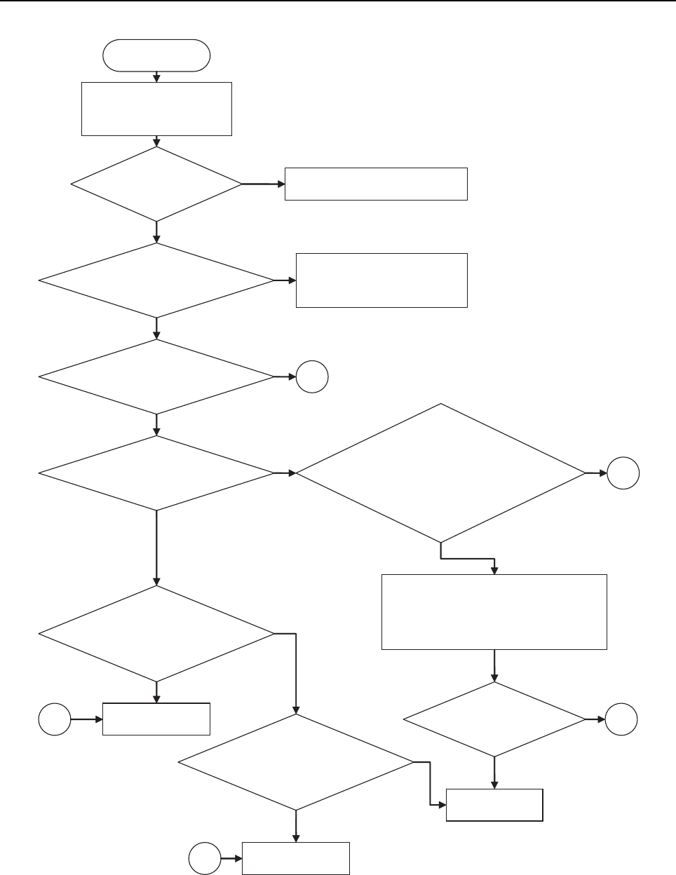
8-42 VHF and UHF1 Troubleshooting Charts
START
Check 2.8V at E002,
2.8V at E004, 1.875V
at E001
,
5V at E003
Are supplies
present? Inspect supply from U3000
16.8MHz signal
from Y001?
Is TP200 at 0.6V –
4.3VDC?
Inspect Y001, R006,
R007, R008, C013, C014,
C015 & C016
Check if U002, Q002,
R013, R014, R016,
C024, C025, C026 &
C027 are OK?
Replace U001
No
Yes
No
Yes
No
Yes
16.8MHz signal at
pin J11 of U001?
Check if L002,
R020, C031, C032
& C033 are OK?
Is RF level at pin
J2 of U001 > -
15dBm?
Check VCO
Check 2.5VDC at pin B4 of U001 in
RX mode, Check 2.5VDC at pin E5
of U001 in TX mode and 2.5VDC
at pin K4 of U001
Are supplies
present?
Replace part
Yes
Yes
Yes
No
No
A
A
B
B
A
No
Yes
No
Yes
No
Troubleshooting Flow Chart for Synthesizer
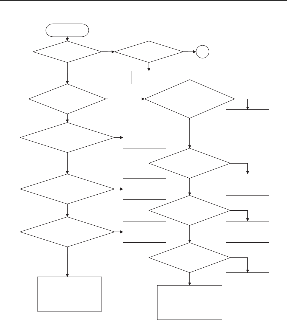
VHF and UHF1 Troubleshooting Charts 8-43
START
TP 200 within
0.6 – 4.3VDC?
2.5VDC at
collector of Q200?
0.6-0.8VDC at
emitter of Q200?
Inspect Q202,
L204 & R202
No
No Yes
No
1.3 -1.5VDC at
base of Q200?
Inspect C212, C213,
C215, C216, C217,
C240, L207, L217,
L218, R220, R221,
R222 & R224
Yes
Yes
Yes
No
No
A
RX LO? No TX Carrier?
Check TX
Yes Yes
No
5VDC at collector
of Q208?
Inspect Q203,
L206 & R218
VDC at base of
Q208?
Inspect R217
& R205
VDC at emitter
of Q208?
Inspect R216
& Q208
Yes
No
No
Yes
Inspect L203,
R200 & R201
Yes
Inspect L205,
R203 & Q200
Inspect L200, L201,
L202, D200, D201,
D202, D203, C201,
C202, C203, C204,
C205, C206 & C207
2.8VDC at Pin
6 of U200?
Yes Inspect R218
& Q203
Troubleshooting Flow Chart for VCO
(Sheet 1 of 2)
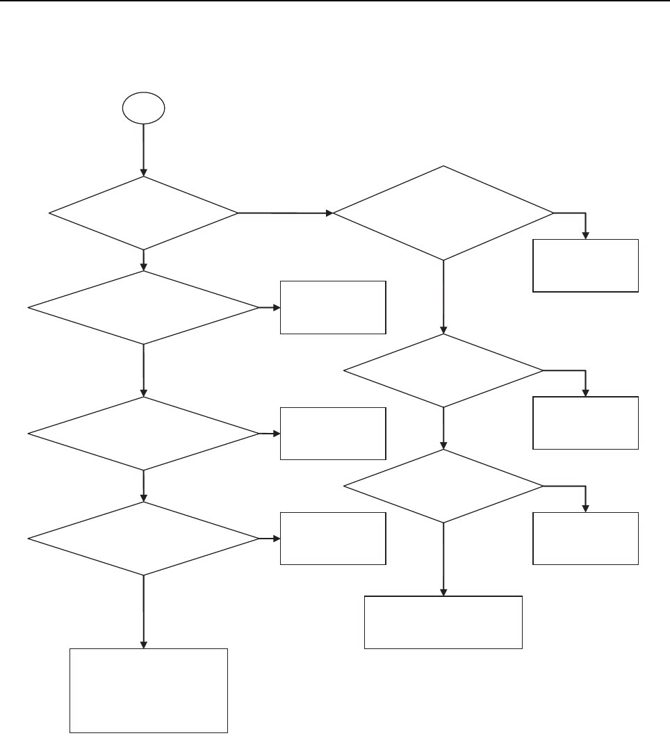
8-44 VHF and UHF1 Troubleshooting Charts
TP 200 within
0.6 – 4.3VDC?
2.5VDC at
collector of Q204?
0.6-0.8VDC at
emitter of Q204?
Inspect Q206,
L212 & R210
No
No Yes
No
1.3 -1.5VDC at
base of Q204?
Inspect C231, C232,
C235, C236, C237 &
L215
Yes
Yes
Yes
No
No
A
Yes
5VDC at collector
of Q205?
Inspect Q207&
L214
VDC at base of
Q205?
Inspect R213
& R212
VDC at emitter
of Q205?
Inspect R214
& Q205
Yes
No
No
Yes
Inspect L211,
R208 & R209
Yes
Inspect L213,
R211 & Q204
Inspect L208, L209,
L210, C220, C221,
C222, C223, C224,
C225, C226, D204,
D205, D206 & D207
Troubleshooting Flow Chart for VCO
(Sheet 2 of 2)
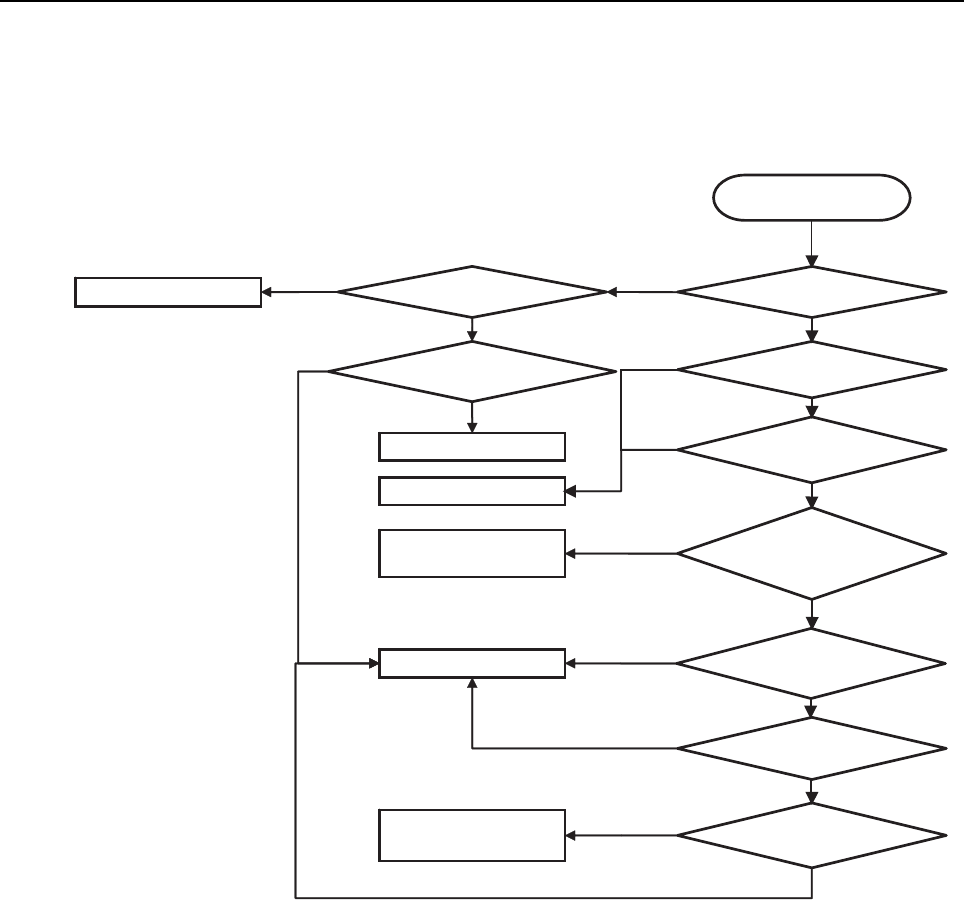
VHF and UHF1 Troubleshooting Charts 8-45
Fail flashing
1. VDDK : C8022 : 1.4 to 1.6V
VDD_BB : C8000 : 2.7 to 3.0V
VCC_IO : C8005 : 2.7 to 3.0V
VCC_RF : C8003 : 2.7 to 3.0V
VDD_RTC : C8031 : 1.4 to 1.6V
No
No
No
No
No
SiRF in internal boot
mode? R8010 toggle
HIGH ~2.775V?
TP_CLK_ACQ :
16.8MHz?
Proper voltage? 1
XTAL_IN (C8020) :
200-1200mV?
XTAL_IN (C8020) :
16.8MHz?
TP_SCLK : 16.8MHz?
Activity on
TP_GPS_TX?
E3700, E3702, E3704 :
3.6V?
No
Inspect U3020
Yes
No
Inspect GPS regulator
Yes
Inspect TCXO, Y001
Yes
No
No
Inspect SiRF IC, U8000
Yes
Yes
Yes
Inspect OMAP, U1000 &
level shifter U1005
Yes
Yes
Configure SiRF IC into
external BOOT MODE
Proper regulator control
voltages?
2
Yes
2. R3704: 1.875V
E8004: 0V
R3700: 2.775V
Troubleshooting Flow Chart for GPS Receiver (Sheet 1 of 3)
8-46 VHF and UHF1 Troubleshooting Charts
2. R3704: 1.875V
E8004: 0V
R3700: 2.775V
1. VDDK : C8022 : 1.4 to 1.6V
VDD_BB : C8000 : 2.7 to 3.0V
VCC_IO : C8005 : 2.7 to 3.0V
VCC_RF : C8003 : 2.7 to 3.0V
VDD_RTC : C8031 : 1.4 to 1.6V
TP_CLK_ACQ :
16.369MHz?
GPS not working.
No data from SiRF IC
Proper voltage?
1
XTAL_IN (C8020) :
200-1200mV?
XTAL_IN (C8020) :
16.8MHz?
Activity on
TP_GPS_RX?
Yes
E3700, E3702, E3704 :
3.6V?
No
Inspect U3020
Yes
No
Inspect GPS regulator
Yes
Inspect TCXO, Y001
Yes
No
No
Inspect SiRF, U8000
Yes
Yes
No
Inspect OMAP, U1000 &
level shifter U 1005
No
SiRF IC flashed?
Proceed to SiRF IC flashing. No
SiRF in external boot
mode? R8010 toggle
LOW, 0V ?
Yes
Configure SiRF IC into external BOOT
MODE & re-run the test No
Proper regulator control
voltages?
Yes
No
2
Yes
Troubleshooting Flow Chart for GPS Receiver (Sheet 2 of 3)
VHF and UHF1 Troubleshooting Charts 8-47
Measure spectrum at R907 = ref
Measure spectrum at
GPS_ANT (C926)
≈ref-1dBm
No
No
No
No
Yes
Yes
Yes
Yes
Yes
Inspect regulator (U3700)
Inspect SiRF IC (U8000)
SiRF_LNA_EN
(R8020)=2.8v?
2.8V_GPS_LNA
(E8006) =2.8v?
No
No
Measure spectrum at
SAW filter1 (C8013)
≈ref-2.8dBm?
Measure spectrum at
LNA (C8017)
≈ref+15.2dBm?
Measure spectrum at SAW
filter2 (C8018)
≈ref+13.4dBm?
Inspect SAW Filter 1(FL8001)
Inspect LNA (U8001)
Inspect SAW Filter 2 (FL8000)
Yes
Data is updated but no
location fix
Yes
Yes
Is R3700 = 2.8v?
XTAL_IN (C8020) within
the phase noise limit?
XTAL_IN (C8020) :
16.8MHz?
Yes
Yes
No
Inspect TCXO, Y001
No
Troubleshooting Flow Chart for GPS Receiver (Sheet 3 of 3)

8-48 VHF and UHF1 Troubleshooting Charts
Notes
Section 9
OPTION BOARD INFORMATION
1.0 Option Board
The option board is an interface board between the main RF board and the keypad and Universal
Connector. The option board interfaces signals on 40-pin connector on the main board with signals on
keypad flex (keypad, side buttons, microphone, backlight control & supply, PTT) and UC flex/
connector of radio side connector (data, USB, accessory device supply, speaker).
The option board also provides test point for each UC signal to allow communication and testing of
radio during production testing. Zener diodes are placed on keypad, side buttons, microphone, PTT,
data, USB, accessory device supply, speaker, lines for protection of radio from electrostatic discharge
(ESD). A transistor is placed here as a switch for backlight LED’s for keypad.
2.0 Board Layout/Schematic for Option Board
Figure 9-1: Option Board Layout
15
1
30 16
J5002
M5001
100
5
Q
TP1
TP2
TP3
TP4
TP5
TP6
TP7
TP8
TP9
TP10
TP11
TP12
VR5000
1
005
R
V
2005RV
3005RV
4005RV
5005
RV
60
05
RV
7
005
R
V
04 12
0
2
110
0
5J
9-2 Board Layout/Schematic for Option Board
Figure 9-2: Option Board Schematic
2.1 Parts List for Option Board
Reference
Symbol
Motorola
Part No. Description
J5002 2887818K04 30 pin board-to-board
connector, connector_p
J5001 2871741C01 40 pin board-to-board
connector, connector_p
Q5001 4815565H01 ROHM IMD14 transistor
VR5001 4813979P10 MMQA5V6T1
VR5002 4813979P10 MMQA5V6T1
VR5005 4813979P10 MMQA5V6T1
VR5006 4813979P10 MMQA5V6T1
VR5007 4813979P10 MMQA5V6T1
VR5003 4815040H01 MM3Z12VT1G
VR5004 4815040H01 MM3Z12VT1G
VR5000 4815040H01 MM3Z12VT1G
M5001 4315275H01 Spacer
GND
To transceiver
OPTA_SEL2
OPTA_SEL1
ONE_WIRE1
KEYPAD_ROW0
NC
GND
MAKO_FSYNC
KEYPAD_COL3
KEYPAD_COL4
BL_EN_FLEX
EXT_MIC+
KEYPAD_ROW3
TO UC PIN 9
EXT_SPKR+
INT_MIC+
KEYPAD_ROW1
KEYPAD_COL2
KEYPAD_COL3
KEYPAD_COL0
KEYPAD_COL1
KEYPAD_COL2
KEYPAD_ROW0
OPTA_SEL2
BL_EN
TO UC PIN 10
KEYPAD_ROW4
KEYPAD_ROW2
VBUS1
KEYPAD_ROW1
TO UC PIN 8
KEYPAD_ROW4
EXT_MIC+
EXT_MIC-
KEYPAD_COL1
PTT
ONE_WIRE1
OPTA_SEL0
GND
KEYPAD_ROW3
OPT_GPIO_2
GND
MAKO_TX
MAKO_RX
GND
OPTA_SEL1
gnitset yrotcaf rof stniop tseT
KEYPAD_ROW2
EXT_SPKR-
PTT
EXT_SPKR-
EXT_SPKR+
GND
VBUS1
KEYPAD_COL0
KEYPAD_COL4
TO UC PIN 5
TO UC PIN 3
TO UC PIN 12
TO UC PIN 4
EXT_MIC-
MAKO_DCLK
TO UC PIN 1
RESET_OUT
To keypad flex 40 PIN CONNECTOR
OPTA_SEL0
USB1_DP
USB1_DM
OPT_SSI_SYNC
INT_MIC-
GND
TO UC PIN 11
TO UC PIN 7
GND
NC
TO UC PIN 2
OPT_GPIO_1
INT_MIC- GND
INT_MIC+
30 PIN CONNECTOR
GND
ROHM
SWB+
Spacer
GND
USB1_DM
USB1_DP
IF_OPT_GPIO_1
IF_MAKO_TX
IF_RESET_OUT
IF_OPT_GPIO_2
IF_MAKO_DCLK
IF_MAKO_RX
J5001-7
2870333D01
J5001-1
J5001-33
J5001-32
J5001-34
4315275H01
M5001
1B
2
B
1C
2C
1E
2E
J5001-6
4815565H01
IMD14
Q5001
IN
J5002-17
J5001-36
TP2
IN
J5001-35
VR5003
MM3Z10VT1G
10.0V
TP3
J5002-22
4815039H01
J5002-21
J5002-20
J5001-3
J5001-4
5
2A
1
1K 3
2
K
OI
4
3
K6
4
K
IN
VR5007
MMQA5V6T1
5.6V
4813979P10
21A
2K
O
I
4
3K 6
4K
TP12
VR5006
MMQA5V6T1
5.6V
4813979P10
21A
5
2A
1
1K 3
J5002-15
IN
TP9
IN
TP11
IN
TP10
TP8
IN
TP6
IN
IF_OPT_SSI_SYNC
J5002-29
IF_MAKO_FSYNC
J5001-40
J5001-39
J5001-21
J5001-38
J5001-19
J5001-20
J5001-17
J5001-18
J5001-37
J5002-14
J5002-8
J5001-31
J5002-7
J5001-29
TP1
IN
4813979P10
21A
5
2A
1
1K 3
2K
OI
4
3K 6
4K
VR5002
MMQA5V6T1
5.6V
J5001-16
J5001-5
J5001-14
J5001-15
J5001-13
4813979P10
21A
5
2A
1
1K 3
2K
OI
4
3K 6
4K
J5001-12
J5002-24
VR5001
MMQA5V6T1
5.6V
J5002-19
J5002-18
J5002-6
J5001-11
J5002-4
J5001-9
J5001-10
J5002-27
J5002-26
J5002-23
J5002-25
J5002-5
J5002-16
J5002-1
2887818K04
J5002-3
TP7
IN
TP5
TPSM2_00X1_50
IN
2K
OI
4
3K 6
4K
4815039H01
VR5000
MM3Z10VT1G
10.0V
VR5005
MMQA5V6T1
5.6V
4813979P10
21A
5
2A
1
1K 3
TP4
IN
J5001-25
J5001-26
J5001-23
J5001-24
J5001-22
J5002-11
J5002-13
J5002-12
J5002-9
VR5004
4815039H01
J5001-8
10.0V
MM3Z10VT1G
J5002-30
J5001-2
J5001-28
J5002-28
J5002-10
J5001-27
J5002-2
IF_SWB+
J5001-30
TT
P
VBUS1
USB1_DM
USB1_DP
2LES_ATPO
0LES_ATPO
0WOR_DAPYEK
1WOR_DAPYEK
1ERIW_ENO
2WOR
_
DAPYEK
4WOR_DAPYEK
0LOC_DAPYEK
3
W
OR
_D
A
PYE
K
1L
OC
_
DA
P
YEK
3LOC_DA
PY
EK
4
LOC_DAP
YEK
2LOC_DA
PY
EK
EXT_SPKR+ EXT_SPKR-
BL_EN
BL_EN_FLEX
EXT_SPKR+
1
SUB
V
VBUS1
1LES_ATPO
OPTA_SEL1
2LES_ATPO
OPTA_SEL2
1ERIW_ENO
ONE_WIRE1
INT_MIC+
+
CI
M
_TNI
INT_MIC-
-
CI
M
_TNI
OPTA_SEL0
0LES_A
TPO
PTT
T
TP
EXT_MIC-
-
CI
M_TXE
EXT_MIC+
+
CI
M_
T
XE
1LES_ATPO
+CIM_TXE
-CIM_TXE
-CIM_TNI
+
C
IM
_
TNI
4WOR_
D
APYEK
KEYPAD_ROW4
NE_LB
+BWS
XELF_NE_LB
SWB+
KEYPAD_COL1
1
LOC_DAPYEK
KEYPAD_COL2
2LOC_DAPYEK
KEYPAD_COL3
3LOC_DAPYEK
KEYPAD_COL0
0LOC_DAPYEK
KEYPAD_COL4
4LOC_DAPYEK
KEYPAD_ROW0
0
WOR_D
A
PYEK
KEYPAD_ROW1
1WO
R_D
APY
EK
KEYPAD_ROW2
2WOR_DAPYEK
KEYPAD_ROW3
3WOR_DAPYEK
-RKPS_TXE
EXT_SPKR-
+RKPS_TXE

Appendix A EMEA Regional Warranty, Service and
Technical Support
1.0 Warranty and Service Support
Motorola offers long term support for its products. This support includes full exchange and/or repair
of the product during the warranty period, and service/ repair or spare parts support out of warranty.
Any "return for exchange" or "return for repair" by an authorized Motorola Dealer must be
accompanied by a Warranty Claim Form. Warranty Claim Forms are obtained by contacting an
Authorized Motorola Dealer.
1.1 Warranty Period and Return Instructions
The terms and conditions of warranty are defined fully in the Motorola Dealer or Distributor or
Reseller contract. These conditions may change from time to time and the following notes are for
guidance purposes only.
In instances where the product is covered under a "return for replacement" or "return for repair"
warranty, a check of the product should be performed prior to shipping the unit back to Motorola.
This is to ensure that the product has been correctly programmed or has not been subjected to
damage outside the terms of the warranty.
Prior to shipping any radio back to the appropriate Motorola warranty depot, please contact
Customer Resources (Please see page A-3). All returns must be accompanied by a Warranty Claim
Form, available from your Customer Services representative. Products should be shipped back in
the original packaging, or correctly packaged to ensure no damage occurs in transit.
1.2 After Warranty Period
After the Warranty period, Motorola continues to support its products in two ways.
1. Motorola's Managed Technical Services (MTS) offers a repair service to both end users and
dealers at competitive prices.
2. MTS supplies individual parts and modules that can be purchased by dealers who are techni-
cally capable of performing fault analysis and repair.
2.0 European Radio Support Centre (ERSC)
The ERSC Customer Information Desk is available through the following service numbers:
Austria: 08 00 29 75 41 Italy: 80 08 77 387
Belgium: 08 00 72 471 Luxemburg: 08 00 23 27
Denmark: 80 88 05 72 Netherlands: 08 00 22 45 13
Finland: 08 00 11 49 910 Norway: 80 01 11 15
France: 08 00 90 30 90 Portugal: 08 00 84 95 70
Germany: 08 00 18 75 240 Spain: 90 09 84 902
Greece: 00 80 04 91 29 020 Sweden: 02 07 94 307

A-2 EMEA Regional Warranty, Service and Technical Support:
UK : 08 00 96 90 95 Switzerland: 08 00 55 30 82
Ireland: 18 00 55 50 21 Iceland: 80 08 147
Or dial the European Repair and Service Centre:
Tel: +49 30 6686 1555
Please use these numbers for repair enquiries only.
3.0 Piece Parts
Some replacement parts, spare parts, and/or product information can be ordered directly.
If a complete Motorola part number is assigned to the part, it is available from Motorola Radio
Products and Solutions Organization (RPSO). If no part number is assigned, the part is not normally
available from Motorola. If the part number is appended with an asterisk, the part is serviceable by
Motorola Depot only. If a parts list is not included, this generally means that no user-serviceable parts
are available for that kit or assembly.
Orders for replacement parts, kits and assemblies should be placed directly on Motorola's local
distribution/dealer organisation or via Motorola Online at: http://emeaonline.motorola.com
* The Radio Products and Solutions Organization (RPSO) was formerly known as the Radio
Products Services Division (RPSD) and/or the Accessories and Aftermarket Division (AAD).
4.0 Technical Support
Motorola Product Services is available to assist the dealer/distributors in resolving any malfunctions
which may be encountered.
North Europe - Stephen Woodrow Central and East Europe - Siggy Punzenberger
Telephone: +44 (0) 1256 488 082 Telephone: +49 (0) 6128 70 2342
Fax: +44 01256 488 080 Fax: +49 (0) 6128 95 1096
Email: CSW066@motorola.com Email: TFG003@email.mot.com
Russia and Belarus - Oleg Machnev Germany - Customer Connect Team
Telephone: +7 495 785 0150 Telephone: +49 (0) 30 6686 1539
Fax: +7 495 785 0185 Fax: +49 (0) 30 6686 1916
Email: CSA002@email.mot.com Email: cgiss.emea@europe.mot.com
Middle East and Africa - Wayne Holmes Italy - Ugo Gentile
Telephone: +27 11 800 7922 Telephone: +39 0 2822 0325
Fax: +27 11 800 7923 Fax: +39 0 2822 0334
Email: radiosupport.za@motorola.com Email: C13864@email.mot.com
France - Armand Roy France - Laurent Irrmann
Telephone: +33 1 6935 7868 Telephone: +33 1 6935 7866
Fax: +33 1 6935 7808 Fax: +33 1 6935 7808
Email: armand.roy@motorola.com Email: laurent.irrmann@motorola.com
5.0 Further Assistance From Motorola
You can also contact the Customer Help Desk through the following web address.
http://www.motorola.com/governmentandenterprise/contactus

Glossary
This glossary contains an alphabetical listing of terms and their definitions that are applicable to
portable and mobile subscriber radio products. All terms do not necessarily apply to all radios, and
some terms are merely generic in nature.
Term Definition
Analog Refers to a continuously variable signal or a circuit or device designed
to handle such signals.
Band Frequencies allowed for a specific purpose.
CPS Customer Programming Software: Software with a graphical user
interface containing the feature set of a radio.
Default A pre-defined set of parameters.
DP Refers to Digital Professional Radio model names in the MOTOTRBO
Professional Digital Two-Way Radio System.
Digital Refers to data that is stored or transmitted as a sequence of discrete
symbols from a finite set; most commonly this means binary data
represented using electronic or electromagnetic signals.
DPL Digital Private-Line: A type of digital communications that utilizes
privacy call, as well as memory channel and busy channel lock out to
enhance communication efficiency.
FCC Federal Communications Commission.
Frequency Number of times a complete electromagnetic-wave cycle occurs in a
fixed unit of time (usually one second).
GPIO General-Purpose Input/Output: Pins whose function is programmable.
GPS Global Positioning System
IC Integrated Circuit: An assembly of interconnected components on a
small semiconductor chip, usually made of silicon. One chip can contain
millions of microscopic components and perform many functions.
IF Intermediate Frequency.
kHz kilohertz: One thousand cycles per second. Used especially as a radio-
frequency unit.
LCD Liquid-Crystal Display: An LCD uses two sheets of polarizing material
with a liquid-crystal solution between them. An electric current passed
through the liquid causes the crystals to align so that light cannot pass
through them.
LED Light Emitting Diode: An electronic device that lights up when electricity
is passed through it.

G-2
MDC Motorola Digital Communications.
MHz Megahertz: One million cycles per second. Used especially as a radio-
frequency unit.
Paging One-way communication that alerts the receiver to retrieve a message.
PC Board Printed Circuit Board. Also referred to as a PCB.
PL Private-Line Tone Squelch: A continuous sub-audible tone that is
transmitted along with the carrier.
Programming Cable A cable that allows the CPS to communicate directly with the radio
using USB.
Receiver Electronic device that amplifies RF signals. A receiver separates the
audio signal from the RF carrier, amplifies it, and converts it back to the
original sound waves.
Repeater Remote transmit/receive facility that re-transmits received signals in
order to improve communications range and coverage (conventional
operation).
RF Radio Frequency: The portion of the electromagnetic spectrum between
audio sound and infrared light (approximately 10 kHz to 10 GHz).
RX Receive.
Signal An electrically transmitted electromagnetic wave.
Spectrum Frequency range within which radiation has specific characteristics.
Squelch Muting of audio circuits when received signal levels fall below a pre-
determined value. With carrier squelch, all channel activity that exceeds
the radio’s preset squelch level can be heard.
TOT Time-out Timer: A timer that limits the length of a transmission.
TPL Tone Private Line
Transceiver Transmitter-receiver. A device that both transmits and receives analog
or digital signals. Also abbreviated as XCVR.
Transmitter Electronic equipment that generates and amplifies an RF carrier signal,
modulates the signal, and then radiates it into space.
TX Transmit.
UHF Ultra-High Frequency.
USB Universal Serial Bus: An external bus standard that supports data
transfer rates of 12 Mbps.
VIP Vehicle Interface Port.
Term Definition