Memorysystemsimulatormanual6 DRAMsim Manual
DRAMsimManual
DRAMsimManual
DRAMsimManual
DRAMsimManual
DRAMsimManual
User Manual:
Open the PDF directly: View PDF ![]() .
.
Page Count: 26
- i. Introduction
- ii. Bus Interface Unit
- iii. System Controller
- Table 1: Summary of DRAM Timing Parameters
- Table 2:
- DRAM User’s Guide: DRAM Related Options
UNIVERSITY OF MARYLAND MEMORY SYSTEM SIMULATOR MANUAL – 1
University of Maryland Memory System Simulator Manual
I.INTRODUCTION
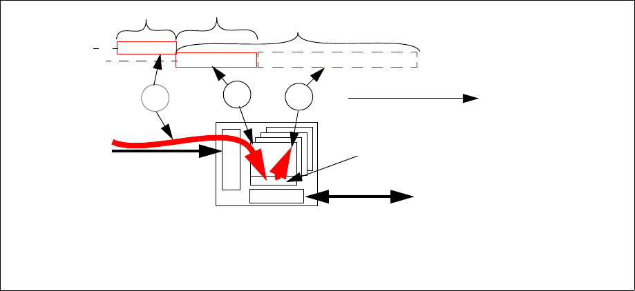
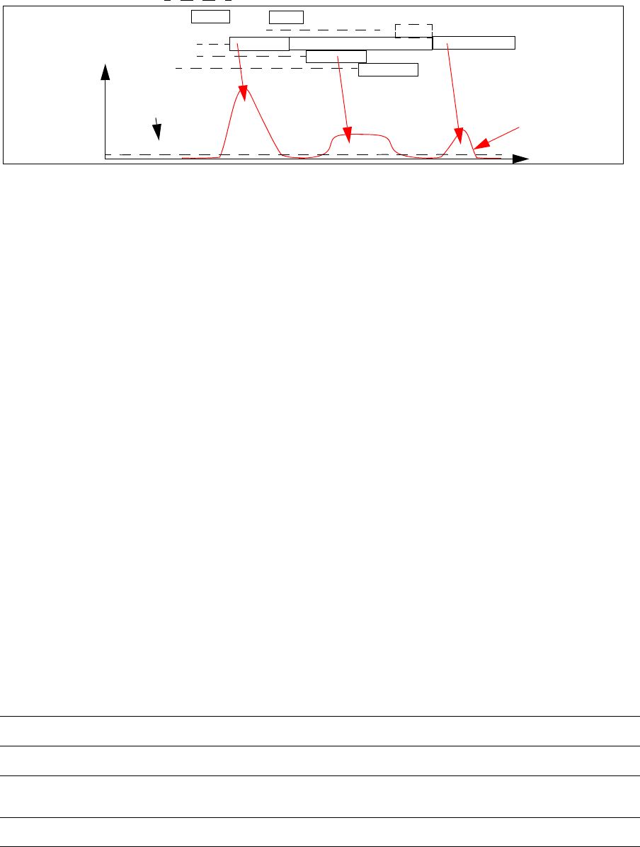
The simulated memory system described in this manual consists of a bus interface unit (BIU), one or more
transaction driven memory controllers, and one or more command driven memory systems. This documentation has
been prepare to familiarize the user to the terminology used in the design of the memory system, and provide a brief
explanation of the basic assumptions of the simulated memory system as well as the simulation framework.
Figure 1 shows the system topology of the simulated processor-memory system. Three distinct and separate
entities that interact in the life of a memory transaction request: are assumed in this framework: processor(s), memory
controller(s), and DRAM memory system(s). Each of these three distinct and separate entities is assumed to be an
independently clocked synchronous state machine that operates in separate clocking domains. In the current
implementation of the simulation framework, there are only two clocking domains: the CPU clock domain and the
DRAM memory system clock domain. {FB-DIMM memory systems excepted} The simulation framework assumes
Fetch Decode WB
Mem
Exec
virtual to physical
address translation
(DTLB access) [A
1
]
[A
2
] L1 D-Cache
access. If miss
then proceed to
[A
3
] L2 Cache
access. If miss
then send to BIU
Bus Interface Unit (BIU)
obtains data from main
memory [A
4
+ B]
[B
1
] BIU arbitrates [B
2
] request
sent to system
controller
[B
8
] system
controller returns
data to CPU
Stages of instruction execution
Proceeding through
the memory hierarchy
in a modern processor
[B
3
]physical addr.
to memory addr.
translation.
[B
4
] memory
L1
cache
L2
cache
DTLB
Processor Core
BIU (Bus Interface Unit)
DRAM System
for ownership of
address bus **
[B
5
] memory
addr. Setup
request
scheduling** (RAS/CAS)
[A
1
]
[B
8
]
[A
4
]
[A
2
][A
3
]
** Steps not required for some processor/system controllers. protocol specific
[B
4
]
[B
3
]
[B
2
]
[B
1
]
I/O to memory traffic memory request
scheduling
physical to
memory addr
mapping [B
7
]
[B
5
]
read
data
buffer
memory controller
processor
DRAM
core
[B
6
]
[B
6
, B
7
] DRAM dev.
obtains data and
returns to controller
Part A: Searching
on-chip for data
Part B: Going
off-chip for data
(CPU clocking
domain)
(DRAM clocking
domain)
Fig. 1: Abstract Illustration of a Load Instruction in a Processor-Memory System
UNIVERSITY OF MARYLAND MEMORY SYSTEM SIMULATOR MANUAL – 2
that the DRAM memory system as well as the memory controller operate in the DRAM memory system clock domain,
and the CPU operates in the CPU clock domain. This assumption holds true for legacy systems with separate memory
controllers, while newer systems where the memory controllers is integrated into the CPU core the assumption may be
reversed. In such a system, the memory controller is assumed to operate in the same clocking domain as the CPU. A
more generalized model would operate the three separate entities as three independent clock domains, then the
frequency of each clock domain may be set separately, and the model may be altered as necessary. However, at this time
we believe that such an implementation would be unnecessarily complex, and decreases simulation speed for minimal
increase in the system simulation model flexibility and accuracy.
II.BUS INTERFACE UNIT
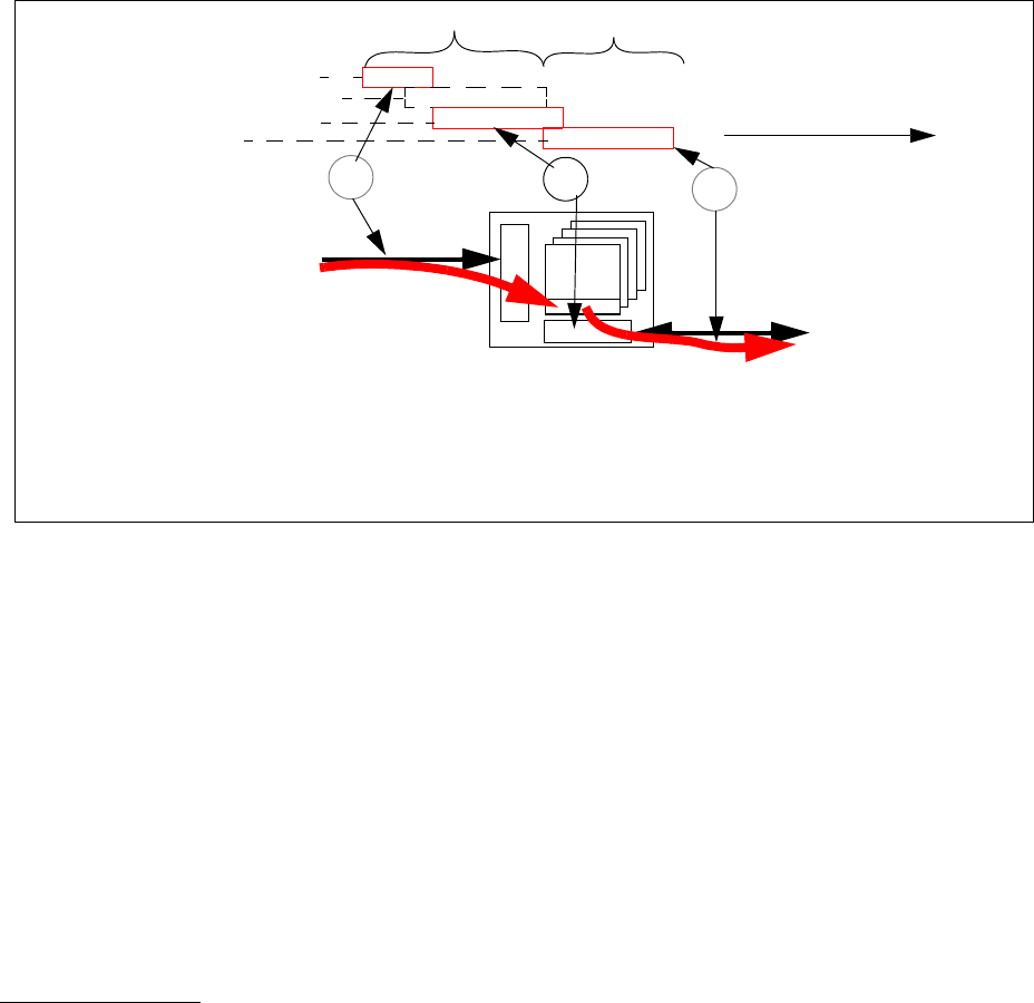
The memory system’s basic assumptions about the processor is illustrated in figure 2. In essence, the memory
system assume an out of order execution core where different portions of the processor can all generate memory
requests. The simulator assume that each request is tagged with a request id (rid), so that when the memory callback
function is invoked, the callback function would be able to uniquely identify the functional unit that had generated the
request and also identify the specific pending operation by the request id. The simulator assumes that each functional
unit can sustain more than one memory transaction miss at a given instance in time, and the memory transaction may be
returned out of order by the memory system. We assume that the life of a memory transaction request begins when a
requesting functional unit generates a DRAM memory request. The requesting unit begins this process by attempting to
place the request into a slot in the bus interface unit (BIU)1. In the simulation framework, the BIU is a data structure
with multiple entires/slots, and the entires/slots in the BIU do not have any assumed ordering. If there is a free slot
available, then the request will be successfully placed into the bus interface unit, and the status MEM_UNKNOWN will
be returned to the requesting functional unit, and the memory system will return the latency of the request at a later time.
If all of the slots have been filled, and no free slot is available, then MEM_RETRY will be returned to the requesting
functional unit, and the functional unit must retry the request at a later time to see if a memory slot has become available
at the later time.
1. The BIU has the functional equiavalence to MSHR’s in this simulator
cpu-fe cpu-exec cpu-commit
BIU: bus interface unit
status rid start_time address access_type
D Read
D Write
I Fetch
Invalid
Va l i d
Valid
Valid
Invalid
Invalid
036
0
-1
-1
-1
-1
14
54 0xXXXX
0xXXXX
0xXXXX
Fig. 2a: Bus Interface of Simulated CPU Fig. 2b: Bus Interface Unit Data Structure
UNIVERSITY OF MARYLAND MEMORY SYSTEM SIMULATOR MANUAL – 3
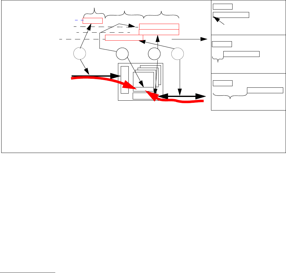
III.SYSTEM CONTROLLER
In figure 3, we show a generalized system controller that supports multiple processors. The simulation of the
system controller begins with the selection of a memory transaction from the BIU to the transaction queue. The
transaction queue then takes the memory transaction and maps the physical address of the transaction to the memory
address in terms of channel ID, rank ID, bank ID, row ID and column ID via an address mapping scheme. Then,
depending on the row-buffer management policy used by the system, a sequence of DRAM commands are generated
for each memory transaction.
The simulated memory system supports multiple memory controllers, each of which can independantly control
a logical channel of memory. Each logical channel may contain multiple physical channels of memory. As an example,
each Alpha EV7 processor contains 2 logical channels of memory, each channel of memory consists of 4 phyiscal
channels of Direct RDRAM. The way to simulate such a system in our simulator is to specify the channel count as “2”,
and the channel width as “8” (unit is in bytes).
A.THE TRANSACTION QUEUE AND THE TRANSACTION ORDERING POLICY
In the memory system simulator, the simulation begins when the system controller goes to the BIU to select a
request for processing. After the appropriate BIU entry(slot) has been selected, the status of the BIU entry is marked as
SCHEDULED, then a memory transaction is created in the memory transaction queue. Unlike the BIU, the memory
transaction queue is nominally implemented as an in-order queue, where DRAM commands of an earlier memory
transaction are given higher priority than DRAM commands from later transactions. The selection of the memory
request from the BIU into the transaction queue is referred to as the transaction ordering policy. Since the transaction
queue is an in-order queue, the transaction ordering policy that selects which request is to be serviced is of great
importance to determine the bandwidth and latency characteristics of DRAM memory systems. In this simulation
framework, four transation ordering policies are supported: First Come First Serve (FCFS), Read or Instruction Fetch
First (RIFF), Bank Round Robin (BRR), and Command Pair Rank Hopping (CPRH).
cpu 3cpu 0 cpu 1 cpu 2
system controller/
(northbridge)
memory controller
transaction queue
Command
Sequence DRAM System
Memory
Controller
Memory
Controller
Memory
Controller
Memory
Controller
DRAM System
DRAM System
DRAM System
Fig. 3: Transaction Queue and Memory Controller(s) System Architecture
BIU
UNIVERSITY OF MARYLAND MEMORY SYSTEM SIMULATOR MANUAL – 4
B.ROW BUFFER MANAGEMENT POLICY
Modern memory controllers typically deploy one of two policies to manage operations of the sense amplifiers.
Since a DRAM access is essentially a two step process, in cases where the memory access sequence has a high degree of
spatial locality, it would be favorable to direct the memory access sequences to the same row of memory. The Open
Page row buffer management policy is designed to favor memory accesses to the same row of memory by keeping
sense amplifiers open and holding an entire row of data for ready access. In contrast, the Close Page row buffer
management policy is designed to favor random accesses to different rows of memory. Different row buffer
management policies exist, including dynamic row buffer management policies that use timers to keep pages open for a
limited period of time before closing. However, dynamic row buffer management policies and other alternative row
buffer management policies are typically derivatives of either the close page or open page policies. For the sake of
simplicity, the discussion and examination in this text is limited to the open page and closed page policies.
In the Open Page row buffer management policy, the primary assumption is that once a row of data is brought to
the array of sense amplifiers, different parts of the same row may be accessed again in the near future. Under this
assumption, after a column access is performed, the sense amplifiers are kept active and the entire row of data is
buffered to await another memory access to the same row. In the case another access is made to the same row, that
memory access could occur with the minimal latency of tCAS, since the row is already active in the sense amplifiers.
However, in the case that the access is to a different row of the same bank, the memory controller would have to first
precharge the DRAM array, perform another row access, then perform the column access. The minimal latency to
access data in this case is tRP + tRCD + tCAS.
In the Close Page row buffer management policy, the primary assumption is that there is limited spatial locality in
the memory access pattern, and as soon as a data has been obtained via a column access, the DRAM array and sense
amplifiers are precharged in preparation for another memory access to a different row of memory.
C.ADDRESS MAPPING
In a memory system, before data can be read from or written to a memory location, the physical address given
by the CPU has to be translated into memory addresses in the form of channel ID, rank ID, bank ID, row ID, and column
ID. In a memory system that implements the open page row buffer management policy, the role of the address mapping
scheme is to optimize the temporal and spatial locality of the address request stream and direct memory accesses to an
open DRAM row (bank) and minimize DRAM bank conflicts. However, in a memory system that implements the close-
page row-buffer management policy, the goal of the address mapping scheme is to minimize temporal and spatial
locality to any given bank and instead distribute memory accesses throughout different banks in the memory system. In
this manner, the DRAM memory system can avoid memory accesses to the same bank of memory and instead focus on
transaction and DRAM command ordering algorithms that rotates through all available DRAM banks to achieve
maximum DRAM bandwidth.
Address mapping scheme depends not only on the row buffer management policy, but also the configuration of
the DRAM memory system as well as the expandability/non-expandability of the memory system. For example,
UNIVERSITY OF MARYLAND MEMORY SYSTEM SIMULATOR MANUAL – 5
depending on design, the channel ID or rank ID can be mapped to the low order address bit to obtain the most bank
parallelism, but in memory systems that allow end users to flexibly configure the memory system by adding more ranks
or changing channel configurations, the channel ID and rank ID’s are typically mapped to the high order address bits.
.Figure 4 demonstrates the device configuration of a specific 256 Mbit SDRAM device. Figure 4 shows that a
256 Mbit SDRAM device may be shipped in one of three different configurations: 64 Mbit x 4, 32 Mbit x 8, and 16
Mbit x 16. Basically, the same 256 Mbit device could contain 64 million uniquely addressable locations with each
location being 4 bit wide, 32 million uniquely addressable 8 bit wide locations, or 16 million uniquely addressable 16 bit
wide locations. However, many modern memory systems use 64 bit wide data busses, so in this case, multiple DRAM
devices are then combined to form the 64 bit wide data bus. The effect of these different configurations is that there are
different numbers of columns per “DRAM page” for each configuration.
Due to the variable sizes and configuration of the memory devices used in memory systems, address mapping
differs with each configuration. One difficulty related to the precise definition of an address mapping scheme is that in a
memory system with differently configured memory modules, the mapping scheme must differ from module to module.
In figure 5, one memory address mapping scheme with 256 Mbit SDRAM devices and uniform configuration of the
memory system is assumed. In this figure there are 4 ranks of memory modules, each module formed from 16 bit wide
256 Mbit SDRAM devices. In this configuration, the 16 bit wide Mbit devices use 9 bits for column addressing, 2 bits to
Device config 64 Meg x 4 32 Meg x 8 16 Meg x 16
Configuration 16 M x 4 x 4 bks 8 M x 8 x 4 bks 4 M x 16 x 4 bks
row addressing 8K (A0 - A12) 8K (A0 - A12) 8K (A0 - A12)
bank addressing 4 (BA0, BA1) 4 (BA0, BA1) 4 (BA0, BA1)
col addressing 2K(A0-A9,A11) 1K (A0-A9) 512 (A0- A8)
8 of the x8 devices
form 64 bit wide
data bus
4 of the x16 devices
form 64 bit wide
data bus
“DRAM page size” differs with different configurations.
Fig. 4: Different Configurations of a 256 Mbit DRAM device
Device config 16 Meg x 16
Configuration 4 M x 16 x 4 bks
row addressing 8K (A0 - A12)
bank addressing 4 (BA0, BA1)
col addressing 512 (A0- A8)
0
2
3
11
12
13
14
26
28 27
29
31
32 bit physical address (byte addressable)
no
memory
rank
ID
bank
ID
column
ID
row
ID
not
used
Fig. 5: Open Page Address Mapping Scheme of a 512 MB system with 256 Mbit DRAM devices

UNIVERSITY OF MARYLAND MEMORY SYSTEM SIMULATOR MANUAL – 6
address 4 different banks, 13 bits to address 8192 rows, and 2 bits to address 4 ranks of memory. Altogether, 29 bits of
physical address is used here to address 512 Megabyte of memory. The address mapping policy illustrated in figure 5 is
optimized for an open page memory system, since the column ID’s are mapped to the lowest order bits, and multiple
accesses to the same array of memory would most likely be mapped to different columns within the saw row and same
bank of DRAM devices. Alternative memory address mapping schemes may achieve a higher degrees of performance
depending on the configuration and row buffer management policy. Finally, the memory addressing scheme presented in
figure 5 is specified for a single channel of memory. Multi-channel memory require an address mapping policy that can
adequately distribute the memory accesses to different channels.
D.BASIC TIMING PARAMETERS
In any DRAM memory-access protocol, a set of timing parameters is used to characterize various command
durations and latencies. Although the exacting desciption of a full and complete protocol requires the use of tens of
different timing parameters, a generic protocol can be well described with a subset of the timing parameters. The timing
parameters used in the simulation framework are summarized in table 1
Parameter Description Illust.
tBurst
Data Burst duration. Time period that data burst occupies on the data bus. Typically 4 or 8 beats of
data. In DDR SDRAM, 4 beats of data occupies 2 full cycles. Also known as tBL.figure 7
tCAS
Column Access Strobe latency. Time interval between column access command and data return by
DRAM device(s). Also known as tCL.figure 7
tCMD
Command transport duration. Time period that a command occupies on the command bus as it is
transported from the DRAM controller to the DRAM devices. figure 6
tCWD
Column Write Delay. Time interval between issuance of column write command and placement of
data on data bus by the DRAM controller. figure 7
tDQS
Data Strobe turnaround. Used in DDR and DDR2 SDRAM memory systems. Not used in SDRAM
or Direct RDRAM memory systems. 1 full cycle in DDR SDRAM systems. figure 12
tFAW
Four bank Activation Window. A rolling time frame in which a maximum of four bank activation
may be engaged. Limits peak current profile. figure 16
tRAS
Row Access Strobe. Time interval between row access command and data restoration in DRAM
array. After tRAS, DRAM bank could be precharged. figure 6
tRC
Row Cycle. Time interval between accesses to different rows in same bank
tRC = tRAS + tRP
figure 7
tRCD
Row to Column command Delay. Time interval between row access command and data ready at
sense amplifiers. figure 6
tRFC Refresh Cycle. Time between refresh commands or refresh command and row activation. figure 10
tRRD
Row activation to Row activation Delay. Minimum time interval between two row activation
commands to same DRAM device. Limits peak current profile. figure 15
tRP
Row Precharge. Time interval that it takes for a DRAM array to be precharged and readied for
another row access. figure 9
tWR
Write Recovery time. Minimum time interval between end of write data burst and the start of a
precharge command. Allows sense amplifiers to restore data to cells figure 8
Table 1: Summary of DRAM Timing Parameters
UNIVERSITY OF MARYLAND MEMORY SYSTEM SIMULATOR MANUAL – 7
E.BASIC DRAM COMMANDS
In this section, five basic DRAM commands are described: row access command, column read command, column
write command, precharge command, and the refresh command. The descriptions of the basic commands form the
foundation of accurate and flexible simulation of DRAM memory systems.
ROW ACCESS COMMAND
In DRAM memory systems, data must be retrieved from DRAM cells and resolved into digital values by an array
of sense amplifiers before it can be accessed by the DRAM controller. The array of sense amplifiers is also known as the
row buffer because a row access command moves an entire row of data from the DRAM cells into the array of sense
amplifiers. DRAM memory systems accomplish this movement of data by issuing a row access command, also known
as a row activation command. Figure 6 illustrates the progression of a generic row access command. A row access
command only moves data internally within a given bank, and it does not make use of I/O gating resources, nor does it
make use of the data bus to move data between the DRAM controller and DRAM devices.
Two timing parameters are associated with the row access command: tRCD and tRAS. One timing parameter
associated with the row access command is the row column delay, labelled as tRCD in figure 6. The row column delay
measures the time it takes for the row access command to move data from the DRAM cell arrays to the sense amplifiers.
After tRCD, the sense amplifiers has completed the task of resolving the electronic charges stored in DRAM cells into
digital values. At this point, one or more column access commands could retrieve data from the sense amplifiers and
move it through the data bus to the memory controller or store data from the memory controller into the sense
amplifiers. However, the act of reading data discharges the DRAM storage cells and the data needs to be restored from
the sense amplifiers back into the DRAM storage cells. The row access strobe latency, tRAS, describes the time duration
between activation of a row and restoration of data into DRAM cell arrays. Essentially, a precharge command to prepare
the sense amplifiers for another row access command cannot be issued until minimally tRAS after the previous row
access command.
Fig. 6: Row Access Command Illustrated
1
data sense
3
Generic DRAM device
(one rank)
address and
command bus
decode
data bus
sense amplifiers
tRAS
data restored to DRAM cells
tRCD
cmd & addr bus
bank “i” utilization
rank “m” utilization
data bus 2
addr & cmd
row access
time
tCMD
To issue a RAS Command
1. Command Bus must be available @NOW
2. Bank must be Idle or a “set idle” event @ NOW + tCMD
RAS-command event-sequence
1. Command Transport: Use Cmd bus for tCMD cycles
2. Activation: for tRCD cycles
3. Restore: Row is accessible for tRAS - tRCD cycles.
4. Active: Row active until precharge command.
UNIVERSITY OF MARYLAND MEMORY SYSTEM SIMULATOR MANUAL – 8
COLUMN READ COMMAND
In DRAM memory systems, once data has been moved into the array of sense amplifiers, it can then be accessed by
the DRAM controller through one or more column read commands or column write commands. The purpose of a
column read command is to move a subset of the row of data from the array of sense amplifiers through the shared data
bus back to the memory controller. There are two timing parameters associated with a column read command, tCAS and
tBurst. The time it takes for the column read command to be issued and for the DRAM device to place the requested data
onto the data bus is known as the column access strobe1 latency, tCAS2. After tCAS, the requested data is moved onto the
data bus then into the memory controller. Modern DRAM memory systems move data in relatively short bursts, usually
occupying 4 or 8 beats on the data bus. The duration of the data burst is simply tBurst3. Figure 7 illustrates the
progression of a column read command and shows that the column read command goes through three basic phases. In
phase one, the command is transported on the address and command busses then latched and decoded by the DRAM
devices. In phase two, the appropriate columns of data is retrieved from the sense amplifier array of the selected bank
and moved through the I/O gating structures and readied for transport across the data bus. In phase three, the data flows
through the I/O gating and out to the data bus, occupying the data bus for the time duration of tBurst. One basic
assumption of the column read command illustrated in figure 7 is that before the I/O gating phase of the command can
proceed, the accessed DRAM bank must be open to the selected row, labelled as row x in figure 7. That is, tRCD time
must have passed since the row access command was issued to the selected row x before the column read command can
be issued.
1. The column access strobe signal also no longer exists in modern DRAM systems, but the terminology remains.
2. Sometimes referred to as tCL, or Cas Latency.
3. Sometimes referred to as tBL.
Fig. 7: Column Read Command
12
Generic DRAM device (one rank)
address and
command bus
decode
data bus
3
tBurst
tCAS
cmd & addr bus
bank “i” utilization
rank “m” utilization
data bus
row x open
data burst
I/O gating
addr & cmd
cmd
time
To issue a CAS Read Command
1. Command Bus must be available @NOW
2. Bank must be Restore or Active @ NOW + tCMD
3. Data Bus must be free @ NOW + tCAS
CAS Read-command event-sequence
1. Command Transport: Use Cmd bus for tCMD cycles
2. CAS latency : for tCAS - tCMD cycles
3. Burst: Move data for tBurst cycles.
UNIVERSITY OF MARYLAND MEMORY SYSTEM SIMULATOR MANUAL – 9
COLUMN WRITE COMMAND
In DRAM memory systems, once a row of data has been moved to the sense amplifiers, write commands can be
issued to overwrite data in the array of sense amplifiers. The array of sense amplifiers then seamlessly restores the new
data values back into the DRAM cells1. From the perspective of the memory access protocol, the column write
command goes through a similar same set of operations as the column read command. However, the primary difference
between a column read command and a column write command is that the direction of data movement is opposite to
each other, and the column write command has one additional phase that accounts for the time that the column write
command overwrites data from the sense amplifiers into the DRAM cells. Moreover, unlike the timing of the column
read command, the timing of the command transport phase with respect to the data transport phase in a column write
command is defined differently for different DRAM memory systems. Figure 8 illustrates the progression of a column
write command through four phases. In figure 8, phase one shows that the column address and column write command
is placed on the address and command bus. In phase two, the data is placed on the data bus by the memory controller. In
phase three the data flows through the I/O gating structures to the array of sense amplifiers. Finally, in phase four, the
sense amplifiers in the selected bank overwrites data in the DRAM cells with the newly received data.
One timing parameters associated with a column write command is tCWD, column write delay2. Column write delay
defines the time it takes for the column write command to be issued and data placed onto the data bus by the DRAM
controller. Figure 8 shows that in SDRAM memory system, the command, address and data is placed on the respective
busses in the same cycle. In this manner, tCWD is zero cycles in duration. In DDR SDRAM memory system, data for the
write command is placed on the data bus one full cycle after the command and address is placed on the command and
1. Some DRAM devices with write buffers operate in a slightly different manner. The analysis here assumes no write buffer.
2. Sometimes referred to as command write delay.
Fig. 8: Column Write Command in SDRAM, DDR SDRAM and DDR2 SDRAM
4
13
Generic DRAM device (one rank)
address and
command bus
decode
data bus
2
tBurst
tCWD
cmd & addr bus
bank “i” utilization
rank “m” utilization
data bus
data restore
data burst
I/O gating
addr & cmd
cmd
data burst
cmd SDRAM
data burst
cmd DDR SDRAM
tCWD = 1
tCWD = 0
data burst
cmd DDR2 SDRAM
tCWD = tCAS - 1
time
tWR
CAS Write-command event-sequence
1. Command Transport: Use Cmd bus for tCMD cycles
2. CWD latency: for tCWD cycles
3. Burst: Move data for tBurst cycles.
To issue a CAS Write Command
1. Command Bus must be available @NOW
2. Bank must be Restore or Active @ NOW + tCWD
3. Data Bus must be free @ NOW + tCWD
4. Write Recovery: Tie up entire rank for tWR cycles.
(Assuming no Write buffers or Write caches)
UNIVERSITY OF MARYLAND MEMORY SYSTEM SIMULATOR MANUAL – 10
address busses, so tCWD is defined as one full cycle. Finally, in DDR2 SDRAM memory system, the write delay is one
full cycle less than tCAS. The definition of write delay to match the read latency simplifies DRAM command scheduling
in a DDR2 SDRAM memory system1.
Figure 8 also illustrates tWR, the write recovery time. The write recovery time denotes the time between the end of
the data burst and the completion of the movement of data into the DRAM arrays. The movement of data into the
DRAM arrays in this time period means that in case of a bank conflict with the next DRAM request, the precharge
command to prepare the array of sense amplifiers for another row access cannot begin until the write recovery time for
the current write command has been satisfied.
PRECHARGE COMMAND
DRAM device data access is a two step process. A row access command moves an entire row of data from the
DRAM cells to the array of sense amplifiers. The data remains in the array of sense amplifiers for one or more column
access commands to move data to and from the DRAM devices to the DRAM controller. In this framework, a precharge
command completes the sequence as it resets the array of sense amplifiers and the bitlines to a preset voltage, and
prepares the sense amplifiers for another row access command. Figure 9 illustrates the progression of a precharge
command. Figure 9 shows that in the first phase, the precharge command is sent to the DRAM device, and in phase two,
the array of sense amplifiers in the selected bank is precharged to the preset voltage.
1. One more difference between a read command and a write command is that the data are offset in different clock phases in
SDRAM, DDR SDRAM and DDR2 SDRAM memory systems. However, the difference in clock phases may be masked by the
use of the tDQS timing parameter to illustrate the overhead in data bus turn around time. One issue that result from this
difference is that column write delay defined as equal to column access latency provides no benefit to the scheduling
algorithms, because the overhead of tDQS would have to be inserted in the protocol to denote the data bus turnaround time. As a
result, the difference in the relative clock phases of read and write data bursts may be abstracted out, and it has no impact in the
description of the abstract DRAM access protocol.
Fig. 9: Row Precharge Command Illustrated
12
Generic DRAM device (one rank)
address and
command bus
decode
data bus
sense amplifiers
tRC
tRP
tRAS
Row access to same bank
(previous command)
cmd & addr bus
bank “i” utilization
rank “m” utilization
data bus
bank precharge
prec
time
PREC-command event-sequence
1. Command Transport: Use Cmd bus for tCMD cycles
2. Precharge: for tRP cycles
3. Upon completion: Bank status set to idle.
To issue a PREC Command
1. Command Bus must be available @NOW
2. Bank must be Active @ NOW + tCMD
UNIVERSITY OF MARYLAND MEMORY SYSTEM SIMULATOR MANUAL – 11
The timing parameter associated with the precharge command is the row precharge duration, tRP
. The row
precharge duration describes the length of time the DRAM devices utilizes to precharge the bitlines and the sense
amplifiers. Figure 9 shows that a precharge command cannot be issued to the DRAM device until minimally tRAS time
period after the previous row access command to the same bank. Collectively, the sum of tRAS and tRP forms tRC, the
row cycle time. The row cycle time of a given DRAM device measures the speed at which a DRAM device could bring
data from the DRAM cell arrays into the sense amplifiers, restore the data values back into the DRAM cells, then
precharge the bitlines and sense amplifiers back to the reference voltage level and made ready for another row access
command. The row cycle time is the fundamental limitation to the speed at which data may be retrieved from different
rows of a given DRAM bank.
REFRESH COMMAND AND TIMING
In DRAM devices, data is stored in the form of electrical charges in DRAM cells. The DRAM cells are composed
of a storage capacitor and an access transistor. With the passage of time, the electrical charges stored in the capacitor
gradually leaks through the access transistor. A low level of charge leakage is acceptable as long as the remaining
electrical charge will still resolve to the correct digital values. However, without intervention, electrical charge leakage
eventually leads to a state where the stored digital values can no longer be correctly resolved by the sense amplifiers. As
a result, data held in DRAM cells must to be periodically read out to the sense amplifiers and restored with full electrical
charge levels back into DRAM cells. As long as DRAM cells are periodically refreshed before the levels of electrical
charges deteriorate to indistinguishable values, DRAM refresh cycles can be used to overcome leaky DRAM cells and
ensure data integrity. The drawback to any refresh mechanism is that refresh commands constitute an overhead in terms
of utilizable bandwidth and additional power consumption by DRAM devices.
There are multitudes of DRAM refresh strategies designed to minimize peak power consumption or maximize
available device bandwidth. Figure 10 illustrates a basic refresh command that allows the DRAM controller to send a
Fig. 10: Refresh Command Illustrated
Generic DRAM device (one rank)
address and
command bus
decode
data bus
sense amplifiers
12
tRC
tRP
tRAS
Row access to all banks all banks precharge
refresh
time
cmd & addr bus
all bank utilization
REFRESH-command event-sequence
1. Command Transport: Use Cmd bus for tCMD cycles
2. Activation: for tRCD cycles
3. Restore: Row is accessible for tRAS - tRCD cycles.
4. Active: Row active until precharge command.
To issue a REFRESH Command
1. Command Bus must be available @NOW
2. Bank must be Idle @ NOW + tCMD
tRFC
additional time
needed by
DRAM device
to recover from
current spike
(all bank refresh)
UNIVERSITY OF MARYLAND MEMORY SYSTEM SIMULATOR MANUAL – 12
single refresh command to a DRAM device, and the device takes the address of the row to be refreshed from an internal
register, sends the same row address to all banks in the device concurrently, each bank then brings a row of data into the
sense amplifiers, resolves the stored electrical charges to full voltage levels, restores the data back into DRAM cells, and
precharges the DRAM array to ready it for another row access. This single, basic refresh command to all banks takes
one row refresh cycle time, tRFC, to complete. The reason that tRFC is longer than tRC is due to the fact that the bank-
concurent refresh command draws a lot of current, and it takes longer than tRC for the DRAM device to recover from the
current spike. In many modern DRAM memory systems, the memory controller would inject one row refresh command
per row in a bank every 32 or 64 milliseconds. Depending on the design and refresh policy, refresh commands could be
issued consecutively or opportunistically, one at a time.
F. DRAM COMMAND SCHEDULING IN MULTI-RANK SYSTEM
Figure 11, illustrates the topology of a DDRx SDRAM memory system. DDrx SDRAM memory systems use
source synchronous data reference strobe signals to ensure proper timing on the data bus. However, the use of the source
synchronous data strobe signal creates problems in scheduling column access commands between different rank in
DDRx SDRAM memory systems.
Rank 1 Rank 2 Rank 3
DDR
Data Bus
Addr & Cmd
Chip (DIMM) Select
DQS (Data Strobe)
similar topology
as SDRAM
SDRAM
Controller
DRAM
Chips
Fig. 11: DDRx SDRAM Memory System Topology
UNIVERSITY OF MARYLAND MEMORY SYSTEM SIMULATOR MANUAL – 13
Figure 12 illustrates the timing and command sequence of two consecutive read commands to different ranks of
DRAM devices in a memory system that uses a data strobe to synchronize timing on the data bus. In figure 12, the rank
switching penalty is labelled as tDQS, the read-write data strobe re-synchronization time. For relatively low frequency
SDRAM memory system, data synchronization strobes are not used and tDQS is zero. For Direct RDRAM memory
system, the use of the topology matched source synchronous clocking scheme obviates the need separate strobe signals,
and tDQS is also zero. However, for DDRx SDRAM memory systems, the use of the data strobe signal means that the
tDQS data strobe re-synchronization penalty for read bursts between different ranks requires at least one full clock cycle.
G.SCHEDULING FOR SERIAL MEMORY PROTOCOLS
The new DRAM standard is the Fully Buffered-DIMM. The specifications are currently being hammered out by
the DRAM standards committee - JEDEC. Based on initial presentations made at Intel Developer Forum and MemCon
we built a picture of the protocol. The simulator supports this model for the FB-DIMM.
In the recent years, memory system designers have moved towards wider and faster buses with lower supportable
DIMM capacity. Due to this limitation of high-speed multi-drop buses, the proposal is to replace the wide bus with a
serial interface and to add onto the existing DIMM a logic block known as the Advanced Memory Buffer (AMB). The
memory controller sends its requests via the high-speed serial link to the AMB. This buffer performs the necessary
serial-parallel conversion of the bundles to standard DRAM commands/data and passes this onto the DRAM via a
standard DRAM interface. The protocol replaces the bi-directional link with two uni-directional links - one to the
DIMMs ( southbound link) and the other back to memory contorller (northbound link). All serial links are point-to-point
i.e. data is sent to an AMB, which forwards to the next AMB and so on.
The transmission time for a bundle/frame on the northbound link is the same as the southbound link. The base
configuration has a 14 bit-wide northbound link and a 10 bit-wide southbound link. The bundles on the northbound link
are larger and communicate only data. Bundles on the southbound link are smaller and are a combination of command
and data. A southbound frame can comprise of either 3 commands, 1 command-2 data slots or 3 data slots. Each slot is
equivalent to roughly 24 bits of information. Additional parameters required are specified in the table.
Fig. 12: Consecutive Read Command to Different Ranks
tBurst
tCAS
cmd&addr
rank “n” utilization
data bus data burst
tDQS
bank j open
data burst
I/O gating
sync
read 0 read 1
tBurst
addr & cmd
decode
data bus
decode
Rank n Rank m
tBurst + tDQS
time
bank “i” of rank “m”
rank “m” utilization
bank i open
I/O gating
n != m
bank “j” of rank “n”
UNIVERSITY OF MARYLAND MEMORY SYSTEM SIMULATOR MANUAL – 14
H.ADDITIONAL CONSTRAINTS: POWER
Numerous constraints exist in modern DRAM memory systems that limits bandwidth utilization of the DRAM
device. One such constraint is related to the power consumption of DRAM devices. With continuing emphasis placed on
memory system performance, DRAM manufacturers are expected to push for ever higher data transfer rates in each
successive generation of DRAM devices. However, just as increasing operating frequencies lead to higher activity rates
and higher power consumption in modern processors, increasing data rates for DRAM devices also increase the
potential for higher activity rates and higher power consumptions on DRAM devices. One solution deployed to limited
the power consumption of DRAM devices is to constrain the activity rate of DRAM devices. However, constraints on
the activity rate of DRAM devices in turn limit the capability of DRAM devices to move data, and further limits the
performance capability of DRAM memory systems.
Memory Controller
Northbound Link
Southbound Link
Figure 13: Simplified representation of a FB-DIMM system. The FB-DIMM system depicted above has two channels which are only three-deep . A fully
populated system is expected to go upto 6 channels each 8 deep.
Parameter Description
tBUNDLE Transmission time for a single frame/bundle.
tBUS
Additional latency to account for delays due to bus propagation time and AMB
receive-send overheads.
tAMB_UP
Time required for AMB to perform serial-parallel conversion of packet
information and then activate the DRAM.
tAMB_DOWN
Overhead associated with converting the parallel data bursts received from the
DRAM to its bundle format.
UNIVERSITY OF MARYLAND MEMORY SYSTEM SIMULATOR MANUAL – 15
In modern DRAM devices, each time a row is activated, thousands of bits are discharged, sensed, then recharged in
parallel. As a result, the row activation command is a relatively energy intensive operation. Figure 14 shows the current
profile of a DRAM read cycle. Figure 14 shows that an active DRAM device draws a relatively constant current level.
The DRAM device then draws additional current for each activity on the DRAM device. The total current draw of the
DRAM device is simply the summation of the quiescent current draw and the current draw of each activity on the
DRAM device.
I.POWER MODEL
The dram simulator is incorporated with a power model for DDR and DDR2 SDRAM. Basically, to calculate the
power is to calculate the average power in one activation-to-activation cycle. That is we calculate the power in each
DRAM state and then multiply it with the fraction of time the device spends in each state in one activation-to-activation
cycle. For simplicity, we consider the power model for DDR SDRAM first, and then make some extensions to cover the
DDR2 case. The power consumption in DDR SDRAM is calculated as follows:
There are parameters extracted from an DDR SDRAM data sheet involved in the calculation. Table 2 shows the IDD
values from a 128Mb DDR SDRAM data sheet and the description of each value. In order to calculate the power, two
states are defined.When data is stored in any of the sense amplifiers, the DRAM is said to be in the “active state”. And
after all banks of the DDR SDRAM has been restored to the memory array, it is said to be in the “precharge state”.
Adddionally, CKE, the device clock enable signal, is considered. In order to send commands, read ,or write data to the
DDR SDRAM, CKE must be HIGH.. If CKE is LOW, the DDR SDRAM clock and input buffers are turned off, and the
device is in the power-down mode.
Parameter/Condition Symbol -75/-75Z -8 Units
OPERATING CURRENT: One bank; Active Precharge; tRC = tRC MIN; tCK = tCK MIN IDD0 105 100 mA
PRECHARGE POWER-DOWN STANDBY CURRENT: All banks idle; Power-down mode; tCK = tCK
MIN; CKE = LOW IDD2P 3 3 mA
IDLE STANDBY CURRENT: CS_ = HIGH; All banks idle; tCK = tCK MIN; CKE = HIGH IDD2F 45 35 mA
Tabl e 2: a
Fig. 14: Current Profile of a DRAM Read Cycle
cmd&addr
bank “i” util.
rank “m” util.
data bus
row x open - data restore
data burst
I/O gating
bank i precharge
read 0
prec
time
row act
data sense
rank “m” internal cmd
current draw in
abstract units
Quiescent
current draw
of active device current draw
profile due to
device activity

UNIVERSITY OF MARYLAND MEMORY SYSTEM SIMULATOR MANUAL – 16
From the definition of active/precharge states and CKE above, a DRAM device can be in four states:
1. Precharge Power-down Power:
2. Precharge Standby Power:
3. Active Power-down Power:
4. Active Standby Power:
where IDD values are defined in the data sheet and VDD is the maximum voltage supply of the device.
BNKpre is the fraction of time the DRAM device is in precharge state (all banks of the DRAM are in precharge
state) compared with the actual activation-to-activation cycle time.
CKEloPRE is the fraction of time the DRAM stays in precharge state and CKE is low compared with the time it
stays in precharge state.
CKEloACT is the fraction of time the DRAM stays in active state and CKE is low compared with the time it stays
in active state.
In addition, when the DRAM device is in Active Standby state, commands can be sent to the device. Therefore, we
have 4 more states in the Active Standby state.
1. Activate Power:
2. Write Power:
3. Read Power:
4. Termination Power:
where
tRC is the shortest activation-to-activation cycle time as specified in the data sheet.
tACT is the actual activation-to-activation cycle time in the real system.
ACTIVE POWER-DOWN STANDBY CURRENT: One bank; Power-down mode; tCK = tCK MIN; CKE
= LOW IDD3P 18 18 mA
ACTIVE STANDBY CURRENT: CS_ = HIGH; One bank; tCK = tCK MIN; CKE = HIGH IDD3N 45 35 mA
OPERATING CURRENT: Burst = 2; READs; Continuous burst; One bank active tCK = tCK MIN; IOUT =
0mA IDD4R 110 90 mA
OPERATING CURRENT: Burst = 2; WRITEs; Continuous burst; One bank active tCK = tCK MIN IDD4W 110 90 mA
AUTO REFRESH CURRENT; tRC = 15.625ms IDD55 5mA
a. Data Sheet Assumptions
1. IDD is dependent on output loading and cycle rates. Specified values are obtained with minimum cycle time at CL = 2 for -75Z, -8 and CL = 2.5 for -75
with the outputs open.
2.
3.
4. CKE must be active (HIGH) during the entire time a REFRESH command is excuted. That is, from the time the AUTO REFRESH command is
registered, CKE must be active at each rising clock edge, until tREF later.
Parameter/Condition Symbol -75/-75Z -8 Units
Tabl e 2: a
0°CT
A70°C≤≤
VDDQ()VDD
⁄2.5V0.2V
+
−
=
p PREpdn()IDD2PVDD×BNKpre CKEloPRE××=
p PREstby()IDD2FVDD×BNKpre 1CKEloPRE–()××=
p
ACTpdn()IDD3PVDD 1BNKpre–()CKEloACT×××=
pACTstby()IDD3NVDD×1BNKpre–()1CKEloACT–()××=
pACT()IDD0IDD3N–()
tRC
tACT
-------------×VDD×=
pWR()IDD4WIDD3N–()WRpercent VDD××=
pRD()IDD4RIDD3N–()RDpercent VDD××=
p
DQ()pperDQ()numDQ numDQS+()RDpercent××=()
UNIVERSITY OF MARYLAND MEMORY SYSTEM SIMULATOR MANUAL – 17
WRpercent is the fraction of time the data, to be written, stays on the data pins compared with the actual activation-
to-activation cycle time.
RDpercent is the fraction of time the read data stays on the data pins compared with the actual activation-to-
activationcycle time.
p(perDQ) is the power of each DQ. It depends on the termination scheme. In this case, we use p(perDQ) = 6.88mW
for DDR SDRAM.
numDQ and numDQS are the number of DQ and DQS pins in the device, respectively.
And, Refresh Power:
Notice that IDD3N is deducted out from the calculation since we already include it in the p(ACTstdby). Also, in the
current version of the DRAM simulator, we simulate a refresh command as a row activate command with a precharge
command. So, we ignore the refresh power at this point.
Then we scale the voltage and frequency to the ones we actually operate on. As a result, we obtain:
Finally, sum everything up for the total power:
In case of DDR2 SDRAM, most of the calculations remain the same except p(ACT) , p(REF), and the I/O and
termination power. For DDR2 SDRAM, p(ACT) before the voltage/frequency scaling is:
p REF()IDD5IDD2P–()VDD×=
P PREpdn()pPREpdn()
useVDD2
maxVDD2
--------------------------×=
PACTpdn()p ACTpdn()
useVDD
2
maxVDD2
--------------------------×=
P PREstby()p PREstby()
usefreq
specfreq
----------------------×useVDD2
maxVDD2
--------------------------×=
PACTstby()pACTstby()
usefreq
specfreq
----------------------×useVDD2
maxVDD2
--------------------------×=
PACT()pACT()
useVDD2
maxVDD2
--------------------------×=
PWR()pWR()
usefreq
specfreq
---------------------- useVDD2
maxVDD2
--------------------------××=
PRD()pRD()
usefreq
specfreq
---------------------- useVDD2
maxVDD2
--------------------------××=
PDQ()pDQ()=usefreq
specfreq
----------------------×
PREF()p REF()
useVDD2
maxVDD2
--------------------------×=
PTOT()P PREpdn()P PREstby()PACTpdn()PACTstby()PACT()PWR()PRD()PDQ()PREF()+ + + + ++++=

UNIVERSITY OF MARYLAND MEMORY SYSTEM SIMULATOR MANUAL – 18
Then we scale it the same as in the DDR SDRAM case.
The refresh power p(REF) is :
In the power model of DDR2 SDRAM, the simulator supports two cases, 1) one-rank, and 2) four-rank case. For
the one rank case, the termination powers are:
WriteTermination Power:
Read Termination Power:
Read Termination Power and Write Termination Power to other ranks are zero:
where p(dqW) = 8.2 mW and p(dqR) = 1.1 mW.
In the case of four ranks, the read termination power and write termination power are the same with p(dqW) = 0 and
p(dqR) = 1.5 mW. However, the termination power from other ranks are:
where
p(dqRDoth) is the termination power when terminating a read from another DRAM, and is equal to 13.1 mW.
p(dqWRoth) is the termination power when terminating write dta to another DRAM, and is equal to 14.6 mW.
termRDsch is the fraction of time that read terminated from another DRAM.
termWRsch is the fraction of time that write terminated to another DRAM.
Finally, we sum it all to obtain the total power of the DDR2 SDRAM:
Detailed informaiton for the calculations can be obtaioned at Micron’s website:
http://www.micron.com/products/dram/syscalc.html
J.TRRD: ROW (ACTIVATION) TO ROW (ACTIVATION) DELAY
In DDR2 SDRAM devices, the timing parameter tRRD has been defined to specify the minimum time period
between row activations on the same DRAM device. In the present context, the acronym RRD stands for row-to-row
pACT()IDD0IDD3NtRASIDD2N tRC tRAS–()×+×
tRC
--------------------------------------------------------------------------------------------------------– VDD×=
p REF()IDD5IDD3N–()VDD tRFCmin
tREFI
------------------------××=
p
termW()p dqW()numDQ numDQS 1++()×WRpercent×=
pDQ()pdqR()numDQ numDQS+()×RDpercent×=
ptermRoth()ptermWoth()0==
ptermRoth()p dqRDoth()numDQ numDQS+()×termRDsch×=
ptermWoth()p dqWRoth()numDQ numDQS 1++()×termWRsch×=
PTOT()P PREpdn()P PREstby()PACTpdn()PACTstby()PACT()PWR()PRD()PDQ()
PREF()ptermW()ptermWoth()ptermRot h()
+ + + + ++++
++ +
=
UNIVERSITY OF MARYLAND MEMORY SYSTEM SIMULATOR MANUAL – 19
activation delay. The timing parameter tRRD is specified in terms of nanoseconds, and figure 15 shows that by
specifying tRDD in terms of nanoseconds instead of number of cycles, a minimum spacing between row activation is
maintained regardless of operating datarates. For memory systems that implement the close page row buffer
management policy, tRRD effectively limits the maximum sustainable bandwidth of a memory system with a single rank
of memory1.
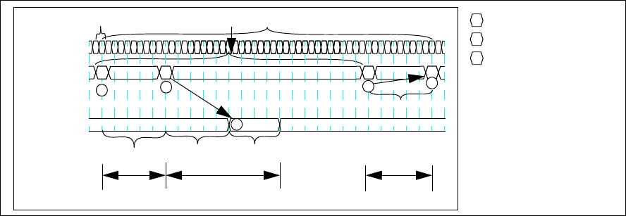
K.TFAW: FOUR BANK ACTIVATION WINDOW
In DDR2 SDRAM devices, the timing parameter tFAW has been defined to specify a rolling time frame in which a
maximum of four row activations on the same DRAM device may be engaged concurrently. The acronym FAW stands
for Four bank Activation Window. Figure 16 shows a sequence of row activation requests to different banks on the same
DDR2 SDRAM device that respects both tRRD as well as tFAW. Figure 16 shows that the row activation requests are
spaced at least tRRD apart from each other, and that the fifth row activation to a different bank is deferred until at least
tFAW time period has passed since the first row activation was initiated. For memory systems that implement the close
page row buffer management system, tFAW places additional constraint on the maximum sustainable bandwidth of a
memory system with a single rank of memory regardless of operating datarates.
1. In a memory system with 2 or more ranks of memory, consecutive row activation commands may be directed to different ranks.
Fig. 15: Row to Row Activation Limited by tRRD
time
current draw
abstract units
cmd&addr
bank “i” util.
row act
data sense
bank “j” util.
data sense
row act
tRRD
Fig. 16: Maximum of Four Row Activations in any tFAW time frame
time
current draw
abstract units
cmd&addr
bank “i” util.
row act
data sense
bank “j” util.
data sense
row act
tRRD
bank “k” util.
bank “l” util.
bank “m” util.
data sense
data sense
data sense
row act row act row act
tRRD tRRD
tFAW
UNIVERSITY OF MARYLAND MEMORY SYSTEM SIMULATOR MANUAL – 20
L. DRAM COMMAND CHAIN
In a DRAM based memory system, each memory transaction is translated into one or more DRAM commands. In
this simulation framework, this sequence of DRAM commands is referred to as the DRAM command chain. The
difficulty associated with the translation process from a transaciton to a DRAM command chain is that the sequence of
DRAM commands in the command chain depends on the row buffer management policy as well as on the state of the
DRAM memory system. In an open page memory system, a memory transaction may be translated into: a single column
access command if the row is already open, a precharge command, a row access command and a column access
command if there is a bank conflict, or just a row access command and a column access command if the bank is
currently idle.
In a close page memory system, all of the memory transactions translate to a sequence of three DRAM commands
that completes a read cycle. Figure 17 illustrates a read cycle in a close-page DDRx SDRAM memory system.
Fig. 17: A Complete “Read Cycle” in DDRx SDRAM Memory System (@ 1 Gbit)
tRCD tBurst
tRC
tCAS
tRP
tRAS
row column read precharge
tCMD
Row Activation Command
Column Read Command
Precharge Command
activation
@ 1Gbps
t
CAS
= 10 ns = 5 cycles = 10 beats
t
RCD
= 10 ns = 5 cycles = 10 beats
t
RP
= 10 ns = 5 cycles = 10 beats
t
RRD
= 10 ns = 5 cycles = 10 beats
t
RAS
= 40 ns = 20 cycles = 40 beats
t
burst
= 8 ns = 4 cycles = 8 beats
t
FAW
= 48 ns = 24 cycles = 48 beats
t
DQS
= 4 ns = 2 cycles = 4 beats
4
5
126
CP
P
R
R
C
R
data
clock
command
data bus
bus
UNIVERSITY OF MARYLAND MEMORY SYSTEM SIMULATOR MANUAL – 21
DRAM User’s Guide: DRAM Related Options
This section has been included to provide a summary of available options that is related to the DRAM system
simulator.
-biu:transaction_ordering_policy ?transaction_ordering_policy ?
transaction_ordering_policy specifies the ordering policy for selecting and prioritizing memory
transactions. Currently supported transaction ordering policies are First Come First Serve (fcfs),
Read or Instruction Fetch First (riff),Wang’s algorithm(wang),Least Pending(least_pending), Most
Pending(most_pending), Open bank first (obf) and Greedy(greedy). Note that the fb-dimm system
supports only Greedy.
-cpu:frequency ?cpu_frequency?
cpu_frequency specifies the frequency of the CPU core. Since everything is relative, we need to
know the frequency of the CPU core so the memory system can have a reference ratio to interact
with it. The unit is assumed to be “MHz”. A default setting of 2000 MHz is assumed if no options are
specified.
-dram:type ?dram_type?
dram_type specifies the type of dram system to be used. “sdram”, “ddrsdram”, “ddr2”, “ddr3” and
“fbdimm” are currently supported options. A default of “sdram” is assumed if no options are
specified.
-dram:frequency ?dram_frequency?
dram_frequency specifies the operating frequency of the memory system. The unit is assumed to be
in “MHz”. A default setting of 100 MHz is assumed if no options are specified. A PC800 RDRAM
memory system should have this option set to 800, and a PC1600 DDR SDRAM memory system
should have this option set to 200.
-dram:channel_count ?channel_count?
channel_count specifies the number of logical channels of DRAM in the memory system. The
current implementation supports one, two, four and eight logical channel of memory system. The
default setting of 1 physical channel is assumed if no options are selected.
-dram:channel_width ?channel_width?
channel_width specifies the width of the data channel in the memory system on a per channel basis.
The units are assumed to be in bytes. To simulate a dual RDRAM channel system with a single
memory controller (as in Intel i850), the channel_count switch above should be set to 1 (channel),
and the channel_width setting should be set to 32 (bytes).
UNIVERSITY OF MARYLAND MEMORY SYSTEM SIMULATOR MANUAL – 22
-dram:refresh? auto_refresh_time_period?
auto_refresh_time_period specifies the time period which the memory controller will cycle through
and refresh all of the rows in a DRAM based memory system. The unit is in milliseconds. The default
is set to 0, which is a special case that specifies no refresh simulated. An auto refresh time setting of
10 milliseconds should reduce available bandwidth by about 1 to 5%, depending on the memory
system and refresh scheme.
-dram:row_buffer_management_policy ?row_buffer_management_policy?
row_buffer_management_policy specifies the row buffer management policy. Currently available
options are “open_page”, “close_page”. The default is set to “open_page”. The open page policy
keeps an accessed page open for as long as possible, until a row refresh closes it, or until another
row access to the same bank forces that page to be closed. The close page policy closes each page
immediately after the column access.
-dram:address_mapping_policy ?address_mapping_policy?
The address mapping policy determines how an address will be broken down to addresses in the
memory system by rank, bank, row, and column. Currently supported options are
“sdram_base_map”, “intel845g_map”, “sdram_close_page_map”, “burger_alt_map” and
“burger_base_map”. sdram_base_map and intel845g_map are to be used for SDRAM and
DDRSDRAM memory systems.
-dram:chipset_delay ?chipset_delay_value?
To simulate the minimum latency through the system controller and memory controller, we
implemented chipset_delay in our simulator. The units are in number of DRAM cycles. Since
DRDRAM based systems are clocked might higher, please set this delay to a higher value. DDR
SDRAM based memory systems should also have this value set to twice that of SDRAM based
systems for “equivalent” latency in terms of nanoseconds through the system controller.

UNIVERSITY OF MARYLAND MEMORY SYSTEM SIMULATOR MANUAL – 23
-dram:spd_input ?input_filename?
Since it gets tedious to specify 20 different parameters to specify a memory system, the preferred
way to do it with a configuration file. Numerous timing parameters and DRAM system configurations
can be specified with a .spd file. A sample .spd file is shown below. Comments are allowed after //
Sample .spd files are defined under the subdirectory of /mem_system_def/
-dram:power_input ?input_filename?The power input file (similar to the spd file) can be specified. The format
of the power input file is :
<parameter> <value> #comment
Below is a sample of power input file.
// DDR3 1000 memory system.
// Composed of 1 Gbit chips. 2 ranks, each rank has 8 (x8) 1 Gbit chips.
// Total is 2 GB
// Peak Bandwidth is 8 GB/s
//
type ddr3
datarate 1000
channel_count 1 // Logical channel
channel_width 8 // Byte width
PA_mapping_policy sdram_hiperf_map // Comments are allowed here
rank_count 2
bank_count 8 // 8 banks per chip
row_count 16384
col_count 1048
t_cas 10 // 10ns
t_cmd 2
t_cwd 8
t_dqs 4
t_faw 48
t_ras 40
t_rc 50
t_rcd 10
t_rrd 10
t_rp 10
t_wr 10
posted_cas FALSE
t_al 8
auto_refresh FALSE
auto_refresh_policy refresh_one_chan_all_rank_all_bank
refresh_time 64000 //specified in us.
Fig. 18: Sample DRAM Configuration File for 1 Gbit DDR3 SDRAM

UNIVERSITY OF MARYLAND MEMORY SYSTEM SIMULATOR MANUAL – 24
-debug:biu
This switch turns on the bus interface debugging feature, and dumps out to stderr for each bus
interface unit slot acquisition and release.
-debug:transaction
This switch turns on the transaction interface debugging feature, and dumps out to stderr each time
a transaction enters into a queue, gets broken down into command sequences or retires.
-debug:threshold <transaction number>
This switch turns on the transaction interface debugging feature, and dumps out to stderr each time
after a particular transaction number is past.
-debug:bundle
Fig. 19: Sample DRAM Power input File for 1 Gbit DDR2 SDRAM
#####################################################
# DDR SDRAM Configuration and Data Sheet Parameters #
# corresponding to 1 Gb 667 MHz 4-4-4 spd file #
#####################################################
density 1024 # Mb
DQS 2 # per chip
max_VDD 1.9 # V
min_VDD 1.7 # V
IDD0 100 # mA
IDD2P 7 # mA
IDD2F 65 # mA
IDD3P 40 # mA
IDD3N 70 # mA
IDD4R 205 # mA
IDD4W 180 # mA
IDD5 270 # mA
t_CK 3 # ns
t_RFC_min 127.5 # ns
t_REFI 7.8 # microseconds
###################################################
# DRAM Usage Conditions in the System Environment #
###################################################
VDD 1.8 # V
UNIVERSITY OF MARYLAND MEMORY SYSTEM SIMULATOR MANUAL – 25
This switch turns on the bundle debugging feature, and dumps out the contents of a bundle being
sent when simulating a FB-DIMM based system.
-debug:amb
This switch turns on the Advanced Memory Buffer (amb) debugging feature, and dumps out to stderr
the state of the amb everytime a command is sent that is going to occupy the buffer or release its
contents to the dram. This flag is valid only when FB-DIMM based configurations are simulated.
-debug:all
This switch turns on biu, transaction and dram memory system debugging all at the same time.
-debug:wave
This switch turns on a simple ASCII text based DRAM memory system waveform display.
-stat:biu
The bus interface unit (BIU) stats file collects latency information for each and every memory
transaction. The final result is placed in stderr or in a common statistical file. The output will show
one column that represents the number of cpu cycles that it took for a memory access to complete,
and the second column represents the number of accesses that incurs the latency.
-stat:dram:bank_hit
The bank hit stats is information for the number of dram cycles that occur between accesses that hit
an open bank.
-stat:dram:bank_conflict
This flag enables the collection information for the number of dram cycles that occur between
accesses that conflicts on an open bank.
-stat:dram:cas_per_ras
This enables collection of data on the number of column read or write commands that gets issued for
each row access open bank/page command.
-stat:dram:power ?output_filename?
The power stats file collects the power statistical data during a specified period of time and the
average power per rank during that time. The format of each line in the file is
<dram_current_time> <channel> <rank> <BNK_PRE> <CKE_LO_PRE> <CKE_LO_ACT> <t_ACT>
<RDpercent> <WRpercent> <P_TOT>/<# of chips per rank> <# of access>
All variables are as explained in “Power model” section.
UNIVERSITY OF MARYLAND MEMORY SYSTEM SIMULATOR MANUAL BIBLIOGRAPHY – 26
Bibliography
[1] D. T. Wang. Modern DRAM Memory Systems: Performance Analysis and a High Performance, Power-Constrained DRAM-
Scheduling Algorithm. PhD thesis, University of Maryland College Park, 2005.
[2] S. Rixner, W. J. Dally, U. J. Kapasi, P. R. Mattson, and J. D. Owens. Memory access scheduling. In ISCA, pages 128–138, 2000
[3] W. fen Lin, S. K. Reinhardt, and D. Burger. Reducing DRAM latencies with an integrated memory hierarchy design. In HPCA,
2001..
