DSR 50/50P DSR50
User Manual: DSR50
Open the PDF directly: View PDF ![]() .
.
Page Count: 285 [warning: Documents this large are best viewed by clicking the View PDF Link!]
- COVER
- TABLE OF CONTENTS
- SERVICE NOTE
- SELF-DIAGNOSIS FUNCTION
- GENERAL
- DISASSEMBLY
- BLOCK DIAGRAMS
- OVERALL BLOCK DIAGRAM 1
- OVERALL BLOCK DIAGRAM 2
- OVERALL BLOCK DIAGRAM 3
- OVERALL BLOCK DIAGRAM 4
- OVERALL BLOCK DIAGRAM 5
- OVERALL BLOCK DIAGRAM 6
- OVERALL BLOCK DIAGRAM 7
- OVERALL BLOCK DIAGRAM 8
- OVERALL BLOCK DIAGRAM 9
- POWER BLOCK DIAGRAM 1
- POWER BLOCK DIAGRAM 2
- POWER BLOCK DIAGRAM 3
- POWER BLOCK DIAGRAM 4
- POWER BLOCK DIAGRAM 5
- POWER BLOCK DIAGRAM 6
- PRINTED WIRING BOARDS AND SCHEMATIC DIAGRAMS
- ADJUSTMENTS
- REPAIR PARTS LIST
- SUPPLEMENT-1
- SUPPLEMENT-2
- SUPPLEMENT-3
- Revision History
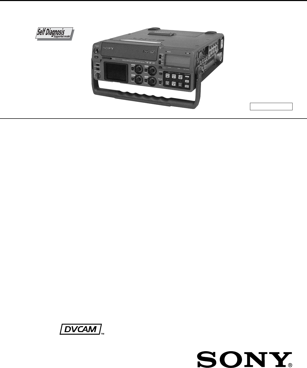
SERVICE MANUAL
Ver 1.5 2006.03
US Model
Canadian Model
DSR-50
AEP Model
UK Model
E Model
Australian Model
New Zealand Model
DSR-50P
PORTABLE DIGITAL VIDEO CASSETTE RECORDER
SPECIFICATIONS
– Continued on next page –
DSR-50/50P
R MECHANISM
System
Recording format DVCAM/DV (SP) format, rotating
2-head helical scan, digital
component recording
Video signal
DSR-50: EIA STANDARD, NTSC color
system
DSR-50P: CCIR STANDARD, PAL colour
system
Video
Quantification 8-bit
Standardization frequency
DSR-50: 13.5 MHz (4:1:1 Component)
DSR-50P: 13.5 MHz (4:2:0 Component)
Audio
Quantification 12-bit (non-linear) or 16-bit
(linear)
Standardization frequency
32 kHz (12-bit recording) or
48 kHz (16-bit recording)
Usable cassettes Standard-DVCAM cassettes and
Mini-DVCAM cassettes
Recording time Standard cassette
DVCAM: 184 minutes (PDV184)
180 minutes (DV270)
DV: 270 minutes (PDV184/
DV270)
Mini cassette
DVCAM: 40 minutes (PDVM40/
DVM60)
DV: 60 minutes (PDVM40/
DVM60)
(We recommend that you use the
DVCAM cassettes.)
Clock
Quartz locked
Power back-up Back-up duration: up to one month
(after a 10-hour charge)
Inputs
VIDEO/REF.IN BNC type
1 Vp-p (75 ohms, unbalanced)
S VIDEO IN Mini DIN 4-pin
Luminance signal: 1 Vp-p
(75 ohms, unbalanced)
Chrominance signal:
0.286 Vp-p (DSR-50)
0.3 Vp-p (DSR-50P)
(75 ohms unbalanced)
DV IN/OUT 6-pin IEEE-1394 standard jack
(i.LINK)
AUDIO INPUT (CH-1 to CH-4)
XLR 3-pin, female, +4/–20/
–60 dBu, Impedance more than
3 kohms, balanced (48 V
phantom power supply)
Maximum input level
–60: –19 dBu (about 90 mVrms)
–20: +8 dBu (about 2 Vrms)
+4: +30 dBu (about 25 Vrms)
CAMERA 26-pin
Composite: 1 Vp-p (75 ohms,
unbalanced)
Component:
Y: 1 Vp-p (75 ohms, unbalanced)
B-Y: 0.7 Vp-p (75 ohms,
unbalanced)
(DSR-50: 75%, color bars / DSR-
50P: 100%, colour bars)
R-Y: 0.7 Vp-p (75 ohms,
unbalanced)
(DSR-50: 75%, color bars / DSR-
50P: 100%, colour bars)
Audio: –20/–60 dBu, Impedance
more than 3 kohms, balanced
TC IN BNC type
0.5 to 18 Vp-p (time code input)
0.5 to 4 Vp-p (through output)
Outputs
VIDEO OUT1 BNC type, 1 Vp-p (75 ohms,
unbalanced) (superimpose)
VIDEO OUT2 BNC type, 1 Vp-p (75 ohms,
unbalanced)
COMPONENT OUTPUT
Y: BNC type
1 Vp-p (75 ohms, unbalanced)
R-Y: BNC type
0.7 Vp-p (75 ohms, unbalanced)
(DSR-50: 75%, color bars / DSR-
50P: 100%, colour bars)
B-Y: BNC type
0.7 Vp-p (75 ohms, unbalanced)
(DSR-50: 75%, color bars / DSR-
50P: 100%, colour bars)
S VIDEO OUT Mini DIN 4-pin
Luminance signal: 1 Vp-p
(75 ohms, unbalanced)
Chrominance signal:
0.286 Vp-p (DSR-50)
0.3 Vp-p (DSR-50P)
(75 ohms, unbalanced)
AUDIO OUTPUT (CH-1 to CH-4)
Phono jack, –10 dBu, 47 kohms,
Output impedance: less than
1 kohms
(DSR-50: –20 dB from full bit /
DSR-50P: –18 dB from full bit)
AUDIO MONITOR OUT
Phono jack
TC OUT BNC type, 2.2 Vp-p, 600 ohms /
1.2 Vp-p, 75 ohms
0.5 to 4 Vp-p (through output,
600 ohms)
– 2 –
1. Check the area of your repair for unsoldered or poorly-sol-
dered connections. Check the entire board surface for solder
splashes and bridges.
2. Check the interboard wiring to ensure that no wires are
“pinched” or contact high-wattage resistors.
3. Look for unauthorized replacement parts, particularly transis-
tors, that were installed during a previous repair. Point them
out to the customer and recommend their replacement.
4. Look for parts which, though functioning, show obvious signs
of deterioration. Point them out to the customer and recom-
mend their replacement.
SAFETY CHECK-OUT
After correcting the original service problem, perform the following
safety checks before releasing the set to the customer.
5. Check the B+ voltage to see it is at the values specified.
6. Flexible Circuit Board Repairing
•Keep the temperature of the soldering iron around 270 ˚C
during repairing.
•Do not touch the soldering iron on the same conductor of
the circuit board (within 3 times).
•Be careful not to apply force on the conductor when sol-
dering or unsoldering.
ATTENTION AU COMPOSANT AYANT RAPPORT
À LA SÉCURITÉ!
LES COMPOSANTS IDENTIFIÉS PAR UNE MARQUE 0
SUR LES DIAGRAMMES SCHÉMATIQUES ET LA LISTE
DES PIÈCES SONT CRITIQUES POUR LA SÉCURITÉ
DE FONCTIONNEMENT. NE REMPLACER CES COM-
POSANTS QUE PAR DES PIÈCES SONY DONT LES
NUMÉROS SONT DONNÉS DANS CE MANUEL OU
DANS LES SUPPLÉMENTS PUBLIÉS PAR SONY.
SAFETY-RELATED COMPONENT WARNING!!
COMPONENTS IDENTIFIED BY MARK 0 OR DOTTED
LINE WITH MARK 0 ON THE SCHEMATIC DIAGRAMS
AND IN THE PARTS LIST ARE CRITICAL TO SAFE
OPERATION. REPLACE THESE COMPONENTS WITH
SONY PARTS WHOSE PART NUMBERS APPEAR AS
SHOWN IN THIS MANUAL OR IN SUPPLEMENTS PUB-
LISHED BY SONY.
PHONES Stereo phone jack
–∞ to –19 dBu, adjustable
DC IN 12V XLR 4-pin, male, 12 V
Control
CONTROL Stereo mini-minijack
REMOTE Stereo minijack
(Edge High, Edge Low, Level
High, Level Low) (Tally)
CONTROL S Stereo minijack
General
Power requirements
DC12 to 17 V, more than 2.0 A
(4.0 A at the peak)
Power consumption15 W (during playback)
Operating temperature
5 °C to 40 °C
(41 °F to 104 °F)
Storage temperature
–20 °C to +60 °C
(–4 °F to +140 °F)
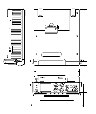
Dimensions Approx. 279 × 99 × 315 mm
(11 × 4 × 12
1
/
2
inches)
(w/h/d, including projecting parts
and controls)
Mass Approx. 3.9 kg (8 lb 10 oz)
Supplied accessories
LCD protection board (1)
(installed at the factory)
Cleaning cassette (1)
Operating instructions (1)
Design and specifications are subject to change
without notice.
183.3 (7
1
/
4
)
289 (11
1
/
2
)
247 (9
3
/
4
)
92.5 (3
3
/
4
)
22 (
7
/
8
)
Unit: mm (inches)
279 (11)

– 3 –
SERVICE NOTE ................................................................ 6
1. Note for Repair ............................................................ 6
SELF-DIAGNOSIS FUNCTION ..................................... 7
1. Self-diagnosis Function ............................................... 7
2. Self-diagnosis Display ................................................. 7
3. Service Mode Display ................................................. 7
4. Self-diagnosis Code Table .......................................... 8
1. GENERAL
Features ................................................................................ 1-1
Location and Function of Parts ............................................. 1-1
Power Preparations ............................................................... 1-7
Connections ........................................................................... 1-8
Notes on Video Cassettes ..................................................... 1-9
Recording .............................................................................. 1-10
Playback ................................................................................ 1-12
Setting the Time Code and User Bits.................................... 1-13
Synchronizing the Time Codes ............................................. 1-14
Adjusting the Sync and Subcarrier Phases
of the Video Signals............................................................... 1-15
Adjusting the Signals ............................................................. 1-16
Duplication (Generating a Work Tape
with the Same Time Code) .................................................... 1-16
Audio Dubbing ....................................................................... 1-17
Operating the Menus ............................................................. 1-18
Troubleshooting ..................................................................... 1-22
Alarm Messages .................................................................... 1-22
Notes on Use ......................................................................... 1-23
2. DISASSEMBLY
2-1. Top/bottom Cover Assemblies .................................... 2-1
2-2. Front Panel .................................................................. 2-1
2-3. FR-157 Board .............................................................. 2-1
2-4. LCD Module (LCD901)................................................ 2-1
2-5. Mechanism Deck ......................................................... 2-2
2-6. CM-59 Board ............................................................... 2-2
2-7. JC-20/DI-73 Boards .................................................... 2-2
2-8. VD-28 Board ................................................................ 2-3
2-9. Side Panel Assembly .................................................. 2-3
2-10. Circuit Boards Location ............................................... 2-4
3. BLOCK DIAGRAMS
3-1. Overall Block Diagram 1.............................................. 3-1
3-2. Overall Block Diagram 2.............................................. 3-3
3-3. Overall Block Diagram 3.............................................. 3-5
3-4. Overall Block Diagram 4.............................................. 3-7
3-5. Overall Block Diagram 5.............................................. 3-9
3-6. Overall Block Diagram 6.............................................. 3-11
3-7. Overall Block Diagram 7.............................................. 3-13
3-8. Overall Block Diagram 8.............................................. 3-15
3-9. Overall Block Diagram 9.............................................. 3-17
3-10. Power Block Diagram 1 ............................................... 3-19
3-11. Power Block Diagram 2 ............................................... 3-21
3-12. Power Block Diagram 3 ............................................... 3-23
3-13. Power Block Diagram 4 ............................................... 3-25
3-14. Power Block Diagram 5 ............................................... 3-27
3-15. Power Block Diagram 6 ............................................... 3-29
4. PRINTED WIRING BOARDS AND
SCHEMATIC DIAGRAMS ..................................... 4-1
4-1. Frame Schematic Diagram (1/2) ................................. 4-3
Frame Schematic Diagram (2/2) ................................. 4-5
4-2. Printed Wiring Boards and Schematic Diagrams ....... 4-7
• RP-234 Printed Wiring Board ................................ 4-7
• RP-234 (REC/PB AMP 1) Schematic Diagram ..... 4-11
• RP-234 (REC/PB AMP 2) Schematic Diagram ..... 4-13
• JC-20 Printed Wiring Board ................................... 4-15
• JC-20 (VIDEO PB AMP) Schematic Diagram ....... 4-19
• JC-20 (VIDEO A/D CONVERTER)
Schematic Diagram ................................................ 4-21
• JC-20 (CHROMA MIX) Schematic Diagram .......... 4-23
• JC-20 (AFC) Schematic Diagram .......................... 4-25
• JC-20 (VFD (VIDEO DSP, D/A CONVERTER))
Schematic Diagram ................................................ 4-27
• JC-20 (SFD) Schematic Diagram .......................... 4-29
• JC-20 (TFD) Schematic Diagram .......................... 4-31
• JC-20 (DV INTERFACE) Schematic Diagram ....... 4-33
• IL-013 Printed Wiring Board
and Schematic Diagram ......................................... 4-34
• JC-20 (MECHANISM CONTROL 1)
Schematic Diagram ................................................ 4-35
• JC-20 (MECHANISM CONTROL 2)
Schematic Diagram ................................................ 4-37
• JC-20 (MODE CONTROL) Schematic Diagram .... 4-39
• JC-20 (AUDIO 1) Schematic Diagram ................... 4-41
• JC-20 (AUDIO 2) Schematic Diagram ................... 4-43
• JC-20 (POWER SUPPLY) Schematic Diagram ..... 4-45
• DI-73 Printed Wiring Board .................................... 4-47
• DI-73 (VIDEO D/A CONVERTER)
Schematic Diagram ................................................ 4-51
• DI-73 (VIDEO FIFO MEMORY)
Schematic Diagram ................................................ 4-53
• DI-73 (SYNC SHIFTER 1) Schematic Diagram .... 4-55
• DI-73 (SYNC SHIFTER 2) Schematic Diagram .... 4-57
• DI-73 (AUDIO HPF) Schematic Diagram............... 4-59
• DI-73 (AUDIO A/D, D/A CONVERTER)
Schematic Diagram ................................................ 4-61
• DI-73 (AUDIO DSP) Schematic Diagram .............. 4-63
• DI-73 (AUDIO DSP CONTROL)
Schematic Diagram ................................................ 4-65
• DI-73 (TIME CODE IN/OUT)
Schematic Diagram ................................................ 4-67
• KP-8, EJ-28, VL-26 Printed Wiring Boards and
Schematic Diagrams .............................................. 4-69
• VD-28 Printed Wiring Board .................................. 4-71
• VD-28 (SYNC GENERATOR 1)
Schematic Diagram ................................................ 4-75
• VD-28 (SYNC GENERATOR 2)
Schematic Diagram ................................................ 4-77
• VD-28 (SYNC GENERATOR 3)
Schematic Diagram ................................................ 4-79
• VD-28 (VIDEO IN 1) Schematic Diagram ............. 4-81
• VD-28 (VIDEO IN 2) Schematic Diagram .............. 4-83
• VD-28 (VIDEO IN 3) Schematic Diagram ............. 4-85
• VD-28 (UVIC) Schematic Diagram ........................ 4-87
• VD-28 (VIDEO OUT 1) Schematic Diagram .......... 4-89
• VD-28 (VIDEO OUT 2) Schematic Diagram .......... 4-91
• VD-28 (VIDEO OUT 3) Schematic Diagram ......... 4-93
• VD-28 (AUDIO) Schematic Diagram...................... 4-95
• VD-28 (HI CONTROL) Schematic Diagram .......... 4-97
• VD-28 (DC IN) Schematic Diagram ....................... 4-99
• VD-28 (DC/DC CONVERTER 1)
Schematic Diagram ................................................ 4-101
• VD-28 (DC/DC CONVERTER 2)
Schematic Diagram ................................................ 4-103
• CM-59 (DC/DC CONVERTER,
REEL MOTOR DRIVE) Schematic Diagram ......... 4-105
• CM-59(DRUM MOTOR DRIVE,
FL MOTOR DRIVE) Schematic Diagram ............... 4-107
• CM-59 (CAPSTAN MOTOR DRIVE,
CAM MOTOR DRIVE) Schematic Diagram ........... 4-109
TABLE OF CONTENTS
Section Title Page Section Title Page

– 4 –
Section Title Page Section Title Page
• CM-59 Printed Wiring Board .................................. 4-111
• MD-76 Printed Wiring Board .................................. 4-115
• MD-76 Schematic Diagram .................................... 4-117
• FR-157 Printed Wiring Board ................................. 4-119
• FR-157 (USER CONTROL 1)
Schematic Diagram ................................................ 4-123
• FR-157 (USER CONTROL 2)
Schematic Diagram ................................................ 4-125
• LT-32 Printed Wiring Board and
Shematic Diagram .................................................. 4-126
• JK-169 Printed Wiring Board ................................. 4-127
• JK-169 (VIDEO IN/OUT, AUDIO OUT)
Schematic Diagram ................................................ 4-131
• JK-169 (AUDIO IN 1) Schematic Diagram............. 4-133
• JK-169 (AUDIO IN 2) Schematic Diagram............. 4-135
• PD-125 Printed Wiring Board ................................ 4-137
• PD-125 (RGB DRIVER) Schematic Diagram ........ 4-139
• PD-125 (TG) Schematic Diagram .......................... 4-141
• HP-117 Printed Wiring Board ................................ 4-143
• HP-117 Schematic Diagram .................................. 4-145
4-3. Waveforms ................................................................... 4-147
4-4. Parts Location ............................................................. 4-153
5. ADJUSTMENTS
1. Before Starting Adjustment ......................................... 5-1
1-1. Adjusting Items when Replacing Main Parts
and Boards .................................................................. 5-2
1-2. Information (Mechanical Section) ............................... 5-4
5-1. MECHANICAL SECTION ADJUSTMENTS................ 5-5
5-1-1. Parts Replacement and Preparation
for Adjustment ........................................................ 5-5
1-1. Assembly/disassembly of Cassette Compartment ..... 5-5
1-2. How To Load/unload .................................................... 5-5
1-3. List of Service Tools .................................................... 5-6
1-4. About Mode Selector II ............................................... 5-7
5-1-2. Periodic Check ....................................................... 5-8
2-1. Cleaning of Rotary Drum Assembly ...................... 5-8
2-2. Cleaning of Tape Path System ............................... 5-8
2-3. Periodic Checks ..................................................... 5-8
5-1-3. Parts Replacement................................................. 5-9
3-1. Tape Guide 1/8 and Guide Guard .......................... 5-9
3-2. Tape Guide 2/7 ....................................................... 5-9
3-3. Capstan Cover ....................................................... 5-10
3-4. Reel Motor .............................................................. 5-10
3-5. FL Motor Assembly, Gear A, Gear B and
Gear CD Assembly ................................................ 5-10
3-6. GL Arm S Assembly, GL Arm T Assembly,
Coaster S Assembly and Coaster T Assembly...... 5-11
3-7. MIC Base Guide, MIC Base Assembly and
MIC Base Spring .................................................... 5-12
3-8. Drum Cap, Drum Assembly and Tape Support ..... 5-12
3-9. Pinch Arm Assembly .............................................. 5-13
3-10. Capstan Motor ........................................................ 5-13
3-11. Pendulum Retainer and
Pendulum Arm Assembly ....................................... 5-13
3-12. Brake Arm S, Ratchet Brake T,
Tension Coil Spring (Brake), SBR Slider and FP-248
Flexible Board (Condensation Sensor) .................. 5-14
3-13. Reel Table Assembly, Idler Gear A Assembly
and Idler Gear B ..................................................... 5-14
3-14. Reel Base Retainer, Reel Base T Assembly and
Reel Base S Assembly (Reel Lock Release Block
and Reel Lock Release Spring) ............................. 5-15
3-15. Cam Motor, Motor Holder....................................... 5-15
3-16. TG2/7 Arm Block, TG2/7 Band Block and
Tension Coil Spring (TG2)/(TG7) ........................... 5-16
3-17. Sub-slider Arm, Sub-slider, Encoder Gear,
Main Cam Gear, Coupling Gear, Sub-cam Gear,
Pinch Slider and Loadeing Arm Assy .................... 5-17
3-18. Main Slider, Main Slider Arm and Pendulum
Stopper Assembly .................................................. 5-19
3-19. MD-76 Board and Encoder Retainer ..................... 5-20
3-20. Components of GL Arm S/T Assembly
(GL Arm Assembly, GL Helical Torsion Spring,
GL Gear)................................................................. 5-21
3-21. Components of MIC Base Assembly
(FP-104 Flexible Board, MIC Base) ....................... 5-21
3-22. Components of Drum Assembly
(Motor FPC Assembly, Elastic Connector) ............ 5-22
3-23. Components of Pinch Arm Assembly (Tape Retainer,
Compression Coil Spring) ...................................... 5-22
3-24. Components of TG2/7 Arm Assembly (ET Magnet,
Magnet Holder) ...................................................... 5-22
5-1-4. Check and Adjustment ........................................... 5-23
4-1. Reel Table Height Check and Adjustment ............. 5-24
4-2. TG1/8 Height Check and Adjustment .................... 5-24
4-3. TG2/7 Height Check and Adjustment .................... 5-25
4-4. FWD/RVS Position Check and Adjustment ........... 5-25
4-5. Electric Tension Regulator Check and Adjustment
of TG2/7 Arm .......................................................... 5-26
4-6. FWD/RVS Back Tension Check and Adjustment... 5-27
4-7. Preparation for Adjustment and
Tape Path Check .................................................... 5-28
4-8. Track Adjustment and Check
(Checking the RF Waveform) ................................. 5-29
4-9. Track Check ............................................................ 5-29
4-10. CUE/REV Check .................................................... 5-30
4-11. Curl Check and Adjustment ................................... 5-30
4-12. Rising Check .......................................................... 5-31
5-2. SERVICE MODE ......................................................... 5-32
5-2-1. Adjusting Remote Commander .............................. 5-32
1. Used Adjustment Remote Commander ................. 5-32
2. Precautions Upon Using the Adjusting Remote
Commander............................................................ 5-32
5-2-2. Data Processing ..................................................... 5-33
5-2-3. Service Mode ......................................................... 5-34
1. Emergence Memory Address ................................ 5-34
2. EMG Code (Emergency Code) .............................. 5-34
3. MSW Code ............................................................. 5-35
4. Bit Value Discriminatiion ........................................ 5-36
5. Recorde of Use Check ........................................... 5-37
6. Switch Check (Audio Jack 1) ................................. 5-38
7. Switch Check (Audio Jack 2) ................................. 5-38
8. Switch Check (Video Jack) .................................... 5-38
9. Switch Check (Key Code) ...................................... 5-39
10. Switch Check (Key Data 1) .................................... 5-39
11. Switch Check (Key Data 2) .................................... 5-39
12. Switch Check (Slide Switch 1) ............................... 5-40
13. Switch Check (Slide Switch 2) ............................... 5-40
14. Switch Check (Slide Switch 3) ............................... 5-40
5-3. VIDEO SECTION ADJUSTMENTS ............................ 5-41
3-1. Preparations Before Adjustment ............................ 5-41
3-1-1. Equipment Used ..................................................... 5-41
3-1-2. Connection of Equipment ....................................... 5-42
3-1-3. Checking the Input Signals .................................... 5-43
1. S VIDEO Input ........................................................ 5-43
2. VIDEO Input ........................................................... 5-43
3. CAMERA Input ....................................................... 5-44
3-1-4. Adjustment Tapes ................................................... 5-45
3-1-5. Input/output Level and Impedance ........................ 5-46
3-2. System Control System Adjustments .................... 5-47
1. Initializing the C, D, E Page Data ........................... 5-47
2. Input of C Page Initial Data .................................... 5-47
3. Input of D Page Initial Data .................................... 5-47
4. Input of E Page Initial Data .................................... 5-47
5. Modification of C, D, E, Page Data ........................ 5-47
6. C Page Table .......................................................... 5-48
7. D Page Table .......................................................... 5-49
8. E Page Table .......................................................... 5-49
9. Node Unique ID No. Input ...................................... 5-51
3-3. Servo and RF System Adjustments....................... 5-53
1. Capstan FG Adjustment (CM-59 Board) ............... 5-53
2. PLL f0 Pre-adjustment (RP-234 Board) ................. 5-53
3. Switching Position Adjustment (RP-234 Board) .... 5-53

– 5 –
Section Title Page
4. RF-AGC Adjustment (RP-234 Board) .................... 5-53
5. CLK DELAY and AEQ Adjustment
(RP-234 Board) ...................................................... 5-54
6. PLL f0 Final Adjustment (RP-234 Board)............... 5-54
3-4. Video System Adjustments .................................... 5-54
3-4-1. JC-20 Board Adjustment ........................................ 5-54
1. VFD SPCK Adjustment (JC-20 Board) .................. 5-54
2. A/D Converter Reference Voltage
Adjustment (1) (JC-20 Board) ................................ 5-54
3. A/D Converter Reference Voltage
Adjustment (2) (JC-20 Board) ................................ 5-54
4. Y Signal Clamp Reference Voltage Adjustment
(JC-20 Board) ......................................................... 5-55
5. CR Signal Clamp Reference Voltage Adjustment
(JC-20 Board) ......................................................... 5-55
6. CB Signal Clamp Reference Voltage Adjustment
(JC-20 Board) ......................................................... 5-55
7. AFC Preliminary Adjustment (JC-20 Board) ......... 5-55
8. AFC Picture Frame Adjustment (JC-20 Board) ..... 5-55
9. AFC Adjustment (JC-20 Board) ............................. 5-55
10. Playback Y Level Adjustment (JC-20 Board) ......... 5-56
11. Playback C Level Adjustment (JC-20 Board) ........ 5-56
3-4-2. General Adjustment ............................................... 5-57
1. Playback Y Sync Level Adjudtment (VD-28 Board) 5-57
2. Playback Blanking Level Adjustment with 0%
Setup (VD-28 Board).............................................. 5-57
3. Playback Signal Level Adjustment with 0% Setup
(VD-28 Board) ........................................................ 5-58
4. Playback CR Signal Level Adjustment with 0%
Setup (VD-28 Board).............................................. 5-58
5. Playback CB Signal Level Adjustment with 0%
Setup (VD-28 Board).............................................. 5-59
6. Playback CR Signal Delay Adjustment
(VD-28 Board) ........................................................ 5-59
7. Playback CB Signal Delay Adjustment
(VD-28 Board) ........................................................ 5-60
8. Encoder Free Run Adjustment (VD-28 Board) ...... 5-60
9. Carrier Balance Adjustment (VD-28 Board) .......... 5-61
10. Burst Level Adjustment (VD-28 Board) ................. 5-61
11. Color Level Adjustment with 0% Setup
(VD-28 Board) ........................................................ 5-62
12. SC_V Phase Adjustment (VD-28 Board) ............... 5-62
13. Playback Blanking Level Adjustment with 7.5%
Setup (VD-28 Board)(DSR-50) .............................. 5-63
14. Playback Y Signal Level Adjustment with 7.5%
Setup (VD-28 Board)(DSR-50) .............................. 5-63
15. Playback CR Signal Level Adjustment with 7.5%
Setup (VD-28 Board)(DSR-50) .............................. 5-64
16. Playback CB Signal Level Adjustment with 7.5%
Setup (VD-28 Board)(DSR-50) .............................. 5-64
17. Color Level Adjustment with 7.5% Setup
(VD-28 Board)(DSR-50) ......................................... 5-65
18. Video Output Level Check (VD-28 Board) ............. 5-65
19. S-Video Output Level Check (VD-28 Board) ......... 5-66
20. Monitor Terminal Output Level Adjustment
(JC-20 Board) ......................................................... 5-67
21. E-E Blanking Level Adjustment (VD-28 Board) ..... 5-68
22. Component E-E Y Signal Level Adjustment
(VD-28 Board) ........................................................ 5-69
23. Component E-E CR Signal Level Adjustment
(VD-28 Board) ........................................................ 5-69
24. Component E-E CB Signal Level Adjustment
(VD-28 Board) ........................................................ 5-70
25. Component E-E CR Signal Delay Adjustment
(VD-28 Board) ........................................................ 5-71
26. Component E-E CB Signal Delay Adjustment
(VD-28 Board) ........................................................ 5-72
27. E-E Color Level Adjustment (VD-28 Board) .......... 5-73
28. Decoder Free Run Adjustment (VD-28 Board)...... 5-74
29. Decoder HUE Adjustment (VD-28 Board) ............ 5-75
30. S Video E-E Y Signal Level Adjustment
(VD-28 Board) ........................................................ 5-76
31. S Video E-E CR Signal Level Adjustment
(VD-28 Board) ........................................................ 5-76
32. S Video E-E CB Signal Level Adjustment
(VD-28 Board) ........................................................ 5-77
33. S Video E-E CR Signal Delay Adjustment
(VD-28 Board) ........................................................ 5-78
34. S Video E-E CB Signal Delay Adjustment
(VD-28 Board) ........................................................ 5-79
35. Composite E-E Y Signal Level Adjustment
(VD-28 Board) ........................................................ 5-80
36. Composite E-E CR Signal Level Check
(VD-28 Board) ........................................................ 5-80
37. Composite E-E CB Signal Level Check
(VD-28 Board) ........................................................ 5-81
38. Composite E-E CR Signal Delay Adjustment
(VD-28 Board) ........................................................ 5-82
39. Composite E-E CB Signal Delay Adjustment
(VD-28 Board) ........................................................ 5-83
40. H Phase Adjustment (VD-28 Board) ...................... 5-84
41. E-E SC Phase Adjustment (VD-28 Board) ............ 5-84
42. Playback SC Phase Adjustment
(EXT SYNC OFF) (VD-28 Board) .......................... 5-85
43. Playback SC Phase Adjustment
(EXT SYNC ON) (VD-28 Board) ............................ 5-85
3-5. LCD System Adjustments ...................................... 5-86
1. VCO Adjustment (PD-125 Board) .......................... 5-86
2. Black Limit Adjustment (PD-125 Board) ................ 5-87
3. Bright Adjustment (PD-125 Board) ........................ 5-87
4. Gamma 1 Adjustment (PD-125 Board).................. 5-88
5. Contrast Adjustment (PD-125 Board) .................... 5-88
6. Center Voltage Adjustment (PD-125 Board).......... 5-89
7. White Balance Adjustment (PD-125 Board) .......... 5-89
3-6. AUDIO System Adjustments .................................. 5-90
1. Audio PAL Data Input (DSR-50P) .......................... 5-91
2. Playing Level Check ............................................... 5-91
3. Audio Level Indication Check ................................. 5-92
4. Recording and Playing Check ................................ 5-92
5. FS48 kHz Frequency Characteristic Check........... 5-93
6. FS48 kHz Noise Level Check ................................ 5-93
7. FS32 kHz Frequency Characteristic Check........... 5-94
8. FS32 kHz Noise Level Check ................................ 5-94
9. Input Level Switching Check .................................. 5-95
10. Microphone Power Supply Check .......................... 5-95
3-7. Time Code System Adjustments ........................... 5-96
1. Analog Through (E-E) Level Check ....................... 5-96
2. Time Code Reading Check .................................... 5-96
3. Internal Time Code Output Waveform Check ........ 5-97
4. Internal Time Code Output Check ......................... 5-97
3-8. Arrangement Diagram for Adjustment Parts.......... 5-98
6. REPAIR PARTS LIST
6-1. EXPLPODED VIEWS .................................................. 6-1
6-1-1. Overall Assembly ................................................... 6-1
6-1-2. Front Panel Assembly-1 ......................................... 6-2
6-1-3. Front Panel Assembly-2 ......................................... 6-3
6-1-4. Main Frame Assembly............................................ 6-4
6-1-5. Side Panel Assembly ............................................. 6-5
6-1-6. Mechanism Deck Assembly (Drum Assembly)...... 6-6
6-1-7. Mechanism Deck Assembly (Gear, Arm)............... 6-7
6-1-8. Mechanism Deck Assembly (Motor, MD Board) .... 6-8
6-1-9. Mechanism Deck Assembly
(Cassette Compartment) ....................................... 6-8
6-2. ELECTRICAL PARTS LIST ......................................... 6-10
Hardware List ........................................................................ 6-52
Section Title Page
– 6 –
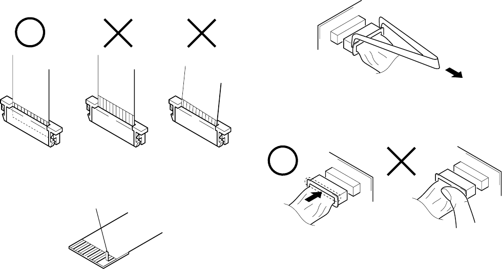
1. NOTE FOR REPAIR
Make sure that the flat cable and flexible board are not cracked of
bent at the terminal.
Do not insert the cable insufficiently nor crookedly.
When remove a connector, don’t pull at wire of connector.
It is possible that a wire is snapped.
Cut and remove the part of gilt
which comes off at the point.
(Be careful or some pieces of
gilt may be left inside)
When installing a connector, don’t press down at wire of connector.
It is possible that a wire is snapped.
SERVICE NOTE
– 7 –
SELF-DIAGNOSIS FUNCTION
1. Self-diagnosis Function
When problems occur while the unit is operating, the self-diagno-
sis function starts working, and displays on the LCD monitor what
to do. This function consists of two display; self-diagnosis display
and service mode display.
Details of the self-diagnosis functions are provided in the Instruc-
tion manual.
Note: The “self-diagnosis display” data will be backed up by the coin-type lithium battery (VL-26 board BT801). When this
coin-type lithium battery is disconnected, the “self-diagnosis display” data will be lost by initialization.
2. Self-diagnosis Display
When problems occur while the unit is operating, the time code of
the LCD monitor shows a 4-digit display consisting of an alpha-
bet and numbers, which blinks at 3.2 Hz. This 5-character display
indicates the “repaired by:”, “block” in which the problem oc-
curred, and “detailed code” of the problem.
3. Service Mode Display
The service mode display shows up to six self-diagnosis codes shown in the past.
3-1. Display Method
While pressing the “STOP” key, set the switch from OFF to “ON”, and continue pressing the “STOP” key for 5 seconds continuously. The
service mode will be displayed, and the time code will show the backup No. and the 5-character self-diagnosis codes.
3-2. Switching of Backup No.
By rotating the SEL/PUSH EXEC dial, past self-diagnosis codes will be shown in order. The backup No. in the [] indicates the order in
which the problem occurred. (If the number of problems which occurred is less than 6, only the number of problems which occurred will
be shown.)
[1] : Occurred first time [4] : Occurred fourth time
[2] : Occurred second time [5] : Occurred fifth time
[3] : Occurred third time [6] : Occurred the last time
3-3. End of Display
Turning OFF the power supply will end the service mode display.
Order of previous errors
Backup No. Self-diagnosis Codes
C : 3 1 : 1 1
[3]
Lights up
LCD monitor
[3] C : 3 1 : 1 1
1 1
3 1C
Repaired by:
Refer to page 10.
Self-diagnosis Code Table.
Indicates the appropriate
step to be taken.
E.g.
31 ....Reload the tape.
32 ....Turn on power again.
Block Detailed Code
Blinks at 3.2Hz
C : Corrected by customer
H : Corrected by dealer
E : Corrected by service
engineer
LCD monitor
C : 3 1 : 1 1
SEL/PUSH EXEC dial

– 8 –
4. Self-diagnosis Code Table
C
C
C
C
C
C
C
C
C
C
C
C
C
C
C
C
Block
Function
21
22
31
31
31
31
31
31
31
32
32
32
32
32
32
32
Detailed
Code
00
00
10
11
22
23
30
40
42
10
11
22
23
30
40
42
Symptom/State
Condensation.
Video head is dirty.
LOAD direction. Loading does not
complete within specified time
UNLOAD direction. Loading does not
complete within specified time
T reel fault.
S reel fault.
FG fault when starting capstan.
FG fault when starting drum.
FG fault during normal drum operations.
LOAD direction loading motor time-
out.
UNLOAD direction loading motor
time-out.
T reel fault.
S reel fault.
FG fault when starting capstan.
FG fault when starting drum.
FG fault during normal drum
operations.
Self-diagnosis Code
Repaired by:
Correction
Remove the cassette, and insert it again after one hour.
Clean with the optional cleaning cassette.
Load the tape again, and perform operations from the beginning.
Load the tape again, and perform operations from the beginning.
Load the tape again, and perform operations from the beginning.
Load the tape again, and perform operations from the beginning.
Load the tape again, and perform operations from the beginning.
Load the tape again, and perform operations from the beginning.
Load the tape again, and perform operations from the beginning.
Remove the battery or power cable, connect, and perform
operations from the beginning.
Remove the battery or power cable, connect, and perform
operations from the beginning.
Remove the battery or power cable, connect, and perform
operations from the beginning.
Remove the battery or power cable, connect, and perform
operations from the beginning.
Remove the battery or power cable, connect, and perform
operations from the beginning.
Remove the battery or power cable, connect, and perform
operations from the beginning.
Remove the battery or power cable, connect, and perform
operations from the beginning.
1-1
SECTION 1
GENERAL This section is extracted from DSR-
50/50P instruction manual.
DSR-50/50P
Chapter 1 Overview
7
(GB)
Chapter 1 Overview
Features
Chapter 1 Overview
The DSR-50/50P is a digital videocassette recorder
using
1
/
4
-inch tape. Offering the DVCAM“ digital
recording format, the DSR-50/50P produces stable,
superior picture quality by digitally processing and
separating image signals into color difference signals
and luminance signal (component video). Featuring a
color LCD monitor, the compact and lightweight DSR-
50/50P is portable and gives you the freedom to check
images on the spot.
The main features of the DSR-50/50P are described
below.
DVCAM Format
DVCAM is based on the consumer DV format, which
uses the 4:1:1 component digital format (DSR-50) or
the 4:2:0 format (DSR-50P), and provides a
1
/
4
-inch
digital recording format for professional use.
High picture quality, high stability
Video signals are separated into color difference
signals and luminance signal, which are encoded and
compressed to one-fifth size before being recorded to
ensure stable and superb picture quality.
Because the recording is digital, multi-generation
dubbing can be performed with virtually no
deterioration of quality.
Wide track pitch
The recording track pitch is about 15 µm, fully 50
percent wider than the DV formats 10 µm track pitch.
Thanks to this feature, the DVCAM format sufficiently
meets the reliability and precision requirements of
professional editing.
High-quality PCM digital audio
PCM recording makes for a wide dynamic range and a
high signal-to-noise ratio, thereby enhancing sound
quality.
There are two recording modes: 2-channel mode (48
kHz sampling and 16 bits linear code), which offers
sound quality equivalent to the DAT (Digital Audio
Tape) format, or 4-channel mode (32 kHz sampling
and 12 bits nonlinear code), which provide four
channel simultaneous recording/playback.
DV format compatibility
A DV cassette recorded on a DV-format VCR can be
played back on this unit (SP mode only). You can also
record an image on a DV-format (SP mode only).
(Recording/playing an image in LP mode is not
available.)
Choice of two cassette sizes
The unit can use both standard-size and mini-size
DVCAM cassettes.
¥According to cassette size, it automatically changes
the position of the reel drive plate.
¥The maximum recording/playback times are 184
minutes for standard size cassettes and 40 minutes for
mini-size cassettes (DVCAM format).
Remote control
The unit can be operated by remote control from a
CONTROL-S system remote control unit, the DSRM-
20 (not supplied).
8
(GB) Chapter 1 Overview
Features
Chapter 1 Overview
High-speed search function
If you use the optional remote control unit (DSRM-
20), the unit has a picture search function that allows
you to view color picture at playback speeds up to 14
times normal speed (DSR-50) or up to 17 times normal
speed (DSR-50P) in forward and reverse directions.
When remote-controlling this unit in shuttle mode
from an editing controller or a remote controller, you
can search at a variable speed in the range 0 (still) to
about 14 times normal (DSR-50) or about 17 times
normal (DSR-50P) in both directions. You can also
search frame-by-frame in jog mode.
You can also hear playback audio.
Internal time code generator/reader
The unit contains a time code generator/reader that can
generate and read longitudinal time code (LTC) in the
SMPTE format (DSR-50) or EBU format (DSR-50P).
This unit can output the time code read from tape as an
analog (LTC) signal, and receive externally generated
time code (LTC).
Digital slow playback
The unit has a frame memory function that allows slow
playback without noise. This is available only at +
1
/
3
-
time speed and —
1
/
3
-time speed. (This function is
available only when the DSRM-20 is used.)
TBC (Time Base Corrector)
The unit has a digital TBC that provides jitter-free
video output for analog signals. The video output
level, chrominance signal output level, setup level
(DSR-50 only), sync and subcarrier level can all be
adjusted.
Jog audio function
If you use the optional remote control unit DSRM-20,
audio can be monitored at various playback speeds
when in jog mode.
Various interface
The unit provides many types of interface connectors.
¥ Analog video: component video, composite video, S-
video (IN/OUT)
¥ Analog audio: XLR (3-pin) input connectors provide
four channel simultaneous recording, phono jack type
output connectors.
¥ i.LINK (DV)
1)
: i.LINK-compliant DV IN/OUT
connector (6-pin) allows input or output of digital
video/audio signals in DVCAM/DV format.
¥ Camera: Camera interface (26-pin) supplies power to
the camera from this unit.
¥ TC (Time code): BNC type input/output connectors
allow input/output of the time code between this unit
and an external device.
Other Features
Built-in color LCD monitor
The unit has a 2.5-type color LCD (liquid crystal
display) monitor that lets you verify images on the
spot. You can see the setup menus and system statuses.
Menus and data can be superimposed over the picture
being displayed.
Duplicate, including cassette memory data
Using the i.LINK cable, you can duplicate a tape that
includes time code and cassette memory data. If the
original tape has blank portions, simply duplicate the
tape skipping the blank portions.
.........................................................................................................................................................................................................
1) i.LINK and the i.LINK logo are trademarks and
indicate that this product is in agreement with IEEE
1394-1995 specifications and their revisions.
Chapter 1 Overview
9
(GB)
Chapter 1 Overview
Audio dubbing function
The unit allows you to record just the sound onto the
recorded tape (audio dubbing). (The tape must be
recorded in DVCAM format and the audio mode must
be 32 kHz.)
Menu selection and operation setting
using the SEL/PUSH EXEC dial
The SEL/PUSH EXEC dial is a Roller-push menu dial
that allows you to easily operate the menu when you
want to set functions and operation conditions tailored
to your particular needs.
Superimposition function
Time code, warnings, and other text data can be output
as analog composite video signals and can be
superimposed on the image output to the LCD
monitor.
Easy maintenance functions
¥ Self-diagnostics/alarm functions: The system
automatically detects an invalid operation, an invalid
connection or a malfunction, and displays a
description, a cause and a recovery method on the
LCD monitor and outputs the data as analog
composite video signals.
¥ Digital hours meter: A digital hours meter counts
four types of time dataoperating time, drum
rotation time, tape running time, and tape threading/
unthreading. The digital hours data is output to the
LCD monitor and output as analog composite video
signals.
AC adaptor/Battery power
BP-L40 (A)/L60A/L90A can be used.
Compact and lightweight
With its VCR and LCD monitor, the compact and
lightweight (about 3.9 kg (8 lb 10 oz)) DSR-50/50P is
easy to transport. The body is made partially of
magnesium alloy for sturdy construction.
, , and are trademarks of Sony
Corporation.
........................................................................................
10
(GB) Chapter 1 Overview
Location and Function of Parts
Chapter 1 Overview
Location and Function of Parts
1 Cassette lid
To open the cassette lid, slide the OPEN switch 6 to
OPEN. The lid will click open. Raise the lid and insert
a cassette.
For details of usable cassettes, see Notes on Video
Cassettes on page 40 (GB).
2 RESET button
Press this button (bottom of unit) to initialize the
internal clock, all menu items and the time code of the
FREE RUN setting. Press this button with the tip of a
ball-point pen or similar tool.
3 Carrying handle
Use the handle to carry the unit.
4 LCD protection board installation screw hole
Use this hole to install the LCD protection board
(supplied).
Front Panel
5 POWER switch
Push up this switch to ON to turn on the power.
Note
Power to the camera cable is not interrupted even if
this switch has been turned off. If you are not going to
use the camera, turn off the power of the camera,
disconnect the camera cable and the DSR-50/50P AC
adaptor, or remove the battery pack.
6 OPEN switch
Slide this switch to the right (OPEN) to open the
cassette lid 1.
1 Cassette lid
2 RESET button (bottom of unit)
3 Carrying handle
1Display window
(see page 11
(GB))
2Tape transport
control section
(see page 13
(GB))
3Audio control section (see page 15 (GB))
4 LCD protection board
installation screw hole
(bottom of unit)
4Monitor display
section (see
page 16 (GB))
5 POWER switch
6 OPEN switch
1-2
Chapter 1 Overview
11
(GB)
Chapter 1 Overview
1 Display window
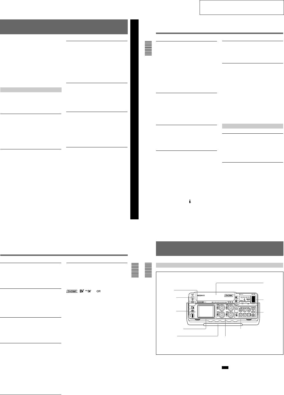
1 Time counter display
Displays the following:
¥Time data: Time code, user bits
¥Self-diagnostics (see page 98 (GB))
Note
The time code is displayed with colons (:) between
digits regardless of the frame mode (drop frame/non-
drop frame).
2 WARNING indicator
Lights or flashes when the battery is exhausted or an
error occurs.
For details, see Alarm Messages on page 94 (GB).
3 COUNTER switch
Selects the time code or user bits to display in the time
counter display, LCD monitor and VIDEO OUT1
output.
TC: Time code
U-BIT: User bits
4 METER switch
Selects the audio channels to display audio levels in
the audio level meters qs.
CH1/2: Displays the audio level of audio channels 1
and 2.
CH3/4: Displays the audio level of audio channels 3
and 4.
5 LIGHT button
Turns on the backlight in the display window. The
backlight will automatically turn off in 10 seconds
after you release this button.
6 Warning indicators
Displays warnings.
For details on warnings, see Alarm Messages on page 94
(GB).
8Date display
9Time display
0Cassette indicator
qa OVER indicators
qs Audio level meters
qd Tape remaining
time indicator
1Time counter display
2WARNING indicator
3COUNTER switch
4METER switch
6Warning indicators
7DVCAM indicator qf Remaining battery
indicator
5LIGHT button
12
(GB) Chapter 1 Overview
Location and Function of Parts
Chapter 1 Overview
7 DVCAM indicator
This indicator appears as follows:
EE: When the DVCAM/DV select switch is set to
DVCAM.
Play: When a DVCAM formatted tape is being
played.
8 Date display
Displays the date on the internal clock.
9 Time display
Displays the time on the internal clock.
Note
When the battery pack is installed or the AC adaptor is
connected, the date and time are displayed even if the
power is turned off. With battery backup, the clock can
run for about one month without being charged by the
unit battery pack or by AC power.
0 Cassette indicator
Lights when a digital video cassette is in the unit and
that cassette is compatible with the unit.
qa OVER indicators
Lights when the audio level exceeds 0 dB in the EE
mode (except when inputting signals from the DV IN/
OUT connector).
Notes
¥These indictors do not light if the AUDIO SELECT
switch has been set to AUTO.
¥These indicators do not light while the unit is playing
a tape or is in the EE mode when inputting signals
from the DV IN/OUT connector.
qs Audio level meters
Displays the recording level in the recording or in the
EE mode; displays the playing level while playing a
tape.
qd Tape remaining time indicator
Displays the tape remaining. If the power has been
turned off, this shows the tape remaining when the
power was turned off. If the tape remaining is more
than 300 minutes (five hours), the number of hours
will be shown. If the tape remaining is less than 300
minutes, this number of minutes will be shown.
Note
If the tape has been rewound to the beginning, this
indicator will not show the tape remaining when the
tape is inserted into the unit. The tape remaining time
is displayed after the tape runs for a while.
qf Remaining battery indicator
Displays the remaining charge in the battery.
For details on the remaining battery, see page 18 (GB).
Chapter 1 Overview
13
(GB)
Chapter 1 Overview
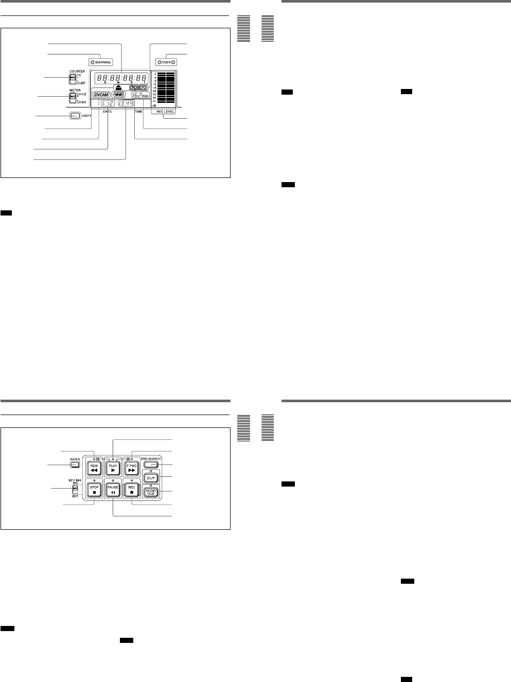
2 Tape transport control section
1 REW (rewind) button/indicator
When you press this button, the indicator lights and the
tape starts rewinding. During rewind, the picture does
not appear on the monitor (except EE pictures
1)
). If you
keep pressing this button during playback, rewind or in
playback pause mode, the contents of the tape will be
shown in reverse on the monitor while it is rewound
(picture search). When operation has stopped, if you
press the PLAY button while holding this button
down, the tape is rewound to the beginning and
automatically played.
You can change the tape transport mode in FF/REW
SPD on the VTR SET menu.
For details on VTR SET menu, see VTR SET menu on
page 90 (GB).
Notes
¥If you set the FF/REW SPD on the VTR SET menu
to SHUTTLEMAX, you can display the picture while
rewinding the tape.
¥If you set PB in EE/PB SET on the DISPLAY SET
menu, the EE pictures are not output while rewinding
the tape.
2 INDEX button
Press to mark an index while recording. An index is
useful when you search for the scene later.
For details on index, see Other Recording Functions on
page 52 (GB).
3 KEY INH (key inhibit) switch
Turning on this switch disables the tape transport
control buttons to prevent invalid button operations.
4 STOP button/indicator
Press to stop the tape. If there is a tape in the unit and
the tape has been stopped, the indicator lights.
5 PLAY button/indicator
Press to play back the tape. When the tape is being
played, the indicator lights.
Notes
¥When the unit is playing the part of the tape where
the format has been changed between the DVCAM
format and the DV format, the picture and sound may
be distorted.
¥The unit cannot play back a cassette recorded in LP
mode of the consumer DV format.
5PLAY button/indicator
6F FWD button/indicator
7END SEARCH button
8DUP button/indicator
9AUDIO DUB button/indicator
0REC button/indicator
qa PAUSE button/indicator
2INDEX button
3KEY INH switch
1) EE pictures
EE stands for Electric to Electric. In this EE mode, the
video and audio signals that are input to the VCRs
recording circuitry do not pass through any magnetic
........................................................................................................................................................................................................
conversion circuits but instead are output via electric circuits
only. This mode is used to check the input signals and adjust
input levels. The pictures output in EE mode are referred to
as EE pictures.
4STOP button/indicator
1REW button/indicator
14
(GB) Chapter 1 Overview
Location and Function of Parts
Chapter 1 Overview
6 F FWD (fast forward) button/indicator
When you press this button, the indicator lights and the
tape is fast forwarded. During fast forward, the picture
does not appear on the monitor (except EE pictures). If
you keep pressing this button during playback, fast-
forward or in playback pause mode, you can locate a
scene monitoring the picture (picture search).
You can change the tape transport mode in FF/REW
SPD on the VTR SET menu.
For details on the VTR SET menu, see VTR SET menu on
page 90 (GB).
Notes
¥If you set the FF/REW SPD on the VTR SET menu
to SHUTTLEMAX, you can display the picture while
fast-forwarding the tape.
¥If you set PB in EE/PB SET on the DISPLAY SET
menu, the EE pictures are not output while fast-
forwarding the tape.
7 END SEARCH button
Searches for the last part of the recorded image and
plays that part for five seconds. This function is used
when you record another image at the end of the
current image or check the last part of the recorded
image.
If you use a cassette without cassette memory and
remove the tape from the unit, the end search function
does not work. If you use a cassette with cassette
memory, the end search function continues to work.
However, if there is a blank portion at the beginning or
between the recorded portions, the end search function
may not work correctly.
8 DUP (duplicate) button/indicator
Used to duplicate a tape, including the time code.
During duplication, the indicator flashes.
For details on duplicate function, see Duplication
(generating a work tape with the same time code) on page
70 (GB).
When the INPUT SELECT selector is set to DV and a
DV signal is input, if you press only this button when
the unit is in the stop mode, the DUP indicator lights
and you can check the EE signals for image, sound and
time code. After checking them, press the STOP
button.
For details, see DISPLAY SET menu on page 84 (GB).
For details on the time code, see DSR-50/50P time codes
on page 62 (GB).
9 AUDIO DUB (audio dubbing) button/indicator
Use this button to dub the sound. The indicator flashes
while the sound is being dubbed.
For details on audio dubbing, see Audio Dubbing on
page 74 (GB).
When the INPUT SELECT selector is set to other than
DV, if you press only this button when the unit is in
the stop mode, the AUDIO DUB indicator lights and
you can check the EE sound signals. After checking
them, press the STOP button.
For details, see DISPLAY SET menu on page 84 (GB).
0 REC (record) button/indicator
When you start recording an image from an external
camera, press the PLAY button while holding this
button down. The unit is set to recording pause mode.
Then press the PAUSE button on the unit or the VTR
button on the camera to start recording. When you start
recording an image from a source other than an
external camera, press the PLAY button while holding
this button down. The indicator flashes and recording
starts. If you press only this button when the unit is in
the stop mode, the REC indicator lights and you can
check the EE signals for image, sound and time code.
After checking them, press the STOP button.
For details, see DISPLAY SET menu on page 84 (GB).
For details on time code, see DSR-50/50P time codes on
page 62 (GB).
Notes
¥The unit cannot record images unless video signals
are input.
¥If the video signals are interrupted during recording,
the unit is set to recording pause mode. When the
video signals are input again, recording is resumed.
That position of the tape where the recording resumes
may be distorted when the tape is played back.
¥This unit cannot record in the LP mode of the
consumer DV format.
qa PAUSE button/indicator
Press this button to set the unit to pause mode while
recording, playing or audio dubbing. Pressing this
button again resumes the operation. The indicator
flashes when the unit is in pause mode.
Note
If you have started recording using an external camera
by pressing the VTR button on the camera, pressing
the PAUSE button while recording does not pause the
recording.
For details on how to record an image using an external
camera, see Recording Using an External Camera on
page 45 (GB).
1-3
Chapter 1 Overview
15
(GB)
Chapter 1 Overview
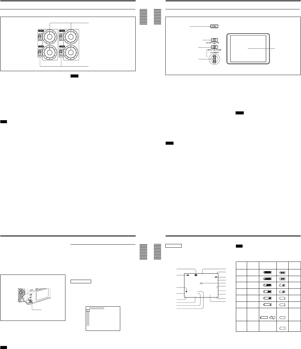
1 Audio recording level control knobs (CH-1 to
CH-4)
By turning these knobs, you can adjust the analog
audio input signal levels. You can adjust the audio
signal level only if the AUDIO SELECT switches 2
have been set to MANU.
If you press the FINE button in the monitor display
section when the DISPLAY (MENU/TC/AUDIO)
selector has been set to AUDIO, detailed audio levels
centered around the audio level that you set through
the menu are displayed.
For details on the AUDIO screen, see AUDIO screen on
page 20 (GB).
Note
You cannot adjust the audio signal level of the DV
signal.
2 AUDIO SELECT switches (CH-1 to CH-4)
Switches the recording level adjustment mode.
AUTO: Disables the audio recording level control
knob and automatically adjusts the recording
level.
MANU: Enables the audio recording level control
knob to manually adjust the recording level.
3 Audio control section
1Audio recording level control knobs
Notes
¥When inputting signals from the DV IN/OUT
connector, these settings are invalid.
¥If the sound is louder than the amplifiers dynamic
range, the AUTO setting is ineffective.
¥Even if AUTO has been set, unless the audio input
level control selectors in the right panel are
appropriate, there may be clipping and noise.
¥The audio level is automatically equalized to an
appropriate level when you select AUTO. It takes
about 20 seconds for the audio level to be stabilized
in the following cases.
—immediately after powering on
—immediately after stopping a playback operation
—immediately after switching the audio mode in
AUDIO MODE on the AUDIO SET menu
¥If the LIMITER on the AUDIO SET menu has been
set to ON, and if the audio input is too loud while you
are manually adjusting the audio level, you can still
record the sound without clipping. The LIMITER
setting is available only when this switch is set to
MANU.
2AUDIO SELECT switches
16
(GB) Chapter 1 Overview
Location and Function of Parts
Chapter 1 Overview
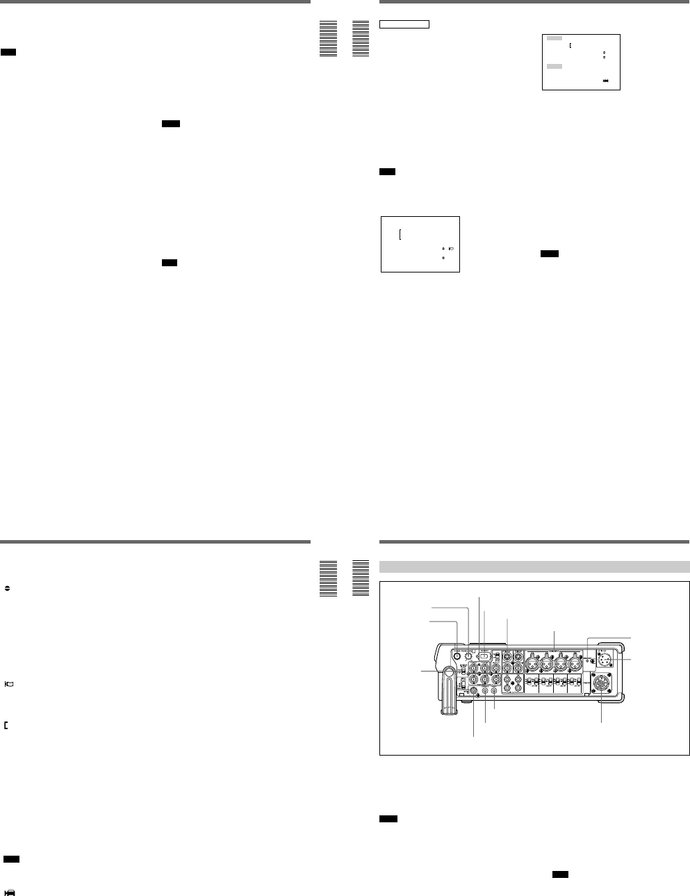
1 FINE button
If you press this button when the DISPLAY (MENU/
TC/AUDIO) selector 3 has been set to AUDIO, the
LCD monitor displays detailed audio level meters
centered around the audio level that you set through
the menu as well as various settings in text.
For details on the FINE screen, see FINE screen on page
20 (GB).
2 DISPLAY (LCD OFF/OFF/ON) selector
Switches the LCD monitor mode.
LCD OFF: Turns off the LCD monitor power.
OFF: Displays the LCD monitor. Text data is not
superimposed. The tape label, title and data codes
(camera data, and date/time recorded by the
camera) are displayed.
ON: Displays the LCD monitor. Text data is
superimposed.
Notes
¥You can set the unit to display/hide a tape label, title
and data codes only from the menus.
¥To change a menu setting, turn ON the DISPLAY
(LCD OFF/OFF/ON) selector or turn ON the
SUPERIMPOSE switch on the right panel. If the
LCD monitor or external monitor does not display a
superimposed screen, you cannot set a menu.
4 Monitor display section
3 DISPLAY (MENU/TC/AUDIO) selector
Switches the superimposed text data for display on the
LCD monitor.
MENU: Displays the menu screen.
TC: Displays the time codes, remaining battery, tape
remaining time, selected input signal, audio mode,
presence or absence of cassette memory, tape
label, title, etc.
AUDIO: Displays the audio levels.
Notes
¥You can use the DSRM-20 (not supplied) to search
for the scene using the index signal on the tape. In
this case you can search for the scene regardless of
this selector setting. But you can display —/+ only
while this selector is set to TC.
¥If you change the setting of this switch during a
cassette memory search, the cassette memory search
is stopped.
S
E
L
/
P
U
S
H
E
X
E
C
5 LCD monitor
1FINE button
2DISPLAY (LCD OFF/OFF/
ON) selector
3DISPLAY (MENU/TC/
AUDIO) selector
4SEL/PUSH EXEC dial
Chapter 1 Overview
17
(GB)
Chapter 1 Overview
4 SEL/PUSH EXEC dial
If the DISPLAY (MENU/TC/AUDIO) selector 3 has
been set to MENU, rotating this dial changes the menu
items being displayed and pressing this dial selects a
particular menu item.
If the DISPLAY (MENU/TC/AUDIO) selector 3 has
been set to TC, rotating this dial adjusts the LCD
monitor brightness.
For details on the menu, see Operating the Menus on
page 76 (GB).
5 LCD (Liquid Crystal Display) monitor
Displays the playback or EE pictures as well as
superimposed time data, status information, menu, etc.
Note
The superimposed data output to the LCD monitor and
the VIDEO OUT1 are the same. You cannot display a
different superimposed data.
Text data superimposed on the LCD
monitor
If you set the DISPLAY (LCD OFF/OFF/ON) selector
to ON, you can superimpose the text data on the LCD
monitor. By setting the DISPLAY (MENU/TC/
AUDIO) selector to a particular setting, you can select
superimposed text data for display on the LCD
monitor.
MENU screen
By setting the DISPLAY (MENU/TC/AUDIO)
selector to MENU, you can set various data in the
menus.
For details on the menu, see Chapter 6, Adjusting and
Setting Through Menus on page 76 (GB).
TC ⁄ UB SET
TC PRESET
UB PRESET
TC FORMAT
TC RUN
TC ⁄ UB IN
TC MAKE
UB TIME
JOG TC OUT
TC
CM
DISP
V
A
LCD
VTR
ETC
Rotate
up/down
Press
18
(GB) Chapter 1 Overview
Location and Function of Parts
Chapter 1 Overview
TC screen
This screen shows the time data, tape remaining time,
remaining battery, data codes, etc. These data items are
important for normal recording/playback operation. To
display the TC screen, set the DISPLAY (MENU/TC/
AUDIO) selector to TC.
L i
MANUAL
10000 ATW
F1. 6 12
dB
N
00:12:34:12
122min
PHOTO –10
SEARCH
PAL
DVCAM
NS 48K
DV IN
1 Remaining battery indicator
Displays the remaining battery and the battery type.
You can select the battery type in uREMAIN on the
DISPLAY SET menu.
Li: Lithium-ion battery
Ni: Ni-Cd (nickel-cadmium) battery
Note
The remaining battery is displayed even if you use the
unit with AC power by connecting the AC adaptor to
the DC IN 12V connector.
a) The indicator flashes 3.2 times per second in the rapid
flashing mode and flashes 0.8 time per second in the slow
flashing mode.
2 Cassette memory indicator
This is shown when a cassette with cassette memory
has been loaded. This indicator flashes when you
remove the cassette while the system is writing data in
the cassette memory.
3 Tape transport mode indicator
Displays the tape transport mode.
4 Time code indicator
Displays the time code or user bits. Change the display
(time code or user bits) by changing the COUNTER
switch on the front panel. In the drop frame mode, a
period is displayed between the minute and second.
(Example: 00:12.58:00)
If the self-diagnostic function is enabled, a diagnostics
code numbers are displayed.
1
2
qj, ql
qk
qg
qh, w;, wa
qf
qd
3
4
5
6
7
8
9
0
qa
qs
Ni-Cd
battery
voltage
Lithium-ion
battery
voltage
LCD monitor/
VIDEO OUT1
display
a)
Display
window
a)
Camera’s
battery
indicator
a)
Slow flashing
Battery-end
warning Light
11.0 V or less 11.0 V or less
Rapid flashing
12.5 V or more 15.0 V or more
12.0 – 12.5 V 14.0 – 15.0 V
11.75 – 12.0 V 13.0 – 14.0 V
11.5 – 11.75 V 12.0 – 13.0 V
11.3 – 11.5 V 11.3 – 12.0 V
11.25 – 11.3 V 11.25 – 11.3 V
11.0 – 11.25 V 11.0 – 11.25 V
Slow
flashing Slow flashing
1-4
Chapter 1 Overview
19
(GB)
Chapter 1 Overview
5 Tape remaining time indicator
If qREMAIN on the DISPLAY SET menu has been
set to ON, the tape remaining time is displayed.
Note
If the tape has been rewound to the beginning, this
indicator will not show the tape remaining time when
the tape is inserted into the unit. The tape remaining
time is displayed after the tape runs for a while.
6 Search/Index indicator
Displays the search mode. If an index has been
marked, this displays INDEX MARK. If you use the
end search function, this displays END SEARCH.
7 Warning indicators
Displays a warning.
For details on warnings, see Alarm Messages on page 94
(GB).
8 PAL (DSR-50)/NTSC (DSR-50P) indicator
DSR-50: Appears for five seconds when you play back
a PAL formatted tape.
DSR-50P: Appears for five seconds when you play
back a NTSC formatted tape.
9 DVCAM/DV indicator
In the EE, recording, and duplicate modes, displays the
DVCAM/DV select switch setting. During playback,
displays the format recorded on the tape.
0 Audio mode indicator
In the EE and recording modes, displays the selected
audio mode in AUDIO MODE on the AUDIO SET
menu. During playback and audio dubbing, displays
the audio mode recorded on the tape. When inputting
signals from the DV IN/OUT connector, displays the
audio mode input from the DV IN/OUT connector.
qa Input signal indicator
Displays the INPUT SELECT selector setting.
qs NS (Non Standard) audio mode indicator
Lights when you play back a tape in the unlock audio
mode or when the unlock mode signal has been input
from the DV IN/OUT connector. Always lights if the
DVCAM/DV select switch has been set to DV and the
unit is in the EE mode.
For details on the unlock mode, see Compatibility of
DVCAM and DV Format on page 99 (GB).
qd Program AE indicator
qf White balance indicator
qg Gain indicator
qh Iris indicator
qj Shutter speed indicator
qk SteadyShot indicator
Notes
¥Data items qd through qk show the settings (camera
data) of the tape recorded by the camera (DSR-200/
200P, 200A/200AP, PD100/PD100P, PD100A/
PD100AP, PD150/PD150P, etc.). This unit cannot
record camera data.
¥Data items qd through qk are displayed only when
DATA CODE on the DISPLAY SET menu has been
set to CAMERA.
For details on DATA CODE, see DISPLAY SET menu on
page 84 (GB).
ql Date indicator
Displays the date when the tape was recorded.
w; Time indicator
Displays the time when the tape was recorded.
Note
Data items ql and w; are displayed only when DATA
CODE on the DISPLAY SET menu has been set to
DATE.
wa LCD monitor brightness
This is displayed when you adjust the LCD monitor
brightness by rotating the SEL/PUSH EXEC dial. This
display disappears in one second after you adjust the
brightness. You can adjust the LCD monitor brightness
when you have set the DISPLAY (MENU/TC/
AUDIO) selector to TC and the DISPLAY (LCD OFF/
OFF/ON) selector to OFF or ON.
20
(GB) Chapter 1 Overview
Location and Function of Parts
Chapter 1 Overview
AUDIO screen
You can check and adjust the audio levels and check
the audio input signal settings on this screen. To
display this screen, set the DISPLAY (MENU/TC/
AUDIO) selector to AUDIO. While this screen is
displayed, you can press the FINE button to display
the FINE screen. The FINE screen is only displayed
when you keep pressing the FINE button.
While a tape is being played back, this screen displays
the audio mode recorded on the tape. When recording
a picture, this screen displays the audio mode selected
in AUDIO MODE on the AUDIO SET menu. When
inputting signals from the DV IN/OUT connector, this
screen displays the input audio mode. If the audio
mode has been set to 32 kHz, this screen displays four
channels; if the audio mode has been set to 48 kHz,
this screen displays two channels.
Note
You cannot change the audio mode while inputting
signals from the DV IN/OUT connector.
Normal screen
–
∞
40 30 20 10 0
dB
CH1 ||||||||||||||||||·|··· ·
CH2 |||||||||||||||||·|···· ·
CH3 ||||||||||||||||||||||| |
CH4 |||||||||||||·|········ ·
······
This screen displays the audio levels. By adjusting the
audio recording level control knobs in the front panel,
you can adjust the recording level. In the EE,
recording, or audio dubbing (only the audio dubbing
channel) modes, the level display runs all the way to
the right (0 dB) and turns red if the input level exceeds
0 dB. During playback, when inputting signals from
the DV IN/OUT connector, or if you have set the
AUDIO SELECT switch to AUTO, the level display
does not run all the way to the right (0 dB).
FINE screen
LEVEL –22 –20 –18
dB
CH1 |||||||||||······
CH2 ||||||||||·······
CH3 |||||||||||||||··
CH4 ||||||···········
INPUT GA I N 48V LVL
CH1 AUTO ON –60
CH2 AUTO ON –60
CH3 AUTO OFF –20
CH4 MANU OFF + 4
When the normal screen is being displayed, pressing
the FINE button displays the FINE screen. The FINE
screen is displayed only while you are pressing the
FINE button. The FINE screen displays narrower
audio levels around the audio levels (—12/—18/—20 dB)
selected in the REF LEVEL on the AUDIO SET menu
and displays the audio input signal settings. You can
finely adjust recording levels by adjusting the audio
recording level control knobs on the front panel.
The audio input signals are displayed as follows:
GAIN: Displays the AUTO/MANU setting of the
AUDIO SELECT switch.
48V: If the audio input level control selector has been
set to —60 and the audio input selector has been set
to +48V ON, this column shows ON, otherwise
this column shows OFF.
LVL: Displays the setting (—60/—20/+4) of the audio
input level control selector.
Notes
¥Changing the REF LEVEL on the AUDIO SET menu
does not change the audio gain of the unit. Adjust the
audio gain by setting the audio input level control
selectors and adjusting the audio recording level
control knobs.
¥The standard output level of the AUDIO OUTPUT
jack of the unit is —10 dBu. This is equivalent to —20
dB level for the full-bit maximum audio level
(—18 dB level for DSR-50P). This value is fixed and
is not affected by the REF LEVEL setting on the
AUDIO SET menu.
¥When inputting signals from the DV IN/OUT
connector, the INPUT field shows DV IN.
¥When inputting signals from other than DV IN/OUT
connector, the INPUT shows the available audio
channels.
Chapter 1 Overview
21
(GB)
Chapter 1 Overview
The audio screen shows the following symbols
depending on the menu settings, etc.
:Audio dubbing symbol
This symbol appears with a channel on which you
can dub sound. You can select a channel to dub
the sound in the AUDIO DUB on the AUDIO
SET menu.
This symbol appears during playback of a tape
recorded in 32 kHz of the DVCAM format.
This symbol also appears during audio dubbing on
a tape recorded in 32 kHz of the DVCAM format.
This symbol does not appear when the INPUT
SELECT selector is set to DV.
:Wind noise reduction symbol
This symbol appears with a channel in which the
WIND on the AUDIO SET menu has been set to
ON.
:Link symbol
If the AGC (Auto Gain Control) of a pair of
channels is linked, this symbol is placed between
the channels.
If AGC CH1, 2 on the AUDIO SET menu have
been set to LINKED and channels 1 and 2 in the
AUDIO SELECT switch have been set to AUTO,
channels 1 and 2 can be linked for AGC operation
and for stereo sound where channel 1 is set for the
left sound and channel 2 is set for the right sound.
If AGC CH3, 4 on the AUDIO SET menu have
been set to LINKED and channels 3 and 4 in the
AUDIO SELECT switch have been set to AUTO,
channels 3 and 4 can be linked for AGC operation
and for stereo sound where channel 3 is set for the
left sound and channel 4 is set for the right sound.
Note
This symbol does not appear when inputting signals
from the DV IN/OUT connector.
:Camera symbol
This symbol appears at the right side of the LVL
display when the INPUT SELECT selector is set
to other than DV and the audio input selector is set
to CAM.
22
(GB) Chapter 1 Overview
Location and Function of Parts
Chapter 1 Overview
Right Panel
1 PHONES (headphones) jack (stereo phone jack)
Connects to the headphones. You can monitor the
audio signals being recorded or played through the
headphones. Select the audio signal you want to
monitor by selecting the channels with the MONITOR
SELECT selector qa.
Notes
¥A warning tone is output on the headphone sound and
return sound to the camera. A warning tone is not
mixed on the signals output from the AUDIO
MONITOR OUT and AUDIO OUTPUT jacks.
¥By setting the BEEP on the OTHERS menu to
MELODY, the selected melody beep sound is mixed
on the headphone sound and the return sound to the
camera when you operate the menu.
2 PHONE LEVEL control knob
Adjusts the volume of the headphones that are
connected to the PHONES jack 1 and the audio level
of the return sound to the camera.
3 TC (time code) IN/OUT connectors (BNC-type)
Used to input or output the time code through these
connectors.
TC IN connector: Connects to the time code output
connector on the external devices such as a time
code generator or a VCR. This connector is used
to synchronize the internal time code generator of
this unit with an external time code.
Note
The unit can read the time code input to this
connector only when the time code is output at
normal play speed.
3TC IN/OUT connectors
4DV IN/OUT connector
5BREAKER button
6DC IN 12V
connector
7CAMERA connector
8REMOTE connector
9CONTROL S connector
0AUDIO MONITOR OUT jack
qa MONITOR
SELECT
selector
1Video signal input/output
section (see page 25 (GB))
2Audio signal input/output section (see page 27 (GB))
1PHONES jack
2PHONE LEVEL
control knob
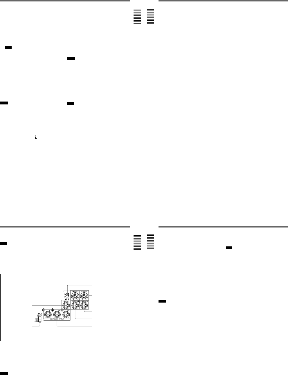
1-5
Chapter 1 Overview
23
(GB)
Chapter 1 Overview
TC OUT connector: Connects to the time code input
connector on the external devices such as a time
code reader or a VCR.
The unit outputs the following time codes
depending on the operating state:
Playing: The time code on the tape is output.
Recording: Either the time code generated by the
internal time code generator or the time code
signals from the external device are output.
For details, see DSR-50/50P time codes on page 62
(GB).
Note
If the JOG TC OUT on the TC/UB SET menu has
been set to ON, the time code is output during
search mode, but the output time code is not a
continuous one.
4 DV IN/OUT connector (6-pin)
Used to input/output the digital signal with a locking
mechanism that complies with the i.LINK standard
(Recommended cable: CCFD-3L, CCF-3L). If you
have an external device that has a DV connector, you
can connect that device to this connector to record or
duplicate a tape or capture pictures. The digital signals
for the sound or pictures captured through this
connector have almost no degradation. For details,
refer to the instruction manual of the external device.
Notes
¥The DV/IN OUT connector of this unit is a 6-pin
connector but does not provide power to any
connected external device. You can also use a 6-pin
connector without a locking mechanism.
¥If video signals have been input to the DV IN/OUT
connector and you output these video signals to the
VIDEO OUT1, VIDEO OUT2, or S VIDEO OUT
connectors, the sync and burst of the EE pictures are
not synchronized.
¥i.LINK and the i.LINK logo are trademarks and
indicate that this product is in agreement with IEEE
1394-1995 specifications and their revisions.
5 BREAKER button
If excessive current flows inside the unit, the breaker is
activated, and the power to the unit is shut down. If
this button is activated and pushed out, check the unit
and the camera connected to the CAMERA connector
to make sure they are not malfunctioning. If they
appear to be functioning properly, press this button. If
there are no problems, power will be supplied again.
6 DC IN 12V connector (XLR 4-pin/Male)
Used to supply the unit with DC power.
If you have installed a battery pack in the battery
compartment, whichever power source is providing the
higher voltage provides the power to the unit.
Notes
¥The DC power source must be 12 V to 17 V/2.0 A
(peak: 4.0 A) or higher.
¥If you have connected an AC adaptor to this
connector and the battery voltage is higher than the
AC power, the battery power is used first.
For details on the DC IN 12V connector, see Power
Preparations on page 31 (GB).
7 CAMERA connector (26-pin)
Connects to a camera (not supplied). The unit can
supply power to the external camera with this
connector.
Note
If you have installed a small capacity battery pack such
as a BP-L40(A) and supplied power to an external
camera connected from the CAMERA connector, the
operation time with the battery pack might be
significantly reduced when the camera power
consumption is too high. Use a large capacity battery
pack or obtain power for the camera from a separate
power source.
For details on how to record images using the CAMERA
connector, see Recording on page 45 (GB).
24
(GB) Chapter 1 Overview
Location and Function of Parts
Chapter 1 Overview
8 REMOTE connector
Connects to a foot switch.
For details on how to set the foot switch, see VTR SET
menu on page 90 (GB).
9 CONTROL S connector (minijack)
Connects to a remote control unit (DSRM-20, not
supplied) for controlling this unit.
0 AUDIO MONITOR OUT jack (phono jack)
Outputs the audio signals for monitoring. Select the
audio signals with the MONITOR SELECT selector
qa.
qa MONITOR SELECT selector
Selects audio channels to output to the PHONES jack
1, AUDIO MONITOR OUT jack 0 and return
sound to the camera.
CH1/2: Channels 1 and 2
MIX: Channels 1 to 4
CH3/4: Channels 3 and 4
Chapter 1 Overview
25
(GB)
Chapter 1 Overview
1 Video signal input/output section
1 VIDEO OUT1 connector (BNC-type)
Outputs composite video signals. Connect to the input
connector of an external monitor. If the
SUPERIMPOSE switch 3 has been set to ON, text
data (time data, menus and alarm messages) is
superimposed.
For details on the superimposed data, see Text data
superimposed on the LCD monitor on page 17 (GB).
Notes
¥When a video sync signal of the EE pictures are
output to the VIDEO OUT1 connector, sync and
burst are not synchronized.
Note
You only can input standard video signals to the unit.
If you input the types of video signals shown below,
the EE picture output to the VIDEO OUT2 connector,
S VIDEO OUT connector and COMPONENT
OUTPUT connectors may be distorted.
¥Signals from some home game machines
¥Blue background screen or gray background screen
from a consumer VCR
¥Pictures played at a speed other than normal by a
VCR that does not have the TBC (Time Base
Corrector)
¥Video signals in which the sync signals are distorted
¥Signals from a defective cassette (tape or recording
condition is bad) played by an analog VCR that does
not have the TBC
¥The video signal output from this connector is not
synchronized with the video signal output from the
line-out connectors (COMPONENT OUTPUT, S
VIDEO OUT, VIDEO OUT2). When the unit is in
the EE mode, the output pictures are delayed by
several lines. When played, the picture is not
externally synchronized only vertically
synchronized. You cannot adjust the sync and
subcarrier phases.
¥If DV input has been selected, color and luminance
may be distorted in the EE mode, depending on the
monitor type.
3SUPERIMPOSE switch
4S VIDEO IN/OUT connectors
5VIDEO/REF. IN connector
6VIDEO OUT2 connector
7COMPONENT OUTPUT
connectors
1VIDEO OUT1 connector
2INPUT SELECT selector
26
(GB) Chapter 1 Overview
Location and Function of Parts
Chapter 1 Overview
¥The superimposed data output to the LCD monitor
and the VIDEO OUT1 are the same. You cannot
display a different superimposed data.
¥The adjustment of VIDEO LVL on the VIDEO SET
menu does not affect the VIDEO OUT1 output and
return signal to the camera.
¥If the unit is externally synchronized, jitters may
appear in the VIDEO OUT1 connector output and the
LCD monitor image because the sync signal
frequency and the burst signals are not synchronized.
If the unit is externally synchronized, use the VIDEO
OUT2 connector. If you use the VIDEO OUT1
connector, set EXT SYNC on the VIDEO SET menu
to OFF.
2 INPUT SELECT selector
You can select DV, VIDEO, S VIDEO or CAMERA
to input the signals. The selected input is displayed on
the TC screen of the LCD monitor.
Notes
¥When inputting signals from the DV IN/OUT
connector, the following settings are disabled:
—Video input level
—Audio input selectors (CAM/LINE/+48V ON)
—Audio input level control selectors (—60/—20/+4)
—Audio recording level
—Audio recording mode (AUTO/MANU)
—Audio mode (32 kHz/48 kHz)
—Audio AGC (Auto Gain Control)
—Wind noise reduction
—Audio limiter
—You cannot display the color bars.
¥If you change this selector, the screen may
momentarily become bright or noise may appear.
This noise will be recorded.
3 SUPERIMPOSE switch
Turn on this switch to superimpose text data onto the
output from the VIDEO OUT1 connector.
Note
The return signal to the camera is the same as the
output from the VIDEO OUT1 connector.
4 S VIDEO IN/OUT connectors (4-pin)
Inputs/Outputs the S-video signal with separated Y
(luminance) and the C (chroma: 3.58 MHz for DSR-50
and 4.43 MHz for DSR-50P).
5 VIDEO/REF.IN (reference input) connector
(BNC-type)
Inputs composite video signals to this unit. When
performing a playback synchronized with the external
sync signal, this connector inputs reference video
(black burst) signal.
6 VIDEO OUT2 connector (BNC-type)
Outputs composite video signals. The text data is not
superimposed.
7 COMPONENT OUTPUT Y, R-Y, B-Y
connectors (BNC-type)
Outputs component video (Y, R-Y, B-Y) signals.
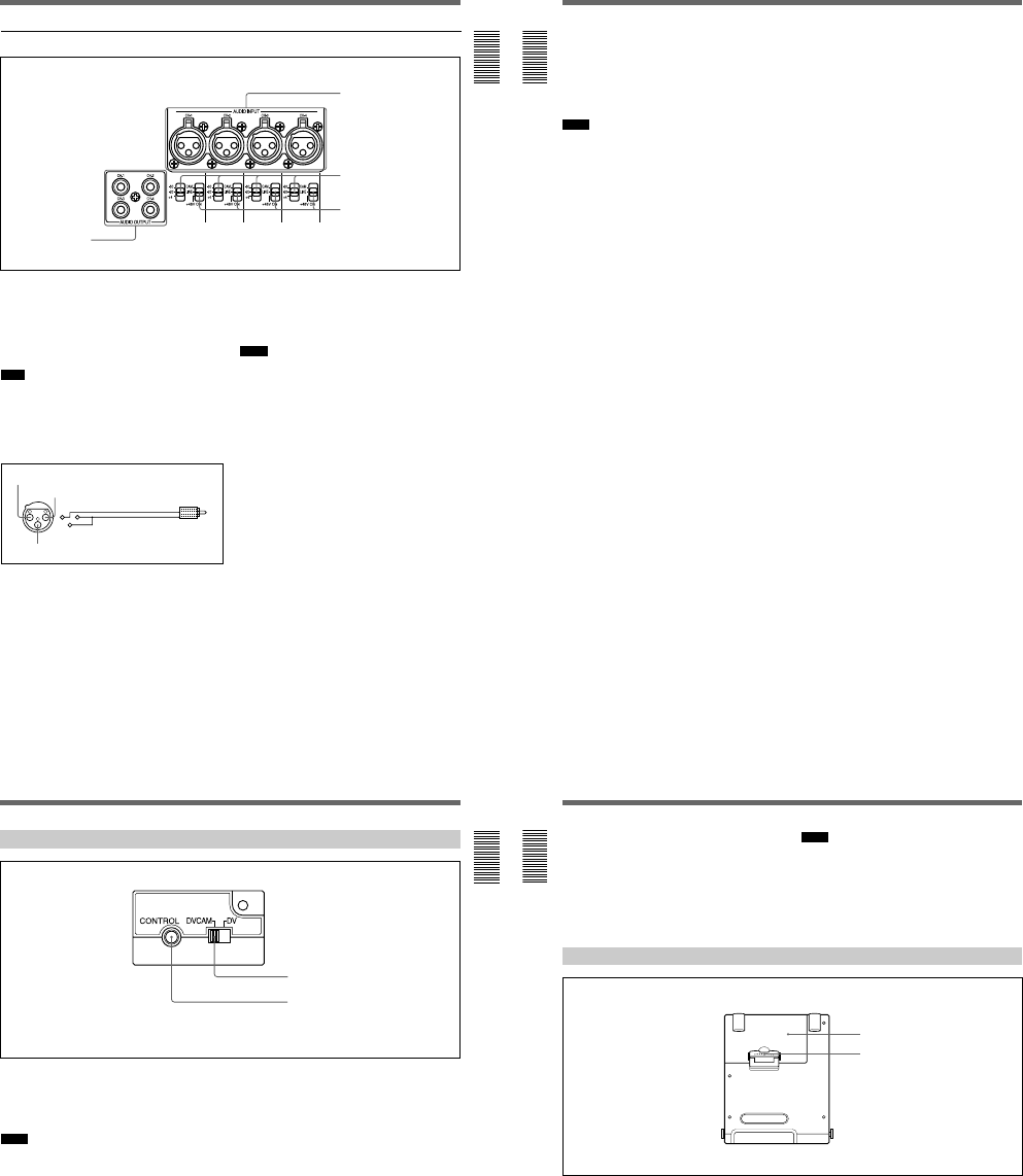
1-6
Chapter 1 Overview
27
(GB)
Chapter 1 Overview
1 AUDIO OUTPUT CH-1 to CH-4 jacks (phono
jack)
Outputs audio signals (CH-1 to CH-4).
2 AUDIO INPUT CH-1 to CH-4 connectors (XLR
3-pin, female)
Inputs audio signals (CH-1 to CH-4).
Note
The unit employs electronically balanced AUDIO
INPUT connectors. To input unbalanced audio signals
(a phono jack of a consumer VCR, etc.), use a
conversion cable as shown below. (This conversion
cable shorts the COLD and the common terminal
(GND)).
2 1
3
2 Audio signal input/output section
3 Audio input level (—60/—20/+4) control selectors
When the INPUT SELECT selector is set to other than
DV, select an audio input signal level (—60/—20/+4) for
the CAMERA connector or AUDIO INPUT
connectors.
Notes
¥If this switch setting is not appropriate, clipping
distortion or noise may occur even if the AUDIO
SELECT switch has been set to AUTO.
¥The unit is not compatible with a camera that outputs
+4 dB. If you set the audio input selectors to CAM,
select —60 dB or —20 dB depending on the output
level of the camera.
¥If you can select the output level (—60 dB or —20 dB)
on the camera, select —20 dB on the camera and the
unit. When the unit and the camera are connected
with a long camera cable, noise may be minimized.
1AUDIO OUTPUT
jacks
2AUDIO INPUT connectors
3Audio input level control
selectors
4Audio input selectors
HOT
COM (GND)
COLD
Signal
GND
28
(GB) Chapter 1 Overview
Location and Function of Parts
Chapter 1 Overview
4 Audio input (CAM/LINE/+48V ON) selectors
Select audio signals input to channels 1 to 4 when the
INPUT SELECT selector is set to other than DV.
CAM: Audio signals from the CAMERA connector
LINE: Audio signals from the AUDIO INPUT
connectors
+48V ON: Supplies power to the 48 V microphone.
Notes
¥If you have selected +48V ON, do not insert a metal
object into the AUDIO INPUT connectors. It may
cause electric shock.
¥If you have selected +48V ON, use a microphone that
is compatible with 48 V. Using a microphone that is
incompatible may damage the microphone, generate
smoke or cause a fire.
¥The +48V ON setting is in effect only when you use
the AUDIO INPUT connectors and the audio input
level control selectors 3 are set to —60 dB.
Chapter 1 Overview
29
(GB)
Chapter 1 Overview
Left Panel
1 DVCAM/DV select switch
Switches the recording mode between DVCAM and
DV (SP mode only). When you play back a tape, the
DVCAM/DV setting will be automatically switched;
you do not need to use this switch.
Notes
¥The unit is not compatible with playing or recording
in consumer DV format (LP mode).
¥If you switch the DVCAM/DV select switch setting
while recording, the unit automatically pauses the
recording and then resumes recording several seconds
later. Nothing is recorded during that interval. You
cannot change the mode smoothly while recording.
¥It is recommended that you record in the DVCAM
format. There are some limitations with respect to
DV recording depending on machine specifications
and the consumer DV format as follows:
—The head system is optimized for DVCAM
recording. A DV recording overwrites the last track
just before the beginning of the recording. As a
result, at the border of these two recorded portions,
picture and sound may be distorted.
—The sound will be recorded unsynchronized.
(unlock mode)
—The time code is fixed to the drop frame mode.
(only for DSR-50)
—You cannot change the TC PRESET, UB PRESET,
TC FORMAT, TC RUN, TC/UB IN, TC MAKE,
UB TIME settings on the TC/UB SET menu. The
setting and status set at the time of the DVCAM
recording will be canceled.
—The time code automatically progresses so that the
recorded tracks are continued.
—If you start recording from a blank portion, the time
code starts from 00:00:00:00.
—The user bits are not recorded. When you play back
the tape, the user bits display will be
— —— —— —— —.
—Even if you input an external time code into the TC
IN connector, the time code used will be the one
provided by the internal time code generator.
¥If you dub a consumer DV tape from the DV IN/OUT
connector, keep the following in mind:
—Set the DVCAM/DV select switch to DV. If the
DVCAM/DV select switch has been set to
DVCAM, a tape with an invalid format (the
recording speed: DVCAM, sound: unsynchronized,
unlock mode) will be made. (The unit cannot
convert unlock mode sound to lock mode sound.)
—When you edit a tape with an invalid format in the
DSR-70/70P, DSR-80/80P, DSR-85/85P, DSR-
2000/2000P, etc., there may be some restrictions.
For details on the DVCAM/DV format compatibility, see
Compatibility of DVCAM and DV Format on page 99
(GB).
1DVCAM/DV select switch
2CONTROL connector
(A lid is installed on the left panel at shipping.)
30
(GB) Chapter 1 Overview
Location and Function of Parts
Chapter 1 Overview
2 CONTROL connector
You can connect most of the LANC
1)
devices to this
connector. On a regular LANC connector, you can
only switch to the recording mode from the stop mode.
This unit has an extended function that allows you to
switch to the recording mode directly from the
playback, fast-forward, rewind, slow-play, still, cue
and review modes.
Notes
¥You cannot control the power on/off of the unit from
a LANC device connected to the CONTROL
connector.
¥The CONTROL connector of this unit has only
LANC-S functions. This unit has no LANC-M
functions.
Top Panel
1 Battery cover
You can open the cover when you attach/remove the
battery into/from the battery compartment.
2 Battery cover lock
Unlock when you open the battery cover.
For details on how to install a battery pack, see Using the
BP-L40(A)/L60A/L90A Battery Pack on page 32 (GB).
1Battery cover
2Battery cover lock
..........................................................................................................................................................................................................
1) LANC (Local Application Control bus system):
Bidirectional interface to control a consumer VCR.
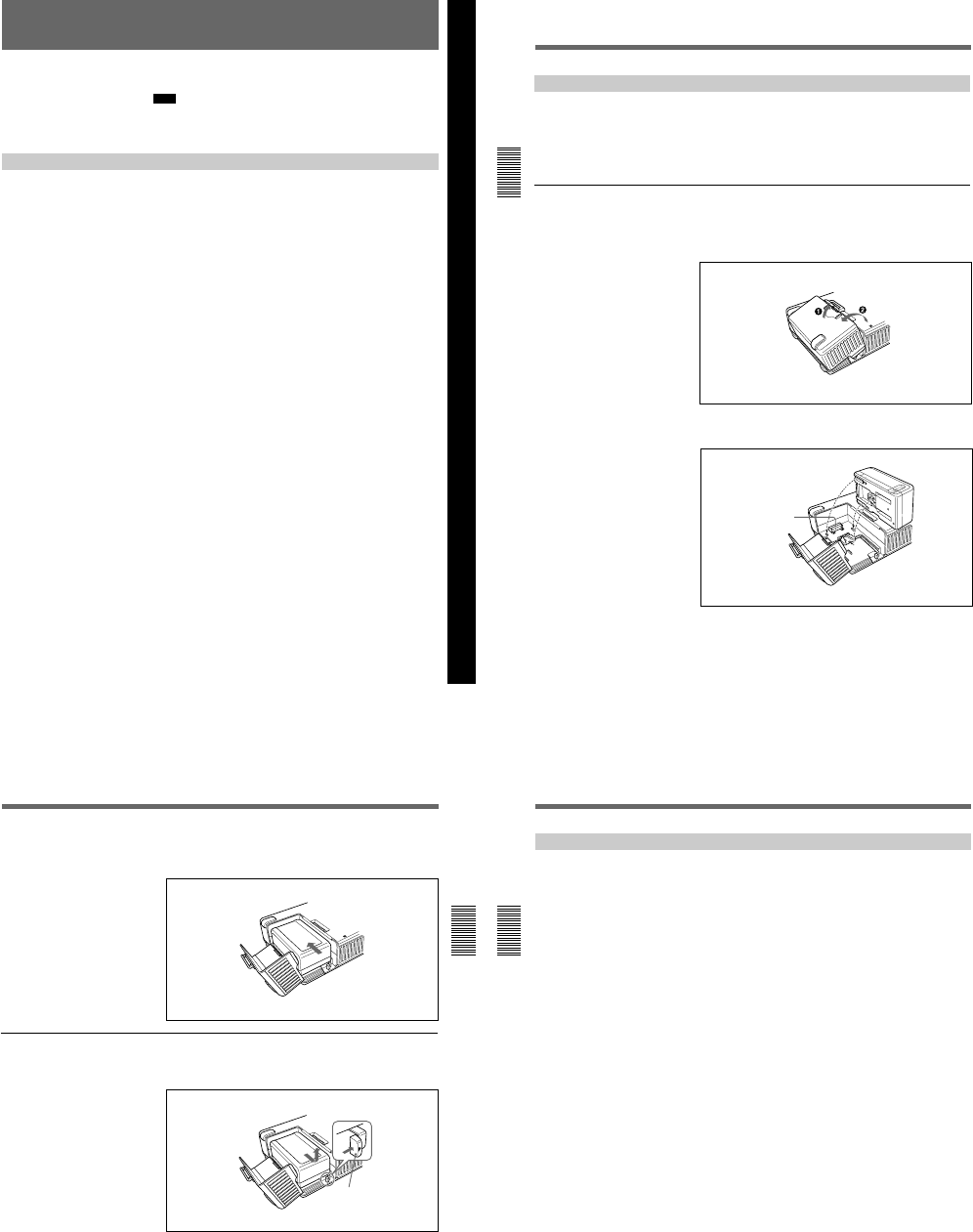
1-7
Chapter 2 Preparations
31
(GB)
Chapter 2 Preparations
Power Preparations
This unit can be powered by batteries or AC power.
Note
If you attach or remove batteries incorrectly, you may drop the battery,
causing bodily injury or damage to the battery. Attach or remove the
battery according to the procedure described below.
Usable Batteries
Use the following batteries: BP-L40, L40A, L60A, L90A. You will need
either the BC-L100 or the BC-L50 battery charger.
Notes about battery usage
¥Before using batteries, be sure to charge the battery with a charger
specified for that particular type of battery. Refer to the operating
instructions of your battery charger for more information about how to
charge the batteries.
¥Batteries may not be completely charged if you charge them immediately
after use when they are still warm. You should wait until the batteries
cool before charging them.
¥This unit cannot charge the battery.
Chapter 2 Preparations
Power Preparations
32
(GB) Chapter 2 Preparations
Chapter 2 Preparations
Using the BP-L40(A)/L60A/L90A Battery Pack
To charge the battery pack
Before use, charge the battery pack with the BC-L100 or BC-L50 battery
charger.
For more information about how to charge the battery pack, refer to the
instruction manual of the battery charger.
To attach the battery pack in the battery compartment
The battery compartment is on the top panel. Attach the battery pack (BP-
L40(A)/L60A/L90A) in the battery compartment as shown below.
1Lift up the battery cover lock and open the battery cover.
2Align the three grooves on the bottom of the BP-L40(A)/L60A/L90A
with the three guides on the unit.
Battery connector
Chapter 2 Preparations
33
(GB)
Chapter 2 Preparations
3Slide the BP-L40(A)/L60A/L90A so that the battery connector
connects to the battery connector of the unit. Continue to slide the BP-
L40(A)/L60A/L90A in until it clicks firmly into place.
To remove the battery pack
With the lever pushed in, slide the BP-L40(A)/L60A/L90A in the direction
of the arrow (see figure).
Lever
Power Preparations
34
(GB) Chapter 2 Preparations
Chapter 2 Preparations
Notes on Using the DC IN 12V Connector
When you attach a battery pack in the battery compartment and connect a
battery adaptor or AC adaptor to the DC IN 12V connector, keep the
following in mind.
¥Noise may appear momentarily on the image or sound in the following
cases:
—The power source has been switched between one from the battery
compartment and the other from the DC IN 12V connector.
—The power source is connected to the battery compartment (or to the
DC IN 12V connector) when the other power source has been
connected to the DC IN 12V connector (or to the battery compartment).
—One of the two power sources is disconnected from the battery
compartment or from the DC IN 12V connector.
¥The remaining charge of the battery is displayed even if you use only the
AC adaptor for the power source.
¥When you have connected both a battery pack and an AC adaptor, the
unit will use the battery pack power if the battery pack power is higher.
¥If you attach a battery pack both in the battery compartment and to the
DC IN 12V connector, every time the voltage difference between the
battery pack and the DC IN 12V power becomes over 1V, the unit
switches to the higher voltage power source. If you use a small capacity
battery pack such as BP-L40(A), the power source will change
frequently. To avoid this, do the following:
—If you use a small capacity battery pack, do not attach battery packs
both in the battery compartment and in DC IN 12V connector at the
same time.
—Use a large capacity battery (e.g., BP-L60A, BP-L90A, etc.).
—Use an AC adaptor.
¥If you have attached a small capacity battery pack such as a BP-L40(A)
and the unit has supplied power to an external camera connected to the
CAMERA connector, the operation time of the unit with the battery pack
will be significantly reduced in the case where the camera power
consumption is too high. Use a large capacity battery pack, connect an
AC adaptor, or obtain power for the camera from a separate power
source.
¥When the unit has supplied power to an external camera, make sure that
the total power consumption of the unit and the camera does not exceed
either the allowable battery pack power or allowable AC adaptor power.
1-8
Chapter 2 Preparations
35
(GB)
Chapter 2 Preparations
Power Preparations
Connections
This section describes basic connections for recording or playback on the
unit.
Connections for Recording
To an external camera
The unit can provide an external camera with power.
To provide power to the camera from the unit, see Notes on Using the DC IN
12V Connector on the previous page.
Some cameras cannot accept power from the CAMERA connector.
For details, refer to the instruction manual of the camera.
Note
Use the CCZ-As for the camera cable to meet the FCC Rules and
EN55103-1. (The last numbers indicated by s are different depending on
the cable length.)
Camera DSR-50/50P (right panel)
to the
camera
connector
Camera cable CCZ-As (not supplied)
: Signal flow
Connections
36
(GB) Chapter 2 Preparations
Chapter 2 Preparations
To digital video equipment with the DV jack
The video and audio signals are sent with hardly any degradation, enabling
high-quality recording. The signal flow is automatically detected so you
need not make separate connections for input and output.
Notes
¥The DV IN/OUT connector in the unit is a 6-pin type but does not
provide power to external equipment.
¥With the DV connection, the data codes (recording date/time, camera
data) recorded on the tape in the player will be transmitted to the unit. To
display the same data code recorded on the source tape, set the DATA
CODE on the DISPLAY SET menu to DATE or CAMERA, or press the
DATA CODE button on the DSRM-20 remote control unit (not supplied)
when you play back the recorded tape. However, the contents of the
cassette memory are not transmitted. If you want to transmit the contents
of the cassette memory, use the duplicate function.
For details on duplicate function, see Duplication (generating a work tape with
the same time code) on page 70 (GB).
¥When no picture appears via the DV jack, disconnect, then reconnect the
i.LINK cable (DV cable).
Digital video equipment
with a DV jack DSR-50/50P (right panel)
to the
DV jack
i.LINK cable (DV cable)
(not supplied)
: Signal flow
Chapter 2 Preparations
37
(GB)
Chapter 2 Preparations
To video equipment without a DV jack (when using the DSR-50/50P as a recorder)
You can connect this unit to video equipment without a DV jack. Use this
unit as a recorder as follows.
Connect one of the followings as a video cable; S-video cable or 75 Ω
coaxial cable.
Notes
¥When recording analog input signals, this unit can digitally output
signals from the DV IN/OUT connector for backup. Set the DV EE OUT
on the VTR SET menu to ON.
¥If you connect the output connectors of this VCR to the input connectors
of the player, a humming noise may be generated or the image may be
distorted.
¥Distorted signals (e.g., when played back at a speed other than normal)
will not be recorded properly.
Player DSR-50/50P (Recorder) (right panel)
to the S-video output
connector
to the video output
connector
to the audio output
connector
S-video cable (not supplied)
75 Ω coaxial cable (not supplied)
Audio cable (XLR) (not supplied)
: Signal flow
Connections
38
(GB) Chapter 2 Preparations
Chapter 2 Preparations
Connections for Playback
To an external monitor
Connect one of the followings as a video cable; video cable (3BNC y
3BNC), 75 Ω coaxial cable, or S-video cable.
Notes
¥If you connect the input connectors of this VCR to the output connectors
of the monitor, a humming noise may be generated or the image may be
distorted.
¥Text data (time code, warnings, menus, etc.) are superimposed only on
the signal sent to the VIDEO OUT1 output.
Monitor
DSR-50/50P (right panel)
to the audio
input jack
to the
component input
connectors
to the video
input connector
to the S-video input
connector
Phono jack cable (not supplied)
Video cable (3BNC y 3BNC) (not supplied)
75 Ω coaxial cable (not supplied)
S-video cable (not supplied)
: Signal flow
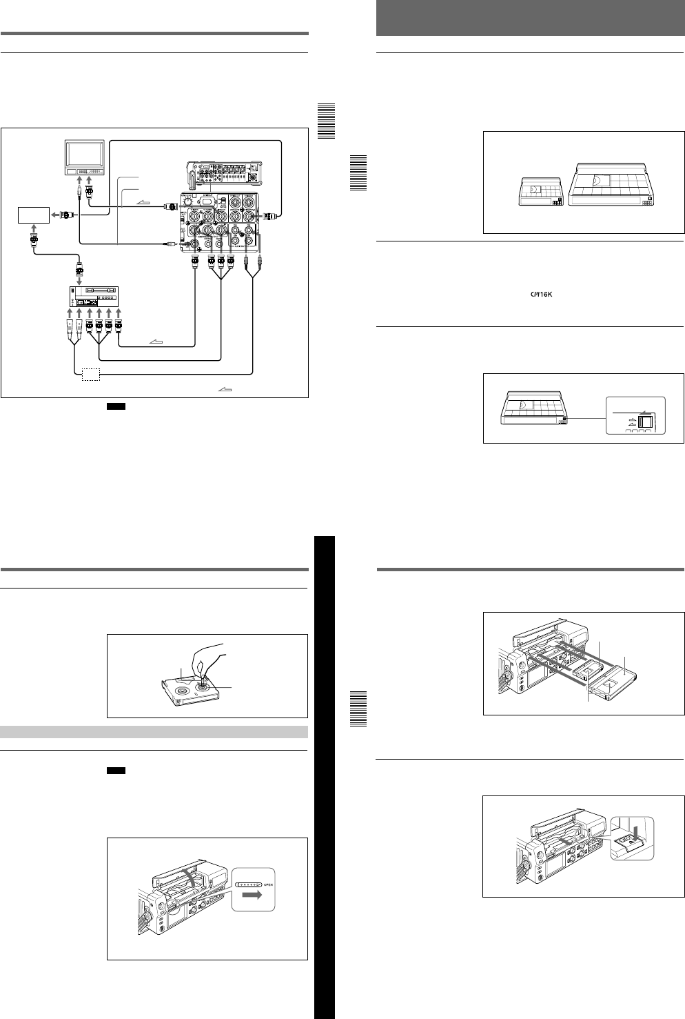
1-9
Chapter 2 Preparations
39
(GB)
Chapter 2 Preparations
To video equipment without a DV jack (when using the DSR-50/50P as a player)
You can connect this unit to video equipment without a DV jack. Use this
unit as a player as follows.
The following shows an example configuration of dubbing a tape with its
time code in the externally-synchronized playback mode. In this
configuration, the recorder is a VCR equipped with component input
connectors.
Notes
¥If you connect the input connectors of this VCR to the output connectors
of the monitor or recorder, a humming noise may be generated or the
image may be distorted.
¥Text data (time code, warnings, menus, etc.) are superimposed only on
the signal sent to the VIDEO OUT1 output.
¥To play back synchronized with the reference video (black burst) signal,
set the EXT SYNC on the VIDEO SET menu to ON.
Monitor
75 Ω coaxial cable (not supplied)
DSR-50/50P (player) (right panel)
to the audio input
jack
to the video input
connector
Reference signal
generator
SG
to the
B.B.OUT
connector
to the
B.B.OUT
connector
75 Ω coaxial cable
(not supplied)
75 Ω coaxial cable
(not supplied)
Phono jack cable (not
supplied)
to the REF.VIDEO
connector
recorder
to the time code
input connector
to the
audio
input
connectors
to the
component input
connectors
75 Ω coaxial cable
(not supplied)
Video cable (3BNC y 3BNC) (not supplied)
Conversion cable (XLR y phono) (not supplied)
: Signal flow
Amplifier (as needed)
Notes on Video Cassettes
Chapter 3 Playback and Recording
40
(GB) Chapter 3 Playback and Recording
Notes on Video Cassettes
Usable cassettes
Use Standard-DVCAM cassettes or Mini-DVCAM cassettes with this unit.
PDV-184 can record programs for 184 minutes and PDVM-40 can record
for 40 minutes (DVCAM format).
You can get the highest quality pictures with this digital videocassette
recorder using DVCAM cassettes. You may not be able to get as good
quality with other cassettes. We recommend using DVCAM cassettes so
that you can record your one-time events in the highest quality.
Cassette memory
Cassette memory is an optional feature that is mounted on some Standard
DVCAM cassettes and Mini DVCAM cassettes. When you record a
program, the recording date and time, and the programs position on the
tape are stored in the cassette memory so that you can quickly locate the
program later on. indicates that you can use the cassettes to store
up to 16 kbits of data. On this unit, you can use cassettes on which up to 16
kbits of data can be stored.
To save a recording
To prevent accidental erasure of a recording, slide in the REC/SAVE
switch on the cassette so that the red portion becomes visible. To record on
a tape, slide out the switch so that the red portion is hidden.
DVCAM cassette
REC/SAVE switch
Mini DVCAM cassette
REC
SAVE
Set to SAVE.
Chapter 3 Playback and Recording
Chapter 3 Playback and Recording
41
(GB)
Checking the tape for slack
Using a paper clip or a similar object, turn the reel gently in the direction
shown by the arrow. If the reel does not move, there is no slack.
Inserting/Ejecting Cassettes
To insert a cassette
Notes
¥Do not insert the cassette forcibly. The unit may be damaged.
¥Do not eject/load the cassette in a place subject to light. Make sure to
close the cassette lid when using the unit. The internal sensor of the unit
may operate incorrectly if too much light falls on the unit.
1With the unit powered on, slide the OPEN switch to the right and
unlock the cassette lid. Open the cassette lid.
Paper clip, etc.
Reel
Chapter 3 Playback and Recording
Notes on Video Cassettes
Chapter 3 Playback and Recording
42
(GB) Chapter 3 Playback and Recording
2After checking the tape for slack, hold the cassette so that the tape
window is facing upward, then insert it into the unit.
The cassette is automatically loaded into the unit.
3Close the cassette lid.
To eject the cassette
1With the unit powered on, open the cassette lid. Press the EJECT
button located at the right side of the cassette compartment.
The cassette is unloaded and ejected.
Mini cassette
Insert the mini cassette into the
center of the cassette compartment.
Standard cassette
Tape window facing upward

1-10
Chapter 3 Playback and Recording
Chapter 3 Playback and Recording
43
(GB)
2Remove the cassette from the unit. Close the cassette lid.
Note
If the battery power falls to below about 11 V, the unit cannot eject the
cassette with the EJECT button. Exchange the battery with a fully charged
one or use an AC adaptor to obtain sufficient power.
For details on confirming the remaining battery power, see TC screen on page
18 (GB).
Notes on Recording/Playback
No compensation for contents of the recording
Contents of the recording cannot be compensated for if recording or
playback is not successful due to a malfunction of the unit, video tape, etc.
Copyright precautions
On recording
You cannot record any software having copyright protection signals on
this unit. If you start recording protected video and audio signals, a
warning appears on the monitor screen and the unit stops recording.
On playback
When you play back software having copyright protection signals on this
unit, you may not be able to copy it onto other equipment.
Limitations caused by the difference in format
The unit can record and play back tapes recorded in DVCAM format. It
can also record and play back tapes recorded in DV format (SP mode).
However, due to the difference in format, you may not be able to record or
edit some tapes affected by recording conditions of the tape (e.g., A tape
originally recorded in DV format is dubbed in DVCAM format).
For details, see Compatibility of DVCAM and DV Format on page 99 (GB).
Simple playback function for a tape recorded in PAL system
(for DSR-50) or in NTSC system (for DSR-50P)
The DSR-50 can play a PAL tape (DSR-50P can play a NTSC tape)
recorded in the DVCAM format or consumer DV format (SP mode only).
This function has the following limitations:
¥The video signals are output only to the LCD monitor, VIDEO OUT1
output, and return signal to the camera.
¥The output video signals are in the format recorded in the tape. You
cannot convert the signals into the other format. If you want to display
the VIDEO OUT1 output, you will need a video monitor able to handle
the format recorded in the tape. If you want to display the return video
signals to the camera on the viewfinder, you will need a video camera
able to handle the format recorded in the tape.
¥The VIDEO OUT1 output and the return video signals to the camera are
optimized and adjusted for one format (DSR-50: NTSC format; DSR-
50P: PAL format). If you play back a tape recorded in the other format,
the levels and phases of the video signal may not be correct.
Notes on Video Cassettes
Chapter 3 Playback and Recording
44
(GB) Chapter 3 Playback and Recording
¥The outputs from the VIDEO OUT2, S VIDEO OUT and COMPONENT
OUTPUT connectors are muted.
¥When the unit plays a tape recorded in the other color system, the image,
sound and time code may be distorted for a while at the beginning of
playback.
¥The TC OUT connector outputs incorrect time code. Do not use this time
code.
¥The unit cannot play back synchronized with the external sync signal.
¥Noise reduction results for the luminance and chrominance signals may
differ between PAL formatted tape and NTSC formatted tapes.
Limitations regarding the differences in color systems
Except for the simple playback function for a tape recorded in the other
color system, this unit is not compatible with any other color systems.
¥This unit cannot record video signals of the other format.
¥Inputting the other format video signals does not output the EE pictures
correctly. The video output may be muted and any signal may not be
displayed.
¥You may not be able to dub sound correctly from a tape recorded in the
other color system in this unit.
¥If a tape has both NTSC and PAL formatted video signals, the following
limitations exist when you play the tape with this unit:
—The image may be distorted and noise may occur at the point that the
recording format changes in the tape.
—The tape transport control buttons may be disabled until the tape speed
is stabilized.
Chapter 3 Playback and Recording
Chapter 3 Playback and Recording
45
(GB)
Recording
This section describes the settings and operations to record on this unit.
For details on connection, see Connections on page 35 (GB).
Notes
¥Before starting a recording session, set the clock on the unit so that the
recording time can be written into the index signal. You can set the clock
by setting the CLOCK SET on the OTHERS menu.
¥If you use a source that is copyright protected, recording and operation
may be restricted.
¥During a recording, the tape transport control buttons (except STOP and
PAUSE) are disabled to prevent the tape running mode from being
changed by an incorrect operation. To disable the STOP and PAUSE
buttons, set the KEY INH switch to ON after the unit starts recording. In
this case, set the KEY INH switch to OFF first, then stop or pause the
recording.
Recording Using an External Camera
Settings for recording
1
6
3
2
5
4
7
External camera
DSR-50/50P
(recorder)
(Continued)
Right panel
Recording
Chapter 3 Playback and Recording
46
(GB) Chapter 3 Playback and Recording
1Turn on the POWER switch.
2Set the INPUT SELECT selector to CAMERA.
3Set up the camera for shooting.
For details, refer to the instruction manual of the camera.
4Set the audio input selectors to CAM.
5Set the audio input level control selectors properly according to the
audio level of the camera.
6Select the audio input level adjustment mode in the AUDIO SELECT
switches.
7If necessary, adjust the audio input level by turning the audio recording
level control knobs.
You can adjust the recording level with the audio recording level
control knobs if you have selected MANU in step 6. While looking at
the audio level meters on the LCD monitor or the display window, turn
the audio recording level control knobs and adjust the recording level.
Adjust the audio recording level so that the recording level does not
exceed 0 dB when the audio signal is at its maximum. If the recording
level exceeds 0 dB, the OVER indicators light.
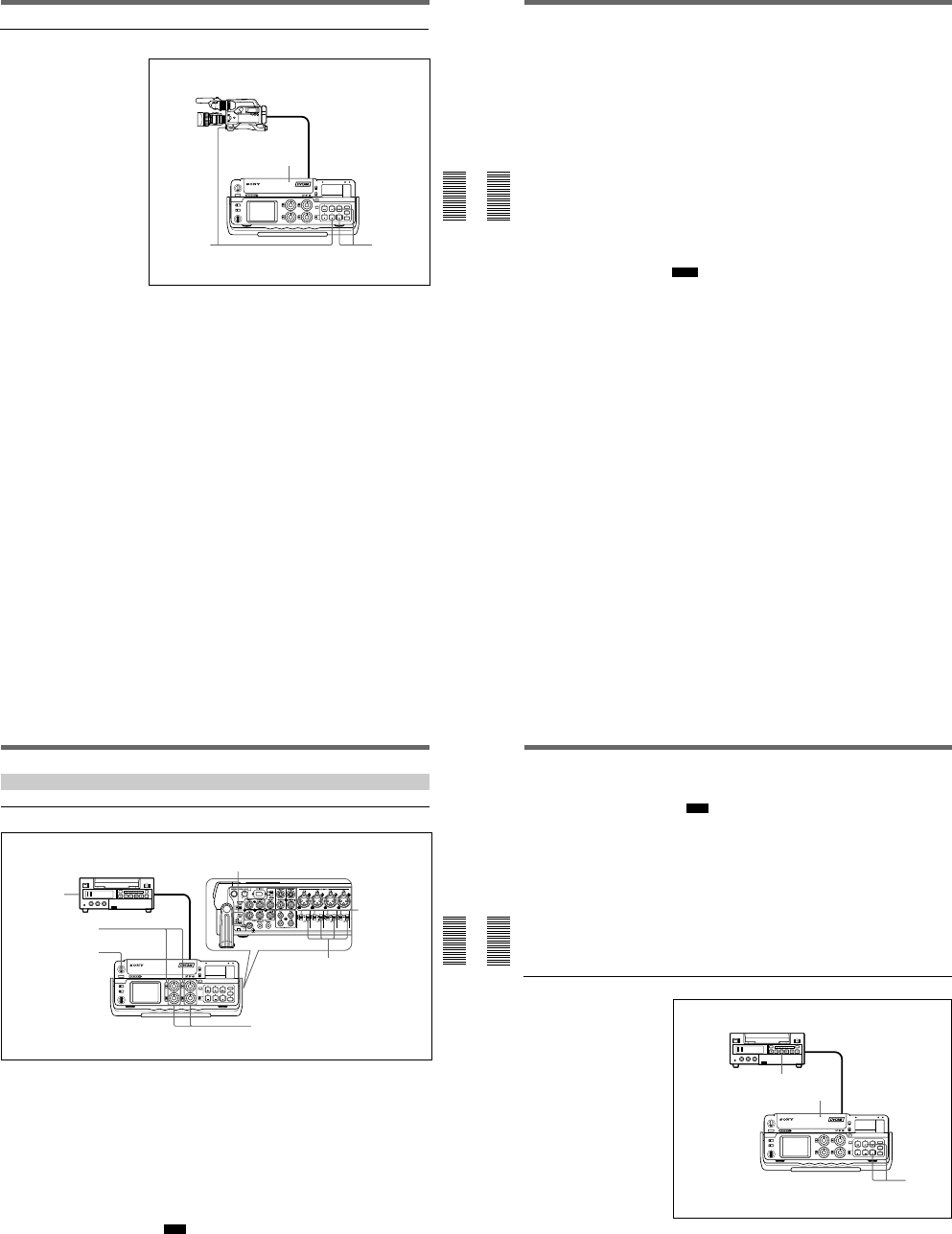
1-11
Chapter 3 Playback and Recording
Chapter 3 Playback and Recording
47
(GB)
Recording procedure
1After checking that the REC/SAVE switch of the cassette is set to the
write enabled position and checking the tape for slack, hold the
cassette so that the tape window is facing upward, then insert it into
this unit.
The cassette is automatically loaded into the unit and the tape will stop.
For details of the REC/SAVE switch and checking the tape for slack, see
Notes on Video Cassettes on page 40 (GB).
2Press the PLAY button while pressing the REC button.
The unit turns to the recording pause mode. The REC and PLAY
indicators light. The PAUSE indicator flashes.
3Press the VTR button on the camera, or press the PAUSE button on the
unit.
The unit starts recording and the index is marked.
To stop recording
Press the STOP button on the unit.
1
23
Recording
Chapter 3 Playback and Recording
48
(GB) Chapter 3 Playback and Recording
To pause recording
¥If you have pressed the VTR button on the camera to start shooting, press
the VTR button on the camera. Pressing the PAUSE button on the unit
does not pause the recording.
¥If you have pressed the PAUSE button on the unit to start shooting, press
the PAUSE button on the unit. To pause recording with the VTR button
on the camera, press the VTR button twice.
To start recording using the DSRM-20 Remote Control Unit (not
supplied)
Press the PLAY button while pressing the REC button. The unit changes to
the recording pause mode. Pressing the PAUSE button on the DSRM-20
starts the recording.
When the battery pack is almost exhausted
The unit has a battery compartment and a DC IN 12V connector. When the
battery pack in the battery compartment is almost exhausted, you can
temporarily connect an AC adaptor to the DC IN 12V connector then
exchange the battery pack to continue the recording and this can be done
without interrupting the recording. In this case, however, some noise may
be recorded.
Notes
¥The unit does not record any pictures unless the video signals are input
(except when inputting signals from the DV IN/OUT connector). If there
are no video signals or signals are interrupted during recording, the unit
pauses; if signals resume, the unit resumes recording.
¥If the camera outputs both component and composite signals, the unit
uses the component signals.
¥If you press the VTR button on the camera to start recording, the tape
transport control buttons, except the STOP button on the unit, are
disabled.
¥The return video signals to the camera are the same as those for the
VIDEO OUT1 output. If you have turned off the SUPERIMPOSE switch,
the superimposed data on the return video signal to the camera will not be
displayed.
¥The unit changes to the stop mode after the recording has been paused for
more than five minutes to protect the tape if you have set FROM REC P
on the VTR SET menu to STOP. Repeat the procedure from step 2 to
start recording again.
Chapter 3 Playback and Recording
Chapter 3 Playback and Recording
49
(GB)
Recording Using the Player
Settings for recording
1Turn on the POWER switch.
2Select an input signal by switching the INPUT SELECT selector.
DV: to record input signals from the DV IN/OUT connector
VIDEO: to record input signals from the VIDEO/REF.IN connector
S VIDEO: to record input signals from the S VIDEO IN connector
3Set up the player to play back a tape.
For details, refer to the instruction manual of the player.
4Set the audio input selectors to LINE.
Note
You do not need to set these selectors if you record signals input from
the DV IN/OUT connector.
5Set the audio input level control selectors properly according to the
audio level of the player.
1
6
3
2
5
4
7
Player (DSR-40/40P, etc.)
DSR-50/50P
(recorder)
Right panel
(Continued)
Recording
Chapter 3 Playback and Recording
50
(GB) Chapter 3 Playback and Recording
6Select the audio input level adjustment mode in the AUDIO SELECT
switches.
Note
You cannot adjust the recording level if you record signals input from
the DV IN/OUT connector.
7If necessary, adjust the audio input level by turning the audio recording
level control knobs.
You can adjust the recording level with the audio recording level
control knobs if you have selected MANU in step 6. While looking at
the audio level meters on the LCD monitor or the display window, turn
the audio recording level control knobs and adjust the recording level.
Adjust the audio recording level so that the recording level does not
exceed 0 dB when the audio signal is at its maximum. If the recording
level exceeds 0 dB, the OVER indicators light.
Recording Procedure
1After checking that the REC/SAVE switch of the cassette is set to the
write enabled position and checking the tape for slack, hold the
cassette so that the tape window is facing upward, then insert it into
this unit.
The cassette is automatically loaded into the unit and the tape will stop.
For details of the REC/SAVE switch and checking the tape for slack, see
Notes on Video Cassettes on page 40 (GB).
1
2
3
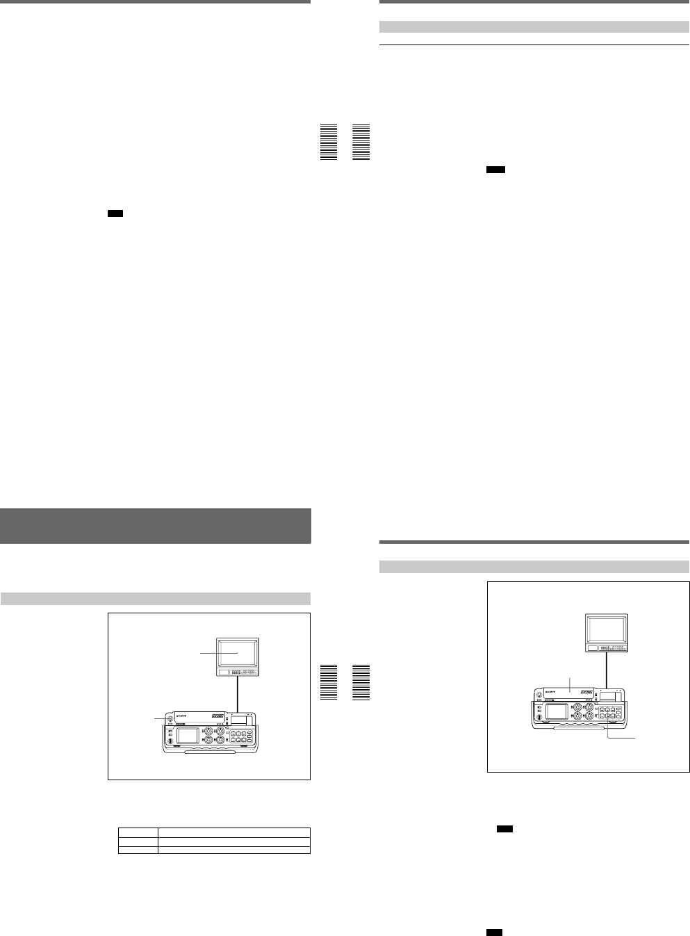
1-12
Chapter 3 Playback and Recording
Chapter 3 Playback and Recording
51
(GB)
2Press the playback button on the player.
The player starts playback.
3Press the PLAY button while pressing the REC button.
The unit starts recording and the index is marked.
To stop recording
Press the STOP button on the unit.
To pause recording
Press the PAUSE button on the unit.
To start recording using the DSRM-20 Remote Control Unit
(not supplied)
Press the PLAY button while pressing the REC button.
To record without inputting any video signals
Set the INPUT SELECT selector to other than DV, then set the COLOR
BAR (for DSR-50)/COLOUR BAR (for DSR-50P) on the DISPLAY SET
menu to ON. The color bars are recorded on the tape. The sound is
recorded according to the setting of the audio input selectors.
Note
The unit does not record any pictures unless the video signals are input
(except when inputting signals from the DV IN/OUT connector). If there
are no video signals or signals are interrupted during recording, the unit
pauses; if signals resume, the unit resumes recording.
Recording
Chapter 3 Playback and Recording
52
(GB) Chapter 3 Playback and Recording
Other Recording Functions
Marking an index
By pressing the INDEX button during a recording, you can mark an index
signal at any place in the tape. The index signal is marked for five seconds.
If you mark an index at the scene you want to search for, you can easily
search for the scene later.
When you start recording in the stop mode, the index signal is marked
automatically.
If you press the INDEX button while recording, the INDEX MARK
indicator appears for seven seconds on the LCD monitor and the VIDEO
OUT1 output (if you have turned on the SUPERIMPOSE switch) and the
index is marked.
If you use a cassette with cassette memory, the index will also be marked
in the cassette memory.
Notes
¥You cannot mark a new index while the INDEX MARK indicator is
showing.
¥If you record on a location in the tape where an index has been marked,
the index will be erased. You cannot delete just an index while keeping
the image or sound.
¥You cannot mark an index during playback, duplicate or audio dubbing
operations. The INDEX button is disabled in these operations.
¥The cassette memory space available limits the number of the indexes
that you can mark by pressing the INDEX button. When you use a
previously recorded tape for repeated recording, make more memory
space available by erasing unwanted items using ITEM ERASE or
ERASE ALL on the CM SET menu before you start recording.
To use an index during playback
You will need the DSRM-20 remote control unit (not supplied).
For details on the playback function using the DSRM-20, see Other Playback
Functions on page 55 (GB).
Chapter 3 Playback and Recording
Chapter 3 Playback and Recording
53
(GB)
Playback
This section describes the required settings and operations to perform
playback on this unit.
For details on connection, see Connections on page 35 (GB).
Settings for Playback
1Turn on the POWER switch.
2Turn on the power to the video monitor and set the switches of the
monitor as shown below.
Switch Setting
75 ΩON (or attach a 75 Ω terminator)
Input switch Set according to the type of input signal from this unit.
1
2
Video monitor
DSR-50/50P
Playback
Chapter 3 Playback and Recording
54
(GB) Chapter 3 Playback and Recording
Playback Procedure
1After checking the tape for slack, hold the cassette so that the tape
window is facing upward, then insert it into this unit.
For details on checking the tape for slack, see Notes on Video Cassettes on
page 40 (GB).
Note
Do not insert the cassette forcibly. The unit may be damaged.
2Press the PLAY button.
This starts the playback operation.
To stop playback
Press the STOP button.
To pause playback
Press the PAUSE button.
Note
When the unit is playing the part of the tape where the format has been
changed between the DVCAM format and the DV format, the picture and
sound may be distorted.
1
2
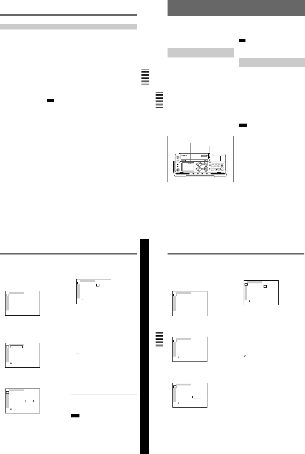
1-13
Chapter 3 Playback and Recording
Chapter 3 Playback and Recording
55
(GB)
Other Playback Functions
You can enjoy various playback functions using the DSRM-20 optional
remote control unit.
For details, refer to the operating instructions supplied with DSRM-20.
Playing at various speeds (JOG)
You can play at various speeds, or play frame by frame.
Searching (SHUTTLE)
You can easily locate the desired scene.
Searching using the index function
Four kinds of search are available:
—Searching for the beginnings of recordings: Index search
—Searching for the boundaries of recorded tape by title: Title search
—Searching for a point on the tape where the recorded date changes: Date
search
—Searching for scenes recorded in the photo mode with a digital
camcorder: Photo search
Note
You cannot make a title, record the date for search, or record in the photo
mode with this unit.
Displaying the tape information
Data codes (shutter speed, iris, white balance, program AE mode, gain,
etc.) are recorded in tapes recorded on a Sony Digital Camcorder (DSR-
200/200P, 200A/200AP, PD100/PD100P, PD100A/PD100AP, PD150/
PD150P, etc.). You can display and check these data codes during
playback by setting the DATA CODE on the DISPLAY SET menu to
DATE or CAMERA in this unit, or by pressing the DATA CODE button
on the DSRM-20.
Setting the Time Code and User Bits
Chapter 4 Setting the Time Code and Adjusting the Video Signals
56
(GB) Chapter 4 Setting the Time Code and Adjusting the Video Signals
Setting the Time Code and User Bits
This unit can set, display, record and play back the
SMPTE/EBU time code and user bits. The unit can
also output the time code read from the tape as an
analog (LTC) signal when it is played back at normal
speed, and receive an external analog time code (LTC)
signal.
Displaying Text Data Such as
Time Data
The LCD monitor on the unit can display
superimposed menus, warnings, audio levels, the
operation statuses and time data.
For details on the menus, see Chapter 6 Adjusting and
Setting Through Menus on page 76 (GB).
To display text data
To display the operation statuses, time data, etc., on
the LCD monitor, set the DISPLAY (LCD OFF/OFF/
ON) selector to ON, and the DISPLAY (MENU/TC/
AUDIO) selector to TC. If you turn the
SUPERIMPOSE switch on, the text data is
superimposed on the output from the VIDEO OUT1
connector.
To display the desired time data in the
time counter display
Use the COUNTER switch to select the type of time
data to be displayed.
TC: Time code
U-BIT: User bits
Note
If the recording on the tape includes discontinuities,
the counter may operate incorrectly during playback at
the corresponding points.
Using the Internal Time Code
Generator
You can set the initial time code value before
recording the time code generated by the internal time
code generator onto a tape. In addition, you can set the
user bits to record user bit data such as the date, time,
scene number, reel number, or other useful
information. The time data settings are set by using the
menu.
For details on the menu, see Chapter 6 Adjusting and
Setting Through Menus on page 76 (GB).
To set the initial time code value
This section describes how to set the time codes initial
value.
Notes
¥The time code can be set only in a DVCAM format
recording. It cannot be set in a DV format recording.
Make sure you set the DVCAM/DV select switch to
DVCAM.
¥Before setting the initial time code value, set TC/UB
IN on the TC/UB SET menu to INTERNAL and TC
MAKE to PRESET.
For details on TC/UB IN and TC MAKE, see TC/UB SET
menu on page 78 (GB).
Time code indicator
COUNTER switch
Time counter display
Chapter 4 Setting the Time Code and Adjusting the Video Signals
Chapter 4 Setting the Time Code and Adjusting the Video Signals
57
(GB)
Chapter 4 Setting the Time Code and Adjusting the Video Signals
1Set the DISPLAY (LCD OFF/OFF/ON) selector to
ON, and the DISPLAY (MENU/TC/AUDIO)
selector to MENU.
The LCD monitor displays the menu. If you turn
the SUPERIMPOSE switch on, the menu is also
displayed on the VIDEO OUT1 output.
TC ⁄ UB SET
TC PRESET
UB PRESET
TC FORMAT
TC RUN
TC ⁄ UB IN
TC MAKE
UB TIME
JOG TC OUT
TC
CM
DISP
V
A
LCD
VTR
ETC
(The TC FORMAT submenu is only for DSR-50.)
2Rotate the SEL/PUSH EXEC dial to select TC/UB
SET, then press the dial.
The following menu appears.
TC ⁄ UB SET
TC PRESET
UB PRESET
TC FORMAT
TC RUN
TC ⁄ UB IN
TC MAKE
UB TIME
JOG TC OUT
RETURN
00:00:00:00
TC
CM
DISP
V
A
LCD
VTR
ETC
3Rotate the SEL/PUSH EXEC dial to select TC
PRESET, then press the dial.
The following menu appears.
TC ⁄ UB SET
TC PRESET
UB PRESET
TC FORMAT
TC RUN
TC ⁄ UB IN
TC MAKE
UB TIME
JOG TC OUT
RETURN
00:00:00:00
RESET
PRESET
RETURN
TC
CM
DISP
V
A
LCD
VTR
ETC
4Rotate the SEL/PUSH EXEC dial to select
PRESET, then press the dial.
The following menu appears.
TC ⁄ UB SET
TC PRESET
UB PRESET
TC FORMAT
TC RUN
TC ⁄ UB IN
TC MAKE
UB TIME
JOG TC OUT
RETURN
OOOO
00:00:00:00
oooo
SET
CANCEL
TC
CM
DISP
V
A
LCD
VTR
ETC
5Set the first two digits. Rotate the SEL/PUSH
EXEC dial to select the number, then press the
dial.
6Repeat step 5 to set the other digits.
7Rotate the SEL/PUSH EXEC dial to select SET,
then press the dial.
The initial time code value is set and the menu
display returns to step 2.
8Rotate the SEL/PUSH EXEC dial to select
RETURN, then press the dial.
The menu display returns to step 1.
To cancel the time code setting
Select CANCEL in step 7, then press the SEL/PUSH
EXEC dial.
To reset the time code
Select RESET in step 4, then press the SEL/PUSH
EXEC dial.
To set the value of the user bits
You can set the user bits as eight-digit hexadecimal
values (base 16) to have the date, time, scene number,
and other information inserted into the time code track.
Notes
¥The user bits can be set only in a DVCAM format
recording. It cannot be set in a DV format recording.
¥Before setting the user bits, set the TC/UB IN on the
TC/UB SET menu to INTERNAL and UB TIME to
OFF.
For details on TC/UB IN and UB TIME, see TC/UB SET
menu on page 78 (GB).
Setting the Time Code and User Bits
Chapter 4 Setting the Time Code and Adjusting the Video Signals
58
(GB) Chapter 4 Setting the Time Code and Adjusting the Video Signals
1Set the DISPLAY (LCD OFF/OFF/ON) selector to
ON, and the DISPLAY (MENU/TC/AUDIO)
selector to MENU.
The LCD monitor displays the menu. If you turn
the SUPERIMPOSE switch on, the menu is also
displayed on the VIDEO OUT1 output.
TC ⁄ UB SET
TC PRESET
UB PRESET
TC FORMAT
TC RUN
TC ⁄ UB IN
TC MAKE
UB TIME
JOG TC OUT
TC
CM
DISP
V
A
LCD
VTR
ETC
2Rotate the SEL/PUSH EXEC dial to select TC/UB
SET, then press the dial.
The following menu appears.
TC ⁄ UB SET
TC PRESET
UB PRESET
TC FORMAT
TC RUN
TC ⁄ UB IN
TC MAKE
UB TIME
JOG TC OUT
RETURN
00:00:00:00
TC
CM
DISP
V
A
LCD
VTR
ETC
3Rotate the SEL/PUSH EXEC dial to select UB
PRESET, then press the dial.
The following menu appears.
TC ⁄ UB SET
TC PRESET
UB PRESET
TC FORMAT
TC RUN
TC ⁄ UB IN
TC MAKE
UB TIME
JOG TC OUT
RETURN
00 00 00 00
RESET
PRESET
RETURN
TC
CM
DISP
V
A
LCD
VTR
ETC
4Rotate the SEL/PUSH EXEC dial to select
PRESET, then press the dial.
The following menu appears.
TC ⁄ UB SET
TC PRESET
UB PRESET
TC FORMAT
TC RUN
TC ⁄ UB IN
TC MAKE
UB TIME
JOG TC OUT
RETURN
OOOO
00 00 00 00
oooo
SET
CANCEL
TC
CM
DISP
V
A
LCD
VTR
ETC
5Set the first two digits. Rotate the SEL/PUSH
EXEC dial to select the number, then press the
dial.
6Repeat step 5 to set the other digits.
7Rotate the SEL/PUSH EXEC dial to select SET,
then press the dial.
The user bits are set and the menu display returns
to step 2.
8Rotate the SEL/PUSH EXEC dial to select
RETURN, then press the dial.
The menu display returns to step 1.
To cancel the user bits setting
Select CANCEL in step 7, then press the SEL/PUSH
EXEC dial.
To reset the user bits
Select RESET in step 4, then press the SEL/PUSH
EXEC dial.
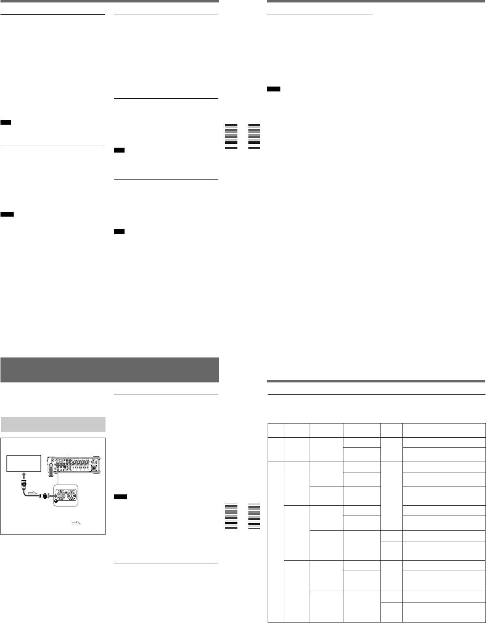
1-14
Chapter 4 Setting the Time Code and Adjusting the Video Signals
Chapter 4 Setting the Time Code and Adjusting the Video Signals
59
(GB)
To set the frame mode (DSR-50 only)
Set TC FORMAT on the TC/UB SET menu to switch
the frame mode.
AUTO: Automatically sets the mode in accordance
with the inserted cassette.
If nothing is recorded on the tape, the mode is set
to the non-drop frame mode. If the unit cannot
read the frame mode correctly in the tape, the unit
will use the mode that was set in the last position
it was able to read correctly on the tape. If you
turn the power on/off or remove the tape, the
mode of the last position it was able to read
correctly is cleared and the mode is set to the non-
drop frame mode. If TC MAKE is set to PRESET,
the mode is set to the non-drop frame mode.
DF: Selects the drop frame mode.
NDF: Selects the non-drop frame mode.
Note
In a DV format recording, the drop-frame mode is
used automatically.
To set the advancement mode
Set TC RUN on the TC/UB SET menu to switch the
advancement mode (counting up).
REC RUN: Time code advances only while
recording.
FREE RUN: Time code advances even when the
unit is not recording. This mode is used to set the
current time as the initial time code value, or to
synchronize the internal time code to an external
time code.
Notes
¥If you set the advancement mode to FREE RUN, the
time code will be updated by the internal clock during
the unit power is off. The time code may have been
delayed or advanced somewhat if you turn on the unit
power again, play back a tape, or set the INPUT
SELECT selector to DV.
¥If the internal backup battery charge is exhausted, the
time code of the FREE RUN setting will be
initialized. The internal backup battery is fully
charged if you connect the power to the unit for about
10 hours. A fully charged internal battery can run for
about one month.
To set the time code when the recording
starts
Set TC MAKE on the TC/UB SET menu to select the
time code when you start recording.
REGEN: The time code value is set to continue the
time code from the time code already recorded on
the tape. If you start recording from a blank
portion of the tape, the time code starts from
00:00:00:00.
PRESET: The time code value is set to the time code
from the value set in PRESET in TC PRESET on
the TC/UB SET menu.
To switch the time code output when
playing at various speeds (JOG)
Set JOG TC OUT on the TC/UB SET menu to control
the time code output from the TC OUT connector
when the tape is played at various speeds.
OFF: Does not output the time code.
ON: Outputs the time code.
Note
The continuous time code is output only when the tape
is played at normal speed. When the unit is in the jog
or search mode, discontinuous time code is output.
To set the current time in the user bits
You can set the current time in the user bits by setting
the UB TIME on the TC/UB SET menu.
OFF: The value set in PRESET in UB PRESET on
the TC/UB SET menu is set to the user bits.
ON: The value set in CLOCK SET on the OTHERS
menu is set to the user bits.
Note
This function is available only when TC/UB IN on the
TC/UB SET menu is set to INTERNAL or TC EXT.
Setting the Time Code and User Bits
Chapter 4 Setting the Time Code and Adjusting the Video Signals
60
(GB) Chapter 4 Setting the Time Code and Adjusting the Video Signals
To select the time code/user bits to record
on the tape
You can set the time code and user bits to record on
the tape by setting TC/UB IN on the TC/UB SET
menu.
INTERNAL: Uses the internal time code/user bits.
TC&UB EXT: Uses the external time code/user bits.
TC EXT: Uses the external time code and internal
user bits.
UB EXT: Uses the internal time code and external
user bits.
Notes
¥This unit has a DV IN/OUT connector. The time code
input or output is different when you connect the unit
to an external device via this DV IN/OUT connector
or via another input/output connector.
For details, see DSR-50/50P time codes on page 62
(GB).
¥The time code output from this unit has some
restrictions.
For details, see Notes on the Time Codes on page 63
(GB).
Chapter 4 Setting the Time Code and Adjusting the Video Signals
Chapter 4 Setting the Time Code and Adjusting the Video Signals
61
(GB)
Synchronizing the Time Codes
You can synchronize the internal time code generator
of the unit by inputting an external time code signal
(LTC).
Connecting to the Time Code
Generator
To synchronize the internal time code to
an external time code
1Set the INPUT SELECT selector to other than DV.
2Input an external time code (LTC) signal to the TC
IN connector of the unit.
3Set TC/UB IN on the TC/UB SET menu to
TC&UB EXT or TC EXT.
The internal time code generator locks onto the
external time code and starts advancing. Once the
internal time code generator has become
synchronized in this way, you can disconnect the
external time code input and this unit will maintain
the time code from the external device.
Notes
¥This unit has a DV IN/OUT connector. The time code
input or output is different when you connect the unit
to an external device via this DV IN/OUT connector
or via another input/output connector.
For details, see DSR-50/50P time codes on page 62
(GB).
¥The time code output from this unit has some
restrictions.
For details, see Notes on the Time Codes on page 63
(GB).
To confirm external synchronization
Before you start recording, check that the internal time
code is synchronized to the external time code.
Press the STOP button to put the unit into stop mode,
then press the REC button.
Look at the time counter display and check that the
time code value displayed there matches the external
time code value.
Time code generator DSR-50/50P (right panel)
to time
code
output
connector
75 Ω coaxial cable
(not supplied)
: Signal flow
Synchronizing the Time Codes
Chapter 4 Setting the Time Code and Adjusting the Video Signals
62
(GB) Chapter 4 Setting the Time Code and Adjusting the Video Signals
DSR-50/50P time codes
This unit has a DV IN/OUT connector. The time code
output and recorded on the tape differs as shown below
EE
INTERNAL
DV
VIDEO
S VIDEO
CAMERA
(Except DV)
UB EXT
DV
VIDEO
S VIDEO
CAMERA
(Except DV)
TC/UB IN
menu
INPUT SELECT
selector Mode TC IN
(EXT)
The time code output from the
TC OUT (INT) connector and the time code/
user bits recorded on the tape
Playback
Playback
Audio dubbing
Playback at various
speeds a)
DUB1 b)
Time code on the tape
JOG TC OUT: ON – Time code on the tape;
JOG TC OUT: OFF – Mute (No output)
Duplicate
DUP1 b) Time code of another device connected to the
DV IN/OUT connector c)
Recording
Recording Pause
REC1 b)
Time code internally generated c)
Recording
Recording Pause
REC1 b)
Time code internally generated c)
Duplicate
DUP1 b) Time code of another device connected to the
DV IN/OUT connector c)
Recording
Recording Pause
REC1 b)
Time code internally generated c)
Recording
Recording Pause
REC1 b)
Yes Time code connected to TC IN (EXT) is
through-output.
No
No output from the TC OUT (INT) connector
(For details, see next page.)
: the time code
and user bits generated internally are
recorded on the tape.
TC&UB EXT
TC EXT
DV
VIDEO
S VIDEO
CAMERA
(Except DV)
Duplicate
DUP1 b) Time code of another device connected to the
DV IN/OUT connector c)
Recording
Recording Pause
REC1 b)
Time code: Time code of another device
connected to the DV IN/OUT
connector
User bits: User bits internally generated d)
Yes Time code connected to TC IN (EXT) is
through-output.
No No output from the TC OUT (INT) connector
(For details, see next page.)
: the time code
and user bits generated internally are
recorded on the tape.
Recording
Recording Pause
REC1 b)
when the INPUT SELECT selector is set to DV and
when it is set to other than DV.
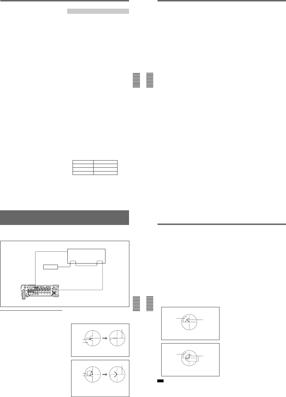
1-15
Chapter 4 Setting the Time Code and Adjusting the Video Signals
Chapter 4 Setting the Time Code and Adjusting the Video Signals
63
(GB)
a) This includes stop, fast-forward or rewind. If the unit
cannot read the time code on the tape correctly, the
counter displays — —:— —:— —:— — and the time code is
not output from the TC OUT connector.
b) DUB1, DUP1 and REC1 represent the state of the
unit when you press each of these buttons (AUDIO DUB,
DUP or REC) in the stop mode. If the counter displays
— —:— —:— —:— —, the time code is not output from the TC
OUT connector when you press the AUDIO DUB button
in the stop mode.
c) The time code is also displayed on the time counter
display in the display window.
d) When the DVCAM/DV select switch is set to DV, the
time code generated internally is output.
Notes on the Time Codes
Time codes output from the unit have the following
restrictions:
¥The unit outputs an EE signal when it is in recording
or recording pause modes, or when you press the
REC button.
While the unit outputs an EE signal, only the time code
from an external device that is connected to the TC IN
connector will be through-output from the TC OUT
connector when the INPUT SELECT selector is set to
other than DV and TC/UB IN on the TC/UB SET menu
has been set to other than INTERNAL. (The time code
and user bits that are internally generated are not output
from the TC OUT connector.)
In this case, as a result, the time code will not be
output from the TC OUT connector when the time
code is not input from the external device connected
to the TC IN connector.
You need to set TC/UB IN on the TC/UB SET menu
to INTERNAL to output a time code from the TC
OUT connector even if no time code has been input
from an external device connected to the TC IN
connector.
To set the unit to inherit a time code from the external
device even after you set TC/UB IN to INTERNAL
from some other setting, follow the steps below.
1Match the settings (used when TC/UB IN is set to
INTERNAL) of the unit with the external device
time code format. (See the setting example
below.)
2After setting TC/UB IN to other than
INTERNAL, input the time code from the
external device connected to the TC IN
connector.
3Set TC/UB IN on the TC/UB SET menu to
INTERNAL.
4Disconnect the external device from the TC IN
connector.
Setting example
If the time code setting of the external device is
TC: Drop frame; UB: 12 34 56 78.
This unit menu Setting
TC RUN FREE RUN
TC FORMAT DF
UB PRESET 12 34 56 78
(The TC FORMAT submenu is only for DSR-50.)
Synchronizing the Time Codes
Chapter 4 Setting the Time Code and Adjusting the Video Signals
64
(GB) Chapter 4 Setting the Time Code and Adjusting the Video Signals
¥The internal time code is output with the phase
synchronized to the line-outs (COMPONENT
OUTPUT, S VIDEO OUT, VIDEO OUT2) when TC/
UB IN on the TC/UB SET menu is set to
INTERNAL.
(When the EE signal is output, the output signals of
the line-outs are delayed for one line from the input
video signal when the component video (CAMERA)
or S-video is input, and delayed for two lines from
the input video signal when the composite video
(CAMERA, VIDEO/REF.IN) is input.)
¥When inputting signals from the DV IN/OUT
connector, if you set TC/UB IN to INTERNAL or
UB EXT, the time code and user bits generated
internally are recorded under the INTERNAL setting
in TC/UB IN on the TC/UB SET menu. If you want
to record with the time code input from the DV IN/
OUT connector, set TC/UB IN to TC EXT or
TC&UB EXT, or use the duplicate function.
¥When the DVCAM/DV select switch is set to
DVCAM, if you set TC/UB IN to TC EXT or
TC&UB EXT, this unit records the time code input
from the DV IN/OUT connector and the user bits
internally generated, and the TC OUT connector
outputs the same time code and user bits.
¥During the duplicate operation, this unit records the
time code and user bits on the source tape currently
being duplicated and the TC OUT connector outputs
the same time code and user bits. The time code and
user bits are output with the phase synchronized to
the line-outs (COMPONENT OUTPUT, S VIDEO
OUT, VIDEO OUT2) during the duplicate operation.
For details on the duplicate function, see Duplication
(generating a work tape with the same time code) on
page 70 (GB).
¥During the audio dubbing operation, the TC OUT
connector outputs the time code and user bits on the
tape currently being played.
For details on audio dubbing, see Audio Dubbing on
page 74 (GB).
¥To display and check the time code currently being
advanced with the FREE RUN setting, press the REC
button when all the conditions below are met.
—The unit is in the stop mode.
—The COUNTER switch is set to TC.
—TC RUN on the TC/UB SET menu is set to FREE
RUN.
—TC MAKE on the TC/UB SET menu is set to
PRESET.
If you press the STOP button, the time code display
returns to the last time code value it was able to read
on the tape.
¥To display the current time that is set in CLOCK SET
on the OTHERS menu as the user bits, press the REC
button when all the conditions below are met.
—The unit is in the stop mode.
—The COUNTER switch is set to U-BIT.
—UB TIME on the TC/UB SET menu is set to ON.
(If UB TIME is set to OFF, the value set in UB
PRESET will be displayed.)
If you press the STOP button, the user bits display
returns to the last value it was able to read on the
tape.
¥If the external time code input is discontinuous or
does not advance correctly, the time code input may
be delayed compared to the time code recorded on the
tape or the time code shown on the display of this
unit. If there is a discontinuous time code on your
recorded tape, you may not be able to edit or search
correctly, depending on the device connected to this
unit.
Chapter 4 Setting the Time Code and Adjusting the Video Signals
Chapter 4 Setting the Time Code and Adjusting the Video Signals
65
(GB)
Adjusting the Sync and Subcarrier Phases of the
Video Signals
When you adjust the phases of the video signals,
follow the steps below.
Performing a phase adjustment operation
1Press the SCH button on the vectorscope.
The vectorscope switches to SCH mode.
2Press the B channel button on the vectorscope.
This selects the black burst signal from the
reference signal generator.
3Press the EXT button on the vectorscope.
This switches the vectorscope to external
synchronization mode.
Vectorscope with SCH mode
A IN
B IN
B Through EXT. REF
IN
EXT. REF
Through
Reference
signal generator
DSR-50/50P VIDEO OUT2
VIDEO/REF.IN
4Adjust the phase synchronization control on the
vectorscope so that the sync and subcarrier phases
are close to the reference line.
(for NTSC)
Subcarrier
phase
Sync
phase
Reference line
Align the sync and subcarrier phase of the black burst
signal to the reference line.
(for PAL)
Subcarrier
phase
Sync
phase
Reference line
Align the sync phase of the black burst signal to the
reference line.
Align the subcarrier phase of the black burst signal
symmetrically up and down.
(Continued)
Adjusting the Sync and Subcarrier Phases of the Video Signals
Chapter 4 Setting the Time Code and Adjusting the Video Signals
66
(GB) Chapter 4 Setting the Time Code and Adjusting the Video Signals
5Play back a tape from this unit after setting EXT
SYNC on the VIDEO SET menu to ON.
6Press the A channel button on the vectorscope.
The vectorscope displays the sync phase and
subcarrier phase (composite signals only) of the
signal from this unit.
7Adjust the SYNC control using H PHASE on the
VIDEO SET menu for rough adjustment, then
adjust H PHASE F for fine adjustment, so that the
output from this unit on channel (A) is in correct
phase alignment with the black burst signal on
channel (B).
8Adjust the SC control using SC PHASE on the
VIDEO SET menu for rough adjustment, then
adjust SC PHASE F for fine adjustment, so that the
output from this unit on channel (A) is in correct
phase alignment with the black burst signal on
channel (B).
Note
When component signals are used, the subcarrier
phase indicator does not appear.
Adjust the sync and subcarrier phase of the output
signal from this unit.
(for NTSC)
This indicator
moves as you
adjust the H
PHASE or H
PHASE F menu.
This indicator
moves as you
adjust the SC
PHASE or SC
PHASE F menu.
Adjust the sync and subcarrier phase of the output
signal from this unit.
(for PAL)
This indicator
moves as you
adjust the H
PHASE or H
PHASE F menu.
This indicator
moves as you
adjust the SC
PHASE or SC
PHASE F menu.
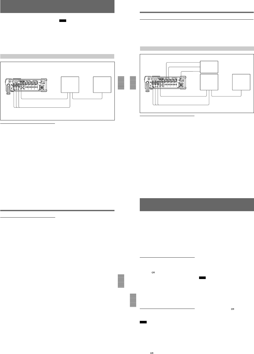
1-16
Chapter 4 Setting the Time Code and Adjusting the Video Signals
Chapter 4 Setting the Time Code and Adjusting the Video Signals
67
(GB)
Adjusting the Signals
You can adjust each signal level of the component
output signal and the chrominance signal gain level of
the composite signal.
Connect the reference video (black burst) signal one-
to-one with a device that generates the reference video
signal, or make a loop-through connection. If the
device has a terminal switch, terminate the connection
properly.
You need both a waveform monitor and a vectorscope
to display the component signals.
Notes
¥If you adjust the component signal level, be sure to
adjust the chrominance signal gain level of composite
signals.
¥Adjust the output level while playing the tape. Adjust
the input level in the EE mode.
¥You cannot adjust the signals input to the DV IN/
OUT connector. You cannot adjust the signals output
from the DV IN/OUT connector during playback.
Adjusting the Output Level
Adjusting the component signal level
1Play back a tape and output the signals from the Y,
R-Y and B-Y connectors of the COMPONENT
OUTPUT connectors.
The waveform monitor displays the picture.
DSR-50/50P
VIDEO OUT2
COMPONENT OUTPUT
Waveform monitor
Composite
video input
Component
input
Composite
video output Composite
video input
Vectorscope
2Adjust the Y, R-Y, and B-Y signal levels in PB
OUTPUT in VIDEO LVL on the VIDEO SET
menu.
Y LVL: Adjusts the Y signal level.
R-Y LVL: Adjusts the R-Y signal level.
B-Y LVL: Adjusts the B-Y signal level.
For details on PB OUTPUT, see VIDEO SET
menu on page 85 (GB).
Adjusting Signals
Chapter 4 Setting the Time Code and Adjusting the Video Signals
68
(GB) Chapter 4 Setting the Time Code and Adjusting the Video Signals
Adjusting the chrominance signal gain level of the composite signal
1Play back a tape to output the signals from the
VIDEO OUT2 connector.
The vectorscope displays the picture.
2Adjust the chrominance signal gain level in PB
OUTPUT in VIDEO LVL on the VIDEO SET
menu.
For details on PB OUTPUT, see VIDEO SET
menu on page 85 (GB).
Adjusting the Input Level
Adjusting the camera component signal
level
1Set the INPUT SELECT selector to CAMERA.
2Stop the unit and set it to the EE mode.
The waveform monitor displays the picture.
Reference
signal generator /
Camera
or
or
DSR-50/50P S VIDEO
IN
VIDEO/
REF.IN CAMERA
VIDEO OUT2
COMPONENT OUTPUT
Composite
video input
Component
input
Waveform monitor
Composite
video output Composite
video input
Vectorscope
3Adjust the Y, R-Y, and B-Y signal levels in
INPUT in VIDEO LVL on the VIDEO SET menu.
Y LVL: Adjusts the Y signal level.
R-Y LVL: Adjusts the R-Y signal level.
B-Y LVL: Adjusts the B-Y signal level.
For details on INPUT, see VIDEO SET menu on
page 85 (GB).
Chapter 4 Setting the Time Code and Adjusting the Video Signals
Chapter 4 Setting the Time Code and Adjusting the Video Signals
69
(GB)
Adjusting the composite signal level
1Set the INPUT SELECT selector to S VIDEO or
VIDEO in accordance with the signal to be
adjusted.
2Stop the unit and set it to the EE mode.
The waveform monitor displays the picture you
selected in step 1.
3Adjust the luminance level, chrominance level and
hue in INPUT in VIDEO LVL on the VIDEO SET
menu.
LUMINANCE: Adjusts the luminance level.
CHROMA: Adjusts the chrominance level.
HUE: Adjusts the hue. (for DSR-50 only)
For details on INPUT, see VIDEO SET menu on
page 85 (GB).
Duplication (generating a work tape with the same time code)
Chapter 5 Duplication and Audio Dubbing
70
(GB) Chapter 5 Duplication and Audio Dubbing
Duplication (generating a work tape with the same
time code)
If you copy a source tape using the DUP (duplicate)
button on this unit, you can copy the time codes
recorded on the source tape as they are. You can easily
make a work tape having the same time codes as the
source tape.
The duplicate function on this unit works only when
using a source tape recorded in DVCAM format and
making DV connections.
This unit functions as a recorder. The duplicate
function on this unit works only when you duplicate a
tape in the DVCAM format. Make sure to change the
DVCAM/DV select switch to DVCAM before
duplicating a tape.
To set the duplicate mode
This unit has three duplicate modes.
Set DUPLICATE on the VTR SET menu to select a
duplicate mode as follows.
AUTOq (AUTO TAPE COPY WITH CM
COPY): The player and the recorder
automatically rewind the tape to the beginning to
start duplicating. The cassette memory is also
duplicated.
AUTOq (AUTO TAPE COPY): The player and
the recorder automatically rewind the tape to the
beginning to start duplicating. The cassette
memory is not duplicated.
MANUALq (MANUAL TAPE COPY): The tape
is duplicated from any location. The cassette
memory is not duplicated.
Duplicating a tape
The duplicate procedure differs depending on the
duplicate mode.
Notes
¥If you operate the player while duplicating, the
duplicate process may be interrupted and the tape
may not be correctly duplicated. Do not operate the
player while duplicating.
¥You can duplicate a tape regardless of the DISPLAY
(MENU/TC/AUDIO) selector setting, but the
duplication screen will be displayed only when the
DISPLAY (MENU/TC/AUDIO) selector has been set
to TC.
AUTOq or AUTOq duplicate mode
1Connect this unit and the player with an i.LINK
cable (DV cable, not supplied). After turning on
power of this unit and player, set the INPUT
SELECT selector on this unit to DV.
2Press the STOP button on this unit to stop the tape
transport operation.
3While pressing the DUP button, press the PLAY
button on this unit.
This unit and the player will automatically rewind
the tape to the beginning. This unit enters the
duplicate-standby mode. The player enters the
playback pause mode. Then the DUP indicator on
this unit flashes and the duplication starts.
If you press the PAUSE and PLAY buttons
while pressing the DUP button in step 3
This unit and the player will automatically rewind the
tape to the beginning. This unit enters the duplicate-
standby mode. The player enters the playback pause
mode. This unit does not start duplication until you
press the PAUSE button.
To stop duplication
Press the STOP button.
Notes
¥You cannot pause during a duplicate process.
¥The duplication starts after the i.LINK
communication is established so that the first part of
the source tape is dropped on the copied tape.
¥Set auto repeat to OFF when the player has an auto
repeat function and set auto rewind to ON when the
player has an auto rewind function.
¥Set still timer to the longest time possible to ensure
enough time for rewinding the tape to the beginning
when the player has a still timer function.
¥If you have selected AUTOq duplicate mode,
the cassette memory will be duplicated after the tape
has been duplicated. While the cassette memory is
being duplicated, an indicator showing the progress
of the duplication appears on the LCD monitor and
on the VIDEO OUT1 output. Duplicating the cassette
memory takes up to a few minutes depending on the
amount of data. Duplication of the cassette memory
will be cancelled and the duplicate operation will be
completed without duplicating the cassette memory
in the following cases:
—You press the STOP button while duplicating.
—You turn off the power to this unit or player.
—You remove the tape.
—You disconnect the DV cable.
If the duplication of the cassette memory stops for
some reason, the cassette memory of this unit will be
completely erased.
¥If you operate the player while duplicating and the
PLAYER UNCONTROLLABLE warning message
appears and duplication is stopped, press the STOP
button on this unit, then repeat the procedure from
step 2.
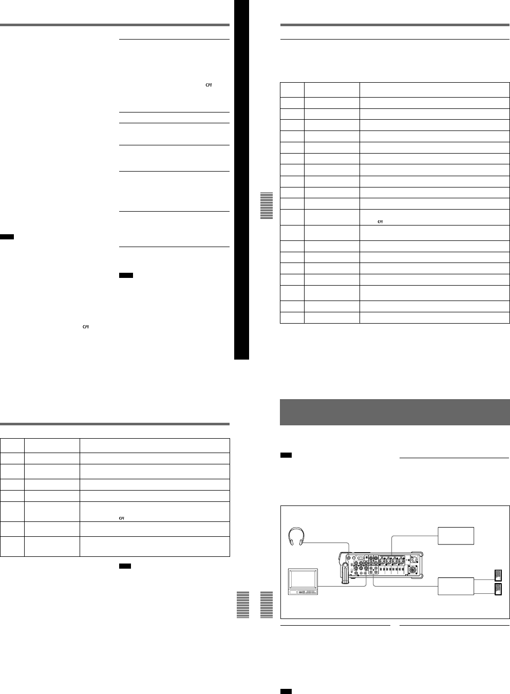
1-17
Chapter 5 Duplication and Audio Dubbing
Chapter 5 Duplication and Audio Dubbing
71
(GB)
Chapter 5 Duplication and Audio Dubbing
¥The player and recorder rewind the tape
automatically after duplication. However, depending
on the specifications, some players do not
automatically rewind the tape after duplication.
¥Before you start duplication, make sure that the
player finished loading the cassette.
MANUALq duplicate mode
1Connect this unit and the player with an i.LINK
cable (DV cable, not supplied). After turning on
power of this unit and player, set the INPUT
SELECT selector on this unit to DV.
2Locate the points where you want to start playback
and recording.
3Press the STOP button on this unit to stop the tape
transport operation.
4While pressing the DUP button, press the PLAY
button on this unit.
This unit enters the duplicate-standby mode. The
player enters the playback pause mode. Then the DUP
indicator on this unit flashes and duplication starts.
To adjust the point where duplication starts
In step 4, while pressing the DUP button, press the
PAUSE button and PLAY button. This unit will not start
duplication until you press the PAUSE button again.
After confirming that the PLAYER display has changed
to READY (flashing) on the LCD monitor, adjust the
duplication start point by operating the player, then press
the PAUSE button on this unit to start duplication.
To stop duplication
Press the STOP button.
Notes
¥You cannot pause during a duplicate process.
¥The duplication starts after the i.LINK
communication is established so that the first part of
the source tape is dropped on the copied tape. Play
back the source tape from the preceding point.
¥Set auto repeat to OFF when the player has an auto
repeat function.
¥You may not be able to duplicate the first part of the
source tape. Locate the recorded portion on the
source tape, then start duplicating.
¥If there is a blank portion on the tape, the first part of
the recorded portion that follows may be dropped on
the copied tape.
¥If you start duplication at some midpoint in the tape,
the search function may not work correctly on the
copied tape or problems may occur when editing. It is
recommended that you select AUTOq or
AUTOq for the duplicate mode.
¥Before start duplication, make sure that the player
finished loading the cassette.
Detecting a blank portion during
duplication
If the unit detects a blank portion in the tape in the
player during duplication, the skip function will
automatically skip the blank portion, reducing the
recorded part of the tape. (This function is available
only when the duplicate mode is AUTOq or
AUTOq.)
The operations of the player and recorder (this unit)
when a blank portion is detected are as follows:
Player detection status
Detects a blank portion
10 seconds after detection
of a blank portion
Detects next recorded
portion
Returns to the location
immediately before the
blank portion ends
This unit does the above operations automatically,
reducing the blank portion for 10 or more seconds in
duplicating a tape.
Notes
¥If the duplicate mode has been set to MANUALq,
this unit will not skip a blank portion even if detects
one.
¥Depending on the specifications, the skip function
may not work on some players.
¥When this unit resumes duplication, the first part of
the recorded portion may be dropped on the copied
tape.
¥A recorded portion of less than one minute between
two blank portions may not be duplicated.
Player/Recorder (this unit)
operation
Player: Continues playing the
tape.
Recorder: Continues
recording.
Player: Continues playing the
tape another 10
seconds and searches
forward.
Recorder: Stops.
Player: Rewinds the tape at
about –2 times
normal speed to the
location
immediately before
the blank portion
ends.
Recorder: Remains stopped.
Player: After entering the
playback pause mode,
starts playing the tape.
Recorder: After entering the
recording pause
mode, starts
recording.
Duplication (generating a work tape with the same time code)
Chapter 5 Duplication and Audio Dubbing
72
(GB) Chapter 5 Duplication and Audio Dubbing
Warnings about duplication
If an error occurs during duplication, a STOP/
CAUTION number and warning message will be
displayed on the LCD monitor and the VIDEO OUT1
output screen.
The following table lists these warnings and messages.
If a warning message is displayed, check this table and
take the appropriate action.
00 RECORDER:
[DV IN] NOT SELECTED The INPUT SELECT selector on the recorder (this unit) is not set to DV. t Set
the INPUT SELECT selector to DV.
STOP/
CAUTION
No.
Warning Message Cause/Remedy
01 i.LINK CABLE:
DISCONNECTED The DV cable is not connected correctly. t Connect the DV cable correctly.
02 i.LINK CABLE:
MULTI CONNECTION There are multiple DV connections or the DV connection is looped. t You
cannot connect multiple devices. Connect only one player to this unit.
03 i.LINK CABLE:
BUS RESET The DV cable has been unplugged and plugged in again. t Check the DV cable
connection. Try to duplicate again.
10 PLAYER:
RECORDING The player is in the recording mode.
11 PLAYER:
NO CASSETTE There is no cassette in the player.
12 PLAYER:
UNCONTROLLABLE The player cannot be controlled, or the duplicate mode has been set to
MANUALq and the cassette in the player has reached the end of the tape.
13 PLAYER:
UNCONTROLLABLE The player rejects control.
14 PLAYER:
UNCONTROLLABLE The player is disabled or is in a different mode than the recorder (this unit) has
requested.
15 PLAYER:
NOT DVCAM The cassette in the player is not recorded in the DVCAM format. t You can
duplicate only a DVCAM recorded tape.
16 PLAYER:
UNCONTROLLABLE The player has been manually operated or the player’s protection function
cancelled the playback pause mode when the duplicate mode was set to
AUTOq or AUTOq.
18 PLAYER:
TAPE INFO. UNKNOWN The cassette information in the player cannot be read. t If the cassette
information is correct, clean the terminal of the cassette and insert the cassette
again
(see page 97 (GB))
.
19a) PLAYER:
CM ERROR The player could not read the cassette memory during duplication. t If the
cassette memory is correct, insert the cassette again.
21 PLAYER:
EMERGENCY STOP The player has detected self-diagnostics. t Refer to the instruction manual of
the player.
22 PLAYER:
DEW STOP Moisture condensation has occurred in the player. t Refer to the instruction
manual of the player.
35 RECORDER:
DVCAM NOT SELECTED The DVCAM/DV select switch of the recorder (this unit) is set to DV. t Switch to
DVCAM.
37 RECORDER:
NO CM The cassette in the recorder (this unit) does not have cassette memory, but the
recorder tried to duplicate the cassette memory. t Insert a cassette with
cassette memory.
39 RECORDER:
CM ERROR The cassette memory data cannot be written in the cassette in the recorder (this
unit). t Clean the gold-plated terminals on the cassette
(see page 97 (GB)).
40 RECORDER:
STOP The recorder (this unit) stopped while duplicating.
Chapter 5 Duplication and Audio Dubbing
Chapter 5 Duplication and Audio Dubbing
73
(GB)
41
STOP/
CAUTION
No.
Warning Message Cause/Remedy
ZThe recorder (this unit) detected self-diagnostics. t
For details on self-
diagnostics, see page 98 (GB).
42 %ZMoisture condensation has occurred in the recorder (this unit). t If the cassette
is in the unit, remove the cassette and keep the cassette lid open and power on
and wait more than one hour.
43 RECORDER:
HEAD CLOG The recorder’s (this unit) video heads are clogged. t Clean the video heads with
the supplied cleaning cassette
(see page 96 (GB))
.
44 PLAYER:
COPY INHIBIT The cassette in the player is a copyright-protected cassette. The duplication is
cancelled. t You cannot copy a copyright-protected cassette.
50
RECORDER:
SMALLER CM SIZE The cassette memory in the recorder (this unit) is smaller than the cassette
memory in the player. t Use a cassette that has larger cassette memory than
the one in the player. (This error is displayed only when the duplicate mode has
been set to AUTOq.)
51
b) c)
RECORDER:
SHORTER TAPE The player’s cassette tape length is longer than that of the recorder’s (this unit)
cassette and duplication has failed. t Use a cassette with a tape length that is
longer than the one in the player.
60
b) c)
RECORDER:
SHORTER TAPE The player’s cassette tape length is longer than that of the recorder’s (this unit)
cassette and there is a possibility that the duplication may fail. t Use a cassette
with a tape length that is longer than the one in the player. (This message is
displayed as a caution for 10 seconds after starting duplication.)
a) If the player could not read the cassette memory when
duplication started, this unit determines that the players
cassette does not have cassette memory and duplication
of the cassette memory will be cancelled. The duplicate
operation will be completed without duplicating the
cassette memory and this warning message will not be
displayed.
b) This unit detects tape length from the cassette memory
data. If two tapes with the same length in the DVCAM
format have been inserted in the player and the recorder
(this unit), complete duplication may not be done due to
the tape length error and this warning may not be
displayed. In this case, if you search the cassette memory
in the duplicated tape, the tape may not have a search
point even though the cassette memory has the search
point data.
c) If the cassette in the player does not have the cassette
memory, this warning is not displayed.
Note
If any warning message not listed in the table is
displayed, contact your authorized Sony dealer.
Audio Dubbing
Chapter 5 Duplication and Audio Dubbing
74
(GB) Chapter 5 Duplication and Audio Dubbing
Audio Dubbing
You can record just sound on a recorded tape. (Audio
dubbing)
Note
You can dub the sound onto a DVCAM-formatted
tape (recorded) in the 32 kHz audio mode (4-channel/
12 bits). You cannot dub the sound on a tape in the 48
kHz audio mode (2-channel/16 bits). If the audio mode
of the recorded tape is 32 kHz, you can dub the sound
regardless of the AUDIO MODE setting on the
AUDIO SET menu.
For details on AUDIO MODE, see AUDIO SET menu
on page 88 (GB).
Connection of external devices
The following shows a basic connection example for
audio dubbing.
Selecting the input channels for audio
dubbing
You can dub the sound in the following channel
combinations: channels 1/2 or channels 3/4.
Set AUDIO DUB on the AUDIO SET menu to select
the input channels for audio dubbing.
CH1,2: Selects the channel 1/2 combination.
CH3,4: Selects the channel 3/4 combination.
OFF: Disables audio dubbing.
Note
You cannot dub the sound in the following channel
combinations:
¥Channels 1 to 4 simultaneously
¥Only one channel
¥Three channels simultaneously (excluding one
channel)
¥Channel 1/3, channel 2/4, channel 1/4 and channel
2/3 combinations
Headphone PHONES DSR-50/50P
(right panel)
AUDIO INPUT
CH-1/CH-2 or
CH-3/CH-4
Audio output Sound source
(microphone,
amplifier, etc.)
Monitor
Composite
video input VIDEO
OUT1 or 2
AUDIO OUTPUT
CH-1/CH-2 or
CH-3/CH-4
Audio input Audio amplifier
Speakers
Dubbing sound
1Connect the unit and the sound source
(microphone, amplifier, etc.) with the XLR (3-pin)
cable (not supplied).
2Select the audio input selectors to select the sound
source.
CAM: Inputs audio signals from the CAMERA
connector.
LINE: Inputs audio signals from the AUDIO
INPUT connectors.
+48V ON: Supplies power to the 48 V
microphone.
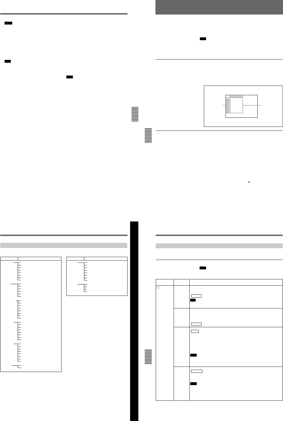
1-18
Chapter 5 Duplication and Audio Dubbing
Chapter 5 Duplication and Audio Dubbing
75
(GB)
Notes
¥If you have selected +48V ON, do not insert a
metal object into the AUDIO INPUT connectors.
It may cause electric shock.
¥If you have selected +48V ON, use a microphone
that is compatible with 48 V. Using a microphone
that is incompatible may damage the microphone,
generate smoke or cause a fire.
3Switch the audio input level control selectors to
select the audio input signal level (—60, —20 or +4).
Note
If you have set the audio input selectors to +48V
ON, set the audio input level control selectors to
—60.
4Set the AUDIO SELECT switch to AUTO or
MANU.
5Adjust the recording level by turning the audio
recording level control knobs.
You can adjust the recording level with the audio
recording level control knobs if you have selected
MANU in step 4. While looking at the audio level
meters on the LCD monitor or the display window,
turn the audio recording level control knobs and
adjust the recording level. Adjust the audio
recording level so that the recording level does not
exceed 0 dB when the audio signal is at its
maximum. If the recording level exceeds 0 dB, the
OVER indicators light.
6Set the tape in the unit (and the sound source, if
any) for dubbing.
7While pressing the PAUSE button, press the PLAY
button to enter the playback pause mode.
8While pressing the AUDIO DUB button, press the
PLAY button to enter the audio dubbing pause
mode.
9Press the PAUSE button.
The AUDIO DUB indicator flashes and audio
dubbing starts.
To pause audio dubbing
Press the PAUSE button.
Pressing the PAUSE button again resumes audio
dubbing.
To stop audio dubbing
Press the STOP button.
To monitor the sound being dubbed
Set the MONITOR SELECT selector as follows:
CH1/2: You can listen to sound on channels 1/2 on
the tape or sound to be dubbed.
CH3/4: You can listen to sound on channels 3/4 on
the tape or sound to be dubbed.
MIX: You can listen to the sound on the tape and the
dubbed sound.
Note
You can monitor the sound on the tape while dubbing
the sound. However, there are some delays between
the sound being recorded and the sound being played.
When you play back the tape after audio dubbing, you
might hear the dubbed sound later than the sound
monitored during audio dubbing.
Operating the Menus
Chapter 6 Adjusting and Setting Through Menus
76
(GB) Chapter 6 Adjusting and Setting Through Menus
Operating the Menus
The unit allows you to set various parameters in the menus. Before you
start using the unit, set the internal clock in CLOCK SET on the OTHERS
menu. Except for clock setting, you can use all other factory-set default
parameters but change them as needed.
Note
If the internal backup battery is exhausted, the menu settings will be
initialized. The internal backup battery is fully charged if you connect the
power to the unit for about 10 hours. The menu settings will be kept for
about one month.
Displaying the menu
1Set the DISPLAY (LCD OFF/OFF/ON) selector to ON.
2Set the DISPLAY (MENU/TC/AUDIO) selector to MENU.
The menu is superimposed on the LCD monitor.
Changing the menu settings
1Rotating the SEL/PUSH EXEC dial, select the menu icon you want to
change, then press the dial.
2Rotating the SEL/PUSH EXEC dial, select the submenu you want to
change, then press the dial.
3Rotating the SEL/PUSH EXEC dial, change the setting.
4Press the SEL/PUSH EXEC dial to return to the submenu.
5Repeat steps 1 to 4, as needed.
To return to step 1
Rotating the SEL/PUSH EXEC dial, select RETURN, then press the
dial.
TC ⁄ UB SET
TC PRESET
UB PRESET
TC FORMAT
TC RUN
TC ⁄ UB IN
TC MAKE
UB TIME
JOG TC OUT
TC
CM
DISP
V
A
LCD
VTR
ETC
Icons Submenus
Chapter 6 Adjusting and Setting Through Menus
Chapter 6 Adjusting and Setting Through Menus
77
(GB)
Chapter 6 Adjusting and Setting Through Menus
Menu Organization
The menu of this unit consists of the following menus and submenus.
Menu
TC/UB SET TC PRESET
(page 78 (GB))
UB PRESET
(page 78 (GB))
TC FORMAT
(page 78 (GB))
a)
TC RUN
(page 78 (GB))
TC/UB IN
(page 79 (GB))
TC MAKE
(page 79 (GB))
UB TIME
(page 79 (GB))
JOG TC OUT
(page 79 (GB))
DISPLAY SET EE/PB SET
(page 84 (GB))
qREMAIN
(page 84 (GB))
DATA CODE
(page 84 (GB))
LTR SIZE
(page 84 (GB))
COLOR BAR
(page 85 (GB))
b)
uREMAIN
(page 85 (GB))
DATE DISP
(page 85 (GB))
TIME DISP
(page 85 (GB))
VIDEO SET PB YNR
(page 85 (GB))
PB CNR
(page 85 (GB))
VIDEO LVL
(page 86 (GB))
EXT SYNC
(page 87 (GB))
H PHASE
(page 87 (GB))
H PHASE F
(page 87 (GB))
SC PHASE
(page 87 (GB))
SC PHASE F
(page 87 (GB))
AUDIO SET AUDIO MODE
(page 88 (GB))
AUDIO DUB
(page 88 (GB))
JOG AUDIO
(page 88 (GB))
REF LEVEL
(page 88 (GB))
AGC CH1,2
(page 88 (GB))
AGC CH3,4
(page 88 (GB))
LIMITER
(page 89 (GB))
WIND
(page 89 (GB))
LCD SET LCD BRIGHT
(page 89 (GB))
LCD COLOR
(page 89 (GB))
c)
CM SET CM SEARCH
(page 80 (GB))
TITLE DISP
(page 80 (GB))
LABEL DISP
(page 80 (GB))
TAPE LABEL
(page 81 (GB))
ITEM ERASE
(page 82 (GB))
ERASE ALL
(page 83 (GB))
VTR SET FF/REW SPD
(page 90 (GB))
STILL TIME
(page 90 (GB))
FROM STILL
(page 90 (GB))
FROM REC P
(page 90 (GB))
DUPLICATE
(page 90 (GB))
FOOT SW
(page 91 (GB))
DV EE OUT
(page 91 (GB))
STILL PICT
(page 91 (GB))
OTHERS BEEP
(page 92 (GB))
A BACK COL
(page 92 (GB))
CLOCK SET
(page 92 (GB))
HRS METER
(page 92 (GB))
Submenu (page) Menu Submenu (page)
a) DSR-50 only
b) COLOUR BAR for DSR-50P
c) LCD COLOUR for DSR-50P
Operating the Menus
Chapter 6 Adjusting and Setting Through Menus
78
(GB) Chapter 6 Adjusting and Setting Through Menus
Menu Contents
Initial settings are indicated with rectangles.
TC/UB SET menu
Note
All items other than JOG TC OUT can be set only when you record in
DVCAM-format.
TC
TC/UB SET
Icon/Menu Submenu Setting
(page)
TC PRESET
(page 56 (GB))
Resets/Sets the time code value.
RESET: Resets the time code value to 00:00:00:00.
PRESET: Sets the time code value.
RETURN : Returns to the TC/UB SET menu without changing the time code value.
Note
Before setting the initial time code value, set TC MAKE to PRESET. If TC MAKE has been
set to REGEN, you cannot change the time code with this submenu.
UB PRESET
(page 57 (GB))
Resets/Sets the user bits value.
RESET: Resets the user bits value to 00 00 00 00.
PRESET: Sets the user bits value. (You can set the user bits as eight-digit hexadecimal
values (0 to 9, A to F) (base 16) to have the date, time, scene number, and other
information inserted into the user bits.)
RETURN : Returns to the TC/UB SET menu without changing the user bits value.
TC FORMAT
(page 59 (GB))
Selects the frame mode.
AUTO : Automatically sets the frame mode in accordance with the inserted cassette. (If
nothing is recorded on the tape, the mode is set to the non-drop frame mode. If the unit
cannot read the frame mode correctly in the tape, the unit will use the frame mode that
was set in the last position it was able to read correctly on the tape. If you turn the
power on/off or remove the tape, the mode of the last position it was able to read
correctly is cleared and the mode is set to the non-drop frame mode.)
DF: Selects the drop frame mode.
NDF: Selects the non-drop frame mode.
Notes
•This menu is displayed only for DSR-50.
•Regardless of this setting, the frame mode is set to drop frame when you record in DV
format.
TC RUN
(page 59 (GB))
Selects the advancement mode (counting up).
REC RUN : Time code value advances only while recording.
FREE RUN: Time code value advances even when the unit is not recording. (This mode is
used to set the current time as the initial time code value, or to synchronize the internal
time code to an external time code.)
Notes
•If you set the advancement mode to FREE RUN, the time code will be updated by the
internal clock when the power is off. Therefore, when you turn on the unit again, the time
code may have been delayed or advanced somewhat.
•If the internal backup battery is exhausted, the time code of the FREE RUN setting is
initialized.
1-19
Chapter 6 Adjusting and Setting Through Menus
Chapter 6 Adjusting and Setting Through Menus
79
(GB)
TC/UB IN
(page 60 (GB))
TC
TC/UB SET
Icon/Menu Submenu Setting
(page)
Selects the time code and user bits to record in the tape.
INTERNAL : Uses the internal time code/user bits.
TC&UB EXT: Uses the external time code/user bits.
TC EXT: Uses the external time code and internal user bits.
UB EXT: Uses the internal time code and external user bits.
Notes
•The time code output from this unit has some restrictions.
For details, see pages 63 (GB),
64 (GB).
•Press the SEL/PUSH EXEC dial to execute this submenu. This will also be executed the
moment you switch the position of the DISPLAY (MENU/TC/AUDIO) selector to TC or
AUDIO.
TC MAKE
(page 59 (GB))
Selects the time code when you start recording.
REGEN : The time code value is set to the continuous time code from the time code
already recorded on the tape. If no time code is recorded on the tape, the time code
starts from 00:00:00:00.
PRESET: The time code value is set to the time code from the value set in PRESET in the
TC PRESET on the TC/UB SET menu.
UB TIME
(page 59 (GB))
Selects whether to set the user bits to any particular value or to the real time clock.
OFF : The value set in PRESET in UB PRESET on the TC/UB SET menu is set in the
user bits.
ON: The value set in CLOCK SET on the OTHERS menu (the real time clock) is set in the
user bits.
Note
This item is available only if TC/UB IN is set to INTERNAL or TC EXT.
JOG TC OUT
(page 59 (GB))
Controls the time code output from the TC OUT connector when the tape is played at a
speed other than normal.
OFF : Does not output the time code.
ON: Outputs the time code.
Note
The continuous time code is output only when the tape is played at a normal speed. When
the unit is in the search mode, discontinuous time code is output.
Operating the Menus
Chapter 6 Adjusting and Setting Through Menus
80
(GB) Chapter 6 Adjusting and Setting Through Menus
LABEL DISP Selects whether or not to display the tape label.
ON : Displays the tape label.
OFF: Hides the tape label.
Notes
•The tape label is displayed only on the LCD monitor, VIDEO OUT1 output or return video
to the camera.
•The tape label is only displayed if you have set the DISPLAY (MENU/TC/AUDIO) selector
to TC.
•If the tape label has been made with an other VCR or camcorder, this unit cannot display
a tape label that includes a font that the unit does not have.
Icon/Menu Submenu Setting
(page)
CM SET menu
CM
CM SET CM SEARCH Selects the mode which searches recordings.
ON : Searches recordings using the cassette memory. (If the tape does not have cassette
memory, the beginning of recording is searched for using the index signals on the tape.)
OFF: Always searches recordings using the index signals on the tape.
TITLE DISP Selects whether or not to display the title.
ON : Displays the title.
OFF: Hides the title.
Notes
•The title input with the camera or external device is displayed. You cannot enter a title in
this unit.
•The unit cannot display a font that the unit does not have.
•The title is displayed only on the LCD monitor, VIDEO OUT1 output or return video to the
camera.
•The title is only displayed if you have set the DISPLAY (MENU/TC/AUDIO) selector to TC.
Chapter 6 Adjusting and Setting Through Menus
Chapter 6 Adjusting and Setting Through Menus
81
(GB)
Icon/Menu Submenu Setting
(page)
CM
CM SET TAPE LABEL Makes a tape label. (You can enter up to 10 characters on a tape label.)
If you select this item, one of the following symbols appears. If no cassette is loaded,
nothing is displayed.
: Tape with cassette memory
: Tape without cassette memory
You can make a tape label as follows:
1On the TAPE LABEL screen, select a line that has the alphabet character you want by
rotating and pushing the SEL/PUSH EXEC dial. (The cursor moves to the first character
of the line.)
2Select a character by rotating and pushing the SEL/PUSH EXEC dial. (The selected
character is entered. To erase a character, select [ P ]; the last character is erased.)
3Repeat steps 1 and 2. After entering all characters for the tape label, select [SET].
Note
The unit cannot display the TAPE LABEL screen in the following cases:
•The unit does not have a tape inserted or the tape is being unloaded.
•The tape does not have cassette memory.
•The cassette memory is full of data other than the tape label data.
•The tape is write-protected.
•The tape is being recorded.
•The tape is being duplicated.
•The cassette memory is being used.
TAPE LABEL
__________
A
F
K
P
U
Z
B
G
L
Q
V
&
C
H
M
R
W
D
I
N
S
X
?
E
J
O
T
Y
!
1
6
'
[
[
2
7
,
S
3
8
.
E
4
9
/
T
5
0
–
]
]
TAPE LABEL
__________
A
F
K
P
U
Z
B
G
L
Q
V
&
C
H
M
R
W
D
I
N
S
X
?
E
J
O
T
Y
!
1
6
'
[
[
2
7
,
S
3
8
.
E
4
9
/
T
5
0
–
]
]
,
TAPE LABEL
__________
A
F
K
P
U
Z
B
G
L
Q
V
&
C
H
M
R
W
D
I
N
S
X
?
E
J
O
T
Y
!
1
6
'
[
[
2
7
,
S
3
8
.
E
4
9
/
T
5
0
–
]
]
TAPE LABEL
S_________
A
F
K
P
U
Z
B
G
L
Q
V
&
C
H
M
R
W
D
I
N
S
X
?
E
J
O
T
Y
!
1
6
'
[
[
2
7
,
S
3
8
.
E
4
9
/
T
5
0
–
]
]
,
(Continued)
Operating the Menus
Chapter 6 Adjusting and Setting Through Menus
82
(GB) Chapter 6 Adjusting and Setting Through Menus
ITEM ERASE
Icon/Menu Submenu Setting
(page)
CM
CM SET
CM SET
I TEM ERASE
I NDEX ALL
T IT LE ALL
DATE ALL
PHOTO ALL
RETURN
RETURN
OK
TC
CM
DISP
V
A
LCD
VTR
ETC
CM SET
I TEM ERASE
I NDEX ALL
T IT LE ALL
DATE ALL
PHOTO ALL
RETURN
RETURN
OK
TC
CM
DISP
V
A
LCD
VTR
ETC
,
Erase a cassette memory item.
If you select this item, one of the following symbols appears. If no cassette is loaded,
nothing is displayed.
: Tape with cassette memory
: Tape without cassette memory
The available items are as follows:
INDEX ALL: Erases the index data.
TITLE ALL: Erases the title data.
DATE ALL: Erases the date data.
PHOTO ALL: Erases the photo data.
You can erase an item as follows:
1Select an item to erase by rotating and pushing the SEL/PUSH EXEC dial.
2To erase the item, select OK, otherwise select RETURN. (If you select OK, the unit will
check again to see if you really want to erase the item.)
3To erase the item, select EXECUTE, otherwise select RETURN. (If you select
EXECUTE, the ERASING message will flash, and the unit will start erasing the item in
the cassette memory. While the ERASING message is flashing, you cannot use the SEL/
PUSH EXEC dial. After the item has been erased, the COMPLETE message appears.
Press or rotate the SEL/PUSH EXEC dial to erase the COMPLETE message.)
Notes
•You cannot make the title, mark the date for date search, or record in the photo mode.
•You cannot erase an item in the cassette memory in the following cases:
– The unit does not have a tape inserted or the tape is being unloaded.
– The tape does not have cassette memory.
– The tape is write-protected.
– The tape is being recorded.
– The tape is being duplicated.
CM SET
I TEM ERASE
I NDEX ALL
T IT LE ALL
DATE ALL
PHOTO ALL
RETURN
RETURN
EXECUTE
TC
CM
DISP
V
A
LCD
VTR
ETC
,
CM SET
I TEM ERASE
I NDEX ALL
T IT LE ALL
DATE ALL
PHOTO ALL
RETURN
ERASING
TC
CM
DISP
V
A
LCD
VTR
ETC
CM SET
I TEM ERASE
I NDEX ALL
T IT LE ALL
DATE ALL
PHOTO ALL
RETURN
COMPLETE
TC
CM
DISP
V
A
LCD
VTR
ETC
,
CM SET
I TEM ERASE
I NDEX ALL
T IT LE ALL
DATE ALL
PHOTO ALL
RETURN
RETURN
OK
TC
CM
DISP
V
A
LCD
VTR
ETC
,
1-20
Chapter 6 Adjusting and Setting Through Menus
Chapter 6 Adjusting and Setting Through Menus
83
(GB)
Icon/Menu Submenu Setting
(page)
CM
CM SET
CM SET
CM SEARCH
TITLE DISP
LABEL DISP
TAPE LABEL
I TEM ERASE
ERASE ALL
RETURN RETURN
OK
TC
CM
DISP
V
A
LCD
VTR
ETC
CM SET
CM SEARCH
TITLE DISP
LABEL DISP
TAPE LABEL
I TEM ERASE
ERASE ALL
RETURN
TC
CM
DISP
V
A
LCD
VTR
ETC
RETURN
OK
,
CM SET
CM SEARCH
TITLE DISP
LABEL DISP
TAPE LABEL
I TEM ERASE
ERASE ALL
RETURN RETURN
EXECUTE
TC
CM
DISP
V
A
LCD
VTR
ETC
,
CM SET
CM SEARCH
TITLE DISP
LABEL DISP
TAPE LABEL
I TEM ERASE
ERASE ALL
RETURN ERASING
TC
CM
DISP
V
A
LCD
VTR
ETC
CM SET
CM SEARCH
TITLE DISP
LABEL DISP
TAPE LABEL
I TEM ERASE
ERASE ALL
RETURN COMPLETE
TC
CM
DISP
V
A
LCD
VTR
ETC
,
CM SET
CM SEARCH
TITLE DISP
LABEL DISP
TAPE LABEL
I TEM ERASE
ERASE ALL
RETURN RETURN
OK
TC
CM
DISP
V
A
LCD
VTR
ETC
,
ERASE ALL Erases all items in the cassette memory.
If you select this item, one of the following symbols appears. If no cassette is loaded,
nothing is displayed.
: Tape with cassette memory
: Tape without cassette memory
Erase all items in the cassette memory as follows:
1To erase all items, select OK, otherwise select RETURN. (If you select OK, the unit will
check again to see if you really want to erase all items.)
2To erase all items, select EXECUTE, otherwise select RETURN. (If you select
EXECUTE, the ERASING message will flash, and the unit starts erasing all items in the
cassette memory. While the ERASING message is flashing, you cannot use the SEL/
PUSH EXEC dial. After all items have been erased, the COMPLETE message appears.
Press or rotate the SEL/PUSH EXEC dial to erase the COMPLETE message.)
Note
You cannot erase all items in the cassette memory in the following cases:
•The unit does not have a tape inserted or the tape is being unloaded.
•The tape does not have cassette memory.
•The tape is write-protected.
•The tape is being recorded.
•The tape is being duplicated.
Operating the Menus
Chapter 6 Adjusting and Setting Through Menus
84
(GB) Chapter 6 Adjusting and Setting Through Menus
DISPLAY SET menu
Icon/Menu Submenu Setting
(page)
DISP
DISPLAY
SET EE/PB SET
(page 14 (GB))
Sets the stop, fast-forward and rewind modes.
EE : Outputs the EE pictures (sound, time code).
PB: Mutes the image and sound.
Notes
•Even if EXT SYNC is set to ON, the line-outs (VIDEO OUT2, COMPONENT OUT, S
VIDEO OUT) in the EE mode are delayed from those of the input signals as follows:
– delayed for two lines when the camera composite or VIDEO/REF. IN is input.
– delayed for one line when S VIDEO or camera component is input.
•If this item is set to PB, the output from the unit will be as follows when you press any of
the REC, DUP, or AUDIO DUB buttons separately when the unit is stopped.
REC button
Image Sound Time code
EE picture of
the input image EE sound of the
input sound
(See page 62 (GB))
DUP button Image input to
the DV IN/OUT
connector
Sound input to
the DV IN/OUT
connector
AUDIO
DUB button Mute screen
(black) EE sound of the
input sound
No button
is pressed
Mute screen
(black)
Mute (no
sound)
qREMAIN
(page 19 (GB))
Selects whether or not to display the tape remaining time in the LCD monitor and VIDEO
OUT1 output.
ON : Displays the tape remaining time.
OFF: Does not display the tape remaining time.
Note
The display window of the unit always displays the tape remaining time.
DATA CODE
(page 19 (GB))
Selects whether or not to display the data codes on the LCD monitor and the VIDEO OUT1
output.
OFF : Does not display the data codes.
DATE: Displays the date when recorded.
CAMERA: Displays the camera data.
LTR SIZE Changes the font size of the menu line at the cursor.
NORMAL : Normal size
×2: Double height size
Chapter 6 Adjusting and Setting Through Menus
Chapter 6 Adjusting and Setting Through Menus
85
(GB)
Icon/Menu Submenu Setting
(page)
DISP
DISPLAY
SET
COLOR BAR
(for DSR-50) /
COLOUR BAR
(for DSR-50P)
(page 51 (GB))
Displays/hides the color bars.
OFF : Hides the color bars.
ON: Displays the color bars.
Notes
•You cannot display the color bars while the unit is playing the tape or when the INPUT
SELECT selector is set to DV.
•The color bars are displayed only on the LCD monitor, VIDEO OUT1 output, or return
video to the camera.
•If you record when the color bars are displayed, the color bars will also be recorded on the
tape.
•You cannot adjust the VIDEO OUT1 output. Do not use the color bars output from the
VIDEO OUT1 connector as a reference signal.
•The reference sound signals are not output even if this item is set to ON.
•This item will be automatically set to OFF if you set the INPUT SELECT selector to DV or
you operate the tape transport control that display the pictures recorded on the tape.
uREMAIN
(page 18 (GB))
Switches the battery type.
LI-ION : Uses a lithium ion battery.
NI-CD: Uses a nickel cadmium battery.
DATE DISP Switches the date display in the display window or in the search screen for index search and
so on.
Y/M/D: Displays YY/MM/DD (year/month/day).
M/D/Y: Displays MM/DD/YY (month/day/year).
D/M/Y: Displays DD/MM/YY (day/month/year).
Note
The default is M/D/Y for DSR-50; D/M/Y for DSR-50P.
TIME DISP Switches the time display in the display window, LCD monitor and VIDEO OUT1 output.
24H : Displays 24-hour time.
12H: Displays 12-hour time.
VIDEO SET menu
Icon/Menu Submenu Setting
(page)
V
VIDEO SET PB YNR Switches the noise reduction level for the luminance signals when a tape is played.
OFF : No noise reduction
LOW: Low noise reduction
HIGH: High noise reduction
Note
When you use noise reduction, there may be an afterimage depending on the condition of
the picture.
PB CNR Switches the noise reduction level for the chrominance signals when a tape is played.
OFF : No noise reduction
LOW: Low noise reduction
HIGH: High noise reduction
Note
When you use noise reduction, there may be an afterimage depending on the condition of
the picture.
(Continued)
Operating the Menus
Chapter 6 Adjusting and Setting Through Menus
86
(GB) Chapter 6 Adjusting and Setting Through Menus
Icon/Menu Submenu Setting
(page)
V
VIDEO SET VIDEO LVL
(page 67 (GB))
Adjusts the video signal levels.
INPUT: Adjusts the input video signals. (This is available only when the EE pictures are
output and the mode is stop, record, recording pause, fast-forward or rewind. This is
disabled for DV input.)
PB OUTPUT: Adjusts the output video signals. (This is available only when the mode is
playback, playback pause, slow playback, cue, or review.)
RETURN: Exits the menu without adjusting video signal levels.
Adjusting the input video signals
LUMINANCE: Adjusts the luminance level of the composite signals.
CHROMA: Adjusts the chrominance level of the composite signals.
HUE: Adjusts the hue of the composite signals. (only for DSR-50)
Y LVL: Adjusting the Y signal level of the camera component signals.
R-Y LVL: Adjusting the R-Y signal level of the camera component signals.
B-Y LVL: Adjusting the B-Y signal level of the camera component signals.
Notes
•This item is disabled for DV input. (You cannot adjust the DV input signals.)
•Adjust the signal levels by looking at the bars. (The triangles under the bars are displayed
in green when the settings are set to the factory preset values.)
•All factory preset values are their center value.
•LUMINANCE, CHROMA and HUE can be adjusted only for VIDEO/REF. IN, camera
composite or S VIDEO input while in the EE mode.
•Y LVL, R-Y LVL and B-Y LVL can be adjusted only for camera component signal input
while in the EE mode.
Adjusting the output video signals
SETUP: Switches the luminance signal setup level (0% or 7.5%). (This item is only for
DSR-50. The setup level for DSR-50P is fixed to 0%.)
Y LVL: Adjusts the Y signal level of the component signals. (If you change this, the Y
signal level of the composite video and S VIDEO will also be changed.)
R-Y LVL: Adjusts the R-Y signal level of the component signals. (If you change this, the
chrominance level of the composite video and S VIDEO will also be changed.)
B-Y LVL: Adjusts the B-Y signal level of the component signals. (If you change this, the
chrominance level of the composite video and S VIDEO will also be changed.)
CHROMA: Adjusts the chrominance level in the composite signals.
Notes
•You can adjust the video levels only while playing the tape.
•Adjust the video levels by looking at the bars (except SETUP). (The triangles under the
bars are displayed in green when the settings are set to the factory preset values.)
•The SETUP default is 0%. Other defaults are their center values.
•The output video signals can be adjusted only for VIDEO OUT2, COMPONENT OUT, or S
VIDEO OUT.
•Set SETUP to 7.5% only if the tape has been recorded at 0% and you want to play back
the tape at 7.5%. If you play back a 7.5% tape at the 7.5% setting, the tape will not be
played at the proper brightness. If you set SETUP at 0% and if you play back a 7.5% tape,
the tape will be played at 7.5%. (You cannot play the tape at 0%.)
1-21
Chapter 6 Adjusting and Setting Through Menus
Chapter 6 Adjusting and Setting Through Menus
87
(GB)
Icon/Menu Submenu Setting
(page)
V
VIDEO SET EXT SYNC Switches the externally synchronized playback setting.
OFF : No external synchronization
ON: External synchronization
Notes
•It may take three or more seconds until a stable image is output in the externally-
synchronized playback mode.
•If external synchronization is applied, jitters may appear on the image output from VIDEO
OUT1 output or on the LCD monitor image. Use the VIDEO OUT2 connector to output an
externally-synchronized image. Set this item to OFF when you use the VIDEO OUT1
connector.
H PHASE
(page 65 (GB))
Roughly adjusts the sync phase in the externally-synchronized playback mode.
Rotate the SEL/PUSH EXEC dial to move the bar and push the dial to select. (The triangle
under the bar is displayed in green when the setting is set to the factory preset value.)
Notes
•You can adjust the H PHASE only in the externally-synchronized playback mode.
•If you change this item, the H PHASE F value will be set to the factory preset value.
H PHASE F
(page 65 (GB))
Finely adjusts the sync phase in the externally-synchronized playback mode.
Rotate the SEL/PUSH EXEC dial to move the bar and push the dial to select. (The triangle
under the bar is displayed in green when the setting is set to the factory preset value.)
Notes
•You can adjust the H PHASE F only in the externally-synchronized playback mode.
•If you change the H PHASE value, this item is set to the factory preset value.
SC PHASE
(page 65 (GB))
Reverses the subcarrier phase in the externally-synchronized playback mode.
0 DEG : The subcarrier phase is not reversed.
180 DEG: The subcarrier phase is reversed.
Note
You can adjust the SC PHASE only in the externally-synchronized playback mode.
SC PHASE F
(page 65 (GB))
Finely adjusts the subcarrier phase in the externally-synchronized playback mode.
Rotate the SEL/PUSH EXEC dial to move the bar and push the dial to select. (The triangle
under the bar is displayed in green when the setting is set to the factory preset value.)
Note
You can adjust the SC PHASE F only in the externally-synchronized playback mode.
Operating the Menus
Chapter 6 Adjusting and Setting Through Menus
88
(GB) Chapter 6 Adjusting and Setting Through Menus
AUDIO SET menu
A
AUDIO SET
Icon/Menu Submenu Setting
(page)
AUDIO
MODE
(page 74 (GB))
Selects the audio mode.
FS32K : Switches the audio mode to the four channel mode (12-bit mode).
FS48K: Switches the audio mode to the two channel stereo mode (16-bit mode). (This
setting records the sound in all audio ranges, providing a high-quality sound recording.)
Notes
•This item is disabled when inputting signals from the DV IN/OUT connector.
•You cannot display the selection screen while in the recording mode.
•Noise may occur at the moment you switch the audio mode.
AUDIO DUB
(page 74 (GB))
Selects the input channel for audio dubbing.
CH1,2: Selects channels 1 and 2.
CH3,4 : Selects channels 3 and 4.
OFF: Disables audio dubbing.
Note
You cannot display the selection screen while dubbing the sound.
JOG AUDIO Turns sound output on/off when the tape is played at a speed other than normal.
OFF : Does not output the sound when playing a tape at a speed other than normal.
ON: Outputs the sound when playing a tape at a speed other than normal.
Note
Even if you have set this item to ON, the sound may not be output or interrupted depending
on the tape format or tape conditions.
REF LEVEL
(page 20 (GB))
Switches the center levels of the audio level meters displayed on the FINE screen.
–12dB: Sets the level to –12 dB
–18dB: Sets the level to –18 dB
–20dB: Sets the level to –20 dB
Notes
•The default is –20 dB for DSR-50; –18 dB for DSR-50P.
•The standard output level of the AUDIO OUTPUT jacks is –10 dBu. This is equivalent to
–20 dB for DSR-50, or –18 dB for DSR-50P from full bit (maximum audio level). This level
is fixed and does not change even if you change the REF LEVEL setting.
•Changing this level does not change the audio gain of this unit. Turn the audio recording
level control knobs to adjust the recording level accordingly.
AGC CH1,2
(page 21 (GB))
Links/separates the AGC (Auto Gain Control) in channels 1 and 2.
SEPARATE : AGC is not linked. (Channels 1 and 2 sound gains are separated.)
LINKED: AGC is linked. (Channels 1 and 2 sound gains are linked as a pair.)
Notes
•This setting is disabled when inputting signals from the DV IN/OUT connector.
•The LINKED setting is enabled after you set the AUDIO SELECT switches on the front
panel to AUTO for both channels 1 and 2.
AGC CH3, 4
(page 21 (GB))
Links/separates the AGC (Auto Gain Control) in channels 3 and 4.
SEPARATE : AGC is not linked. (Channels 3 and 4 sound gains are separated.)
LINKED: AGC is linked. (Channels 3 and 4 sound gains are linked as a pair.)
Notes
•This setting is disabled when inputting signals from the DV IN/OUT connector.
•The LINKED setting is enabled after you set the AUDIO SELECT switches on the front
panel to AUTO for both channels 3 and 4.
Chapter 6 Adjusting and Setting Through Menus
Chapter 6 Adjusting and Setting Through Menus
89
(GB)
A
AUDIO SET
Icon/Menu Submenu Setting
(page)
LIMITER Turns the limiter on/off.
OFF : No limiter
ON: Uses the limiter.
Notes
•This setting is disabled when inputting signals from the DV IN/OUT connector.
•This setting is available only when you have set the AUDIO SELECT switches on the front
panel to MANU.
•Make sure to set the audio input level control selectors on the right panel correctly. Even if
you have set this item to ON, the limiter will not work for a sound that exceeds the dynamic
range of the input amplifier.
WIND
(page 21 (GB))
Enables/disables the wind noise reduction function for microphones.
You can set the wind noise reduction for audio channels 1 to 4 separately. If you select this
item, the channel to which the noise reduction is currently applied is displayed. (Example: If
noise reduction is applied to channels 1 and 3, “CH1,3” is displayed. If all channels are set
to OFF, “OFF” is displayed.)
OFF : No wind noise reduction
ON: Wind noise reduction
If you press the SEL/PUSH EXEC dial, the channel names are displayed. Select the
channel to be changed, change the setting, then press the SEL/PUSH EXEC dial.
Note
This setting is disabled when inputting signals from the DV IN/OUT connector.
LCD SET menu
Icon/Menu Submenu Setting
(page)
LCD
LCD SET LCD BRIGHT Adjusts the LCD monitor brightness. Rotate and press the SEL/PUSH EXEC dial to adjust
and set the brightness. You can also adjust the brightness by rotating the SEL/PUSH EXEC
dial on the TC screen. (The triangle under the bar is displayed in green when the setting is
set to the factory preset value.)
LCD COLOR
(for DSR-50) /
LCD COLOUR
(for DSR-50P)
Adjusts the depth of color of the LCD monitor. Rotate and press the SEL/PUSH EXEC dial
to adjust and set the depth of color. (The triangle under the bar is displayed in green when
the setting is set to the factory preset value.)
Operating the Menus
Chapter 6 Adjusting and Setting Through Menus
90
(GB) Chapter 6 Adjusting and Setting Through Menus
VTR SET menu
Icon/Menu Submenu Setting
(page)
VTR
VTR SET FF/REW SPD Selects the tape transport mode in fast-forward and rewind.
FF/REW : Fast-forwards or rewinds the tape at maximum speed without displaying the
picture.
SHUTTLEMAX: Fast-forwards or rewinds the tape at maximum speed (about 14 times
normal speed for the DSR-50; about 17 times normal speed for the DSR-50P) while
displaying the picture.
STILL TIME Selects the time to switch to the tape protection mode from the still mode.
30 SEC: 30 seconds
1 MIN : 1 minute
2 MIN: 2 minutes
3 MIN: 3 minutes
5 MIN: 5 minutes
Notes
•If the unit is left in playback pause mode for a long time, the tape or the video heads may
be damaged or the video heads may become clogged. Select the shortest time possible
—particularly when using a Mini-DV cassette that is longer than 60 minutes, select 30
SEC or 1 MIN.
•When the setting is changed, the first tape protection mode change uses the time setting
from before the settings were changed. From the second tape protection mode change,
the new time setting is used.
FROM STILL Selects the tape protection mode to change the mode from the still mode.
STEP FWD : Forwards one frame.
STOP: Stops the tape.
FROM REC
PSwitches the tape protection mode that the system changes to after the recording has been
paused for more than five minutes.
STOP : Stops the tape.
REC PAUSE: Maintains the recording pause mode.
Notes
•The unit changes to the stop mode after the recording has been paused for more than five
minutes when you select STOP. In this case you cannot start recording with the VTR
button on the camera. Repeat the procedure from step 2 on page 47 (GB) to start
recording again.
•When the recording pause mode continues for a long time after you select REC PAUSE,
the tape may be damaged or the video heads may be damaged or clogged. If there is no
other reason to do this, select STOP. Particularly when you use a Mini-DV cassette that is
longer than 60 minutes, select STOP.
DUPLICATE
(page 70 (GB))
Switches the duplicate mode.
AUTOq: Starts duplication after rewinding the tape to the beginning in the player and
recorder. (The cassette memory is also duplicated.)
AUTOq: Starts duplication after rewinding the tape to the beginning in the player and
recorder. (The cassette memory is not duplicated.)
MANUALq : Duplicates the tape from any point. (The cassette memory is not
duplicated.)
Note
You cannot display the setting selection screen during duplication.
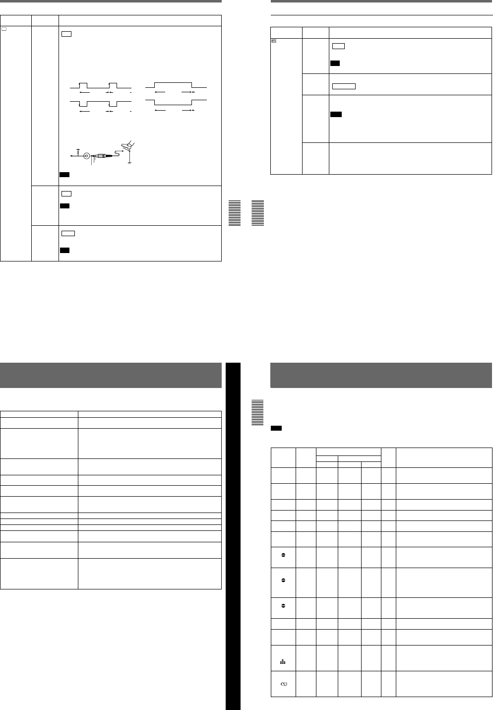
1-22
Chapter 6 Adjusting and Setting Through Menus
Chapter 6 Adjusting and Setting Through Menus
91
(GB)
Icon/Menu Submenu Setting
(page)
VTR
VTR SET FOOT SW Selects a foot switch mode.
OFF : Disables the foot switch.
EDGE HIGH: Switches between recording and recording pause mode each time you
release the foot switch.
EDGE LOW: Switches between recording and recording pause mode each time you press
the foot switch. (This is the most popular use for foot switch.)
LEVEL HIGH: Records only while the foot switch is released.
LEVEL LOW: Records only while the foot switch is pressed.
The following shows the trigger statuses.
The following shows the foot switch circuit.
Note
You cannot operate audio dubbing or duplication from the foot switch.
EDGE HIGH
EDGE LOW
Recording Recording
pause
Recording Recording
pause
LEVEL HIGH
LEVEL LOW
Recording Recording
pause
Recording Recording
pause
DSR-50/50P
5 V Stereo
minijack
GND
Tally LED
Foot Switch
DV EE OUT
(page 37 (GB))
Selects the output from the DV IN/OUT connector in the EE mode.
OFF : Outputs only the playback video and audio signals from the DV IN/OUT connector.
ON: Outputs the selected analog input signals from the DV IN/OUT connector.
Note
When you connect a computer to the DV IN/OUT connector, depending on your computer
software, the selected analog input signals may be output to the computer even if this item
is set to OFF.
STILL PICT Switches the image displayed in the still mode.
AUTO : Displays an optimized image according to the movement in the image.
FRAME: Displays a frame image.
FIELD: Displays a field image.
Note
If you select FIELD, the image of field 2 is displayed.
Operating the Menus
Chapter 6 Adjusting and Setting Through Menus
92
(GB) Chapter 6 Adjusting and Setting Through Menus
OTHERS menu
Icon/Menu Submenu Setting
(page)
OTHERS BEEP Selects the beep.
BEEP : Normal beep
MELODY: Melody beep (The melody beep is also mixed during a menu operation.)
OFF: Disables the beep.
Note
The beep sound is mixed only on the headphone sound and return sound to the camera.
A BACK COL Changes the background color of the AUDIO screen when you have set the DISPLAY
(MENU/TC/AUDIO) selector on the front panel to AUDIO.
HALFTONE : Halftone
BLACK: Black
CLOCK SET Sets the internal clock of the unit.
Rotating and pressing the SEL/PUSH EXEC dial, sets the time (year, month, day, hour and
minute). (When you set the minute, the second count will start from 00.)
Notes
•Regardless of the DATE DISP setting, the date is displayed in the Y/M/D format while you
are setting CLOCK SET.
•The internal backup battery will be fully charged in about 10 hours when power is provided
to the unit. A fully charged internal backup battery can run the internal clock for about one
month without the battery pack or power provided through the AC adaptor.
HRS METER
(page 97 (GB))
Displays the accumulated time counts (by the digital hours meter) in units of 10 hours or 10
counts.
OPERATION: Power on duration
DRUM RUN: Drum rotation duration
TAPE RUN: Tape run duration
THREADING: Tape unthreading count
Chapter 7 Maintenance
93
(GB)
Chapter 7 Maintenance
Symptom Cause/Remedy
The power cannot be turned on. •Battery pack charge is low. t Replace the battery pack.
•The AC adaptor is disconnected. t Connect the AC adaptor.
The unit will not operate even if the power
has been turned on. •Moisture condensation has occurred. t Turn off the power, remove the battery
pack and disconnect the AC adaptor. Reinstall the battery pack or connect the
AC adaptor after about one minute and turn on the power. Then if there is a
cassette in the unit, remove the cassette and keep the cassette lid open, power
on the unit and leave it on for more than one hour.
•The cassette is not inserted straight. t Insert it straight.
The cassette cannot be inserted. •There is moisture condensation on the head drum. t Keep the cassette lid
open and turn the power on. Then, wait more than one hour.
•The cassette is not inserted straight. t Insert it straight.
It takes time to eject the cassette. This is not a malfunction. t This unit ejects the cassette slowly to protect the
tape.
No picture. The video heads are dirty. t Clean the video heads using the supplied cleaning
cassette.
Noise appears on the screen. •A damaged cassette is inserted. t Insert an other cassette.
•The video heads are dirty. t Clean the video heads using the supplied
cleaning cassette.
No picture via the DV jack. Reconnect the i.LINK cable (DV cable) (not supplied).
The audio is noisy. A damaged cassette is inserted. t Insert an other cassette.
Pause is released automatically. Pause mode is automatically released to protect the tape.
Duplication does not function. Check the STOP/CAUTION No. and the warning messages displayed on the
LCD monitor. Take the appropriate action
(See page 72 (GB))
.
Audio dubbing does not function. You are trying to dub the sound on a DV-formatted tape. t You can dub the
sound only on a DVCAM-formatted tape. Use a DVCAM-formatted tape
(See
page 74 (GB))
.
A menu is not available. •If you have set the DVCAM/DV select switch to DV, some menus will be
disabled. t Set the DVCAM/DV select switch to DVCAM
(See page 29 (GB))
.
•Some menus are only available in the EE mode or playback mode. t Set the
unit to the EE mode or playback mode.
•Some TC/UB SET menu items are available only if you have set TC MAKE to
PRESET. t Set TC MAKE to PRESET.
Troubleshooting
Please check the following before contacting your Sony dealer.
Chapter 7 Maintenance
94
(GB) Chapter 7 Maintenance
Chapter 7 Maintenance
Alarm Message
Alarm Messages
If an error occurs, a warning appears on the LCD monitor and the VIDEO OUT1 output (if the SUPERIMPOSE
switch is set to ON). If you have set the DISPLAY (LCD OFF/OFF/ON) selector to LCD OFF, you still can
recognize a warning by means of the display window, the warning indicator or warning tone. Check them with the
following list.
Note
A warning tone is only output to the headphones or return sound to the camera. The warning tone is not output to
the AUDIO MONITOR OUT jack or the AUDIO OUT jacks.
LCD
monitor
Display
window
Indicator lamp (flash/on) a)
Unit Camera
WARNING REC/Tally BATT
Beep Description/Recovery
%%
Rapid
flashing Rapid
flashing Beep
Moisture condensation (without a tape) t Keep the
cassette lid open and turn the power on, then wait
more than one hour.
%Z%Z
Rapid
flashing Rapid
flashing Beep Moisture condensation (with a tape) t Remove the
cassette and keep the cassette lid open and turn the
power on, then wait more than one hour.
Q
NO TAPE
Q
Slow
flashing Beep You tried to record without a cassette. t Insert a
cassette.
QQ
Slow
flashing Slow
flashing No
beep The tape is reaching the end. t Provide a new
cassette.
QZ
TAPE END
QZ
ON Rapid
flashing Beep The tape reached the end and still tried to record. t
Rewind the tape or replace the tape with a new one.
QZQZ
Slow
flashing Beep The cassette is write-protected. (The REC/SAVE switch
is set to SAVE.) t Set the REC/SAVE switch to REC
or use another cassette
(See page 40 (GB))
.
REC MODE Slow
flashing Beep
You tried to dub the sound onto a tape that is not
DVCAM-formatted. t Use a DVCAM-formatted tape
on which the sound has been recorded in the 32 kHz
audio mode (4-channel/12 bits).
TAPE Slow
flashing Beep
You tried to dub the sound onto a blank tape or onto
a tape on which the sound has been not recorded in
the 32 kHz audio mode (4-channel/12 bits). t Use a
DVCAM-formatted tape on which the sound has been
recorded in the 32 kHz audio mode (4-channel/12
bits).
DV IN Slow
flashing Beep
You tried to dub the sound when the INPUT SELECT
selector has been set to DV. t You cannot dub the
sound in the DV input mode. Select another input
mode.
CLOCK SET No
beep
You have not set the clock when you turned on the unit.
t
Set the clock with the menu
(See page 92 (GB))
.
COPY
INHIBIT
Slow
flashing Beep You tried to record a copyright-protected source.
t You cannot record a copyright-protected source
(See page 43 (GB))
.
Rapid
flashing Rapid
flashing
No
beep
The video heads are clogged. t Clean the video
heads with the supplied cleaning cassette. (The unit
detects if the video heads are clean only before
recording. If the video heads get clogged during
recording, the unit cannot detect it.)
e
Slow
flashing Slow
flashing Slow
flashing
No
beep
The power voltage is low. t If you are using a
battery pack, replace the battery pack. If you are
using an AC adaptor, select NI-CD in uREMAIN. If
the warning is still displayed, use an AC adaptor that
meets the specifications of the unit.
x
Y
x
Displayed
alternately
CLEANING
CASSETTE
1-23
Chapter 7 Maintenance
95
(GB)
Chapter 7 Maintenance
LCD
monitor
Display
window
Indicator lamp (flash/on)
a)
Unit Camera
WARNING REC/Tally BATT
Beep Description/Recovery
e
ON Rapid
flashing ON No
beep
The power voltage is very low. t If you are using a
battery pack, replace the battery pack because there
is no battery charge. If you are using an AC adaptor,
select NI-CD in uREMAIN. If the warning is still
displayed, use an AC adaptor that meets the
specifications of the unit.
ZZ
Rapid
flashing
Rapid
flashing Beep
The unit is running the self-diagnostics
(See page 98
(GB))
. This warning display is erased when you turn
on/off the power of the unit.
a) The indicator flashes 3.2 times per second in the rapid flashing mode and flashes 0.8 time per second in the slow flashing
mode.
96
(GB) Chapter 7 Maintenance
Chapter 7 Maintenance
Notes on Use
Notes on Use
Notes on the videocassette recorder
Do not use the unit in a place subject to direct
sunlight or heat sources
If you do, its cabinet, mechanical parts, etc., may be
damaged.
Do not use the unit in an extremely hot place
If the unit is left in a car parked with its windows
closed (especially in summer), its cabinet, mechanical
parts, etc., may be damaged or it may not work
correctly.
If the unit is brought directly from a cold to a
warm location
Moisture may condense inside the unit and cause
damage to the video heads and tape. If you use the unit
in a place subject to direct cold currents from an air
conditioner, moisture may also condense inside the
unit.
Do not place a heavy object on the unit
The cabinet, mechanical parts, etc., may be damaged,
or the unit may not work correctly.
Do not handle the unit roughly
Avoid rough handling or mechanical shock.
To avoid damaging the cabinet’s finish
Plastic is partially used for the surface finishing of the
unit. Do not spray a volatile solvent such as an
insecticide toward the cabinet or place rubber or vinyl
products on the cabinet for a long time. If you do, the
finish of the cabinet may be damaged or the coating
may come off.
Do not clean the cabinet with thinner or
benzine
The cabinet may be damaged or its coating may come
off. When you use a chemical-impregnated cloth, use
it according to its directions.
Clean the cabinet with a soft dry cloth
When the cabinet is very dirty, clean it with a soft dry
cloth lightly moistened with a mild detergent solution
and finish it with a dry cloth.
Do not put magnetic objects close to the unit
Magnetic fields may damage the recording.
To prevent electromagnetic interference
caused by radio communication equipment
such as cellular phones, transceivers, etc.
The use of the radio communication equipment such as
cellular phones or transceivers near the unit may cause
a malfunction and can affect the audio/video signals.
The cellular phones or transceivers near the unit
should be switched off.
Do not use the unit in an area exposed to
radiation
A malfunction may occur.
Checking the video heads every 1000 hours
A VCR is a high-precision piece of equipment that
records and plays back the picture on a magnetic tape.
In particular, the video heads and other mechanical
parts may become dirty or worn. To maintain a clean
picture, we recommend maintenance every 1000
hours, even though the conditions of use may differ
depending on temperature, humidity, dust, etc.
Cleaning of the video heads
If the video heads are contaminated, the pictures
cannot be recorded properly or the playback pictures
become noisy. If the following phenomena occur, use
the cleaning cassette (supplied) to clean the heads.
¥Square-shaped noise appears on the playback picture.
¥A part of the playback picture does not move.
¥The playback picture does not appear on the screen.
To use the cleaning cassette
Refer to your cleaning cassettes operating
instructions.
After prolonged use, the video heads may become
worn out. If optimum picture quality is not restored
even after you have cleaned the video heads with the
cleaning cassette, the video heads may have worn out.
In that case, you have to replace the video heads with
new ones. Please consult your Sony dealer.
Symptoms caused by contaminated video heads
If these pictures appear on the
screen, use the cleaning cassette.
Normal picture
Chapter 7 Maintenance
97
(GB)
Chapter 7 Maintenance
Notes on the video cassettes
If the cassette memory function does not work
Reinsert the cassette a few times. The terminal portion
of the cassette may be dusty or dirty.
Cleaning the terminal
If the terminal of the cassette gets dirty, or dust sticks
to the terminal, the unit may not work correctly.
Clean the terminal with the swab once every ten times
you eject a cassette.
When affixing a label to the cassette
Be sure to affix a label on only the correct location so
as not to cause malfunction of the unit.
After using a cassette
After use, please be sure to rewind the tape completely
(to prevent picture and sound distortion). Return it to
its case and store it in an upright position.
About moisture condensation
If the unit or tape is brought directly from a cold to a
warm location, moisture may condense inside or
outside the unit or tape. If you use the tape or video
heads in this condition, the tape may adhere to the
head drum, and the video heads or the tape may be
damaged, or malfunction may occur.
Moisture condensation is likely to occur under the
following conditions:
¥The unit or tape is brought from the cold outdoors to
a warm indoor location.
¥The unit or tape is brought from the air-conditioned
indoors to the hot outdoors.
¥The unit is used in a place subject to cold currents
from an air conditioner.
When bringing the unit or tape from a cold place to a
warm place or vice versa, put it in a plastic bag and
seal the bag tightly. After bringing it into the new
place, leave the bag on for more than one hour, and
remove the bag when the air temperature inside it has
reached the temperature surrounding it.
If moisture condensation occurred
You cannot operate the unit except to press EJECT,
and the cassette cannot be inserted. If this occurs, turn
on the power to remove the cassette, then keep
opening the cassette lid, and finally wait more than one
hour for the moisture to evaporate.
Digital hours meter
The digital hours meter keeps cumulative counts of the
total operation time, the head drum rotation time, the
tape running time and the number of unthreading
operations. These counts can be displayed on the
monitor screen. Use them as guidelines for scheduling
maintenance.
In general, consult your Sony dealer about necessary
periodic maintenance checks.
The digital hours meter has the following four display
modes and you can check them in HRS METER of the
OTHERS menu (See page 92 (GB)).
¥OPERATION mode
The cumulative total hours of operating time is
displayed in 10-hour increments.
¥DRUM ROTATION mode
The cumulative total hours of drum rotation with tape
threaded is displayed in 10-hour increments.
¥TAPE RUN mode
The cumulative total hours of tape running time is
displayed in 10-hour increments.
¥THREADING mode
The cumulative number of tape unthreading
operations is displayed in 10-operation increments.
Terminal
98
(GB) Chapter 7 Maintenance
Chapter 7 Maintenance
Notes on Use
Self-diagnostics function
The unit has a self-diagnosis display function.
This function displays the current condition of the unit
as a five-digit code (a combination of a letter and
numbers) on the display window, the LCD monitor and
VIDEO OUT1 output. If a five-digit code is displayed,
check the following code chart. The last two digits
(indicated by ss) will differ depending on the state
of your unit.
If you are unable to resolve the problem, or a code
other than those in the above chart appears, contact
your Sony dealer or local authorized Sony service
facility and inform them of the number.
Code
C:21:ss
C:22:ss
C:31:ss
C:32:ss
Symptom
Moisture
condensation has
occurred.
The video heads are
dirty.
To prevent the unit
from malfunctioning,
the self-diagnosis
function has taken
over.
To prevent the unit
from malfunctioning,
the self-diagnosis
function has taken
over.
Remedy
Remove the cassette
and keep the cassette
lid open and turn the
power on, then wait
more than one hour.
Clean the heads using
the cleaning cassette
(supplied).
•Remove the cassette,
or turn on/off the unit.
•Disconnect the
battery and AC
adaptor. After
reconnecting them,
operate the unit.
•Turn on/off the unit.
•Disconnect the
battery and AC
adaptor. After
reconnecting them,
operate the unit.
1-23E
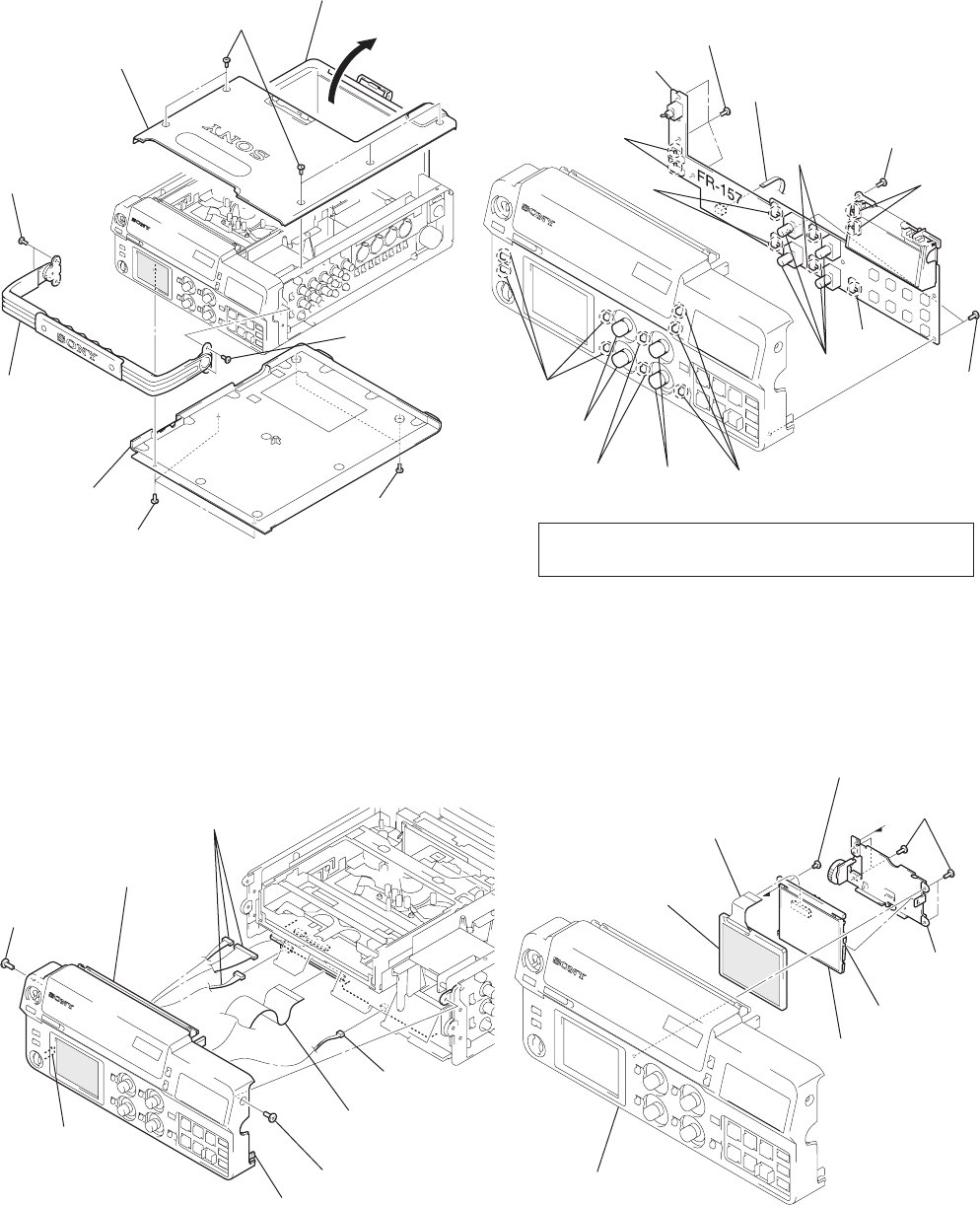
2-1
Note: Follow the disassembly procedure in the numerical order given.
2-1. TOP/BOTTOM COVER ASSEMBLIES 2-3. FR-157 BOARD
2-2. FRONT PANEL 2-4. LCD MODULE (LCD901)
SECTION 2
DISASSEMBLY
DSR-50/50P
4Open the battery
cover assembly.
6Top cover assembly
5Five screws
(B3 × 6)
2Two screws
(B3 × 6)
8Three screws
(B3 × 6)
9Bottom cover
assembly
3Carrying
handle assembly
7Two screws
(B3 × 6)
1Two screws
(B3 × 6)
5Screw
(B3 × 6)
8Front panel
3Three connectors
(CN331, 333, 705)
1Connector
(CN704)
2Flat cable
(FVJ-7) (CN701)
4Screw (B3 × 6)
7Claw
6Claw
3Screw (B2)
4Three screws
(B2)
5FR-157 board
1Flat cable
(CN504)
2Two screws
(B2)
Switches
Switch
Switches
Switches
Switches
Slide knobs
Slide
knobs Slide knobs
Volume
knobs
Volume
knobs
Volumes
8LCD module
(LCD901)
7Flexible board
(CN8200)
5LCD
frame
4Claw
2Front panel assembly
6PD-125 board,
cold cathode tube
3Screw
(M1.7 × 4)
1Four screws
(B2)
Note: When installing FR-157 board, connect volumes with
volume knobs and switches with slide knobs.
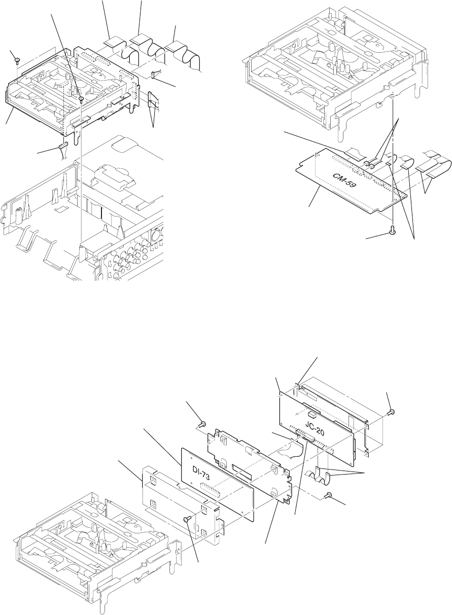
2-2
2-5. MECHANISM DECK 2-6. CM-59 BOARD
2-7. JC-20/DI-73 BOARDS
7Two step screws
(M3)
6Two step screws
(M3)
2Flat cable
(FVJ-14) (CN6001)
1Flat cable
(FVJ-13)
(CN1101)
3Flat cable
(FVJ-13)
(CN7002)
4Connector
(CN7001)
9Connector
(CN100)
8Mechanism
deck 5Two connectors
(CN1100, 4400)
4Flat cable
(FJC-1)
(CN001)
6CM-59 board
5Two screws
(T3 × 4.5)
1Two flat cables
(FMD-14)
(CN200, 201)
2Two flat cables
(FRJ-1)
(CN400, 500)
3Two connectors
(CN300, 501)
qa DI shield case
qs DI-73 board
7Screw
(B2 × 4)
0Four screws
(T2 × 4.5)
1Four screws
(T2 × 4.5)
8Screw
(B2 × 4)
5Connector
(CN8001)
9JC shield case
4Two flat cables (FRJ-1)
(CN4401, 4402)
6JC-20 board
2JC shield case
3Flat cable
(FJC-1)
(CN5005)
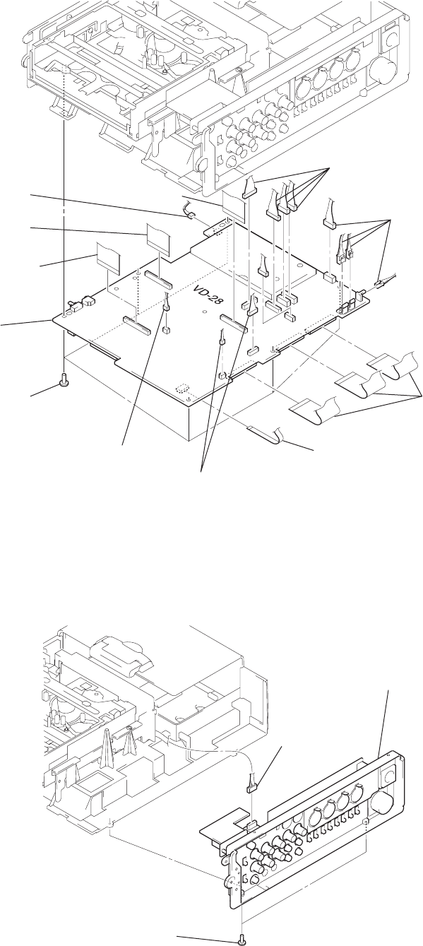
2-3
2-8. VD-28 BOARD
2-9. SIDE PANEL ASSEMBLY
0Flat cable
(FVJ-13) (CN606)
3Flat cable
(FVJ-10) (CN607)
2Three flat cables
(FVJ-7)
(CN102, 603, 604)
1Connector
(CN706)
qs Flat cable
(FVJ-13) (CN332)
qa Flat cable
(FVJ-14) (CN703)
5VD-28 board
4Six screws
(B3 × 6)
9Connector
(CN702)
7Two connectors
(CN101, 401)
6Four connectors
(CN900 – 903)
8Five connectors
(CN601, 602, 605, 904, 905)
2Two screws
(B3 × 6)
1Connector
(CN391)
3Side panel assembly
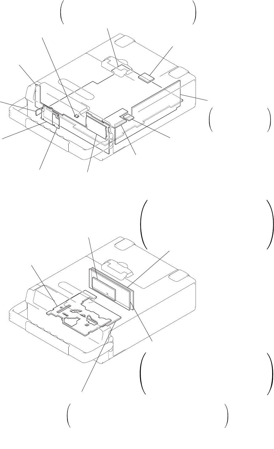
2-4
2-10. CIRCUIT BOARDS LOCATION
2-4 E
PD-125
(RGB DRIVER, TG)
LT-32
(BACK LIGHT)
RP-234
(REC/PB AMP)
MD-76
(TAPE SENSOR)
HP-117
(HEAD PHONE)
IL-013
(DV CONNECTOR)
VL-26
(LITHIUM BATTERY)
EJ-28
(EJECT SWITCH)
FR-157
(USER CONTROL)
KP-8
(SWITCH) JK-169
VIDEO IN/OUT,
AUDIO IN,
AUDIO IN/OUT
Inverter trans unit
VD-28
SYNC GENERATOR, VIDEO IN, UVIC,
VIDEO OUT, AUDIO, HI CONTROL,
DC IN, DC/DC CONVERTER
CM-59
DC/DC CONVERTER, REEL MOTOR DRIVE,
CAPSTAN MOTOR DRIVE, FL MOTOR DRIVE,
DRUM MOTOR DRIVE, CAM MOTOR DRIVE
JC-20
VIDEO AD CONVERTER,
CHROMA MIX, AFC, VIDEO DISP,
D/A CONVERTER, SFD, TFD,
DV INTERFACE, AUDIO,
MECHANISM CONTROL,
MODE CONTROL, POWER SUPPLY
DI-73
VIDEO D/A CONVERTER,
VIDEO FIFO MEMORY, AUDIO HPF,
SYNC SHIFTER, D/A CONVERTER,
AUDIO A/D, TIME CODE IN/OUT,
AUDIO DSP, AUDIO DSP CONTROL
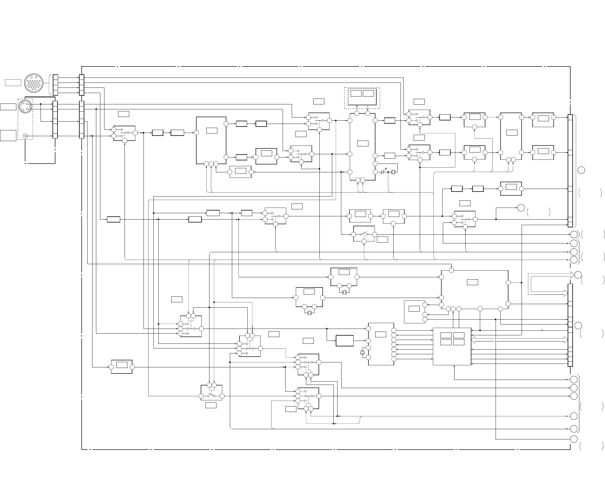
DSR-50/50P
3
1
5
7
1
3
5
7
CAMERA
1
3
4
7
1
4
7
17
2
3
17
7
2
3 1
31
11
4 1
2
39 3
25
33 41
3
5
1
7
4 2
17 6 3 1
4
3
2
3
1
7
2
3
1
7
63
2
3
15143
6 3
4
7 5
3 4
3 1
3 1
20
10
12
195
28 24
18
25
411
2 6
5
3
1
7
2 4
2 4
3
1
3
5
7
2 4
3
5
1
7
2 4
1
37
2
2
2 8
2 8
1110
1110
3
73
7
13
5
3
10
11
12
13
28
29
6807932 19
5
2
461
83
82
18
17
31
32
VD-28 BOARD (1/5)
JK-169 BOARD
(1/4)
(SEE PAGE 4-132)
IC102
IC109
IC119
IC131
IC104
TRAP
FL105
FL103 DL102
FL104
TRAP
S-C/C SWITCH
IC117
IC115
AMP
IC116
VC AMP
B-Y/C SWITCH
IC122
VC AMP
IC129
AMP
IC128
AMP
IC126
SYNC SELECT
IC709
IC704
IC333 IC335
IC334 IC336
RESET
IC108
SIGNAL SELECT
IC113
SIGNAL SELECT
IC101
BUFFER BUFFER
BUFFER
SIGNAL SELECT
IC133
AMP
05
IC112
S VIDEO/VIDEO
DETECT
IC106
COMPONENT
DETECT
IC107
S-Y/Y SWITCH
X101
500kHz
IC110
SWITCH
IC132
SWITCH
IC105
SIGNAL SELECT
IC332
UVIC
CONTROL
(1/3)
HI CONTROL
IC120
VC DELAY
IC121
VC DELAY
IC125
AMP
IC118
R-Y/C SWITCH
IC124
C DECODE
DSR-50P
OSC
Y/C SEP IC103
AMP
S-Y/Y SWITCH
FL106
FL107
DL101
FL108 B. P. F.
CLAMP
VIDEO SWITCH
J105 (1/4)
CN103 (1/2) CN102 (1/2)
CN026 (1/4)
CN101
B-Y IN
R-Y IN
Y IN
S-C IN
S-Y IN
SC DET
VIDEO IN
VIDEO IN
G7
G8
G10
G11
G9
G4
G6
G3
G5
G3 – G6
X104
14.318182MHz
:DSR-50
17.734475MHz
:DSR-50P
G7 – G11
XCAM SEL
XS SEL
XS SEL
10
8
12
1
14
CR IN
CB IN
Y IN
AFC Y
AFC Y
V SYNC
FSC ADJ
GEN REFY
DIG/XANA, XCPNT SEL
DV SEL, FSC TEST,
XS SEL, XCAM SEL, G1 – G11
VD-28
BOARD (2/5)
VD-28
BOARD (4/5)
JC-20 BOARD
(3/6)
CN6001 (2/2)
VD-28
BOARD (2/5)
VD-28
BOARD (5/5)
CN332
(1/4)
JC-20 BOARD
(1/6)
CN1101 (1/4)
1
19
A
2
3
4
17
B
5
6
7
9
8
DIG/
XANA
XCPNT SEL
XCPNT SEL
XCPNT SEL
29
28
27
17
15
13
11
9
8
7
6
XIC RST
XSLEEP
MO XWAKEUP
XSYS RST
XCS UVIC
UVIC BUSY
UVIC SWIN
UVIC GATE
INT/EXT DET
GEN LOCK Y
GEN LOCK C
EE/XPB, INT/XEXT
DV REF SYNC, DV REF SC
AND GATE/INVERTER
Q338
SYNC SEP
X331
3.579545MHz
:DSR-50
4.433619MHz
:DSR-50P
DV REF SC
DV REF SYNC
X102
500kHz
DV SEL
FSC
TEST
G1
99
10
XRESET
EE/XPB
INT/XEXT
(SEE PAGE 4-81)
(SEE PAGE 4-81)
(SEE PAGE 4-81)
(SEE PAGE 4-82)
(SEE PAGE 4-81)
(SEE PAGE 4-81)
IC130IC127
SYNC SEP
(SEE PAGE 4-82)
(SEE PAGE 4-81)
(SEE PAGE 4-85)
(SEE PAGE 4-85)
(SEE PAGE 4-86)
(SEE PAGE 4-86)
(SEE PAGE 4-86)
(SEE PAGE 4-86)
(SEE PAGE 4-86)
(SEE PAGE 4-86)
(SEE PAGE 4-86)
(SEE PAGE 4-98)
(SEE PAGE 4-97)
(SEE PAGE 4-87)
(SEE PAGE 4-84)
(SEE PAGE 4-83)
(SEE PAGE 4-83)
(SEE PAGE 4-84)
(SEE PAGE 4-83)
(SEE PAGE 4-84)
(SEE PAGE 4-82)
(SEE PAGE 4-84) (SEE PAGE 4-85)
(SEE PAGE 4-83)
(SEE PAGE 4-84)
(SEE PAGE 4-88)
(SEE PAGE 4-84) VD-28 BOARD (2/5)
21
23
25
19
CN703 (1/2)
HI SI, HI SO, HI SCK, XCS MO
MO SCK, MO SO, MO SI
S VIDEO IN
VIDEO/
REF. IN
OVERALL2
SEE PAGE 3-3
OVERALL7
SEE PAGE 3-14
OVERALL5
SEE PAGE 3-9
OVERALL4
SEE PAGE 3-7
OVERALL9
SEE PAGE 3-17
OVERALL4
SEE PAGE 3-8
OVERALL4
SEE PAGE 3-8
VD-28
BOARD (2/5)
OVERALL4
SEE PAGE 3-7
31
3-1 3-2
SECTION 3
BLOCK DIAGRAMS
3-1. OVERALL BLOCK DIAGRAM 1
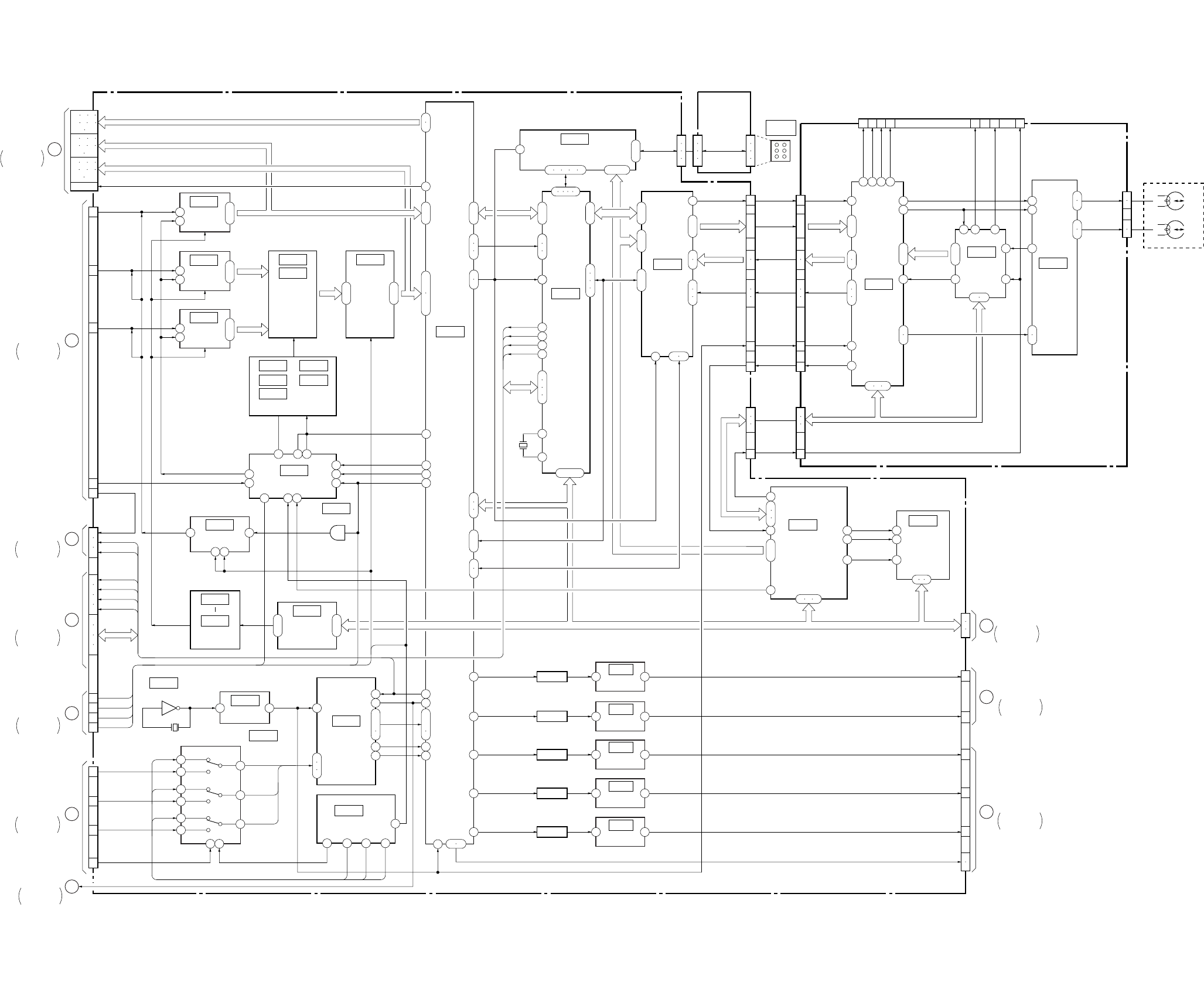
DSR-50/50P
3-3 3-4
3-2. OVERALL BLOCK DIAGRAM 2
5 2
IC1108
1
ı
3
19
ı
21
2
ı
9
18
ı
11
1
ı
8
17
ı
8
90
ı
83
53
ı
61
71
ı
80
5
ı
12
JC-20 BOARD (1/6)
43
24
5248 60
3 11
1 5 8
11
13
11 45 46 44
96
23 41
7
22
55
28
104
105
21
12
A/D
CONVERTER
(SEE PAGE 4-22)
IC2214
IC2209
IC2208
IC2211
IC1101
IC5002
IC1107
IC2202
IC2203
IC2204
IC2212
IC2210 IC2213
CHROMA
MIX
(SEE PAGE 4-23)
IC2215
BUFFER
(SEE PAGE 4-24)
IC3300
VFD
(SEE PAGE 4-27)
IC4400
SFD
(SEE PAGE 4-29)
IC4401
TFD
IC301
TRX
(SEE PAGE 4-11)
IC201
TRF
(SEE PAGE 4-13)
IC101
TRW
IC4402
LIP
(SEE PAGE 4-33)
IC1109 1
ı
8
21
12
A/D
CONVERTER
(SEE PAGE 4-22)
IC1110 1
ı
8
21
12
A/D
CONVERTER
(SEE PAGE 4-22)
TIMING GEN.
(SEE PAGE 4-23, 24)
CLOCK GENERATOR
(SEE PAGE 4-26)
REF DC
GEN.
(SEE PAGE 4-21)
D/A
CONVERTER
(SEE PAGE 4-35)
IC3303
CHARACTER
GENERATOR
(SEE PAGE 4-28)
IC3302
IC3301
BUFFER
(SEE PAGE 4-28)
IC6003
SWITCH
(SEE PAGE 4-40)
IC6001
MODE CONTROL
(SEE PAGE 4-40)
18
ı
16
14
35
34
26
ı
28
33
4
2
3
7
5
6
9
11
10
1 15
1
2
3
(1/2)
7
ı
4
109
ı
106
100
101
20
19
36
37
82
81
80
82
81
80
21
22
20
32
31
21
96
97
38
4
43
37
26
41
61
14
14
13
61
12
47
84 – 86
111
ı
114
115
116
117
22
23
FL1101
IC1112
BUFFER
(SEE PAGE 4-20)
3 4
68 FL1102
IC1111
BUFFER
(SEE PAGE 4-20)
3 4
72 FL1100
IC1000
BUFFER
(SEE PAGE 4-20)
3 4
74 FL1103
IC1001
BUFFER
(SEE PAGE 4-20)
3 4
76
50
FL1104
IC1002
BUFFER
(SEE PAGE 4-20)
3 4
TBUS 0 – 7
50 52 39 49 40
5 6 7 8 9
37 – 27
9
ı
6
99
100
17
18
44
46
45
47
95
ı
100
38
ı
48
15
ı
19
26
ı
22
6
ı
1
15
ı
20
X4400
24.576MHz
LRCK
SFD LRCK
MS BUSMS BUS
VSP SI, VSP SO, XVSP SCK VSP SI, VSP SO, XVSP SCK
31 32
23
24
30
29
19
18
34
37
6
5
3
2
6
5
3
2
3
4
5
6
6
14
1
4
12
ı
8
17
16
20
19
6
14
1
4
12
ı
8
17
16
20
19
6
10
9
8
6
10
9
8
63
65
64
51
118
95 90 7
89 6
88 1
60
78
79
80
26
ı
37
74 75 76
2 3 4
IC5003
MECHANISM
CONTROL
(SEE PAGE 4-37)
IC5006
EEPROM
(SEE PAGE 4-38)
(1/2)
MS BUS
75
78
76
IL-013
BOARD
CN4400 CN392
DV
IN/OUT
CN391
27 13
46
11
7
40
42
45 44 43
345 41
13 31
42 27
21
23
30
17
19
60
62
64
66
55
57
56
58
26
28
45
41
43
35
30
29
52 53
47 50 51
22 24
7
6
2
1
12 3 17 8 12 6
RP-234 BOARD
CN8001 (3/7)
CN1101 (2/4)
15
1
3
5
13
26
27
N
VD-28 BOARD (3/5)
CN332 (3/4)
D
VD-28 BOARD (2/5)
CN332 (2/4)
M
DI-73 BOARD (2/3)
CN9500 (4/5)
3
2
A
VD-28 BOARD (1/5)
CN332 (1/4)
L
DI-73 BOARD (1/3)
CN9500 (1/5)
J
DI-73 BOARD (2/3)
CN9500 (4/5)
K
DI-73 BOARD (2/3)
CN9500 (4/5)
I
DI-73 BOARD (1/3)
CN9500 (2/5)
H
VD-28 BOARD (5/5)
CN703 (2/2)
11
JC-20 BOARD
(3/6)
CN1101 (1/4)
Y IN
CR IN
CB IN
AFC Y
V SYNC
CN6001 (1/2)
LRCK
PB/XREC
X3300
13.5MHz
SPCK2
PAL/XNT
AFH
SFD LRCK
BCK
SFD BCK
OSD SO HI
OSD SCK HI
XCS OSD HI
OSD SW
OSD VD
05
CR (8)
Y (8) VBUS
0 – 7
CB (8)
CR/CB
(8)
CR/CB
(8)
VRT, VRB
PB/XREC
AFH
SPCK2
VFD HD
MONITOR Y
MONITOR C
PANEL Y
PANEL CR
PANEL CB
VFD VD, VFD HD
M045
M046
M044
M045
M046
M044
6
5
CN101
M901 (1/2)
DRUM HEAD
YODD, XODD
YEVEN, XEVEN
MSI, XSCK
ADDT0 – 5
CN201
JIG PIN
(FOR CHECK)
CN202CN4402
CN203CN4401
TMS
TCK
TDI
TDO
RF MONITOR
RF IN
JSWP
TXDT0 – 4
XTDT0,
XTDT1
TXDT0 – 4
XTDT0,
XTDT1
CRCKCRCK CRCK
TXDT0 – 4
CLK135
ATF
CLK135
ATF
CLK135
ATF
SWP
XTDT0, 1
HPCK,
XTSY,
TXST
HPCK,
XTSY,
TXST
HPCK, XTSY,
TXST
NTPB,
TPB,
NTPA,
TPA
MSI, MSO, XSCK
DRP SI,
DRPSO,
MS CK
41
BCK
39
SFD BCK
CLAMP
(SEE PAGE 4-25)
(SEE PAGE 4-25)
(SEE PAGE 4-28)
LVD
31
13 15 17
19 21 23
25 27
14 16 18
20 22 24
26 28
32 34 36
38 40 42
44 46
CN8001 (1/7)
MY00 – 17
Y0 – 7
JC00 – 07
MHO 46
SOA,
SOB,
SIC,
SID
PAL/XNT
67
69
70
CN8001 (2/7)
SOA,
SOB,
SIC,
SID
VFD VD
VFD OE
VFD HD
(SEE PAGE 4-31)
(SEE PAGE 4-34)
(SEE PAGE 4-14)
OVERALL3
SEE PAGE 3-5
OVERALL1
SEE PAGE 3-2
OVERALL8
SEE PAGE 3-16
OVERALL8
SEE PAGE 3-15
OVERALL9
SEE PAGE 3-17
OVERALL5
SEE PAGE 3-9
OVERALL3
SEE PAGE 3-5
OVERALL8
SEE PAGE 3-16
OVERALL4
SEE PAGE 3-7
OVERALL6
SEE PAGE 3-11
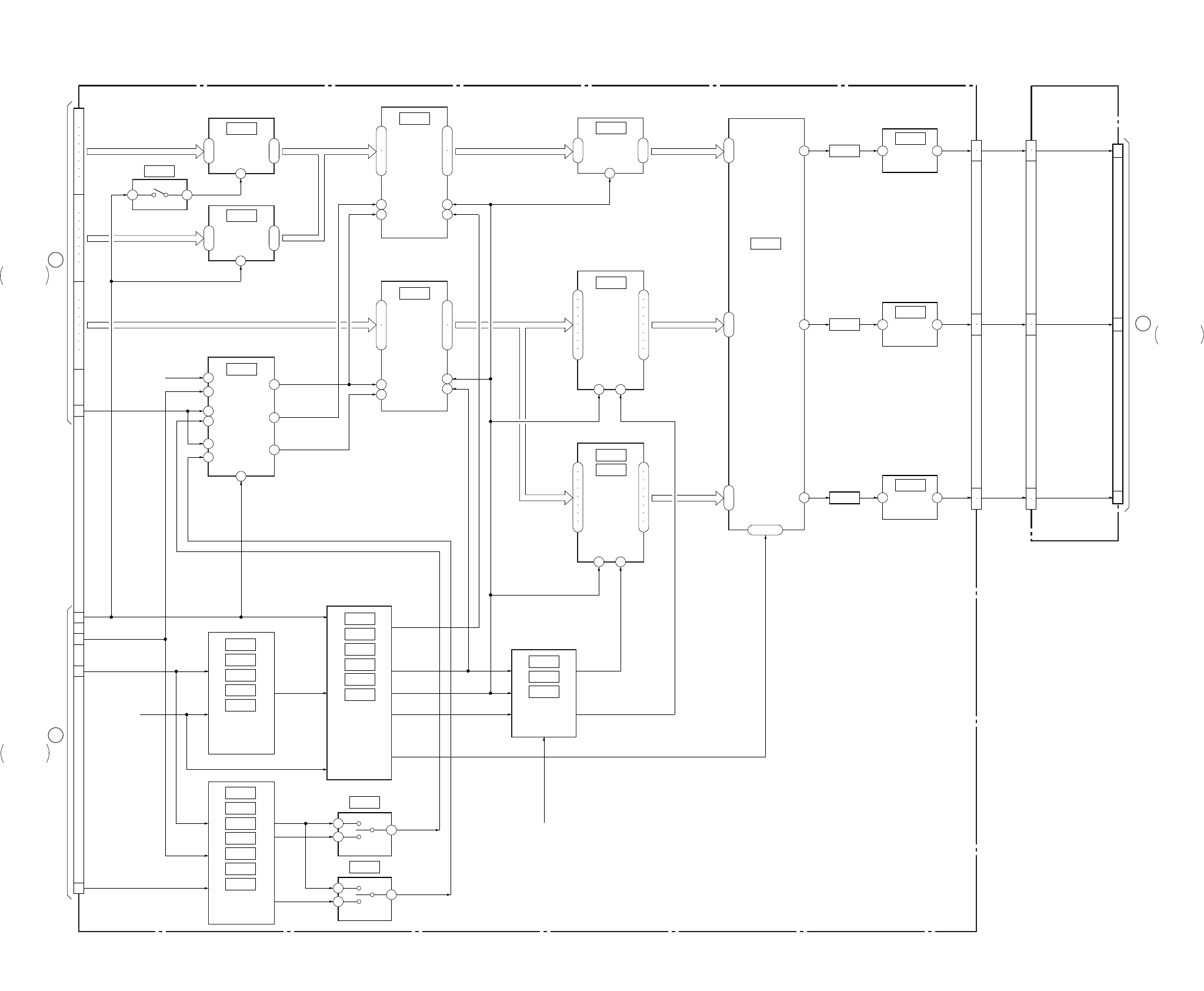
DSR-50/50P
3-5 3-6
3-3. OVERALL BLOCK DIAGRAM 3
2
ı
9
18
ı
11
1
IC9016
IC9014
ANALOG
SWITCH
2
ı
9
18
ı
11
1
IC9015
ANALOG
SWITCH
1 7
19
17
8
6
24
ı
21
16
ı
13
1
ı
4
9
ı
12
IC9011
FIFO C
IC9008
CB
SWITCH
17
19
8
611
24
ı
21
16
ı
13
1
ı
4
9
ı
12
IC9012
FIFO
CONTROL
2
1
3
11
10
5
6
4
9
7
7
2
ı
9
19
ı
12
11
IC9004
Y
SWITCH
IC9000
VIDEO
D/A CONVERTER
3
4
7
8
13
14
17
18
2
5
6
9
12
15
16
19
1
IC9005
IC9009
CR
SWITCH
11
3
4
7
8
13
14
17
18
2
5
6
9
12
15
16
19
1
IC9500
IC9503
IC9506
IC9509
IC9512
SYNC
SHIFTER
IC9502
IC9501
IC9504
IC9505
IC9507
IC9508
SYNC
SHIFTER
IC9006
IC9018
IC9019
CB/CR
CONTROL
IC9513
IC9511
IC9510
IC9518
IC9514
IC9515
IC9516
IC9517
Y/C
SELECT
1
24
IC9519
1
24
17
ı
24
1
ı
8
9
ı
16
27 – 29
41 FL9000 AMP
3 1
IC9001
39 FL9001 AMP
3 1
IC9007
37 FL9002 AMP
3 1
IC9010
DI-73 BOARD (1/3)
13
15
17
19
21
23
25
27
31
45
41
43
35
JC-20 BOARD (2/6)
(SEE PAGE 4-45)
14
16
18
20
22
24
26
28
32
34
36
38
40
42
44
46
L
JC-20 BOARD
(1/6)
CN8001 (1/7)
I
JC-20 BOARD
(1/6)
CN8001 (4/8)
1
2
5
6
9
10
1
2
5
6
9
10
11
9
7
CN1101
(3/4)
VD-28 BOARD (2/5)
CN332 (2/4)
C
CN9500 (1/5)
MY00 – 07 MY00 – MY07 Y00 – Y07
CB00 – CB07
DY0 – DY7
CR0 – CR7
JC0 – JC7
Y0 – 7
JC00 – 07
MHO
DA135
SPCK2
PB/XREC
PAL/XNT
AFH
VH-HD
CN9500
(2/5)
CN8001
(4/7)
DPB Y OUT
DPB CR OUT
DPB CB OUT
Y LINE
CR LINE
CB LINE
EE WHDY
EE WHDC
FIFO MUTE
IC9013
FIFO Y
05
(SEE PAGE 4-54)
(SEE PAGE 4-54)
(SEE PAGE 4-54)
(SEE PAGE 4-53)
(SEE PAGE 4-53)
(SEE PAGE 4-51)
(SEE PAGE 4-51)
(SEE PAGE 4-52)
(SEE PAGE 4-52)
(SEE PAGE 4-53)
(SEE PAGE 4-54)
(SEE PAGE 4-54)
(SEE PAGE 4-55, 56, 57, 58)
(SEE PAGE 4-52)
(SEE PAGE 4-55, 56)
(SEE PAGE 4-57, 58)
(SEE PAGE 4-52)
(SEE PAGE 4-52)
(SEE PAGE 4-54)
OVERALL2
SEE PAGE 3-3
OVERALL2
SEE PAGE 3-3
OVERALL4
SEE PAGE 3-7
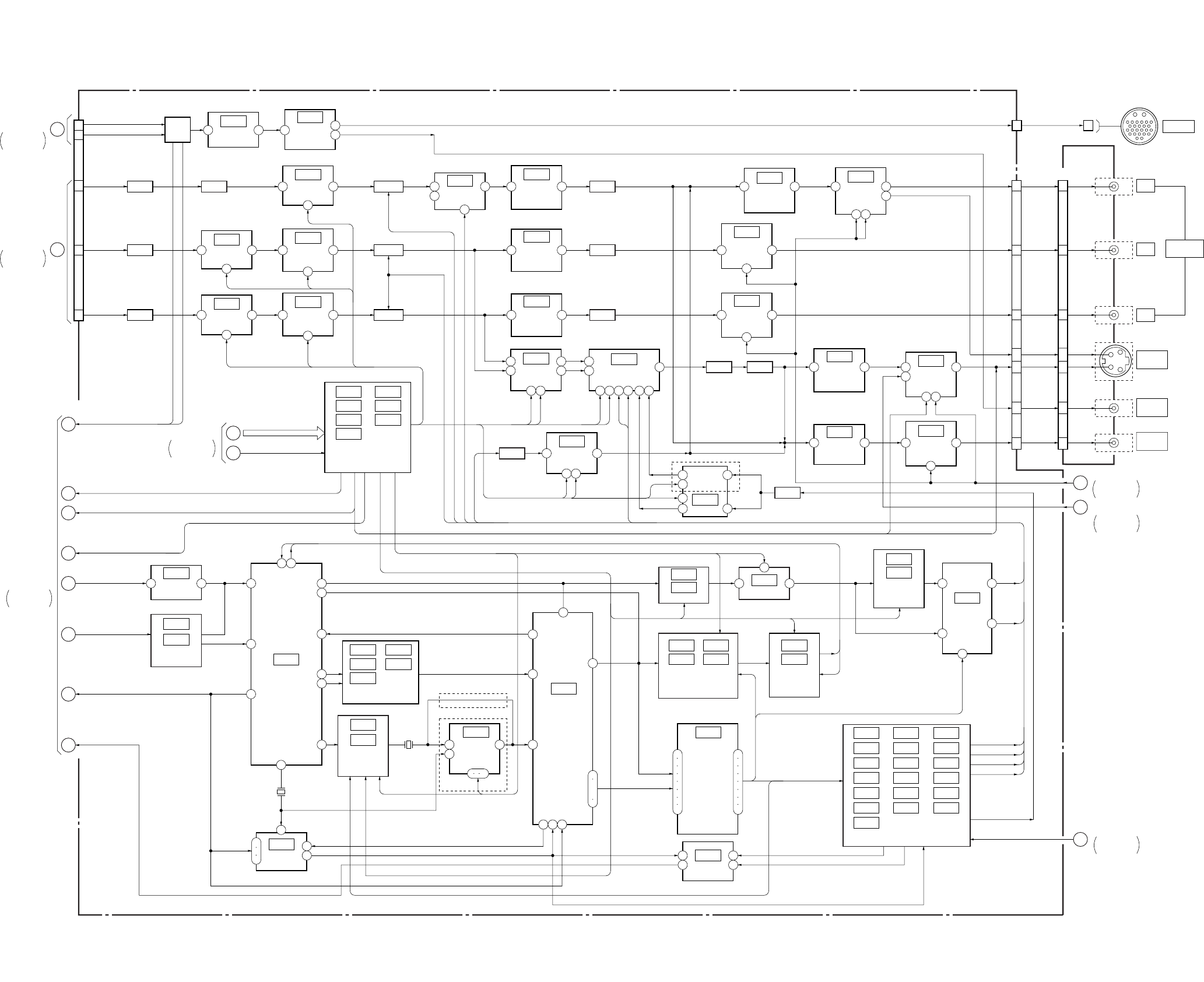
DSR-50/50P
3-7 3-8
VD-28 BOARD(2/5)
JK-169
BOARD (2/4)
20
22
24
18
16
181
CN332 (2/4)
30
27
24
15
18
21
12
CN102
(2/2)
30
27
24
CN103 (2/2) J102 (1/2)
FL406
FL404
FL405
MIX
1 6
IC427
VC AMP
DL404 DL403
DL401
DL402
B. P. F.
3
6 3
IC402
VC DELAY
4
7 5
IC428
(1/2)
VC AMP
6
213
IC423
R-Y OUT
DRIVER
14
213
IC424
B-Y OUT
DRIVER
14
1 3
IC428
(2/2)
VC AMP
2
6 3
IC403
VC DELAY
4
13
IC417
AMP
4 1
IC416
INVERT
AMP
3 1
IC414
NON INVERT
AMP
3 1
IC415
NON INVERT
AMP
211
IC418
IC001 IC013
IC002 IC017
IC007 IC061
IC009
MONITOR
DRIVER 13
4 1
IC419
INVERT
AMP
213
11
1014
IC422
Y OUT
DRIVER
213
4
146
IC426
C OUT
DRIVER
6
216
IC410
Y BLANKING
SET UP ADD
4
CLAMP
CLAMP
CLAMP
CN401
D/A
CONVERTER
1
7
3
5
IC411
VC AMP
2 6
1
24 18
IC413
C ENCODE
21 54 20 3
4 1
IC421
INVERT
AMP
15
18
21
12
4 1
IC420
INVERT
AMP
213
IC425
VIDEO OUT
DRIVER
14
1 5
IC405
VC AMP
3 7
FL402
9
15
16
C
3
4
8
6
7
5
2
DV SEL, FSC TEST, XS SEL,
XCAM SEL, G1 – G11
2 1 17
15
18
14
7
8
IC003
SYNC SEP
IC004
IC008
SC PROC
IC012
IC057 IC062
IC058 IC063
IC059
GEN LOCK
IC027
SYNC GEN
DSR-50P
DSR-50
IC024
BUFFER
J103 (1/2)
J104 (1/2)
J105 (2/4)
J104 (2/2)
J105 (3/4)
VD-28 BOARD (4/5)
VD-28 BOARD (1/5)
4
11 VR ADJ
10
1
29
22
17
23
8
724 18
IC016
IC021
SC SWITCH
AMP X002
14.31818MHz
:DSR-50
17.734475MHz
:DSR-50P
5 8
IC060
SC
COMPARATOR
13
1 2 12
6
9
12
IC005
NOR 1
8
9
11
X001
14.31818MHz
:DSR-50
14.1875MHz
:DSR-50P
20
21
IC049
SYNC GEN 29
24
2
2
4
6
8
11
13
15
17
3
5
7
9
12
14
16
18
31
2
ı
6
10
Y LINE
CR LINE
CB LINE
MONITOR Y
MONITOR C
RETURN VIDEO
DV REF SYNC,
DV REF SC
DIG/XANA,
XCPNT SEL
EE/XPB, INT/XEXT
GEN LOCK Y
GEN LOCK C
INT/EXT DET
GEN REF Y
IC031
IC035
SC PHASE ADJ
2
1 4
IC040
EX OR
IC025 IC030
IC028 IC033
HD SHIF
COURSE ADJ
IC019
IC022
HD SHIF
FINE ADJ
IC037
IC042
HD PHASE
90˚ SHIFT
4
1
9
3
6
IC043
0˚/180˚
LALT
TIMING DELAY
PULSE STRECH
IC014 IC034 IC050
IC018 IC039 IC051
IC020 IC044 IC052
IC023 IC046 IC054
IC026 IC047 IC055
IC029 IC048 IC056
IC032
6
1
5 7
3
2
IC404
VC AMP
FL401
FL403
CN026 (2/4)
JC-20 BOARD (2/6)
CN1101 (3/4)
D
JC-20 BOARD (1/6)
CN1101 (2/4)
VIDEO
OUT2
VD-28
BOARD (1/5)
B13
B2
B15
MUTE
MUTE
MUTE
MUTE
FSC TEST, SDC
FSC TEST
MUTE
FSC ADJ
FSC ADJ
SDC
SC U
SC V
E5
C4
C3
E6
A5
A1 – A4
C1
C2
E5
R SYNC OUT
R Y BLK
R Y CLAMP
R UV CLAMP
R BF OUT
AFC Y VD-28 BOARD (1/5)
E1, E2, E4, E6, E8
E7
E5, E6
B10
B11
SCU
SCV
R UV CLAMP
R Y CLAMP
R Y BLK
R SYNC OUT
B8
B9
B4
B5
C1 – C4
A1 – A7
SCU, SCV
B4 – B7
A1 – A5
A6, A7
E7
C2
A6
A7
22
05
19
(SEE PAGE 4-90)
(SEE PAGE 4-90)
(SEE PAGE 4-89)
(SEE PAGE 4-93)
VD SO, VD SCK
EVR LOAD, V S/P XSTB
(SEE PAGE 4-79, 80)
(SEE PAGE 4-75)
(SEE PAGE 4-75)
(SEE PAGE 4-75)
(SEE PAGE 4-76)
(SEE PAGE 4-75)
(SEE PAGE 4-76)
(SEE PAGE 4-80)
(SEE PAGE 4-76)
(SEE PAGE 4-77)
(SEE PAGE 4-78) (SEE PAGE 4-78)
(SEE PAGE 4-78)
(SEE PAGE 4-93)
(SEE PAGE 4-94) (SEE PAGE 4-94) (SEE PAGE 4-131)
(SEE PAGE 4-94)
(SEE PAGE 4-92)
(SEE PAGE 4-92)
(SEE PAGE 4-92)
(SEE PAGE 4-92)
(SEE PAGE 4-93)
(SEE PAGE 4-93)
(SEE PAGE 4-94)
(SEE PAGE 4-91)
(SEE PAGE 4-91)
(SEE PAGE 4-91)
(SEE PAGE 4-91)
(SEE PAGE 4-94)
(SEE PAGE 4-77, 78)
(SEE PAGE 4-76)
(SEE PAGE 4-76, 77, 78, 79, 80)
(SEE PAGE 4-75)
(SEE PAGE 4-75, 76)
(SEE PAGE 4-93)
(SEE PAGE 4-89) (SEE PAGE 4-90)
Y OUT
R-Y OUT
B-Y OUT
S-Y OUT
S-C OUT
VIDEO
MON
OUT
VIDEO
OUT
14
1
V MUTE
VD-28 BOARD (4/5)
B-Y
Y
CAMERA
S VIDEO
OUT
R-Y COMPONENT
OUTPUT
VIDEO
OUT1
OVERALL2
SEE PAGE 3-4
OVERALL3
SEE PAGE 3-6
OVERALL7
SEE PAGE 3-14
OVERALL1
SEE PAGE 3-2
OVERALL1
SEE PAGE 3-2
OVERALL1
SEE PAGE 3-2
OVERALL7
SEE PAGE 3-14
B7
B6
DSR-50P
3-4. OVERALL BLOCK DIAGRAM 4
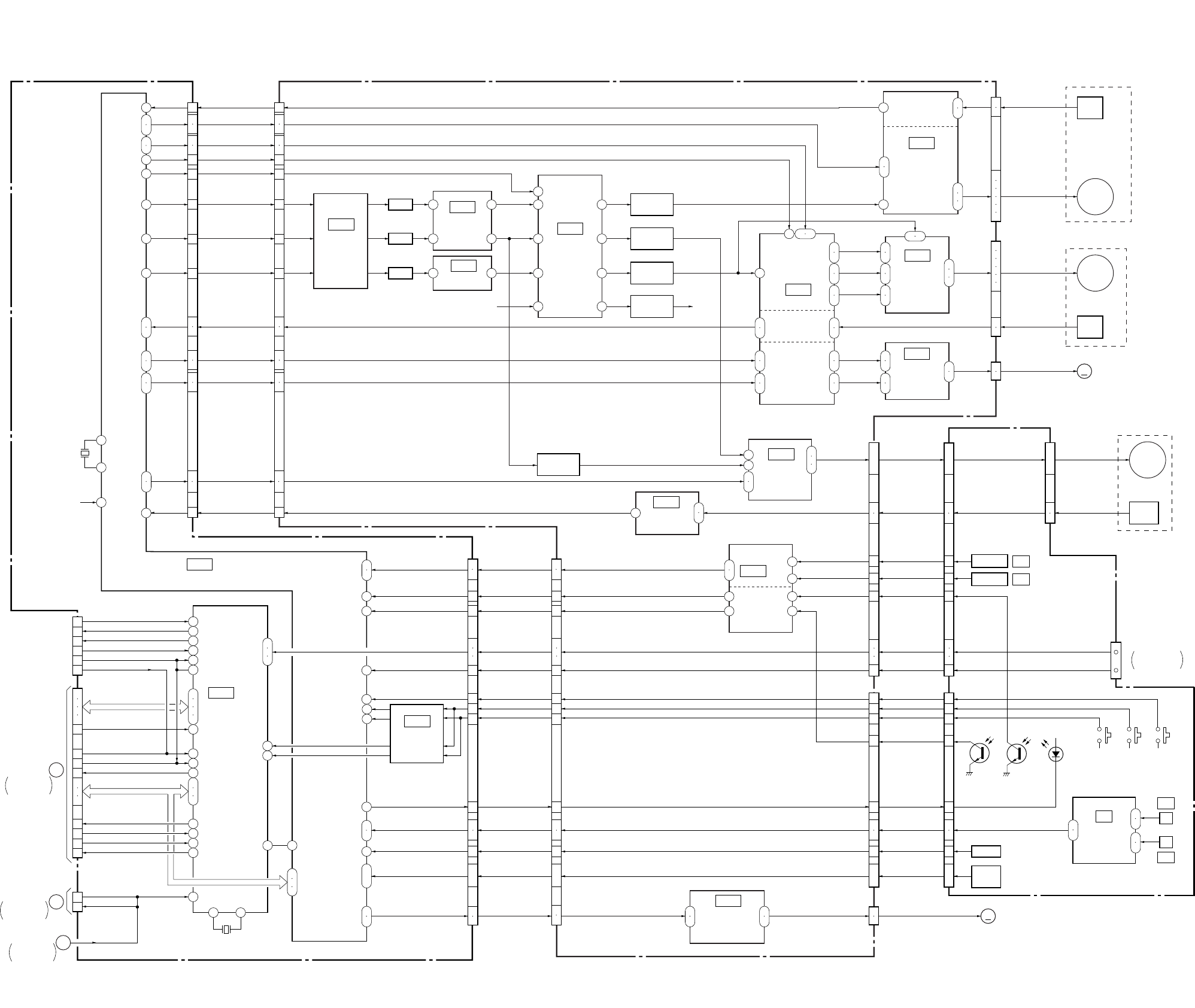
DSR-50/50P
3-9 3-10
3-5. OVERALL BLOCK DIAGRAM 5
JC-20 BOARD (3/6) CM-59 BOARD
115
63
36
31
34
33
27
26
30
29
43
44
45
46
15
20
17
18
24
25
21
22
8
7
6
5
46
45
48
47
117
116
49
50
51
52
6.25V
14
15
55 53 5 20
25
22
26
23
27
24
4
1
21
24
6
19
1
63
4
60
42
41
39
40
30
31
32
33
18
12
17
13
9
11
23
22
24
54
17
3
5
7
9
2
23
18
1
2
16
17
14
13
8
7
10
9
11
10
5
6
3
4
1
2
CN5005 (1/2)
CAP FWD, CAP ON
CAP FG
DRUM MASTER CLK
DRUM FWD,
DRUM ON
IC5003
IC500
IC400
IC501
(1/2)
CAPSTAN
MOTOR
DRIVER
CAPSTAN
FG AMP
IC501
(2/2)
C MOTOR
DRIVER
(2/2)
MECHANISM
CONTROL
IC6001 (2/2)
MODE
CONTROL
DRUM PG, DRUM FG
CM (+), CM (–)
CM LIMIT ON,
CM LIMIT DET
05
(SEE PAGE 4-107)
(SEE PAGE 4-110)
(SEE PAGE 4-108)
(SEE PAGE 4-108)
C MOTOR
DRIVER
DRUM PG/FG
DRIVER
DRUM
PREDRIVE
CM LIMIT ON, CM LIMIT DET
CM+, CM–
DRUM PG, DRUM FG
DRUM CLK
CAP VS
REEL VS
DRUM VS
DRUM FWD, DRUM ON
CAP FG
CAP FWD, CAP ON
CN001 (1/2)
(SEE PAGE 4-37)
(SEE PAGE 4-40)
DRUM
MOTOR
DRIVER
MM
DRUM
PG
CAP
FG
DRUM
MOTOR
CAPSTAN
MOTOR
M905
FL MOTOR
CN400
CN500
CN501
M904
M903
M901 (2/2)
68
69
71
9
28
35
40
50
23
16
11
1
8
6
7SWICHING
SWICHING
SWICHING
SWICHING
16
7
9
25
6
7
30
11 44
39
46
40
IC300
IC100
DC/DC
CONVERTER
HI C/R SW
REEL PWM
CAP PWM
DRUM PWM L. P. F.
L. P. F.
L. P. F.
L. P. F.
L. P. F.
(1/3)
IC102
BUFFER
(SEE PAGE 4-105) IC500
(SEE PAGE 4-107)
(SEE PAGE 4-109)
(SEE PAGE 4-105)
VREF
IC200
REEL
MOTOR
DRIVE
(SEE PAGE 4-106)
IC202
REEL MOTOR
FG AMP
(SEE PAGE 4-105)
44
43
41
39
38
119
26
6
1
4
10
12
13
21
22
23
Q200
BUFFER
2
3
REEL
FG
1
ı
6
8
10
REEL
MOTOR
REEL FWD,
REEL ON
REEL M FG
REEL FWD, REEL ON
REEL M FG
CN3
V, U, W
U, V, W
PG, FG
CM LOAD, CM UNLOAD
U, V, W
FG2, FG1
FG1, FG2
REEL V/U/W
MR FG1, MR FG2
15
25
24
2
29
1
2
LM (+), LM (–)
IC300
(3/3)
LOADING MOTOR
DRIVER
(SEE PAGE 4-109)
LM+, LM–LM+, LM–MM M902
CAM MOTOR
CN300
MD-76 BOARD
IC300
(SEE PAGE 4-109)
(2/3)
REEL FG AMP
TAPE TOP/END
DETECT
113
114
7
8
13
14
6
12
10
11
18
19
53
54
20
23
14
17
13
16
19
22
85
96
55
97
22
18
68
98
99
17
16
42
ı
39
4
ı
1
20
IC5008
LEVEL SHIFT
(SEE PAGE 4-38)
71
72
73
22
23
24
44
43
38
37
45
39
41
40
33
32
29
28
27
47
ı
50
34
35
13
21
15
14
1
18
17
16
13
21
15
14
18
17
16
7
ı
4
15
12
14
3
2
8
9
1
7
ı
4
15
12
14
3
2
8
9
IC5
IC4
S REEL FG
T REEL FG
1
7
2
3
6
7
ELETEN
ERROR AMP
(SEE PAGE 4-117)
IC1
IC2
IC3
H
H
MODE
SW
DEW
CN5005 (2/2) CN001 (2/2)
SREEL FG, TREEL FG
TAPE ON
TAPE END
CHIME SCK, CHIME SDA,
CHIME VDD
REC PROOF
S REEL ERR,
T REEL ERR
MODE SW D-A
DW DET
TAPE LED ON
L CASSETTE
SREEL FG,
TREEL FG
TAPE TOP
TAPE END
CHIME SCK,
CHIME SDA,
CHIME VDD
REC PROOF
S ELTN ERR,
T ELTN ERR
MODE SW D-A
DEW DET
TAPE LED ON
L CASSETTE
XC IN
XCC DOWN
S REEL FG, T REEL FG
TAPE TOP
TAPE END
CHIME SCK, CHIME SDA, CHIME VDD
REC PROOF
DEW
TAPE LED
L CASSETTE
C IN
CC DOWN
REEL ERROR
CN201 CN1
SFG IN
TFG IN
TOP SENS
CN200 CN2
END SENS
S ELETEN, T ELETEN
MODE D-A
DEW
TAPE LED
L CASSETTE
C IN
CC DOWN
MODE D-A
DEW
TAPE LED
L CASSETTE
C IN
CC DOWN
S REEL FG
T REEL FG
TAPE TOP
REC PROOF
TAPE END
S ELETEN
T ELETEN
CHIME2 (SCK)
CHIME3 (SDA)
CHIME4 (VDD)
Q2
(TAPE TOP)
Q1
(TAPE END)
FOR CASSETTE
MEMORY
D1
(TAPE LED)
S1
(L/S CASSETTE)
S2
(C IN)
S3
(CC DOWN)
1
2
7
X5001
20MHz
XSYS RESET
1
2
21
17
27
30
61
38
58
65
67
55
7222
64
62
9
34
33
35
32
50
49
48
81
82
83
40 41
X6001
20MHz
15
17
3
1
5
28
29
19
22
14
4
2
3
23
24
25
16
18
20
10
8
6
12
CN6002
CN6001 (2/2)
LANC IN
LANC OUT
XLANC PWR ON
EJECT
PARSLEY MODE
XRESET
XSLEEP
XIC RST
MO XWAKEUP
XSYS RST
XCS UVIC
UVIC BUSY
UVIC GATE
XI/O SYNC HI
XI/O SYNC VFD
OSD VD
JC-20 BOARD
(1/6)
VD-28 BOARD
(5/5)
CN332 (4/4)
VD-28 BOARD
(1/5)
CN703 (1/2)
UVIC SWIN
MO SCK, MO SO, MO SI
HI SI, HI SO,
HI SCK, XCS MO
CN1101 (4/4)
JIG PIN
(FOR CHECK)
B
E
11
104
105
48
49
3
2
1
ı
6
9
12
1
ı
6
9
12
OVERALL1
SEE PAGE 3-2
OVERALL9
SEE PAGE 3-17
OVERALL2
SEE PAGE 3-3
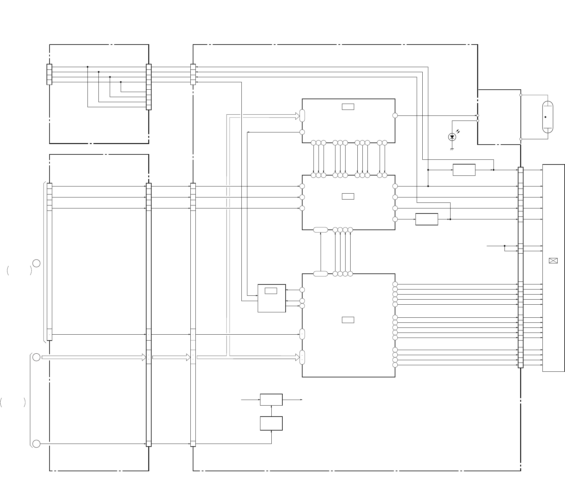
DSR-50/50P
3-11 3-12
3-6. OVERALL BLOCK DIAGRAM 6
22
10
20
24
8
9
10
37
37
38
39
40
41
42
44
45
46
47
48
1
2
3
15
38
12
35
7
33
5
40
6
27
4
31
1
39
3
32
29
25
14
23
28
4
36
24
2
6
11
8
1
9
26
32
34
35
19
ı
22
13
14
16
20
21
27 – 30
48 – 45
9
10
7
6
5
4
5
2
1
2
1
4
5
4
2
1
FR-157 BOARD (1/2)
(SEE PAGE 4-123, 124)
PD-125 BOARD
VD-28 BOARD (3/5)
(SEE PAGE 4-87)
COM
VG
PSIG
VCO CENT
COM
VG
PSIG
VCO CENT
COM
VG
PSIG
VCO CENT
COM
VG
PSIG
VCO CENT
XSCK, DATA FROM HI,
DAC SO, XCS
VCO CENT
PSIG
COM
VG
JIG PIN
(FOR CHECK)
(OPEN)
CN505 CN504 CN8201
28
30
26
5
4
6
5
7
8
9
10
1
2
3
6
5
7
8
9
10
1
2
3
N
12
13
JC-20 BOARD (1/6)
CN1101 (2/4)
CN332 (3/4) CN331 CN8001
PANEL Y
PANEL CR
PANEL CB
PANEL Y
PANEL CR
PANEL CB
XVD, XHD XVD, XHD XVD, XHD
LCD DD ON
VD SCK,
DATA FROM HI,
XCS LCD DAC
VFD VD, VFD HD
VD SO, VD SCK, PANEL DA CS
LCD DD ON
Q8003, 8007
B+ SWITCH
PANEL B+
ON/OFF
CONTROL
B+ B+
Q8000
Q8001
IC8202
VCO
IC8200
EVR
(SEE PAGE 4-141)
IC8001
RGB
DRIVER
(SEE PAGE 4-140)
IC8201
LCD
TIMING GENERATOR
(SEE PAGE 4-141)
(SEE PAGE 4-141)
XSCK, XCS,
DATA FROM HI
XSCK,
DAC SO,
XCS
Y
CR
CB
VCO
5
23
6
16
18
7
2
8
9
10
11
12
13
14
15
19
20
21
3
4
VG
COM
PSIG
VB
VR
G-Y
CN8200
COM Y
PSIG Y
B-Y
R-Y
22
DWN
RGT
PCG
XPCG
EN
XEN
VCK1
VCK2
VST
XVST
HCK2
HCK1
XHST
HST
HCK1
RGT
HCK2
CR
SOUT
REF
HST
WIDE
CS
VSS
DWN
EN
VCK
VST
LCD901
2.5INCH
COLOR LCD
UNIT
VVDD
HVDD
B+
(PANEL 12V Y)
Q8010
COM BUFFER
Q8009, 8011
BUFFER
INVERTER
BLOCK
ND901
BACK
LIGHT
D8100
05
VD-28 BOARD (4/5)
OVERALL2
SEE PAGE 3-4
OVERALL7
SEE PAGE 3-14
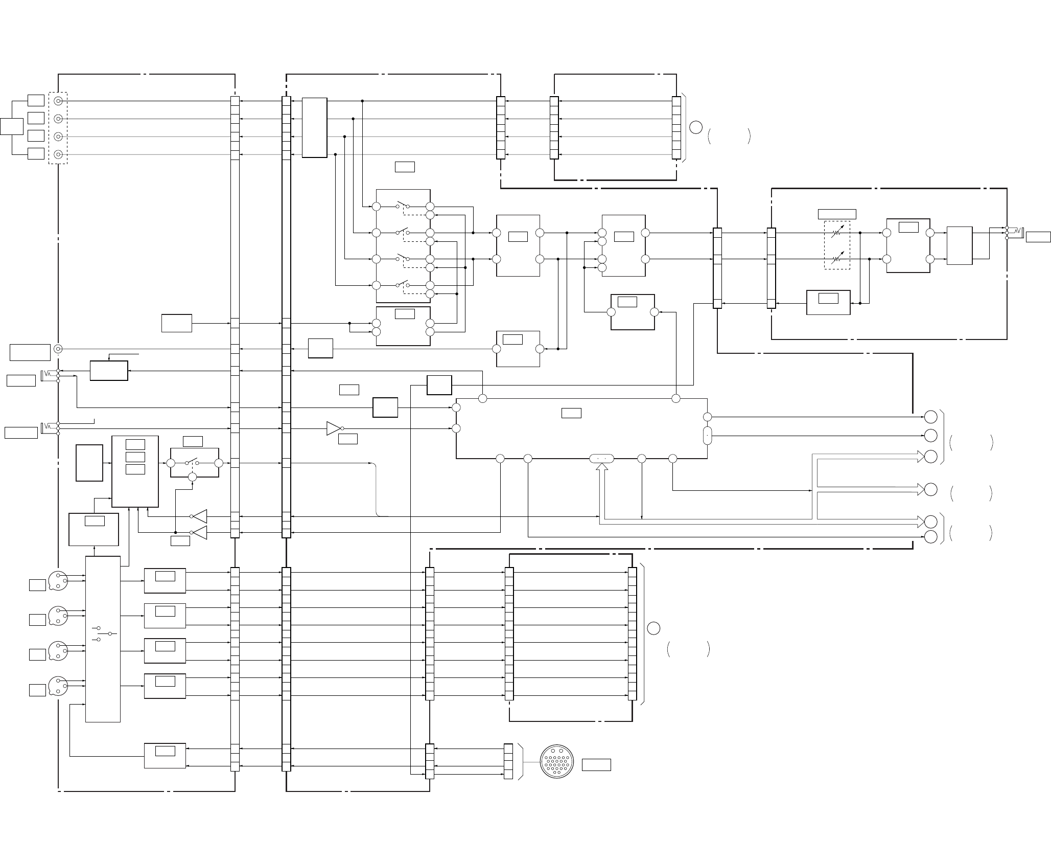
DSR-50/50P
3-13 3-14
3-7. OVERALL BLOCK DIAGRAM 7
JK-169 BOARD (3/4) VD-28 BOARD (4/5)
JC-20 BOARD (4/6)
(SEE PAGE 4-41, 45)
HP-117 BOARD
JC-20 BOARD (5/6)
(SEE PAGE 4-43, 45)
2
13
10
12
4
2
6
1
7
3
5
1
7
2
6
7 6
5
8
1
11
3
9
6
7
1
5
2
1 2
2
6
1
7
4
21
18
4
IC110
BUFFER
IC104
IC105
IC601
IC602 IC603
CN601 CN301
HP L
HP R
VTR RET AUDIO
IC604 IC305
IC301
PHONES
HP
AMP MUTE
PHONE LEVEL
RV301
AMP
ATT
ALARM
IC604
(2/2)
(1/2)
IC709 (2/3)
AMP
AUDIO MONITOR
SELECT
IC605
IC701
IC702
SWITCH
CONTROL
IC101
IC102
IC103
PARALLEL/
SERIAL
CONVERTER
INVERTER
IC107
AND GATE
IC111
BUFFER
IC113
BUFFER
IC114
BUFFER
IC109
BUFFER
05
3658
7
4
1
10
30
13
28
29
26
20
22
18
7
4
1
10
30
13
28
29
26
20
22
18
28
25
23
20
18
15
13
30
10
8
28
25
23
20
18
15
13
30
10
8
2
4
5
7
8
1
10
11
29
27
26
24
23
30
21
20
120
115
116
111
112
119
107
108
1
3
5
9
10
20
5
1
3
7
5
1
3
7
96
104
100
92
1
3
10
1
3
10
J105 (4/4)
AUDIO
OUTPUT
CN104 CN603
CH1 OUT
CH3 OUT
CH2 OUT
CH4 OUT
J106
REMOTE
J101
S101
B+ (+5V)
AUDIO
MONITOR SEL
AUDIO
MONITOR OUT
TALLY LED
FOOT SW
SIRCS DATA
P/S DATA
P/S SCK
P/S CS
CH1 IN Y
CH1 IN X
CH2 IN Y
CH2 IN X
CH3 IN Y
CH3 IN X
CH4 IN Y
MIC X
MIC Y
CH4 IN X
B+ SWITCH
Q109, 110
B+ (+5V)
S110,
S111
CN105 CN604 CN606 (1/2) CN7002 (1/2) CN8001 (6/7)
CN026 (3/4)
CN106
CN107
CN108
CN109
CN605 CN7001 CN8001
(5/7)
DI-73 BOARD (2/3)
CN9500 (4/5)
BUFFER
Q606
MUTE
Q601-
604
MUTE
Q605
MUTE
AU X1 IN
AU Y1 IN
AU X2 IN
AU Y2 IN
AU X3 IN
AU Y3 IN
AU X4 IN
AU Y4 IN
AU X1 IN
AU Y1 IN
AU X2 IN
AU Y2 IN
AU X3 IN
AU Y3 IN
AU X4 IN
AU Y4 IN
CN602
CAMERA
CH1 OUT
CH3 OUT
CH2 OUT
CH4 OUT
AU CH1 OUT
AU CH3 OUT
AU CH2 OUT
AU CH4 OUT
CH1 OUT
CH3 OUT
CH2 OUT
CH4 OUT
F
HI CONTROL
GDI-73 BOARD (2/3)
CN9500 (3/5)
VTR RET
AUDIO
R IN
L IN J301
S102 – 109
(SEE PAGE 4-132)
(SEE PAGE 4-132)
(SEE PAGE 4-132)
(SEE PAGE 4-135)
(SEE PAGE 4-135)
(SEE PAGE 4-134)
(SEE PAGE 4-136)
(SEE PAGE 4-134)
(SEE PAGE 4-133)
(SEE PAGE 4-98)
(SEE PAGE 4-96)
(SEE PAGE 4-97)
(SEE PAGE 4-97)
(SEE PAGE 4-96)
(SEE PAGE 4-95)
(SEE PAGE 4-145)
(SEE PAGE 4-145)
VD-28 BOARD (2/5)
VD-28 BOARD (1/5)
VD-28 BOARD (3/5)
(SEE PAGE 4-96)
(SEE PAGE 4-95)
MIX AMP
(SEE PAGE 4-95)
MIX AMP
HPL
HPR
16 11 22
78
27
84
85
33 34 35
14
15
16
17
12
13
V MUTE
EVR LOAD, V S/P XSTB
VD SO, VD SCK
HI SI, HI SO, HI SCK, XCS MO
VD SO, VD SCK, PANEL DACS
LCD DD ON
XCS MO
PANEL DACS
VD SI, VD SCK
VD SI
VD SCK
MIC IN (X)
MIC IN (Y)
MIC IN X
MIC IN Y
AUDIO MON/VTR SAVE
J107
CONTROL S
CH-1
CH-2
CH-3
CH-4
CH-1
CH-3
CH-2
CH-4
AUDIO
MONITOR OUT
MONITOR
SELECT
OVERALL8
SEE PAGE 3-16
OVERALL4
SEE PAGE 3-7, 8
OVERALL1
SEE PAGE 3-2
OVERALL6
SEE PAGE 3-11
OVERALL8
SEE PAGE 3-15
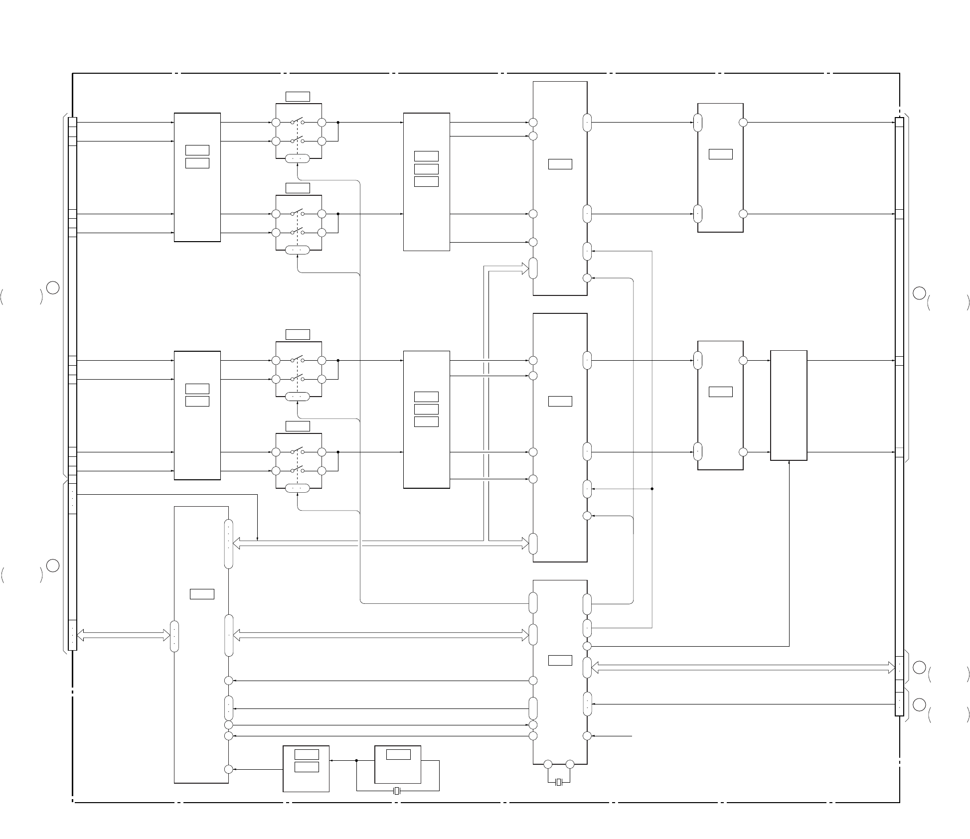
DSR-50/50P
3-15 3-16
3-8. OVERALL BLOCK DIAGRAM 8
IC7000
IC7002
IC7005
H. P. F
IC7008
IC7010
IC7013
AMP
IC7009
IC7011
IC7014
AMP
IC7001
IC7003
H. P. F
IC8003
AUDIO
DSP
4 5
15 1
9 10 11
IC7004
4 5
15 1
9 10 11
IC7007
4 5
15 1
9 10 11
IC7006
4 5
15 1
9 10 11
IC8001
IC8002
CLOCK
IC8000
CLOCK
OSC
5
4
2
7
1
3
19
5
4
2
7
1
3
19
71
48
40
99
26
15
9
7 8
Q7004
Q7005
Q7007
Q7008
MUTE
DI-73 BOARD (2/3)
11
ı
14
20
21
26
25
28
27
2
3
6
5
11
ı
14
20
21
28
27
26
25
2
3
6
5
68
ı
70
45
ı
47
52
ı
59
22
ı
24
36
ı
39
82
83
84
43
42
4
5
117
118
113
ı
116
16
ı
20
23
ı
25
2
3
119
120
9
10
14
X8000
24.576MHz
X8001
4.608MHz
IC8009
(1/2)
AUDIO
DSP
CONTROL
IC7018
A/D, D/A
CONVERTER
IC7016
A/D, D/A
CONVERTER
IC7020
MIX/LPF
IC7021
MIX/LPF
120
115
116
111
112
107
108
60
62
64
66
119
55
57
56
58
XRST
75
76
78
104
100
70
67
69
96
92
J
JC-20 BOARD (1/6)
CN8001 (4/8)
G
JC-20 BOARD (5/6)
CN8001 (6/7)
F
JC-20 BOARD (4/6)
CN8001 (5/7)
M
JC-20 BOARD (1/6)
CN8001 (3/7)
K
JC-20 BOARD (1/6)
CN8001 (2/7)
CN9500 (3/5) CN9500 (4/5)
AU Y1 IN
AU X2 IN
AU Y2 IN
AU X3 IN
AU Y3 IN
AU X4 IN
AU Y4 IN
SFD BCK, BCK, SFD LRCK, LRCK
SOA, SOB,
SIC, SID
AU X1 IN
XCH1 HPF
XCH2 HPF
XCH3 HPF
XCH4 HPF
A. DA DATA1, A. DA DATA2,
A. AD DATA1, A. AD DATA2
XCH1 HPF, XCH2 HPF, XCH3 HPF, XCH4 HPF
A HD0 – A HD7
A HA0
A XHDWR, A XHDRD, A XHDCS
A. HRDY
XPD AD1,
XPD AD2,
XPD DA1,
XPD DA2
DEM0, DEM1
DEM0, DEM1
XPD AD2,
XPD DA2
DEM0,
DEM1
XPD AD1,
XPD DA1
AU CH1 OUT
AU CH2 OUT
AU CH3 OUT
AU CH4 OUT
VSP SI, XVSP SCK, VSP SO
VFD HD, VFD VD, VFD OE
05
72
13
(SEE PAGE 4-59)
(SEE PAGE 4-59)
(SEE PAGE 4-59)
(SEE PAGE 4-59)
(SEE PAGE 4-59)
(SEE PAGE 4-59)
(SEE PAGE 4-64)
(SEE PAGE 4-63)
(SEE PAGE 4-63)
(SEE PAGE 4-65)
(SEE PAGE 4-61)
(SEE PAGE 4-61)
(SEE PAGE 4-60)
(SEE PAGE 4-60)
(SEE PAGE 4-62)
(SEE PAGE 4-62)
OVERALL7
SEE PAGE 3-14
OVERALL2
SEE PAGE 3-3
OVERALL2
SEE PAGE 3-3
OVERALL2
SEE PAGE 3-4
OVERALL7
SEE PAGE 3-14
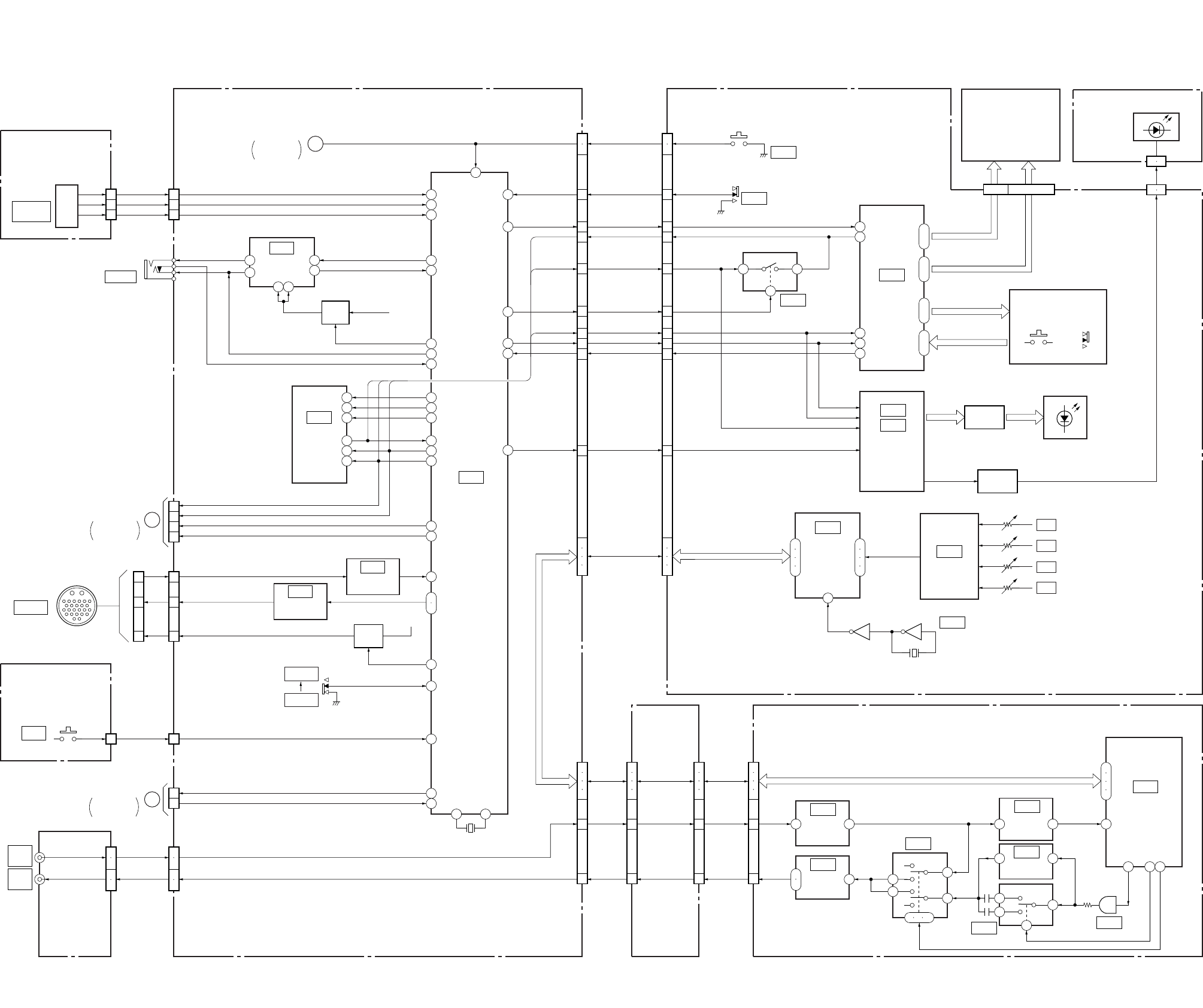
DSR-50/50P
3-17 3-18
3-9. OVERALL BLOCK DIAGRAM 9
38
67 14
23 9
8
2 1
4
24
56
7
11
10
19
100
68
71
12
21
30
26
8
28
44
46
45
1
7
6
4
2
3
43
10
97
72
17
7
64
20
2
1
12
10
84
14
11
98
99
9
12
15
14
1
2
3
4
21
ı
24
33
ı
74
25
ı
32
2
ı
5
3 4
6
7
1
9 10 11
1
5
1 4 80
4
7
6
3
79 61 78
1
5
85
86
87
33
,
5
3
1
S601 DIAL A
DIAL B
EXEC SW
DIAL A
DIAL B
EXEC SW
5
3
130
7
9
13
5
3
15
11
1
13
15
2
3
1 1
1
3
2
5
3
2
1
1
2
4
5
1
2
4
5
29
27
28
26
23
20
30
7
9
13
5
3
15
11
1
29
27
28
26
23
20
23
21
19
17
18
16
8
10
12
14
87
88
82
84
83
81
87
88
82
84
83
81
KP-8 BOARD
(SEE PAGE 4-70)
VD-28 BOARD (5/5) FR-157 BOARD (2/2) LT-32 BOARD
(SEE PAGE 4-126)
DI-73 BOARD (3/3)JC-20 BOARD
(6/6)
(SEE PAGE 4-43, 45)
CN601
10
CN705
XRESET
VD-28 BOARD (1/5) XRESET
IC708
BUFFER
(SEE PAGE 4-98)
IC710
BUFFER
IC706
EEPROM
IC709
(3/3)
HI CONTROL
(SEE PAGE 4-98)
(SEE PAGE 4-98)
(SEE PAGE 4-97)
CONTROL
LCD
BRIGHT
IC707
LANC
DRIVER
(SEE PAGE 4-97)
B+
J701
Q702
B+ SW
CN701 CN502
RESET
POWER SW
LCD STB
DATA TO HI
DATA FROM HI
W/R
SCK
OE
LED STB
KEY REQ
DSP SCK,
DSP SI (TO DSP)
DSP SO (FROM DSP),
DSP CS
RESET
S537
POWER
IC502
IC501
LCD DRIVER,
MATRIX KEY
CONTROL
(SEE PAGE 4-123)
(SEE PAGE 4-123)
IC403
BUFFER
IC402
A/D
CONVERTER
IC505
IC504
SERIAL/
PARALLEL
CONVERTER
(SEE PAGE 4-125)
(SEE PAGE 4-125)
(SEE PAGE 4-123)
IC404
CLOCK
IC8009
(2/2)
IC8011
IC8010
IC8007
BUFFER
IC8006
HYST
COMPARATOR
IC8004
INPUT
AMP
TC IN
TC OUT
IC8005
OUTPUT
AMP
IC8008
BUFFER
AUDIO DSP
(SEE PAGE 4-65)
(SEE PAGE 4-68)
(SEE PAGE 4-68)
(SEE PAGE 4-67)
(SEE PAGE 4-67)
(SEE PAGE 4-67)
(SEE PAGE 4-67)
CN9500 (5/5)
CN7002
(2/2)
CN8001
(7/7)
VR/AD SCK, VR/AD SO, VR/AD SI, VR/AD CS
(SEE PAGE 4-125)
S526
LCD902
(CHARACTOR DISPLAY)
COM 1 – 4
BOTTOM LED VCC, TOP LED VCC
SEG 9 – 50
KS 1 – 8
KEY 1 – 4
KEY MATRIX
S515, 516, S518 – 525,
S527 – 536, S538
D502 – 512
Q502 – 512
LED DRIVE
Q513 – 515
LED DRIVE
1 5
1 5
CN301
CN503
CN501
D301 – 310
(BACK LIGHT)
RV401
RV402
RV403
RV404
CH-1
CH-2
CH-3
CH-4
X401
13.5MHz
15
4
TC IN
DSP SCK,
DSPSO,
DSP SI,
DSP CS
TC OUT
TC IN
DSP SCK,
DSPSO,
DSP SI,
DSP CS
TC OUT
TC IN
TC OUT
CN606
(2/2)
Q706
B+ SW
B+
S702
DVCAM
DV
CN704
CN332 (4/4)
CN607
TC IN
TC OUT
CN101
05
EJECT SW
BATTERY INDICATION
REC/TALLY
VTR START/STOP
OSD SO HI
OSD SCK HI
XCS OSD HI
OSD SW
CN702
CN703 (2/2)
JC-20 BOARD (1/6)
CN6001 (1/2)
XI/O SYNC HI
XI/O SYNC VFD
TC IN
TC OUT
E
H
JK-169 BOARD
(4/4)
(SEE PAGE 4-131)
EJ-28 BOARD
(SEE PAGE 4-70)
J102 (2/2)
J103 (2/2)
EJECT SW
CN101
EJECT
JC-20 BOARD (3/6)
CN1101 (4/4)
S101
15
13
12
CN026 (4/4)
CAMERA
X701
20MHz
40 41
8 – 15 1 – 7, 16 – 50
TC IN
(EXT)
TC OUT
(INT)
OVERALL2
SEE PAGE 3-3
OVERALL1
SEE PAGE 3-2
OVERALL5
SEE PAGE 3-9
6
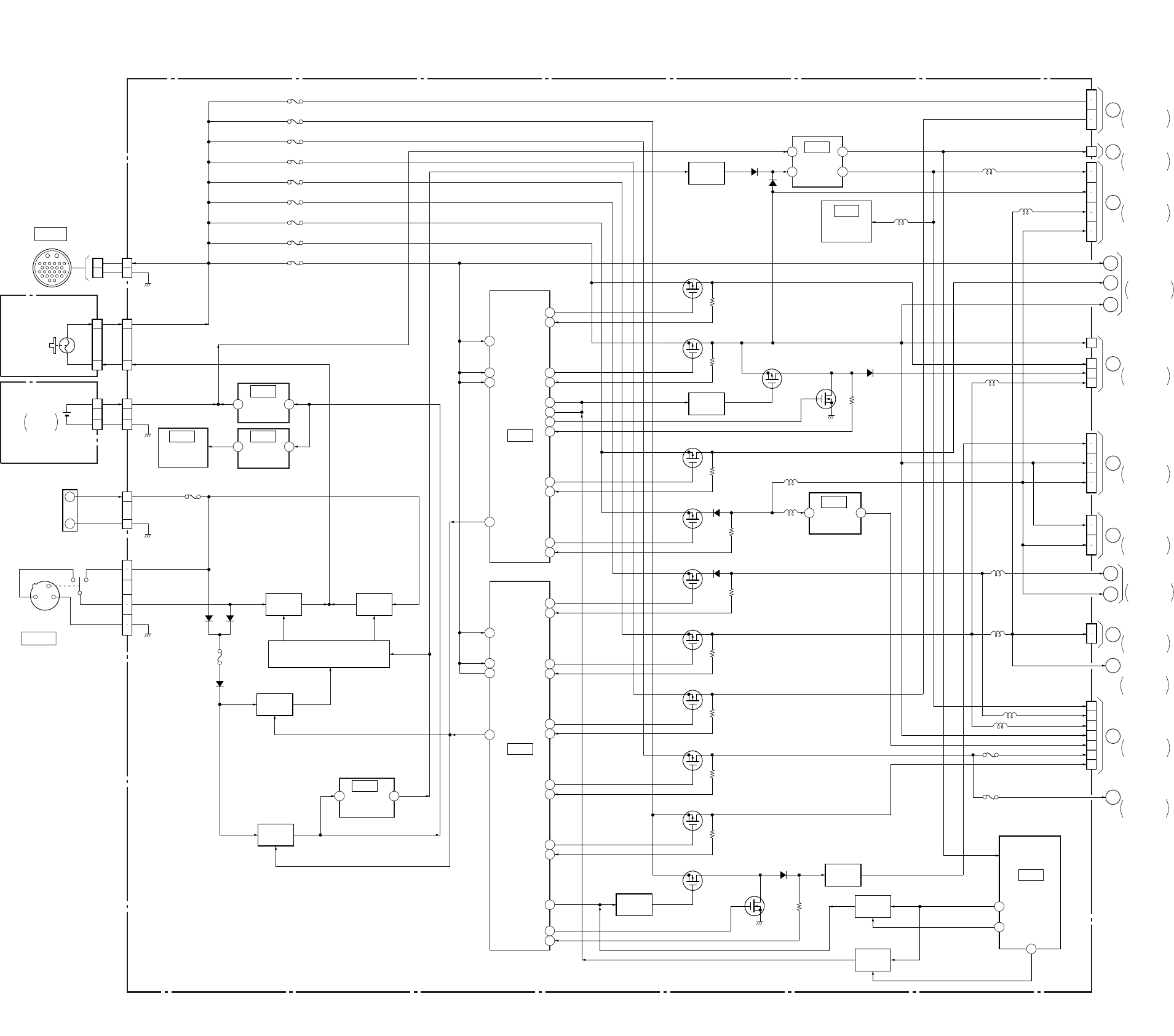
DSR-50/50P
3-19 3-20
3-10. POWER BLOCK DIAGRAM 1
44
27
35
1
27
44
35
1
14
39
25
40
22
41
16
46
16
46
14
39
25
40
13
43
22
41
19
45
30
30
34
19
45
VD-28 BOARD (1/2)
VL-26 BOARD
(SEE PAGE 4-70)
JK-169 BOARD (1/2)
(SEE PAGE 4-132)
2
1
26
25
2
1
2
1
2
1
2
1
F911
F905
F904
F912
F903
F906
F902
F913
F901
F900
CN902
CAMERA UNREG +12V
GND
CN903
CN801
CN102
CN026
CN706
CN901
CN9901
CN900
CAMERA
BREAKER OUT
BREAKER IN
VL BATT 3V
BATTRY 12V
BATTRY 12V
SELECTED 12V
VL BATT GND
GND
GND
CB101
(BREAKER)
BT801
BT901
BATTERY
TERMINAL
3
3
2
2
IC705
IC712IC713
+5V
REG
+3.6V
REG
(SEE PAGE 4-97)
2 3
IC909
+5V
REG
(SEE PAGE 4-100)
IC900
DC
CONTROL
(SEE PAGE 4-101)
IC709
HI CONTROL
(SEE PAGE 4-98)
IC902
DC
CONTROL
(SEE PAGE 4-103)
IC704
REG,
RESET
(SEE PAGE 4-97)
IC706
EEPROM
(SEE PAGE 4-97)
IC901
–5V
REG
(SEE PAGE 4-102)
(SEE PAGE 4-97)
BATT DET
(SEE PAGE 4-97)
DC IN 12V
1
2
3
4
5
6
Q900, 901
B+ SW
Q919, 925
SWITCH
Q934, 937
B+ SW
05
Q909
ON/OFF SW
Q922
B+ SW
Q907, 908
SWITCH
Q935, 936
SWITCH
Q903, 905
B+ SW
Q910
ON/OFF SW
Q708
B+ SW
Q906, 913, 918, 923, 924
Q930, 931, 940 – 943
VOLTAGE CONTROL
D910 – 914
F910
D909 D908
Q911
SWITCHING
Q917
SWITCHING
Q915
SWITCHING
Q928
SWITCING
Q916
SWITCHING
Q914
SWITCHING
Q926
SWITCHING
Q927
SWITCHING
Q929
SWITCHING
Q933
SWITCHING
D915
D905
7
3 6
8
D915
Q912
SWITCHING
Q921
SWITCH
L935
L928
3 1
D901
Q920
SWITCH 29
55
11
6
7
AUDIO +5V
SW +6V
SW +3V
EVR +3V
AUDIO –5V
VIDEO +5V
VIDEO +5V
VIDEO –5V 2
4
1
13
11
12
3
30
9
3
7
H
6
5
G
4
F
E
D
3
2
1
CN904
L919
L921
L920
L933
L701
L702
L922
F915
F914
5
6
7
8
17
27
VD-28
BOARD (2/2)
JC-20 BOARD
CN1100
VD-28
BOARD (2/2)
JK-169
BOARD (2/2)
CN104
VD-28
BOARD (2/2)
HP-117 BOARD
CN301
JK-169
BOARD (2/2)
CN105
PD-125 BOARD
CN8002, CN8001
VD-28
BOARD (2/2)
A
5
6
3
4
CM-59 BOARD
CN100
B
JC-20 BOARD
CN6001
1
2
4
5
6
7
C
FR-157 BOARD
CN502
21
22
18
19
16
17
24
25
SW +3V
SW +3V
SW –5.5V
SW –6V
SW –6V
SW +6V
SW +6V
UNREG
SW +5.5V
SW –6V
SW +3V
SW +6V
EVR +3V
BACK UP +3V
DIG +5V
UNREG
UNREG
CM REG 5V
LCD 4.6V
ORG 12V
SW +48V
LCD +3.0V
VIDEO –5V
CN603
CN601
CN604
CN331
CN333
CN701
CN703
CN905
L703
D716
D717
2
1
+
–
LITHIUM
BATTERY
POWER5
SEE PAGE 3-27
POWER3
SEE PAGE 3-23
POWER6
SEE PAGE 3-29
POWER5
SEE PAGE 3-27
POWER6
SEE PAGE 3-29
POWER4
SEE PAGE 3-25
POWER6
SEE PAGE 3-29
POWER3
SEE PAGE 3-23
POWER2
SEE PAGE 3-21
POWER2
SEE PAGE 3-21
POWER2
SEE PAGE 3-21
POWER2
SEE PAGE 3-21
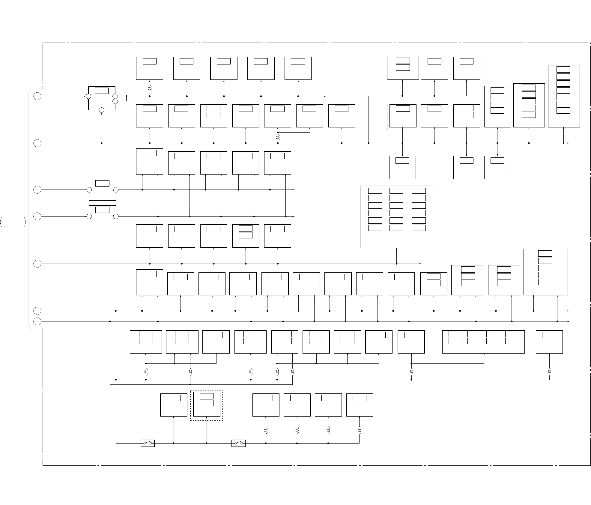
DSR-50/50P
3-21 3-22
3-11. POWER BLOCK DIAGRAM 2
IC707
LANC
DRIVER
(SEE PAGE 4-97)
IC041
+9V
REG
(SEE PAGE 4-80)
1 6
3
2IC708
BUFFER
(SEE PAGE 4-98)
IC332
U V/C
CONTROL
(SEE PAGE 4-87)
IC334
IC333
AND GATE
(SEE PAGE 4-88)
IC016
IC012
GEN. CLOCK
(SEE PAGE 4-75, 76)
IC040
EX OR
(SEE PAGE 4-78)
IC027
SYNC
GEN.
(SEE PAGE 4-76)
IC701
BUFFER
(SEE PAGE 4-97)
IC702
BUFFER
(SEE PAGE 4-97)
IC336
IC335
IC710
BUFFER
(SEE PAGE 4-98)
IC043
0˚/180˚
LALT
(SEE PAGE 4-78)
IC412
SWITCH
(SEE PAGE 4-93)
IC124
C
DECODE
(SEE PAGE 4-81)
IC122
VC AMP
(SEE PAGE 4-86)
IC133
AMP
(SEE PAGE 4-83)
IC132
SWITCH
(SEE PAGE 4-82)
IC413
C
ENCODE
(SEE PAGE 4-93)
IC116
VC AMP
(SEE PAGE 4-85)
IC422
Y OUT
DRIVER
(SEE PAGE 4-92)
IC423
R-Y OUT
DRIVER
(SEE PAGE 4-92)
IC425
VIDEO OUT
DRIVER
(SEE PAGE 4-94)
IC426
C OUT
DRIVER
(SEE PAGE 4-94)
IC424
B-Y OUT
DRIVER
(SEE PAGE 4-92) AMP
(SEE PAGE 4-91)
IC428
IC427
IC411
IC405
IC404
VC AMP
(SEE PAGE 4-90, 93, 94)
IC418
MONITOR
DRIVER
(SEE PAGE 4-93)
IC601
AUDIO
MONITOR
SELECTOR
(SEE PAGE 4-95)
IC410
Y BLANKING
SET UP
ADD
(SEE PAGE 4-91)
IC602
MIX AMP
(SEE PAGE 4-95)
IC603
MIX AMP
(SEE PAGE 4-95)
IC604
AMP
(SEE PAGE 4-96)
IC605
SWITCH
CONTROL
(SEE PAGE 4-96)
IC024
BUFFER
(SEE PAGE 4-76)
IC031
SC PHASE
ADJ
(SEE PAGE 4-77)
IC021
SC SWITCH
(SEE PAGE 4-76)
IC035
SC PHASE
ADJ
(SEE PAGE 4-78)
IC022
HD SHIFT
FINE ADJ
(SEE PAGE 4-76)
IC042
HD PHASE
90˚ PHASE
(SEE PAGE 4-78)
IC037
HD PHASE
90˚ SHIFT
(SEE PAGE 4-78)
IC060
SC
COMPARATOR
(SEE PAGE 4-75)
IC008
IC004
SC PROC
(SEE PAGE 4-75)
IC014
TIMING
DELAY
(SEE PAGE 4-79)
IC018 IC034 IC050
IC049
IC020 IC039 IC051
IC023 IC044 IC052
IC026 IC046 IC054
IC029 IC047 IC055
IC032 IC048 IC056
SYNC
GEN.
(SEE PAGE 4-80)
IC003
SYNC
SEP
(SEE PAGE 4-75)
IC019
HD SHIFT
FINE ADJ
(SEE PAGE 4-76)
VIDEO +9V
IC033
IC030
IC028
IC025
HD SHIFT
COURSE ADJ
(SEE PAGE 4-77)
IC063
IC062
IC059
IC058
IC057
VR ADJ
(SEE PAGE 4-75, 76)
IC061
IC017
IC013
IC009
IC007
IC002
IC001
D/A
CONVERTER
(SEE PAGE 4-79, 80)
DIG +5V
VIDEO +5V
VIDEO –5V
SW +3V
+5V
–5V
IC607
+5V
REG
(SEE PAGE 4-96)
2 3
IC606
–5V
REG
(SEE PAGE 4-96)
3 1
TIMING DELAY
PULSE STRECH
(SEE PAGE 4-76, 77, 78, 79, 80)
IC403
IC402
IC416
IC415
IC414
INVERT AMP
(SEE PAGE 4-92, 94)
IC421
IC420
IC419
VC DELAY
(SEE PAGE 4-89)
IC126
IC107
SYNC SELECT
(SEE PAGE 4-84, 86)
IC115
IC125
AMP
(SEE PAGE 4-84, 86)
IC106
IC112
SYNC SEP.
(SEE PAGE 4-83, 84)
IC129
IC128
AMP
(SEE PAGE 4-86)
IC121
IC120
VC DELAY
(SEE PAGE 4-86)
IC118
IC117
SWITCH
(SEE PAGE 4-85)
IC102
IC101
IC104
IC103
IC108
IC105
IC113
IC110
SELECT SWITCH
(SEE PAGE 4-81, 83, 84)
1
2
3
5
6
7
4
IC119
Y/C
SEP.
(SEE PAGE 4-82)
IC109
AMP
(SEE PAGE 4-81)
IC134
AMP
(SEE PAGE 4-82)
IC131
OSC
(SEE PAGE 4-81)
Q151, 152 Q148, 150
L706
L005
L121 L122 L123 L124 L107 L126L106
L112 L108 L110 L111
VD-28
BOARD (1/2)
UNREG
DIG +5V
SW +5.5V
SW –5.5V
SW +3V
VIDEO +5V
VIDEO –5V
IC005
NOR
(SEE PAGE 4-75)
IC127
IC130
SYNC SEP
(SEE PAGE 4-82)
(SEE PAGE 4-88)
05
VD-28 BOARD (2/2)
POWER1
SEE PAGE 3-20
DSR-50P
DSR-50
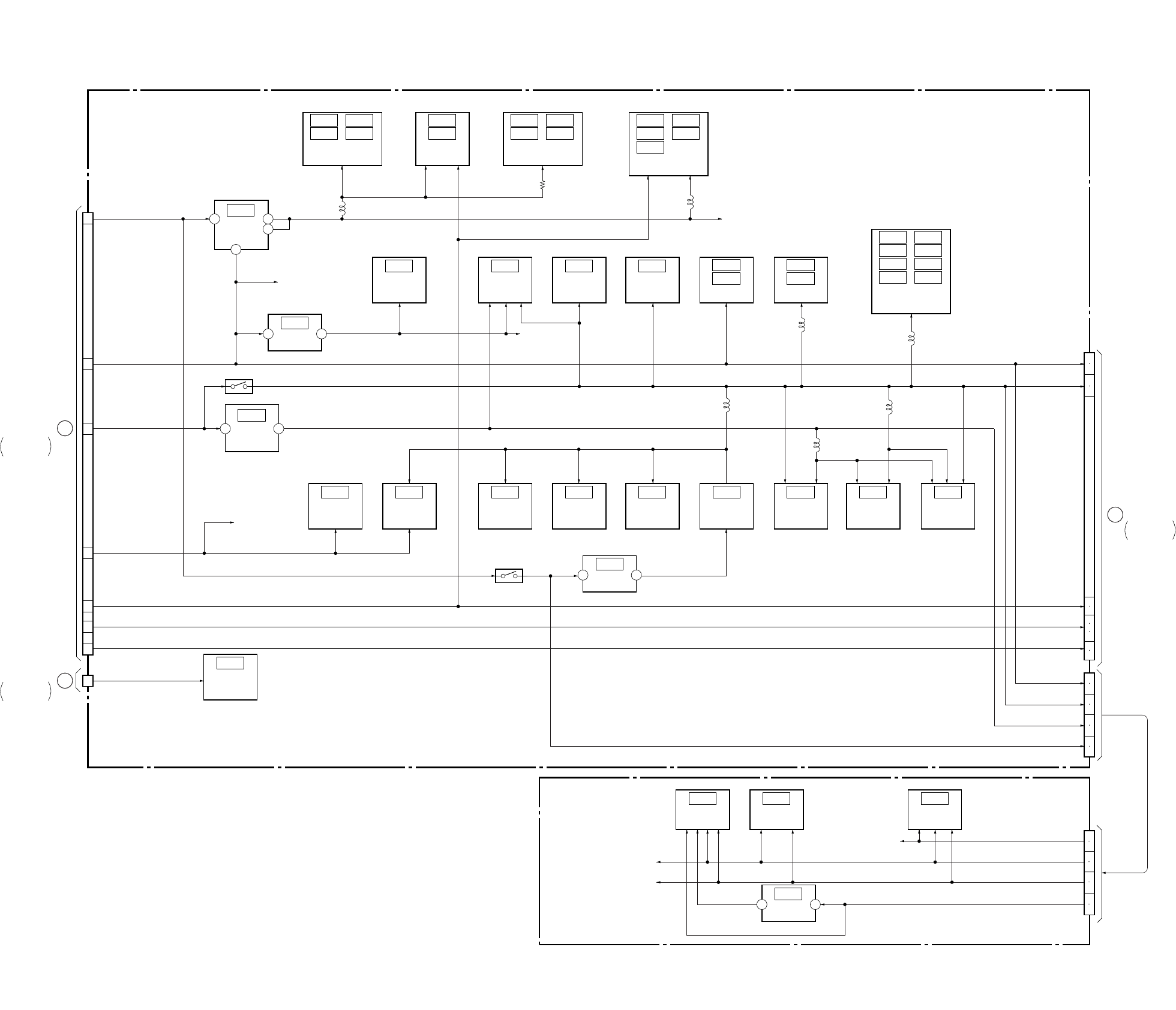
DSR-50/50P
3-23 3-24
3-12. POWER BLOCK DIAGRAM 3
JC-20 BOARD
RP-234 BOARD
IC1101 IC1103
IC1102 IC1104
IC2202
IC2203
REF DC
GEN.
(SEE PAGE 4-21)
IC1107 IC1108
IC1108 IC1109
A/D
CONVERTER
(SEE PAGE 4-21, 22)
IC1000 IC1111
IC1001
IC1002
IC1112
BUFFER
(SEE PAGE 4-20)
IC2208 IC2212
IC2209
IC2210 IC2214
IC2211 IC2215
IC2213
TIMING GEN.,
CHROMA MIX
(SEE PAGE 4-23, 24)
AFH CLP.
(SEE PAGE 4-25)
IC1105
IC1106
REF DC
GEN.
(SEE PAGE 4-21)
BUFFER
(SEE PAGE 4-28)
IC3301
IC3302
IC1113
VOL
CONT.
(SEE PAGE 4-45)
IC3300
VFD
(SEE PAGE 4-27)
IC5006
EEPROM
(SEE PAGE 4-38)
IC5003
MECHANISM
CONTROL
(SEE PAGE 4-37)
IC5007
INVERTER
(SEE PAGE 4-35)
IC5002
D/A
CONVERTER
(SEE PAGE 4-35)
IC4400
SFD
(SEE PAGE 4-29)
IC4401
TFD
(SEE PAGE 4-31)
IC4402
LIP
(SEE PAGE 4-33)
IC5008
AND
(SEE PAGE 4-38)
IC6003
SWITCH
(SEE PAGE 4-40)
IC2204
CLOCK
GEN.
(SEE PAGE4-26)
IC2200
REG
(SEE PAGE 4-25)
IC3303
CHARACTOR
GEN.
(SEE PAGE 4-28)
IC6004
INVERTER
(SEE PAGE 4-40)
1 3
6
2
1 3
IC1100
1.9V
REG
(SEE PAGE 4-46)
6 4
VIDEO +5V
AFC 3V
Q1131, 1132
Q5001, 5002
UNSW +3V
IC5001
REG
(SEE PAGE 4-35)
3 1
IC6001
MODE
CONTROL
(SEE PAGE 4-40)
IC101
TRW
(SEE PAGE 4-14)
IC301
TRX
(SEE PAGE 4-11)
IC201
TRF
(SEE PAGE 4-13)
IC102
REG
(SEE PAGE 4-14)
1 3
+5V
L1108
L1110
L5001
L3303
L4401
L4402
L2205
+3V
+5V
+1.9V
3
4
2
6
7
9
1
1
CN8001
CN4401
CN203
VIDEO +5V
J 3V
VIDEO –5V
A +5V
A –5V
RF 6V
5V
3V
1.9V
5V
3V
1.9V
RF 6V
49
50
53
54
99
101
103
95
97
51
52
13
14
15
16
17
18
21
22
13
14
15
16
17
18
21
22
CN1100
CN6001
SW +6V
VIDEO +5V
SW +3V
EVR +3V
VIDEO –5V
VIDEO +5V
AUDIO –5V
BACK UP +3V
VD-28 BOARD
(1/2)
CN904 H
VD-28 BOARD
(1/2)
CN703 B
I
DI-73 BOARD
CN9500
05
POWER1
SEE PAGE 3-20
POWER1
SEE PAGE 3-20
POWER4
SEE PAGE 3-25
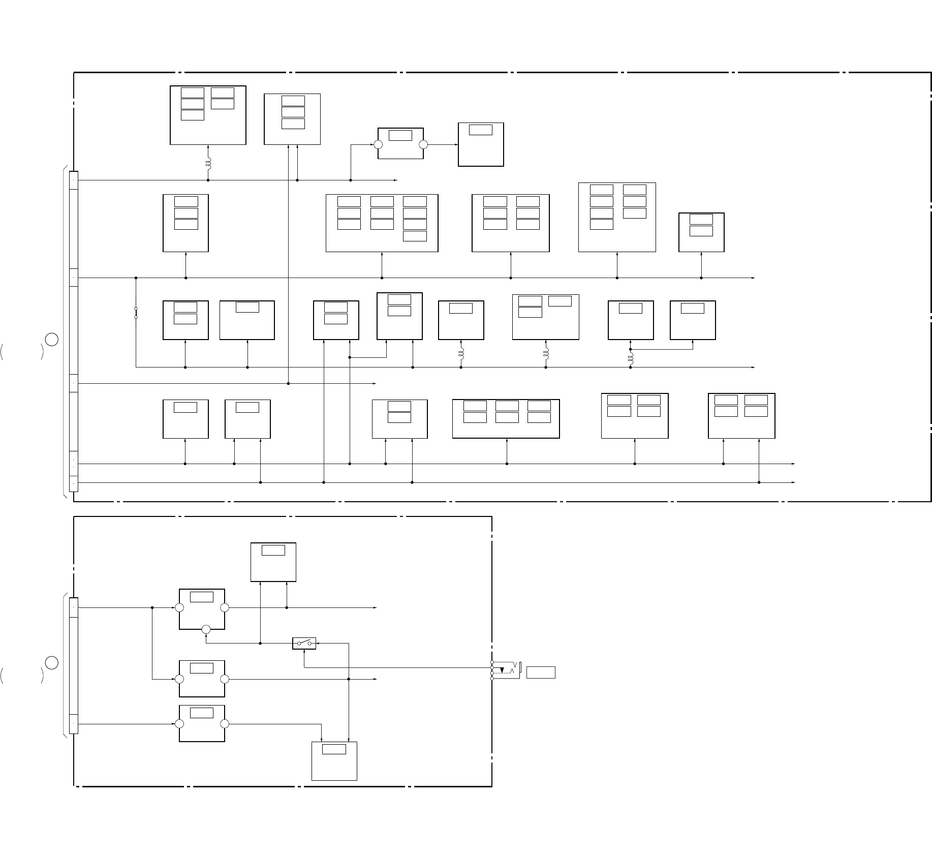
DSR-50/50P
3-25 3-26
3-13. POWER BLOCK DIAGRAM 4
DI-73 BOARD
HP-117 BOARD
IC9519
IC9518
SWITCH
(SEE PAGE 4-57)
IC7021
IC7020
MIX/LPF
(SEE PAGE 4-62)
IC8010
IC8007
SWITCH
(SEE PAGE 4-67, 68)
IC7018
IC7016
D/A
CONVERTER
(SEE PAGE 4-61)
IC8011
BUFFER
(SEE PAGE 4-68)
IC8005
OUTPUT
AMP
(SEE PAGE 4-67)
IC301
HP
AMP
(SEE PAGE 4-145)
IC305
AMP
(SEE PAGE 4-145)
IC8004
INPUT
AMP
(SEE PAGE 4-67)
IC8003
AUDIO
DSP
(SEE PAGE 4-64)
IC8009
AUDIO
DSP
(SEE PAGE 4-65)
IC8201
CRIP
(SEE PAGE 4-66)
CB/CR
CONTROL
(SEE PAGE 4-52)
IC9019
IC9018
IC9006
FIFO
MEMORY
(SEE PAGE 4-53, 54)
IC9008
IC9005
IC9004
IC9012
IC9011
IC9009
IC9015
IC9016
IC9014
IC9013
SYNC
SHIFTER
(SEE PAGE 4-55, 56)
IC9504
IC9502
IC9501
IC9508
IC9507
IC9505
Y/C
SELECT
(SEE PAGE 4-57, 58)
IC9515
IC9514
IC9513
IC9517
IC9516
IC9510 IC9511
AMP
(SEE PAGE 4-51, 52)
IC9010
IC9007
IC9001
IC7009
IC7008
IC7011
IC7010
IC7014
IC7013
AMP
(SEE PAGE 4-60)
IC9000
VIDEO
D/A
CONVERTER
(SEE PAGE 4-51)
IC302
+5V
REG
(SEE PAGE 4-146)
1 5
2
IC304
+5V
REG
(SEE PAGE 4-145)
2 3
IC303
–5V
REG
(SEE PAGE 4-145)
3 1
IC9017
REG
(SEE PAGE 4-51)
1 3
IC8000 IC8002
IC8001
CLOCK
(SEE PAGE 4-63)
IC7004 IC7006
IC7005 IC7007
AUDIO
SELECT
(SEE PAGE 4-59, 60)
IC7000 IC7002
IC7001 IC7003
H. P. F
(SEE PAGE 4-59)
IC9500 IC9509
IC9503
IC9506
IC9512
SYNC
SHIFTER
(SEE PAGE 4-55, 56, 57, 58)
IC8008
IC8006
(SEE PAGE 4-67, 68)
HYST
COMPARATOR
B+
B+
Q301
J301
PHONES
STB
SHUTDOWN
JC7201
AUDIO –5V
J +3V
+2.8V
A +5V
A –5V
VIDEO +5V
49
50
5
6
7
8
51
52
53
54
95
97
99
101
103
F
VD-28 BOARD
(1/2)
CN601
I
JC-20 BOARD
CN8001
L9500
L8203
L8201L8202
CN9500
CN301
VIDEO +5V
J 3V
VIDEO –5V
A +5V
A –5V
SW +6V
SW –6V
05
POWER3
SEE PAGE 3-24
POWER1
SEE PAGE 3-20
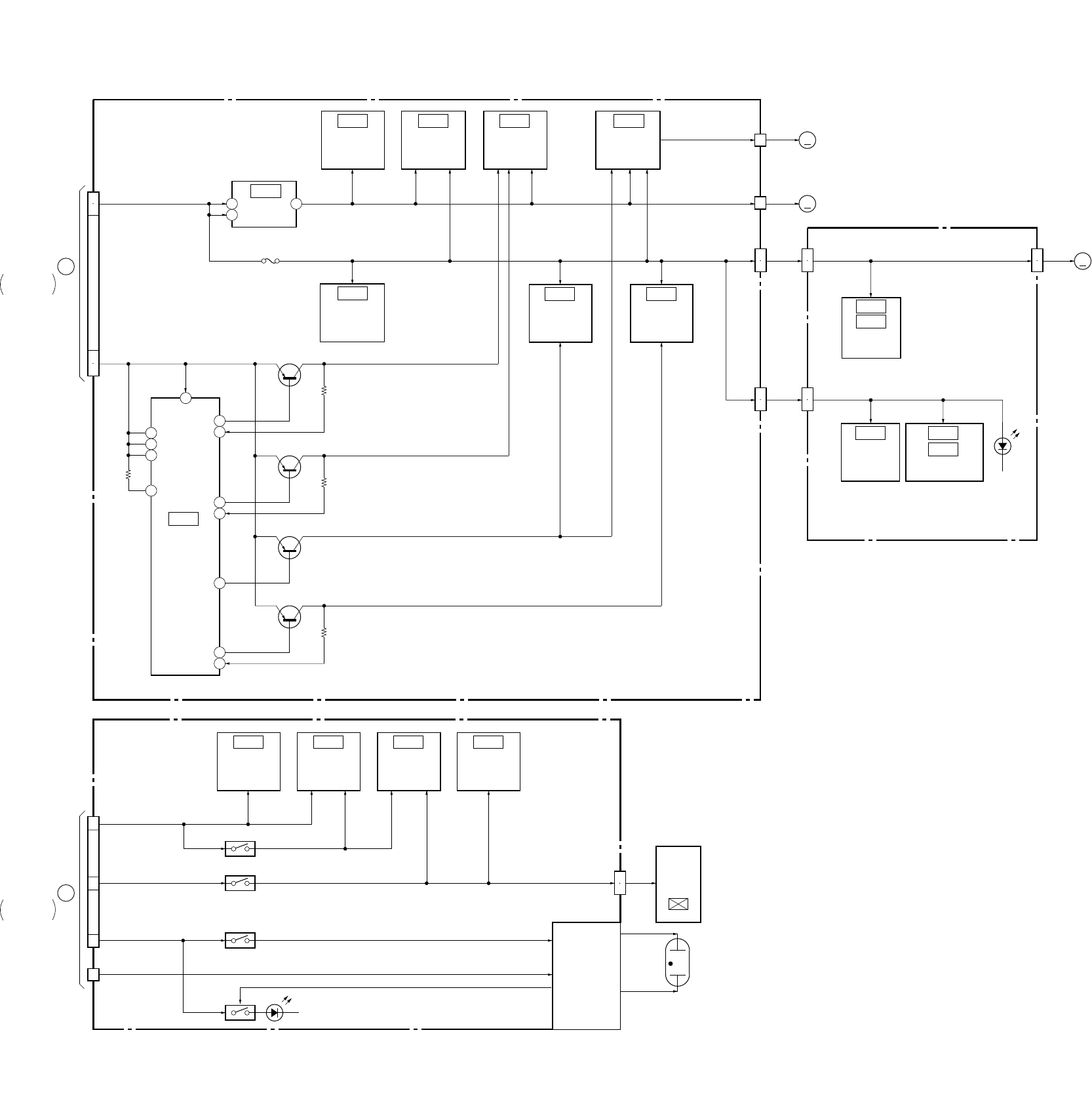
DSR-50/50P
3-27 3-28
3-14. POWER BLOCK DIAGRAM 5
CM-59 BOARD
MD-76 BOARD
PD-125 BOARD
IC300
LOADING
MOTOR
DRIVE
(SEE PAGE 4-109)
IC400
CAPSTAN
MOTOR
DRIVE
(SEE PAGE 4-110)
IC500
DRUM/C
MOTOR
DRIVE
(SEE PAGE 4-107)
IC102
BUFFER
(SEE PAGE 4-105)
IC202
REEL FG
AMP
(SEE PAGE 4-105)
IC100
DC
CONTROL
(SEE PAGE 4-105)
IC101
+3V
REG
(SEE PAGE 4-105)
5
1
4
F100
IC200
REEL
MOTOR
DRIVE
(SEE PAGE 4-106)
IC1
ELETEN
ERROR AMP
(SEE PAGE 4-117)
IC2
IC3
IC4
IC5
T/S
REEL FG
(SEE PAGE 4-118)
DRUM/C
MOTOR
DRIVER
(SEE PAGE 4-108)
IC501
LCD
TIMING
GENERATOR
(SEE PAGE 4-141)
IC8201
EVR
(SEE PAGE 4-141)
IC8200
RGB
DRIVER
(SEE PAGE 4-140)
IC8001
VCO
(SEE PAGE 4-141)
IC8202
20
22
24
8
18
46
7
44
12
29
40
39
INVERTER
BLOCK
LCD901
2.5INCH
COLOR
LCD UNIT
MM
MM
MM
3
4
5
6
A
VD-28 BOARD
(1/2)
CN905
D
VD-28 BOARD
(1/2)
CN331, CN333
12
13
11
3
CN100
CM REG 5V
UNREG CAPSTAN
6.25V DC
DRUM
REEL
18
9
9
18
10
11
10
11
10
11
16
18
10
11
M901
DRUM
MOTOR
M903
CAPSTAN
MOTOR
M904
REEL
MOTOR
CN500
SENSOR VCC
CN400
FG VCC
CN200 CN3
5V
CN2
5V MR VCC, HE VCC
CN201
5V
CN1
5V
D1
TAPE
LED
Q100
SWITCHING
Q101
SWITCHING
Q103
SWITCHING
Q102
SWITCHING
CN8001
CN8002
LCD 3.0V
ORG 12V
Q8000, 8007
Q8100 D8100
Q8001, 8003
Q8101, 8102
LCD 4.6V
UNREG
ND901
BACK LIGHT
VVDD, HVDD
CN8200
(SEE PAGE 4-117, 118)
05
POWER1
SEE PAGE 3-20
POWER1
SEE PAGE 3-20
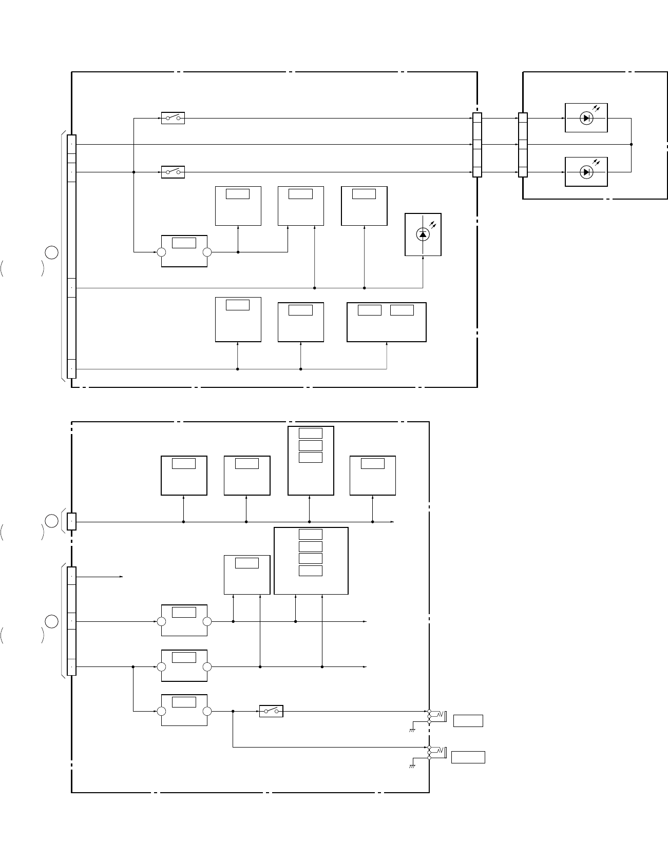
DSR-50/50P
3-29 3-30 E
3-15. POWER BLOCK DIAGRAM 6
FR-157 BOARD
JK-169 BOARD (2/2)
LT-32 BOARD
(SEE PAGE 4-126)
IC403
BUFFER
(SEE PAGE 4-125)
IC105
SWITCH
(SEE PAGE 4-132)
IC104
INVERTER
(SEE PAGE 4-132)
IC109
BUFFER
(SEE PAGE 4-133)
IC107
AND
GATE
(SEE PAGE 4-135)
IC103
IC102
IC101
PARALLEL/
SERIAL
CONVERTER
(SEE PAGE 4-132)
IC114
IC113
IC111
IC110
BUFFER
(SEE PAGE 4-134, 135, 136)
IC402
A/D
CONVERTER
(SEE PAGE 4-125)
IC501
LCD DRIVE,
MAT KEY
CONTROL
(SEE PAGE 4-123)
IC502
SWITCH
(SEE PAGE 4-123)
IC504 IC505
SERIAL/PARALLEL
CONVERTER
(SEE PAGE 4-123)
IC404
CLOCK
(SEE PAGE 4-125)
IC401
REG
(SEE PAGE 4-125)
3 1
IC108
REG
(SEE PAGE 4-133)
3 1
IC112
REG
(SEE PAGE 4-133)
2 3
SW +3V
SW +48V
SW –6V
SW +6V
IC115
REG
(SEE PAGE 4-131)
2 3
Q109, 110
Q513
Q514
24
25
21
22
16
17
18
19
1
BOTTOM
LED
VCC (+6V)
LED
COM (–6V)
TOP LED
VCC (+6V)
3
5
5
3
1
1
2
6
7
17
27
4
5
C
VD-28 BOARD
(1/2)
CN701
G
VD-28 BOARD
(1/2)
CN603
E
VD-28 BOARD
(1/2)
CN604
CN503 CN301
CN502
SW –6V
CN104
CN105
SW +3V
SW +48V
SW –6V
SW +6V
SW +6V
SW +3V
EVR +3V
D505 – 517
D301 – 305
D306 – 310
05
J106
REMOTE
J107
CONTROL S
POWER1
SEE PAGE 3-20
POWER1
SEE PAGE 3-20
POWER1
SEE PAGE 3-20
4-1
SECTION 4
PRINTED WIRING BOARDS AND SCHEMATIC DIAGRAMS
For printed wiring boards:
•b: Pattern from the side which enables seeing.
(The other layers’ pattern are not indicated)
• Circled numbers refer to waveforms.
• Through hole is omitted.
• There are a few cases that the part printed on diagram isn’t
mounted in this model.
• Chip parts.
For schematic Diagram:
• All capacitors are in µF unless otherwise noted. pF : µµF
50V or less are not indicated except for electrolytics and
tantalums.
• Chip resistors are 1/10 W unless otherwise noted.
kΩ : 1000Ω, MΩ : 1000kΩ.
• Caution when replacing chip parts.
New parts must be attached after removal of chip.
Be careful not to heat the minus side of tantalum capacitor,
because it is damaged by the heat.
• Some chip part will be indicated as follows.
• Constants of resistors, capasitors, ICs and etc with XX indi-
cate that they are not used. In such cases, the unused cir-
cuits may be indicated.
• Parts with ★ differ according to the model/destination. Re-
fer to the mount table for each function.
• All variable and adjustable resistors have characteristic curve
B, unless otherwise noted.
• Signal name
XEDIT → EDIT PB/XREC → PB/REC
•2: nonflammable resistor.
•1: fusible resistor.
•C: panel designation.
•A: B+ Line.*
•B: B– Line.*
•J: IN/OUT direction of B line (+, –).*
•C: adjustment for repair.*
• Circled numbers refer to waveforms.*
21
3
21
3
21
3
345
21
123
654
EB
C
31
5
5
2
46
123
54
Transistor Diode
Example C 541
22U
TA A
L 452
10UH
2520
Kinds of Temperature External
capacitor characteristics dimensions (mm)
Measuring conditions voltege and waveform:
•Voltages and waveforms are measured between the mea-
surement points and graound when color bar signal
input.They are reference values and reference waveforms.*
(VOM of DC 10 M Ω input impedance is used)
•Voltage values change depending upon input impedance
of VOM used.
*Indicated by the color red.
When indicating parts by reference
number, please include the board
name.
Note:
The components identi-
fied by mark 0 or dotted
line with mark 0 are criti-
cal for safety.
Replace only with part
number specified.
Note:
Les composants identifiés par
une marque 0 sont critiques
pour la sécurité.
Ne les remplacer que par une
piéce portant le numéro
spécifié.
DSR-50/50P
THIS NOTE IS COMMON FOR PRINTED WIRING BOARDS AND SCHEMATIC DIAGRAMS.
(In addition to this, the necessary note is printed in each block)
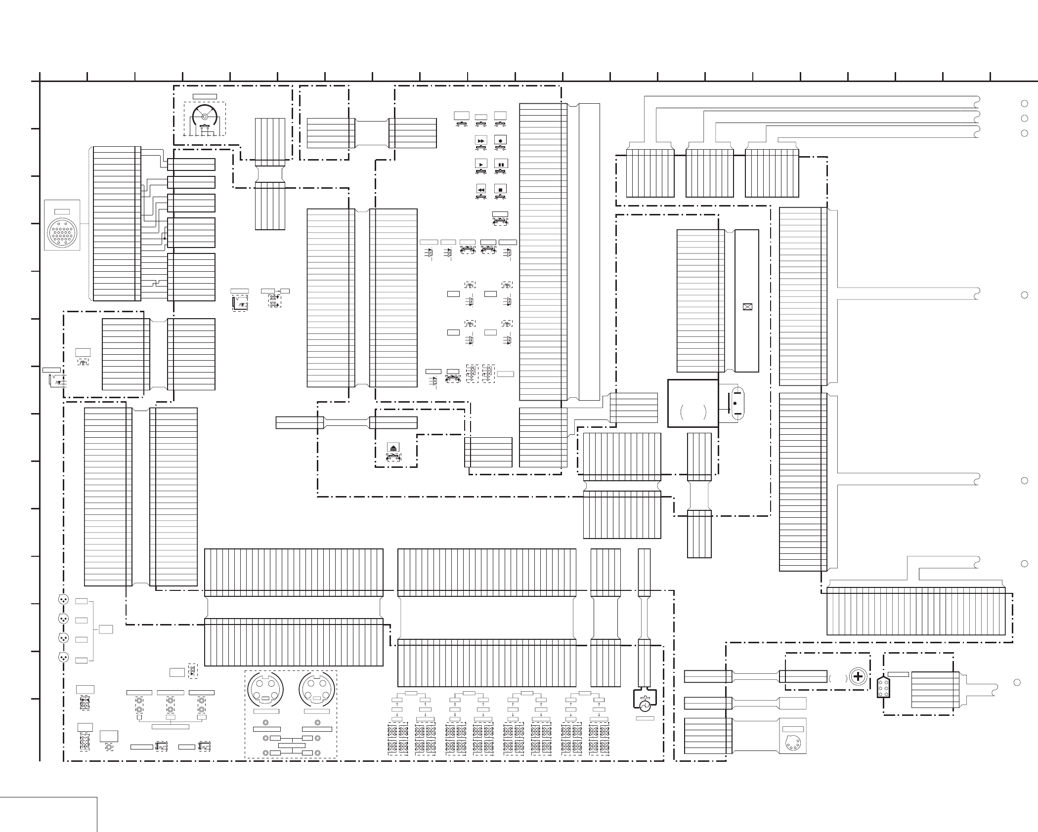
DSR-50/50P
4-3 4-4
4-1. FRAME SCHEMATIC DIAGRAM (1/2)
FRAME (1/2)
5P
CN101
1
TC IN
2
TC IN
3
GND
4
TC OUT
5
TC OUT
30P
CN103
1
VIDEO IN
2
GND
3
GND
4
S-Y IN
5
GND
6
GND
7
S-C IN
8
GND
9
SC DET
10
GND
11
GND
12
VIDEO OUT
13
GND
14
GND
15
S-Y OUT
16
GND
17
GND
18
S-C OUT
19
GND
20
GND
21
VIDEO MON OUT
22
GND
23
GND
24
B-Y OUT
25
GND
26
GND
27
R-Y OUT
28
GND
29
GND
30
Y OUT
30P
CN104
1
CH4 OUT
2
GND
3
GND
4
CH2 OUT
5
GND
6
GND
7
CH3 OUT
8
GND
9
GND
10
CH1 OUT
11
GND
12
GND
13
AUDIO MONITOR OUT
14
GND
15
GND
16
+48V DD ON
17
SW +3V
18
P/S CS
19
GND
20
P/S DATA
21
GND
22
P/S SCK
23
GND
24
NC
25
GND
26
SIRCS DATA
27
SW +3V
28
TALLY LED
29
FOOT SW
30
AUDIO MONITOR SEL
30P
CN105
1
SW +48V
2
SW +48V
3
NC
4
SW +6V
5
SW +6V
6
SW -6V
7
SW -6V
8
MIC Y
9
GND
10
MIC X
11
GND
12
GND
13
CH4 IN Y
14
GND
15
CH4 IN X
16
GND
17
GND
18
CH3 IN Y
19
GND
20
CH3 IN X
21
GND
22
GND
23
CH2 IN Y
24
GND
25
CH2 IN X
26
GND
27
GND
28
CH1 IN Y
29
GND
30
CH1 IN X
6P
CN901
1BATTERY 12V
2BATTERY 12V
3SELECTED 12V
4SELECTED 12V
5GND
6GND
8P
CN101
1 VIDEO IN
2 VIDEO IN (GND)
3 Y IN
4 Y IN (GND)
5 R-Y IN
6 R-Y IN (GND)
7 B-Y IN
8 B-Y IN (GND)
5P
CN602
1 MIC IN (X)
2 MIC IN (X-GND)
3 MIC IN (Y)
4 MIC IN (Y-GND)
5 AUDIO MON/VTR SAVE
2P
CN401
1 RETURN VIDEO (X)
2 RETURN VIDEO (GND)
3P
CN702
1 VTR START/STOP
2 BATTERY INDICATION
3 REC/TALLY
30P
CN502
1KEY REQ
2GND
3SCK
4GND
5DATA TO HI
6GND
7DATA FROM HI
8GND
9_W/R
10 GND
11 LED STB
12 GND
13 LCD STB
14 GND
15 OE
16 SW +3V
17 SW +3V
18 EVR +3V
19 EVR +3V
20 DSP_CS
21 SW +6V
22 SW +6V
23 DSP_SO (FROM DSP)
24 SW -6V
25 SW -6V
26 DSP_SI (TO DSP)
27 RESET
28 DSP_SCK
29 RESET
30 POWER SW
30PCN701
1
KEY REQ
2
GND
3
SCK
4
GND
5
DATA TO HI
6
GND
7
DATA FROM HI
8
GND
9
_W/R
10
GND
11
LED STB
12
GND
13
LCD STB
14
GND
15
OE
16
SW +3V
17
SW +3V
18
EVR +3V
19
EVR +3V
20
DSP_CS
21
SW +6V
22
SW +6V
23
DSP_SO (FROM DSP)
24
SW -6V
25
SW -6V
26
DSP_SI (TO DSP)
27
RESET
28
DSP_SCK
29
RESET
30
POWER SW
30P
CN102
1 VIDEO IN
2 GND
3 GND
4 S-Y IN
5 GND
6 GND
7 S-C IN
8 GND
9 SC DET
10 GND
11 GND
12 VIDEO OUT
13 GND
14 GND
15 S-Y OUT
16 GND
17 GND
18 S-C OUT
19 GND
20 GND
21 VIDEO MON OUT
22 GND
23 GND
24 B-Y OUT
25 GND
26 GND
27 R-Y OUT
28 GND
29 GND
30 Y OUT
30P
CN603
1 CH4 OUT
2 GND
3 GND
4 CH2 OUT
5 GND
6 GND
7 CH3 OUT
8 GND
9 GND
10 CH1 OUT
11 GND
12 GND
13 AUDIO MONITOR OUT
14 GND
15 GND
16 +48V DD ON
17 SW +3V
18 P/S CS
19 GND
20 P/S DATA
21 GND
22 P/S SCK
23 GND
24 NC
25 GND
26 SIRCS DATA
27 SW +3V
28 TALLY LED
29 FOOT SW
30 AUDIO MONITOR SEL
30P
CN604
1 SW +48V
2 SW +48V
3NC
4 SW +6V
5 SW +6V
6 SW -6V
7 SW -6V
8 MIC Y
9 GND
10 MIC X
11 GND
12 GND
13 CH4 IN Y
14 GND
15 CH4 IN X
16 GND
17 GND
18 CH3 IN Y
19 GND
20 CH3 IN X
21 GND
22 GND
23 CH2 IN Y
24 GND
25 CH2 IN X
26 GND
27 GND
28 CH1 IN Y
29 GND
30 CH1 IN X
5P
CN607
1TC IN
2TC IN
3GND
4TC OUT
5TC OUT
12P
CN301
1
HP L
2
HP L GND
3
HP R
4
HP R GND
5
SW +6V
6
SW +6V
7
SW -6V
8
SW -6V
9
NC
10
VTR RET AUDIO
11
VTR RET AUDIO GND
12
GND
12PCN601
1 HP L
2 HP L GND
3 HP R
4 HP R GND
5 SW +6V
6 SW +6V
7 SW -6V
8 SW -6V
9NC
10 VTR RET AUDIO
11 VTR RET AUDIO GND
12 GND
6P
CN391
1GND
2TPA
3NTPA
4GND
5TPB
6NTPB
8PCN605
1CH1 OUT
2GND(CH1 OUT)
3CH2 OUT
4GND(CH2 OUT)
5CH3 OUT
6GND(CH3 OUT)
7CH4 OUT
8GND(CH4 OUT)
30P
CN703
1
XCS_OSD_HI
2
OSD_SW
3
OSD_SCK_HI
4
GND
5
OSD_SO_HI
6
UVIC_GATE
7
UVIC_SWIN
8
UVIC_BUSY
9
XCS_UVIC
10
GND
11
MO_SI
12
GND
13
MO_SO
14
GND
15
MO_SCK
16
GND
17
XSYS_RST
18
GND
19
XCS_MO
20
GND
21
HI_SI
22
GND
23
HI_SO
24
GND
25
HI_SCK
26
GND
27
MO_XWAKEUP
28
XSLEEP
29
XIC_RST
30
BACK_UP_+3V
8P
CN905
1SW +3V
2GND
3CM REG 5V
4CM REG 5V
5UNREG
6UNREG
7GND
8GND
9P
CN904
1SW +6V
2EVR +3V
3VIDEO +5V
4SW +3V
5GND
6VIDEO -5V
7AUDIO +5V
8AUDIO GND
9AUDIO -5V
30PCN606
1AU X1 IN
2AU Y1 IN
3GND
4AU X2 IN
5AU Y2 IN
6GND
7AU X3 IN
8AU Y3 IN
9GND
10AU X4 IN
11AU Y4 IN
12GND
13TC IN
14GND
15TC OUT
16GND
17DSP CS
18GND
19DSP SI
20GND
21DSP SO
22GND
23DSP SCK
24NC
25NC
26NC
27NC
28NC
29NC
30NC
5P
CN503
5TOP LED VCC (+6V)
4NC
3LED COM (-6V)
2NC
1BOTTOM LED VCC (+6V)
5P
CN301
5
BOTTOM LED VCC (+6V)
4
NC
3
LED COM (-6V)
2
NC
1
TOP LED VCC (+6V)
2P
CN101
1EJECT SW
2GND
2P
CN704
1
EJECT SW
2
GND
2P
CN902
1 CAMERA UNREG +12V
2 GND
4P
CN333
1ORG_15.5V
2PWM
3UNREG
4GND
13PCN331
1VD_SCK
2DATA_FROM_HI
3XCS_LCD_DAC
4GND
5PANEL_Y
6PANEL_CR
7PANEL_CB
8LCD_DD_ON
9XVD
10XHD
11LCD_4.6V
12LCD_3.0V
13ORG_12V
13PCN8001
1 VD_SCK
2 DATA_FROM_HI
3 XCS_LCD_DAC
4GND
5 PANEL_Y
6 PANEL_CR
7 PANEL_CB
8 LCD_DD_ON
9 XVD
10 XHD
11 LCD_4.6V
12 LCD_3.0V
13 ORG_12V
4P
CN8002
1 ORG_15.5V
2PWM
3 UNREG
4GND
2P
CN706
1
VL BATT 3V
2
VL BATT GND
2P
CN801
1VL BATT 3V
2VL BATT GND
2P
CN900
1
BATTERY 12V
2
GND
S601
5P
CN601
1 DIAL_A
2 GND
3 DIAL_B
4 GND
5 EXEC_SW
5PCN705
1DIAL_A
2GND
3DIAL_B
4GND
5EXEC_SW
50P
CN501
1
15A 15B 15C M13
2
15F 15G 15E 15D
3
14A 14B 14C 12C
4
14F 14G 14E 14D
5
13A 13B 13C C1
6
13F 13G 13A 13D
7
12A,D,G 12E F 12B
8
COM1
9
COM2
10
COM3
11
COM4
12
COM4
13
COM3
14
COM2
15
COM1
16
1F 1G 1E 1D
17
1A 1B 1C DVCAM
18
2F 2G 2E 2D
19
2A 2B 2C CL1.H
20
3F 3G 3E 3D
21
3F 3G 3E 3D
22
4F 4G 4E 4D
23
4A 4B 4 M6
24
5F 5G 5E 5D
25
5A 5B 5C CL2.M.S
26
6F 6G 6E 6D
27
6A 6B 6C CL3.F
28
7F 7G 7E 7D
29
7A 7B 7C
30
8F 8G 8E 8D
31
8A 8B 8C
32
M9 M8 M10 M11
33
M3 M2 M1 M7
34
M5 M4 9B 9C
35
10F 10G 10E 10D
36
10A 10B 10C 9ADEG
37
11F 11G 11E 11D
38
11A 11B 11C MIN
39
LM5 LM6 LM7 LM8
40
LM4 LM3 LM2 LM1
41
LM12 LM11 LM10 LM9
42
LM13 12 14 15 16
43
19A 19B 19C PM
44
19F 19G 19E 19D
45
18A 18B 18C AM
46
18F 18G 18E 18D
47
17A 17B 17C CL4
48
17F 17G 17E 17D
49
16A 16B 16C X
50
16F 16G 16E 16D
5PCN505
1 VCO_CENT
2 PSIG
3 GND
4 COM
5VG
10P
CN504
1
VG
2
COM
3
GND
4
PSIG
5
VCO_CENT
6
VCO_CENT
7
PSIG
8
GND
9
COM
10
VG
CN8200 24P
TESTR 1
RGT 2
VB 3
VR 4
VG 5
PSIG 6
HCK1 7
HCK2 8
CR 9
SOUT 10
REF 11
HST 12
WIDE 13
CS 14
VSS 15
VVDD 16
VSS 17
HVDD 18
DWN 19
EN 20
VCK 21
VST 22
COM 23
TESTL 24
5P
CN8201
1VG
2 COM
3 GND
4 PSIG
5 VCO_CENT
30P
CN332
1
V_SYNC
2
XI/O SYNC VFD
3
XI/O SYNC HI
4
VFD_HD
5
VFD_VD
6
VD HD
7
GND
8
CB_IN
9
GND
10
CR_IN
11
GND
12
Y_IN
13
GND
14
AFC Y
15
GND
16
MONITOR C
17
GND
18
MONITOR Y
19
GND
20
Y LINE
21
GND
22
CR LINE
23
GND
24
CB LINE
25
GND
26
PANEL CB
27
GND
28
PANEL CR
29
GND
30
PANEL Y
S109
CB101
S107
S518
S529
S101
1
A
S533
S528 S532
S527 S531
S534S535 S530
S516 S538 S515 S519
S537
S536
RV404
S523
S521
RV402
S520
RV401
S522
RV403
RV301
J301
S108S106S105S103S102 S104
2P
CN102
2
BREAKER IN
1
BREAKER OUT
2P
CN903
2BREAKER IN
1BREAKER OUT
S526
26P
CN026
1VIDEO IN
2VIDEO IN(GND)
3Y IN(GND)
4Y IN
5R-Y IN
6R-Y IN(GND)
7B-Y IN
8B-Y IN(GND)
9MIC IN(X)
10MIC IN(Y)
11MIC IN(GND)
12VTR START/STOP
13BATTERY INDICATION
14NC
15REC/TALLY
16NC
17NC(GND)
18RETURN VIDEO(X)
19RETURN VIDEO(GND)
20AUDIO MON/VTR SAVE
21NC
22NC(COLOR FRAMING)
23NC
24NC
25CAMERA UNREG +12V
26GND
6P
LCD BRIGHT
CH-4
CAM
LINE
+48V ON+4
-20
-60
CY
GG
LT-32
BOARD
EJECT
EJ-28
BOARD
BOARD
HP-117
LCD902
CHARACTER
DISPLAY
PD-125 BOARD
CAMERA
CN026
26P
2 16
L
I
20
K
12
G
6
N
8
D
E
B
7
05
19151310 1711
C
21
H
F
3 18
J
14945
M
IL-013 BOARD
DV IN/OUT
VL-26 BOARD
BATTERY
TARMINAL
FR-157 BOARD
CONTINUED ON
PAGE 4-5
CONTINUED ON
PAGE 4-5
CONTINUED ON
PAGE 4-5
DC IN 12V
CN9901
F FWD
PLAY
REC
PAUSE
REW STOP
AUDIO
DUB
END
SEARCH DUP
COUNTER METER LIGHT INDEX KEY INH
RESET
POWER FINE
CH-4
RV404,S523
CH-2
RV402,S521
CH-1
RV401,S520
CH-3
RV403,S522
S524,S525
DISPLAY
S524 S525
DVCAM
S702
DV
J701
CONTROL
LEVEL
PHONE
PHONES
CONTINUED ON
PAGE 4-5
CONTINUED ON
PAGE 4-5
CONTINUED ON
PAGE 4-5
CONTINUED ON
PAGE 4-5
CH-1
3P
CN106
CH-2
3P
CN107
3P
CN108
CH-3
CH-4
CN109
3P
BREAKER
-20
+48V ON+4
CH-3
-60 CAM
LINE
CAM
LINE-20
+48V ON+4
CH-2
-60
-20
CAM
LINE
-60
CH-1
+4 +48V ON
CONTROL S
J107
REMOTE
J106
SELECT
INPUT
S111
MONITOR
SELECT
S101
AUDIO
MONITOR
J101
OUT
S VIDEO OUT
SUPER
IMPOSE
S110
J102
TC IN (EXT)
Y
TC OUT (INT)
J103
R-Y
VIDEO OUT 1
J104
B-Y
COMPONENT OUTPUT
S VIDEO IN
G
Y
G
C
VIDEO OUT 2 VIDEO/REF,IN
CH-1 CH-3
CH-2 CH-4
AUDIO OUTPUT
J105
VD-28 BOARD
JK-169 BOARD
KP-8 BOARD
JIG PIN
(FOR CHECK)
LCD901
2.5INCH
COLOR LCD
UNIT
FVJ-14 FLAT CABLE
VC-58 HARNESS
JV-58 HARNESS
VJ-106 HARNESS
FVJ-13 FLAT CABLE
FVJ-13 FLAT CABLE
IN-50
HARNESS
CN392
BT901
BV-50 HARNESS
BA-54 HARNESS
DC-66 HARNESS
LITHIUM
BATTERY
BT801
FVJ-10
FLAT CABLE
VB-50 HARNESS
FVJ-7 FLAT CABLE
FVJ-7 FLAT CABLE
RM-129
HARNESS
LC-111 HARNESS
EV-70 HARNESS
ND901
BACK LIGHT
BLOCK
INVERTER
LIGHT
DRIVER
BACK
FVJ-7 FLAT CABLE
HP-135 HARNESS
KP-52
HARNESS
FVJ-7 FLAT CABLE
1
2
3
4
5
6
7
AUDIO
INPUT
FVJ-12
FLAT CABLE
FJV-3
FLAT CABLE
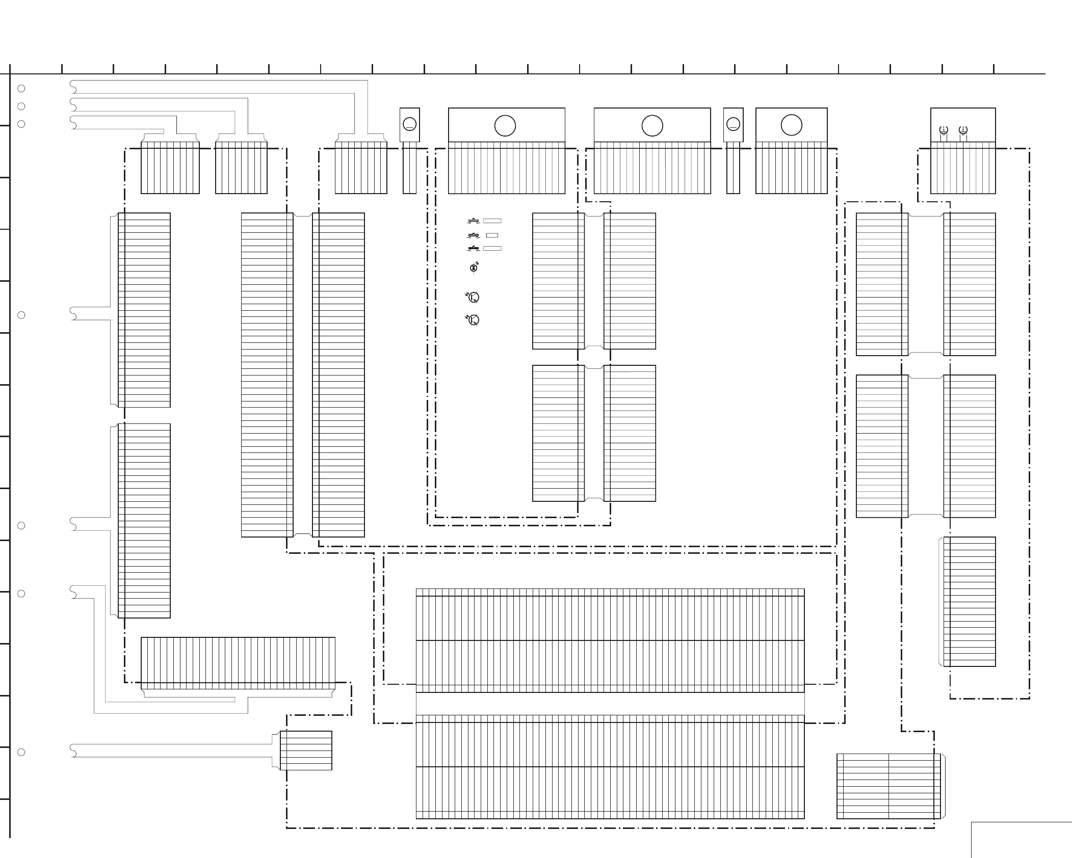
DSR-50/50P
4-5 4-6
FRAME SCHEMATIC DIAGRAM (2/2)
FRAME (2/2)
8P
CN7001
1CH1 OUT
2GND(CH1 OUT)
3CH2 OUT
4
GND(CH2 OUT)
5CH3 OUT
6GND(CH3 OUT)
7CH4 OUT
8GND(CH4 OUT)
30P
CN1101
1 PANEL Y
2 GND
3 PANEL CR
4 GND
5 PANEL CB
6 GND
7 CB LINE
8 GND
9 CR LINE
10 GND
11 Y LINE
12 GND
13 MONITOR Y
14 GND
15 MONITOR C
16 GND
17 AFC Y
18 GND
19 Y_IN
20 GND
21 CR_IN
22 GND
23 CB_IN
24 GND
25 VD HD
26 VFD_VD
27 VFD HD
28 XI/O SYNC HI
29 XI/O SYNC VFD
30 V_SYNC
30P
CN6001
1 BACK_UP_+3V
2 XIC_RST
3 XSLEEP
4 MO_XWAKEUP
5 GND
6 HI_SCK
7 GND
8 HI_SO
9 GND
10 HI_SI
11 GND
12 XCS_MO
13 GND
14 XSYS_RST
15 GND
16 MO_SCK
17 GND
18 MO_SO
19 GND
20 MO_SI
21 GND
22 XCS_UVIC
23 UVIC_BUSY
24 UVIC_SWIN
25 UVIC_GATE
26 OSD_SO_HI
27 GND
28 OSD_SCK_HI
29 OSD_SW
30 XCS_OSD_HI
8P
CN100
1SW +3V
2GND
3CM REG 5V
4CM REG 5V
5UNREG
6UNREG
7GND
8GND
6P
CN4400
1 GND
2TPA
3 NTPA
4 GND
5 TPB
6 NTPB
30PCN7002
1NC
2NC
3NC
4NC
5NC
6NC
7NC
8DSP SCK
9GND
10 DSP SO
11 GND
12 DSP SI
13 GND
14 DSP CS
15 GND
16 TC OUT
17 GND
18 TC IN
19 GND
20 AU Y4 IN
21 AU X4 IN
22 GND
23 AU Y3 IN
24 AU X3 IN
25 GND
26 AU Y2 IN
27 AU X2 IN
28 GND
29 AU Y1 IN
30 AU X1 IN
50P
CN001
1 HI_C/R_SW
2 LM(-)
3 LM(+)
4 CM_LIMIT_EVR
5 CM_LIMIT_DET
6 CM_LIMIT_ON
7 CM(-)
8 CM(+)
9 GND
10 REEL_M_FG
11 REEL_PWM
12 REEL_FWD
13 REEL_ON
14 GND
15 CAP_FG
16 CAP_PWM
17 CAP_FWD
18 CAP_ON
19 GND
20 DRUM_MASTER_CLK
21 DRUM_PG
22 DRUM_FG
23 DRUM_PWM
24 DRUM_FWD
25 DRUM_ON
26 GND
27 CHIME_VDD
28 CHIME_SDA
29 CHIME_SCK
30 CAP_EVR
31 REEL_EVR
32 TREEL_FG
33 SREEL_FG
34 S_ELTN_ERR
35 T_ELTN_ERR
36 GND
37 DEW_DET
38 REC_PROOF
39 L_CASSETTE
40 XCC_DOWN
41 XC_IN
42 GND
43 TAPE_END
44 TAPE_TOP
45 TAPE_LED_ON
46 GND
47 MODE_SW_D
48 MODE_SW_C
49 MODE_SW_B
50 MODE_SW_A
M
2P
CN501
1CM_UNLOAD
2CM_LOAD
11P
CN500
1W
2W
3V
4V
5U
6U
7GND
8GND
9SENSOR Vcc
10FG
11PG
18P
CN400
1
HW-
2
HW+
3
HV-
4
HV+
5
HU-
6
HU+
7
V
8
V
9
W
10
W
11
HE VCC
12
HE GND
13
U
14
U
15
MR GND
16FG2
17
FG1
18
FG VCC
M
2P
CN300
1LM+
2LM-
18P
CN3
1
V
2
V
3
U
4
U
5
W
6
W
7
MR_GND
8
MR_FG1
9
MR_VCC
10
MR_FG2
11
U+
12
U-
13
V+
14
V-
15
W+
16W-
17
HE GND
18
HE VCC
21P
CN200
1 TAPE_END
2 CC_DOWN
3 C_IN
4 MODE_A
5 MODE_B
6 MODE_C
7 MODE_D
8 S_ELETEN
9 T_ELETEN
10 5V
11 5V
12 TAPE_LED
13 GND
14 L_CASSETTE
15 DEW
16 W-
17 W+
18 V-
19 V+
20 U-
21 U+
21P
CN201
1 REEL_V
2 REEL_V
3 REEL_U
4 REEL_U
5 REEL_w
6 REEL_W
7 GND
8 GND
9 FG1
10 5V
11 5V
12 FG2
13 SREEL_FG
14 TREEL_FG
15 REC_PROOF
16 CHIME_4(VDD)
17 CHIME_3(SDA)
18 CHIME_2(SCK)
19 GND
20 GND
21 TAPE_TOP
50P
CN5005
1MODE_SW_A
2MODE_SW_B
3MODE_SW_C
4MODE_SW_D
5GND
6TAPE_LED_ON
7TAPE_TOP
8TAPE_END
9GND
10XC_IN
11XCC_DOWN
12L_CASSETTE
13REC_PROOF
14DEW_DET
15GND
16T_ELTN_ERR
17S_ELTN_ERR
18SREEL_FG
19TREEL_FG
20REEL_EVR
21CAP_EVR
22CHIME_SCK
23CHIME_SDA
24CHIME_VDD
25GND
26DRUM_ON
27DRUM_FWD
28DRUM_PWM
29DRUM_FG
30DRUM_PG
31DRUM_MASTER_CLK
32GND
33CAP_ON
34CAP_FWD
35CAP_PWM
36CAP_FG
37GND
38REEL_ON
39REEL_FWD
40REEL_PWM
41REEL_M_FG
42GND
43CM(+)
44CM(-)
45CM_LIMIT_ON
46CM_LIMIT_DET
47CM_LIMIT_EVR
48LM(+)
49LM(-)
50HI_C/R_SW
21P
CN2
1TAPE_END
2CC_DOWN
3C_IN
4MODE_A
5MODE_B
6MODE_C
7MODE_D
8S_ELETEN
9T_ELETEN
105V
115V
12
TAPE_LED
13GND
14L_CASSETTE
15DEW
16W-
17W+
18V-
19V+
20U-
21U+
21P
CN1
1REEL_V
2REEL_V
3REEL_U
4REEL_U
5REEL_w
6REEL_W
7GND
8GND
9FG1
105V
115V
12FG2
13SREEL_FG
14TREEL_FG
15REC_PROOF
16CHIME_4(VDD)
17CHIME_3(SDA)
18CHIME_2(SCK)
19GND
20GND
21TAPE_TOP
9P
CN1100
1
SW +6V
2EVR +3V
3VIDEO +5V
4SW +3V
5GND
6VIDEO -5V
7AUDIO +5V
8AUDIO GND
9AUDIO -5V
CN8001 120P
1 DPB_YOUT
3 GND
5 DPB_CROUT
7 GND
9 DPB_CBOUT
11 GND
13 MY00
15 MY01
17 MY02
19 MY03
21 MY04
23 MY05
25 MY06
27 MY07
29 GND
31 MHO
33 DA135
35 AFH
37 VD_HD
39 N.C
41 SPCK2
43 PAL/XNT
45 PB/XREC
47 FIFO/MUTE
49 J_3V
51 VIDEO_+5V
53 VIDEO_-5V
55 SOA
57 SOB
59 LOCK_MCK
61 OCK
63 SFD_FCK
65 N.C
67 VFD_VD
69 VFD_OE
71 GND
73 XCS_DSP
75 VSP_SI
77 XRST_VSP
79 GND
81 DSP_CS
83 DSP_SI
85 TC/GNDIN
87 TC_IN
89 AUDIO_GND
91 AUDIO_GND
93 AUDIO_GND
95 A.-5V
97 A.-5V
99 A.+5V
2DPB_YOUT
4GND
6DPB_CROUT
8GND
10DPB_CBOUT
12GND
14Y0
16Y1
18Y2
20Y3
22Y4
24Y5
26Y6
28Y7
30GND
32JC00
34JC01
36JC02
38JC03
40JC04
42JC05
44JC06
46JC07
48N.C
50J_3V
52VIDEO_+5V
54VIDEO_-5V
56SIC
58SID
60SFDBCK
62BCK
64SFD_LRCK
66LRCK
68N.C
70VFD_HD
72GND
74N.C
76XVSP_SCK
78VSP_SO
80GND
82DSP_SCK
84DSP_SO
86TC/GND_OUT
88TC_OUT
90AU_GND4_OUT
92AU_CH4_OUT
94AU_GND3_OUT
96AU_CH3_OUT
98AU_GND2_OUT
100
AU_CH2_OUT
101 A.+5V 102
AU_GND1_OUT
103 A.+5V 104
AU_CH1_OUT
105 AU_4_GND_IN 106
AU_4_GND_IN
107 AU_Y4_IN 108
AU_X4_IN
109 AU_3_GND_IN 110
AU_3_GND_IN
111 AU_Y3_IN 112
AU_X3_IN
113 AU_2_GND_IN 114
AU_2_GND_IN
115 AU_Y2_IN 116
AU_X2_IN
117 AU_1_GND_IN 118AU_1_GND_IN
119 AU_Y1_IN 120
AU_X1_IN
22P
CN4402
1CLK135
2 REEL_EVR
3 CAP_EVR
4 ATF
5 GND
6TXST
7 GND
8TXDT4
9TXDT3
10TXDT2
11TXDT1
12TXDT0
13 GND
14 CRCK
15 GND
16 XTDT1
17 XTDT0
18 GND
19 XTSY
20 HPCK
21 N.C.
22 N.C.
22P
CN4401
1DSWP
2CONT_O
3CONT_E
4SC_WD
5CLK150
6SWP
7XRST
8MSCK
9DRP_SO
10 DRP_SI
11XCS_TRF
12XCS_TRX
13 5V
14 5V
15 3V
16 3V
17 1.9V
18 1.9V
19 GND
20 C1ERRP
21 RF 6V
22 RF 6V
10PCN101
1
GND
2
XEVEN
3
YEVEN
4
GND
5
XODD
6
YODD
7
GND
8
XSDL
9
YSDL
10
GND
22P
CN202
1 CLK135
2 REEL_EVR
3 CAP_EVR
4ATF
5 GND
6 TXST
7 GND
8 TXDT4
9 TXDT3
10 TXDT2
11 TXDT1
12 TXDT0
13 GND
14 CRCK
15 GND
16 XTDT1
17 XTDT0
18 GND
19 XTSY
20 HPCK
21 N.C.
22 N.C.
22P
CN203
1 DSWP
2 CONT_O
3 CONT_E
4 SC_WD
5 CLK150
6SWP
7 XRST
8 MSCK
9 DRP_SO
10 DRP_SI
11 XCS_TRF
12 XCS_TRX
13 5V
14 5V
15 3V
16 3V
17 1.9V
18 1.9V
19 GND
20 C1ERRP
21 RF 6V
22 RF 6V
20P
CN201
1 TCK
2 TMS
3 TDI
4 GND
5N.C.
6 JSWP
7 GND
8 RF_MONITOR
9N.C.
10 N.C.
11 N.C.
12 RF_IN
13 N.C.
14 N.C.
15 N.C.
16 GND
17 TDO
18 C1ERRP
19 N.C.
20 GND
20P
CN6002
1
PARSLEY_MODE
3
EJECT
5
XRESET
7
GND
9
B.UP_3V
11
UNSW_3V
13
UNSW_6V
15
XLANC_PWR_ON
17
LANC_OUT
19
LANC_IN
2N.C.
4N.C.
6N.C.
8GND
10 GND
12 ONBOAD80
14 TDOB/ONBOAD79
16 TDI/ONBOAD78
18 TCK/ONBOAD73
20 TMS/ONBOAD55
CN9500 120P
1 DPB_YOUT
3 GND
5 DPB_CROUT
7 GND
9 DPB_CBOUT
11 GND
13 MY00
15 MY01
17 MY02
19 MY03
21 MY04
23 MY05
25 MY06
27 MY07
29 GND
31 MHO
33 DA135
35 AFH
37 VD_HD
39 N.C
41 SPCK2
43 PAL/XNT
45 PB/XREC
47 FIFO/MUTE
49 J_3V
51 VIDEO_+5V
53 VIDEO_-5V
55 SOA
57 SOB
59 LOCK_MCK
61 OCK
63 SFD_FCK
65 N.C
67 VFD_VD
69 VFD_OE
71 GND
73 XCS_DSP
75 VSP_SI
77 XRST_VSP
79 GND
81 DSP_CS
83 DSP_SI
85 TC/GNDIN
87 TC_IN
89 AUDIO_GND
91 AUDIO_GND
93 AUDIO_GND
95 A.-5V
97 A.-5V
99 A.+5V
2DPB_YOUT
4GND
6DPB_CROUT
8GND
10DPB_CBOUT
12GND
14Y0
16Y1
18Y2
20Y3
22Y4
24Y5
26Y6
28Y7
30GND
32JC00
34JC01
36JC02
38JC03
40JC04
42JC05
44JC06
46JC07
48N.C
50J_3V
52VIDEO_+5V
54VIDEO_-5V
56SIC
58SID
60SFDBCK
62BCK
64SFD_LRCK
66LRCK
68N.C
70VFD_HD
72GND
74N.C
76XVSP_SCK
78VSP_SO
80GND
82DSP_SCK
84DSP_SO
86TC/GND_OUT
88TC_OUT
90AU_GND4_OUT
92AU_CH4_OUT
94AU_GND3_OUT
96AU_CH3_OUT
98AU_GND2_OUT
100
AU_CH2_OUT
101 A.+5V 102
AU_GND1_OUT
103 A.+5V 104
AU_CH1_OUT
105 AU_4_GND_IN 106
AU_4_GND_IN
107 AU_Y4_IN 108
AU_X4_IN
109 AU_3_GND_IN 110
AU_3_GND_IN
111 AU_Y3_IN 112
AU_X3_IN
113 AU_2_GND_IN 114
AU_2_GND_IN
115 AU_Y2_IN 116
AU_X2_IN
117 AU_1_GND_IN 118AU_1_GND_IN
119 AU_Y1_IN 120
AU_X1_IN
1
A
S3
S2
S1
Q2
Q1
M905
FL MOTOR
DRUM
MOTOR
M903
M902
MOTOR
CAM MOTOR
CAPSTAN
M901(1/2)
ODD
DRUM HEAD
EVEN
(2/2)
M901
M904
REEL
MOTOR
CONTINUED ON
PAGE 4-4
CONTINUED ON
PAGE 4-4
CONTINUED ON
PAGE 4-4
CONTINUED ON
PAGE 4-4
CONTINUED ON
PAGE 4-4
CONTINUED ON
PAGE 4-4
CONTINUED ON
PAGE 4-4
05
CM-59 BOARDMD-76 BOARD
DI-73 BOARD
JC-20 BOARD
RP-234 BOARD
B to B
JIG PIN
JIG PIN
2 16
L
I
20
K
12
G
6
N
8
D
E
B
7 19151310 1711
C
H
F
3 18
J
14945
M
O
FRJ-1 FLAT CABLEFRJ-1 FLAT CABLE
FMD-14 FLAT CABLEFMD-14 FLAT CABLE
FVJ-1 FLAT CABLE
FVJ-13 FLAT CABLE
IN-50 HARNESS
FVJ-13
FLAT CABLE
FVJ-14
FLAT CABLE
VJ-106 HARNESS
JV-58 HARNESS
VC-58 HARNESS
1
2
3
4
5
6
7
CC DOWN
C IN
L/S-CAS
TAPE LED
TAPE TOP
TAPE END
D1
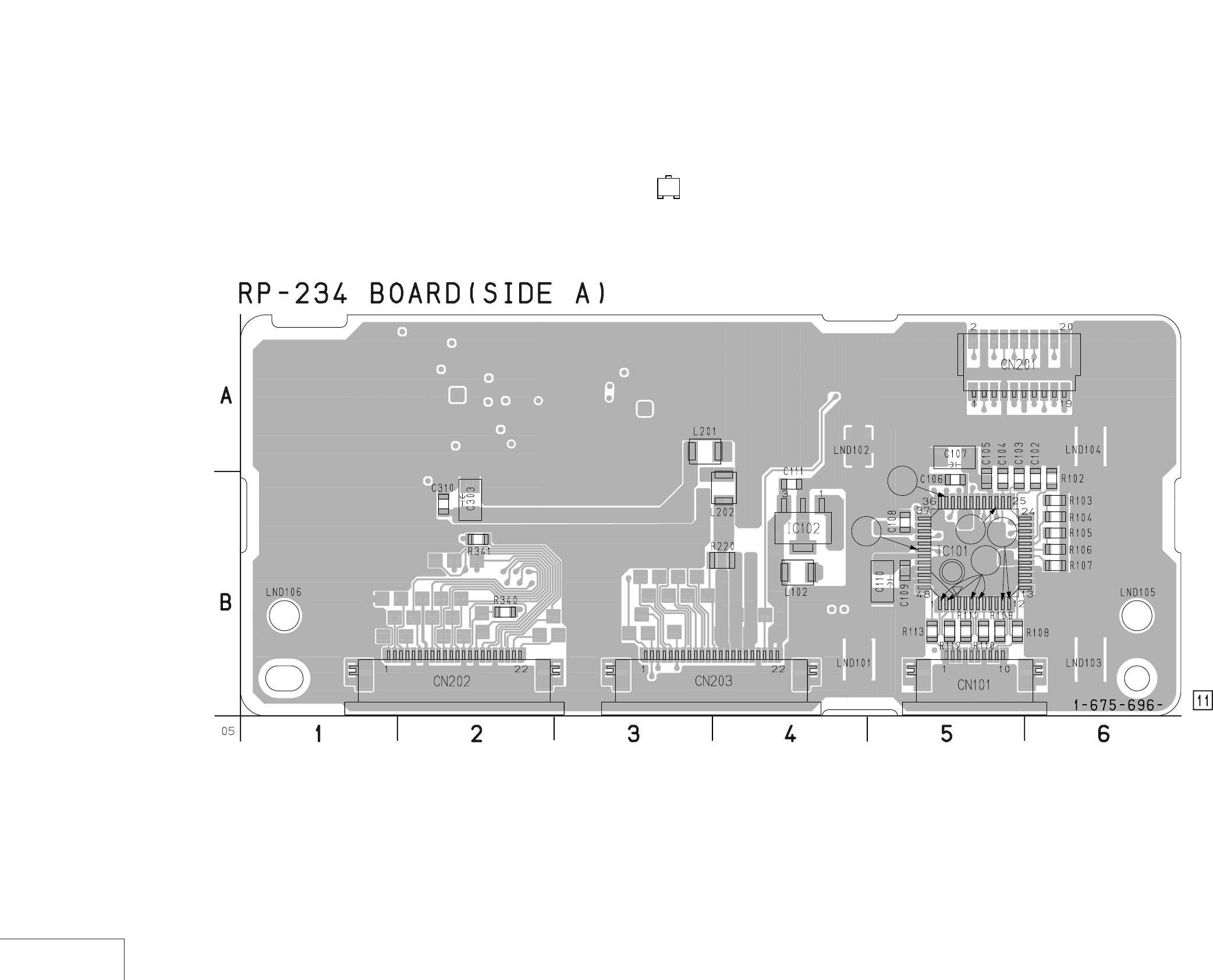
DSR-50/50P
4-7 4-8
4-2. PRINTED WIRING BOARDS AND SCHEMATIC DIAGRAMS
RP-234 (REC/PB AMP) PRINTED WIRING BOARD
– Ref. No.: RP-234 board; 30,000 series –
REC/PB AMP
RP-234
• For Printed Wiring Board.
•RP-234 board is six-layer print board. However, the patterns of
layers 2 to 5 have not been included in the diagram.
•There are a few cases that the part isn't mounted in this model
is printed on this diagram.
•See page 4-153 for printed parts location.
•Chip transistor
EB
C
5
4
3
6
7
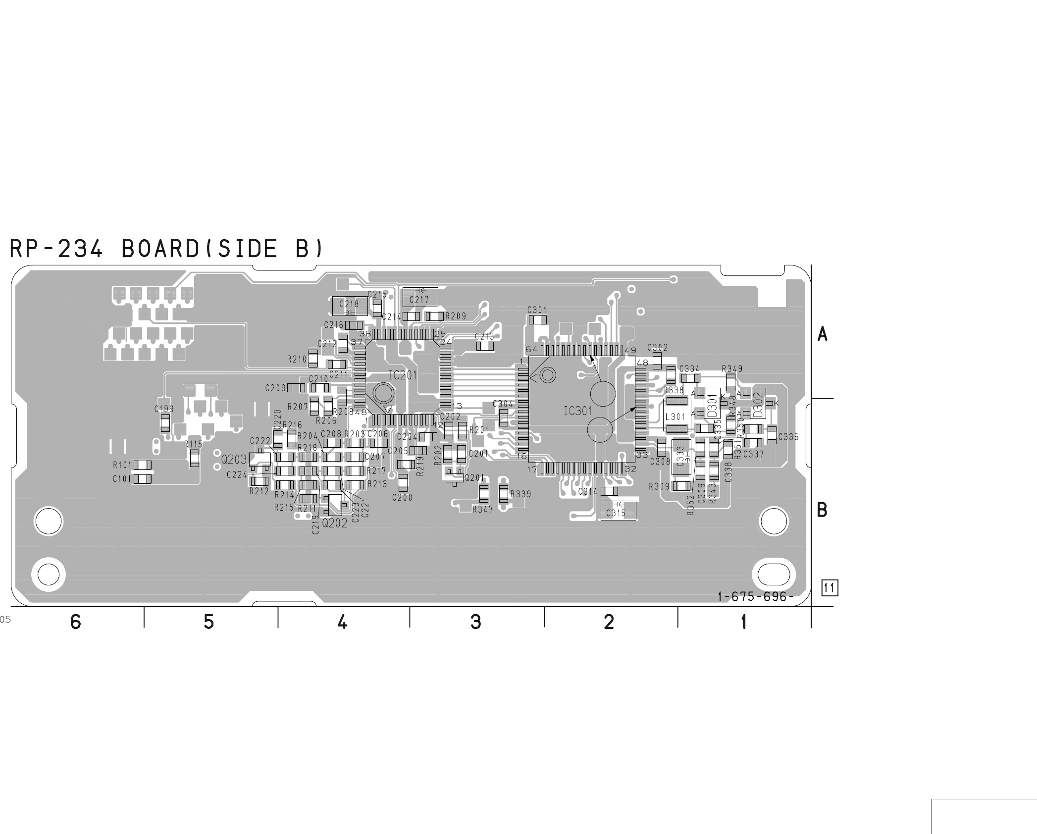
DSR-50/50P
4-9 4-10 REC/PB AMP
RP-234
2
1
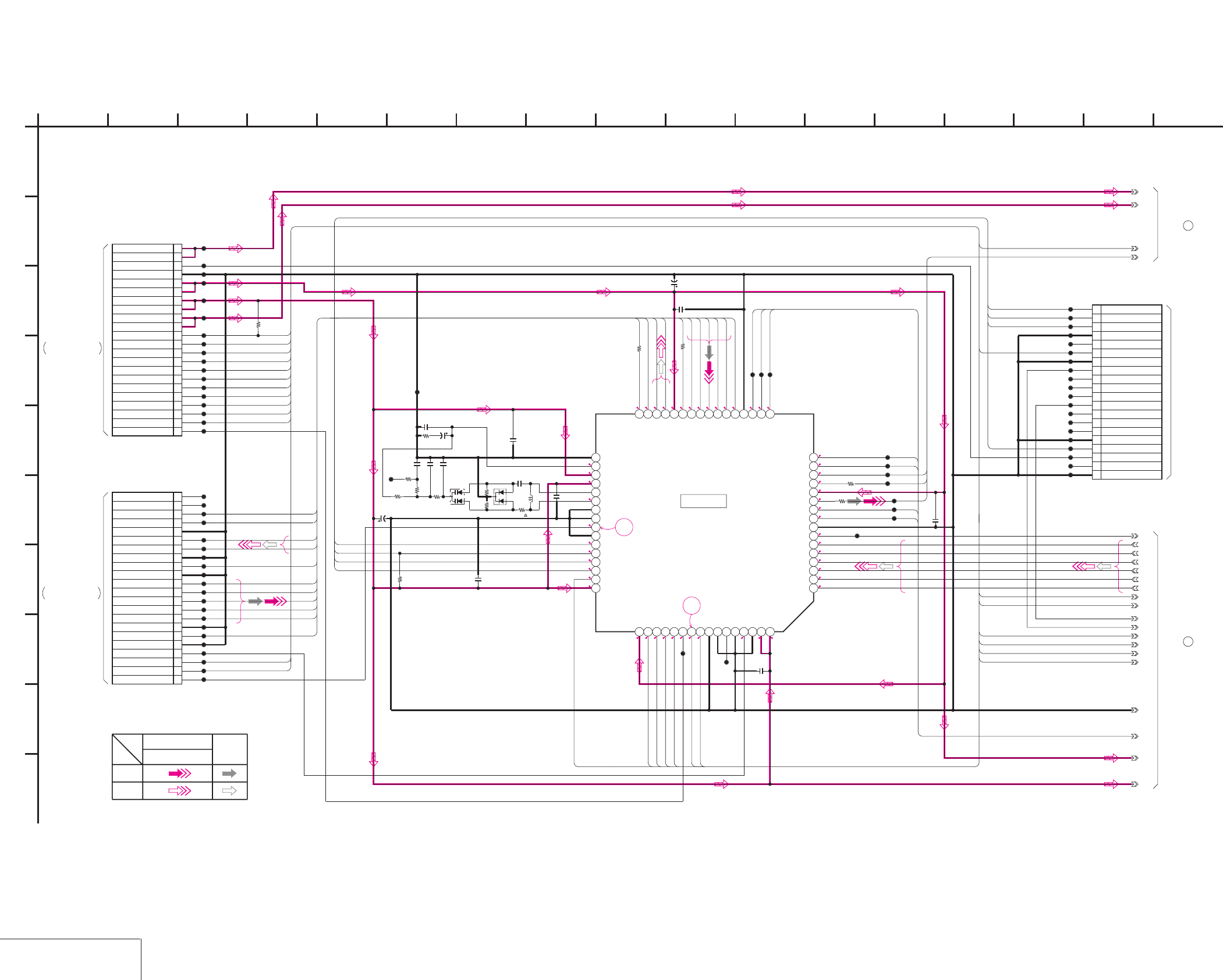
DSR-50/50P
4-11 4-12
RP-234 (REC/PB AMP 1) SCHEMATIC DIAGRAM • See page 4-7 for RP-234 printed wiring board. • See page 4-147 for waveforms.
REC/PB AMP 1
RP-234 (1/2)
R0.9/P0
1 R1.9/P0
1
2.8 R1.9/P0
NO MARK:REC/PB MODE
R:REC MODE
P:PB MODE
2
R1.2/P0
0
0
R0.2/P1.1
R0.2/P1.4
R0.2/P1.4
R0.2/P1.4
R0.2/P1.4
R0.2/P1.4
R0.2/P1.4
R0/P1.2 0
R0/P0.8
R0/P0.8
21
R1.1/P0
R1.1/P0
R1.1/P0
R1.1/P0
R1.1/P0
0
R2/P0
02
2.8
0
1.7
1.3
2.7
1.4
1.4
2.7
2.8
2.7
2.7
2.7
20
1.4
1.4
0.1
1.4
2.8
2.8
1
2
0.01u
C314
100k
R338
0.01u
C308
0.01u
C301
0
R341
6.3V
10u
C315
XX
R343
0.1u
C309
F712504DPM-TEB
IC301
1 2 3 4 5 6 7 8 9 10 11 12 13 14 15 16
17181920212223242526272829303132
33343536373839404142434445464748
49 50 51 52 53 54 55 56 57 58 59 60 61 62 63 64
0
R340
0.01u
C304
R309
15
0.01u
C310
0
R339
0.01u
C302
6.3V
10u
C303
20P
CN201
1 TCK
2 TMS
3 TDI
4 GND
5N.C.
6 JSWP
7 GND
8 RF_MONITOR
9N.C.
10 N.C.
11 N.C.
12 RF_IN
13 N.C.
14 N.C.
15 N.C.
16 GND
17 TDO
18 C1ERRP
19 N.C.
20 GND
CL103
CL104
CL105
CL106
CL107
CL108
CL109
CL110
CL111
CL112
CL113
CL114
CL115
CL116
CL117
CL118
CL119
CL120
CL121
CL122
CL123
CL124
CL125
CL126
CL127
CL128
CL129
CL130
CL131
CL132
CL133
CL134
CL135
CL136
CL137
CL138
CL139
CL140
CL141
CL142
CL143
CL144
CL145
CL146
CL147
CL148
CL152
CL154
CL155
CL156
CL157
CL158
CL159
CL160
CL161
CL166
CL167
CL168
CL169
0
R347
CL170
22P
CN203
1DSWP
2CONT_O
3CONT_E
4SC_WD
5
CLK150
6SWP
7XRST
8MSCK
9DRP_SO
10DRP_SI
11XCS_TRF
12
XCS_TRX
13 5V
14 5V
15 3V
16 3V
17 1.9V
18 1.9V
19 GND
20 C1ERRP
21 RF 6V
22 RF 6V
22P
CN202
1CLK135
2REEL_EVR
3CAP_EVR
4ATF
5 GND
6TXST
7 GND
8TXDT4
9TXDT3
10TXDT2
11TXDT1
12TXDT0
13 GND
14CRCK
15 GND
16XTDT1
17XTDT0
18 GND
19XTSY
20HPCK
21 N.C.
22 N.C.
CL200
CL201
CL202
CL203
CL204
CL205
CL206
CL207
CL208
CL209
CL210
CL211
CL212
XX
L301
XX
C335
XX
D301
XX
R348
10k
R349
XX
D302
XX
R350
XX
R351
XX
R352
XX
C336
XX
C337
XX
C338
4V
3.3u
C333
CL400
470k
R220
0
C334
1
A
RF6V
5V
1-1
1-2
2-1
2-8
2-10
2-12
2-11
2-13
2-15
2-9
2-14
1.9V
GND
2-16
3V
2-7
2-3
2-2
2-6
2-4
2-5
CONT1
ALL_PS
CONT0
RECA2
PLLSW
PLLMSK
TXDT4
TXST
SW_PS
XRST
XSCK
CLK150
SC_WD
MSO
XCS_TRX
CRCK
TXDT2
TXDT3
TXDT1
HPCK
XTSY
XTDT0
XTDT1
TXDT0
RECA1
RECCK
TMS
TCK
TRX_TDO
MSI
XSCK
MSO
XCS_TRF
REEL_EVR
MSI
MSO
XSCK
CONT_O
CONT_E
SC_WD
CLK150
SWP
XRST
XTSY
HPCK
TXST
TXDT4
TXDT3
TXDT2
TXDT1
TXDT0
CRCK
XTDT1
XTDT0
RECDT
TCK
TMS
TRX_TDI
TRX_TDO
XCS_TRX
SWP
XCS_TRF
REEL_EVR
CAP_EVR
SWP
CAP_EVR
TRX_TDI
13
I
G
9154102
D
712
B
16
J
6
E
F
3
C
17811
H
5 14
05
RP-234 BOARD (2/2)
1
JIG PIN
RP-234 BOARD (2/2)
2
THROUGH THE
CN4401
JC-20 BOARD (7/14)
SIGNAL
REC
SIGNAL PATH
AUDIO
VIDEO SIGNAL
Y/CHROMA
PB
XX MARK:NO MOUNT
-REF.NO.:30,000 SERIES-
REC/PB AMP 1
RP-234 BOARD (1/2)
IC301
(Note)
Note:Resistor is mounted to the location
where C334 is printed.
FRJ-1 FLAT CABLE
(SEE PAGE 4-32)
FRJ-1 FLAT CABLE
(SEE PAGE 4-32)
THROUGH THE
CN4402
JC-20 BOARD (7/14)
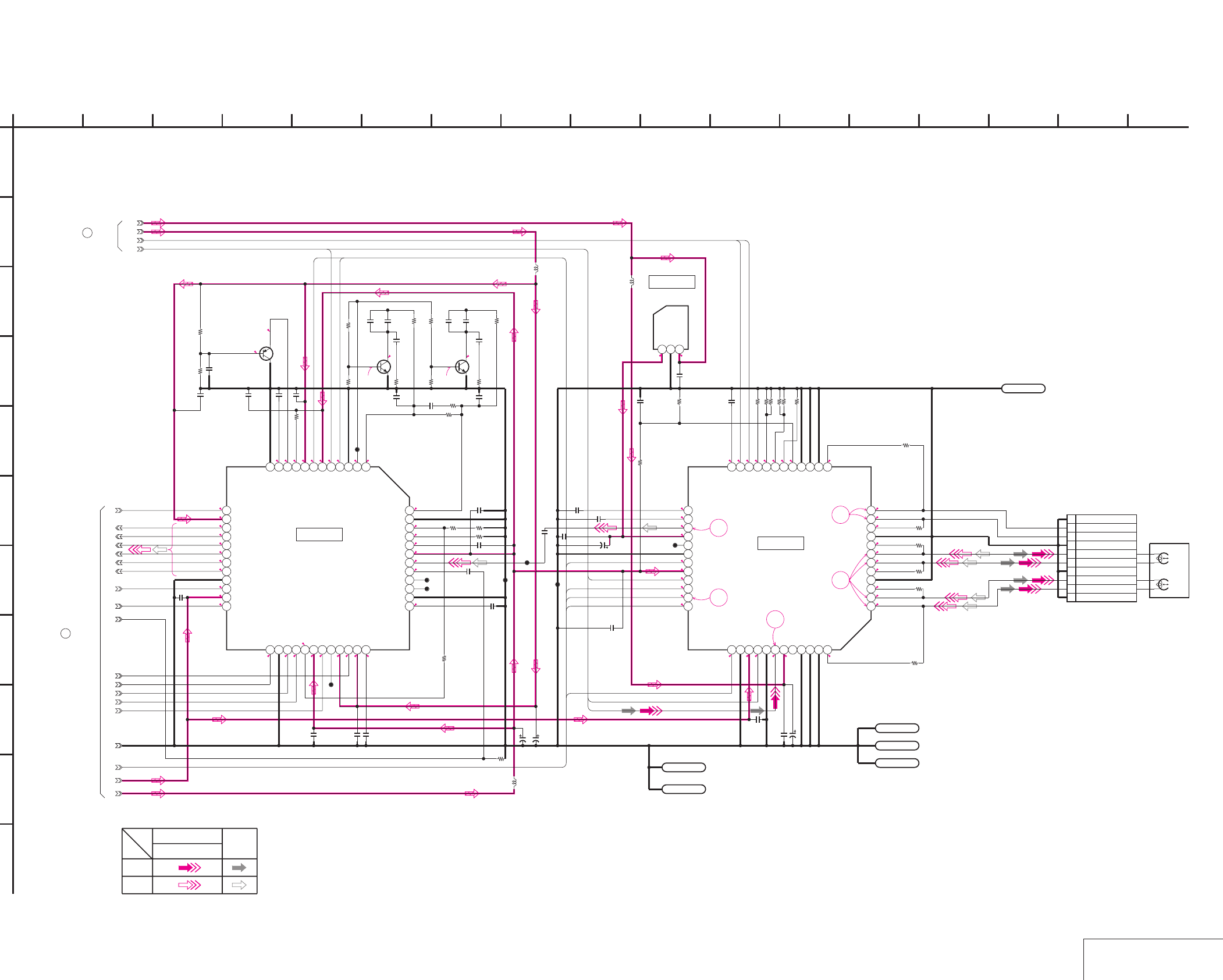
DSR-50/50P
4-13 4-14
RP-234 (REC/PB AMP 2) SCHEMATIC DIAGRAM • See page 4-7 for RP-234 printed wiring board. • See page 4-147 for waveforms.
REC/PB AMP 2
RP-234 (2/2)
NO MARK:REC/PB MODE
R:REC MODE
P:PB MODE
5
R0.2/P1.1
R0.2/P1.4
2.7
2
0
2.7
R2.6/P1.4
1.4
2
1.4
2.8
R3.7/P2.35
0.9
5
3.7
2.8
0.2
2.8
0
2.2
0.1
2.2
2.1
R1.9/P0
0
R1.2/P0
2.8
05
2.8
R0/P2.7
R0/P3.2
R0/P2.7
20
R0.7/P0.1
0
R0.7/P0.1
55.5
R0/P2.3
R0/P2.3
R4.8/P2.7
5
R1.9/P0
2.8
R1.9/P0
R2/P0
1
2
0
2.7
R2.3/P1.3
2.7
2.7
1.3
1.8
2.7
R3.9/P1.8
R3.9/P1.8
R3.9/P1.8
R3.9/P1.8
R4.2/P1.7
R4.1/P1.7
R4.2/P1.7
R4.2/P1.7
R4.1/P1.7
R4.2/P1.7
R0.9/P0
5.5
R1.2/P0
20
R4.1/P1.7
R4.1/P1.7
R0.2/P1.4
R0.2/P1.4
R0.2/P1.4
R0.2/P1.4
R0.2/P1.4
3
4
5
6
7
10k
R208
47p
C208
0.1u
C104
150k
R203
0.01u
C108
6.3V
10u
C217
220
R112
12k
R207
47p
C206
0.01u
C101
0.01u
C105
470p
C216
10uH
L201
10k
R101
220
R111
0.1u
C210
0.01u
C214
1M
R209
10V
10u
C107
LND104
GND
10V
10u
C218
220
R110
2SB1462J-QR(K8).SO
Q201
0.01u
C215
CXA2072R-T4
IC101
123456789101112
1314
15161718192021222324
252627282930313233343536
37 38 39 40 41 42 43 44 45 46 47 48
4700
R115
LND103
GND
0.01u
C109
220
R109
0.01u
C202
12k
R206
0.01u
C204
10P
CN101
1GND
2XEVEN
3YEVEN
4GND
5XODD
6YODD
7GND
8XSDL
9YSDL
10 GND
0.1u
C103
22k
R102
0.01u
C205
0.01u
C211
0.01u
C209
220
R108
22k
R107
0.01u
C213
68
R210
10uH
L202
22k
R106
0.033u
C207
0.1u
C102
0.01u
C200
10k
R201
6800
R202
LND101
GND
15k
R103
470
R204
LND102
GND
470p
C212
0.01u
C201
20kR104
0.01u
C199
22kR105
0.01u
C106
220
R113
10uH
L102
10V
10u
C110
2SC4851-TL
Q202
2SC4851-TL
Q203
4700
R212
2200R213
4700
R211
2200
R214
120
R215
2200
R216
3300p
C219 3300p
C220
3900p
C221
3900p
C222
8200p
C223
8200p
C224
100
R217
100
R218
CL149
CL150
CL151
CL153
CL162
CL163
CL164
CL165
0
R219
LND105
GND
LND106
GND
S-81350HG-KD-T1
IC102
123
0.1u
C111
RF6V
5V
1-1
1-2
2-1
2-8
2-9
2-10
2-11
2-13
2-15
2-14
2-12
GND
2-16
3V
1.9V
CXA2071R-T4
IC201
123456789101112
131415161718192021222324
25 26 27 28 29 30 31 32 33 34 35 36
37 38 39 40 41 42 43 44 45 46 47 48
1
A
2-2
2-3
2-4
2-5
2-6
2-7
PLLMSK
RECDT
PLLSW
RECA1
ALL_PS
CONT1
CONT0
SW_PS
RECA2
RECCK
RECDT
CONT_O
CONT_E
RP-234 BOARD (1/2)
1
RP-234 BOARD (1/2)
2
DRUM HEAD
M901(1/2)
ODD
EVEN
SIGNAL
VIDEO SIGNAL
REC
Y/CHROMA
PB
AUDIO
SIGNAL PATH
134
I
10
G
9152 12
REC/PB AMP 2
D
B
-REF.NO.:30,000 SERIES-
7 16
J
XX MARK:NO MOUNT
6
RP-234 BOARD (2/2)
E
F
3
C
17811
H
5 14
05
k
IC201 IC101
IC102
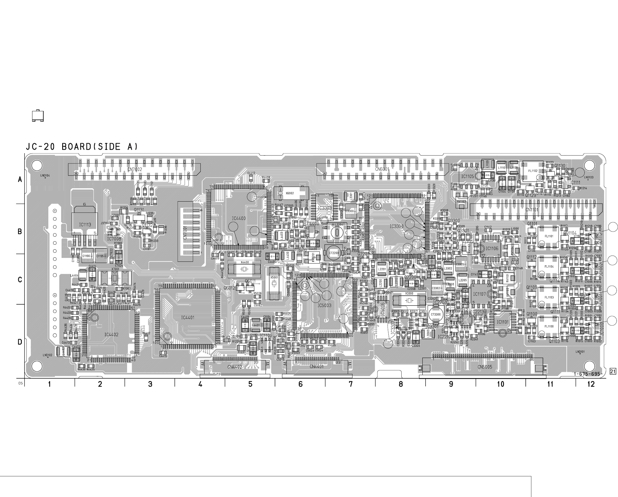
DSR-50/50P
JC-20 (VIDEO PB AMP, VIDEO A/D CONVERTER, CHROMA MIX, AFC, VFD, SFD, TFD, DV INTERFACE, MECHANISM CONTROL, AUDIO, POWER SUPPLY) PRINTED WIRING BOARD
– Ref. No.: JC-20 board; 20,000 series –
4-15 4-16
VIDEO PB AMP, VIDEO A/D CONVERTER, CHROMA MIX, AFC, VFD, SFD, TFD, DV INTERFACE, MECHANISM CONTROL, AUDIO, POWER SUPPLY
JC-20
• For Printed Wiring Board.
•JC-20 board is six-layer print board. However, the patterns of
layers 2 to 5 have not been included in the diagram.
•There are a few cases that the part isn't mounted in this model
is printed on this diagram.
•See page 4-153 for printed parts location.
•Chip transistor
EB
C
31
30
32
33 34 35
36 37
38
29
16 28
27
26
25 24
5
3
2
4
1
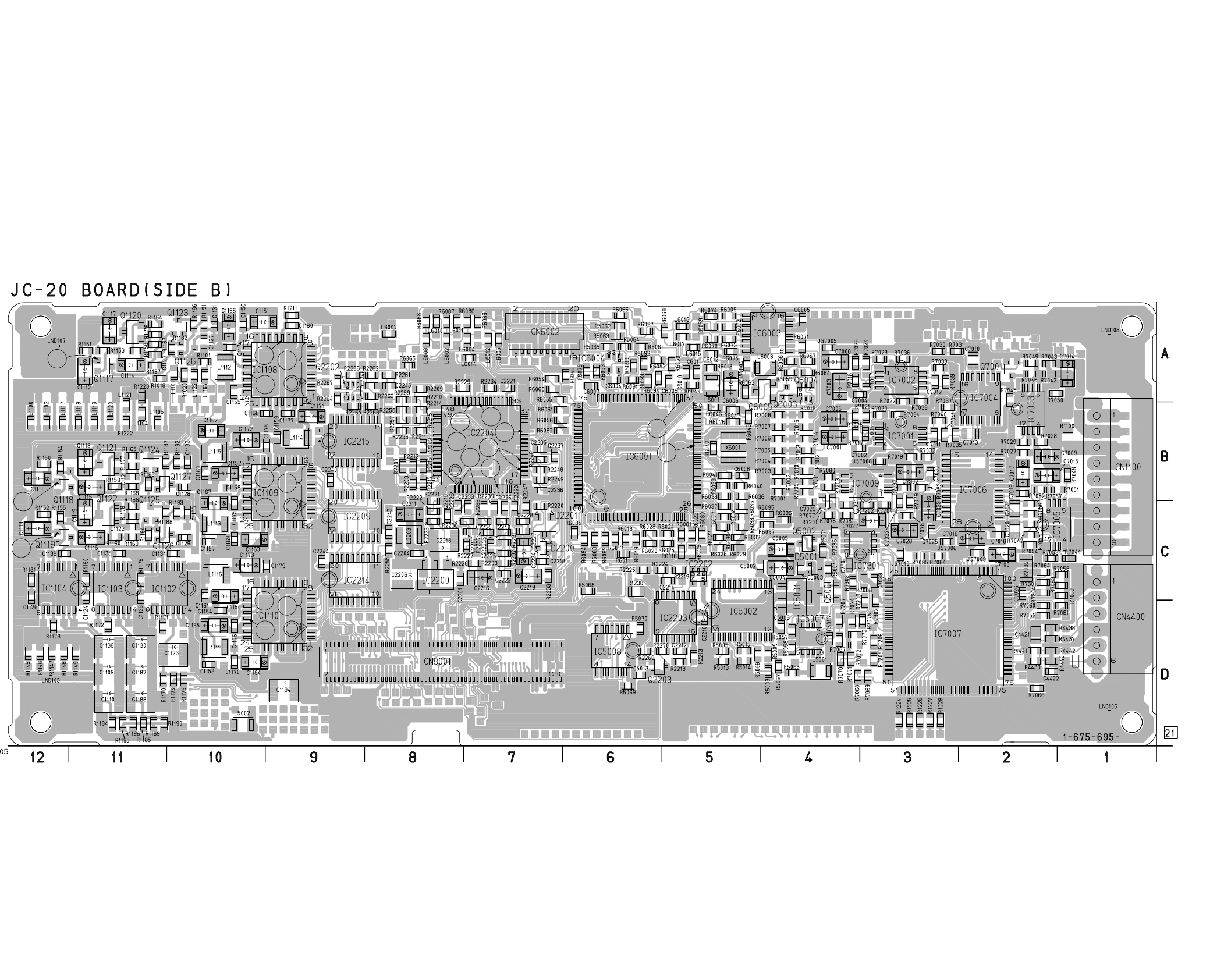
DSR-50/50P
4-17 4-18
VIDEO PB AMP, VIDEO A/D CONVERTER, CHROMA MIX, AFC, VFD, SFD, TFD, DV INTERFACE, MECHANISM CONTROL, AUDIO, POWER SUPPLY
JC-20
6
7
8
10
9
11
10
12
13
10
14
15
19
17 18
20
23
21
22
40
39
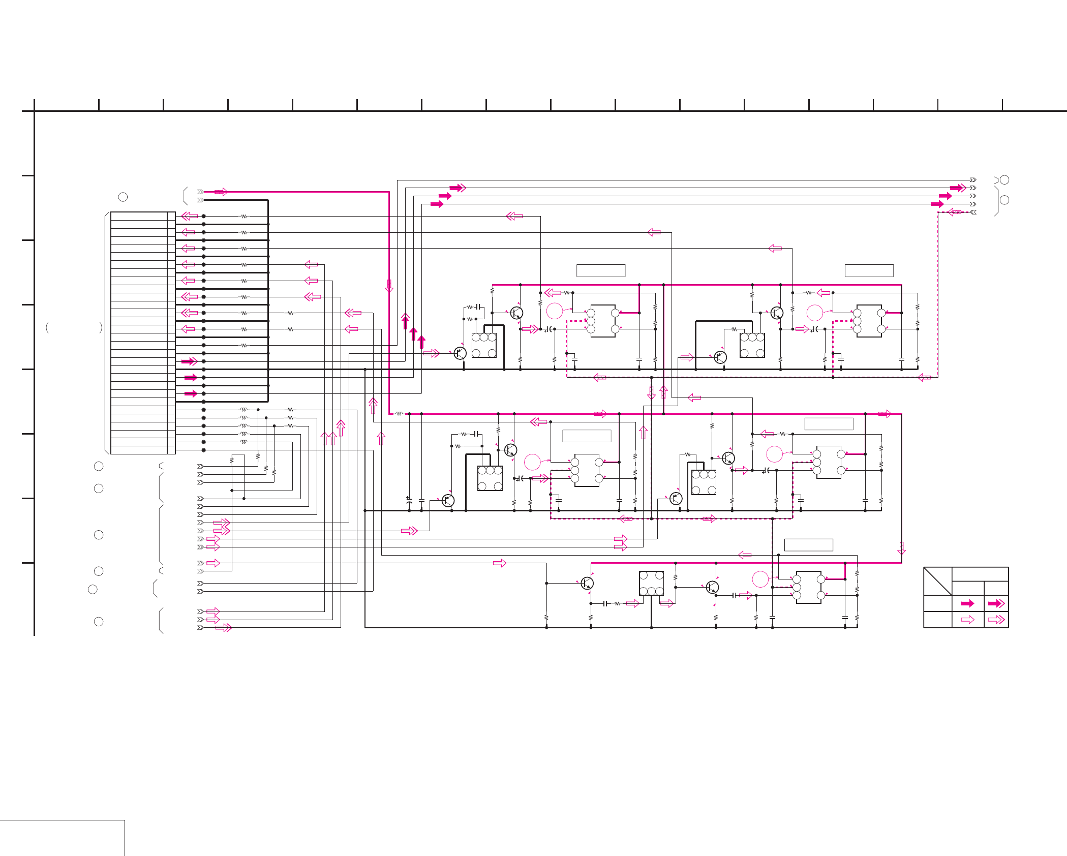
DSR-50/50P
4-19 4-20
JC-20 (VIDEO PB AMP) SCHEMATIC DIAGRAM • See page 4-15 for JC-20 printed wiring board. • See page 4-147 for waveforms.
VIDEO PB AMP
JC-20 (1/14)
NO MARK:REC/PB MODE
50.7
-4.9
0.4 0.4
1
-4.9
0.4 0.4
51.2
3
-4.9
0.40.4
50.7
2
2.2
2.8
5
3.9
3.3
3.9
5
2.8
2.2
3.3
2.7
3.2
3.5
5
4.1
2.8
2.2
5
4.4
5
5
4
5
2.9
2.3
3.3
0.6 5
0.4 0.4
-4.9
4
-4.9
1.2 5
0.40.4
5
R1120
470
R1127
1k
R1112
1k
R1129
1k
R1134
470
R1117
1k
R1139
1k
R1143
470
R1136 1k
R1111
220 C1106
22p
C1101
0.01u
L1108
10uH
CL1111
CL1110
CL1114
CL1123
CL1119
CL1126
CL1117
CL1130
CL1127
CL1132
CL1128
CL1133
CL1124
CL1134
CL1112
C1100
10u
6.3V
Y_OUT
CR_OUT
CB_OUT
Q1109
2SA1576A-T106-R
Q1101
2SA1576A-T106-R
Q1111
2SC4081T106R
Q1104
2SC4081T106R
Q1112
2SA1576A-T106-R
Q1114
2SC4081T106R
FL1103
123
4
6
FL1101
123
4
6
FL1104
123
4
6
C_OUT
30P
CN1101
1PANEL Y
2GND
3PANEL CR
4GND
5PANEL CB
6GND
7CB LINE
8GND
9CR LINE
10GND
11Y LINE
12GND
13MONITOR Y
14GND
15MONITOR C
16GND
17AFC Y
18GND
19Y_IN
20GND
21CR_IN
22GND
23CB_IN
24GND
25VD HD
26VFD_VD
27VFD_HD
28XI/O SYNC HI
29XI/O SYNC VFD
30V_SYNC
CL1138
CL1113
CL1125
CL1135
CL1136
CL1115
CL1116
CL1120
CL1122
CL1129
CL1131
CL1137
CL1139
CL1121
CL1118
L1101
L1107
0.01u
C1107
1k
R1118
2200
R1125
2200
R1114
XX
R1110
1k
R1123
VFD_HD
2SA1576A-T106-R
Q1100
1k
R1109
FL1100
123
4
6
1k
R1113
470
R1116
2SC4081T106R
Q1103
Y_SIKISA
DPB_CBOUT
DPB_CROUT
DPB_YOUT
XI/O_SINC_HI
L1122
2SC4081T106R
Q1129
2SC4081T106R
Q1130
VFD_VD
0.1u
C1182
0
R1215
LM7131BCM5X
IC1111
123
45
1500
R1212
470
R1214
22k
R1213
0.01u
C1183
0.01u
C1181
1500
R1218
22k
R1216
0
R1219
22u
4V
C1184
470
R1217
0.1u
C1186
LM7131BCM5X
IC1112
123
45
0.1u
C1185
820
R1002
0
R1000
22u
4V
C1008
0.1u
C1000
820
R1001
0.1u
C1001
22k
R1015
LM7131BCM5X
IC1000
123
45
XX
R1220 0
R1221
820
R1008
XX
R1003
0.1u
C1004
22k
R1004
LM7131BCM5X
IC1001
123
45
0.1u
C1003
820
R1007
22u
4V
C1002
0
R1006
0
R1005
22u
4V
C1005
0
R1012
LM7131BCM5X
IC1002
123
45
0.1u
C1007
0
R1011
820
R1014
820
R1013
XX
R1009
22k
R1010
0.1u
C1006
VD_HD
HUE_ADJ
PB/XEE
S/XV
XX
R1019
XXR1021
L1001
XX
R1020
0
R1017
0
R1018
0
R1016
L1000
0
R1101
V_FROM_SYNCGEN
0
R1222
0
R1223
FL1102
123
4
6
10
R1102
10
R1103
10
R1105
10
R1104
10
R1115
10
R1121
10
R1107
10
R1119
10
R1122
OSDVD
+5V
GND
AFC_Y
Y_IN
CR_IN
CB_IN
-5V
1
A
33p
C1103
220
R1108
2 1612
G
68
D
E
JC-20 BOARD (1/14)
B
7
05
151310 11
C
H
F
3 14945
XX MARK:NO MOUNT
VIDEO PB AMP
-REF.NO.:20,000 SERIES-
Y
REC
CHROMA
PB
VIDEO SIGNAL
SIGNAL PATH
JC-20 BOARD (4/14)
8
9JC-20 BOARD (2/14)
2JC-20 BOARD (9/14)
5JC-20 BOARD (5/14)
3JC-20 BOARD (11/14)
JC-20 BOARD (5/14)
4
JC-20 BOARD (14/14)
6
JC-20 BOARD (14/14)
7
JC-20 BOARD (14/14)
1
IC1000
(SEE PAGE 4-87)
FVJ-13 FLAT CABLE
CN332
THROUGH THE
VD-28 BOARD (7/15)
IC1002
IC1112
IC1001
IC1111
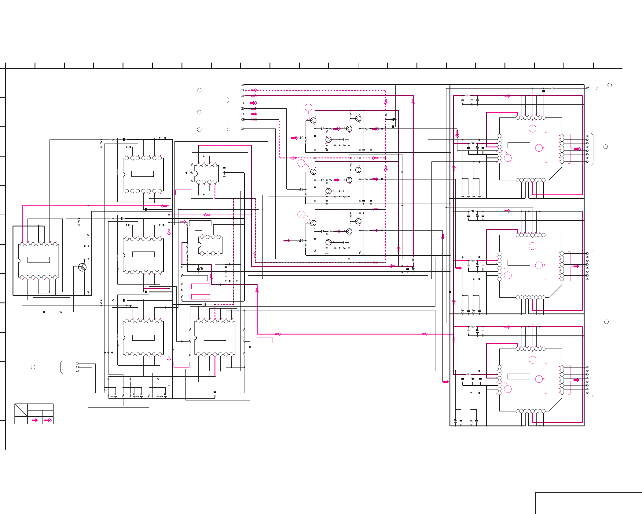
DSR-50/50P
4-21 4-22
JC-20 (VIDEO A/D CONVERTER) SCHEMATIC DIAGRAM • See page 4-15 for JC-20 printed wiring board. • See page 4-147 for waveforms.
VIDEO A/D CONVERTER
JC-20 (2/14)
NO MARK:REC/PB MODE
R:REC MODE
P:PB MODE
1
3.2
3.2
2.9
R1.6/P4
3.2
3.2
3.2
3.2
1.2
3.2
3.2
3.2
R0.8/P3.2
R1.3/P3.2
R1.3/P3.2
R1.6/P3.2
R1.2/P3.2
R1.2/P3.2
R1.2/P3.2
R1.4/P3.2
11
10
9
R1.6/P3.2
R1.6/P3.2
R1.8/P3.2
R1.4/P3.2
R1.4/P3.2
R1.4/P3.2
R1.4/P3.2
R1.4/P3.2
1
3.2
3.2
3.2
3.2
3.2
3.2
3.2
3.2
1.2
R1.9/P4
2.9
3.2
13
10
12
R1.1/P3.2
R1.5/P3.2
R1.3/P3.2
R1.3/P3.2
1
3.2
3.2
3.2
3.2
3.2
3.2
3.2
3.2
1.2
R1.9/P4
2.9
3.2
15
10
14
R1.3/P3.2
R1.1/P3.2
R1.9/P3.2
R1.4/P3.2
5
R1.6/P4.4
R2.2/P5
R1.6/
P4.6
-4.9
R0.9/P0.7
R1.6/
P4.6
R1.2/P1
5
-0.3
-0.9
6
7
5
R2/P1.7
5
R1.9/P4.4
R0.9/P0.7
R2/
P4.5
R2.6/P5
-0.9
-4.9
-0.3
R2/
P4.5
5
R2/P1.7
5
R1.9/P4.4
R0.9/P0.7
R2/
P4.5
R2.6/P5
-0.9
8
-4.9
-0.2
R2/
P4.5
2.92.92.95
-4.9111
R1.2/P1
R1.2/P1
R1.2/P1
R1.1/P0.2
R1.1/
P0.7
R1.1/
P0.7
5 1.2 1.2 1.2
2.6
3.2
5
R2/P1.7
22
R2/P1.6
R2/P1.6
R2/P1.7
R2/
P1.7
R2/
P1.6
2
R2/
P1.6
5
R2/P1.6
R2/
P1.7
R2/P1.7
R2/P1.6
22
R2/P1.7
2 1115111
2.9 2.9 2.9 2.9 2.9 2.9-4.9
55
5
R1.1/P0.7
R1.1/P0.7
55
R2/P1.6
R2/P1.6
R2/P1.6
R2/P1.6
RV1103
Y CLAMP
REF.VOLTAGE
A/D CONV.
RV1100
REF.VOLTAGE 1
RV1101
REF.VOLTAGE 2
A/D CONV.
CR CLAMP
RV1102
REF.VOLTAGE
RV1104
CB CLAMP
REF.VOLTAGE
R1174
XX
R1158
0
R1164
2200
R1153
1k
R1167
100
R1176
4700
R1182
1k
R1208
0
R1209
1k
R1175
3300
R1169
100
R1184
1k
R1193
100
R1206
1k
R1188
1800
R1185
4700
R1190
15k
R1207
4700
R1210
1k
R1196
15k
R1205
1k
R1156
4700
R1180
10k
R1194
4700
R1179
1k
R1170
4700
R1181
10k
R1204
1500
R1157
XX
R1197
0
R1183
1k
R1154
1k
R1166
10k
R1168
100
R1178
4700
R1191
100
R1177
4700
R1165
10k
R1155
1k
R1192
100
R1159
0
R1160
0
R1151
22k
R1186
1800
R1187
1800
R1195
XX
R1189
XX
R1163
XX
R1211
0
R1201
47
R1200
8200
R1199
15k
R1171
1k
R1173
4700
R1172
4700
R1203
0
R1152
22k
R1202
390
R1150
22k
R1161
XX
R1162
XX
R1198
1500
C1129
0.01u
C1154
0.01u
C1128
0.01u
C1127
0.01u C1131
10p
C1146
0.01u
C1143
0.01u
C1147
0.01u
C1126
0.01u
C1133
10p
C1140
0.01u
C1125 0.01u
C1124 0.01u
C1156
0.01u
C1176
0.01u
C1174
0.01u
C1177
0.01u
C1168
0.01u
C1158
0.01u
C1169
0.01u
C1132
10p
C1175
0.01u
C1153
XX
C1161
XX
C1157
XX
C1178
0.01u
C1160
XX
C1155
XX
C1159
XX
C1180
XX
C1120
XX
C1121
XX
C1122
XX
C1170
0.01u
C1179
0.01u
C1134
0.01u
C1135
0.01u
C1148
0.01u
C1149
0.01u
C1142 0.01u
C1145
0.01u
C1137
0.01u
C1138
0.01u
L1110
10uH
L1112 10uH
L1109
10uH
L1114
10uH
L1116
10uH
L1111 10uH
L1113 10uH
L1115
10uH
CL1159
CL1146
CL1158
CL1147
CL1157
CL1148
CL1145
CL1160
CL1149
CL1156
CL1174
CL1150
CL1167
CL1161 CL1173
CL1170
CL1165
CL1152
CL1155
CL1151
CL1175
CL1154
CL1166
CL1162
CL1168
CL1164
CL1171
CL1153
CL1163
CL1178
CL1172
CL1177
CL1176
CL1169
C1114
1u
16V
C1117
10u
6.3V
C1144
10u
6.3V
C1141
10u
6.3V
C1116
1u
16V
C1119
10u
6.3V
C1151
10u
6.3V
C1162
10u
6.3V
C1171
10u
6.3V
C1166
10u
6.3V
C1118
10u
6.3V
C1164
10u
6.3V
C1115
1u
16V
C1172
10u
6.3V
C1152
10u
6.3V
C1163
10u
6.3V
C1150
10u
6.3V
C1165
10u
6.3V
C1112
22u
4V
C1167
10u
6.3V
C1173
10u
6.3V
C1130
100u
6.3V
C1139
10u
6.3V
C1136
100u
6.3V
C1123
47u
6.3V
C1111
22u
4V
C1113
22u
4V
IC1101 TC74HC4066AFS-EL
1234567
891011121314
IC1107
NJM431M(TE2)
1234
5678
IC1105
BA10358F-E2
1234
5678
IC1110
CXD2300Q-T4
12345678
910111213141516
1718192021222324
25 26 27 28 29 30 31 32
IC1109
CXD2300Q-T4
12345678
910111213141516
1718192021222324
25 26 27 28 29 30 31 32
IC1108
CXD2300Q-T4
12345678
910111213141516
1718192021222324
25 26 27 28 29 30 31 32
SPCK1
Q1117
2SC4081T106R
Q1126
2SC4081T106R
Q1119
2SC4081T106R
Q1128
2SC4081T106R
Q1118
2SC4081T106R
Q1127
2SC4081T106R
Q1125
2SA1576A-T106-R Q1124
2SA1576A-T106-R
Q1123
2SA1576A-T106-R
Q1120
2SC3326N-TE85L-B
Q1122
2SC3326N-TE85L-B
Q1121
2SC3326N-TE85L-B
Q1116
UN5213-TX
IC1104 BA10324AFV-E2
1234567
891011121314
IC1103 BA10324AFV-E2
1234567
891011121314
IC1102 BA10324AFV-E2
1234567
891011121314
IC1106 BA10324AFV-E2
1234567
891011121314
RV1102
2200
RV1100
4700
RV1101
4700
RV1103
1k
RV1104
2200
100u
6.3V
C1109
100u
6.3V
C1110
100u
6.3V
C1187
100u
6.3V
C1188
47u
6.3V
C1194
AFH_CLP
CB_IN
CR_IN
Y_IN
+5V
VIDEO_-5V
GND
R1106
XX
CL1181
Y_CLP_ERR
CR_CLP_ERR
CB_CLP_ERR
1
A
CB7
CB6
CB5
CB4
CB1
CB3
CB2
CB0
CR4
CR1
CR5
CR2
CR6
CR3
CR0
CR7
Y1
Y4
Y3
Y7
Y2
Y5
Y6
Y0
-5V
XX MARK:NO MOUNT
VIDEO A/D CONVERTER
-REF.NO.:20,000 SERIES-
11
JC-20 BOARD (4/14)
2 16
L
I
20
K
12
G
68
D
E
JC-20 BOARD (2/14)
B
7
05
19151310 1711
C
21
H
F
3 18
J
14945
M
13
JC-20 BOARD (4/14)
JC-20 BOARD (5/14)
14
JC-20 BOARD (3/14)
15
9
JC-20 BOARD (1/14)
10
JC-20 BOARD (14/14)
12
JC-20 BOARD (9/14)
CHROMA
SIGNAL PATH
Y
REC
VIDEO SIGNAL
IC1108
IC1109
IC1110
IC1106IC1104
IC1103
IC1102
IC1101
IC1105
IC1107
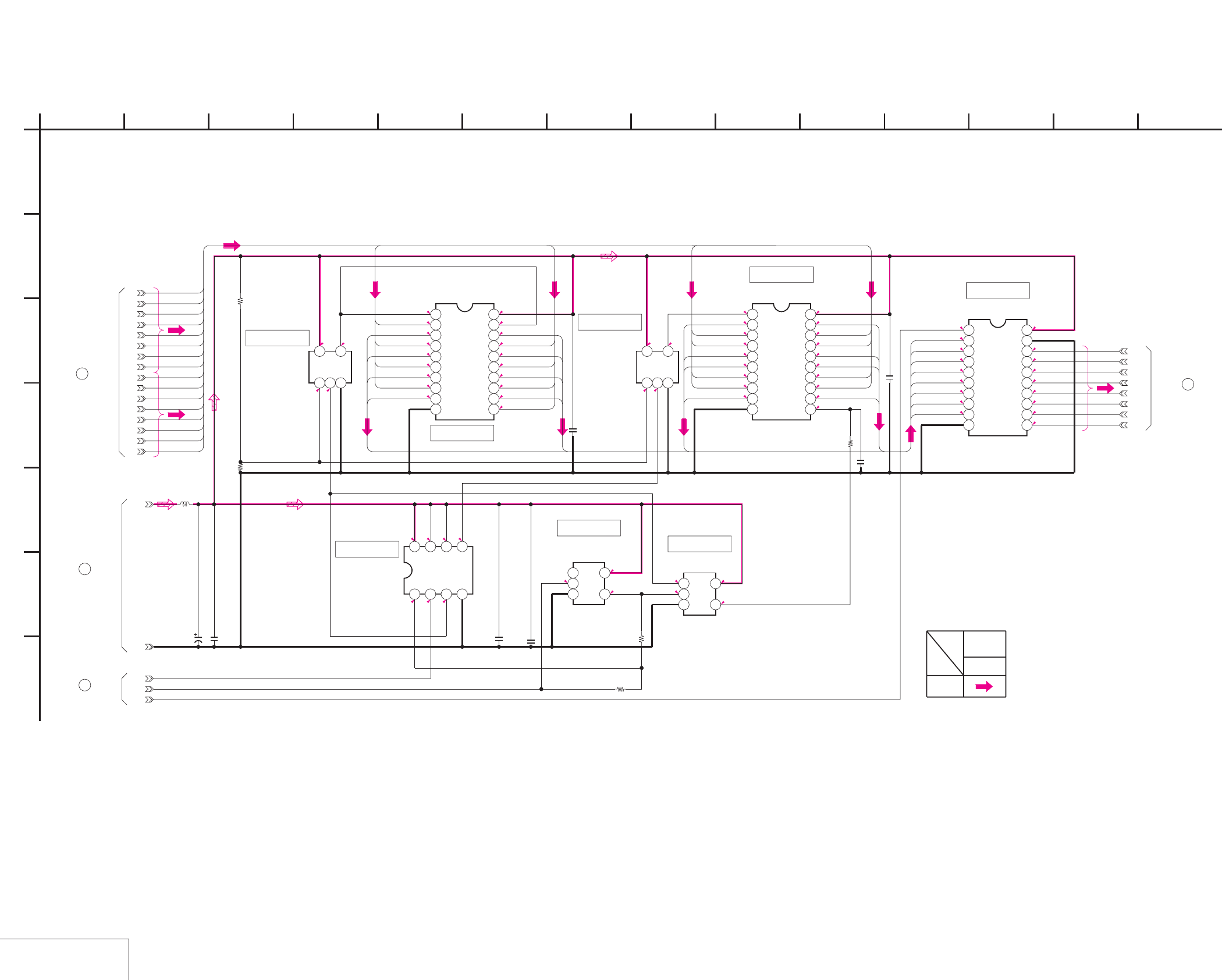
DSR-50/50P
4-23 4-24
JC-20 (CHROMA MIX) SCHEMATIC DIAGRAM • See page 4-15 for JC-20 printed wiring board.
CHROMA MIX
JC-20 (3/14)
2.81.4
NO MARK:REC/PB MODE
R:REC MODE
P:PB MODE
1.4
2.8
1.4
2.8 1.42.82.8
1.41.51.2
1.2
2.8
1.7
1.4
1.7
2.8
0.9
1.42.8
1.4
2.8
1.42.8
R1.4/P3.2
R1.7/P2.8
R1.6/P3.2
R1.1/P2.8
R1.6/P3.2
R1.2/P2.8
R1.4/P3.2
R1.2/P2.8
R1.3/P2.8
R1.8/P3.2
R1.4/P2.8
R1.4/P3.2
R1.1/P2.8
R1.4/P3.2
R1.1/P2.8
R1.4/P3.2
R1.3/P2.8
1.4
R1.4/P3.2
R1.3/P3.2
R1.4/P2.8
R1.1/P2.8
R1.1/P3.2
R1.1/P3.2
R1.1/P2.8
R1.7/P2.8
2.8
R1.9/P3.2
R1.3/P3.2
R1.1/P2.8
R1.2/P2.8
R1.3/P3.2
R1.5/P3.2
R1.2/P2.8
0.9
R0/P2.8 2.8
R1.3/P2.8
R1.4/P2.8
R1.1/P2.8
R1.1/P2.8
R1.2/P2.8
R1.2/P2.8
R1.1/P2.8
R1.7/P2.8
R1.3/P1
R1.4/P1.1
R1.1/P1
R1.1/P0.9
R1.2/P1.1
R1.2/P1
R1.1/P1
R1.7/P1.9
CB0
CR4
CB1
CR2
GND
CR5
CB2
CR6
CB3
CR0
CR7
CB4
CB5
CR1
CB6
CB7
CR3
J_3V
10k
R2250
0.01u
C2242
TC7WH74FU(TE12R)
IC2213
1234
5678
0.01u
C2244
TC74VHC244FT(EL)
IC2209
12345678910
11 12 13 14 15 16 17 18 19 20
TC74VHC374FT(EL)
IC2214
12345678910
11 12 13 14 15 16 17 18 19 20
TC7SH04FU-TE85R
IC2210
123
45
0.01u
C2240
TC7SH08FU-TE85R
IC2211
123
45
1u
C2241
TC7SH00FU-TE85R
IC2208
123
45
TC7SH00FU-TE85R
IC2212
123
45
XX
C2243
0
R2252
0
R2255
XX
R2254
10uH
L2205
10u
6.3V
C2238
1u
C2239
JC00
JC01
JC02
JC03
JC04
JC05
JC06
JC07
17-3
TC74VHC541FT(EL)
IC2215
12345678910
11 12 13 14 15 16 17 18 19 20
17-1
17-2
1
A
XX
R2251
C3
C6 C1
C0
C7
C5
C4
CB6
CB5
CB3
CB2
CB7
CB0
C2
CB1
CB4
CR2
CR1
CR0 C0
C3
C7
C2
C1
C5
C4
C6
CR3
CR4
CR5
CR6
CR7
CR0
CR1
CR2
CR3
CR4
CR5
CR6
CR7
CB0
CB1
CB2
CB3
CB4
CB5
CB6
CB7
C0
C1
C2
C3
C4
C5
C6
C7
REC
SIGNAL PATH
CHROMA
VIDEO
SIGNAL
17
JC-20 BOARD (4/14)
16
JC-20 BOARD (14/14)
15
JC-20 BOARD (2/14)
JC-20 BOARD (5/14)
18
B
E
11 12
05
C
3
D
5 148
F
2 94 7 10 136
G
JC-20 BOARD (3/14)
-REF.NO.:20,000 SERIES-
CHROMA MIX
XX MARK:NO MOUNT
IC2209
IC2208
IC2212
IC2214
IC2215
IC2210
IC2213 IC2211
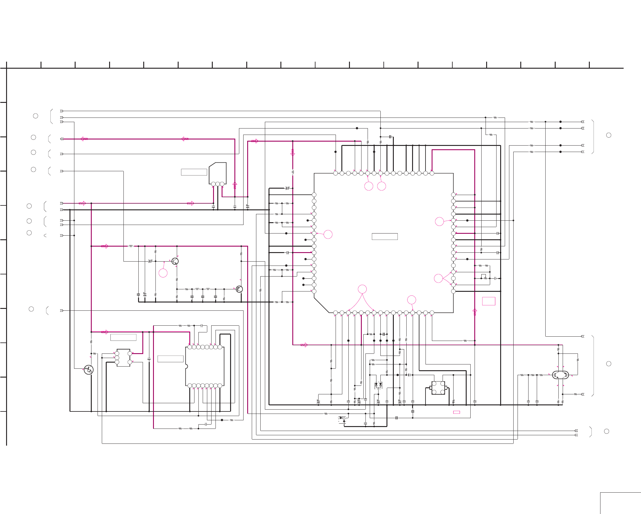
DSR-50/50P
4-25 4-26
JC-20 (AFC) SCHEMATIC DIAGRAM • See page 4-15 for JC-20 printed wiring board. • See page 4-147, 148 for waveforms.
AFC
JC-20 (4/14)
2.6
2.5
3.12.3
32.1
NO MARK:REC/PB MODE
R:REC MODE
P:PB MODE
5 3.1
0
0
5
0
R5/P0
R0/P2.8
3.8
3.2
5
16
0
5
R4.6/P5
0R5/P0
R4.6/P5
R5/P0
R4.6/P5
R0.2/P0
0
4.9
1.2
1.6 1.5 2 1.6 3.1 1.5 2 1.6 1.8 1.71.6 1.5 1.5 3.1
1.6
2.2
3.1
0
2.8
3.1
1.6
3.1
0
3.1 3.1 1.2 1.2 3.1
3.1
3.1
0
1.5
3.1
1.5
1.2
0
0.8
0.8
19
17 18
23
22
21
20
RV2201
AFC
PICTURE
FRAME
CT2200
AFC
1500
R2224
C2218
0.1u
L2202
10uH
R2233
33k C2223
XX
R2203
1k
220
R2225
CL2209
CL2216
R2216
XX
C2203
390p
R2230
680k
220
R2218
CL2211
R2247
10k
R2214
XX
R2237
33k
4700
R2213
R2246
0
R2249
XX
PAL/XNT
L2200
56uH
1000p
C2212
C2208
10u
6.3V
XX
R2210
1000p
C2214
C2236
0.001u
C2233
0.01u
GND
0.01u
C2210
R2236
0
RV2201
4700
R2229
0
R2205
470
XX
R2207
CL2210
R2232 XX
CSM
R2215
10k
CL2215
CL2203
R2220
8200
R2234
0
C2216
1u
16V
CL2205
C2225
XX
C2215
0.01u
AFC_Y
R2206
1k
SPCK1
CL2218
R2240
33k
C2228
18p
C2202
82p
CL2201
C2224
3.3u
16V
R2222
270
L2204
13
46
78
CL2208
CL2200
R2209
0
C2220
4700p
R2226
4700
CL2214
C2211
10u
6.3V
C2200
22u
4V
R2239
1k
Q2201
2SA1576A-T106-R
C2226
470p
C2237
XX
R2228
4700
CL2204
R2200
10k
CL2212
R2204
470
R2238
10k
C2217 0.01u
Q2200
2SC4081T106R
C2221
XX
5p
C2227
C2219
1u
16V
R2223
4700
C2209
0.01u
R2212
0
CL2213
VIDEO_+5V
D2201
KV1470TL00
L2201
120uH
R2248
XX
XX
R2208
C2213
47u
6.3V
0
R2217
C2205
1000p
C2222
3300p
L2203
10uH
CL2206
TK11630UTL
IC2200
123
TC7SET08FU(TE85R)
IC2202
123
45
C2235
0.01u
D2200
XX
R2227
270
R2211
XX
C2207
0.01u
0.01u
C2204
R2231
XX
TC74VHC123AFT(EL)
IC2203
12345678
910111213141516
R2202
0
LVD
CL2202
R2221
4700
0.01u
C2201
AFH_CLP
IC2204
CXD2193AR-ER
12345678910111213141516
17 18 19 20 21 22 23 24 25 26 27 28 29 30 31 32
33343536373839404142434445464748
49505152535455565758596061626364
R2235
33k
R2201
39k
CL2217
CL2207
CT2200
4V
47u
C2206
SPCK0
WEVN
AFH
0
R2253
VD
220
R2219
CL2236
CL2237
CL2238
CL2239
0
R2256
0
R2257
0
R2258
0
R2259
4700
R2263
XP4601-TXE
Q2202
82k
R2262
4700
R2267
0
R2268
82k
R2261
4700
R2266
WEVN
PB/XREC
UN5213-TX
Q2203
4700
R2269
0
R2270
SPCK2
XX
R2241
17-1
17-2
220p
C2245
330p
C2246
10k
R2264 10k
R2265
17-3
1
A
AFC_3V
PB/XREC
22
JC-20 BOARD (5/14)
23
JC-20 BOARD (9/14)
24
JC-20 BOARD (11/14)
17
JC-20 BOARD (3/14)
19
JC-20 BOARD (5/14)
JC-20 BOARD (2/14)
13
8
JC-20 BOARD (1/14)
JC-20 BOARD (14/14)
20
21
JC-20 BOARD (14/14)
JC-20 BOARD (2/14)
11
-REF.NO.:20,000 SERIES-
JC-20 BOARD (4/14)
AFC
XX MARK:NO MOUNT
12 1715
B
E
11
05
C
J
3
D
H
185 148
F
2 1694 7 10 136
G
I
K
IC2204
IC2200
IC2202
IC2203
64
52
13
JC-20 BOARD (9/14)
68
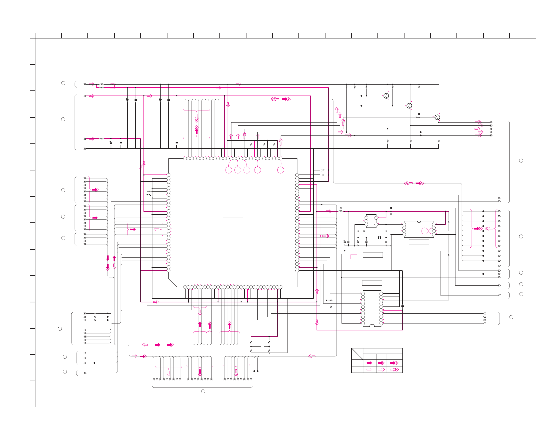
DSR-50/50P
4-27 4-28
JC-20 (VFD (VIDEO DSP, D/A CONVERTER)) SCHEMATIC DIAGRAM • See page 4-15 for JC-20 printed wiring board. • See page 4-148 for waveforms.
VFD (VIDEO DSP, D/A CONVERTER)
JC-20 (5/14)
E-E
E-E
NO MARK:REC/PB MODE
R:REC MODE
P:PB MODE
2.8
2.8
1.5
1.5
1.3
1.3
2.8
1.3
1.4
1.5
0
0
0
0
0
0
2.8
2.6
2.8
2.8
2.8
2.9
0.3
2.9
3.1
2.3 3.1
2.9
2.3
2.8
3.1
2.2
2.7
3.1
2.6
3.1
2.6
2.6
2.6
3.1
3.1
2.8
2.9
3.1
2
2.9
0011
0.8
0.8
0.9
0.6
0.6
0.8
R0/P2
3.1
2.8
2.8
2.6
1.4
1.5
2
2.6
2.8
0.9
1
1.3
1.5
0.6
0.6
1.1
1
2.6
2.8
2.8
0
0
0
2
2.8
1.4
1.4
0
1.6
1.2
0
0
2.8
2.8
2.8
2.6
2.7
2.7
2.8
R0.7/P0.4
R0.8/P0.4
R1.2/P1.1
R1.2/P1
R1.1/P1
R1.7/P1.9
2.8
2.8
2.8
2.8
2.8
2.8
00000
0.6
1.4
R1.4/P3.2
R1.2/P3.2
R1.2/P3.2
R1.2/P3.2
R1.6/P3.2
R1.3/P3.2
R1.3/P3.2
R0.8/P3.2
R1.3/P1
R1.4/P1.1
R1.1/P1
R1.1/P0.9
29
24 25 26 27 28
CT3300
VFD
SPCK
M65511FP-R60S
IC3300
123456789101112131415161718192021222324252627282930
31 32 33 34 35 36 37 38 39 40 41 42 43 44 45 46 47 48 49 50 51 52 53 54 55 56 57 58 59 60
616263646566676869707172737475767778798081828384858687888990
919293949596979899100101102103104105106107108109110111112113114115116117118119120
MB90097PFV-G-120-BND
IC3303
12345678910
11121314151617181920
XVSP_SCK
VSP_SO
XCS_VFD
XRST_VSP
GND
J_3V
L3302
10uH
0.01u
C3306
J_1.9V
XOSD_SCK
XCS_OSD
OSD_SO
XSYS_RESET
0.01u
C3313
VREF
FRRV
TRRV
WEVN
VD
AFH
JC07
JC06
JC05
JC04
JC03
JC02
JC01
JC00
SPCK0
Y7
Y6
Y5
Y4
Y3
Y2
Y1
Y0
2SD2216J-QR(K8).SO
Q3300
2SD2216J-QR(K8).SO
Q3302
470
R3308
470
R3310
470
R3315
4700
R3309
4700
R3312
4700
R3314
3300
R3304
3300
R3307
330
R3319
2SD2216J-QR(K8).SO
Q3301
510
R3318
1500
R3301
TMS
TCK
0.01u
C3308
0.01u
C3301
C3305
6.3V
22u
TDO3
TRCK
TUSV
XVEN
TUVS
VBUS7
VBUS6
VBUS5
VBUS4
VBUS3
VBUS2
VBUS1
VBUS0
VFD_HD
VFD_VD
Y_SIKISA
CB_OUT
CR_OUT
Y_OUT
C_OUT
R3300 0
0
R3316
VSP_SI
C3307
10V
10u
0.01u
C3310
1M
R3317
TC7SU04FU(TE85R)
IC3301
123
45
5p
C3312
13.5MHz
X3300
6.3V
10u
C3309
XX
C3311
0
R3311
0
R3313
XX
R3302
0
R3303
XX
R3305
0
R3306
CLK135
0.01u
C3304
CT3300
10uH
L3301
10uH
L3300
6.3V
22u
C3300
6.3V
22u
C3302
0.01u
C3303
CL3306
CL3307
CL3308
CL3309
CL3310
CL3311
CL3312
CL3313
CL3314
CL3315
CL3316
CL3303
CL3304
CL3300
CL3301
CL3302
CL3305
CL3317
OSDVD
0
R3320
0
R3323
0
R3322
0
R3321
CL3318
CL3319
CL3320
10uH
L3303
MHO
MY07
MY06
MY05
MY04
MY03
MY02
MY01
MY00
CL3321
CL3322
VFD_OE
DA135
CL3323
TC7WH04FU(TE12R)
IC3302
1234
5678
0.01u
C3314
0
R3324
AFC_3V
TD02
XX
R3326
0
R3325
JC02
JC03
JC01
AFH
JC07
JC04
JC05
JC06
JC00
Y3
Y5
Y7
Y6
Y1
Y2
Y0
Y4
1
A
OSDHD
XRST_VSP
AFCK
CAM_C4
CAM_C5
CAM_C6
CAM_C7
CAM_FLD
CAM_VD
CAM_HD
CAM_C3
CAM_C2
CAM_C1
CAM_C0
CAM_Y7
CAM_Y6
CAM_Y5
CAM_Y4
CAM_Y2
CAM_Y1
CAM_Y3
TMS
TCK
TDI
TDO
TUSV
TUVS
XVEN
VBUS7
VBUS6
VBUS5
VBUS4
VBUS3
VBUS2
VBUS1
VBUS0
DATA_TO_MS_VSP
DATA_FROM_MS_VSP
XMS_SCK_VSP
XCS_VFD
CAM_C3
CAM_C1
CAM_Y5
CAM_Y3
CAM_Y1
CAM_Y0
CAM_Y2
CAM_Y4
CAM_C2
CAM_C0
CAM_Y7
CAM_Y6
TDO
CAM_C6
CAM_C7
CAM_HD
CAM_VD
AFCK
CAM_FLD
CAM_Y0
XMS_SCK_VSP
XCS_VFD
DATA_TO_MS_VSP
DATA_FROM_MS_VSP
CAM_C5
CAM_C4
VBUS0
VBUS1
VBUS2
VBUS3
VBUS4
VBUS5
VBUS6
VBUS7
TUVS
XVEN
TUSV
TCK
MVO
MHO
MY07
MY06
MY05
MY04
MY03
MY02
MY01
MY00
MY00
MY01
MY02
MY03
MY04
MY05
MY06
MY07
MHO
MOE
MVO
TMS
XRST_VSP
TDI
MOE
CAM_HD
CAM_C0
CAM_C1
CAM_C2
CAM_C3
CAM_C4
CAM_C5
CAM_C6
CAM_C7
CAM_Y0
CAM_Y1
CAM_Y2
CAM_Y3
CAM_Y4
CAM_Y5
CAM_Y6
CAM_Y7
Y/CHROMA
REC
PB
Y
VIDEO SIGNAL
CHROMA
SIGNAL PATH
JC-20 BOARD (1/14)
4
30
JC-20 BOARD (6/14)
JC-20 BOARD (14/14)
31
JC-20 BOARD (7/14)
32
5
JC-20 BOARD (1/14)
JC-20 BOARD (11/14)
33
25
JC-20 BOARD (14/14)
JC-20 BOARD (4/14)
19
14
JC-20 BOARD (2/14)
18
JC-20 BOARD (3/14)
22
JC-20 BOARD (4/14)
JC-20 BOARD (9/14)
26
27
JC-20 BOARD (11/14)
JC-20 BOARD (6/14)
28
29
JC-20 BOARD (14/14)
56 11
I
D
16
C
1410 19
E
H
9 17
J
127 15
F
M
L
813184
K
B
32
G
XX MARK:NO MOUNT
VFD(VIDEO DSP,D/A CONVERTER)
-REF.NO.:20,000 SERIES-
JC-20 BOARD (5/14)
IC3300
IC3301
IC3302
IC3303
05
N
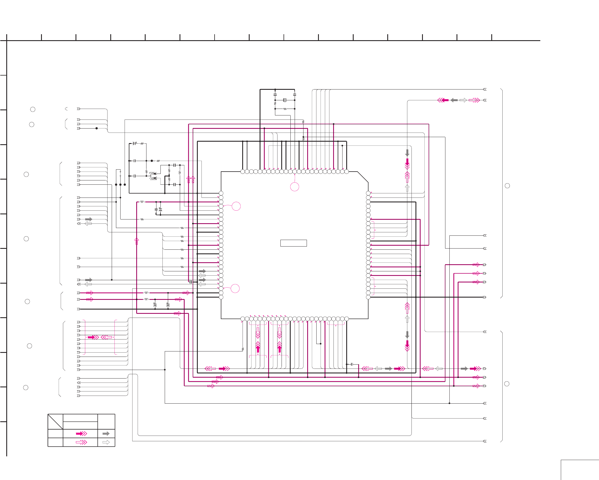
DSR-50/50P
4-29 4-30
JC-20 (SFD) SCHEMATIC DIAGRAM • See page 4-15 for JC-20 printed wiring board. • See page 4-148 for waveforms.
SFD
JC-20 (6/14)
R:REC MODE
P:PB MODE
NO MARK:REC/PB MODE
*:IMPOSSIBLE TO MEASURE THE
VOLTAGE AT THE MARKED POINTS.
2
2.8
2.8
1.3
1.3
1.3
2
2.8
00
2.8
2.8
R2.8/P0
R2.8/P1.7
R1.4/P0.3
2.8
2.8
2
R2.8/P2.1
2.8
2.7
2.7
R0.8/P0.4
2.6
2
2
2
R0.4/P0.7
R0.4/P0.7
200
0.5
20
R0/P2
0
11
0.8
0.8
2
0.6
0.6
0.9
0.8
1.4
1.6
*
*
*
*
1.4
1.5
2
1.4
1.4
2.8
1.4
0.8
1.2
2
1.2
1.3
1.4
2.8
30
32
31
HG73C050TETL
IC4400
12345678910111213141516171819202122232425
26272829303132333435363738394041424344454647484950
51 52 53 54 55 56 57 58 59 60 61 62 63 64 65 66 67 68 69 70 71 72 73 74 75
76 77 78 79 80 81 82 83 84 85 86 87 88 89 90 91 92 93 94 95 96 97 98 99 100
SFD_FCK
SFD_LRCK
SFD_BCK
SOA
GND
J_1.9V
J_3V
VSP_SO
XCS_SFD
XVSP_SCK
XRST_VSP
TRCK
VBUS0
VBUS1
VBUS2
VBUS3
VBUS4
VBUS5
VBUS6
VBUS7
TUVS
XVEN
TUSV
0
R4409
10k
R4404
0.001u
C4407
10k
R4403
0.001u
C4408
KV1470TL1-3
D4400
1
2
3
4700
R4401 1.5uH
L4403
0.047u
C4401
0.001u
C4402
330
R4402
10p
C4410 10p
C4411
0.01u
C4404
TDO3
TCK
TMS
0.01u
C4412
47
R4400
C4405
10u
6.3V
C4403
10u
6.3V
10uH
L4401
10uH
L4402
C4406
10u
6.3V
C4400
2.2u
6.3V
24.576MHz
X4400
VSP_SI
0
R4405
0
R4406
0
R4407
10uH
L4400
XX
R4410
CL4400
0
R4408
BCK
LRCK
SOB
CL4434
LOCK_MCK
0
R4444
OCK
TD05
0
R4445
0
R4446
0
R4447
SOA
SFD_BCK
SFD_LRCK
SFD_FCK
SIC
SOB
JS7001
0
CL7003
CL7002
CL7001
40-5
40-4
40-3
39-3
39-4
40-1
39-1
39-2
0
R4411
XX
C4409
47
R4443
1
A
40-2
SFD_1.9V
SFD_3V
J_3V
SFD_1.9V
SFD_3V
GND
SIC
SID
TBUS7
TBUS6
TBUS5
TBUS0
TBUS1
TBUS2
TBUS3
VBUS0
VBUS1
VBUS2
VBUS3
VBUS4
VBUS5
VBUS6
VBUS7
TUVS
XVEN
ADAI1
DATA_TO_MECHA
DATA_FROM_MECHA
XMECHA_SCK
XCS_SFD
XRST_VSP
TDO3
TMS
TCK
TDO3
TDO4
FCK0
LRCK0
ADAI1
LBUS3
LBUS2
LBUS1
FRL
FCLR
DIR
XENA
XACC
DATA_FROM_MECHA
DATA_TO_MECHA
XCS_SFD
XMECHA_SCK
TMS
SEN
TUTS
TUSV
ADAO1
LBUS0
TBUS4
FCK0
LRCK0
BCK0
BCK0
TUSV
XVEN
TUVS
VBUS7
VBUS6
VBUS5
VBUS4
VBUS3
VBUS2
VBUS1
VBUS0
XRST_VSP
ADAO1
TDO5
TCK
FCK0
LRCK0
BCK0
ADAI1
ADAO1
XRST_VSP
1310 11
C
H
F
3 14945
XX MARK:NO MOUNT
SFD
-REF.NO.:20,000 SERIES-
JC-20 BOARD (8/14)
1262
G
E
JC-20 BOARD (6/14)
D
8
B
7
05
15
28
JC-20 BOARD (5/14)
39
40
JC-20 BOARD (7/14)
JC-20 BOARD (11/14)
34
35
JC-20 BOARD (12/14)
JC-20 BOARD (14/14)
36
JC-20 BOARD (14/14)
37
30
JC-20 BOARD (5/14)
JC-20 BOARD (9/14)
38
J
I
PB
SIGNAL PATH
Y/CHROMA
VIDEO SIGNAL AUDIO
REC
SIGNAL
K
IC4400
L
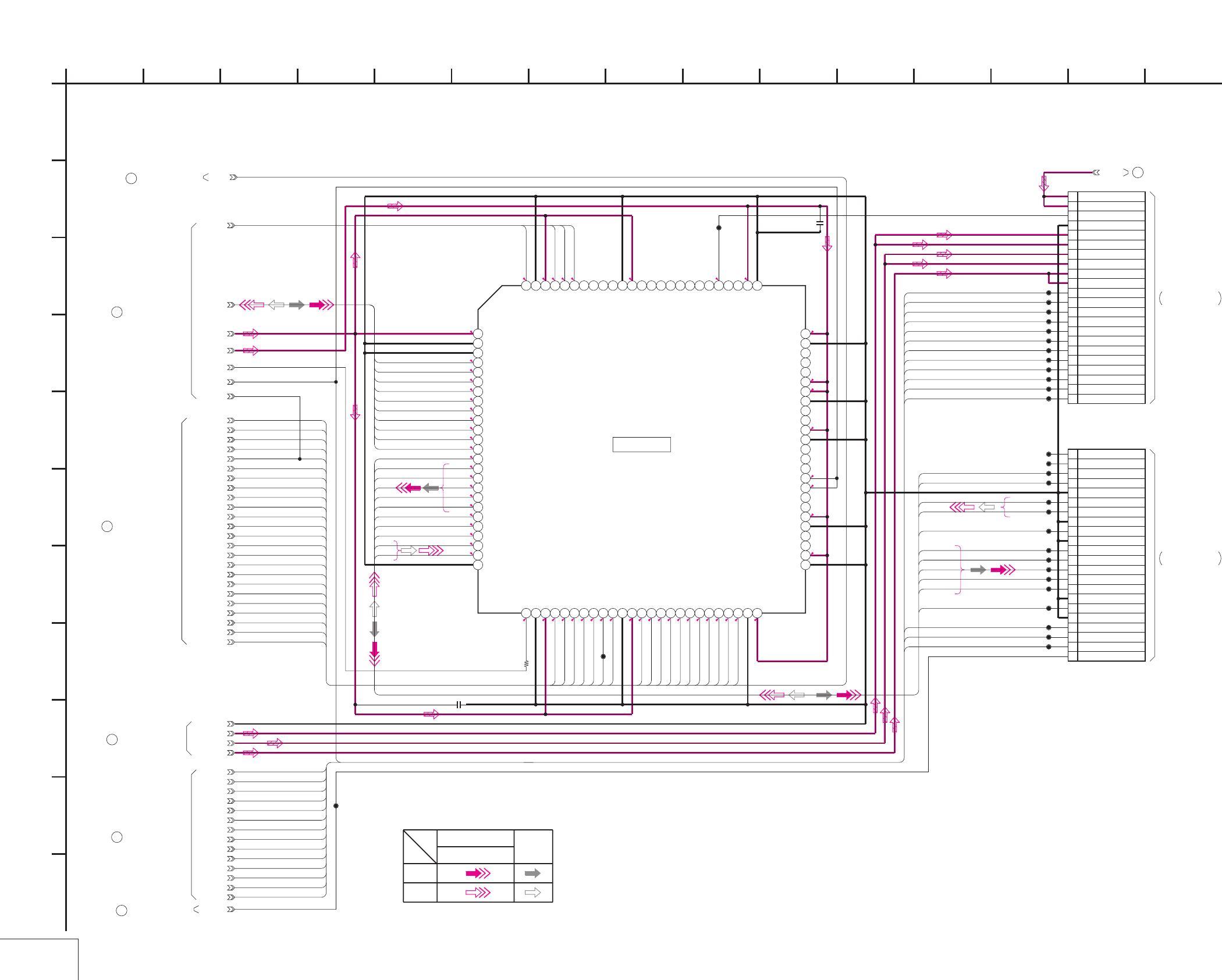
DSR-50/50P
4-31 4-32
JC-20 (TFD) SCHEMATIC DIAGRAM • See page 4-15 for JC-20 printed wiring board.
TFD
JC-20 (7/14)
NO MARK:REC/PB MODE
R:REC MODE
P:PB MODE
2.82
0
R0.4/P0.7
R0.4/P0.7
R0.4/P0.7
R0.4/P0.7
R0.4/P0.7
R0.4/P0.7
R0.4/P0.7
R0.4/P0.7
0.5
0.9
R1/P0
R1/P0
R1/P0
R1/P0
R1/P0
0
0
R0/P1
R0/P0.8
R0/P0.8
2.8
2.8
2.8
2.8
2.8
2.8
2.8
R1.4/P0.3
2
2.8
R0.9/P0.5
2.8
2
0
2.8
1.4
2
2.8
2.8
0.6
1.4
1.4
1.4
0
2
2.5
R2.5/P1.5
R2.1/P1.5
R2.2/P1.2
R1.4/P0.6
R0.9/P1.3
R1.2/P1.8
R2/P1.3
0.3
2.4
2.4
2.8
CXD3129R-T6
IC4401
12345678910111213141516171819202122232425
26 27 28 29 30 31 32 33 34 35 36 37 38 39 40 41 42 43 44 45 46 47 48 49 50
51 52 53 54 55 56 57 58 59 60 61 62 63 64 65 66 67 68 69 70 71 72 73 74 75
767778798081828384858687888990919293949596979899100
WR01
RDX
FRRV
TRRT
SWP
ALE
DXXA10
D24A00
D25A01
D26A02
D27A03
D28A04
D29A05
D30A06
D31A07
DXXA08
DXXA09
XDVCN
LIP_SLEEP
LPS
OFR
XRST_PHY
XRST_LINK
0.01u
C4420
0.01u
C4415
DRP
CL4402
CL4401
0
R4413
ATF
CAP_EVR
REEL_EVR
XCS_TRX
XCS_TRF
DRP_SI
DRP_SO
XDRP_SCK
SWP
DRP
SC_WD
CONT_E
CONT_O
CL4408
CL4409
CL4410
CL4411
CL4412
CL4413
CL4414
CL4415
CL4416
CL4417
CL4418
CL4419
CL4420
CL4421
CL4422
CL4423
CL4424
CL4425
CL4426
CL4427
CL4428
CL4429
CL4430
CL4431
CL4432
CL4433
DSWP
CL4435
RF_6V
CL4437
CL4438
22P
CN4402
1 CLK135
2 REEL_EVR
3 CAP_EVR
4ATF
5 GND
6 TXST
7 GND
8 TXDT4
9 TXDT3
10 TXDT2
11 TXDT1
12 TXDT0
13 GND
14 CRCK
15 GND
16 XTDT1
17 XTDT0
18 GND
19 XTSY
20 HPCK
21 N.C.
22 N.C.
22P
CN4401
1 DSWP
2 CONT_O
3 CONT_E
4 SC_WD
5 CLK150
6 SWP
7 XRST
8 MSCK
9 DRP_SO
10 DRP_SI
11 XCS_TRF
12 XCS_TRX
13 5V
14 5V
15 3V
16 3V
17 1.9V
18 1.9V
19 GND
20 C1ERRP
21 RF 6V
22 RF 6V
CLK135
GND
J_3V
J_1.9V
VIDEO_+5V
40-4
40-3
SFD_3V
40-2
40-5
SFD_1.9V
40-1
41-1
1
A
TXDT1
TXDT2
TXDT3
TXDT4
TXST
XTSY
XTDT0
XTDT1
TRRT
DRP
ALE
DXXA10
D24A00
D25A01
D26A02
D27A03
D28A04
D29A05
D30A06
D31A07
DXXA08
DXXA09
WR01
RDX
FRRV TMS
RDX
FRRV
TRRT
SWP
ALE
DXXA10
D24A00
D25A01
D26A02
D27A03
D28A04
D29A05
D30A06
D31A07
DXXA08
DXXA09
XDVCN
LIP_SLEEP
LPS
FP
TDO5
TBUS0
TBUS1
TBUS2
TBUS3
TBUS4
TBUS5
TBUS6
TBUS7
TDO4
SEN
HPCK
TXDT0
CRCK
TUTS
WR01
TCK
SWP
XRST_LINK
XRST_PHY
TXST
TXDT4
TXDT3
TXDT2
TXDT1
TXDT0
CRCK
XTDT1
XTDT0
XTSY
HPCK
ATF
CAP_EVR
REEL_EVR
XCS_TRX
XCS_TRF
DRP_SI
DRP_SO
XDRP_SCK
SWP
DRP
SC_WD
CONT_E
CONT_O
ATF
CAP_EVR
REEL_EVR
CONT_O
CONT_E
SC_WD
DRP
SWP
XDRP_SCK
DRP_SO
DRP_SI
XCS_TRF
XCS_TRX
XRST_VSP
DSWP
DSWP
DRP
XRST_VSP
40
JC-20 BOARD (6/14)
JC-20 BOARD (9/14)
42
41
JC-20 BOARD (8/14)
JC-20 BOARD (14/14)
43
44
JC-20 BOARD (10/14)
32
JC-20 BOARD (5/14)
45
JC-20 BOARD (9/14)
F
3 14945
XX MARK:NO MOUNT
TFD
-REF.NO.:20,000 SERIES-
126
IC4401
2
G
E
JC-20 BOARD (7/14)
D
8
B
7
05
15
K
10
J
I
11 13
C
H
Y/CHROMA
REC
SIGNAL
SIGNAL PATH
VIDEO SIGNAL
PB
AUDIO
THROUGH THE
CN203
FRJ-1 FLAT CABLE
(SEE PAGE 4-11)
RP-234 BOARD (1/2)
FRJ-1 FLAT CABLE
THROUGH THE
RP-234 BOARD (1/2)
(SEE PAGE 4-11)
CN202
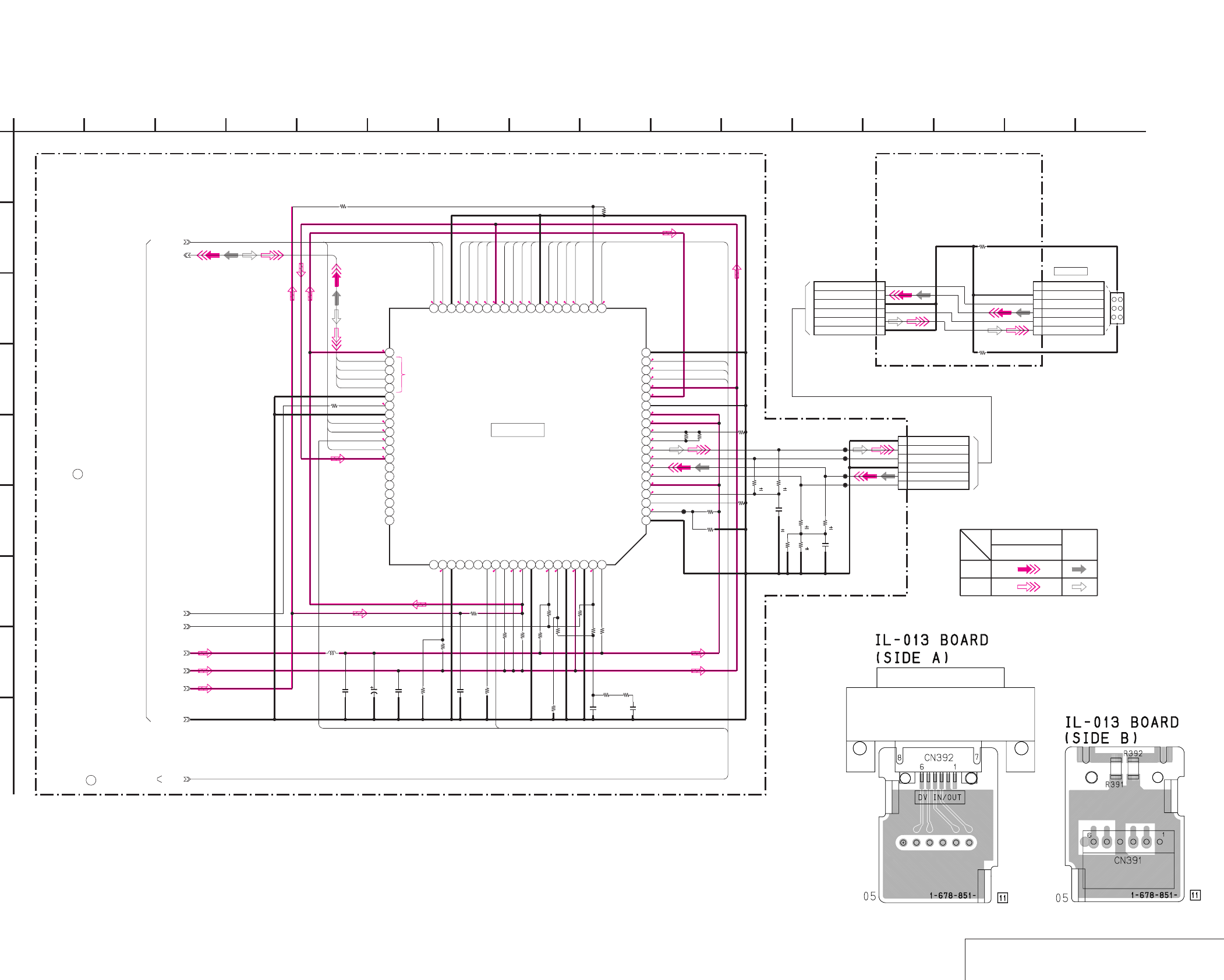
DSR-50/50P
4-33 4-34
JC-20 (DV INTERFACE) SCHEMATIC DIAGRAM • See page 4-15 for JC-20 printed wiring board.
IL-013 (DV CONNECTOR) PRINTED WIRING BOARD AND SCHEMATIC DIAGRAM
– Ref. No.: IL-013 board; 10,000 series –
DV INTERFACE
/
DV CONNECTOR
JC-20 (8/14) IL-013
NO MARK:REC/PB MODE
R:REC MODE
P:PB MODE
2.8
20
2.8
2.8
2.5
R2.5/P1.5
R2.1/P1.5
R2.2/P1.2
R1.4/P0.6
2.8
R0.9/P1.3
R1.2/P1.8
R2/P1.3
0.3
02.8
2
1.4
0
0
2.8
R2.8/P0
R2.8/P1.7
R2.8/P2.1
2.8
2.8
0
2.8
2
2.8
2.8
1.3
0
1.9
1.9
0
0
2.8
1.9
2.8
2.8
2.8
2.8
22.8
1.2
2.8
1.3
SN104266PN-TEB
IC4402
1234567891011121314151617181920
2122232425262728293031323334353637383940
4142434445464748495051525354555657585960
61 62 63 64 65 66 67 68 69 70 71 72 73 74 75 76 77 78 79 80
0.01u
C4416
10uH
L4404
0.01u
C4413
XX
C4419
0.1u
C4418
1u
C4421
56
R4440
0.5% 56
R4442
0.5%
220p
C4422
10k
R4441
0.5%
10k
R4439
0.5%
56
R4438
0.5%
56
R4437
0.5%
C4414
10u
6.3V XX
R4429
XX
R4428
XX
R4418
CL4403
12k
R4431 12k
R4434 XX
R4436
0
R4432
XX
R4427
XX
R4426
0
R4423 XXR4421
0
R4424
0
R4420
XX
R4419
0
R4416
XX
R4422
XX
C4417
0
R4415
XX
R4414
XX
R4417
XX
R4433
XX
R4430
0
R4412
6P
CN4400
1 GND
2TPA
3 NTPA
4 GND
5 TPB
6 NTPB
CL4405
CL4406
CL4407
CL4404
1
A
SFD_1.9V
SFD_3V
39-1
J_3V
GND
39-3
39-4
41-1
0
R4435
0
R4425
CN392
6P
VP1
VG2
NTPB3
TPB4
NTPA5
TPA6
0
R391
0
R392
6P
CN391
1GND
2TPA
3NTPA
4GND
5TPB
6NTPB
39-2
XACC
XDVCN
XRST_PHY
LIP_SLEEP
LPS
LBUS3
LBUS2
LBUS1
LBUS0
XENA
FRL
FP
DIR
XRST_LINK
ALE
DXXA10
RDX
WR01
D25A01
D24A00
D31A07
D30A06
D29A05
D28A04
D27A03
D26A02
FCLR
3
JC-20 BOARD (6/14)
05
7
B
8
D
JC-20 BOARD (8/14)
E
G
26 12
-REF.NO.:20,000 SERIES-
DV INTERFACE
XX MARK:NO MOUNT
5 144910
I
11 13
C
H
F
39
Y/CHROMA
REC
SIGNAL
SIGNAL PATH
VIDEO SIGNAL
PB
AUDIO
41
JC-20 BOARD (7/14)
IC4402
DV IN/OUT
DV CONNECTOR
CN392
-REF.NO.:10,000 SERIES-
IL-013 BOARD
15 16
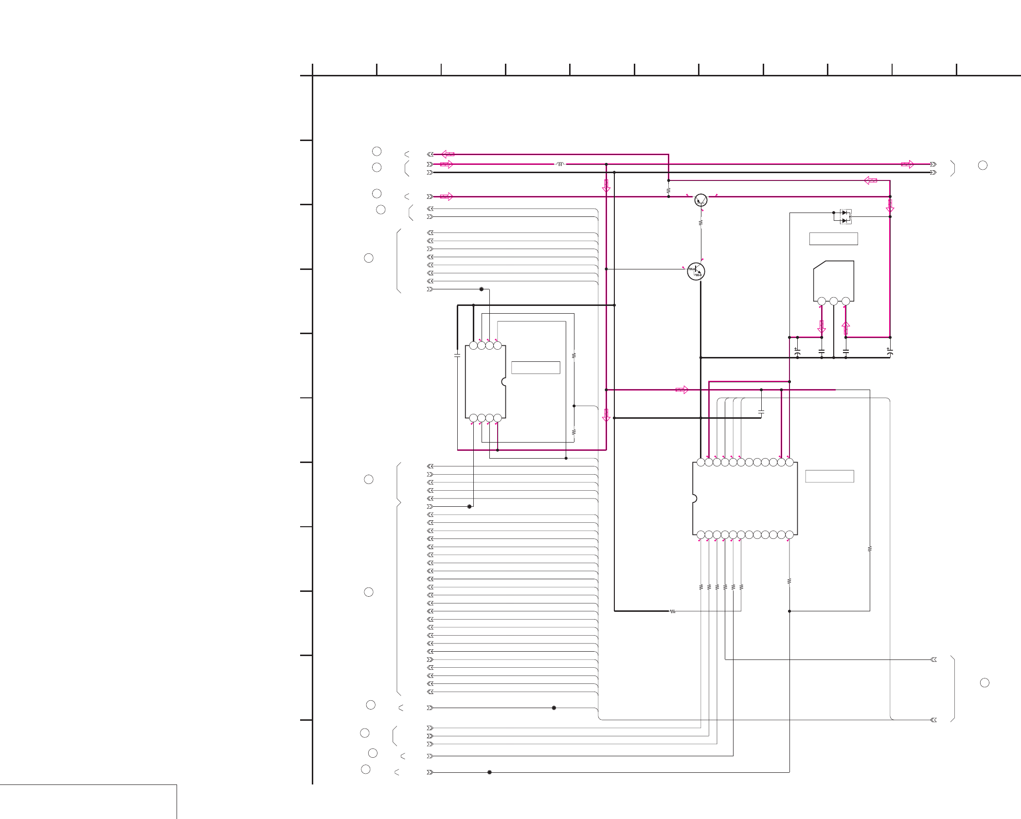
DSR-50/50P
4-35 4-36
JC-20 (MECHANISM CONTROL 1) SCHEMATIC DIAGRAM • See page 4-15 for JC-20 printed wiring board.
MECHANISM CONTROL 1
JC-20 (9/14)
NO MARK:REC/PB MODE
R:REC MODE
P:PB MODE
5.5 5.4
4.8
0.2
2.8
5.1
5.5
2.8
0
0
0
0
0
0
R2.7/P0.3
5.1
2.8
2.6
R0.8/P0.4
2.7
2.8
5.1
0
0
0
5
R2.6/P2.1
R2.6/P2.1
10uH
L5001
GND
J_3V
DRP
XVSP_SCK
VSP_SO
LPS
LIP_SLEEP
D29A05
D30A06
D31A07
DXXA08
DXXA09
DXXA10
XCS_SFD
SWP
WEVN
D26A02
D27A03
D28A04
XRST_VSP
FRRV
TRRT
TRRV
D24A00
RDX
WR01
ALE
XRST_PHY
XCS_VFD
D25A01
XRST_LINK
VSP_SI
VREF
LVD
XDVCN
10V
10u
C5004
0.01u
C5003
100R5014
22k
R5003
Y_CLP_ERR
100
R5005
0.01u
C5002
CB_CLP_ERR
SW_6V
CR_CLP_ERR
S-81350HG-KD-T1
IC5001
123
10k
R5009
0.01u
C5006
100R5015
100
R5013
100
R5008
XRST_VSP
XVSP_SCK
VSP_SI
VSP_SO
FRRV
OFR
IC5007
TC7W241FU-TE12R
1234
5678
1k
R5057
1k
R5058
CL5740
CL5738
0.01u
C5016
PB/XREC CL5748
MB88146APFV-G-BND-ER
IC5002
123456789101112
131415161718192021222324
CL5947
FIFO_MUTE
100k
R5066
100
R5067
MA132WK-TX
D5001
2SB624-T1BV4
Q5001
Q5002
UN5213-TX
1k
R5004
16V
6.8u
C5005
XX
R5071
HUE_ADJ
50-2
50-1
1
A
J_3V
GND
RF_6V
MS26
MS27
MS28
MS29
MS30
MS31
MS32
MS33
MS35
MS36
MS37
MS77
MS84
MS14
MS60
MS13
MS19
MS76
MS75
MS16
MS61
MS75
MS76
MS74
MS92
MS15
MS106
MS107
MS112
MS91
MS118
MS74
MS17
MS76
MS75
MS92
MS106
MS108
MS10
MS11
MS8
MS111
MS38
MS74
49
JC-20 BOARD (10/14)
50
JC-20 BOARD (10/14)
48
JC-20 BOARD (14/14)
JC-20 BOARD (1/14)
2
JC-20 BOARD (2/14)
12
JC-20 BOARD (7/14)
42
38
JC-20 BOARD (6/14)
JC-20 BOARD (5/14)
26
JC-20 BOARD (4/14)
23
47
JC-20 BOARD (14/14)
JC-20 BOARD (14/14)
46
45
JC-20 BOARD (7/14)
7
E
6
B
543
D
J
G
10
-REF.NO.:20,000 SERIES-
JC-20 BOARD (9/14)
MECHANISM CONTROL 1
XX MARK:NO MOUNT
F
05
9
I
8
K
2
H
11
CIC5001
IC5002
IC5007
JC-20 BOARD (4/14)
68
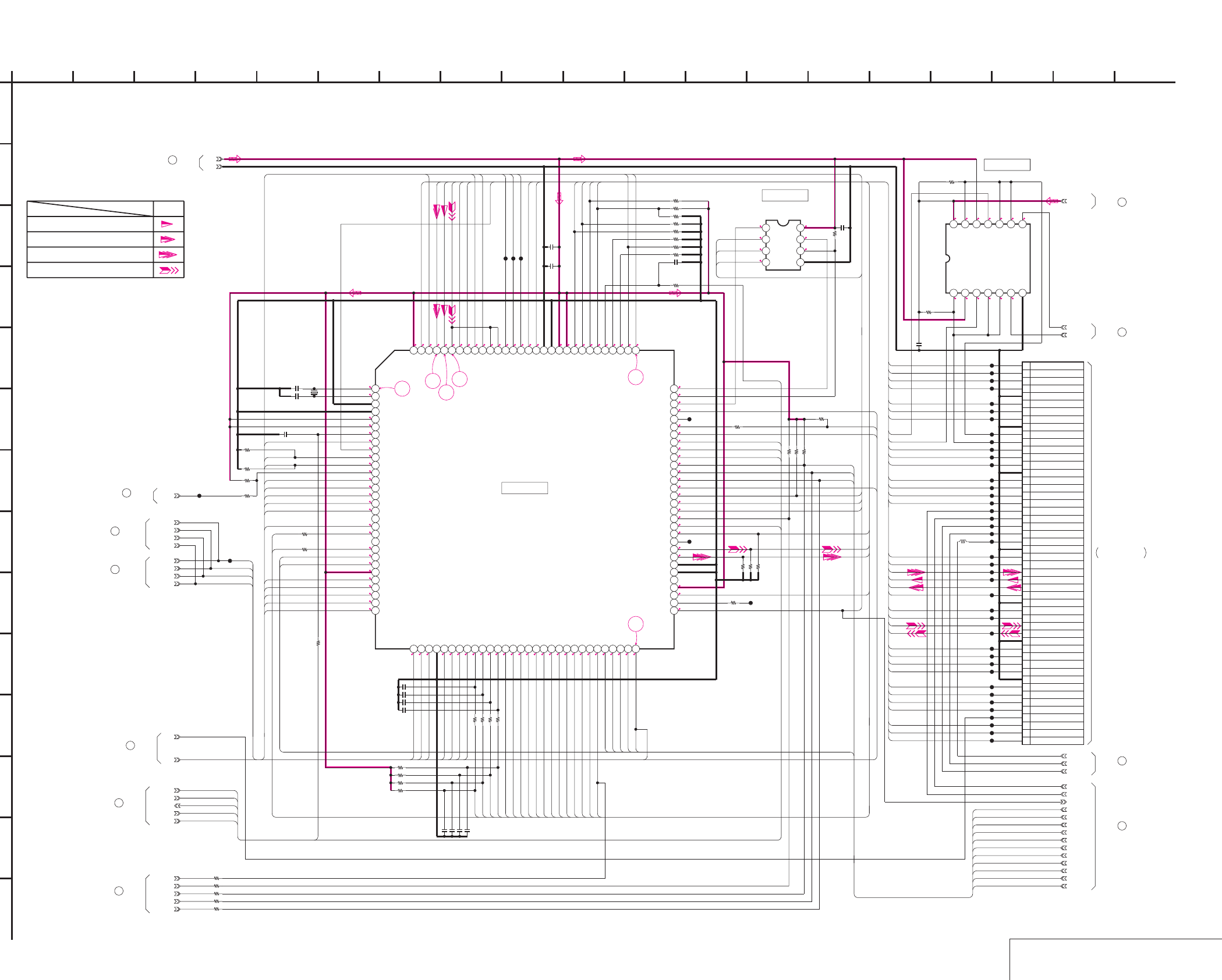
DSR-50/50P
4-37 4-38
JC-20 (MECHANISM CONTROL 2) SCHEMATIC DIAGRAM • See page 4-15 for JC-20 printed wiring board. • See page 4-148 for waveforms.
MECHANISM CONTROL 2
JC-20 (10/14)
NO MARK:REC/PB MODE
R:REC MODE
P:PB MODE
2.7
2.7
R0.8/P0.4
2.6
2.8
2.8
2.7
03.1 0002.80
00000 2.8
1.6
00
2.7
1.4
00
2.3
1.3
2.8
2.8
00
0.6
1.4
1.4
1.3
1.3
00**
1.3
1.5
0.2
3
1.4
2.8
1.1
1.2
2.8
2.8
2.8
R0/P2.8
0
2.8
2.8
2.6
0
2.8
2.8
2.8
2.7
2.8
0
0
2.7
2.8
2.8
R2.5/P1.5
R2.1/P1.5
R2.2/P1.2
R1.4/P0.6
R0.9/P1.3
R1.2/P1.8
R2/P1.3
0.3
2.4
2.4
2.5
2.7
2.7
2.7
0
2.7
2.7
0
2.7
2.7
2.7
2.7
000
2.9
2.9
0
0.4
2.7
2.7
1.4
0.2
1.4
1.4
1.4
2.8
0.8
0.5
0.4
2.9
2.5
2.7
R0.8/P0.4
2.6
2.8
2.7
0
2.7
2.7
2.6
0.2
0
0
2.7
2.7
2.7
2.8
38
33 34
35
36 37
10p
C5008 X5001
20MHz
10p
C5009
MB91192PFF-G-119-BND-ER
IC5003
123456789101112131415161718192021222324252627282930
31 32 33 34 35 36 37 38 39 40 41 42 43 44 45 46 47 48 49 50 51 52 53 54 55 56 57 58 59 60
61 62 63 64 65 66 67 68 69 70 71 72 73 74 75 76 77 78 79 80 81 82 83 84 85 86 87 88 89 90
919293
949596
979899100101102103104105106107108109110111112113114115116117118119120
C5012
0.01u
AK6480AM-E2
IC5006
1234
5678
0.01u
C5015
GND
J_3V
MODE_SI
MODE_SO
XMODE_SCK
XSYS_RESET
R5026
1k
0.001uC5007
1k
R5033
1k
R5034
1k
R5035
47kR5031
47k
R5030
47kR5029
47k
R5028
100k
R5043
100k
R5042
100k
R5046
100k
R5045
1k
R5032
100k
R5047
100k
R5038
220k
R5041
47k
R5039
100k
R5018
100k
R5019
470k
R5020
470k
R5044
100k
R5040
4700
R5037
0.01u
C5014
1u
C5011
DRP
CHIME_VDD
1uH
L5002
CHIME_SCK
CHIME_SDA
CL5301
CL5302
CL5303
CL5304
CL5306
CL5308
CL5309
CL5311
CL5313
CL5314
CL5315
CL5316
CL5318
CL5319
CL5320
CL5321
CL5323
CL5324
CL5401
CL5402
CL5403
CL5404
CL5406
CL5407
CL5408
CL5410
CL5411
CL5412
CL5413
CL5414
CL5416
CL5417
CL5418
CL5419
10k
R5048
10k
R5025
100k
R5053
1k
R5055
100k
R5050
100k
R5051
100k
R5052
100k
R5049
VSP_SI
CAP_EVR
CONT_O
REEL_EVR
XCS_TRF
DRP_SI
SC_WD
XDRP_SCK
SWP
CONT_E
DRP_SO
XCS_TRX
ATF
XCS_MECHA
XCC_DOWN
1k
R5059
100k
R5060
CL5420
CL5421
CL5422
CL5423
CL5424
ONBOAD55
ONBOAD73
ONBOAD78
ONBOAD79
ONBOAD80
1k
R5061
1k
R5062
1k
R5063
1k
R5064
1k
R5065
DSWP
XCS_DSP
CL5747
XC_IN
CL5749
CL5750
50P
CN5005
1 MODE_SW_A
2 MODE_SW_B
3 MODE_SW_C
4 MODE_SW_D
5 GND
6 TAPE_LED_ON
7 TAPE_TOP
8 TAPE_END
9 GND
10 XC_IN
11 XCC_DOWN
12 L_CASSETTE
13 REC_PROOF
14 DEW_DET
15 GND
16 T_ELTN_ERR
17 S_ELTN_ERR
18 SREEL_FG
19 TREEL_FG
20 REEL_EVR
21 CAP_EVR
22 CHIME_SCK
23 CHIME_SDA
24 CHIME_VDD
25 GND
26 DRUM_ON
27 DRUM_FWD
28 DRUM_PWM
29 DRUM_FG
30 DRUM_PG
31 DRUM_MASTER_CLK
32 GND
33 CAP_ON
34 CAP_FWD
35 CAP_PWM
36 CAP_FG
37 GND
38 REEL_ON
39 REEL_FWD
40 REEL_PWM
41 REEL_M_FG
42 GND
43 CM(+)
44 CM(-)
45 CM_LIMIT_ON
46 CM_LIMIT_DET
47 CM_LIMIT_EVR
48 LM(+)
49 LM(-)
50 HI_C/R_SW
CL5965
XMUTN
CL5322
CL5325
1k
R5068
CL5966
CL5967
CL5968
TC74VHC08FT(EL)
IC5008
1234567
891011121314
UNSW_3.0V
0.01u
C5013
100k
R5069
100k
R5070
XX
C5017
XX
C5018
XX
C5019
XX
C5020
XX
C5021
XX
C5022
XX
C5023
XX
C5024
50-1
VSP_SO
XVSP_SCK
XCS_DSP
VSP_SO
XVSP_SCK
VSP_SI
50-2
CL4436
1
A
MS118
MS117
MS116
MS114
MS113
MS105
MS104
MS119
MS111
MS81
MS83
MS82
MS7
MS72
MS76
MS75
MS74
MS92
MS96
MS7
MS23
MS24
MS84
MS83
MS82
MS81
MS77
MS75
MS72
MS69
MS68
MS63
MS106
MS112
MS97
MS98
MS99
MS95
MS24
MS23
MS80
MS79
MS78
MS60
MS59
MS57
MS56
MS47
MS48
MS68
MS117
MS63
MS45
MS46
MS69
MS115
MS43
MS44
MS71
MS119
MS49
MS50
MS51
MS52
MS104
MS105
MS116
MS107
MS108
MS59
MS76
MS95
MS58
MS74
MS71
MS56
MS57
MS58
MS91
MS54
MS53
MS52
MS51
MS50
MS49
MS48
MS47
MS46
MS45
MS43
MS85
MS44
MS87
MS9
MS9
MS39
MS40
MS41
MS42
MS55
MS53
MS54
MS97
MS85
MS96
MS99
MS98
MS113
MS114
MS20
MS22
MS22
MS20
MS39
MS40
MS41
MS42
MS61
MS55
MS80
MS79
MS78
MS87
MS74
MS75
MS76
MS26
MS27
MS28
MS29
MS30
MS19
MS17
MS16
MS15
MS14
MS13
MS11
MS10
MS8
MS31
MS32
MS33
MS35
MS36
MS37
MS38
MS60
MS60
MS115
JC-20 BOARD (14/14)
56
JC-20 BOARD (11/14)
57
(SEE PAGE 4-105)
CM-59 BOARD (1/3)
CN001
58
JC-20 BOARD (11/14)
44
JC-20 BOARD (7/14)
REC/PB
Drum speed servo
Drum servo(speed and phase)
SIGNAL PATH
Drum phase servo
49
JC-20 BOARD (9/14)
JC-20 BOARD (14/14)
51
52
JC-20 BOARD (13/14)
JC-20 BOARD (14/14)
53
50
JC-20 BOARD (9/14)
54
JC-20 BOARD (11/14)
JC-20 BOARD (11/14)
55
-REF.NO.:20,000 SERIES-
JC-20 BOARD (10/14)
MECHANISM CONTROL 2
XX MARK:NO MOUNT
F
05
9
I
178
K
14 152
H
11 13
C
7 18
E
6
N
B
1612
L
543
D
J
M
G
10
IC5008
IC5006
19
IC5003
FVJ-1 FLAT CABLE
THROUGH THE
Capstan servo(speed and phase)
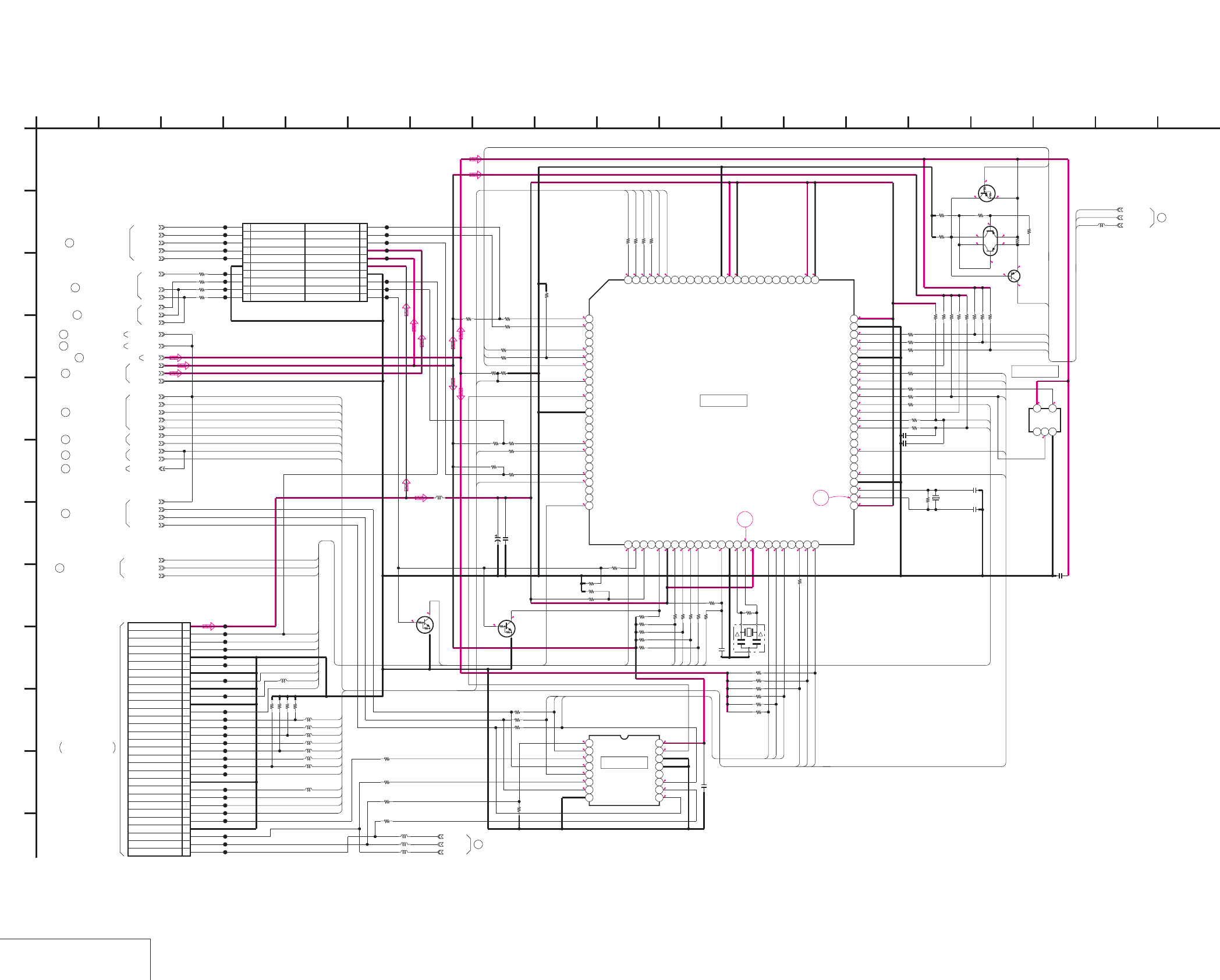
DSR-50/50P
4-39 4-40
MODE CONTROL
JC-20 (11/14)
JC-20 (MODE CONTROL) SCHEMATIC DIAGRAM • See page 4-15 for JC-20 printed wiring board. • See page 4-148 for waveforms.
NO MARK:REC/PB MODE
R:REC MODE
P:PB MODE
0
3
3.1
2.8
2.8
3
2.8
0.3
0.3
2.8
2.9
2.9
0
3
0
0
000000 33 33
3
2.8
2.8
2.8
2.9
0
0
R2.5/P2.8
R0.4/P0
2.9
2.9
0
3
2.9
0
1.5
1.2
3
3.1
0
2.8
2.8
0
2.8
0
3.1
0
3.1
2.9
0
00 33R0/P3
2.9
3
2.9
R1.2/P1.8
3
1.6
1.5
33
2.8
2.8
2.6
0.2
2.7
2.8
R2.5/
P2.8
R0.4/
P0
2.8
2.8
2.8
2.2
2.8
2.92.8
2.2
2.4
2.8
0
2.8
39
40
1k
R6041
20MHz
X6001
S579637PZ-TEB
IC6001
12345678910111213141516171819202122232425
26
27
28
29
30
31
32
33
34
35
36
37
38
39
40
41
42
43
44
45
46
47
48
49
50
51 52 53 54 55 56 57 58 59 60 61 62 63 64 65 66 67 68 69 70 71 72 73 74 75
76
77
78
79
80
81
82
83
84
85
86
87
88
89
90
91
92
93
94
95
96
97
98
99
100
0.022u
C6008
0.01u
C6007
470k
R6048
10k
R6016
10uH
L6001
32.768kHz
X6002
C6006
10u
6.3V
10k
R6032
10M
R6049
47k
R6040
XX
R6011
C6010
22p
C6011
15p
C6009 0.1u
100k
R6046
100k
R6047
100k
R6034
100k
R6035
100k
R6036
4700
R6064
2200
R6058
1500
R6059
5600
R6057
2SB624-T1BV4
Q6005
UN9113J-(K8).SO
Q6003
XP4401-TXE
Q6004
6
2
1
3
5
4
3300R6061
3300R6060
CHIME_VDD
CHIME_SDA
CHIME_SCK
3300R6062
GND
J_3V
XCS_MECHA
XOSD_SCK
XCS_OSD
OSD_SO
XSYS_RESET
100
R6019
100
R6020
1k
R6054
1k
R6055
1k
R6056
UNSW_3.0V
XX
R6028
1uH
L6003
1M
R6042
1k
R6022
SW_6V
MODE_SI
MODE_SO
XMODE_SCK
470k
R6050
XCC_DOWN
XI/O_SINC_HI
CL6515
CL6506
CL6512
CL6518
CL6505
CL6519
CL6530
CL6504
CL6529
CL6520
30P
CN6001
1BUCK_UP_+3V
2XIC_RST
3XSLEEP
4MO_XWAKEUP
5GND
6HI_SCK
7GND
8HI_SO
9GND
10HI_SI
11GND
12XCS_MO
13GND
14XSYS_RST
15GND
16MO_SCK
17GND
18MO_SO
19GND
20MO_SI
21GND
22XCS_UVIC
23UVIC_BUSY
24UVIC_SWIN
25UVIC_GATE
26OSD_SO_HI
27GND
28OSD_SCK_HI
29OSD_SW
30XCS_OSD_HI
CL6526
CL6508
CL6503
CL6524
CL6525
CL6513
CL6522
CL6502
CL6528
CL6516
CL6523
CL6514
CL6517
CL6501
10k
R6026
10k
R6029
1k
R6027
470k
R6009
1k
R6053
100k
R6043
100k
R6033
1k
R6037
100
R6038
1k
R6039
470k
R6052
100
R6017
1k
R6018
TC7S04FU(TE85R)
IC6004
123
45
0.1u
C6004
TC74LCX157FT(EL)
IC6003
12345678
9 10111213141516
470k
R6013
C6005
0.01u
XC_IN
20P
CN6002
1
PARSLEY_MODE
3
EJECT
5
XRESET
7
GND
9
B.UP_3V
11
UNSW_3V
13
UNSW_6V
15
XLANC_PWR_ON
17
LANC_OUT
19
LANC_IN
2N.C.
4N.C.
6N.C.
8GND
10 GND
12 ONBOAD80
14 TDOB/ONBOAD79
16 TDI/ONBOAD78
18 TCK/ONBOAD73
20 TMS/ONBOAD55
CL6531
CL6532
CL6533
CL6534
CL6535
CL6539
CL6540
CL6541
CL6542
CL6543
CL6546
CL6545
CL6544
CL6510
ONBOAD55
ONBOAD73
ONBOAD78
ONBOAD79
ONBOAD80
1k
R6065
1k
R6066
1k
R6067
1k
R6068
XX
R6069
XX
R6070
XX
R6071
1k
R6072
1k
R6073
1k
R6074
1k
R6075
PAL/XNT
CSM
CL6547
CL6548
CL6549
CL6550
1k
R6076
1k
R6077
L6010
L6011
L6012
L6007
L6014
470k
R6078
1k
R6080
10k
R6079
1k
R6081
100
R6085
100
R6084
100
R6083
100
R6082
0.1uC6012
L6002 XX
L6004 XX
L6005 XX
0
R6086
0
R6087
0
R6088
0
R6089
L6008
XX
Q6012
UN5213-TX
Q6011
UN5213-TX
L6017 XX
L6016 XX
L6015 XX
A.XUP
A.MON.2
A.MON.1
TCK
TD02
TD05
TMS
S/XV
PB/XEE
1k
R6090
1k
R6091
1kR6092
1k
R6093
1kR6094
100k
R6095
100k
R6096
100k
R6097
TMS
TCK
100k
R6025
XX
R6024
XX
R6030
3.3
R6063
XSYS_RESET
XSYS_RESET
XSYS_RESET
1
A
PAL/XNT
MO73
MO72
MO7
MO73
MO72
MO72
MO71
MO7
MO73
MO22
MO50
MO49
MO48
MO67
MO58
MO55
MO18
MO22
MO33
MO34
MO35
MO68
MO71
MO68
MO38
MO61
MO48
MO49
MO50
MO64
MO96
MO95
MO95
MO62
MO18
MO67
MO65
MO55
MO48
MO58
MO50
MO49
MO9
MO35
MO100
MO99
MO98
MO97
MO32
MO38
MO61
MO71
MO9
MO100
MO98
MO99
MO32
MO33
MO34
MO46
MO97
MO44
MO62
MO25
MO26
MO25
MO26
MO65
MO64
MO46
MO45
MO44
MO62
MO45
MO9
MO96
VD-28 BOARD (12/15)
CN703
(SEE PAGE 4-98)
37
05
B
JC-20 BOARD (10/14)
JC-20 BOARD (11/14)
E
D
8
G
26 12
-REF.NO.:20,000 SERIES-
MODE CONTROL
XX MARK:NO MOUNT
5 144910
I
11 13
C
H
F
55
JC-20 BOARD (5/14)
27
JC-20 BOARD (6/14)
34
JC-20 BOARD (13/14)
59
JC-20 BOARD (14/14)
60
JC-20 BOARD (14/14)
61
JC-20 BOARD (14/14)
62
JC-20 BOARD (10/14)
54
JC-20 BOARD (10/14)
57
JC-20 BOARD (4/14)
24
JC-20 BOARD (5/14)
33
JC-20 BOARD (1/14)
3
JC-20 BOARD (10/14)
58
JC-20 BOARD (13/14)
63
IC6001
IC6004
IC6003
K
L
J
1716 1815 19
JIG PIN
THROUGH THE
FVJ-14 FLAT CABLE
JC-20 BOARD (14/14)
70
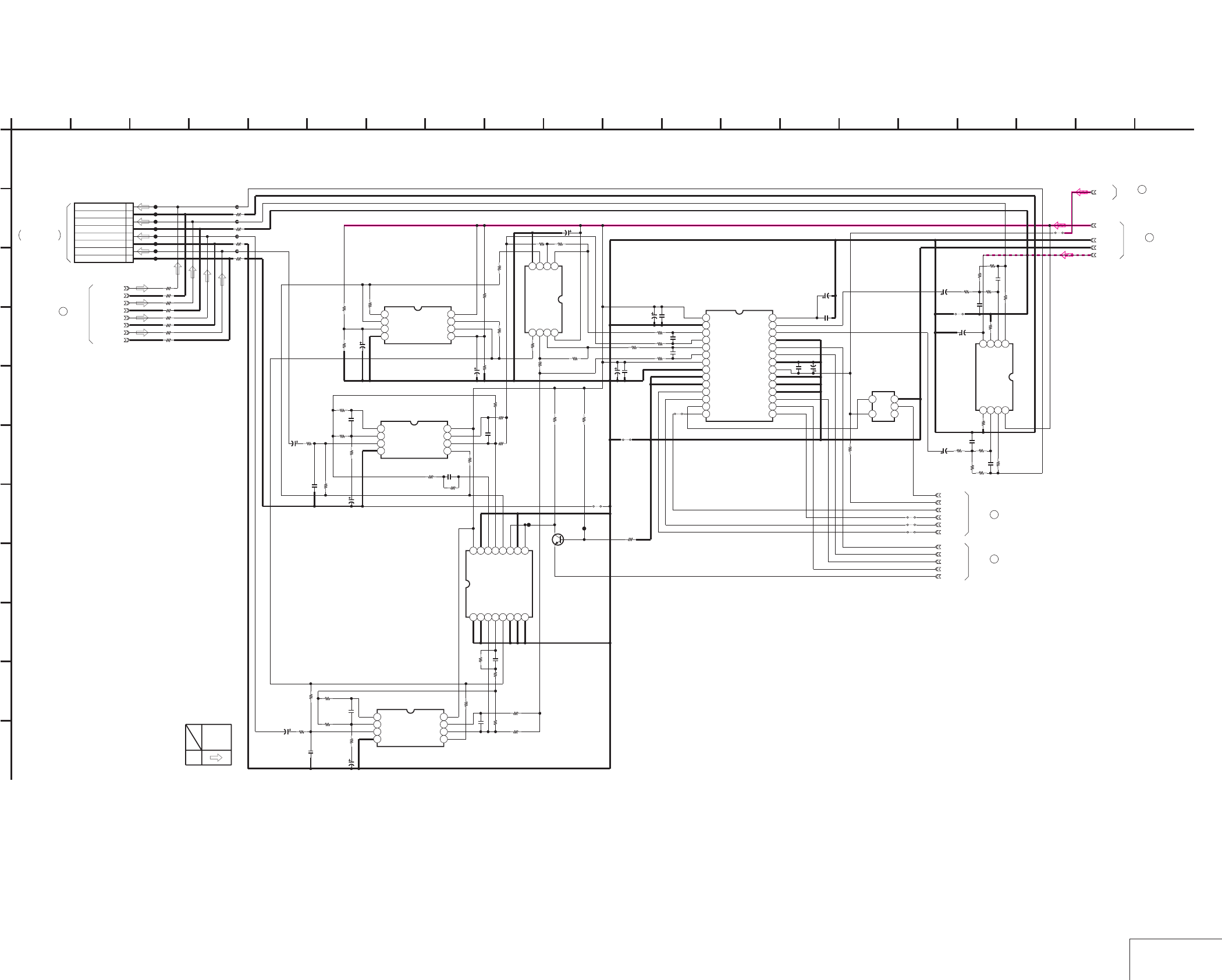
DSR-50/50P
4-41 4-42 AUDIO 1
JC-20 (12/14)
JC-20 (AUDIO 1) SCHEMATIC DIAGRAM • See page 4-15 for JC-20 printed wiring board.
8P
CN7001
1
CH1 OUT
2
GND(CH1 OUT)
3
CH2 OUT
4
GND(CH2 OUT)
5
CH3 OUT
6
GND(CH3 OUT)
7
CH4 OUT
8
GND(CH4 OUT)
XX
R7057
XX
IC7003
1234
5678
XX
C7025
XX
R7081
XX
C7019 6.3V
XX
C7024
XX
R7042
XX
C7032
XX
C7022
6.3V
XX
C7017
XX
R7054
GND
XX
R7077
XX
C7021
AU_CH4_OUT
6.3V
XX
C7016
XX
R7047
XX
R7045
XX
R7048
XX
R7044
AU_CH3_OUT
XX
R7051
6.3V
XX
C7003
J_3V
A.-5V
XX
R7055
AU_GND3_OUT
6.3V
XX
C7014
XX
IC7009
1234
5678
XX
R7052
4V
XX
C7027
XX
R7043
XX
C7018
6.3V
XX
C7015
XX
R7078
XX
R7082
4V
XX
C7028
6.3V
XX
C7009
XX
R7083
XX
R7076
XX
IC7006
1234567891011121314
15 16 17 18 19 20 21 22 23 24 25 26 27 28
XX
R7056
6.3V
XX
C7023
XX
C7020
XX
R7027
XX
C7031
XX
R7079
AU_GND4_OUT
XX
IC7005
1234
5678
XX
R7080
XX
R7028
XXR7053
A.+5V
XX
R7029
AU_CH2_OUT
AU_CH1_OUT
AU_GND1_OUT
AU_GND2_OUT
0
R7001
0R7002
0
R7003
0
R7004
0
R7005
0
R7006
0
R7007
0
R7008
XXR7011
XX
R7012
XX
R7014
XX
R7016
CL7032
CL7033
CL7034
CL7035
CL7036
CL7037
CL7038
CL7039
SFD_LRCK
SFD_BCK
SOA
SIC
DEM1
XPD_DA
XPD_AD
DEM0
SFD_FCK
XX
IC7008
123
45
XX
IC7002
1234
5678
6.3V
XX
C7008
R7022
XX
XX
R7026
XX
R7033
XX
C7007
XX
C7012
XX
R7023
XX
R7024
XX
R7018
XX
IC7004
12345678
910111213141516
XX
R7036
XX
Q7001 XX
R7050
XX
R7030
XX
R7049
EMP
XXR7031
XX
C7010
XX
R7038
CL7040
XX
C7004
XX
R7046
XX
R7039
AUDIO_GND
XX
R7021
XX
R7041
XX
R7025
XX
IC7001
1234
5678
XX
C7002
XX
R7017
XX
R7034
XX
R7020
XX
R7037
XX
R7035
6.3V
XX
C7001
XX
R7032
XX
R7040
XX
C7011
XX
R7019
XX
C7013
XX
C7005
6.3V
XX
C7006
XX
JS7007
XX
JS7005
XX
JS7008
XX
JS7006
SOB
XX
R7065
XX
JS7009
XX
C7030
XX
C7029
XX
R7202
XX
R7201
XX
R7204
XX
R7203
CL7209
R7009
XX
R7010 XX
R7013 XX
R7015 XX
XX
C7302
0
JS7001
0
JS7002
0
JS7003
1
A
JC-20 BOARD (14/14)
65
66
JC-20 BOARD (14/14)
35
JC-20 BOARD (6/14)
JC-20 BOARD (13/14)
67
JC-20 BOARD (14/14)
64
CN605
VD-28 BOARD (11/15)
(SEE PAGE 4-95)
XX MARK:NO MOUNT
AUDIO 1
JC-20 BOARD (12/14)
-REF.NO.:20,000 SERIES-
AUDIO
SIGNAL
PB
SIGNAL PATH
1816
F
17
C
153 1045
J
1172
D
8 19
K
H
12
I
136
G
B
E
14 20
05
9
THROUGH THE
JV-58 HARNESS
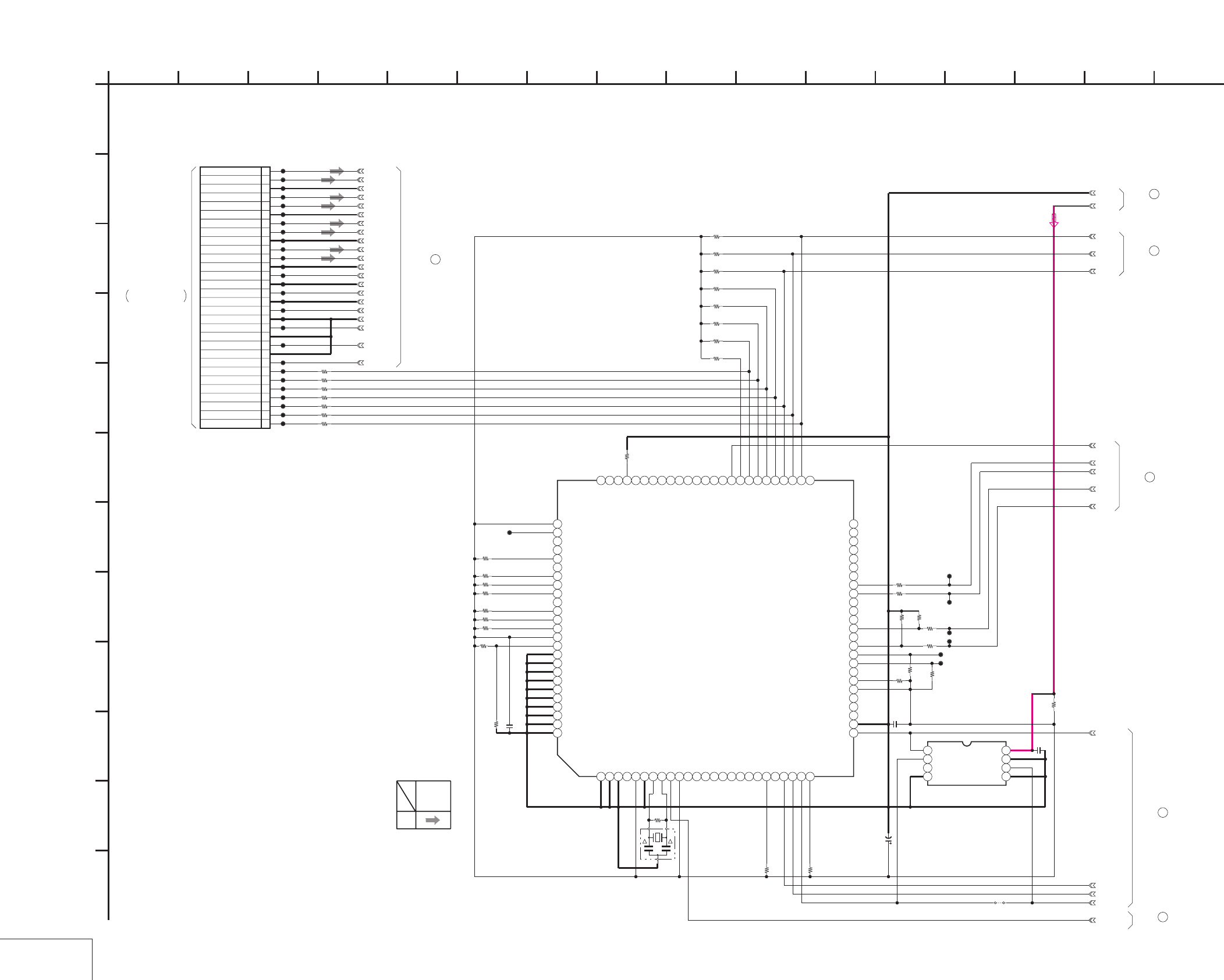
DSR-50/50P
4-43 4-44
AUDIO 2
JC-20 (13/14)
JC-20 (AUDIO 2) SCHEMATIC DIAGRAM • See page 4-15 for JC-20 printed wiring board.
30P
CN7002
1
NC
2
NC
3
NC
4
NC
5
NC
6
NC
7
NC
8
DSP SCK
9
GND
10
DSP SO
11
GND
12
DSP SI
13
GND
14
DSP CS
15
GND
16
TC OUT
17
GND
18
TC IN
19
GND
20
AU Y4 IN
21
AU X4 IN
22
GND
23
AU Y3 IN
24
AU X3 IN
25
GND
26
AU Y2 IN
27
AU X2 IN
28
GND
29
AU Y1 IN
30
AU X1 IN
CL7004
CL7005
CL7006
CL7007
CL7013
CL7014
CL7015
CL7016
CL7017
CL7018
CL7019
CL7020
CL7021
CL7022
CL7023
CL7024
CL7025
CL7026
CL7027
CL7028
CL7029
CL7030
CL7031
CL7008
CL7009
CL7010
CL7011
CL7012
GND
J_3V
XX
R7088
XX
C7033
XX
R7085
XX
R7087
XX
R7067
XX
IC7007
1 2 3 4 5 6 7 8 9 10111213141516171819202122232425
26 27 28 29 30 31 32 33 34 35 36 37 38 39 40 41 42 43 44 45 46 47 48 49 50
5152535455565758
5960616263
646566676869707172737475
767778798081828384858687888990919293949596979899100
XX
R7071
X7001
XX
XX
R7069
XX
R7075
XX
R7086
XX
R7073
XX
C7026
XX
R7063
XX
R7068
XX
R7072
XX
R7084
XX
R7074
XX
R7064
CL7043
XX
R7070
CL7041
XX
R7058
CL7042
XX
R7066
XVSP_SCK
VSP_SO
VSP_SI
XCS_DSP
XSYS_RESET
AU_X1_IN
TC_IN
DSP_SCK
TC_OUT
DSP_CS
DSP_SO
DSP_SI
AU_Y1_IN
AU_Y2_IN
AU_X2_IN
AU_X3_IN
AU_Y3_IN
AU_Y4_IN
AU_X4_IN
AU_1_GND_IN
XPD_DA
XPD_AD
DEM1
DEM0
XX
R7060
XX
R7061
XXR7062
XX
R7059
XX
R7089
AU_2_GND_IN
AU_3_GND_IN
AU_4_GND_IN
TC/GNDOUT
TC/GNDIN
GND
XX
JS7010
EMP
6.3V
XX
C7100
XX
R7106
XX
R7105
XX
R7104
XXR7103
XX
R7102
XX
R7101
XX
R7100
A.MON.1
A.MON.2
A.XUP
XX
R7205
CL7205
XX
R7206
CL7206
XX
R7207
CL7207
XX
R7208
CL7208
XX
R7301
XX
R7302 XX
R7303
XX
IC7301
1234
5678
XX
C7301
XX
R7304
1
A
JC-20 BOARD (14/14)
68
JC-20 BOARD (11/14)
63
JC-20 BOARD (12/14)
67
52
JC-20 BOARD (10/14)
59
JC-20 BOARD (11/14)
69
JC-20 BOARD (14/14)
(SEE PAGE 4-95)
CN606
VD-28 BOARD (11/15)
-REF.NO.:20,000 SERIES-
XX MARK:NO MOUNT
JC-20 BOARD (13/14)
AUDIO 2
1093 15141154287 1612 136
E
J
D
G
K
L
I
F
05
C
B
H
REC
SIGNAL PATH
SIGNAL
AUDIO
THROUGH THE
FVJ-13 FLAT CABLE
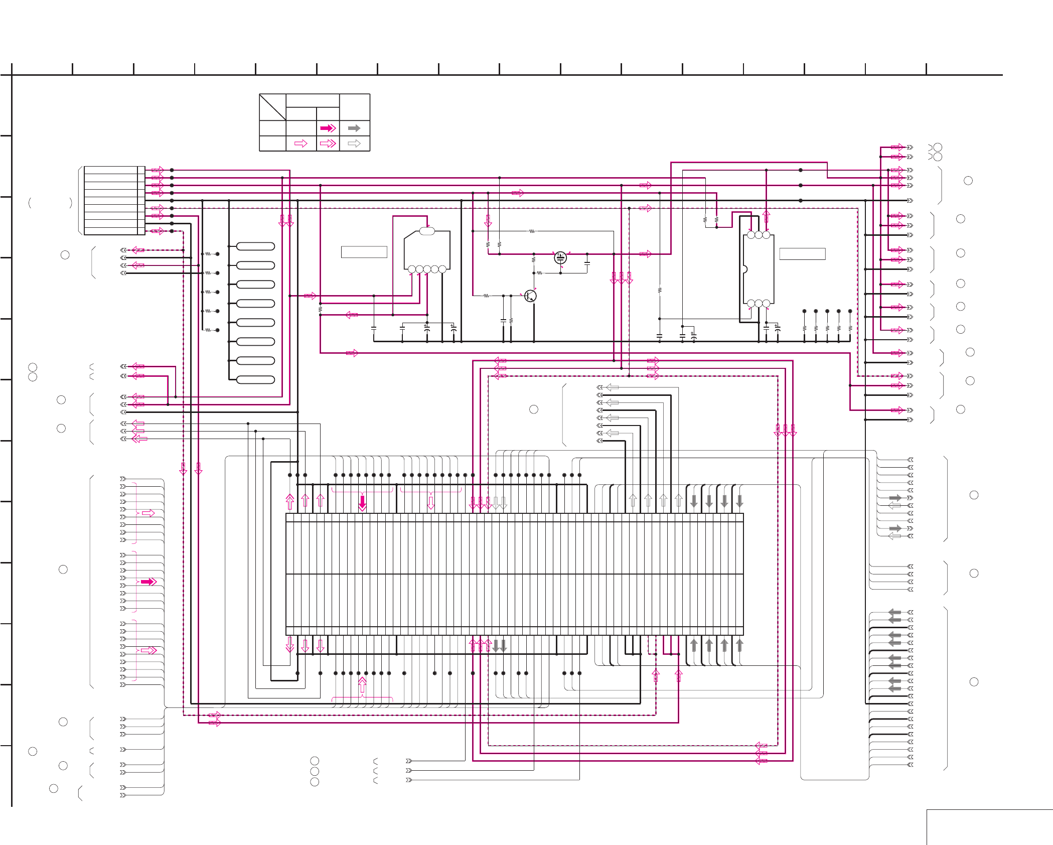
DSR-50/50P
4-45 4-46 POWER SUPPLY
JC-20 (14/14)
JC-20 (POWER SUPPLY) SCHEMATIC DIAGRAM • See page 4-15 for JC-20 printed wiring board.
E-E
E-E
NO MARK:REC/PB MODE
555.5
5
2.82.8
0
0
0.7
1.32.8
2.8 2
CL1102
CL1103
CL1180
CL1179
6.3V
10u
C1104
0.01u
C1102
XX
C1108
CL1105
CL1100
CL1101
CL1106
CL1107
CL1108
CL1104
LND101
GND
LND102
GND
LND103
GND
LND104
GND
LND105
GND
LND106
GND
LND107
GND
LND108
GND
XX
R1146
XX
R1147
XX
R1148
XX
R1149
XX
R1145
CL1140
CL1141
CL1142
CL1143
CL1144
9P
CN1100
1
SW +6V
2EVR +3V
3VIDEO +5V
4SW +3V
5GND
6VIDEO -5V
7AUDIO +5V
8AUDIO GND
9AUDIO -5V
PQ05TZ1U
IC1113
12345
6
6.3V
47u
C1190
0.01u
C1189
0.01u
C1191
XX
R1100
IC1100
TK11220BMCL
123
456
0.1u
C1192
6.3V
XX
C1193
6.3V
47u
C1195
CL1182
0
R1229
SI2301DS-T1
Q1131
10k
R1230
220k
R1231
2SC4081T106R
Q1132
10k
R1232
15k
R1233
0.033u
C1196
XX
R1234
XX
R1224
XX
R1225
XX
R1226
XX
R1227
XX
R1228
CL1183
CL1184
CL1185
CL1186
CL1187
0
R1236
XX
R1235
0
R1237
XX
R1238
1u
C1197
CL8004
CL8026
CL8018
AU_Y2_IN
CL8040
CL8056
JC04
CL8077
JC06
CL8063
DA135
CL8003
CL8025
OCK
CL8017
AU_2_GND_IN
CL8038
CL8075
CL8055
AU_4_GND_IN
CL8076
Y6
MY06
CL8058
CL8002
CL8024
LOCK_MCK
CL8016
AU_Y1_IN
CL8036
CL8050
CL8073
JC02
CL8070
MY04
VSP_SO
SPCK2
CL8015
AU_3_GND_IN
CL8034
VSP_SI
CL8049
OSD_HD
CL8074
Y0
CL8064
MY01
PAL/XNT
CL8014
CL8032
CL8022
CL8046
Y1
CL8068
Y4
XCS_DSP
MY03
CL8066
Y7
Y3
VD_HD
CL8013
CL8031
CL8021
CL8044
Y5
CL8048
MY07
JC01
CL8060
PB/XREC
XVSP_SCK
CL8009
AU_Y4_IN
CL8028
CL8020
CL8043
JC03
CL8039
CL8023
Y2
MY05
GND
VFD_OE
JC05
CL8061
MY00
V_FROM_SYNCGEN
CL8006
CL8027
CL8019
AU_Y3_IN
CL8042
CN8001 120P
1 DPB_YOUT
3 GND
5 DPB_CROUT
7 GND
9 DPB_CBOUT
11 GND
13 MY00
15 MY01
17 MY02
19 MY03
21 MY04
23 MY05
25 MY06
27 MY07
29 GND
31 MHO
33 DA135
35 AFH
37 VD_HD
39 N.C
41 SPCK2
43 PAL/XNT
45 PB/XREC
47 FIFO/MUTE
49 J_3V
51 VIDEO_+5V
53 VIDEO_-5V
55 SOA
57 SOB
59 LOCK_MCK
61 OCK
63 SFD_FCK
65 N.C
67 VFD_VD
69 VFD_OE
71 GND
73 XCS_DSP
75 VSP_SI
77 XRST_VSP
79 GND
81 DSP_CS
83 DSP_SI
85 TC/GNDIN
87 TC_IN
89 AUDIO_GND
91 AUDIO_GND
93 AUDIO_GND
95 A.-5V
97 A.-5V
99 A.+5V
2DPB_YOUT
4GND
6DPB_CROUT
8GND
10DPB_CBOUT
12GND
14Y0
16Y1
18Y2
20Y3
22Y4
24Y5
26Y6
28Y7
30GND
32JC00
34JC01
36JC02
38JC03
40JC04
42JC05
44JC06
46JC07
48N.C
50J_3V
52VIDEO_+5V
54VIDEO_-5V
56SIC
58SID
60SFDBCK
62BCK
64SFD_LRCK
66LRCK
68N.C
70VFD_HD
72GND
74N.C
76XVSP_SCK
78VSP_SO
80GND
82DSP_SCK
84DSP_SO
86TC/GNDOUT
88TC_OUT
90AU_GND4_OUT
92AU_CH4_OUT
94AU_GND3_OUT
96AU_CH3_OUT
98AU_GND2_OUT
100
AU_CH2_OUT
101 A.+5V 102
AU_GND1_OUT
103 A.+5V 104
AU_CH1_OUT
105 AU_4_GND_IN 106
AU_4_GND_IN
107 AU_Y4_IN 108
AU_X4_IN
109 AU_3_GND_IN 110
AU_3_GND_IN
111 AU_Y3_IN 112
AU_X3_IN
113 AU_2_GND_IN 114
AU_2_GND_IN
115 AU_Y2_IN 116
AU_X2_IN
117 AU_1_GND_IN 118AU_1_GND_IN
119 AU_Y1_IN 120
AU_X1_IN
CL8057
JC00
CL8078
JC07
AU_1_GND_IN
MY02
CL8062
AFH
FIFO_MUTE
XMUTN
XSYS_RESET
AU_X1_IN
AU_X2_IN
AU_X3_IN
AU_X4_IN
TC_IN
TC/GNDIN
TC_OUT
TC/GNDOUT
DSP_CS
DSP_SI
DSP_SO
DSP_SCK
SFD_FCK
SFD_LRCK
SFD_BCK
SIC
BCK
LRCK
SID
1
A
MHO
AU_GND4_OUT
AU_CH4_OUT
AU_GND3_OUT
AU_CH3_OUT
AU_GND2_OUT
AU_CH2_OUT
AU_GND1_OUT
AU_CH1_OUT
SW_6V
UNSW_3.0V
DPB_YOUT
DPB_CROUT
DPB_CBOUT
GND
SW_6V
UNSW_3.0V
A.+5V
AUDIO_GND
A.-5V
GND
GND
J_3V
J_1.9V
J_3V
GND
J_1.9V
J_3V
J_3V
GND
GND
VIDEO_+5V
+5V
GND
GND
J_3V
+5V
J_1.9V
VIDEO_-5V
VIDEO_+5V
GND
GND
J_3V
J_3V
J_3V
GND
SOB
SOA
VFD_HD
2 16
L
I
K
12
G
68
D
E
JC-20 BOARD (14/14)
B
7
05
151310 11
C
H
F
3
J
14945
SIGNAL PATH
REC
Y
VIDEO SIGNAL AUDIO
CHROMA SIGNAL
PB
XX MARK:NO MOUNT
POWER SUPPLY
-REF.NO.:20,000 SERIES-
(SEE PAGE 4-102)
VD-28 BOARD (14/15)
CN904
CN9500
(SEE PAGE 4-67)
DI-73 BOARD (9/9)
JC-20 BOARD (12/14)
66
56
JC-20 BOARD (10/14)
47
JC-20 BOARD (9/14)
JC-20 BOARD (11/14)
62
JC-20 BOARD (1/14)
7
29
JC-20 BOARD (5/14)
31
JC-20 BOARD (5/14)
JC-20 BOARD (4/14)
21
JC-20 BOARD (1/14)
6
JC-20 BOARD (12/14)
64
61
JC-20 BOARD (11/14)
65
JC-20 BOARD (12/14)
69
JC-20 BOARD (13/14)
53
JC-20 BOARD (10/14)
JC-20 BOARD (6/14)
36
43
JC-20 BOARD (7/14)
25
JC-20 BOARD (5/14)
37
JC-20 BOARD (6/14)
16
JC-20 BOARD (3/14)
46
JC-20 BOARD (9/14)
JC-20 BOARD (13/14)
68
20
JC-20 BOARD (4/14)
JC-20 BOARD (2/14)
10
1
JC-20 BOARD (1/14)
IC1113 IC1100
48
JC-20 BOARD (9/14)
JC-20 BOARD (10/14)
51
60
JC-20 BOARD (11/14)
THROUGH THE
VJ-106 HARNESS
70
JC-20 BOARD (11/14)
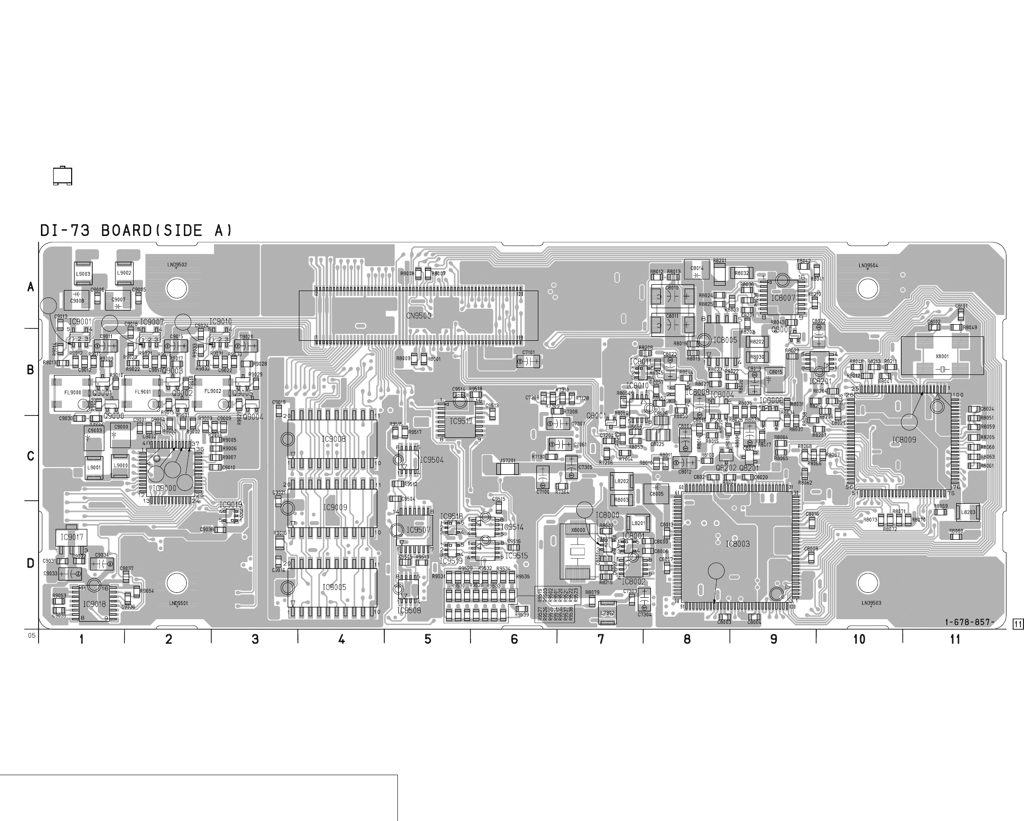
DSR-50/50P
4-47
4-48
VIDEO D/A CONVERTER, SYNC SHIFTER,
AUDIO A/D, D/A CONVERTER, AUDIO DSP, TIME CODE IN/OUT
DI-73
DI-73 (VIDEO D/A CONVERTER, SYNC SHIFTER, AUDIO A/D, D/A CONVERTER, AUDIO DSP, TIME CODE IN/OUT) PRINTED WIRING BOARD
– Ref. No.: DI-73 board; 10,000 series –
• For Printed Wiring Board.
• DI-73 board is four-layer print board. However, the patterns of
layers 2 to 3 have not been included in the diagram.
• There are a few cases that the part isn't mounted in this model
is printed on this diagram.
• See page 4-153 for printed parts location.
• Chip transistor
EB
C
4
56
13
2
7
8
9
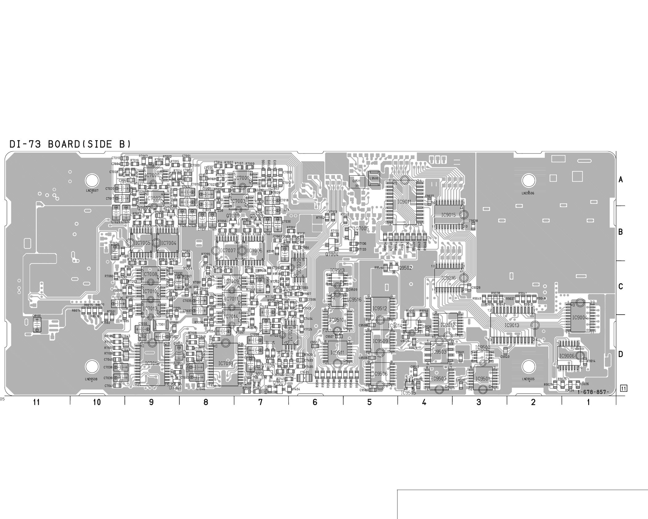
DSR-50/50P
4-49
4-50
VIDEO D/A CONVERTER, SYNC SHIFTER,
AUDIO A/D, D/A CONVERTER, AUDIO DSP, TIME CODE IN/OUT
DI-73
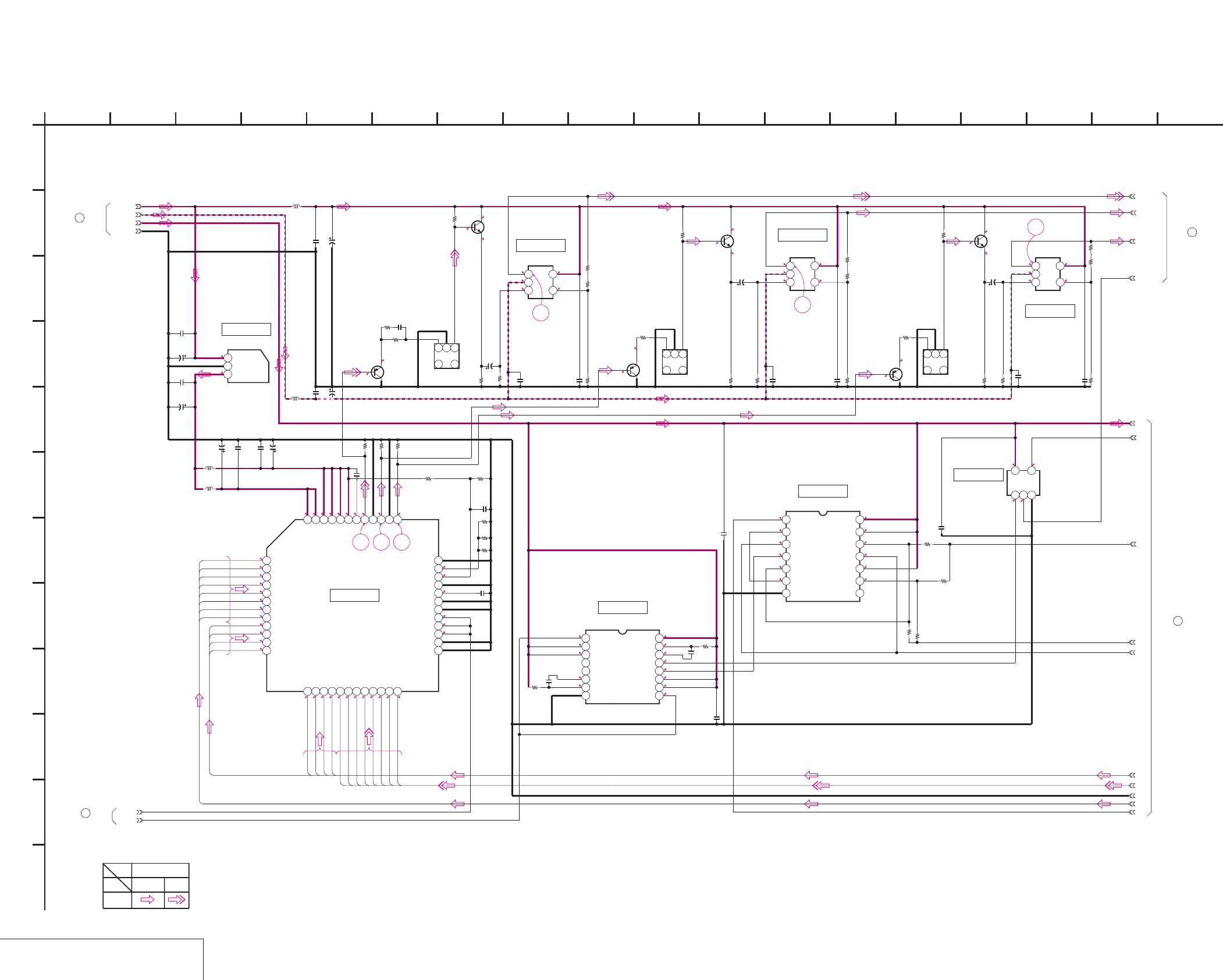
DSR-50/50P
4-51 4-52
VIDEO D/A CONVERTER
DI-73 (1/9)
DI-73 (VIDEO D/A CONVERTER) SCHEMATIC DIAGRAM • See page 4-47 for DI-73 printed wiring board. • See page 4-149 for waveforms.
NO MARK:REC/PB MODE
5
3.1
1.1
0.5
3.1
2.4
5
5
0.4
0.6
-4.9
0.4
1.3
0.7
5
2.5
3.2
5
0.4
0.7
-4.9
0.4
1.3
0.7
5
2.5
3.2
5
0.4
0.7
-4.9
0.4
0.32.8
0.3 0
2.8
2.8
1.4
1.5
2.8
1.4
2.6
1.5
1.5
2.8
1.4
1.5
2.8
2.6
0
0.3
2.8
2.8
2.8
2.5
2.5
2.8
2.8
0
2.8
3.1
3.1
3.1
3.1
3.1
3.1
1.6
0.5
0.7
0.7
1.3
1.3
0.5
1.5
1.5
1.5
0.8
1.1
1.1
1.1
1.1
1.8
1.1
1.1
0.8
0.9
1.3
1.5
1.2
1.2
1
1
1.1
1.1
1.1
1.8
1.2
1.3
1.2
1.2
6
5
4
321
VIDEO_5V
J_3V
6.3V
47u
C9000
0.1u
C9004
GND
27k
R9007
27k
R9006
TC74VHC74FT(EL)
IC9006
1234567
8 9 10 11 12 13 14
8200
R9005
0.01u
F
C9009
0.1u
C9010
10uH
L9001
10uH
L9000
0.01u
C9002
6.3V
47u
C9003
VIDEO_-5V
0.01u
C9001
470
R9029
10uH
L9003
2SC4081T106R
Q9005
470
R9018
22k
R9019
1k
R9017 1k
R9028
2SC4081T106R
Q9003
10uH
L9002
22u
4V
C9011
FL9001
123
4
6
2SA1576A-T106-R
Q9004
470
R9010
22u
4V
C9015
1k
R9027
2SC4081T106R
Q9001
1k
R9015
DPB_YOUT
2SA1576A-T106-R
Q9002
DPB_CROUT
22k
R9011
DPB_CBOUT
FL9000
123
4
6
6.3V
47u
C9007
6.3V
47u
C9008
1k
R9009
22k
R9030
2SA1576A-T106-R
Q9000
0.01u
C9005
0.01u
C9006
1k
R9008
FL9002
123
4
6
22u
4V
C9020
0.01u
C9014
FIFO_MUTE
LM7131BCM5X
IC9001
123
45
470
R9014
470
R9013
0
R9012
470
R9023
0
R9021
470
R9022
LM7131BCM5X
IC9007
123
45
0
R9031
470
R9032
LM7131BCM5X
IC9010
12
3
45
470
R9033
330
R9002
330
R9001
330
R9000
1800
R9003
1200
R9004
0
R9024
0
R9025
XX
R9020
XX
R9026
0.1u
C9012
0.1u
C9013
0.1u
C9017 0.1u
C9018 0.1u
C9022 0.1u
C9024
220
R9052 33p
C9030
TK11630UTL
IC9017
123
0.1u
C9031
6.3V
10u
C9033
6.3V
10u
C9034
0.1u
C9032
TC74VHC221AFT(EL)
IC9018
12345678
9 10111213141516
100p
C9035
5600
R9053
27k
R9054
100p
C9036
0.1u
C9037
IC9019
TC7SH32FU-TE85R
123
45
0.1u
C9038
RCK_1
MASK_HD
GND
4-5
4-6
4-7
4-8
4-4
4-3
4-2
J_3V
4-1
1
A
CXD2304R
IC9000
123456789101112
13 14 15 16 17 18 19 20 21 22 23 24
25 26 27 28 29 30 31 32 33 34 35 36
373839404142434445464748
DY7
DY6
DY5
DY4
DY3
DY2
DY1
DY0
CR07
CR06
CR05
CR04
CR03
CR02
CR01
CR00
CB07
CB06
CB05
CB04
CB03
CB02
CB01
CB00
4
DI-73 BOARD (2/9)
2
DI-73 BOARD (3/9)
1
DI-73 BOARD (9/9)
DI-73 BOARD (1/9)
XX MARK:NO MOUNT
-REF.NO.:10,000 SERIES-
VIDEO D/A CONVERTER
3
DI-73 BOARD (9/9)
PB
CHROMA
SIGNAL PATH
Y
VIDEO SIGNAL
E
6
K
16
G
12 1354
D
2
J
810
F
189
I
3 17
L
14 15
H
11
B
C
05
7
IC9017
IC9001
IC9007
IC9010
IC9019
IC9006
IC9018
IC9000
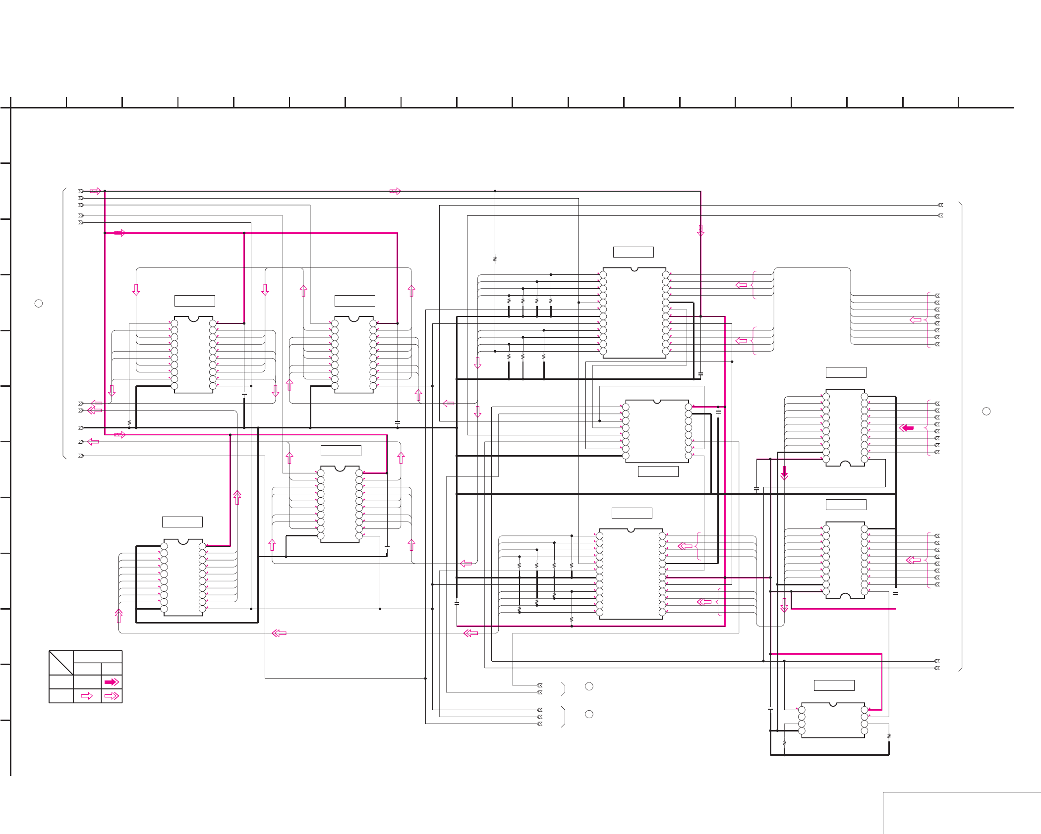
DSR-50/50P
4-53 4-54
VIDEO FIFO MEMORY
DI-73 (2/9)
DI-73 (VIDEO FIFO MEMORY) SCHEMATIC DIAGRAM • See page 4-47 for DI-73 printed wiring board.
E-E
E-E
NO MARK:REC/PB MODE
R:REC MODE
P:PB MODE
R0/
P2.8 2.8
R2.8/P0
1.1
0.8
1.3
1.6
0.8
0.8
1.1
1
R2.8/P0
0.8
1
1.2
1.4
0.8
0.8
1.1
1
2.8
0.8
0.8
1.2
1
0.8
1.4
2.8
1.1
1
R0.9/P3.2
R1.2/P3.2
R1.4/P3.2
R1.3/P3.2
R0.9/P3.2
R0.9/P3.2
R1.3/P3.2
R1/P3.2
R0/P2.8
2.8
2.6
2.6
2.6
R0/P2.8
2.6
2.6
2.6
1.1
1.5
1.3
1.1
1.1
1.2
1.2
0.3
2.6
1.1
1.5
1.1
1.1
1.8
2.6
2.8
1.1
1.3
1.1
1.1
1.8
1.1
1.1
1.2
1.2
2.8
1.1
1.1
1.8
1.1
1.8
1.1
1.1
1.1
1.5
1.1
1.1
1.2
1.2
1.2
1.2
1.3
1.2
1.4
1.8
1.1
2.8
1.1
1.8
1.1
1.1
1.1
1.5
1.1
1.2
1.2
1.2
1.2
1.3
0
1.3
1.2
1.2
1.2
1
1.1
1.2
1.2
1.4
1.2
1
1.1
1.8
1.1
2.8
1.1
1.8
1.1
1.1
1.1
1.5
1.1
0.8
1.5
0.9
1.3
1.1
1.1
1.5
2.8
0.8
1.1
0.8
1.5
1.3
0.8
1.1
1.1
0.9
1.1
2.6
0.3
1.1
0.8
0.8
1.1
1.1
0.9
1.3
1.5
1.5 1.3
2.8
1.1
0.8
0.8
1
2.6
1.4
1.2
1
0.8
(Note)
Note:This signal follows the same
circuit as PB signal after
this point.
SN74HC377ANSR
IC9005
12345678910
11 12 13 14 15 16 17 18 19 20
PB/XREC
0
R9016
0.01u
C9021
0.01u
C9016
DA135
MY00
MY01
MY02
MY03
0.01u
C9019
TC74VHC574FT(EL)
IC9004
12345678910
11 12 13 14 15 16 17 18 19 20
MY04
MY05
MY06
MY07
SN74HC377ANSR
IC9008
12345678910
11 12 13 14 15 16 17 18 19 20
JC06
JC00
JC07
JC01
JC05
JC03
JC04
JC02
IC9013
M66280FP-280D
123456789101112
13 14 15 16 17 18 19 20 21 22 23 24
IC9011
M66280FP-280D
123456789101112
13 14 15 16 17 18 19 20 21 22 23 24
SN74HC377ANSR
IC9009
12345678910
11 12 13 14 15 16 17 18 19 20
TC74VHC541FT(EL)
IC9016
12345678910
11121314151617181920
TC74VHC541FT(EL)
IC9015
12345678910
11121314151617181920
Y7
Y4
Y5
Y1
Y3
Y0
Y6
Y2
TC74VHC157FT(EL)
IC9012
12345678
9 10111213141516
SPCK2
0.01u
C9027
0.01u
C9026
0.01u
C9028
0.01u
C9029
0.01u
C9025
0.01u
C9023
EE_WHDC
RCK_2
RHD_Y
RHD_C
0
R9051
0
R9050
47k
R9046
47k
R9043
47k
R9039
47k
R9036
47k
R9047
47k
R9044
47k
R9040
47k
R9034
47k
R9048
47k
R9045
47k
R9041
47k
R9037
47k
R9049
TC7WH04FU(TE12R)
IC9014
1234
5678
EE_WHDY
J-3V
4-1
4-2
4-3
4-4
4-5
4-6
GND
4-7
4-8
MHO
47kR9042
47k
R9038
47k
R9035
1
A
MY07
MY06
MY05
MY04
MY03
MY02
MY01
MY00
Y00
Y02
Y04
Y01
Y03
JC6
JC7
JC5
JC2
JC1
JC0
JC4
JC3
CR4
CR5
CR6
CR7
CR3
CR1
CR2
CR0
CR3
CR2
CR1
CR0
CR4
CR5
CR6
CR7
JC0
JC1
JC2
JC3
JC7
JC6
JC5
JC4
CB07
CB06
CB05
CB04
JC7
JC6
JC5
JC4
JC0
JC1
JC2
JC3
CR07
CR06
CR05
CR04
CR00
CR01
CR02
CR03
DY7
DY6
DY5
DY4
DY3
DY2
DY1
DY0
Y00
Y01
Y02
Y03
Y04
Y05
Y06
Y07
MY07
MY06
MY05
MY04
MY03
MY02
MY01
MY00
MY07
MY06
MY05
MY04
MY03
MY02
MY01
MY00
JC07
JC06
JC05
JC04
JC03
JC02
JC01
JC00
JC07
JC06
JC05
JC04
JC03
JC02
JC01
JC00
CB03
CB02
CB01
CB00
Y05
Y06
Y07
E
8
J
XX MARK:NO MOUNT
2
D
45
-REF.NO.:10,000 SERIES-
G
DI-73 BOARD (2/9)
K
6
VIDEO FIFO MEMORY
1312 167
L
1714 153
I
9 18
F
10
05
C
B
11
H
DI-73 BOARD (1/9)
4
5
DI-73 BOARD (4/9)
6
DI-73 BOARD (3/9)
7
DI-73 BOARD (9/9)
REC
YCHROMA
SIGNAL PATH
VIDEO SIGNAL
PB
IC9005 IC9009
IC9004
IC9008
IC9011
IC9012
IC9013
IC9015
IC9016
IC9014
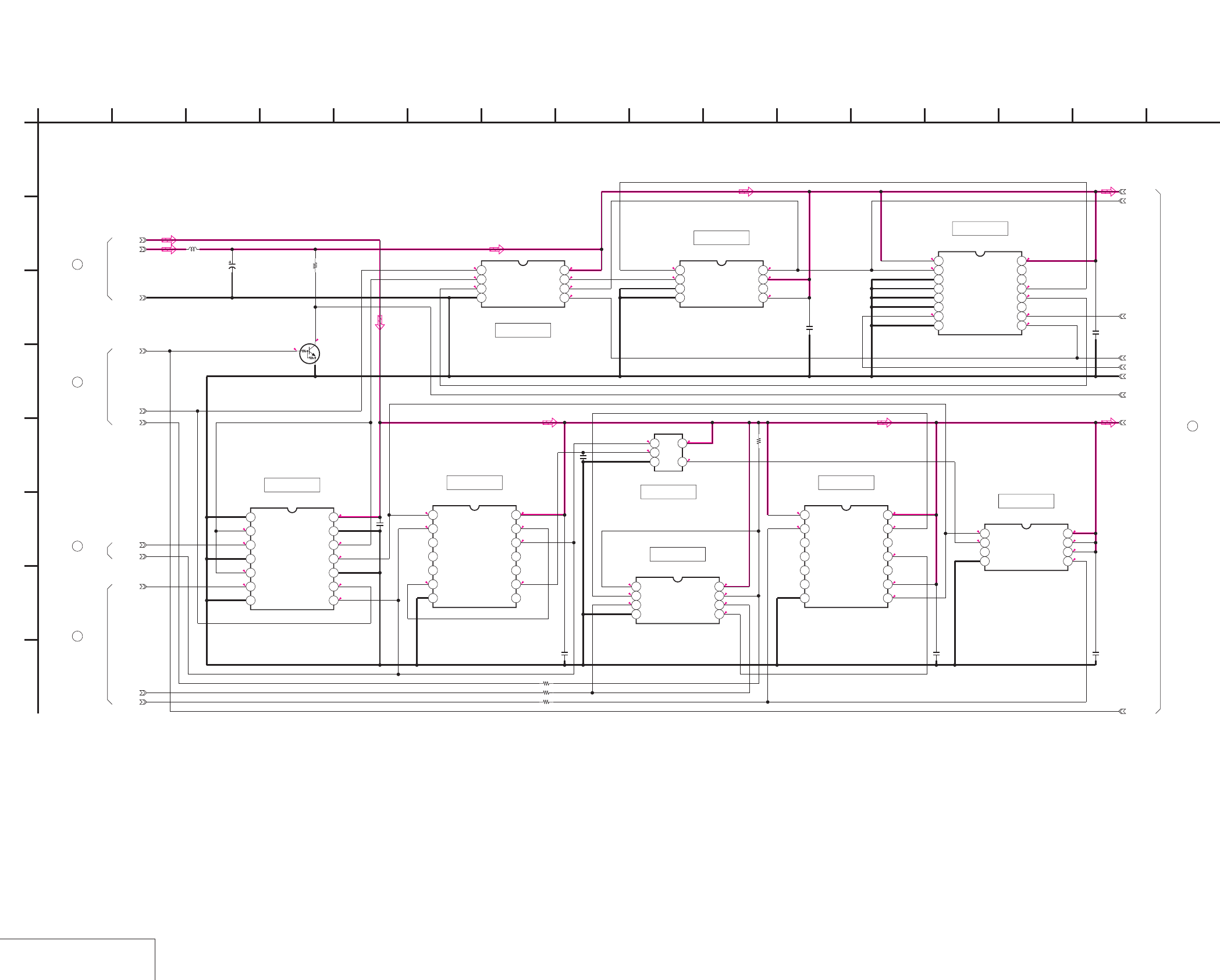
DSR-50/50P
4-55 4-56
SYNC SHIFTER 1
DI-73 (3/9)
DI-73 (SYNC SHIFTER 1) SCHEMATIC DIAGRAM • See page 4-47 for DI-73 printed wiring board.
5
3
0
0.5
5
5
2.4
0.4
0
5
NO MARK:REC/PB MODE
R:REC MODE
P:PB MODE
54.5
2.7
0
0.6
2.4
5
2.4
5
5
3
0.6
2.8
2.8
2.6
2.8
1.5
2.6
2.8
2.6 2.5
1.5
2.5
2.8
2.8
0.2
2.8
2.5
1.5
0.2
2.5
0.2
1.5
2.7
2.7
4.5
2.8
2.7
1.5
1.5
2.5
2.8
2.6
R0/P2.8
2.5
R0/P2.8
2.5
2.6
0.2
2.82.5
2.6
TC74VHC163FT(EL)
IC9506
12345678
9 10111213141516
0.1u
C9503
TC7W04FU(TE12R)
IC9500
1234
5678
VD_HD
0.1u
C9501
VIDEO_5V
GND
R9516
10k
PAL/XNT
TC74VHC125FT(EL)
IC9501
1234567
8 9 10 11 12 13 14
J_3V
RCK_1
RCK_2
TC74VHC393FT(EL)
IC9502
1234567
8 9 10 11 12 13 14
0.1u
C9500
0.1u
C9502
TC74VHC164FT(EL)
IC9507
1234567
8 9 10 11 12 13 14
0.1u
C9504
0
R9512
0
R9513
0.1u
C9505
RHD_Y
RHD_C
TC7S32FU(TE85R)
IC9505
123
45
TC7W241FU-TE12R
IC9504
1234
5678
TC7W74FU(TE12R)
IC9508
1234
5678
PB/XREC
UN5213-TX
Q9502
AV9173-15CS08T
IC9503
1234
5678
XX
R9515
0
R9517
MASK_HD
10uH
L9500
6.3V
47u
C9511
10-4
GND
10-6
10-5
J_3V
10-2
10-1
10-3
VIDEO_5V
100p
C9510
1
A
DI-73 BOARD (4/9)
10
IC9504
IC9505 IC9507
IC9508
IC9502
IC9501
IC9503
IC9500
IC9506
DI-73 BOARD (9/9)
8
DI-73 BOARD (9/9)
9
2
DI-73 BOARD (1/9)
6
DI-73 BOARD (2/9)
2
F
163 14129
G
4658
XX MARK:NO MOUNT
D
-REF.NO.:10,000 SERIES-
E
SYNC SHIFTER 1
DI-73 BOARD (3/9)
B
7
05
151310 11
C
H
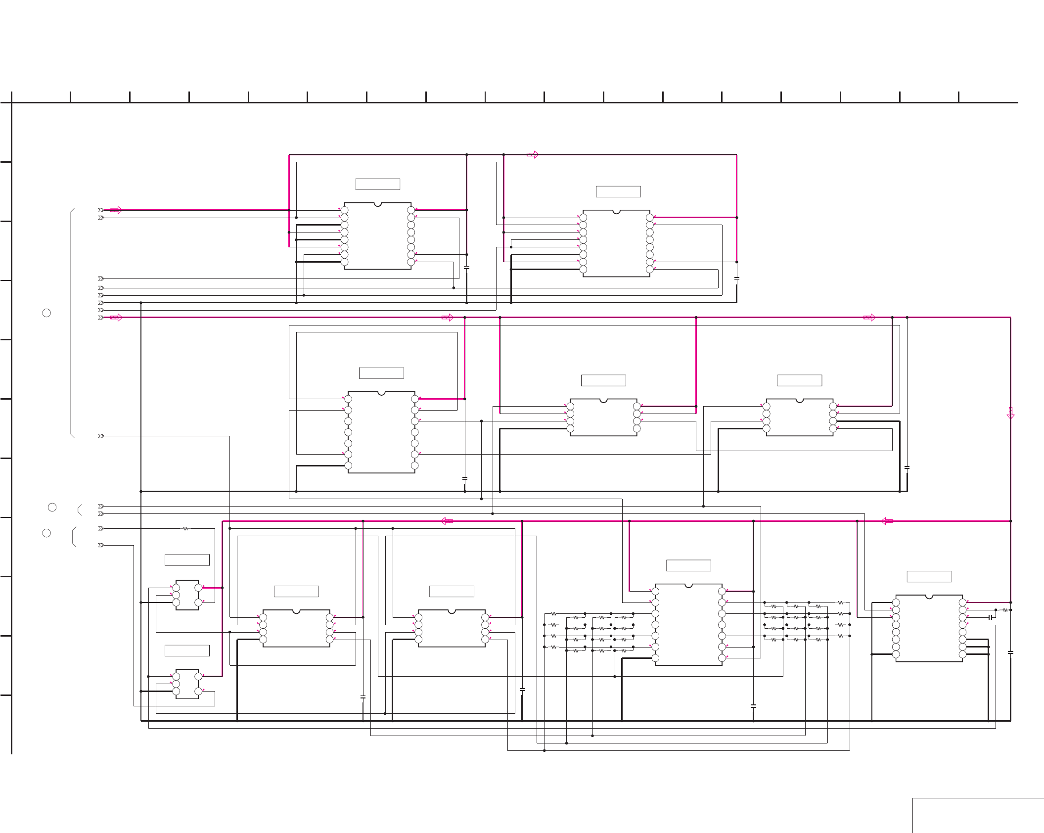
DSR-50/50P
4-57 4-58
DI-73 (SYNC SHIFTER 2) SCHEMATIC DIAGRAM • See page 4-47 for DI-73 printed wiring board.
SYNC SHIFTER 2
DI-73 (4/9)
0
2.8
2.8
NO MARK:REC/PB MODE
1.1
1.6
0
2.6
02.8
0
2.8
2.8
2.8
2.8
2.6
0
2.8
0.4
5
5
5
5
2.4
5
5
5
5
5
5
2.4 0.5
55
5
0.4
5
0.2
00.2
2.6
2.81.6
2.6
2.6 2.5
2.8
2.82.5
2.8
1.1
0
2.5
0
2.5
2.5
2.8
2.5
2.5
0 2.8
2.5
2.52.5
0
2.8
2.5
0
2.6
2.6
0 2.8
2.5
TC74VHC163FT(EL)
IC9509
12345678
9 10111213141516
TC74VHC163FT(EL)
IC9512
12345678
9 10111213141516
10-1
0.1u
C9506
0.1u
C9508
VIDEO_5V
GND
J_3V
TC74VHC393FT(EL)
IC9510
1234567
8 9 10 11 12 13 14
EE_WHDY
SPCK2
AFH
0.1u
C9507
0.1u
C9509
TC74VHC164FT(EL)
IC9511
1234567
8 9 10 11 12 13 14
XX
R9507
XX
R9506
XX
R9505
XX
R9504
0R9508
XX
R9509
XXR9510
XX
R9511
TC7WH74FU(TE12R)
IC9513
1234
5678
TC7WH04FU(TE12R)
IC9516
1234
5678
0.1u
C9512
0.1u
C9514
TC74VHC221AFT(EL)
IC9517
12345678
9 10111213141516
100p
C9513
5600
R9518
TC7S32FU(TE85R)
IC9518
123
45
XX
R9522
XX
R9523
XX
R9520
XXR9521
XX
R9501
0
R9519
XX
R9503
XX
R9502
EE_WHDC
TC7S32FU(TE85R)
IC9519
123
45
XX
R9529
XX
R9524
XX
R9526
XX
R9528
XX
R9531
XX
R9530
0
R9527
XX
R9525
XXR9534
XX
R9537
XX
R9539
XXR9535
0R9532
XXR9533
XX
R9536
XX
R9538
TC7W241FU-TE12R
IC9515
1234
5678
0.1u
C9516
0.1u
C9515
TC7W241FU-TE12R
IC9514
1234
5678
R9514
0
10-6
10-5
10-4
10-3
10-2
1
A
2 16
I
K
12
G
68
D
E
DI-73 BOARD (4/9)
B
7
05
151310 1711
C
H
F
3
J
14945
XX MARK:NO MOUNT
-REF.NO.:10,000 SERIES-
SYNC SHIFTER 2
11
DI-73 BOARD (9/9)
IC9509
DI-73 BOARD (2/9)
5
DI-73 BOARD (3/9)
10
IC9512
IC9510 IC9513 IC9516
IC9517
IC9511
IC9515IC9514
IC9518
IC9519
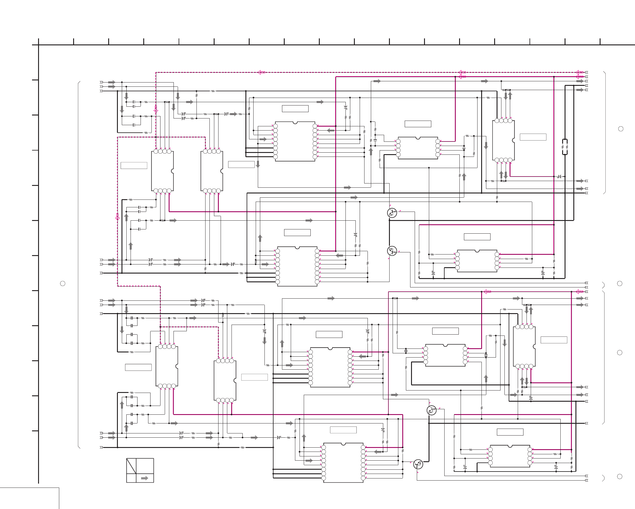
DSR-50/50P
4-59 4-60
AUDIO HPF
DI-73 (5/9)
DI-73 (AUDIO HPF) SCHEMATIC DIAGRAM • See page 4-47 for DI-73 printed wiring board.
NO MARK:REC/PB MODE
0
0
0
-4.9
0
0
0
5
0
0
0
0
0
5
-4.9
0
2.5
2.5
2.5
2.5
2.5
5
2.5
2.5
2.5
2.5
0
0
0
5
2.5
2.52.5
2.5
2.5
2.5
2.5
2.5
2.5
2.5
2.5
2.5
5
2.5
2.5
2.5
2.5
2.5
2.5
5
2.5
2.5
2.5
2.5
52.5
2.5
2.5
2.5
2.52.5
5
2.52.5
2.5
2.5
2.52.5
2.5
5
2.5
5
0
2.5
2.5
2.5 2.5
0
2.5
0
2.5
2.5
2.5
2.5
5
2.5
2.5
0
2.5
2.5
2.5
2.5
2.5
0
2.5
0
2.5
5
0
2.5
2.5
2.5
2.6
0
2.5
2.5
2.5
2.5
0
2.5
2.8
0
2.8
0
0
2.8
2.8
0
0
0
0
5
0
-4.9
0
0
0
0
5
0
-4.9
0
0
0
NJM2115V(TE2)
IC7013
1234
5678
100
R7083
XX
C7036
100
R7087
4700
R7085
0
R7008
AU_X1_IN
AU_Y1_IN
AU_Y2_IN
AU_X2_IN
AU_1_GND_IN
AU_2_GND_IN
NJM4580V(TE2)
IC7000
1234
5678
3300
R7014
3300
R7015
3300
R7002
3300
R7017
3300
R7016
3300
R7003
0.22u
C7000
0.22u
C7001
0.22u
C7005
0.22u
C7004
XX
C7008
XX
C7011
XX
C7009
XX
C7010
A.-5V
10k
R7027
10k
R7031
6.3V
10u
C7022
10k
R7038
10k
R7026
10k
R7036
NJM2115V(TE2)
IC7002
1234
5678
10k
R7034
6.3V
10u
C7016
6.3V
10u
C7020
6.3V
10u
C7017
10k
R7067
6800
R7098
100
R7093
6800
R7066
6.3V
10u
C7032
NJM2115V(TE2)
IC7010
1234
5678
10k
R7099
100
R7071
6.3V
10u
C7034
TC74HC4053AFT(EL)
IC7004
12345678
9 10111213141516
10k
R7030
10k
R7051
10k
R7050
6.3V
10u
C7028
10k
R7046
10k
R7042
6.3V
10u
C7026
NJM2115V(TE2)
IC7008
1234
5678
4700
R7062
100
R7063
6.3V
10u
C7029
10k
R7052 10k
R7053
TC74HC4053AFT(EL)
IC7005
12345678
9 10111213141516
6.3V
10u
C7024
10k
R7043
100
R7076
4700
R7080
10k
R7058
UN9211J-
(K8).SO
Q7001
XCH2_HPF
6.3V
10u
C7019
0
R7009
10k
R7060
4700
R7081
100
R7072
AU_4_GND_IN
10k
R7056
3300
R7019
10k
R7039
10k
R7101
AU_3_GND_IN
6.3V
10u
C7031
3300
R7018
100
R7084
TC74HC4053AFT(EL)
IC7006
12345678
9 10111213141516
100
R7077
NJM2115V(TE2)
IC7011
1234
5678
0.22u
C7007
100
R7065
NJM4580V(TE2)
IC7001
1234
5678
6.3V
10u
C7018
0.22u
C7006
6.3V
10u
C7033
XX
C7013
XX
C7012
100
R7088
10k
R7037
NJM2115V(TE2)
IC7014
1234
5678
XX
C7015
6800
R7068
3300
R7007
NJM2115V(TE2)
IC7009
1234
5678
6.3V
10u
C7023
NJM2115V(TE2)
IC7003
1234
5678
0.22u
C7003
10k
R7045
10k
R7069
3300
R7023
4700
R7090
AU_X3_IN
6.3V
10u
C7027
XCH4_HPF
10k
R7033
10k
R7041
6.3V
10u
C7025
100
R7094
3300
R7020
XX
C7037
AU_X4_IN
10k
R7044
10k
R7035
10k
R7028
UN9211J-
(K8).SO
Q7003
TC74HC4053AFT(EL)
IC7007
12345678
9 10111213141516
6800
R7100
3300
R7021
0.22u
C7002
AU_Y4_IN
6.3V
10u
C7030
10k
R7057
3300
R7006
AU_Y3_IN
10k
R7055
10k
R7029
6.3V
10u
C7021
10k
R7054
6.3V
10u
C7035
10k
R7049
3300
R7025 10k
R7048
XX
C7014
10k
R7059
UN9211J-
(K8).SO
Q7002
XCH1_HPF
UN9211J-
(K8).SO
Q7000
10k
R7061
XCH3_HPF
0
R7156
0
R7157
100
R7203
47p
C7202
100
R7204
100
R7205
0
R7501
0
R7502
A.+5V
AUDIO_GND
GND
13-1
13-2
13-3
13-4
A.+5V
15-1
15-2
15-3
15-4
AUDIO_GND
GND
4700
R7089
4700
R7095
10k
R7047
10k
R7040
3300
R7024
3300
R7022
47p
C7203
47p
C7204
4700
R7064
100
R7206
4700
R7091
4700
R7097
4700
R7096
10k
R7032
4700
R7086
47p
C7201
1
A
IC7013
IC7002
IC7014
IC7000
IC7007
IC7003
IC7001
2 16
L
I
K
12
G
68
D
E
DI-73 BOARD (5/9)
B
7
05
151310 1711
C
H
F
3
J
14945
AUDIO HPF
XX MARK:NO MOUNT
-REF.NO.:10,000 SERIES-
12
DI-73 BOARD (9/9)
13
DI-73 BOARD (6/9)
14
DI-73 BOARD (8/9)
15
DI-73 BOARD (6/9)
16
DI-73 BOARD (8/9)
SIGNAL
AUDIO
SIGNAL PATH
REC
IC7011
IC7006 IC7009
IC7010
IC7005
IC7008
IC7004
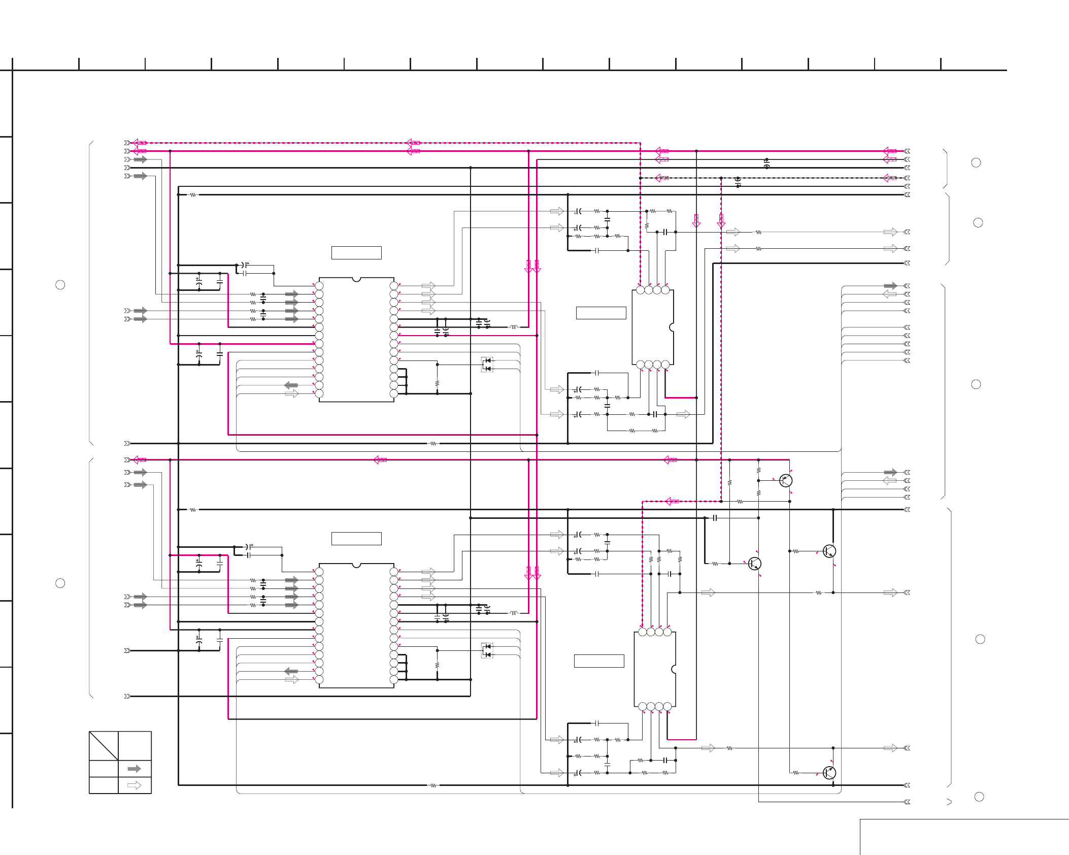
DSR-50/50P
4-61 4-62
DI-73 (AUDIO A/D, D/A CONVERTER) SCHEMATIC DIAGRAM • See page 4-47 for DI-73 printed wiring board.
AUDIO A/D, D/A CONVERTER
DI-73 (6/9)
NO MARK:REC/PB MODE
*:IMPOSSIBLE TO MEASURE THE
VOLTAGE AT THE MARKED POINTS.
2.5
5
2.5
2.5
2.5 2.5
2.8
0
2.5
2.5
2.5
2.5
2.8
2.3
5
5
2.8
0.8
1.5
1.4
*
*
2.5
2.3
2.8
2.5
1.5
2.5
1.4
2.5
*
2.8
2.5
2.5
5
0.8
5
2.5
2.8
*
0
5
2.5
2.5
0
005
0-4.9
0
0
0
000
-4.9 0
5
0
2.8
2.5
4.9
0
-0.2
-0.3
4.9
5
-0.2
0
4V
22u
C7061
470R7106
4700
R7128
4700
R7139
4V
22u
C7060
BCK
220
R7144
470R7105
470
R7112
1500
R7145
470
R7108
470
R7110
470
R7109
4700
R7130
+2.8V
0.1u
C7047
GND
XPD_DA1
4V
22u
C7059
220
R7143
LRCK
4700
R7129
16V
6.8u
C7045
0.1u
C7052
4700
R7146
6.3V
4.7u
C7054
SOD
1500
R7135
0.1u
C7046
XPD_DA2
0.1u
C7041
4700
R7127
16V
6.8u
C7039
DEM1
680p
C7069
4700
R7140
1500
R7138
470
R7107
4700
R7126 4700p
C7066
680p
C7065
4700
R7124
A.+5V
DEM0
6.3V
4.7u
C7050
680p
C7064
16V
6.8u
C7042
16V
6.8u
C7038
680p
C7068
220
R7131
4700p
C7062
4700p
C7063
470
R7111
0.1u
C7056
0.1u
C7040
220
R7134
100
R7153
A.-5V
100
R7150
100
R7151
XPD_AD1
XPD_AD2
4V
22u
C7058
SIB
MCK
SIA
SOC
AU_CH1_OUT
AU_CH2_OUT
AU_CH3_OUT
AU_CH4_OUT
AU_GND1_OUT
AU_GND2_OUT
AU_GND4_OUT
AU_GND3_OUT
0
R7116
0
R7115
0
R7120
0
R7122
AUDIO_GND
100
R7152
220
R7123
220
R7125
4700
R7137
4700
R7133
4700
R7136
2SC4081T106R
Q7008
2SA1576A
-T106-R
Q7007
47k
R7149
100k
R7148
100k
R7147
DA_CH3/4_ON
4700
R7132
4700
R7201
4700
R7202
MA132WK-TX
D7301
10k
R7301
10uH
L7301
10uH
L7302
MA132WK-TX
D7302
10k
R7302
4V22u
C7305 4700
R7304
220
R7303
C7306
680p
1500
R7307
4V
22u
C7307
4700
R7308
1500
R7309
C7308
680p
220
R7310
AK4528VF-E2
IC7016
123
4567891011121314
15 16 17 18 19 20 21 22 23 24 25 26 27 28
NJM3414AV(TE2)
IC7020
1234
5678
AK4528VF-E2
IC7018
123
45678910111213
14
15 16 17 18 19 20 21 22 23 24 25 26 27 28
NJM3414AV(TE2)
IC7021
1234
5678
2SC3326N
-TE85L-B
Q7005
2SC3326N
-TE85L-B
Q7004
47k
R7403
100k
R7404
4V
22u
C7401
1500
R7406
4700p
C7067
1500
R7405
680p
C7403
680p
C7404
4V
22u
C7402
1500
R7407
4700
R7408
2.2u
C7405
1
A
15-2
GND
13-2
15-1
A.+5V
AUDIO_GND
13-1
A.+5V
15-4
GND
A.-5V
13-4
15-3
AUDIO_GND
13-3
2200p
C7043
2200p
C7044
0.1u
C7051
0.1u
C7301
10V
10u
C7302
10V10u
C7053
2200p
C7048
2200p
C7049
0.1u
C7055
0.1u
C7303
10V
10u
C7304
10V10u
C7057
16V
6.8u
C7101
10V
10u
C7100
LRCK
BCK
A.DA_DATA2
A.AD_DATA2
LRCK
BCK
A.AD_DATA1
A.DA_DATA1
XPD_AD1
XPD_DA1
DEM1
DEM0
BCK
LRCK
MCK
XPD_DA2
XPD_AD2
A.DA_DATA2
A.AD_DATA2
MCK
DEM1
DEM0
XPD_AD1
XPD_DA1
MCK XPD_AD2
XPD_DA2
DEM0
DEM1
A.DA_DATA1
A.AD_DATA1
E
DI-73 BOARD (6/9)
B
7
05
151310 11
C
2
H
I
F
3
K
12
J
G
14698
AUDIO A/D,D/A CONVERTER
XX MARK:NO MOUNT
-REF.NO.:10,000 SERIES-
45
D
IC7016
PB
REC
SIGNAL PATH
AUDIO
SIGNAL
13
DI-73 BOARD (5/9)
15
DI-73 BOARD (5/9)
DI-73 BOARD (7/9)
DI-73 BOARD (9/9)
19
20
18
DI-73 BOARD (9/9)
DI-73 BOARD (9/9)
17
21
DI-73 BOARD (8/9)
IC7018
IC7020
IC7021
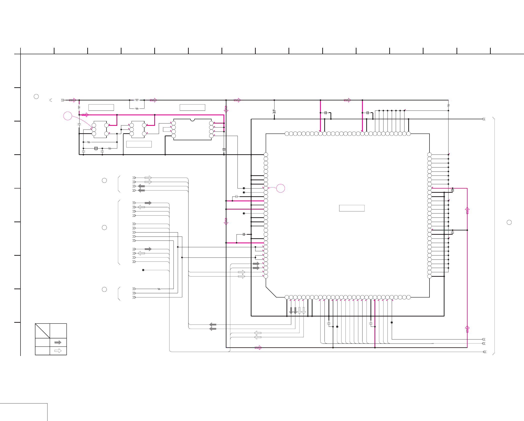
DSR-50/50P
4-63 4-64
AUDIO DSP
DI-73 (7/9)
DI-73 (AUDIO DSP) SCHEMATIC DIAGRAM • See page 4-47 for DI-73 printed wiring board. • See page 4-149 for waveforms.
NO MARK:REC/PB MODE
*:IMPOSSIBLE TO MEASURE THE
VOLTAGE AT THE MARKED POINTS.
1.4
2.8
1.3 1.3
2.81.3
1.3
2.8
2.8
2.8
1.6
1.3
1.4
1.4
1.6
1.4
1.4
1.5
1.5
*
*
*
*
****
2.8
2.8
2.7
2.7
2.1
2.1
2.7
2.1
2.1
2.1
2.1
2.2
2.2
2.2
2.8
2.8
2.8
0
0
0
2.8
2.8
0
2.8
7
8
IC8003
CXD2712R
123456789101112131415161718192021222324252627282930
31 32 33 34 35 36 37 38 39 40 41 42 43 44 45 46 47 48 49 50 51 52 53 54 55 56 57 58 59 60
616263646566676869707172737475767778798081828384858687888990
919293949596979899100101102103104105106107108109110111112113114115116117118119120
TC7W74FU(TE12R)
IC8002
1234
5678
0.01u
C8008 0.01u
C8016
0.01u
C8013
0.01u
C8007
0.01u
C8003
0.01u
C8004
10V
33u
C8005
0.01u
C8006
CL8002
CL8003
CL8004
CL8006
CL8005
10k
R8040
XPD_DA1
XPD_AD2
SIB
LRCK
DEM0
BCK
XPD_DA2
SIA
DEM1
SOC
XPD_AD1
SOD
TC7SU04FU(TE85R)
IC8000
123
45
TC7S08FU(TE85R)
IC8001
123
45
24.576MHz
X8000
10p
C8001
10p
C8002
220k
R8002
0.01u
C8000
XX
R8003
SIC
SOA
SID
SOB
10uH
L8201
10uH
L8202
10
R8215
LRCK
BCK
SFD_FCK
MCK
CL7401
R8001
0
0.01u
C8020
0.01u
C8021
+2.8V
GND
25-1
25-2
25-3
1
A
A_XHDRD
A_XHDWR
A_HRDY
A_XHDCS
A_HA0
A_HD0
A_HD1
A_HD2
A_HD3
A_HD4
A_HD5
A_HD6
A_HD7
A.AD_DATA1
A.DA_DATA1
XPD_AD1
XPD_DA1
DEM1
DEM0
A.AD_DATA2
A.DA_DATA2
XPD_AD2
XPD_DA2
A.DA_DATA2
A.DA_DATA1
DATA_TO_SFD
ADAI2
ADAO2
DATA_FROM_SFD
A.AD_DATA1
A.AD_DATA2
DATA_FROM_SFD
ADAO2
DATA_TO_SFD
ADAI2
A2CH/X4CH
2
I
12
G
68
D
E
DI-73 BOARD (7/9)
B
7
05
151310 11
C
H
F
3 14945
IC8002
IC8001
IC8000
XX MARK:NO MOUNT
AUDIO DSP
-REF.NO.:10,000 SERIES-
22
DI-73 BOARD (9/9)
DI-73 BOARD (8/9)
25
DI-73 BOARD (9/9)
23
19
DI-73 BOARD (6/9)
DI-73 BOARD (9/9)
24
IC8003
SIGNAL
SIGNAL PATH
REC
PB
AUDIO
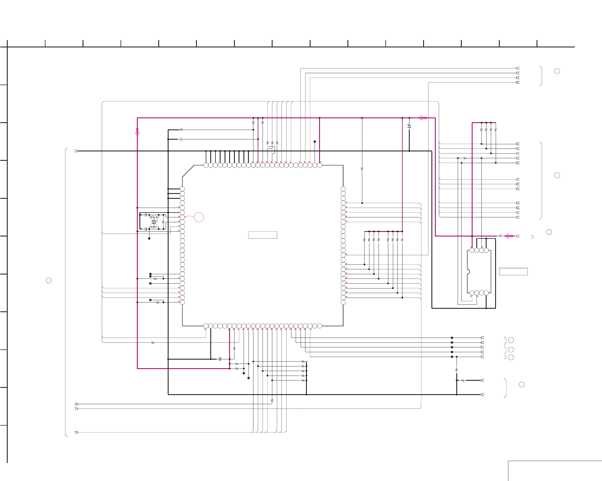
DSR-50/50P
4-65 4-66 AUDIO DSP CONTROL
DI-73 (8/9)
DI-73 (AUDIO DSP CONTROL) SCHEMATIC DIAGRAM • See page 4-47 for DI-73 printed wiring board. • See page 4-149 for waveform.
NO MARK:REC/PB MODE
*:IMPOSSIBLE TO MEASURE THE
VOLTAGE AT THE MARKED POINTS.
1.5
2.8
1.4
2.8
2.8
2.8
2.8
2.8
0.8
2.7
2.8 2.8
2.8
2.8
2.6
2.8
2.8
2.8
2.8
2.8
2.8
0.3
2.8
0
2.8
2.8
2.8
2.8
2.8
2.7
2.7
2.1
2.7
2.8
0
2.2
2.1
2.2
2.1
2.2
2.1
2.1
2.1
2.8
2.8
1.5
0
2.6
2.8
1.5
2.8
2.7
*
0
2.8
2.8
2.8
2.6
2.8 2.8
9
1M
R8049
100k
R8059
0
R8051
100kR8071
100k
R8072
100k
R8074
100k
R8073
100k
R8075
100k
R8077
100k
R8076
+2.8V
1k
R8069
0
R8080
AUDIO_GND
GND
VR/AD_CS
VR/AD_SO
VR/AD_SI
VR/AD_SCK
XVSP_SCK
VSP_SO
VSP_SI
VFD_VD
XCS_DSP
VFD_HD
VFD_OE
IC8009
HD6433837TSC73X
12345678910111213141516171819202122232425
26 27 28 29 30 31 32 33 34 35 36 37 38 39 40 41 42 43 44 45 46 47 48 49 50
51 52 53 54 55 56 57 58 59 60 61 62 63 64 65 66 67 68 69 70 71 72 73 74 75
767778798081828384858687888990919293949596979899100
XRST_VSP
0.01u
C8027
0.01u
C8024
CL8007
CL8008
CL8009
CL8010
CL8013
100kR8047
100k
R8048
100k
R8058
CL8011
CL8012
1k
R8062
100k
R8070
33
R8046
33
R8063
33
R8061
33
R8060
100k
R8064
100k
R8065
100k
R8066
100k
R8067
100k
R8068
CL8014
CL8015
CL8016
CL8017
XCH1_HPF
XCH2_HPF
XCH3_HPF
XCH4_HPF
DA_CH3/4_ON
CL8018
100k
R8079
10V
10u
C8100
15p
C8101
15p
C8102
TC7W241FU-TE12R
IC8201
1234
5678
XX
R8204
10uH
L8203
100k
R8205
100k
R8206
100k
R8207
CL8204
100k
R8214
100k
R8213
100k
R8212
100k
R8211
4.608MHz
X8001
TC/REC_DATA
TC/PB_DATA
TC/XTHRU
TC_XNT
GND
25-1
25-2
25-3
1
A
A_HRDY
A_HA0
A_XHDCS
A_XHDRD
A_XHDWR
A_HD7
A_HD6
A_HD5
A_HD4
A_HD3
A_HD2
A_HD1
A_HD0
DEM1
DEM0
A2CH/X4CH
XPD_DA2
XPD_DA1
XPD_AD2
XPD_AD1
VSP_SI_DSP
VSP_SO
XVSP_SCK
VFD_OE
VFD_VD
VFD_HD
VR/AD_SI
XRST_VSP
VFD_OE
VFD_VD
VFD_HD
VR/AD_CS
VR/AD_SI
VR/AD_SO
VR/AD_SCK
XCS_DSP
VR/AD_SCK
VR/AD_SO
VSP_SI_DSP
XRST_VSP
XVSP_SCK
VSP_SO
XCS_DSP
VR/AD_CS
2
I
K
12
G
68
D
E
DI-73 BOARD (8/9)
B
7
05
151310 11
C
H
F
3
J
14945
25
DI-73 BOARD (7/9)
XX MARK:NO MOUNT
AUDIO DSP CONTROL
-REF.NO.:10,000 SERIES-
IC8009
26
DI-73 BOARD (9/9)
DI-73 BOARD (9/9)
27
DI-73 BOARD (9/9)
28
DI-73 BOARD (6/9)
21
DI-73 BOARD (5/9)
16
DI-73 BOARD (5/9)
14
DI-73 BOARD (9/9)
29
IC8201
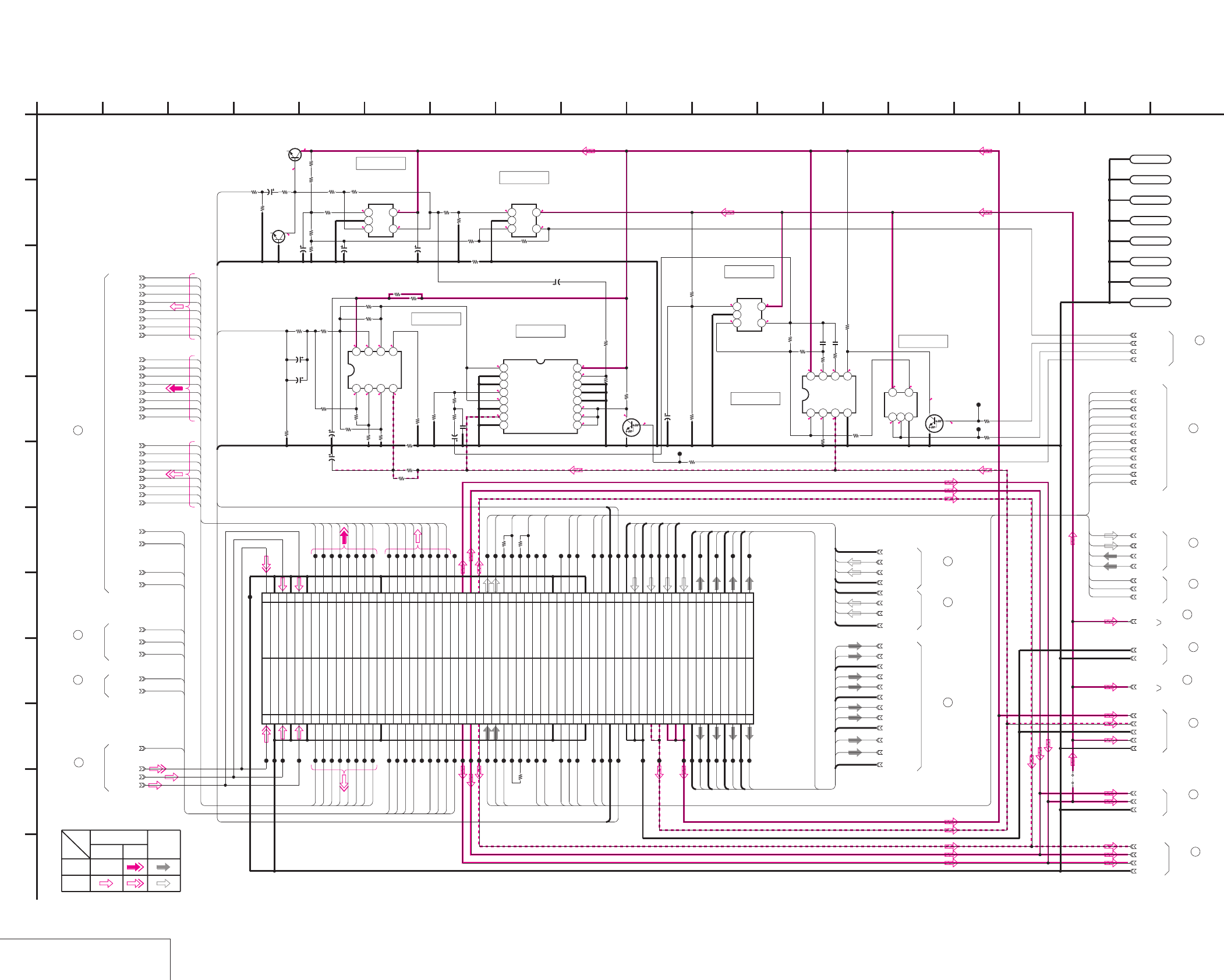
DSR-50/50P
4-67 4-68
TIME CODE IN/OUT
DI-73 (9/9)
DI-73 (TIME CODE IN/OUT) SCHEMATIC DIAGRAM • See page 4-47 for DI-73 printed wiring board.
E-E
E-E
NO MARK:REC/PB MODE
5
2.5
2.5
2.5
2.5
5
2.5
2.80.8
0.8 0
0 0 0 -4.2
4.3 0 0 0
0
0
0
-4.9
5
0
0
0
0
0
2.6
1.5 2.8
1.51.5
50
1.4 4.9
1.5 0
-4.9
1.42.8
1.5
1.5
4.9
0
TLV2231CDBVR
IC8008
123
45
6800
R8010
6800
R8011
6800
R8021
22k
R8026
10k
R8034
10k
R8035
10
R8037 1M
R8039
0
R8020
TLV2231CDBVR
IC8004
123
45
10V
10u
C8012
10V
10u
C8009
16V
6.8u
C8018
4V
22u
C8017
22k
R8014
22k
R8016
10k
R8015
10k
R8017
22k
R8031 TC75S56F(TE85R)
IC8006
123
45
NJM4556AM-A-TE2
IC8005
1234
5678 TC74HC4053AFT(EL)
IC8007
12345678
9 10111213141516
6.3V
100u
C8010
6.3V
100u
C8011
XX
R8013
150
R8018
150
R8019
XX
R8012
0
R8022
0
R8023
XX
R8027
XX
R8028
6800
R8024
6800
R8025
10
R8029
1k
R8033
100k
R8036
1500
R8038
3300
R8041
100k
R8042
100k
R8043
180
R8032
180
R8030
6.3V
47u
C8014
6.3V
47u
C8015
6.3V
4.7u
C8022
6.3V
4.7u
C8019
UN9211J-(K8).SO
Q8001
UN9211J-
(K8).SO
Q8000
TC7S08FU(TE85R)
IC8011
123
45
TC7W53FU(TE12R)
IC8010
1234
5678
10k
R8044
10k
R8045
18k
R8050
100
R8053
100
R8055
100k
R8056
6800
R8057
0
R8054
4700p
C8025
1500p
C8026
10V
XX
C8023
XX
R8052
10
R8100
180
R8201
180
R8202
1800
R8203
0.01u
C8201
2SC4081T106R
Q8202
2SC4081T106R
Q8201
1kR8208
1k
R8209
CL8202
CL8201
1k
R8210
CL8203
LND9501
GND
LND9506
GND
LND9502
GND
LND9507
GND
LND9503
GND
LND9508
GND
LND9504
GND
LND9505
GND
J_3V
CL9587
JC02
CL9527
CL9524
AUDIO_GND
VSP_SO
BCK
CL9572
CL9531
AU_CH2_OUT
CL9594
SID
Y2
Y5
AFH
JC03
CL9590
VD_HD
Y6
CL9583
CL9598
MY00
CL9582
CL9506
AU_GND2_OUT
CL9507
CL9591
CL9559
DPB_YOUT
CL9578
CL9581
FIFO_MUTE
CL9535
CL9539
VR/AD_SCK
CL9526
AU_X1_IN
CL9589
AU_GND3_OUT
CL9580
AU_Y4_IN
AU_1_GND_IN
CL9544
MY06
CL9585
XCS_DSP
CL9547
120PCN9500
1 DPB_YOUT
3 GND
5 DPB_CROUT
7 GND
9 DPB_CBOUT
11 GND
13 MY00
15 MY01
17 MY02
19 MY03
21 MY04
23 MY05
25 MY06
27 MY07
29 GND
31 MHO
33 DA135
35 AFH
37 VD_HD
39 N.C
41 SPCK2
43 PAL/XNT
45 PB/XREC
47 FIFO/MUTE
49 J_3V
51 VIDEO_+5V
53 VIDEO_-5V
55 SOA
57 SOB
59 LOCK_MCK
61 OCK
63 SFD_FCK
65 N.C
67 VFD_VD
69 VFD_OE
71 GND
73 XCS_DSP
75 VSP_SI
77 XRST_VSP
79 GND
81 DSP_CS
83 DSP_SI
85 TC/GNDIN
87 TC_IN
89 AUDIO_GND
91 AUDIO_GND
93 AUDIO_GND
95 A.-5V
97 A.-5V
99 A.+5V
2DPB_YOUT
4GND
6DPB_CROUT
8GND
10DPB_CBOUT
12GND
14Y0
16Y1
18Y2
20Y3
22Y4
24Y5
26Y6
28Y7
30GND
32JC00
34JC01
36JC02
38JC03
40JC04
42JC05
44JC06
46JC07
48N.C
50J_3V
52VIDEO_+5V
54VIDEO_-5V
56SIC
58SID
60SFD_BCK
62BCK
64SFD_LRCK
66LRCK
68N.C
70VFD_HD
72GND
74N.C
76XVSP_SCK
78VSP_SO
80GND
82DSP_SCK
84DSP_SO
86TC/GNDOUT
88TC_OUT
90AU_GND4_OUT
92AU_CH4_OUT
94AU_GND3_OUT
96AU_CH3_OUT
98AU_GND2_OUT
100
AU_CH2_OUT
101 A.+5V 102
AU_GND1_OUT
103 A.+5V 104
AU_CH1_OUT
105 AU_4_GND_IN 106
AU_4_GND_IN
107 AU_Y4_IN 108
AU_X4_IN
109 AU_3_GND_IN 110
AU_3_GND_IN
111 AU_Y3_IN 112
AU_X3_IN
113 AU_2_GND_IN 114
AU_2_GND_IN
115 AU_Y2_IN 116
AU_X2_IN
117 AU_2_GND_IN 118AU_1_GND_IN
119 AU_Y1_IN 120
AU_X1_IN
JC01
A.-5V
Y0
JC05
MY04
XRST_VSP
JC00
AU_3_GND_IN
MHO
DPB_CBOUT
VIDEO_5V
CL9563
CL9548
CL9562
CL9568
CL9557
CL9529
CL9601
CL9509
CL9550
CL9508
CL9505
CL9596
VSP_SI
CL9600
A.+5V
AU_4_GND_IN
CL9558
CL9525
TC/XTHRU
MY03
CL9532
CL9510
CL9602
CL9533
VR/AD_SI
CL9586
AU_CH4_OUT
CL9579
Y4
MY05
AU_Y3_IN
CL9567
CL9502
CL9536
DA135
VFD_OE
CL9522
DPB_CROUT
SIC
CL9530
CL9603
CL9520
CL9542
AU_Y2_IN
CL9556
CL9565
CL9500
CL9516
CL9546
AU_X2_IN
CL9553
CL9537
CL9541
AU_X4_IN
AU_Y1_IN
CL9523
JC04
CL9604
CL9564
CL9577
CL9515
CL9512
CL9538
JC07
VFD_VD
CL9561
VR/AD_CS
VIDEO_-5V
MY01
GND
CL9511
XVSP_SCK
PAL/XNT
CL9605
AU_GND1_OUT
PB/XREC
GND
CL9545
MY07
CL9514
CL9588
Y1
VIDEO_5V
VR/AD_SO
CL9574
CL9555
AU_2_GND_IN
CL9518
CL9592
CL9566
VFD_HD
CL9534
CL9501
CL9584
AU_CH3_OUT
CL9519
Y3
CL9575
AU_GND4_OUT
CL9543
CL9503
MY02
CL9576
CL9560
CL9573
CL9517
SOA
J_3V
JC06
CL9521
SOB
AU_X3_IN
SPCK2
LRCK
CL9540
CL9513
AU_CH1_OUT
Y7
CL9504
PB/XREC
SPCK2
GND
+2.8V
+2.8V
GND
AUDIO_GND
+2.8V
SFD_SCK
TC/PB_DATA
TC_XNT
TC/REC_DATA
JS7201
0
R8009
0
R8008
0
R8007
CL9554
1
A
TC/IN
TC/GNDIN
TC/GNDOUT
TC/OUT
2 16
L
I
K
12
G
68
D
E
DI-73 BOARD (9/9)
B
7
05
151310 1711
C
H
F
3 18
J
14945
XX MARK:NO MOUNT
TIME CODE IN/OUT
-REF.NO.:10,000 SERIES-
VIDEO SIGNAL AUDIO
CHROMA SIGNAL
PB
SIGNAL PATH
REC
Y
IC8004
IC8006
IC8007
IC8005
IC8011
IC8008
IC8010
(SEE PAGE 4-45)
JC-20 BOARD (14/14)
CN8001
DI-73 BOARD (1/9)
3
DI-73 BOARD (4/9)
11
9
DI-73 BOARD (3/9)
7
DI-73 BOARD (2/9)
DI-73 BOARD (6/9)
18
DI-73 BOARD (6/9)
20
12
DI-73 BOARD (5/9)
DI-73 BOARD (8/9)
26
DI-73 BOARD (8/9)
27
23
DI-73 BOARD (7/9)
DI-73 BOARD (7/9)
24
DI-73 BOARD (8/9)
28
29
DI-73 BOARD (8/9)
DI-73 BOARD (7/9)
22
DI-73 BOARD (6/9)
17
DI-73 BOARD (3/9)
8
1
DI-73 BOARD (1/9)
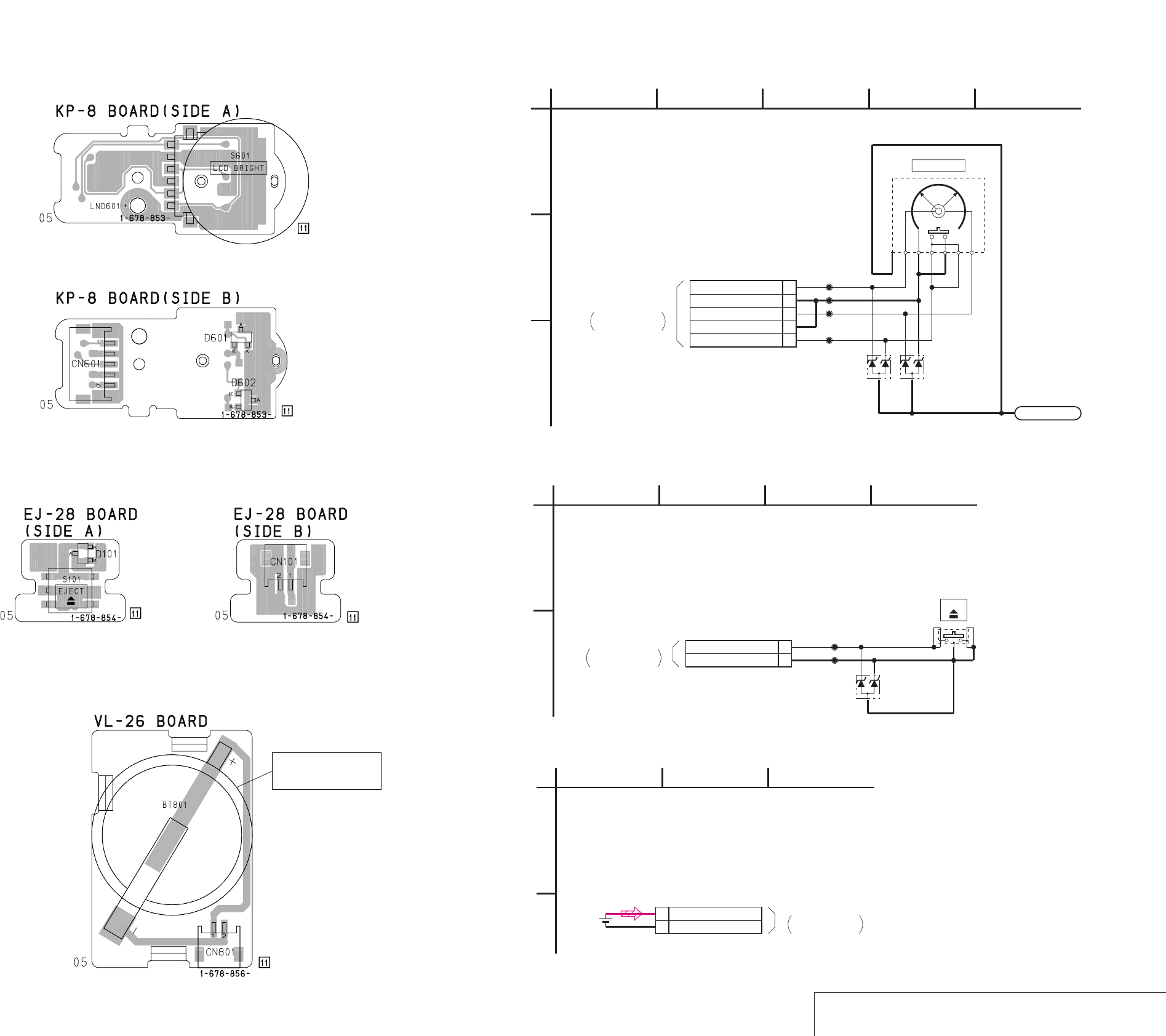
DSR-50/50P
4-69
4-70
SWITCH
/
EJECT SWITCH
/
LITHIUM BATTERY
KP-8 EJ-28 VL-26
KP-8 (SWITCH), EJ-28 (EJECT SWITCH), VL-26 (LITHIUM BATTERY) PRINTED WIRING BOARDS AND SCHEMATIC DIAGRAMS
– Ref. No.: KP-8 board; 20,000 series, EJ-28 board; 50,000 series, VL-26 board; 20,000 series –
BT801
BATTERY,
LITHIUM SECONDARY
(
(
MA3075WA-(TX)
D601
MA3075WA-(TX)
D602
LND601
LND601
5P
CN601
1DIAL_A
2GND
3DIAL_B
4GND
5EXEC_SW
CL601
CL602
CL603
CL604
S601
1
A
32
-REF.NO.:20,000 SERIES-
KP-8 BOARD
LCD BRIGHT
45
C
B
05
SWITCH
CN705
VD-28 BOARD (12/15)
KP-52 HARNESS
(SEE PAGE 4-98)
THROUGH THE
MA3075WA-(TX)
D101
2PCN101
1EJECT SW
2GND
CL101
CL102
S101
1
A
EJECT SWITCH
-REF.NO.:50,000 SERIES-
42
EJ-28 BOARD
B
3
EJECT
05
CN704
VD-28 BOARD (12/15)
EV-70 HARNESS
(SEE PAGE 4-98)
THROUGH THE
2P
CN801
1 VL BATT 3V
2 VL BATT GND
BT801
1
A
-REF.NO.:20,000 SERIES-
VL-26 BOARD
23
B
05
CN706
VD-28 BOARD (12/15)
BV-50 HARNESS
(SEE PAGE 4-97)
THROUGH THE
LITHIUM BATTERY
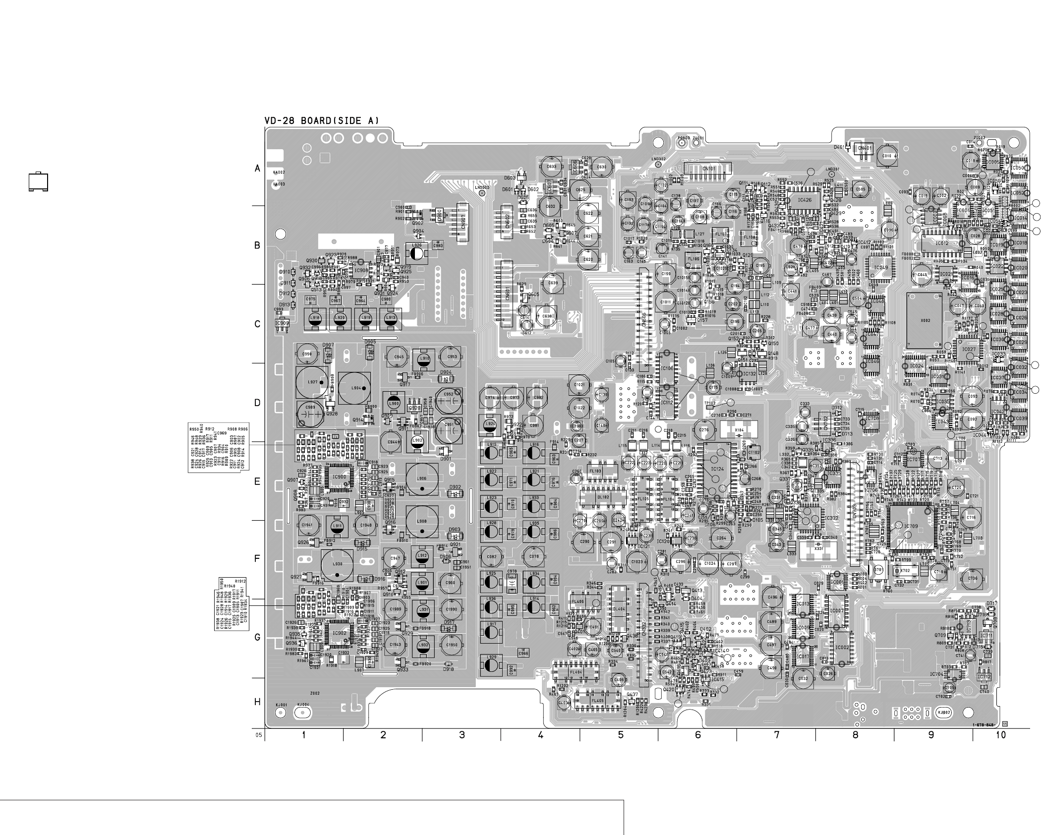
DSR-50/50P
4-71
4-72
SYNC GENERATOR, VIDEO IN, UVIC, VIDEO OUT, AUDIO, HI CONTROL, DC IN, DC/DC CONVERTER
VD-28
VD-28 (SYNC GENERATOR, VIDEO IN, UVIC, VIDEO OUT, AUDIO, HI CONTROL, DC IN, DC/DC CONVERTER) PRINTED WIRING BOARD
– Ref. No.: VD-28 board; 10,000 series –
• For Printed Wiring Board.
•VD-28 board is four-layer print board. However, the patterns of
layers 2 to 3 have not been included in the diagram.
•There are a few cases that the part isn't mounted in this model
is printed on this diagram.
•See page 4-154 for printed parts location.
•Chip transistor
EB
C
25
24 32
1
8
9
16
17
1
8
9
16 17
24
25
32
50
51
53
55
61
59
25 28
26
27
29
30
34
33
72
48
47 49
77
76
13
12
11
8
6
7
4
3
2
17
15
16
5
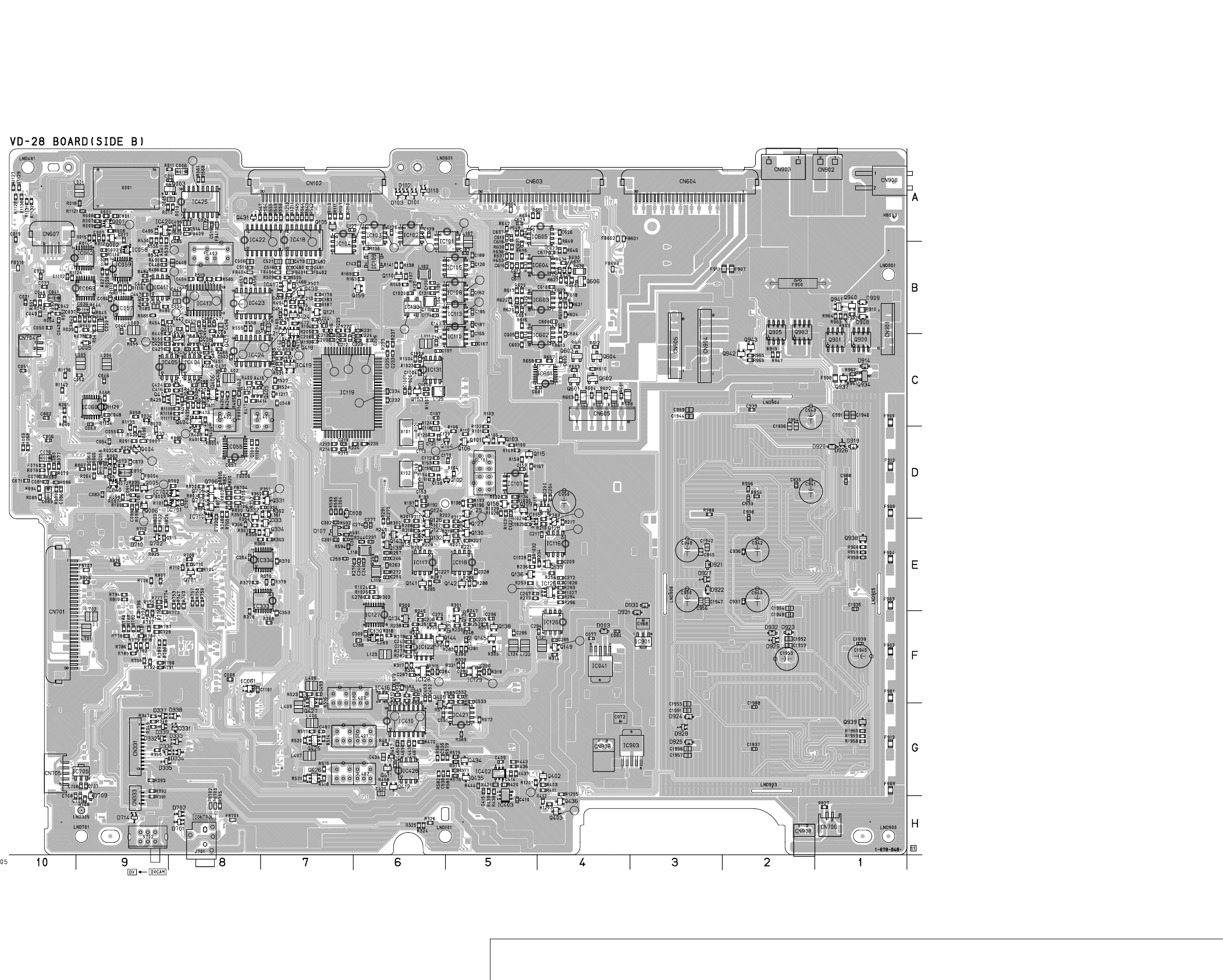
DSR-50/50P
4-73
4-74
SYNC GENERATOR, VIDEO IN, UVIC, VIDEO OUT, AUDIO, HI CONTROL, DC IN, DC/DC CONVERTER
VD-28
41
25
24
40
64
65
1
80
1
71
70
66
67
68
69
65
14
64
9
10
46
63
62
60
58 75
19
18 20
35
37
38
36
74
73
21 23
22
24
31
42 44 32
39
40
41
45
43
57
56
52
54
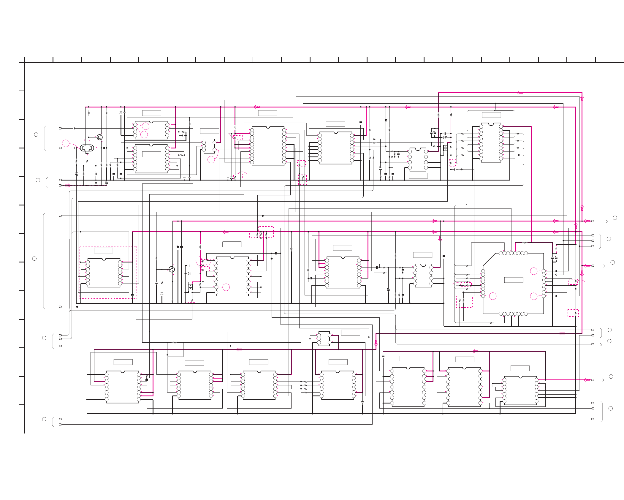
DSR-50/50P
4-75 4-76
SYNC GENERATOR 1
VD-28 (1/15)
VD-28 (SYNC GENERATOR 1) SCHEMATIC DIAGRAM • See page 4-71 for VD-28 printed wiring board. • See page 4-149 for waveforms.
NO MARK:REC/PB MODE
R:REC MODE
P:PB MODE
5
0
0
4.8
4.4
4.6
4.8
2.5
3.9
3.8
3.8
3.4
2.5
4.8
4.5
4.4
4.8
9.12.9
2.1
2.1
5
2.2
2.5
2.5
2.6
4.8
5
2.1
2.2
2.1
5
5
5
0.2
1.3
4.9
2.4
05
3.3
0.1
4.6
3.8
2.5
0.1
5
0.2
4.2
4.7
5
2.5
1.2
4.6
2
5
0.4
0.4
4.7
4.5
4.5
0.4
3.4
3.4
4.3
4.7
0.2
4.7
2.6
5
2.5
2.6
-1.9
5
-2.4
-1.9
R5/P0 5
R5/P0
R0.4/P5
R0.4/P5
R5/P0.1
4.5
4.7
R5/P0
R0/P5
R0/P5
4.9
R5/P0.1
3.4
3.4
0
0
0
5
3.8
4.8 4.7 5
4.6
2.5
3.8
4.4
3.4
3
4.8 0
9.1
4.9
4.9
R3.4/
P3.9
5
5
0
0.1
0.1
R3.5/P4.4
0
0
5
5
5
4.9
0.9
5
0
3.4
5
0
5
5
3.4
3.4
3.4
0
0
2.7
9.1
2.4
2.6
5
5
5
2.8
0
3.2
3.1
0
0
5
5
2.9
3.2
2.9
2.8
2.8
0.1
2.6
2.6
0.2
0.2
2.6
2.8
2.9
2.6
2.9
1.8
2.9
2.6
2.6
2.9
2.9
2.9
3.4
1.8
1.8
5
3.7
1.3
1.3
5
5
3.7
5
4.5
4.5
5
5
5
2.9
2.5
2.5
2
4.9
2.9
2.9
2.5
4.5
5
3
0
2.9
5
5
2.5
5
2
1
2
3
4
5
68
7
DSR-50
DSR-50P
DSR-50
DSR-50P DSR-50P
:DSR-50
:DSR-50P
DSR-50P
DSR-50
DSR-50P
DSR-50
DSR-50
:DSR-50
:DSR-50P
DSR-50
DSR-50
DSR-50P
DSR-50P
DSR-50
2.5
IC012 CXD1216M-T6
12345678910
11 12 13 14 15 16 17 18 19 20
X002
*
33k
R047
TC74HC4053AFT(EL)
IC016
12345
678
9 10111213141516
TC74VHCT244AFT(EL)
IC024
12345678910
11 12 13 14 15 16 17 18 19 20
10uH
L004
1k
R056
10u
C039
0.1u
C046
6.3V
47uC047
10k
R046
6800
R048
0.1u
C038
2200
R045
3300
R044
10uH
L003
0.1u
C044
16V
47u
C045
0.1u
C048
0.01u
C037
16V
1u
C036
10k
R043
1k
R040
1kR042
10k
R038
10k
R039
4700
R041
68k
R055
10uH
L002
0.1u
C027
6.3V
47u
C028
R027
0
10uH
L005
0.1u
C052
6.3V
47u
C053
0
R035
0
R034
0
R059
0
R057
2200
R010
0.47u
C005
33k
R011
10V
4.7u
C006
S
2SK94-T1X2X3X4
Q003
6.3V
47u
C018
0.1u
C014
1k
R018
10uH
L001
X001
*
4700
R013
TC74VHC02FT(EL)
IC005
1234567
8 9 10 11 12 13 14
0
R024
0
R022 0
R026
0
R019
0
R020
0.01u
C025
TC74VHC123AFT(EL)
IC019
12345678
9 10111213141516
16V47u
C010
0.1u
C011
0.1u
C042
100
R053
10V
6.8u
C041
100k
R037
1u
C034
2k
R049
47p
C040
10k
R050
XX
R054
1k
R051
82k
R052
INT/EXT_DET
SC_DET
LM1881MX
IC003
1234
5678
GEN_LOCK_Y
GEN_LOCK_C
TC74VHC00FT(EL)
IC004
1234567
8 9 10 11 12 13 14
0
R028
10k
R023
33p
C022
100k
R021
33p
C021
47p
C016
100k
R017
82k
R016
150p
C012
330k
R014
220k
R015
TC7S02FU(TE85R)
IC008
123
45
XP6501-
(TX).SO
Q001
6
5
1
4
3
2
2SC4081T106R
Q002
0.01u
C007
2200
R012
2200
R008
1k
R005
1k
R007
2200
R009
6.3V
47u
C002
0.01u
C001
3300
R006
VIDEO_-5V
6.3V47u
C009
0.1u
C004
6.3V
47u
C015
0.1u
C017
0.1u
C035
TC74VHC393FT(EL)
IC018
12345
67
8 9 10 11 12 13 14
TC74VHC164FT(EL)
IC020
1234567
89
10 11 12 13 14
TC74VHC00FT(EL)
IC023
1234567
8 9 10 11 12 13 14
0.1u
C031
0.1u
C033
0
R061
0
R060
CL014
CL009
CL008
CL001
0.1u
C043
1u
C003
MA112-TX
D005
UPC358G2-E2
IC021
1234
5678
CXD1217Q-T4
IC027
12345678
9 10111213141516
17 18 19 20 21 22 23 24
2526272829303132
UPC358G2-E2
IC022
1234
5678
680k
R1110
0.1u
C023
TC74VHC00FT(EL)
IC057
1234567
8 9 10 11 12 13 14
TC7S02FU(TE85R)
IC058
123
45
TC74VHC164FT(EL)
IC059
1234567
8 9 10 11 12 13 14
0.1u
C094
XX
R1113
0
R1114
XX
R1115
XX
R1116
TC74VHC00FT(EL)
IC060
1234
567
8 9 10 11 12 13 14
0
R1120
0
R1121
0.1u
C063
TC74VHC00FT(EL)
IC062
1234567
8 9 10 11 12 13 14
TC74VHC123AFT(EL)
IC063
12345678
9 10111213141516
XX
R1123
1u
C1102
56k
R1124
0
R025
100
R030
100
R029
100
R031
100
R032
100
R033
0
R036
100
R058
100
R1135
100
R1138
100
R1139
100
R1140
100
R1137
100
R1136
100
R1141
FB011
FB012
4-3
4-2
4-1
5-1
5-2
7-3
7-2
7-1
0.1uC049
VIDEO_+9V
DIG_+5V
9-1
12-3
9-2
12-2
12-1
SW_+3V
1
A
GND
R1134
R1133
R1142
10-1
F4
F3
F2
F1
F8
F7
F6
F5
C2
C3
E7
A6
A7
F1
E1
E2
E3
E4
E5
E6
E7
F7
F6
F5
F4
F3
F2
F8
E8
2 16
L
I
20
K
12
G
68
D
E
VD-28 BOARD (1/15)
B
7
05
19151310 1711
C
21
H
F
3 18
J
14945
M
IC024
IC021
IC016
IC012
IC008
IC003
IC004
IC060
IC005 IC019
IC022
IC027
IC023
IC020
IC018
IC059
IC058
IC057
IC062
IC063
XX MARK:NO MOUNT
SYNC GENERATOR 1
-REF.NO.:10,000 SERIES-
(Note)
(Note)
Note:Ferrite beads are mounted to the
location where R1133,1134 and 1142 are printed.
(Note)
6
VD-28 BOARD
(3/15)
VD-28 BOARD
10
(2/15)
11
VD-28 BOARD
(14/15)
VD-28 BOARD
(15/15)
8
VD-28 BOARD
3
(7/15)
VD-28 BOARD
(3/15)
4
(3/15)
VD-28 BOARD
5
VD-28 BOARD
(14/15)
2
1
VD-28 BOARD
(5/15)
VD-28 BOARD
(2/15)
12
9
VD-28 BOARD
(3/15)
7
VD-28 BOARD
(2/15)
14.31818MHz
17.734475MHz
*X002
14.31818MHz
14.1875MHz
*X001
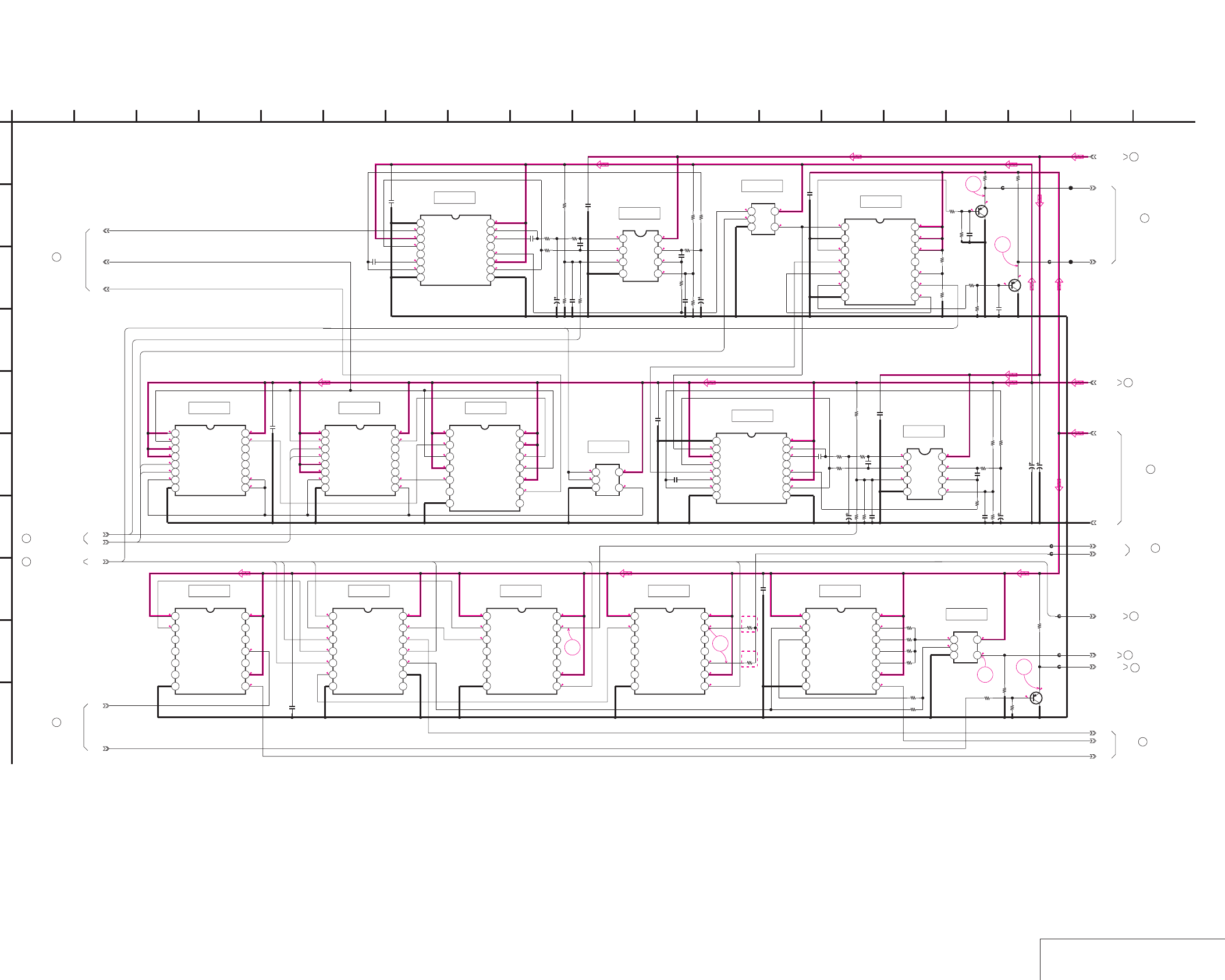
DSR-50/50P
4-77 4-78 SYNC GENERATOR 2
VD-28 (2/15)
VD-28 (SYNC GENERATOR 2) SCHEMATIC DIAGRAM • See page 4-71 for VD-28 printed wiring board. • See page 4-149 for waveforms.
0.7
0.1
10
14
1.1
1.6
2.9
0.6
0.7
0.7
13
2.9
0.7
2.9
1.83.8
2.9
2.9
0.1
0.7
2.9
0.1
2.9
12
0.2
2.9
11
3.8
2.9
2.9
0.2
0.2
0.2
2.9
3.8
2.6
0.7
4.6
0.2
4.4
0.3
0.1
4.8
0.3
2.9
1.8
2.9
2.9
0.3
0.1
0.7
9
2.9
2.9
2.9
2.9
2.9
0
3.8
3.8
1.8
1.8
2.9
3.8
0
3.8
5
9.1
4.2
2.5
2.5
R4.2/P3.8
R2.4/P1.7
R2.4/P1.70
3.8
5
3.8
5
50
R3.9/P3.2
R3.7/P3
3.9 R3.7/P3
NO MARK:REC/PB MODE
R:REC MODE
P:PB MODE
3.4
5
0
5
5
0
0.5
0.1
5
0.5
0.5
0
5
0.1
0.5
5
5
0.5
3.4
0
5
R0/P5
5
0.1
3.4
0.1
55
5
5
0
0
3.4
5
0.5
4.5
4.5
3.8
0
5
3.8
2.5
3.9
3.1
5
0
3.8
5
2.5
3.8
1.4
1.4
2.5
2.5
4.1
9.1
DSR-50P
DSR-50
0.1
33k
R064
22k
R066
0.1u
C061
TC74VHC123AFT(EL)
IC031
12345678
9 10111213141516
18p
C055
100
R065
22p
C056
10V
6.8u
C058
2k
R062
10k
R063
10k
R067
0.1u
C072
100
R070
10V
6.8u
C075
2200
R074
10k
R071
27k
R072
R073
27k
TC74VHC163FT(EL)
IC025
12345678
9 10111213141516
TC74VHC163FT(EL)
IC028
12345678
9 10111213141516
TC74VHC74FT(EL)
IC030
1234567
8 9 10 11 12 13 14
TC7S02FU(TE85R)
IC033
123
45
TC7S86FU(TE85R)
IC040
123
45
10V
6.8u
C076
22p
C074
100
R078
18p
C066
TC74VHC123AFT(EL)
IC037
12345678
9 10111213141516
0.1u
C079
22k
R080
33k
R077
2k
R075
27k
R089
27k
R088
10k
R086
2k
R094
10V
6.8u
C089
100
R085
0.1u
C085
10k
R079
10k
R076
TC74VHC86FT(EL)
IC043
1234567
8 9 10 11 12 13 14
0.1u
C073
0
R092
XX
R093
2SA1576A-
T106-R
Q005
2SA1576A-
T106-R
Q006
1k
R087
1k
R097
100
R099
100
R095 C091
10p
10p
C095
4700
R098
4700
R100
SC_U
SC_V
0.1u
C086
0.1u
C080
0.1u
C060
0.1u
C054
0.1u
C083
0.1u
C062
6.3V
100u
C092
16V
47u
C093
0.1u
C050
0.1u
C081
0.1u
C064
TC74VHC164FT(EL)
IC034
1234567
8 9 10 11 12 13 14
TC74VHC04FT(EL)
IC029
1234567
8 9 10 11 12 13 14
TC74VHC164FT(EL)
IC032
1234567
8 9 10 11 12 13 14
R_SYNC_OUT
TC74VHC164FT(EL)
IC026
1234567
8 9 10 11 12 13 14
0
R068
0
R069
R_BF_OUT
TC74VHC164FT(EL)
IC039
1234567
8 9 10 11 12 13 14
TC7S08FU(TE85R)
IC044
123
45
XX
R081
XX
R082
XX
R083
0
R084
R_Y_BLK
0.1u
C051
0.1u
C071
FB004
FB009
FB005
FB001
FB006
6800
R090
2200
R091
4700
R096
2SA1576A-T106-R
Q004
FB007
GEN_REF_Y
CL015
CL016
FB003 V_SYNC_HI
DIG_+5V
UPC358G2-E2
IC035
1234
5678
UPC358G2-E2
IC042
1234
5678
SW_+3V
0
R1111
XX
R1112
4700
R1122
14-2
12-2
12-3
12-1
10-1
13-2
7-3
7-2
7-1
14-1
1
A
VIDEO_+9V
13-1
GND
A4
A1
A2
A3
C4
E5
C1
E8
E8
E4
E6
E1
A5
E7
E2
E6
IC029
IC030
IC031 IC043
2 16
I
12
G
68
D
E
VD-28 BOARD (2/15)
B
7
05
19151310 1711
C
H
F
3 18
J
14945
IC035
IC040
IC042
IC037
IC033
IC028IC025
IC026 IC032 IC034 IC039
IC044
VD-28 BOARD (1/15)
12
VD-28 BOARD (6/15)
22
VD-28 BOARD (9/15)
21
VD-28 BOARD (7/15)
20
VD-28 BOARD (10/15)
19
VD-28 BOARD (15/15)
17
VD-28 BOARD (3/15)
15
VD-28 BOARD (10/15)
16
18
VD-28 BOARD (14/15)
VD-28 BOARD (1/15)
7
XX MARK:NO MOUNT
SYNC GENERATOR 2
-REF.NO.:10,000 SERIES-
VD-28 BOARD (3/15)
14
VD-28 BOARD (1/15)
10
VD-28 BOARD (3/15)
13
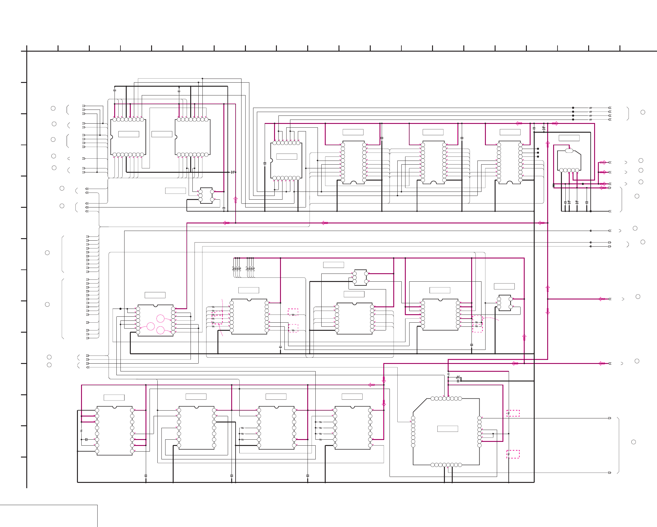
DSR-50/50P
4-79 4-80
SYNC GENERATOR 3
VD-28 (3/15)
VD-28 (SYNC GENERATOR 3) SCHEMATIC DIAGRAM • See page 4-71 for VD-28 printed wiring board. • See page 4-149 for waveforms.
*:IMPOSSIBLE TO MEASURE THE
VOLTAGE AT THE MARKED POINTS.
R:REC MODE
P:PB MODE
NO MARK:REC/PB MODE
55
0
4.9
0.1
1
2.1
3.2
3.2
1.6
3.7 9.1 5 13.2
9.1
55
R0/P2.9
R2.8/P1.5
0.1
0
4.9
2.8
1.7
3
2.7
2.7
3.5
3.5
2.9
2.5
2.5
3
5
2.6
2.4
3.5
3.6
3.3
2.1
1.6
0
5
0.8
1.3
4.9
1.5
2.8
*
5000
*
*
*
335
2.9
2.9
4.9
4.9
555
4.9
4.9
05
R5/P0
00
R0/P5
05
R0/P5
0
R0/P5
0
4.9
55500
4.4
2.9
0.3
0.3
2.9
2.9
2.5
2.9
1.4
1.4
2.9
2.9
2.9
1.2
1.6
2.6 2.9
2.9
2.7
2.9 2.9
0.5
2.9
0.5
2.9
2.7
0.5
0.6
2.9
2.6
2.9
0.5
1.6
4.4
0.5
0.5
0.6
5
R5/P0
0
R5/P0
1.2 5
1.2
2.1
2.6
2.6
4.4
0.1
0.1
0.2
0.3
0.3
0.5
15
16
17
2.9
2.9
2.9
2.9
2.9
1.8
4.4
0
2
0.6
0.7
3.9
1.8
2.9
0.6
2.92.9
4.4
2.9
0.7
2.6
2.9
2.6
2.6
2.9
3.9
4.5
3.3
4.5
0
0
5
52.1
0
2.9
0.5
0.5
0.5
DSR-50
DSR-50P
DSR-50
DSR-50P
DSR-50
DSR-50P
1.4
DSR-50P
DSR-50
**
*
UNREG
TC74VHCT08AFT(EL)
IC014
1234567
8 9 10 11 12 13 14
0.1u
C019
R_Y_CLAMP
R_UV_CLAMP
M62352GP-70ED
IC009
12345678910
11121314151617181920
M62352GP-70ED
IC013
12345678910
11121314151617181920
M62352GP-70ED
IC017
12345678910
11121314151617181920
0.1u
C024
0.1u
C029
0.1u
C030
Y/C_SEP_Y_GAIN
C_DECODE_HUE
Y/C_SEP_C_GAIN
REC_U_GAIN
REC_Y_GAIN
REC_V_GAIN
REC_U_DELAY
REC_V_DELAY
PB_V_DELAY
PB_U_DELAY
COMPOSITE_SYNC
BURST_U
COMPONENT_SYNC
BURST_V
COMPOSITE_U_GAIN
COMPOSITE_V_GAIN
COMPOSITE_U_BAL
COMPOSITE_V_BAL
CL010
6.3V
100u
C032
FB008
FB002
PQ09TZ5U
IC041
12345
6
MA112-TX
D003
0.1u
C077
16V
47u
C078
0.1u
C084
50V
22u
C082
TC74VHCT08AFT(EL)
IC001
1234567
891011121314
VD_SCK
EVR_LOAD
V_S/P_XSTB
VD_SO
0.1u
C008
NJU3712M(TE2)
IC002
12345678
910111213141516
NJU3712M(TE2)
IC007
12345678
910111213141516
0.1u
C013
0.1u
C020
XCPNT_SEL
XS_SEL
DV_SEL
XCAM_SEL
EE/XPB
INT/XEXT
SDC
C_DECODE_LEVEL
6.3V
22u
C026
GND
0
R001
0
R002
0
R003
0R004
CL002
CL003
CL004
CL005
Y_BLK_LEVEL
CL018
CL020
DIG/XANA
FSC_TEST
PB_Y_LEVEL
PB_U_LEVEL
PB_V_LEVEL
TC74VHC393FT(EL)
IC046
1234567
8 9 10 11 12 13 14
TC74VHC164FT(EL)
IC047
1234567
8 9 10 11 12 13 14
TC74VHC164FT(EL)
IC048
1234567
8 9 10 11 12 13 14
CXD1217Q-T4
IC049
12345678
9 10111213141516
17 18 19 20 21 22 23 24
2526272829303132
10uH
L006
6.3V
47u
C096
0.1u
C097
0.1u
C098
0
R1101
0
R1102
0.1u
C099
CL022
CL049
CL050
0
R1103
0
R1104
TC74VHC4040FT(EL)
IC050
12345678
9 10111213141516
TC74VHC74FT(EL)
IC052
1234567
8 9 10 11 12 13 14
RB001 RB002
TC74VHC20FT(EL)
IC051
1234567
8 9 10 11 12 13 14
TC7SH32FU-TE85R
IC054
123
45
VIDEO_+9V
R_HD
TC74VHC123AFT(EL)
IC055
1
2
345678
9 10111213141516
XX
R1105
XX
R1106
0
R1107
XX
R1108
22k
R1109
0.001u
C100
TC7SH04FU-TE85R
IC056
123
45
0.1u
C057 0.1u
C059
FB010
XX
R1117
0
R1118
XX
R1119
TC7SH32FU-TE85R
IC061
123
45
0.1u
C1101
0
R1125
0
R1126
0
R1127
XX
R1128
0
R1129
0
R1130
0
R1131
0
R1132
14-2
5-2
5-1
SW_+3V
XCPNT_SEL
XS_SEL
FSC_TEST
DIG_+5V
4-3
1
A
VIDEO_+9V
VIDEO_+9V
14-1
9-2
9-1
DEC_FREERUN_ADJ
4-1
13-1
4-2
13-2
C25
C24
C23
C22
C21
C20
C19
C13
C11
C10
C9
C8
C7
C4
C3
C1
C17
C18
C16
C5
C6
C14 C2
C5
C6
C8
C9
C10
C11
C13
C14
C16
C17
C18
C19
C20
C21
C22
C23
C24
C25
A1
A2
A3
A4
A5
A6
A9
A8
A10
A11
A14
A10
A12
A13
A14
C27
C27
C7
C26
A15
A16
C29
C30
C31
C29
C30
C31
A7
A12
PU1
PU2
PU3
PU4
PU5
PU6
PU7
PU8
PU2
PU1
PU8
PU7
PU6
PU5
PU4
PU3
PU1
PU2
PU3
PU4
PU5
PU6
PU7
PU8
E8
E6
E6
E3
A13
C26
A9
A8
A11
A15
A16
IC007IC002
2 16
L
I
20
K
12
G
6
N
8
D
E
VD-28 BOARD (3/15)
B
7
05
19151310 1711
C
H
F
3 18
J
14945
M
IC061
IC001
IC009 IC013 IC017
IC041
IC056
IC052
IC054
IC051
IC050
IC014
IC055 IC046 IC047 IC048
IC049
XX MARK:NO MOUNT
SYNC GENERATOR 3
-REF.NO.:10,000 SERIES-
VD-28 BOARD (12/15)
30
VD-28 BOARD (2/15)14
VD-28 BOARD (1/15)
6
15
VD-28 BOARD (2/15)
VD-28 BOARD (12/15)
31
VD-28 BOARD (15/15)
32
VD-28 BOARD (1/15)9
29
VD-28 BOARD (10/15)
VD-28 BOARD (4/15)
28
VD-28 BOARD (7/15)
33
VD-28 BOARD (8/15)
34
VD-28 BOARD (15/15)
35
VD-28 BOARD (14/15)
36
5
VD-28 BOARD (1/15)
VD-28 BOARD (1/15)
4
13
VD-28 BOARD (2/15)
27
VD-28 BOARD (10/15)
26
VD-28 BOARD (6/15)
25
VD-28 BOARD (5/15)
VD-28 BOARD (4/15)
24
VD-28 BOARD (4/15)
23
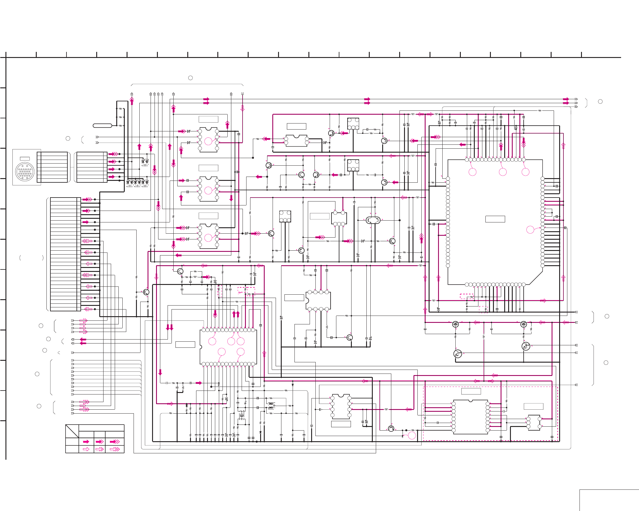
DSR-50/50P
4-81 4-82 VIDEO IN 1
VD-28 (4/15)
VD-28 (VIDEO IN 1) SCHEMATIC DIAGRAM • See page 4-71 for VD-28 printed wiring board. • See page 4-149, 150 for waveforms.
4.9 1.1
4.9
1.6
18
1.8
NO MARK:REC/PB MODE
2.7
2.7
4.9
19
24.9
1.15
1.5
1.8
20
4.9
1.5
24.9
1.4 4.9
1.4 1.3
4.9
2.2
2.8
2.8
1.5
0.9
4.9
1.5
0.9
1.6
1
1.2
0.6
3
4.9
2.4
1.9
1.3
2
1.9
4.9
2
1.3
4.9
0.8
1.4
4.9
1.7
2.3
4.9
1.1
0.6
4.9
0
0
2
2.7
4.92.7
0
4.9
3.9
3.2
30
0
4.9
4.9
0.4
4.9 4.9 4.9
0.4
0
4.9
0.6
2.6
3.4 3.14.9
322.5
4.2
2.7
2.2
2.9
2.8
4.3
4.8
2.7
1.9
2.1
2.1
3.9
4.9
2.8
4.9
2.2
2.2
2.3
2.9
2.9
4
2.9
2.9
2.6
2.4
3.2
2.8
272625
2928
4.9
0.5
4.8
00 0
4.9
0
4.9
4.9
2.2
2.2
4.9
4.9
3.2
3.2
3.2
4.9
2.3
3.2
4.9
3.3
11
1.7
1.6
0.6
4.9
4.9
4.9
2.5
1.3
21 22 23
24
DSR-50
DSR-50P
4.2
4.9
4.9
4.2
0
2.8
4.9
4.2
0
0.7
1.9
4.9
4.9
0.7
1.9
0.7
4.9
4.3
DSR-50P
:DSR-50
:DSR-50P
:DSR-50
:DSR-50P
:DSR-50P
:DSR-50
:DSR-50P
:DSR-50
:DSR-50P
:DSR-50
:DSR-50P
:DSR-50
:DSR-50P
:DSR-50:DSR-50
:DSR-50P
:DSR-50
:DSR-50P
DSR-50P
DSR-50
DSR-50
XS_SEL
10k
R145
1k
R141
0.1u
C224
1k
R161
2SC4081T106R
Q112
2SC4081T106R
Q110
1k
R140
22k
R165
0.1u
C146
220
R216
10k
R166
0.1u
C203
1k
R177
3900
R225
1k
R172
0.1u
C201
2200
R186
220
R231
1k
R178
3900
R194
2200
R187
6.3V
22u
C202
2SA1576A-T106-R
Q120
0.1u
C226
0.01u
C168
IC119
123456789101112131415161718192021222324
25262728293031323334353637383940
414243444546474849505152535455565758596061626364
65 66 67 68 69 70 71 72 73 74 75 76 77 78 79 80
2SC4081T106R
Q116
0.01u
C233
10uH
L112
6.3V
22u
C205
2SA1576A-T106-R
Q121
0.1u
C234
1k
R139
1k
R150
3900
R204
MM1031XML
IC109
12
34
10uH
L113
2SC4081T106R
Q111
3900
R205
0.1u
C219
22k
R144
0.1u
C208
10k
R214
1k
R147
0.1u
C213
XX
R215
2200
R146
0.1u
C218
0.01u
C183
47
R136
10uH
L111
MM1115XFBE
IC103
1234
5678
0.1u
C127
22u
6.3V
C115
22u
6.3V
C116
0.01u
C110
0.01u
C111
MM1111XFBE
IC104
1234
5678
MM1115XFBE
IC102
1234
5678
6.3V
22u
C107
6.3V
22u
C108
0
R235
3300
R233
2200
R237
6.3V
100u
C199
0.1u
C197
22p
C180 220
R179
10uH
L110
0.1u
C126
0.1u
C129
CL123
CL124
CL125
CL128
0
R224
0
R213
2SC4081T106R
Q105
100
R107
100k
R111
4700
R113
SDC_DET
1k
R163
4V
22u
C138
22k
R137
22k
R138
0.1u
C206
3900
R222
2200
R223
0.1u
C212
REC_Y_GAIN
REC_V_DELAY
REC_V_GAIN
REC_U_DELAY
REC_U_GAIN
Y/C_SEP_Y_GAIN
Y/C_SEP_C_GAIN
C_DECODE_HUE
30P
CN102
1VIDEO IN
2GND
3GND
4S-Y IN
5GND
6GND
7S-C IN
8GND
9SC DET
10GND
11GND
12VIDEO OUT
13GND
14GND
15S-Y OUT
16GND
17GND
18S-C OUT
19GND
20GND
21VIDEO MON OUT
22GND
23GND
24B-Y OUT
25GND
26GND
27R-Y OUT
28GND
29GND
30Y OUT
8P
CN101
1VIDEO IN
2VIDEO IN(GND)
3Y IN
4Y IN(GND)
5R-Y IN
6R-Y IN(GND)
7B-Y IN
8B-Y IN(GND)
10uH
L108
10uH
L109
6.3V
47u
C196
0.01u
C192
6.3V
47u
C194
0.01u
C190
6.3V
47u
C195
0.01u
C191
0.1u
C143
C_DECODE_LEVEL
XCAM_SEL
VIDEO_OUT
S-Y_OUT
S-C_OUT
MONITOR_OUT
CPNT-Y_OUT
CPNT-V_OUT
CPNT-U_OUT
1M
R323
100k
R322
NDS356AP
Q151
0.022u
C292
0.022u
C282
NDS356AP
Q148
1M
R313
100k
R312
10k
R199
10k
R228
01ZA8.2
(TPL3)
D102
01ZA8.2
(TPL3)
D101
01ZA8.2
(TPL3)
D103
CL101
CL102
CL103
CL104
CL105
CL106
CL107
CL108
CL109
CL110
CL111
CL112
CL113
CL114
CL115
CL116
CL117
CL118
CL119
LND101
SHAS
0
R324
0
R325
0
R326
DEC_FREERUN_ADJ
01ZA8.2
(TPL3)
D110
150
R1002 150
R1003
NJM2240M(TE2)
IC131
1234
5678
0.01u
C1001
0.001u
C1002
0.01u
C1003
C1004
3300
R1004
360
R1005
25V
4.7u
C1005
10uH
L125
100p
C1006
1k
R1006
220k
R1007
2SC4081T106R
Q153
6.3V
100u
C1011
2SC4081T106R
Q156
XN4601-TW
Q157
100k
R1015
10k
R1016
50V
1u
C1012
470
R1017
470
R1018
47
R1019
100p
C1013
16V
10u
C1014
16V
10u
C1015
FL106
123
4
6
*
R1023
FL107
123
46
1k
R169
2SC4081T106R
Q159
35V
2.2u
C166
FL108
123
46
LM7131BCM5X
IC134
123
45
4700
R1033
4V
47u
C1029
0.1u
C1030
2SA1576A
-T106-R
Q160
1k
R1034
1k
R1035
8200
R1036
100k
R592
2SC4081T106R
Q139
16V
10u
C1009
2.2u 35VC263
MA112-TX
D106
*
R289
*
X104
0.001u
C278
4700R284
XX
L119
100k
R593
TC74VHC221AFT(EL)
IC127
12345678
9 10111213141516
0
R292
XS_SEL
6800
R295
8200R270
XX
R264
0.1uC261
100k
R594
*
C270
1u
C249
CL130
0.1uC247
MA112-TX
D105
0
R1024
0.47u
C253
33k
R260
0.001uC248
0
R263
470uH
L118
UN9211J-(K8).SO
Q150
*
R290
0
R259
TP102
0.1u
C303
82k
R268
0.1u
C273
39k
R303
UN9211J-(K8).SO
Q152
6800
R258
XX
R1025
2SC4081T106R
Q143
0.1u
C288
100u 6.3V
C264
0.1u
C259
XX
C246
4.7u 25V
C268
0.001u
C277
MA112-TX
D108
4V
22u
C255
0.001u
C245
TC7S00FU(TE85R)
IC130
123
45
*
R267
39k
R250
0.1u
C300
0.01u
C256
CL131
22p
C301
10p
C271
MM1111XFBE
IC132
1234
5678
2200
R269
470kR276
120p
C289
22p
C240
10k
R274
0
R291
0.047u
C262
XX
C250
22p
C302
1k
R257
4700
R595
0.01u
C1007
*
C269
6800
R297
33k
R299
33k
R298
1k
R302
10k
R273
10uH
L120
100
R249
KV1470TL1-3
D107
0.1u
C1010
0.1u
C304
0.01u
C1008
XCPNT_SEL
CL132
CT102
XX
6800
R261
1k
R244
56k
R318
FSC_TEST
0.1uC254
100p
C237
100k
R591
0.001u
C274
10uH
L126
0.047u
C265
0.1uC275
100u
6.3V
C276
0.01u
C266
M51271FP-70AD
IC124
1234567891011121314
1516171819202122232425262728
FSC_ADJ
XX
R272
1k
R275
42-3
0.01u
C232
0.01u
C225
0.1u
C229
42-1
42-2
41-6
41-7
41-4
41-5
41-3
41-2
41-1
38-1
38-2
1
A
VIDEO_+5V
GND
1 VIDEO IN
2 VIDEO IN(GND)
3Y IN
4 Y IN(GND)
5 R-Y IN
6 R-Y IN(GND)
7 B-Y IN
8 B-Y IN(GND)
41-8
G7
G8
G9
G11
G10
G7
G11
G1
G3
G10
G4
G9
G5
G8
G6
IC104
IC103
IC102 IC134
2 16
L
I
20
K
12
G
68
D
E
VD-28 BOARD (4/15)
B
7
05
19151310 1711
C
H
F
3 18
J
14945
M
IC109
IC131
IC124
IC119
IC132
YCHROMA
SIGNAL PATH
Y/CHROMA
REC
PB
VIDEO SIGNAL
-REF.NO.:10,000 SERIES-
VIDEO IN 1
XX MARK:NO MOUNT
VD-28 BOARD (3/15)
24
VD-28 BOARD (6/15)
42
VD-28 BOARD (14/15)
43
23
VD-28 BOARD (3/15)
VD-28 BOARD (9/15)
37
VD-28 BOARD (6/15)
38
VD-28 BOARD (12/15)
39
VD-28 BOARD (3/15)
28
VD-28 BOARD (10/15)
40
JK-169 BOARD (1/3)
CN103
FVJ-7 FLAT CABLE
(SEE PAGE 4-131)
THROUGH THE
VD-28 BOARD (5/15)
41
CAMERA
(1/5)
CN026
13
2
46
5
IC127
IC130
CXD2024AQ
CXD2023Q
0
1k
*R1023
6p
5p
47
*R289
56
*C269
6p
10p
*X104
17.734475MHz
14.318182MHz0.001u
560p
*C270
100
330
*R290
22k
20k
*R267
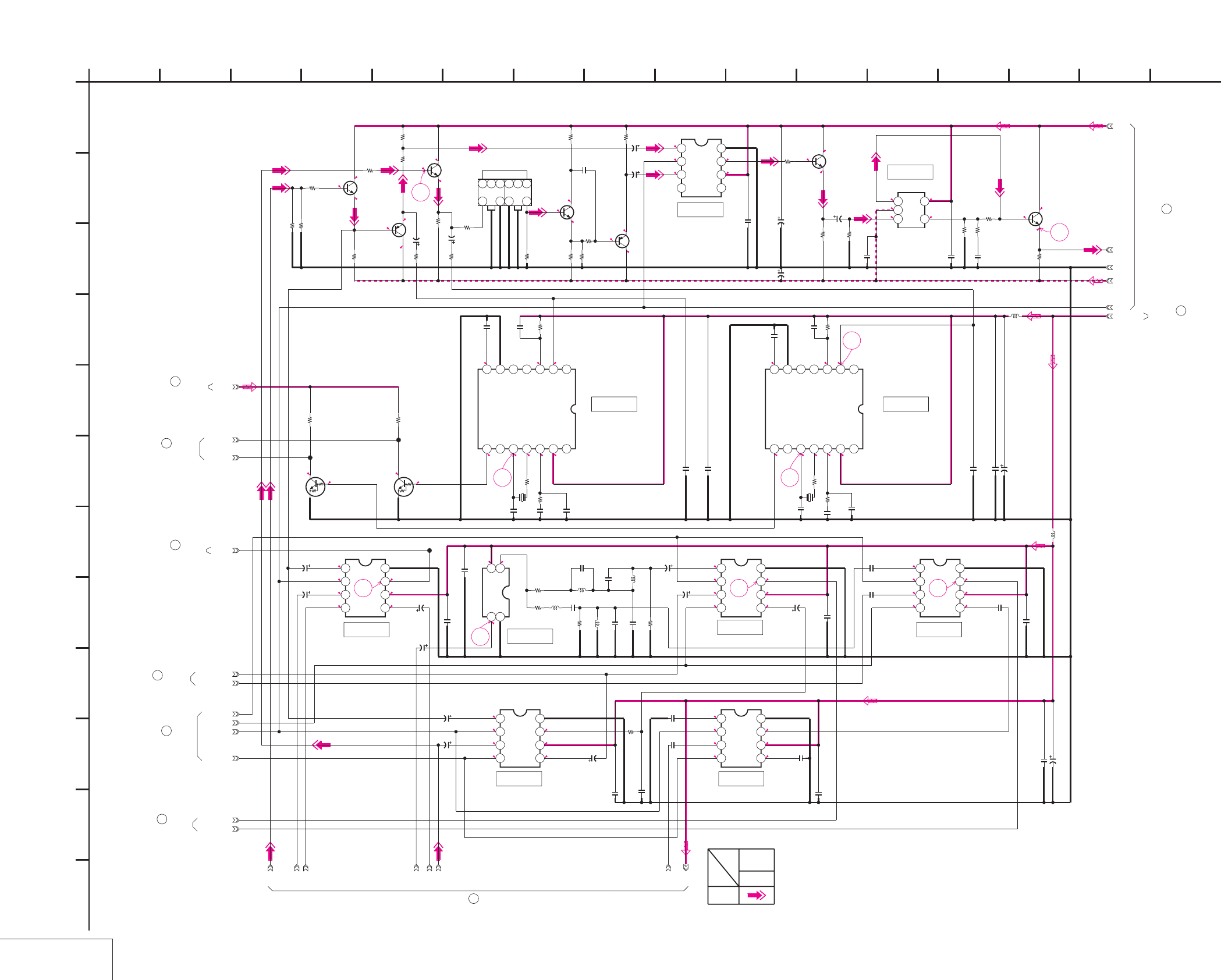
DSR-50/50P
2
2.7
2.7
4.9
0
2.7
R5/P0
38
NO MARK:REC/PB MODE
R:REC MODE
P:PB MODE
4.9
1.8
37
1.8
R5/P0
1.1
2
0
4.9
2.7
2.7
0
2
2.7
4.91.1
1.8
4.9
4.9
2.1
1.6
0
4.9 2
2.3
36
1.1
1.4
4.9
35 4.9
1.8
1.5
4.9
0
3.5
2.9
0.1
0 2.43.6
4.92.12.73.90.1
33
3.5 2.73.9 2.1 4.9
33
4.7 3.1
34
2.4
0
-0.6
4.9
0
-0.6
-4.9
1.1
4.9
0.5
31
-0.3
3
0.2
-0.3
-4.9
0.2
1.6
4.9
1.6
0.9
4.9
0.3
4.9
0.9
4.90.4
0.2
-4.9
0.2
4.9
0.4
-0.2 32
:DSR-50
:DSR-50P
:DSR-50P
:DSR-50
:DSR-50P
:DSR-50
:DSR-50P
:DSR-50
:DSR-50P
:DSR-50
:DSR-50P
:DSR-50
:DSR-50P
:DSR-50
GEN_LOCK_Y
GEN_LOCK_C
DV_SEL
0.1u
C200
1k
R1030
22u
6.3V
C101
LM7131BCM5X
IC115
123
45
0.01u
C174
2200
R1029
S/V_DET
0.1u
C159
22u
4V
C141
1500
R1028
150k
R153
0
R110
MM1117XFBE
IC108
1234
5678
2SC4081T106R
Q158
0.01u
C161
0.1u
C162
820p
C153
22u
4V
C145
470
R210
470
R115
1k
R127
0.001u
C1017
330p
C170
*
C131
3900
R154
L102
DV_REF_SC
0.056u
C155
C125
0.022u
C144
*
C135
500kHz
X102
1k
R131
LA7218M-TE-R
IC112
1234567
8 9 10 11 12 13 14
CL122
1k
R130
4700
R167
2.2u
35V
C109 22k
R191
1k
R135
2SC4081T106R
Q115
XX
C1025
560
R149
10uH
L107
680
R203
35V
2.2u
C114
100
R159
1u
C158
22u
4V
C198
6.3V
47u
C193
*
L104
0.1u
C172
0.1u
C189
CPNT_DET
6.3V
22u
C175
0.1u
C137
10uH
L106
EE/XPB
0.022u
C106
22u
4V
C163
470
R112
220
R1020
SW_+3V
0.01u
C187
500kHz
X101
DV_REF_SYNC
1u
C120
220
R132
*
L127
0.01u
C167
DL101
7
123456
10 912
*
L128
0.1u
C165
2SC4081T106R
Q101
2SC4081T106R
Q128
820p
C113
220
R120
*
C1018
UVIC_Y
2200
R105
150k
R124
*
C1019
0.01u
C147
100
R103
LA7218M-TE-R
IC106
1234567
8 9 10 11 12 13 14
MM1031XML
IC133
12
34
0.01u
C148
150
R102
2.2u
35V
C105
0.1u
C1020
XCPNT_SEL
MM1113XFBE
IC110
1234
5678
150
R101
0.01u
C121
22u
6.3V
C117
2SA1576A-T106-R
Q103
0.056u
C118
XX
R1026
1k
R108
MM1117XFBE
IC105
1234
5678
560
R121
22u
6.3V
C139
10k
R104
0
R109
22u
6.3V
C132
330p
C133
10k
R106
22u
6.3V
C140
0.1u
C128
2SA1576A
-T106-R
Q109
0.1u
C103
UN9213J-(K8).SO
Q102
MM1115XFBE
IC107
1234
5678
22u 6.3V
C119
2200
R134
0.1u
C204
CL120
22u
6.3V
C104
UN9213J-(K8).SO
Q104
0.1u
C185
1k
R114
INT/XEXT
CL121
47p
C1027
6.3V
100u
C1021
MM1117XFBE
IC101
1234
5678
0.01u
C173
2SC4081T106R
Q106
680
R200
220
R1031
6.3V
100u
C1022
22u 6.3V
C102
MM1113XFBE
IC113
1234
5678
48-1
48-4
48-2
GND
48-3
41-2
41-1
41-3
41-4
41-5
41-6
41-7
1
A
3900
R125
VIDEO_+5V
41-8
D
86
G
12
K
I
L
162 14
J
9
E
3
F
H
C
1110 13 15
05
7
B
VD-28 BOARD (5/15)
54
IC108
IC110IC105
IC113
IC133
IC101
IC106 IC112
IC115
IC107 VD-28 BOARD (6/15)
48
VIDEO
SIGNAL
SIGNAL PATH
Y
REC
-REF.NO.:10,000 SERIES-
VIDEO IN 2
XX MARK:NO MOUNT
49
VD-28 BOARD (14/15)
44
VD-28 BOARD (14/15)
VD-28 BOARD (12/15)
45
VD-28 BOARD (7/15)
46
VD-28 BOARD (10/15)
47
VD-28 BOARD (3/15)
25
VD-28 BOARD (1/15)
1
41
VD-28 BOARD (4/15)
18uH
22uH
*C1018,1019
82uH
100uH
82p
100p
*L127,128
18p
22p
*C135
120p
100p
*C131
220p
180p
*L104
8.2uH
10uH
4-83 4-84
VIDEO IN 2
VD-28 (5/15)
VD-28 (VIDEO IN 2) SCHEMATIC DIAGRAM • See page 4-71 for VD-28 printed wiring board. • See page 4-150 for waveforms.
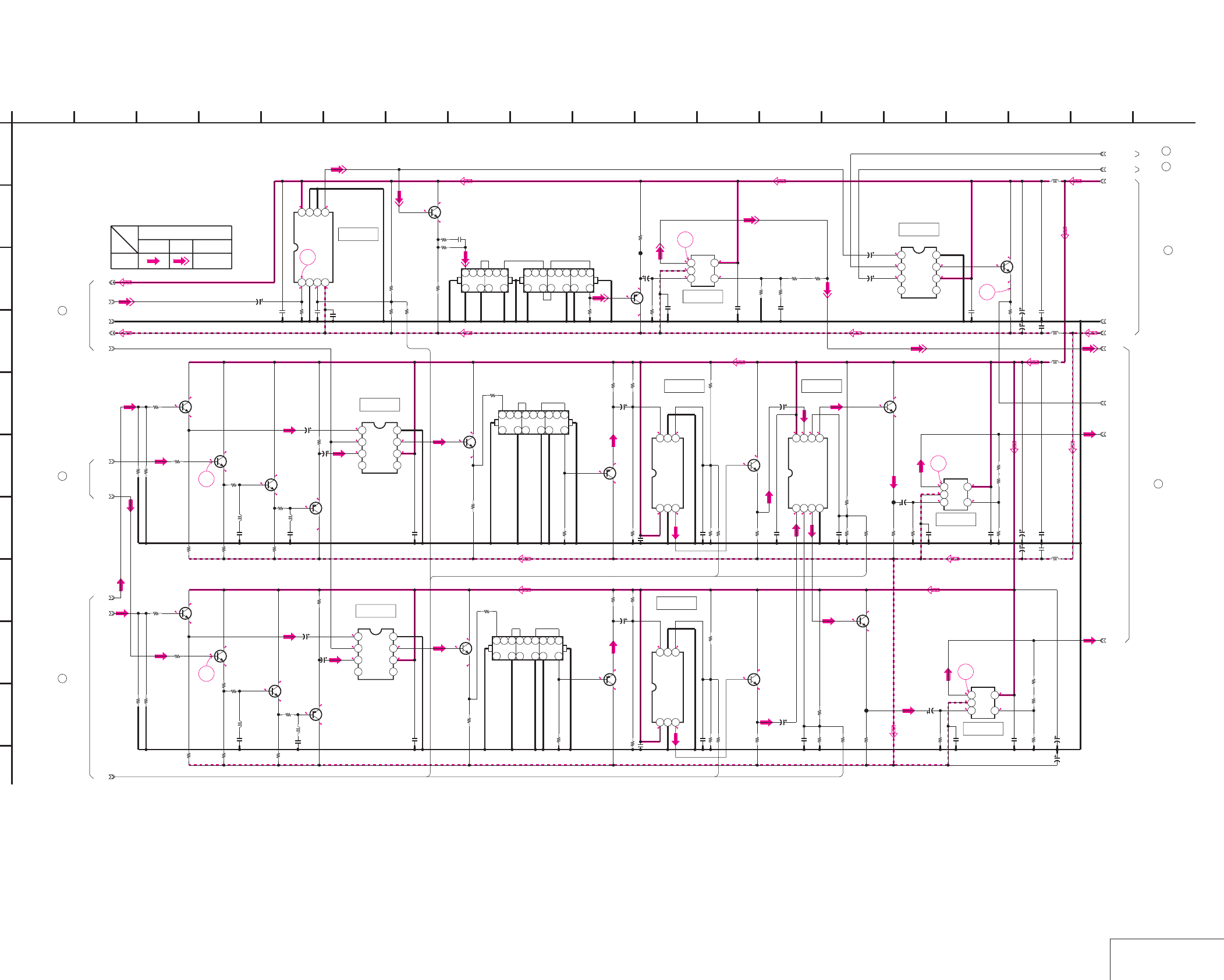
DSR-50/50P
2
4.9
2.7
2.5
NO MARK:REC/PB MODE
R:REC MODE
P:PB MODE
-0.6
4.9
0
4.9
1.4
2.1
-0.8
-0.2
4.9
-4.9
-0.2
-0.8
44
4.9
4.9
2.7
1.3
2
4.9
0.7
1.3
-4.9
2.94.9
2.9 2.8
2.9
2.3
4.9
1.4
2
4.9
4.91.2
-4.9
0.3 0.3
45
0.2
4.9
0.2
43
1
-4.9
2.9
2.94.8
2.8
3.4
2
2.5
3.4
2
4.9
2
1.4
2.9
4.9
0.7
-4.9
1.3
1.3
2
4.9
2
4.9
4.9
2.7
2.7
4.9 0
0 -4.9
1.1
39
42
0.8
1.5
2.1
4.9
-4.9
1.4
4.9
0.8
-0.6
4.9
0
1.4
0
4.9
-0.6
-0.2
-4.9
0.3
0.3
40
0.6 4.9
0.3
-4.9
2.4
2.6
R0/P5 1.7
4.9
1.7
1.1
4.9
41
:DSR-50
:DSR-50P
:DSR-50
:DSR-50P
:DSR-50
:DSR-50P
:DSR-50P
:DSR-50
:DSR-50P
:DSR-50
:DSR-50P
:DSR-50
:DSR-50P
:DSR-50
:DSR-50P
:DSR-50
:DSR-50
:DSR-50P
:DSR-50P
:DSR-50
560
R300
560
R301
2200
R285
2200
R286
560
R287
560
R288
2200
R254
680
R253
1k
R234
680
R236
0.01u
C295
0.01u
C299
0.01u
C294
0.01u
C298
10uH
L123
10uH
L122
10uH
L124
10uH
L121
100u
6.3V
C291
100u
6.3V
C297
100u
6.3V
C290
22u
4V
C260
100u
6.3V
C296
2SC4081T106R
Q142
2SC4081T106R
Q141
2SC4081T106R
Q133
REC_Y
VIDEO_+5V
AFC_Y
VIDEO_-5V
REC_CB
FL103
7
123456
1012 9
REC_CR
4700
R305
2SA1576A
-T106-R
Q134
2200
R238
22u
4V
C281
22k
R310
22k
R311
22u
4V
C283
CXA1521M-T4
IC116
1234
5678
10k
R217
15k
R229
12k
R230 8200
R232
0.1u
C214
0.1u
C252
TK16074MTL
IC121
123
456
10k
R283
18k
R247
33k
R248
27k
R243
10k
R252
10k
R280
0.1u
C239
2SC4081T106R
Q138
18k
R242
22k
R281
4700
R256
0.1u
C251
TK16074MTL
IC120
123
456
10k
R282
18k
R245
33k
R246
27k
R241
10k
R251
CXA1211M-T4
IC122
1234
5678
10k
R278
0.1u
C238
2SC4081T106R
Q137
18k
R240
22k
R279
4700
R255
LM7131BCM5X
IC125
123
45
22k
R277
*
R296
680
R293
2SC4081T106R
Q149
2200
R314
22u
6.3V
C280
22u
6.3V
C279
GEN_REF_Y
680
R321
LM7131BCM5X
IC129
123
45
2200
R319
680
R317
2200
R315
LM7131BCM5X
IC128
123
45
4700
R304
2200
R239
2SA1576A
-T106-R
Q135
22u
6.3V
C220
22u
6.3V
C221
MM1111XFBE
IC117
1234
5678
MM1111XFBE
IC118
1234
5678
22u
6.3V
C223
22u
6.3V
C222
470
R220
2SA1576A
-T106-R
Q131
2SC4081T106R
Q129
4700
R218
2200
R226
470
R221
4700
R219
2SA1576A-T106-R
Q132
2200
R227
2SC4081T106R
Q130
0.1u
C227
0.1u
C228
*
L116
*
L117
*
C215
*
C216
2SC4081T106R
Q127
1k
R212
C211
1200
R209
L115
1k
R211
*
L114
4700
R208
C210
2SC4081T106R
Q126
2200
R206
2SC4081T106R
Q124
2SC4081T106R
Q125
2200
R207
100
R197
100
R201
100
R198
100
R202
0.1u
C217
0.1u
C209 0.1u
C272
0.1u
C267
0.1u
C285
0.1u
C243
0.1u
C284
0.1u
C287
0.1u
C286
0.1u
C293
MM1115XFBE
IC126
1234
5678
150
R192
150
R195
150
R193 150
R196
100
R320
100
R316
*
R294
2SA1576A
-T106-R
Q136
CL133
CL134
CL129
3300
R1021
4V
47u
C207
4V
47u
C230
4V
47u
C241
4V
47u
C242
4V
47u
C231
6.3V
100u
C1023
6.3V
100u
C1024
FL104
7
12345689
10
13
15
16
18 12
FL105
7
12345689
10
13
15
16
18 12
DIG/XANA
2SC4081T106R
Q144
2SC4081T106R
Q145
22p
C1026
820
R1027
47k
R1032
39p
C1028
DL102
7
12345689
10
13
15
16
18 12
1
A
GND
48-2
48-4
38-1
38-2
42-2
42-3
42-1
0.1u
C235
0.1u
C236
GND
48-1
48-3
G5
G6
G3
G4
G1
15
05
B
54 137
VD-28 BOARD (6/15)
103
F
H
J
9
E
C
11 142 128
I
6
G
K
16
D
IC122IC120
IC121
IC129
IC125
IC116
IC117
IC118
IC126
IC128
Y
REC
Y/CHROMA
VIDEO SIGNAL
CHROMA
SIGNAL PATH
17 18 19
-REF.NO.:10,000 SERIES-
VIDEO IN 3
XX MARK:NO MOUNT
VD-28 BOARD (2/15)
22
VD-28 BOARD (3/15)
26
VD-28 BOARD (14/15)
50
51
VD-28 BOARD (7/15)
48
VD-28 BOARD (5/15)
VD-28 BOARD (4/15)
38
VD-28 BOARD (4/15)
42
560
470
*R296*R294
270
330
8.2uH
*L117
6.8uH
15p
*C216
12p
12uH
15uH
30p
27p
*C215
12p
15p
15uH
12uH
30p
27p
8.2uH
*L116
6.8uH
*L114
4-85 4-86 VIDEO IN 3
VD-28 (6/15)
VD-28 (VIDEO IN 3) SCHEMATIC DIAGRAM • See page 4-71 for VD-28 printed wiring board. • See page 4-150, 151 for waveforms.
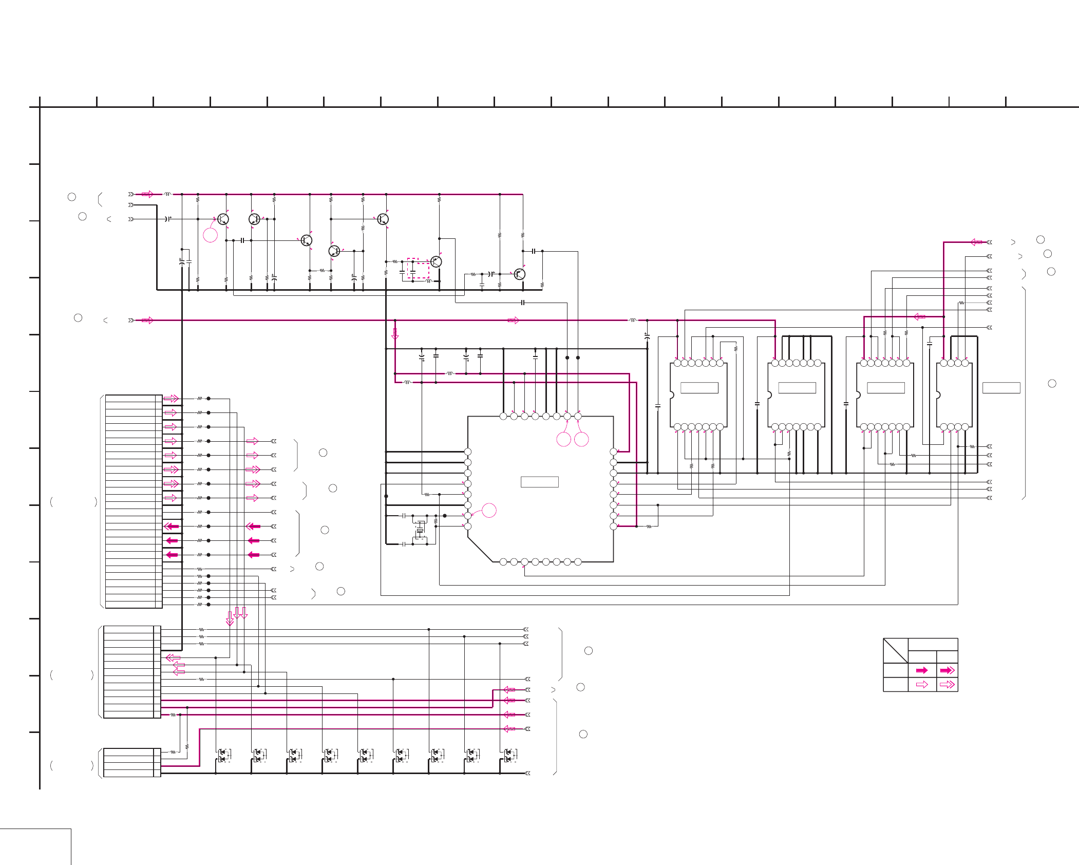
DSR-50/50P
4-87 4-88
UVIC
VD-28 (7/15)
VD-28 (UVIC) SCHEMATIC DIAGRAM • See page 4-71 for VD-28 printed wiring board. • See page 4-151 for waveforms.
NO MARK:REC/PB MODE
R:REC MODE
P:PB MODE
2.9
2.6
4.8
2.8
4.8
2.8
2.2
2.8
4.9
2.3
1.6
4.9
46
2.8
2.9
4.9
3.7
2.1
1.5
3
4.9
3.7
3.6
3
3.2
2.6
2.9
4.9
4.9
2.9
2.9
55
000
R0.6/P0
R0.6/P0
R0.3/P0
2.8
2.8
5
5
5
5
2.7
4.8
5
0.1
0.2
0552.8 4.8
55
R2.1/P5
R1.7/P0.7
R1.8/P0.1
5
5
0.2
4.8
4.8
4.8
0
2.7
2.7
R0.6/P0
5
47 48
49
:DSR-50
:DSR-50P
:DSR-50
:DSR-50P
DSR-50
:DSR-50P
:DSR-50
R369 470k
R371
47k
R373
1k
R374
100k
R372
47k
R362
18k
R370
1k
R368
10k
R363
22k
R361
10k
R355
22k
R364
1k
R360
470
R359
1k
R358
390
R357
680
R356
33k
R352
47k
R367
1k
R375
10k
R354
220k
R353
1k
R351
47k
C342
15p
C338
*
C350
0.1u
C347
0.1u
C346
220p
C340
10p
C344
0.01u
C348
0.01u
C339
10p
C332
0.01u
L331
10uH
L334
10uH
L333
10uH
L332 *
CL349
CL350
CL348
C331
22u
6.3V
C345
22u
6.3V
C343
22u
6.3V
C349
10u
16V
C336
10u
16V
C335
10u
16V
C333
10u
16V
UVIC_Y
IC332
MC68HC68VBIFB
12345678
9 10111213141516
1718192021222324
2526272829303132
Q335
2SC4081T106R
Q331
2SC4081T106R
Q334
2SC4081T106R
Q333
2SC4081T106R
Q332
2SC4081T106R
X331
*
Q338
2SA1576A-T106-R
Q337
2SA1576A-T106-R
XCS_UVIC
UVIC_BUSY
UVIC_SWIN
UVIC_GATE
MO_SCK
MO_SO
MO_SI
XSYS_RST
330
R365
VIDEO_+5V
1u
C334
0.1u
C351
CL347
CL340
0
R339
100
R346
0
R333
CL333
CL346
0
R336
CL336
0
R335
CL342
0
R331
CL338
CL345
CL337
CL341
100
R344
0
R341
CL339
CL332
100
R345
CL344
0
R334
100R343
0
R337
CL335
0
R340
0
R342
0
R332
CL334
30P
CN332
1V_SYNC
2XI/O SYNC VFD
3XI/O SYNC HI
4VFD HD
5VFD VD
6VD HD
7GND
8CB IN
9GND
10CR IN
11GND
12Y IN
13GND
14AFC Y
15GND
16MONITOR C
17GND
18MONITOR Y
19GND
20Y LINE
21GND
22CR LINE
23GND
24CB LINE
25GND
26PANEL CB
27GND
28PANEL CR
29GND
30PANEL Y
0
R338
CL331
CL343
TC74VHCT08AFT(EL)
IC333
1234567
891011121314
TC74VHCT08AFT(EL)
IC334
1234567
891011121314
TC74VHC08FT(EL)
IC335
1234567
891011121314
10
R379
0.1u
C353
0.1u
C354
0.1u
C355
10
R376
10
R377
10
R378
10
R384
10
R382
TC7WH125FU(TE12R)
IC336
1234
5678
SW_+3V
0.1u
C356
AFC_Y
REC_Y
REC_CR
REC_CB
PB_Y
PB_CR
PB_CB
MONITOR_Y
MONITOR_C
XI/O_SYNC_VFD
XI/O_SYNC_HI
100
R347
100R348
100
R349
100
R350
VD_SCK
VD_SO
PANEL_DA_CS
LCD_DD_ON
10uH
L335
22u
6.3V
C352
INT/EXT_DET
INT/EXT_IN
SC_DET
SC_EXIST
100
R381
100
R383
SW_+12V
10
R386
V_SYNC_HI
V_SYNC
DIG_+5V
LCD_+3V
100
R389 CL351
SW_+4.6V
R_HD
100
R390
01ZA8.2(TPL3)
D331
01ZA8.2(TPL3)
D332
01ZA8.2(TPL3)
D333
01ZA8.2(TPL3)
D334 01ZA8.2(TPL3)
D335
01ZA8.2(TPL3)
D336
01ZA8.2(TPL3)
D337
01ZA8.2(TPL3)
D338
01ZA8.2(TPL3)
D339
GND
13P
CN331
1VD_SCK
2DATA_FROM_HI
3XCS_LCD_DAC
4GND
5PANEL_Y
6PANEL_CR
7PANEL_CB
8LCD_DD_ON
9XVD
10XHD
11LCD_4.6V
12LCD_3.0V
13ORG_12V
4P
CN333
1ORG_15.5V
2PWM
3UNREG
4GND
XX
R391
SW_+5.5V
0
R393
XX
R392
1
A
GND
10
R385
2 16
L
I
K
12
G
68
D
E
VD-28 BOARD (7/15)
B
7
05
151310 1711
C
H
F
3 18
J
14945
IC333 IC334 IC335 IC336
IC332
REC
CHROMA
PB
VIDEO SIGNAL
SIGNAL PATH
Y
-REF.NO.:10,000 SERIES-
UVIC
XX MARK:NO MOUNT
52
VD-28 BOARD (14/15)
VD-28 BOARD (5/15)
46
VD-28 BOARD (15/15)
53
JC-20 BOARD (1/14)
THROUGH THE
FVJ-13 FLAT CABLE
CN1101
(SEE PAGE 4-19)
(SEE PAGE 4-139)
CN8001
THROUGH THE
LC-111 HARNESS
PD-125 BOARD (1/2)
THROUGH THE
CN8002
(SEE PAGE 4-139)
PD-125 BOARD (1/2)
RM-129 HARNESS
54
VD-28 BOARD (8/15)
VD-28 BOARD (10/15)
55
VD-28 BOARD (6/15)
51
33
VD-28 BOARD (3/15)
VD-28 BOARD (12/15)
56
57
VD-28 BOARD (14/15)
VD-28 BOARD (12/15)
58
VD-28 BOARD (15/15)
59
VD-28 BOARD (14/15)
60
VD-28 BOARD (2/15)
20
VD-28 BOARD (1/15)
3
VD-28 BOARD (12/15)
61
39uH
47uH
*L332
33p
*C338
27p
3.579545MHz
4.433619MHz
*X331
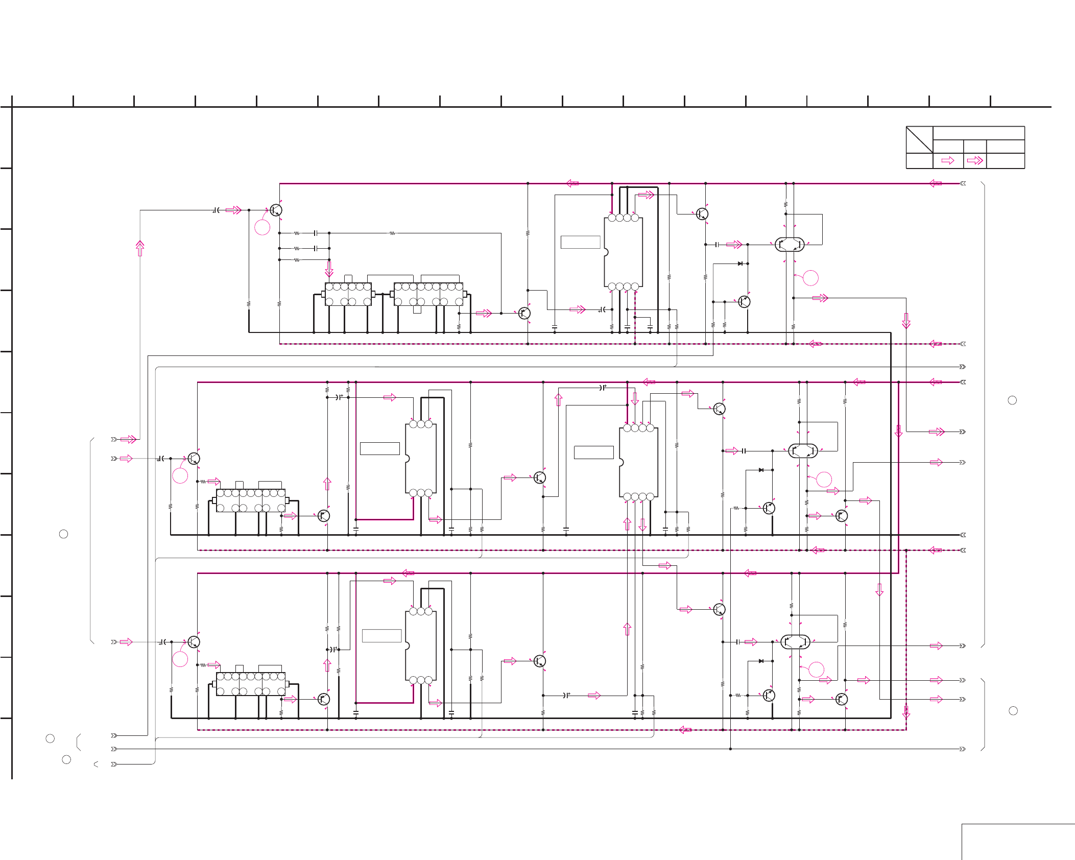
DSR-50/50P
4-89 4-90 VIDEO OUT 1
VD-28 (8/15)
VD-28 (VIDEO OUT 1) SCHEMATIC DIAGRAM • See page 4-71 for VD-28 printed wiring board. • See page 4-151 for waveforms.
2.9
2.94.9
2.4
2
1.4
4.9
NO MARK:REC/PB MODE
4.9
2.5
4.1
2
2.5
4.1
2
52
-0.6
0
4.8
2.9
2.9
2.2
4.9
4.9 0
0 -4.9
0.4
4.9
50
0
-0.6
4.9
-0.3
0.3
0.3
0
-0.6
0
4.9
0.3
4.9
0.3
0.9
0.9
-4.9
51
0.7
-4.9
0.1 0.7
4.8
0.1
53
0.6
0.1
-4.9
0.1
0.1
2
4.9
1.4
2.3
4.9
2.9
-0.3
0.3
-4.9
4.9
54
0
-0.6
-0.3
0.3
-4.9
4.9
2.9
2.3
55
-4.9
0.7
0.1 0.7
0.1
4.9
0.1
0.1
-4.9
-0.4
-1
PB_Y
PB_CR
PB_CB
2SC4081T106R
Q401
1k
R410
0.47u
C433
4700
R455
4700
R406
2SC4081T106R
Q409
C401
6.3V
47u
18k
R420
2SC4081T106R
Q402
4V
47u
C402
2200
R411
18k
R436 0.47u
C434
27k
R421
TK16074MTL
IC402
123
456
4700
R457
33k
R437
0.1u
C414
4700
R403
10k
R443
2SC4081T106R
Q411
2SC4081T106R
Q412
33k
R439
4700
R458
TK16074MTL
IC403
123
456
27k
R423
0.47u
C435
18k
R438
2200
R412
10k
R444
4V
47u
C403
2SC4081T106R
Q403
18k
R422
0.1u
C415
4700
R407
2SC3326N
-TE85L-AB
Q413
2SC3326N-TE85L-AB
Q415
2SC3326N-TE85L-AB
Q416
10k
R465
4700
R463
4700
R462
10k
R464
4700
R456
10k
R459
XN4601-TW
Q420
XN4601-TW
Q419
XN4601-TW
Q414
4700
R460
4700
R461
R477
4700
4700
R473
3300
R479
4700
R474
0
R476
1k
R478
2SA1576A-T106-R
Q422
2SA1576A-T106-R
Q423
4700
R488
4700
R487
R_UV_CLAMP
R_Y_CLAMP
0.1u
C409
0.1u
C410
MA112-TX
D402
MA112-TX
D403
MA112-TX
D404
4V
47u
C405
4V
47u
C406
2SC4081T106R
Q434
2SC4081T106R
Q435
4700
R570
4700
R571
CXA1521M-T4
IC427
1234
5678
CXA1211M-T4
IC428
1234
5678
10k
R572
6800
R575
6800
R576
15k
R577
12k
R578
XX
R579
XX
R580
8200
R581
8200
R582
8200
R583
0.1u
C531
0.1u
C532
0.1u
C533
0.1u
C534
0.1u
C535
0.1u
C538
4V
47u
C540
4V
47u
C541
4V
47u
C542
2SA1576A
-T106-R
Q436
2SA1576A
-T106-R
Q437
560
R1201
560
R1202
560
R1203
560
R1204
2200
R1205
2200
R1206
FL404
7
12345689
10
13
15
16
18 12
FL405
7
12345689
10
13
15
16
18 12
FL406
7
123456
1012 9
680
R1207
680
R1208
2200
R1209
2SA1576A-T106-R
Q438
XX
R1214
39p
C546
18k
R1215
220
R1216
27p
C547
DL404
7
12345689
10
13
15
16
18 12
63-5
GND
63-2
63-6
63-8
64-1
64-2
64-3
62-1
63-4
1
A
63-7
63-1
63-3
B2
B3
B13
B15
B14
IC428
IC402
2 16
I
K
12
G
68
D
E
VD-28 BOARD (8/15)
B
7
05
151310 1711
C
H
F
3
J
14945
Y/CHROMA
PB
VIDEO SIGNAL
Y
SIGNAL PATH
CHROMA
IC427
IC403
-REF.NO.:10,000 SERIES-
VIDEO OUT 1
XX MARK:NO MOUNT
64
VD-28 BOARD (10/15)
2
31
5
64
1
5
4
2
6
3
3
2
64
5
1
VD-28 BOARD (9/15)
63
VD-28 BOARD (3/15)
34
VD-28 BOARD (10/15)
62
VD-28 BOARD (7/15)
54
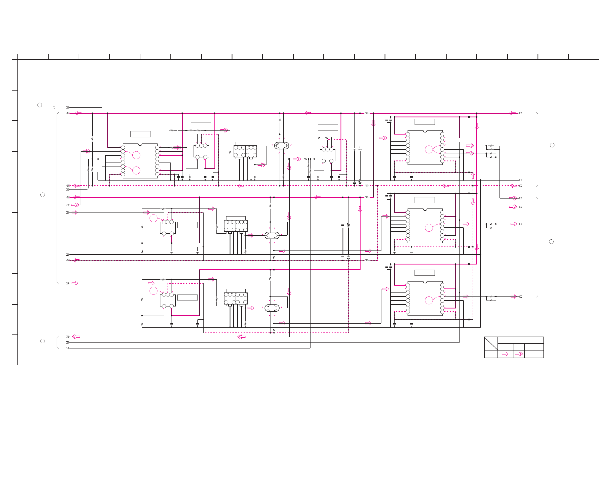
DSR-50/50P
4-91 4-92
VIDEO OUT 2
VD-28 (9/15)
VD-28 (VIDEO OUT 2) SCHEMATIC DIAGRAM • See page 4-71 for VD-28 printed wiring board. • See page 4-151 for waveforms.
NO MARK:REC/PB MODE
-0.3
4.9
-4.9
0.3
0.3
-0.2
0.1
4.9
-4.9
0.7
0.7
0.1
0.1
-4.9
0.1
0.7 4.9
0.7
0.2
0.1
0.1 4.9
-4.9
61
0.2
59
0.1
-4.9
0.1 4.9
0
-4.9
-0.5
0 4.9
-4.9
0.3
4.9
0
0
4.9
4.9
0
0.7
0.7
0
-4.9
0.3
-4.9
58
60
-4.9
4.9
4.9
4.9
0.1
0
-4.9
0.2
-4.9
0.2
4.9
4.90.1
4.9
62
0
-4.9
-4.9-4.9
4.9
4.9
4.9
57
4.9
0.3
0.1
0.6
0.6
56
:DSR-50
:DSR-50P
:DSR-50P
:DSR-50
VIDEO_+5V
VIDEO_-5V
CXA1451M-T4
IC410
12345678
9 10111213141516
DL403
7
123456
10 912
DL401
7
123456
10 912
DL402
7
123456
10 912
LM7131BCM5X
IC416
123
45
4700
R496
4700
R508
0
R506
0.1u
C465
0.1u
C470
R503
0.1u
C458
0.1u
C462
LM7131BCM5X
IC414
123
45
1k
R498
1k
R500
0.1u
C463
LM7131BCM5X
IC415
123
45
R504
0.1u
C459
220
R512
220
R510
220
R511
220
R514
220
R515
220
R516
3k
R533
0.1u
C486
0.1u
C492
LM7131BCM5X
IC419
123
45
2200
R531
1k
R523
4700
R519
XN4601-TW
Q427
2700
R524
4700
R520
XN4601-TW
Q425
4700
R517
XN4601-TW
Q426
4700
R518
4700
R521
6800
R527
10uH
L409
10uH
L408
6.3V
100u
C496
0.1u
C493
0.1u
C494
6.3V
100u
C497
CXA1451M-T4
IC423
12345678
9 10111213141516
FB407
0.1u
C512
FB406
0.1u
C517
4.7u
C507
4.7u
C522
CXA1451M-T4
IC424
12345678
9 10111213141516
FB408
4.7u
C523
4.7u
C508
0.1u
C518
0.1u
C513
FB403
CXA1451M-T4
IC422
12345678
9 10111213141516
FB405
0.1u
C516
FB404
0.1u
C511
4.7u
C521
4.7u
C506
150
R555
150
R554
150
R559
150
R558
150
R556
150
R557
150
R550
150
R549
CPNT-Y_OUT
CPNT-U_OUT
S-Y_OUT
CPNT-V_OUT
6.3V
100u
C490
0.1u
C488
0.1u
C487
6.3V
100u
C489
10uH
L406
10uH
L407
0.1u
C453
0.1u
C452
220
R497
220
R499
CL401
8200
R469
7500
R470
39k
R467
0.1u
C443
0
R564
0
R568
XX
R586
XX
C543
1500
R1217
0.1u
C548
65-1
65-2
65-3
63-8
GND
63-6
63-3
63-5
R_Y_BLK
1
A
63-1
63-2
63-4
63-7
GND
B12
IC423
IC422
2 16
I
12
G
68
D
E
VD-28 BOARD (9/15)
B
7
05
151310 1711
C
H
F
3 18
J
14945
CHROMA
SIGNAL PATH
Y
VIDEO SIGNAL
PB
Y/CHROMA
IC424
IC419
IC410
IC416
IC414
IC415
19
-REF.NO.:10,000 SERIES-
VIDEO OUT 2
XX MARK:NO MOUNT
21
VD-28 BOARD (2/15)
65
VD-28 BOARD (10/15)
63
VD-28 BOARD (8/15)
66
VD-28 BOARD (14/15)
VD-28 BOARD (4/15)
37
2
4
3
6
1
5
2
4
3
6
1
5
46
2
31
5
1200
2200
2200
1200
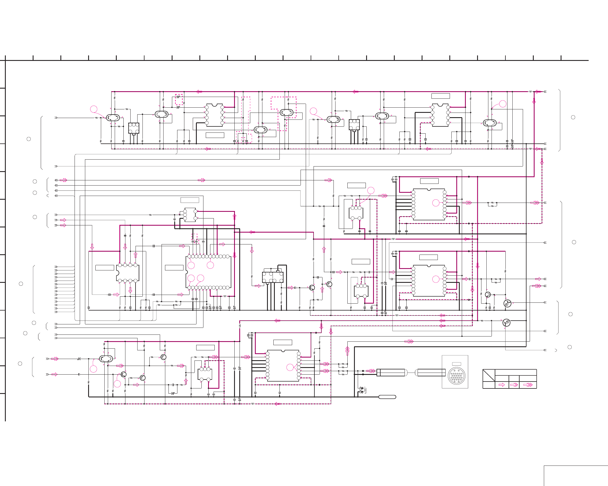
DSR-50/50P
4-93 4-94 VIDEO OUT 3
VD-28 (10/15)
VD-28 (VIDEO OUT 3) SCHEMATIC DIAGRAM • See page 4-71 for VD-28 printed wiring board. • See page 4-151, 152 for waveforms.
NO MARK:REC/PB MODE
R:REC MODE
P:PB MODE
0.1
4.9
0.1
-0.4
-4.9
-0.4-4.9
0.1
0.1 4.9
0
0.1-4.9
4.9
-0.4
-0.4
0.1
0.1
0.1
-4.9
4.9
-0.4
-0.4
0.1
2
-4.9
4.9
1.4
1.4
2
2.6
3.2
2
4.9
3
1.5
00.1
-4.9
4.9
-0.4
-0.4
0.1
0.1
-4.9
4.9
-0.4
-0.4
0.1
0.5
4.9
4.4
0.30
-4.9
4.90
4.9
0
0.6
4.9
-4.9
4.9
0.3
-4.9
R4.8/P0
R0/P5
R4.8/P0
R4.2/
P0
4.9
0
2.9
4.9
0
0
0
-4.9
4.9
0
0
4.9
-4.9
00
-4.9
4.90
0
-0.6
-4.9
4.9
0
-0.6
4.92.3
4.4
2.4
3.5
2.9
1.7
2.3 1.7
1.7
2.8
2.9
3.5
2.9
4.9
3.32.5 2
4.9 2.5 3.7 2
0.1
0.1
0.7
0.7
-4.9
4.9
4.9
0
-0.6
0
-0.6
-4.9
0.1
0.7
-4.9
0.1 0.2
-4.9
0.1 4.9
4.9
0.4
0.4
-4.9
0
0
4.9
0.2
-4.9
65
64
63
70
71
72
67
66
68 69
75
74
73
DSR-50P
2.8
DSR-50P DSR-50P DSR-50P
1k
R562
SDC
V_MUTE
M51272FP-TE2
IC413
123456789101112
131415161718192021222324
C454
0.1u
4.7u
C456
0.1u
C460
0.1u
C455
4.7u
C457
0.1u
C461
0.1u
C464
0.1u
C471
10uH
L403
16V
10u
C472
16V
10u
C467
0.1u
C468
16V
10u
C476
0.1u
C473
4.7u
C449
4.7u
C450
SC_V
SC_U
2200
R501
2200
R502
56k
R493
56k
R495
10k
R489
4700
R480
47k
R482
0.1u
C447
4700
R486
47k
R490
0.1u
C448
10k
R484
4.7u
C446
4.7u
C445
10uH
L411
10uH
L410
0.1u
C502
6.3V
47u
C505
0.1u
C503
6.3V
47u
C504
3k
R539
0
R538
LM7131BCM5X
IC420
123
45
0.1u
C499
6800
R530
0.1u
C495
1500
R535
2700
R534
FL403
12
136
7
9
10
1k
R513
1k
R522
TC7S02FU(TE85R)
IC412
123
45
64-3
0.1u
C483
12k
R525
2SC4081T106R
Q428
2SA1576A-T106-R
Q429
0
R528
XX
R529
2200
R526
XX
C484
220
R532
1200
R536
0
R540
LM7131BCM5X
IC421
123
45
0.1u
C501
0.1u
C498
3k
R541
1500
R537
0.1u
C491
0.1u
C485
PB_V_DELAY
PB_U_DELAY
COMPONENT_SYNC
BURST_V
COMPOSITE_SYNC
BURST_U
COMPOSITE_U_GAIN
COMPOSITE_U_BAL
COMPOSITE_V_BAL
COMPOSITE_V_GAIN
R_BF_OUT
IC405
CXA1521M-T4
1234
5678
XN4601-TW
Q407
4
2
31
5
6
12k
R441
15k
R440
0.1u
C416
33k
R433
22k
R450
XX
R449
0.1u
C426
XX
R445
4700
R453
2200
R454
XN4601-TW
Q410
4
2
3
1
5
6
R_SYNC_OUT
4700
R409
2200
R414
FL401
123
46
1k
R402
3300
R405
XN4601-TW
Q405
4
2
3
1
5
6
1k
R424
1k
R417
3300
R415
33p
C407
22k
R432
XN4601-TW
Q408
4
2
3
1
5
6
2200
R447
4700
R426
XN4601-TW
Q406
4
2
3
1
5
6
CXA1211M-T4
IC404
1234
5678
10k
R431
10k
R430 0.1u
C412
4700
R446
4700
R427 2200
R468
10k
R448
10k
R451
0.1u
C431
22k
R452
4700
R466
XN4601-TW
Q417
4.7u
C510
FB412
0.1u
C520
FB411
0.1u
C515
4.7u
C525
150
R552
150
R551
CXA1451M-T4
IC426
12345678
9 10111213141516
150
R561
FB410
CXA1451M-T4
IC425
12345678
9 10111213141516
4.7u
C509
4.7u
C524
150
R560
0.1u
C514
0.1u
C519
FB409
0.1u
C526
2SC4081T106R
Q430
10k
R548
47k
R553
0.1u
C527
10k
R546
0.1u
C500
4700
R547
CXA1211M-T4
IC411
1234
5678
MONITOR_OUT
VIDEO_OUT
S-C_OUT
2P
CN401
1 RETURN VIDEO(X)
2 RETURN VIDEO(GND)
4.7u
C482
CXA1451M-T4
IC418
12345678
9 10111213141516
0.1u
C480
150
R545
150
R542
FB401
150
R543
0.1u
C481
4.7u
C479
150
R544
FB402
0.1u
C437
6.3V
47u
C440
6.3V
47u
C439
10uH
L402
0.1u
C436
10uH
L401
0.1u
C474
10uH
L404
10uH
L405
6.3V
47u
C478
0.1u
C475
6.3V
47u
C477
6.3V
47u
C441
22k
R471
MONITOR_Y
MONITOR_C
2SC4081T106R
Q421
4700
R483
22k
R481
0.01u
C442
LM7131BCM5X
IC417
123
45
2700
R494
2200
R492
0.1u
C466
0.1u
C469
2200
R507
2200
R509
XN4601-TW
Q418
4
2
31
5
6
4700
R472
4700
R475
UN9211J-(K8).SO
Q431
UN9211J-
(K8).SO
Q432
0.1u
C424
0.1u
C427
0.1u
C425
0.1u
C444
LND401
SHAS
01ZA8.2(TPL3)
D401
CL402
CL403
270
R505
0.1u
C451
2SA1576A-T106-R
Q424
4700
R491
100
R485
DV_REF_SYNC
Y_BLK_LEVEL
4V
47u
C528
1500
R565
100p
C529
0
R566
FSC_ADJ
FSC_TEST
0.1u
C530
0
R567
PB_Y_LEVEL
PB_U_LEVEL
PB_V_LEVEL
100
R585
XX
R1210
0
R1211
2SA1576A-T106-R
Q439
100
R1212
4700
R1213
DV_REF_SC
4V
22u
C544
4V
22u
C545
390
R1218
4700
R428
4700
R408
XN4601-TW
Q404
4
2
3
1
5
6
3300
R404
2200
R413
1k
R416
3300
R401
4700
R429
1k
R425
FL402
123
46
33p
C411
65-2
VIDEO_+5V
VIDEO_-5V
65-1
65-3
62-1
64-2
64-1
1
A
GND
18RETURN VIDEO(X)
19RETURN VIDEO(GND)
B10
B9
B8
B2
B3
B4
B5
B6
B7
B8
B9
B10
B11
B5
B4
B6
B11
B12
B13
B14
B15
B7
IC411 IC413
2 16
L
I
20
K
12
G
68
D
E
VD-28 BOARD (10/15)
B
7
05
19151310 1711
C
21
H
F
3 18
J
14945
M
IC425
IC426
IC421
IC405
IC404
IC418
IC420
IC417
VIDEO SIGNAL
SIGNAL PATH
Y/CHROMACHROMA
PB
Y
XX MARK:NO MOUNT
-REF.NO.:10,000 SERIES-
VIDEO OUT 3
IC412
CN026
(2/5)
CAMERA
VD-28 BOARD (14/15)
67
40
VD-28 BOARD (4/15)
VD-28 BOARD (3/15)
27
VD-28 BOARD (12/15)
68
VD-28 BOARD (2/15)
19
VD-28 BOARD (9/15)
65
62
VD-28 BOARD (8/15)
VD-28 BOARD (8/15)
64
VD-28 BOARD (3/15)
29
16
VD-28 BOARD (2/15)
VD-28 BOARD (5/15)
47
55
VD-28 BOARD (7/15)
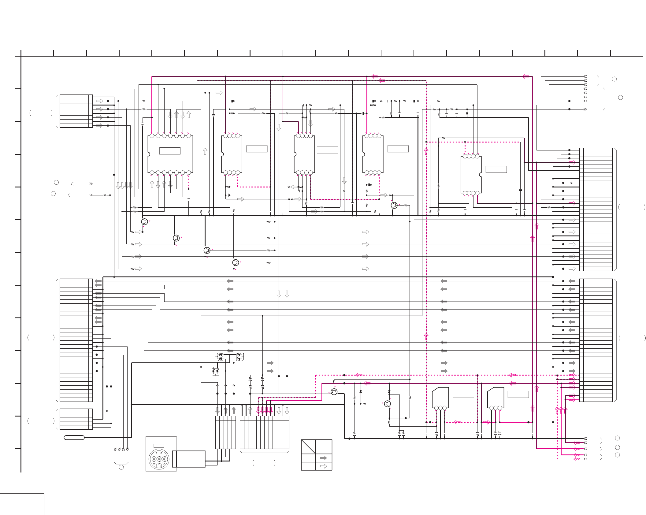
DSR-50/50P
4-95 4-96
AUDIO
VD-28 (11/15)
VD-28 (AUDIO) SCHEMATIC DIAGRAM • See page 4-71 for VD-28 printed wiring board.
1.4
-5
NO MARK:REC/PB MODE
5.1
5.5
-5.4-5
5.3
5.5
-5
-5
0
2.2
1.4
5.1
0.7
5.1
5.1
-5
0
00
0
-5
5.1 0
0
0
000-5
05.1 0 00005.1
000-5
05.1
000
00
-5
5.15.10
05.1 5.1
-5
0
-5
0
0
-5
-5
0
30P
CN603
1CH4 OUT
2GND
3GND
4CH2 OUT
5GND
6GND
7CH3 OUT
8GND
9GND
10 CH1 OUT
11 GND
12 GND
13 AUDIO MONITOR OUT
14 GND
15 GND
16 +48V DD ON
17 SW +3V
18 P/S CS
19 GND
20 P/S DATA
21 GND
22 P/S SCK
23 GND
24 NC
25 GND
26 SIRCS DATA
27 SW +3V
28 TALLY LED
29 FOOT SW
30 AUDIO MONITOR SEL
30P
CN604
1SW +48V
2SW +48V
3NC
4SW +6V
5SW +6V
6SW -6V
7SW -6V
8MIC Y
9GND
10 MIC X
11 GND
12 GND
13 CH4 IN Y
14 GND
15 CH4 IN X
16 GND
17 GND
18 CH3 IN Y
19 GND
20 CH3 IN X
21 GND
22 GND
23 CH2 IN Y
24 GND
25 CH2 IN X
26 GND
27 GND
28 CH1 IN Y
29 GND
30 CH1 IN X
TC74HC4066AFT(EL)
IC601
1234567
891011121314
NJM2115M-TE2
IC604
1234
5678
NJU7211U50-TE1
IC606
123
NJU7201U50-TE1
IC607
123
12P
CN601
1HP L
2HP L GND
3HP R
4HP R GND
5SW +6V
6SW +6V
7SW -6V
8SW -6V
9NC
10VTR RET AUDIO
11VTR RET AUDIO GND
12GND
5P
CN602
1MIC IN(X)
2MIC IN(X-GND)
3MIC IN(Y)
4MIC IN(Y-GND)
5AUDIO MON/VTR SAVE
SW_+3V
SW_+5.5V
SW_-5.5V
SW_+48V
SIRCS_DATA
FOOT_SW
TALLY_LED
P/S_CS
VD_SI
VD_SCK
GND
+48V_DD_ON
01ZA8.2
(TPL3)
D602
01ZA8.2
(TPL3)
D601
16V
10u
C614
16V
10u
C612
MA3200WA-TX
D603
82k
R652
33k
R653
0
R655
4.7u
C635 XX
C636
16V
47u
C632
16V
47u
C633
16V
47u
C625
16V
47u
C630
0.1u
C631 0.1u
C634
0.1u
C628
0.1u
C624
NJM2115M-TE2
IC602
1234
5678
NJU7102AM-TE1
IC605
1234
5678
10k
R646
150k
R647
330k
R648
150k
R649 0.1u
C626
0.1u
C627
0.1u
C629
XX
C623
47k
R603
47k
R604
47k
R602
47k
R601
10k
R615
10k
R616
22k
R613
22k
R614
10p
C604
10p
C605
NJM2115M-TE2
IC603
1234
5678
47k
R621
47k
R619
47k
R618 47k
R623
47k
R622
47k
R617
47k
R620 47k
R625
10p
C608
10p
C609 ATT_ALARM
68k
R642
1u
C619
10k
R639
0.033u
C618
10k
R637
56k
R636
1u
C616
0
R633
47k
R632
47k
R635
10p
C615
10p
C613
27k
R631
47k
R634
47k
R627
47k
R628
220
R638
100
R624
100
R626
1u
C602
1u
C601
1u
C603
1u
C606
1u
C607
1u
C610
1u
C611
1u
C617
2SA1576A-T106-R
Q607
16V
47u
C620
6.3V
100u
C622
6.3V
100u
C621
MA112-TX
D604
MA112-TX
D605
10k
R644
10k
R645
47k
R641
2SC3326N
-TE85L-AB
Q605
10k
R629
2SC3326N-
TE85L-AB
Q606
2200
R640
220
R605
220
R606
220
R607
220
R608
2SC3326N-TE85L-AB
Q601
2SC3326N-TE85L-AB
Q602
2SC3326N-TE85L-AB
Q603
2SC3326N-TE85L-AB
Q604
2200
R609
2200
R610
2200
R611
2200
R612
CL650
CL651
CL623
CL624
CL625
CL626
CL628
CL629
CL630
CL634
CL631
CL632
CL633
CL635
CL636
CL639
CL637
CL638
CL640
CL641
CL642
CL643
CL644
CL645
CL646
CL647
CL649
CL616
CL612
CL613
CL615
CL614
CL621
CL617
CL618
CL619
CL620
CL648
CL622
0
R650
VTR_SAVE
MA729-
(K8).S0
D606
HI_48V_DD_ON
0
R651
XX
R654
100
R630
8P
CN605
1
CH1 OUT
2
GND (CH1 OUT)
3
CH2 OUT
4
GND (CH2 OUT)
5
CH3 OUT
6
GND (CH3 OUT)
7
CH4 OUT
8
GND (CH4 OUT)
XX
R657 XX
R658
CL601
CL603
CL604
CL605
CL602
30P
CN606
1AU X1 IN
2AU Y1 IN
3GND
4AU X2 IN
5AU Y2 IN
6GND
7AU X3 IN
8AU Y3 IN
9GND
10AU X4 IN
11AU Y4 IN
12GND
13TC IN
14GND
15TC OUT
16GND
17DSP CS
18GND
19DSP SI
20GND
21DSP SO
22GND
23DSP SCK
24NC
25NC
26NC
27NC
28NC
29NC
30NC
5P
CN607
1TC IN
2TC IN
3GND
4TC OUT
5TC OUT
DSP_CS
DSP_SI
DSP_SO
DSP_SCK
CL606
CL607
CL608
CL609
CL610
CL611
LND601
LND601
0.033u
C637
FB601
FB602
FB603
FB604
XX
C638
XX
C639
1
A
20 AUDIO MON/VTR SAVE
11 GND (MIC IN)
10 MIC IN (Y)
9 MIC IN (X)
SIGNAL PATH
PB
AUDIO
SIGNAL
REC
17 18 191554 137
VD-28 BOARD (11/15)
103 9 11 142 1286 16
IC607
05
B
F
H
J
E
C
I
G
D
IC606
IC605
IC604
IC603
IC602
IC601
K
L
M
VD-28 BOARD (14/15)
69
JC-20 BOARD (12/14)
CN7001
JV-58 HARNESS
(SEE PAGE 4-41)
THROUGH THE
-REF.NO.:10,000 SERIES-
AUDIO
XX MARK:NO MOUNT
VD-28 BOARD (12/15)
70
(SEE PAGE 4-43)
JC-20 BOARD (13/14)
CN7002
FVJ-13 FLAT CABLE
THROUGH THE
FVJ-10 FLAT CABLE
CN101
THROUGH THE
JK-169 BOARD (1/3)
(SEE PAGE 4-131)
73
VD-28 BOARD (12/15)
VD-28 BOARD (12/15)
72
THROUGH THE
CN104
(SEE PAGE 4-131)
JK-169 BOARD (1/3)
FVJ-7 FLAT CABLE
(SEE PAGE 4-133)
JK-169 BOARD (2/3)
FVJ-7 FLAT CABLE
THROUGH THE
CN105
VD-28 BOARD (14/15)
74
VD-28 BOARD (14/15)
75
76
VD-28 BOARD (15/15)
VD-28 BOARD (12/15)
71
THROUGH THE
(SEE PAGE 4-145)
HP-135 HARNESS
HP-117 BOARD
CN301
CAMERA
CN026
(3/5)
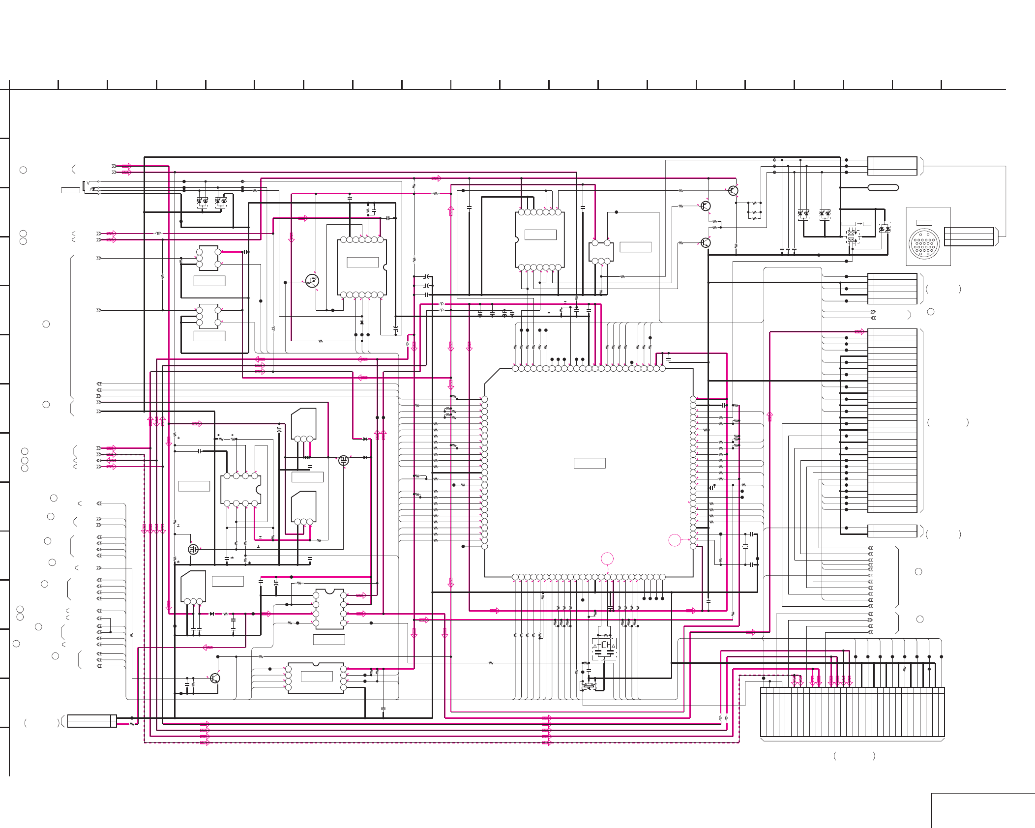
DSR-50/50P
4-97 4-98 HI CONTROL
VD-28 (12/15)
VD-28 (HI CONTROL) SCHEMATIC DIAGRAM • See page 4-71 for VD-28 printed wiring board. • See page 4-152 for waveforms.
R:REC MODE
P:PB MODE
*:IMPOSSIBLE TO MEASURE THE
VOLTAGE AT THE MARKED POINTS.
NO MARK:REC/PB MODE
2.9
2.9
0
2.9
2.9
4.9
2.9
2.9
0.2
9.100.2
000.2 2.8
2.6
5000
000R0/P3
R0/P3
R0/P5
2.9 0
0
4.4
5
4.9
4.4
5
4.9
R4.9/P0.1
R0/
P0.6
5
5
0
5
11.1
5501.9
0
2.51.9
0.1
0
3.6
11.1
2.9
0
3
2.8
0.2
2.9
2.9
3
3
3
3
3
4.72.8
3.6
3
3
0
0
2.9
0
2.8
2.9
0
2.9
2.8
2.7
2.8
2.8
3
0
0
2.9
R2.9/P0
1.5
1.2
3
3
2.9
3
2.9
2.5
2.9
2.9
2.8
*
2.9
03
1.6
1.5
3
2.7
2.8
0.2
2.8
2.8
0
0
3
2.9
0
2.8
3
2.8
2.9
2.4
2.9
0
3
3
2.9
3
0
2.8
2.9
2.9
0.1
*
0 0 33300
2.9
2.9
2.9
2.9
33
2.4
R0/P3
77
76
S579642PZ-TEB
IC709
12345678910111213141516171819202122232425
26
27
28
29
30
31
32
33
34
35
36
37
38
39
40
41
42
43
44
45
46
47
48
49
50
51 52 53 54 55 56 57 58 59 60 61 62 63 64 65 66 67 68 69 70 71 72 73 74 75
76
77
78
79
80
81
82
83
84
85
86
87
88
89
90
91
92
93
94
95
96
97
98
99
100
47
R792
0.1u
C726
2700
R711
10k
R712
1M
R763
0
R707
MA729-
(K8).S0
D709
0.1u
C711
BATT_SENSE_UNREG
10M
R799
22p
C731
TL1596CPWR
IC707
1234567
8 9 10 11 12 13 14
15p
C732
S-81236SGUP-DQ7-T1
IC705
123
0.1u
C729
27
R708
0.1u
C712
470k
R703
S-8423YFS-T2
IC704
1234
5678
0.1u
C702
SW_+3V
UN9111J-
(K8).SO
Q702
AK6440AM-E2
IC706
1234
5678
6.3V
47u
C718
16V
10u
C705
16V
47u
C713
47
R761
MA112-TX
D710
SW_+5.5V
0.1u
C719
S701
XX
47
R760
01ZA8.2
(TPL3)
D701
J701
27
R705
01ZA8.2
(TPL3)
D702
10uHL704
FB701
FB702
FB703
TC7SH04FU-TE85R
IC701
123
45
100k
R701
SIRCS_DATA
0.1u
C706
TC7SH32FU-TE85R
IC702
123
45
10k
R702
FOOT_SW
TALLY_LED
1M
R753
100k
R743
47k
R762
100k
R730
0.1u
C714
47
R789
SDC_DET
3P
CN702
1 VTR START/STOP
2 BATTERY INDICATION
3 REC/TALLY
2SA1576A
-T106-R
Q706
2SA1576A
-T106-R
Q705
2SC4081T106R
Q707
TC7SH32FU-TE85R
IC710
123
45
FB704
FB705
FB706
01ZA8.2(TPL3)
D712
01ZA8.2(TPL3)
D713
47p
C735
47p
C734
47p
C733
100k
R806
47k
R800
47k
R801
47k
R804
100k
R748
2200
R805
2200
R802
TC74VHCT08AFT(EL)
IC708
1234567
891011121314
47k
R765
1k
R803
0.1u
C722
0.1u
C715
6.3V
47u
C720
0.1u
C721
ATT_ALARM
30P
CN703
1XCS_OSD_HI
2OSD_SW
3OSD_SCK_HI
4GND
5OSD_SO_HI
6UVIC_GATE
7UVIC_SWIN
8UVIC_BUSY
9XCS_UVIC
10 GND
11 MO_SI
12 GND
13 MO_SO
14 GND
15 MO_SCK
16 GND
17 XSYS_RST
18 GND
19 XCS_MO
20 GND
21 HI_SI
22 GND
23 HI_SO
24 GND
25 HI_SCK
26 GND
27 MO_XWAKEUP
28 XSLEEP
29 XIC_RST
30 BACK_UP_3V
100
R725
47
R721
VTR_SAVE
10uH
L703
47k
R719
100k
R718
470k
R727
47
R726
100k
R757
100kR776
100k
R777
100k
R759
100k
R758
100k
R787
30P
CN701
1
KEY REQ
2
GND
3
SCK
4
GND
5
DATA TO HI
6
GND
7
DATA FROM HI
8
GND
9
_W/R
10
GND
11
LED STB
12
GND
13
LCD STB
14
GND
15
OE
16
SW +3V
17
SW +3V
18
EVR +3V
19
EVR +3V
20
DSP_CS
21
SW +6V
22
SW +6V
23
DSP_SO(FROM DSP)
24
SW -6V
25
SW -6V
26
DSP_SI(TO DSP)
27
RESET
28
DSP_SCK
29
RESET
30
POWER SW
SW_-5.5V
10uH
L702
10uHL701
CPNT_DET
S/V_DET
V_MUTE
EVR_LOAD
V_S/P_XSTB
VD_SCK
VD_SO
47
R770
47
R752
47
R751
100k
R728
47
R724
47
R734
47
R735
47
R764
470
R713
47
R714
100
R740
47
R715
47
R716
47
R717
47
R723
47
R732
0
R733
47
R744
47
R745
47
R746
47R747
0R773
0
R774
100
R795
100
R796
100
R767
100
R766
100
R742
470
R739
470
R738
470
R737
4V
220u
C716
0.1u
C717
0.1u
C725
0.1u
C730
0.1uC728
0.1u
C727
0.1u
C724
PANEL_DA_CS
LCD_DD_ON
100
R720
VD_SCK
VD_SI
P/S_CS
MAIN_DD_ON
HI_48V_DD_ON
LCD_DD_ON
47
R722
4700
R704
3300
R709
4700
R710
0.01u
C710
2SC4081T106R
Q701
100
R772
100kR775
100k
R793
100k
R797
CL749
CL737
CL736
CL735
100k
R780
XI/O_SYNC_VFD
XI/O_SYNC_HI
MO_SCK
MO_SO
MO_SI
XCS_UVIC
UVIC_BUSY
UVIC_SWIN
UVIC_GATE
XSYS_RST
32.768kHz
X702
20MHz
X701
FAN_ON
47
R798
47
R791
CL748
100k
R784
1k
R783
CL740
0.1u
C723
0.5%
1M
R749
0.5%
220k
R750
47R790
0
R771
CL738
CL742
CL743
CL744
CL745
100
R754
0
R755
0
R756
CL729
100k
R731
100
R736
CABLE_POWER_ON
100
R779
100
R785
100
R786
22k
R781
22k
R782
22k
R788
100R778
CL733
CL734
5P
CN705
1 DIAL_A
2GND
3 DIAL_B
4GND
5 EXEC_SW
01ZA8.2(TPL3)
D714
100
R768
100
R769
DSP_SCK
DSP_SI
DSP_SO
DSP_CS
CL702
CL703
CL704
CL705
CL708
CL720
CL722
CL721
CL719
CL717
CL726
CL727
CL731
CL730
CL750
CL751
CL752
CL778
CL754
CL762
CL763
CL764
CL765
CL766
CL767
CL768
CL769
CL776
CL746
CL747
CL741
CL739
CL709
CL714
CL716
CL715
CL713
CL712
CL711
CL710
CL707
CL706
CL701
CL772
CL773
CL774
CL775
2P
CN704
1 EJECT SW
2GND
CL777
100R741
100k
R729
CL755
CL756
CL757
CL758
CL759
CL770
CL771
CL753
CL760
CL761
CL779
CL780
CL781
CL723
CL782
CL783
CL784
CL785
CL786
CL787
CL788
CL789
10uH
L705
GND
LND701
LND701
2P
CN706
1VL BATT 3V
2VL BATT GND
4V
220u
C736
100
R807
XX
IC711
123
S-81250SGUP-DQD-T1
IC712
123
NJU7102AM-TE1
IC713
1234
5678
0.5%
1M
R808
0.5%
220k
R809
0.5%
4700
R810
0.5%
470k
R811
0.5%
270k
R812
0.5%
10k
R813
0.5%
10
R814
0.5%
240k
R815
0.5%
330k
R816
XX
R817
XX
D715
MA112
-TX
D716
NDS356AP
Q708
0.01u
C737
0.01u
C738
0.47u
C739
0.47u
C740
2SK3018
-T106
Q709
MA112
-TX
D717
100R818
CL724
CL728
CL732
XX
R706
XX
R794
XX
R819
S702
25V
4.7u
C741
1k
R820
1k
R821
DROPPED_UNREG
FB707
0
R822
XX
R823
XX
R824
0.1u
C703
DIG_+5V
VIDEO_+9V
10uH
L706
XX
L707
EVR_+5V
0
R825
XX
R826
0
R827
1k
R828
1
A
VD_SCK
VD_SO
0.1u
C707 XX
C709
XX
C708
0.1u
C701
V_SYNC
INT/EXT_IN
SC_EXIST
12 VTR START/STOP
13 BATTERY INDICATION
15 REC/TALLY
MAIN_DD_ON
EVR_+3V
HI61
HI78
HI84
HI85
HI82
HI83
HI84
HI85
HI36
HI46
HI64
HI63
HI82
HI83
HI45
HI20
HI27
HI28
HI29
HI26
HI38
HI31
HI73
HI44
HI7
HI64
HI11
HI27
HI56
HI55
HI58
HI57
HI43
HI35
HI34
HI33
HI100
HI78
HI79
HI80
HI30
HI32
HI68
HI67
HI17
HI71
HI6
HI5
HI38
HI71
HI68
HI67
HI10
HI46
HI45
HI9
HI22
HI33
HI34
HI35
HI43
HI65
HI16
HI33
HI35
HI3
HI57
HI55
HI11
HI35
HI34
HI34
HI35
HI61
HI8
HI24
HI23
HI22
HI21
HI20
HI14
HI16
HI17
HI18
HI19
HI12
HI11
HI10
HI9
HI8
HI6
HI5
HI4
HI3
HI2
HI1
HI7
HI73
HI36
HI31
HI28
HI26
HI46
HI45
HI44
HI32
HI58
HI2
HI1
HI12
HI30
HI4
HI18
HI65
HI56
HI23
HI19
HI24
HI45
HI44
HI46
HI100
HI9
HI63
HI14
HI21
HI79
HI80
HI29
3 10
VD-28 BOARD (12/15)
71345 15 191817
D
9
K
L
G
I
C
E
J
H
F
B
1668 122 1411
IC705
IC706
IC704
IC713
IC712
IC702
IC701
IC707
IC708
IC710
IC709
CONTROL
M
CN601
KP-8 BOARD
CN6001
JC-20 BOARD (11/14)
CN101
EJ-28 BOARD
FR-157 BOARD (1/2)
XX MARK:NO MOUNT
-REF.NO.:10,000 SERIES-
HI CONTROL
(SEE PAGE 4-123)
THROUGH THE
FVJ-7 FLAT CABLE
FVJ-14 FLAT CABLE
THROUGH THE
(SEE PAGE 4-39)
THROUGH THE
(SEE PAGE 4-70)
EV-70 HARNESS
THROUGH THE
(SEE PAGE 4-70)
KP-52 HARNESS
(4/5)
CN026
CAMERA
20
CN801
THROUGH THE
(SEE PAGE 4-70)
BV-50 HARNESS
VL-26 BOARD
VD-28 BOARD (13/15)
77
VD-28 BOARD (7/15)
56
61
VD-28 BOARD (7/15)
71
VD-28 BOARD (11/15)
VD-28 BOARD (3/15)
31
78 VD-28 BOARD (15/15)
VD-28 BOARD (15/15)
80
VD-28 BOARD (14/15)
81
82 VD-28 BOARD (14/15)
VD-28 BOARD (11/15)
73
79
VD-28 BOARD (13/15)
VD-28 BOARD (10/15)
68
45
VD-28 BOARD (5/15)
30
VD-28 BOARD (3/15)
39
VD-28 BOARD (4/15)
VD-28 BOARD (7/15)
57
84
VD-28 BOARD (15/15)
72
VD-28 BOARD (11/15)
VD-28 BOARD (13/15)
85
VD-28 BOARD (14/15)
83
VD-28 BOARD (11/15)
70
05
NCN502
DVCAM DV
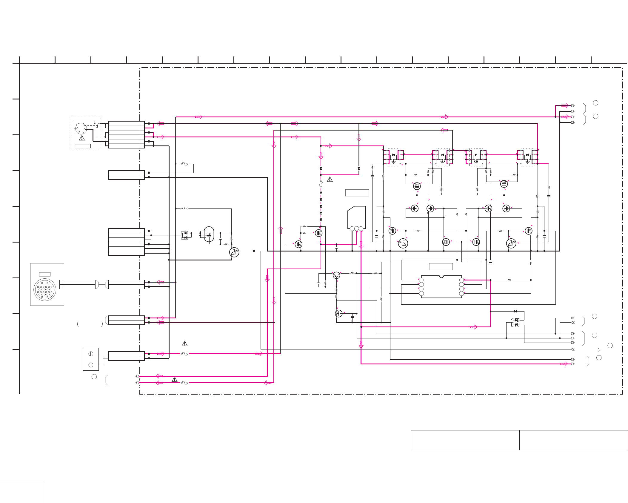
DSR-50/50P
4-99 4-100
DC IN
VD-28 (13/15)
VD-28 (DC IN) SCHEMATIC DIAGRAM • See page 4-71 for VD-28 printed wiring board.
The components identified by mark 0 or dotted
line with mark 0 are critical for safety.
Replace only with part number specified.
Les composants identifiés par une marque 0 sont
critiques pour la sécurité. Ne les remplacer que
par une piéce portant le numéro spécifié.
NO MARK:REC/PB MODE
0
12.5
13.213.2
12.5
13.5
13.5
13.5
0
13.5
0
13.6
12.513.1
12
0.1
12
12.4
0.1
0
5
5
0
0.1
0
4.9
0
0
0
4.9
4.9
0
13.5
0
0
0
0
0.2
5
11.1
0
11.1
11.1
0
9.8
11.1 0
11
9.8
0
5
5
0
2.5
5
0
2.6
6P
CN901
1
BATTERY 12V
2
BATTERY 12V
3
SELECTED 12V
4
SELECTED 12V
5GND
6GND
C901
0.47u
2P
CN902
CAMERA UNREG +12V 1
GND 2
2P
CN903
1BREAKER OUT
2
BREAKER IN
XX
CN907
1UNREG(1.5A)
2UNREG(1.5A)
3UNREG(1.5A)
4GND
5GND
6GND
XX
C900
XX
R901
XX
Q904
XX
R902
XX
D900
XX
F907
CL900
CL903
CL906
CL907
CL908
CL909
CL910
CL911
CL912
CL914
CL916
CL918
2P
CN900
1BATTERY 12V
2GND
XX
Q902
630mA/24V
F908
BATT_SENSE_UNREG
HAT1036R-EL
Q900
1
2
3
4
5
6
7
8
HAT1036R-EL
Q901
1
2
3
45
6
7
8
HAT1036R-EL
Q903
1
2
3
4
5
6
7
8
HAT1036R-EL
Q905
1
2
3
45
6
7
8
1M
R903
47k
R932 47k
R947
0.01u
B
C995
0.01u
C996
100p
C997 100p
C998
1M
R986
1M
R988
220k
R990
220k
R991
22k
R992
2SK3018-T106
Q906
2SK3018-T106
Q930
2SK3018-T106
Q931
NJU7102AM-TE1
IC908
1234
5678
470k
R993
470k
R994
XX
CN908
1EXT DC(+12V)
2GND
XX
F909
CL920
CL921
MA112-TX
D908
MA112-TX
D909
MA112-TX
D910
MA112-TX
D911
MA112-TX
D912
MA112-TX
D913
MA112-TX
D914
630mA/24V
F910
0.1u
C993
S-81250SGUP-DQD-T1
IC909
123
2SK3018-T106
Q932
22k
R985
1M
R913
DROPPED_UNREG
10k
R919 10k
R930
220k
R921
220k
R920
UN9213J-(K8).SO
Q913
UN9213J-(K8).SO
Q918
220k
R978
220k
R979
2SK3018-T106
Q923 2SK3018-T106
Q924
2SK3018-T106
Q925
470k
R952
220k
R953
XX
C940
2SA1576A-T106-R
Q919
1M
R951
220k
R943
01ZA8.2(TPL3)
D929
0
R904
F900
8A/125V
EVR_+5V
CPH3304-TL
Q934
1M
R961
10k
R962
2SK3018-T106
Q937
MA112-TX
D932
0.01u
C977
2SK3018-T106
Q943
2SK3018-T106
Q941
10k
R964
1M
R963 1M
R965
10k
R966
2SK3018-T106
Q940 2SK3018-T106
Q942
0
R973
CABLE_POWER_ON
89-3
89-2
89-1
1
A
CAMERA UNREG +12V25
GND26
BT901
UNREG
GND
UNREG
GND
88-2
88-1
GND
2 16
I
12
G
68
D
E
VD-28 BOARD (13/15)
B
7 151310 11
C
H
F
3 14945
IC909
IC908
JK-169 BOARD (1/3)
CN102
17
05
CN026
CAMERA
(5/5)
DC IN 12V
CN9901
1
2
3
4
TERMINAL
BATTERY
VD-28 BOARD
85
(12/15)
89
VD-28 BOARD
(15/15)
VD-28 BOARD
(14/15)
88
79
VD-28 BOARD
(12/15)
86
VD-28 BOARD
VD-28 BOARD
87
(15/15)
(14/15)
(12/15)
VD-28 BOARD
77
VB-50 HARNESS
THROUGH THE
(SEE PAGE 4-132)
XX MARK:NO MOUNT
-REF.NO.:10,000 SERIES-
DC IN
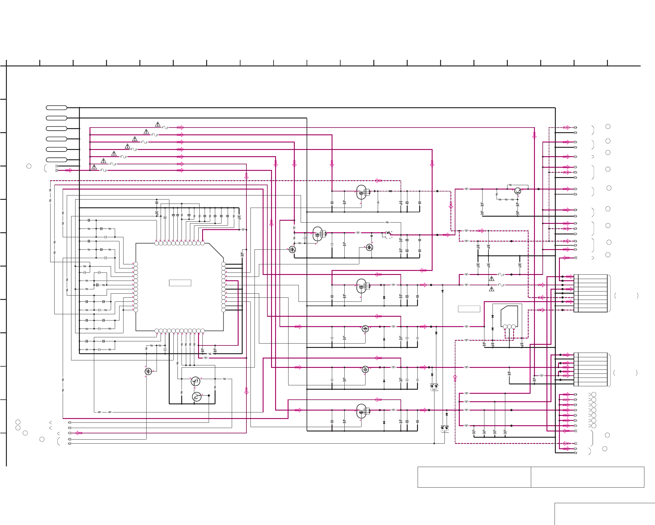
DSR-50/50P
4-101 4-102 DC/DC CONVERTER 1
VD-28 (14/15)
VD-28 (DC/DC CONVERTER 1) SCHEMATIC DIAGRAM • See page 4-71 for VD-28 printed wiring board.
The components identified by mark 0 or dotted
line with mark 0 are critical for safety.
Replace only with part number specified.
Les composants identifiés par une marque 0 sont
critiques pour la sécurité. Ne les remplacer que
par une piéce portant le numéro spécifié.
NO MARK:REC/PB MODE
0
0
0.5
13.5
10.2
0.1
0
0
12.3
13.5
0
12.4
0.3
8.7
13.5 5.1
5.113.5
8.7
5.1
10.4
13.5
13.5
10.8
3
-5.4-4.9
0.8
9.8
0
0
0.3 2.9
2.9
0
0.8
0.7
1
0.6
0.6
0
2.2
1
1
0.8
1
1
2.2
1.3
1
2.2
2.2
10
2.2
0.9
113.5
10.2
0
13.5
8.7
10.4
10.8
8.7
2.6
13.5
2.9
2.9
2.9
2.9
0.2
2.2
0.7
01
D901
SB02-09CP-TB
C950
20V
22u
C943
20V
22u
C944
25V
47u
Q920
2SK1764KYTR
C938
0.1u
C937
0.1u
C951
50V
33u
C952
50V
33u
C936
0.1u
C949
20V
22u
C942
20V
22u
C948
20V
22u
C935
0.1u
C941
20V
22u
L902
100uH
F906
630mA/24V
630mA/24V
F905
1.4A/24V
F904
630mA/24V
F903
L920
10uH
L921
10uH
L924
100uH
C967
20V
10u
C976
20V
10u
C973
50V
22u
C954
4.7u
C955
4.7u
C956
4.7u
C957
0.1u
C958
0.1u
8PCN905
1 SW +3V
2 GND
3 CM REG 5V
4 CM REG 5V
5 UNREG
6 UNREG
7 GND
8 GND
R954
1M
R956
100k
C933
0.1u
1.4A/24V
F911
SW_+48V
VIDEO_+5V
VIDEO_-5V
SW_+3V
C968
20V
10u
C979
20V
10u
C980
20V
10u
C963
20V
10u
C945
50V
22u C959
4.7u
L916
10uH
C953
50V
22u
C939
0.1u
630mA/24V
F901
C964
20V
10u
C965
20V
10u
L922
10uH
L923
10uH
C970
20V
10u
C971
20V
10u
C975
20V
10u
UN9113J-(K8).SO
Q907
50V
22u
C974
220k
R939
10uH
L900
10uH
L915
10uH
L918
CL942
CL943
CL944
CL945
CL946
CL948
CL951
CL953
CL955
CL935
CL933
CL936
CL926
CL927
CL929
CL930
CL931
CL939
9PCN904
1 SW +6V
2 EVR +3V
3 VIDEO +5V
4 SW +3V
5 GND
6 VIDEO -5V
7 AUDIO +5V
8 AUDIO GND
9 AUDIO -5V
EVR_+3V
CL941
CL940
2SC4081T106R
Q922
560
R971
50V
22u
C982
50V
22u
C981
LND900
S_GND
560
R968
XX
R972
LND901
S_GND
4.7u
C991
CL959
50V
33u
C989
0.1u
C988
25V
47u
C990
47uH
L927
CL928
R911
1800
R912
22k
220k
R983
LND903
SHLD_GND
LND904
SHLD_GND
LND905
SHLD_GND
LND906
SHLD_GND
CPH6302-TL
Q911
2
3
4
1
6
5
22k
R980
CPH6302-TL
Q914
2
3
4
1
6
5
CPH6302-TL
Q915
2
3
4
1
6
5
CPH6302-TL
Q916
2
3
4
1
6
5
CPH3304-TL
Q928
22uH
L904
22uH
L906
47uH
L908
100uH
L910
20V
10u
C983
C932
35V
2.2u
C912
XX
R922
33k
R946
10k
R940
1k
R942
1k
C925 0.1u
R906
1k
R949
12k
R909
470k
16V
1u
C931
C915
XX
C907
220p
R935
1k
C923 0.1u
R905
39k
10uH
L905
R916
47k
C918
20V
2.2u
XX
C917
C906
0.001u
R936
39k
R937
1k
C924
XX
IC900
FA3675F
123456789101112
131415161718192021222324
25 26 27 28 29 30 31 32 33 34 35 36
37 38 39 40 41 42 43 44 45 46 47 48
XX
C903
C922
0.1u
R938
33k
R917
1k
R908
3900
XX
C902
100k
R934
XX
C905
C926
0.1u
C908
0.001u
C919
0.1u
10uH
L903
C921
0.001u
R915
10k
R907
15k
C909
0.01u
XX
C904
C929
100p
R924
33k
C913
XX
R926
33k
R914
10k
R928
330k
R925
33k
100k
R941
R931
330k
0.01u
C927
C910
XX
C914
0.001u
R950
1k
R927
390k
R944
1k
R933
360k
20V
2.2u
C920
C911
XX
0
R918
R923
33k
R948
39k
R929
10k
C916
0.1u
R945
1k
XX
C928
R910
47k
C930
35V
2.2u
0.1u
C969
CL938
10uH
L933
20V
10u
C984
LCD_+3V
L919
10uH
10uH
L913
10uH
L928
2SK3018-T106
Q909
UN9213J-(K8).SO
Q908
NJU7211U50-TE1
IC901
123
CL957
CPH3304-TL
Q917
FB900
FB902
FB904
FB906
FB908
FB910
3.3M
R958
MA112-TX
D919
MA112-TX
D920
MA112-TX
D921
MA112-TX
D922
01ZA8.2(TPL3)
D926
01ZA8.2(TPL3)
D927
2SK3018-T106
Q938
3.3M
R960
3.3M
R959
RB051L-40TE25
D905
RB051L-40TE25
D902
RB051L-40TE25
D904
RB051L-40TE25
D907
RB051L-40TE25
D903
1.4A/24V
F914
1.4A/24V
F915
630mA/24V
F912
10uH
L926
MA112-TX
D930
MA112-TX
D931
560
R970
560
R969
0.033u
C987
6.3V
47u
C999
100
R967
4.7u
C1936
0.1u
C1938
0.1u
C1940
4.7u
C1942
4.7u
C1944
4.7u
C1946
4.7u
C1947
GND
UNREG
+48_DD_ON
88-1
MAIN_DD_ON
90-1
1
A
GND
88-2
SW_+3V
SW_+3V
SW_+3V
SW_+3V
SW_+3V
SW_+3V
GND
GND
VIDEO_+5V
GND
VIDEO_-5V
VIDEO_+5V
VIDEO_-5V
GND
VIDEO_+5V
GND
VIDEO_+5V
VIDEO_-5V
VIDEO_+5V
GND
GND
SW_+6V
AUDIO_-5V
IC901
2 16
L
I
K
12
G
68
D
E
VD-28 BOARD (14/15)
B
7
05
19151310 1711
C
H
F
3 18
J
14945
IC900
JC-20 BOARD (14/14)
CN1100
CM-59 BOARD (1/3)
CN100
-REF.NO.:10,000 SERIES-
DC/DC CONVERTER 1
(SEE PAGE 4-45)
VJ-106 HARNESS
THROUGH THE
THROUGH THE
VC-58 HARNESS
(SEE PAGE 4-105)
11 VD-28 BOARD (1/15)
36 VD-28 BOARD (3/15)
VD-28 BOARD (7/15)
58
82 VD-28 BOARD (12/15)
75 VD-28 BOARD (11/15)
VD-28 BOARD (7/15)
60
44 VD-28 BOARD (5/15)
91
VD-28 BOARD (15/15)
18
VD-28 BOARD (2/15)
2
VD-28 BOARD (1/15)
VD-28 BOARD (4/15)
43
VD-28 BOARD (11/15)
74
VD-28 BOARD (5/15)
49
50
VD-28 BOARD (6/15)
52
VD-28 BOARD (7/15)
VD-28 BOARD (9/15)
66
67
VD-28 BOARD (10/15)
81
VD-28 BOARD (12/15)
VD-28 BOARD (11/15)
69
83 VD-28 BOARD (12/15)
VD-28 BOARD (15/15)
90
VD-28 BOARD (13/15)
88
86
VD-28 BOARD (13/15)
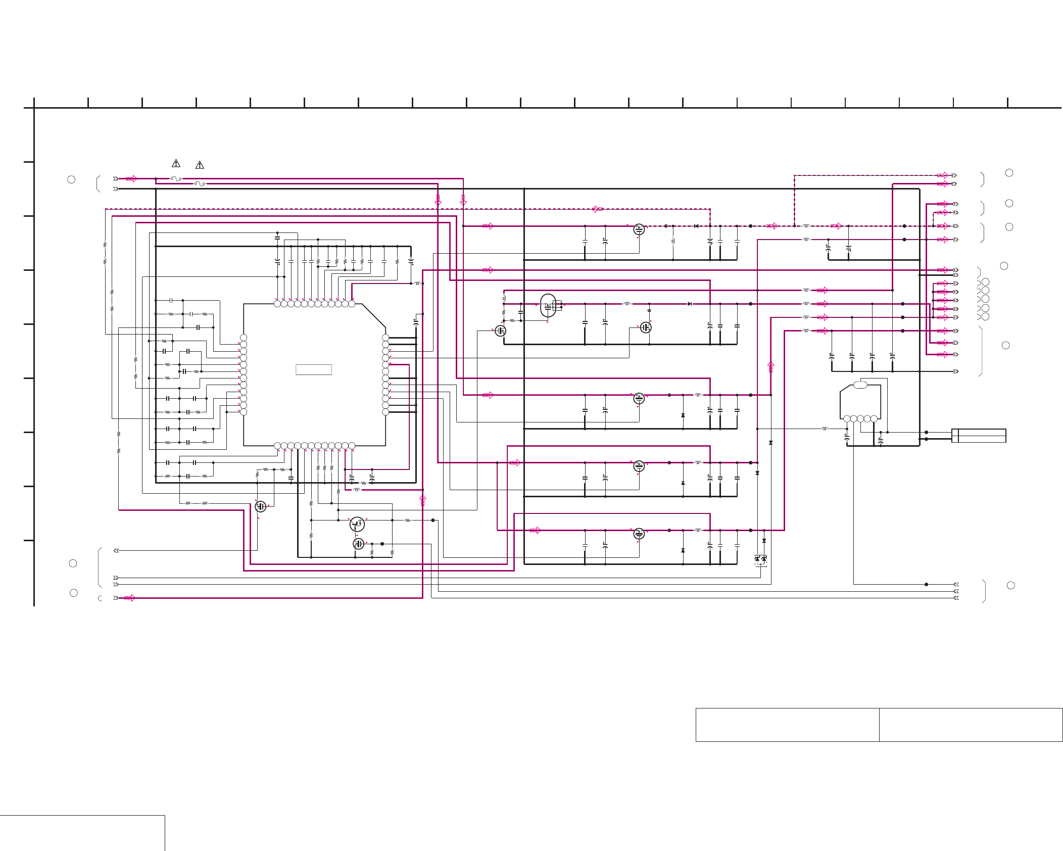
DSR-50/50P
4-103 4-104
DC/DC CONVERTER 2
VD-28 (15/15)
VD-28 (DC/DC CONVERTER 2) SCHEMATIC DIAGRAM • See page 4-71 for VD-28 printed wiring board.
The components identified by mark 0 or dotted
line with mark 0 are critical for safety.
Replace only with part number specified.
Les composants identifiés par une marque 0 sont
critiques pour la sécurité. Ne les remplacer que
par une piéce portant le numéro spécifié.
NO MARK:REC/PB MODE
1
0.5
0.3
0.5
0.7
1
0.9
1
1
0.8
1
10
0.8
2.2
2.9
2.9
0
2.9
2.9
13.5
2.6
9.9
7.2
13.5
8.7
8.1
12.2
13.51110
0.9
2.2
1.2
2.2
1.3
2.2
2.2
0
0
9.8
2.9 2.9
0
2.4
2.9
0
5.5
0
5.5
13.5
9.9
0.1
7.2
5.5
13.5
5.1
8.7
5.7
13.5
8.1
4.6
13.5
12.2
L914
10uH
L925
100uH
C962
20V
10u
C978
10u
25V
SW_+12V
LCD_DD_ON
FAN_ON
XX
CN906
1 FAN +5V
2 GND
C966
XX C972
XX
XX
IC903
12345
6
UNREG
XX
L917
100k
R957
0.1u
C934
1M
R955
10uH
L901
0.1u
C946
2.2u
C961
CPH3404-TL
Q921 50V
22u
C960
100uH
L912
50V
22u
C947
CL949
CL950
CL937
CL932
CL925
CL934
20V
10u
C992
100uH
L929 CL960
SW_+4.6V
CPH6302-TL
Q912
2
3
4
1
6
5
2SK3018-T106
Q910
XX
C1915
390k
R1933
0.001u
C1906
0.01u
C1927
CL924
560k
R1909
XX
C1910
XX
C1905
36k
R1908
20V
2.2u
C1918
XX
C1917
1k
R1940
10uH
L909
39k
R1936
0.001u
C1914
33k
R1922
0.1u
C1923
XX
C1911
1k
R1942
330k
R1931
0.1u
C1919
0
R1918
10k
R1929
35V
2.2u
C1932
0.1u
C1925
10uH
L907
47k
R1911
6200
R1950
XX
C1913
0.1u
C1916
0.001u
C1921
12k
R1949
220k
R1939
33k
R1925
100k
R1941
XX
C1904
16V
1u
C1931
10k
R1946
100k
R1934
20V
2.2u
C1920
XX
C1928
100p
C1907
33k
R1938
10k
R1915
100p
C1929
UN9113J-(K8).SO
Q935
33k
R1923
5600
R1910
47k
R1916
330k
R1928
390k
R1927
33k
R1926
XX
R1930
0.01u
C1909
XX
C1903
4700
R1917
4700
R1912
0
R1907
1k
R1935
39k
R1948
2SK3018-T106
Q936
0.1u
C1926
35V
2.2u
C1930
1k
R1937
0.1u
C1922
1k
R1944
XX
C1924
1k
R1945
FA3675F
IC902
123456789101112
131415161718192021222324
25 26 27 28 29 30 31 32 33 34 35 36
37 38 39 40 41 42 43 44 45 46 47 48
CL915
100uH
L932
4.7u
C1991
50V
22u
C1989
CL923
CL917
47uH
L931
4.7u
C1956
25V
47u
C1948
0.1u
C1939
50V
22u
C1943
25V
47u
C1990
0.1u
C1937
4.7u
C1959
20V
22u
C1945
47uH
L930
0.1u
C1988
0.1u
C1935
CL922
47uH
L911 4.7u
C1954
50V
22u
C1950
50V
22u
C1941
0.1u
C1969
CL958
10uH
L934
20V
10u
C994
DIG_+5V
MA729-(K8).S0
D906
CPH3304-TL
Q926
CPH3304-TL
Q927
CPH3304-TL
Q929
CPH3304-TL
Q933
FB912
FB914
FB916
FB918
FB920
3.3M
R1958
3.3M
R1959
MA112-TX
D923
MA112-TX
D924
MA112-TX
D925
01ZA8.2(TPL3)
D928
3.3M
R1960
2SK3018-T106
Q939
10uH
L935
10uH
L936
20V
10u
C985
20V
10u
C986
SW_-5.5V
SW_+5.5V
CL954
CL956
RB051L-40TE25
D915
RB051L-40TE25
D916
RB051L-40TE25
D917
MA729-(K8).S0
D918
220k
R1983
100
R1967
4.7u
C1949
2.2u
C1951
4.7u
C1952
4.7u
C1955
4.7u
C1957
20V
22u
C1953
90-1
MAIN_DD_ON
89-2
89-3
89-1
UNREG
1
A
GND
AUDIO_-5V
SW_+6V
F913
630mA/24V F902
630mA/24V
GND
SW_+5.5V
SW_+5.5V
SW_-5.5V
GND
DIG_+5V
DIG_+5V
DIG_+5V
DIG_+5V
2 16
I
12
G
68
D
E
VD-28 BOARD (15/15)
B
7
05
19151310 1711
C
H
F
3 1814945
IC902
-REF.NO.:10,000 SERIES-
DC/DC CONVERTER 2
VD-28 BOARD (13/15)
87
89
VD-28 BOARD (13/15)
90
VD-28 BOARD (14/15)
VD-28 BOARD (1/15)
8
VD-28 BOARD (2/15)
17
VD-28 BOARD (3/15)
35
53
VD-28 BOARD (7/15)
VD-28 BOARD (12/15)
78
91
VD-28 BOARD (14/15)
76
VD-28 BOARD (11/15)
VD-28 BOARD (12/15)
80
32
VD-28 BOARD (3/15)
59
VD-28 BOARD (7/15)
VD-28 BOARD (12/15)
84
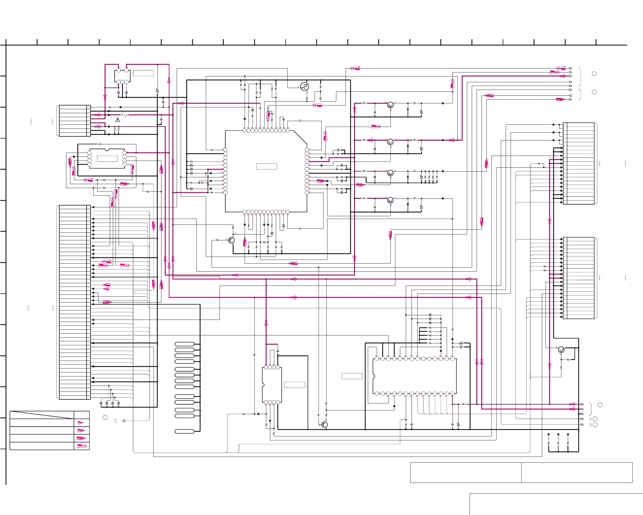
DSR-50/50P
4-105
4-106
DC/DC CONVERTER, REEL MOTOR DRIVE
CM-59 (1/3)
CM-59 (DC/DC CONVERTER, REEL MOTOR DRIVE) SCHEMATIC DIAGRAM • See page 4-111 for CM-59 printed wiring board.
The components identified by mark 0 or dotted
line with mark 0 are critical for safety.
Replace only with part number specified.
Les composants identifiés par une marque 0 sont
critiques pour la sécurité. Ne les remplacer que
par une piéce portant le numéro spécifié.
0.1
4.4
1
0.4
2.5
1.3
-0.2
5
2.5 -0.2
00.14.6
2.54.6 2.7 2.54.2 2.5 2.5 2.5 2.5 2.5 5
0.7 0.7 0.7 0 0 2.8
13.3
2.813
13.4
13 2.4
6.713
13.4
13 0.8
13.4
14.16.7
0.9
13.4
13
13.4
2
13.4
13.3
0.9
0.5
14
14 13.3
12.9
0
1.9
0.5
0.5
50
1.8
2.5
2.5
1.3
1.6
5
2.5
5
5
5
5
0
1.4
1.4
1.4
2.5
2.8
11
1.3
2.5
12.9
14 13.2
7
0.4
0
0.5
2.9
NO MARK:REC/PB MODE
2.9
5
5
47k
R224
10u
20V
C134
4700
R223
22uH
L106
100uH
L104
L102
10uH
100uH
L105
2SD2216J-QR(K8).SO
Q201
10uH
L101
10u
20V
C136
10uH
L100
10u
20V
C135
0.1u
C203
0.1uC200
0.1u
C201
0.1u
C202
1
R205
1
R206
1
R207
1M
R204
20k
R202
12k
R203
2SB709A-QRS-TX
Q200
10k
R201
1k
R200
25V
4.7u
C204
0.1u
C205
0.1u
C206
470k
R209
10uH
L200
C207
4.7u
20V
MB3785APFV-G-BND-ER
IC100
123456789101112
131415161718192021222324
25 26 27 28 29 30 31 32 33 34 35 36
37 38 39 40 41 42 43 44 45 46 47 48
0.001u
C100
0.001u
C101
0.001u
C102 0.001u
C103
1k
R100
470
R101
100
R102
3300p
C104
0.001u
C105
3300p
C106
0.1uC107
47k
R103
62k
R104
33k
R105
5600
R107
0.022u
C108
0
R108
0
R110
10k
R111
560p
C109
6800
R106
220p
C111
XX
R210
27k
R123
10u
20V
C137
10uH
L103
33uH
L107
1k
R112
3300p
C112
5600
R131
0
R136
0
R122
CL105
CL109
CL110
CL117
CL116
CL115
CL114
CL111
CL113
CL212
CL203
CL206
CL205
CL210
CL231
CL230
CL229
CL228
CL227
CL225
CL224
CL223
CL221
CL220
CL219
CL218
CL222
CL217
CL216
CL215
CL214
CL213
CL251
CL250
CL249
CL248
CL246
CL245
CL244
CL243
CL242
CL241
CL247
CL240
CL239
CL238
CL237
CL236
CL235
CL233
CL232
CL001
CL004
CL005
CL006
CL007
CL008
CL009
CL012
CL013
CL014
CL017
CL018
CL019
CL022
CL023
CL024
CL025
CL026
CL030
CL031
CL036
CL042
CL045
CL046
8PCN100
1SW_+3V
2GND
3CM REG 5V
4CM REG 5V
5UNREG
6UNREG
7GND
8GND
CL103
CL102
CL100
CL104
0.1u
C113
0
R124
XX
R125
0
R120
XX
R121
XX
R119
0
R118
0
R109
XX
R113
0
R225
0.022u
C114
22k
R114
33k
R115
NJM2903V(TE2)
IC202
1234
5678
0.01u
C208
21P
CN200
1 TAPE_END
2 CC_DOWN
3 C_IN
4 MODE_A
5 MODE_B
6 MODE_C
7 MODE_D
8 S_ELETEN
9 T_ELETEN
10 5V
11 5V
12 TAPE_LED
13 GND
14 L_CASSETTE
15 DEW
16 W-
17 W+
18 V-
19 V+
20 U-
21 U+
21P
CN201
1 REEL_V
2 REEL_V
3 REEL_U
4 REEL_U
5 REEL_w
6 REEL_W
7 GND
8 GND
9 FG1
10 5V
11 5V
12 FG2
13 SREEL_FG
14 TREEL_FG
15 REC_PROOF
16 CHIME_4(VDD)
17 CHIME_3(SDA)
18 CHIME_2(SCK)
19 GND
20 GND
21 TAPE_TOP
CL226
CL234
CL119
CL120
CL121
CL122
20k
R116
12k
R117
C115 0.1u
C116
0.47u
C117
0.1u
C118
CL101
CL112
XX
R134 CL106
1
R208
2SB709A-QRS-TX
Q104
10k
R126
1.25A
/125V
F100
UN9211J-(TX).SO
Q105
56k
R127
LND001
case_A1
LND002
case_A2
LND003
case_A3
LND004
case_A4
LND005
case_B1
LND006
case_B2
LND007
case_B3
LND008
case_B4
LND009
GND
LND010
GND
LND011
GND
LND012
GND
0
R128
LB1897D
IC200
1234567891011121314
1516171819202122232425262728
0R211
50P
CN001
1HI_C/R_SW
2LM(-)
3LM(+)
4CM_LIMIT_EVR
5CM_LIMIT_DET
6CM_LIMIT_ON
7CM(-)
8CM(+)
9GND
10REEL_M_FG
11REEL_PWM
12REEL_FWD
13REEL_ON
14GND
15CAP_FG
16CAP_PWM
17CAP_FWD
18CAP_ON
19GND
20
DRUM_MASTER_CLK
21DRUM_PG
22DRUM_FG
23DRUM_PWM
24DRUM_FWD
25DRUM_ON
26GND
27CHIME_VDD
28CHIME_SDA
29CHIME_SCK
30CAP_EVR
31REEL_EVR
32TREEL_FG
33SREEL_FG
34S_ELTN_ERR
35T_ELTN_ERR
36GND
37DEW_DET
38REC_PROOF
39L_CASSETTE
40XCC_DOWN
41XC_IN
42GND
43TAPE_END
44TAPE_TOP
45TAPE_LED_ON
46GND
47MODE_SW_D
48MODE_SW_C
49MODE_SW_B
50MODE_SW_A
RB051L-40TE25
D101
RB051L-40TE25
D102
RB051L-40TE25
D103
RB051L-40TE25
D104
1k
R212
CPH3109-TL
Q100
CPH3109-TL
Q101
CPH3109-TL
Q103
CPH3109-TL
Q102
C129
10u
C130
10u
C131
10u
C132
10u
LP001
LEAD PIN
C119
10u
1W
180
R526
1W
180
R529
1W
180
R527
1W
180
R528
0.001u
C526
0.001u
C527 0.001u
C528
0.001u
C529
0.47u
C110
XX
R129
6800
R214
6800
R213
1k
R215
TC7W34FU(TE12R)
IC102
1234
5678
XXR130
XX
R132
XX
R133
0.1u
C120
CL011
CL016
CL504
IC101
MM1385GNLE
123
45
0.1u
C121 10V
4.7u
C122
1-2
6.25V
1-3
2-2
2-1
1-4
1-1
2-3
XX
R992
CL990
XX
R991
XX
R990
CL992CL991
4-1
1
A
3V
5V
5-1
GND
6-1
REC_PROOF
CHIME_VDD
END_SENS
TAPE_LED
C_IN
CC_DOWN
MODE_A
MODE_B
MODE_C
MODE_D
TOP_SENS
CHIME_SCK
CHIME_SDA
SFG_IN
TFG_IN
UHE_+
UHE_-
VHE_+
VHE_-
WHE_+
WHE_-
WHE_-
WHE_+
VHE_-
VHE_+
UHE_-
UHE_+
LM-
LM+
CM_LIMIT_DET
CM_LIMIT_ON
CM-
CM+
REEL_M_FG
REEL_FWD
REEL_ON
CAP_FG
CAP_FWD
CAP_ON
DRUM_CLK
DRUM_PG
DRUM_FG
DRUM_FWD
DRUM_ON
CHIME_VDD
CHIME_SDA
CHIME_SCK
REEL_EVR
TREEL_FG
SREEL_FG
S_ELETEN
T_ELETEN
REC_PROOF
L_CASSETTE
CC_DOWN
C_IN
TAPE_END
TAPE_TOP
TAPE_LED
L_CASSETTE
REEL_EVR
MODE_A
MODE_B
MODE_C
T_ELETEN
S_ELETEN
REEL_PWM
CAP_PWM
DRUM_PWM
REEL_ON
REEL_M_FG
REEL_FWD
MODE_D
2 16
L
I
20
K
12
G
6
N
8
D
E
CM-59 BOARD (1/3)
B
7
05
19151310 1711
C
H
F
3 18
J
14945
M
IC202
IC200
IC101
IC100
IC102
XX MARK:NO MOUNT
DC/DC CONVERTER,REEL MOTOR DRIVE
-REF.NO.:20,000 SERIES-
Drum speed servo
Capstan servo(speed and phase)
Drum servo(speed and phase)
SIGNAL PATH
Drum phase servo
REC/PB
1
CM-59 BOARD (3/3)
(2/3,3/3)
3
CM-59 BOARD
CM-59 BOARD (3/3)
4
MD-76 BOARD
CN1
THROUGH THE
(SEE PAGE 4-117)
FMD-14 FLAT CABLE
CM-59 BOARD (2/3)
2
5
CM-59 BOARD (2/3)
CN905
VD-28 BOARD (14/15)
(SEE PAGE 4-102)
THROUGH THE
VC-58 HARNESS
CN5005
JC-20 BOARD (10/14)
(SEE PAGE 4-38)
THROUGH THE
FVJ-1 FLAT CABLE
CN2
MD-76 BOARD
(SEE PAGE 4-117)
THROUGH THE
FMD-14 FLAT CABLE
6
CM-59 BOARD
(3/3)
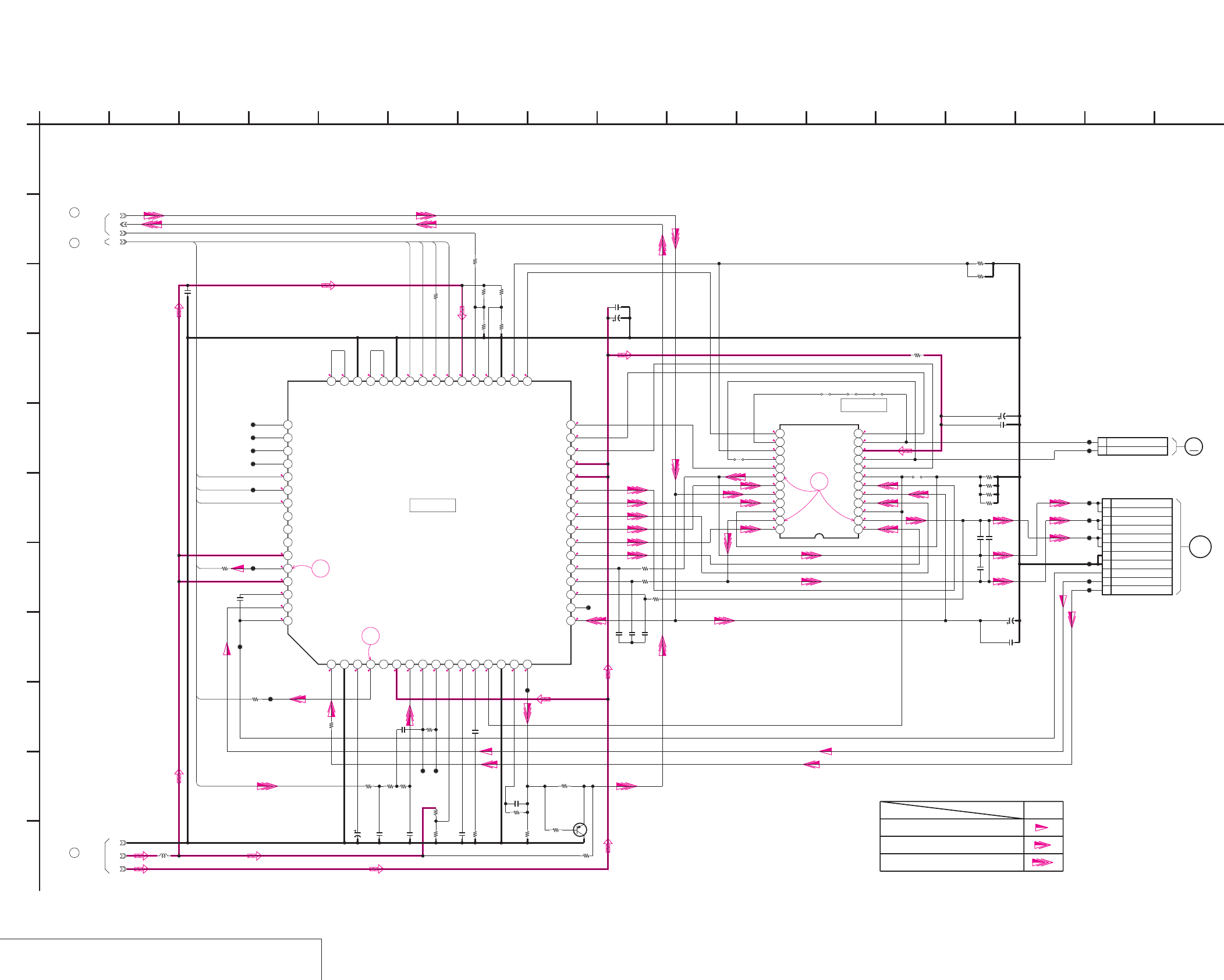
DSR-50/50P
4-107
4-108
DRUM MOTOR DRIVE, FL MOTOR DRIVE
CM-59 (2/3)
CM-59 (DRUM MOTOR DRIVE, FL MOTOR DRIVE) SCHEMATIC DIAGRAM • See page 4-111 for CM-59 printed wiring board. • See page 4-152 for waveforms.
NO MARK:REC/PB MODE
2.7
2.7
1.5
5
0
5
1.4
2.9
2.9
1.3
1.3
1.3
5
5
1.8
1.8
1.8
0.6
0.6
0.6
1.1
1.2
1.2
2.4
0.3 0.3 2.8 000.3 0
0.3 2.9 0.5 0.4 00
1 0.21.3 5 0.7 0.7 0.7 0.2 1.2 0.6 0 0.2 1.4
05
0.5
0
0.5
0
1.2
0.6
2.4
1.8
0
1.2
0.6
0.5
5
0.5
5
0
1.8
2.4
1.8
0
1.2
0.6
1
2
3
100
R514
0
R506
0.1u
C507
XX
R521
120k
R520
1
R535
0.1u
C512
0.001u
C504
C511
4.7u
20V
XX
R510
0.1u
C505
560p
C518
10k
R509
16V
1u
C501
10k
R503
0.1u
C515
TA8486F(EL)
IC501
123456789101112
131415161718192021222324
0.01u
C510
22k
R519
1k
R507
C520
4.7u
20V
0.1u
C503
1
R515
22k
R518
1
R534
4700p
C502
1
R533
10k
R504
0.01u
C509
0.1u
C521
0.1u
C506
0.1u
C519
470
R501
10k
R505
150k
R508
0.1u
C523
0.01u
C508
0.1u
C522
C525
4.7u
20V
1
R516
0.1u
C524
100
R513
3300
R511
2P
CN501
1 CM_UNLOAD
2 CM_LOAD
100
R512
1
R532
CL526
CL527
CL500
CL501
CL502
CL503
CL505
CL506
CL507
CL508
CL509
CL510
CL512
CL515
CL516 CL517
CL519
11P
CN500
1W
2W
3V
4V
5U
6U
7 GND
8 GND
9 SENSOR Vcc
10 FG
11 PG
CL524 CL525
CL511
0
R500
JR501
JR502 JR503 JR504
JR505
180k
R522
XX
Q500
XX
R523
XX
R524
0
R525
1k
R530
1k
R531
1k
R536
CXA8062R-EB
IC500
12345678910111213141516
17 18 19 20 21 22 23 24 25 26 27 28 29 30 31 32
33343536373839404142434445464748
49505152535455565758596061626364
10uH
L500
GND
3V
5V
2-1
5-1
2-3
M
1
A
2-2
DRUM_PWM
DRUM_PG
DRUM_FG
DRUM_FWD
DRUM_CLK
DRUM_ON
CM+
CM-
CM_LIMIT_DET
CM_LIMIT_ON
3
CM-59 BOARD (1/3)
5
CM-59 BOARD (1/3)
2
CM-59 BOARD (1/3)
M905
FL MOTOR
DRUM
MOTOR
M901(2/2)
IC501
IC500
DRUM MOTOR DRIVE,FL MOTOR DRIVE
-REF.NO.:20,000 SERIES-
XX MARK:NO MOUNT
CM-59 BOARD (2/3)
Drum servo(speed and phase)
Drum speed servo
Drum phase servo
REC/PB
SIGNAL PATH
C
27
K
E
36
G
9 1612
B
5
D
8
J
05
10
F
4
H
I
1714 1511 13
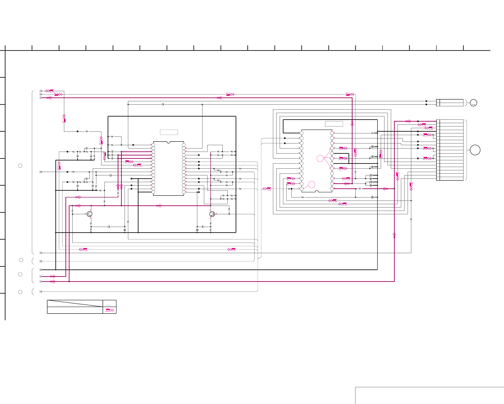
DSR-50/50P
4-109
4-110
CAPSTAN MOTOR DRIVE, CAM MOTOR DRIVE
CM-59 (3/3)
CM-59 (CAPSTAN MOTOR DRIVE, CAM MOTOR DRIVE) SCHEMATIC DIAGRAM • See page 4-111 for CM-59 printed wiring board. • See page 4-152 for waveforms.
0.1
0
2.9
0.4
0
0
NO MARK:REC/PB MODE
*:IMPOSSIBLE TO MEASURE THE
VOLTAGE AT THE MARKED POINTS.
5
5
0.5
0.5
0.4
0.4
0
0
2.9
1.3
0
0
*
*
1.7
*
*
1.7
0
1.3
2.8
2.9
2.2
2.7
0.7
2.7
1.8
1.8
1.4
1.4
1
1
1.4
1.4
1.2
0.9
1.9
0.4
0.4
0.4
0.8
6.7
2.9
2.9
2.2
2.8
4
5
C405
4.7u
20V
15k
R300
0.1u
C407
2P
CN300
1 LM+
2 LM-
560
R302
100p
C300
15k
R301
100p
C302
0.1u
C402
18k
R403
0.1u
C403
10uH
L400
0.1u
C401
0.1u
C404
10k
R400
C406
4.7u
20V
0.1u
C400
0.1u
C301
0
R402
LB1991V-TLM
IC400
123456789101112
131415161718192021222324
0.1u
C303
560R303
100k
R405
LB8112V-TLM
IC300
123456789101112131415
16 17 18 19 20 21 22 23 24 25 26 27 28 29 30
C320
0.1u
C321
0.1u
2.2uC322
0.001u
C323
0.1u
C324
0.001u
C327
0.022u
C329
4700p
C330
4700p
C331
0
R323
10k
R324
100k
R325
10k
R326
10k
R327
10k
R328
0
R329
100k
R330
XX
R331
100k
R332
10k
R333
10k
R334
3300
R335
100k
R336
1
R337
0.1u
C326
CL307
CL308
CL309
CL310
CL311
4700
R339
3300
R340
1
R342
CL314
C325
0.1u
CL303
CL305
CL304
CL306
CL301
CL302
CL400
CL401
CL402
CL313
CL312
CL407
CL404
CL411
CL408
CL409
CL410
CL412
18P
CN400
1HW-
2HW+
3HV-
4HV+
5HU-
6HU+
7V
8V
9W
10 W
11 HE VCC
12 HE GND
13 U
14 U
15 MR GND
16 FG2
17 FG1
18 FG VCC
CL300
CL315
CL316
CL318
0
R304
XX
R305
0
R306
2SD2216J-QR(K8).SO
Q302
2SD2216J-QR(K8).SO
Q301
1k
R308
1k
R307
1k
R309
1k
R310
3300
R311 4700
R312
2700R314
2700
R313
47k
R315
47k
R316
R401
1k
1k
R320
1k
R317
1k
R318
1k
R319
1-1
1-2
6.25v
1-4
GND
5V
3V
1-3
4-1
6-1
M
1
A
LM-
LM+
END_SENS
CAP_FWD
CAP_ON
TOP_SENS
SFG_IN
TFG_IN
CAP_PWM
REEL_PWM
CAP_FG
TAPE_TOP
TAPE_END
TREEL_FG
SREEL_FG
CM-59 BOARD (1/3)
1
CM-59 BOARD (1/3)
3
CM-59 BOARD (1/3)
6
CAM
MOTOR
M902
M903
CAPSTAN
MOTOR
IC400
IC300
CAPSTAN MOTOR DRIVE,CAM MOTOR DRIVE
CM-59 BOARD (3/3)
XX MARK:NO MOUNT
-REF.NO.:20,000 SERIES-
18328
G
4
B
05
13
E
10 14
C
16
D
I
1165
F
15712
J
179
H
REC/PB
Capstan servo(speed and phase)
SIGNAL PATH
4
CM-59 BOARD (1/3)
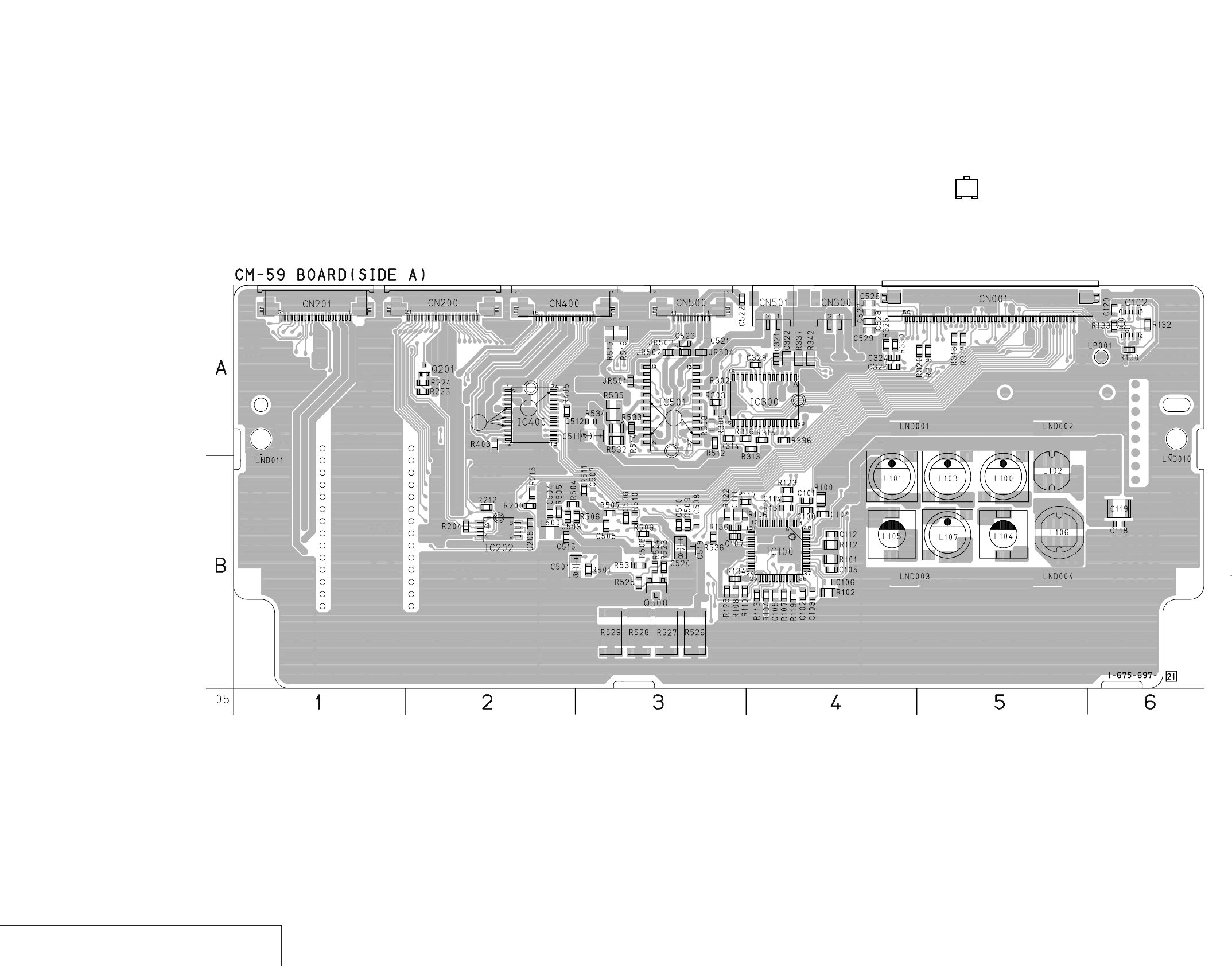
DSR-50/50P
4-111 4-112
DC/DC CONVERTER, MOTOR DRIVE
CM-59
CM-59 (DC/DC CONVERTER, MOTOR DRIVE) PRINTED WIRING BOARD
– Ref. No.: CM-59 board; 20,000 series – • For Printed Wiring Board.
• There are a few cases that the part isn't mounted in this model
is printed on this diagram.
• See page 4-154 for printed parts location.
• Chip transistor
EB
C
5
43
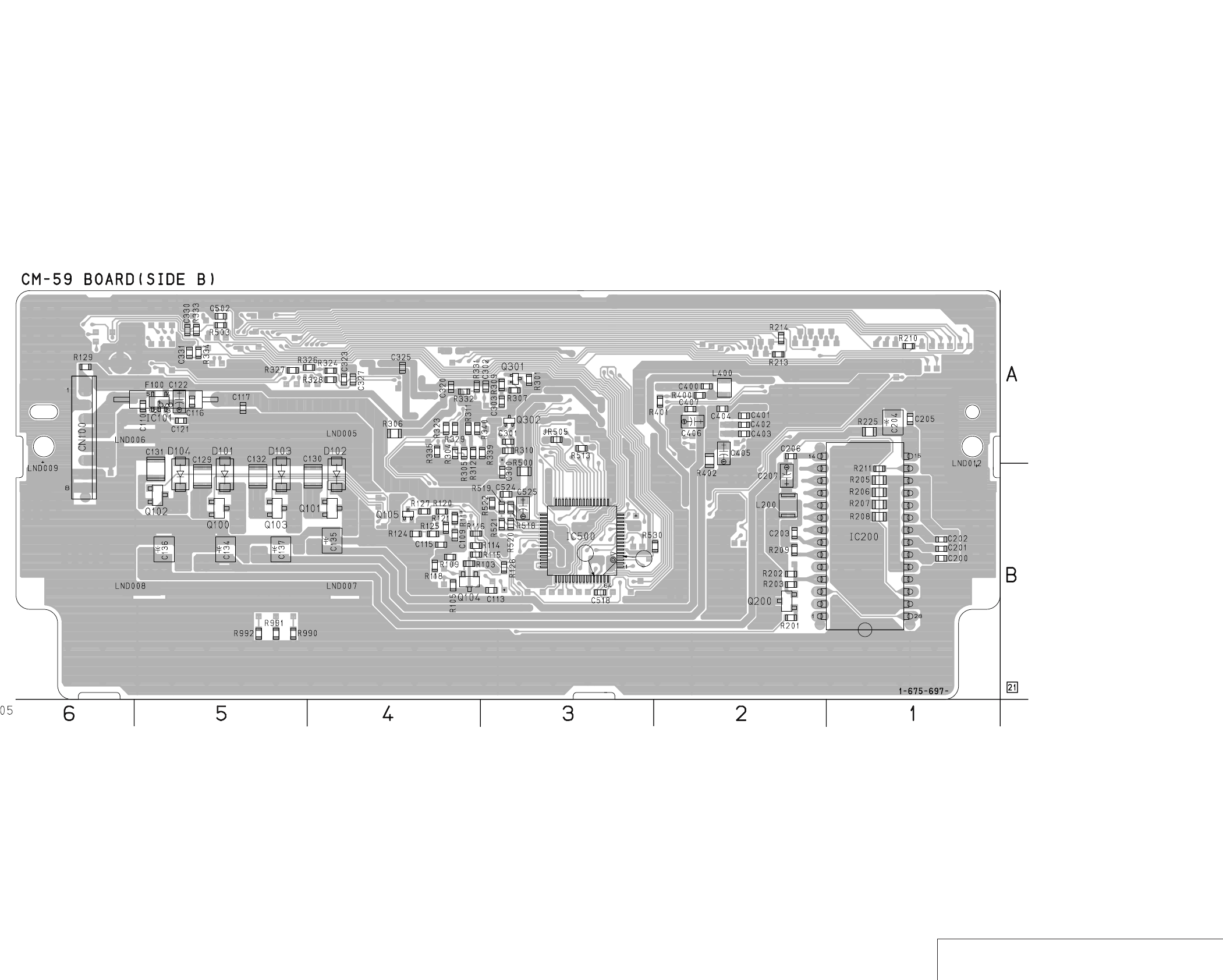
DSR-50/50P
4-113 4-114 DC/DC CONVERTER, MOTOR DRIVE
CM-59
49
48
33
32 17
16
12
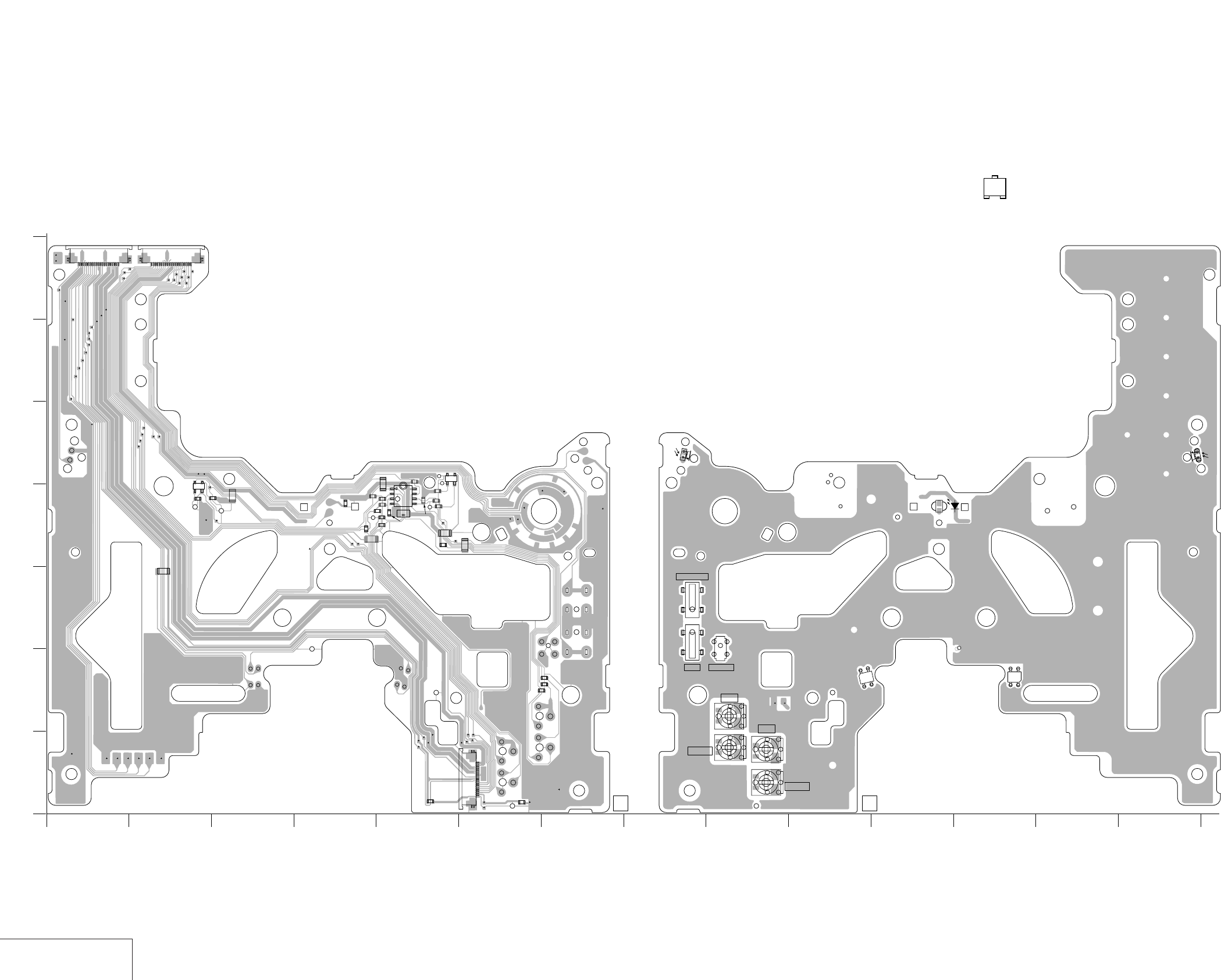
DSR-50/50P
4-115 4-116
TAPE SENSOR
MD-76
MD-76 (TAPE SENSOR) PRINTED WIRING BOARD
– Ref. No.: MD-76 board; 30,000 series –
• For Printed Wiring Board.
• MD-76 board is four-layer print board. However, the patterns of
layers 2 to 3 have not been included in the diagram.
• There are a few cases that the part isn't mounted in this model
is printed on this diagram.
• See page 4-155 for printed parts location.
• Chip transistor
EB
C
RV3
GAIN
S1
S2
S3
C IN
IC5
4
1
3
2
RV2
OFFSET
IC4
1
2
4
3
#PC00090
#PC00091 #PC00092
D1
Q1 Q2
#PC00089
1
G
F
E
D
C
B
A
2345678 9 10
1-675-562- 111-675-562-
11 12 13 14
JR5
R5
R6
JR6
JR3
#PC00114
#PC00096
JR1
R4 R26
C2
IC1
IC3
12
4
8
5
1
4
3
C1
R30
R3
JR4
CL19
#PC00010
#PC00088
#PC00003
IC2
R28
R14
R7
R8 R29
R27
R11
R13
R10
R12
R31
R32
R9
R33
#PC00097
R1
R15
CN3
1
5
10
15
18
CN2
21 151015
CN1
21 151015
L/S CAS
CC DOWN
11
12
43
05
RV1
GAIN
RV4
OFFSET
MD-76 BOARD (SIDE A) MD-76 BOARD (SIDE B)
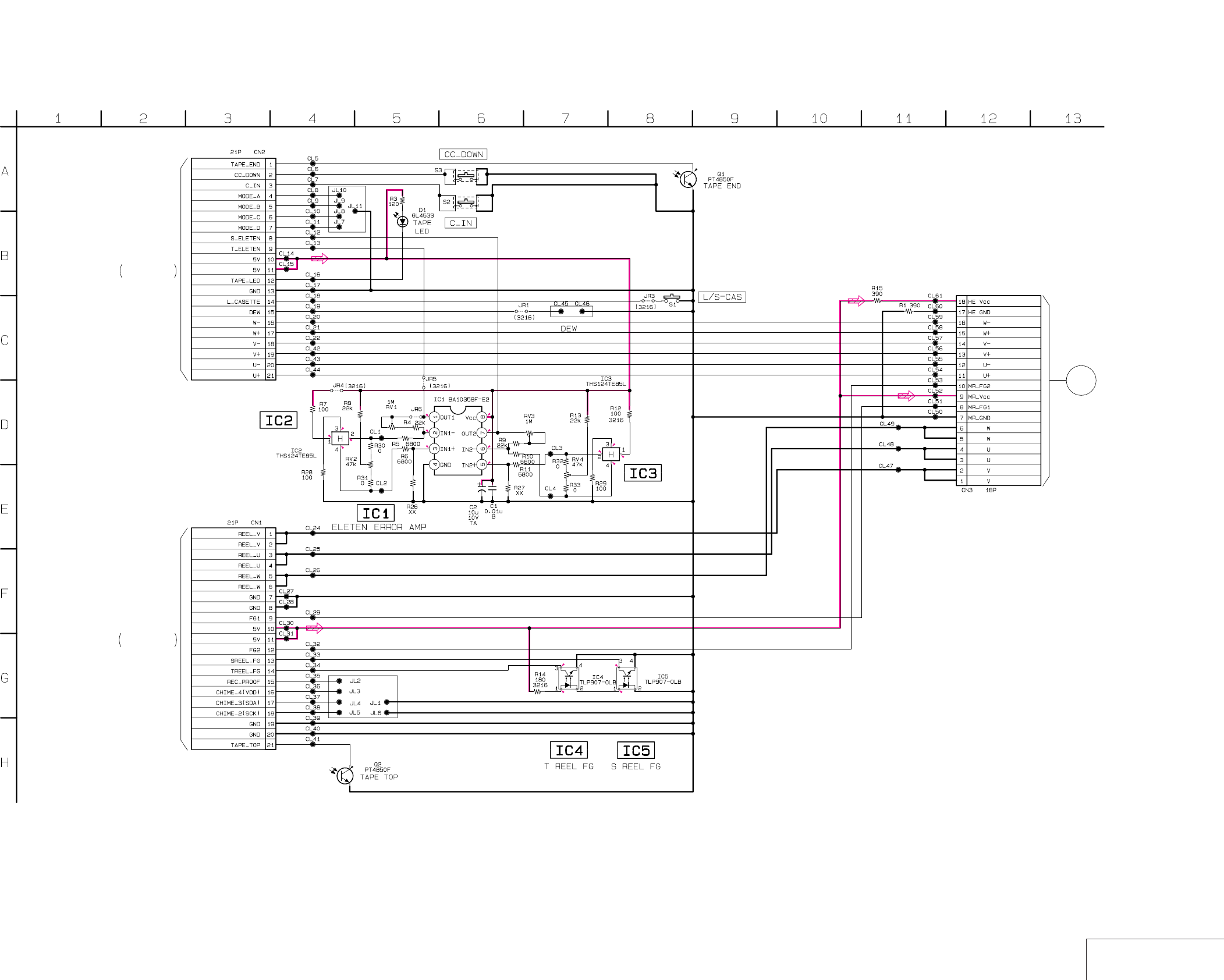
DSR-50/50P
4-117 4-118 TAPE SENSOR
MD-76
MD-76 (TAPE SENSOR) SCHEMATIC DIAGRAM
NO MARK : REC/PB MODE
* : IMPOSSIBLE TO MEASURE THE
VOLTAGE AT THE MARKED POINTS.
4.6
2.6
0.4
2.6
1.2
2.6
2.6
5
2.2
2.6
2.6 4.6
0.3
2.6
2.6
*
2.4 1.2
*
MD-76 BOARD
TAPE SENSOR
— REF. NO. : 30,000 SERIES —
XX MARK : NO MOUNT
REEL
MOTOR
OFFSET OFFSET
GAIN
GAIN
3.0
3.0
CM-59 BOARD(1/3)
CN200
THROUGH THE
FMD-14 FLAT CABLE
(SEE PAGE 4-106)
CM-59 BOARD(1/3)
CN201
THROUGH THE
FMD-14 FLAT CABLE
(SEE PAGE 4-106)
05
M904
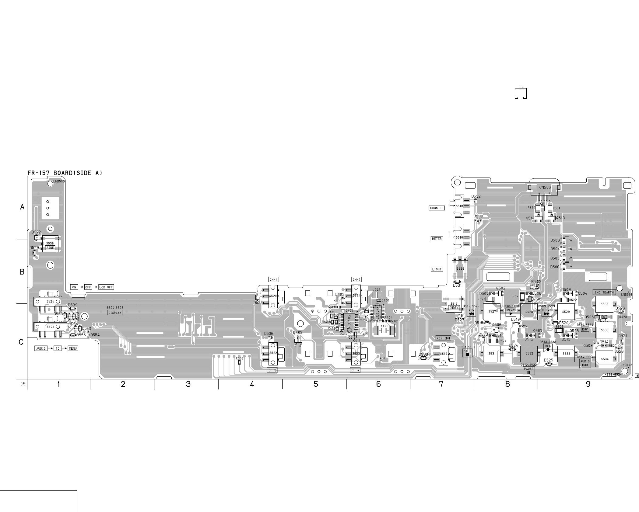
DSR-50/50P
4-119 4-120
USER CONTROL
FR-157
FR-157 (USER CONTROL) PRINTED WIRING BOARD
– Ref. No.: FR-157 board; 30,000 series –• For Printed Wiring Board.
•There are a few cases that the part isn't mounted in this model
is printed on this diagram.
•See page 4-155 for printed parts location.
•Chip transistor
EB
C
1
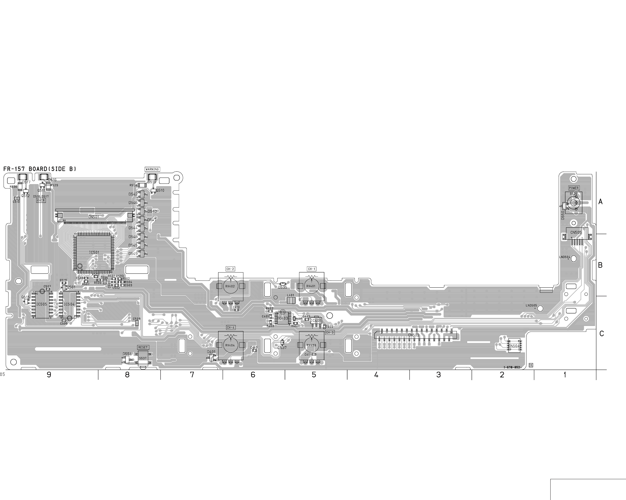
DSR-50/50P
4-121 4-122 USER CONTROL
FR-157
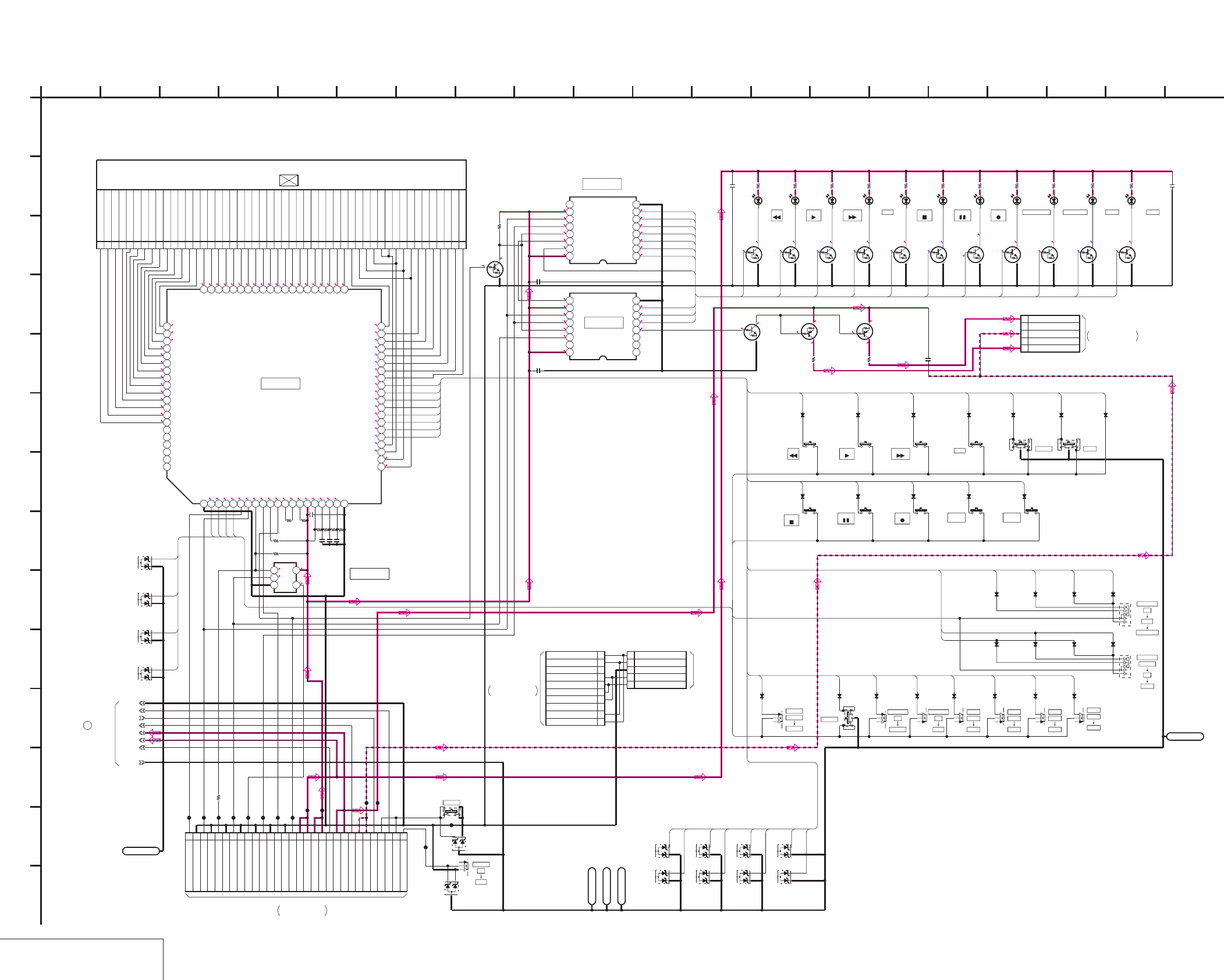
DSR-50/50P
4-123 4-124
USER CONTROL 1
FR-157 (1/2)
FR-157 (USER CONTROL 1) SCHEMATIC DIAGRAM • See page 4-119 for FR-157 printed wiring board.
NO MARK:REC/PB MODE
*:IMPOSSIBLE TO MEASURE THE
VOLTAGE AT THE MARKED POINTS.
R:REC MODE
P:PB MODE
1.5
1.5
1.5
1.5
1.5
1.5
1.5
1.5
1.5
1.5
1.5
1.5
1.5
1.5
1.5
1.4
1.4
1.5
1.5
1.4
1.4
1.5
1.4
1.5
1.5
1.5
1.5
1.5
1.5
1.5
1.5
1.5
1.5
1.5
1.5
1.5
1.5
1.5
1.5
1.5
1.5
1.5
1.5
1.5
1.5
1.5
1.5
1.5
1.5
1.5
1.4
1.4
1.4
1.5
0.6
0.8
1.6
1.5
2.6
2.8
2.9
2.9
3
2.9
1.3
1.4
3
3
3
1.4
1.4
1.4
0
3
0
0
0
0
R*/P0
3
3
0
0.2
0
3
2.9
0.2
3
2.9
3
0
0.2
3
0
0
0
0
0
2.9
3
0
0.2
2.9
0
3
0
0.1 3
0
3
00
33
0
R0,3/
P3
R2.4,0.1/
P2.4
0
2.9
0
2.4
0
2.4
0
2.4
0
5.5 5.5
5.5
-0.2
5.5
-0.2
5.5
50PCN501
115A 15B 15C M13
215F 15G 15E 15D
314A 14B 14C 12C
414F 14G 14E 14D
513A 13B 13C C1
613F 13G 13A 13D
712A,D,G 12E F 12B
8COM1
9COM2
10 COM3
11 COM4
12 COM4
13 COM3
14 COM2
15 COM1
16 1F 1G 1E 1D
17 1A 1B 1C DVCAM
18 2F 2G 2E 2D
19 2A 2B 2C CL1.H
20 3F 3G 3E 3D
21 3F 3G 3E 3D
22 4F 4G 4E 4D
23 4A 4B 4 M6
24 5F 5G 5E 5D
25 5A 5B 5C CL2.M.S
26 6F 6G 6E 6D
27 6A 6B 6C CL3.F
28 7F 7G 7E 7D
29 7A 7B 7C
30 8F 8G 8E 8D
31 8A 8B 8C
32 M9 M8 M10 M11
33 M3 M2 M1 M7
34 M5 M4 9B 9C
35 10F 10G 10E 10D
36 10A 10B 10C 9ADEG
37 11F 11G 11E 11D
38 11A 11B 11C MIN
39 LM5 LM6 LM7 LM8
40 LM4 LM3 LM2 LM1
41 LM12 LM11 LM10 LM9
42 LM13 12 14 15 16
43 19A 19B 19C PM
44 19F 19G 19E 19D
45 18A 18B 18C AM
46 18F 18G 18E 18D
47 17A 17B 17C CL4
48 17F 17G 17E 17D
49 16A 16B 16C X
50 16F 16G 16E 16D
UPD16431AGC-7ET
IC501
1234567891011121314151617181920
21 22 23 24 25 26 27 28 29 30 31 32 33 34 35 36 37 38 39 40
4142434445464748495051525354555657585960
6162636465666768697071727374757677787980
XX
R501
XX
R502
XX
R503
XX
R504
XX
C501
XX
C502
XX
C503
100k
R505
4700
R506
4700
R507
470k
R508
TC7S66FU(TE85R)
IC502
123
45
1u
C506
30P
CN502
1KEY REQ
2GND
3
SCK
4GND
5DATA TO HI
6GND
7DATA FROM HI
8GND
9_W/R
10GND
11LED STB
12GND
13LCD STB
14GND
15OE
16SW +3V
17SW +3V
18EVR +3V
19EVR +3V
20DSP_CS
21SW +6V
22SW +6V
23DSP_SO(FROM DSP)
24SW -6V
25SW -6V
26DSP_SI(TO DSP)
27RESET
28DSP_SCK
29RESET
30POWER SW
TC74VHC595F(EL)
IC504
12345678
910111213141516
TC74VHC595F(EL)
IC505
12345678
910111213141516
MA3075WA-(TX)
D503
MA3075WA-(TX)
D504
MA3075WA-(TX)
D505
MA3075WA-(TX)
D506
LND502
LND502
0.1u
C507
0.1u
C508
UN5214-TX
Q501
100k
R519
UN5214-TX
Q502
UN5214-TX
Q503 UN5214-TX
Q504
UN5214-TX
Q505 UN5214-TX
Q506
UN5214-TX
Q507 UN5214-TX
Q508
UN5214-TX
Q509
UN5214-TX
Q510
UN5214-TX
Q511 UN5214-TX
Q512
DTB113EK-T-146
Q513 DTB113EK-T-146
Q514
CL-170Y-CD-T
D507 CL-170PG-CD-T
D508 CL-170Y-CD-T
D509 CL-170Y-CD-T
D510
CL-170Y-CD-T
D511
CL-170Y-CD-T
D512 CL-170UR-CD-T
D513
CL-170Y-CD-T
D514
CL-200HR-C-TSL
D515
CL-200HR-C-TSL
D516
CL-200HR-C-TSL
D517
68
R520
47
R521
68
R522
68
R523
68
R524
68
R525 100
R526
68
R527
100
R528
100
R529
100
R530
2.2u
C509
2.2u
C510
150
R531
150
R532
UN5214-TX
Q515
2.2u
C511
S515
1SS367-T3SONY
D518
1SS367-T3SONY
D519
1SS367-T3SONY
D520
1SS367-T3SONY
D521
1SS367-T3SONY
D522
1SS367-T3SONY
D523
1SS367-T3SONY
D524
1SS367-T3SONY
D525
1SS367-T3SONY
D526
1SS367-T3SONY
D527
1SS367-T3SONY
D528
XX
D529
S516 S518 S519 S520 S521 S522 S523
S525
1SS367-T3SONY
D530
1SS367-T3SONY
D531
1SS367-T3SONY
D532
1SS367-T3SONY
D533
1SS367-T3SONY
D534 1SS367-T3SONY
D535 1SS367-T3SONY
D536
1SS367-T3SONY
D537
1SS367-T3SONY
D538
1SS367-T3SONY
D540
1SS367-T3SONY
D541
MA3075WA-(TX)
D542
MA3075WA-(TX)
D543
MA3075WA-(TX)
D544
MA3075WA-(TX)
D545
MA3075WA-(TX)
D546
MA3075WA-(TX)
D547
MA3075WA-(TX)
D548
MA3075WA-(TX)
D549
S526
MA3075WA-(TX)
D550
CL501
CL502
CL503
CL504
CL505
CL506
CL507
CL508
CL509
CL510
CL511
CL512
CL514
CL515
DSP_CS
DSP_SO
DSP_SCK
DSP_SI
SW_+6V
SW_+3V
GND
S-GND
5PCN503
1BOTTOM LED VCC(+6V)
2NC
3LED COM(-6V)
4NC
5TOP LED VCC(+6V)
S527 S528 S529 S530
S531 S532 S533 S534 S535
S524
1SS367-T3SONY
D539
S536
S537
MA3075WA-(TX)
D551
1SS367-T3SONY
D552
1SS367-T3SONY
D553
1SS367-T3SONY
D554
1SS367-T3SONY
D555
S538
0
R533
10P
CN504
1
VG
2
COM
3
GND
4
PSIG
5
VCO_CENT
6
VCO_CENT
7
PSIG
8
GND
9
COM
10
VG
5PCN505
1 VCO_CENT
2PSIG
3 GND
4COM
5VG
LND503
LND503
LND504
LND504
LND505
LND505
LND501
LND501
1
A
KEY1
KEY2
KEY3
KEY4
REW
PLAY
FF
DUP
STOP
PAUSE
REC
DUB
WARNING
OVER13
OVER24
REW
PLAY
FF
DUP
STOP
PAUSE
REC
DUB
WARNING
KEY1
KEY2
KEY3
KEY4
KEY3
KS8
KS7
KS6
KS5
KS4
KS3
KS2
KS1
KS1
KS2
KS3
KS4
KS6
KS8
KS2
KS3
KS4
KS5
KS1
KS2
KS3
KS4
KS5
KS6
KS7
KS8
KS1
KS3
KS5
KS7
KS2
KS4
KS6
KS8
KS6
KS5
OVER13
OVER24
KEY2
KEY1
KS5
KS6
KS7
KS8
KS5
KS6
KEY4
2 16
L
I
20
K
12
G
6
N
8
D
E
FR-157 BOARD (1/2)
B
7
05
19151310 1711
C
H
F
3 18
J
14945
M
METER
CH1/2
CH3/4
TC
U-BIT
COUNTER
LIGHT ON
OFF
KEY INH
AUTO
MANU
CH-1
MANU
CH-2
AUTO
CH-3
AUTO
MANU MANU
CH-4
AUTO
AUDIO
TC
DISPLAY
MENU
DISPLAY
OFF
ON
LCD OFF
IC501
IC504
IC505
RESET
POWER
OFF
ON
REW PLAY F FWD INDEX FINE
DUP
PAUSE
STOP REC AUDIO
DUB SEARCH
END
REW PLAY F FWD STOP PAUSE RECDUP AUDIO DUB WARNING OVER OVER
XX MARK:NO MOUNT
USER CONTROL 1
-REF.NO.:30,000 SERIES-
FR-157 BOARD (2/2)
1
LT-32 BOARD
THROUGH THE
CN301
FVJ-12 FLAT CABLE
(SEE PAGE 4-126)
THROUGH THE
CN8201
FJV-3 FLAT CABLE
PD-125 BOARD (2/2)
(SEE PAGE 4-142)
JIG PIN
THROUGH THE
FVJ-7 FLAT CABLE
VD-28 BOARD (12/15) CN701
(SEE PAGE 4-98)
LCD902
CHARACTER DISPLAY
IC502
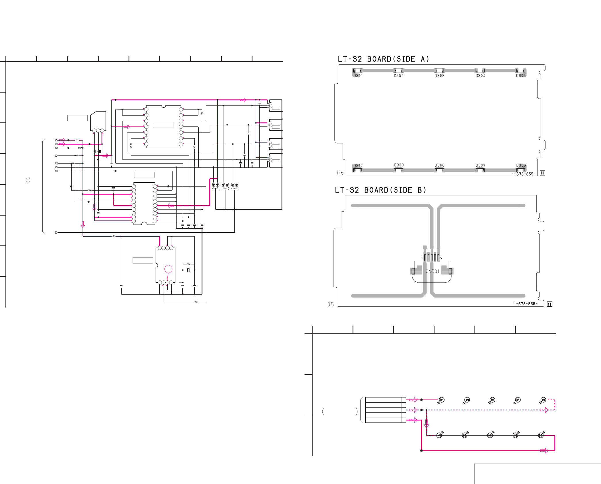
DSR-50/50P
4-125 4-126 USER CONTROL 2
/
BACK LIGHT
FR-157 (2/2) LT-32
FR-157 (USER CONTROL 2) SCHEMATIC DIAGRAM
• See page 4-119 for FR-157 printed wiring board. • See page 4-152 for waveform. LT-32 (BACK LIGHT) PRINTED WIRING BOARD AND SCHEMATIC DIAGRAM
– Ref. No.: LT-32 board; 50,000 series –
NO MARK:REC/PB MODE
5 5.6
0
0
0
5
0
0
0
0
0
0
0
0
0
2.7
1.6
2.7
2.9
2.9
2.6
0.7
5
5
5
0
0
0
0
2.9 1.71.7
1.8
1.6
1
MA3075WA-(TX)
D401
MA3075WA-(TX)
D403
MA3075WA-(TX)
D402
S-81350HG-KD-T1
IC401
123
MB88102PFV-G-BND-ER
IC402
12345678910
11121314151617181920
NJU7064V(TE2)
IC403
1234567
8 9 10 11 12 13 14
TC7WU04F(TE12R)
IC404
1234
5678
22p
C401
22p
C402
1M
R401
100
R402
100
R403
100
R404
100
R405
1u
C403 1u
C404
1u
C405
1u
C406
1u
C407
1u
C408
0.1u
C409
0.1u
C410
0.1u
C411
0.1u
C412
1u
C413
XX
R407
XX
R408
XX
R409
470
R410
0.01u
C414
0.01u
C415
0.01u
C416
0.01u
C417
0
R411
CL404
CL401
CL406
CL403
CL405
CL402
CL407
100uH
L401
10uH
L402
CL408
CL409
SW_+3V
SW_+6V
DSP_CS
DSP_SO
GND
DSP_SCK
DSP_SI
13.5MHz
X401
S-GND
20k
RV401
20k
RV402
20k
RV403
20k
RV404
1
A
IC404
IC402
IC403
IC401
CH-4
CH-3
CH-2
CH-1
6
-REF.NO.:30,000 SERIES-
USER CONTROL 2
9
FR-157 BOARD (2/2)
F
G
B
E
753
D
2
FR-157 BOARD (1/2)
84
1
H
XX MARK:NO MOUNT
C
CL-220TY-C-TS
D310 CL-220TY-C-TS
D306
CL-220TY-C-TS
D309
CL-220TY-C-TS
D301 CL-220TY-C-TS
D305
CL-220TY-C-TS
D307
CL-220TY-C-TS
D303
CL-220TY-C-TS
D308
CL-220TY-C-TS
D302
CL-220TY-C-TS
D304
5P
CN301
1TOP LED VCC(+6V)
2NC
3LED COM(-6V)
4NC
5
BOTTOM LED VCC(+6V)
CL301
CL302
CL303
1
A
54
BACK LIGHT
-REF.NO.:50,000 SERIES-
32
LT-32 BOARD
C
B
05
6
RF-157 BOARD (1/2)
THROUGH THE
CN503
FVJ-12 FLAT CABLE
(SEE PAGE 4-124)
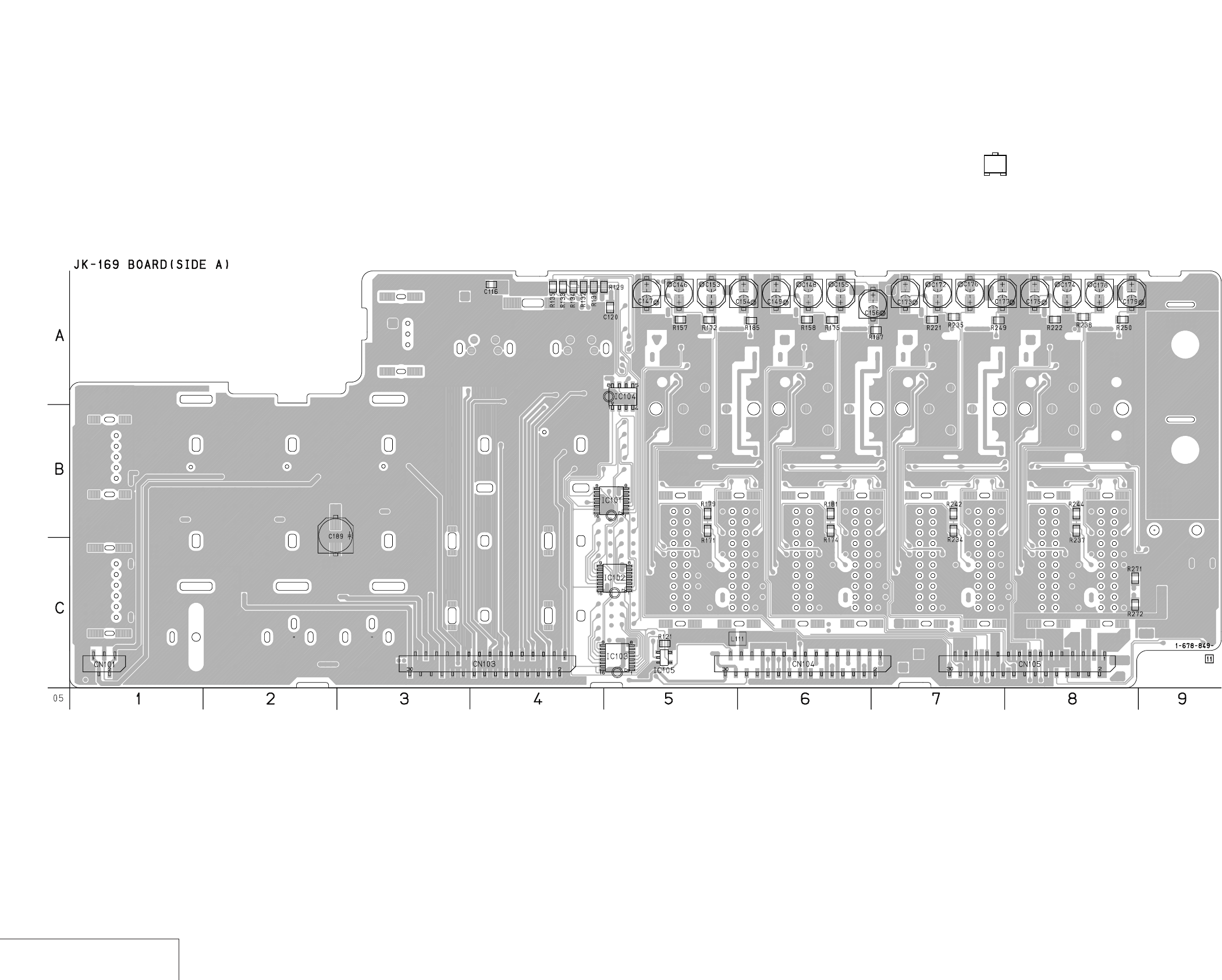
DSR-50/50P
4-127 4-128
VIDEO/AUDIO IN/OUT
JK-169
JK-169 (VIDEO/AUDIO IN/OUT) PRINTED WIRING BOARD
– Ref. No.: JK-169 board; 40,000 series –
• For Printed Wiring Board.
•There are a few cases that the part isn't mounted in this model
is printed on this diagram.
•See page 4-155 for printed parts location.
•Chip transistor
EB
C
1
3
5
4
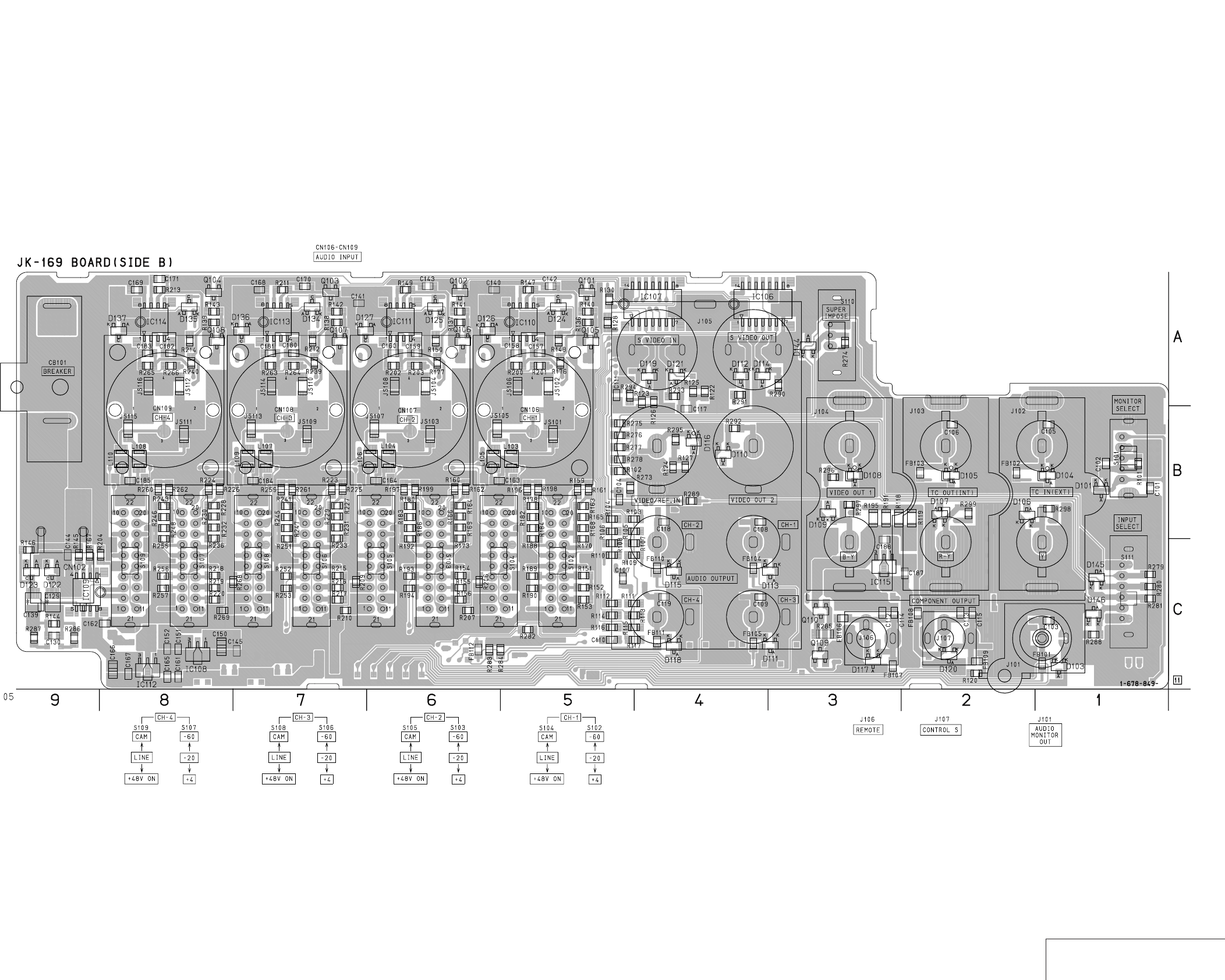
DSR-50/50P
4-129 4-130 VIDEO/AUDIO IN/OUT
JK-169
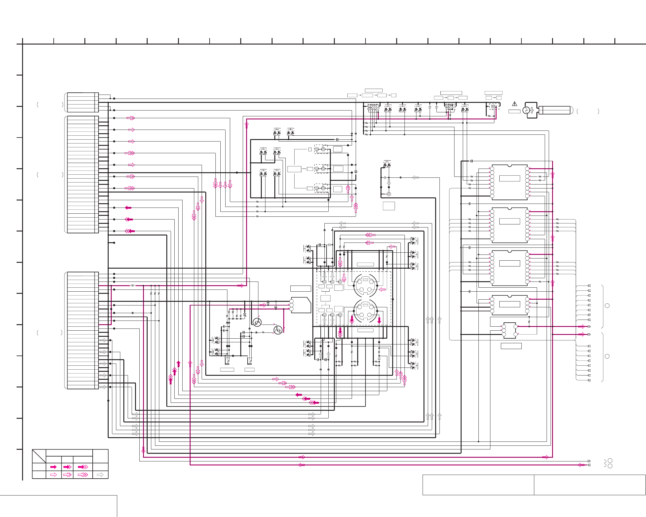
DSR-50/50P
0
0.1
2.9
3
0
R0/P5.1
5.1
NO MARK:REC/PB MODE
R:REC MODE
P:PB MODE
R5.1/P0
5.1
5.5
R2.9/P0
2.9
0
2.9
2.9
0
2.9
0
0
0.1
2.9
0
0.1
0
2.9
0
0
3
2.9
2.9
0
2.9
2.9
0
2.9
0
0
2.9
2.9
3
2.9
2.9
0
2.9
0.1
0
0
2.9
0
2.9
2.9
0.1
3
2.92.9
2.9
0
30PCN103
1
VIDEO IN
2
GND
3
GND
4
S-Y IN
5
GND
6
GND
7
S-C IN
8
GND
9
SC DET
10
GND
11
GND
12
VIDEO OUT
13
GND
14
GND
15
S-Y OUT
16
GND
17
GND
18
S-C OUT
19
GND
20
GND
21
VIDEO MON OUT
22
GND
23
GND
24
B-Y OUT
25
GND
26
GND
27
R-Y OUT
28
GND
29
GND
30
Y OUT
30P
CN104
1
CH4 OUT
2
GND
3
GND
4
CH2 OUT
5
GND
6
GND
7
CH3 OUT
8
GND
9
GND
10
CH1 OUT
11
GND
12
GND
13
AUDIO MONITOR OUT
14
GND
15
GND
16
+48V DD ON
17
SW +3V
18
P/S CS
19
GND
20
P/S DATA
21
GND
22
P/S SCK
23
GND
24
NC
25
GND
26
SIRCS DATA
27
SW +3V
28
TALLY LED
29
FOOT SW
30
AUDIO MONITOR SEL
S101
MA3075WA
-(TX)
D101
10k
R101
XX
C101
0.1u
C102
J104
J102
J103
J101
FB103
MA3200WA
-TX
D105
47p
C105
47p
C106
MA3075WA
-(TX)
D107
MA3200WA-TX
D104
MA3075WA
-(TX)
D106
MA3075WA
-(TX)
D109
MA3075WA
-(TX)
D108
MA3075WA-(TX)
D103
47p
C103
MA3075WA-(TX)
D114
FB104
47p
C108
MA3075WA-(TX)
D112
MA3075WA-(TX)
D110
MA3075WA-(TX)
D113
MA3075WA-(TX)
D111
47p
C109
FB105
47p
C118
FB110
MA3075WA-(TX)
D115
MA3075WA-(TX)
D118
FB111
47p
C119 150
R122
150
R125
150
R123
150
R126
150
R127
150
R124 0.1u
C117
MA3075WA-(TX)
D121
MA3075WA-(TX)
D116
MA3075WA-(TX)
D119
J106J107
MA3075WA-(TX)
D117
MA3075WA-(TX)
D120
FB106
FB107
FB108
FB109
47p
C114
47p
C112
47p
C115
47p
C113
220
R118
220
R119
22
R120
TC74VHC165FT(EL)
IC101
12345678
9 10111213141516
TC7S66F(TE85R)
IC105
123
45
TC74VHC165FT(EL)
IC102
12345678
9 10111213141516
TC74VHC165FT(EL)
IC103
12345678
9 10111213141516
0.1u
C104
0.1u
C107
0.1u
C110
0.1u
C111
100k
R121
CB101
2P
CN102
1BREAKER OUT
2BREAKER IN
1k
R103
1k
R105
1k
R107
1k
R109
1k
R111
1k
R113
1kR115
1k
R117
1k
R116
1k
R114
1k
R112
1k
R110
1k
R108
1k
R106
1k
R104
1k
R102
100
R273
FB101
CL101
CL102
CL103
CL104
CL105
CL106
CL107
CL108
CL109
CL110
CL111
CL112
CL113
CL114 CL115
CL116
CL117
CL118
CL119
CL121
CL122
CL123
CL125
CL126
CL127
CL128
CL129
CL130
CL146
CL147
CL149
CL150
CL151
CL152
CL153
CL154
CL155
CL156
CL157
CL158
CL159
CL160
CL161
CL162
CL163
CL164
CL165
CL166
CL167
CL168
CL169
CL170
S110
100k
R274
1k
R275
MA3075WA
-(TX)
D144
S111
1k
R276
1k
R277
1k
R278
MA3075WA
-(TX)
D145
100k
R280
100k
R281
10uHL111
XX
R282
XX
R283
XX
R284
5P
CN101
1TC IN
2TC IN
3GND
4TC OUT
5TC OUT
FB102
CL148
NJU7201U50-TE1
IC115
123
UN2214-TX
Q109
UN2113-TX
Q110
270
R285
2.2u
C187
2.2u
C188
J105
100k
R288
1k
R289
100k
R279
MA3075WA
-(TX)
D146
FB112
220
R191
220
R195
6.3V
XX
C189
0
R290
0
R291
0
R292
0
R293
0
R294
0
R295
0
R296
0R297
0
R298
0
R299
1
A
SW_+3V
+48V_DD_ON
SW_+6V
TC7WU04F(TE12R)
IC104
1234
5678
SW_+3V
SW16
SW15
SW12
SW11
SW08
SW07
SW04
SW03
SW14
SW13
SW10
SW09
SW06
SW05
SW02
SW01
SW12
SW13
SW14
SW15
SW04
SW05
SW06
SW07
SW01
SW02
SW03
SW08
SW09
SW10
SW11
SW16
2 16
L
I
20
K
12
G
6
N
8
D
E
JK-169 BOARD (1/3)
B
7
05
19151310 1711
C
H
F
3 18
J
14945
M
XX MARK:NO MOUNT
VIDEO IN/OUT,AUDIO OUT
-REF.NO.:40,000 SERIES-
1
JK-169 BOARD (2/3)
JK-169 BOARD (3/3)
2
JK-169 BOARD (2/3)
3
IC101
IC102
IC103
IC104
IC105
IC115
AUDIO
Y/CHROMA
SIGNAL PATH
VIDEO SIGNAL
CHROMA SIGNAL
PB
REC
Y
VD-28 BOARD (11/15)
THROUGH THE
CN607
FVJ-10 FLAT CABLE
(SEE PAGE 4-95)
VD-28 BOARD (4/15)
CN102
THROUGH THE
(SEE PAGE 4-81)
FVJ-7 FLAT CABLE
THROUGH THE
VD-28 BOARD (11/15)
FVJ-7 FLAT CABLE
(SEE PAGE 4-96)
CN603
CN903
VD-28 BOARD (13/15)
VB-50 HARNESS
(SEE PAGE 4-99)
THROUGH THE
BREAKER
OFF ON
SUPER IMPOSE
CH3/4
MONITOR SELECT
MIX CH1/2
S VIDEO
INPUT SELECT
VIDEOCAMERA DV
Y
R-Y
B-Y
COMPONENT
OUTPUT
TC IN
(EXT)
TC OUT
(INT)
OUT 1
VIDEO
MONITOR
AUDIO
OUT
S VIDEO OUT
S VIDEO IN
CONTROL S REMOTE
CH-4 CH-2
AUDIO
OUTPUT
VIDEO/
REF,IN
VIDEO
OUT 2
CH-3 CH-1
JK-169 BOARD (3/3)
7
YC
GG
YC
G
G
4-131 4-132
VIDEO IN/OUT, AUDIO OUT
JK-169 (1/3)
JK-169 (VIDEO IN/OUT, AUDIO OUT) SCHEMATIC DIAGRAM • See page 4-127 for JK-169 printed wiring board.
The components identified by mark 0 or dotted
line with mark 0 are critical for safety.
Replace only with part number specified.
Les composants identifiés par une marque 0 sont
critiques pour la sécurité. Ne les remplacer que
par une piéce portant le numéro spécifié.
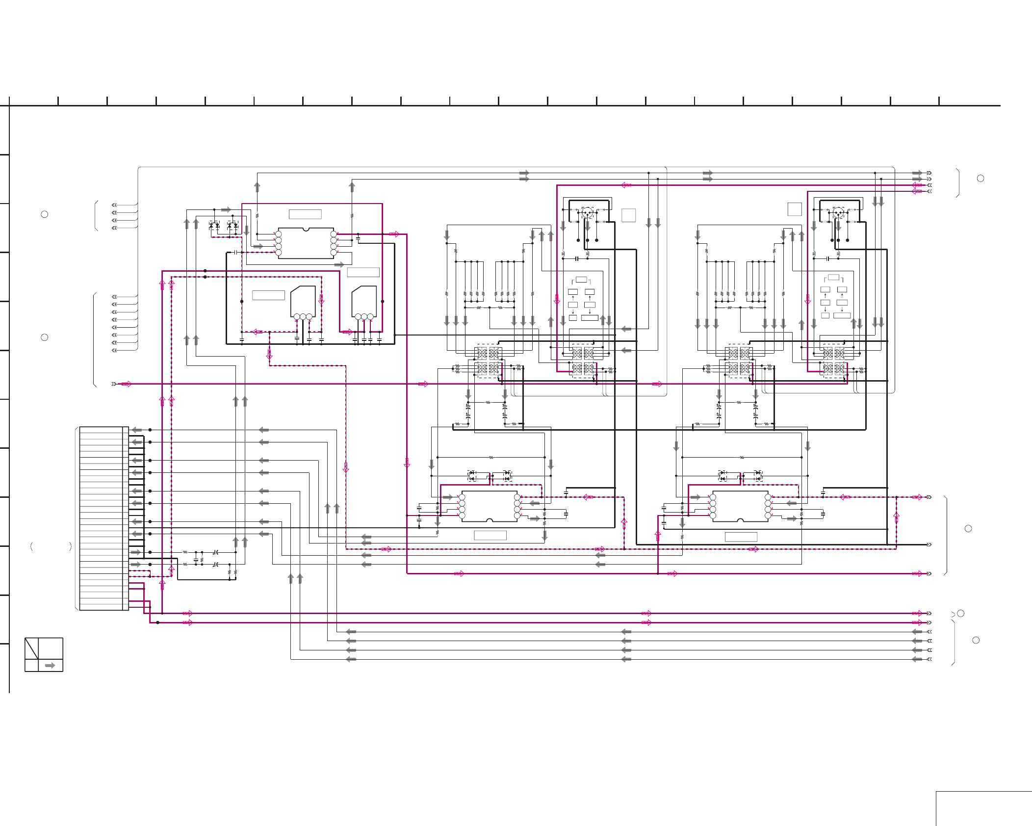
DSR-50/50P
4-133 4-134 AUDIO IN 1
JK-169 (2/3)
JK-169 (AUDIO IN 1) SCHEMATIC DIAGRAM • See page 4-127 for JK-169 printed wiring board.
NO MARK:REC/PB MODE
0
5
0
0
0
0
-4.9
0
-4.9 -5.5
5.6
5
5
0
0
0
0
-4.9
0
0-4.9
0
0
05
0
0
0
30PCN105
1
SW +48V
2
SW +48V
3
NC
4
SW +6V
5
SW +6V
6
SW -6V
7
SW -6V
8
MIC Y
9
GND
10
MIC X
11
GND
12
GND
13
CH4 IN Y
14
GND
15
CH4 IN X
16
GND
17
GND
18
CH3 IN Y
19
GND
20
CH3 IN X
21
GND
22
GND
23
CH2 IN Y
24
GND
25
CH2 IN X
26
GND
27
GND
28
CH1 IN Y
29
GND
30
CH1 IN X
NJM2068M-D-TE2
IC109
1234
5678
0.001u
C130
35V
3.3u
C139
35V
3.3u
C129
3300
R144
R145
100k
100k
R146
NJU7201U50-TE1
IC112
123
NJU7211U50-TE1
IC108
123
0.1u
C145
4.7u
C152
0.1u
C167
4.7u
C161
R204
100
R167
100
NJM2068M-D-TE2
IC114
1234
5678
100k
R257
0.001u
C185
4700
R238
0
R224
18k
R255
8.2uH
L110
8.2uH
L108
18k
R228
4700
R265
1800
R226
4700
R213
XX
JS112
47k
R240
470
R237
0
JS116
18k
R243
10k
R219
18kR248
MA153-TX
D137
MA153-TX
D135
XX
R220
18kR232
18kR246
1800
R260
3P
CN109
390
R218
S109
18k
R236
470
R244
100k
R222 100k
R250
0
JS111
S107
XX
JS115
10
R214
100p
C183
18kR230
0
R262
10
R266
100p
C171
100k
R271
100k
R256
100k
R272
100p
C143
10
R150
4700
R202
0
R160
470
R181
18kR183
10k
R155 100k
R209
100p
C160
1800
R162
18k
R192
100k
R158
1800
R197
18kR186
100k
R193
18kR166
4700
R149
NJM2068M-D-TE2
IC111
1234
5678
100k
R187
3P
CN107
MA153-TX
D127
100k
R210
0
R199
XX
JS104
8.2uH
L106
100k
R194
0
JS103
390
R154
MA153-TX
D125
0
JS108
47k
R177
8.2uH
L104
0.001u
C164
S103 S105
XX
R156
10
R203
470
R174
18k
R164
4700
R175
XX
JS107
18k
R173
18kR169
18k
R180
2.2u
C162
2.2u
C144
2.2u
C159
2.2u
C141
2.2u
C182
2.2u
C169
35V
10u
C148
35V
10u
C155
35V
10u
C149
35V
10u
C156
35V
10u
C174
35V
10u
C178
35V
10u
C175
35V
10u
C179
MA153-TX
D122
MA153-TX
D123
CL131
CL134
CL135
CL136
CL137
CL138
CL139
CL140
CL141
CL142
CL143
CL144
CL145
CL177
CL178
CL179
CL183
CL184
CL185
4.7u
C165
4.7u
C151
10
R286
10
R287
22u
C150
22u
C166
4-1
4-2
SW_+48V_CH4
CH1_IN_X
CH1_IN_Y
CH3_IN_X
CH3_IN_Y
GND
5-1
SW_+6V
SW_+48V
CL133
CL132
SW_+48V_CH2
SW_+3V
1
A
5-2
SW16
SW15
SW12
SW11
SW08
SW07
SW04
SW03
SW16
SW12
SW07
SW03
SW15
SW16
SW07
SW08
SW11
SW12
SW03
SW04
2 16
L
I
20
K
12
G
68
D
E
JK-169 BOARD (2/3)
B
7
05
19151310 1711
C
H
F
3 18
J
14945
XX MARK:NO MOUNT
AUDIO IN 1
-REF.NO.:40,000 SERIES-
REC
SIGNAL PATH
AUDIO
SIGNAL
IC112
IC108
4
JK-169 BOARD (3/3)
JK-169 BOARD (3/3)
5
6
JK-169 BOARD (3/3)
3
JK-169 BOARD
(1/3)
1
JK-169 BOARD (1/3)
IC109
IC114
IC111
VD-28 BOARD (11/15)
CN604
THROUGH THE
(SEE PAGE 4-96)
FVJ-7 FLAT CABLE
INPUT
CH-2
AUDIO
CN107
CN109
INPUT
CH-4
AUDIO
CH-4
CH-2
-60
S103 S105
CAM
-20 LINE
+4 +48V ON
-60
S107 S109
CAM
-20 LINE
+4 +48V ON
12
3
12
3
8
JK-169 BOARD (3/3)
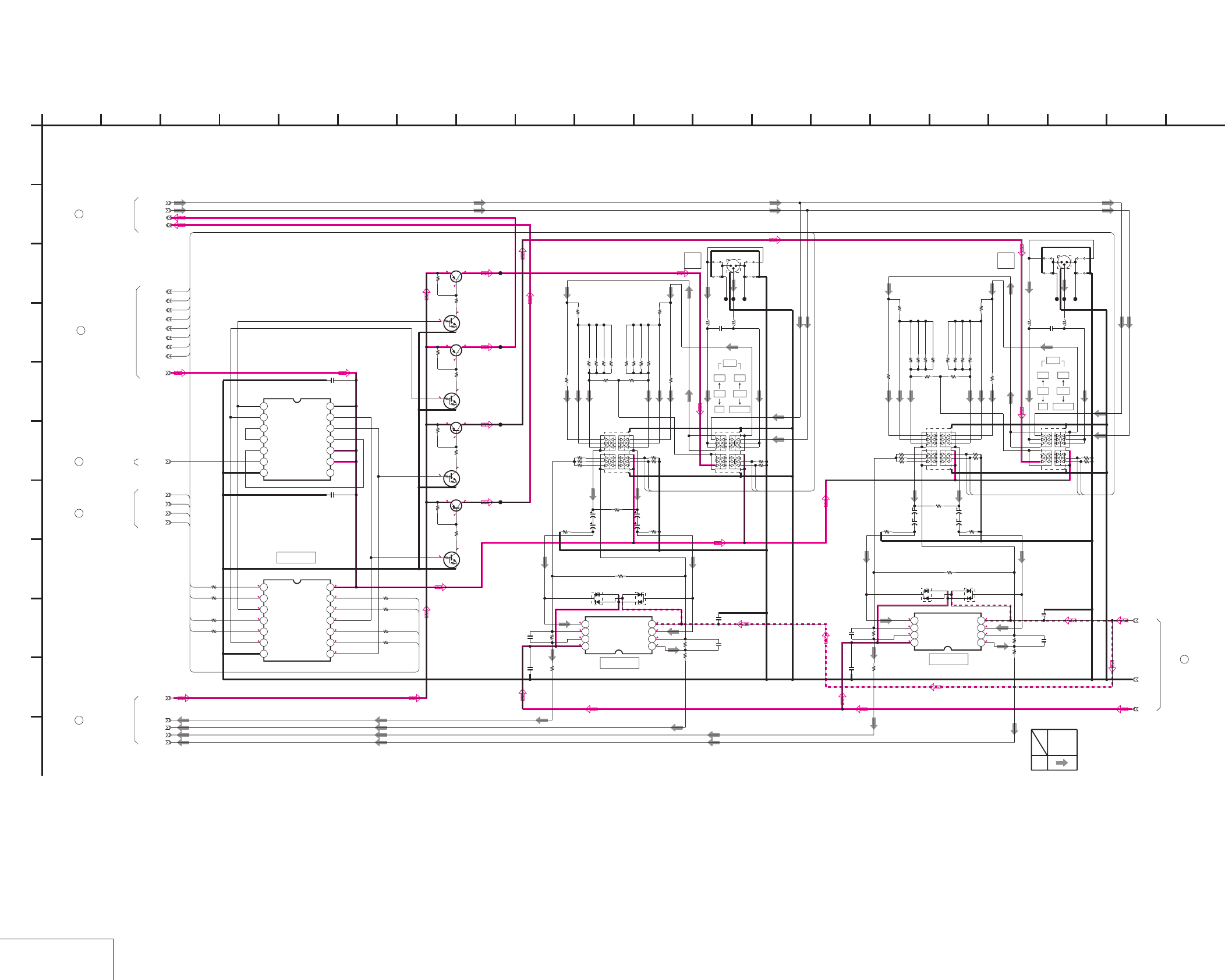
DSR-50/50P
4-135 4-136
AUDIO IN 2
JK-169 (3/3)
JK-169 (AUDIO IN 2) SCHEMATIC DIAGRAM • See page 4-127 for JK-169 printed wiring board.
0.4
NO MARK:REC/PB MODE
0.4
0
0
0
0
5
0
0
0
0
-4.9
0
2.9
0
0
0
-4.9
0
0
0
0
0
0
5
0
0
0
0
0
0
0
0.4 0
0.4
0
00.4
0.4
0.4
0
00.4
0.4
0.4
0
00.4
0.4
3P
CN106
S102 S104
0
JS101
XX
JS105
0
JS106
XX
JS102
8.2uH
L105
8.2uH
L103
0.001u
C163
TC74VHC08F(EL)
IC107
1234567
8 9 10 11 12 13 14
XX
IC106
1234567
8 9 10 11 12 13 14
2SA811A-T1C17
Q105
2SA811A-T1C17
Q106
2SA811A-T1C17
Q107
2SA811A-T1C17
Q108
UN2214-TX
Q101
UN2214-TX
Q102
UN2214-TX
Q103
UN2214-TX
Q104
2200
R136
2200
R137
2200
R138
2200
R139
100k
R140
100k
R141
100k
R142
100k
R143
100k
R189
100k
R190 100k
R206
100k
R207
1800
R196
18k
R188
18kR184
18kR182
18k
R178
0
R198
470
R179
18kR165
1800
R161
18k
R170
0
R159
18kR168
18k
R163
470
R171
NJM2068M-D-TE2
IC110
1234
5678
4700
R172
100k
R157
100k
R185
MA153-TX
D124
MA153-TX
D126
390
R151
10k
R152
XX
R153
47k
R176
4700
R147
4700
R200
100p
C142
100p
C158
10
R148
10
R201
47k
R239
XX
R217
100k
R221
4700
R235
4700
R263
18k
R241
3P
CN108
XX
JS113
100k
R268
0.001u
C184
18k
R227
18kR245
0
JS109
10
R264
100k
R253
8.2uH
L107
0
JS114
18kR231
NJM2068M-D-TE2
IC113
1234
5678
8.2uH
L109
470
R234
MA153-TX
D134
470
R242 0
R261
XX
JS110
MA153-TX
D136
18k
R233
18kR229
100k
R269
18k
R251
4700
R211
18kR247
S108
100p
C181
100k
R252
0
R223
1800
R225
10k
R216
390
R215
10
R212
1800
R259
S106
100p
C170
2.2u
C157
2.2u
C140
2.2u
C168
2.2u
C180
XX
C116
0.1u
C120
1k
R129
1k
R131
1k
R133
1k
R135
1k
R134
1k
R132
1k
R130
1k
R128
35V
10u
C146
35V
10u
C153
35V
10u
C147
35V
10u
C154
35V
10u
C172
35V
10u
C176
35V
10u
C173
35V
10u
C177
CL120
CL171
CL172
CL173
CL174
CL175
CL176
CL180
CL181
CL182
100k
R249
CH3_IN_Y
CH3_IN_X
CH1_IN_Y
CH1_IN_X
SW_+48V
SW_+48V_CH4
SW_+48V_CH2
4-1
4-2
5-1
GND
1
A
SW_+3V
+48V_DD_ON
5-2
SW14
SW13
SW10
SW09
SW06
SW05
SW02
SW01
SW03
SW07
SW12
SW16
SW12
SW03
SW10
SW01
SW16
SW07
SW14
SW05
SW01
SW02
SW09
SW05
SW06
SW13
SW14
SW10
2 16
I
20
K
12
G
68
D
E
JK-169 BOARD (3/3)
B
7
05
19151310 1711
C
H
F
3 18
J
14945
XX MARK:NO MOUNT
AUDIO IN 2
-REF.NO.:40,000 SERIES-
REC
SIGNAL PATH
AUDIO
SIGNAL
JK-169 BOARD (1/3)
2
JK-169 BOARD (2/3)
6
JK-169 BOARD (1/3)
7
4
JK-169 BOARD (2/3)
5
JK-169 BOARD (2/3)
IC107
IC113
IC110
S102
+48V ON
CAM-60
S104
CH-1
+4
-20 LINE
CH-3
-60
S106 S108
CAM
-20 LINE
+4 +48V ON
INPUT
CH-1
AUDIO
CN106 CN108
INPUT
CH-3
AUDIO 1
2
3
2
3
1
8
JK-169 BOARD (2/3)
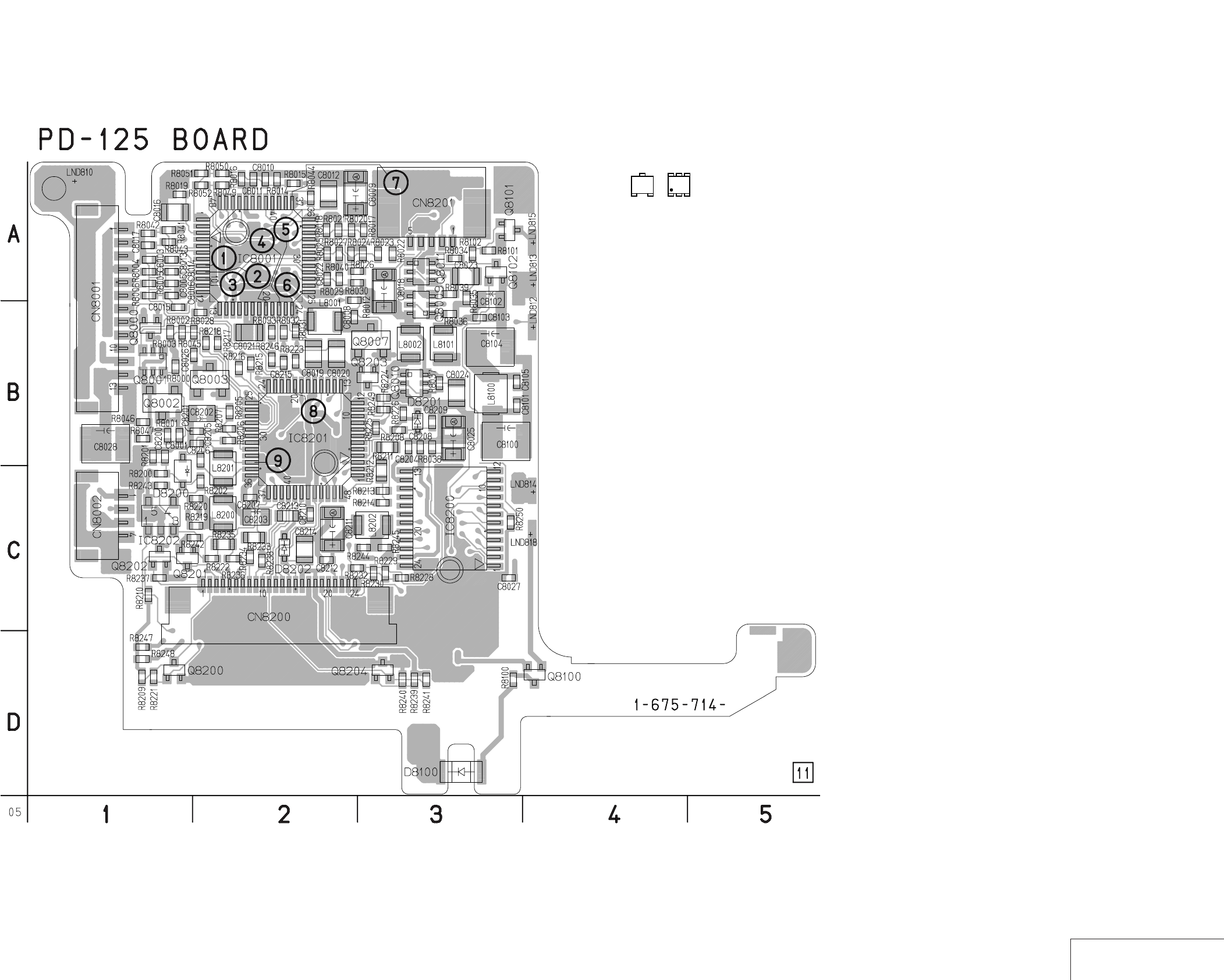
DSR-50/50P
4-137 4-138 RGB DRIVER, TG
PD-125
PD-125 (RGB DRIVER, TG) PRINTED WIRING BOARD
– Ref. No.: PD-125 board; 30,000 series –
• For Printed Wiring Board.
•There are a few cases that the part isn't mounted in this model
is printed on this diagram.
•See page 4-155 for printed parts location.
•Chip transistor
EB
C
31
5
5
2
46
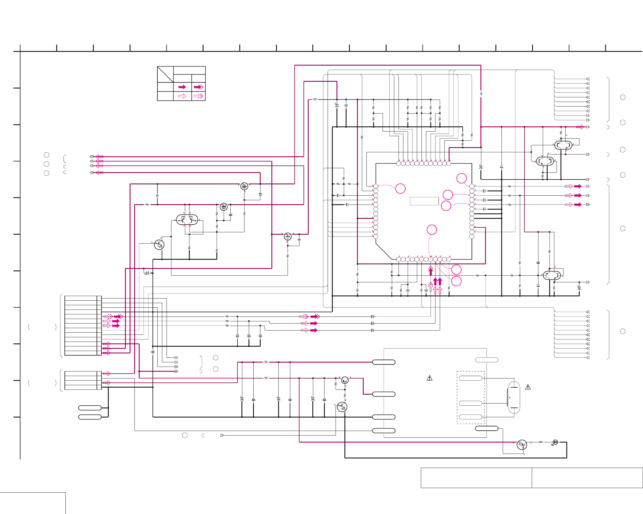
DSR-50/50P
4-139 4-140
RGB DRIVER
PD-125 (1/2)
PD-125 (RGB DRIVER) SCHEMATIC DIAGRAM • See page 4-137 for PD-125 printed wiring board. • See page 4-152 for waveforms.
The components identified by mark 0 or dotted
line with mark 0 are critical for safety.
Replace only with part number specified.
Les composants identifiés par une marque 0 sont
critiques pour la sécurité. Ne les remplacer que
par une piéce portant le numéro spécifié.
NO MARK:REC/PB MODE
2.5
0
0
15.5 0
15.5
15.515.5
12.2 12.2
0
2.82.8
0
12.2
6.1
5.4
5.4
6.1
5.4
4.8
12.2
5.4
4.8
5.5
12.2
5.5
4.9
5.0
5.4
2.8
1.2
2.0
1.7
2.8
0.9
2.8
0.9
0.9
1.2
0.7
0
1.3
1.7
1.8
1.8
1.2
5.4
1.7
5.4
1.7
5.4
1.7
2.8
2.7
2.8
1.2
1.5
1.6
1.7
1.6
1.5
1.4
0
1.3
5.5
12.2
7
6
5
4
1
3
2
4.54.5
3.8
0
2.4
1.0
4.5
4.5
LND811
A
XCLP_Y
B_Y
XX
R8051
NDS356AP
Q8003
PRG_Y
P_3.0V_Y
27k
R8034
33k
R8017
0.01uC8013
FRP_Y
XP4113-TXE
Q8001
XX
Q8002
XX
C8027
10uH
L8001
4700
R8022
XX
R8002
1M
R8012
2.2u
C8023
XP4601-TXE
Q8010
SI2301DS-T1
Q8007
2.2u
2012
C8016
100k
R8028
XX
C8001
CONTRAST_Y
0.01u
C8015
XX
C8003
C8009
47u
4V
XX
C8006
470k
R8019
220k
R8037
39k
R8027
100k
R8016
0
R8004
PSIG_Y
XX
R8049
2200p
C8008
0.1u
C8017
10k
R8043
XX
R8001
SH1_Y
R8031
100
22k
R8020
COLOR_Y
C8019
2.2u
39k
R8018
XP4601-TXE
Q8011
XP4601-TXE
Q8009
UN9213J-(K8).SO
Q8000
47k
R8025
0
R8046
C8012
2.2u
IC8001
CXA8116R-T4
1 2 3 4 5 6 7 8 9 10 11 12
13 14 15 16 17 18 19 20 21 22 23 24
252627282930313233343536
373839404142434445464748
56k
R8030
PSIGGRAY_Y
0.01u
C8026
C8020
2.2u
REG_GND_Y
20V
2.2u
C8018
0.1u
C8011
R_Y
0
R8005
3.0V_Y
22k
R8024
33k
R8040
0.1u
C8010
10k
R8015
4P
CN8002
1ORG_15.5V
2PWM
3UNREG
4GND
1M
R8003
270k
R8035
0
R8006
VREF_Y
16V
4.7u
C8025
SH4_Y
22k
R8038
XTEST_Y
BRIGHT_Y
PANEL_15.5V_Y
XHD_Y
SH2_Y
XX
R8029
PANEL_12V_Y
SH3_Y
33k
R8026
R8033
100
C8021
2.2u
XVD_Y
3300
R8039
2.2u
C8024
R8032
100
LND810
A
100k
R8000
13P
CN8001
1VD_SCK
2DATA_FROM_HI
3XCS_LCD_DAC
4GND
5PANEL_Y
6PANEL_CR
7PANEL_CB
8LCD_DD_ON
9XVD
10XHD
11LCD_4.6V
12LCD_3.0V
13ORG_12V
PICTURE_Y
XX
C8005
P_12V_Y
10uH
L8002
47k
R8021
RGBBLK_Y
10k
R8045
10k
R8044
4700
R8023
XX
R8050
3300
R8036
18k
R8014
XX
R8047
0
R8052
BRT_R_Y
COM_Y
B.LIMIT_Y
G_Y
BRT_B_Y
0.01u
C8022
0
R8042
GAMMA1_Y
0.01uC8014
XX
R8041
4V
68u
C8028
LND812
BL_PWM
10u
C8102
6.3V
BL_LEV_Y
4700
R8101
UN9112J-(K8).SO
Q8100
0.1u
C8103
LND818
LED_ON/OFF
1k
R8102
PG1111R-TR
D8100
100
R8100
0.01u
C8101
100uH
L8101
LND814
UNREG_GND
C8104
22u
16V
LND813
PANEL_UNREG
C8100
22u
16V
Q8101
2SB1462J-QR(K8).SO
4.7uH
L8100
UN9214J-(K8).SO
Q8102
0.01u
C8105
LND815
VDD ND901
XHI_XSCK_Y
DATA_FROM_HI_Y
XCS_LCD_D/A_Y
4.6V_Y
1
A
COLOR
BRT_R
BRT_B
CONTRAST
B.LIMIT
GAMMA1
PSIGGRAY
PICTURE
CONTRAST
SH4
SH3
SH2
XCLP
BRIGHT
B.LIMIT
FRP
BRT_R
PSIGGRAY
GAMMA1
BRT_B
SH1
XHD
XVD
XTEST
VREF
BRIGHT
SH4
SH3
SH2
SH1
XVD
FRP
XCLP
XHD
PRG
VREF
COLOR
XTEST
RGBBLK
RGBBLK
PRG
PICTURE
PANEL ON/OFF
SWITCH
BL_LOW
BL_GND
BL_HI
DUMY_LND
BACK
LIGHT
LED DRIVER
-REF.NO.:30,000 SERIES-
PD-125 BOARD(1/2)
RGB DRIVER (PD-1 BLOCK)
XX MARK:NO MOUNT
PD-125 BOARD (2/2)
8
10
9
7
PD-125 BOARD (2/2)
12
2
Q8101,8102
BACK LIGHT
SWITCH
SWITCH
INV.
SWICH
IC8001
BUFFER
BUFFER
BUFFER
4
5
11
6
1
3
47
G
9
C
I
16
E
K
8
J
B
13
D
146
F
10 113 1512 1725
H
05
INVERTER BLOCK
(BACK LIGHT DRIVER)
PD-125 BOARD (2/2)
PD-125 BOARD (2/2)
PD-125 BOARD (2/2)
PD-125 BOARD (2/2)
PD-125 BOARD (2/2)
PD-125 BOARD (2/2)
PD-125 BOARD (2/2)
PD-125 BOARD (2/2)
PD-125 BOARD (2/2)
PD-125 BOARD (2/2)
YCHROMA
VIDEO SIGNAL
SIGNAL PATH
PB
REC
CN331
VD-28 BOARD (7/15)
LC-111 HARNESS
(SEE PAGE 4-87)
THROUGH THE
(SEE PAGE 4-87)
RM-129 HARNESS
THROUGH THE
CN333
VD-28 BOARD (7/15)
(STARTOR)
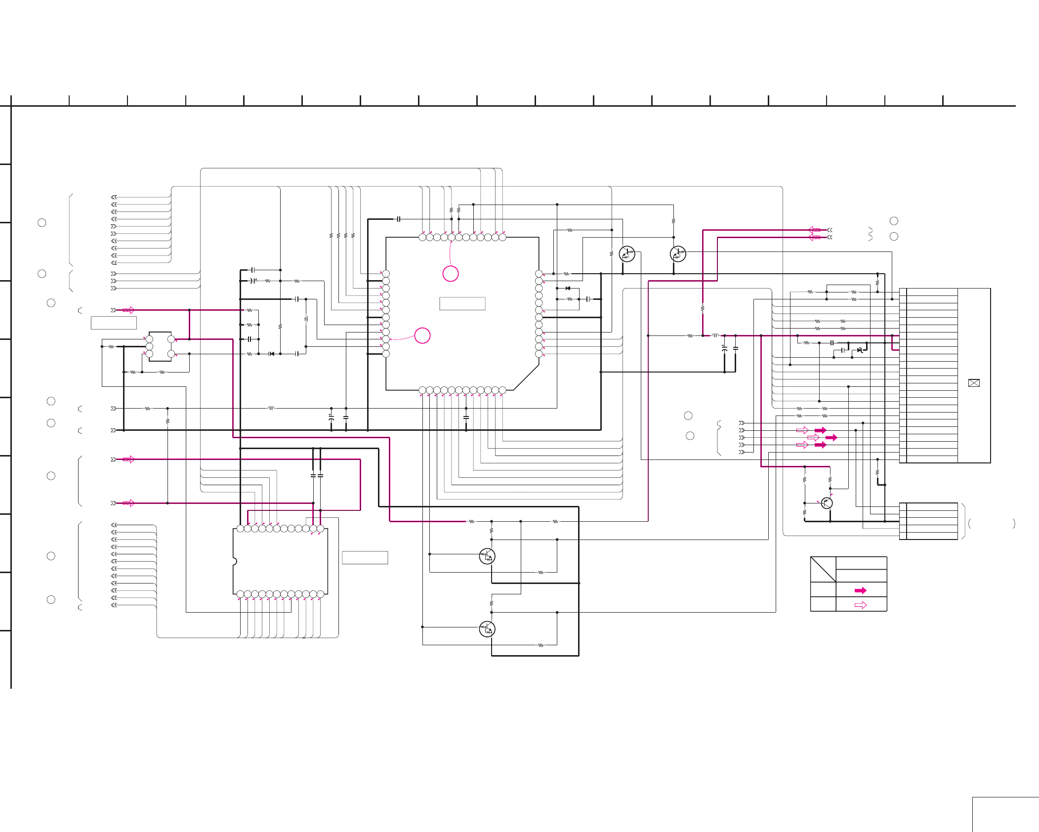
DSR-50/50P
4-141 4-142 TG
PD-125 (2/2)
PD-125 (TG) SCHEMATIC DIAGRAM • See page 4-137 for PD-125 printed wiring board. • See page 4-152 for waveforms.
NO MARK:REC/PB MODE
2.8
2.9
0.1
1.7
2.6
2.8
2.8
1.6
1.3
1.6
1.4
2.0
1.3
1.6
1.2
1.2
2.4
1.2
1.2
1.4
0.9
0.9
2.8
0.9
1.8
2.8
1.4
1.4
9
1.4
0
1.4
10.9
0.2
1.3
2.8
0
0
4.9
-1.9
0
0
2.8
2.8
0
0
1.4
2.2
2.8
2.7
2.6
2.8
2.8
2.8
2.9
0.4
2.6
8
12.5
2.5
1.2
1.2
1.4
0.7
470
R8207
XX
R8210
NJM2130F(TE2)
IC8202
123
45
PANEL_12V_Y
18k
R8202
XX
R8228
1608 0
R8212
33k
R8240
PRG_Y
SH3_Y
0.1u
C8204
100
R8217
0
R8224
FRP_Y
XX
Q8203
R_Y
XX
R8244
2SB1462J-QR(K8).SO
Q8204
0.01u
C8200
56k
R8241
4700
R8205
XCLP_Y
P_3.0V_Y
0R8246
470k
R8243
P_12V_Y
D8201
XX
XX
R8237
0
R8225
20V
2.2u
C8211
XHD_Y
0
R8245
XX
R8249
B_Y
XVD_Y
COM_Y
0
R8232
0
R8221
M62376GP-65AD
IC8200
123456789101112
131415161718192021222324
1608
0
R8235
SH1_Y
CN8200 24P
TESTR1
RGT2
VB3
VR4
VG5
PSIG6
HCK17
HCK28
CR9
SOUT10
REF11
HST12
WIDE13
CS14
VSS15
VVDD16
VSS17
HVDD18
DWN19
EN20
VCK21
VST22
COM23
TESTL24
39p
C8205
RGBBLK_Y
XX
Q8200
XX
Q8202
XX
R8229
4.6V_Y
0
R8230
0
R8236
10u
C8203
6.3V
REG_GND_Y
XX
R8226
1u
C8214
XX
R8209
1M
R8201
3.0V_Y
RD2.7UM-T1B
D8202
G_Y
10u
C8202
6.3V
R8223
0
100
R8216
0.1u
C8208
1T369-01-T8A
D8200
0.1u
C8207
3.3uH
L8201
100
R8215
1608
0
R8211
XX
R8219
SH4_Y
R8247
XX
SH2_Y
6800p
C8201
0
R8213
470k
R8242
100uH
L8202
100k
R8200
1608
0
R8233
R8248
XX
0.1u
C8209
0
R8220
PANEL_15.5V_Y
XHI_XSCK_Y
0
R8222
0.001u
C8206
10uH
L8200
150k
R8238
0
R8234
XX
C8210
DATA_FROM_HI_Y
100k
R8208
100
R8218
0
R8214
33k
R8206
PSIG_Y
5P
CN8201
1VG
2 COM
3 GND
4 PSIG
5 VCO_CENT
XX
Q8201
XX
C8215
0.01u
C8212
XCS_LCD_D/A_Y
16080.1u
C8213
560k
R8239
47k
R8250
CXD2471AR-T4
IC8201
123456789101112
131415161718192021222324
252627282930313233343536
37 38 39 40 41 42 43 44 45 46 47 48
BRIGHT_Y
COLOR_Y
BRT_R_Y
BRT_B_Y
CONTRAST_Y
B.LIMIT_Y
CAMMA1_Y
PSIGGRAY_Y
PICTURE_Y
VREF_Y
XTEST_Y
BL_LEV_Y
1
A
XVD
SH1
SH2
SH3
SH4
XHD
FRP
XHST
XHD
BRIGHT
BRT_B
CONTRAST
B.LIMIT
VREF
BRT_R
HST
HCK1
VCK2
VCK1
EN
HST
XHST
VST
XVST
VCK2
VCK1
XEN
EN
HCK1
HCK2
HCK2
FRP
PRG
DAC_SO
XSCK
XCS
DATA_FROM_HI
XCS
XSCK
XCS
DAC_SO
DATA_FROM_HI
XSCK
COLOR
PICTURE
PSIGGRAY
VCO_CENT
VCO_CENT
PCG
XPCG
PRG
GAMMA1
XTEST
XCLP
XCLP
SH4
SH3
SH2
SH1
RGBBLK
VST
XPCG
PCG
BRT_R
BRT_B
CONTRAST
B.LIMIT
GAMMA1
PICTURE
VREF
XTEST
BL_LEV
BL_LEV
XEN
XVST
XVD
RGBBLK
BRIGHT
COLOR
PSIGGRAY
DWN
RGT
SB:C4889
LCD901
2.5INCH
COLOR LCD
UNIT
-REF.NO.:30,000 SERIES-
XX MARK:NO MOUNT
PD-125 BOARD(2/2)
TG (PD-2 BLOCK)
9
10
11
1
4
7
5
12
6
8
2
3
47
G
9
C
I
16
E
8
B
13
D
146
F
10 113 1512 1725
H
05
IC8201
IC8202
J
IC8200
REC
VIDEO SIGNAL
CHROMA
SIGNAL PATH
PB
PD-125 BOARD (1/2)
PD-125 BOARD (1/2)
PD-125 BOARD (1/2)
PD-125 BOARD (1/2)
PD-125 BOARD (1/2)
PD-125 BOARD (1/2)
PD-125 BOARD (1/2)
PD-125 BOARD (1/2)
PD-125 BOARD (1/2)
PD-125 BOARD (1/2)
PD-125 BOARD (1/2)
PD-125 BOARD (1/2)
FR-157 BOARD (1/2)
THROUGH THE
CN504
FJV-3 FLAT CABLE
(SEE PAGE 4-123)
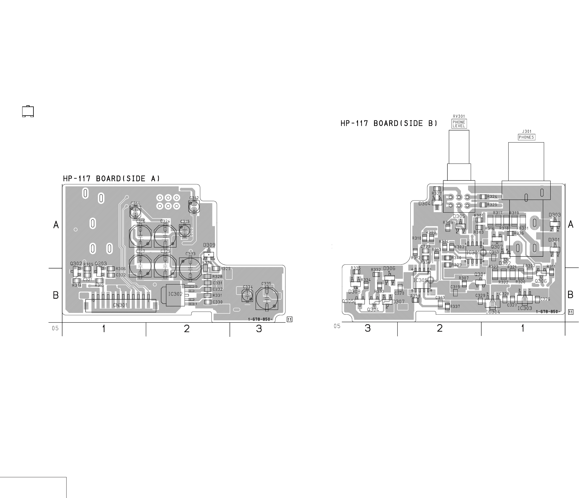
DSR-50/50P
4-143 4-144
HEAD PHONE
HP-117
HP-117 (HEAD PHONE) PRINTED WIRING BOARD
– Ref. No.: HP-117 board; 40,000 series –
• For Printed Wiring Board.
•There are a few cases that the part isn't mounted in this model
is printed on this diagram.
•See page 4-156 for printed parts location.
•Chip transistor
EB
C
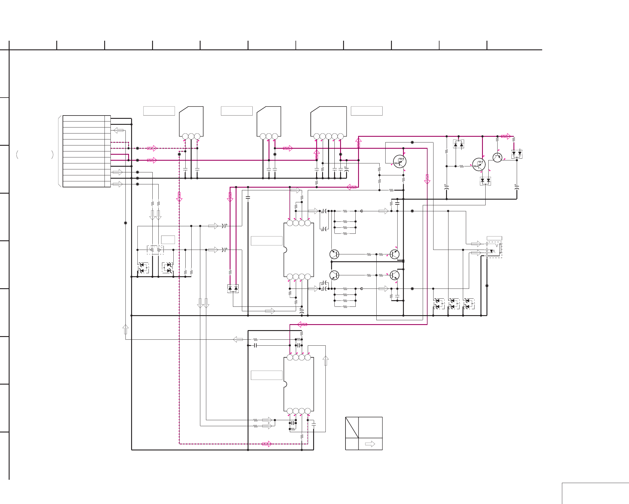
DSR-50/50P
4-145 4-146 HEAD PHONE
HP-117
HP-117 (HEAD PHONE) SCHEMATIC DIAGRAM
5.6
4.9
00
5.6
5-4.9-5.5
000 4.9
000
0005
000 4.9
5
0.1
4.9
0
-1.1
0
0
0
-1.1
0
-0.7
-0.7
0
NO MARK:REC/PB MODE
12P
CN301
1
HP L
2
HP L GND
3
HP R
4
HP R GND
5
SW +6V
6
SW +6V
7
SW -6V
8
SW -6V
9
NC
10
VTR RET AUDIO
11
VTR RET AUDIO GND
12
GND
LM4880M
IC301
1234
5678
L88MS05T-FA-TL
IC302
12345
NJU7211U50-TE1
IC303
123
NJU7201U50-TE1
IC304
123
NJM4556AM-A-TE2
IC305
1234
5678
UN2113-TX
Q301
RV301
20k/20k
10k
R301
22k
R302
22k
R303
10k
R304
35V
2.2u
C312
35V
2.2u
C314
16V
10u
C315
6.3V
100u
C316
6.3V
100u
C317
1u
C318
1k
R305
1k
R306
47k
R307
22k
R309
22k
R310
10k
R312
1u
C319
1u
C320
100
R313
FB301
FB302 47p
C322
47p
C321
2SC3326N-TE85L-AB
Q303
2SC3326N-TE85L-AB
Q302
470
R315
470
R314
CL301
CL302
CL303
CL304
CL305
CL307
CL309
CL308
MA3075WA-(TX)
D301
MA3075WA-(TX)
D302
J301
MA3075WA-(TX)
D303
47
R316
47R317
47
R318
47
R319
47
R320
47
R321
47
R322
47
R323
CL310
CL311
MA3075WA-(TX)
D304
MA3075WA-(TX)
D305
0
R324
0
R325
CL312 CL313
CL314
47p
C323
6.3V
100u
C324
6.3V
100u
C325
0
R330
XX
R331
4.7u
C326
4.7u
C327
4.7u
C328
4.7u
C329
4.7u
C330
4.7u
C331
1u
C332
6.3V
100u
C333
47k
R332
16V
10u
C334
6.3V
100u
C335
MA152WK-TX
D306
MA152WK-TX
D307
MA152WK-TX
D308
UN2113-TX
Q304
2SA811A-T1C17
Q305
1k
R333
4700
R334 270
R335
10k
R308
10k
R327
10k
R336
100k
R337 10k
R338
47p
C313
2SC3326N-TE85L-AB
Q306
2SC3326N-TE85L-AB
Q307
470
R311
470
R326
1k
R328
MA721WA-TX
D309
0
R329
0
R339
XX
R340
1
A
IC301
IC305
IC302IC303 IC304
2
I
G
68
D
E
HP-117 BOARD
B
7
05
10 11
C
H
F
3945
XX MARK:NO MOUNT
HEAD PHONE
-REF.NO.:40,000 SERIES-
PB
SIGNAL PATH
SIGNAL
AUDIO
PHONE
LEVEL
PHONES
CN601
VD-28 BOARD (11/15)
HP-135 HARNESS
(SEE PAGE 4-95)
THROUGH THE
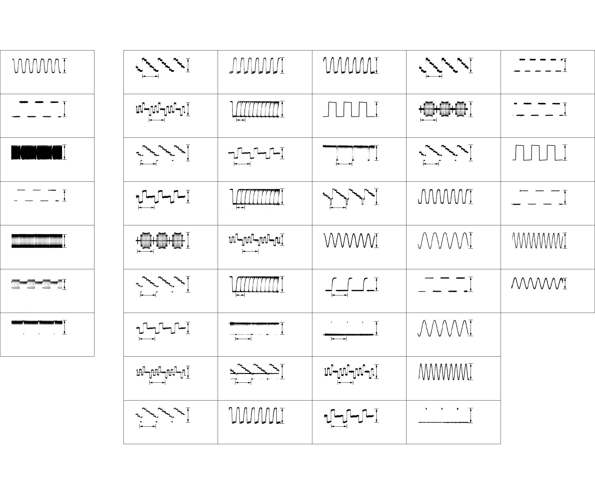
2.0 Vp-p
IC101 1, 2, 6, 7 REC
3.7 Vp-p
6
IC301 ra REC/PB
13.5 MHz
150 Hz
2.8 Vp-p
1
IC301 tg REC/PB
2.8 Vp-p
2
300 Hz
IC101 wj PB
510 mVp-p
3
IC101 eg REC/PB
4
IC101 rs REC
2.5 Vp-p
5
300 Hz
150 Hz
300 Hz
150 Hz
IC101 qa, qs REC
2.8 Vp-p
7
240 mVp-p
Q1117 B REC
1.7 Vp-p
6
IC1000 1 REC/PB
H
H
260 mVp-p
1
IC1002 1 REC/PB
250 mVp-p
2
H
IC1112 1 REC/PB
760 mVp-p
3
IC1001 1 REC/PB
4
IC1111 1 REC/PB
600 mVp-p
5
H
H
H
H
H
Q1118 B REC
1.0 Vp-p
7
Q1119 B REC
1.1 Vp-p
8
H
IC1108 wa REC
1.7 mVp-p
9
3.3 Vp-p
IC1110 1 – 8 REC
33 Vp-p
qg
IC1108 – IC1110 qs REC/PB
13.5 MHz
0.6 µsec
3.3 Vp-p
0
IC1108 1 – 8 REC
3.3 Vp-p
qa
H
IC1109 wa REC
1.0 Vp-p
qs
IC1109 1 – 8 REC
qd
IC1110 wa REC
1.1 Vp-p
qf
H
0.16 µsec
H
H
0.16 µsec
Q2200 B PB
1.1 Vp-p
qh
Q2200 B REC
1.6 Vp-p
qh
13.5 MHz
IC2204 rd REC/PB
3.0 Vp-p
qj
830 mVp-p
IC2204 qk, w; REC/PB
3.0 Vp-p
ws
IC2204 ra REC/PB
13.5 MHz
30 Hz
3.0 Vp-p
qk
IC2204 tg REC/PB
3.0 Vp-p
ql
H
IC2204 3, 7 PB
550 mVp-p
w;
IC2204 3, 7 REC
w;
IC2204 qd REC/PB
2.8 Vp-p
wa
H
H
H
13.5 MHz
H
IC2204 wk REC/PB
2.8 Vp-p
wd
IC3300 uh REC/PB
280 mVp-p
wf
H
IC3300 uf REC/PB
260 mVp-p
wg
2.6 Vp-p
IC4400 rk REC/PB
2.7 Vp-p
ea
IC3300 us REC/PB
H
H
270 mVp-p
wh
IC3300 yk REC/PB
300 mVp-p
wj
H
IC3300 ya REC/PB
400 mVp-p
wk
IC3302 5, 7 REC/PB
wl
IC4400 wl REC/PB
1.9 Vp-p
e;
24.576 MHz
150 Hz
20 Hz
24.576 MHz
13.5 MHz
2.8 Vp-p
IC6001 ts REC/PB
2.3 Vp-p
r;
IC5003 <zzn> REC/PB
900 Hz
1.62 kHz (DVCAM)
1.08 kHz (DV)
3.0 Vp-p
eg
IC5003 <zzb> REC/PB
3.0 Vp-p
eh
30 Hz
IC5003 oa REC/PB
3.0 Vp-p
ej
IC5003 y; REC/PB
ek
IC6001 ra REC/PB
1.6 Vp-p
el
32.768 kHz
20 MHz
150 Hz
IC4400 qd REC/PB
1.7 Vp-p
es
IC5003 1 REC/PB
1.6 Vp-p
ed
150 Hz
IC5003 <zzm> REC/PB
2.9 Vp-p
ef
4-147 4-148
4-3. WAVEFORMS
JC-20 BOARDRP-234 BOARD
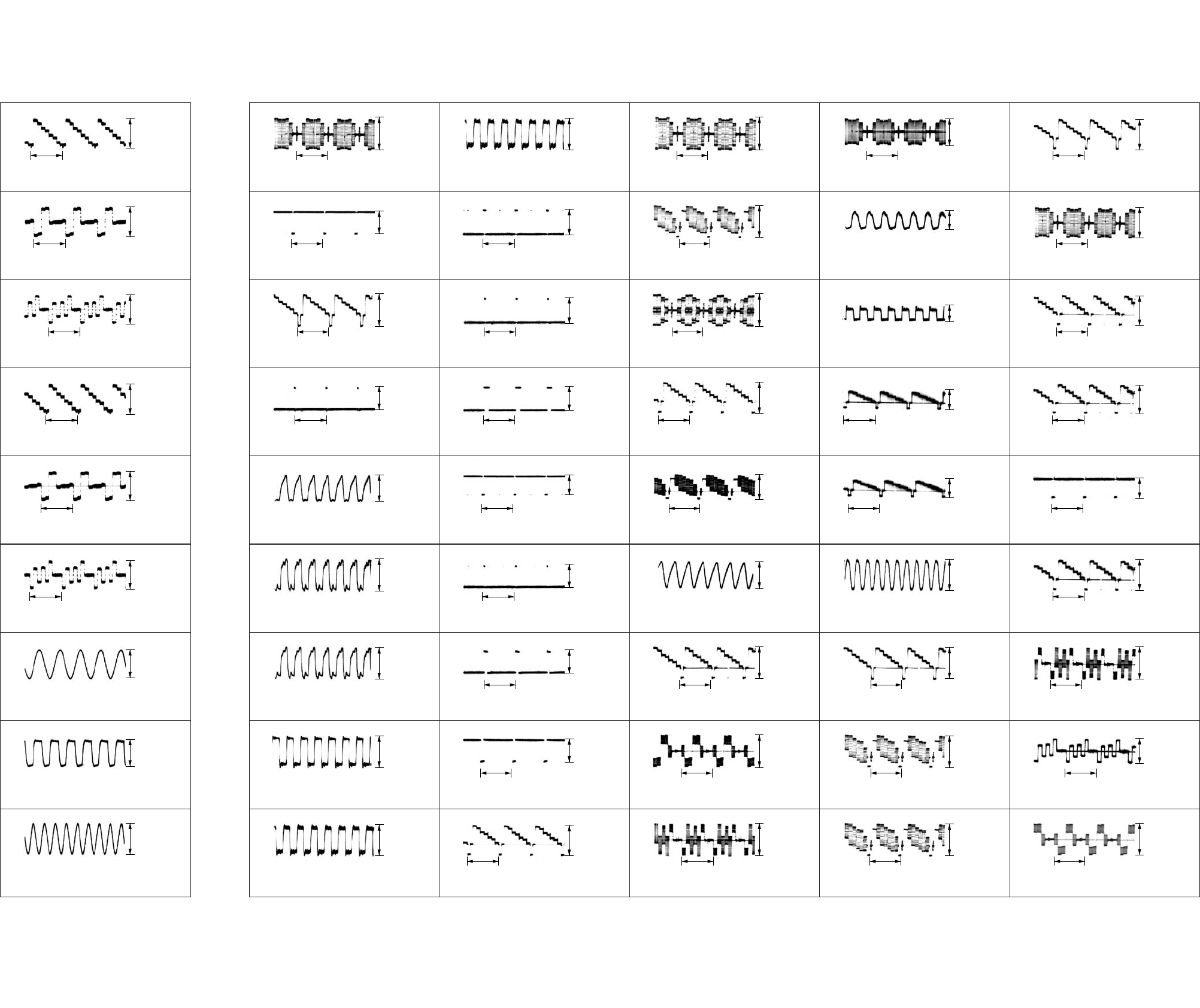
920 mVp-p
IC9010 1 REC/PB
900 mVp-p
6
IC9000 ra REC/PB
H
H
920 mVp-p
1
IC9000 el REC/PB
880 mVp-p
2
H
IC9000 ej REC/PB
900 mVp-p
3
IC9001 1 REC/PB
4
IC9007 1 REC/PB
880 mVp-p
5
24.576 MHz
H
12.288 MHz
H
H
IC8003 2 REC/PB
1.8 Vp-p
7
IC8003 ol REC/PB
2.8 Vp-p
8
4.608 MHz
IC8009 7 REC/PB
1.8 Vp-p
9
5.0 Vp-p
IC027 8 REC/PB
6.0 Vp-p
(NTSC)
4.6 Vp-p
(PAL)
6
Q001 5 REC
H
H
600 mVp-p
1
IC003 2 REC
4.9 Vp-p
2
H
IC003 2 REC
780 mVp-p
3
IC008 4 REC
4
IC005 6 REC/PB
4.8 Vp-p
5
14.32 MHz
14.32 MHz (NTSC)
17.734 MHz (PAL)
3.58 MHz (NTSC)
4.43 MHz (PAL)
14.32 MHz
H
IC027 wf REC/PB
6.0 Vp-p
7
IC027 qj REC/PB
5.3 Vp-p
(NTSC)
3.7 Vp-p
(PAL)
8
3.58 MHz (NTSC)
4.43 MHz (PAL)
Q005 E REC/PB
280 mVp-p
9
2.8 Vp-p
IC014 qa REC/PB
5.2 Vp-p
qg
Q006 E REC/PB
3.58 MHz (NTSC)
4.43 MHz (PAL)
H
280 mVp-p
0
IC032 qd REC/PB
2.8 Vp-p
qa
H
IC034 0 REC/PB (NTSC)
IC034 qd REC/PB (PAL)
2.8 Vp-p
qs
IC044 4 REC/PB
qd
Q004 E REC/PB
1.1 Vp-p
qf
H
H
H
H
H
IC014 8 REC/PB
4.8 Vp-p
qh
IC014 6 REC/PB
4.8 Vp-p
qj
H
IC103 7 REC
810 mVp-p
qk
860 mVp-p
IC119 qa REC/PB
2.6 Vp-p
(NTSC)
1.4 Vp-p
(PAL)
wf
IC104 7 REC
H
H
600 mVp-p
(NTSC)
760 mVp-p
(PAL)
ql
IC102 7 REC
1.0 Vp-p
w;
H
IC119 el REC
920 mVp-p
(NTSC)
1.1 Vp-p
(PAL)
wa
IC119 ea REC
ws
IC119 wg REC
1.2 Vp-p
wd
H
14.32 MHz (NTSC)
17.734 MHz (PAL)
H
H
H
IC124 wg REC
750 mVp-p
wg
IC124 w; REC
860 mVp-p
wh
H
IC124 ql REC
650 mVp-p
wj
800 mVp-p
IC106, IC112 0 REC/PB
630 mVp-p
ed
IC124 5 REC
H
14.32 MHz (NTSC)
17.734 MHz (PAL)
250 mVp-p
(NTSC)
290 mVp-p
(PAL)
wk
IC124 0 REC/PB
950 mVp-p
(NTSC)
1.1 Vp-p
(PAL)
wl
3.58 MHz (NTSC)
4.43 MHz (PAL)
TP102 REC/PB
720 mVp-p
e;
Q106 B REC
ea
IC128 E REC
800 mVp-p
es
H
500 kHz
H
H
H
IC112 2 REC
780 mVp-p
ef
IC101 7 REC
1.0 Vp-p
eg
H
IC133 3 REC
1.0 Vp-p
eh
1.8 Vp-p
Q149 E REC
1.7 Vp-p
ra
IC108 7 REC
H
H
800 mVp-p
ej
IC113 7 REC
520 mVp-p
(NTSC)
720 mVp-p
(PAL)
ek
H
IC116 1 REC
750 mVp-p
el
IC125 1 REC
r;
Q149 E PB
1.1 Vp-p
ra
H
H
H
H
H
Q126 B REC
700 mVp-p
rs
IC128 1 REC
1.1 Vp-p
rd
H
Q127 B REC
870 mVp-p
rf
4-149 4-150
VD-28 BOARD (1/2)DI-73 BOARD
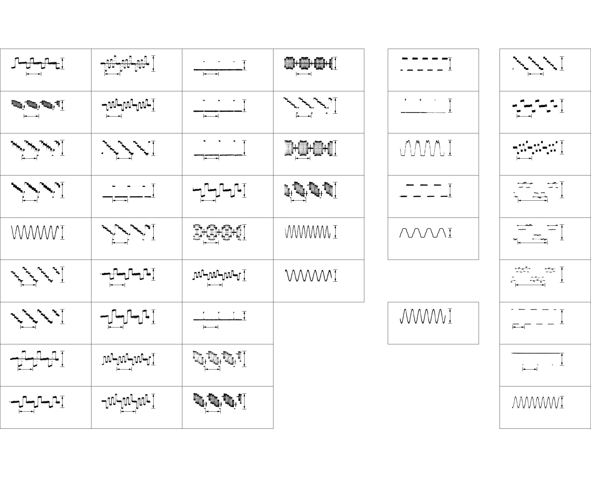
740 mVp-p
Q401 B REC/PB
740 mVp-p
t;
IC129 1 REC
H
H
1.1 Vp-p
rg
Q331 B REC
1.0 Vp-p
rh
H
IC332 qk REC
1.7 Vp-p
rj
IC332 qj REC
rk
IC332 ea REC/PB
2.8 Vp-p
rl
H
H
H
3.58 MHz (NTSC)
4.43 MHz (PAL)
H
3.0 Vp-p
IC500 y; REC/PB
900 Hz
150 Hz
3.0 Vp-p
1
IC500 4 REC/PB
2.9 Vp-p
2
900 Hz
IC501 2, qk, wd REC/PB
2.1 Vp-p
3
IC400 wf REC/PB
4
IC400 5, 7, 9 REC/PB
5
18 Hz (DVCAM)
12 Hz (DV)
1.62 kHz (DVCAM)
1.08 kHz (DV)
Q414 6 REC/PB
520 mVp-p
ta
Q402 B REC/PB
680 mVp-p
(NTSC)
790 mVp-p
(PAL)
ts
H
Q419 6 REC/PB
420 mVp-p
td
2.8 Vp-p
IC414 3 REC/PB
440 mVp-p
tl
Q403 B REC/PB
H
H
720 mVp-p
tf
Q420 6 REC/PB
450 mVp-p
tg
H
IC410 2 REC/PB
500 mVp-p
th
IC410 6 REC/PB
tj
IC422 qa, qd REC/PB
1.6 Vp-p
tk
H
H
H
H
H
IC423 qd REC/PB
1.4 Vp-p
(NTSC)
1.1 Vp-p
(PAL)
y;
IC415 3 REC/PB
460 mVp-p
ya
H
IC424 qd REC/PB
1.5 Vp-p
(NTSC)
1.0 Vp-p
(PAL)
ys
540 mVp-p
IC413 1 REC/PB
400 mVp-p
yk
Q405 5 REC/PB
H
H
2.2 Vp-p
yd
Q404 5 REC/PB
1.4 Vp-p
yf
H
Q410 3 REC/PB
730 mVp-p
yg
IC413 wf REC/PB
yh
IC413 qk REC/PB
800 mVp-p
yj
H
H
H
H
H
1.9 Vp-p
IC709 ts REC/PB
2.5 Vp-p
uj
IC426 qd REC/PB
H
H
1.2 Vp-p
us
Q418 2 REC/PB
780 mVp-p
ud
H
Q421 B REC/PB
600 mVp-p
uf
IC418 qa, qd REC/PB
ug
IC709 ra REC/PB
1.2 Vp-p
uh
32.768 kHz
20 MHz
H
IC413 3 REC/PB
1.0 Vp-p
yl
13.5 MHz
IC404 3 REC/PB
3.1 Vp-p
1
IC420 1 REC/PB
1.0 Vp-p
u;
H
IC425 qd REC/PB
1.9 Vp-p
ua
5.6 Vp-p
IC8001 wf REC/PB
6.9 Vp-p
6
IC8001 8 REC/PB
H
H
270 mVp-p
1
IC8001 9 REC/PB
250 mVp-p
2
H
IC8001 0 REC/PB
260 mVp-p
3
IC8001 w; REC/PB
4
IC8001 ws REC/PB
5.7 Vp-p
5
2H
2H
V
2H
2H
IC8001 ej REC/PB
4.8 Vp-p
7
IC8201 w; REC/PB
2.7 Vp-p
8
18 MHz
IC8201 ef REC/PB
2.5 Vp-p
9
420 mVp-p
(DVCAM)
330 mVp-p
(DV)
VD-28 BOARD (2/2) PD-125 BOARD
4-151 4-152
CM-59 BOARD
FR-157 BOARD
4-153
4-4. PARTS LOCATION
RP-234 BOARD
(SIDE A)
CN101 B-5
CN201 A-5
CN202 B-2
CN203 B-4
IC101 B-5
IC102 B-4
RP-234 BOARD
(SIDE B)
IC201 A-4
IC301 B-2
Q201 B-3
Q202 B-4
Q203 B-5
JC-20 BOARD
(SIDE B)
CN1100 B-1
CN4400 D-1
CN6002 A-7
CN8001 D-8
D2201 C-7
D5001 C-4
IC1102 C-11
IC1103 C-11
IC1104 C-12
IC1108 A-9
IC1109 B-9
IC1110 D-9
IC2200 C-8
IC2202 C-5
IC2203 D-5
IC2204 B-7
IC2209 C-9
IC2214 C-9
IC2215 B-9
IC5001 C-4
IC5002 D-5
IC5007 D-4
IC5008 D-6
IC6001 B-6
IC6003 A-4
IC6004 A-6
Q1117 A-11
Q1118 B-12
Q1119 C-12
Q1120 A-11
Q1121 B-11
Q1122 B-11
Q1123 A-10
Q1124 B-11
Q1125 C-11
Q1126 A-10
Q1127 B-10
Q1128 C-11
Q2202 A-9
Q2203 D-6
Q5001 C-4
Q5002 C-4
Q6003 A-4
Q6004 A-4
Q6005 A-4
DI-73 BOARD
(SIDE A)
CN9500 A-5
IC8000 D-7
IC8001 D-7
IC8002 D-7
IC8003 D-9
IC8004 B-8
IC8005 B-8
IC8006 B-9
IC8007 A-9
IC8008 B-8
IC8009 C-11
IC8010 B-7
IC8011 B-7
IC8201 B-10
IC9000 C-2
IC9001 B-1
IC9005 D-4
IC9007 B-2
IC9008 C-4
IC9009 D-4
IC9010 B-3
IC9017 D-1
IC9018 D-1
IC9019 D-3
IC9504 C-5
IC9507 D-5
IC9508 D-5
IC9514 D-6
IC9515 D-6
IC9517 C-5
IC9518 D-5
IC9519 D-5
Q8000 B-9
Q8001 C-7
Q8201 C-9
Q8202 C-8
Q9000 B-1
Q9001 B-1
Q9002 B-2
Q9003 B-2
Q9004 B-3
Q9005 B-3
DI-73 BOARD
(SIDE B)
D7301 D-9
D7302 D-7
IC7000 A-9
IC7001 A-7
IC7002 A-9
IC7003 A-7
IC7004 B-9
IC7005 B-9
IC7006 B-7
IC7007 B-8
IC7008 C-9
IC7009 C-8
IC7010 C-9
IC7011 C-8
IC7013 C-9
IC7014 D-8
IC7016 D-9
IC7018 D-8
IC7020 C-6
IC7021 D-6
IC9004 D-1
IC9006 D-1
IC9011 A-4
IC9012 D-4
IC9013 D-2
IC9014 D-4
IC9015 B-4
IC9016 C-4
IC9500 D-3
IC9501 D-3
IC9502 D-4
IC9503 D-4
IC9505 D-4
IC9506 D-5
IC9509 D-5
IC9510 D-6
IC9511 D-6
IC9512 C-5
IC9513 C-6
IC9516 C-6
Q7000 B-8
Q7001 B-9
Q7002 B-9
Q7003 B-7
Q7004 B-6
Q7005 B-5
Q7007 D-7
Q7008 D-7
Q9502 C-5
JC-20 BOARD
(SIDE A)
CN1101 B-11
CN4401 D-6
CN4402 D-5
CN5005 D-10
CN6001 A-8
CN7001 B-4
CN7002 A-3
D4400 B-6
IC1000 D-12
IC1001 C-12
IC1002 C-12
IC1100 D-5
IC1101 D-10
IC1105 A-9
IC1106 B-10
IC1107 C-10
IC1111 A-11
IC1112 B-12
IC1113 B-2
IC2208 C-9
IC2210 D-9
IC2211 D-9
IC2212 D-9
IC2213 D-9
IC3300 B-8
IC3301 D-9
IC3302 D-8
IC3303 B-6
IC4400 B-5
IC4401 D-4
IC4402 D-2
IC5003 D-6
IC5006 D-8
Q1100 D-11
Q1101 B-11
Q1103 D-11
Q1104 B-11
Q1109 C-11
Q1111 D-11
Q1112 C-11
Q1114 C-11
Q1116 D-10
Q1129 A-11
Q1130 A-11
Q1131 B-3
Q1132 B-3
Q2200 C-8
Q2201 C-7
Q3300 B-9
Q3301 B-9
Q3302 B-9
Q6011 C-5
Q6012 C-5
4-154
VD-28 BOARD
(SIDE A)
CN101 A-6
CN332 G-5
CN401 A-8
CN601 C-4
CN602 B-4
CN606 C-5
CN702 D-8
CN703 E-8
D105 E-7
D106 F-6
D401 A-8
D402 G-6
D403 G-6
D404 F-6
D601 A-4
D602 A-4
D603 A-4
D604 B-4
D605 B-4
D606 A-4
D712 D-8
D713 D-8
D716 G-10
D717 G-10
D901 E-3
D902 E-3
D903 F-3
D904 D-3
D905 C-2
D906 F-3
D907 C-1
D910 B-1
D911 B-1
D912 C-1
D913 C-1
D915 F-2
D916 F-2
D917 G-3
D918 G-3
IC001 F-8
IC002 G-8
IC003 B-9
IC004 B-9
IC005 A-10
IC007 G-8
IC008 B-9
IC009 G-7
IC012 B-9
IC013 G-7
IC014 B-10
IC016 B-9
IC017 G-7
IC018 B-10
IC019 B-10
IC020 B-10
IC021 B-9
IC022 B-10
IC023 C-10
IC024 D-9
IC025 C-10
IC026 C-10
IC027 C-9
IC028 C-10
IC029 C-10
IC030 C-10
IC031 D-9
IC032 D-10
IC033 C-10
IC034 D-10
IC035 D-9
IC037 D-10
IC039 D-10
IC042 D-10
IC043 D-9
IC044 D-10
IC046 C-8
IC047 C-8
IC048 C-8
IC049 B-8
IC050 A-10
IC051 B-10
IC052 A-10
IC054 B-10
IC056 A-10
IC106 D-6
IC112 D-6
IC120 F-6
IC121 F-5
IC124 E-6
IC132 D-7
IC134 B-6
IC332 E-7
IC335 E-8
IC336 E-8
IC412 B-8
IC414 G-6
IC415 H-6
IC421 B-8
IC426 A-7
IC606 A-4
IC607 A-4
IC704 G-9
IC706 E-8
IC707 E-9
IC708 D-8
IC709 F-9
IC712 G-10
IC713 G-9
IC900 E-1
IC902 G-1
IC908 B-2
IC909 C-1
Q111 A-7
Q112 A-7
Q116 B-7
Q120 B-7
Q148 C-7
Q150 C-7
Q151 C-7
Q152 C-7
Q156 C-6
Q157 C-6
Q160 B-6
Q335 E-7
Q337 E-7
Q338 E-7
Q401 G-4
Q413 F-6
Q414 G-6
Q415 G-6
Q416 G-6
Q419 G-6
Q420 H-6
Q422 G-6
Q423 G-6
Q428 A-8
Q429 B-8
Q430 B-7
Q432 B-7
Q437 H-5
Q438 G-5
Q605 C-4
Q607 B-4
Q708 G-10
Q709 G-9
Q906 B-1
Q907 E-1
Q908 E-1
Q909 D-2
Q910 F-2
Q911 D-2
Q912 F-2
Q913 C-1
Q914 D-2
Q915 E-2
Q916 F-2
Q917 D-2
Q918 B-1
Q919 B-2
Q920 D-2
Q921 F-3
Q922 D-4
Q924 C-2
Q925 B-2
Q926 F-1
Q927 F-1
Q928 D-1
Q929 G-2
Q930 B-1
Q931 C-2
Q932 B-1
Q933 G-2
Q935 G-1
Q936 G-1
CM-59 BOARD
(SIDE A)
CN001 A-5
CN200 A-2
CN201 A-1
CN300 A-4
CN400 A-2
CN500 A-3
CN501 A-4
IC100 B-4
IC102 A-6
IC202 B-2
IC300 A-4
IC501 A-3
Q201 A-2
CM-59 BOARD
(SIDE B)
CN100 A-6
D101 B-5
D102 B-4
D103 B-5
D104 B-5
IC101 A-5
IC200 B-1
IC500 B-3
Q100 B-5
Q101 B-4
Q102 B-5
Q103 B-5
Q104 B-4
Q105 B-4
Q200 B-2
Q301 A-3
Q302 A-3
VD-28 BOARD (SIDE B)
CN102 A-7
CN331 G-9
CN333 H-9
CN603 A-4
CN604 A-3
CN605 C-4
CN607 A-10
CN701 F-10
CN704 C-10
CN705 G-10
CN706 H-1
CN900 A-1
CN901 B-1
CN902 A-1
CN903 A-2
CN904 C-3
CN905 C-3
D003 F-4
D005 C-9
D101 A-6
D102 A-6
D103 A-6
D107 E-7
D108 D-6
D110 A-6
D331 G-8
D332 G-9
D333 G-8
D334 G-8
D335 G-9
D336 G-9
D337 G-9
D338 G-8
D339 G-9
D701 H-8
D702 H-8
D709 G-9
D710 E-9
D714 H-9
D908 B-1
D909 B-1
D914 C-1
D919 D-1
D920 D-1
D921 E-3
D922 E-3
D923 F-2
D924 G-3
D925 G-3
D926 D-1
D927 E-3
D928 G-3
D929 F-2
D930 E-3
D931 F-3
D932 F-2
IC040 D-9
IC041 F-4
IC055 D-8
IC057 B-9
IC058 B-9
IC059 B-9
IC060 C-9
IC061 F-8
IC062 B-9
IC063 B-9
IC101 A-5
IC102 A-6
IC103 A-6
IC104 B-7
IC105 B-5
IC107 D-5
IC108 B-5
IC109 B-6
IC110 C-5
IC113 B-5
IC115 D-4
IC116 E-4
IC117 E-6
IC118 E-5
IC119 C-7
IC122 F-6
IC125 E-4
IC126 F-4
IC127 F-6
IC128 F-6
IC129 F-5
IC130 F-6
IC131 C-6
IC133 B-6
IC333 E-7
IC334 E-7
IC402 G-5
IC403 H-5
IC404 C-8
IC405 C-8
IC410 G-6
IC411 B-9
IC413 B-8
IC416 F-6
IC417 B-7
IC418 A-7
IC419 C-7
IC420 A-9
IC422 A-7
IC423 B-8
IC424 C-8
IC425 A-8
IC427 G-5
IC428 G-6
IC601 C-4
IC602 C-4
IC603 B-4
IC604 B-4
IC605 A-4
IC701 D-8
IC702 D-9
IC705 G-9
IC710 D-8
IC901 F-3
Q001 A-9
Q002 B-9
Q003 A-8
Q004 D-9
Q005 D-9
Q006 D-9
Q101 D-5
Q102 D-5
Q103 D-5
Q104 D-5
Q105 A-7
Q106 D-5
Q109 D-5
Q110 B-6
Q115 D-5
Q121 B-7
Q124 D-6
Q125 D-5
Q126 E-6
Q127 E-5
Q128 E-4
Q129 E-6
Q130 E-5
Q131 E-6
Q132 E-6
Q133 E-4
Q134 F-6
Q135 F-5
Q136 E-5
Q137 F-5
Q138 F-5
Q139 E-6
Q141 E-6
Q142 E-5
Q143 E-6
Q144 F-5
Q145 F-5
Q149 F-4
Q153 C-6
Q158 D-5
Q159 B-6
Q331 D-7
Q332 D-8
Q333 E-7
Q334 E-7
Q402 G-4
Q403 H-4
Q404 C-8
Q405 C-7
Q406 C-8
Q407 C-9
Q408 C-8
Q409 F-6
Q410 C-8
Q411 G-6
Q412 G-6
Q417 C-8
Q418 C-7
Q421 B-7
Q424 B-7
Q425 G-7
Q426 G-7
Q427 G-7
Q431 A-8
Q434 G-5
Q435 G-5
Q436 H-4
Q439 B-7
Q601 C-4
Q602 C-4
Q603 C-4
Q604 C-4
Q606 B-4
Q701 E-8
Q702 E-9
Q705 D-8
Q706 D-8
Q707 D-8
Q900 C-1
Q901 C-1
Q903 B-2
Q905 B-2
Q923 B-1
Q934 C-1
Q937 C-1
Q938 E-1
Q939 G-1
Q940 B-1
Q941 B-1
Q942 C-2
Q943 C-2
4-155
MD-76 BOARD
(SIDE A)
CN001 A-1
CN002 A-2
CN003 G-6
IC001 D-5
IC002 D-5
IC003 C-5
FR-157 BOARD
(SIDE A)
CN503 A-9
D402 C-5
D403 B-5
D503 A-9
D504 B-9
D505 B-9
D506 B-9
D507 B-8
D508 B-8
D509 B-9
D510 C-9
D511 C-8
D512 C-8
D513 C-9
D514 C-9
D518 C-8
D519 C-8
D520 C-9
D521 C-9
D522 A-1
D523 C-8
D524 C-8
D525 C-9
D526 C-9
D527 C-7
D528 C-9
D530 A-8
D531 B-7
D532 A-8
D533 C-7
D534 B-4
D536 C-4
D538 C-1
D539 C-1
D540 C-1
D541 C-1
D552 C-1
D553 C-1
D554 C-1
D555 C-1
IC402 C-6
IC404 C-6
IC502 B-8
Q502 B-8
Q503 B-8
Q504 B-9
Q505 C-9
Q506 C-8
Q507 C-8
Q508 C-9
Q509 C-9
Q513 A-9
Q514 A-8
FR-157 BOARD
(SIDE B)
CN501 A-9
CN502 C-3
CN504 C-2
CN505 A-1
D401 C-7
D515 A-8
D516 A-9
D517 A-9
D535 B-6
D537 C-6
D542 A-8
D543 A-8
D544 A-8
D545 B-8
D546 A-8
D547 A-8
D548 B-8
D549 B-8
D550 A-1
D551 C-8
IC401 C-5
IC403 C-6
IC501 B-9
IC504 D-9
IC505 D-9
Q501 B-9
Q510 A-8
Q511 A-9
Q512 A-9
Q515 D-9
JK-169 BOARD
(SIDE A)
CN101 C-1
CN103 C-4
CN104 C-6
CN105 C-8
IC101 B-5
IC102 C-5
IC103 C-5
IC104 A-5
IC105 C-5
PD-125 BOARD
CN8001 A-1
CN8002 C-1
CN8200 C-2
CN8201 A-3
D8100 D-3
D8200 C-1
D8202 C-2
IC8001 A-2
IC8200 C-3
IC8201 B-2
IC8202 C-1
Q8000 B-1
Q8001 B-1
Q8003 B-2
Q8007 B-3
Q8009 B-3
Q8010 B-3
Q8011 A-3
Q8100 D-4
Q8101 A-3
Q8102 A-3
Q8204 D-3
JK-169 BOARD (SIDE B)
CN102 C-9
CN106 B-5
CN107 B-6
CN108 B-7
CN109 B-8
D101 B-1
D103 C-1
D104 B-1
D105 B-2
D106 B-2
D107 B-2
D108 B-3
D109 B-3
D110 B-4
D111 C-3
D112 A-4
D113 C-3
D114 A-3
D115 C-4
D116 B-4
D117 C-3
D118 C-4
D119 A-4
D120 C-2
D121 A-4
D122 C-9
D123 C-9
D124 A-5
D125 A-6
D126 A-6
D127 A-7
D134 A-7
D135 A-8
D136 A-7
D137 A-8
D144 A-3
D145 C-1
D146 C-1
IC107 A-4
IC108 C-8
IC109 C-9
IC110 A-5
IC111 A-6
IC112 C-8
IC113 A-7
IC114 A-8
IC115 C-3
Q101 A-5
Q102 A-6
Q103 A-7
Q104 A-8
Q105 A-5
Q106 A-6
Q107 A-7
Q108 A-8
Q109 C-3
Q110 C-3
MD-76 BOARD
(SIDE B)
D001 D-11
IC004 F-12
IC005 F-10
Q001 C-8
Q002 C-14

4-156
HP-117 BOARD
(SIDE A)
CN301 B-1
D309 A-2
IC302 B-2
Q302 A-1
Q303 A-1
HP-117 BOARD
(SIDE B)
D301 A-1
D302 A-1
D303 A-1
D304 A-2
D305 A-2
D306 B-3
D307 B-3
D308 B-3
IC301 A-2
IC303 B-1
IC304 B-1
IC305 B-2
Q301 B-2
Q304 B-3
Q305 B-3
Q306 B-1
Q307 A-1
4-156 E
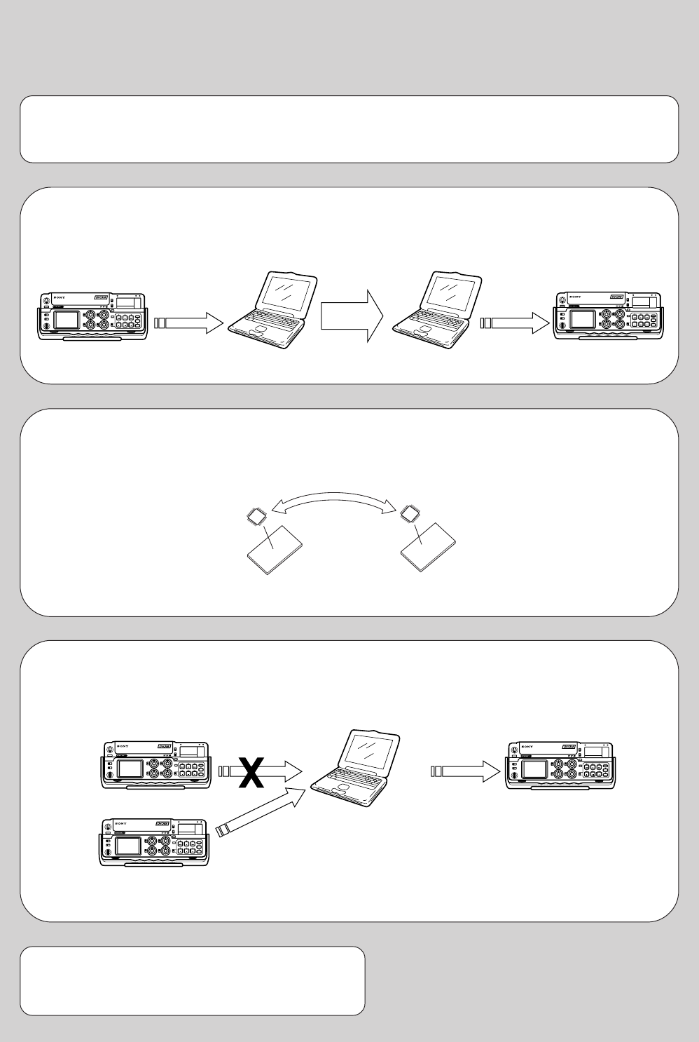
5-1
DSR-50/50P
SECTION 5
ADJUSTMENTS
1. Before starting adjustment
EVR Data Re-writing Procedure When Replacing Board
The data that is stored in the repair board, is not necessarily correct.
Perform either procedure 1 or procedure 2 or procedure 3 when replacing board.
Procedure 1
Save the EVR data of the machine in which a board is going to be replaced. Download the saved data after a
board is replaced.
Remove the EEPROM and install it.
(Former board) (New board)
Procedure 2
Remove the EEPROM from the board of the machine that is going to be repaired. Install the removed
EEPROM to the replaced board.
Procedure 3
When the data cannot be saved due to defective EEPROM, or when the EEPROM cannot be removed or
installed, save the data from the same model of the same destination, and download it.
After the EVR data is saved and downloaded, check the
respective items of the EVR data.
(Refer to page 5-3 for the items to be checked)
(Machine before starting repair) (Machine after a board is replaced)
PC PC
Save the EVR data
to a personal computer.
Download the saved
data to a machine.
(Machine to be repaired) (Machine to be repaired)
(The same model of the same destination)
Save the data.
Download the data.
PC
5-2
1-1. Adjusting items when replacing main parts and boards
• Adjusting items when replacing main parts
When replacing main parts, adjust the items indicated by z in the following table.
Replaced part
Block replacement Mounted part replacement
Adjustment Section Adjustment
(Drum assembly)
(Capstan motor)
(LCD panel)
(Fluorescent tube)
(TRW)
(TRF)
(A/D CONV.)
(CLOCK GEN.)
(VFD)
(D/A CONV.)
(VC AMP)
(Y/C SEP.)
(C DECODE)
(VC DELAY)
(VC AMP)
(VC AMP)
(Y BLANKING, SETUP ADD)
(VC AMP)
(C ENCODE)
(VC AMP)
(RGB DRIVER)
(TIMING GEN.)
Mechanism deck
Mechanism deck M901
Mechanism deck M903
LCD block LCD901
LCD block ND901
PR-234 board IC101
RP-234 board IC201
JC-20 board IC1108-1110
JC-20 board IC2204
JC-20 board IC3300
DI-73 board IC9000
VD-28 board IC116, 122
VD-28 board IC119
VD-28 board IC124
VD-28 board IC402, 403
VD-28 board IC404
VD-28 board IC405
VD-28 board IC410
VD-28 board IC411
VD-28 board IC413
VD-28 board IC427, 428
PD-125 board IC8001
PD-125 board IC8201
System control Initialization of C, D, E page data
Node unique ID No. input
Servo, RF CAPSTAN FG adj. zz
Switching position adj. zz
RF-AGC adj. zz zz
CLK DELAY and AEQ adj. zz zz
PLL f
0
adj. zz zz
Video VFD SPCK adj. z
A/D converter reference voltage adj. z
Y/CR/CB clamp reference voltageadj. z
AFC picture frame adj. z
AFC adj. z
Playback Y/C level adj. z
Playback SYNC level adj. z
Playback blanking level adj. with 0% setup z
Playback Y/CR/CB signal level adj. with 0% setup z zzz
Playback CR/CB signal delay adj. zz
Encoder free run adj.
Carrier balance adj. zz
Burst level adj. zz
Color level adj. with 0% setup zz
SC_V phase adj.
Playback blanking level adj. with 7.5% setup (*1) z
Playback Y/CR/CB signal level adj. with 7.5% setup (*1) zz
Color level adj. with 7.5% setup (*1) zz
Monitor terminal output level adj. z
E-E blanking level adj. z
Component E-E Y/CR/CB signal level adj. zzzzz
Component E-E CR/CB signal delay adj. z
E-E color level adj. zzz
Decoder free run adj. z
Decoder HUE adj. z
S video E-E Y/CR/CB signal level adj. zz
S video E-E CR/CB signal delay adj. z
Composite E-E Y signal level adj.
Composite E-E CR/CB signal delay adj.
H phase adj.
E-E SC phase adj.
Playback SC phase adj.
LCD VCO adj. zz
Black limit adj. z
Bright adj. z
Gamma 1 adj. z
Contrast adj. z
Center voltage adj. zz
White balance adj. zz z
Audio Audio PAL data input (*2)
Mechanism Tape path adj. zzz
5-3
• Adjusting items when replacing a board or EEPROM
When replacing a board or EEPROM, adjust the items indicated by z in the following table.
Note:
*1: DSR-50 only
*2: DSR-50P only
Replaced part
Board replcement
Adjustment Section Adjustment
(COMPLETE)
(COMPLETE)
(COMPLETE)
(COMPLETE)
(COMPLETE)
(COMPLETE)
(EEP ORM)
(EEP ROM)
CM-59 board
RP-234 board
JC-20 board
DI-73 board
VD-28 board
PD-125 board
JC-20 board IC5006
VD-28 board IC706
System control Initialization of C, D, E page data zzzz
Node unique ID No. input zz
Servo, RF CAPSTAN FG adj. zz z
Switching position adj. zz z
RF-AGC adj. zz z
CLK DELAY and AEQ adj. zz z
PLL f
0
adj. zz z
Video VFD SPCK adj. zz
A/D converter reference voltage adj. zz
Y/CR/CB clamp reference voltageadj. zz
AFC picture frame adj. zz
AFC adj. zz
Playback Y/C level adj. zz
Playback SYNC level adj. zz
Playback blanking level adj. with 0% setup zz
Playback Y/CR/CB signal level adj. with 0% setup zz z
Playback CR/CB signal delay adj. zz
Encoder free run adj. zz
Carrier balance adj. zz
Burst level adj. zz
Color level adj. with 0% setup zz
SC_V phase adj. zz
Playback blanking level adj. with 7.5% setup (*1) zz
Playback Y/CR/CB signal level adj. with 7.5% setup (*1) zz
Color level adj. with 7.5% setup (*1) zz
Monitor terminal output level adj. zzz
E-E blanking level adj. zz
Component E-E Y/CR/CB signal level adj. zz
Component E-E CR/CB signal delay adj. zz
E-E color level adj. zz
Decoder free run adj. zz
Decoder HUE adj. zz
S video E-E Y/CR/CB signal level adj. zz
S video E-E CR/CB signal delay adj. zz
Composite E-E Y signal level adj. zz
Composite E-E CR/CB signal delay adj. zz
H phase adj. zz
E-E SC phase adj. zz
Playback SC phase adj. zz
LCD VCO adj. zz
Black limit adj. zz
Bright adj. zz
Gamma 1 adj. zz
Contrast adj. zz
Center voltage adj. zz
White balance adj. zz
Audio Audio PAL data inpit (*2) zz
Mechanism Tape path adj.
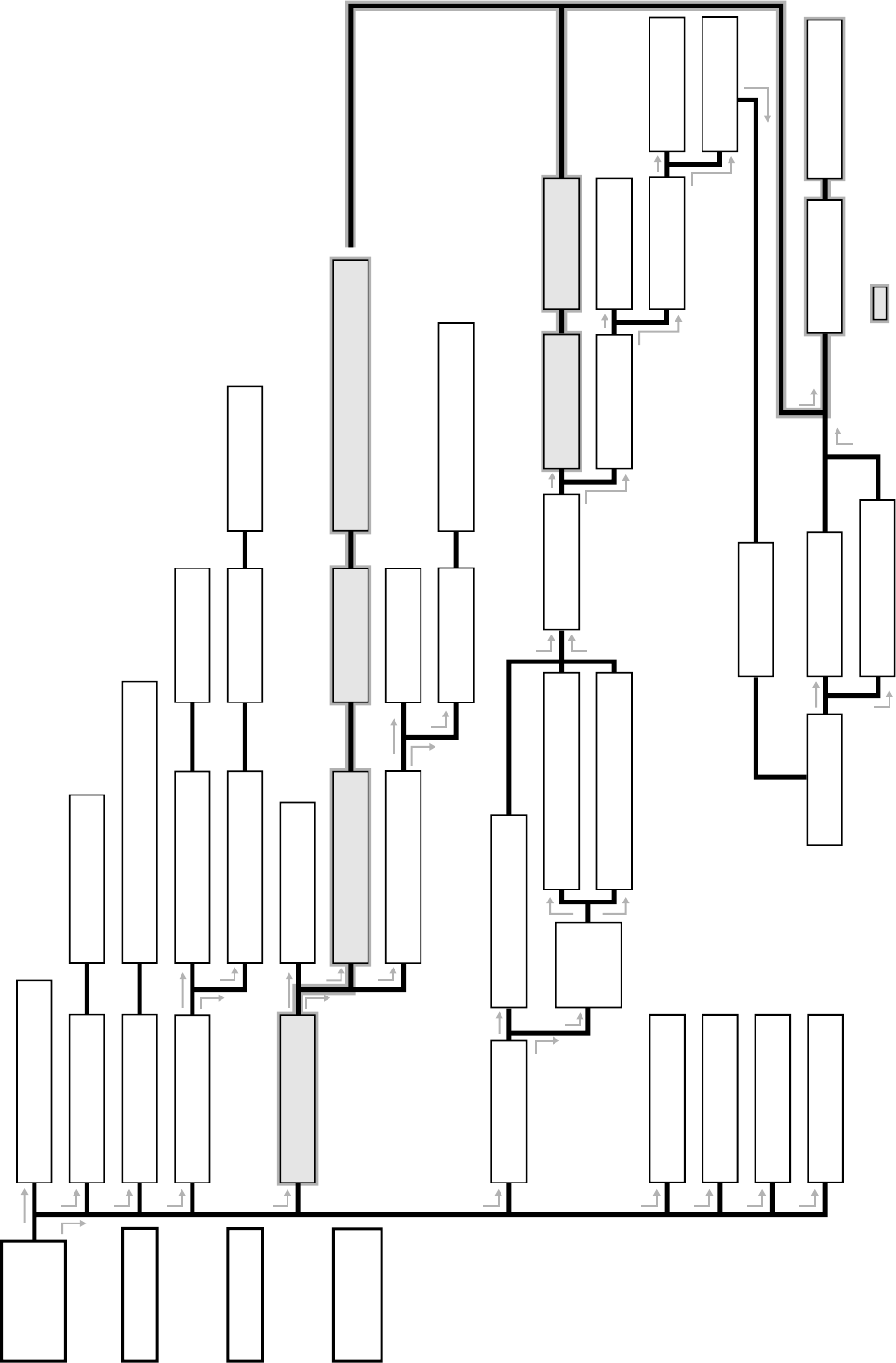
5-4
Tape guide 1
(Drawing numbers: 710 to 714)
Cassette
compartment
(Drawing numbers:
722, 851)
FL motor block
(Drawing numbers: M905, 853 to 856)
GL arm S/T block
(Drawing numbers: 810 to 817)
Coaster S/T Block
(Drawing numbers: 801 to 802)
MIC base guide
(Drawing numbers: 702)
MIC base assembly
(Drawing numbers: 701, 703, 723, 724, CN004, S004)
Drum cap
(Drawing numbers: 721)
Drum assembly
(Drawing numbers: M901)
Tape support
(Drawing numbers: 717)
Pinch arm assembly
(Drawing numbers: 718 to 720)
Capstan cover
(Drawing numbers: 819)
Capstan motor
(Drawing numbers: M903)
Tape guide 8
(Drawing numbers: 710 to 714)
Tape guide 2
(Drawing numbers: 776 to 780)
Tape guide 7
(Drawing numbers: 776 to 782)
Guide guard
(Drawing numbers: 715)
Capstan cover
(Drawing numbers: 819)
Reel motor
(Drawing numbers:
M904)
Pendulum retainer
(Drawing numbers: 705)
Pendulum
retainer
(Drawing
numbers: 705)
Pendulum arm assembly
(Drawing numbers: 706)
Brake arm S/Ratchet brake T
(Drawing numbers: 707, 708, 709)
SBR slider
(Drawing numbers: 757)
Cam motor
(Drawing numbers: M902)
Idler gear A/B
(Drawing numbers: 751, 752)
Motor holder block
(Drawing numbers: 763, 764, M902)
TG2 arm/TG2 band block
(Drawing numbers: 766, 768, 771 to 775)
TG7 arm/TG7 band block
(Drawing numbers: 767, 769, 770, 775)
Sub-slider arm
(Drawing numbers: 761)
Sub-slider
(Drawing numbers: 758)
Main cam gear
(Drawing numbers: 755)
Coupling gear
(Drawing numbers: 762)
Sub-cam gear
(Drawing numbers: 756)
Pinch slider
(Drawing numbers: 760)
Loading drive lever
(Drawing numbers: 759)
Main slider
(Drawing numbers: 820)
Brake arm S
(Drawing numbers: 708)
Main slider arm
(Drawing numbers: 803)
Encoder cover
(Drawing numbers: 818)
MD-76 board
(Drawing numbers: 824, etc.)
Pendulum stopper assembly
(Drawing numbers: 805)
Encoder gear
(Drawing numbers: 754)
Reel table S/T
(Drawing numbers: 753)
Reel base retainer
(Drawing numbers: 829)
Reel base S/T block
(Drawing numbers: 822, 823, 827, 828)
FP-248 flexible board (condensation sensor)
(Drawing numbers: 821)
Page 5-5
Page 5-10
Page 5-11
Page 5-12
Page 5-12
Page 5-13
Page 5-14 Page 5-14 Page 5-14
Page 5-12
Page 5-13
Page 5-13
Page 5-14
Page 5-15
Page 5-16 Page 5-17
Page 5-17 Page 5-17
Page 5-17
Page 5-14
Page 5-19 Page 5-19 Page 5-20 Page 5-20
Page 5-19
Page 5-17
Page 5-17
Page 5-17 Page 5-17
Page 5-16
Page 5-13
Page 5-15
Page 5-9
Page 5-9
Page 5-9
Page 5-9
Page 5-14
Page 5-15 Page 5-15
Page 5-10 Page 5-13
Page 5-12
Page 5-21
Page 5-11
Page 5-9
Page 5-10
Page 5-10
Note: When removing the MD-76 board, all the parts in the shaded
boxes ( ) of the chart need to be removed.
Find the replacement parts in Section 6, “Repair parts list (ex-
ploded views)” and attach or remove the parts in the following
order. When replacing and re-attaching the parts, adjustments are
sometimes required. Follow the instructions of each item.
Note: Drawing numbers in each box of the chart refer to the
numbers assigned to each part in the exploded views of
Section 6, “Repair parts list”.
1-2. Information (Mechanical Section)
START
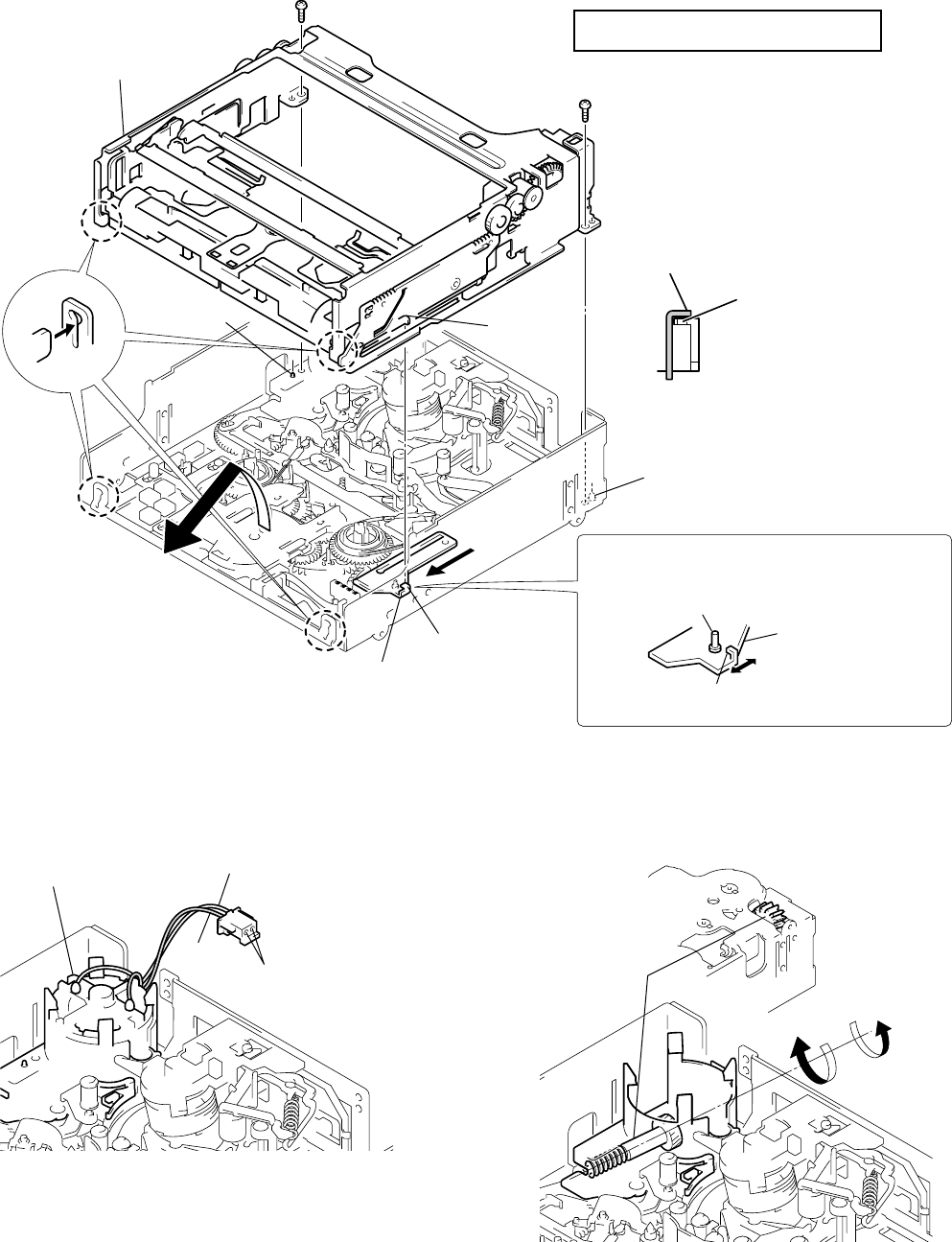
5-5
1-1. ASSEMBLY/DISASSEMBLY OF CASSETTE COMPARTMENT
For details on disassembling the mechanism deck (R mechanism), refer to the Service Manual of the main unit in which the R mechanism
is mounted.
Before attaching or removing the cassette compartment, check the position of “L cassette”.
1-2. HOW TO LOAD/UNLOAD
[Using the regulated power supply]
Note: Make sure to remove the connector of the cam motor from
the board of the main unit and apply +5V current.
[Manual: No cam motor]
Note: Remove the cam motor from the motor holder while referring
to “Information” on page 5-4.
5-1. MECHANICAL SECTION ADJUSTMENTS
5-1-1. PARTS REPLACEMENT AND PREPARATION FOR ADJUSTMENT
When attaching the cassette compartment,
move the reel selector slider in the direction of
arrow Bto check the position of “L cassette”.
Bent portion C
Positioning pin
Bent portion C
SL shifter
Screw
Screw
Positioning pin
Cassette compartment
(Remove in the
direction of arrow A.)
SL shifter
Bent portion C of the reel
selector slider should be
securely hooked on the
bent portion of the SL
shifter.
A
B
Tightening torque of cassette compartment
0.3432 ± 0.0196N • m (3.5 ± 0.2 kg • cm)
Select the desired cassette position by pressing
the claw position.
Reel select slider
Do not touch the slider drive shaft.
When selecting a cassette position, be careful not to
touch the slider drive shaft because it can be easily
bent or broken.
Cam motor
Gray
White
Apply current from
the inlets of the connector.
Loading : Apply positive polarity (+) of power supply to the gray wire
and negative polarity (–) of power supply to the white wire.
Unloading : Apply negative polarity (–) of power supply to the gray wire
and positive polarity (+) of power supply to the white wire.
[Rear side of chassis]
Unloading
Loading
Coupling gear
Rotate the coupling gear by hand to load or unload.
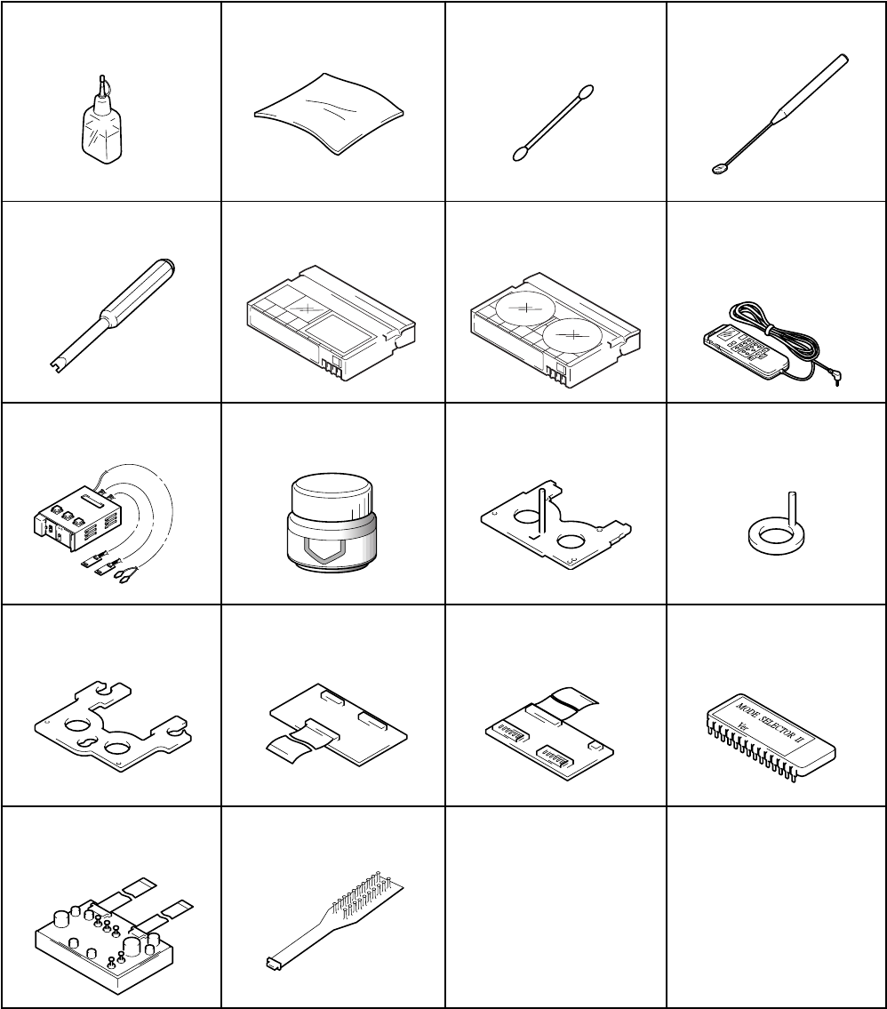
5-6
1-3. LIST OF SERVICE TOOLS
J-1. Cleaning fluid
(9-919-573-01) J-2. Wiping cloth
(7-741-900-53) J-3. Super fine applicator
(Made by NIPPON
APPLICATOR (P752D))
(J-2501-023-A)
J-4. Mirror (Small oval type)
(J-6080-840-A)
J-5. Screwdriver for tape path
(J-6082-026-A) J-6. Tracking tape (XH2-1A1)
(8-967-999-03)
J-9. Mode selector II
(J-6082-282-B) J-10. Floil Grease (SG-941)
(7-622-001-39)
J-7. Mini DV torque cassette
(J-6082-360-A) J-8. Adjusting remote
commander (RM-95)
(remodeled partly) Note 1
(J-6082-053-B)
J-11. Cassette reference plate
(J-6082-330-A) J-12. Reel reference plate
(J-6082-331-A)
J-13. TG 2/7 preset plate
(J-6082-459-A) J-14. Relay board for tension
regulator adjustment
(J-6082-461-A)
J-15. Mode selector
conversion board
(J-6082-460-A)
J-16. ROM for Mode Selector
(Cope with R mechanism:
Note 2)
(J-6082-314-E)
J-17. Board for tension
regulator adjustment
(J-6082-359-A)
J-18. CPC-8 jig
(J-6082-388-A)
Note 1: If the micro processor IC in the adjustment remote
commander is not the new micro processor (UPD7503G-
C56-12), the pages cannot be switched. In this case,
replace with the new micro processor (8-759-148-35).
Note 2: The ROM makes mode selector II’s version up to use it
with R mechanism.
Ver. 1.1 2001. 05
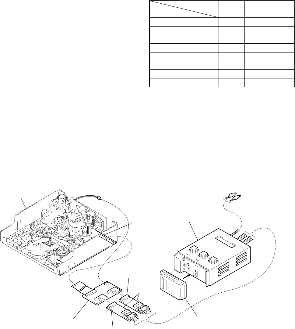
5-7
1-4. About Mode Selector II
• About Mode Selector II
4-1. OUTLINE
This unit is a mechanism drive tool which supplements the main-
tenance of each mechanism deck. Its functions are described below.
1. Manual test
A mode which drives the motor only while the switch is ON. It
enables the operator to control the motor as desired.
2. Step test
A mode which drives the motor until the current condition de-
tected by the sensor changes to another condition. It enables the
movements made by the motor in each operation to be controlled
while being detected.
3. Auto test
A mode that checks if the mechanism operates normally accord-
ing to the condition shift table recorded in the unit for each mecha-
nism deck. All the conditions of the decks are checked through a
series of operations.
An error message is displayed and operations are stopped if incor-
rect shifts and conditions are detected.
4-3. MODE SELECTOR II CONNECTION
4-2. MECHANISM CONDITION (POSITION)
SHIFTING ORDER LIST
After selecting the mechanism deck, select one of the two test
modes other than the auto test, and press the RVS or FF button to
specify the mechanism state (position).
R mechanism
CN2
Connector (white) 6P
Mode selector II
Alligator clip
Battery of NP-55, 77, etc. (power supply)
Connector (black) 6P
Relay boards
Mode selector conversion board (R)
Connector from the cam motor
A
Code
1
1
1
1
1
0
0
D
MD name R mechanism
1
0
0
1
1
1
1
FWD / RVS
STOP
FF
REW
LE
DEW
ULE
7
6
5
4
3
2
1
C
0
1
1
0
1
1
1
B
1
1
0
0
0
0
1
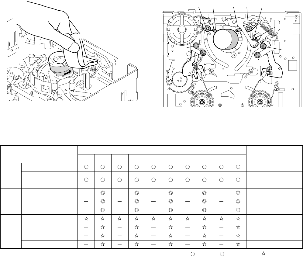
5-8
5-1-2. PERIODIC CHECK
• Carry out the following maintenance and periodic checks not only to fully display the functions and performance of the set, but also for
the equipment and tape. After replacing, service the set as follows, regardless of the length of use.
2-1. CLEANING OF ROTARY DRUM ASSEMBLY
1. Press a wiping cloth (J-2) moistened with cleaning fluid (J-1)
against the rotary drum assembly gently, and clean it while
rotating the rotary drum assembly slowly with your finger in
the counterclockwise direction.
Note: Do not rotate the motor on power or rotate the rotary drum
assembly in the clockwise direction with your finger. The
head tip will also be damaged if the wiping cloth is moved
perpendicularly against it. Therefore, be sure to follow the
above instructions when cleaning the rotary drum assembly.
Note: When overhauling, refer to the checks above and replace
parts.
Note: Greasing
Always use the specified grease. If the viscosity differs,
various problems may occur.
(Use SG-941 for all parts of the R mechanism.)
Check the quantity of grease when installing the parts which
is needed to apply the grease. When replacing these parts,
make sure to apply the specified amount of grease.
• FOIL (SG-941): Part No. 7-662-601-39
2-3. PERIODIC CHECKS
2-2. CLEANING OF TAPE PATH SYSTEM
1. Clean the tape path systems (TG1 to TG8 and capstan) and the
lower drum using a super fine applicator (J-3) moistened with
cleaning fluid.
Note: Make sure that no oil or grease of the link mechanisms sticks
to the super file applicator (J-3).
Note: Do not use a applicator moistened with alcohol to the other
guide cleaning. But clean the pinch roller using alcohol.
Cleaning cloth
Rotary
drum assembly
TG 3 Pinch roller
Capstan
TG 8
TG 7
TG 6TG 5TG 4
TG 2
TG 1
Cleaning of tape path surface
Capstan (Bearing)
Cam motor (worm block)
Abnormal noise
Back tension measurement
Brake system
FWD/RVS torque measurement
Gear
Cleaning and degaussing
of rotary drum assembly
Make sure that no oil gets
on the tape path surface.
Be careful of the oil.
X-3946-702-1 (M902)
Be careful of the oil.
500 500045004000350030002500
Hours of Use (H)
Location of Maintenance
and Check Remarks
200015001000
Performance
Confirmation
Driving
System
: Cleaning
: Appling grease
: Confirmation
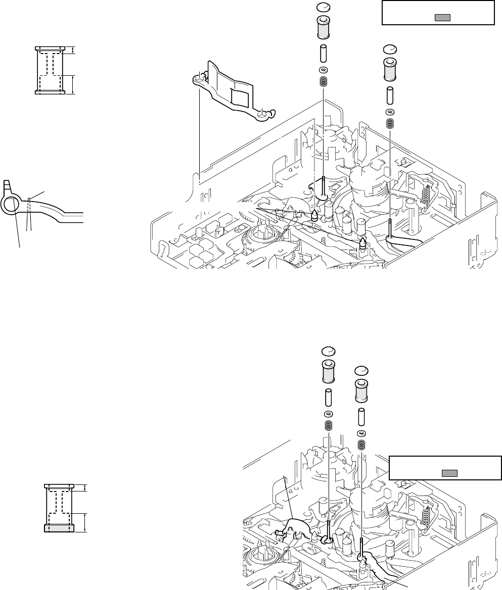
5-9
5-1-3. PARTS REPLACEMENT
• Precaution
For details on disassembling the cabinets, boards and other parts, refer to “Section 2, Disassembly”. For details on replacing parts
(disassembly, assembly) of the mechanism deck, refer to “Information” on page 5-4.
3-2. TAPE GUIDE 2/7
Disassembly/Assembly
When the tape guide 2/7 is replaced or attached, perform each
adjustment from Adjustment Start -3 of the flowchart on page 5-
23.
To attach or remove the tape guide, use the
screwdriver for the tape path (J-5). When
attaching the TG rollers, check the upward and
downward directions and that the TG roller to be
attached to the TG7 side is exclusively for the
TG7 side. Then attach the TG rollers to the
chassis shaft.
3-1. TAPE GUIDE 1/8 AND GUIDE GUARD
Disassembly/Assembly
When the tape guide 1/8 is replaced or attached, perform each
adjustment from Adjustment Start -2 of the flowchart on page 5-
23.
To attach or remove the tape guide, use the
screwdriver for the tape path (J-5). When
attaching the TG rollers, check the upward and
downward directions and attach them to the
chassis shaft.
The guide guard is fixed at each slit of the
cassette positioning shaft. To attach the guide
guard, only insert it into the right and left holes.
To remove it, use a pair of tweezers as shown in
the figure below.
[TG2 side]
TG upper flange
TG roller
TG sleeve
TG sleeve
TG ring
TG ring
Compression coil
spring (TG)
Compression coil spring (TG)
TG2 arm block
[TG7 side]
TG upper flange
TG7 roller (Note that the shape is
different from that of the other rollers.)
Be careful not to touch the
tape guide ( part).
TG7 arm block
Face the side of the deepest
hole downward and insert the
roller into the shaft.
The lower flange of the TG7
roller is thicker than those of
the TG1, 2, and 8 rollers.
TG7 roller
[TG1 side]
(The components are the
same as on the TG8 side.)
Be careful not to touch the
tape guide ( part).
[TG8 side]
TG upper flange
TG roller
TG sleeve
TG ring
Compression coil
spring (TG)
Guide guard
Cassette positioning shafts
TG roller
Face the side of the
deepest hole downward
and insert the roller into
the shaft.
Insert a pair of tweezers into the
clearance of the chassis to release
the lock of the slit.
Lock of slit
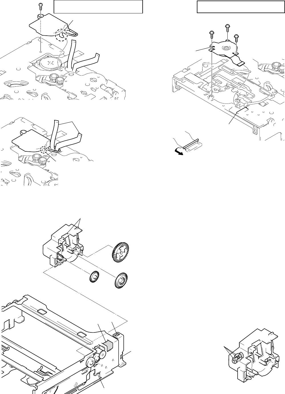
5-10
3-4. REEL MOTOR
Disassembly/Assembly
Remove the claws of the FL motor assembly from hole A and hole
B and remove the FL motor assembly. Then, remove each gear,
etc.
To attach them, after attaching the gears, etc. to the FL motor
assembly and hook the positioning bosses of the FL motor block on
holes C and D then fit the two claws in each hole A and B.
The worm gears are attached inside the
FL motor assembly. When attaching the
FL motor assembly, apply grease there.
3-5. FL MOTOR ASSEMBLY, GEAR A, GEAR B AND GEAR CD ASSEMBLY
Disassembly/Assembly
3-3. CAPSTAN COVER
Disassembly/Assembly
Gear A
Gear B
Positioning bosses
FL motor assembly
Hole D
Hole A
Hole C
Hole B
Gear CD assembly
Apply grease.
(half size of one grain of rice)
Do not fasten
this screw.
CN 3
Screw 2
Fasten the screws
in order of 1, 2, 3.
Reel motor
Screw 1
Screw 3
Tightening torque of reel motor
0.0686 ± 0.0098 N • m (0.7 ± 0.1 kg • cm)
After inserting the flexible board
of the reel motor into CN3, attach
the reel motor and lock CN3.
Tightening torque of capstan cover
0.3432 ± 0.0196 N • m (3.5 ± 0.2 kg • cm)
Capstan cover
Screw
Claw
1
2
Pass the two flexible boards
of the drum assembly through
the hole.
Insert the claw into the long hole
of the chassis and fix the cover
with the screw.
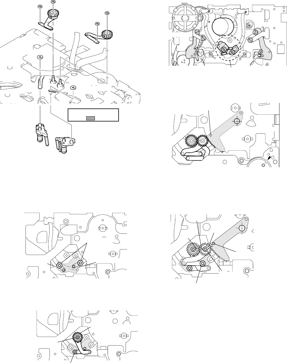
5-11
1Attach the coaster S/T assembly to the chassis with a new
coaster stopper while being careful not to touch the tape guide.
Do the work while holding the drum side of each coaster.
2Attach the GL arm T assembly. Fix the stop washers in the
correct position, using new stop washers.
3Attach the GL arm S assembly while checking the phase of
each part. Fix the stop washers at the correct position, using
new stop washers.
Check each phase adjustment while referring to the above
figure.
Hole A of the GL gear T and hole B of the GL gear S must
face each other. Hole D of the loading arm assy must be aligned
with the hole of the chassis, and the endmost gear tooth of the
loading arm assy must face toward hole C of the GL gear S.
Assembly
With consideration for future assembly, check from the rear of the
chassis that the phase of the loading arm assy is aligned.
Move the TG2/7 arms to the loading position with the regulated
power supply or by hand while referring to page 5-5. Each coaster
assembly must be in the unloading position.
For the disassembling and assembling procedures of the GL gear,
GL helical torsion spring, etc., refer to page 5-21.
3-6. GL ARM S ASSEMBLY, GL ARM T ASSEMBLY, COASTER S ASSEMBLY AND COASTER T ASSEMBLY
Disassembly: Remove the parts in order of 1,2,3,4,5,6,7,8,9,0
1
4
3
7
8
0
9
62
5
Stop washer
Stop washer
Coater stop
washer
Coater stop
washer
GL arm S
assembly
Coaster stopper
Coaster S assembly
Coaster T
assembly
GL arm T
assembly
Do not touch the tape
guide ( part).
Coaster stopper
Unloading position
TG7 arm
TG2 arm
Loading arm assy
The phase must be aligned
with the hole of the chassis.
Coaster T assembly
Coaster stoppers
Coaster S assembly
Coaster stop washer
(
The sto
p
hole is lar
g
er.
)
Stop washer
(The stop hole is smaller.)
GL arm T assembly
Stop washer
(The stop hole is smaller.)
Coaster stop washer
(The stop hole is larger.)
Hole
A
Hole
B
Hole
C
Hole
D
Loading arm assy
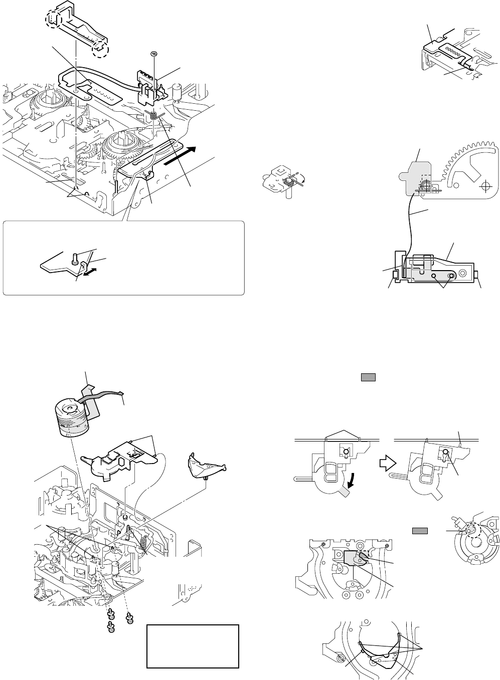
5-12
MIC base guide
Claw
Claw
FP-104 flexible
board
(Remove the
six solders.)
Reel selector slider
MIC base spring
Positioning pins
Hole A
MIC base
assembly
Stop washer
(Do not reuse.)
B
Select the desired cassette position by pressing the claw position.
Reel select slider
Do not touch the slider drive shaft.
When selecting a cassette position, be careful not to touch the
slider drive shaft because it can be easily bent or broken.
MD-76 board
Six solders
Temperature of tip
of soldering iron : 350 ± 20 °C
Hold time : one second or shorter
Hole A
MIC base guide
FP-104
flexible board
Clearance
Claw
D
Pins Claw
C
MIC base assembly
Disassembly: Remove them in order of 1,2,3
For the disassembly and assembly procedures of the components
of the drum assembly, refer to page 5-22.
Assembly: Attach the parts while referring to the
disassembly procedure and the figure below.
(After assembling, adjust the tape path while referring to page 5-
23 and thereafter.)
Disassembly/Assembly
For the disassembling and assembling procedures of the compo-
nents of the MIC base assembly, refer to page 5-21.
3-7. MIC BASE GUIDE, MIC BASE ASSEMBLY AND MIC BASE SPRING
Remove the six solders on the FP-104 flexible board from
the rear of the chassis. Pass the flexible board through
hole A and pull it out of the front side of the chassis while
being careful not to damage it. To attach the flexible board,
perform the steps of disassembly in reverse order.
Move the reel selector slider in the direction of arrow B
and attach the MIC base assembly at the position of “S
cassette”. For the assembly of the MIC base spring, refer
to the figure.
Insert the side of the
shorter spring into the
hole of the holder and
hook the side of the
longer spring.
When attaching the MIC base
guide, lock the positioning pins, claw
C, and claw D in this order. Route
the flexible board into the clearance
of the MIC base guide.
3-8. DRUM CAP, DRUM ASSEMBLY AND TAPE SUPPORT
Assembly and disassembly of the drum assembly
When pulling the part in the direction of the arrow,
the claw is removed from the center shaft, then the right
pin and the drum cap are removed as shown in the figure
on the right. To attach the drum assembly, perform the
disassembly steps in reverse order.
Assembly and disassembly of the drum assembly
Assembly and disassembly of the tape support
Note: Do not hold the shaft
when selecting the reels.
3
2
14
Flexible board (7P)
Flexible board (10P)
Drum
assembly
Drum cap
Positioning pins
Tape support
Drum fixing screw assembly
(Fasten the screws in order 1, 2, 3.)
Be careful not to remove
this together with the drum
cap.
1
2
3
Tightening torque of
drum assembly
0.02941 ± 0.0049 N • m
(0.3 ± 0.05 kg • cm)
Drum reference pins
Pins Pin
Center shaft
Insertion hole of
flexible board (7P)
Insertion hole of
flexible board
(
10P
)
The claw is hooked
on the sub-chassis.
The claws are
hooked under
the sub-chassis.
Positioning pin
Be careful that the 7P flexible board
does not interfere with the part.
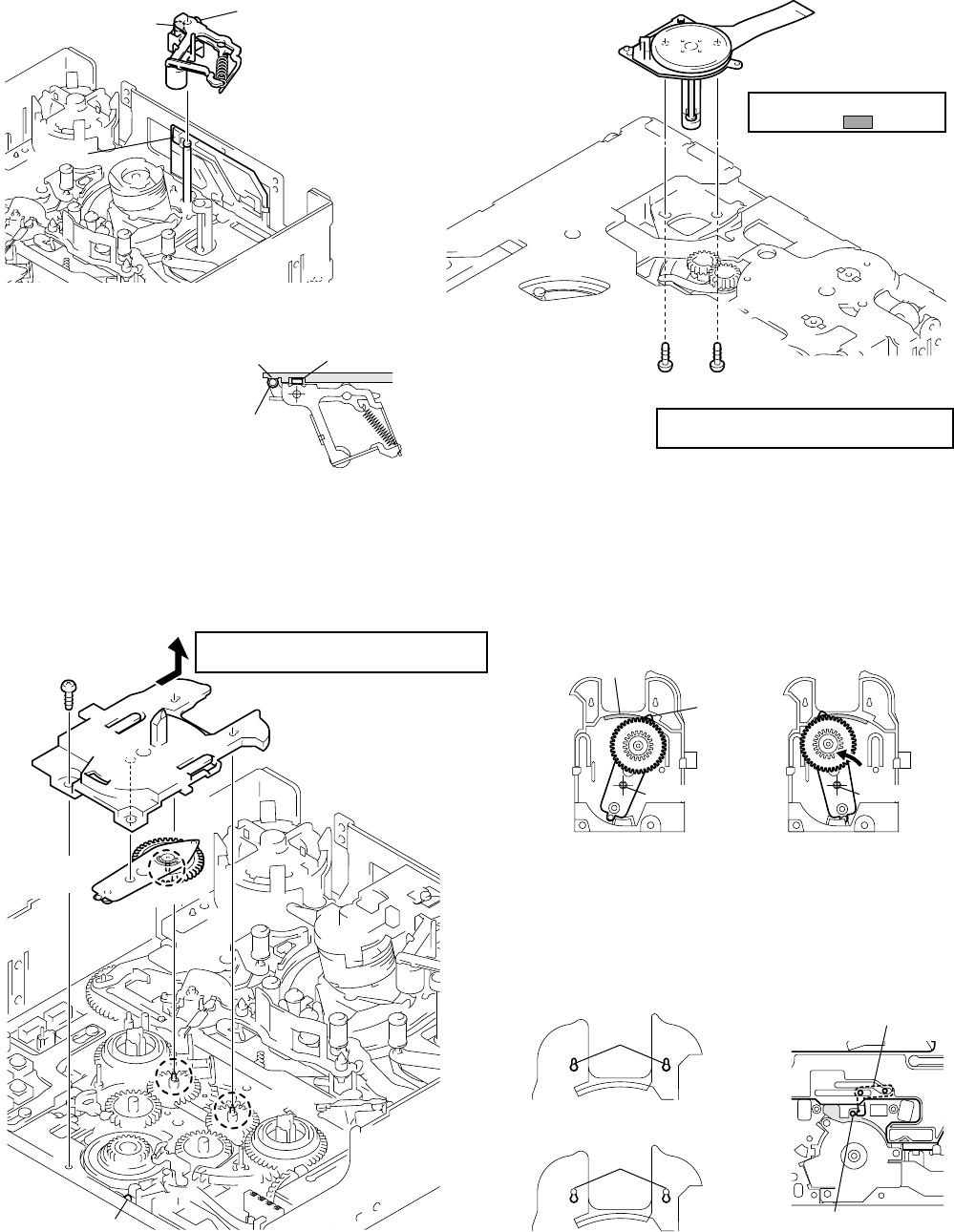
5-13
3-10. CAPSTAN MOTOR
Disassembly/Assembly
(After assembling, adjust the tape path from page 5-23.)
3-9. PINCH ARM ASSEMBLY
Disassembly/Assembly
For the disassembling and assembling procedures of the tape re-
tainer and compression coil spring (tape retainer), refer to page 5-
22.
Push roller A into the
groove as shown in the
figure. Insert roller B into
the claw. To remove the
pinch arm assembly, pull
out the pinch arm upward
while pushing the claw.
3-11. PENDULUM RETAINER AND PENDULUM ARM ASSEMBLY
Disassembly: Remove them in order of 1,2,3
(To attach them, perform the disassembly steps in reverse order.) Notes during assembly
When assembling or disassembling the pendulum arm assembly,
be careful of the following.
Attach the pendulum retainer to shaft B. Be careful of the positions
of the pendulum stopper at the rear of the chassis and shaft A of
the pendulum arm.
1
2
3
Screw
Tightening torque of pendulum retainer
0.3432 ± 0.0196 N • m (3.5 ± 0.2 kg • cm)
Pendulum retainer
(Remove in the direction
of the arrow.)
Pendulum arm
assembly
Shaft
Positioning boss
Shaft
B
Shaft
A
Shaft
B
Hole
E
D
F
[Rear side of pendulum retainer]
Insert tip
D
of the pendulum
arm into hole
E
of the pendulum
retainer and insert the pendulum
into shaft
C
.
Shaft
C
Shaft
C
Slide the pendulum arm in
the direction of arrow
F
and
attach it to the chassis.
Shafts B
Shafts B
Cannot be removed.
Can be removed.
Pendulum stopper
Shaft A of the pendulum
must be in this position.
Capstan motor
Screw
Tightening torque of capstan motor
0.1961 ± 0.0196 N • m (2.0 ± 0.2 kg • cm)
Be careful not to touch the
motor shaft ( part).
Roller BRoller A
Pinch arm assembly
Claw
Roller B
Roller A
Claw
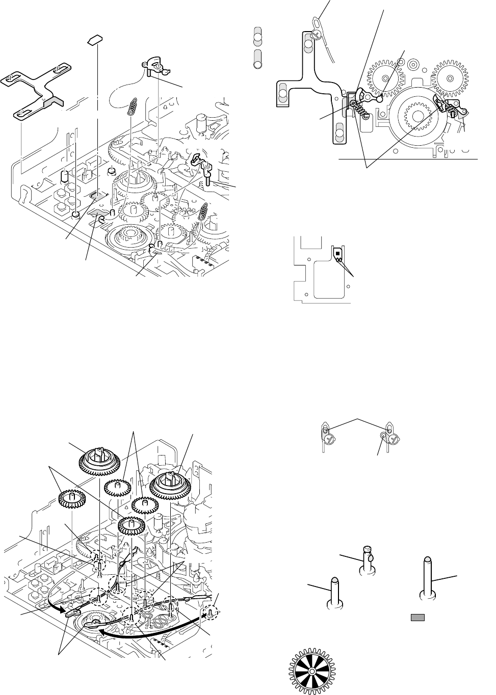
5-14
Disassembly/Assembly
(Do not touch the TG band block.)
When the reel table assembly is replaced or attached, perform each
adjustment from Adjustment Start -1 of the flowchart on page 5-
23.
3-13. REEL TABLE ASSEMBLY, IDLER GEAR A ASSEMBLY AND IDLER GEAR B
Disassembly: Remove them in order of 1,2,3,4
(To attach them, perform the disassembly steps in reverse order.)
3-12. BRAKE ARM S, RATCHET BRAKE T, TENSION COIL SPRING (BRAKE), SBR SLIDER AND FP-248 FLEXIBLE
BOARD (CONDENSATION SENSOR)
Checks before work
The TG band winds around the slit of the reel table assembly. Be-
fore removing the reel table assembly, clear off the TG band while
referring to the left figure. When attaching the TG band, be sure to
use new stop washers.
When attaching each gear, apply grease to each fixing shaft. Apply
grease of half the size of one rice grain to the top side of shaft C.
When attaching the idler gear A assembly, be careful not to apply
grease to the reflection panel.
Shaft
E
Shaft
A
Shaft
B
Shaft
B
Shaft
A
Shaft
D
Shaft
C
Clear off the stop washers of
the adjuster side of the TG
band in advance as shown
in the figure.
Idler gear A
assemblies
Reel table assembly
Idler gears B Reel table assembly
Apply grease to part.
(half size of one grain of rice)
Shaft BShaft A
Shaft C
Good Not good
Shaft
D
or
E
When attaching the TG band, the part also
must be inserted into shaft
D
or
E
.
When attaching the idler gear
A assembly, be careful not to
apply grease to the reflection panel.
1
2
1
4
3
2
Shaft
B
Hole
A
C
Shaft
A
Hole
B
FP-248 flexible board
(Condensation sensor)
SBR slider
Brake arm S
Clean here
with alcohol.
Tension coil spring
(brake)
Ratchet brake T
Tension coil
spring (brake)
Remove the SBR slider
while being careful not
to touch the adjuster. Portion
C
of the SBR slider
and brake arm S must run
close to each other.
The idler gear A assembly
must be engaged with the
gear teeth.
Cannot be
removed.
Can be
removed.
Insert shaft
A
into hole
A
.Insert shaft
B
into hole
B
.
Hook the hook of the spring on
the brake side from underneath.
When attaching the FP-248 flexible
board, scrape the contact surface
with a swab to stick the flexible
board to the chassis.
Do not touch the sensor block
(black area).
Two solders
Temperature of tip of soldering iron:
350 ± 20 °C
Hold time:
one second or shorter
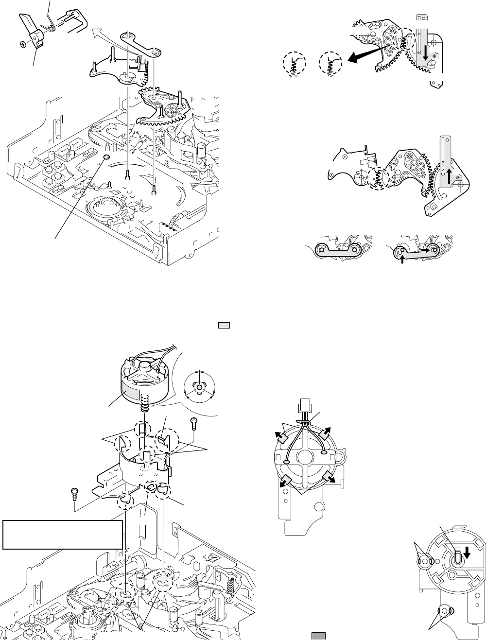
5-15
1Move the reel selector slider in the direction of arrow A to
check that the reel selector lever is “L cassette”. At this position,
attach the reel base T assembly. The gear teeth must be engaged
as shown in the figure.
2Move the reel selector slider in the direction of arrow B and
switch the reel selector lever to “S cassette”. At this position,
attach the reel base S assembly. The gear teeth (circled by a)
must be engaged as shown in the figure.
3Attach the reel base retainer.
3-14. REEL BASE RETAINER, REEL BASE T ASSEMBLY AND REEL BASE S ASSEMBLY
(REEL LOCK RELEASE BLOCK AND REEL LOCK RELEASE SPRING)
Disassembly: Remove them in order of 1,2,3
(Refer to Assembly, too.)
3-15. CAM MOTOR, MOTOR HOLDER
Assembly: Attach them in order of 1,2,3
Disassembly/Assembly
[Rear side of motor holder]
The motor holder is fixed by the two
screws and claw B at the rear. To
remove it, push claw B in the
direction of the arrow from the rear
of the chassis. Note that positioning
pins D are easy to break when
attaching the motor holder. Apply
grease (half size of one grain of rice)
to the two parts shown in the
right figure.
[Front side of motor holder]
While spreading claws A in the
direction of the arrow, pull out the
cam motor upward. To attach it, push
the cam motor into the motor holder
and route the two wires of the cam
motor into claw C.
When attaching the TG2 control arm,
claw E must be inserted into the
hole of the TG2 control arm.
Checks before disassembly and assembly
The cam motor is fixed on the motor holder by the four
claws. Releasing the four claws enables the cam motor
to be removed without removing the motor holder from
the chassis. When attaching the cam motor, be careful of
the assembling direction (the label must face toward the
front). If the phase of the gear, etc. moves when removing
the motor holder, refer to page 5-11.
Note: Do not hold the shaft when selecting the reels.
1
2
3
Reel base retainer
(Remove in reverse
order of assembly.)
Reel base
T assembly
Reel base S assembly
Reek lock release block
Reel lock release spring
This shaft hinders removing or
attaching the reel base S assembly.
Do the work while being careful not
to touch it.
Stop
washer
Not goodGood A
Reel base T assembly Reel selector slider
Reel selector lever
B
Reel base S assembly
The gear teeth circled
by a are engaged.
Attach in order of 1, 2.
(
Attach to the slits.
)
1
2
Fixing state
Cam motor
Label
Screw
Motor holder
(Release claw B at the rear.)
Apply grease to
the three parts
and tip.
(half size of one
grain of rice for
each part)
Positionin
g
holes of
p
in D
Tightening torque of motor holder
0.1961 ± 0.0196 N • m
(2.0 ± 0.2 kg • cm)
120 °
Screw
120 °
120 °
Claws C
Claws A
Claw E
Pins D
Claws A
Pins D
Claws A
Claws A
Claw C
Claw B
Pins D
Pins D
5-16
3-16. TG2/7 ARM BLOCK, TG2/7 BAND BLOCK AND TENSION COIL SPRING (TG2)/(TG7)
Disassembly: Remove them in order of 1,2,3,4
For the disassembling and assembling procedures of the assembly
components of the TG2/TG7 arm, refer to page 5-22.
Disassembly of the band TG2/TG7 assembly
When pulling portion E of the TG2 or TG7 band in the
direction of the arrow, a click sound is heard as the
band is removed. To attach the bands, pull out the
opposite side to portion E to lock.
Notes during work
Be careful when handling the TG arm and the peripheral parts.
• Twisting and bending of the band block and tension coil spring
• Dirt and scratches of the tape guide
• Loss of the compression coil spring (TG)
Do not reuse removed stop washers.
Assembly: Attach them while referring to figure above
or below and the descriptions.
When these parts are replaced or attached, perform each adjust-
ment from Adjustment Start -3 of the flowchart on page 5-23.
1Apply grease to the top side of the fixing shaft (A or B) of
the TG arm. (Fig. 1)
1
1
4
2
3
3
2
4
Stop washer
Compression
coil spring (TG) TG2 arm
assembly
TG7 arm assembly
Tension coil
spring (TG7)
Shaft B
Tension coil
spring (TG2)
Stop washer Stop washer
Compression coil
spring (TG)
Shaft A
Shaft C
Shaft D
Stop washer
Be careful not to touch
the tape guide ( part) and TG band block.
Band TG2/TG7 assembly
Shaft
E
HC
FG
D
Sub-slider
Hook each spring on
the second hook from above
Half size of one grain of rice
[TG2 side] [TG7 side]
Hook the spring from the inside
and
p
ut it under the TG band. Hook the spring from the outside
and
p
ut it under the arm.
Good
This part also must be
inserted into the shaft.
Not good
Fixing shaft C or D
2Attach the TG band assembly to the TG arm assembly. (Fig. 2)
Be sure that the felt sides of the TG band face toward the reel
tables so that they surround the respective reel tables.
3Attach the tension coil spring to the TG arm assembly. (Fig. 3,
4)
• Hook the spring of the tension coil spring (TG2) from the
inside and put it under the TG band. (Fig. 3-F, 4)
• Hook the spring of the tension coil spring (TG7) from the
outside and put it under the TG7 band. (Fig. 3-G, 4)
4Attach the TG arm block to the shaft (A or B) and attach the
tension coil spring to the second hook. When attaching the TG2
arm, the part must be at the left of portion H of the slider.
(Fig. 3)
5Attach the adjuster of the TG band to shafts C and D.
6Fix the TG band and TG arm with new stop washers. When
attaching the TG arm, do not forget to attach the compression
coil spring (TG). (Fig. 1)
Fig. 1
Fig. 2
Fig. 3
Fig. 4
5-17
Disassembly of the pinch slider
Check before work
When attaching the parts described in this section, various phase
adjustments are required. Before work, refer to page 5-19 and check
the reference phases.
Assembly: Attach them while referring to the figure above or below and the descriptions.
Move the pinch slider to the leftmost end, and
slide it upward and remove it when two shafts
A are superimposed on the holes of the pinch
slider.
Move the sub-slider to the rightmost and remove
it from two shafts B.
Disassembly: Remove them in order of 1,2,3,4,5,6,7,8
3-17. SUB-SLIDER ARM, SUB-SLIDER, ENCODER GEAR, MAIN CAM GEAR, COUPLING GEAR, SUB-CAM GEAR,
PINCH SLIDER AND LOADING ARM ASSY
1Attach the loading arm assy. (Refer to the figure above.)
The phases of the GL gear S and GL gear T must match and
the positioning hole G of the loading arm assy must be
superimposed on the hole of the chassis. (Fig. 5)
2Attach the pinch slider. (Fig. 1, 2)
3Apply grease to the groove at the rear of the sub-cam gear.
(Fig. 6)
After applying, adjust the phase of the sub-cam gear to that of
the pinch slider. (Fig. 7)
Phase pin D of the loading arm assy must be inserted into the
groove at the rear of the sub-cam gear. (Fig. 5, 7)
Disassembly of the encoder gear
Disassembly of the sub-slider
2
4
6
1
3
7
8
Pinch slider
Sub-cam gear
5
Phase pin D
Loading arm assy
Phase pin F
Sub-slider
Shafts A
Shafts B
Phase
pin E
Encoder gear
(A claw is hooked.)
Main cam gear
Sub-slider arm
Coupling gear
This can be removed.
This cannot be removed.
Pull out the encoder gear
upward while pushing into
the claw.
Encoder gear
1
Phase adjustment hole H
Sub-cam gear
Loading arm assy
Positioning hole G
GL gear T
GL gear S
Main cam gear
Phase pin M
Main slider arm
Phase pin D
[Rear side of chassis]
Sub-cam gear
(front side)
Phase adjustment hole H
matches the hole of the
chassis.
Check phase pin D
through this hole
Pinch slider
Fig. 1
Fig. 2
Fig. 3
Fig. 4
Fig. 5
Fig. 6
Fig. 7
Sub-cam gear (rear side)
Apply grease to the seven parts.
(half size of one grain of rice for each part)
5-18
4Apply grease to the fixing block (shaft J and U-shaped groove
K) of the coupling gear and portion L of the sub-cam gear
(half size of one grain of rice for each part). (Fig. 8)
5Attach the coupling gear. After attaching, apply grease while
rotating the coupling gear by 120˚ each time. (Fig. 9, 10)
6Attach the main cam gear while being careful of the directions
of the front and rear sides. Also, take care of the phase
adjustment to the sub-cam gear. (Fig. 8, 11, 12)
Phase pin M of the main slider arm should be fitted in the
groove of the main cam gear (rear side). (Fig. 5)
Sub-cam gear
Main cam gear
Encoder gear
Groove K
Shaft J
L
[Front side of chassis]
▲ marks should face
each other.
a marks should face
each other.
Not
good
Not
good
Main cam gear
Sub-cam gear
U-shaped groove K
Shaft J
Attach the coupling gear to shaft J
and U-shaped groove K in order.
120 °120 °
120 °
Apply grease to the three parts
(half size of one grain of rice for each part).
Main cam gear (rear side)
( a does not exist.) Main cam gear (front side)
( a exists.)
Phase pin C should be fitted in
the groove of the main cam gear
(front side).
N
Sub-slider
Sub-slider arm
Reel selector slider
(After attaching the sub-slider arm,
return the reel base to the original
position (L cassette).)
(Position when L cassette is set)
Phase pin F should be fitted in
the long hole of the sub-slider arm.
Reel base S Reel base T
Do not hold the shaft
when selecting the reels.
[Front side of chassis]
7Attach the encoder gear. (Fig. 3)
Adjust the phases (marked) to those of the main cam gear. (Fig.
4/Fig. 8)
8After moving the reel selector slider in the direction of arrow
N to set the position of the reel base to “L cassette”, attach the
sub-slider in reverse order while referring to Fig. 3. (Fig. 13)
9Attach the sub-slider arm. (Fig. 1/Fig. 13)
Fig. 8
Fig. 11
Fig. 9
Fig. 10
Fig. 12
Fig. 13
5-19
1Insert the main slider arm into the fixing hole and attach
it to the fixing shaft at the front of the chassis while
referring to the figure above. (To facilitate assembly,
stick adhesive tape so that the main slider arm does not
drop.)
2Perform assembly so that the main slider can pass under
the bent portion of the chassis. If “Ratchet brake T”
remains, move down the “Ratchet brake T” as shown in
the left figure and attach the main slider.
3Carefully attach the pendulum stopper assembly so that
the two shafts fit in the two long holes of the main slider.
3-18. MAIN SLIDER, MAIN SLIDER ARM AND PENDULUM STOPPER ASSEMBLY
Disassembly: Remove them in order of 1,2,3Disassembly of each part
The main slider controls several parts. Before removing the main
slider, remove “Brake arm S” at the front of the chassis while re-
ferring to “Information” on page 5-4. Otherwise, the main slider
cannot be removed.
Main slider
The main slider is fixed by the two shafts and the two
bent portions at the rear of the chassis. The main slider
can be removed when it is moved to the rightmost end
( positions).
Assembly: Attach them while referring to the figure
above or below and the descriptions.
Assembly of each part
Attach each part while referring to the figure above or below. When
attaching the parts, adjust the positions carefully while referring
to the instructions in the figure below. Because these positioning
will be used as a reference when assembling in future, make sure
to adjust the positions and phases correctly.
4Attach the shaft of the main slider arm to the long hole
of the main slider.
5Move the main slider to the leftmost end so that the
small positioning hole of the main slider is superimposed
on the small positioning hole of the chassis, and fix the
main slider. The position where the main slider is fixed
will be used as a reference during assembling and phase
adjustment in future.
(To avoid affecting the main unit, fix the reel motor and
main slider with adhesive tape, etc.)
1
23
Main slider
Main slider arm
Fixing shaft of
main slider arm
Fixing hole of
main slider arm
Bent portions
Pendulum
stopper assembly
Brake arm S
Shafts
Bent portions
1
5
2
34
[Rear side of chassis]
Main slider arm
Main slider
Move the main slider so that
the positioning holes are
superimposed.
The shaft of the ratchet brake T
should be at the position where
it can be viewed fromthe outside
as shown in the figure.
Pendulum stopper assembly
Main slider
Pendulum stopper assembly shafts
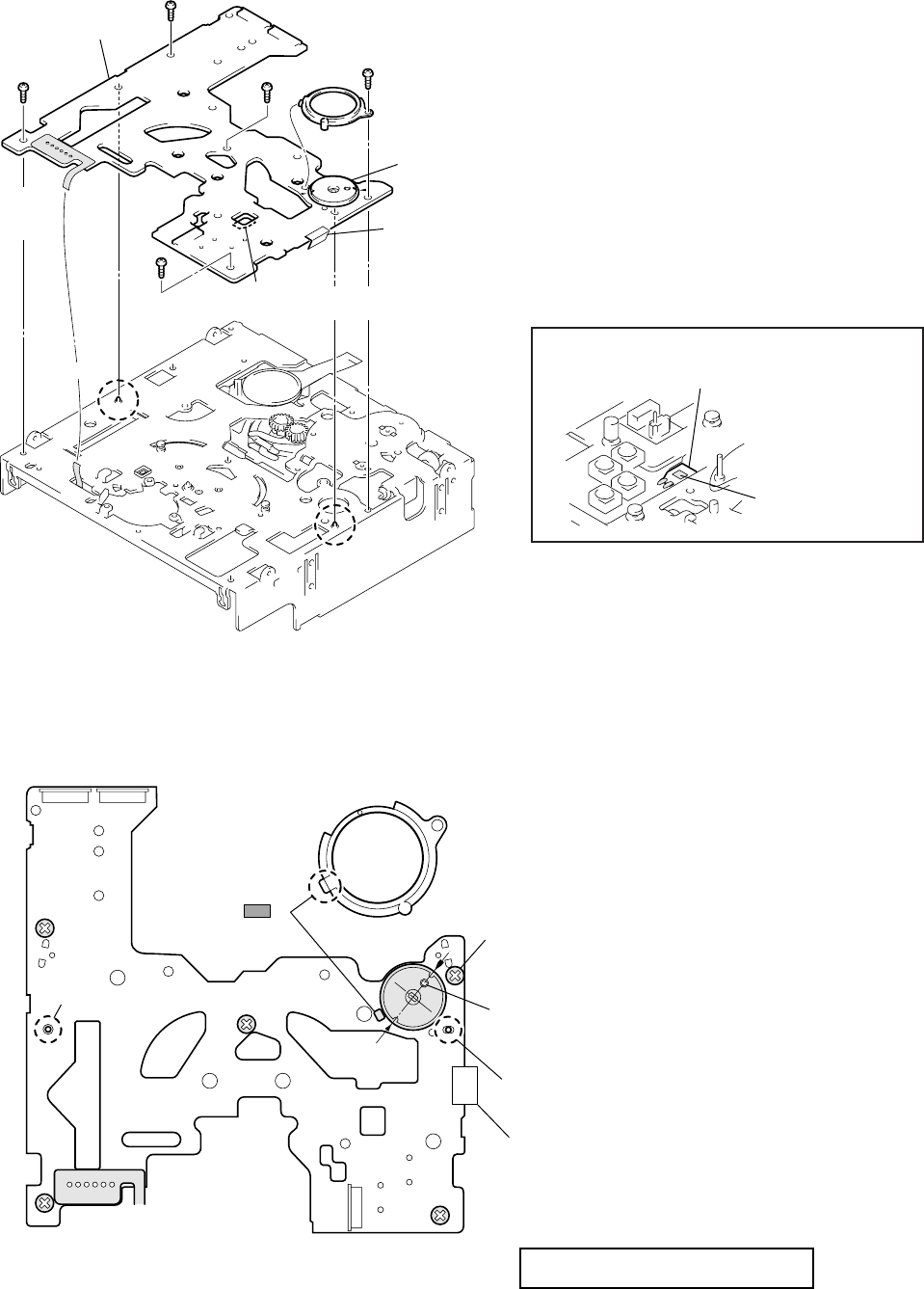
5-20
Disassembly of MD-76 board
Peel off the FP-248 flexible board at the front of the chas-
sis (refer to page 5-14). Remove the six solders on the
FP-104 flexible board from the rear of the chassis.
Remove the screws in order of 3 to 8 shown in the
figure. When removing the MD-76 board from the
chassis, be careful not to let the sensors touch the chassis.
3-19. MD-76 BOARD AND ENCODER RETAINER
Disassembly: Remove them in order of 1,2,3,4,5,6,7,8,9
Assembly: Attach them in order of 9,4,3,5,6,7,8,1,2
(Refer to the figure above or below.)
Assembly of MD-76 board
While being careful not to let the sensors touch the chas-
sis, position the two positioning pins and fasten the screws
in order of 1 to 5. Then, solder the six parts on the
removed FP-104 flexible board and position the encoder
disk. Finally, stick the FP-248 flexible board on the front
of the chassis. (Refer to page 5-14.)
FP-248 flexible board
3
6
8
1
2
7
9
4
5
Screw
Positioning pin
tape A
FP-104
flexible board
(Six parts
are soldered.)
Screw Screw
Positioning pin
Screw
Encoder cover
(A positioning
claw is hooked.)
Encoder disk
(Positioning is
required.)
FP-248 flexible board
(Condensation sensor)
Screw
MD-76 board
Sensor block
Peel off the flexible board while being careful not to get
the sensor block dirty or damage the sensor block.
Tape A
(Adhere a half of the tape in the peripheral of
the switches S2 and S3 on the MD-76 board
and adhere the remaining half on the mechanism
chassis.)
Solder the FP-104 flexible board
(six parts).
Temperature of tip of soldering iron: 350 ± 20 °C
Hold time: one second or shorter
Positioning pin
Screw
1
(This screw fixes the encoder cover.)
Encoder cover
Screw
3
Screw
2
Screw
5
Screw
4
Positioning pin
Tightening torque of MD-76 board
0.3432 ± 0.0196 N·m (3.5 ± 0.2 kg • cm)
Positioning the encoder disk
Align the mark of the disk with the v mark
printed on the board as shown in the figure.
(Be careful of the position of a.)
Fit this claw
in the hole of
and fasten the screws.
MD-76 board
Note: When the tape A is removed, use the new tape A for
replacement. (See the illustration below.)
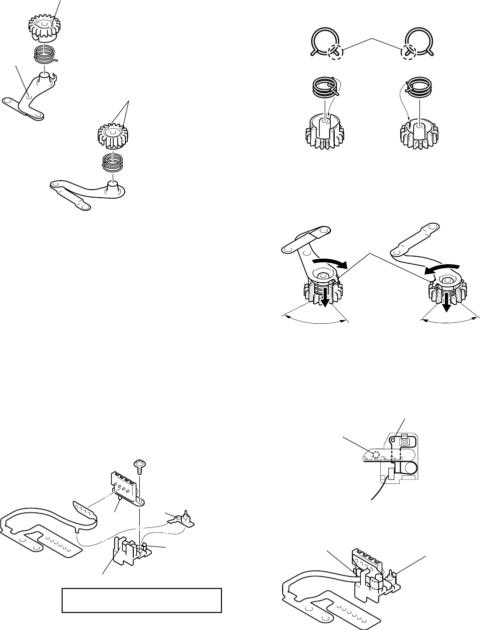
5-21
3-20. COMPONENTS OF GL ARM S/T ASSEMBLY
(GL ARM ASSEMBLY, GL HELICAL TORSION SPRING, GL GEAR)
3-21. COMPONENTS OF MIC BASE ASSEMBLY
(FP-104 FLEXIBLE BOARD, MIC BASE)
Disassembly
Remove the push switch from claw A of the MIC base.
Remove the screw and connector (4P). Then, remove the
flexible board while being careful not to touch hook B.
Assembly
1Attach each GL helical torsion spring to the GL gear. To
distinguish the S side from the T side when the opening of the
spring tip is facing toward the front, note that the coil tip of the
S side is located on the left and that of the T side is located on
the right.
2Hook the tip of the spring on the bent portion of the GL arm
assembly and push the bent portion of the GL arm into the
large cut-out of the GL gear while rotating the GL gear in the
direction of the arrow.
AssemblyDisassembly and distinguishing the S side from the T side
One phase adjustment hole
GL gear T
GL helical torsion spring T
Indented
GL arm assembly T
Two phase adjustment holes
GL gear S
GL helical torsion spring S
GL arm assembly S
Tip of coil
[T side] [S side]
Fit the tip of the spring into the small cut-out of the GL gear.
Bent portions
Push here.
When the bent portion of the GL arm comes
inside this range, push the bent portion into the gear.
Screw
Connector (4P)
Push switch (one key)
Hole
C
Pin
D
FP-104 flexible board
(Four parts are soldered.)
Claw
A
MIC base
Hook
B
Tightening torque of connector (4P)
0.0392 ± 0.0098N • m (0.4 ± 0.1 kg • cm)
Hook the flexible
board on hook BAttach the push switch
(one key) to claw A.
Insert the pin of the
MIC base into hole C.
Insert pin D into the hole
of the MIC base.
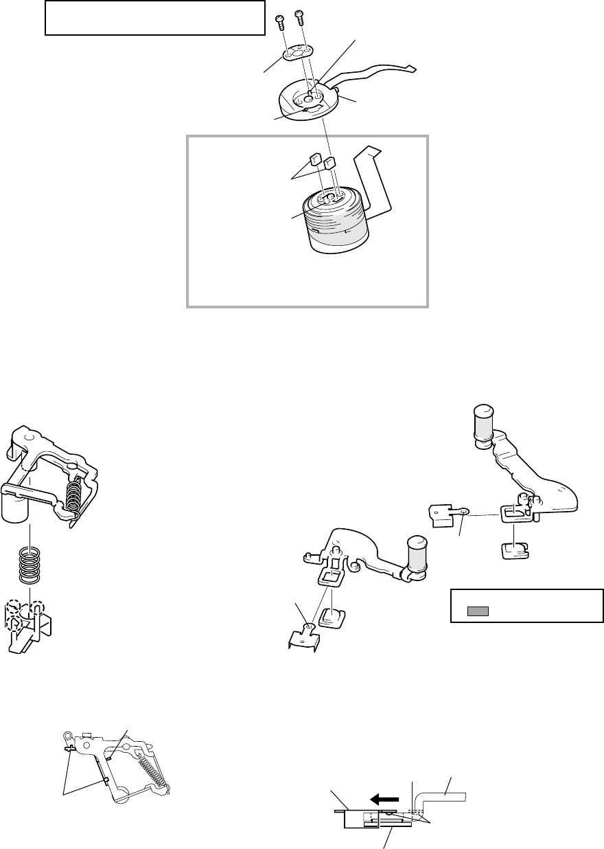
5-22
3-24. COMPONENTS OF TG2/7 ARM ASSEMBLY
(ET MAGNET, MAGNET HOLDER)
Disassembly/Assembly
3-22. COMPONENTS OF DRUM ASSEMBLY
(MOTOR FPC ASSEMBLY, ELASTIC CONNECTOR)
Disassembly/Assembly
Connect the elastic connector to the drum assembly and
attach the motor FPC assembly while aligning pin B with
hole C of the drum assembly. Fix the supporter plate with
the screws while being careful of pin A of the motor FPC
assembly.
3-23. COMPONENTS OF PINCH ARM ASSEMBLY
(TAPE RETAINER, COMPRESSION COIL SPRING)
Disassembly/Assembly
Remove the TG2 arm assembly and the TG7 arm assembly
in the direction of the arrow while pushing the lock pin of
the magnet holder from the rear of each TG arm. To attach
them, insert the TG2 or TG7 arm assembly in the direction
opposite to the arrow while holding the ET magnet with
the magnet holder, then hook the lock pin.
Tightening torque of motor FPC assembly
0.0294 ± 0.0049N • m (0.3 ± 0.05 kg • cm)
Screws
Supporter plate (This component is
not supplied as an independent
repair part.)
Positioning pin A
Motor FPC assembly
Positioning pin B
Elastic connectors
Hole C
Drum assembly
Note: Be careful not to get these parts dirty
when handling them.Also, do not touch
the running side of the tape.
Pinch arm assembly
Compression coil spring
(tape retainer)
Claw
A
Claw
B
Pin
C
Tape retainer
Push pin
C
into
this position.
Claw
A
and claw
B
should
fix the
p
inch arm.
TG7 arm assembly
ET magnet
Lock pin
Magnet holder
TG2 arm assembly
Lock pin
ET magnet
Magnet holder
Do not touch the tape guide
( part).
D
D
Magnet holder TG arm
When attaching the magnet holder,
the lock pin should be fixed at a
position deeper than line
ET ma
g
net
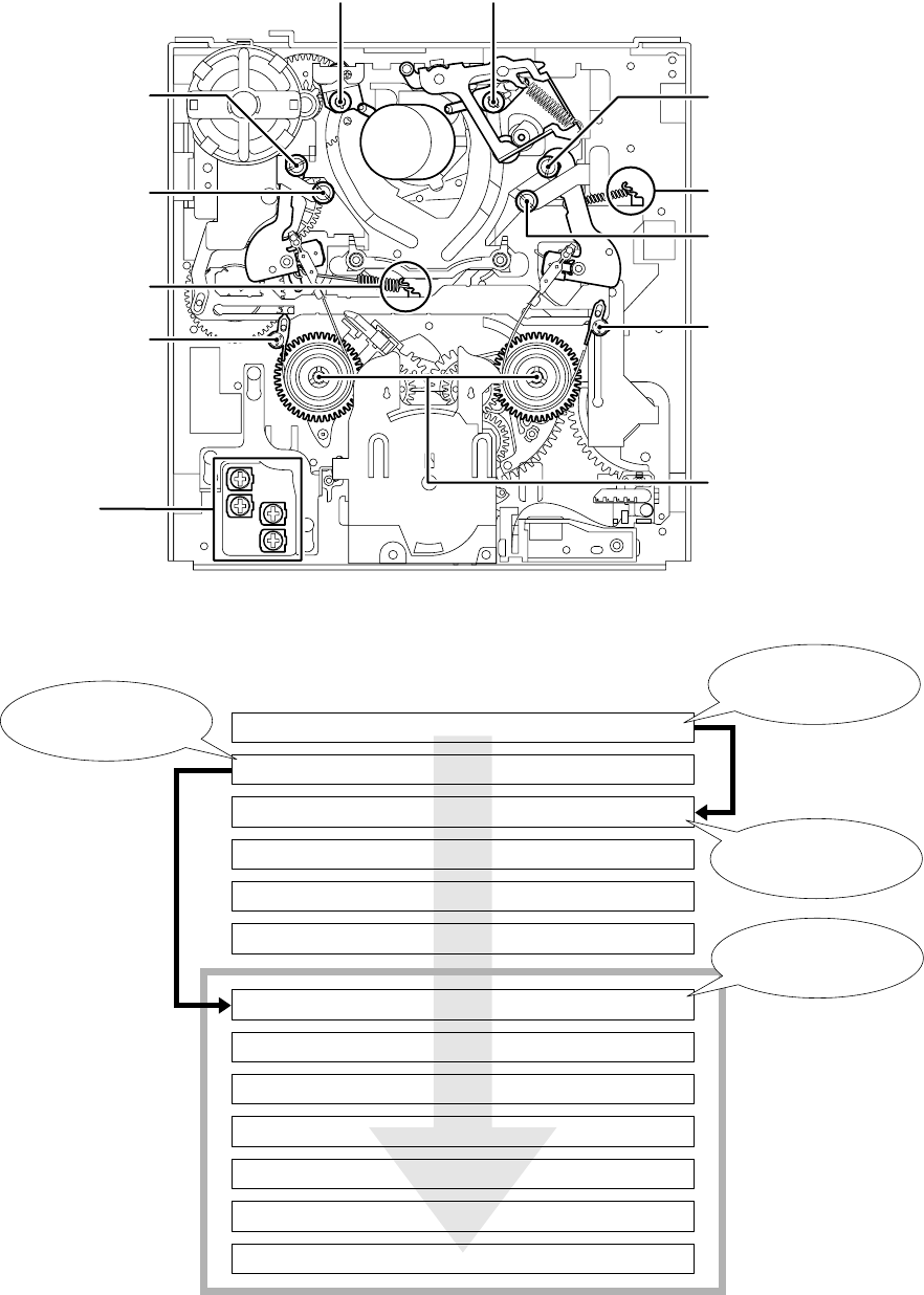
5-23
5-1-4. CHECK AND ADJUSTMENT
• When the parts of the tape path (tape guide, reel table, etc.) have been removed or parts have been replaced, adjust the following parts
according to the flowchart below.
•ADJUSTMENT POSITION
•ADJUSTMENT ORDER (FLOWCHART)
ADJUSTMENT END
4-12. RISING CHECK
4-11. CURL CHECK AND CURL ADJUSTMENT
4-10. CUE/REV CHECK
4-9. TRACK CHECK
4-8. TRACK ADJUSTMENT AND CHECK
4-7. PREPARATION FOR ADJUSTMENT AND TAPE PATH CHECK
4-6. FWD/RVS BACK TENSION CHECK AND ADJUSTMENT
4-5. TG2/7 ELECTRIC TENSION REGULATOR CHECK AND ADJUSTMENT
4-4. FWD/RVS POSITION CHECK AND ADJUSTMENT
4-3. TG2/7 HEIGHT CHECK AND ADJUSTMENT
4-2. TG1/8 HEIGHT CHECK AND ADJUSTMENT
4-1. REEL TABLE HEIGHT CHECK AND ADJUSTMENT
ADJUSTMENT START -2
When only the TG1/8 guide
is replaced, perform tape
path adjustment after height
adjustment.
If the TG1/8 guide is not
replaced and removed,
proceed to TG2/7 height
adjustment.
Tape Path Adjustment
ADJUSTMENT START -4
ADJUSTMENT START -3
ADJUSTMENT START -1
RV1
RV3
RV2
RV4
TG3
(Tracking entrance, curl) TG6
(Tracking exit, curl)
TG7
(TG7 height/RVS position, curl)
Spring hook slider
(RVS back tension)
TG8
(TG8 height, curl)
T band adjuster
(RVS position)
Reel table
(height)
RV1 to 4 (MD-76 board)
(TG2/7 electric tension regulator)
S band adjuster
(FWD position)
Spring hook slider
(FWE back tension)
TG1
(TG1 height, curl)
TG2
(TG2 height/FWD height, curl)
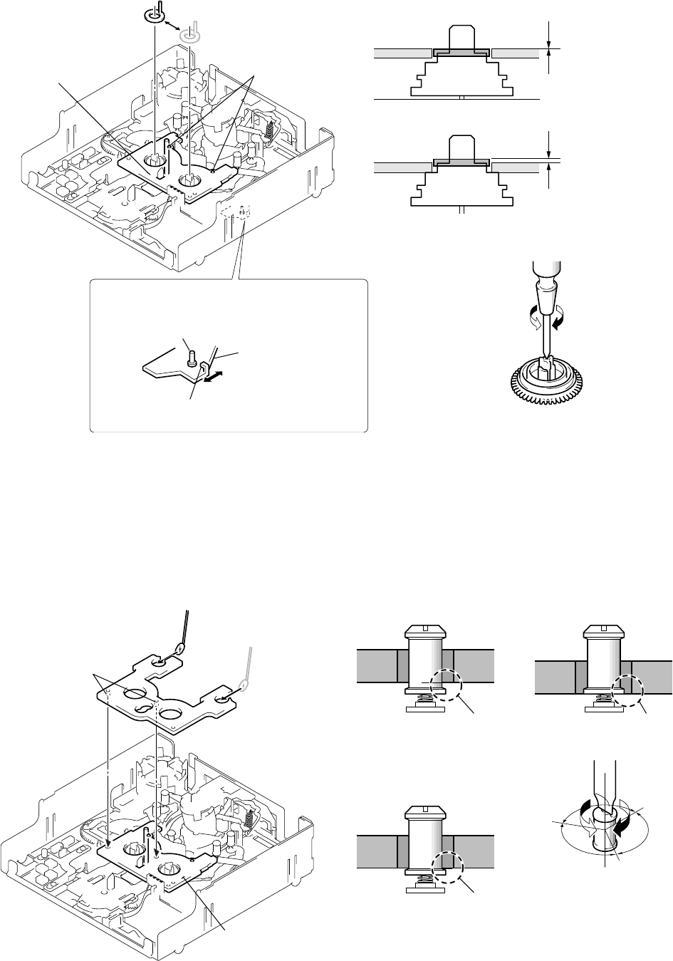
5-24
Attach the boss while aligning
it in the hole of the cassette
reference plate (J-11).
Boss
TG2/7 preset plate
(J-13)
Cassette reference plate
(J-11)
Face the mirror (J-4) in the
direction of the arrow and
perform a visual check.
Reel reference plate (J-12)
Respectively attach it to
the S and T sides and
perform the checks.
Cassette positioning
shafts
Cassette reference
plate (J-11)
Attach the cassette
reference plate (J-11)
when the reel table is
at the position of
"S cassette".
Select the desired cassette position by pressing
the claw position.
Reel select slider
Do not touch the slider drive shaft.
When selecting a cassette position, be careful not to
touch the slider drive shaft because it can be easily
bent or broken.
1. Preparation before check
Check that the cassette compartment has already been removed.
(Refer to page 5-5.)
Fit the cassette reference plate (J-11) in the cassette positioning
shafts.
2. Check and adjustment
Put the reel reference plate (J-12) on each reel table. Rotate the
screw block of the reel table so that the height of the cassette ref-
erence plate is the same as that of the reel reference plate.
Put the reel and cassette
reference plate and adjust
the height.
4-2. TG1/8 HEIGHT CHECK AND ADJUSTMENT
1. Preparation before check
1) Check that the cassette compartment block has already been
removed. (Refer to page 5-5.)
2) Set the mechanism deck to the loading end position (TG2 to 7
already moved to the loading end position and the pinch roller
is in the unloading position). Alternatively, set the mechanism
deck to the “LE position” using the mode selector II. (Refer to
page 5-5.)
3) Place the TG2/7 preset plate (J-13).
2. Check and adjustment
Rotate the TG upper flange until the heights of the TG2/7 preset
plate (J-13) and TG1 or TG8 roller block are the same. Alterna-
tively, rotate the TG upper flange by 120˚ in the direction of
lowering the guide from the reference height where the preset plate
and roller have the same height.
4-1. REEL TABLE HEIGHT CHECK AND ADJUSTMENT
Same height
(normal position)
The reel table is too high.
(Adjust the height while
referring to the figure below.)
S/T reel table
S/T reel table
Cross-headed screwdriver
The reel table is lowered. The reel table is raised.
S/T reel table
TG1 or TG8 TG1 or TG8
The guide is too low. The guide is too high.
Screwdriver for tape path (J-5)
The guide
is raised.
The guide
is lowered.
120°120°
The normal height is the position where the TC
upper flange is rotated by 120° in the direction
of lowering the guide from the adjusted height
while referring to the figure below.
Not good Not good
Good
TG1 or TG8
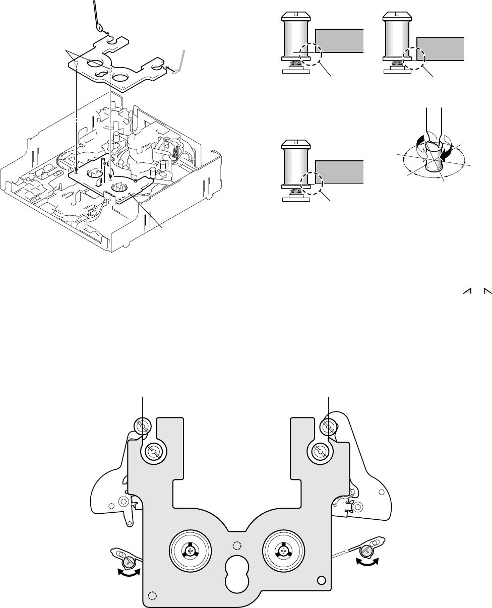
5-25
4-3. TG2/7 HEIGHT CHECK AND ADJUSTMENT
1. Preparation before check
1) Check that the cassette compartment block has already been
removed. (Refer to page 5-5.)
2) Set the mechanism deck to the loading end position (TG2 to 7
already moved to the loading end position and the pinch roller
is in the unloading position). Alternatively, set the mechanism
deck to the “LE position” using the mode selector II. (Refer to
page 5-5.)
3) Place the TG2/7 preset plate (J-13).
2. Check and adjustment
Rotate the TG upper flange until the height of the TG2/7 preset
plate (J-13) and TG2 or TG7 roller block is the same. Alterna-
tively, rotate the TG upper flange of only TG2 by 60˚ in the direction
of raising the guide from the adjusted height while referring to the
figure below.
1. Preparation before check
1) Check that the cassette compartment block has already been
removed. (Refer to page 5-5.)
2) Set the mechanism deck to the loading end position (TG2 to 7
already moved to the loading end position and the pinch roller
is in the unloading position). Alternatively, set the mechanism
deck to the “LE position” using the mode selector II. (Refer to
page 5-5.)
3) Place the TG2/7 preset plate (J-13).
2. Check and adjustment
Rotate each adjuster to adjust the TG2/7 position until or of
the TG2/7 preset plate (J-13), TG2 and TG7 are in line.
4-4. FWD/RVS POSITION CHECK AND ADJUSTMENT
Face the mirror (J-4) in the
direction of the arrow and
perform a visual check.
TG2/7 preset plate
(J-13)
Boss
Cassette reference plate
(J-11)
Attach the boss while
aligning it with the
hole of the cassette
reference plate (J-11).
TG2 or TG7
The guide is too low. The guide is too high.
Screwdriver for tape path (J-15)
The guide
is raised.
The guide
is lowered.
Not good Not good
Good
TG2 or TG7
TG2 or TG7
The normal height of TG2 is the position
where the TC upper flange is rotated by
60° in the direction of raising the guide
from the adjusted height while referring
to the figure below.
The normal height of TG7 is the current
one.
60°
60°
60°
60°
Align the center of TG2 with the vertically
extended line of the jig plate's tip as shown.
TG2 arm TG7 arm
Rotate the adjuster with a resin
screwdriver, etc. Be careful not
to bend the band.
Align the center of TG7 with the vertically
extended line of the jig plate's tip as shown.
TG2/7 preset plate (J-13)
Rotate the adjuster with a resin
screwdriver, etc. Be careful not
to bend the band.
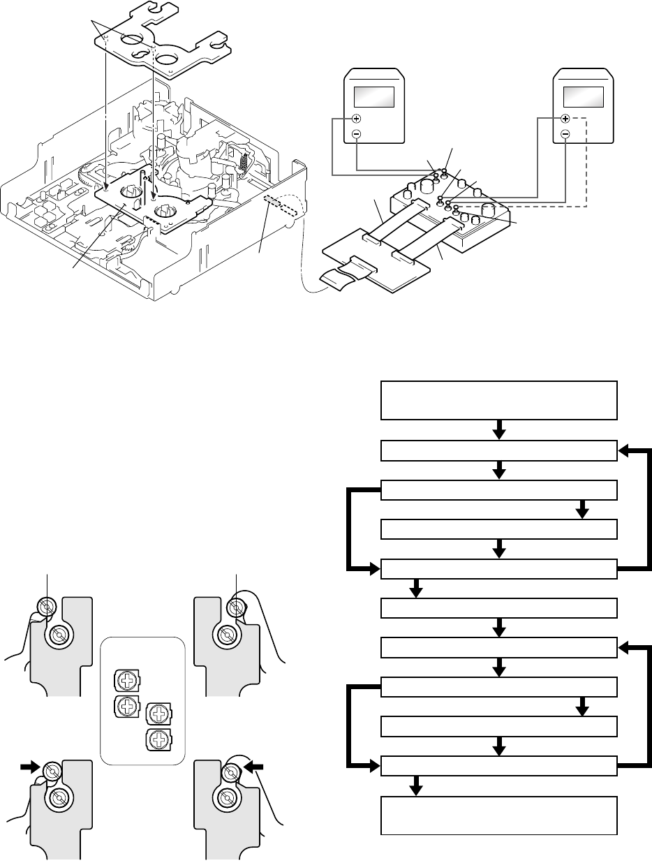
5-26
4-5. ELECTRIC TENSION REGULATOR CHECK AND ADJUSTMENT OF TG2/7 ARM
1. Preparation before check
1) Check that the cassette compartment block has already been
removed. (Refer to page 5-5.)
2) Set the mechanism deck to the loading end position (TG2 to 7
already moved to the loading end position and the pinch roller
is in the unloading position). Alternatively, set the mechanism
deck to the “LE position” using the mode selector II (J-9). (Refer
to page 5-5.)
3) Attach the cassette reference plate (J-11) and TG2/7 preset plate
(J-13). (Refer to page 5-25.)
4) Connect the relay board for tension regulator adjustment (J-
14) and other equipment as shown in the figure below.
2. Check and adjustment
Connect the positive (+) probe of a digital voltmeter to E.T out
(TG2: for measurement of TG2 data) or to E.T out (TG7: for mea-
surement of TG7 data). First, press the guide to the TG2/7 preset
plate (J-13), then release your hand from the guide and read the
voltmeter value. Adjust RV4 (TG2 side) or RV2 (TG7 side) until
the voltmeter measurement is 2.5 ± 0.1 V (TG2 side) or 2.2 ± 0.1
V (TG7 side) when releasing your hand. Then press the guide to
the TG2/7 preset plate (J-13). Adjust RV3 (TG2 side) or RV1 (TG7
side) until the voltmeter measurement is 1.3 ± 0.1 V.
Attach the boss while
aligning it with the hole
of the cassette reference
plate (J-11).
Boss TG2/7 preset plate
(J-13)
Regulated power supply
Apply +6.5 to 8.5V.
Digital voltmeter
Change the connection of the
positive (+) probe to
E.T out (TG7) and E.T out (TG2)
for measurement.
Cassette reference plate
(J-11)
CN2
Relay board for tension regulator adjustment (J-14)
16 pin
Board for tension regulator
adjustment (J-17)
E. T out (TG 2)
9 pin
DC IN (+) DC IN (–)
E. T out (TG 7)
GND
RV1
RV3
RV2
RV4
[2.5V adjustment of TG2]
Release your hand from the
guide and rotate RV4.
[2.2V adjustment of TG7]
Release your hand from the
guide and rotate RV2.
[1.3V adjustment of TG2]
Rotate RV3 while pushing
the guide.
[1.3V adjustment of TG7]
Rotate RV1 while pushing
the guide.
MD-76 board
Adjustment start
1 TG2: 2.5V adjustment (MD-76 board: RV4)
Adjustment end
Good 0 TG7: 1.3V check Not good
Good 8 TG7: 2.2V check Not good
Good 5 TG2: 1.3V check Not good
Good 3 TG2: 2.5V check Not good
2 TG2: 1.3V adjustment (MD-76 board: RV3)
4 TG2: 2.5V adjustment (MD-76 board: RV4)
6TG7: 2.2V adjustment (MD-76 board: RV2)
7 TG7: 1.3V adjustment (MD-76 board: RV1)
9 TG7: 2.2V adjustment (MD-76 board: RV2)
[Adjustment order]
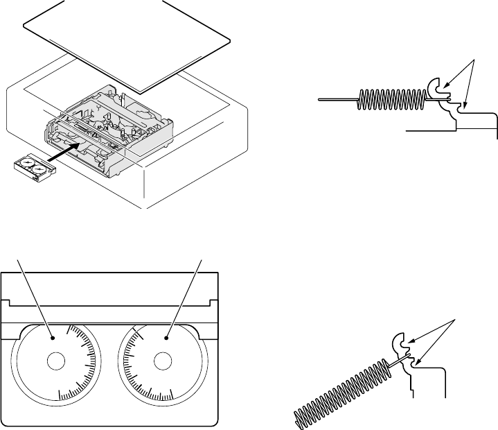
5-27
4-6. FWD/RVS BACK TENSION CHECK AND ADJUSTMENT
X
1
0
m
N
m
40
30
20
10
0
X
1
0
m
N
m
0
10
20
30
40
[FWD side]
9.5 ± 1.5 × 10
-1
mN • m [RVS side]
9.5 ± 1.5 × 10
-1
mN • m
Re-attach the spring to the upper hook if the
measurement value is beyond the specifications
or re-attach the spring to the lower hook if the
measurement value is below the specifications.
Then, repeat the measurement.
For more details,
refer to page 5-23.
Re-attach the spring to the upper hook if the
measurement value is beyond the specifications
or re-attach the spring to the lower hook if the
measurement value is below the specifications.
Then, repeat the measurement.
Be careful that these spring blocks may hinder
the FL motor.
For more details,
refer to page 5-23.
1. Preparation before check
Mount the mechanism deck in the main unit, connect all the con-
nectors, then insert the mini DV torque cassette (J-7) into the
mechanism block.
2. Check and adjustment
• FWD (TG2) side
The torque value should satisfy 9.5 ± 1.5 × 10⁻¹ mN • m while
the mini DV torque cassette runs in the FWD mode. If it does
not satisfy this, take the following measure.
• RVS (TG7) side
The torque value should satisfy 9.5 ± 1.5 × 10⁻¹ mN • m while
the mini DV torque cassette runs in the RVS mode. If it does
not satisfy this, take the following measure.
Visually check
the gauge block
of the cassette
with the top cover
assembly removed.
Mini DV torque cassette (J-7)
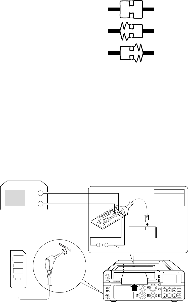
5-28
4-7. PREPARATION FOR ADJUSTMENT AND TAPE PATH CHECK
Preparation before adjustment (connection and setting)
1. Mount the mechanism deck in the main unit.
(Connect all the connectors.)
2. Clean the tape running side.
(Refer to “5-1-2. Periodic check”.)
3. Connect an oscilloscope to RP-234 board CN201 via the CPC-
13 jig (J-6082-388-A)(J-18).
Channel 1: RP-234 board, CN201 Pin 8 (Note)
External trigger: RP-234 board, CN007 Pin 6
Note: Connect a 75 Ω resistor between pins 8 of CN007 and 7
(GND).
75 Ω resistor (Parts code: 1-247-804-11)
4. Connect the adjustment remote commander (J-8) to the
CONTROL jack (LANC jack).
5. Turn the HOLD switch of the adjustment remote commander
to the ON position.
6. Select page: 3, address: 33, set data: 08 and press the PAUSE
button.
7. Select page: 3, address: 26, set data: 31 and press the PAUSE
button.
Procedure after operations
1. Connect the adjustment remote commander to the CONTROL
jack (LANC jack).
2. Turn the HOLD switch of the adjustment remote commander
to the ON position.
3. Select page: 3, address: 33, set data: 00 and press the PAUSE
button.
4. Select page: 3, address: 26, set data: 00 and press the PAUSE
button.
Tape path check (checking the RF waveform)
Play back the tracking tape (J-6) and check the states at the en-
trance and exit of the RF waveform. If it is not flat at either side,
perform the adjustments from Adjustment Start-4 in the flowchart
on page 5-23.
Normal entrance and exit sides
Faulty entrance side
Faulty exit side
XH2-1
CH1
EXT
TRIG
Oscilloscope
Connect to pin 8
Connect to pin 6
Pin No. Signal name
RF MONITOR
GND
JSWP
8
7
6
Connect to pin 7
75 Ω resistor Connect to pin 8
CN201
RP-234 board
RP-234 board
DECK
CPC-8 jig (J-18)
Adjustment
remote commander
(J-8)
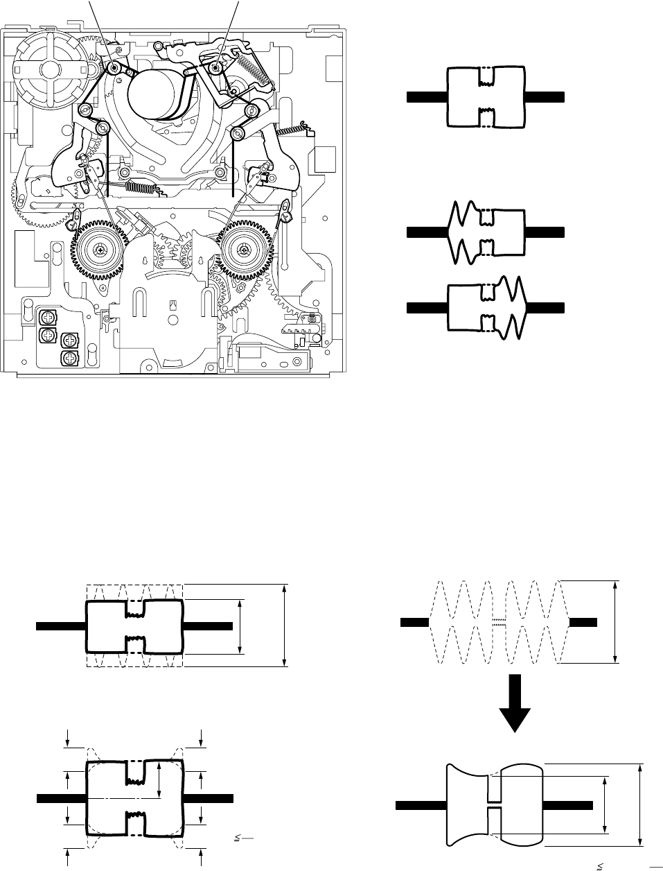
5-29
4-8. TRACK ADJUSTMENT AND CHECK
(Checking the RF Waveform)
• Checking the RF waveform
Check that the RF waveforms at both the entrance and exit are flat
while the tracking tape (J-6) runs in the PLAY mode.
4-9. TRACK CHECK
• Check
The difference between the maximum value and minimum value
of the waveform amplitude during playback of the tracking tape
(J-6) in the FWD mode should be 30% or less of the waveform
amplitude during the CUE (or REV) mode (which is taken as 100%
as shown). At the same time, there must not exist too much fluc-
tuation of waveform amplitude.
• If not flat
If the waveform at the entrance is bad, rotate TG3. If the wave-
form at the exit is bad, rotate TG6 to flatten the waveform.
RV1
RV3
RV2
RV4
TG3
(adjustment of entrance) TG6
(adjustment of exit)
C
C
0.65 A A
A : 100 %
C
C
AC 8
1
Tracking waveform check -1
Tracking waveform check -2
The waveform should not change sharply.
A
Emin
(Emin - Emax) 30% or ( A)
10
3
Emax
A : 100%
[Waveform in CUE or REV mode]
[Waveform in FWD mode]
Emin: Minimum value
Emax: Maximum value
If the waveform at
the entrance is bad,
rotate TG3 to adjust
the waveform.
If the waveform at
the exit is bad,
rotate TG6 to adjust
the waveform.
Exit sideEntrance side
Normal waveform
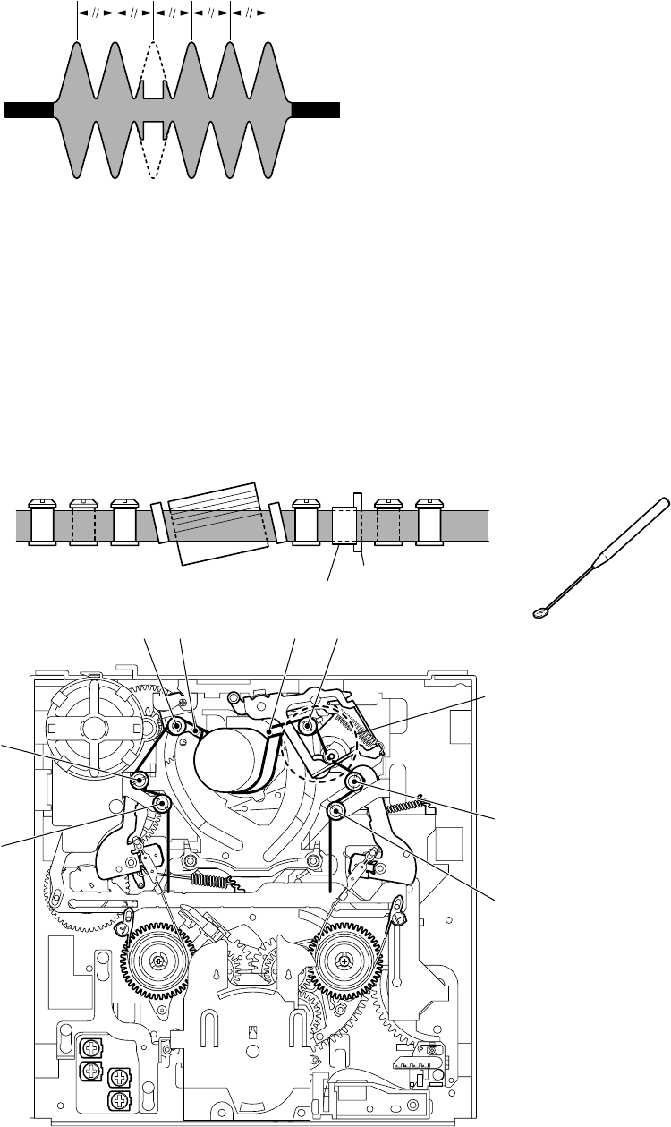
5-30
4-10. CUE/REV CHECK
• Check
Check that the intervals of the waveform peaks are consistent while
the tracking tape (J-6) runs in the CUE mode or REV mode.
4-11. CURL CHECK AND ADJUSTMENT
• Check
Check that the tape runs along each upper and lower flange while
the tracking tape (J-6) runs in the CUE or REV mode. Also check
that there are no large curls on each tape guide and pinch roller.
• If not even
If the waveform peaks are not even, perform Section 4-8, “Tack-
ing adjustment”.
• If the curl is large
Perform the adjustment from Adjustment Start -3 (TG7 side) of
the flowchart on page 5-23 again.
[Waveform in CUE or REV mode]
The intervals of the waveform peaks
must be consistent.
RV1
RV3
RV2
RV4
There should be no large curls
while the tape runs along each
upper and lower flange. Pinch rollerCapstan
Drum
Be careful that there are often large curls
around the capstan and pinch roller between
TG6 and TG7. If there are large curls, rotate
the upper flange of TG7 to remove the curls.
TG 2
TG 1
TG 1 TG 2
TG 8
TG 7
TG 6TG 5TG 4TG 3
TG 8TG 7TG 6TG 5TG 4TG 3
To check the tape path visually, use
the mirror (J-4) to facilitate check as
the frame of the cassette compartment
hinders operations.
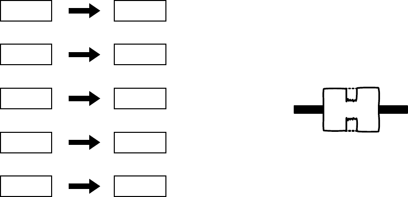
5-31
4-12. RISING CHECK
• Check
Check that when the tracking tape (J-6) is switched from the STOP,
CUE, REV, FF, REW modes to the PLAYBACK mode, the wave-
form rises horizontally within 2 seconds. (Perform this 2 or 3 times.)
• Check after checking rising
• Check that the tape loads and unloads smoothly.
• Play a self-recorded or already recorded tape, and check that
the sound and images are normal.
When switching the modes, the waveform
should rise horizontally within 2 seconds.
STOP
REV
REW
FF
CUE
PLAYBACK
PLAYBACK
PLAYBACK
PLAYBACK
PLAYBACK
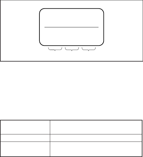
5-32
5-2. SERVICE MODE
5-2-1. ADJUSTING REMOTE COMMANDER
The adjusting remote commander is used for changing the calcu-
lation coefficient in signal processing, EVR data, etc. The adjust-
ing remote commander performs bi-directional communication
with the unit using the remote commander signal line (LANC).
The resultant data of this bi-directional communication is written
in the non-volatile memory.
1. Used Adjustment Remote Commander
1) With the unit set in STANDBY mode, connect the adjusting
remote commander to the remote (LANC) terminal.
2) Adjust the HOLD switch of the adjusting remote commander
to “HOLD” (SERVICE position).
3) Turn on the power with the ON/STANDBY switch of the unit.
If it has been properly connected, the LCD on the adjusting re-
mote commander will display as shown in Fig. 5-2-1.
Fig. 5-2-1
4) Operate the adjusting remote commander as follows.
• Changing the page
The page increases when the EDIT SEARCH + button is
pressed, and decreases when the EDIT SEARCH – button is
pressed. There are altogether 16 pages, from 0 to F.
Hexadecimal 0123456789ABCDEF
notation
LCD Display 0123456789AbcdEF
Decimal notation 0 1 2 3 4 5 6 7 8 9 10 11 12 13 14 15
conversion value
Table 5-2-1
• Changing the address
The address increases when the FF (M) button is pressed,
and decreases when the REW (m) button is pressed. There
are altogether 256 addresses, from 00 to FF.
• Changing the data (Data setting)
The data increases when the PLAY (N) button is pressed,
and decreases when the STOP (x) button is pressed. There
are altogether 256 data, from 00 to FF.
• Writing the adjustment data
The PAUSE button must be pressed to write the adjustment
data (C page, D page and E page) in the nonvolatile memory.
(The new adjustment data will not be recorded in the non-
volatile memory if this step is not performed.)
2. Precautions Upon Using the Adjusting Remote
Commander
Mishandling of the adjusting remote commander may erase the
correct adjustment data at times. To prevent this, it is recommended
that all adjustment data be noted down before beginning adjust-
ments and new adjustment data after each adjustment.
0 : 00 : 00
Page Data Address
5-33
5-2-2. DATA PROCESSING
The calculation of the adjusting remote commander display data
(hexadecimal notation) are required for obtaining the adjustment
data of some adjustment items. In this case, after converting the
hexadecimal notation to decimal notation, calculate and convert
the result to hexadecimal notation, and use it as the adjustment
data. Table 5-2-2 indicates the hexadecimal notation- the decimal
notation, calculation table.
Hexadecimal nontation-Decimal notation
The lower digits of the 0 1 2 3 4 5 6 7 8 9 A B C D E F
hexadecimal notation
The upper digits of the (A)(b)(c)(d)(E)(F)
hexadecimal notation
00 1 2 3 4 5 6 7 8 9 10 11 12 13 14 15
116 17 18 19 20 21 22 23 24 25 26 27 28 29 30 31
232 33 34 35 36 37 38 39 40 41 42 43 44 45 46 47
348 49 50 51 52 53 54 55 56 57 58 59 60 61 62 63
464 65 66 67 68 69 70 71 72 73 74 75 76 77 78 79
580 81 82 83 84 85 86 87 88 89 90 91 92 93 94 95
696 97 98 99 100 101 102 103 104 105 106 107 108 109 110 111
7112 113 114 115 116 117 118 119 120 121 122 123 124 125 126 127
8128 129 130 131 132 133 134 135 136 137 138 139 140 141 142 143
9144 145 146 147 148 149 150 151 152 153 154 155 156 157 158 159
A (A)160 161 162 163 164 165 166 167 168 169 170 171 172 173 174 175
B (b)176 177 178 179 180 181 182 183 184 185 186 187 188 189 190 191
C (c)192 193 194 195 196 197 198 199 200 201 202 203 204 205 206 207
D (d)208 209 210 211 212 213 214 215 216 217 218 219 220 221 222 223
E (E)224 225 226 227 228 229 230 231 232 233 234 235 236 237 238 239
F (F)240 241 242 243 244 245 246 247 248 249 250 251 252 253 254 255
1→
2
↓
Note : ( ) indicate the adjusting remote control unit display.
(Example) In the case that the adjusting remote control unit display are BD (bd).
As the upper digit of the hexadecimal notation is B (b), and the lower digit is D (d), the intersection “189” of the
1 and 2 in the above table is the decimal notation to be calculated.
Table 5-2-2
5-34
5-2-3. SERVICE MODE
1. Emergence Memory Address
Page C Address 38 to 43
Address Contents
38 EMG code when first error occurs
3A Upper: MSW code when shift starts when first error
occurs
Lower: MSW code when first error occurs
3B Lower: MSW code to be moved when first error
occurs
3C EMG code when second error occurs
3E Upper: MSW code when shift starts when second
error occurs
Lower: MSW code when second error occurs
3F Lower: MSW code to be moved when second error
occurs
40 EMG code when last error occurs
42 Upper: MSW code when shift starts when last error
occurs
Lower: MSW code when last error occurs
43 Lower: MSW code to be moved when last error
occurs
When no error occurs in this unit, data “00” is written in the above
addresses (38 to 43). when first error occurs in the unit, the data
corresponding to the error is written in the first emergency ad-
dress (38 to 3B). In the same way, when the second error occurs,
the data corresponding to the error is written in the second emer-
gency address (3C to 3F).
Finally, when the last error occurs, the data corresponding to the
error is written in the last emergency address (40 to 43).
Note 2: After completing adjustments, be sure to initialize the
data of addresses 38 to 43 to “00”.
Initializing method:
1) Select page: 0, address: 01, and set data: 01.
2) Select page: C, address: 38, set data: 00, and press the PAUSE
button.
3) Select address: 39 to 43 and set data “00” into them in the
same way as in address: 10.
4) Select page: 0, address: 01, and set data: 00.
2. EMG Code (Emergency Code)
Codes corresponding to the errors which occur are written in ad-
dresses 38, 3C, 3E. The type of error indicated by the code are
shown in the following table.
Code Error Type
00 No error (Initial state)
10 Loading motor time-out during LOAD
11 Loading motor time-out during UNLOAD
20 Error during tape take up
22 T reel error
23 S reel error
25 Reel motor error
30 Error during normal capstan rotation
40 FG error during drum start-up
42 FG error during normal drum rotation
50 DEW detection
52 Wet DEW detection
70 Cassette compartment LOAD error
71 Cassette compartment UNLOAD error
72 Retry error because something is caught
5-35
3. MSW Code
MSW when an alarm occurred: MSW (Mode Switch) information when an alarm occurred.
MSW when a transition starts: MSW information when the mechanism position starts to move (if L motor runs).
MSW of target destination: MSW information of target position if the mechanism position moves.
Mechanism position MSW code Description
ULE E Unload end position. The mechanism stops at this position when it ejects a cassette. It waits for cassette
insertion. The guide starts to expand as it advances to the load position.
BL F Blank code. It is provided between code and code. The mechanism does not stop at this code (excluding
Load/Unload).
DEW C Code during loading.
LE D Load end position of tape guide.
REW 9 Position of REW operation. The pinch rollers are released.
FF 5 Position of FF operation. The pinch rollers are released.
STOP 7 Stop position. The pinch rollers are released, the tension regulator returns, and the brake is applied to both
reels.
FWD/RVS B PB, REC, CUE, REVIEW, and PAUSE positions. The mechanism operates at this position in the mode
where normal screen appears with the pinch rollers in contact state and the tension regulator turned on.
NULL 0 Code not existing in MD. Default value.
1110=E
1111=F
T UNLOAD
Pinch rollers contact
ULE BL
1100=C
1111=F
DEW BL
1101=D
1111=F
LE BL
1001=9
1111=F
REW BL
0101=5
1111=F
FF BL
0111=7
1111=F
STOP BL
1011=B
FWD/RVS
LOAD t
Mechanism position
D (MSB)
C
B
A (LSB)
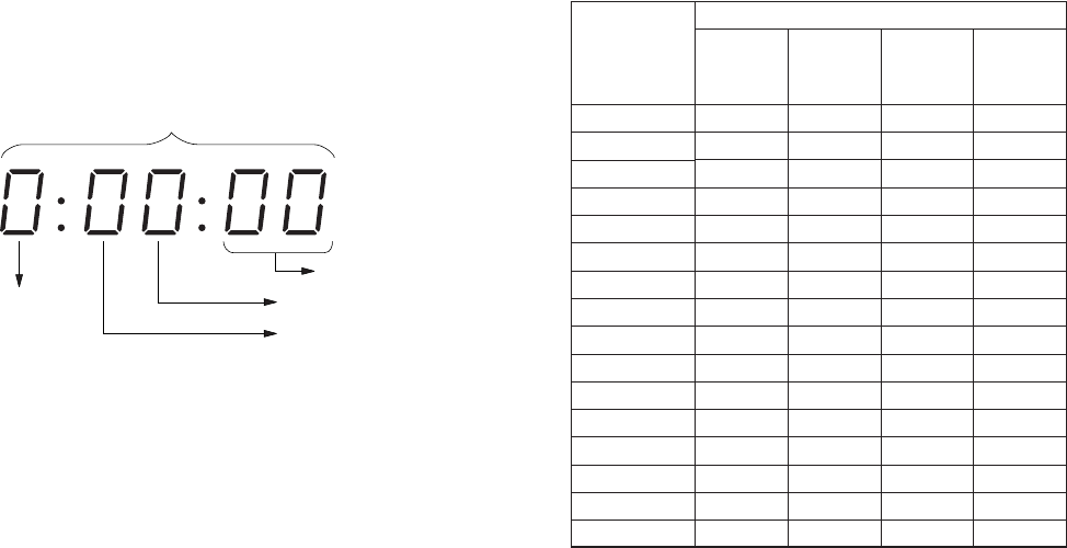
5-36
4. Bit Value Discrimination
Bit values must be discriminated using the display data of the ad-
justment remote commander for the following items. Us the table
below to discriminate if the bit value is “1” or “0”.
(Example) If the remote commander display is “8E”, bit value from
bit 7 to bit 4 can be discriminated from the column A,
and those from bit 3 to bit 0 from column B.
Page
Address
bit3 to bit0 discrimination
bit7 to bit4 discrimination
Display on the adjustment remote commander
Display on the
adjustment
remote
commander
0
1
2
3
4
5
6
7
8
9
A (A)
B (b)
C (C)
D (d)
E (E)
F (F)
Bit values
bit3
or
bit7
0
0
0
0
0
0
0
0
1
1
1
1
1
1
1
1
bit2
or
bit6
0
0
0
0
1
1
1
1
0
0
0
0
1
1
1
1
bit1
or
bit5
0
0
1
1
0
0
1
1
0
0
1
1
0
0
1
1
bit0
or
bit4
0
1
0
1
0
1
0
1
0
1
0
1
0
1
0
1
A
B

5-37
5. Record of Use Check
Page E Address D0 to E3
Using method:
1) The record of use data is displayed at page: E, addresses: D0
to E3.
Note: When the drum was replaced, initialize the drum rotation
counted time.
Initializing method:
1) Select page: 0, address: 01, and set data: 01.
2) Select page: E, address: D0, set data: 00, and press the PAUSE
button.
3) Select address: D1 and E3 and set data “00” into them in the
same way as in address: D0.
4) Select page: 0, address: 01, and set data: 00.
Function
OPRATION 1 Lower two digits
Higher two digits
DRUM RUN 1 Lower two digits
Higher two digits
TAPE RUN 1 Lower two digits
Higher two digits
THREADING 1 Lower two digits
Higher two digits
CHECK SUM 1 Lower two digits
Higher two digits
OPRATION 2 Lower two digits
Higher two digits
DRUM RUN 2 Lower two digits
Higher two digits
TAPE RUN 2 Lower two digits
Higher two digits
THREADING 2 Lower two digits
Higher two digits
CHECK SUM 2 Lower two digits
Higher two digits
Address
D0
D1
D2
D3
D4
D5
D6
D7
D8
D9
DA
DB
DC
DD
DE
DF
E0
E1
E2
E3
Remark
The cumulative total hours of operating time is displayed.
The cumulative total hours of drum rotation with tape threaded is displayed.
The cumulative total hours of tape running time is displayed.
The cumulative number of tape unthreading operations is displayed.
The cumulative total hours of operating time is displayed.
The cumulative total hours of drum rotation with tape threaded is displayed.
The cumulative total hours of tape running time is displayed.
The cumulative number of tape unthreading operations is displayed.
5-38
6. Switch Check (Audio jack 1)
Page 9 Address E0
Using method:
1) Select page: 9, address: E0.
2) By discriminating the bit value of display data, the state of the
switches can be discriminated.
7. Switch Check (Audio jack 2)
Page 9 Address E1
Using method:
1) Select page: 9, address: E1.
2) By discriminating the bit value of display data, the state of the
switches can be discriminated.
8. Switch Check (Video jack)
Page 9 Address E2
Using method:
1) Select page: 9, address: E2.
2) By discriminating the bit value of display data, the state of the
switches can be discriminated.
Bit
1,0
3,2
5,4
7,6
Function
Audio input level switch (CH-1)
(JK-169 board S102)
Audio input level switch (CH-2)
(JK-169 board S103)
Audio input level switch (CH-3)
(JK-169 board S106)
Audio input level switch (CH-4)
(JK-169 board S107)
When bit value = 0, 0 When bit value = 0, 1 When bitvalue = 1, 0
+4 -60 -20
+4 -60 -20
+4 -60 -20
+4 -60 -20
Bit
1,0
3,2
5,4
7,6
Function
Audio input select switch (CH-1)
(JK-169 board S104)
Audio input select switch (CH-2)
(JK-169 board S105)
Audio input select switch (CH-3)
(JK-169 board S108)
Audio input select switch (CH-4)
(JK-169 board S109)
When bit value = 0, 0 When bit value = 0, 1 When bitvalue = 1, 0
CAM LINE +48V ON
CAM LINE +48V ON
CAM LINE +48V ON
CAM LINE +48V ON
Bit
0
1
2
3
4
Function
SUPERIMPOSE
(JK-169 board S110)
INPUT SELECT
(JK-169 board S111)
When bit value = 0 When bit value = 1
OFF ON
DV
VIDEO
S VIDEO
CAMERA
5-39
9. Switch Check (Key code)
Page 9 Address 13
Function Data
PLAY (FR-157 board S528) 01
STOP (FR-157 board S531) 02
F FWD (FR-157 board 529) 03
REW (FR-157 board S527) 04
PAUSE (FR-157 board S532) 05
REC (FR-157 board S533) 15
REC (FR-157 board S533) 06
+ PLAY (FR-157 board S528)
END SEARCH (FR-157 board S535) 10
DUP (FR-157 board S530) 1D
AUDIO DUB (FR-157 board S534) 1C
AUDIO DUB (FR-157 board S534) 0B
+ PLAY (FR-157 board S528)
DUP (FR-157 board S530) 1A
+ PLAY (FR-157 board S528)
DUP (FR-157 board S530) 1E
+ PLAY (FR-157 board S528)
+ PAUSE (FR-157 board S532)
INDEX (FR-157 board S515) 1B
Using method:
1) Select page: 9, address: 13.
2) By discriminating the display data, the pressed key can be
discriminated.
10. Switch Check (Key data 1)
Page 9 Address 26
Bit Function
0 STOP (FR-157 board S531)
1 REW (FR-157 board S527)
2 PLAY (FR-157 board S528)
3 REC (FR-157 board S533)
4 PAUSE (FR-157 board S532)
5 F FWD (FR-157 board S529)
6 END SERCH (FR-157 board S535)
7
Using method:
1) Select page: 9, address: 26.
2) By discriminating the bit value of display data, the pressed
key can be discriminated.
11. Switch Check (Key data 2)
Page 9 Address 27
Bit Function
0 AUDIO DUB (FR-157 board S534)
1 INDEX (FR-157 board S515)
2 DUP (FR-157 board S530)
3 FINE (FR-157 board S536)
4 LIGHT (FR-157 board S538)
5
6
7
Using method:
1) Select page: 9, address: 27.
2) By discriminating the bit value of display data, the pressed
key can be discriminated.
5-40
12. Switch Check (Slide switch 1)
Page 9 Address 28
Bit Function When bit value = 0 When bit value = 1
0 DV CAM/DV DV CAM DV
(VD-28 board S702)
Using method:
1) Select page: 9, address: 28.
2) By discriminating the bit value of display data, the state of the switches can be discriminated.
13. Switch Check (Slide switch 2)
Page 9 Address 28
Bit Function When bit value = 0, 1 When bit value = 1, 0 When bit value = 1, 1
5, 4 DISPLAY (ON/OFF/LCD OFF) OFF ON LCD OFF
(FR-157 board S524)
7, 6 DISPLAY (AUDIO/TC/MENU) TC AUDIO MENU
(FR-157 board S525)
Using method:
1) Select page: 9, address: 28.
2) By discriminating the bit value of display data, the state of the
switches can be discriminated.
14. Switch Check (Slide switch 3)
Page 9 Address 29
Bit Function When bit value = 0 When bit value = 1
0 METER CH 3/4 CH 1/2
(FR-157 board S516)
1
2 COUNTER U-BIT TC
(FR-157 board S518)
3 KEY INH OFF ON
(FR-157 board S519)
4 AUDIO SELECT (CH-1) MANU AUTO
(FR-157 board S520)
5 AUDIO SELECT (CH-2) MANU AUTO
(FR-157 board S521)
6 AUDIO SELECT (CH-3) MANU AUTO
(FR-157 board S522)
7 AUDIO SELECT (CH-4) MANU AUTO
(FR-157 board S523)
Using method:
1) Select page: 9, address: 29.
2) By discriminating the bit value of display data, the state of the
switches can be discriminated.
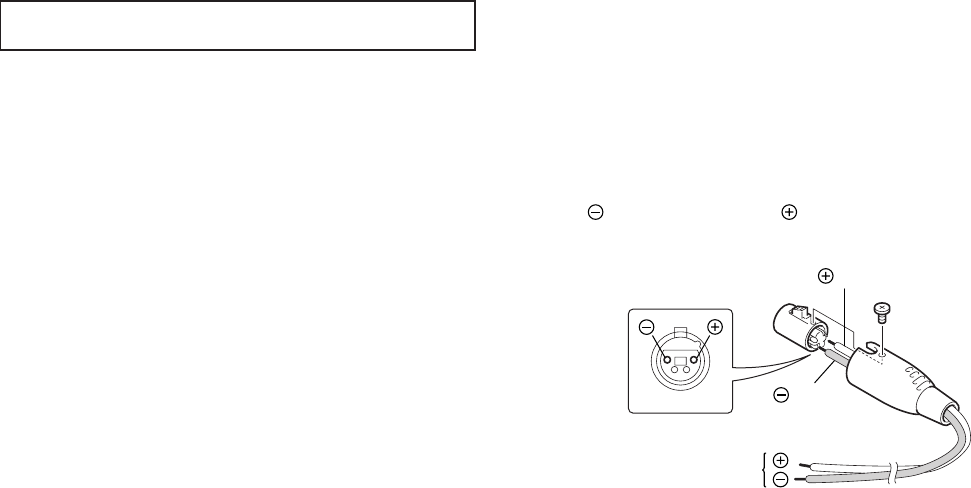
5-41
Solder a cable to the pin 1 and a cable to the pin 4 of the
circular connector (PF, XLR4P) (1-784-897-11).
Regulated power supply
(14.4 ± 0.2 Vdc, 4 A or more)
cable
cable
1
23
4
5-3. VIDEO SECTION ADJUSTMENTS
When performing adjustments, refer to the layout diagrams
for adjustment related parts on page 5-98.
3-1. PREPARATIONS BEFORE ADJUSTMENT
3-1-1. Equipment Used
1) TV monitor
2) Oscilloscope with 2-phenomenon, 30 MHz band, and delay
mode (Unless specified otherwise, use a 10 : 1 probe)
3) Frequency counter
4) Digital voltmeter
5) Balanced audio generator
6) Audio level meter
7) Audio noise meter
8) Audio attenuator
9) Pattern generator (with VIDEO OUTPUT terminal and exter-
nal sync function)
10) Pattern generator (with COMPONENT OUTPUT terminal)
11) Vectorscope (with SCH function)
(NTSC: with SETUP function)
12) Alignment tape
•SW/OL reference (XH2-3)
Parts code: 8-967-997-11
•Audio operation check for NTSC (XH5-3)
Parts code: 8-967-997-51
•System operation check for NTSC (XH5-5)
Parts code: 8-967-997-61
•Audio operation check for PAL (XH5-3P)
Parts code: 8-967-997-55
•System operation check for PAL (XH5-5P)
Parts code: 8-967-997-66
13) Adjusting remote control unit (J-6082-053-B)
14) Extension board
•For extension between CN8001 of the JC-20 board and
CN9500 of the DI-73 board. (120P, 0.5 mm) (J-6082-511-A)
15) Regulated power supply
16) Time code generator (NTSC: BVG-1600/
PAL : BVG-1600P etc.)
17) Time code reader (BVG-1500 etc.)
18) Circular connector (PF, XLR4P)
•For connection of the regulated power supply. (Note)
Parts code: 1-784-897-11
NTSC: DSR-50
PAL : DSR-50P
Note: How to Make DC Cable
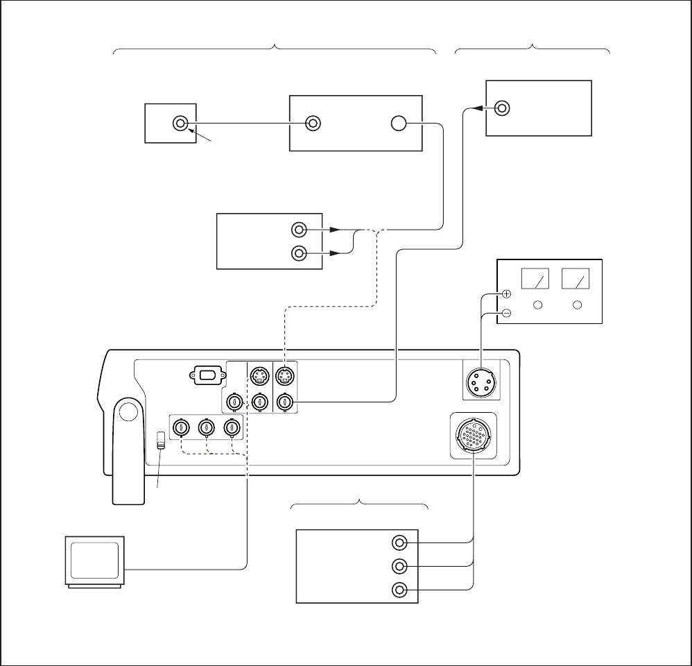
5-42
3-1-2. Connection of Equipment
According to the specification for the input terminal (CAMERA
input, S VIDEO input, VIDEO input, or DV input), connect
measuring equipment as shown in Fig. 5-3-1, and make adjustment.
The input terminal is specified in ( ) of the signal column.
Any input terminal can be used unless otherwise specified.
To switch between CAMERA input, S VIDEO input, VIDEO input
and DV input, use the INPUT SELECT switch.
Fig. 5-3-1
Note 1: In adjustments specifying for the S VIDEO input to be
used, using the VIDEO input would disable the product
specifications of this unit from being satisfied. Always
use the input signal specified.
Note 2: If adjustments are used with the VTR with the S video
output terminal as the signal source, the performance of
this unit may be affected by the VTR. Use a pattern gen-
erator with a Y/C separator terminal as much as possible.
Pattern generator
Pattern generator
•When a pattern generator without
the Y/C separator terminal is used.
VTR with S VIDEO terminal (E-E mode)
VIDEO IN
S VIDEO OUT
VIDEO OUT
(75 Ω)
•When a pattern generator with
the Y/C separator terminal is used.
Pattern generator
NTSC: DSR-50
PAL : DSR-50P
DV
INPUT SELECT
switch
MONITOR TV
When CAMERA is specified
Y OUT (75 Ω)
R-Y OUT (75 Ω)
B-Y OUT (75 Ω)
Pattern generator with the
COMPONENT OUTPUT terminal
Regulated power supply
(14.4 ± 0.2 Vdc, 4A or more)
When VIDEO is specified
When S VIDEO is specified
VIDEO OUT
(75 Ω)
Y OUT (75 Ω)
CHROMA
OUT (75 Ω)
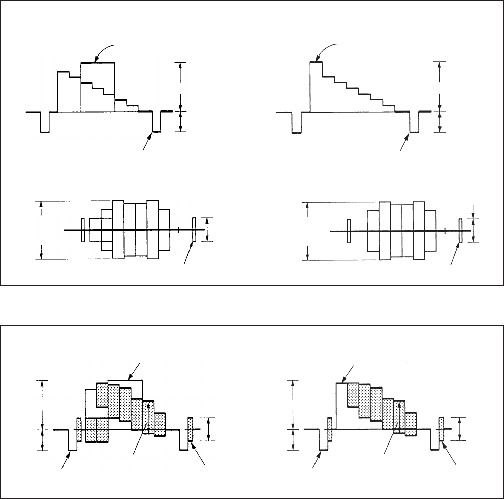
5-43
3-1-3. Checking the Input Signals
Because the video signal obtained from the pattern generator is
used as the adjustment signal for adjustments, the video output
signal must satisfy the given specifications.
1. S VIDEO Input
Connect the oscilloscope to the Y signal terminal of the S VIDEO
input terminal, and check that the sync signal of the Y signal is
approximately <0.286> [0.30] V and that the amplitude of the video
section is approximately <0.714> [0.70] V. (When a VTR with the
S VIDEO output terminal is used, also check that the chroma sig-
nal and burst signal have not remained)
Connect the oscilloscope to the chroma signal terminal of the S
VIDEO input terminal, and check that the burst signal amplitude
of the chroma signal is approximately <0.286> [0.30] V and flat,
and that the red signal amplitude of the chroma signal is approxi-
mately <0.66> [0.67] V. The Y and chroma signals used in the
adjustment are shown in Fig. 5-3-2.
< >: NTSC model
[ ]: PAL model
2. VIDEO Input
Connect the oscilloscope to the VIDEO input terminal, and check
that the sync signal amplitude of the video signal is approximately
<0.286> [0.30] V, the amplitude of the video section is approxi-
mately <0.714> [0.70] V, the amplitude of the burst signal is ap-
proximately <0.286> [0.30] V and flat, and that the red signal am-
plitude of the chroma signal is approximately <0.66> [0.67] V.
The video signal (color bar) used for adjustments is shown in Fig.
5-3-3.
< >: NTSC model
[ ]: PAL model
NTSC: DSR-50
PAL : DSR-50P
Fig. 5-3-2 Color Bar Signal of Pattern Generator
Fig. 5-3-3 Color Bar Signal of Pattern Generator
For NTSC model (with setup)
Y Signal
White (100%)
Approx. 0.714 V
Approx.
0.286 V
Horizontal sync signal
For PAL model
Y Signal
White (100%)
Approx. 0.70 V
Approx.
0.30 V
Horizontal sync signal
Chroma Signal
Chroma signal
amplitude
Approx. 0.67 V
Burst signal
amplitude
Approx. 0.286 V
Burst signal (Should be flat)
Chroma Signal
Chroma signal
amplitude
Approx. 0.66 V
Burst signal
amplitude
Approx.
0.30 V
Burst signal (Should be flat)
For NTSC model (with setup)
Approx. 0.714 V
Approx.
0.286 V
Horizontal sync signal
Red
(Approx. 0.67 V) Burst signal
(Should be flat)
White (Approx. 100%)
Approx.
0.286 V
Approx. 0.7 V
Approx.
0.3 V
Horizontal sync signal
Red
(Approx. 0.66 V) Burst signal
(Should be flat)
White (Approx. 100%)
Approx.
0.30 V
For PAL model
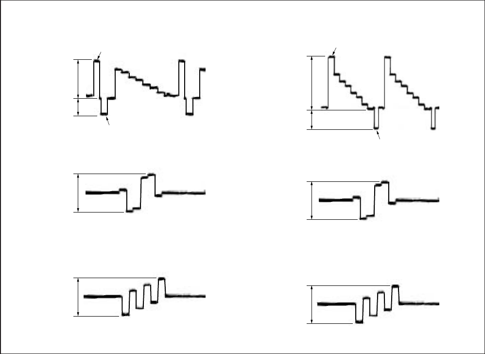
5-44
3. CAMERA Input
Connect the oscilloscope to the Y signal terminal of the CAM-
ERA terminal, and check that the sync signal of the Y signal is
approximately <0.286> [0.30] V and that the amplitude of the video
section is approximately <0.714> [0.70] V. Connect the oscillo-
scope to the R-Y signal terminal of the CAMERA terminal, and
check that the R-Y signal amplitude is approximately <0.700>
[0.525] V. Connect the oscilloscope to the B-Y signal terminal of
the CAMERA terminal, and check that the B-Y signal amplitude
is approximately <0.700> [0.525] V. The Y, R-Y and B-Y signals
used in the adjustment are shown in Fig. 5-3-4.
< >: NTSC model
[ ]: PAL model
Fig. 5-3-4
Approx.
0.714 V
White (100%)
Y signal
CR signal
CB signal
Approx.
0.286 V
Horizontal sync signal
Approx.
0.7 V
Approx.
0.7 V
Approx.
0.70 V
White (100%)
Y signal
CR signal
CB signal
Approx.
0.30 V
Horizontal sync signal
Approx.
0.525 V
Approx.
0.525 V
NTSC: DSR-50
PAL : DSR-50P
For NTSC model (with Setup) For PAL model
5-45
3-1-4. Adjustment Tapes
Use the alignment tapes shown in the following table.
Use tapes specified in the signal column of each adjustment.
Name Use
SW/OL standard (XH2-3) Switching position
adjustment
Audio operation check Audio system adjustment
(XH5-3 (NTSC), XH5-3P (PAL))
System operation check Operation check
(XH5-5 (NTSC), XH5-5P (PAL))
BIST check BIST check
(XH5-6 (NTSC), XH5-6P (PAL))
Table 5-3-1
Fig. 5-3-5 shows the color bar signals recorded on the alignment
tape for Audio Operation Check.
Note: Measure with video terminal (Terminated at 75 Ω)
NTSC: DSR-50
PAL : DSR-50P
Fig. 5-3-5 Color Bar Signal of Alignment Tapes
White (100%)
Color bar signal waveform
0.714 V
Horizontal sync signal
White (75%)
1 V
0.286 V Q I
Burst signal
Yellow
Cyan
Green
Magenta
Red
Blue
0.286 V
(75%)
Yellow
Cyan
Green
Magenta
Red
Blue
White
Q I
White
(100%)
Black
Color bar Pattern
White (100%)
Color bar signal waveform
0.7 V
Horizontal sync signal
1 V
0.3 V
Burst signal
Yellow
Cyan
Green
Magenta
Red
Blue
0.3 V
(100%)
Yellow
Cyan
Green
Magenta
Red
Blue
White
Black
Color bar Pattern
For NTSC model
For PAL model
5-46
3-1-5. Input/output Level and Impedance
Inputs
VIDEO/REF.IN BNC type
1 Vp-p (75 ohms, unbalanced)
S VIDEO IN Mini DIN 4-pin
Luminance signal: 1 Vp-p
(75 ohms, unbalanced)
Chrominance signal:
0.286 Vp-p (DSR-50)
0.3 Vp-p (DSR-50P)
(75 ohms unbalanced)
DV IN/OUT 6-pin IEEE-1394 standard jack
(i.LINK)
AUDIO INPUT (CH-1 to CH-4)
XLR 3-pin, female, +4/ –20/
–60 dBu, Impedance more than
3 kohms, balanced (48 V
phantom power supply)
Maximum input level
–60: –19 dBu (about 90 mVrms)
–20: +8 dBu (about 2 Vrms)
+4: +30 dBu (about 25 Vrms)
CAMERA 26-pin
Composite: 1 Vp-p (75 ohms,
unbalanced)
Component:
Y : 1 Vp-p (75 ohms, unbalanced)
B-Y: 0.7 Vp-p (75 ohms,
unbalanced)
(DSR-50: 75%, color bars / DSR-
50P: 100%, colour bars)
R-Y: 0.7 Vp-p (75 ohms,
unbalanced)
(DSR-50: 75%, color bars / DSR-
50P: 100%, colour bars)
Audio: –20/ –60 dBu, Impedance
more than 3 kohms, balanced
TC IN BNC type
0.5 to 18 Vp-p (time code input)
0.5 to 4 Vp-p (through output)
Outputs
VIDEO OUT1 BNC type, 1 Vp-p (75 ohms,
unbalanced) (superimpose)
VIDEO OUT2 BNC type, 1 Vp-p (75 ohms,
unbalanced)
COMPONENT OUTPUT
Y: BNC type
1 Vp-p (75 ohms, unbalanced)
R-Y: BNC type
0.7 Vp-p (75 ohms, unbalanced)
(DSR-50: 75%, color bars / DSR-
50P: 100%, colour bars)
B-Y: BNC type
0.7 Vp-p (75 ohms, unbalanced)
(DSR-50: 75%, color bars / DSR-
50P: 100%, colour bars)
S VIDEO OUT Mini DIN 4-pin
Luminance signal: 1 Vp-p
(75 ohms, unbalanced)
Chrominance signal:
0.286 Vp-p (DSR-50)
0.3 Vp-p (DSR-50P)
(75 ohms, unbalanced)
AUDIO OUTPUT (CH-1 to CH-4)
Phono jack, –10 dBu, 47 kohms,
Output impedance: less than
1 kohms
(DSR-50: –20 dB from full bit /
DSR-50P: –18 dB from full bit)
AUDIO MONITOR OUT
Phono jack
TC OUT BNC type, 2.2 Vp-p, 600 ohms /
1.2 Vp-p, 75 ohms
0.5 to 4 Vp-p (through output,
600 ohms)
PHONES Stereo phone jack
–∞ to –19 dBu, adjustable
DC IN 12V XLR 4-pin, male, 12 V

5-47
3-2. SYSTEM CONTROL SYSTEM
ADJUSTMENTS
1. Initializing the C, D, E Page Data
Note 1: If “Initializing the C, D, E Page Data” is performed, all
data of the C page, D page and E page will be initialized.
Note 2: If the C, D, E page data has been initialized, “Modifica-
tion of C, D, E page Data” and all adjustments need to be
performed again.
Mode E-E
Signal Arbitrary
Adjustment Page C
Adjustment Address 00 to DF
Adjustment Page D
Adjustment Address 10 to 3F
Adjustment Page E
Adjustment Address 10 to E8
5. Modification of C, D, E, Page Data
If the C, D, E page data has been initialized, change the data of the
“Fixed data-2” address shown in the following tables by manual
input.
Modifying Method:
1) Before changing the data, select page: 0, address: 01, and set
data: 01.
2) New data for changing are not shown in the tables because
they are different in destination. When changing the data, copy
the data built in the same model.
Note : If copy the data built in the different model, this set may
not operate.
3) When changing the data, press the PAUSE button of the ad-
justing remote commander each time when setting new data
to write the data in the non-volatile memory.
4) Check that the data of adjustment addresses is the initial value.
If not, change the data to the initial value.
5) After completing “Modification of C, D, E Page Data”, select
page: 0, address: 01, and set data: 00. Also perform all adjust-
ments.
2. Input of C Page Initial Data
Input method:
1) Select page: 0, address: 01, and set data: 01.
2) Select page: 3, address: 80, set data: 0C, and press the PAUSE
button on the adjustment remote commander.
3) Select page: 3, address: 80, and check that the data change to
“1C”.
4) Press the RESET switch at the bottom of the set using a thin
and long pin.
5) Modify the C page data. (Refer to C page table)
3. Input of D Page Initial Data
Input method:
1) Select page: 0, address: 01, and set data: 01.
2) Select page: 3, address: 80, set data: 0D, and press the PAUSE
button on the adjustment remote commander.
3) Select page: 3, address: 80, and check that the data change to
“1D”.
4) Press the RESET switch at the bottom of the set using a thin
and long pin.
5) Modify the D page data. (Refer to D page table)
4. Input of E Page Initial Data
Input method:
1) Select page: 0, address: 01, and set data: 01.
2) Select page: 9, address: 00, set data: 2D, and press the PAUSE
button on the adjustment remote commander.
3) Select page: 9, address: 01, set data: 2D, and press the PAUSE
button.
4) Select page: 9, address: 02, and check that the data change to
“01”.
5) Disconnect the adjustment remote commander, and turn the
POWER switch OFF.
6) Turn off the regulated power supply connected to the DCIN
terminal once, and turn it on again.
7) Check that the date, time, available tape capacity, and format
are displayed on the display window (monochrome LCD) of
the set.
8) Turn the POWER switch ON.
9) Press the RESET switch at the bottom of the set using a thin
and long pin.
10) Modify the E page data. (Refer to E page table)
5-48
Address Initial value Remark
NTSC PAL
00 to 0F Fixed data-1 (Initialized data)
10 EE EE
11 00 00 Switching position adj.
12 EE EE
13 00 00
14, 15 Fixed data-1 (Initialized data)
16 E0 E0 Capstan FG adj.
17 Fixed data-1 (Initialized data)
18 2A 2A CLK DELAY and AEQ adj.
19 2A 2A
1A Fixed data-1 (Initialized data)
1B 33 33 CLK DELAY and AEQ adj.
1C 33 33
1D Fixed data-1 (Initialized data)
1E 25 25 RF-AGC adj.
1F 3E 3E PLL f0 adj.
20 3E 3E
21 DC DC CLK DELAY and AEQ adj.
22 99 99 PLL f0 adj.
23, 24 Fixed data-1 (Initialized data)
25 88 88 Playback Y level adj./
Monitor terminal output Y level adj.
26 E3 E3 Playback C level adj./
Monitor terminal output C level adj.
27 A1 A1 Playback C level adj./
Monitor terminal output C level adj.
28 to 2B Fixed data-1 (Initialized data)
2C 08 08
2D 00 00
2E 46 46
2F 01 01 Node unique ID No. input
30 02 02
31 00 00
32 00 00
33 00 00
34
35 Fixed data-2
36
37
38 00 00
39 00 00
3A 00 00
3B 00 00
3C 00 00
3D 00 00 Emergency memory
3E 00 00
3F 00 00
40 00 00
41 00 00
42 00 00
43 00 00
6. C Page Table
Note: Fixed data-1: Initialized data. (Refer to “Input of C page
Initial Data”)
Fixed data-2: Modified data. (Refer to “Modified of C, D,
E Page Data”)
Address Initial value Remark
NTSC PAL
44 to 46 Fixed data-1 (Initialized data)
47 20 20 PLL f0 adj.
48 to 72 Fixed data-1 (Initialized data)
73 03 03 CLK DELAY and AEQ adj.
74 to DF Fixed data-1 (Initialized data)
5-49
8. E Page Table
Note: Fixed data-1: Initialized data. (Refer to “Input of E page
Initial Data”)
Fixed data-2: Modified data. (Refer to “Modified of C, D,
E Page Data”)
Address Initial value Remark
NTSC PAL
10 to 12 Fixed data-1 (Initialized data)
13 Fixed data-2
14 to 29 Fixed data-1 (Initialized data)
2A 08 08 H phase adj.
2B to 69 Fixed data-1 (Initialized data)
6A
6B Fixed data-2
6C
6D Fixed data-1 (Initialized data)
6E Fixed data-2
6F
70 to 7F Fixed data-1 (Initialized data)
80 90 90 White barance adj. (LCD)
81 8E 8E
82 74 74 Black limit adj. (LCD)
83 82 82 Gamma 1 adj. (LCD)
84 7B 7B VCO adj. (LCD)
85 69 69 Center voltage adj. (LCD)
86 Fixed data-1 (Initialized data)
87 69 69 Black limit adj. (LCD)
88, 89 Fixed data-1 (Initialized data)
8A 90 90 Bright adj. (LCD)
8B Fixed data-1 (Initialized data)
8C B0 B0 Contrast adj. (LCD)
8D to 8F Fixed data-1 (Initialized data)
90 2A 26 Composite E-E Y signal level adj.
91 Fixed data-2
92 Fixed data-1 (Initialized data)
93 72 3B Decoder HUE adj.
94 26 27 Component E-E Y signal level adj.
95 42 BC Component E-E CB signal level adj.
96 4A C2 Component E-E CR signal level adj.
97 Fixed data-1 (Initialized data)
98 72 4E Component E-E CB signal delay adj.
99 70 45 Component E-E CR signal delay adj.
9A Fixed data-1 (Initialized data)
9B 2A 49 Playback CB signal delay adj.
9C 2A 59 Playback CR signal delay adj.
9D 7A 88 Playback sync level adj.
9E Fixed data-1 (Initialized data)
9F A8 50 Burst level adj.
A0 –62 Fixed data-2 (NTSC) /
Burst level adj. (PAL)
A1 93 A6 Color level adj. with 0% setup
A2 B9 CE
A3 B1 AF Carrier balance adj.
A4 8F 89
A5 83 86 Encoder free run adj.
A6 Fixed data-1 (Initialized data)
A7 58 B8 Playback SC phase adj.
(EXT SYNC ON)
A8 35 36 SC_V phase adj.
7. D Page Table
Note: Fixed data-1: Initialized data. (Refer to “Input of D page
Initial Data”)
Fixed data-2: Modified data. (Refer to “Modified of C, D,
E Page Data”)
Address Initial value Remark
NTSC PAL
10 to 12 Fixed data-1 (Initialized data)
13 Fixed data-2
14 to 21 Fixed data-1 (Initialized data)
22 Fixed data-2
23 to 35 Fixed data-1 (Initialized data)
36 Fixed data-2
37
38 to 3B Fixed data-1 (Initialized data)
3C Fixed data-2
3D
3E, 3F Fixed data-1 (Initialized data)
5-50
Address Initial value Remark
NTSC PAL
DB 00 00
DC 00 00
DD 00 00
DE 00 00
DF 00 00 Record of use
E0 00 00
E1 00 00
E2 00 00
E3 00 00
E4 Fixed data-1 (Initialized data)
E5 Fixed data-2
E6 to E8 Fixed data-1 (Initialized data)
Address Initial value Remark
NTSC PAL
A9 5C 75 Decoder free run adj.
AA 93 A5 Playback blanking level adj.
with 0% Setup
AB Fixed data-1 (Initialized data)
AC 4F 4F Playback Y signal level adj.
with 0% Setup
AD AD A5 Playback CB signal level adj.
with 0% Setup
AE 94 A5 Playback CR signal level adj.
with 0% Setup
AF to B4 Fixed data-1 (Initialized data)
B5 BF 46 S Video E-E CB signal delay adj.
B6 A5 77 S Video E-E CR signal delay adj.
B7 Fixed data-1 (Initialized data)
B8 E3 7A Composite E-E CB signal delay adj.
B9 AF 4D Composite E-E CR signal delay adj.
BA
BB Fixed data-2
BC
BD A0 9E S video E-E Y signal level adj.
BE A0 BA S video E-E CB signal level adj.
BF 9B C1 S video E-E CR signal level adj.
C0 94 –Chroma level adj. with 7.5% setup
C1 B1 –(NTSC)
Fixed data-1 (Initialized data) (PAL)
Playback Y signal level adj.
C2 40 –with 7.5% setup (NTSC)
Fixed data-1 (Initialized data) (PAL)
Playback CB signal level adj.
C3 8B –with 7.5% setup (NTSC)
Fixed data-1 (Initialized data) (PAL)
Playback CR signal level adj.
C4 7C –with 7.5% setup (NTSC)
Fixed data-1 (Initialized data) (PAL)
C5 to C7 Fixed data-1 (Initialized data)
Playback blanking level adj.
C8 72 –with 7.5% Setup (NTSC)
Fixed data-1 (Initialized data) (PAL)
C9 94 76 H phase adj.
CA 8F B0 E-E chroma level adj.
CB AA CA
CC 94 A6 E-E blanking level adj.
CD Fixed data-1 (Initialized data)
CE 88 5E E-E SC phase adj.
CF 3F 31 Playback SC phase adj.
(EXT SYNC OFF)
D0 00 00
D1 00 00
D2 00 00
D3 00 00
D4 00 00
D5 00 00 Record of use
D6 00 00
D7 00 00
D8 00 00
D9 00 00
DA 00 00
5-51
9-2. Input of Serial No.
Write the serial No. and model code to the EEPROM (nonvolatile
memory).
In writing the serial No., a decimal number should be converted
into
a hexadecimal number.
1) Select page: 0, address: 01, and set data: 01.
2) Read the serial No. from the model name label, and it is as-
sumed to be D1.
Example: If serial No. is “77881”,
D1 = 77881
3) From Table 5-3-2, obtain D2 and H1 that correspond to D1.
Example: If D1 = 77881,
D2 = D1 – 65536 = 12345
H1 = 5A
D1 (decimal) D2 (decimal) H1 (hexadecimal)
(Service model code)
00001 to 65535 D15A
65536 to 131071 D1 – 65536 5A
131072 to196607 D1 – 131072 5A
Table 5-3-2
4) Enter H1 to address: 31 on page: C.
Example: If H1 = 5A,
select page: C, address: 31, and set data: 5A, then press the
PAUSE button.
5) From Table 5-3-3, obtain the maximum decimal number less
than D2, and it is assumed to be D3.
Example: If D2 = 12345.
D3 = 12288
6) From Table 5-3-3, obtain a hexadecimal number that corre-
sponds to D3, and it is assumed to be H3.
Example: If D3 = 12288,
H3 = 3000
7) Caluculate D4 using following equations (decimal
caluculation). (0 D4 225)
D4 = D2 – D3
Example: If D2 = 12345 and D3 = 12288,
D4 = 12345 – 12288 = 57
8) Convert D4 into a hexadecimal number to obtain H4. (See Table
5-2-2 “Hexadecimal - decimal conversion table” in 5-2. Ser-
vice Mode)
Example: If D4 = 57,
H4 = 39
9) Enter higher two digits of H3 to address: 32 on page: C.
Example: If H3 = 3000,
select page: C, address: 32, and set data: 30, then press the
PAUSE button.
10) Enter H4 to address: 33 on page: C.
Example: If H4 = 39,
select page: C, address: 33, and set data: 39, then press the
PAUSE button.
11) Select page: 0, address: 01, and set data: 00.
9. Node Unique ID No. Input
Note 1: Perform “2-2. Input of Serial No.” if the data on page C
has been cleared and the node unique ID No. is not found.
9-1. Input of Company ID
Write the company ID to the EEPROM (nonvolatile memory).
Page C
Address 2C, 2D, 2E, 2F, 30
Input method:
1) Select page: 0, address: 01, and set data: 01.
2) Enter the following data.
Note 2: Each time the data is set, press the PAUSE button on the
adjusting remote commander.
Address Data
2C 08
2D 00
2E 46
2F 01
30 02
3) Select page: 0, address: 01, and set data: 00.
Page C
Address 31, 32,33

5-52
D3H3D3H3D3
0 0000 8192 2000 16384 4000 24576 6000 32768 8000 40960 A000 49152 C000 57344 E000
256 0100 8448 2100 16640 4100 24832 6100 33024 8100 41216 A100 49408 C100 57600 E100
512 0200 8704 2200 16896 4200 25088 6200 33280 8200 41472 A200 49664 C200 57856 E200
768 0300 8960 2300 17152 4300 25344 6300 33536 8300 41728 A300 49920 C300 58112 E300
1024 0400 9216 2400 17408 4400 25600 6400 33792 8400 41984 A400 50176 C400 58368 E400
1280 0500 9472 2500 17664 4500 25856 6500 34048 8500 42240 A500 50432 C500 58624 E500
1536 0600 9728 2600 17920 4600 26112 6600 34304 8600 42496 A600 50688 C600 58880 E600
1792 0700 9984 2700 18176 4700 26368 6700 34560 8700 42752 A700 50944 C700 59136 E700
2048 0800 10240 2800 18432 4800 26624 6800 34816 8800 43008 A800 51200 C800 59392 E800
2304 0900 10496 2900 18688 4900 26880 6900 35072 8900 43264 A900 51456 C900 59648 E900
2560 0A00 10752 2A00 18944 4A00 27136 6A00 35328 8A00 43520 AA00 51712 CA00 59904 EA00
2816 0B00 11008 2B00 19200 4B00 27392 6B00 35584 8B00 43776 AB00 51968 CB00 60160 EB00
3072 0C00 11264 2C00 19456 4C00 27648 6C00 35840 8C00 44032 AC00 52224 CC00 60416 EC00
3328 0D00 11520 2D00 19712 4D00 27904 6D00 36096 8D00 44288 AD00 52480 CD00 60672 ED00
3584 0E00 11776 2E00 19968 4E00 28160 6E00 36352 8E00 44544 AE00 52736 CE00 60928 EE00
3840 0F00 12032 2F00 20224 4F00 28416 6F00 36608 8F00 44800 AF00 52992 CF00 61184 EF00
4096 1000 12288 3000 20480 5000 28672 7000 36864 9000 45056 B000 53248 D000 61440 F000
4352 1100 12544 3100 20736 5100 28928 7100 37120 9100 45312 B100 53504 D100 61696 F100
4608 1200 12800 3200 20992 5200 29184 7200 37376 9200 45568 B200 53760 D200 61952 F200
4864 1300 13056 3300 21248 5300 29440 7300 37632 9300 45824 B300 54016 D300 62208 F300
5120 1400 13312 3400 21504 5400 29696 7400 37888 9400 46080 B400 54272 D400 62464 F400
5376 1500 13568 3500 21760 5500 29952 7500 38144 9500 46336 B500 54528 D500 62720 F500
5632 1600 13824 3600 22016 5600 30208 7600 38400 9600 46592 B600 54784 D600 62976 F600
5888 1700 14080 3700 22272 5700 30464 7700 38656 9700 46848 B700 55040 D700 63232 F700
6144 1800 14336 3800 22528 5800 30720 7800 38912 9800 47104 B800 55296 D800 63488 F800
6400 1900 14592 3900 22784 5900 30976 7900 39168 9900 47360 B900 55552 D900 63744 F900
6656 1A00 14848 3A00 23040 5A00 31232 7A00 39424 9A00 47616 BA00 55808 DA00 64000 FA00
6912 1B00 15104 3B00 23296 5B00 31488 7B00 39680 9B00 47872 BB00 56064 DB00 64256 FB00
7168 1C00 15360 3C00 23552 5C00 31744 7C00 39936 9C00 48128 BC00 56320 DC00 64512 FC00
7424 1D00 15616 3D00 23808 5D00 32000 7D00 40192 9D00 48384 BD00 56576 DD00 64768 FD00
7680 1E00 15872 3E00 24064 5E00 32256 7E00 40448 9E00 48640 BE00 56832 DE00 65024 FE00
7936 1F00 16128 3F00 24320 5F00 32512 7F00 40704 9F00 48896 BF00 57088 DF00 65280 FF00
H3D3H3D3H3D3H3D3H3D3H3
Note: D3: Decimal
H3: Hexadecimal
Table 5-3-3

5-53
3-3. SERVO AND RF SYSTEM ADJUSTMENTS
1. Capstan FG Adjustment (CM-59 Board)
Mode E-E
Signal No signal
Measurement Point Displayed data of page: 3, address:
03
Measuring Instrument Adjustment remote commander
Adjustment Page C
Adjustment Address 16
Specified Value “ 00 ”
Adjusting method:
1) Close the cassette compartment without tape.
2) Select page: 0, address: 01, and set data: 01.
3) Select page: 3, address: 01, set data: 1B, and press the PAUSE
button of adjustment remote commander.
4) Select page: 3, address: 02 , and check that the data change to
“ 1B ” → “ 2B ” → “ 00 ”.
5) Select page: 3, address: 03, and check data: “ 00 ”.
Note: If page: 3, address: 03 is “ 01 ”, there are errors.
6) Set page: 0, address: 01, and set data: 00.
2. PLL f0 Pre-adjustment (RP-234 Board)
Mode E-E
Signal No signal
Measurement Point Displayed data of page: 3, address:
03
Measuring Instrument Adjustment remote commander
Adjustment Page C
Adjustment Address 1F, 20, 22, 47
Specified Value “ 00 ”
Adjusting method:
1) Select page: 0, address: 01, and set data: 01.
2) Select page: 3, address: 01, set data: 30, and press the PAUSE
button of the adjustment remote commander.
3) Select page: 3, address: 02, and check that the data changes to
“ 00 ”.
4) Select page: 3, address: 03, and check that the data is “ 00 ”.
5) Select page: 0, address: 01, and set data: 00.
3. Switching Position Adjustment (RP-234 Board)
Mode Playback
Signal Alignment tape: SW/OL standard
(XH2-3)
Measurement Point Displayed data of page: 3, address:
03
Measuring Instrument Adjustment remote commander
Adjustment Page C
Adjustment Address 10, 11, 12, 13
Specified Value “ 00 ”
Adjusting method:
1) Select page: 0, address: 01, and set data: 01.
2) Select page: 3, address: 01, set data: 0D, and press the PAUSE
button of the adjustment remote commander.
3) Select page: 3, address: 02, and check that the data changes to
“ 00 ”.
4) Select page: 3, address: 03, and check that the data is “ 00 ”.
5) Select page: 0, address: 01, and set data: 00.
4. RF-AGC Adjustment (RP-234 Board)
Mode Recording and playback
Signal Color bar
Measurement Point Displayed data of page: 3, address:
03
Measuring Instrument Adjustment remote commander
Adjustment Page C
Adjustment Address 1E
Specified Value “ 00 ”
Adjusting method:
1) Record the color bar signal in the optional tape about 2 minutes.
2) Select page: 0, address: 01, and set data: 01.
3) Select page: C, address: 54, set data: CC, and press the PAUSE
button of the adjustment remote commander.
4) Select page: 3, address: 1D, set data: 21, and press the PAUSE
button.
5) Play back the recorded section.
6) Select page: 3, address: 01, set data: 23, and press the PAUSE
button.
7) Select page: 3, address: 02, and check that the data changes to
“ 00 ”.
8) Select page: 3, address: 03, and check that the data is “ 00 ”.
9) Select page: 3, address: 1D, set data: 20, and press the PAUSE
button.
10) Select page: C, address: 54, set data: 00, and press the PAUSE
button.
11) Select page: 0, address: 01, and set data: 00.

5-54
5. CLK DELAY and AEQ Adjustment (RP-234 Board)
Mode Recording and playback
Signal Color bar
Measurement Point Displayed data of page: 3, address:
03
Measuring Instrument Adjustment remote commander
Adjustment Page C
Adjustment Address 18, 19, 1B, 1C, 21, 73
Specified Value “ 00 ”
Adjusting method:
1) Record the color bar signal in the optional tape about 2 minutes.
2) Select page: 0, address: 01, and set data: 01.
3) Select page: C, address: 54, set data: CC, and press the PAUSE
button of the adjustment remote commander.
4) Select page: 3, address: 1D, set data: 21, and press the PAUSE
button.
5) Play back the recorded section.
6) Select page: 3, address: 01, set data: 07, and press the PAUSE
button.
7) Select page: 3, address: 02, and check that the data changes to
“ 00 ”.
8) Select page: 3, address: 03, and check that the data is “ 00 ”.
9) Select page: 3, address: 1D, set data: 20, and press the PAUSE
button.
10) Select page: C, address: 54, set data: 00, and press the PAUSE
button.
11) Select page: 0, address: 01, and set data: 00.
6. PLL f0 Final Adjustment (RP-234 Board)
Mode E-E
Signal No signal
Measurement Point Displayed data of page: 3, address:
03
Measuring Instrument Adjustment remote commander
Adjustment Page C
Adjustment Address 1F, 20, 22, 47
Specified Value “ 00 ”
Adjusting method:
1) Select page: 0, address: 01, and set data: 01.
2) Select page: 3, address: 01, set data: 30, and press the PAUSE
button of the adjustment remote commander.
3) Select page: 3, address: 02, and check that the data changes to
“ 00 ”.
4) Select page: 3, address: 03, and check that the data is “ 00 ”.
5) Select page: 0, address: 01, and set data: 00.
3-4. VIDEO SYSTEM ADJUSTMENTS
3-4-1. JC-20 Board Adjustment
1. VFD SPCK Adjustment (JC-20 Board)
Mode E-E
Signal No signal
Measuring Point Pin 5 of IC3302 (CL3305)
Measuring Instrument Frequency counter
Adjustment Element CT3300
Specified value f = 13500000 ± 20 Hz
Adjusting method:
1) Set the VFD SPCK frequency (f) to the specified value using
CT3300.
2. A/D Converter Reference Voltage Adjustment (1)
(JC-20 Board)
Mode E-E
Signal Arbitrary
Measuring Point Pin 5 of IC1105 (CL1170)
Measuring Instrument Digital voltmeter
Adjustment Element RV1100
Specified value A = 2.83 ± 0.01 Vdc
Adjusting method:
1) Set the VRT voltage (A) to the specified value using RV1100.
3. A/D Converter Reference Voltage Adjustment (2)
(JC-20 Board)
Mode E-E
Signal Arbitrary
Measuring Point Pin 3 of IC1105 (CL1169)
Measuring Instrument Digital voltmeter
Adjustment Element RV1101
Specified value A = 0.96 ± 0.01 Vdc
Adjusting method:
1) Set the VBT voltage (A) to the specified value using RV1101.
5-55
4. Y Signal Clamp Reference Voltage Adjustment
(JC-20 Board)
Mode E-E
Signal Color bar
Measuring Point Pin 8 of IC1102 (CL1161)
Measuring Instrument Digital voltmeter
Adjustment Element RV1103
Specified value A = 1.150 ± 0.005 Vdc
Connection: Connect a jumper wire between Pin 6 of IC1101
(CL1145 or Q1116 collector) and GND.
Adjusting method:
1) Set the Y signal clamp reference voltage (A) to the specified
value using RV1103.
5. CR Signal Clamp Reference Voltage Adjustment
(JC-20 Board)
Mode E-E
Signal Color bar
Measuring Point Pin 8 of IC1103 (CL1160)
Measuring Instrument Digital voltmeter
Adjustment Element RV1102
Specified value A = 1.915 ± 0.005 Vdc
Connection: Connect a jumper wire between Pin 6 of IC1101
(CL1145 or Q1116 collector) and GND.
Adjusting method:
1) Set the CR signal clamp reference voltage (A) to the specified
value using RV1102.
6. CB Signal Clamp Reference Voltage Adjustment
(JC-20 Board)
Mode E-E
Signal Color bar
Measuring Point Pin 8 of IC1104 (CL1162)
Measuring Instrument Digital voltmeter
Adjustment Element RV1104
Specified value A = 1.915 ± 0.005 Vdc
Connection: Connect a jumper wire between Pin 6 of IC1101
(CL1145 or Q1116 collector) and GND.
Adjusting method:
1) Set the CB signal clamp reference voltage (A) to the specified
value using RV1104.
7. AFC Preliminary Adjustment (JC-20 Board)
Mode Recording
Signal Color bar
Measuring Point Pin 9 of IC2204 (CL2214)
Measuring Instrument Digital voltmeter
Adjustment Element CT2200
Specified value A = 1.9 ± 0.5 Vdc
Adjusting method:
1) Set the DC voltage (A) to the specified value using CT2200.
8. AFC Picture Frame Adjustment (JC-20 Board)
Mode Recording
Signal Color bar
Measuring Point CH1: Pin wa of IC1108 (CL1157)
CH2: Pin wk of IC2204 (CL2217)
Measuring Instrument Oscilloscope
Adjustment Element RV2201
Specified value T = 110 ± 10 nsec
Adjusting method:
1) Set the time difference (T) between the center of COMP SYNC
falling and AFH rising to the specified vale using RV2201.
Fig. 5-3-6
9. AFC Adjustment (JC-20 Board)
Mode Recording
Signal Color bar
Measuring Point Pin 9 of IC2204 (CL2214)
Measuring Instrument Digital voltmeter
Adjustment Element CT2200
Specified value A = 1.90 ± 0.05 Vdc
Adjusting method:
1) Set the DC voltage (A) to the specified value using CT2200.
H
Magnified
T
CH1
CH2
CH1
CH2
5-56
10. Playback Y level Adjustment (JC-20 Board)
Mode E-E
Signal No signal
Measuring Point Pin qd of CN1101 (CL1122)
Measuring Instrument Oscilloscope
Adjustment Page C
Adjustment Address 25
Specified value Y level: A = 1.00 ± 0.01 Vp-p
SYNC level: B = 0.286 ± 0.01 Vp-p
Adjusting method:
1) Select page: 0, address: 01, and set data: 01.
2) Select page: 3, address: 0C, set data: 02, and press the PAUSE
button of the adjustment remote commander.
3) Select page: C, address: 25, change the data and adjust the Y
signal level (A) to the specified value.
4) Press the PAUSE button of the adjustment remote commander.
5) Check that the SYNC signal level (B) is specified value.
6) Select page: 3, address: 0C, and set data: 00, and press the
PAUSE button.
7) Select page: 0, address: 01, and set data: 00.
11. Playback C level Adjustment (JC-20 Board)
Mode E-E
Signal No signal
Measuring Point Pin qg of CN1101 (CL1124)
Measuring Instrument Oscilloscope
Adjustment Page C
Adjustment Address 26, 27
Specified value CR level: A = 0.714 ± 0.01 Vp-p
CB level: B = 0.714 ± 0.01 Vp-p
Adjusting method:
1) Select page: 0, address: 01, and set data: 01.
2) Select page: 3, address: 0C, set data: 02, and press the PAUSE
button of the adjustment remote commander.
3) Select page: C, address: 26, change the data and adjust the CR
signal level (A) to the specified value.
4) Press the PAUSE button of the adjustment remote commander.
5) Select page: C, address: 27, change the data and adjust the CB
signal level (B) to the specified value.
6) Press the PAUSE button of the adjustment remote commander.
7) Select page: 3, address: 0C, set data: 00, and press the PAUSE
button.
8) Select page: 0, address: 01, and set data: 00.
Fig. 5-3-7
H
A
B
Fig. 5-3-8
H
C
A
0.28 µsec (NTSC)
0.23 µsec (PAL)
B
0.28 µsec (NTSC)
0.23 µsec (PAL)
5-57
magnified
A
2. Playback Blanking Level Adjustment with 0%
Setup (VD-28 Board)
Mode Playback
Signal Arbitrary
Measurement Point COMPONENT OUTPUT Y terminal
(75 Ω terminated)
Measuring Instrument Oscilloscope
Adjustment Page E
Adjustment Address AA
Specified Value A = 0 ± 3 mV
Adjusting method:
1) Select page: 0, address: 01, and set data: 01.
2) Select page: 3, address: 0C, set data: 01, and press the PAUSE
button of the adjustment remote commander.
3) Select page: E, address: AA, change the data and adjust the
blanking level (A) to the specified value.
4) Press the PAUSE button of the adjustment remote commander.
5) Select page: 3, address: 0C, set data: 00, and press the PAUSE
button.
6) Select page: 0, address: 01, and set data: 00.
A
H
3-4-2. General Adjustment
1. Playback Sync Level Adjustment (VD-28 Board)
Mode Playback
Signal Arbitrary
Measurement Point COMPONENT OUTPUT Y terminal
(75 Ω terminated)
VIDEO OUT 2 terminal
(75 Ω terminated)
S VIDEO OUT Y terminal
(75 Ω terminated)
Measuring Instrument Oscilloscope
Adjustment Page E
Adjustment Address 9D
Specified Value Adjustment :
A = 286 ± 5 mVp-p (NTSC)
A = 300 ± 5 mVp-p (PAL)
Check : A = 286 ± 7 mVp-p (NTSC)
A = 300 ± 7 mVp-p (PAL)
Adjusting method:
1) Select page: 0, address: 01, and set data: 01.
2) Select page: 3, address: 0C, set data: 01, and press the PAUSE
button of the adjustment remote commander.
3) Select page: E, address: 9D, change the data and adjust the
SYNC level (A) of the component Y signal output to the
specified value.
4) Press the PAUSE button of the adjustment remote commander.
5) Check the composite output and the SYNC level (A) of the S
Video Y signal output to the specified value.
6) Select page: 3, address: 0C, set data: 00, and press the PAUSE
button.
7) Select page: 0, address: 01, and set data: 00.
Fig. 5-3-9
Fig. 5-3-10
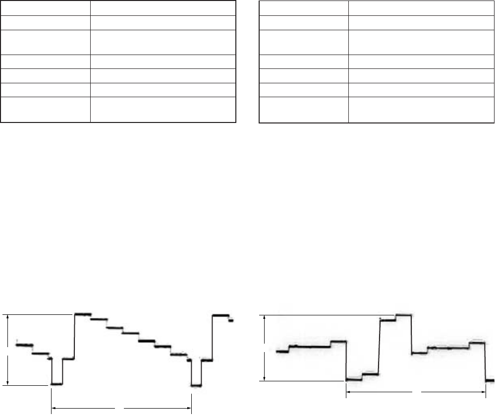
5-58
4. Playback CR Signal Level Adjustment with 0%
Setup (VD-28 Board)
Mode Playback
Signal Arbitrary
Measurement Point COMPONENT OUTPUT R-Y
terminal (75 Ω terminated)
Measuring Instrument Oscilloscope
Adjustment Page E
Adjustment Address AE
Specified Value A = 757 ± 10 mVp-p (NTSC)
A = 525 ± 10 mVp-p (PAL)
Adjusting method:
1) Select page: 0, address: 01, and set data: 01.
2) Select page: 3, address: 0C, set data: 01, and press the PAUSE
button of the adjustment remote commander.
3) Select page: E, address: AE, change the data and adjust the
component CR signal level (A) to the specified value. Read
the this adjustment data, and this data is named DAE.
4) Press the PAUSE button of the adjustment remote commander.
5) Select page: E, address: BC, set data: DAE, and press the PAUSE
button.
6) Select page: 3, address: 0C, set data: 00, and press the PAUSE
button.
7) Select page: 0, address: 01, and set data: 00.
A
H
3. Playback Y Signal Level Adjustment with 0% Setup
(VD-28 Board)
Mode Playback
Signal Arbitrary
Measurement Point COMPONENT OUTPUT Y terminal
(75 Ω terminated)
Measuring Instrument Oscilloscope
Adjustment Page E
Adjustment Address AC
Specified Value A = 822 ± 10 mVp-p (NTSC)
A = 825 ± 10 mVp-p (PAL)
Adjusting method:
1) Select page: 0, address: 01, and set data: 01.
2) Select page: 3, address: 0C, set data: 01, and press the PAUSE
button of the adjustment remote commander.
3) Select page: E, address: AC, change the data and adjust the
component Y signal level (A) to the specified value. Read the
this adjustment data, and this data is named DAC.
4) Press the PAUSE button of the adjustment remote commander.
5) Select page: E, address: BA, set data: DAC, and press the PAUSE
button.
6) Select page: 3, address: 0C, set data: 00, and press the PAUSE
button.
7) Select page: 0, address: 01, and set data: 00.
Fig. 5-3-11
A
H
Fig. 5-3-12
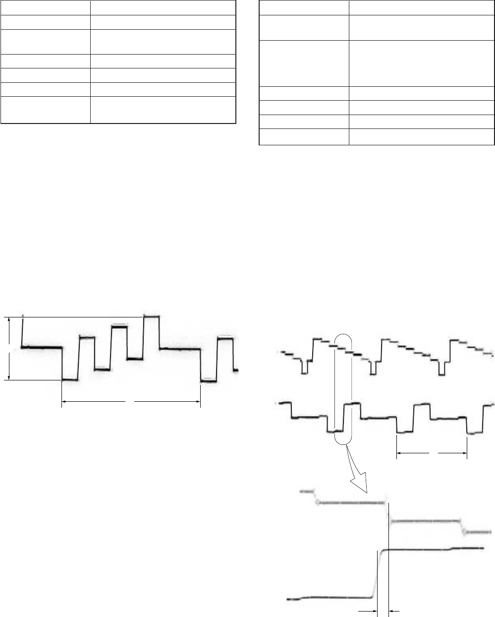
5-59
H
t
CH1
CH1
CH2
CH2
magnified
6. Playback CR Signal Delay Adjustment
(VD-28 Board)
Mode Playback
Signal A tape that the color bar signal is
recorded (Note1)
Measurement Point CH1: COMPONENT OUTPUT Y
terminal (75 Ω terminated)
CH2: COMPONENT OUTPUT R-Y
terminal (75 Ω terminated)
Measuring Instrument Oscilloscope
Adjustment Page E
Adjustment Address 9C
Specified Value t = 0 ± 20 nsec
Note1: A tape recorded with the status that “COLOR BAR” of
“DISPLAY SET” on the menu setting is ON.
Note2: After this adjustment, check that the specified value of
“Playback CR Signal Level Adjustment with 0% Setup”
is satisfied.
If not satisfied, perform “Playback CR Signal Level
Adjustment with 0% Setup”.
Adjusting method:
1) Select page: 0, address: 01, and set data: 01.
2) Select page: E, address: 9C, change the data and adjust the
time difference (t) between the boundary of green and magenta
on Y signal and CR signal, that to the specified value.
3) Press the PAUSE button of the adjustment remote commander.
4) Select page: 0, address: 01, and set data: 00.
A
H
5. Playback CB Signal Level Adjustment with 0%
Setup (VD-28 Board)
Mode Playback
Signal Arbitrary
Measurement Point COMPONENT OUTPUT B-Y
terminal (75 Ω terminated)
Measuring Instrument Oscilloscope
Adjustment Page E
Adjustment Address AD
Specified Value A = 757 ± 10 mVp-p (NTSC)
A = 525 ± 10 mVp-p (PAL)
Adjusting method:
1) Select page: 0, address: 01, and set data: 01.
2) Select page: 3, address: 0C, set data: 01, and press the PAUSE
button of the adjustment remote commander.
3) Select page: E, address: AD, change the data and adjust the
component CB signal level (A) to the specified value. Read
the this adjustment data, and this data is named DAD.
4) Press the PAUSE button of the adjustment remote commander.
5) Select page: E, address: BB, set data: DAD, and press the PAUSE
button.
6) Select page: 3, address: 0C, set data: 00, and press the PAUSE
button.
7) Select page: 0, address: 01, and set data: 00.
Fig. 5-3-13
Fig. 5-3-14
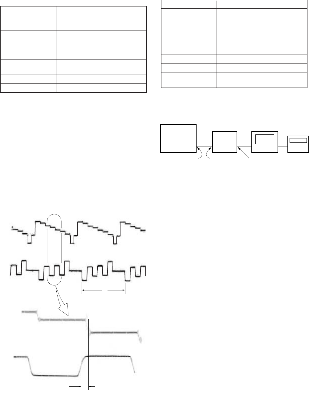
5-60
DSR-50/50P
Patern
generator Frequency
counter
Oscilloscope
VIDEO OUT 2 EXT SYNC IN SC OUT
8. Encoder Free Run Adjustment (VD-28 Board)
Mode E-E
Signal No signal (DV input) (Note1)
Measurement Point VIDEO OUT 2 terminal
Measuring Instrument Pattern generator (External
synchronization mode)
Oscilloscope
Frequency counter (Note2)
Adjustment Page E
Adjustment Address A5
Specified Value f = 3579545 ± 10 Hz (NTSC)
f = 4433618 ± 10 Hz (PAL)
Note1: Set “DV” mode with the INPUT SELECT switch.
Note2: Connection of equipment
Adjusting method:
1) Select page: 0, address: 01, and set data: 01.
2) Select page: E, address: 28, set data: 81, and press the PAUSE
button of the adjustment remote commander.
3) Select page: E, address: A5, change the data and adjust the
encoder free run frequency (f) to the specified value.
4) Press the PAUSE button of the adjustment remote commander.
5) Select page: E, address: 28, set data: 80, and press the PAUSE
button.
6) Select page: 0, address: 01, and set data: 00.
H
t
CH1
CH1
CH2
CH2
magnified
7. Playback CB Signal Delay Adjustment
(VD-28 Board)
Mode Playback
Signal A tape that the color bar signal is
recorded (Note1)
Measurement Point CH1: COMPONENT OUTPUT Y
terminal (75 Ω terminated)
CH2: COMPONENT OUTPUT B-Y
terminal (75 Ω terminated)
Measuring Instrument Oscilloscope
Adjustment Page E
Adjustment Address 9B
Specified Value t = 0 ± 20 nsec
Note1: A tape recorded with the status that “COLOR BAR” of
“DISPLAY SET” on the menu setting is ON.
Note2: After this adjustment, check that the specified value of
“Playback CB Signal Level Adjustment with 0% Setup”
is satisfied.
If not satisfied, perform “Playback CB Signal Level
Adjustment with 0% Setup”
Adjusting method:
1) Select page: 0, address: 01, and set data: 01.
2) Select page: E, address: 9B, change the data and adjust the
time difference (t) between the boundary of green and magenta
on Y signal and CB signal, that to the specified value.
3) Press the PAUSE button of the adjustment remote commander.
4) Select page: 0, address: 01, and set data: 00.
Fig. 5-3-15
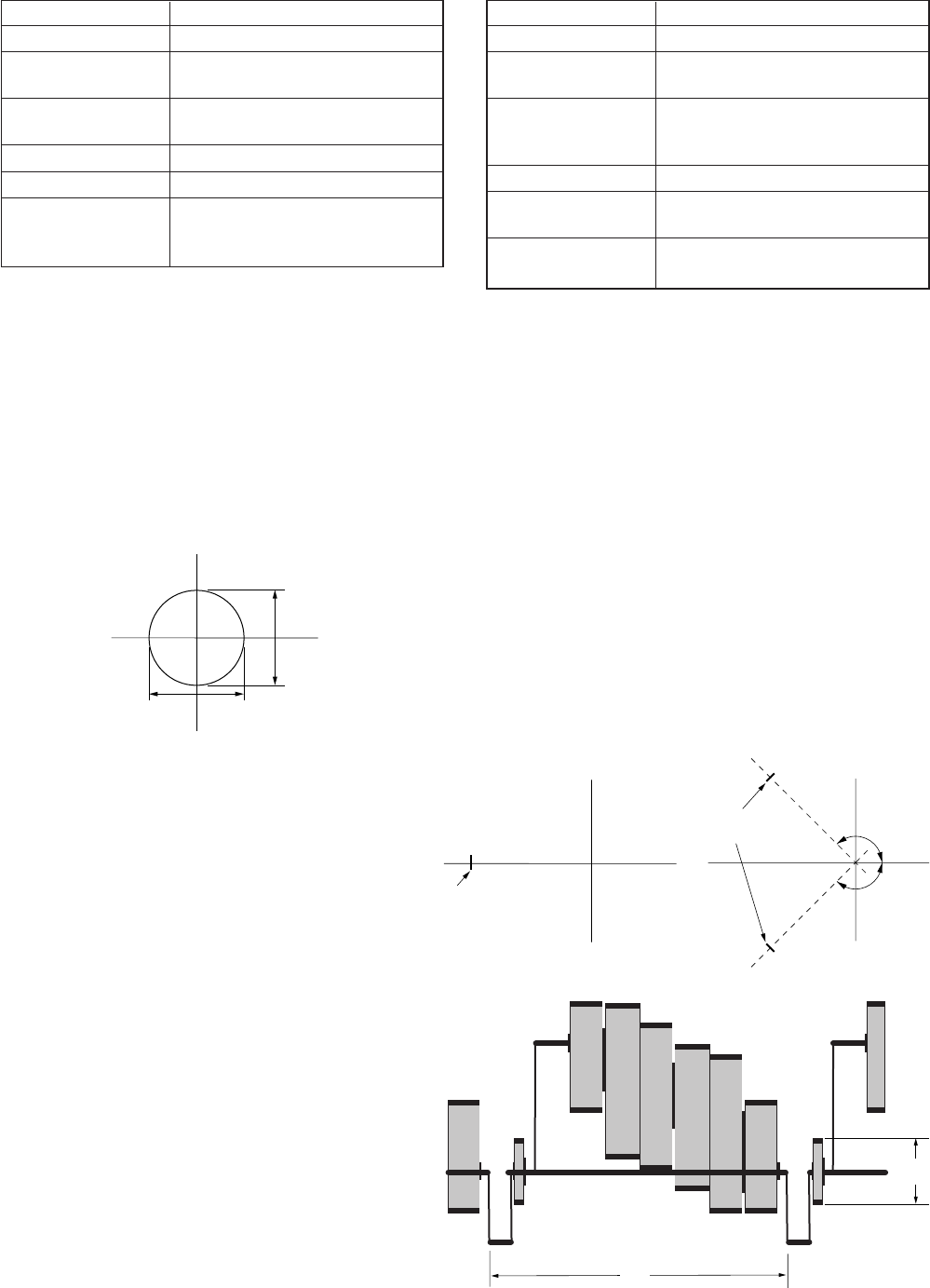
5-61
9. Carrier Balance Adjustment (VD-28 Board)
Mode Playback
Signal Arbitrary
Measurement Point VIDEO OUT 2 terminal (75 Ω
terminated)
Measuring Instrument Vectorscope (NTSC: 7.5% setup
mode)
Adjustment Page E
Adjustment Address A3, A4
Specified Value White luminance point settles within
the circle (Ø 2 mm) on center of the
vectorscope
Adjusting method:
1) Select page: 0, address: 01, and set data: 01.
2) Select page: 3, address: 0C, set data: 01, and press the PAUSE
button of the adjustment remote commander.
3) Set the vectorscope gain to x10.
4) Change the data on page: E, address: A3, A4 and adjust so that
a white luminance point positions in the center of vectorscope.
5) Press the PAUSE button of the adjustment remote commander.
6) Select page: 3, address: 0C, set data: 00, and press the PAUSE
button.
7) Select page: 0, address: 01, and set data: 00.
10. Burst Level Adjustment (VD-28 Board)
Mode Playback
Signal Arbitrary
Measurement Point VIDEO OUT 2 terminal (75 Ω
terminated)
Measuring Instrument Vectorscope (NTSC: 7.5% setup
mode)
Oscilloscope
Adjustment Page E
Adjustment Address 9F (NTSC)
9F , A0 (PAL) (Note)
Specified Value A = 286 ± 5 mVp-p (NTSC)
A = 300 ± 5 mVp-p (PAL)
Note: PAL model is the tracking adjustment in relation to
address: 9F and A0.
Adjusting method:
1) Select page: 0, address: 01, and set data: 01.
2) Select page: 3, address: 0C, set data: 01, and press the PAUSE
button of the adjustment remote commander.
3) Adjust the phase synchronization control on the vectorscope
so that the burst luminance point is close to the U-axis (NTSC
model) or axis of ±135° (PAL model).
4) Select page: E, address: 9F (NTSC model) or 9F, A0 (PAL
model), change tha data and adjust the the burst luminance
point to the 75% cursor position of the vectorscope.
5) Press the PAUSE button of the adjustment remote commander.
6) Confirm with the oscilloscope that the burst level (A) satisfied
the specified value.
7) Select page: 3, address: 0C, set data: 00, and press the PAUSE
button.
8) Select page: 0, address: 01, and set data: 00.
V
U
2 mm
2 mm
Fig. 5-3-16
75% cursor position
V
U
75% cursor
position
V
+135°
-135°
U
A
H
Fig. 5-3-17
Vectorscope
For NTSC model For PAL model
Oscillscope
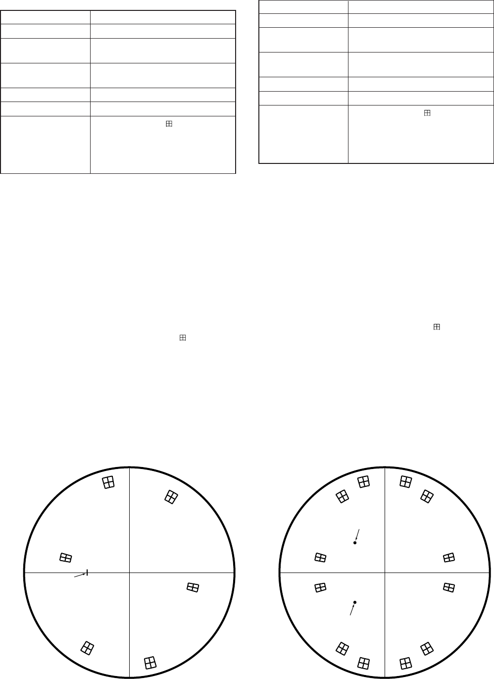
5-62
11. Color Level Adjustment with 0% Setup
(VD-28 Board)
Mode Playback
Signal Arbitrary
Measurement Point VIDEO OUT 2 terminal (75 Ω
terminated)
Measuring Instrument Vectorscope (NTSC: 0% setup
mode)
Adjustment Page E
Adjustment Address A1, A2
Specified Value From the center of mark on the
vectorscope, each luminance point
must satisfy the following:
Level: ± 5%
Phase: ± 3º
Note: This is the tracking adjustment in relation to “SC_V Phase
Adjustment”.
Adjusting method:
1) Select page: 0, address: 01, and set data: 01.
2) Select page: 3, address: 0C, set data: 01, and press the PAUSE
button of the adjustment remote commander.
3) Only for NTSC model, set the vectorscope to the 7.5% setup
mode.
4) Adjust the burst luminance point to the specified position using
the PHASE and GAIN knobs of vectorscope.
5) Only for NTSC model, set the vectorscope to the 0% setup
mode.
6) Change the data on page: E, addresses: A1, A2 and adjust so
that each luminance point positions at the mark on the
vectorscope.
7) Press the PAUSE button of the adjustment remote commander.
8) Select page: 3, address: 0C, set data: 00, and press the PAUSE
button.
9) Select page: 0, address: 01, and set data: 00.
12. SC_V Phase Adjustment (VD-28 Board)
Mode Playback
Signal Arbitrary
Measurement Point VIDEO OUT 2 terminal (75 Ω
terminated)
Measuring Instrument Vectorscope (NTSC: 0% setup
mode)
Adjustment Page E
Adjustment Address A8
Specified Value From the center of mark on the
vectorscope, each luminance point
must satisfy the following:
Level: ± 5%
Phase: ± 3º
Note: This is the tracking adjustment in relation to “Color Level
Adjustment with 0% Setup”.
Adjusting method:
1) Select page: 0, address: 01, and set data: 01.
2) Select page: 3, address: 0C, set data: 01, and press the PAUSE
button of the adjustment remote commander.
3) Only for NTSC model, set the vectorscope to the 7.5% setup
mode.
4) Adjust the burst luminance point to the specified position using
the PHASE and GAIN knobs of vectorscope.
5) Only for NTSC model, set the vectorscope to the 0% setup
mode.
6) Change the data on page: E, address: A8 and adjust so that
each luminance point positions at the mark on the
vectorscope.
7) Press the PAUSE button of the adjustment remote commander.
8) Select page: 3, address: 0C, set data: 00, and press the PAUSE
button.
9) Select page: 0, address: 01, and set data: 00.
R
M
G
Y
L
Burst
GC
Y
B
Fig. 5-3-18
For NTSC model For PAL model
R
–R
M
G
–M
G
Y
L
–Y
L
Burst
–Burst
G
–G
C
Y
–C
Y
B
–B
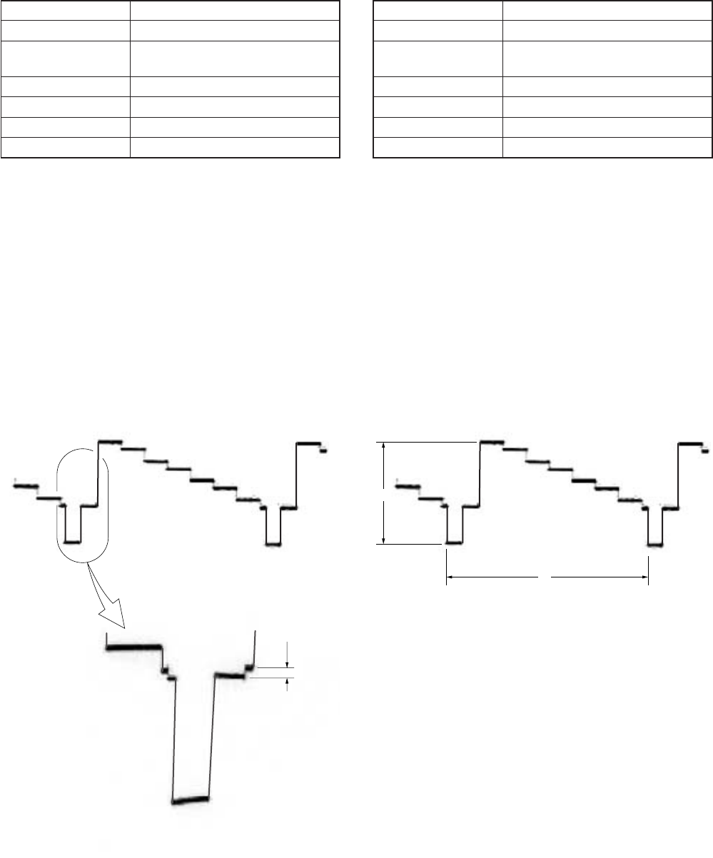
5-63
A
H
magnified
A
13. Playback Blanking Level Adjustment with 7.5%
Setup (VD-28 Board) (DSR-50)
Mode Playback
Signal Arbitrary
Measurement Point COMPONENT OUTPUT Y terminal
(75 Ω terminated)
Measuring Instrument Oscilloscope
Adjustment Page E
Adjustment Address C8
Specified Value A = 53.6 ± 3 mV (7.5 IRE)
Note: Perform this adjustment after inserting and playing a tape
into the set and setting “SETUP” for “VIDEO LVL” of
the “VIDEO SET” menu to 7.5%.
After the adjustment finished, return “SETUP” to 0%.
Adjusting method:
1) Select page: 0, address: 01, and set data: 01.
2) Select page: 3, address: 0C, set data: 01, and press the PAUSE
button of the adjustment remote commander.
3) Select page: E, address: C8, change the data and adjust the
blanking level (A) to the specified value.
4) Press the PAUSE button of the adjustment remote commander.
5) Select page: 3, address: 0C, set data: 00, and press the PAUSE
button.
6) Select page: 0, address: 01, and set data: 00.
14. Playback Y Signal Level Adjustment with 7.5%
Setup (VD-28 Board) (DSR-50)
Mode Playback
Signal Arbitrary
Measurement Point COMPONENT OUTPUT Y terminal
(75 Ω terminated)
Measuring Instrument Oscilloscope
Adjustment Page E
Adjustment Address C2
Specified Value A = 835 ± 10 mVp-p
Note: Perform this adjustment after inserting and playing a tape
into the set and setting “SETUP” for “VIDEO LVL” of
the “VIDEO SET” menu to 7.5%.
After the adjustment finished, return “SETUP” to 0%.
Adjusting method:
1) Select page: 0, address: 01, and set data: 01.
2) Select page: 3, address: 0C, set data: 01, and press the PAUSE
button of the adjustment remote commander.
3) Select page: E, address: C2, change the data and adjust the
component Y signal level (A) to the specified value.
4) Press the PAUSE button of the adjustment remote commander.
5) Select page: 3, address: 0C, set data: 00, and press the PAUSE
button.
6) Select page: 0, address: 01, and set data: 00.
Fig. 5-3-19
Fig. 5-3-20
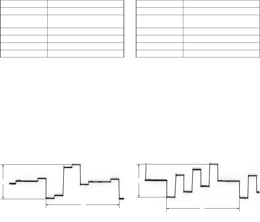
5-64
A
H
A
H
15. Playback CR Signal Level Adjustment with 7.5%
Setup (VD-28 Board) (DSR-50)
Mode Playback
Signal Arbitrary
Measurement Point COMPONENT OUTPUT R-Y
terminal (75 Ω terminated)
Measuring Instrument Oscilloscope
Adjustment Page E
Adjustment Address C4
Specified Value A = 700 ± 10 mVp-p
Note: Perform this adjustment after inserting and playing a tape
into the set and setting “SETUP” for “VIDEO LVL” of
the “VIDEO SET” menu to 7.5%.
After the adjustment finished, return “SETUP” to 0%.
Adjusting method:
1) Select page: 0, address: 01, and set data: 01.
2) Select page: 3, address: 0C, set data: 01, and press the PAUSE
button of the adjustment remote commander.
3) Select page: E, address: C4, change the data and adjust the
component CR signal level (A) to the specified value.
4) Press the PAUSE button of the adjustment remote commander.
5) Select page: 3, address: 0C, set data: 00, and press the PAUSE
button.
6) Select page: 0, address: 01, and set data: 00.
16. Playback CB Signal Level Adjustment with 7.5%
Setup (VD-28 Board) (DSR-50)
Mode Playback
Signal Arbitrary
Measurement Point COMPONENT OUTPUT B-Y
terminal (75 Ω terminated)
Measuring Instrument Oscilloscope
Adjustment Page E
Adjustment Address C3
Specified Value A = 700 ± 10 mVp-p
Note: Perform this adjustment after inserting and playing a tape
into the set and setting “SETUP” for “VIDEO LVL” of
the “VIDEO SET” menu to 7.5%.
After the adjustment finished, return “SETUP” to 0%.
Adjusting method:
1) Select page: 0, address: 01, and set data: 01.
2) Select page: 3, address: 0C, set data: 01, and press the PAUSE
button of the adjustment remote commander.
3) Select page: E, address: C3, change the data and adjust the
component CB signal level (A) to the specified value.
4) Press the PAUSE button of the adjustment remote commander.
5) Select page: 3, address: 0C, set data: 00, and press the PAUSE
button.
6) Select page: 0, address: 01, and set data: 00.
Fig. 5-3-21 Fig. 5-3-22
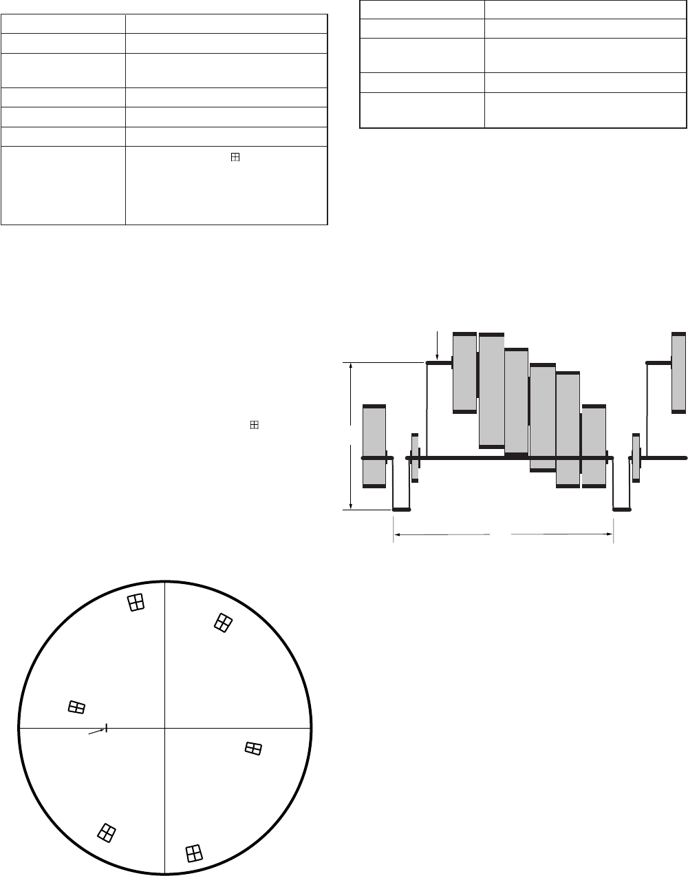
5-65
17. Color Level Adjustment with 7.5% Setup
(VD-28 Board) (DSR-50)
Mode Playback
Signal Arbitrary
Measurement Point VIDEO OUT 2 terminal (75 Ω
terminated)
Measuring Instrument Vectorscope (7.5% setup mode)
Adjustment Page E
Adjustment Address C0, C1
Specified Value From the center of mark on the
vectorscope, each luminance point
must satisfy the following:
Level: ± 5%
Phase: ± 3º
Note: Perform this adjustment after inserting and playing a tape
into the set and setting “SETUP” for “VIDEO LVL” of
the “VIDEO SET” menu to 7.5%.
After the adjustment finished, return “SETUP” to 0%.
Adjusting method:
1) Select page: 0, address: 01, and set data: 01.
2) Select page: 3, address: 0C, set data: 01, and press the PAUSE
button of the adjustment remote commander.
3) Adjust the burst luminance point to the specified position using
the PHASE and GAIN knobs of vectorscope.
4) Change the data on page: E, addresses: C0, C1 and adjust so
that each luminance point positions at the mark on the
vectorscope.
5) Press the PAUSE button of the adjustment remote commander.
6) Select page: 3, address: 0C, set data: 00, and press the PAUSE
button.
7) Select page: 0, address: 01, and set data: 00.
R
M
G
Y
L
Burst
GC
Y
B
Fig. 5-3-23
18. Video Output Level Check (VD-28 Board)
Mode Playback
Signal Arbitrary
Measurement Point VIDEO OUT 2 terminal (75 Ω
terminated)
Measuring Instrument Oscilloscope
Specified Value A = 822 ± 20 mVp-p (NTSC)
A = 825 ± 20 mVp-p (PAL)
Adjusting method:
1) Select page: 0, address: 01, and set data: 01.
2) Select page: 3, address: 0C, set data: 01, and press the PAUSE
button of the adjustment remote commander.
3) Check that the video signal level (A) is satisfied the specified
value.
4) Select page: 3, address: 0C, set data: 00, and press the PAUSE
button.
5) Select page: 0, address: 01, and set data: 00.
A
H
White
Fig. 5-3-24
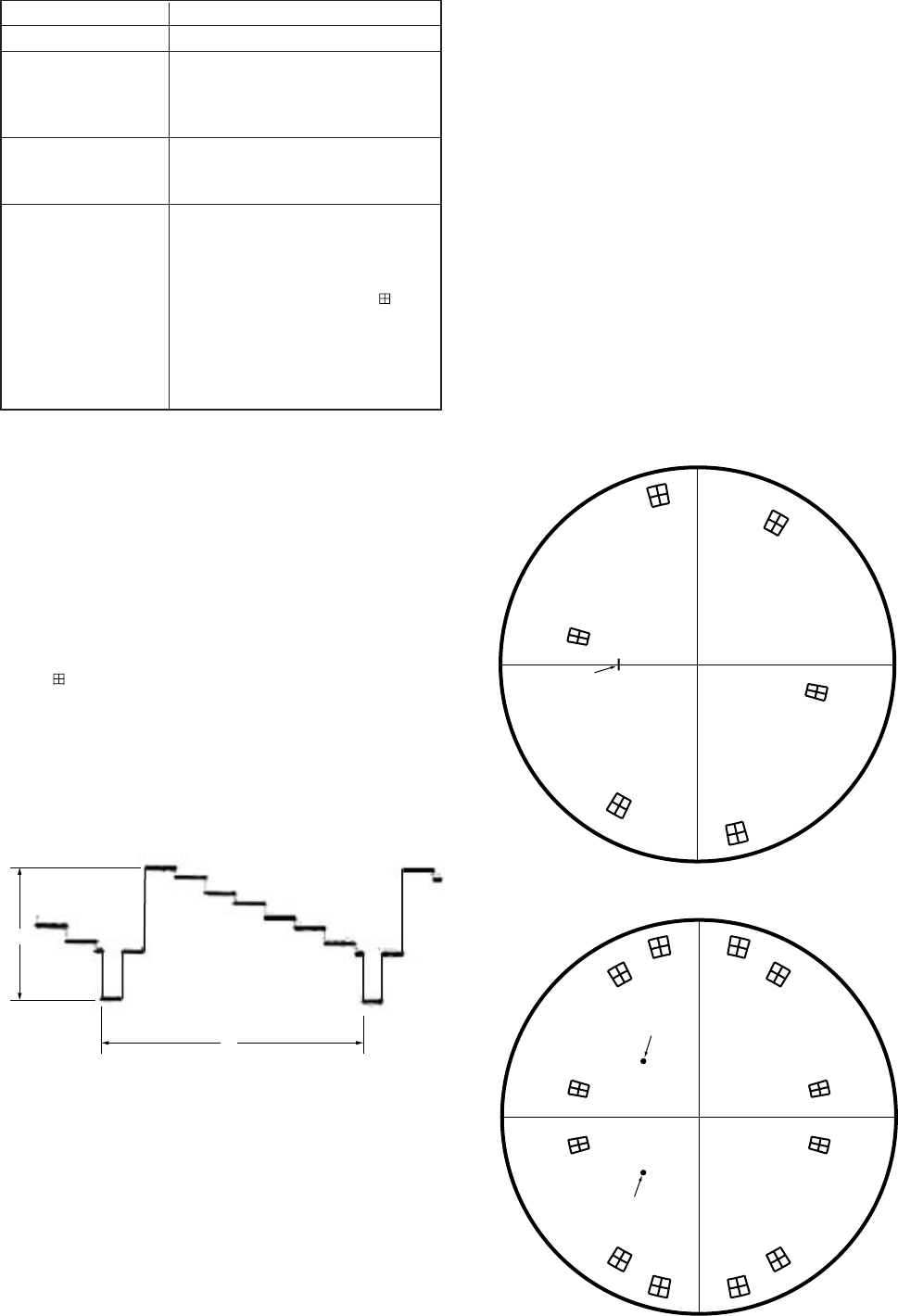
5-66
A
H
Y signal
19. S-Video Output Level Check (VD-28 Board)
Mode Playback
Signal Arbitrary
Measurement Point S VIDEO OUT Y terminal (75 Ω
terminated)
S VIDEO OUT C terminal (75 Ω
terminated)
Measuring Instrument Vectorscope (NTSC: 0% setup
mode)
Oscilloscope
Specified Value Y signal: A = 822 ± 20 mVp-p
(NTSC)
A = 825 ± 20 mVp-p
(PAL)
C signal: From the center of mark
on the vectorscope, each
luminance point must
satisfy the following:
Level: ± 5%
Phase: ± 3º
Adjusting method:
1) Select page: 0, address: 01, and set data: 01.
2) Select page: 3, address: 0C, set data: 01, and press the PAUSE
button of the adjustment remote commander.
3) Confirm that the Y signal level (A) satisfied the specified value.
4) Only for NTSC model, set the vectorscope to the 7.5% setup
mode.
5) Adjust the burst luminance point to the specified position using
the PHASE and GAIN knobs of vectorscope.
6) Only for NTSC model, set the vectorscope to the 0% setup
mode.
7) Make sure that each luminance point of C signal positions at
the mark on the vectorscope.
8) Select page: 3, address: 0C, set data: 00, and press the PAUSE
button.
9) Select page: 0, address: 01, and set data: 00.
R
M
G
Y
L
Burst
GC
Y
B
Fig. 5-3-25
C signal
For NTSC model
For PAL model
R
–R
M
G
–M
G
Y
L
–Y
L
Burst
–Burst
G
–G
C
Y
–C
Y
B
–B
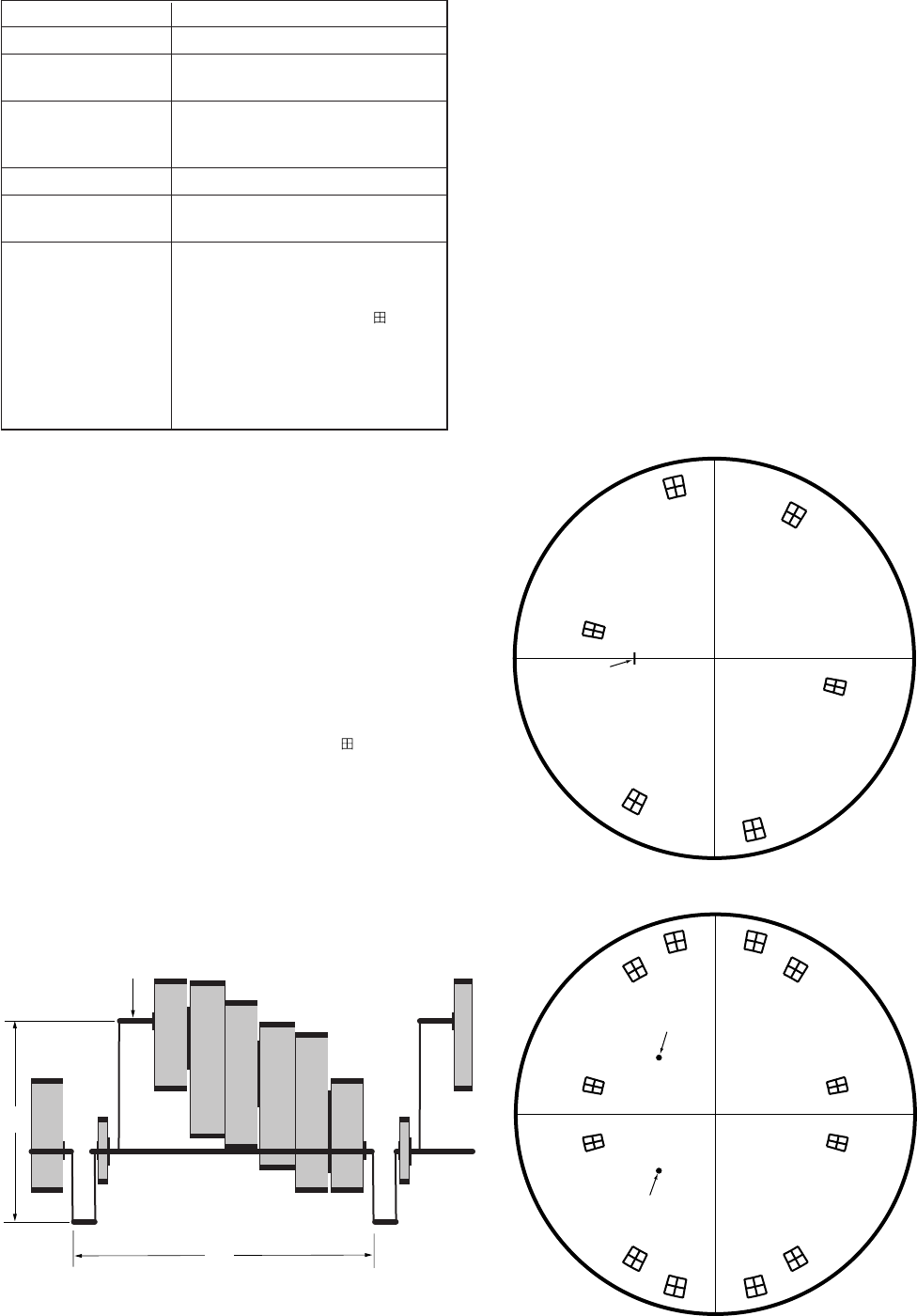
5-67
20. Monitor Terminal Output Level Adjustment
(JC-20 Board)
Mode Playback
Signal Arbitrary
Measurement Point VIDEO OUT 1 terminal (75 Ω
terminated)
Measuring Instrument Vectorscope (NTSC: 0% setup
mode)
Oscilloscope
Adjustment Page C
Adjustment Address 25 (Y level)
26, 27 (C level)
Specified Value Y level: A = 822 ± 20 mVp-p
(NTSC)
A = 825 ± 20 mVp-p (PAL)
C level: From the center of mark
on the vectorscope, each
luminance point must
satisfy the following:
Level: ± 5%
Phase: ± 3º
Adjusting method:
1) Select page: 0, address: 01, and set data: 01.
2) Select page: 3, address: 0C, set data: 01, and press the PAUSE
button of the adjustment remote commander.
3) Select page: C, address: 25, change the data and adjust the Y
level (A) to the specified value.
4) Press the PAUSE button of the adjustment remote commander.
5) Only for NTSC model, set the vectorscope to the 7.5% setup
mode.
6) Adjust the burst luminance point to the specified position using
the PHASE and GAIN knobs of vectorscope.
7) Only for NTSC model, set the vectorscope to the 0% setup
mode.
8) Change the data on page: E, addresses: 26, 27 and adjust so
that each luminance point positions at the mark on the
vectorscope.
9) Press the PAUSE button of the adjustment remote commander.
10) Select page: 3, address: 0C, set data: 00, and press the PAUSE
button.
11) Select page: 0, address: 01, and set data: 00.
A
H
White
R
M
G
Y
L
Burst
GC
Y
B
Fig. 5-3-26
Y level
C level
For NTSC model
For PAL model
R
–R
MG
–MG
YL
–YL
Burst
–Burst
G
–G
CY
–CY
B
–B
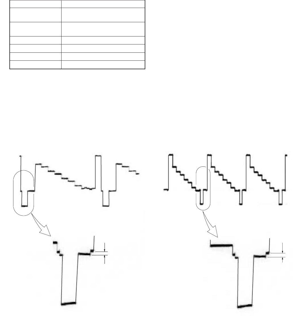
5-68
21. E-E Blanking Level Adjustment (VD-28 Board)
Mode E-E
Signal Color bar (NTSC: with 7.5% setup)
(CAMERA input) (Note)
Measurement Point COMPONENT OUTPUT Y terminal
(75 Ω terminated)
Measuring Instrument Oscilloscope
Adjustment Page E
Adjustment Address CC
Specified Value A = 0 ± 3 mV
Note1: Set “CAMERA” mode with INPUT SELECT switch
Adjusting method:
1) Select page: 0, address: 01, and set data: 01.
2) Select page: E, address: CC, change the data and adjust the
blanking level (A) to the specified value.
3) Press the PAUSE button of the adjustment remote commander.
4) Select page: 0, address: 01, and set data: 00.
A
magnified
magnified
A
Fig. 5-3-27
For PAL modelFor NTSC model
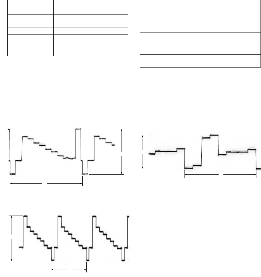
5-69
A
H
A
H
A
H
22. Component E-E Y Signal Level Adjustment
(VD-28 Board)
Mode E-E
Signal Color bar (CAMERA input) (Note)
Measurement Point COMPONENT OUTPUT Y terminal
(75 Ω terminated)
Measuring Instrument Oscilloscope
Adjustment Page E
Adjustment Address 94
Specified Value A = 1000 ± 10 mVp-p
Note1: Set “CAMERA” mode with INPUT SELECT switch
Adjusting method:
1) Select page: 0, address: 01, and set data: 01.
2) Select page: E, address: 94, change the data and adjust the
component Y signal level (A) to the specified value.
3) Press the PAUSE button of the adjustment remote commander.
4) Select page: 0, address: 01, and set data: 00.
Fig. 5-3-28
For PAL model
For NTSC model
23. Component E-E CR Signal Level Adjustment
(VD-28 Board)
Mode E-E
Signal Color bar (NTSC: with 7.5% setup)
(CAMERA input) (Note)
Measurement Point COMPONENT OUTPUT R-Y
terminal (75 Ω terminated)
Measuring Instrument Oscilloscope
Adjustment Page E
Adjustment Address 96
Specified Value A = 700 ± 10 mVp-p (NTSC)
A = 525 ± 10 mVp-p (PAL)
Note: Set “CAMERA” mode with INPUT SELECT switch
Adjusting method:
1) Select page: 0, address: 01, and set data: 01.
2) Select page: E, address: 96, change the data and adjust the
component CR signal level (A) to the specified value.
3) Press the PAUSE button of the adjustment remote commander.
4) Select page: 0, address: 01, and set data: 00.
Fig. 5-3-29
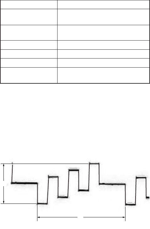
5-70
A
H
24. Component E-E CB Signal Level Adjustment
(VD-28 Board)
Mode E-E
Signal Color bar (NTSC: with 7.5% setup)
(CAMERA input) (Note)
Measurement Point COMPONENT OUTPUT B-Y
terminal (75 Ω terminated)
Measuring Instrument Oscilloscope
Adjustment Page E
Adjustment Address 95
Specified Value A = 700 ± 10 mVp-p (NTSC)
A = 525 ± 10 mVp-p (PAL)
Note1: Set “CAMERA” mode with INPUT SELECT switch
Adjusting method:
1) Select page: 0, address: 01, and set data: 01.
2) Select page: E, address: 95, change the data and adjust the
component CB signal level (A) to the specified value.
3) Press the PAUSE button of the adjustment remote commander.
4) Select page: 0, address: 01, and set data: 00.
Fig. 5-3-30
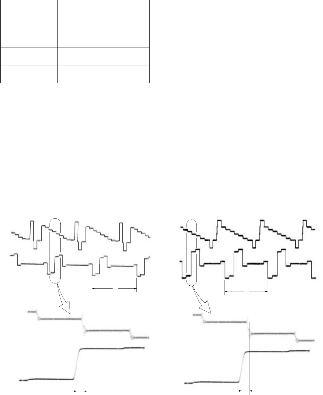
5-71
H
t
CH1
CH1
CH2
CH2
magnified
H
t
CH1
CH1
CH2
CH2
magnified
25. Component E-E CR Signal Delay Adjustment
(VD-28 Board)
Mode E-E
Signal Color bar (CAMERA input) (Note1)
Measurement Point CH1: COMPONENT OUTPUT Y
terminal (75 Ω terminated)
CH2: COMPONENT OUTPUT R-Y
terminal (75 Ω terminated)
Measuring Instrument Oscilloscope
Adjustment Page E
Adjustment Address 99
Specified Value t = 0 ± 20 nsec
Note1: Set “CAMERA” mode with INPUT SELECT switch
Note2: After this adjustment, check that the specified value of
“Component E-E CR Signal Level Adjustment” is
satisfied.
If not satisfied, perform “Component E-E CR Signal
Level Adjustment”.
Adjusting method:
1) Select page: 0, address: 01, and set data: 01.
2) Select page: E, address: 99, change the data and adjust the
time difference (t) between the boundary of green and magenta
on Y signal and CR signal, that to the specified value.
3) Press the PAUSE button of the adjustment remote commander.
4) Select page: 0, address: 01, and set data: 00.
For PAL modelFor NTSC model
Fig. 5-3-31
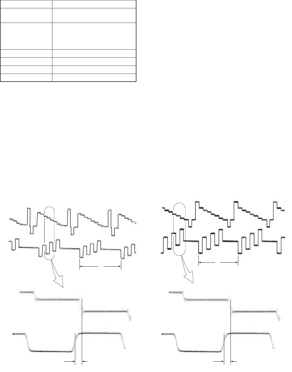
5-72
H
t
CH1
CH1
CH2
CH2
magnified
H
t
CH1
CH1
CH2
CH2
magnified
26. Component E-E CB Signal Delay Adjustment
(VD-28 Board)
Mode E-E
Signal Color bar (NTSC: with 7.5% setup)
(CAMERA input) (Note1)
Measurement Point CH1: COMPONENT OUTPUT Y
terminal (75 Ω terminated)
CH2: COMPONENT OUTPUT B-Y
terminal (75 Ω terminated)
Measuring Instrument Oscilloscope
Adjustment Page E
Adjustment Address 98
Specified Value t = 0 ± 20 nsec
Note1: Set “CAMERA” mode with INPUT SELECT switch
Note2: After this adjustment, check that the specified value of
“Component E-E CB Signal Level Adjustment” is
satisfied.
If not satisfied, perform “Component E-E CB Signal
Level Adjustment”.
Adjusting method:
1) Select page: 0, address: 01, and set data: 01.
2) Select page: E, address: 98, change the data and adjust the
time difference (t) between the boundary of green and magenta
on Y signal and CB signal, that to the specified value.
3) Press the PAUSE button of the adjustment remote commander.
4) Select page: 0, address: 01, and set data: 00.
For PAL model
For NTSC model
Fig. 5-3-32
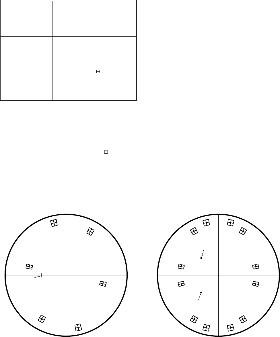
5-73
27. E-E Color Level Adjustment (VD-28 Board)
Mode E-E
Signal Color bar (NTSC: with 7.5% setup)
(CAMERA input) (Note)
Measurement Point VIDEO OUT 2 terminal (75 Ω
terminated)
Measuring Instrument Vectorscope (NTSC: 7.5% setup
mode)
Adjustment Page E
Adjustment Address CA, CB
Specified Value From the center of mark on the
vectorscope, each luminance point
must satisfy the following:
Level: ± 5%
Phase: ± 3º
Note1: Set “CAMERA” mode with INPUT SELECT switch
Adjusting method:
1) Select page: 0, address: 01, and set data: 01.
2) Adjust the burst luminance point to the specified position using
the PHASE and GAIN knobs of vectorscope.
3) Change the data on page: E, addresses: CA, CB and adjust so
that each luminance point positions at the mark on the
vectorscope.
4) Press the PAUSE button of the adjustment remote commander.
5) Select page: 0, address: 01, and set data: 00.
R
M
G
Y
L
Burst
GC
Y
B
For PAL modelFor NTSC model
Fig. 5-3-33
R
–R
MG
–MG
YL
–YL
Burst
–Burst
G
–G
CY
–CY
B
–B
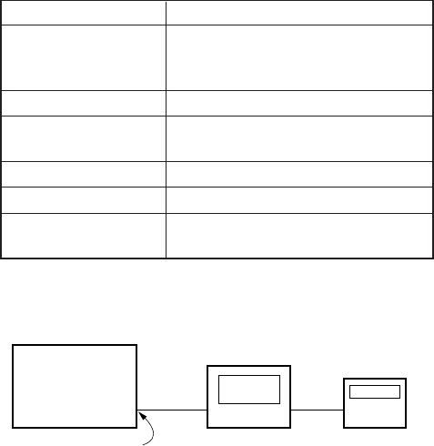
5-74
DSR-50/50P
Frequency
counter
Oscilloscope
S VIDEO OUT C
28. Decoder Free Run Adjustment (VD-28 Board)
Mode E-E
Signal Color bar (burst signal and chroma
signal OFF)
(S VIDEO input) (Note1)
Measurement Point S VIDEO OUT C terminal
Measuring Instrument Oscilloscope
Frequency counter (Note2)
Adjustment Page E
Adjustment Address A9
Specified Value f = 3579545 ± 20 Hz (NTSC)
f = 4433618 ± 20 Hz (PAL)
Note1: Set “S VIDEO” mode with INPUT SELECT switch
Note2: Connection of equipment
Adjusting method:
1) Select page: 0, address: 01, and set data: 01.
2) Select page: 9, address: 06, set data: 20, and press the PAUSE
button.
3) Select page: E, address: A9, change the data and adjust the
decoder free run frequency (f) to the specified value.
4) Press the PAUSE button of the adjustment remote commander.
5) Select page: 9, address: 06, set data: 00, and press the PAUSE
button.
6) Select page: 0, address: 01, and set data: 00.
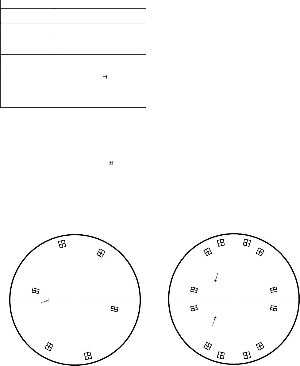
5-75
29. Decoder HUE Adjustment (VD-28 Board)
Mode E-E
Signal Color bar (NTSC: with 7.5% setup)
(S VIDEO input) (Note)
Measurement Point VIDEO OUT 2 terminal (75 Ω
terminated)
Measuring Instrument Vectorscope (NTSC: 7.5% setup
mode)
Adjustment Page E
Adjustment Address 93
Specified Value From the center of mark on the
vectorscope, each luminance point
must satisfy the following:
Level: ± 5%
Phase: ± 3º
Note: Set “S VIDEO” mode with INPUT SELECT switch
Adjusting method:
1) Select page: 0, address: 01, and set data: 01.
2) Adjust the burst luminance point to the specified position using
the PHASE and GAIN knobs of vectorscope.
3) Change the data on page: E, address: 93 and adjust so that a
blue luminance point positions at the mark on the
vectorscope. At this time, make sure that each luminance point
satisfies the specified value.
4) Press the PAUSE button of the adjustment remote commander.
5) Select page: 0, address: 01, and set data: 00.
R
M
G
Y
L
Burst
GC
Y
B
For PAL modelFor NTSC model
Fig. 5-3-34
R
–R
M
G
–M
G
Y
L
–Y
L
Burst
–Burst
G
–G
C
Y
–C
Y
B
–B
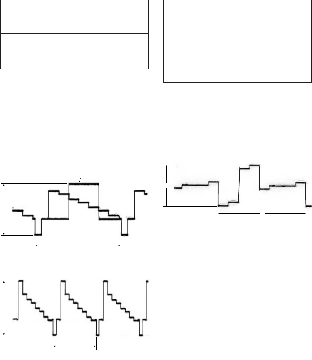
5-76
A
H
A
H
A
H
White 100%
30. S Video E-E Y Signal Level Adjustment
(VD-28 Board)
Mode E-E
Signal Color bar (S VIDEO input) (Note)
Measurement Point COMPONENT OUTPUT Y terminal
(75 Ω terminated)
Measuring Instrument Oscilloscope
Adjustment Page E
Adjustment Address BD
Specified Value A = 1000 ± 10 mVp-p
Note: Set “S VIDEO” mode with INPUT SELECT switch
Adjusting method:
1) Select page: 0, address: 01, and set data: 01.
2) Select page: E, address: BD, change the data and adjust the
component Y signal level (A) to the specified value.
3) Press the PAUSE button of the adjustment remote commander.
4) Select page: 0, address: 01, and set data: 00.
For PAL model
For NTSC model
Fig. 5-3-35
31. S Video E-E CR Signal Level Adjustment
(VD-28 Board)
Mode E-E
Signal Color bar (NTSC: with 7.5% setup)
(S VIDEO input) (Note)
Measurement Point COMPONENT OUTPUT R-Y
terminal (75 Ω terminated)
Measuring Instrument Oscilloscope
Adjustment Page E
Adjustment Address BF
Specified Value A = 700 ± 10 mVp-p (NTSC)
A = 525 ± 10 mVp-p (PAL)
Note: Set “S VIDEO” mode with INPUT SELECT switch
Adjusting method:
1) Select page: 0, address: 01, and set data: 01.
2) Select page: E, address: BF, change the data and adjust the
component CR signal level (A) to the specified value.
3) Press the PAUSE button of the adjustment remote commander.
4) Select page: 0, address: 01, and set data: 00.
Fig. 5-3-36
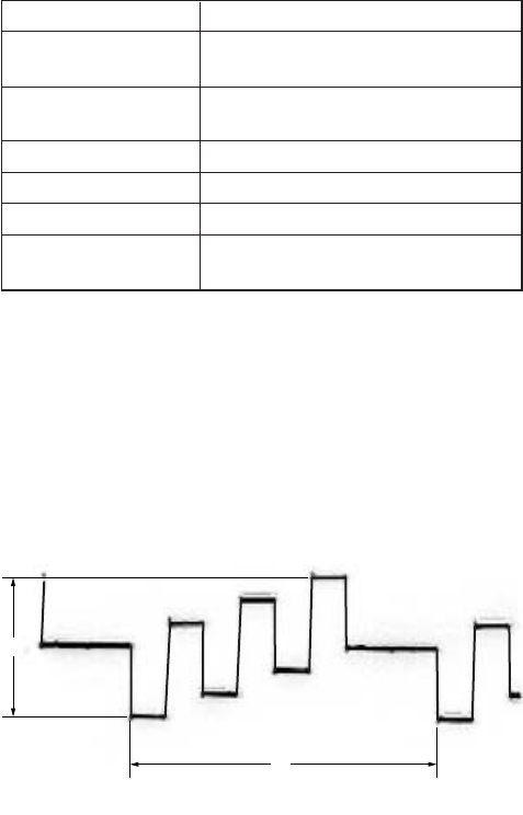
5-77
A
H
32. S Video E-E CB Signal Level Adjustment
(VD-28 Board)
Mode E-E
Signal Color bar (NTSC: with 7.5% setup)
(S VIDEO input) (Note)
Measurement Point COMPONENT OUTPUT B-Y
terminal (75 Ω terminated)
Measuring Instrument Oscilloscope
Adjustment Page E
Adjustment Address BE
Specified Value A = 700 ± 10 mVp-p (NTSC)
A = 525 ± 10 mVp-p (PAL)
Note: Set “S VIDEO” mode with INPUT SELECT switch
Adjusting method:
1) Select page: 0, address: 01, and set data: 01.
2) Select page: E, address: BE, change the data and adjust the
component CB signal level (A) to the specified value.
3) Press the PAUSE button of the adjustment remote commander.
4) Select page: 0, address: 01, and set data: 00.
Fig. 5-3-37
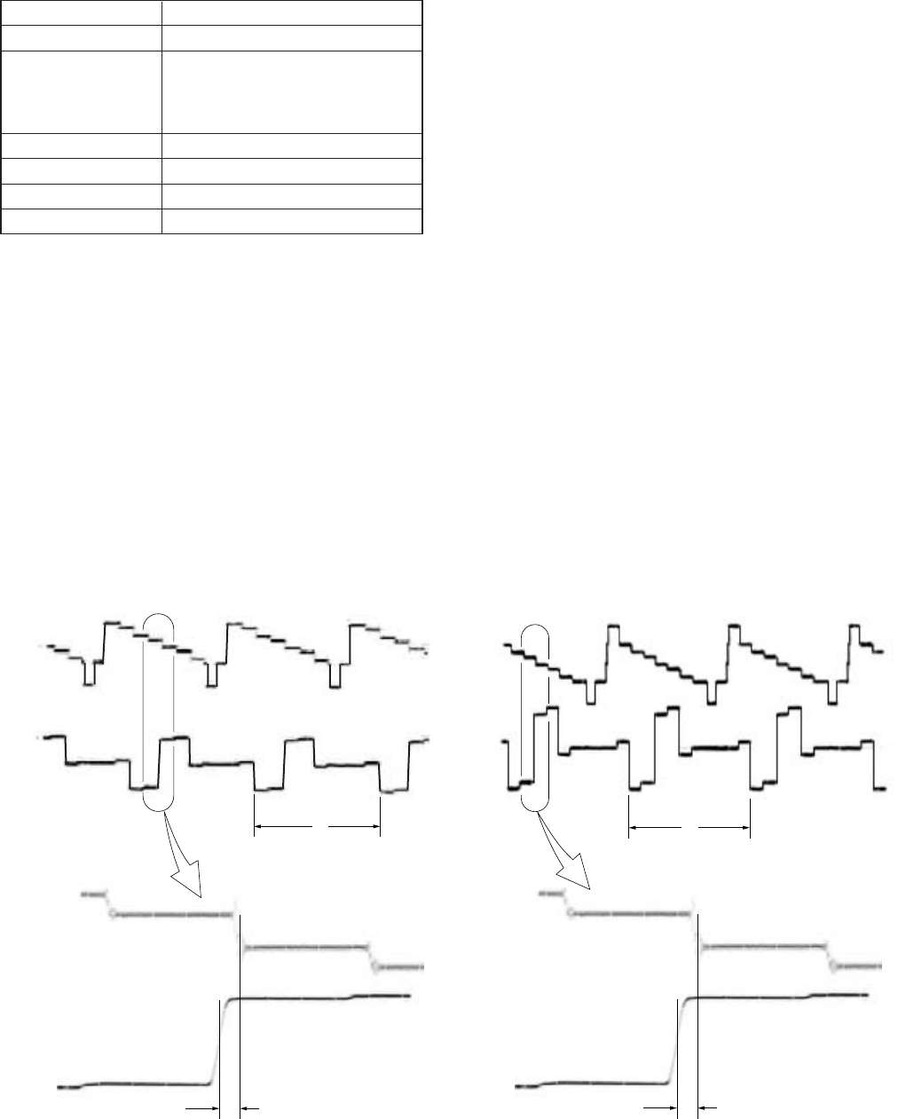
5-78
H
t
CH1
CH1
CH2
CH2
magnified
H
t
CH1
CH1
CH2
CH2
magnified
33. S Video E-E CR Signal Delay Adjustment
(VD-28 Board)
Mode E-E
Signal Color bar (S VIDEO input) (Note1)
Measurement Point CH1: COMPONENT OUTPUT Y
terminal (75 Ω terminated)
CH2: COMPONENT OUTPUT R-Y
terminal (75 Ω terminated)
Measuring Instrument Oscilloscope
Adjustment Page E
Adjustment Address B6
Specified Value t = 0 ± 20 nsec
Note1: Set “S VIDEO” mode with INPUT SELECT switch
Note2: After this adjustment, check that the specified value of
“S Video E-E CR Signal Level Adjustment” is satisfied.
If not satisfied, perform “S Video E-E CR Signal Level
Adjustment”.
Adjusting method:
1) Select page: 0, address: 01, and set data: 01.
2) Select page: E, address: B6, change the data and adjust the
time difference (t) between the boundary of green and magenta
on Y signal and CR signal, that to the specified value.
3) Press the PAUSE button of the adjustment remote commander.
4) Select page: 0, address: 01, and set data: 00.
For PAL modelFor NTSC model
Fig. 5-3-38
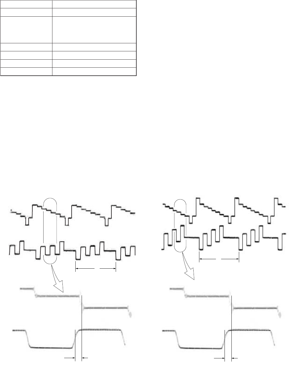
5-79
H
t
CH1
CH1
CH2
CH2
magnified
H
t
CH1
CH1
CH2
CH2
magnified
34. S Video E-E CB Signal Delay Adjustment
(VD-28 Board)
Mode E-E
Signal Color bar (S VIDEO input) (Note1)
Measurement Point CH1: COMPONENT OUTPUT Y
terminal (75 Ω terminated)
CH2: COMPONENT OUTPUT B-Y
terminal (75 Ω terminated)
Measuring Instrument Oscilloscope
Adjustment Page E
Adjustment Address B5
Specified Value t = 0 ± 20 nsec
Note1: Set “S VIDEO” mode with INPUT SELECT switch
Note2: After this adjustment, check that the specified value of
“S Video E-E CB Signal Level Adjustment” is satisfied.
If not satisfied, perform “S Video E-E CB Signal Level
Adjustment”.
Adjusting method:
1) Select page: 0, address: 01, and set data: 01.
2) Select page: E, address: B5, change the data and adjust the
time difference (t) between the boundary of green and magenta
on Y signal and CB signal, that to the specified value.
3) Press the PAUSE button of the adjustment remote commander.
4) Select page: 0, address: 01, and set data: 00.
For PAL modelFor NTSC model
Fig. 5-3-39
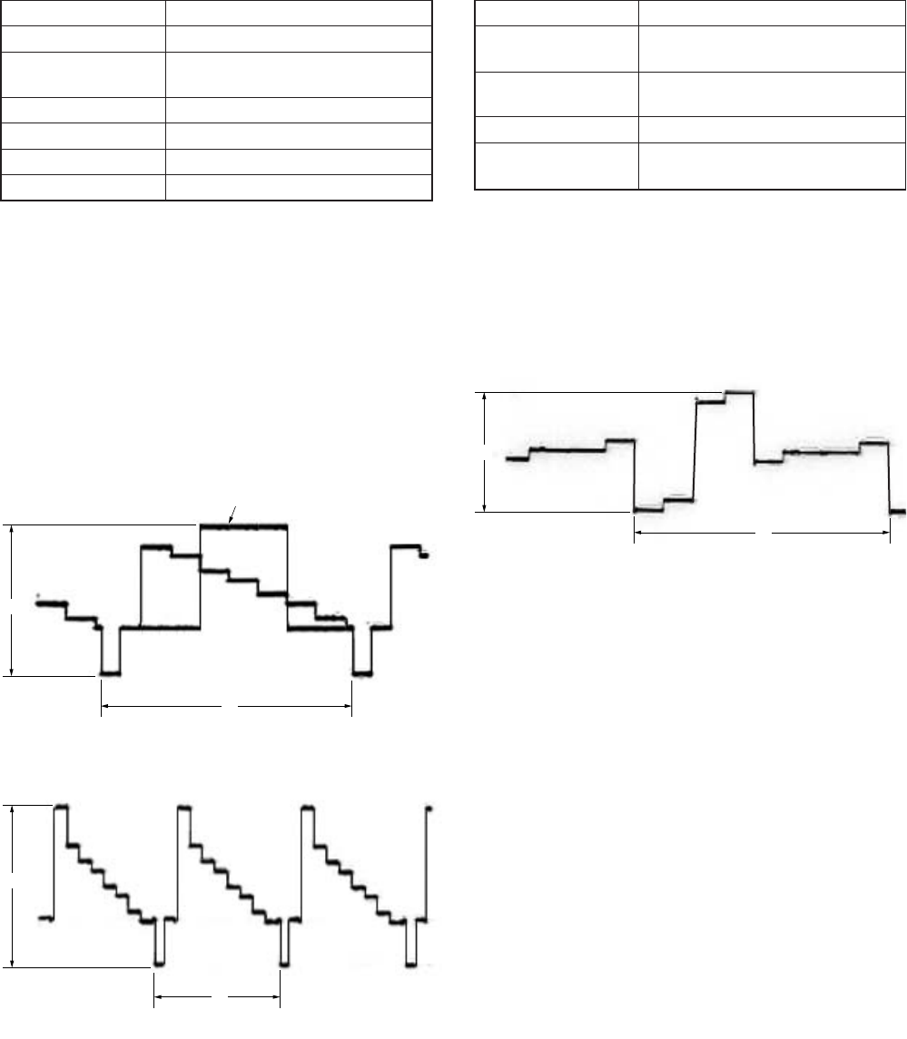
5-80
A
H
A
H
A
H
White 100%
35. Composite E-E Y Signal Level Adjustment
(VD-28 Board)
Mode E-E
Signal Color bar (VIDEO input) (Note)
Measurement Point COMPONENT OUTPUT Y terminal
(75 Ω terminated)
Measuring Instrument Oscilloscope
Adjustment Page E
Adjustment Address 90
Specified Value A = 1000 ± 10 mVp-p
Note: Set “VIDEO” mode with INPUT SELECT switch
Adjusting method:
1) Select page: 0, address: 01, and set data: 01.
2) Select page: E, address: 90, change the data and adjust the
component Y signal level (A) to the specified value.
3) Press the PAUSE button of the adjustment remote commander.
4) Select page: 0, address: 01, and set data: 00.
For PAL model
For NTSC model
Fig. 5-3-40
36. Composite E-E CR Signal Level Check
(VD-28 Board)
Mode E-E
Signal Color bar (NTSC: with 7.5% setup)
(VIDEO input) (Note)
Measurement Point COMPONENT OUTPUT R-Y
terminal (75 Ω terminated)
Measuring Instrument Oscilloscope
Specified Value A = 700 ± 10 mVp-p (NTSC)
A = 525 ± 10 mVp-p (PAL)
Note: Set “VIDEO” mode with INPUT SELECT switch
Adjusting method:
1) Check the component CR signal level (A) to the specified value.
Fig. 5-3-41
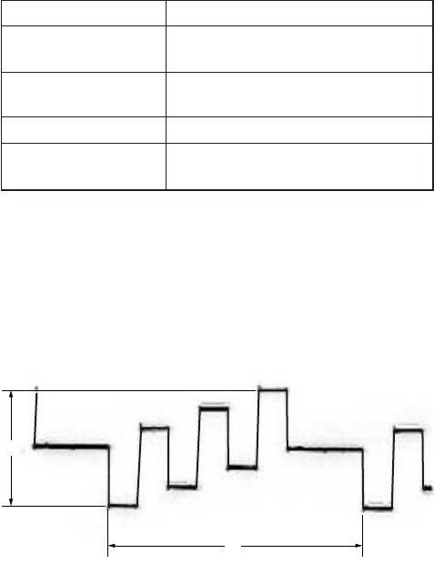
5-81
A
H
37. Composite E-E CB Signal Level Check
(VD-28 Board)
Mode E-E
Signal Color bar (NTSC: with 7.5% setup)
(VIDEO input) (Note)
Measurement Point COMPONENT OUTPUT B-Y
terminal (75 Ω terminated)
Measuring Instrument Oscilloscope
Specified Value A = 700 ± 10 mVp-p (NTSC)
A = 525 ± 10 mVp-p (PAL)
Note: Set “VIDEO” mode with INPUT SELECT switch
Adjusting method:
1) Check the component CB signal level (A) to the specified value.
Fig. 5-3-42
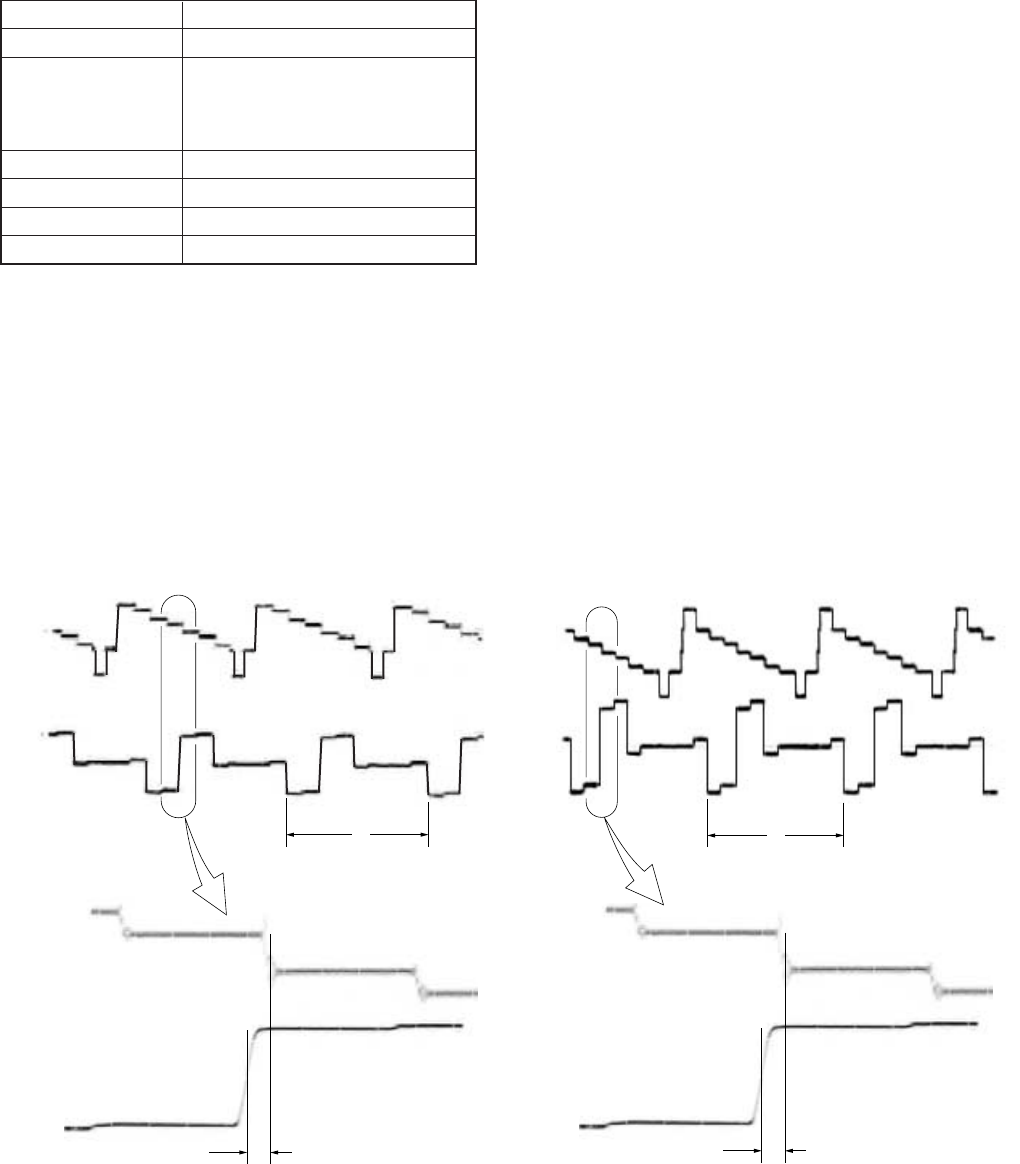
5-82
H
t
CH1
CH1
CH2
CH2
magnified
H
t
CH1
CH1
CH2
CH2
magnified
38. Composite E-E CR Signal Delay Adjustment
(VD-28 Board)
Mode E-E
Signal Color bar (VIDEO input) (Note)
Measurement Point CH1: COMPONENT OUTPUT Y
terminal (75 Ω terminated)
CH2: COMPONENT OUTPUT R-Y
terminal (75 Ω terminated)
Measuring Instrument Oscilloscope
Adjustment Page E
Adjustment Address B9
Specified Value t = 0 ± 20 nsec
Note: Set “VIDEO” mode with INPUT SELECT switch
Adjusting method:
1) Select page: 0, address: 01, and set data: 01.
2) Select page: E, address: B9, change the data and adjust the
time difference (t) between the boundary of green and magenta
on Y signal and CR signal, that to the specified value.
3) Press the PAUSE button of the adjustment remote commander.
4) Select page: 0, address: 01, and set data: 00.
For PAL modelFor NTSC model
Fig. 5-3-43
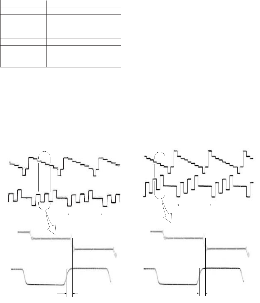
5-83
H
t
CH1
CH1
CH2
CH2
magnified
H
t
CH1
CH1
CH2
CH2
magnified
39. Composite E-E CB Signal Delay Adjustment
(VD-28 Board)
Mode E-E
Signal Color bar (VIDEO input) (Note)
Measurement Point CH1: COMPONENT OUTPUT Y
terminal (75 Ω terminated)
CH2: COMPONENT OUTPUT B-Y
terminal (75 Ω terminated)
Measuring Instrument Oscilloscope
Adjustment Page E
Adjustment Address B8
Specified Value t = 0 ± 20 nsec
Note: Set “VIDEO” mode with INPUT SELECT switch
Adjusting method:
1) Select page: 0, address: 01, and set data: 01.
2) Select page: E, address: B8, change the data and adjust the
time difference (t) between the boundary of green and magenta
on Y signal and CB signal, that to the specified value.
3) Press the PAUSE button of the adjustment remote commander.
4) Select page: 0, address: 01, and set data: 00.
For PAL modelFor NTSC model
Fig. 5-3-44
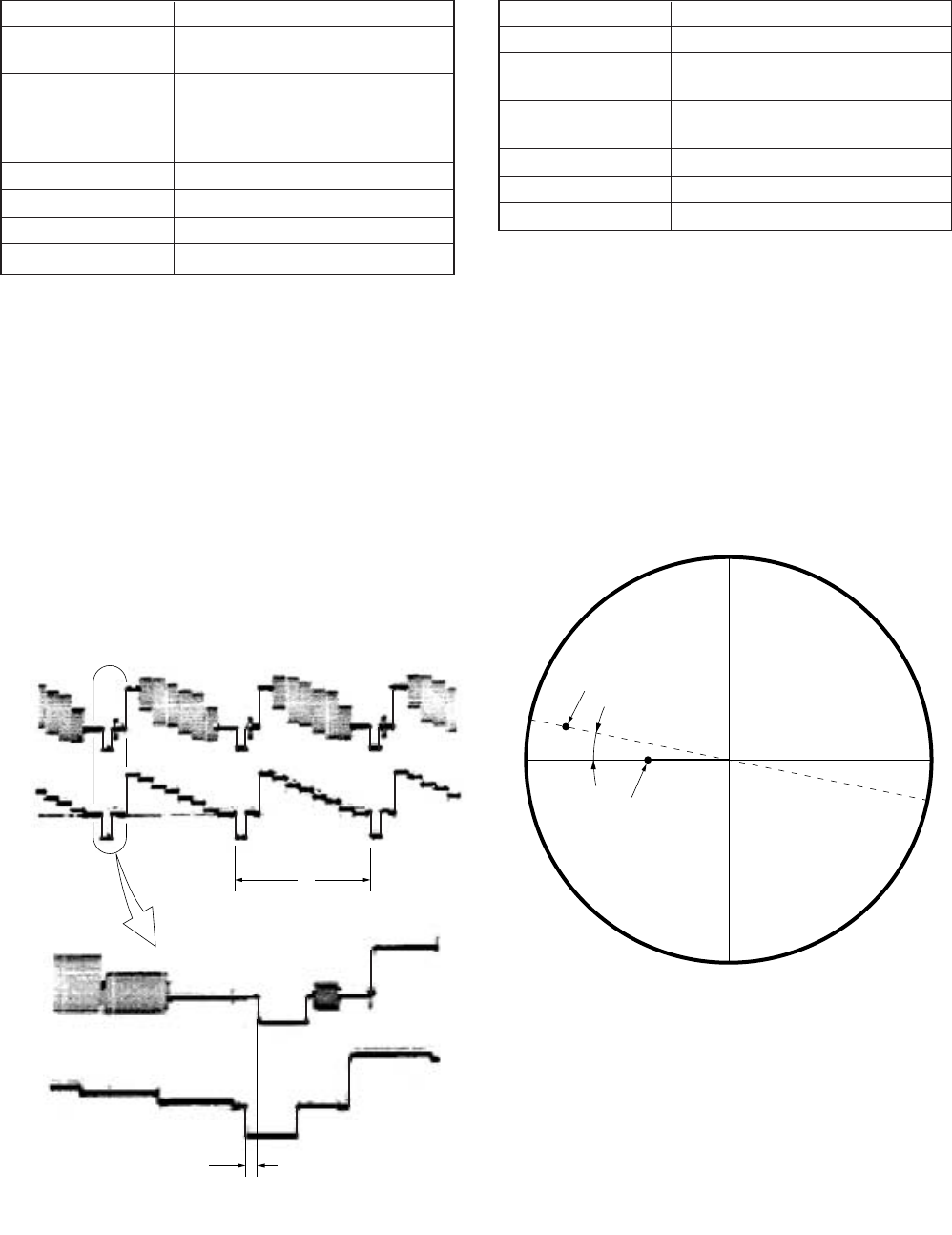
5-84
H
t
CH1
CH1
CH2
CH2
magnified
40. H Phase Adjustment (VD-28 Board)
Mode PB (EXT SYNC ON) (Note)
Signal Arbitray tape
Color bar (VIDEO input)
Measurement Point CH1: Color bar (The same signal
that VIDEO input)
CH2: COMPONENT OUTPUT Y
terminal (75 Ω terminated)
Measuring Instrument Oscilloscope
Adjustment Page E
Adjustment Address 2A (Coarse), C9 (Fine)
Specified Value t = 0 ± 20 nsec
Note: “EXT SYNC” of “VIDEO SET” on the menu setting is
ON.
Adjusting method:
1) Select page: 0, address: 01, and set data: 01.
2) Change the data on page: E, address: C9 and adjust so that the
difference in SYNC falling time (t) between CH1 and CH2
satisfies the specified value, and then press the PAUSE button.
At this time, check that the data at address: C9 is “40” to “C0”.
3) If the data at address: C9 is other than “40” to “C0”, change
the lower 1 digit (lower 4 bits) of the data on page: E, address:
2A, and press the PAUSE button, then repeat from step 3).
(Initial value of data on page: E, address: 2A is 08)
4) Select page: 0, address: 01, and set data: 00.
Fig. 5-3-45
41. E-E SC Phase Adjustment (VD-28 Board)
Mode E-E
Signal Color bar (VIDEO input) (Note)
Measurement Point VIDEO OUT 2 terminal (75 Ω
terminated)
Measuring Instrument Vectorscope (SCH measurement
mode)
Adjustment Page E
Adjustment Address CE
Specified Value Ø = 0 ± 5°
Note: Set “VIDEO” mode with INPUT SELECT switch
Adjusting method:
1) Select page: 0, address: 01, and set data: 01.
2) Adjust the phase synchronization control on the vectorscope
so that the burst luminance point is close to the U-axis.
3) Select page: E, address: CE, change tha data and adjust the
phase difference (Ø) between the burst and H phase to the
specified value.
4) Press the PAUSE button of the adjustment remote commander.
5) Select page: 0, address: 01, and set data: 00.
H phase
Burst phase
ø
Fig. 5-3-46
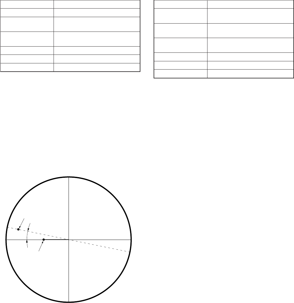
5-85
42. Playback SC Phase Adjustment (EXT SYNC OFF)
(VD-28 Board)
Mode Playback
Signal Arbitrary
Measurement Point VIDEO OUT 2 terminal (75 Ω
terminated)
Measuring Instrument Vectorscope (SCH measurement
mode)
Adjustment Page E
Adjustment Address CF
Specified Value Ø = 0 ± 5°
Note: “EXT SYNC” of “VIDEO SET” on the menu setting is
OFF.
Adjusting method:
1) Select page: 0, address: 01, and set data: 01.
2) Adjust the phase synchronization control on the vectorscope
so that the burst luminance point is close to the U-axis.
3) Select page: E, address: CF, change tha data and adjust the
phase difference (Ø) between the burst and H phase to the
specified value.
4) Press the PAUSE button of the adjustment remote commander.
5) Select page: 0, address: 01, and set data: 00.
H phase
Burst phase
ø
Fig. 5-3-47
43. Playback SC Phase Adjustment (EXT SYNC ON)
(VD-28 Board)
Mode Playback
Signal Arbitrary
Color bar (VIDEO input (REF. IN))
Measurement Point VIDEO OUT 2 terminal (75 Ω
terminated)
Measuring Instrument Vectorscope (SCH measurement
mode)
Adjustment Page E
Adjustment Address A7
Specified Value Ø = 0 ± 5°
Note: “EXT SYNC” of “VIDEO SET” on the menu setting is
ON.
Adjusting method:
1) Select page: 0, address: 01, and set data: 01.
2) Adjust the phase synchronization control on the vectorscope
so that the burst luminance point is close to the U-axis.
3) Select page: E, address: A7, change tha data and adjust the
phase difference (Ø) between the burst and H phase to the
specified value.
4) Press the PAUSE button of the adjustment remote commander.
5) Select page: 0, address: 01, and set data: 00.
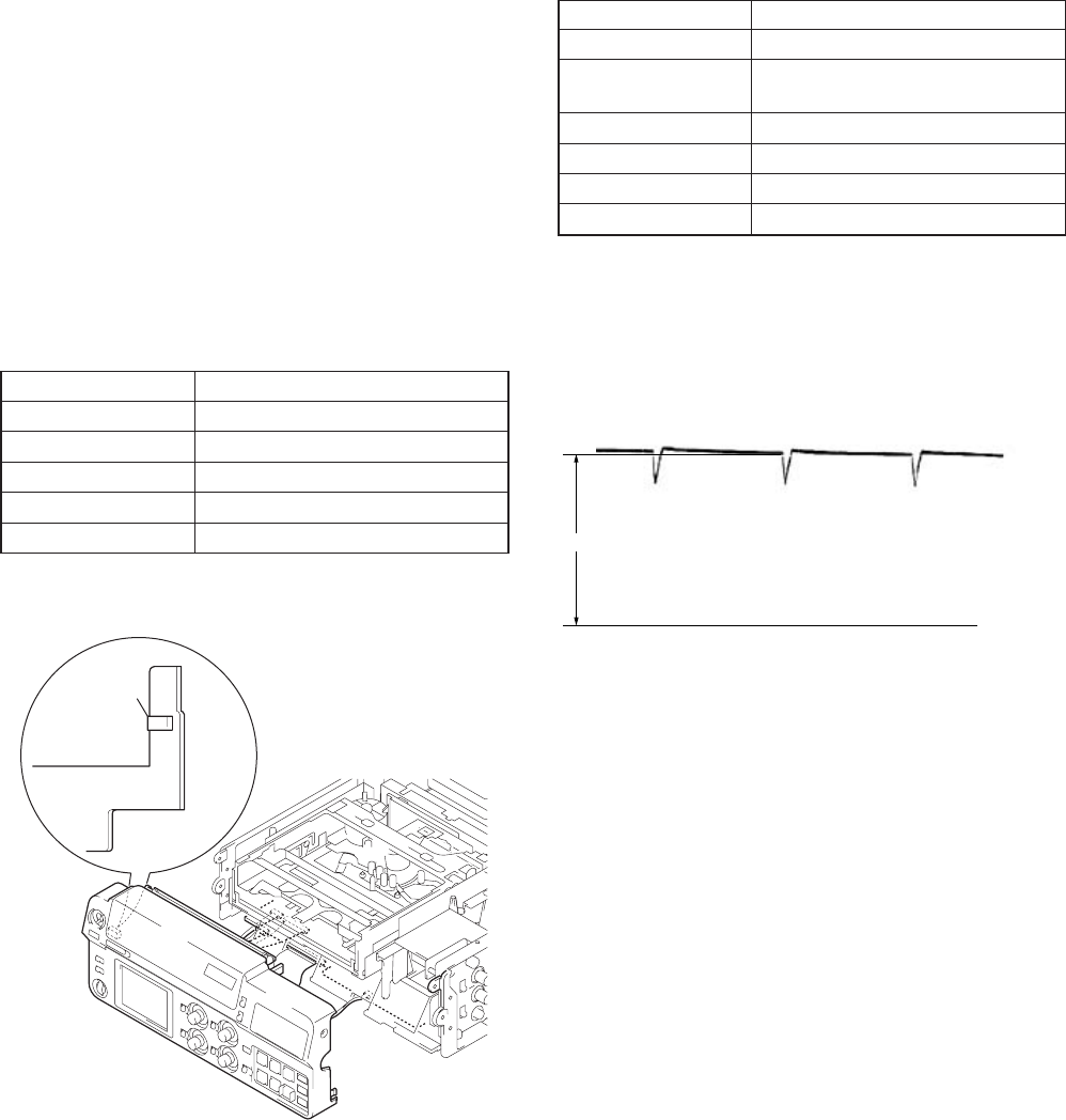
5-86
A
GND level
(0 Vdc)
1. VCO Adjustment (PD-125 Board)
Mode E-E
Signal Arbitrary
Measurement Point Pin 1 of CN505 on FR-157 board
(VCO CENT)
Measuring Instrument Oscilloscope (DC range)
Adjustment Page E
Adjustment Address 84
Specified Value A = 1.8 ± 0.1 V
Adjusting method:
1) Select page: 0, address: 01, and set data: 01.
2) Check that the GND level of oscilloscope.
3) Select page: E, address: 84, change the data and adjust the
voltage (A) of the VCO output to the specified value.
4) Press the PAUSE button of the adjustment remote commander.
5) Select page: 0, address: 01, and set data: 00.
Fig. 5-3-49
3-5. LCD SYSTEM ADJUSTMENTS
Note 1: The back light (fluorescent tube) is driven by high voltage
AC power supply. Therefore, do not touch the back light
holder to avoid electrical shock.
Note 2: When replacing the LCD unit, be careful to prevent
damages caused by static electricity.
Note 3: Adjust the LCD BRIGHT and LCD COLOR to the center
on menu display.
[Adjusting connector]
Most of the measuring points for adjusting the LCD are
concentrated in the CN505 of FR-157 board.
The following table shows the Pin No. and signal name of the
CN505.
Pin No. Signal Name
1 VCO_CENT
2 PSIG
3 GND
4 COM
5VG
Fig. 5-3-48
CN505
15
FR-157 board
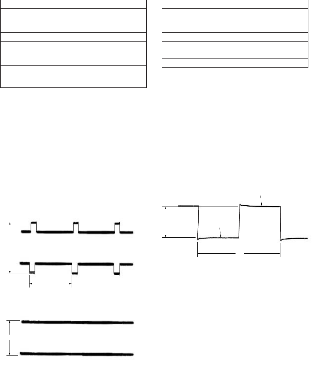
5-87
B
A
WIDE mode
NORMAL mode
V
2. Black Limit Adjustment (PD-125 Board)
Mode E-E
Signal Arbitrary
Measurement Point Pin 2 of CN505 on FR-157 board
(PSIG)
Measuring Instrument Oscilloscope
Adjustment Page E
Adjustment Address 82 (WIDE mode), 87 (NORMAL
mode)
Specified Value WIDE mode: A = 8.00 ± 0.05 Vp-p
NORMAL mode: B = 5.00 ± 0.05
Vp-p
Adjusting method:
1) Select page: 0, address: 01, and set data: 01.
2) Select page: 9, address: 0F, set data: 01, and press the PAUSE
button.
3) Check that the LCD screen change to wide mode.
4) Select page: E, address: 82, change the data and adjust PSIG
signal (A) to the specified value.
5) Press the PAUSE button of the adjustment remote commander.
6) Select page: 9, address: 0F, set data: 00, and press the PAUSE
button.
7) Check that the LCD screen change to normal mode.
8) Select page: E, address: 87, change the data and adjust PSIG
signal (B) to the specified value.
9) Press the PAUSE button of the adjustment remote commander.
10) Select page: 0, address: 01, and set data: 00.
Fig. 5-3-50
A
2H
Black level
Black level
3. Bright Adjustment (PD-125 Board)
Mode E-E
Signal Arbitrary
Measurement Point Pin 5 of CN505 on FR-157 board
(VG)
Measuring Instrument Oscilloscope
Adjustment Page E
Adjustment Address 8A
Specified Value A = 5.75 ± 0.05 Vp-p
Adjusting method:
1) Select page: 0, address: 01, and set data: 01.
2) Select page: 3, address: 0C, set data: 60, and press the PAUSE
button of the adjustment remote commander.
3) Select page: 3, address: 22, set data: 08, and press the PAUSE
button.
4) Select page: E, address: 8A, change the data and adjust the
voltage (A) between the reversed waveform black level and
non-reversed waveform black level to the specified value.
5) Press the PAUSE button of the adjustment remote commander.
6) Select page: 3, address: 22, set data: 00, and press the PAUSE
button.
7) Select page: 3, address: 0C, set data: 00, and press the PAUSE
button.
8) Select page: 0, address: 01, and set data: 00.
Fig. 5-3-51
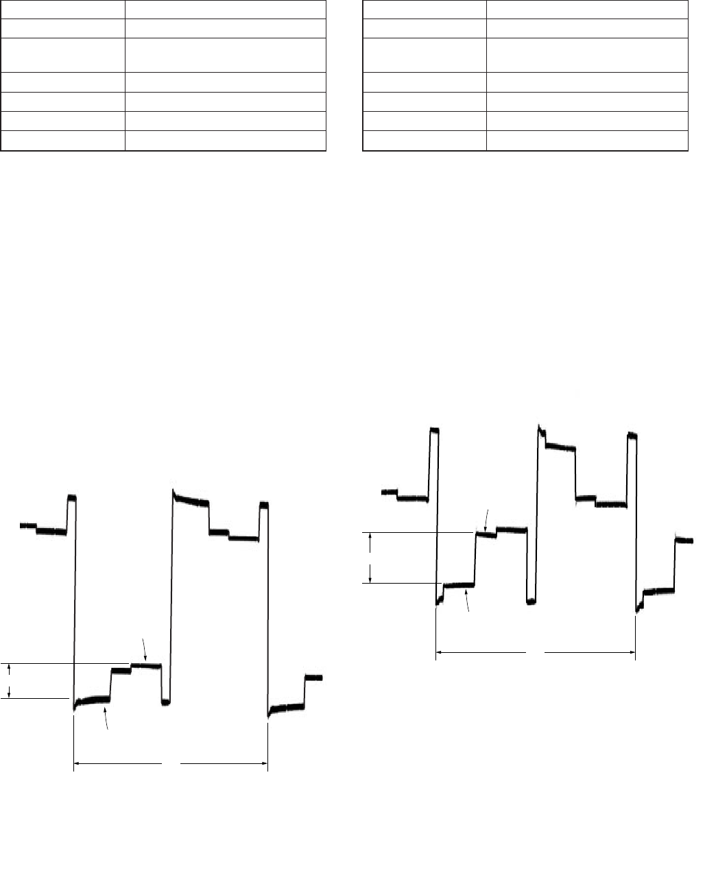
5-88
A
2H
Pedestal
(0 IRE)
90 IRE
5. Contrast Adjustment (PD-125 Board)
Mode E-E
Signal Arbitrary
Measurement Point Pin 5 of CN505 on FR-157 board
(VG)
Measuring Instrument Oscilloscope
Adjustment Page E
Adjustment Address 8C
Specified Value A = 2.00 ± 0.05 Vp-p
Adjusting method:
1) Select page: 0, address: 01, and set data: 01.
2) Select page: 3, address: 0C, set data: 60, and press the PAUSE
button of the adjustment remote commander.
3) Select page: 3, address: 22, set data: 01, and press the PAUSE
button.
4) Select page: E, address: 8C, change the data and adjust the
voltage (A) between the pedestal and 90IRE to the specified
value.
5) Press the PAUSE button of the adjustment remote commander.
6) Select page: 3, address: 22, set data: 00, and press the PAUSE
button.
7) Select page: 3, address: 0C, set data: 00, and press the PAUSE
button.
8) Select page: 0, address: 01, and set data: 00.
Fig. 5-3-53
A
2H
Pedestal
(0 IRE)
GAMMA 1
limiter level
4. Gamma 1 Adjustment (PD-125 Board)
Mode E-E
Signal Arbitrary
Measurement Point Pin 5 of CN505 on FR-157 board
(VG)
Measuring Instrument Oscilloscope
Adjustment Page E
Adjustment Address 83
Specified Value A = 0.92 ± 0.05 Vp-p
Adjusting method:
1) Select page: 0, address: 01, and set data: 01.
2) Select page: 3, address: 0C, set data: 60, and press the PAUSE
button of the adjustment remote commander.
3) Select page: 3, address: 22, set data: 02, and press the PAUSE
button.
4) Select page: 9, address: 0E, set data: 40, and press the PAUSE
button.
5) Select page: E, address: 83, change the data and adjust the
voltage (A) between the pedestal and GAMMA 1 limiter level
to the specified value.
6) Press the PAUSE button of the adjustment remote commander.
7) Select page: 9, address: 0E, set data: 00, and press the PAUSE
button.
8) Select page: 3, address: 22, set data: 00, and press the PAUSE
button.
9) Select page: 3, address: 0C, set data: 00, and press the PAUSE
button.
10) Select page: 0, address: 01, and set data: 00.
Fig. 5-3-52
5-89
6. Center Voltage Adjustment (PD-125 Board)
Mode E-E
Signal Arbitrary
Measurement Point Pin 5 of CN505 on FR-157 board
(VG)
Measuring Instrument Digital voltmeter
Adjustment Page E
Adjustment Address 85
Specified Value A = 5.50 ± 0.10 V
Adjusting method:
1) Select page: 0, address: 01, and set data: 01.
2) Select page: 3, address: 0C, set data: 60, and press the PAUSE
button of the adjustment remote commander.
3) Select page: 3, address: 22, set data: 08, and press the PAUSE
button.
4) Select page: E, address: 85, change the data and adjust the
voltage (A) between the pin 5 (VG) of CN505 board and pin
3 (GND) of CN505 on FR-157 to the specified value.
5) Press the PAUSE button of the adjustment remote commander.
6) Select page: 3, address: 22, set data: 00, and press the PAUSE
button.
7) Select page: 3, address: 0C, set data: 00, and press the PAUSE
button.
8) Select page: 0, address: 01, and set data: 00.
7. White Balance Adjustment (PD-125 Board)
Mode E-E
Signal Arbitrary
Measurement Point Check on LCD screen
Measuring Instrument
Adjustment Page E
Adjustment Address 80, 81
Specified Value LCD screen must not be colored
Note: Check the white balance only when replacing the
following parts. If necessary, adjust them.
1. LCD panel
2. Light induction plate
3. IC8001
Adjusting method:
1) Select page: 0, address: 01, and set data: 01.
2) Select page: 3, address: 0C, set data: 60, and press the PAUSE
button of the adjustment remote commander.
3) Select page: 3, address: 22, set data: 0B, and press the PAUSE
button.
4) Select page: E, address: 80 and 81, and set data to the initial
value.
Note: To write in the non-volatile memory (EEPROM), press
the PAUSE button of the adjustment remote commander
each time to set the data.
Address Data
NTSC PAL
80 93 94
81 7C 7D
5) Check that the LCD screen is not colored. If colored, change
the data of page: E, address:80 and 81 so that the LCD screen
is not colored.
Note: To write in the non-volatile memory (EEPROM), press
the PAUSE button of the adjustment remote commander
each time to set the data.
6) Select page: 3, address: 22, set data: 00, and press the PAUSE
button of the adjustment remote commander.
7) Select page: 3, address: 0C, set data: 00, and press the PAUSE
button.
8) Select page: 0, address: 01, and set data: 00.
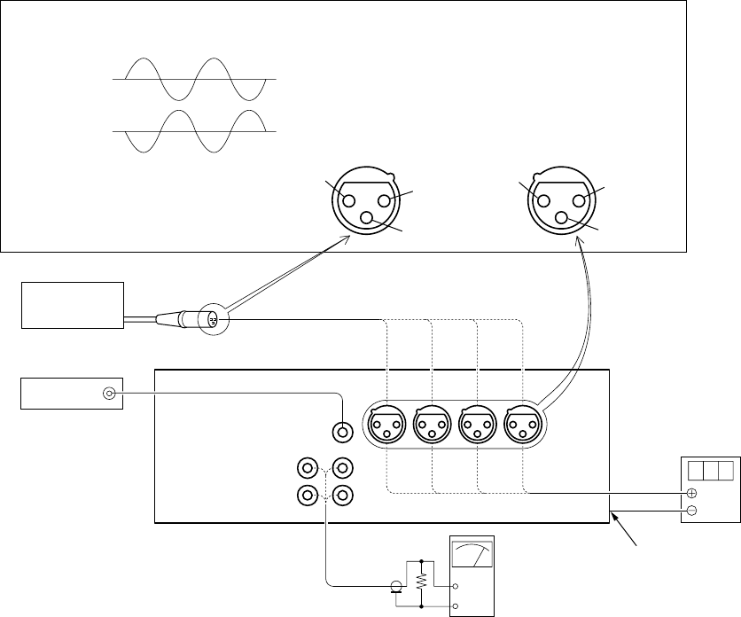
5-90
3-6. AUDIO SYSTEM ADJUSTMENTS
Set the switches and menu to the following positions unless otherwise specified.
Switch setting
DVCAM/DV SELECT switch (Inside of the cover at left panel) .......................... DVCAM
REC LEVEL CONTROL SELECT switch (Front panel) (CH-1 to CH-4) ........... AUTO
REC LEVEL CONTROL knob (Front panel) (CH-1 to CH-4) .............................. CENTER
AUDIO INPUT SELECT switch (Right panel) (CH-1 to CH-4) ........................... LINE
AUDIO INPUT LEVEL CONTROL switch (Right panel) (CH-1 to CH-4) ......... –20
MONITOR SELECT (Right panel)......................................................................... CH1/2
DISPLAY (LCD OFF/OFF/ON) switch (Front panel) ........................................... ON
DISPLAY (MENU/TC/AUDIO) switch (Front panel) ........................................... AUDIO
METER switch (Front panel) .................................................................................. CH1/2
VIDEO INPUT SELECT switch (Right panel) ...................................................... VIDEO (except DV)
Menu setting (AUDIO SET menu)
AUDIO MODE .................................................. FS32K
AUDIO DUB ...................................................... CH3, 4
JOG AUDIO ....................................................... ON
REF LEVEL ....................................................... –20
AGC CH1, 2 ....................................................... SEPARATE
AGC CH3, 4 ....................................................... SEPARATE
LIMITER............................................................ OFF
WIND (CH-1 to CH-4) ...................................... OFF
Connection of equipment
Audio
level meter
or
Audio
noise meter
47 kΩ
47 kΩ: 1-249-437-11
Pattern generator
Balanced audio generator
VIDEO OUT
1 pin: GND
1 pin
2 pin: + signal
3 pin: – signal
Chassis GND
Digital
voltmeter
AUDIO
INPUT
terminal
AUDIO
OUTPUT
terminal
CH-4
CH-4
CH-3
CH-3
CH-2
CH-2 CH-1
CH-1
VIDEO/REF.IN
terminal
2 pin
male female
3 pin
2 pin 1 pin
3 pin
The input signal level is the level of pin 2 against pin 3.
Fig. 5-3-54
5-91
1. Audio PAL Data Input (DSR-50P)
When replacing JC-20 board or IC5006 of JC-20 board, change
the data of the address shown in the following tables by manual
input.
Mode VTR stop
Signal Arbitray
Adjustment Page D
Adjustment Address 40 to 47
Input method:
1) Select page: 0, address: 01, and set data: 01.
2) Select page: D, and input data in the following table.
Note: To write in the non-volatile memory (EEPROM), press the
PAUSE button of the adjustment remote commander each
time to set the data.
3) Select page: 0, address: 01, and set data: 00.
Address Data
40 00
41 18
42 AC
43 65
44 00
45 1A
46 AC
47 65
2. Playing Level Check
Mode PLAY
Signal Alignment tape: For audio check
(NTSC: XH5-3/PAL: XH5-3P)
Measurement point AUDIO OUTPUT terminal (CH-1, 2)
Measuring instrument Audio level meter, Oscilloscope
Specified value 32kHz mode section:
1 kHz signal must be outputted.
48kHz mode section:
1 kHz signal level is +6 to +10 dBV.
44.1kHz mode EMP ON section:
7.35 kHz signal level is 0 to +4 dBV.
44.1kHz mode EMP OFF section:
7.35 kHz signal level is +6 to +10 dBV.
Note: 0 dBV = 1 Vrms
Checking method (NTSC):
1) Play the alignment tape (XH5-3).
2) Check that the play signal level satisfies the specified value.
3) Check with the oscilloscope that no clip is found in the output
waveform.
Checking method (PAL) :
1) Select page: 0, address: 01, and set data: 01.
2) Select page: D, address: 40, and check that the data is “00”.
3) Select page: D, address: 41, and check that the data is “18”.
4) Select page: D, address: 42, set data: FF, and press the PAUSE
button on the adjustment remote commander.
5) Select page: D, address: 43, set data: 7F, and press the PAUSE
button.
6) Select page: D, address: 44, and check that the data is “00”.
7) Select page: D, address: 45, and check that the data is “1A”.
8) Select page: D, address: 46, set data: FF, and press the PAUSE
button.
9) Select page: D, address: 47, set data: 7F, and press the PAUSE
button.
10) Disconnect the adjustment remote commander, and turn the
POWER switch OFF.
11) Turn the POWER switch ON.
12) Play the aligment tape (XH5-3P).
13) Check that the play signal level satisfies the specified value.
14) Check with the oscilloscope that no clip is found in the output
waveform.
15) Connect the adjustment remote commander.
16) Select page: 0, address: 01, and set data: 01.
17) Select page: D, address: 40, and check that the data is “00”.
18) Select page: D, address: 41, and check that the data is “18”.
19) Select page: D, address: 42, set data: AC, and press the PAUSE
button.
20) Select page: D, address: 43, set data: 65, and press the PAUSE
button.
21) Select page: D, address: 44, and check that the data is “00”.
22) Select page: D, address: 45, and check that the data is “1A”.
23) Select page: D, address: 46, set data: AC, and press the PAUSE
button.
24) Select page: D, address: 47, set data: 65, and press the PAUSE
button.
25) Disconnect the adjustment remote commander, and turn the
POWER switch OFF.

5-92
3. Audio Level Indication Check
Mode STOP
Signal Audio: 1 kHz, 0 dBu signal
AUDIO INPUT terminal
(CH-1 to 4)
Measurement point Audio level indication on the front
panel
Measuring instrument (Indication on LCD monitor and on
display window of the set)
Specified value LCD monitor:
All level meters light up and a red
LED on the right side of meter lights
up.
Display window of the set:
All level meter light up and the
OVER indicator on the meter lights
up.
Note: 0 dBu = 0.775 Vrms/balance
Switch setting
DISPLAY (LCD OFF/OFF/ON) switch ...... ON
DISPLAY (MENU/TC/AUDIO) switch ...... AUDIO
VIDEO INPUT SELECT switch ................. VIDEO (except DV)
AUDIO INPUT SELECT switch (CH-1 to CH-4) ................. LINE
AUDIO INPUT LEVEL CONTROL switch (CH-1 to CH-4).... –20
Menu setting (AUDIO SET menu)
AUDIO MODE ...................... FS32K
LIMITER................................ OFF
Checking method:
1) Enter 1 kHz, 0 dBu signal to the AUDIO INPUT terminal (CH-
1).
2) Set the REC level mode switch (CH-1) on the front panel to
“MANU”, and rotate the REC level adjusting knob to the
maximum position (clockwise).
3) At this time, check that the CH-1 level meters on the LCD
monitor all light up, and a red LED on the right side of meter
lights up.
4) Set the METER switch on the front panel to “CH1/2”.
5) At this time, check that the CH-1 level meters on the display
window of the set all light up, and the OVER indicator on the
meter lights up.
6) For the CH-2, 3 and 4, perform checking in the same manner.
4. Recording and Playing Check
Mode REC and PLAY
Signal Audio: 1 kHz, 0 dBu signal
AUDIO INPUT terminal
(CH-1 to 4)
Video: Color bar
VIDEO IN terminal
Measurement point AUDIO OUTPUT terminal (CH-1 to 4)
Measuring instrument Audio level meter, Oscilloscope
Specified value REC level adjusting knob:
Within 1 division from the center.
Output level: +6 to +10 dBV
Output waveform: No clip
When the recorded part is cued/
reversed, the playback sounds at the
changed speed must be outputted.
Switch setting
DISPLAY (LCD OFF/OFF/ON) switch ...... ON
DISPLAY (MENU/TC/AUDIO) switch ...... AUDIO
VIDEO INPUT SELECT switch ................. VIDEO (except DV)
AUDIO INPUT SELECT switch (CH-1 to CH-4) .............. LINE
AUDIO INPUT LEVEL CONTROL switch (CH-1 to CH-4).... –20
Menu setting (AUDIO SET menu)
AUDIO MODE ...................... FS32K
LIMITER................................ OFF
Checking method:
1) Enter 1 kHz, 0 dBu signal to the AUDIO INPUT terminal (CH-
1).
2) Set the REC level mode switch (CH-1) on the front panel to
“MANU”.
3) Rotate the REC level adjusting knob so that 0 dB on the CH-1
level meter on the LCD monitor lights up and a red LED on
the right side of meter does not light up.
4) At this time, check that the rotating angle of the REC level
adjusting knob is within 1 division from the center.
Note: Hence, do not rotate the REC level adjusting knob unless
otherwise specified, as this set position (rotating angle) of the
REC level adjusting knob is required in other checking items.
5) Perform recording continuously for about 30 seconds, and play
the recorded part.
6) Check that the output level on CH-1 satisfies the specified
value.
7) Observing the output waveform on CH-1 with the oscilloscope,
check that no clip is found.
8) Check that the playback sounds at the changed speed are
outputted, when the recorded part is cued/reversed.
9) For the CH-2, 3 and 4, perform checking in the same manner.

5-93
5. FS48 kHz Frequency Characteristic Check
Mode STOP
Signal Audio: 1 kHz, –4 dBu signal
10 Hz, –4 dBu signal
20 kHz, –4 dBu signal
AUDIO INPUT terminal (CH-1, 2)
Measurement point AUDIO OUTPUT terminal (CH-1, 2)
Measuring instrument Audio level meter
Specified value Difference in output level:
A = –2.0 dB to +1.0 dB
B = –1.0 dB to +1.0 dB
Switch setting
REC LEVEL CONTROL knob (Front panel) (CH-1 to CH-4)
...................The position at Recording and Playing Check
Menu setting (AUDIO SET menu)
AUDIO MODE ...................... FS48K
Checking method:
1) Enter 1 kHz, –4 dBu signal to the AUDIO INPUT terminal
(CH-1).
2) At this time, measure the output level on CH-1, and the
measured value is assumed to be “a” (dBV).
3) Enter 10 Hz, –4 dBu signal to the AUDIO INPUT terminal
(CH-1).
4) At this time, measure the output level on CH-1, and the
measured value is assumed to be “b” (dBV).
5) Enter 20 kHz, –4 dBu signal to the AUDIO INPUT terminal
(CH-1).
6) At this time, measure the output level on CH-1, and the
measured value is assumed to be “c” (dBV).
7) Obtain the difference A (dB) between output level “b” (dBV)
and “a” (dBV) to check that it satisfies the specified value.
A = b – a
8) Obtain the difference B (dB) between output level “c” (dBV)
and “b” (dBV) to check that it satisfies the specified value.
B = c – b
9) For the CH-2, perform checking in the same manner.
6. FS48 kHz Noise Level Check
Mode STOP
Signal Audio: No signal
Nothing is connected to the
AUDIO INPUT terminal (CH-1, 2)
Measurement point AUDIO OUTPUT terminal (CH-1, 2)
Measuring instrument Audio noise meter
(with A-weight filter)
Specified value –78 dBV or less
(A-weight filter ON)
Switch setting
REC LEVEL CONTROL knob (Front panel) (CH-1 to CH-4)
................... The position at Recording and Playing Check
Menu setting (AUDIO SET menu)
AUDIO MODE ...................... FS48K
Checking method:
1) Connect the audio noise meter to the AUDIO OUTPUT
terminal (CH-1), and turn the A-weight filter on.
2) At this time, measure the noise level to check that it satisfies
the specified value.
3) For the CH-2, perform checking in the same manner.

5-94
7. FS32 kHz Frequency Characteristic Check
Mode STOP
Signal Audio: 1 kHz, –4 dBu signal
10 Hz, –4 dBu signal
14 kHz, –4 dBu signal
40 Hz, –4 dBu signal
AUDIO INPUT terminal (CH-1 to 4)
Measurement point AUDIO OUTPUT terminal (CH-1 to 4)
Measuring instrument Audio level meter
Specified value Difference in output level:
A = –2.0 dB to +1.0 dB
B = –1.0 dB to +1.0 dB
C = –2.0 dB to +1.0 dB
D = –20.0 dB to –12.0 dB
Switch setting
REC LEVEL CONTROL knob (Front panel) (CH-1 to CH-4)
................. The position at Recording and Playing Check
Menu setting (AUDIO SET menu)
AUDIO MODE ...................... FS32K
Checking method:
1) Enter 1 kHz, –4 dBu signal to the AUDIO INPUT terminal
(CH-1).
2) At this time, measure the output level on CH-1, and the
measured value is assumed to be “a” (dBV).
3) Enter 10 Hz, –4 dBu signal to the AUDIO INPUT terminal
(CH-1).
4) At this time, measure the output level on CH-1, and the
measured value is assumed to be “b” (dBV).
5) Enter 14 kHz, –4 dBu signal to the AUDIO INPUT terminal
(CH-1).
6) At this time, measure the output level on CH-1 to attain “c”
(dBV).
7) Obtain the difference A (dB) between output level “b” (dBV)
and “a” (dBV) to check that it satisfies the specified value.
A = b – a
8) Obtain the difference B (dB) between output level “c” (dBV)
and “b” (dBV) to check that it satisfies the specified value.
B = c – b
9) Set the “WIND CH-1” of the AUDIO SET menu to ON.
10) Enter 1 kHz, –4 dBu signal to the AUDIO INPUT terminal
(CH-1).
11) At this time, measure the output level on CH-1 to attain “d”
(dBV).
12) Enter 40 Hz, –4 dBu signal to the AUDIO INPUT terminal
(CH-1).
13) t this time, measure the output level on CH-1 to attain “e”
(dBV).
14) Set the “WIND CH-1” of the AUDIO SET menu to OFF.
15) Obtain the difference C (dB) between output level “d” (dBV)
and “a” (dBV) to check that it satisfies the specified value.
C = d – a
16) Obtain the difference D (dB) between output level “e” (dBV)
and “a” (dBV) to check that it satisfies the specified value.
D = e – a
17) For the CH-2, 3 and 4, perform checking in the same manner.
8. FS32 kHz Noise Level Check
Mode STOP
Signal Audio: No signal
Nothing is connected to the
AUDIO INPUT terminal (CH-1 to 4)
Measurement point AUDIO OUTPUT terminal (CH-1 to 4)
Measuring instrument Audio noise meter
(with A-weight filter)
Specified value –78 dBV or less
(A-weight filter ON)
Switch setting
REC LEVEL CONTROL knob (Front panel) (CH-1 to CH-4)
.................. The position at Recording and Playing Check
Menu setting (AUDIO SET menu)
AUDIO MODE ...................... FS32K
Checking method:
1) Connect the audio noise meter to the AUDIO OUTPUT
terminal (CH-1), and turn the A-weight filter on.
2) At this time, measure the noise level on the CH-1 to check that
it satisfies the specified value.
3) For the CH-2, 3 and 4, perform checking in the same manner.
5-95
9. Input Level Switching Check
Switch setting
DISPLAY (LCD OFF/OFF/ON) switch ...................... ON
DISPLAY (MENU/TC/AUDIO) switch ...................... AUDIO
REC LEVEL CONTROL SELECT switch (CH-1 to CH-4) ..... AUTO
VIDEO INPUT SELECT switch ..................VIDEO (except DV)
AUDIO INPUT SELECT switch (CH-1 to CH-4) .............. LINE
Menu setting (AUDIO SET menu)
AUDIO MODE ...................... FS32K
REF LEVEL ........................... –20
LIMITER................................ OFF
(1) –20 dB check
Mode STOP
Signal Audio: 1 kHz, –22 dBu (to –18 dBu)
signal
AUDIO INPUT terminal (CH-1 to 4)
Measurement point AUDIO INPUT terminal (CH-1 to 4)
Measuring instrument Audio level meter
Specified value –22.0 dBu to –18.0 dBu
Checking method
1) Set the input level adjusting switch (CH-1) on the right panel
to “–20”.
2) Enter 1 kHz, –22 dBu signal to the AUDIO INPUT terminal
(CH-1).
3) Press the “FINE” button on the front panel to display the audio
level indication of the LCD monitor on the FINE screen.
4) Raise the output of balance audio oscillator to “–22.0 dBu”
t “–21.9 dBu” t “–21.8 dBu” ... until the level indication
on the FINE screen on the CH-1 becomes “–20.0 dBu”.
5) At this time, measure the AUDIO INPUT terminal level on the
CH-1 to check that it satisfies the specific value.
6) For the CH-2, 3 and 4, perform checking in the same manner.
(2) –60 dB check
Mode STOP
Signal Audio: 1 kHz, –60 dBu signal
AUDIO INPUT terminal (CH-1 to 4)
Measurement point AUDIO OUTPUT terminal (CH-1 to 4)
Measuring instrument Audio level meter
Specified value –14.0 dBV to –10.0 dBV
Checking method
1) Set the input level adjusting switch (CH-1) on the right panel
to “–60”.
2) Enter 1 kHz, –60 dBu signal to the AUDIO INPUT terminal
(CH-1).
3) At this time, measure the AUDIO OUTPUT terminal level on
the CH-1 to check that it satisfies the specific value.
4) For the CH-2, 3 and 4, perform checking in the same manner.
(3) +4 dB check
Mode STOP
Signal Audio: 1 kHz, +4 dBu signal
AUDIO INPUT terminal (CH-1 to 4)
Measurement point AUDIO OUTPUT terminal (CH-1 to 4)
Measuring instrument Audio level meter
Specified value –15.0 dBV to –9.0 dBV
Checking method
1) Set the input level adjusting switch (CH-1) on the right panel
to “+4”.
2) Enter 1 kHz, +4 dBu signal to the AUDIO INPUT terminal
(CH-1).
3) At this time, measure the AUDIO OUTPUT terminal level on
the CH-1 to check that it satisfies the specific value.
4) For the CH-2, 3 and 4, perform checking in the same manner.
10. Microphone Power Supply Check
Mode STOP
Signal No signal
Measurement point AUDIO INPUT terminal (CH-1 to 4)
+ probe: pin 2, 3
– probe: GND (Note 1)
Measuring instrument Digital voltmeter
Specified value Audio input select switch
In +48V ON position:
A = +45 V to +50 V
In CAM or LINE position:
B = 0 V to +1 V
Note 1: Connect to the chassis of the set (such as GND of VIDEO/
REF.IN terminal).
Switch setting
AUDIO INPUT LEVEL CONTROL switch (CH-1 to CH-4)
........................................................................ –60
Checking method:
1) Connect the + probe of digital voltmeter to the pin 2 on CH-
1.
2) Set the audio input select switch (CH-1) on the right panel to
“+48V ON”.
3) At this time, check that the DC voltage (A) satisfies the
specified value.
4) Check that the DC voltage (B) satisfies the specified value
when the audio input select switch (CH-1) on the right panel
is set to “LINE” and “CAM”.
Note 2: In the “LINE” position, the discharge time of +48V is
long, and therefore set the switch to “CAM” first to
discharge +48V rapidly.
5) Connect the + probe of digital voltmeter to the pin 3 on CH-
1, and repeat steps 2) to 4).
6) For the CH-2, 3 and 4, perform checking in the same manner.
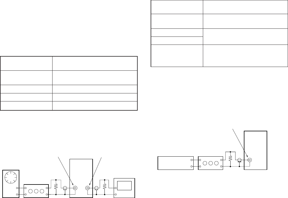
5-96
3-7. TIME CODE SYSTEM ADJUSTMENTS
Set the switches to the following positions unless otherwise
specified.
Operation mode switch .................................. DVCAM
VIDEO INPUT SELECT switch ..................... VIDEO (except DV)
Cassette tape................................................... None
1. Analog Through (E-E) Level Check
Mode STOP (no cassette tape)
Press the REC button.
Signal TC IN (INT) terminal:
6 kHz sine wave 3.0 Vp-p
Measurement point TC OUT (INT) terminal (600 Ω load)
Measuring instrument Oscilloscope
Specified value 2.0 to 4.0 Vp-p
Menu setting (TC/UB SET menu)
TC/UB IN ............................... TC & UB EXT
Connection of equipment
Checking method:
1) Check that the TC output signal level satisfies the specified
value.
2) Check with the oscilloscope that no clip is found in the output
waveform.
2. Time Code Reading Check
Mode STOP (no cassette tape)
Press the REC button.
Signal TC IN (INT) terminal:
0.25 Vp-p time code signal
Measurement point Time counter on the front panel
Measuring instrument Counter value on the display
Specified value The value indicated on the time code
generator must be same as the counter
value on the front panel.
Switch setting
Set the counter switch on the front panel to “TC”.
Menu setting (TC/UB SET menu)
TC/UB IN ............................... TC & UB EXT
Connection of equipment
Checking method:
1) Enter 0.25 Vp-p time code signal obtained by attenuating the
output of time code generator (such as NTSC: BVG-1600/PAL:
BVG-1600P) to the TC IN (EXT) terminal.
2) Check that the value indicated on the time code generator is
same as the counter value on the front panel.
DSR-50/
50P
600 Ω600 Ω
Attenuator
TC OUT (INT)TC IN (EXT)
600 Ω: 270 (1-249-410-11) +330 (1-249-411-11)
Audio
generator
Oscilloscope
DSR-50/
50P
600 Ω
Attenuator
TC IN (EXT)
600 Ω: 270 (1-249-410-11) +330 (1-249-411-11)
Time code
generator
1H 09M 40S
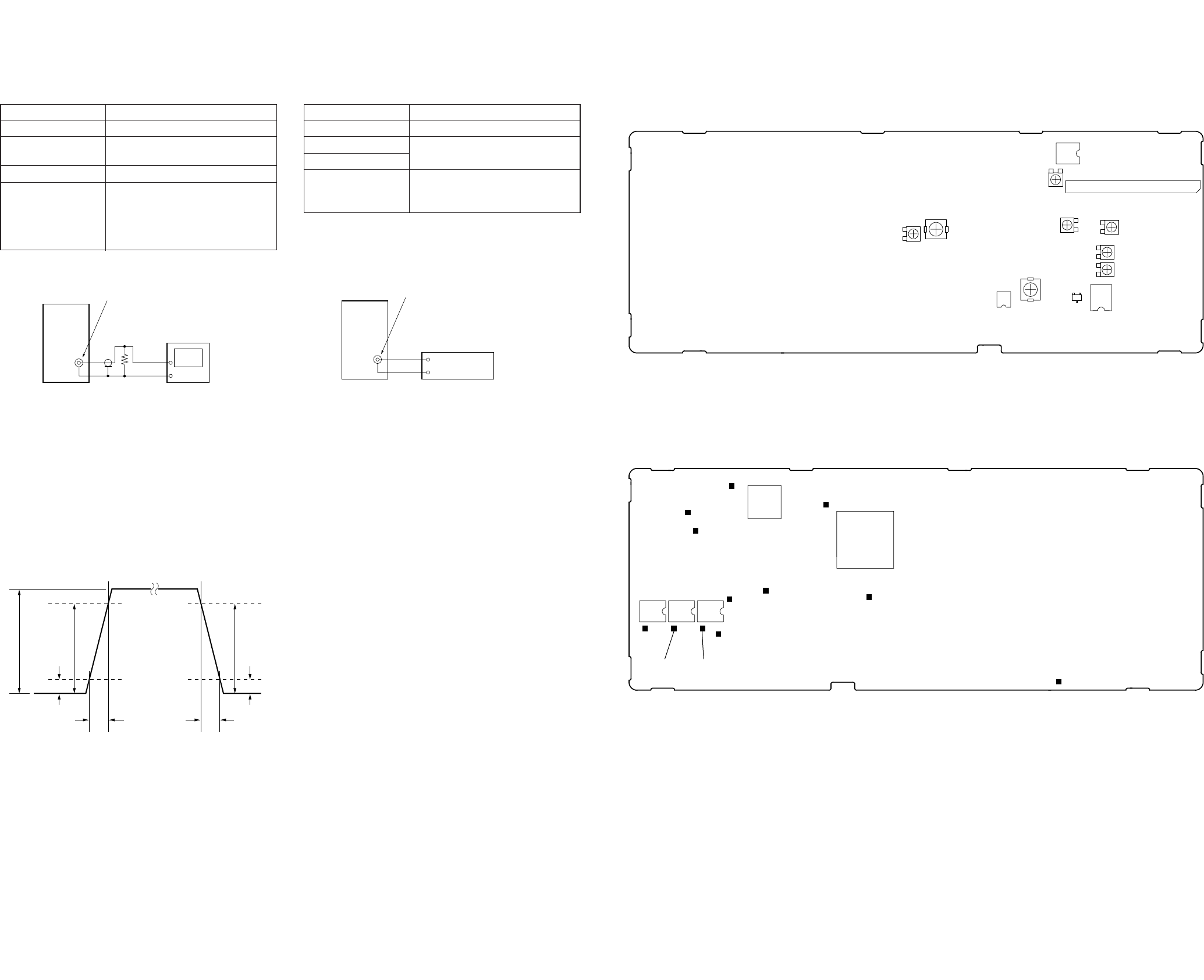
5-97 5-98 E
3. Internal Time Code Output Waveform Check
Mode PLAY
Signal Time code recorded tape
Measurement point TC OUT (INT) terminal (600 Ω
load)
Measuring instrument Oscilloscope
Specified value A = 2.0 to 3.0 Vp-p (NTSC/PAL)
T1 = 20 to 30 µsec (NTSC)
T1 = 40 to 65 µsec (PAL)
T2 = 20 to 30 µsec (NTSC)
T2 = 40 to 65 µsec (PAL)
Connection of equipment
Checking method:
1) Check that the TC output signal level (A) satisfies the specified
value.
2) Check that the TC output signal rising time (T1) satisfies the
specified value.
3) Check that the TC output signal falling time (T2) satisfies the
specified value.
DSR-50/
50P
600 Ω
TC OUT (INT)
600 Ω: 270 (1-249-410-11) +330 (1-249-411-11)
Oscilloscope
4. Internal Time Code Output Check
Mode PLAY
Signal Time code recorded tape
Measurement point Counter value of timer code reader
Measuring instrument
Specified value The counter value on the front panel
must be same as the value indicated
on the time code reader.
Switch setting
Set the counter switch on the front panel to “TC”.
Connection of equipment
Checking method:
1) Connect the time code reader (such as BVG-1500) to the TC
OUT (INT) terminal.
2) Check that the counter value on the front panel is same as the
value indicated on the time code reader.
A90% 90%
10% 10%
T1 T2
Fig. 5-3-55
Time code reader
1H 09M 40S
DSR-50/
50P
TC OUT (INT)
3-8. ARRANGEMENT DIAGRAM FOR ADJUSTMENT PARTS
CT2200
RV2201
RV1103
IC1105
CN1101
RV1102 RV1104
RV1101
RV1100
IC1101IC3302
CL1157
CL1122
CL1124
CL1169
CL2214
CL3305
CL1170
CL1162
CL1160 CL1161
CL1145
IC1102
IC1103IC1104
CL2217
16 9
48
49
64
32
17
33
116
25 32 1
8
24
17
IC1108
IC2204
CT3300 Q1116
EB
C
JC-20 BOARD (SIDE A)
JC-20 BOARD (SIDE B)
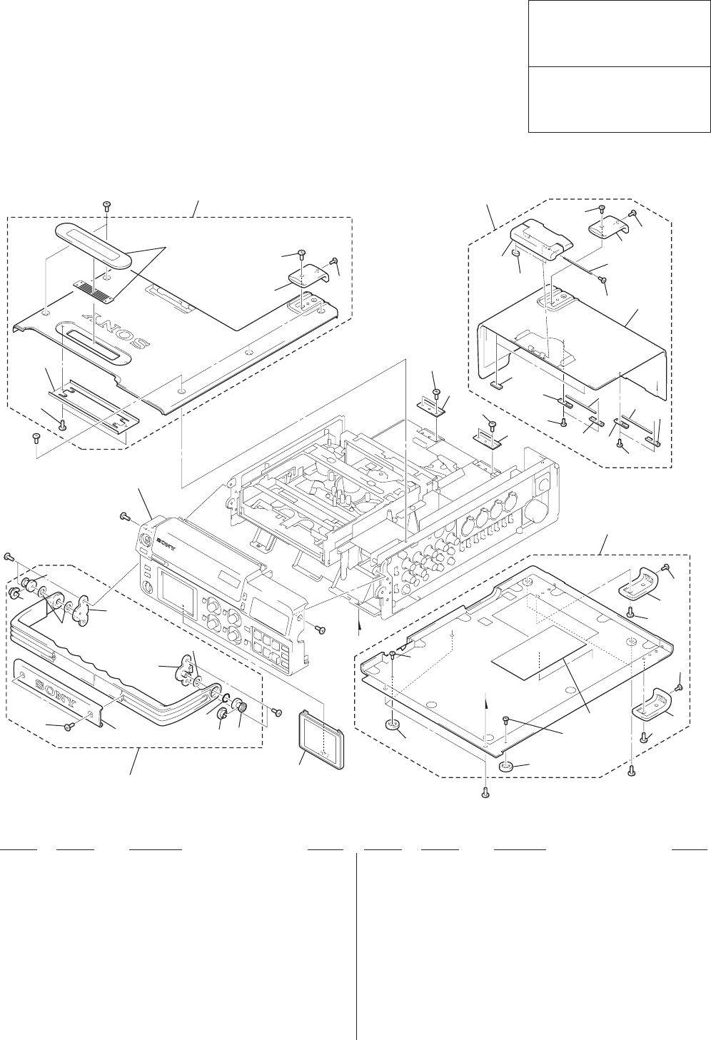
6-1
NOTE:
• -XX and -X mean standardized parts, so they may
have some difference from the original one.
• Items marked “*” are not stocked since they are
seldom required for routine service. Some delay
should be anticipated when ordering these items.
• The mechanical parts with no reference number in
the exploded views are not supplied.
• Hardware (# mark) list and accessories are given
in the last of the electrical parts list.
SECTION 6
REPAIR PARTS LIST
6-1. EXPLODED VIEWS
DSR-50/50P
The components identified by mark
0 or dotted line with mark 0 are
critical for safety.
Replace only with part number speci-
fied.
Les composants identifiés par une
marque 0 sont critiquens pour la
sécurité.
Ne les remplacer que par une pièce
portant le numéro spécifié.
Ref. No. Part No. Description RemarkRef. No. Part No. Description Remark
6-1-1. OVERALL ASSEMBLY
1 X-3950-890-1 HANDLE ASSY, CARRYING
2 3-063-328-01 SCREW (M3X6), BIND
3 3-063-325-01 COVER, HANDLE
4 3-063-322-01 RETAINER, HANDLE SHAFT
5 3-950-858-01 RING (P-9), O
6 3-063-330-01 GUIDE, CARRYING BELT
7 3-063-329-01 SHAFT, CARRYING BELT
8 X-3950-889-1 COVER ASSY, TOP
9 3-063-315-01 FOOT (L)
10 3-968-729-31 SCREW (M2), LOCK ACE, P2
*11 X-3950-886-1 COVER ASSY, BATTERY
*12 3-063-308-01 CUSHION, BUCKLE
*13 3-063-307-01 CUSHION, BT RUBBER
*14 3-063-302-01 RETAINER, HINGE SHAFT
*15 3-063-301-01 SHAFT, HINGE
16 3-989-735-81 SCREW (M1.7), LOCK ACE, P2
*17 3-063-300-01 COVER, BATTERY
*18 X-3950-888-1 COVER ASSY, BOTTOM
19 3-063-316-01 FOOT (S)
20 3-063-339-01 HINGE
21 X-3950-892-1 GUARD ASSY, LCD
22 3-968-729-91 SCREW (M2), LOOK ACE, P2
23
1
6
7
4
#1
#1
57
21
#1
6
4
#1
#1
#1
#1
#1
not
supplied
19
10
19
10 10 9
10
10
10
9
18
20
2
20
2
16
14
13
14 16
15
14
15 14
17
10
12
not
supplied
not
supplied
10
not
supplied
10
11
10
10
9
8
22
Front panel section
(See page 6-2 to 6-3.)
not
supplied
not
supplied
not
supplied
9
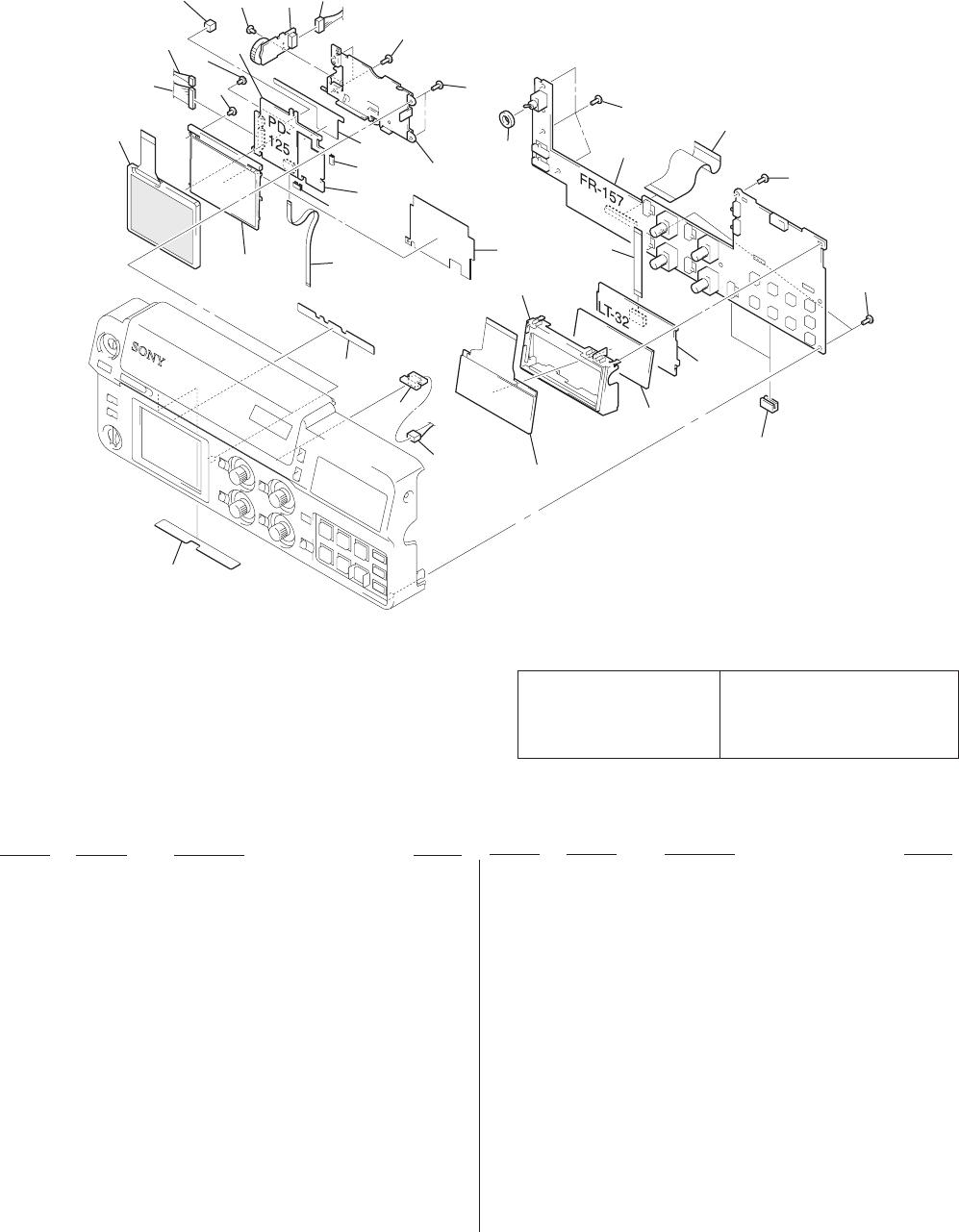
6-2
LCD901
ND901
LCD902
51
75
77
78
76
74
54
65
65
72
71
65
53
52
70
55 73
56
57 61
59
60
58
62 63 64
65
65
66
67
68
69
68
6-1-2. FRONT PANEL ASSEMBLY-1
Ref. No. Part No. Description Remark
Ref. No. Part No. Description Remark
The components identified by
mark 0 or dotted line with
mark 0 are critical for safety.
Replace only with part num-
ber specified.
Les composants identifiés par une
marque 0 sont critiques pour la
sécurité.
Ne les remplacer que par une pièce
portant le numéro spécifié.
*51 3-065-147-01 SHEET (A), LIGHT INTERCEPTION
52 1-960-626-11 HARNESS (EV-70)
53 A-7074-529-A EJ-28 BOARD, COMPLETE
*54 3-065-148-01 SHEET (A), LIGHT INTERCEPTION
55 1-792-981-11 CABLE, FLAT (FJV-3)
56 1-960-627-11 HARNESS (LC-111)
57 1-960-634-11 HARNESS (RM-129)
58 3-713-791-71 SCREW (M1.7X4)
59 3-989-735-11 SCREW (M1.7), LOCK ACE, P2
60 3-062-195-01 SPACER, PD
61 A-7074-107-A PD-125 BOARD, COMPLETE
62 3-968-729-51 SCREW (M2), LOCK ACE, P2
63 A-7074-528-A KP-8 BOARD, COMPLETE
64 1-960-638-11 HARNESS (KP-52)
65 3-948-339-61 TAPPING
*66 3-063-334-01 FRAME, LCD
*67 3-063-349-01 SHEET, BL INSULATING
*68 3-051-232-01 CLIP, PCB
069 1-418-517-11 TRANSFORMER UNIT, INVERTER
70 3-063-890-01 CUSHION (POWER), PROTECTION
71 A-7067-277-A FR-157 BOARD, COMPLETE
72 1-782-824-11 CABLE, FLAT (FVJ-7)
73 3-055-797-01 SHEET, BL SHIELD
74 1-792-983-11 CABLE, FLAT (FVJ-12)
*75 3-063-335-01 HOLDER, LCD
76 A-7074-527-A LT-32 BOARD, COMPLETE
*77 3-063-336-01 ILLUMINATOR, LCD
*78 3-065-766-01 EDGING, RUBBER
LCD901 8-753-050-58 ACX300BK-2
LCD902 1-801-515-21 DISPLAY PANEL, LIQUID CRYSTAL
0ND901 1-517-877-21 TUBE, FLUORESCENT,COLD CATHODE
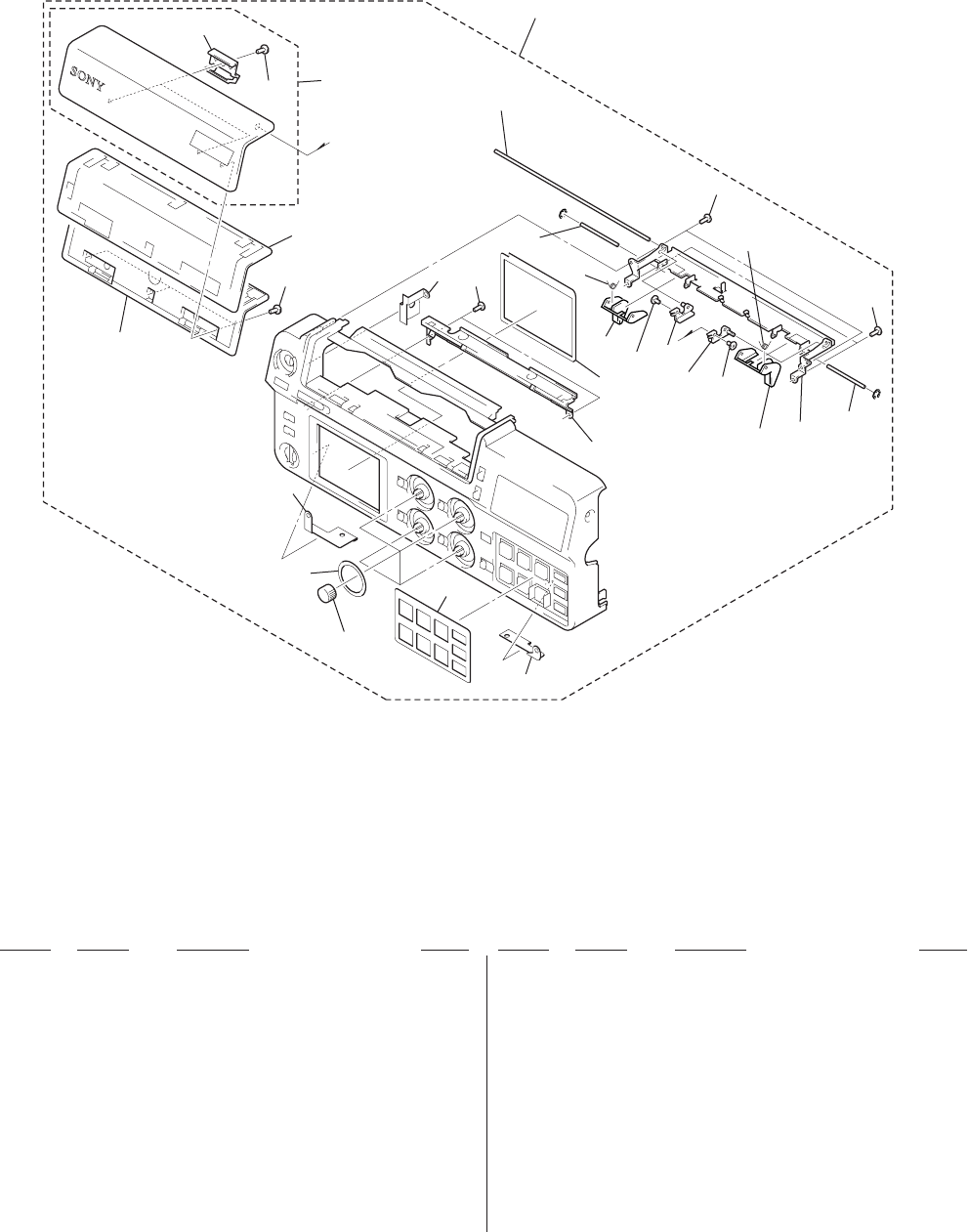
6-3
6-1-3. FRONT PANEL ASSEMBLY-2
Ref. No. Part No. Description Remark
Ref. No. Part No. Description Remark
101 X-3950-877-1 PANEL ASSY, FRONT (DSR-50)
101 X-3950-893-1 PANEL ASSY, FRONT (DSR-50P)
*102 3-063-263-01 PLATE (A), FR GROUND
*103 3-063-266-01 LABEL, CONTROL KEY
104 3-063-271-01 RUBBER, VOLUME KNOB
*105 3-063-265-01 LABEL, VOL
*106 3-063-272-01 PLATE, LC GROUND
*107 3-063-274-01 PLATE (B), FR GROUND
108 3-063-262-01 RETAINER, CC PACKING
109 3-968-729-61 SCREW (M2X3), LOCK ACE, P2
110 3-063-261-01 PACKING, CC
*111 X-3950-883-1 COVER ASSY, CASSETTE
*112 3-063-292-01 LOCK, CC
113 3-948-339-61 TAPPING
*114 3-063-892-01 PACKING, LCD
*115 3-063-889-01 SHAFT, CG
*116 3-063-532-01 SPRING, CC TORSION COIL
*117 3-063-536-01 GUIDE (L), CASSETTE
*118 3-063-524-01 GUIDE (R), CASSETTE
*119 X-3950-881-1 ARM (L) ASSY, CC
*120 X-3950-880-1 ARM (R) ASSY, CC
*122 X-3950-878-1 FRAME ASSY, CC
123 3-948-339-71 TAPPING
*124 X-3950-882-1 SLIDER ASSY, CC
not
supplied
#2
#2
102
103
104
105
106
109 109
118 115
117
123
122
113 116
116
114
115
124
119
120
113
107
112
109 111
110
109
108
101
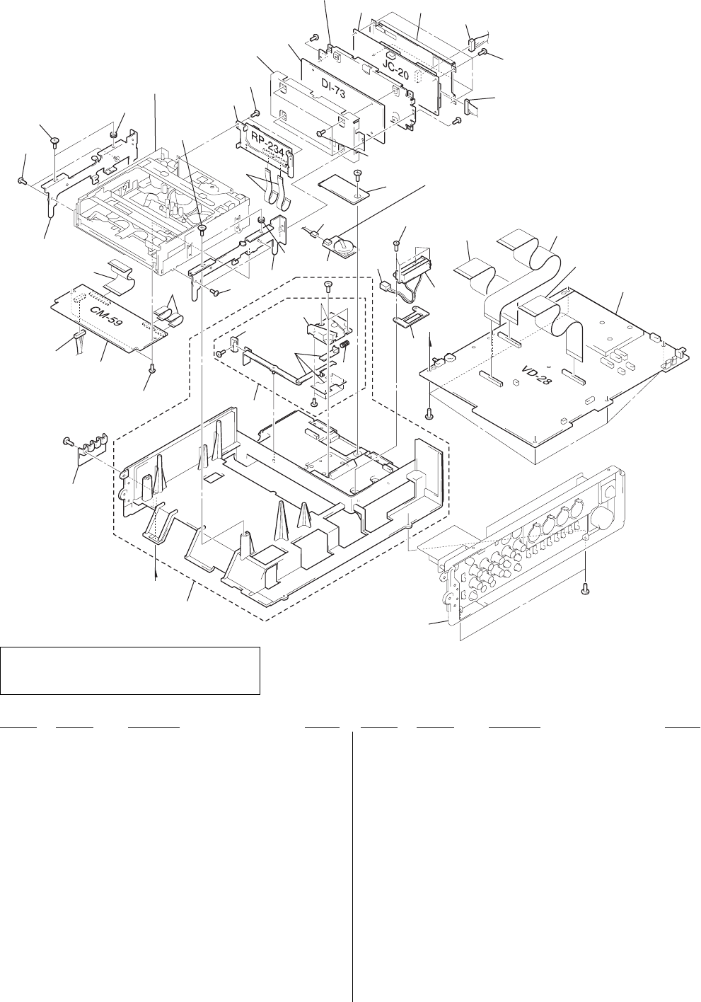
6-4
Ref. No. Part No. Description Remark
Ref. No. Part No. Description Remark
6-1-4. MAIN FRAME ASSEMBLY
151
Side panel section
(See page 6-5.)
#1
#1
#3
#3
#1
not
supplied
BT901
not
supplied
not
supplied
not
supplied
#1
Machanism deck section
(See page 6-6 to 6-9.)
160
161
160
178
159
156 157
180
158 180
154
155
153
BT801
179
161
169
172
^
168
171
173
#5
#6
#6
174 175
174
176
152
180
162
180
180
163
164
165 166
180
167
177
170
(including BT801)
!:
BT801 (V/L RECHARGEABLE BATTERY)
Board on the mount position. (See page 4-69.)
*151 X-3950-884-1 FRAME ASSY, MAIN
*152 X-3950-885-1 MOUNT ASSY, BATTERY
*153 3-680-952-01 KNOB,RELEASE LEVER
*154 3-679-648-02 SPRING,COMPRESSION
*155 3-679-690-02 MOUNT,V
156 1-960-629-11 HARNESS (VC-58)
157 A-7067-274-A CM-59 BOARD, COMPLETE
158 1-791-662-11 CABLE, FLEXIBLE FLAT (FMD-14)
159 1-791-660-11 CABLE, FLEXIBLE FLAT (FJC-1)
160 3-974-010-01 SCREW (M3), STEP
161 3-974-011-01 RUBBER, VIBRATION PROOF
162 A-7067-275-A RP-234 BOARD, COMPLETE
163 1-791-661-11 CABLE, FLEXIBLE FLAT (FRJ-1)
164 A-7067-272-A DI-73 BOARD, COMPLETE
165 A-7067-273-A JC-20 BOARD, COMPLETE
166 1-960-630-11 HARNESS (JV-58)
167 1-960-636-11 HARNESS (VJ-106)
168 3-063-344-01 COVER, VL
169 1-960-633-11 HARNESS (BU-50)
170 A-7074-524-A VL-26 BOARD, COMPLETE
171 3-061-062-01 BOLT (M2.6)
172 1-960-632-11 HARNESS (BA-54)
173 3-063-361-01 SPACER, TERMINAL
174 1-792-984-11 CABLE, FLAT (FVJ-13)
175 1-792-985-11 CABLE, FLAT (FVJ-14)
176 A-7067-271-A VD-28 BOARD, COMPLETE (DSR-50)
176 A-7067-278-A VD-28 BOARD, COMPLETE (DSR-50P)
177 3-063-341-01 COVER, TERMINAL
*178 3-057-525-02 BRACKET (L), MD
*179 3-057-526-02 BRACKET (R), MD
180 3-732-817-01 SCREW (2X4.5), TAPPING
BT801 1-528-694-11 BATTERY, V/L RICHARGEABLE
BT901 1-766-377-12 CONNECTOR, BATTERY
CAUTION
Danger of explosion if battery is incorrectly replaced.
Replace only with the same or equivalent type.
Ver 1.4 2004. 10
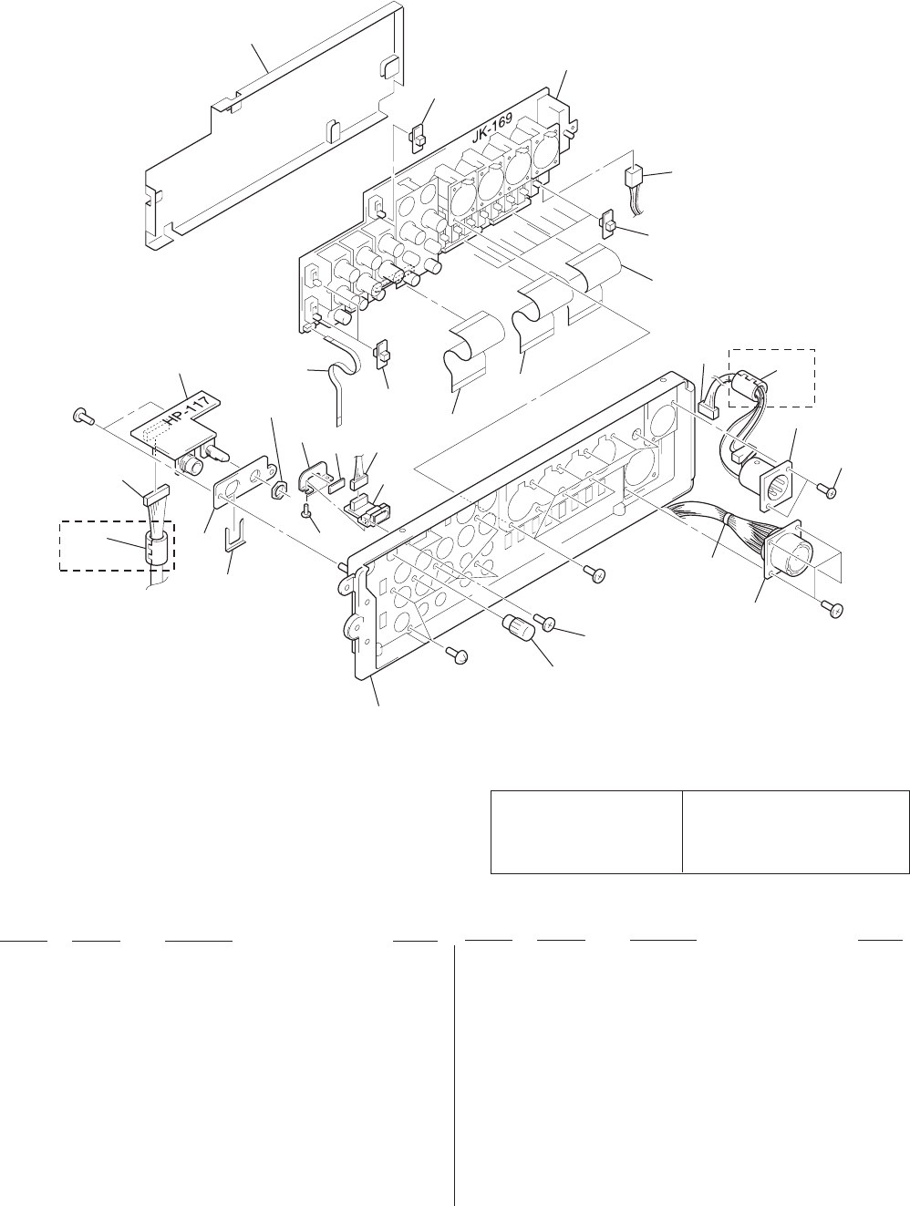
6-5
Ref. No. Part No. Description Remark
Ref. No. Part No. Description Remark
6-1-5. SIDE PANEL ASSEMBLY
The components identified by
mark 0 or dotted line with
mark 0 are critical for safety.
Replace only with part num-
ber specified.
Les composants identifiés par une
marque 0 sont critiques pour la
sécurité.
Ne les remplacer que par une pièce
portant le numéro spécifié.
215
211
214
213
211
212
212
212
211
210
207
220
218
206
219
supplied with
RV301
209
supplied with
J301
#1
#4
#1
CN026 #1
CN9901
216
204 221
221
203
217
202
201
208
205
DSR-50P
DSR-50P
201 X-3950-887-1 PANEL ASSY, SIDE
*202 3-063-350-01 KNOB, ROTARY
203 3-968-729-11 SCREW (M2), LOCK ACE, P2
204 1-960-637-11 HARNESS (DC-66)
*205 3-063-338-01 HOLDER, HP
206 A-7074-525-A IL-013 BOARD, COMPLETE
207 1-960-635-11 HARNESS (IN-50)
208 1-960-628-11 HARNESS (HP-135)
209 A-7074-526-A HP-117 BOARD, COMPLETE
210 1-792-982-11 CABLE, FLAT (FVJ-10)
*211 3-063-337-01 SWITCH, SLIDE
212 1-782-824-11 CABLE, FLAT (FVJ-7)
213 1-960-631-11 HARNESS (VB-50)
214 A-7067-276-A JK-169 BOARD, COMPLETE
215 3-063-351-01 COVER, JK
216 3-061-062-01 BOLT (M2.6)
217 1-757-063-11 WIRE, SPECIAL TERMINAL PROCESS
*218 3-064-914-01 REINFORCEMENT, DV TERMINAL
219 3-719-381-11 SCREW (M2X5)
*220 3-065-149-01 SHEET, DV TERMINAL PROTECTION
221 1-500-051-11 BEAD, FERRITE (WITH CASE) (DSR-50P)
CN026 1-562-245-11 RECEPTACLE, CONNECTOR (26P)
0CN9901 1-564-603-11 CONNECTOR (WITH DC SW) 4P
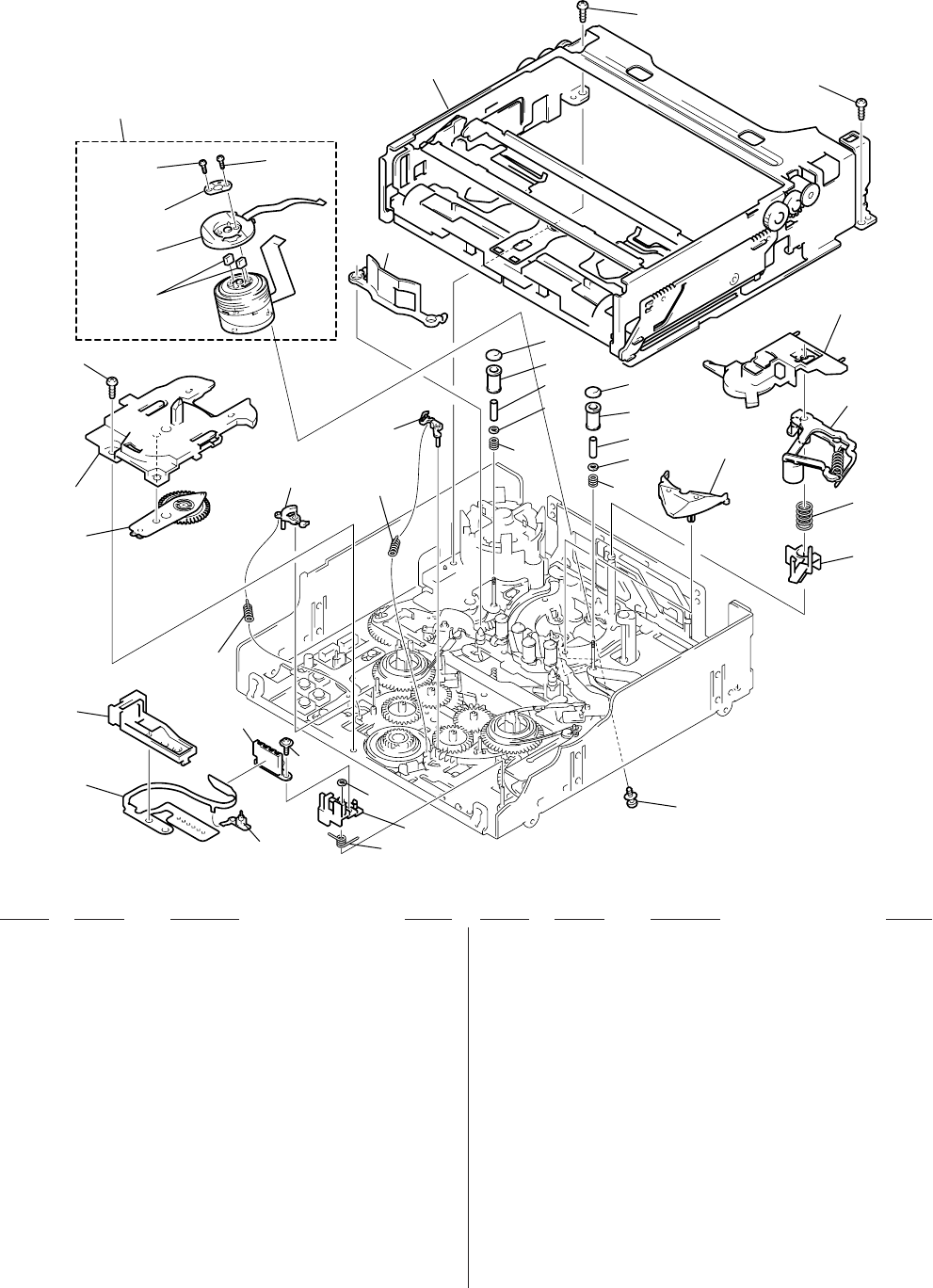
6-6
6-1-6. MECHANISM DECK ASSEMBLY
(DRUM ASSEMBLY)
Ref. No. Part No. Description RemarkRef. No. Part No. Description Remark
701 1-675-561-11 FP-104 FLEXIBLE BOARD
*702 3-057-351-01 GUIDE, MIC BASE
703 3-057-350-02 BASE, MIC
704 3-732-817-01 SCREW (2X4.5), TAPPING
705 3-057-319-01 RETAINER, PENDULUM
706 X-3949-922-1 ARM ASSY, PENDULUM
707 3-057-286-01 SPRING, EXTENSION (BRAKE)
708 3-057-280-01 ARM (S), BRAKE
709 3-057-279-01 BRAKE (T), RATCHET
710 3-057-232-01 SPRING, COMPRESSION (TG)
711 3-057-238-01 RING, TG
712 3-057-237-01 SLEEVE, TG
713 3-057-235-01 ROLLER, TG
714 3-057-234-01 FLANGE, TG UPPER
715 3-057-379-01 GUARD, GUIDE
716 A-7094-608-B SCREW ASSY, DRUM FITTING
717 3-973-171-01 SUPPORT, TAPE
718 3-057-227-01 RETAINER, TAPE
719 3-973-818-01 SPRING, COMPRESSION (TAPE RETAINER)
720 X-3949-915-1 ARM ASSY, PINCH
721 3-057-228-01 CAP, DRUM
722 A-7094-602-B COMPARTMENT BLOCK ASSY
723 3-726-829-01 WASHER, STOPPER
724 3-057-353-01 SPRING, MIC BASE
725 3-318-201-11 SCREW (B) (1.4X3), TAPPING
726 3-973-266-01 SCREW (M2X2.2 (MEK)), HEAD
727 3-703-816-74 SCREW (M1.4X4.5)
728 X-3944-897-1 FPC ASSY, MOTOR
729 1-770-363-11 CONNECTOR, ELASTIC
CN004 1-770-312-21 CONNECTOR 4P
M901 A-7048-947-A DRUM ASSY (DEH-21A-R)
S004 1-762-351-21 SWITCH, PUSH (1 KEY) (REC PROOF)
M901
not supplied
S004
701
703
723
724
702
726
705
706
707
707
708
709
715
722
727 727
728
729
717
721
716
718
719
720
CN004
714
712
711
713
710
714
712
711
713
710
704
704
-77.203
725
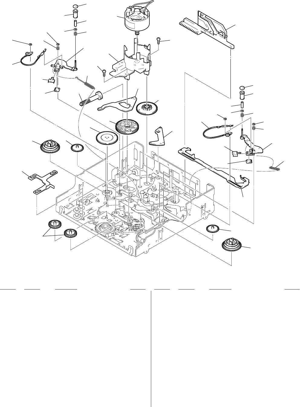
6-7
Ref. No. Part No. Description RemarkRef. No. Part No. Description Remark
6-1-7. MECHANISM DECK ASSEMBLY
(GEAR, ARM)
751 X-3949-923-1 GEAR (A) ASSY, IDLER
752 3-057-311-01 GEAR (B), IDLER
753 A-7094-599-A REEL (LARGE) BLOCK ASSY
754 3-057-267-01 GEAR, ENCODER
755 3-057-294-01 GEAR, MAIN CAM
756 3-973-140-01 GEAR, SUB CAM
*757 3-057-302-01 SLIDER, SBR
*758 3-057-314-01 SLIDER, SUB
759 X-3950-816-1 ARM ASSY, LOADING
760 3-057-221-01 SLIDER, PINCH
*761 3-057-252-01 ARM, SUB SLIDER
762 3-973-159-01 GEAR, JOINT
763 3-057-222-02 HOLDER, MOTOR
765 3-973-266-01 SCREW (M2X2.2 (MEK)), HEAD
766 X-3949-918-1 ARM ASSY, TG2
767 X-3949-919-1 ARM ASSY, TG7
768 3-057-295-01 SPRING, EXTENSION (TG2)
769 3-057-296-02 SPRING, EXTENSION (TG7)
770 X-3949-921-1 BAND (TG7) ASSY
771 X-3949-920-1 BAND (TG2) ASSY
772 3-057-281-01 MAGNET, ET
773 3-057-336-01 HOLDER, MAGNET
774 3-057-344-01 SPRING, COMPRESSION (TG ARM)
775 3-726-829-01 WASHER, STOPPER
776 3-057-232-01 SPRING, COMPRESSION (TG)
777 3-057-238-01 RING, TG
778 3-057-237-01 SLEEVE, TG
779 3-057-235-01 ROLLER, TG
780 3-057-234-01 FLANGE, TG UPPER
781 3-057-337-01 ROLLER, TG7
782 3-063-887-01 FLANGE (2), TG UPPER
M902 X-3946-702-1 MOTOR ASSY, CAM
751 752
758
752
753
757
753
M902
756
754 755
762 761
765
760
765
763
775
780
781
776
774
775
767
772 769
773
770 777
778
771
775 774
773
775
766
768
772
782
778
776
777
779
759
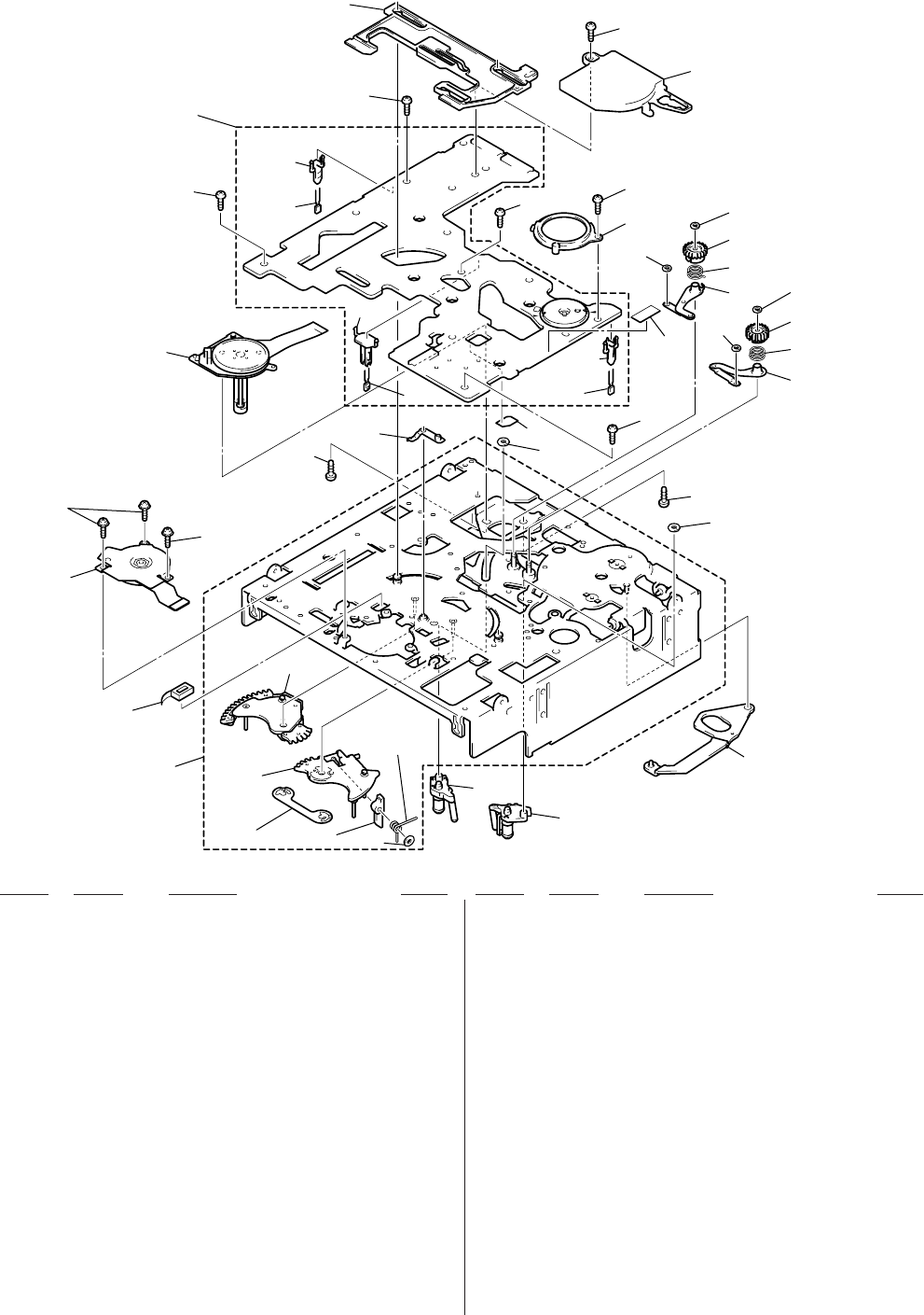
6-8
Ref. No. Part No. Description RemarkRef. No. Part No. Description Remark
6-1-8. MECHANISM DECK ASSEMBLY
(MOTOR, MD BOARD)
801 A-7025-007-A COASTER (T) BLOCK ASSY
802 A-7025-006-A COASTER (S) BLOCK ASSY
*803 3-057-283-01 ARM, MAIN SLIDER
804 X-3949-916-9 CHASSIS ASSY, MECHANICAL
805 X-3949-924-1 STOPPER ASSY, PENDULUM
806 3-947-503-01 SCREW (M1.4)
807 3-732-817-01 SCREW (2X4.5), TAPPING
808 3-973-266-01 SCREW (M2X2.2 (MEK)), HEAD
809 3-973-142-01 STOPPER, COASTER PUNCHING
810 X-3946-690-1 ARM (S) ASSY, GL
811 X-3946-689-1 ARM (T) ASSY, GL
812 3-973-146-02 SPRING (S), GL TORSION
813 3-973-156-02 SPRING (T), GL TORSION
814 3-973-264-01 GEAR (S), GL
815 3-973-138-01 GEAR (T), GL
816 3-727-176-01 WASHER, STOPPER
817 3-973-143-01 WASHER, COASTER STOPPER
818 3-057-339-01 COVER, ENCODER
819 3-057-340-01 COVER, CAPSTAN
820 3-057-282-01 SLIDER, MAIN
821 1-657-785-11 FP-248 FLEXIBLE BOARD (DEW SENSOR)
822 3-057-320-01 BLOCK, REEL LOCK RELEASE
823 3-057-354-01 SPRING, REEL LOCK RELEASE
824 A-7067-229-A MD-76 BOARD, COMPLETE
*825 3-057-376-01 HOLDER, SENSOR
*826 3-057-555-01 HOLDER, LED
827 X-3950-199-1 BASE (S) ASSY, REEL
828 X-3950-200-1 BASE (T) ASSY, REEL
829 3-057-265-01 RETAINER, REEL BASE
830 3-941-343-21 TAPE (A)
831 3-726-829-01 WASHER, STOPPER
832 3-064-576-01 ECLIPSER
D001 8-719-988-42 DIODE GL453S
M903 8-835-648-01 MOTOR, DC SCD17A/J-N (CAPSTAN)
M904 X-3949-928-1 MOTOR ASSY, REEL
Q001 8-729-907-25 PHOTO TRANISTOR PT4850F (TAPE END)
Q002 8-729-907-25 PHOTO TRANISTOR PT4850F (TAPE TOP)
801
804
828
832
827
823
822 831
805 807
825 830
826
821
808
808
807
818
807
807
807
806
806
M903
Q001
D001
825
Q002
802
803
810
812
814
816
817
817
811
813
815
816
809
809
824
820
819
807
M904
829
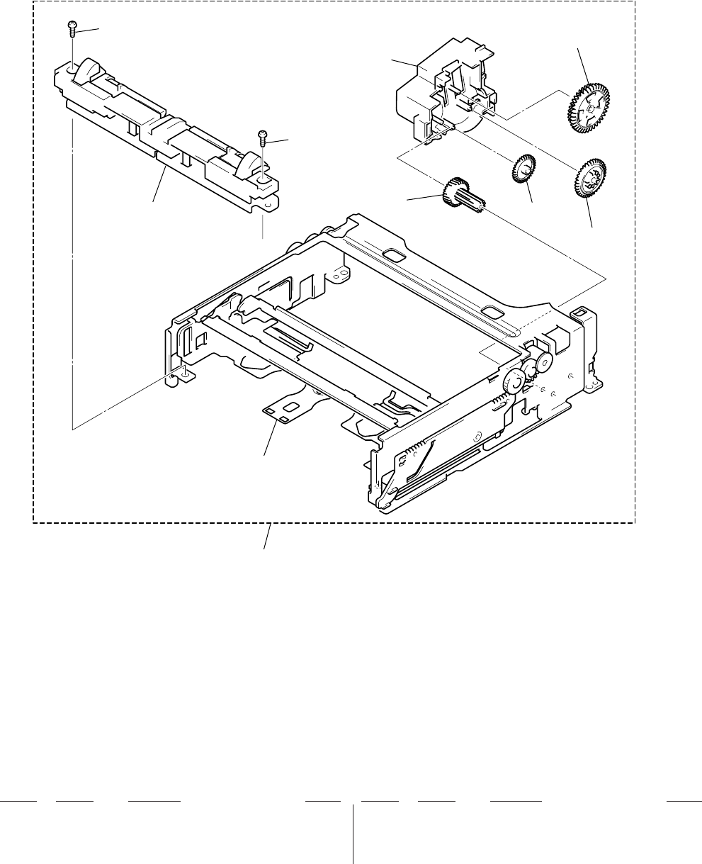
6-9
Ref. No. Part No. Description RemarkRef. No. Part No. Description Remark
6-1-9. MECHANISM DECK ASSEMBLY
(CASSETTE COMPARTMENT)
851 A-7094-602-B COMPARTMENT BLOCK ASSY
852 3-732-817-01 SCREW (2X4.5), TAPPING
853 3-057-253-01 GEAR, WHEEL
854 3-057-254-01 GEAR (A)
855 3-057-255-01 GEAR (B)
856 A-7094-689-A CD BLOCK ASSY, GEAR
M905 X-3949-925-1 MOTOR ASSY, FL
852
M905
not supplied
852
853
851
854
855
856
not supplied

NOTE:
• Due to standardization, replacements in the
parts list may be different from the parts speci-
fied in the diagrams or the components used
on the set.
• Items marked “*” are not stocked since they
are seldom required for routine service.
Some delay should be anticipated when order-
ing these items.
• RESISTORS
All resistors are in ohms.
METAL: Metal-film resistor.
METAL OXIDE: Metal oxide-film resistor.
F: nonflammable
• SEMICONDUCTORS
In each case, u: µ, for example:
uA. . : µA. . uPA. . : µPA. .
uPB. .: µPB. . uPC. . : µPC. .
uPD. .: µPD. .
• CAPACITORS
uF: µF
• COILS
uH: µH
6-2. ELECTRICAL PARTS LIST
Ref. No. Part No. Description Remark Ref. No. Part No. Description Remark
Les composants identifiés par une
marque 0 sont critiquens pour la
sécurité.
Ne les remplacer que par une pièce
portant le numéro spécifié.
The components identified by
mark 0 or dotted line with mark
0 are critical for safety.
Replace only with part number
specified.
When indicating parts by reference
number, please include the board.
6-10
CM-59
A-7067-274-A CM-59 BOARD, COMPLETE
**********************
(Ref. No. 20,000 Series)
< CAPACITOR >
C100 1-162-964-11 CERAMIC CHIP 0.001uF 10% 50V
C101 1-162-964-11 CERAMIC CHIP 0.001uF 10% 50V
C102 1-162-964-11 CERAMIC CHIP 0.001uF 10% 50V
C103 1-162-964-11 CERAMIC CHIP 0.001uF 10% 50V
C104 1-162-967-11 CERAMIC CHIP 0.0033uF 10% 50V
C105 1-162-964-11 CERAMIC CHIP 0.001uF 10% 50V
C106 1-162-967-11 CERAMIC CHIP 0.0033uF 10% 50V
C107 1-107-826-11 CERAMIC CHIP 0.1uF 10% 16V
C108 1-164-227-11 CERAMIC CHIP 0.022uF 10% 25V
C109 1-164-739-11 CERAMIC CHIP 560PF 5% 50V
C110 1-117-863-11 CERAMIC CHIP 0.47uF 10% 6.3V
C111 1-164-230-11 CERAMIC CHIP 220PF 5% 50V
C112 1-162-967-11 CERAMIC CHIP 0.0033uF 10% 50V
C113 1-107-826-11 CERAMIC CHIP 0.1uF 10% 16V
C114 1-164-227-11 CERAMIC CHIP 0.022uF 10% 25V
C115 1-164-360-11 CERAMIC CHIP 0.1uF 16V
C116 1-117-863-11 CERAMIC CHIP 0.47uF 10% 6.3V
C117 1-164-360-11 CERAMIC CHIP 0.1uF 16V
C118 1-164-156-11 CERAMIC CHIP 0.1uF 25V
C119 1-119-869-91 CERAMIC CHIP 10uF 35V
C120 1-164-360-11 CERAMIC CHIP 0.1uF 16V
C121 1-164-156-11 CERAMIC CHIP 0.1uF 25V
C122 1-135-210-11 TANTALUM CHIP 4.7uF 20% 10V
C129 1-119-869-91 CERAMIC CHIP 10uF 35V
C130 1-119-869-91 CERAMIC CHIP 10uF 35V
C131 1-119-869-91 CERAMIC CHIP 10uF 35V
C132 1-119-869-91 CERAMIC CHIP 10uF 35V
C134 1-113-985-11 TANTAL. CHIP 10uF 20% 20V
C135 1-113-985-11 TANTAL. CHIP 10uF 20% 20V
C136 1-113-985-11 TANTAL. CHIP 10uF 20% 20V
C137 1-113-985-11 TANTAL. CHIP 10uF 20% 20V
C200 1-107-826-11 CERAMIC CHIP 0.1uF 10% 16V
C201 1-107-826-11 CERAMIC CHIP 0.1uF 10% 16V
C202 1-107-826-11 CERAMIC CHIP 0.1uF 10% 16V
C203 1-107-826-11 CERAMIC CHIP 0.1uF 10% 16V
C204 1-113-987-11 TANTAL. CHIP 4.7uF 20% 25V
C205 1-107-826-11 CERAMIC CHIP 0.1uF 10% 16V
C206 1-107-826-11 CERAMIC CHIP 0.1uF 10% 16V
C207 1-131-861-91 TANTAL. CHIP 4.7uF 20% 20V
C208 1-162-970-11 CERAMIC CHIP 0.01uF 10% 25V
C300 1-162-927-11 CERAMIC CHIP 100PF 5% 50V
C301 1-107-826-11 CERAMIC CHIP 0.1uF 10% 16V
C302 1-162-927-11 CERAMIC CHIP 100PF 5% 50V
C303 1-107-826-11 CERAMIC CHIP 0.1uF 10% 16V
C320 1-164-360-11 CERAMIC CHIP 0.1uF 16V
C321 1-164-360-11 CERAMIC CHIP 0.1uF 16V
C322 1-164-505-11 CERAMIC CHIP 2.2uF 16V
C323 1-162-964-11 CERAMIC CHIP 0.001uF 10% 50V
C324 1-107-826-11 CERAMIC CHIP 0.1uF 10% 16V
C325 1-164-360-11 CERAMIC CHIP 0.1uF 16V
C326 1-107-826-11 CERAMIC CHIP 0.1uF 10% 16V
C327 1-162-964-11 CERAMIC CHIP 0.001uF 10% 50V
C329 1-164-227-11 CERAMIC CHIP 0.022uF 10% 25V
C330 1-162-968-11 CERAMIC CHIP 0.0047uF 10% 50V
C331 1-162-968-11 CERAMIC CHIP 0.0047uF 10% 50V
C400 1-107-826-11 CERAMIC CHIP 0.1uF 10% 16V
C401 1-107-826-11 CERAMIC CHIP 0.1uF 10% 16V
C402 1-107-826-11 CERAMIC CHIP 0.1uF 10% 16V
C403 1-107-826-11 CERAMIC CHIP 0.1uF 10% 16V
C404 1-107-826-11 CERAMIC CHIP 0.1uF 10% 16V
C405 1-131-861-91 TANTAL. CHIP 4.7uF 20% 20V
C406 1-131-861-91 TANTAL. CHIP 4.7uF 20% 20V
C407 1-107-826-11 CERAMIC CHIP 0.1uF 10% 16V
C501 1-135-177-21 TANTALUM CHIP 1uF 20% 20V
C502 1-162-968-11 CERAMIC CHIP 0.0047uF 10% 50V
C503 1-107-826-11 CERAMIC CHIP 0.1uF 10% 16V
C504 1-162-964-11 CERAMIC CHIP 0.001uF 10% 50V
C505 1-107-826-11 CERAMIC CHIP 0.1uF 10% 16V
C506 1-107-826-11 CERAMIC CHIP 0.1uF 10% 16V
C507 1-107-826-11 CERAMIC CHIP 0.1uF 10% 16V
C508 1-162-970-11 CERAMIC CHIP 0.01uF 10% 25V
C509 1-162-970-11 CERAMIC CHIP 0.01uF 10% 25V
C510 1-162-970-11 CERAMIC CHIP 0.01uF 10% 25V
C511 1-131-861-91 TANTAL. CHIP 4.7uF 20% 20V
C512 1-107-826-11 CERAMIC CHIP 0.1uF 10% 16V
C515 1-107-826-11 CERAMIC CHIP 0.1uF 10% 16V
C518 1-164-739-11 CERAMIC CHIP 560PF 5% 50V
C519 1-107-826-11 CERAMIC CHIP 0.1uF 10% 16V
C520 1-131-861-91 TANTAL. CHIP 4.7uF 20% 20V
C521 1-107-826-11 CERAMIC CHIP 0.1uF 10% 16V

6-11
Ref. No. Part No. Description Remark Ref. No. Part No. Description Remark
CM-59
The components identified by
mark 0 or dotted line with
mark 0 are critical for safety.
Replace only with part num-
ber specified.
Les composants identifiés par une
marque 0 sont critiques pour la
sécurité.
Ne les remplacer que par une pièce
portant le numéro spécifié.
C522 1-107-826-11 CERAMIC CHIP 0.1uF 10% 16V
C523 1-107-826-11 CERAMIC CHIP 0.1uF 10% 16V
C524 1-107-826-11 CERAMIC CHIP 0.1uF 10% 16V
C525 1-131-861-91 TANTAL. CHIP 4.7uF 20% 20V
C526 1-162-964-11 CERAMIC CHIP 0.001uF 10% 50V
C527 1-162-964-11 CERAMIC CHIP 0.001uF 10% 50V
C528 1-162-964-11 CERAMIC CHIP 0.001uF 10% 50V
C529 1-162-964-11 CERAMIC CHIP 0.001uF 10% 50V
< CONNECTOR >
CN001 1-778-637-21 CONNECTOR, FFC/FPC (ZIF) 50P
CN100 1-506-473-11 PIN, CONNECTOR 8P
CN200 1-691-385-21 CONNECTOR, FFC/FPC 21P
CN201 1-691-385-21 CONNECTOR, FFC/FPC 21P
*CN300 1-580-055-21 PIN, CONNECTOR (SMD) 2P
CN400 1-750-341-11 CONNECTOR, FFC/EPC (ZIF) 18P
CN500 1-573-351-11 CONNECTOR, FFC/FPC (ZIF) 11P
*CN501 1-580-055-21 PIN, CONNECTOR (SMD) 2P
< DIODE >
D101 8-719-066-98 DIODE RB051L-40TE25
D102 8-719-066-98 DIODE RB051L-40TE25
D103 8-719-066-98 DIODE RB051L-40TE25
D104 8-719-066-98 DIODE RB051L-40TE25
< FUSE >
0 F100 1-532-777-21 FUSE, MICRO (SECONDARY) (1.25A/125V)
< IC >
IC100 8-759-060-94 IC MB3785APFV-G-BND-ER
IC101 8-759-689-44 IC MM1385GNLE
IC102 8-759-648-48 IC TC7W34FU (TE12R)
IC200 8-759-339-61 IC LB1897D
IC202 8-759-338-95 IC NJM2903V (TE2)
IC300 8-759-327-61 IC LB8112V-TLM
IC400 8-759-431-41 IC LB1991V-TLM
IC500 8-759-431-30 IC CXA8062R-EB
IC501 8-759-434-46 IC TA8486F (EL)
< JUMPER RESISTOR >
JR501 1-216-864-11 METAL CHIP 0 5% 1/16W
JR502 1-216-864-11 METAL CHIP 0 5% 1/16W
JR503 1-216-864-11 METAL CHIP 0 5% 1/16W
JR504 1-216-864-11 METAL CHIP 0 5% 1/16W
JR505 1-216-864-11 METAL CHIP 0 5% 1/16W
< COIL >
L100 1-406-823-11 INDUCTOR 10uH
L101 1-406-823-11 INDUCTOR 10uH
L102 1-424-522-21 INDUCTOR 10uH
L103 1-406-823-11 INDUCTOR 10uH
L104 1-409-535-41 INDUCTOR 100uH
L105 1-409-535-41 INDUCTOR 100uH
L106 1-424-523-21 INDUCTOR 22uH
L107 1-406-825-11 INDUCTOR 33uH
L200 1-414-398-11 INDUCTOR 10uH
L400 1-414-754-11 INDUCTOR 10uH
L500 1-414-754-11 INDUCTOR 10uH
< TRANSISTOR >
Q100 8-729-048-75 TRANSISTOR CPH3109-TL
Q101 8-729-048-75 TRANSISTOR CPH3109-TL
Q102 8-729-048-75 TRANSISTOR CPH3109-TL
Q103 8-729-048-75 TRANSISTOR CPH3109-TL
Q104 8-729-216-22 TRANSISTOR 2SB709A-QRS-TX
Q105 8-729-037-72 TRANSISTOR UN9211J- (TX).SO
Q200 8-729-216-22 TRANSISTOR 2SB709A-QRS-TX
Q201 8-729-037-52 TRANSISTOR 2SD2216J-QR (K8).SO
Q301 8-729-037-52 TRANSISTOR 2SD2216J-QR (K8).SO
Q302 8-729-037-52 TRANSISTOR 2SD2216J-QR (K8).SO
< RESISTOR >
R100 1-216-049-11 RES-CHIP 1K 5% 1/10W
R101 1-216-041-00 METAL CHIP 470 5% 1/10W
R102 1-216-025-11 RES-CHIP 100 5% 1/10W
R103 1-216-841-11 METAL CHIP 47K 5% 1/16W
R104 1-218-890-11 METAL CHIP 62K 0.5% 1/16W
R105 1-218-883-11 METAL CHIP 33K 0.5% 1/16W
R106 1-216-831-11 METAL CHIP 6.8K 5% 1/16W
R107 1-218-865-11 METAL CHIP 5.6K 0.5% 1/16W
R108 1-216-864-11 METAL CHIP 0 5% 1/16W
R109 1-216-864-11 METAL CHIP 0 5% 1/16W
R110 1-216-864-11 METAL CHIP 0 5% 1/16W
R111 1-216-833-11 METAL CHIP 10K 5% 1/16W
R112 1-216-049-11 RES-CHIP 1K 5% 1/10W
R114 1-216-837-11 METAL CHIP 22K 5% 1/16W
R115 1-216-839-11 METAL CHIP 33K 5% 1/16W
R116 1-218-878-11 METAL CHIP 20K 0.5% 1/16W
R117 1-216-834-11 METAL CHIP 12K 5% 1/16W
R118 1-216-864-11 METAL CHIP 0 5% 1/16W
R120 1-216-864-11 METAL CHIP 0 5% 1/16W
R122 1-216-864-11 METAL CHIP 0 5% 1/16W
R123 1-216-838-11 METAL CHIP 27K 5% 1/16W
R124 1-216-864-11 METAL CHIP 0 5% 1/16W
R126 1-216-833-11 METAL CHIP 10K 5% 1/16W
R127 1-216-842-11 METAL CHIP 56K 5% 1/16W
R128 1-216-864-11 METAL CHIP 0 5% 1/16W
R131 1-218-865-11 METAL CHIP 5.6K 0.5% 1/16W
R136 1-216-864-11 METAL CHIP 0 5% 1/16W
R200 1-216-821-11 METAL CHIP 1K 5% 1/16W
R201 1-216-833-11 METAL CHIP 10K 5% 1/16W
R202 1-218-878-11 METAL CHIP 20K 0.5% 1/16W
R203 1-218-873-11 METAL CHIP 12K 0.5% 1/16W
R204 1-216-857-11 METAL CHIP 1M 5% 1/16W
R205 1-217-671-11 METAL CHIP 1 5% 1/10W
R206 1-217-671-11 METAL CHIP 1 5% 1/10W
R207 1-217-671-11 METAL CHIP 1 5% 1/10W
R208 1-217-671-11 METAL CHIP 1 5% 1/10W
R209 1-216-853-11 METAL CHIP 470K 5% 1/16W
R211 1-216-864-11 METAL CHIP 0 5% 1/16W
R212 1-216-821-11 METAL CHIP 1K 5% 1/16W
R213 1-216-831-11 METAL CHIP 6.8K 5% 1/16W
R214 1-216-831-11 METAL CHIP 6.8K 5% 1/16W
R215 1-216-821-11 METAL CHIP 1K 5% 1/16W
R223 1-216-829-11 METAL CHIP 4.7K 5% 1/16W
R224 1-216-841-11 METAL CHIP 47K 5% 1/16W

6-12
Ref. No. Part No. Description Remark Ref. No. Part No. Description Remark
CM-59 DI-73
R225 1-216-295-11 SHORT 0
R300 1-216-835-11 METAL CHIP 15K 5% 1/16W
R301 1-216-835-11 METAL CHIP 15K 5% 1/16W
R302 1-216-818-11 METAL CHIP 560 5% 1/16W
R303 1-216-818-11 METAL CHIP 560 5% 1/16W
R304 1-216-864-11 METAL CHIP 0 5% 1/16W
R306 1-216-295-11 SHORT 0
R307 1-216-821-11 METAL CHIP 1K 5% 1/16W
R308 1-216-821-11 METAL CHIP 1K 5% 1/16W
R309 1-216-821-11 METAL CHIP 1K 5% 1/16W
R310 1-216-821-11 METAL CHIP 1K 5% 1/16W
R311 1-218-859-11 METAL CHIP 3.3K 0.5% 1/16W
R312 1-218-863-11 METAL CHIP 4.7K 0.5% 1/16W
R313 1-216-826-11 METAL CHIP 2.7K 5% 1/16W
R314 1-216-826-11 METAL CHIP 2.7K 5% 1/16W
R315 1-216-841-11 METAL CHIP 47K 5% 1/16W
R316 1-216-841-11 METAL CHIP 47K 5% 1/16W
R317 1-216-821-11 METAL CHIP 1K 5% 1/16W
R318 1-216-821-11 METAL CHIP 1K 5% 1/16W
R319 1-216-821-11 METAL CHIP 1K 5% 1/16W
R320 1-216-821-11 METAL CHIP 1K 5% 1/16W
R323 1-216-864-11 METAL CHIP 0 5% 1/16W
R324 1-216-833-11 METAL CHIP 10K 5% 1/16W
R325 1-216-845-11 METAL CHIP 100K 5% 1/16W
R326 1-216-833-11 METAL CHIP 10K 5% 1/16W
R327 1-216-833-11 METAL CHIP 10K 5% 1/16W
R328 1-216-833-11 METAL CHIP 10K 5% 1/16W
R329 1-216-864-11 METAL CHIP 0 5% 1/16W
R330 1-216-845-11 METAL CHIP 100K 5% 1/16W
R332 1-216-845-11 METAL CHIP 100K 5% 1/16W
R333 1-216-833-11 METAL CHIP 10K 5% 1/16W
R334 1-216-833-11 METAL CHIP 10K 5% 1/16W
R335 1-216-827-11 METAL CHIP 3.3K 5% 1/16W
R336 1-216-845-11 METAL CHIP 100K 5% 1/16W
R337 1-217-671-11 METAL CHIP 1 5% 1/10W
R339 1-218-863-11 METAL CHIP 4.7K 0.5% 1/16W
R340 1-218-859-11 METAL CHIP 3.3K 0.5% 1/16W
R342 1-217-671-11 METAL CHIP 1 5% 1/10W
R400 1-216-833-11 METAL CHIP 10K 5% 1/16W
R401 1-216-821-11 METAL CHIP 1K 5% 1/16W
R402 1-216-295-11 SHORT 0
R403 1-216-836-11 METAL CHIP 18K 5% 1/16W
R405 1-216-845-11 METAL CHIP 100K 5% 1/16W
R500 1-216-295-11 SHORT 0
R501 1-218-839-11 METAL CHIP 470 0.5% 1/16W
R503 1-216-833-11 METAL CHIP 10K 5% 1/16W
R504 1-216-833-11 METAL CHIP 10K 5% 1/16W
R505 1-216-833-11 METAL CHIP 10K 5% 1/16W
R506 1-216-864-11 METAL CHIP 0 5% 1/16W
R507 1-216-821-11 METAL CHIP 1K 5% 1/16W
R508 1-218-899-11 METAL CHIP 150K 0.5% 1/16W
R509 1-218-871-11 METAL CHIP 10K 0.5% 1/16W
R511 1-216-827-11 METAL CHIP 3.3K 5% 1/16W
R512 1-216-809-11 METAL CHIP 100 5% 1/16W
R513 1-216-809-11 METAL CHIP 100 5% 1/16W
R514 1-216-809-11 METAL CHIP 100 5% 1/16W
R515 1-217-671-11 METAL CHIP 1 5% 1/10W
R516 1-217-671-11 METAL CHIP 1 5% 1/10W
R518 1-218-879-11 METAL CHIP 22K 0.5% 1/16W
R519 1-218-879-11 METAL CHIP 22K 0.5% 1/16W
R520 1-218-897-11 METAL CHIP 120K 0.5% 1/16W
R522 1-218-901-11 METAL CHIP 180K 0.5% 1/16W
R525 1-216-864-11 METAL CHIP 0 5% 1/16W
R526 1-218-629-91 METAL CHIP 180 5% 1W
R527 1-218-629-91 METAL CHIP 180 5% 1W
R528 1-218-629-91 METAL CHIP 180 5% 1W
R529 1-218-629-91 METAL CHIP 180 5% 1W
R530 1-216-821-11 METAL CHIP 1K 5% 1/16W
R531 1-216-821-11 METAL CHIP 1K 5% 1/16W
R532 1-217-671-11 METAL CHIP 1 5% 1/10W
R533 1-217-671-11 METAL CHIP 1 5% 1/10W
R534 1-217-671-11 METAL CHIP 1 5% 1/10W
R535 1-217-671-11 METAL CHIP 1 5% 1/10W
R536 1-216-821-11 METAL CHIP 1K 5% 1/16W
A-7067-272-A DI-73 BOARD, COMPLETE
*********************
(Ref. No.10,000 Series)
< CAPACITOR >
C7000 1-115-467-11 CERAMIC CHIP 0.22uF 10% 10V
C7001 1-115-467-11 CERAMIC CHIP 0.22uF 10% 10V
C7002 1-115-467-11 CERAMIC CHIP 0.22uF 10% 10V
C7003 1-115-467-11 CERAMIC CHIP 0.22uF 10% 10V
C7004 1-115-467-11 CERAMIC CHIP 0.22uF 10% 10V
C7005 1-115-467-11 CERAMIC CHIP 0.22uF 10% 10V
C7006 1-115-467-11 CERAMIC CHIP 0.22uF 10% 10V
C7007 1-115-467-11 CERAMIC CHIP 0.22uF 10% 10V
C7016 1-135-259-11 TANTAL. CHIP 10uF 20% 6.3V
C7017 1-135-259-11 TANTAL. CHIP 10uF 20% 6.3V
C7018 1-135-259-11 TANTAL. CHIP 10uF 20% 6.3V
C7019 1-135-259-11 TANTAL. CHIP 10uF 20% 6.3V
C7020 1-135-259-11 TANTAL. CHIP 10uF 20% 6.3V
C7021 1-135-259-11 TANTAL. CHIP 10uF 20% 6.3V
C7022 1-135-259-11 TANTAL. CHIP 10uF 20% 6.3V
C7023 1-135-259-11 TANTAL. CHIP 10uF 20% 6.3V
C7024 1-135-259-11 TANTAL. CHIP 10uF 20% 6.3V
C7025 1-135-259-11 TANTAL. CHIP 10uF 20% 6.3V
C7026 1-135-259-11 TANTAL. CHIP 10uF 20% 6.3V
C7027 1-135-259-11 TANTAL. CHIP 10uF 20% 6.3V
C7028 1-135-259-11 TANTAL. CHIP 10uF 20% 6.3V
C7029 1-135-259-11 TANTAL. CHIP 10uF 20% 6.3V
C7030 1-135-259-11 TANTAL. CHIP 10uF 20% 6.3V
C7031 1-135-259-11 TANTAL. CHIP 10uF 20% 6.3V
C7032 1-135-259-11 TANTAL. CHIP 10uF 20% 6.3V
C7033 1-135-259-11 TANTAL. CHIP 10uF 20% 6.3V
C7034 1-135-259-11 TANTAL. CHIP 10uF 20% 6.3V
C7035 1-135-259-11 TANTAL. CHIP 10uF 20% 6.3V
C7038 1-113-994-11 TANTAL. CHIP 6.8uF 20% 16V
C7039 1-113-994-11 TANTAL. CHIP 6.8uF 20% 16V
C7040 1-164-360-11 CERAMIC CHIP 0.1uF 16V
C7041 1-164-360-11 CERAMIC CHIP 0.1uF 16V
C7042 1-113-994-11 TANTAL. CHIP 6.8uF 20% 16V
C7043 1-164-161-11 CERAMIC CHIP 0.0022uF 10% 100V
C7044 1-164-161-11 CERAMIC CHIP 0.0022uF 10% 100V
C7045 1-113-994-11 TANTAL. CHIP 6.8uF 20% 16V
C7046 1-164-360-11 CERAMIC CHIP 0.1uF 16V
C7047 1-164-360-11 CERAMIC CHIP 0.1uF 16V
C7048 1-164-161-11 CERAMIC CHIP 0.0022uF 10% 100V
C7049 1-164-161-11 CERAMIC CHIP 0.0022uF 10% 100V

6-13
Ref. No. Part No. Description Remark Ref. No. Part No. Description Remark
DI-73
C7050 1-135-181-21 TANTALUM CHIP 4.7uF 20% 6.3V
C7051 1-164-360-11 CERAMIC CHIP 0.1uF 16V
C7052 1-164-360-11 CERAMIC CHIP 0.1uF 16V
C7053 1-104-851-11 TANTAL. CHIP 10uF 20% 10V
C7054 1-135-181-21 TANTALUM CHIP 4.7uF 20% 6.3V
C7055 1-164-360-11 CERAMIC CHIP 0.1uF 16V
C7056 1-164-360-11 CERAMIC CHIP 0.1uF 16V
C7057 1-104-851-11 TANTAL. CHIP 10uF 20% 10V
C7058 1-104-847-11 TANTAL. CHIP 22uF 20% 4V
C7059 1-104-847-11 TANTAL. CHIP 22uF 20% 4V
C7060 1-104-847-11 TANTAL. CHIP 22uF 20% 4V
C7061 1-104-847-11 TANTAL. CHIP 22uF 20% 4V
C7062 1-162-968-11 CERAMIC CHIP 0.0047uF 10% 50V
C7063 1-162-968-11 CERAMIC CHIP 0.0047uF 10% 50V
C7064 1-162-963-11 CERAMIC CHIP 680PF 10% 50V
C7065 1-162-963-11 CERAMIC CHIP 680PF 10% 50V
C7066 1-162-968-11 CERAMIC CHIP 0.0047uF 10% 50V
C7067 1-162-968-11 CERAMIC CHIP 0.0047uF 10% 50V
C7068 1-162-963-11 CERAMIC CHIP 680PF 10% 50V
C7069 1-162-963-11 CERAMIC CHIP 680PF 10% 50V
C7100 1-104-851-11 TANTAL. CHIP 10uF 20% 10V
C7101 1-113-994-11 TANTAL. CHIP 6.8uF 20% 16V
C7201 1-162-923-11 CERAMIC CHIP 47PF 5% 50V
C7202 1-162-923-11 CERAMIC CHIP 47PF 5% 50V
C7203 1-162-923-11 CERAMIC CHIP 47PF 5% 50V
C7204 1-162-923-11 CERAMIC CHIP 47PF 5% 50V
C7301 1-164-360-11 CERAMIC CHIP 0.1uF 16V
C7302 1-104-851-11 TANTAL. CHIP 10uF 20% 10V
C7303 1-164-360-11 CERAMIC CHIP 0.1uF 16V
C7304 1-104-851-11 TANTAL. CHIP 10uF 20% 10V
C7305 1-104-847-11 TANTAL. CHIP 22uF 20% 4V
C7306 1-162-963-11 CERAMIC CHIP 680PF 10% 50V
C7307 1-104-847-11 TANTAL. CHIP 22uF 20% 4V
C7308 1-162-963-11 CERAMIC CHIP 680PF 10% 50V
C7401 1-104-847-11 TANTAL. CHIP 22uF 20% 4V
C7402 1-104-847-11 TANTAL. CHIP 22uF 20% 4V
C7403 1-162-963-11 CERAMIC CHIP 680PF 10% 50V
C7404 1-162-963-11 CERAMIC CHIP 680PF 10% 50V
C7405 1-164-337-11 CERAMIC CHIP 2.2uF 16V
C8000 1-162-974-11 CERAMIC CHIP 0.01uF 50V
C8001 1-162-915-11 CERAMIC CHIP 10PF 0.5PF 50V
C8002 1-162-915-11 CERAMIC CHIP 10PF 0.5PF 50V
C8003 1-162-974-11 CERAMIC CHIP 0.01uF 50V
C8004 1-162-974-11 CERAMIC CHIP 0.01uF 50V
C8005 1-113-682-11 TANTAL. CHIP 33uF 20% 10V
C8006 1-162-974-11 CERAMIC CHIP 0.01uF 50V
C8007 1-162-974-11 CERAMIC CHIP 0.01uF 50V
C8008 1-162-974-11 CERAMIC CHIP 0.01uF 50V
C8009 1-104-851-11 TANTAL. CHIP 10uF 20% 10V
C8010 1-111-253-11 TANTAL. CHIP 100uF 20% 6.3V
C8011 1-111-253-11 TANTAL. CHIP 100uF 20% 6.3V
C8012 1-104-851-11 TANTAL. CHIP 10uF 20% 10V
C8013 1-162-974-11 CERAMIC CHIP 0.01uF 50V
C8014 1-110-569-11 TANTAL. CHIP 47uF 20% 6.3V
C8015 1-110-569-11 TANTAL. CHIP 47uF 20% 6.3V
C8016 1-162-974-11 CERAMIC CHIP 0.01uF 50V
C8017 1-104-847-11 TANTAL. CHIP 22uF 20% 4V
C8018 1-113-994-11 TANTAL. CHIP 6.8uF 20% 16V
C8019 1-135-181-21 TANTALUM CHIP 4.7uF 20% 6.3V
C8020 1-162-974-11 CERAMIC CHIP 0.01uF 50V
C8021 1-162-974-11 CERAMIC CHIP 0.01uF 50V
C8022 1-135-181-21 TANTALUM CHIP 4.7uF 20% 6.3V
C8024 1-162-974-11 CERAMIC CHIP 0.01uF 50V
C8025 1-162-625-11 CERAMIC CHIP 0.0047uF 5% 50V
C8026 1-164-686-11 CERAMIC CHIP 0.0015uF 5% 50V
C8027 1-162-974-11 CERAMIC CHIP 0.01uF 50V
C8100 1-104-851-11 TANTAL. CHIP 10uF 20% 10V
C8101 1-162-917-11 CERAMIC CHIP 15PF 5% 50V
C8102 1-162-917-11 CERAMIC CHIP 15PF 5% 50V
C8201 1-162-970-11 CERAMIC CHIP 0.01uF 10% 25V
C9000 1-110-569-11 TANTAL. CHIP 47uF 20% 6.3V
C9001 1-162-974-11 CERAMIC CHIP 0.01uF 50V
C9002 1-162-974-11 CERAMIC CHIP 0.01uF 50V
C9003 1-110-569-11 TANTAL. CHIP 47uF 20% 6.3V
C9004 1-164-360-11 CERAMIC CHIP 0.1uF 16V
C9005 1-162-974-11 CERAMIC CHIP 0.01uF 50V
C9006 1-162-974-11 CERAMIC CHIP 0.01uF 50V
C9007 1-110-569-11 TANTAL. CHIP 47uF 20% 6.3V
C9008 1-110-569-11 TANTAL. CHIP 47uF 20% 6.3V
C9009 1-162-974-11 CERAMIC CHIP 0.01uF 50V
C9010 1-164-360-11 CERAMIC CHIP 0.1uF 16V
C9011 1-104-847-11 TANTAL. CHIP 22uF 20% 4V
C9012 1-164-156-11 CERAMIC CHIP 0.1uF 25V
C9013 1-164-156-11 CERAMIC CHIP 0.1uF 25V
C9014 1-162-974-11 CERAMIC CHIP 0.01uF 50V
C9015 1-104-847-11 TANTAL. CHIP 22uF 20% 4V
C9016 1-162-974-11 CERAMIC CHIP 0.01uF 50V
C9017 1-164-156-11 CERAMIC CHIP 0.1uF 25V
C9018 1-164-156-11 CERAMIC CHIP 0.1uF 25V
C9019 1-162-974-11 CERAMIC CHIP 0.01uF 50V
C9020 1-104-847-11 TANTAL. CHIP 22uF 20% 4V
C9021 1-162-974-11 CERAMIC CHIP 0.01uF 50V
C9022 1-164-156-11 CERAMIC CHIP 0.1uF 25V
C9023 1-162-974-11 CERAMIC CHIP 0.01uF 50V
C9024 1-164-156-11 CERAMIC CHIP 0.1uF 25V
C9025 1-162-974-11 CERAMIC CHIP 0.01uF 50V
C9026 1-162-974-11 CERAMIC CHIP 0.01uF 50V
C9027 1-162-974-11 CERAMIC CHIP 0.01uF 50V
C9028 1-162-974-11 CERAMIC CHIP 0.01uF 50V
C9029 1-162-974-11 CERAMIC CHIP 0.01uF 50V
C9030 1-162-921-11 CERAMIC CHIP 33PF 5% 50V
C9031 1-164-156-11 CERAMIC CHIP 0.1uF 25V
C9032 1-164-156-11 CERAMIC CHIP 0.1uF 25V
C9033 1-135-259-11 TANTAL. CHIP 10uF 20% 6.3V
C9034 1-135-259-11 TANTAL. CHIP 10uF 20% 6.3V
C9035 1-162-927-11 CERAMIC CHIP 100PF 5% 50V
C9036 1-162-927-11 CERAMIC CHIP 100PF 5% 50V
C9037 1-164-156-11 CERAMIC CHIP 0.1uF 25V
C9038 1-164-156-11 CERAMIC CHIP 0.1uF 25V
C9500 1-164-360-11 CERAMIC CHIP 0.1uF 16V
C9501 1-164-360-11 CERAMIC CHIP 0.1uF 16V
C9502 1-164-360-11 CERAMIC CHIP 0.1uF 16V
C9503 1-164-360-11 CERAMIC CHIP 0.1uF 16V
C9504 1-164-360-11 CERAMIC CHIP 0.1uF 16V
C9505 1-164-360-11 CERAMIC CHIP 0.1uF 16V
C9506 1-164-360-11 CERAMIC CHIP 0.1uF 16V
C9507 1-164-360-11 CERAMIC CHIP 0.1uF 16V
C9508 1-164-360-11 CERAMIC CHIP 0.1uF 16V
C9509 1-164-360-11 CERAMIC CHIP 0.1uF 16V
C9510 1-162-927-11 CERAMIC CHIP 100PF 5% 50V

6-14
Ref. No. Part No. Description Remark Ref. No. Part No. Description Remark
DI-73
C9511 1-110-569-11 TANTAL. CHIP 47uF 20% 6.3V
C9512 1-164-360-11 CERAMIC CHIP 0.1uF 16V
C9513 1-162-927-11 CERAMIC CHIP 100PF 5% 50V
C9514 1-164-156-11 CERAMIC CHIP 0.1uF 25V
C9515 1-164-360-11 CERAMIC CHIP 0.1uF 16V
C9516 1-164-360-11 CERAMIC CHIP 0.1uF 16V
< CONNECTOR >
CN9500 1-794-773-11 CONNECTOR BOARD TO BOARD 120P
< DIODE >
D7301 8-719-421-67 DIODE MA132WK-TX
D7302 8-719-421-67 DIODE MA132WK-TX
< FILTER >
FL9000 1-233-345-21 FILTER, LOW PASS (5.5MHz)
FL9001 1-233-345-21 FILTER, LOW PASS (5.5MHz)
FL9002 1-233-345-21 FILTER, LOW PASS (5.5MHz)
< IC >
IC7000 8-759-422-21 IC NJM4580V (TE2)
IC7001 8-759-422-21 IC NJM4580V (TE2)
IC7002 8-759-358-47 IC NJM2115V (TE2)
IC7003 8-759-358-47 IC NJM2115V (TE2)
IC7004 8-759-523-02 IC TC74HC4053AFT (EL)
IC7005 8-759-523-02 IC TC74HC4053AFT (EL)
IC7006 8-759-523-02 IC TC74HC4053AFT (EL)
IC7007 8-759-523-02 IC TC74HC4053AFT (EL)
IC7008 8-759-358-47 IC NJM2115V (TE2)
IC7009 8-759-358-47 IC NJM2115V (TE2)
IC7010 8-759-358-47 IC NJM2115V (TE2)
IC7011 8-759-358-47 IC NJM2115V (TE2)
IC7013 8-759-358-47 IC NJM2115V (TE2)
IC7014 8-759-358-47 IC NJM2115V (TE2)
IC7016 8-759-679-92 IC AK4528VF-E2
IC7018 8-759-679-92 IC AK4528VF-E2
IC7020 8-759-359-49 IC NJM3414AV (TE2)
IC7021 8-759-359-49 IC NJM3414AV (TE2)
IC8000 8-759-058-60 IC TC7SU04FU (TE85R)
IC8001 8-759-058-62 IC TC7S08FU (TE85R)
IC8002 8-759-083-94 IC TC7W74FU (TE12R)
IC8003 8-752-391-87 IC CXD2712R
IC8004 8-759-678-15 IC TLV2231CDBVR
IC8005 8-759-369-73 IC NJM4556AM-A-TE2
IC8006 8-759-494-88 IC TC75S56F (TE85R)
IC8007 8-759-523-02 IC TC74HC4053AFT (EL)
IC8008 8-759-678-15 IC TLV2231CDBVR
IC8009 8-759-696-00 IC HD6433837TSC73X
IC8010 8-759-564-49 IC TC7W53FU (TE12R)
IC8011 8-759-058-62 IC TC7S08FU (TE85R)
IC8201 8-759-443-08 IC TC7W241FU-TE12R
IC9000 8-752-371-65 IC CXD2304R-T4
IC9001 8-759-449-58 IC LM7131BCM5X
IC9004 8-759-524-52 IC TC74VHC574FT (EL)
IC9005 8-759-270-56 IC SN74HC377ANSR
IC9006 8-759-523-95 IC TC74VHC74FT (EL)
IC9007 8-759-449-58 IC LM7131BCM5X
IC9008 8-759-270-56 IC SN74HC377ANSR
IC9009 8-759-270-56 IC SN74HC377ANSR
IC9010 8-759-449-58 IC LM7131BCM5X
IC9011 8-759-582-71 IC M66280FP-280D
IC9012 8-759-524-10 IC TC74VHC157FT (EL)
IC9013 8-759-582-71 IC M66280FP-280D
IC9014 8-759-531-92 IC TC7WH04FU (TE12R)
IC9015 8-759-524-50 IC TC74VHC541FT (EL)
IC9016 8-759-524-50 IC TC74VHC541FT (EL)
IC9017 8-759-368-81 IC TK11630UTL
IC9018 8-759-528-99 IC TC74VHC221AFT (EL)
IC9019 8-759-196-97 IC TC7SH32FU-TE85R
IC9500 8-759-082-57 IC TC7W04FU (TE12R)
IC9501 8-759-524-04 IC TC74VHC125FT (EL)
IC9502 8-759-524-48 IC TC74VHC393FT (EL)
IC9503 8-759-431-92 IC AV9173-15CS08T
IC9504 8-759-443-08 IC TC7W241FU-TE12R
IC9505 8-759-058-64 IC TC7S32FU (TE85R)
IC9506 8-759-524-18 IC TC74VHC163FT (EL)
IC9507 8-759-524-19 IC TC74VHC164FT (EL)
IC9508 8-759-083-94 IC TC7W74FU (TE12R)
IC9509 8-759-524-18 IC TC74VHC163FT (EL)
IC9510 8-759-524-48 IC TC74VHC393FT (EL)
IC9511 8-759-524-19 IC TC74VHC164FT (EL)
IC9512 8-759-524-18 IC TC74VHC163FT (EL)
IC9513 8-759-447-77 IC TC7WH74FU (TE12R)
IC9514 8-759-443-08 IC TC7W241FU-TE12R
IC9515 8-759-443-08 IC TC7W241FU-TE12R
IC9516 8-759-531-92 IC TC7WH04FU (TE12R)
IC9517 8-759-528-99 IC TC74VHC221AFT (EL)
IC9518 8-759-058-64 IC TC7S32FU (TE85R)
IC9519 8-759-058-64 IC TC7S32FU (TE85R)
< JUMPER RESISTOR >
JS7201 1-216-296-91 SHORT 0
< COIL >
L7301 1-414-398-11 INDUCTOR 10uH
L7302 1-414-398-11 INDUCTOR 10uH
L8201 1-414-398-11 INDUCTOR 10uH
L8202 1-414-398-11 INDUCTOR 10uH
L8203 1-414-398-11 INDUCTOR 10uH
L9000 1-414-398-11 INDUCTOR 10uH
L9001 1-414-398-11 INDUCTOR 10uH
L9002 1-414-398-11 INDUCTOR 10uH
L9003 1-414-398-11 INDUCTOR 10uH
L9500 1-414-398-11 INDUCTOR 10uH
< TRANSISTOR >
Q7000 8-729-037-72 TRANSISTOR UN9211J- (K8).SO
Q7001 8-729-037-72 TRANSISTOR UN9211J- (K8).SO
Q7002 8-729-037-72 TRANSISTOR UN9211J- (K8).SO
Q7003 8-729-037-72 TRANSISTOR UN9211J- (K8).SO
Q7004 8-729-202-38 TRANSISTOR 2SC3326N-TE85L-B
Q7005 8-729-202-38 TRANSISTOR 2SC3326N-TE85L-B
Q7007 8-729-026-52 TRANSISTOR 2SA1576A-T106-R
Q7008 8-729-905-35 TRANSISTOR 2SC4081T106R
Q8000 8-729-037-72 TRANSISTOR UN9211J- (K8).SO
Q8001 8-729-037-72 TRANSISTOR UN9211J- (K8).SO
Q8201 8-729-905-35 TRANSISTOR 2SC4081T106R
Q8202 8-729-905-35 TRANSISTOR 2SC4081T106R
Q9000 8-729-026-52 TRANSISTOR 2SA1576A-T106-R

6-15
Ref. No. Part No. Description Remark Ref. No. Part No. Description Remark
DI-73
Q9001 8-729-905-35 TRANSISTOR 2SC4081T106R
Q9002 8-729-026-52 TRANSISTOR 2SA1576A-T106-R
Q9003 8-729-905-35 TRANSISTOR 2SC4081T106R
Q9004 8-729-026-52 TRANSISTOR 2SA1576A-T106-R
Q9005 8-729-905-35 TRANSISTOR 2SC4081T106R
Q9502 8-729-402-42 TRANSISTOR UN5213-TX
< RESISTOR >
R7002 1-216-827-11 METAL CHIP 3.3K 5% 1/16W
R7003 1-216-827-11 METAL CHIP 3.3K 5% 1/16W
R7006 1-216-827-11 METAL CHIP 3.3K 5% 1/16W
R7007 1-216-827-11 METAL CHIP 3.3K 5% 1/16W
R7008 1-216-864-11 METAL CHIP 0 5% 1/16W
R7009 1-216-864-11 METAL CHIP 0 5% 1/16W
R7014 1-216-827-11 METAL CHIP 3.3K 5% 1/16W
R7015 1-216-827-11 METAL CHIP 3.3K 5% 1/16W
R7016 1-216-827-11 METAL CHIP 3.3K 5% 1/16W
R7017 1-216-827-11 METAL CHIP 3.3K 5% 1/16W
R7018 1-216-827-11 METAL CHIP 3.3K 5% 1/16W
R7019 1-216-827-11 METAL CHIP 3.3K 5% 1/16W
R7020 1-216-827-11 METAL CHIP 3.3K 5% 1/16W
R7021 1-216-827-11 METAL CHIP 3.3K 5% 1/16W
R7022 1-216-827-11 METAL CHIP 3.3K 5% 1/16W
R7023 1-216-827-11 METAL CHIP 3.3K 5% 1/16W
R7024 1-216-827-11 METAL CHIP 3.3K 5% 1/16W
R7025 1-216-827-11 METAL CHIP 3.3K 5% 1/16W
R7026 1-216-833-11 METAL CHIP 10K 5% 1/16W
R7027 1-216-833-11 METAL CHIP 10K 5% 1/16W
R7028 1-216-833-11 METAL CHIP 10K 5% 1/16W
R7029 1-216-833-11 METAL CHIP 10K 5% 1/16W
R7030 1-216-833-11 METAL CHIP 10K 5% 1/16W
R7031 1-216-833-11 METAL CHIP 10K 5% 1/16W
R7032 1-216-833-11 METAL CHIP 10K 5% 1/16W
R7033 1-216-833-11 METAL CHIP 10K 5% 1/16W
R7034 1-216-833-11 METAL CHIP 10K 5% 1/16W
R7035 1-216-833-11 METAL CHIP 10K 5% 1/16W
R7036 1-216-833-11 METAL CHIP 10K 5% 1/16W
R7037 1-216-833-11 METAL CHIP 10K 5% 1/16W
R7038 1-216-833-11 METAL CHIP 10K 5% 1/16W
R7039 1-216-833-11 METAL CHIP 10K 5% 1/16W
R7040 1-216-833-11 METAL CHIP 10K 5% 1/16W
R7041 1-216-833-11 METAL CHIP 10K 5% 1/16W
R7042 1-216-833-11 METAL CHIP 10K 5% 1/16W
R7043 1-216-833-11 METAL CHIP 10K 5% 1/16W
R7044 1-216-833-11 METAL CHIP 10K 5% 1/16W
R7045 1-216-833-11 METAL CHIP 10K 5% 1/16W
R7046 1-216-833-11 METAL CHIP 10K 5% 1/16W
R7047 1-216-833-11 METAL CHIP 10K 5% 1/16W
R7048 1-216-833-11 METAL CHIP 10K 5% 1/16W
R7049 1-216-833-11 METAL CHIP 10K 5% 1/16W
R7050 1-216-833-11 METAL CHIP 10K 5% 1/16W
R7051 1-216-833-11 METAL CHIP 10K 5% 1/16W
R7052 1-216-833-11 METAL CHIP 10K 5% 1/16W
R7053 1-216-833-11 METAL CHIP 10K 5% 1/16W
R7054 1-216-833-11 METAL CHIP 10K 5% 1/16W
R7055 1-216-833-11 METAL CHIP 10K 5% 1/16W
R7056 1-216-833-11 METAL CHIP 10K 5% 1/16W
R7057 1-216-833-11 METAL CHIP 10K 5% 1/16W
R7058 1-216-833-11 METAL CHIP 10K 5% 1/16W
R7059 1-216-833-11 METAL CHIP 10K 5% 1/16W
R7060 1-216-833-11 METAL CHIP 10K 5% 1/16W
R7061 1-216-833-11 METAL CHIP 10K 5% 1/16W
R7062 1-216-829-11 METAL CHIP 4.7K 5% 1/16W
R7063 1-216-809-11 METAL CHIP 100 5% 1/16W
R7064 1-216-829-11 METAL CHIP 4.7K 5% 1/16W
R7065 1-216-809-11 METAL CHIP 100 5% 1/16W
R7066 1-216-831-11 METAL CHIP 6.8K 5% 1/16W
R7067 1-216-833-11 METAL CHIP 10K 5% 1/16W
R7068 1-216-831-11 METAL CHIP 6.8K 5% 1/16W
R7069 1-216-833-11 METAL CHIP 10K 5% 1/16W
R7071 1-216-809-11 METAL CHIP 100 5% 1/16W
R7072 1-216-809-11 METAL CHIP 100 5% 1/16W
R7076 1-216-809-11 METAL CHIP 100 5% 1/16W
R7077 1-216-809-11 METAL CHIP 100 5% 1/16W
R7080 1-216-829-11 METAL CHIP 4.7K 5% 1/16W
R7081 1-216-829-11 METAL CHIP 4.7K 5% 1/16W
R7083 1-216-809-11 METAL CHIP 100 5% 1/16W
R7084 1-216-809-11 METAL CHIP 100 5% 1/16W
R7085 1-216-829-11 METAL CHIP 4.7K 5% 1/16W
R7086 1-216-829-11 METAL CHIP 4.7K 5% 1/16W
R7087 1-216-809-11 METAL CHIP 100 5% 1/16W
R7088 1-216-809-11 METAL CHIP 100 5% 1/16W
R7089 1-216-829-11 METAL CHIP 4.7K 5% 1/16W
R7090 1-216-829-11 METAL CHIP 4.7K 5% 1/16W
R7091 1-216-829-11 METAL CHIP 4.7K 5% 1/16W
R7093 1-216-809-11 METAL CHIP 100 5% 1/16W
R7094 1-216-809-11 METAL CHIP 100 5% 1/16W
R7095 1-216-829-11 METAL CHIP 4.7K 5% 1/16W
R7096 1-216-829-11 METAL CHIP 4.7K 5% 1/16W
R7097 1-216-829-11 METAL CHIP 4.7K 5% 1/16W
R7098 1-216-831-11 METAL CHIP 6.8K 5% 1/16W
R7099 1-216-833-11 METAL CHIP 10K 5% 1/16W
R7100 1-216-831-11 METAL CHIP 6.8K 5% 1/16W
R7101 1-216-833-11 METAL CHIP 10K 5% 1/16W
R7105 1-218-839-11 METAL CHIP 470 0.5% 1/16W
R7106 1-218-839-11 METAL CHIP 470 0.5% 1/16W
R7107 1-218-839-11 METAL CHIP 470 0.5% 1/16W
R7108 1-218-839-11 METAL CHIP 470 0.5% 1/16W
R7109 1-218-839-11 METAL CHIP 470 0.5% 1/16W
R7110 1-218-839-11 METAL CHIP 470 0.5% 1/16W
R7111 1-218-839-11 METAL CHIP 470 0.5% 1/16W
R7112 1-218-839-11 METAL CHIP 470 0.5% 1/16W
R7115 1-216-864-11 METAL CHIP 0 5% 1/16W
R7116 1-216-864-11 METAL CHIP 0 5% 1/16W
R7120 1-216-864-11 METAL CHIP 0 5% 1/16W
R7122 1-216-864-11 METAL CHIP 0 5% 1/16W
R7123 1-216-813-11 METAL CHIP 220 5% 1/16W
R7124 1-216-829-11 METAL CHIP 4.7K 5% 1/16W
R7125 1-216-813-11 METAL CHIP 220 5% 1/16W
R7126 1-216-829-11 METAL CHIP 4.7K 5% 1/16W
R7127 1-216-829-11 METAL CHIP 4.7K 5% 1/16W
R7128 1-216-829-11 METAL CHIP 4.7K 5% 1/16W
R7129 1-216-829-11 METAL CHIP 4.7K 5% 1/16W
R7130 1-216-829-11 METAL CHIP 4.7K 5% 1/16W
R7131 1-216-813-11 METAL CHIP 220 5% 1/16W
R7132 1-216-829-11 METAL CHIP 4.7K 5% 1/16W
R7133 1-216-829-11 METAL CHIP 4.7K 5% 1/16W
R7134 1-216-813-11 METAL CHIP 220 5% 1/16W
R7135 1-216-823-11 METAL CHIP 1.5K 5% 1/16W
R7136 1-216-829-11 METAL CHIP 4.7K 5% 1/16W

6-16
Ref. No. Part No. Description Remark Ref. No. Part No. Description Remark
DI-73
R7137 1-216-829-11 METAL CHIP 4.7K 5% 1/16W
R7138 1-216-823-11 METAL CHIP 1.5K 5% 1/16W
R7139 1-216-829-11 METAL CHIP 4.7K 5% 1/16W
R7140 1-216-829-11 METAL CHIP 4.7K 5% 1/16W
R7143 1-216-813-11 METAL CHIP 220 5% 1/16W
R7144 1-216-813-11 METAL CHIP 220 5% 1/16W
R7145 1-216-823-11 METAL CHIP 1.5K 5% 1/16W
R7146 1-216-829-11 METAL CHIP 4.7K 5% 1/16W
R7147 1-216-845-11 METAL CHIP 100K 5% 1/16W
R7148 1-216-845-11 METAL CHIP 100K 5% 1/16W
R7149 1-216-841-11 METAL CHIP 47K 5% 1/16W
R7150 1-216-809-11 METAL CHIP 100 5% 1/16W
R7151 1-216-809-11 METAL CHIP 100 5% 1/16W
R7152 1-216-809-11 METAL CHIP 100 5% 1/16W
R7153 1-216-809-11 METAL CHIP 100 5% 1/16W
R7156 1-216-864-11 METAL CHIP 0 5% 1/16W
R7157 1-216-864-11 METAL CHIP 0 5% 1/16W
R7201 1-216-829-11 METAL CHIP 4.7K 5% 1/16W
R7202 1-216-829-11 METAL CHIP 4.7K 5% 1/16W
R7203 1-216-809-11 METAL CHIP 100 5% 1/16W
R7204 1-216-809-11 METAL CHIP 100 5% 1/16W
R7205 1-216-809-11 METAL CHIP 100 5% 1/16W
R7206 1-216-809-11 METAL CHIP 100 5% 1/16W
R7301 1-216-833-11 METAL CHIP 10K 5% 1/16W
R7302 1-216-833-11 METAL CHIP 10K 5% 1/16W
R7303 1-216-813-11 METAL CHIP 220 5% 1/16W
R7304 1-216-829-11 METAL CHIP 4.7K 5% 1/16W
R7307 1-216-823-11 METAL CHIP 1.5K 5% 1/16W
R7308 1-216-829-11 METAL CHIP 4.7K 5% 1/16W
R7309 1-216-823-11 METAL CHIP 1.5K 5% 1/16W
R7310 1-216-813-11 METAL CHIP 220 5% 1/16W
R7403 1-216-841-11 METAL CHIP 47K 5% 1/16W
R7404 1-216-845-11 METAL CHIP 100K 5% 1/16W
R7405 1-216-823-11 METAL CHIP 1.5K 5% 1/16W
R7406 1-216-823-11 METAL CHIP 1.5K 5% 1/16W
R7407 1-216-823-11 METAL CHIP 1.5K 5% 1/16W
R7408 1-216-829-11 METAL CHIP 4.7K 5% 1/16W
R7501 1-216-864-11 METAL CHIP 0 5% 1/16W
R7502 1-216-864-11 METAL CHIP 0 5% 1/16W
R8001 1-216-864-11 METAL CHIP 0 5% 1/16W
R8002 1-216-849-11 METAL CHIP 220K 5% 1/16W
R8007 1-216-864-11 METAL CHIP 0 5% 1/16W
R8008 1-216-864-11 METAL CHIP 0 5% 1/16W
R8009 1-216-864-11 METAL CHIP 0 5% 1/16W
R8010 1-216-831-11 METAL CHIP 6.8K 5% 1/16W
R8011 1-216-831-11 METAL CHIP 6.8K 5% 1/16W
R8014 1-218-879-11 METAL CHIP 22K 0.5% 1/16W
R8015 1-218-871-11 METAL CHIP 10K 0.5% 1/16W
R8016 1-218-879-11 METAL CHIP 22K 0.5% 1/16W
R8017 1-218-871-11 METAL CHIP 10K 0.5% 1/16W
R8018 1-216-811-11 METAL CHIP 150 5% 1/16W
R8019 1-216-811-11 METAL CHIP 150 5% 1/16W
R8020 1-216-864-11 METAL CHIP 0 5% 1/16W
R8021 1-216-831-11 METAL CHIP 6.8K 5% 1/16W
R8022 1-216-864-11 METAL CHIP 0 5% 1/16W
R8023 1-216-864-11 METAL CHIP 0 5% 1/16W
R8024 1-216-831-11 METAL CHIP 6.8K 5% 1/16W
R8025 1-216-831-11 METAL CHIP 6.8K 5% 1/16W
R8026 1-216-837-11 METAL CHIP 22K 5% 1/16W
R8029 1-216-797-11 METAL CHIP 10 5% 1/16W
R8030 1-216-180-00 RES-CHIP 180 5% 1/8W
R8031 1-218-879-11 METAL CHIP 22K 0.5% 1/16W
R8032 1-216-180-00 RES-CHIP 180 5% 1/8W
R8033 1-216-821-11 METAL CHIP 1K 5% 1/16W
R8034 1-218-871-11 METAL CHIP 10K 0.5% 1/16W
R8035 1-216-833-11 METAL CHIP 10K 5% 1/16W
R8036 1-216-845-11 METAL CHIP 100K 5% 1/16W
R8037 1-216-797-11 METAL CHIP 10 5% 1/16W
R8038 1-216-823-11 METAL CHIP 1.5K 5% 1/16W
R8039 1-216-857-11 METAL CHIP 1M 5% 1/16W
R8040 1-216-833-11 METAL CHIP 10K 5% 1/16W
R8041 1-216-827-11 METAL CHIP 3.3K 5% 1/16W
R8042 1-216-845-11 METAL CHIP 100K 5% 1/16W
R8043 1-216-845-11 METAL CHIP 100K 5% 1/16W
R8044 1-216-833-11 METAL CHIP 10K 5% 1/16W
R8045 1-216-833-11 METAL CHIP 10K 5% 1/16W
R8046 1-216-803-11 METAL CHIP 33 5% 1/16W
R8047 1-216-845-11 METAL CHIP 100K 5% 1/16W
R8048 1-216-845-11 METAL CHIP 100K 5% 1/16W
R8049 1-216-857-11 METAL CHIP 1M 5% 1/16W
R8050 1-216-836-11 METAL CHIP 18K 5% 1/16W
R8051 1-216-864-11 METAL CHIP 0 5% 1/16W
R8053 1-216-809-11 METAL CHIP 100 5% 1/16W
R8054 1-216-864-11 METAL CHIP 0 5% 1/16W
R8055 1-216-809-11 METAL CHIP 100 5% 1/16W
R8056 1-216-845-11 METAL CHIP 100K 5% 1/16W
R8057 1-216-831-11 METAL CHIP 6.8K 5% 1/16W
R8058 1-216-845-11 METAL CHIP 100K 5% 1/16W
R8059 1-216-845-11 METAL CHIP 100K 5% 1/16W
R8060 1-216-803-11 METAL CHIP 33 5% 1/16W
R8061 1-216-803-11 METAL CHIP 33 5% 1/16W
R8062 1-216-821-11 METAL CHIP 1K 5% 1/16W
R8063 1-216-803-11 METAL CHIP 33 5% 1/16W
R8064 1-216-845-11 METAL CHIP 100K 5% 1/16W
R8065 1-216-845-11 METAL CHIP 100K 5% 1/16W
R8066 1-216-845-11 METAL CHIP 100K 5% 1/16W
R8067 1-216-845-11 METAL CHIP 100K 5% 1/16W
R8068 1-216-845-11 METAL CHIP 100K 5% 1/16W
R8069 1-216-821-11 METAL CHIP 1K 5% 1/16W
R8070 1-216-845-11 METAL CHIP 100K 5% 1/16W
R8071 1-216-845-11 METAL CHIP 100K 5% 1/16W
R8072 1-216-845-11 METAL CHIP 100K 5% 1/16W
R8073 1-216-845-11 METAL CHIP 100K 5% 1/16W
R8074 1-216-845-11 METAL CHIP 100K 5% 1/16W
R8075 1-216-845-11 METAL CHIP 100K 5% 1/16W
R8076 1-216-845-11 METAL CHIP 100K 5% 1/16W
R8077 1-216-845-11 METAL CHIP 100K 5% 1/16W
R8079 1-216-845-11 METAL CHIP 100K 5% 1/16W
R8080 1-216-864-11 METAL CHIP 0 5% 1/16W
R8100 1-216-797-11 METAL CHIP 10 5% 1/16W
R8201 1-216-180-00 RES-CHIP 180 5% 1/8W
R8202 1-216-180-00 RES-CHIP 180 5% 1/8W
R8203 1-216-824-11 METAL CHIP 1.8K 5% 1/16W
R8205 1-216-845-11 METAL CHIP 100K 5% 1/16W
R8206 1-216-845-11 METAL CHIP 100K 5% 1/16W
R8207 1-216-845-11 METAL CHIP 100K 5% 1/16W
R8208 1-216-821-11 METAL CHIP 1K 5% 1/16W
R8209 1-216-821-11 METAL CHIP 1K 5% 1/16W
R8210 1-216-821-11 METAL CHIP 1K 5% 1/16W
R8211 1-216-845-11 METAL CHIP 100K 5% 1/16W

6-17
Ref. No. Part No. Description Remark Ref. No. Part No. Description Remark
DI-73 EJ-28 FR-157
R8212 1-216-845-11 METAL CHIP 100K 5% 1/16W
R8213 1-216-845-11 METAL CHIP 100K 5% 1/16W
R8214 1-216-845-11 METAL CHIP 100K 5% 1/16W
R8215 1-216-797-11 METAL CHIP 10 5% 1/16W
R9000 1-216-815-11 METAL CHIP 330 5% 1/16W
R9001 1-216-815-11 METAL CHIP 330 5% 1/16W
R9002 1-216-815-11 METAL CHIP 330 5% 1/16W
R9003 1-216-824-11 METAL CHIP 1.8K 5% 1/16W
R9004 1-216-822-11 METAL CHIP 1.2K 5% 1/16W
R9005 1-216-832-11 METAL CHIP 8.2K 5% 1/16W
R9006 1-216-838-11 METAL CHIP 27K 5% 1/16W
R9007 1-216-838-11 METAL CHIP 27K 5% 1/16W
R9008 1-216-821-11 METAL CHIP 1K 5% 1/16W
R9009 1-216-821-11 METAL CHIP 1K 5% 1/16W
R9010 1-216-817-11 METAL CHIP 470 5% 1/16W
R9011 1-216-837-11 METAL CHIP 22K 5% 1/16W
R9012 1-216-864-11 METAL CHIP 0 5% 1/16W
R9013 1-216-817-11 METAL CHIP 470 5% 1/16W
R9014 1-216-817-11 METAL CHIP 470 5% 1/16W
R9015 1-216-821-11 METAL CHIP 1K 5% 1/16W
R9016 1-216-295-11 SHORT 0
R9017 1-216-821-11 METAL CHIP 1K 5% 1/16W
R9018 1-216-817-11 METAL CHIP 470 5% 1/16W
R9019 1-216-837-11 METAL CHIP 22K 5% 1/16W
R9021 1-216-864-11 METAL CHIP 0 5% 1/16W
R9022 1-216-817-11 METAL CHIP 470 5% 1/16W
R9023 1-216-817-11 METAL CHIP 470 5% 1/16W
R9024 1-216-864-11 METAL CHIP 0 5% 1/16W
R9025 1-216-864-11 METAL CHIP 0 5% 1/16W
R9027 1-216-821-11 METAL CHIP 1K 5% 1/16W
R9028 1-216-821-11 METAL CHIP 1K 5% 1/16W
R9029 1-216-817-11 METAL CHIP 470 5% 1/16W
R9030 1-216-837-11 METAL CHIP 22K 5% 1/16W
R9031 1-216-864-11 METAL CHIP 0 5% 1/16W
R9032 1-216-817-11 METAL CHIP 470 5% 1/16W
R9033 1-216-817-11 METAL CHIP 470 5% 1/16W
R9034 1-216-841-11 METAL CHIP 47K 5% 1/16W
R9035 1-216-841-11 METAL CHIP 47K 5% 1/16W
R9036 1-216-841-11 METAL CHIP 47K 5% 1/16W
R9037 1-216-841-11 METAL CHIP 47K 5% 1/16W
R9038 1-216-841-11 METAL CHIP 47K 5% 1/16W
R9039 1-216-841-11 METAL CHIP 47K 5% 1/16W
R9040 1-216-841-11 METAL CHIP 47K 5% 1/16W
R9041 1-216-841-11 METAL CHIP 47K 5% 1/16W
R9042 1-216-841-11 METAL CHIP 47K 5% 1/16W
R9043 1-216-841-11 METAL CHIP 47K 5% 1/16W
R9044 1-216-841-11 METAL CHIP 47K 5% 1/16W
R9045 1-216-841-11 METAL CHIP 47K 5% 1/16W
R9046 1-216-841-11 METAL CHIP 47K 5% 1/16W
R9047 1-216-841-11 METAL CHIP 47K 5% 1/16W
R9048 1-216-841-11 METAL CHIP 47K 5% 1/16W
R9049 1-216-841-11 METAL CHIP 47K 5% 1/16W
R9050 1-216-864-11 METAL CHIP 0 5% 1/16W
R9051 1-216-864-11 METAL CHIP 0 5% 1/16W
R9052 1-216-813-11 METAL CHIP 220 5% 1/16W
R9053 1-216-830-11 METAL CHIP 5.6K 5% 1/16W
R9054 1-216-838-11 METAL CHIP 27K 5% 1/16W
R9508 1-216-864-11 METAL CHIP 0 5% 1/16W
R9512 1-216-864-11 METAL CHIP 0 5% 1/16W
R9513 1-216-864-11 METAL CHIP 0 5% 1/16W
R9514 1-216-864-11 METAL CHIP 0 5% 1/16W
R9516 1-216-833-11 METAL CHIP 10K 5% 1/16W
R9517 1-216-864-11 METAL CHIP 0 5% 1/16W
R9518 1-216-830-11 METAL CHIP 5.6K 5% 1/16W
R9519 1-216-864-11 METAL CHIP 0 5% 1/16W
R9527 1-216-864-11 METAL CHIP 0 5% 1/16W
R9532 1-216-864-11 METAL CHIP 0 5% 1/16W
< VIBRATOR >
X8000 1-767-399-11 VIBRATOR, CRYSTAL (24.576MHz)
X8001 1-579-128-11 VIBRATOR, CRYSTAL (4.608MHz)
A-7074-529-A EJ-28 BOARD, COMPLETE
*********************
(Ref. No. 50,000 Series)
< CONNECTOR >
*CN101 1-580-055-21 PIN, CONNECTOR (SMD) 2P
< DIODE >
D101 8-719-421-59 DIODE MA3075WA- (TX)
< SWITCH >
S101 1-572-725-11 SWITCH, TACTILE (EJECT Z)
A-7067-277-A FR-157 BOARD, COMPLETE
**********************
(Ref. No. 30,000 Series)
< CAPACITOR >
C401 1-162-919-11 CERAMIC CHIP 22PF 5% 50V
C402 1-162-919-11 CERAMIC CHIP 22PF 5% 50V
C403 1-115-156-11 CERAMIC CHIP 1uF 10V
C404 1-115-156-11 CERAMIC CHIP 1uF 10V
C405 1-115-156-11 CERAMIC CHIP 1uF 10V
C406 1-115-156-11 CERAMIC CHIP 1uF 10V
C407 1-115-156-11 CERAMIC CHIP 1uF 10V
C408 1-115-156-11 CERAMIC CHIP 1uF 10V
C409 1-164-360-11 CERAMIC CHIP 0.1uF 16V
C410 1-164-360-11 CERAMIC CHIP 0.1uF 16V
C411 1-164-360-11 CERAMIC CHIP 0.1uF 16V
C412 1-164-360-11 CERAMIC CHIP 0.1uF 16V
C413 1-115-156-11 CERAMIC CHIP 1uF 10V
C414 1-162-974-11 CERAMIC CHIP 0.01uF 50V
C415 1-162-974-11 CERAMIC CHIP 0.01uF 50V
C416 1-162-974-11 CERAMIC CHIP 0.01uF 50V
C417 1-162-974-11 CERAMIC CHIP 0.01uF 50V
C506 1-164-346-11 CERAMIC CHIP 1uF 16V
C507 1-164-360-11 CERAMIC CHIP 0.1uF 16V
C508 1-164-360-11 CERAMIC CHIP 0.1uF 16V
C509 1-164-505-11 CERAMIC CHIP 2.2uF 16V
C510 1-164-505-11 CERAMIC CHIP 2.2uF 16V
C511 1-164-505-11 CERAMIC CHIP 2.2uF 16V
< CONNECTOR >
CN501 1-778-637-21 CONNECTOR, FFC/FPC (ZIF) 50P
CN502 1-774-770-11 CONNECTOR, FFC/FPC 30P
CN503 1-566-521-11 CONNECTOR, FPC (ZIF) 5P
*CN504 1-750-075-11 CONNECTOR, FFC/FPC 10P

6-18
Ref. No. Part No. Description Remark Ref. No. Part No. Description Remark
FR-157
CN505 1-770-688-11 CONNECTOR, FFC/FPC 5P
< DIODE >
D401 8-719-421-59 DIODE MA3075WA- (TX)
D402 8-719-421-59 DIODE MA3075WA- (TX)
D403 8-719-421-59 DIODE MA3075WA- (TX)
D503 8-719-421-59 DIODE MA3075WA- (TX)
D504 8-719-421-59 DIODE MA3075WA- (TX)
D505 8-719-421-59 DIODE MA3075WA- (TX)
D506 8-719-421-59 DIODE MA3075WA- (TX)
D507 8-719-033-13 DIODE CL-170Y-CD-T (REW m)
D508 8-719-033-14 DIODE CL-170PG-CD-T (PLAY B)
D509 8-719-033-13 DIODE CL-170Y-CD-T (F FWD M)
D510 8-719-033-13 DIODE CL-170Y-CD-T (DUP)
D511 8-719-033-13 DIODE CL-170Y-CD-T (STOP x)
D512 8-719-033-13 DIODE CL-170Y-CD-T (PAUSE X)
D513 8-719-026-34 DIODE CL-170UR-CD-T (REC z)
D514 8-719-033-13 DIODE CL-170Y-CD-T (AUDIO DUB)
D515 8-719-989-53 DIODE CL-200HR-C-TSL (WARNING)
D516 8-719-989-53 DIODE CL-200HR-C-TSL (OVER)
D517 8-719-989-53 DIODE CL-200HR-C-TSL (OVER)
D518 8-719-049-09 DIODE 1SS367-T3SONY
D519 8-719-049-09 DIODE 1SS367-T3SONY
D520 8-719-049-09 DIODE 1SS367-T3SONY
D521 8-719-049-09 DIODE 1SS367-T3SONY
D522 8-719-049-09 DIODE 1SS367-T3SONY
D523 8-719-049-09 DIODE 1SS367-T3SONY
D524 8-719-049-09 DIODE 1SS367-T3SONY
D525 8-719-049-09 DIODE 1SS367-T3SONY
D526 8-719-049-09 DIODE 1SS367-T3SONY
D527 8-719-049-09 DIODE 1SS367-T3SONY
D528 8-719-049-09 DIODE 1SS367-T3SONY
D530 8-719-049-09 DIODE 1SS367-T3SONY
D531 8-719-049-09 DIODE 1SS367-T3SONY
D532 8-719-049-09 DIODE 1SS367-T3SONY
D533 8-719-049-09 DIODE 1SS367-T3SONY
D534 8-719-049-09 DIODE 1SS367-T3SONY
D535 8-719-049-09 DIODE 1SS367-T3SONY
D536 8-719-049-09 DIODE 1SS367-T3SONY
D537 8-719-049-09 DIODE 1SS367-T3SONY
D538 8-719-049-09 DIODE 1SS367-T3SONY
D539 8-719-049-09 DIODE 1SS367-T3SONY
D540 8-719-049-09 DIODE 1SS367-T3SONY
D541 8-719-049-09 DIODE 1SS367-T3SONY
D542 8-719-421-59 DIODE MA3075WA- (TX)
D543 8-719-421-59 DIODE MA3075WA- (TX)
D544 8-719-421-59 DIODE MA3075WA- (TX)
D545 8-719-421-59 DIODE MA3075WA- (TX)
D546 8-719-421-59 DIODE MA3075WA- (TX)
D547 8-719-421-59 DIODE MA3075WA- (TX)
D548 8-719-421-59 DIODE MA3075WA- (TX)
D549 8-719-421-59 DIODE MA3075WA- (TX)
D550 8-719-421-59 DIODE MA3075WA- (TX)
D551 8-719-421-59 DIODE MA3075WA- (TX)
D552 8-719-049-09 DIODE 1SS367-T3SONY
D553 8-719-049-09 DIODE 1SS367-T3SONY
D554 8-719-049-09 DIODE 1SS367-T3SONY
D555 8-719-049-09 DIODE 1SS367-T3SONY
< IC >
IC401 8-759-512-69 IC S-81350HG-KD-T1
IC402 8-759-248-78 IC MB88102PFV-G-BND-ER
IC403 8-759-388-63 IC NJU7064V (TE2)
IC404 8-759-242-70 IC TC7WU04F (TE12R)
IC501 8-759-580-20 IC uPD16431AGC-7ET
IC502 8-759-082-60 IC TC7S66FU (TE85R)
IC504 8-759-186-23 IC TC74VHC595F (EL)
IC505 8-759-186-23 IC TC74VHC595F (EL)
< COIL >
L401 1-412-032-11 INDUCTOR CHIP 100uH
L402 1-412-029-11 INDUCTOR CHIP 10uH
< TRANSISTOR >
Q501 8-729-402-93 TRANSISTOR UN5214-TX
Q502 8-729-402-93 TRANSISTOR UN5214-TX
Q503 8-729-402-93 TRANSISTOR UN5214-TX
Q504 8-729-402-93 TRANSISTOR UN5214-TX
Q505 8-729-402-93 TRANSISTOR UN5214-TX
Q506 8-729-402-93 TRANSISTOR UN5214-TX
Q507 8-729-402-93 TRANSISTOR UN5214-TX
Q508 8-729-402-93 TRANSISTOR UN5214-TX
Q509 8-729-402-93 TRANSISTOR UN5214-TX
Q510 8-729-402-93 TRANSISTOR UN5214-TX
Q511 8-729-402-93 TRANSISTOR UN5214-TX
Q512 8-729-402-93 TRANSISTOR UN5214-TX
Q513 8-729-904-48 TRANSISTOR DTB113EK-T-146
Q514 8-729-904-48 TRANSISTOR DTB113EK-T-146
Q515 8-729-402-93 TRANSISTOR UN5214-TX
< RESISTOR >
R401 1-216-857-11 METAL CHIP 1M 5% 1/16W
R402 1-216-809-11 METAL CHIP 100 5% 1/16W
R403 1-216-809-11 METAL CHIP 100 5% 1/16W
R404 1-216-809-11 METAL CHIP 100 5% 1/16W
R405 1-216-809-11 METAL CHIP 100 5% 1/16W
R410 1-216-817-11 METAL CHIP 470 5% 1/16W
R411 1-216-864-11 METAL CHIP 0 5% 1/16W
R505 1-216-845-11 METAL CHIP 100K 5% 1/16W
R506 1-216-829-11 METAL CHIP 4.7K 5% 1/16W
R507 1-216-829-11 METAL CHIP 4.7K 5% 1/16W
R508 1-216-853-11 METAL CHIP 470K 5% 1/16W
R519 1-216-845-11 METAL CHIP 100K 5% 1/16W
R520 1-216-170-00 RES-CHIP 68 5% 1/8W
R521 1-216-166-00 RES-CHIP 47 5% 1/8W
R522 1-216-170-00 RES-CHIP 68 5% 1/8W
R523 1-216-170-00 RES-CHIP 68 5% 1/8W
R524 1-216-170-00 RES-CHIP 68 5% 1/8W
R525 1-216-170-00 RES-CHIP 68 5% 1/8W
R526 1-216-174-00 RES-CHIP 100 5% 1/8W
R527 1-216-170-00 RES-CHIP 68 5% 1/8W
R528 1-216-174-00 RES-CHIP 100 5% 1/8W
R529 1-216-174-00 RES-CHIP 100 5% 1/8W
R530 1-216-174-00 RES-CHIP 100 5% 1/8W
R531 1-216-178-00 RES-CHIP 150 5% 1/8W
R532 1-216-178-00 RES-CHIP 150 5% 1/8W
R533 1-216-864-11 METAL CHIP 0 5% 1/16W

6-19
Ref. No. Part No. Description Remark Ref. No. Part No. Description Remark
FR-157 HP-117
< VARIABLE RESISTOR >
RV401 1-223-649-11 RES, VAR, CARBON 20K (CH-1)
RV402 1-223-649-11 RES, VAR, CARBON 20K (CH-2)
RV403 1-223-649-11 RES, VAR, CARBON 20K (CH-3)
RV404 1-223-649-11 RES, VAR, CARBON 20K (CH-4)
< SWITCH >
S515 1-572-725-11 SWITCH, TACTILE (INDEX)
S516 1-572-272-11 SWITCH, SLIDE (METER)
S518 1-572-272-11 SWITCH, SLIDE (COUNTER)
S519 1-572-272-11 SWITCH, SLIDE (KEY INH)
S520 1-572-272-11 SWITCH, SLIDE (CH-1)
S521 1-572-272-11 SWITCH, SLIDE (CH-2)
S522 1-572-272-11 SWITCH, SLIDE (CH-3)
S523 1-572-272-11 SWITCH, SLIDE (CH-4)
S524 1-572-342-11 SWITCH, SLIDE (DISPLAY ON/OFF/LCD OFF)
S525 1-572-342-11 SWITCH, SLIDE (DISPLAY AUDIO/TC/MENU)
S526 1-570-984-11 SWITCH, TOGGLE (POWER)
S527 1-692-838-21 SWITCH, TACTILE (RUBBER) (REW m)
S528 1-692-838-21 SWITCH, TACTILE (RUBBER) (PLAY B)
S529 1-692-838-21 SWITCH, TACTILE (RUBBER) (F FWD M)
S530 1-692-838-21 SWITCH, TACTILE (RUBBER) (DUP)
S531 1-692-838-21 SWITCH, TACTILE (RUBBER) (STOP x)
S532 1-692-838-21 SWITCH, TACTILE (RUBBER) (PAUSE X)
S533 1-692-838-21 SWITCH, TACTILE (RUBBER) (REC z)
S534 1-692-838-21 SWITCH, TACTILE (RUBBER) (AUDIO DUB)
S535 1-692-838-21 SWITCH, TACTILE (RUBBER) (END SEARCH)
S536 1-572-725-11 SWITCH, TACTILE (FINE)
S537 1-692-088-41 SWITCH, TACTILE (RESET)
S538 1-572-725-11 SWITCH, TACTILE (LIGHT)
< VIBRATOR >
X401 1-760-654-21 VIBRATOR, CRYSTAL (13.5MHz)
A-7074-526-A HP-117 BOARD, COMPLETE
**********************
(Ref. No. 40,000 Series)
< CAPACITOR >
C312 1-128-007-11 ELECT CHIP 2.2uF 20% 35V
C313 1-163-243-11 CERAMIC CHIP 47PF 5% 50V
C314 1-128-007-11 ELECT CHIP 2.2uF 20% 35V
C315 1-128-004-11 ELECT CHIP 10uF 20% 16V
C316 1-126-392-11 ELECT CHIP 100uF 20% 6.3V
C317 1-126-392-11 ELECT CHIP 100uF 20% 6.3V
C318 1-164-346-11 CERAMIC CHIP 1uF 16V
C319 1-164-346-11 CERAMIC CHIP 1uF 16V
C320 1-164-346-11 CERAMIC CHIP 1uF 16V
C321 1-163-243-11 CERAMIC CHIP 47PF 5% 50V
C322 1-163-243-11 CERAMIC CHIP 47PF 5% 50V
C323 1-163-243-11 CERAMIC CHIP 47PF 5% 50V
C324 1-126-392-11 ELECT CHIP 100uF 20% 6.3V
C325 1-126-392-11 ELECT CHIP 100uF 20% 6.3V
C326 1-117-720-11 CERAMIC CHIP 4.7uF 10V
C327 1-117-720-11 CERAMIC CHIP 4.7uF 10V
C328 1-117-720-11 CERAMIC CHIP 4.7uF 10V
C329 1-117-720-11 CERAMIC CHIP 4.7uF 10V
C330 1-117-720-11 CERAMIC CHIP 4.7uF 10V
C331 1-117-720-11 CERAMIC CHIP 4.7uF 10V
C332 1-164-346-11 CERAMIC CHIP 1uF 16V
C333 1-126-392-11 ELECT CHIP 100uF 20% 6.3V
C334 1-128-004-11 ELECT CHIP 10uF 20% 16V
C335 1-126-392-11 ELECT CHIP 100uF 20% 6.3V
< CONNECTOR >
*CN301 1-766-383-11 PIN, CONNECTOR (1.5mm) (SMD) 12P
< DIODE >
D301 8-719-421-59 DIODE MA3075WA- (TX)
D302 8-719-421-59 DIODE MA3075WA- (TX)
D303 8-719-421-59 DIODE MA3075WA- (TX)
D304 8-719-421-59 DIODE MA3075WA- (TX)
D305 8-719-421-59 DIODE MA3075WA- (TX)
D306 8-719-801-78 DIODE MA152WK-TX
D307 8-719-801-78 DIODE MA152WK-TX
D308 8-719-801-78 DIODE MA152WK-TX
D309 8-719-041-79 DIODE MA721WA-TX
< FERRITE BEAD >
FB301 1-543-813-21 FERRITE 0uH
FB302 1-543-813-21 FERRITE 0uH
< IC >
*IC301 8-759-390-22 IC LM4880M
IC302 8-759-822-99 IC L88MS05T-FA-TL
IC303 8-759-180-19 IC NJU7211U50-TE1
IC304 8-759-711-38 IC NJU7201U50-TE1
IC305 8-759-369-73 IC NJM4556AM-A-TE2
< JACK >
J301 1-778-723-11 JACK (LARGE TYPE) (PHONES)
< TRANSISTOR >
Q301 8-729-424-18 TRANSISTOR UN2113-TX
Q302 8-729-202-38 TRANSISTOR 2SC3326N-TE85L-AB
Q303 8-729-202-38 TRANSISTOR 2SC3326N-TE85L-AB
Q304 8-729-424-18 TRANSISTOR UN2113-TX
Q305 8-729-119-64 TRANSISTOR 2SA811A-T1C17
Q306 8-729-202-38 TRANSISTOR 2SC3326N-TE85L-AB
Q307 8-729-202-38 TRANSISTOR 2SC3326N-TE85L-AB
< RESISTOR >
R301 1-208-806-11 METAL CHIP 10K 0.5% 1/10W
R302 1-208-814-91 METAL CHIP 22K 0.5% 1/10W
R303 1-208-814-91 METAL CHIP 22K 0.5% 1/10W
R304 1-208-806-11 METAL CHIP 10K 0.5% 1/10W
R305 1-208-782-11 METAL CHIP 1K 0.5% 1/10W
R306 1-208-782-11 METAL CHIP 1K 0.5% 1/10W
R307 1-216-089-11 RES-CHIP 47K 5% 1/10W
R308 1-208-806-11 METAL CHIP 10K 0.5% 1/10W
R309 1-208-814-91 METAL CHIP 22K 0.5% 1/10W
R310 1-208-814-91 METAL CHIP 22K 0.5% 1/10W
R311 1-216-041-00 METAL CHIP 470 5% 1/10W
R312 1-208-806-11 METAL CHIP 10K 0.5% 1/10W
R313 1-216-025-11 RES-CHIP 100 5% 1/10W
R314 1-216-041-00 METAL CHIP 470 5% 1/10W
R315 1-216-041-00 METAL CHIP 470 5% 1/10W
R316 1-216-166-00 RES-CHIP 47 5% 1/8W
R317 1-216-166-00 RES-CHIP 47 5% 1/8W

6-20
Ref. No. Part No. Description Remark Ref. No. Part No. Description Remark
HP-117 IL-013 JC-20
R318 1-216-166-00 RES-CHIP 47 5% 1/8W
R319 1-216-166-00 RES-CHIP 47 5% 1/8W
R320 1-216-166-00 RES-CHIP 47 5% 1/8W
R321 1-216-166-00 RES-CHIP 47 5% 1/8W
R322 1-216-166-00 RES-CHIP 47 5% 1/8W
R323 1-216-166-00 RES-CHIP 47 5% 1/8W
R324 1-216-295-11 SHORT 0
R325 1-216-295-11 SHORT 0
R326 1-216-041-00 METAL CHIP 470 5% 1/10W
R327 1-208-806-11 METAL CHIP 10K 0.5% 1/10W
R328 1-208-782-11 METAL CHIP 1K 0.5% 1/10W
R329 1-216-295-11 SHORT 0
R330 1-216-295-11 SHORT 0
R332 1-216-089-11 RES-CHIP 47K 5% 1/10W
R333 1-216-049-11 RES-CHIP 1K 5% 1/10W
R334 1-216-065-91 RES-CHIP 4.7K 5% 1/10W
R335 1-216-035-00 METAL CHIP 270 5% 1/10W
R336 1-208-806-11 METAL CHIP 10K 0.5% 1/10W
R337 1-208-830-11 METAL CHIP 100K 0.5% 1/10W
R338 1-208-806-11 METAL CHIP 10K 0.5% 1/10W
R339 1-216-295-11 SHORT 0
< VARIABLE RESISTOR >
RV301 1-227-214-11 RES, VAR, CARBON 20K/20K (PHONE LEVEL)
A-7074-525-A IL-013 BOARD, COMPLETE
**********************
(Ref. No. 10,000 Series)
< CONNECTOR >
CN391 1-506-485-11 PIN, CONNECTOR 6P
CN392 1-793-304-12 SQUARE-BUILT CONNECTOR (1394)
(DV IN/OUT)
< RESISTOR >
R391 1-216-296-91 SHORT 0
R392 1-216-296-91 SHORT 0
A-7067-273-A JC-20 BOARD, COMPLETE
*********************
(Ref. No. 20,000 Series)
< CAPACITOR >
C1000 1-164-156-11 CERAMIC CHIP 0.1uF 25V
C1001 1-164-156-11 CERAMIC CHIP 0.1uF 25V
C1002 1-104-847-11 TANTAL. CHIP 22uF 20% 4V
C1003 1-164-156-11 CERAMIC CHIP 0.1uF 25V
C1004 1-164-156-11 CERAMIC CHIP 0.1uF 25V
C1005 1-104-847-11 TANTAL. CHIP 22uF 20% 4V
C1006 1-164-156-11 CERAMIC CHIP 0.1uF 25V
C1007 1-164-156-11 CERAMIC CHIP 0.1uF 25V
C1008 1-104-847-11 TANTAL. CHIP 22uF 20% 4V
C1100 1-135-259-11 TANTAL. CHIP 10uF 20% 6.3V
C1101 1-162-974-11 CERAMIC CHIP 0.01uF 50V
C1102 1-162-974-11 CERAMIC CHIP 0.01uF 50V
C1103 1-162-921-11 CERAMIC CHIP 33PF 5% 50V
C1104 1-135-259-11 TANTAL. CHIP 10uF 20% 6.3V
C1106 1-162-919-11 CERAMIC CHIP 22PF 5% 50V
C1107 1-162-970-11 CERAMIC CHIP 0.01uF 10% 25V
C1109 1-128-964-91 TANTAL. CHIP 100uF 20% 6.3V
C1110 1-128-964-91 TANTAL. CHIP 100uF 20% 6.3V
C1111 1-104-847-11 TANTAL. CHIP 22uF 20% 4V
C1112 1-104-847-11 TANTAL. CHIP 22uF 20% 4V
C1113 1-104-847-11 TANTAL. CHIP 22uF 20% 4V
C1114 1-135-177-21 TANTALUM CHIP 1uF 20% 20V
C1115 1-135-177-21 TANTALUM CHIP 1uF 20% 20V
C1116 1-135-177-21 TANTALUM CHIP 1uF 20% 20V
C1117 1-135-259-11 TANTAL. CHIP 10uF 20% 6.3V
C1118 1-135-259-11 TANTAL. CHIP 10uF 20% 6.3V
C1119 1-135-259-11 TANTAL. CHIP 10uF 20% 6.3V
C1123 1-110-569-11 TANTAL. CHIP 47uF 20% 6.3V
C1124 1-162-974-11 CERAMIC CHIP 0.01uF 50V
C1125 1-162-974-11 CERAMIC CHIP 0.01uF 50V
C1126 1-162-974-11 CERAMIC CHIP 0.01uF 50V
C1127 1-162-974-11 CERAMIC CHIP 0.01uF 50V
C1128 1-162-974-11 CERAMIC CHIP 0.01uF 50V
C1129 1-162-974-11 CERAMIC CHIP 0.01uF 50V
C1130 1-128-964-91 TANTAL. CHIP 100uF 20% 6.3V
C1131 1-162-915-11 CERAMIC CHIP 10PF 0.5PF 50V
C1132 1-162-915-11 CERAMIC CHIP 10PF 0.5PF 50V
C1133 1-162-915-11 CERAMIC CHIP 10PF 0.5PF 50V
C1134 1-162-974-11 CERAMIC CHIP 0.01uF 50V
C1135 1-162-974-11 CERAMIC CHIP 0.01uF 50V
C1136 1-128-964-91 TANTAL. CHIP 100uF 20% 6.3V
C1137 1-162-974-11 CERAMIC CHIP 0.01uF 50V
C1138 1-162-974-11 CERAMIC CHIP 0.01uF 50V
C1139 1-135-259-11 TANTAL. CHIP 10uF 20% 6.3V
C1140 1-162-974-11 CERAMIC CHIP 0.01uF 50V
C1141 1-135-259-11 TANTAL. CHIP 10uF 20% 6.3V
C1142 1-162-974-11 CERAMIC CHIP 0.01uF 50V
C1143 1-162-974-11 CERAMIC CHIP 0.01uF 50V
C1144 1-135-259-11 TANTAL. CHIP 10uF 20% 6.3V
C1145 1-162-974-11 CERAMIC CHIP 0.01uF 50V
C1146 1-162-974-11 CERAMIC CHIP 0.01uF 50V
C1147 1-162-974-11 CERAMIC CHIP 0.01uF 50V
C1148 1-162-974-11 CERAMIC CHIP 0.01uF 50V
C1149 1-162-974-11 CERAMIC CHIP 0.01uF 50V
C1150 1-135-259-11 TANTAL. CHIP 10uF 20% 6.3V
C1151 1-135-259-11 TANTAL. CHIP 10uF 20% 6.3V
C1152 1-135-259-11 TANTAL. CHIP 10uF 20% 6.3V
C1154 1-162-974-11 CERAMIC CHIP 0.01uF 50V
C1156 1-162-974-11 CERAMIC CHIP 0.01uF 50V
C1158 1-162-974-11 CERAMIC CHIP 0.01uF 50V
C1162 1-135-259-11 TANTAL. CHIP 10uF 20% 6.3V
C1163 1-135-259-11 TANTAL. CHIP 10uF 20% 6.3V
C1164 1-135-259-11 TANTAL. CHIP 10uF 20% 6.3V
C1165 1-135-259-11 TANTAL. CHIP 10uF 20% 6.3V
C1166 1-135-259-11 TANTAL. CHIP 10uF 20% 6.3V
C1167 1-135-259-11 TANTAL. CHIP 10uF 20% 6.3V
C1168 1-162-974-11 CERAMIC CHIP 0.01uF 50V
C1169 1-162-974-11 CERAMIC CHIP 0.01uF 50V
C1170 1-162-974-11 CERAMIC CHIP 0.01uF 50V
C1171 1-135-259-11 TANTAL. CHIP 10uF 20% 6.3V
C1172 1-135-259-11 TANTAL. CHIP 10uF 20% 6.3V
C1173 1-135-259-11 TANTAL. CHIP 10uF 20% 6.3V
C1174 1-162-974-11 CERAMIC CHIP 0.01uF 50V
C1175 1-162-974-11 CERAMIC CHIP 0.01uF 50V
C1176 1-162-974-11 CERAMIC CHIP 0.01uF 50V
C1177 1-162-974-11 CERAMIC CHIP 0.01uF 50V

6-21
Ref. No. Part No. Description Remark Ref. No. Part No. Description Remark
JC-20
C1178 1-162-974-11 CERAMIC CHIP 0.01uF 50V
C1179 1-162-974-11 CERAMIC CHIP 0.01uF 50V
C1181 1-162-970-11 CERAMIC CHIP 0.01uF 10% 25V
C1182 1-164-156-11 CERAMIC CHIP 0.1uF 25V
C1183 1-162-974-11 CERAMIC CHIP 0.01uF 50V
C1184 1-104-847-11 TANTAL. CHIP 22uF 20% 4V
C1185 1-164-156-11 CERAMIC CHIP 0.1uF 25V
C1186 1-164-156-11 CERAMIC CHIP 0.1uF 25V
C1187 1-128-964-91 TANTAL. CHIP 100uF 20% 6.3V
C1188 1-128-964-91 TANTAL. CHIP 100uF 20% 6.3V
C1189 1-162-974-11 CERAMIC CHIP 0.01uF 50V
C1190 1-110-569-11 TANTAL. CHIP 47uF 20% 6.3V
C1191 1-162-974-11 CERAMIC CHIP 0.01uF 50V
C1192 1-164-360-11 CERAMIC CHIP 0.1uF 16V
C1194 1-110-569-11 TANTAL. CHIP 47uF 20% 6.3V
C1195 1-110-569-11 TANTAL. CHIP 47uF 20% 6.3V
C1196 1-164-677-11 CERAMIC CHIP 0.033uF 10% 16V
C1197 1-115-156-11 CERAMIC CHIP 1uF 10V
C2200 1-104-847-11 TANTAL. CHIP 22uF 20% 4V
C2201 1-162-974-11 CERAMIC CHIP 0.01uF 50V
C2202 1-162-926-11 CERAMIC CHIP 82PF 5% 50V
C2203 1-164-392-11 CERAMIC CHIP 390PF 5% 50V
C2204 1-162-974-11 CERAMIC CHIP 0.01uF 50V
C2205 1-164-357-11 CERAMIC CHIP 0.001uF 5% 50V
C2206 1-110-569-11 TANTAL. CHIP 47uF 20% 4V
C2207 1-162-974-11 CERAMIC CHIP 0.01uF 50V
C2208 1-135-259-11 TANTAL. CHIP 10uF 20% 6.3V
C2209 1-162-974-11 CERAMIC CHIP 0.01uF 50V
C2210 1-162-974-11 CERAMIC CHIP 0.01uF 50V
C2211 1-135-259-11 TANTAL. CHIP 10uF 20% 6.3V
C2212 1-164-357-11 CERAMIC CHIP 0.001uF 5% 50V
C2213 1-110-569-11 TANTAL. CHIP 47uF 20% 6.3V
C2214 1-164-357-11 CERAMIC CHIP 0.001uF 5% 50V
C2215 1-162-970-11 CERAMIC CHIP 0.01uF 10% 25V
C2216 1-135-177-21 TANTALUM CHIP 1uF 20% 20V
C2217 1-162-970-11 CERAMIC CHIP 0.01uF 10% 25V
C2218 1-164-360-11 CERAMIC CHIP 0.1uF 16V
C2219 1-135-177-21 TANTALUM CHIP 1uF 20% 20V
C2220 1-162-968-11 CERAMIC CHIP 0.0047uF 10% 50V
C2222 1-162-967-11 CERAMIC CHIP 0.0033uF 10% 50V
C2224 1-104-912-11 TANTAL. CHIP 3.3uF 20% 16V
C2226 1-164-315-11 CERAMIC CHIP 470PF 5% 50V
C2227 1-162-910-11 CERAMIC CHIP 5PF 0.25PF 50V
C2228 1-162-918-11 CERAMIC CHIP 18PF 5% 50V
C2233 1-162-974-11 CERAMIC CHIP 0.01uF 50V
C2235 1-162-974-11 CERAMIC CHIP 0.01uF 50V
C2236 1-162-964-11 CERAMIC CHIP 0.001uF 10% 50V
C2238 1-135-259-11 TANTAL. CHIP 10uF 20% 6.3V
C2239 1-115-156-11 CERAMIC CHIP 1uF 10V
C2240 1-162-970-11 CERAMIC CHIP 0.01uF 10% 25V
C2241 1-115-156-11 CERAMIC CHIP 1uF 10V
C2242 1-162-970-11 CERAMIC CHIP 0.01uF 10% 25V
C2244 1-162-970-11 CERAMIC CHIP 0.01uF 10% 25V
C2245 1-162-960-11 CERAMIC CHIP 220PF 10% 50V
C2246 1-162-961-11 CERAMIC CHIP 330PF 10% 50V
C3300 1-104-852-11 TANTAL. CHIP 22uF 20% 6.3V
C3301 1-162-974-11 CERAMIC CHIP 0.01uF 50V
C3302 1-104-852-11 TANTAL. CHIP 22uF 20% 6.3V
C3303 1-162-974-11 CERAMIC CHIP 0.01uF 50V
C3304 1-162-974-11 CERAMIC CHIP 0.01uF 50V
C3305 1-104-852-11 TANTAL. CHIP 22uF 20% 6.3V
C3306 1-162-974-11 CERAMIC CHIP 0.01uF 50V
C3307 1-104-851-11 TANTAL. CHIP 10uF 20% 10V
C3308 1-162-970-11 CERAMIC CHIP 0.01uF 10% 25V
C3309 1-135-259-11 TANTAL. CHIP 10uF 20% 6.3V
C3310 1-162-970-11 CERAMIC CHIP 0.01uF 10% 25V
C3312 1-162-910-11 CERAMIC CHIP 5PF 0.25PF 50V
C3313 1-162-970-11 CERAMIC CHIP 0.01uF 10% 25V
C3314 1-162-970-11 CERAMIC CHIP 0.01uF 10% 25V
C4400 1-135-149-21 TANTALUM CHIP 2.2uF 20% 10V
C4401 1-165-176-11 CERAMIC CHIP 0.047uF 10% 16V
C4402 1-162-964-11 CERAMIC CHIP 0.001uF 10% 50V
C4403 1-135-259-11 TANTAL. CHIP 10uF 20% 6.3V
C4404 1-162-970-11 CERAMIC CHIP 0.01uF 10% 25V
C4405 1-135-259-11 TANTAL. CHIP 10uF 20% 6.3V
C4406 1-135-259-11 TANTAL. CHIP 10uF 20% 6.3V
C4407 1-162-964-11 CERAMIC CHIP 0.001uF 10% 50V
C4408 1-162-964-11 CERAMIC CHIP 0.001uF 10% 50V
C4410 1-162-915-11 CERAMIC CHIP 10PF 0.5PF 50V
C4411 1-162-915-11 CERAMIC CHIP 10PF 0.5PF 50V
C4412 1-162-970-11 CERAMIC CHIP 0.01uF 10% 25V
C4413 1-162-970-11 CERAMIC CHIP 0.01uF 10% 25V
C4414 1-135-259-11 TANTAL. CHIP 10uF 20% 6.3V
C4415 1-162-970-11 CERAMIC CHIP 0.01uF 10% 25V
C4416 1-162-970-11 CERAMIC CHIP 0.01uF 10% 25V
C4418 1-107-826-11 CERAMIC CHIP 0.1uF 10% 16V
C4420 1-162-970-11 CERAMIC CHIP 0.01uF 10% 25V
C4421 1-109-982-11 CERAMIC CHIP 1uF 10% 10V
C4422 1-164-816-11 CERAMIC CHIP 220PF 2% 50V
C5002 1-162-970-11 CERAMIC CHIP 0.01uF 10% 25V
C5003 1-162-970-11 CERAMIC CHIP 0.01uF 10% 25V
C5004 1-104-851-11 TANTAL. CHIP 10uF 20% 10V
C5005 1-113-994-11 TANTAL. CHIP 6.8uF 20% 16V
C5006 1-162-970-11 CERAMIC CHIP 0.01uF 10% 25V
C5007 1-162-964-11 CERAMIC CHIP 0.001uF 10% 50V
C5008 1-162-915-11 CERAMIC CHIP 10PF 0.5PF 50V
C5009 1-162-915-11 CERAMIC CHIP 10PF 0.5PF 50V
C5011 1-109-982-11 CERAMIC CHIP 1uF 10% 10V
C5012 1-162-970-11 CERAMIC CHIP 0.01uF 10% 25V
C5013 1-162-970-11 CERAMIC CHIP 0.01uF 10% 25V
C5014 1-162-970-11 CERAMIC CHIP 0.01uF 10% 25V
C5015 1-162-970-11 CERAMIC CHIP 0.01uF 10% 25V
C5016 1-162-970-11 CERAMIC CHIP 0.01uF 10% 25V
C6004 1-164-360-11 CERAMIC CHIP 0.1uF 16V
C6005 1-162-970-11 CERAMIC CHIP 0.01uF 10% 25V
C6006 1-135-259-11 TANTAL. CHIP 10uF 20% 6.3V
C6007 1-162-970-11 CERAMIC CHIP 0.01uF 10% 25V
C6008 1-164-227-11 CERAMIC CHIP 0.022uF 10% 25V
C6009 1-164-156-11 CERAMIC CHIP 0.1uF 25V
C6010 1-162-919-11 CERAMIC CHIP 22PF 5% 50V
C6011 1-162-917-11 CERAMIC CHIP 15PF 5% 50V
C6012 1-164-156-11 CERAMIC CHIP 0.1uF 25V
< CONNECTOR >
CN1100 1-506-488-11 PIN, CONNECTOR 9P
CN1101 1-774-770-11 CONNECTOR, FFC/FPC 30P
CN4400 1-506-485-11 PIN, CONNECTOR 6P
CN4401 1-691-386-11 CONNECTOR, FFC/FPC 22P
CN4402 1-691-386-11 CONNECTOR, FFC/FPC 22P
CN5005 1-778-637-21 CONNECTOR, FFC/FPC (ZIF) 50P

6-22
Ref. No. Part No. Description Remark Ref. No. Part No. Description Remark
JC-20
CN6001 1-774-770-11 CONNECTOR, FFC/FPC 30P
CN6002 1-750-303-41 CONNECTOR, BOARD TO BOARD 20P
*CN7001 1-691-591-11 PIN, CONNECTOR (1.5mm) (SMD) 8P
CN7002 1-774-770-11 CONNECTOR, FFC/FPC 30P
*CN8001 1-785-551-21 CONNECTOR, BOARD TO BOARD 120P
< TRIMMER >
CT2200 1-141-423-61 CAP, ADJ 20PF (AFC)
CT3300 1-141-422-11 CAP, ADJ 10PF (VFD SPCK)
< DIODE >
D2201 8-719-041-39 DIODE KV1470TL00
D4400 8-719-055-86 DIODE KV1470TL1-3
D5001 8-719-421-67 DIODE MA132WK-TX
< FILTER >
FL1100 1-233-345-21 FILTER, LOW PASS (5.5MHz)
FL1101 1-233-345-21 FILTER, LOW PASS (5.5MHz)
FL1102 1-233-345-21 FILTER, LOW PASS (5.5MHz)
FL1103 1-233-345-21 FILTER, LOW PASS (5.5MHz)
FL1104 1-233-345-21 FILTER, LOW PASS (5.5MHz)
< IC >
IC1000 8-759-449-58 IC LM7131BCM5X
IC1001 8-759-449-58 IC LM7131BCM5X
IC1002 8-759-449-58 IC LM7131BCM5X
IC1100 8-759-477-81 IC TK11220BMCL
IC1101 8-759-523-03 IC TC74HC4066AFS-EL
IC1102 8-759-338-78 IC BA10324AFV-E2
IC1103 8-759-338-78 IC BA10324AFV-E2
IC1104 8-759-338-78 IC BA10324AFV-E2
IC1105 8-759-510-71 IC BA10358F-E2
IC1106 8-759-338-78 IC BA10324AFV-E2
IC1107 8-759-359-51 IC NJM431M (TE2)
IC1108 8-752-352-09 IC CXD2300Q-T4
IC1109 8-752-352-09 IC CXD2300Q-T4
IC1110 8-752-352-09 IC CXD2300Q-T4
IC1111 8-759-449-58 IC LM7131BCM5X
IC1112 8-759-449-58 IC LM7131BCM5X
IC1113 8-759-157-22 IC PQ05TZ1U
IC2200 8-759-368-81 IC TK11630UTL
IC2202 8-759-485-79 IC TC7SET08FU (TE85R)
IC2203 8-759-523-97 IC TC74VHC123AFT (EL)
IC2204 8-759-343-09 IC CXD2193AR-ER
IC2208 8-759-196-93 IC TC7SH00FU-TE85R
IC2209 8-759-524-27 IC TC74VHC244FT (EL)
IC2210 8-759-271-86 IC TC7SH04FU-TE85R
IC2211 8-759-196-96 IC TC7SH08FU-TE85R
IC2212 8-759-196-93 IC TC7SH00FU-TE85R
IC2213 8-759-447-77 IC TC7WH74FU (TE12R)
IC2214 8-759-524-41 IC TC74VHC374FT (EL)
IC2215 8-759-524-50 IC TC74VHC541FT (EL)
IC3300 8-759-570-60 IC M65511FP-R60S
IC3301 8-759-058-60 IC TC7SU04FU (TE85R)
IC3302 8-759-531-92 IC TC7WH04FU (TE12R)
IC3303 8-759-579-96 IC MB90097PFV-G-120-BND
IC4400 8-759-570-61 IC HG73C050TETL
IC4401 8-752-390-00 IC CXD3129R-T6
IC4402 8-759-566-52 IC SN104266PN-TEB
IC5001 8-759-512-69 IC S-81350HG-KD-T1
IC5002 8-759-427-85 IC MB88146APFV-G-BND
IC5003 8-759-693-43 IC MB91192PFF-G-119-BND-ER
IC5006 8-759-445-94 IC AK6480AM-E2
IC5007 8-759-443-08 IC TC7W241FU-TE12R
IC5008 8-759-523-81 IC TC74VHC08FT (EL)
IC6001 8-759-695-23 IC S579637PZ-TEB
IC6003 8-759-475-45 IC TC74LCX157FT (EL)
IC6004 8-759-058-58 IC TC7S04FU (TE85R)
< JUMPER RESISTOR >
JS7001 1-216-864-11 METAL CHIP 0 5% 1/16W
JS7002 1-216-864-11 METAL CHIP 0 5% 1/16W
JS7003 1-216-864-11 METAL CHIP 0 5% 1/16W
JS7004 1-216-864-11 METAL CHIP 0 5% 1/16W
< COIL >
L1000 1-414-760-21 FERRITE 0uH
L1001 1-414-760-21 FERRITE 0uH
L1101 1-414-760-21 FERRITE 0uH
L1107 1-414-760-21 FERRITE 0uH
L1108 1-414-398-11 INDUCTOR 10uH
L1109 1-414-398-11 INDUCTOR 10uH
L1110 1-414-398-11 INDUCTOR 10uH
L1111 1-414-398-11 INDUCTOR 10uH
L1112 1-414-398-11 INDUCTOR 10uH
L1113 1-414-398-11 INDUCTOR 10uH
L1114 1-414-398-11 INDUCTOR 10uH
L1115 1-414-398-11 INDUCTOR 10uH
L1116 1-414-398-11 INDUCTOR 10uH
L1122 1-414-760-21 FERRITE 0uH
L2200 1-410-390-11 INDUCTOR CHIP 56uH
L2201 1-410-655-31 INDUCTOR CHIP 120uH
L2202 1-414-398-11 INDUCTOR 10uH
L2203 1-414-398-11 INDUCTOR 10uH
L2204 1-411-275-21 COIL, VARIABLE
L2205 1-414-398-11 INDUCTOR 10uH
L3300 1-414-398-11 INDUCTOR 10uH
L3301 1-414-398-11 INDUCTOR 10uH
L3302 1-414-398-11 INDUCTOR 10uH
L3303 1-414-398-11 INDUCTOR 10uH
L4400 1-414-398-11 INDUCTOR 10uH
L4401 1-414-398-11 INDUCTOR 10uH
L4402 1-414-398-11 INDUCTOR 10uH
L4403 1-410-371-41 INDUCTOR CHIP 1.5uH
L4404 1-414-754-11 INDUCTOR 10uH
L5001 1-414-754-11 INDUCTOR 10uH
L5002 1-414-751-11 INDUCTOR 1uH
L6001 1-414-754-11 INDUCTOR 10uH
L6003 1-414-751-11 INDUCTOR 1uH
L6007 1-414-760-21 FERRITE 0uH
L6010 1-414-760-21 FERRITE 0uH
L6011 1-414-760-21 FERRITE 0uH
L6012 1-414-760-21 FERRITE 0uH
L6014 1-414-760-21 FERRITE 0uH
< TRANSISTOR >
Q1100 8-729-026-52 TRANSISTOR 2SA1576A-T106-R
Q1101 8-729-026-52 TRANSISTOR 2SA1576A-T106-R
Q1103 8-729-905-35 TRANSISTOR 2SC4081T106R
Q1104 8-729-905-35 TRANSISTOR 2SC4081T106R
Q1109 8-729-026-52 TRANSISTOR 2SA1576A-T106-R

6-23
Ref. No. Part No. Description Remark Ref. No. Part No. Description Remark
JC-20
Q1111 8-729-905-35 TRANSISTOR 2SC4081T106R
Q1112 8-729-026-52 TRANSISTOR 2SA1576A-T106-R
Q1114 8-729-905-35 TRANSISTOR 2SC4081T106R
Q1116 8-729-402-42 TRANSISTOR UN5213-TX
Q1117 8-729-905-35 TRANSISTOR 2SC4081T106R
Q1118 8-729-905-35 TRANSISTOR 2SC4081T106R
Q1119 8-729-905-35 TRANSISTOR 2SC4081T106R
Q1120 8-729-202-38 TRANSISTOR 2SC3326N-TE85L-B
Q1121 8-729-202-38 TRANSISTOR 2SC3326N-TE85L-B
Q1122 8-729-202-38 TRANSISTOR 2SC3326N-TE85L-B
Q1123 8-729-026-52 TRANSISTOR 2SA1576A-T106-R
Q1124 8-729-026-52 TRANSISTOR 2SA1576A-T106-R
Q1125 8-729-026-52 TRANSISTOR 2SA1576A-T106-R
Q1126 8-729-905-35 TRANSISTOR 2SC4081T106R
Q1127 8-729-905-35 TRANSISTOR 2SC4081T106R
Q1128 8-729-905-35 TRANSISTOR 2SC4081T106R
Q1129 8-729-905-35 TRANSISTOR 2SC4081T106R
Q1130 8-729-905-35 TRANSISTOR 2SC4081T106R
Q1131 8-729-046-75 TRANSISTOR SI2301DS-T1
Q1132 8-729-905-35 TRANSISTOR 2SC4081T106R
Q2200 8-729-905-35 TRANSISTOR 2SC4081T106R
Q2201 8-729-026-52 TRANSISTOR 2SA1576A-T106-R
Q2202 8-729-427-74 TRANSISTOR XP4601-TXE
Q2203 8-729-402-42 TRANSISTOR UN5213-TX
Q3300 8-729-037-52 TRANSISTOR 2SD2216J-QR (K8).SO
Q3301 8-729-037-52 TRANSISTOR 2SD2216J-QR (K8).SO
Q3302 8-729-037-52 TRANSISTOR 2SD2216J-QR (K8).SO
Q5001 8-729-141-48 TRANSISTOR 2SB624-T1BV4
Q5002 8-729-402-42 TRANSISTOR UN5213-TX
Q6003 8-729-037-61 TRANSISTOR UN9113J- (K8).SO
Q6004 8-729-427-70 TRANSISTOR XP4401-TXE
Q6005 8-729-141-48 TRANSISTOR 2SB624-T1BV4
Q6011 8-729-402-42 TRANSISTOR UN5213-TX
Q6012 8-729-402-42 TRANSISTOR UN5213-TX
< RESISTOR >
R1000 1-216-864-11 METAL CHIP 0 5% 1/16W
R1001 1-216-820-11 METAL CHIP 820 5% 1/16W
R1002 1-216-820-11 METAL CHIP 820 5% 1/16W
R1004 1-216-837-11 METAL CHIP 22K 5% 1/16W
R1005 1-216-864-11 METAL CHIP 0 5% 1/16W
R1006 1-216-864-11 METAL CHIP 0 5% 1/16W
R1007 1-216-820-11 METAL CHIP 820 5% 1/16W
R1008 1-216-820-11 METAL CHIP 820 5% 1/16W
R1010 1-216-837-11 METAL CHIP 22K 5% 1/16W
R1011 1-216-864-11 METAL CHIP 0 5% 1/16W
R1012 1-216-864-11 METAL CHIP 0 5% 1/16W
R1013 1-216-820-11 METAL CHIP 820 5% 1/16W
R1014 1-216-820-11 METAL CHIP 820 5% 1/16W
R1015 1-216-837-11 METAL CHIP 22K 5% 1/16W
R1016 1-216-864-11 METAL CHIP 0 5% 1/16W
R1017 1-216-864-11 METAL CHIP 0 5% 1/16W
R1018 1-216-864-11 METAL CHIP 0 5% 1/16W
R1101 1-216-864-11 METAL CHIP 0 5% 1/16W
R1102 1-216-797-11 METAL CHIP 10 5% 1/16W
R1103 1-216-797-11 METAL CHIP 10 5% 1/16W
R1104 1-216-797-11 METAL CHIP 10 5% 1/16W
R1105 1-216-797-11 METAL CHIP 10 5% 1/16W
R1107 1-216-797-11 METAL CHIP 10 5% 1/16W
R1108 1-216-813-11 METAL CHIP 220 5% 1/16W
R1109 1-216-821-11 METAL CHIP 1K 5% 1/16W
R1111 1-216-813-11 METAL CHIP 220 5% 1/16W
R1112 1-216-821-11 METAL CHIP 1K 5% 1/16W
R1113 1-216-821-11 METAL CHIP 1K 5% 1/16W
R1114 1-216-825-11 METAL CHIP 2.2K 5% 1/16W
R1115 1-216-797-11 METAL CHIP 10 5% 1/16W
R1116 1-216-817-11 METAL CHIP 470 5% 1/16W
R1117 1-216-821-11 METAL CHIP 1K 5% 1/16W
R1118 1-216-821-11 METAL CHIP 1K 5% 1/16W
R1119 1-216-797-11 METAL CHIP 10 5% 1/16W
R1120 1-216-817-11 METAL CHIP 470 5% 1/16W
R1121 1-216-797-11 METAL CHIP 10 5% 1/16W
R1122 1-216-797-11 METAL CHIP 10 5% 1/16W
R1123 1-216-821-11 METAL CHIP 1K 5% 1/16W
R1125 1-216-825-11 METAL CHIP 2.2K 5% 1/16W
R1127 1-216-821-11 METAL CHIP 1K 5% 1/16W
R1129 1-216-821-11 METAL CHIP 1K 5% 1/16W
R1134 1-216-817-11 METAL CHIP 470 5% 1/16W
R1136 1-216-821-11 METAL CHIP 1K 5% 1/16W
R1139 1-216-821-11 METAL CHIP 1K 5% 1/16W
R1143 1-216-817-11 METAL CHIP 470 5% 1/16W
R1150 1-216-837-11 METAL CHIP 22K 5% 1/16W
R1151 1-216-837-11 METAL CHIP 22K 5% 1/16W
R1152 1-216-837-11 METAL CHIP 22K 5% 1/16W
R1153 1-216-821-11 METAL CHIP 1K 5% 1/16W
R1154 1-216-821-11 METAL CHIP 1K 5% 1/16W
R1155 1-216-821-11 METAL CHIP 1K 5% 1/16W
R1156 1-216-829-11 METAL CHIP 4.7K 5% 1/16W
R1158 1-216-864-11 METAL CHIP 0 5% 1/16W
R1159 1-216-864-11 METAL CHIP 0 5% 1/16W
R1160 1-216-864-11 METAL CHIP 0 5% 1/16W
R1164 1-216-825-11 METAL CHIP 2.2K 5% 1/16W
R1165 1-216-833-11 METAL CHIP 10K 5% 1/16W
R1166 1-216-833-11 METAL CHIP 10K 5% 1/16W
R1167 1-216-809-11 METAL CHIP 100 5% 1/16W
R1168 1-216-809-11 METAL CHIP 100 5% 1/16W
R1169 1-216-809-11 METAL CHIP 100 5% 1/16W
R1170 1-216-829-11 METAL CHIP 4.7K 5% 1/16W
R1171 1-216-821-11 METAL CHIP 1K 5% 1/16W
R1172 1-216-829-11 METAL CHIP 4.7K 5% 1/16W
R1173 1-216-829-11 METAL CHIP 4.7K 5% 1/16W
R1175 1-216-827-11 METAL CHIP 3.3K 5% 1/16W
R1176 1-216-829-11 METAL CHIP 4.7K 5% 1/16W
R1177 1-216-829-11 METAL CHIP 4.7K 5% 1/16W
R1178 1-216-829-11 METAL CHIP 4.7K 5% 1/16W
R1179 1-216-821-11 METAL CHIP 1K 5% 1/16W
R1180 1-216-833-11 METAL CHIP 10K 5% 1/16W
R1181 1-216-833-11 METAL CHIP 10K 5% 1/16W
R1182 1-216-821-11 METAL CHIP 1K 5% 1/16W
R1183 1-216-821-11 METAL CHIP 1K 5% 1/16W
R1184 1-216-821-11 METAL CHIP 1K 5% 1/16W
R1185 1-216-829-11 METAL CHIP 4.7K 5% 1/16W
R1186 1-216-824-11 METAL CHIP 1.8K 5% 1/16W
R1187 1-216-824-11 METAL CHIP 1.8K 5% 1/16W
R1188 1-216-824-11 METAL CHIP 1.8K 5% 1/16W
R1190 1-216-835-11 METAL CHIP 15K 5% 1/16W
R1191 1-216-809-11 METAL CHIP 100 5% 1/16W
R1192 1-216-809-11 METAL CHIP 100 5% 1/16W
R1193 1-216-809-11 METAL CHIP 100 5% 1/16W
R1194 1-216-829-11 METAL CHIP 4.7K 5% 1/16W

6-24
Ref. No. Part No. Description Remark Ref. No. Part No. Description Remark
JC-20
R1196 1-216-835-11 METAL CHIP 15K 5% 1/16W
R1197 1-216-864-11 METAL CHIP 0 5% 1/16W
R1198 1-216-823-11 METAL CHIP 1.5K 5% 1/16W
R1199 1-216-835-11 METAL CHIP 15K 5% 1/16W
R1200 1-216-832-11 METAL CHIP 8.2K 5% 1/16W
R1201 1-216-805-11 METAL CHIP 47 5% 1/16W
R1202 1-216-816-11 METAL CHIP 390 5% 1/16W
R1203 1-216-864-11 METAL CHIP 0 5% 1/16W
R1204 1-216-823-11 METAL CHIP 1.5K 5% 1/16W
R1205 1-216-821-11 METAL CHIP 1K 5% 1/16W
R1206 1-216-821-11 METAL CHIP 1K 5% 1/16W
R1207 1-216-829-11 METAL CHIP 4.7K 5% 1/16W
R1208 1-216-864-11 METAL CHIP 0 5% 1/16W
R1209 1-216-821-11 METAL CHIP 1K 5% 1/16W
R1210 1-216-821-11 METAL CHIP 1K 5% 1/16W
R1211 1-216-864-11 METAL CHIP 0 5% 1/16W
R1212 1-216-823-11 METAL CHIP 1.5K 5% 1/16W
R1213 1-216-837-11 METAL CHIP 22K 5% 1/16W
R1214 1-216-817-11 METAL CHIP 470 5% 1/16W
R1215 1-216-864-11 METAL CHIP 0 5% 1/16W
R1216 1-216-837-11 METAL CHIP 22K 5% 1/16W
R1217 1-216-817-11 METAL CHIP 470 5% 1/16W
R1218 1-216-823-11 METAL CHIP 1.5K 5% 1/16W
R1219 1-216-864-11 METAL CHIP 0 5% 1/16W
R1221 1-216-864-11 METAL CHIP 0 5% 1/16W
R1222 1-216-864-11 METAL CHIP 0 5% 1/16W
R1223 1-216-864-11 METAL CHIP 0 5% 1/16W
R1229 1-216-864-11 METAL CHIP 0 5% 1/16W
R1230 1-216-833-11 METAL CHIP 10K 5% 1/16W
R1231 1-216-849-11 METAL CHIP 220K 5% 1/16W
R1232 1-216-833-11 METAL CHIP 10K 5% 1/16W
R1233 1-216-835-11 METAL CHIP 15K 5% 1/16W
R1236 1-216-295-11 SHORT 0
R1237 1-216-295-11 SHORT 0
R2200 1-216-833-11 METAL CHIP 10K 5% 1/16W
R2201 1-216-840-11 METAL CHIP 39K 5% 1/16W
R2202 1-216-864-11 METAL CHIP 0 5% 1/16W
R2203 1-216-821-11 METAL CHIP 1K 5% 1/16W
R2204 1-216-817-11 METAL CHIP 470 5% 1/16W
R2205 1-216-817-11 METAL CHIP 470 5% 1/16W
R2206 1-216-821-11 METAL CHIP 1K 5% 1/16W
R2209 1-216-864-11 METAL CHIP 0 5% 1/16W
R2212 1-216-864-11 METAL CHIP 0 5% 1/16W
R2213 1-218-863-11 METAL CHIP 4.7K 0.5% 1/16W
R2215 1-216-833-11 METAL CHIP 10K 5% 1/16W
R2217 1-216-864-11 METAL CHIP 0 5% 1/16W
R2218 1-218-831-11 METAL CHIP 220 0.5% 1/16W
R2219 1-218-831-11 METAL CHIP 220 0.5% 1/16W
R2220 1-216-832-11 METAL CHIP 8.2K 5% 1/16W
R2221 1-216-829-11 METAL CHIP 4.7K 5% 1/16W
R2222 1-216-814-11 METAL CHIP 270 5% 1/16W
R2223 1-216-829-11 METAL CHIP 4.7K 5% 1/16W
R2224 1-218-851-11 METAL CHIP 1.5K 0.5% 1/16W
R2225 1-218-831-11 METAL CHIP 220 0.5% 1/16W
R2226 1-216-829-11 METAL CHIP 4.7K 5% 1/16W
R2227 1-216-814-11 METAL CHIP 270 5% 1/16W
R2228 1-216-829-11 METAL CHIP 4.7K 5% 1/16W
R2229 1-216-864-11 METAL CHIP 0 5% 1/16W
R2230 1-216-855-11 METAL CHIP 680K 5% 1/16W
R2233 1-216-839-11 METAL CHIP 33K 5% 1/16W
R2234 1-216-864-11 METAL CHIP 0 5% 1/16W
R2235 1-216-839-11 METAL CHIP 33K 5% 1/16W
R2236 1-216-864-11 METAL CHIP 0 5% 1/16W
R2237 1-216-839-11 METAL CHIP 33K 5% 1/16W
R2238 1-216-833-11 METAL CHIP 10K 5% 1/16W
R2239 1-216-821-11 METAL CHIP 1K 5% 1/16W
R2240 1-216-839-11 METAL CHIP 33K 5% 1/16W
R2246 1-216-864-11 METAL CHIP 0 5% 1/16W
R2247 1-216-833-11 METAL CHIP 10K 5% 1/16W
R2250 1-216-833-11 METAL CHIP 10K 5% 1/16W
R2252 1-216-864-11 METAL CHIP 0 5% 1/16W
R2253 1-216-864-11 METAL CHIP 0 5% 1/16W
R2255 1-216-864-11 METAL CHIP 0 5% 1/16W
R2256 1-216-864-11 METAL CHIP 0 5% 1/16W
R2257 1-216-864-11 METAL CHIP 0 5% 1/16W
R2258 1-216-864-11 METAL CHIP 0 5% 1/16W
R2259 1-216-864-11 METAL CHIP 0 5% 1/16W
R2261 1-216-844-11 METAL CHIP 82K 5% 1/16W
R2262 1-216-844-11 METAL CHIP 82K 5% 1/16W
R2263 1-216-829-11 METAL CHIP 4.7K 5% 1/16W
R2264 1-216-833-11 METAL CHIP 10K 5% 1/16W
R2265 1-216-833-11 METAL CHIP 10K 5% 1/16W
R2266 1-216-829-11 METAL CHIP 4.7K 5% 1/16W
R2267 1-216-829-11 METAL CHIP 4.7K 5% 1/16W
R2268 1-216-864-11 METAL CHIP 0 5% 1/16W
R2269 1-216-829-11 METAL CHIP 4.7K 5% 1/16W
R2270 1-216-864-11 METAL CHIP 0 5% 1/16W
R3300 1-216-864-11 METAL CHIP 0 5% 1/16W
R3301 1-216-823-11 METAL CHIP 1.5K 5% 1/16W
R3303 1-216-864-11 METAL CHIP 0 5% 1/16W
R3304 1-216-827-11 METAL CHIP 3.3K 5% 1/16W
R3306 1-216-864-11 METAL CHIP 0 5% 1/16W
R3307 1-216-827-11 METAL CHIP 3.3K 5% 1/16W
R3308 1-216-817-11 METAL CHIP 470 5% 1/16W
R3309 1-216-829-11 METAL CHIP 4.7K 5% 1/16W
R3310 1-216-817-11 METAL CHIP 470 5% 1/16W
R3311 1-216-864-11 METAL CHIP 0 5% 1/16W
R3312 1-216-829-11 METAL CHIP 4.7K 5% 1/16W
R3313 1-216-864-11 METAL CHIP 0 5% 1/16W
R3314 1-216-829-11 METAL CHIP 4.7K 5% 1/16W
R3315 1-216-817-11 METAL CHIP 470 5% 1/16W
R3316 1-216-864-11 METAL CHIP 0 5% 1/16W
R3317 1-216-857-11 METAL CHIP 1M 5% 1/16W
R3318 1-218-840-11 METAL CHIP 510 0.5% 1/16W
R3319 1-216-815-11 METAL CHIP 330 5% 1/16W
R3320 1-216-864-11 METAL CHIP 0 5% 1/16W
R3321 1-216-864-11 METAL CHIP 0 5% 1/16W
R3322 1-216-864-11 METAL CHIP 0 5% 1/16W
R3323 1-216-864-11 METAL CHIP 0 5% 1/16W
R3324 1-216-864-11 METAL CHIP 0 5% 1/16W
R3325 1-216-864-11 METAL CHIP 0 5% 1/16W
R4400 1-216-805-11 METAL CHIP 47 5% 1/16W
R4401 1-216-829-11 METAL CHIP 4.7K 5% 1/16W
R4402 1-216-815-11 METAL CHIP 330 5% 1/16W
R4403 1-216-833-11 METAL CHIP 10K 5% 1/16W
R4404 1-216-833-11 METAL CHIP 10K 5% 1/16W
R4405 1-216-864-11 METAL CHIP 0 5% 1/16W
R4406 1-216-864-11 METAL CHIP 0 5% 1/16W
R4407 1-216-864-11 METAL CHIP 0 5% 1/16W
R4408 1-216-864-11 METAL CHIP 0 5% 1/16W

6-25
Ref. No. Part No. Description Remark Ref. No. Part No. Description Remark
JC-20
R4409 1-216-864-11 METAL CHIP 0 5% 1/16W
R4411 1-216-864-11 METAL CHIP 0 5% 1/16W
R4412 1-216-864-11 METAL CHIP 0 5% 1/16W
R4413 1-216-864-11 METAL CHIP 0 5% 1/16W
R4415 1-216-864-11 METAL CHIP 0 5% 1/16W
R4416 1-216-864-11 METAL CHIP 0 5% 1/16W
R4420 1-216-864-11 METAL CHIP 0 5% 1/16W
R4423 1-216-864-11 METAL CHIP 0 5% 1/16W
R4424 1-216-864-11 METAL CHIP 0 5% 1/16W
R4425 1-216-864-11 METAL CHIP 0 5% 1/16W
R4431 1-216-834-11 METAL CHIP 12K 5% 1/16W
R4432 1-216-864-11 METAL CHIP 0 5% 1/16W
R4434 1-216-834-11 METAL CHIP 12K 5% 1/16W
R4435 1-216-864-11 METAL CHIP 0 5% 1/16W
R4437 1-211-987-11 METAL CHIP 56 0.5% 1/16W
R4438 1-211-987-11 METAL CHIP 56 0.5% 1/16W
R4439 1-218-871-11 METAL CHIP 10K 0.5% 1/16W
R4440 1-211-987-11 METAL CHIP 56 0.5% 1/16W
R4441 1-218-871-11 METAL CHIP 10K 0.5% 1/16W
R4442 1-211-987-11 METAL CHIP 56 0.5% 1/16W
R4443 1-216-805-11 METAL CHIP 47 5% 1/16W
R4444 1-216-864-11 METAL CHIP 0 5% 1/16W
R4445 1-216-864-11 METAL CHIP 0 5% 1/16W
R4446 1-216-864-11 METAL CHIP 0 5% 1/16W
R4447 1-216-864-11 METAL CHIP 0 5% 1/16W
R5003 1-216-837-11 METAL CHIP 22K 5% 1/16W
R5004 1-216-821-11 METAL CHIP 1K 5% 1/16W
R5005 1-216-809-11 METAL CHIP 100 5% 1/16W
R5008 1-216-809-11 METAL CHIP 100 5% 1/16W
R5009 1-216-833-11 METAL CHIP 10K 5% 1/16W
R5013 1-216-809-11 METAL CHIP 100 5% 1/16W
R5014 1-216-809-11 METAL CHIP 100 5% 1/16W
R5015 1-216-809-11 METAL CHIP 100 5% 1/16W
R5018 1-216-845-11 METAL CHIP 100K 5% 1/16W
R5019 1-216-845-11 METAL CHIP 100K 5% 1/16W
R5020 1-216-853-11 METAL CHIP 470K 5% 1/16W
R5025 1-216-833-11 METAL CHIP 10K 5% 1/16W
R5026 1-216-821-11 METAL CHIP 1K 5% 1/16W
R5028 1-216-841-11 METAL CHIP 47K 5% 1/16W
R5029 1-216-841-11 METAL CHIP 47K 5% 1/16W
R5030 1-216-841-11 METAL CHIP 47K 5% 1/16W
R5031 1-216-841-11 METAL CHIP 47K 5% 1/16W
R5032 1-216-821-11 METAL CHIP 1K 5% 1/16W
R5033 1-216-821-11 METAL CHIP 1K 5% 1/16W
R5034 1-216-821-11 METAL CHIP 1K 5% 1/16W
R5035 1-216-821-11 METAL CHIP 1K 5% 1/16W
R5037 1-216-829-11 METAL CHIP 4.7K 5% 1/16W
R5038 1-216-845-11 METAL CHIP 100K 5% 1/16W
R5039 1-218-887-11 METAL CHIP 47K 0.5% 1/16W
R5040 1-216-845-11 METAL CHIP 100K 5% 1/16W
R5041 1-218-903-11 METAL CHIP 220K 0.5% 1/16W
R5042 1-216-845-11 METAL CHIP 100K 5% 1/16W
R5043 1-216-845-11 METAL CHIP 100K 5% 1/16W
R5044 1-216-853-11 METAL CHIP 470K 5% 1/16W
R5045 1-216-845-11 METAL CHIP 100K 5% 1/16W
R5046 1-216-845-11 METAL CHIP 100K 5% 1/16W
R5047 1-216-845-11 METAL CHIP 100K 5% 1/16W
R5048 1-216-833-11 METAL CHIP 10K 5% 1/16W
R5049 1-216-845-11 METAL CHIP 100K 5% 1/16W
R5050 1-216-845-11 METAL CHIP 100K 5% 1/16W
R5051 1-216-845-11 METAL CHIP 100K 5% 1/16W
R5052 1-216-845-11 METAL CHIP 100K 5% 1/16W
R5053 1-216-845-11 METAL CHIP 100K 5% 1/16W
R5055 1-216-821-11 METAL CHIP 1K 5% 1/16W
R5057 1-216-821-11 METAL CHIP 1K 5% 1/16W
R5058 1-216-821-11 METAL CHIP 1K 5% 1/16W
R5059 1-216-821-11 METAL CHIP 1K 5% 1/16W
R5060 1-216-845-11 METAL CHIP 100K 5% 1/16W
R5061 1-216-821-11 METAL CHIP 1K 5% 1/16W
R5062 1-216-821-11 METAL CHIP 1K 5% 1/16W
R5063 1-216-821-11 METAL CHIP 1K 5% 1/16W
R5064 1-216-821-11 METAL CHIP 1K 5% 1/16W
R5065 1-216-821-11 METAL CHIP 1K 5% 1/16W
R5066 1-216-845-11 METAL CHIP 100K 5% 1/16W
R5067 1-216-809-11 METAL CHIP 100 5% 1/16W
R5068 1-216-821-11 METAL CHIP 1K 5% 1/16W
R5069 1-216-845-11 METAL CHIP 100K 5% 1/16W
R5070 1-216-845-11 METAL CHIP 100K 5% 1/16W
R6009 1-216-853-11 METAL CHIP 470K 5% 1/16W
R6013 1-216-853-11 METAL CHIP 470K 5% 1/16W
R6016 1-216-833-11 METAL CHIP 10K 5% 1/16W
R6017 1-216-809-11 METAL CHIP 100 5% 1/16W
R6018 1-216-821-11 METAL CHIP 1K 5% 1/16W
R6019 1-216-809-11 METAL CHIP 100 5% 1/16W
R6020 1-216-809-11 METAL CHIP 100 5% 1/16W
R6022 1-216-821-11 METAL CHIP 1K 5% 1/16W
R6025 1-216-845-11 METAL CHIP 100K 5% 1/16W
R6026 1-216-833-11 METAL CHIP 10K 5% 1/16W
R6027 1-216-821-11 METAL CHIP 1K 5% 1/16W
R6029 1-216-833-11 METAL CHIP 10K 5% 1/16W
R6032 1-216-833-11 METAL CHIP 10K 5% 1/16W
R6033 1-216-845-11 METAL CHIP 100K 5% 1/16W
R6034 1-216-845-11 METAL CHIP 100K 5% 1/16W
R6035 1-216-845-11 METAL CHIP 100K 5% 1/16W
R6036 1-216-845-11 METAL CHIP 100K 5% 1/16W
R6037 1-216-821-11 METAL CHIP 1K 5% 1/16W
R6038 1-216-809-11 METAL CHIP 100 5% 1/16W
R6039 1-216-821-11 METAL CHIP 1K 5% 1/16W
R6040 1-216-841-11 METAL CHIP 47K 5% 1/16W
R6041 1-216-821-11 METAL CHIP 1K 5% 1/16W
R6042 1-216-857-11 METAL CHIP 1M 5% 1/16W
R6043 1-216-845-11 METAL CHIP 100K 5% 1/16W
R6046 1-216-845-11 METAL CHIP 100K 5% 1/16W
R6047 1-216-845-11 METAL CHIP 100K 5% 1/16W
R6048 1-216-853-11 METAL CHIP 470K 5% 1/16W
R6049 1-219-570-11 RES-CHIP 10M 5% 1/16W
R6050 1-216-853-11 METAL CHIP 470K 5% 1/16W
R6052 1-216-853-11 METAL CHIP 470K 5% 1/16W
R6053 1-216-821-11 METAL CHIP 1K 5% 1/16W
R6054 1-216-821-11 METAL CHIP 1K 5% 1/16W
R6055 1-216-821-11 METAL CHIP 1K 5% 1/16W
R6056 1-216-821-11 METAL CHIP 1K 5% 1/16W
R6057 1-216-830-11 METAL CHIP 5.6K 5% 1/16W
R6058 1-216-825-11 METAL CHIP 2.2K 5% 1/16W
R6059 1-216-823-11 METAL CHIP 1.5K 5% 1/16W
R6060 1-216-827-11 METAL CHIP 3.3K 5% 1/16W
R6061 1-216-827-11 METAL CHIP 3.3K 5% 1/16W
R6062 1-216-827-11 METAL CHIP 3.3K 5% 1/16W
R6063 1-216-791-11 METAL CHIP 3.3 5% 1/16W
R6064 1-216-829-11 METAL CHIP 4.7K 5% 1/16W

6-26
Ref. No. Part No. Description Remark Ref. No. Part No. Description Remark
JC-20 JK-169
R6065 1-216-821-11 METAL CHIP 1K 5% 1/16W
R6066 1-216-821-11 METAL CHIP 1K 5% 1/16W
R6067 1-216-821-11 METAL CHIP 1K 5% 1/16W
R6068 1-216-821-11 METAL CHIP 1K 5% 1/16W
R6072 1-216-821-11 METAL CHIP 1K 5% 1/16W
R6073 1-216-821-11 METAL CHIP 1K 5% 1/16W
R6074 1-216-821-11 METAL CHIP 1K 5% 1/16W
R6075 1-216-821-11 METAL CHIP 1K 5% 1/16W
R6076 1-216-821-11 METAL CHIP 1K 5% 1/16W
R6077 1-216-821-11 METAL CHIP 1K 5% 1/16W
R6078 1-216-853-11 METAL CHIP 470K 5% 1/16W
R6079 1-216-833-11 METAL CHIP 10K 5% 1/16W
R6080 1-216-821-11 METAL CHIP 1K 5% 1/16W
R6081 1-216-821-11 METAL CHIP 1K 5% 1/16W
R6082 1-216-809-11 METAL CHIP 100 5% 1/16W
R6083 1-216-809-11 METAL CHIP 100 5% 1/16W
R6084 1-216-809-11 METAL CHIP 100 5% 1/16W
R6085 1-216-809-11 METAL CHIP 100 5% 1/16W
R6086 1-216-864-11 METAL CHIP 0 5% 1/16W
R6087 1-216-864-11 METAL CHIP 0 5% 1/16W
R6088 1-216-864-11 METAL CHIP 0 5% 1/16W
R6089 1-216-864-11 METAL CHIP 0 5% 1/16W
R6090 1-216-821-11 METAL CHIP 1K 5% 1/16W
R6091 1-216-821-11 METAL CHIP 1K 5% 1/16W
R6092 1-216-821-11 METAL CHIP 1K 5% 1/16W
R6093 1-216-821-11 METAL CHIP 1K 5% 1/16W
R6094 1-216-821-11 METAL CHIP 1K 5% 1/16W
R6095 1-216-845-11 METAL CHIP 100K 5% 1/16W
R6096 1-216-845-11 METAL CHIP 100K 5% 1/16W
R6097 1-216-845-11 METAL CHIP 100K 5% 1/16W
R7001 1-216-864-11 METAL CHIP 0 5% 1/16W
R7002 1-216-864-11 METAL CHIP 0 5% 1/16W
R7003 1-216-864-11 METAL CHIP 0 5% 1/16W
R7004 1-216-864-11 METAL CHIP 0 5% 1/16W
R7005 1-216-864-11 METAL CHIP 0 5% 1/16W
R7006 1-216-864-11 METAL CHIP 0 5% 1/16W
R7007 1-216-864-11 METAL CHIP 0 5% 1/16W
R7008 1-216-864-11 METAL CHIP 0 5% 1/16W
< VARIABLE RESISTOR >
RV1100 1-238-855-11 RES, ADJ, CERMET 4.7K
(A/D CONV. REF. VOLTTAGE1)
RV1101 1-238-855-11 RES, ADJ, CERMET 4.7K
(A/D CONV. REF. VOLTAGE2)
RV1102 1-238-854-11 RES, ADJ, CERMET 2.2K
(CR CLAMP REF. VOLTAGE)
RV1103 1-238-853-11 RES, ADJ, CERMET 1K
(Y CLAMP REF. VOLTAGE)
RV1104 1-238-854-11 RES, ADJ, CERMET 2.2K
(CB CLAMP REF. VOLTAGE)
RV2201 1-238-855-11 RES, ADJ, CERMET 4.7K
(AFC PICTURE FRAME)
< VIBRATOR >
X3300 1-760-654-21 VIBRATOR, CRYSTAL (13.5MHz)
X4400 1-579-922-11 VIBRATOR, CRYSTAL (CHIP TYPE)
(24.576MHz)
X5001 1-760-655-41 VIBRATOR, CRYSTAL (20MHz)
X6001 1-767-450-11 VIBRATOR, CERAMIC (20MHz)
X6002 1-760-458-21 VIBRATOR, CRYSTAL (32.768kHz)
A-7067-276-A JK-169 BOARD, COMPLETE
**********************
(Ref. No. 40,000 Series)
< CAPACITOR >
C102 1-163-038-11 CERAMIC CHIP 0.1uF 25V
C103 1-163-243-11 CERAMIC CHIP 47PF 5% 50V
C104 1-163-038-11 CERAMIC CHIP 0.1uF 25V
C105 1-163-243-11 CERAMIC CHIP 47PF 5% 50V
C106 1-163-243-11 CERAMIC CHIP 47PF 5% 50V
C107 1-163-038-11 CERAMIC CHIP 0.1uF 25V
C108 1-163-243-11 CERAMIC CHIP 47PF 5% 50V
C109 1-163-243-11 CERAMIC CHIP 47PF 5% 50V
C110 1-163-038-11 CERAMIC CHIP 0.1uF 25V
C111 1-163-038-11 CERAMIC CHIP 0.1uF 25V
C112 1-163-243-11 CERAMIC CHIP 47PF 5% 50V
C113 1-163-243-11 CERAMIC CHIP 47PF 5% 50V
C114 1-163-243-11 CERAMIC CHIP 47PF 5% 50V
C115 1-163-243-11 CERAMIC CHIP 47PF 5% 50V
C117 1-163-038-11 CERAMIC CHIP 0.1uF 25V
C118 1-163-243-11 CERAMIC CHIP 47PF 5% 50V
C119 1-163-243-11 CERAMIC CHIP 47PF 5% 50V
C120 1-163-038-11 CERAMIC CHIP 0.1uF 25V
C129 1-113-992-11 TANTAL. CHIP 3.3uF 20% 35V
C130 1-163-275-11 CERAMIC CHIP 0.001uF 5% 50V
C139 1-113-992-11 TANTAL. CHIP 3.3uF 20% 35V
C140 1-164-505-11 CERAMIC CHIP 2.2uF 16V
C141 1-164-505-11 CERAMIC CHIP 2.2uF 16V
C142 1-163-251-11 CERAMIC CHIP 100PF 5% 50V
C143 1-163-251-11 CERAMIC CHIP 100PF 5% 50V
C144 1-164-505-11 CERAMIC CHIP 2.2uF 16V
C145 1-163-038-11 CERAMIC CHIP 0.1uF 25V
C146 1-126-399-11 ELECT CHIP 10uF 20% 35V
C147 1-126-399-11 ELECT CHIP 10uF 20% 35V
C148 1-126-399-11 ELECT CHIP 10uF 20% 35V
C149 1-126-399-11 ELECT CHIP 10uF 20% 35V
C150 1-119-667-11 CERAMIC CHIP 22uF 10V
C151 1-117-720-11 CERAMIC CHIP 4.7uF 10V
C152 1-117-720-11 CERAMIC CHIP 4.7uF 10V
C153 1-126-399-11 ELECT CHIP 10uF 20% 35V
C154 1-126-399-11 ELECT CHIP 10uF 20% 35V
C155 1-126-399-11 ELECT CHIP 10uF 20% 35V
C156 1-126-399-11 ELECT CHIP 10uF 20% 35V
C157 1-164-505-11 CERAMIC CHIP 2.2uF 16V
C158 1-163-251-11 CERAMIC CHIP 100PF 5% 50V
C159 1-164-505-11 CERAMIC CHIP 2.2uF 16V
C160 1-163-251-11 CERAMIC CHIP 100PF 5% 50V
C161 1-117-720-11 CERAMIC CHIP 4.7uF 10V
C162 1-164-505-11 CERAMIC CHIP 2.2uF 16V
C163 1-163-275-11 CERAMIC CHIP 0.001uF 5% 50V
C164 1-163-275-11 CERAMIC CHIP 0.001uF 5% 50V
C165 1-117-720-11 CERAMIC CHIP 4.7uF 10V
C166 1-119-667-11 CERAMIC CHIP 22uF 10V
C167 1-163-038-11 CERAMIC CHIP 0.1uF 25V
C168 1-164-505-11 CERAMIC CHIP 2.2uF 16V
C169 1-164-505-11 CERAMIC CHIP 2.2uF 16V
C170 1-163-251-11 CERAMIC CHIP 100PF 5% 50V
C171 1-163-251-11 CERAMIC CHIP 100PF 5% 50V
C172 1-126-399-11 ELECT CHIP 10uF 20% 35V
C173 1-126-399-11 ELECT CHIP 10uF 20% 35V

6-27
Ref. No. Part No. Description Remark Ref. No. Part No. Description Remark
JK-169
C174 1-126-399-11 ELECT CHIP 10uF 20% 35V
C175 1-126-399-11 ELECT CHIP 10uF 20% 35V
C176 1-126-399-11 ELECT CHIP 10uF 20% 35V
C177 1-126-399-11 ELECT CHIP 10uF 20% 35V
C178 1-126-399-11 ELECT CHIP 10uF 20% 35V
C179 1-126-399-11 ELECT CHIP 10uF 20% 35V
C180 1-164-505-11 CERAMIC CHIP 2.2uF 16V
C181 1-163-251-11 CERAMIC CHIP 100PF 5% 50V
C182 1-164-505-11 CERAMIC CHIP 2.2uF 16V
C183 1-163-251-11 CERAMIC CHIP 100PF 5% 50V
C184 1-163-275-11 CERAMIC CHIP 0.001uF 5% 50V
C185 1-163-275-11 CERAMIC CHIP 0.001uF 5% 50V
C187 1-164-505-11 CERAMIC CHIP 2.2uF 16V
C188 1-164-505-11 CERAMIC CHIP 2.2uF 16V
< CIRCUIT BREAKER >
0 CB101 1-532-525-31 BREAKER, CIRCUIT (BREAKER)
< CONNECTOR >
CN101 1-779-353-21 CONNECTOR, FFC/FPC 5P
*CN102 1-568-226-11 PIN, CONNECTOR 2P
CN103 1-774-770-11 CONNECTOR, FFC/FPC 30P
CN104 1-774-770-11 CONNECTOR, FFC/FPC 30P
CN105 1-774-770-11 CONNECTOR, FFC/FPC 30P
CN106 1-750-788-11 CONNECTOR (XLR TYPE) 3P
(AUDIO INPUT CH-1)
CN107 1-750-788-11 CONNECTOR (XLR TYPE) 3P
(AUDIO INPUT CH-2)
CN108 1-750-788-11 CONNECTOR (XLR TYPE) 3P
(AUDIO INPUT CH-3)
CN109 1-750-788-11 CONNECTOR (XLR TYPE) 3P
(AUDIO INPUT CH-4)
< DIODE >
D101 8-719-421-59 DIODE MA3075WA- (TX)
D103 8-719-421-59 DIODE MA3075WA- (TX)
D104 8-719-062-19 DIODE MA3200WA-TX
D105 8-719-062-19 DIODE MA3200WA-TX
D106 8-719-421-59 DIODE MA3075WA- (TX)
D107 8-719-421-59 DIODE MA3075WA- (TX)
D108 8-719-421-59 DIODE MA3075WA- (TX)
D109 8-719-421-59 DIODE MA3075WA- (TX)
D110 8-719-421-59 DIODE MA3075WA- (TX)
D111 8-719-421-59 DIODE MA3075WA- (TX)
D112 8-719-421-59 DIODE MA3075WA- (TX)
D113 8-719-421-59 DIODE MA3075WA- (TX)
D114 8-719-421-59 DIODE MA3075WA- (TX)
D115 8-719-421-59 DIODE MA3075WA- (TX)
D116 8-719-421-59 DIODE MA3075WA- (TX)
D117 8-719-421-59 DIODE MA3075WA- (TX)
D118 8-719-421-59 DIODE MA3075WA- (TX)
D119 8-719-421-59 DIODE MA3075WA- (TX)
D120 8-719-421-59 DIODE MA3075WA- (TX)
D121 8-719-421-59 DIODE MA3075WA- (TX)
D122 8-719-800-76 DIODE MA153-TX
D123 8-719-800-76 DIODE MA153-TX
D124 8-719-800-76 DIODE MA153-TX
D125 8-719-800-76 DIODE MA153-TX
D126 8-719-800-76 DIODE MA153-TX
D127 8-719-800-76 DIODE MA153-TX
D134 8-719-800-76 DIODE MA153-TX
D135 8-719-800-76 DIODE MA153-TX
D136 8-719-800-76 DIODE MA153-TX
D137 8-719-800-76 DIODE MA153-TX
D144 8-719-421-59 DIODE MA3075WA- (TX)
D145 8-719-421-59 DIODE MA3075WA- (TX)
D146 8-719-421-59 DIODE MA3075WA- (TX)
< FERRITE BEAD >
FB101 1-500-241-22 FERRITE 0uH
FB102 1-500-241-22 FERRITE 0uH
FB103 1-500-241-22 FERRITE 0uH
FB104 1-500-241-22 FERRITE 0uH
FB105 1-500-241-22 FERRITE 0uH
FB106 1-500-241-22 FERRITE 0uH
FB107 1-500-241-22 FERRITE 0uH
FB108 1-500-241-22 FERRITE 0uH
FB109 1-500-241-22 FERRITE 0uH
FB110 1-500-241-22 FERRITE 0uH
FB111 1-500-241-22 FERRITE 0uH
FB112 1-500-241-22 FERRITE 0uH
< IC >
IC101 8-759-524-20 IC TC74VHC165FT (EL)
IC102 8-759-524-20 IC TC74VHC165FT (EL)
IC103 8-759-524-20 IC TC74VHC165FT (EL)
IC104 8-759-242-70 IC TC7WU04F (TE12R)
IC105 8-759-062-66 IC TC7S66F (TE85R)
IC107 8-759-081-48 IC TC74VHC08F (EL)
IC108 8-759-180-19 IC NJU7211U50-TE1
IC109 8-759-394-76 IC NJM2068M-D-TE2
IC110 8-759-394-76 IC NJM2068M-D-TE2
IC111 8-759-394-76 IC NJM2068M-D-TE2
IC112 8-759-711-38 IC NJU7201U50-TE1
IC113 8-759-394-76 IC NJM2068M-D-TE2
IC114 8-759-394-76 IC NJM2068M-D-TE2
IC115 8-759-711-38 IC NJU7201U50-TE1
< JACK >
J101 1-766-596-11 JACK, PIN 1P (AUDIO MONITOR OUT)
* J102 1-764-066-11 CONNECTOR, BNC (TC IN (EXT))
(COMPONENT OUTPUT Y)
*J103 1-764-066-11 CONNECTOR, BNC (TC OUT (INT))
(COMPONENT OUTPUT R-Y)
*J104 1-764-066-11 CONNECTOR, BNC (VIDEO OUT 1)
(COMPONENT OUTPUT B-Y)
J105 1-694-727-11 TERMINAL BOARD (S VIDEO IN/OUT)
(VIDEO OUT 2) (VIDEO/REF. IN)
(AUDIO OUTPUT)
J106 1-507-792-31 JACK (REMOTE)
J107 1-507-792-31 JACK (CONTROL S)
< JUMPER RESISOR >
JS101 1-216-296-91 SHORT 0
JS103 1-216-296-91 SHORT 0
JS106 1-216-296-91 SHORT 0
The components identified by
mark 0 or dotted line with
mark 0 are critical for safety.
Replace only with part num-
ber specified.
Les composants identifiés par une
marque 0 sont critiques pour la
sécurité.
Ne les remplacer que par une pièce
portant le numéro spécifié.

6-28
Ref. No. Part No. Description Remark Ref. No. Part No. Description Remark
JK-169
JS108 1-216-296-91 SHORT 0
JS109 1-216-296-91 SHORT 0
JS111 1-216-296-91 SHORT 0
JS114 1-216-296-91 SHORT 0
JS116 1-216-296-91 SHORT 0
< COIL >
L103 1-410-380-31 INDUCTOR CHIP 8.2uH
L104 1-410-380-31 INDUCTOR CHIP 8.2uH
L105 1-410-380-31 INDUCTOR CHIP 8.2uH
L106 1-410-380-31 INDUCTOR CHIP 8.2uH
L107 1-410-380-31 INDUCTOR CHIP 8.2uH
L108 1-410-380-31 INDUCTOR CHIP 8.2uH
L109 1-410-380-31 INDUCTOR CHIP 8.2uH
L110 1-410-380-31 INDUCTOR CHIP 8.2uH
L111 1-412-029-11 INDUCTOR CHIP 10uH
< TRANSISTOR >
Q101 8-729-900-52 TRANSISTOR UN2214-TX
Q102 8-729-900-52 TRANSISTOR UN2214-TX
Q103 8-729-900-52 TRANSISTOR UN2214-TX
Q104 8-729-900-52 TRANSISTOR UN2214-TX
Q105 8-729-119-64 TRANSISTOR 2SA811A-T1C17
Q106 8-729-119-64 TRANSISTOR 2SA811A-T1C17
Q107 8-729-119-64 TRANSISTOR 2SA811A-T1C17
Q108 8-729-119-64 TRANSISTOR 2SA811A-T1C17
Q109 8-729-900-52 TRANSISTOR UN2214-TX
Q110 8-729-424-18 TRANSISTOR UN2113-TX
< RESISTOR >
R101 1-216-073-00 METAL CHIP 10K 5% 1/10W
R102 1-216-049-11 RES-CHIP 1K 5% 1/10W
R103 1-216-049-11 RES-CHIP 1K 5% 1/10W
R104 1-216-049-11 RES-CHIP 1K 5% 1/10W
R105 1-216-049-11 RES-CHIP 1K 5% 1/10W
R106 1-216-049-11 RES-CHIP 1K 5% 1/10W
R107 1-216-049-11 RES-CHIP 1K 5% 1/10W
R108 1-216-049-11 RES-CHIP 1K 5% 1/10W
R109 1-216-049-11 RES-CHIP 1K 5% 1/10W
R110 1-216-049-11 RES-CHIP 1K 5% 1/10W
R111 1-216-049-11 RES-CHIP 1K 5% 1/10W
R112 1-216-049-11 RES-CHIP 1K 5% 1/10W
R113 1-216-049-11 RES-CHIP 1K 5% 1/10W
R114 1-216-049-11 RES-CHIP 1K 5% 1/10W
R115 1-216-049-11 RES-CHIP 1K 5% 1/10W
R116 1-216-049-11 RES-CHIP 1K 5% 1/10W
R117 1-216-049-11 RES-CHIP 1K 5% 1/10W
R118 1-216-182-00 RES-CHIP 220 5% 1/8W
R119 1-216-182-00 RES-CHIP 220 5% 1/8W
R120 1-216-009-91 RES-CHIP 22 5% 1/10W
R121 1-216-097-11 RES-CHIP 100K 5% 1/10W
R122 1-208-762-11 METAL CHIP 150 0.5% 1/10W
R123 1-208-762-11 METAL CHIP 150 0.5% 1/10W
R124 1-208-762-11 METAL CHIP 150 0.5% 1/10W
R125 1-208-762-11 METAL CHIP 150 0.5% 1/10W
R126 1-208-762-11 METAL CHIP 150 0.5% 1/10W
R127 1-208-762-11 METAL CHIP 150 0.5% 1/10W
R128 1-216-049-11 RES-CHIP 1K 5% 1/10W
R129 1-216-049-11 RES-CHIP 1K 5% 1/10W
R130 1-216-049-11 RES-CHIP 1K 5% 1/10W
R131 1-216-049-11 RES-CHIP 1K 5% 1/10W
R132 1-216-049-11 RES-CHIP 1K 5% 1/10W
R133 1-216-049-11 RES-CHIP 1K 5% 1/10W
R134 1-216-049-11 RES-CHIP 1K 5% 1/10W
R135 1-216-049-11 RES-CHIP 1K 5% 1/10W
R136 1-216-057-00 METAL CHIP 2.2K 5% 1/10W
R137 1-216-057-00 METAL CHIP 2.2K 5% 1/10W
R138 1-216-057-00 METAL CHIP 2.2K 5% 1/10W
R139 1-216-057-00 METAL CHIP 2.2K 5% 1/10W
R140 1-216-097-11 RES-CHIP 100K 5% 1/10W
R141 1-216-097-11 RES-CHIP 100K 5% 1/10W
R142 1-216-097-11 RES-CHIP 100K 5% 1/10W
R143 1-216-097-11 RES-CHIP 100K 5% 1/10W
R144 1-208-794-11 METAL CHIP 3.3K 0.5% 1/10W
R145 1-208-830-11 METAL CHIP 100K 0.5% 1/10W
R146 1-208-830-11 METAL CHIP 100K 0.5% 1/10W
R147 1-208-798-11 METAL CHIP 4.7K 0.5% 1/10W
R148 1-216-603-11 METAL CHIP 10 0.5% 1/10W
R149 1-208-798-11 METAL CHIP 4.7K 0.5% 1/10W
R150 1-216-603-11 METAL CHIP 10 0.5% 1/10W
R151 1-208-772-11 METAL CHIP 390 0.5% 1/10W
R152 1-208-806-11 METAL CHIP 10K 0.5% 1/10W
R154 1-208-772-11 METAL CHIP 390 0.5% 1/10W
R155 1-208-806-11 METAL CHIP 10K 0.5% 1/10W
R157 1-208-830-11 METAL CHIP 100K 0.5% 1/10W
R158 1-208-830-11 METAL CHIP 100K 0.5% 1/10W
R159 1-216-295-11 SHORT 0
R160 1-216-295-11 SHORT 0
R161 1-208-788-11 METAL CHIP 1.8K 0.5% 1/10W
R162 1-208-788-11 METAL CHIP 1.8K 0.5% 1/10W
R163 1-208-812-11 METAL CHIP 18K 0.5% 1/10W
R164 1-208-812-11 METAL CHIP 18K 0.5% 1/10W
R165 1-208-812-11 METAL CHIP 18K 0.5% 1/10W
R166 1-208-812-11 METAL CHIP 18K 0.5% 1/10W
R167 1-208-758-11 METAL CHIP 100 0.5% 1/10W
R168 1-208-812-11 METAL CHIP 18K 0.5% 1/10W
R169 1-208-812-11 METAL CHIP 18K 0.5% 1/10W
R170 1-208-812-11 METAL CHIP 18K 0.5% 1/10W
R171 1-208-774-11 METAL CHIP 470 0.5% 1/10W
R172 1-208-798-11 METAL CHIP 4.7K 0.5% 1/10W
R173 1-208-812-11 METAL CHIP 18K 0.5% 1/10W
R174 1-208-774-11 METAL CHIP 470 0.5% 1/10W
R175 1-208-798-11 METAL CHIP 4.7K 0.5% 1/10W
R176 1-208-822-11 METAL CHIP 47K 0.5% 1/10W
R177 1-208-822-11 METAL CHIP 47K 0.5% 1/10W
R178 1-208-812-11 METAL CHIP 18K 0.5% 1/10W
R179 1-208-774-11 METAL CHIP 470 0.5% 1/10W
R180 1-208-812-11 METAL CHIP 18K 0.5% 1/10W
R181 1-208-774-11 METAL CHIP 470 0.5% 1/10W
R182 1-208-812-11 METAL CHIP 18K 0.5% 1/10W
R183 1-208-812-11 METAL CHIP 18K 0.5% 1/10W
R184 1-208-812-11 METAL CHIP 18K 0.5% 1/10W
R185 1-208-830-11 METAL CHIP 100K 0.5% 1/10W
R186 1-208-812-11 METAL CHIP 18K 0.5% 1/10W
R187 1-208-830-11 METAL CHIP 100K 0.5% 1/10W
R188 1-208-812-11 METAL CHIP 18K 0.5% 1/10W
R189 1-216-097-11 RES-CHIP 100K 5% 1/10W
R190 1-216-097-11 RES-CHIP 100K 5% 1/10W
R191 1-216-182-00 RES-CHIP 220 5% 1/8W
R192 1-208-812-11 METAL CHIP 18K 0.5% 1/10W

6-29
Ref. No. Part No. Description Remark Ref. No. Part No. Description Remark
JK-169 KP-8
R193 1-216-097-11 RES-CHIP 100K 5% 1/10W
R194 1-216-097-11 RES-CHIP 100K 5% 1/10W
R195 1-216-182-00 RES-CHIP 220 5% 1/8W
R196 1-208-788-11 METAL CHIP 1.8K 0.5% 1/10W
R197 1-208-788-11 METAL CHIP 1.8K 0.5% 1/10W
R198 1-216-295-11 SHORT 0
R199 1-216-295-11 SHORT 0
R200 1-208-798-11 METAL CHIP 4.7K 0.5% 1/10W
R201 1-216-603-11 METAL CHIP 10 0.5% 1/10W
R202 1-208-798-11 METAL CHIP 4.7K 0.5% 1/10W
R203 1-216-603-11 METAL CHIP 10 0.5% 1/10W
R204 1-208-758-11 METAL CHIP 100 0.5% 1/10W
R206 1-216-097-11 RES-CHIP 100K 5% 1/10W
R207 1-216-097-11 RES-CHIP 100K 5% 1/10W
R209 1-216-097-11 RES-CHIP 100K 5% 1/10W
R210 1-216-097-11 RES-CHIP 100K 5% 1/10W
R211 1-208-798-11 METAL CHIP 4.7K 0.5% 1/10W
R212 1-216-603-11 METAL CHIP 10 0.5% 1/10W
R213 1-208-798-11 METAL CHIP 4.7K 0.5% 1/10W
R214 1-216-603-11 METAL CHIP 10 0.5% 1/10W
R215 1-208-772-11 METAL CHIP 390 0.5% 1/10W
R216 1-208-806-11 METAL CHIP 10K 0.5% 1/10W
R218 1-208-772-11 METAL CHIP 390 0.5% 1/10W
R219 1-208-806-11 METAL CHIP 10K 0.5% 1/10W
R221 1-208-830-11 METAL CHIP 100K 0.5% 1/10W
R222 1-208-830-11 METAL CHIP 100K 0.5% 1/10W
R223 1-216-295-11 SHORT 0
R224 1-216-295-11 SHORT 0
R225 1-208-788-11 METAL CHIP 1.8K 0.5% 1/10W
R226 1-208-788-11 METAL CHIP 1.8K 0.5% 1/10W
R227 1-208-812-11 METAL CHIP 18K 0.5% 1/10W
R228 1-208-812-11 METAL CHIP 18K 0.5% 1/10W
R229 1-208-812-11 METAL CHIP 18K 0.5% 1/10W
R230 1-208-812-11 METAL CHIP 18K 0.5% 1/10W
R231 1-208-812-11 METAL CHIP 18K 0.5% 1/10W
R232 1-208-812-11 METAL CHIP 18K 0.5% 1/10W
R233 1-208-812-11 METAL CHIP 18K 0.5% 1/10W
R234 1-208-774-11 METAL CHIP 470 0.5% 1/10W
R235 1-208-798-11 METAL CHIP 4.7K 0.5% 1/10W
R236 1-208-812-11 METAL CHIP 18K 0.5% 1/10W
R237 1-208-774-11 METAL CHIP 470 0.5% 1/10W
R238 1-208-798-11 METAL CHIP 4.7K 0.5% 1/10W
R239 1-208-822-11 METAL CHIP 47K 0.5% 1/10W
R240 1-208-822-11 METAL CHIP 47K 0.5% 1/10W
R241 1-208-812-11 METAL CHIP 18K 0.5% 1/10W
R242 1-208-774-11 METAL CHIP 470 0.5% 1/10W
R243 1-208-812-11 METAL CHIP 18K 0.5% 1/10W
R244 1-208-774-11 METAL CHIP 470 0.5% 1/10W
R245 1-208-812-11 METAL CHIP 18K 0.5% 1/10W
R246 1-208-812-11 METAL CHIP 18K 0.5% 1/10W
R247 1-208-812-11 METAL CHIP 18K 0.5% 1/10W
R248 1-208-812-11 METAL CHIP 18K 0.5% 1/10W
R249 1-208-830-11 METAL CHIP 100K 0.5% 1/10W
R250 1-208-830-11 METAL CHIP 100K 0.5% 1/10W
R251 1-208-812-11 METAL CHIP 18K 0.5% 1/10W
R252 1-216-097-11 RES-CHIP 100K 5% 1/10W
R253 1-216-097-11 RES-CHIP 100K 5% 1/10W
R255 1-208-812-11 METAL CHIP 18K 0.5% 1/10W
R256 1-216-097-11 RES-CHIP 100K 5% 1/10W
R257 1-216-097-11 RES-CHIP 100K 5% 1/10W
R259 1-208-788-11 METAL CHIP 1.8K 0.5% 1/10W
R260 1-208-788-11 METAL CHIP 1.8K 0.5% 1/10W
R261 1-216-295-11 SHORT 0
R262 1-216-295-11 SHORT 0
R263 1-208-798-11 METAL CHIP 4.7K 0.5% 1/10W
R264 1-216-603-11 METAL CHIP 10 0.5% 1/10W
R265 1-208-798-11 METAL CHIP 4.7K 0.5% 1/10W
R266 1-216-603-11 METAL CHIP 10 0.5% 1/10W
R268 1-216-097-11 RES-CHIP 100K 5% 1/10W
R269 1-216-097-11 RES-CHIP 100K 5% 1/10W
R271 1-216-097-11 RES-CHIP 100K 5% 1/10W
R272 1-216-097-11 RES-CHIP 100K 5% 1/10W
R273 1-216-025-11 RES-CHIP 100 5% 1/10W
R274 1-216-097-11 RES-CHIP 100K 5% 1/10W
R275 1-216-049-11 RES-CHIP 1K 5% 1/10W
R276 1-216-049-11 RES-CHIP 1K 5% 1/10W
R277 1-216-049-11 RES-CHIP 1K 5% 1/10W
R278 1-216-049-11 RES-CHIP 1K 5% 1/10W
R279 1-216-097-11 RES-CHIP 100K 5% 1/10W
R280 1-216-097-11 RES-CHIP 100K 5% 1/10W
R281 1-216-097-11 RES-CHIP 100K 5% 1/10W
R285 1-216-184-00 RES-CHIP 270 5% 1/8W
R286 1-216-603-11 METAL CHIP 10 0.5% 1/10W
R287 1-216-603-11 METAL CHIP 10 0.5% 1/10W
R288 1-216-097-11 RES-CHIP 100K 5% 1/10W
R289 1-216-049-11 RES-CHIP 1K 5% 1/10W
R290 1-216-295-11 SHORT 0
R291 1-216-295-11 SHORT 0
R292 1-216-295-11 SHORT 0
R293 1-216-295-11 SHORT 0
R294 1-216-295-11 SHORT 0
R295 1-216-295-11 SHORT 0
R296 1-216-295-11 SHORT 0
R297 1-216-295-11 SHORT 0
R298 1-216-295-11 SHORT 0
R299 1-216-295-11 SHORT 0
< SWITCH >
S101 1-692-505-11 SWITCH, SLIDE (MONITOR SELECT)
S102 1-762-825-11 SWITCH, SLIDE (CH-1 -60/-20/+4)
S103 1-762-825-11 SWITCH, SLIDE (CH-2 -60/-20/+4)
S104 1-762-825-11 SWITCH, SLIDE (CH-1 CAM/LINE/+48V ON)
S105 1-762-825-11 SWITCH, SLIDE (CH-2 CAM/LINE/+48V ON)
S106 1-762-825-11 SWITCH, SLIDE (CH-3 -60/-20/+4)
S107 1-762-825-11 SWITCH, SLIDE (CH-4 -60/-20/+4)
S108 1-762-825-11 SWITCH, SLIDE (CH-3 CAM/LINE/+48V ON)
S109 1-762-825-11 SWITCH, SLIDE (CH-4 CAM/LINE/+48V ON)
S110 1-762-824-11 SWITCH, SLIDE (SUPER IMPOSE)
S111 1-572-561-11 SWITCH, SLIDE (INPUT SELECT)
A-7074-528-A KP-8 BOARD, COMPLETE
*********************
(Ref. No. 20,000 Series)
< CONNECTOR >
*CN601 1-569-775-21 PIN, CONNECTOR (SMD) 5P
< DIODE >
D601 8-719-421-59 DIODE MA3075WA- (TX)

6-30
Ref. No. Part No. Description Remark Ref. No. Part No. Description Remark
KP-8 LT-32 MD-76 PD-125
D602 8-719-421-59 DIODE MA3075WA- (TX)
< SWITCH >
S601 1-771-025-21 SWITCH, ROTARY (ENCODER) (LCD BRIGHT)
A-7074-527-A LT-32 BOARD, COMPLETE
*********************
(Ref. No. 50,000 Series)
< CONNECTOR >
CN301 1-566-521-11 CONNECTOR, FPC (ZIF) 5P
< DIODE >
D301 8-719-059-99 DIODE CL-220TY-C-TS
D302 8-719-059-99 DIODE CL-220TY-C-TS
D303 8-719-059-99 DIODE CL-220TY-C-TS
D304 8-719-059-99 DIODE CL-220TY-C-TS
D305 8-719-059-99 DIODE CL-220TY-C-TS
D306 8-719-059-99 DIODE CL-220TY-C-TS
D307 8-719-059-99 DIODE CL-220TY-C-TS
D308 8-719-059-99 DIODE CL-220TY-C-TS
D309 8-719-059-99 DIODE CL-220TY-C-TS
D310 8-719-059-99 DIODE CL-220TY-C-TS
A-7067-229-A MD-76 BOARD, COMPLETE
**********************
(Ref. No. 30,000 Series)
*3-057-376-01 HOLDER, SENSOR
*3-057-555-01 HOLDER, LED
3-973-185-01 ENCODER
< CAPACITOR >
C001 1-162-970-11 CERAMIC CHIP 0.01uF 10% 25V
C002 1-104-851-11 TANTAL. CHIP 10uF 20% 10V
< CONNECTOR >
CN001 1-691-359-21 CONNECTOR, FFC/FPC (ZIF) 21P
CN002 1-691-359-21 CONNECTOR, FFC/FPC (ZIF) 21P
CN003 1-691-356-21 CONNECTOR, FFC/FPC (ZIF) 18P
< DIODE >
D001 8-719-988-42 DIODE GL453S (TAPE LED)
< IC >
IC001 8-759-510-71 IC BA10358F-E2
IC002 8-719-052-03 ELEMENT, HOLE THS124TE85L
IC003 8-719-052-03 ELEMENT, HOLE THS124TE85L
IC004 8-719-801-60 PHOTO TRASISTOR TLP907-OLB
IC005 8-719-801-60 PHOTO TRASISTOR TLP907-OLB
< JUMPER RESISTOR >
JR001 1-216-296-91 SHORT 0
JR003 1-216-296-91 SHORT 0
JR004 1-216-296-91 SHORT 0
JR005 1-216-296-91 SHORT 0
JR006 1-216-864-11 METAL CHIP 0 5% 1/16W
< TRANSISTOR >
Q001 8-729-907-25 PHOTO TRANSISTOR PT4850F
(TAPE END)
Q002 8-729-907-25 PHOTO TRANSISTOR PT4850F
(TAPE TOP)
< RESISTOR >
R001 1-216-816-11 METAL CHIP 390 5% 1/16W
R003 1-216-810-11 METAL CHIP 120 5% 1/16W
R004 1-216-837-11 METAL CHIP 22K 5% 1/16W
R005 1-216-831-11 METAL CHIP 6.8K 5% 1/16W
R006 1-216-831-11 METAL CHIP 6.8K 5% 1/16W
R007 1-216-809-11 METAL CHIP 100 5% 1/16W
R008 1-216-837-11 METAL CHIP 22K 5% 1/16W
R009 1-216-837-11 METAL CHIP 22K 5% 1/16W
R010 1-216-831-11 METAL CHIP 6.8K 5% 1/16W
R011 1-216-831-11 METAL CHIP 6.8K 5% 1/16W
R012 1-216-174-00 RES-CHIP 100 5% 1/8W
R013 1-216-837-11 METAL CHIP 22K 5% 1/16W
R014 1-216-180-00 RES-CHIP 180 5% 1/8W
R015 1-216-816-11 METAL CHIP 390 5% 1/16W
R028 1-216-809-11 METAL CHIP 100 5% 1/16W
R029 1-216-809-11 METAL CHIP 100 5% 1/16W
R030 1-216-864-11 METAL CHIP 0 5% 1/16W
R031 1-216-864-11 METAL CHIP 0 5% 1/16W
R032 1-216-864-11 METAL CHIP 0 5% 1/16W
R033 1-216-864-11 METAL CHIP 0 5% 1/16W
< VARIABLE RESISTOR >
RV001 1-241-770-11 RES, ADJ, CARBON 1M (GAIN)
RV002 1-238-019-11 RES, ADJ, CARBON 47K (OFFSET)
RV003 1-241-770-11 RES, ADJ, CARBON 1M (GAIN)
RV004 1-238-019-11 RES, ADJ, CARBON 47K (OFFSET)
< SWITCH >
S001 1-762-551-21 SWITCH, PUSH (L/S CAS)
S002 1-771-604-11 SWITCH, DETECTION (C IN)
S003 1-771-604-11 SWITCH, DETECTION (CC DOWN)
A-7074-107-A PD-125 BOARD, COMPLETE
**********************
(Ref. No. 30,000 Series)
< CAPACITOR >
C8008 1-164-939-11 CERAMIC CHIP 0.0022uF 10% 16V
C8009 1-131-862-91 TANTAL. CHIP 47uF 20% 4V
C8010 1-125-777-11 CERAMIC CHIP 0.1uF 10% 10V
C8011 1-125-777-11 CERAMIC CHIP 0.1uF 10% 10V
C8012 1-125-838-11 CERAMIC CHIP 2.2uF 10% 6.3V
C8013 1-164-943-11 CERAMIC CHIP 0.01uF 10% 16V
C8014 1-164-943-11 CERAMIC CHIP 0.01uF 10% 16V
C8015 1-164-943-11 CERAMIC CHIP 0.01uF 10% 16V
C8016 1-125-838-11 CERAMIC CHIP 2.2uF 10% 6.3V
C8017 1-125-777-11 CERAMIC CHIP 0.1uF 10% 10V
C8018 1-104-915-11 TANTAL. CHIP 2.2uF 20% 20V
C8019 1-125-838-11 CERAMIC CHIP 2.2uF 10% 6.3V
C8020 1-125-838-11 CERAMIC CHIP 2.2uF 10% 6.3V
C8021 1-125-838-11 CERAMIC CHIP 2.2uF 10% 6.3V
C8022 1-164-943-11 CERAMIC CHIP 0.01uF 10% 16V
C8023 1-164-505-11 CERAMIC CHIP 2.2uF 16V

6-31
Ref. No. Part No. Description Remark Ref. No. Part No. Description Remark
PD-125
C8024 1-164-505-11 CERAMIC CHIP 2.2uF 16V
C8025 1-107-686-11 TANTAL. CHIP 4.7uF 20% 16V
C8026 1-164-943-11 CERAMIC CHIP 0.01uF 10% 16V
C8028 1-113-988-11 TANTAL. CHIP 68uF 20% 4V
C8100 1-119-751-11 TANTAL. CHIP 22uF 20% 16V
C8101 1-164-943-11 CERAMIC CHIP 0.01uF 10% 16V
C8102 1-117-919-11 TANTAL. CHIP 10uF 20% 6.3V
C8103 1-125-777-11 CERAMIC CHIP 0.1uF 10% 10V
C8104 1-119-751-11 TANTAL. CHIP 22uF 20% 16V
C8105 1-164-943-11 CERAMIC CHIP 0.01uF 10% 16V
C8200 1-164-943-11 CERAMIC CHIP 0.01uF 10% 16V
C8201 1-164-942-11 CERAMIC CHIP 0.0068uF 10% 16V
C8202 1-117-919-11 TANTAL. CHIP 10uF 20% 6.3V
C8203 1-117-919-11 TANTAL. CHIP 10uF 20% 6.3V
C8204 1-125-777-11 CERAMIC CHIP 0.1uF 10% 10V
C8205 1-164-864-11 CERAMIC CHIP 39PF 5% 16V
C8206 1-164-937-11 CERAMIC CHIP 0.001uF 10% 16V
C8207 1-125-777-11 CERAMIC CHIP 0.1uF 10% 10V
C8208 1-125-777-11 CERAMIC CHIP 0.1uF 10% 10V
C8209 1-125-777-11 CERAMIC CHIP 0.1uF 10% 10V
C8211 1-104-915-11 TANTAL. CHIP 2.2uF 20% 20V
C8212 1-164-943-11 CERAMIC CHIP 0.01uF 10% 16V
C8213 1-107-826-11 CERAMIC CHIP 0.1uF 10% 16V
C8214 1-109-982-11 CERAMIC CHIP 1uF 10% 10V
< CONNECTOR >
CN8001 1-779-065-11 PIN, CONNECTOR (PC BOARD) 13P
CN8002 1-778-507-21 PIN, CONNECTOR (PC BOARD) 4P
*CN8200 1-778-172-11 CONNECTOR, FFC/FPC (ZIF) 24P
CN8201 1-764-704-21 CONNECTOR, FFC/FPC (LIF) 5P
< DIODE >
D8100 8-719-059-47 DIODE PG1111R-TR
D8200 8-713-102-80 DIODE 1T369-01-T8A
D8202 8-719-050-39 DIODE RD2.7UM-T1B
< IC >
IC8001 8-759-524-98 IC CXA8116R-T4
IC8200 8-759-364-05 IC M62376GP-65AD
IC8200 8-759-364-05 IC MB40D001PFV-G-BND-ER
IC8201 8-752-401-19 IC CXD2471AR-T4
IC8202 8-759-580-26 IC NJM2130F (TE2)
< COIL >
L8001 1-469-525-91 INDUCTOR 10uH
L8002 1-469-525-91 INDUCTOR 10uH
L8100 1-412-056-11 INDUCTOR 4.7uH
L8101 1-469-528-91 INDUCTOR 100uH
L8200 1-469-525-91 INDUCTOR 10uH
L8201 1-412-945-11 INDUCTOR 3.3uH
L8202 1-469-528-91 INDUCTOR 100uH
< TRANSISTOR >
Q8000 8-729-037-74 TRANSISTOR UN9213J- (K8).SO
Q8001 8-729-427-16 TRANSISTOR XP4113-TXE
Q8003 8-729-041-23 TRANSISTOR NDS356AP
Q8007 8-729-046-75 TRANSISTOR SI2301DS-T1
Q8009 8-729-427-74 TRANSISTOR XP4601-TXE
Q8010 8-729-427-74 TRANSISTOR XP4601-TXE
Q8011 8-729-427-74 TRANSISTOR XP4601-TXE
Q8100 8-729-042-59 TRANSISTOR UN9112J- (K8).SO
Q8101 8-729-042-26 TRANSISTOR 2SB1462J-QR (K8).SO
Q8102 8-729-042-72 TRANSISTOR UN9214J- (K8).SO
Q8204 8-729-042-26 TRANSISTOR 2SB1462J-QR (K8).SO
< RESISTOR >
R8000 1-218-977-11 RES-CHIP 100K 5% 1/16W
R8003 1-218-989-11 RES-CHIP 1M 5% 1/16W
R8004 1-218-990-11 SHORT 0
R8005 1-218-990-11 SHORT 0
R8006 1-218-990-11 SHORT 0
R8012 1-218-989-11 RES-CHIP 1M 5% 1/16W
R8014 1-218-968-11 RES-CHIP 18K 5% 1/16W
R8015 1-218-965-11 RES-CHIP 10K 5% 1/16W
R8016 1-218-977-11 RES-CHIP 100K 5% 1/16W
R8017 1-218-971-11 RES-CHIP 33K 5% 1/16W
R8018 1-218-972-11 RES-CHIP 39K 5% 1/16W
R8019 1-218-985-11 RES-CHIP 470K 5% 1/16W
R8020 1-218-969-11 RES-CHIP 22K 5% 1/16W
R8021 1-218-973-11 RES-CHIP 47K 5% 1/16W
R8022 1-218-961-11 RES-CHIP 4.7K 5% 1/16W
R8023 1-218-961-11 RES-CHIP 4.7K 5% 1/16W
R8024 1-218-969-11 RES-CHIP 22K 5% 1/16W
R8025 1-218-973-11 RES-CHIP 47K 5% 1/16W
R8026 1-218-971-11 RES-CHIP 33K 5% 1/16W
R8027 1-218-972-11 RES-CHIP 39K 5% 1/16W
R8028 1-218-977-11 RES-CHIP 100K 5% 1/16W
R8030 1-218-974-11 RES-CHIP 56K 5% 1/16W
R8031 1-218-941-11 RES-CHIP 100 5% 1/16W
R8032 1-218-941-11 RES-CHIP 100 5% 1/16W
R8033 1-218-941-11 RES-CHIP 100 5% 1/16W
R8034 1-218-970-11 METAL CHIP 27K 0.5% 1/16W
R8035 1-218-982-11 METAL CHIP 270K 0.5% 1/16W
R8036 1-218-959-11 RES-CHIP 3.3K 5% 1/16W
R8037 1-218-981-11 RES-CHIP 220K 5% 1/16W
R8038 1-218-969-11 RES-CHIP 22K 5% 1/16W
R8039 1-218-959-11 RES-CHIP 3.3K 5% 1/16W
R8040 1-218-971-11 RES-CHIP 33K 5% 1/16W
R8042 1-218-990-11 SHORT 0
R8043 1-218-965-11 RES-CHIP 10K 5% 1/16W
R8044 1-218-965-11 RES-CHIP 10K 5% 1/16W
R8045 1-218-965-11 RES-CHIP 10K 5% 1/16W
R8046 1-218-990-11 SHORT 0
R8052 1-218-990-11 SHORT 0
R8100 1-218-941-11 RES-CHIP 100 5% 1/16W
R8101 1-218-961-11 RES-CHIP 4.7K 5% 1/16W
R8102 1-218-953-11 RES-CHIP 1K 5% 1/16W
R8200 1-218-977-11 RES-CHIP 100K 5% 1/16W
R8201 1-218-989-11 RES-CHIP 1M 5% 1/16W
R8202 1-218-968-11 RES-CHIP 18K 5% 1/16W
R8205 1-218-961-11 RES-CHIP 4.7K 5% 1/16W
R8206 1-218-971-11 RES-CHIP 33K 5% 1/16W
R8207 1-218-949-11 RES-CHIP 470 5% 1/16W
R8208 1-218-977-11 RES-CHIP 100K 5% 1/16W
R8211 1-216-864-11 METAL CHIP 0 5% 1/16W
R8212 1-216-864-11 METAL CHIP 0 5% 1/16W
R8213 1-218-990-11 SHORT 0
R8214 1-218-990-11 SHORT 0
R8215 1-218-941-11 RES-CHIP 100 5% 1/16W
R8216 1-218-941-11 RES-CHIP 100 5% 1/16W
R8217 1-218-941-11 RES-CHIP 100 5% 1/16W

6-32
Ref. No. Part No. Description Remark Ref. No. Part No. Description Remark
PD-125 RP-234
R8218 1-218-941-11 RES-CHIP 100 5% 1/16W
R8220 1-218-990-11 SHORT 0
R8221 1-218-990-11 SHORT 0
R8222 1-218-990-11 SHORT 0
R8223 1-218-990-11 SHORT 0
R8224 1-218-990-11 SHORT 0
R8225 1-218-990-11 SHORT 0
R8230 1-218-990-11 SHORT 0
R8232 1-218-990-11 SHORT 0
R8233 1-216-864-11 METAL CHIP 0 5% 1/16W
R8234 1-218-990-11 SHORT 0
R8235 1-216-864-11 METAL CHIP 0 5% 1/16W
R8236 1-218-990-11 SHORT 0
R8238 1-218-979-11 RES-CHIP 150K 5% 1/16W
R8239 1-218-986-11 RES-CHIP 560K 5% 1/16W
R8240 1-218-971-11 RES-CHIP 33K 5% 1/16W
R8241 1-218-974-11 RES-CHIP 56K 5% 1/16W
R8242 1-218-985-11 RES-CHIP 470K 5% 1/16W
R8243 1-218-985-11 RES-CHIP 470K 5% 1/16W
R8245 1-218-990-11 SHORT 0
R8246 1-218-990-11 SHORT 0
R8250 1-218-973-11 RES-CHIP 47K 5% 1/16W
A-7067-275-A RP-234 BOARD, COMPLETE
***********************
(Ref. No. 30,000 Series)
3-732-817-01 SCREW (2X4.5), TAPPING
< CAPACITOR >
C101 1-162-970-11 CERAMIC CHIP 0.01uF 10% 25V
C102 1-107-826-11 CERAMIC CHIP 0.1uF 10% 16V
C103 1-107-826-11 CERAMIC CHIP 0.1uF 10% 16V
C104 1-107-826-11 CERAMIC CHIP 0.1uF 10% 16V
C105 1-162-970-11 CERAMIC CHIP 0.01uF 10% 25V
C106 1-162-970-11 CERAMIC CHIP 0.01uF 10% 25V
C107 1-104-851-11 TANTAL. CHIP 10uF 20% 10V
C108 1-162-970-11 CERAMIC CHIP 0.01uF 10% 25V
C109 1-162-970-11 CERAMIC CHIP 0.01uF 10% 25V
C110 1-104-851-11 TANTAL. CHIP 10uF 20% 10V
C111 1-107-826-11 CERAMIC CHIP 0.1uF 10% 16V
C199 1-162-970-11 CERAMIC CHIP 0.01uF 10% 25V
C200 1-162-970-11 CERAMIC CHIP 0.01uF 10% 25V
C201 1-162-970-11 CERAMIC CHIP 0.01uF 10% 25V
C202 1-162-970-11 CERAMIC CHIP 0.01uF 10% 25V
C204 1-162-970-11 CERAMIC CHIP 0.01uF 10% 25V
C205 1-162-970-11 CERAMIC CHIP 0.01uF 10% 25V
C206 1-162-923-11 CERAMIC CHIP 47PF 5% 50V
C207 1-164-677-11 CERAMIC CHIP 0.033uF 10% 16V
C208 1-162-923-11 CERAMIC CHIP 47PF 5% 50V
C209 1-162-970-11 CERAMIC CHIP 0.01uF 10% 25V
C210 1-107-826-11 CERAMIC CHIP 0.1uF 10% 16V
C211 1-162-970-11 CERAMIC CHIP 0.01uF 10% 25V
C212 1-162-962-11 CERAMIC CHIP 470PF 10% 50V
C213 1-162-970-11 CERAMIC CHIP 0.01uF 10% 25V
C214 1-162-970-11 CERAMIC CHIP 0.01uF 10% 25V
C215 1-162-970-11 CERAMIC CHIP 0.01uF 10% 25V
C216 1-162-962-11 CERAMIC CHIP 470PF 10% 50V
C217 1-135-259-11 TANTAL. CHIP 10uF 20% 6.3V
C218 1-104-851-11 TANTAL. CHIP 10uF 20% 10V
C219 1-162-967-11 CERAMIC CHIP 0.0033uF 10% 50V
C220 1-162-967-11 CERAMIC CHIP 0.0033uF 10% 50V
C221 1-164-173-11 CERAMIC CHIP 0.0039uF 10% 50V
C222 1-164-173-11 CERAMIC CHIP 0.0039uF 10% 50V
C223 1-164-174-11 CERAMIC CHIP 0.0082uF 10% 25V
C224 1-164-174-11 CERAMIC CHIP 0.0082uF 10% 25V
C301 1-162-970-11 CERAMIC CHIP 0.01uF 10% 25V
C302 1-162-970-11 CERAMIC CHIP 0.01uF 10% 25V
C303 1-135-259-11 TANTAL. CHIP 10uF 20% 6.3V
C304 1-162-970-11 CERAMIC CHIP 0.01uF 10% 25V
C308 1-162-970-11 CERAMIC CHIP 0.01uF 10% 25V
C309 1-107-826-11 CERAMIC CHIP 0.1uF 10% 16V
C310 1-162-970-11 CERAMIC CHIP 0.01uF 10% 25V
C314 1-162-970-11 CERAMIC CHIP 0.01uF 10% 25V
C315 1-135-259-11 TANTAL. CHIP 10uF 20% 6.3V
C333 1-135-180-21 TANTALUM CHIP 3.3uF 20% 6.3V
C334 1-216-864-11 METAL CHIP 0 5% 1/16W
(Note)
< CONNECTOR >
CN101 1-691-374-11 CONNECTOR, FFC/FPC 10P
CN201 1-750-303-41 CONNECTOR, BOARD TO BOARD 20P
*CN202 1-750-343-11 CONNECTOR, FFC/EPC (ZIF) 22P
*CN203 1-750-343-11 CONNECTOR, FFC/EPC (ZIF) 22P
< IC >
IC101 8-752-086-53 IC CXA2072R-T4
IC102 8-759-512-69 IC S-81350HG-KD-T1
IC201 8-752-086-52 IC CXA2071R-T4
IC301 8-759-584-35 IC F712504DPM-TEB
< COIL >
L102 1-414-754-11 INDUCTOR 10uH
L201 1-414-754-11 INDUCTOR 10uH
L202 1-414-754-11 INDUCTOR 10uH
< TRANSISTOR >
Q201 8-729-042-26 TRANSISTOR 2SB1462J-QR (K8).SO
Q202 8-729-013-04 TRANSISTOR 2SC4851-TL
Q203 8-729-013-04 TRANSISTOR 2SC4851-TL
< RESISTOR >
R101 1-216-833-11 METAL CHIP 10K 5% 1/16W
R102 1-216-837-11 METAL CHIP 22K 5% 1/16W
R103 1-216-835-11 METAL CHIP 15K 5% 1/16W
R104 1-218-878-11 METAL CHIP 20K 0.5% 1/16W
R105 1-216-837-11 METAL CHIP 22K 5% 1/16W
R106 1-216-837-11 METAL CHIP 22K 5% 1/16W
R107 1-216-837-11 METAL CHIP 22K 5% 1/16W
R108 1-218-831-11 METAL CHIP 220 0.5% 1/16W
R109 1-218-831-11 METAL CHIP 220 0.5% 1/16W
R110 1-218-831-11 METAL CHIP 220 0.5% 1/16W
R111 1-218-831-11 METAL CHIP 220 0.5% 1/16W
R112 1-218-831-11 METAL CHIP 220 0.5% 1/16W
R113 1-218-831-11 METAL CHIP 220 0.5% 1/16W
Note: Resistor is mounted to the location where
C334 is printed.

6-33
Ref. No. Part No. Description Remark Ref. No. Part No. Description Remark
RP-234 VD-28
R115 1-218-863-11 METAL CHIP 4.7K 0.5% 1/16W
R201 1-216-833-11 METAL CHIP 10K 5% 1/16W
R202 1-216-831-11 METAL CHIP 6.8K 5% 1/16W
R203 1-216-847-11 METAL CHIP 150K 5% 1/16W
R204 1-216-817-11 METAL CHIP 470 5% 1/16W
R206 1-216-834-11 METAL CHIP 12K 5% 1/16W
R207 1-216-834-11 METAL CHIP 12K 5% 1/16W
R208 1-216-833-11 METAL CHIP 10K 5% 1/16W
R209 1-216-857-11 METAL CHIP 1M 5% 1/16W
R210 1-216-807-11 METAL CHIP 68 5% 1/16W
R211 1-216-829-11 METAL CHIP 4.7K 5% 1/16W
R212 1-216-829-11 METAL CHIP 4.7K 5% 1/16W
R213 1-216-825-11 METAL CHIP 2.2K 5% 1/16W
R214 1-216-825-11 METAL CHIP 2.2K 5% 1/16W
R215 1-216-810-11 METAL CHIP 120 5% 1/16W
R216 1-216-825-11 METAL CHIP 2.2K 5% 1/16W
R217 1-216-809-11 METAL CHIP 100 5% 1/16W
R218 1-216-809-11 METAL CHIP 100 5% 1/16W
R219 1-216-864-11 METAL CHIP 0 5% 1/16W
R220 1-216-113-00 METAL CHIP 470K 5% 1/10W
R309 1-216-799-11 METAL CHIP 15 5% 1/16W
R338 1-216-845-11 METAL CHIP 100K 5% 1/16W
R339 1-216-864-11 METAL CHIP 0 5% 1/16W
R340 1-216-864-11 METAL CHIP 0 5% 1/16W
R341 1-216-864-11 METAL CHIP 0 5% 1/16W
R347 1-216-864-11 METAL CHIP 0 5% 1/16W
R349 1-216-833-11 METAL CHIP 10K 5% 1/16W
A-7067-271-A VD-28 BOARD, COMPLETE (DSR-50)
A-7067-278-A VD-28 BOARD, COMPLETE (DSR-50P)
*********************
(Ref. No. 10,000 Series)
03-065-228-01 COVER, FUSE
< CAPACITOR >
C001 1-162-970-11 CERAMIC CHIP 0.01uF 10% 25V
C002 1-126-205-11 ELECT CHIP 47uF 20% 6.3V
C003 1-115-156-11 CERAMIC CHIP 1uF 10V
C004 1-164-156-11 CERAMIC CHIP 0.1uF 25V
C005 1-107-823-11 CERAMIC CHIP 0.47uF 10% 16V
C006 1-135-210-11 TANTALUM CHIP 4.7uF 20% 10V
C007 1-162-970-11 CERAMIC CHIP 0.01uF 10% 25V
C008 1-164-156-11 CERAMIC CHIP 0.1uF 25V
C009 1-126-205-11 ELECT CHIP 47uF 20% 6.3V
C010 1-126-396-11 ELECT CHIP 47uF 20% 16V
C011 1-164-156-11 CERAMIC CHIP 0.1uF 25V
C012 1-164-217-11 CERAMIC CHIP 150PF 5% 50V
C013 1-164-156-11 CERAMIC CHIP 0.1uF 25V
C014 1-164-156-11 CERAMIC CHIP 0.1uF 25V
C015 1-126-205-11 ELECT CHIP 47uF 20% 6.3V
C016 1-162-923-11 CERAMIC CHIP 47PF 5% 50V
C017 1-164-156-11 CERAMIC CHIP 0.1uF 25V
C018 1-126-205-11 ELECT CHIP 47uF 20% 6.3V
C019 1-164-156-11 CERAMIC CHIP 0.1uF 25V
C020 1-164-156-11 CERAMIC CHIP 0.1uF 25V
C021 1-162-921-11 CERAMIC CHIP 33PF 5% 50V
C022 1-162-921-11 CERAMIC CHIP 33PF 5% 50V
C023 1-164-156-11 CERAMIC CHIP 0.1uF 25V
C024 1-164-156-11 CERAMIC CHIP 0.1uF 25V
C025 1-162-970-11 CERAMIC CHIP 0.01uF 10% 25V
C026 1-124-778-00 ELECT CHIP 22uF 20% 6.3V
C027 1-164-156-11 CERAMIC CHIP 0.1uF 25V
C028 1-126-205-11 ELECT CHIP 47uF 20% 6.3V
C029 1-164-156-11 CERAMIC CHIP 0.1uF 25V
C030 1-164-156-11 CERAMIC CHIP 0.1uF 25V
C031 1-164-156-11 CERAMIC CHIP 0.1uF 25V
C032 1-126-392-11 ELECT CHIP 100uF 20% 6.3V
C033 1-164-156-11 CERAMIC CHIP 0.1uF 25V
C034 1-115-156-11 CERAMIC CHIP 1uF 10V
C035 1-164-156-11 CERAMIC CHIP 0.1uF 25V
C036 1-135-177-21 TANTALUM CHIP 1uF 20% 20V
C037 1-162-970-11 CERAMIC CHIP 0.01uF 10% 25V
C038 1-164-156-11 CERAMIC CHIP 0.1uF 25V
C039 1-125-817-11 CERAMIC CHIP 10uF 10% 6.3V
C040 1-162-923-11 CERAMIC CHIP 47PF 5% 50V
C041 1-104-850-11 TANTAL. CHIP 6.8uF 20% 10V
C042 1-164-156-11 CERAMIC CHIP 0.1uF 25V
C043 1-164-156-11 CERAMIC CHIP 0.1uF 25V
C044 1-164-156-11 CERAMIC CHIP 0.1uF 25V
C045 1-126-396-11 ELECT CHIP 47uF 20% 16V
C046 1-164-156-11 CERAMIC CHIP 0.1uF 25V
C047 1-126-205-11 ELECT CHIP 47uF 20% 6.3V
C048 1-164-156-11 CERAMIC CHIP 0.1uF 25V
C049 1-164-156-11 CERAMIC CHIP 0.1uF 25V
C050 1-164-156-11 CERAMIC CHIP 0.1uF 25V
C051 1-164-156-11 CERAMIC CHIP 0.1uF 25V
C052 1-164-156-11 CERAMIC CHIP 0.1uF 25V
C053 1-126-205-11 ELECT CHIP 47uF 20% 6.3V
C054 1-164-156-11 CERAMIC CHIP 0.1uF 25V
C055 1-162-918-11 CERAMIC CHIP 18PF 5% 50V
C056 1-162-919-11 CERAMIC CHIP 22PF 5% 50V
C057 1-164-156-11 CERAMIC CHIP 0.1uF 25V
C058 1-104-850-11 TANTAL. CHIP 6.8uF 20% 10V
C059 1-164-156-11 CERAMIC CHIP 0.1uF 25V
C060 1-164-156-11 CERAMIC CHIP 0.1uF 25V
C061 1-164-156-11 CERAMIC CHIP 0.1uF 25V
C062 1-164-156-11 CERAMIC CHIP 0.1uF 25V
C063 1-164-156-11 CERAMIC CHIP 0.1uF 25V
(DSR-50)
C064 1-164-156-11 CERAMIC CHIP 0.1uF 25V
C066 1-162-918-11 CERAMIC CHIP 18PF 5% 50V
C071 1-164-156-11 CERAMIC CHIP 0.1uF 25V
C072 1-164-156-11 CERAMIC CHIP 0.1uF 25V
C073 1-164-156-11 CERAMIC CHIP 0.1uF 25V
C074 1-162-919-11 CERAMIC CHIP 22PF 5% 50V
C075 1-104-850-11 TANTAL. CHIP 6.8uF 20% 10V
C076 1-104-850-11 TANTAL. CHIP 6.8uF 20% 10V
C077 1-164-156-11 CERAMIC CHIP 0.1uF 25V
C078 1-126-396-11 ELECT CHIP 47uF 20% 16V
C079 1-164-156-11 CERAMIC CHIP 0.1uF 25V
C080 1-164-156-11 CERAMIC CHIP 0.1uF 25V
C081 1-164-156-11 CERAMIC CHIP 0.1uF 25V
C082 1-128-405-11 ELECT CHIP 22uF 20% 50V
C083 1-164-156-11 CERAMIC CHIP 0.1uF 25V
C084 1-164-156-11 CERAMIC CHIP 0.1uF 25V
The components identified by
mark 0 or dotted line with
mark 0 are critical for safety.
Replace only with part num-
ber specified.
Les composants identifiés par une
marque 0 sont critiques pour la
sécurité.
Ne les remplacer que par une pièce
portant le numéro spécifié.

6-34
Ref. No. Part No. Description Remark Ref. No. Part No. Description Remark
VD-28
C085 1-164-156-11 CERAMIC CHIP 0.1uF 25V
C086 1-164-156-11 CERAMIC CHIP 0.1uF 25V
C089 1-104-850-11 TANTAL. CHIP 6.8uF 20% 10V
C091 1-162-915-11 CERAMIC CHIP 10PF 0.5PF 50V
C092 1-126-392-11 ELECT CHIP 100uF 20% 6.3V
C093 1-126-396-11 ELECT CHIP 47uF 20% 16V
C094 1-164-156-11 CERAMIC CHIP 0.1uF 25V
C095 1-162-915-11 CERAMIC CHIP 10PF 0.5PF 50V
C096 1-126-205-11 ELECT CHIP 47uF 20% 6.3V
C097 1-164-156-11 CERAMIC CHIP 0.1uF 25V
C098 1-164-156-11 CERAMIC CHIP 0.1uF 25V
C099 1-164-156-11 CERAMIC CHIP 0.1uF 25V
C100 1-162-964-11 CERAMIC CHIP 0.001uF 10% 50V
C101 1-124-778-00 ELECT CHIP 22uF 20% 6.3V
C102 1-124-778-00 ELECT CHIP 22uF 20% 6.3V
C103 1-164-156-11 CERAMIC CHIP 0.1uF 25V
C104 1-124-778-00 ELECT CHIP 22uF 20% 6.3V
C105 1-128-007-11 ELECT CHIP 2.2uF 20% 35V
C106 1-164-227-11 CERAMIC CHIP 0.022uF 10% 25V
C107 1-124-778-00 ELECT CHIP 22uF 20% 6.3V
C108 1-124-778-00 ELECT CHIP 22uF 20% 6.3V
C109 1-128-007-11 ELECT CHIP 2.2uF 20% 35V
C110 1-162-970-11 CERAMIC CHIP 0.01uF 10% 25V
C111 1-162-970-11 CERAMIC CHIP 0.01uF 10% 25V
C113 1-163-139-00 CERAMIC CHIP 820PF 5% 50V
C114 1-128-007-11 ELECT CHIP 2.2uF 20% 35V
C115 1-124-778-00 ELECT CHIP 22uF 20% 6.3V
C116 1-124-778-00 ELECT CHIP 22uF 20% 6.3V
C117 1-124-778-00 ELECT CHIP 22uF 20% 6.3V
C118 1-164-343-11 CERAMIC CHIP 0.056uF 10% 25V
C119 1-124-778-00 ELECT CHIP 22uF 20% 6.3V
C120 1-115-156-11 CERAMIC CHIP 1uF 10V
C121 1-162-970-11 CERAMIC CHIP 0.01uF 10% 25V
C125 1-162-918-11 CERAMIC CHIP 18PF 5% 50V
(DSR-50P)
C125 1-162-919-11 CERAMIC CHIP 22PF 5% 50V
(DSR-50)
C126 1-164-156-11 CERAMIC CHIP 0.1uF 25V
C127 1-164-156-11 CERAMIC CHIP 0.1uF 25V
C128 1-164-156-11 CERAMIC CHIP 0.1uF 25V
C129 1-164-156-11 CERAMIC CHIP 0.1uF 25V
C131 1-164-218-11 CERAMIC CHIP 180PF 0.25PF 50V
(DSR-50P)
C131 1-164-230-11 CERAMIC CHIP 220PF 5% 50V
(DSR-50)
C132 1-124-778-00 ELECT CHIP 22uF 20% 6.3V
C133 1-162-959-11 CERAMIC CHIP 330PF 5% 50V
C135 1-162-927-11 CERAMIC CHIP 100PF 5% 50V
(DSR-50P)
C135 1-162-928-11 CERAMIC CHIP 120PF 5% 50V
(DSR-50)
C137 1-164-156-11 CERAMIC CHIP 0.1uF 25V
C138 1-128-003-11 ELECT CHIP 22uF 20% 4V
C139 1-124-778-00 ELECT CHIP 22uF 20% 6.3V
C140 1-124-778-00 ELECT CHIP 22uF 20% 6.3V
C141 1-128-003-11 ELECT CHIP 22uF 20% 4V
C143 1-164-156-11 CERAMIC CHIP 0.1uF 25V
C144 1-164-227-11 CERAMIC CHIP 0.022uF 10% 25V
C145 1-128-003-11 ELECT CHIP 22uF 20% 4V
C146 1-164-156-11 CERAMIC CHIP 0.1uF 25V
C147 1-162-970-11 CERAMIC CHIP 0.01uF 10% 25V
C148 1-162-970-11 CERAMIC CHIP 0.01uF 10% 25V
C153 1-163-139-00 CERAMIC CHIP 820PF 5% 50V
C155 1-164-343-11 CERAMIC CHIP 0.056uF 10% 25V
C158 1-115-156-11 CERAMIC CHIP 1uF 10V
C159 1-164-156-11 CERAMIC CHIP 0.1uF 25V
C161 1-162-970-11 CERAMIC CHIP 0.01uF 10% 25V
C162 1-164-156-11 CERAMIC CHIP 0.1uF 25V
C163 1-128-003-11 ELECT CHIP 22uF 20% 4V
C165 1-164-156-11 CERAMIC CHIP 0.1uF 25V
C166 1-128-007-11 ELECT CHIP 2.2uF 20% 35V
C167 1-162-970-11 CERAMIC CHIP 0.01uF 10% 25V
C168 1-162-970-11 CERAMIC CHIP 0.01uF 10% 25V
C170 1-162-959-11 CERAMIC CHIP 330PF 5% 50V
C172 1-164-156-11 CERAMIC CHIP 0.1uF 25V
C173 1-162-970-11 CERAMIC CHIP 0.01uF 10% 25V
C174 1-162-970-11 CERAMIC CHIP 0.01uF 10% 25V
C175 1-124-778-00 ELECT CHIP 22uF 20% 6.3V
C180 1-162-919-11 CERAMIC CHIP 22PF 5% 50V
C183 1-162-970-11 CERAMIC CHIP 0.01uF 10% 25V
C185 1-164-156-11 CERAMIC CHIP 0.1uF 25V
C187 1-162-970-11 CERAMIC CHIP 0.01uF 10% 25V
C189 1-164-156-11 CERAMIC CHIP 0.1uF 25V
C190 1-162-970-11 CERAMIC CHIP 0.01uF 10% 25V
C191 1-162-970-11 CERAMIC CHIP 0.01uF 10% 25V
C192 1-162-970-11 CERAMIC CHIP 0.01uF 10% 25V
C193 1-126-205-11 ELECT CHIP 47uF 20% 6.3V
C194 1-126-205-11 ELECT CHIP 47uF 20% 6.3V
C195 1-126-205-11 ELECT CHIP 47uF 20% 6.3V
C196 1-126-205-11 ELECT CHIP 47uF 20% 6.3V
C197 1-164-156-11 CERAMIC CHIP 0.1uF 25V
C198 1-128-003-11 ELECT CHIP 22uF 20% 4V
C199 1-126-392-11 ELECT CHIP 100uF 20% 6.3V
C200 1-164-156-11 CERAMIC CHIP 0.1uF 25V
C201 1-164-156-11 CERAMIC CHIP 0.1uF 25V
C202 1-124-778-00 ELECT CHIP 22uF 20% 6.3V
C203 1-164-156-11 CERAMIC CHIP 0.1uF 25V
C204 1-164-156-11 CERAMIC CHIP 0.1uF 25V
C205 1-124-778-00 ELECT CHIP 22uF 20% 6.3V
C206 1-164-156-11 CERAMIC CHIP 0.1uF 25V
C207 1-126-607-11 ELECT CHIP 47uF 20% 4V
C208 1-164-156-11 CERAMIC CHIP 0.1uF 25V
C209 1-164-156-11 CERAMIC CHIP 0.1uF 25V
C210 1-162-920-11 CERAMIC CHIP 27PF 5% 50V
(DSR-50P)
C210 1-164-378-11 CERAMIC CHIP 30PF 5% 50V
(DSR-50)
C211 1-162-920-11 CERAMIC CHIP 27PF 5% 50V
(DSR-50P)
C211 1-164-378-11 CERAMIC CHIP 30PF 5% 50V
(DSR-50)
C212 1-164-156-11 CERAMIC CHIP 0.1uF 25V
C213 1-164-156-11 CERAMIC CHIP 0.1uF 25V
C214 1-164-156-11 CERAMIC CHIP 0.1uF 25V
C215 1-162-916-11 CERAMIC CHIP 12PF 5% 50V
(DSR-50P)
C215 1-162-917-11 CERAMIC CHIP 15PF 5% 50V
(DSR-50)
C216 1-162-916-11 CERAMIC CHIP 12PF 5% 50V
(DSR-50P)
C216 1-162-917-11 CERAMIC CHIP 15PF 5% 50V
(DSR-50)

6-35
Ref. No. Part No. Description Remark Ref. No. Part No. Description Remark
VD-28
C217 1-164-156-11 CERAMIC CHIP 0.1uF 25V
C218 1-164-156-11 CERAMIC CHIP 0.1uF 25V
C219 1-164-156-11 CERAMIC CHIP 0.1uF 25V
C220 1-124-778-00 ELECT CHIP 22uF 20% 6.3V
C221 1-124-778-00 ELECT CHIP 22uF 20% 6.3V
C222 1-124-778-00 ELECT CHIP 22uF 20% 6.3V
C223 1-124-778-00 ELECT CHIP 22uF 20% 6.3V
C224 1-164-156-11 CERAMIC CHIP 0.1uF 25V
C225 1-162-970-11 CERAMIC CHIP 0.01uF 10% 25V
C226 1-164-156-11 CERAMIC CHIP 0.1uF 25V
C227 1-164-156-11 CERAMIC CHIP 0.1uF 25V
C228 1-164-156-11 CERAMIC CHIP 0.1uF 25V
C229 1-164-156-11 CERAMIC CHIP 0.1uF 25V
C230 1-126-607-11 ELECT CHIP 47uF 20% 4V
C231 1-126-607-11 ELECT CHIP 47uF 20% 4V
C232 1-162-970-11 CERAMIC CHIP 0.01uF 10% 25V
C233 1-162-970-11 CERAMIC CHIP 0.01uF 10% 25V
C234 1-164-156-11 CERAMIC CHIP 0.1uF 25V
C235 1-164-156-11 CERAMIC CHIP 0.1uF 25V
C236 1-164-156-11 CERAMIC CHIP 0.1uF 25V
C237 1-162-927-11 CERAMIC CHIP 100PF 5% 50V
C238 1-164-156-11 CERAMIC CHIP 0.1uF 25V
C239 1-164-156-11 CERAMIC CHIP 0.1uF 25V
C240 1-162-919-11 CERAMIC CHIP 22PF 5% 50V
C241 1-126-607-11 ELECT CHIP 47uF 20% 4V
C242 1-126-607-11 ELECT CHIP 47uF 20% 4V
C243 1-164-156-11 CERAMIC CHIP 0.1uF 25V
C245 1-162-964-11 CERAMIC CHIP 0.001uF 10% 50V
C247 1-164-156-11 CERAMIC CHIP 0.1uF 25V
C248 1-162-964-11 CERAMIC CHIP 0.001uF 10% 50V
C249 1-115-156-11 CERAMIC CHIP 1uF 10V
C251 1-164-156-11 CERAMIC CHIP 0.1uF 25V
C252 1-164-156-11 CERAMIC CHIP 0.1uF 25V
C253 1-107-823-11 CERAMIC CHIP 0.47uF 10% 16V
C254 1-164-156-11 CERAMIC CHIP 0.1uF 25V
C255 1-128-003-11 ELECT CHIP 22uF 20% 4V
C256 1-162-970-11 CERAMIC CHIP 0.01uF 10% 25V
C259 1-164-156-11 CERAMIC CHIP 0.1uF 25V
C260 1-128-003-11 ELECT CHIP 22uF 20% 4V
C261 1-164-156-11 CERAMIC CHIP 0.1uF 25V
C262 1-165-176-11 CERAMIC CHIP 0.047uF 10% 16V
C263 1-128-007-11 ELECT CHIP 2.2uF 20% 35V
C264 1-126-392-11 ELECT CHIP 100uF 20% 6.3V
C265 1-165-176-11 CERAMIC CHIP 0.047uF 10% 16V
C266 1-162-970-11 CERAMIC CHIP 0.01uF 10% 25V
C267 1-164-156-11 CERAMIC CHIP 0.1uF 25V
C268 1-128-006-11 ELECT CHIP 4.7uF 20% 25V
C269 1-162-911-11 CERAMIC CHIP 6PF 0.50PF 50V
(DSR-50P)
C269 1-162-915-11 CERAMIC CHIP 10PF 0.5PF 50V
(DSR-50)
C270 1-162-964-11 CERAMIC CHIP 0.001uF 10% 50V
(DSR-50)
C270 1-164-739-11 CERAMIC CHIP 560PF 5% 50V
(DSR-50P)
C271 1-162-915-11 CERAMIC CHIP 10PF 0.5PF 50V
C272 1-164-156-11 CERAMIC CHIP 0.1uF 25V
C273 1-164-156-11 CERAMIC CHIP 0.1uF 25V
C274 1-162-964-11 CERAMIC CHIP 0.001uF 10% 50V
C275 1-164-156-11 CERAMIC CHIP 0.1uF 25V
C276 1-126-392-11 ELECT CHIP 100uF 20% 6.3V
C277 1-162-964-11 CERAMIC CHIP 0.001uF 10% 50V
C278 1-162-964-11 CERAMIC CHIP 0.001uF 10% 50V
(DSR-50P)
C279 1-124-778-00 ELECT CHIP 22uF 20% 6.3V
C280 1-124-778-00 ELECT CHIP 22uF 20% 6.3V
C281 1-128-003-11 ELECT CHIP 22uF 20% 4V
C282 1-164-227-11 CERAMIC CHIP 0.022uF 10% 25V
C283 1-128-003-11 ELECT CHIP 22uF 20% 4V
C284 1-164-156-11 CERAMIC CHIP 0.1uF 25V
C285 1-164-156-11 CERAMIC CHIP 0.1uF 25V
C286 1-164-156-11 CERAMIC CHIP 0.1uF 25V
C287 1-164-156-11 CERAMIC CHIP 0.1uF 25V
C288 1-164-156-11 CERAMIC CHIP 0.1uF 25V
(DSR-50P)
C289 1-162-928-11 CERAMIC CHIP 120PF 5% 50V
(DSR-50P)
C290 1-126-392-11 ELECT CHIP 100uF 20% 6.3V
C291 1-126-392-11 ELECT CHIP 100uF 20% 6.3V
C292 1-164-227-11 CERAMIC CHIP 0.022uF 10% 25V
C293 1-164-156-11 CERAMIC CHIP 0.1uF 25V
C294 1-162-970-11 CERAMIC CHIP 0.01uF 10% 25V
C295 1-162-970-11 CERAMIC CHIP 0.01uF 10% 25V
C296 1-126-392-11 ELECT CHIP 100uF 20% 6.3V
C297 1-126-392-11 ELECT CHIP 100uF 20% 6.3V
C298 1-162-970-11 CERAMIC CHIP 0.01uF 10% 25V
C299 1-162-970-11 CERAMIC CHIP 0.01uF 10% 25V
C300 1-164-156-11 CERAMIC CHIP 0.1uF 25V
(DSR-50P)
C301 1-162-919-11 CERAMIC CHIP 22PF 5% 50V
C302 1-162-919-11 CERAMIC CHIP 22PF 5% 50V
C303 1-164-156-11 CERAMIC CHIP 0.1uF 25V
C304 1-164-156-11 CERAMIC CHIP 0.1uF 25V
C331 1-124-778-00 ELECT CHIP 22uF 20% 6.3V
C332 1-162-970-11 CERAMIC CHIP 0.01uF 10% 25V
C333 1-128-004-11 ELECT CHIP 10uF 20% 16V
C334 1-115-156-11 CERAMIC CHIP 1uF 10V
C335 1-128-004-11 ELECT CHIP 10uF 20% 16V
C336 1-128-004-11 ELECT CHIP 10uF 20% 16V
C338 1-162-920-11 CERAMIC CHIP 27PF 5% 50V
(DSR-50)
C338 1-162-921-11 CERAMIC CHIP 33PF 5% 50V
(DSR-50P)
C339 1-162-915-11 CERAMIC CHIP 10PF 0.5PF 50V
C340 1-162-915-11 CERAMIC CHIP 10PF 0.5PF 50V
C342 1-162-917-11 CERAMIC CHIP 15PF 5% 50V
(DSR-50)
C343 1-124-778-00 ELECT CHIP 22uF 20% 6.3V
C344 1-162-970-11 CERAMIC CHIP 0.01uF 10% 25V
C345 1-124-778-00 ELECT CHIP 22uF 20% 6.3V
C346 1-164-230-11 CERAMIC CHIP 220PF 5% 50V
C347 1-164-156-11 CERAMIC CHIP 0.1uF 25V
C348 1-162-970-11 CERAMIC CHIP 0.01uF 10% 25V
C349 1-128-004-11 ELECT CHIP 10uF 20% 16V
C350 1-164-156-11 CERAMIC CHIP 0.1uF 25V
C351 1-164-156-11 CERAMIC CHIP 0.1uF 25V
C352 1-124-778-00 ELECT CHIP 22uF 20% 6.3V
C353 1-164-156-11 CERAMIC CHIP 0.1uF 25V
C354 1-164-156-11 CERAMIC CHIP 0.1uF 25V
C355 1-164-156-11 CERAMIC CHIP 0.1uF 25V
C356 1-164-156-11 CERAMIC CHIP 0.1uF 25V
C401 1-126-205-11 ELECT CHIP 47uF 20% 6.3V

6-36
Ref. No. Part No. Description Remark Ref. No. Part No. Description Remark
VD-28
C402 1-126-607-11 ELECT CHIP 47uF 20% 4V
C403 1-126-607-11 ELECT CHIP 47uF 20% 4V
C405 1-126-607-11 ELECT CHIP 47uF 20% 4V
C406 1-126-607-11 ELECT CHIP 47uF 20% 4V
C407 1-162-921-11 CERAMIC CHIP 33PF 5% 50V
C409 1-164-156-11 CERAMIC CHIP 0.1uF 25V
C410 1-164-156-11 CERAMIC CHIP 0.1uF 25V
C411 1-162-921-11 CERAMIC CHIP 33PF 5% 50V
C412 1-164-156-11 CERAMIC CHIP 0.1uF 25V
C414 1-164-156-11 CERAMIC CHIP 0.1uF 25V
C415 1-164-156-11 CERAMIC CHIP 0.1uF 25V
C416 1-164-156-11 CERAMIC CHIP 0.1uF 25V
C424 1-164-156-11 CERAMIC CHIP 0.1uF 25V
C425 1-164-156-11 CERAMIC CHIP 0.1uF 25V
C426 1-164-156-11 CERAMIC CHIP 0.1uF 25V
C427 1-164-156-11 CERAMIC CHIP 0.1uF 25V
C431 1-164-156-11 CERAMIC CHIP 0.1uF 25V
(DSR-50P)
C433 1-107-823-11 CERAMIC CHIP 0.47uF 10% 16V
C434 1-107-823-11 CERAMIC CHIP 0.47uF 10% 16V
C435 1-107-823-11 CERAMIC CHIP 0.47uF 10% 16V
C436 1-164-156-11 CERAMIC CHIP 0.1uF 25V
C437 1-164-156-11 CERAMIC CHIP 0.1uF 25V
C439 1-126-205-11 ELECT CHIP 47uF 20% 6.3V
C440 1-126-205-11 ELECT CHIP 47uF 20% 6.3V
C441 1-126-205-11 ELECT CHIP 47uF 20% 6.3V
C442 1-162-970-11 CERAMIC CHIP 0.01uF 10% 25V
C443 1-164-156-11 CERAMIC CHIP 0.1uF 25V
C444 1-164-156-11 CERAMIC CHIP 0.1uF 25V
C445 1-117-720-11 CERAMIC CHIP 4.7uF 10V
C446 1-117-720-11 CERAMIC CHIP 4.7uF 10V
C447 1-164-156-11 CERAMIC CHIP 0.1uF 25V
C448 1-164-156-11 CERAMIC CHIP 0.1uF 25V
C449 1-117-720-11 CERAMIC CHIP 4.7uF 10V
C450 1-117-720-11 CERAMIC CHIP 4.7uF 10V
C451 1-164-156-11 CERAMIC CHIP 0.1uF 25V
C452 1-164-156-11 CERAMIC CHIP 0.1uF 25V
C453 1-164-156-11 CERAMIC CHIP 0.1uF 25V
C454 1-164-156-11 CERAMIC CHIP 0.1uF 25V
C455 1-164-156-11 CERAMIC CHIP 0.1uF 25V
C456 1-117-720-11 CERAMIC CHIP 4.7uF 10V
(DSR-50P)
C457 1-117-720-11 CERAMIC CHIP 4.7uF 10V
C458 1-164-156-11 CERAMIC CHIP 0.1uF 25V
C459 1-164-156-11 CERAMIC CHIP 0.1uF 25V
C460 1-164-156-11 CERAMIC CHIP 0.1uF 25V
C461 1-164-156-11 CERAMIC CHIP 0.1uF 25V
C462 1-164-156-11 CERAMIC CHIP 0.1uF 25V
C463 1-164-156-11 CERAMIC CHIP 0.1uF 25V
C464 1-164-156-11 CERAMIC CHIP 0.1uF 25V
C465 1-164-156-11 CERAMIC CHIP 0.1uF 25V
C466 1-164-156-11 CERAMIC CHIP 0.1uF 25V
C467 1-128-004-11 ELECT CHIP 10uF 20% 16V
C468 1-164-156-11 CERAMIC CHIP 0.1uF 25V
C469 1-164-156-11 CERAMIC CHIP 0.1uF 25V
C470 1-164-156-11 CERAMIC CHIP 0.1uF 25V
C471 1-164-156-11 CERAMIC CHIP 0.1uF 25V
C472 1-128-004-11 ELECT CHIP 10uF 20% 16V
C473 1-164-156-11 CERAMIC CHIP 0.1uF 25V
C474 1-164-156-11 CERAMIC CHIP 0.1uF 25V
C475 1-164-156-11 CERAMIC CHIP 0.1uF 25V
C476 1-128-004-11 ELECT CHIP 10uF 20% 16V
C477 1-126-205-11 ELECT CHIP 47uF 20% 6.3V
C478 1-126-205-11 ELECT CHIP 47uF 20% 6.3V
C479 1-117-720-11 CERAMIC CHIP 4.7uF 10V
C480 1-164-156-11 CERAMIC CHIP 0.1uF 25V
C481 1-164-156-11 CERAMIC CHIP 0.1uF 25V
C482 1-117-720-11 CERAMIC CHIP 4.7uF 10V
C483 1-164-156-11 CERAMIC CHIP 0.1uF 25V
C485 1-164-156-11 CERAMIC CHIP 0.1uF 25V
C486 1-164-156-11 CERAMIC CHIP 0.1uF 25V
C487 1-164-156-11 CERAMIC CHIP 0.1uF 25V
C488 1-164-156-11 CERAMIC CHIP 0.1uF 25V
C489 1-126-392-11 ELECT CHIP 100uF 20% 6.3V
C490 1-126-392-11 ELECT CHIP 100uF 20% 6.3V
C491 1-164-156-11 CERAMIC CHIP 0.1uF 25V
C492 1-164-156-11 CERAMIC CHIP 0.1uF 25V
C493 1-164-156-11 CERAMIC CHIP 0.1uF 25V
C494 1-164-156-11 CERAMIC CHIP 0.1uF 25V
C495 1-164-156-11 CERAMIC CHIP 0.1uF 25V
C496 1-126-392-11 ELECT CHIP 100uF 20% 6.3V
C497 1-126-392-11 ELECT CHIP 100uF 20% 6.3V
C498 1-164-156-11 CERAMIC CHIP 0.1uF 25V
C499 1-164-156-11 CERAMIC CHIP 0.1uF 25V
C500 1-164-156-11 CERAMIC CHIP 0.1uF 25V
C501 1-164-156-11 CERAMIC CHIP 0.1uF 25V
C502 1-164-156-11 CERAMIC CHIP 0.1uF 25V
C503 1-164-156-11 CERAMIC CHIP 0.1uF 25V
C504 1-126-205-11 ELECT CHIP 47uF 20% 6.3V
C505 1-126-205-11 ELECT CHIP 47uF 20% 6.3V
C506 1-117-720-11 CERAMIC CHIP 4.7uF 10V
C507 1-117-720-11 CERAMIC CHIP 4.7uF 10V
C508 1-117-720-11 CERAMIC CHIP 4.7uF 10V
C509 1-117-720-11 CERAMIC CHIP 4.7uF 10V
C510 1-117-720-11 CERAMIC CHIP 4.7uF 10V
C511 1-164-156-11 CERAMIC CHIP 0.1uF 25V
C512 1-164-156-11 CERAMIC CHIP 0.1uF 25V
C513 1-164-156-11 CERAMIC CHIP 0.1uF 25V
C514 1-164-156-11 CERAMIC CHIP 0.1uF 25V
C515 1-164-156-11 CERAMIC CHIP 0.1uF 25V
C516 1-164-156-11 CERAMIC CHIP 0.1uF 25V
C517 1-164-156-11 CERAMIC CHIP 0.1uF 25V
C518 1-164-156-11 CERAMIC CHIP 0.1uF 25V
C519 1-164-156-11 CERAMIC CHIP 0.1uF 25V
C520 1-164-156-11 CERAMIC CHIP 0.1uF 25V
C521 1-117-720-11 CERAMIC CHIP 4.7uF 10V
C522 1-117-720-11 CERAMIC CHIP 4.7uF 10V
C523 1-117-720-11 CERAMIC CHIP 4.7uF 10V
C524 1-117-720-11 CERAMIC CHIP 4.7uF 10V
C525 1-117-720-11 CERAMIC CHIP 4.7uF 10V
C526 1-164-156-11 CERAMIC CHIP 0.1uF 25V
C527 1-164-156-11 CERAMIC CHIP 0.1uF 25V
C528 1-126-607-11 ELECT CHIP 47uF 20% 4V
C529 1-162-927-11 CERAMIC CHIP 100PF 5% 50V
C530 1-164-156-11 CERAMIC CHIP 0.1uF 25V
C531 1-164-156-11 CERAMIC CHIP 0.1uF 25V
C532 1-164-156-11 CERAMIC CHIP 0.1uF 25V
C533 1-164-156-11 CERAMIC CHIP 0.1uF 25V
C534 1-164-156-11 CERAMIC CHIP 0.1uF 25V
C535 1-164-156-11 CERAMIC CHIP 0.1uF 25V

6-37
Ref. No. Part No. Description Remark Ref. No. Part No. Description Remark
VD-28
C538 1-164-156-11 CERAMIC CHIP 0.1uF 25V
C540 1-126-607-11 ELECT CHIP 47uF 20% 4V
C541 1-126-607-11 ELECT CHIP 47uF 20% 4V
C542 1-126-607-11 ELECT CHIP 47uF 20% 4V
C544 1-128-003-11 ELECT CHIP 22uF 20% 4V
C545 1-128-003-11 ELECT CHIP 22uF 20% 4V
(DSR-50P)
C546 1-162-922-11 CERAMIC CHIP 39PF 5% 50V
C547 1-162-920-11 CERAMIC CHIP 27PF 5% 50V
C548 1-164-156-11 CERAMIC CHIP 0.1uF 25V
C601 1-115-156-11 CERAMIC CHIP 1uF 10V
C602 1-115-156-11 CERAMIC CHIP 1uF 10V
C603 1-115-156-11 CERAMIC CHIP 1uF 10V
C604 1-162-915-11 CERAMIC CHIP 10PF 0.5PF 50V
C605 1-162-915-11 CERAMIC CHIP 10PF 0.5PF 50V
C606 1-115-156-11 CERAMIC CHIP 1uF 10V
C607 1-115-156-11 CERAMIC CHIP 1uF 10V
C608 1-162-915-11 CERAMIC CHIP 10PF 0.5PF 50V
C609 1-162-915-11 CERAMIC CHIP 10PF 0.5PF 50V
C610 1-115-156-11 CERAMIC CHIP 1uF 10V
C611 1-115-156-11 CERAMIC CHIP 1uF 10V
C612 1-128-004-11 ELECT CHIP 10uF 20% 16V
C613 1-162-915-11 CERAMIC CHIP 10PF 0.5PF 50V
C614 1-128-004-11 ELECT CHIP 10uF 20% 16V
C615 1-162-915-11 CERAMIC CHIP 10PF 0.5PF 50V
C616 1-115-156-11 CERAMIC CHIP 1uF 10V
C617 1-115-156-11 CERAMIC CHIP 1uF 10V
C618 1-164-677-11 CERAMIC CHIP 0.033uF 10% 16V
C619 1-115-156-11 CERAMIC CHIP 1uF 10V
C620 1-126-396-11 ELECT CHIP 47uF 20% 16V
C621 1-126-392-11 ELECT CHIP 100uF 20% 6.3V
C622 1-126-392-11 ELECT CHIP 100uF 20% 6.3V
C624 1-164-156-11 CERAMIC CHIP 0.1uF 25V
C625 1-126-396-11 ELECT CHIP 47uF 20% 16V
C626 1-164-156-11 CERAMIC CHIP 0.1uF 25V
C627 1-164-156-11 CERAMIC CHIP 0.1uF 25V
C628 1-164-156-11 CERAMIC CHIP 0.1uF 25V
C629 1-164-156-11 CERAMIC CHIP 0.1uF 25V
C630 1-126-396-11 ELECT CHIP 47uF 20% 16V
C631 1-164-156-11 CERAMIC CHIP 0.1uF 25V
C632 1-126-396-11 ELECT CHIP 47uF 20% 16V
C633 1-126-396-11 ELECT CHIP 47uF 20% 16V
C634 1-164-156-11 CERAMIC CHIP 0.1uF 25V
C635 1-117-720-11 CERAMIC CHIP 4.7uF 10V
C637 1-164-677-11 CERAMIC CHIP 0.033uF 10% 16V
C701 1-164-156-11 CERAMIC CHIP 0.1uF 25V
C702 1-164-156-11 CERAMIC CHIP 0.1uF 25V
C703 1-164-156-11 CERAMIC CHIP 0.1uF 25V
C705 1-128-004-11 ELECT CHIP 10uF 20% 16V
C706 1-164-156-11 CERAMIC CHIP 0.1uF 25V
C707 1-164-156-11 CERAMIC CHIP 0.1uF 25V
C710 1-162-970-11 CERAMIC CHIP 0.01uF 10% 25V
C711 1-164-156-11 CERAMIC CHIP 0.1uF 25V
C712 1-164-156-11 CERAMIC CHIP 0.1uF 25V
C713 1-126-396-11 ELECT CHIP 47uF 20% 16V
C714 1-164-156-11 CERAMIC CHIP 0.1uF 25V
C715 1-164-156-11 CERAMIC CHIP 0.1uF 25V
C716 1-126-412-11 ELECT CHIP 220uF 20% 4V
C717 1-164-156-11 CERAMIC CHIP 0.1uF 25V
C718 1-126-205-11 ELECT CHIP 47uF 20% 6.3V
C719 1-164-156-11 CERAMIC CHIP 0.1uF 25V
C720 1-126-205-11 ELECT CHIP 47uF 20% 6.3V
C721 1-164-156-11 CERAMIC CHIP 0.1uF 25V
C722 1-164-156-11 CERAMIC CHIP 0.1uF 25V
C723 1-164-156-11 CERAMIC CHIP 0.1uF 25V
C724 1-164-156-11 CERAMIC CHIP 0.1uF 25V
C725 1-164-156-11 CERAMIC CHIP 0.1uF 25V
C726 1-164-156-11 CERAMIC CHIP 0.1uF 25V
C727 1-164-156-11 CERAMIC CHIP 0.1uF 25V
C728 1-164-156-11 CERAMIC CHIP 0.1uF 25V
C729 1-164-156-11 CERAMIC CHIP 0.1uF 25V
C730 1-164-156-11 CERAMIC CHIP 0.1uF 25V
C731 1-162-919-11 CERAMIC CHIP 22PF 5% 50V
C732 1-162-917-11 CERAMIC CHIP 15PF 5% 50V
C733 1-162-923-11 CERAMIC CHIP 47PF 5% 50V
C734 1-162-923-11 CERAMIC CHIP 47PF 5% 50V
C735 1-162-923-11 CERAMIC CHIP 47PF 5% 50V
C736 1-126-412-11 ELECT CHIP 220uF 20% 4V
C737 1-162-970-11 CERAMIC CHIP 0.01uF 10% 25V
C738 1-162-970-11 CERAMIC CHIP 0.01uF 10% 25V
C739 1-107-823-11 CERAMIC CHIP 0.47uF 10% 16V
C740 1-107-823-11 CERAMIC CHIP 0.47uF 10% 16V
C741 1-128-006-11 ELECT CHIP 4.7uF 20% 25V
C901 1-107-823-11 CERAMIC CHIP 0.47uF 10% 16V
C906 1-162-964-11 CERAMIC CHIP 0.001uF 10% 50V
C907 1-164-230-11 CERAMIC CHIP 220PF 5% 50V
C908 1-162-964-11 CERAMIC CHIP 0.001uF 10% 50V
C909 1-162-970-11 CERAMIC CHIP 0.01uF 10% 25V
C914 1-162-964-11 CERAMIC CHIP 0.001uF 10% 50V
C916 1-115-339-11 CERAMIC CHIP 0.1uF 10% 50V
C918 1-104-915-11 TANTAL. CHIP 2.2uF 20% 20V
C919 1-115-339-11 CERAMIC CHIP 0.1uF 10% 50V
C920 1-104-915-11 TANTAL. CHIP 2.2uF 20% 20V
C921 1-162-964-11 CERAMIC CHIP 0.001uF 10% 50V
C922 1-115-339-11 CERAMIC CHIP 0.1uF 10% 50V
C923 1-115-339-11 CERAMIC CHIP 0.1uF 10% 50V
C925 1-115-339-11 CERAMIC CHIP 0.1uF 10% 50V
C926 1-115-339-11 CERAMIC CHIP 0.1uF 10% 50V
C927 1-162-970-11 CERAMIC CHIP 0.01uF 10% 25V
C929 1-162-927-11 CERAMIC CHIP 100PF 5% 50V
C930 1-135-212-21 TANTAL. CHIP 2.2uF 20% 35V
C931 1-135-177-21 TANTALUM CHIP 1uF 20% 20V
C932 1-135-212-21 TANTAL. CHIP 2.2uF 20% 35V
C933 1-164-156-11 CERAMIC CHIP 0.1uF 25V
C934 1-164-156-11 CERAMIC CHIP 0.1uF 25V
C935 1-164-156-11 CERAMIC CHIP 0.1uF 25V
C936 1-164-156-11 CERAMIC CHIP 0.1uF 25V
C937 1-164-156-11 CERAMIC CHIP 0.1uF 25V
C938 1-164-156-11 CERAMIC CHIP 0.1uF 25V
C939 1-164-156-11 CERAMIC CHIP 0.1uF 25V
C941 1-127-530-11 ELECT 22uF 20% 20V
C942 1-127-530-11 ELECT 22uF 20% 20V
C943 1-127-530-11 ELECT 22uF 20% 20V
C944 1-128-400-11 ELECT CHIP 47uF 20% 25V
C945 1-128-405-11 ELECT CHIP 22uF 20% 50V
C946 1-164-156-11 CERAMIC CHIP 0.1uF 25V
C947 1-128-405-11 ELECT CHIP 22uF 20% 50V
C948 1-127-530-11 ELECT 22uF 20% 20V
C949 1-127-530-11 ELECT 22uF 20% 20V
C950 1-127-530-11 ELECT 22uF 20% 20V

6-38
Ref. No. Part No. Description Remark Ref. No. Part No. Description Remark
VD-28
C951 1-128-406-11 ELECT CHIP 33uF 20% 50V
C952 1-128-406-11 ELECT CHIP 33uF 20% 50V
C953 1-128-405-11 ELECT CHIP 22uF 20% 50V
C954 1-117-720-11 CERAMIC CHIP 4.7uF 10V
C955 1-117-720-11 CERAMIC CHIP 4.7uF 10V
C956 1-117-720-11 CERAMIC CHIP 4.7uF 10V
C957 1-115-339-11 CERAMIC CHIP 0.1uF 10% 50V
C958 1-115-339-11 CERAMIC CHIP 0.1uF 10% 50V
C959 1-117-720-11 CERAMIC CHIP 4.7uF 10V
C960 1-128-405-11 ELECT CHIP 22uF 20% 50V
C961 1-164-505-11 CERAMIC CHIP 2.2uF 16V
C962 1-113-985-11 TANTAL. CHIP 10uF 20% 20V
C963 1-113-985-11 TANTAL. CHIP 10uF 20% 20V
C964 1-113-985-11 TANTAL. CHIP 10uF 20% 20V
C965 1-113-985-11 TANTAL. CHIP 10uF 20% 20V
C967 1-113-985-11 TANTAL. CHIP 10uF 20% 20V
C968 1-113-985-11 TANTAL. CHIP 10uF 20% 20V
C969 1-115-339-11 CERAMIC CHIP 0.1uF 10% 50V
C970 1-113-985-11 TANTAL. CHIP 10uF 20% 20V
C971 1-113-985-11 TANTAL. CHIP 10uF 20% 20V
C973 1-128-405-11 ELECT CHIP 22uF 20% 50V
C974 1-128-405-11 ELECT CHIP 22uF 20% 50V
C975 1-113-985-11 TANTAL. CHIP 10uF 20% 20V
C976 1-113-985-11 TANTAL. CHIP 10uF 20% 20V
C977 1-162-970-11 CERAMIC CHIP 0.01uF 10% 25V
C978 1-104-919-11 TANTAL. CHIP 10uF 20% 25V
C979 1-113-985-11 TANTAL. CHIP 10uF 20% 20V
C980 1-113-985-11 TANTAL. CHIP 10uF 20% 20V
C981 1-128-405-11 ELECT CHIP 22uF 20% 50V
C982 1-128-405-11 ELECT CHIP 22uF 20% 50V
C983 1-113-985-11 TANTAL. CHIP 10uF 20% 20V
C984 1-113-985-11 TANTAL. CHIP 10uF 20% 20V
C985 1-113-985-11 TANTAL. CHIP 10uF 20% 20V
C986 1-113-985-11 TANTAL. CHIP 10uF 20% 20V
C987 1-164-677-11 CERAMIC CHIP 0.033uF 10% 16V
C988 1-164-156-11 CERAMIC CHIP 0.1uF 25V
C989 1-128-406-11 ELECT CHIP 33uF 20% 50V
C990 1-128-400-11 ELECT CHIP 47uF 20% 25V
C991 1-117-720-11 CERAMIC CHIP 4.7uF 10V
C992 1-113-985-11 TANTAL. CHIP 10uF 20% 20V
C993 1-164-156-11 CERAMIC CHIP 0.1uF 25V
C994 1-113-985-11 TANTAL. CHIP 10uF 20% 20V
C995 1-162-970-11 CERAMIC CHIP 0.01uF 10% 25V
C996 1-162-970-11 CERAMIC CHIP 0.01uF 10% 25V
C997 1-162-927-11 CERAMIC CHIP 100PF 5% 50V
C998 1-162-927-11 CERAMIC CHIP 100PF 5% 50V
C999 1-127-562-11 ELECT 47uF 20% 6.3V
C1001 1-162-970-11 CERAMIC CHIP 0.01uF 10% 25V
C1002 1-162-964-11 CERAMIC CHIP 0.001uF 10% 50V
C1003 1-162-970-11 CERAMIC CHIP 0.01uF 10% 25V
C1004 1-162-910-11 CERAMIC CHIP 5PF 0.25PF 50V
(DSR-50P)
C1004 1-162-911-11 CERAMIC CHIP 6PF 0.50PF 50V
(DSR-50)
C1005 1-128-006-11 ELECT CHIP 4.7uF 20% 25V
C1006 1-162-927-11 CERAMIC CHIP 100PF 5% 50V
C1007 1-162-970-11 CERAMIC CHIP 0.01uF 10% 25V
C1008 1-162-970-11 CERAMIC CHIP 0.01uF 10% 25V
C1009 1-128-004-11 ELECT CHIP 10uF 20% 16V
C1010 1-164-156-11 CERAMIC CHIP 0.1uF 25V
C1011 1-126-392-11 ELECT CHIP 100uF 20% 6.3V
C1012 1-128-013-11 ELECT CHIP 1uF 20% 50V
C1013 1-162-927-11 CERAMIC CHIP 100PF 5% 50V
C1014 1-128-004-11 ELECT CHIP 10uF 20% 16V
C1015 1-128-004-11 ELECT CHIP 10uF 20% 16V
C1017 1-162-964-11 CERAMIC CHIP 0.001uF 10% 50V
C1018 1-162-926-11 CERAMIC CHIP 82PF 5% 50V
(DSR-50P)
C1018 1-162-927-11 CERAMIC CHIP 100PF 5% 50V
(DSR-50)
C1019 1-162-926-11 CERAMIC CHIP 82PF 5% 50V
(DSR-50P)
C1019 1-162-927-11 CERAMIC CHIP 100PF 5% 50V
(DSR-50)
C1020 1-164-156-11 CERAMIC CHIP 0.1uF 25V
C1021 1-126-392-11 ELECT CHIP 100uF 20% 6.3V
C1022 1-126-392-11 ELECT CHIP 100uF 20% 6.3V
C1023 1-126-392-11 ELECT CHIP 100uF 20% 6.3V
C1024 1-126-392-11 ELECT CHIP 100uF 20% 6.3V
C1026 1-162-919-11 CERAMIC CHIP 22PF 5% 50V
C1027 1-162-923-11 CERAMIC CHIP 47PF 5% 50V
C1028 1-162-922-11 CERAMIC CHIP 39PF 5% 50V
C1029 1-126-607-11 ELECT CHIP 47uF 20% 4V
C1030 1-107-826-11 CERAMIC CHIP 0.1uF 10% 16V
C1101 1-164-156-11 CERAMIC CHIP 0.1uF 25V
C1102 1-115-156-11 CERAMIC CHIP 1uF 10V
C1906 1-162-964-11 CERAMIC CHIP 0.001uF 10% 50V
C1907 1-162-927-11 CERAMIC CHIP 100PF 5% 50V
C1909 1-162-970-11 CERAMIC CHIP 0.01uF 10% 25V
C1914 1-162-964-11 CERAMIC CHIP 0.001uF 10% 50V
C1916 1-115-339-11 CERAMIC CHIP 0.1uF 10% 50V
C1918 1-104-915-11 TANTAL. CHIP 2.2uF 20% 20V
C1919 1-115-339-11 CERAMIC CHIP 0.1uF 10% 50V
C1920 1-104-915-11 TANTAL. CHIP 2.2uF 20% 20V
C1921 1-162-964-11 CERAMIC CHIP 0.001uF 10% 50V
C1922 1-115-339-11 CERAMIC CHIP 0.1uF 10% 50V
C1923 1-115-339-11 CERAMIC CHIP 0.1uF 10% 50V
C1925 1-115-339-11 CERAMIC CHIP 0.1uF 10% 50V
C1926 1-115-339-11 CERAMIC CHIP 0.1uF 10% 50V
C1927 1-162-970-11 CERAMIC CHIP 0.01uF 10% 25V
C1929 1-162-927-11 CERAMIC CHIP 100PF 5% 50V
C1930 1-135-212-21 TANTAL. CHIP 2.2uF 20% 35V
C1931 1-135-177-21 TANTALUM CHIP 1uF 20% 20V
C1932 1-135-212-21 TANTAL. CHIP 2.2uF 20% 35V
C1935 1-164-156-11 CERAMIC CHIP 0.1uF 25V
C1936 1-117-720-11 CERAMIC CHIP 4.7uF 10V
C1937 1-164-156-11 CERAMIC CHIP 0.1uF 25V
C1938 1-115-339-11 CERAMIC CHIP 0.1uF 10% 50V
C1939 1-164-156-11 CERAMIC CHIP 0.1uF 25V
C1940 1-115-339-11 CERAMIC CHIP 0.1uF 10% 50V
C1941 1-128-405-11 ELECT CHIP 22uF 20% 50V
C1942 1-117-720-11 CERAMIC CHIP 4.7uF 10V
C1943 1-128-405-11 ELECT CHIP 22uF 20% 50V
C1944 1-117-720-11 CERAMIC CHIP 4.7uF 10V
C1945 1-127-530-11 ELECT 22uF 20% 20V
C1946 1-117-720-11 CERAMIC CHIP 4.7uF 10V
C1947 1-117-720-11 CERAMIC CHIP 4.7uF 10V
C1948 1-128-400-11 ELECT CHIP 47uF 20% 25V
C1949 1-117-720-11 CERAMIC CHIP 4.7uF 10V
C1950 1-128-405-11 ELECT CHIP 22uF 20% 50V
C1951 1-164-505-11 CERAMIC CHIP 2.2uF 16V

6-39
Ref. No. Part No. Description Remark Ref. No. Part No. Description Remark
VD-28
C1952 1-117-720-11 CERAMIC CHIP 4.7uF 10V
C1953 1-127-530-11 ELECT 22uF 20% 20V
C1954 1-117-720-11 CERAMIC CHIP 4.7uF 10V
C1955 1-117-720-11 CERAMIC CHIP 4.7uF 10V
C1956 1-117-720-11 CERAMIC CHIP 4.7uF 10V
C1957 1-117-720-11 CERAMIC CHIP 4.7uF 10V
C1959 1-117-720-11 CERAMIC CHIP 4.7uF 10V
C1969 1-115-339-11 CERAMIC CHIP 0.1uF 10% 50V
C1988 1-164-156-11 CERAMIC CHIP 0.1uF 25V
C1989 1-128-405-11 ELECT CHIP 22uF 20% 50V
C1990 1-128-400-11 ELECT CHIP 47uF 20% 25V
C1991 1-117-720-11 CERAMIC CHIP 4.7uF 10V
< CONNECTOR >
*CN101 1-691-591-11 PIN, CONNECTOR (1.5mm) (SMD) 8P
*CN102 1-569-035-11 CONNECTOR, FPC (ZIF) 30P
CN331 1-779-065-11 PIN, CONNECTOR (PC BOARD) 13P
CN332 1-774-770-11 CONNECTOR, FFC/FPC 30P
CN333 1-778-507-21 PIN, CONNECTOR (PC BOARD) 4P
*CN401 1-695-320-21 PIN, CONNECTOR (1.5mm) (SMD) 2P
*CN601 1-766-383-11 PIN, CONNECTOR (1.5mm) (SMD) 12P
*CN602 1-573-768-21 PIN, CONNECTOR (1.5mm) (SMD) 5P
*CN603 1-569-035-11 CONNECTOR, FPC (ZIF) 30P
*CN604 1-569-035-11 CONNECTOR, FPC (ZIF) 30P
CN605 1-506-473-11 PIN, CONNECTOR 8P
CN606 1-774-770-11 CONNECTOR, FFC/FPC 30P
CN607 1-566-521-11 CONNECTOR, FPC (ZIF) 5P
*CN701 1-569-035-11 CONNECTOR, FPC (ZIF) 30P
CN702 1-691-550-11 PIN, CONNECTOR (1.5mm) (SMD) 3P
CN703 1-774-770-11 CONNECTOR, FFC/FPC 30P
*CN704 1-580-055-21 PIN, CONNECTOR (SMD) 2P
*CN705 1-569-775-21 PIN, CONNECTOR (SMD) 5P
*CN706 1-580-055-21 PIN, CONNECTOR (SMD) 2P
*CN900 1-566-693-11 PIN, CONNECTOR 2P
*CN901 1-564-005-11 PIN, CONNECTOR 6P
CN902 1-564-320-00 PIN, CONNECTOR 2P
CN903 1-564-321-00 PIN, CONNECTOR 2P
CN904 1-506-474-11 PIN, CONNECTOR 9P
CN905 1-506-473-11 PIN, CONNECTOR 8P
< DIODE >
D003 8-719-067-56 DIODE MA112-TX
D005 8-719-067-56 DIODE MA112-TX
D101 8-719-062-16 DIODE 01ZA8.2 (TPL3)
D102 8-719-062-16 DIODE 01ZA8.2 (TPL3)
D103 8-719-062-16 DIODE 01ZA8.2 (TPL3)
D105 8-719-067-56 DIODE MA112-TX
D106 8-719-067-56 DIODE MA112-TX
D107 8-719-055-86 DIODE KV1470TL1-3
D108 8-719-067-56 DIODE MA112-TX
D110 8-719-062-16 DIODE 01ZA8.2 (TPL3)
D331 8-719-062-16 DIODE 01ZA8.2 (TPL3)
D332 8-719-062-16 DIODE 01ZA8.2 (TPL3)
D333 8-719-062-16 DIODE 01ZA8.2 (TPL3)
D334 8-719-062-16 DIODE 01ZA8.2 (TPL3)
D335 8-719-062-16 DIODE 01ZA8.2 (TPL3)
D336 8-719-062-16 DIODE 01ZA8.2 (TPL3)
D337 8-719-062-16 DIODE 01ZA8.2 (TPL3)
D338 8-719-062-16 DIODE 01ZA8.2 (TPL3)
D339 8-719-062-16 DIODE 01ZA8.2 (TPL3)
D401 8-719-062-16 DIODE 01ZA8.2 (TPL3)
D402 8-719-067-56 DIODE MA112-TX
D403 8-719-067-56 DIODE MA112-TX
D404 8-719-067-56 DIODE MA112-TX
D601 8-719-062-16 DIODE 01ZA8.2 (TPL3)
D602 8-719-062-16 DIODE 01ZA8.2 (TPL3)
D603 8-719-062-19 DIODE MA3200WA-TX
D604 8-719-067-56 DIODE MA112-TX
D605 8-719-067-56 DIODE MA112-TX
D606 8-719-073-28 DIODE MA729- (K8).S0
D701 8-719-062-16 DIODE 01ZA8.2 (TPL3)
D702 8-719-062-16 DIODE 01ZA8.2 (TPL3)
D709 8-719-073-28 DIODE MA729- (K8).S0
D710 8-719-067-56 DIODE MA112-TX
D712 8-719-062-16 DIODE 01ZA8.2 (TPL3)
D713 8-719-062-16 DIODE 01ZA8.2 (TPL3)
D714 8-719-062-16 DIODE 01ZA8.2 (TPL3)
D716 8-719-067-56 DIODE MA112-TX
D717 8-719-067-56 DIODE MA112-TX
D901 8-719-987-21 DIODE SB02-09CP-TB
D902 8-719-066-98 DIODE RB051L-40TE25
D903 8-719-066-98 DIODE RB051L-40TE25
D904 8-719-066-98 DIODE RB051L-40TE25
D905 8-719-066-98 DIODE RB051L-40TE25
D906 8-719-073-28 DIODE MA729- (K8).S0
D907 8-719-066-98 DIODE RB051L-40TE25
D908 8-719-067-56 DIODE MA112-TX
D909 8-719-067-56 DIODE MA112-TX
D910 8-719-067-56 DIODE MA112-TX
D911 8-719-067-56 DIODE MA112-TX
D912 8-719-067-56 DIODE MA112-TX
D913 8-719-067-56 DIODE MA112-TX
D914 8-719-067-56 DIODE MA112-TX
D915 8-719-066-98 DIODE RB051L-40TE25
D916 8-719-066-98 DIODE RB051L-40TE25
D917 8-719-066-98 DIODE RB051L-40TE25
D918 8-719-073-28 DIODE MA729- (K8).S0
D919 8-719-067-56 DIODE MA112-TX
D920 8-719-067-56 DIODE MA112-TX
D921 8-719-067-56 DIODE MA112-TX
D922 8-719-067-56 DIODE MA112-TX
D923 8-719-067-56 DIODE MA112-TX
D924 8-719-067-56 DIODE MA112-TX
D925 8-719-067-56 DIODE MA112-TX
D926 8-719-062-16 DIODE 01ZA8.2 (TPL3)
D927 8-719-062-16 DIODE 01ZA8.2 (TPL3)
D928 8-719-062-16 DIODE 01ZA8.2 (TPL3)
D929 8-719-062-16 DIODE 01ZA8.2 (TPL3)
D930 8-719-067-56 DIODE MA112-TX
D931 8-719-067-56 DIODE MA112-TX
D932 8-719-067-56 DIODE MA112-TX
< DELAY LINE >
DL101 1-415-551-11 DELAY LINE 140nS
DL102 1-234-528-21 DELAY LINE
DL401 1-415-551-11 DELAY LINE 140nS
DL402 1-415-551-11 DELAY LINE 140nS
DL403 1-415-551-11 DELAY LINE 140nS
DL404 1-234-528-21 DELAY LINE

6-40
Ref. No. Part No. Description Remark Ref. No. Part No. Description Remark
VD-28
< FUSE >
0 F900 1-532-861-11 FUSE, GLASS TUBE (8A/125V)
0 F901 1-576-447-21 FUSE, MICRO (630mA/24V)
0 F902 1-576-447-21 FUSE, MICRO (630mA/24V)
0 F903 1-576-447-21 FUSE, MICRO (630mA/24V)
0 F904 1-576-286-21 FUSE, MICRO (1.4A/24V)
0 F905 1-576-447-21 FUSE, MICRO (630mA/24V)
0 F906 1-576-447-21 FUSE, MICRO (630mA/24V)
0 F908 1-576-447-21 FUSE, MICRO (630mA/24V)
0 F910 1-576-447-21 FUSE, MICRO (630mA/24V)
0 F911 1-576-286-21 FUSE, MICRO (1.4A/24V)
0 F912 1-576-447-21 FUSE, MICRO (630mA/24V)
0 F913 1-576-447-21 FUSE, MICRO (630mA/24V)
0 F914 1-576-286-21 FUSE, MICRO (1.4A/24V)
0 F915 1-576-286-21 FUSE, MICRO (1.4A/24V)
< FERRITE BEAD >
FB001 1-414-445-11 FERRITE 0uH
FB002 1-414-445-11 FERRITE 0uH
FB003 1-414-445-11 FERRITE 0uH
FB004 1-414-445-11 FERRITE 0uH
FB005 1-414-445-11 FERRITE 0uH
FB006 1-414-445-11 FERRITE 0uH
FB007 1-414-445-11 FERRITE 0uH
FB008 1-414-445-11 FERRITE 0uH
FB009 1-414-445-11 FERRITE 0uH
FB010 1-414-445-11 FERRITE 0uH
FB011 1-500-283-11 INDUCTOR CHIP 0uH
FB012 1-500-283-11 INDUCTOR CHIP 0uH
FB401 1-414-445-11 FERRITE 0uH
FB402 1-414-445-11 FERRITE 0uH
FB403 1-414-445-11 FERRITE 0uH
FB404 1-414-445-11 FERRITE 0uH
FB405 1-414-445-11 FERRITE 0uH
FB406 1-414-445-11 FERRITE 0uH
FB407 1-414-445-11 FERRITE 0uH
FB408 1-414-445-11 FERRITE 0uH
FB409 1-414-445-11 FERRITE 0uH
FB410 1-414-445-11 FERRITE 0uH
FB411 1-414-445-11 FERRITE 0uH
FB412 1-414-445-11 FERRITE 0uH
FB601 1-414-445-11 FERRITE 0uH
FB602 1-414-445-11 FERRITE 0uH
FB603 1-414-445-11 FERRITE 0uH
FB604 1-414-445-11 FERRITE 0uH
FB701 1-414-445-11 FERRITE 0uH
FB702 1-414-445-11 FERRITE 0uH
FB703 1-414-445-11 FERRITE 0uH
FB704 1-414-445-11 FERRITE 0uH
FB705 1-414-445-11 FERRITE 0uH
FB706 1-414-445-11 FERRITE 0uH
FB707 1-414-445-11 FERRITE 0uH
FB900 1-414-772-11 FERRITE 0uH
FB902 1-414-864-11 FERRITE 0uH
FB904 1-414-772-11 FERRITE 0uH
FB906 1-414-864-11 FERRITE 0uH
FB908 1-414-864-11 FERRITE 0uH
FB910 1-414-772-11 FERRITE 0uH
FB912 1-414-864-11 FERRITE 0uH
FB914 1-414-864-11 FERRITE 0uH
FB916 1-414-864-11 FERRITE 0uH
FB918 1-414-864-11 FERRITE 0uH
FB920 1-414-864-11 FERRITE 0uH
< FILTER >
FL103 1-233-500-11 FILTER, LOW PASS
FL104 1-233-501-11 FILTER, LOW PASS
FL105 1-233-501-11 FILTER, LOW PASS
FL106 1-233-345-21 FILTER, LOW PASS (5.5MHz)
FL107 1-233-345-21 FILTER, LOW PASS (5.5MHz)
FL108 1-233-345-21 FILTER, LOW PASS (5.5MHz)
FL401 1-235-584-11 FILTER, LOW PASS
FL402 1-235-584-11 FILTER, LOW PASS (DSR-50P)
FL402 1-235-786-11 FILTER, LOW PASS (3MHz) (DSR-50)
FL403 1-235-161-00 FILTER, BAND PASS (DSR-50)
FL403 1-235-181-00 FILTER, BAND PASS (DSR-50P)
FL404 1-233-501-11 FILTER, LOW PASS
FL405 1-233-501-11 FILTER, LOW PASS
FL406 1-233-500-11 FILTER, LOW PASS
< IC >
IC001 8-759-491-47 IC TC74VHCT08AFT (EL)
IC002 8-759-357-72 IC NJU3712M (TE2)
IC003 8-759-987-27 IC LM1881MX
IC004 8-759-523-78 IC TC74VHC00FT (EL)
IC005 8-759-523-79 IC TC74VHC02FT (EL)
IC007 8-759-357-72 IC NJU3712M (TE2)
IC008 8-759-058-56 IC TC7S02FU (TE85R)
IC009 8-759-635-27 IC M62352GP-70ED
IC012 8-752-335-47 IC CXD1216M-T6
IC013 8-759-635-27 IC M62352GP-70ED
IC014 8-759-491-47 IC TC74VHCT08AFT (EL)
IC016 8-759-523-02 IC TC74HC4053AFT (EL)
IC017 8-759-635-27 IC M62352GP-70ED
IC018 8-759-524-48 IC TC74VHC393FT (EL)
IC019 8-759-523-97 IC TC74VHC123AFT (EL)
IC020 8-759-524-19 IC TC74VHC164FT (EL)
IC021 8-759-144-72 IC uPC358G2-E2
IC022 8-759-144-72 IC uPC358G2-E2
IC023 8-759-523-78 IC TC74VHC00FT (EL)
IC024 8-759-491-50 IC TC74VHCT244AFT (EL)
IC025 8-759-524-18 IC TC74VHC163FT (EL)
IC026 8-759-524-19 IC TC74VHC164FT (EL)
IC027 8-752-341-58 IC CXD1217Q-T4
IC028 8-759-524-18 IC TC74VHC163FT (EL)
IC029 8-759-491-46 IC TC74VHC04FT (EL)
IC030 8-759-523-95 IC TC74VHC74FT (EL)
IC031 8-759-523-97 IC TC74VHC123AFT (EL)
IC032 8-759-524-19 IC TC74VHC164FT (EL)
IC033 8-759-058-56 IC TC7S02FU (TE85R)
IC034 8-759-524-19 IC TC74VHC164FT (EL)
IC035 8-759-144-72 IC uPC358G2-E2
IC037 8-759-523-97 IC TC74VHC123AFT (EL)
IC039 8-759-524-19 IC TC74VHC164FT (EL)
IC040 8-759-195-81 IC TC7S86FU (TE85R)
The components identified by
mark 0 or dotted line with
mark 0 are critical for safety.
Replace only with part num-
ber specified.
Les composants identifiés par une
marque 0 sont critiques pour la
sécurité.
Ne les remplacer que par une pièce
portant le numéro spécifié.

6-41
Ref. No. Part No. Description Remark Ref. No. Part No. Description Remark
VD-28
IC041 8-759-182-88 IC PQ09TZ5U
IC042 8-759-144-72 IC uPC358G2-E2
IC043 8-759-523-96 IC TC74VHC86FT (EL)
IC044 8-759-058-62 IC TC7S08FU (TE85R)
IC046 8-759-524-48 IC TC74VHC393FT (EL)
IC047 8-759-524-19 IC TC74VHC164FT (EL)
IC048 8-759-524-19 IC TC74VHC164FT (EL)
IC049 8-752-341-58 IC CXD1217Q-T4
IC050 8-759-530-31 IC TC74VHC4040FT (EL)
IC051 8-759-523-91 IC TC74VHC20FT (EL)
IC052 8-759-523-95 IC TC74VHC74FT (EL)
IC054 8-759-196-97 IC TC7SH32FU-TE85R
IC055 8-759-523-97 IC TC74VHC123AFT (EL)
IC056 8-759-271-86 IC TC7SH04FU-TE85R
IC057 8-759-523-78 IC TC74VHC00FT (EL)
IC058 8-759-058-56 IC TC7S02FU (TE85R)
IC059 8-759-524-19 IC TC74VHC164FT (EL)
IC060 8-759-523-78 IC TC74VHC00FT (EL) (DSR-50)
IC061 8-759-196-97 IC TC7SH32FU-TE85R
IC062 8-759-523-78 IC TC74VHC00FT (EL)
IC063 8-759-523-97 IC TC74VHC123AFT (EL)
IC101 8-759-257-87 IC MM1117XFBE
IC102 8-759-337-26 IC MM1115XFBE
IC103 8-759-337-26 IC MM1115XFBE
IC104 8-759-432-78 IC MM1111XFBE
IC105 8-759-257-87 IC MM1117XFBE
IC106 8-759-164-09 IC LA7218M-TE-R
IC107 8-759-337-26 IC MM1115XFBE
IC108 8-759-257-87 IC MM1117XFBE
IC109 8-759-433-44 IC MM1031XML
IC110 8-759-446-66 IC MM1113XFBE
IC112 8-759-164-09 IC LA7218M-TE-R
IC113 8-759-446-66 IC MM1113XFBE
IC115 8-759-449-58 IC LM7131BCM5X
IC116 8-752-054-80 IC CXA1521M-T4
IC117 8-759-432-78 IC MM1111XFBE
IC118 8-759-432-78 IC MM1111XFBE
IC119 8-752-352-20 IC CXD2023Q (DSR-50)
IC119 8-752-372-78 IC CXD2024AQ (DSR-50P)
IC120 8-759-498-27 IC TK16074MTL
IC121 8-759-498-27 IC TK16074MTL
IC122 8-752-053-21 IC CXA1211M-T4
IC124 8-759-603-54 IC M51271FP-70AD
IC125 8-759-449-58 IC LM7131BCM5X
IC126 8-759-337-26 IC MM1115XFBE
IC127 8-759-528-99 IC TC74VHC221AFT (EL) (DSR-50P)
IC128 8-759-449-58 IC LM7131BCM5X
IC129 8-759-449-58 IC LM7131BCM5X
IC130 8-759-058-54 IC TC7S00FU (TE85R) (DSR-50P)
IC131 8-759-711-62 IC NJM2240M (TE2)
IC132 8-759-432-78 IC MM1111XFBE
IC133 8-759-433-44 IC MM1031XML
IC134 8-759-449-58 IC LM7131BCM5X
IC332 8-759-349-01 IC MC68HC68VBIFB
IC333 8-759-491-47 IC TC74VHCT08AFT (EL)
IC334 8-759-491-47 IC TC74VHCT08AFT (EL)
IC335 8-759-523-81 IC TC74VHC08FT (EL)
IC336 8-759-497-44 IC TC7WH125FU (TE12R)
IC402 8-759-498-27 IC TK16074MTL
IC403 8-759-498-27 IC TK16074MTL
IC404 8-752-053-21 IC CXA1211M-T4
IC405 8-752-054-80 IC CXA1521M-T4
IC410 8-752-052-73 IC CXA1451M-T4
IC411 8-752-053-21 IC CXA1211M-T4
IC412 8-759-058-56 IC TC7S02FU (TE85R)
IC413 8-759-603-56 IC M51272FP-TE2
IC414 8-759-449-58 IC LM7131BCM5X
IC415 8-759-449-58 IC LM7131BCM5X
IC416 8-759-449-58 IC LM7131BCM5X
IC417 8-759-449-58 IC LM7131BCM5X
IC418 8-752-052-73 IC CXA1451M-T4
IC419 8-759-449-58 IC LM7131BCM5X
IC420 8-759-449-58 IC LM7131BCM5X
IC421 8-759-449-58 IC LM7131BCM5X
IC422 8-752-052-73 IC CXA1451M-T4
IC423 8-752-052-73 IC CXA1451M-T4
IC424 8-752-052-73 IC CXA1451M-T4
IC425 8-752-052-73 IC CXA1451M-T4
IC426 8-752-052-73 IC CXA1451M-T4
IC427 8-752-054-80 IC CXA1521M-T4
IC428 8-752-053-21 IC CXA1211M-T4
IC601 8-759-523-03 IC TC74HC4066AFT (EL)
IC602 8-759-357-68 IC NJM2115M-TE2
IC603 8-759-357-68 IC NJM2115M-TE2
IC604 8-759-357-68 IC NJM2115M-TE2
IC605 8-759-391-99 IC NJU7102AM-TE1
IC606 8-759-180-19 IC NJU7211U50-TE1
IC607 8-759-711-38 IC NJU7201U50-TE1
IC701 8-759-271-86 IC TC7SH04FU-TE85R
IC702 8-759-196-97 IC TC7SH32FU-TE85R
IC704 8-759-424-79 IC S-8423YFS-T2
IC705 8-759-580-27 IC S-81236SGUP-DQ7-T1
IC706 8-759-445-93 IC AK6440AM-E2
IC707 8-759-642-45 IC TL1596CPWR
IC708 8-759-491-47 IC TC74VHCT08AFT (EL)
IC709 8-759-713-39 IC S579642PZ-TEB
IC710 8-759-196-97 IC TC7SH32FU-TE85R
IC712 8-759-486-99 IC S-81250SGUP-DQD-T1
IC713 8-759-391-99 IC NJU7102AM-TE1
IC900 8-759-581-08 IC FA3675F
IC901 8-759-180-19 IC NJU7211U50-TE1
IC902 8-759-581-08 IC FA3675F
IC908 8-759-391-99 IC NJU7102AM-TE1
IC909 8-759-486-99 IC S-81250SGUP-DQD-T1
< JACK >
J701 1-565-276-31 JACK, ULTRA SMALL 1P (CONTROL)
< COIL >
L001 1-412-029-11 INDUCTOR CHIP 10uH
L002 1-412-029-11 INDUCTOR CHIP 10uH
L003 1-412-029-11 INDUCTOR CHIP 10uH
L004 1-412-029-11 INDUCTOR CHIP 10uH
L005 1-412-029-11 INDUCTOR CHIP 10uH
L006 1-412-029-11 INDUCTOR CHIP 10uH
L102 1-410-392-11 INDUCTOR CHIP 82uH (DSR-50P)
L102 1-410-393-11 INDUCTOR CHIP 100uH (DSR-50)
L104 1-410-380-31 INDUCTOR CHIP 8.2uH (DSR-50P)
L104 1-410-381-11 INDUCTOR CHIP 10uH (DSR-50)

6-42
Ref. No. Part No. Description Remark Ref. No. Part No. Description Remark
VD-28
L106 1-412-029-11 INDUCTOR CHIP 10uH
L107 1-412-029-11 INDUCTOR CHIP 10uH
L108 1-412-029-11 INDUCTOR CHIP 10uH
L109 1-412-029-11 INDUCTOR CHIP 10uH
L110 1-412-029-11 INDUCTOR CHIP 10uH
L111 1-412-029-11 INDUCTOR CHIP 10uH
L112 1-412-029-11 INDUCTOR CHIP 10uH
L113 1-412-029-11 INDUCTOR CHIP 10uH
L114 1-410-382-31 INDUCTOR CHIP 12uH (DSR-50P)
L114 1-410-383-31 INDUCTOR CHIP 15uH (DSR-50)
L115 1-410-382-31 INDUCTOR CHIP 12uH (DSR-50P)
L115 1-410-383-31 INDUCTOR CHIP 15uH (DSR-50)
L116 1-410-379-31 INDUCTOR CHIP 6.8uH (DSR-50P)
L116 1-410-380-31 INDUCTOR CHIP 8.2uH (DSR-50)
L117 1-410-379-31 INDUCTOR CHIP 6.8uH (DSR-50P)
L117 1-410-380-31 INDUCTOR CHIP 8.2uH (DSR-50)
L118 1-412-808-21 INDUCTOR 470uH
L120 1-412-029-11 INDUCTOR CHIP 10uH
L121 1-412-029-11 INDUCTOR CHIP 10uH
L122 1-412-029-11 INDUCTOR CHIP 10uH
L123 1-412-029-11 INDUCTOR CHIP 10uH
L124 1-412-029-11 INDUCTOR CHIP 10uH
L125 1-410-381-11 INDUCTOR CHIP 10uH
L126 1-412-029-11 INDUCTOR CHIP 10uH
L127 1-410-384-31 INDUCTOR CHIP 18uH (DSR-50P)
L127 1-410-385-11 INDUCTOR CHIP 22uH (DSR-50)
L128 1-410-384-31 INDUCTOR CHIP 18uH (DSR-50P)
L128 1-410-385-11 INDUCTOR CHIP 22uH (DSR-50)
L331 1-412-029-11 INDUCTOR CHIP 10uH
L332 1-410-388-31 INDUCTOR CHIP 39uH (DSR-50P)
L332 1-410-389-31 INDUCTOR CHIP 47uH (DSR-50)
L333 1-412-029-11 INDUCTOR CHIP 10uH
L334 1-412-029-11 INDUCTOR CHIP 10uH
L335 1-412-029-11 INDUCTOR CHIP 10uH
L401 1-412-029-11 INDUCTOR CHIP 10uH
L402 1-412-029-11 INDUCTOR CHIP 10uH
L403 1-412-029-11 INDUCTOR CHIP 10uH
L404 1-412-029-11 INDUCTOR CHIP 10uH
L405 1-412-029-11 INDUCTOR CHIP 10uH
L406 1-412-029-11 INDUCTOR CHIP 10uH
L407 1-412-029-11 INDUCTOR CHIP 10uH
L408 1-412-029-11 INDUCTOR CHIP 10uH
L409 1-412-029-11 INDUCTOR CHIP 10uH
L410 1-412-029-11 INDUCTOR CHIP 10uH
L411 1-412-029-11 INDUCTOR CHIP 10uH
L701 1-412-029-11 INDUCTOR CHIP 10uH
L702 1-412-029-11 INDUCTOR CHIP 10uH
L703 1-412-029-11 INDUCTOR CHIP 10uH
L704 1-412-029-11 INDUCTOR CHIP 10uH
L705 1-412-029-11 INDUCTOR CHIP 10uH
L706 1-412-029-11 INDUCTOR CHIP 10uH
L900 1-409-529-41 INDUCTOR 10uH
L901 1-409-529-41 INDUCTOR 10uH
L902 1-409-535-41 INDUCTOR 100uH
L903 1-412-029-11 INDUCTOR CHIP 10uH
L904 1-416-758-21 INDUCTOR 22uH
L905 1-412-029-11 INDUCTOR CHIP 10uH
L906 1-416-758-21 INDUCTOR 22uH
L907 1-412-029-11 INDUCTOR CHIP 10uH
L908 1-416-606-11 INDUCTOR 47uH
L909 1-412-029-11 INDUCTOR CHIP 10uH
L910 1-409-535-41 INDUCTOR 100uH
L911 1-409-556-11 INDUCTOR 47uH
L912 1-409-535-41 INDUCTOR 100uH
L913 1-409-529-41 INDUCTOR 10uH
L914 1-409-529-41 INDUCTOR 10uH
L915 1-409-529-41 INDUCTOR 10uH
L916 1-409-529-41 INDUCTOR 10uH
L918 1-409-529-41 INDUCTOR 10uH
L919 1-409-529-41 INDUCTOR 10uH
L920 1-409-529-41 INDUCTOR 10uH
L921 1-409-529-41 INDUCTOR 10uH
L922 1-409-529-41 INDUCTOR 10uH
L923 1-409-529-41 INDUCTOR 10uH
L924 1-409-535-41 INDUCTOR 100uH
L925 1-409-535-41 INDUCTOR 100uH
L926 1-409-529-41 INDUCTOR 10uH
L927 1-416-606-11 INDUCTOR 47uH
L928 1-409-529-41 INDUCTOR 10uH
L929 1-409-535-41 INDUCTOR 100uH
L930 1-416-606-11 INDUCTOR 47uH
L931 1-409-556-11 INDUCTOR 47uH
L932 1-409-535-41 INDUCTOR 100uH
L933 1-409-529-41 INDUCTOR 10uH
L934 1-409-529-41 INDUCTOR 10uH
L935 1-409-529-41 INDUCTOR 10uH
L936 1-409-529-41 INDUCTOR 10uH
< TRANSISTOR >
Q001 8-729-427-83 TRANSISTOR XP6501- (TX).SO
Q002 8-729-905-35 TRANSISTOR 2SC4081T106R
Q003 8-729-141-53 TRANSISTOR 2SK94-T1X2X3X4
Q004 8-729-026-52 TRANSISTOR 2SA1576A-T106-R
Q005 8-729-026-52 TRANSISTOR 2SA1576A-T106-R
Q006 8-729-026-52 TRANSISTOR 2SA1576A-T106-R
Q101 8-729-905-35 TRANSISTOR 2SC4081T106R
Q102 8-729-037-74 TRANSISTOR UN9213J- (K8).SO
Q103 8-729-026-52 TRANSISTOR 2SA1576A-T106-R
Q104 8-729-037-74 TRANSISTOR UN9213J- (K8).SO
Q105 8-729-905-35 TRANSISTOR 2SC4081T106R
Q106 8-729-905-35 TRANSISTOR 2SC4081T106R
Q109 8-729-026-52 TRANSISTOR 2SA1576A-T106-R
Q110 8-729-905-35 TRANSISTOR 2SC4081T106R
Q111 8-729-905-35 TRANSISTOR 2SC4081T106R
Q112 8-729-905-35 TRANSISTOR 2SC4081T106R
Q115 8-729-905-35 TRANSISTOR 2SC4081T106R
Q116 8-729-905-35 TRANSISTOR 2SC4081T106R
Q120 8-729-026-52 TRANSISTOR 2SA1576A-T106-R
Q121 8-729-026-52 TRANSISTOR 2SA1576A-T106-R
Q124 8-729-905-35 TRANSISTOR 2SC4081T106R
Q125 8-729-905-35 TRANSISTOR 2SC4081T106R
Q126 8-729-905-35 TRANSISTOR 2SC4081T106R
Q127 8-729-905-35 TRANSISTOR 2SC4081T106R
Q128 8-729-905-35 TRANSISTOR 2SC4081T106R
Q129 8-729-905-35 TRANSISTOR 2SC4081T106R
Q130 8-729-905-35 TRANSISTOR 2SC4081T106R
Q131 8-729-026-52 TRANSISTOR 2SA1576A-T106-R
Q132 8-729-026-52 TRANSISTOR 2SA1576A-T106-R
Q133 8-729-905-35 TRANSISTOR 2SC4081T106R
Q134 8-729-026-52 TRANSISTOR 2SA1576A-T106-R

6-43
Ref. No. Part No. Description Remark Ref. No. Part No. Description Remark
Q135 8-729-026-52 TRANSISTOR 2SA1576A-T106-R
Q136 8-729-026-52 TRANSISTOR 2SA1576A-T106-R
Q137 8-729-905-35 TRANSISTOR 2SC4081T106R
Q138 8-729-905-35 TRANSISTOR 2SC4081T106R
Q139 8-729-905-35 TRANSISTOR 2SC4081T106R
Q141 8-729-905-35 TRANSISTOR 2SC4081T106R
Q142 8-729-905-35 TRANSISTOR 2SC4081T106R
Q143 8-729-905-35 TRANSISTOR 2SC4081T106R
Q144 8-729-905-35 TRANSISTOR 2SC4081T106R
Q145 8-729-905-35 TRANSISTOR 2SC4081T106R
Q148 8-729-041-23 TRANSISTOR NDS356AP
Q149 8-729-905-35 TRANSISTOR 2SC4081T106R
Q150 8-729-037-72 TRANSISTOR UN9211J- (K8).SO
Q151 8-729-041-23 TRANSISTOR NDS356AP
Q152 8-729-037-72 TRANSISTOR UN9211J- (K8).SO
Q153 8-729-905-35 TRANSISTOR 2SC4081T106R
Q156 8-729-905-35 TRANSISTOR 2SC4081T106R
Q157 8-729-402-84 TRANSISTOR XN4601-TW
Q158 8-729-905-35 TRANSISTOR 2SC4081T106R
Q159 8-729-905-35 TRANSISTOR 2SC4081T106R
Q160 8-729-026-52 TRANSISTOR 2SA1576A-T106-R
Q331 8-729-905-35 TRANSISTOR 2SC4081T106R
Q332 8-729-905-35 TRANSISTOR 2SC4081T106R
Q333 8-729-905-35 TRANSISTOR 2SC4081T106R
Q334 8-729-905-35 TRANSISTOR 2SC4081T106R
Q335 8-729-905-35 TRANSISTOR 2SC4081T106R
Q337 8-729-026-52 TRANSISTOR 2SA1576A-T106-R
Q338 8-729-026-52 TRANSISTOR 2SA1576A-T106-R
Q401 8-729-905-35 TRANSISTOR 2SC4081T106R
Q402 8-729-905-35 TRANSISTOR 2SC4081T106R
Q403 8-729-905-35 TRANSISTOR 2SC4081T106R
Q404 8-729-402-84 TRANSISTOR XN4601-TW
Q405 8-729-402-84 TRANSISTOR XN4601-TW
Q406 8-729-402-84 TRANSISTOR XN4601-TW
Q407 8-729-402-84 TRANSISTOR XN4601-TW
Q408 8-729-402-84 TRANSISTOR XN4601-TW
Q409 8-729-905-35 TRANSISTOR 2SC4081T106R
Q410 8-729-402-84 TRANSISTOR XN4601-TW
Q411 8-729-905-35 TRANSISTOR 2SC4081T106R
Q412 8-729-905-35 TRANSISTOR 2SC4081T106R
Q413 8-729-202-38 TRANSISTOR 2SC3326N-TE85L-AB
Q414 8-729-402-84 TRANSISTOR XN4601-TW
Q415 8-729-202-38 TRANSISTOR 2SC3326N-TE85L-AB
Q416 8-729-202-38 TRANSISTOR 2SC3326N-TE85L-AB
Q417 8-729-402-84 TRANSISTOR XN4601-TW (DSR-50P)
Q418 8-729-402-84 TRANSISTOR XN4601-TW
Q419 8-729-402-84 TRANSISTOR XN4601-TW
Q420 8-729-402-84 TRANSISTOR XN4601-TW
Q421 8-729-905-35 TRANSISTOR 2SC4081T106R
Q422 8-729-026-52 TRANSISTOR 2SA1576A-T106-R
Q423 8-729-026-52 TRANSISTOR 2SA1576A-T106-R
Q424 8-729-026-52 TRANSISTOR 2SA1576A-T106-R
Q425 8-729-402-84 TRANSISTOR XN4601-TW
Q426 8-729-402-84 TRANSISTOR XN4601-TW
Q427 8-729-402-84 TRANSISTOR XN4601-TW
Q428 8-729-905-35 TRANSISTOR 2SC4081T106R
Q429 8-729-026-52 TRANSISTOR 2SA1576A-T106-R
Q430 8-729-905-35 TRANSISTOR 2SC4081T106R
Q431 8-729-037-72 TRANSISTOR UN9211J- (K8).SO
Q432 8-729-037-72 TRANSISTOR UN9211J- (K8).SO
Q434 8-729-905-35 TRANSISTOR 2SC4081T106R
Q435 8-729-905-35 TRANSISTOR 2SC4081T106R
Q436 8-729-026-52 TRANSISTOR 2SA1576A-T106-R
Q437 8-729-026-52 TRANSISTOR 2SA1576A-T106-R
Q438 8-729-026-52 TRANSISTOR 2SA1576A-T106-R
Q439 8-729-026-52 TRANSISTOR 2SA1576A-T106-R
Q601 8-729-202-38 TRANSISTOR 2SC3326N-TE85L-AB
Q602 8-729-202-38 TRANSISTOR 2SC3326N-TE85L-AB
Q603 8-729-202-38 TRANSISTOR 2SC3326N-TE85L-AB
Q604 8-729-202-38 TRANSISTOR 2SC3326N-TE85L-AB
Q605 8-729-202-38 TRANSISTOR 2SC3326N-TE85L-AB
Q606 8-729-202-38 TRANSISTOR 2SC3326N-TE85L-AB
Q607 8-729-026-52 TRANSISTOR 2SA1576A-T106-R
Q701 8-729-905-35 TRANSISTOR 2SC4081T106R
Q702 8-729-042-58 TRANSISTOR UN9111J- (K8).SO
Q705 8-729-026-52 TRANSISTOR 2SA1576A-T106-R
Q706 8-729-026-52 TRANSISTOR 2SA1576A-T106-R
Q707 8-729-905-35 TRANSISTOR 2SC4081T106R
Q708 8-729-041-23 TRANSISTOR NDS356AP
Q709 8-729-048-50 TRANSISTOR 2SK3018-T106
Q900 8-729-045-32 TRANSISTOR HAT1036R-EL
Q901 8-729-045-32 TRANSISTOR HAT1036R-EL
Q903 8-729-045-32 TRANSISTOR HAT1036R-EL
Q905 8-729-045-32 TRANSISTOR HAT1036R-EL
Q906 8-729-048-50 TRANSISTOR 2SK3018-T106
Q907 8-729-037-61 TRANSISTOR UN9113J- (K8).SO
Q908 8-729-037-74 TRANSISTOR UN9213J- (K8).SO
Q909 8-729-048-50 TRANSISTOR 2SK3018-T106
Q910 8-729-048-50 TRANSISTOR 2SK3018-T106
Q911 8-729-048-12 TRANSISTOR CPH6302-TL
Q912 8-729-048-12 TRANSISTOR CPH6302-TL
Q913 8-729-037-74 TRANSISTOR UN9213J- (K8).SO
Q914 8-729-048-12 TRANSISTOR CPH6302-TL
Q915 8-729-048-12 TRANSISTOR CPH6302-TL
Q916 8-729-048-12 TRANSISTOR CPH6302-TL
Q917 8-729-048-11 TRANSISTOR CPH3304-TL
Q918 8-729-037-74 TRANSISTOR UN9213J- (K8).SO
Q919 8-729-026-52 TRANSISTOR 2SA1576A-T106-R
Q920 8-729-017-65 TRANSISTOR 2SK1764KYTR
Q921 8-729-044-26 TRANSISTOR CPH3404-TL
Q922 8-729-905-35 TRANSISTOR 2SC4081T106R
Q923 8-729-048-50 TRANSISTOR 2SK3018-T106
Q924 8-729-048-50 TRANSISTOR 2SK3018-T106
Q925 8-729-048-50 TRANSISTOR 2SK3018-T106
Q926 8-729-048-11 TRANSISTOR CPH3304-TL
Q927 8-729-048-11 TRANSISTOR CPH3304-TL
Q928 8-729-048-11 TRANSISTOR CPH3304-TL
Q929 8-729-048-11 TRANSISTOR CPH3304-TL
Q930 8-729-048-50 TRANSISTOR 2SK3018-T106
Q931 8-729-048-50 TRANSISTOR 2SK3018-T106
Q932 8-729-048-50 TRANSISTOR 2SK3018-T106
Q933 8-729-048-11 TRANSISTOR CPH3304-TL
Q934 8-729-048-11 TRANSISTOR CPH3304-TL
Q935 8-729-037-61 TRANSISTOR UN9113J- (K8).SO
Q936 8-729-048-50 TRANSISTOR 2SK3018-T106
Q937 8-729-048-50 TRANSISTOR 2SK3018-T106
Q938 8-729-048-50 TRANSISTOR 2SK3018-T106
Q939 8-729-048-50 TRANSISTOR 2SK3018-T106
Q940 8-729-048-50 TRANSISTOR 2SK3018-T106
Q941 8-729-048-50 TRANSISTOR 2SK3018-T106
VD-28

6-44
Ref. No. Part No. Description Remark Ref. No. Part No. Description Remark
Q942 8-729-048-50 TRANSISTOR 2SK3018-T106
Q943 8-729-048-50 TRANSISTOR 2SK3018-T106
< RESISTOR >
R001 1-216-864-11 METAL CHIP 0 5% 1/16W
R002 1-216-864-11 METAL CHIP 0 5% 1/16W
R003 1-216-864-11 METAL CHIP 0 5% 1/16W
R004 1-216-864-11 METAL CHIP 0 5% 1/16W
R005 1-216-821-11 METAL CHIP 1K 5% 1/16W
R006 1-216-827-11 METAL CHIP 3.3K 5% 1/16W
R007 1-216-821-11 METAL CHIP 1K 5% 1/16W
R008 1-216-825-11 METAL CHIP 2.2K 5% 1/16W
R009 1-216-825-11 METAL CHIP 2.2K 5% 1/16W
R010 1-216-825-11 METAL CHIP 2.2K 5% 1/16W
R011 1-216-839-11 METAL CHIP 33K 5% 1/16W
R012 1-216-825-11 METAL CHIP 2.2K 5% 1/16W
R013 1-216-829-11 METAL CHIP 4.7K 5% 1/16W
R014 1-216-851-11 METAL CHIP 330K 5% 1/16W
R015 1-216-849-11 METAL CHIP 220K 5% 1/16W
R016 1-216-844-11 METAL CHIP 82K 5% 1/16W
R017 1-216-845-11 METAL CHIP 100K 5% 1/16W
R018 1-216-821-11 METAL CHIP 1K 5% 1/16W
R019 1-216-864-11 METAL CHIP 0 5% 1/16W
(DSR-50)
R020 1-216-864-11 METAL CHIP 0 5% 1/16W
(DSR-50P)
R021 1-216-845-11 METAL CHIP 100K 5% 1/16W
R022 1-216-864-11 METAL CHIP 0 5% 1/16W
(DSR-50)
R023 1-216-833-11 METAL CHIP 10K 5% 1/16W
R024 1-216-864-11 METAL CHIP 0 5% 1/16W
(DSR-50P)
R025 1-216-864-11 METAL CHIP 0 5% 1/16W
R026 1-216-864-11 METAL CHIP 0 5% 1/16W
(DSR-50P)
R027 1-216-864-11 METAL CHIP 0 5% 1/16W
(DSR-50)
R028 1-216-864-11 METAL CHIP 0 5% 1/16W
(DSR-50P)
R029 1-216-809-11 METAL CHIP 100 5% 1/16W
R030 1-216-809-11 METAL CHIP 100 5% 1/16W
R031 1-216-809-11 METAL CHIP 100 5% 1/16W
R032 1-216-809-11 METAL CHIP 100 5% 1/16W
R033 1-216-809-11 METAL CHIP 100 5% 1/16W
R034 1-216-864-11 METAL CHIP 0 5% 1/16W
(DSR-50P)
R035 1-216-864-11 METAL CHIP 0 5% 1/16W
(DSR-50)
R036 1-216-864-11 METAL CHIP 0 5% 1/16W
R037 1-216-845-11 METAL CHIP 100K 5% 1/16W
R038 1-216-833-11 METAL CHIP 10K 5% 1/16W
R039 1-216-833-11 METAL CHIP 10K 5% 1/16W
R040 1-216-821-11 METAL CHIP 1K 5% 1/16W
R041 1-216-829-11 METAL CHIP 4.7K 5% 1/16W
R042 1-216-821-11 METAL CHIP 1K 5% 1/16W
R043 1-216-833-11 METAL CHIP 10K 5% 1/16W
R044 1-216-827-11 METAL CHIP 3.3K 5% 1/16W
R045 1-216-825-11 METAL CHIP 2.2K 5% 1/16W
R046 1-216-833-11 METAL CHIP 10K 5% 1/16W
R047 1-216-839-11 METAL CHIP 33K 5% 1/16W
R048 1-216-831-11 METAL CHIP 6.8K 5% 1/16W
R049 1-218-854-11 METAL CHIP 2K 0.5% 1/16W
R050 1-216-833-11 METAL CHIP 10K 5% 1/16W
R051 1-216-821-11 METAL CHIP 1K 5% 1/16W
R052 1-216-844-11 METAL CHIP 82K 5% 1/16W
R053 1-216-809-11 METAL CHIP 100 5% 1/16W
R055 1-216-843-11 METAL CHIP 68K 5% 1/16W
R056 1-216-821-11 METAL CHIP 1K 5% 1/16W
R057 1-216-864-11 METAL CHIP 0 5% 1/16W
(DSR-50)
R058 1-216-809-11 METAL CHIP 100 5% 1/16W
R059 1-216-864-11 METAL CHIP 0 5% 1/16W
(DSR-50P)
R060 1-216-864-11 METAL CHIP 0 5% 1/16W
(DSR-50P)
R061 1-216-864-11 METAL CHIP 0 5% 1/16W
(DSR-50)
R062 1-218-854-11 METAL CHIP 2K 0.5% 1/16W
R063 1-216-833-11 METAL CHIP 10K 5% 1/16W
R064 1-216-839-11 METAL CHIP 33K 5% 1/16W
R065 1-216-809-11 METAL CHIP 100 5% 1/16W
R066 1-216-837-11 METAL CHIP 22K 5% 1/16W
R067 1-216-833-11 METAL CHIP 10K 5% 1/16W
R068 1-216-864-11 METAL CHIP 0 5% 1/16W
(DSR-50P)
R069 1-216-864-11 METAL CHIP 0 5% 1/16W
(DSR-50)
R070 1-216-809-11 METAL CHIP 100 5% 1/16W
R071 1-216-833-11 METAL CHIP 10K 5% 1/16W
R072 1-218-881-11 METAL CHIP 27K 0.5% 1/16W
R073 1-218-881-11 METAL CHIP 27K 0.5% 1/16W
R074 1-218-855-11 METAL CHIP 2.2K 0.5% 1/16W
R075 1-218-854-11 METAL CHIP 2K 0.5% 1/16W
R076 1-216-833-11 METAL CHIP 10K 5% 1/16W
R077 1-216-839-11 METAL CHIP 33K 5% 1/16W
R078 1-216-809-11 METAL CHIP 100 5% 1/16W
R079 1-216-833-11 METAL CHIP 10K 5% 1/16W
R080 1-216-837-11 METAL CHIP 22K 5% 1/16W
R084 1-216-864-11 METAL CHIP 0 5% 1/16W
R085 1-216-809-11 METAL CHIP 100 5% 1/16W
R086 1-216-833-11 METAL CHIP 10K 5% 1/16W
R087 1-218-847-11 METAL CHIP 1K 0.5% 1/16W
R088 1-218-881-11 METAL CHIP 27K 0.5% 1/16W
R089 1-218-881-11 METAL CHIP 27K 0.5% 1/16W
R090 1-216-831-11 METAL CHIP 6.8K 5% 1/16W
R091 1-216-825-11 METAL CHIP 2.2K 5% 1/16W
R092 1-216-864-11 METAL CHIP 0 5% 1/16W
R094 1-218-854-11 METAL CHIP 2K 0.5% 1/16W
R095 1-218-823-11 METAL CHIP 100 0.5% 1/16W
R096 1-216-829-11 METAL CHIP 4.7K 5% 1/16W
R097 1-218-847-11 METAL CHIP 1K 0.5% 1/16W
R098 1-216-829-11 METAL CHIP 4.7K 5% 1/16W
R099 1-218-823-11 METAL CHIP 100 0.5% 1/16W
R100 1-216-829-11 METAL CHIP 4.7K 5% 1/16W
R101 1-218-827-11 METAL CHIP 150 0.5% 1/16W
R102 1-218-827-11 METAL CHIP 150 0.5% 1/16W
R103 1-216-809-11 METAL CHIP 100 5% 1/16W
R104 1-216-833-11 METAL CHIP 10K 5% 1/16W
R105 1-216-825-11 METAL CHIP 2.2K 5% 1/16W
R106 1-216-833-11 METAL CHIP 10K 5% 1/16W
R107 1-216-809-11 METAL CHIP 100 5% 1/16W
R108 1-216-821-11 METAL CHIP 1K 5% 1/16W
R109 1-216-864-11 METAL CHIP 0 5% 1/16W
VD-28

6-45
Ref. No. Part No. Description Remark Ref. No. Part No. Description Remark
R110 1-216-864-11 METAL CHIP 0 5% 1/16W
R111 1-216-845-11 METAL CHIP 100K 5% 1/16W
R112 1-216-817-11 METAL CHIP 470 5% 1/16W
R113 1-216-829-11 METAL CHIP 4.7K 5% 1/16W
R114 1-216-821-11 METAL CHIP 1K 5% 1/16W
R115 1-216-817-11 METAL CHIP 470 5% 1/16W
R120 1-218-831-11 METAL CHIP 220 0.5% 1/16W
R121 1-218-841-11 METAL CHIP 560 0.5% 1/16W
R124 1-218-899-11 METAL CHIP 150K 0.5% 1/16W
R125 1-218-861-11 METAL CHIP 3.9K 0.5% 1/16W
R127 1-218-847-11 METAL CHIP 1K 0.5% 1/16W
R130 1-218-847-11 METAL CHIP 1K 0.5% 1/16W
R131 1-218-847-11 METAL CHIP 1K 0.5% 1/16W
R132 1-218-831-11 METAL CHIP 220 0.5% 1/16W
R134 1-216-825-11 METAL CHIP 2.2K 5% 1/16W
R135 1-218-847-11 METAL CHIP 1K 0.5% 1/16W
R136 1-211-985-11 METAL CHIP 47 0.5% 1/16W
R137 1-216-837-11 METAL CHIP 22K 5% 1/16W
R138 1-216-837-11 METAL CHIP 22K 5% 1/16W
R139 1-216-821-11 METAL CHIP 1K 5% 1/16W
R140 1-218-847-11 METAL CHIP 1K 0.5% 1/16W
R141 1-218-847-11 METAL CHIP 1K 0.5% 1/16W
R144 1-216-837-11 METAL CHIP 22K 5% 1/16W
R145 1-216-833-11 METAL CHIP 10K 5% 1/16W
R146 1-216-825-11 METAL CHIP 2.2K 5% 1/16W
R147 1-216-821-11 METAL CHIP 1K 5% 1/16W
R149 1-218-841-11 METAL CHIP 560 0.5% 1/16W
R150 1-216-821-11 METAL CHIP 1K 5% 1/16W
R153 1-218-899-11 METAL CHIP 150K 0.5% 1/16W
R154 1-218-861-11 METAL CHIP 3.9K 0.5% 1/16W
R159 1-216-809-11 METAL CHIP 100 5% 1/16W
R161 1-216-821-11 METAL CHIP 1K 5% 1/16W
R163 1-216-821-11 METAL CHIP 1K 5% 1/16W
R165 1-216-837-11 METAL CHIP 22K 5% 1/16W
R166 1-216-833-11 METAL CHIP 10K 5% 1/16W
R167 1-216-829-11 METAL CHIP 4.7K 5% 1/16W
R169 1-218-847-11 METAL CHIP 1K 0.5% 1/16W
R172 1-218-847-11 METAL CHIP 1K 0.5% 1/16W
R177 1-218-847-11 METAL CHIP 1K 0.5% 1/16W
R178 1-218-847-11 METAL CHIP 1K 0.5% 1/16W
R179 1-218-831-11 METAL CHIP 220 0.5% 1/16W
R186 1-216-825-11 METAL CHIP 2.2K 5% 1/16W
R187 1-216-825-11 METAL CHIP 2.2K 5% 1/16W
R191 1-216-837-11 METAL CHIP 22K 5% 1/16W
R192 1-218-827-11 METAL CHIP 150 0.5% 1/16W
R193 1-218-827-11 METAL CHIP 150 0.5% 1/16W
R194 1-216-828-11 METAL CHIP 3.9K 5% 1/16W
R195 1-218-827-11 METAL CHIP 150 0.5% 1/16W
R196 1-218-827-11 METAL CHIP 150 0.5% 1/16W
R197 1-216-809-11 METAL CHIP 100 5% 1/16W
R198 1-216-809-11 METAL CHIP 100 5% 1/16W
R199 1-216-833-11 METAL CHIP 10K 5% 1/16W
R200 1-218-843-11 METAL CHIP 680 0.5% 1/16W
R201 1-216-809-11 METAL CHIP 100 5% 1/16W
R202 1-216-809-11 METAL CHIP 100 5% 1/16W
R203 1-218-843-11 METAL CHIP 680 0.5% 1/16W
R204 1-216-828-11 METAL CHIP 3.9K 5% 1/16W
R205 1-216-828-11 METAL CHIP 3.9K 5% 1/16W
R206 1-216-825-11 METAL CHIP 2.2K 5% 1/16W
R207 1-216-825-11 METAL CHIP 2.2K 5% 1/16W
R208 1-216-829-11 METAL CHIP 4.7K 5% 1/16W
R209 1-216-822-11 METAL CHIP 1.2K 5% 1/16W
R210 1-216-817-11 METAL CHIP 470 5% 1/16W
R211 1-216-821-11 METAL CHIP 1K 5% 1/16W
R212 1-216-821-11 METAL CHIP 1K 5% 1/16W
R213 1-216-864-11 METAL CHIP 0 5% 1/16W
(DSR-50P)
R214 1-216-833-11 METAL CHIP 10K 5% 1/16W
R216 1-216-813-11 METAL CHIP 220 5% 1/16W
R217 1-216-833-11 METAL CHIP 10K 5% 1/16W
R218 1-216-829-11 METAL CHIP 4.7K 5% 1/16W
R219 1-216-829-11 METAL CHIP 4.7K 5% 1/16W
R220 1-216-817-11 METAL CHIP 470 5% 1/16W
R221 1-216-817-11 METAL CHIP 470 5% 1/16W
R222 1-216-828-11 METAL CHIP 3.9K 5% 1/16W
R223 1-216-825-11 METAL CHIP 2.2K 5% 1/16W
R224 1-216-864-11 METAL CHIP 0 5% 1/16W
(DSR-50)
R225 1-216-828-11 METAL CHIP 3.9K 5% 1/16W
R226 1-216-825-11 METAL CHIP 2.2K 5% 1/16W
R227 1-216-825-11 METAL CHIP 2.2K 5% 1/16W
R228 1-216-833-11 METAL CHIP 10K 5% 1/16W
R229 1-216-835-11 METAL CHIP 15K 5% 1/16W
R230 1-216-834-11 METAL CHIP 12K 5% 1/16W
R231 1-216-813-11 METAL CHIP 220 5% 1/16W
R232 1-216-832-11 METAL CHIP 8.2K 5% 1/16W
R233 1-216-827-11 METAL CHIP 3.3K 5% 1/16W
R234 1-216-821-11 METAL CHIP 1K 5% 1/16W
R235 1-216-864-11 METAL CHIP 0 5% 1/16W
R236 1-218-843-11 METAL CHIP 680 0.5% 1/16W
R237 1-216-825-11 METAL CHIP 2.2K 5% 1/16W
R238 1-216-825-11 METAL CHIP 2.2K 5% 1/16W
R239 1-216-825-11 METAL CHIP 2.2K 5% 1/16W
R240 1-216-836-11 METAL CHIP 18K 5% 1/16W
R241 1-216-838-11 METAL CHIP 27K 5% 1/16W
R242 1-216-836-11 METAL CHIP 18K 5% 1/16W
R243 1-216-838-11 METAL CHIP 27K 5% 1/16W
R244 1-216-821-11 METAL CHIP 1K 5% 1/16W
R245 1-216-836-11 METAL CHIP 18K 5% 1/16W
R246 1-216-839-11 METAL CHIP 33K 5% 1/16W
R247 1-216-836-11 METAL CHIP 18K 5% 1/16W
R248 1-216-839-11 METAL CHIP 33K 5% 1/16W
R249 1-218-823-11 METAL CHIP 100 0.5% 1/16W
R250 1-216-840-11 METAL CHIP 39K 5% 1/16W
R251 1-216-833-11 METAL CHIP 10K 5% 1/16W
R252 1-216-833-11 METAL CHIP 10K 5% 1/16W
R253 1-218-843-11 METAL CHIP 680 0.5% 1/16W
R254 1-216-825-11 METAL CHIP 2.2K 5% 1/16W
R255 1-216-829-11 METAL CHIP 4.7K 5% 1/16W
R256 1-216-829-11 METAL CHIP 4.7K 5% 1/16W
R257 1-218-847-11 METAL CHIP 1K 0.5% 1/16W
R258 1-216-831-11 METAL CHIP 6.8K 5% 1/16W
R259 1-216-864-11 METAL CHIP 0 5% 1/16W
R260 1-216-839-11 METAL CHIP 33K 5% 1/16W
R261 1-216-831-11 METAL CHIP 6.8K 5% 1/16W
R263 1-216-864-11 METAL CHIP 0 5% 1/16W
R267 1-218-878-11 METAL CHIP 20K 0.5% 1/16W
(DSR-50)
R267 1-218-879-11 METAL CHIP 22K 0.5% 1/16W
(DSR-50P)
VD-28

6-46
Ref. No. Part No. Description Remark Ref. No. Part No. Description Remark
R268 1-216-844-11 METAL CHIP 82K 5% 1/16W
R269 1-216-825-11 METAL CHIP 2.2K 5% 1/16W
R270 1-218-869-11 METAL CHIP 8.2K 0.5% 1/16W
R273 1-218-871-11 METAL CHIP 10K 0.5% 1/16W
R274 1-216-833-11 METAL CHIP 10K 5% 1/16W
(DSR-50)
R275 1-216-821-11 METAL CHIP 1K 5% 1/16W
R276 1-216-853-11 METAL CHIP 470K 5% 1/16W
R277 1-216-837-11 METAL CHIP 22K 5% 1/16W
R278 1-216-833-11 METAL CHIP 10K 5% 1/16W
R279 1-216-837-11 METAL CHIP 22K 5% 1/16W
R280 1-216-833-11 METAL CHIP 10K 5% 1/16W
R281 1-216-837-11 METAL CHIP 22K 5% 1/16W
R282 1-216-833-11 METAL CHIP 10K 5% 1/16W
R283 1-216-833-11 METAL CHIP 10K 5% 1/16W
R284 1-216-829-11 METAL CHIP 4.7K 5% 1/16W
R285 1-216-825-11 METAL CHIP 2.2K 5% 1/16W
R286 1-216-825-11 METAL CHIP 2.2K 5% 1/16W
R287 1-218-841-11 METAL CHIP 560 0.5% 1/16W
R288 1-218-841-11 METAL CHIP 560 0.5% 1/16W
R289 1-211-987-11 METAL CHIP 56 0.5% 1/16W
(DSR-50P)
R289 1-216-805-11 METAL CHIP 47 5% 1/16W
(DSR-50)
R290 1-216-815-11 METAL CHIP 330 5% 1/16W
(DSR-50)
R290 1-218-823-11 METAL CHIP 100 0.5% 1/16W
(DSR-50P)
R291 1-216-864-11 METAL CHIP 0 5% 1/16W
(DSR-50P)
R292 1-216-864-11 METAL CHIP 0 5% 1/16W
(DSR-50)
R293 1-218-843-11 METAL CHIP 680 0.5% 1/16W
R294 1-218-833-11 METAL CHIP 270 0.5% 1/16W
(DSR-50P)
R294 1-218-835-11 METAL CHIP 330 0.5% 1/16W
(DSR-50)
R295 1-218-867-11 METAL CHIP 6.8K 0.5% 1/16W
R296 1-218-839-11 METAL CHIP 470 0.5% 1/16W
(DSR-50)
R296 1-218-841-11 METAL CHIP 560 0.5% 1/16W
(DSR-50P)
R297 1-218-867-11 METAL CHIP 6.8K 0.5% 1/16W
R298 1-218-883-11 METAL CHIP 33K 0.5% 1/16W
R299 1-216-839-11 METAL CHIP 33K 5% 1/16W
R300 1-218-841-11 METAL CHIP 560 0.5% 1/16W
R301 1-218-841-11 METAL CHIP 560 0.5% 1/16W
R302 1-216-821-11 METAL CHIP 1K 5% 1/16W
R303 1-216-840-11 METAL CHIP 39K 5% 1/16W
(DSR-50P)
R304 1-216-829-11 METAL CHIP 4.7K 5% 1/16W
R305 1-216-829-11 METAL CHIP 4.7K 5% 1/16W
R310 1-216-837-11 METAL CHIP 22K 5% 1/16W
R311 1-216-837-11 METAL CHIP 22K 5% 1/16W
R312 1-216-845-11 METAL CHIP 100K 5% 1/16W
R313 1-216-857-11 METAL CHIP 1M 5% 1/16W
R314 1-216-825-11 METAL CHIP 2.2K 5% 1/16W
R315 1-218-855-11 METAL CHIP 2.2K 0.5% 1/16W
R316 1-218-823-11 METAL CHIP 100 0.5% 1/16W
R317 1-218-843-11 METAL CHIP 680 0.5% 1/16W
R318 1-216-842-11 METAL CHIP 56K 5% 1/16W
(DSR-50P)
R319 1-218-855-11 METAL CHIP 2.2K 0.5% 1/16W
R320 1-218-823-11 METAL CHIP 100 0.5% 1/16W
R321 1-218-843-11 METAL CHIP 680 0.5% 1/16W
R322 1-216-845-11 METAL CHIP 100K 5% 1/16W
R323 1-216-857-11 METAL CHIP 1M 5% 1/16W
R324 1-216-864-11 METAL CHIP 0 5% 1/16W
R325 1-216-864-11 METAL CHIP 0 5% 1/16W
R326 1-216-864-11 METAL CHIP 0 5% 1/16W
R331 1-216-864-11 METAL CHIP 0 5% 1/16W
R332 1-216-864-11 METAL CHIP 0 5% 1/16W
R333 1-216-864-11 METAL CHIP 0 5% 1/16W
R334 1-216-864-11 METAL CHIP 0 5% 1/16W
R335 1-216-864-11 METAL CHIP 0 5% 1/16W
R336 1-216-864-11 METAL CHIP 0 5% 1/16W
R337 1-216-864-11 METAL CHIP 0 5% 1/16W
R338 1-216-864-11 METAL CHIP 0 5% 1/16W
R339 1-216-864-11 METAL CHIP 0 5% 1/16W
R340 1-216-864-11 METAL CHIP 0 5% 1/16W
R341 1-216-864-11 METAL CHIP 0 5% 1/16W
R342 1-216-864-11 METAL CHIP 0 5% 1/16W
R343 1-216-809-11 METAL CHIP 100 5% 1/16W
R344 1-216-809-11 METAL CHIP 100 5% 1/16W
R345 1-216-809-11 METAL CHIP 100 5% 1/16W
R346 1-216-809-11 METAL CHIP 100 5% 1/16W
R347 1-216-809-11 METAL CHIP 100 5% 1/16W
R348 1-216-809-11 METAL CHIP 100 5% 1/16W
R349 1-216-809-11 METAL CHIP 100 5% 1/16W
R350 1-216-809-11 METAL CHIP 100 5% 1/16W
R351 1-216-841-11 METAL CHIP 47K 5% 1/16W
R352 1-216-841-11 METAL CHIP 47K 5% 1/16W
R353 1-216-821-11 METAL CHIP 1K 5% 1/16W
R354 1-216-849-11 METAL CHIP 220K 5% 1/16W
R355 1-216-837-11 METAL CHIP 22K 5% 1/16W
R356 1-216-839-11 METAL CHIP 33K 5% 1/16W
R357 1-216-819-11 METAL CHIP 680 5% 1/16W
R358 1-216-816-11 METAL CHIP 390 5% 1/16W
R359 1-216-821-11 METAL CHIP 1K 5% 1/16W
R360 1-216-817-11 METAL CHIP 470 5% 1/16W
R361 1-216-833-11 METAL CHIP 10K 5% 1/16W
R362 1-216-836-11 METAL CHIP 18K 5% 1/16W
R363 1-216-837-11 METAL CHIP 22K 5% 1/16W
R364 1-216-821-11 METAL CHIP 1K 5% 1/16W
R365 1-216-815-11 METAL CHIP 330 5% 1/16W
R367 1-216-821-11 METAL CHIP 1K 5% 1/16W
R368 1-216-833-11 METAL CHIP 10K 5% 1/16W
R369 1-216-853-11 METAL CHIP 470K 5% 1/16W
R370 1-216-821-11 METAL CHIP 1K 5% 1/16W
R371 1-216-841-11 METAL CHIP 47K 5% 1/16W
R372 1-216-841-11 METAL CHIP 47K 5% 1/16W
R373 1-216-821-11 METAL CHIP 1K 5% 1/16W
R374 1-216-845-11 METAL CHIP 100K 5% 1/16W
R375 1-216-833-11 METAL CHIP 10K 5% 1/16W
R376 1-216-797-11 METAL CHIP 10 5% 1/16W
R377 1-216-797-11 METAL CHIP 10 5% 1/16W
R378 1-216-797-11 METAL CHIP 10 5% 1/16W
R379 1-216-797-11 METAL CHIP 10 5% 1/16W
R381 1-216-809-11 METAL CHIP 100 5% 1/16W
R382 1-216-797-11 METAL CHIP 10 5% 1/16W
R383 1-216-809-11 METAL CHIP 100 5% 1/16W
R384 1-216-797-11 METAL CHIP 10 5% 1/16W
R385 1-216-797-11 METAL CHIP 10 5% 1/16W
VD-28

6-47
Ref. No. Part No. Description Remark Ref. No. Part No. Description Remark
R386 1-216-797-11 METAL CHIP 10 5% 1/16W
R389 1-216-809-11 METAL CHIP 100 5% 1/16W
R390 1-216-809-11 METAL CHIP 100 5% 1/16W
R393 1-216-864-11 METAL CHIP 0 5% 1/16W
R401 1-216-827-11 METAL CHIP 3.3K 5% 1/16W
R402 1-216-821-11 METAL CHIP 1K 5% 1/16W
R403 1-216-829-11 METAL CHIP 4.7K 5% 1/16W
R404 1-216-827-11 METAL CHIP 3.3K 5% 1/16W
R405 1-216-827-11 METAL CHIP 3.3K 5% 1/16W
R406 1-216-829-11 METAL CHIP 4.7K 5% 1/16W
R407 1-216-829-11 METAL CHIP 4.7K 5% 1/16W
R408 1-216-829-11 METAL CHIP 4.7K 5% 1/16W
R409 1-216-829-11 METAL CHIP 4.7K 5% 1/16W
R410 1-216-821-11 METAL CHIP 1K 5% 1/16W
R411 1-216-825-11 METAL CHIP 2.2K 5% 1/16W
R412 1-216-825-11 METAL CHIP 2.2K 5% 1/16W
R413 1-216-825-11 METAL CHIP 2.2K 5% 1/16W
R414 1-216-825-11 METAL CHIP 2.2K 5% 1/16W
R415 1-218-859-11 METAL CHIP 3.3K 0.5% 1/16W
R416 1-218-847-11 METAL CHIP 1K 0.5% 1/16W
R417 1-218-847-11 METAL CHIP 1K 0.5% 1/16W
R420 1-216-836-11 METAL CHIP 18K 5% 1/16W
R421 1-216-838-11 METAL CHIP 27K 5% 1/16W
R422 1-216-836-11 METAL CHIP 18K 5% 1/16W
R423 1-216-838-11 METAL CHIP 27K 5% 1/16W
R424 1-218-847-11 METAL CHIP 1K 0.5% 1/16W
R425 1-218-847-11 METAL CHIP 1K 0.5% 1/16W
R426 1-216-829-11 METAL CHIP 4.7K 5% 1/16W
R427 1-216-829-11 METAL CHIP 4.7K 5% 1/16W
R428 1-216-829-11 METAL CHIP 4.7K 5% 1/16W
R429 1-216-829-11 METAL CHIP 4.7K 5% 1/16W
R430 1-216-833-11 METAL CHIP 10K 5% 1/16W
R431 1-216-833-11 METAL CHIP 10K 5% 1/16W
R432 1-216-837-11 METAL CHIP 22K 5% 1/16W
R433 1-216-839-11 METAL CHIP 33K 5% 1/16W
R436 1-216-836-11 METAL CHIP 18K 5% 1/16W
R437 1-216-839-11 METAL CHIP 33K 5% 1/16W
R438 1-216-836-11 METAL CHIP 18K 5% 1/16W
R439 1-216-839-11 METAL CHIP 33K 5% 1/16W
R440 1-216-835-11 METAL CHIP 15K 5% 1/16W
R441 1-216-834-11 METAL CHIP 12K 5% 1/16W
R443 1-216-833-11 METAL CHIP 10K 5% 1/16W
R444 1-216-833-11 METAL CHIP 10K 5% 1/16W
R446 1-216-829-11 METAL CHIP 4.7K 5% 1/16W
R447 1-216-825-11 METAL CHIP 2.2K 5% 1/16W
R448 1-218-871-11 METAL CHIP 10K 0.5% 1/16W
(DSR-50P)
R450 1-216-837-11 METAL CHIP 22K 5% 1/16W
R451 1-218-871-11 METAL CHIP 10K 0.5% 1/16W
(DSR-50P)
R452 1-216-837-11 METAL CHIP 22K 5% 1/16W
R453 1-216-829-11 METAL CHIP 4.7K 5% 1/16W
R454 1-216-825-11 METAL CHIP 2.2K 5% 1/16W
R455 1-216-829-11 METAL CHIP 4.7K 5% 1/16W
R456 1-216-829-11 METAL CHIP 4.7K 5% 1/16W
R457 1-216-829-11 METAL CHIP 4.7K 5% 1/16W
R458 1-216-829-11 METAL CHIP 4.7K 5% 1/16W
R459 1-216-833-11 METAL CHIP 10K 5% 1/16W
R460 1-216-829-11 METAL CHIP 4.7K 5% 1/16W
R461 1-216-829-11 METAL CHIP 4.7K 5% 1/16W
R462 1-216-829-11 METAL CHIP 4.7K 5% 1/16W
R463 1-216-829-11 METAL CHIP 4.7K 5% 1/16W
R464 1-216-833-11 METAL CHIP 10K 5% 1/16W
R465 1-216-833-11 METAL CHIP 10K 5% 1/16W
R466 1-216-829-11 METAL CHIP 4.7K 5% 1/16W
(DSR-50P)
R467 1-218-885-11 METAL CHIP 39K 0.5% 1/16W
R468 1-216-825-11 METAL CHIP 2.2K 5% 1/16W
(DSR-50P)
R469 1-218-869-11 METAL CHIP 8.2K 0.5% 1/16W
R470 1-218-868-11 METAL CHIP 7.5K 0.5% 1/16W
R471 1-216-837-11 METAL CHIP 22K 5% 1/16W
R472 1-216-829-11 METAL CHIP 4.7K 5% 1/16W
R473 1-216-829-11 METAL CHIP 4.7K 5% 1/16W
R474 1-216-829-11 METAL CHIP 4.7K 5% 1/16W
R475 1-216-829-11 METAL CHIP 4.7K 5% 1/16W
R476 1-216-864-11 METAL CHIP 0 5% 1/16W
R477 1-216-829-11 METAL CHIP 4.7K 5% 1/16W
R478 1-216-821-11 METAL CHIP 1K 5% 1/16W
R479 1-216-827-11 METAL CHIP 3.3K 5% 1/16W
R480 1-216-829-11 METAL CHIP 4.7K 5% 1/16W
R481 1-216-837-11 METAL CHIP 22K 5% 1/16W
R482 1-216-841-11 METAL CHIP 47K 5% 1/16W
R483 1-216-829-11 METAL CHIP 4.7K 5% 1/16W
R484 1-216-833-11 METAL CHIP 10K 5% 1/16W
R485 1-216-809-11 METAL CHIP 100 5% 1/16W
R486 1-216-829-11 METAL CHIP 4.7K 5% 1/16W
R487 1-216-829-11 METAL CHIP 4.7K 5% 1/16W
R488 1-216-829-11 METAL CHIP 4.7K 5% 1/16W
R489 1-216-833-11 METAL CHIP 10K 5% 1/16W
R490 1-216-841-11 METAL CHIP 47K 5% 1/16W
R491 1-216-829-11 METAL CHIP 4.7K 5% 1/16W
R492 1-218-855-11 METAL CHIP 2.2K 0.5% 1/16W
R493 1-216-842-11 METAL CHIP 56K 5% 1/16W
R494 1-218-857-11 METAL CHIP 2.7K 0.5% 1/16W
R495 1-216-842-11 METAL CHIP 56K 5% 1/16W
R496 1-218-863-11 METAL CHIP 4.7K 0.5% 1/16W
R497 1-218-831-11 METAL CHIP 220 0.5% 1/16W
R498 1-218-847-11 METAL CHIP 1K 0.5% 1/16W
R499 1-218-831-11 METAL CHIP 220 0.5% 1/16W
R500 1-218-847-11 METAL CHIP 1K 0.5% 1/16W
R501 1-216-825-11 METAL CHIP 2.2K 5% 1/16W
R502 1-216-825-11 METAL CHIP 2.2K 5% 1/16W
R503 1-218-849-11 METAL CHIP 1.2K 0.5% 1/16W
(DSR-50P)
R503 1-218-855-11 METAL CHIP 2.2K 0.5% 1/16W
(DSR-50)
R504 1-218-849-11 METAL CHIP 1.2K 0.5% 1/16W
(DSR-50P)
R504 1-218-855-11 METAL CHIP 2.2K 0.5% 1/16W
(DSR-50)
R505 1-218-833-11 METAL CHIP 270 0.5% 1/16W
R506 1-216-864-11 METAL CHIP 0 5% 1/16W
R507 1-218-855-11 METAL CHIP 2.2K 0.5% 1/16W
R508 1-218-863-11 METAL CHIP 4.7K 0.5% 1/16W
R509 1-218-855-11 METAL CHIP 2.2K 0.5% 1/16W
R510 1-218-831-11 METAL CHIP 220 0.5% 1/16W
R511 1-218-831-11 METAL CHIP 220 0.5% 1/16W
R512 1-218-831-11 METAL CHIP 220 0.5% 1/16W
R513 1-218-847-11 METAL CHIP 1K 0.5% 1/16W
R514 1-218-831-11 METAL CHIP 220 0.5% 1/16W
VD-28

6-48
Ref. No. Part No. Description Remark Ref. No. Part No. Description Remark
R515 1-218-831-11 METAL CHIP 220 0.5% 1/16W
R516 1-218-831-11 METAL CHIP 220 0.5% 1/16W
R517 1-216-829-11 METAL CHIP 4.7K 5% 1/16W
R518 1-216-829-11 METAL CHIP 4.7K 5% 1/16W
R519 1-216-829-11 METAL CHIP 4.7K 5% 1/16W
R520 1-216-829-11 METAL CHIP 4.7K 5% 1/16W
R521 1-216-829-11 METAL CHIP 4.7K 5% 1/16W
R522 1-218-847-11 METAL CHIP 1K 0.5% 1/16W
R523 1-216-821-11 METAL CHIP 1K 5% 1/16W
R524 1-218-857-11 METAL CHIP 2.7K 0.5% 1/16W
R525 1-218-873-11 METAL CHIP 12K 0.5% 1/16W
R526 1-216-825-11 METAL CHIP 2.2K 5% 1/16W
R527 1-218-867-11 METAL CHIP 6.8K 0.5% 1/16W
R528 1-216-864-11 METAL CHIP 0 5% 1/16W
R530 1-218-867-11 METAL CHIP 6.8K 0.5% 1/16W
R531 1-216-825-11 METAL CHIP 2.2K 5% 1/16W
R532 1-216-813-11 METAL CHIP 220 5% 1/16W
R533 1-218-858-11 METAL CHIP 3K 0.5% 1/16W
R534 1-218-857-11 METAL CHIP 2.7K 0.5% 1/16W
R535 1-218-851-11 METAL CHIP 1.5K 0.5% 1/16W
R536 1-216-822-11 METAL CHIP 1.2K 5% 1/16W
R537 1-218-851-11 METAL CHIP 1.5K 0.5% 1/16W
R538 1-216-864-11 METAL CHIP 0 5% 1/16W
R539 1-218-858-11 METAL CHIP 3K 0.5% 1/16W
R540 1-216-864-11 METAL CHIP 0 5% 1/16W
R541 1-218-858-11 METAL CHIP 3K 0.5% 1/16W
R542 1-218-827-11 METAL CHIP 150 0.5% 1/16W
R543 1-218-827-11 METAL CHIP 150 0.5% 1/16W
R544 1-218-827-11 METAL CHIP 150 0.5% 1/16W
R545 1-218-827-11 METAL CHIP 150 0.5% 1/16W
R546 1-216-833-11 METAL CHIP 10K 5% 1/16W
R547 1-216-829-11 METAL CHIP 4.7K 5% 1/16W
R548 1-216-833-11 METAL CHIP 10K 5% 1/16W
R549 1-218-827-11 METAL CHIP 150 0.5% 1/16W
R550 1-218-827-11 METAL CHIP 150 0.5% 1/16W
R551 1-218-827-11 METAL CHIP 150 0.5% 1/16W
R552 1-218-827-11 METAL CHIP 150 0.5% 1/16W
R553 1-216-841-11 METAL CHIP 47K 5% 1/16W
R554 1-218-827-11 METAL CHIP 150 0.5% 1/16W
R555 1-218-827-11 METAL CHIP 150 0.5% 1/16W
R556 1-218-827-11 METAL CHIP 150 0.5% 1/16W
R557 1-218-827-11 METAL CHIP 150 0.5% 1/16W
R558 1-218-827-11 METAL CHIP 150 0.5% 1/16W
R559 1-218-827-11 METAL CHIP 150 0.5% 1/16W
R560 1-218-827-11 METAL CHIP 150 0.5% 1/16W
R561 1-218-827-11 METAL CHIP 150 0.5% 1/16W
R562 1-218-847-11 METAL CHIP 1K 0.5% 1/16W
R564 1-216-864-11 METAL CHIP 0 5% 1/16W
R565 1-218-851-11 METAL CHIP 1.5K 0.5% 1/16W
R566 1-216-864-11 METAL CHIP 0 5% 1/16W
R567 1-216-864-11 METAL CHIP 0 5% 1/16W
R568 1-216-864-11 METAL CHIP 0 5% 1/16W
R570 1-216-829-11 METAL CHIP 4.7K 5% 1/16W
R571 1-216-829-11 METAL CHIP 4.7K 5% 1/16W
R572 1-216-833-11 METAL CHIP 10K 5% 1/16W
R575 1-216-831-11 METAL CHIP 6.8K 5% 1/16W
R576 1-216-831-11 METAL CHIP 6.8K 5% 1/16W
R577 1-216-835-11 METAL CHIP 15K 5% 1/16W
R578 1-216-834-11 METAL CHIP 12K 5% 1/16W
R581 1-216-832-11 METAL CHIP 8.2K 5% 1/16W
R582 1-216-832-11 METAL CHIP 8.2K 5% 1/16W
R583 1-216-832-11 METAL CHIP 8.2K 5% 1/16W
R585 1-218-823-11 METAL CHIP 100 0.5% 1/16W
R591 1-216-845-11 METAL CHIP 100K 5% 1/16W
R592 1-216-845-11 METAL CHIP 100K 5% 1/16W
R593 1-216-845-11 METAL CHIP 100K 5% 1/16W
R594 1-216-845-11 METAL CHIP 100K 5% 1/16W
R595 1-216-829-11 METAL CHIP 4.7K 5% 1/16W
R601 1-218-887-11 METAL CHIP 47K 0.5% 1/16W
R602 1-218-887-11 METAL CHIP 47K 0.5% 1/16W
R603 1-218-887-11 METAL CHIP 47K 0.5% 1/16W
R604 1-218-887-11 METAL CHIP 47K 0.5% 1/16W
R605 1-216-182-00 RES-CHIP 220 5% 1/8W
R606 1-216-182-00 RES-CHIP 220 5% 1/8W
R607 1-216-182-00 RES-CHIP 220 5% 1/8W
R608 1-216-182-00 RES-CHIP 220 5% 1/8W
R609 1-216-825-11 METAL CHIP 2.2K 5% 1/16W
R610 1-216-825-11 METAL CHIP 2.2K 5% 1/16W
R611 1-216-825-11 METAL CHIP 2.2K 5% 1/16W
R612 1-216-825-11 METAL CHIP 2.2K 5% 1/16W
R613 1-218-879-11 METAL CHIP 22K 0.5% 1/16W
R614 1-218-879-11 METAL CHIP 22K 0.5% 1/16W
R615 1-218-871-11 METAL CHIP 10K 0.5% 1/16W
R616 1-218-871-11 METAL CHIP 10K 0.5% 1/16W
R617 1-218-887-11 METAL CHIP 47K 0.5% 1/16W
R618 1-218-887-11 METAL CHIP 47K 0.5% 1/16W
R619 1-218-887-11 METAL CHIP 47K 0.5% 1/16W
R620 1-218-887-11 METAL CHIP 47K 0.5% 1/16W
R621 1-218-887-11 METAL CHIP 47K 0.5% 1/16W
R622 1-218-887-11 METAL CHIP 47K 0.5% 1/16W
R623 1-218-887-11 METAL CHIP 47K 0.5% 1/16W
R624 1-218-823-11 METAL CHIP 100 0.5% 1/16W
R625 1-218-887-11 METAL CHIP 47K 0.5% 1/16W
R626 1-218-823-11 METAL CHIP 100 0.5% 1/16W
R627 1-218-887-11 METAL CHIP 47K 0.5% 1/16W
R628 1-218-887-11 METAL CHIP 47K 0.5% 1/16W
R629 1-216-833-11 METAL CHIP 10K 5% 1/16W
R630 1-218-823-11 METAL CHIP 100 0.5% 1/16W
R631 1-218-881-11 METAL CHIP 27K 0.5% 1/16W
R632 1-216-841-11 METAL CHIP 47K 5% 1/16W
R633 1-216-864-11 METAL CHIP 0 5% 1/16W
R634 1-218-887-11 METAL CHIP 47K 0.5% 1/16W
R635 1-216-841-11 METAL CHIP 47K 5% 1/16W
R636 1-216-842-11 METAL CHIP 56K 5% 1/16W
R637 1-216-833-11 METAL CHIP 10K 5% 1/16W
R638 1-216-182-00 RES-CHIP 220 5% 1/8W
R639 1-216-833-11 METAL CHIP 10K 5% 1/16W
R640 1-216-825-11 METAL CHIP 2.2K 5% 1/16W
R641 1-216-841-11 METAL CHIP 47K 5% 1/16W
R642 1-216-843-11 METAL CHIP 68K 5% 1/16W
R644 1-216-833-11 METAL CHIP 10K 5% 1/16W
R645 1-216-833-11 METAL CHIP 10K 5% 1/16W
R646 1-216-833-11 METAL CHIP 10K 5% 1/16W
R647 1-216-847-11 METAL CHIP 150K 5% 1/16W
R648 1-216-851-11 METAL CHIP 330K 5% 1/16W
R649 1-216-847-11 METAL CHIP 150K 5% 1/16W
R650 1-216-864-11 METAL CHIP 0 5% 1/16W
R651 1-216-864-11 METAL CHIP 0 5% 1/16W
R652 1-216-844-11 METAL CHIP 82K 5% 1/16W
R653 1-216-839-11 METAL CHIP 33K 5% 1/16W
VD-28

6-49
Ref. No. Part No. Description Remark Ref. No. Part No. Description Remark
R655 1-216-864-11 METAL CHIP 0 5% 1/16W
R701 1-216-845-11 METAL CHIP 100K 5% 1/16W
R702 1-216-833-11 METAL CHIP 10K 5% 1/16W
R703 1-216-853-11 METAL CHIP 470K 5% 1/16W
R704 1-216-829-11 METAL CHIP 4.7K 5% 1/16W
R705 1-216-802-11 RES-CHIP 27 5% 1/16W
R707 1-216-864-11 METAL CHIP 0 5% 1/16W
R708 1-216-802-11 RES-CHIP 27 5% 1/16W
R709 1-216-827-11 METAL CHIP 3.3K 5% 1/16W
R710 1-216-829-11 METAL CHIP 4.7K 5% 1/16W
R711 1-216-826-11 METAL CHIP 2.7K 5% 1/16W
R712 1-216-833-11 METAL CHIP 10K 5% 1/16W
R713 1-216-817-11 METAL CHIP 470 5% 1/16W
R714 1-216-805-11 METAL CHIP 47 5% 1/16W
R715 1-216-805-11 METAL CHIP 47 5% 1/16W
R716 1-216-805-11 METAL CHIP 47 5% 1/16W
R717 1-216-805-11 METAL CHIP 47 5% 1/16W
R718 1-216-845-11 METAL CHIP 100K 5% 1/16W
R719 1-216-841-11 METAL CHIP 47K 5% 1/16W
R720 1-216-809-11 METAL CHIP 100 5% 1/16W
R721 1-216-805-11 METAL CHIP 47 5% 1/16W
R722 1-216-805-11 METAL CHIP 47 5% 1/16W
R723 1-216-805-11 METAL CHIP 47 5% 1/16W
R724 1-216-805-11 METAL CHIP 47 5% 1/16W
R725 1-216-809-11 METAL CHIP 100 5% 1/16W
R726 1-216-805-11 METAL CHIP 47 5% 1/16W
R727 1-216-853-11 METAL CHIP 470K 5% 1/16W
R728 1-216-845-11 METAL CHIP 100K 5% 1/16W
R729 1-216-845-11 METAL CHIP 100K 5% 1/16W
R730 1-216-845-11 METAL CHIP 100K 5% 1/16W
R731 1-216-845-11 METAL CHIP 100K 5% 1/16W
R732 1-216-805-11 METAL CHIP 47 5% 1/16W
R733 1-216-864-11 METAL CHIP 0 5% 1/16W
R734 1-216-805-11 METAL CHIP 47 5% 1/16W
R735 1-216-805-11 METAL CHIP 47 5% 1/16W
R736 1-216-809-11 METAL CHIP 100 5% 1/16W
R737 1-216-817-11 METAL CHIP 470 5% 1/16W
R738 1-216-817-11 METAL CHIP 470 5% 1/16W
R739 1-216-817-11 METAL CHIP 470 5% 1/16W
R740 1-216-809-11 METAL CHIP 100 5% 1/16W
R741 1-216-809-11 METAL CHIP 100 5% 1/16W
R742 1-216-809-11 METAL CHIP 100 5% 1/16W
R743 1-216-845-11 METAL CHIP 100K 5% 1/16W
R744 1-216-805-11 METAL CHIP 47 5% 1/16W
R745 1-216-805-11 METAL CHIP 47 5% 1/16W
R746 1-216-805-11 METAL CHIP 47 5% 1/16W
R747 1-216-805-11 METAL CHIP 47 5% 1/16W
R748 1-216-845-11 METAL CHIP 100K 5% 1/16W
R749 1-216-857-11 METAL CHIP 1M 5% 1/16W
R750 1-218-903-11 METAL CHIP 220K 0.5% 1/16W
R751 1-216-805-11 METAL CHIP 47 5% 1/16W
R752 1-216-805-11 METAL CHIP 47 5% 1/16W
R753 1-216-857-11 METAL CHIP 1M 5% 1/16W
R754 1-216-809-11 METAL CHIP 100 5% 1/16W
R755 1-216-864-11 METAL CHIP 0 5% 1/16W
R756 1-216-864-11 METAL CHIP 0 5% 1/16W
R757 1-216-845-11 METAL CHIP 100K 5% 1/16W
R758 1-216-845-11 METAL CHIP 100K 5% 1/16W
R759 1-216-845-11 METAL CHIP 100K 5% 1/16W
R760 1-216-805-11 METAL CHIP 47 5% 1/16W
R761 1-216-805-11 METAL CHIP 47 5% 1/16W
R762 1-216-841-11 METAL CHIP 47K 5% 1/16W
R763 1-216-857-11 METAL CHIP 1M 5% 1/16W
R764 1-216-805-11 METAL CHIP 47 5% 1/16W
R765 1-216-841-11 METAL CHIP 47K 5% 1/16W
R766 1-216-809-11 METAL CHIP 100 5% 1/16W
R767 1-216-809-11 METAL CHIP 100 5% 1/16W
R768 1-216-809-11 METAL CHIP 100 5% 1/16W
R769 1-216-809-11 METAL CHIP 100 5% 1/16W
R770 1-216-805-11 METAL CHIP 47 5% 1/16W
R771 1-216-864-11 METAL CHIP 0 5% 1/16W
R772 1-216-809-11 METAL CHIP 100 5% 1/16W
R773 1-216-864-11 METAL CHIP 0 5% 1/16W
R774 1-216-864-11 METAL CHIP 0 5% 1/16W
R775 1-216-845-11 METAL CHIP 100K 5% 1/16W
R776 1-216-845-11 METAL CHIP 100K 5% 1/16W
R777 1-216-845-11 METAL CHIP 100K 5% 1/16W
R778 1-216-809-11 METAL CHIP 100 5% 1/16W
R779 1-216-809-11 METAL CHIP 100 5% 1/16W
R780 1-216-845-11 METAL CHIP 100K 5% 1/16W
R781 1-216-837-11 METAL CHIP 22K 5% 1/16W
R782 1-216-837-11 METAL CHIP 22K 5% 1/16W
R783 1-216-821-11 METAL CHIP 1K 5% 1/16W
R784 1-216-845-11 METAL CHIP 100K 5% 1/16W
R785 1-216-809-11 METAL CHIP 100 5% 1/16W
R786 1-216-809-11 METAL CHIP 100 5% 1/16W
R787 1-216-845-11 METAL CHIP 100K 5% 1/16W
R788 1-216-837-11 METAL CHIP 22K 5% 1/16W
R789 1-216-805-11 METAL CHIP 47 5% 1/16W
R790 1-216-805-11 METAL CHIP 47 5% 1/16W
R791 1-216-805-11 METAL CHIP 47 5% 1/16W
R792 1-216-805-11 METAL CHIP 47 5% 1/16W
R793 1-216-845-11 METAL CHIP 100K 5% 1/16W
R795 1-216-809-11 METAL CHIP 100 5% 1/16W
R796 1-216-809-11 METAL CHIP 100 5% 1/16W
R797 1-216-845-11 METAL CHIP 100K 5% 1/16W
R798 1-216-805-11 METAL CHIP 47 5% 1/16W
R799 1-219-570-11 RES-CHIP 10M 5% 1/16W
R800 1-216-841-11 METAL CHIP 47K 5% 1/16W
R801 1-216-841-11 METAL CHIP 47K 5% 1/16W
R802 1-216-825-11 METAL CHIP 2.2K 5% 1/16W
R803 1-216-821-11 METAL CHIP 1K 5% 1/16W
R804 1-216-841-11 METAL CHIP 47K 5% 1/16W
R805 1-216-825-11 METAL CHIP 2.2K 5% 1/16W
R806 1-216-845-11 METAL CHIP 100K 5% 1/16W
R807 1-216-809-11 METAL CHIP 100 5% 1/16W
R808 1-216-857-11 METAL CHIP 1M 5% 1/16W
R809 1-218-903-11 METAL CHIP 220K 0.5% 1/16W
R810 1-218-863-11 METAL CHIP 4.7K 0.5% 1/16W
R811 1-218-911-11 METAL CHIP 470K 0.5% 1/16W
R812 1-218-905-11 METAL CHIP 270K 0.5% 1/16W
R813 1-218-871-11 METAL CHIP 10K 0.5% 1/16W
R814 1-211-969-11 METAL CHIP 10 0.5% 1/16W
R815 1-218-904-11 METAL CHIP 240K 0.5% 1/16W
R816 1-218-907-11 METAL CHIP 330K 0.5% 1/16W
R818 1-216-809-11 METAL CHIP 100 5% 1/16W
R820 1-216-821-11 METAL CHIP 1K 5% 1/16W
R821 1-216-821-11 METAL CHIP 1K 5% 1/16W
R822 1-216-864-11 METAL CHIP 0 5% 1/16W
R825 1-216-864-11 METAL CHIP 0 5% 1/16W
VD-28

6-50
Ref. No. Part No. Description Remark Ref. No. Part No. Description Remark
R827 1-216-864-11 METAL CHIP 0 5% 1/16W
R828 1-216-821-11 METAL CHIP 1K 5% 1/16W
R903 1-216-857-11 METAL CHIP 1M 5% 1/16W
R904 1-216-295-11 SHORT 0
R905 1-218-885-11 METAL CHIP 39K 0.5% 1/16W
R906 1-218-847-11 METAL CHIP 1K 0.5% 1/16W
R907 1-218-875-11 METAL CHIP 15K 0.5% 1/16W
R908 1-218-861-11 METAL CHIP 3.9K 0.5% 1/16W
R909 1-218-911-11 METAL CHIP 470K 0.5% 1/16W
R910 1-218-887-11 METAL CHIP 47K 0.5% 1/16W
R911 1-218-853-11 METAL CHIP 1.8K 0.5% 1/16W
R912 1-218-879-11 METAL CHIP 22K 0.5% 1/16W
R913 1-216-857-11 METAL CHIP 1M 5% 1/16W
R914 1-218-871-11 METAL CHIP 10K 0.5% 1/16W
R915 1-218-871-11 METAL CHIP 10K 0.5% 1/16W
R916 1-218-887-11 METAL CHIP 47K 0.5% 1/16W
R917 1-218-847-11 METAL CHIP 1K 0.5% 1/16W
R918 1-216-295-11 SHORT 0
R919 1-218-871-11 METAL CHIP 10K 0.5% 1/16W
R920 1-218-903-11 METAL CHIP 220K 0.5% 1/16W
R921 1-218-903-11 METAL CHIP 220K 0.5% 1/16W
R922 1-218-883-11 METAL CHIP 33K 0.5% 1/16W
R923 1-218-883-11 METAL CHIP 33K 0.5% 1/16W
R924 1-218-883-11 METAL CHIP 33K 0.5% 1/16W
R925 1-218-883-11 METAL CHIP 33K 0.5% 1/16W
R926 1-218-883-11 METAL CHIP 33K 0.5% 1/16W
R927 1-218-909-11 METAL CHIP 390K 0.5% 1/16W
R928 1-218-907-11 METAL CHIP 330K 0.5% 1/16W
R929 1-218-871-11 METAL CHIP 10K 0.5% 1/16W
R930 1-218-871-11 METAL CHIP 10K 0.5% 1/16W
R931 1-218-907-11 METAL CHIP 330K 0.5% 1/16W
R932 1-218-887-11 METAL CHIP 47K 0.5% 1/16W
R933 1-218-908-91 METAL CHIP 360K 0.5% 1/16W
R934 1-218-895-11 METAL CHIP 100K 0.5% 1/16W
R935 1-218-847-11 METAL CHIP 1K 0.5% 1/16W
R936 1-218-885-11 METAL CHIP 39K 0.5% 1/16W
R937 1-218-847-11 METAL CHIP 1K 0.5% 1/16W
R938 1-218-883-11 METAL CHIP 33K 0.5% 1/16W
R939 1-218-903-11 METAL CHIP 220K 0.5% 1/16W
R940 1-218-847-11 METAL CHIP 1K 0.5% 1/16W
R941 1-218-895-11 METAL CHIP 100K 0.5% 1/16W
R942 1-218-847-11 METAL CHIP 1K 0.5% 1/16W
R943 1-218-903-11 METAL CHIP 220K 0.5% 1/16W
R944 1-218-847-11 METAL CHIP 1K 0.5% 1/16W
R945 1-218-847-11 METAL CHIP 1K 0.5% 1/16W
R946 1-218-871-11 METAL CHIP 10K 0.5% 1/16W
R947 1-218-887-11 METAL CHIP 47K 0.5% 1/16W
R948 1-218-885-11 METAL CHIP 39K 0.5% 1/16W
R949 1-218-873-11 METAL CHIP 12K 0.5% 1/16W
R950 1-218-847-11 METAL CHIP 1K 0.5% 1/16W
R951 1-216-857-11 METAL CHIP 1M 5% 1/16W
R952 1-218-911-11 METAL CHIP 470K 0.5% 1/16W
R953 1-218-903-11 METAL CHIP 220K 0.5% 1/16W
R954 1-216-857-11 METAL CHIP 1M 5% 1/16W
R955 1-216-857-11 METAL CHIP 1M 5% 1/16W
R956 1-218-895-11 METAL CHIP 100K 0.5% 1/16W
R957 1-218-895-11 METAL CHIP 100K 0.5% 1/16W
R958 1-216-863-11 RES-CHIP 3.3M 5% 1/16W
R959 1-216-863-11 RES-CHIP 3.3M 5% 1/16W
R960 1-216-863-11 RES-CHIP 3.3M 5% 1/16W
R961 1-216-857-11 METAL CHIP 1M 5% 1/16W
R962 1-218-871-11 METAL CHIP 10K 0.5% 1/16W
R963 1-216-857-11 METAL CHIP 1M 5% 1/16W
R964 1-218-871-11 METAL CHIP 10K 0.5% 1/16W
R965 1-216-857-11 METAL CHIP 1M 5% 1/16W
R966 1-218-871-11 METAL CHIP 10K 0.5% 1/16W
R967 1-218-823-11 METAL CHIP 100 0.5% 1/16W
R968 1-218-841-11 METAL CHIP 560 0.5% 1/16W
R969 1-218-841-11 METAL CHIP 560 0.5% 1/16W
R970 1-218-841-11 METAL CHIP 560 0.5% 1/16W
R971 1-218-841-11 METAL CHIP 560 0.5% 1/16W
R973 1-216-295-11 SHORT 0
R978 1-218-903-11 METAL CHIP 220K 0.5% 1/16W
R979 1-218-903-11 METAL CHIP 220K 0.5% 1/16W
R980 1-218-879-11 METAL CHIP 22K 0.5% 1/16W
R983 1-218-903-11 METAL CHIP 220K 0.5% 1/16W
R985 1-218-879-11 METAL CHIP 22K 0.5% 1/16W
R986 1-216-857-11 METAL CHIP 1M 5% 1/16W
R988 1-216-857-11 METAL CHIP 1M 5% 1/16W
R990 1-218-903-11 METAL CHIP 220K 0.5% 1/16W
R991 1-218-903-11 METAL CHIP 220K 0.5% 1/16W
R992 1-218-879-11 METAL CHIP 22K 0.5% 1/16W
R993 1-218-911-11 METAL CHIP 470K 0.5% 1/16W
R994 1-218-911-11 METAL CHIP 470K 0.5% 1/16W
R1002 1-218-827-11 METAL CHIP 150 0.5% 1/16W
R1003 1-218-827-11 METAL CHIP 150 0.5% 1/16W
R1004 1-218-859-11 METAL CHIP 3.3K 0.5% 1/16W
R1005 1-218-836-11 METAL CHIP 360 0.5% 1/16W
R1006 1-216-821-11 METAL CHIP 1K 5% 1/16W
R1007 1-216-849-11 METAL CHIP 220K 5% 1/16W
R1015 1-216-845-11 METAL CHIP 100K 5% 1/16W
R1016 1-216-833-11 METAL CHIP 10K 5% 1/16W
R1017 1-216-817-11 METAL CHIP 470 5% 1/16W
R1018 1-216-817-11 METAL CHIP 470 5% 1/16W
R1019 1-216-805-11 METAL CHIP 47 5% 1/16W
R1020 1-218-831-11 METAL CHIP 220 0.5% 1/16W
R1021 1-216-827-11 METAL CHIP 3.3K 5% 1/16W
R1023 1-218-847-11 METAL CHIP 1K 0.5% 1/16W
(DSR-50)
R1023 1-216-864-11 METAL CHIP 0 5% 1/16W
(DSR-50P)
R1024 1-216-864-11 METAL CHIP 0 5% 1/16W
R1027 1-218-845-11 METAL CHIP 820 0.5% 1/16W
R1028 1-216-823-11 METAL CHIP 1.5K 5% 1/16W
R1029 1-216-825-11 METAL CHIP 2.2K 5% 1/16W
R1030 1-216-821-11 METAL CHIP 1K 5% 1/16W
R1031 1-216-813-11 METAL CHIP 220 5% 1/16W
R1032 1-218-887-11 METAL CHIP 47K 0.5% 1/16W
R1033 1-216-829-11 METAL CHIP 4.7K 5% 1/16W
R1034 1-218-847-11 METAL CHIP 1K 0.5% 1/16W
R1035 1-218-847-11 METAL CHIP 1K 0.5% 1/16W
R1036 1-216-832-11 METAL CHIP 8.2K 5% 1/16W
R1101 1-216-864-11 METAL CHIP 0 5% 1/16W
(DSR-50P)
R1102 1-216-864-11 METAL CHIP 0 5% 1/16W
(DSR-50)
R1103 1-216-864-11 METAL CHIP 0 5% 1/16W
(DSR-50P)
R1104 1-216-864-11 METAL CHIP 0 5% 1/16W
(DSR-50)
R1107 1-216-864-11 METAL CHIP 0 5% 1/16W
VD-28

6-51
Ref. No. Part No. Description Remark Ref. No. Part No. Description Remark
R1109 1-218-879-11 METAL CHIP 22K 0.5% 1/16W
R1110 1-216-855-11 METAL CHIP 680K 5% 1/16W
R1111 1-216-864-11 METAL CHIP 0 5% 1/16W
R1114 1-216-864-11 METAL CHIP 0 5% 1/16W
R1118 1-216-864-11 METAL CHIP 0 5% 1/16W
R1120 1-216-864-11 METAL CHIP 0 5% 1/16W
(DSR-50P)
R1121 1-216-864-11 METAL CHIP 0 5% 1/16W
(DSR-50)
R1122 1-216-829-11 METAL CHIP 4.7K 5% 1/16W
R1124 1-216-842-11 METAL CHIP 56K 5% 1/16W
R1125 1-216-864-11 METAL CHIP 0 5% 1/16W
(DSR-50P)
R1126 1-216-864-11 METAL CHIP 0 5% 1/16W
(DSR-50)
R1127 1-216-864-11 METAL CHIP 0 5% 1/16W
R1129 1-216-864-11 METAL CHIP 0 5% 1/16W
(DSR-50)
R1130 1-216-864-11 METAL CHIP 0 5% 1/16W
(DSR-50P)
R1131 1-216-864-11 METAL CHIP 0 5% 1/16W
(DSR-50P)
R1132 1-216-864-11 METAL CHIP 0 5% 1/16W
R1133 1-500-283-11 INDUCTOR CHIP 0uH (Note)
R1134 1-500-283-11 INDUCTOR CHIP 0uH (Note)
R1135 1-216-809-11 METAL CHIP 100 5% 1/16W
R1136 1-216-809-11 METAL CHIP 100 5% 1/16W
(DSR-50)
R1137 1-216-809-11 METAL CHIP 100 5% 1/16W
R1138 1-216-809-11 METAL CHIP 100 5% 1/16W
R1139 1-216-809-11 METAL CHIP 100 5% 1/16W
R1140 1-216-809-11 METAL CHIP 100 5% 1/16W
R1141 1-216-809-11 METAL CHIP 100 5% 1/16W
R1142 1-500-283-11 INDUCTOR CHIP 0uH (Note)
R1201 1-218-841-11 METAL CHIP 560 0.5% 1/16W
R1202 1-218-841-11 METAL CHIP 560 0.5% 1/16W
R1203 1-218-841-11 METAL CHIP 560 0.5% 1/16W
R1204 1-218-841-11 METAL CHIP 560 0.5% 1/16W
R1205 1-216-825-11 METAL CHIP 2.2K 5% 1/16W
R1206 1-216-825-11 METAL CHIP 2.2K 5% 1/16W
R1207 1-218-843-11 METAL CHIP 680 0.5% 1/16W
R1208 1-218-843-11 METAL CHIP 680 0.5% 1/16W
R1209 1-216-825-11 METAL CHIP 2.2K 5% 1/16W
R1211 1-216-864-11 METAL CHIP 0 5% 1/16W
R1212 1-216-809-11 METAL CHIP 100 5% 1/16W
R1213 1-216-829-11 METAL CHIP 4.7K 5% 1/16W
R1215 1-218-877-11 METAL CHIP 18K 0.5% 1/16W
R1216 1-218-831-11 METAL CHIP 220 0.5% 1/16W
R1217 1-218-851-11 METAL CHIP 1.5K 0.5% 1/16W
R1218 1-218-837-11 METAL CHIP 390 0.5% 1/16W
R1907 1-216-864-11 METAL CHIP 0 5% 1/16W
R1908 1-218-884-11 METAL CHIP 36K 0.5% 1/16W
R1909 1-218-913-91 METAL CHIP 560K 0.5% 1/16W
R1910 1-218-865-11 METAL CHIP 5.6K 0.5% 1/16W
R1911 1-218-887-11 METAL CHIP 47K 0.5% 1/16W
R1912 1-218-863-11 METAL CHIP 4.7K 0.5% 1/16W
R1915 1-218-871-11 METAL CHIP 10K 0.5% 1/16W
R1916 1-218-887-11 METAL CHIP 47K 0.5% 1/16W
R1917 1-218-863-11 METAL CHIP 4.7K 0.5% 1/16W
R1918 1-216-295-11 SHORT 0
R1922 1-218-883-11 METAL CHIP 33K 0.5% 1/16W
R1923 1-218-883-11 METAL CHIP 33K 0.5% 1/16W
R1925 1-218-883-11 METAL CHIP 33K 0.5% 1/16W
R1926 1-218-883-11 METAL CHIP 33K 0.5% 1/16W
R1927 1-218-909-11 METAL CHIP 390K 0.5% 1/16W
R1928 1-218-907-11 METAL CHIP 330K 0.5% 1/16W
R1929 1-218-871-11 METAL CHIP 10K 0.5% 1/16W
R1931 1-218-907-11 METAL CHIP 330K 0.5% 1/16W
R1933 1-218-909-11 METAL CHIP 390K 0.5% 1/16W
R1934 1-218-895-11 METAL CHIP 100K 0.5% 1/16W
R1935 1-218-847-11 METAL CHIP 1K 0.5% 1/16W
R1936 1-218-885-11 METAL CHIP 39K 0.5% 1/16W
R1937 1-218-847-11 METAL CHIP 1K 0.5% 1/16W
R1938 1-218-883-11 METAL CHIP 33K 0.5% 1/16W
R1939 1-218-903-11 METAL CHIP 220K 0.5% 1/16W
R1940 1-218-847-11 METAL CHIP 1K 0.5% 1/16W
R1941 1-218-895-11 METAL CHIP 100K 0.5% 1/16W
R1942 1-218-847-11 METAL CHIP 1K 0.5% 1/16W
R1944 1-218-847-11 METAL CHIP 1K 0.5% 1/16W
R1945 1-218-847-11 METAL CHIP 1K 0.5% 1/16W
R1946 1-218-871-11 METAL CHIP 10K 0.5% 1/16W
R1948 1-218-885-11 METAL CHIP 39K 0.5% 1/16W
R1949 1-218-873-11 METAL CHIP 12K 0.5% 1/16W
R1950 1-218-866-11 METAL CHIP 6.2K 0.5% 1/16W
R1958 1-216-863-11 RES-CHIP 3.3M 5% 1/16W
R1959 1-216-863-11 RES-CHIP 3.3M 5% 1/16W
R1960 1-216-863-11 RES-CHIP 3.3M 5% 1/16W
R1967 1-218-823-11 METAL CHIP 100 0.5% 1/16W
R1983 1-218-903-11 METAL CHIP 220K 0.5% 1/16W
< COMPOSITION CIRCUIT BLOCK >
RB001 1-239-437-91 NETWORK RESISTOR (CHIP) 39K
RB002 1-239-437-91 NETWORK RESISTOR (CHIP) 39K
< SWITCH >
S702 1-692-990-21 SWITCH, SLIDE (DV CAM/DV)
< VIBRATOR >
X001 1-760-266-11 OSCILLATOR, CRYSTAL (VCO TYPE)
(14.1875MHz) (DSR-50P)
X001 1-760-267-11 OSCILLATOR, CRYSTAL (VCO TYPE)
(14.31818MHz) (DSR-50)
X002 1-760-267-11 OSCILLATOR, CRYSTAL (VCO TYPE)
(14.31818MHz) (DSR-50)
X002 1-760-268-11 OSCILLATOR, CRYSTAL (VCO TYPE)
(17.734475MHz) (DSR-50P)
X101 1-577-165-11 VIBLATOR, CERAMIC (500kHz)
X102 1-577-165-11 VIBLATOR, CERAMIC (500kHz)
X104 1-579-738-21 VIBRATOR, CRYSTAL (14.318182MHz)
(DSR-50)
X104 1-579-780-21 VIBRATOR, CRYSTAL (17.734475MHz)
(DSR-50P)
*X331 1-579-466-11 VIBRATOR, CRYSTAL (3.579545MHz)
(DSR-50)
X331 1-579-661-21 OSCILLATOR, CRYSTAL (4.433619MHz)
(DSR-50P)
X701 1-767-450-11 VIBRATOR, CERAMIC (20MHz)
VD-28
Note: Ferrite beads are mounted to the location where
R1133, R1134 and R1142 are printed.

6-52
Ref. No. Part No. Description Remark Ref. No. Part No. Description Remark
X702 1-760-458-21 VIBRATOR, CRYSTAL (32.768kHz)
A-7074-524-A VL-26 BOARD, COMPLETE
*********************
(Ref. No. 20,000 Series)
< BATTERY >
BT801 1-528-694-11 BATTERY, V/L RECHARGEABLE
< CONNECTOR >
*CN801 1-580-055-21 PIN, CONNECTOR (SMD) 2P
**************
HARDWARE LIST
**************
#1 7-682-547-09 SCREW +B 3X6
#2 7-624-101-04 STOP RING 1.2 (E TYPE)
#3 7-627-553-38 SCREW, PRECISION +P 2X3
#4 7-685-645-79 SCREW +BVTP 3X6 TYPE2 N-S
#5 7-682-547-04 SCREW +B 3X6
#6 7-621-772-10 SCREW +B 2X4
ACCESSORIES & PACKING MATERIALS
********************************
3-063-346-11 MANUAL, INSTRUCTION (ENGLISH, FRENCH)
3-063-346-21 MANUAL, INSTRUCTION (GERMAN, ITALIAN)
(DSR-50P)
8-883-121-64 TAPE, DV CASSETTE DVM-4CLD J
VD-28 VL-26
6-52 E
– 378 –
DSR-50/50P
9-929-851-12 Sony EMCS Co. 2006C0500-1
© 2006.3
Published by DI Technical Support Department

– 2 –
Former Type New Type
Ref. No. Part No. Description Remark
8 X-3950-889-1 COVER ASSY, TOP
*18 X-3950-888-1 COVER ASSY, BOTTOM
Ref. No. Part No. Description Remark
8 X-3950-889-1 COVER ASSY, TOP (DSR-50)
8 X-3951-431-2 COVER ASSY, TOP (DSR-50P)
*18 X-3950-888-1 COVER ASSY, BOTTOM (DSR-50)
*18 X-3951-432-2 COVER ASSY, BOTTOM (DSR-50P)
6-1. EXPLODED VIEWS
- : Points changed portion.
6-1-1. OVER ALL ASSEMBLY
(Service manual page 6-1)
SECTION 6
REPAIR PARTS LIST
NOTE:
• Items marked “*” are not stocked since they are
seldom required for routine service. Some delay
should be anticipated when ordering these items.
[
[
[
[
6-1-4. MAIN FRAME ASSEMBLY
(Service manual page 6-4)
Former Type New Type
Ref. No. Part No. Description RemarkRef. No. Part No. Description Remark
*151 X-3950-884-1 FRAME ASSY, MAIN (DSR-50)
*151 X-3951-429-3 FRAME ASSY, MAIN (DSR-50P)
*152 X-3950-885-2 MOUNT ASSY, BATTERY
[
*151 X-3950-884-1 FRAME ASSY, MAIN
*152 X-3950-885-1 MOUNT ASSY, BATTERY
[
[
6-1-5. SIDE PANEL ASSEMBLY
(Service manual page 6-5)
Former Type New Type
Ref. No. Part No. Description RemarkRef. No. Part No. Description Remark
201 X-3950-887-1 PANEL ASSY, SIDE (DSR-50)
201 X-3951-430-1 PANEL ASSY, SIDE (DSR-50P)
[
201 X-3950-887-1 PANEL ASSY, SIDE
[
DSR-50/50P
Sony EMCS Co.
9-929-851-81 2001J0500-1
C 2001. 10
Published by DI Customer Center
SERVICE MANUAL
Sony EMCS Co.
DSR-50/50P
US Model
Canadian Model
DSR-50
AEP Model
UK Model
E Model
Australian Model
New Zealand Model
DSR-50P
SUPPLEMENT-2
File this supplement with the service manual.
(PV02-020)
• Change of a repair part
Ver 1.3 2003. 04
SECTION 6
REPAIR PARTS LIST
9-929-851-82
2003D0500-1
©2003.4
Published by DI Customer Center
6-2. ELECTRICAL PARTS LIST
Page FORMER NEW
Ref. No. Part No. Description Remark
A-7067-273-A JC-20 BOARD, COMPLETE
*********************
(Ref. No. 20,000 Series)
IC5003 6-802-635-01 IC MB91192PFF-G-160-BND-ER
Ref. No. Part No. Description Remark
A-7067-273-A JC-20 BOARD, COMPLETE
*********************
(Ref. No. 20,000 Series)
IC5003 8-759-693-43 IC MB91192PFF-G-119-BND-ER6-22
DSR-50/50P
SERVICE MANUAL
SUPPLEMENT-3
File this supplement with the service manual.
(PV05-098)
•Change of a repair part
Sony EMCS Co.
2006C0500-1
© 2006.3
Published by DI Technical Support Department
9-929-851-83
SECTION 6
REPAIR PARTS LIST
: Points changed portion.
6-1. EXPLODED VIEWS
Page FORMER NEW
6-6 M901 A-7048-947-A DRUM ASSY (DEH-21A-R) M901 A-1153-061-A DRUM ASSY (DEH-21B/J-RP)
DSR-50/50P
US Model
Canadian Model
DSR-50
AEP Model
UK Model
E Model
Australian Model
New Zealand Model
DSR-50P
Ver 1.5 2006.03
Ref. No. Part No. DescriptionRef. No. Part No. Description

Revision History
Reverse
Ver.
1.0
1.1
1.2
1.3
1.4
1.5
Date
2000.08
2001.05
2001.10
2003.04
2004.10
2006.03
History
Official Release
Correction
Supplement-1
(S1 PV01-019)
Supplement-2
(S2 PV02-020)
Correction-2
(C2)
Supplement-3
(S3 PV05-098)
Contents
—
S.M. correction: Page 5-6
• Changed of parts No.
• Change of a repair part
•Addition of Note about Lithium Secondary
Battery
S.M. correction: Page 6-4
• Change of a repair part
S.M. Rev.
issued
—
Yes
No
No
Yes
No
992985116.pdf
