DTC 5150_Controller_Specifications_May83 5150 Controller Specifications May83
DTC-5150_Controller_Specifications_May83 DTC-5150_Controller_Specifications_May83
User Manual: DTC-5150_Controller_Specifications_May83
Open the PDF directly: View PDF ![]() .
.
Page Count: 35
·
Data
Technology
Corporation
DTC-5150
CONTROLLER SPECIFICATIONS
2775
Northwestern
Parkway
Santa
Clara,
CA
95051
Telephone
(408) 496-0434
TWX
910-338-2044
092·
REV.
00
MAY
23, 1983
:~~~~
__
~~.-
__
DrT_C~5_1~5_0_S_P~E~C
__
R_EV~I~S~I_0_N_:_RE_C_O_R_D
__________________
__
IECO
# Rev Date I
Description
1092.2
00
1
I~----~---+------~---------------------------------------------
I
______
~
__
~
______
~l
____________________________________________
_
Page
2
DTC-5150
Controller
TABLE
OF
CONTENTS
1.0
INTRODUCTION
2.0
DTC-5150
BASIC
FEATURES
2.1
Standard
Capabilities
2.2
Bus
Interface
2.3
Interface
Register
Definition
2.4
Theory
of
Operation
2.5
Command
Sequence
Operation
3.0
HARDWARE
THEORY
OF
OPERATION
3.1
I/O
Logic
Operation
3.2
Interrupt
Logic
3.3
DMA
Channel
4.0
COMMANDS
4.1
Command
Format
4.2
Status
Format
4.3
Logical
Address
4.4
Error
Code
Descriptions
5.0
ELECTRICAL/MECHANICAL
SPECIFICATION
6.0
INSTALLATION
6.1
Inspection
6.2
Address,
Interrupt
and
DMA
Setup
6.3
Initial
Checkout
1.0
REFERENCE
DOCUMENTATION
8.0
SECTOR
FORMAT
8.1
8.2
APPENDIX
A
APPENDIX
B
256
Byte
Sectors
512
Byte
Sectors
Commands/Programming
IBM
5150 System
Bus
Signal
Definition
Technical
Specification
Page
3
1.0
INTRODUCTION
The DTC-5150
Controller
consists
of
a
microprocessor-based
controller
with
on-board
data
separator
logic,
and
is
able
to
control
a
maximum
of
two
industry
standard
5
1/4"
Winchester
disk
drives.
The DTC-5150
is
a
single
printed
circuit
board
device
and
can
be
plugged
into
anyone
of
the
five
(5)
IBM
5150 Bus
I/O
slots.
The DTC-5150
Controller
presents
one
unit
load
to
the
I/O
Bus.
Commands
are
issued
to
the
controller
over
the
IBM
5150
I/O
bus
under
program
I/O
mode and
data
is
transferred
via
direct
memory
access
mode
or
program
I/O
mode.
The
on-board
data
separator/"serdes"
logic
serializes
bytes
and
converts
to
MFM
data,
and
deserializes
MFM
data
into
8-bit
bytes.
Due
to
the
microprogrammed
approach
utilized
in
the
controller,
extensive
diagnostic
capabilities
are
implemented.
This
methodology
increases
fault
isolation
efficiency
and
reduces
system
down
time.
Error
detection
and
correction
will
tolerate
media
imperfections
up
to
4-bit
burst
errors.
Page 4 DTC-5150
Controller
2.0
DTC-5150
BASIC
FEATURES
The DTC-5150
has
a
full
set
of
features
that
enables
it
to
be
an
integral
part
of
an
IBM
5150
system.
2.1
Capabililties
supplied
as
standard
with
the
DTC-5150:
DIIlA
OR
PROGRAM
I/O
VECTORED
INTERRUPTS
AUTOMATIC
SEEK
AND
VERIFY
FAULT
DETECTION
AUTOMATIC
HEAD
AND
CYLINDER
SWITCHING
DATA
ERROR
SENSING
AND
CORRECTION
LOGICAL
TO
PHYSICAL
DRIVE
CORRELATION
ON
BOARD
SECTOR
BUFFER
SECTOR
INTERLEAVE
Technical
Specification
Commands
are
transferred
under
program
I/O
mode.
Data
can
be
tranferred
under
either
program
I/O
or
DMA
mode. The
controller
can
connect
to
any
of
the
three
DMA
channels
on
the
IBM
5150
computer.
The
DTC5150
can
connect
to
any
of
the
six
levels
of
interrupts
on
the
IBM
5150
computer.
A
seek
command
is
implied
in
every
data
transfer
command
(READ,WRITE,
CHECK,etc).
If
the
heads
are
not
positioned
over
the
correct
cylinder,
a
seek
is
initiated,
and
a
cylinder
verification
is
performed
after
the
seek
completes.
Two
classes
of
faults
are
flagged
to
improve
error
handling.
*
Controller
faults
*
Disk
faults
If
during
a
multi-block
data
transfer
the
end
of
a
track
is
reached,
the
controller
automatically
switches
to
the
next
track.
If
the
end
of
a
cylinder
is
reached,
the
controller
issues
a
seek
and
resumes
the
transfer.
If
a
data
error
is
detected
during
a
disk
data
transfer,
the
controller
indicates
whether
or
not
it
is
correctable.
If
correctable,
either
a
pointer
and
mask
can
be
requested
by
the
host
for
applying
the
correction
or
the
error
can
be
automatically
corrected.
Logical
unit
numbers
(LUN's)
are
independent
of
physical
port
numbers.
All
accesses
specify
LUN's.
A
sector
buffer
is
provided
on
the
controller
to
eliminate
the
possibility
of
data
overruns
during
a
data
transfer.
Sector
interleaving
is
programmable
with
up
to
16
way
interleave.
Page
5
256/512
BYTES
PER
SECTOR
NUMBER
OF
DRIVES
PROGRAMMABLE
DISK
PARAMETERS
ALTERNATE
DISK
TRACK
ASSIGNMENT
Page
6
Jumper
selectable
sector
size.
256
or
512
bytes/sector
256
bytes/sector
-33
sectors/track
512
bytes/sector
-
18
sectors/track
The
controller
will
connect
to
a
maximum
of
two
(2)
5
1/4"
disk
drives.
The
disk
parameters
(step
pulse
width,
step
period,
step
mode -
buffered,
fast
step
mode; number
of
heads
number
of
cylinders
and
reduced
write
current)
can
be
passed
to
the
controller
to
define
the
drive
characteristics.
The
host
can
assign
an
alternate
track
for
a
defective
track.
Subsequent
accesses
to
the
defective
track
will
cause
the
controller
to
transfer
data
from
the
new
track
automatically.
The
maximum
number
of
alternate
tracks
is
half
the
total
number
of
tracks
on
the
disk.
The
alternate
track
must be
assigned
to
one
level
only,
i.e.,
the
new
track
that
is
assigned
as
an
alternate
track
can
not
have
another
new
track
assigned
to
it.
DTC-5150
Controller
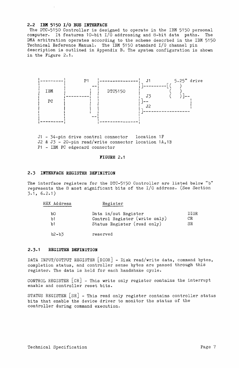
2.2
IBM
5150 I/O
BUS
INTERFACE
The DTC-5150
Controller
is
designed
to
operate
in
the
IBM
5150
personal
computer.
It
features
10-bit
I/O
addressing
and
8-bit
data
paths.
The
DMA
arbitration
operates
according
to
the
scheme
descrbed
in
the
IBM
5150
Technical
Reference
ManuaL The
IBM
5150
standard
I/O
channel
pin
description
is
outlined
in
Appendix
B. The
system
configuration
is
shown
in
the
Figure
2.1.
P1
Jl
5.25"
drive
IBM
DTC5150
PC
]---------[(
J3
(
(
)
)
)]--
]--
:
_
J2
:
J------------------
Jl
-
34-pin
drive
control
connector
location
lF
J2
&
J3
-
20-pin
read/write
connector
location
lA,lB
P1
-
IBM
PC
edgecard
connector
FIGURE
2.1
2.3
INTERFACE
REGISTER
DEFINITION
The
interface
registers
for
the
DTC-5150
Controller
are
listed
below
"b"
represents
the
8
most
significant
bits
of
the
I/O
address.
(See
Section
3.1,6.2.1)
2·3·1
HEX
Address
bO
bl
bl
b2-b3
Register
Data
in/out
Register
Control
Register
(write
only)
Status
Register
(read
only)
reserved
REGISTER
DEFINITION
DIOR
CR
SR
DATA
INPUT/OUTPUT
REGISTER
[DIOR] -
Disk
read/write
data,
command
bytes,
completion
status,
and
controller
sense
bytes
are
passed
through
this
register.
The
data
is
held
for
each
handshake
cycle.
CONTROL
REGISTER
[CR] -
This
write
only
register
contains
the
interrupt
enable
and
controller
reset
bits.
STATUS
REGISTER
[SR] -
This
read
only
register
contains
controller
status
bits
that
enable
the
device
driver
to
monitor
the
status
of
the
controller
during
command
execution.
Technical
Specification
Page
7
REGISTER
BIT
DEFINITION
I.
The
Completion
Status
Register
contains
the
status
of
the
command
that
has
just
completed.
(Refer
to
the
SR
description
below.)
The
bit
definition
for
this
byte
follows.
This
byte
is
held
in
the
DIOR
upon
the
completion
of
the
command.
Completion
Status
Register
(CSTAT)
Input
Address
bO
Bit
7
Bit
6
Bit
5
Bit
4
Bit
3
Bit
2
Bit
1
Bit
0
Device
Logic
Unit
Number (msb)
Device
Logic
Unit
Number
Device
Logic
Unit
Number
(lsb)
Not
used
Error
-The
device
driver
must
issue
the
Request
Sense
command
for
a
detailed
error
description.
Not
used
Not
used
Not
used
II.
The
control
register
is
a
write
only
register.
The
bits
are
defined
below.
Control
Register
(CR)
Bit
7
Bi t 6
Bit
5
Bit
4
Bit
3
Bit
2
Bit
1
Bit
0
Output
Address
b1
Not
used
Interrupt
Enable-enables
the
interrupt
upon
the
completion
of
the
transfer
of
each
block
of
data,
and
at
the
end
of
each
command.
Not
used
Controller
Reset
-
Resets
the
controller.
The
internal
state
of
the
controller
is
initialized
as
if
a power up
had
occurred.
Not
used
Not
used
Not
used
Not
used
111.
The
Status
Register
is
a
read-only
register.
The
bits
are
defined
below.
Status
Register
(SR)
Bit
7
Bit
6
Page
8
Input
Address
b1
REQ
-
indicates
the
controller
requests
data
or
has
data
for
host.
Also
indicates
that
bits
6
and
5
in
the
SR
are
valid.
IN/OUT
- A
low
indicates
data
to
host,
a
high
indicates
data
to
controller.
DTC-5150
Controller
Bit
5
Bi t 4
Bit
3
Bit
2
Bit
1
Bit
0
Note
that
when
REQ
IN/OUT
COM/DTA
0 0
0 1
1 0
1 1
is
set
bits
5
COM/DTA
- A low
indicates
that
the
bytes
transferred
through
the
Data
Register
are
data
bytes.
A
high
indicates
that
the
bytes
are
command
or
status
bytes.
SEE
TABLE
BELOW.
Not
used
Not
used
Not
used
Not
used
Not
used
& 6
are
interpreted
as
follows:
Meaning
of
bytes
passed
through
Data
Register
Data
out
of
controller
(i.e.
disk
read).
Completion
status
byte
out
of
controller.
Data
into
controller
(i.e.
disk
write).
Command
byte
into
controller.
2.4
THEORY
OF
OPERATION
2.4.0
COMMAND
INITIATION
Disk
commands
are
issued
to
the
DTC-5150
Controller
via
program
I/O
mode.
The
data
bytes
can
be
transferred
either
by
program
I/O
or
DMA
mode. The
controller
will
request
6
command
bytes.
Upon
receipt
of
the
last
command
byte
the
controller
will
begin
execution
of
the
command.
2.4.1
COMMAND
EXECUTION
For
the
data
transfer
commands, a
check
is
performed
on
the
disk
address
and
an
error
is
flagged
if
the
disk
address
exceeds
the
physical
limits
of
the
drive.
The
data
is
stored
in
a
sector
buffer
in
the
controller
before
it
is
transferred
to
the
host
or
disk
drive.
This
buffer
eliminates
any
possibility
of
data
overruns
between
the
host
and
the
disk.
Upon
the
completion
of
each
block
transfer,
the
controller
will
interrupt
the
device
driver
(if
the
interrupt
enable
bit
is
set).
After
the
last
block
has
been
transferred,
the
controller
will
interrupt
the
driver
after
the
Completion
Status
byte
is
loaded
into
the
DIOR.
(If
no
data
transfers
are
required
see
section
2.4.2.)
COMMAND
COMPLETION
Upon
completion
of
the
command,
the
controller
will
output
the
completion
status
to
the
DIOR
and
generate
an
interrupt
if
the
Interrupt
Enable
bit
is
set
in
the
SR.
If
the
Error
bit
is
set
in
the
SR
more
detailed
error
information
is
available
by
issuing
the
Request
Sense
Command
.•
2.5
COMMAND
SEQUENCE
OPERATION
The method by which a
command
is
executed
is
as
follows:
1 - The
device
driver
reads
the
SR
to
determine
whether
the
controller
is
REquesting
command
bytes.
When
REQ
is
set,
IN/OUT
and
COM/DTA
are
valid.
The
decode
of
the
two
bits
should
indicate
command
byte
transfer
(IN/OUT
&
COM/DTA
are
both
set).
2 -
If
the
decode
indicates
a
command
transfer,
the
device
driver
then
writes
the
first
command
byte
into
the
DIOR.
REQ
will
be
cleared
at
this
Technical
Specification
Page 9
time.
When
REQ
is
set
again,
the
second
command
byte
may
be
written.
The
controller
will
set
REQ
ahd
expect
a
command
byte
to
be
written
into
the
DIOR
until
all
command
bytes
are
received
from
the
driver.
The
driver
does
not
need
to
keep
a
count
of
the
number
of
command
bytes
transferred
to
the
controller.
The
controller
will
request
only
enough
bytes
to
complete
the
command.
3 -
After
the
command
bytes
have
been
transferred,
the
driver
should
wait
until
REQ
is
again
set
to
determine
the
next
phase
of
the
command.
By
decoding
the
IN/OUT
&
COM/DTA
bits
the
driver
can
dispatch
to
either
the
data
transmit,
data
recieve,
or
status
receive
routines.
If
the
command
is
a
READ,
WRITE,
REQUEST
SENSE,
or
REQUEST
SYNDROME
command,
data
will
be
transferred
through
the
DIOR.
In
which
case
the
driver
can
determine
the
direction
of
the
command
by
reading
the
IN/OUT
bit
in
the
SR.
If
the
data
is
transferred
under
program
I/O,
the
driver
can
use
similar
procedure
as
that
described
in
the
command
byte
transfer.
If
the
data
is
transferred
under
DMA
mode,
the
driver
must program
the
appropriate
8237
channel
for
the
address
of
the
data
buffer
in
the
system
memor~.
The word
count
should
be programmed
for
the
maximum
count
(65536
bytes).
The
direction
is
determined
by
the
IN/OUT
bit
in
the
SR. (The
8237
channel
must be programmed
in
the
Demand
Transfer
Mode.)
In
either
case
the
controller
will
transfer
a
block
of
data
to,
or
from,
the
host
cpu
whenever
the
data
is
ready
to
be
transferred.
If
the
command
is
a
READ
data
command,
the
controller
will
store
the
data
block
in
the
sector
buffer
before
it
is
transmitted
to
the
host
cpu.
If
the
command
is
a
WRITE
data
command
the
controller
will
fetch
the
data
block
from
the
host
cpu
before
it
is
transferred
to
the
disk.
This
sequence
is
repeated
until
all
data
blocks
are
transferred
between
the
controller
and
the
host
cpu.
The
device
driver
need
not
keep
a
count
of
the
data
bytes
transferred.
4 - Upon
the
completion
of
the
command
due
to
normal
or
abnormal
conditions,
the
controller
will
load
the
Completion
Status
byte
into
the
DIOR
and
issue
an
interrupt
to
the
driver
(if
the
Interrupt
Enable
bit
is
set).
The
driver
must
then
read
the
SR
to
handshake
the
byte
with
REQ.
After
the
Completion
Status
byte
has
been
read
the
controller
will
set
REQ,
IN/OUT, and
COM/DTA
to
indicate
that
it
is
ready
to
accept
the
first
byte
of
the
next
command.
(This
is
the
idle
state
of
the
controller.)
If
the
error
bit
is
set
in
the
Completion
Status
byte,
the
driver
should
issue
a
Request
Sense
Command
to
recieve
detailed
error
information.
Page
10 DTC-5150
Controller
3.0
HARDWARE
THEORY
OF
OPERATION
The DTC-5150
has
three
basic
modes
of
operation
-
slave
mode,
interrupt
mode
and
DMA
mode. The
functional
description
is
discussed
below.
3.1
I/O
LOGIC
OPERATION
(BUS
SLAVE)
The
controller
occupies
4
locations
in
the
I/O
address
space.
The
address
is
set
with
an
eight
position
dipswitch
(Address
bits
9
to
2).
Upon
the
assertion
of
the
lOR
or
lOW
signals
the
data
on
the
bus
will
be
transferred
to,
or
from,
the
appropriate
register.
Refer
to
section
6.2
for
address
setup.
The
address
decode
is
indicated
below.
I/O
Address
15 14 13 12
11
10 9 8 7 6 5 4 3 2 1 0
x x x x x x s s s s s s s s x x
x
don't
care
s
switch
selection
3.2
INTERRUPT
LOGIC
The DTC-5150
can
generate
an
interrupt
if
the
interrupt
enable
is
set
in
the
CR.
An
interrupt
will
be
generated
at
the
end
of
the
command
after
the
completion
status
byte
is
loaded
into
the
DIOR.
When
an
interrupt
is
generated,
the
interrupt
request
line
is
asserted
until
the
SR
is
read.
Refer
to
6.2.3
for
the
interrupt
jumper
assignment.
3.3
DIRECT
KEMORY
ACCESS
LOGIC
The
DMA
channel
in
the
DTC-5150
is
always
enabled.
DREQ
is
asserted
whenever
the
controller
sets
REQ
in
the
SR
for
a
data
transfer.
If
the
data
is
transferred
under
programmed
I/O
mode
the
controller
will
still
assert
DREQ
onto
the
IBM
bus
if
the
DMA
jumpers
are
installed.
Under
DMA
mode
the
data
transfer
is
assumed
to
be
in
the
Demand
Transfer
mode
of
the
8237.
For
each
byte
that
is
transferred,
DREQ
is
asserted.
DREQ
will
be
asserted
only
for
data
transfers.
Refer
to
section
6.2.2
for
DMA
jumper
configuration.
Technical
Specification
Page
11
4.0
COMMANDS
An
I/O
request
to
a
disk
drive
is
performed
by
passing
a
command
descriptor
block
(CDB)
to
the
controller.
The
first
byte
of
a
CDB
is
the
command
class
and
opcode.
The
remaining
bytes
specify
the
drive
logical
unit
number
(LUN)
,
block
address,
control
bytes,
number
of
blocks
to
transfer
or
the
destination
device
ID. The
controller
performs
an
implied
seek
and
verify
when
required
to
access
a
block.
Commands
are
categorized
into
three
classes
as
indicated:
Class
°
Non-data
Transfer,
Data
Transfer
and
Status
Commands
Class
1-5
Reserved
Class
6
Disk
Parameter
Assign
Command
Class
7
Diagnostic
Commands
The
command
descriptor
blocks
in
Command
Class
0,
6
and
7
are
6
bytes
in
length.
Although
all
6
command
bytes
must
be
sent
to
the
controller,
some
commands
may
not
require
that
all
command
bytes,
or
command
fields,
be
specified.
In
which
case
those
command
bytes,
and
fields,
that
need
not
be
specified
should
be
zero.
The
description
for
each
command
will
indicate
which
command
fields
must
be
specified.
Page
12 DTC-5150
Controller
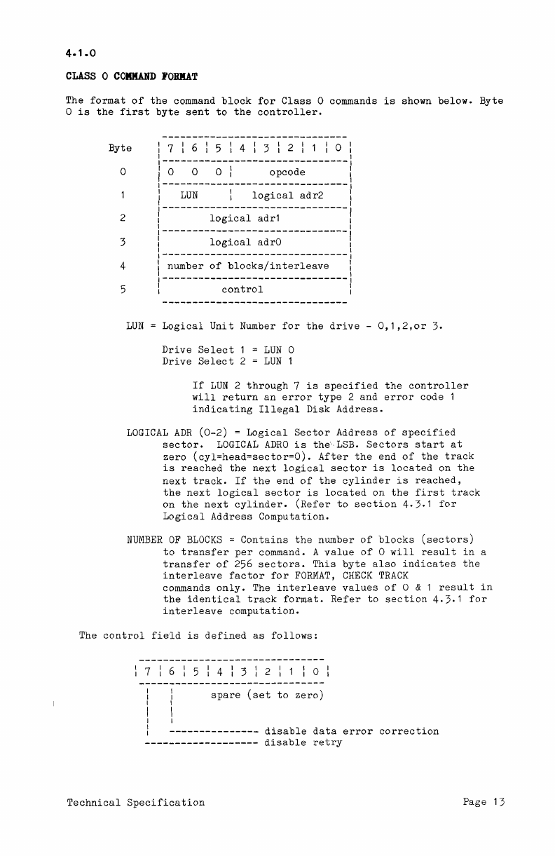
4.1.0
CLASS
0
COMMAND
I'OBIIAT
The
format
of
the
command
block
for
Class
0 commands
is
shown
below.
Byte
o
is
the
first
byte
sent
to
the
controller.
Byte
17161514131211101
o
2
3
4
5
1 1
1-------------------------------1
I 0 0
0:
opcode
I
1-------------------------------1
I
LUN
I
logical
adr2
I
1 1
1-------------------------------,
I
logical
adr1 1
1 1
1-------------------------------1
I
logical
adrO I
1 1
1-------------------------------1
I number
of
blocks/interleave
I
1 1
1-------------------------------1
I
control
I
LUN
Logical
Unit
Number
for
the
drive
-
0,1,2,or
3.
Drive
Select
1
Drive
Select
2
LUN
0
LUN
1
If
LUN
2
through
7
is
specified
the
controller
will
return
an
error
type
2
and
error
code 1
indicating
Illegal
Disk
Address.
LOGICAL
ADR
(0-2)
=
Logical
Sector
Address
of
specified
sector.
LOGICAL
ADRO
is
the
LSB.
Sectors
start
at
zero
(cyl=head=sector=O).
After
the
end
of
the
track
is
reached
the
next
logical
sector
is
located
on
the
next
track.
If
the
end
of
the
cylinder
is
reached,
the
next
logical
sector
is
located
on
the
first
track
on
the
next
cylinder.
(Refer
to
section
4.3.1
for
Logical
Address
Computation.
NUMBER
OF
BLOCKS
=
Contains
the
number
of
blocks
(sectors)
to
transfer
per
command. A
value
of
0
will
result
in
a
transfer
of
256
sectors.
This
byte
also
indicates
the
interleave
factor
for
FORMAT,
CHECK
TRACK
commands
only.
The
interleave
values
of
0 & 1
result
in
the
identical
track
format.
Refer
to
section
4.3.1
for
interleave
computation.
The
control
field
is
defined
as
follows:
spare
(set
to
zero)
---------------
disable
data
error
correction
-------------------
disable
retry
Technical
Specification
Page 13
If
the
DISABLE
RETRY
bit
is
1,
the
controller
will
not
attempt
to
retry
the
command.
If
the
DISABLE
RETRY
bit
is
0,
the
following
errors
result
in
a
retry
attempt:
a)
Records
not
found
,
b)
seek
error,
c)
uncorrrectable
data
error
,
d)
correctable
data
error,
e)
no ID
address
mark,
f)
no
Data
address
mark.
For
error
conditions
(a)
&
(b),
a
recalibrate,
reseek,
and
reread
are
performed.
For
error
condition
(c)
thru
(f)
only
a
reread
is
performed.
A
total
of
eight
attempts
are
performed
before
an
error
is
reported.
If
the
retry
is
successful,
the
controller
will
not
report
the
error
to
the
host.
The
retry
count
is
incremented
for
any
retry
attempted
(refer
to
REQUEST
LOGOUT
command).
Note,
no
retry
attempt
is
made
if
a
No
ID
address
mark
error
during
the
CHECK
TRACK
command
occurs.
If
the
DISABLE
DATA
ERROR
CORRECTION
bit
is
0,
the
controller
will
correct
the
data
if
a
correctable
data
error
occured.
The
controller
will
continue
with
the
command
as
though
there
was no
data
error.
The
error
is
not
reported
to
the
host.
An
uncorrectable
data
error
will
result
in
the
termination
of
the
command
after
the
transfer
of
the
erroneous
data
block
to
the
host
has
completed.
If
the
DISABLE
DATA
ERROR
CORRECTION
bit
is
1,
the
controller
will
not
correct
the
data
if
a
correctable
data
error
occured.
The command
will
terminate
as
if
an
uncorrectable
data
error
occurred.
The
controller
terminates
the
command
after
the
block
is
transferred
to
the
host
and
the
error
is
reported
to
the
host.
The
host
must
issue
a
REQUEST
SYNDROME
command
(class
0
opcode
2)
before
it
performs
the
correction.
The
permanent
error
count
(refer
to
REQUEST
LOGOUT
command)
is
incremented
by
one
in
both
cases
(disable/enable
data
error
correction).
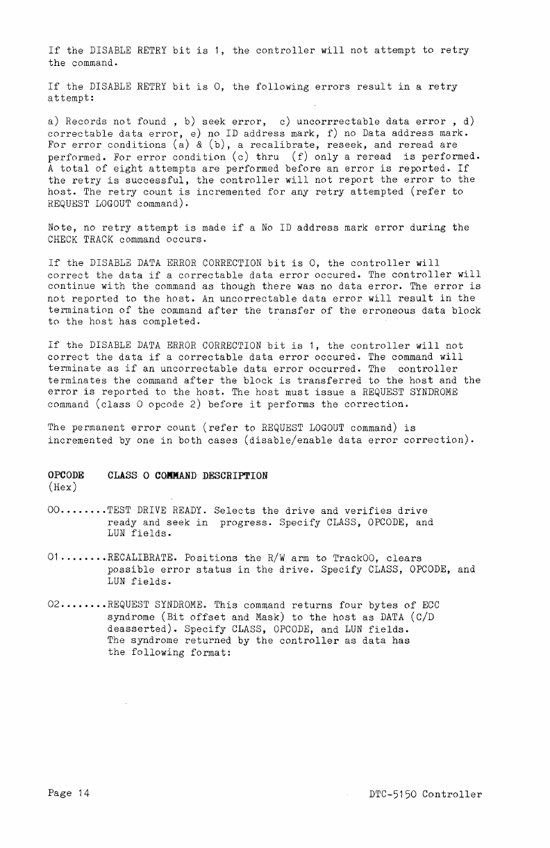
OPCODE
(Hex)
CLASS
0
COMMAND
DESCRIPTION
OO
.•......
TEST
DRIVE
READY.
Selects
the
drive
and
verifies
drive
ready
and
seek
in
progress.
Specify
CLASS,
OPCODE,
and
LUN
fields.
01
........
RECALIBRATE.
Positions
the
R/W
arm
to
TrackOO,
clears
possible
error
status
in
the
drive.
Specify
CLASS,
OPCODE,
and
LUN
fields.
02
........
REQUEST
SYNDROME.
This
command
returns
four
bytes
of
ECC
syndrome
(Bit
offset
and
Mask)
to
the
host
as
DATA
(C/D
deasserted).
Specify
CLASS,
OPCODE,
and
LUN
fields.
The
syndrome
returned
by
the
controller
as
data
has
the
following
format:
Page
14 DTC-5150
Controller
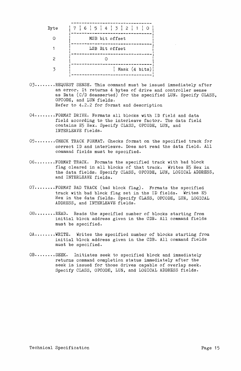
Byt e 7 I 6 I 5 I 4 I 3 I 2 I 1 I 0
o
MSB
bit
offset
LSB
Bit
offset
2 o
3 I Mask
(4
bits)
03
......
·.REQUEST
SENSE.
This
command
must
be
issued
immediately
after
an
error.
It
returns
4
bytes
of
drive
and
controller
sense
as
Data
(C/D
deasserted)
for
the
specified
LUN.
Specify
CLASS,
OPCODE,
and
LUN
fields.
Refer
to
4.2.2
for
format
and
description
04
....•••.
FORMAT
DRIVE.
Formats
all
blocks
with
ID
field
and
data
field
according
to
the
interleave
factor.
The
data
field
contains
E5
Hex.
Specify
CLASS,
OPCODE,
LUN,
and
INTERLEAVE
fields.
05
...•...•
CHECK
TRACK
FORMAT.
Checks
format
on
the
specified
track
for
correct
ID
and
interleave.
Does
not
read
the
data
field.
All
command
fields
must
be
specified.
06
..•..•..
FORMAT
TRACK.
Formats
the
specified
track
with
bad
block
flag
cleared
in
all
blocks
of
that
track.
Writes
E5
Hex
in
the
data
fields.
Specify
CLASS,
OPCODE,
LUN,
LOGICAL
ADDRESS,
and
INTERLEAVE
fields.
07
......•.
FOID~AT
BAD
TRACK
(bad
block
flag).
Formats
the
specified
track
with
bad
block
flag
set
in
the
ID
fields.
Writes
E5
Hex
in
the
data
fields.
Specify
CLASS,
OPCODE,
LUN,
LOGICAL
ADDRESS,
and
INTERLEAVE
fields.
08
..•.•.••
READ.
Reads
the
specified
number
of
blocks
starting
from
initial
block
address
given
in
the
CDB.
All
command
fields
must
be
specified.
OA
..•.••••
WRITE.
Writes
the
specified
number
of
blocks
starting
from
initial
block
address
given
in
the
CDB.
All
command
fields
must
be
specified.
OB
..•.....
SEEK.
Initiates
seek
to
specified
block
and
immediately
returns
command
completion
status
immediately
after
the
seek
is
issued
for
those
drives
capable
of
overlap
seek.
Specify
CLASS,
OPCODE,
LUN,
and
LOGICAL
ADDRESS
fields.
Technical
Specification
Page
15
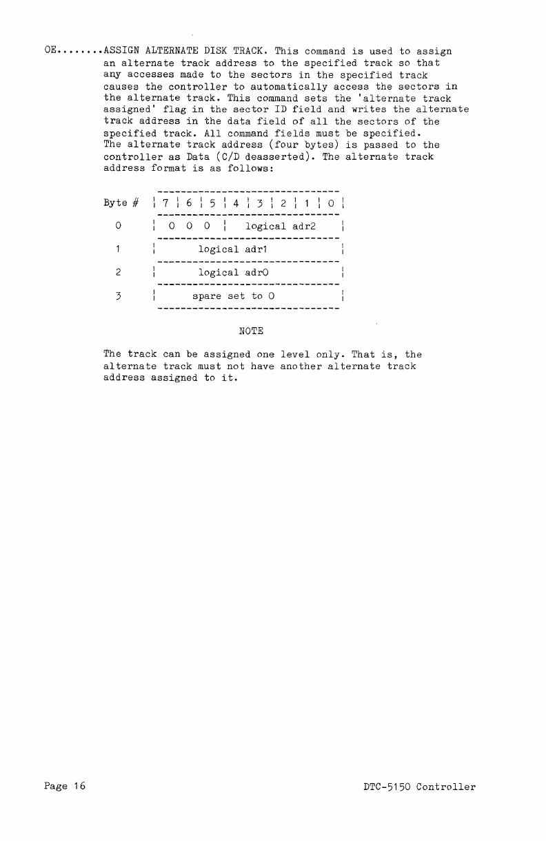
OE
........
ASSIGN
ALTERNATE
DISK
TRACK.
This
command
is
used
to
assign
an
alternate
track
address
to
the
specified
track
so
that
Page
16
any
accesses
made
to
the
sectors
in
the
specified
track
causes
the
controller
to
automatically
access
the
sectors
in
the
alternate
track.
This
command
sets
the
'alternate
track
assigned'
flag
in
the
sector
ID
field
and
writes
the
alternate
track
address
in
the
data
field
of
all
the
sectors
of
the
specified
track.
All
command
fields
must
be
specified.
The
alternate
track
address
(four
bytes)
is
passed
to
the
controller
as
Data
(C/D
deasserted).
The
alternate
track
address
format
is
as
follows:
Byte
# I 7 I 6 I 5 I 4 I 3 I 2 I 1 I 0 I
o
000
logical
adr2
logical
adr1
2
logical
adrO
3
spare
set
to
0
NOTE
The
track
can
be
assigned
one
level
only.
That
is,
the
alternate
track
must
not
have
another
alternate
track
address
assigned
to
it.
DTC-5150
Controller
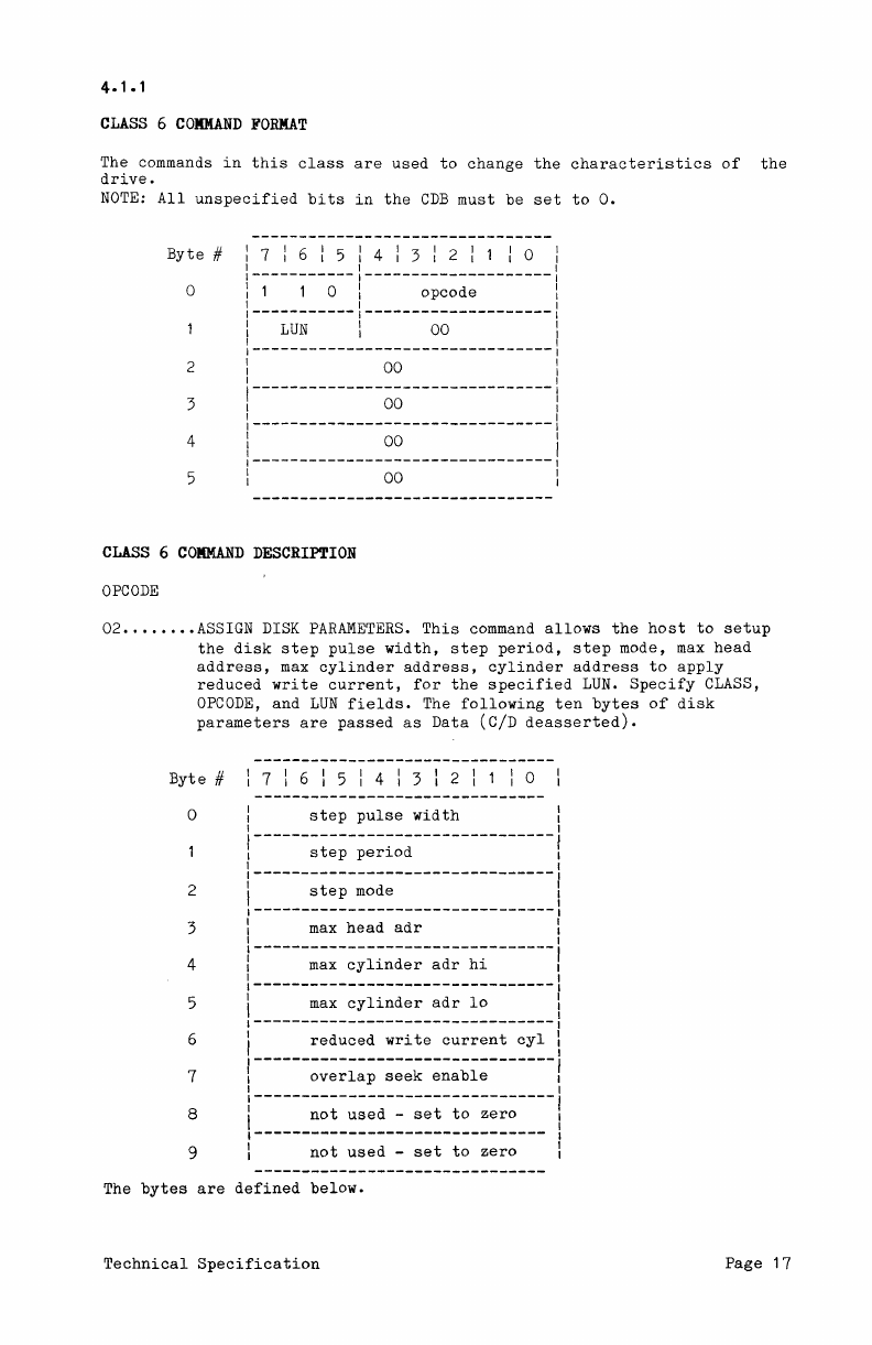
4.1.1
CLASS
6
COMMAND
FORMAT
The commands
in
this
class
are
used
to
change
the
characteristics
of
the
drive.
NOTE:
All
unspecified
bits
in
the
CDB
must
be
set
to
O.
Byte
#
o o
opcode
LUN
00
2
00
3
00
4
00
5
00
CLASS
6
COMMAND
DESCRIPTION
OPCODE
02
...••.•.
ASSIGN
DISK
PARAMETERS.
This
command
allows
the
host
to
setup
the
disk
step
pulse
width,
step
period,
step
mode,
max
head
address,
max
cylinder
address,
cylinder
address
to
apply
reduced
write
current,
for
the
specified
LUN.
Specify
CLASS,
OPCODE,
and
LUN
fields.
The
following
ten
bytes
of
disk
parameters
are
passed
as
Data
(C/D
deasserted).
Byte
#
0
step
pulse
width
:
, ,
,--------------------------------1
,
step
period
,
, ,
,--------------------------------,
2 I
step
mode I
,--------------------------------,
3 :
max
head
adr
:
, ,
4
1--------------------------------,
:
max
cylinder
adr
hi
1
, ,
1--------------------------------1
5 I
max
cylinder
adr
10
I
1--------------------------------1
6 I
reduced
write
current
cyl
\
7
1--------------------------------1
:
overlap
seek
enable
1
1 ,
8
1--------------------------------,
I
not
used
-
set
to
zero
:
1-------------------------------
1
9 :
not
used
-
set
to
zero
:
The
bytes
are
defined
below.
Technical
Specification
Page
17
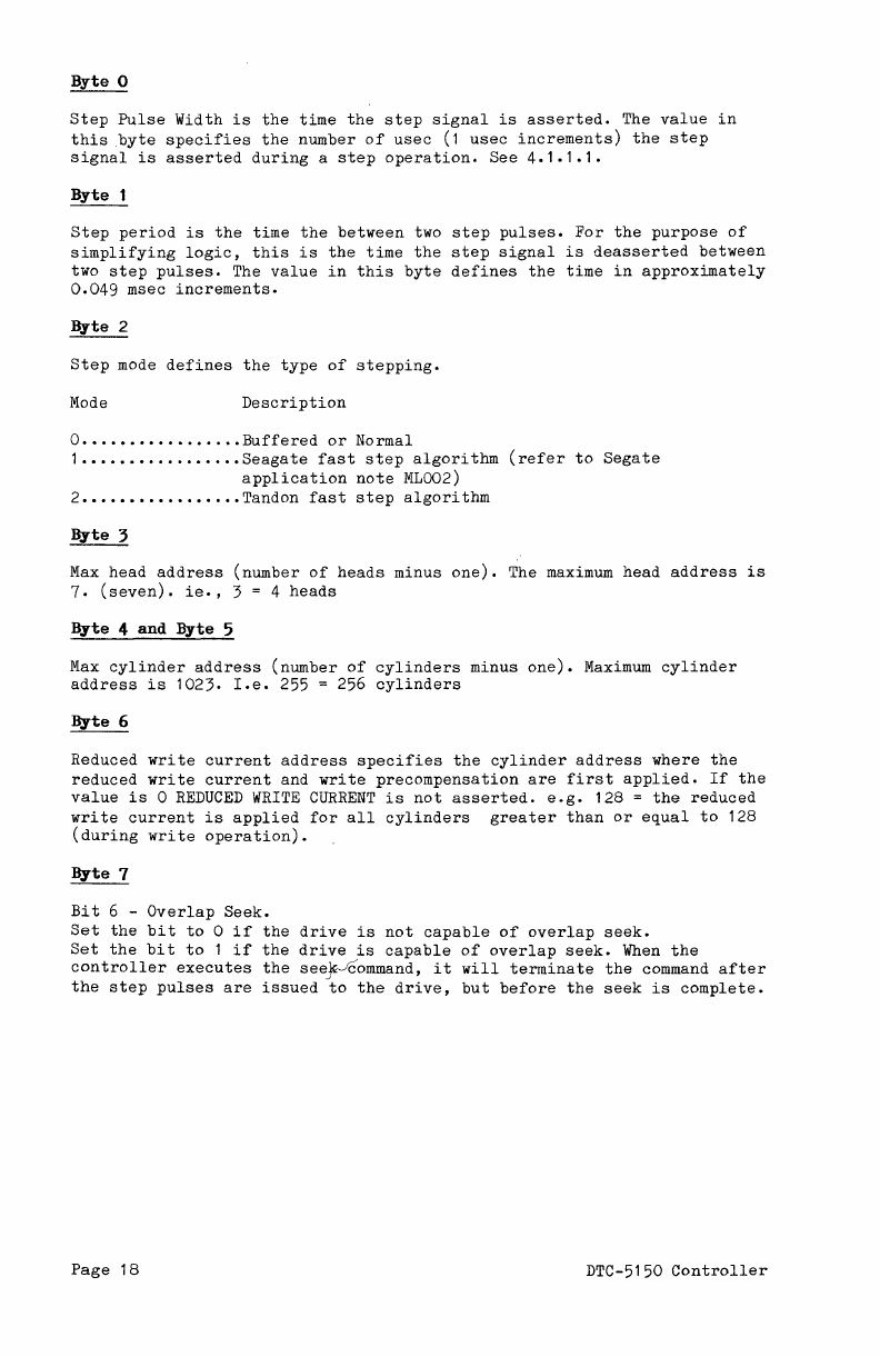
Step
Pulse
Width
is
the
time
the
step
signal
is
asserted.
The
value
in
this
byte
specifies
the
number
of
usec
(1
usec
increments)
the
step
signal
is
asserted
during
a
step
operation.
See
4.1.1.1.
Step
period
is
the
time
the
between
two
step
pulses.
For
the
purpose
of
simplifying
logic,
this
is
the
time
the
step
signal
is
deasserted
between
two
step
pulses.
The
value
in
this
byte
defines
the
time
in
approximately
0.049
msec
increments.
Step
mode
defines
the
type
of
stepping.
Mode
Description
O
•••.••.•••••••.•.
Buffered
or
Normal
1
.••••.•..•.••...•
Seagate
fast
step
algorithm
(refer
to
Segate
application
note
MLOO2)
2
••..•••.•••.••••.
Tandon
fast
step
algorithm
Max
head
address
(number
of
heads
minus
one).
The
maximum
head
address
is
7.
(seven).
ie.,
3 = 4
heads
B,yte 4 and B,yte 5
Max
cylinder
address
(number
of
cylinders
minus
one).
Maximum
cylinder
address
is
1023.
I.e.
255 = 256
cylinders
Reduced
write
current
address
specifies
the
cylinder
address
where
the
reduced
write
current
and
write
pre
compensation
are
first
applied.
If
the
value
is
0
REDUCED
WRITE
CURRENT
is
not
asserted.
e.g.
128 =
the
reduced
write
current
is
applied
for
all
cylinders
greater
than
or
equal
to
128
(during
write
operation).
Bit
6 -
Overlap
Seek.
Set
the
bit
to
0
if
the
drive
is
not
capable
of
overlap
seek.
Set
the
bit
to
1
if
the
drive
is
capable
of
overlap
seek.
When
the
controller
executes
the
see~ommand,
it
will
terminate
the
command
after
the
step
pulses
are
issued
to
the
drive,
but
before
the
seek
is
complete.
Page
18
DTC-5150
Controller
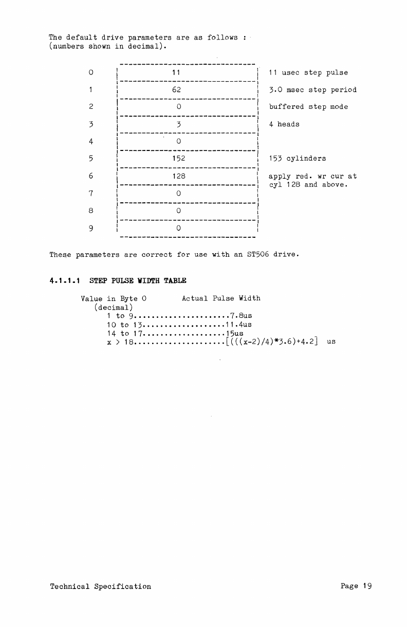
The
default
drive
parameters
are
as
follows
(numbers
shown
in
decimal).
o
2
3
4
5
11
62
o
3
o
152
11
usec
step
pulse
3.0
msec
step
period
buffered
step
mode
4
heads
153
cylinders
6 128
apply
red.
wr
cur
at
-------------------------------
cyl
128
and
above.
7 o
8 o
9 o
The~e
parameters
are
correct
for
use
with
an
ST506
drive.
4.1.1.1
STEP
PULSE
WIDTH
TABLE
Value
in
Byte
0
Actual
Pulse
Width
(decimal)
1
to
9
•...••.••••.••.•.••.••
7.8us
10
to
13
••.••••.•••••.••••.
11
.4us
14
to
17
••••.••.•••.•••••..
15us
x >
18
•.•••••••.•.•.••.•.••
[(((x-2)/4)*3.6)+4.2]
us
Technical
Specification
Page
19
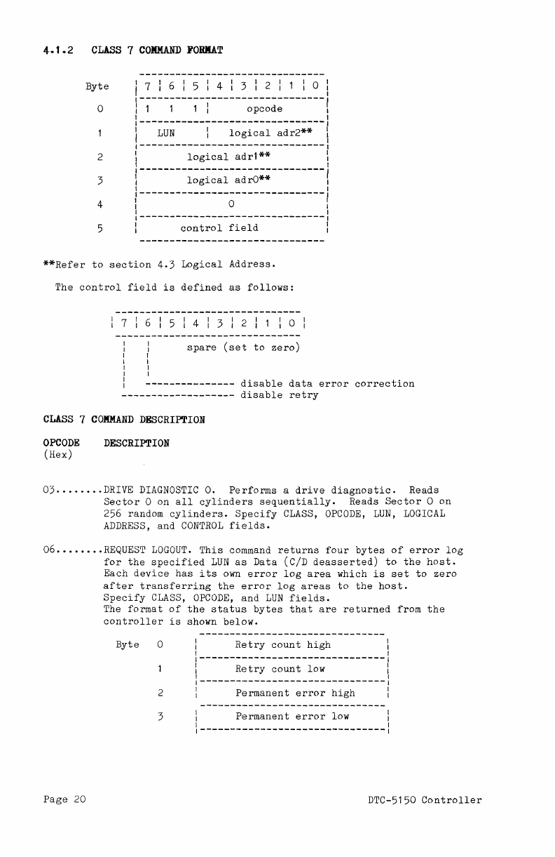
CLASS
1
C01lMAND
FORMAT
Byt e 1 I 6 I 5 I 4 I 3 I 2 I 1 I 0
o 1 I
opcode
LUN
logical
adr2**
2
logical
adr1**
3
logical
adrO**
4 o
5
control
field
**Refer
to
section
4.3
Logical
Address.
The
control
field
is
defined
as
follows:
spare
(set
to
zero)
---------------
disable
data
error
correction
-------------------
disable
retry
CLASS
1
COMMAND
DESCRIPTION
OPCODE
(Hex)
DESCRIPTION
03
..•..•..
DRIVE
DIAGNOSTIC
O.
Performs
a
drive
diagnostic.
Reads
Sector
0 on
all
cylinders
sequentially.
Reads
Sector
0
on
256 random
cylinders.
Specify
CLASS,
OPCODE,
LUN,
LOGICAL
ADDRESS,
and
CONTROL
fields.
06
..•.....
REQUEST
LOGOUT.
This
command
returns
four
bytes
of
error
log
for
the
specified
LUN
as
Data
(C/D
deasserted)
to
the
host.
Each
device
has
its
own
error
log
area
which
is
set
to
zero
after
transferring
the
error
log
areas
to
the
host.
Page
20
Specify
CLASS,
OPCODE,
and
LUN
fields.
The
format
of
the
status
bytes
that
are
returned
from
the
controller
is
shown
below.
Byte
o
2
3
Retry
count
high
Retry
count
low
Permanent
error
high
Permanent
error
low 1
1
1 1
1-------------------------------1
DTC-5150
Controller
The
following
errors
cause
the
log
area
to
be
incremented:
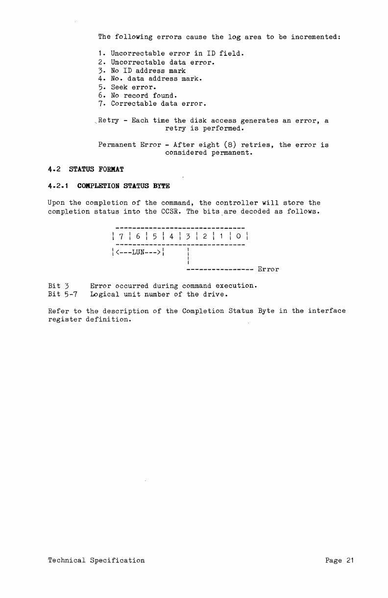
1-
Uncorrectable
error
in
ID
field.
2.
Uncorrectable
data
error.
3.
No
ID
address
mark
4. No.
data
address
mark.
5.
Seek
error.
6.
No
record
found.
7.
Correctable
data
error.
,Retry
-Each
time
the
disk
access
generates
an
error,
a
retry
is
performed.
Permanent
Error
-
After
eight
(8)
retries,
the
error
is
considered
permanent.
4.2
STATUS
FORMAT
4.2.1
COKPLETION
STATUS
BYTE
Upon
the
completion
of
the
command,
the
controller
will
store
the
completion
status
into
the
CCSR.
The
bits
are
decoded
as
follows.
Bit
3
Bit
5-7
\
<---LUN--->
\
Error
occurred
during
command
execution.
Logical
unit
number
of
the
drive.
Error
Refer
to
the
description
of
the
Completion
Status
Byte
in
the
interface
register
definition.
Technical
Specification
Page
21
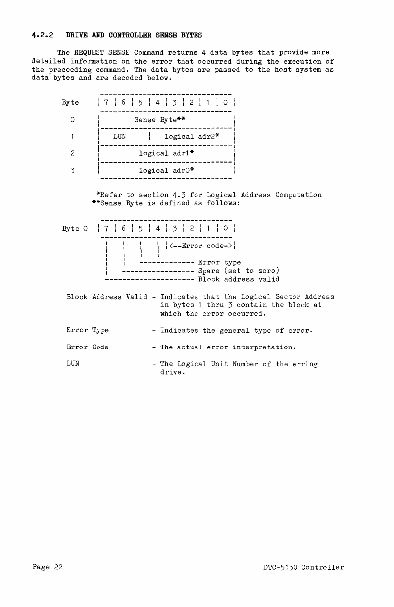
DRIVE
AND
CONTROLLER
SENSE
BYTES
The
REQUEST
SENSE
Command
returns
4
data
bytes
that
provide
more
detailed
information
on
the
error
that
occurred
during
the
execution
of
the
preceeding
command. The
data
bytes
are
passed
to
the
host
system
as
data
bytes
and
are
decoded
below.
Byte
I 7 I 6 I 5 I 4 I 3 I 2 I 1 I 0 I
Page
22
o
2
3
\
Sense
Byte**
I
1-------------------------------1
:
LUN
:
logical
adr2*
:
1 1
,-------------------------------1
1
logical
adr1*
I
1 1
1-------------------------------1
I
logical
adrO* :
*Refer
to
section
4.3
for
Logical
Address
Computation
**Sense
Byte
is
defined
as
follows:
Byt
eO:
7 : 6 : 5 : 4 : 3 : 2 : 1 : 0 :
I I
<--Error
code->l
1
Error
type
Spare
(set
to
zero)
Block
address
valid
Block
Address
Valid
-
Indicates
that
the
Logical
Sector
Address
in
bytes
1
thru
3
contain
the
block
at
which
the
error
occurred.
Error
Type
Error
Code
LUN
-
Indicates
the
general
type
of
error.
-The
actual
error
interpretation.
-The
Logical
Unit
Number
of
the
erring
drive.
DTC-5150
Controller
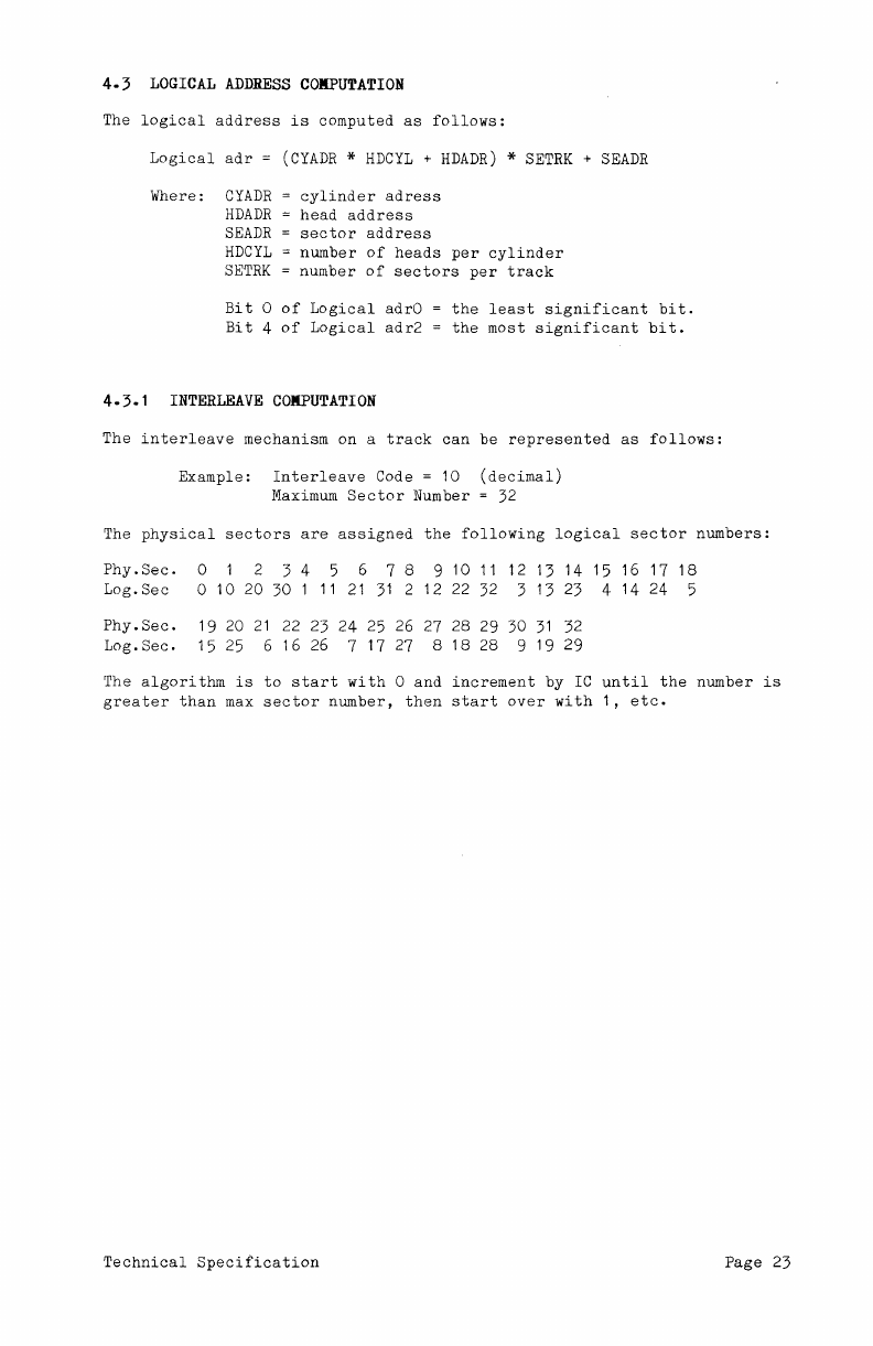
4.3
LOGICAL
ADDRESS
COXPUTATION
The
logical
address
is
computed
as
follows:
Logical
adr
=
(CYADR
*
HDCYL
+
HDADR)
*
SETRK
+
SEADR
Where:
CYADR
cylinder
adress
head
address
sector
address
HDADR
SEADR
HDCYL
SETRK
number
of
heads
per
cylinder
number
of
sectors
per
track
Bit
0
of
Logical
adrO
Bit
4
of
Logical
adr2
4.3.1
INTERLEAVE
COXPUTATION
the
least
significant
bit.
the
most
significant
bit.
The
interleave
mechanism
on
a
track
can
be
represented
as
follows:
Example:
Interleave
Code = 10
(decimal)
Maximum
Sector
Number = 32
The
physical
sectors
are
assigned
the
following
logical
sector
numbers:
Phy.Sec.
0 2 3 4 5 6 7 8 9 10
11
12 13 14 15 16 17
18
Log.Sec
0
10
20
30
1
11
21
31
2 12 22 32 3 13 23 4 14 24 5
Phy.Sec.
19 20
21
22 23 24 25 26 27 28 29 30
31
32
Log.Sec.
15 25 6 16
26
7 17 27 8
18
28 9 19 29
The
algorithm
is
to
start
with
o
and
increment
by
IC
until
the
number
is
greater
than
max
sector
number,
then
start
over
with
1,
etc.
Technical
Specification
Page
23
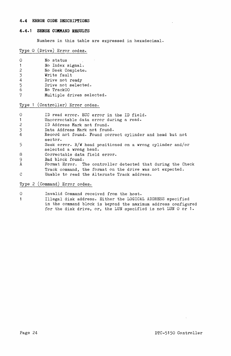
4.4
ERROR
CODE
DESCRIPTIONS
4.4.1
SENSE
COMMAND
RESULTS
Numbers
in
this
table
are
expressed
in
hexadecimal.
Type 0
(Drive)
Error
codes.
o
No
status
1
No
Index
signal.
2
No
Seek
Complete.
3
Write
fault
4
Drive
not
ready
5
Drive
not
selected.
6
No
TrackOO
7
Multiple
drives
selected.
Type
(Controller)
Error
codes.
o ID
read
error.
ECC
error
in
the
ID
field.
1
Uncorrectable
data
error
during
a
read.
2 ID
Address
Mark
not
found.
3
Data
Address
Mark
not
found.
4
Record
not
found.
Found
correct
cylinder
and
head
but
not
sector.
5
Seek
error.
R/W
head
positioned
on
a wrong
cylinder
and/or
selected
a wrong
head.
S
Correctable
data
field
error.
9 Bad
block
found.
A
Format
Error.
The
controller
detected
that
during
the
Check
Track
command,
the
format
on
the
drive
was
not
expected.
C
Unable
to
read
the
Alternate
Track
address.
Type 2 (Command)
Error
codes.
o
Page
24
Invalid
Command
received
from
the
host.
Illegal
disk
address.
Either
the
LOGICAL
ADDRESS
specified
in
the
command
block
is
beyond
the
maximum
address
configured
for
the
disk
drive,
or,
the
LUN
specified
is
not
LUN
0
or
1.
DTC-5150
Controller
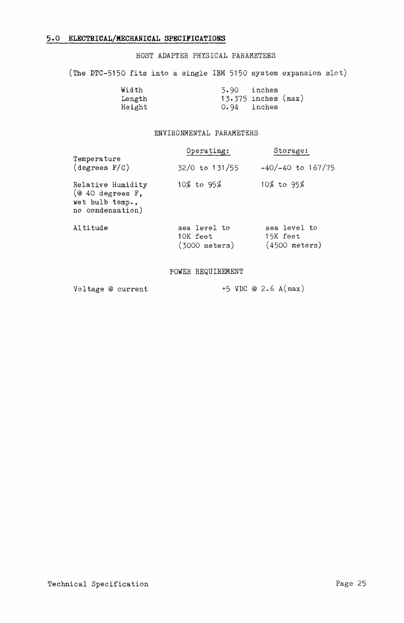
5.0
ELECTRICAL/MECHANICAL
SPECIFICATIONS
HOST
ADAPTER
PHYSICAL
PARAMETERS
(The DTC-5150
fits
into
a
single
IBM
5150
system
expansion
slot)
Width
Length
Height
Temperature
(degrees
F/C)
Relative
Humidity
(@
40
degrees
F,
wet
bulb
temp.,
no
condensation)
Altitude
Voltage
@
current
Technical
Specification
3.90
inches
13.375
inches
(max)
0.94
inches
ENVIRONMENTAL
PARAMETERS
Operating:
32/0
to
131/55
10%
to
95%
sea
level
to
10K
feet
(3000
meters)
POWER
REQUIREMENT
Storage:
-40/-40
to
167/75
10%
to
95%
sea
level
to
15K
feet
(4500
meters)
+5
VDC
@
2.6
A(max)
Page
25
6.0
INSTALLATION
6.1
INSPECTION
Inspect
all
shipping
containers
for
damage.
If
a
container
is
damaged
the
contents
should
be
checked
and
the
DTC-5150
Controller
verified
electrically.
If
the
controller
is
damaged,
call
Data
Technology
Corporation
Customer
Service
for
Return
Material
Authorization
(RMA)
number.
Please
retain
all
shipping
lablels
and
documentation.
6.2
ADDRESS,
INTERRUPT
AND
DMA
SETUP
Before
the
DTC-5150
Controller
can
be
used,
initial
setup
may
be
required.
Be
sure
the
power
requirements
for
the
controller
are
met
(section
5.0).
The
controller
is
installed
in
a
vacant
slot
in
the
IBM
5150
backplane.
(NOTE:
BECAUSE
OF
THE
PLACEMENT
OF
THE
SPEAKER,
DO
NOT
MOUNT
THE
DTC-5150
IN
THE
FAR
LEFT
SLOT).
Two
mass-terminated
cables,
a
20-pin
and
a
34-pin
connect
the
controller
to
the
external
peripheral
drive
(s).
Refer
to
figure
2.1
for
connection
of
the
controller
to
the
disk
drives.
Note
that
all
cables,
including
drive
cables,
are
of
the
mass-terminated
type,
so
no
inadvertant
signal
swapping
can
occur.
The
following
sections
describe
in
detail
the
proper
jumper
settings
on
the
DTC-5150
controller.
Coordinates
of
board
locations
are
referenced
to
letters
across
the
top
of
the
board
and
numbers
down
the
right
side.
For
detailed
installation
instructions,
see
DTC-5150
Installation
Guide,
DTC
part
#IG-092-00.
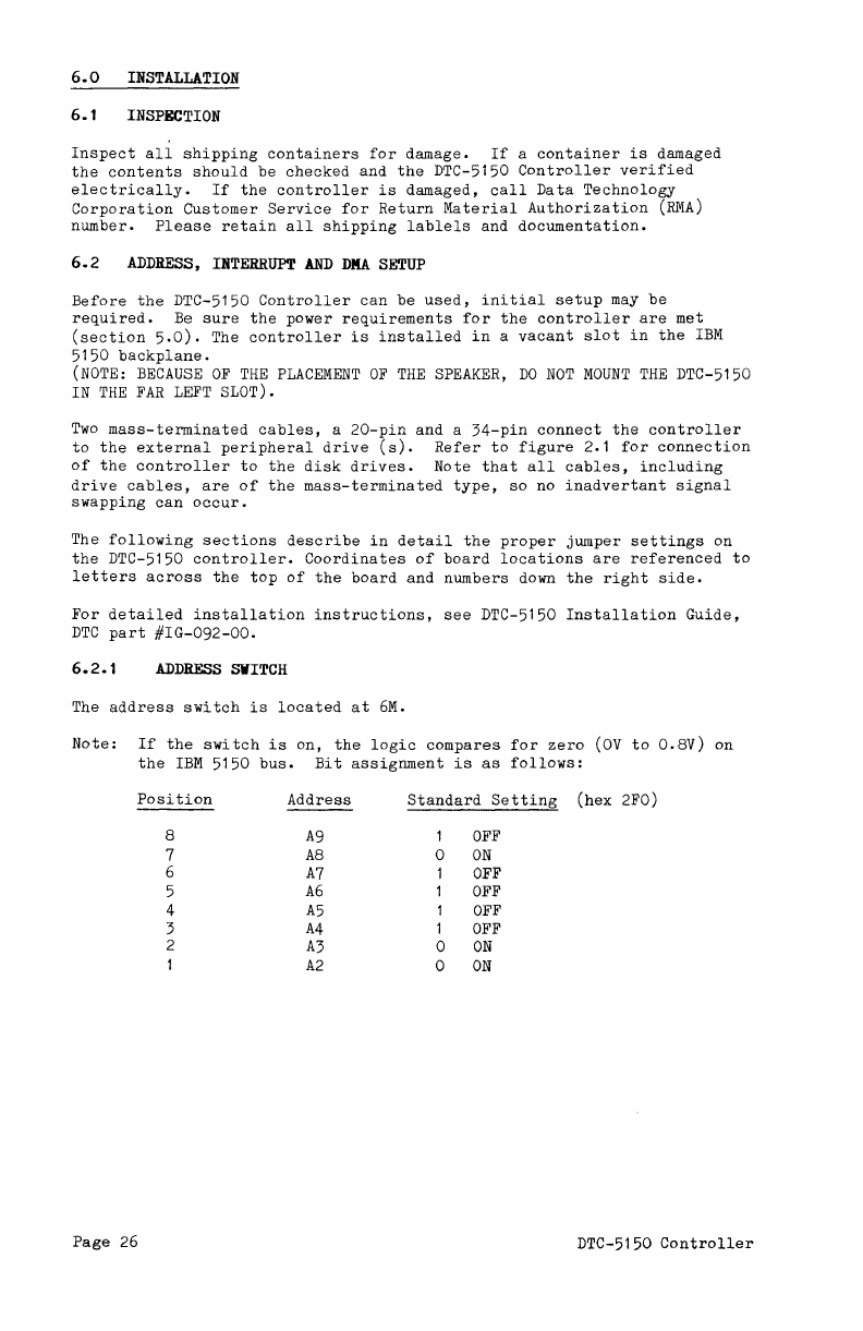
6.2.1
ADDRESS
SWITCH
The
address
switch
is
located
at
6M.
Note:
If
the
switch
is
on,
the
logic
compares
for
zero
(OY
to
0.8Y)
on
the
IBM
5150
bus.
Bit
assignment
is
as
follows:
Position
Address
Standard
Setting
(hex
2FO)
8
A9
1
OFF
7
A8
0
ON
6
A7
1
OFF
5
A6
1
OFF
4
A5
1
OFF
3
A4
1
OFF
2
A3
0
ON
1
A2
0
ON
Page
26 DTC-5150
Controller
6.2.2
DIIA
JUMPER
Only
one
pair
can
same
channel.
DAK
Jumper
W15
W14
W13
W5
W4
W6
be
is
installed.
The
DAK
and
DRQ
jumpers
must
refer
to
the
near
6N.
DR2
is
near
4N.
Function
DAK3
DAK2
DAK1
DRQ3
DRQ2
DRQ1
Standard
Setting
Jumper
in
No
jumper
No
jumper
Jumper
in
No
jumper
No
jumper
6.2.3
INTERRUPT
JUMPER
The
interrupt
request
output
is
connected
to
the
I/O
bus
vectored
interrupt
channel
as
follows.
Only one
jumper
may
be
installed.
Interrupt
jumpers
are
located
near
5N.
6.2.4
Jumper
W12
W7
W8
W9
W11
W10
OTHER
JUMPERS
W1
W2
Function
Standard
Setting
IRQ2
No
jumper
IRQ3
No
jumper
IRQ4
No
jumper
IRQ5
Jumper
in
IRQ6
No
jumper
IRQ7
No
jumper
Function
Clock
for
Controller
(always
in)
located
at
6C.
Bytes/Sector
Select
(out
for
256
bytes
and
in
for
512
bytes)
located
at
31'11.
6.3
INITIAL
CHECKOUT
The
initial
verification
of
the
disk
subsystem
can
be
done
via
an
appropriate
monitor
program,
or
through
a
debugging
utililty
such
as
DEBUG.
Verify
that
all
the
interface
registers
are
accessible
through
the
correct
addresses
and
that
the
registers
can
be
read/written
with
the
expected
results.
Technical
Specification
Page
27
1.0
REFERENCE
DOCUMENTATION
This
section
provides
information
regarding
the
documentation
available
for
using
the
DTC-5150
Controller.
1.1
IBM
5150
a.
IBM
Hardware
Reference
Manual
(first
edition
August
1981)
b.
IBM
Disk
operating
System
V2.0
(first
edition,
January
1983)
(Especially
Chapter
14,
Device
Drivers).
1.2
DISK
DRIVE
DOCUMENTATION
Use
the
appropriate
drive
manufacturer's
manual
for
your
disk
drive.
1.3
DTC
5150
DRIVER
AND
INSTALLATION
GUIDE
Software
to
allow
use
of
hard
disks
with
the
DTC
5150
Controller
under
IBM
PC
DOS
V2.00
is
available
from
DTC.
An
Installation
Guide,
DTC
part
#IG-092-00,
describes
installation
of
the
controller
and
use
of
the
driver
software.
Page
28
DTC-5150
Controller
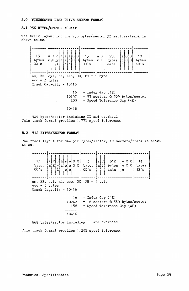
8.0
WINCHESTER
DISK
DRIVE
SECTOR
FORMAT
8.1
256
BYTES/SECTOR
FORMAT
The
track
layout
for
the
256
bytes/sector
33
sectors/track
is
shown
below.
I I I
-7-7-7-7-7-7-7-1-------1-7-7---------7-7-1-------
I I I I I I I I I I I I I I
13 a I F I c I hI s I e I 0
101
13 I a I F I 256 e I 0
101
10
bytes
mlElyldlelclOlOl
bytes
lml81
bytes
clolol
bytes
00'
s !!
II
I c I c I I I
00'
s I I I
data
c I I I 4E' s
I I I I I I I I I I I I I I
I I I I I I I I I I I I I I
I I I
---------------1-------1-----------------1-------
am,
FE,
cyl,
hd,
sec,
00,
F8 = 1
byte
ecc
= 3
bytes
Track
Capacity
= 10416
16
10197
203
10416
Index
Gap
(4E)
33
sectors
@ 309
bytes/sector
Speed
Tolerance
Gap
(4E)
309
bytes/sector
including
ID and
overhead
This
track
format
provides
1.77%
speed
tolerence.
8.2
512
BYTES/SECTOR
FORMAT
The
track
layout
for
the
512
bytes/sector,
18
sectors/track
is
shown
below.
I
---------------1-------
I I I I I I I I
I I I I I I I I
13
alFlclhlslelOIOI
13
bytes
mlElyldlelclOIOI
bytes
00 ' s I
III
I C I C I I I
00'
I I I
II
I 1
lis
I I I I I I I I
I
---------------1-------
am,
FE,
cyl,
hd,
sec,
00,
F8 =
ecc
= 3
bytes
Track
Capacity
= 10416
I
-----------------1-------
I I I I I
I I I I I
alFI
512 elOIOI 14
ml81
bytes
clolol
bytes
) )
data
c) I I
4E's
I I I I I
I
-----------------1-------
byte
16
10242
158
Index
Gap
(4E)
10416
18
sectors
@ 569
bytes/sector
Speed
Tolerance
Gap
(4E)
569
bytes/sector
including
ID
and
overhead
This
track
format
provides
1.29%
speed
tolerence.
Technical
Specification
Page 29
APPENDIX
A
COMMANDS/PROGRAMMING
An
I/O
request
on
the
DTC
controller
is
performed
by
passing
a
command
descriptor
bolck
CCDB)
to
the
controller.
The
first
byte
of
a
CDB
is
the
command
class
and
opcode.
The
remaining
bytes
specify
the
drive
logical
unit
number
(LUN)
,
block
address,
control
bytes,
and
number
of
blocks
to
transfer.
The
controller
performs
an
implied
seek
and
verify
when
command
to
access
a
block.
Due
to
the
different
types
of
commands
the
controller
recognizes,
the
comand
format
for
the
DTC-5150
Controller
will
only
indicate
the
skeletal
representation
of
the
command. The
reader
is
directed
to
Section
4.0
of
this
specification
for
more
detailed
command
information.
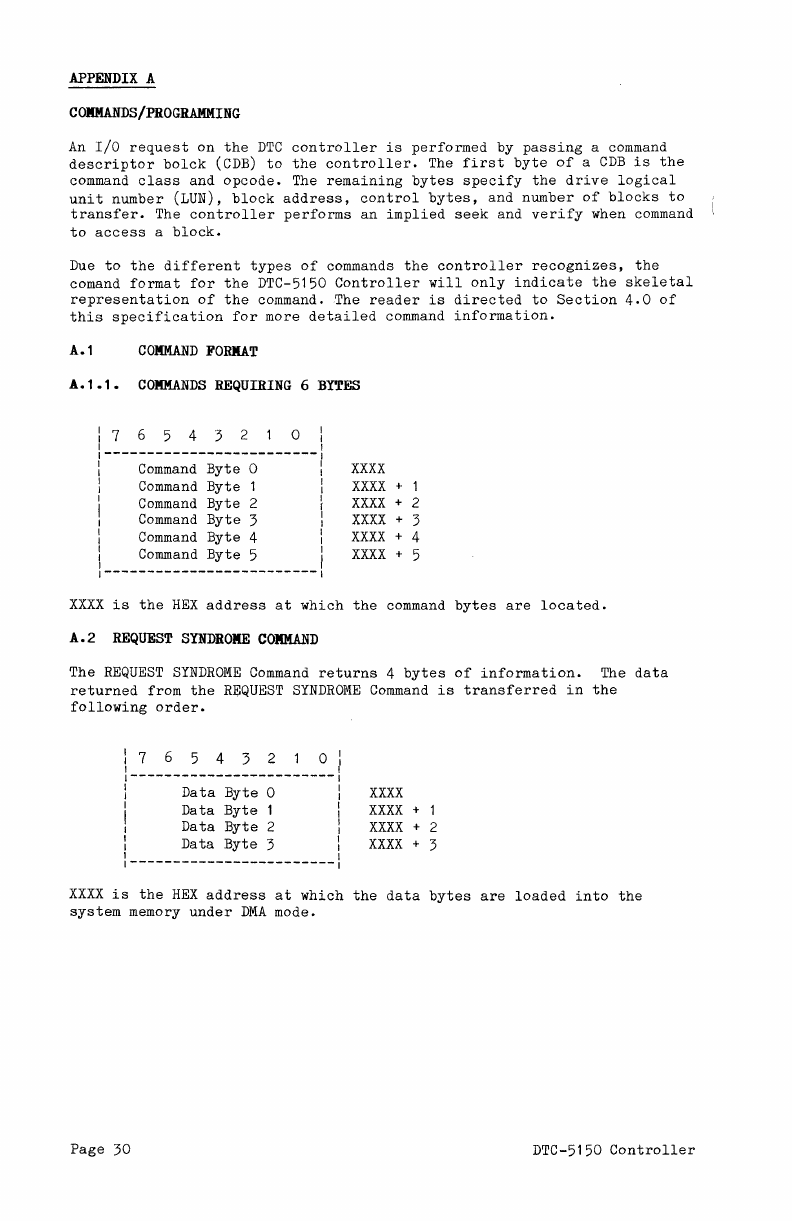
A.l
COMMAND
FORMAT
A.l.l.
COMMANDS
REQUIRING 6 BYTES
7 6 5 4 3 2 0
-------------------------
Command
Byte
0
XXXX
Command
Byte
1
XXXX
+ 1
Command
Byte
2
XXXX
+ 2
Command
Byte
3
XXXX
+ 3
Command
Byte
4
XXXX
+ 4
Command
Byte
5
XXXX
+ 5
-------------------------
XXXX
is
the
HEX
address
at
which
the
command
bytes
are
located.
A.2
REQUEST SYNDR01lE
COBMAND
The
REQUEST
SYNDROME
Command
returns
4
bytes
of
information.
The
data
returned
from
the
REQUEST
SYNDROME
Command
is
transferred
in
the
following
order.
7 6 5 4 3 2 0 I
I
------------------------,
Data
Byte
0 I
Data
Byte
1 I
Data
Byte
2 :
Data
Byte
3 I
------------------------1
XXXX
XXXX
+ 1
XXXX
+ 2
XXXX
+ 3
XXXX
is
the
HEX
address
at
which
the
data
bytes
are
loaded
into
the
system
memory
under
DMA
mode.
Page
30
DTC-5150
Controller
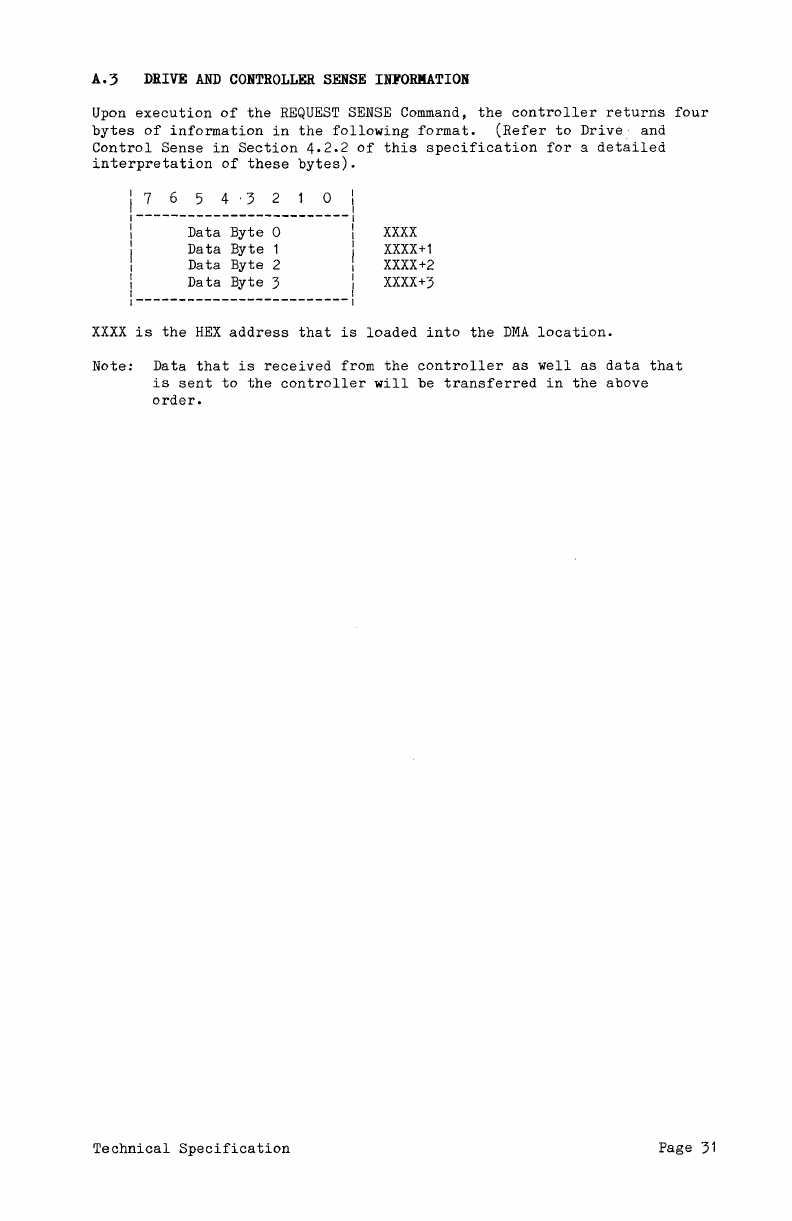
A.3
DRIVE
AND
CONTROLLER
SENSE
INFORMATION
Upon
execution
of
the
REQUEST
SENSE
Command,
the
controller
returns
four
bytes
of
information
in
the
following
format.
(Refer
to
Drive
and
Control
Sense
in
Section
4.2.2
of
this
specification
for
3
detailed
interpretation
of
these
bytes).
7 6 5
4·3
2 0 \
-------------------------1
Data
Byte
0 I
Data
Byte
1 I
Data
Byte
2 1
Data
Byte
3 I
1
-------------------------1
XXXX
XXXX+1
XXXX+2
XXXx+3
XXXX
is
the
HEX
address
that
is
loaded
into
the
DMA
location.
Note:
Data
that
is
received
from
the
controller
as
well
as
data
that
is
sent
to
the
controller
will
be
transferred
in
the
above
order.
Technical
Specification
Page
31
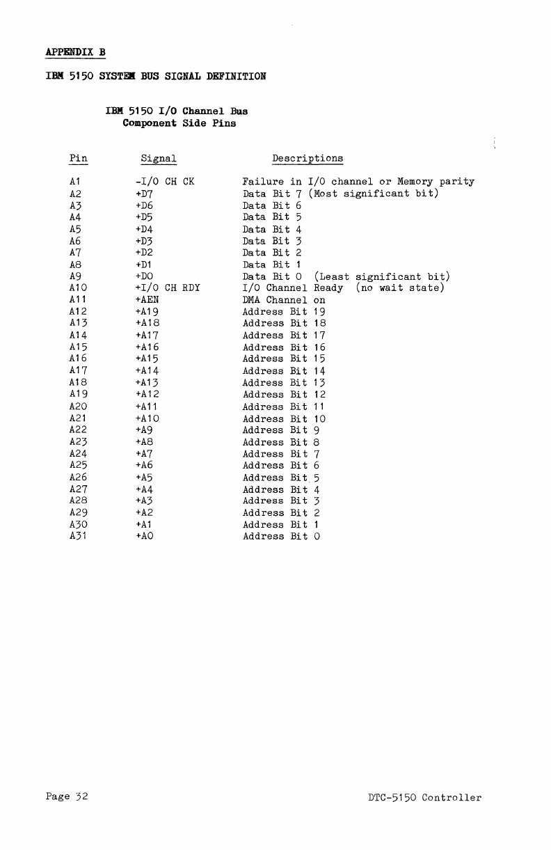
APPENDIX
B
IBM
5150
SYSTEK
BUS
SIGNAL
DEFINITION
IBM
5150
I/O
Channel
Bus
Component
Side
Pins
Pin
Signal
Descriptions
Al
-I/O
CH CK
Failure
in
I/O
channel
or
Memory
parity
A2
+D7
Data
Bit
7 (Most
significant
bit)
A3
+D6
Data
Bit
6
A4
+D5
Data
Bit
5
A5
+D4
Data
Bit
4
A6
+D3
Data
Bit
3
A7
+D2
Data
Bit
2
A8
+Dl
Data
Bit
1
A9
+DO
Data
Bit
0
(Least
significant
bit)
Al0 +1/0
CH
RDY
I/O
Channel Ready (no
wait
state)
All
+AEN
DMA
Channel on
A12
+A19
Address
Bit
19
A13
+A18
Address
Bit
18
A14
+A17
Address
Bit
17
A15
+A16
Address
Bit
16
A16
+A15
Address
Bit
15
A17
+A14
Address
Bit
14
A18
+A13
Address
Bit
13
A19
+A12
Address
Bit
12
A20
+All
Address
Bit
11
A21
+Al0
Address
Bit
10
A22
+A9
Address
Bit
9
A23
+A8
Address
Bit
8
A24
+A7
Address
Bit
7
A25
+A6
Address
Bit
6
A26
+A5
Address
Bit
5
A27
+A4
Address
Bit
4
A28
+A3
Address
Bit
3
A29
+A2
Address
Bit
2
A30
+Al
Address
Bit
1
A31
+AO
Address
Bit
0
Page
32 DTC-5150
Controller
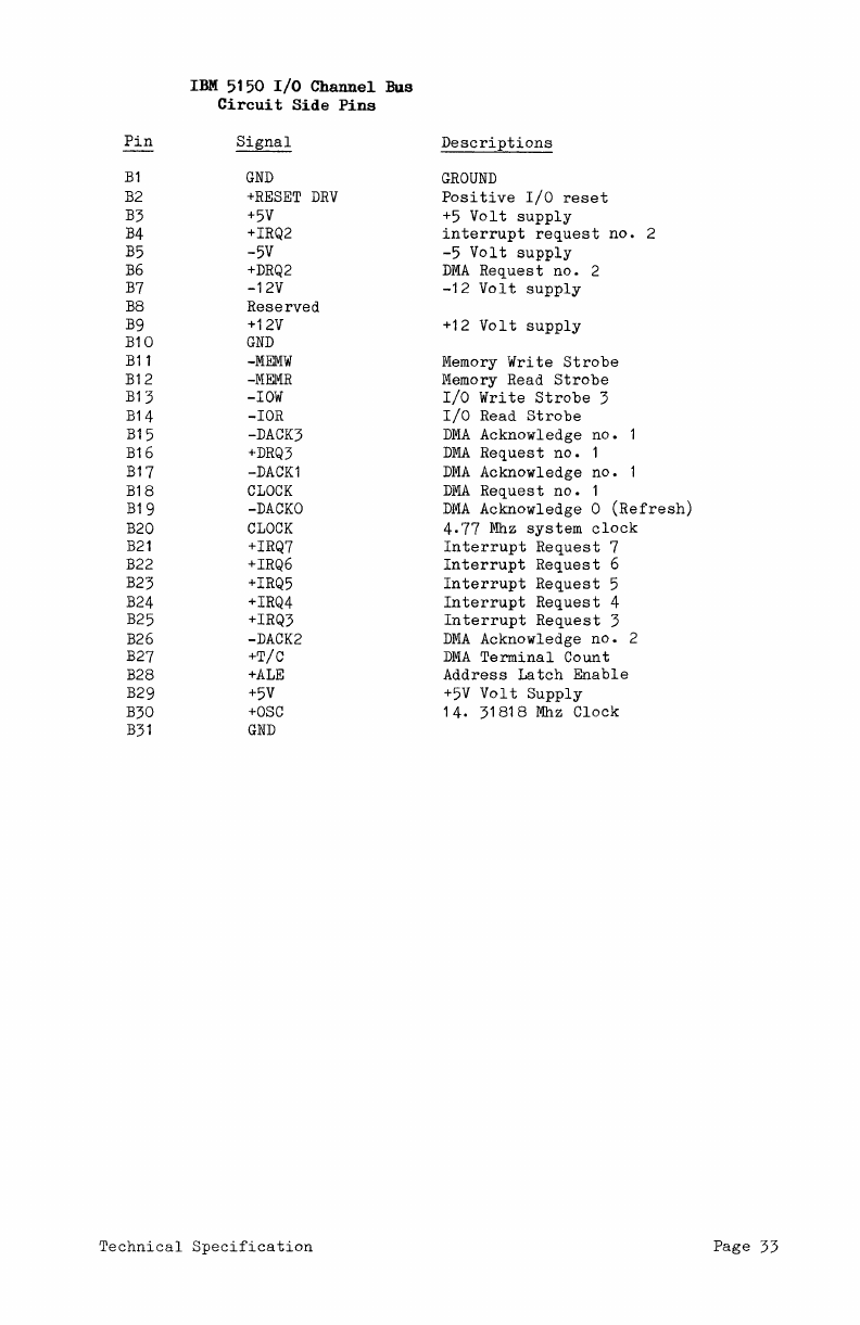
Pin
B1
B2
B3
B4
B5
B6
B7
B8
B9
B10
B11
B12
B13
B14
B15
B16
B17
B18
B19
B20
B21
B22
B23
B24
B25
B26
B27
B28
B29
B30
B31
IBM
5150
I/O
Channel
Bus
Circuit
Side
Pins
GND
+RESET
DRV
+5V
+IRQ2
-5V
+DRQ2
-12V
Reserved
+12V
GND
-MEMW
-MElVlR
-lOW
-lOR
-DACK3
+DRQ3
-DACK1
CLOCK
-DACKO
CLOCK
+IRQ7
+IRQ6
+IRQ5
+IRQ4
+IRQ3
-DACK2
+T/C
+ALE
+5V
+OSC
GND
Technical
Specification
Descriptions
GROUND
Positive
I/O
reset
+5
Volt
supply
interrupt
request
no.
2
-5
Volt
supply
DMA
Request
no.
2
-12
Volt
supply
+12
Volt
supply
Memory
Write
Strobe
Memory
Read
Strobe
I/O
Write
Strobe
3
I/O
Read
Strobe
DMA
Acknowledge
no.
DMA
Request
no.
1
DMA
Acknowledge
no.
DMA
Request
no.
1
DMA
Acknowledge 0
(Refresh)
4.77
Mhz
system
clock
Interrupt
Request
7
Interrupt
Request
6
Interrupt
Request
5
Interrupt
Request
4
Interrupt
Request
3
DMA
Acknowledge
no.
2
DMA
Terminal
Count
Address
Latch
Enable
+5V
Volt
Supply
14.
31818
Mhz
Clock
Page 33

NOTES

DC
