DV760X
User Manual: DV760X
Open the PDF directly: View PDF ![]() .
.
Page Count: 76
1
SX9Q5DV-760X/
SERVICE MANUAL
In the interests of user-safety (Required by safety regula-
tions in some countries) the set should be restored to its
original condition and only parts identical to those specified
be used.
SHARP CORPORATION
Page
1. IMPORTANT SAFEGUARDS AND PRECAUTIONS ......................................................................1-1
2. FEATURES/3. SPECIFICATIONS ..................................................................................................2-1
4. PART NAMES ................................................................................................................................. 4-1
5. MAINTENANCE CHECK ITEMS AND EXECUTION TIME ............................................................ 5-1
6. DISASSEMBLY AND REPLACEMENT OF MAIN PARTS ............................................................. 6-1
7. EXPLANATION OF MECHANISM ..................................................................................................7-1
8. OPERATION OF PICKUP ............................................................................................................... 8-1
9. TEST MODE ................................................................................................................................... 9-1
10. TROUBLESHOOTING .................................................................................................................. 10-1
11. IC FUNCTION LIST....................................................................................................................... 11-1
12. SEMICONDUCTOR LEAD IDENTIFICATION ..............................................................................12-1
13. WIRING DIAGRAM ....................................................................................................................... 13-1
14. BLOCK DIAGRAMS ...................................................................................................................... 14-1
15. SCHEMATIC DIAGRAMS ............................................................................................................. 15-1
16. PRINTED WIRING BOARD ASSEMBLIES ...................................................................................16-1
17. REPLACEMENT PARTS LIST ...................................................................................................... 17-1
18. PACKING OF THE SET ................................................................................................................ 18-1
CONTENTS
MODEL
DV-760X
DV-760X
DVD VIDEO PLAYER
SERVICE MANUAL DVD VIDEO PLAYER MODEL DV-760X
DV-760X
1. IMPORTANT SAFEGUARDS AND PRECAUTIONS
1-1
DV-760X
2. FEATURES
2-1
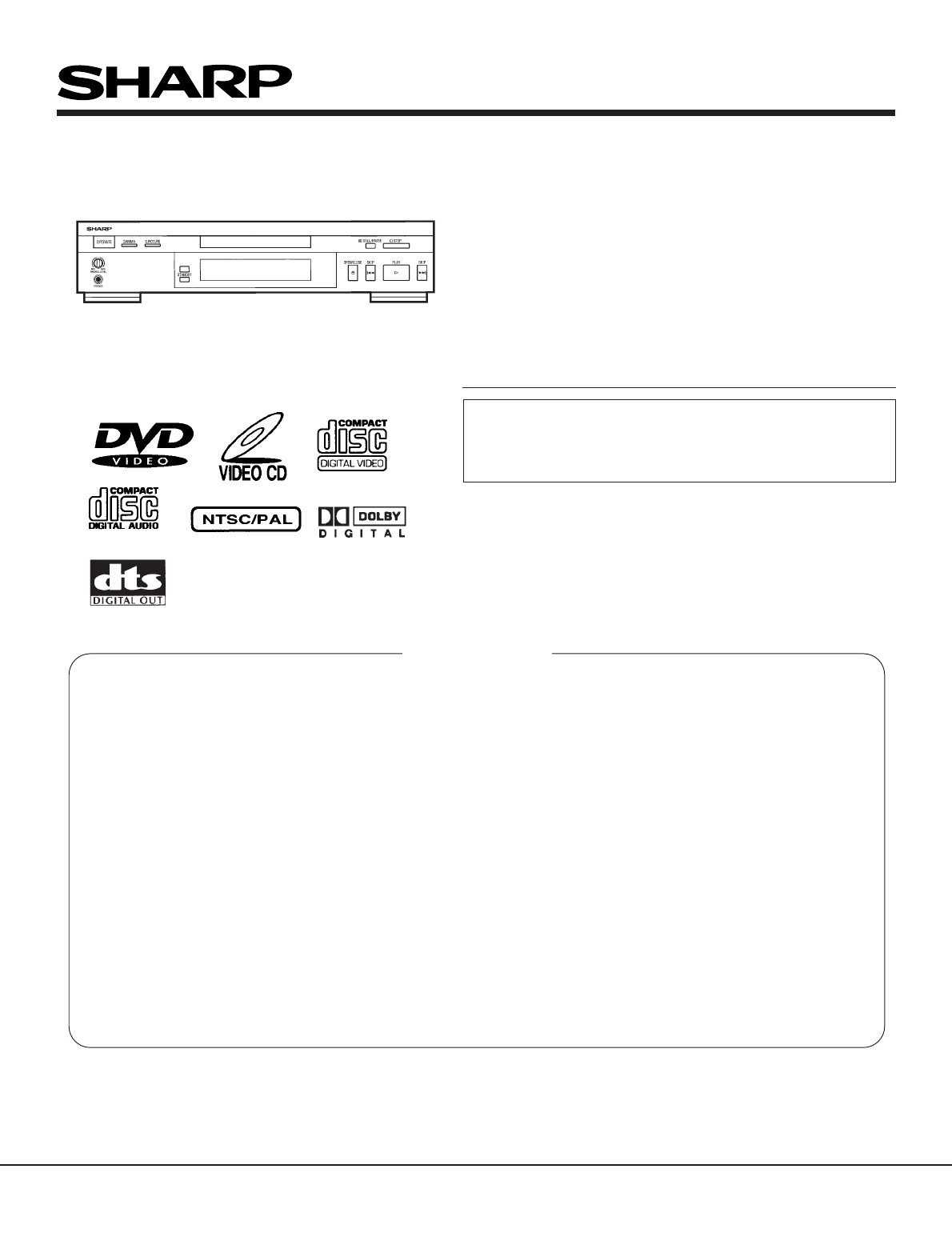
• Plays DVD, video CD and CD (Digital Audio) discs
• Built-in Dolby Digital decoder supporting Dolby Pro Logic*1 decoding and Virtual Surround
• For the audio on a DVD disc recorded in MPEG Audio Version 2.0 multi channel (5.1ch)
• New Digital Gamma correction and New Digital Super Picture functions
• Separate colour component output connectors (Y, PB (CB) and PR (CR))
• DTS*2 AUDIO DECODER (DIGITAL THEATRE SYSTEM)
*1 Manufactured under license from Dolby Laboratories. "Dolby", "Pro Logic" and the double-D symbol are trademarks of
Dolby Laboratories.
*2 "DTS" and "DTS Digital Surround" are trademarks of Digital Theater Systems, Inc.
3. SPECIFICATIONS
Signal System: NTSC/PAL
Video output: Output connector: Pin-jack
Output level: 1 Vp-p (75Ω)
S video output: Y output level: 1 Vp-p (75Ω)
C output level: 0.30 Vp-p (75Ω)
Output connector: S connector
Component colour output: Y output level: 1 Vp-p (75Ω)
PB (CB) output level: 0.525 Vp-p (75Ω)/75% colour
PR (CR) output level: 0.525 Vp-p (75Ω)/75% colour
Output connector: Pin-jack
Audio output: 5.1ch output: Front L/R, surround L/R, centre and subwoofer
5ch output: Front L/R, surround L/R and center
Output connector: Pin-jack
Output level: 2 Vrms (1 kHz, 0 dB)
Digital audio I/F: Optical digital output: Optical connector
Audio output: Coaxial digital output: Pin-jack
Headphone output: Output connector: Standard jack
Video signal horizontal resolution: 500 lines (DVD)
S/N ratio: 60 dB (DVD)
Audio signal frequency characteristics: For DVD linear PCM playback:
4 Hz to 22 kHz (48 kHz sampling)
4 Hz to 44 kHz (96 kHz sampling)
CD playback: 4Hz to 20 kHz (EIAJ)
(MPEG Audio 1/2)
S/N ratio: CD: 105 dB, 1 kHz (EIAJ)
Dynamic range: DVD linear PCM: 94 dB (EIAJ)
CD: 94 dB (EIAJ)
Total harmonic distortion ratio: CD: 0.005% or less (EIAJ)
Operating temperature: 5°C to 40°C
Storage temperature: –20°C to 55°C
Power supply : 220 V to 240 V AC, 50/60 Hz
Power consumption: 16 W
Dimensions: 430 mm × 351 mm × 97 mm (W × D × H) (Including attachments)
Weight: 3.8 kg
Specifications are subject to change without notice.
Weight and dimensions are approximate.
Digital Output
· The digital output format (optical or coaxial) used in this DVD player is linear PCM audio sampling at 44.1 kHz or 48 kHz.
Linear PCM sound for DVD video discs sampled at 96 kHz cannot be output digitally.
Check the disc jacket for information on the audio sampling used.
3-1. ACCESSORIES
Accessories: Video/audio cord x 1, UM3 battery x 2,
Remote Control Unit x 1, S-Video cord x 1
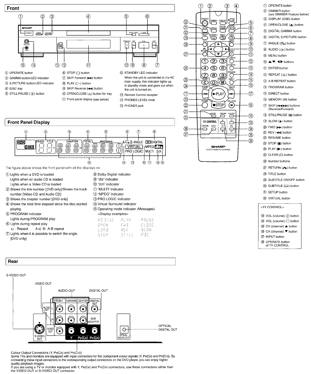
DV-760X
For details on the use of each control.
4. PART NAMES
4-1
DV-760X
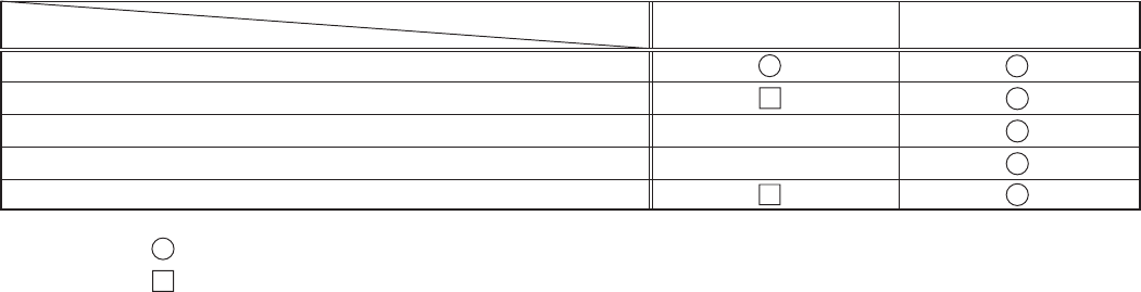
5. MAINTENANCE CHECK ITEMS AND EXECUTION TIME
Parts Maintained 1,000 hrs. 2,000 hrs.
Pickup
Spindle Unit
Sled Motor
Loading Motor
Belt
Note : Part Replacement
: Cleaning
(For cleaning, use a lint-free cloth danpened with pure isopropyl alcohol.)
Use the following table as a guide to maintain the mechanical parts in good operating condition.
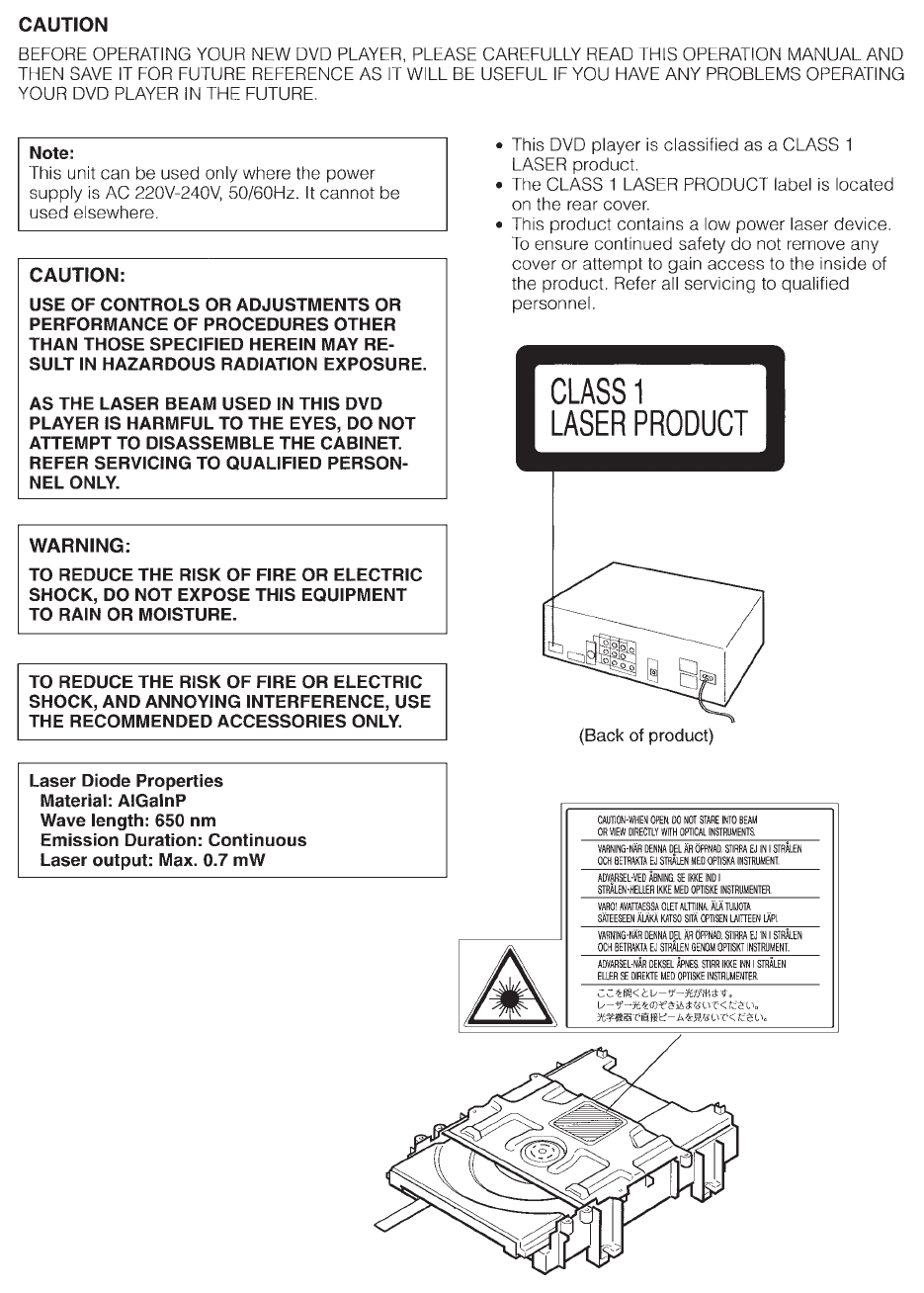
CARES WHEN USING THE PICKUP
1. The laser light having wavelength 650 nm is emitted from the objective lens. BE CAREFUL SO THAT THE LASER
LIGHT DOES NOT ENTER DIRECTLY INTO YOUR EYE.
2. The semiconductor laser may be easily damaged by electrostatic charges. When handling the pickup, take care so that
the electrostatic charge is not generated.
3. The semiconductor laser may be easily damaged by overcurrent. Use the power supply unit which does not give any
spike current when the power is turned on and off.
4. Carefully remove the dust and dirt from the objective lens with the lens blower.
When handling the objective lens, take due care so that it is not contaminated with fingerprint, etc. If the objective lens
is contaminated, impregnate the cleaning paper with a small quantity of solvent (isopropyl alcohol), and gently wipe to
clean.
5. The ozone layer depleting components (ODC) are not used in the production process for the product.
MECHANICAL PARTS REGUIRING PERIODICAL INSPECTION
5-1
DV-760X
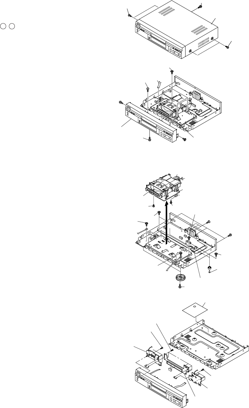
6. DISASSEMBLY AND REPLACEMENT OF MAIN PARTS
6-1. DISASSEMBLY
1.Remove five screws (A), and remove the cabinet.
Note: When assembling it, tighten the screws in
order of 1 - 2 .
(Because the set may rise a little by tightening
the screws.)
6-1
17. Remove five screws (T) which install the volume
PWB of the front panel.
18. Remove six screws (U) which install the display
PWB.
19. Remove six screws (V) which install the operate
PWB.
* The spacer and insulation seat under the indication
tube of (W) are bonded with both-side sticking tape.
7.Disconnect the lead lines (F) and (G) and (H) from
the main PWB under the mechanism.
8.Remove three screws (J) on both sides of the termi-
nal angle frame.
9.Remove three screws (K) which install the terminal/
power PWB.
10. Remove three screws (L) which install the terminal
block.
11. Remove three screws (M) of the display PWB.
12. Remove four screws (N) of the mecha angle.
13. Remove one screw (P) of the mecha angle.
14. Remove two screws (Q) of the decorative leg.
15. Push out the middle pin (R) of the setting leg in the
direction opposite to insertion. (Two places)
16. Remove two screws (S) which install the main
PWB under the mechanical unit.
2.Remove two screws (B).
3.Remove three screw (C).
4. Release the hooks of the front panel at two places on
both sides and at three places on the bottom, and
slide the front panel toward you.
5.Disconnect the connector (D).
6.Remove four screws (E) which installs the mechani-
cal unit.
Top Cabinet
(A) x2 1(A) 2
(A) x2 1
(D)
(E) x4
(B) x2
(C) x1
Front Panel
(C) x1
(C) x1
Remove it when you remove
a front panel because screw
catch is done with terminal
in the substrate (headphone)
and the angle from the panel.
(L) x3
(K)
(J) x3
(N) x4
(P) (R) x2
(K)
Terminal PWB
(Q) x2
(M) x3
(S)
(S)
(F)
(G) (H)
Mechanism
Main PWB
Volume PWB
(W)
Operate PWB
Display PWB
(V) x6
(T) x5
(U) x6
DV-760X
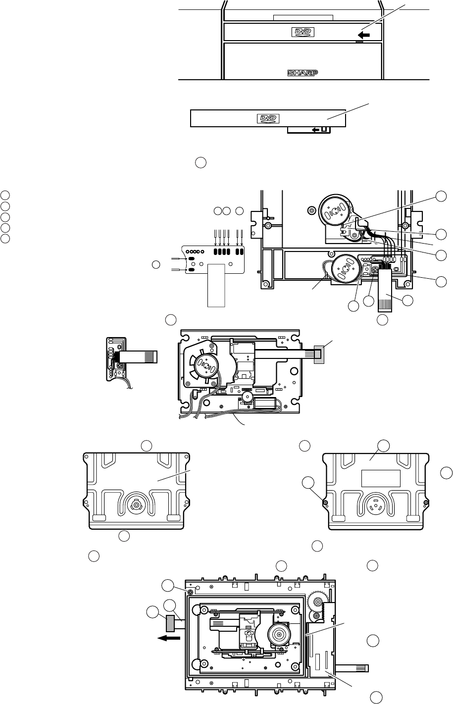
6-2. REPLACEMENT OF MAIN PARTS
<Disassembling and assembling procedure>
· Removing the tray (emergency ejection)
Removing the tray lock (set state)
VIDEO
Tray Decoration Panel
Insert a thin plate into the hatching part, slowly move the it in the arrow direction so that the tray is moved out a little in the arrow direction.
Note: In this state the tray cannot be removed completely.
· Drive Unit State
VIDEO
Tray Decoration Panel
Slowly move in the arrow direction, using the screwdriver having a fine head.
<Disassembling and assembling the mechanism chassis>
1. Remove the pickup FPC and loading relay FFC A from the main PWB.
Note: Fit the conductive rubber cap to the front end of pickup FPC (short-circuit).
2. Remove the solder joint of loading relay PWB at drive unit rear side.
1 Sled motor lead wire (Yellow·Orange)
2 IN SW lead wire 2 (White)
3 Spindle motor lead wire (Red·Black)
4 Loading motor lead wire (Red·Black)
5 Remove each lead wire from the claw.
1
1
2
3
4
3
2
4A
B
C
SLmotor 1
SLmotor 2
SW
GND
SP1
SP2
L motor2
L motor2
Black
Red
Red
Black
White
White
Orange
Yellow
Remove the lead wire.
Remove the lead wire.
3. Remove the relay PWB mounting screw B (M2.6S + 6S S tight), and remove the relay PWB C .
Relay PWB
Rear side of moving chassis assembly
Conductive rubber cap
(Earth sponge)
4. Disassembling the mechanism chassis moving chassis assembly
(1) Remove the four M2.6 screws A , and remove the clamped top plate B .
P tight screw
with M2.6 washer
A
A
B
(2) Remove the M2.6 screw C .
(3) Holding aslant upward the mechanism chassis moving chassis assembly D in the arrow direction, remove.
Note: The slide rack E must be moved to the left side as shown in diagram.
Take care so that the lead wires, especially the earth sponge G at the pickup FPC F front end, must not beremoved.
Slide rack
Mechanism chassis moving
chassis assembly
P tight screw with
M2.6 washer
G
C
F
E
D
Clamper top
plate rear side
6-2
DV-760X
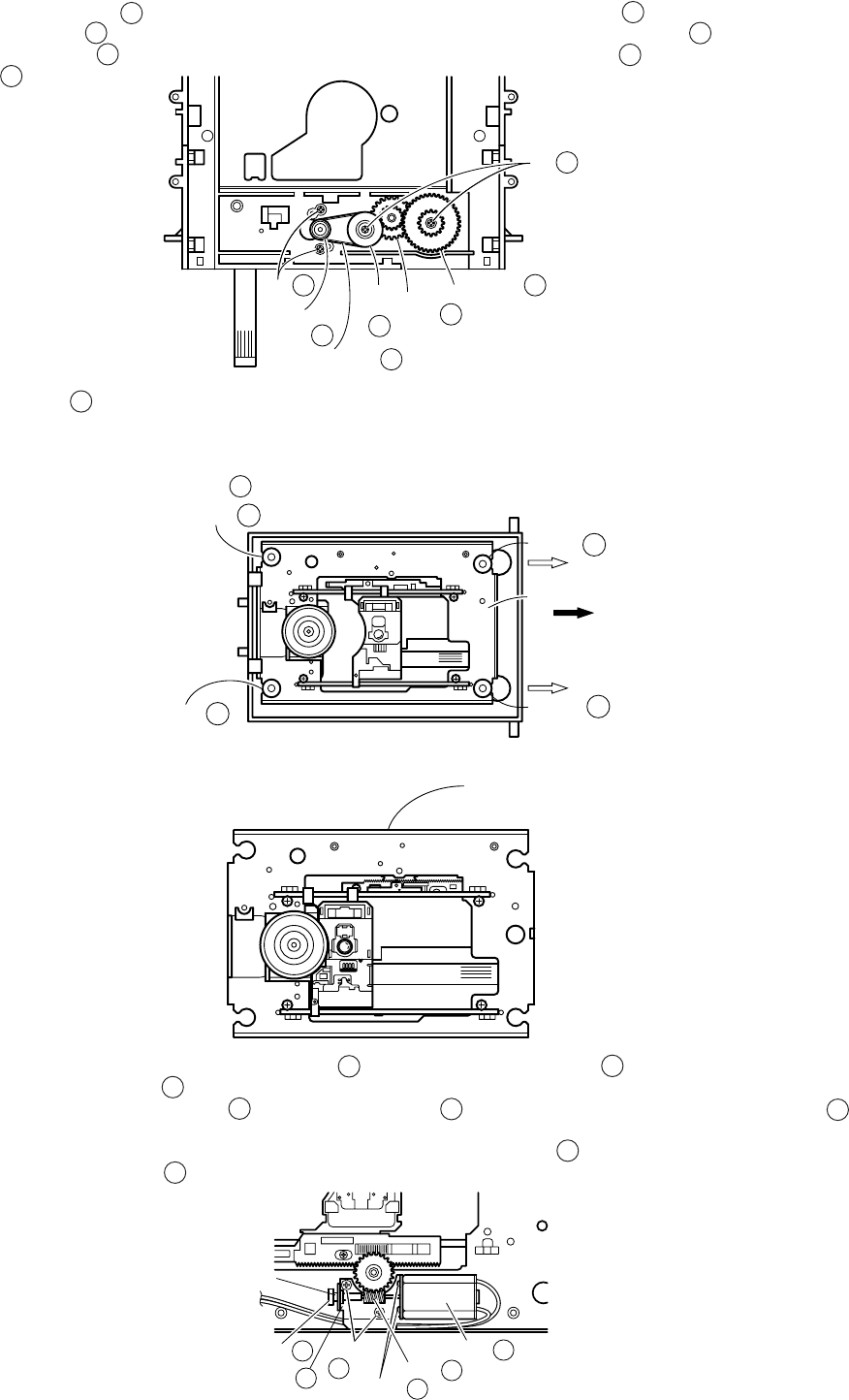
8. Replacing the Sled Motor
(1) At the rear side of chassis remove the two M1.7 screws A , and remove the motor angle B .
(2) Remove the thrust holding screw C (for easier removing wipe off the thread lock).
(3) Remove the two motor fitting screws M1.4 D , and replace the motor E . Motor is replaced in the state while the worm F is
kept press-fitted to the output shaft.
Note: When installing the motor, take care so that the worm does not damage the ANG B hole.
(4) Screw in the thrust holding screw C , adjust the worm front end clearance to 0 to 0.1 mm, and apply screw lock.
5. Disassembling the loading drive system
(1) Remove the two M2 screws A . (4) Remove relay gear 2 E .
(2) Remove the tray pinion B . (5) Remove the two M1.7 screws F .
(3) Remove the relay gear 1 C together with the (6) Remove the L motor G (with pulley) downward.
timing belt S D .
M2
M1.7
L·Motor Pulley
L·Motor
Timing belt S
Relay
gear1 Relay
gear2
Tray pinion
A
B
E
C
D
G
F
6. Disassembling the mechanism chassis from the moving chassis
(1) Remove the insulator B (2 pcs. at the right side in diagram) parallel in the arrow direction.
(At this time it is better to insert the fine head of screw driver at the ID side of insulator and to move in the arrow direction, which
facilitates removal.)
(2) Remove the mechanism chassis in the arrow direction, pulling upward aslant.
At this time take care so that the insulator C (left side, 2 pcs.) is not damaged. (Do not put at once the mechanism chassis
assembly.)
Insulator
Insulator
Insulator
Insulator
Mechanism chassis
C
B
B
C
7. Replacing the pickup and the spindle motor
Since the pickup optical axis and turntable inclination of DVD are adjusted with higher accuracy than of CD/MD, make a replacement
as a mechanism service chassis ass'y (refer to Parts List).
Thrust holding screw
Apply screw-lock.
M1.4 screw
M1.7 screw
Motor Angle BA
D
Worm F
Sled motor E
C
Mecha chassis Ass'y
6-3
DV-760X
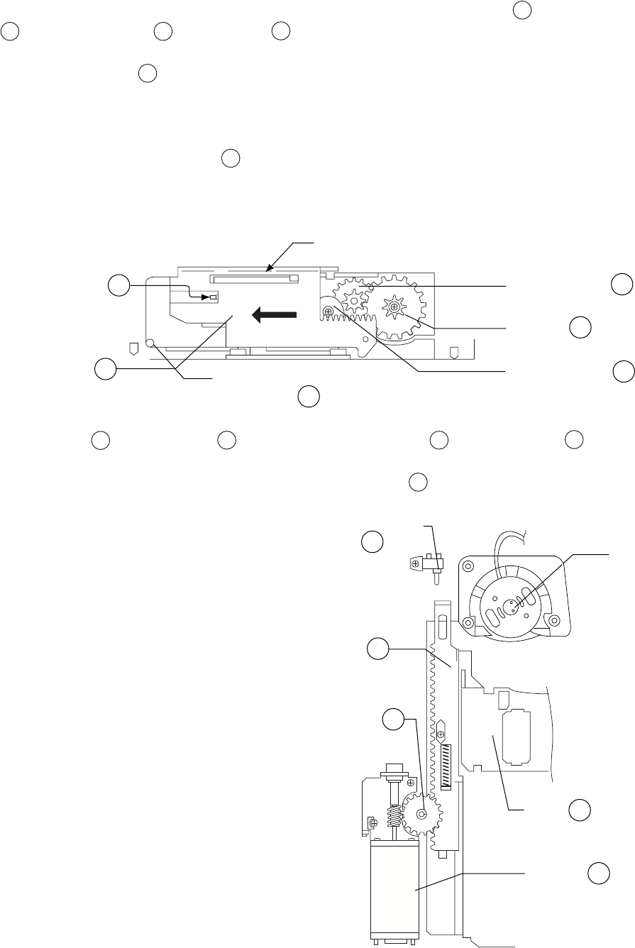
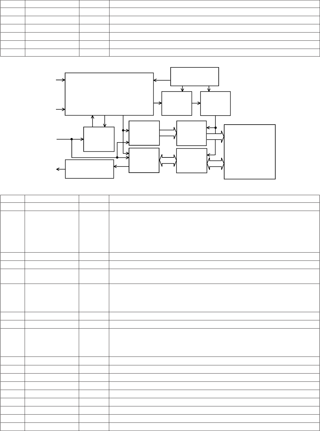
7. EXPLANATION OF MECHANISM
(1) Tray loading mechanism
When the tray loading motor rotates counterclockwise, motion is transmitted to the slide rack D through the intermediate
gear 1 A , intermediate gear 2 B and tray pinion C , resulting in insignificant motion in the arrow direction.
The slide rack is linked with the operating chassis. It lowers the pickup mechanism.
The protrusion of slide rack E is linked with the tray through the groove at the rear side of tray, so that the tray is
pushed ahead a little. When the tray is pushed out, the slide rack is disconnected from the tray pinion, and at the same
time the gear at the rear side of tray is connected with the tray pinion, and the tray is pushed ahead.
When the tray is pushed out fully, the slide rack moves further in the arrow direction through the groove at the rear side
of tray. The tray position detection switch F is turned on, and the tray loading motor stops.
When the tray closes the operation is as follows. If the tray OPEN/CLOSE button or tray is pressed and the detection
switch is turned off, the tray loading motor rotates clockwise, so that the tray is retracted. When the detection switch
is turned on again, the tray loading motor stops.
Intermediate gear 2
Intermediate gear 1
Tray pinion
Pawl linked with the groove at the
rear side of tray
This groove is linked with the pawl of
pickup mechanism.
Tray position detection switch
Slide rack
F
D
E
B
C
A
Sled motor
Pickup
Sled pinion
Rack
Pickup
Position detection
switch
Spindle motor
E
C
B
A
D
(2) Pickup feed mechanism
When the sled motor A rotates, the rack C moves through the sled pinion B so that the pickup D is moved to the
internal or external periphery.
When it is moved to the innermost periphery, the position detection switch E is pushed by the rack, so that the position
of pickup is initialized.
(3) Disc rotation mechanism
The spindle motor is used to rotate.
IC701 is used to control.
When the spindle motor is replaced, replace the
spindle unit.
7-1
DV-760X
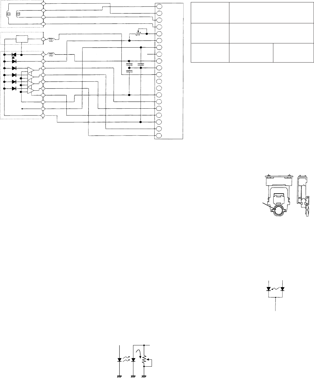
8-3. POLARITIES OF SIGNAL
8. OPERATION OF PICKUP
8-1. CIRCUIT CONFIGURATION OF PICKUP
The pickup unit reads signals from the disk, and the flexible cable is connected to the board. The following signals flow through the
cable.
8-2. EQUIVALENT CIRCUIT OF PICKUP
FO+
TR–
TR+
FO–
ACTUATOR
OSC VOS
LD
PD
VA
VB
VC
VD
Sga
Vraf
Vcc
GND
–
+
–
+
–
+
–
+
HOLOGRAM LASER UNIT
1
2
3
4
5
6
7
8
9
10
11
12
13
14
15
16
17
18
19
20 1
TR–
FO+
TR+
FO–
VR
PD
VCC
GND
LD
GND
VOS
NC
NC
Vref(VCC/2)
VA
VC
Sga
GND
VB
VD
(NC)
Power adjust
HIGH-FREQUENCY CONVOLUTION
Focus When electric current is flowed
FO+, FO- from FO+ to FO-, the lens comes
to near the disk.
Tracking When electric current is flowed
TR+, TR- from TR+ to TR-, the lens goes
toward the outer circumference.
Gain switching DVD one Layer High gain
Sga DVD two Layer Sga : +5V
CD
8-4. SIGNALS OF PICKUP
8-4-1. Tracking drive signal (TR+, TR-)
The signal drives the tracking servo mechanism which projects the beam on the track by moving the objective lens (OL) to the outer
or inner circumference (at a right angle against the track) of the disk.
2-focus objective lens
Actuator assembly
Monitor Diode
Basic Structure of Laser Diode
Laser Diode
LD PD
8-1
8-4-2. Focus drive signal (FO+, FO-)
The signal drives the focus servo mechanism which aligns the focus on the pit of the disk
by elevating OL (vertically against the disk surface.)
The VR terminal is connected to GND.
8-4-3. Monitor Diode (PD)
Since the laser diode largely varies output of the laser light even if the flowing current is slightly varied, the projection
light is detected with the monitor diode to control the laser light to be equally output.
Since the current varies on the monitor diode according to the intensity of the received light of the laser diode, the drive current of
the laser diode is reduced if the current of the monitor diode increases. On the contrary, the drive current of the laser diode is increased
if the current of the monitor diode decreases.
As the projection light of the laser diode becomes stronger, the current of the monitor diode increases to increase the current which
flows into the monitor diode output (PD). This is input to the pin 44 of IC303 and is compared with the reference voltage to control
the drive current of the laser diode.
The circuit is called ALPC (Automatic Laser Power Control).
8-4-4. Laser diode drive current control (LD)
Power supply to drive the laser diode
8-4-5. High-frequency convolution module power supply (VOSC)
The high-frequency convolution imposes the high-frequency signal on the DC current to impose the high frequency on the drive
current of the laser. Thus, the interference of outgoing light and reflected light is prevented.
8-4-6. HF Signal (VA, VB, VC, VD)
Signals recorded in the disk When the quantity of laser light increases, the current shown in
figure increases and the PD terminal voltage rises.
IC303 is used to control. The LD terminal voltage lowers, and
the quantity of light reduces. (IC303 is actuated by voltage
input.)
DV-760X
9-1
9. TEST MODE
Test Mode A power source is put, and a playback key and a stop key are pushed after the "NO DISC" display at the same
time. (It keeps pushing it for about three seconds.)
ROM Renewal Mode A power source is put with pushing a playback key and a halt key at the same time.
(It keeps pushing it for about three seconds.)
[TEST MODE]
The preparation date display of the program
10000000 ∗∗∗∗∗∗∗∗
(Last updata)
Model number display
10000001 00007604
(Model number)
The version display of the program
10000002 ∗∗∗∗∗∗∗∗
(Program ver.)
Reagion number display
10000003 00000008
(Region code:Binary display)
Color bar display
20000001 00000000 (FIP)
Micro-code number display
10000004 ∗∗∗∗∗∗∗∗
(Microcode ver.)
The preparation date display of the servo program
10000005 ∗∗∗∗∗∗∗∗
(Servo ver.)
It is returned to the test mode initial image plane.
It is returned to the test mode initial image plane.
<The "2" key of the remote controller is pushed.>
<The "1" key of the remote controller is pushed.>
Test mode initial image plane
F0000000 00000000
The "playback" key of the remote controller is pushed.
The "playback" key of the remote controller is pushed.
The "playback" key of the remote controller is pushed.
The "reactivation" key of the remote controller is pushed.
The "playback" key of the remote controller is pushed.
The "playback" key of the remote controller is pushed.
The "playback" key of the remote controller is pushed.
There is no copy guard signal.
As for the symptom when it was
dubbed in the video tape recorder?
Color bar display
20000002 00000000 (FIP)
The "playback" key of the remote controller is pushed.
AGC only
As for the symptom when it was
dubbed in the video tape recorder?
Color bar display
20000003 00000000 (FIP)
The "playback" key of the remote controller is pushed.
AGC+Color stripe1
As for the symptom when it was
dubbed in the video tape recorder?
AGC+Color stripe2
As for the symptom when it was
dubbed in the video tape recorder?
Color bar display
20000003 00000000 (FIP)
To (1)
The all FIPs burning
40000000 00000000 (OSD only)
<The "4" key of the remote controller is pushed.>
The "4" key of the remote controller is pushed.
Model name Model number
DV-750 00007503
DV-750TK 00007503
Model name Reagion cord
DV-750 00000004
DV-750TK 00000004
Micro-code is the thing of the process
program of the system integrated circuit.
DV-760X
9-2
Mecah test mode display
3000E000 EEEEEEEE
<Disk is put, and the "2" key of the remote controller is pushed.>
*It is usually returned in power source off for the state.
<The "3" key of the remote controller is pushed.>
<The "OPEN/CLOSE" key of the remote controller is pushed.>
The "OPEN/CLOSE" key of the remote controller is pushed.
Or, a tray is pushed by hand.
<The "1" key of the remote controller is pushed.>
When it failed in servo initialization.
It is returned to the test mode initial image plane
by pushing "the playback" of the body and a
"stop" key at the same time.
Laser test mode display
0D000100 00000000
The "playback" key of the remote controller is pushed.
A playback key and a stop key are pushed at
the same time, and it is returned to the test mode
initial image plane.
Light is sent out by DVD laser, and a spindle
motor rotates, and a pickup is moved to the
circumference.
DD000100 00000000
The "1" key of the remote controller is pushed.
Note:Not to face the light of the laser squarely,
caution!
The "playback" key of the remote controller is pushed.
The "playback" key of the remote controller is pushed.
From (1)
To (2)
Mecah test mode display
30000000 00000000
Tray eject failure
3000E001 EEEEEEEE
When it failed in tray eject
It is returned to the test mode initial image plane
by pushing "the playback" of the remote
controller and a "stop" key at the same time.
Tray eject success
30000001 00000000
Tray load failure
3000E002 EEEEEEEE
When it failed in tray load
It is returned to the test mode initial image plane
by pushing "the playback" of the remote
controller and a "stop" key at the same time.
Tray load display
30000002 00000000
DDT mode
0D000100 00000000
DDT step 1
DD000201 ∗∗++--00
DDT mode
0D00E201 000000EE When a disk is not in.
It is executed to focus on of DDT.
Focus offset value(∗∗)
Track offset value(++)
0 layer focus balance value(--)
The "playback" key of the remote controller is pushed.
DDT step 2
DD000202 ∗∗++0000
After track balance adjustment is done, a track, slead on are done.
Track offsete value(∗∗)
Track balance value(++)
The "playback" key of the remote controller is pushed.
DDT step 3
DD000203 ∗∗++--00
A two-layer disk does RF gain adjustment, and a CD does track balance readjustment.
Just focus adjustment is done after the completion.
0 layer focus balance value(∗∗)
Track balance value(++)
0 layer RF gain value(--)
The "playback" key of the remote controller is pushed.
DDT step 4
DD000204 ∗∗000000
Focus gain adjustment is done.
0 layer focus gain value(∗∗)
The "playback" key of the remote controller is pushed.
DDT step 5
DD000205 ∗∗++0000
Track gain adjustment is done. RF gain readjustment is done after the completion.
Track gain value(∗∗)
0 layer RF gain value(++)
DDT step 6
DD000206 ∗∗++0000 (DVD)
DD000206 ∗∗++--000 (CD)
A two-layer disk does just focus of layer 1 and focus gain adjustment.
A CD does reading of TOC.
DVD mode
1 layer focus gain value(∗∗)
1 layer focus balance value(++)
CD mode
0 layer focus gain value(∗∗)
0 layer focus balance value(++)
The corrected front 0 layer focus balance value(--)
DV-760X
9-3
The "playback" key of the remote controller is pushed.
The "playback" key of the remote controller is pushed.
From (2)
Servo version display
F1000001 ∗∗∗∗∗∗∗∗
Focus offset value display
F1000002 ∗∗00∗∗00
The "playback" key of the remote controller is pushed.
Track offset value display
F1000003 ∗∗00∗∗00
The "playback" key of the remote controller is pushed.
0 layer focus balance value display
F1000004 ∗∗00∗∗00
The "playback" key of the remote controller is pushed.
1 layer focus balance value display
F1000005 ∗∗00∗∗00
The "playback" key of the remote controller is pushed.
Track balance value display
F1000006 ∗∗00∗∗00
The "playback" key of the remote controller is pushed.
0 layer focus gain value display
F1000007 ∗∗00∗∗00
The "playback" key of the remote controller is pushed.
1 layer focus gain value display
F1000008 ∗∗00∗∗00
The "playback" key of the remote controller is pushed.
Track gaine value display
F1000009 ∗∗00∗∗00
The "playback" key of the remote controller is pushed.
RF swing value display
F100000A ∗∗00∗∗00
The "playback" key of the remote controller is pushed.
RF gain value display
F100000B ∗∗00∗∗00
The "playback" key of the remote controller is pushed.
The "playback" key of the remote controller is pushed.
The inside switch ID value display
F100000C ∗∗∗∗∗∗∗∗
[ROM RENEWAL MODE]
1. A DVD itself and a personal computer are articulated as the right figure. Software for the renewal is started more.
2. A power source is put with pushing a DVD's own playback key and a halt key at the same time. (It keeps pushing it for about three
seconds.)
3. When "a lateral" is inputted in accordance with the personal computer display and data transfer indication is shown and renewal
process is started normally when an ENTER key is pushed.
4. When renewal is completed normally.
R : OK It is displayed.
W : STR It is displayed.
W : END It is displayed.
Personal computer
(DOS)
DVD itself
DIGITAL It is articulated to the
OUT terminal connection child.
Fixture for the ROM renewal
DV-760X
10-1
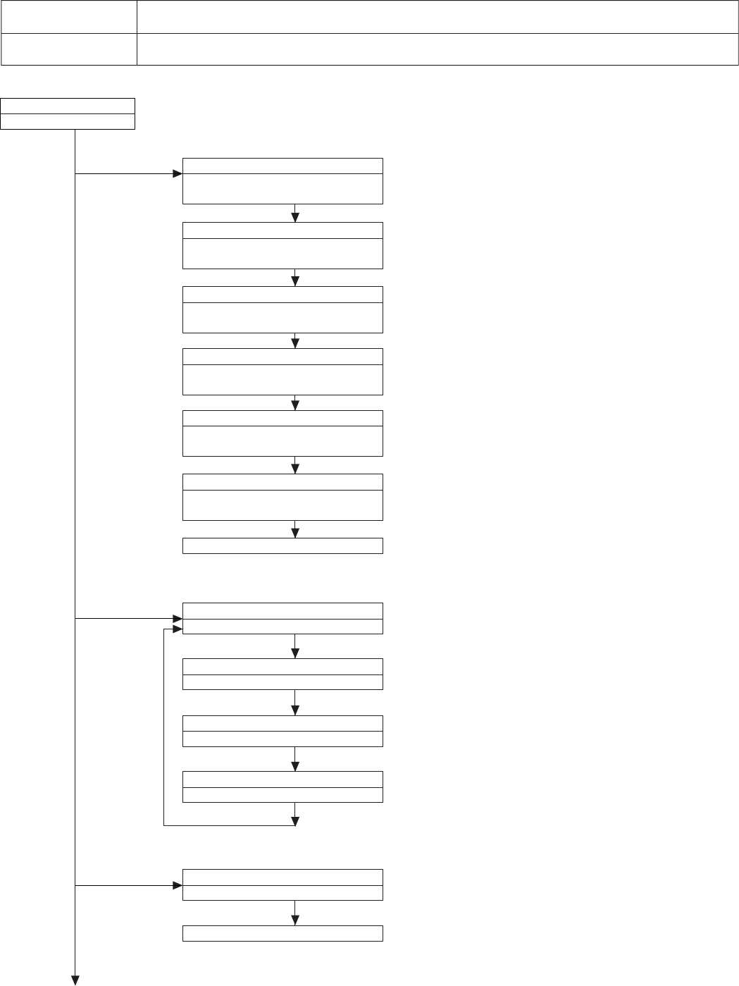
10. TROUBLESHOOTING
FLOW CHART NO.1
The power cannot be turned on.(1)
Is the fuse normal?
See FLOW CHART No.3 <The fuse blows out.>
No
No
Is normal state restored when once unplugged
power cord is plugged again after several
seconds?
Replace the fuse.
Yes
Yes
No
Is the AT 5V line voltage normal?
Check for leak or short-circuiting of primary
circuit component?
(Q9008,Q9010,D9016,T9001,D9012-3,C9021-
2,etc)
Yes
Is the voltage of AT 12V, AT -30V and filament
normal?
No Check each rectifying circuit of secondary circuit.
FLOW CHART NO.2
FLOW CHART NO.3
The fuse blows out.
Is there leaking or short-circuited primary
component?
No
The power cannot be turned on.(2)
Does the change from STANDBY LED indicate
turn-off?
No
Is the supply voltage of 5V fed to pins(15) and (16)
of IC8201? Check the AT 5V line.
Yes
No
Yes
No
Is the supply voltage about 5V fed to pin(3) of
IC8201? Check the IC8202.
Yes
No
Is there 4.0MHz oscillation at pins(1) and (2) of
IC8201? Check the FL8201 and IC8201.
Yes
No
Does the "L" signal inputted at pin(14) of IC8201,
when the POWER button activated on the DVD. Check the S8151 and POWER KEY line.
Yes
The STANDBY LED indicate it flashing after the
0.5sec.
No
Does the remote control "L" signal inputted at
pin(4) of IC8201, when the POWER button
activated on the remote control unit?
Check the line between the remote control
receiver and the pin(4) of IC8201.
Yes
Yes (below, confirmed operating at LED turn-off of 0.5sec interval.)
Check for short-circuiting of rectifying diode and
circuit in each rectifying circuit of secondary side.
Replace IC8201.
Yes
Replace IC8201.
No
Are the "P–CON(L)" pulse outputted from the
pin(7) of IC8201? Replace IC8201.
Yes No
Does the P–CON switch circuit is operate normally?
Check each component and if poor the replace.
Yes No
Are the "H" pulse inputted into the pin(9) of IC8201?
Check or replace D9035-9.
FLOW CHART NO.6
The fluorescent display tube does not light.
No
Is the supply voltage of 5V fed to pin(18) of
IC5001? Check the AT 5V line.
Yes No
Is the supply voltage of -30V fed to pin(16) of
IC5001? Check the AT -30V line and Q9025.
Yes No
Is there 4.0 MHz oscillation at pins(19) and (20) of
IC5001? Check FL5001, IC5001 and their periphery.
Yes No
Check the signal lines of FIP DA, FIP CK, FIP CS
of IC5001 and IC504. Check or replace IC5001 and IC504.
FLOW CHART NO.7
The key operation is disabled.
No
Is key switch contact and installation state? Replace key switch.
Yes
Is the control voltage normally into the pins(95)
and (96) of IC504?
No Check the power circuit,D5001 and Q9026.
No Check that the fluorescent display tube is free from
damages such as crack.
Yes
Are the filament voltage applied between (1) and
(62) of the fluorescent display tube?
Also negative voltage applied between these pins
and GND.
Yes
Check the fluorescent display tube and its periphery.
FLOW CHART NO.4
When the output voltage fluctuates.
No
Does the secondary side photocoupler circuit
operate normally? Check the circuit and replace the parts.
(D9020, D9041, D9046, Q9028, etc.)
Yes
No
Does the primary side photocoupler circuit
operate normally? Check the circuit and replace the parts.
(D9020, D9023, D9040, etc.)
FLOW CHART NO.5
When buzz is heard from the vicinity of power circuit.
Check for short-circuiting of rectifying diode and circuit in each rectifying circuit of secondary side.
(D9005-8,D9025,IC9001-3,Q9020-27,etc.)
Yes
Replace D9020.
KEY-1/2 INPUT
5.0V
4.3V
3.8V
3.1V
2.4V
1.9V
1.3V
0.6V
0V
OFF
S8106
STOP
S8105 S8154
S8104
S8103
S8101
S8153
STILL/PAUSE GAMMA
SKIP(+)
SKIP(-)
S.PICTURE
PLAY
KEY–1 KEY–2
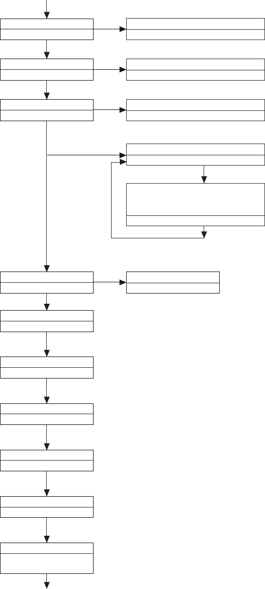
DV-760X
10-2
FLOW CHART NO.9
PC 9V is not output.
Is 12V voltage supplied at pin(3) of IC9001? No Check the secondary circuit, AT 12V and PC 12V
line.
Yes No
Is there output at pin(1) of IC9001? Check the IC9001 periphery circuit.
Yes
Check for load circuit short-circuiting or leak.
FLOW CHART NO.10
PC 3.3V is not output.
Is 5V voltage supplied at pin(1) of IC9003? No
Check the secondary circuit, AT 5V and PC 3.3V line.
Yes
Is there output at pin(2) of IC9003? No Check the IC9003 periphery circuit.
Yes
Check for load circuit short-circuiting or leak.
FLOW CHART NO.8
No operation is possible from the infrared remote control.
No
Operation is possible from the DVD, but no
operation is possible from the infrared remote
control.
Replace the remote control receiver or replace the
remote control transmitter is necessary.
Yes
Is 5V voltage supplied to the pin(3) terminal of
remote control receiver?
No Check AT 5V line.
Yes
Is the "L" pulse sent out pin(1) terminal of receiver
when the infrared remote control is activated?
Yes
Replace IC504.
No Replace the remote control receiver.
Yes
Is pulse signal supplied to the pin(32) of IC504? No Check the line between the remote control receiver
and the pin(32) of IC504.
FLOW CHART NO.11
The disc tray cannot be opened and closed.(For remote control is possible.)
No
Are the "L" pulse inputted into the pin(13) of
IC8201 when the KEY button is pressed? Check the S8102 and OPEN/CLOSE KEY line.
Yes No
Are the "L" pulse outputted from the pin(10) of
IC8201?
Replace IC8201.
Yes
No
Are the "L" pulse inputted into the pin(11) of
IC8201? Check the TRAY ACK(L) line.
Yes
See FLOW CHART NO.12<The disc tray cannot
be opened and closed.>
FLOW CHART NO.12
The disc tray cannot be opened and closed.
No
Is the signal from the pins(70) and (69) of IC504
input into the pins(6) and (7) of iC702? Check the LD-REV/FWD signal line between the
IC702 and the IC504.
Yes
No
Is loading motor drive voltage output from the
pins(10) and (11) of IC702?
Is 8V voltage applied to the pin(21) of IC702?
Yes
No
Is the loading motor drive voltage applied to the
pins(3) and (2) of AG connector?
Check the line between the IC702 and the AG connector.
Yes
Yes
Check for mechanism and gear engagement and
breakage.
Replace IC702.
Check AT 8V line.
No
No
No
No
Is FE signal inputted at pin(38) of IC707?
(Checking of symptom.)
Check the line between the pin(21) of IC303 and pin(38) of
IC707.
Yes
Yes
Is the focus control signal output to the pin(43) of
IC707? Check the IC707 power source periphery circuit.
If it is normal, replace IC707.
Is the focus control signal from the pin(43) of IC504
input into the pin(19) of IC702? Check the focus control signal (FOO) line between the
IC702 and the IC504.
Yes
No
Check the line between the IC702 and the AB connector.
No
Is the focus control drive voltage output from the
pins(17) and (18) of IC702?
Yes
Is the focus control drive voltage applied to the
pins(4) and (2) of AB connector?
Yes
Check the connection of optical pickup cable.
If it is normal, replace the optical pickup.
No
No
No
No
The disc is ejected.
(In case of focus error)
Does the objective lens of optical pickup move up
and down after the disc is removed?
(Checking of symptom).
See FLOW CHART NO.14<The disc is ejected. (In case
focus servo does not function.)>
Yes Yes Yes
Is FE signal output to the pin(21) of IC303 when the
disc is set?
Is there input signal on the pins (49, 54), (50, 55),
(46, 52), and (47, 53) of IC303?
Is there output signal on the pins(18),(17),(16) and (15) of
IC301?
Check the connection of optical pickup cable.
If it is normal, replace the optical pickup.
FLOW CHART NO.13
FLOW CHART NO.14
The disc is ejected.
(In case of focus servo does not function.)
Is 8V voltage applied to the pin(21) of IC702?
Yes
Replace IC702.
Check AT 8V line.
No
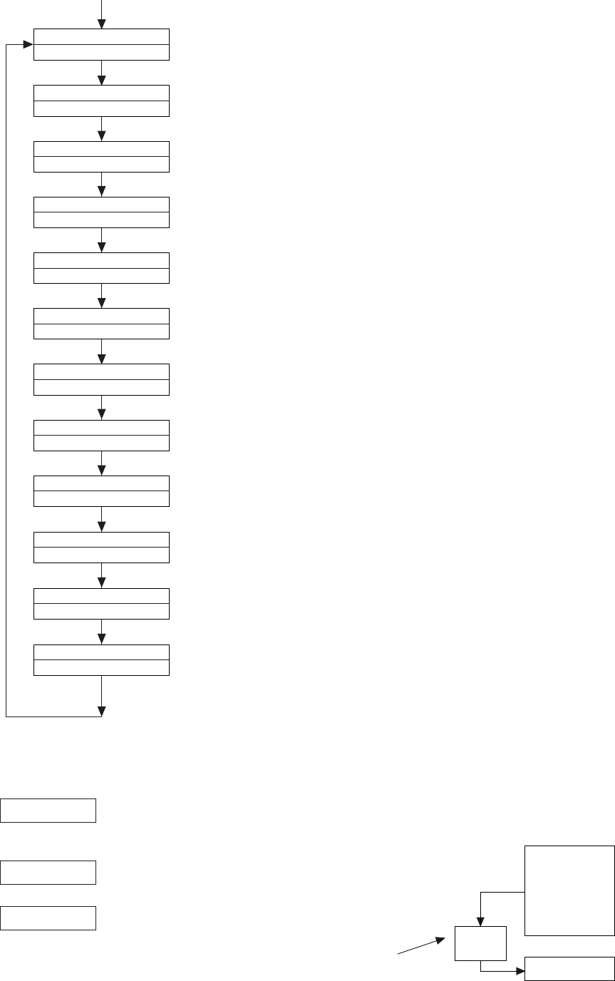
DV-760X
10-3
Yes
Check the connection of optical pickup cable.
If it is normal, replace the optical pickup.
No
No
Is the Q301 (LD POWER ON) drive signal (SEL)
output to the pin(52) of IC707?
Is the Q307 (LD POWER CTL) drive signal (LDO1)
output to the pin(45) of IC303?
(Checking of symptom.)
Is 3.3V voltage applied to the emitter of Q301 and,
5V voltage applied to the emitter of Q307?
Yes
Yes
Are the 3.3V and 2.3V voltage supplied to the
pins(11) and (9) of AB connector, respectively?
Check the D_3.3V (1) line and the A_5V line.
No
FLOW CHART NO.15
The disc is ejected.
(When the laser beam does not light.)
Check the line between the pin(52) of IC707 and the
base of Q301 through Q304.
Ceck the line between the pin(45) of IC303 and the
base of Q307.
No
Check the line between the Q301, Q307 and AB connector.
Yes
Replace the main PWB unit.
No
No
Set the disc on the disc tray.
Is it possible to hold normally the disc with the check?
Yes
Yes
Is the level of RF signal which is output from the
pin(28) of IC303, normal?
Yes
Check the video amplifier unit and the audio amplifier unit. (IC2004-4, IC801-3)
Check for contamination of objective lens of optical pickup.
FLOW CHART NO.16
Both picture and sound do not operate normally.
Check the loading switch.
No Replace the optical pickup unit.
No
No
Are the video signals outputted to the pins of
main unit connector CN801 and CN803?
CN803 5Pin CVBS
CN803 7Pin Y
CN803 9Pin C
CN801 25Pin Cb
CN801 27Pin Cr
CN801 29Pin Y
Check the line between the pins of main unit connector
CN801 and the pins of IC2007.
CN803 5Pin → IC2007 5Pin CVBS
CN803 9Pin → IC2007 2Pin C
CN803 7Pin → IC2007 12Pin Y
No
FLOW CHART NO.17
Picture do not operate normally.
Check the main unit. (Make sure that the IC201,
Q208-13 peripheral circuit.
Check the main unit.
(IC201, Q202-7 peripheral circuit.)
No Check the peripheral circuit of Cb/V DRIVE circuit
IC2003 from the pin(4) of IC2007.
No
No
No
No
No
Set the disc on the disc tray.
Yes
Are the video signals shown above input into the
pins of IC2007?
IC2007 5Pin CVBS
IC2007 2Pin C
IC2007 12Pin Y
Yes
Are the video signals outputted to the specific
output terminal?
Are the composite video signals outputted to
the VIDEO OUT terminal (J2001)?
Are the luminance signals outputted to the
S–OUT terminal (J2002)?
Are the chroma signals outputted to the
S–OUT terminal (J2002)?
Are the Cb signals outputted to the Cb OUT
terminal (J2001)?
Are the Y signals outputted to the Y–OUT
terminal (J2001)?
Are the Cr signals outputted to the Cr OUT
terminal (J2001)?
Check the peripheral circuit of S–YC DRIVE circuit
IC2002 from the pin(14) of IC2007.
Check the peripheral circuit of S–YC DRIVE circuit
IC2002 from the pin(15) of IC2007.
Check the peripheral circuit of Cb/V DRIVE circuit
IC2003 from the pin(25) of CN801.
Check the peripheral circuit of Cr/Y DRIVE circuit
IC2004 from the pin(29) of CN801.
Check the peripheral circuit of Cr/Y DRIVE circuit
IC2004 from the pin(27) of CN801.
No
Yes
Are the video signal outputted to each pins of
IC2007?
IC2007 4Pin CVBS
IC2007 15Pin S–C
IC2007 14Pin S–Y
Make sure that the level of pins(9), (10) and (11) of
IC2007 is "L" level.
Check or replace IC2007.
Check the V-MUTE line.
Yes
No
Yes
Check the main unit.(IC801-3)
Are the audio signals outputted to the pins of main unit connector CN801?
CN801 1Pin FRONT-L
CN801 3Pin FRONT-R
CN801 5Pin REAR-L
Yes
Are the audio signals output to the specific
outputted terminals?
No
Are the audio signals outputted to the FRONT–L/R
OUT terminal (J2001)?
Are the audio signals outputted to the REAR–L/R
OUT terminal (J2001)?
Are the audio signals outputted to the CENTER/
SUB WOOFER OUT terminal (J2001)?
No Check the peripheral circuit of AUDIO AMP. circuit
IC6001 from the pins(1) and (3) of CN801.
Check the peripheral circuit of AUDIO AMP. circuit
IC6002 from the pins(5) and (6) of CN801.
Check the peripheral circuit of AUDIO AMP. circuit
IC6002 from the pins(7) and (8) of CN801.
No
No
FLOW CHART NO.18
Sound do not operate normally.
Set the disc on the disc tray.
Yes
CN801 6Pin REAR-R
CN801 7Pin CENTER
CN801 8Pin SUB WOOFER

DV-760X
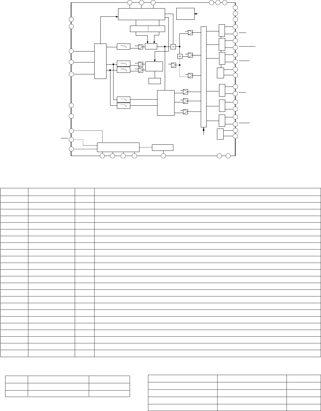
Pin No. Terminal name I/O Operation function
1 CVBS/Cb/B1 O Analog composite video signal output or Cb or B signal output current drive (positive)
2 CVBS/Cb/B1 O Analog composite video signal output or Cb or B signal output current drive (negative)
3 CVBS/Cb/B1 Vdd Power Supply for CVBS / Cb/B DAC1 circuit
4 Y/G 1 O Analog luminance or G signal output current drive (positive)
5 Y/G 1 O Analog luminance or G signal output current drive (negative)
6 Y/G 1Vdd Power Supply for Y/G DAC1 circuit
7 C/Cr/R 1 O Analog chrominance signal output or Cr or R signal output current drive (positive)
8 C/Cr/R 1 O Analog chrominance signal output or Cr or R signal output current drive (negative)
9 C/Cr/R 1Vdd Power Supply for C/Cr/R DAC1 circuit
10 DA Vss Ground for DAC circuit
11 Ibias 1 O Reference current for the 1st set of 3 DACs
12 VRef 1 Reference full scale voltage for the 1st set of 3 DACs
13 DA Vdd Power Supply for DACs
14 VRef 2 Reference full scale voltage for the 2nd set of 3 DACs
15 Ibias 2 O Reference current for 2nd set of the 3 DACs
16 NC No connect to pin
17 CVBS/Cb/B2 O Analog composite video signal output or Cb or B signal output current drive (positive)
18 CVBS/Cb/B2 O Analog composite video signal output or Cb or B signal output current drive (negative)
19 CVBS/Cb/B2 Vdd Power Supply for CVBS / Cb/B DAC2 circuit
20 Y/G 2 O Analog luminance or G signal output current drive (positive)
21 Y/G 2 O Analog luminance or G signal output current drive (negative)
22 Y/G Vdd Power Supply for Y/G DAC2 circuit
23 C/Cr/R 2 O Analog chrominance signal output or Cr or R signal output current drive (positive)
24 C/Cr/R 2 O Analog chrominance signal output or Cr or R signal output current drive (negative)
25 C/Cr/R 2Vdd Power Supply for C/Cr/R DAC2 circuit
26 ChipA I2C chip address select {0 : 40(hex)/41(hex) 1 : 1D(hex)/1E(hex)}
27 TEST I TEST pin (Ground)
28 DVss Ground for Digital circuit
29 CLOCK I 27MHz clock input
30 DVdd Power Supply for Digital circuit
31 Reset I Reset signal, active LOW
32 PAL/NTSC I NTSC/PAL select. This pin is sampledonly at Reset.(NTSC : Low PAL : High)
33 SO z(O) In SPI mode, serial data output / In I2C mode, grounded.
34 SDA/SI I/O(I) Serial data input, Open drain output / If SPI mode, serial data input
35 SCL/SCK I Serial clock
36 SEL I/(I) Connect to Ground / If SPI mode, this pin is chip select
37 DVdd Power supply for Digital circuit
38 DVss Ground for Digital circuit
39-46 DVIA7-0 I/O 8-bit Multiplexd Y/Cr/Cb 4:2:2 data (ITU Rec656/601) input (DVIA) or Multiplexd Y data
(ITU-Rec656/601) input in 16-bit input mode
47 Vmute I Video mute on Reset (0: normal, 1: mute)
48 C/Fsync/VBI I/O Csync/Frame sync input/output
49 F/Vsync I/O Frame sync or Vertical sync input/output
50 Hsync I/O Horizontal sync input/output
51 A/B sel I Switch control for 8-bit x 2 Mutiplexed 4:2:2 data (ITU Rec656/601) input (DVIA) or (DVIB)
52-55 DVIB7-4 I/O 8-bit Multiplexed 4:2:2 data (ITU Rec656-601) input (DVIB), or Multiplexed Cr/Cb data
(ITU Rec656/601) input in 16-bit input mode
56 DVss Ground for Digital circuit
57 DVdd Power Supply for Digital circuit
58-61 DVIB3-0 I/O Multiplexed 4:2:2 data (ITU Rec656/601) input (DVIB), or Multiplexed Cr/Cb data
(ITU Rec656/601) input in 16-bit input mode
62 TP I/O Test data input/output (Grounded)
63,64 NC No connect to pin (Ground)
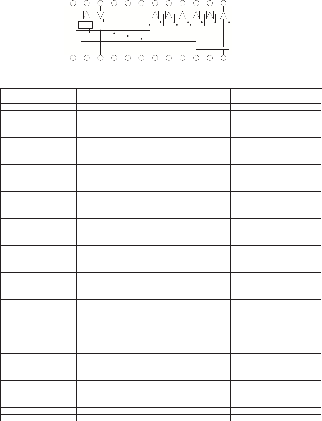
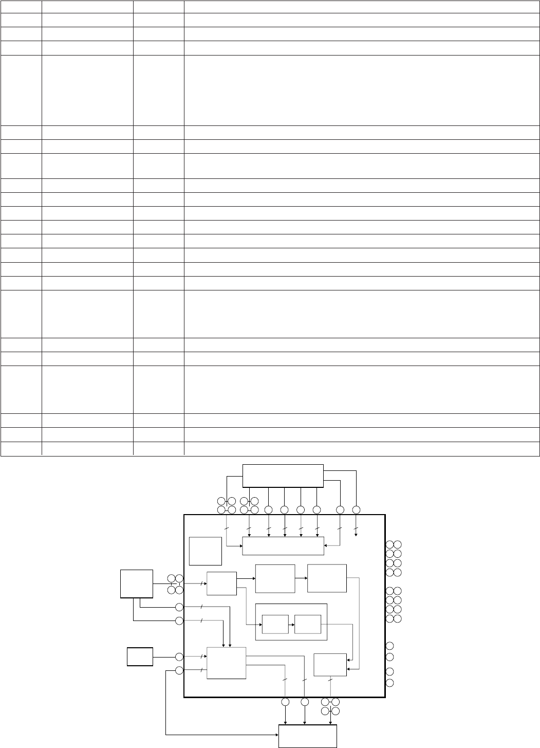
11. IC FUNCTION LIST
11-1. IC201 MC44724A DIGITAL VIDEO ENCODER
11-1
DV-760X
Pin No. Terminal name I/O Operation function
1 EIN I RF signal input. Input of RF signal output of optical pickup.
2 GND1 – Ground
3 S/DUAL I Single layer/dual layer selection signal input.
4 AIN I RF signal input. Input of RF signal output of optical pickup.
5 BIN I RF signal input. Input of RF signal output of optical pickup.
6 CIN I RF signal input. Input of RF signal output of optical pickup.
7 DIN I RF signal input. Input of RF signal output of optical pickup.
8 VrefIN I Reference voltage input. (2.1V)
9 FIN I RF signal input. Input of RF signal output of optical pickup.
10 GAINsel1 I Amp gain selection input 1.
11 VCC1 – Power terminal. (5.0V)
12 GAINsel2 I Amp gain selection input 2.
13 FOUT O RF signal output. Input RF signal is current-voltage-converted and output.
14 EOUT O RF signal output. Input RF signal is current-voltage-converted and output.
15 DOUT O RF signal output. Input RF signal is current-voltage-converted and output.
16 COUT O RF signal output. Input RF signal is current-voltage-converted and output.
17 BOUT O RF signal output. Input RF signal is current-voltage-converted and output.
18 AOUT O RF signal output. Input RF signal is current-voltage-converted and output.
19 VCC2 – Power terminal. (5.0V)
20 RFPOUT O Data read signal output. The same phase as MIXIN.
21 RFNOUT O Data read signal output. Reverse phase with respect to MIXIN.
22 MIXIN I Data read signal input.
23 MIXOUT O Data read signal output.
24 GND2 – Ground
• Block Diagram
• Mode selection table
GAINsel1 (Terminal 10) GAINsel2 (Terminal 12) Amp gain
L L +6dB
H, OPEN L -2dB
L H, OPEN +2dB
H, OPEN H, OPEN -6dB
Amp. gain selection
Layer S/DSEL (Terminal 3) Amp gain
Single L, OPEN 0dB
Dual H +10dB
Single layer/dual layer selection
11-2. IC301 IX1461GE RF PRE AMP.
H, V
Y
demux
Cb
Cr
Modulator
subcarrier
gen
off_set
0
0
0
CGMS,
WSS gen CC_gen
Sync_generator
BG
copy
protection bus
bus
TESTI2C/SPI
BIAS DAC DAC
DAC
30 37, 57
28
51
38, 56
39~46
52~55, 58~61
DVdd
DVss
DVIA [7:0]
DVIB [7:0]
A/B_sel
62
TP
29
Clock
26
Chip A
31
Reset
32
33
PAL/NTSC
SO
34
SDA/SI
35
SCL/SCK
36
SEL
27
TEST
10
DAVss
13
DAVdd
15 Ibias 2
14 Vref 2
24 C/Cr/R 2
23 C/Cr/R 2
18 CVBS/Cb/B 2
17 CVBS/Cb/B 2
21 Y/G 2
20 Y/G 2
11 Ibias 1
12 Vref 1
8C/Cr/R 1
7C/Cr/R 1
2CVBS/Cb/B 1
1CVBS/Cb/B 1
5Y/G 1
4Y/G 1
9C/Cr/R 1Vdd
3CVBS/Cb/B 1Vdd
6Y/G 1Vdd
25
C/Cr/R 2Vdd
19
CVBS/Cb/B 2Vdd
22
Y/G Vdd
50
Hsync
49
F/Vsync
48
C/Fsync/VBI
MC44724/5A
BIAS DAC DAC
Output Selector
DAC
0
0
0
0
0
0
0
RGB matrix
11-2
DV-760X
1 GND – GND terminal. –
2 P2TP I TE+input (CD) VrA
3 P2TN I TE–input (CD) VrA
4 LDO2 O Drive ouput –
5 MDI2 I Monitor input –
6 VrA O Analog VREF 2.1[V]
7 VrD O Digital VREF – Vdd 1/2
8 Vdd I Power terminal 4.2V (3.3V)
9 DPAC – DPD AC combination capacity 1 –
10 DPBD – DPD AC combination capacity 2 –
11 DPD1 – DPD integral capacity 1 –
12 DPD2 – DPD integral capacity 2 –
13 SCB I Control line (Bit clock) 2.2[V]
14 SCL I Control line (Latch signal) 2.2[V]
15 SCD I Control line (Sirial Data) 2.2[V]
16 VRCK I Reference clock input 2.3[V] When frequency is increased, the
filters excepting the servo LPF are
shifted to high frequency side.
17 VCKF –
Capacity for time constant adjustment
–
18 VccP – Power terminal –
19 LVL O Servo addition output Vrd x (1/2)
20 TEO O TE output VrD
21 FEO O FE output VrD
22 DFTN I DPD difect – Low DPD output: Mute
23 VccS – Power terminal (servo) –
24 RPZ O RF ripple center voltage VrD
25 RPO O RF ripple output VrD
26 RPB O RF ripple bottom –
27 RPP O RF ripple peak –
28 RFO O Equalizing RF output 2.3[V]
29 NC – NC terminal – To be connected to GND
30 NC – NC terminal – To be connected to GND
31 VccR – Power terminal (RF) –
32 DPDB I Pit depth adjustment VrD When D PDB is raised, the A/B
side delay increases.
33 TEB I TE balance VrD When TEB is raised, the TP side
gain increases and the A+C side
delay increases.
34 FEB I FE balance VrD When FEB is raised, the A+C (FP)
side gain increases.
35 PSC I VRCK frequency division ON/OFF – High: Frequency division OFF
36 Vcc2 – Power terminal –
37 NC – NC terminal VrD To be connected to VrD, or to GND
through C
38 EQD I Group delay correction VrD When EQD is raised, the group
delay increases at the right side.
39 GND2 – GND terminal. –
40 RFDC – DC feedback capacity –
Pin No. Terminal name I/O Operation function
Terminal DC Voltage(TYP.)
Remarks
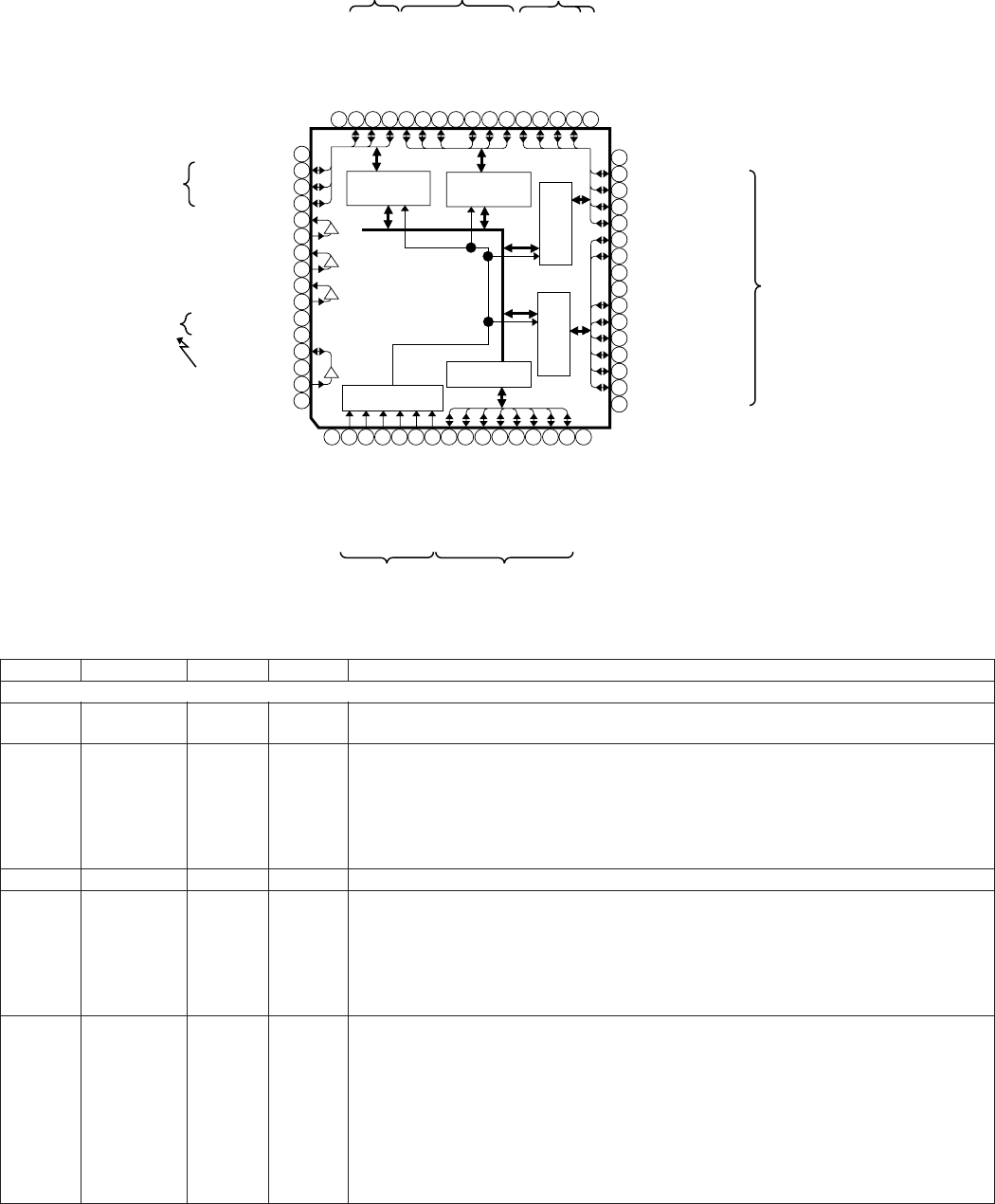
11-3. IC303 IX1517GE RF SIGNAL PROCESSOR
• Block Diagram
24 23 22 21 20 19 18 17 16 15 14 13
1 98765432 10 1211
MIX
EIN
CIN
BIN
AIN
S/DUAL
GND1
FIN
VrefIN
DIN
DOUT
FOUT
VCC1
GAINsel1
GAINsel2
RFPOUT
VCC2
AOUT
BOUT
COUT
EOUT
RFNOUT
GND2
MIXOUT
MIXIN
11-3
DV-760X
41 RFA O RF total addition output 2.2[V]
42 EQB I Boost adjustment VrD
When EQB is raised, the boost increases.
43 EQF I Frequency adjustment VrD When EQF is raised, shift to the
high frequency side occurs.
44 MDI1 I Monitor input –
45 LDO1 O Drive output –
46 P1TN I TE–input (DVD) VrA
47 P1TP I TE+input (DVD) VrA
48 NC – NC terminal – To be connected to GND
49 P1FN I FE–input (DVD) VrA
50 P1FP I FE+input (DVD) VrA
51 LDP1 I APC polarity 1 – Positive polarity when this terminal
is connected to Vcc.
52 P1DI I D input (DVD)
53 P1CI I C input (DVD) VrA
54 P1BI I B input (DVD) VrA
55 P1AI I A input (DVD) VrA
56 GNDR – GND terminal (RF) –
57 LDP2 I APC polarity 2 – Positive polarity when this terminal
is connected to Vcc.
58 P2AI I A input (CD) VrA
59 P2BI I B input (CD) VrA
60 P2CI I C input (CD) VrA
61 P2DI I D input (CD) VrA
62 GNDS – GND terminal (Servo) –
63 P2FP I FE+input (CD) VrA
64 P2FN I FE–input (CD) VrA
Pin No. Terminal name I/O Operation function
Terminal DC Voltage(TYP.)
Remarks
Terminal Terminal name Function
10~13,16~20,9 A0~A8,A9R Address input
8 RAS Row address strobe
23 CAS Column address strobe
2~5,24~27 DQ1~DQ8 Data input/Data output
22 OE Output enable
7 WE Light enable
1, 14 Vcc Power (5V)
15, 28 Vss Ground (0V)
6, 21 NC Not connected
11-4. IC401 IX1484GE 4M DRAM
P1FN
P1FP
LDP1
P1DI
P1CI
P1BI
P1AI
GNDR
LDP2
P2AI
P2BI
P2CI
P2DI
GNDS
P2FP
P2FN
DPDB
VccR
NC
NC
RFO
RPP
RPB
RPO
RPZ
VccS
DFTN
FEO
TEO
LVL
VccP
VCKF
NC
P1TP
P1TN
LDO1
MDI1
EQF
EQB
RFA
RFDC
GND2
EQD
NC
Vcc2
PSC
FEB
TEB
GND
P2TP
P2TN
LDO2
MDI2
VrA
VrD
Vdd
DPAC
DPBD
DPD1
DPD2
SCB
SCL
SCD
VRCK
12345678910111213141516
17
18
19
20
21
22
23
24
25
26
27
28
29
30
31
32
48 47 46 45 44 43 42 41 40 39 38 37 36 35 34 33
64
63
62
61
60
59
58
57
56
55
54
53
52
51
50
49
APC1
sel-RF
R-gain
Adjust EQ
F-gain
Adjust
F-gain
Adjust
RF Ripple
creation
FE creation
DPDTE
creation
FE-gain
Adjust
TE-gain
Adjust
Level detect
T-gain
Adjust
3BTE creation
APC2
B U S
Time
constant
adjustment
sel-PD
sel-PD
sel-PD
mode-TE
sel-FE
sel-IC
sel-TE
sel-DPD
sel-LVL
• Block Diagram
11-4

DV-760X
11-5. IC402 IX1474GE DEM/ECC (DVD)
Pin No. Terminal name I/O Operation function Remarks
1 DPCK1 I Signal processing reference clock input. 0.5-3.3Vp-p Feedback
resistor built in.
2 DVDD3 – Digital power. (3.3V) For logic cell
3 SVCK1 I Servo reference clock input. (Oscillation circuit input terminal) 3.3V-I/F Feedback
4 SVCK0 O Servo reference clock output. (Oscillation circuit input terminal) resistor built in.
5 DVSS – Digital power. (0V) For logic cell
6 DVDD2 – Digital power. (3.3V) For logic cell
7 N.C. – User use prohibited. Open
8 HDWR I MPU write signal. TTL level
9 HDRD I MPU read signal. TTL level
10 ECCCS I MPU chip selection. TTL level
11 D8 I/O MPU data bus. TTL level
12 D9 I/O MPU data bus. TTL level
13 D10 I/O MPU data bus. TTL level
14 D11 I/O MPU data bus. TTL level
15 D12 I/O MPU data bus. TTL level
16 D13 I/O MPU data bus. TTL level
17 D14 I/O MPU data bus. TTL level
18 D15 I/O MPU data bus. TTL level
19 DVSS – Digital power. (0V) For I/O cell
20 DVDD5 – Digital power. (5V) For I/O cell
21 HINT O MPU interruption signal. (Occurrence of interruption = “L”) OPEN DRAIN
22 HA0 I MPU address bus. TTL level
23 HA1 I MPU address bus. TTL level
24 PLCK I/O Read channel clock input/output terminal.
25 ED0 – User use is prohibited (N.C.) since it is for shipping adjustment. Open
26 ED1 –
27 ED2 –
28 ED3 –
29 ED4 –
30 ED5 –
31 ED6 –
32 ED7 –
33 TEST I For shipping adjustment. Set to “L”
34 PDON O PLL phase error signal output. (Negative polarity)
35 PDOP O PLL phase error signal output. (Positive polarity)
36 RLLD O RLL detection result output.
37 LPFN I PLL loop filter amp. reverse input.
38 LPFO O PLL loop filter amp. output.
39 VCOF O VCO filter terminal.
40 SLCO O Built-in comparator reference voltage output terminal.
41 AVSS – Analog power. (0V)
42 AVR O Non-PLL system analog reference potential. (1.65V)
43 VRC – Resistance division point potential. (For analog reference
potential generation: 1.65)
44 PVR O PLL system analog reference potential. (1.65V)
45 AVDD – Analog power. (3.3V)
46 RVR2 – 2nd reference voltage. (For capacitor connection)
47 RVDD – Exclusive-use power terminal. (3.3V)
48 RFIN I RF signal input.
49 RVSS – Exclusive-use power terminal. (0V)
50 RVR1 – 1nd reference voltage. (For capacitor connection)
51 DVR I DMO reference potential. (1.65V recommended)
52 DMO O Disc equalizer output for DVD. (Triple value PWM + HiZ)
53 RASN O External RAM row address selection. (Negative logic)
54 CASN O External RAM row address selection. (Negative logic)
11-5

DV-760X
Pin No. Terminal name I/O Operation function Remarks
55 MOEN O External RAM output permission signal.
56 MWEN O External RAM read/write selection.
57 DVSS – Digital power. (0V) For logic cell
58 DVDD3 – Digital power. (3.3V) For logic cell
59 MA9 O External RAM address bus.
60 MA8 O External RAM address bus.
61 MA7 O External RAM address bus.
62 MA6 O External RAM address bus.
63 MA5 O External RAM address bus.
64 MA4 O External RAM address bus.
65 MA3 O External RAM address bus.
66 MA2 O External RAM address bus.
67 MA1 O External RAM address bus.
68 MA0 O External RAM address bus.
69 DVSS – Digital power. (0V) For I/O cell
70 DVDD5 – Digital power. (5V) For I/O cell
71 MD7 I/O External RAM data bus. TTL level
72 MD6 I/O External RAM data bus. TTL level
73 MD5 I/O External RAM data bus. TTL level
74 MD4 I/O External RAM data bus. TTL level
75 MD3 I/O External RAM data bus. TTL level
76 MD2 I/O External RAM data bus. TTL level
77 MD1 I/O External RAM data bus. TTL level
78 MD0 I/O External RAM data bus. TTL level
79 SD7 O MPEG data output.
80 SD6 O MPEG data output.
81 SD5 O MPEG data output.
82 SD4 O MPEG data output.
83 DVSS – Digital power. (0V) For logic cell
84 DVDD3 – Digital power. (3.3V) For logic cell
85 SD3 O MPEG data output.
86 SD2 O MPEG data output.
87 SD1 O MPEG data output.
88 SD0 O MPEG data output.
89 SERR O MPEG data reliability flag. (Data error: “L”)
90 SOSO O MPEG output sector sync signal. (Sector top: “L”)
91 SVAL O MPEG data effective flag. (Effective state: “L”)
92 SDCK O MPEG data transfer clock.
93 DVSS – Digital power. (0V) For logic cell
94 SREQ I MPEG data request flag. (Request state: “L”) TTL level
95 RSTN I Hard reset input. (Reset state: “L”)
96 DVDD3 – Digital power. (3.3V) For logic cell
97 STDA O Operation state monitor data. Common with PWM.
(Output synchronizing with SDCK fall)
98 STCK O Operation state monitor sync signal. (Data top bit: “L”) Common with PWM.
99 UPWM O General-use PWM output. 4mA, 5V-I/F
100 DVSS – Digital power. (0V) For logic cell
11-6
DV-760X
11-6. IC501 IX1614GE FLASH
Symbol Type Name and function
Byte selection address: When the device is in the x8 mode, the low or high order byte is
DQ15/A-1 Input selected. It is not used in the x16 mode.
(If BYTE# is high, DQ15/A-1 input circuit does not operate.)
A0-A12 Input Word selection address: Selection of one word of 16k byte block. These addresses are
latched during data wiring operation.
A13-A17 Input Block selection address: Selection of 1/32 erase block. These addresses are latched
during data writing, erasing and lock block operation.
Low order byte data input/output: Command user interface writing cycle data and command
DQ0-DQ7Input/Output input. Various data read memory identifier and status data output Chip nonselection or output
disable: Float state
DQ8-DQ15 Input/Output High order byte data input/output: The function is the same as that of low order byte data
input/output. Operative only in x16 mode. x8 mode: Float state DQ15/A-1 is address.
CE# Input Chip enable: Device control logic, input buffer, decoder and sense amp. are activated.
Chip becomes active only when CE# is “Low”.
Reset/Power down: If RP# is set to “Low”, the control circuit is initialized when power is turned
on. Hence, the RP#pin is set to “Low”. When power is turned on or off or in case of fluctuation it
RP# Input is kept at “Low” so as to protect data from noise. When RP# is in “Low” state, the device is in
deep power down state. 480 ns is required to recover from the deep power down state. If the RP#
pin becomes “Low”, the whole chip operation is interrupted and reset. After recovery the device is set
to array read state.
OE# Input Output enable: When OE# is set to “Low”, data is output from the DQ pin. When OE# is
set to “High”, the DQ pin is set to float state.
Write enable: Command user interface, data Q register and address Q latch access is controlled.
WE# Input In “Low” state WE# becomes active. At rise edge the address and data are fetched.
Ready/busy: The state of internal write state machine is output. In “Low” state it is indicated that the
RY/BY# Output write state machine is in operation. If the write state machine waits for next operation instruction, erase
is suspended or it is in deep power down state, the RY/BY# pin is in float state.
Byte enable: When BYTE# is set to “Low”, the device is set to the x8 mode. At this time the
BYTE# Input DQ8-DQ15 pin becomes float state. Address A-1 selects high order/low order byte.
When BYTE# is “High”, the device is set to the x16 mode. The A-1 input circuit is disabled.
Vpp Write/erase power supply: 5.0 ± 0.5V is applied during writing/erasing.
Vcc Device power supply: 5.0 ± 0.5V
GND Ground
NC Nonconnection
• Block Diagram
ID
Register
CSR
ESRs
DQ
8-15
DQ
0-7
OUTPUT MULTIPLEXER
Program Erase
Voltage Switch
BYTE#
CUIWSM
16-KBYTE
Block 31
16-KBYTE
Block 30
16-KBYTE
Block 1
16-KBYTE
Block 0
CE#
OE#
WE#
RP#
RY/BY#
V
PP
V
CC
GND
Y GATING/SENSING
X-DECODER
Y-DECODER
Input
Buffer
ADDRESS
QUEUE
LATCHES
ADDRESS
COUNTER
A
-1.0~17
Output
Buffer Output
Buffer Input
Buffer Input
Buffer
I/O Logic
DATA
QUEUE
REGISTER
Register
Data
Comparator
11-7
DV-760X
11-7. IC504 IX1478GE SYSCON
MD
2
Vcc
Vcc
Vcc
Vcc
Vcc
Vss
Vss
Vss
Vss
Vss
Vss
Vss
Vss
PD
7
/D
15
PD
6
/D
14
PD
5
/D
13
PD
4
/D
12
PD
3
/D
11
PD
2
/D
10
PD
1
/D
9
PD
0
/D
8
PE
7
/D
7
PE
6
/D
6
PE
5
/D
5
PE
4
/D
4
PE
3
/D
3
PE
2
/D
2
PE
1
/D
1
PE
0
/D
0
PA
7
/A
23
/IRQ7
PA
6
/A
22
/IRQ6
MD
1
MD
0
PF
7
/ø
PF
6
/AS
PF
5
/RD
PF
4
/HWR
EXTAL
XTAL
STBY
RES
WDTOVF
NMI
PF
3
/LWR
PF
1
/BACK
PF
0
/BREQ
PG
4
/CS0
PG
3
/CS1
PG
2
/CS2
PG
1
/CS3
PG
0
/CAS
P6
7
/CS7/IRQ3
P6
6
/CS6/IRQ2
P6
5
/IRQ1
P6
4
/IRQ0
P6
3
/TEND1
P6
2
/DREQ1
P6
1
/TEND0/CS5
P6
0
/DREQ0/CS4
PF
2
/
LCAS/WAIT/BFEQO
P1
0
/PO8/TIOCA0/DACK0
P1
1
/PO9/TIOCB0/DACK1
P1
2
/PO10/TIOCC0/TCLKA
P1
3
/PO11/TIOCD0/TCLKB
P1
4
/PO12/TIOCA1
P1
5
/PO13/TIOCB1/TCLKC
P1
6
/PO14/TIOCA2
P1
7
/PO15/TIOCB2/TCLKD
P2
0
/PO0/TIOCA3
P2
1
/PO1/TIOCB3
P2
2
/PO2/TIOCC3
P2
3
/PO3/TIOCD3
P2
4
/PO4/TIOCA4
P2
5
/PO5/TIOCB4
P2
6
/PO6/TIOCA5
P2
7
/PO7/TIOCB5
P4
7
/AN7/DA1
P4
6
/AN6/DA0
P4
5
/AN5
P4
4
/AN4
P4
3
/AN3
P4
2
/AN2
P4
1
/AN1
P4
0
/AN0
Vref
AVcc
AVss
PA
5
/A
21
/IRQ5
PA
4
/A
20
/IRQ4
PA
3
/A
19
PA
2
/A
18
PA
1
/A
17
PA
0
/A
16
PB
7
/A
15
PB
6
/A
14
PB
5
/A
13
PB
4
/A
12
PB
3
/A
11
PB
2
/A
10
PB
1
/A
9
PB
0
/A
8
PC
7
/A
7
PC
6
/A
6
PC
5
/A
5
PC
4
/A
4
PC
3
/A
3
PC
2
/A
2
PC
1
/A
1
PC
0
/A
0
P3
5
/SCK1
P3
4
/SCK0
P3
3
/RxD1
P3
2
/RxD0
P3
1
/TxD1
P3
0
/TxD0
P5
0
P5
1
P5
2
P5
3
/ADTRG
ROM *
RAM
TPU
PPG
SCI
WDT
DMAC
DTC
H8S/2000 CPU
D/A converter
A/D converter
Clock oscillator
Interruption
controller
Bass Controller
Port D
Port FPort GPort 6
Port 5 Port 3 Port C Port B Port A
Port E
Port 1 Port 2 Port 4
Internal data bus
Peripheral data bus
Peripheral address bus
Internal address bus
131072 WORDS
X 8 BYS
(1024 ROWS
X126 COLUMNS
X8 BL9OCKS)
8
7
6
5
4
3
31
28
27
12
10
9
23
25
26
11
2
13
14
15
17
18
19
20
21
29
22
30
24
32
16
A4
A5
A6
A7
A12
A14
A16
A15
A13
A8
A0
A2
A3
A1
A9
A10
A11
I/O1
I/O2
I/O3
I/O4
I/O5
I/O6
I/O7
I/O8
R/W
CE1
CE2
OE
VDD
(5V)
GND
(0V)
ADDRESS INPUT
BUFFER
ROW
DECORDER
SENSE AMP.
OUTPUT
BUFFER
DATA INPUT
BUFFER
CLOCK
GENERATOR
COLUMN
DECODER
ADDRESS INPUT
BUFFER
ADDRESS INPUT
BUFFER
BLOCK
DECODER
11-8. IC506 IX1618GE 1M SRAM
11-8
DV-760X
11-9. IC507 BR93L46F EEPROM
Terminal Terminal name In/Output Function
2 VCC – Power
7 GND – All input/output reference voltage, 0V
3 CS Input Tip select input
4 CLK Input Sirial clock input
5 DIN Input Start bit, operation code, address and serial data input
6 OCNT Output Serial data output, READY/BUSY internal status indication output
• Block Diagram
C S
S K
D I
D O Dummy bit
Instruction
register
Data
resistor R/W
Amp.
Address
buffer Address
Decoder
Instruction decode control
clock generation
Wave voltage
detection
Write
inhibition
High voltage
generation
bit
EEPROM
Aray
1,024
6bit 6bit
16bit 16bit
1 VDD – Digitan power +3.3V
2 HADR (0) Input CPU Address bus
3 HADR (1) Input CPU Address bus
4 HADR (2) Input CPU Address bus
5 HADR (3) Input CPU Address bus
6 HADR (4) Input CPU Address bus
7 HADR (5) Input CPU Address bus
8 VSS – Digital GND
9 VDD – Digitan power +3.3V
10 HADR (6) Input CPU Address bus
11 HADR (7) Input CPU Address bus
12 HADAT (0) Input CPU Data bus
13 HADAT (1) Input CPU Data bus
14 HADAT (2) Input CPU Data bus
15 HADAT (3) Input CPU Data bus
16 VSS – Digital GND
17 VDD – Digitan power +3.3V
18 HADAT (4) Input CPU Data bus
19 HADAT (5) Input CPU Data bus
20 HADAT (6) Input CPU Data bus
21 HADAT (7) Input CPU Data bus
22 INT Input CPU Data bus
23 WAIT Input CPU Data bus
24 VSS – Digital GND
25 VDD – Digitan power +3.3V
26 HRD Input CPU read signal
27 HWR Input CPU write signal
28 HAS Input CPU address strobe signal
29 HCS Input CPU tip select signal
30 HIM Input CPU bus control selection signal (I/M mode = H/L)
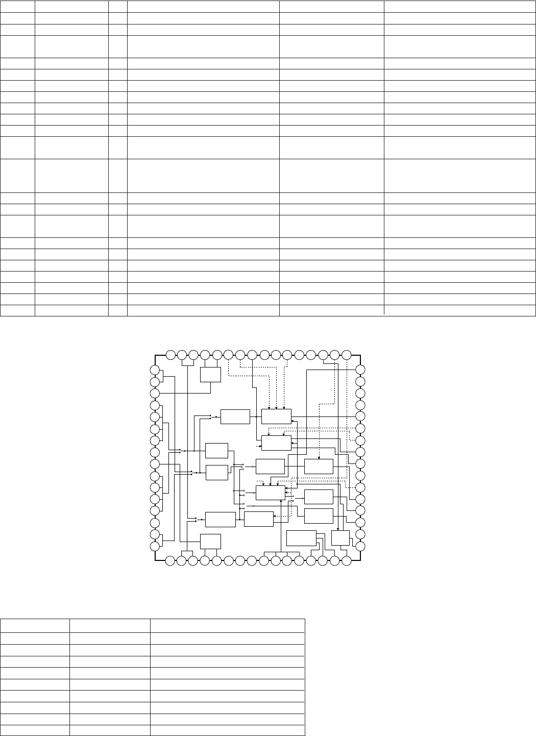
11-10. IC508 IX1516GE GAMMA S-P-TONE
Terminal Terminal name In/Output Function
11-9
DV-760X
31 MRST Input Reset signal
32 VSS – Digital GND
33 VDD – Digital power +3.3V
34 PXDO (0) Output Pixel data output
35 PXDO (1) Output
8-bit parallel video data conforming to ITU-R BT.601 and BT.656 standard (Cb/Y/Cr/Y)
36 PXDO (2) Output MSB=PXDO(7), LSB=PXDO(0)
37 PXDO (3) Output
38 PXDO (4) Output
39 PXDO (5) Output
40 VSS – Digital GND
41 VDD – Digital power +3.3V
42 PXDO (6) Output
43 PXDO (7) Output
44 PXCLKO Output Reference clock output for pixel data. 27 MHz
45 VSYNCO Output Vertical sync signal output
46 HSYNCO Output Horizontal sync signal output
47 VSYNCI Input Vertical sync signal output
48 VSS – Digital GND
49 VDD – Digital power +3.3V
50 HSYNCI Input Horizontal sync signal output
51 PXCLKI Input Reference clock output for pixel data. 27 MHz
52 PXDI (0) Input Pixel data output
53 PXDI (1) Input
8-bit parallel video data conforming to ITU-R BT.601 and BT.656 standard (Cb/Y/Cr/Y)
54 PXDI (2) Input MSB=PXDI(7), LSB=PXDI(0)
55 PXDI (3) Input
56 VSS – Digital GND
57 VDD – Digital power +3.3V
58 PXDI (4) Input
59 PXDI (5) Input
60 PXDI (6) Input
61 PXDI (7) Input
62 TEST0 Input Test terminal
63 TEST1 Input Test terminal
64 VSS – Digital GND
Terminal Terminal name In/Output Function
• Block Diagram
12
HADAT
PXDI
HSYNCI
HADR HCS HAS HWR HRD HIM MRST
VDD
VSS
TEST0
TEST1
INT
WAIT
PXDOVSYNCOHSYNCO
PXCLKI
VSYNCI
PXCLKO
64pin LQFP
18
8
8
81
1
1
111 11
15
10 11
27
21 29 28 27 26 30 31
19
8
17
16
25
24 32
33 41
40 48
49 57
56 64
62
63
22
23
3934
43
4546
42
44
51
47
50
55 61
52 58
CPU
Host interface
ITU-R
601/656
interface
ITU-R
601/656
formatter
Timing
generation
Clock
Gen.
Source
Dec.
NTSC Enc.
(3ch D/A built in)
Edge
creation
SPT circuit
Digital
dinamic
r circuit
Digital color correction
Color
offset
correction
White
correction
DR-SPT
circuit
8
11
1
1
11-10

DV-760X
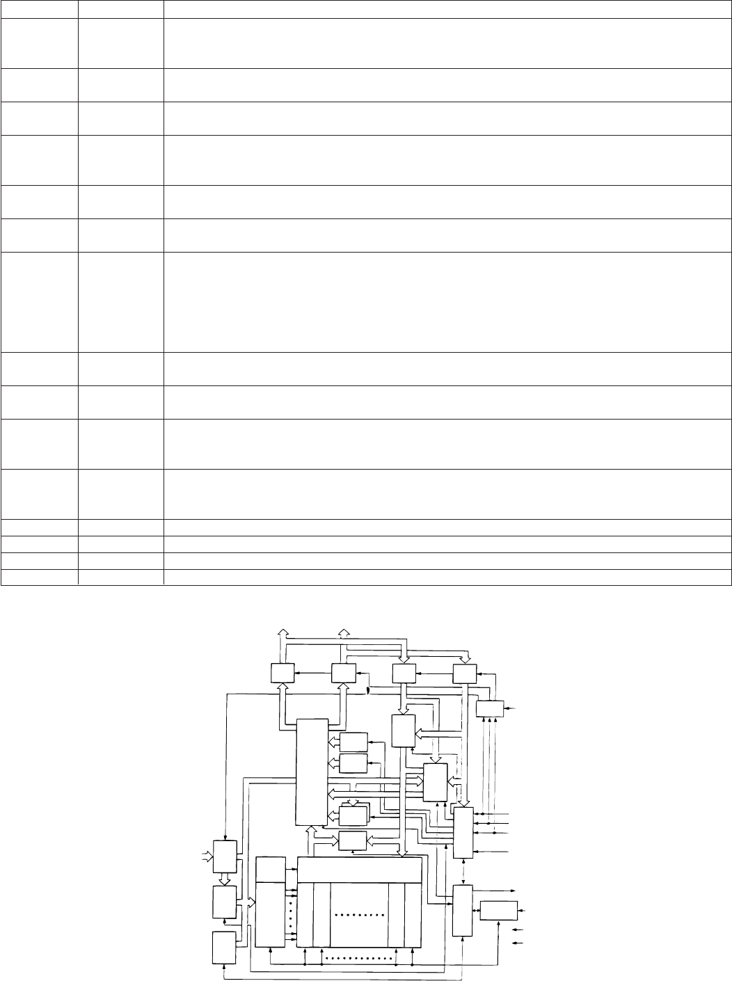
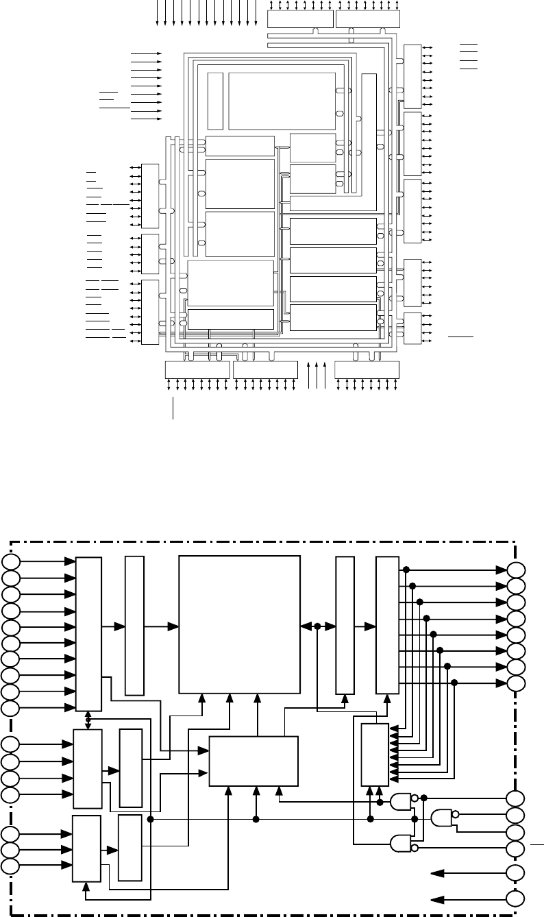
11-11. IC512 IX1535GE HOST I/F
1 VDD – Power +3.3V
2 HADR0 Input CPU Address bus
3 HADR1 Input CPU Address bus
4 HADR2 Input CPU Address bus
5 HCS Input CPU Tip select
6 HWR Input CPU Write signal
7 HRD Input CPU Read signal
8 HDAT0 In/Output CPU Data bus
9 HDAT1 In/Output CPU Data bus
10 HDAT2 In/Output CPU Data bus
11 HDAT3 In/Output CPU Data bus
12 HDAT4 In/Output CPU Data bus
13 HDAT5 In/Output CPU Data bus
14 HDAT6 In/Output CPU Data bus
15 HDAT7 In/Output CPU Data bus
16 VSS – Digital GND
17 VDD – Power +3.3V
18 EXPAL (0) In/Output General-use input/output terminal Gr.A
19 EXPAL (1) In/Output General-use input/output terminal Gr.A
20 EXPAL (2) In/Output General-use input/output terminal Gr.A
21 EXPAL (3) In/Output General-use input/output terminal Gr.A
22 EXPAU (0) In/Output General-use input/output terminal Gr.A
23 EXPAU (1) In/Output General-use input/output terminal Gr.A
24 VSS – Digital GND
25 VDD – Power +3.3V
26 EXPAU (2) In/Output General-use input/output terminal Gr.A
27 EXPAU (3) In/Output General-use input/output terminal Gr.A
28 EXPBL (0) In/Output General-use input/output terminal Gr.B
29 EXPBL (1) In/Output General-use input/output terminal Gr.B
30 EXPBL (2) In/Output General-use input/output terminal Gr.B
31 EXPBL (3) In/Output General-use input/output terminal Gr.B
32 VSS – Digital GND
33 VDD – Power +3.3V
34 EXPBU (0) In/Output General-use input/output terminal Gr.B
35 EXPBU (1) In/Output General-use input/output terminal Gr.B
36 EXPBU (2) In/Output General-use input/output terminal Gr.B
37 EXPBU (3) In/Output General-use input/output terminal Gr.B
38 EXPC (0) In/Output General-use input/output terminal Gr.C
39 EXPC (1) In/Output General-use input/output terminal Gr.C
40 EXPC (2) In/Output General-use input/output terminal Gr.C
41 VSS – Digital GND
42 EXPC (3) In/Output General-use input/output terminal Gr.C
43 EXPC (4) In/Output General-use input/output terminal Gr.C
44 EXPC (5) In/Output General-use input/output terminal Gr.C
45 EXPD (0) In/Output General-use input/output terminal Gr.D
46 EXPD (1) In/Output General-use input/output terminal Gr.D
47 EXPD (2) In/Output General-use input/output terminal Gr.D
48 VSS – Digital GND
49 VDD – Power +3.3V
50 EXPD (3) In/Output General-use input/output terminal Gr.D
51 EXPD (4) In/Output General-use input/output terminal Gr.D
52 EXPD (5) In/Output General-use input/output terminal Gr.D
53 BUFDO Output Buffer output D
54 BUFDI Input Buffer input D
55 SBUFBO Output Schmidt buffer output B
56 SBUFBI Input Schmidt buffer input B
57 SBUFAO Output Schmidt buffer output A
58 SBUFAI Input Schmidt buffer input A
59 MRST Input Reset terminal
60 MODE Input Mode selection terminal
61 BUFCO In/Output Buffer output C
62 TEST Input Test terminal (for Epson)
63 BUFCI Input Buffer input C
64 VSS – Digital GND
Terminal Terminal name In/Output Function
11-11
DV-760X
Pin1~15........ There is a possibility of simultaneous change. Operating frequency: Approx. 10 MHz
Pin18~47 ..... There is a possibility of simultaneous change.(Static signal) Operating frequency: Approx. 1 MHz
Pin50~57 ..... There is almost no possibility of simultaneous change. Operating frequency: Approx. 1 MHz
Pin63............ Not used
• Block Diagram
Data Buffer
Latch D Data Buffer
Latch C
Data Buffer
Latch B Data Buffer
Latch A
Data Buffer
R/W CTL
48
49
50
51
52
53
54
55
56
57
58
59
60
61
62
63
64
47 46 45 44 43 42 41 40 39 38 37 36 35 34 33
32
31
30
29
28
27
26
25
24
23
22
21
20
19
18
17
16151413121110987654321
VDD
EXPD(3)
EXPD(4)
EXPD(5)
BUFDO
BUFDI
SBUFBO
SBUFBI
SBUFAO
SBUFAI
MRST
MODE
BUFCO
TEST
BUFCI
VSS
VDD
SOUT(3)
SOUT(4)
SOUT(5)
MRST
MODE
SEL
TEST
CK
VSS
VSS
EXPD(2)
EXPD(1)
EXPD(0)
EXPC(5)
EXPC(4)
EXPC(3)
VSS
EXPC(2)
EXPC(1)
EXPC(0)
EXPBU(3)
EXPBU(2)
EXPBU(1)
EXPBU(0)
VDD
VSS
SOUT(2)
SOUT(1)
SOUT(0)
S2(5)
S2(4)
S2(3)
VSS
S2(2)
S2(1)
S2(0)
Q2(7)
Q2(6)
Q2(5)
Q2(4)
VDD
VSS
EXPBL(3)
EXPBL(2)
EXPBL(1)
EXPBL(0)
EXPAU(3)
EXPAU(2)
VDD
VSS
EXPAU(1)
EXPAU(0)
EXPAL(3)
EXPAL(2)
EXPAL(1)
EXPAL(0)
VDD
VSS
Q2(3)
Q2(2)
Q2(1)
Q2(0)
Q1(7)
Q1(6)
VDD
VSS
Q1(5)
Q1(4)
Q1(3)
Q1(2)
Q1(1)
Q1(0)
VDD
VDD
HADR0
HADR1
HADR2
HCS
HWR
HRD
HDAT0
HDAT1
HDAT2
HDAT3
HDAT4
HDAT5
HDAT6
HDAT7
VSS
VDD
D(0)
D(1)
D(2)
D(3)
D(4)
D(5)
D(6)
D(7)
S1(0)
S1(1)
S1(2)
S1(3)
S1(4)
S1(5)
VSS
In/Output Pin Exclusive-use pin
In/Output Pin
In/Output Pin
In/Output Pin
In/Output Pin
Output:
Open drain
Input Pin In/Output Pin
Output: Open drain
11-12. IC601 IX1521GE SOURCE DECODER
Pin No. Pin name Type Direction Function
22 HA[3:0] I I Address bus input for microcomputer connection.
24-26 Used for register access and so on
HTYPE = L
It works as HR/W#(read/write) input terminal for connection to Motorola
27 HWR# II
type microcomputer.
(HR/W#) HTYPE = H
It works as HWR# (write) input terminal for connection to general purpose
microcomputer.
29 HCS# I I Chip select input for connection to microcomputer
HTYPE = L
It works as HDS#(data strobe) input terminal for connection to Motorola
30 HRD# II
type microcomputer.
(HDS#) HTYPE = H
It works as HRD# (read) input terminal for connection to general purpose
microcomputer.
Bit stream input ready output terminal If the bit stream is input from
microcomputer, the terminal is bored.
For 3-state output, connect the pull-up resistor.
HRDY = L
31 HRDY 3-S O Bit stream can not be input.
HRDY = H
The number of bytes which are set by CodBurstLen parameter can be
transferred from the microcomputer. During the time from transfer start of
the number of set bytes to transfer end, the terminal varies in 3 states.
Microcomputer interface
11-12

DV-760X
Pin No. Pin name Type Direction Function
HTYPE = L
It works as HACK# (acknowledge) output terminal for connection to
32 HACK# Motorola type microcomputer.
(HR/W#) It can be used as the weight terminal for connection to the general pur
pose microcomputer. For 3-state output, connect the pull-up resistor.
Interrupt request. If interrupt status register is read, interrupt is masked or
34 HIRQ# 3-S O device is reset, the signal is deasserted.
For 3-state output, connect the pull-up resistor.
The bus width of the microcomputer interface If the device is worked as
CD-G decoder or CD-DSP is connected, select the 8-bit bus mode.
35 HWID I I Fix it before power up.
L=8bit bus mode
H=16bit bus mode
When HWID is H (16-bit bus MODE), byte order is set.
Setting is valid only when HWID is H.
36 HORD I I Fix it before power up.
L=HD [15:8] is regarded as m.s. byte. (Motorola type)
H=HD [7:0] is regarded as m.s. byte. (Intel type)
Bus type of microcomputer interface is set.
37 HTYPE I I Fix it before power up.
L=Motorola type
H=General purpose type
141 RESET# I I RESET is input.
142 IDLE 3-S O It is output to indicate the idle state.
Microcomputer interface terminal list
Microcomputer interface
Pin No. Pin name Type Direction Function
When 16-bit bus width is selected, (HWID=low)
It works as the microcomputer data bus of 15th bit.
When 8-bit bus width is selected, (HWID=high)
It works as the terminal to input bit clock from DC-DSP.
When 16-bit bus width is selected, (HWID=low)
It works as the microcomputer data bus of 14th bit.
When 8-bit bus width is selected, (HWID=high)
It works as the terminal to input the stream/PCM data from CD-DSP.
When 16-bit bus width is selected, (HWID=low)
It works as the microcomputer data bus of 13th bit.
When 8-bit bus width is selected, (HWID=high)
It works as the terminal to input frame synchronous signal from CD-DSP.
When 16-bit bus width is selected, (HWID=low)
It works as the microcomputer data bus of 12th bit.
When 8-bit bus width is selected, (HWID=high)
It works as the terminal to input error signal to CD-DSP.
When 16-bit bus width is selected, (HWID=low)
It works as the microcomputer data bus of 11th bit.
When 8-bit bus width is selected, (HWID=high)
It works as the terminal to output the subcode reading clock to the
subcode interface of CD-DSP.
When 16-bit bus width is selected, (HWID=low)
It works as the microcomputer data bus of 10th bit.
When 8-bit bus width is selected, (HWID=high)
It works as the terminal to input subcode data from subcode interface of CD-DSP.
Microcomputer / CD·subcode interface terminal list
Microcomputer interface / CD·subcode interface
3HD15 3-S I/O
(CDERR) (I) (I)
4HD14 3-S I/O
(CDFRM) (I) (I)
5HD13 3-S I/O
(CDDAT) (I) (I)
6HD12 3-S I/O
(CDCLK) (I) (I)
7HD11 3-S I/O
(SCCLK) (O) (O)
9HD10 3-S I/O
(SCDAT) (I) (I)
Function
General purpose terminal.
General input/output terminal. After resetting, it becomes the input direction.
General output terminal.
General port terminal list
Pin No. Pin name Type Direction
2 GPSI I I
122-123 GPAIO[1:0] 3-S I/O
159 GPSO O O
General port
11-13
DV-760X
Pin No. Pin name Type Direction
126 GCLK1 I I
128 XO O O
129 GCLK I I
135, 137
PLLGFG[1:0] I I
136 PLLCA – –
Microcomputer / CD·subcode interface terminal list
Pin No. Pin name Type Direction Function
When 16-bit bus width is selected, (HWID=low)
It works as the microcomputer data bus of 9th bit.
When 8-bit bus width is selected, (HWID=high)
It works as the terminal to input the subcode synchronous signal from the
subcode interface of CD-DSP.
When 16-bit bus width is selected, (HWID=low)
It works as the microcomputer data bus of 9th bit.
When 8-bit bus width is selected, (HWID=high)
It works as the terminal to input the frame synchronous signal from the
subcode interface of CD-DSP.
It works as the microcomputer bus of bits 7 thru 0.
10 HD9 3-S I/O
(SCSYN) (I) (I)
11 HD8 3-S I/O
(SCFRM) (I) (I)
12
14-17 HD[7:0] 3-S I/O
19-21
Microcomputer interface / CD·subcode interface
PLL interface terminal list
Pin No. Pin name Type Direction Function
Test terminal. Don’t connect it.
If quartz oscillator is connected to GCLK terminal, connect the other
terminal of quartz oscillator to this pin.
Master clock input terminal of device Input 27 MHz.
PLL is set. Before power-up, fix it.
External capacitor terminal for PLL.
PLL interface
Pin No. Pin name Type Direction
102 C7 3-S O
(N.C.) (3-S) (O)
104 C6 3-S O
(N.C.) (3-S) (O)
105 C5 3-S O
(N.C.) (3-S) (O)
106 C4 3-S O
(OSDPLT) (3-S) (I)
107 C3 3-S O
(OSDPEL3) (3-S) (I)
Video/OSD interface terminal list
Pin No. Pin name Type Direction Function
Video8 register = 0
Color difference signal output terminal of 7th bit.
Video8 register = 1
The terminal becomes invalid.
Video8 register = 0
Color difference signal output terminal of 6th bit.
Video8 register = 1
The terminal becomes invalid.
Video8 register = 0
Color difference signal output terminal of 5th bit.
Video8 register = 1
The terminal becomes invalid.
Video8 register = 0
Color difference signal output terminal of 4th bit.
Video8 register = 1
Input terminal to select pallet table of OSD.
For OSDPLT=low, pallet table 0 is used.
For OSDPLT=high, pallet table 1 is used.
Video8 register = 0
Color difference signal output terminal of 3th bit.
Video8 register = 1
It works as the OSD pallet data input terminal of 3rd bit.
Video interface · OSD interface
11-14

DV-760X
Pin No. Pin name Type Direction Function
Video8 register = 0
Color difference signal output terminal of 2th bit.
Video8 register = 1
It works as the OSD pallet data input terminal of 2rd bit.
Video8 register = 0
Color difference signal output terminal of 1th bit.
Video8 register = 1
It works as the OSD pallet data input terminal of 1rd bit.
Video8 register = 0
Color difference signal output terminal of 0th bit.
Video8 register = 1
It works as the OSD pallet data input terminal of 0rd bit.
109 C2 3-S O
(OSDPEL2) (3-S) (I)
110 C1 3-S O
(OSDPEL1) (3-S) (I)
111 C0 3-S O
(OSDPEL0) (3-S) (I)
Video/OSD interface terminal list
Video interface · OSD interface
Pin No. Pin name Type Direction Function
Clock gained by dividing VCLK x 2 signal into halves.
Input terminal to switch video master/slave.
VMASTER=L
Video master mode. Video synchronizing signal and video clock are
internally generated.
HTYPE=H
Video slave mode. Video synchronizing signal and video clock are re
ceived from the external.
Video output enable input terminal
VDEN#=H
Y [7:0] and C [7:0] terminals are made to be disable (3-state).
VDEN#=L
Y [7:0] and C [7:0] terminals are made to be enable.
Note: C [7:0] terminal is the multiplexed terminal as OSDPLT [3:0] and so on.
For Video8 register = 0, VDEN# terminal is valid for Y [7:0] alone.
Composite blank output terminal. Horizontal/vertical blanking area and
polarity are programmable.
Input/output terminal of vertically synchronous signal. Polarity and synchronous
signal length are programmable.
Input/output terminal of horizontally synchronous signal.Polarity and
synchronous signal length are programmable.
Input/output terminal for identification of even/odd number field. Polarity is
programmable.
Video8 register = 0
Brightness signal output/input terminal.
Video8 register = 1
Brightness/color difference multiplex terminal as ITU-T656
Terminal to input video clock or output 27 MHz.
84 VCLK 3-S I/O
85 VMASTER I I
87 VDEN# I I
88 CBLANK O O
89 VSYNC 3-S I/O
90 HSYNC 3-S I/O
91 FI 3-S I/O
92
94-97 Y[7:0] 3-S O
99-101
124 VCLK X 2 3-S I/O
Video interface terminal list
Video interface
Pin No. Pin name Type Direction Function
Audio (PCM) input terminal.
Stereo x1
Audio (PCM) output terminal.
Stereo x3
S/PDIF output terminal AC-3 stream or PCM stream can be output.
Moreover, it works as the audio output terminal of 7th and 8th channels
Left/Right clock output terminal of AOUT [2:0] and AIN.
The polarity is programmable.
Bit clock output terminal of AOUT [2:0] and AIN.
The polarity is programmable.
Audio master clock input/output terminal.
256 Fs or 386 Fs can be used.
Audio interface terminal list
Pin No. Pin name Type Direction
112 AIN I I
114-116 AOUT[2:0] O O
117 S/PDIF OO
(AOUT[3])
118 ALRCLK O O
119 ABCLK O O
132 AMCLK 3-S I/O
Audio interface
11-15
DV-760X
Pin No. Pin name Type Direction Function
Address bus output for SDRAM connection.
Tip select output for SDRAM connection.
Tip select output terminal for SDRAM connection. It is connected to 2nd
SDRAM.
RAS output terminal for SDRAM connection.
Clock output terminal for SDRAM connection.
CAS output terminal for SDRAM connection.
Write enable output terminal for SDRAM.
Data masking output terminal for SDRAM.
Bi-directional data bus for SDRAM.
Function
Data error input for DVD-DSP connection.
Sector start input for DVD-DSP connection.
Data valid input for DVD-DSP connection.
Data strobe input for DVD-DSP connection.
Data request output for DVD-DSP connection.
Stream input for DVD-DSP connection
Pin No. Pin name Type Direction
143 DVDERR I I
144 DVDSOS I I
146 DVDVALID I I
147 DVDSTRB I I
148 DVDREQ O O
149
151-154
DVDDAT[7:0]
II
156-158
DVD-DSP interface terminal list
DVD-DSP interface
Pin No. Pin name Type Direction
38-39
42-47
RAMADD[11:0]
OO
49-52
54 RAMCS0# O O
55 RAMCS1# O O
56 RAMRAS# O O
57 PCLK O O
59 RAMCAS# O O
60 RAMWE# O O
61 RAMDQM O O
62
64-67
69-72
RAMDAT[15:0]
3-S I/O
74-79
82
SD-RAM interface terminal list
SDRAM interface
Power terminal · other list
Pin No. Pin name Type Direction
1, 13, 23
40, 41
53, 68
80, 81 GND
93, 108
120, 121
125, 131
145, 160
8, 18, 28
33, 48
58, 63
73, 86 VDD
98, 103
113, 133
140,
150, 155
83
TESTMODE
II
127 SCNENBL I I
130 PWRDN# I I
134 PLLGND
138 PLLVDD
139 ICEMODE I I
Pin No. Pin name Type Direction Function
Ground terminal
+ 3.3V power input terminal
Test terminal. Pull it down to GND.
Test terminal. Pull it up to VDD.
Power-down terminal. When it is [low], current consumption becomes
minimum with all functions of the device stopped. (Power-down mode) To
return it to normal state, set the terminal at [high]. Then, reset the device
with RESET# terminal.
Ground terminal for internal PLL.
Internal PLL + 3.3V power input terminal.
Test terminal. Pull it down to GND.
Power terminal · other
11-16
DV-760X
11-17
11-13. IC602 IX0750TA 16M SDARM
35 CLK System Clock Active on the positive going edge to sample all inputs.
18 CS Chip Select Disables or enables device operation by masking or enabling all inputs
except CLK. CKE and L(U)DQM
34 CKE Clock Enable Masks system clock to freeze operation from the next clock cycle.
CKE should be enabled at least one cycle prior to new command.
Disable input buffers for power down in stanby.
21~24 A0~A10/AP Address Row/column address are multiplexed on the same pins.
27~32 Row address: RA0~RA10, column address: CA0~CA7
20
19 BA Bank Select Address Selects bank to be activated during row address latch time.
Selects bank for read/write during clumn address latch time.
17 RAS Row Address Strobe Latches row address on the positive going edge of the CLK with RAS low.
Enables row access & precharge.
16 CAS Column Address Strobe Latches addresses on the positive going edge of the CLK with CAS low.
Enables row access.
15 WE Write Enable Enable write operation and row precharge.
Latches data in starting from CAS, WE active.
14, 36 L(U)DOM Data Input/Output Mask Makes data output Hi-Z, tsHZ after the clock and masks the output.
Blocks data input when L(U)DQM active.
2, 3, 5, DQ0~15 Data Input/Output Data inputs/outputs are multiplexed on the same pins.
6, 8, 9, 11, 12, 39, 40,
42, 43, 45, 46, 48, 49
Vcc/Vss Power Supply/Ground Power and ground for the input buffers and the core logic.
25, 1/26
Vcc/VssO
Data Output Power/Ground
Isolated power supply and ground for the output buffers to provide
44, 38, 13, 7/4, 10, 41, 47, 50 improved noise immunity.
37 NC/RFU No Connection/ This pin is recommanded to be left No Connection on the device
Reserved for Future Use
Terminal Terminal Name Name Input Function
CLK
CLK CKE CS RAS CAS WE
ADD
LCKE
Address Register
Bank Select
Row Buffer
Refrsh Counter
Rown Decorder Col. Buffer
LRAS
LRAS
LCBR
LCBR LWE LCAS
L(U)DOM
Timing Register
LWCBR LDOM
Programming Resiter
Latency & Burst Length
Column Decoder
Data Input Register
512K x 16
512K x 16
Sense AMP
I/O Control Output Buffer
LWE
LDOM
DQi
• Samsung Electronics reserves the right to
change products or specification without
• Block Diagram
DV-760X
11-14. IC702 BA6796FP MOTOR DRIVER
T.S.D ; Thermal shutdown
D; Drive buffer
Unit of resistance is [Ω].
• Mode change table
CTL1 and CTL2
Note: OFF state: Output has high impedance.
For F and R (CH5 control, valid only when CH5 is ON)
F R Output mode
L L High impedance
L H Reversing (reverse)
H L Forward rotation (forward)
H H Brake
Pin No. Terminal name
Operation function
Pin No. Terminal name
Operation function
1 OPOUT Ope amp. output terminal 15 CH2-OUT- CH2 Negative output terminal
2 CH4-IN CH4 Input terminal 16 CH2-OUT+ CH2 Positive output terminal
3 CH4-IN’ CH4 Gain adjustment input terminal 17 CH1-OUT- CH1 Negative output terminal
4 CTL1 Contorol 1 input terminal 18 CH1-OUT+ CH1 Positive output terminal
5 CTL2 Contorol 2 input terminal 19 CH1-IN CH1 Input terminal
6 FWD Tray forward input terminal 20 CH1-IN’ CH1 Input terminal for gain adjustment
7 REV Tray reverse input terminal 21 VCC VCC
8 TRAY-IN Tray input terminal 22 CH2-IN CH2 Input terminal
9 GND Sub-straight GND 23 CH2-IN’ CH2 Input terminal for gain adjustment
10 CH5-OUT- Tray negative output terminal 24 CH3-IN CH3 Input terminal
11 COM-OUT Tray positive output terminal/CH4 25 CH3-IN’ CH3 Input terminal for gain adjustment
negative output terminal
12 CH4-OUT+ CH4 Positive output terminal 26 VREF-IN Bias amp. input terminal
13 CH3-OUT+ CH3 Positive output terminal 27 OPIN+
Operational amplifier nonreverse input terminal
14 CH3-OUT- CH3 Negative output terminal 28 OPIN-
Operational amplifier reverse input terminal
Note 1: Positive and negative output have polarity with respect to input. (An example: 19 pin input ‘H’: 18 pin output ‘H’)
Note 2: Tray positive output and tray negative output have polarity with respect to mode. (An example: 11 pin output
‘H’ in FORWARD mode)
28 27 26 25 24 23 22 21 20 19 18 17 16 15
CH2-OUTCH1-OUTCH1-INCH2-INCH3-IN
10K 10K
13.3K 13.3K 13.3K
10K
+
-
Level shift
Level shift
Level shift
Level shift
VCC
D
DDD
DDD DD
V/I
T.S.D
26.6K
10K CTL1 CTL2 PWD REV
LOGIC
1234567 891011121314
CH4-IN CH5-IN CH5-OUTCH4-OUTCH3-OUT
+
-
+
-
+
-
+-
• Block Diagram
11-18
CTL1 CTL2 CH1 CH2 CH3 CH4 CH5
LL OFF ON
LH
H L ON OFF
H H OFF ON OFF ON
DV-760X
11-15. IC707 IX1473GE SERVO PROCCESSOR
Pin No. Terminal name I/O Operation function Remarks
1 VSS – Digital ground terminal.
2 BCK O Bit clock (1.4122MHz) output terminal.
3 AOUT O Audio data output terminal.
4 DOUT O Digital out output terminal.
5 MBOB O Buffer memory over signal output terminal. Over: “H”
6 IPF O Correction flag output terminal. When correction disable symbol
is given if AOUT output is C2 correction: “H”.
7 SBOK O Sub-code Q data CRCC judgment result output terminal.
Judgment result OK: “H”.
8 CLCK I/O Sub-code P to W data read clock output/input terminal.
Selectable with command bit.
9 VDD – Digital + power terminal
10 VSS – Digital ground terminal
11 DATA O Sub code P-W data output terminal.
12 SFSY O Playback system frame sync signal output terminal.
13 SBSY O Subcode block sync output terminal.
When subcode sync is detected, S1 position: “H”.
14 SPCK O Processor status signal read clock (176.4 kHz) output terminal.
15 SPDA O Processor status signal output terminal.
16 COFS O Correction system frame clock (7.35 kHz) output terminal.
17 MONIT O LSI internal signal monitor terminal.
DSP internal flag and PLL system clock can be monitored with
microcomputer command.
18 VDD – Digital + power terminal.
19 TESIO0 I Test input/output terminal. Usually fixed to “L”.
20 P2VREF – PLL system 2VREF terminal.
21 SPDO O VCO center frequency shift terminal.
22 PDOS O EFM and PLCK signal phase error signal output terminal.
(To be used when x8 speed operation is used)
23 PDO O EFM and PLCK signal phase error signal output terminal.
24 XMAXS O TMAX detection result output terminal.
To be selected with command bit TMPS.
25 TMAX O
26 LPFN I Reverse input terminal for low pass filter amplifier.
27 LPFO O Output terminal for low pass filter amplifier.
28 PVREF – PLL system VREF terminal.
29 VCOREF I VCO center frequency reference level terminal.
To be fixed usually to “PVREF”.
30 VCOF O Filter terminal for VCO.
31 AVSS – Analog system ground terminal.
32 SLCO O Data slice level generation DAC output terminal.
33 RFIN I RF signal input terminal.
34 AVDD – Analog system power terminal.
35 RFCT I RFRP signal center level input terminal.
36 RFZI I RFRP zero cross input terminal.
37 RFRP I RF ripple signal input terminal.
38 FEIN I Focus error signal input terminal.
39 SBAD I Sub-beam addition signal input terminal.
40 TSIN I Test input terminal. To be fixed usually to “Vref”
41 TEIN I Tracking error signal input terminal.
(Fetching when tracking servo is ON)
42 TEZI I Tracking error zero cross input terminal.
43 FOO O Focus equalizer output terminal.
TMAX detection result TMAXoutput
Longer than specific period “P2VREFF”
Shorter than specific period “VSS”
Within specified period “HiZ”
11-19

DV-760X
Pin No. Terminal name I/O Operation function Remarks
44 TRO O Tracking equalizer output terminal.
45 VREF – Analog reference power terminal.
46 RFGC O RF amplitude adjustment control signal output terminal.
Output of 3-pole PWM signal. (PWM carrier = 88.2 kHz)
47 TEBC O Tracking balance control signal output terminal.
Output of 3-pole PWM signal. (PWM carrier = 88.2 kHz)
48 FMO O Feed equalizer output terminal.
Output of 3-pole PWM signal. (PWM carrier = 88.2 kHz)
49 FVO O Speed error signal or feed search EQ output terminal.
Output of 3-pole PWM signal. (PWM carrier = 88.2 kHz)
50 DMO O Disc equalizer output terminal.
Output of 3-pole PWM signal. (PWM carrier = DSP system
88.2kHz, to be synchronized with PXO)
51 2VREF –
52 SEL O
53 /FOON O
54 /DFCT O
55 /SRCH O
56 /SHC O
57 VDD –
58 VSS –
59 IO0 I/O General use I/O port.
60 IO1 It is possible to select the input port and output port according
to command.
61 IO2 In case of input port the terminal state (H/L) can be read with
the read command.
62 IO3 In case of output port the terminal state (H/L/HiZ) can be
controlled with the command.
63 /DMOUT Terminal to set the mode to output dual value PWM of feed
equalizer from the IO0,1 terminal and to output the dual value
PWM from disc equalizer of IO2,3 terminal “L” Active.
64 /CKSE X’tal selection terminal.
When 16.9344 MHz: “H” When 33.8688 MHz: “L”
65 /DACT Test terminal.
66 TESIN Test input terminal.
67 TESIO1 Test input/output terminal.
68 VSS Digital ground terminal.
69 PXI DSP system clock oscillation circuit input terminal.
70 PXO DSP system clock oscillation circuit output terminal.
71 VDD Digital + power terminal.
72 XVSS Ground terminal for system clock oscillation circuit.
73 XI System clock oscillation circuit input terminal.
74 XO System clock oscillation circuit output terminal.
75 XVDD Positive power terminal for system clock oscillation circuit.
76 DVDD – D/A converting section power terminal.
77 RO O R channel data forward rotation output terminal.
78 DVSS – D/A converting section analog ground terminal.
79 DVR – D/A converting section reference voltage terminal.
80 LO O L channel data forward rotation output terminal.
81 DVDD – D/A converting section power terminal.
82 TEST1 I Test terminal. Pull-up resistor
To be opened usually. built in.
83 TEST2 I Test terminal. Pull-up resistor
To be opened usually. built in.
84 TEST3 I Test terminal. Pull-up resistor
To be opened usually. built in.
85 BUS0 I/O Microcomputer interface data input/output terminal. Schmidt input
86 BUS1 I/O CMOS port
87 BUS2 I/O
11-20
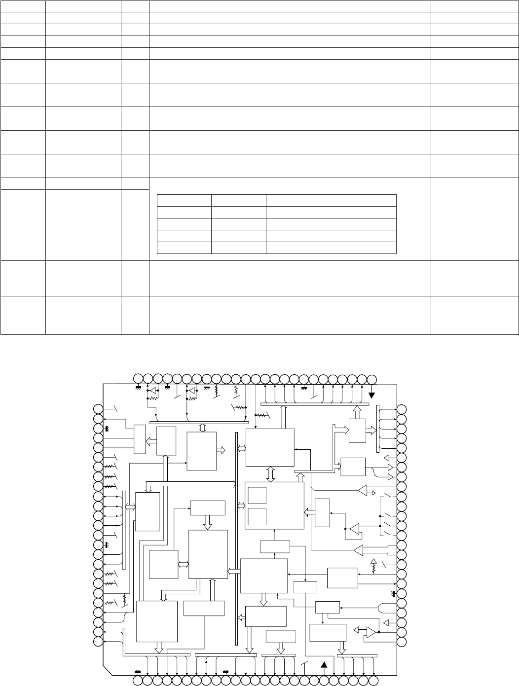
DV-760X
Pin No. Terminal name I/O Operation function Remarks
88 BUS3 I/O
89 VDD – Digital + power terminal.
90 VSS – Digital ground terminal.
91 BUCK I Microcomputer interface clock input terminal. Schmidt input
92 /CCE I Microcomputer interface chip enable signal input terminal. Schmidt input
BUS0 to 3 is active in “L” state.
93 TEST4 I Test terminal. Pull-up resistor
To be opened usually. built in.
94 /TEMOD I Local test mode selection terminal. Pull-up resistor
built in.
95 /RST I Reset signal input terminal. Pull-up resistor
Reset state: “L” built in.
96 TEST0 I Test terminal. Pull-up resistor
To be opened usually. built in.
97 /HSO O Playback speed mode flag output terminal.
98 /UHSO O
99 EMPH O Subcode Q data emphasis flag output terminal.
Emphasis ON: “H” OFF: “L”
Output polarity can be inverted by the command.
100 LRCK O Channel clock (44.1 kHz) output terminal.
L channel “L” R channel: “H”
Output polarity can be inverted by the command.
/UHSO /HSO Playback speed
H H x1 speed playback
H L x2 speed playback
L H x4 speed playback
L L x8 speed playback
• Block Diagram
76DVDD
77RO
78DVSS
79DVR
80LO
81DVDD
82TEST1
83TEST2
84TEST3
85BUS0
86BUS1
87BUS2
88BUS3
89VDD
90VSS
91BUCK
92/CCE
93TEST4
94/TEMOD
95/RST
96TEST0
97/HSO
98/UHSO
99EMPH
100LRCK
50 DMO
49 FVO
48 FMO
47 TEBC
46 RFGC
45 VREF
44 TRO
43 FOO
42 TEZI
41 TEIN
40 TSIN
39 SBAD
38 FEIN
37 RFRP
36 RFZI
35 RFCT
34 AVDD
33 RFIN
32 SLCO
31 AVSS
30 VCOF
29 VCOREF
28 PVREF
27 LPFO
26 LPFN
1234
VSS
BCK
AOUT
5678
MBOB
IPF
SBOK
CLCK
91011
12
VDD
VSS
DATA
13
SBSY
14
SPCK
15
SPDA
16
COFS
17
MONIT
18
VDD
19
TESIO0
20
P2VREF
21
SPDO
22
PDOS
23
PDO
24
XMAXS
25
TMAX
SFSY
DOUT
75 74 73 72
XVDD
XO
XI
71 70 69 68
VDD
PXO
PXI
VSS
67 66 65 64
TESIO1
TESIN
/DACT
63
/DMOUT
62
IO3
61
IO2
60
IO1
59
IO0
58
VSS
57
VDD
56
/SHC
55
/SRCH
54
/DFCT
53
/FOON
52
SEL
51
2VREF
/CKSE
XVSS
LPF
1Bit
DAC
ROM
RAM
1Gk RAM
PWM
D/A
A/D
CLV servo
PWM
VCO
PLL TMAX
+
–
+
–
+
–
+
–
Clock
genelator
Servo control
Digital
equalizer
Automatic
adjusting circuit
Micon
inter
face
Digital out
Status
Correction
circuit
Sync signal
protection
EFM
demodulation
Data slicer
Subcode
demodulation
circuit
Audio output
circuit
Address circuit
11-21
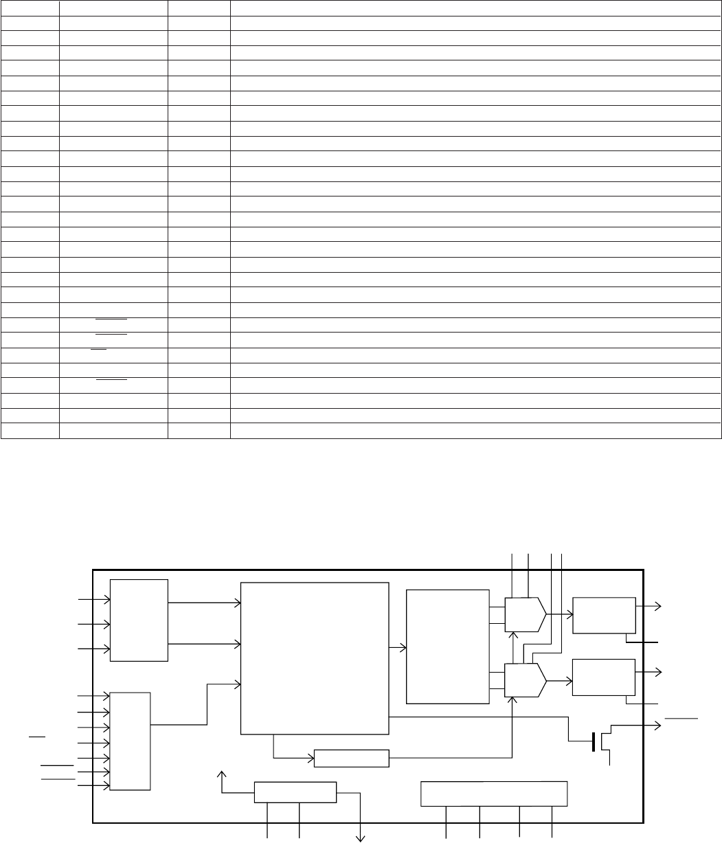
DV-760X
Pin No. Terminal name I/O Operation function
1 LRCIN I LRCK clock input (fs) (3)
2 DIN I Data input (3)
3 BCKI I Bit clock input for data.
4 CLKO O System clock buffered output.
5 XTI I Connection of crystal oscillator or external clock input.
6 XTO O Connection of crystal oscillator
7 DGND – Digital GND
8VDD – Digital power +5V
9VCC2R – Analog power +5V
10 AGND2R – Analog GND
11 EXTR O Rch Analog output amp. • common
12 NC – Not connected.
13 VOUTR O Rch Analog voltage output
14 AGND1 – Analog GND
15 VCC1 – Analog power +5V
16 VOUTL O Lch Analog voltage output
17 NC – Not connected.
18 EXTL O Lch Analog output amp. • common
19 AGND2L – Analog GND
20 VCC2L – Analog power +5V
21 ZERO O Zero data • flug
22 RSTB I
Resetting. While this pin is in "L" state, the DF and delta -sigma modulator is in reset state.
(1)
23 CS/IWO I Chip selection/input format selection (2)
24 MODE I Mode control selection (H: Software, L: Hardware) (1)
25 MUTE I Mute control (1)
26 MD/DM0 I Mode control data/deemphasis selection 1 (1)
27 MC/DM1 I Mode control BCK/deemphasis selection 2 (2)
28 ML/IIS I Mode control latch/input format selection (1)
Note: (1) Pins 22, 24, 25, 26, 27, and 28: With Schmidt trigger input pull-up resistor (2) Pin 23: With Schmidt trigger input pull-down resistor
(3) Pins 1, 2, and 3: Schmidt trigger input
11-16. IC801 PCM1716E AUDIO D/A CONVERTER
BCKI
LRCIN
DIN
ML/IIS
MC/DM1
MD/DM0
CS/IWO
MODE
MUTE
RSTB
Sirial
Input
I/F
Mode
Control
I/F
XTI XTO CLKO V
CC
1AGND1 DGNDV
DD
Power
BPZ-Cont.
Crystal OSC
8-time oversampling
digital filter with
function controller
Multilevel
delta/sigma
modulator
DAC
20 19 9 10
DAC
Low-pass
filter
Low-pass
filter
V
OUT
L
V
CC
2L
AGND2L
V
CC
2R
AGND2R
EXTL
EXTR
V
OUT
R
ZERO
Open Drain
16
18
13
11
21
784651415
22
25
24
23
26
27
28
2
1
3
• Block Diagram
11-22
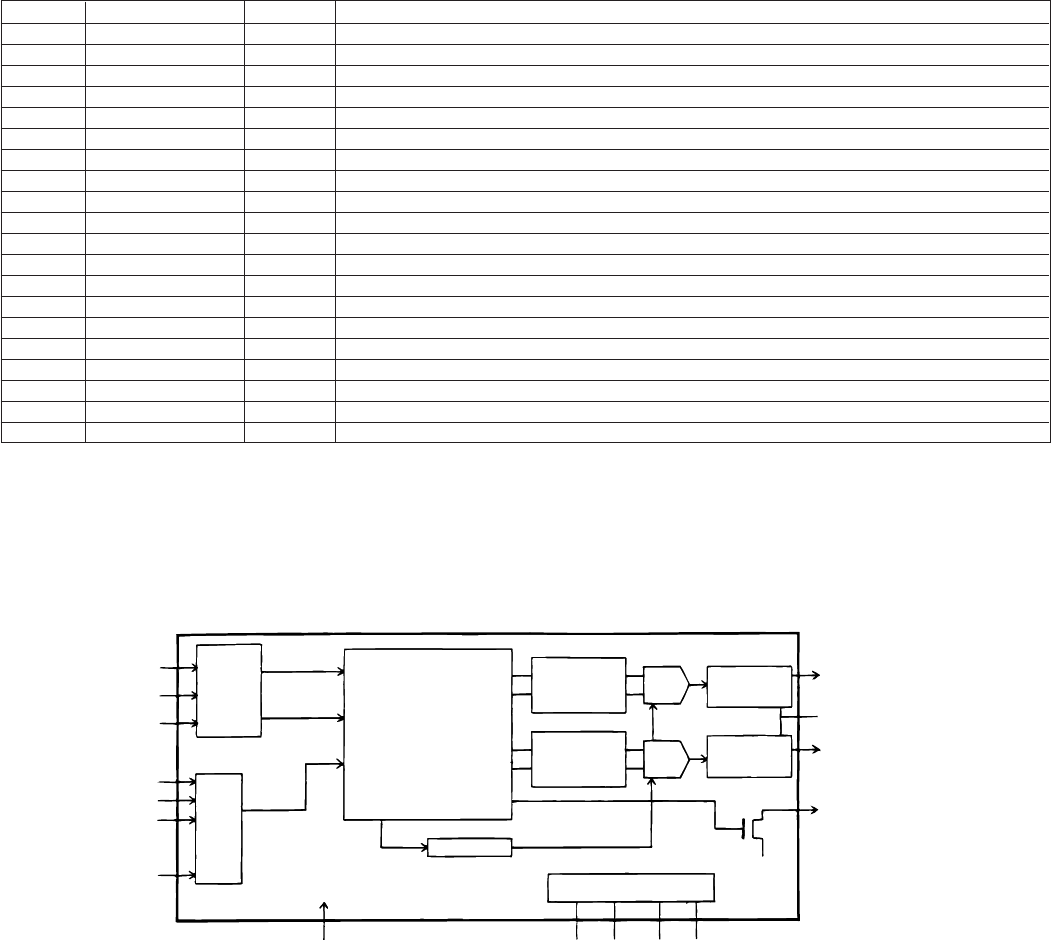
DV-760X
11-23
Pin No. Terminal name I/O Operation function
1 NC – Not connected.
2 SCKI I System clock input. (256fs/384fs)
3 TEST – Not connected. Be sure to open.
4 ML I Control data input. Enable terminal. *1
5 MC I Control data input. Bit clock terminal. *1
6 MD I Control data input. Data terminal. *1
7 RSTB I Reset input terminal. Active “L” *1
8 ZERO O Infinity zero flag output terminal. Open drain.
9 VOUTR O Rch analog voltage output terminal.
10 AGND – Analog GND terminal.
11 VCC – Analog power terminal.
12 VOUTL O Lch analog voltage output terminal.
13 CAP – Internal bias decouple terminal
14 BCKIN I Audio data. Bit clock input terminal. *2
15 DIN I Audio data. Data input terminal. *2
16 LRCIN I Audio data. Reference sampling clock input terminal. *2
17 TEST – Connect to GND.
18 NC – Not connected. Be sure to open.
19 VDD – Digital power terminal.
20 DGND – Digital GND terminal.
*1: Internal pull-up provided. Schmidt trigger input.
*2: Schmidt trigger input.
11-17. IC802~ 803 PCM1720E AUDIO D/A CONVERTER
• Block Diagram
BCKIN
LRCIN
DIN
ML
MC
MD
RSTB
Serial
Input
I/F
Mode
Control
I/F
256fs/384fs
SCKI VCC AGND CGNDVDD
Power Supply.
BPZ-Cont.
8X Oversampling
Digital Filter
with
Function Controller
Multi. -level·
Delta/Sigma
Modulator
Multi. -level·
Delta/Sigma
Modulator
DAC
DAC
Low-pass
Filter
Low-pass
Filter
VOUTL
CAP
VOUTR
ZERO
Open drain
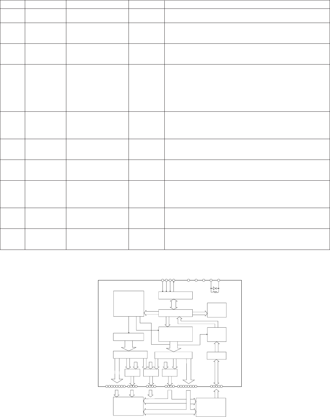
DV-760X
11-18. IC5001 IMN12510F FL DRIVER
18 VDD Power supply terminal Input VDD: +5V±0.5V
21 VSS VSS: 0V
16 VPP FLP driver power Input VPP: VDD–35V
The voltage to be supplied to the SEG 0 to 7, DGT 0 to 7 pull-down
resistor is applied.
19 OSCI Clock input Input Oscillation input terminal
A terminal to which the ceramic
20 OSCO Clock output Oscillation output terminal
oscillation terminal is connected.
To OSCI in case of clock input from outside in case of separate excitation
22 NCS Chip select input Input "L": Serial input allowed "H": Serial input inhibited
23 SCK Sirial clock input Input Serial transfer clock input
24 SDI Sirial data input Input Sirial data input
The command data, address data, indication data, control register
data, and port output data are input.
25 SDO Sirial data output Output Sirial data output
The key scan input data and port input data are output.
26~30 P30~P34 Key scan input In/Output
There are 5 bits. Bitwise selection of key scan input/general-use
input/general-use output is enabled. The pull-down resistor is pro
vided
between this terminal and the
VSS terminal.
The general-use output is large current output for LED drive.
31~38 SEG0~SEG7
High voltage resistance output
Output 8-bit high voltage resistance output port. (Segment output)
The output type is Pch open drain. The pull-down resistor is built in
between this terminal and the VPP terminal.
39~42 P10~P13
High voltage resistance output
Output 4-bit high voltage resistance output port.
SEG8~SEG11 Bitwise selection of general-use output/segment output is enabled.
The output type is Pch open drain.
43, 44 P20~23
High voltage resistance output
In/Output 4-bit high voltage resistance output port.
1, 2
DGT12/SEG15 Bitwise selection of general-use input/general-use output/seg ment
output/digit output is enabled. The output type is Pch open drain.
DGT15/SEG12 Large current output for LED drive
3~6 P00~P03
High voltage resistance output
Output 4-bit high voltage resistance output port.
DGT8~DGT11 Bitwise selection of general-use output/digit output is enabled.
The output type is Pch open drain.
7~10 DGT0~DGT7
High voltage resistance output
Output 8-bit high voltage resistance output port. (Digit output)
12~15 The output type is Pch open drain. The pull-down resistor is built
in between this terminal and the VPP terminal.
Terminal Terminal Name Name In/Output Function
~
)
• Block Diagram
11-24
NC S
SC K
SD I
SD O
VP P
VD D
VS S
S C1
S C2
D0 D7D8
(P53) (P32) (P20) (P23) (P13) (P10)
D11 DS12 DS15 S11 S8 S7 S0 P34 P30
5
8
444444
444
8
4
Timing generating
circuit
S B ( 8 )
L A T C H ( 8 )
Shift Resistor
MPL MPL MPL
LATCH(5)
5 X 1 2
( 8 X 3 2 ) X 2
S E G ( 1 6 )
D G T ( 1 6 )
F L P K E Y
M A T R I X
Comannding
Decoder
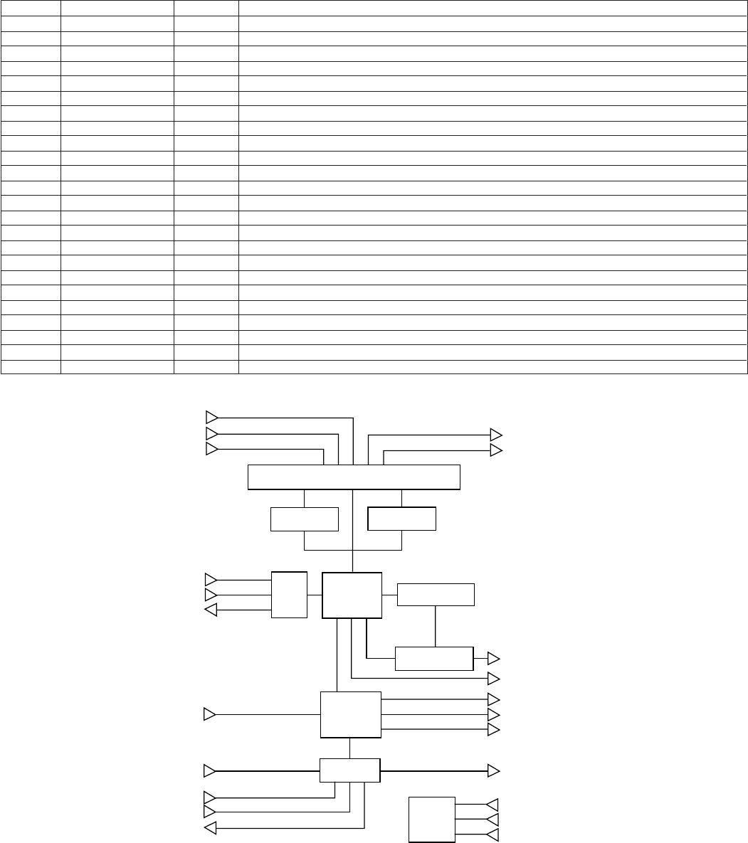
DV-760X
11-25
11-19. IC6501 LC8905V DIGITAL AUDIO INTERFACE
Pin No. Terminal name I/O Operation function
1 DIN1 I Amplifier built-in data input terminal (coaxial, corresponding to optical module)
2 DIN2 I Data input terminal (corresponding to optical module)
3 E/DOUT O Emphasis, input biphase, validity flag output terminal
4 VDD Power
5 R I VCO gain control input terminal
6 VIN I VCO free run setting input terminal
7 VCO O LPF setting terminal of PLL
8 GND Grounding
9 CKSEL I System clock selection input terminal
10 XMODE I Reset input terminal
11 AVOCK I PLL erroneous lock prevention clock input terminal
12 TEST1 I Test input terminal (to be grounded usually)
13 TEST2 I Test input terminal (to be grounded usually)
14 SCLK/CL I Microcomputer IF Clock input terminal
15 XLAT/CE I Microcomputer IF latch/chip enable input terminal
16 SWDT/DI I Microcomputer IF write data input terminal
17 SRDT/DO O Microcomputer IF read data output terminal
18 DQSY/LD O Microcomputer IF Sub-Q sync and ID sync output terminal
19 CKOUT O VCO clock output terminal (Self-run oscillation 384fs, 512fs)
20 FS128 O 128fs clock output terminal
21 BCK O Bit clock output terminal
22 LRCK O
L/R clock output terminal (L-ch=H, R-ch=L)
23 DATAOUT O Audio data output terminal
24 ERROR O PLL lock error mute output terminal
• Block Diagram
Microcomputer interface
C-Bit detection
Input
section Data
demodulator
Lock error detection
Mute output
Timing
PLL
TEST
Sub-Q detection
SCLK/CL
14
15
16
1
2
3
XLAT/CE
SWDT/DI
DIN1
DIN2
E/DOUT
CKSEL
AVOCK
R
VIN
VCO
DQSY/LD
SRDT/DO
ERROR
DATAOUT
SFS128
LRCK
BCK
CKOUT
TEST1
TEST21
XMODE
9
5
6
7
11
18
17
24
23
20
22
21
19
12
13
10

DV-760X
11-26
11-20. IC6502 CS49300 MPEG AUDIO DECODER
VA—Analog Positive Supply: Pin 34
Analog positive supply for clock generator. Nominally +3.3 V.
AGND—Analog Supply Ground: Pin 35
Analog ground for clock generator PLL.
VD1, VD2, VD3—Digital Positive Supply: Pins 1, 12, 23
Digital positive supplies. Nominally +2.5 V.
DGND1, DGND2, DGND3—Digital Supply Ground: Pins 2, 13, 24
Digital ground.
FILT1—Phase-Locked Loop Filter: Pin 33
Connects to an external filter for the on-chip phase-locked loop. This pin does not meet Cirrus Logic's ESD tolerance of 2000V
using the human body model. This pin will tolerate ESD of 1000V using the human body model.
FILT2—Phase Locked Loop Filter: Pin 32
Connects to an external filter for the on-chip phase-locked loop. This pin does not meet Cirrus Logic's ESD tolerane of 2000V
using the human body model. This pin will tolerate ESD of 1000V using the human body model.
CLKIN—Master Clock Input: Pin 30
CS493XX clock input. When in internal clock mode (CLKSEL=DGND), this input is connected to the internal Pll from which all internal
clocks are derived. When in external clock mode (CLKSEL=VD), this input is connected to the DSP clock.
CLKSEL—DSP Clock Select: Pin 31
This pin selects the clock mode of the CS493XX. When CLKSEL is low, CLKIN is connected to the internal PLL from which all internal
clocks are derived. When CLKSEL is high CLKIN is connected to the DSP clock.
DATA7, EMAD7, GPIO7 — Pin8
DATA6, EMAD6, GPIO6 — Pin9
DATA5, EMAD5, GPIO5 — Pin10
DATA4, EMAD4, GPIO4 — Pin11
DATA3, EMAD3, GPIO3 — Pin14
DATA2, EMAD2, GPIO2 — Pin15
DATA1, EMAD1, GPIO1 — Pin16
DATA0, EMAD0, GPIO0 — Pin17
In parallel host mode, these pins provide a bidirectional data bus. If a serial host mode is selected, these pins can provide a multiplexed
address and data bus for connecting an 8-bit external memory. Otherwise, in serial host mode, these pins can act as general-purpose
input or output pins that can be individually configured and controlled by the DSP.
A0, SCCLK—Host Parallel Address Bit Zero or Serial Control Port Clock: Pin 7
In parallel host mode, this pin serves as one of two address input pins used to select one of four parallel registers. In serial host mode,
this pin serves as the serial control clock signal, specifically as the SPI clock input or the I2C clock input.
A1, SCDIN—Host Address Bit One or SPI Serial Control Data Input: Pin 6
In parallel host mode, this pin seves as on of two address input pins used to select one of four parallel registers. In SPI serial host mode,
this pin serves as the data input.
RD, R/W, EMOE, GPIO11—Host Parallel Output Enable or Host Parallel R/W or External Memory Output Enable or General Purpose
Input & Output Number 11: Pin 5
In Intel parallel host mode, this pin serves as the active-low data bus enable input. In Motorola parallel host mode, this pin serves as the
read-high/write-low control input signal. In serial host mode, this pin can serve as the external memory active-low data-enable output
signal. Also in serial host mode, this pin can serve as a general purpose input or output bit.
WR, DS, EMWR, GPIO10—Host Write Strobe or Host Data Strobe or External Memory Write Enable or General Purpose Input &
Output Number 10: Pin 4
In Intel parallel host mode, this pin serves as the active-low data-write-input strobe. In Motorola parallel host mode, this pin serves as the
active-low data-strobe-input signal. In serial host mode, this pin can serve as the external-memory active-low write-enable output signal.
Also in serial host mode, this pin can serve as a general purpose input or output bit.
CS—Host Parallel Chip Select, Host Serial SPI Chip Select: Pin 18
In parallel host mode, this pin serves as the active-low chip-select input signal. In serial host SPI mode, this pin is used as the active-low
chip-select input signal.
RESET—Master Reset Input: Pin 36
Asynchronous active-low master reset input. Reset should be low at power-up to initialize the CS493XX and to guarantee that the device
is not active during initial power-on stabilization periods. At the rising edge of reset the host interface mode is selected contingent on the
state of the RD, WR and PSEL pins. Additionally, an autoboot sequence can be initiated if a serial control mode is selected and ABOOT
is held low. If reset is low all bidirectional pins are high impedance inputs.
SCDIO, SCDOUT, PSEL, GPIO9—Serial Control Port Data Input and Output, Parallel Port Type Select: Pin 19
In I2C mode, this pin serves as the open-drain bidirectional data pin. In SPI mode this pin serves as the data output pin. In parallel host
mode, this pin is sampled at the rising edge of RESET to configure the parallel host mode as an Intel type bus or as a Motorola type bus.
In Parallel host mode, after the bus mode has been selected, the pin can function as a general-purpose input or output pin.
EXTMEM, GPIO8—External Memory Chip Select or General Purpose Input & Output Number 8: Pin 21
In serial control port mode, this pin can serve as an output to provide the chip-select for an external byte-wide ROM. In parallel and serial
host mode, this pin can also function as a general-purpose input or output pin.
INTREQ, ABOOT—Control Port Interrupt Request, Automatic Boot Enable: Pin 20
Open-drain interrupt-request output. This pin is driven low to indicate that the DSP has outgoing control data and should be serviced by
the host. Also in serial host mode, this siganl intiates an automatic boot cycle from external memory if it is held low through the rising edge
of reset.
AUDATA2—Digital Audio Output 2: Pin 39
PCM multi-format digital-audio data output, capable of two-channel 20-bit output. This PCM output defaults to DGND as output until
enabled by the DSP software.
DV-760X
11-27
AUDATA1—Digital Audio Output 1: Pin 40
PCM multi-format digital-audio data output, capable of two-channel 20-bit output. This PCM output defaults to DGND as output until
enabled by the DSP software.
AUDATA0—Digital Audio Output 0: Pin 41
PCM multi-format digital-audio data output, capable of two-, four-, or six-channel 20-bit output. This PCM output defaults to DGND as
output until enabled by the DSP software.
MCLK—Audio Master Clock: Pin 44
Bidirectional master audio clock. MCLK can be an output from the CS493XX that provides an oversampled audio- output clock at either
128 Fs, 256 Fs, or 512 Fs. MCLK can be an input at 128 Fs, 256 Fs, 384 Fs, or 512 Fs. MCLK is used to derive SCLK and LRCLK when
SCLK and LRCKL are driven by the CS493XX.
SCLK—Audio Output Bit Clock: Pin 43
Bidirectional digital-audio output bit clock. SCLK can be an output that is dirived from MCLK to provide 32 Fs, 64 Fs,128Fs, 256 Fs, or
512 Fs, depending on the MCLK rate and the digital-output configuration. SCLK can also be an input and must be at least 48Fs or greater.
LRCLK—Audio Output Sample Rate Clock: Pin 42
Bidirectional digital-audio output-sample-rate clock. LRCLK can be an output that is divided from MCLK to provide the output sample rate
depending on the output configuration. LRCLK can also be an input. AS an input LRCLK is independent of MCLK.
XMT958—SPDIF Transmitter Output: Pin 3
CMOS level output that contains a biphase-encoded clock for synchronously providing two channels of PCM digital audio or a IEC61937
compressed-data interface or both. This output typically connects to the input of an RS-422 transmitter or to the input of an optical
transmitter.
SCLKN1, STCCLK2—PCM Audio Input Bit Clock: Pin 25
Bidirectional digital-audio bit clock that is an output in master mode and an input in slave mode. In slave mode, SCLKN1 operates
asynchronously from all other CS493XX clocks. In master mode, SCLKN1 is derived from the CS493XX internal clock generator. In either
master or slave mode, the active edge of SCLKN1 can be programmed by the DSP. For applications supporting PES layer synchronization
this pin can be used as STCCLK2, which provides a path to the internal STC 33 bit counter.
LRCLKN1—PCM Audio Input Sample Rate Clock: Pin 26
Bidirectional digital-audio frame clock that is an output in master mode and an input slave mode. LRCLKN1 typically is run at the sampling
frequency. In slave mode, LRCLKN1 operates asynchronously from all other CS493XX clocks. In master mode, LRCLKN1 is derived from
the CS493XX internal clock generator. In either master or slave mode, the polarity of LRCLKN1 for a particular subframe can be
programmed by the DSP.
SDATAN1—PCM Audio Data Input Number One: Pin 22
Digital-audio data input that can accept from one to six channels of compressed or PCM data. SDATAN1 can be sampled with either edge
of SCLKN1, depending on how SCLKN1 has been configured.
CMPCLK, SCLKN2—PCM Audio Input Bit Clock: Pin 28
Bidirectional digital-audio bit clock taht is an output in master mode and an input in slave mode. In slave mode, SCLKN2 operates
asynchronously from all other CS493XX clocks. In master mode, SCLKN2 is derived from the CS493XX internal clock generator. In either
master or slave mode, the active edge of SCLKN2 can be programmed by the DSP. If the CDI is configured for bursty delivery, CMPCLK
is an input used to sample CMPDAT.
CMPREQ, LRCLKN2—PCM Audio Input Sample Rate Clock: Pin 29
When the CDI is configured as a digital audio input, this pin serves as a bidirectional digital-audio frame clock that is an output in master
mode and an input in slave mode. LRCLKN2 typically is run at the sampling frequency. In slave mode, LRCLKN2 operates asynchronously
from all other CS493XX clocks. In master mode, LRCLKN2 is derived from the CS493XX internal clock generator. In either master or slave
mode, the polarity of LRCLKN2 for a particular subframe can be programmed by the DSP. When the CDI is configured for bursty delivery,
or parallel audio data delivery is being used, CMPREQ is an output which serves as an internal FIFO monitor. CMPREQ is an active low
signal that indicates when another block of data can be accepted.
CMPDAT, SDATAN2—PCM Audio Data Input Number Two: Pin 27
Digital-audio data input that can accept from one to six channels of compressed or PCM data. SDATAN2 can be sampled with either edge
of SCLKN2, depending on how SCLKN2 has been configured. Similarly CMPDAT is the compressed data input pin when the CDI is
configured for bursty delivery. When in this mode, the CS493XX internal PLL is driven by the clock recovered from the incoming data
stream.
DC—Reserved: Pin 38
This pin is reserved and should be pulled up with an external 4.7k resistor.
DD—Reserved: Pin 37
This pin is reserved and should be pulled up with an external 4.7k resistor.
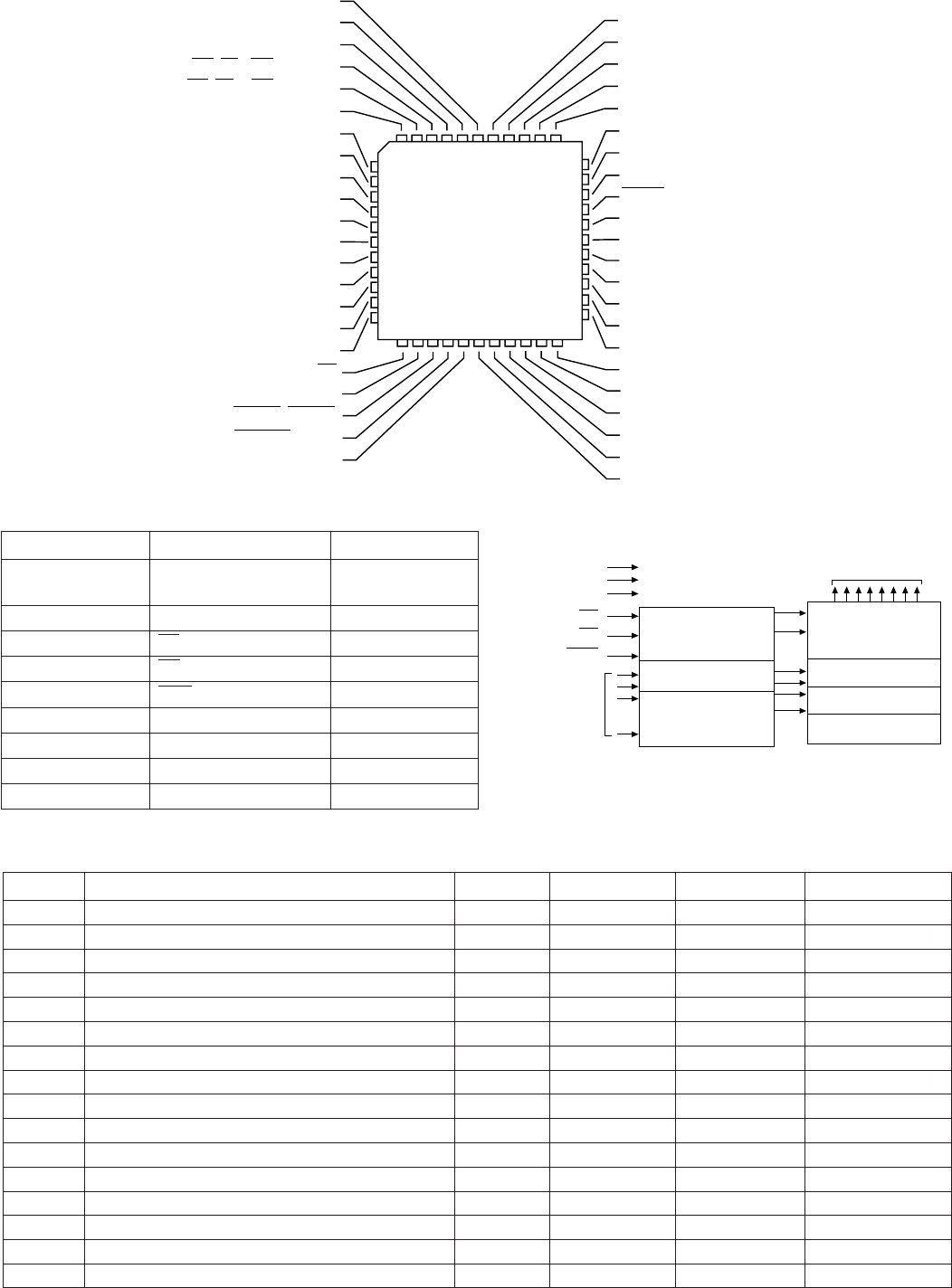
DV-760X
11-28
• Block Diagram
PIN No. PIN NAME I/O ATTR I/O CELL PDV CELL LIO CELL
1 VDD P VDD * *
2 HADR0 I IDC * *
3 HADR1 I IDC * *
4 HADR2 I IDC * *
5 HCS I IDC * *
6 HWR I IDC * *
7 HRD I IDC * *
8 HDAT0 B BDC3 PDV2T *
9 HDAT1 B BDC3 PDV2T *
10 HDAT2 B BDC3 PDV2T *
11 HDAT3 B BDC3 PDV2T *
12 HDAT4 B BDC3 PDV2T *
13 HDAT5 B BDC3 PDV2T *
14 HDAT6 B BDC3 PDV2T *
15 HDAT7 B BDC3 PDV2T *
16 VSS P VSS PDV2T *
11-22. IC6511 IX1535GE DSP I/F
6
VD1
DGND1
AUDATA3, XMT958
WR, DS EMWR, GPIO10
RD, R/W, EMOE, GPIO11
A1, SCDIN
A0, SCCLK
DATA7, EMAD7, GPIO7
DATA6, EMAD6, GPIO6
DATA5, EMAD5, GPIO5
DATA4, EMAD4, GPIO4
VD2
DGND2
DATA3, EMAD3, GPIO3
DATA2, EMAD2, GPIO2
DATA1, EMAD1, GPIO1
DATA0, EMAD0, GPIO0
CS
SCDIO,SCDOUT, PSEL, GPIO9
ABOOT, INTREQ
EXTMEM, GPIO8
SDATAN1
7
8
9
10
11
12 CS493XX-CL
44-Pin PLCC
Top View
13
14
15
16
17
18 19 2021 22 23 24 25 26 27 28
29
30
31
32
33
34
35
36
37
38
39
543214443424140
MCLK
SCLK
LRCLK
AUDATA0
AUDATA1
AUDATA2
DC
DD
RESET
AGND
VA
FILT1
FILT2
CLKSEL
CLKIN
CMPREQ, LRCLKN2
CMPCLK, SCLKN2
CMPDAT, SDATAN2, RCV958
LRCLKN1
SCLKN1,STCCLK2
DGND3
VD3
Pin No. Pin Name
2,3,4,5-12,23,25, A0~A16 Addresses
26,27,28,29
13-15,17-24 O0~O7 Outputs
22 CE Chip Enable
24 OE Output Enable
31 PGM Program Strobe
30 NC No Connect
32 Vcc
1 Vpp
16 GND
Function
11-21. IC6503 IX1617GE ROM
Vcc
GND
VPP
OE
CE
PGM
A0~A16
ADDRESS
INPUTS
OE, CE AND
PROGRAM LOGIC
Y DECODER
X DECODER
OUTPUT
BUFFERS
Y-GATING
CELL MATRIX
IDENTIFICATION
DATA OUTPUTS
O0~O7

DV-760X
11-29
17 VDD P VDD * *
18 EXPAL0 B UC3 PDV2T *
19 EXPAL1 B UC3 PDV2T *
20 EXPAL2 B UC3 PDV2T *
21 EXPAL3 B UC3 PDV2T *
22 EXPAU0 B UC3 PDV2T *
23 EXPAU1 B UC3 PDV2T *
24 VSS P VSS * *
25 VDD P VDD * *
26 EXPAU2 B UC3 PDV2T *
27 EXPAU3 B UC3 PDV2T *
28 EXPBL0 B UC3 PDV2T *
29 EXPBL1 B UC3 PDV2T *
30 EXPBL2 B UC3 PDV2T *
31 EXPBL3 B UC3 PDV2T *
32 VSS P VSS * *
33 VDD P VDD * *
34 EXPBU0 B UC3 PDV2T *
35 EXPBU1 B UC3 PDV2T *
36 EXPBU2 B UC3 PDV2T *
37 EXPBU3 B UC3 PDV2T *
38 EXPC0 B BDC3 PDV2T *
39 EXPC1 B BDC3 PDV2T *
40 EXPC2 P BDC3 * *
41 VSS P VSS * *
42 EXPC3 B BDC3 PDV2T *
43 EXPC4 B BDC3 PDV2T *
44 EXPC5 B BDC3 PDV2T *
45 EXPD0 B UC3 PDV2T *
46 EXPD1 B UC3 PDV2T *
47 EXPD2 B UC3 PDV2T *
48 VSS P VSS * *
49 VDD P VDD * *
50 EXPD3 B UC3 PDV2T *
51 EXPD4 B UC3 PDV2T *
52 EXPD5 B UC3 PDV2T *
53 BUFDO O ODN3 PDV1T *
54 BUFDI I IDC * *
55 SBUFBO O ODN3 PDV1T *
56 SBUFBI I LIN * STB
57 SBUFAO O ODN3 PDV1T *
58 SBUFAI I LIN * STB
59 MRST I IDC * *
60 MODE I IDC * *
61 BUFCO B BDC3 PDV2T *
62 TEST I ITST1 * *
63 IBUFCI I IDC * *
64 VSS P VSS * *
PIN No. PIN NAME I/O ATTR I/O CELL PDV CELL LIO CELL
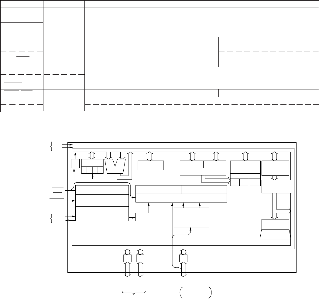
DV-760X
11-30
11-23. IC8201 IX1610GE
Pin Name Input/Output Functions
R43 to R40
I/O
4-bit I/O port with latch.
When used as input port, the latch must be set to "1".
R53 to R50 Every bit data is possible to be set cleared and tested by the bit manipulation instruction of the
L-register indirect addressing.
R81 (T2) 2-bit I/O port with latch. Timer/Counter 2 external input
I/O(Input) When used as input port, external interrupt input
R80 (INT2) pin, or timer/counter external input pin, the latch External interrupt 2 input
must be set to "1".
XIN Input Resonator connecting pins.
XOUT Output For inputting external clock, XIN is used and XOUT is opened.
RESET Input Reset signal input
HOLD(INT1) I/O(Input) Hold request/release signal input External interrupt 1 input and R82 I/O
VDD Power Supply +5V
Vss 0V (GND)
• Block Diagram
Hold controller
System controller
Timing Generator
Clock Generator Interval Timer
12-bit
Timer/Counter
(2ch)
CZSG
FLAG
ALU
KE Accumulator HR LR
RAM Address buffer
Data Memory
(RAM) Program
Counter
IR register
IR Decoder
EIR
Interrupt controller
EIF
Stack SPW
DCTC2TC1
R5
R53
to
R50
R4
R43
to
R40
R8
R81 (T2)
R80 (INT2)
I/O
port
I/O port
(
R4 is Hi
g
h current port
)
T/C input
Interrupt input
Program
Memory (ROM)
VDD
VSS
HOLD
(INT1)
RESET
Power Supply
XIN
XOUT
Osc. connecting
pins
Hold input
Reset input

DV-760X
11-31
- M E M O -
DV-760X
12. SEMICONDUCTOR LEAD IDENTIFICATION
12-1
IC602
RH-iX0750TAZZ
IC702
VHiBA6796FP-1
IC802
IC803
VHiPCM1720E-1
1
1
1
1
1
S H A R P
1
1
IC201
VHiMC44724A-1
IC303
RH-iX1517GEZZ
IC402
RH-iX1474GEZZ
IC504
RH-iX1478GEZZ
IC508
RH-iX1516GEZZ
IC512
IC6511
RH-iX1535GEZZ
IC601
RH-iX1521GEZZ
IC707
RH-iX1473GEZZ
IC9001
VHiT78DL09S-1
IC9002
VHiKA7808Pi-1
IC9003
IC9004
VHiPQ30RV11-1
IC6503
RH-iX1617GEZZ
IC6502
VHiCS49300/-1
IC704 IC2007
RH-iX1531CEZZ
IC2102
VHiTC4W53F/-1
IC6001 IC6602
VHiNJM4560M-1
IC5001
VHiMN12510F/-1
X601
RCRSC0031GEZZ
X702
RCRSC0035GEZZ
X6501
RCRSC0038GEZZ
IPN
IPN
IC301
RH-iX1461GEZZ
IC6501
VHiLC89051V-1
IC801
VHiPCM1716E-1
IC401
RH-iX1484GEZZ
IC501
RH-iX1614GEZZ
1
IC6002
VHiNJM2060M-1
IC6504
VHiLVX125FT-1
IC6512
VHiTVHCU04F-1
IC703
VHi10324AFV-1
IC506
RH-iX1618GEZZ
IC507
VHiBR93L46F-1
IC509 IC8202
VHiPST600iM-1
IC8201
RH-iX1610GEZZ
IC2002 IC2003
IC2004
VHiHJM2268M-1
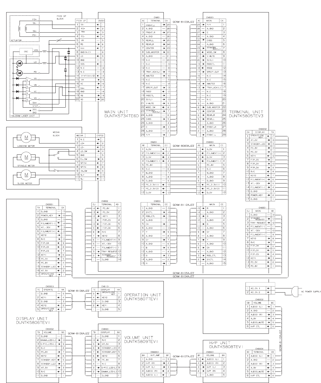
DV-760X
13-1
13. WIRING DIAGRAM
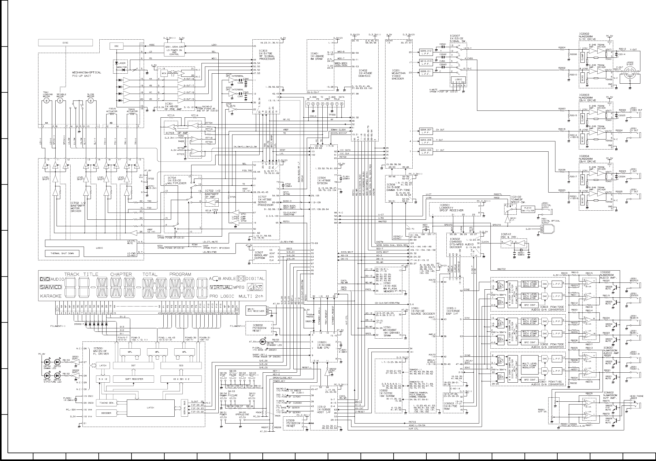
1234567891011 12 13 14 15 16 17 18 19 20
A
B
C
D
E
F
G
H
I
J
DV-760X DV-760X
14-1~14-2
14. BLOCK DIAGRAMS
14-1. MAIN BLOCK DIAGRAM
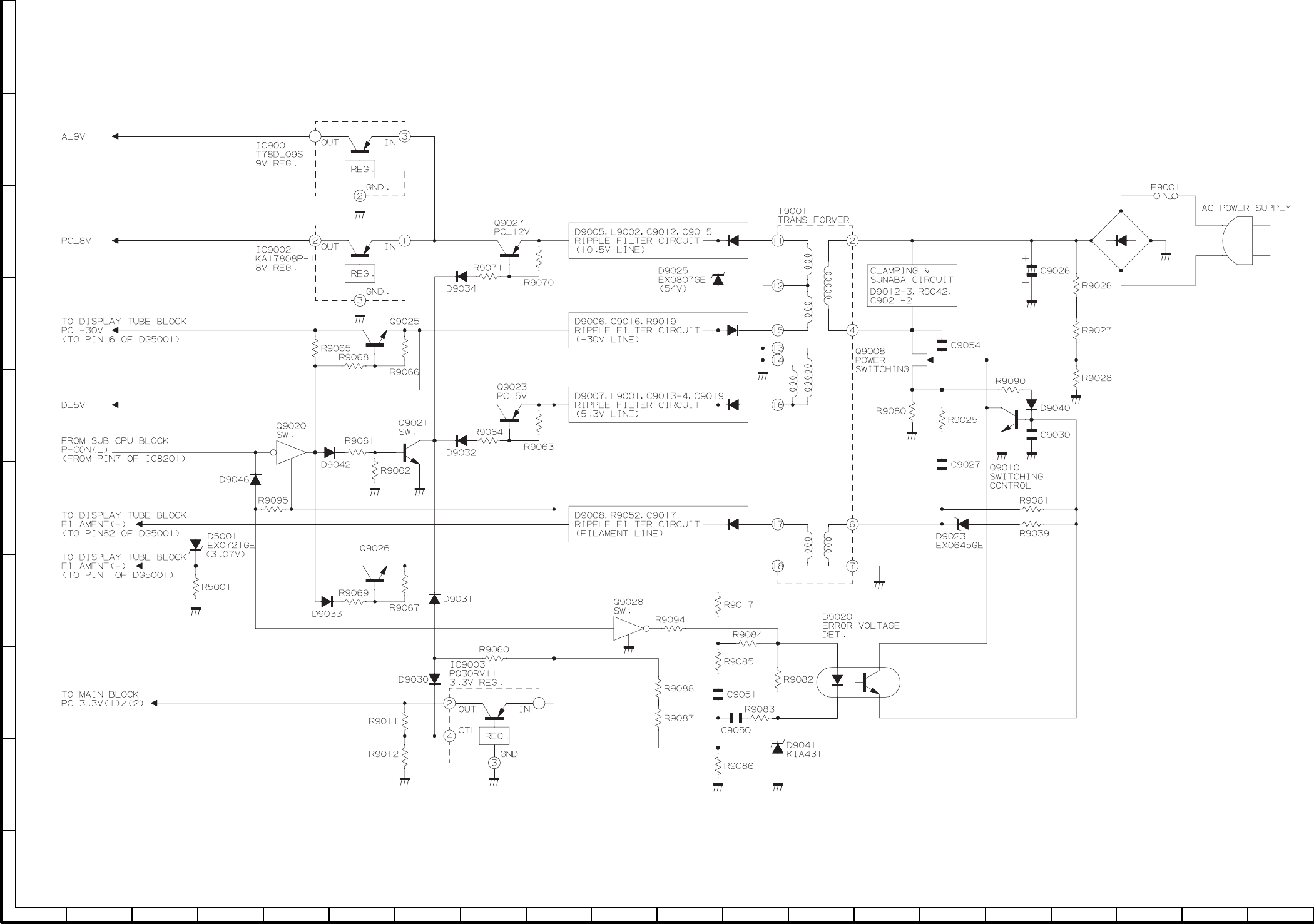
1234567891011 12 13 14 15 16 17 18 19 20
A
B
C
D
E
F
G
H
I
J
DV-760X DV-760X
14-3~14-4
14-2. POWER BLOCK DIAGRAM
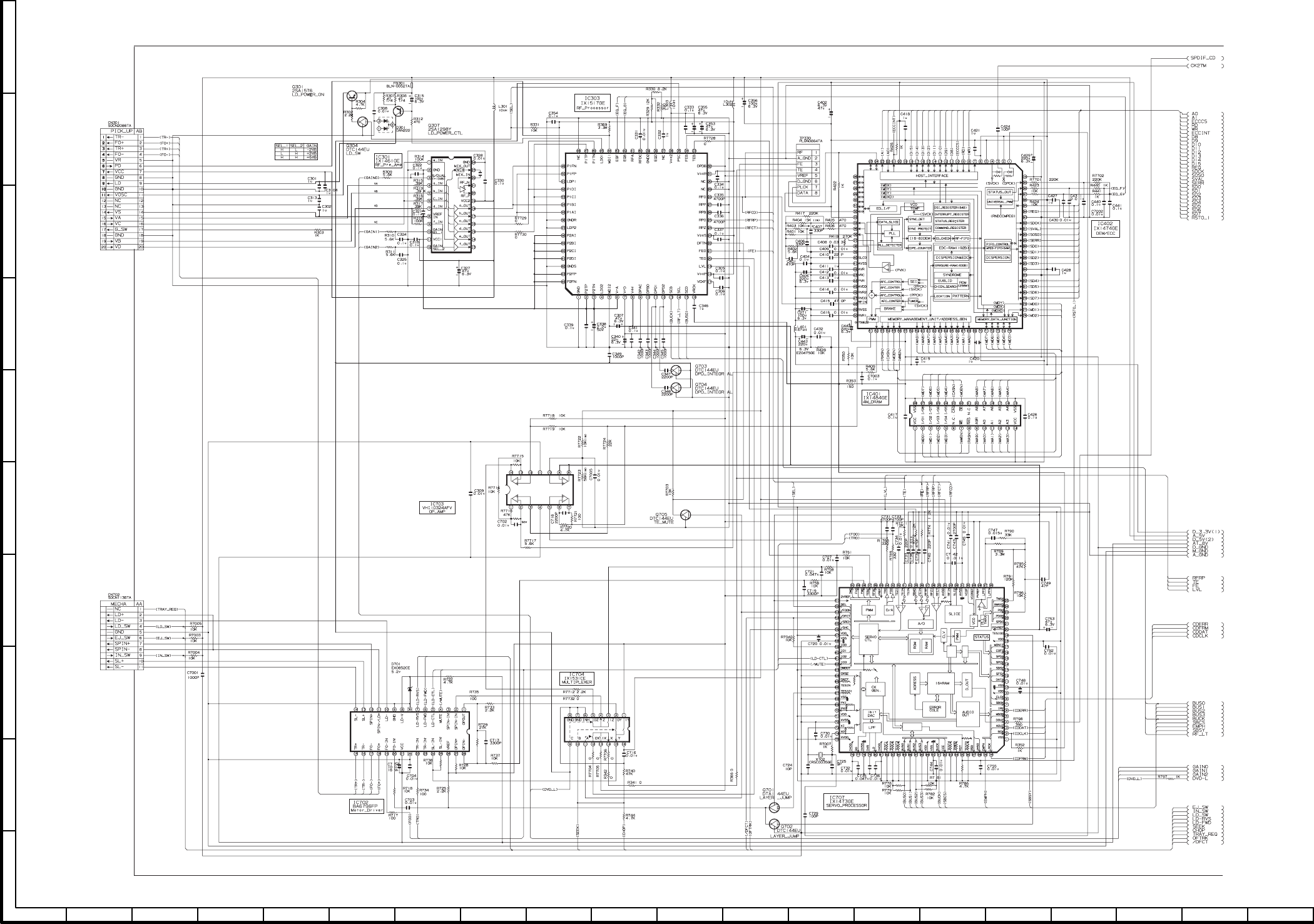
1234567891011 12 13 14 15 16 17 18 19 20
A
B
C
D
E
F
G
H
I
J
DV-760X DV-760X
15-1~15-2
15. SCHEMATIC DIAGRAMS 15-1. MAIN (1) CIRCUIT SCHEMATIC DIAGRAM
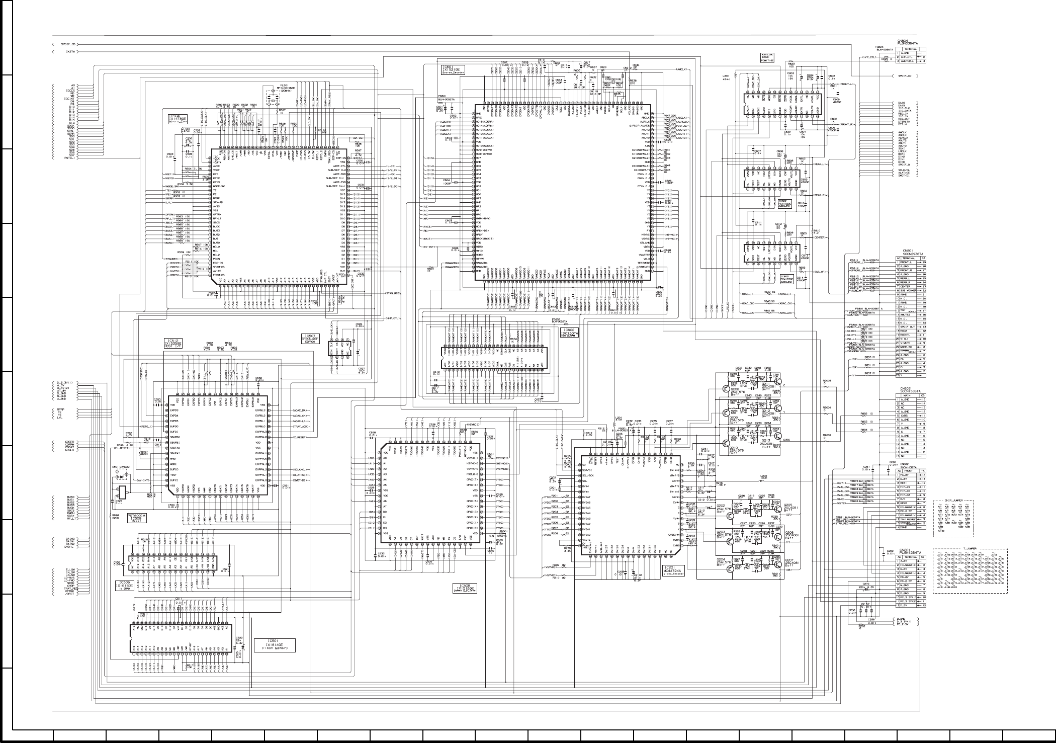
1234567891011 12 13 14 15 16 17 18 19 20
A
B
C
D
E
F
G
H
I
J
DV-760X DV-760X
15-3~15-4
15-2. MAIN (2) CIRCUIT SCHEMATIC DIAGRAM
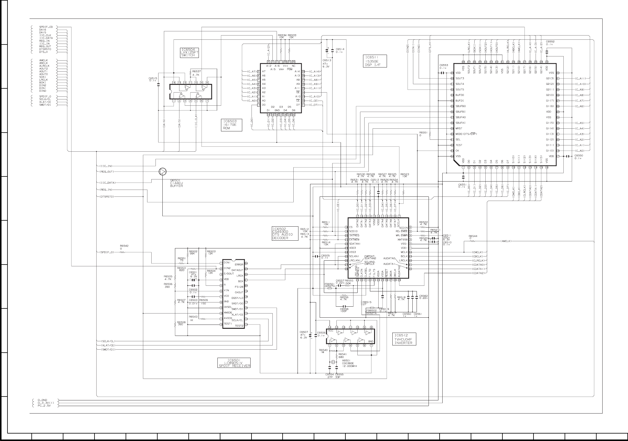
1234567891011 12 13 14 15 16 17 18 19 20
A
B
C
D
E
F
G
H
I
J
DV-760X DV-760X
15-5~15-6
15-3. MAIN (3) CIRCUIT SCHEMATIC DIAGRAM
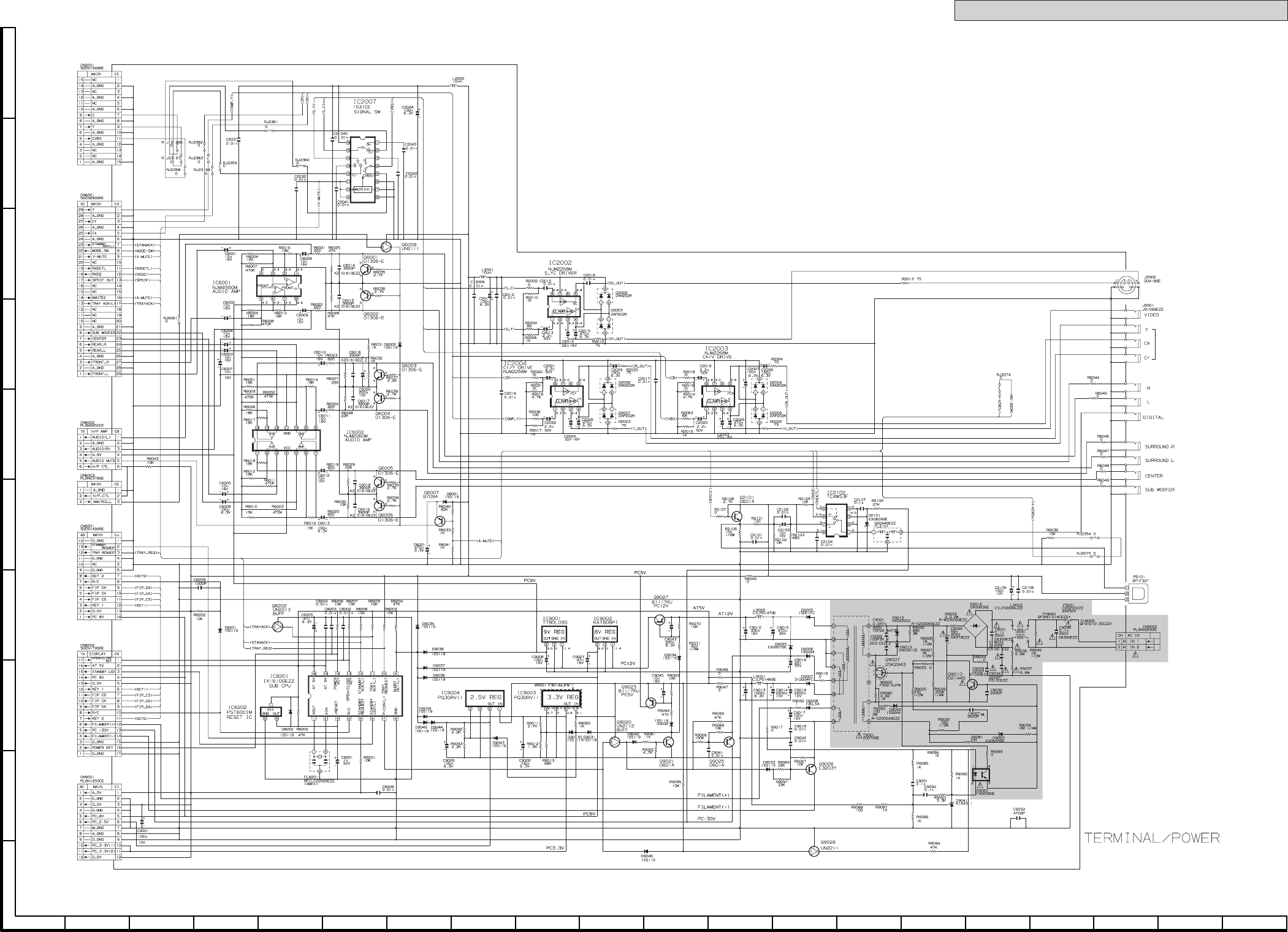
1234567891011 12 13 14 15 16 17 18 19 20
A
B
C
D
E
F
G
H
I
J
DV-760X DV-760X
15-7~15-8
15-4. TERMINAL CIRCUIT SCHEMATIC DIAGRAM å AND SHADED COMPONENTS=SAFETY RELATED PARTS
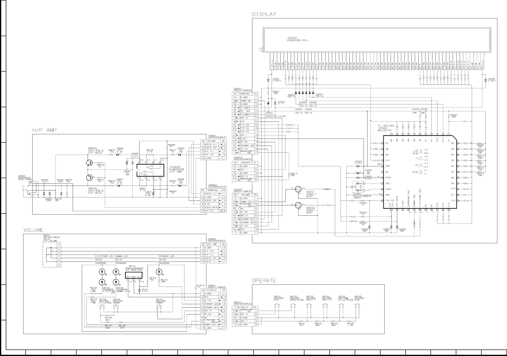
1234567891011 12 13 14 15 16 17 18 19 20
A
B
C
D
E
F
G
H
I
J
DV-760X DV-760X
15-9~15-10
15-5. DISPLAY/OPERATE/VOLUME/H/P AMP CIRCUIT SCHEMATIC DIAGRAM
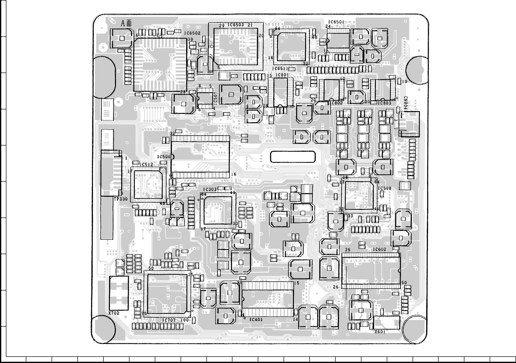
1234567891011 12 13 14 15 16 17 18 19 20
A
B
C
D
E
F
G
H
I
J
DV-760X DV-760X
16-1~16-2
Componet Side
16. PRINTED WIRING BOARD ASSEMBLIES 16-1. MAIN PWB
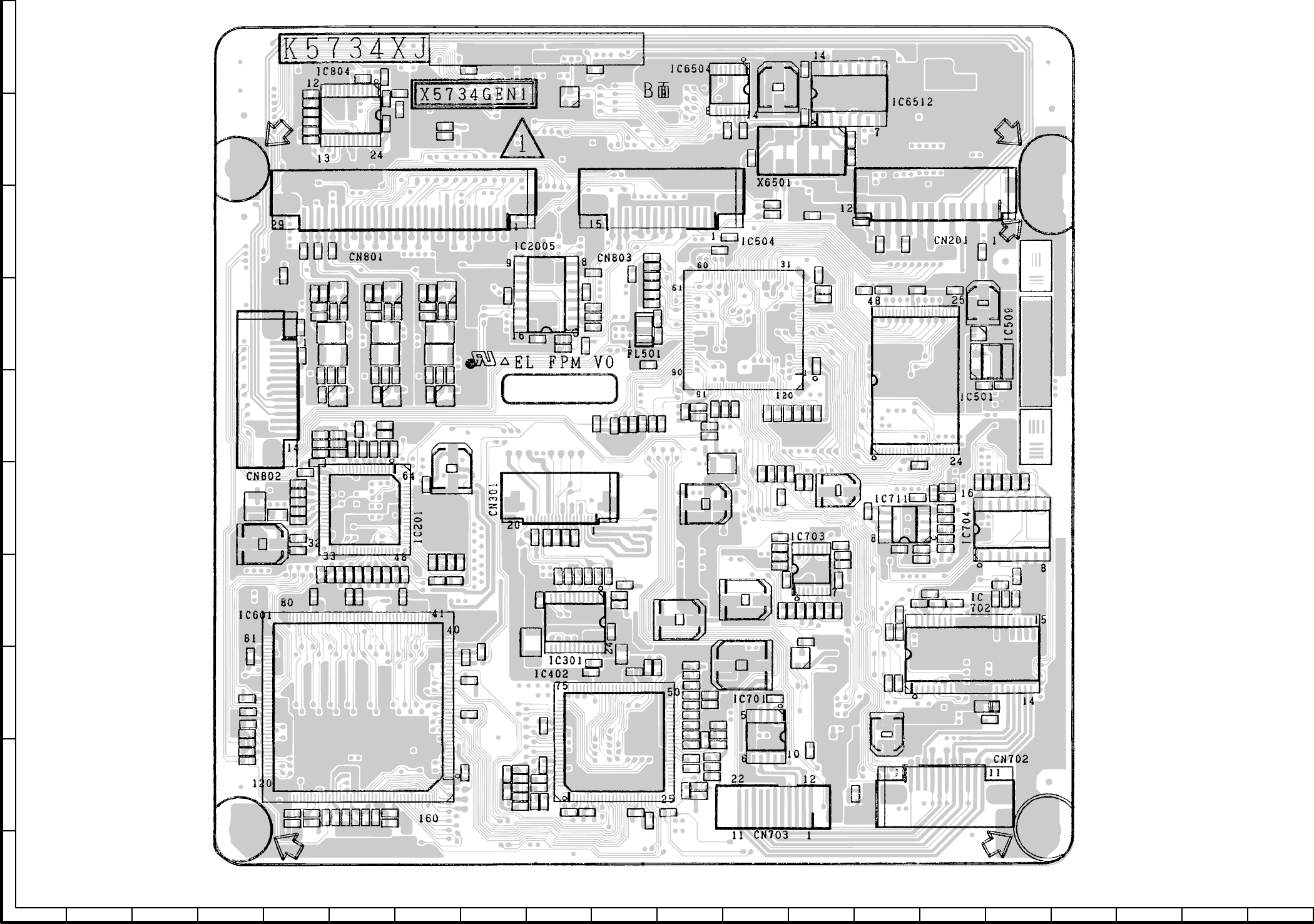
1234567891011 12 13 14 15 16 17 18 19 20
A
B
C
D
E
F
G
H
I
J
DV-760X DV-760X
16-2. MAIN PWB
Wiring Side
16-3~16-4
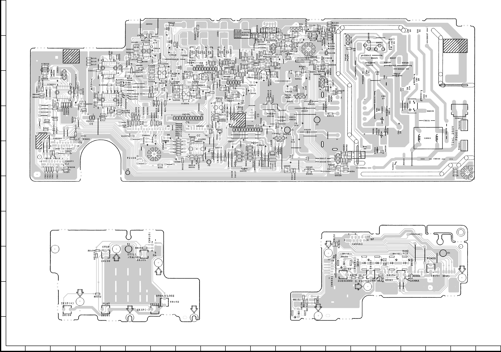
1234567891011 12 13 14 15 16 17 18 19 20
A
B
C
D
E
F
G
H
I
J
DV-760X DV-760X
16-5~16-6
16-3. TERMINAL/OPERATE/VOLUME PWB
TERMINAL
OPERATE VOLUME
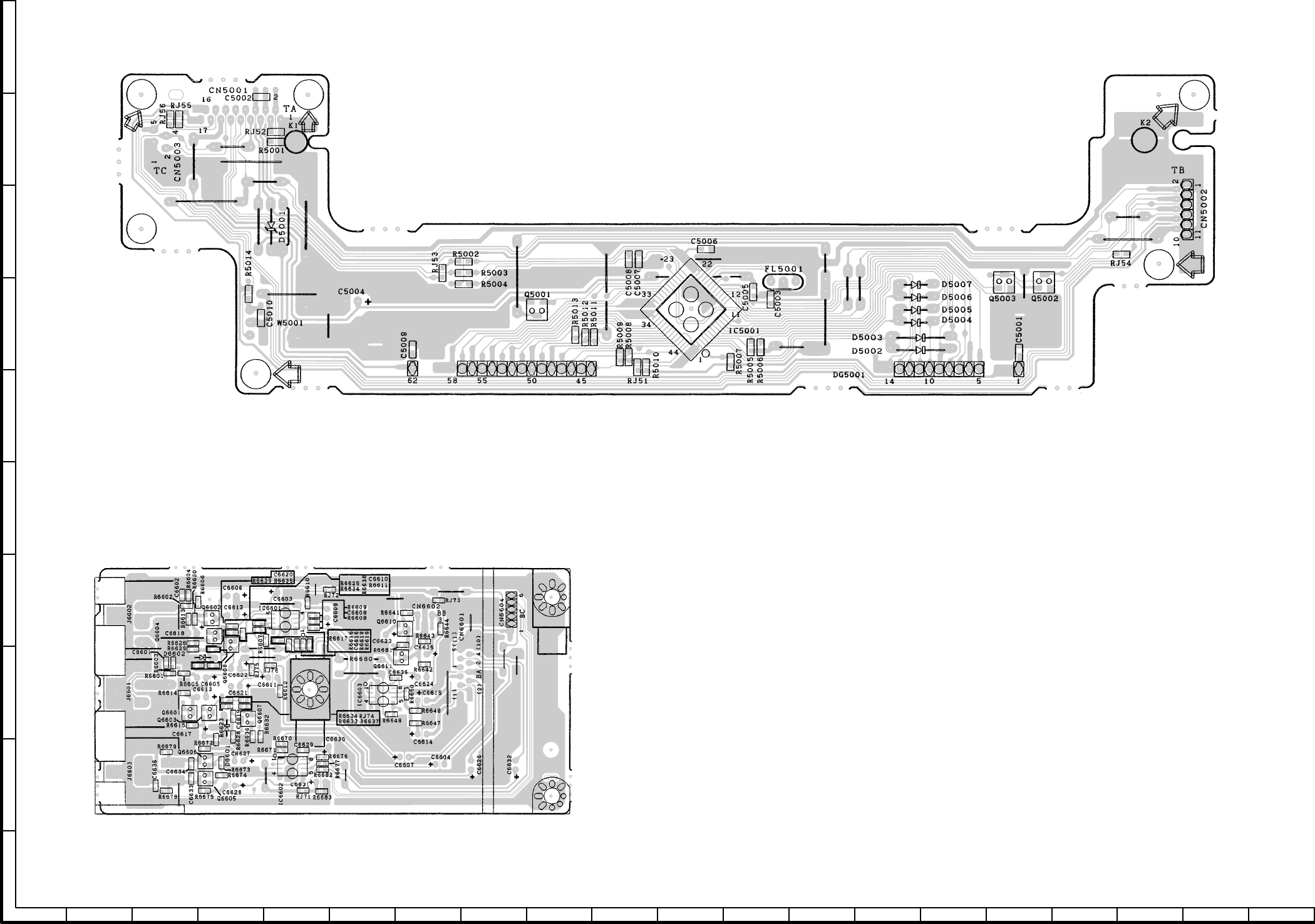
1234567891011 12 13 14 15 16 17 18 19 20
A
B
C
D
E
F
G
H
I
J
DV-760X DV-760X
16-7~16-8
16-4. DISPLAY/H/P AMP PWB
DISPLAY
H/P AMP

Ref. No. Part No. ★Description Code Ref. No. Part No. ★Description Code
73
DV-760X
17.REPLACEMENT PARTS LIST/
EXPLODED VIEWS
ELECTRICAL PARTS LIST
Parts marked with
"
å
"
are important for maintaining the safety of the
set. Be sure to replace these parts with specified ones for maintaining
the safety and performance of the set.
"
HOW TO ORDER REPLACEMENT PARTS
"
★MARK : SPARE PARTS-DELIVERY SECTION : ALL JAPAN
To have your order filled promptly and correctly, please furnish
the following informations.
1. MODEL NUMBER 2. REF. NO.
3. PART NO. 4. DESCRIPTION
5. PRICE CODE
å MARK: SAFETY RELATED PARTS
PWB ASSEMBLY IS NOT REPLACEMENT ITEM
Ref. No. Part No. ★Description Code
Q203 VS2SA1576//-1 2SA1576 AB
Q204 VS2SA1576//-1 2SA1576 AB
Q205 VS2SC4081//-1 2SC4081 AB
Q206 VS2SC4081//-1 2SC4081 AB
Q207 VS2SC4081//-1 2SC4081 AB
Q208 VS2SA1576//-1 2SA1576 AB
Q209 VS2SA1576//-1 2SA1576 AB
Q210 VS2SA1576//-1 2SA1576 AB
Q211 VS2SC4081//-1 2SC4081 AB
Q212 VS2SC4081//-1 2SC4081 AB
Q213 VS2SC4081//-1 2SC4081 AB
Q301 VS2SA1576//-1 2SA1576 AB
Q304 VSDTC144EU/-1 DTC144EU AB
Q307 VS2SA1298Y/-1 2SA1298Y AB
Q701 VSDTA144EU/-1 DTA144EU AC
Q702 VSDTC144EU/-1 DTC144EU AB
Q703 VSDTC144EU/-1 DTC144EU AB
Q704 VSDTC144EU/-1 DTC144EU AB
Q705 VSDTC144EU/-1 DTC144EU AB
Q6501 VSDTC144EU/-1 DTC144EU AB
DIODES
D301 VHDDAN222//-1 DAN222 AA
D501 VHDDAN222//-1 DAN222 AA
D701 RH-EX0852CEZZ Zener, EX0852CE AC
PACKAGED CIRCUITS
X601 RCRSC0031GEZZ Crystal, CRSC0031GE AK
X702 RCRSC0035GEZZ Crystal, CRSC0035GE AG
X6501 RCRSC0038GEZZ Crystal, CRSC0038GE AK
FILTER
FL501 RFiLC0196GEZZ Filter, FiLC0196GE AE
COILS
L201 VP-NM470K2R0N Peaking, 47µHAB
L202 VP-NM100KR42N Peaking, 10µHAB
L203 VP-1M270K3R8N Peaking, 27µHAC
L204 VP-1M270K3R8N Peaking, 27µHAC
L205 VP-1M270K3R8N Peaking, 27µHAC
L206 VP-1M270K3R8N Peaking, 27µHAC
L207 VP-1M270K3R8N Peaking, 27µHAC
L208 VP-1M270K3R8N Peaking, 27µHAC
L209 VP-1M270K3R8N Peaking, 27µHAC
L210 VP-1M270K3R8N Peaking, 27µHAC
L211 VP-1M270K3R8N Peaking, 27µHAC
L212 VP-1M270K3R8N Peaking, 27µHAC
L213 VP-1M270K3R8N Peaking, 27µHAC
L214 VP-1M270K3R8N Peaking, 27µHAC
L301 VP-NM100KR42N Peaking, 10µHAB
L302 VP-NM100KR42N Peaking, 10µHAB
L303 VP-NM100KR42N Peaking, 10µHAB
L401 VP-NM470K2R0N Peaking, 47µHAB
L501 VP-NM470K2R0N Peaking, 47µHAB
L801 VP-NM470K2R0N Peaking, 47µHAB
CAPACITORS
C201 VCKYCY1HB103K 0.01 50V Ceramic AA
C202 VCEAPF0JW476M 47 6.3V Electrolytic AB
C203 VCKYCY1HB103K 0.01 50V Ceramic AA
C204 VCEAPF0JW476M 47 6.3V Electrolytic AB
C205 VCKYCY1HB103K 0.01 50V Ceramic AA
C206 VCEAPF0JW476M 47 6.3V Electrolytic AB
C207 VCKYCY1HB103K 0.01 50V Ceramic AA
C208 VCKYCY1HB103K 0.01 50V Ceramic AA
C209 VCKYCY1HB103K 0.01 50V Ceramic AA
C210 VCKYCY1HB103K 0.01 50V Ceramic AA
C211 VCEAPF0JW476M 47 6.3V Electrolytic AB
C212 VCKYCY1HB103K 0.01 50V Ceramic AA
C213 VCEAPF0JW476M 47 6.3V Electrolytic AB
C216 VCCCCY1HH270J 27p 50V Ceramic AA
C217 VCCCCY1HH270J 27p 50V Ceramic AA
C218 VCCCCY1HH270J 27p 50V Ceramic AA
C219 VCCCCY1HH620J 62p 50V Ceramic AA
17-1
PRINTED WIRING BOARD ASSEMBLIES
(NOT REPLACEMENT ITEM)
DUNTK5734TE6D Main PWB Unit —
DUNTK5805TEV3 Terminal PWB Unit —
DUNTK5806TEV1 Display PWB Unit —
DUNTK5807TEV1 Operate PWB Unit —
DUNTK5808TEV1 H/P Amp PWB Unit —
DUNTK5809TEV1 Volume PWB Unit —
DUNTK5734TE6D
MAIN PWB UNIT
INTEGRATED CIRCUITS
IC201 VHiMC44724A-1 MC44724A, Video Encoder AY
IC301 RH-iX1461GEZZ IX1461GE, RF Pre Amp AP
IC303 RH-iX1517GEZZ IX1517GE, RF Processor AX
IC401 RH-iX1484GEZZ IX1484GE, 4M DRAM AU
IC402 RH-iX1474GEZZ IX1474GE, DEM/ECC BG
IC501 RH-iX1614GEZZ IX1614GE, Flash Memory AX
IC504 RH-iX1478GEZZ IX1478GE, Micro Com. BA
IC506 RH-iX1618GEZZ IX1618GE, 1M SRAM AR
IC507 VHiBR93L46F-1 BR93L46F, E2PROM AG
IC508 RH-iX1516GEZZ IX1516GE, Gamma S-P Tone AV
IC509 VHiPST600iM-1 PST600iM, Reset AE
IC512 RH-iX1535GEZZ IX1535GE, Host I/F AN
IC601 RH-iX1521GEZZ IX1521GE, Source Decoder BQ
IC602 RH-iX0750TAZZ IX0750TA, 16M SDRAM AX
IC702 VHiBA6796FP-1 BA6796FP, Motor Driver AN
IC703 VHi10324AFV-1 10324AFV, OP Amp AF
IC704 RH-iX1531CEZZ IX1531CE, Multiplexer AF
IC707 RH-iX1473GEZZ IX1473GE, Servo Processor BA
IC801 VHiPCM1716E-1 PCM1716E, Audio DAC AV
IC802 VHiPCM1720E-1 PCM1720E, Audio DAC AP
IC803 VHiPCM1720E-1 PCM1720E, Audio DAC AP
IC6501 VHiLC89051V-1 LC89051V, Spdif Receiver AQ
IC6502 VHiCS49300/-1 CS49300, DTS Audio DecoderBH
IC6503 RH-iX1617GEZZ IX1617GE, ROM AS
IC6504 VHiLVX125FT-1 LVX125FT, Switch AG
IC6511 RH-iX1535GEZZ IX1535GE, DSP I/F AN
IC6512 VHiTVHCU04F-1 TVHCU04F, Inverter AE
TRANSISTORS
Q202 VS2SA1576//-1 2SA1576 AB

Ref. No. Part No. ★Description Code Ref. No. Part No. ★Description Code
74
DV-760X
C346 VCKYCY1AF105Z 1 10V Ceramic AC
C347 VCKYCY1HB222K 2200p 50V Ceramic AA
C348 VCKYCY1HB222K 2200p 50V Ceramic AA
C349 VCKYCY1HB102K 1000p 50V Ceramic AA
C353 VCEAPF0JW476M 47 6.3V Electrolytic AB
C354 VCKYCY1CB104K 0.1 16V Ceramic AB
C355 VCEAPF0JW476M 47 6.3V Electrolytic AB
C356 VCEAPF0JW107M 100 6.3V Electrolytic AC
C401 VCKYCY1HB471K 470p 50V Ceramic AA
C402 VCEAPF0JW476M 47 6.3V Electrolytic AB
C404 VCKYCY1CB104K 0.1 16V Ceramic AB
C405 RC-EZ0475GEZZ 220 6.3V Electrolytic AD
C406 VCCCCY1HH331J 330p 50V Ceramic AA
C407 VCCCCY1HH331J 330p 50V Ceramic AA
C408 VCKYCY1CB333K 0.033 16V Ceramic AA
C409 VCKYCY1HB103K 0.01 50V Ceramic AA
C410 VCCCCY1HH220J 22p 50V Ceramic AA
C411 VCKYCY1AF105Z 1 10V Ceramic AC
C412 VCKYCY1HB103K 0.01 50V Ceramic AA
C413 VCKYCY1AF105Z 1 10V Ceramic AC
C414 VCKYCY1HB103K 0.01 50V Ceramic AA
C415 VCKYCY1HB471K 470p 50V Ceramic AA
C416 VCKYCY1HB103K 0.01 50V Ceramic AA
C417 VCKYCY1CB104K 0.1 16V Ceramic AB
C418 VCKYCY1AF105Z 1 10V Ceramic AC
C419 VCKYCY1AF105Z 1 10V Ceramic AC
C420 VCKYCY1AF105Z 1 10V Ceramic AC
C421 VCKYCY1AF105Z 1 10V Ceramic AC
C424 VCCCCY1HH101J 100p 50V Ceramic AA
C426 VCKYCY1CB104K 0.1 16V Ceramic AB
C427 VCKYCY1AF105Z 1 10V Ceramic AC
C428 VCKYCY1AF105Z 1 10V Ceramic AC
C429 RC-EZ0475GEZZ 220 6.3V Electrolytic AD
C430 VCKYCY1HB103K 0.01 50V Ceramic AA
C431 VCKYCY1HB103K 0.01 50V Ceramic AA
C432 VCKYCY1HB103K 0.01 50V Ceramic AA
C440 VCKYCY1CB104K 0.1 16V Ceramic AB
C441 VCKYCY1CB104K 0.1 16V Ceramic AB
C442 RC-EZ0475GEZZ 220 6.3V Electrolytic AD
C443 RC-EZ0475GEZZ 220 6.3V Electrolytic AD
C502 VCKYCY1HB103K 0.01 50V Ceramic AA
C503 VCKYCY1HB103K 0.01 50V Ceramic AA
C505 VCEAPF0JW476M 47 6.3V Electrolytic AB
C506 VCKYCY1CB104K 0.1 16V Ceramic AB
C507 VCKYCY1HB103K 0.01 50V Ceramic AA
C511 VCKYCY1HB103K 0.01 50V Ceramic AA
C512 VCKYCY1HB103K 0.01 50V Ceramic AA
C513 VCKYCY1AF105Z 1 10V Ceramic AC
C517 VCKYCY1HB103K 0.01 50V Ceramic AA
C520 VCKYCY1HB103K 0.01 50V Ceramic AA
C521 VCKYCY1HB103K 0.01 50V Ceramic AA
C522 VCEAPF0JW226M 22 6.3V Electrolytic AB
C523 VCKYCY1CB104K 0.1 16V Ceramic AB
C524 VCKYCY1HB103K 0.01 50V Ceramic AA
C526 VCKYCY1HB103K 0.01 50V Ceramic AA
C527 VCEAPF0JW107M 100 6.3V Electrolytic AC
C528 VCKYCY1HB103K 0.01 50V Ceramic AA
C529 VCKYCY1HB103K 0.01 50V Ceramic AA
C530 VCKYCY1HB103K 0.01 50V Ceramic AA
C531 VCKYCY1HB103K 0.01 50V Ceramic AA
C532 VCKYCY1HB103K 0.01 50V Ceramic AA
C533 VCKYCY1HB103K 0.01 50V Ceramic AA
C535 VCKYCY1HB103K 0.01 50V Ceramic AA
C536 VCKYCY1HB103K 0.01 50V Ceramic AA
C537 VCKYCY1HB103K 0.01 50V Ceramic AA
C538 VCKYCY1HB103K 0.01 50V Ceramic AA
C539 VCEAPF0JW476M 47 6.3V Electrolytic AB
C540 VCKYCY1AF105Z 1 10V Ceramic AC
C550 VCKYCY1HB103K 0.01 50V Ceramic AA
C551 VCKYCY1HB103K 0.01 50V Ceramic AA
C552 VCKYCY1HB103K 0.01 50V Ceramic AA
C553 VCKYCY1HB103K 0.01 50V Ceramic AA
C601 RC-EZ0475GEZZ 220 6.3V Electrolytic AD
C602 VCKYCY1HB103K 0.01 50V Ceramic AA
C603 VCKYCY1CB104K 0.1 16V Ceramic AB
17-2
DUNTK5734TE6D
MAIN PWB UNIT(Continued)
C220 VCCCCY1HH620J 62p 50V Ceramic AA
C221 VCCCCY1HH620J 62p 50V Ceramic AA
C222 VCCCCY1HH5R0C 5p 50V Ceramic AA
C223 VCCCCY1HH5R0C 5p 50V Ceramic AA
C224 VCCCCY1HH5R0C 5p 50V Ceramic AA
C225 VCCCCY1HH390J 39p 50V Ceramic AA
C226 VCCCCY1HH390J 39p 50V Ceramic AA
C227 VCCCCY1HH390J 39p 50V Ceramic AA
C230 VCCCCY1HH100D 10p 50V Ceramic AA
C232 VCEAPF0JW476M 47 6.3V Electrolytic AB
C233 VCKYCY1HB103K 0.01 50V Ceramic AA
C235 VCKYCY1HB103K 0.01 50V Ceramic AA
C237 VCKYCY1HB103K 0.01 50V Ceramic AA
C238 VCCCCY1HH270J 27p 50V Ceramic AA
C239 VCCCCY1HH270J 27p 50V Ceramic AA
C240 VCCCCY1HH270J 27p 50V Ceramic AA
C241 VCKYCY1HB103K 0.01 50V Ceramic AA
C242 VCCCCY1HH620J 62p 50V Ceramic AA
C243 VCCCCY1HH620J 62p 50V Ceramic AA
C244 VCCCCY1HH620J 62p 50V Ceramic AA
C245 VCCCCY1HH5R0C 5p 50V Ceramic AA
C246 VCCCCY1HH5R0C 5p 50V Ceramic AA
C247 VCCCCY1HH5R0C 5p 50V Ceramic AA
C248 VCCCCY1HH390J 39p 50V Ceramic AA
C249 VCCCCY1HH390J 39p 50V Ceramic AA
C250 VCCCCY1HH390J 39p 50V Ceramic AA
C251 VCCCCY1HH100D 10p 50V Ceramic AA
C252 VCCCCY1HH100D 10p 50V Ceramic AA
C253 VCCCCY1HH100D 10p 50V Ceramic AA
C254 VCCCCY1HH100D 10p 50V Ceramic AA
C255 VCCCCY1HH100D 10p 50V Ceramic AA
C256 VCKYCY1HB103K 0.01 50V Ceramic AA
C257 VCKYCY1HB103K 0.01 50V Ceramic AA
C258 VCKYCY1HB103K 0.01 50V Ceramic AA
C259 VCKYCY1HB103K 0.01 50V Ceramic AA
C260 VCKYCY1HB103K 0.01 50V Ceramic AA
C261 VCKYCY1HB103K 0.01 50V Ceramic AA
C270 RC-EZ0475GEZZ 220 6.3V Electrolytic AD
C271 VCEAEA0JW107M 100 6.3V Electrolytic AB
C301 VCKYCY1AF105Z 1 10V Ceramic AC
C302 VCKYCY1AF105Z 1 10V Ceramic AC
C304 VCKYCY1AF105Z 1 10V Ceramic AC
C305 VCKYCY1CB104K 0.1 16V Ceramic AB
C306 VCKYCY1CB104K 0.1 16V Ceramic AB
C307 VCEAPF0JW476M 47 6.3V Electrolytic AB
C308 VCKYCY1HB103K 0.01 50V Ceramic AA
C309 VCKYCY1HB103K 0.01 50V Ceramic AA
C313 VCKYCY1AF105Z 1 10V Ceramic AC
C315 VCEAPF0JW107M 100 6.3V Electrolytic AC
C318 VCKYCY1CB104K 0.1 16V Ceramic AB
C321 VCKYCY1CB104K 0.1 16V Ceramic AB
C322 VCKYCY1CB104K 0.1 16V Ceramic AB
C324 VCKYCY1CB104K 0.1 16V Ceramic AB
C325 VCKYCY1CB104K 0.1 16V Ceramic AB
C327 VCEAPF0JW476M 47 6.3V Electrolytic AB
C328 VCKYCY1HB103K 0.01 50V Ceramic AA
C330 VCKYCY1CB104K 0.1 16V Ceramic AB
C331 VCKYCY1HB103K 0.01 50V Ceramic AA
C332 VCKYCY1AF105Z 1 10V Ceramic AC
C333 VCKYCY1CB104K 0.1 16V Ceramic AB
C334 VCKYCY1CB104K 0.1 16V Ceramic AB
C335 VCKYCY1HB472K 4700p 50V Ceramic AA
C336 VCKYCY1HB472K 4700p 50V Ceramic AA
C337 VCKYCY1CB104K 0.1 16V Ceramic AB
C338 VCEAPF1HW225M 2.2 50V Electrolytic AB
C339 VCKYCY1CB104K 0.1 16V Ceramic AB
C340 VCEAPF0JW226M 22 6.3V Electrolytic AB
C341 VCKYCY1CB104K 0.1 16V Ceramic AB
C342 VCKYCY1HB102K 1000p 50V Ceramic AA
C343 VCKYCY1HB102K 1000p 50V Ceramic AA
C344 VCKYCY1HB102K 1000p 50V Ceramic AA
C345 VCKYCY1HB102K 1000p 50V Ceramic AA

Ref. No. Part No. ★Description Code Ref. No. Part No. ★Description Code
75
DV-760X
C812 VCEAPF1CW106M 10 16V Electrolytic AB
C813 RC-KZ0162GEZZ 4700p AB
C814 RC-KZ0162GEZZ 4700p AB
C829 VCKYCY1CB104K 0.1 16V Ceramic AB
C6501 VCEAPF0JW476M 47 6.3V Electrolytic AB
C6502 VCKYCY1CB104K 0.1 16V Ceramic AB
C6503 VCKYCY1HB103K 0.01 50V Ceramic AA
C6505 VCKYCY1CB104K 0.1 16V Ceramic AB
C6506 VCKYCY1CB104K 0.1 16V Ceramic AB
C6507 VCEAPF0JW476M 47 6.3V Electrolytic AB
C6509 VCKYCY1CB104K 0.1 16V Ceramic AB
C6510 VCKYCY1CB104K 0.1 16V Ceramic AB
C6511 RC-EZ0475GEZZ 220 6.3V Electrolytic AD
C6512 VCKYCY1CB104K 0.1 16V Ceramic AB
C6513 VCEAPF0JW476M 47 6.3V Electrolytic AB
C6514 VCKYCY1CB104K 0.1 16V Ceramic AB
C6515 VCKYCY1CB104K 0.1 16V Ceramic AB
C6550 VCKYCY1CB104K 0.1 16V Ceramic AB
C6551 VCKYCY1CB104K 0.1 16V Ceramic AB
C6552 VCKYCY1CB104K 0.1 16V Ceramic AB
C6553 VCKYCY1CB104K 0.1 16V Ceramic AB
C6554 VCCCCY1HH270J 27p 50V Ceramic AA
C6555 VCCCCY1HH330J 33p 50V Ceramic AA
C6557 VCKYCY1CF224Z 0.22 16V Ceramic AA
C6558 VCCCCY1HH101J 100p 50V Ceramic AA
C6560 VCKYCY1AF105Z 1 10V Ceramic AC
C6561 VCKYCY1AF105Z 1 10V Ceramic AC
C6562 VCKYCY1CF224Z 0.22 16V Ceramic AA
C7001 VCKYCY1HB102K 1000p 50V Ceramic AA
C7002 VCKYCY1HB103K 0.01 50V Ceramic AA
C7003 VCKYCY1CB104K 0.1 16V Ceramic AB
C7005 VCKYCY1HB103K 0.01 50V Ceramic AA
RESISTORS
R201 VRS-CY1JF820J 82 1/16W Metal Oxide AA
R202 VRS-CY1JF820J 82 1/16W Metal Oxide AA
R203 VRS-CY1JF820J 82 1/16W Metal Oxide AA
R204 VRS-CY1JF820J 82 1/16W Metal Oxide AA
R205 VRS-CY1JF820J 82 1/16W Metal Oxide AA
R206 VRS-CY1JF820J 82 1/16W Metal Oxide AA
R207 VRS-CY1JF820J 82 1/16W Metal Oxide AA
R208 VRS-CY1JF820J 82 1/16W Metal Oxide AA
R209 VRS-CY1JF820J 82 1/16W Metal Oxide AA
R210 VRS-CY1JF820J 82 1/16W Metal Oxide AA
R212 VRS-CY1JF472J 4.7k 1/16W Metal Oxide AA
R213 VRS-CY1JF220J 22 1/16W Metal Oxide AA
R214 VRS-CY1JF472J 4.7k 1/16W Metal Oxide AA
R215 VRS-CY1JF472J 4.7k 1/16W Metal Oxide AA
R216 VRS-CY1JF152F 1.5k 1/16W Metal Oxide AA
R217 VRS-CY1JF182F 1.8k 1/16W Metal Oxide AA
R221 VRS-CY1JF181F 180 1/16W Metal Oxide AA
R222 VRS-CY1JF181F 180 1/16W Metal Oxide AA
R223 VRS-CY1JF181F 180 1/16W Metal Oxide AA
R224 VRS-CY1JF152F 1.5k 1/16W Metal Oxide AA
R225 VRS-CY1JF681J 680 1/16W Metal Oxide AA
R226 VRS-CY1JF681J 680 1/16W Metal Oxide AA
R227 VRS-CY1JF681J 680 1/16W Metal Oxide AA
R228 VRS-CY1JF681J 680 1/16W Metal Oxide AA
R229 VRS-CY1JF681J 680 1/16W Metal Oxide AA
R230 VRS-CY1JF681J 680 1/16W Metal Oxide AA
R233 VRS-CY1JF391J 390 1/16W Metal Oxide AA
R234 VRS-CY1JF391J 390 1/16W Metal Oxide AA
R235 VRS-CY1JF391J 390 1/16W Metal Oxide AA
R236 VRS-CY1JF392J 3.9k 1/16W Metal Oxide AA
R237 VRS-CY1JF392J 3.9k 1/16W Metal Oxide AA
R238 VRS-CY1JF392J 3.9k 1/16W Metal Oxide AA
R239 VRS-CY1JF391J 390 1/16W Metal Oxide AA
R240 VRS-CY1JF391J 390 1/16W Metal Oxide AA
R241 VRS-CY1JF391J 390 1/16W Metal Oxide AA
R244 VRS-CY1JF181F 180 1/16W Metal Oxide AA
R246 VRS-CY1JF181F 180 1/16W Metal Oxide AA
R248 VRS-CY1JF181F 180 1/16W Metal Oxide AA
R249 VRS-CY1JF681J 680 1/16W Metal Oxide AA
R250 VRS-CY1JF681J 680 1/16W Metal Oxide AA
R251 VRS-CY1JF681J 680 1/16W Metal Oxide AA
17-3
DUNTK5734TE6D
MAIN PWB UNIT(Continued)
C604 VCKYCY1HB102K 1000p 50V Ceramic AA
C605 VCKYCY1CB104K 0.1 16V Ceramic AB
C606 VCKYCY1HB103K 0.01 50V Ceramic AA
C607 VCKYCY1HB103K 0.01 50V Ceramic AA
C608 VCKYCY1CB104K 0.1 16V Ceramic AB
C609 VCKYCY1CB104K 0.1 16V Ceramic AB
C610 VCKYCY1CB104K 0.1 16V Ceramic AB
C611 VCEAPF0JW476M 47 6.3V Electrolytic AB
C612 VCKYCY1HB103K 0.01 50V Ceramic AA
C613 VCKYCY1CB104K 0.1 16V Ceramic AB
C614 VCKYCY1HB102K 1000p 50V Ceramic AA
C615 VCKYCY1CB104K 0.1 16V Ceramic AB
C616 VCKYCY1HB102K 1000p 50V Ceramic AA
C617 RC-EZ0475GEZZ 220 6.3V Electrolytic AD
C618 VCKYCY1HB682K 6800p 50V Ceramic AA
C619 VCKYCY1HB102K 1000p 50V Ceramic AA
C620 VCCCCY1HH8R0D 8p 50V Ceramic AA
C621 VCKYCY1HB103K 0.01 50V Ceramic AA
C622 VCCCCY1HH1R0C 1p 50V Ceramic AA
C623 VCKYCY1CB104K 0.1 16V Ceramic AB
C625 VCKYCY1HB103K 0.01 50V Ceramic AA
C626 VCKYCY1HB102K 1000p 50V Ceramic AA
C627 VCKYCY1HB103K 0.01 50V Ceramic AA
C628 VCKYCY1CB104K 0.1 16V Ceramic AB
C630 RC-EZ0475GEZZ 220 6.3V Electrolytic AD
C702 VCKYCY1HB103K 0.01 50V Ceramic AA
C703 VCKYCY1HB103K 0.01 50V Ceramic AA
C704 VCKYCY1HB103K 0.01 50V Ceramic AA
C713 VCKYCY1HB332K 3300p 50V Ceramic AA
C716 VCKYCY1HB103K 0.01 50V Ceramic AA
C718 VCKYCY1HB222K 2200p 50V Ceramic AA
C719 VCKYCY1HB332K 3300p 50V Ceramic AA
C720 VCKYCY1HB103K 0.01 50V Ceramic AA
C721 VCKYCY1CB473K 0.047 16V Ceramic AA
C724 VCCCCY1HH100D 10p 50V Ceramic AA
C725 VCCCCY1HH9R0D 9p 50V Ceramic AA
C727 VCKYCY1HB103K 0.01 50V Ceramic AA
C729 VCCCCY1HH101J 100p 50V Ceramic AA
C730 VCKYCY1HB103K 0.01 50V Ceramic AA
C731 VCKYCY1HB472K 4700p 50V Ceramic AA
C732 VCKYCY1HB103K 0.01 50V Ceramic AA
C733 VCKYCY1HB472K 4700p 50V Ceramic AA
C734 VCKYCY1HB103K 0.01 50V Ceramic AA
C735 VCKYCY1CB473K 0.047 16V Ceramic AA
C736 VCKYCY1HB103K 0.01 50V Ceramic AA
C737 VCCCCY1HH221J 220p 50V Ceramic AA
C738 VCKYCY1HB103K 0.01 50V Ceramic AA
C739 VCKYCY1HB471K 470p 50V Ceramic AA
C740 VCCCCY1HH221J 220p 50V Ceramic AA
C741 VCKYCY1HB103K 0.01 50V Ceramic AA
C742 VCKYCY1HB103K 0.01 50V Ceramic AA
C743 VCKYCY1HB272K 2700p 50V Ceramic AA
C744 VCKYCY1HB103K 0.01 50V Ceramic AA
C745 VCKYCY1HB103K 0.01 50V Ceramic AA
C747 VCKYCY1EB153K 0.015 25V Ceramic AA
C748 VCKYCY1HB103K 0.01 50V Ceramic AA
C749 VCCCCY1HH470J 47p 50V Ceramic AA
C752 VCKYCY1HB103K 0.01 50V Ceramic AA
C753 VCEAPF0JW476M 47 6.3V Electrolytic AB
C754 VCEAPF1CW106M 10 16V Electrolytic AB
C755 VCKYCY1HB103K 0.01 50V Ceramic AA
C801 VCEAPF1CW106M 10 16V Electrolytic AB
C802 VCKYCY1CB104K 0.1 16V Ceramic AB
C803 VCEAPF1CW106M 10 16V Electrolytic AB
C804 RC-EZ0475GEZZ 220 6.3V Electrolytic AD
C805 RC-KZ0162GEZZ 4700p AB
C806 RC-KZ0162GEZZ 4700p AB
C807 VCKYCY1CB104K 0.1 16V Ceramic AB
C808 VCEAPF1CW106M 10 16V Electrolytic AB
C809 RC-KZ0162GEZZ 4700p AB
C810 RC-KZ0162GEZZ 4700p AB
C811 VCKYCY1CB104K 0.1 16V Ceramic AB

Ref. No. Part No. ★Description Code Ref. No. Part No. ★Description Code
76
DV-760X
17-4
R518 VRS-CY1JF473J 47k 1/16W Metal Oxide AA
R519 VRS-CY1JF103J 10k 1/16W Metal Oxide AA
R520 VRS-CY1JF102J 1k 1/16W Metal Oxide AA
R521 VRS-CY1JF103J 10k 1/16W Metal Oxide AA
R522 VRS-CY1JF102J 1k 1/16W Metal Oxide AA
R523 VRS-CY1JF102J 1k 1/16W Metal Oxide AA
R524 VRS-CY1JF102J 1k 1/16W Metal Oxide AA
R525 VRS-CY1JF103J 10k 1/16W Metal Oxide AA
R526 VRS-CY1JF824J 820k 1/16W Metal Oxide AA
R527 VRS-CY1JF100J 10 1/16W Metal Oxide AA
R528 VRS-CY1JF103J 10k 1/16W Metal Oxide AA
R529 VRS-CY1JF103J 10k 1/16W Metal Oxide AA
R530 VRS-CY1JF103J 10k 1/16W Metal Oxide AA
R531 VRS-CY1JF103J 10k 1/16W Metal Oxide AA
R535 VRS-CY1JF103J 10k 1/16W Metal Oxide AA
R548 VRS-CY1JF220J 22 1/16W Metal Oxide AA
R550 VRS-CY1JF820J 82 1/16W Metal Oxide AA
R551 VRS-CY1JF820J 82 1/16W Metal Oxide AA
R562 VRS-CY1JF103J 10k 1/16W Metal Oxide AA
R563 VRS-CY1JF151J 150 1/16W Metal Oxide AA
R564 VRS-CY1JF151J 150 1/16W Metal Oxide AA
R565 VRS-CY1JF151J 150 1/16W Metal Oxide AA
R566 VRS-CY1JF151J 150 1/16W Metal Oxide AA
R567 VRS-CY1JF151J 150 1/16W Metal Oxide AA
R568 VRS-CY1JF151J 150 1/16W Metal Oxide AA
R569 VRS-CY1JF151J 150 1/16W Metal Oxide AA
R590 VRS-CY1JF472J 4.7k 1/16W Metal Oxide AA
R592 VRS-CY1JF472J 4.7k 1/16W Metal Oxide AA
R593 VRS-CY1JF472J 4.7k 1/16W Metal Oxide AA
R595 VRS-CY1JF472J 4.7k 1/16W Metal Oxide AA
R596 VRS-CY1JF472J 4.7k 1/16W Metal Oxide AA
R597 VRS-CY1JF472J 4.7k 1/16W Metal Oxide AA
R603 VRS-CY1JF102J 1k 1/16W Metal Oxide AA
R630 VRS-CY1JF000J 0 1/16W Metal Oxide AA
R632 VRS-CY1JF000J 0 1/16W Metal Oxide AA
R634 VRS-CY1JF102J 1k 1/16W Metal Oxide AA
R635 VRS-CY1JF000J 0 1/16W Metal Oxide AA
R636 VRS-CY1JF271J 270 1/16W Metal Oxide AA
R638 VRS-CY1JF220J 22 1/16W Metal Oxide AA
R641 VRS-CY1JF102J 1k 1/16W Metal Oxide AA
R642 VRS-CY1JF102J 1k 1/16W Metal Oxide AA
R643 VRS-CY1JF102J 1k 1/16W Metal Oxide AA
R644 VRS-CY1JF102J 1k 1/16W Metal Oxide AA
R645 VRS-CY1JF102J 1k 1/16W Metal Oxide AA
R647 VRS-CY1JF221J 220 1/16W Metal Oxide AA
R648 VRS-CY1JF221J 220 1/16W Metal Oxide AA
R649 VRS-CY1JF391J 390 1/16W Metal Oxide AA
R650 VRS-CY1JF221J 220 1/16W Metal Oxide AA
R651 VRS-CY1JF221J 220 1/16W Metal Oxide AA
R652 VRS-CY1JF221J 220 1/16W Metal Oxide AA
R653 VRS-CY1JF564J 560k 1/16W Metal Oxide AA
R654 VRS-CY1JF101J 100 1/16W Metal Oxide AA
R657 VRS-CY1JF000J 0 1/16W Metal Oxide AA
R658 VRS-TV1JD270J 27 1/16W Metal Oxide AA
R670 VRS-CY1JF220J 22 1/16W Metal Oxide AA
R717 VRS-CY1JF101J 100 1/16W Metal Oxide AA
R718 VRS-CY1JF103J 10k 1/16W Metal Oxide AA
R722 VRS-CY1JF472J 4.7k 1/16W Metal Oxide AA
R725 VRS-CY1JF222J 2.2k 1/16W Metal Oxide AA
R728 VRS-CY1JF103J 10k 1/16W Metal Oxide AA
R729 VRS-CY1JF273J 27k 1/16W Metal Oxide AA
R733 VRS-CY1JF222J 2.2k 1/16W Metal Oxide AA
R734 VRS-CY1JF101J 100 1/16W Metal Oxide AA
R735 VRS-CY1JF101J 100 1/16W Metal Oxide AA
R737 VRS-CY1JF103J 10k 1/16W Metal Oxide AA
R738 VRS-CY1JF103J 10k 1/16W Metal Oxide AA
R740 VRS-CY1JF473J 47k 1/16W Metal Oxide AA
R744 VRS-CY1JF472J 4.7k 1/16W Metal Oxide AA
R756 VRS-CY1JF103J 10k 1/16W Metal Oxide AA
R758 VRS-CY1JF103J 10k 1/16W Metal Oxide AA
R761 VRS-CY1JF103J 10k 1/16W Metal Oxide AA
R768 VRS-CY1JF331J 330 1/16W Metal Oxide AA
R769 VRS-CY1JF331J 330 1/16W Metal Oxide AA
R771 VRS-CY1JF123J 12k 1/16W Metal Oxide AA
R772 VRS-CY1JF123J 12k 1/16W Metal Oxide AA
DUNTK5734TE6D
MAIN PWB UNIT(Continued)
R252 VRS-CY1JF681J 680 1/16W Metal Oxide AA
R253 VRS-CY1JF681J 680 1/16W Metal Oxide AA
R254 VRS-CY1JF681J 680 1/16W Metal Oxide AA
R256 VRS-CY1JF182F 1.8k 1/16W Metal Oxide AA
R257 VRS-CY1JF152F 1.5k 1/16W Metal Oxide AA
R258 VRS-CY1JF152F 1.5k 1/16W Metal Oxide AA
R259 VRS-CY1JF391J 390 1/16W Metal Oxide AA
R260 VRS-CY1JF391J 390 1/16W Metal Oxide AA
R261 VRS-CY1JF391J 390 1/16W Metal Oxide AA
R262 VRS-CY1JF392J 3.9k 1/16W Metal Oxide AA
R263 VRS-CY1JF392J 3.9k 1/16W Metal Oxide AA
R264 VRS-CY1JF392J 3.9k 1/16W Metal Oxide AA
R265 VRS-CY1JF391J 390 1/16W Metal Oxide AA
R266 VRS-CY1JF391J 390 1/16W Metal Oxide AA
R267 VRS-CY1JF391J 390 1/16W Metal Oxide AA
R278 VRS-CY1JF332J 3.3k 1/16W Metal Oxide AA
R292 VRS-CY1JF000J 0 1/16W Metal Oxide AA
R302 VRS-CY1JF222J 2.2k 1/16W Metal Oxide AA
R303 VRS-CY1JF102J 1k 1/16W Metal Oxide AA
R304 VRS-CY1JF472J 4.7k 1/16W Metal Oxide AA
R307 VRS-TW2ED470J 47 1/4W Metal Oxide AA
R308 VRS-TW2ED470J 47 1/4W Metal Oxide AA
R309 VRS-CY1JF562J 5.6k 1/16W Metal Oxide AA
R310 VRS-CY1JF562J 5.6k 1/16W Metal Oxide AA
R311 VRS-CY1JF562J 5.6k 1/16W Metal Oxide AA
R312 VRS-CY1JF471J 470 1/16W Metal Oxide AA
R314 VRS-CY1JF104J 100k 1/16W Metal Oxide AA
R315 VRS-CY1JF393J 39k 1/16W Metal Oxide AA
R316 VRS-CY1JF393J 39k 1/16W Metal Oxide AA
R317 VRS-CY1JF393J 39k 1/16W Metal Oxide AA
R318 VRS-CY1JF104J 100k 1/16W Metal Oxide AA
R319 VRS-CY1JF393J 39k 1/16W Metal Oxide AA
R329 VRS-CY1JF123J 12k 1/16W Metal Oxide AA
R330 VRS-CY1JF822J 8.2k 1/16W Metal Oxide AA
R331 VRS-CY1JF103J 10k 1/16W Metal Oxide AA
R332 VRS-CY1JF391J 390 1/16W Metal Oxide AA
R341 VRS-CY1JF000J 0 1/16W Metal Oxide AA
R342 VRS-CY1JF000J 0 1/16W Metal Oxide AA
R350 VRS-CY1JF103J 10k 1/16W Metal Oxide AA
R352 VRS-CY1JF102J 1k 1/16W Metal Oxide AA
R353 VRS-CY1JF151J 150 1/16W Metal Oxide AA
R366 VRS-CY1JF000J 0 1/16W Metal Oxide AA
R369 VRS-CY1JF335J 3.3M 1/16W Metal Oxide AA
R401 VRS-CY1JF103J 10k 1/16W Metal Oxide AA
R402 VRS-CY1JF562J 5.6k 1/16W Metal Oxide AA
R403 VRS-CY1JF103F 10k 1/16W Metal Oxide AA
R404 VRS-CY1JF153F 15k 1/16W Metal Oxide AA
R405 VRS-CY1JF471J 470 1/16W Metal Oxide AA
R406 VRS-CY1JF471J 470 1/16W Metal Oxide AA
R409 VRS-CY1JF562J 5.6k 1/16W Metal Oxide AA
R417 VRS-CY1JF224J 220k 1/16W Metal Oxide AA
R418 VRS-CY1JF274J 270k 1/16W Metal Oxide AA
R422 VRS-CY1JF102J 1k 1/16W Metal Oxide AA
R423 VRS-CY1JF103J 10k 1/16W Metal Oxide AA
R424 VRS-CY1JF103J 10k 1/16W Metal Oxide AA
R426 VRS-CY1JF102J 1k 1/16W Metal Oxide AA
R428 VRS-CY1JF103J 10k 1/16W Metal Oxide AA
R440 VRS-CY1JF102J 1k 1/16W Metal Oxide AA
R441 VRS-CY1JF102J 1k 1/16W Metal Oxide AA
R501 VRS-CY1JF103J 10k 1/16W Metal Oxide AA
R502 VRS-CY1JF100J 10 1/16W Metal Oxide AA
R503 VRS-CY1JF100J 10 1/16W Metal Oxide AA
R504 VRS-CY1JF332J 3.3k 1/16W Metal Oxide AA
R505 VRS-CY1JF332J 3.3k 1/16W Metal Oxide AA
R506 VRS-CY1JF332J 3.3k 1/16W Metal Oxide AA
R507 VRS-CY1JF103J 10k 1/16W Metal Oxide AA
R509 VRS-CY1JF103J 10k 1/16W Metal Oxide AA
R511 VRS-CY1JF103J 10k 1/16W Metal Oxide AA
R512 VRS-CY1JF103J 10k 1/16W Metal Oxide AA
R513 VRS-CY1JF103J 10k 1/16W Metal Oxide AA
R514 VRS-CY1JF103J 10k 1/16W Metal Oxide AA
R517 VRS-CY1JF103J 10k 1/16W Metal Oxide AA

Ref. No. Part No. ★Description Code Ref. No. Part No. ★Description Code
77
DV-760X
17-5
R6529 VRS-CY1JF472J 4.7k 1/16W Metal Oxide AA
R6530 VRS-CY1JF472J 4.7k 1/16W Metal Oxide AA
R6531 VRS-CY1JF472J 4.7k 1/16W Metal Oxide AA
R6533 VRS-CY1JF103J 10k 1/16W Metal Oxide AA
R6534 VRS-CY1JF103J 10k 1/16W Metal Oxide AA
R6537 VRS-CY1JF472J 4.7k 1/16W Metal Oxide AA
R6540 VRS-CY1JF105J 1M 1/16W Metal Oxide AA
R6541 VRS-CY1JF681J 680 1/16W Metal Oxide AA
R6542 VRS-CY1JF000J 0 1/16W Metal Oxide AA
R6543 VRS-CY1JF102J 1k 1/16W Metal Oxide AA
R6544 VRS-CY1JF000J 0 1/16W Metal Oxide AA
R6551 VRS-CY1JF000J 0 1/16W Metal Oxide AA
R6553 VRS-CY1JF821J 820 1/16W Metal Oxide AA
R6555 VRS-CY1JF154J 150k 1/16W Metal Oxide AA
R6556 VRS-CY1JF472J 4.7k 1/16W Metal Oxide AA
R7003 VRS-CY1JF103J 10k 1/16W Metal Oxide AA
R7004 VRS-CY1JF103J 10k 1/16W Metal Oxide AA
R7005 VRS-CY1JF103J 10k 1/16W Metal Oxide AA
R7007 VRS-CY1JF102J 1k 1/16W Metal Oxide AA
R7042 VRS-CY1JF103J 10k 1/16W Metal Oxide AA
R7701 VRS-CY1JF224J 220k 1/16W Metal Oxide AA
R7702 VRS-CY1JF224J 220k 1/16W Metal Oxide AA
R7703 VRS-CY1JF103J 10k 1/16W Metal Oxide AA
R7704 VRS-CY1JF000J 0 1/16W Metal Oxide AA
R7705 VRS-CY1JF000J 0 1/16W Metal Oxide AA
R7706 VRS-CY1JF000J 0 1/16W Metal Oxide AA
R7712 VRS-CY1JF222J 2.2k 1/16W Metal Oxide AA
R7714 VRS-CY1JF103J 10k 1/16W Metal Oxide AA
R7715 VRS-CY1JF103J 10k 1/16W Metal Oxide AA
R7716 VRS-CY1JF473J 47k 1/16W Metal Oxide AA
R7717 VRS-CY1JF562J 5.6k 1/16W Metal Oxide AA
R7718 VRS-CY1JF103J 10k 1/16W Metal Oxide AA
R7719 VRS-CY1JF103J 10k 1/16W Metal Oxide AA
R7720 VRS-CY1JF472J 4.7k 1/16W Metal Oxide AA
R7721 VRS-CY1JF101J 100 1/16W Metal Oxide AA
R7722 VRS-CY1JF103F 10k 1/16W Metal Oxide AA
R7723 VRS-CY1JF563F 56k 1/16W Metal Oxide AA
R7724 VRS-CY1JF223J 22k 1/16W Metal Oxide AA
R7728 VRS-CY1JF000J 0 1/16W Metal Oxide AA
R7729 VRS-CY1JF000J 0 1/16W Metal Oxide AA
R7730 VRS-CY1JF000J 0 1/16W Metal Oxide AA
R7732 VRS-CY1JF000J 0 1/16W Metal Oxide AA
MISCELLANEOUS PARTS
CN201 QPLGN1264TAZZ Plug, 12Pin AE
CN301 QSOCN2086TAZZ Socket, 20Pin AD
CN702 QSOCN1136TAZZ Socket, 11Pin AD
CN801 QSOCN2936TAZZ Socket, 29Pin AF
CN802 QSOCN1436TAZZ Socket, 14Pin AE
CN803 QSOCN1536TAZZ Socket, 15Pin AE
CN804 QPLGN0364TAZZ Plug, 3Pin AC
FB201 RBLN-0052TAZZ Balun, BLN-0052TA AC
FB301 RBLN-0052TAZZ Balun, BLN-0052TA AC
FB501 RBLN-0052TAZZ Balun, BLN-0052TA AC
FB601 RBLN-0052TAZZ Balun, BLN-0052TA AC
FB603 RBLN-0052TAZZ Balun, BLN-0052TA AC
FB801 RBLN-0056TAZZ Balun, BLN-0056TA AC
FB802 RBLN-0056TAZZ Balun, BLN-0056TA AC
FB804 RBLN-0056TAZZ Balun, BLN-0056TA AC
FB805 RBLN-0056TAZZ Balun, BLN-0056TA AC
FB806 RBLN-0056TAZZ Balun, BLN-0056TA AC
FB811 RBLN-0056TAZZ Balun, BLN-0056TA AC
FB812 RBLN-0056TAZZ Balun, BLN-0056TA AC
FB813 RBLN-0056TAZZ Balun, BLN-0056TA AC
FB814 RBLN-0056TAZZ Balun, BLN-0056TA AC
FB815 RBLN-0056TAZZ Balun, BLN-0056TA AC
FB816 RBLN-0056TAZZ Balun, BLN-0056TA AC
FB817 RBLN-0056TAZZ Balun, BLN-0056TA AC
FB818 RBLN-0056TAZZ Balun, BLN-0056TA AC
FB819 RBLN-0056TAZZ Balun, BLN-0056TA AC
FB820 RBLN-0056TAZZ Balun, BLN-0056TA AC
FB821 RBLN-0056TAZZ Balun, BLN-0056TA AC
FB824 RBLN-0056TAZZ Balun, BLN-0056TA AC
FB825 RBLN-0056TAZZ Balun, BLN-0056TA AC
FB6501 RBLN-0052TAZZ Balun, BLN-0052TA AC
DUNTK5734TE6D
MAIN PWB UNIT(Continued)
R774 VRS-CY1JF123J 12k 1/16W Metal Oxide AA
R778 VRS-CY1JF103J 10k 1/16W Metal Oxide AA
R779 VRS-CY1JF103J 10k 1/16W Metal Oxide AA
R781 VRS-CY1JF103J 10k 1/16W Metal Oxide AA
R782 VRS-CY1JF103J 10k 1/16W Metal Oxide AA
R786 VRS-CY1JF472J 4.7k 1/16W Metal Oxide AA
R789 VRS-CY1JF335J 3.3M 1/16W Metal Oxide AA
R790 VRS-CY1JF333J 33k 1/16W Metal Oxide AA
R791 VRS-CY1JF124J 120k 1/16W Metal Oxide AA
R795 VRS-CY1JF473J 47k 1/16W Metal Oxide AA
R796 VRS-CY1JF103J 10k 1/16W Metal Oxide AA
R797 VRS-CY1JF102J 1k 1/16W Metal Oxide AA
R798 VRS-CY1JF391J 390 1/16W Metal Oxide AA
R801 VRS-CY1JF102J 1k 1/16W Metal Oxide AA
R802 VRS-CY1JF102J 1k 1/16W Metal Oxide AA
R803 VRS-CY1JF102J 1k 1/16W Metal Oxide AA
R804 VRS-CY1JF102J 1k 1/16W Metal Oxide AA
R805 VRS-CY1JF102J 1k 1/16W Metal Oxide AA
R806 VRS-CY1JF102J 1k 1/16W Metal Oxide AA
R808 VRS-CY1JF221J 220 1/16W Metal Oxide AA
R809 VRS-CY1JF221J 220 1/16W Metal Oxide AA
R810 VRS-TV1JD8R2J 8.2 1/16W Metal Oxide AA
R819 VRS-CY1JF101J 100 1/16W Metal Oxide AA
R820 VRS-CY1JF101J 100 1/16W Metal Oxide AA
R821 VRS-CY1JF101J 100 1/16W Metal Oxide AA
R822 VRS-CY1JF101J 100 1/16W Metal Oxide AA
R823 VRS-CY1JF101J 100 1/16W Metal Oxide AA
R825 VRS-CY1JF000J 0 1/16W Metal Oxide AA
R839 VRS-CY1JF560J 56 1/16W Metal Oxide AA
R840 VRS-CY1JF560J 56 1/16W Metal Oxide AA
R841 VRS-CY1JF560J 56 1/16W Metal Oxide AA
R850 VRS-CY1JF100J 10 1/16W Metal Oxide AA
R851 VRS-CY1JF100J 10 1/16W Metal Oxide AA
R852 VRS-CY1JF100J 10 1/16W Metal Oxide AA
R882 VRS-CY1JF100J 10 1/16W Metal Oxide AA
R883 VRS-CY1JF100J 10 1/16W Metal Oxide AA
R884 VRS-CY1JF100J 10 1/16W Metal Oxide AA
R891 VRS-CY1JF472J 4.7k 1/16W Metal Oxide AA
R892 VRS-CY1JF152J 1.5k 1/16W Metal Oxide AA
R893 VRS-CY1JF472J 4.7k 1/16W Metal Oxide AA
R894 VRS-CY1JF472J 4.7k 1/16W Metal Oxide AA
R895 VRS-CY1JF472J 4.7k 1/16W Metal Oxide AA
R897 VRS-CY1JF824J 820k 1/16W Metal Oxide AA
R898 VRS-CY1JF824J 820k 1/16W Metal Oxide AA
R2001 VRS-CY1JF000J 0 1/16W Metal Oxide AA
R2002 VRS-CY1JF000J 0 1/16W Metal Oxide AA
R2003 VRS-CY1JF000J 0 1/16W Metal Oxide AA
R6501 VRS-CY1JF750J 75 1/16W Metal Oxide AA
R6502 VRS-CY1JF563J 56k 1/16W Metal Oxide AA
R6503 VRS-CY1JF123J 12k 1/16W Metal Oxide AA
R6504 VRS-CY1JF123J 12k 1/16W Metal Oxide AA
R6505 VRS-CY1JF472J 4.7k 1/16W Metal Oxide AA
R6506 VRS-CY1JF391J 390 1/16W Metal Oxide AA
R6507 VRS-CY1JF472J 4.7k 1/16W Metal Oxide AA
R6508 VRS-CY1JF391J 390 1/16W Metal Oxide AA
R6509 VRS-CY1JF151J 150 1/16W Metal Oxide AA
R6511 VRS-CY1JF103J 10k 1/16W Metal Oxide AA
R6512 VRS-CY1JF103J 10k 1/16W Metal Oxide AA
R6513 VRS-CY1JF472J 4.7k 1/16W Metal Oxide AA
R6514 VRS-CY1JF103J 10k 1/16W Metal Oxide AA
R6515 VRS-CY1JF270J 27 1/16W Metal Oxide AA
R6517 VRS-CY1JF472J 4.7k 1/16W Metal Oxide AA
R6518 VRS-CY1JF472J 4.7k 1/16W Metal Oxide AA
R6520 VRS-CY1JF472J 4.7k 1/16W Metal Oxide AA
R6521 VRS-CY1JF472J 4.7k 1/16W Metal Oxide AA
R6522 VRS-CY1JF472J 4.7k 1/16W Metal Oxide AA
R6523 VRS-CY1JF103J 10k 1/16W Metal Oxide AA
R6524 VRS-CY1JF472J 4.7k 1/16W Metal Oxide AA
R6525 VRS-CY1JF472J 4.7k 1/16W Metal Oxide AA
R6526 VRS-CY1JF472J 4.7k 1/16W Metal Oxide AA
R6527 VRS-CY1JF472J 4.7k 1/16W Metal Oxide AA
R6528 VRS-CY1JF472J 4.7k 1/16W Metal Oxide AA

Ref. No. Part No. ★Description Code Ref. No. Part No. ★Description Code
78
DV-760X
D9035 VHD1SS119//-1 1SS119 AB
D9036 VHD1SS119//-1 1SS119 AB
D9037 VHD1SS119//-1 1SS119 AB
D9038 VHD1SS119//-1 1SS119 AB
D9039 VHD1SS119//-1 1SS119 AB
D9040 VHD1SS244//-1 1SS244 AB
D9041 VHiKiA431//-1 KiA431 AE
D9042 VHD1SS119//-1 1SS119 AB
D9043 VHD1SS119//-1 1SS119 AB
åD9044 VHD1SS119//-1 1SS119 AB
D9045 VHD1SS119//-1 1SS119 AB
D9046 VHD1SS119//-1 1SS119 AB
P2101 VHPGP1F32T/-1 PhotoDiode AK
FILTERS
FL2101 RFiLN0044GEZZ Filter, FiLN0044GE AB
FL8201 RFiLC0202GEZZ Filter, FiLC0202GE AD
COILS AND TRANSFORMER
L2001 VP-MK100K0000 Peaking, 10µHAB
L2002 VP-DF100K0000 Peaking, 10µHAB
L9001 RCiLP0146GEZZ Coil, CiLP0146GE AC
L9002 RCiLP0147GEZZ Coil, CiLP0147GE AC
åL9003 RCiLF0009AJZZ Coil, CiLF0009AJ AK
åT9001 RTRNZ0079GEZZ Transformer AN
CAPACITORS
C2009 VCKYCY1EB103K 0.01 25V Ceramic AA
C2010 VCKYCY1EB103K 0.01 25V Ceramic AA
C2011 VCEAEM0JW107M 100 6.3V Electrolytic AB
C2012 VCKYCY1EB103K 0.01 25V Ceramic AA
C2013 VCEAEM1HW225M 2.2 50V Electrolytic AB
C2014 VCEAEM1CW226M 22 16V Electrolytic AB
C2015 VCEA2A0JW477M 470 6.3V Electrolytic AB
C2016 VCKYCY1EB103K 0.01 25V Ceramic AA
C2017 VCKYD41CY103N 0.01 16V Ceramic AA
C2018 VCKYCY1EB103K 0.01 25V Ceramic AA
C2019 VCEAEA1HW225M 2.2 50V Electrolytic AB
C2020 VCEAEA1HW225M 2.2 50V Electrolytic AB
C2021 VCEAEA1HW225M 2.2 50V Electrolytic AB
C2022 VCEAEA1HW225M 2.2 50V Electrolytic AB
C2023 VCEAEA1CW226M 22 16V Electrolytic AB
C2024 VCEAEM1CW226M 22 16V Electrolytic AB
C2025 VCEA2A0JW477M 470 6.3V Electrolytic AB
C2026 VCEA2A0JW477M 470 6.3V Electrolytic AB
C2027 VCEAEM0JW107M 100 6.3V Electrolytic AB
C2028 VCEAEM0JW107M 100 6.3V Electrolytic AB
C2029 VCEAEM0JW107M 100 6.3V Electrolytic AB
C2031 VCKYCY1EB103K 0.01 25V Ceramic AA
C2032 VCKYCY1EB103K 0.01 25V Ceramic AA
C2040 VCKYCY1EB103K 0.01 25V Ceramic AA
C2041 VCKYCY1EB103K 0.01 25V Ceramic AA
C2042 VCKYCY1EB103K 0.01 25V Ceramic AA
C2043 VCKYCY1EB103K 0.01 25V Ceramic AA
C2044 VCEAGA0JW107M 100 6.3V Electrolytic AB
C2101 VCKYCY1EB103K 0.01 25V Ceramic AA
C2102 VCKYCY1EB103K 0.01 25V Ceramic AA
C2103 VCEAEM1CW106M 10 16V Electrolytic AB
C2104 VCKYCY1EB103K 0.01 25V Ceramic AA
C2105 VCEAEM1AW107M 100 10V Electrolytic AB
C2106 VCKYCY1EB103K 0.01 25V Ceramic AA
C2107 VCKYCY1CB104K 0.1 16V Ceramic AB
C6001 VCEAEM1CW106M 10 16V Electrolytic AB
C6002 VCEAEM1CW106M 10 16V Electrolytic AB
C6003 VCEAEM1CW106M 10 16V Electrolytic AB
C6004 VCEAEM1CW106M 10 16V Electrolytic AB
C6005 VCEAEM1CW106M 10 16V Electrolytic AB
C6006 VCEAEM0JW107M 100 6.3V Electrolytic AB
C6007 VCEAEM1CW106M 10 16V Electrolytic AB
C6008 VCEAEM1CW106M 10 16V Electrolytic AB
C6009 VCEAEM1CW106M 10 16V Electrolytic AB
C6010 VCEAEM1CW106M 10 16V Electrolytic AB
C6011 VCEAEM1CW106M 10 16V Electrolytic AB
C6012 VCEAEM1CW106M 10 16V Electrolytic AB
17-6
FB6502 RBLN-0052TAZZ Balun, BLN-0052TA AC
TP330 QPLGN0864TAZZ Plug, 8Pin AD
DUNTK5805TEV3
TERMINAL PWB UNIT
INTEGRATED CIRCUITS
IC2002 VHiNJM2268M-1 NJM2268M, S-Yc Driver AF
IC2003 VHiNJM2268M-1 NJM2268M AF
IC2004 VHiNJM2268M-1 NJM2268M, Cr/Y Drive AF
IC2007 RH-iX1531CEZZ IX1531CE, Signal SW AF
IC2102 VHiTC4W53F/-1 TC4W53F, Cb/V Drive AE
IC6001 VHiNJM4560M-1 NJM4560M, Audio Amp AG
IC6002 VHiNJM2060M-1 NJM2060M, Audio Amp AE
IC8201 RH-iX1610GEZZ IX1610GE, Sub CPU AL
IC8202 VHiPST600iM-1 PST600iM, Reset IC AE
IC9001 VHiT78DL09S-1 T78DL09S, 9V REG AG
IC9002 VHiKA7808Pi-1 KIA7808PI, 8V REG AF
IC9003 VHiPQ30RV11-1 PQ30RV11, 3.3V REG AF
IC9004 VHiPQ30RV11-1 PQ30RV11, 2.5V REG AF
TRANSISTORS
Q2101 VS2SD601A//-1 2SD601A AC
Q6001 VS2SD1306-E1E 2SD1306-E AD
Q6002 VS2SD1306-E1E 2SD1306-E AD
Q6003 VS2SD1306-E1E 2SD1306-E AD
Q6004 VS2SD1306-E1E 2SD1306-E AD
Q6005 VS2SD1306-E1E 2SD1306-E AD
Q6006 VS2SD1306-E1E 2SD1306-E AD
Q6007 VS2SB709A//-1 2SB709A AA
Q6008 VSUN2111///-1 UN2111 AA
Q8202 VSUN2213///-1 UN2213 AA
åQ9007 VS2SK2943//-1 2SK2943 AL
åQ9010 VS2SD2144S/-1 2SD2144S AC
Q9020 VSUN2112///-1 UN2112 AA
Q9021 VS2SD601A//-1 2SD601A AC
Q9023 VS2SB1117KU1E 2SB1117KU AE
Q9025 VS2SD601A//-1 2SD601A AC
Q9026 VS2SC3203Y/-1 2SC3203Y AB
Q9027 VS2SB1117KU1E 2SB1117KU AE
Q9028 VSUN2211///-1 UN2211 AA
DIODES
D2002 VHDDAN202K/-1 DAN202K AB
D2003 VHDDAP202K/-1 DAP202K AB
D2004 VHDDAN202K/-1 DAN202K AB
D2005 VHDDAP202K/-1 DAP202K AB
D2006 VHDDAN202K/-1 DAN202K AB
D2007 VHDDAP202K/-1 DAP202K AB
D2101 RH-EX0609GEZZ Zener, EX0609GE AA
D6001 VHD1SS119//-1 1SS119 AB
D6002 VHD1SS119//-1 1SS119 AB
D8201 VHD1SS119//-1 1SS119 AB
D8202 VHD1SS119//-1 1SS119 AB
D9005 VHD15DF1FC/1E 15DF1FC AD
D9006 VHD1SS244//-1 1SS244 AB
D9007 VHD31DQ04FC1E 31DQ04FC AC
D9008 VHD10ELS4//-1 10ELS4 AD
åD9012 RH-DX0220CEZZ DX0220CE AB
åD9013 RH-DX0321CEZZ DX0321CE AC
åD9016 RH-DX0083GEZZ DX0083GE AC
åD9020 RH-FX0008GEZZ FX0008GE AE
åD9023 RH-EX0645GEZZ Zener, EX0645GE AB
D9025 RH-EX0807GEZZ Zener, EX0807GE AC
D9030 VHD1SS119//-1 1SS119 AB
D9031 VHD1SS119//-1 1SS119 AB
D9032 VHD1SS119//-1 1SS119 AB
D9033 VHD1SS119//-1 1SS119 AB
D9034 VHD1SS119//-1 1SS119 AB
DUNTK5734TE6D
MAIN PWB UNIT(Continued)

Ref. No. Part No. ★Description Code Ref. No. Part No. ★Description Code
79
DV-760X
R2105 VRD-RA2BE273J 27k 1/8W Carbon AA
R2106 VRD-RM2HD101J 100 1/2W Carbon AA
R2107 VRS-CY1JF000J 0 1/16W Metal Oxide AA
R2108 VRS-CY1JF272J 2.7k 1/16W Metal Oxide AA
R6001 VRS-CY1JF183J 18k 1/16W Metal Oxide AA
R6002 VRS-CY1JF474J 470k 1/16W Metal Oxide AA
R6003 VRS-CY1JF474J 470k 1/16W Metal Oxide AA
R6004 VRS-CY1JF183J 18k 1/16W Metal Oxide AA
R6005 VRS-CY1JF183J 18k 1/16W Metal Oxide AA
R6006 VRS-CY1JF183J 18k 1/16W Metal Oxide AA
R6007 VRS-CY1JF474J 470k 1/16W Metal Oxide AA
R6008 VRS-CY1JF474J 470k 1/16W Metal Oxide AA
R6009 VRS-CY1JF474J 470k 1/16W Metal Oxide AA
R6010 VRS-CY1JF153J 15k 1/16W Metal Oxide AA
R6011 VRS-CY1JF474J 470k 1/16W Metal Oxide AA
R6012 VRS-CY1JF183J 18k 1/16W Metal Oxide AA
R6013 VRS-CY1JF183J 18k 1/16W Metal Oxide AA
R6014 VRS-CY1JF183J 18k 1/16W Metal Oxide AA
R6015 VRS-CY1JF153J 15k 1/16W Metal Oxide AA
R6016 VRS-CY1JF183J 18k 1/16W Metal Oxide AA
R6017 VRS-CY1JF183J 18k 1/16W Metal Oxide AA
R6018 VRS-CY1JF183J 18k 1/16W Metal Oxide AA
R6019 VRS-CY1JF821J 820 1/16W Metal Oxide AA
R6020 VRS-CY1JF821J 820 1/16W Metal Oxide AA
R6021 VRS-CY1JF821J 820 1/16W Metal Oxide AA
R6022 VRS-CY1JF821J 820 1/16W Metal Oxide AA
R6023 VRS-CY1JF821J 820 1/16W Metal Oxide AA
R6024 VRS-CY1JF821J 820 1/16W Metal Oxide AA
R6025 VRS-CY1JF473J 47k 1/16W Metal Oxide AA
R6026 VRS-CY1JF473J 47k 1/16W Metal Oxide AA
R6027 VRS-CY1JF223J 22k 1/16W Metal Oxide AA
R6028 VRS-CY1JF223J 22k 1/16W Metal Oxide AA
R6029 VRS-CY1JF223J 22k 1/16W Metal Oxide AA
R6030 VRS-CY1JF103J 10k 1/16W Metal Oxide AA
R6031 VRS-CY1JF102J 1k 1/16W Metal Oxide AA
R6032 VRS-CY1JF102J 1k 1/16W Metal Oxide AA
R6033 VRD-RA2BE102J 1k 1/8W Carbon AA
R6034 VRS-CY1JF272J 2.7k 1/16W Metal Oxide AA
R6035 VRS-CY1JF272J 2.7k 1/16W Metal Oxide AA
R6036 VRS-CY1JF272J 2.7k 1/16W Metal Oxide AA
R6037 VRS-CY1JF222J 2.2k 1/16W Metal Oxide AA
R6038 VRS-CY1JF272J 2.7k 1/16W Metal Oxide AA
R6039 VRS-CY1JF272J 2.7k 1/16W Metal Oxide AA
R6040 VRS-CY1JF823J 82k 1/16W Metal Oxide AA
R6041 VRS-CY1JF102J 1k 1/16W Metal Oxide AA
R6043 VRS-CY1JF103J 10k 1/16W Metal Oxide AA
R8201 VRS-CY1JF103J 10k 1/16W Metal Oxide AA
R8202 VRS-CY1JF103J 10k 1/16W Metal Oxide AA
R8203 VRS-CY1JF103J 10k 1/16W Metal Oxide AA
R8204 VRS-CY1JF473J 47k 1/16W Metal Oxide AA
R8205 VRS-CY1JF103J 10k 1/16W Metal Oxide AA
R8206 VRS-CY1JF103J 10k 1/16W Metal Oxide AA
R8207 VRS-CY1JF103J 10k 1/16W Metal Oxide AA
R8208 VRS-CY1JF103J 10k 1/16W Metal Oxide AA
R8209 VRS-CY1JF473J 47k 1/16W Metal Oxide AA
R9011 VRS-CY1JF272J 2.7k 1/16W Metal Oxide AA
R9012 VRS-CY1JF152J 1.5k 1/16W Metal Oxide AA
R9013 VRS-CY1JF683J 68k 1/16W Metal Oxide AA
R9019 VRS-CY1JF000J 0 1/16W Metal Oxide AA
åR9025 VRD-RM2HD331J 330 1/2W Carbon AA
åR9026 VRD-RM2HD105J 1M 1/2W Carbon AA
åR9027 VRD-RM2HD105J 1M 1/2W Carbon AA
åR9028 VRD-RA2EE224J 220k 1/4W Carbon AA
åR9030 VRD-RM2HD331J 330 1/2W Carbon AA
åR9033 RR-WZ0002GEZZ 2.2 2W AD
åR9036 VRC-UA2HG685K 6.8M 1/2W Solid AA
åR9037 VRC-UA2HG685K 6.8M 1/2W Solid AA
åR9039 VRD-RA2EE183J 18k 1/4W Carbon AA
åR9040 VRD-RM2HD105J 1M 1/2W Carbon AA
åR9042 RR-SZ0006GEZZ 68k 3W AD
R9047 VRS-CY1JF000J 0 1/16W Metal Oxide AA
R9048 VRS-CY1JF000J 0 1/16W Metal Oxide AA
R9052 VRS-CY1JF1R0J 1 1/16W Metal Oxide AA
R9060 VRS-CY1JF102J 1k 1/16W Metal Oxide AA
R9061 VRS-CY1JF102J 1k 1/16W Metal Oxide AA
17-7
DUNTK5805TEV3
TERMINAL PWB UNIT(Continued)
C6013 VCEAEM0JW107M 100 6.3V Electrolytic AB
C6014 RC-KZ0161GEZZ 3900p AB
C6015 RC-KZ0161GEZZ 3900p AB
C6016 RC-KZ0161GEZZ 3900p AB
C6017 RC-KZ0161GEZZ 3900p AB
C6018 RC-KZ0161GEZZ 3900p AB
C6019 RC-KZ0161GEZZ 3900p AB
C6020 VCEA2A1AW227M 220 10V Electrolytic AB
C6021 VCEA2A0JW477M 470 6.3V Electrolytic AB
C8201 VCEAEM1HW105M 1 50V Electrolytic AB
C8202 VCKYCY1HF103Z 0.01 50V Ceramic AA
C8203 VCKYCY1HF103Z 0.01 50V Ceramic AA
C8204 VCKYCY1HF103Z 0.01 50V Ceramic AA
C8205 VCEAEM0JW476M 47 6.3V Electrolytic AB
C8208 VCKYCY1HF103Z 0.01 50V Ceramic AA
C8209 VCKYCY1HB102K 1000p 50V Ceramic AA
C9001 VCEAEM1AW107M 100 10V Electrolytic AB
C9002 VCEAEM0JW107M 100 6.3V Electrolytic AB
C9007 VCEAEM1CW476M 47 16V Electrolytic AB
C9008 RC-EZ0476GEZZ 100 16V Electrolytic AD
C9012 RC-EZ0477GEZZ 330 16V Electrolytic AD
C9013 VCEA2A0JW108M 1000 6.3V Electrolytic AB
C9014 VCEA0A1AW228M 2200 10V Electrolytic AD
C9015 RC-EZ0478GEZZ 470 35V Electrolytic AE
C9016 VCEAEM1HW226M 22 50V Electrolytic AB
C9017 VCEAEM1CW107M 100 16V Electrolytic AB
C9018 VCKYCY1HF103Z 0.01 50V Ceramic AA
C9019 VCEA0A1AW228M 2200 10V Electrolytic AD
åC9021 VCFYZP2GA473K 0.047 400V AC
åC9022 RC-KZ0031CEZZ 100p 2kV AC
åC9026 RC-EZ0437GEZZ 68 400V AK
åC9027 VCQYTA1HM562J 5600p 50V Mylar AA
åC9029 RC-KZ0105GEZZ 2200p AD
åC9030 VCKYCY1HB222K 2200p 50V Ceramic AA
åC9031 RC-FZ063SGEZZ 0.1 250V AE
åC9033 RC-KZ0310CEZZ 2200p AC
åC9034 RC-KZ0310CEZZ 2200p AC
åC9036 RC-FZ063SGEZZ 0.1 250V AE
C9040 VCEAEM1CW106M 10 16V Electrolytic AB
C9041 VCKYCY1HF103Z 0.01 50V Ceramic AA
C9042 VCKYCY1HF103Z 0.01 50V Ceramic AA
C9043 VCEAEM0JW227M 220 6.3V Electrolytic AB
C9050 VCKYCY1CF104Z 0.1 16V Ceramic AA
C9051 VCKYCY1CF104Z 0.1 16V Ceramic AA
C9052 VCKYCY1HB472K 4700p 50V Ceramic AA
C9055 VCEAEM0JW107M 100 6.3V Electrolytic AB
RESISTORS
R2004 VRD-RA2BE680J 68 1/8W Carbon AA
R2006 VRS-CY1JF102J 1k 1/16W Metal Oxide AA
R2010 VRS-CY1JF102J 1k 1/16W Metal Oxide AA
R2012 VRS-CY1JF750J 75 1/16W Metal Oxide AA
R2013 VRS-CY1JF750J 75 1/16W Metal Oxide AA
R2014 VRS-CY1JF472J 4.7k 1/16W Metal Oxide AA
R2015 VRS-CY1JF102J 1k 1/16W Metal Oxide AA
R2016 VRS-CY1JF472J 4.7k 1/16W Metal Oxide AA
R2017 VRS-CY1JF102J 1k 1/16W Metal Oxide AA
R2018 VRD-RA2BE102J 1k 1/8W Carbon AA
R2019 VRS-CY1JF102J 1k 1/16W Metal Oxide AA
R2020 VRD-RA2BE102J 1k 1/8W Carbon AA
R2021 VRS-CY1JF102J 1k 1/16W Metal Oxide AA
R2022 VRS-CY1JF750J 75 1/16W Metal Oxide AA
R2023 VRS-CY1JF750J 75 1/16W Metal Oxide AA
R2024 VRS-CY1JF750J 75 1/16W Metal Oxide AA
R2025 VRS-CY1JF750J 75 1/16W Metal Oxide AA
R2032 VRS-CY1JF103J 10k 1/16W Metal Oxide AA
R2038 VRD-RA2BE101J 100 1/8W Carbon AB
R2063 VRS-CY1JF680J 68 1/16W Metal Oxide AA
R2101 VRS-CY1JF151J 150 1/16W Metal Oxide AA
R2102 VRS-CY1JF103J 10k 1/16W Metal Oxide AA
R2103 VRS-CY1JF681J 680 1/16W Metal Oxide AA
R2104 VRS-CY1JF103J 10k 1/16W Metal Oxide AA

Ref. No. Part No. ★Description Code Ref. No. Part No. ★Description Code
80
DV-760X
C5003 VCKYCY1HF103Z 0.01 50V Ceramic AA
C5004 VCEAEM1CW106M 10 16V Electrolytic AB
C5005 VCKYCY1HF103Z 0.01 50V Ceramic AA
C5006 VCCCCY1HH330J 33p 50V Ceramic AA
C5007 VCCCCY1HH330J 33p 50V Ceramic AA
C5008 VCCCCY1HH330J 33p 50V Ceramic AA
C5009 VCKYCY1HF473Z 0.047 50V Ceramic AA
RESISTORS
R5001 VRS-CY1JF333J 33k 1/16W Metal Oxide AA
R5002 VRS-CY1JF102J 1k 1/16W Metal Oxide AA
R5003 VRS-CY1JF102J 1k 1/16W Metal Oxide AA
R5004 VRS-CY1JF102J 1k 1/16W Metal Oxide AA
R5005 VRS-CY1JF333J 33k 1/16W Metal Oxide AA
R5006 VRS-CY1JF333J 33k 1/16W Metal Oxide AA
R5007 VRS-CY1JF333J 33k 1/16W Metal Oxide AA
R5008 VRS-CY1JF333J 33k 1/16W Metal Oxide AA
R5009 VRS-CY1JF333J 33k 1/16W Metal Oxide AA
R5010 VRS-CY1JF333J 33k 1/16W Metal Oxide AA
R5011 VRS-CY1JF333J 33k 1/16W Metal Oxide AA
R5012 VRS-CY1JF333J 33k 1/16W Metal Oxide AA
R5013 VRS-CY1JF333J 33k 1/16W Metal Oxide AA
R5015 VRS-CY1JF561J 560 1/16W Metal Oxide AA
MISCELLANEOUS PARTS
CN5001 QSOCN1799REZZ Socket, 17Pin AD
CN5002 QSOCN1199REZZ Socket, 11Pin AD
CN5003 QSOCN0595REZZ Socket, 5Pin AB
DUNTK5807TEV1
OPERATE PWB UNIT
RESISTORS
R8101 VRS-CY1JF471J 470 1/16W Metal Oxide AA
R8102 VRS-CY1JF681J 680 1/16W Metal Oxide AA
R8103 VRS-CY1JF821J 820 1/16W Metal Oxide AA
R8104 VRS-CY1JF122J 1.2k 1/16W Metal Oxide AA
MISCELLANEOUS PARTS
CN8101 QSOCN0595REZZ Socket, 5Pin AB
S8101 QSW-K0079GEZZ Switch, Play AB
S8102 QSW-K0079GEZZ Switch, Open/Close AB
S8103 QSW-K0079GEZZ Switch, Skip (-) AB
S8104 QSW-K0079GEZZ Switch, Skip (+) AB
S8105 QSW-K0079GEZZ Switch, Still/Pause AB
S8106 QSW-K0079GEZZ Switch, Stop AB
DUNTK5808TEV1
H/P AMP PWB UNIT
INTEGRATED CIRCUIT
IC6602 VHiNJM4560M-1 NJM4560M, H/P Amp AG
TRANSISTORS
Q6605 VS2SD1306-E1E 2SD1306-E AD
Q6606 VS2SD1306-E1E 2SD1306-E AD
CAPACITORS
C6626 VCEAEM1CW106M 10 16V Electrolytic AB
C6627 VCEAEM0JW476M 47 6.3V Electrolytic AB
C6628 VCEAEM0JW476M 47 6.3V Electrolytic AB
C6629 VCKYCY1HF103Z 0.01 50V Ceramic AA
C6630 VCEAEM1CW106M 10 16V Electrolytic AB
C6631 VCEAEM0JW107M 100 6.3V Electrolytic AB
C6632 VCEAEM1CW106M 10 16V Electrolytic AB
C6633 VCCCCY1HH101J 100p 50V Ceramic AA
C6634 VCCCCY1HH101J 100p 50V Ceramic AA
C6636 VCKYCY1HF103Z 0.01 50V Ceramic AA
17-8
DUNTK5805TEV3
TERMINAL PWB UNIT(Continued)
R9062 VRS-CY1JF472J 4.7k 1/16W Metal Oxide AA
R9063 VRS-CY1JF103J 10k 1/16W Metal Oxide AA
R9064 VRS-CY1JF471J 470 1/16W Metal Oxide AA
R9065 VRS-CY1JF473J 47k 1/16W Metal Oxide AA
R9066 VRS-CY1JF103J 10k 1/16W Metal Oxide AA
R9067 VRS-CY1JF103J 10k 1/16W Metal Oxide AA
R9068 VRS-CY1JF104J 100k 1/16W Metal Oxide AA
R9069 VRS-CY1JF333J 33k 1/16W Metal Oxide AA
R9070 VRS-CY1JF103J 10k 1/16W Metal Oxide AA
R9071 VRD-RA2EE821J 820 1/4W Carbon AA
åR9080 VRN-VV3ABR82J 0.82 1W Metal Film AA
åR9081 VRD-RA2BE333J 33k 1/8W Carbon AA
R9082 VRS-CY1JF102J 1k 1/16W Metal Oxide AA
R9083 VRS-CY1JF332J 3.3k 1/16W Metal Oxide AA
R9084 VRS-CY1JF102J 1k 1/16W Metal Oxide AA
R9085 VRS-CY1JF102J 1k 1/16W Metal Oxide AA
R9086 VRS-CY1JF102J 1k 1/16W Metal Oxide AA
R9087 VRS-CY1JF102J 1k 1/16W Metal Oxide AA
R9088 VRD-RA2BE101J 100 1/8W Carbon AB
åR9090 RR-SZ0004GEZZ 100 2W AB
R9092 VRD-RA2BE222J 2.2k 1/8W Carbon AA
R9093 VRS-CY1JF222J 2.2k 1/16W Metal Oxide AA
R9094 VRS-CY1JF473J 47k 1/16W Metal Oxide AA
R9095 VRS-CY1JF103J 10k 1/16W Metal Oxide AA
R9097 VRS-CY1JF333J 33k 1/16W Metal Oxide AA
MISCELLANEOUS PARTS
CN2001 QSOCN1599REZZ Socket, 15Pin AD
CN6001 QSOCN2999REZZ Socket, 29Pin AE
CN6002 QPLGN0650CEZZ Plug, 6Pin AB
CN6003 QPLGN0378GEZZ Plug, 3Pin AB
CN8201 QSOCN1499REZZ Socket, 14Pin AD
CN8202 QSOCN1799REZZ Socket, 17Pin AD
CN9001 QPLGN1250CEZZ Plug, 12Pin AE
åCN9002 QPLGN0269GEZZ Plug, 2Pin AB
åFH9001 QFSHD1014CEZZ Fuse Holder AC
åFH9002 QFSHD1013CEZZ Fuse Holder AC
åF9001 QFS-C2025CEZZ Fuse, 2A 250V AD
J2001 QTANJ9109GEZZ Terminal AP
J2002 QSOCD0418GEZZ Socket AF
W9001 PRDAF3014AJFW Heat Sink AE
åW9002 PRDAF5021AJFW Heat Sink AE
DUNTK5806TEV1
DISPLAY PWB UNIT
INTEGRATED CIRCUIT
IC5001 VHiMN12510F-1 MN12510F, FL Driver AM
TRANSISTORS
Q5001 VSUN2211///-1 UN2211 AA
Q5002 VSUN2211///-1 UN2211 AA
DIODES
DG5001 VVK20U56103-1 Display AY
D5001 RH-EX0721GEZZ Zener, EX0721GE AA
D5002 VHD1SS119//-1 1SS119 AB
D5003 VHD1SS119//-1 1SS119 AB
D5004 VHD1SS119//-1 1SS119 AB
D5005 VHD1SS119//-1 1SS119 AB
D5006 VHD1SS119//-1 1SS119 AB
D5007 VHD1SS119//-1 1SS119 AB
FILTER
FL5001 RFiLC0198GEZZ Filter, FiLC0198GE AE
CAPACITORS
C5001 VCKYCY1HF473Z 0.047 50V Ceramic AA
C5002 VCKYCY1CF104Z 0.1 16V Ceramic AA

Ref. No. Part No. ★Description Code Ref. No. Part No. ★Description Code
81
DV-760X
17-9
DUNTK5808TEV1
H/P AMP PWB UNIT(Continued)
RESISTORS
R6670 VRS-CY1JF102J 1k 1/16W Metal Oxide AA
R6671 VRS-CY1JF472J 4.7k 1/16W Metal Oxide AA
R6672 VRS-CY1JF151J 150 1/16W Metal Oxide AA
R6673 VRS-CY1JF102J 1k 1/16W Metal Oxide AA
R6674 VRS-CY1JF102J 1k 1/16W Metal Oxide AA
R6675 VRS-CY1JF151J 150 1/16W Metal Oxide AA
R6676 VRS-CY1JF472J 4.7k 1/16W Metal Oxide AA
R6677 VRS-CY1JF102J 1k 1/16W Metal Oxide AA
R6678 VRS-CY1JF103J 10k 1/16W Metal Oxide AA
R6679 VRS-CY1JF103J 10k 1/16W Metal Oxide AA
R6682 VRS-CY1JF102J 1k 1/16W Metal Oxide AA
R6683 VRS-CY1JF102J 1k 1/16W Metal Oxide AA
MISCELLANEOUS PARTS
CN6601 QSOCN0595REZZ Socket, 5Pin AB
CN6604 QPLGN0650CEZZ Plug, 6Pin AB
J6603 QJAKE0200GEZZ Jack AF
DUNTK5809TEV1
VOLUME PWB UNIT
DIODES
D8152 RH-PX0282GEZZ LED, S Picture AC
D8153 RH-PX0282GEZZ LED, S Picture AC
D8154 RH-PX0282GEZZ LED, Gamma AC
D8155 RH-PX0282GEZZ LED, Gamma AC
D8156 RH-PX0300GEZZ LED, Standby AD
CONTROL
R6661 RVR-A4014GEZZ Variable Resistor AF
CAPACITOR
C8151 VCKYCY1HF103Z 0.01 50V Ceramic AA
RESISTORS
R8152 VRD-RA2BE221J 220 1/8W Carbon AA
R8153 VRD-RA2BE221J 220 1/8W Carbon AA
R8154 VRS-CY1JF101J 100 1/16W Metal Oxide AA
R8155 VRS-CY1JF681J 680 1/16W Metal Oxide AA
R8156 VRS-CY1JF471J 470 1/16W Metal Oxide AA
R8157 VRS-CY1JF681J 680 1/16W Metal Oxide AA
R8158 VRS-CY1JF821J 820 1/16W Metal Oxide AA
MISCELLANEOUS PARTS
CN6661 QSOCN1199REZZ Socket, 11Pin AD
CN6663 QSOCN0595REZZ Socket, 5Pin AB
S8151 QSW-K0079GEZZ Switch, Power AB
S8153 QSW-K0079GEZZ Switch, S Picture AB
S8154 QSW-K0079GEZZ Switch, Gamma AB
W8151 RRMCU0064GEZZ Remote Receiver AG
QCNW-8083AJZZ Connecting Cord, 12 Pin AH
CN201-CN9001
QCNW-8103AJZZ Connecting Cord, 29 Pin AE
CN801-CN6001
QCNW-8104AJZZ Connecting Cord, 17 Pin AF
CN5001-CN8202
QCNW-8105AJZZ Connecting Cord, 14 Pin AE
CN802-CN8201
QCNW-8106AJZZ Connecting Cord, 11 pin AD
CN5002-CN6661
QCNW-8107AJZZ Connecting Cord, 5 Pin AD
CN6663-CN6601
QCNW-8108AJZZ Connecting Cord, 5 Pin AD
CN5003-CN8101
QCNW-8110AJZZ Connecting Cord, 6 Pin AF
CN6604-CN6002
QCNW-8112AJZZ Connecting Cord, 15 Pin AD
CN803-CN2001
OTHER PARTS
åQACCL3051AJZZ AC Power Cord AQ
RRMCG1203AJSA Remote Control Unit AZ
TiNS-3647AJZZ Operation Manual AL
QCNW-8012AJZZ S-Video Cord AM
QCNW-7581GEZZ Video/Audio Cord AM
SUPPLIED ACCESSORIES
SPAKC4181AJZZ Packing Case —
SPAKF0162AJZZ Packing Meterial —
SPAKF0164AJZZ Air-Cap —
SPAKP0187AJZZ For Set Polyethylene Sack —
SPAKX1059AJZZ Packing Add —
SSAKA0001AJZZ Polyethylene Bag, —
Accessories
SSAKA0158AJZZ Polyethylene Bag —
PACKING PARTS
(NOT REPLACEMENT ITEM)

Ref. No. Part No. ★Description Code Ref. No. Part No. ★Description Code
82
DV-760X
17-10
MECHANISM PARTS
1 CCHSS0164GE02 Chassis Ass'y BU
1-1 MSPRC0216GEZZ Rack Spring AB
1-2 LX-BZ3163GEFN Screw(M1.7+2.5S) AC
1-3 LX-BZ1003GEZZ Thrust Holding Screw AC
1-4 LANGT9174GEFW Sled Motor Angle AD
1-5 LX-BZ3185GEFN Screw(M1.4+2.5S) AB
1-6 LX-BZ3192GEZZ Screw(M1.4+3.5S) AA
1-7 NGERR1009GEZZ Rack AD
1-8 NGERR1010GEZZ Double-acting Rack AC
1-9 CMOTV1022GE03 Sled Motor AP
1-10 QCNW-7914GEZZ Sled Motor Read Wire AC
1-11 PCUSU0001GEZZ Sled Cushion AB
1-12 NGERP1003GEZZ Sled Pinion AC
1-13 LX-WZ1076GE02 Washer AA
1-14 LX-BZ3189GEZZ Guide Axis Pressing Biss AB
14 QSW-M0045GEZZ In Switch AD
15 QCNW-7936GEZZ In Switch Read Wire AD
16 LANGG9105GEZZ Clamper Angle AF
17 LHLDM1001GEZZ Clamper Hunger AC
18 LX-WZ0102GEFD Yoke Plate AB
20 LCRA-0001GEZZ Disc Clamper AC
21 LHLDZ2051GEZZ Base Chassis AM
22 RMOTM1077GEZZ Loading Motor AL
23 NPLYD0001GEZZ L Motor Pulley AD
24 NBLTT0012GEZZ Timing Belt S AE
25 NGERH1291GEZZ Idler Gear 1 AD
26 NGERH1292GEZZ Idler Gear 2 AC
27 NGERP1001GEZZ Tray Pinion AC
28 MSLiP0009GEZZ Slide Rack AF
29 LCHSS0046GEZZ Moving Chassis AG
30 PCUSG0001GEZZ Insulator AC
31 QSW-B0007GEZZ Loading Switch AD
32 CPWBF5437GE01 L Idler PWB Ass’y AH
33 GCOVA2120GESB Tray AH
37 LX-BZ3186GEZZ Screw(M2.6+8S P TAI) AB
41 XAPSF20P06000 Screw(M2+6S) AA
43 LX-BZ3163GEFN Screw(M1.7+2.5S) AC
44 LX-HZ3037GEFD Screw(M2.6S P TAI) AA
45 XEPSD26P06000 Screw(M2.6+6S P TAI) AA
52 PMAGS1001GEZZ Clamper Magnet AF
53 PCUSU0002GEZZ Tray Cussion AC
CABINET PARTS LIST
1 CCABA3140TEV2 Top Cabinet AX
2 HDECQ2093AJSA Tray DEC Plate AK
4-2 GLEGP9135AJZZ Rear Foot AD
4-3 PSHEP0011AJZZ Sheet AK
4-4 LX-HZ3099GEFD Screw AB
4-5 XHPSF30P10WS0 Screw AA
4-6 LX-HZ3100GEFF Screw AA
4-7-1 GBDYU3109AJFW Chassis AU
4-7-2 LANGF9646AJFW Mecha Angle AF
4-7-3 XHPSF30P06WS0 Screw AA
4-8 LHLDW1072GEZZ WH AA
4-9 CLEGP9133TEV1 F-Foot Ass'y AK
4-10-1 PSPAZ0353AJZZ PWB Spacer AC
4-10-2 PSPAZ0478AJZZ PWB Spacer AA
4-14 GCOVA3047AJZZ Rear Plate AQ
4-15 XHPSF30P06WS0 Screw AA
5-1 TLABM4122AJZZ Model Label AC
11 LX-HZ3096GEZZ Screw AB
12 XHPSD30P06WS0 Screw AA
13 XEBSF30P08000 Screw AA
14 XHPSF30P06WS0 Screw AA
15 LHLDK1012AJZZ Holder AC
16 XEPSD26P08000 Screw AA
17 QCNW-8110AJZZ Connector AF
18 QCNW-8083AJZZ Connector AH
19 QCNW-8103AJZZ FFC AE
20 QCNW-8105AJZZ FFC AE
FRONT PANEL PARTS LIST
3-1 JKNBK1128AJSA VR Knob AG
3-2 XEPSD26P08000 Screw AA
3-3 CPNLC2670TEV1 KS Front Panel BA
3-3-2 JBTN-3004AJSA Operate Button AG
3-3-3 JBTN-2996AJSA Gamma Button AD
3-3-4 PSPAZ0551AJZZ Spacer AC
3-3-5 HDECQ2075AJSA Window DEC AH
3-3-6 HiNDP2110AJSA Window IND-P AG
3-3-7 HDECQ2079AJZZ R/C DEC AC
3-3-8 HDECQ2094AJZZ Standby LED DEC AC
3-3-9 JBTN-2997AJSA Mode Button AG
3-3-10 HBDGB3032AJSC SHARP Badge AL
3-3-11 HBDGS9000AJSA DVD Badge AG
3-3-12 PSPAZ0549AJZZ Display Spacer AB
3-3-13 LHLDP1089AJ00 LED Holder AC
3-4 QCNW-8104AJZZ FFC AF
3-5 QCNW-8106AJZZ FFC AD
3-6 QCNW-8107AJZZ FFC AD
3-7 QCNW-8108AJZZ FFC AD
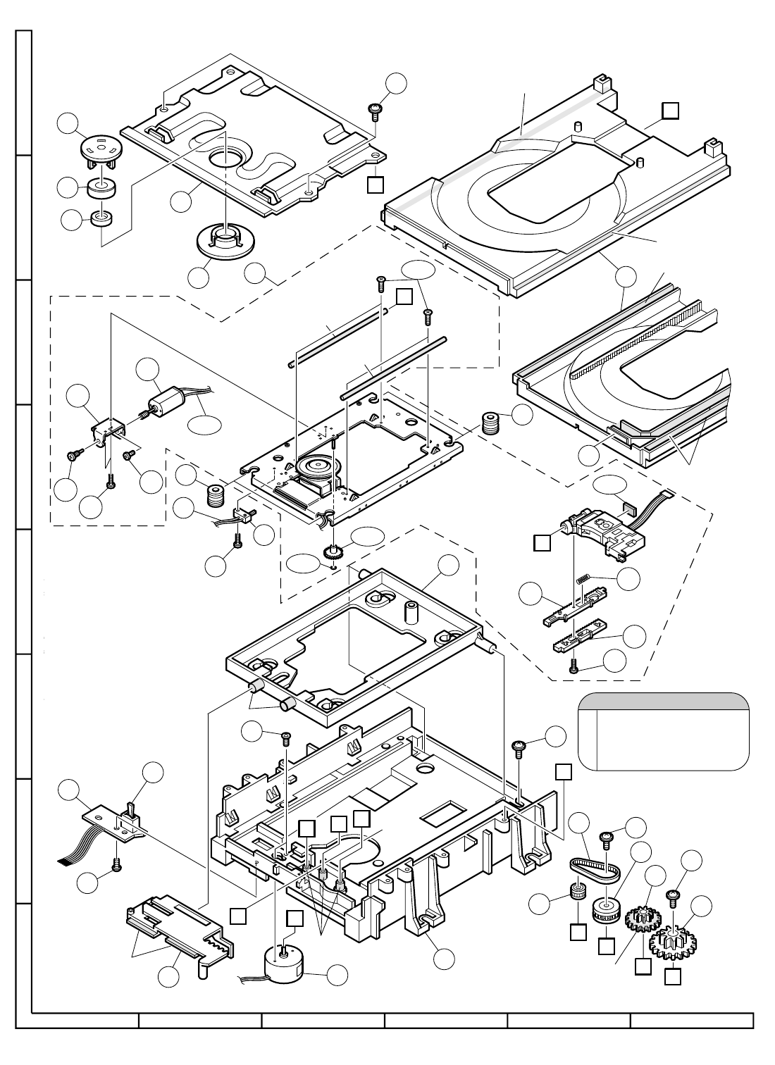
Ref. No. Part No. ★Description Code Ref. No. Part No. ★Description Code
83
DV-760X
17-11
A
B
C
D
E
F
G
H
123456
Oil
30
B
D
B
37
17
16
20
1-9
1-4
1-3
1-2
1-5
1-10 30
53
14
41
15
29
32
31
45
28
AC
22 21
GFE
43 37
A
33
44
25
26 44
27
E
F
G
C
23
24
Grease
Grease
Grease
Grease
Grease
Grease
Dry Coading
Grease
Dry Coading
D
1-2
1-6
1-3
1-13
1-12
1-11
1-14
1-1
1-8
1-6
1-7
18
52
1
When touching the pickup,
wear an earth band to p
revent breakage by static
electricity.
å Caution
•
MECHANISM EXPLODED VIEW
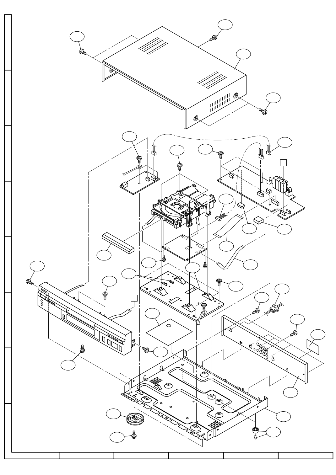
Ref. No. Part No. ★Description Code Ref. No. Part No. ★Description Code
84
DV-760X
A
B
C
D
E
F
G
H
123456
17-12
CABINET EXPLODED VIEW
a
a
4-9
14
14
4-3
13
14
4-4
4-5 4-4 17
18
19
20
11
1
12
21
11
2
16
4-8
4-10-1
4-10-2
4-5 4-2
4-14
5-1
15
4-15
4-7-3
4-7-2
4-6
4-7-1
DV-760S/H ONLY
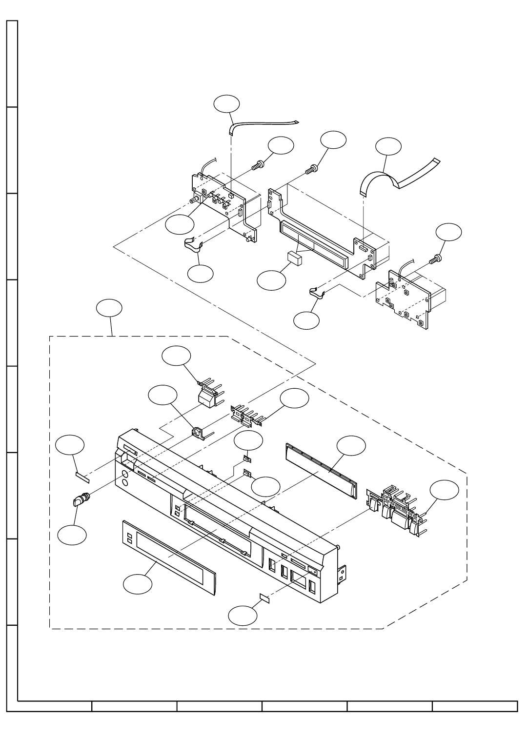
Ref. No. Part No. ★Description Code Ref. No. Part No. ★Description Code
85
DV-760X
A
B
C
D
E
F
G
H
123456
17-13
FRONT PANEL PARTS EXPLODED VIEW
3-3
3-3-10
3-1
3-3-6
3-3-9
3-3-5
3-3-8
3-3-7
3-3-3
3-3-4
3-3-2
3-3-13
3-3-12
3-2
3-6
3-4
3-7
3-5
3-2
3-2
3-3-11
Ref. No. Part No. ★Description Code Ref. No. Part No. ★Description Code
86
DV-760X
18. PACKING OF THE SET
18-1
★SSAKA0158AJZZ
(Polystylene Bag)
★SPAKX1059AJZZ
(Packing Add.)
RRMCG1203AJSA
(Remote Control Unit)
★SSAKA0001AJZZ
(Polystylene Bag, Accessories)
★SPAKF0162AJZZ
(Packing Meterial)
★SPAKC4181AJZZ
(Packing Case)
★SPAKF0164AJZZ
(Air-Cap)
★SPAKP0187AJZZ
(For Set Polystylene Sack)
QCNW-8012AJZZ
(S-Video Cord)
QCNW-7581GEZZ
(Video/Audio Cord)
TiNS-3647AJZZ
(Operation Manual)
★TGAN-0068PEZZ
(Guarantee Card)
No
POS
QACCL3051AJZZ
(AC Power Cord)
å
★ Not Replacement Items

Ref. No. Part No. ★Description Code Ref. No. Part No. ★Description Code
87
DV-760X

Ref. No. Part No. ★Description Code Ref. No. Part No. ★Description Code
88
DV-760X
SHARP CORPORATION
AV Systems Group
Quality & Reliability Control Center
Yaita, Tochigi 329-2193, Japan
COPYRIGHT C 1999 BY SHARP CORPORATION
ALL RIGHTS RESERVED.
No part of this publication may be reproduced,
stored in a retrieval system, or transmitted in
any form or by any means, electronic, mechanical,
photocopying, recording, or otherwise, without
prior written permission of the publisher.
TQ0763-S
Nov. 1999 Printed in JAPAN
SA. NS
DV-760X
