DVD3800_Cover.p65 DVD3800
User Manual: DVD3800
Open the PDF directly: View PDF ![]() .
.
Page Count: 138 [warning: Documents this large are best viewed by clicking the View PDF Link!]
- DVD-3800
- COVER
- SPECIFICATIONS
- IOP Measurement Method
- Note for Handling the Laser Pick-up
- Replacement of the Traverse Unit
- DISASSEMBLY
- How to Replace Traverse Unit
- Service Mode
- TROUBLESHOOTING
- Electrical Adjustment for Video
- BLOCK DIAGRAM
- SEMICONDUCTORS
- PRINTED WIRING BOARDS
- NOTE FOR PARTS LIST
- PARTS LIST OF P.W.B. UNIT ASS'Y
- EXPLODED VIEW
- PARTS LIST OF EXPLOED VIEW
- EXPLODED VIEW OF DVD MECHANISM
- PARTS LIST OF DVD MECHANISM
- POINTS OF GREASING
- PACKING VIEW/PARTS LIST OF PACKING & ACCESSORIES
- WIRING DIAGRAM
- MEASURING METHOD AND WAVEFORMS
- SCHEMATIC DAIGRAMS
- (1/8) GU-3389A-1 MAIN UNIT(1/3)
- (2/8) GU-3389A-1 MAIN UNIT(2/3)
- (3/8) GU-3389A-1 MAIN UNIT(3/3)
- (4/8) GU-3438-1 AUDIO UNIT
- (5/8) GU-3438-2 VIDEO UNIT
- (6/8) GU-3439-1 DIGI. POWER/GU-3439-6 IF UNIT
- (7/8) GU-3439-2 DISPLAY/GU-3439-3 LED/GU-3439-4 SW/GU-3439-5 P.SW UNIT
- (8/8) GU-3442-1 SCART UNIT (Europe model only)
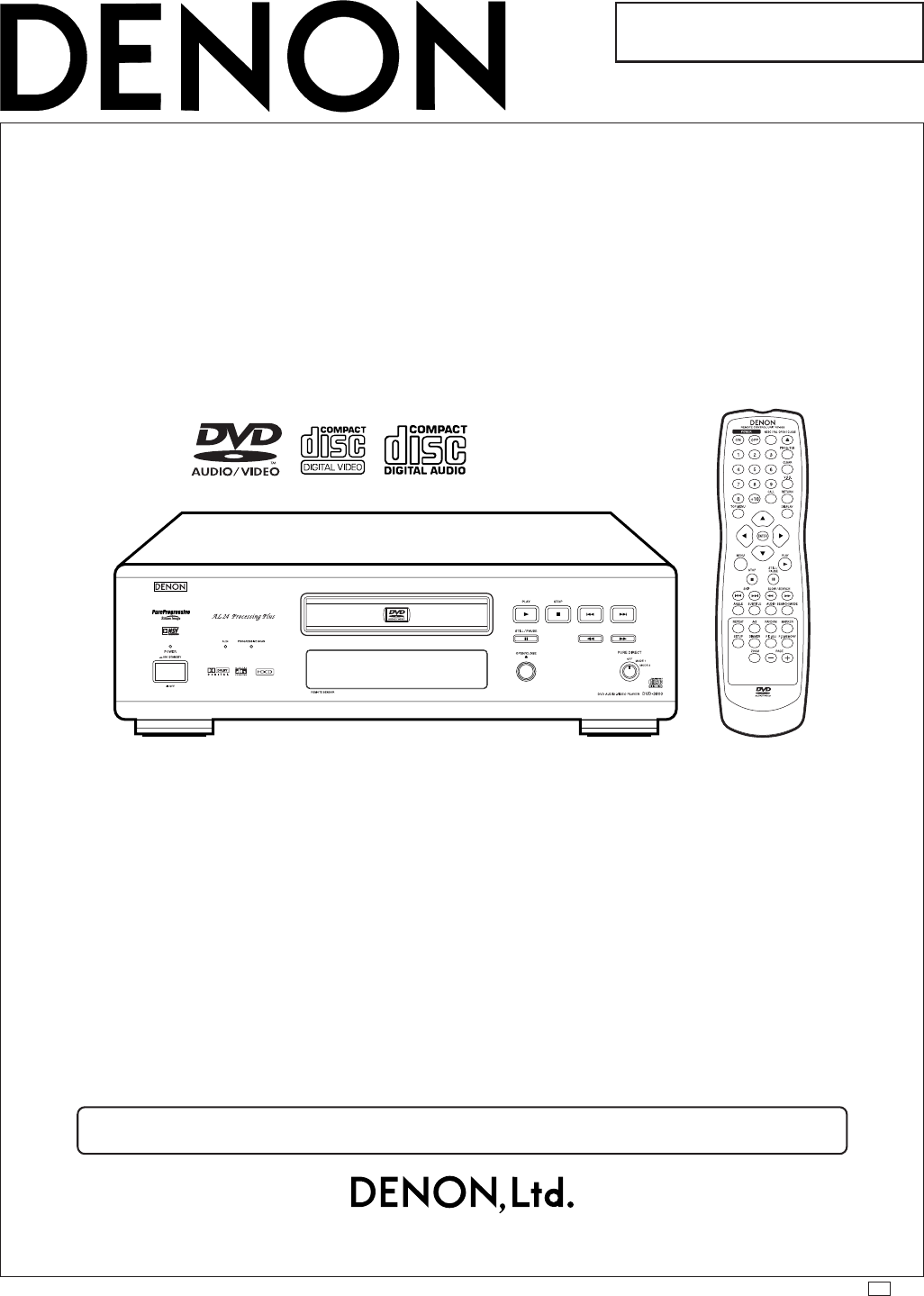
Digital Player
SERVICE MANUAL
MODEL
DVD-3800
DVD AUDIO-VIDEO PLAYER
Some illustrations using in this service manual are slightly different from the actual set.
16-11, YUSHIMA 3-CHOME, BUNKYOU-KU, TOKYO 113-0034 JAPAN
Telephone: 03 (3837) 5321
For U.S.A., Canada, Europe,
Asia & Korea model
X0137 NC 0207
2
DVD-3800
SAFETY PRECAUTIONS
The following check should be performed for the continued protection of the customer and service technician.
LEAKAGE CURRENT CHECK
Before returning the unit to the customer, make sure you make either (1) a leakage current check or (2) a line to chassis
resistance check. If the leakage current exceeds 0.5 milliamps, or if the resistance from chassis to either side of the
power cord is less than 460 kohms, the unit is defective.
SPECIFICATIONS
Signal System: NTSC/PAL
Applicable Discs: (1) DVD-Audio/DVD-Video discs
1-layer 12 cm single-sided discs, 2-layer 12 cm single-sided discs,
2-layer 12 cm double-sided discs (1 layer per side)
1-layer 8 cm single-sided discs, 2-layer 8 cm single-sided discs,
2-layer 8 cm double-sided discs (1 layer per side)
(2) Compact discs (CD-DA, Video CD)
12 cm discs, 8 cm discs
S-Video Output: Y output level: 1 Vp-p (75 Ω/ohms)
C output level: 0.286 Vp-p (For U.S.A., Canada, Asia & Korea model)
0.3 Vp-p (For Europe model)
Output connectors: S connectors, 2 setS
AV 1 connector, 1 set (For Europe model)
Video Output: Output level: 1 Vp-p (75 Ω/ohms)
Output connector: Pin-plug jacks, 2 setS
AV 1 connector, 1 set/AV2 connector, 1 set (For Europe model)
Component Output: Y output level: 1 Vp-p (75 Ω/ohms)
PB/CBoutput level: 0.648 Vp-p (75 Ω/ohms) (For U.S.A., Canada, Asia & Korea model)
0.7 Vp-p (75 Ω/ohms) (For Europe model)
PR/CR output level: 0.648 Vp-p (75 Ω/ohms) (For U.S.A., Canada, Asia & Korea model)
0.7 Vp-p (75 Ω/ohms) (For Europe model)
Output connector: Pin jack, 1 set
RGB Output: Output level: 0.7 Vp-p (75 Ω/ohms) (For Europe model)
Output connector: AV 1 connector, 1 set (For Europe model)
Audio Output: Output level: 2 Vrms
2 channel (FL, FR) output connector: Pin jacks, 2 sets
Multi channel (C, SW, SL, SR) output connector: Pin jack, 1 set
AV 1, 1 set/AV 2, 1 set (For Europe model)
Audio Output Properties: (1) Frequency response
1DVDs (linear PCM) : 2 Hz to 22 kHz (48 kHz sampling)
: 2 Hz to 44 kHz (96 kHz sampling)
: 2 Hz to 88 kHz (192 kHz sampling)
2CDs : 2 Hz to 20 kHz
(2) S/N ratio
1
DVDs : 116 dB
2
CDs : 116 dB
(3) Total harmonic distortion
1DVDs : 0.0015 %
2
CDs : 0.0018 %
(4) Dynamic range
1
DVDs : 108 dB
2CDs : 100 dB
Digital Audio Output: Optical digital output : Optical connector, 1 set
Coaxial digital output : Pin jack, 1 set
Power Supply: AC 120 V, 60 Hz (For U.S.A. & Canada model)
AC 230 V, 50 Hz (For Europe & Asia model)
AC 220 V, 50 Hz (For China model)
AC 220 V, 60 Hz (For Korea model)
Power Consumption: 30 W (For U.S.A. & Canada model)
32 W (For Europe, Asia & Korea model)
Maximum External Dimensions: 434 (W) × 132 (H) × 343 (D) mm (including protruding parts)
Mass: 10.0 kg
Remote Control Unit: RC-553
Type: Infrared pulse
Power Supply: DC 3 V, 2 "AA" /R6P batteries
∗Design and specifications are subject to change without notice in the course of product improvement.
3
DVD-3800
Laser current initial value
DVD mA
CD mA
1
1
1
2
4
1
1
1
1
1
115
1
1
20 21
40
45
8
1
6
717
18
28
29 39
40
16
1732
7
814
11
12
24
25 36
37
48
25
26
50
5175
76
100
20
2140
20
21
40
41
60
61
80
14
15 28
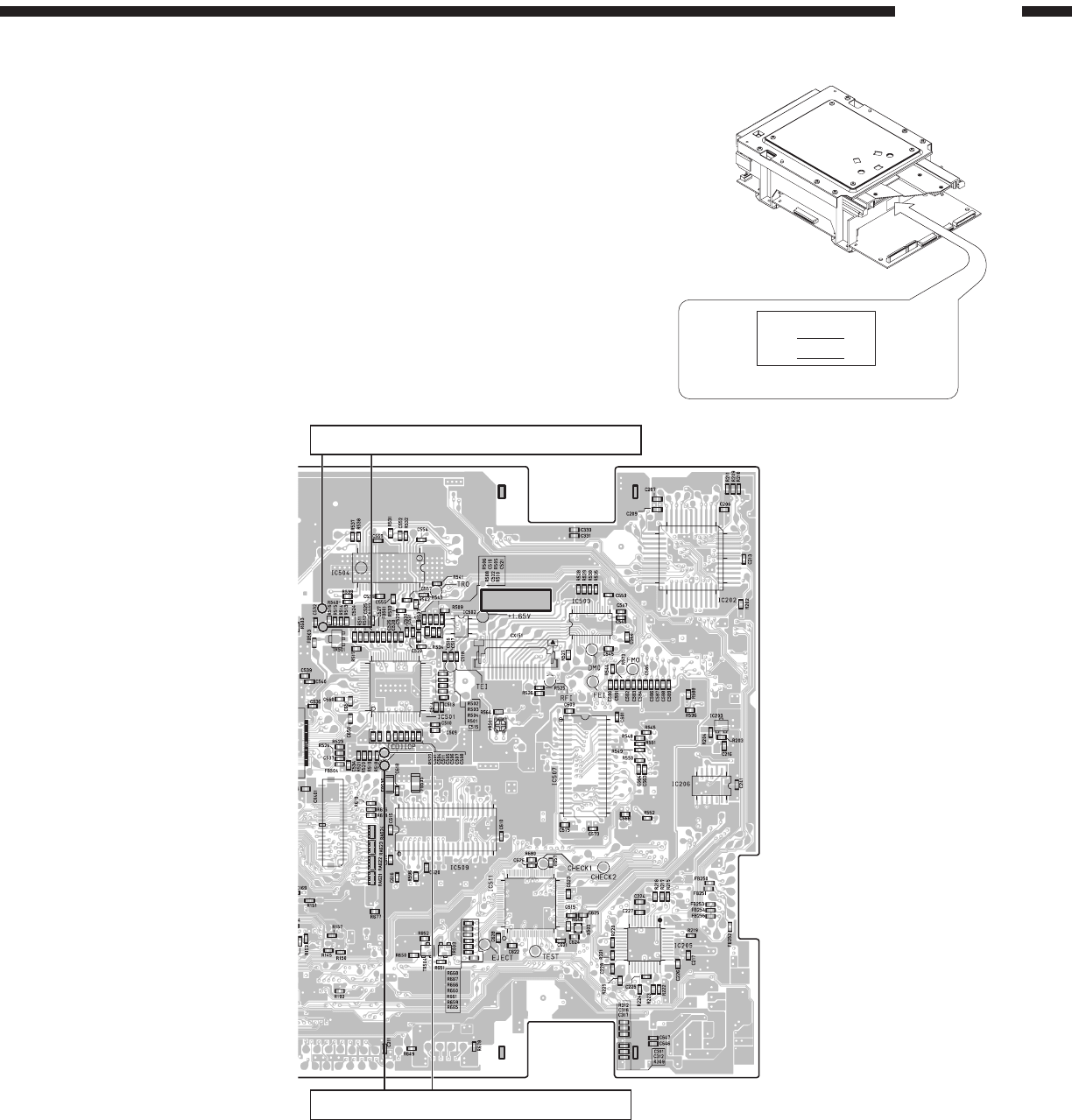
DVD laser drive current measuring points
Nearby C532
CD laser drive current measuring points
[CD] IOP silk point
GU-3389 P.W.B. (foil side)
(1) DVD laser current measurement
• Playback the title 1/chapter 1 of DVD test disc (DVDT-S01) or the equivalent.
• Connect the oscilloscope to the above mentioned point.
• DVD laser current = Measured Voltage Value / 39 (Resistance Value)
(2) CD laser current measurement
• Playback the track 1 of CD test disc (TCD-784) or the equivalent.
• Connect the oscilloscope to the above mentioned point.
• CD laser current value = Measured Voltage Value / 39 (Resistance Value)
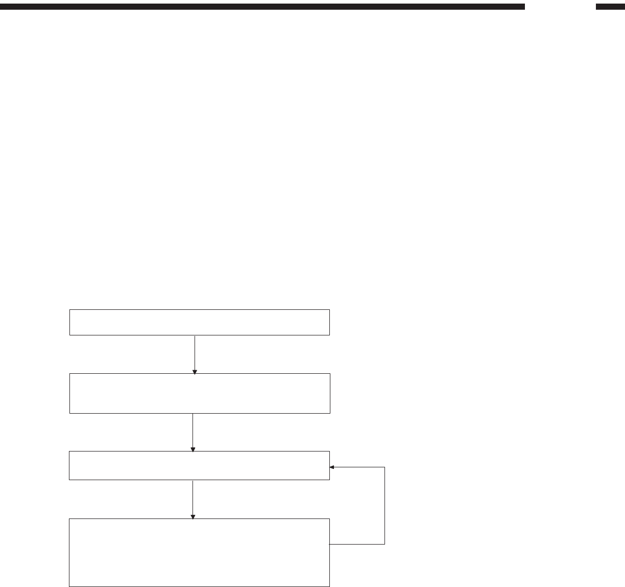
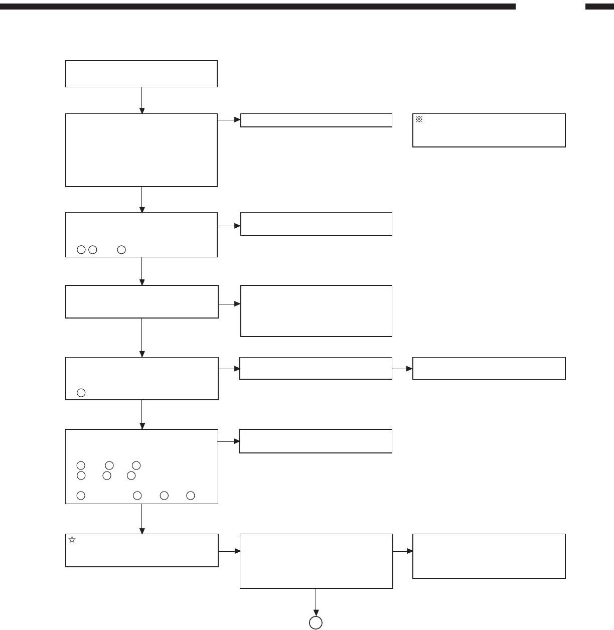
Iop Measurement Method (Diagnostics of Traverse Unit)
Diagnostics of optical pickup (Replacing Traverse Unit) as shown as below.
1. Arrange of Judgment
(1) Check read discs
Disc no read, unsteady playback, etc.
(2) Laser current (Iop) check
Check the Iop (Laser drive current).
If the present Iop value exceeds +50% of the initial value,
replace the Traverse Unit with a new one.
(3) Replacing the Traverse Unit
Traverse Unit replacing (See page 8 and 9).
No mechanical adjustment is necessary after the replacement.
2. Iop Measurement Method
4
DVD-3800
Note for Handling the Laser Pick-up
The protection for the damage of laser diode.
If you want to change the optical device unit from any other units, you must keep the following.
(1) It should be done at the desk already took measures the static electricity in care of removing the OPU's
(Optical device unit) connector cable.
(2) Workers should be put on the "Earth Band".
(3) It shold be done to add the solder to the short land to prevent the broken Laser diode before removing the
24P FFC cable.
(4) Don't touch OPU's connector parts carelessly.
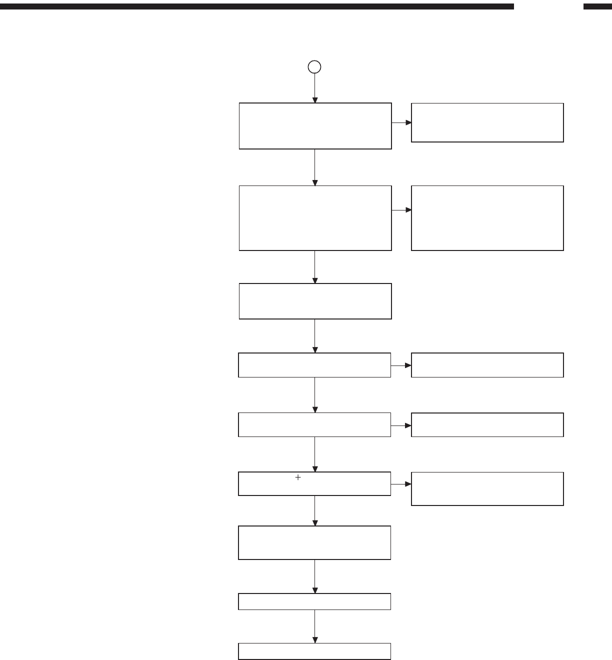
Replacement of the Traverse Unit
When repairing, carry out failure diagnostics by following the procedure described below.
If the present value of the laser drive current is 50% up to initial value, it is the point of the pickup replacement.
In case of the pickup replacement, replace the Traverse Unit with no adjustment.
The initial value is indicated on the label on back side of Mecha.
NO DISC indicated, Playback not smooth, etc.
Laser drive current check
HF signal check
Traverse Unit replacement (refer to page 8)
Present value: 50% up to initial value
Laser drive current check after replacement.
If the present value is less than 80mA, write on
the new label by hand, put on the new label over
the old label.
If the present value exceeds 80mA,
replace the Traverse Unit with a new one.
Cause: Damaged electrostatically when replaced.
5
DVD-3800
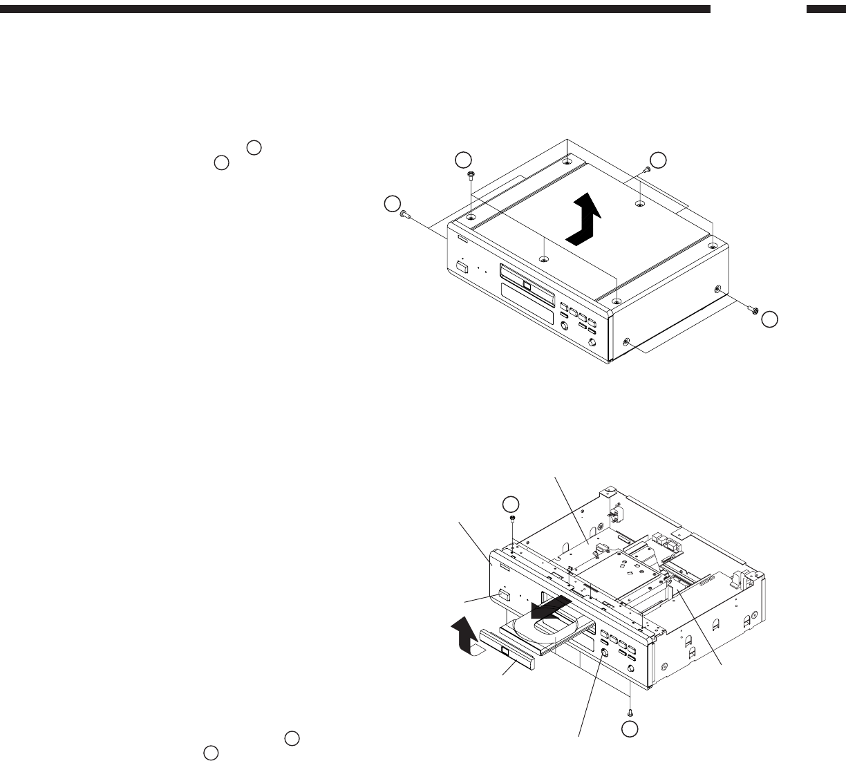
DISASSEMBLY
( Follow the procedure below in reverse order when reassembling )
1. Top Cover
(1) Remove 10 screws 1 on the top and both sides,
and 2 screws 2 on the rear.
(2) Widen the Top Cover a little laterally, then detach it
with sliding in the arrow direction.
1
1
2
1
2. Loader Panel, Front Panel
2-1. When the Disc Tray can be ejected electrically
(1) After removing the Top Cover, proceed
as follows.
(2) Plug the power cord to the wall outlet,
switch on the power, and press the
“OPEN/CLOSE” button to open the Disc
Tray.
(3) Detach the Loader Panel by lifting it in
the arrow direction.
(4) Press the “OPEN/CLOSE” button to
close the Disc Tray, then unplug the
power cord.
(5) Disconnect the wire (CX025, CX041)
connecting the Front Panel’s P.W.B. and
the Power PWB in the Chassis.
(6) Remove 4 top screws 3 and 4 bottom
screws 4, then detach the Front Panel
to the arrow direction.
(7) Disconnect the FFC (CX171) connecting
the Front Panel’s P.W.B. and the Main
P.W.B. in the Chassis.
4
3
Power P.W.B.
Front Panel
Main P.W.B.
“OPEN/CLOSE” button
Loader Panel
Power Switch
6
DVD-3800
2-2. When the Disc Tray cannot be ejected electrically
(1) After removing the Top Cover, proceed as
follows.
(2) Remove 2 screws 5 on the Trans.
Bracket and 2 bottom screws 6.
(3) Turn the Trans. and Bracket to the arrow
direction, then remove 2 screws 7.
(4) Move the Trans. toward the Front Panel.
(5) Insert a screwdriver into the left hole of
the Mecha. Fix Bracket, and push the Plate
Gear of the DVD Mecha. slowly to open
the Disc Tray.
(6) Remove the Loader Panel, and close the
Disc Tray.
(7) Detach the Front Panel following the same
steps described on the previous page 2-1.
(5)~(7).
5
6
Trans. Bracket
7
Trans.
screwdriver
Front Panel
Front Panel
DVD Mecha.
Loader Panel
Mecha. Fix Bracket Plate Gear
7
DVD-3800
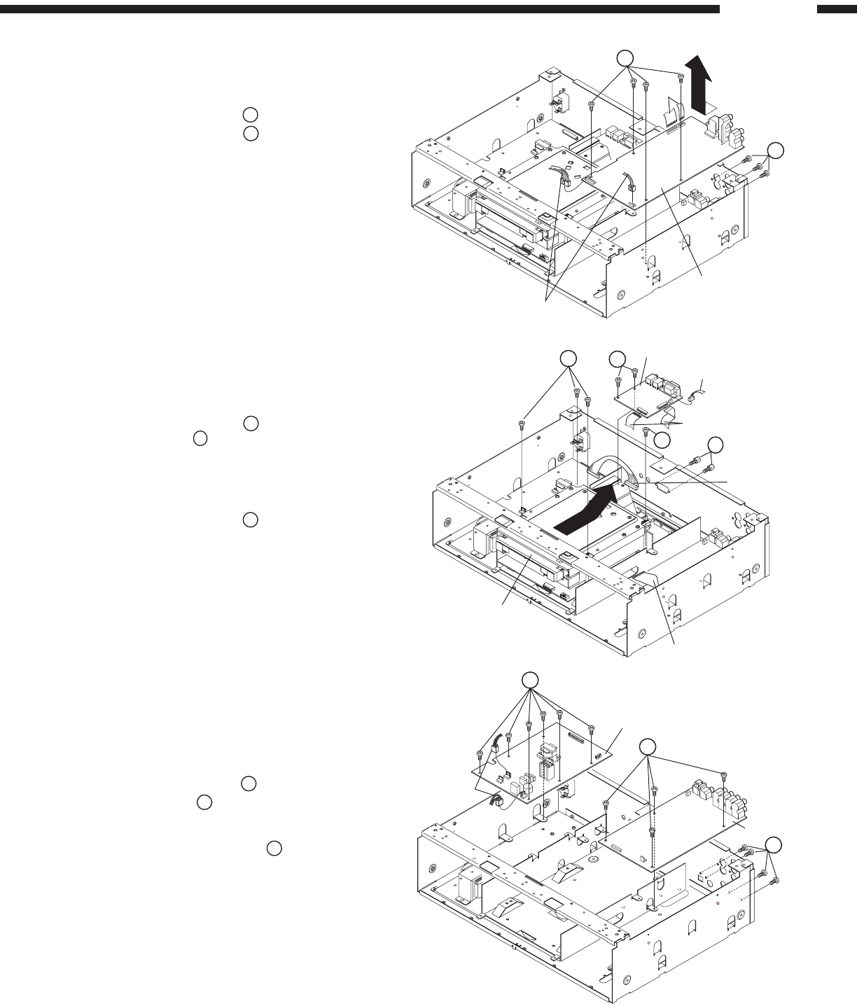
3. Video P.W.B.
(1) Disconnect 2 connectors.
(2) Disconnect 2 FFCs (CY272, CY131).
(3) Remove 4 screws 8 on the Video P.W.B.
(4) Remove 3 screws 9 from the rear.
(5) Detach the Video P.W.B. to the arrow direction.
5. Audio P.W.B. / Power P.W.B.
5-1. Audio P.W.B.
Remove 4 screw ! on the Audio P.W.B.,
4 screws " from the rear.
5-2. Power P.W.B.
(1) Remove 6 screws # on the Power P.W.B.
(2) Disconnect 2 connectors (CX024, CX026).
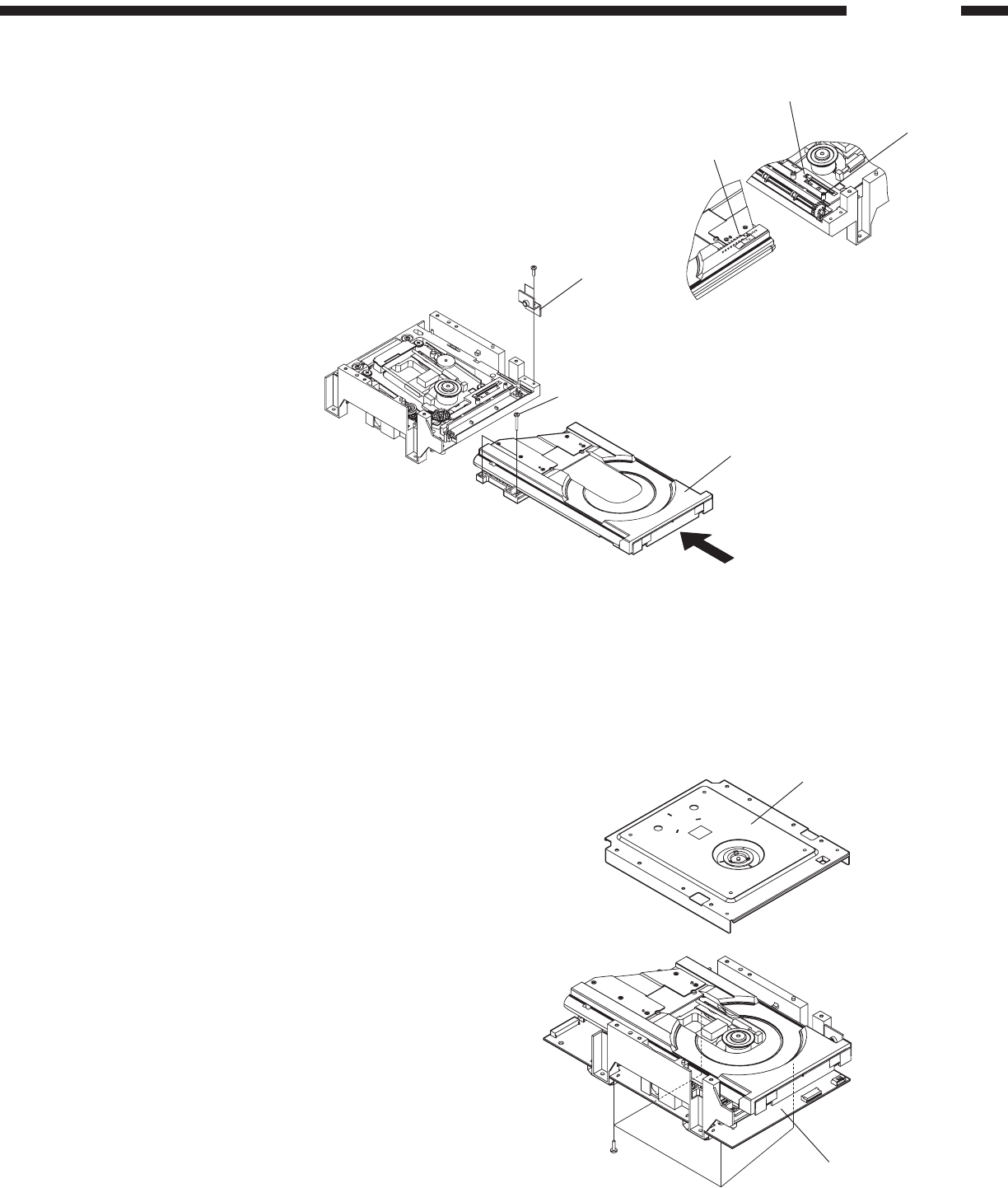
4. DVD Mecha.
(1) Remove 2 screws on the I/F P.W.B.,
2 screws
from the rear, then disconnect
2 FFCs (CY211, CY212) and 1 connector
(CY036) to detach the I/F P.W.B.
(2) Disconnect each one of 30P FFC (CY301) and
14P connector (CX141) from the DVD Mecha.
(3) Remove 4 screws on the DVD Mecha., and
take it off in the arrow direction.
9
8
Video P.W.B.
Connector
FFC
I/F P.W.B.
Connector
FFC
14P Connector
30P FFC
DVD Mecha.
!
"
#
Connector
Power P.W.B.
Audio P.W.B.
8
DVD-3800
A
Solder to short-circuit (CD)
Solder to short-circuit (DVD)
Short-circuit with solder (enlarged fig. A)
(a)
(b)
(c)
(d)
(e)
Clamp Base Damper
Clamp Base
Holder Loader
Bearing Plate
Main P.W.B. Ass'y
(f)
Damper
Traverse Unit
(3)
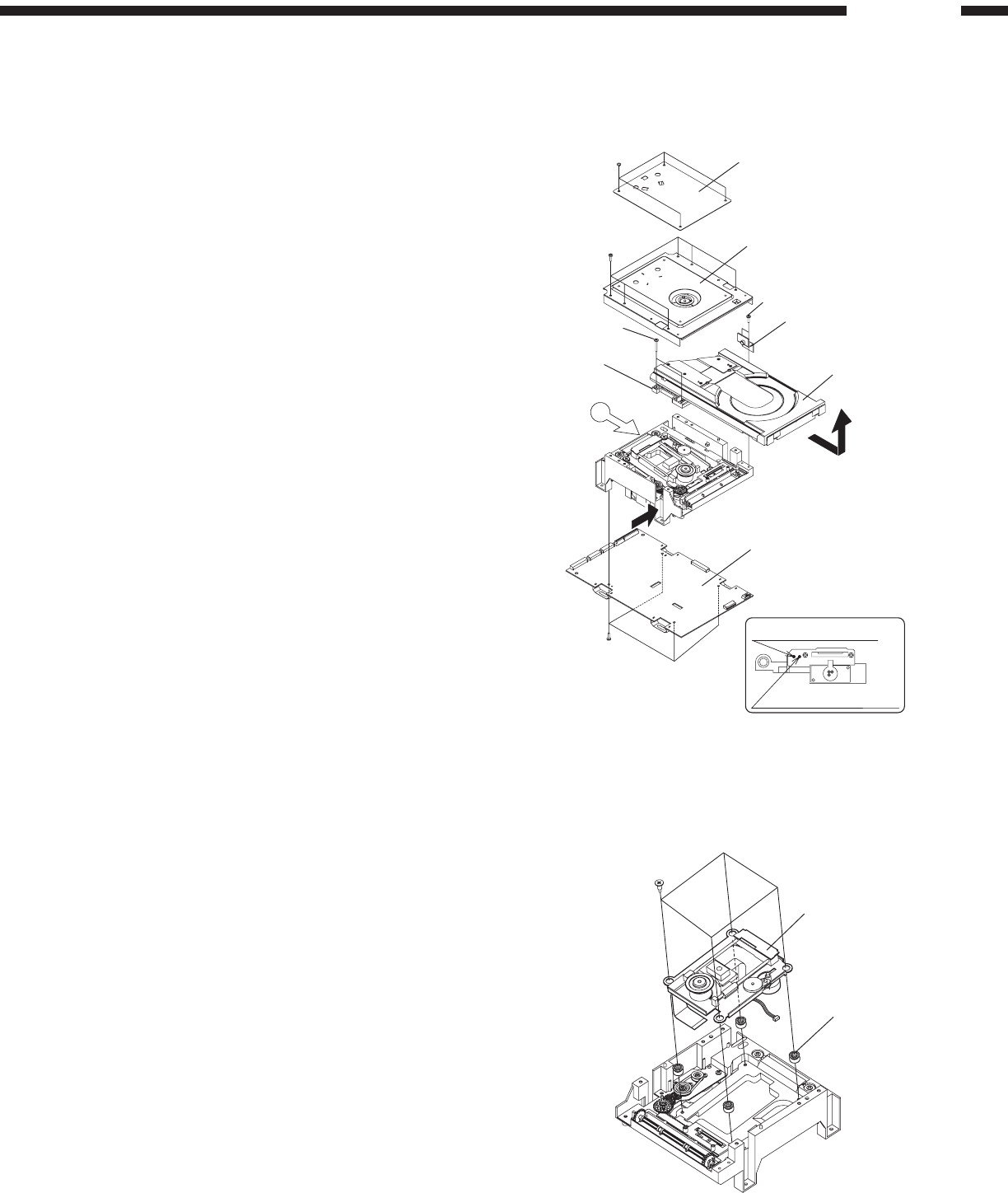
2. Replacing Traverse Unit
(1) Removing Wires
• CX241: 24P-FFC for Pickup
• CX151: 15P-FFC for Spindle
• CX031: 3P-PH wire for PU Slide
(2) Removing Traverse Unit
Remove 4 pcs of special screw (f) and dampers, then
take out the Traverse Unit upward.
(3) Mounting Traverse Unit
Mount the Traverse Unit following the reverse order.
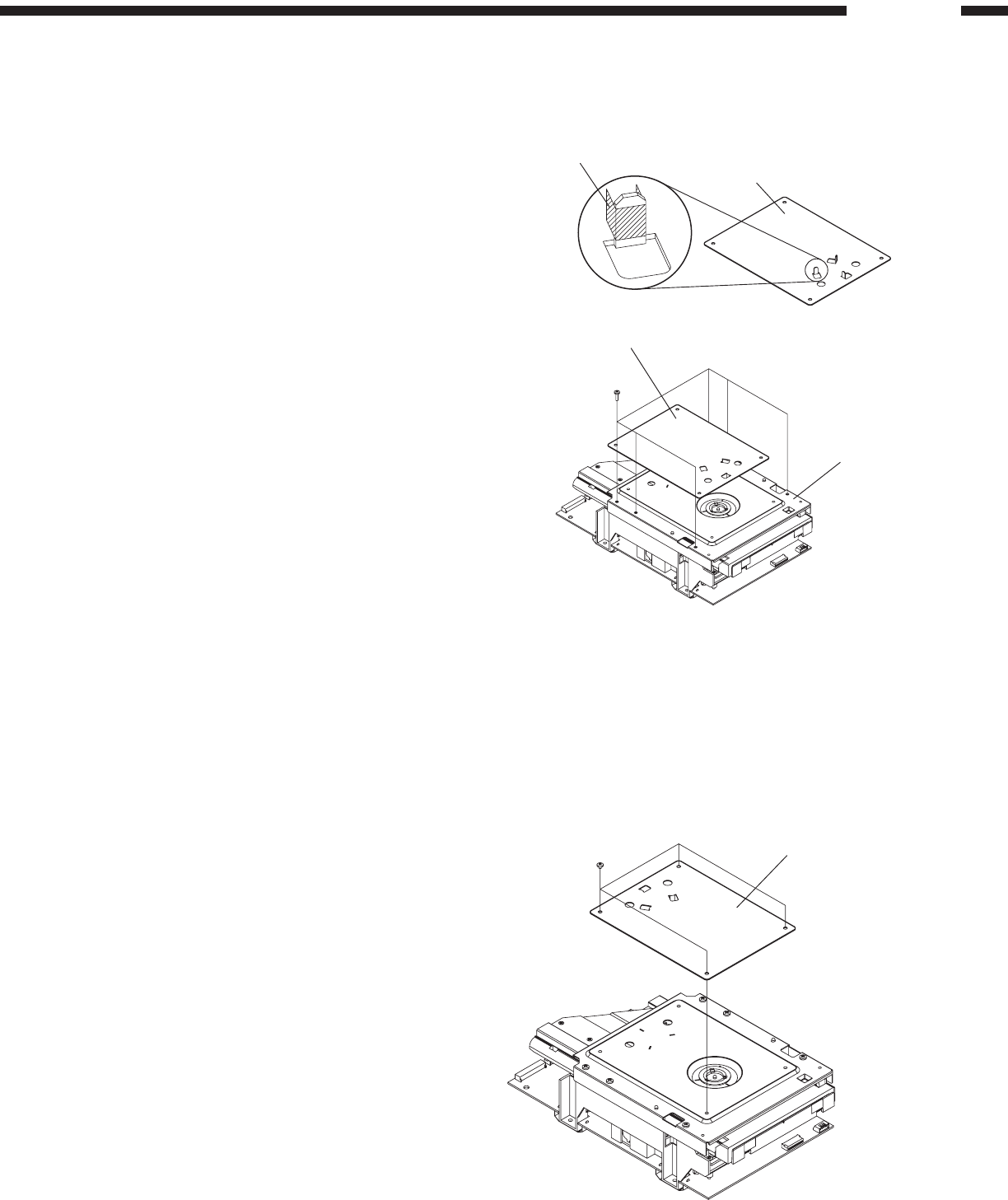
1. Preparing for Replacement
(1) Removing Clamp Base Damper
Remove 4 pcs of 2.6mm machine screw (a), and detach
the Clamp Base Damper upward.
(2) Removing Clamp Base
Remove 6 pcs of 3mm P-tight screw (b), and detach the
Clamp Base upward.
(3) Ejecting Loader
Through the left rectangular hole of the Mechanism Unit,
push the slider with a ruler or screwdriver until the
Traverse portion lowers and the Loader comes out a little.
(4) Removing Loader
• Remove 2 pcs of 3mm P-tight screw (c) on the Loader
Holder left.
• Remove 2 pcs of 3mm P-tight screw (d) on the Loader
Holder right, then pull up the Bearing Plate.
• Fully pull out the Loader forward, and lift up to take it
out.
(5) Shorting Pickup
To protect the Pickup from static electricity, short-circuit
2 positions as shown in figure.
(6) Removing Main P.W.B. Ass'y
Remove 4 pcs of 3mm P-tight screw (e), and detach the
Main P.W.B. Ass'y downward.
How to Replace Traverse Unit
(4)
9
DVD-3800
(d)
(c)
Loader
Bearing Plate
Plate Gear
Boss
Groove
(e)
Clamp Base
Main P.W.B. Ass'y
4. Assembly (1)
(1) Assembling Main P.W.B. Ass'y
Fix the Main P.W.B. Ass'y with 6 pcs of 3mm P-tight
screw (e).
(2) Removing Pickup-short Solder
After connecting 24P-FFC of the Pickup with P.W.B.,
remove solder from 2 shorted positions.
(3) Temporary Positioning Clamp Base
To protect your eyes from laser light, put the Clamp Base
temporarily. (At this moment, be sure to make chucking
the Clamper and Turn-table securly.)
(4) Positioning up Traverse Unit
Connect the following wires of the Mechanism Unit, and
operate it.
• CX141: 14P-PH wire for power
• CX131: 13P-FFC wire from Display P.W.B.
Turn on the power to the unit, and press "OPEN/CLOSE"
button to close the Loader.
The Traverse Unit rises up. (display: 0h00m00s)
3. Installing Loader
(1) Inserting Loader
Set and push the Loader to the arrow direction until it
stops. When installing the Loader, move the Plate Gear
to right beforehand so as that the boss of the Plate Gear
fits in the backside groove of the Loader. (See figure right)
(2) Fixing Loader
Fix the Loader with each 2 screws (c) and (d).
10
DVD-3800
6. Assembly (3)
(1) Detaching Tape from Clamp Base Damper
Detach acetate cloth tape from 3 projections of the Clamp
Base Damper backside.
(2) Assembling Clamp Base Damper
Set the Clamp Base Damper to the Clamp Base contrary
to the direction set in step above.
Fix the Clamp Base Damper with 4 pcs of 3mm S-tight
screw (a).
(b)
(a)
Clamp Base Damper
Clamp Base
Clamp Base Damper
Acetate Cloth Tape
Clamp Base Damper
5. Assembly (2)
(1) Attaching Tape to Clamp Base Damper
Attach acetate cloth tape to 3 projections of the Clamp
Base Damper backside. (Be careful not to make it
overlapped.)
(2) Assembling Clamp Base
Set the Clamp Base Damper with positioning for clamper
by 3 projections.
Fix the Clamp Base with 6 pcs of 3mm P-tight screw (b).
11
DVD-3800
No. Error contents Error code FL display
1 During tray work, it doesn’t end within the time specified. 045300 ERROR 01
2 No spindle work during playback. 040990 ERROR 02
3 Out of focus during playback, search, or pause. 031100 ERROR 04
4 No data read when spin up. 031100 ERROR 04
5 No data read when playback. 031100 ERROR 04
6 Cannot read TOC within the time specified. 025700 ERROR 05
7 No sub-code read 025700 ERROR 05
8 No response from DVD drive more than 10 sec. 0B4000 ERROR 06
9 Error not specified (other than above). --- ERROR 07
Service Mode
1. Aging Mode
(1) Preparation
(a) Equipment used: Any one of DVD Karaoke Disc (containing more than 10 titles), CD/Video CD (Ver1.0: None
playback control), or No-menu DVD. (Setting varies according to the disc used.)
(b) Unit setting: No spec other than the following procedure (Aging mode)
At the tray open status, press the "POWER" button to turn on the power while pressing the "PLAY" and
"OPEN/CLOSE" buttons for DVD operation simultaneously. mark on the FL lights, and the unit is set to the heat
run mode.
(2) Procedure
(a) According the above, set to the aging mode.
(b) Set a DVD Karaoke disc to the tray and press the "PLAY" button once. mark on the FL blinks, and aging peration
(after playback title-1 and title-10 of the disc, the tray open/close is made automatically, then playback the title-1
again) starts. This aging operation continues automatically until it is stopped or it stops caused by an error.
(c) When using other than a DVD Karaoke disc, aging operation (after playback all titles of the disc, the tray open/close
is made automatically, then playback all titles again) starts by pressing the "PLAY" button once, and mark on
the FL lights. The aging operation continues automatically until it is stopped or it stops caused by an error. In case
of some error in DVD, the tray opens and the following error messages are displayed on the FL.
2. Initial Setting Mode
(1) Preparation
(a) Equipment used: None
(b) Unit setting: No spec other than the following procedure
(2) Procedure
(a) Initialize the DVD player when µcom, peripheral parts of µcom, or Main P.W.B. has been replaced in servicing.
(b) Carry out the following to restore factory setting mode. At the player stop condition, press 3 buttons for DVD peration
("PLAY", "OPEN/CLOSE", and " SKIP") until "INITIALIZE" appears and disappears in the FL.
("Initialized" appears and disappears on the TV screen.)
(c) All user setting will be lost and its factory setting will be restored when this initialization is made. Be sure to
memorize your setting for restoring again after the initialization.
12
DVD-3800
3. P.W.B. Check Mode
(1) Preparation
(a) Equipment used: None
(b) Unit setting: No spec other than the following procedure
(2) Procedure
(a) Press the "POWER" button to turn on the power while pressing the "PLAY" and "OPEN/CLOSE" buttons for DVD
operation simultaneously.
(b) FL all light/extinguish mode.
This mode is for detecting FL defects. Press "STILL/PAUSE( )"on the remote control unit once to light all FL
segments, and press it once again to extinguish them.
(c) DVD µcom and main unit µcom firm check mode.
This mode is for displaying the status of each µcom employed.
• DVD µcom firm: Press the "MENU" button. Each time the "MENU" button is pressed, µcom firm is displayed one
after another.
Ex.: [DRV_6067, ESS_6094, PANEL 6093]
Set Serial No. (lower 5 digits) Bus Manager Drive Pcom ESS Pcom Panel Pcom
1 00001~ V.52 Ver. 6067
(Display) 6067
Ver. 6094
(Display) 6094
Ver. 6093
(Display) 6093
2
3
4
13
DVD-3800
1. No power
(FL tube doesn't light.)
Check connector insertion.
Switching power (GU-3439-1):
[CX024, CX025, CX026, CY041,
CX141]
Main PWB (GU-3389):
[CX031, CX131, CX141, CX171,
CX272]
Re-insert the connector. When replacing µcom, µcom
peripheral parts, or Main PWB,
perform initializing of DVD player.
Check switching power (GU-3439-1)
voltages.
[CX141]: 14P PH for Main PWB:
5
, +5V, " (3.3V)
Replace the switching power
unit (GU-3439-1).
(1) Check reset signal (3V) at 67pin of
IC601 on DISP PWB.
(2) Check 4.3MHz at 65pin of IC601.
(1) Check R681, R602 solderring.
(2) After checking X601 and IC601
soldering, change X601.
If still NG after changing, replace
IC601.
Check switching power (GU-3439-1)
voltages.
[CX041]: 4P PH for Main PWB:
1
+3.6V
Check soldering of IC201 on Main PWB
(GU-3389).
Check after replacing IC201 on Main
PWB (GU-3389).
Check switching power (GU-3439-1)
voltages.
[CX141]: 14P PH for Main PWB:
1+12V 2-12V 3+5V
93.3V +5V
!
+3.3V
[CX041]: 4P PH for DISP PWB:
1ON/ST(3.6V) 2-24V 3-29V 4-32V
Replace the switching power unit
(GU-3439-1).
A
No
No
No
No No
No
Perform operation check after
changing Main PWB (GU-3389) with
a perfect one.
There is something wrong in Main PWB
(GU-3389).
→ Check 27MHz output of IC101 (49)
pin/XIN, (105) pin/CLK, and (116) pin/
PCLK2X on Main PWB.
Check soldering of IC108, IC110 and
IC116 on Main PWB (GU-3389), then
change IC101 if it's NG. Change IC111 if
it's still NG.
No No
Note: When switching power unit is repairable, refer to the waveforms and voltages shown in Schematic Diagram.
TROUBLESHOOTING
14
DVD-3800
There is something wrong in Main PWB
(GU-3389).
→ Check if CLOCK and DATA signals of
ICBUS are output on IC101 (160) pin/
AUX0, (161) pin/AUX1 when the power
is on.
Check soldering of IC106, IC703, IC706
and IC101 on Main PWB (GU-3389),
and change IC101 if it's NG. Change
IC106, then IC703 and IC706 if it's still
NG. Finally, change IC601 on Video
PWB (GU-3438-2) if still NG.
Check soldering of IC101 (208 pins) on
Main PWB (GU-3389).
→ Perform re-soldering.
Caused by Main PWB (GU-3389).
→Check 20MHz output on IC703(10) pin.
Caused by Main PWB (GU-3389).
→Check 27MHz input on IC706 (32) pin.
No
No Check soldering of IC703 and X701, and
replace if NG.
No Check soldering of IC706, and replace
if NG.
Check RESET 5V output of IC511 (30)
pin on Main PWB.
Check soldering of R637 and IC101
(145) pin on Main PWB.
→ Perform re-soldering.
Check Laser drive current/HF wave form.
Criterion: Iop is less than 1.5 times of its
initial value.
No
Replace Traverse Unit.
Write Iop after replacing the unit.
A
There is something wrong in Main PWB
(GU-3389).
→ Check 11MHz input of IC101 (39) pin/
MCLK.
Check IC109→IC113→IC112→IC111
(see Schematic Diagram) on Main PWB
(GU-3389).
No
15
DVD-3800
No
2. No power
(Both FL tube & LED don't light.)
Check connector insertion.
Switching power (GU-3439-1):
[CX024, CY025, CX028, CY141,
CX041]
Main PWB (GU-3389):
[CX141, CX171]
Re-insert the connector.
Check switching power voltages.
[CY141]: 14P PH for Main PWB:
+5V(NSW) " +3.3V(NSW)
No Replace the switching power unit.
Check Main PWB voltages.
[CX171]:
1pin: +5V check
(CX141
→CX171 1 break check)
pin: +3.3V check
(CX141
"
→CX171 2 break check),
etc.
16
DVD-3800
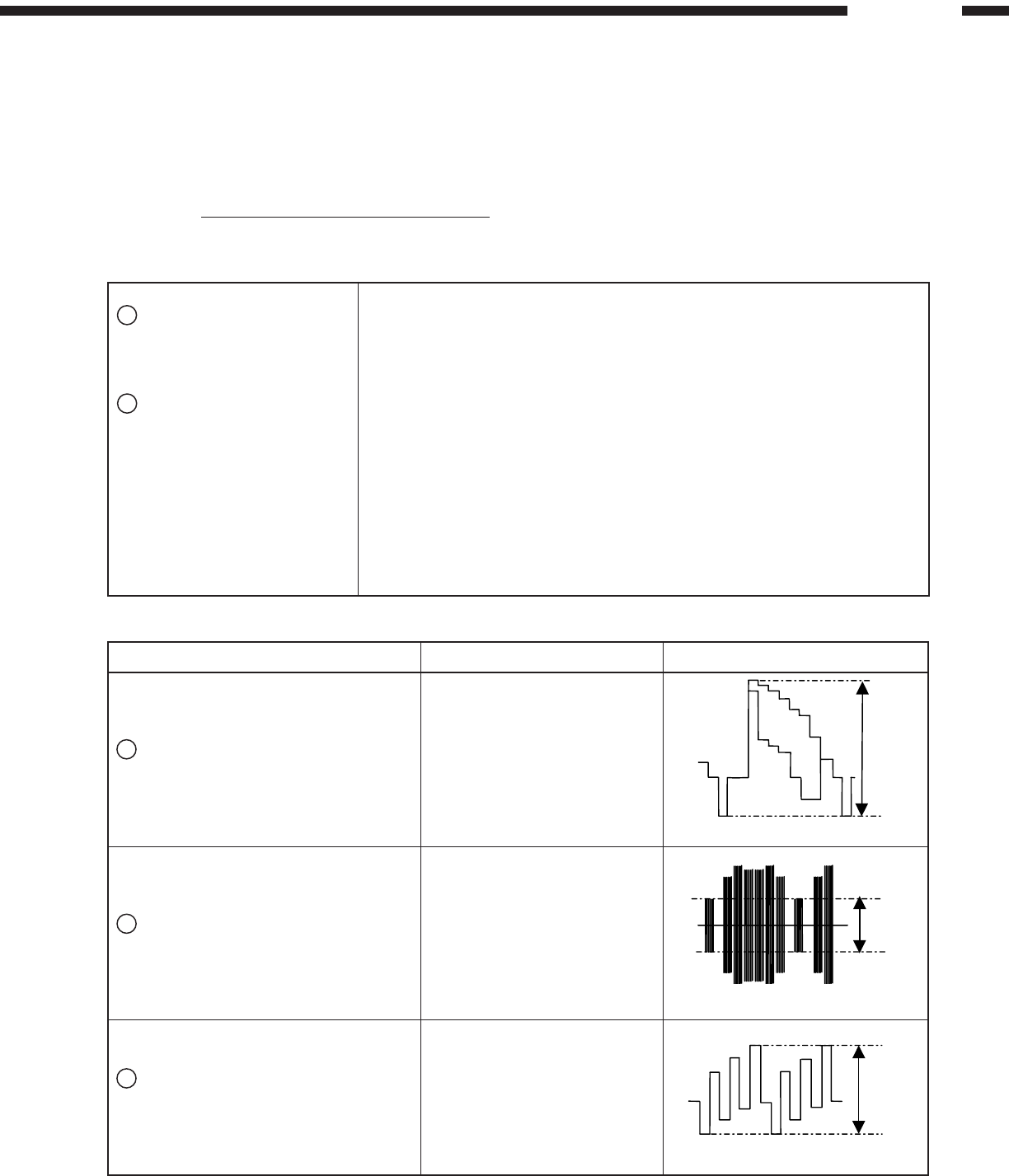
Setting the Oscilloscope as bellow.
1PB / CB / PR / CR
(a) TIME / DIV : 2 µS
(b) VOLT / DIV : 100 mV
(use the probe : ×10)
2
Y / C
(a) TIME / DIV :2 µS
(b) VOLT / DIV :50 mV
(use the probe : ×10)
Power on. Power Supply
U.S.A.& Canada : 120 V
Asia : 230 V
China : 220 V
Europe : 230 V
1. Power on.
2. Set the [SOURCE] selector knob : DVD.
3. Push [OPEN/CLOSE] button, then open the Disc Tray.
4. Set DVD test disc (DVDT-S01) on the Disc Tray, and then push [CLOSE] button.
5. FL display appear "STOP", push [PLAY] button to playback DVD.
6. Set the Video output to INTERLACED by remote control unit. (Push the
[SETUP] button, set to the mode of VIDEO SETUP.)
7. Push the [DISPLAY] button of remote control unit and then appear the ON-
Screen Display (GUI) on the monitor TV.
8. Push the [12] button, select title 12 of DVD.
9. Push the [SELECT] button, playback title 12. (color bar 75%)
Adjust the signal of S2 video out by the
wave of Oscilloscope.
1
Y-signal
Adjust the signal of S2 video out by the
wave of Oscilloscope.
2 C-signal
Adjust the signal of Component video out.
1
CB-signal
Point : VR602
Adjustment Value : 1000 ±20 mV
Point : VR603
Adjustment Value : 286 ±5 mV
Point : VR601
Adjustment Value : *525 ±10 mV
Adjustment Point & Adjustment Value Wave
Y-signal of S2 video out
C-signal of S2 video out
PB-signal
Y
C
PB
Electrical Adjustment for Video
SETTING
1. Connect the monitor TV to the video output 1 terminal.
2. Connect the Oscilloscope to the Y-signal and C-signal of S2 video output terminal and each terminate at 75 Ohms.
3. Connect the Oscilloscope to the PB-signal , CB-signal and Y-signal of Component video output terminal and each
terminate at 75 Ohms.
Use the 75 Ohms resistance must be 1%
4. DVD test disc : DVDT-S01
ADJUSTMENT
17
DVD-3800
Adjust the signal of Component video out
2
Y-signal
Set the Video output to PROGRESSIVE by
remote control unit. (Push the [SETUP]
button, set to the mode of VIDEO SETUP.)
1 Y-signal
Set the Video output to PROGRESSIVE by
remote control unit.
(Push the [SETUP] button, set to the mode
of VIDEO SETUP.)
2
PB-signal
Set the Video output to PROGRESSIVE by
remote control unit.
(Push the [SETUP] button, set to the mode
of VIDEO SETUP.)
3 PR-signal
Point: VR604
Adjustment Value: 1000 ±20mV
Point: VR710
Adjustment Value: 1000 ±20mV
Point: VR709
Adjustment Value: *525 ±10mV
Point: VR708
Adjustment Value: *525 ±10mV
Adjustment Point & Adjustment Value Wave
Y-signal
PB-signal
PR-signal
Y
PB
Y
PR
*: 486 ±10mV for U.S.A. & Canada model
Y-signal
18
DVD-3800
4
32
15678
D
C
B
A
E
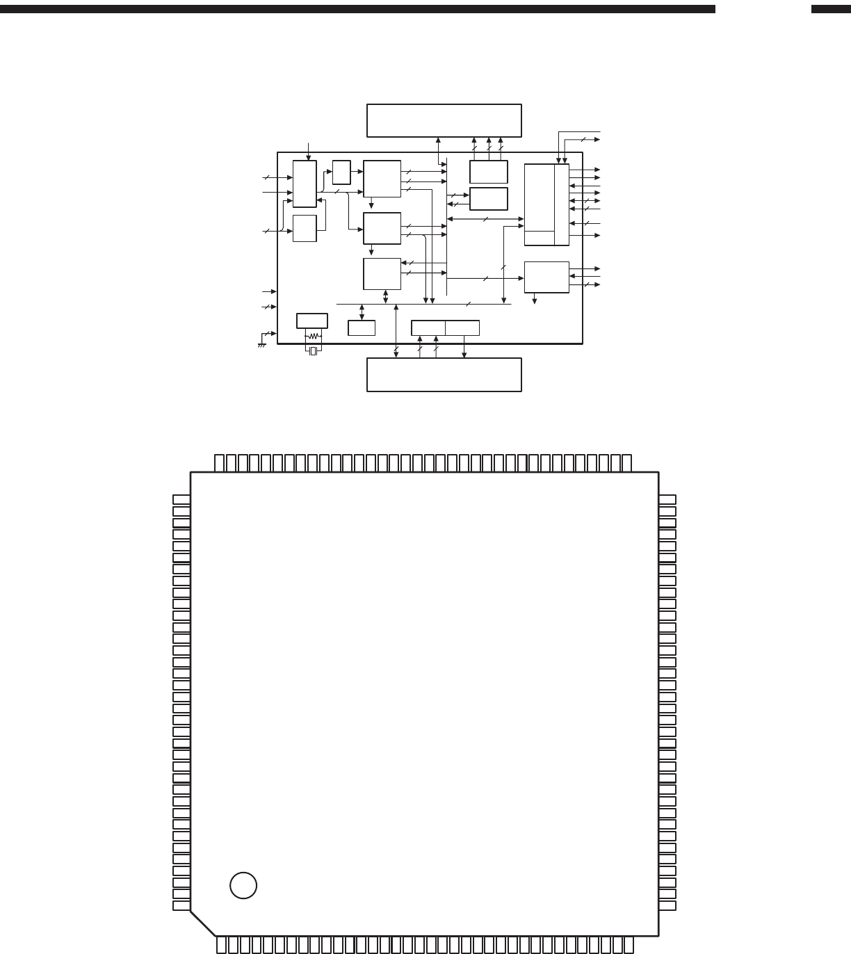
DVD DRIVE
MECHA UNIT
[FG-180]
ACT/MOTOR
DRIVER
ATAPI INTERFACE
DVD DECODER
[TC9469BF]
DRIVE CONTROL
µ-COM
[TMP95FY64F]
FRONTEND
PROCESSOR
[TA1293F]
DISC SERVO
PROCESSOR
[TA1293F]
DRAMDRAM
< FRONT END >
DVD PROCESSOR
[ES6038]
64M SDRAM 16M FLASH ROM E2PROM
I/O
EXPAN
PLL
27MHz
OSC
33MHz
OSC
< BACK END >
DIGITAL
POWER
UNIT
64M SDRAM
ANALOG
POWER
UNIT
POWER
TRANS
I/P µCOM
[PIC18LC242] I/P CONVERTER
[SiI504]
FPGA
XC2530
PROM
VIDEO ENCODER
[ADV7190]
VIDEO ENCODER
[ADV7300]
VR &
FILTER
VR &
FILTER
< VIDEO BLOCK >
MONO MULTI
MONO MULTI
SELECTOR CLAMP &
DRIVER
CLAMP &
DRIVER 525I/625I
525P
DAC
[PCM1738]
DAC
[PCM1738]
FLASH
ROM
ALPHA
PROCESSOR
[DXP7001]
BASS
MANAGEMENT.
DSP
[ADSPMEL322]
12MHz
OSC
FILTER&
AMP
FILTER&
AMP
FILTER&
AMP
FILTER&
AMP
FILTER&
AMP
FILTER&
AMP
RESET
FLT
KEY ROT SW.REM
WIRED REM
FLASH
ROM
RS-232C
LED
< PANEL CONTROL >
PANEL CONTROL
µ-COM
[MN102H460B]
FL DRIVER
[ML9207]
SPDIF
SW
S L
C
S R
F L
F R
[PCM1738]
DAC
< AUDIO BLOCK >
BLOCK DIAGRAM
DVD3800_Block.p65 02/06/18, 14:20Page 18 Adobe PageMaker 6.5J/Win
19
DVD-3800
to Driver Digital
IN
Analog
Out
from
RF-Amp.
(RF signal)
from
RF-Amp.
(servo signal)
ADC
Digital
Servo
DSP
Output
I/F
1bit DAC
for CD-DA
Clock
PLL
RF Signal
Process Sync ECC Output
I/F
PLL MPU I/F
1Mbit
DRAM
Data Out
MPU
SEMICONDUCTORS
IC’s
Note: Indications before IC numbers denote P.W.B. name.
AV: AUDIO/VIDEO P.W.B.
MA: MAIN P.W.B.
PD: POWER/DISPLAY P.W.B.
SC: SCART P.W.B.
TC9453F (MA: IC505)
133
134
135
136
137
138
139
140
141
142
143
144
145
146
147
148
149
150
151
152
153
154
155
156
157
158
159
160
161
162
163
164
165
166
167
168
169
170
171
172
173
174
175
176
LPFN
LPFO
PVREF
VCOREF
VCOF
PVDD
SLCO1
TESM9
TEST2
RFCD
RFDVD
AVDD
RFCT
RFZ1
TEZ1
AWIN
AVSS
FE1
TE1
RFSB
RFRP
AVSS
TESM10
EXTAD
VREF
FOO
TRO
AVDD
AWCTL
FMO
DMO
TEBC
FEBC
DPDC
EQBC
ANMON
/DFCT
VRCK
VSS3
SCD
SCL
SCB
FGIN
NC
1
2
3
4
5
6
7
8
9
10
11
12
13
14
15
16
17
18
19
20
21
22
23
24
25
26
27
28
29
30
31
32
33
34
35
36
37
38
39
40
41
42
43
NC
NC
DVSS
RO
DVDD
DVR
LO
DVSS
XVSS
XI
XO
XVDD
TESM0
TESM1
TESM2
VDD3
VSS3
VPFC
TEST0
VLPF1
VLPF0
VSS3
MON0
MON1
MON2
MON3
MON4
MON5
MON6
MON7
MON8
MON9
VDD3
NC
NC
TEST1
FLGA
FLGB
VSS3
/RST
/MA
/MRD
/MWR
/MCE
88
87
86
85
84
83
82
81
80
79
78
77
76
75
74
73
72
71
70
69
68
67
66
65
64
63
62
61
60
59
58
57
56
55
54
53
52
51
50
49
48
47
46
45
BA8
BA7
BA6
BA5
BA4
VSS5
BA3
BA2
BA1
BA0
VDD3
TESM4
DIGI
TESM3
VDD5
PDCK
/PDRQ
/PSYC
PD8
PD7
PD6
PD5
VSS3
PD4
PD3
PD2
PD1
VSS5
PD0
VDD3
VMCK
SMCK
NC
NC
VDD5
MD7
MD6
MD5
MD4
MD3
MD2
MD1
MD0
/MINT
132
131
130
129
128
127
126
125
124
123
122
121
120
119
118
117
116
115
114
113
112
111
110
109
108
107
106
105
104
103
102
101
100
99
98
97
96
95
94
93
92
91
90
89
PDON2
PDOP2
PDON1
PDOP1
PESP
PVSS
PESV
PPW
CFC2
CFC1
VSS3
TESM8
TESM7
TESM6
TESM5
PLCK
VDD3
NC
NC
BD15
BD14
BD13
VSS5
BD12
BD11
BD10
BD9
VSS3
BD8
BD7
BD6
BD5
BD4
BD3
BD2
BD1
BD0
VDD5
/BWU
/BWL
/BCAS
/BRAS
/BOE
VDD3
44

20
DVD-3800
1NC
2NC
3DVSS GND for DAC
4 RO O R-ch output signal, Analog output pin
5DVDD Power for DAC
6 DVR O Amp ref. signal output, Analog input pin
7 LO O L-ch output signal, Analog output pin
8DVSS GND for DAC
9XVSS GND for oscillator
10 XI I X’tal osc. input, Analog input pin
11 XO O X’tal osc. output, Analog output pin
12 XVDD Power for oscillator
13 TESM0 Test pin, Connect to GND
14 TESM1 Test pin, Open
15 TESM2 Test pin, Connect to VDD3
16 VDD3 3.3V digital power
17 VSS3 3.3V digital GND
18 VPFC O Clock PLL block phase/freq. comparator out, Analog output pin
19 TEST0 I Test mode pin, Connect to VDD3
20 VLPFI I VCO block filter input for clock PLL, Analog input pin
21 VLPFO O VCO block filter output for clock PLL, Analog output pin
22 VSS3 3.3V digital GND
23 MON0 O Test monitor
24 MON1 O Test monitor
25 MON2 O Test monitor
26 MON3 O Test monitor
27 MON4 O Test monitor
28 MON5 O Test monitor
29 MON6 O Test monitor
30 MON7 O Test monitor
31 MON8 O Test monitor
32 MON9 O Test monitor
33 VDD3 3.3V digital power
34 NC
35 NC
36 TEST1 I Test mode pin, Connect to VDD3
37 FLGA I/O Universal I/O or flag monitor
38 FLGB I/O Universal I/O or flag monitor
39 VSS3 3.3V digital GND
40 /RST I Reset pin, Pull-up resister built-in
41 /MA I µcom address enable signal, Fail-safe pin
42 /MRD I µcom data read signal, Fail-safe pin
43 /MWR I µcom data write signal, Fail-safe pin
44 /MCE I µcom chip enable signal, Fail-safe pin
45 /MINT O µcom interrupt signal, Open drain pin
46 MD0 O µcom data bus
47 MD1 O µcom data bus
48 MD2 O µcom data bus
49 MD3 O µcom data bus
50 MD4 O µcom data bus
51 MD5 O µcom data bus
52 MD6 O µcom data bus
53 MD7 O µcom data bus
54 VDD5 Power for 5V
55 NC
56 NC
57 SMCK O 22M block clock output
58 VMCK O Data output block (signal processing system) clock output
Pin Name Function
Pin No. I/O
TC9453F Terminal Function
21
DVD-3800
59 VDD3 3.3V digital power
60 PD0 O DVD/CD data output
61 VSS5 GND for 5V
62 PD1 O DVD/CD data output
63 PD2 O DVD/CD data output
64 PD3 O DVD/CD data output
65 PD4 O DVD/CD data output
66 VSS3 3.3V digital GND
67 PD5 O DVD/CD data output
68 PD6 O DVD/CD data output
69 PD7 O DVD/CD data output
70 PD8 O DVD/CD data output
71 /PSYC O DVD data sector sync signal
72 /PDRQ O DVD data transfer block
73 PDCK O DVD data transfer clock
74 VDD5 Power for 5V
75 TESM3 Test pin, Connect to VSS5
76 DIGI I 1bit DAC digital-in input
77 TESM4 Test pin, Connect to VSS5
78 VDD3 3.3V digital power
79 BA0 O External RAM address output
80 BA1 O External RAM address output
81 BA2 O External RAM address output
82 BA3 O External RAM address output
83 VSS5 GND for 5V
84 BA4 O External RAM address output
85 BA5 O External RAM address output
86 BA6 O External RAM address output
87 BA7 O External RAM address output
88 BA8 O External RAM address output
89 VDD3 3.3V digital power
90 /BOE O External RAM/OE signal
91 /BRAS O External RAM/RAS signal
92 /BCAS O External RAM/CAS signal
93 /BWL O External RAM Lower/WE signal
94 /BWU O External RAM Upper/WE signal
95 VDD5 Power for 5V
96 BD0 I/O External RAM data in/output
97 BD1 I/O External RAM data in/output
98 BD2 I/O External RAM data in/output
99 BD3 I/O External RAM data in/output
100 BD4 I/O External RAM data in/output
101 BD5 I/O External RAM data in/output
102 BD6 I/O External RAM data in/output
103 BD7 I/O External RAM data in/output
104 BD8 I/O External RAM data in/output
105 VSS3 3.3V digital GND
106 BD9 I/O External RAM data in/output
107 BD10 I/O External RAM data in/output
108 BD11 I/O External RAM data in/output
109 BD12 I/O External RAM data in/output
110 VSS5 GND for 5V
111 BD13 I/O External RAM data in/output
112 BD14 I/O External RAM data in/output
113 BD15 I/O External RAM data in/output
114 NC
115 NC
116 VDD3 3.3V digital power
117 PLCK I/O PLL block clock in/output
Pin Name Function
Pin No. I/O

22
DVD-3800
118 TESM5 Test pin, Connect to GND
119 TESM6 Test pin, Connect to GND
120 TESM7 Test pin, Open
121 TESM8 Test pin, Open
122 VSS3 3.3V digital GND
123 CFC1 O VCO frequency control signal, Analog output pin
124 CFC2 O VCO frequency control signal, Analog output pin
125 PPW O Phase comparator offset adj. V out, Analog output pin
126 PESV I Phase comparator offset adj. sig. in, Analog input pin
127 PVSS GND for 3.3V PLL block
128 PESP O Phase comparator offset adj. sig. out, Analog output pin
129 PDOP1 O DVD/CD phase control sig. (positive), Analog output pin
130 PDON1 O DVD/CD phase control sig. (negative), Analog output pin
131 PDOP2 O DVD/CD phase control sig. (positive), Analog output pin
132 PDON2 O DVD/CD phase control sig. (negative), Analog output pin
133 LPFN I Data PLL low pass filter inverted input, Analog input pin
134 LPFO O Data PLL low pass filter output, Analog output pin
135 PVREF Ref. V for data PLL block
136 VCOREF I VCO reference, Analog input pin
137 VCOF I VCO auto-adj. filter out, Analog input pin
138 PVDD Power for 3.3V PLL block
139 SLCO1 O Data slice 6bitDAC out, Analog output pin
140 TESM9 Test pin, Open
141 TEST2 I Test mode pin, Connect to VDD3
142 RFCD I CD RF signal input, Analog input pin
143 RFDVD I DVD RF signal input, Analog input pin
144 AVDD Power for 3.3V analog block
145 RFCT I RFRP center V input (zero-cross intake), Analog input pin
146 RFZI I RFRP signal input (zero-cross intake), Analog input pin
147 TEZI I Tracking error signal input (zero-cross intake), Analog input pin
148 AWIN I Active wide PLL control signal input, Analog input pin
149 AVSS GND for 3.3V analog block
150 FEI I Focus error signal input, Analog input pin
151 TEI I Tracking error signal input, Analog input pin
152 RFSB I RF level or sub beam signal add input, Analog input pin
153 RFRP I RFRP signal input, Analog input pin
154 SAVSS GND for 3.3V analog block
155 TESM10 Test pin, Connect to VREF
156 EXTAD I Universal outside ADC input, Analog input pin
157 VREF Ref. V (1.65V) for analog block
158 FOO O Focus EQ output, Analog output pin
159 TRO O Tracking EQ output, Analog output pin
160 AVDD Power for 3.3V analog block
161 AWCTL O Active wide PLL control output, Analog output pin
162 FMO O Focus EQ output, Analog output pin
163 DMO O Disc EQ output, Analog output pin
164 TEBC O Tracking balance control signal, Analog output pin
165 FEBC O Focus balance control signal, Analog output pin
166 DPDC O DPD error signal pit depth adj. signal, Analog output pin
167 EQBC O RF wide boost adj. signal, Analog output pin
168 ANMON O Universal PWM output, Analog output pin
169 /DFCT O Black dot detect signal
170 VRCK O RF EQ characteristic control clock
171 VSS3 3.3V digital GND
172 SCD O Head amp serial data
173 SCL O Head amp serial data latch pulse
174 SCB O Head amp serial data clock
175 FGIN I Disc FG signal input (w/ self-bias circuit), Feedback R/Analog input pin
176 NC
Pin Name Function
Pin No. I/O
* Pin names begin with “/” are active “L” terminals.
23
DVD-3800
Buffer
DRAM 256kw/128kw/64kw
(4Mbit/2Mbit/1Mbit)
BD15-0
/BWU./BWL
/BOE
/RAS./CAS
BA8-0
SEDVD
PSYCN.PDROM
PDCK
PDA8
PDA(7:0)
/RST
Gnd
Vdd
TEST2-0
XI
XO
Clock
AUTH
MD7-0
/MWR./WRD
/MCE
MA6-0
/MINT
(M-IF)
ASYC
M-FIFO
(8B
´
3ch) AV-IF
H-FIFO
(64B)
ECC
SUB-IF
SBDa
SBQa
CD-IF &
DVD-IF
HSYC
Da
Daf
HEDda
(H-IF)
CSEL
/PDIAG./DASP
IORDY
HDRQ
/HDAK
/IOCS16
HD15-0
/HRD./HWR
/HCS3./HCS1
HA2-0
INTRQ
DIGO
AZCK
ABCK.ACHCK
ADO
Buffer
Address
BSYC
Input
IF
Convert H Interrupt
TC9469BF
M Interrupt
M Address
3
8
30
3
837
3
8
8
8
16
16
16
64
64
8
16
64
8
16
9
5
2
16
2
29
3
16
mcom
Driver
Correc-
tion
Input
Selecter
TC9469BF (MA: IC508)
109
110
111
112
113
114
115
116
117
118
119
120
121
122
123
124
125
126
127
128
129
130
131
132
133
134
135
136
137
138
139
140
141
142
143
144
V
DD
HD7
HD8
HD6
HD9
HD5
HD10
V
SS
HD4
HD11
HD3
HD12
HD2
HD13
HD1
HD14
HD0
V
DD
V
SS
HD15
HDRQ
/HWR
VSShr
/HRD
V
SS
24
IORDY
V
DD
24
V
SS
/HDAK
INTRO
/IOCS16
HA1
/PDIAG
HA0
V
DD
(NC)
1
2
3
4
5
6
7
8
9
10
11
12
13
14
15
16
17
18
19
20
21
22
23
24
25
26
27
28
29
30
31
32
33
34
35
36
(NC)
V
SS
A2
/HCS1
/HCS3
/DASP
CSEL
V
SS
V
DD
BD15
BD14
BD13
BD12
BD11
BD10
BD9
BD8
V
DD
V
SS
BD4
BD5
BD7
BD6
BD3
BD2
BD1
BD0
V
SS
/BWU(/BWE)
/BWL(/CASL)
/CAS(/CASU)
/RAS
/BOE
BA8
V
DD
(NC)
72
71
70
69
68
67
66
65
64
63
62
61
60
59
58
57
56
55
54
53
52
51
50
49
48
47
46
45
44
43
42
41
40
39
38
37
(NC)
(NC)
V
SS
(LRCK)PDA0
(BCK)PDA1
(DA1)PDA2
(C2P1)PDA3
(CLCK)PDA4
V
SS
(SB01)PDA5
(SFSY)PDA6
(SBSY)PDA7
PDA8
PSYCN
PDRQN
PDCK
(NC)
DIGO
VDDck
X0
X1
VSSck
TEST2
TEST1
TEST0
BA3
BA1
BA2
V
SS
BA0
BA4
BA5
BA6
BA7
V
SS
(NC)
108
107
106
105
104
103
102
101
100
99
98
97
96
95
94
93
92
91
90
89
88
87
86
85
84
83
82
81
80
79
78
77
76
75
74
73
(NC)
V
SS
V
SS
V
DD
/RST
ESTOUT
/MINT
/MWR
V
SS
/WRD
/WCE
MA6
MA5
MA4
MA3
MA2
MA1
MA0
V
DD
V
SS
MD7
MD6
MD5
MD4
MD3
MD2
MD1
MD0
V
SS
SEDVD
V
DD
ACHCK
AD0
ABCK
AZCK
(NC)

24
DVD-3800
1NC
2VSS GND pin
3 HA2 I Host address 2 input: IDE sig. DA2, TTL level input, pull-up R built-in
4 /HCS1 I Chip select 1 input: IDE sig. /CS1FX, TTL level input, pull-up R built-in
5 HCS3 I Chip select 3 input: IDE sig. /CS3FX, TTL level input, pull-up R built-in
6 /DASP I/O Drive active in/output: IDE sig. /DASP, TTL level input, open drain out, pull-up R built-in
7 CSEL I Cable select pin: IDE sig. CSEL
8VSS GND pin
9VDD Power pin
10 BD15 I/O Buffer RAM data in/output, at low power: output
11 BD14 I/O Buffer RAM data in/output, at low power: output
12 BD13 I/O Buffer RAM data in/output, at low power: output
13 BD12 I/O Buffer RAM data in/output, at low power: output
14 BD11 I/O Buffer RAM data in/output, at low power: output
15 BD10 I/O Buffer RAM data in/output, at low power: output
16 BD9 I/O Buffer RAM data in/output, at low power: output
17 BD8 I/O Buffer RAM data in/output, at low power: output
18 VDD Power pin
19 VSS GND pin
20 BD4 I/O Buffer RAM data in/output, at low power: output
21 BD5 I/O Buffer RAM data in/output, at low power: output
22 BD7 I/O Buffer RAM data in/output, at low power: output
23 BD6 I/O Buffer RAM data in/output, at low power: output
24 BD3 I/O Buffer RAM data in/output, at low power: output
25 BD2 I/O Buffer RAM data in/output, at low power: output
26 BD1 I/O Buffer RAM data in/output, at low power: output
27 BD0 I/O Buffer RAM data in/output, at low power: output
28 VSS GND pin
29 /BWU O For write enable bit (for /BWE sig.), at low power: H
30 /BWL O For /CAS signal lower 8bit (for /CASL sig.), at low power: H
31 /CAS O For /CAS signal upper 8bit (for /CASU sig.), at low power: H
32 /RAS O RAS signal output, at low power: H
33 /BOE O Output enable, at low power: H
34 BA8 O Buffer address output
35 VDD Power pin
36 NC
37 NC
38 VSS GND pin
39 BA7 O Buffer address output
40 BA6 O Buffer address output
41 BA5 O Buffer address output
42 BA4 O Buffer address output
43 BA0 O Buffer address output
44 VSS GND pin
45 BA2 O GND pin
46 BA1 O GND pin
47 BA3 O Buffer address output
48 TEST0 I Test pin, Fixed to “L”
49 TEST1 I Test pin, Fixed to “L”
50 TEST2 I Test pin, Fixed to “L”
51 VSSck GND pin (for clock system)
52 XI I Master clock in/output, feedback R built-in
53 XO O Master clock in/output, feedback R built-in
54 VDDck Power pin (for clock system)
55 DIGO O Digital out pin
56 NC
57 PDCK I Data read clock input
58 PDRQN I Data effective flag input
Pin Name Function
Pin No. I/O
TC9469BF Terminal Function
25
DVD-3800
59 PSYCN I Sync signal input
60 PDA8 I Parallel data 8 input
61 PDA7 I Parallel data 7 input
62 PDA6 I Parallel data 6 input
63 PDA5 I Parallel data 5 input
64 VSS GND pin
65 PDA4 I Parallel data 4 input
66 PDA3 I Parallel data 3 input
67 PDA2 I Parallel data 2 input
68 PDA1 I Parallel data 1 input
69 PDA0 I Parallel data 0 input
70 VSS GND pin
71 NC
72 NC
73 NC
74 AZCK I Ref. clock input for audio playback
75 ABCK O Bit clock (BCK) output for audio playback
76 ADO O Data output for audio playback
77 ACHCK O Channel clock (LRCK) output for audio playback
78 VDD Power pin
79 SEDVD I Input IF select
80 VSS GND pin
81 MD0 I/O µcom data in/output, tri-state output
82 MD1 I/O µcom data in/output, tri-state output
83 MD2 I/O µcom data in/output, tri-state output
84 MD3 I/O µcom data in/output, tri-state output
85 MD4 I/O µcom data in/output, tri-state output
86 MD5 I/O µcom data in/output, tri-state output
87 MD6 I/O µcom data in/output, tri-state output
88 MD7 I/O µcom data in/output, tri-state output
89 VSS GND pin
90 VDD Power pin
91 MA0 I µcom address input
92 MA1 I µcom address input
93 MA2 I µcom address input
94 MA3 I µcom address input
95 MA4 I µcom address input
96 MA5 I µcom address input
97 MA6 I µcom address input
98 /MCE I Chip enable signal input
99 /MRD µcom chip read signal input
100 VSS GND pin
101 /MWR I µcom write signal input
102 /MINT O µcom interrupt signal output, open drain, pull-up R built-in
103 TESTOUT O Output for test, leave it open
104 /RST I Hardware reset input (CMOS level), pull-up R built-in
105 VDD Power pin
106 VSS GND pin
107 VSS GND pin
108 NC
109 VDD Power pin
110 HD7 I/O
111 HD8 I/O
112 HD6 I/O
113 HD9 I/O Host data in/output (HD[0:15]:IDE sig. DD[0:15]), TTL level, tri-state out, pull-up R built-in
114 HD5 I/O
115 HD10 I/O
116 VSS GND pin
Pin Name Function
Pin No. I/O
26
DVD-3800
117 HD4 I/O
118 HD11 I/O
119 HD3 I/O
120 HD12 I/O
121 HD2 I/O Host data in/output (HD[0:15]:IDE sig. DD[0:15]), TTL level, tri-state out, pull-up R built-in
122 HD13 I/O
123 HD1 I/O
124 HD14 I/O
125 HD0 I/O
126 VDD Power pin
127 VSS GND pin
128 HD15 I/O Host data in/output (HD[0:15]:IDE sig. DD[0:15])
129 HDRQ O Data request output: IDE sig. DMARQ, tri-state out, drive-ability 12mA
130 /HWR I Host write signal input: IDE sig. /DIOW, TTL level, pull-up R built-in
131 VSShr GND pin (for /HR)
132 /HRD I Host read signal input: IDE sig. /DIOR, TTL level, pull-up R built-in
133 VSS24 GND pin (for IORDY)
134 IORDY O IO transfer ready output: IDE sig. IORDY, tri-state out, drive-ability 24mA
135 VDD24 Power pin (for IORDY)
136 VSS GND pin
137 /HDAK I Data acknowledge input: IDE sig. /DMACK, TTL level, pull-up R built-in
138 INTRQ O Interrupt signal output: IDE sig. INTRQ, tri-state out, drive-ability 12mA
139 /IOCS16 O Data bit wide select output: IDE sig. /IOCS16, open drain, pull-up R built-in
140 HA1 I Host address 1 input: IDE sig. DA1, TTL level, pull-up R built-in
141 /PDIAG I/O Post diagnostic in/output: IDE sig. /PDIAG, TTL level, tri-state out, pull-up R built-in
142 HA0 I Host address 0 input: IDE sig. DA0, TTL level, pull-up R built-in
143 VDD Power pin
144 NC
Pin Name Function
Pin No. I/O
* Pin names begin with “/” PSYNCN, and PDRQN are active “L” terminals.
1
2
3
4
5
6
7
8
9
10
11
12
13
14
15
16
17
18
19
20
21
24
23
22
A15
A13
A14
A10
A11
RESET
WE
A19
A8
A4
A3
A2
A1
A12
NC
NC
RY/BY
A18
A17
A7
A6
A5
NC
A9
A16
GND
BYTE
Q14
Q7
V
CC
Q4
Q5
Q13
OE
GND
CE
A0
Q15/A-1
Q12
Q3
Q10
Q2
Q9
Q1
Q8
Q0
Q11
Q6
48
47
46
45
44
43
42
41
40
39
38
37
36
35
34
33
32
31
30
29
28
25
26
27
SYMBOL PIN NAME
A0~A19 Address Input
Q0~Q14 Data Input/Output
Q15/A-1 Q15 (Word mode)/LSB addr (Byte mode)
CE Chip Enable Input
WE Write Enable Input
BYTE Word/Byte Selection input
RESET Hardware Reset Pin/Sector Protect Unlock
OE Output Enable Input
RY/BY Ready/Busy Output
VCC Power Supply Pin (2.7V~3.6V)
GND Ground Pin
MX29LV160BTC-90 (MA: IC102)
27
DVD-3800
TMP95FY64F (MA: IC511)
76
77
78
79
80
81
82
83
84
85
86
87
88
89
90
91
92
93
94
95
96
97
98
99
100
P33/A11
P32/A10
P31/A9
P30/A8
P47/A7
P46/A6
P45/A5
P44/A4
P43/A3
P42/A2
P41/A1
P40/A0
P50/RD
P51/WR
P52/HWR
(GND)VSS
PA0/AN0
PA1/AN1
PA2/AN2
PA3/AN3/ADTRG
PA4/AN4
PA5/AN5
PA6/AN6
PA7/AN7
VREFH
50
49
48
47
46
45
44
43
42
41
40
39
38
37
36
35
34
33
32
31
30
29
28
27
26
P05/D5
P04/D4
P03/D3
P02/D2
P01/D1
P00/D0
VCC
P96/TOA/TOB
P95/TIB/INT8
P94/TIA/INT7
P93/TO9
P92/TO8
P91/TI9/INT6
P90/TI8/INT5
P75/TO7/INT4
P74/TO5
P73/TI4/INT3
P72/TO3/INT2
P71/TO1
P70/TI0/INT1
RESET
EA
X2
X1
VSS(GND)
P34/A12
P35/A13
P36/A14
P37/A15
P20/A16
P21/A17
P22/A18
P23/A19
P24/A20
P25/A21
P26/A22
P27/A23
VCC
VSS(GND)
AM8/16
P17/D15
P16/D14
P15/D13
P14/D12
P13/D11
P12/D10
P11/D9
P10/D8
P07/D7
P06/D6
75
74
73
72
71
70
69
68
67
66
65
64
63
62
61
60
59
58
57
56
55
54
53
52
51
1
2
3
4
5
6
7
8
9
10
11
12
13
14
15
16
17
18
19
20
21
22
23
24
25
VREFL
AVSS
AVCC
DAOUT0
DAOUT1
NMI
P53/BUSRQ
P54/BUSAK
P55/WAIT
P56/INTO
P57/SCLK2/CTS2
P80/TxD0
P81/RxD1
P82/SCLK0/CTS0
P83/TxD1
P84/RxD1
P85/SCLK1/CTS1
P86/TxD2
P87/RxD2
P60/CS0
P61CS1
P62/CS2
P62/CS3
CLK
VCC
Pin Name Function
Pin No. Symbol
TMP95FY64F Terminal Function
1 VREFL VREFL I Ref. V input (L) for A/D converter
2AVSS AVSS GND
3AVCC AVCC Power
4 DAOUT0 DAOUT0 O D/A output 0
5 DAOUT1 DAOUT1 O D/A output 1
6 NMI NMI I Non-maskable interrupt request pin
7 P53 STBN O TA8493F/BA5952FP standby pin
8 P54 AMUTE O Not used
9 P55 Not used
10 INT0 DSPINT I Interrupt input from TC9453F
11 P57 RSTN O Reset output of TC9453F
12 P80 Not used
13 P81 Not used
14 P82 TEST I Not used
15 P83 Not used
16 P84 TMM+ O Loading motor control pin
17 P85 TMM- O Loading motor control pin
18 P86 O Not used
19 P87 I Not used
20 CS0 DECCSN O TC9469BF chip select
21 CS1 DSPCSN O TC9453F chip select
22 P62 Not used
23 P63 Not used
24 CLK Not used
25 VCC VCC Power
26 VSS VSS GND
27 X1 X1 I X’tal connection
28 X2 X2 O X’tal connection
29 EA EA I Power
30 RESET RESET I Reset input pin
31 INT1 DECINT I Interrupt input from TC9469BF
32 P71 Not used
33 P72 Not used
I/O

28
DVD-3800
34 INT3 FG I FG signal input from TA8493F
35 P74 BRKN O Brake signal output to TA8493F
36 P75 Not used
37 INT5 SLIDE_PULSE I Pulse counter input of slide
38 P91 P-LOW O PLL filter switching output
39 P92 PLLD Not used
40 P93 P-HIGH O PLL filter switching output
41 INT7 Not used
42 P95 Not used
43 P96 PLLB Not used
44 VCC VCC Power
45 D0 MD0 I/O Data bus
46 D1 MD1 I/O Data bus
47 D2 MD2 I/O Data bus
48 D3 MD3 I/O Data bus
49 D4 MD4 I/O Data bus
50 D5 MD5 I/O Data bus
51 D6 MD6 I/O Data bus
52 D7 MD7 I/O Data bus
53 D8 T22 Not used
54 D9 T9 Not used
55 D10 T10 Not used
56 D11 T11 Not used
57 D12 T12 Not used
58 D13 T13 Not used
59 D14 T14 Not used
60 D15 T15 Not used
61 AM8/16 AM8/16 I Pull-up
62 VSS VSS GND
63 VCC VCC Power
64 P27 BUSY O Busy output
65 P26 O Not used
66 P25 O Not used
67 P24 Not used
68 P23 Not used
69 P22 Not used
70 P21 Not used
71 A16 Not used
72 A15 Not used
73 A14 Not used
74 A13 Not used
75 A12 Not used
76 A11 Not used
77 A10 Not used
78 A9 Not used
79 A8 MA8 O Address bus
80 A7 Not used
81 A6 MA6 O Address bus
82 A5 MA5 O Address bus
83 A4 MA4 O Address bus
84 A3 MA3 O Address bus
85 A2 MA2 O Address bus
86 A1 MA1 O Address bus
87 A0 MA0 O Address bus
88 RD RDN O Strobe signal output for read
89 WR WRN O Strobe signal output for write
90 P52 Not used
91 VSS VSS Power
92 PA0 MASTER I Pull-down
93 PA1 SLAVE I Pull-up
94 PA2 CSEL I Pull-up
95 PA3 CLOS I Loader close SW input pin
96 PA4 OPEN I Loader open SW input pin
97 PA5 INSWN I Pickup inner SW input pin
98 AN6 +1.65V I Analog input pin
99 PA7 EJECT I Not used
100 VREFH VREFH I Ref. V input (H) for A/D converter
Pin Name Function
Pin No. Symbol I/O
29
DVD-3800
61
62
63
64
65
66
67
68
69
70
71
72
73
74
75
76
77
78
79
80
P1TN
P1TP
P1FN
P1FP
LDP1
GNDR
P1DI
P1CI
P1BI
P1AI
LDP2
P2AI
P2BI
P2CI
P2DI
GNDS
P2FP
P2FN
P2TP
P2TN
1
2
3
4
5
6
7
8
9
10
11
12
13
14
15
16
17
18
19
20
GNDP
LDO2
MDI2
NC
NC
VrA
Vrfi
VrD
Vdd
DPAC
DPBD
DPD1
DPD2
SCB
SCL
SCD
VRCK
NC
NC
VCKF
40
39
38
37
36
35
34
33
32
31
30
29
28
27
26
25
24
23
22
21
DFTN
NC
NC
NC
NC
NC
FEO
TEO
NC
LVL
NC
NC
NC
VccS
RFSW
NC
NC
NC
NC
VccP
60
59
58
57
56
55
54
53
52
51
50
49
48
47
46
45
44
43
42
41
LDO1
MDI1
EQF
EQB
RFDC
GND2
EQD
NC
Vcc2
VccO
PSC
FEB
TEB
DPDB
VccR
RFO
RPP
RPB
RPO
RPZ
TA1293F (MA: IC501)
Pin Name FunctionPin No. I/O
TA1293F Terminal Function
1 GNDP GND pin
2 LDO2 O Drive pin
3 MDI2 I Monitor pin
4 NC Used connecting with VrA
5 NC Used connecting with VrA
6 VrA O Analog VREF
7 Vrfi Filter capacity for reference
8 VrD O Digital VREF, outputs 1/2 of Vdd
9 Vdd I Power pin, connect Vdd of servo IC
10 DPAC DPD AC coupling capacity 1
11 DPBD DPD AC coupling capacity 2
12 DPD1 DPD integral capacity 1
13 DPD2 DPD integral capacity 2
14 SCB I Control line (bit clock)
15 SCL I Control line (latch signal)
16 SCD I Control line (serial data)
17 VRCK I Ref. clock input
18 NC Used connecting with GND
19 NC Used connecting with GND
20 VCKF Capacity for adjusting time constant
21 VccP Power pin
22 NC Used in open
23 NC Used in open
24 NC Used in open
25 NC Used connecting with GND
26 RFSW I RFO control pin, outputs signal after EQ at L
27 VccS Power pin
28 NC Used in open
29 NC Used connecting with VrA

30
DVD-3800
30 NC Used connecting with VrA
31 LVL O Servo addition output
32 NC Used in open
33 TEO O TE output
34 FEO O TE output
35 NC Used connecting with VrA
36 NC Used connecting with VrA
37 NC Used connecting with VrA
38 NC Used connecting with VrA
39 NC Used connecting with VrA
40 DFTN I DPD defect, L: DPD out = Mute
41 RPZ O RF ripple center output
42 RPO O RF ripple output
43 RPB O Bottom of RF ripple
44 RPP O Peak of RF ripple
45 RFO O Equivalent RF output
46 VccR Power pin (RF)
47 DPDB I Pit depth adjustment
48 TEB I TE balance
49 FEB I FE balance
50 PSC I VRCK divide on/off, H: divide off
51 VccO Power pin
52 Vcc2 Power pin
53 NC Connect with VrD, or GND via C
54 EQD I Group delay correction
55 GND2 GND pin
56 RFDC DC feedback capacity
57 EQB I Boost adjustment
58 EQF I Frequency adjustment
59 MDI1 I Monitor input
60 LDO1 O Drive output
61 P1TN I TE(-) input (DVD)
62 P1TP I TE(+) input (DVD)
63 P1FN I FE(-) input (DVD)
64 P1FP I FE(+) input (DVD)
65 LDP1 I APC polarity 1, positive when connected to Vcc
66 GNDR GND pin
67 P1DI I D input (DVD)
68 P1CI I C input (DVD)
69 P1BI I B input (DVD)
70 P1AI I A input (DVD)
71 LDP2 I APC polarity 2, positive when connected to Vcc
72 P2AI I A input (CD)
73 P2BI I B input (CD)
74 P2CI I C input (CD)
75 P2DI I D input (CD)
76 GNDS GND pin
77 P2FP I FE(+) input (CD)
78 P2FN I FE(-) input (CD)
79 P2TP I TE(+) input (CD)
80 P2TN I TE(-) input (CD)
Pin Name Function
Pin No. I/O
31
DVD-3800
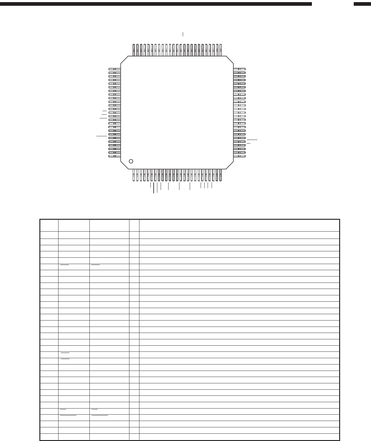
FunctionI/OPin No. Pin Name
SiI504CM208 Terminal Function
2, 41, 51, 56,
99, 106, 146, VDDCore Pwr 1.8V Core Power.
160, 168, 199,
205
3, 40, 47, 50,
55, 100, 102, GNDCore Pwr Digital Ground for Core Power.
107, 150, 162,
167, 206
4 LCDPwrEn Out LCD Power Enable
5 CBlank Out Composite Blank
6 CSync Out Composite Sync
7 VSync Out Vertical Sync
8 HSync Out Horizontal Sync
9~14, 17~20 Blue_Cb[9:0] Out Blue Data (RGB output mode); Cb Data (YCrCb output mode)
15, 21, 33, 61,
66, 72, 79, 85,
93, 114, 118, GNDIO Pwr Digital Ground for I/O Power.
121, 126, 131,
144, 183, 190,
198
1
2
3
4
5
6
7
8
9
10
11
12
13
14
15
16
17
18
19
20
21
22
23
24
25
26
27
28
29
30
31
32
33
34
35
36
37
38
39
40
41
42
43
44
45
46
47
48
49
50
51
52
53
54
55
56
57
58
59
60
62
61
63
64
65
66
67
68
69
70
71
72
73
74
75
76
77
78
79
80
81
82
83
84
85
86
87
88
89
90
91
92
93
94
95
96
97
98
99
100
101
102
103
104
156
155
154
153
152
151
150
149
148
147
146
145
144
143
142
141
140
139
138
137
136
135
134
133
132
131
130
129
128
127
126
125
124
123
122
121
120
119
118
117
116
115
114
113
112
111
110
109
108
107
106
105
208
207
206
205
204
203
202
201
200
199
198
197
196
195
194
193
192
191
190
189
188
187
186
185
184
183
182
181
180
179
178
177
176
175
174
173
172
171
170
169
168
167
166
165
164
163
162
161
160
159
158
157
RSVD
VDDCore
GNDCore
LCDPwrEn
CBIank
CSync
VSync
HSync
Blue_Cb0
Blue_Cb1
Blue_Cb2
Blue_Cb3
Blue_Cb4
Blue_Cb5
GNDIO
VDDIO
Blue_Cb6
Blue_Cb7
Blue_Cb8
Blue_Cb9
GNDIO
Green_Y0
Green_Y1
Green_Y2
Green_Y3
VDDIO
Green_Y4
Green_Y5
Green_Y6
Green_Y7
Green_Y8
Green_Y9
GNDIO
Red_Cr0
Red_Cr1
Red_Cr2
Red_Cr3
Red_Cr4
Red_Cr5
GNDCore
VDDCore
Red_Cr6
Red_Cr7
Red_Cr8
Red_Cr9
VidOutClk
GNDCore
BypPLLClk48M
Clk48M
GNDCore
VDDCore
ExtRefSel
RSVD
GNDCore
VDDCore
MemAddr3
MemAddr2
MemAddr1
MemAddr0
GNDIO
MemAddr4
MemAddr5
MemAddr6
MemAddr7
GNDIO
MemAddr8
MemAddr9
MemAddr10
MemAddr11
RSVD
GNDIO
VDDIO
VDDIO
RAS
CAS
WE
DQM
GNDIO
MemData7
MemData6
MemData5
MemData4
MemData3
GNDIO
MemData2
MemData1
MemData0
VDDIO
PuPdDis
MemData8
MemData9
GNDIO
MemData10
MemData11
MemData12
MemData13
MemData14
GNDCore
MemClk
VDDCore
GNDCore
RSVD
HostAddr5
HostAddr4
HostAddr3
HostAddr2
HostAddr1
HostAddr0
GNDCore
HostCS
HostRd_SDA
HostWr_SCL
VDDCore
VidlnClk
GNDIO
VidlnData9
VidlnData8
VidlnData7
VidlnData6
VidlnData5
VidlnData4
VidlnData3
VidlnData2
VDDIO
ExtRefXtalIOut
ExtRefXtalIn
VDDIO
GNDIO
MemData16
MemData17
MemData18
MemData19
GNDIO
MemData20
MemData21
MemData22
MemData23
GNDIO
MemData31
MemData30
GNDIO
VDDIO
MemData29
MemData28
GNDIO
MemData27
MemData26
MemData25
MemData24
MemData15
BypPLLMemClk
GNDCore
VDDCore
RSVD
AVDD
ARTN
GNDCore
VDDCore
Clk54_72M
BypPLLClk54_72M
Test1
Test0
Reset
VDDCore
GNDIO
SCKIn
WSIn
SDIn
VDDIO
SCKOut
WSOut
SDOut
GNDIO
VDDIO
MemAddr12
DeintDone
DetVideo
Det22PD
Det32PD
GNDIO
VDDIO
HostData0
HostData1
HostData2
HostData3
HostData4
HostData5
HostData6\HS
HostData7\VS
RSVD
HostData8\VidlnData12
HostData9\VidlnData13
HostData10\VidlnData14
HostData11\VidlnData15
VDDCore
GNDCore
HostData12\VidlnData16
HostData13\VidlnData17
HostData14\VidlnData18
HostData15\VidlnData19
GNDCore
HostClk
VDDCore
HostMode
HostAddr7
HostAddr6
TOP VIEW
RSVD
RSVD
SiI504CM208 (MA: IC701)
32
DVD-3800
16, 26, 73, 74,
89, 117, 132, VDDIO Pwr 3.3V I/O Power.
135, 182, 189,
194
22~25, 27~32 Green_Y[9:0] Out Green Data (RGB output mode); Y Data (YCrCb output mode)
34~39, 42~45 Red_Cr[9:0] Out Red Data (RGB output mode); Cr Data (YCrCb output mode)
46 VidOutClk Out Video Output Clock, 36, 27 or 24 MHZ
48 BypPLLClk48M In Bypass PLL for Clk48M.
49 Clk48M InOut 48 MHz Clock.
52 ExtRefSel In External APLL Reference Select.
57~60, 62~65,
67~70, 188 MemAddr[12:0] InOut SDRAM Address when an output. Configuration at reset when an input.
75 RAS Out SDRAM Row Address Strobe.
76 CAS Out SDRAM Column Address Strobe.
77 WE Out SDRAM Write Enable.
78 DQM Out SDRAM Data Mask.
80~84, 86~88,
91, 92, 94~98,
109, 110~113, MemData[31:0] InOut SDRAM Data.
115, 116, 119,
120, 122~125,
127~130
90 PuPdDis In Internal pullup and pulldown disable test function.
101 MemClk InOut SDRAM Clock.
108 BypPLLMemClk In Bypass PLL for MemClk.
133 ExtRefXtalIn In External APLL Reference Crystal/oscillator Input.
134 ExtRefXtalOut Out External APLL Reference Crystal Output.
136~143 VidlnData[9:2] In Multiplexed Video Input Data; Y Video Input Data.
145 VidlnClk In Video Input Clock, 27.0 MHz
147 HostWr_SCL In 186-Compatible Write when HostMode=0. Serial Clock when HostMode=1.
148 HostRd_SDA InOut 186-Compatible Read when HostMode=0. Serial Data when HostMode=1.
149 HostCS In 186-Compatible Chip Select when HostMode=0.
When HostMode=1, must be tied to VDD or pulled up to VDD.
151~158 HostAddr[7:0] In 186-Compatible Address when HostMode=0. No connect when HostMode=1.
159 HostMode In Serial Host Interface when HostMode=1. 186-compatible host interface when HostMode=0.
161 HostClk InOut 186-Compatible Clock when HostMode=0. No connect when HostMode=1.
163~166, HostData[15:8]
169~172 (VidInData[19:2]) InOut 186-Compatible Data when HostMode=0. Chroma video input data when HostMode=1.
174 HostData[7](VS) InOut 186-Compatible Data when HostMode=0. Vertical sync input when HostMode=1.
175 HostData[6](HS) InOut 186-Compatible Data when HostMode=0. Horizontal sync input when HostMode=1.
176~181 HostData[5:0] InOut 186-Compatible Data when HostMode=0. No connect when HostMode=1.
184 Det32PD Out 3:2 Pulldown Sequence Detected.
185 Det22PD Out 2:2 Pulldown Sequence Detected.
186 DetVideo Out Interlaced Video Sequence Detected.
187 DeintDone Out Deinterlace processing complete for current field period.
191 SDOut Out Serial Digital Audio Output Data.
192 WSOut Out Serial Digital Audio Output Word Select.
193 SCKOut Out Serial Digital Audio Output Clock.
195 SDIn In Serial Digital Audio Input Data.
196 WSIn In Serial Digital Audio Input Word Select.
197 SCKIn In Serial Digital Audio Input Clock.
200 Reset In Hardware Reset.
201, 202 Test[1:0] In Production hardware test support.
203
BypPLLClk54_72M
In Bypass PLL for Clk54_72M.
204 Clk54_72M InOut 54 or 72 MHz Clock.
207 ARTN Pwr Analog Return for PLLs.
208 AVDD Pwr 1.8V Analog Power for PLL.
FunctionI/O
Pin No. Pin Name
33
DVD-3800
1VDD_IO P Digital power supply.
2~9, 12, 13 Y9-0 I 10-Bit Progressive scan/ HDTV input port for Y data.
10, 56 VDD P Digital power supply.
11, 57 DGND G Digital Ground
14~18, 26~30 C9-0 I 10-Bit Progressive scan/ HDTV input port for CrCb color data in 4:2:2 input mode.
When this input pin is brought low, the ADV7300 interfaces over the SPI port and uses this
19 SPI/I2C I input as part of the 4 wire SPI interface. When this input pin is tied high [VDD_IO], the ADV7300
interfaces over the I2C port.
20 ALSB_SO I/O Multifunctional pin.
21 SDA_CLKSP I/O Multifunctional pin.
22 SCLK_SI I Multifunctional input.
23 P_HSYNC I Video Horizontal Sync Control Signal for HD sync in simultaneous SD/HD mode
and HD only mode.
24 P_VSYNC I Video Vertical Sync Control Signal for HD sync in simultaneous SD/HD mode
and HD only mode.
25 P_BLANK I Video Blanking Control Signal for HD sync in simultaneous SD/HD mode and HD only mode.
31 RTC_SCR_TR I Multifunctional input.
32 CLKIN_A I Pixel Clock Input for HD only or SD only modes.
33 RESET I This input resets the on-chip timing generator and sets the ADV7300 into Default Register
setting. Reset is an active low signal.
34 EXT_LF I External Loop filter for the internal PLL.
35, 47 RSET1,2 IA1520 Ohms resistor must be connected from this pin to AGND and is used to control the
amplitudes of the DAC outputs.
36,45 COMP O Compensation Pin for DACs.
37 DAC F O In SD only mode: Chroma/RED/V analog output.
In HD only mode and simultaneus HD/SD: Pb/ BLUE (HD) analog output.
38 DAC E O In SD only mode: Luma/BLUE/U analog output.
In HD only mode and simultaneus HD/SD: Pr/ RED (HD) analog output.
39 DAC D O In SD only mode: CVBS/GREEN/Y analog output.
In HD only mode and simultaneus HD/SD: Y/ GREEN (HD) analog output.
40 AGND G Analog Ground
41 VAA P Analog power supply.
42 DAC C O Chroma/ RED/ V SD analog output.
43 DAC B O Luma/ BLUE/ U SD analog output.
44 DAC A O CVBS/ GREEN/ Y SD analog output.
46 VREF I/O Optional External Voltage Reference Input for DACs or Voltage Reference Output (1.235V).
48 S_BLANK I/O Video Blanking Control Signal for SD.
49 S_VSYNC I/O Video Vertical Sync Control Signal for SD.
50 S_HSYNC I/O Video Horizontal Control Signal for SD.
51~55, 58~62 S9-S0 I 10-Bit Standard Definition input port. Or Progressive Scan/ HDTV input port for
Cr [Red/V] color data in 4:4:4 input mode.
63 CLKIN_B I Pixel Clock Input.
64 GND_IO G Digital Ground
FunctionI/O
Pin No. Pin Name
ADV7300 (MA: IC706)
ADV7300 Terminal Function
1
2
3
4
5
6
7
8
9
10
11
12
13
14
15
16
48
47
46
45
44
43
42
41
40
39
38
37
36
35
34
33
17
18
19
20
21
22
23
24
25
26
27
28
29
30
31
32
64
63
62
61
60
59
58
57
56
55
54
53
52
51
50
49
VDD_IO
Y0
Y1
Y2
Y3
Y4
Y5
Y6
Y7
VDD
DGND
Y8
Y9
C0
C1
C2
C3
C4
ALSB_SO
SDA_CLKSP
SCLK_SI
P_BLANK
C5
C6
C7
C8
C9
RTC_SCR_TR
CLKIN_A
VREF
COMP1
DAC A
DAC B
DAC C
VAA
AGND
DAC D
DAC E
DAC F
COMP2
R
EXT_LF
SET 2
R
SET 1
GND_IO
CLKIN_B
S9
S8
S7
S6
S5
DGND
VDD
S4
S3
S2
S1
S0
SPI/I2C
P_HSYNC
P_VSYNC
RESET
S_BLANK
S_VSYNC
S_HSYNC
TOP VIEW
34
DVD-3800
1 MCLR I Master Clear (Reset) input. This pin is an active low RESET to the device.
2 RA0 I/O Digital I/O.
3 RA1 I/O Digital I/O.
4 RA2 I/O Digital I/O.
5 RA3 I/O Digital I/O.
6 RA4 I/O Digital I/O. Open drain when configured as output.
7 RA5 I/O Digital I/O.
8VSS P Ground reference for logic and I/O pins.
9 OSC1 I Oscillator crystal input or external clock source input.
ST buffer when configured in RC mode. CMOS otherwise.
10 OSC2 O Oscillator crystal output. Connects to crystal or resonator in Crystal Oscillator mode.
11 RC0 I/O Digital I/O.
12 RC1 I/O Digital I/O.
13 RC2 I/O Digital I/O.
14 RC3 I/O Digital I/O.
15 RC4 I/O Digital I/O.
16 RC5 I/O Digital I/O.
17 RC6 I/O Digital I/O.
18 RC7 I/O Digital I/O.
19 VSS P Ground reference for logic and I/O pins.
20 VDD P Positive supply for logic and I/O pins.
21 INT0 I External Interrupt 0.
22 RB1 I/O Digital I/O.
23 RB2 I/O Digital I/O.
24 RB3 I/O Digital I/O.
25 RB4 I/O Digital I/O. Interrupt-on-change pin.
26 RB5 I/O Digital I/O. Interrupt-on-change pin.
27 RB6 I/O Digital I/O. Interrupt-on-change pin. ICSP programming clock.
28 RB7 I/O Digital I/O. Interrupt-on-change pin. ICSP programming data.
DescriptionI/O
Pin No. Pin Name
Legend: O=Output
I=Input
P=Power
PIC18LC242-I/SO (MA: IC703)
RA1
RA0
RA4
RA3
RC1
RC0
OSC1
V
SS
RA2
OSC2
RC3
RC2
RA5
RB7
RB5
RB6
RB2
RB3
RC6
RC7
V
DD
INT0
RB4
V
SS
RC4
RC5
RB1
1
2
3
4
5
6
7
8
9
10
11
12
13
14
28
27
26
25
24
23
22
21
20
19
18
17
16
15
MCLR
TOP VIEW
PIC18LC242-I/SO Terminal Function
35
DVD-3800
FunctionI/OPin No. Pin Name
ES6038 Terminal Function
1, 18, 27, 59,
68, 75, 92, 99,
104, 130, 148, VEE I I/O power supply.
157, 159, 164,
183, 193, 201
8, 17, 26, 34,
43, 52, 60, 67,
76, 84, 91, 98,
103, 112, 120, VSS I Ground.
129, 138, 147,
156, 163, 171,
177, 184, 192,
200, 208
23:19, 16:10,
7:2, 207:204 LA[21:0] O Device address output.
9, 35, 44, 83,
121, 139, 172 VCC I Core power supply.
1
2
3
4
5
6
7
8
9
10
11
12
13
14
15
16
17
18
19
20
21
22
23
24
25
26
27
28
29
30
31
32
33
34
35
36
37
38
39
40
41
42
43
44
45
46
47
48
49
50
51
52
53
54
55
56
57
58
59
60
61
62
63
64
65
66
67
68
69
70
71
72
73
74
75
76
77
78
79
80
81
82
83
84
85
86
87
88
89
90
91
92
93
94
95
96
97
98
99
100
101
102
103
104
156
155
154
153
152
151
150
149
148
147
146
145
144
143
142
141
140
139
138
137
136
135
134
133
132
131
130
129
128
127
126
125
124
123
122
121
120
119
118
117
116
115
114
113
112
111
110
109
108
107
106
105
208
207
206
205
204
203
202
201
200
199
198
197
196
195
194
193
192
191
190
189
188
187
186
185
184
183
182
181
180
179
178
177
176
175
174
173
172
171
170
169
168
167
166
165
164
163
162
161
160
159
158
157
VEE
LA4
LA5
LA6
LA7
LA8
LA9
VSS
VCC
LA10
LA11
LA12
LA13
LA14
LA15
LA16
VSS
VEE
LA17
LA18
LA19
LA20
LA21
RESET#
TDMDX
VSS
VEE
TDMDR
TDMCLK
TDMFS
TDMTSC#
TWS/SEL_PLL2
TSD0/SEL_PLL0
VSS
VCC
TSD1/SEL_PLL1
TSD2
TSD3
MCLK
TBCK
SPDIF/PLL3
NC
VSS
VCC
RSD
RWS
RBCK
NC
XIN
XOUT
AVEE
VSS
DMA0
DMA1
DMA2
DMA3
DMA4
DMA5
VEE
VSS
DMA6
DMA7
DMA8
DMA9
DMA10
DMA11
VSS
VEE
DCAS#
DSCK_EN
DWE#
DRAS#
DMBS0
DMBS1
VEE
VSS
DB0
DB1
DB2
DB3
DB4
DB5
VCC
VSS
DB6
DB7
DB8
DB9
DB10
DB11
VSS
VEE
DB12
DB13
DB14
DB15
DCS1#
VSS
VEE
DCS0#
DQM
DSCK
VSS
VEE
VSS
HA1
HA0
HCS3FX#
HCS1FX#
HIOCS16#
HRD#
HWR#
VEE
VSS
HIORDY
HRST#
HIRQ
HRDQ#
HWRQ#
HD15
HD14
VCC
VSS
HD13
HD12
HD11
HD10
HD9
HD8
HD7
VEE
VSS
HD6
HD5
HD4
HD3
HD2
HD1
HD0
VCC
VSS
HSYNC#
VSYNC#
PCLKQSCN
PCLK2XSCN
YUV7
YUV6
YUV5
VSS
ADVEE
YUV4
YUV3
YUV2
YUV1
YUV0
DCLK
VSS
LA3
LA2
LA1
LA0
CAMIN1
CAMIN0
VEE
VSS
LWRHL#
LWRLL#
LD15
LD14
LD13
LD12
VEE
VSS
LD11
LD10
LD9
LD8
LD7
LD6
LD5
VSS
VEE
LD4
LD3
LD2
LD1
LD0
VSS
LCS3#
LCS2#
LCS1#
LCS0#
VCC
VSS
LOE#
AUX[7]
AUX[6]
AUX[5]
AUX[4]
AUX[3]
VEE
VSS
AUX[2]
AUX[1]
AUX[0]
VEE
HA2
VEE
ES6038 (MA: IC101)
36
DVD-3800
24 RESET# I Reset input, active low.
25 TDMDX O TDM transmit data.
28 TDMDR I TDM receive data.
29 TDMCLK I TDM clock input.
30 TDMFS I TDM frame sync.
31 TDMTSC# O TDM output enable.
TWS O Audio transmit frame sync.
SEL_PLL2 I System and DSCK output clock frequency selection is made at the rising edge of RESET#.
The matrix below lists the available clock frequencies and their respective PLL bit settings.
SEL_PLL2 SEL_PLL1 SEL_PLL0 Clock Type
0 0 0 VCO off.
0 0 1 DCLK
32 0 1 0 Bypass mode
0 1 1 DCLK x 2
1 0 0 DCLK x 4.5
1 0 1 DCLK x 3
1 1 0 DCLK x 3.5z
1 1 1 DCLK x 4
33 TSD0 O Audio transmit serial data port 0.
SEL_PLL0 I Refer to the description and matrix for SEL_PLL2 pin 32.
36 TSD1 O Audio transmit serial data port 1.
SEL_PLL1 I Refer to the description and matrix for SEL_PLL2 pin 32.
37 TSD[2] O Audio transmit serial data output 2.
38 TSD[3] O Audio transmit serial data output 3.
39 MCLK I/O Audio master clock for audio DAC.
40 TBCK O Audio transmit bit clock.
SPDIF O S/PDIF output.
SEL_PLL3 I Clock source select.
41 SEL_PLL3 Clock Source
0 Crystal oscillator
1 DCLK input
42,48 NC No connect pins. Leave open.
45 RSD I Audio receive serial data.
46 RWS I Audio receive frame sync.
47 RBCK I Audio receive bit clock.
49 XIN I Crystal input.
50 XOUT O Crystal output.
51 AVEE I Analog power for PLL.
66:61, 58:53 DMA[11:0] O DRAM address bus [11:0]
69 DCAS# O DRAM column address strobe,
70 DSCK_EN O DRAM clock enable.
71 DWE# O DRAM write enable.
72 DRAS# O DRAM row address strobe.
73 DMBS0 O SDRAM bank select 0.
74 DMBS1 O SDRAM bank select 1.
96:93, 90:85,
82:77 DB[15:0] I/O DRAM data bus [15:0]
97, 100 DCS[1:0]# O SDRAM chip select [1:0]
101 DQM O Data input/output mask.
102 DSCK O Output clock to SDRAM.
105 DCLK I 27 MHz clock input to PLL.
106 YUV0 O YUV0 pixel output data.
107 YUV1 O YUV1 pixel output data.
108 YUV2 O YUV2 pixel output data.
109 YUV3 O YUV3 pixel output data.
110 YUV4 O YUV4 pixel output data.
111 ADVEE I Analog power for video DAC.
113 YUV5 O YUV5 pixel output data.
FunctionI/O
Pin No. Pin Name
37
DVD-3800
114 YUV6 O YUV6 pixel output data.
115 YUV7 O YUV7 pixel output data.
116 PCLK2XSCN I/O 27 MHz video output pixel clock.
117 PCLKQSCN O 13.5 MHz video output pixel clock.
118 VSYNC# I/O Vertical sync, active low.
119 HSYNC# I/O Horizontal sync, active low.
127:122 HD[5:0] I/O Host data I/O [5:0].
128 HD[6] I/O Host data I/O [6].
131 HD[7] I/O Host data I/O [7].
132 HD[8] I/O Host data bus 8.
133 HD[9] I/O Host data bus line 9.
134 HD[10] I/O Host data bus line 10.
135 HD[11] I/O Host data bus line 11.
136 HD[12] I/O Host data bus line 12.
137 HD[13] I/O Host data bus line 13.
140 HD[14] I/O Host data bus line 14.
141 HD[15] I/O Host data bus line 15.
142 HWRQ# O Host write request.
143 HRRQ# O Host read request.
144 HIRQ I/O Host interrupt.
145 HRST# O Host reset.
146 HIORDY I Host I/O ready.
149 HWR# I/O Host write.
150 HRD# O Host read.
151 HIOCS16# I Device16-bit data transfer.
152 HCS1FX# O Host select 1.
153 HCS3FX# O Host select 3.
158, 155:154 HA[2:0] I/O Host address bus.
160 AUX[1:0] I/O Auxiliary ports 1:0.
162 AUX[2] I/O Auxiliary ports 2.
165 AUX[3] I/O Auxiliary ports 3.
169:166 AUX[7:3] I/O Auxiliary ports 7:3.
170 LOE# O Device output enable.
176:173 LCS[3:0]# O Chip select [3:0].
197:194,
191:185, LD[15:0] I/O EPROM device data bus.
182:178
198 LWRLL# O Device low-byte write enable.
199 LWRHL# O Device high-byte write enable.
202 CAMIN0 I Camera YUV 0.
203 CAMIN1 I Camera YUV 1.
FunctionI/O
Pin No. Pin Name
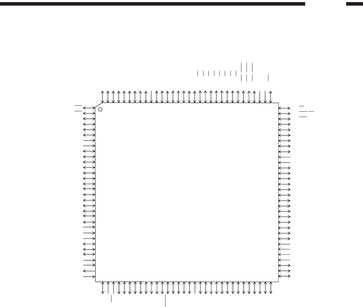
38
DVD-3800
TOP VIEW
P46,A22, CS0
P47,A23, CS1
P00,AD0,D0
P01,AD1,D1
P02,AD2,D2
P03,AD3,D3
VDD
VSS
P04,AD4,D4
P05,AD5,D5
P06,AD6,D6
P07,AD7,D7
P10,AD8,D8
P11,AD9,D9
P12,AD10,D10
PD0,RTP0
PD1,RTP1
P13,AD11,D11
P14,AD12,D12
P15,AD13,D13
P16,AD14,D14
P17,AD15,D15
MODE0
MODE1
MODE2
PC3,TM10O,TM7I,TM21IR
PC2,TM8O,TM6I
PC1,TM6O,TM11I
VDD
OSCI
OSCO
VSS
1
2
3
4
5
6
7
8
9
10
11
12
13
14
15
16
17
18
19
20
21
22
23
24
25
26
27
28
29
30
31
32
127 125 123 121 119 117 115 113
128 126 124 122 120 118 116 114 111 109 107 105 103 101 99 97
112 110 108 106 104 102 100 98
96
95
94
93
92
91
90
89
88
87
86
85
84
83
82
81
80
79
78
77
76
75
74
73
72
71
70
69
68
67
66
65
P52, RE
P51, WEH,WE
P50, WEL
PC7,NBRACK
PC6,NBREQ
P97,AN15,TM20IB
P96,AN14,TM15O,TM19IB
P95,AN13,TM13O,TM2I
P94,AN12,TM11O,TM4I
AVDD
VREFH
P93,AN11
P92,AN10
P91,AN9
P90,AN8
PD5,RTP5
PD4,RTP4
P87,AN7
P86,AN6
P85,AN5
P84,AN4
P83,AN3
P82,AN2
P81,AN1
P80,AN0
VREFL
AVSS
VSS
VDD
PB5,SBT3,SCL3
PB4,SBO3,SDA3
PB3,SBI3
34 36 38 40 42 44 46 48
33 35 37 39 41 43 45 47 50 52 54 56 58 60 62 64
49 51 53 55 57 59 61 63
P57,/DUMX,BOSC
PC5,NMI
RST
PC0,TM4O,TM10I
P76,TM19IOA
P60,IRQ0
P61,IRQ1,TM3I
P62,IRQ2,TM16IA
P63,IRQ3,TM16IB
P64,IRQ4,TM17IA
P65,IRQ5,TM18IA
P66,IRQ6
P67,IRQ7, EXTDK
P70,TM16OA
P71,TM16OB,WDOUT
PD2,RTP2
PD3,RTP3
VDD
P77,TM20IOA
P72,TM17OA
P73,TM17OB,STOP
P74,TM18OA
P75,TM18IOB,TM21ID
PA0,SBI0
PA1,SBO0
PA2,SBT0
PA3,SBI1
PA4,SBO1,SDA1
PA5,SBT1,SCL1
PB0,SBI2,TM16IC
PB1,SBO2,TM17IC
PB2,SBT2,TM18IC
P45,A21
P44,A20
P43,A19
P42,A18
P41,A17
P40,A16
P37,A15
P36,A14
PC4,TM12O,TM8I,TM21IA
VDD(VPP)
P35,A13
P34,A12
P33,A11
P32,A10
P31,A9
PD7,RTP7
PD6,RTP6
P30,A8
P27,A7, KI7,TMI17B
P26,A6, KI6
P25,A5, KI5
P24,A4, KI4
P23,A3, KI3
P22,A2, KI2
P21,A1, KI1
P20,A0, KI0
P56, CS3, UCAS,BIBT2
P55, CAS, LCAS,BIBT1
P54, RAS, RFSH
VSS
VDD
P53, CS2,ALE
MN102H460B (MA: IC201)
39
DVD-3800
ADSPMEL322 (MA: IC207)
TOP VIEW
1
2
3
4
5
6
7
8
9
10
11
12
13
14
15
16
17
18
19
20
21
22
23
24
25
26
27
28
29
30
31
32
33
34
35
36
108
107
106
105
104
103
102
101
100
99
98
97
96
95
94
93
92
91
90
89
88
87
86
85
84
83
82
81
80
79
78
77
76
75
74
73
37
38
39
40
41
42
43
44
45
46
47
48
49
50
51
52
53
54
55
56
57
58
59
60
61
62
63
64
65
66
67
68
69
70
71
72
144
143
142
141
140
139
138
137
136
135
134
133
132
131
130
129
128
127
126
125
124
123
122
121
120
119
118
117
116
115
114
113
112
111
110
109
D13
V
DDEXT
D12
D11
D10
D9
D8
D7
D6
D5
GND
XTAL
CLKIN
V
DDEXT
CLKOUT
GND
D4
V
DDINT
D3
D2
D1
D0
RD
WR
ACK
MS3
V
DDEXT
MS2
MS1
MS0
IOMS
BMS
BR
BG
BGH
A21
D14
D15
HAD0
HAD1
GND
HAD2
HAD3
HAD4
HAD5
HAD6
HAD7
HAD8
V
DDEXT
HAD9
HAD10
GND
HAD11
HAD12
V
DDINT
HAD13
HAD14
HAD15
HA16
HACK_P
V
DDEXT
HACK
HCMS
HCIOMS
GND
HALE
HRD
HWR
GND
PF0
PF1
PF2
A20
A19
A18
GND
A17
A16
A15
A14
V
DDEXT
A13
A12
A11
A10
A9
GND
A8
A7
A6
V
DDEXT
A5
A4
A3
A2
A1
A0
OPMODE
V
DDINT
EMU
GND
TRST
TCK
GND
TMS
TDI
TDO
RESET
PF3
PF4
PF5
V
DDEXT
PF6
PF7
TMR0
TMR1
TMR2
DT2
TCLK2
TFS2
DR2
RCLK2
RFS2
RXD
TXD
GND
GND
DT0
TCLK0
V
DDINT
TFS0
DR0
RCLK0
RFS0
V
DDEXT
DT1
TCLK1
TFS1
DR1
RCLK1
RFS1
BMODE0
BMODE1
BYPASS
40
DVD-3800
XC2S30-5VQ100C (MA: IC711)
76
77
78
79
80
81
82
83
84
85
86
87
88
89
90
91
92
93
94
95
96
97
98
99
100
50
49
48
47
46
45
44
43
42
41
40
39
38
37
36
35
34
33
32
31
30
29
28
27
26
75
74
73
72
71
70
69
68
67
66
65
64
63
62
61
60
59
58
57
56
55
54
53
52
51
1
2
3
4
5
6
7
8
9
10
11
12
13
14
15
16
17
18
19
20
21
22
23
24
25
GND
TMS
YDATA<7>
YDATA<6>
YDATA<5>
YDATA<4>
YDATA<3>
YDATA<2>
YDATA<1>
YDATA<0>
GND
VCCO
NC
VCCINT
CDATA<9>
CDATA<8>
CDATA<7>
CDATA<6>
CDATA<5>
CDATA<4>
CDATA<3>
CDATA<2>
M1
GND
M0
CCLK
NC
DIN
YOUT<7>
YOUT<8>
YOUT<9>
COUT<0>
COUT<1>
COUT<2>
COUT<3>
COUT<4>
GND
VCCO
DELAYHSYNC
VCCINT
DELAYVSYNC
DELAYBLANK
NC
COUT<5>
COUT<6>
COUT<7>
COUT<8>
COUT<9>
INIT-
NC
VCCO
NC(TDO)
GND
NC(TDI)
YOUT<6>
YOUT<5>
YOUT<4>
YOUT<3>
YOUT<2>
VCCINT
YOUT<1>
YOUT<0>
NC
GND
VCCO
CLOCK
VCCINT
BYPASS
VCCINT
GRAYBITS<0>
GRAYBITS<1>
YDATA<9>
YDATA<8>
NC(TCK)
VCCO
VCCO
DONE
GND
NC
NC
NC
NC
NC
VCCINT
RESET
BLANK
NC
GND
VCCO
NC
VCCINT
VSYNC
VCCINT
HSYNC
CDATA<0>
CDATA<1>
NC
NC
M2
VCCO
41
DVD-3800
W986416DH (MA: IC103)
1
2
3
4
5
6
7
8
9
10
11
12
13
14
15
16
17
18
19
20
21
25
24
23
22
V
CC
V
CC
Q
DQ0
V
SS
Q
DQ2
V
SS
Q
DQ6
V
CC
Q
DQ4
BS0
BS1
A10/AP
A0
DQ1
DQ5
V
CC
LDQM
Vcc
WE
CAS
RAS
CS
DQ7
DQ3
26
27
A1
A2
V
SS
VssQ
DQ15
V
CC
Q
DQ13
V
CC
Q
DQ9
V
SS
Q
DQ11
A9
A8
A7
A6
A5
DQ14
DQ10
V
SS
NC
UDQM
CLK
CKE
NC
A11
DQ8
DQ12
A4
Vss
54
53
52
51
50
49
48
47
46
45
44
43
42
41
40
39
38
37
36
35
34
30
31
32
33
29
28
A3
1, 14, 27 VCC Power (+3.3V) Power for input buffers and logic circuit inside DRAM.
2, 4, 5, 7, 8, 10,
11, 13, 42, 44, DQ0-DQ15 Data Input/Output Multiplexed pins for data output and input.
45, 47, 48, 50,
51, 53
3, 9, 43, 49 VCCQ Power (+3.3V) for I/O buffer Separated power from VCC, to improve DQ noise immunity.
6, 12, 46, 52 VSSQ Ground for I/O buffer Separated ground from VSS, to improve DQ noise immunity.
16 WE Write Enable Referred to RAS.
17 CAS Column Address Strobe Referred to RAS.
18 RAS Row Address Strobe Command input. When sampled at the rising edge of the clock RAS, CAS
and WE define the operation to be executed.
19 CS Chip Select Disable or enable the command decoder. When command decoder is
disabled, new command is ignored and previous operation continues.
20, 21 BS0, BS1 Bank Select Select bank to activate during row address latch time, or bank to read/write
during address latch time.
23~26, 22 Multiplexed pins for row and column address. Row address: A0-A11.
29~35 A0-A11 Address Column address: A0-A7. A10 is sampled during a precharge command to
determine if all banks are to be precharged or bank selected by BS0, BS1.
28, 41, 54 VSS Ground Ground for input buffers and logic circuit inside DRAM.
36, 40 NC No Connection No Connection
37 CKE Clock Enable CKE controls the clock activation and deactivation. When CKE is low,
Power Down mode, Suspend mode, or Self Refresh mode is entered.
38 CLK Clock Inputs System clock used to sample inputs on the rising edge of clock.
The output buffer is placed at Hi-Z (with latency of 2) when DQM is sampled
39, 15 UDQM, LDQM Input/Output mask high in read cycle. In write cycle, sampling DQM high will block the write
operation with zero latency.
DescriptionFunction
Pin No. Pin Name
W986416DH Terminal Function
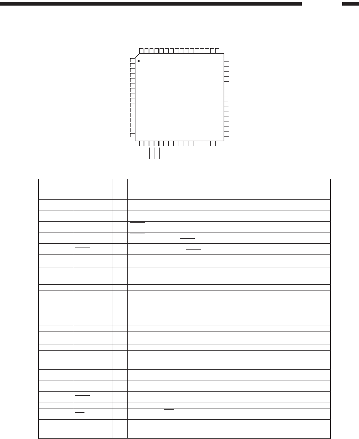
42
DVD-3800
FunctionI/OPin No. Pin Name
ADV7190 Terminal Function
1~16 P0-P15 I 8-Bit or 16-Bit 4:2:2 Multiplexed YCrCb Pixel Port. The LSB of the input data is set up on Pin P0.
17, 25, 29, 38,
43, 54, 63 VAA P Analog Power Supply (3.3V to 5V).
18, 24, 26, 33,
39, 42, 55, 64 AGND G Analog Ground.
19 HSYNC I/O HSYNC (Modes 1, 2, and 3) Control Signal. This pin may be configured to be an output
(Master Mode) or an input (Slave Mode) and accept Sync Signals.
20 VSYNC I/O VSYNC Control Signal. This pin may be configured as an output (Master Mode) or as an input
(Slave Mode) and accept VSYNC as a Control Signal.
21 BLANK I/O Video Blanking Control Signal. This signal is optional. For further information see Vertical
Blanking Data Insertion and BLANK Input section.
22 ALSB I TTL Address Input. This signal sets up the LSB of the MPU address.
23 TTXREQ O Teletext Data Request Output Signal, used to control teletext data transfer.
27 CLKIN I TTL Clock Input. Requires a stable 27 MHz reference clock for standard operation. Alternatively,
a 24.5454 MHz (NTSC) or 29.5 MHz (PAL) can be used for square pixel operation.
28 CLKOUT O Clock Output Pin.
30 SCL I MPU Port Serial Interface Clock Input.
31 SDA I/O MPU Port Serial Data Input/Output.
32
SCRESET/RTC/TR
IMultifunctional Input: Real-Time Control (RTC) Input, Timing Reset Input,
Subcarrier Reset Input.
34 RSET2 IA 1200 ohm resistor connected from this pin to ground is used to control full-scale amplitudes of
the Video Signals from DACs D, E, and F.
35 COMP 2 O Compensation Pin for DACs D, E, and F. Connect a 0.1µF Capacitor from COMP2 to VAA.
36 DAC F O S-Video C/V/RED Analog Output. This DAC is capable of providing 4.33 mA output.
37 DAC E O S-Video Y/U/BLUE Analog Output. This DAC is capable of providing 4.33 mA output.
40 DAC D O Composite/Y/GREEN Analog Output. This DAC is capable of providing 4.33 mA output.
41 DAC C O S-Video C/V/RED Analog Output. This DAC is capable of providing 4.33 mA output.
44 DAC B O S-Video Y/U/BLUE Analog Output. This DAC is capable of providing 4.33 mA output.
45 DAC A O Composite/Y/GREEN Analog Output. This DAC is capable of providing 4.33 mA output.
46 COMP 1 O Compensation Pin for DACs A, B, and C. Connect a 0.1µF Capacitor from COMP1 to VAA.
47 VREF I/O Voltage Reference Input for DACs or Voltage Reference Output (1.235V). An external VREF
cannot be used in 4x oversampling mode.
48 RSET1 IA 1200 ohm resistor connected from this pin to ground is used to control full-scale amplitudes of
the Video Signals from DACs A, B, and C.
49 RESET I The input resets the on-chip timing generator and sets the ADV7190/ADV7191 into default
mode. See Appendix 8 for Default Register Settings.
50 CSO_HSO O Dual function CSO or HSO Output Sync Signal at TTL Level.
51 VSO/CLAMP I/O Multifunction Pin. VSO Output Sync Signal at TTL level. CLAMP TTL Output Signals can be
used to drive external circuitry to enable clamping of all Video Signals.
52 PAL_NTSC I Input signal to select PAL or NTSC mode of operation, pin set to Logic 1 selects PAL.
53, 57~62 NC No Connect.
56 TTX I Teletext Data Input Pin.
ADV7190 (AV: IC601)
49505152535455565758596061626364
RESET
CSO_HSO
VSO/CLAMP
PAL_NTSC
NC
VAA
AGND
TTX
NC
NC
NC
NC
NC
NC
VAA
AGND
1
2
3
4
5
6
7
8
9
10
11
12
13
14
15
16
P0
P1
P2
P3
P4
P5
P6
P7
P8
P9
P10
P11
P12
P13
P14
P15
323130
29
28
27
2625
24
23
22
21201918
17
SCRESET/TRC/TR
SDA
SCL
VAA
CLKOUT
CLKIN
AGND
VAA
AGND
TTXREQ
ALSB
BLANK
VSYNC
HSYNC
AGND
VAA
48
47
46
45
44
43
42
41
40
39
38
37
36
35
34
33
R
SET1
V
REF
COMP 1
DAC A
DAC B
V
AA
AGND
DAC C
DAC D
AGND
V
AA
DAC E
DAC F
COMP 2
R
SET2
AGND
TOP VIEW
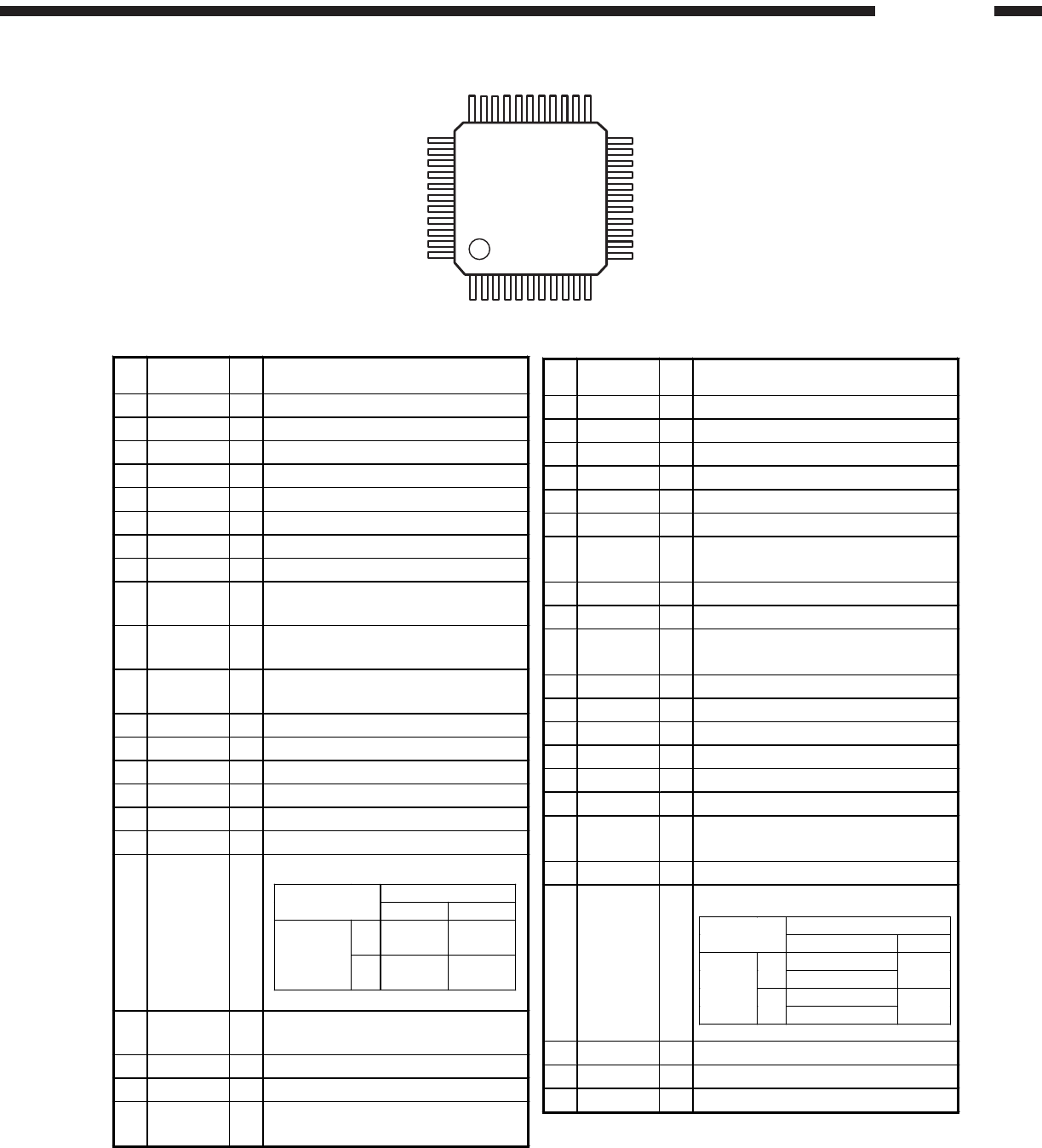
43
DVD-3800
DXP7001AF (AV: IC201)
111
12
22
23
33
34
44
DXP7001AF Terminal Function
Pin
No. Pin Name I/O Description
1 MDT Ip Microcomputer Interface Data
2 MCK Ip Microcomputer Interface Clock
3 MLEN Ip Microcomputer Interface Latch Enable
4 RSTN Ip Reset Terminal
5 DLRCK Ip Audio Serial Input Data L/R Clock
6 VSS Ground Terminal
7 DBCK Ip Audio Serial Input Bit Clock
8 DDT Ip Audio Serial Input Data
9 TEST2N Ip Test Setting Terminal 2 (Alpha-processor 1
Output shifts 12-bit.)
10 TEST3N Ip Test Setting Terminal 3 (Alpha-processor 2
Output stops.)
11 TEST4N Ip Test Setting Terminal 4 (Lambda-processor
Output stops.)
12 DFBCK Ip Lambda-processor Input Bit Clock
13 DFWCK Ip Lambda-processor Input Word Clock
14 DOL Ip Lambda-processor Input Data L-channel
15 DOR Ip Lambda-processor Input Data R-channel
16 LMOD Ip Lambda-processor Operation Mode Set
17 OMOD1 Ip Output Mode Setting Terminal 1
18 OMOD2 Ip
Output Mode Setting Terminal 2
19 INVIN Ip Lambda-processor Input Reversed
Polarity Terminal
20 BCKO O Lambda-processor Output Bit Clock
21 WCKO O Lambda-processor Output Word Clock
22 WCKO2 O Lambda-processor Output Word Clock 2
(for Canceling OFFSET on 1DAC
Pin
No. Pin Name I/O Description
23 P24L O /Lambda-processor Lch 24th bit Output *1, *2
24 P23L O /Lambda-processor Lch 23rd bit Output *1, *2
25 P22L O /Lambda-processor Lch 22nd bit Output *1, *2
26 P21L O /Lambda-processor Lch 21st bit Output *1
27 P20L O /Lambda-processor Lch 20th bit Output *1
28 VDD Power Supply Terminal
29 SO2L/P19L O Lambda-processor Lch() Output /19th bit
Output *1
30 SO1L O Lambda-processor Lch(+) Output
31 SO1R O Lambda-processor Rch(+) Output
32 SO2R/P19R OLambda-processor Rch() Output/19th bit
Output *1
33 P20R O /Lambda-processor Rch 20th bit Output *1
34 P21R O /Lambda-processor Rch 21st bit Output *1, *2
35 P22R O /Lambda-processor Rch 22nd bit Output *1, *2
36 P23R O /Lambda-processor Rch 23rd bit Output *1, *2
37 P24R O /Lambda-processor Rch 24th bit Output *1, *2
38 TEST1N Ip Test Terminal 1 (Alpha-processor 1 stops)
39 CKSLN Ip System Clock Select (384fs system /
256fs system)
40 CKDV1 Ip System Clock Divider Select Terminal 1
41 CKDV2 Ip
System Clock Divider Select Terminal 2
42 XTI I X-TAL Oscillator Input Terminal
43 XTO O X-TAL Oscillator Output Terminal
44 CKO O Clock Output Terminal
(Ip = Input Terminal with pull-up)
*1: Outputted on OMOD1=L (18-bit Alternate Output or 20-bit Parallel Output)
*2: Internal Signal is outputted on OMOD1=H (24-bit Alternate Output or 24-bit Parallel Output) and one of TEST1N, TEST2N, TEST3N
or TEST4N is set to L.
OMOD1
LH
L18bit
Alternate
24bit
Alternate
OMOD2
H20bit
Parallel
24bit
Parallel
CKDV1
LH
192fs (CKSLN=H)
L256fs (CKSLN=H) 768fs
192fs (CKSLN=H)
CKDV2
H256fs (CKSLN=H) 384fs
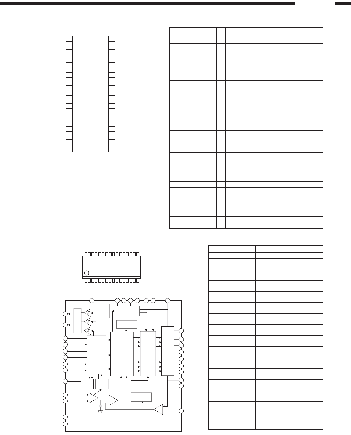
44
DVD-3800
PCM1738-1 (AV: IC206, 209, 212)
20
10
7
6
5
4
3
2
1
8
9
30
11
18 16 15 14 13 12 32 31
19
27
28
24
25
21
22
23
26
17
FG2
FG
H1H
H1L
H2H
H2L
H3H
H3L
VHB
EC
ECR
BMS
START
GND
CS1
CS2
A32
A31
A22
A21
A12
A11
VM2
VM1
VLP
VPUMP
BC1
BC2
BC3
BC4
VDD
Hall
Bias
X5
CSOUT
SRESET
PWMOUT
VCL
VT
OSC
Hall Amp
Matrix
Pre-Driver
Start/Stop
Logic Circuit
Booster
Thermal
Protect
Divider
3ø Bridge
Direction
SW
AN8471SA (MA: IC503)
1 VHB Hall bias pin
2 H3L Hall element 3 input (-)
3 H3H Hall element 3 input (+)
4 H2L Hall element 2 input (-)
5 H2H Hall element 2 input (+)
6 H1L Hall element 1 input (-)
7 H1H Hall element 1 input (+)
8 EC Torque command input pin
9 ECR Torque command ref. input pin
10 FG1 FG signal lout put pin (0.C)
11 START Start/Stop switching pin
12 VPUMP Booster pin
13 BC1 Booster cap. connecting pin 1
14 BC2 Torque command input pin 2
15 BC3 Torque command input pin 3
16 BC4 Torque command input pin 4
17 GND GND pin
18 VDD Power pin
19 VM2 Motor power pin 2
20 FG2 3x FG signal output pin (0.C)
21 A31 Drive output 3
22 A32 Drive output 3
23 CS2 Current detect pin 2
24 A21 Drive output 2
25 A22 Drive output 2
26 CS1 Current detect pin 1
27 A11 Drive output 1
28 A12 Drive output 1
29 NC N.C.
30 BMS Brake mode switching pin
31 VM1 Motor power pin 1
32 VLP Pre-driver lower power
116
32 17
1
2
3
4
5
6
7
8
9
10
11
12
13
14
28
27
26
25
24
23
22
21
20
19
18
17
16
15
RST
ZEROL
ZEROR
LRCK
DATA
BCK
SCKI
DGND
V
DD
SCKO
MDO
MDI
MC
CS
VCC3
AGND2
I
OUT
L
-
I
OUT
L+
V
CC
2
V
CC
1
V
COM
3
I
REF
V
COM
2
V
COM
1
AGND1
I
OUT
R+
I
OUT
R
-
MUTE
1 RST I Reset (1)
2 ZEROL O Zero-flag for Lch
3 ZEROR O Zero-flag for Rch
Normal mode: L/R clock (fs) input (1)
4 LRCK I Ext. DF mode: WDCK clock input
DSD mode: GND connection
5 DATA I Normal mode: Serial audio data input (1)
Ext. DF & DSD mode: Lch audio data input
6 BCK I Normal mode: Bit clock input (1)
DSD mode: GND connection
7 SCKI I Normal mode: System clock input (1)
DSD mode: BCK (64fs) clock input
8 DGND Digital GND
9VDD Digital power +3.3V
10 SCKO O System clock output
11 MDO O Function control register serial data output (2)
12 MDI I Function control register serial data input (1)
13 MC I Function control register shift clock (1)
14 CS I Mode control chip select and latch signal (1)
15 MUTE I Normal mode: Analog output mute control (1)
Ext. DF & DSD mode: Rch audio data input
16 LOUTR−O Rch analog current output (−)
17 LOUTR+ O Rch analog current output (+)
18 AGND1 Analog GND
19 VCOM1Internal bias de-coupling pin
20 VCOM2Common mode voltage of I/V
21 IREF Output current reference bias pin
22 VCOM3Internal bias de-coupling pin
23 VCC1Analog power +5.0V
24 VCC2Analog power +5.0V
25 IOUTL+ O Lch analog current output (+)
26 IOUTL−O Lch analog current output (−)
27 AGND2 Analog GND
28 VCC3Analog power +5.0V
Pin Name Function
Pin No. I/O
PCM1738-1 Terminal Function
Note: (1) Schmitt trigger input, 5V input possible (2) Tri-state output
Pin Name Function
Pin No.
AN8471SA Terminal Function
45
DVD-3800
SM8701BM (MA: IC109)
1
2
3
4
5
6
7
8
9
10
20
19
18
17
16
15
MLEN/R2
P/S
V
DD
GND
XTO
XTI
GNDP
V
DD
P
V
DD
3
MO
MCK/R1
MDT/R0
RSTN
SO3
V
DD
O
GNDO
SO2
SO4
SO1
MON
14
13
12
11
Control signal input.
1 MLEN/R2 Ip1In serial mode: latch enable signal
In parallel mode: sampling rate select signal
2 P/S Ip1Mode select signal.
LOW: serial mode, HIGH: parallel mode
3VDD 5V supply (Digital block)
4 GND Ground (Digital block)
5 XTO O Reference signal crystal oscillator element connection
6 XTI I Reference signal crystal oscillator element connection
or external clock input
7 GNDP Ground (PLL block)
8VDDP5V supply (PLL block)
9VDD33.3V supply (output buffer)
10 MO O 27 MHz fixed-frequency output
11 MON O 27 MHz fixed-frequency output (inverted)
12 SO1 O 33.8688 MHz fixed-frequency output
13 SO4 O 768fs output
14 SO2 O 256fs output
15 GNDO Ground (output buffer)
16 VDDO3.3V supply (output buffer)
17 SO3 O 384fs output
18 RSTN Ip2LOW-level reset input
Control signal input.
19 MDT/R0 Ip1In serial mode: control data input signal
In parallel mode: sampling frequency select signal
Control signal input.
20 MCK/R1 Ip1In serial mode: clock signal
In parallel mode: sampling frequency select signal
Pin Name Function
Pin No. I/O
SM8701BM Terminal Function
Note: 1. Schmitt trigger input with pull-down resistor
2. Schmitt trigger input with pull-up resistor
64M SDRAM (MA: IC702)
W986432AH
25~27, 60~66, 24 A0-A10 Address for row and column
22, 23 BS0, BS1 Bank Select to activate during row
address latch time
2, 4, 5, 7, 8, 10, 11 ,13,
31, 33, 34, 36, 37, 39,
40, 42, 45, 47, 48, 50, DQ0-DQ31 Data Input / Output pins for data
51, 53, 54, 56, 74, 76,
77, 79, 80, 82, 83, 85
20 CS Chip Selec to disable or enable the
command decoder
19 RAS Row Address Strobe
18 CAS Column Address Strobe
17 WE Write Enable
16, 28, 59, 71 DQM0-DQM3 Input / Out put Mask
68 CLK Clock Inputs
67 CKE Clock Enable
1, 15, 29, 43 VCC Power (+3.3V)
44, 58, 72, 86 VSS Ground
3, 9, 35, 41, 49, 55, VCCQ Power (+3.3V) for I/O Buffer
75, 81
6, 12, 32, 38, 46, 52, VSSQ Ground for I/O Buffer
78, 84
14, 21, 30, 57, 69, NC No Connection
70, 73
1
2
3
4
5
6
7
8
9
10
11
12
13
14
15
16
17
18
19
20
21
25
24
23
22
V
CC
V
CC
Q
DQ0
V
SS
Q
DQ2
V
SS
Q
DQ6
V
CC
Q
DQ4
NC
BS0
BS1
A10/AP
A0
DQ1
DQ5
NC
V
CC
DQM0
WE
CAS
RAS
CS
DQ7
DQ3
26
27
28
29
30
31
32
33
34
35
36
37
38
39
40
41
42
43
A1
DQM2
A2
DQ16
NC
DQ20
DQ19
DQ18
DQ17
V
CC
V
CC
Q
DQ21
DQ22
V
CC
Q
DQ23
V
CC
V
SS
Q
V
SS
Q
V
SS
V
CC
Q
DQ15
V
CC
Q
DQ13
V
CC
Q
DQ9
V
SS
Q
DQ11
A9
A8
A7
A6
A5
DQ14
DQ10
NC
V
SS
DQM1
NC
NC
CLK
CKE
DQ8
DQ12
A4
DQM3
A3
DQ31
NC
DQ27
DQ28
DQ29
DQ30
V
SS
V
SS
Q
DQ26
DQ25
V
SS
Q
DQ24
V
SS
V
CC
Q
V
CC
Q
86
85
84
83
82
81
80
79
78
77
76
75
74
73
72
71
70
69
68
67
66
62
63
64
65
61
60
59
58
57
56
55
54
53
52
51
50
49
48
47
46
45
44
Pin Name Function
Pin No.
W986432AH Terminal Function
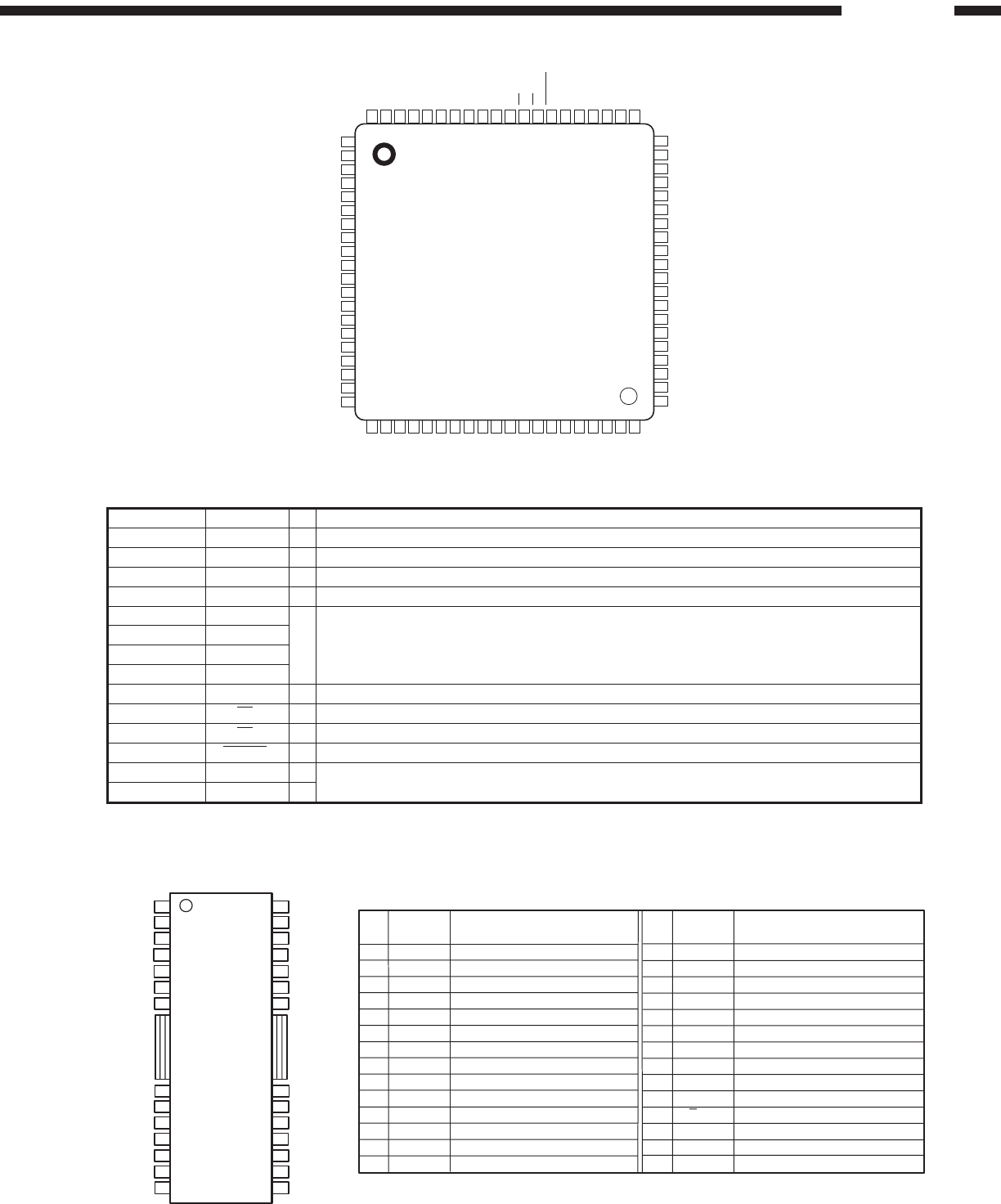
46
DVD-3800
ML9207-01 (PD: IC101)
3~37 SEG1~35 O FL display anode drive output pin
39~62 COM1~24 O FL display grid drive output pin
1,2, 79, 80 AD1~4 O FL display anode drive output pin
72~75 P1~4 O General port output pin
71 VDD VDD-GND: Power supply for logic block
38, 78 VDISP1~2
VDISP-VFL: Power supply for FL display drive
64 GND For VDD and VDISP, apply from same power source
63, 76 VFL1~2
70 DA I Serial data input pin (positive logic)
69 CP I Shift clock input pin
68 CS I Chip select input pin
67 RESET I Reset input pin
65 OSC0 I Pin for self-oscillation
66 OSC1 O
Pin Name FunctionPin No. I/O
ML9207-01 Terminal Function
61
62
63
64
65
66
67
68
69
70
71
72
73
74
75
76
77
78
79
80
COM23
COM24
V
FL1
GND
OSC0
OSC1
RESET
CS
CP
DA
V
DD
P1
P2
P3
P4
V
FL2
NC
V
DISP2
AD1
AD2
1
2
3
4
5
6
7
8
9
10
11
12
13
14
15
16
17
18
19
20
AD3
AD4
SEG1
SEG2
SEG3
SEG4
SEG5
SEG6
SEG7
SEG8
SEG9
SEG10
SEG11
SEG12
SEG13
SEG14
SEG15
SEG16
SEG17
SEG18
40
39
38
37
36
35
34
33
32
31
30
29
28
27
26
25
24
23
22
21
COM2
COM1
V
DISP1
SEG35
SEG34
SEG33
SEG32
SEG31
SEG30
SEG29
SEG28
SEG27
SEG26
SEG25
SEG24
SEG23
SEG22
SEG21
SEG20
SEG19
60
59
58
57
56
55
54
53
52
51
50
49
48
47
46
45
44
43
42
41
COM22
COM21
COM20
COM19
COM18
COM17
COM16
COM15
COM14
COM13
COM12
COM11
COM10
COM9
COM8
COM7
COM6
COM5
COM4
COM3
28
27
26
25
24
23
22
21
20
19
18
17
16
15
1
2
3
4
5
$
7
&
9
10
11
12
13
14
MUTE
BIAS
VINTK
CTKerr1
CTKerr2
VINLD
PreGND
PVcc2
VNFTK
PGND
VOLD-
VOLD+
VOTK-
VOTK+
VINFC
CFCErr1
CFCErr2
VINSL+
VINSL-
VOSL
VNFFC
PreVcc
PVcc1
PGND
VOSL-
VOSL+
VOFC-
VOFC+
Terminal Function
Pin
No. Name Function
1
2
3
4
5
6
7
8
9
10
11
12
13
14
CFCerr1
CFCerr2
VINSL+
VINSL-
VOSL
VNFFC
PreVcc
PVcc1
PGND
VOSL-
VOSL+
VOFC-
VOFC+
Focus driver input
Cap.connecting pin for error amp filter
Cap.connecting pin for error amp filter
Op.amp input (+) for sled driver
Op.amp input (-) for sled driver
Op.amp output for sled driver
Focus driver feedback pin
Pre Vcc
Power Vcc of sled driver
Power GND of sled driver
Sled driver output(-)
Sled driver output(+)
Focus driver output(-)
Focus driver output(+)
15
16
17
18
19
20
21
22
23
24
25
26
27
28
VOTK+
VOTK-
VOLD+
PGND
VNFTK
PVcc1
PreGND
VINLD
CTKerr2
CTKerr1
VINTK
BIAS
Tracking driver output(+)
Tracking driver output(-)
Loading driver output(+)
Loading driver output(-)
Power GND
Tracking driver feedback pin
Power GND
Pre GND
Loading driver input
Cap.connecting pin for error amp filter
Cap.connecting pin for error amp filter
Tracking driver input
Bias input
Mute control pin
Pin
No. Name Function
VINFC
VOLD-
MUTE
BA5952AFP (MA: IC504)
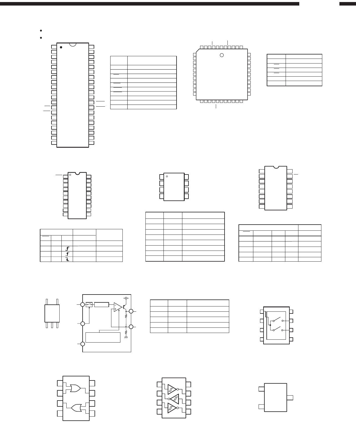
47
DVD-3800
SN74AHCT273PW
(MA: IC104, 105, 114)
S-24C02BFJ-TB (MA: IC106)
Truth Table
Input Function
Output
DCK QCLR
L
H
H
H
X
L
H
X
L
L
H
Qn
XClear
¾
¾
No change
X: Don't Care
Terminal Function
Name
Function
A0
A1
A2
GND
SDA
TEST/WP
Address input
GND
Serial data input/output
Test, connect to GND
Pin No.
1
2
3
4
5
6
7
8
SCL
Vcc
Address input
Address input
Serial clock input
Power supply
1
2
3
4
8
7
6
5
A0
A1
NC
GND
Vcc
TEST/WP
SCL
SDA
1
2
3
4
5
6
7
8
10
9
20
19
18
17
16
15
14
13
12
11
CLR
Q1
D1
D2
Q2
Q3
D3
D4
Q4
GND
Vcc
Q8
D8
D7
Q7
Q6
D6
D5
Q5
CK
V
CC
VCC
GND
A4
GND
1
2
3
4
5
6
7
8
9
10
11
12
13
14
15
16
17
18
19
20
40
39
38
37
36
35
34
33
32
31
30
29
28
27
26
25
24
23
22
21
I/O0
I/O1
I/O2
I/O3
VCC
I/O4
I/O5
I/O6
I/O7
NC
NC
WE
RAS
NC
A0
A1
A2
I/O15
I/O14
I/O13
I/O12
GND
I/O11
I/O10
I/O9
I/O8
NC
LCAS
UCAS
OE
A8
A7
A6
A5
A3
Name
A0-A8
Function
I/O0-15
Address Inputs
Data Inputs/Outputs
WE Write Enable
Output Enable
Row Address Strobe
Upper Column Address Strobe
OE
RAS
UCAS
LCAS Lower Column Address Strobe
Vcc Power
GND Ground
NC No Connection
Terminal Function
4M DRAM (SOJ)-35 (IC507, 509)
IS41C16256
M11B416256A
COM
NH
V
EE
V
CC
ch0
ch1
GND ADR
TC4W53F (SC: IC855)
(Europe model only)
1
2
3
4
5
6
7
8
AT49LV1025 (MA: IC202)
7
8
9
10
11
12
13
14
15
16
17
39
38
37
36
35
34
33
32
31
30
29
18
19
20
21
22
23
24
25
26
27
6
5
4
3
2
1
44
43
42
41
40
I/O12
I/O11
I/O10
I/O9
I/O8
GND
NC
I/O7
I/O6
I/O5
I/O4
I/O3
I/O2
I/O 0
OE
NC
A2
A3
A4
A11
A10
A9
GND
NC
A8
A7
A6
A5
A12
I/O 13
I/O 14
I/O 15
CE
NC
NC
VCC
WE
NC
A15
A14
I/O1
A0
A1
A13
28
Pin Name
A0-A15
Function
Address Inputs
CE Chip Enable
Output Enable
OE
NC No Connection
Terminal Function
I/O0-I/O15 Data Inputs/Outputs
WE Write Enable
TC74VHC157A (MA: IC113)
1
2
3
4
5
6
7
8
SELECT
1A
1B
1Y
2A
2B
2Y
GND
Vcc
ST
4A
4B
4Y
3A
3B
3Y
16
15
14
13
12
11
10
9
INPUTS OUTPUTS
SELECT ABST
H
L
L
L
X
L
L
H
X
X
X
L
X: Don't Care
Y
L
L
H
L
X
L
H
X
LHHH
X
TOP VIEW
1
3
5
Vref
Vcc
CTL
OUT
BA033LBSG (AV: IC205, 208, 211)
13
TOP
VIEW
2
54
2
GND
4
C
Over current protection
Over temperature protection
Terminal Function
Name
Function
GND
CTL
C
OUT
Ripple Improve
Output
Pin No.
1
2
3
4
5
Vcc
Ground
Power Save
Power
1
2
3
4
8
7
6
5
1A
1B
2Y
GND
Vcc
1Y
2B
2A
TC7W32F (MA: IC107) MN1382-S (MA: IC203)
1
2
3
OUT
V
DD
V
SS
TOP VIEW
1
2
3
4
8
7
6
5
1A
3Y
2A
GND
Vcc
1Y
3A
2Y
TC7W14F (MA: IC111, 115, 116)
TOP VIEW
Terminal Function
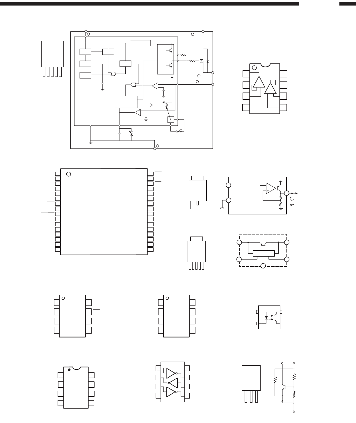
48
DVD-3800
A11
A9
A8
A13
A14
A17
WE
V
CC
RESET
A16
OE
A10
CE
I/O7
I/O6
I/O5
I/O4
I/O3
GND
I/O2
AT49LV002-70TC (MA: IC210)
1
2
3
4
5
6
7
8
10
9
32
31
30
29
28
27
26
25
24
23
A15
A12
A7
A6
A5
A4
I/O1
I/O0
A0
A1
A2
A3
11
12
13
14
16
15
22
21
20
19
18
17
XC17S30AV08C (MA: IC712)
1
2
3
4
8
7
6
5
DATA
CLK
RESET/OE
CE
V
CC
V
CC
NC
GND
TC7WH157FU (MA: IC112)
1
2
3
4
8
7
6
5
A
B
Y
GND
V
CC
ST
SELECT
Y
COLLECTOR
EMITTER
ANODE
CATHODE
TOP VIEW
PC123 (PD: IC902)
1
2
3
4
8
7
6
5
1A
3Y
2A
GND
Vcc
1Y
3A
2Y
TC7WU04F (MA: IC108, 110)NJM2267M (SC: IC852)
(Europe model only)
1
2
3
45
6
7
8
GND
V
SAG1
V
OUT1
V
+
V
SAG2
V
OUT2
V
IN2
V
IN1
TOP VIEW
STR-F6674 (PD: IC901)
3
2
1
4
5
Vin
Start
Reg.
O.V.P
DRV.REC=8.6V
Latch
T.S.D
DRV
Rg1
47ohm
Source
OCP/FB
Vth1=0.73±0.05V
OCP/FB comp.
Vth2=1.3~1.6V
Tth(min)=1mS
INH comp.
Iconst trm.
Drain
GND
TOFF=50mS typ.
4700pF
OSC
+
+
1.35mA
Rg2:
STR-F6632 360
ohm
STR-F6672 180
ohm
Rg2
O.C.P./F.B.
D
FRONT
VIEW
VIN
GND
S
BA15218F (MA: IC510)
NJM2068DD (AV: IC407, 408)
NJM2068MD (AV: IC301~308, 401~406)
NJM4558M (MA: IC502)
TK15420MTL (AV: IC701~707, 803, 804)
1
2
3
45
6
7
8
OUT1
OUT2
+
1ch
+
-
-
V
CC
2ch
-IN1
+IN1
V
EE
-IN2
+IN2
1
2
3
REFFERENCE
VOLTAGE
Vcc
GND
OUT
BA033FP (MA: IC302, 512)
BA18BC0FP (MA: IC710)
PQ070XZ01Z (MA: IC301, 303, 304, 709)
13
2
TOP
VIEW
123
3
TOP
VIEW
45
1 3
4
5
GND
DC output
(V
O
)
Output voltage
adjustment (V
ADJ
)
Specific IC
2
DC input
(V
IN
)
On/Off control
(V
O
)
SE005N (PD: IC903)
1
FRONT
VIEW
23
12
3
GND
VoutC
49
DVD-3800
1
2
3
4
5
6
7
14
13
12
11
10
9
8
1A
1Y
2A
2Y
3A
3Y
GND
Vcc
6A
6Y
5A
5Y
4A
4Y
SN74LV04APW (MA: IC208, 213)
TC74HCT04AF (AV: IC219, 506)
TC74HCU04AF (AV: IC216)
BA7660FS (SC: IC856)
(Europe model only)
GND
MUTE
INA
GND
INB
GND
N.C.
INC
1
2
3
4
5
6
7
8
16
15
14
13
12
11
10
9
V
CC
OUTA1
OUTA2
OUTB1
OUTB2
N.C.
OUTC1
OUTC2
6dB
Y
1
1
2
3
4
5
6
7
14
13
12
11
10
9
8
15
16
Y
0
Z
1
Z
Z
0
Inhibit
V
EE
GND
V
CC
Y
X
X
1
X
0
A
B
C
Y1
Y
0
Z
1
Z
Z
0
Inhibit
Y
X
X
1
X
0
A
B
C
TC4053BF (AV: IC801, 802)
(SC: IC851~854, 858)
(Europe model only)
PQ1CG21H2FZ (PD: IC905)
V
IN
V
OUT
COM
FRONT
VIEW
O
ADJ
ON/OFF
TC74HCT7007AF (MA: IC206, 209)
1
2
3
4
5
6
7
14
13
12
11
10
9
8
1A
1Y
2A
2Y
3A
3Y
GND
Vcc
6A
6Y
5A
5Y
4A
4Y
SN74LV74APW (AV: IC215)
2Q
2Q
2PR
2CK
2D
2CLR
8
9
10
11
12
13
14 V
CC
CK
PR CLR
D
QQ
CK
CLR PR
D
QQ
TC74VHC123AF (AV: IC602, 708)
15
1
2
3
4
5
6
7
8
5
16
14
13
12
11
10
9
CLR
Q
Q
CLR
1A
1B
1CLR
1Q
2Q
2Cx
2Rx/Cx
GND
Vcc
1Rx/Cx
1Cx
1Q
2Q
2CLR
2B
2A
Q
Q
BA033T (PD: IC904)
NJM7805FA(S) (AV: IC204, 207,
210, 951)
NJM7812FA(S) (AV: IC953)
FRONT
VIEW
Input
GND
Output
NJM7905FA (AV: IC952)
NJM7912FA (AV: IC954)
FRONT
VIEW
Common
Input
Output
GND
1Q
1Q
1PR
1CK
1D
7
6
5
4
3
2
11CLR
SELECT
1A
1B
1Y
2A
2B
2Y
GND
V
CC
STROBE
4A
4B
4Y
3A
3B
3Y
INPUTS
1
2
3
4
5
6
7
8
16
15
14
13
12
11
10
9
S
3Y
1A
1B
1Y
2A
2B
2Y
G
4A
4B
4Y
3A
3B
OUTPUT
INPUTS
OUTPUT
INPUTS
OUTPUT
INPUTS
OUTPUT
SN74LV157APW (AV: IC214)
1
2
3
4
5
6
7
8
9
10
20
19
18
17
16
15
V
DD
C
1
+
V
CC
C
1
-
C
5
+
C
5
-
D
IN1
D
IN2
R
OUT1
R
OUT2
C
4
+
GND
C
4
-
V
SS
STBY
V
CHA
D
OUT1
D
OUT2
R
IN1
R
IN2
14
13
12
11
m
PD4721GS (PD: IC511)
300ohm
5.5kohm
5.5kohm
1
2
3
4
5
6
7
14
13
12
11
10
9
8
IN/OUT1
OUT/IN1
CONT2
V
DD
CONT1
IN/OUT4
OUT/IN4
IN/OUT2
OUT/IN2
CONT3
V
SS
CONT4
OUT/IN3
IN/OUT3
74VHC4066MTC (MA: IC506)
75ohm
6dB
75ohm
6dB
75ohm
300ohm
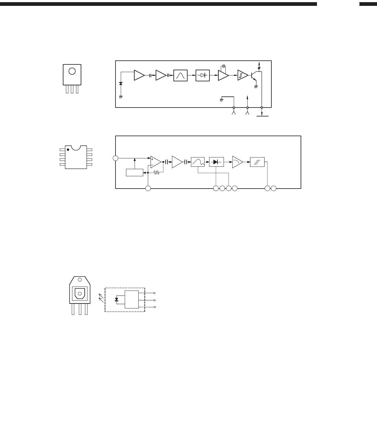
50
DVD-3800
OTHERS
GP1UM271XK (Remote Control Sensor)
(PD: IC103)
GND
V
CC
V
OUT
Head
Amp BPF Integrator
TOP VIEW
V
OUT
V
CC
GND
Limiter
Amp
Detector &
Comparator
Hysteresis
Comparator
1
45
8
2 3 4 5 6 7 8
1
IN
ABLC
C1 C2 GND fo N.C. OUT Vcc
Detector &
Comparator Integrator
TOP
VIEW
CXA1511M (PD: IC510)
Head
Amp
Limiter
Amp
BPF
BEF
Hysteresis
Comparator
V
IN
V
CC
GND
V
CC
V
IN
GND
DRIVE
IC
FRONT VIEW
LED
OPTICAL
Output
GP1FA551TZ (AV: JK503)
R
L
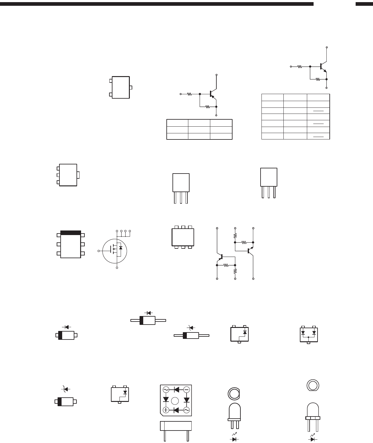
51
DVD-3800
TRANSISTORS
2SA1022
2SA1036K (Europe model only)
2SB709A
2SC2411K (Europe model only)
2SC2412K
2SD601A
KTC2875B
DTA114EK
DTA124EK
DTC114EK
DTC124TK (Europe model only)
DTC143EK
DTC143TK
DTC144EK (Europe model only)
DTC144TK (Europe model only)
B
C
E
R1
R2
B
C
E
R1
R2
DTA114EK
DTA124EK
DTC114EK
DTC124TK
DTC143EK
DTC143TK
DTC144EK
DTC144TK
2SC1740S
2SD468
TOP
VIEW
E
B
C
DTA114EK
DTA124EK
R1
10kohm
R2
22kohm
10kohm
22kohm
FRONT
VIEW
B
C
E
TOP
VIEW
E
B
CC
2SB1260
DIODES (Including LED)
TOP VIEW
1SS355
RB161L-40
1
2
3
6
5
4
TOP VIEW
4 Source
3 Gate
1,2,5,6 Drain
12
3
4
56
DDDD
G
S
HAT2053M
2SB1266
2SB1274
2SD1902
FRONT
VIEW
E
C
B
DTC114EK
R1
10kohm
R2
10kohm
DTC143EK 4.7kohm
DTC124TK 22kohm
1SR139-400
AG01ZT(V1)
AL01ZT(V1)
EM01AT(V1)
RJ43 LF015-305
RK39 LF-C4
SARS01T(V1)
HZS4C-1
TOP VIEW
TOP VIEW
SEL1210S (Red)
SELU1E10CXM-002 (Blue)
4
TOP
VIEW
56
321
(4) (5) (6)
(3) (2) (1)
R1 R2
DTr1
DTr2
R2 R1
10k
10k
10k
10k
MA152WK
(Europe model only)
TOP VIEW
TOP VIEW
MA152A
(Europe model only)
RB411D
TOP VIEW
SEL2810A (Amber)
TOP VIEW
SIDE VIEW
TOP VIEW
S4VB20
TOP VIEW
DTC143TK 4.7kohm
4.7kohm
DTC144TK 47kohm
DTC144EK 47kohm 47kohm
IMD3A
TOP VIEW
UDZS12B
UDZS13B
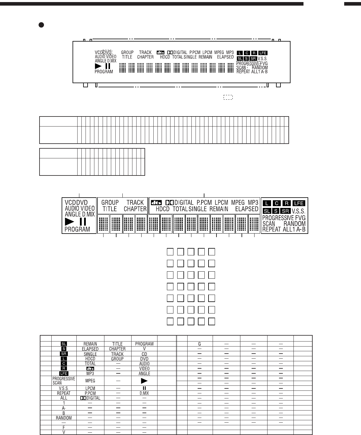
52
DVD-3800
PIN NO.
CONNECTION
1
F
-
2
N
X
3
N
P
4
N
P
5
P
1
6
P
2
7
P
3
8
P
4
9
P
5
1
0
P
6
1
1
P
7
1
2
P
8
1
3
P
9
1
4
P
1
0
1
5
P
1
1
1
6
P
1
2
1
7
P
1
3
1
8
P
1
4
1
9
P
1
5
2
0
P
1
6
2
1
P
1
7
2
2
P
1
8
2
3
P
1
9
2
4
P
2
0
2
5
P
2
1
2
6
P
2
2
2
7
P
2
3
2
8
P
2
4
2
9
P
2
5
3
0
P
2
6
3
1
P
2
7
3
2
P
2
8
3
3
P
2
9
3
4
P
3
0
3
5
P
3
1
3
6
P
3
2
3
7
P
3
3
3
8
P
3
4
3
9
P
3
5
4
0
N
C
N
C
N
C
N
C
N
C
N
C
4
1
4
2
4
3
4
4
4
5
4
6
1
7
G
4
7
1
6
G
4
8
1
5
G
4
9
1
4
G
5
0
1
3
G
PIN NO.
CONNECTION
5
1
1
2
G
5
2
1
1
G
5
3
1
0
G
5
4
9
G
5
5
8
G
5
6
7
G
5
7
6
G
5
8
5
G
5
9
4
G
6
0
3
G
6
1
2
G
6
2
1
G
6
3
N
P
6
4
N
P
6
5
N
X
6
6
F
+
1-1
1-2
1-3
1-4
1-5
1-6
1-7
2-1
2-2
2-3
2-4
2-5
2-6
2-7
3-1
3-2
3-3
3-4
3-5
3-6
3-7
4-1
4-2
4-3
4-4
4-5
4-6
4-7
5-1
5-2
5-3
5-4
5-5
5-6
5-7
[13G~1G]
13G 12G 11G 10G 9G 8G 7G 6G 5G 4G 3G 2G 1G
16G15G14G
1 66
P1
17G 16G 15G 14G 13G~1G
P2
P3
P4
P5
P6
P7
P8
P9
P10
P11
P12
P13
P14
P15
P16
P17
P18
P19
17G 16G 15G 14G 13G~1G
P20
P21
P22
P23
P24
P25
P26
P27
P28
P29
P30
P31
P32
P33
P34
P35
PIN CONNECTION
GRID ASSIGNMENT
ANODE CONNECTION
NOTE 1) F-,F+ ---------- Filament
2) NP ------------- No pin
3) NX ------------- No extend pin
4) DL ------------ Datum line
5) 1G~17G ----- Grid
6) Visual Field -- Upper 22.6° min.
7) NC ------------ No connection
(NC pin should be electorically open on the PC board)
1-1
2-1
3-1
4-1
5-1
1-2
2-2
3-2
4-2
5-2
1-3
2-3
3-3
4-3
5-3
1-4
2-4
3-4
4-4
5-4
1-5
2-5
3-5
4-5
5-5
1-6
2-6
3-6
4-6
5-6
1-7
2-7
3-7
4-7
5-7
COLOR ILLUMINATION Reddish Orange ----- Above pattern part
Green ------------------ Other
FL DISPLAY 17-ST-04GNK (FL101)
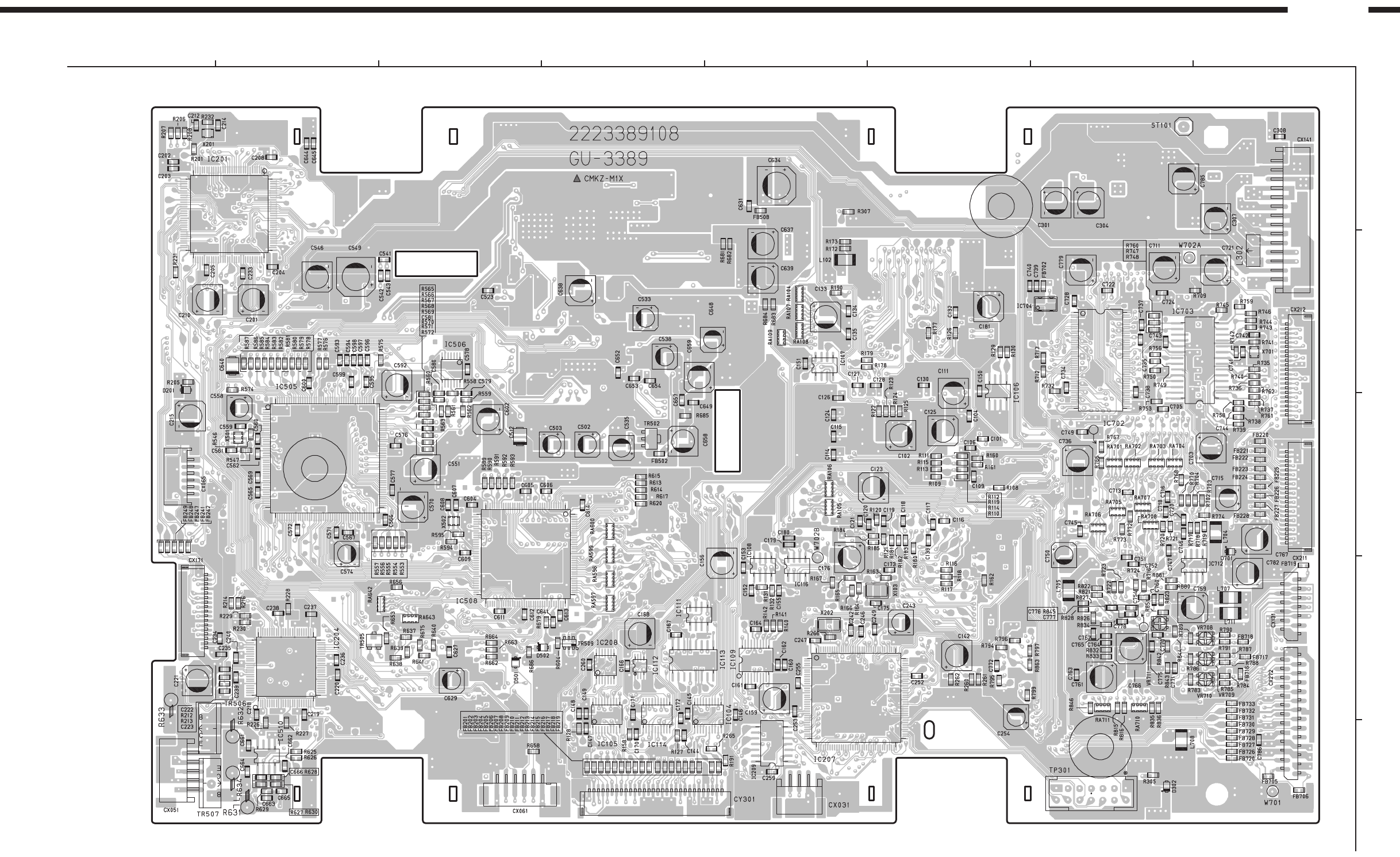
1
1
7
814
1
1
1
1
1
7
8
14
36
37 72
73
108
109
144
25
26
50
5175
76
100
36
37
72
73 108
109
144
44
45 88
89
132
133176
32
33
64
65 96
97
128
7
814
1
1 4
58
1 10
1120
1 10
1120
1 10
1120
1 8
916
1 10
1120
1 4
58
1 4
58
1 4
58
1 4
58
1 4
58
1
1
43 44
86
4
58
1
1415
28
1 4
58
1
6
1
17
1
516
11
30 3
26 27
1
2
21
12 13
1
1
1
21
21
14
COMPONENT SIDE
PRINTED WIRING BOARD
8
76
5
4
3
2
1
A
B
C
D
E
DVD-3800
53
GU-3389A MAIN P.W.B. UNIT Ass'y
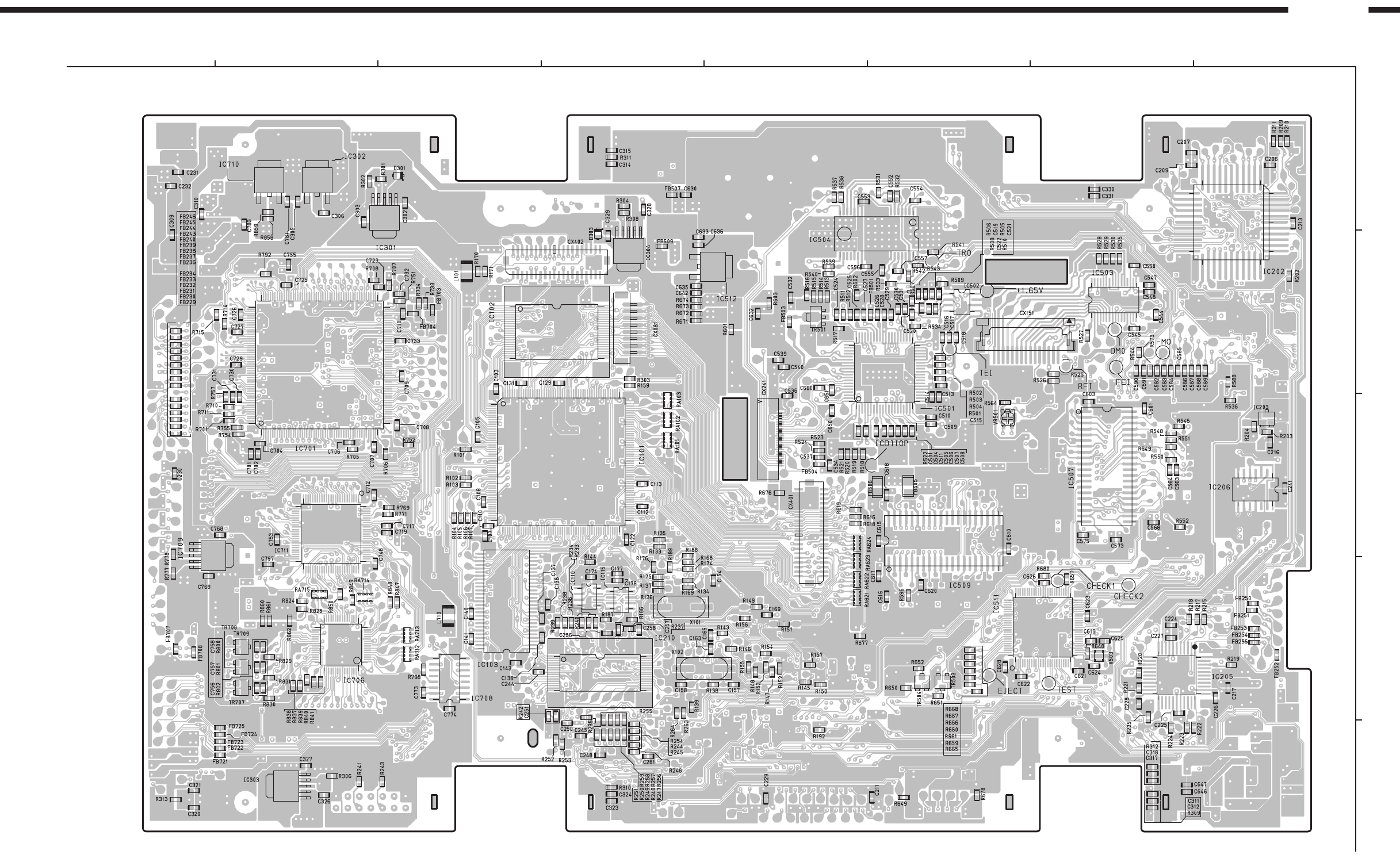
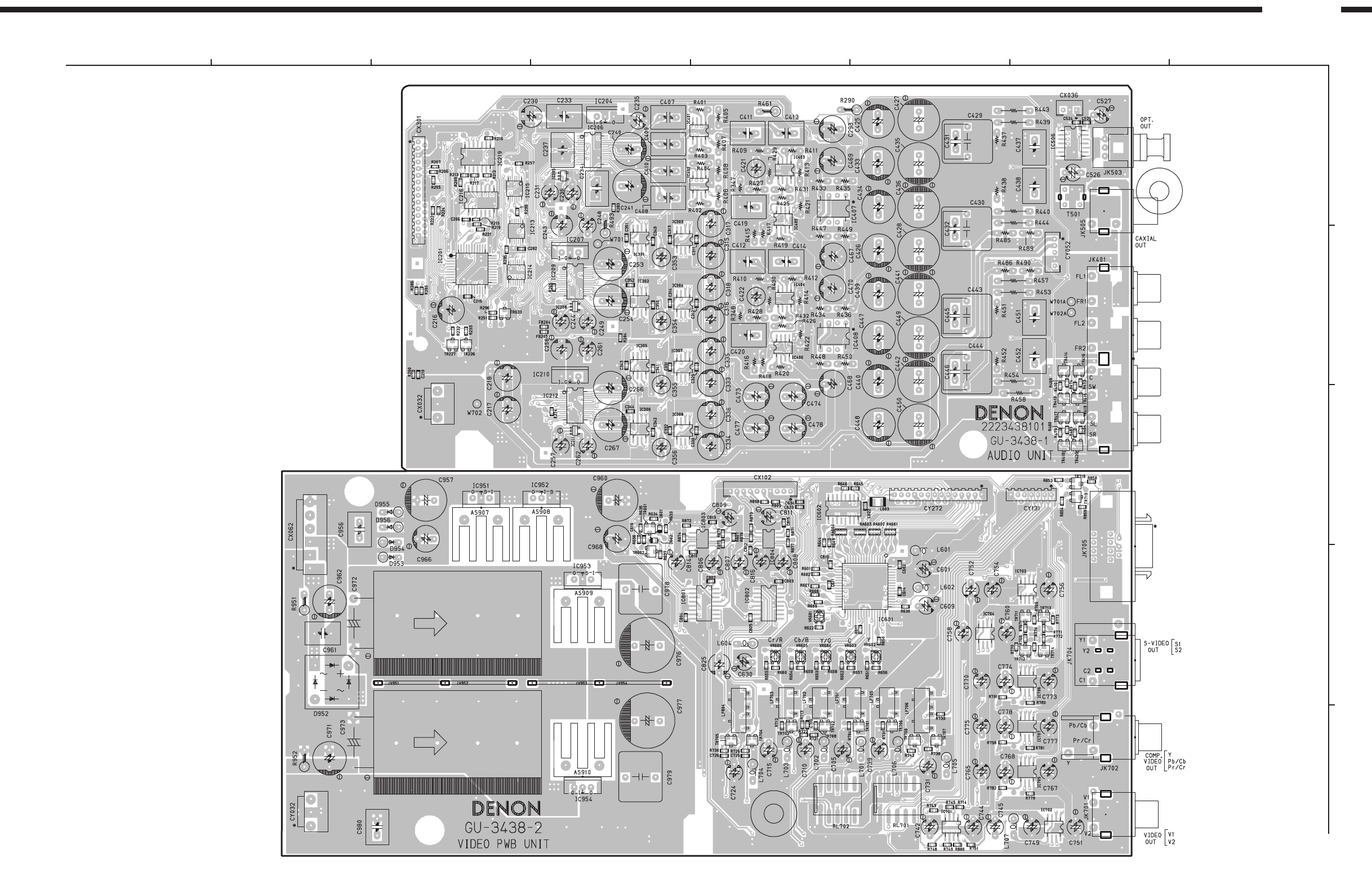
1 7
814
1 7
814
1
230
29
1 3
1
1
17
8 14
17
8 14
8
914
11
12 22
23
33
3444
1
14 15
28
1
4
5 8
1
4
5 8
1
4
5 8
1
4
5 8
1
4
5 8
1
4
5 8
1
4
5 8
1
4
5 8
1
4
5 8
1
4
5 8
1
4
5 8
14
5
8
1
4
58
1
4
58
1
4
5 8
14
5
8
1
14 15
28
1
14 15
28
1
78
9
13
15
1
2
1
212
1327
26
14
5 8
14
5 8
1
16 9
8
14
5 8
14
5 8
14
5 8
14
5 8
14
5 8
1
16
17
32
33 48
49
64
110
1
1 3 6
COMPONENT SIDE
8
76
5
4
3
2
1
A
B
C
D
E
DVD-3800
55
GU-3438 AUDIO/VIDEO P.W.B. UNIT Ass'y
GU-3438-1 AUDIO P.W.B.
GU-3438-2 VIDEO P.W.B.
FOIL SIDE
8
76
5
4
3
2
1
A
B
C
D
E
DVD-3800
56
GU-3438 AUDIO/VIDEO P.W.B. UNIT Ass'y
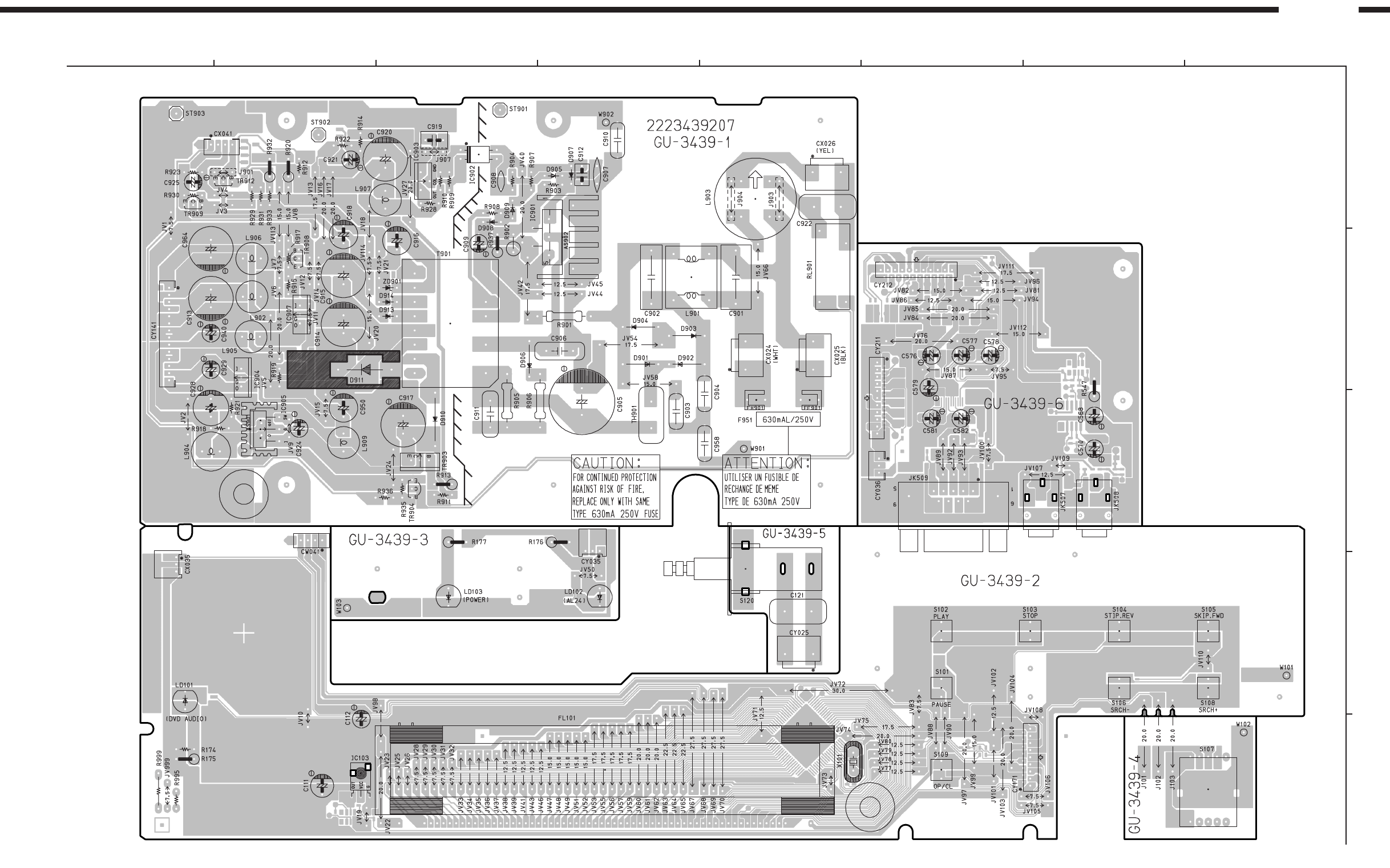
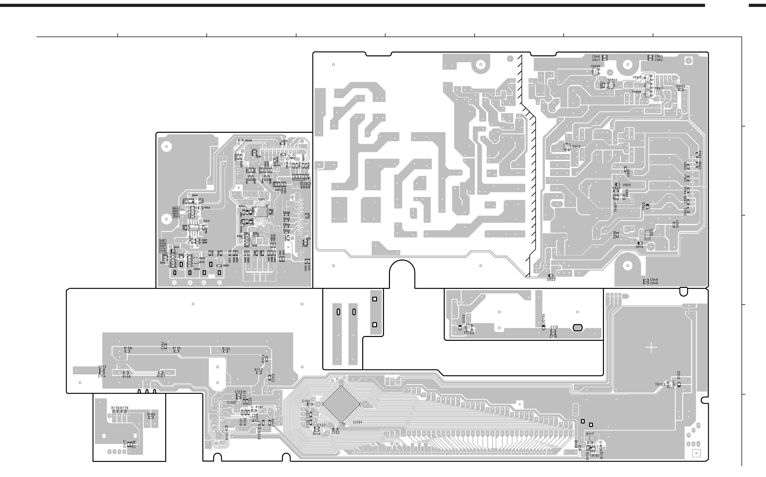
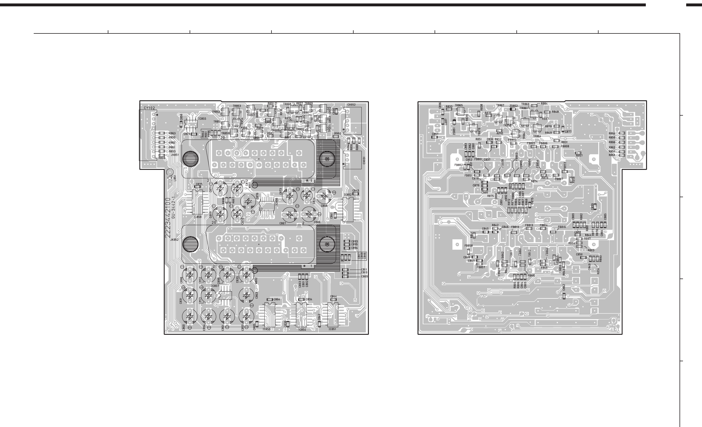
60
DVD-3800
tttt
ll
ll
lResistors
Ex.:RN 14K 2E 182 GFR
Type Shape Power Resist- Allowable Others
and per- ance error
formance
tt
tt
s
s
s
s
Resistance
1 8 2⇒1800 ohm = 1.8 kohm
Indicates number of zeros after effective number.
2-digit effective number.
• Units: ohm
1 R 2⇒1.2 ohm
1-digit effective number.
2-digit effective number, decimal point indicated by R.
• Units: ohm
ll
ll
lCapacitors
Ex.:CE 04W 1H 2R2 MBP
Type Shape Dielectric Capacity Allowable Others
and per- strength error
formance
s
s
s
s
ss
Capacity (electrolyte only)
2 2 2⇒2200µF
Indicates number of zeros after effective number.
2-digit effective number.
• Units: µF.
2 R 2⇒2.2µF
1-digit effective number.
2-digit effective number, decimal point indicated by R.
• Units: µF.
Capacity (except electrolyte)
2 2 2⇒2200pF=0.0022µF
(More than 2) Indicates number of zeros after effective number.
2-digit effective number.
• Units: pF.
2 2 1⇒220pF
(0 or 1) Indicates number of zeros after effective number.
2-digit effective number.
• Units: pF.
• When the dielectric strength is indicated in AC, "AC" is included after the dieelectric
strength value.
ss
NOTE FOR PARTS LIST
lPart indicated with the mark "" are not always in stock and possibly to take a long period of time for supplying, or in
some case supplying of part may be refused.
lWhen ordering of part, clearly indicate "1" and "I" (i) to avoid mis-supplying.
lOrdering part without stating its part number can not be supplied.
lPart indicated with the mark " " is not illustrated in the exploded view.
lNot including Carbon Film ±5%, 1/4W Type in the P.W.Board parts list. (Refer to the Schematic Diagram for those parts.)
WARNING:
Parts marked with this symbol have critical characteristics.
Use ONLY replacement parts recommended by the manufacturer.
RD : Carbon 2B : 1/8W F : ±1% P : Pulse-resistant type
RC : Composition 2E : 1/4W G : ±2% NL : Low noise type
RS : Metal oxide film 2H : 1/2W J : ±5% NB : Non-burning type
RW : Winding 3A : 1W K : ±10% FR : Fuse-resistor
RN : Metal film 3D : 2W M : ±20% F : Lead wire forming
RK : Metal mixture 3F : 3W
3H : 5W
CE : Aluminum foil 0J : 6.3V F : ±1% HS : High stability type
electrolytic
CA : Aluminum solid 1A : 10V G : ±2% BP : Non-polar type
electrolytic
CS : Tantalum electrolytic 1C : 16V J : ±5% HR : Ripple-resistant type
CQ : Film 1E : 25V K : ±10% DL : For change and discharge
CK : Ceramic 1V : 35V M : ±20% HF : For assuring high
requency
CC : Ceramic 1H : 50V Z : +80% U : UL part
CP : Oil 2A : 100V –20% C : CSA part
CM : Mica 2B : 125V P : +100% W : UL-CSA type
CF : Metallized 2C : 160V –0% F : Lead wire forming
CH : Metallized 2D : 200V C : ±0.25pF
2E : 250V D : ±0.5pF
2H : 500V = : Others
2J : 630V
61
DVD-3800
PARTS LIST OF P.W.B. UNIT ASS'Y
GU-3389A MAIN P.W.B. UNIT
Ref. No. Part No. Part Name Remarks Ref. No. Part No. Part Name Remarks
SEMICONDUCTORS GROUP
IC101 262 3051 007 IC ES6038
IC102 GEN 6094 ROM sub Ass’y MX29LV160BTC-90
IC103 262 3119 004 IC W986416DH-7
IC104,105 262 2801 902 IC SN74AHCT273PW-EL2
IC106 262 3053 908 IC S-24C02BFJ-TB
IC107 262 2391 904 IC TC7W32F(TE12L)
IC108 262 1953 903 IC TC7WU04F
IC109 262 3052 909 IC SM8701BM
IC110 262 1953 903 IC TC7WU04F
IC111 262 2104 900 IC TC7W14F
IC112 262 3046 902 IC TC7WH157FU
IC113 262 3129 900 IC TC74VHC157AF-EL
IC114 262 2801 902 IC SN74AHCT273PW-EL2
IC115,116 262 2104 900 IC TC7W14F
IC201 262 3054 004 IC MN102H460B
IC202 GEN 6093 ROM sub Ass’y AT49LV1025-70JC
IC203 262 1647 905 IC MN1382-S(TX)
IC206 262 2376 903 IC TC74HCT7007AF(TP1)
IC207 262 3121 005 IC ADSPMEL322
IC208 262 2515 900 IC SN74LV04APW-EL2
IC209 262 2376 903 IC TC74HCT7007AF(TP1)
IC210 GEN 6074 Bass M.ROM sub Ass’y AT49LV002-70TC
IC301 263 1110 901 IC PQ070XZ01ZP
IC302 263 1079 903 IC BA033FP
IC303,304 263 1110 901 IC PQ070XZ01ZP
IC501 262 2802 008 IC TA1293F
IC502 263 0425 901 IC NJM4558M (TAPE)
IC503 263 1109 909 IC AN8471SA
IC504 263 1080 905 IC BA5952AFP
IC505 262 2803 007 IC TC9453F
IC506 262 2892 908 IC 74VHC4066MTC
IC507 262 2877 907 IC 4M DRAM(SOJ)-35
IC508 262 2798 002 IC TC9469BF
IC509 262 2877 907 IC 4M DRAM(SOJ)-35
IC510 263 0615 902 IC BA15218F-DXE2
IC511 GEN 6100 DRV ROM sub Ass’y TMP95FY64F
IC512 263 1079 903 IC BA033FP
IC701 262 3058 000 IC SII504CM208
IC702 262 2916 004 IC 64M SDRAM(TSOP)
IC703 262 3059 902 IC PIC18LC242-I/SO TAPE
IC706 262 3050 008 IC ADV7300
IC708 262 1348 903 IC TC74HC123AF(TP1)
IC709 263 1110 901 IC PQ070XZ01ZP
IC710 262 2977 904 IC BA18BC0FP-E2
IC711 262 3126 000 IC XC2S30-5VQ100C
IC712 262 3127 009 IC XC17S30AV08C(SQZ)
TR501,502 272 0156 902 Transistor 2SB1260-Q
TR503-505 269 0091 906 Transistor DTC143TKT96
TR506 274 0154 007 Transistor 2SD1902(R,S)
TR507 272 0110 003 Transistor 2SB1266(R,S)
TR509 269 0171 907 Transistor IMD3A-T108
TR707 271 0293 901 Transistor 2SA1022-B
TR708,709 272 0125 904 Transistor 2SB709A
D201 276 0717 903 Diode 1SS355 TE-17
D301-303 276 0717 903 Diode 1SS355 TE-17
D501,502 276 0717 903 Diode 1SS355 TE-17
D701 276 0717 903 Diode 1SS355 TE-17
RESISTORS GROUP
R101 247 2007 943 Carbon chip 1 kohm 1/16W RM73B--102JT
R102-105 247 2004 920 Carbon chip 47 ohm 1/16W RM73B--470JT
R106 247 2018 903 Carbon chip 0 ohm 1/16W RM73B--0R0KT
R107,108 247 2004 920 Carbon chip 47 ohm 1/16W RM73B--470JT
R109 247 2009 909 Carbon chip 4.7 kohm 1/16W RM73B--472JT (1608)
R111 247 2009 909 Carbon chip 4.7 kohm 1/16W RM73B--472JT (1608)
R113 247 2009 909 Carbon chip 4.7 kohm 1/16W RM73B--472JT (1608)
R116-118 247 2009 941 Carbon chip 6.8 kohm 1/16W RM73B--682JT
R119 247 2009 909 Carbon chip 4.7 kohm 1/16W RM73B--472JT (1608)
R120-125 247 2009 941 Carbon chip 6.8 kohm 1/16W RM73B--682JT
R126 247 2018 903 Carbon chip 0 ohm 1/16W RM73B--0R0KT
R127-130 247 2007 943 Carbon chip 1 kohm 1/16W RM73B--102JT
R131 247 2014 965 Carbon chip 1 Mohm 1/16W RM73B--105JT
R132 247 2006 944 Carbon chip 390 ohm 1/16W RM73B--391JT
R133 247 2003 989 Carbon chip 33 ohm 1/16W RM73B--330JT
R135-137 247 2003 989 Carbon chip 33 ohm 1/16W RM73B--330JT
R143 247 2007 943 Carbon chip 1 kohm 1/16W RM73B--102JT
R144 247 2018 903 Carbon chip 0 ohm 1/16W RM73B--0R0KT
R145,146 247 2004 920 Carbon chip 47 ohm 1/16W RM73B--470JT
R147,148 247 2018 903 Carbon chip 0 ohm 1/16W RM73B--0R0KT
R150,151 247 2004 920 Carbon chip 47 ohm 1/16W RM73B--470JT
R152-155 247 2018 903 Carbon chip 0 ohm 1/16W RM73B--0R0KT
R157 247 2004 920 Carbon chip 47 ohm 1/16W RM73B--470JT
R158 247 2007 943 Carbon chip 1 kohm 1/16W RM73B--102JT
R159 247 2018 903 Carbon chip 0 ohm 1/16W RM73B--0R0KT
R160 247 2009 983 Carbon chip 10 kohm 1/16W RM73B--103JT
R163 247 2014 965 Carbon chip 1 Mohm 1/16W RM73B--105JT
R164 247 2005 987 Carbon chip 220 ohm 1/16W RM73B--221JT
R166,167 247 2003 989 Carbon chip 33 ohm 1/16W RM73B--330JT
R169-174 247 2018 903 Carbon chip 0 ohm 1/16W RM73B--0R0KT
R177-179 247 2018 903 Carbon chip 0 ohm 1/16W RM73B--0R0KT
R180-185 247 2003 989 Carbon chip 33 ohm 1/16W RM73B--330JT
R186,187 247 2018 903 Carbon chip 0 ohm 1/16W RM73B--0R0KT
R189-191 247 2018 903 Carbon chip 0 ohm 1/16W RM73B--0R0KT
Note : The symbols in the column “Remarks” indicate the following destinations.
E3 : U.S.A. & Canada model E2 : Europe model
E1 : Asia model

62
DVD-3800
R201 247 2003 989 Carbon chip 33 ohm 1/16W RM73B--330JT
R202 247 2004 920 Carbon chip 47 ohm 1/16W RM73B--470JT
R203 247 2008 984 Carbon chip 3.9 kohm 1/16W RM73B--392JT
R205 247 2005 987 Carbon chip 220 ohm 1/16W RM73B--221JT
R207 247 2009 909 Carbon chip 4.7 kohm 1/16W RM73B--472JT (1608)
R209 247 2009 909 Carbon chip 4.7 kohm 1/16W RM73B--472JT (1608)
R211 247 2009 909 Carbon chip 4.7 kohm 1/16W RM73B--472JT (1608)
R231 247 2018 903 Carbon chip 0 ohm 1/16W RM73B--0R0KT
R233,234 247 2009 983 Carbon chip 10 kohm 1/16W RM73B--103JT
R235 247 2018 903 Carbon chip 0 ohm 1/16W RM73B--0R0KT
R236 247 2009 983 Carbon chip 10 kohm 1/16W RM73B--103JT
R237 247 2014 965 Carbon chip 1 Mohm 1/16W RM73B--105JT
R238-242 247 2009 983 Carbon chip 10 kohm 1/16W RM73B--103JT
R243 247 2007 943 Carbon chip 1 kohm 1/16W RM73B--102JT
R244,245 247 2009 983 Carbon chip 10 kohm 1/16W RM73B--103JT
R247,248 247 2009 983 Carbon chip 10 kohm 1/16W RM73B--103JT
R250,251 247 2009 983 Carbon chip 10 kohm 1/16W RM73B--103JT
R253 247 2018 903 Carbon chip 0 ohm 1/16W RM73B--0R0KT
R254-264 247 2009 983 Carbon chip 10 kohm 1/16W RM73B--103JT
R266 247 2007 969 Carbon chip 1.2 kohm 1/16W RM73B--122JT
R301 247 2007 972 Carbon chip 1.3 kohm 1/16W RM73B--132JT
R302 247 2007 943 Carbon chip 1 kohm 1/16W RM73B--102JT
R303 247 2018 903 Carbon chip 0 ohm 1/16W RM73B--0R0KT
R304 247 2008 926 Carbon chip 2.2 kohm 1/16W RM73B--222JT
R305-307 247 2007 943 Carbon chip 1 kohm 1/16W RM73B--102JT
R308 247 2010 927 Carbon chip 15 kohm 1/16W RM73B--153JT
R309-313 247 2018 903 Carbon chip 0 ohm 1/16W RM73B--0R0KT
R501 247 2009 983 Carbon chip 10 kohm 1/16W RM73B--103JT
R502 247 2006 960 Carbon chip 470 ohm 1/16W RM73B--471JT
R503 247 2009 983 Carbon chip 10 kohm 1/16W RM73B--103JT
R504 247 2007 943 Carbon chip 1 kohm 1/16W RM73B--102JT
R505,506 247 2009 983 Carbon chip 10 kohm 1/16W RM73B--103JT
R507 247 2012 925 Carbon chip 100 kohm 1/16W RM73B--104JT
R508 247 2011 942 Carbon chip 47 kohm 1/16W RM73B--473JT
R510 247 2012 925 Carbon chip 100 kohm 1/16W RM73B--104JT
R511,512 247 2011 942 Carbon chip 47 kohm 1/16W RM73B--473JT
R513,514 247 2005 958 Carbon chip 160 ohm 1/16W RM73B--161JT
R515,516 247 2005 945 Carbon chip 150 ohm 1/16W RM73B--151JT
R517 247 2007 943 Carbon chip 1 kohm 1/16W RM73B--102JT
R518,519 247 2005 958 Carbon chip 160 ohm 1/16W RM73B--161JT
R520,521 247 2005 945 Carbon chip 150 ohm 1/16W RM73B--151JT
R522 247 2007 943 Carbon chip 1 kohm 1/16W RM73B--102JT
R523 247 2004 988 Carbon chip 82 ohm 1/16W RM73B--820JT
R524 247 2005 903 Carbon chip 100 ohm 1/16W RM73B--101JT
R525 247 2009 983 Carbon chip 10 kohm 1/16W RM73B--103JT
R526,527 247 2005 903 Carbon chip 100 ohm 1/16W RM73B--101JT
R528-530 247 2018 916 Carbon chip 1 ohm 1/16W RM73B--010KT
R531 247 2010 972 Carbon chip 24 kohm 1/16W RM73B--243JT
R532,533 247 2009 983 Carbon chip 10 kohm 1/16W RM73B--103JT
R534 247 2018 903 Carbon chip 0 ohm 1/16W RM73B--0R0KT
Ref. No. Part No. Part Name Remarks Ref. No. Part No. Part Name Remarks
R535 247 2018 916 Carbon chip 1 ohm 1/16W RM73B--010KT
R536 247 2011 942 Carbon chip 47 kohm 1/16W RM73B--473JT
R537-540 247 2018 916 Carbon chip 1 ohm 1/16W RM73B--010KT
R541,542 247 2009 983 Carbon chip 10 kohm 1/16W RM73B--103JT
R543-545 247 2018 903 Carbon chip 0 ohm 1/16W RM73B--0R0KT
R546 247 2014 965 Carbon chip 1 Mohm 1/16W RM73B--105JT
R547 247 2006 902 Carbon chip 330 ohm 1/16W RM73B--331JT (1608)
R548 247 2009 983 Carbon chip 10 kohm 1/16W RM73B--103JT
R549 247 2013 982 Carbon chip 470 kohm 1/16W RM73B--474JT
R550 247 2009 909 Carbon chip 4.7 kohm 1/16W RM73B--472JT (1608)
R551,552 247 2009 983 Carbon chip 10 kohm 1/16W RM73B--103JT
R553-557 247 2018 903 Carbon chip 0 ohm 1/16W RM73B--0R0KT
R558 247 2012 996 Carbon chip 200 kohm 1/16W RM73B--204JT
R559 247 2009 925 Carbon chip 5.6 kohm 1/16W RM73B--562JT
R560 247 2009 941 Carbon chip 6.8 kohm 1/16W RM73B--682JT
R561,562 247 2009 925 Carbon chip 5.6 kohm 1/16W RM73B--562JT
R563 247 2010 985 Carbon chip 27 kohm 1/16W RM73B--273JT
R564 247 2011 968 Carbon chip 56 kohm 1/16W RM73B--563JT
R565,566 247 2007 943 Carbon chip 1 kohm 1/16W RM73B--102JT
R568 247 2013 924 Carbon chip 270 kohm 1/16W RM73B--274JT
R571 247 2012 970 Carbon chip 160 kohm 1/16W RM73B--164JT
R573 247 2011 942 Carbon chip 47 kohm 1/16W RM73B--473JT
R574 247 2018 903 Carbon chip 0 ohm 1/16W RM73B--0R0KT
R575 247 2011 942 Carbon chip 47 kohm 1/16W RM73B--473JT
R576 247 2009 983 Carbon chip 10 kohm 1/16W RM73B--103JT
R577 247 2010 998 Carbon chip 30 kohm 1/16W RM73B--303JT
R578 247 2011 942 Carbon chip 47 kohm 1/16W RM73B--473JT
R579-585 247 2009 983 Carbon chip 10 kohm 1/16W RM73B--103JT
R586 247 2008 968 Carbon chip 3.3 kohm 1/16W RM73B--332JT
R587 247 2007 943 Carbon chip 1 kohm 1/16W RM73B--102JT
R589-594 247 2018 903 Carbon chip 0 ohm 1/16W RM73B--0R0KT
R596 247 2009 983 Carbon chip 10 kohm 1/16W RM73B--103JT
R604 247 2009 983 Carbon chip 10 kohm 1/16W RM73B--103JT
R613-617 247 2009 983 Carbon chip 10 kohm 1/16W RM73B--103JT
R618 247 2007 943 Carbon chip 1 kohm 1/16W RM73B--102JT
R619,620 247 2009 983 Carbon chip 10 kohm 1/16W RM73B--103JT
R625,626 247 2012 941 Carbon chip 120 kohm 1/16W RM73B--124JT
R627 247 2009 954 Carbon chip 7.5 kohm 1/16W RM73B--752JT
R628 247 2010 927 Carbon chip 15 kohm 1/16W RM73B--153JT
R629 247 2011 997 Carbon chip 75 kohm 1/16W RM73B--753JT
R630 247 2010 914 Carbon chip 13 kohm 1/16W RM73B--133JT
R631 244 2050 904 Metal oxide 22 ohm 1W(NB)
RS14B3A220JNBST(S)
R632 244 2052 960 Metal oxide 220 ohm 1W(NB)
RS14B3A221JNBST(S)
R633 244 2051 945 Metal oxide 1 ohm 1W(NB)
RS14B3A010JNBST(S)
R634 244 2052 960 Metal oxide 220 ohm 1W(NB)
RS14B3A221JNBST(S)
R637 247 2007 943 Carbon chip 1 kohm 1/16W RM73B--102JT
R638 247 2009 983 Carbon chip 10 kohm 1/16W RM73B--103JT
R640 247 2009 983 Carbon chip 10 kohm 1/16W RM73B--103JT
R648 247 2011 900 Carbon chip 33 kohm 1/16W RM73B--333JT
R649 247 2005 961 Carbon chip 180 ohm 1/16W RM73B--181JT
R650 247 2010 969 Carbon chip 22 kohm 1/16W RM73B--223JT
63
DVD-3800
R651-653 247 2009 983 Carbon chip 10 kohm 1/16W RM73B--103JT
R656-664 247 2009 983 Carbon chip 10 kohm 1/16W RM73B--103JT
R668 247 2018 903 Carbon chip 0 ohm 1/16W RM73B--0R0KT
R671-674 247 2018 903 Carbon chip 0 ohm 1/16W RM73B--0R0KT
R675 247 2009 983 Carbon chip 10 kohm 1/16W RM73B--103JT
R679 247 2007 943 Carbon chip 1 kohm 1/16W RM73B--102JT
R680 247 2009 983 Carbon chip 10 kohm 1/16W RM73B--103JT
R681-685 247 2018 903 Carbon chip 0 ohm 1/16W RM73B--0R0KT
R686 247 2009 983 Carbon chip 10 kohm 1/16W RM73B--103JT
R702-704 247 2003 989 Carbon chip 33 ohm 1/16W RM73B--330JT
R705 247 2018 903 Carbon chip 0 ohm 1/16W RM73B--0R0KT
R709 247 2009 983 Carbon chip 10 kohm 1/16W RM73B--103JT
R710 247 2007 943 Carbon chip 1 kohm 1/16W RM73B--102JT
R712 247 2018 903 Carbon chip 0 ohm 1/16W RM73B--0R0KT
R713 247 2009 909 Carbon chip 4.7 kohm 1/16W RM73B--472JT (1608)
R714,715 247 2018 903 Carbon chip 0 ohm 1/16W RM73B--0R0KT
R716 247 2003 989 Carbon chip 33 ohm 1/16W RM73B--330JT
R722-724 247 2003 989 Carbon chip 33 ohm 1/16W RM73B--330JT
R733 247 2018 903 Carbon chip 0 ohm 1/16W RM73B--0R0KT
R734 247 2003 989 Carbon chip 33 ohm 1/16W RM73B--330JT
R735 247 2009 909 Carbon chip 4.7 kohm 1/16W RM73B--472JT (1608)
R736,737 247 2008 926 Carbon chip 2.2 kohm 1/16W RM73B--222JT
R738-741 247 2018 903 Carbon chip 0 ohm 1/16W RM73B--0R0KT
R743,744 247 2018 903 Carbon chip 0 ohm 1/16W RM73B--0R0KT
R745 247 2009 909 Carbon chip 4.7 kohm 1/16W RM73B--472JT (1608)
R746,747 247 2008 926 Carbon chip 2.2 kohm 1/16W RM73B--222JT
R748 247 2009 909 Carbon chip 4.7 kohm 1/16W RM73B--472JT (1608)
R749 247 2003 989 Carbon chip 33 ohm 1/16W RM73B--330JT
R750 247 2009 909 Carbon chip 4.7 kohm 1/16W RM73B--472JT (1608)
R751,752 247 2018 903 Carbon chip 0 ohm 1/16W RM73B--0R0KT
R753 247 2009 909 Carbon chip 4.7 kohm 1/16W RM73B--472JT (1608)
R754,755 247 2018 903 Carbon chip 0 ohm 1/16W RM73B--0R0KT
R757 247 2007 943 Carbon chip 1 kohm 1/16W RM73B--102JT
R759-762 247 2003 989 Carbon chip 33 ohm 1/16W RM73B--330JT
R766-768 247 2003 989 Carbon chip 33 ohm 1/16W RM73B--330JT
R769 247 2009 983 Carbon chip 10 kohm 1/16W RM73B--103JT
R770 247 2003 989 Carbon chip 33 ohm 1/16W RM73B--330JT
R771 247 2009 983 Carbon chip 10 kohm 1/16W RM73B--103JT
R774 247 2007 943 Carbon chip 1 kohm 1/16W RM73B--102JT
R777,778 247 2007 943 Carbon chip 1 kohm 1/16W RM73B--102JT
R783 247 2005 987 Carbon chip 220 ohm 1/16W RM73B--221JT
R784 247 2003 989 Carbon chip 33 ohm 1/16W RM73B--330JT
R785 247 2007 943 Carbon chip 1 kohm 1/16W RM73B--102JT
R786 247 2005 987 Carbon chip 220 ohm 1/16W RM73B--221JT
R787 247 2003 989 Carbon chip 33 ohm 1/16W RM73B--330JT
R788 247 2007 943 Carbon chip 1 kohm 1/16W RM73B--102JT
R789 247 2005 987 Carbon chip 220 ohm 1/16W RM73B--221JT
R790 247 2003 989 Carbon chip 33 ohm 1/16W RM73B--330JT
R791 247 2007 943 Carbon chip 1 kohm 1/16W RM73B--102JT
R794 247 2007 943 Carbon chip 1 kohm 1/16W RM73B--102JT
R795 247 2003 989 Carbon chip 33 ohm 1/16W RM73B--330JT
Ref. No. Part No. Part Name Remarks Ref. No. Part No. Part Name Remarks
R796 247 2009 983 Carbon chip 10 kohm 1/16W RM73B--103JT
R798 247 2018 903 Carbon chip 0 ohm 1/16W RM73B--0R0KT
R799 247 2007 985 Carbon chip 1.5 kohm 1/16W RM73B--152JT
R800-802 247 2005 987 Carbon chip 220 ohm 1/16W RM73B--221JT
R815,816 247 2003 989 Carbon chip 33 ohm 1/16W RM73B--330JT
R821,822 247 2003 989 Carbon chip 33 ohm 1/16W RM73B--330JT
R823 247 2007 943 Carbon chip 1 kohm 1/16W RM73B--102JT
R827 247 2018 903 Carbon chip 0 ohm 1/16W RM73B--0R0KT
R828 247 2009 909 Carbon chip 4.7 kohm 1/16W RM73B--472JT (1608)
R832-834 247 2018 903 Carbon chip 0 ohm 1/16W RM73B--0R0KT
R838 247 2007 985 Carbon chip 1.5 kohm 1/16W RM73B--152JT
R839-841 247 2005 987 Carbon chip 220 ohm 1/16W RM73B--221JT
R844 247 2007 943 Carbon chip 1 kohm 1/16W RM73B--102JT
R845 247 2007 901 Carbon chip 680 ohm 1/16W RM73B--681JT
R846 247 2018 903 Carbon chip 0 ohm 1/16W RM73B--0R0KT
R847-850 247 2003 989 Carbon chip 33 ohm 1/16W RM73B--330JT
R851 247 2006 960 Carbon chip 470 ohm 1/16W RM73B--471JT
R860-862 247 2018 903 Carbon chip 0 ohm 1/16W RM73B--0R0KT
R863 247 2009 983 Carbon chip 10 kohm 1/16W RM73B--103JT
R880,881 247 2009 909 Carbon chip 4.7 kohm 1/16W RM73B--472JT (1608)
RA101-103 247 9002 909 Chip network 33 ohm 1/16W MNR14=330JE0AB
RA104 247 9002 912 Chip network 6.8 kohm 1/16W MNR14=682JEOAB
RA105,106 247 9002 909 Chip network 33 ohm 1/16W MNR14=330JE0AB
RA107-109 247 9002 912 Chip network 6.8 kohm 1/16W MNR14=682JEOAB
RA597-600 247 9002 909 Chip network 33 ohm 1/16W MNR14=330JE0AB
RA621-624 247 9002 912 Chip network 6.8 kohm 1/16W MNR14=682JEOAB
RA642,643 247 9002 912 Chip network 6.8 kohm 1/16W MNR14=682JEOAB
RA701-704 247 9002 909 Chip network 33 ohm 1/16W MNR14=330JE0AB
RA710-715 247 9002 909 Chip network 33 ohm 1/16W MNR14=330JE0AB
VR708-710 211 6148 906 Semi fixed resistor 470 ohm
V03PB471MT(RH03ADCS)
CAPACITORS GROUP
C101 257 0511 904 Ceramic chip 0.01uF/50V CK73F1H103ZT
C102 254 4464 906 Electrolytic 100uF/6.3V CE67C0J101MT
C103 257 0512 903 Ceramic chip 0.1uF/25V CK73F1E104ZT
C104 257 0511 904 Ceramic chip 0.01uF/50V CK73F1H103ZT
C105,106 257 0512 903 Ceramic chip 0.1uF/25V CK73F1E104ZT
C108-110 257 0512 903 Ceramic chip 0.1uF/25V CK73F1E104ZT
C111 254 4464 906 Electrolytic 100uF/6.3V CE67C0J101MT
C112-122 257 0512 903 Ceramic chip 0.1uF/25V CK73F1E104ZT
C123 254 4464 906 Electrolytic 100uF/6.3V CE67C0J101MT
C124 257 0512 903 Ceramic chip 0.1uF/25V CK73F1E104ZT
C125 254 4464 906 Electrolytic 100uF/6.3V CE67C0J101MT
C126-131 257 0512 903 Ceramic chip 0.1uF/25V CK73F1E104ZT
C132 257 0511 904 Ceramic chip 0.01uF/50V CK73F1H103ZT

64
DVD-3800
C133 254 4464 906 Electrolytic 100uF/6.3V CE67C0J101MT
C134 257 0509 929 Ceramic chip 1000pF/50V CK73B1H102KT
C135-141 257 0512 903 Ceramic chip 0.1uF/25V CK73F1E104ZT
C142 254 4464 906 Electrolytic 100uF/6.3V CE67C0J101MT
C143 257 0512 903 Ceramic chip 0.1uF/25V CK73F1E104ZT
C144 257 0511 904 Ceramic chip 0.01uF/50V CK73F1H103ZT
C145 257 0512 903 Ceramic chip 0.1uF/25V CK73F1E104ZT
C146 257 0509 929 Ceramic chip 1000pF/50V CK73B1H102KT
C147 257 0511 904 Ceramic chip 0.01uF/50V CK73F1H103ZT
C148 257 0512 903 Ceramic chip 0.1uF/25V CK73F1E104ZT
C149 257 0509 929 Ceramic chip 1000pF/50V CK73B1H102KT
C150,151 257 0512 903 Ceramic chip 0.1uF/25V CK73F1E104ZT
C152 257 0502 997 Ceramic chip 7pF/50V CC73CH1H7R0DT
C153 257 0512 903 Ceramic chip 0.1uF/25V CK73F1E104ZT
C154 257 0509 929 Ceramic chip 1000pF/50V CK73B1H102KT
C155 257 0502 997 Ceramic chip 7pF/50V CC73CH1H7R0DT
C156 254 4465 918 Electrolytic 47uF/16V CE67C1C470MT
C159 254 4464 906 Electrolytic 100uF/6.3V CE67C0J101MT
C160,161 257 0512 903 Ceramic chip 0.1uF/25V CK73F1E104ZT
C162 257 0509 929 Ceramic chip 1000pF/50V CK73B1H102KT
C163 257 0512 903 Ceramic chip 0.1uF/25V CK73F1E104ZT
C164 257 0509 929 Ceramic chip 1000pF/50V CK73B1H102KT
C165 257 0511 904 Ceramic chip 0.01uF/50V CK73F1H103ZT
C166,167 257 0512 903 Ceramic chip 0.1uF/25V CK73F1E104ZT
C168 254 4464 906 Electrolytic 100uF/6.3V CE67C0J101MT
C169 257 0512 903 Ceramic chip 0.1uF/25V CK73F1E104ZT
C170 257 0511 904 Ceramic chip 0.01uF/50V CK73F1H103ZT
C171 257 0512 903 Ceramic chip 0.1uF/25V CK73F1E104ZT
C172 257 0509 929 Ceramic chip 1000pF/50V CK73B1H102KT
C173 257 0503 967 Ceramic chip 15pF/50V CC73CH1H150JT
C174 257 0512 903 Ceramic chip 0.1uF/25V CK73F1E104ZT
C175 257 0503 941 Ceramic chip 12pF/50V CC73CH1H120JT
C176 254 4465 918 Electrolytic 47uF/16V CE67C1C470MT
C177 257 0512 903 Ceramic chip 0.1uF/25V CK73F1E104ZT
C178,179 257 0509 929 Ceramic chip 1000pF/50V CK73B1H102KT
C180 257 0512 903 Ceramic chip 0.1uF/25V CK73F1E104ZT
C181 254 4464 906 Electrolytic 100uF/6.3V CE67C0J101MT
C201 254 4464 906 Electrolytic 100uF/6.3V CE67C0J101MT
C202-207 257 0512 903 Ceramic chip 0.1uF/25V CK73F1E104ZT
C208 257 0509 929 Ceramic chip 1000pF/50V CK73B1H102KT
C209 257 0512 903 Ceramic chip 0.1uF/25V CK73F1E104ZT
C210 254 4464 906 Electrolytic 100uF/6.3V CE67C0J101MT
C211 257 0512 903 Ceramic chip 0.1uF/25V CK73F1E104ZT
C212 257 0503 967 Ceramic chip 15pF/50V CC73CH1H150JT
C213 257 0509 929 Ceramic chip 1000pF/50V CK73B1H102KT
C214 257 0503 967 Ceramic chip 15pF/50V CC73CH1H150JT
C215 254 4465 918 Electrolytic 47uF/16V CE67C1C470MT
C216 257 0511 904 Ceramic chip 0.01uF/50V CK73F1H103ZT
C229,230 257 0512 903 Ceramic chip 0.1uF/25V CK73F1E104ZT
C231-233 257 0511 904 Ceramic chip 0.01uF/50V CK73F1H103ZT
C234,235 257 0512 903 Ceramic chip 0.1uF/25V CK73F1E104ZT
Ref. No. Part No. Part Name Remarks Ref. No. Part No. Part Name Remarks
C241,242 257 0512 903 Ceramic chip 0.1uF/25V CK73F1E104ZT
C243 254 4465 905 Electrolytic 22uF/16V CE67C1C220MT
C244 257 0511 904 Ceramic chip 0.01uF/50V CK73F1H103ZT
C245-253 257 0512 903 Ceramic chip 0.1uF/25V CK73F1E104ZT
C254 254 4465 905 Electrolytic 22uF/16V CE67C1C220MT
C255,256 257 0512 903 Ceramic chip 0.1uF/25V CK73F1E104ZT
C257 257 0504 924 Ceramic chip 27pF/50V CC73CH1H270JT
C258 257 0504 940 Ceramic chip 33pF/50V CC73CH1H330JT
C259-261 257 0512 903 Ceramic chip 0.1uF/25V CK73F1E104ZT
C301 254 4464 906 Electrolytic 100uF/6.3V CE67C0J101MT
C302,303 257 0512 903 Ceramic chip 0.1uF/25V CK73F1E104ZT
C304 254 4464 906 Electrolytic 100uF/6.3V CE67C0J101MT
C305,306 257 0512 903 Ceramic chip 0.1uF/25V CK73F1E104ZT
C307 254 4464 906 Electrolytic 100uF/6.3V CE67C0J101MT
C326-329 257 0512 903 Ceramic chip 0.1uF/25V CK73F1E104ZT
C501 257 0511 904 Ceramic chip 0.01uF/50V CK73F1H103ZT
C503 254 4465 905 Electrolytic 22uF/16V CE67C1C220MT
C504-506 257 0512 903 Ceramic chip 0.1uF/25V CK73F1E104ZT
C507,508 257 0509 929 Ceramic chip 1000pF/50V CK73B1H102KT
C509 257 0503 925 Ceramic chip 10pF/50V CC73CH1H100DT
C510 257 0512 903 Ceramic chip 0.1uF/25V CK73F1E104ZT
C511 257 0511 904 Ceramic chip 0.01uF/50V CK73F1H103ZT
C512 257 2010 937 Electrolytic 22uF/10V CS77B1A220MT
C513,514 257 0512 903 Ceramic chip 0.1uF/25V CK73F1E104ZT
C515-517 257 0507 976 Ceramic chip 330pF/50V CC73CH1H331JT
C519 257 0511 904 Ceramic chip 0.01uF/50V CK73F1H103ZT
C522 257 0503 925 Ceramic chip 10pF/50V CC73CH1H100DT
C523 257 0512 903 Ceramic chip 0.1uF/25V CK73F1E104ZT
C524 257 0511 904 Ceramic chip 0.01uF/50V CK73F1H103ZT
C526 257 0512 903 Ceramic chip 0.1uF/25V CK73F1E104ZT
C527 257 0509 929 Ceramic chip 1000pF/50V CK73B1H102KT
C528,529 257 0512 903 Ceramic chip 0.1uF/25V CK73F1E104ZT
C530,531 257 0510 934 Ceramic chip 4700pF/50V CK73B1H472KT
C532 257 0511 904 Ceramic chip 0.01uF/50V CK73F1H103ZT
C533 254 4465 905 Electrolytic 22uF/16V CE67C1C220MT
C534 257 0511 904 Ceramic chip 0.01uF/50V CK73F1H103ZT
C535 254 4465 905 Electrolytic 22uF/16V CE67C1C220MT
C536,537 257 0511 904 Ceramic chip 0.01uF/50V CK73F1H103ZT
C538 254 4465 905 Electrolytic 22uF/16V CE67C1C220MT
C539,540 257 0511 904 Ceramic chip 0.01uF/50V CK73F1H103ZT
C544,545 257 0512 903 Ceramic chip 0.1uF/25V CK73F1E104ZT
C546 254 4464 906 Electrolytic 100uF/6.3V CE67C0J101MT
C547 257 0512 903 Ceramic chip 0.1uF/25V CK73F1E104ZT
C548 257 0509 929 Ceramic chip 1000pF/50V CK73B1H102KT
C549 257 4010 906 Electrolytic 100uF/16V CE67C1C101MT
C550 257 0511 904 Ceramic chip 0.01uF/50V CK73F1H103ZT
C552 257 0516 909 Ceramic chip 0.022uF/25V CK73B1E223KT
C553 257 0512 903 Ceramic chip 0.1uF/25V CK73F1E104ZT
C554 257 0506 977 Ceramic chip 120pF/50V CC73CH1H121JT
C555,556 257 0512 903 Ceramic chip 0.1uF/25V CK73F1E104ZT

65
DVD-3800
Ref. No. Part No. Part Name Remarks Ref. No. Part No. Part Name Remarks
C557 257 0506 977 Ceramic chip 120pF/50V CC73CH1H121JT
C560 257 0512 903 Ceramic chip 0.1uF/25V CK73F1E104ZT
C562 257 0512 903 Ceramic chip 0.1uF/25V CK73F1E104ZT
C563 257 0509 929 Ceramic chip 1000pF/50V CK73B1H102KT
C564 257 0501 927 Ceramic chip 0.015uF/50V CK73B1H153KT
C565-569 257 0512 903 Ceramic chip 0.1uF/25V CK73F1E104ZT
C570 254 4464 906 Electrolytic 100uF/6.3V CE67C0J101MT
C571-573 257 0512 903 Ceramic chip 0.1uF/25V CK73F1E104ZT
C574 254 4465 905 Electrolytic 22uF/16V CE67C1C220MT
C575-577 257 0512 903 Ceramic chip 0.1uF/25V CK73F1E104ZT
C578 257 0511 904 Ceramic chip 0.01uF/50V CK73F1H103ZT
C579 257 0510 918 Ceramic chip 3300pF/50V CK73B1H332KT
C580 257 0501 927 Ceramic chip 0.015uF/50V CK73B1H153KT
C582-589 257 0512 903 Ceramic chip 0.1uF/25V CK73F1E104ZT
C590,591 257 0507 976 Ceramic chip 330pF/50V CC73CH1H331JT
C592 254 4464 906 Electrolytic 100uF/6.3V CE67C0J101MT
C593 257 0510 950 Ceramic chip 6800pF/50V CK73B1H682KT
C594 257 0509 945 Ceramic chip 1200pF/50V CK73B1H122KT
C595 257 0512 903 Ceramic chip 0.1uF/25V CK73F1E104ZT
C596 257 0506 951 Ceramic chip 100pF/50V CC73CH1H101JT
C597 257 0509 990 Ceramic chip 2200pF/50V CK73B1H222KT
C598 257 0509 945 Ceramic chip 1200pF/50V CK73B1H122KT
C599-601 257 0512 903 Ceramic chip 0.1uF/25V CK73F1E104ZT
C602 254 4464 906 Electrolytic 100uF/6.3V CE67C0J101MT
C603-606 257 0512 903 Ceramic chip 0.1uF/25V CK73F1E104ZT
C609-618 257 0512 903 Ceramic chip 0.1uF/25V CK73F1E104ZT
C619 257 0511 904 Ceramic chip 0.01uF/50V CK73F1H103ZT
C620-623 257 0512 903 Ceramic chip 0.1uF/25V CK73F1E104ZT
C626-628 257 0512 903 Ceramic chip 0.1uF/25V CK73F1E104ZT
C629 254 4465 905 Electrolytic 22uF/16V CE67C1C220MT
C630-633 257 0512 903 Ceramic chip 0.1uF/25V CK73F1E104ZT
C634 257 4010 906 Electrolytic 100uF/16V CE67C1C101MT
C635,636 257 0512 903 Ceramic chip 0.1uF/25V CK73F1E104ZT
C637 254 4464 906 Electrolytic 100uF/6.3V CE67C0J101MT
C639 254 4464 906 Electrolytic 100uF/6.3V CE67C0J101MT
C640 257 2010 937 Electrolytic 22uF/10V CS77B1A220MT
C641 257 0511 904 Ceramic chip 0.01uF/50V CK73F1H103ZT
C650 257 0506 951 Ceramic chip 100pF/50V CC73CH1H101JT
C660-662 257 0512 903 Ceramic chip 0.1uF/25V CK73F1E104ZT
C664 257 0512 903 Ceramic chip 0.1uF/25V CK73F1E104ZT
C701 257 0511 904 Ceramic chip 0.01uF/50V CK73F1H103ZT
C702 257 0512 903 Ceramic chip 0.1uF/25V CK73F1E104ZT
C703 254 4464 906 Electrolytic 100uF/6.3V CE67C0J101MT
C704-710 257 0512 903 Ceramic chip 0.1uF/25V CK73F1E104ZT
C711 254 4464 906 Electrolytic 100uF/6.3V CE67C0J101MT
C712,713 257 0512 903 Ceramic chip 0.1uF/25V CK73F1E104ZT
C714 254 4533 921 Electrolytic 100uF/6.3V
CE04W0J101MT SMG/RE3
C715 254 4465 905 Electrolytic 22uF/16V CE67C1C220MT
C716-720 257 0512 903 Ceramic chip 0.1uF/25V CK73F1E104ZT
C721 254 4464 906 Electrolytic 100uF/6.3V CE67C0J101MT
C722-730 257 0512 903 Ceramic chip 0.1uF/25V CK73F1E104ZT
C731 257 0511 904 Ceramic chip 0.01uF/50V CK73F1H103ZT
C732-735 257 0512 903 Ceramic chip 0.1uF/25V CK73F1E104ZT
C736 254 4464 906 Electrolytic 100uF/6.3V CE67C0J101MT
C737,738 257 0512 903 Ceramic chip 0.1uF/25V CK73F1E104ZT
C741,742 257 0502 942 Ceramic chip 2pF/50V CC73CH1H2R0CT
C743 257 0512 903 Ceramic chip 0.1uF/25V CK73F1E104ZT
C744 257 0511 904 Ceramic chip 0.01uF/50V CK73F1H103ZT
C745-748 257 0512 903 Ceramic chip 0.1uF/25V CK73F1E104ZT
C750 254 4465 905 Electrolytic 22uF/16V CE67C1C220MT
C751,752 257 0512 903 Ceramic chip 0.1uF/25V CK73F1E104ZT
C756-758 257 0512 903 Ceramic chip 0.1uF/25V CK73F1E104ZT
C759 254 4464 906 Electrolytic 100uF/6.3V CE67C0J101MT
C760 257 0511 904 Ceramic chip 0.01uF/50V CK73F1H103ZT
C761 254 4464 906 Electrolytic 100uF/6.3V CE67C0J101MT
C762,763 257 0512 903 Ceramic chip 0.1uF/25V CK73F1E104ZT
C766,767 254 4464 906 Electrolytic 100uF/6.3V CE67C0J101MT
C768-770 257 0512 903 Ceramic chip 0.1uF/25V CK73F1E104ZT
C772 257 0507 934 Ceramic chip 220pF/50V CC73CH1H221JT
C773 257 0509 929 Ceramic chip 1000pF/50V CK73B1H102KT
C774,775 257 0512 903 Ceramic chip 0.1uF/25V CK73F1E104ZT
C776 257 0510 921 Ceramic chip 3900pF/50V CK73B1H392KT
C777 257 0509 903 Ceramic chip 820pF/50V CK73B1H821KT
C778 257 0512 903 Ceramic chip 0.1uF/25V CK73F1E104ZT
C779 254 4464 906 Electrolytic 100uF/6.3V CE67C0J101MT
C782 254 4464 906 Electrolytic 100uF/6.3V CE67C0J101MT
C783,784 257 0512 903 Ceramic chip 0.1uF/25V CK73F1E104ZT
C785 254 4464 906 Electrolytic 100uF/6.3V CE67C0J101MT
C786 257 0512 903 Ceramic chip 0.1uF/25V CK73F1E104ZT
C797 257 0512 903 Ceramic chip 0.1uF/25V CK73F1E104ZT
66
DVD-3800
GU-3438 AUDIO/VIDEO P.W.B. UNIT
Ref. No. Part No. Part Name Remarks
OTHER PARTS GROUP
CX031 205 0863 936 3P PH connector base (L) 1
CX051 205 0863 952 5P PH connector base (L) 1
CX061 205 1072 946 6P PH connector base 1
CX131 205 1170 932 13P FFC base (FMNBMTT) 1
CX141 205 1172 943 14P PH connector base (L) 1
CX151 205 1149 905 15P FFC base (52207) 1
CX171 205 1174 909 17P FFC base (FMNSMT) 1
CX211,212 205 1174 938 21P FFC base (FMNSMT) 2
CX241 205 1152 905 24P FFC base (FLZ-SM1) 1
CX272 205 1170 929 27P FFC base (FMNBMTT) 1
CY301 205 1174 941 30P FFC base (FMNSMT) 1
FB201-210 235 0130 903 Chip emifil (11A121) 10
FB211-216 247 2018 903 Carbon chip 0 ohm 1/16W 6
FB217-219 235 0130 903 Chip emifil (11A121) 3
FB225 235 0130 903 Chip emifil (11A121) 1
FB229 235 0130 903 Chip emifil (11A121) 1
FB233,234 235 0130 903 Chip emifil (11A121) 2
FB236-255 235 0130 903 Chip emifil (11A121) 20
FB501 235 0136 907 Beads inductor
FBMJ1608HS280NT
1
FB502-504 235 0130 903 Chip emifil (11A121) 3
FB505,506 235 0138 905 Beads inductor
FBMH3216MH501NT
2
FB507-509 235 0136 907 Beads inductor
FBMJ1608HS280NT
3
FB703,704 247 2018 903 Carbon chip 0 ohm 1/16W 2
FB705-708 235 0130 903 Chip emifil (11A121) 4
FB716-720 235 0130 903 Chip emifil (11A121) 5
FB721 247 2018 903 Carbon chip 0 ohm 1/16W 1
FB722,723 235 0130 903 Chip emifil (11A121) 2
FB724,725 247 2018 903 Carbon chip 0 ohm 1/16W 2
FB726-733 235 0130 903 Chip emifil (11A121) 8
L302 235 0048 901 Chip emifil 1
L704,705 235 0125 905 Inductor 22uH 2
L710,711 235 0125 905 Inductor 22uH 2
W702 203 0515 039 1P SIN connector cord 1
X101 399 0619 906 Crystal 27 MHz 1
X103 399 0807 909 Crystal 33.333 MHz 1
X201 399 0698 901 Ceramic 25.00 MHz 1
X202 399 0806 900 Crystal 12.288 MHz 1
X501 399 0697 902 Ceramic 22.57 MHz 1
X502 399 0699 900 Ceramic 50.00 MHz 1
X503 399 0698 901 Ceramic 25.00 MHz 1
X701 399 0706 903 Ceramic 20.00 MHz 1
001 0130 041 1P wire 3
461 0415 007 Rubber sheet 3
Ref. No. Part No. Part Name Remarks Q'ty
SEMICONDUCTORS GROUP
IC201 262 2978 000 IC DXP7001AF
IC204 263 0809 006 IC NJM7805FA(S)
IC205 263 1136 901 IC BA033LBSG-TR
IC206 262 3072 905 IC PCM1738-1
IC207 263 0809 006 IC NJM7805FA(S)
IC208 263 1136 901 IC BA033LBSG-TR
IC209 262 3072 905 IC PCM1738-1
IC210 263 0809 006 IC NJM7805FA(S)
IC211 263 1136 901 IC BA033LBSG-TR
IC212 262 3072 905 IC PCM1738-1
IC213 262 2515 900 IC SN74LV04APW-EL2
IC214 262 2669 908 IC SN74LV157APW
IC215 262 2518 907 IC SN74LV74APW-EL2
IC216 262 1205 907 IC TC74HCU04AF(TP1)
IC219 262 1421 901 IC TC74HCT04AF(TAPE1)
IC301-308 263 0896 909 IC NJM2068MD-T1
IC401-406 263 0896 909 IC NJM2068MD-T1
IC407,408 263 0609 002 IC NJM2068DDC
IC506 262 1421 901 IC TC74HCT04AF(TAPE1)
IC601 262 3093 007 IC ADV7190
IC602 262 1348 903 IC TC74HC123AF(TP1)
IC701-707 263 1082 903 IC TK15420MTL
IC801,802 262 0707 901 IC TC4053BF (TAPE) for E2
IC803,804 263 1082 903 IC TK15420MTL for E2
IC951 263 0809 006 IC NJM7805FA(S)
IC952 263 0554 005 IC NJM7905FA
IC953 263 0801 004 IC NJM7812FA(S)
IC954 263 0641 002 IC NJM7912FA
TR217 273 0384 900
Transistor 2SC2412KT96(S)
TR218 269 0083 901 Transistor DTA114EKT96
TR219 269 0119 901
Transistor DTA124EKT96(TAPE)
TR220 269 0082 902 Transistor DTC114EKT96
TR226,227 269 0082 902 Transistor DTC114EKT96
TR305-308 273 0460 905 Transistor KTC2875B-RTK
TR401-410 273 0460 905 Transistor KTC2875B-RTK
TR411 269 0119 901
Transistor DTA124EKT96(TAPE)
TR412 269 0082 902 Transistor DTC114EKT96
TR413-420 273 0460 905 Transistor KTC2875B-RTK
TR421-424 273 0460 905 Transistor KTC2875B-RTK for E2
TR425 269 0119 901
Transistor DTA124EKT96(TAPE)
TR426 269 0082 902 Transistor DTC114EKT96
67
DVD-3800
Ref. No. Part No. Part Name Remarks Ref. No. Part No. Part Name Remarks
TR601 274 0163 904 Transistor 2SD601A
TR602 272 0125 904 Transistor 2SB709A
TR603 274 0163 904 Transistor 2SD601A
TR604 272 0125 904 Transistor 2SB709A
TR605 271 0293 901 Transistor 2SA1022-B
TR606 272 0125 904 Transistor 2SB709A
TR607 271 0293 901 Transistor 2SA1022-B
TR608,609 272 0125 904 Transistor 2SB709A
TR633 273 0460 905 Transistor KTC2875B-RTK
TR701-705 272 0125 904 Transistor 2SB709A
TR706 271 0293 901 Transistor 2SA1022-B
TR707,708 272 0125 904 Transistor 2SB709A
TR709,710 274 0163 904 Transistor 2SD601A
TR715-717 274 0163 904 Transistor 2SD601A
TR801,802 269 0048 904 Transistor DTC143EK-T96
TR807,808 274 0163 904 Transistor 2SD601A for E2
D202,203 276 0717 903 Diode 1SS355 TE-17
D206,207 276 0717 903 Diode 1SS355 TE-17
D601-604 276 0717 903 Diode 1SS355 TE-17
D801,802 276 0717 903 Diode 1SS355 TE-17
D952 276 0305 001 Diode S4VB20
D953-956 276 0765 900
Diode 1SR139-400
RESISTORS GROUP
R202 247 2018 903 Carbon chip 0 ohm 1/16W RM73B--0R0KT
R203-207 247 2004 920 Carbon chip 47 ohm 1/16W RM73B--470JT
R208-211 247 2018 903 Carbon chip 0 ohm 1/16W RM73B--0R0KT
R215 247 2011 942 Carbon chip 47 kohm 1/16W RM73B--473JT
R219 247 2013 940 Carbon chip 330 kohm 1/16W RM73B--334JT
R221 247 2004 933 Carbon chip 51 ohm 1/16W RM73B--510JT
R222 247 2018 903 Carbon chip 0 ohm 1/16W RM73B--0R0KT
R223 247 2007 943 Carbon chip 1 kohm 1/16W RM73B--102JT
R224 247 2018 903 Carbon chip 0 ohm 1/16W RM73B--0R0KT
R226 247 2006 902 Carbon chip 330 ohm 1/16W RM73B--331JT (1608)
R227,228 247 2007 943 Carbon chip 1 kohm 1/16W RM73B--102JT
R230-234 247 2018 903 Carbon chip 0 ohm 1/16W RM73B--0R0KT
R235 247 2009 983 Carbon chip 10 kohm 1/16W RM73B--103JT
R238 247 2009 983 Carbon chip 10 kohm 1/16W RM73B--103JT
R239,240 247 2004 920 Carbon chip 47 ohm 1/16W RM73B--470JT
R241 247 2018 903 Carbon chip 0 ohm 1/16W RM73B--0R0KT
R242 247 2004 920 Carbon chip 47 ohm 1/16W RM73B--470JT
R243 247 2018 903 Carbon chip 0 ohm 1/16W RM73B--0R0KT
R244 247 2004 920 Carbon chip 47 ohm 1/16W RM73B--470JT
R245,246 247 2018 903 Carbon chip 0 ohm 1/16W RM73B--0R0KT
R248 247 2018 903 Carbon chip 0 ohm 1/16W RM73B--0R0KT
R252 247 2007 943 Carbon chip 1 kohm 1/16W RM73B--102JT
R254 247 2018 903 Carbon chip 0 ohm 1/16W RM73B--0R0KT
R255 247 2010 930 Carbon chip 16 kohm 1/16W RM73B--163JT
R261 247 2007 943 Carbon chip 1 kohm 1/16W RM73B--102JT
R263 247 2018 903 Carbon chip 0 ohm 1/16W RM73B--0R0KT
R264 247 2010 930 Carbon chip 16 kohm 1/16W RM73B--163JT
R270 247 2007 943 Carbon chip 1 kohm 1/16W RM73B--102JT
R272 247 2018 903 Carbon chip 0 ohm 1/16W RM73B--0R0KT
R273 247 2010 930 Carbon chip 16 kohm 1/16W RM73B--163JT
R276 247 2018 903 Carbon chip 0 ohm 1/16W RM73B--0R0KT
R278 247 2018 903 Carbon chip 0 ohm 1/16W RM73B--0R0KT
R279 247 2004 920 Carbon chip 47 ohm 1/16W RM73B--470JT
R281 247 2004 920 Carbon chip 47 ohm 1/16W RM73B--470JT
R285-287 247 2007 943 Carbon chip 1 kohm 1/16W RM73B--102JT
R288,289 247 2009 983 Carbon chip 10 kohm 1/16W RM73B--103JT
R290 244 2051 974 Metal oxide 1 kohm 1W(NB)
RS14B3A102JNBST(S)
R292 247 2005 903 Carbon chip 100 ohm 1/16W RM73B--101JT
R293,294 247 2004 920 Carbon chip 47 ohm 1/16W RM73B--470JT
R295 247 2018 903 Carbon chip 0 ohm 1/16W RM73B--0R0KT
R297 247 2004 991 Carbon chip 91 ohm 1/16W RM73B--910JT
R298-300 247 2004 920 Carbon chip 47 ohm 1/16W RM73B--470JT
R301 247 2007 930 Carbon chip 910 ohm 1/16W RM73B--911JT
R302 247 2006 999 Carbon chip 620 ohm 1/16W RM73B--621JT
R303 247 2007 930 Carbon chip 910 ohm 1/16W RM73B--911JT
R304-316 247 2006 999 Carbon chip 620 ohm 1/16W RM73B--621JT
R317-320 247 2008 913 Carbon chip 2 kohm 1/16W RM73B--202JT
R321-336 247 2006 999 Carbon chip 620 ohm 1/16W RM73B--621JT
R337,338 247 2008 913 Carbon chip 2 kohm 1/16W RM73B--202JT
R342 247 2004 920 Carbon chip 47 ohm 1/16W RM73B--470JT
R345,346 247 2008 913 Carbon chip 2 kohm 1/16W RM73B--202JT
R349-352 247 2011 942 Carbon chip 47 kohm 1/16W RM73B--473JT
R439,440 241 2420 946 Carbon film 150 ohm 1/4W
RD14B2E151JT(PSNB)
R441,442 247 2008 942 Carbon chip 2.7 kohm 1/16W RM73B--272JT
R443,444 241 2420 946 Carbon film 150 ohm 1/4W
RD14B2E151JT(PSNB)
R445,446 247 2008 942 Carbon chip 2.7 kohm 1/16W RM73B--272JT
R453,454 241 2420 946 Carbon film 150 ohm 1/4W
RD14B2E151JT(PSNB)
R455,456 247 2008 942 Carbon chip 2.7 kohm 1/16W RM73B--272JT
R457,458 241 2420 946 Carbon film 150 ohm 1/4W
RD14B2E151JT(PSNB)
R459,460 247 2008 942 Carbon chip 2.7 kohm 1/16W RM73B--272JT
R461 244 2051 932 Metal oxide 3.3 kohm 1W(NB)
RS14B3A332JNBST(S)
R462 247 2009 983 Carbon chip 10 kohm 1/16W RM73B--103JT
R465,466 247 2010 998 Carbon chip 30 kohm 1/16W RM73B--303JT
R467,468 247 2005 945 Carbon chip 150 ohm 1/16W RM73B--151JT
R469,470 247 2008 942 Carbon chip 2.7 kohm 1/16W RM73B--272JT
R471,472 247 2005 945 Carbon chip 150 ohm 1/16W RM73B--151JT
R473,474 247 2008 942 Carbon chip 2.7 kohm 1/16W RM73B--272JT
R475,476 247 2010 998 Carbon chip 30 kohm 1/16W RM73B--303JT
R477,478 247 2005 945 Carbon chip 150 ohm 1/16W RM73B--151JT
R479,480 247 2008 942 Carbon chip 2.7 kohm 1/16W RM73B--272JT
R481,482 247 2005 945 Carbon chip 150 ohm 1/16W RM73B--151JT
R483,484 247 2008 942 Carbon chip 2.7 kohm 1/16W RM73B--272JT

68
DVD-3800
R487,488 247 2008 942 Carbon chip 2.7 kohm 1/16W RM73B--272JT, for E2
R491,492 247 2008 942 Carbon chip 2.7 kohm 1/16W RM73B--272JT, for E2
R493 244 2051 932 Metal oxide 3.3 kohm 1W(NB)
RS14B3A332JNBST(S)
R494 247 2009 983 Carbon chip 10 kohm 1/16W RM73B--103JT
R495-500 247 2018 903 Carbon chip 0 ohm 1/16W RM73B--0R0KT
R517 247 2011 942 Carbon chip 47 kohm 1/16W RM73B--473JT
R518 247 2006 960 Carbon chip 470 ohm 1/16W RM73B--471JT
R519 247 2018 903 Carbon chip 0 ohm 1/16W RM73B--0R0KT
R520 247 2004 975 Carbon chip 75 ohm 1/16W RM73B--750JT
R522 247 2018 903 Carbon chip 0 ohm 1/16W RM73B--0R0KT
R601,602 247 2018 903 Carbon chip 0 ohm 1/16W RM73B--0R0KT
R603,604 247 2009 909 Carbon chip 4.7 kohm 1/16W RM73B--472JT (1608)
R606,607 247 2018 903 Carbon chip 0 ohm 1/16W RM73B--0R0KT
R608,609 247 2003 989 Carbon chip 33 ohm 1/16W RM73B--330JT
R610,611 247 2009 909 Carbon chip 4.7 kohm 1/16W RM73B--472JT (1608)
R612-615 247 2018 903 Carbon chip 0 ohm 1/16W RM73B--0R0KT
R621 247 2007 969 Carbon chip 1.2 kohm 1/16W RM73B--122JT
R623 247 2005 987 Carbon chip 220 ohm 1/16W RM73B--221JT
R624 247 2018 903 Carbon chip 0 ohm 1/16W RM73B--0R0KT
R627,628 247 2018 903 Carbon chip 0 ohm 1/16W RM73B--0R0KT
R630 247 2007 943 Carbon chip 1 kohm 1/16W RM73B--102JT
R632 247 2018 903 Carbon chip 0 ohm 1/16W RM73B--0R0KT
R633,634 247 2009 983 Carbon chip 10 kohm 1/16W RM73B--103JT
R635-637 247 2009 909 Carbon chip 4.7 kohm 1/16W RM73B--472JT (1608)
R638,639 247 2009 983 Carbon chip 10 kohm 1/16W RM73B--103JT
R640-642 247 2009 909 Carbon chip 4.7 kohm 1/16W RM73B--472JT (1608)
R643 247 2007 943 Carbon chip 1 kohm 1/16W RM73B--102JT
R644 247 2018 903 Carbon chip 0 ohm 1/16W RM73B--0R0KT
R645 247 2009 983 Carbon chip 10 kohm 1/16W RM73B--103JT
R646 247 2018 903 Carbon chip 0 ohm 1/16W RM73B--0R0KT
R647 247 2009 983 Carbon chip 10 kohm 1/16W RM73B--103JT
R648 247 2008 913 Carbon chip 2 kohm 1/16W RM73B--202JT
R649 247 2018 903 Carbon chip 0 ohm 1/16W RM73B--0R0KT
R650 247 2005 987 Carbon chip 220 ohm 1/16W RM73B--221JT
R651-655 247 2005 903 Carbon chip 100 ohm 1/16W RM73B--101JT
R659,660 247 2005 903 Carbon chip 100 ohm 1/16W RM73B--101JT
R661-665 247 2003 989 Carbon chip 33 ohm 1/16W RM73B--103JT
R666-670 247 2007 943 Carbon chip 1 kohm 1/16W RM73B--102JT
R701 247 2006 986 Carbon chip 560 ohm 1/16W RM73B--561JT
R702 247 2009 983 Carbon chip 10 kohm 1/16W RM73B--103JT
R703 247 2005 903 Carbon chip 100 ohm 1/16W RM73B--101JT
R704 247 2008 926 Carbon chip 2.2 kohm 1/16W RM73B--222JT
R705 247 2006 986 Carbon chip 560 ohm 1/16W RM73B--561JT
R706 247 2008 926 Carbon chip 2.2 kohm 1/16W RM73B--222JT
R707 247 2005 903 Carbon chip 100 ohm 1/16W RM73B--101JT
R708 247 2008 926 Carbon chip 2.2 kohm 1/16W RM73B--222JT
R709 247 2006 986 Carbon chip 560 ohm 1/16W RM73B--561JT
R710 247 2009 983 Carbon chip 10 kohm 1/16W RM73B--103JT
R711 247 2005 903 Carbon chip 100 ohm 1/16W RM73B--101JT
R712 247 2008 926 Carbon chip 2.2 kohm 1/16W RM73B--222JT
R713 247 2018 903 Carbon chip 0 ohm 1/16W RM73B--0R0KT
R716,717 247 2006 960 Carbon chip 470 ohm 1/16W RM73B--471JT
R718,719 247 2007 927 Carbon chip 820 ohm 1/16W RM73B--821JT
R720 247 2005 974 Carbon chip 200 ohm 1/16W RM73B--201JT
R723 247 2006 986 Carbon chip 560 ohm 1/16W RM73B--561JT
R724 247 2009 983 Carbon chip 10 kohm 1/16W RM73B--103JT
R725 247 2005 903 Carbon chip 100 ohm 1/16W RM73B--101JT
R726 247 2008 926 Carbon chip 2.2 kohm 1/16W RM73B--222JT
R727 247 2006 986 Carbon chip 560 ohm 1/16W RM73B--561JT
R728 247 2009 983 Carbon chip 10 kohm 1/16W RM73B--103JT
R729 247 2005 903 Carbon chip 100 ohm 1/16W RM73B--101JT
R730,731 247 2008 926 Carbon chip 2.2 kohm 1/16W RM73B--222JT
R732 247 2006 986 Carbon chip 560 ohm 1/16W RM73B--561JT
R733 247 2009 983 Carbon chip 10 kohm 1/16W RM73B--103JT
R734 247 2005 903 Carbon chip 100 ohm 1/16W RM73B--101JT
R735 247 2006 986 Carbon chip 560 ohm 1/16W RM73B--561JT
R736 247 2009 983 Carbon chip 10 kohm 1/16W RM73B--103JT
R737 247 2005 903 Carbon chip 100 ohm 1/16W RM73B--101JT
R738 247 2008 926 Carbon chip 2.2 kohm 1/16W RM73B--222JT
R739 247 2006 986 Carbon chip 560 ohm 1/16W RM73B--561JT
R740 247 2009 983 Carbon chip 10 kohm 1/16W RM73B--103JT
R741 247 2005 903 Carbon chip 100 ohm 1/16W RM73B--101JT
R742 247 2008 926 Carbon chip 2.2 kohm 1/16W RM73B--222JT
R743 247 2018 903 Carbon chip 0 ohm 1/16W RM73B--0R0KT
R746 247 2018 903 Carbon chip 0 ohm 1/16W RM73B--0R0KT
R747,748 247 2008 926 Carbon chip 2.2 kohm 1/16W RM73B--222JT
R749 247 2009 925 Carbon chip 5.6 kohm 1/16W RM73B--562JT
R750 247 2007 943 Carbon chip 1 kohm 1/16W RM73B--102JT
R751,752 247 2018 903 Carbon chip 0 ohm 1/16W RM73B--0R0KT
R753 247 2005 974 Carbon chip 200 ohm 1/16W RM73B--201JT
R755 247 2014 965 Carbon chip 1 Mohm 1/16W RM73B--105JT
R756 247 2009 983 Carbon chip 10 kohm 1/16W RM73B--103JT
R757,758 247 2006 960 Carbon chip 470 ohm 1/16W RM73B--471JT
R760 247 2009 983 Carbon chip 10 kohm 1/16W RM73B--103JT
R761 247 2014 965 Carbon chip 1 Mohm 1/16W RM73B--105JT
R762,763 247 2006 960 Carbon chip 470 ohm 1/16W RM73B--471JT
R764 247 2004 962 Carbon chip 68 ohm 1/16W RM73B--680JT
R765,766 247 2006 960 Carbon chip 470 ohm 1/16W RM73B--471JT
R782 247 2018 903 Carbon chip 0 ohm 1/16W RM73B--0R0KT
R785,786 247 2018 903 Carbon chip 0 ohm 1/16W RM73B--0R0KT
R787,788 247 2014 965 Carbon chip 1 Mohm 1/16W RM73B--105JT
R789 247 2009 983 Carbon chip 10 kohm 1/16W RM73B--103JT
R790 247 2006 960 Carbon chip 470 ohm 1/16W RM73B--471JT
R791-793 247 2018 903 Carbon chip 0 ohm 1/16W RM73B--0R0KT
R794,795 247 2014 965 Carbon chip 1 Mohm 1/16W RM73B--105JT
R796 247 2009 983 Carbon chip 10 kohm 1/16W RM73B--103JT
R797 247 2006 960 Carbon chip 470 ohm 1/16W RM73B--471JT
R798,799 247 2018 903 Carbon chip 0 ohm 1/16W RM73B--0R0KT
R803,804 247 2014 965 Carbon chip 1 Mohm 1/16W RM73B--105JT, for E2
R806 247 2014 965 Carbon chip 1 Mohm 1/16W RM73B--105JT, for E2
R808 247 2018 903 Carbon chip 0 ohm 1/16W RM73B--0R0KT, for E2
Ref. No. Part No. Part Name Remarks Ref. No. Part No. Part Name Remarks
69
DVD-3800
Ref. No. Part No. Part Name Remarks Ref. No. Part No. Part Name Remarks
C248,249 254 4313 921 Electrolytic 22uF/50V
CE04W1H220MT(ASF)
C250 257 3006 924 Metalized chip 0.01uF/16V
CF73=1C103JT(ECHUB5)
C251 257 0501 901 Ceramic chip 0.01uF/50V
CK73B1H103KT (1608)
C253,254 254 4313 798 Electrolytic 220uF/50V
CE04W1H221MC(ASF)
C256 254 4313 934 Electrolytic 47uF/50V
CE04W1H470MT(ASF)
C257 254 4313 921 Electrolytic 22uF/50V
CE04W1H220MT(ASF)
C258 257 3012 921 Metalized chip 0.01uF/50V
CF73=1H103JT(ECHUB5)
C259,260 257 0501 901 Ceramic chip 0.01uF/50V
CK73B1H103KT (1608)
C261,262 254 4313 921 Electrolytic 22uF/50V
CE04W1H220MT(ASF)
C263 257 3006 924 Metalized chip 0.01uF/16V
CF73=1C103JT(ECHUB5)
C264 257 0501 901 Ceramic chip 0.01uF/50V
CK73B1H103KT (1608)
C266,267 254 4313 798 Electrolytic 220uF/50V
CE04W1H221MC(ASF)
C269 257 0512 903 Ceramic chip 0.1uF/25V CK73F1E104ZT
C270 257 0511 904 Ceramic chip 0.01uF/50V CK73F1H103ZT
C271 257 0512 903 Ceramic chip 0.1uF/25V CK73F1E104ZT
C272 257 0511 904 Ceramic chip 0.01uF/50V CK73F1H103ZT
C273 257 0512 903 Ceramic chip 0.1uF/25V CK73F1E104ZT
C274 257 0511 904 Ceramic chip 0.01uF/50V CK73F1H103ZT
C275 257 0512 903 Ceramic chip 0.1uF/25V CK73F1E104ZT
C276 257 0511 904 Ceramic chip 0.01uF/50V CK73F1H103ZT
C277,278 257 0509 929 Ceramic chip 1000pF/50V CK73B1H102KT
C279,280 257 0501 901 Ceramic chip 0.01uF/50V
CK73B1H103KT (1608)
C281 257 0509 929 Ceramic chip 1000pF/50V CK73B1H102KT
C282 257 0501 901 Ceramic chip 0.01uF/50V
CK73B1H103KT (1608)
C283 257 0509 929 Ceramic chip 1000pF/50V CK73B1H102KT
C293 254 4319 750 Electrolytic 470uF/25V
CE04W1E471MC(ASF)
C301 255 4232 940 Mylar film 1800pF/100V CQ93P2A182JT(NH)
C302 255 4237 903 Mylar film 2700pF/100V CQ93P2A272JT(NH)
C303 255 4232 940 Mylar film 1800pF/100V CQ93P2A182JT(NH)
C304 255 4237 903 Mylar film 2700pF/100V CQ93P2A272JT(NH)
C305,306 255 4232 953 Mylar film 4700pF/100V CQ93P2A472JT(NH)
C307-310 257 0509 929 Ceramic chip 1000pF/50V CK73B1H102KT
C311-314 257 0512 903 Ceramic chip 0.1uF/25V CK73F1E104ZT
C315-318 254 4313 950 Electrolytic 100uF/50V
CE04W1H101MT(ASF)
C319-322 255 4237 903 Mylar film 2700pF/100V CQ93P2A272JT(NH)
C323,324 255 4232 953 Mylar film 4700pF/100V CQ93P2A472JT(NH)
C325-328 257 0509 929 Ceramic chip 1000pF/50V CK73B1H102KT
C329-332 257 0512 903 Ceramic chip 0.1uF/25V CK73F1E104ZT
C333-336 254 4313 950 Electrolytic 100uF/50V
CE04W1H101MT(ASF)
C341-344 257 0512 903 Ceramic chip 0.1uF/25V CK73F1E104ZT
C349-352 257 0512 903 Ceramic chip 0.1uF/25V CK73F1E104ZT
C353-356 254 4598 908 Electrolytic 22uF/50V
CE04W1H220MTBP(ASF)
C357-360 257 0503 925 Ceramic chip 10pF/50V CC73CH1H100DT
C407-410 255 4232 940 Mylar film 1800pF/100V CQ93P2A182JT(NH)
C411-414 255 4235 918 Mylar film 100pF/100V CQ93P2A101JT(NH)
C415-418 257 3011 948 Metalized chip 2200pF/50V
CF73=1H222JT(ECHUB5)
C419,420 255 4237 945 Mylar film 1200pF/100V CQ93P2A122JT(NH)
C421,422 254 4598 908 Electrolytic 22uF/50V
CE04W1H220MTBP(ASF)
C423,424 257 0503 925 Ceramic chip 10pF/50V CC73CH1H100DT
C425,426 254 4347 751 Electrolytic 2.2uF/50V
CE04W1H2R2MC(ARSA)
R811,812 247 2018 903 Carbon chip 0 ohm 1/16W RM73B--0R0KT
R813,814 247 2014 965 Carbon chip 1 Mohm 1/16W RM73B--105JT
R815 247 2009 983 Carbon chip 10 kohm 1/16W RM73B--103JT
R816-819 247 2006 960 Carbon chip 470 ohm 1/16W RM73B--471JT
R820-825 247 2004 975 Carbon chip 75 ohm 1/16W RM73B--750JT
R826-839 247 2018 903 Carbon chip 0 ohm 1/16W RM73B--0R0KT
R840-842 247 2004 975 Carbon chip 75 ohm 1/16W RM73B--750JT
R843-849 247 2018 903 Carbon chip 0 ohm 1/16W RM73B--0R0KT
R867 247 2014 965 Carbon chip 1 Mohm 1/16W RM73B--105JT, for E2
R868,869 247 2009 983 Carbon chip 10 kohm 1/16W RM73B--103JT, for E2
R870 247 2018 903 Carbon chip 0 ohm 1/16W RM73B--0R0KT, for E2
R871-874 247 2006 960 Carbon chip 470 ohm 1/16W RM73B--471JT, for E2
R876,877 247 2006 960 Carbon chip 470 ohm 1/16W RM73B--471JT, for E2
R878,879 247 2007 969 Carbon chip 1.2 kohm 1/16W RM73B--122JT
R881,882 247 2005 974 Carbon chip 200 ohm 1/16W RM73B--201JT, for E2
R951 244 2051 974 Metal oxide 1 kohm 1W(NB)
RS14B3A102JNBST(S)
R952 244 2043 940 Metal oxide 2.2 kohm 1W(NB)
RS14B3A222JNBST(S)
RA601-604 247 9002 909 Chip network 33 ohm 1/16W MNR14=330JE0AB
VR601 211 6138 903 Semi fixed resistor 1 kohm
V03PB102MT(RH03ADC)
VR602-604 211 6148 906 Semi fixed resistor 470 ohm
V03PB471MT(RH03ADCS)
CAPACITORS GROUP
C200 257 0512 903 Ceramic chip 0.1uF/25V CK73F1E104ZT
C201,202 257 0509 929 Ceramic chip 1000pF/50V CK73B1H102KT
C203 257 0511 904 Ceramic chip 0.01uF/50V CK73F1H103ZT
C204 257 0501 901 Ceramic chip 0.01uF/50V
CK73B1H103KT (1608)
C205 257 0509 929 Ceramic chip 1000pF/50V CK73B1H102KT
C206,207 257 0501 901 Ceramic chip 0.01uF/50V
CK73B1H103KT (1608)
C208 257 0509 929 Ceramic chip 1000pF/50V CK73B1H102KT
C209 257 0512 903 Ceramic chip 0.1uF/25V CK73F1E104ZT
C210 257 0509 929 Ceramic chip 1000pF/50V CK73B1H102KT
C211 253 4536 925 Ceramic 12pF/50V
CC45SL1H120JT(DD-3)
C212-214 257 0501 901 Ceramic chip 0.01uF/50V
CK73B1H103KT (1608)
C215 257 0509 929 Ceramic chip 1000pF/50V CK73B1H102KT
C216-218 254 4313 950 Electrolytic 100uF/50V
CE04W1H101MT(ASF
)
C219,220 257 0509 929 Ceramic chip 1000pF/50V CK73B1H102KT
C221,222 257 0501 901 Ceramic chip 0.01uF/50V
CK73B1H103KT (1608)
C230 254 4313 934 Electrolytic 47uF/50V
CE04W1H470MT(ASF)
C231 254 4313 921 Electrolytic 22uF/50V
CE04W1H220MT(ASF)
C232 257 3012 921 Metalized chip 0.01uF/50V
CF73=1H103JT(ECHUB5)
C233,234 255 4235 934 Mylar film 0.01uF/100V CQ93P2A103JT(NH)
C235,236 254 4313 921 Electrolytic 22uF/50V
CE04W1H220MT(ASF)
C237 255 4235 934 Mylar film 0.01uF/100V CQ93P2A103JT(NH)
C238 257 0501 901 Ceramic chip 0.01uF/50V
CK73B1H103KT (1608)
C240,241 254 4313 798 Electrolytic 220uF/50V
CE04W1H221MC(ASF)
C243 254 4313 934 Electrolytic 47uF/50V
CE04W1H470MT(ASF)
C244 254 4313 921 Electrolytic 22uF/50V
CE04W1H220MT(ASF)
C245 257 3012 921 Metalized chip 0.01uF/50V
CF73=1H103JT(ECHUB5)
C246,247 257 0501 901 Ceramic chip 0.01uF/50V
CK73B1H103KT (1608)

70
DVD-3800
C427,428 254 4356 713 Electrolytic 100uF/50V
CE04W1H101MC(ARS)
C431,432 255 4235 934 Mylar film 0.01uF/100V CQ93P2A103JT(NH)
C433,434 254 4347 751 Electrolytic 2.2uF/50V
CE04W1H2R2MC(ARSA)
C435,436 254 4356 713 Electrolytic 100uF/50V
CE04W1H101MC(ARS)
C437,438 255 4235 989 Mylar film 470pF/100V CQ93P2A471JT(NH)
C439,440 254 4347 751 Electrolytic 2.2uF/50V
CE04W1H2R2MC(ARSA)
C441,442 254 4356 713 Electrolytic 100uF/50V
CE04W1H101MC(ARS)
C445,446 255 4235 934 Mylar film 0.01uF/100V CQ93P2A103JT(NH)
C447,448 254 4347 751 Electrolytic 2.2uF/50V
CE04W1H2R2MC(ARSA)
C449,450 254 4356 713 Electrolytic 100uF/50V
CE04W1H101MC(ARS)
C451,452 255 4235 989 Mylar film 470pF/100V CQ93P2A471JT(NH)
C467-470 254 4313 950 Electrolytic 100uF/50V CE04W1H101MT(ASF)
C473,474 254 4313 950 Electrolytic 100uF/50V CE04W1H101MT(ASF)
C475,476 257 0509 929 Ceramic chip 1000pF/50V CK73B1H102KT
C477,478 254 4313 950 Electrolytic 100uF/50V CE04W1H101MT(ASF)
C479-481 257 0509 929 Ceramic chip 1000pF/50V CK73B1H102KT
C482 257 0501 901 Ceramic chip 0.01uF/50V
CK73B1H103KT (1608)
C483,484 257 0508 933 Ceramic chip 560pF/50V
CC73CH1H561JT, for E2
C485,486 257 0512 903 Ceramic chip 0.1uF/25V CK73F1E104ZT
C524 257 0509 929 Ceramic chip 1000pF/50V CK73B1H102KT
C525 257 0512 903 Ceramic chip 0.1uF/25V CK73F1E104ZT
C526 254 4525 900 Electrolytic 33uF/50V
CE04W1H330MT SMG/RE3
C527 254 4524 985 Electrolytic 10uF/50V
CE04W1H100MT SMG/RE3
C528 257 0501 901 Ceramic chip 0.01uF/50V
CK73B1H103KT (1608)
C533 257 0512 903 Ceramic chip 0.1uF/25V CK73F1E104ZT
C534 257 0509 929 Ceramic chip 1000pF/50V CK73B1H102KT
C535 257 0512 903 Ceramic chip 0.1uF/25V CK73F1E104ZT
C536 257 0509 929 Ceramic chip 1000pF/50V CK73B1H102KT
C537 257 0512 903 Ceramic chip 0.1uF/25V CK73F1E104ZT
C538 257 0509 929 Ceramic chip 1000pF/50V CK73B1H102KT
C601 254 4533 934 Electrolytic 220uF/6.3V
CE04W0J221MT SMG/RE3
C602 257 0512 903 Ceramic chip 0.1uF/25V CK73F1E104ZT
C605-608 257 0512 903 Ceramic chip 0.1uF/25V CK73F1E104ZT
C609 254 4533 934 Electrolytic 220uF/6.3V
CE04W0J221MT SMG/RE3
C610-614 257 0512 903 Ceramic chip 0.1uF/25V CK73F1E104ZT
C615 257 0511 904 Ceramic chip 0.01uF/50V CK73F1H103ZT
C616-618 257 0509 929 Ceramic chip 1000pF/50V CK73B1H102KT
C619-622 257 0512 903 Ceramic chip 0.1uF/25V CK73F1E104ZT
C623,624 257 0509 929 Ceramic chip 1000pF/50V CK73B1H102KT
C625-629 257 0512 903 Ceramic chip 0.1uF/25V CK73F1E104ZT
C630 254 4533 934 Electrolytic 220uF/6.3V
CE04W0J221MT SMG/RE3
C631 257 0511 904 Ceramic chip 0.01uF/50V CK73F1H103ZT
C632 257 0512 903 Ceramic chip 0.1uF/25V CK73F1E104ZT
C701 257 0512 903 Ceramic chip 0.1uF/25V CK73F1E104ZT
C704 257 0512 903 Ceramic chip 0.1uF/25V CK73F1E104ZT
C705 254 4533 934 Electrolytic 220uF/6.3V
CE04W0J221MT SMG/RE3
C706 257 0512 903 Ceramic chip 0.1uF/25V CK73F1E104ZT
C709 257 0512 903 Ceramic chip 0.1uF/25V CK73F1E104ZT
C710 254 4533 934 Electrolytic 220uF/6.3V
CE04W0J221MT SMG/RE3
C711 257 0512 903 Ceramic chip 0.1uF/25V CK73F1E104ZT
C714 257 0512 903 Ceramic chip 0.1uF/25V CK73F1E104ZT
C715 254 4533 934 Electrolytic 220uF/6.3V
CE04W0J221MT SMG/RE3
C717 257 0512 903 Ceramic chip 0.1uF/25V CK73F1E104ZT
C720 257 0512 903 Ceramic chip 0.1uF/25V CK73F1E104ZT
C723 257 0512 903 Ceramic chip 0.1uF/25V CK73F1E104ZT
C724 254 4533 934 Electrolytic 220uF/6.3V
CE04W0J221MT SMG/RE3
C727 257 0512 903 Ceramic chip 0.1uF/25V CK73F1E104ZT
C730 257 0512 903 Ceramic chip 0.1uF/25V CK73F1E104ZT
C731 254 4533 934 Electrolytic 220uF/6.3V
CE04W0J221MT SMG/RE3
C732 257 0512 903 Ceramic chip 0.1uF/25V CK73F1E104ZT
C735 257 0512 903 Ceramic chip 0.1uF/25V CK73F1E104ZT
C738 257 0512 903 Ceramic chip 0.1uF/25V CK73F1E104ZT
C739 254 4533 934 Electrolytic 220uF/6.3V
CE04W0J221MT SMG/RE3
C741 257 0512 903 Ceramic chip 0.1uF/25V CK73F1E104ZT
C742 254 4538 939 Electrolytic 47uF/16V
CE04W1C470MT SMG/RE3
C743 257 0512 903 Ceramic chip 0.1uF/25V CK73F1E104ZT
C744 254 4538 939 Electrolytic 47uF/16V
CE04W1C470MT SMG/RE3
C745 254 4533 921 Electrolytic 100uF/6.3V
CE04W0J101MT SMG/RE3
C747 257 0504 940 Ceramic chip 33pF/50V CC73CH1H330JT
C748 257 0512 903 Ceramic chip 0.1uF/25V CK73F1E104ZT
C749 254 4538 913 Electrolytic 22uF/16V
CE04W1C220MT SMG/RE3
C750 257 0512 903 Ceramic chip 0.1uF/25V CK73F1E104ZT
C751 254 4538 913 Electrolytic 22uF/16V
CE04W1C220MT SMG/RE3
C752 254 4533 921 Electrolytic 100uF/6.3V
CE04W0J101MT SMG/RE3
C753 257 0512 903 Ceramic chip 0.1uF/25V CK73F1E104ZT
C754 254 4538 913 Electrolytic 22uF/16V
CE04W1C220MT SMG/RE3
C755 257 0512 903 Ceramic chip 0.1uF/25V CK73F1E104ZT
C756 254 4538 913 Electrolytic 22uF/16V
CE04W1C220MT SMG/RE3
C757 257 0512 903 Ceramic chip 0.1uF/25V CK73F1E104ZT
C758 254 4538 913 Electrolytic 22uF/16V
CE04W1C220MT SMG/RE3
C759 257 0512 903 Ceramic chip 0.1uF/25V CK73F1E104ZT
C760 254 4538 913 Electrolytic 22uF/16V
CE04W1C220MT SMG/RE3
C761,762 257 0501 901 Ceramic chip 0.01uF/50V
CK73B1H103KT (1608)
C764 257 0512 903 Ceramic chip 0.1uF/25V CK73F1E104ZT
C765 254 4538 939 Electrolytic 47uF/16V
CE04W1C470MT SMG/RE3
C766 257 0512 903 Ceramic chip 0.1uF/25V CK73F1E104ZT
C767 254 4538 939 Electrolytic 47uF/16V
CE04W1C470MT SMG/RE3
C768 254 4533 921 Electrolytic 100uF/6.3V
CE04W0J101MT SMG/RE3
C769 257 0512 903 Ceramic chip 0.1uF/25V CK73F1E104ZT
C770 254 4538 913 Electrolytic 22uF/16V
CE04W1C220MT SMG/RE3
C771,772 257 0512 903 Ceramic chip 0.1uF/25V CK73F1E104ZT
C773 254 4538 913 Electrolytic 22uF/16V
CE04W1C220MT SMG/RE3
C774 254 4538 900 Electrolytic 10uF/16V
CE04W1C100MT SMG/RE3
C775 254 4538 913 Electrolytic 22uF/16V
CE04W1C220MT SMG/RE3
C776 257 0512 903 Ceramic chip 0.1uF/25V CK73F1E104ZT
C777 254 4538 913 Electrolytic 22uF/16V
CE04W1C220MT SMG/RE3
C778 254 4538 900 Electrolytic 10uF/16V
CE04W1C100MT SMG/RE3
C781-786 257 0504 982 Ceramic chip 47pF/50V CC73CH1H470JT
C791-793 257 0504 982 Ceramic chip 47pF/50V CC73CH1H470JT
C802-805 257 0512 903 Ceramic chip 0.1uF/25V
CK73F1E104ZT, for E2
Ref. No. Part No. Part Name Remarks Ref. No. Part No. Part Name Remarks
71
DVD-3800
C807,808 254 4538 900 Electrolytic 10uF/16V
CE04W1C100MT SMG/RE3
for E2
C809 254 4538 939 Electrolytic 47uF/16V
CE04W1C470MT SMG/RE3
for E2
C810 257 0512 903 Ceramic chip 0.1uF/25V
CK73F1E104ZT, for E2
C811 254 4538 913 Electrolytic 22uF/16V
CE04W1C220MT SMG/RE3
for E2
C812,813 257 0512 903 Ceramic chip 0.1uF/25V
CK73F1E104ZT, for E2
C814 254 4538 939 Electrolytic 47uF/16V
CE04W1C470MT SMG/RE3
for E2
C815 257 0512 903 Ceramic chip 0.1uF/25V
CK73F1E104ZT, for E2
C816 254 4538 913 Electrolytic 22uF/16V
CE04W1C220MT SMG/RE3
for E2
C820 257 0503 925 Ceramic chip 10pF/50V CC73CH1H100DT
C823 257 0503 925 Ceramic chip 10pF/50V CC73CH1H100DT
C825 254 4533 950 Electrolytic 470uF/6.3V
CE04W0J471MT SMG/RE3
for E2
C956 255 4235 934 Mylar film 0.01uF/100V CQ93P2A103JT(NH)
C957 254 4599 703 Electrolytic 2200uF/16V
CE04W1C222MC (KMF)
C960 254 4599 703 Electrolytic 2200uF/16V
CE04W1C222MC (KMF)
C961 255 4235 934 Mylar film 0.01uF/100V CQ93P2A103JT(NH)
C963 257 0511 904 Ceramic chip 0.01uF/50V CK73F1H103ZT
C965 257 0511 904 Ceramic chip 0.01uF/50V CK73F1H103ZT
C966 254 4368 947 Electrolytic 220uF/25V CE04W1E221MT(ASF)
C968 254 4368 947 Electrolytic 220uF/25V CE04W1E221MT(ASF)
C969,970 257 0512 903 Ceramic chip 0.1uF/25V CK73F1E104ZT
C972,973 254 4543 704 Electrolytic 3300uF/50V
CE04W1H332MC(ARS)
C976,977 254 4356 742 Electrolytic 470uF/50V CE04W1H471(ARS)
C980 255 4235 934 Mylar film 0.01uF/100V CQ93P2A103JT(NH)
C983 257 0509 929 Ceramic chip 1000pF/50V CK73B1H102KT
C984 257 0501 901 Ceramic chip 0.01uF/50V
CK73B1H103KT (1608)
C985 257 0509 929 Ceramic chip 1000pF/50V CK73B1H102KT
C986 257 0511 904 Ceramic chip 0.01uF/50V CK73F1H103ZT
C987 257 0509 929 Ceramic chip 1000pF/50V CK73B1H102KT
C989,990 257 0509 929 Ceramic chip 1000pF/50V CK73B1H102KT
C991 257 0511 904 Ceramic chip 0.01uF/50V CK73F1H103ZT
C992 257 0512 903 Ceramic chip 0.1uF/25V CK73F1E104ZT
C993 257 0511 904 Ceramic chip 0.01uF/50V CK73F1H103ZT
C994 257 0512 903 Ceramic chip 0.1uF/25V CK73F1E104ZT
Ref. No. Part No. Part Name Remarks
OTHER PARTS GROUP
AS909,910 417 0476 010 Radiator 2
CX032 205 0653 036 3P VH connector base 1
CX036 205 0343 032 3P connector base (KR-PH) 1
CX062 205 0653 065 6P VH connector base 1
CX102 205 0375 000 10P connector base (KR-PH) for E2 1
CX301 205 0892 075 30P FFC base (P=1) 1
CY032 205 0653 036 3P VH connector base 1
CY052 205 0343 058 5P connector base (KR-PH) for E2 1
CY131 205 0892 088 13P FFC base 1
CY272 205 1100 083 27P FFC base (P=1) 1
FB201 235 0130 903 Chip emifil (11A121) 1
FB202-207 247 2018 903 Carbon chip 0 ohm 1/16W 6
FB208,209 235 0130 903 Chip emifil (11A121) 2
FB406,407 235 0130 903 Chip emifil (11A121) 2
FB511,512 235 0130 903 Chip emifil (11A121) 2
JK401 204 8632 014 8P pin jack (AU) 1
JK503 269 0187 001
Optical connector GP1FA551TZ
1
JK505 204 8618 009 1P pin jack (AU) 1
JK701 204 8631 002 2P pin jack (AU) 1
JK702 204 8620 000 3P pin jack (AU) 1
JK704 204 8633 000 2P S-terminal (AU) 1
L601,602 235 0070 911 Inductor 22uH 2
L603 235 0125 905 Inductor 22uH 1
L604 235 0070 911 Inductor 22uH 1
L701-706 235 0070 911 Inductor 22uH 6
L707 235 0060 934 Inductor 47uH 1
LF701-703 261 0159 909 Filter ELB4B584 3
LF705 261 0159 909 Filter ELB4B584 1
LF706 261 0160 901 Filter ELB4C572 1
LF804 261 0160 901 Filter ELB4C572 1
RL701,702 214 0211 906 Relay (EB2-5NU-L1) 2
T501 231 8063 009 Pulse trans. 1
001 0112 043 Vinyl wire 1
001 0130 041 1P wire for E2 1
412 2160 015 Common plate 2
461 0415 007 Rubber sheet 17
471 3303 016 Screw 3x6 CBS-Z 2
Ref. No. Part No. Part Name Remarks Q'ty

72
DVD-3800
Ref. No. Part No. Part Name Remarks Ref. No. Part No. Part Name Remarks
GU-3439 POWER/DISPLAY P.W.B. UNIT
SEMICONDUCTORS GROUP
IC101 262 3048 007 IC ML9207-01GP
IC103 499 0303 004
Remote sensor GP1UM271XK
IC510 262 2580 906 IC CXA1511M
IC511 262 2114 903 IC UPD4721GS-GJG
IC901 265 0112 003 IC STR-F6674
IC902 262 3047 008 IC PC123 Y-22
IC903 263 1113 005 IC SE005N
IC904 263 1048 002 IC BA033T
IC905 263 1114 004 IC PQ1CG21H2FZ
TR101 269 0171 907 Transistor IMD3A-T108
TR102,103 269 0082 902 Transistor DTC114EKT96
TR501 269 0171 907 Transistor IMD3A-T108
TR902 269 0082 902 Transistor DTC114EKT96
TR903 272 0093 010 Transistor 2SB1274 (R/S)
TR904 273 0303 910 Transistor 2SC1740S(S)-T
TR905 269 0083 901 Transistor DTA114EKT96
TR906 269 0082 902 Transistor DTC114EKT96
TR907 275 0106 906 Transistor HAT2053M(TAPE)
TR908,909 274 0036 905 Transistor 2SD468(C)TF
TR910,911 269 0083 901 Transistor DTA114EKT96
TR912 274 0036 905 Transistor 2SD468(C)TF
D102-104 276 0717 903 Diode 1SS355 TE-17
D901-904 276 0729 904 Diode EM01AT (V1)
D905 276 0730 906 Diode AG01ZT (V1)
D906 276 0724 909 Diode SARS01T (V1)
D907-909 276 0730 906 Diode AG01ZT (V1)
D910 276 0725 704 Diode RK39 LF-C4
D911 276 0726 703 Diode RJ43 LF015-305
D912 276 0745 904 Diode RB411DT146
D913,914 276 0727 906 Diode AL01ZT (V1)
D916 276 0717 903 Diode 1SS355 TE-17
D917 276 0737 909 Diode RB161L-40 (TAPE)
D922,923 276 0717 903 Diode 1SS355 TE-17
ZD901 276 0457 904 Zener diode HZS4C-1TD
LD101 393 9623 908 LED SEL2810A(TP7) Amber
LD102 393 9576 903 LED SELU1E10CXM-002 Blue
LD103 393 9504 904 LED SEL1210S(TP7) Red
TH901 279 0044 002 Thermistor NTH11D8R0LA
RESISTORS GROUP
R101 247 2018 903 Carbon chip 0 ohm 1/16W RM73B--0R0KT
R102 247 2007 943 Carbon chip 1 kohm 1/16W RM73B--102JT
R103 247 2005 945 Carbon chip 150 ohm 1/16W RM73B--151JT
R104 247 2005 961 Carbon chip 180 ohm 1/16W RM73B--181JT
R105 247 2007 943 Carbon chip 1 kohm 1/16W RM73B--102JT
R106 247 2005 945 Carbon chip 150 ohm 1/16W RM73B--151JT
R107 247 2005 961 Carbon chip 180 ohm 1/16W RM73B--181JT
R108 247 2006 915 Carbon chip 270 ohm 1/16W RM73B--271JT
R109 247 2007 943 Carbon chip 1 kohm 1/16W RM73B--102JT
R110 247 2009 967 Carbon chip 8.2 kohm 1/16W RM73B--822JT
R116 247 2007 943 Carbon chip 1 kohm 1/16W RM73B--102JT
R118 247 2007 943 Carbon chip 1 kohm 1/16W RM73B--102JT
R120-122 247 2018 903 Carbon chip 0 ohm 1/16W RM73B--0R0KT
R175 244 2051 929 Metal oxide 820 ohm 1W(NB) RM73B--102JT
R176 244 2052 915 Metal oxide 1.8 kohm 1W(NB) RM73B--470JT
R177 244 2055 996 Metal oxide 1.2 kohm 1W(NB)
RS14B3A122JNBST(S)
R178 247 2005 961 Carbon chip 180 ohm 1/16W RM73B--181JT
R179 247 2005 945 Carbon chip 150 ohm 1/16W RM73B--151JT
R180 247 2007 943 Carbon chip 1 kohm 1/16W RM73B--102JT
R181 247 2008 984 Carbon chip 3.9 kohm 1/16W RM73B--392JT
R529 247 2018 903 Carbon chip 0 ohm 1/16W RM73B--0R0KT
R534 247 2007 943 Carbon chip 1 kohm 1/16W RM73B--102JT
R542 247 2007 943 Carbon chip 1 kohm 1/16W RM73B--102JT
R544 247 2007 943 Carbon chip 1 kohm 1/16W RM73B--102JT
R545 247 2006 960 Carbon chip 470 ohm 1/16W RM73B--471JT
R546 247 2012 996 Carbon chip 200 kohm 1/16W RM73B--204JT
R547 244 2052 928 Metal oxide 47 ohm 1W(NB)
RS14B3A470JNBST(S)
R549-551 247 2018 903 Carbon chip 0 ohm 1/16W RM73B--0R0KT
R552 247 2007 943 Carbon chip 1 kohm 1/16W RM73B--102JT
R553 247 2011 926 Carbon chip 39 kohm 1/16W RM73B--393JT
R554 247 2007 943 Carbon chip 1 kohm 1/16W RM73B--102JT
R555-557 247 2018 903 Carbon chip 0 ohm 1/16W RM73B--0R0KT
R559 247 2018 903 Carbon chip 0 ohm 1/16W RM73B--0R0KT
R561 247 2007 943 Carbon chip 1 kohm 1/16W RM73B--102JT
R563 247 2007 943 Carbon chip 1 kohm 1/16W RM73B--102JT
R572-574 247 2007 943 Carbon chip 1 kohm 1/16W RM73B--102JT
R578 247 2007 943 Carbon chip 1 kohm 1/16W RM73B--102JT
R580 247 2011 942 Carbon chip 47 kohm 1/16W RM73B--473JT, for E3
R581 247 2011 942 Carbon chip 47 kohm 1/16W RM73B--473JT, for E1
R582,583 247 2011 942 Carbon chip 47 kohm 1/16W
RM73B--473JT, for E2,E1
R584 247 2011 942 Carbon chip 47 kohm 1/16W
RM73B--473JT, for E2,E1
R585 247 2011 942 Carbon chip 47 kohm 1/16W
RM73B--473JT, for E3,E2
R586,587 247 2011 942 Carbon chip 47 kohm 1/16W RM73B--473JT, for E3
R901 244 2675 716 Metal oxide 68 kohm 2W(NB)
RS14B3D683JNBF (ERG)
R902 244 2671 956 Metal oxide 0.47 ohm 2W(NB)
RS14B3DR47JNBST(S)
R905 244 2675 729
Metal oxide 220 kohm 2W(NB)
RS14B3D224JNBF (ERG)
R906 244 2675 703 Metal oxide 47 ohm 2W(NB)
RS14B3D470JNBF (ERG)
R913 244 2043 953 Metal oxide 470 ohm 1W(NB)
RS14B3A471JNBST(S)
R920 244 2051 974 Metal oxide 1 kohm 1W(NB)
RS14B3A102JNBST(S)
73
DVD-3800
Ref. No. Part No. Part Name Remarks Ref. No. Part No. Part Name Remarks
C905 254 4589 700 Electrolytic 47uF/400V
CE04W2G470MC (KMG)
for E2,E1
C905 254 4589 713 Electrolytic 100uF/400V
CE04W2G101MC(KMG)
for E3
C906 253 4546 711 Ceramic 220pF/2000V CC45SL3D221JC
C907 253 4452 902 Ceramic 470pF/50V CC45SL1H471JT
C908 253 9030 963 Ceramic 0.01uF/25V CK45=1E103KT
C909 254 4522 945 Electrolytic 47uF/35V
CE04W1V470MT SMG/RE3
C910 253 8029 700 Ceramic 2200pF/250V(AC)
CK45F2EAC222MC (KX)
C911 253 8028 701 Ceramic 2200pF/1000V CK45R3A222KC
C912 255 1249 923 Mylar film 680pF/50V CQ93M1H681JT (B)
C913 254 4356 713 Electrolytic 100uF/50V
CE04W1H101MC(ARS)
C914 254 4592 700 Electrolytic 2200uF/6.3V
CE04W0J222MC K20(LXV
C915 254 4593 709 Electrolytic 1200uF/16V
CE04W1C122MC K20(LXJ
C916 254 4591 905 Electrolytic 100uF/50V
CE04W1H101MT (KMF)
C917 254 4593 709 Electrolytic 1200uF/16V
CE04W1C122MC K20(LXJ
C918 254 4591 905 Electrolytic 100uF/50V
CE04W1H101MT (KMF)
C919 256 1058 971 Metalized 0.1uF/50V CF93A1H104JT (JL)
C920 254 4368 947 Electrolytic 220uF/25V CE04W1E221MT(ASF)
C921 254 4524 985 Electrolytic 10uF/50V
CE04W1H100MT SMG/RE3
C922 253 8022 707 Ceramic 0.01uF/250V(AC) CK45F2EAC103MC
C923 257 0512 903 Ceramic chip 0.1uF/25V CK73F1E104ZT
C924 254 4538 942 Electrolytic 100uF/16V
CE04W1C101MT SMG/RE3
C925 254 4522 945 Electrolytic 47uF/35V
CE04W1V470MT SMG/RE3
C926 257 0512 903 Ceramic chip 0.1uF/25V CK73F1E104ZT
C927 257 0511 904 Ceramic chip 0.01uF/50V CK73F1H103ZT
C928 254 4585 908 Electrolytic 470uF/6.3V CE04W0J471MT(LXV)
C929 254 4533 921 Electrolytic 100uF/6.3V
CE04W0J101MT SMG/RE3
C932,933 257 0512 903 Ceramic chip 0.1uF/25V CK73F1E104ZT
C935 257 0512 903 Ceramic chip 0.1uF/25V CK73F1E104ZT
C936 257 0511 904 Ceramic chip 0.01uF/50V CK73F1H103ZT
C938 257 0512 903 Ceramic chip 0.1uF/25V RM73B—103JT
C941 257 0511 904 Ceramic chip 0.01uF/50V CK73F1H103ZT
C942 257 0512 903 Ceramic chip 0.1uF/25V CK73F1E104ZT
C945,946 257 0512 903 Ceramic chip 0.1uF/25V CK73F1E104ZT
C947 257 0511 904 Ceramic chip 0.01uF/50V CK73F1H103ZT
C948 257 0512 903 Ceramic chip 0.1uF/25V CK73F1E104ZT
C949 257 0511 904 Ceramic chip 0.01uF/50V CK73F1H103ZT
C950 254 4313 950 Electrolytic 100uF/50V CE04W1H101MT(ASF)
C964 254 4313 950 Electrolytic 100uF/50V CE04W1H101MT(ASF)
R932 244 2052 999 Metal oxide 10 kohm 1W(NB)
RS14B3A103JNBST(S)
R937 244 2064 929 Metal oxide 3.3 ohm 1W(NB)
RS14B3A3R3JNBST(S)
R991 247 2006 902 Carbon chip 330 ohm 1/16W RM73B--331JT (1608)
R992 247 2018 916 Carbon chip 1 ohm 1/16W RM73B--010KT
CAPACITORS GROUP
C101,102 257 0512 903 Ceramic chip 0.1uF/25V CK73F1E104ZT
C106,107 257 0502 971 Ceramic chip 5pF/50V CC73CH1H5R0CT
C108,109 257 0512 903 Ceramic chip 0.1uF/25V CK73F1E104ZT
C110 257 0509 929 Ceramic chip 1000pF/50V CK73B1H102KT
C111 254 4299 964 Electrolytic 47uF/16V
CE04W1C470MT(SRE)
C113 257 0509 929 Ceramic chip 1000pF/50V CK73B1H102KT
C114 257 0511 904 Ceramic chip 0.01uF/50V CK73F1H103ZT
C115 257 0509 929 Ceramic chip 1000pF/50V CK73B1H102KT
C116,117 257 0511 904 Ceramic chip 0.01uF/50V CK73F1H103ZT
C118 257 0509 929 Ceramic chip 1000pF/50V CK73B1H102KT
C119 257 0512 903 Ceramic chip 0.1uF/25V CK73F1E104ZT
C120 257 0509 929 Ceramic chip 1000pF/50V CK73B1H102KT
C121 253 8022 707 Ceramic 0.01uF/250V(AC) CK45F2EAC103MC
C122 257 0509 929 Ceramic chip 1000pF/50V CK73B1H102KT
C501 257 0511 904 Ceramic chip 0.01uF/50V CK73F1H103ZT
C502 257 0509 929 Ceramic chip 1000pF/50V CK73B1H102KT
C503 257 0512 903 Ceramic chip 0.1uF/25V CK73F1E104ZT
C504 257 0509 929 Ceramic chip 1000pF/50V CK73B1H102KT
C505 257 0512 903 Ceramic chip 0.1uF/25V CK73F1E104ZT
C507 257 0511 904 Ceramic chip 0.01uF/50V CK73F1H103ZT
C508 257 0509 929 Ceramic chip 1000pF/50V CK73B1H102KT
C509 257 0512 903 Ceramic chip 0.1uF/25V CK73F1E104ZT
C510 257 0509 929 Ceramic chip 1000pF/50V CK73B1H102KT
C511 257 0511 904 Ceramic chip 0.01uF/50V CK73F1H103ZT
C566 257 0506 951 Ceramic chip 100pF/50V CC73CH1H101JT
C567 257 0501 901 Ceramic chip 0.01uF/50V
CK73B1H103KT (1608)
C568 254 4538 939 Electrolytic 47uF/16V
CE04W1C470MT SMG/RE3
C569 257 0501 901 Ceramic chip 0.01uF/50V
CK73B1H103KT (1608)
C570 254 4524 943 Electrolytic 1uF/50V
CE04W1H010MT SMG/RE3
C571 257 0501 901 Ceramic chip 0.01uF/50V
CK73B1H103KT (1608)
C573 257 0501 901 Ceramic chip 0.01uF/50V
CK73B1H103KT (1608)
C574 257 0509 929 Ceramic chip 1000pF/50V CK73B1H102KT
C575 257 0501 901 Ceramic chip 0.01uF/50V
CK73B1H103KT (1608)
C576-578 254 4524 901 Electrolytic 0.1uF/50V
CE04W1H0R1MT SMG/RE3
C579 254 4533 921 Electrolytic 100uF/6.3V
CE04W0J101MT SMG/RE3
C580 257 0512 903 Ceramic chip 0.1uF/25V CK73F1E104ZT
C581,582 254 4524 901 Electrolytic 0.1uF/50V
CE04W1H0R1MT SMG/RE3
C585,586 257 0506 951 Ceramic chip 100pF/50V CC73CH1H101JT
C588 257 0506 951 Ceramic chip 100pF/50V CC73CH1H101JT
C589,590 257 0511 917 Ceramic chip 0.022uF/50V CK73F1H223ZT
C591 257 0509 929 Ceramic chip 1000pF/50V CK73B1H102KT
C592-594 257 0511 904 Ceramic chip 0.01uF/50V CK73F1H103ZT
C901 256 8038 017 Metalized 0.22uF/250V CF99--2EAC224M
C902 256 8038 004 Metalized 0.1uF/250V CF99--2EAC104M
74
DVD-3800
Ref. No. Part No. Part Name Remarks Q’ty Ref. No. Part No. Part Name Remarks Q’ty
X101 399 0151 008 Crystal 4.332 MHz 1
203 5299 004 3P PH connector cord for E2 1
415 0299 000 Condenser cover for C121 1
417 0631 004 Heat sink 1
417 0632 003 Heat sink 1
461 1125 118 FL spacer 4
471 3305 027 Screw 3x10 CBS-B 1
473 7005 002 Screw 3x10 CBTS(S)-Z 1
OTHER PARTS GROUP
AS902 417 0610 009 Heat sink 1
CW041 203 6589 001 4P PH-SAN connector cord 1
CX024 205 0581 001 2P VH connector base 1
CX025 205 0581 056 2P VH connector base 1
CX026 205 1093 006 2P VH connector base 1
CX035 205 0355 033 3P KR connector base (L) 1
CX041 205 0343 045 4P connector base (KR-PH) 1
CY025 205 0581 056 2P VH connector base 1
CY035 205 0355 033 3P KR connector base (L) 1
CY036 205 0343 032 3P connector base (KR-PH) 1
CY141 205 0375 042 14P connector base (KR-PH) 1
CY171 205 1006 080 17P FFC base (P=1) 1
CY211,212 205 1006 022 21P FFC base (P=1) 2
F951 206 1087 002 Fuse ET0.63A for E3 1
206 1015 058 Fuse 1.6A for E2,E1 1
FB503-507 235 0130 903 Chip emifil (11A121) 5
FB519 235 0130 903 Chip emifil (11A121) 1
FB523-530 235 0130 903 Chip emifil (11A121) 8
FB753-756 235 0130 903 Chip emifil (11A121) 4
FF901 202 0040 909 Fuse clip 1
FH901 202 0040 909 Fuse clip 1
FL101 393 8060 009 FLT (17-ST-04GNK) 1
JK507,508 204 8612 005 Mini jack 2
JK509 205 1153 001 9P S SUB connector 1
L901 235 0141 002 Line filter (PLA10A) 1
L902 235 0142 917 Inductor 4.7uH 1
L903 239 8019 002 Line filter coil 1
L904 235 0140 906 Inductor 100uH 1
L907 235 0142 917 Inductor 4.7uH 1
L909 235 0142 917 Inductor 4.7uH 1
RL901 214 0202 009 Relay DG1U TV-8 1
S101-106 212 5604 910 Tact switch 6
S107 212 0389 007 Rotary switch 1
S108,109 212 5604 910 Tact switch 2
S120 212 1030 009 Power switch (TV-5) 1
ST901-903 205 0452 017 Style pin 3
T901 233 6403 007 Switching trans. (WIDE) 1
75
DVD-3800
Ref. No. Part No. Part Name Remarks
GU-3442 SCART P.W.B. UNIT
Ref. No. Part No. Part Name Remarks
SEMICONDUCTORS GROUP
IC851-854 262 0707 901 IC TC4053BF (TAPE)
IC855 262 1793 901 IC TC4W53F
IC856 262 2534 907 IC BA7660FS-E2
IC857 263 1115 906 IC NJM2267M (T1)
IC858 262 0707 901 IC TC4053BF (TAPE)
TR851,852 269 0054 901 Transistor DTC144EKT96
TR853 269 0085 909 Transistor DTC144TKT96
TR854,855 269 0054 901 Transistor DTC144EKT96
TR856 269 0123 900 Transistor DTC124TKT146
TR857 269 0119 901
Transistor DTA124EKT96(TAPE)
TR858 269 0123 900 Transistor DTC124TKT146
TR859 269 0119 901
Transistor DTA124EKT96(TAPE)
TR860 271 0260 905
Transistor 2SA1036KT146(S/R)
TR861 273 0437 909 Transistor 2SC2411K-T146
TR862-864 269 0054 901 Transistor DTC144EKT96
TR865 273 0437 909 Transistor 2SC2411K-T146
TR866 271 0260 905
Transistor 2SA1036KT146(S/R)
TR867 269 0054 901 Transistor DTC144EKT96
TR868 271 0260 905
Transistor 2SA1036KT146(S/R)
TR869 273 0437 909 Transistor 2SC2411K-T146
TR870 269 0054 901 Transistor DTC144EKT96
TR871 271 0260 905
Transistor 2SA1036KT146(S/R)
TR872 272 0125 904 Transistor 2SB709A
TR873 273 0437 909 Transistor 2SC2411K-T146
TR874 272 0125 904 Transistor 2SB709A
D851 276 0679 902 Diode MA152A(TAPE)
D852 276 0628 908 Diode MA152WK
D853 276 0679 902 Diode MA152A(TAPE)
ZD851 276 0683 969 Diode UDZS12B-TE17
ZD852 276 0683 972 Diode UDZS13B-TE17
RESISTORS GROUP
R801-804 247 2018 903 Carbon chip 0 ohm 1/16W RM73B--0R0KT
R807 247 2018 903 Carbon chip 0 ohm 1/16W RM73B--0R0KT
R831 247 2007 943 Carbon chip 1 kohm 1/16W RM73B--102JT
R832 247 2009 925 Carbon chip 5.6 kohm 1/16W RM73B--562JT
R833 247 2009 983 Carbon chip 10 kohm 1/16W RM73B--103JT
R834,835 247 2008 968 Carbon chip 3.3 kohm 1/16W RM73B--332JT
R836 247 2009 925 Carbon chip 5.6 kohm 1/16W RM73B--562JT
R837 247 2008 900 Carbon chip 1.8 kohm 1/16W RM73B--182JT
R838 247 2008 968 Carbon chip 3.3 kohm 1/16W RM73B--332JT
R839 247 2009 925 Carbon chip 5.6 kohm 1/16W RM73B--562JT
R840 247 2006 960 Carbon chip 470 ohm 1/16W RM73B--471JT
R841,842 247 2005 903 Carbon chip 100 ohm 1/16W RM73B--101JT
R843-847 247 2004 975 Carbon chip 75 ohm 1/16W RM73B--750JT
R848,849 247 2009 909 Carbon chip 4.7 kohm 1/16W RM73B--472JT (1608)
R850 247 2008 968 Carbon chip 3.3 kohm 1/16W RM73B--332JT
R851,852 247 2005 903 Carbon chip 100 ohm 1/16W RM73B--101JT
R853 247 2006 960 Carbon chip 470 ohm 1/16W RM73B--471JT
R854,855 247 2005 945 Carbon chip 150 ohm 1/16W RM73B--151JT
R856 247 2005 958 Carbon chip 160 ohm 1/16W RM73B--161JT
R857,858 247 2004 975 Carbon chip 75 ohm 1/16W RM73B--750JT
R859,860 247 2006 902 Carbon chip 330 ohm 1/16W RM73B--331JT (1608)
R861 247 2005 929 Carbon chip 120 ohm 1/16W RM73B--121JT
R862 247 2005 945 Carbon chip 150 ohm 1/16W RM73B--151JT
R863 247 2005 903 Carbon chip 100 ohm 1/16W RM73B--101JT
R864 247 2005 945 Carbon chip 150 ohm 1/16W RM73B--151JT
R865 247 2005 929 Carbon chip 120 ohm 1/16W RM73B--121JT
R866 247 2005 945 Carbon chip 150 ohm 1/16W RM73B--102JT
R867 247 2011 900 Carbon chip 33 kohm 1/16W RM73B--470JT
R868 247 2009 925 Carbon chip 5.6 kohm 1/16W RM73B--562JT
R869 247 2011 900 Carbon chip 33 kohm 1/16W RM73B--333JT
R870 247 2009 925 Carbon chip 5.6 kohm 1/16W RM73B--562JT
R871 247 2011 900 Carbon chip 33 kohm 1/16W RM73B--333JT
R872 247 2009 925 Carbon chip 5.6 kohm 1/16W RM73B--562JT
R873-875 247 2004 975 Carbon chip 75 ohm 1/16W RM73B--750JT
R876 247 2009 909 Carbon chip 4.7 kohm 1/16W RM73B--472JT (1608)
R877,878 247 2018 903 Carbon chip 0 ohm 1/16W RM73B--0R0KT
R883 247 2009 909 Carbon chip 4.7 kohm 1/16W RM73B--472JT (1608)
R884 247 2008 968 Carbon chip 3.3 kohm 1/16W RM73B--332JT
R885,886 247 2018 903 Carbon chip 0 ohm 1/16W RM73B--0R0KT
R887 247 2009 925 Carbon chip 5.6 kohm 1/16W RM73B--562JT
R888-891 247 2008 968 Carbon chip 3.3 kohm 1/16W RM73B--332JT
R892 247 2004 962 Carbon chip 68 ohm 1/16W RM73B--680JT
R893,894 247 2018 903 Carbon chip 0 ohm 1/16W RM73B--0R0KT
R895,896 247 2009 909 Carbon chip 4.7 kohm 1/16W RM73B--472JT (1608)
R897-899 247 2018 903 Carbon chip 0 ohm 1/16W RM73B--0R0KT
CAPACITORS GROUP
C801,802 247 2018 903 Carbon chip 0 ohm 1/16W RM73B--0R0KT
C809 257 0512 903 Ceramic chip 0.1uF/25V CK73F1E104ZT
C810 257 0511 904 Ceramic chip 0.01uF/50V CK73F1H103ZT
C811 257 0509 929 Ceramic chip 1000pF/50V CK73B1H102KT
C831 254 4299 964 Electrolytic 47uF/16V
CE04W1C470MT(SRE)
C832,833 254 4300 963 Electrolytic 100uF/6.3V
CE04W0J101MT(SRE)
C834,835 257 0512 903 Ceramic chip 0.1uF/25V CK73F1E104ZT
C836,837 257 0508 917 Ceramic chip 470pF/50V CC73CH1H471JT
C838,839 257 0512 903 Ceramic chip 0.1uF/25V CK73F1E104ZT
C841-844 257 0512 903 Ceramic chip 0.1uF/25V CK73F1E104ZT
C845,846 257 0508 917 Ceramic chip 470pF/50V CC73CH1H471JT
C847,848 257 0506 951 Ceramic chip 100pF/50V CC73CH1H101JT
C851,852 257 0506 951 Ceramic chip 100pF/50V CC73CH1H101JT
C853 254 4299 964 Electrolytic 47uF/16V
CE04W1C470MT(SRE)
C854,855 254 4300 963 Electrolytic 100uF/6.3V CE04W0J101MT(SRE)
C856-859 257 0512 903 Ceramic chip 0.1uF/25V CK73F1E104ZT
C860,861 254 4300 963 Electrolytic 100uF/6.3V CE04W0J101MT(SRE)
C862 257 0512 903 Ceramic chip 0.1uF/25V CK73F1E104ZT
C863 254 4300 963 Electrolytic 100uF/6.3V CE04W0J101MT(SRE)
C864,865 257 0512 903 Ceramic chip 0.1uF/25V CK73F1E104ZT
C866-868 254 4299 964 Electrolytic 47uF/16V
CE04W1C470MT(SRE)
Note: Addition for Europe model
76
DVD-3800
Ref. No. Part No. Part Name Remarks
C869 254 4300 963 Electrolytic 100uF/6.3V CE04W0J101MT(SRE)
C870 254 4299 919 Electrolytic 22uF/16V
CE04W1C220MT(SRE)
C871 254 4300 963 Electrolytic 100uF/6.3V CE04W0J101MT(SRE)
C872 254 4299 919 Electrolytic 22uF/16V
CE04W1C220MT(SRE)
C873 254 4300 963 Electrolytic 100uF/6.3V CE04W0J101MT(SRE)
C874 254 4299 919 Electrolytic 22uF/16V
CE04W1C220MT(SRE)
C875 257 0512 903 Ceramic chip 0.1uF/25V CK73F1E104ZT
C876 254 4300 963 Electrolytic 100uF/6.3V CE04W0J101MT(SRE)
C877,878 257 0512 903 Ceramic chip 0.1uF/25V CK73F1E104ZT
C879 257 0511 904 Ceramic chip 0.01uF/50V CK73F1H103ZT
C880 257 0509 929 Ceramic chip 1000pF/50V CK73B1H102KT
C890,891 247 2018 903 Carbon chip 0 ohm 1/16W RM73B--0R0KT
C896,897 257 0512 903 Ceramic chip 0.1uF/25V CK73F1E104ZT
C898,899 254 4300 963 Electrolytic 100uF/6.3V CE04W0J101MT(SRE)
OTHER PARTS GROUP Q'ty
CX031 205 0355 033 3P KR connector base (L) 1
CX052 205 0355 059 5P KR connector base (L) 1
CY102 205 0480 005 10P KR connector base (L) 1
FB801-816 235 0130 903 Chip emifil (11A121) 16
FB851-862 235 0130 903 Chip emifil (11A121) 12
JK851,852 204 6649 009 RGB connector 2
L851 235 0070 911 Inductor 22uH 1
W801,802 414 0903 005 SCART shield plate 2
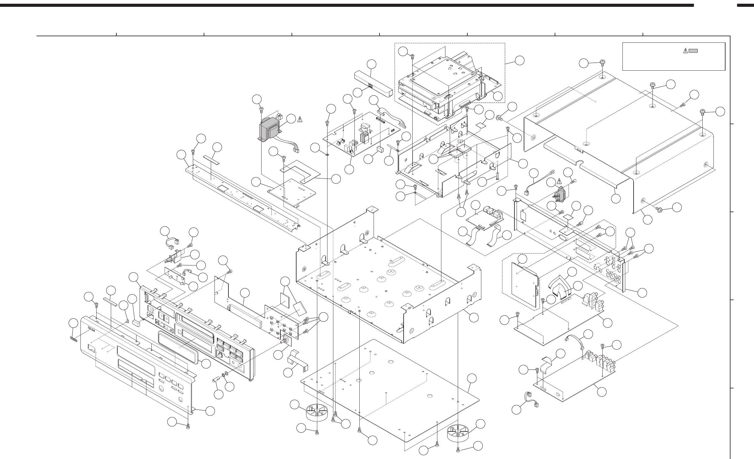
40
106
50
42
47
43
107
3-2
107
49
41
48
115
106
39
46
105
103
26
103
3-1
26
103
28
55
103
5
56
23
103
22
105
18
24
103
31
16
30
3-6
106
13
12
104
106 52 114
112
919
(for Europe, Asia &
Korea model)
25
38
103
51
107
3-5
107
44
3-3
8
103
4
2-2
35
103
2-1
103
29
27
103
112
112
6
113
113
53
11
33
32
54
113
106
113
103 17
113
103
1
10
103
103
10
103 103
103
3-4
45
(Europe model only)
EXPLODED VIEW
8
76
5
4
3
2
1
A
B
C
D
E
DVD-3800
77
Parts marked with this symbol have critical
characteristics.
Use ONLY replacement parts recommended by the
manufacturer.
WARNING:
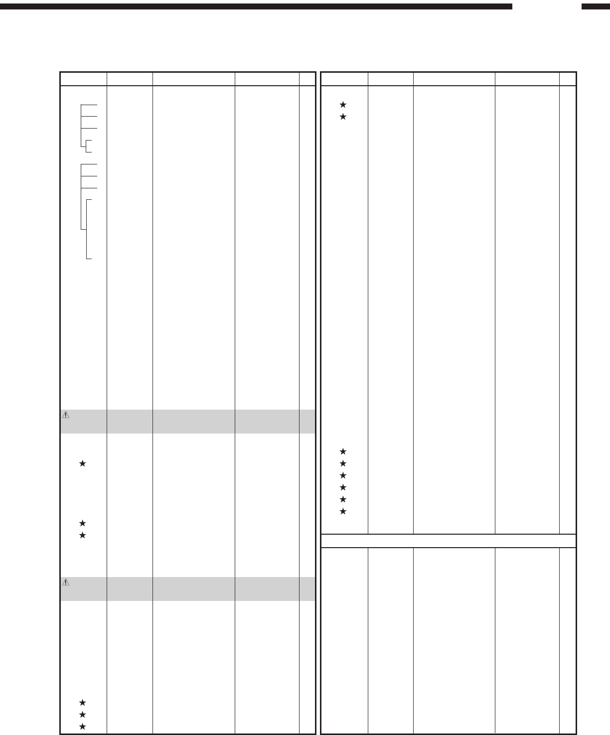
78
DVD-3800
PARTS LIST OF EXPLODED VIEW
Ref. No. Part No. Part Name Remarks
Q'ty
Ref. No. Part No. Part Name Remarks
Q'ty
1 GU- 3389 A Main P.W.B. unit 1
2 GU- 3438
Audio/Video P.W.B. unit Ass’y
for E3 1
2 GU- 3438 D
Audio/Video P.W.B. unit Ass’y
for E2 1
2 GU- 3438 E
Audio/Video P.W.B. unit Ass’y
for E1, E1K 1
2-1
Audio P.W.B. unit
2-2
Video P.W.B. unit
3 GU- 3439
Power/Display P.W.B. unit Ass’y
for E3 1
3 GU- 3439 D
Power/Display P.W.B. unit Ass’y
for E2 1
3 GU- 3439 E
Power/Display P.W.B. unit Ass’y
for E1, E1K 1
3-1
Digital power P.W.B. unit
3-2
Display P.W.B. unit
3-3
LED P.W.B. unit
3-4
Select P.W.B. unit
3-5
Power switch P.W.B. unit
3-6
I/F P.W.B. unit
4 GU- 3442 SCART P.W.B. unit for E2 1
5 GEN 5903
FG-180 DVD mecha. sub Ass’y
1
6 411 1961 102 Chassis 1
7 513 3363 004 Caution label for E3 1
8 105 1402 009 Bottom cover 1
9 441 1963 004 Trans. bracket 1
10 104 0313 015 Foot 4
11 105 1401 000 Rear panel for E3 1
11 105 1401 026 Rear panel for E2 1
11 105 1401 039 Rear panel for E1 1
11 105 1401 042 Rear panel for E1K 1
12 203 3994 000 AC inlet for E3 1
203 3995 009 AC inlet for E2, E1, E1K 1
13 203 5293 013 3P VH connector cord CW024 1
14 342 0032 011 Ferrite clamp (RFC-9) 1
15 445 0033 005 Wire clamp band 1
16 417 0634 001 Heat sink 2
17 417 0636 009 Heat sheet 2
18 412 4927 201 Mech. fix bracket 1
19 461 1137 009 Spacer for E2,E1, E1K 1
20 513 3827 016 Fuse label for E2,E1, E1K 2
21 513 3827 003 Fuse label for E2,E1, E1K 1
22 461 1136 013 Spacer 2
23 461 1125 121 FL spacer 1
24 412 2197 046 Card stand (H=18) 2
25 233 6404 006 Power trans. for E3 1
233 6406 004 Power trans. for E2,E1, E1K 1
26 445 0048 016 Cord holder (L50) 5
27 203 5295 008 3P VH-VH connector cord CW032 1
28 204 6741 004 14P PH-PH connector cord CW141 1
29 009 0235 047 30P FFC (1.0) CW301 1
30 009 0235 021 21P FFC (1.0) CW211 1
31 009 0235 034 21P FFC (1.0) CW212 1
32 009 0235 005 27P FFC (1.0) CW272 1
33 009 0235 018 13P FFC (1.0) CW131 1
34 513 3406 107 Label (A) for E3 1
34 513 3463 001 Label (Laser) for E2,E1, E1K 1
34 513 2065 002 E2 laser caution for E2 1
Note : The symbols in the column “Remarks” indicate the following destinations.
E3 : U.S.A. & Canada model E2 : Europe model
E1 : Asia model E1K : Korea model
35 203 5296 010 3P PH-PH connector cord CW036 1
36 203 8532 001 5P PH-PH connector cord CW052 for E2 1
37 204 2942 001 10P PH-PH connector cord CW102 for E2 1
38 412 4944 006 Front angle 1
39 144 2750 263 Front panel for Black model 1
39 144 2750 276 Front panel for Gold model 1
40 131 9004 013 DENON mark for Black model 1
40 131 9004 068 DENON mark for Gold model 1
41 143 1145 009 Window 1
42 143 1110 005 Lens 3
43 146 2225 309 Inner panel for Black model 1
43 146 2225 312 Inner panel for Gold model 1
44 203 5296 007 3P PH-PH connector cord CW035 1
45 009 0234 006 17P FFC (1.0) CW171 1
46 203 5294 009 3P VH-VH connector cord CW025 1
47 113 1886 008 Power switch knob for Black model 1
47 113 1886 011 Power switch knob for Gold model 1
48 112 0855 024 Volume knob (B) for Black model 1
48 112 0855 037 Volume knob (B) for Gold model 1
49 461 1109 011 PWB rubber 2
50 129 0253 048 Rubber sheet 2
51 461 1131 005 Rubber foam 2
52 461 1131 018 Rubber foam 1
53 102 0644 005 Top cover for Black model 1
53 102 0644 018 Top cover for Gold model 1
54 105 1403 008 Top cover damper 1
55 146 2282 009 Loader panel for Black model 1
55 146 2282 012 Loader panel for Gold model 1
56 135 0067 006 DVD-A plate for Black model 1
56 135 0067 019 DVD-A plate for Gold model 1
57 513 3747 002 Rating sheet for E3 1
57 513 3798 006 Rating sheet for E2 1
57 513 3842 004 Rating sheet for E1 1
57 513 3886 003 Rating sheet for E1K 1
58 513 3437 008 Label C for E1 1
59 513 1381 004 Manufac. date label for E3 1
SCREWS
103 473 7002 018 Screw 3x8 CBTS(S)-Z 52
104 473 7003 017 Screw 3x8 CFTS (S)-B 2
105 473 7007 000 Screw 4x8 CBTS(S)-B 4
106 473 7015 005 Screw 3x6 CBTS (S)-B 15
107 473 7500 044 Screw 3x8 CBTS(P)-B 14
112 477 0064 123 Fixing screw for E3, E1, E1K 8
112 477 0064 123 Fixing screw for E2 12
113 477 0263 005 3P. swelling screw for Black model 10
113 477 0263 018 3P. swelling screw for Gold model 10
114
Special screw Attachment for 9P 2
S SUB connector
115
9 SP nut
Attachment for Rotary switch
1
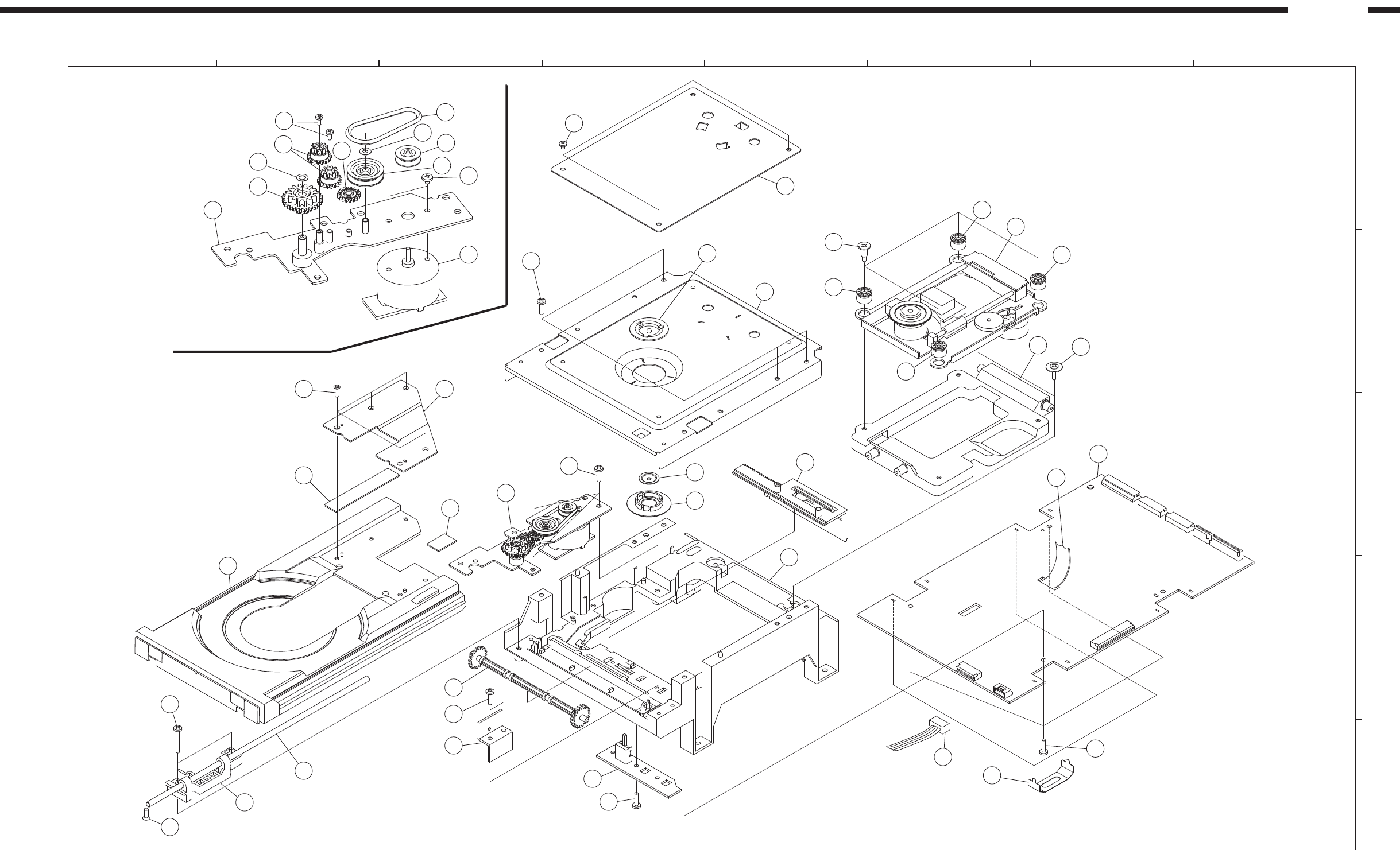
80
DVD-3800
PARTS LIST OF DVD MECHANISM
Ref. No. Part No. Part Name Remarks
Q'ty
1 411 1988 101 Mecha chassis 1
2 431 0426 503 Plate gear 1
3 9KA 2A40 3D Gear base sub ass'y 1
4 441 1952 109 Gear base ass'y 1
5 9KM 01T1 32 LD Motor 1
6-1 9KA 85P0 05 Detector SW P.W.B. 1
6-2 9KA 85G0 27 2P Connector wire 1
6-3 9KA 82G3 08 2P Connector 1
6-4 9KS 01W1 48 Detector SW 1
7 421 0772 108 Motor pully 1
8 424 0269 209 Gear C 1
9 424 0268 200 Gear B 2
10 424 0267 201 Gear A 1
11 424 0270 104 Pulley gear 1
12 423 0077 100 Belt 1
13 446 0063 007 Mecha frame 1
14 9KC 2A07 4A TRAV. Mecha 1
15 9KC 2G08 3A Damper-IDLE 4
16 424 0246 109 Loader gear 1
17 431 0427 405 Loader 1
18 461 1131 005 Rubber form 1
19 461 1131 018 Rubber form 1
20 412 4817 104 Loader bracket 1
21 431 0384 001 Slide shaft 1
22 431 0428 006 Holder 1
23 412 4818 006 Bearing plate Ass'y 1
24 GU- 3389 Main P.W.B. unit 1
25 009 0186 015 24P FFC cable (0.5) 1
26 203 8517 068 5P PH-PH Connector cord 1
27 414 0963 003 Earth plate 4
28 412 4820 201 Clamp base 1
29 9KA 7G20 3B Clamper L 1
30 9KA 7P08 5A Clamper T 1
31 9KA 7G20 2D Clamper H 1
32 403 0061 002 Clamp base damper 1
34 513 3436 009 ROM seal 1
SCREWS
50 471 9057 007 Special screw M1.7 2
51 9KM 01T1 32 Screw 2.6x2.5CBS-NI 2
52 471 3813 001 Screw 2.6x4 CBS-B 4
53 9KH 26P0 08 Screw 2.6x8CFTS(P) 5
54 473 7511 004 Screw 3x10 CFTS (P)-Z 1
55 473 7508 017 Screw 3x10 CBTS (P)-B 16
56 473 7508 046 Screw 3x16 CBTS (P)-B 2
57 477 0262 006 Special screw 2
58 9KC 1H01 1A SCW-Damper 4
59 9KP 36C6 25 Slit washer 1
60 9KP 26C6 25 Slit washer 1
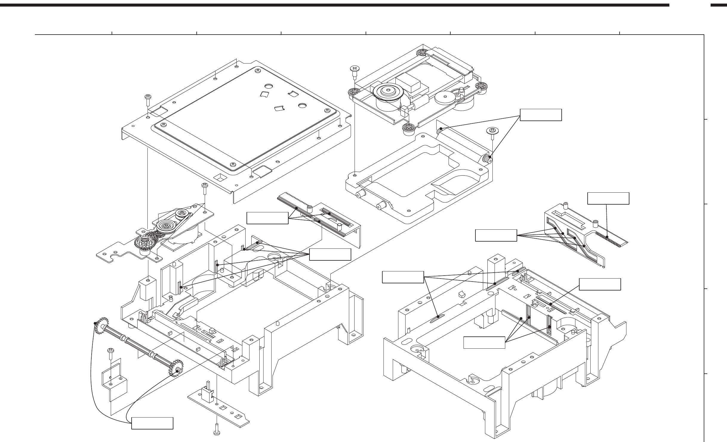
MOLYKOTE EM-30L
0.1mg x 4 points
MOLYKOTE EM-30L
0.1mg x 3 points
MOLYKOTE EM-30L
0.1mg x 4 points
MOLYKOTE EM-30L
0.1mg x 4 points
MOLYKOTE EM-30L
0.1mg
MOLYKOTE EM-30L
0.1mg
MOLYKOTE EM-30L
0.1mg x 3 points
MOLYKOTE EM-30L
0.1mg x 3 points
MOLYKOTE EM-30L
0.1mg x 4 points
POINTS OF GREASING (1/2)
8
76
5
4
3
2
1
A
B
C
D
E
DVD-3800
81
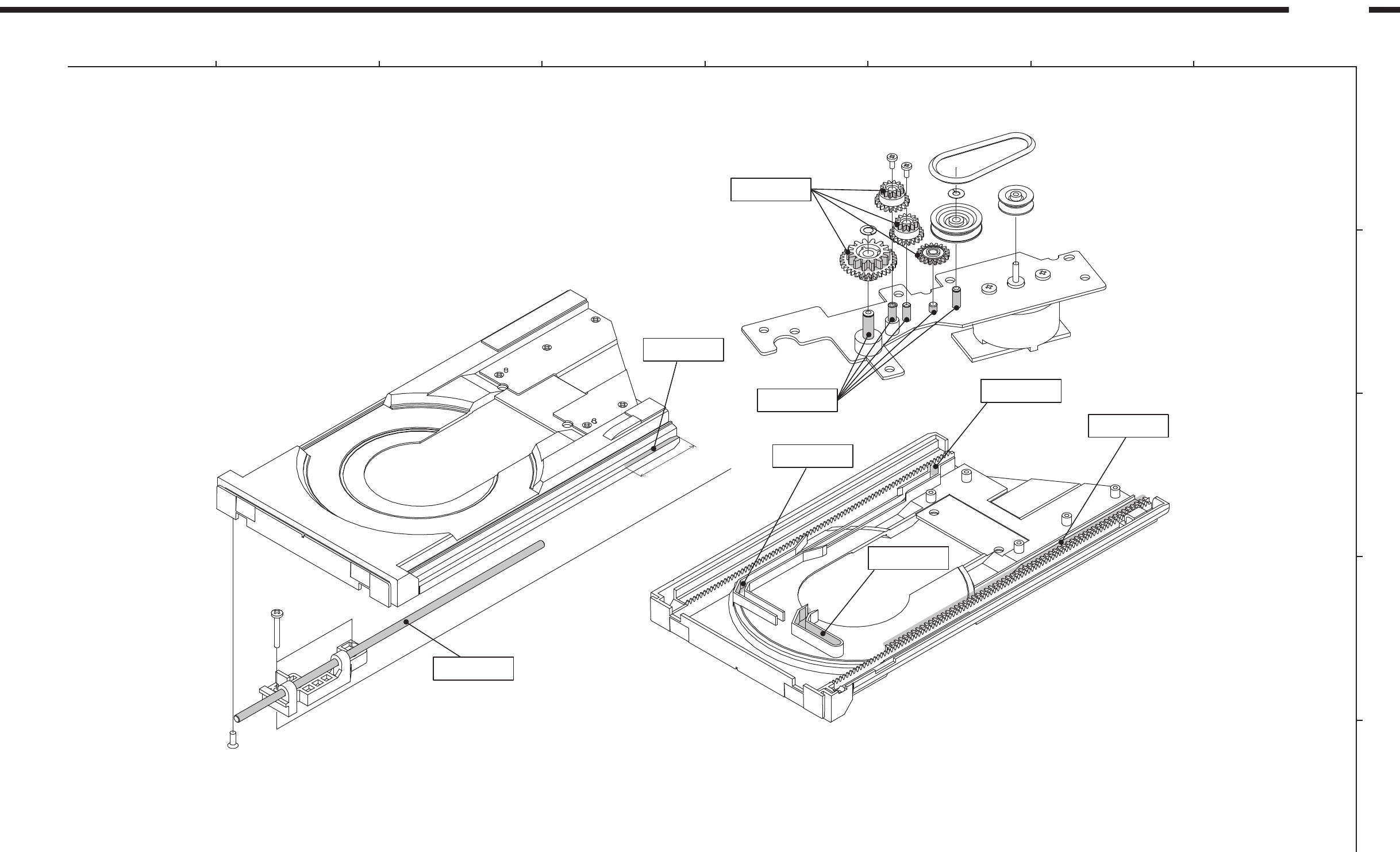
MOLYKOTE EM-30L
0.3mg
MOLYKOTE EM-30L
0.1mg
HANARL UD777
0.1mg
MOLYKOTE EM-30L
0.1mg
HANARL FL777
0.1mg
MOLYKOTE EM-30L
0.1mg
MOLYKOTE EM-30L
0.1mg x 5 points
MOLYKOTE EM-30L
0.1mg x 4 points
40~50mm
POINTS OF GREASING (2/2)
8
76
5
4
3
2
1
A
B
C
D
E
DVD-3800
82
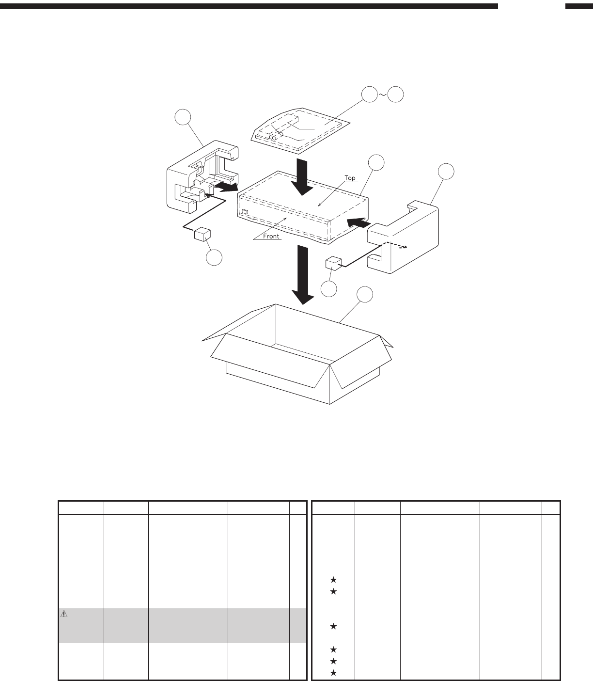
83
DVD-3800
PACKING VIEW
PARTS LIST OF PACKING & ACCESSORIES
Ref. No. Part No. Part Name Remarks Q'tyRef. No. Part No. Part Name Remarks Q'ty
201 505 0038 043 Poly. cover 1
202 511 3877 002 Instruction manual for E3 1
511 3897 008 Instruction manual for E2 1
511 3898 007 Instruction manual for E1 1
511 3957 003 Instruction manual for E1K 1
203 511 3928 100 Correction sheet for E3 1
511 3934 000 Correction sheet for E2 1
204 515 0921 005 Service station list (EX) 1
205 206 2202 006 AC cord set for E3 1
206 2203 005 AC cord set for E2,E1 1
206 2210 001 AC cord for E1K 1
206 203 5224 008 3P pin cord 1
207 399 0795 008 Remote controller RC-553 1
208
Battery (AA/R6P)
209 505 0312 028 Cabinet cover 1
210 503 1374 001 Cushion 2
211 503 1440 003 Bottom cushion 2
212 501 2172 002 Carton case for E3, E2 1
501 2172 028 Carton case for E1, E1K 1
213
Control card
214
UPC label for E3
POS label for E2 Black model
POS label for E2 Gold model
215 513 3579 005 Region label for E3 2
513 3579 018 Region label for E2 2
217 513 9111 001 Color label (gold) for Gold model 2
218 513 3580 007 Carton label (CHINA) for E1, E1K 1
219 515 0690 404 DEL warranty home for E3 1
Note : The symbols in the column “Remarks” indicate the following destinations.
E3 : U.S.A. & Canada model E2 : Europe model
E1 : Asia model E1K: Korea model
210
211
211
210
201
209
208
212
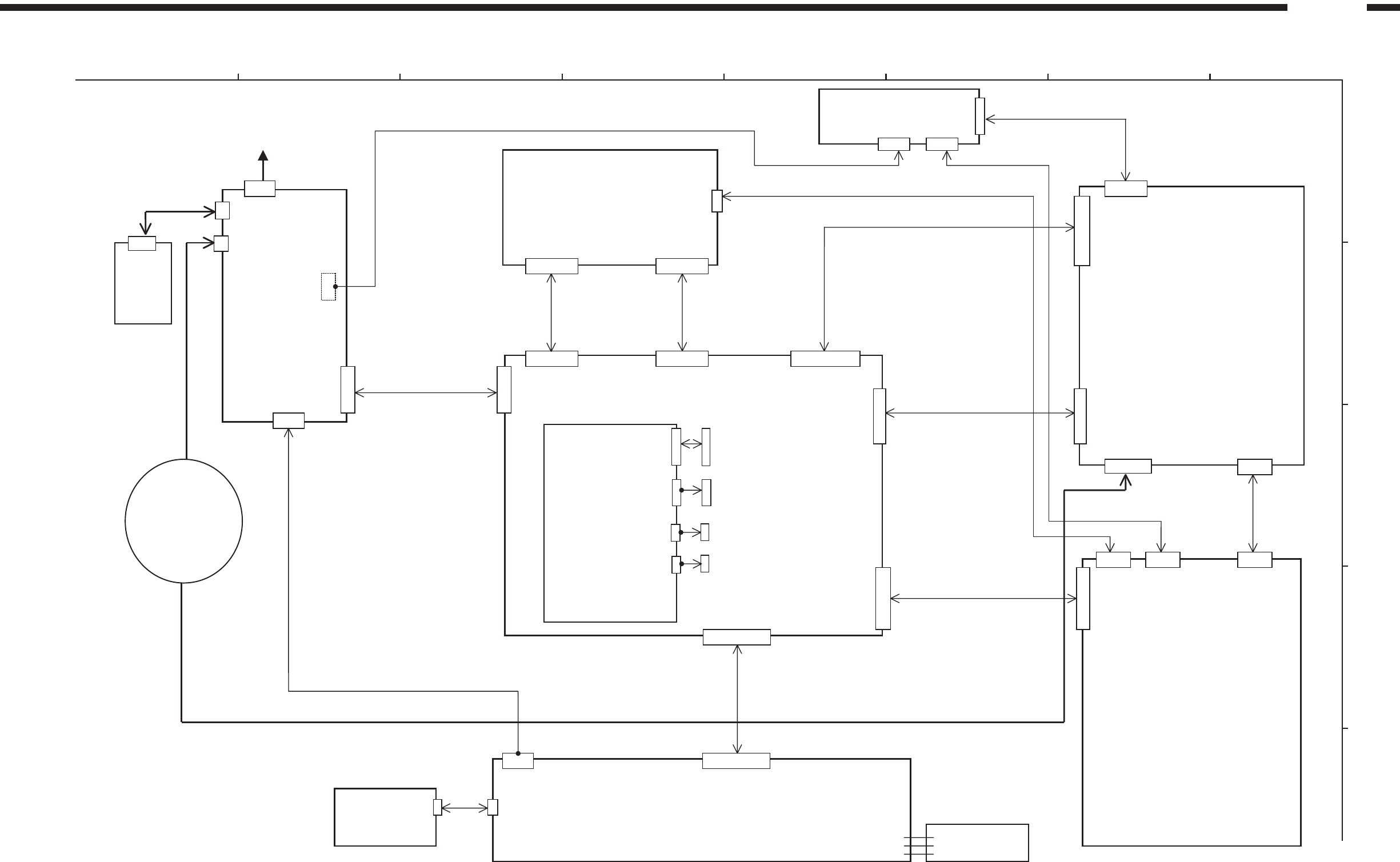
84
DVD-3800
4
32
15678
D
C
B
A
E
WIRING DIAGRAM
2P VH
2P VH
AC IN
GU-3439-4
SELECT UNIT
30P FFC
3P PH
17P FFC
13P FFC
CX212
CX141
CX211 CX272
CX131
CY301
CX171
CX035
CY035
CW041 CY171
DVD DRIVE MECHA
UNIT [FG-180]
GU-3389-1
MAIN UNIT
CX241
24P FFC
CX151
15P FFC
CX051
5 P PH
CX031
3P PH
GU-3439-2 DISPLAY UNIT
GU-3439-3
LED UNIT
GU-3442-1
SCART UNIT
(E2 MODEL ONLY)
14P PH
21P FFC
27P FFC
3P PH
21P FFC
3P PH
10P PH
CY212 CY211
CY036
CX052CX031
CX102
CY272
CY102
GU-3439-6
INTERFACE UNIT
5P PH 3P VH
CY131
CY032
CX062
CX036
CX301
CX032CY052
GU-3438-1
AUDIO UNIT
GU-3438-2
VIDEO UNIT
2P VH
6P VH
4P PH
AC IN
CX024
CX025
CY025
CX026
(CW033)
CY141
CX041
GU-3439-1
DIGI.POWER UNIT
POWER
TRANS
OUTPUT
GU-3439-5
P.SW UNIT
DVD3800_Wiring.p65 02/06/25, 9:26Page 84 Adobe PageMaker 6.5J/Win
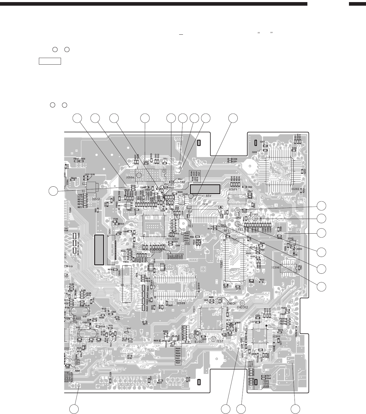
85
DVD-3800
MEASURING METHOD AND WAVEFORMS
To check the waveforms on the Servo P.W.B., the GND ( ) probe of the oscilloscope to Vref point.
(Except for Inner SW, TRVSW)
* For
&
~
, connect the GND (−) probe to "GND".
NOTES
Measuring Disc: DVD/DVDT-S01 or TDV-520A
CD/TCD-784
(It is better to use wires for extending between the probe and test points.)
When watching the HF waveform, use the extending wire as short as possible.
When HF waveform is noisy or cannot discriminate the eye-pattern, replace the Traverse Unit after measuring the Iop.
1
~
points have the certain test points shown below.
0
5
5
6
17
32
1
1
1
1
24
1
1
1
1
1
115
1
1
20 21
40
45
8
1
6
717
18
28
29 39
40
16
1732
7
814
11
12
24
25 36
37
48
25
26
50
5175
76
100
20
2140
20
21
40
41
60
61
80
14
15 28
9
8 5 4 14 15 3 127
10
13
11
6
1
16
20191817
2
Main P.W.B. Unit Foil Side
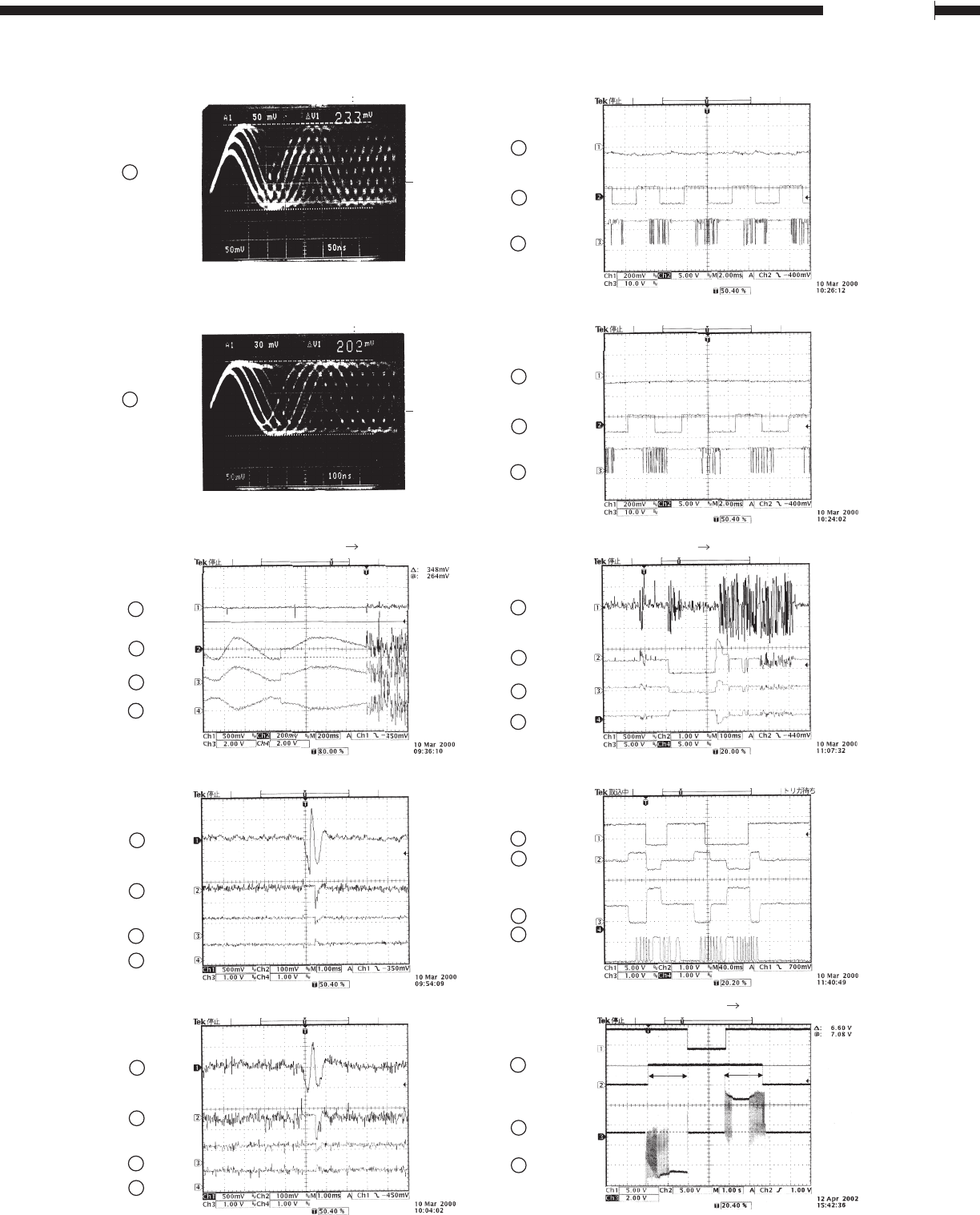
86
DVD-3800
Disc DVDT-S01
Disc TCD-784A
V = 0.5 V/div
V = 0.5 V/div
(DVD/CD) LOADING PLAY
DVD PLAY
CD PLAY
Vref
Vref
2 FEI
3 FOO
4
FO+
5
FO−
6 TEI
7
TRO
8 TR+
9
TR−
6
TEI
7 TRO
8
TR+
9
TR−
DVD PLAY (INNER)
CD PLAY (INNER)
SERCH TO OUTER CHAPTER
POWER ON (INNER SWITCH ON)
LOADER OPEN CLOSE
OPEN CLOSE
DMO
FG
A3
DMO
FG
A3
6
TEI
!
FMO
"
FM−
#
FM+
$
INSWN
!
FMO
"
FM+
%
OUT
&
OPEN
'
CLOSE
LOADING+
DVD PLAY
CD PLAY
(INNER OUTER)
WAVEFORMS
GU-3389-1 MAIN P.W.B.
1 HF (RFI)
1
HF (RFI)
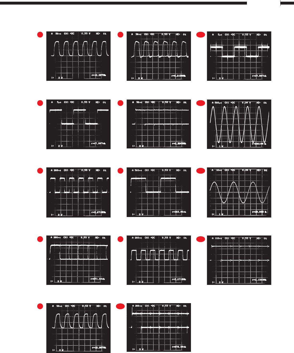
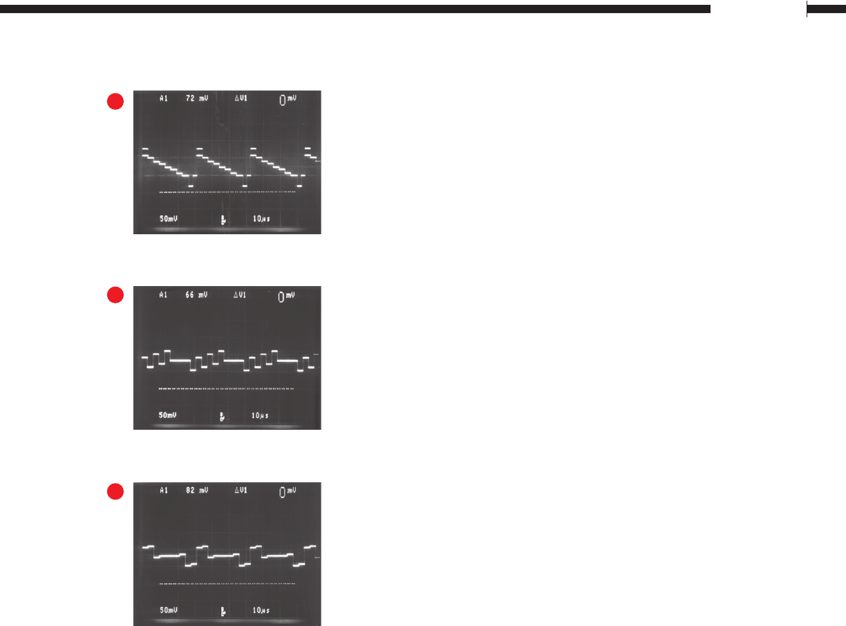
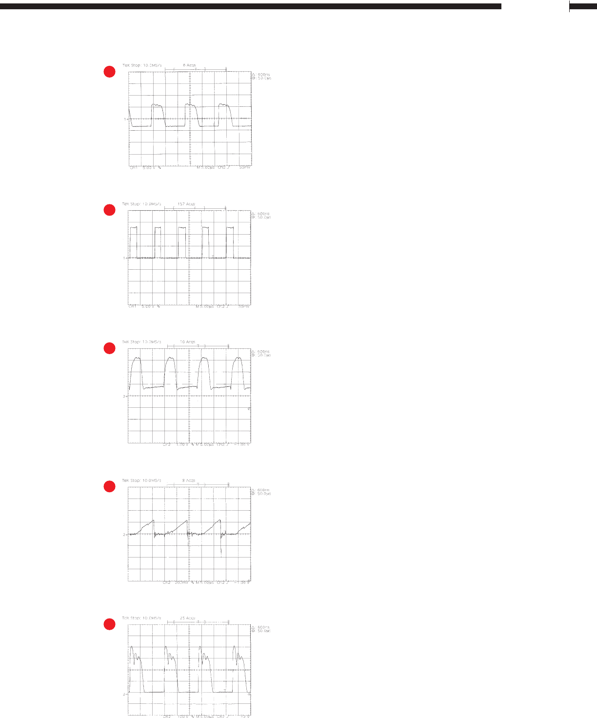
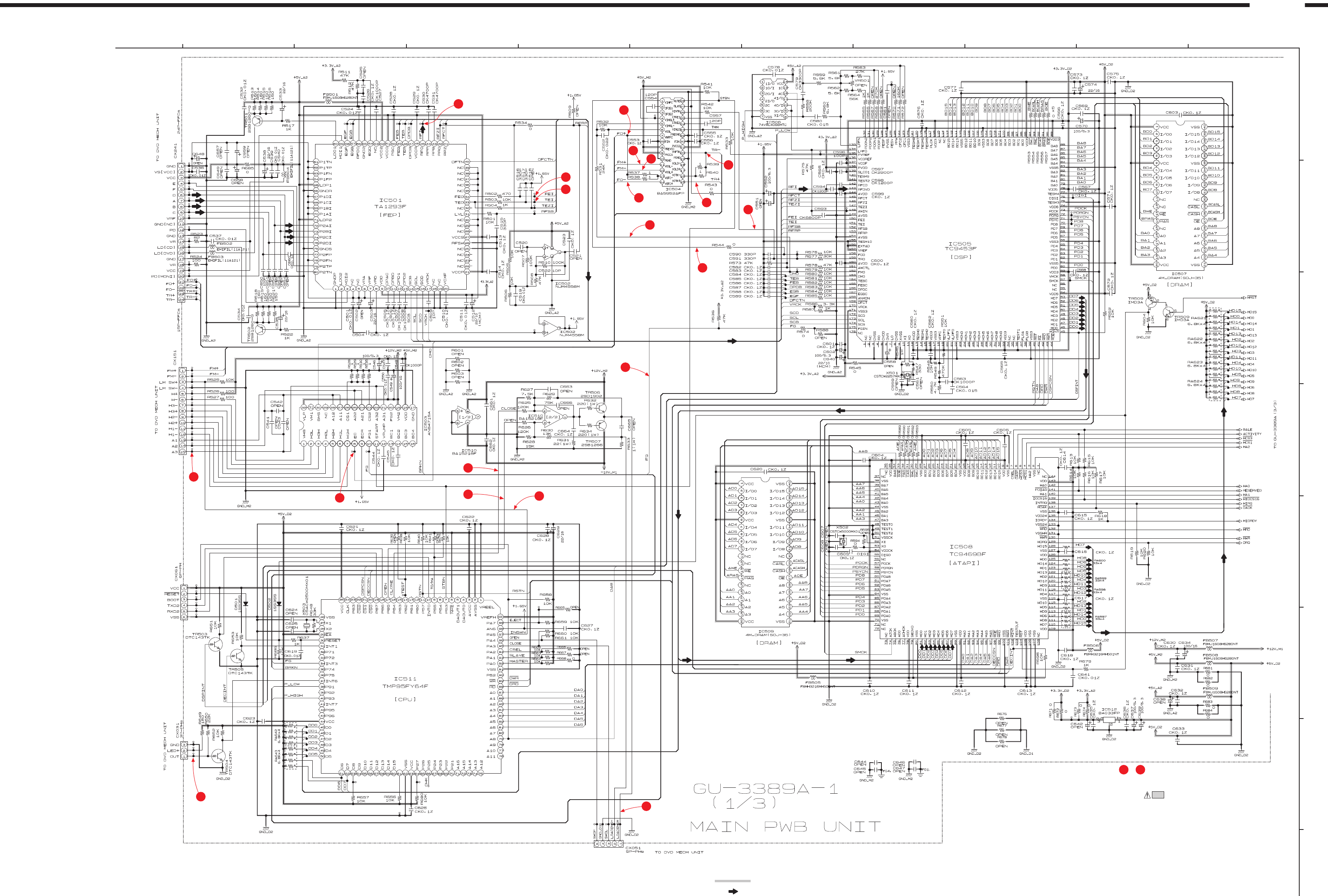
12
10
19
18 16
11
20
17
13
1
2
8
5
7
3
9
6
4
15 14
For the Waveforms marked with numbers ~ , refer to page 86 (WAVEFORMS).
20
1
91
SCHEMATIC DIAGRAMS (1/8)
GU-3389A-1 MAIN UNIT(1/3)
SCHEMATIC DIAGRAMS (1/8)
1 2 3 4 5 6 7 8 9 10 11
A
B
C
D
E
F
G
H
NOTICE
ALL RESISTANCE VALUES IN OHM. k=1,000 OHM M=1,000,000 OHM
ALL CAPACITANCE VALUES IN MICRO FARAD. P=MICRO-MICRO FARAD
EACH VOLTAGE AND CURRENT ARE MEASUERD AT MO SIGNAL INPUT
CONDITION.
CIRCUIT AND PARTS ARE SUBJECT TO CHANGE WITHOUT PRIOR
NOTICE.
WARNING:
Parts marked with this symbol have critical characteristics.
Use ONLY replacement parts recommended by the manufacture.
CAUTION:
Before returning the unit to the customer, make sure you make either (1) a
leakage current check or (2) a line to chassis resistance check. If the leakage
current exceeds 0.5 milliamps, or if the resistance from chassis to either side
of the power card is less than 460kohms, the unit is defective.
WARNING:
DO NOT return the unit to the customer until the problem is located and
corrected.
SIGNAL LINE
DVD-3800
B LINE
_
+
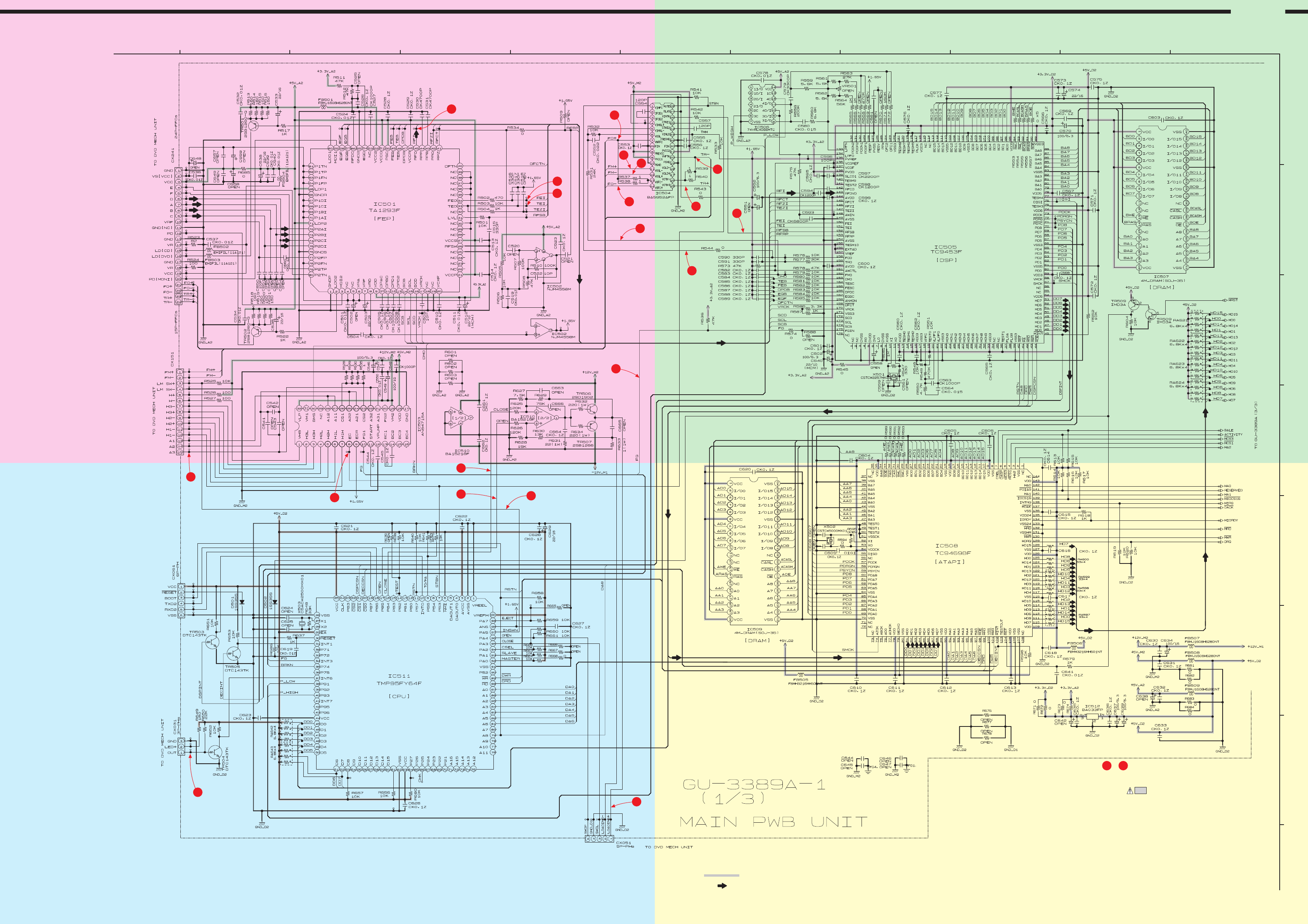
A
AB
B
C
CD
D
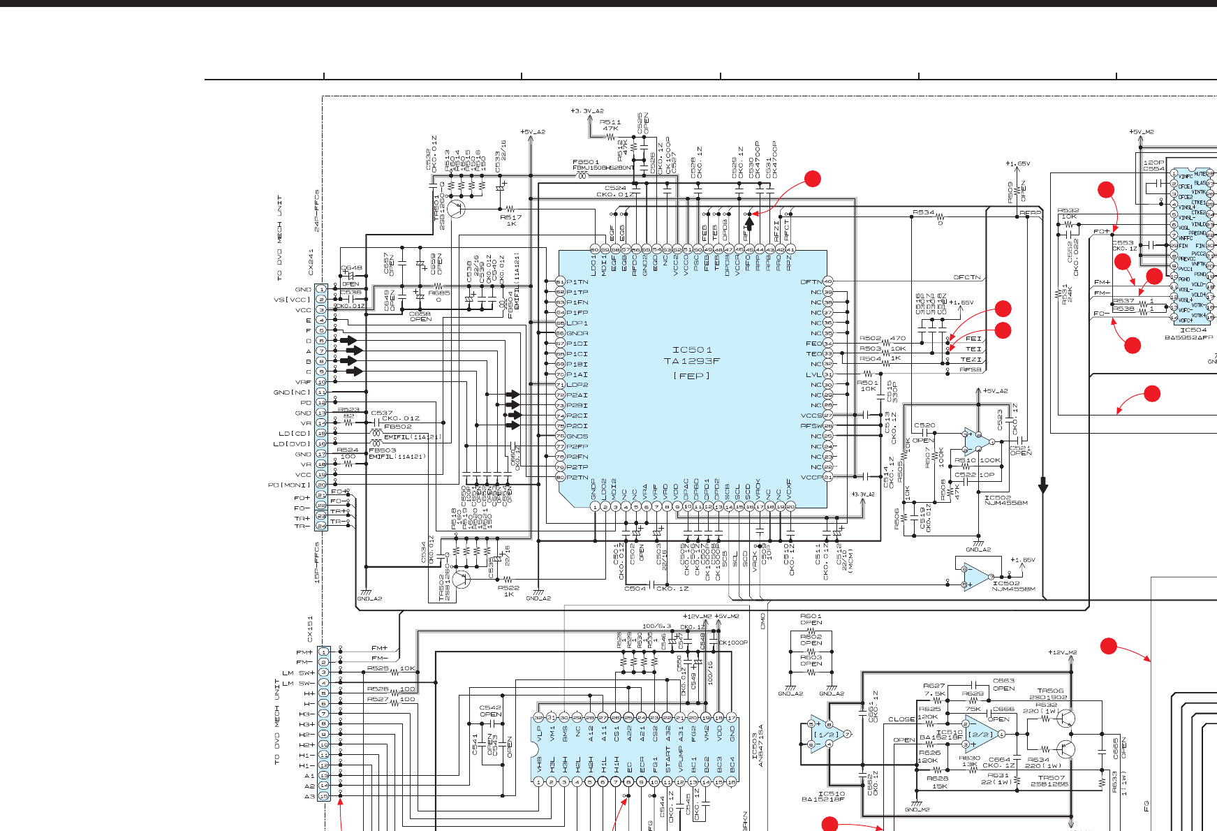
12
10
19
18 16
11
20
17
13
1
2
8
5
7
3
9
6
4
15 14
For the Waveforms marked with numbers ~ , refer to page 86 (WAVEFORMS).
20
1
91
SCHEMATIC DIAGRAMS (1/8)
GU-3389A-1 MAIN UNIT(1/3)
SCHEMATIC DIAGRAMS (1/8)
1 2 3 4 5 6 7 8 9 10 11
A
B
C
D
E
F
G
H
NOTICE
ALL RESISTANCE VALUES IN OHM. k=1,000 OHM M=1,000,000 OHM
ALL CAPACITANCE VALUES IN MICRO FARAD. P=MICRO-MICRO FARAD
EACH VOLTAGE AND CURRENT ARE MEASUERD AT MO SIGNAL INPUT
CONDITION.
CIRCUIT AND PARTS ARE SUBJECT TO CHANGE WITHOUT PRIOR
NOTICE.
WARNING:
Parts marked with this symbol have critical characteristics.
Use ONLY replacement parts recommended by the manufacture.
CAUTION:
Before returning the unit to the customer, make sure you make either (1) a
leakage current check or (2) a line to chassis resistance check. If the leakage
current exceeds 0.5 milliamps, or if the resistance from chassis to either side
of the power card is less than 460kohms, the unit is defective.
WARNING:
DO NOT return the unit to the customer until the problem is located and
corrected.
SIGNAL LINE
DVD-3800
DVD-3800
DVD-3800
DVD-3800
DVD-3800
DVD-3800
DVD-3800
DVD-3800
DVD-3800
DVD-3800
B LINE
_
+
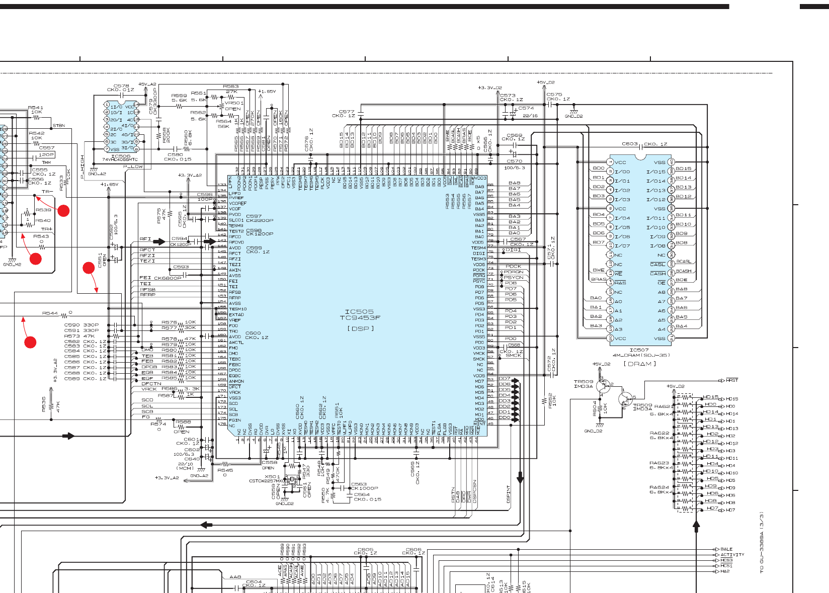
12
10
19
18 16
11
20
17
13
1
2
8
5
7
3
9
6
4
15 14
For the Waveforms marked with numbers ~ , refer to page 86 (WAVEFORMS).
20
1
91
SCHEMATIC DIAGRAMS (1/8)
GU-3389A-1 MAIN UNIT(1/3)
SCHEMATIC DIAGRAMS (1/8)
1 2 3 4 5 6 7 8 9 10 11
A
B
C
D
E
F
G
H
NOTICE
ALL RESISTANCE VALUES IN OHM. k=1,000 OHM M=1,000,000 OHM
ALL CAPACITANCE VALUES IN MICRO FARAD. P=MICRO-MICRO FARAD
EACH VOLTAGE AND CURRENT ARE MEASUERD AT MO SIGNAL INPUT
CONDITION.
CIRCUIT AND PARTS ARE SUBJECT TO CHANGE WITHOUT PRIOR
NOTICE.
WARNING:
Parts marked with this symbol have critical characteristics.
Use ONLY replacement parts recommended by the manufacture.
CAUTION:
Before returning the unit to the customer, make sure you make either (1) a
leakage current check or (2) a line to chassis resistance check. If the leakage
current exceeds 0.5 milliamps, or if the resistance from chassis to either side
of the power card is less than 460kohms, the unit is defective.
WARNING:
DO NOT return the unit to the customer until the problem is located and
corrected.
SIGNAL LINE
DVD-3800
B LINE
_
+
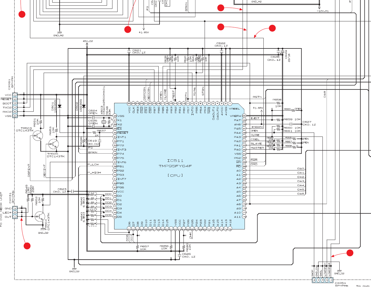
12
10
19
18 16
11
20
17
13
1
2
8
5
7
3
9
6
4
15 14
For the Waveforms marked with numbers ~ , refer to page 86 (WAVEFORMS).
20
1
91
SCHEMATIC DIAGRAMS (1/8)
GU-3389A-1 MAIN UNIT(1/3)
SCHEMATIC DIAGRAMS (1/8)
1 2 3 4 5 6 7 8 9 10 11
A
B
C
D
E
F
G
H
NOTICE
ALL RESISTANCE VALUES IN OHM. k=1,000 OHM M=1,000,000 OHM
ALL CAPACITANCE VALUES IN MICRO FARAD. P=MICRO-MICRO FARAD
EACH VOLTAGE AND CURRENT ARE MEASUERD AT MO SIGNAL INPUT
CONDITION.
CIRCUIT AND PARTS ARE SUBJECT TO CHANGE WITHOUT PRIOR
NOTICE.
WARNING:
Parts marked with this symbol have critical characteristics.
Use ONLY replacement parts recommended by the manufacture.
CAUTION:
Before returning the unit to the customer, make sure you make either (1) a
leakage current check or (2) a line to chassis resistance check. If the leakage
current exceeds 0.5 milliamps, or if the resistance from chassis to either side
of the power card is less than 460kohms, the unit is defective.
WARNING:
DO NOT return the unit to the customer until the problem is located and
corrected.
SIGNAL LINE
DVD-3800
B LINE
_
+
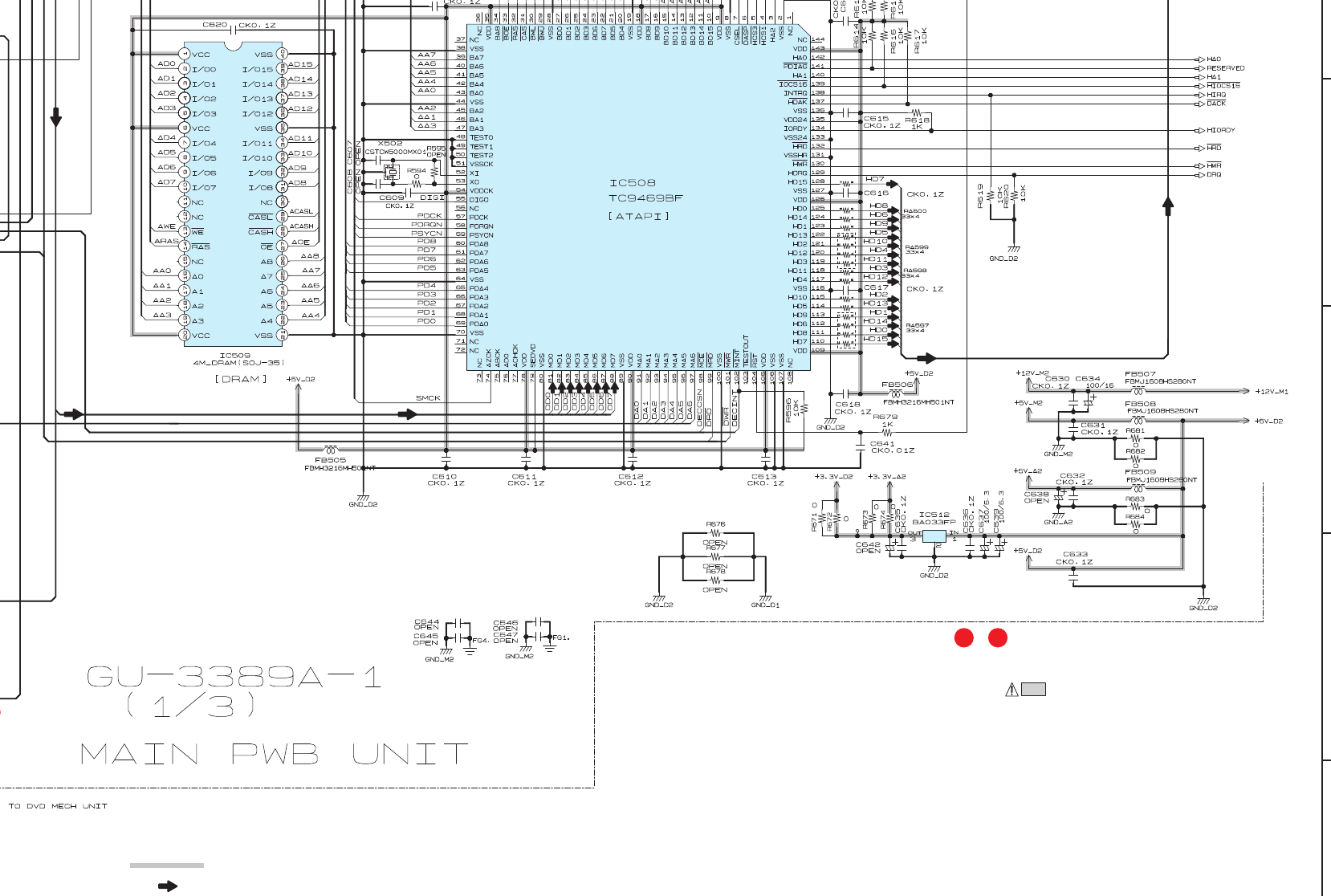
12
10
19
18 16
11
20
17
13
1
2
8
5
7
3
9
6
4
15 14
For the Waveforms marked with numbers ~ , refer to page 86 (WAVEFORMS).
20
1
91
SCHEMATIC DIAGRAMS (1/8)
GU-3389A-1 MAIN UNIT(1/3)
SCHEMATIC DIAGRAMS (1/8)
1 2 3 4 5 6 7 8 9 10 11
A
B
C
D
E
F
G
H
NOTICE
ALL RESISTANCE VALUES IN OHM. k=1,000 OHM M=1,000,000 OHM
ALL CAPACITANCE VALUES IN MICRO FARAD. P=MICRO-MICRO FARAD
EACH VOLTAGE AND CURRENT ARE MEASUERD AT MO SIGNAL INPUT
CONDITION.
CIRCUIT AND PARTS ARE SUBJECT TO CHANGE WITHOUT PRIOR
NOTICE.
WARNING:
Parts marked with this symbol have critical characteristics.
Use ONLY replacement parts recommended by the manufacture.
CAUTION:
Before returning the unit to the customer, make sure you make either (1) a
leakage current check or (2) a line to chassis resistance check. If the leakage
current exceeds 0.5 milliamps, or if the resistance from chassis to either side
of the power card is less than 460kohms, the unit is defective.
WARNING:
DO NOT return the unit to the customer until the problem is located and
corrected.
SIGNAL LINE
DVD-3800
B LINE
_
+
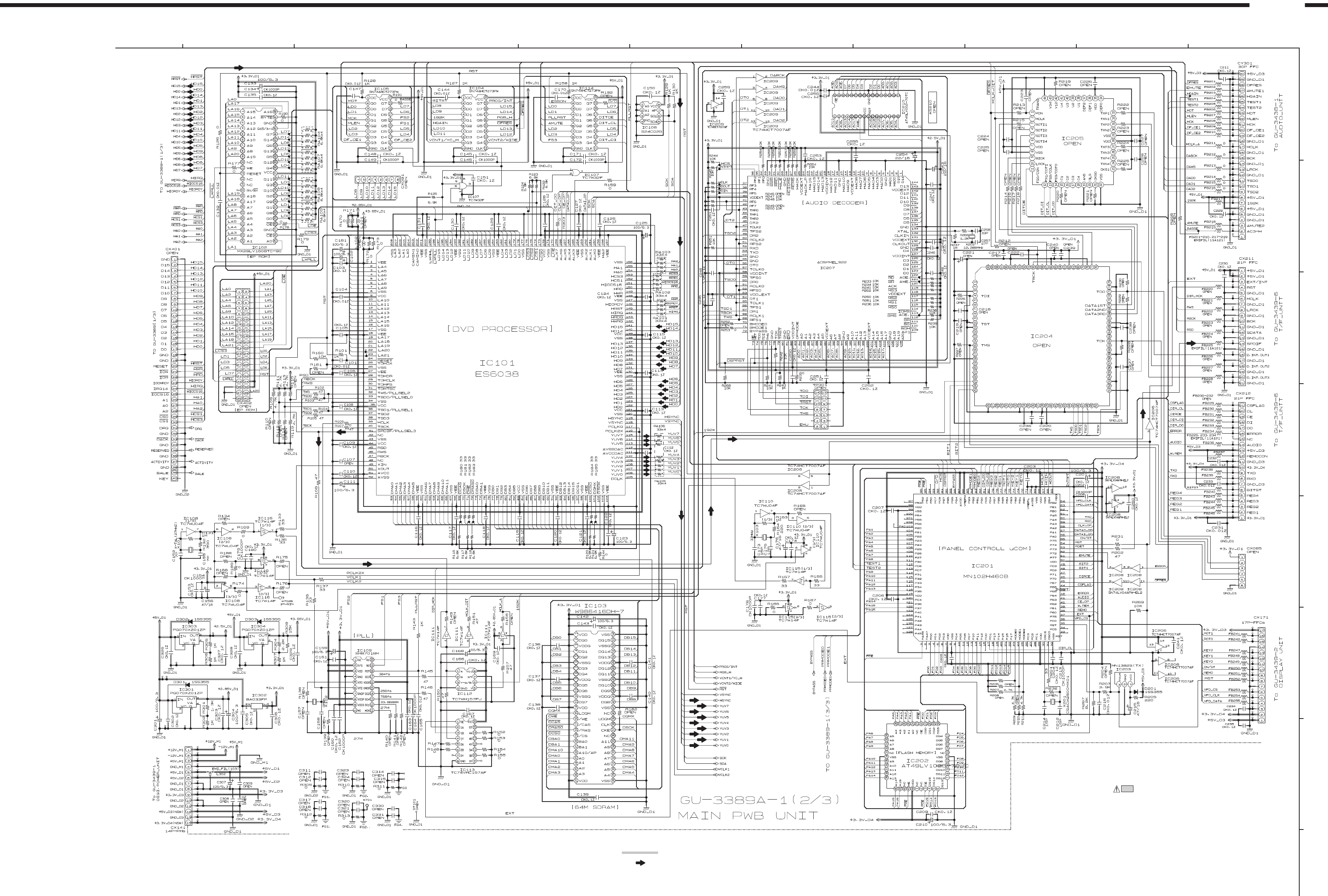
92
SCHEMATIC DIAGRAMS (2/8)
GU-3389A-1 MAIN UNIT(2/3)
SCHEMATIC DIAGRAMS (2/8)
1 2 3 4 5 6 7 8 9 10 11
A
B
C
D
E
F
G
H
NOTICE
ALL RESISTANCE VALUES IN OHM. k=1,000 OHM M=1,000,000 OHM
ALL CAPACITANCE VALUES IN MICRO FARAD. P=MICRO-MICRO FARAD
EACH VOLTAGE AND CURRENT ARE MEASUERD AT MO SIGNAL INPUT
CONDITION.
CIRCUIT AND PARTS ARE SUBJECT TO CHANGE WITHOUT PRIOR
NOTICE.
WARNING:
Parts marked with this symbol have critical characteristics.
Use ONLY replacement parts recommended by the manufacture.
CAUTION:
Before returning the unit to the customer, make sure you make either (1) a
leakage current check or (2) a line to chassis resistance check. If the leakage
current exceeds 0.5 milliamps, or if the resistance from chassis to either side
of the power card is less than 460kohms, the unit is defective.
WARNING:
DO NOT return the unit to the customer until the problem is located and
corrected.
SIGNAL LINE
DVD-3800
B LINE
_
+
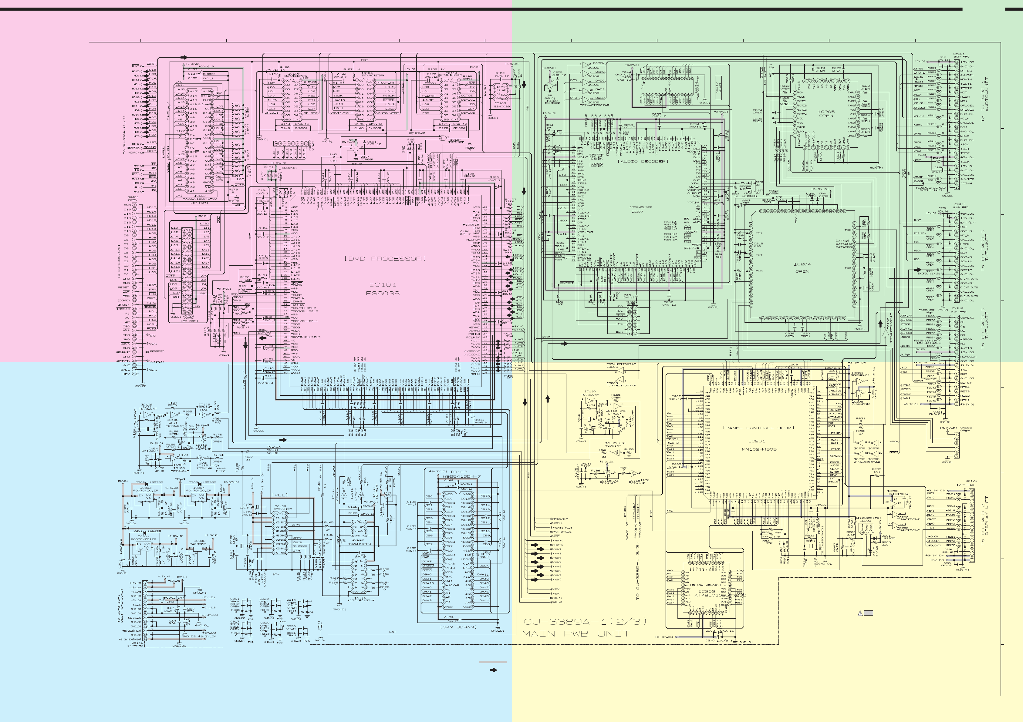
92
SCHEMATIC DIAGRAMS (2/8)
GU-3389A-1 MAIN UNIT(2/3)
SCHEMATIC DIAGRAMS (2/8)
1 2 3 4 5 6 7 8 9 10 11
A
B
C
D
E
F
G
H
NOTICE
ALL RESISTANCE VALUES IN OHM. k=1,000 OHM M=1,000,000 OHM
ALL CAPACITANCE VALUES IN MICRO FARAD. P=MICRO-MICRO FARAD
EACH VOLTAGE AND CURRENT ARE MEASUERD AT MO SIGNAL INPUT
CONDITION.
CIRCUIT AND PARTS ARE SUBJECT TO CHANGE WITHOUT PRIOR
NOTICE.
WARNING:
Parts marked with this symbol have critical characteristics.
Use ONLY replacement parts recommended by the manufacture.
CAUTION:
Before returning the unit to the customer, make sure you make either (1) a
leakage current check or (2) a line to chassis resistance check. If the leakage
current exceeds 0.5 milliamps, or if the resistance from chassis to either side
of the power card is less than 460kohms, the unit is defective.
WARNING:
DO NOT return the unit to the customer until the problem is located and
corrected.
SIGNAL LINE
DVD-3800
B LINE
_
+
A
AB
B
C
CD
D
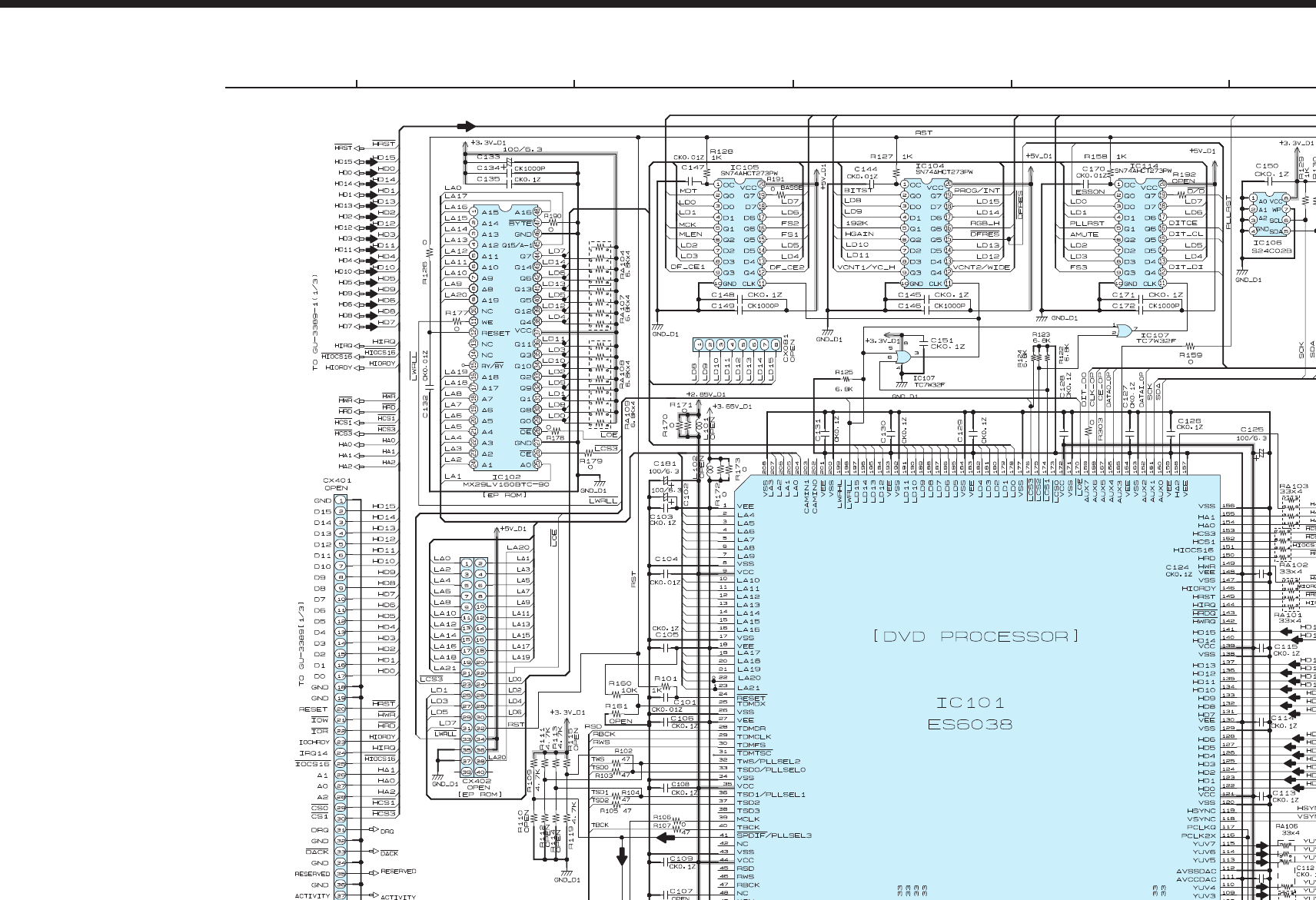
92
SCHEMATIC DIAGRAMS (2/8)
GU-3389A-1 MAIN UNIT(2/3)
SCHEMATIC DIAGRAMS (2/8)
1 2 3 4 5 6 7 8 9 10 11
A
B
C
D
E
F
G
H
NOTICE
ALL RESISTANCE VALUES IN OHM. k=1,000 OHM M=1,000,000 OHM
ALL CAPACITANCE VALUES IN MICRO FARAD. P=MICRO-MICRO FARAD
EACH VOLTAGE AND CURRENT ARE MEASUERD AT MO SIGNAL INPUT
CONDITION.
CIRCUIT AND PARTS ARE SUBJECT TO CHANGE WITHOUT PRIOR
NOTICE.
WARNING:
Parts marked with this symbol have critical characteristics.
Use ONLY replacement parts recommended by the manufacture.
CAUTION:
Before returning the unit to the customer, make sure you make either (1) a
leakage current check or (2) a line to chassis resistance check. If the leakage
current exceeds 0.5 milliamps, or if the resistance from chassis to either side
of the power card is less than 460kohms, the unit is defective.
WARNING:
DO NOT return the unit to the customer until the problem is located and
corrected.
SIGNAL LINE
DVD-3800
B LINE
_
+
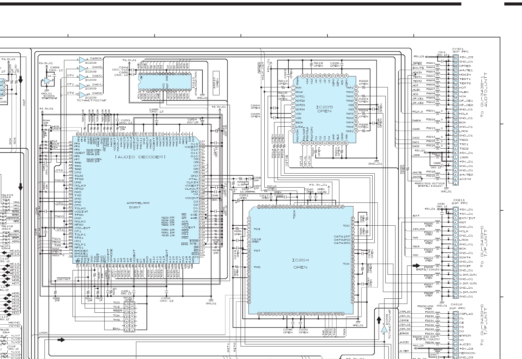
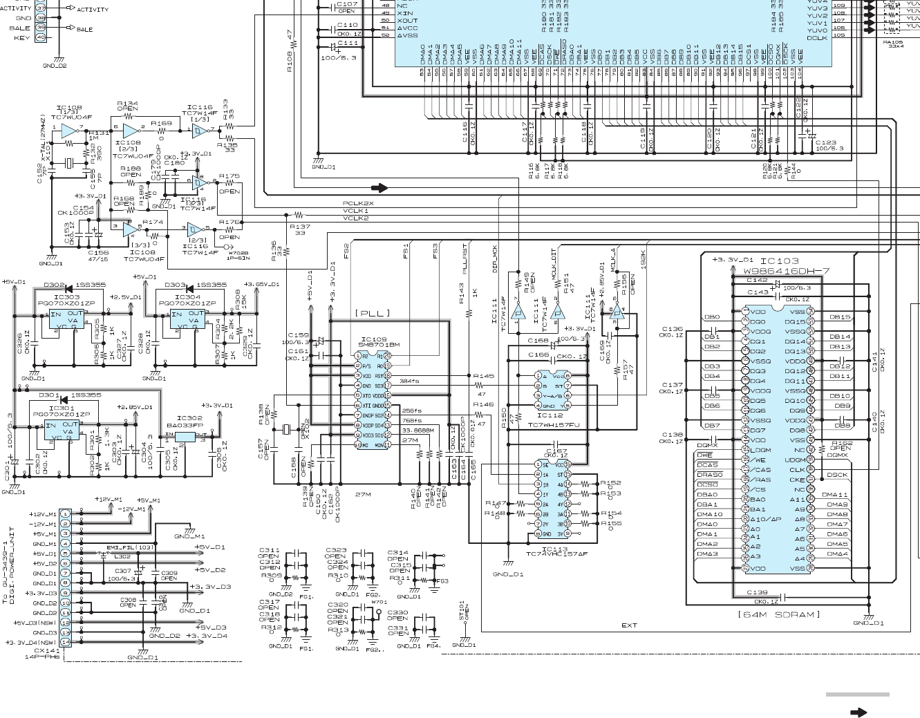
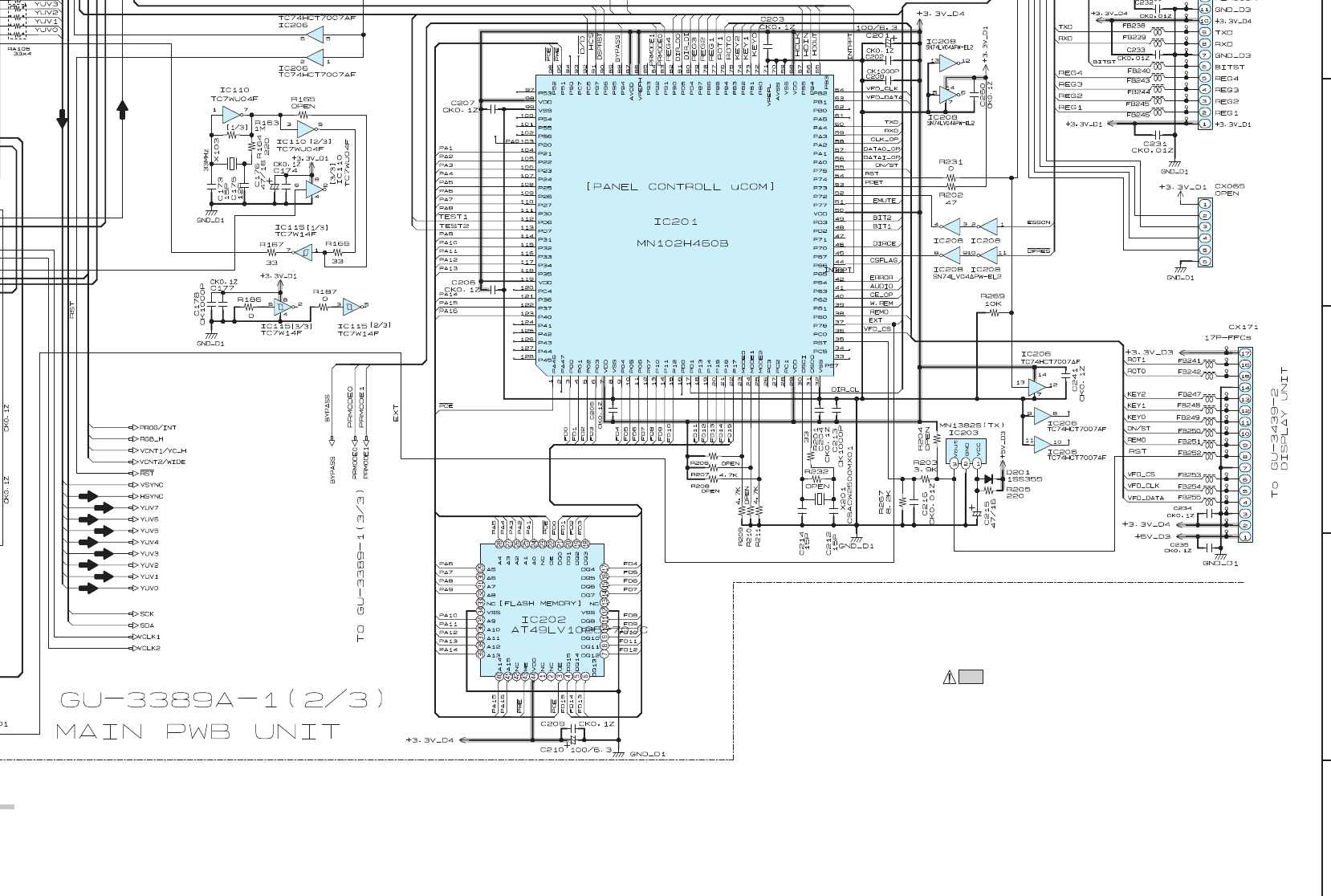
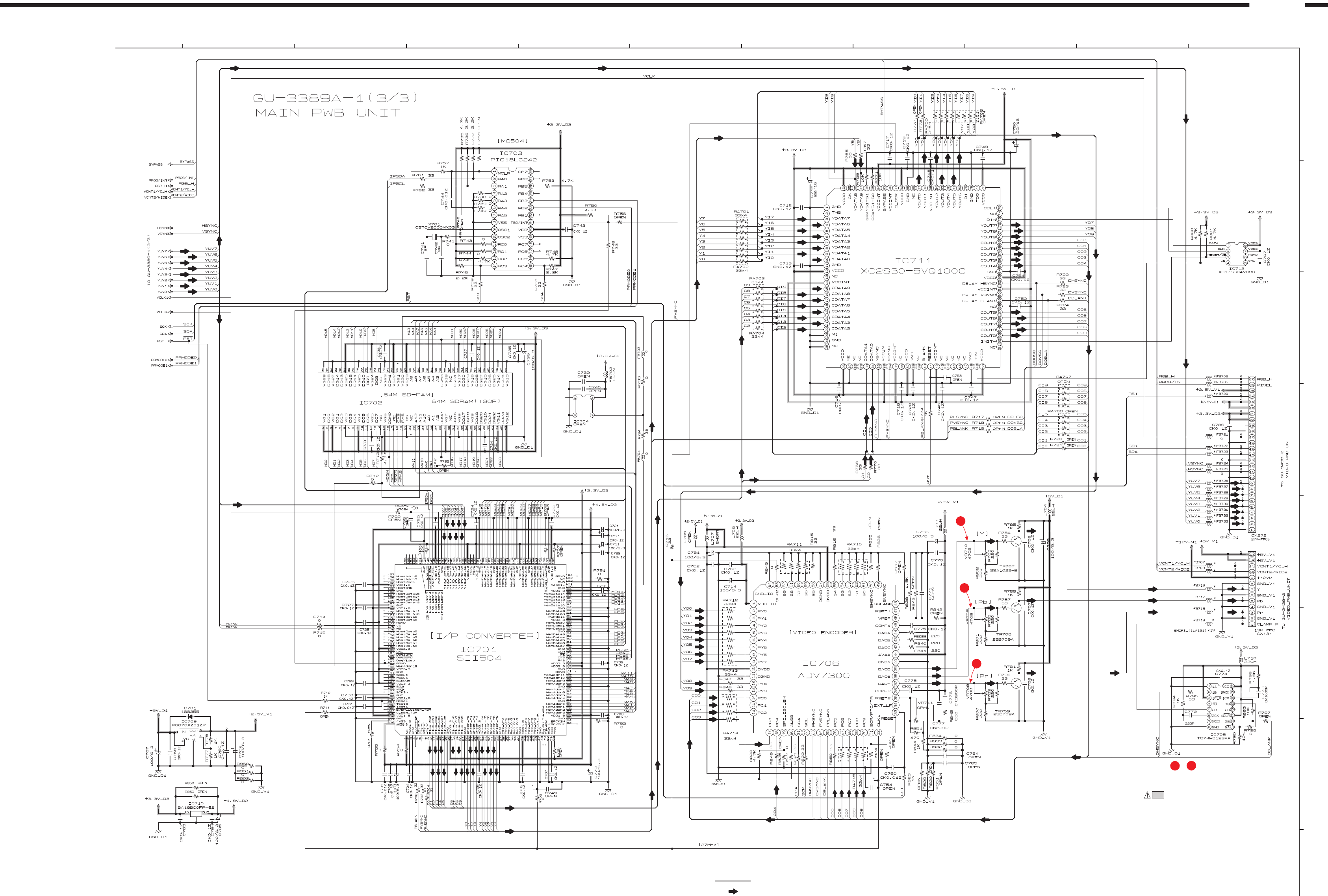
P1
P2
P3
P1 P3
For the Waveforms marked with numbers ~ ,
refer to page 88 (WAVEFORMS).
93
SCHEMATIC DIAGRAMS (3/8)
GU-3389A-1 MAIN UNIT(3/3)
SCHEMATIC DIAGRAMS (3/8)
1 2 3 4 5 6 7 8 9 10 11
A
B
C
D
E
F
G
H
NOTICE
ALL RESISTANCE VALUES IN OHM. k=1,000 OHM M=1,000,000 OHM
ALL CAPACITANCE VALUES IN MICRO FARAD. P=MICRO-MICRO FARAD
EACH VOLTAGE AND CURRENT ARE MEASUERD AT MO SIGNAL INPUT
CONDITION.
CIRCUIT AND PARTS ARE SUBJECT TO CHANGE WITHOUT PRIOR
NOTICE.
WARNING:
Parts marked with this symbol have critical characteristics.
Use ONLY replacement parts recommended by the manufacture.
CAUTION:
Before returning the unit to the customer, make sure you make either (1) a
leakage current check or (2) a line to chassis resistance check. If the leakage
current exceeds 0.5 milliamps, or if the resistance from chassis to either side
of the power card is less than 460kohms, the unit is defective.
WARNING:
DO NOT return the unit to the customer until the problem is located and
corrected.
SIGNAL LINE
DVD-3800
B LINE
_
+
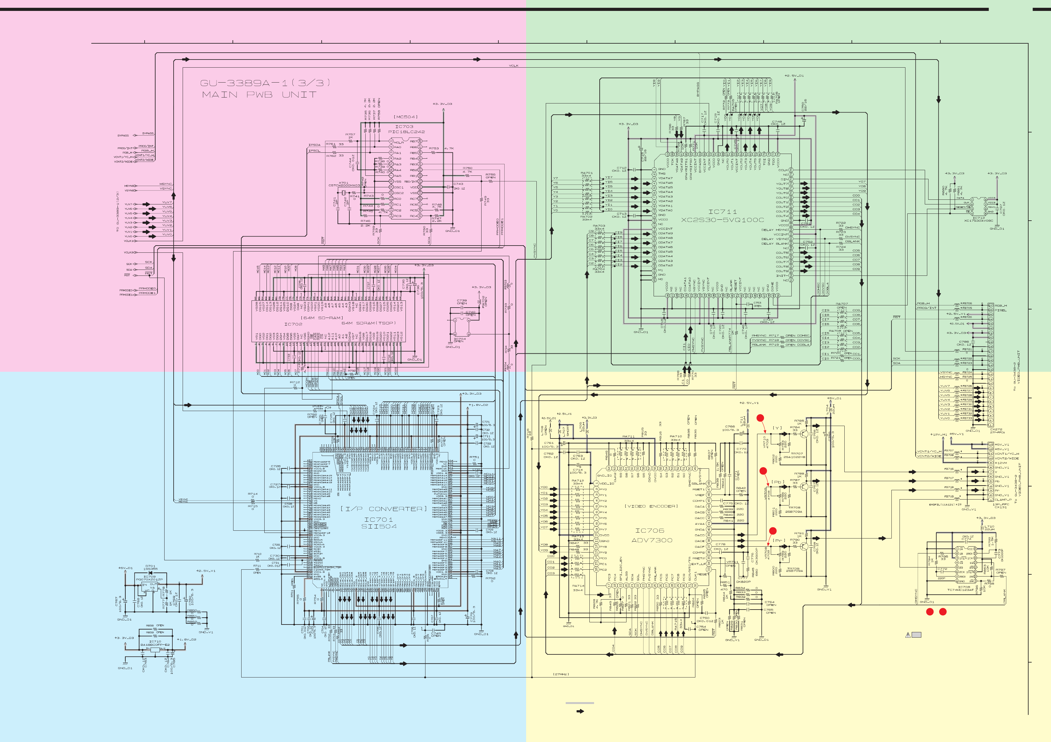
P1
P2
P3
P1 P3
For the Waveforms marked with numbers ~ ,
refer to page 88 (WAVEFORMS).
93
SCHEMATIC DIAGRAMS (3/8)
GU-3389A-1 MAIN UNIT(3/3)
SCHEMATIC DIAGRAMS (3/8)
1 2 3 4 5 6 7 8 9 10 11
A
B
C
D
E
F
G
H
NOTICE
ALL RESISTANCE VALUES IN OHM. k=1,000 OHM M=1,000,000 OHM
ALL CAPACITANCE VALUES IN MICRO FARAD. P=MICRO-MICRO FARAD
EACH VOLTAGE AND CURRENT ARE MEASUERD AT MO SIGNAL INPUT
CONDITION.
CIRCUIT AND PARTS ARE SUBJECT TO CHANGE WITHOUT PRIOR
NOTICE.
WARNING:
Parts marked with this symbol have critical characteristics.
Use ONLY replacement parts recommended by the manufacture.
CAUTION:
Before returning the unit to the customer, make sure you make either (1) a
leakage current check or (2) a line to chassis resistance check. If the leakage
current exceeds 0.5 milliamps, or if the resistance from chassis to either side
of the power card is less than 460kohms, the unit is defective.
WARNING:
DO NOT return the unit to the customer until the problem is located and
corrected.
SIGNAL LINE
DVD-3800
B LINE
_
+
A
AB
B
C
CD
D
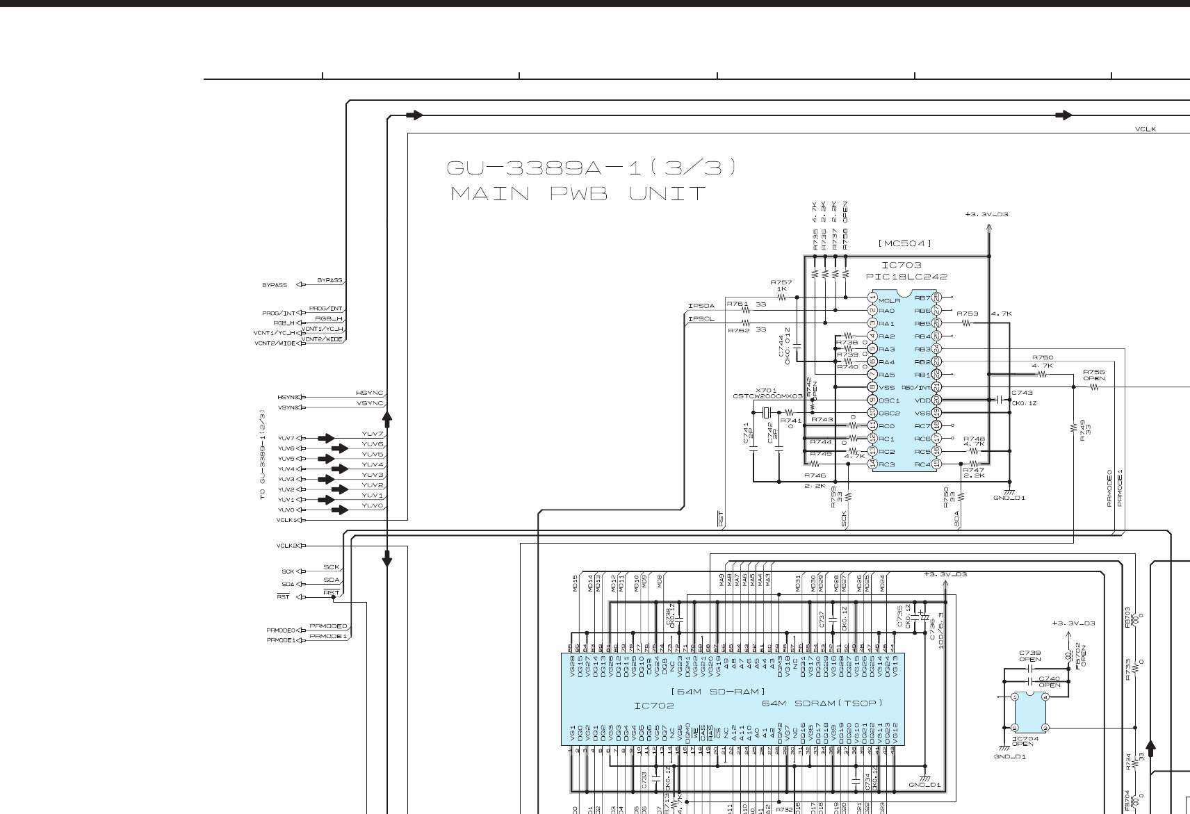
P1
P2
P3
P1 P3
For the Waveforms marked with numbers ~ ,
refer to page 88 (WAVEFORMS).
93
SCHEMATIC DIAGRAMS (3/8)
GU-3389A-1 MAIN UNIT(3/3)
SCHEMATIC DIAGRAMS (3/8)
1 2 3 4 5 6 7 8 9 10 11
A
B
C
D
E
F
G
H
NOTICE
ALL RESISTANCE VALUES IN OHM. k=1,000 OHM M=1,000,000 OHM
ALL CAPACITANCE VALUES IN MICRO FARAD. P=MICRO-MICRO FARAD
EACH VOLTAGE AND CURRENT ARE MEASUERD AT MO SIGNAL INPUT
CONDITION.
CIRCUIT AND PARTS ARE SUBJECT TO CHANGE WITHOUT PRIOR
NOTICE.
WARNING:
Parts marked with this symbol have critical characteristics.
Use ONLY replacement parts recommended by the manufacture.
CAUTION:
Before returning the unit to the customer, make sure you make either (1) a
leakage current check or (2) a line to chassis resistance check. If the leakage
current exceeds 0.5 milliamps, or if the resistance from chassis to either side
of the power card is less than 460kohms, the unit is defective.
WARNING:
DO NOT return the unit to the customer until the problem is located and
corrected.
SIGNAL LINE
DVD-3800
B LINE
_
+
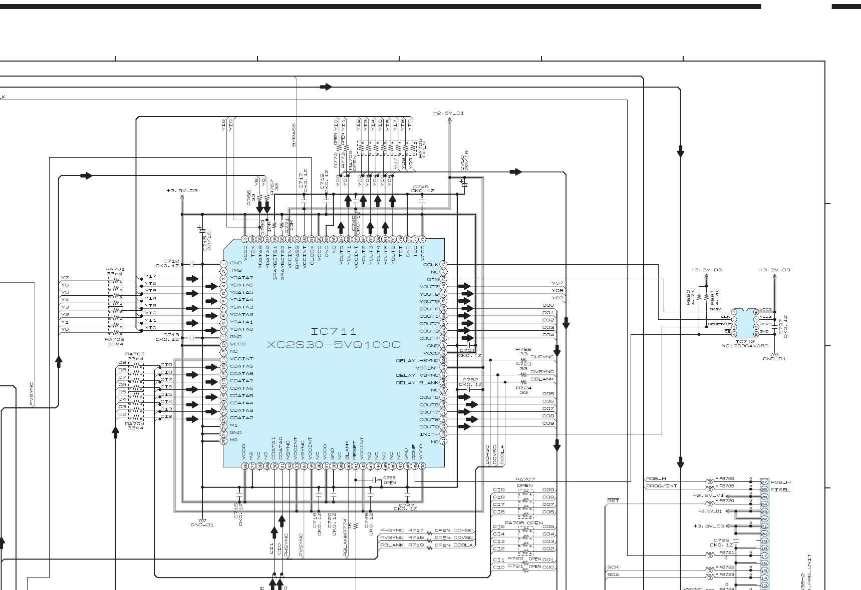
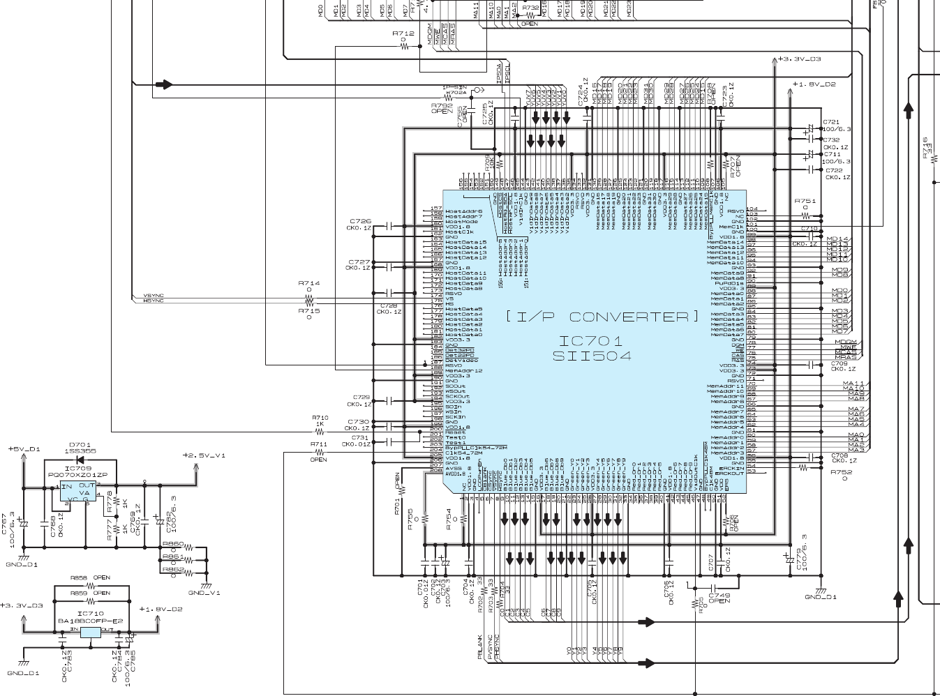
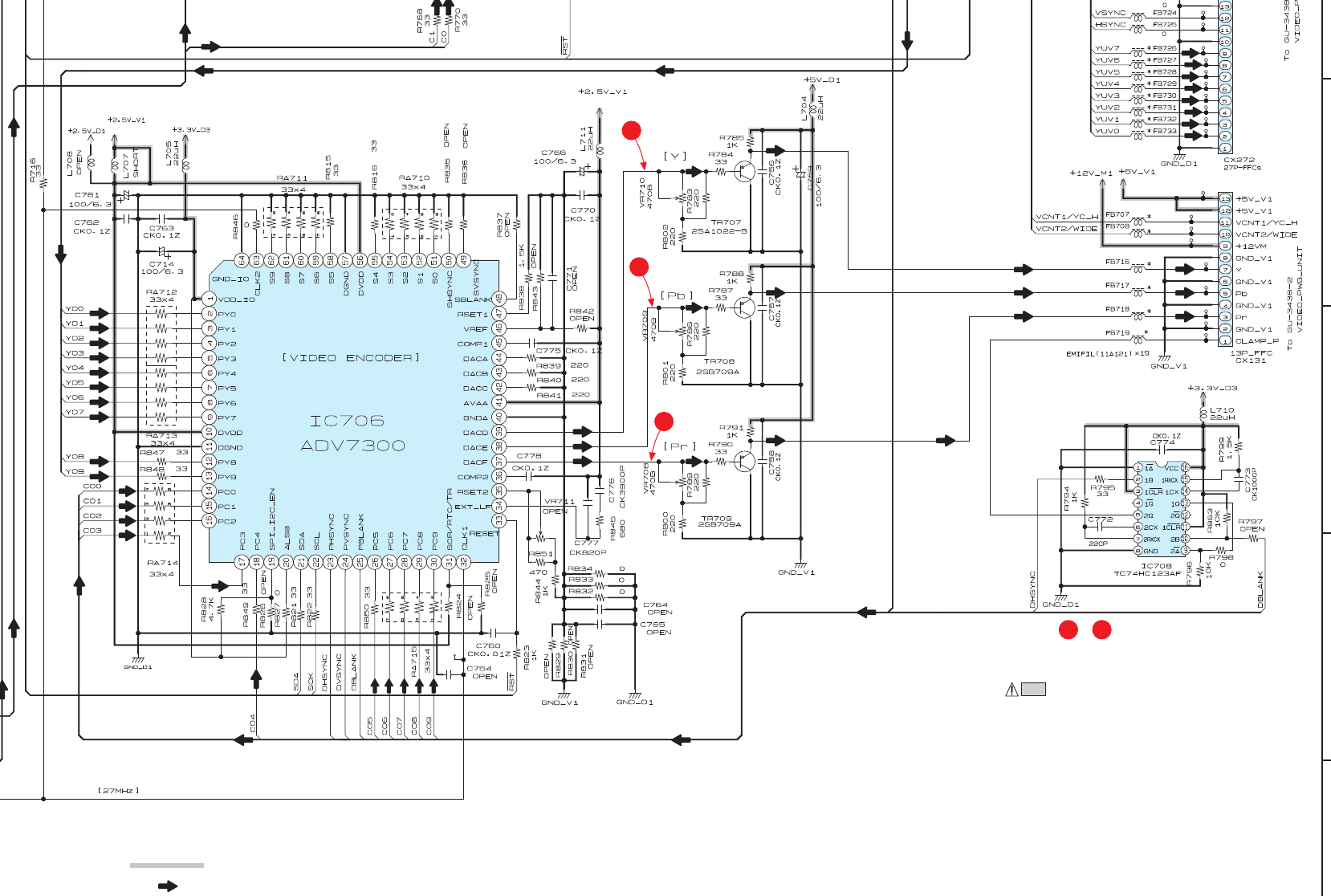
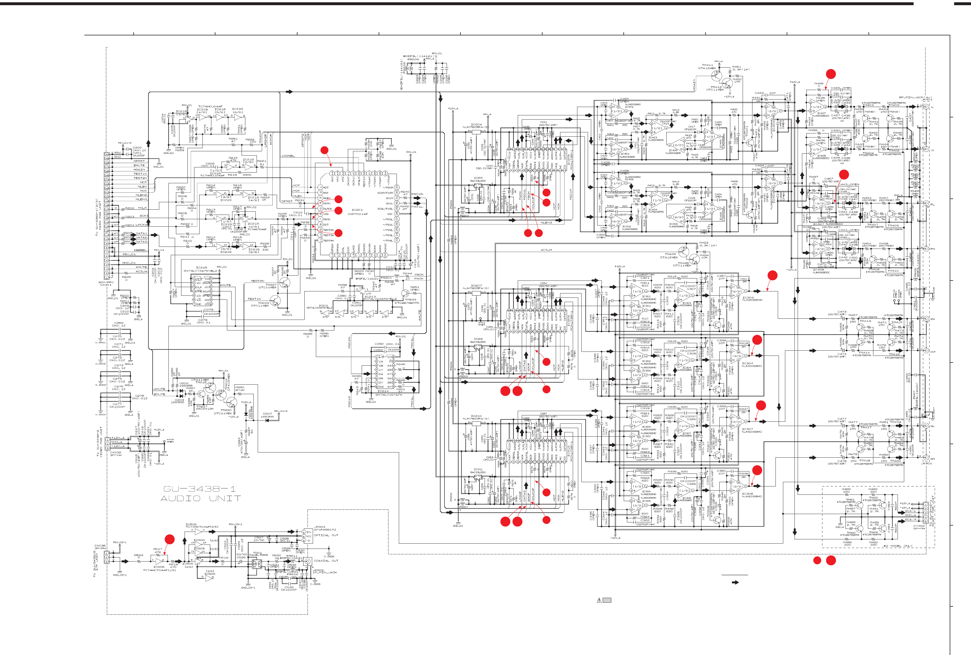
A1
A5
A6
A8 A7
A5
A9
A2
A3
A4
A10A11
A5
A9
A10A11
A12
A13
A12
A12
A12
A14
A12
For the Waveforms marked with numbers ~ , refer to page 87 (WAVEFORMS).
A1 A14
94
SCHEMATIC DIAGRAMS (4/8)
GU-3438-1 AUDIO UNIT
SCHEMATIC DIAGRAMS (4/8)
1 2 3 4 5 6 7 8 9 10 11
A
B
C
D
E
F
G
H
NOTICE
ALL RESISTANCE VALUES IN OHM. k=1,000 OHM M=1,000,000 OHM
ALL CAPACITANCE VALUES IN MICRO FARAD. P=MICRO-MICRO FARAD
EACH VOLTAGE AND CURRENT ARE MEASUERD AT MO SIGNAL INPUT
CONDITION.
CIRCUIT AND PARTS ARE SUBJECT TO CHANGE WITHOUT PRIOR
NOTICE.
WARNING:
Parts marked with this symbol have critical characteristics.
Use ONLY replacement parts recommended by the manufacture.
CAUTION:
Before returning the unit to the customer, make sure you make either (1) a
leakage current check or (2) a line to chassis resistance check. If the leakage
current exceeds 0.5 milliamps, or if the resistance from chassis to either side
of the power card is less than 460kohms, the unit is defective.
WARNING:
DO NOT return the unit to the customer until the problem is located and
corrected.
SIGNAL LINE
DVD-3800
B LINE
_
+
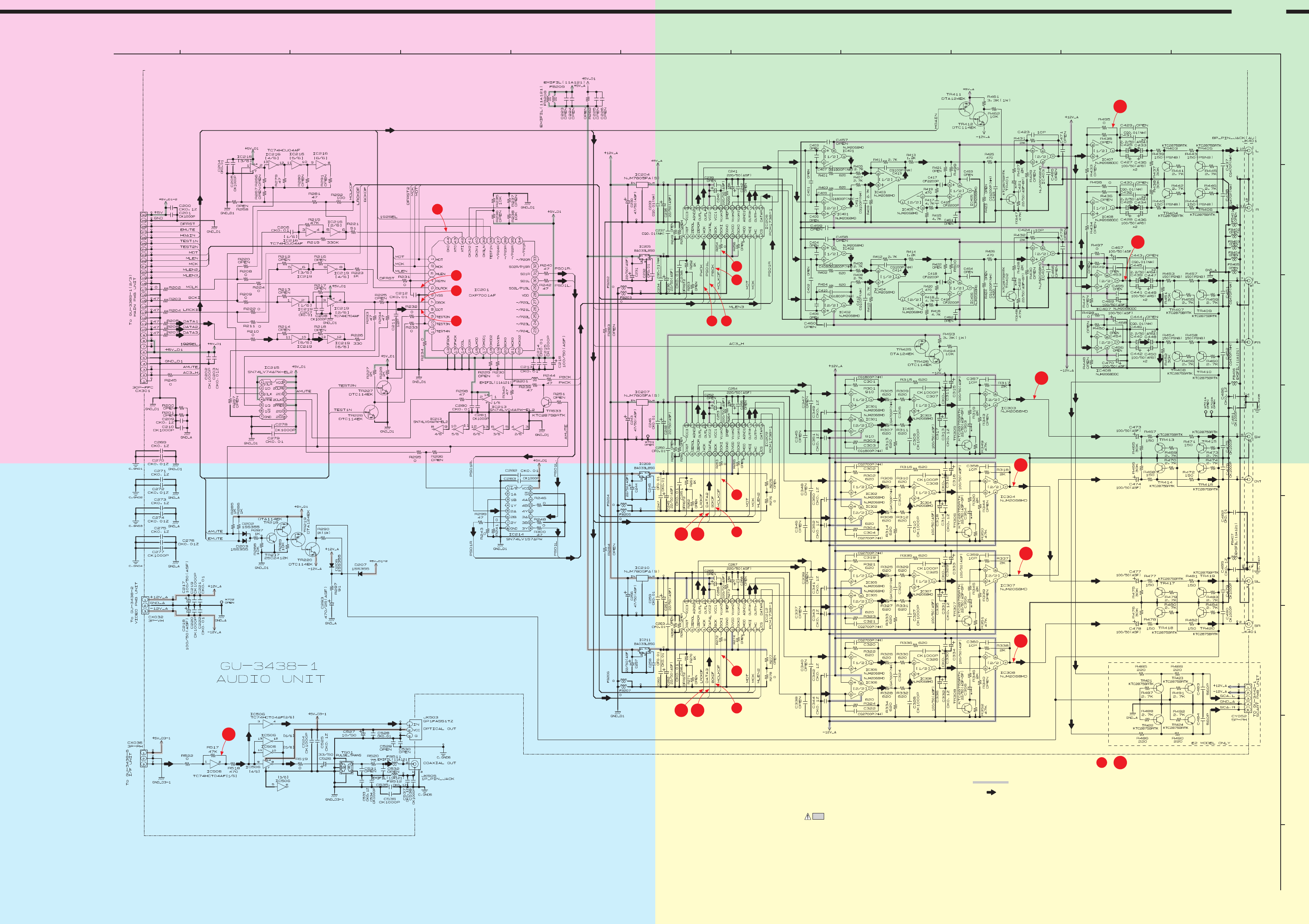
A1
A5
A6
A8 A7
A5
A9
A2
A3
A4
A10A11
A5
A9
A10A11
A12
A13
A12
A12
A12
A14
A12
For the Waveforms marked with numbers ~ , refer to page 87 (WAVEFORMS).
A1 A14
94
SCHEMATIC DIAGRAMS (4/8)
GU-3438-1 AUDIO UNIT
SCHEMATIC DIAGRAMS (4/8)
1 2 3 4 5 6 7 8 9 10 11
A
B
C
D
E
F
G
H
NOTICE
ALL RESISTANCE VALUES IN OHM. k=1,000 OHM M=1,000,000 OHM
ALL CAPACITANCE VALUES IN MICRO FARAD. P=MICRO-MICRO FARAD
EACH VOLTAGE AND CURRENT ARE MEASUERD AT MO SIGNAL INPUT
CONDITION.
CIRCUIT AND PARTS ARE SUBJECT TO CHANGE WITHOUT PRIOR
NOTICE.
WARNING:
Parts marked with this symbol have critical characteristics.
Use ONLY replacement parts recommended by the manufacture.
CAUTION:
Before returning the unit to the customer, make sure you make either (1) a
leakage current check or (2) a line to chassis resistance check. If the leakage
current exceeds 0.5 milliamps, or if the resistance from chassis to either side
of the power card is less than 460kohms, the unit is defective.
WARNING:
DO NOT return the unit to the customer until the problem is located and
corrected.
SIGNAL LINE
DVD-3800
B LINE
_
+
A
AB
B
C
CD
D
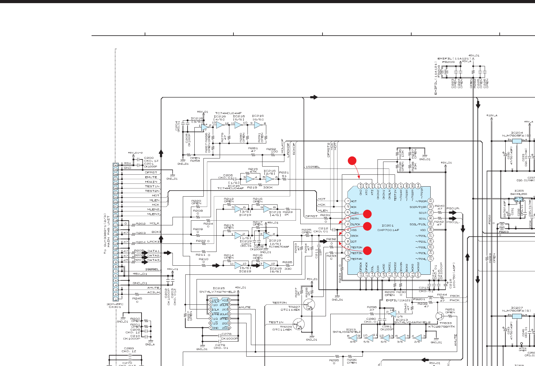
A1
A5
A6
A8 A7
A5
A9
A2
A3
A4
A10A11
A5
A9
A10A11
A12
A13
A12
A12
A12
A14
A12
For the Waveforms marked with numbers ~ , refer to page 87 (WAVEFORMS).
A1 A14
94
SCHEMATIC DIAGRAMS (4/8)
GU-3438-1 AUDIO UNIT
SCHEMATIC DIAGRAMS (4/8)
1 2 3 4 5 6 7 8 9 10 11
A
B
C
D
E
F
G
H
NOTICE
ALL RESISTANCE VALUES IN OHM. k=1,000 OHM M=1,000,000 OHM
ALL CAPACITANCE VALUES IN MICRO FARAD. P=MICRO-MICRO FARAD
EACH VOLTAGE AND CURRENT ARE MEASUERD AT MO SIGNAL INPUT
CONDITION.
CIRCUIT AND PARTS ARE SUBJECT TO CHANGE WITHOUT PRIOR
NOTICE.
WARNING:
Parts marked with this symbol have critical characteristics.
Use ONLY replacement parts recommended by the manufacture.
CAUTION:
Before returning the unit to the customer, make sure you make either (1) a
leakage current check or (2) a line to chassis resistance check. If the leakage
current exceeds 0.5 milliamps, or if the resistance from chassis to either side
of the power card is less than 460kohms, the unit is defective.
WARNING:
DO NOT return the unit to the customer until the problem is located and
corrected.
SIGNAL LINE
DVD-3800
B LINE
_
+
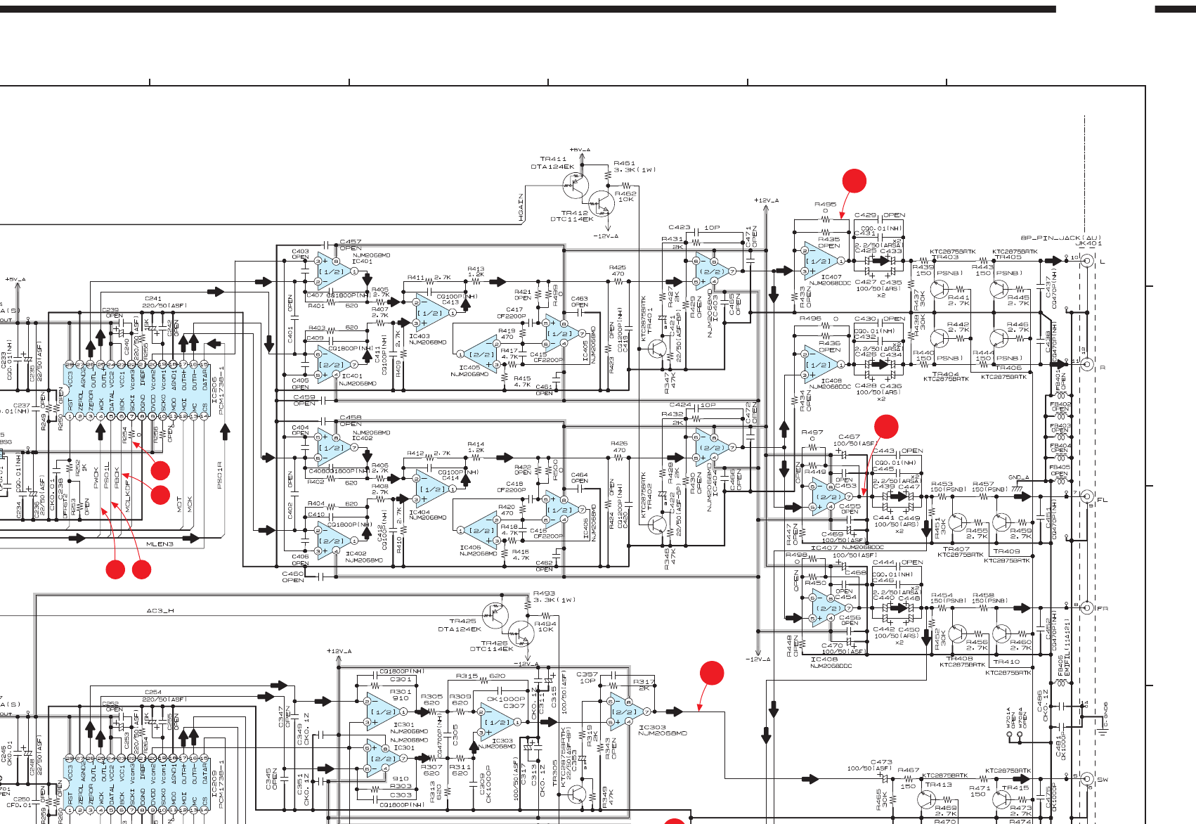
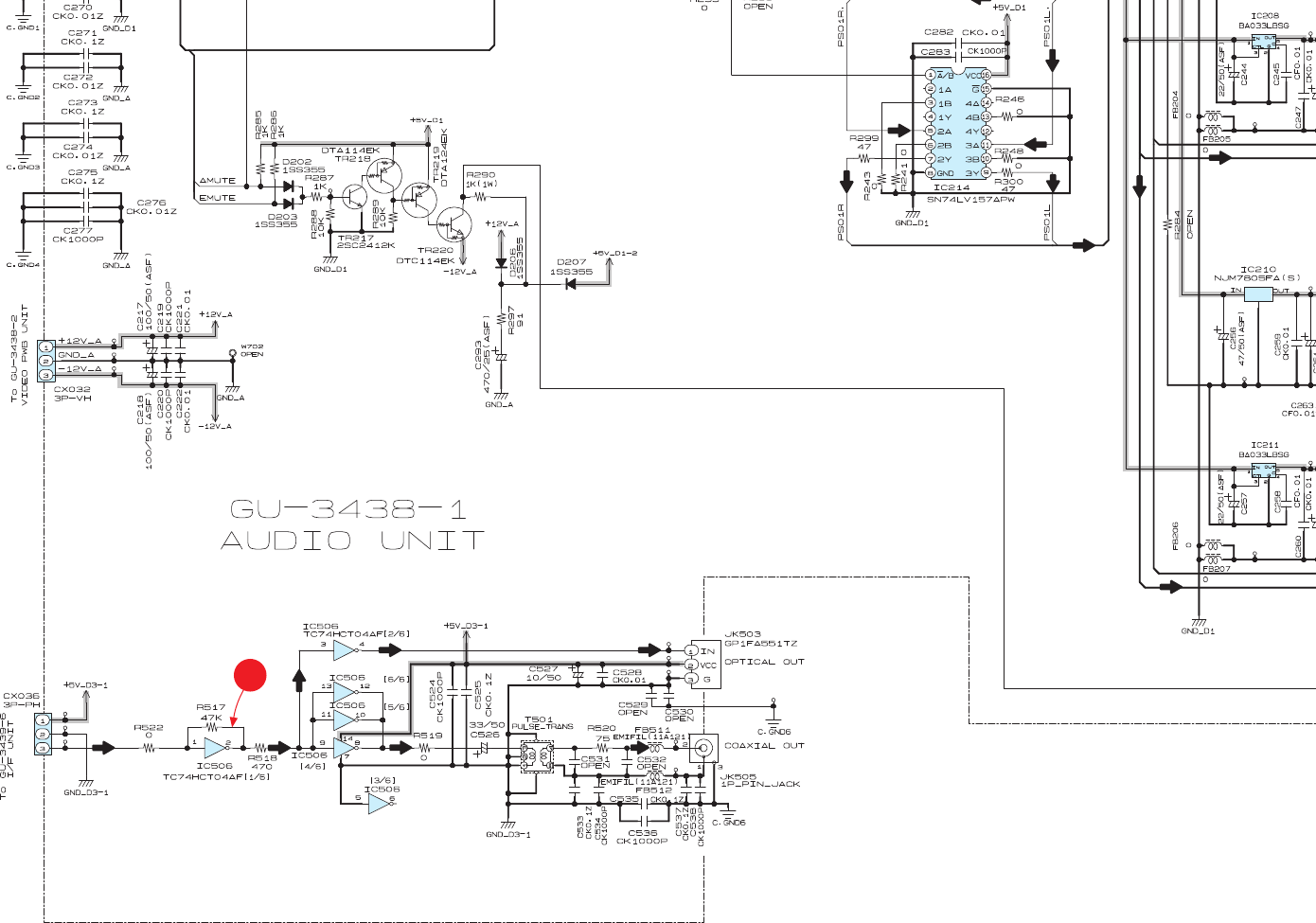
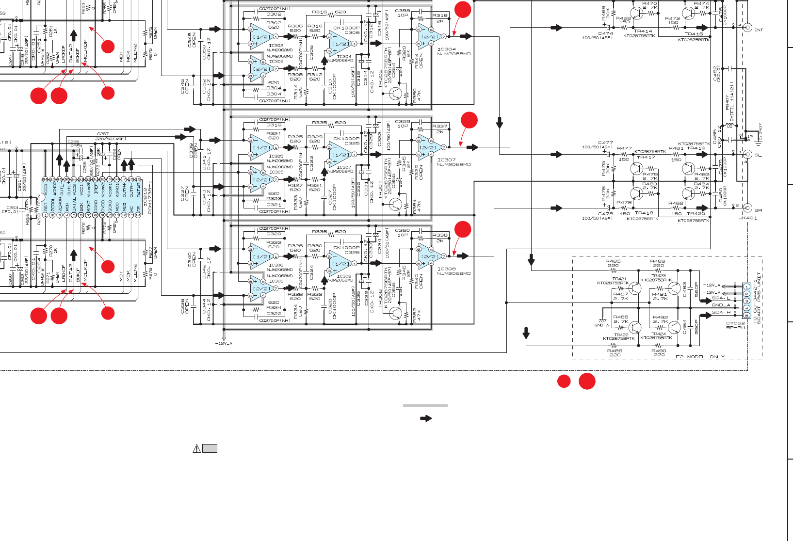
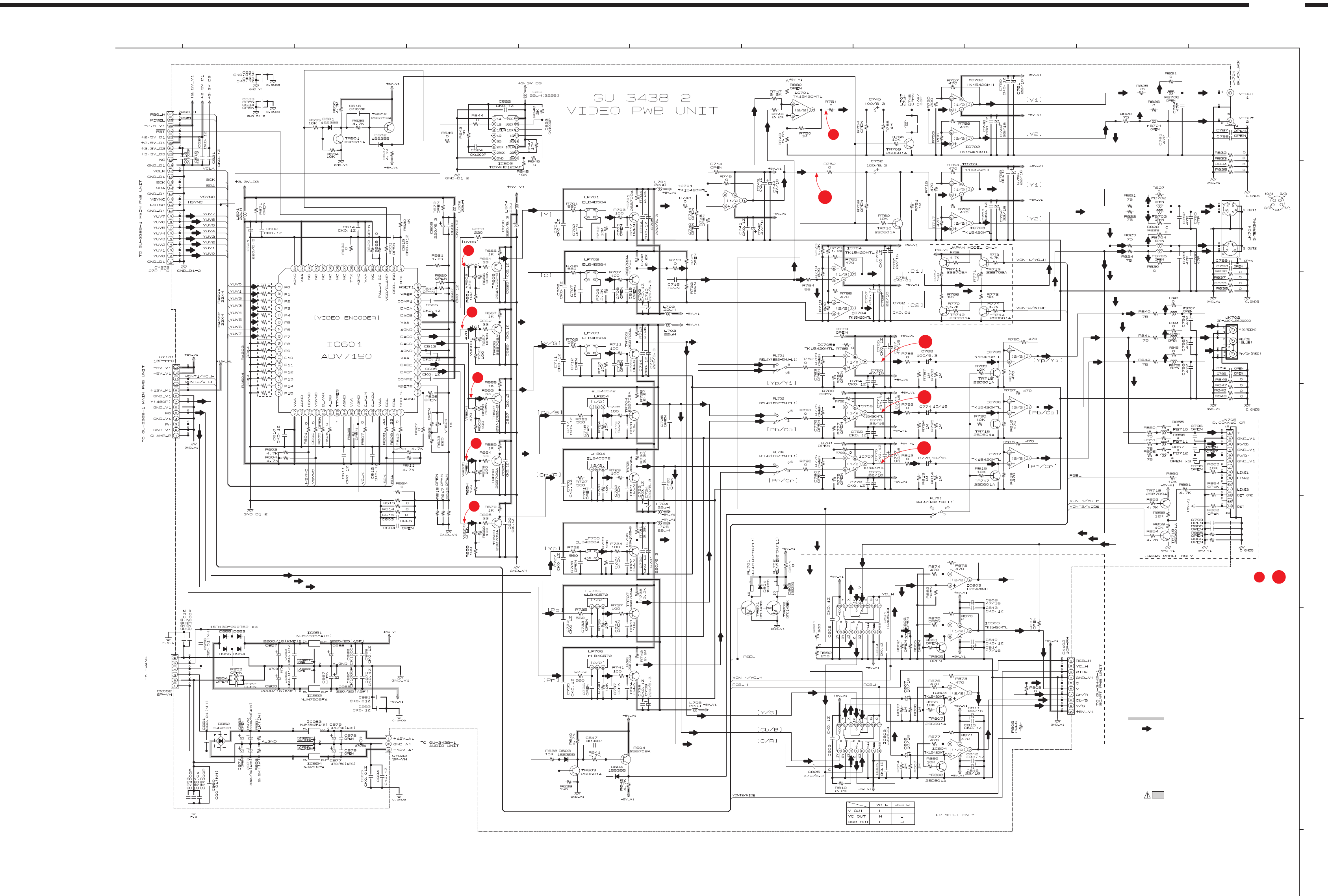
P4
P5
P6
P7
P8
P9
P10
P12 Progre only
P13 Progre only
Progre only
P11
P4 P13
For the Waveforms marked with numbers ~ ,
refer to page 89 (WAVEFORMS).
95
SCHEMATIC DIAGRAMS (5/8)
GU-3438-2 VIDEO UNIT
SCHEMATIC DIAGRAMS (5/8)
1 2 3 4 5 6 7 8 9 10 11
A
B
C
D
E
F
G
H
NOTICE
ALL RESISTANCE VALUES IN OHM. k=1,000 OHM M=1,000,000 OHM
ALL CAPACITANCE VALUES IN MICRO FARAD. P=MICRO-MICRO FARAD
EACH VOLTAGE AND CURRENT ARE MEASUERD AT MO SIGNAL INPUT
CONDITION.
CIRCUIT AND PARTS ARE SUBJECT TO CHANGE WITHOUT PRIOR
NOTICE.
WARNING:
Parts marked with this symbol have critical characteristics.
Use ONLY replacement parts recommended by the manufacture.
CAUTION:
Before returning the unit to the customer, make sure you make either (1) a
leakage current check or (2) a line to chassis resistance check. If the leakage
current exceeds 0.5 milliamps, or if the resistance from chassis to either side
of the power card is less than 460kohms, the unit is defective.
WARNING:
DO NOT return the unit to the customer until the problem is located and
corrected.
SIGNAL LINE
DVD-3800
B LINE
_
+
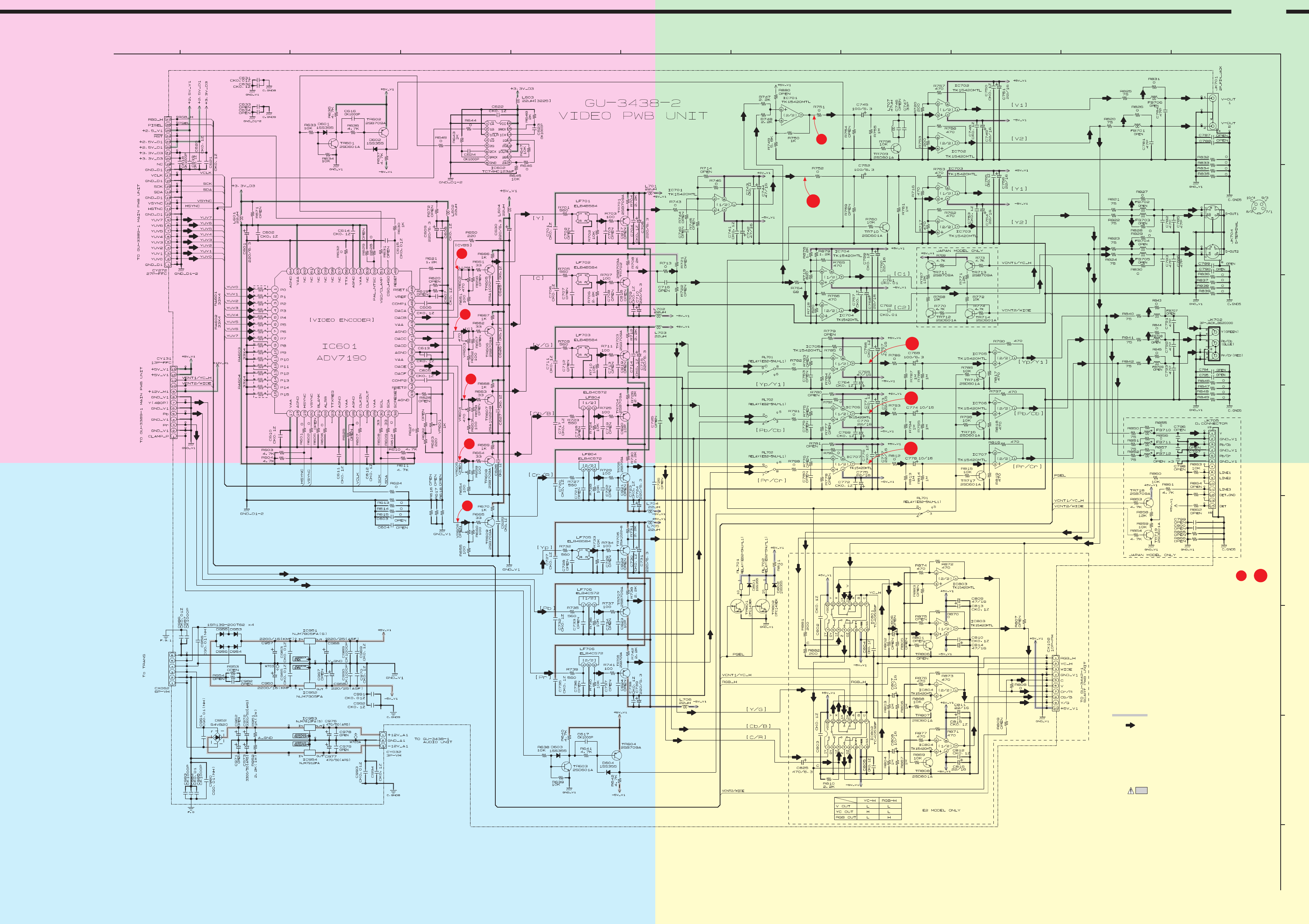
P4
P5
P6
P7
P8
P9
P10
P12 Progre only
P13 Progre only
Progre only
P11
P4 P13
For the Waveforms marked with numbers ~ ,
refer to page 89 (WAVEFORMS).
95
SCHEMATIC DIAGRAMS (5/8)
GU-3438-2 VIDEO UNIT
SCHEMATIC DIAGRAMS (5/8)
1 2 3 4 5 6 7 8 9 10 11
A
B
C
D
E
F
G
H
NOTICE
ALL RESISTANCE VALUES IN OHM. k=1,000 OHM M=1,000,000 OHM
ALL CAPACITANCE VALUES IN MICRO FARAD. P=MICRO-MICRO FARAD
EACH VOLTAGE AND CURRENT ARE MEASUERD AT MO SIGNAL INPUT
CONDITION.
CIRCUIT AND PARTS ARE SUBJECT TO CHANGE WITHOUT PRIOR
NOTICE.
WARNING:
Parts marked with this symbol have critical characteristics.
Use ONLY replacement parts recommended by the manufacture.
CAUTION:
Before returning the unit to the customer, make sure you make either (1) a
leakage current check or (2) a line to chassis resistance check. If the leakage
current exceeds 0.5 milliamps, or if the resistance from chassis to either side
of the power card is less than 460kohms, the unit is defective.
WARNING:
DO NOT return the unit to the customer until the problem is located and
corrected.
SIGNAL LINE
DVD-3800
B LINE
_
+
A
AB
B
C
CD
D
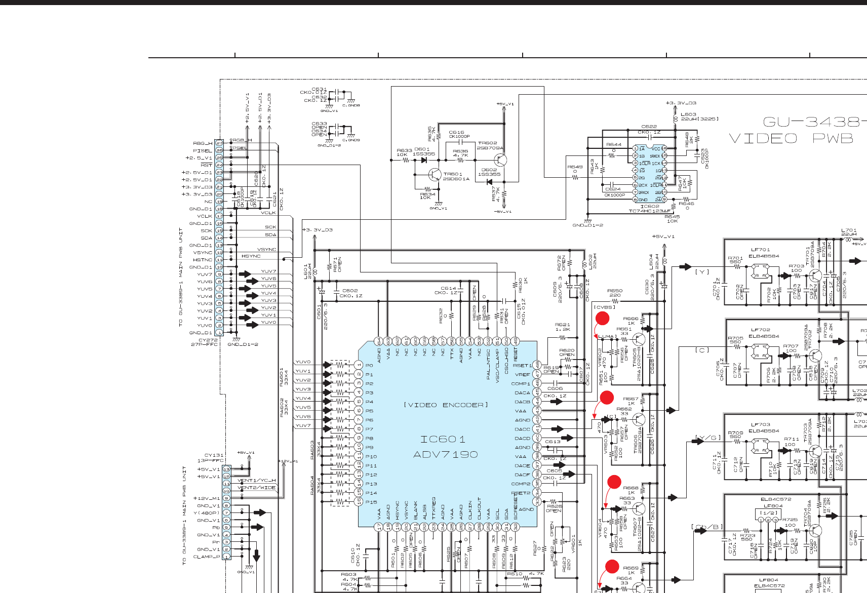
P4
P5
P6
P7
P8
P9
P10
P12 Progre only
P13 Progre only
Progre only
P11
P4 P13
For the Waveforms marked with numbers ~ ,
refer to page 89 (WAVEFORMS).
95
SCHEMATIC DIAGRAMS (5/8)
GU-3438-2 VIDEO UNIT
SCHEMATIC DIAGRAMS (5/8)
1 2 3 4 5 6 7 8 9 10 11
A
B
C
D
E
F
G
H
NOTICE
ALL RESISTANCE VALUES IN OHM. k=1,000 OHM M=1,000,000 OHM
ALL CAPACITANCE VALUES IN MICRO FARAD. P=MICRO-MICRO FARAD
EACH VOLTAGE AND CURRENT ARE MEASUERD AT MO SIGNAL INPUT
CONDITION.
CIRCUIT AND PARTS ARE SUBJECT TO CHANGE WITHOUT PRIOR
NOTICE.
WARNING:
Parts marked with this symbol have critical characteristics.
Use ONLY replacement parts recommended by the manufacture.
CAUTION:
Before returning the unit to the customer, make sure you make either (1) a
leakage current check or (2) a line to chassis resistance check. If the leakage
current exceeds 0.5 milliamps, or if the resistance from chassis to either side
of the power card is less than 460kohms, the unit is defective.
WARNING:
DO NOT return the unit to the customer until the problem is located and
corrected.
SIGNAL LINE
DVD-3800
B LINE
_
+
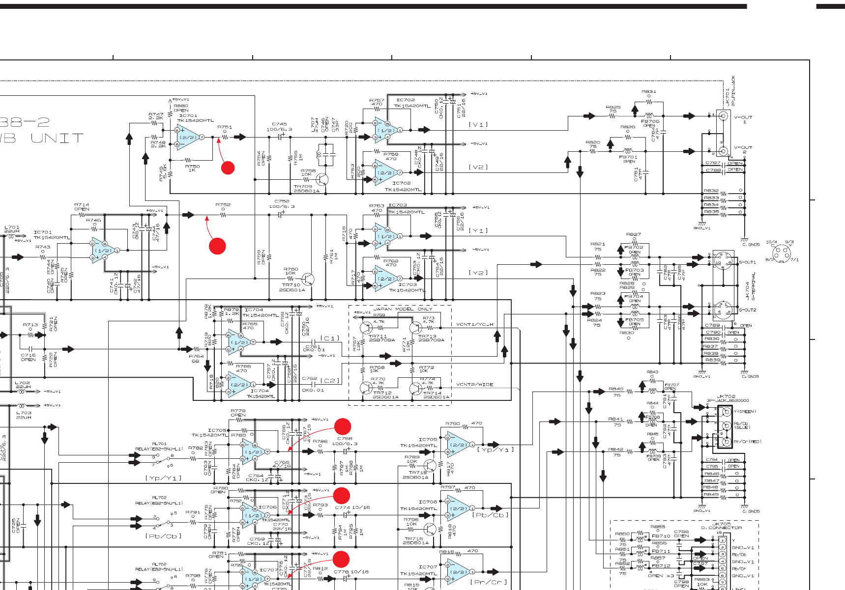
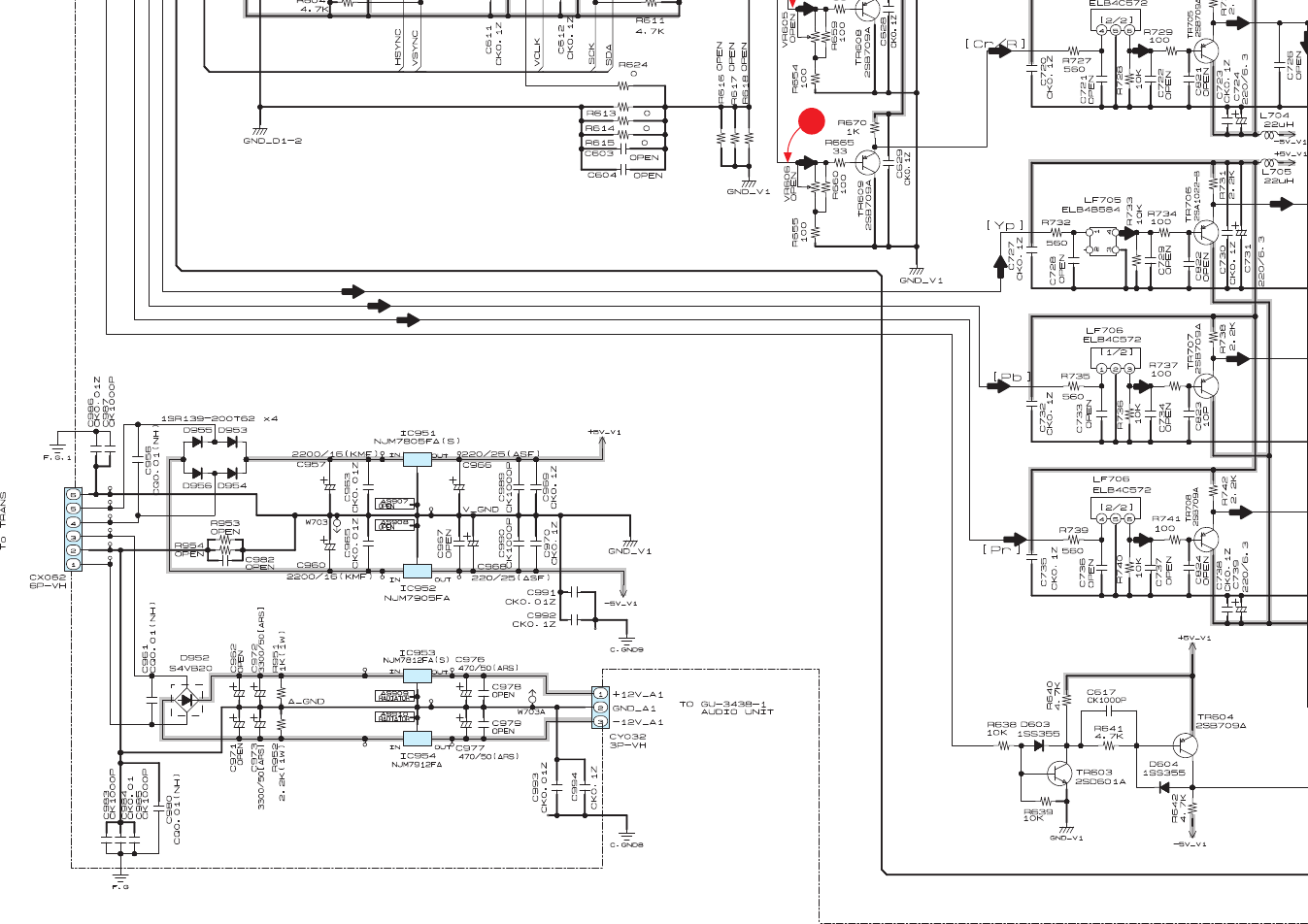
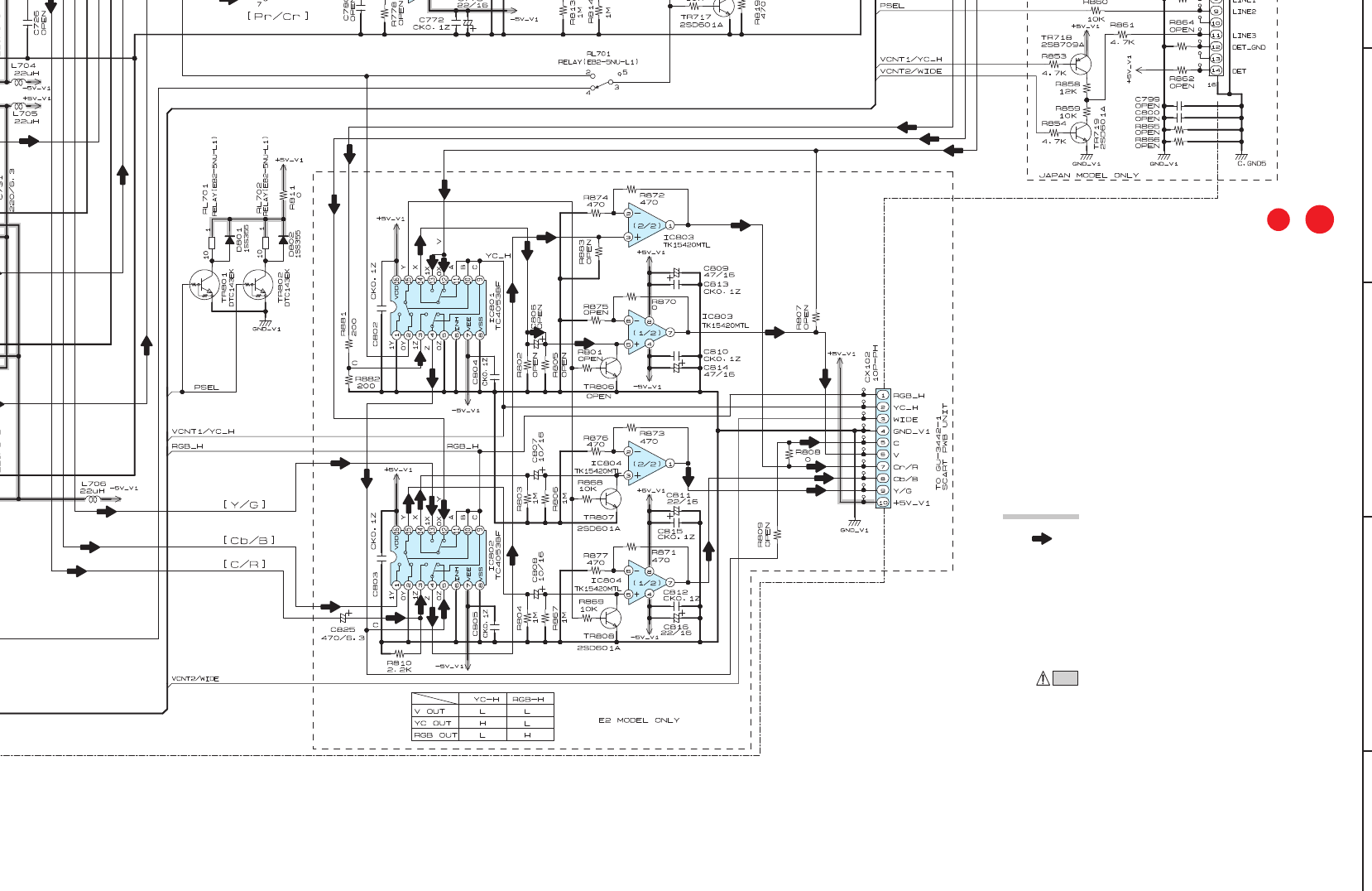
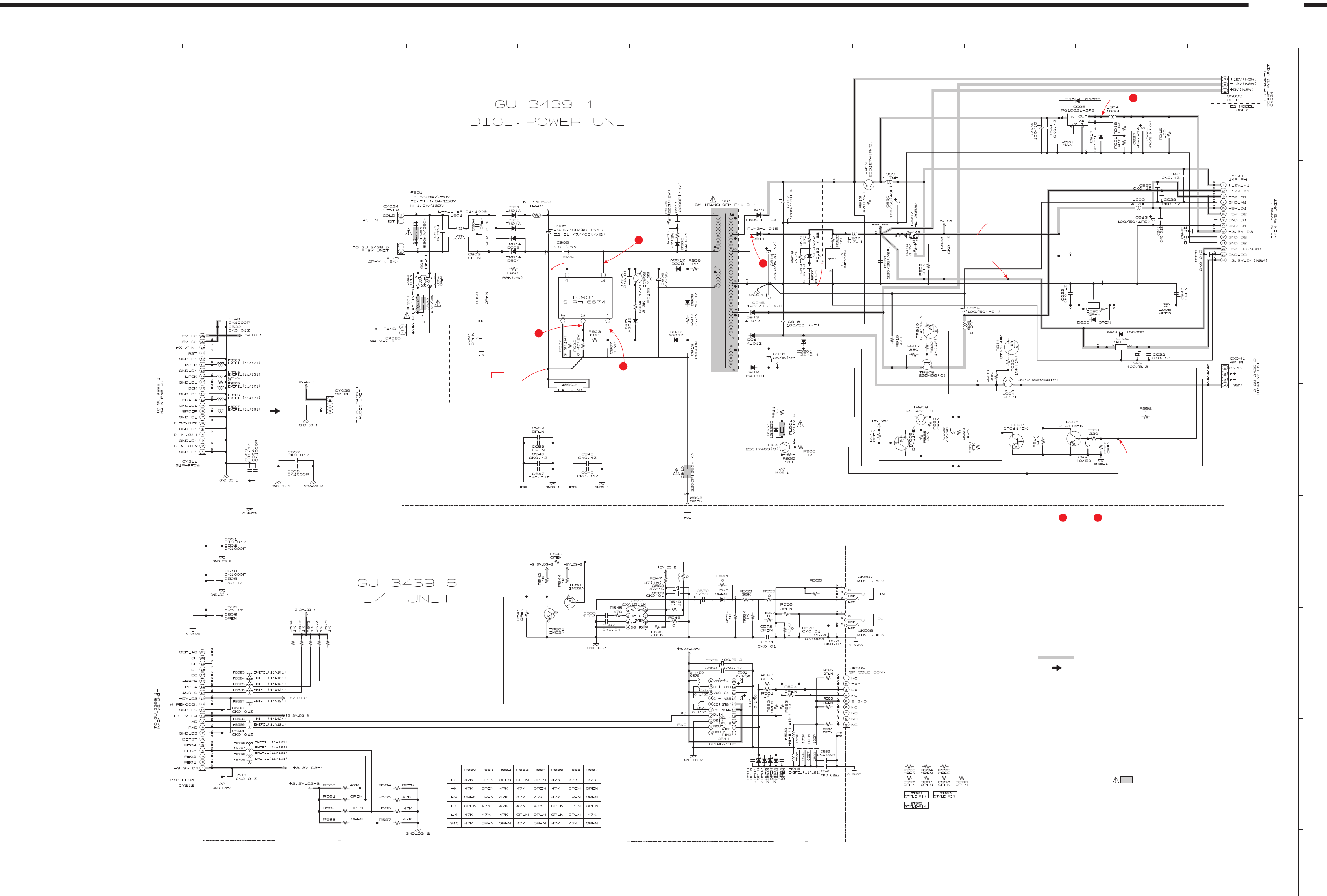
A3439-
E3439-
D3439-
C3439-
B3439-
POWER ON : +3.2VDC
St-by : 0VDC
POWER ON : +5VDC
St-by : +0VDC
POWER ON/
St-by : +5VDC
+3.6VDC
+18VDC
GND for
Primary circuit
A3439- E3439-
For the Waveforms marked with numbers ~ , refer to page 90 (WAVEFORMS).
96
SCHEMATIC DIAGRAMS (6/8)
1 2 3 4 5 6 7 8 9 10 11
A
B
C
D
E
F
G
H
NOTICE
ALL RESISTANCE VALUES IN OHM. k=1,000 OHM M=1,000,000 OHM
ALL CAPACITANCE VALUES IN MICRO FARAD. P=MICRO-MICRO FARAD
EACH VOLTAGE AND CURRENT ARE MEASUERD AT MO SIGNAL INPUT
CONDITION.
CIRCUIT AND PARTS ARE SUBJECT TO CHANGE WITHOUT PRIOR
NOTICE.
WARNING:
Parts marked with this symbol have critical characteristics.
Use ONLY replacement parts recommended by the manufacture.
CAUTION:
Before returning the unit to the customer, make sure you make either (1) a
leakage current check or (2) a line to chassis resistance check. If the leakage
current exceeds 0.5 milliamps, or if the resistance from chassis to either side
of the power card is less than 460kohms, the unit is defective.
WARNING:
DO NOT return the unit to the customer until the problem is located and
corrected.
SIGNAL LINE
DVD-3800
B LINE
_
+
SCHEMATIC DIAGRAMS (6/8)
GU-3439-1 DIGI. POWER UNIT
GU-3439-6 I/F UNIT
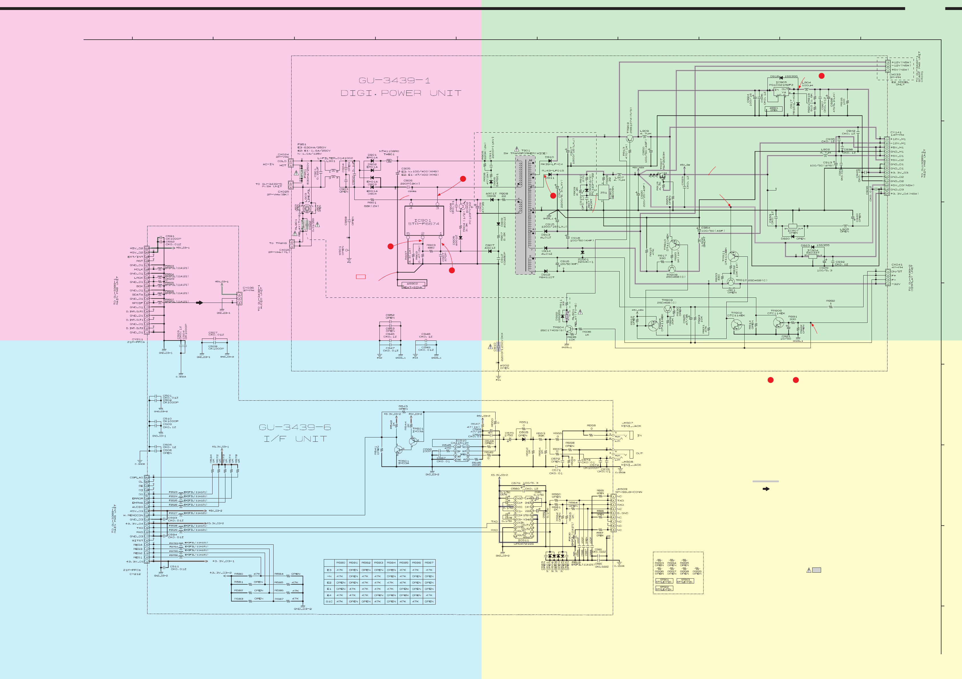
A
AB
B
C
CD
D
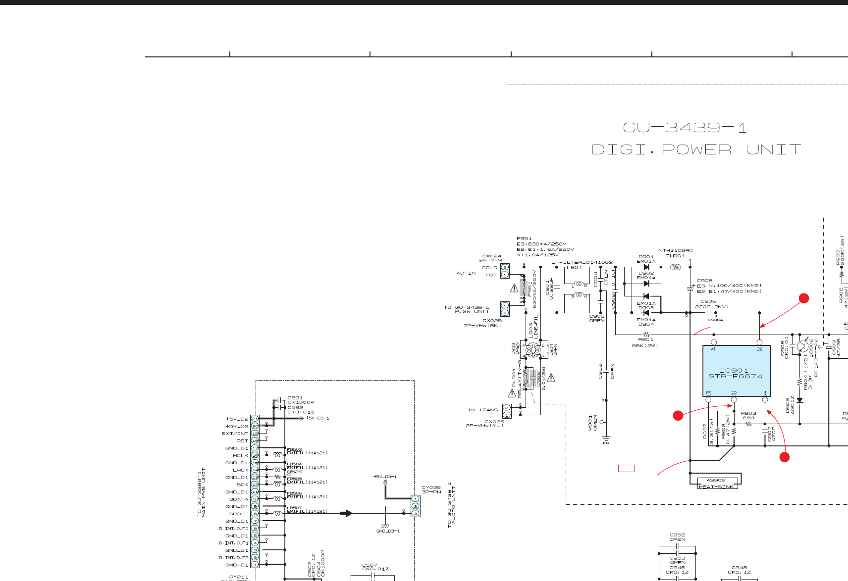
A3439-
E3439-
D3439-
C3439-
B3439-
POWER ON : +3.2VDC
St-by : 0VDC
POWER ON : +5VDC
St-by : +0VDC
POWER ON/
St-by : +5VDC
+3.6VDC
+18VDC
GND for
Primary circuit
A3439- E3439-
For the Waveforms marked with numbers ~ , refer to page 90 (WAVEFORMS).
96
SCHEMATIC DIAGRAMS (6/8)
1 2 3 4 5 6 7 8 9 10 11
A
B
C
D
E
F
G
H
NOTICE
ALL RESISTANCE VALUES IN OHM. k=1,000 OHM M=1,000,000 OHM
ALL CAPACITANCE VALUES IN MICRO FARAD. P=MICRO-MICRO FARAD
EACH VOLTAGE AND CURRENT ARE MEASUERD AT MO SIGNAL INPUT
CONDITION.
CIRCUIT AND PARTS ARE SUBJECT TO CHANGE WITHOUT PRIOR
NOTICE.
WARNING:
Parts marked with this symbol have critical characteristics.
Use ONLY replacement parts recommended by the manufacture.
CAUTION:
Before returning the unit to the customer, make sure you make either (1) a
leakage current check or (2) a line to chassis resistance check. If the leakage
current exceeds 0.5 milliamps, or if the resistance from chassis to either side
of the power card is less than 460kohms, the unit is defective.
WARNING:
DO NOT return the unit to the customer until the problem is located and
corrected.
SIGNAL LINE
DVD-3800
B LINE
_
+
SCHEMATIC DIAGRAMS (6/8)
GU-3439-1 DIGI. POWER UNIT
GU-3439-6 I/F UNIT
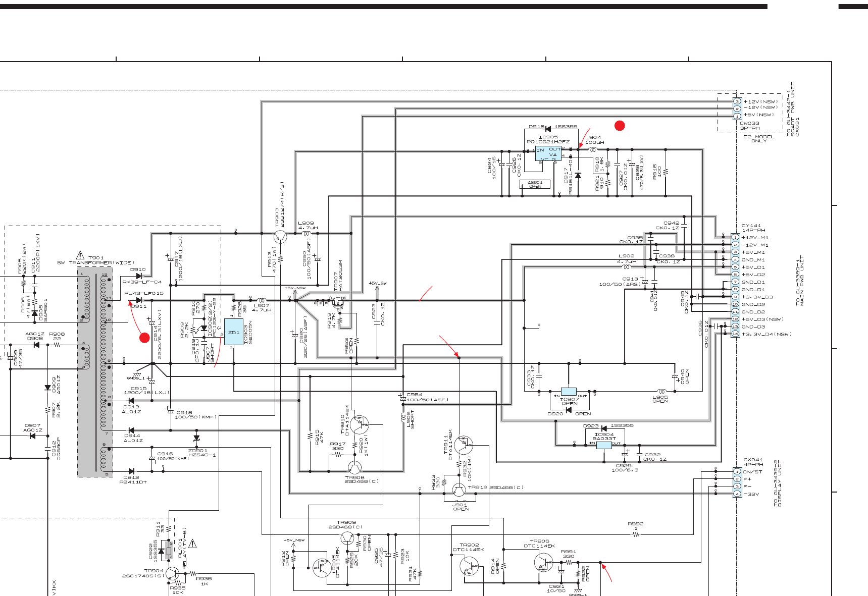
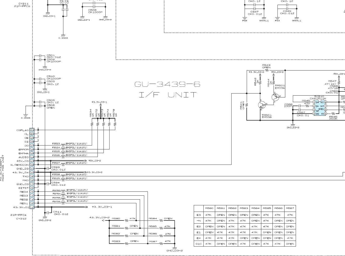
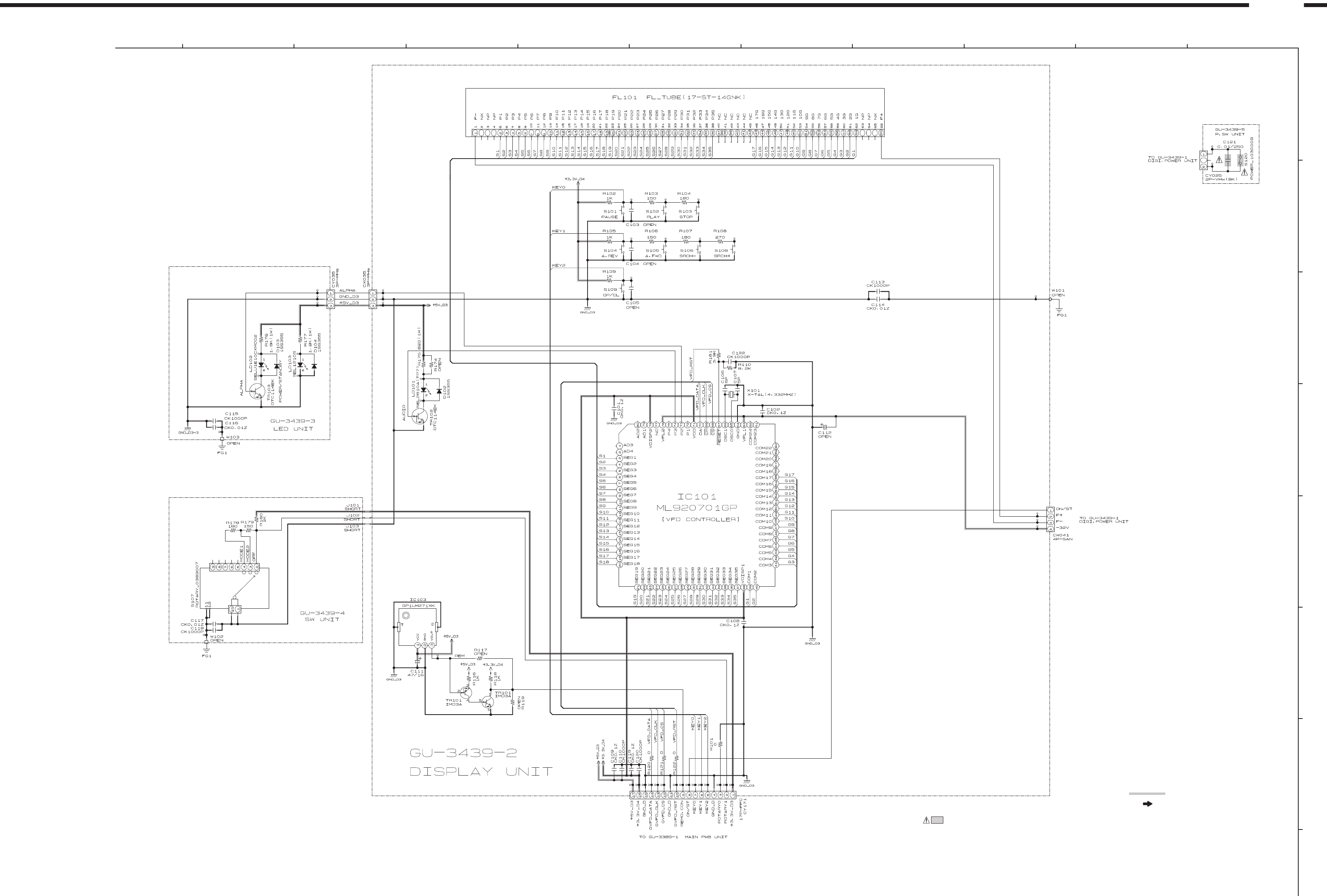
97
SCHEMATIC DIAGRAMS (7/8)
GU-3439-2 DISPLAY UNIT
GU-3439-3 LED UNIT
GU-3439-4 SW UNIT
GU-3439-5 P.SW UNIT
SCHEMATIC DIAGRAMS (7/8)
1 2 3 4 5 6 7 8 9 10 11
A
B
C
D
E
F
G
H
NOTICE
ALL RESISTANCE VALUES IN OHM. k=1,000 OHM M=1,000,000 OHM
ALL CAPACITANCE VALUES IN MICRO FARAD. P=MICRO-MICRO FARAD
EACH VOLTAGE AND CURRENT ARE MEASUERD AT MO SIGNAL INPUT
CONDITION.
CIRCUIT AND PARTS ARE SUBJECT TO CHANGE WITHOUT PRIOR
NOTICE.
WARNING:
Parts marked with this symbol have critical characteristics.
Use ONLY replacement parts recommended by the manufacture.
CAUTION:
Before returning the unit to the customer, make sure you make either (1) a
leakage current check or (2) a line to chassis resistance check. If the leakage
current exceeds 0.5 milliamps, or if the resistance from chassis to either side
of the power card is less than 460kohms, the unit is defective.
WARNING:
DO NOT return the unit to the customer until the problem is located and
corrected.
SIGNAL LINE
DVD-3800
B LINE
_
+
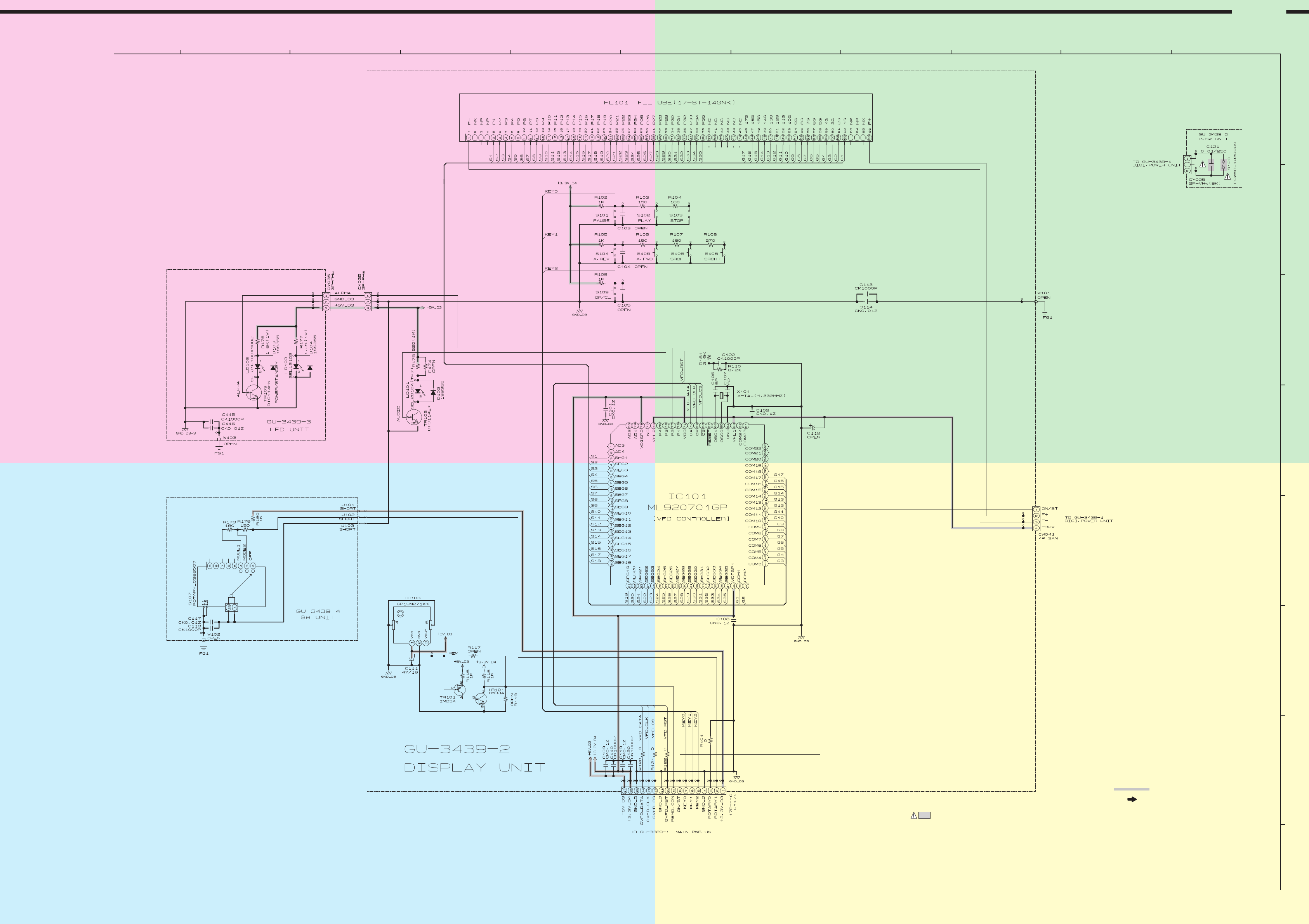
A
AB
B
C
CD
D
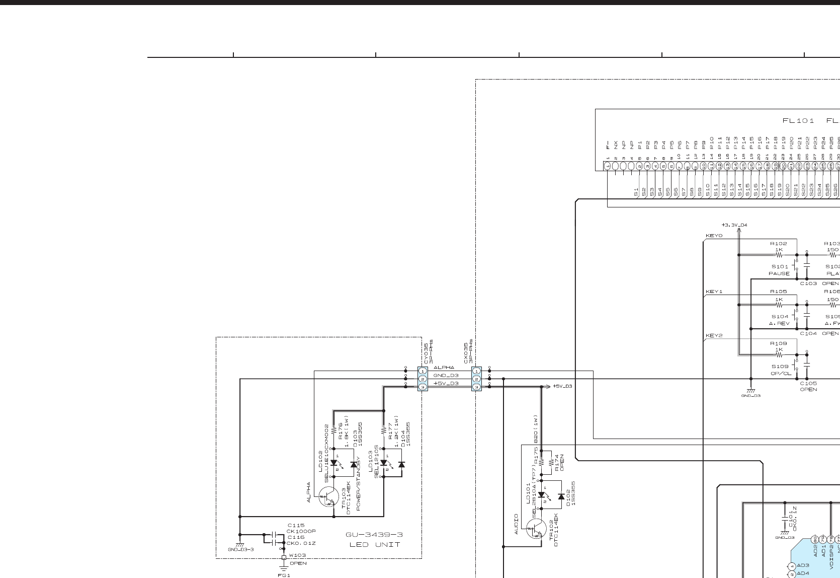
97
SCHEMATIC DIAGRAMS (7/8)
GU-3439-2 DISPLAY UNIT
GU-3439-3 LED UNIT
GU-3439-4 SW UNIT
GU-3439-5 P.SW UNIT
SCHEMATIC DIAGRAMS (7/8)
1 2 3 4 5 6 7 8 9 10 11
A
B
C
D
E
F
G
H
NOTICE
ALL RESISTANCE VALUES IN OHM. k=1,000 OHM M=1,000,000 OHM
ALL CAPACITANCE VALUES IN MICRO FARAD. P=MICRO-MICRO FARAD
EACH VOLTAGE AND CURRENT ARE MEASUERD AT MO SIGNAL INPUT
CONDITION.
CIRCUIT AND PARTS ARE SUBJECT TO CHANGE WITHOUT PRIOR
NOTICE.
WARNING:
Parts marked with this symbol have critical characteristics.
Use ONLY replacement parts recommended by the manufacture.
CAUTION:
Before returning the unit to the customer, make sure you make either (1) a
leakage current check or (2) a line to chassis resistance check. If the leakage
current exceeds 0.5 milliamps, or if the resistance from chassis to either side
of the power card is less than 460kohms, the unit is defective.
WARNING:
DO NOT return the unit to the customer until the problem is located and
corrected.
SIGNAL LINE
DVD-3800
B LINE
_
+
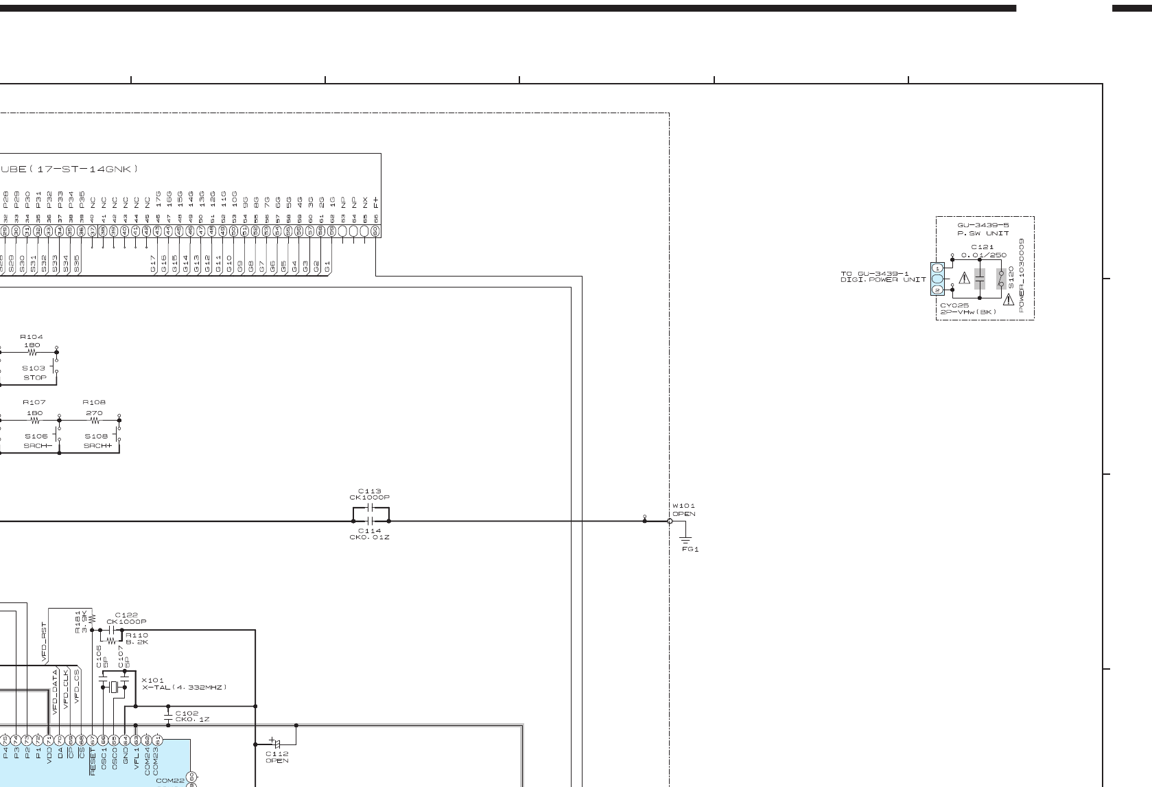
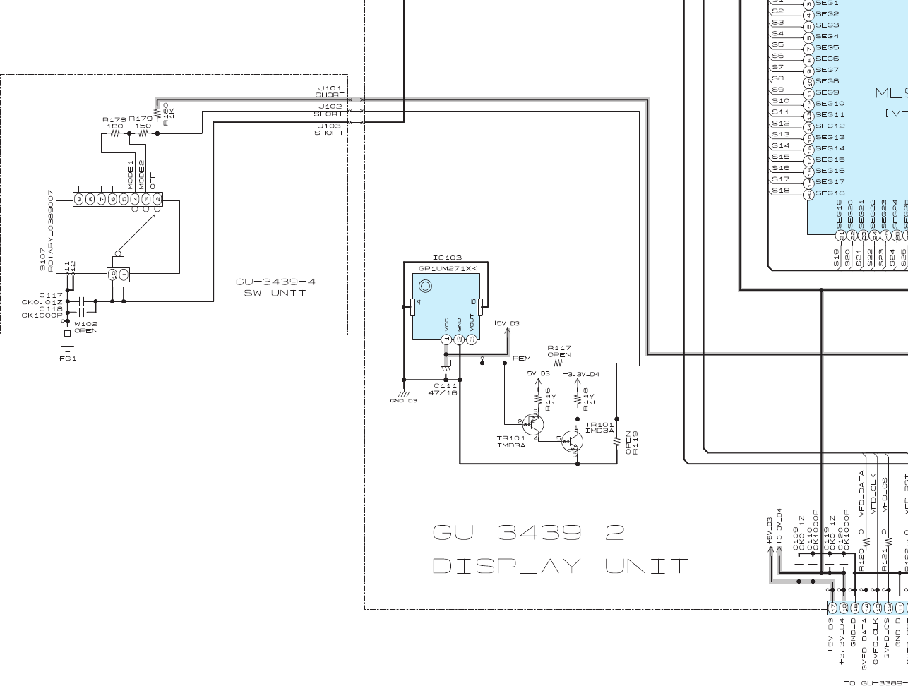
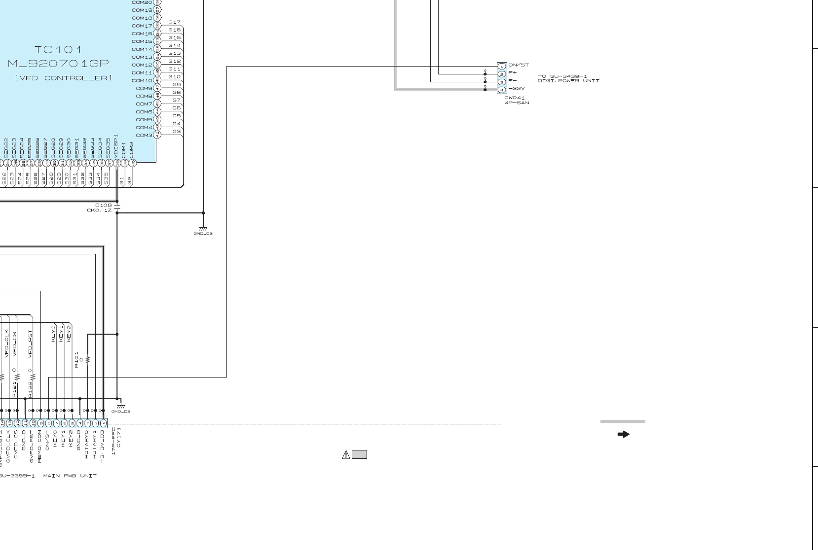
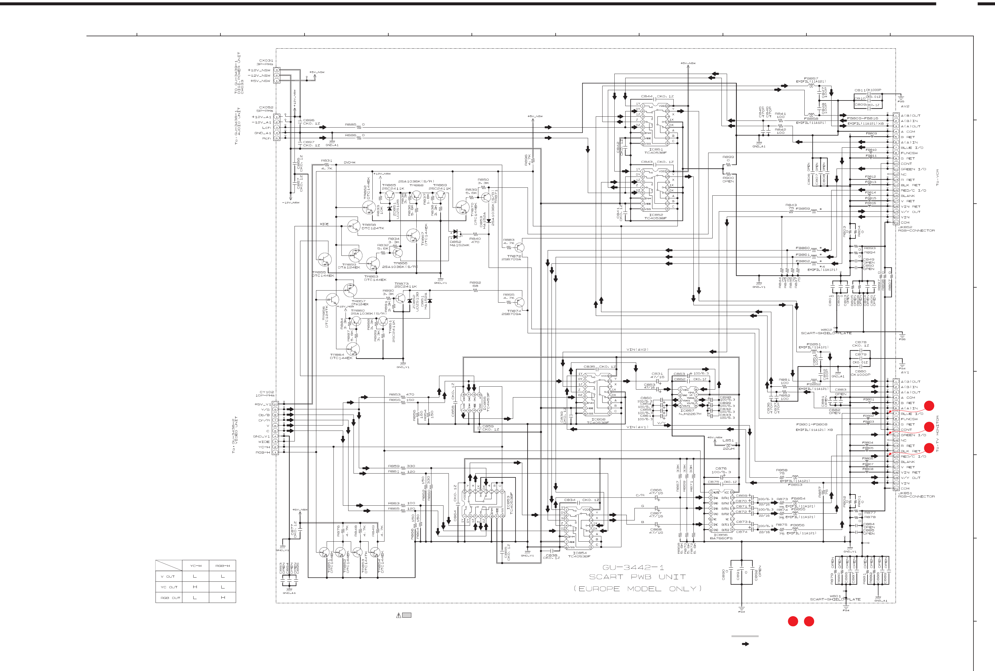
P16
P15
P14
P16
P14
For the Waveforms marked with numbers ~ , refer to page 89 (WAVEFORMS).
98
SCHEMATIC DIAGRAMS (8/8)
1 2 3 4 5 6 7 8 9 10 11
A
B
C
D
E
F
G
H
NOTICE
ALL RESISTANCE VALUES IN OHM. k=1,000 OHM M=1,000,000 OHM
ALL CAPACITANCE VALUES IN MICRO FARAD. P=MICRO-MICRO FARAD
EACH VOLTAGE AND CURRENT ARE MEASUERD AT MO SIGNAL INPUT
CONDITION.
CIRCUIT AND PARTS ARE SUBJECT TO CHANGE WITHOUT PRIOR
NOTICE.
WARNING:
Parts marked with this symbol have critical characteristics.
Use ONLY replacement parts recommended by the manufacture.
CAUTION:
Before returning the unit to the customer, make sure you make either (1) a
leakage current check or (2) a line to chassis resistance check. If the leakage
current exceeds 0.5 milliamps, or if the resistance from chassis to either side
of the power card is less than 460kohms, the unit is defective.
WARNING:
DO NOT return the unit to the customer until the problem is located and
corrected.
SIGNAL LINE
DVD-3800
B LINE
_
+
SCHEMATIC DIAGRAMS (8/8)
GU-3442-1 SCART UNIT (Europe model only)
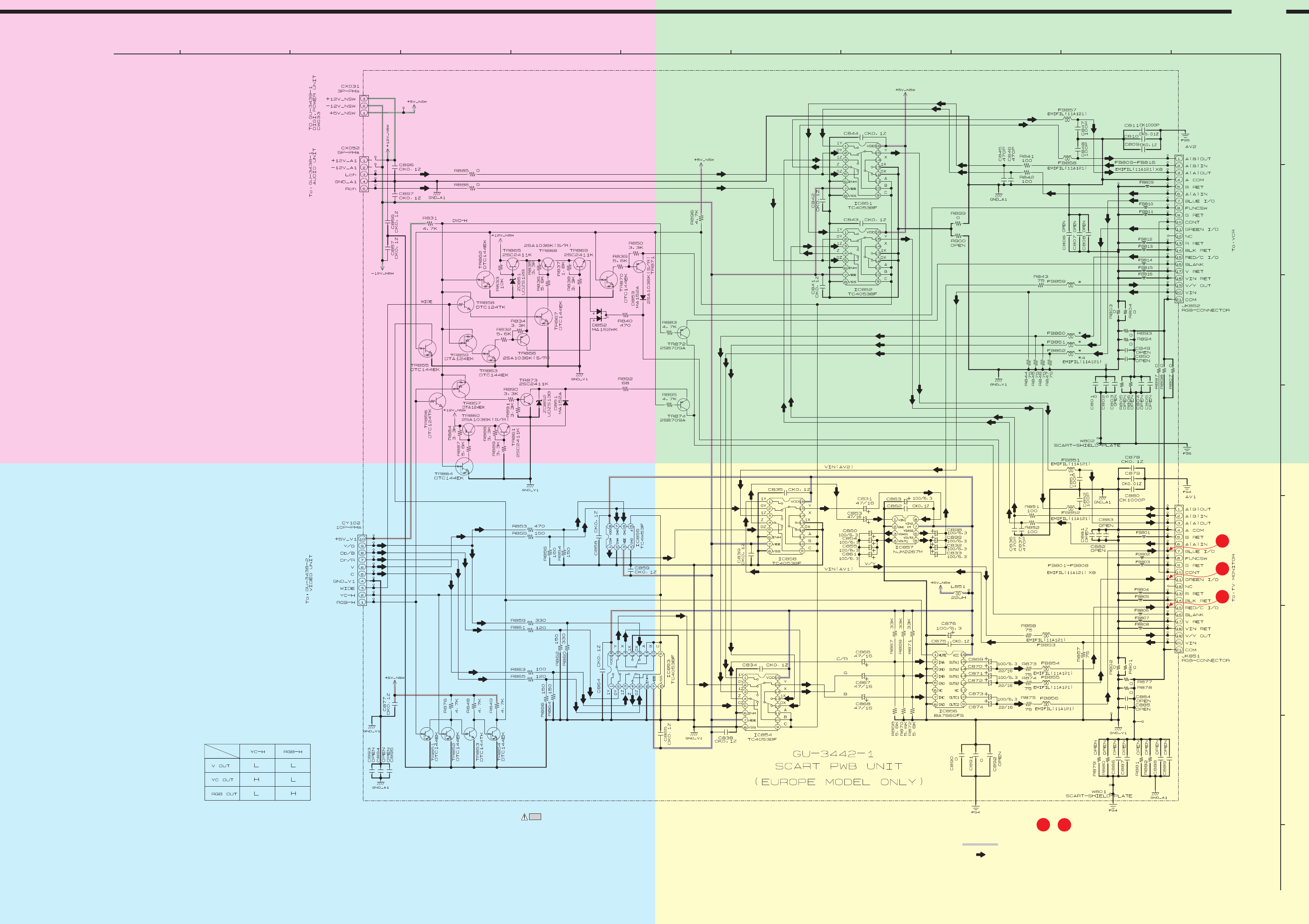
P16
P15
P14
P16
P14
For the Waveforms marked with numbers ~ , refer to page 89 (WAVEFORMS).
98
SCHEMATIC DIAGRAMS (8/8)
1 2 3 4 5 6 7 8 9 10 11
A
B
C
D
E
F
G
H
NOTICE
ALL RESISTANCE VALUES IN OHM. k=1,000 OHM M=1,000,000 OHM
ALL CAPACITANCE VALUES IN MICRO FARAD. P=MICRO-MICRO FARAD
EACH VOLTAGE AND CURRENT ARE MEASUERD AT MO SIGNAL INPUT
CONDITION.
CIRCUIT AND PARTS ARE SUBJECT TO CHANGE WITHOUT PRIOR
NOTICE.
WARNING:
Parts marked with this symbol have critical characteristics.
Use ONLY replacement parts recommended by the manufacture.
CAUTION:
Before returning the unit to the customer, make sure you make either (1) a
leakage current check or (2) a line to chassis resistance check. If the leakage
current exceeds 0.5 milliamps, or if the resistance from chassis to either side
of the power card is less than 460kohms, the unit is defective.
WARNING:
DO NOT return the unit to the customer until the problem is located and
corrected.
SIGNAL LINE
DVD-3800
B LINE
_
+
SCHEMATIC DIAGRAMS (8/8)
GU-3442-1 SCART UNIT (Europe model only)
A
AB
B
C
CD
D
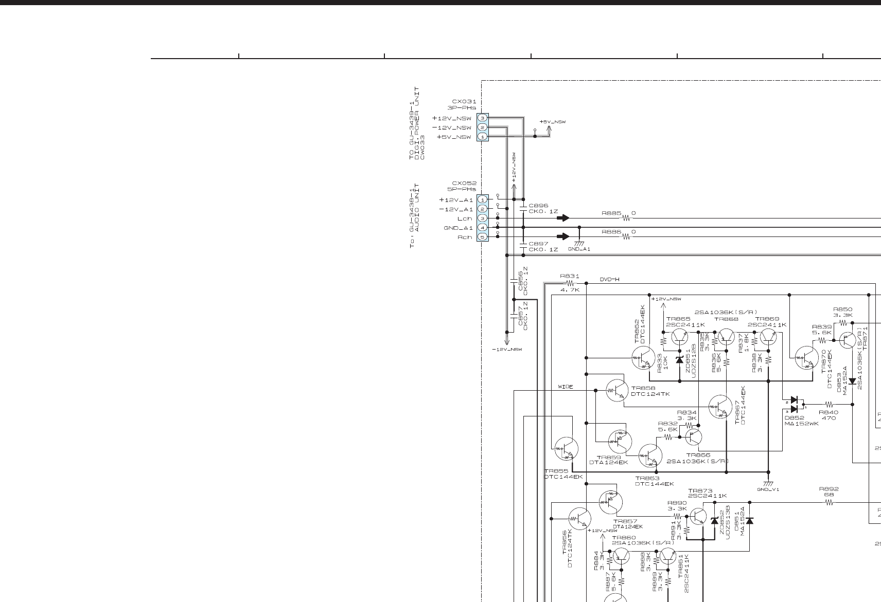
P16
P15
P14
P16
P14
For the Waveforms marked with numbers ~ , refer to page 89 (WAVEFORMS).
98
SCHEMATIC DIAGRAMS (8/8)
1 2 3 4 5 6 7 8 9 10 11
A
B
C
D
E
F
G
H
NOTICE
ALL RESISTANCE VALUES IN OHM. k=1,000 OHM M=1,000,000 OHM
ALL CAPACITANCE VALUES IN MICRO FARAD. P=MICRO-MICRO FARAD
EACH VOLTAGE AND CURRENT ARE MEASUERD AT MO SIGNAL INPUT
CONDITION.
CIRCUIT AND PARTS ARE SUBJECT TO CHANGE WITHOUT PRIOR
NOTICE.
WARNING:
Parts marked with this symbol have critical characteristics.
Use ONLY replacement parts recommended by the manufacture.
CAUTION:
Before returning the unit to the customer, make sure you make either (1) a
leakage current check or (2) a line to chassis resistance check. If the leakage
current exceeds 0.5 milliamps, or if the resistance from chassis to either side
of the power card is less than 460kohms, the unit is defective.
WARNING:
DO NOT return the unit to the customer until the problem is located and
corrected.
SIGNAL LINE
DVD-3800
B LINE
_
+
SCHEMATIC DIAGRAMS (8/8)
GU-3442-1 SCART UNIT (Europe model only)
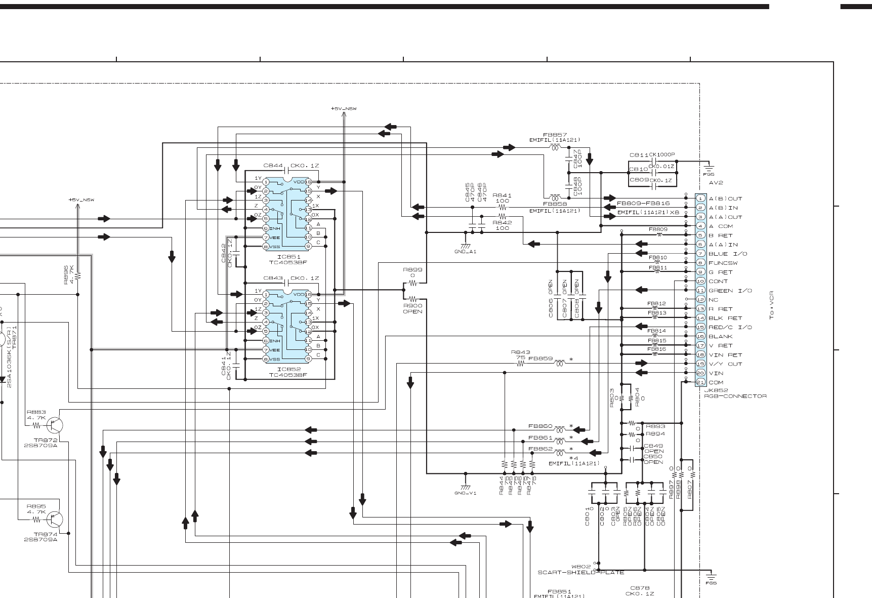
P16
P15
P14
P16
P14
For the Waveforms marked with numbers ~ , refer to page 89 (WAVEFORMS).
98
SCHEMATIC DIAGRAMS (8/8)
1 2 3 4 5 6 7 8 9 10 11
A
B
C
D
E
F
G
H
NOTICE
ALL RESISTANCE VALUES IN OHM. k=1,000 OHM M=1,000,000 OHM
ALL CAPACITANCE VALUES IN MICRO FARAD. P=MICRO-MICRO FARAD
EACH VOLTAGE AND CURRENT ARE MEASUERD AT MO SIGNAL INPUT
CONDITION.
CIRCUIT AND PARTS ARE SUBJECT TO CHANGE WITHOUT PRIOR
NOTICE.
WARNING:
Parts marked with this symbol have critical characteristics.
Use ONLY replacement parts recommended by the manufacture.
CAUTION:
Before returning the unit to the customer, make sure you make either (1) a
leakage current check or (2) a line to chassis resistance check. If the leakage
current exceeds 0.5 milliamps, or if the resistance from chassis to either side
of the power card is less than 460kohms, the unit is defective.
WARNING:
DO NOT return the unit to the customer until the problem is located and
corrected.
SIGNAL LINE
DVD-3800
B LINE
_
+
SCHEMATIC DIAGRAMS (8/8)
GU-3442-1 SCART UNIT (Europe model only)
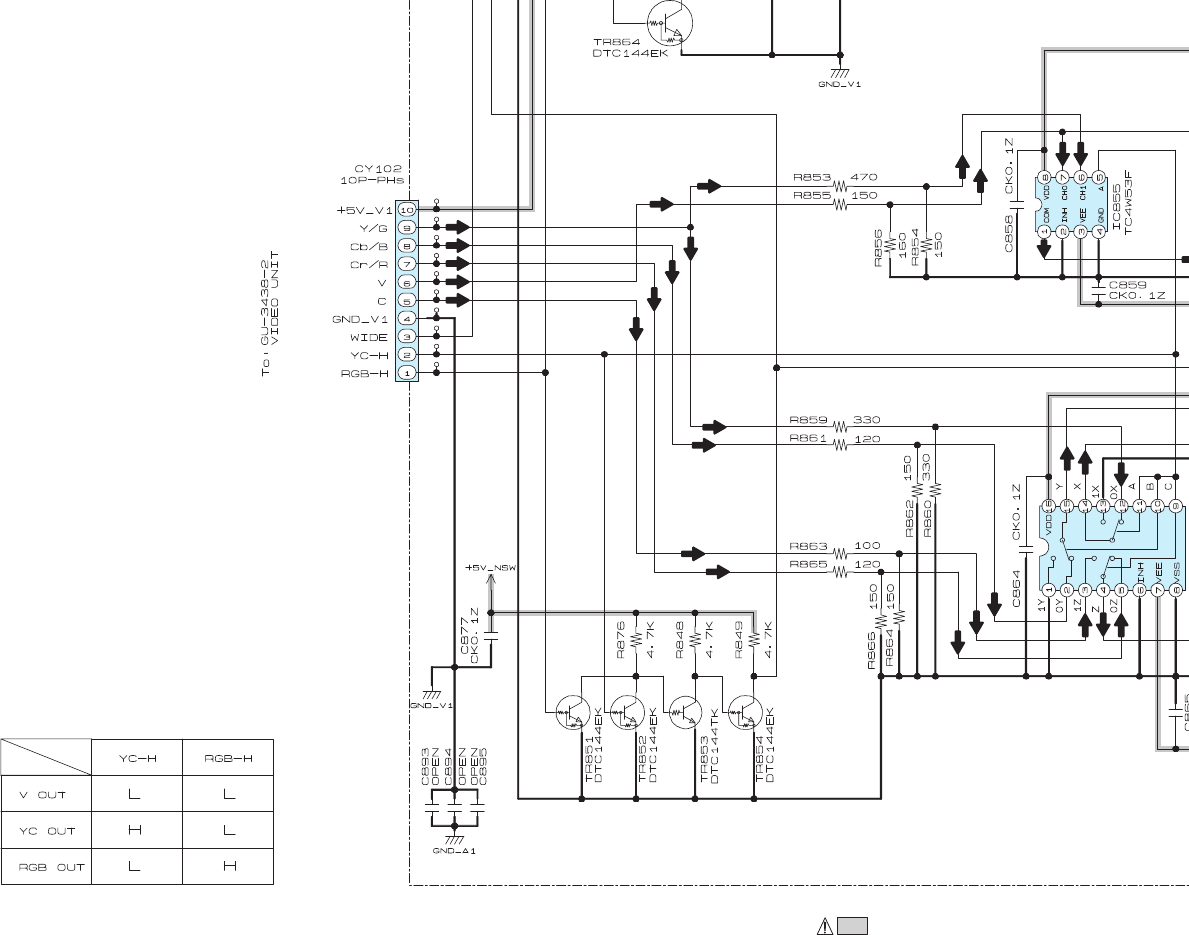
P16
P15
P14
P16
P14
For the Waveforms marked with numbers ~ , refer to page 89 (WAVEFORMS).
98
SCHEMATIC DIAGRAMS (8/8)
1 2 3 4 5 6 7 8 9 10 11
A
B
C
D
E
F
G
H
NOTICE
ALL RESISTANCE VALUES IN OHM. k=1,000 OHM M=1,000,000 OHM
ALL CAPACITANCE VALUES IN MICRO FARAD. P=MICRO-MICRO FARAD
EACH VOLTAGE AND CURRENT ARE MEASUERD AT MO SIGNAL INPUT
CONDITION.
CIRCUIT AND PARTS ARE SUBJECT TO CHANGE WITHOUT PRIOR
NOTICE.
WARNING:
Parts marked with this symbol have critical characteristics.
Use ONLY replacement parts recommended by the manufacture.
CAUTION:
Before returning the unit to the customer, make sure you make either (1) a
leakage current check or (2) a line to chassis resistance check. If the leakage
current exceeds 0.5 milliamps, or if the resistance from chassis to either side
of the power card is less than 460kohms, the unit is defective.
WARNING:
DO NOT return the unit to the customer until the problem is located and
corrected.
SIGNAL LINE
DVD-3800
B LINE
_
+
SCHEMATIC DIAGRAMS (8/8)
GU-3442-1 SCART UNIT (Europe model only)
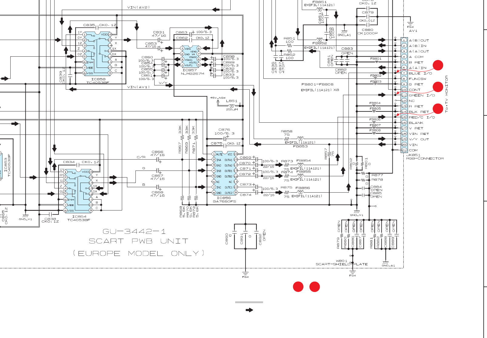
P16
P15
P14
P16
P14
For the Waveforms marked with numbers ~ , refer to page 89 (WAVEFORMS).
98
SCHEMATIC DIAGRAMS (8/8)
1 2 3 4 5 6 7 8 9 10 11
A
B
C
D
E
F
G
H
NOTICE
ALL RESISTANCE VALUES IN OHM. k=1,000 OHM M=1,000,000 OHM
ALL CAPACITANCE VALUES IN MICRO FARAD. P=MICRO-MICRO FARAD
EACH VOLTAGE AND CURRENT ARE MEASUERD AT MO SIGNAL INPUT
CONDITION.
CIRCUIT AND PARTS ARE SUBJECT TO CHANGE WITHOUT PRIOR
NOTICE.
WARNING:
Parts marked with this symbol have critical characteristics.
Use ONLY replacement parts recommended by the manufacture.
CAUTION:
Before returning the unit to the customer, make sure you make either (1) a
leakage current check or (2) a line to chassis resistance check. If the leakage
current exceeds 0.5 milliamps, or if the resistance from chassis to either side
of the power card is less than 460kohms, the unit is defective.
WARNING:
DO NOT return the unit to the customer until the problem is located and
corrected.
SIGNAL LINE
DVD-3800
B LINE
_
+
SCHEMATIC DIAGRAMS (8/8)
GU-3442-1 SCART UNIT (Europe model only)
