A4_DVDR5350H_SM_cover DVDR5350
User Manual: DVDR5350
Open the PDF directly: View PDF ![]() .
.
Page Count: 194 [warning: Documents this large are best viewed by clicking the View PDF Link!]

Published by KC-TE 0636 AV Systems Printed in the Netherlands Subject to modification EN 3139 785 31532
DVDR5350H/02/05/19
HDD & DVD Recorder
CLASS 1
LASER PRODUCT
Contents Page
1 Technical Specifications and Connection
Facilities 2
2 Safety Information, General Notes & Lead
Free Requirements 5
3 Directions for Use 7
4 Mechanical Instructions 10
5 Firmware Upgrading & Diagnostic Software 14
6 Block Diagrams,Waveforms, Wiring Diagram 117
Overall block diagram 117
Wiring diagram 118
Waveforms of Analog Board 119
Waveforms of Digital Board 120
Waveforms of Front Board 121
Waveforms of HDMI Board 121
Test Points Overview for Analog Board 122
Test Points Overview for Display/
Front Connector Board 123
Test Points Overview for Digital Board 124
Test Points Overview for HDMI Board 125
Contents Page
7 Circuit Diagrams and PWB Layout 126
Analog Circuit Diagrams 126
Analog Layout Diagrams 136
Front Display/Connector Circuit Diagrams 138
Front Display/Connector Layout Diagrams 140
Front Standby Circuit & Layout Diagrams 141
Front Tray LED Left/Right Circuit &
Layout Diagrams 142
Digital Circuit Diagrams 143
Digital Layout Diagrams 154
HDMI Circuit Diagrams 156
HDMI Layout Diagrams 160
8 Alignments & Test Procedures 163
9 Circuit and IC description 164
Circuit Description 164
IC Description 172
10 Exploded view & Service parts list 188
Exploded view 188
Service parts list 192
11 Revision list 194
©Copyright 2005 Philips Consumer Electronics B.V. Eindhoven, The Netherlands.
All rights reserved. No part of this publication may be reproduced, stored in a
retrieval system or transmitted, in any form or by any means, electronic,
mechanical, photocopying, or otherwise without the prior permission of Philips.
Version 1.2
DVDR7310H/75/97 & DVDR7300H/02/05/19/75/97
EN 2 3139 785 31532
1. Technical Specifi cations and Connection Facilities
1. Technical Specifi cations and Connection Facilities
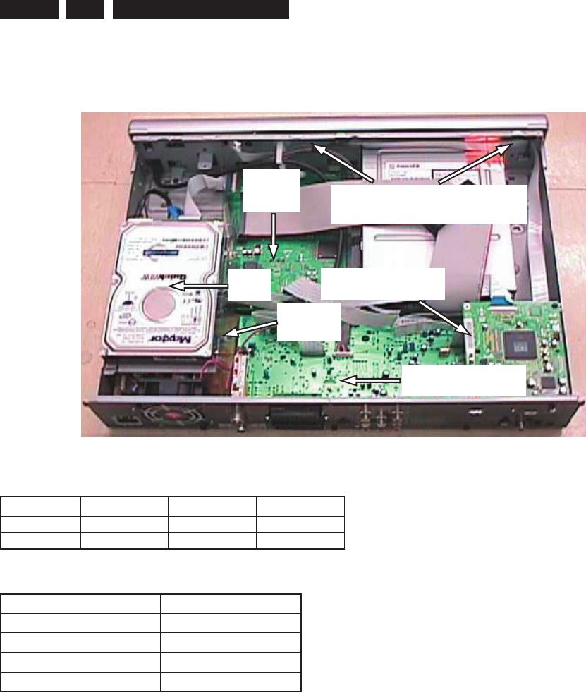
1.1 PCB Locations
1.2 Diversity Matrix
DVDR5350H DVDR7300H DVDR7310H
HDD capacity 160GB 250GB 250GB
HDMI – x x
1.3 Read / Write Speed
Type of Disc (Function) Disc Rotation Speed
Read Speed CD 7X CAV
Read Speed DVD 4X CAV
Write Speed DVD+R/+RW 2.4X ZCAV
Write Speed DVD-R/-RW 2X
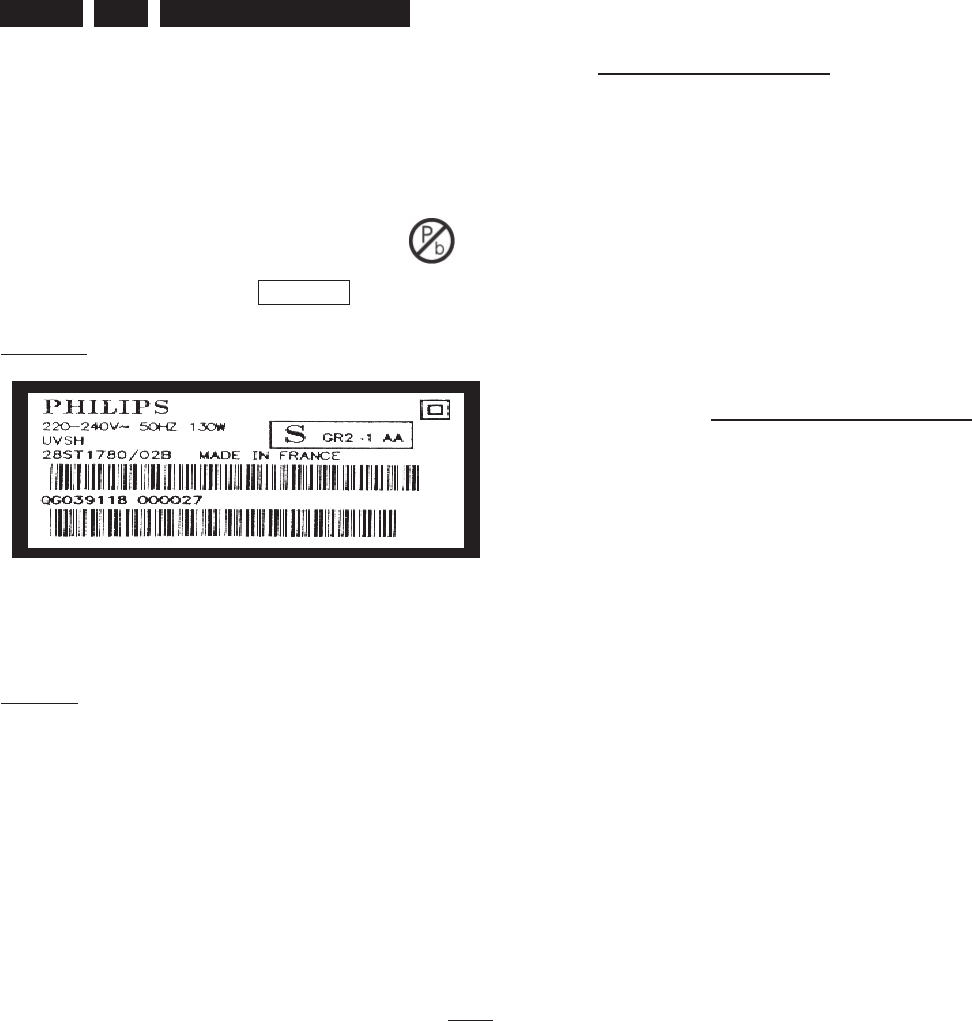
1.4 General:
Mains voltage : 220V – 240V
Mains frequency : 50 Hz
Power consumption (record) : 40 W
Standby Power Consumption : < 4 W
Eco standby : < 3 W
1.5 RF Tuner
Test equipment: Fluke 54200 TV Signal generator
Test streams: PAL BG Philips Standard test pattern
1.5.1 System
PAL B/G, PAL D/K, SECAM L/L’, PAL I
1.5.2 RF - Loop Through:
Frequency range : 45 MHz – 860 MHz
Gain: (ANT IN - ANT OUT) : -6dB to 0dB
1.5.3 Receiver:
PLL tuning with AFC for optimum reception
Frequency range : 45.25 MHz – 857 MHz
Sensitivity at 40dB S/N
(video unweighted) : 60dBV at 75
1.5.4 Video Performance:
Channel 25 / 503,25 MHz,
Test pattern: PAL BG PHILIPS standard test pattern,
RF Level 74dBV, Measured on SCART 1
Frequency response : 0.1 MHz – 4 MHz ± 3dB
Group delay (0.1 MHz - 4.4 MHz) : 0 nsec ± 150 nsec
1.5.5 Audio Performance:
Audio Performance Analogue - HiFi:
Frequency response at SCART 1
(L+R) output : 100 Hz – 12 kHz / 0 ±
3dB
S/N Ratio (20Hz – 20kHz)
unweighted : 50dB
Harmonic distortion (1 kHz, ± 25
kHz deviation) : 1.5%
Audio Performance NICAM:
Frequency response at SCART 1
(L+R) output : 40 Hz – 15 kHz / 0 ±
3dB
S/N Ratio (20Hz – 20kHz)
unweighted : 60dB
Harmonic distortion (1kHz, ± 25
kHz deviation) : 0.5%
Analog Board
HDMI Board
Front Boards
(Behind the Front Plate)
HDD
Digital
Board
PSU
Board

EN 3
3139 785 31532 1.
Technical Specifi cations and Connection Facilities
1.5.6 Tuning
Automatic Search Tuning
Scanning time without RF signal : 3min. typical
Stop level (vision carrier) : 37dB/V
Maximum tuning error of a recalled
program : ± 100 kHz
Maximum tuning error (drift) during
operation : ± 100 kHz
Tuning Principle:
Automatic B, G, I, DK and L/L’ detection
Manual selection in “STORE” mode
1.6 Analog Inputs / Outputs
1.6.1 SCART 1 (Connected to TV)
Pin Signals:
1 Audio-out R 1.8V RMS
2 Audio-in R
3 Audio-out L 1.8V RMS
4 Audio GND
5 Blue / Chroma GND
6 Audio-in L
7 Blue-out 0.7Vpp ± 0.1V into 75
8 Function switch < 2V = TV
> 4.5V / < 7V = asp. Ratio 16:9 DVD
> 9.5V / < 12V = asp. Ratio 4:3 DVD
9 Green GND
10 P50 control not use
11 Green out 0.7Vpp ± 0.1V into 75
12 NC
13 Red / Chroma GND
14 Fast switch GND
15 Red-out / 0.7Vpp ± 0.1V into 75
Chroma-out 300mVpp ± 3dB
16 Fast switch
RGB / CVBS
or Y out < 0.4V into 75 = CVBS
>1V / < 3V into 75 = RGB
17 Y/CVBS-out GND
18 CVBS-in GND
19 CVBS-out / Y-out 1Vpp ± 0.1V into 75
20 CVBS-in
21 Shield
1.6.2 SCART 2 (Connected to AUX)
Pin Signals:
1 Audio-out R 1.8V RMS
2 Audio-in R
3 Audio-out L 1.8V RMS
4 Audio GND
5 Blue / Chroma GND
6 Audio-in L
7 Blue-in
8 Function switch
9 Green GND
10 P50 control
11 Green-in
12 NC
13 Red / Chroma GND
14 Fast switch GND
15 Red-in /
Chroma-in
16 Fast switch
RGB / CVBS or Y in
17 CVBS-out GND
18 Y / CVBS-in GND
19 CVBS-out 1Vpp ± 0.1V into 75
20 CVBS-in / Y-in
21 Shield
1.6.3 Audio/Video Front Input Connectors
Audio - Cinch
Input voltage : 2.2Vrms
Input impedance : > 10k
Video - Cinch
Input voltage : 1Vpp ± 3dB
Input impedance : 75
Video - YC (Hosiden)
According to IEC 933-5
Superimposed DC-level on pin 4 (load > 100k)
< 2.4V is detected as 4:3 aspect ratio
> 3.5V is detected as 16:9 aspect ratio
Input voltage Y : 1Vpp ± 3dB
Input impedance Y : 75
Input voltage C : 300mVpp ± 3dB
Input impedance C : 75
1.6.4 Out 1
Component Video Cinch Y/Pb/Pr
according EIO-770-I-A, EIA-770-2
Audio - Cinch
Output voltage : 2Vrms max.
Output impedance : > 10k
1.6.5 Out 2
Audio - Cinch
Output voltage : 2Vrms max.
Output impedance : > 10k
Video - Cinch
Output voltage : 1Vpp ± 3dB
Output impedance : 75
Video - YC (Hosiden)
According to IEC 933-5
Superimposed DC-level on pin 4 (load > 100k)
< 2.4V is detected as 4:3 aspect ratio
> 3.5V is detected as 16:9 aspect ratio
Output voltage Y : 1Vpp ± 3dB
Input impedance : 75
Output voltage C : 300mVpp ± 3dB
Input impedance : 75
1.7 Digital Inputs / Outputs
1.7.1 Digital Output
Digital Audio – Coaxial / Optical
LCM : according IEC 60958
MPEG 1, MPEG 2, AC3 : according IEC 61937
DTS : according IEC 61937 +
addendum
1.7.2 HDMI Output
Type A connector (19 pins)
1.7.3 Digital Video Input (IEEE 1394)
Implementation Standard according:
IEEE Std 1394-1995
IEC61883 - Part1
IEC61883 - Part 2 SD-DVCR (02-01-1997)
Specifi cation of consumer use digital VCR’s using 6.3mm
magnetic tape – dec.1994
Mechanical connection according to Annex of IEC 61883-1

EN 4 3139 785 31532
1. Technical Specifi cations and Connection Facilities
1.7.4 G-Link (for IR-remote transmitting device)
Output voltage : 5 ± 0.5V (high level)
0.4 ± 0.3V (low level)
Output impedance : 150
1.8 Video Performance
All outputs loaded with 75
SNR measurements over full bandwidth without weighting.
1.8.1 SCART (RGB)
SNR : 55dB on all output
Bandwidth : 4.8MHz -3dB
1.9 Audio Performance
1.9.1 Cinch Output Rear
Output voltage 2 channel mode : 2Vrms ± 2dB
Channel unbalance (1kHz) : < 0.22dB
Crosstalk 1kHz : > 100dB
Crosstalk 16Hz-20kHz : > 87dB
Frequency response 20Hz-20kHz : ± 0.5dB
Signal to noise ratio (unweighted) : > 85dB
Dynamic range 1kHz : > 83dB
Distortion and noise 1kHz : > 83dB
Distortion and noise 16Hz-20kHz : > 75dB
Intermodulation distortion : > 70dB
Mute : > 95dB
1.9.2 Scart Audio
Output voltage 2 channel mode : 1.6Vrms ± 2dB
Channel unbalance (1kHz) : < 1dB
Crosstalk 1kHz : > 85dB
Crosstalk 16Hz-20kHz : > 70dB
Frequency response 20Hz-20kHz : ± 0.5dB
Signal to noise ratio (unweighted) : > 80dB
Dynamic range 1kHz : > 75dB
Distortion and noise 1kHz : > 75dB
Distortion and noise 16Hz-20kHz : > 50dB
Intermodulation distortion : > 70dB
Mute : > 80dB
1.10 Dimensions and Weight
Height of feet : 5.5mm
Apparatus tray closed : WxDxH:435x335x76mm
Apparatus tray open : WxDxH:435x472x76mm
Weight without packaging : 5kg
Weight with packaging : 8kg
1.11 Laser Output Power & Wavelength
1.11.1 DVD
Output power during reading : 0.8mW
Output power during writing : 20mW
Wavelength : 650nm
1.11.2 CD
Output power : 0.3mW
Wavelength : 780nm

EN 5
3139 785 31532 2.
Safety Information, General Notes & Lead Free Requirements
2.1 Safety Instructions
2.1.1 General Safety
Safety regulations require that during a repair:
• Connect the unit to the mains via an isolation transformer.
• Replace safety components, indicated by the symbol ,
only by components identical to the original ones. Any
other component substitution (other than original type)
may increase risk of fi re or electrical shock hazard.
Safety regulations require that after a repair, you must return
the unit in its original condition. Pay, in particular, attention to
the following points:
• Route the wires/cables correctly, and fi x them with the
mounted cable clamps.
• Check the insulation of the mains lead for external
damage.
• Check the electrical DC resistance between the mains
plug and the secondary side:
1. Unplug the mains cord, and connect a wire between
the two pins of the mains plug.
2. Set the mains switch to the ‘on’ position (keep the
mains cord unplugged!).
3. Measure the resistance value between the mains
plug and the front panel, controls, and chassis
bottom.
4. Repair or correct unit when the resistance
measurement is less than 1 M.
5. Verify this, before you return the unit to the customer/
user (ref. UL-standard no. 1492).
6. Switch the unit ‘off’, and remove the wire between the
two pins of the mains plug.
2.1.2 Laser Safety
This unit employs a laser. Only qualifi ed service personnel
may remove the cover, or attempt to service this device (due
to possible eye injury).
Laser Device Unit
Type : Semiconductor laser
GaAlAs
Wavelength : 650 nm (DVD)
: 780 nm (VCD/CD)
Output Power : 20 mW
(DVD+RW writing)
: 0.8 mW
(DVD reading)
: 0.3 mW
(VCD/CD reading)
Beam divergence : 60 degree
CLASS 1
LASER PRODUCT
Figure 2-1
Note: Use of controls or adjustments or performance of
procedure other than those specifi ed herein, may result in
hazardous radiation exposure. Avoid direct exposure to beam.
2.2 Warnings
2.2.1 General
• All ICs and many other semiconductors are susceptible to
electrostatic discharges (ESD, ). Careless handling
during repair can reduce life drastically. Make sure that,
during repair, you are at the same potential as the mass
of the set by a wristband with resistance. Keep
components and tools at this same potential.
Available ESD protection equipment:
– Complete kit ESD3 (small tablemat, wristband,
connection box, extension cable and earth cable)
4822 310 10671.
– Wristband tester 4822 344 13999.
• Be careful during measurements in the live voltage
section. The primary side of the power supply, including
the heatsink, carries live mains voltage when you
connect the player to the mains (even when the
player is ‘off’!). It is possible to touch copper tracks and/
or components in this unshielded primary area, when
you service the player. Service personnel must take
precautions to prevent touching this area or components
in this area. A ‘lightning stroke’ and a stripe-marked
printing on the printed wiring board, indicate the primary
side of the power supply.
• Never replace modules, or components, while the unit is
‘on’.
2.2.2 Laser
• The use of optical instruments with this product, will
increase eye hazard.
• Only qualifi ed service personnel may remove the cover or
attempt to service this device, due to possible eye injury.
• Repair handling should take place as much as possible
with a disc loaded inside the player.
• Text below is placed inside the unit, on the laser cover
shield:
Figure 2-2
2. Safety Information, General Notes & Lead Free Requirements
CAUTION VISIBLE AND INVISIBLE LASER RADIATION WHEN OPEN AVOID EXPOSURE TO BEAM
ADVARSEL SYNLIG OG USYNLIG LASERSTRÅLING VED ÅBNING UNDGÅ UDSÆTTELSE FOR STRÅLING
ADVARSEL SYNLIG OG USYNLIG LASERSTRÅLING NÅR DEKSEL ÅPNES UNNGÅ EKSPONERING FOR STRÅLEN
VARNING SYNLIG OCH OSYNLIG LASERSTRÅLNING NÄR DENNA DEL ÄR ÖPPNAD BETRAKTA EJ STRÅLEN
VARO! AVATTAESSA OLET ALTTIINA NÄKYVÄLLE JA NÄKYMÄTTÖMÄLLE LASER SÄTEILYLLE. ÄLÄ KATSO SÄTEESEEN
VORSICHT SICHTBARE UND UNSICHTBARE LASERSTRAHLUNG WENN ABDECKUNG GEÖFFNET NICHT DEM STRAHL AUSSETSEN
DANGER VISIBLE AND INVISIBLE LASER RADIATION WHEN OPEN AVOID DIRECT EXPOSURE TO BEAM
ATTENTION RAYONNEMENT LASER VISIBLE ET INVISIBLE EN CAS D’OUVERTURE EXPOSITION DANGEREUSE AU FAISCEAU
EN 6 3139 785 31532
2. Safety Information, General Notes & Lead Free Requirements
2.3 Lead Free Requirement
Information about Lead-free produced sets
Philips CE is starting production of lead-free sets from
1.1.2005 onwards.
INDENTIFICATION:
Regardless of special logo (not always indicated)
One must treat all sets from 1 Jan 2005 onwards, according
next rules.
Example S/N:
Bottom line of typeplate gives a 14-digit S/N. Digit 5&6 is the year, digit 7&8 is
the week number, so in this case 1991 wk 18
So from 0501 onwards = from 1 Jan 2005 onwards
Important note: In fact also products of year 2004 must be treated in this way as long as you
avoid mixing solder-alloys (leaded/ lead-free). So best to always use SAC305 and the higher
temperatures belong to this.
Due to lead-free technology some rules have to be respected by the
workshop during a repair:
• Use only lead-free solder alloy Philips SAC305 with order
code 0622 149 00106. If lead-free solder-pate is required,
please contact the manufacturer of your solder-equipment.
In general use of solder-paste within workshops should be
avoided because paste is not easy to store and to handle.
• Use only adequate solder tools applicable for lead-free
solder alloy. The solder tool must be able
o To reach at least a solder-temperature of 400°C,
o To stabilize the adjusted temperature at the solder-tip
o To exchange solder-tips for different applications.
• Adjust your solder tool so that a temperature around 360°C
– 380°C is reached and stabilized at the solder joint.
Heating-time of the solder-joint should not exceed ~ 4 sec.
Avoid temperatures above 400°C otherwise wear-out of
tips will rise drastically and fl ux-fl uid will be destroyed. To
avoid wear-out of tips switch off un-used equipment, or
reduce heat.
• Mix of lead-free solder alloy / parts with leaded solder alloy
/ parts is possible but PHILIPS recommends strongly to
avoid mixed solder alloy types (leaded and lead-free).
If one cannot avoid or does not know whether product is
lead-free, clean carefully the solder-joint from old solder
alloy and re-solder with new solder alloy (SAC305).
• Use only original spare-parts listed in the Service-Manuals.
Not listed standard-material (commodities) has to be
purchased at external companies.
• Special information for BGA-ICs:
- always use the 12nc-recognizable soldering temperature
profi le of the specifi c BGA (for de-soldering always use the
lead-free temperature profi le, in case of doubt)
- lead free BGA-ICs will be delivered in so-called ‘dry-
packaging’ (sealed pack including a silica gel pack) to
protect the IC against moisture. After opening, dependent
of MSL-level seen on indicator-label in the bag, the
BGA-IC possibly still has to be baked dry. (MSL=Moisture
Sensitivity Level). This will be communicated via AYS-
website.
Do not re-use BGAs at all.
• For sets produced before 1.1.2005 (except products of
2004), containing leaded solder-alloy and components,
all needed spare-parts will be available till the end of the
service-period. For repair of such sets nothing changes.
• On our website www.atyourservice.ce.Philips.com you
fi nd more information to:
BGA-de-/soldering (+ baking instructions)
Heating-profi les of BGAs and other ICs used in Philips-sets
You will fi nd this and more technical information within the
“magazine”, chapter “workshop news”.
For additional questions please contact your local repair-helpdesk.
EN 7
3139 785 31532
3. Directions For Use
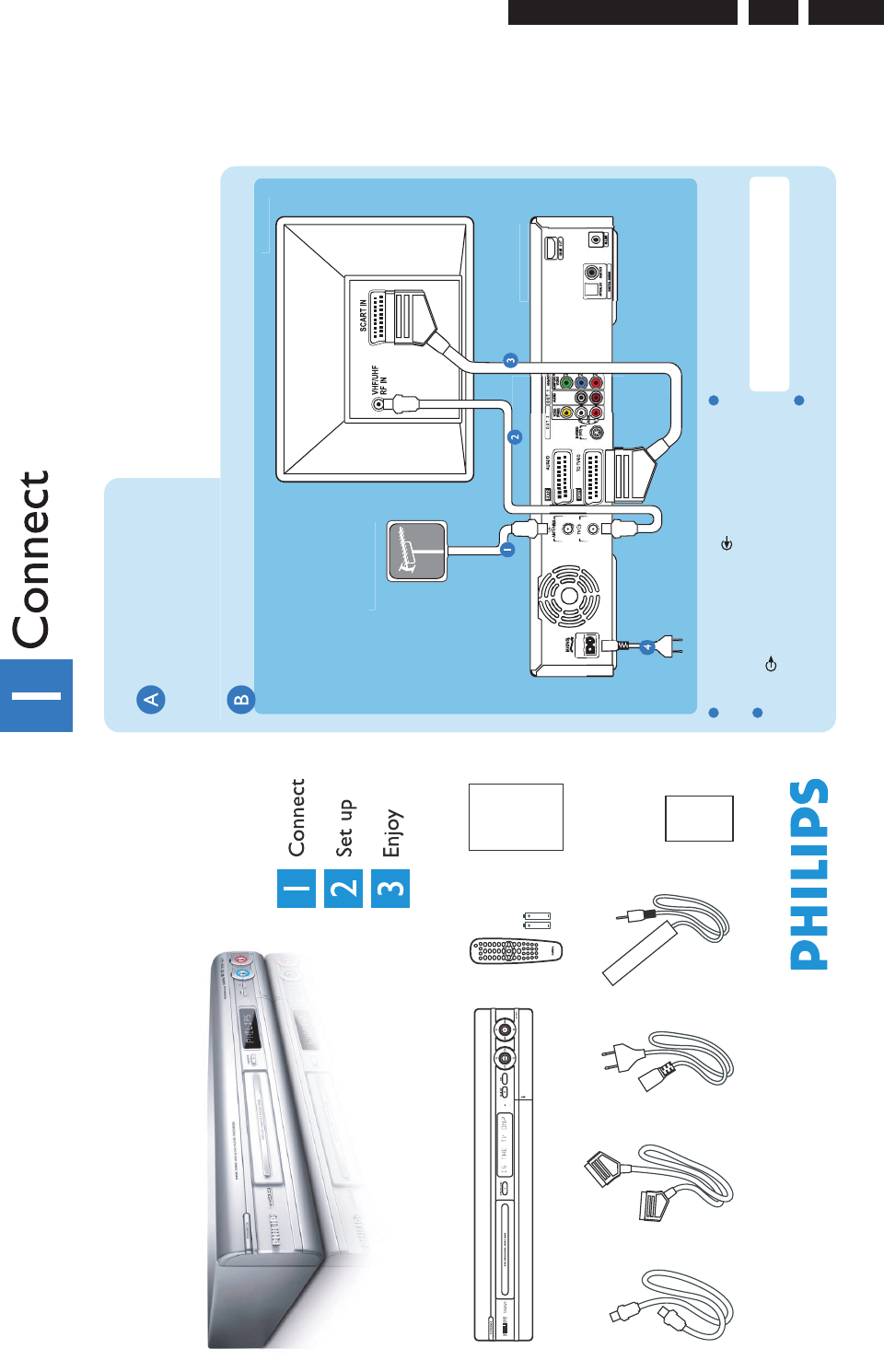
The following except of the Quick Use Guide serves as an introduction to the set.
The Complete Direction for the Use can be downloaded in different languages from the internet site of Philips Customer care Center:
www.p4c.philips.com
Quick Start Guide
DVDR 5350H
DVDR 7300H
HDD & DVD Player / Recorder
RF coaxial cable Scart cable
G-LINK cable
& transmitterPower cable
Quick start guideRemote control
and 2 batteries
User manual
DVD recorder/hard disk
What’s in the Box
3.
Directions For Use
From
a
n off-
a
ir
a
nt
e
nn
a
or
cable
b
o
x
Television (rear
)
Phili
p
s Recorder
(
rear
)
Basic connection
Before connecting
Unplug the antenna cable that is currently
connected to your TV.
Connecting
1 Disconnect the antenna cable from your TV
and connect it to the ANTENNA socket
on this recorder.
2 Use the supplied RF coaxial cable to connect
the TV socket on this recorder to the
Antenna In socket on your TV.
3 Use the supplied scart cable to connect the
EXT1 TO TV-I/O Scart socket on this
recorder to the SCART IN socket on your TV.
Note See the accompanying user manual for
others possible connection (e.g. HDMI,
Component Video).
4 Connect the power cable from the recorder
to an AC power outlet.
Start with the 'Basic connection'.
If you have a VCR, follow the instructions for ‘Connection with VCR or similar device’.
If you have a set-top box, follow the instructions for ‘Connection with set-top box’.
EN 8 3139 785 31532
3. Directions For Use
Setup External Receiver 1
Has the External Receiver 1 changed to Programme
Number 101?
Television
(
rear
)
V
C
R
o
r
s
imil
ar
device
(
rear
)
Positionin
g
of G-LINK transmitte
r
set-to
p
bo
x
G
-LINK
t
r
a
n
s
mi
tte
r
Television
(
rear
)
T
o
sou
r
ce
Se
(
GUIDE
(rear)
p
p
From an off-air
antenna or
cable box
Connection with VCR
or similar device
Before connecting
Your new Philips Recorder replaces the VCR for
your recording needs. First, unplug all the
connections from your VCR.
Connecting
1 Follow step 1 to 4 of 'Basic connection' to
connect this recorder before you proceed to
step 2 below.
2 Use another scart cable (not supplied) to
connect the EXT2 AUX-I/O Scart socket on
this recorder to the SCART OUT socket on
your VCR.
3 Connect the power cable from the VCR to an
AC power outlet.
Note In this setup, the VCR cannot record
TV programmes.
Connection with set-top box
Your new Philips Recorder provides a G-LINK
transmitter which allows you to control the
tuner of the set-top box (satellite receiver, cable
TV box) through the GUIDE Plus+ system. You
can record the TV programmes that are received
through the set-top box.
Connecting
1 Follow step 1 to 4 of 'Basic connection' to
connect this recorder before you proceed to
step 2 below.
2 Connect the supplied G-LINK cable to the
G-LINK socket on this recorder.
3 Place the G-LINK transmitter in front of your
set-top box in such a way that it can acquire
the signal broadcasted by the transmitter.
4 Connect the power cable from the set-top
box to an AC power outlet.
Finding the viewing channel
1 Press STANDBY-ON on the recorder.
The recorder will display ‘IS THE TV ON?’.
2 Switch on the TV.
You should see the { EASY SETUP } menu.
Note If connected to your VCR, make sure it
is turned off before proceeding.
3 If not, press the Channel Down button on
your TV's remote control repeatedly (or AV,
SELECT button) until you see the menu. This
is the correct viewing channel for the recorder.
Start basic setup
Use the recorder's remote control and follow
the on-screen instructions to complete the
installation.
1 Select the desired menu language, your
country and the TV shape.
Note Select { Done } in the menu and press
to go to the next screen.
2 Activate automatic channel search.
3 Check the date and time and press .
4 To continue with the GUIDE Plus+
installation, select { Continue } and press .
Otherwise, select { Do not install now } and
press . Wait until the recorder has finished
initialising the system, then press again.
Install the GUIDE Plus+ system
1 Enter your language, country and postal code
To change, press and follow the on-screen
instructions.
Install the set-top box
If you do not have a set-top box, skip ‘D’ and go
to ‘E’.
1 Press DOWN to select ‘External
Receiver 1’ and press .
2 Press again to continue.
3 Select the type of reception, service provider
and brand name of the connected set-top box.
Note Press to go to the next screen.
Select { None } if none of the entries are
applicable.
4 Select the recorder socket through which
your set-top box is connected (e.g. 'EXT2' for
EXT 2 AUX-I/O socket) and press .
5 Turn on your set-top box and select channel
number 02 on the set-top box.
6 Read the instructions on the TV and press .
7 The recorder will now attempt to change the
set-top box’s channel through the G-LINK
transmitter. If the set-top box has switched to
the same programme number as displayed on
the TV, select { Yes } in the menu and press .
Note If not, select { No } and press to try a
different code.
8 Your set-top box is now installed.
Load the TV listing data
1 Press the GREEN button to leave the
menu.
Note To switch the GUIDE Plus+ system’s host
channel manually, go to { Host Channel Setup }.
2 Press GUIDE to exit the GUIDE Plus+
system. Leave the recorder in 'standby' mode
and turn 'on' the set-top box overnight to
collect the TV listing data, this may take up to
24 hours.
Note If you tune to your Host Channel
before going to 'standby' mode, this recorder
will start immediately to download the TV
listings data.
3 Check the { Editor } screen the next day to
ensure the source and programme numbers
are matching for all channels.
EN 9
3139 785 31532
COPY
PAU SE
BROWSER
BACK
Record
Mode
HQ
SP
SPP
LP
EP
SLP
SEP
Hours of recordings can be stored on the
HDD or an empty DVD recordable disc.
1
2
2.5
3
4
6
8
DVD±R/
DVD±RW
HDD
(250 GB)
47
95
119
143
191
287
400
DVD+R
Double Layer
1hr 55mins
3hr 40mins
4hr 35mins
5hr 30mins
7hr 20mins
11h 05mins
14h 45mins
Start playback
From the hard disk
1 Press HDD-BROWSER , then press
RIGHT until you see the { TITLES } and
{ INFO } menus.
2 Press UP or DOWN to select a title.
3 Press PLAY to start playback.
Search TV programmes
1 Press UP until you highlight the menu bar
(‘Grid’, ‘Search’, ‘My TV’, etc.)
2 Highlight { Search } and press DOWN .
3 Press RIGHT or LEFT to select a
search category and press DOWN .
4 Press DOWN to select a sub-category
and press to start the search.
Note If ‘No programme found’ appears, that
means there are no programmes of that
category for that day.
Using the GUIDE Plus+ system
Make sure that the TV listing data download is
completed.
Record TV programmes
1 Press GUIDE .
2 Press DOWN to select a TV channel.
Note Press the YELLOW to see an
overview of all the available channels and
choose from there.
3 Press RIGHT or LEFT to select a
TV programme.
Note Press DAY- or DAY+ to go
directly to a day before or the next day TV
listings.
4 Press the RED button to set the
highlighted programme for recording.
Note You can store up to 25 programmes for
recording.
Watch TV - Pause live TV
Your Philips Recorder allows you to control the TV
programme. You can PAUSE it as if you were in
control of the live broadcast.
1 Turn on your recorder and press CHANNEL
+/- to select a TV programme.
2 Press PAUSE to suspend it.
3 Press PLAY to continue.
Note When the recorder is turned on, the
programme you are watching will be stored in
the temporary hard disk storage. When you
switch the recorder to another input signal (e.g.
CAM) or to standby mode, the programme will
be erased.
4 Press TUNER to return to the live
broadcast.
Record to hard disk
Contents in the temporary
HDD storage
1 Press INFO to see what is temporarily
stored in the hard disk storage.
2 Press UP or DOWN to choose the
title you want to record.
3 Press REC to record the title.
Note The title will be marked in red and the
recording will only take effect when you turn
off the recorder.
From a disc
1 Hold down the STOP until the disc tray
opens, load in a disc and close the disc tray.
2 If the content menu appears, press RIGHT
until you see the { TITLES }, { TRACKS } or
{ PHOTO ROLLS } menu, depending on the
disc type.
3 Press UP or DOWN to select a title.
4 Press PLAY to start playback.
Need help?
GUIDE Plus+ system
Go to www.europe.guideplus.com
User Manual
See the user manual that came with your Philips
Recorder
Online
Go to www.philips.com/support 2005 © Koninklijke Philips N.V.
All rights reserved.
12 NC 31 39 246 18511
www.philips.com
SOURCES 1/3
Hard Disk
Disc Tray
Disc Library
Video
Audio
Photo
CONTENT
[BROWSER]
Current TV programme
1 Press REC to start recording. It can record
up to 6 hours.
Note To set the recording time, press REC
repeatedly to extend the recording time in 30
minutes increments for up to 6 hours.
If the GUIDE Plus+ system is available, ‘Record
1 program’ is displayed and the current
programme will be recorded.
2 Press STOP to stop the recording
immediately.
DAY-
GUIDE
DAY+
3.
Directions For Use
EN 10 3139 785 31532
4. Mechanical Instructions
4. Mechanical Instructions
Note: The position numbers given here refers to the
Exploded view on chapter 10.
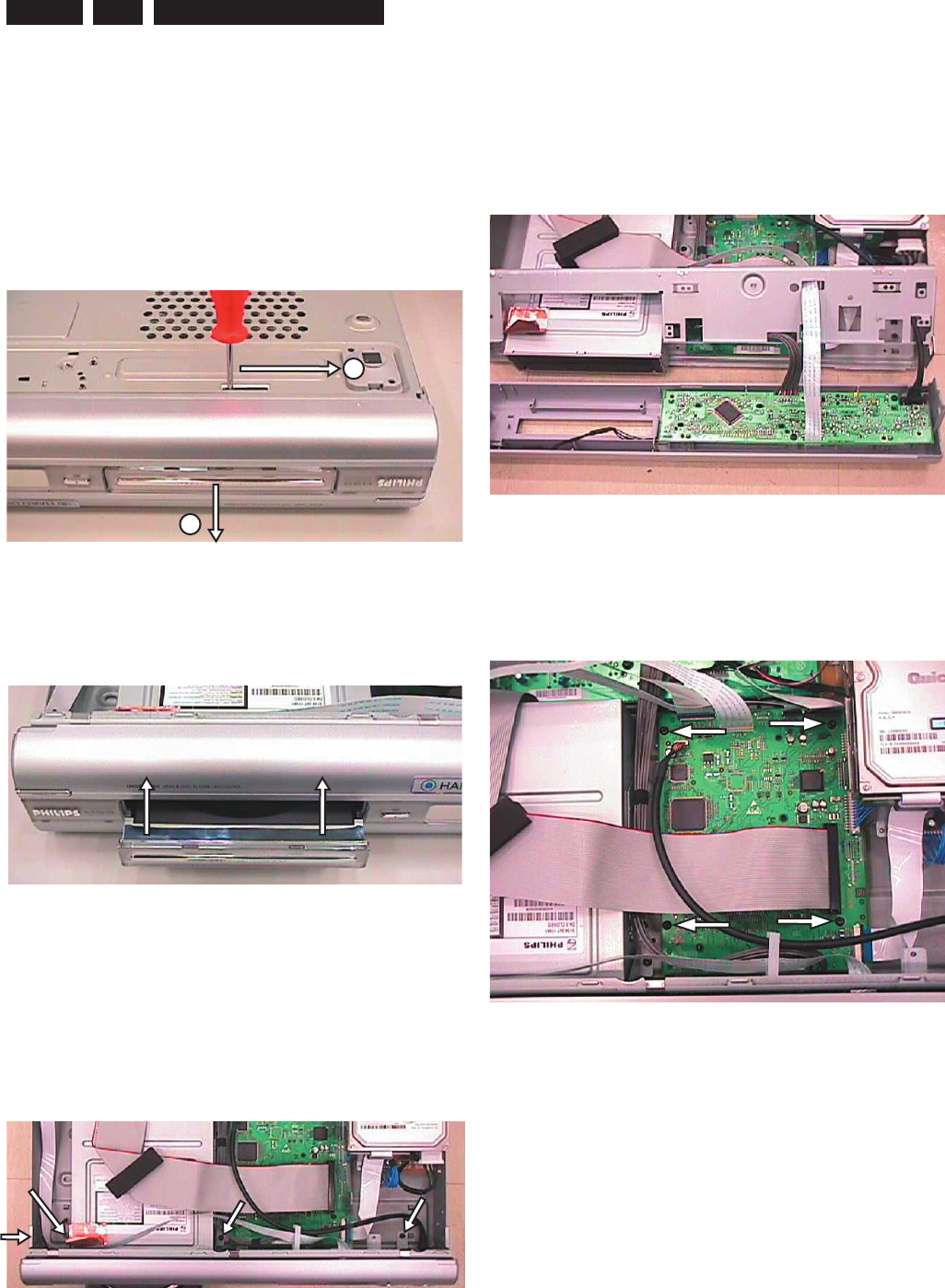
4.1 Dismantling of the DVD Tray cover
1) Insert a screw-driver into the slot provided at the bottom
of the set and push in the direction as shown in
picture 4-1 to unlock before sliding the Tray cover
assembly out.
Figure 4-1: Remove DVDR tray
2) Remove the Tray cover assembly as shown in
Figure 4-2.
Figure 4-2: Remove tray cover assembly
4.2 Dismantling of the Front Panel assembly
1) Remove 7 screws to loosen Top cover.
2) Remove the DVD Tray cover as given in step 4-1.
3) Loosen the Digital Board & HDD as given in step 4-3.
4) Loosen 3 screws and 2 catches as shown in Figure 4-3
to separate the Front panel assembly from the Frame
assembly.
Figure 4-3
5) Remove 6 screws to loosen the Front plate to reach
the Front board service position (see Figure 4-4).
Figure 4-4: Front Board Service position
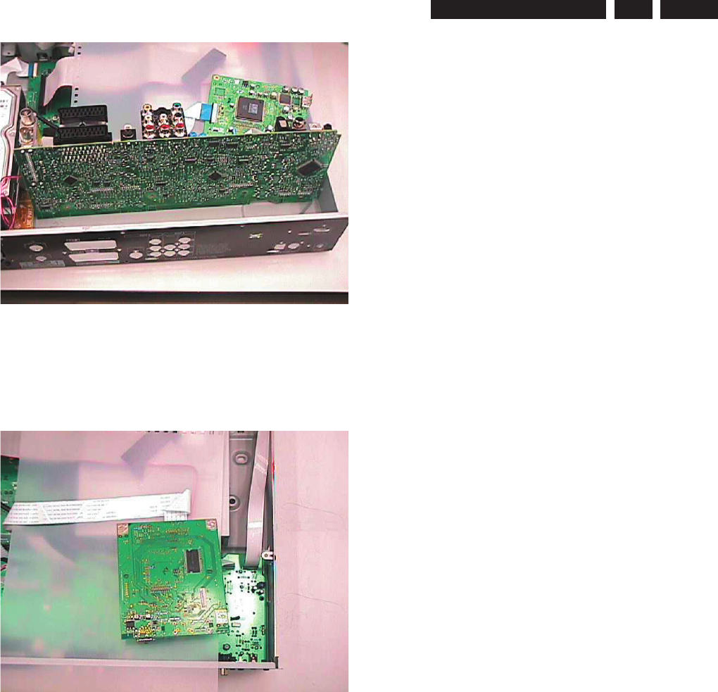
4.3 Dismantling of the Digital Board / HDD
1) Remove 4 screws to loosen the Digital Board as
shown in Figure 4-5.
Figure 4-5: Digital Board
1
2
EN 11
3139 785 31532 4.
Mechanical Instructions
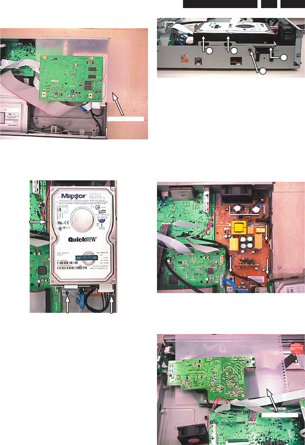
2) Service position for Digital Board is given in Figure 4-6.
Figure 4-6: Digital Board Service Position
1) Remove the 3 screws to loosen the HDD assembly
as shown in Figure 4-7.
Figure 4-7
1) Unscrew screw labelled 1 in fi gure 4-8.
2) Lift up the harddisk in the arrow labeled 3 and 4 in
fi gure 4-8.
3) Slide out in the direction of the arrow labeled 2 in
fi gure 4-8.
Insulation Sheet
Figure 4-8
4) Remove 4 screws 247,248,249,250 to separate the
Bracket HDD from the HDD.
Note: Screws 247,248,249,250 are special type of screws
that must be replaced only with those specifi ed in the Service
Parts list on Chapter 10.
4.4 Dismantling of the PSU Board
1) Remove 3 mounting screw on PSU Board as shown in
fi gure 4-9.
Figure 4-9: PSU remove screw
2) Service position for the PSU Board as shown in fi gure
4-10.
Figure 4-10: PSU Board Service Position
4
1
3
2
Insulation Sheet
EN 12 3139 785 31532
4. Mechanical Instructions
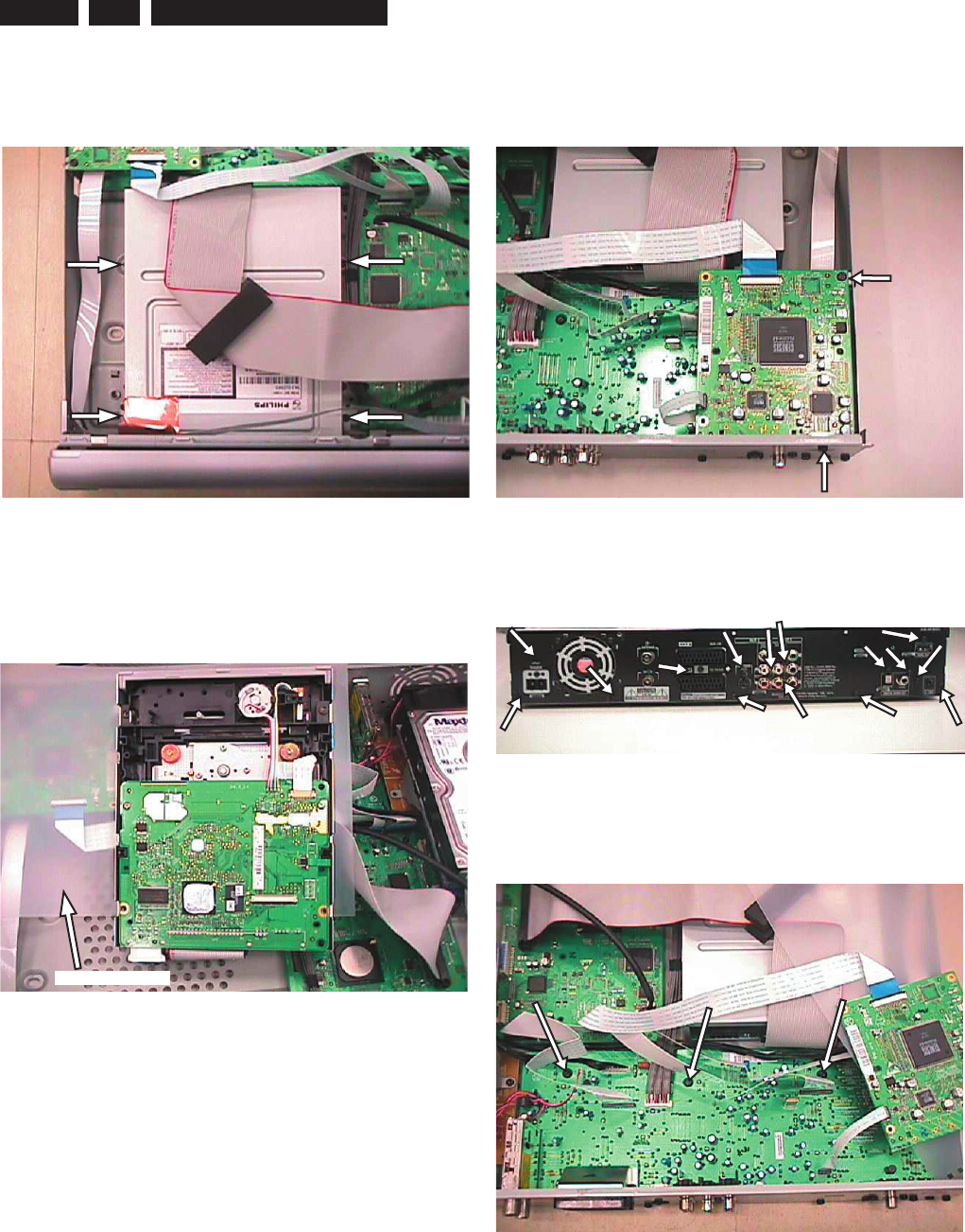
4.5 Dismantling of the Basic Engine (Drive D4.3)
1) Remove 4 screws to loosen the Basic Engine assembly
as shown in Figure 4-11.
Figure 4-11
2) Remove 2 screws to loosen the Bracket Loader and
uncatch the Dust cover assembly.
3) Remove 4 screws to loosen the Cover of the Basic
Engine to reach Service position Figure 4-12.
Figure 4-12: Basic Engine Service Position
Insulation Sheet
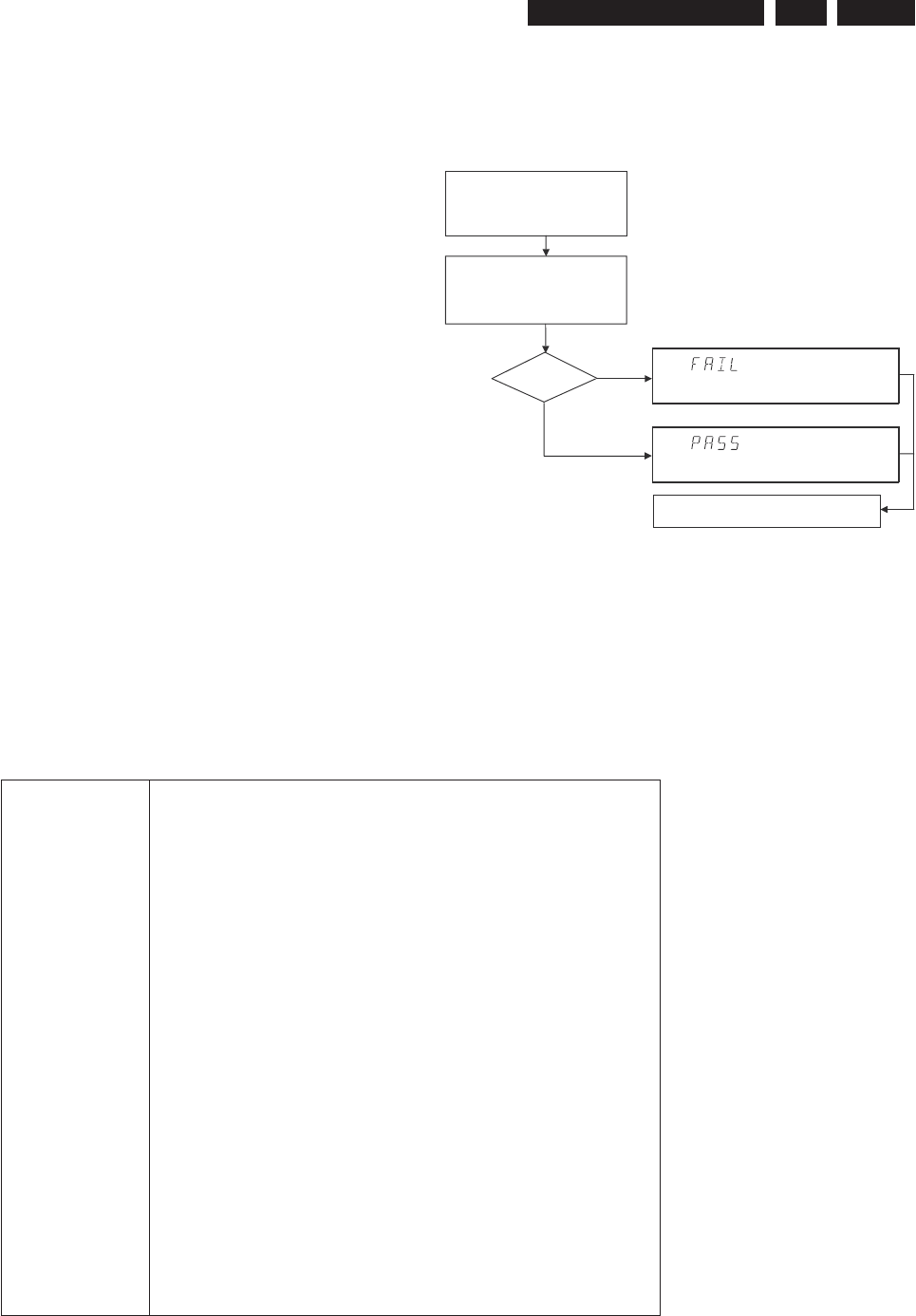
4.6 Dismantling of the Analog Board
1) Remove the Basic Engine assembly as given in step 4.4.
2) Remove the HDMI board as shown in Figure 4-13.
Figure 4-13
3) Remove 15 screws on the Rear panel as shown in
Figure 4-13.
Figure 4-14
4) Remove 3 screw mounting the Analog Board to the
Frame Assembly as given in Figure 4-13.
Figure 4-15
5) Service position is achieved by placing the Analog Board
in the vertical position as shown in Figure 4-16.
EN 13
3139 785 31532 4.
Mechanical Instructions
Figure 4-16: Analog Board Service Position
4.7 Dismantling of the HDMI Board
1) Remove the HDMI board as shown in Figure 4-13.
2) Service Position of HDMI board given in Figure 4-17.
Figure 4-17: HDMI Board Service Position

EN 14 3139 785 31532 Firmware Upgrading & Diagnostic Software
5.
5. Firmware Upgrading & Diagnostic Software
5.1 Firmware Upgrading
A. Preparation to upgrade fi rmware:
1. Unzip the zip-archive fi le
2. Start the CD Burning software and create a new CD project (data disc) with the following settings:
File system: Joliet
Format: MODE 2: CDROM XA
Recording mode: SINGLE SESSION (TRACK-AT-ONCE), FINALIZED CD
Note: Long fi le name is necessary for the preparation of the upgrade disc
3. Place the content of the zip-archive into the root directory of the new CD project.
4. Burn the data onto a blank CDR or CD-RW
B. Procedure to apply the fi rmware upgrade:
1. Hold the <Record> + <Next> buttons down and Power up the set.
2. The tray opens and set will display:
DOWNLOAD −>……….INSERT DISC
3. Insert the prepared Upgrade CDROM and close the tray.
4. The set will display:
INIT DISC −> DOWNLOAD −>……….
The whole process takes less than 10 minutes
Note: Do not press any buttons or interrupt the mains supply during the upgrading process, otherwise the set may becomes
defective.
5. When the upgrade is completed the tray will open automatically and the set will display:
REMOVE DISC
6. Close the tray and the set will display:
DONE
7. The set will go into Standby mode.
C. How to read out the fi rmware version to confi rm set has been upgraded:
1. Power up the set.
2. Press <System> button on the Remote control and select {Setup} option
3. Press <Right> button to select {System}
4. The set will prompt you about clearing the Time Shift Buffer
5. Select {Yes} and press <OK> button
6. Press <Down> button several times to select {Version info}
7. Press <OK> button
8. The TV connected to the set will display:
DIF05_5/56299AN SV11201
BE 43.2.13 ASP1,18,1,10FP
SIT5300-FNAC6-S3_299-F536_B1
20050909-1857 dev sxc
EPG:DPMS:P_DPM
9. Press <System> button to exit
EN 15
3139 785 31532 5.
Firmware Upgrading & Diagnostic Software
Diagnostic Software
Due to the complexity of the DVD recorder, the time to find a
defect in the recorder can become long. To reduce this time,
the recorder has been equipped with Diagnostic and Service
software (DS). The DS offers functionality to diagnose the
DVDR hardware and tests the following:
• Interconnections between components
• Accessibility of components
• Functionality of the audio and video paths
This functionality can be accessed via several interfaces:
1. End user/Dealer script interface
2. Command Interface
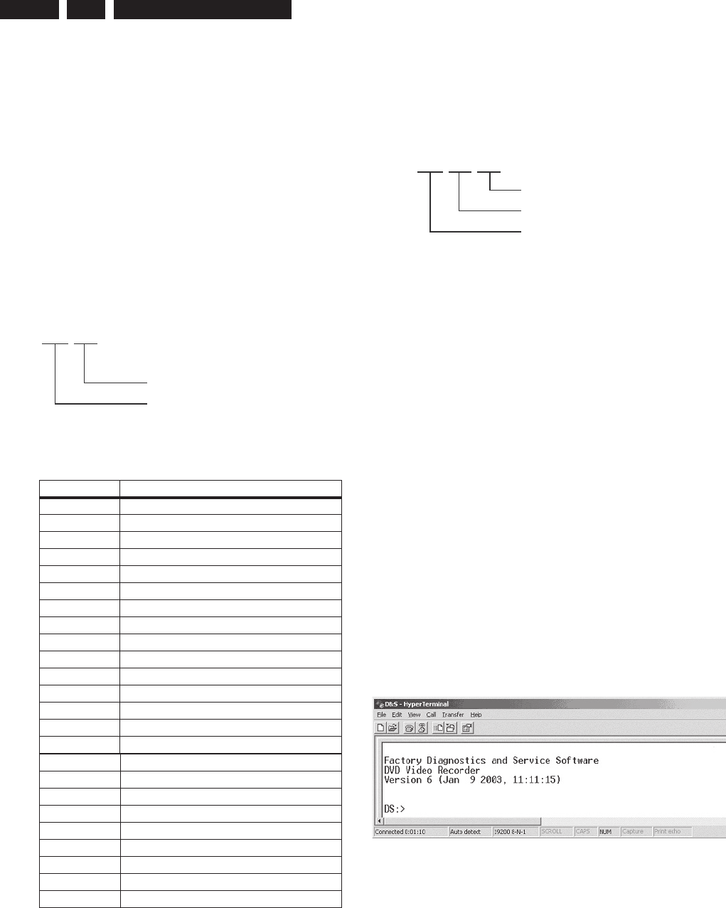
The End user/Dealer script interface gives a diagnosis on a
stand alone DVD recorder. During this mode, a number of
hardware tests (nuclei) are automatically executed to check if
the recorder is faulty. The diagnosis is simply a "fail" or "pass"
message. If the message "FAIL" appears on the display, there
is apparently a failure in the recorder. If the message "PASS"
appears, the nuclei in this mode have been executed
successfully. There can be still a failure in the recorder
because the nuclei in this mode don't cover the complete
functionality of the recorder.
Figure 5-1
The End use/Dealer script executes all diagnostic nuclei that
do not need any user interaction and are meaningful on a
standalone DVD recorder.
Hold key <PLAY> pressed
while you plug the recorder
Unplug the power cord
SET O.K.?
YES
NO
To exit DEALER SCRIPT, unplug the power cord
During the test, the display will show
the a sequence of nuclei under test
TR 18029_001
120304
Included tests: 1.DS_ANAB_COMMUNICATIONECHO_NUC
2.DS_DCB_COMMUNICATIONECHO_NUC
3. DS_BROM_COMMUNICATION_NUC
4. DS_SYS_SETTINGSDISPLAY_NUC
5. DS_CHR_DEVTYPEGET_NUC
6. DS_CHR_INT_PIC_NUC
7. DS_CHR_DMA_NUC
8. DS_BROM_WRITEREAD_NUC
9. DS_NVRAM_COMMUNICATION_NUC
10. DS_NVRAM_WRITEREAD_NUC
11. DS_SDRAM_WRITEREADFAST_NUC
12. DS_FLASH_WRITEREAD_NUC
13.DS_FLASH_CHECKSUMPROGRAM_NUC
14.DS_SYS_HARDWAREVERSIONGET_NUC
15. DS_VIP_DEVTYPEGET_NUC
16. DS_VIP_COMMUNICATION_NUC
17. DS_DVIO_LINKDEVTYPEGET_NUC
18. DS_DVIO_PHYDEVTYPEGET_NUC
19. DS_DVIO_LINKCOMMUNICATION_NUC
20. DS_DVIO_PHYCOMMUNICATION_NUC
21.DS_PSCAN_COMMUNICATIONDENC_NUC
22.DS_PSCAN_COMMUNICATIONDEINTERLACER_NUC
23. DS_BE_COMMUNICATIONECHO_NUC
24.DS_ANAB_COMMUNICATIONIICNVRAM_NUC
25.DS_ANAB_COMMUNICATIONIICTUNER_NUC
26.DS_ANAB_COMMUNICATIONIICSOUNDPROCESSOR_NUC
27.DS_ANAB_COMMUNICATIONIICAVSELECTOR_NUC
28. DS_ANAB_CHECKSUMPROGRAM_NUC
5.2 End User/Dealer Script Interface
5.2.1 Description
5.2.2 Structure
5.2.3 Contents
EN 16 3139 785 31532 Firmware Upgrading & Diagnostic Software
5.
5.3 Player Script Interface
5.3.1
5.4 Menu and Command Mode Interface
5.4.1 Nuclei Numeration
Each nucleus has a unique number of four digits. This number
is the input of the command mode.
Figure 5-3
Group number Group name
0 Scripts
1 Codec (e.g. Chrysalis, Leco)
2 Boot EEPROM
3NVRAM
4 SDRAM
5 Flash
6 Video Input Processor
7DVIO
8 Progressive Scan
9 Basic Engine
10* Display and Control Board
11* Analogue Board
12 System
13 Electronic Program Guide Board
14* PCMCIA
[ XX YY ]
Nucleus number
Nucleus group number
CL 06532152_012.eps
051200
5.4.3 Command Mode Interface
Set-Up Physical Interface Components
Hardware required:
• Service PC
• one free COM port on the Service PC
• special cable to connect DVD recorder to Service PC
The service PC must have a terminal emulation program (e.g.
Hyperterminal) installed and must have a free COM port (e.g.
COM1). Activate the terminal emulation program and check
that the port settings for the free COM port are: 19200 bps, 8
data bits, no parity, 1 stop bit and no flow control. The free COM
port must be connected via a special cable to the RS232 port
of the DVD recorder. This special cable will also connect the
test pin, which is available on the connector, to ground (i.e.
activate test pin).
Code number of PC interface cable: 3122 785 90017
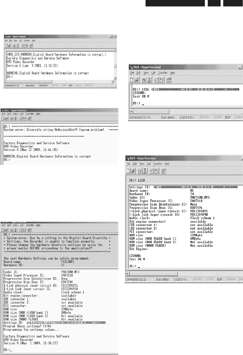
Activation of Diagnostic Software
1. Pull the mains cord from the recorder and reconnect it
again (reboot).
2. The next welcome message will appear on the PC:
Welcome screen D&S program
Figure 5-5
Now, the prompt 'DS:>' will appear. The diagnostic software is
now ready to receive commands. The commands that can be
given are the numbers of the nuclei. If you see above shown
screen, continue with paragraph 'Nuclei Codes'.
5.4.2 Error Handling
Each nucleus returns an error code. This code contains six
numerals, which means:
Figure 5-4
The nucleus group numbers and nucleus numbers are the
same as above.
[ XX YY ZZ ]
Error code
Nucleus number
Nucleus group number
CL 06532152_013.eps
051200
15 HDMI
16 Analogue Slave Processor
17 Analogue Board EEPROM
18 Video Matrix
19 Audio Matrix
20 Front End
21 Hard Disk
22* Di
23* USB
gital Terrestrial Tuner Module
* Not applicable for DVDR5350H, DVDR7300H
and DVDR7310H Ranges
If you want that the recorder starts up in Virgin mode, follow this
procedure:
• Unplug the recorder
• plug the recorder again while you keep the STAND BY/ON
key pressed
• the set starts up in Virgin mode.
Virgin mode
EN 17
3139 785 31532 5.
Firmware Upgrading & Diagnostic Software
3. It is possible that the next messages will appear when
starting the DVD+RW for the first time
Error messages D&S program
Figure 5-6a
Error messages D&S program
Figure 5-6b
In these cases, the boot EEPROM of the Digital Board does not
contain the required string with the hardware information. To
update the Digital Board with the correct string, nucleus 1226
must be executed.
See next section 'Diversity String Input'.
There can also be the next error message.
Figure 5-6c
Enter "Y" to program a safe string. With this automatically
generated string the board will work in principle but it has to be
checked if all board settings were detected correctly.
Diversity String Input
4. Execute nucleus 1226 to enter the string. Please see
chapter 8 for details
Nucleus 1226 execution with string
Figure 5-7
5. To check if the hardware info is filled correctly, you can
execute nucleus 1228.
Nucleus 1228 info example
Figure 5-8
6. Exit the 'Terminal' program.
7. Reboot the DVD recorder to allow the software to start.

EN 18 3139 785 31532 Firmware Upgrading & Diagnostic Software
5.
Command overview Digital Board
Below you will find an overview of the nuclei, their numbers,
and their error codes. This overview is preliminary and subject
to modifications.
Note: AV3 in the overview includes also the AV3.5 drive.
Codec Host Controller (CHR)
Nucleus Name DS_CHR_DevTypeGet
Nucleus Number 100
Description Retrieves the device id, the module ids and revisions of the Codec and returns
them to the stdout port.
Technical -Determine the codec id by means of comparing version ids of the modules.
-Read the module-id register of every module and display it to the user.
Execution Time Less than 1 second.
User Input None
Error Number Description
10000 Getting the information succeeded
10001 Wrong codec id detected
Example DS:> 100
010000:
Device ID 7100
Codec ID PNX7100_C
F-BCU (0x0102) 1.0 INTC (0x011d) 1.0 PCI-XIO(0x0113) 1.0
SIF (0x013b) 1.0 EJTAG (0x0104) 0.1 S-BCU (0x0102) 1.0
BOOT (0x010a) 1.0 CONFIG (0x013f) 1.1 RESET (0x0123) 1.0
DEBUG (0x0116) 0.0 UART0 (0x0107) 0.1 UART1 (0x0107) 0.1
UART2 (0x0107) 0.1 UART3 (0x0107) 0.1 I2C0 (0x0105) 0.1
I2C1 (0x0105) 0.1 GPIO (0x013c) 1.0 SYNC (0x013a) 1.0
DISP0 (0xa015) 1.12 DISP1 (0xa00f) 1.1 OSD (0x0136) 0.1
SPU (0xa00e) 0.0 MIXER (0x0137) 1.0 DENC (0x0138) 1.0
CCIR (0x0139) 1.0 VDEC (0x0133) 0.2 PARSER (0xa00d) 0.0
DV (0xa00c) 0.0 BEI (0xa00a) 0.1 IDE (0xa009) 0.1
SGDX (0xa008) 1.0 BYTE (0xa00b) 0.1 OUTPUT (0xa003) 1.0
ACOMP (0xa000) 1.0 VFE (0xa001) 0.1 VCOMP (0xa002) 1.0
SCR (0x0000) 0.0 SIFF (0xa011) 0.1 WMD (0xa010) 0.0
AUDIO0 (0xa015) 1.12 AUDIO1 (0xa00f) 1.1 PSCAN (0xa018) 0.1
Test OK @
Nucleus Name DS_CHR_TestImageOn
Nucleus Number 101
Description Generates a test-image of a selected video standard on selected video output
on the digital board. When no input is given, the default values will be used (see
user input description below). Make sure to use the proper nuclei to route the
video signal on the analogue board to get the video signal to the proper output.
Note: Although a DTT has a Chrysalis C3, the codec IC may never use the
YUV functionality of the internal DENC. This is specified by the hardware. The
digital boards for DTT do have a YUV-matrix. The signals from this YUV-matrix
are not routed to the regular video output connector but to the progressive scan
output connector.
Technical -Validate the user input.
-Initialise the SYNC module.
-Initialise the DISPLAY module.
-Initialise the MIXER module.
-Initialise the DENC module.
-Set the selected video standard.
-Generate the selected test image in memory.
-Start the DISPLAY module.
-Start the MIXER module.
-Start the DENC module according to the selected test image id.
Execution Time 6 seconds.
EN 19
3139 785 31532 5.
Firmware Upgrading & Diagnostic Software
User Input The user has to decide which test image, video standard and video output must
be used: < Test image id > < Video standard > < Video output >
Test image id:
0 VERTICAL_COLOURBAR (default)
1 HORIZONTAL_COLOURBAR
2WHITE
3 YELLOW
4 CYAN
5 GREEN
6 MAGENTA
7 RED
8 BLUE
9 BLACK
10 GRAY
11 TEST_IMAGE_FOR_PROGRESSIVE_SCAN
Video standard:
PAL Standard PAL 50 Hz (default)
NTSC Standard NTSC 60 Hz
Video output:
ALL CVBS and YC and RGB DACs are enabled (default)
CVBS CVBS DAC is enabled
YC Y and C DAC is enabled
RGB CVBS, R, G, and B DACs are enabled
YUV Y, U, and V DACs are enabled
PSCAN Progressive scan is enabled.
Error Number Description
10100 Generating the test image succeeded.
10101 Invalid input was provided.
10102 The Codec SYNC-module cannot be initialised.
10103 The Codec MIXER-module cannot be initialised.
10104 The Codec VPP-module cannot be initialised.
10105 The Codec DENC-module cannot be initialised.
10106 The digital board hardware information is corrupt
Example DS:> 101
010100:
Test OK @
DS:> 101 0 pal cvbs
010100:
Test OK @
DS:> 101 4 ntsc yc
010100:
Test OK @
Nucleus Name DS_CHR_TestImageOff
Nucleus Number 102
Description Switches the test-image off.
Technical -Stop the DENC module.
Execution Time Less than 1 second.
User Input None
Error Number Description
10200 Stopping the test image generation succeeded
10201 The Codec DENC-module failed.
Example DS:> 102
010200:
Test OK @

EN 20 3139 785 31532 Firmware Upgrading & Diagnostic Software
5.
Nucleus Name DS_CHR_SineOn
Nucleus Number 103
Description Generate an audio sine signal on the audio output of the digital board.
Note: Left channel 6kHz, right channel 12 kHz sine. Make sure to route the
signal first.
Technical -De-mute the analogue board
-Set fifo parameters for audio
-Set the volume
-Set the I2S outputs and configuration paths
-Set the decoder mode
-Configure the audio decoder
-Put the AC3 audio in the fifo
-Send ‘prepare’ command to the audio decoder
-Send ‘play’ command to the audio decoder
Execution Time Less than 1 second
User Input None
Error Number Description
10300 The sine signal was successfully generated
10301 The analogue board could not be de-muted
10302 The audio decoder did not initialise
10303 The dsp2 (DUET) of the audio decoder did not configure
10304 The dsp1 (PALM) of the audio decoder did not configure
10305 There was a delay-error before starting
10306 Wrong input was given to the decoder function
10307 Wrong input was given to the decoder function @@@@@
10308 The audio decoder did not get into the ‘prepared’ state
Example DS:> 103
010300:
Test OK @
Nucleus Name DS_CHR_SineOff
Nucleus Number 104
Description Stop generating the audio sine signal
Technical -Reset the audio block of the Codec
Execution Time Less than 1 second.
User Input None
Error Number Description
10400 Switching off the audio sine signal succeeded
10401 Failed to reset the audio decoder
Example DS:> 104
010400:
Test OK @
Nucleus Name DS_CHR_SineBurst
Nucleus Number 105
Description Generate an audio sine signal on the audio output of the digital board for 4
seconds.
Note: Left channel 6kHz, right channel 12 kHz sine with some known hick-ups
Technical -Call the DS_CHR_SineOn nucleus
-Delay for 4 seconds
-Call the DS_CHR_SineOff nucleus
Execution Time 4 seconds
User Input None
Error Number Description
10500 The sine signal burst was successfully generated
10501 The delay did not succeed during the burst
10502 The audio sine could not be generated
Example DS:> 105
010500:
Test OK @

EN 21
3139 785 31532 5.
Firmware Upgrading & Diagnostic Software
Nucleus Name DS_CHR_MuteOn
Nucleus Number 106
Description Mute the audio outputs of the digital board
Technical -Send the ‘Mute’ command to the audio decoder
-Activate the ‘audio mute’ PIO pin
Execution Time Less than 1 second.
User Input “PIO” to just use the PIO pin mute. When muting using this, also de-mute using
this as this works ‘paired’.
Error Number Description
10600 Muting the audio succeeded
10601 Muting the audio through the PIO-pin failed
Example DS:> 106
010600:
Test OK @
DS:> 106 PIO
010600:
Test OK @
Nucleus Name DS_CHR_MuteOff
Nucleus Number 107
Description De-mute the audio outputs of the digital board
Technical -Send the ‘DeMute’ command to the audio decoder
-Deactivate the ‘audio mute’ PIO pin
Execution Time “PIO” to just use the PIO pin de-mute. Only de-mute using this when you muted
using the PIO parameter, as this works ‘’paired.
User Input None
Error Number Description
10700 De-muting the audio succeeded
10701 De-muting the audio through the PIO-pin failed
Example DS:> 107
010700:
Test OK @
DS:> 107 PIO
010700:
Test OK @
Nucleus Name DS_CHR_DvLedOn
Nucleus Number 108
Description Check the connection to the DV-LED on the digital board by switching it on
Technical -Write to the PIO pin to light the DV LED
Execution Time Less than 1 second.
User Input None
Error Number Description
10800 Switching the DV-LED on succeeded
10801 Switching the DV-LED on failed
Example DS:> 108
010800:
Test OK @
Nucleus Name DS_CHR_DvLedOff
Nucleus Number 109
Description Switch off the DV-LED on the digital board
Technical -Write to the PIO pin to switch off the DV LED
Execution Time Less than 1 second.
User Input None
Error Number Description
10900 Switching the DV-LED off succeeded
10901 Switching the DV-LED off failed
Example DS:> 109
010900:
Test OK @

EN 22 3139 785 31532 Firmware Upgrading & Diagnostic Software
5.
Nucleus Name DS_CHR_MacroVisionOn
Nucleus Number 110
Description Turn on MacroVision.
Technical -Set some registers of the DENC module in the Codec.
Execution Time Less than 1 second.
User Input None
Error Number Description
11000 Turning on MacroVision succeeded
11001 Turning on MacroVision failed
Example DS:> 110
011000:
Test OK @
Nucleus Name DS_CHR_MacroVisionOff
Nucleus Number 111
Description Turn off MacroVision.
Technical -Set some registers of the DENC module in the Codec.
Execution Time Less than 1 second.
User Input None
Error Number Description
11100 Turning off MacroVision succeeded
11101 Turning off MacroVision failed
Example DS:> 111
011100:
Test OK @
Nucleus Name DS_CHR_Peek
Nucleus Number 112
Description Peek a value on a specified address
Technical -Check the user input
-Read out the address specified
-Check whether the address to be read is aligned on 4 bytes
Execution Time Less than 1 second.
User Input The address to peek on
Error Number Description
11200 Peeking on the specified address succeeded
11201 Peeking on the specified address failed, wrong user input
11202 Peeking on the specified address failed due to misalignment
Example DS:> 112 0xa0700000
011200: Value read = 0x000001BD
Test OK @
Nucleus Name DS_CHR_Poke
Nucleus Number 113
Description Poke a value on a specified address
Technical -Check the user input
-Change the value on the address specified
-Check whether the address to be modified is aligned on 4 bytes
Execution Time Less than 1 second.
User Input The address to poke and the value: <address><value>
Error Number Description
11300 Poking the specified address succeeded
11301 Poking the specified address failed, wrong user input
11302 Poking the specified address failed due to misalignment
Example DS:> 113 0xa0700000 0xaabbccdd
011300:
Test OK @
EN 23
3139 785 31532 5.
Firmware Upgrading & Diagnostic Software
Nucleus Name DS_CHR_INT_PICInterrupts
Nucleus Number 114
Description Test all interrupts of the priority interrupt controller
Technical -Install interrupt handlers
-Generate interrupts
-Test whether all interrupts were received
Execution Time Less than 1 second.
User Input -
Error Number Description
11400 Testing all the PIC interrupts succeeded
11401 Testing all the PIC interrupts failed
Example DS:> 114
011400:
Test OK @
Nucleus Name DS_CHR_DMA_TestDMA
Nucleus Number 115
Description Test the memory to memory DMA transfer
Technical -Create a block with known data in memory
-Copy this block to the consecutive area using 3 different DMAs
-Check whether all DMAs transferred the data properly
Execution Time Less than 2 seconds.
User Input -
Error Number Description
11500 The testing of the DMAs succeeded
11501 The initialisation of the DMAs failed for one or more DMA
11502 One or more DMAs failed the test
Example DS:> 115
011500:
Test OK @
Boot EEPROM (BROM)
Nucleus Name DS_BROM_Communication
Nucleus Number 200
Description Check the communication between the IIC controller of the Codec and the boot
EEPROM
Technical -Initialise IIC
-Read something from the EEPROM
Execution Time Less than 1 second.
User Input None
Error Number Description
20000 The data is properly read so the communication is OK
20001 The IIC bus was not accessible
20002 There was a timeout reading the device
20003 The IIC acknowledge was not received
20004 An IIC-bus error occurred
20005 The IIC bus initialisation failed
20006 An unexpected IIC error occurred
Example DS:> 200
020000:
Test OK @

EN 24 3139 785 31532 Firmware Upgrading & Diagnostic Software
5.
Nucleus Name DS_BROM_WriteRead
Nucleus Number 201
Description Check whether the Boot EEPROM can be written to and read from
Technical -Initialise IIC
-Write something to the EEPROM
-Read from the same location and check whether it is the same as written
Execution Time Less than 1 second.
User Input None
Error Number Description
20100 The write-read test succeeded
20101 The write-read test failed
20102 An IIC-bus error occurred
20103 There was a timeout reading the device
20104 The IIC bus was not accessible
20105 The IIC acknowledge was not received
20106 Got unknown IIC bus error
20107 The IIC bus initialisation failed
Example DS:> 201
020100:
Test OK @
Non Volatile RAM (NVRAM)
Nucleus Name DS_NVRAM_Communication
Nucleus Number 300
Description Check the communication between the IIC controller of the Codec and the
NVRAM EEPROM
Technical -Initialise IIC
-Read from a location in the NVRAM EEPROM device
Important note: This nucleus only checks the physical connection between the Codec and IIC
EEPROM. If no EEPROM is mounted this test will fail. However other NVRAM
nuclei might still work because the software will store NVM data into flash
memory
Execution Time Less than 1 second.
User Input None
Error Number Description
30000 Something is properly read so the communication is OK
30001 The IIC bus was not accessible
30002 There was a timeout reading the device
30003 The IIC acknowledge was not received
30004 The communication with the device failed
30005 The IIC bus initialisation failed
Example DS:> 300
030000:
Test OK @
Nucleus Name DS_NVRAM_WriteRead
Nucleus Number 301
Description Check whether the EEPROM can be written to and read from
Technical -Initialise IIC
-If no IIC EEPROM was found then initialise flash memory to use NVM
pages
-Backup data from location to modify
-Write to location and read it back again
-Write back the backed up data to the location to leave the NVRAM as
found
Execution Time Less than 1 second
User Input None
Error Number Description
30100 The write-read test succeeded
30101 The IIC bus could not be initialised
30102 There was an NVRAM IO error
30103 The value could not be read back from the NVRAM
Example DS:> 301
030100:
Test OK @

EN 25
3139 785 31532 5.
Firmware Upgrading & Diagnostic Software
Nucleus Name DS_NVRAM_Clear
Nucleus Number 302
Description Make the EEPROM empty, containing all zeroes.
Technical -Initialise IIC
-If no IIC EEPROM was found then initialise flash memory to use NVM
pages
-Read the DVID and diversity string from NVM (either EEPROM or Flash)
-Create a memory block filled with zeroes
-Write this block to the NVRAM (either EEPROM or Flash)
-Write back the Read the DVID and diversity string to NVM (either
EEPROM or Flash)
Important note: The Hardware Diversity Information and unique identification number
(IEE1394-specific) of the Digital Video processing part is NOT cleared by this
nucleus!
Execution Time 16 seconds
User Input None
Error Number Description
30200 The clearing of the NVRAM succeeded
30201 There was an IIC error
30202 Clearing the NVRAM failed
Example DS:> 302
030200:
Test OK @
Nucleus Name DS_NVRAM_Modify
Nucleus Number 303
Description Modifies one or more locations in NVRAM and updates the checksum of the
section modified
Technical -Initialise IIC
-If no IIC EEPROM was found then initialise flash memory to use NVM
pages
-Decode user input
-Modify the NVRAM as indicated
-Validate the NVRAM by calculating the checksum and storing it
Execution Time Less than 1 second
User Input 1. The location that must be modified
i.e. "ALL" "BOOT" "DIAGNOSTICS" "DOWNLOAD" "CONFIG"
"RECORDER" or no string if an offset from the base address of the
NVRAM is required
2. The offset and data which to put on the selected location
<offset> <length> <data>
Error Number Description
30300 Modifying the NVRAM contents succeeded
30301 Unable to initialise NVM
30302 Modifying the NVRAM contents failed
30303 length out of range
30304 unable to decode length
30305 offset out of range
30306 unable to decode offset
30307 unknown location specified
30308 no location is specified
30309 number of values incorrect
30310 There was an IIC error
Example DS:> 303 DIAGNOSTICS 5 1 0x5a
030300: Section is modified successfully
Test OK @

EN 26 3139 785 31532 Firmware Upgrading & Diagnostic Software
5.
Nucleus Name DS_NVRAM_Read
Nucleus Number 304
Description Read out one or more locations in the NVRAM
Technical -Initialise IIC
-If no IIC EEPROM was found then initialise flash memory to use NVM
pages
-Decode user input
-Read from the NVRAM and return this info to the user
Execution Time Less than 1 second
User Input 1. The location which must be read
i.e. "ALL" "BOOT" "DIAGNOSTICS" "DOWNLOAD" "CONFIG"
"RECORDER" or no string if an offset from the base address of the
NVRAM is required
2. The offset and number of bytes to read
<offset> <length>
Error Number Description
30400 Value read
30401 Unable to initialise NVM
30402 Reading the NVRAM contents failed
30403 Length out of range
30404 Unable to decode length
30405 Offset out of range
30406 Unable to decode offset
30407 Unknown location specified
30408 No location is specified
Example 304 DIAGNOSTICS 0 6
030400: Value read = 0x00 0x00 0x00 0x00 0x00 0x5A
Test OK @
SDRAM (SDRAM)
Nucleus Name DS_SDRAM_WriteRead
Nucleus Number 400
Description Check all data lines, address lines and memory locations of the SDRAM
Technical -Test the data bus
-Test the address bus
-Test the integrity of the device itself (memory locations)
Execution Time 11 seconds for 32 Mb
23 seconds for 64 Mb
User Input None
Error Number Description
40000 The write-read test succeeded
40001 The data bus contains an error
40002 The address bus contains an error
40003 The SDRAM itself contains an error
Example DS:> 400
040000:
Test OK @
Nucleus Name DS_SDRAM_WriteReadFast
Nucleus Number 401
Description Check all data lines and address lines of the SDRAM
Technical -Test the data bus
-Test the address bus
Execution Time Less than 1 second
User Input None
Error Number Description
40100 The write-read test succeeded
40101 The data bus contains an error
40102 The address bus contains an error
Example DS:> 401
040100:
Test OK @

EN 27
3139 785 31532 5.
Firmware Upgrading & Diagnostic Software
Nucleus Name DS_SDRAM_Write
Nucleus Number 402
Description Write to a specific un-cached memory address
Technical -Decode the user input and check its ranges and alignment on 4 bytes
-Write the data to the SDRAM
Execution Time Less than 1 second
User Input 1. The location that must be modified
(SDRAM starts at address 0xA0000000)
2. The value to put on the selected location
Error Number Description
40200 Writing to the SDRAM succeeded
40201 Writing to the SDRAM failed; Wrong user input
40202 Address is not dividable by 4
Example DS:> 402 0xa1000010 0xad112222
040200:
Test OK @
Nucleus Name DS_SDRAM_Read
Nucleus Number 403
Description Read from a specific un-cached memory address
Technical -Decode the user input and check the ranges
-Read from the SDRAM and return this info to the user
Execution Time Less than 1 second
User Input The location from which the data must be read
(SDRAM starts at address 0xA0000000)
Error Number Description
40300 Reading from the SDRAM succeeded
40301 Reading from the SDRAM failed; Wrong user input
40302 Address is not dividable by 4
Example DS:> 403 0xa1000010
040300: Value read = 0xAD112222
Test OK @
Nucleus Name DS_SDRAM_DmaWriteRead
Nucleus Number 404
Description Write a pattern to the entire SDRAM using DMA and check the data
Technical -Check if the Stack pointer is not in the write range
-Clear a 64kb block and then fill it with a pattern
-Initialise the DMA controller and write the data to the SDRAM
-Then check if all the data was written correctly (except descriptor tables)
-Repeat the process 4 times with 4 different patterns
Execution Time 24 seconds
User Input None.
Error Number Description
40400 Writing to the SDRAM succeeded
40401 Stack area definition ERROR!
40402 DMA controller could not be initialised.
40403 Not all data was transferred correctly
Example DS:> 404
040400:
Test OK @

EN 28 3139 785 31532 Firmware Upgrading & Diagnostic Software
5.
FLASH (FLASH)
Nucleus Name DS_FLASH_DevTypeGet
Nucleus Number 500
Description Get the device (revision) type information of the FLASH ICs. (type,
manufacturer, device ID and size)
Technical -Set the timing for the flash writing
-Write a command sequence to determine device type information
-Return the information to the user
Execution Time Less than 1 second
User Input None
Error Number Description
50000 Getting the information from the FLASH succeeded
50001 Getting the information from the FLASH failed
Example DS:> 500
050000: Found FLASH memory:
NOR AMD 29DL640G 8MB,NOR AMD 29DL640G 8MB
Test OK @
Nucleus Name DS_FLASH_WriteRead
Nucleus Number 501
Description Check whether the FLASH can be written to and read from
Technical -Find the test segment in flash
-Read the data into SDRAM
-Modify the data
-Write this data from SDRAM to FLASH and verify it by reading back again
Execution Time Less than 1 second.
User Input None
Error Number Description
50100 The FLASH write-read test succeeded
50101 The test segment could not be found
50102 All bits in the TEST region are filled with 0 (region exhausted)
50103 The Write Read test failed
50104 The Write Failed
Example DS:> 501
050100:
Test OK @
Nucleus Name DS_FLASH_Read
Nucleus Number 502
Description Read from a specific memory address in FLASH
Technical -Decode the user input and check the ranges and whether the address is
aligned on 4 bytes
-Read the data and return this to the user
Execution Time Less than 1 second.
User Input The location from which data must be read
(FLASH starts at address 0xB8000000)
Error Number Description
50200 Reading the FLASH succeeded
50201 Reading the FLASH failed; Wrong user input
50202 Address is not dividable by 4
Example DS:> 502 0xb8000000
050200: Value read = 0x3C08A000
Test OK @

EN 29
3139 785 31532 5.
Firmware Upgrading & Diagnostic Software
Nucleus Name DS_FLASH_ChecksumProgram
Nucleus Number 503
Description Check the checksum of the application partitions by recalculating and
comparing partition checksums
Technical -Determine the number of segments
-Find the application in each segment and determine its checksum
-Check whether the checksums stored match the newly calculated
Execution Time 6 seconds
User Input None
Error Number Description
50300 The checksum is valid, the test succeeded
50301 The checksum is invalid
Example DS:> 503
050300:
BootCode checksum is: 0xBABE5B6F, which is correct
Diagnostics checksum is: 0xBABEBAFF, which is correct
Download checksum is: 0xBABEEDBF, which is correct
Application checksum is: 0xBABE8EEC, which is correct
Test OK @
Nucleus Name DS_FLASH_CalculateChecksum
Nucleus Number 504
Description Calculate the checksum over all memory addresses. Used to check entire
FLASH contents
Technical -Run the checksum calculation algorithm on all flash memory addresses
Execution Time 6 seconds
User Input None
Error Number Description
50400 Calculating the checksum over all addresses succeeded
Example DS:> 504
050400: The Checksum = 0xBABE30A4
Test OK @
Nucleus Name DS_FLASH_CalculateChecksumFast
Nucleus Number 505
Description Calculate a checksum over a selected number of address locations
Technical -Run the checksum calculation algorithm on a selected number of flash
memory addresses
Execution Time 6 seconds
User Input None
Error Number Description
50500 Calculating the checksum over selected addresses succeeded
Example DS:> 505
050500: The Checksum = 0xBABEB064
Test OK @
Video Input Processor (VIP)
Nucleus Name DS_VIP_DevTypeGet
Nucleus Number 600
Description Get the device (revision) type information of the VIP IC
Technical -Initialise IIC
-Read out the device (revision) type information of the VIP IC
Execution Time Less than 1 second
User Input None
Error Number Description
60000 Getting the information from the VIP succeeded
60001 The IIC bus initialisation failed
60002 The was an error getting the information from the VIP
60003 Type not according to type stored in HW diversity string
Example DS:> 600
060000: Found SAA7118
Test OK @

EN 30 3139 785 31532 Firmware Upgrading & Diagnostic Software
5.
Nucleus Name DS_VIP_Communication
Nucleus Number 601
Description Check the communication between the IIC controller of the Codec and the VIP
IC
Technical -Initialise IIC
-Read data from a location in the VIP
Execution Time Less than 1 second
User Input None
Error Number Description
60100 Communicating with the VIP succeeded
60101 The IIC bus was not accessible
60102 There was a timeout reading the device
60103 The IIC acknowledge was not received
60104 The communication with the device failed
60105 The IIC bus initialisation failed
Example DS:> 601
060100:
Test OK @
Nucleus Name DS_VIP_ClockOutputOn
Nucleus Number 602
Description Switch the clock output on
Technical -Initialise IIC
-Set the clock output through IIC
Execution Time Less than 1 second
User Input None
Error Number Description
60200 Switching the clock output on succeeded
60201 Switching the clock output on failed
Example DS:> 602
060200:
Test OK @
Nucleus Name DS_VIP_ClockOutputOff
Nucleus Number 603
Description Switch the clock output off
Technical -Initialise IIC
-Reset the clock output through IIC
Execution Time Less than 1 second
User Input None
Error Number Description
60300 Switching the clock output off succeeded
60301 Switching the clock output off failed
Example DS:> 603
060300:
Test OK @
EN 31
3139 785 31532 5.
Firmware Upgrading & Diagnostic Software
Nucleus Name DS_VIP_SelectInput
Nucleus Number 604
Description Select an input video path to be switched to the analogue output pin (AOUT) of
the VIP
Technical -Check the user input
-Initialise IIC
-Read out the VIP id
-Write the set of registers required for the input specified
Execution Time Less than 1 second
User Input The input to select, see table below.
Available channels for input of the 7118 and their description:
Channel number Description
1 CVBS_Y_IN_A
2 CVBS_OUT_B
3 CVBS_Y_IN_B
4 CVBS_Y_IN_C
6 C_IN
8 G_IN
9 Y_IN
13 B_IN
14 U_IN
18 R_IN
19 V_IN
Available channels for input of the 7115 and their description:
Channel number Description
1 CVBS_Y_IN_B
2 CVBS_OUT_B_VIP
4 C_IN_VIP
7 CVBS_Y_IN_B
Available channels for input of the 7119 and their description:
Channel number Description
1 Y / CVBS
3 CVBS
4 Y3
6 C / CVBS
8 G
9 Y
12 Y2
13 B
14 U
17 C
18 R
19 V
Available channels for input of the 7173 and their description:
Channel number Description
1 CVBS_TUNER_IN
2 CVBS_REAR_IN
3 CVBS_FRONT_IN
4 C_REAR_IN
5 Y_REAR_IN
6 Y_FRONT_IN
7 C_FRONT_IN
8 AL_REAR_IN
9 AL_FRONT_IN
10 AR_FRONT_IN
11 AR_REAR_IN
12 SIF_TUNER_IN

EN 32 3139 785 31532 Firmware Upgrading & Diagnostic Software
5.
Error Number Description
60400 Selecting the input of the VIP succeeded
60401 The user provided wrong input
60402 The VIP was not accessible
60403 An unsupported VIP was found
Example DS:> 604 1
060400:
Test OK @
Digital Video Input Output Circuit (DVIO)
Nucleus Name DS_DVIO_LinkDevTypeGet
Nucleus Number 700
Description Get the device (revision) type information of the 1394 Link layer IC
Technical -Initialise the PIO pins on the Codec
-Read out the ID register
Execution Time Less than 1 second
User Input None
Error Number Description
70000 Getting the information from the link layer IC succeeded
70001 Getting the information from the link layer IC failed
70002 Type not according to type stored in HW diversity string
Example DS:> 700
070000: Device type of the link layer IC: ffc00301
Test OK @
Nucleus Name DS_DVIO_PhyDevTypeGet
Nucleus Number 701
Description Get the device (revision) type information of the 1394 Physical layer IC
Technical -Initialise the PIO pins of the Codec
-Write the PHY-access register in the Link chip to indicate phy read access
-Wait until the link chip has obtained the value from the phy-chip
-Read this out and filter the data to be returned to the user
Execution Time Less than 1 second
User Input None
Error Number Description
70100 Getting the information from the physical layer IC succeeded
70101 The physical layer IC was not accessible
70102 Getting the information from the physical layer IC failed
70103 Type not according to type stored in HW diversity
Example DS:> 701
070100: Physical layer IC: VendorID: 0x006037, ProductID: 0x412801
Test OK @
Nucleus Name DS_DVIO_LinkCommunication
Nucleus Number 702
Description Check the accessibility of the 1394 Link layer IC by writing to and reading from
a specific address
Technical -Initialise the PIO pins of the Codec
-Write a pattern to the CYCTM register of the link chip
-Read back and verify the pattern
Execution Time Less than 1 second
User Input None
Error Number Description
70200 Communicating with the link layer IC succeeded
70201 Communicating with the link layer IC failed
70202 Result of nucleus not according to HW diversity string
Example DS:> 702
070200:
Test OK @

EN 33
3139 785 31532 5.
Firmware Upgrading & Diagnostic Software
Nucleus Name DS_DVIO_PhyCommunication
Nucleus Number 703
Description Check the accessibility of the 1394 Physical layer IC by writing to and reading
from a specific address
Technical -Initialise the PIO pins of the Codec
-Initialise IIC
-Write the data to be written to the PHY-chip to the link chip first
-Wait until the link chip indicates that the data has been written to the PHY
-Write the PHY-access register in the Link chip to indicate PHY read access
-Wait until the link chip has obtained the value from the PHY-chip
-Test whether the value read back equals the one previously written
Execution Time Less than 1 second
User Input None
Error Number Description
70300 Communicating with the physical layer IC succeeded
70301 The physical layer IC was not accessible
70302 Communicating with the physical layer IC failed
70303 Result of nucleus not according to HW diversity string
Example DS:> 703
070300:
Test OK @
Nucleus Name DS_DVIO_Routing
Nucleus Number 704
Description Route a DV stream containing an audio and video signal through the physical
and link layer ICs to the Codec. This test works for both NTSC and PAL.
Technical -Initialise the DMA to transfer 5 frames PAL/NTSC
-Initialise the DV de-multiplexer
-Initialise the 1394 interface and start reception of the DV stream
-Check whether the stream was copied to memory properly by the byte
input interface (port to memory type DMA)
Execution Time 6-10 seconds (6 when OK, 10 when no stream or error)
User Input None
Error Number Description
70400 Routing the signals succeeded
70401 The 1394 link chip could not be initialised properly
70402 There was a syntax error in the DV stream
70403 DMA could not copy DV stream to memory. Stream connected?
70404 DMA not working properly
Example DS:> 704
070400:
Test OK @
Nucleus Name DS_DVIO_DetectNode
Nucleus Number 705
Description Check whether a DV node can be detected by the hardware. This test works for
both NTSC and PAL.
Technical -Initialise the 1394 interface
-Detect whether a node is in range
Execution Time 3 or 5 seconds (3 when OK, 5 when no stream or error)
User Input None
Error Number Description
70500 The node was detected OK
70501 The 1394 link chip could not be initialised properly
70502 Unable to write to 1394 PHY chip
70503 Unable to read from 1394 PHY chip
70504 No node was detected
Example DS:> 705
070500:
Test OK @

EN 34 3139 785 31532 Firmware Upgrading & Diagnostic Software
5.
Nucleus Name DS_DVIO_DetectStream
Nucleus Number 706
Description Check whether a DV stream can be detected by the hardware. This test works
for both NTSC and PAL.
Technical -Initialise the 1394 interface
-Start receiving the stream
-Detect whether the stream is OK
Execution Time 3 or 5 seconds (3 when OK, 5 when no stream or error)
User Input None
Error Number Description
70600 The stream was detected
70601 The 1394 link chip could not be initialised properly
70602 No stream detected
Example DS:> 706
070600:
Test OK @
Progressive Scan Circuit (PSCAN)
Nucleus Name DS_PSCAN_DevTypeGet
Nucleus Number 800
Description Get the device (revision) type information of the progressive scan ic.
Technical -Initialise the progressive scan ic.
-Try to read the version register of the progressive scan ic.
Execution Time 1 second
User Input None
Error Number Description
80000 Everything went well.
80001 The communication with the device failed
80002 No chip was expected
Example DS:> 800
080000:
Chip name : 2300
Chip version : 1
Test OK @
DS:> 800
080000:
Chip name : ADV7196
Test OK @
DS:> 800
080000:
Chip name : ADV7302
Test OK @
Nucleus Name DS_PSCAN_Communication
Nucleus Number 801
Description Check the communication between the IIC controller of the Codec and the
progressive scan IC
Technical -Initialise IIC
-Write data to a register of the progressive scan ic through IIC
Execution Time Less than 1 second
User Input None
Error Number Description
80100 Communicating with the progressive scan ic succeeded
80101 The IIC bus was not accessible
80102 There was a timeout reading the device
80103 The IIC acknowledge was not received
80104 Communicating with the progressive scan ic failed
80105 The initialisation of the IIC bus failed
80106 The read data is not the same as the written data
80107 No chip was expected
Example DS:> 801
080100:
Test OK @
EN 35
3139 785 31532 5.
Firmware Upgrading & Diagnostic Software
Nucleus Name DS_PSCAN_TestImageOn
Nucleus Number 802
Description Generate the test images that are present on the progressive scan IC.
Technical -Determine whether the user wanted a HATCH or a FRAME image pattern
-Initialise the PIO pins of the Codec
-Initialise IIC
-Reset the DENC
-Enable the 27Mhz clock
-Send all settings for the pattern to the DENC through IIC
Execution Time Less than 1 second
User Input In case of ADV7196:
When no input is given “HATCH” is the default
-“HATCH”
-“FRAME”
Remark:
“HATCH” is a crosshatch test pattern (horizontal and vertical white lines are
displayed against a black background)
“FRAME” is a uniform coloured frame/field test pattern (default white).
In case of FLI2300: Nothing.
Error Number Description
80200 The generation of the test image succeeded
80201 Unable to initialise PSCAN IC
80202 Unable to reset DENC
80203 Unable to generate image
80204 No chip was expected
Example DS:> 802 HATCH
080200:
Test OK @
Nucleus Name DS_PSCAN_TestImageOff
Nucleus Number 803
Description Switch off the generated test image
Technical -Initialise IIC
-Send the default DENC settings to the DENC through IIC
Execution Time Less than 1 second
User Input None
Error Number Description
80300 Turning off the test image succeeded
80301 Unable to initialise PSCAN IC
80302 IIC Error during writing PSCAN IC
80303 No chip was expected
Example DS:> 803
080300:
Test OK @

EN 36 3139 785 31532 Firmware Upgrading & Diagnostic Software
5.
Nucleus Name DS_PSCAN_TestImageColourSettingsSet
Nucleus Number 804
Description Set the colour of the hatch- or the frame- field to a different value than the
default white
Technical -Determine which colour must be set.
-Initialise IIC.
-Enable 27 MHz PSCAN Clock.
-Send all settings to the DENC through IIC.
Execution Time Less than 1 second.
User Input A colour string of one of the next non-case sensitive strings ( WHITE, BLACK,
RED, GREEN, BLUE, YELLOW, CYAN, MAGENTA ) or Y Cr Cb (hexa-)
decimal values.
Error Number Description
80400 Setting the new colour-settings succeeded
80401 The user provided wrong input
80402 Unable to initialise PSCAN IC
80403 Unable to set colour
80404 No chip was expected
Example DS:> 804 yellow
080400:
Test OK @
DS:> 804 0x6a 0xde 0xca
080400:
Test OK @
Nucleus Name DS_PSCAN_TestImageColourSettingsGet
Nucleus Number 805
Description Get the colour settings of the hatch- or the frame- field.
Technical -Initialise IIC.
-Read the colour settings from the DENC through IIC.
Execution Time Less than 1 second.
User Input None
Error Number Description
80500 Getting the colour-settings succeeded
80501 The progressive scan DENC-IC was not accessible through IIC
80502 Unable to get colour
80503 No chip was expected
Example DS:> 805
080500: Colour Y Cr Cb values: 0xD2 0x92 0x10
Test OK @
Nucleus Name DS_PSCAN_Routing
Nucleus Number 806
Description Route a video signal from the codec host processor through the progressive
scan ICs to the progressive scan output of the set.
Note: To route the progressive scan to the output of the set, first call the
nucleus to do the video routing on the analogue (part of the) board.
Technical -Initialise the PIO pins of the codec
-Initialise IIC
-Reset the DENC
-Enable the 27Mhz clock
-Send all settings to the DENC through IIC.
Execution Time Less than 1 second.
User Input None
Error Number Description
80600 Routing path is created successfully.
80601 Unable to initialise the Codec.
80602 Unable to access DENC
80603 Unable to access de-interlacer.
80604 Wrong chips were expected.
Example DS:> 806
080600:
Test OK @
EN 37
3139 785 31532 5.
Firmware Upgrading & Diagnostic Software
Nucleus Name DS_PSCAN_DevTypeGetDeinterlacer
Nucleus Number 807
Description See nucleus 800.
Example DS:> 807
080700:
Chip name : 2300
Chip version : 1
Test OK @
Nucleus Name DS_PSCAN_CommunicationDeinterlacer
Nucleus Number 808
Description See nucleus 801.
Example DS:> 808
080800:
Test OK @
Basic Engine (BE)
Nucleus Name DS_BE_CommunicationEcho
Nucleus Number 900
Description Check the communication between the digital board and the basic engine by
issuing an echo command
Technical -Check if an AV2 or AV3 is connected
-In case of an AV2 Check the communication between the digital board and
the basic engine by issuing an echo command over the S2B interface
-Check if the BE returned the string 0x00 0xAA 0x55
-In case of an AV3 send an ATAPI TEST_UNIT_READY command
Execution Time Less than 1 second
User Input None
Error Number Description
90000 Communicating with the BE over the S2B interface succeeded
90001 There was a time-out while communicating
90002 The Basic Engine returned an unexpected result
90003 The Basic Engine returned an error code
90004 No acknowledge received from BE
90005 Communicating with the Basic Engine failed
90006 Echo check failed, no echo received
90007 Echo check failed, received wrong pattern
Example DS:> 900
090000:
Test OK @
Nucleus Name DS_BE_Reset
Nucleus Number 901
Description Reset the basic engine
Technical -Check if an AV2 or AV3 is connected
-In case of an AV2 Toggle the reset pin of the I2S interface
-In case of an AV3 Toggle the reset pin of the IDE interface
Execution Time 2 seconds on AV2
9 seconds on AV3 (when disc inside)
User Input None
Error Number Description
90100 Resetting the Basic Engine succeeded
90101 Resetting the Basic Engine failed
Example DS:> 901
090100:
Test OK @

EN 38 3139 785 31532 Firmware Upgrading & Diagnostic Software
5.
Nucleus Name DS_BE_GetSelftestResult
Nucleus Number 902
Description Return the self-test results through the service port
Technical -Check if an AV2 or AV3 is connected
-In case of an AV2 Send the S2B GET_SELF_TEST_RESULT command
-In case of an AV3 Send the ATAPI REPORT_DRIVE_DIAGNOSTICS
command
-On error display the specific error codes received from the BE
Execution Time Less than 1 second
User Input None
Error Number Description
90200 Self test succeeded, no errors
90201 There was a time-out while communicating
90202 The Basic Engine returned an unexpected result
90203 The BE returned an error code
90204 No acknowledge received from BE
90205 Communicating with the Basic Engine failed
90206 Basic Engine returned no info
90207 Self test failed, errors are echoed
Example DS:> 902
090200:
Self-test result byte : 00000000
Self-test result byte : 00000000
Self-test result byte : 00000000
Test OK @
Nucleus Name DS_BE_VersionGet
Nucleus Number 903
Description Get the version of the basic engine and that of the optical unit
Technical -Check if an AV2 or AV3 is connected
-In case of an AV2 send the S2B GET_VERSION_NUMBER command
-In case of an AV3 send the ATAPI INQUIRY command
-Send the GET_OPU_VERSION command
-Display the returned version information
Execution Time Less than 1 second
User Input None
Error Number Description
90300 BE version OK
90301 There was a time-out while communicating
90302 The Basic Engine returned an unexpected result
90303 The BE returned an error code
90304 No acknowledge received from BE
90305 Communicating with the Basic Engine failed
90306 The BE returned no info
Example (AV2) DS:> 903
090300: BE version = 20.09.18 Optical unit version = 3C.00.09.41.08
Test OK @
Example (AV3) DS:> 903
090300:
BE version = 31.30.24. PHILIPS ,VAD8031
,31302400,REL_8031_313024 2073,
Optical unit version = 00.06.82.19.00
Test OK @

EN 39
3139 785 31532 5.
Firmware Upgrading & Diagnostic Software
Nucleus Name DS_BE_TrayOut
Nucleus Number 904
Description Open the tray of the basic engine
Technical -Check if an AV2 or AV3 is connected
-In case of an AV2 Send the S2B TRAY_OUT command
-In case of an AV3 send an ATAPI START_STOP_UNIT command
Execution Time Approximately 2 seconds
User Input None
Error Number Description
90400 The command executed successfully
90401 There was a time-out while communicating
90402 The Basic Engine returned an unexpected result
90403 The BE returned an error code
90404 No acknowledge received from BE
90405 Unable to enter normal mode
90406 Communicating with the Basic Engine failed
Example DS:> 904
090400:
Test OK @
Nucleus Name DS_BE_TrayIn
Nucleus Number 905
Description Close the tray of the basic engine
Technical -Check if an AV2 or AV3 is connected
-Send the S2B TRAY_IN command
-In case of an AV3 send an ATAPI START_STOP_UNIT command
Execution Time Approximately 1 - 2 seconds
User Input None
Error Number Description
90500 The command executed successfully
90501 There was a time-out while communicating
90502 The Basic Engine returned an unexpected result
90503 The BE returned an error code
90504 No acknowledge received from BE
90505 Unable to enter normal mode
90506 Communicating with the Basic Engine failed
Example DS:> 905
090500:
Test OK @

EN 40 3139 785 31532 Firmware Upgrading & Diagnostic Software
5.
Nucleus Name DS_BE_WriteReadDvdRw
Nucleus Number 906
Description Write data to and read data from a DVD+RW disc through the basic engine for
verification of the writing
Technical -Check if an AV2 or AV3 is connected
-Execute DS_BE_GetSelftestResults
-Send the TRAY_IN command
-Send the READ_TOC command
-Generate a random disc location
-Generate test data to write to the DVD+RW
-In case of an AV2 Transfer the test data to the disc location using DMA
-In case of an AV3 Transfer the test data to the disc location using PIO
mode ATAPI WRITE_10
-In case of an AV2 Read back the data from disc using DMA
-In case of an AV3 Transfer the test data to the disc location using PIO
mode ATAPI READ_10
-Compare the two data areas and check whether the areas are equal
Execution Time Approximately 20 seconds
User Input None
Error Number Description
90600 The command executed successfully
90601 This nucleus cannot be executed because the Self-Test failed
90602 The BE cannot enter normal operating mode
90603 Unable to send the tray in
90604 Unable to read TOC from disc
90605 Invalid disc is loaded, please insert a DVD+RW disc
90606 Writing the test pattern to DVD+RW failed
90607 Reading back the test pattern from DVD+RW failed
90608 Compare check failed
90609 Calibrating DVD+RW failed
Example DS:> 906
090600: Testing on sector 0x5dbe0: OK
Test OK @
EN 41
3139 785 31532 5.
Firmware Upgrading & Diagnostic Software
Nucleus Name DS_BE_WriteReadDvdR
Nucleus Number 907
Description Write data to and read data from a DVD+R disc through the basic engine for
verification of the writing
Technical -Check if an AV2 or AV3 is connected
-Execute DS_BE_GetSelftestResults
-Send the TRAY_IN command
-Send the READ_TOC command
-Use the OPC area to test if the DVD+R is (still) writable
-Generate test data to write to the DVD+R
-In case of an AV2 Transfer the test data to the disc location using DMA
-In case of an AV3 Transfer the test data to the disc location using PIO
mode ATAPI WRITE_10
-In case of an AV2 Read back the data from disc using DMA
-In case of an AV3 Transfer the test data to the disc location using PIO
mode ATAPI READ_10
-Compare the two data areas and check whether the areas are equal
Execution Time Approximately 20 seconds
User Input None
Error Number Description
90700 The command executed successfully
90701 This nucleus cannot be executed because the Self-Test failed
90702 The BE cannot enter normal operating mode
90703 Unable to send the tray in
90704 Unable to read TOC from disc
90705 Invalid disc is loaded, please insert a DVD+RW disc
90706 Unable to write, the DVD+R disc is full
90707 No writable DVD+R sector found
90708 Writing the test pattern to DVD failed
90709 Reading back the test pattern from DVD failed
90710 Compare check failed
Example DS:> 907
090700: Testing on sector 0x36210: OK
Test OK @

EN 42 3139 785 31532 Firmware Upgrading & Diagnostic Software
5.
Nucleus Name
Note:
DS_BE_StatisticalInformationGet
Not for ATAPI based drives!
Command may not work for ATAPI based drives!
Nucleus Number 908
Description Retrieve the statistical information from the basic engine
Technical -Check if an AV2 or AV3 is connected
-In case of an AV2 Send the S2B GET_STATISTICAL_INFO command
-In case of an AV3 Send the transparent BIT engine
GET_STATISTICAL_INFO command
-Display the info returned from the BE
Execution Time Less than 1 second on AV2
2 seconds on AV3
User Input None
Error Number Description
90800 The command executed successfully
90801 There was a time-out while communicating
90802 The Basic Engine returned an unexpected result
90803 The BE returned an error code
90804 No acknowledge received from BE
90805 Communicating with the Basic Engine failed
90806 The BE returned no info
Example (AV2) DS:> 908
Number of times Tray went Open/Closed : 4
Total minutes the CD laser was on : 0
Total minutes the DVD laser was on : 0
Total minutes the write laser was on : 0
090800:
Test OK @
Example (AV3) DS:> 908
Number of times Tray went Open/Closed
4
Total time the power power on (HR:MIN)
0:0h
Total time of reading CDROM discs (HR:MIN)
0:0h
Total time of reading high speed CD-R discs (HR:MIN) 0:0h
Total time of reading other CD-R discs (HR:MIN) 0:0h
Total time of reading high speed CD-RW discs (HR:MIN) 0:0h
Total time of reading other CD-RW discs (HR:MIN) 0:0h
Total time of reading high speed DVD SL discs (HR:MIN) 0:0h
Total time of reading other DVD SL discs (HR:MIN) 0:0h
Total time of reading high speed DVD DL discs (HR:MIN) 0:0h
Total time of reading other DVD DL discs (HR:MIN) 0:0h
Total time of reading high speed DVD+R discs (HR:MIN) 0:0h
Total time of reading other DVD+R discs (HR:MIN) 0:2h
Total time of reading high speed DVD+RW discs (HR:MIN) 0:0h
Total time of reading other DVD+RW discs (HR:MIN) 0:35h
Total time of writing DVD+R discs at 2.4 x (HR:MIN) 0:0h
Total time of writing DVD+R discs at 4 x (HR:MIN) 0:0h
Total time of writing DVD+RW discs at 2.4 x (HR:MIN) 0:0h
Total time of writing DVD+RW discs at 4 x (HR:MIN) 0:0h
090800:
Test OK @
EN 43
3139 785 31532 5.
Firmware Upgrading & Diagnostic Software
Nucleus Name DS_BE_StatisticalInformationReSet
Nucleus Number 909
Description Reset the statistical information in the basic engine
Technical -Check if an AV2 or AV3 is connected
-In case of an AV2
-Send the S2B RESET_STATISTICAL_INFO command
-Send the S2B POWER_DOWN command
-Toggle the reset pin of the I2S interface
-In case of an AV3 Send the transparent BIT engine
RESET_STATISTICAL_INFO command
Execution Time 2 seconds
User Input None
Error Number Description
90900 The command executed successfully
90901 There was a time-out while communicating
90902 The Basic Engine returned an unexpected result
90903 The BE returned an error code
90904 No acknowledge received from BE
90905 Communicating with the Basic Engine failed
Example DS:> 909
090900:
Test OK @
Nucleus Name DS_BE_ErrorLogGet
Nucleus Number 910
Description Get the error log from the basic engine
Technical -Check if an AV2 or AV3 is connected
-In case of an AV2 Send the S2B GET_ERROR command
-In case of an AV3 Send the transparent BIT engine GET_ERROR and
GET_FATAL commands
-Display the returned info
Execution Time Less than 1 second
User Input None
Error Number Description
91000 The command executed successfully
91001 There was a time-out while communicating
91002 The Basic Engine returned an unexpected result
91003 The BE returned an error code
91004 No acknowledge received from BE
91005 Communicating with the Basic Engine failed
91006 The BE returned no info
Example (AV2) DS:> 910
Momentary errors (Byte 1 - Byte 7) : 0x00 0x00 0x00 0x00 0x00
0x00 0x00
Cumulative errors (Byte 1 - Byte 7) : 0x00 0x00 0x00 0x20 0x00
0x00 0x00
Fatal errors (Oldest - Youngest) : 0x00 0x00 0x00 0x00 0x00
091000:
Test OK @
Example (AV3) DS:> 910
Momentary errors (0-9): 0x00 0x00 0x00 0x00 0x00 0x00 0x00 0x00
0x00 0x00
Cumulative errors (1-9) : 0x00 0x80 0x20 0x00 0x00 0x00 0x00 0x00
0x00
Software fatal assert : 799 engineproxy.cpp
091000:
Test OK @
Note: Not for ATAPI based drives!
Command may not work for ATAPI based drives!
Note: Not for ATAPI based drives!
Command may not work for ATAPI based drives!

EN 44 3139 785 31532 Firmware Upgrading & Diagnostic Software
5.
Nucleus Name DS_BE_ErrorLogReset
Nucleus Number 911
Description Reset the error log in the basic engine
Technical -Check if an AV2 or AV3 is connected
-In case of an AV2
-Send theS2B RESET_STATISTICAL_INFO command
-Send the S2B POWER_DOWN command
-Toggle the reset pin of the I2S interface
-In case of an AV3 Send the transparent BIT engine
RESET_STATISTICAL_INFO command
Execution Time 2 seconds
User Input None
Error Number Description
91100 The command executed successfully
91101 There was a time-out while communicating
91102 The Basic Engine returned an unexpected result
91103 The BE returned an error code
91104 No acknowledge received from BE
91105 Communicating with the Basic Engine failed
Example DS:> 911
091100:
Test OK @
Nucleus Name DS_BE_JitterOptimise
Nucleus Number 912
Description Perform jitter optimisation:
A formatted DVD must be loaded into the engine before executing this nucleus
Technical -Check if an AV2 or AV3 is connected
-Send the TRAY_IN command
-Send the READ_TOC command
-In case of an AV2
-Send the JITTER_COMMAND command with parameter 0x00 0x00
-Send the JITTER_COMMAND command with parameter 0x00 0x01
-Send the JITTER_COMMAND command with parameter 0x00 0x02
until offset 0x80 is received
-In case of an AV3 Send the MEASURE_JITTER_BLER_PPN command
and display the average jitter and bler values
Execution Time Approximately 20 seconds
User Input None
Error Number Description
91200 Optimising jitter succeeded
91201 There was a time-out while communicating
91202 The Basic Engine returned an unexpected result
91203 The Basic Engine returned an error code
91204 No acknowledge received from BE
91205 Unable to send tray in
91206 Unable to read the disc
91207 No disc is loaded
91208 Unknown disc is loaded
91209 Unable to enter service mode
Example (AV2) DS:> 912
091200: Jitter bathtub: (-42,135)(-40,127)(-38,106)(-36,106)(-
34,101)(-32,97)(-30,92)(-28,92)(-26,92)(-24,92)(-22,86)(-20,80)(-
18,86)(-16,86)(-14,80)(-12,80)(-10,80)(-8,80)(-6,80)(-4,86)(-
2,86)(0,86)(2,86)(4,92)(6,92)(8,101)(10,106)(12,111)(14,120)(16,12
3)(18,127)(20,142)
Test OK @
Example (AV3) DS:> 912
091200: Average Jitter, Bler C1, Bler C2: (92,4,254)
Test OK @
Note: Not for ATAPI based drives!
Command may not work for ATAPI based drives!

EN 45
3139 785 31532 5.
Firmware Upgrading & Diagnostic Software
Nucleus Name DS_BE_FocusOn
Nucleus Number 913
Description Put the laser of the BE into focus
Technical -Check if an AV2 or AV3 is connected
-In case of an AV2 Send the FOCUS command with parameter 0x01
-In case of an AV3 Send the transparent BIT engine FOCUS command
Execution Time 3 seconds
User Input None
Error Number Description
91300 Focus on succeeded
91301 There was a time-out while communicating
91302 The Basic Engine returned an unexpected result
91303 The BE returned an error code
91304 No acknowledge received from BE
91305 Communicating with the Basic Engine failed
91306 Unable to enter service mode
Example DS:> 913
091300:
Test OK @
Nucleus Name DS_BE_FocusOff
Nucleus Number 914
Description Turn off putting the laser of the BE into focus
Technical -Check if an AV2 or AV3 is connected
-In case of an AV2 Send the FOCUS command with parameter 0x00
-In case of an AV3 Send the transparent BIT engine FOCUS command
Execution Time Less than 1 second on AV2
2 seconds on AV3
User Input None
Error Number Description
91400 Focus off succeeded
91401 There was a time-out while communicating
91402 The Basic Engine returned an unexpected result
91403 The BE returned an error code
91404 No acknowledge received from BE
91405 Communicating with the Basic Engine failed
91406 Unable to enter service mode
Example DS:> 914
091400:
Test OK @
Nucleus Name DS_BE_MotorOn
Nucleus Number 915
Description Turn on the turntable motor
Technical -Check if an AV2 or AV3 is connected
-In case of an AV2 Send the TURN_TABLE_MOTOR_ON command
-In case of an AV3 Send the transparent BIT engine TTM command
Execution Time Less than 1 second on AV2
4 seconds on AV3
User Input None
Error Number Description
91500 Turn table motor is on
91501 There was a time-out while communicating
91502 The Basic Engine returned an unexpected result
91503 The BE returned an error code
91504 No acknowledge received from BE
91505 Communicating with the Basic Engine failed
91506 Unable to enter service mode
Example DS:> 915
091500:
Test OK @
Note: Not for ATAPI based drives!
Command may not work for ATAPI based drives!
Note: Not for ATAPI based drives!
Command may not work for ATAPI based drives!
EN 46 3139 785 31532 Firmware Upgrading & Diagnostic Software
5.
Nucleus Name DS_BE_MotorOff
Nucleus Number 916
Description Turn off the turntable motor
Technical -Check if an AV2 or AV3 is connected
-In case of an AV2 Send the TURN_TABLE_MOTOR_OFF command
-In case of an AV3 Send the transparent BIT engine TTM command
Execution Time Less than 1 second on AV2
4 seconds on AV3
User Input None
Error Number Description
91600 Turn table motor is off
91601 There was a time-out while communicating
91602 The Basic Engine returned an unexpected result
91603 The BE returned an error code
91604 No acknowledge received from BE
91605 Communicating with the Basic Engine failed
91606 Unable to enter service mode
Example DS:> 916
091600:
Test OK @
Nucleus Name DS_BE_Tilt
Nucleus Number 920
Description Test the tilt mechanism control loop, or allow its proper functioning to be
measured.
Before executing this nucleus a non-empty disc must be loaded in the recorder
Technical -Check if an AV2 or AV3 is connected
-In case of an AV2
-Send the TRAY_IN command
-Send the READ_TOC command
-Send the TILT_COMMAND command with parameter 0x00 0x00
-Send the TILT_COMMAND command with parameter 0x00 0x01
-Send the TILT_COMMAND command with parameter 0x00 0x02
-In case of an AV3 display a “not supported” message
Execution Time Approximately 15 seconds
User Input None
Error Number Description
92000 The command executed successfully
92001 There was a time-out while communicating
92002 The Basic Engine returned an unexpected result
92003 The Basic Engine returned an error code
92004 No acknowledge received from BE
92005 Unable to send tray in
92006 Unable to read the disc
92007 No disc is loaded
92008 Unknown disc is loaded
92009 Unable to enter service mode
92010 This nucleus is not supported by the engine
Example (AV2) DS:> 920
092000: Tilt sensor bathtub: (71,-12,145)(68,-12,135)(62,-
10,120)(56,-92,97)(50,-75,86)(44,-59,80)(41,-52,80)(35,-
37,86)(29,-22,86)(23,-
7,92)(17,8,111)(11,23,135)(8,31,138)(5,39,158)
Test OK @
Example (AV3) DS:> 920
092010: Tilt function is not supported by the engine
Error @
EN 47
3139 785 31532 5.
Firmware Upgrading & Diagnostic Software
Nucleus Name DS_BE_CheckDisc
Nucleus Number 921
Description Check whether there is a disc inside the BE
Technical -Send the TRAY_IN command
-Send the READ_TOC command
-Display the Disc type info
-If Disc type is a DVD+R(W), then read ADIP info.
-Display manufacturer and media type.
Execution Time Approximately 10 seconds
User Input None
Error Number Description
92100 There was a disc inside the set
92101 Unable to load the tray
92102 Error received from BE
Example DS:> 921
092100:
Disc type: DVD+RW disc
Disc manufacturer id: PHILIPS
Media type id: 010
Test OK @
DS:> 921
090500:
Disc type: None
Test OK @
DS:> 921
092100:
Disc type: DVD+R disc
Disc manufacturer id: RICOHJPN
Media type id: R00
Test OK @
Nucleus Name DS_BE_SledgeMotor
Nucleus Number 922
Description Send the sledge to its home position, then to the middle of the disc, and then to
the end.
Technical -Send the PCS_COMMAND command with parameter 0x03 0x00
-Send the PCS_COMMAND command with parameter 0x02 0x00
-Send the PCS_COMMAND command with parameter 0x00 0x01
-Send the PCS_JUMP_SLEGE_STEPS command for 3 times
-Send the PCS_COMMAND command with parameter 0x00 0x00
Execution Time 4 seconds on AV2
11 seconds on AV3
User Input None
Error Number Description
92200 The command executed successfully
92201 There was a time-out while communicating
92202 The Basic Engine returned an unexpected result
92203 The BE returned an error code
92204 No acknowledge received from BE
92205 Communicating with the Basic Engine failed
92206 Unable to enter service mode
Example DS:> 922
092200:
Test OK @

EN 48 3139 785 31532 Firmware Upgrading & Diagnostic Software
5.
Nucleus Name DS_BE_ReadTocInfo
Nucleus Number 924
Description Read the TOC from the disc. This gives a good indication if the BE works
properly.
Technical -Send the TRAY_IN command
-Send the READ_TOC command
-Display the TOC info.
Execution Time Approximately 10 seconds
User Input None
Error Number Description
92400 A disc is loaded, TOC info if echoed
92401 Unable to load the tray
92402 The BE has not returned TOC info
92403 Error received from BE
Example DS:> 924
092400: TOC info [hex] = 91 3A 0C
Test OK @
DS:> 924
092403: The BE returned: 0x10 #{no_disc_error} No disc is detected
Error @
DS:> 924
092403: The BE returned: 0x1e #{illegal_medium_error} Engine
unable to handle current disc. Probably illegal medium.
Error @
Nucleus Name DS_BE_DiscErase
Nucleus Number 925
Description Perform a DC-erase on a DVD+RW disc.
Technical -Check if an AV2 or AV3 is connected
-In case of an AV2
-Execute DS_BE_GetSelftestResults
-Send the TRAY_IN command
-Send the READ_TOC command
-Send the SET_INPUT_TYPE command with parameter DC_ERASE
-Overwrite the header of the DVD+RW disc with DC erase data.
-Send the SET_INPUT_TYPE command with parameter NORMAL.
-In case of an AV3 display a “not supported” message
Execution Time Approximately 1:15 minute
User Input None
Error Number Description
92500 A DVD+RW disc is erased
92501 This nucleus cannot be executed because the Self-Test failed
92502 The BE cannot enter normal operating mode
92503 Unable to send the tray in
92504 Unable to read TOC from disc
92505 Invalid disc is loaded, please insert a DVD+RW disc
92506 Calibrating DVD+RW failed
92507 Set Input Type command failed
92508 Erasing the DVD+RW disc failed
92509 Erasing is aborted by user
92510 This nucleus is not supported by the engine
Example (AV2) DS:> 925
The entirely disc will be erased.
Are you sure you want this?[y/n]
092500:
Test OK @
Example (AV3) 092510: This nucleus is not supported by the engine
Error @

EN 49
3139 785 31532 5.
Firmware Upgrading & Diagnostic Software
Nucleus Name DS_BE_RegionCodeSet
Nucleus Number 928
Description Set the region code in the AV3.
Technical -Check if an AV2 or AV3 is connected
-In case of anAV2 display a “not supported” message
-In case of an AV3 send the ATAPI SEND_KEY command
Execution Time
User Input Region code
Error Number Description
92800 The command executed successfully
92801 There was a time-out while communicating
92802 The Basic Engine returned an unexpected result
92803 The BE returned an error code
92804 No acknowledge received from BE
92805 Communicating with the Basic Engine failed
92806 No disc is present, please insert disc
92807 Region code out of range
92808 User input wrong
92809 Region counter expired
92810 This nucleus is not supported by the engine
Example (AV2) DS:> 928
092810: This nucleus is not supported by the engine
Error @
Example (AV2) DS:> 928 1
092800:
Test OK @
Nucleus Name DS_BE_RegionCodeGet
Nucleus Number 929
Description Read the region code from the AV3.
Technical -Check if an AV2 or AV3 is connected
-In case of an AV2 display a “not supported” message
-In case of an AV3 send the ATAPI REPORT_KEY command
Execution Time
User Input None
Error Number Description
92900 The command executed successfully
92901 There was a time-out while communicating
92902 The Basic Engine returned an unexpected result
92903 The BE returned an error code
92904 No acknowledge received from BE
92905 Communicating with the Basic Engine failed
92906 This nucleus is not supported by the engine
Example (AV2) DS:> 929
092906: This nucleus is not supported by the engine
Error @
Example (AV3) DS:> 929
092900: DVD region 1
Test OK @

EN 50 3139 785 31532 Firmware Upgrading & Diagnostic Software
5.
Nucleus Name DS_BE_RegionCounterReset
Nucleus Number 930
Description Reset the region counter in the AV3.
Technical -Check if an AV2 or AV3 is connected
-In case of an AV2 display a “not supported” message
-In case of an AV3 send a special ATAPI RESET_REGION_COUNTER
command
Execution Time
User Input None
Error Number Description
93000 The command executed successfully
93001 There was a time-out while communicating
93002 The Basic Engine returned an unexpected result
93003 The BE returned an error code
93004 No acknowledge received from BE
93005 Communicating with the Basic Engine failed
93006 This nucleus is not supported by the engine
Example (AV2) DS:> 930
093006: This nucleus is not supported by the engine
Error @
Example (AV3) DS:> 930
093000:
Test OK @
Nucleus Name DS_BE_AdjustLaserControl
Nucleus Number 931
Description Adjust the DVD-M (with the OPU) with PCBA. (So adjusts the two PCBS to
each other)
Technical -Check if an AV2 or AV3 is connected
-In case of an AV2 display a “not supported” message
-In case of an AV3 adjust the DVD-M (with the OPU) with PCBA by sending
a S2B command to align the PCBs to each other.
Execution Time 30 seconds
User Input None
Error Number Description
93100 The command executed successfully
93101 There was a time-out while communicating
93102 The Basic Engine returned an unexpected result
93103 The BE returned an error code
93104 No acknowledge received from BE
93105 Communicating with the Basic Engine failed
93106 Unable to enter service mode
93107 This nucleus is not supported by the engine
Example (AV2) DS:> 931
093107: This nucleus is not supported by the engine
Error @
Example (AV3) DS:> 931
093100:
Test OK @

EN 51
3139 785 31532 5.
Firmware Upgrading & Diagnostic Software
Nucleus Name DS_BE_WriteReadDvdRDualLayer
Nucleus Number 932
Description Write data to and read data from both layers of a DVD+R DL disc through the
basic engine for verification of the writing
Technical - Send the TRAY_IN command
- Send the READ_TOC command
- Use READ_TRACK_INFORMATION to determine the next free writable
address on Layer 0.
- In case of address 0, reserve a track of 0x1FD800 sectors for Layer 0
- Use command SEND_OPC_INFORMATION to calibrate Layer 0
- Generate test data to write to the disc
- Transfer the test data to Layer 0 using PIO mode ATAPI WRITE_12
- Use READ_TRACK_INFORMATION to determine the next free writable
address on Layer 1
- Use command SEND_OPC_INFORMATION to calibrate Layer 1
- Transfer the test data to Layer 1 using PIO mode ATAPI WRITE_12
- Read back the data of Layer 0 using PIO mode ATAPI READ_12
- Compare the original data with the read data and check whether the areas
are equal
- Read back the data of Layer 1 using PIO mode ATAPI READ_12
- Compare the original data with the read data and check whether the areas
are equal
Execution Time Approximately 30 seconds
User Input None
Error Number Description
93200 The command executed successfully
93201 This nucleus cannot be executed because the Self-Test failed
93202 The BE cannot enter normal operating mode
93203 Unable to send the tray in
93204 Unable to read TOC from disc
93205 Invalid disc is loaded, please insert a DVD+R DL disc
93206 Unable to write, the DVD+R DL disc is full
93207 No writable sector found
93208 Writing the test pattern to Layer 0 failed
93209 Writing the test pattern to Layer 1 failed
93210 Reading back the test pattern from Layer 0 failed
93211 Reading back the test pattern from Layer 1 failed
93212 Compare check for Layer 0 failed
93213 Compare check for Layer 1 failed
Example DS:> 932
093200: Dual Layer DVD+R test on LBA 0x750 and 0x1fdf60 OK
Test OK @

EN 52 3139 785 31532 Firmware Upgrading & Diagnostic Software
5.
System (SYS)
Nucleus Name DS_SYS_HardwareVersionGet
Nucleus Number 1200
Description Get the hardware version and type of the digital board
Technical -Initialise the PIO pins of the Codec
-Read the segment header in FLASH and determine hardware version
Execution Time Less than 1 second
User Input None
Error Number Description
120000 Getting the hardware version and type of the digital board
succeeded
120001 Getting the hardware version and type of the digital board failed
120002 Wrong hardware version read from FLASH
Example DS:> 1200
120000: Hardware ID = 0x29
Test OK @
Nucleus Name DS_SYS_SoftwareVersionBootGet
Nucleus Number 1201
Description Get the version of the boot software on the digital board
Technical -Read the segment header in FLASH and determine Boot software version
Execution Time Less than 1 second
User Input None
Error Number Description
120100 Getting the Boot software version succeeded
120101 Getting the Boot software version failed
Example DS:> 1201
120100: Software Boot Version = 0331
Test OK @
Nucleus Name DS_SYS_SoftwareVersionDownloadGet
Nucleus Number 1202
Description Get the version of the download software on the digital board
Technical -Read the segment header in FLASH and determine Download software
version
Execution Time Less than 1 second
User Input None
Error Number Description
120200 Getting the Download software version succeeded
120201 Getting the Download software version failed
Example DS:> 1202
120200: Software Download Version = 0001
Test OK @
Nucleus Name DS_SYS_SoftwareVersionApplGet
Nucleus Number 1203
Description Get the version of the application software on the digital board
Technical -Read the segment header in FLASH and determine Application software
version
Execution Time Less than 1 second
User Input None
Error Number Description
120300 Getting the Application software version succeeded
120301 Getting the Application software version failed
Example DS:> 1203
120300: Software Application Version = 0001
Test OK @

EN 53
3139 785 31532 5.
Firmware Upgrading & Diagnostic Software
Nucleus Name DS_SYS_SoftwareVersionDiagnosticsGet
Nucleus Number 1204
Description Get the version of the diagnostics software on the digital board
Technical -Read the segment header in FLASH and determine Diagnostics software
version
Execution Time Less than 1 second
User Input None
Error Number Description
120400 Getting the Diagnostics software version succeeded
120401 Getting the Diagnostics software version failed
Example DS:> 1204
120400: Software Diagnostics Version = 0001
Test OK @
Nucleus Name DS_SYS_EepromUpload
Nucleus Number 1205
Description Upload the contents of the NVRAM on the analogue board or the digital board
to the service PC, by using the X-modem protocol
Technical -Decode the user input
-Determine whether to upload the analogue board or digital board NVRAM
-Start uploading using the XMODEM protocol
-Determine whether all was uploaded OK
Execution Time This depends on the chosen NVRAM and the User.
User Input Choose one of the following parameters for the nucleus:
1. Upload the contents of the NVRAM of the digital board
2. Upload the contents of the NVRAM of the analogue board
Choose in the terminal on the control PC -> transfer -> receive file.
Select X-modem protocol. Then click receive in the dialogue and fill in the file
name in which you want to store the data.
Note: If no analogue board NVRAM is in the product no user input is needed.
Error Number Description
120500 Download succeeded.
120501 User input is not valid.
120502 Something went wrong while copying the data from NVRAM to
SDRAM .
120503 Something went wrong while transferring the data.
120504 User cancelled the upload.
Example DS:> 1205 1
120500:
Test OK @

EN 54 3139 785 31532 Firmware Upgrading & Diagnostic Software
5.
Nucleus Name DS_SYS_EepromDownload
Nucleus Number 1206
Description Download a file with the contents of the NVRAM for the analogue board or the
digital board from the service PC to the recorder, by using the X-modem
protocol
Technical -Decode the user input and determine what EEPROM to fill: digital /
analogue
-Store the downloaded (using XMODEM) bytes in SDRAM first
-Then copy these contents into the EEPROM after verification
Execution Time This depends on the chosen NVRAM and the User.
User Input Choose one of the following parameters for the nucleus:
1. Download the contents of the NVRAM of the digital board
2. Download the contents of the NVRAM of the analogue board
Choose in the terminal of the control PC -> transfer -> send file.
Select X-modem protocol. Then choose a file with the Browse button in the
dialogue and click on send.
Note: If no analogue board NVRAM is in the product no user input is needed.
Error Number Description
120600 Download succeeded
120601 The write to NVRAM failed.
120602 Timeout. Too many retries.
120603 A file was sent with a wrong header.
120604 User cancelled the download.
120605 User input is not valid.
120606 Unknown Error
Example DS:> 1206 1
120600:
Test OK @
Nucleus Name DS_SYS_DvIdNumberSet
Nucleus Number 1207
Description Set the IEEE 1394 unique ID
Technical -Decode the user input
-Store the id (<b4><b3><b2><b1><b0>) into NVRAM (offset +
<b4><b3><b2><b1><b0>)
-Validate the segment of storage by updating the checksum
Execution Time Less than 1 second.
User Input The unique ID to be set.
Error Number Description
120700 Setting the unique DV ID succeeded
120701 User input is not valid.
120702 Setting the unique DV ID failed.
120703 Write succeeded, but checksum is corrupt.
Example DS:> 1207 1234567890
120700:
Test OK @
Nucleus Name DS_SYS_DvIdNumberGet
Nucleus Number 1208
Description Get the IEEE1394 unique ID
Technical -Read out the ID from the configuration segment and return this info to the
user
Execution Time Less than 1 second.
User Input None
Error Number Description
120800 Getting the unique DV ID succeeded
120801 Getting the unique DV ID failed
120802 Reading an unexpected section version in NVRAM
Example DS:> 1208
120800: The DvIdNumber is: 1234567890
Test OK @

EN 55
3139 785 31532 5.
Firmware Upgrading & Diagnostic Software
Nucleus Name DS_SYS_IicWrite
Nucleus Number 1209
Description Perform an IIC write action on the digital board
Technical -Determine bus ID, slave address, number of bytes to be written and the
byte array of data from the user input
-Initialise IIC
-Write the data to the slave specified through IIC
Execution Time Less than 1 second
User Input The user input the number of bytes to write followed by the bytes to write:
<BusID><Slave address to write to><number of bytes to
write><d1><d2><..><dx>
Where the bus id is either 0 (normally used) or 1
Error Number Description
120900 Writing the data over IIC succeeded
120901 The IIC bus was not accessible
120902 There was a timeout writing to the device
120903 The IIC acknowledge was not received
120904 The communication with the device failed
120905 Got unknown IIC bus error:
120906 Unable to initialise IIC bus
120907 Decoding bus ID unsigned value failed
120908 Decoding slaveAddr unsigned value failed
120909 Decoding nrBytes unsigned value failed
120910 Bus ID out of range
120911 nrBytes out of range
120912 Unable to decode parameters
Example DS:> 1209 0 0xa0 1 0x6
120900: 1 Bytes written
Test OK @
Nucleus Name DS_SYS_IicRead
Nucleus Number 1210
Description Perform an IIC read action on the digital board
Technical -Determine the bus ID, slave address and number of bytes to read from the
user input
-Initialise IIC
-Read the data form the slave specified
Execution Time Less than 1 second
User Input The user inputs the bus number, the address to read them from and the
number of bytes to read:
<BusID><Slave address to read from><Number of bytes to read>
Where the bus id is either 0 (normally used) or 1
Error Number Description
121000 Reading the data over IIC succeeded
121001 The IIC bus was not accessible
121002 There was a timeout writing to the device
121003 The IIC acknowledge was not received
121004 The communication with the device failed
121005 There was an unknown IIC bus error
121006 IIC bus initialisation failed
121007 Decoding bus ID unsigned value failed
121008 Decoding slave address unsigned value failed
121009 Decoding number of bytes unsigned value failed
121010 Bus ID out of range
121011 nrBytes out of range
Example DS:> 1210 0 0xa0 0x20
Read :
0x0000: 0x00 0x00 0x00 0x00 0x00 0x00 0x00 0x00
0x0008: 0x00 0x00 0x00 0x00 0x00 0x00 0x00 0x00
0x0010: 0x00 0x00 0x00 0x00 0x00 0x00 0x00 0x00
0x0018: 0x00 0x00 0x00 0x00 0x00 0x00 0x00 0x00
121000: 0 0xa0 0x20
Test OK @

EN 56 3139 785 31532 Firmware Upgrading & Diagnostic Software
5.
Nucleus Name DS_SYS_UartWrite
Nucleus Number 1211
Description Perform an UART write action on the digital board on a specified UART
Technical - Decode the user input for the proper port to use
- Write out the bytes through the indicated port
Execution Time Less than 1 second.
User Input The user inputs the UART to write to, the number of bytes and the bytes to be
written to the UART.
1=UART port 1 : not used
2=UART port 2 : Bit Engine
3=UART port 3 : Analogue board
<UartNr><Number of bytes to write><d1><d2><..><dx>
Error Number Description
121100 Writing the bytes to the UART succeeded
121101 The user provided wrong input
121102 Writing to the UART failed
Example DS:> 1211 2 2 0xd1 0x01
121100:
Test OK @
Nucleus Name DS_SYS_UartRead
Nucleus Number 1212
Description Perform an UART read action on the digital board on a specified UART
Technical - Decode the user input for the port to read from
- Read from the port and return data read to the user
Execution Time Less than 1 second.
User Input The user inputs the UART to read from.
1=UART port 1 : not used
2=UART port 2 : Bit Engine
3=UART port 3 : Analogue board
<UartNr >
Error Number Description
121200 Reading the data from the UART succeeded
121201 The user provided wrong input
121202 Reading the data from the UART failed
Example DS:> 1212 2
121200: The HEX value that was read is: 0x50 0xD1 0x00
Test OK @
Nucleus Name DS_SYS_VideoLoopThroughStart
Nucleus Number 1213
Description The video signal, which is conform the user input, is routed from the input to the
output. The input is set using the proper nucleus to route the signal on the
board(s). All outputs are enabled.
Technical - Decode the videosignal: PAL / NTSC and Y/C, RGB, CVBS,YUV
- Initialise the Video Input Processor and check for valid signal
- Initialise the Video Front End and start capturing frames to memory
- Initialise the SYNC module
- Initialise the Video Post Processing and retrieve frames from memory
- Initialise the mixer
- Initialise the DENC module
- Route the signal to all outputs
Execution Time Less than 1 second, but stays running.
Note: When a DTT module is in the set use DS_DTTM_SwitchCVBSPath as well !

EN 57
3139 785 31532 5.
Firmware Upgrading & Diagnostic Software
User Input <vipInput> <VideoOutput> <VideoStandard>
1. vipInput (see table below).
GEN, OLAX, DXC, DTT specific
User input Video input Data path to VIP
CVBS RGB CVBS from
analogue board
YC YC YC from analogue
board
YUV CVBS YUV from analogue
board
RGB CVBS RGB from analogue
board
10 XPORT Digital video from
DTT module
OLAL22LITE specific
User input Video input Data path to VIP
R_CVBS CVBS Rear CVBS
F_CVBS CVBS Front CVBS
T_CVBS CVBS Tuner CVBS
R_YC YC Rear YC
F_YC YC Front YC
OLAL22PREMIER specific
User input Video input Data path to VIP
1 RGB SCART aux RGB in
2 YC SCART aux YC in
3 CVBS SCART aux CVBS
4 CVBS Tuner
5 YC Front YC
6 CVBS Front CVBS
7 CVBS SCART TV CVBS
8 YC CE mode YC in
9 CVBS CE mode CVBS in
OLAL22MKII (mark II) specific
User input Video input Data path to VIP
F_CVBS CVBS Front CVBS
T_CVBS CVBS Tuner CVBS
E1_CVBS CVBS SCART 1 CVBS in
E2_CVBS CVBS SCART 2 CVBS in
F_YC YC Front YC
OLAL22VCRCOMBI specific:
Same as Premier, exept User input nr 4 is for tuner and VCR module
2. VideoOutput (YUV, RGB).
3. VideoStandard (PAL, NTSC).
Error Number Description
121300 Video LoopthroughStart succeeded
121301 User input is not valid.
121302 Initialisation of the VIP failed.
121303 Unable to stop the loop through before restarting.
121304 Video Signal on the input is not a valid signal.
121305 Initialisation of the VFE failed.
121306 The digital board hardware information is corrupt
Example DS:> 1213 CVBS RGB PAL
121300:
Test OK @

EN 58 3139 785 31532 Firmware Upgrading & Diagnostic Software
5.
Nucleus Name DS_SYS_VideoLoopThroughStop
Nucleus Number 1214
Description Stop routing the video input to all the outputs.
Technical -Stop the DENC and the Video Front End
Execution Time Less than 1 second.
User Input None
Error Number Description
121400 VideoLoopthroughStop succeeded
121401 DENC module on Codec failed.
Example DS:> 1214
121400:
Test OK @
Nucleus Name DS_SYS_VideoLoop
Nucleus Number 1215
Description The Codec generates a video signal with a specific signature and sends it to
the output of the digital board. The user selects which video input path must be
routed on the digital board and a video standard. The Codec encodes the video
signal, checks the signature, and returns a conclusion.
Note: Before executing this nucleus the user must route the video signal on the
analog board with the proper nucleus.
Technical -Evaluate user input.
-Reset the global variables, video memory.
-Fill the video memory with a vertical colourbar.
-Initialise the Codec SYNC-module.
-Initialise the Codec MIXER-module.
-Initialise the Codec VPP-module.
-Initialise the Codec DENC-module.
-Display the original image.
-Initialise the VIP.
-Initialise the Codec VFE-module.
-Try to detect a sync in the VIP input.
-Catch the received image in memory.
-Display the received image.
-Compare the received image with original image.
-Create a conclusion.
Execution Time 3 seconds.
NOTE!! MORE INFO ON NEXT PAGES

EN 59
3139 785 31532 5.
Firmware Upgrading & Diagnostic Software
User Input <vipinput> <video standard>
1 Vip input of the digital board:
GEN, OLAX, DXC, DTT specific
User input Video input Data path to VIP
CVBS RGB CVBS from
analogue board
YC YC YC from analogue
board
YUV CVBS YUV from analogue
board
RGB CVBS RGB from analogue
board
TEST CVBS CVBS from host
controller.
10 XPORT Digital video from
DTT module
OLAL22LITE specific
User input Video input Data path to VIP
R_CVBS CVBS Rear CVBS
F_CVBS CVBS Front CVBS
T_CVBS CVBS Tuner CVBS
R_YC YC Rear YC
F_YC YC Front YC
OLAL22PREMIER specific
User input Video input Data path to VIP
1 RGB SCART aux RGB in
2 YC SCART aux YC in
3 CVBS SCART aux CVBS
4 CVBS Tuner
5 YC Front YC
6 CVBS Front CVBS
7 CVBS SCART TV CVBS
8 YC CE mode YC in
9 CVBS CE mode CVBS in
OLAL22MKII (mark II) specific
User input Video input Data path to VIP
F_CVBS CVBS Front CVBS
T_CVBS CVBS Tuner CVBS
E1_CVBS CVBS SCART 1 CVBS in
E2_CVBS CVBS SCART 2 CVBS in
F_YC YC Front YC
2 Video standard:
-PAL
-NTSC
When no input is given, the nucleus will take TEST for video input and PAL for
video standard.
Error Number Description
121500 Videoloop test succeeded.
121501 Wrong user input.
121502 The Codec SYNC-module cannot be initialised.
121503 The Codec MIXER-module cannot be initialised.
121504 The Codec VideoPostProcessor-module cannot be initialised.
121505 The Codec DENC-module cannot be initialised.
121506 The VideoInputProcessor cannot be initialised.
121507 The VideoInputProcessor cannot detect a sync-signal.
121508 The Codec VideoFrontEnd-module cannot be initialised.
121509 The Codec VideoFrontEnd-module cannot capture a video
field.

EN 60 3139 785 31532 Firmware Upgrading & Diagnostic Software
5.
121510 When selected the RGB video input:
Error in colour red signal and/or
Error in colour green signal and/or
Error in colour blue signal.
When selected one of the other video inputs:
Error in luminance signal (Y) and/or
Error in chrominance signal (U) and/or
Error in chrominance signal (V).
121511 The digital board hardware information is corrupt
Example DS:> 1215 cvbs ntsc
121500:
Test OK @
DS:> 1215 cvbs pal
121508: The VideoInputProcessor cannot detect a sync-signal.
Error @
DS:> 1215 yuv ntsc
121511:
Error in luminance signal(Y)
Error in chrominance signal(U)
Error in chrominance signal(V)
Error @
Nucleus Name DS_SYS_AudioLoop
Nucleus Number 1216
Description The user first needs to select how the audio path must be routed on the
analogue board and/or digital board before calling this nucleus. The user also
has to route the audio outputs back to the inputs by means of cables.
In this nucleus the Codec generates an audio sine signal with a specific
signature and sends it to the output of the digital board. The Codec encodes
the audio signal to MPEG I layer II and after this the signature of the signal will
be checked.
Technical -The user needs to route the signal to the audio inputs so the test can
encode the audio to MPEG I layer II
-An audio signal is generated, resulting in a sine of 6kHz on the left and
12kHz on the right channel.
-Then the signal is decoded in memory.
-When both signals are detected correctly in the MPEG, the test succeeded.
Execution Time Approximately 9 seconds
User Input InputType:
-I2S (default, when no user input is given)
-SPDIF: This input needs a second parameter:
- OPT (optical, default, when no user input is given)
- COAX
Error Number Description
121600 Testing the components on the audio signal path succeeded
121601 The audio encoder did not initialise.
121602 No audio could be generated.
121603 The audio encoder did not encode audio.
121604 The audio could not be decoded.
121605 Frequency on left channel out of range.
121606 Frequency on right channel out of range.
121607 The frequencies on both channels are out of range.
121608 Frequency on left channel out of range. Right channel silent.
121609 Right channel is silent.
121610 Frequency on right channel out of range. Left channel silent.
121611 Left channel is silent.
121612 Both channels are silent.

EN 61
3139 785 31532 5.
Firmware Upgrading & Diagnostic Software
Example DS:> 1216
121600:
Test OK @
DS:> 1216 spdif coax
121600:
Test OK @
DS:> 1216 spdif opt
121600:
Test OK @
Nucleus Name DS_SYS_SlashVersionSet
Nucleus Number 1217
Description Set the slash version of the system
Technical -Decode the user input for the slash version to set
-Issue the command to set the slash version to the analogue board
Execution Time Less than 1 second.
User Input The slash version
Error Number Description
121700 Setting the slash version succeeded
121701 Invalid slash version, no slash version is set.
121702 Setting the slash version on the Analogue Board fails.
121703 Invalid input.
121704 The returned error code from the analogue board is unknown:
121705 No DS error code known for analogue board error:
121706 There was no response from the analogue board.
121707 Retrieving the current version failed
121708 Unknown recorder layout type
121709 Validating the section where the version is stored failed
121710 Getting the configuration section from NVRAM failed
121711 Initialisation of IIC or reaching NVRAM failed
Example DS:> 1217 82
121700:
Test OK @
Nucleus Name DS_SYS_SlashVersionGet
Nucleus Number 1218
Description Get the slash version of the system
Technical -Issue the command to get the slash version to the analogue board
-Return the received information to the user
Execution Time Less than 1 second.
User Input None
Error Number Description
121800 Getting the slash version succeeded
121801 Getting the slash version failed
121802 The IIC write failed
121803 The IIC read failed
121804 There was no response from the analogue board.
121805 No DS error code known for analogue board error:
121806 Reading the slash version failed
121807 Initialisation of IIC or reaching NVRAM failed
121808 Reading an unexpected section version in NVRAM
Example DS:> 1218
121800: The slash version is: 82
Test OK @

EN 62 3139 785 31532 Firmware Upgrading & Diagnostic Software
5.
Nucleus Name DS_SYS_Virginize
Nucleus Number 1219
Description (Re-) Virginize the recorder. User data in the NVRAM of the analogue board is
cleared
Technical -Issue the command to return to the factory defaults to the analogue board
Execution Time 1 second.
User Input None
Error Number Description
121900 Virginization succeeded
121901 Virginization on the Analogue Board failed.
121902 The returned error code from the analogue board is unknown:
121903 No DS error code known for analogue board error:
121904 There was no response from the analogue board.
Example DS:> 1219
121900:
Test OK @
Nucleus Name DS_SYS_VirginModeOn
Nucleus Number 1220
Description Turn on the virgin mode functionality (e.g. the auto channel search upon start-
up)
Technical -Issue the command to set the bit for the virgin mode to the analogue board
Execution Time Less than 1 second.
User Input None
Error Number Description
122000 Turning on the virgin mode succeeded
122001 Turning on VirginMode on the Analogue Board failed.
122002 The returned error code from the analogue board is unknown:
122003 No DS error code known for analogue board error:
122004 There was no response from the analogue board.
122005 Section validation or write failed in NVRAM
122006 Reading the CONFIG section from NVRAM failed
122007 Initialisation of IIC or reaching NVRAM failed
Example DS:> 1220
122000:
Test OK @
Nucleus Name DS_SYS_VirginModeOff
Nucleus Number 1221
Description Turn off the virgin mode functionality (e.g. the auto channel search upon start-
up)
Technical -Issue the command to reset the bit for the virgin mode to the analogue
board
Execution Time Less than 1 second.
User Input None
Error Number Description
122100 Turning off the virgin mode succeeded
122101 Turning off VirginMode on the Analogue Board failed.
122102 The returned error code from the analogue board is unknown:
122103 No DS error code known for analogue board error:
122104 There was no response from the analogue board.
122105 Section validation or write failed in NVRAM
122106 Reading the CONFIG section from NVRAM failed
122107 Initialisation of IIC or reaching NVRAM failed
Example DS:> 1221
122100:
Test OK @

EN 63
3139 785 31532 5.
Firmware Upgrading & Diagnostic Software
Nucleus Name DS_SYS_VirginModeGet
Nucleus Number 1222
Description Get the virgin mode functionality status (e.g. the auto channel search upon
start-up)
Technical -Issue the command to reset the bit for the virgin mode to the analogue
board
Execution Time Less than 1 second.
User Input None
Error Number Description
122200 Getting the virgin mode succeeded
122201 Reading the Virgin Mode flag from NVRAM failed
122202 Initialisation of IIC or reaching the NVRAM failed
122203 Reading an unexpected version of the section in NVRAM
Example DS:> 1222
122200: The Virgin Mode functionality is: ON
Test OK @
Nucleus Name DS_SYS_DisplayFatalOn
Nucleus Number 1223
Description Turn on the display-fatal functionality which displays debug-information on the
display when encountering a fatal error condition from which could not be
recovered automatically
Technical -Issue the command to use the display-fatal functionality to the analogue
board
Execution Time Less than 1 second.
User Input None
Error Number Description
122300 Turning on the display-fatal functionality succeeded
122301 Turning on the display-fatal functionality failed
122302 The returned error code from the analogue board is unknown:
122303 No DS error code known for analogue board error:
122304 There was no response from the analogue board.
122305 Section validation or write failed in NVRAM
122306 Reading the section from NVRAM failed
122307 Initialisation of IIC or reaching NVRAM failed
Example DS:> 1223
122300:
Test OK @
Nucleus Name DS_SYS_DisplayFatalOff
Nucleus Number 1224
Description Turn off the display-fatal functionality which displays debug-information on the
display when encountering a fatal error condition from which could not be
recovered automatically
Technical -Issue the command to stop using the display-fatal functionality to the
analogue board
Execution Time Less than 1 second.
User Input None
Error Number Description
122400 Turning off the display-fatal functionality succeeded
122401 Turning off the display-fatal functionality failed
122402 The returned errorcode from the analogue board is unknown:
122403 No DS errCode known for analogue board error:
122404 There was no response from the analogue board.
122405 Section validation or write failed in NVRAM
122406 Reading the section from NVRAM failed
122407 Initialisation of IIC or reaching NVRAM failed
Example DS:> 1224
122400:
Test OK @

EN 64 3139 785 31532 Firmware Upgrading & Diagnostic Software
5.
Nucleus Name DS_SYS_DisplayFatalGet
Nucleus Number 1225
Description Get the display-fatal flag of the recorder
Technical -Issue the command to get the status of the display-fatal functionality to the
analogue board
Execution Time Less than 1 second.
User Input None
Error Number Description
122500 Getting the display-fatal flag succeeded
122501 Getting the display-fatal flag failed
122502 The returned errorcode from the analogue board is unknown:
122503 No DS errCode known for analogue board error:
122504 There was no response from the analogue board.
122505 Reading the display fatal flag failed
122506 Initialisation of IIC or reaching NVRAM failed
122507 Unexpected version read from NVRAM section
122508 Reading the fatal flag from NVRAM failed
Example DS:> 1225
122500: The Display Fatal functionality is ON
Test OK @
Nucleus Name DS_SYS_SettingsSet
Nucleus Number 1226
Description Programs the digital board settings into the boot EEPROM on the digital board.
Technical -Evaluate user input.
-Set-up IIC-bus.
-Write data to boot EEPROM.
-Update checksum.
Execution Time 1 second
User Input A large hexadecimal value that represents the digital board settings obtained
from the XDIVTOOL.exe program or from a reference set.
Error Number Description
122600 The settings were successfully programmed.
122601 User input is invalid.
122602 IIC access failed.
Example DS:> 1226 646961677473746201010200010101010101000020080000
122600:
Test OK @

EN 65
3139 785 31532 5.
Firmware Upgrading & Diagnostic Software
Nucleus Name DS_SYS_SettingsDisplay
Nucleus Number 1228
Description Show the settings that are programmed in the BROM on the digital board.
Technical -Set-up IIC-bus.
-Read Digital Board Settings from boot EEPROM.
-Display the settings.
Execution Time 1 second
User Input None.
Error Number Description
122800 The settings were successfully displayed.
122801 IIC access failed.
122802 Invalid settings
Example DS:> 1228
Settings ID:
444248491D9420014E46332B0000000029040303000101020001010040080800
Board name: NF3+
Hardware ID: 29
Codec IC: PNX7100_C2/C3
Video Input Processor IC: SAA7118
Progressive Scan Deinterlacer IC: S2301
Progressive Scan Denc IC: None
I-Link physical layer circuit IC: PDI1394P25
I-Link link layer circuit IC: PDI1394P40
Audio clock: Clock scheme 1
Bit engine connector: not available
IDE connector 1: available
IDE connector 2: available
PCI connector: not available
RAM size 64MByte
ROM size (NOR FLASH bank 1) 8MByte
ROM size (NOR FLASH bank 2) 8MByte
ROM size (NAND FLASH) Not available
Bit Engine: AV 3.1
122800:
Test OK @
Nucleus Name DS_SYS_SettingsGet
Nucleus Number 1229
Description Get the digital board diversity settings string that is programmed in the BROM
on the digital board.
Technical -Set-up IIC-bus.
-Read Digital Board Settings from boot EEPROM.
-Read System Settings from boot EEPROM.
-Display the settings.
Execution Time 1 second
User Input None.
Error Number Description
122900 The settings were successfully displayed.
122901 IIC access failed.
122902 The settings are invalid
Example DS:> 1229
122900: 6D7920626F61726400020300010101020101000020080000
Test OK @
EN 66 3139 785 31532 Firmware Upgrading & Diagnostic Software
5.
Nucleus Name DS_SYS_AudioLoopThroughStart
Nucleus Number 1230
Description Description: The audio input is routed from the input to all outputs. The input is
set routing the signal with the proper nucleus. All outputs are enabled.
Technical -Encode the audio to AC3 in memory
-Decode the AC3 in memory to audio on the outputs
Execution Time 1second buffer time and 30 seconds playing.
Available for all sets except for sets with a SAA7173 VIP onboard
InputType:
-I2S (default)
-SPDIF (Only for recorders with 5.1 input and DTT module)
InputPort: (Only for recorders with 5.1 input. For DTT modules no parameter
should be filled in, so default is chosen )
-OPT : Optical input path is selected (default)
-COAX : Coax input path is selected
User Input
Available only for sets with a SAA7173 VIP onboard
User input Data path to VIP
R_A Rear Cinch
F_A Front Cinch
T_A Tuner
Error Number Description
123000 AudioLoopthroughStart succeeded
123001 Resetting the audio decoder failed
123002 Resetting the audio encoder failed
123003 Encoding the audio failed
123004 Decoding the audio failed
Example DS:> 1230
123000:
Test OK @
Example DTT DS:> 1230 spdif
123000:
Test OK @
Example 5.1 input DS:> 1230 spdif coax
123000:
Test OK @
Example SAA7173 DS:> 1230 T_A
123000:
Test OK @
Nucleus Name DS_SYS_AudioLoopThroughStop
Nucleus Number 1231
Description Stop routing the audio input to all the outputs
Technical -Send the ‘Mute’ command to the audio decoder and reset the audio
decoder
Execution Time Less than 1 second.
User Input None.
Error Number Description
123100 AudioLoopthroughStop succeeded
123101 Resetting the audio decoder failed
123102 Resetting the audio encoder failed
Example DS:> 1231
123100:
Test OK @

EN 67
3139 785 31532 5.
Firmware Upgrading & Diagnostic Software
Nucleus Name DS_SYS_SettingsHwIdSet
Nucleus Number 1232
Description This nucleus sets the HW-Id in the HW-diversity string
Technical -Read out the HW-diversity string
-Modify the HW-ID in that string as requested
-Write the modified HW-diversity string to the EEPROM
Execution Time Less than 1 second.
User Input -<HW-ID> - The hardware ID to set
-No input - The user will be asked for the ID
Error Number Description
123200 Setting the hardware ID succeeded
123201 Setting the hardware ID failed
123202 The user aborted setting the hardware ID, no changes made
Example DS:> 1232
Enter the new HW ID of the digital board (Currently equals 21)
Enter a value between 0 and 99:
> 22
The HW ID will be set to: 22. Is that correct? ([Y/N]):y
123200:
Test OK @
DS:> 1232
Enter the new HW ID of the digital board (Currently equals 22)
Enter a value between 0 and 99:
>
The HW ID will be set to: 0. Is that correct? ([Y/N]):N
123202: Setting the HW ID was aborted by the user.
Error @
DS:> 1232 99
123200:
Test OK @

EN 68 3139 785 31532 Firmware Upgrading & Diagnostic Software
5.
Nucleus Name DS_SYS_SettingsDoubleCheck
Nucleus Number 1233
Description Double check whether stored HW-string equals actual HW as far
as we can automatically detect this. An automatic and a manual mode is
supported.
Technical -Read out the HW diversity string
-Check whether these settings correspond the actual hardware
-In case of modification: Write back the new HW-diversity settings.
Execution Time 4 seconds in auto mode when everything matches
User Input -‘manual’ or ‘MANUAL’ to enter manual mode
-default is automatic mode where the nucleus stops upon and reports the
first encountered error
Error Number Description
123300 Double checking the HW-diversity settings succeeded
123301 Double check failed, a difference in settings was encountered
123302 Reading the HW-diversity settings failed
123303 Writing the modified HW-diversity settings failed
Example DS:> 1233
123300:
Test OK @
DS:> 1233 manual
123300:
Test OK @
DS:> 1233
123301:
Hardware ID mismatch: in HW-Diversity string:99, actual in FLASH:0
Error @
DS:> 1233 manual
Hardware ID mismatch! in HW-Diversity string:99, actual in FLASH:0
Enter the correct HW ID of the digital board.
> 0
The HW-diversity string has been modified by you. Settings:
Board name: DIAG
Hardware ID: 0
Codec IC: PNX7100_MF3
Video Input Processor IC: SAA7118
Progressive Scan Deinterlacer IC: None
Progressive Scan Denc IC: ADV7196
I-Link physical layer circuit IC: PDI1394P25
I-Link link layer circuit IC: PDI1394P40
Audio clock: Clock scheme 1
Bit engine connector: available
IDE connector 1: available
IDE connector 2: not available
PCI connector: not available
RAM size 32MByte
ROM size (NOR FLASH bank 1) 8MByte
ROM size (NOR FLASH bank 2) Not available
ROM size (NAND FLASH) Not available
Is it OK to program this in
the new HW-diversity string? ([y]es/[n]o):y
Diversity HW-string programmed successfully.
123300:
Test OK @
DS:>
EN 69
3139 785 31532 5.
Firmware Upgrading & Diagnostic Software
Nucleus Name DS_SYS_SettingsDlTableFilenameSet
Nucleus Number 1234
Description This nucleus sets the Download table filename in the HW-diversity string
Technical -Retrieve the new filename from the user
-Ask the user whether the filename is correct before setting it
-Update the diversity settings to use the newly entered filename
Execution Time Dependent on the user confirmation
User Input -The filename to be set
-No input - No new filename will be set
Error Number Description
123400 Setting the new filename succeeded
123401 Unsupported setting of the current HW-diversity settings
123402 Setting the filename was aborted by the user.
Example DS:> 1234
Enter the new Download Table Filename (Currently equals
DVDR2001.001)
Enter a filename:
>
The Download Table Filename will be set to: DVDR2001.001. Is that
correct? ([Y/N]):
123402: Setting the filename was aborted by the user.
Error @
DS:> 1234
Enter the new Download Table Filename (Currently equals
DVDR2001.001)
Enter a filename:
>DVDR2002.001
The Download Table Filename will be set to: DVDR2002.001. Is that
correct? ([Y/N]):Y
123400:
Test OK @
Nucleus Name DS_SYS_IicWriteRead
Nucleus Number 1235
Description Perform an IIC write-read action on the digital board
Technical -Determine bus ID, slave address, number of bytes to be written and the
byte array of data from the user input
-Initialise IIC
-Write the data to the IIC slave
-Read the data from the IIC slave
Execution Time Less than 1 second
User Input The user inputs the Bus ID, Slave Address, number of bytes to read,
number of bytes to write and the bytes to be written
<NucNr><BusId><SlaveAddr><ReadLen><WriteLen><WrByte0...WrByteN>
Max number of bytes to write: 255
Max number of bytes to read: 255
Error Number Description
123500 Writing data to and reading data from the IIC slave succeeded
123501 The IIC bus was not accessible
123502 There was a bus timeout reading the device
123503 The IIC acknowledge was not received
123504 Unable to initialise IIC bus
123505 The communication with the device failed
123506 Unknown IIC bus error received
123507 Decoding bus ID unsigned value failed
123508 Decoding slave address unsigned value failed
123509 Decoding number of bytes unsigned value failed
123510 Bus ID out of range
123511 Number of bytes out of range
Example DS:> 1235 0 0xa0 0xf 1 0
0x0000: 0x00 0x00 0x00 0x00 0x00 0x00 0x00 0x00
0x0008: 0x00 0x00 0x00 0x00 0x00 0x00 0x00
123500:
Test OK @
EN 70 3139 785 31532 Firmware Upgrading & Diagnostic Software
5.
Nucleus Name DS_SYS_BuildInfoGet
Nucleus Number 1236
Description Retrieve the software build information of the Diagnostics & Service application
Technical -Show the information that is stored in the DVDR_BuildInfoType structure
Execution Time Less than 1 second
User Input None
Error Number Description
123600 Retrieving build info succeeded
123601 Retrieving build info failed
Example DS:> 1236
123600:
Version :560
Build :20040614_0510
Release :C1
Buildtype :no
Baseline :F_P1_9_152
Variant :verum:dvdrw2_lib
Test OK @
Nucleus Name DS_SYS_UartSetup
Nucleus Number 1237
Description Set up a configuration for the selected UART
Technical -Parse user input
-Use MIS_UART_Setup to setup the selected UART with the requested
parameters
Execution Time Less than 1 second
User Input The user inputs 6 parameters:
<UartNr><baudrate><flowcontrol><databits><parity><stopbits>
UartNr:
1=UART port 1 : not used (Chrysalis only)
2=UART port 2 : Bit Engine or DTTM (Chrysalis only)
3=UART port 3 : Analogue board
baudrate:
115200,62500,57600,38400,19200,9600,4800,2400,1200
flowcontrol:
0=disabled 1=enabled
databits:
7 or 8
parity:
“NO”, “ODD” or “EVEN”
stopbits:
1 or 2
Error Number Description
123700 Setting up the selected UART succeeded
123701 User provided Invalid setup parameters
123702 Setting up the selected UART Failed
123703 Selected UART is not available
Example (Chrysalis) DS:> 1237 2 38400 0 8 NO 1
123700:
Test OK @
Example (Leco) DS:> 1237 2 38400 0 8 NO 1
123703: The selected UART is not available
Error @
EN 71
3139 785 31532 5.
Firmware Upgrading & Diagnostic Software
Nucleus Name DS_SYS_GLinkWriteRead
Nucleus Number 1238
Description Send out some data through the G-Link UART and read back the data.
The user must short-circuit the TX and RX line of the G-Link connector.
Technical -UART 3 setup (1200, 8, n, 1)
-Send “HELLO”.
-Receive data.
-Compare data with “HELLO”.
Execution Time 1 second
User Input None
Error Number Description
123800 Writing and reading back data through the G-Link succeeded
123801 Unable to setup the G-Link UART
123802 Failed to write data to the the G-Link connector
123803 No data was received from the G-Link connector
123804 Invalid data was received from the G-Link connector
Example DS:> 1238
123800:
Test OK @
Electronic Program Guide Board (EPGB)
Nucleus Name DS_EPGB_VersionGet
Nucleus Number 1300
Description Returns the version of the EPG board.
Technical - Issue the command to get the version of the EPG board to the analogue
board
- Return the received information to the user
Execution Time 3 seconds.
User Input None
Error Number Description
130000 Getting the version succeeded
130001 Communication with the analogue board failed.
130002 Communication with the EPG board failed.
130003 There was no response from the analogue board.
130004 No DS error code known for analogue board error.
Example DS:> 1300
130000:
Version : 6.1.9
Test OK @
High-Defi nition Multimedia Interface (HDMI)
Nucleus Name DS_HDMI_DevTypeGet
Nucleus Number 1500
Description Get the device (revision) type information of the HDMI-IC.
Technical - Read out the information through IIC
Execution Time Less than 1 second
User Input None
Error Number Description
150000 Getting the device type of the nucleus succeeded
150001 Failed to retrieve the hardware diversity string
150002 Failed to initialise the IIC communication
150003 The hardware was not detected although indicated by Diversity
150004 Failed to access HDMI transmitter chip SI9030
Example DS:> 1500
150000:
Vendor ID : 0x 0 0x 1
Device ID : 0x91 0x42
Device Revision : 0x 0
Test OK @

EN 72 3139 785 31532 Firmware Upgrading & Diagnostic Software
5.
Nucleus Name DS_HDMI_Communication
Nucleus Number 1501
Description Check the communication between the I2C controller on the Codec and the
HDMI-IC by reading and writing data to one device register. This test detects
faults of the I2C lines or a defected HDMI transmitter IC.
Technical - Read out an accessible register in the HDMI transmitter IC
- Modify this register by writing a known value to it
- Read back and check this value for correctness
Execution Time Less than 1 second.
User Input None
Error Number Description
150100 Communicating with the HDMI tx chip succeeded
150101 Failed to retrieve the hardware diversity string
150102 Failed to initialise the IIC communication
150103 The hardware was not detected although indicated by Diversity
150104 An IIC-bus error occurred
150105 There was a timeout reading the device
150106 The IIC bus was not accessible
150107 The IIC acknowledge was not received
150108 There was an IIC error upon the stop-condition
150109 The IIC bus was chosen wrong
150110 The IIC functionality is not running
150111 An unknown error was returned by the IIC read
150112 The data written did not equal the date read
Example DS:> 1501
150100:
Test OK @

EN 73
3139 785 31532 5.
Firmware Upgrading & Diagnostic Software
Nucleus Name DS_HDMI_EdidParse
Nucleus Number 1502
Description Return the E-EDID (Enhanced Extended Display Identification Data) contained
in the HDMI / DVI able TV attached to the DVD+RW.
Parse the information retrieved to print the capabilities of the TV in user
understandable format
Technical - Read out the E-EDID through the DDC channel (IIC)
- Parse the information contained in the E-EDID
- Print out the information to the user in understandable format
Execution Time 2 seconds.
User Input None
Error Number Description
150200 Getting the configuration of the HDMI-IC succeeded
150201 Failed to retrieve the hardware diversity string
150202 Failed to initialise the IIC communication
150203 The hardware was not detected although indicated by Diversity
150204 Retrieving the E-EDID failed
Example DS:> 1502
Checksum OK of EDID block 0.
Checking EDID Structure with 1 extensions:
Checking each Extension for consistency.
E-EDID structure contains no errors.
EDID structure OK.
Vendor Specific Data Block: 03 0c 00 10 00
Attached Display is an HDMI device.
EDID Version 1.3
Total Native DTD Formats = 0
Monitor Features (CEA Byte 3): BasicAudio YCbCr444
YCbCr422
HDMI compatible EDID
Supported video format 1
Supported video format 2
Supported video format 3
Supported video format 5
Supported video format 6
Supported video format 7
index:0 Linear PCM 1 channels, 48KHz, 44KHz, 32KHz,
SPK:RLC FLC RC RL FC LFE FL
RRC FRC .. RR .. ... FR
Attached display is HDMI compatible.
Display is YCbCr444 compatible.
Display is YCbCr422 compatible.
150200:
Test OK @

EN 74 3139 785 31532 Firmware Upgrading & Diagnostic Software
5.
Nucleus Name DS_HDMI_DefaultVideoSet
Nucleus Number 1503
Description Set a default video configuration in the HDMI TX chip (720x480p)
Technical - Write a known configuration for 720x480P in the registers of the HDMI
transmitter chip
Execution Time Less than 1 second.
User Input None
Error Number Description
150300 Setting the video configuration succeeded
150301 Failed to retrieve the hardware diversity string
150302 Failed to initialise the IIC communication
150303 The hardware was not detected although indicated by Diversity
150304 Setting the video configuration failed
Example DS:> 1503
150300:
Test OK @
DS:> 101 11 ntsc all
010100:
Test OK @
Nucleus Name DS_HDMI_Reset
Nucleus Number 1504
Description Reset the HDMI transmitter chip by means of a hardware reset and re-initialize
in order to have the HDMI transmitter chip accessible again.
Technical - Pull the reset line connected to the HDMI transmitter low
- Wait a little while
- Enable the HDMI chip again by setting the reset line high
Execution Time 9 seconds.
User Input None
Error Number Description
150400 Resetting the HDMI tx chip succeeded
150401 Failed to retrieve the hardware diversity string
150402 Failed to initialise the IIC communication
150403 The hardware was not detected although indicated by Diversity
150404 Resetting the HDMI tx chip trhrough PIO failed.
150405 Software Reset of the HDMI tx chip failed.
Example DS:> 1504
150400:
Test OK @
Nucleus Name DS_HDMI_Bist
Nucleus Number 1505
Description This nucleus performs the Built In Self Test ( BIST ) of the SII9030
Technical -
Execution Time Less than 1 second.
User Input None
Error Number Description
150500 The BIST succeeded
150501 Failed to retrieve the hardware diversity string
150502 Failed to initialise the IIC communication
150503 The hardware was not detected although indicated by Diversity
150504 The BIST failed
150505 There was no IIC communication to the BIST registers
150506 Counter expired in BIST test
150507 The BIST failed due to an unknown type of error
150508 BIST prerequisites were not met
Example DS:> 1505
150500:
Test OK @
EN 75
3139 785 31532 5.
Firmware Upgrading & Diagnostic Software
Nucleus Name DS_HDMI_DdcIicWrite
Nucleus Number 1506
Description Perform an IIC write action to a device on the DDC bus
Technical -
Execution Time Less than 1 second.
User Input <TimeOut> <Slave address> <offset> <nr of bytes> <d1> <.> <dx>
Error Number Description
150600 Writing to the device was OK, number of bytes is echoed
150601 Failed to retrieve the hardware diversity string
150602 Failed to initialise the IIC communication
150603 The hardware was not detected although indicated by Diversity
150604 Writing the bytes to the device failed
150605 Decoding time-out unsigned value failed
150606 Decoding slave address unsigned value failed
150607 Decoding offset unsigned value failed
150608 Decoding number of bytes unsigned value failed
150609 Number of bytes out of range. Should be less than 17.
150610 Incorrect number of data bytes entered
150611 Unable to initialise IIC
Example DS:> 1506 1 0xa0 1 0
150600:
Test OK @
DS:> 1506 1 0xa8 1 0
150604: Writing the bytes to the device failed.
Error @
Nucleus Name DS_HDMI_DdcIicRead
Nucleus Number 1507
Description Perform an IIC read action to a device on the DDC bus
Technical -
Execution Time Less than 1 second.
User Input <TimeOut> <Slave address> <Offset> <Number of bytes>
Error Number Description
150700
150701 Failed to retrieve the hardware diversity string
150702 Failed to initialise the IIC communication
150703 The hardware was not detected although indicated by Diversity
150704 Reading from the device on the DDC bus failed
150705 Decoding time-out unsigned value failed
150706 Decoding slave address unsigned value failed
150707 Decoding offset unsigned value failed
150708 Decoding number of bytes unsigned value failed
150709 Unable to initialise IIC bus
Example DS:> 1507 1 0xa0 0 15
[ 0]:0x0
[ 1]:0xff
[ 2]:0xff
[ 3]:0xff
[ 4]:0xff
[ 5]:0xff
[ 6]:0xff
[ 7]:0x0
[ 8]:0x34
[ 9]:0xa9
[ 10]:0x53
[ 11]:0xc0
[ 12]:0x1a
[ 13]:0x0
[ 14]:0x0
150700:
Test OK @

EN 76 3139 785 31532 Firmware Upgrading & Diagnostic Software
5.
Nucleus Name DS_HDMI_ExtendedWrite
Nucleus Number 1508
Description Perform an IIC write action on port 0/1 of the HDMI transmitter
Technical -
Execution Time Less than 1 second.
User Input <Port> <Register> <Data> Where 0 == Port 0 and 1 == Port 1
Error Number Description
150800 Byte was written OK
150801 Failed to retrieve the hardware diversity string
150802 Failed to initialise the IIC communication
150803 The hardware was not detected although indicated by Diversity
150804 A wrong port number was given by the user
150805 An invalid register was given by the user
150806 Invalid data was given by the user
150807 There was an error writing to the register indicated
Example DS:> 1508 0 0x10 0x22
150800:
Test OK @
Nucleus Name DS_HDMI_ExtendedRead
Nucleus Number 1509
Description Perform an IIC read action on port 0 or 1 of the HDMI transmitter
Technical -
Execution Time Less than 1 second.
User Input <Port> <Register> Where 0 == Port0 and 1 == Port 1
Error Number Description
150900 Byte was read and echoed OK
150901 Failed to retrieve the hardware diversity string
150902 Failed to initialise the IIC communication
150903 The hardware was not detected although indicated by Diversity
150904 A wrong port number was given by the user
150905 An invalid register was given by the user
150906 There was an error reading the register indicated
Example DS:> 1509 0 0x10
150900: Data read: 0x22
Test OK @
Nucleus Name DS_HDMI_CheckHPDTx
Nucleus Number 1510
Description Check whether Hot-Plugging of the HDMI cable is detected by the SII9030
HDMI transmitter.
Technical -
Execution Time Less than 1 second.
User Input None
Error Number Description
151000 The Hot Plug was detected OK by the HDMI transmitter
151001 Failed to retrieve the hardware diversity string
151002 Failed to initialise the IIC communication
151003 The hardware was not detected although indicated by Diversity
151004 Error writing to interrupt register
151005 Error reading interrupt register
151006 Test aborted by user
151007 Unknown action
Example DS:> 1510
Insert or remove the HDMI cable.(or type 'a' to abort):
151006: Test aborted by user.
Test OK @
DS:> 1510
Insert or remove the HDMI cable.(or type 'a' to abort):
151000:
Test OK @
EN 77
3139 785 31532 5.
Firmware Upgrading & Diagnostic Software
Nucleus Name DS_HDMI_CheckHPDChrysalis
Nucleus Number 1511
Description Check whether Hot-Plugging of the HDMI cable is detected by the software.
This tests the interrupt line to the Chrysalis.
Technical -
Execution Time Less than 1 second.
User Input None
Error Number Description
151100 The Hot Plug was detected OK by software. Interrupt line OK.
151101 Failed to retrieve the hardware diversity string
151102 Failed to initialise the IIC communication
151103 The hardware was not detected although indicated by Diversity
151104 Error writing to HDMI tx register
151105 User aborted HPD test
151106 Error reading from HDMI tx register
Example DS:> 1511
Insert or remove the HDMI cable.(or type 'a' to abort):
151100:
Test OK @
DS:> 1511
Insert or remove the HDMI cable.(or type 'a' to abort):
151105: User aborted HPD test.
Test OK @
Nucleus Name DS_HDMI_FLI2310_DevTypeGet
Nucleus Number 1512
Description Get the device and revision information of the FLI2310
Technical -
Execution Time Less than 1 second.
User Input None
Error Number Description
151200 Retrieving the device type information succeeded
151201 Failed to retrieve the hardware diversity string
151202 Failed to initialise the IIC communication
151203 The hardware was not detected although indicated by Diversity
151204 The communication with the device failed
Example DS:> 1512
151200:
Chip name : 2300
Chip version : 4
Test OK @
Nucleus Name DS_HDMI_FLI2310_Communication
Nucleus Number 1513
Description Test whether the communication to the FLI2310 can be established
Technical -
Execution Time Less than 1 second.
User Input None
Error Number Description
151300 Something is properly read so the communication is OK
151301 Failed to retrieve the hardware diversity string
151302 Failed to initialise the IIC communication
151303 The hardware was not detected although indicated by Diversity
151304 The IIC bus was not accessible
151305 There was a timeout reading the device
151306 The IIC acknowledge was not received
151307 The communication with the device failed
151308 The IIC bus initialisation failed
151309 The read data is not the same as the written data
Example DS:> 1513
151300:
Test OK @

EN 78 3139 785 31532 Firmware Upgrading & Diagnostic Software
5.
Nucleus Name DS_HDMI_FLI2310_TestIma
g
eOn
Nucleus Number 1514
Description Generate a test image using the FLI2310
Technical -
Execution Time Less than 1 second.
User Input None
Error Number Description
151400 Test image is generated successfully
151401 Failed to retrieve the hardware diversity string
151402 Failed to initialise the IIC communication
151403 The hardware was not detected although indicated by Diversity
151404 Unable to generate image
151405 Unable to initialise De-inter-lacer
Example DS:> 1514
151400:
Test OK @
Nucleus Name DS_HDMI_FLI2310_TestImageOff
Nucleus Number 1515
Description Switch of test-image generation by the FLI2310
Technical -
Execution Time Less than 1 second.
User Input None
Error Number Description
151500 Test image is turned off successfully
151501 Failed to retrieve the hardware diversity string
151502 Failed to initialise the IIC communication
151503 The hardware was not detected although indicated by Diversity
151504 Unable to initialise De-Inter-lacer
151505 IIC Error during writing DENC
Example DS:> 1515
151500:
Test OK @
Nucleus Name DS_HDMI_FLI2310_Routing
Nucleus Number 1516
Description Have the FLI2310 pass the video from its input to its output
Technical -
Execution Time Less than 1 second.
User Input None
Error Number Description
151600 Routing path is created successfully
151601 Failed to retrieve the hardware diversity string
151602 Failed to initialise the IIC communication
151603 The hardware was not detected although indicated by Diversity
151604 Unable to initialise the Chrysalis.
151605 Unable to access de-inter-lacer
Example DS:> 1516
151600:
Test OK @

EN 79
3139 785 31532 5.
Firmware Upgrading & Diagnostic Software
Nucleus Name DS_HDMI_FLI2310_ExtendedWrite
Nucleus Number 1517
Description Write to any register of the FLI2310
Technical -
Execution Time Less than 1 second.
User Input <Register> <RegLen:1=8bits;2=16bits> <Data>
Error Number Description
151700 The IIC write action succeeded
151701 Failed to retrieve the hardware diversity string
151702 Failed to initialise the IIC communication
151703 The hardware was not detected although indicated by Diversity
151704 Decoding register unsigned value failed
151705 Decoding register length unsigned value failed
151706 Decoding register data unsigned value failed
151707 Error writing to register
Example DS:> 1517 0x303 1 0x9a
151700:
Test OK @
Nucleus Name DS_HDMI_FLI2310_ExtendedRead
Nucleus Number 1518
Description Read from any register of the FLI2310
Technical -
Execution Time Less than 1 second.
User Input <Register> <RegLen:1=8bits;2=16bits>
Error Number Description
151800 The IIC read action succeeded
151801 Failed to retrieve the hardware diversity string
151802 Failed to initialise the IIC communication
151803 The hardware was not detected although indicated by Diversity
151804 Decoding register unsigned value failed
151805 Decoding register length unsigned value failed
151806 Error reading from the register
Example DS:> 1518 0x303 1
151800: Data read: 0x009A
Test OK @
Nucleus Name DS_HDMI_FLI2310_1080I
Nucleus Number 1519
Description Set the Faroudja FLI2310 to generate a 1080I image from the video on its
inputs.
Technical -
Execution Time Less than 1 second.
User Input None
Error Number Description
151900 Generating the up-scaled image succeeded
151901 Failed to retrieve the hardware diversity string
151902 Failed to initialise the IIC communication
151903 The hardware was not detected although indicated by Diversity
151904 Generating the up-scaled image failed
Example DS:> 1519
151900:
Test OK @

EN 80 3139 785 31532 Firmware Upgrading & Diagnostic Software
5.
Nucleus Name DS_HDMI_Adv7302_Communication
Nucleus Number 1520
Description Test whether communication with the ADV7320 can be established
Technical -
Execution Time Less than 1 second.
User Input None
Error Number Description
152000 Something is properly written so the communication is OK
152001 Failed to retrieve the hardware diversity string
152002 Failed to initialise the IIC communication
152003 The hardware was not detected although indicated by Diversity
152004 The IIC bus was not accessible
152005 There was a timeout reading the device
152006 The IIC acknowledge was not received
152007 The communication with the device failed
152008 Data read back does not match the data written
152009 Got unknown error: xx on MIS_IIC_Read
152010 Unable to initialise the ADV7320
Example DS:> 1520
152000:
Test OK @
Nucleus Name DS_HDMI_Adv7302_TestImageOn
Nucleus Number 1521
Description Generate a test-image using the ADV7320.
Generate the test images that are present on the progressive scan DENC-IC.
This can be a crosshatch test pattern (horizontal and vertical white lines are
displayed against a black background) or a uniform coloured frame/field test
pattern. Default is a white hatch.
Technical -
Execution Time Less than 1 second.
User Input Image pattern type containing the next non-case sensitive string "HATCH" or
"FRAME" or nothing.
Error Number Description
152100 Test image is generated successfully
152101 Failed to retrieve the hardware diversity string
152102 Failed to initialise the IIC communication
152103 The hardware was not detected although indicated by Diversity
152104 Unable to generate image
152105 Unable to initialise DENC
152106 Unable to reset DENC
Example DS:> 1521
152100:
Test OK @
DS:> 1521 FRAME
152100:
Test OK @
DS:> 1521 HATCH
152100:
Test OK @

EN 81
3139 785 31532 5.
Firmware Upgrading & Diagnostic Software
Nucleus Name DS_HDMI_Adv7302_TestImageOff
Nucleus Number 1522
Description Switch off test-image generation by the ADV7320
Technical -
Execution Time Less than 1 second.
User Input None
Error Number Description
152200 Testimage is turned off successfully
152201 Failed to retrieve the hardware diversity string
152202 Failed to initialise the IIC communication
152203 The hardware was not detected although indicated by Diversity
152204 IIC Error during writing DENC
Example DS:> 1522
152200:
Test OK @
Nucleus Name DS_HDMI_Adv7302_Routing
Nucleus Number 1523
Description Have the ADV7320 pass the video from its inputs to its outputs
Technical -
Execution Time Less than 1 second.
User Input None
Error Number Description
152300 Routing path is created successfully
152301 Failed to retrieve the hardware diversity string
152302 Failed to initialise the IIC communication
152303 The hardware was not detected although indicated by Diversity
152304 Unable to initialise the Chrysalis
152305 Unable to access DENC
Example DS:> 1523
152300:
Test OK @
Nucleus Name DS_HDMI_Adv7302_ColSettingsSet
Nucleus Number 1524
Description Set the colour of the hatch- or frame-field to a different colour than the default
white colour.
Technical -
Execution Time Less than 1 second.
User Input colour string or Y Cr Cb values:
either one of the next non-case sensitive strings:
- WHITE, BLACK, RED, GREEN, BLUE, YELLOW, CYAN, MAGENTA
or 3 unsigned values,
- hex: <0xYY> <0xUU> <0xVV> or decimal <YY> <UU> <VV>
Error Number Description
152400 Colour is set successfully
152401 Failed to retrieve the hardware diversity string
152402 Failed to initialise the IIC communication
152403 The hardware was not detected although indicated by Diversity
152404 Invalid parameters
152405 IIC Error during writing DENC
Example DS:> 1524 yellow
152400:
Test OK @
DS:> 1524 0x6a 0xde 0xca
152400:
Test OK @

EN 82 3139 785 31532 Firmware Upgrading & Diagnostic Software
5.
Nucleus Name DS_HDMI_Adv7302_ColSettingsGet
Nucleus Number 1525
Description Get the colour settings of the hatch- or frame-field
Technical -
Execution Time Less than 1 second.
User Input None
Error Number Description
152500 Reading the colour settings succeeded
152501 Failed to retrieve the hardware diversity string
152502 Failed to initialise the IIC communication
152503 The hardware was not detected although indicated by Diversity
152504 IIC Error during accessing DENC
Example DS:> 1525
152500: Colour Y Cr Cb values: 0x6A 0xDE 0xCA
Test OK @
Nucleus Name DS_HDMI_Adv7302_ExtendedWrite
Nucleus Number 1526
Description Perform an IIC write action to the ADV7320
Technical -
Execution Time Less than 1 second.
User Input The register to write to and the data to be written:
<Register> <data>
Error Number Description
152600 Writing to the register succeeded
152601 Failed to retrieve the hardware diversity string
152602 Failed to initialise the IIC communication
152603 The hardware was not detected although indicated by Diversity
152604 Decoding register unsigned value failed
152605 Decoding data unsigned value failed
152606 Error writing to the register
Example DS:> 1526 0 0x1e
152600:
Test OK @
Nucleus Name DS_HDMI_Adv7302_ExtendedRead
Nucleus Number 1527
Description Perform an IIC read action on the ADV7320
Technical -
Execution Time Less than 1 second.
User Input The register to read from:
<Register>
Error Number Description
152700 Reading from the register succeeded
152701 Failed to retrieve the hardware diversity string
152702 Failed to initialise the IIC communication
152703 The hardware was not detected although indicated by Diversity
152704 Decoding register unsigned value failed
152705 Error reading from register
Example DS:> 1527 0
152700: Data read: 0x1E
Test OK @

EN 83
3139 785 31532 5.
Firmware Upgrading & Diagnostic Software
Nucleus Name DS_HDMI_Audio
Nucleus Number 1528
Description Set the proper audio settings to the HDMI transmitter.
Note: When 1528 spdif is used to set the HDMI transmitter audio settings
correctly and just 103 is entered i.s.o. 103 spdif then ‘clicking’ audio is heard
because the Chrysalis audio decoder does not use its SPDIF-path explicitly.
Note: Currently there is an issue in the order of the tests:
- Reboot the set.
- First create the video, as audio is passed alongside the video on HDMI
- Create the spdif audio using nucleus 103 spdif
- Create the spdif audio settings in the HDMI transmitter using nucleus
1528 spdif
- The spdif audio will be audible
- Switch off spdif audio using nucleus 104
- Create i2s audio using nucleus 103
- Create the i2s audio settings in the HDMI transmitter using nucleus
1528 or 1528 I2S
- The audio will be audible
- Switch off the audio using nucleus 104
Technical -
Execution Time Less than 1 second.
User Input ‘SPDIF’ - Set the HDMI transmitter's audio path to SPDIF
‘I2S’ or nothing - Set the HDMI transmitter's audio path to I2S
Error Number Description
152800 Creating the proper audio settings succeeded
152801 Failed to retrieve the hardware diversity string
152802 Failed to initialise the IIC communication
152803 The hardware was not detected although indicated by Diversity
Example DS:> 1528 i2s
152800: i2s
Test OK @
DS:> 1528 spdif
152800: spdif
Test OK @
Nucleus Name DS_HDMI_ColumbusTestImage
Nucleus Number 1529
Description Have the Columbus IC generate a test image
Technical -
Execution Time Less than 1 second.
User Input None
Error Number Description
152900 Generating the test-image on the Columbus succeeded
152901 Failed to retrieve the hardware diversity string
152902 Failed to initialise the IIC communication
152903 The hardware was not detected although indicated by Diversity
152904 Generating the test-image on the Columbus failed
152905 Soft reset of the Columbus failed
152906 IIC initialisation failed
152907 Columbus did not answer the call (reading dig. ID)
Example DS:> 1529
152905: Soft reset of Columbus failed.
Test OK @
DS:> 1529
152900:
Test OK @

EN 84 3139 785 31532 Firmware Upgrading & Diagnostic Software
5.
Nucleus Name DS_HDMI_ColumbusPass
Nucleus Number 1530
Description Have the Columbus pass the video from its inputs to its outputs
Technical -
Execution Time Less than 1 second.
User Input None
Error Number Description
153000 Getting the columbus to pass the video succeeded
153001 Failed to retrieve the hardware diversity string
153002 Failed to initialise the IIC communication
153003 The hardware was not detected although indicated by Diversity
153004 Getting the columbus to pass the video failed
Example DS:> 1530
153000:
Test OK @
Analogue Slave Processor (ASP)
Nucleus Name DS_ASP_Communication
Nucleus Number 1600
Description This nucleus checks the communication between the IIC controller of the Codec
and the ASP.
Technical -Initialise IIC-bus.
-Read something from ASP.
-Handle the errorcode.
Execution Time Less than 1 second.
User Input None
Error Number Description
160000 Communicating with the ASP succeeded
160001 The IIC bus was not accessible
160002 There was a timeout reading the device
160003 The IIC acknowledge was not received
160004 An IIC-bus error occurred
160005 Got unknown IIC bus error
160006 The IIC bus initialisation failed
Example DS:> 1600
160000:
Test OK @
Nucleus Name DS_ASP_Version
Nucleus Number 1601
Description This nucleus returns the version number of the software running on the ASP or
MCU and if available that of the display driver.
Technical -Read versions from ASP and display it.
Execution Time Less than 1 second.
User Input None
Error Number Description
160100 Retrieving the software versions succeeded
160101 The IIC bus initialisation failed.
160102 The IIC bus failed.
160103 The CRC checksum of the message is wrong.
Example ASP DS:> 1601
160100:
Software version : 0.9
Display driver version: 0.1
Hardware version : 0x02
Hardware layout : 0x03
Hardware revision : 0x00
Test OK @
Example MCU DS:> 1601
160100:
Software main version: 0.3
Software sub version: 0.0
Test OK @

EN 85
3139 785 31532 5.
Firmware Upgrading & Diagnostic Software
Nucleus Name DS_ASP_RealTimeClockSetValues
Nucleus Number 1602
Description This nucleus is used to set the real time clock to the correct values.
Technical -Decode the user input.
-Write RTC value to ASP.
Execution Time Less than 1 second.
User Input User must give time and date like this:
hh:mm:ss dd/mm/yy
Error Number Description
160200 Setting the real time clock succeeded
160201 The ASP initialisation failed.
160202 The IIC bus failed.
160203 Wrong user input.
Example DS:> 1602 03:20:01 22/06/03
160200:
Test OK @
Nucleus Name DS_ASP_RealTimeClockGetValues
Nucleus Number 1603
Description This nucleus is used to retrieve the actual real time from the ASP
Technical -Read RTC value from ASP.
-Decode the RTC value.
Execution Time Less than 1 second.
User Input None
Error Number Description
160300 Retrieving the real time succeeded
160301 The ASP initialisation failed.
160302 The IIC bus failed.
160303 The CRC checksum of the message is wrong.
160304 The Real Time Clock has been found invalid or was not found.
Example DS:> 1603
Time: 03:20:17
Date: 22/06/03 (dd/mm/yy)
160300:
Test OK @
Nucleus Name DS_ASP_RealTimeClockAdjustment
Nucleus Number 1605
Description This nucleus sets a test signal for clock crystal measurement. The signal with a
frequency of 1 kHz and duty cycle of 50% appears on pin RCC.
Technical -Send ‘Clock Adjustment’ command to the ASP.
Execution Time Less than 1 second.
User Input None
Error Number Description
160500 The test succeeded
160501 The ASP initialisation failed.
160502 The IIC bus failed.
Example DS:> 1605
160500:
Test OK @

EN 86 3139 785 31532 Firmware Upgrading & Diagnostic Software
5.
Nucleus Name DS_ASP_NTCGet
Nucleus Number 1606
Description This nucleus reads the value of the NTC-resistor connected to the ASP, which
tells the ambient temperature to the processor.
Technical -Read the ADC input pin of the ASP that is connected to the NTC-resistor.
-Display this value.
Execution Time Less than 1 second.
User Input None
Error Number Description
160600 Getting the NTC-value succeeded
160601 The IIC bus failed
Example DS:> 1606
160600: Temperature(NTC) ADC input value = 0x94
Test OK @
Nucleus Name DS_ASP_FanSpeedSet
Nucleus Number 1607
Description This nucleus sets the speed of the fan that controls the temperature within the
set.
Technical -Decode user input.
-Set pio-pins FAN_C1 and FAN_C2.
Execution Time Less than 1 second.
User Input Speed to be set: off, low, medium, high
Error Number Description
160700 Setting the new fan speed succeeded
160701 The IIC bus failed
160702 The user provided wrong input
Example DS:> 1607 low
160700:
Test OK @
Nucleus Name DS_ASP_LightDisplay
Nucleus Number 1608
Description This nucleus lights the entire display.
Technical -Set all segments on in the display buffer.
-Set the grids correct in the display buffer.
-Send the display buffer to the ASP.
Execution Time Less than 1 second.
User Input None
Error Number Description
160800 Lighting the entire display succeeded
160801 IIC-bus communication failed
Example DS:> 1608
160800:
Test OK @

EN 87
3139 785 31532 5.
Firmware Upgrading & Diagnostic Software
Nucleus Name DS_ASP_BlinkDisplay
Nucleus Number 1609
Description This nucleus lights the entire display, and lets it blink. Only for ASP
Technical -Set all segments on in the blink buffer.
-Set the grids correct in the blink buffer.
-Send the blink buffer to the ASP.
Execution Time Less than 1 second.
User Input None or ‘on’ to start the blinking of the display.
‘off’ To stop the blinking of the display.
Error Number Description
160900 The test succeeded
160901 IIC-bus communication failed
160902 The user provided wrong input
Example ASP DS:> 1609
160900:
Test OK @
DS:> 1609 off
160900:
Test OK @
Example MCU DS:> 1609
160900: Empty function
Test OK @
Nucleus Name DS_ASP_DimmingDisplay
Nucleus Number 1610
Description This nucleus lights the entire display, and dims it.
Technical -Change in a loop the display brightness from maximum to minimum.
Execution Time Less than 1 second.
User Input ‘ON’ or ‘OFF’
Error Number Description
161000 The test succeeded
161001 IIC-bus communication failed
161002 The user provided wrong input
Example DS:> 1610 ON
161000:
Test OK @
Nucleus Name DS_ASP_ClearDisplay
Nucleus Number 1611
Description This nucleus clears the display and deactivates dimming/blinking functionality
Technical -Make the display buffer empty.
-Make the blink buffer empty.
-Send the display buffer to the ASP.
-Send the blink buffer to the ASP.
Execution Time Less than 1 second.
User Input None
Error Number Description
161100 The test succeeded
161101 IIC-bus communication failed
Example DS:> 1611
161100:
Test OK @

EN 88 3139 785 31532 Firmware Upgrading & Diagnostic Software
5.
Nucleus Name DS_ASP_KeyBoard
Nucleus Number 1612
Description This nucleus checks all keys of the keyboard by having the user confirm the
key-code displayed of all keys. If the user presses ‘a’ or ‘A’ the test is aborted.
If the user presses ‘o’ or ‘O’ the test is indicated as OK.
If the user holds down ‘PLAY’ for more than a second the test is indicated as
OK, if the user holds down ‘RECORD’ the test is indicated as failed.
Indicate the number of keys pressed to the user, both in the terminal logging
and on the display.
Technical -Initialise the display.
-Display the key pressed by the user on the display.
-Monitor the service port for an abort and get the next key pressed.
-Update the display and repeat previous steps until user stops / confirms.
-Display the number of keys that were pressed.
Execution Time Depends on the user.
User Input None
Error Number Description
161200 Checking all keys succeeded
161201 IIC-bus communication failed
161202 The user signals a failure of the keyboard
161203 The user aborted the test
Example DS:> 1612
161200: 3 keys were pressed.
Test OK @
Nucleus Name DS_ASP_RemoteControl
Nucleus Number 1613
Description This nucleus checks the interface to the remote control by having the user
confirm the key-code displayed.
At least one key must be tested.
If the user presses ‘a’ or ‘A’ the test is aborted. If the user presses ‘o’ or ‘O’ the
test is indicated as OK.
If the user holds down ‘PLAY’ for more than a second the test is indicated as
OK, if the user holds down ‘RECORD’ the test is indicated as failed.
Indicate the number of keys pressed to the user, both in the terminal logging
and on the display.
Technical -Initialise the display.
-Display the key pressed by the user on the display.
-Monitor the service port for an abort and get the next key pressed.
-Update the display and repeat previous steps until user stops / confirms.
-Display the number of keys that were pressed.
Execution Time Depends on the user.
User Input None
Error Number Description
161300 The test succeeded
161301 IIC-bus communication failed
161302 The user signals a failure of the remote control
161303 The user aborted the test
Example DS:> 1613
161300: 4 keys were pressed.
Test OK @
EN 89
3139 785 31532 5.
Firmware Upgrading & Diagnostic Software
Nucleus Name DS_ASP_LEDsOn
Nucleus Number 1614
Description Switches on the display leds.
Technical ASP specific
-Check if the analogue board is a MOBO board, if so:
- Read the ASP pio port.
- Set the RECORD-LED bit on in this port.
- Write the ASP pio port.
- Read the ASP pio port.
- Set the TRAY-LED bit on in this port.
- Write the ASP pio port.
- Read the ASP pio port.
- Set the EPG-LED bit on in this port.
- Write the ASP pio port.
-Else
- Set the RECORD-LED bit on.
- Write the external ASP pio port.
- Set the TRAY-LED bit on.
- Write the external ASP pio port.
- Set the EPG-LED bit on.
- Write the external ASP pio port.
MCU Specific
-Get the user input and capitalize it and check validity
-Check which lights should be turned on
-Write the command to the MCU
Execution Time Less than 1 second.
User Input None, Green or Red: Choose which colour of the bi-led should be lit with the
rest (only for OLAL22PREMIER variant)
Error Number Description
161400 Switching on the LEDs succeeded
161401 IIC-bus communication failed
161402 Invalid parameter
Example DS:> 1614
161400:
Test OK @

EN 90 3139 785 31532 Firmware Upgrading & Diagnostic Software
5.
Nucleus Name DS_ASP_LEDsOff
Nucleus Number 1615
Description This nucleus switches off the display leds.
Technical ASP specific
-Check if the analogue board is a MOBO board, if so:
- Read the ASP pio port.
- Set the RECORD-LED bit off in this port.
- Write the ASP pio port.
- Read the ASP pio port.
- Set the TRAY-LED bit off in this port.
- Write the ASP pio port.
- Read the ASP pio port.
- Set the EPG-LED bit off in this port.
- Write the ASP pio port.
-Else
- Set the RECORD-LED bit off.
- Write the external ASP pio port.
- Set the TRAY-LED bit off.
- Write the external ASP pio port.
- Set the EPG-LED bit off.
- Write the external ASP pio port.
MCU Specific
-Write the command to the MCU to turn all display leds off
Execution Time Less than 1 second.
User Input None
Error Number Description
161500 Switching off the LEDs succeeded
161501 IIC-bus communication failed
Example DS:> 1615
161500:
Test OK @
Nucleus Name DS_ASP_Reset
Nucleus Number 1616
Description This nucleus resets the ASP.
Technical -Reset the ASP by toggling the reset wire by a GPIO pin of the codec.
-Wait 500ms according to the HSI.
-Read Status from ASP.
-Put ASP in normal mode.
-Configure general ASP PIO.
-Make a ASP pio pin low to read the version.
-Get GPP40 - GPP47 and GPP48 - GPP55.
-Decode hardware version, revision, and layout.
-Configure the ASP clock.
-Configure display, part 1.
-Configure display, part 2.
-Configure blinking.
-Configure external ASP PIO.
-Configure ADC input.
-Configure remote control input.
-Enable power on the AV3.
Execution Time 3 seconds.
User Input None
Error Number Description
161600 Reset command succeeded
161601 IIC-bus communication failed
Example DS:> 1616
161600:
Test OK @

EN 91
3139 785 31532 5.
Firmware Upgrading & Diagnostic Software
Nucleus Name DS_ASP_Watchdog
Nucleus Number 1618
Description This nucleus configures the watchdog timer of the ASP, and waits till the
watchdog expires. The watchdog time-out is 10 seconds. On expiry of the
watchdog timer, the ASP switching off, and on its power supply, and resets the
main controller.
So, this nucleus will not return an error code when the test succeeded, but the
system will restart again.
Technical -Configure watchdog timer.
-Wait till the watchdog expired.
Execution Time 10 seconds.
User Input None
Error Number Description
161801 IIC-bus communication failed.
161802 The ASP did not reset the host processor.
Example DS:> 1618
Waiting till the watchdog expires.
Factory Diagnostics and Service Software
DVD Video Recorder (Sep 10 2004, 08:11:24)
Version :662 Build :20040910_0515
Release :C1_1 Buildtype :no
Baseline :F_C1_195 Variant :verum:dvdrw2_lib
DS:>
Nucleus Name DS_ASP_Reboot
Nucleus Number 1619
Description This command forces a reboot of the main controller. The ASP shutdown the
digital board power supply and then switch it on to force reset.
So, this nucleus will not return an error code when the test succeeded, but the
system will restart again.
Technical -Send command reboot to ASP.
Execution Time 2 seconds.
User Input None
Error Number Description
161901 IIC-bus communication failed.
161902 The ASP did not reset the host processor.
Example DS:> 1619
Factory Diagnostics and Service Software
DVD Video Recorder (Sep 10 2004, 08:11:24)
Version :662 Build :20040910_0515
Release :C1_1 Buildtype :no
Baseline :F_C1_195 Variant :verum:dvdrw2_lib
DS:>
Nucleus Name DS_ASP_DetectVideo
Nucleus Number 1620
Description Checks if an active video signal is available on the CVBS input of SCART 1 or
SCART 2.
Technical -Read out the WU ADC pin on the ASP
Execution Time 2 seconds.
User Input None
Error Number Description
162000 Detecting the Active video succeeded.
162001 Detecting the Active video failed.
162002 This test is not applicable for current HW layout.
162003 Could not retrieve hardware version from ASP.
Example DS:> 1620
162000: Active video is ON
Test OK @

EN 92 3139 785 31532 Firmware Upgrading & Diagnostic Software
5.
Nucleus Name DS_ASP_GlinkRcLoop
Nucleus Number 1621
Description Checks if an RC command can be transmitted via the G-Link connector and
test if the sent command can be read back.
The user must connect the G-Link to the rear G-Link connector and place the
RC transmitter in front of the RC receiver of the front panel.
Technical -Send IR data to the ASP.
-Check the RC input of the ASP.
Execution Time 2 seconds.
User Input None
Error Number Description
162100 Detecting the Active video succeeded.
162101 Sending RC command failed.
162102 Receiving RC command failed.
162103 No RC command was received
162104 Could not retrieve hardware version from ASP
Example DS:> 1621
162100:
Test OK @
EN 93
3139 785 31532 5.
Firmware Upgrading & Diagnostic Software
Nucleus Name DS_ASP_VcrControl
Nucleus Number 1622
Description This nucleus makes it possible to control the VCR module. It puts the VCR
module into specified operation. It configures VCR play parameters. It
configures VCR record parameters. It returns the status of the VCR module.
Technical -Get the parameters from the user input and then execute the correct test
Execution Time 1 seconds.
User Input <Command> <parameters>
1 Command:
OPERATE:
User input Meaning of value
0 Stop
1 Eject
2 Play
3 Pause
4 Fast Forward (FF)
5 Rewind (REW)
6 Slow
7 Enter Index Search
8 Forward Index Search
9 Reverse Index Search
10 Record (REC)
11 DVDR->VCR Dubbing Standby
12 VCR->DVDR Dubbing Standby
13 Start Dubbing
14 Cancel Dubbing
15 Reserved
16 Increase Tracking Value
17 Decrease Tracking Value
18 Restore Default Tracking Value
19 Cancel Tracking
20-31 Reserved
SETUPPLAY: (One byte)
7 6 5 4 3 2 1 0
N.U. HiFiAudioSelect SmartPicture Videosystem
VideoSystem: (Selects type of video system for playback.)
0 Auto
1 SECAM
2 PAL
3 ME-SECAM
SmartPicture: (Selects how video is enhanced during playback.)
0 Natural
1 Distinct
2 Soft
3 Sharp
HiFiAudioSelect: (type of audio for playback of recorded HiFi tape.)
0 Stereo left & right channels
1 Left channel only
2 Right channel only
3 Mono channel
4 Mixed left & right channels
5..7 Reserved
NotUsed:

EN 94 3139 785 31532 Firmware Upgrading & Diagnostic Software
5.
User Input Continued SETUPRECORD: (One Byte)
7 6 5 4 3 2 1 0
Not Used T.E. S. M.A. A. VideoSys
VideoSystem:
Selects type of video system to record.
Value range: [0..3]
Default value: 0
Meaning of values:
0Auto
1 SECAM
2 PAL
3 ME-SECAM
Aspect:
Selects video aspect ratio during DVDRÆVCR dubbing.
Value range: [0..1]
Default value: 0
Meaning of values:
0 4:3
1 16:9
MonoAudio:
Selects type of audio to record on monoaural audio track.
Value range: [0..1]
Default value: 0
Meaning of values:
0 Mixed left & right channels
1 Left channel only
Speed:
Selects tape speed for recording.
Value range: [0..1]
Default value: 0
Meaning of values:
0 SP
1 LP
TapeEnd:
Selects how tape end condition is handled during recording.
Value range: [0..1]
Default value: 0
Meaning of values:
0 Auto-rewind and go to Stop
1 Eject and go to Stop
NotUsed:
STATUS:
No Parameters needed
Error Number Description
162200 succeeded.
162201 The IIC bus failed.
162202 The CRC checksum of the message is wrong.
162203 Invalid parameter.
Example DS:> 1622 operate 0
162200:
Test OK @

EN 95
3139 785 31532 5.
Firmware Upgrading & Diagnostic Software
Analogue Board EEPROM (AROM)
Nucleus Name DS_AROM_Communication
Nucleus Number 1700
Description Check the communication between the IIC controller of the Codec and the
EEPROM
Technical -Initialise IIC
-Read from a location in AROM
Execution Time Less than 1 second.
User Input None
Error Number Description
170000 Something is properly read so the communication is OK
170001 The IIC bus was not accessible
170002 There was a timeout reading the device
170003 The IIC acknowledge was not received
170004 The communication with the device failed
170005 The IIC bus failed
170006 The IIC bus initialisation failed
Example DS:> 1700
170000:
Test OK @
Video Matrix (VMIX)
Nucleus Name DS_VMIX_Communication
Nucleus Number 1800
Description This nucleus checks the communication between the IIC controller of the Codec
and the Video Matrix on the analogue board
Technical -Try to read anything from the video matrix by means of IIC
Execution Time Less than 1 second.
User Input None
Error Number Description
180000 Communicating wit the Video Matrix succeeded
180001 An IIC-bus error occurred
180002 There was a timeout reading the device
180003 The IIC bus was not accessible
180004 The IIC acknowledge was not received
180005 There was an IIC error upon the stop-condition
180006 The IIC bus was chosen wrong
180007 The IIC functionality is not running
180008 An unknown error was returned
Example DS:> 1800
180000:
Test OK @
Nucleus Name DS_VMIX_Routing
Nucleus Number 1801
Description This nucleus performs the routing of the video signals in the set. It sets the
video path according to the user input.
Technical -Determine whether the set is NAFTA/APAC or EUROPE
-Switch the videomatrix according to the input specified by the user
Execution Time Less than 1 second.
User Input The user inputs the path Id of choice, as specified in tables below for
Europe/NAFTA-APAC
Error Number Description
180100 Routing the video path succeeded
180101 The user provided wrong input
180102 There was no response from the video matrix
180103 Could not retrieve region from analogue slave processor
Example DS:> 1801 00
180100:
Test OK @
EN 96 3139 785 31532 Firmware Upgrading & Diagnostic Software
5.
Table 6: Available VIDEO path-Ids for EUROPE routing
EURO Path ID Description
( DbOut=Digital Board Output, DbIn = Digital Board Input )
00 DbOut-CVBS/YC/RGB to RearOut-CVBS/YC and Scart_1-RGB.
01 - DbOut-CVBS to RearOut-CVBS.
- FrontIn-CVBS to DbIn-CVBS.
- FrontIn-CVBS to VcrIn-CVBS. (If a VCR module is present)
02 - DbOut-YC to RearOut-YC.
- FrontIn-YC to DbIn-YC.
03 - DbOut-CVBS to Scart_1-CVBS.
- Scart_2-CVBS to DbIn-CVBS.
- Scart_2-CVBS to VcrIn-CVBS. (If a VCR module is present)
04 - DbOut-YC to Scart_1-YC.
- Scart_2-YC to DbIn-YC.
- Scart_2-YC to VcrIn-YC. (If a VCR module is present)
05 - DbOut-RGB to Scart_1-RGB.
- Scart_2-RGB to DbIn-RGB.
06 - DbOut-CVBS to RearOut-CVBS.
- Tuner-CVBS to DbIn-CVBS.
- Tuner-CVBS to VcrIn-CVBS. (If a VCR module is present)
07 - DbOut-CVBS to DbIn-CVBS.
- DbOut-CVBS to VcrIn-CVBS. (If a VCR module is present
08 DbOut-PSCAN to RearOut-YUV.
09 DbOut-YUV to RearOut-YUV.
10 - DbOut-CVBS to Scart_2-CVBS.
- Scart_1-CVBS to DbIn-CVBS.
11 - DbOut-YC to Scart_2-YC.
- Scart_1-YC to DbIn-YC.
12 Scart_2-RGB to Scart_1-RGB.
13 Scart_2-CVBS to Scart_1-CVBS.
14 Scart_1-CVBS to Scart_2-CVBS.
Table 7: Available VIDEO path-Ids for NAFTA / APAC routing
NAFTA PathID Description
( DbOut=Digital Board Output, DbIn = Digital Board Input )
00 DbOut-CVBS/YC/YUV to RearOut-CVBS/YC/YUV.
01 - DbOut-CVBS to RearOut-CVBS.
- FrontIn-CVBS to DbIn-CVBS.
02 - DbOut-YC to RearOut-YC.
- FrontIn-YC to DbIn-YC.
03 - DbOut-CVBS to RearOut-CVBS.
- RearIn-CVBS to DbIn-CVBS.
04 - DbOut-YC to RearOut-YC.
- RearIn-YC to DbIn-YC.
05 - DbOut-YUV to RearOut-YUV.
- RearIn-YUV to DbIn-YUV.
06 - DbOut-CVBS to RearOut-CVBS.
- Tuner-CVBS to DbIn-CVBS.
07 DbOut-CVBS to DbIn-CVBS.
08 DbOut-PSCAN to RearOut-YUV.
EN 97
3139 785 31532 5.
Firmware Upgrading & Diagnostic Software
Nucleus Name DS_VMIX_FastBlankingCheck
Nucleus Number 1803
Description Check if the Fast Blanking signal can be set low and high. The user must
connect SCART2 (pin16) to SCART1 (pin16) on the outside of the set. Works
on EURO sets only.
Technical -Set the Fast blanking pin of the Video Matrix low
-Measure the value on the ASP Fast blanking input ADC
-Set the Fast blanking pin of the Video Matrix high
-Measure the value on the ASP Fast blanking input ADC
Execution Time Less than 1 second
User Input None
Error Number Description
180300 Detecting Fast blanking signal succeeded
180301 Detecting Fast blanking signal failed
180302 This test is not applicable for current HW layout
180304 Could not retrieve hardware version from AS
Example DS:> 1803
180300:
Test OK @
Nucleus Name DS_VMIX_8SC2Check
Nucleus Number 1804
Description Check if the 8SC2 signal (slow blanking) can be set low, medium and high. The
user must connect SCART2 (pin8) to SCART1 (pin8) on the outside of the set.
Works on EURO sets only.
Technical -Set the Digital out 3 pin of the Video Matrix low
-Measure the value on the ASP 8SC2 input ADC
-Set the Digital out 3 pin of the Video Matrix to medium level
-Measure the value on the 8SC2 input ADC
-Set the Digital out 3 pin of the Video Matrix high
-Measure the value on the ASP 8SC2 input ADC
Execution Time Less than 1 second
User Input None
Error Number Description
180400 Detecting 8SC2 signal succeeded
180401 Detecting 8SC2 signal failed
180402 This test is not applicable for current HW layout
180403 Could not retrieve hardware version from AS
Example DS:> 1804
180400:
Test OK @
EN 98 3139 785 31532 Firmware Upgrading & Diagnostic Software
5.
Nucleus Name DS_VMIX_WideScreenSignallingCheck
Nucleus Number 1805
Description Check if the wide screen signal can be set low and high The user must specify
if he uses the Rear In-YC or the Front In-YC. Before starting this nucleus, Rear
Out-YC must be connected to Rear In-YC to Front In-YC. Works on NAFTA and
APAC sets only.
Technical -Check user input
-In case of Rear In YC
-Set the Digital out 5 & 6 pin of the Video Matrix low
-Measure the value on the ASP AIN0 input ADC
-Set the Digital out 5 to HIGH and 6 to LOW
-Measure the value on the ASP AIN0 input ADC
-In case of Front In YC
-Set the Digital out 5 to HIGH and 6 to LOW
-Measure the value on the ASP AIN1 input ADC
-Set the Digital out 5 to HIGH and 6 to HIGH
-Measure the value on the ASP AIN1 input ADC
Execution Time Less than 1 second
User Input The route to check i.e.
- "REAR": to test the Rear In-YC
- "FRONT": to test the Front In-YC
Error Number Description
180400 Detecting wide screen signal succeeded
180401 Detecting wide screen signal failed
180402 This test is not applicable for current HW layout
180403 Could not retrieve hardware version from ASP
180404 Invalid user input
Example DS:> 1805 rear
180500:
Test OK @
EN 99
3139 785 31532 5.
Firmware Upgrading & Diagnostic Software
Audio Matrix (Sound Processor) (AMIX)
Nucleus Name DS_AMIX_Communication
Nucleus Number 1900
Description This nucleus checks the communication between the IIC controller of the Codec
and the Audio Matrix ( sound processor ) on the analogue board
Technical -Test whether anything can be read from the sound processor
Execution Time Less than 1 second.
User Input None
Error Number Description
190000 Communicating wit the Audio Matrix succeeded
190001 An IIC-bus error occurred
190002 There was a timeout reading the device
190003 The IIC bus was not accessible
190004 The IIC acknowledge was not received
190005 There was an IIC error upon the stop-condition
190006 The IIC bus was chosen wrong
190007 The IIC functionality is not running
190008 An unknown error was returned
Example DS:> 1900
190000:
Test OK @
Nucleus Name DS_AMIX_Routing
Nucleus Number 1901
Description This nucleus performs the routing of the audio signals in the set. It sets the
audio path according to the user input.
Technical ASP -Determine whether the set is of type NAFTA-APAC or EUROPE
-Parse the user input to determine the routing
-According to parameters set the sound processor and multiplexers
Technical MCU -Determine whether the set is of type NAFTA-APAC or EUROPE
-Configure the UDA1380
-Parse the user input to determine the routing
-According to parameters set the sound processor and multiplexers
Execution Time Less than 1 second.
User Input The user inputs the path ID of his/her choice, as specified in tables below for
Europe/NAFTA
Error Number Description
190100 Routing the audio path succeeded
190101 Routing the audio path failed
190102 There was an error resetting the sound processor
190103 The user provided wrong input
190104 There was no response from the ASP
Example DS:> 1901 00
190100:
Test OK @
EN 100 3139 785 31532 Firmware Upgrading & Diagnostic Software
5.
Table 8: Available AUDIO path-Ids for EUROPE routing
EURO Path ID Description
( DbOut=Digital Board Output, DbIn = Digital Board Input )
00 DbOut to All Outs.
01 - DbOut to RearOut for CVBS/YC, and RearOut for YUV.
- FrontIn to DbIn.
- FrontIn to VcrIn. (If a VCR module is present)
02 - DbOut to Scart_1-AOut.
- Scart_2-AIn to DbIn.
- Scart_2-AIn to VcrIn. (If a VCR module is present)
03 - DbOut to Scart_2-AOut.
- Scart_1-AIn to DbIn.
- Scart_1-AIn to VcrIn. (If a VCR module is present)
04 - DbOut to RearOut for CVBS/YC.
- Tuner to DbIn.
- Tuner to VcrIn. (If a VCR module is present)
05 DbOut to RearOut-5.1.
06 DbOut to DbIn
07 Scart_2-AIn to Scart_1-AOut.
08 Scart_1-AIn to Scart_2-AOut.
09 VcrOut to DbIn (If a VCR module is present)
Table 9: Available AUDIO path-Ids for NAFTA / APAC routing
NAFTA PathID Description
( DbOut=Digital Board Output, DbIn = Digital Board Input )
00 DbOut to All Outputs.
01 - DbOut to RearOut for CVBS/YC, and RearOut for YUV.
- FrontIn to DbIn.
02 - DbOut to RearOut for CVBS/YC, and RearOut for YUV.
- RearIn1 ( EXT2 ) for CVBS/YC to DbIn.
03 - DbOut to RearOut for CVBS/YC, and RearOut for YUV.
- RearIn2 ( EXT1) for YUV to DbIn.
04 - DbOut to RearOut for CVBS/YC, and RearOut for YUV.
- Tuner to DbIn.
05 DbOut to RearOut-5.1.
06 DbOut to DbIn.
Nucleus Name DS_AMIX_VersionGet
Nucleus Number 1902
Description This nucleus gets the version information from the sound processor.
Technical -Read the information from the sound processor using IIC
Execution Time Less than 1 second
User Input -
Error Number Description
190200 Getting the version info from the sound processor succeeded
190201 Getting the version info from the sound processor failed
Example DS:> 1902
Hardware Version:0x 2, Revision Code :0x 7
MSP Product Code:0x19, ROM Version Code:0x48
190200:
Test OK @
EN 101
3139 785 31532 5.
Firmware Upgrading & Diagnostic Software
Nucleus Name DS_AMIX_Control
Nucleus Number 1903
Description Test the controllability of the sound processor by performing a controlled reset
Technical Test the control register, contains 0x80 after reset and 0x0
after first read of this control register. MSP is reset and
the control register is tested for the 0x80 reset indication
Execution Time 1 second
User Input None
Error Number Description
190300 Testing the controllability succeeded
190301 Accessing the MSP failed
190302 Accessing the MSP succeeded, but wrong data was returned
Example DS:> 1903
190300:
Test OK @
Note European sets only !!
Nucleus Name DS_AMIX_Beep
Nucleus Number 1904
Description Test the beeper functionality of the sound processor
Technical -
Execution Time 3 seconds
User Input 'ON' or 'OFF'
Error Number Description
190400 Testing the beeper succeeded
190401 Testing the beeper failed
190402 There was an error routing the test path
190402 The user provided the wrong input
Example DS:> 1904 ON
190400:
Test OK @

EN 102 3139 785 31532 Firmware Upgrading & Diagnostic Software
5.
Nucleus Name DS_AMIX_CommunicationAdcDac
Nucleus Number 1906
Description This nucleus checks the communication between the IIC controller of the Codec
and the ADC/DAC chip (UDA 1380) on the analogue board
Technical -Test whether anything can be read from the ADC/DAC
Execution Time Less than 1 second.
User Input None
Error Number Description
190600 Communicating with the ADC/DAC succeeded
190601 The IIC bus was not accessible
190602 There was a timeout reading the device
190603 The IIC acknowledge was not received
190604 An IIC-bus error occurred
190605 Got unknown IIC bus error
190606 The IIC bus initialisation failed
Example DS:> 1906
190600:
Test OK @
Nucleus Name DS_AMIX_Mute
Nucleus Number 1907
Description Set or unset the master mute of the ADC/DAC chip (UDA 1380) on the
analogue board
Technical -Send the master mute command via IIC
Execution Time Less than 1 second.
User Input 'ON' or 'OFF'
Error Number Description
190700 Muting the sound processor succeeded
190701 Muting sound processor failed
Example DS:> 1907
190700:
Test OK @
Frontend (Tuner) (FRE)
Nucleus Name DS_FRE_Communication
Nucleus Number 2000
Description This nucleus checks the communication between the IIC controller of the Codec
and the Front End (Tuner) on the analogue board
Technical -Determine whether anything can be read from the FRE through IIC
Execution Time Less than 1 second.
User Input None
Error Number Description
200000 Communicating with the front end succeeded
200001 The IIC bus was not accessible
200002 There was a timeout reading the device
200003 The IIC acknowledge was not received
200004 An IIC-bus error occurred
200005 Got unknown IIC bus error
200006 The IIC bus initialisation failed
Example DS:> 2000
200000:
Test OK @
EN 103
3139 785 31532 5.
Firmware Upgrading & Diagnostic Software
Nucleus Name DS_FRE_ChannelSelect
Nucleus Number 2001
Description This nucleus sets the tuner to receive a valid audio and video signal
Technical -Parse the user input to determine all parameters to set
-Pass these parameters to the respective parts using IIC
Execution Time Less than 1 second
User Input <Frequency*16> <video standard id> <Tuner>
Tuner frequency: to tune the tuner to e.g. 216 MHz, this parameter must be
3456. (Since 216*16 = 3456. This is to avoid the decimal points to the
parameter list.)
Video Standard ID: The table below shows which video standards are possible
ID Europe Nafta / Apac
0 PAL_BG_S NTSC
1 PAL_BG_M Invalid
2 PAL_I_M Invalid
3 PAL_DK_S Invalid
4 PAL_DK_M Invalid
Tuner: Select the tuner type that you want to tune. This input is not mandatory.
(If no input is detected, tuner will be defined run-time (if recognised).)
Name Colour system Transmission
standard
Sound modulation
PAL_BG_S PAL BG FM-Stereo
PAL_BG_M PAL BG FM-Mono / NICAM
PAL_I_M PAL I FM-Mono / NICAM
PAL_DK_S PAL DK FM-Stereo
PAL_DK_M PAL DK FM-Mono / NICAM
NTSC_M_S NTSC M FM-Stereo
Tuner Tuner ID Runtime Detected
1 FE1316 (Europe Philips) V
2 FE1319 (Europe Philips) V
3 TMQZ2-403A (Europe ALPS)
4 JS6B2-L121 (Europe Xuguang)
5 TCPK0601 (APAC Samsung)
6 TCMN0682 (NAFTA Samsung) V
7 TCPK0600 (APAC Samsung)
8 TCPD0601 (APAC Samsung)
9 VPC12R_ENG56PPG1F (Panasonic)
Error Number Description
200100 Setting the tuner channel succeeded
200101 Invalid user input
200102 Getting the version of the set failed
200103 Configuration of the tuner failed
200104 Configuration of the IF module failed
Example DS:> 2001 3456 0 1
200100:
Test OK @
EN 104 3139 785 31532 Firmware Upgrading & Diagnostic Software
5.
Note European sets only!!
Nucleus Name DS_FRE_CommunicationIfModule
Nucleus Number 2003
Description This nucleus checks the communication with the IF(Intermediate Frequency)
module of the front end
Technical -Determine whether the IF module can be read through IIC
Execution Time Less than 1 second
User Input <Tuner>
Tuner: Select the tuner type that you want to tune. This input is not mandatory.
(If no input is detected, tuner will be defined run-time (if recognised).)
Tuner Tuner ID Runtime Detected
1 FE1316 (Europe Philips) V
2 FE1319 (Europe Philips) V
3 TMQZ2-403A (Europe ALPS)
Error Number Description
200300 Communicating with the front end succeeded
200301 The IIC bus was not accessible
200302 There was a timeout reading the device
200303 The IIC acknowledge was not received
200304 An IIC-bus error occurred
200305 Got unknown IIC bus error
200306 The IIC bus initialisation failed
200307 Not a Europe set
Example DS:> 2003 3
200300:
Test OK @
Hard Disk Drive (HDD)
Nucleus Name DS_HDD_Communication
Nucleus Number 2100
Description Check the communication between the digital board and the hard disk drive by
querying the device type of the hard disk drive
Technical -Initialise/start IDE
-Check for an ATA device on the IDE interface
Execution Time 3 seconds
User Input None
Error Number Description
210000 Communication with the hard disk drive succeeded
210001 The initialisation of IDE failed
210002 Communication with the hard disk drive failed
Example DS:> 2100
210000: Found a hard disk drive: MASTER device on IDE interface 1
Test OK @
Nucleus Name DS_HDD_Reset
Nucleus Number 2101
Description Reset the hard disk drive
Technical -Initialise/start IDE
-Check for an ATA device on the IDE interface
-Toggle the IDE reset pin of the selected interface
Execution Time 1 second
User Input None
Error 210100 Resetting the hard disk drive succeeded
210101 The initialisation of IDE failed
210102 Communication with the hard disk drive failed
210103 Failed to reset the hard disk drive
Example DS:> 2101
210100: Resetting IDE interface 1 succeeded
Test OK @

EN 105
3139 785 31532 5.
Firmware Upgrading & Diagnostic Software
Nucleus Name DS_HDD_VersionGet
Nucleus Number 2102
Description Get the vendor- and product identification and the product revision level of the
hard disk drive
Technical -Initialise/start IDE
-Send ATA command IDENTIFY DRIVE
-Display the serial, firmware revision and model information
Execution Time Less than 1 second.
User Input None
Error 210200 Version info successfully
210201 The initialisation of IDE failed
210202 Communication with the hard disk drive failed
210203 Failed to get version info from the hard disk drive
Example DS:> 2102
210200: Serial number = F19LP8WE,Firmware rev. = VAM51JJ0 ,Model
nu
mber = Maxtor 2F040L0
Test OK @
Nucleus Name DS_HDD_WriteRead
Nucleus Number 2103
Description Write data to the hard disk, read it back and verify the data read back.
Technical -Initialise/start IDE
-Generate a random sector number
-Generate test data to write to the disk
-Read the data from the sector using READ_SECTOR(S) and store this in a
temporarily buffer
-Transfer the test data to the disk location using ATA command
WRITE_SECTOR(S)
-Read back the data from the disk location using ATA command
READ_SECTOR(S)
-Compare the two data areas and check whether the areas are equal
-Write back the data from the temporarily buffer
Execution Time 3 seconds
User Input None
Error 210300 Version info successfully
210301 The initialisation of IDE failed
210302 Communication with the hard disk drive failed
210303 Unable to retrieve device capabilities from HDD
210304 Writing data to HDD failed
210305 Reading back data from HDD failed
210306 Data read back did not equal written data
Example DS:> 2103
210300: OK, writing to sector 3f95776
Test OK @

EN 106 3139 785 31532 Firmware Upgrading & Diagnostic Software
5.
Nucleus Name DS_HDD_CapabilitiesGet
Nucleus Number 2104
Description Get the cylinders, heads and track information of the hard disk drive
Technical -Initialise/start IDE
-Send ATA command Identify drive information
-Display all required capabilities
Execution Time Less than 1 second.
User Input None
Error 210400 Capabilities are displayed correctly
210401 The initialisation of IDE failed
210402 Communication with the hard disk drive failed
210403 Failed to get information from the hard disk drive
Example DS:> 2104
Number of cylinders 16383
Number of heads 16
Number of sectors per track 63
Capacity in sectors 80293248
Number of current cylinders 16383
Number of current heads 16
Number of current sectors per track 63
Current capacity in sectors 16514064
Number of unformatted bytes per track 0
Number of unformatted bytes per sector 0
210400:
Test OK @
Nucleus Name DS_HDD_Diagnostics
Nucleus Number 2105
Description Shall perform the internal diagnostic tests implemented by the hard disk drive.
Technical -Initialise/start IDE
-Send the diagnostic (ATA) command to the HDD device
Execution Time Less than 1 second.
User Input None
Error Number Description
210500 The Diagnostic test on the hard disk drive device succeeded
210501 The initialisation of IDE failed
210502 The hard disk drive failed
210503 The diagnostics ATA command failed
Example DS:> 2105
210500:
Test OK @
Nucleus Name DS_HDD_UploadImage
Nucleus Number 2106
Description Upload raw data from the HDD to a DVD+RW
Technical -Initialise/start IDE
-Check for an ATA device on the IDE interface
-Check for an ATAPI DVD+RW drive
-Calibrate the DVD+RW laser
-Repeat until transfer is completed
-Read x MB from HDD source sector into SDRAM
-Write x MB from SDRAM to the destination sector on DVD+RW
-Read sector 0x34000 on DVD containing the transfer table to use
-Update the contents of the table and write it back
Execution Time Depending on the number of sectors to transfer it may take approximately 2 MB
per second.

EN 107
3139 785 31532 5.
Firmware Upgrading & Diagnostic Software
p
User Input The user can enter 3 parameters in the next format:
<COMMAND> <HDD sector> <nr of HDD sectors>
<COMMAND> is one of the next strings:
x NEW: Create a new transfer image table, <HDD sector> and <nr of
HDD sectors> must be entered. The tray of the DVD drive is sent out
an the user is asked to insert a DVD+RW
x ADD: Add a section to the current transfer table, <HDD sector> and
<nr of HDD sectors> must be entered
x READ: Read the current transfer image table from the DVD. The tray
of the DVD drive is sent out an the user is asked to insert a DVD+RW
x VIEW: View the contents of the current transfer table
x GO: Copy data from the HDD to the DVD+RW according to the
currently entered transfer table
<HDD sector> = the sector on HDD to start reading from
<HDD sectors> = the number of HDD sectors to transfer
Error Number Description
210600 Uploading image succeeded
210601 The initialisation of IDE failed
210602 Communication with the hard disk drive failed
210603 Communication with the AV3 failed
210604 No DVD+RW is available
210605 Calibrating DVD+RW failed
210607 Error while reading image data from HDD
210608 Error while writing image to DVD+RW
210609 Unable to update the transfer table on the DVD+RW
Example DS:> 2106
210605: Invalid user input
Error @
DS:> 2106 READ
Please insert a writable DVD+RW
210609: Unable to update transfer table
Error @
DS:> 2106 NEW 0x1 2048
Creating new transfer table
Adding entry 1 to transfer table
Length 1 entries
210605: NEW 0X1 2048
Test OK @
DS:> 2106 VIEW
Length 1 entries
Entry 1:
hddPosition : 0x1
nrHddSectors : 0x800
dvdPosition : 0x34040
nrDvdSectors : 0x200
210605: VIEW
Test OK @
DS:> 2106 ADD 0x2001 20480
Adding entry 2 to transfer table
Length 2 entries
210605: ADD 0X2001 20480
Test OK @
DS:> 2106 GO
Please insert a writable DVD+RW
Executing transfer table 1 of 1, size 1048576 bytes (=1 MB)
Calibrating laser of DVD drive
Start creating image on DVD at 0x34040. Checking ... <OK>
210600: Transfer OK
Test OK @

EN 108 3139 785 31532 Firmware Upgrading & Diagnostic Software
5.
Nucleus Name DS_HDD_DownloadImage
Nucleus Number 2107
Description Download a raw image from a DVD+RW disc to the hard disc drive. This image
will be written on the hard disc drive.
Technical -Initialise/start IDE
-Check for an ATA device on the IDE interface
-Check for an ATAPI DVD+RW drive
-Mount the DVD containing the image to transfer
-Read sector x containing the transfer table to use
-Read the source sector, destination sector and transfer length from the
transfer table
-Repeat until transfer is completed
-Read x MB from DVD source sector into SDRAM
-Write x MB from SDRAM to the destination sector on HDD
Execution Time Assumption based on 4.3GB data Æ 11 movies of 3 minutes.
33 minutes
User Input Actions:
The tray of the DVD drive is sent out and the user is asked to insert a DVD+RW
Error Number Description
210700 Downloading image succeeded
210701 The initialisation of IDE failed
210702 Communication with the hard disk drive failed
210703 Communication with the AV3 failed
210704 No disc is available
210705 Invalid medium is mounted
210706 Unable to read the transfer table from DVD
210707 Error while reading image from DVD
210708 Error while writing image to HDD
Example DS:> 2107
Please insert the Master DVD <OK>
Executing transfer table 1 of 4
524288 bytes
Dvd Sector 0x50000
Dvd Sector Count 256
Hdd Sector 0x40000
Hdd Sector Count 1024
please wait ..<OK>
Executing transfer table 2 of 4
10485760 bytes (=10 MB)
Dvd Sector 0x70000
Dvd Sector Count 5120
Hdd Sector 0x60000
Hdd Sector Count 20480
please wait ..<OK>
Executing transfer table 3 of 4
524288 bytes
Dvd Sector 0x50000
Dvd Sector Count 256
Hdd Sector 0x40000
Hdd Sector Count 1024
please wait ..<OK>
Executing transfer table 4 of 4
524288 bytes
Dvd Sector 0x50000
Dvd Sector Count 256
Hdd Sector 0x40000
Hdd Sector Count 1024
please wait ..<OK>
210700: Transfer OK
Test OK @

EN 109
3139 785 31532 5.
Firmware Upgrading & Diagnostic Software
Nucleus Name DS_HDD_RandomReadScan
Nucleus Number 2108
Description Perform a short random read scan of x times 1000 commands (x is
selectable between 1 to 20) to test the servo. If anything would
be wrong with the servo or tracking, the result would be too
slow. Recheck the LBA addresses that caused the disc to fail in
order to avoid incorrect failure caused by shock or vibrations
during the measurement.
Technical -Initialise the HDD connection
-Get the user input
-Generate a random sequence of test sectors
-For every sector in the random sequence do
-Read 1000 sectors and measure the time to perform this action
-Update a list of statistics about the measurement
-Display statistical information about the test sequence
-If more than 10% above 160 ms and/or more than 1 request in between
200 & 250ms and/or requests above 250 ms make the result of the test fail.
Execution Time Depending on the user input x times 4 minutes
User Input parameters in the next format:
<nr_cmds><GRAPH>
- Number of commands to send (in multiples of 1000), if no input
is given 1000 commands will be sent
- "GRAPH" optional to print out the measured read scan graph
Error Number Description
210800 Communication with the hard disk drive succeeded
210801 The initialisation of the HDD failed
210802 Invalid user input
210803 Performance failure: more than 10% above 160 ms and/or
more than 1 request in between 200 & 250ms and/or
requests above 250 msec
210804 Read error, unable to read a specified sector from disc
Example DS:> 2108 1
210800:
Minimum access time = 142 msec
Maximum access time = 159 msec
Average access time = 146 msec
Number of commands below 160 msec = 1000
Number of commands between 160 and 200 msec = 0
Number of commands between 200 and 250 msec = 0
Number of commands above 250 = 0
Test OK @

EN 110 3139 785 31532 Firmware Upgrading & Diagnostic Software
5.
Nucleus Name DS_HDD_LinearSurfaceScan
Nucleus Number 2109
Description Perform a linear surface scan so that most of the disc is covered.
Technical -Initialise the HDD connection
-Get the user input
-Generate a sequence of test sectors according to the user input
-For every sector in the sequence do
-Read the sector and measure the time to perform this action
-Update a list of statistics about the measurement
-Display statistical information about the test sequence
-If more than 1% above 100 ms and/or more than 0.1% above 200 msec
and/or requests above 300 msec make the result of the test fail.
Execution Time Depending on the user input and HDD size
User Input parameters in the next format:
<SECTORS> <STEP> <LOW> <HIGH>
where
- SECTORS: Specifies the number of sectors to read in each access
- STEP: Specifies the step (in sectors) between each access.
- LOW: The start sector address of an explicit range of LBA
addresses to be used for testing. If no value is entered LBA
0 will be used
- HIGH: The end sector address of an explicit range of LBA
addresses to be used for testing. If no value is entered the
maximum LBA will be used.
The user must enter either no parameter or all parameters
If no parameters are entered the next defaults will be used:
1000 sector each access, steps of 1000 sectors and an address
range from 0 to the maximum LBA
Error Number Description
210900 Communication with the hard disk drive succeeded
210901 The initialisation of the HDD failed
210902 Invalid user input
210903 Performance failure: more than 10% above 160 ms and/or
more than 1 request in between 200 & 250ms and/or
requests above 250 msec
210904 Read error, unable to read a specified sector from disc
Example DS:> 2109 1000 1000 0 100000
210900:
Executed 100 linear seeks of 1000 sectors each
Minimum access time = 141 msec
Maximum access time = 148 msec
Average access time = 141 msec
Number of commands below 160 msec = 100
Number of commands between 160 and 200 msec = 0
Number of commands between 200 and 250 msec = 0
Number of commands above 250 = 0
Test OK @
Nucleus Name DS_HDD_SpinOff
Nucleus Number 2110
Description Put the HDD in parking position by sending the sleep command so it can be
moved without endangering the mechanical parts
Technical -Initialise/start IDE
-Send the Sleep (ATA) command to the HDD device
Execution Time Less than 1 second.
User Input None
Error Number Description
211000 The spin off of the hard disk drive device succeeded
211001 The initialisation of IDE failed
211002 The hard disk drive failed
211003 The sleep ATA command failed
Note All other HDD nuclei will not work until DS_HDD_Reset is executed
Example DS:> 2110
211000:
Test OK @

EN 111
3139 785 31532 5.
Firmware Upgrading & Diagnostic Software
Nucleus Name DS_HDD_SectorRead
Nucleus Number 2111
Description Read 512 bytes from a specified sector on HDD
Technical - Get the user input
- Read the data from the sector using READ_SECTOR(S) and display the
contents
Execution Time Less than 1 second.
User Input 3 parameters in the next format: <sector> <offset> <length>
where
- sector is the sector to read from
- offset is the byte-offset in the sector buffer (0 .. 256)
- length the length (in bytes) of the data to display (1 .. 256)
Error Number Description
211100 Reading from HDD succeeded
211101 Invalid user input
211102 The initialisation of IDE failed
211103 The hard disk drive failed
211104 The read command failed
Example DS:> 2111 0x80001 0 128
211100:
0x00 : 0xFF 0xFF 0xFF 0xFF 0xFF 0xFF 0xFF 0xFF
0x08 : 0xFF 0xFF 0xFF 0xFF 0xFF 0xFF 0xFF 0xFF
0x10 : 0xFF 0xFF 0xFF 0xFF 0xFF 0xFF 0xFF 0xFF
0x18 : 0xFF 0xFF 0xFF 0xFF 0xFF 0xFF 0xFF 0xFF
0x20 : 0xFF 0xFF 0xFF 0xFF 0xFF 0xFF 0xFF 0xFF
0x28 : 0xFF 0xFF 0xFF 0xFF 0xFF 0xFF 0xFF 0xFF
0x30 : 0xFF 0xFF 0xFF 0xFF 0xFF 0xFF 0xFF 0xFF
0x38 : 0xFF 0xFF 0xFF 0xFF 0xFF 0xFF 0xFF 0xFF
0x40 : 0xFF 0xFF 0xFF 0xFF 0xFF 0xFF 0xFF 0xFF
0x48 : 0xFF 0xFF 0xFF 0xFF 0xFF 0xFF 0xFF 0xFF
0x50 : 0xFF 0xFF 0xFF 0xFF 0xFF 0xFF 0xFF 0xFF
0x58 : 0xFF 0xFF 0xFF 0xFF 0xFF 0xFF 0xFF 0xFF
0x60 : 0xFF 0xFF 0xFF 0xFF 0xFF 0xFF 0xFF 0xFF
0x68 : 0xFF 0xFF 0xFF 0xFF 0xFF 0xFF 0xFF 0xFF
0x70 : 0xFF 0xFF 0xFF 0xFF 0xFF 0xFF 0xFF 0xFF
0x78 : 0xFF 0xFF 0xFF 0xFF 0xFF 0xFF 0xFF 0xFF
Test OK @
Nucleus Name DS_HDD_SetPower
Nucleus Number 2112
Description Set the power of the HDD On or Off
Technical - Get user input
- Set the IDE1_POWER PIO line to the desired value
Execution Time Less than 1 second.
User Input 1 parameter:
"ON" , enables the power of the HDD
"OFF" , turn off the power of the HDD
Error Number Description
211200 Setting the HDD power mode succeeded
211201 Setting the HDD power mode failed
211202 Invalid user input
Note All other HDD nuclei will not work until DS_HDD_Reset is executed
Example DS:> 2112 off
211200:
Test OK @

EN 112 3139 785 31532 Firmware Upgrading & Diagnostic Software
5.
SCRIPT (SCRIPT)
Nucleus Name DS_IH_ScriptHandler
Nucleus Number Script
Description The test requires no user interaction. A number of nuclei will be run before a
message is returned indicating if there is a failure in the DVD Recorder. When a
nucleus failed, the script stops and displays the message "FAIL". Otherwise it
displays "PASS" at the end when all nuclei are executed. During the execution
of a script, a progress indicator is displayed on the display of the DVD
Recorder.
Technical Execute the included nuclei one by one
If a nucleus fails quit and display the failed nucleus on the local display and
service port
Execution Time 16 seconds
Included tests: 1. DS_ANAB_COMMUNICATIONECHO_NUC
2. DS_DCB_COMMUNICATIONECHO_NUC
3. DS_BROM_COMMUNICATION_NUC
4. DS_SYS_SETTINGSDISPLAY_NUC
5. DS_CHR_DEVTYPEGET_NUC
6. DS_CHR_INT_PIC_NUC
7. DS_CHR_DMA_NUC
8. DS_BROM_WRITEREAD_NUC
9. DS_NVRAM_COMMUNICATION_NUC
10. DS_NVRAM_WRITEREAD_NUC
11. DS_SDRAM_WRITEREADFAST_NUC
12. DS_FLASH_WRITEREAD_NUC
13. DS_FLASH_CHECKSUMPROGRAM_NUC
14. DS_SYS_HARDWAREVERSIONGET_NUC
15. DS_VIP_DEVTYPEGET_NUC
16. DS_VIP_COMMUNICATION_NUC
17. DS_DVIO_LINKDEVTYPEGET_NUC
18. DS_DVIO_PHYDEVTYPEGET_NUC
19. DS_DVIO_LINKCOMMUNICATION_NUC
20. DS_DVIO_PHYCOMMUNICATION_NUC
21. DS_PSCAN_COMMUNICATIONDENC_NUC
22. DS_PSCAN_COMMUNICATIONDEINTERLACER_NUC
23. DS_BE_COMMUNICATIONECHO_NUC
24. DS_ANAB_COMMUNICATIONIICNVRAM_NUC
25. DS_ANAB_COMMUNICATIONIICTUNER_NUC
26. DS_ANAB_COMMUNICATIONIICSOUNDPROCESSOR_NUC
27. DS_ANAB_COMMUNICATIONIICAVSELECTOR_NUC
28. DS_ANAB_CHECKSUMPROGRAM_NUC
Note! Invocation by holding down the PLAY button when powering up the
system
Note! The following example is for a generation 2.1 DVD+RW recorder. The variant
you test may behave differently. For a detailed description of the script-
behaviour of your variant under test refer to the [RW2_1_SWA_DS].

EN 113
3139 785 31532 5.
Firmware Upgrading & Diagnostic Software
Example DS:> script
Executing User/Dealer script.
Busy executing NUC1100 1-28
Hello Analogue Board
Busy executing NUC1000 2-28
Busy executing NUC200 3-28
Busy executing NUC1228 4-28
Settings ID: 4C4541440D00000000030300010101020101000020080000
Board name: LEAD
Hardware ID: 0
Codec IC: PNX7100_MF3
Video Input Processor IC: SAA7118
Progressive Scan Deinterlacer IC: None
Progressive Scan Denc IC: ADV7196
I-Link physical layer circuit IC: PDI1394P25
I-Link link layer circuit IC: PDI1394P40
Audio clock: Clock scheme 1
Bit engine connector: available
IDE connector 1: available
IDE connector 2: not available
PCI connector: not available
RAM size 32MByte
ROM size (NOR FLASH bank 1) 8MByte
ROM size (NOR FLASH bank 2) Not available
ROM size (NAND FLASH) Not available
Bit Engine: AV 2.0
Busy executing NUC100 5-28
Device ID 7100
Codec ID PNX7100_MF3
F-BCU (0x0102) 1.0 INTC (0x011d) 1.0 PCI-XIO(0x0113) 1.0
SIF (0x013b) 1.0 EJTAG (0x0104) 0.0 S-BCU (0x0102) 1.0
BOOT (0x010a) 1.0 CONFIG (0x013f) 1.0 RESET (0x0123) 1.0
DEBUG (0x0116) 0.0 UART0 (0x0107) 0.1 UART1 (0x0107) 0.1
UART2 (0x0107) 0.1 UART3 (0x0107) 0.1 I2C0 (0x0105) 0.1
I2C1 (0x0105) 0.1 GPIO (0x013c) 1.0 SYNC (0x013a) 1.0
DISP0 (0xa015) 0.2 DISP1 (0xa00f) 0.0 OSD (0x0136) 0.1
SPU (0xa00e) 0.0 MIXER (0x0137) 1.0 DENC (0x0138) 0.1
CCIR (0x0139) 1.0 VDEC (0x0133) 0.1 PARSER (0xa00d) 0.0
DV (0xa00c) 0.0 BEI (0xa00a) 0.0 IDE (0xa009) 0.0
SGDX (0xa008) 0.0 BYTE (0xa00b) 0.0 OUTPUT (0xa003) 0.0
ACOMP (0xa000) 0.0 VFE (0xa001) 0.0 VCOMP (0xa002) 0.0
SCR (0x0000) 0.0 SIFF (0xa011) 0.0 WMD (0xa010) 0.0
AUDIO0 (0xa015) 0.2 AUDIO1 (0xa00f) 0.0 PSCAN (0xa018) 0.0
Busy executing NUC114 6-28
Busy executing NUC115 7-28
Busy executing NUC201 8-28
Busy executing NUC300 9-28
Busy executing NUC301 10-28
Busy executing NUC401 11-28
Busy executing NUC501 12-28
Busy executing NUC503 13-28
BootCode checksum is: 0xBABEB432, which is correct
Diagnostics checksum is: 0xBABED22B, which is correct
Download checksum is: 0xBABE025F, which is correct
Application checksum is: 0xBABE2825, which is correct
Busy executing NUC1200 14-28
Hardware ID = 00
Busy executing NUC600 15-28
Found SAA7118

EN 114 3139 785 31532 Firmware Upgrading & Diagnostic Software
5.
Example Busy executing NUC601 16-28
Busy executing NUC700 17-28
Device type of the link layer IC: ffc00301
Busy executing NUC701 18-28
Device type of the phy layer IC: 0
Busy executing NUC702 19-28
Busy executing NUC703 20-28
Busy executing NUC801 21-28
Busy executing NUC808 22-28
The IIC acknowledge was not received, which is correct
Busy executing NUC900 23-28
Busy executing NUC1101 24-28
Busy executing NUC1102 25-28
Busy executing NUC1104 26-28
Busy executing NUC1105 27-28
Busy executing NUC1111 28-28
BootCode checksum is: 0xBABE6240, which is correct
Diagnostics checksum is: 0xBABEDC9A, which is correct
Download checksum is: 0xBABEA6B7, which is correct
Application checksum is: 0xBABE5968, which is correct
PASS
DS:>
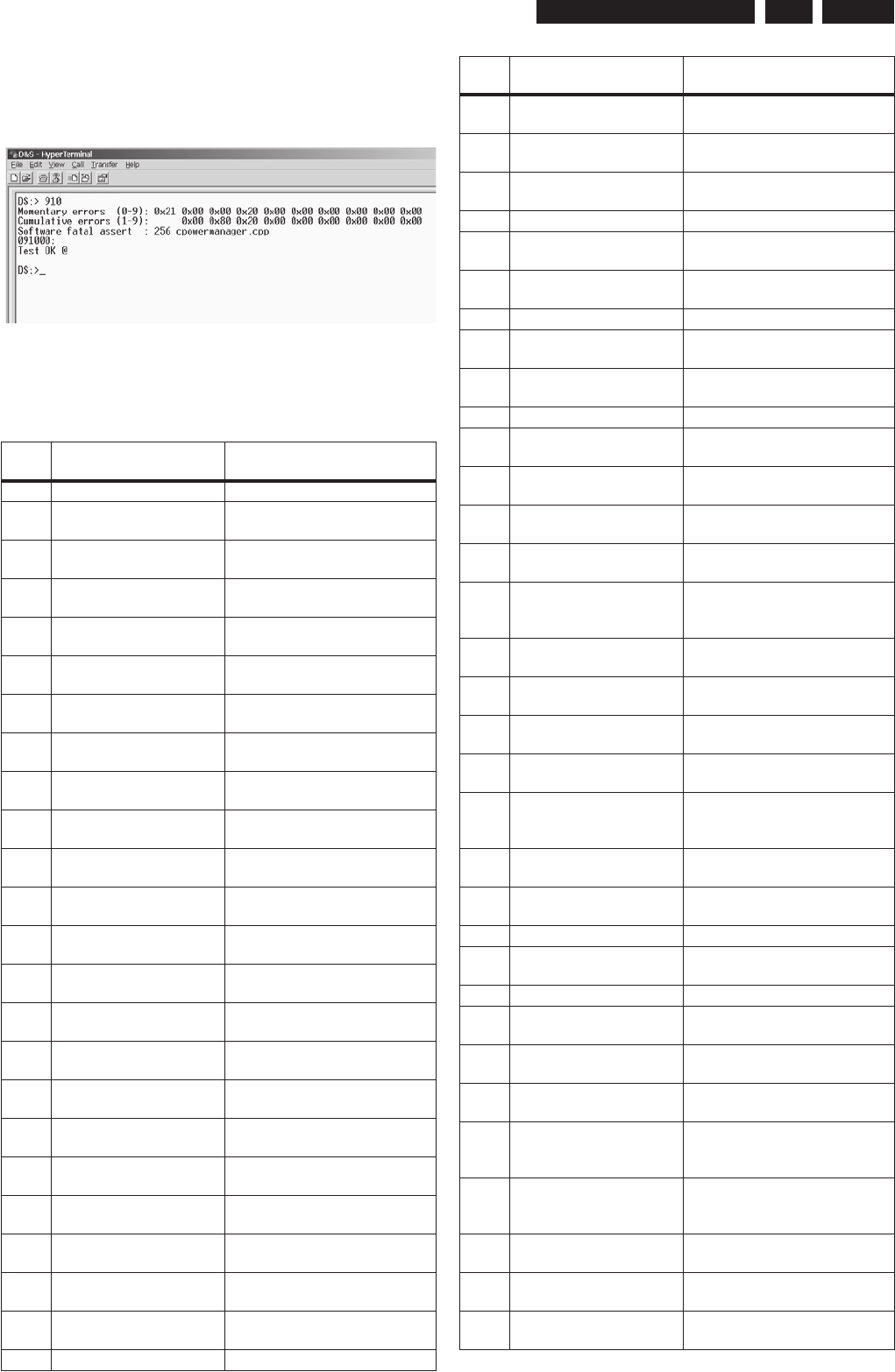
EN 115
3139 785 31532 5.
Firmware Upgrading & Diagnostic Software
5.4 DVD Module Error code
With DSW command 910 the set software can retrieve an
overview of all occurred engine errors.
5.4.1 Momentary Errors
Byte 0: latest error:
Overview of the BE error codes.
error
code
error meaning
0x00 no_error No error has occurred
0x01 illegal_command_error Command not allowed in this
state or unknown command
0x02 illegal_parameter_error Parameter(s) not valid for this
command
0x03 command_timeout_error The maximum execution time for
the command has exceeded
0x04 sledge_home_error The sledge could not be moved
home
0x05 sledge_calibration_error An error occurred during calibra-
tion of the sledge
0x06 sledge_unstable_error The sledge detected unstable
control
0x07 speed_timeout_error Spindle motor could not reach its
target speed within timeout
0x08 speed_window_error Measured spinning speed is not
within expected window
0x09 focus_timeout_error Focus could not be achieved
within the timeout
0x0A focus_retries_error The amount of focus retries ex-
pired
0x0B focus_agc_error The focus agc results are out of
range
0x0C radial_timeout_error Servo didn’t get on track within
the timeout
0x0D radial_retries_error Servo didn’t get on track after
several retries
0x0E radial_agc_error The radial agc results are out of
range
0x0F radial_init_error Unreliable signal scaling after the
radial initialisation
0x10 hf_pll_error HF-decoder pll could not lock to
HF signal
0x11 wobble_pll_error Wobble pll could not lock to wob-
ble signal
0x12 subcode_timeout_error Subcode information could not
be read
0x13 subcode_notfound_error Requested subcode item could
not be found
0x14 header_timeout_error Header information could not be
read
0x15 adip_timeout_error Adip information could not be
read
0x16 adip_window_error Adip address was not within ex-
pected window
0x17 adip_sync_error No adip sync was detected
0x18 atip_timeout_error Atip information could not be
read
0x19 atip_notfound_error Requested atip item could not be
found
0x1A atip_window_error Atip address was not within ex-
pected window
0x1B atip_sync_error No atip sync was detected
0x1C tray_error Tray could not be closed or
opened within the timeout
0x1D seek_error The requested seek couldn’t be
performed within the timeout
0x1E no_hf_present_error Attempt to read from a blank area
0x1F record_error An error occurred during the re-
cording
0x20 illegal_stopaddress_error The requested stopaddress with
modify-stop-address is not valid
0x21 no_disc_error No disc is detected
0x22 not_initialised_error The system is not initialised (e.g.
seek on unknown disctype)
0x23 illegal_medium_error BE detected an unsupported me-
dium during disc recognition
0x24 cd_frequency_error Measured HF frequency is not
within CD frequency range
0x25 dvd_frequency_error Measured HF frequency is not
within DVD frequency range
0x26 re-
served(non_existing_bca_
error)
Attempt to read non-existing bca
information
0x27 reserved(bca_read_error) An error occurred during reading
of bca information
0x28 selftest_error An error occurred during the self-
test of the BE
0x29 i2c_error The I2C interface does not oper-
ate
0x2A laser_pll_error Laser control pll did not lock or
lost lock on write clock
0x2B laser_forward_sense_erro
r
Forward sense value didn’t
change with changing laser pow-
er
0x2C jitter_optimisation_error An error occurred during optimis-
ation of the jitter
0x2D tilt_calibration_error An error occurred during calibra-
tion of the tilt frame
0x2E reserved
0x2F frontend_offset_calib_erro
r
The offset in the frontend couldn’t
be calibrated
0x30 reserved
0x31 wsg_calculation_error An error occurred in the calcula-
tion of the write strategy
0x32 buffer_overrun_error The buffer input stream overran
the buffer output stream
0x33 return_value_invalid_error The requested information is not
available for this inquiry
0x34 illegal_recording_speed_e
rror
The selected speed is not al-
lowed for a recording on this me-
dium
0x35 opc_media_parameter_err
or
The media parameters (info in
ATIP/ADIP) are invalid or not
read
0x36 opc_record_power_error The final optimum power was not
reached
0x37 opc_start_power_low_erro
r
OPC start power too low (opti-
mum power is higher)
0x38 opc_start_power_high_err
or
OPC start power too high (opti-
mum power is lower)
error
code
error meaning

EN 116 3139 785 31532 Firmware Upgrading & Diagnostic Software
5.
This error is overwritten by the next player / inquiry command.
0x39 opc_power_calculation_er
ror
Error during OPC power calcula-
tion (samples are wrong)
0x3A opc_test_zone_full_error OPC can’t be performed because
test zone is full
0x3B opc_bad_jitter_measurem
ent_error
The jitter measurement during
OPC samples readback failed
0x3C opc_read_samples_error An error occurred during OPC
readback sampling
0x3D ropc_alpha_overflow_error The determined value for the op-
timum power is too high
0x3E ropc_alpha_ref_current_er
ror
The alpha measurement refer-
ence current is wrong (IAN)
0x3F ropc_alpha_gain_error The alpha measurement alpha
gain is wrong
0x40 beta_over_under_flow_err
or
During the walking OPC a beta
over-/under-flow was detected
0x41 not_enough_calib_points_
error
Not enough valid calibration
points available for re-calibration
0x42 not_enough_power_error The calculated power during re-
calibration exceeds max power
0x43 illegal_reading_speed_err
or
The selected speed is not al-
lowed for the requested com-
mand
0x44 servo_fatal_error The actuator dissipation became
too high during a servo recovery
error
code
error meaning
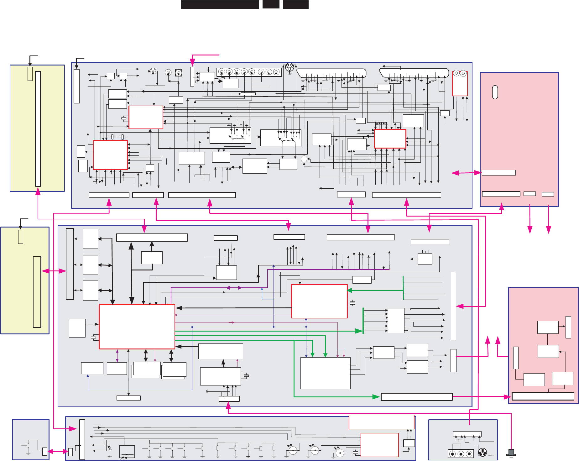
EN 117
3139 785 31532 6.
6. Block Diagrams, Waveforms, Wiring Diagram
Overall Block Diagram
Block Diagrams, Waveforms, Wiring Diagram.
7201
PDI1394L40
Link Chip
GND 22
A_BCLK 21
A_WCLK 20
GND 19
A_DATA 18
GND 17
A_PCMCLK 16
GND 15
D_BCLK 14
GND 13
D_WCLK 12
D_DATA0 11
GND 10
D_PCMCLK 9
GND 8
D_KILL 7
SPDIF_COAX_IN(N/U) 6
5V 5
SPDIF_OPT_IN(N/U) 4
GND 3
DAOUT 2
GND 1
1900 (AUDIO I/O)
1104 (I2C/Reset)
GND 1
VIP_FB 2
N / U 3
N / U 4
SCL0 5
SDA0 6
INT 7
TXD3 8
RX D3 9
ANALOG_RESETn 10
1500 (PSU)
3V3 1
3V3 2
3V3 3
3V3 4
GND 5
12V 6
GND 7
GND 8
5V 9
HD_ON 10
GND 11
-5V12
1904
(VIDEO
I/O)
A_VR 22
GND 21
A_UB 20
GND 19
A_YG 18
GND 17
A_C 16
GND 15
A_YCVBS 14
GND 13
GND 12
D_CVBS 11
GND 10
D_Y 9
GND 8
D_C 7
GND 6
D_VR 5
GND 4
D_YG 3
GND 2
D_UB 1
7007
SAA7118E
VIP
7200
PDI1394P25
Physical Chip
7601
AD8091AR
Buffer GND 1
Y 2
GND 3
PB(U) 4
GND 5
PR(V) 6
GND 7
1002
(PSCAN)
R_OUT
VIP ANALOG VIDEO INPUT
ITU_IN[0:7]
UART 3 (EPG*)
VIDEO OUT
Discrete
Filter
&
Buffer
DIGITAL AUDIO
MPIO7_MUTE_LV
+5V 7
N/U 6
GND 5
N/U 4
RXD0 3
2
TXD0 1
1103 (Service)
Buffer
UART 0
B_OUT
G_OUT
7809
EEPROM
(APPL)
7810
EEPROM
(BOOT)
I2C 1
7812/13
SDRAM
(64M B)
6
5
4
3
2
1
1203 (DV-IN)
7602
AD8092AR
Buffer
7400
PNX7100EH/G/C3
CHRYSALIS PROGY&C_OUT[0:7]
DAC F
DAC E
DAC D
7603
ADV7322(NTSC/PAL)
Progressive Denc
Y_OUT
C_OUT
CVBS_O UT
ITU_OUT[0:7]
7106
NCP
303
PNX7100_
RESETn
P-Scan
Filter
PCI_AD[8:31]
IDE1
1102
IDE1_DD(15:0) & IDE1_CTL
(D4.3)
40
1
MPIO19_EEPROM_En(Diags En)
1400 (E-JTAG)
I2C 0
I2C 0
7108
74LVC245
MPIO17_HD_ON
+1V8
to Chrysalis
7501
&
7500
140
7320
74LVC245
7321
74LVC245
7322
74LVC245
IDE21101 HARD-DISC
1900
22 GNDD
21 DAOUT
20 GND
19 DAINOPT (N/U)
18 NC
17 DADINCOAX (N/U )
16 D_KILL
15 GND
14 D_PCMCLK
13 GND
12 D_DATA0
11 D_WCLK
10 GND
9 D_BCLK
8 GND
7 A_PCMCLK
6 GND
5A_DAT
4 GND
3 A_WCLK
2 A_BCLK
1 GND
CVBS
7004
AD1852JRS
DAC
S-VIDEO
1922B
1 12VSTBY
2 STBY
3 5VSTBY
4 DD_ON
5 3V3STBY
6 IPFAIL
7 5NSTBY
8 GND
9 33VSTBY
10 GND
11 VGNSTBY
1932
1 AINFR
2 GND
3 AINFL
4 CVBSFIN
5 GND
6 NC
7 CFIN
8 GND
9 YFIN
1942
22 D_UB
21 GND
20 D_YG
19 GND
18 D_VR
17 GND
16 D_C
15 GND
14 D_Y
13 GND
12 D_CVBS
11 GND
10 GND
9 A_YCVBS
8 GND
7 A_C
6 GND
5 A_YG
4 GND
3 A_UB
2 GND
1 A_VR
1947
7007
UDA1361TS
ADC
1940-2
AL
AR
1 GND
2 SDA_F
3 SCL_F
4 CSN_F
5 IPORT1
6 RC
7 5VSTBY
8 TEMP_SENSE
9 KEY1
10 12VSTBY
11 KEY2
12 F_IROUT
13 VGNSTBY
7501
HEF4052BT
Analog Switch
7600
MSP3415G
Sound Processor
7509
MC33078D
Dual Amp
7203
NJM2267M
Video Amp
AIN1L
AFER
ARADC
ALADC
ARDAC
ANTENNA
INPUT
TV OUT
SCART 2
21
20 CVBSIN1
19 YCVBSOUT1
18
17
16 FBOUT
15 RCOUT
14
13
12
11 GOUT
10 P50
9
8 8SC1
7 BOUT_CIN
6 AIN1L
5
4
3 AOUT1L
2 AIN1R
1 AOUT1R
1940-1
1921
7504
HEF4052BT
Analog Switch
AIN1R
7505
MC33078D
Dual Amp
AFEL
7413
NJM2235M
Video Switch
AIN2L
AIN2R
AOUT1L/R
AOUT2L
AOUT2R
ALDAC
C
SCART 1
SCL_5V
SDA_5V
ASC1
RSA1/2
1925
DIGITAL
OUT
7700
74HCU04D
VFV
VFV
7108
TMP87CH74F
Processor
6255
AIN2L
AIN2R
7408
STV6618
Video Switch
Matrix
AOUT2L/R
SCL_5V
SDA_5V
SIF1
18.432M
8M 7412
NJM2234M
Video Switch
1 RESET
2 TXD
3 RXD
4 INT
5 SDA0
6 SCL0
7 NC
8 D-IROUT(n/u)
9 FB
10 GND
1914
7100
NCP
301
SCL_5V
SDA_5V
FAN
0/6/12
8SC2
to 7108
FB to
7108
FB
8SC2
WSFI
WSFI
1911
Level
shift
PSU
12VE 1
GND 2
GND 3
5VE 4
HARD-DISC
CVBS
MPIO17_HD_ON
To conn.
1932
of Analog Bd.
To power
conn.
of D4.3
To power
conn.
of Hard-
disc
12VH 1
GND 2
GND 3
5VH 4
From PSU
O O
AC MAINS
INPUT
DVDR5350H/DVDR73x0H
Digital Board
Analog Board
N/U
Standby
Board
1930
STOPPLAY
REC
POWER
1 GND
2 SDA_F
3 SCL_F
4 CSN_F
5 IPORT1
6 RC
7 5VSTBY
8 TEMP_SENSE
9 KEY1
10 12VSTBY
11 KEY2
12 F_IROUT(n/u)
13 VGNSTBY
3V3D 1
3V3D 2
3V3D 3
3V3D 4
GND 5
12VD 6
GND 7
GND 8
5VD 9
HD_ON 10
GND 11
-5VD 12
1 12VSTBY
2 STBY
3 5VSTBY
4 DD_ON
5 3V3STBY
6 IPFAIL
7 5NSTBY
8 GND
9 33VSTBY
10 GND
11 VGNSTBY
1
2
8019 (DV-IN)
D 4.3
(VAD8043 )
12VE 1
GND 2
GND 3
5VE 4
1911
1910
GND
N/ U
N/ U
PNX7100_ITU_IN_CLK(27M)
PNX7100_ITU_OUT_CLK / P_CLK(54M)
HSCKB
4M
24.576M
SYSCLK(49.152M)
24.576M
401
1 RESETn
2 GND
3 DD[7]
4 DD[8]
5 DD[6]
6 DD[9]
7 DD[5]
8 DD[10]
9 DD[4]
10 DD[11]
11 DD[3]
12 DD[12]
13 DD[2]
14 DD[13]
15 DD[1]
16 DD[14]
17 DD[0]
18 DD[15]
19 GND
20 Keypin
21 DMARQ
22 GND
23 DIOW_n
24 GND
25 DIOR_n
26 GND
27 IORDYC
28 SEL
29 DMACK_n
30 GND
31 INTRQ
32 IOCS16
33 DA1
34 PDIAG_n
35 DA0
36 DA2
37 CS0_n
38 CS1_n
39 DASP_n
40 GND
CNB
CNA
CND CNE
CN1
32.768K
REAR OUT
21
20 YCVBSIN 2
19 CVBSOUT2
18
17
16 FBIN
15 RCIN
14
13
12
11 GIN
10 P50(N/U)
9
8
7 BIN_COUT
6 AIN2L
5
4
3 AOUT2L
2 AIN2R
1 AOUT2R
Detector
7401-3
WU
Y
Level
Translator
IMUTE
OR OR
D_KILL
BKILL
(Cinch)
AKILL
(Scart)
DAC
Mute
DAC
Mute
3134
NTC
B57875
AL
AR
YUV
1922A
7200
NJM2584M
Video Switch 7201
NJM2580M
Video AMP
1700
TMQZ2
- 439A
Tuner
To MSP
SIF
From tuner
GND 1
Pr 2
GND 3
Pb 4
GND 5
Y 6
GND 7
1920
To conn. 1920
of Analog Bd
D_UB
D_YG
D_VR
Comparator
7934
FOME
CVBSIN1
CVBSIN2
+0/5 V
To/from 1911/4
G-LINK
OUT
1924
F_IROUT
TXD
RXD
12VE 1
GND 2
GND 3
5VE 4
12VH 1
GND 2
GND 3
5VH 4
P50
To/from 1924
From 1940
P50 to
7108
1 AINFR
2 GND
3 AINFL
4 CVBSFIN
5 GND
6 NC
7 CFIN
8 GND
9 YFIN
1922
7103
TMP86PM74A
Proccessor
FTD DISPLAY
7100 (9-ST-35GNK)
16M
PROGRAM+
PAUSE
1
2
GND
KEY1 NEXT
PREV OPEN/
CLOSE
KEY1
PROGRAM-TUNER
7805/07
FLASH
(16M B)
From conn. 1002
of Digital board
IR
7107
TSOP4840
REC.
LED
(red)
HDD
LED
(blue)
From PSU
AV in
Board
From PSU
ARDAC
ALD AC
ARDAC
ALDAC
IPRO
from 71 08
IPRO
to 7200
Y/CVBSo ut - REC
RCin2
BOUT_CIN1
CFin
Ctr l lines
D_KILL
Muting
Cct.
AKILL
Muting
Cct.
AKILL
Muting Cct.
BKILL
KEY2 Filament
cct.
PWM
FIL1
FIL2
1920
CVBS
AL
AR
YC IN
1921
STBY
DD_ON
Display Board
GUIDE
LED
(white)
1004 (HDMI)
1004 (HDMI)
40
1
HDMI Board
(For DVDR73x0H only)
1
2
3
4
5
6
7
GND
Y
GND
Pb(U)
GND
Pr(V)
GND
1920
(PSCAN)
40
1
7304
HDMI Trx
SII9030
7100
FAROUDJA IC
FLI2310
7253
ADV7320
(NTSC/PAL)
7251/7252
AD8091ART
AD8092AR
1
23
1920
(HDMI)
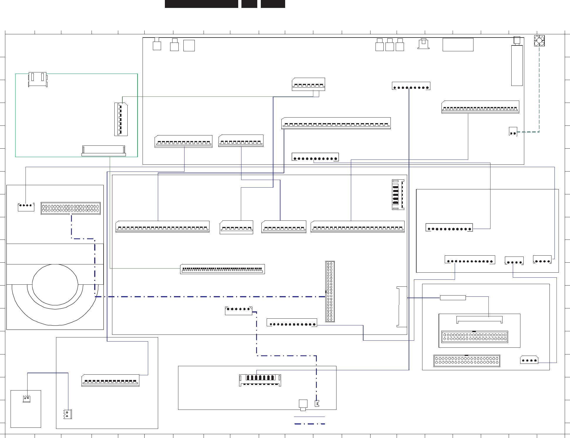
EN 118
3139 785 31532 6.Block Diagrams, Waveforms, Wiring Diagram.
1234567891011121314151617181920
A
B
C
D
E
F
G
H
I
J
K
L
M
N
O
P
Q
A
B
C
D
E
F
G
H
I
J
K
L
M
N
O
P
Q
1234567891011121314151617181920
BASIC ENGINE
(1007)
1
2
3
4
5
6
7
8
9
10
ION
GNDD
VIP_FB
BE_FAN
ANA_WE
VSM_UART1_RTSn
VSM_UART1_CTSn
VSM_UART1_TX
VSM_UART1_RX
IRESET_DIG
1102
39
1
STANDBY
KEY1
GND
1930
S2B-EH
1
2
KEY1
GND
1911
1
2
1
2
3
4
5
6
7
8
9
10
11
12
13
14
15
16
17
18
19
20
21
22
GNDD
AD_SPDIF33
N.C.
+5V
+3V3
MUTEN
GNDD
AD_ACLK
GNDD
AD_DATA0
AD_WCLK
GNDD
AD_BCLK
GNDD
AD_BCLK
GNDD
AE_DATA1
GNDD
AE_WCLK
AE_BCLK
GNDD
S2B-EH
13FMN-BTRK-A
1910
1
2
3
4
5
6
7
8
9
10
11
12
13
GND
SDA_F
SCL_F
CSN_F
IPOR1
RC
5VSTBY
TEMP_SENSE
VGNSTBY
KEY1
12VSTBY
KEY2
F_IROUT
DISPLAY
(1004a)
1932
1
2
3
4
5
6
7
8
9
10
11
12VSTBY
STBY
5VSTBY
DD_ON
3V3STBY
IPFAIL
5NSTBY2
GND
33VSTBY
GND
VGNSTBY
40-pol IDE connector
39
1
4
3
2
1
+5V
GND
GND
+12V
4-pol PC connector
1500
1
2
3
4
5
6
7
8
9
10
11
+3V3
+3V3
+3V3
+3V3
GNDD
N.C.
GNDD
GNDD
+5V
ION
GNDD
JST-KR
1904
1
2
3
4
5
6
7
8
9
10
11
12
13
14
15
16
17
18
19
20
21
22
B_OUT_B
GNDD
G_OUT_B
GNDD
R_OUT_B
GNDD
C_OUT_B
GNDD
Y_OUT_B
GNDD
CVBS_OUT_B
GNDD
GNDD
CVBS_Y_IN
GNDD
C_IN
GNDD
Y_IN
GNDD
U_IN
GNDD
V_IN
N.C.
2mm
12-5V
SETFAN
1932
1
2
3
4
5
6
7
8
9
10
11
12VSTBY
STBY
5VSTBY
DD_ON
3V3STBY
IPFAIL
5NSTBY2
GND
33VSTBY
GND
VGNSTBY
1mm
1934
1
2
3
4
5VH
GND
GND
12VH
PSU
(1008)
FFC-Cable
Cable Tree Assy
HCON2
39
1
1
2
3
4
5V
GND
GND
12V
4-pol PC connector
40-pol IDE connector
1301
1
40
40-pol FFC0, 5mm pitch
1800… 3103 607 10121 IDE adapter assy
5000 Ferrite core HDD
(1200)
8022….3103 601 0016
+5V
TX1P 7
6
5
4
3
2
1
1103
CTS1P
GND
RST1P
RX1P
BCLK_CTL_SERVICE
2mmJST-KR
SERVICE
1104 1mm1mm
1900
1
40
1101
12-5V
1901
1
2
3
4
5
6
7
8
9
10
11
+3V3
+3V3
+3V3
+3V3
GNDD
N.C.
GNDD
GNDD
+5V
ION
GNDD
2.5mm
1934
1
2
3
4
5VE
GND
GND
12VE
2mm JST-KR
2mm JST-KR 2.5mm
1
2
3
4
5
6
1
2
3
4
5
6
7
8
9
10
SCL0
GND
VIP_FB
D_IROUT
N.C.
SDA0
INT
TXT
RXD
RESET
1911
1
2
3
4
5
6
7
8
9
10
11
12
13
GND
SDA_F
SCL_F
CSN_F
IPOR1
RC
5VSTBY
TEMP_SENSE
VGNSTBY
KEY1
12VSTBY
KEY2
F_IROUT
TUNER
1900
1
2
3
4
5
6
7
8
9
10
11
12
13
14
15
16
17
18
19
20
21
22GND
DAOUT
N.C.
N.C.
N.C.
N.C.
D_IKILL
GND
D_PCMCLK
GND
D_DATA0
D_WCLK
GNDD
D_BCLK
GND
A_PCMCLK
GND
A_DAT
GND
A_WCLK
A_BCLK
GND
GND
D_G
GND
D_R
GND
D_C
GND
D_Y
GND
D_CVBS
GND
GND
A_YCVBS
GND
A_C
GND
A_G
GND
A_B
GND
A_R
D_B
G-Link
6255
1914
1920
1mm
1mm 1mm
SCART1/ SCART 2
19401922
CVBS-
Audio out
1935
1
2
GND
5V
2mm
ANALOG BOARD
(1001)
1942
1
2
3
4
5
6
7
8
9
AINFR
GND
AINFL
CVBSFIN
GND
N.C.
CFINI
GND
YFIN
JST-KR
1947
1
2
3
4
5
6
7
8
9
10
11
12
13
14
15
16
17
18
19
20
21
22
1mm
2mm JST-KR
1924 COAX
1925
OPTICAL
DIGITAL AUDIO
OUT
1921
Y/C outAudio
out
YUV-
Progressive 1700
GND
TPA0+
TPA0-
GND
TPB0+
TPB0-
1203 DV In
AV IN
(1004b) CVBS-
Audio out
DV In
2mmJST-KR
7
6
5
4
3
2
1
8
GND
CFIN_FC
N.C.
GND
CVBSFIN_FC
AFCLI_FC
GND
AFCRI_FC
1922
9
YFIN_FC
8010….3103 601 0065
8009….3103 601 0061
8026….31036010072
8004….31036010063
8001….31036010059
FFCFOIL22P/220/22PBDFLDUL
8013….31036010031
CBLE KR 12P/140/12P KR UL
8019….3103 601 0036
8030…31036070057
8013… 3103 607 0086
Part of IDE Assembly
8012….3103 601 0056
HCON2
39
1
1
2
3
4
5
6
7
Y
GND
GND
U
GND
V
GND
DIGITAL BOARD
(1002)
CBL HER 4P/430/4P LC UL
FFCFOIL 22P/226/22PFLDUL
CBL IDE 40P/400/40P IDE CBL
FFCFOIL 10P/315/10PBDFLDUL
JST 6P FIREWIRE CABLE 360mm
FFC FOIL 13P/600/13P AD UL
CBLEKR9P/380/9PKRSLDUL
CBLEK
R11P/160/11PKRUL
8008….3103 601 0044
CBLEHER4P/130/4PLC
8005….31036010075
140
19 1
1930
1 TX2+_1
2 GND
3 TX2-_1
4 TX1+_1
5 GND
6 TX1-_1
7 TX0+_1
8 GND
9 TX0-_1
10 TXC+_1
11 GND
12 TXC-_1
13 NC
14 NC
15 TX_DDC_SCL
16 TX_DDC_SDA
17 GND
18 +5V_HDMI
19 HPD
HDMI BOARD
(1009)
40
1
GND
INT_HDMI
GND
PSCAN_RSTn
HDMI_R
STn
GND
GND
GND
WS12_OUT
GND
GND
GND
GND
SPDIF_OUT
SD
_OUT
SK12_OUT
FSCLK12_OUT
-5V
ITU_OUT(7)
ITU_OUT(6)
ITU_OUT(5)
ITU_OUT(4)
ITU_OUT(3)
ITU_OUT(2)
ITU_O UT(1)
ITU_OUT(0)
VO_CLK
+3V3
+3V3
+3V3
+5V
+12V
GND
GND
GND
SCL0
SDA0
GND
GND
GND
1911 HDMI
1920
1mm
1
2
3
4
5
6
7
Y
GND
GND
U
GND
V
GND
8038….3139 241 0145
FFC FOIL 40P/280/40P BD 0.5MMP
8039….3139 110 0214
FFC FOIL 7P/100/7P BD 1.0MMP
(For DVDR7300H HDMI Connection ONLY)
1
2
3
4
5
6
7
Y
GND
GND
U
GND
V
GND
8002….31036010062
FFCFOIL 7P/290/7PBDFLDUL
(For DVDR7300H HDMI Connection ONLY)
(ForDVDR5350HwithoutHDMIONLY)
(For DVDR5350H without HDMI ONLY)
(For DVDR7300H ONLY)
DVDR5350_WIRING VER1.0.pdf 2005-05-03
Wiring Diagram
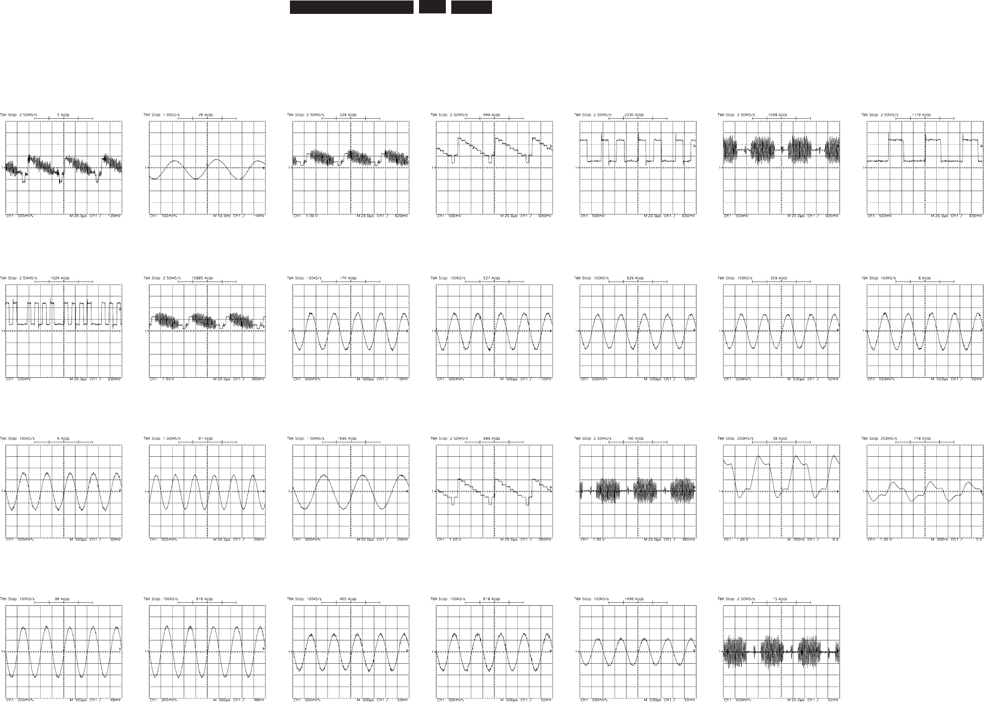
EN 119
3139 785 31532 6.Block Diagrams, Waveforms, Wiring Diagram.
Waveforms of Analog Board
I700 IC 1700VIDOUT I703 F4019 CVBS_OUT F4019 Y_OUT F4015 R_OUT F4015 C_OUT F4011 G_OUT
F4007 B_OUT F4119 CVBS_OUT I502 AFER I504 AFEL F502 IC 7504 PIN 12 F501 IC 7504 PIN 5 I618_AFER
I619_AFEL I612_AOUT2R I634_AOUT2L F210 Y_OUT F211 C_OUT F251 DIGITAL_OUT
OPTICAL
F2502 DIGITAL_OUT
CHINCH
I014 ARADC I032 ALADC I528 IC 7509 PIN 7 I505 IC 7509 PIN 1 I506 AOUT1L I507 AOUT1R
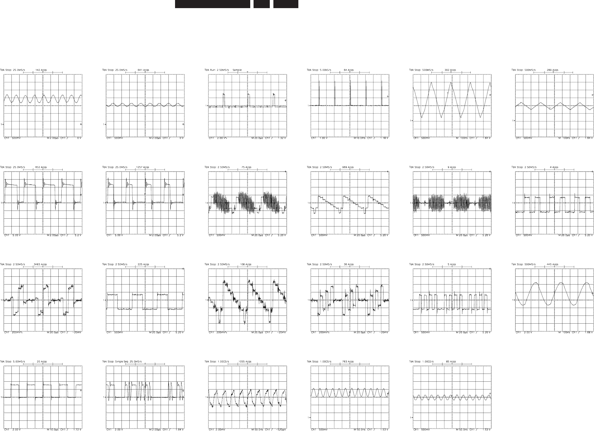
EN 120
3139 785 31532 6.
Block Diagrams, Waveforms, Wiring Diagram.
Waveforms of Digital Board
F203 IC 7200 PIN 60 IC 7200 PIN 59 F403 HS_OUT F404 VS_OUT F405 XTAL_IN F406 XTAL_OUT
IC7501 PIN 5 IC7501 PIN 6 I912 D_CVBS I913 D_Y I914 D_C I915 D_R
I915 D_V I916 D_G I916 D_Y I917 D_U I917 D_B F1914 D_BCLK
F1912 W_BCLK F1911 D_DATA0 F1909 D_PCMCLK XTAL 1001_IN XTAL 1001_OUT
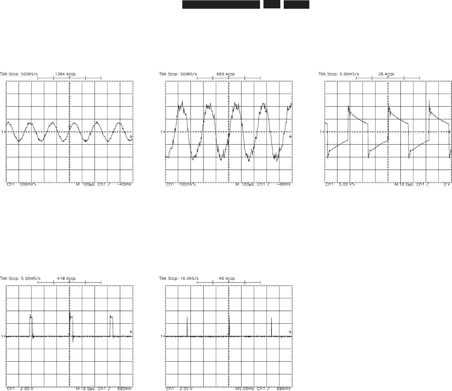
EN 121
3139 785 31532
Waveforms of Front Board
I150 IC7103 PIN 2
6.Block Diagrams, Waveforms, Wiring Diagram.
I151 IC7103 PIN 3 I164 7106 / 7108 EMITTER
Waveforms of HDMI Board
F111 P H_SYNC F112 P V_SYNC
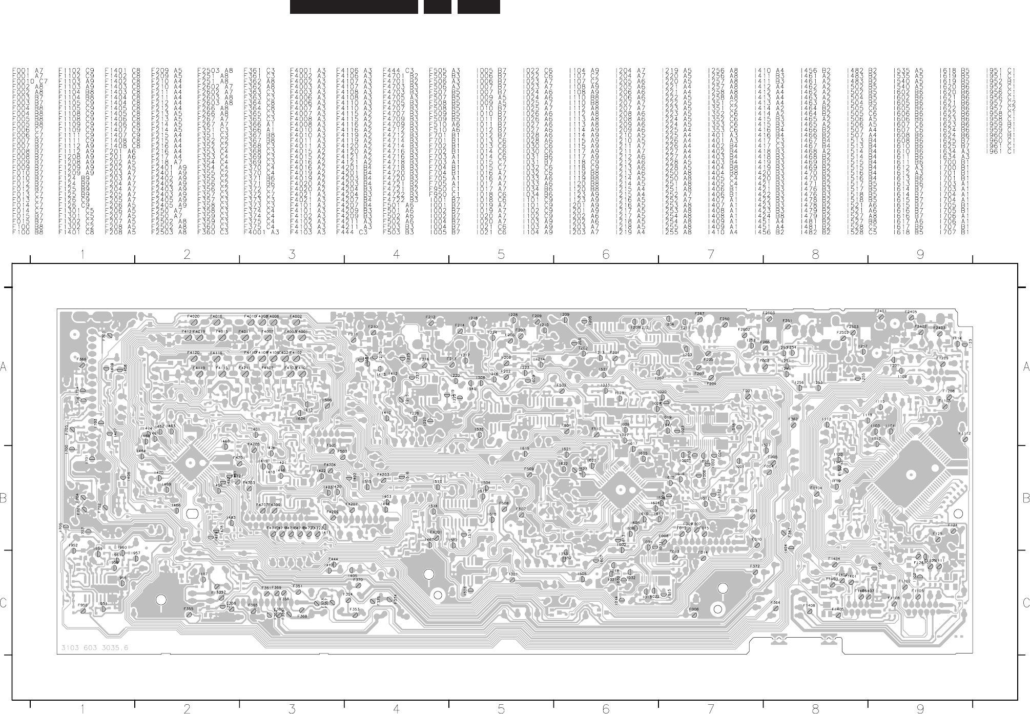
EN 122
3139 785 31532 6.Block Diagrams, Waveforms, Wiring Diagram.
Test Points Overview for Analog Board
Anabd_3139_603_30356_testpoint_2.pdf 2005-10-14
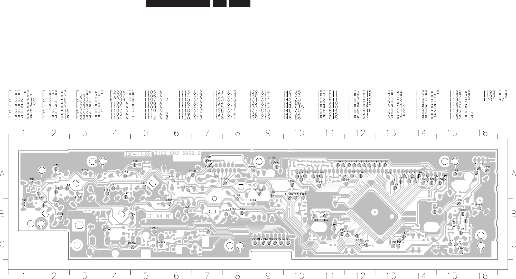
EN 123
3139 785 31532
Test Points Overview for Display/Front Connector Board
6.
Block Diagrams, Waveforms, Wiring Diagram.
Frontbd_3139_603_30380_testpoint_2.pdf 2005-10-14
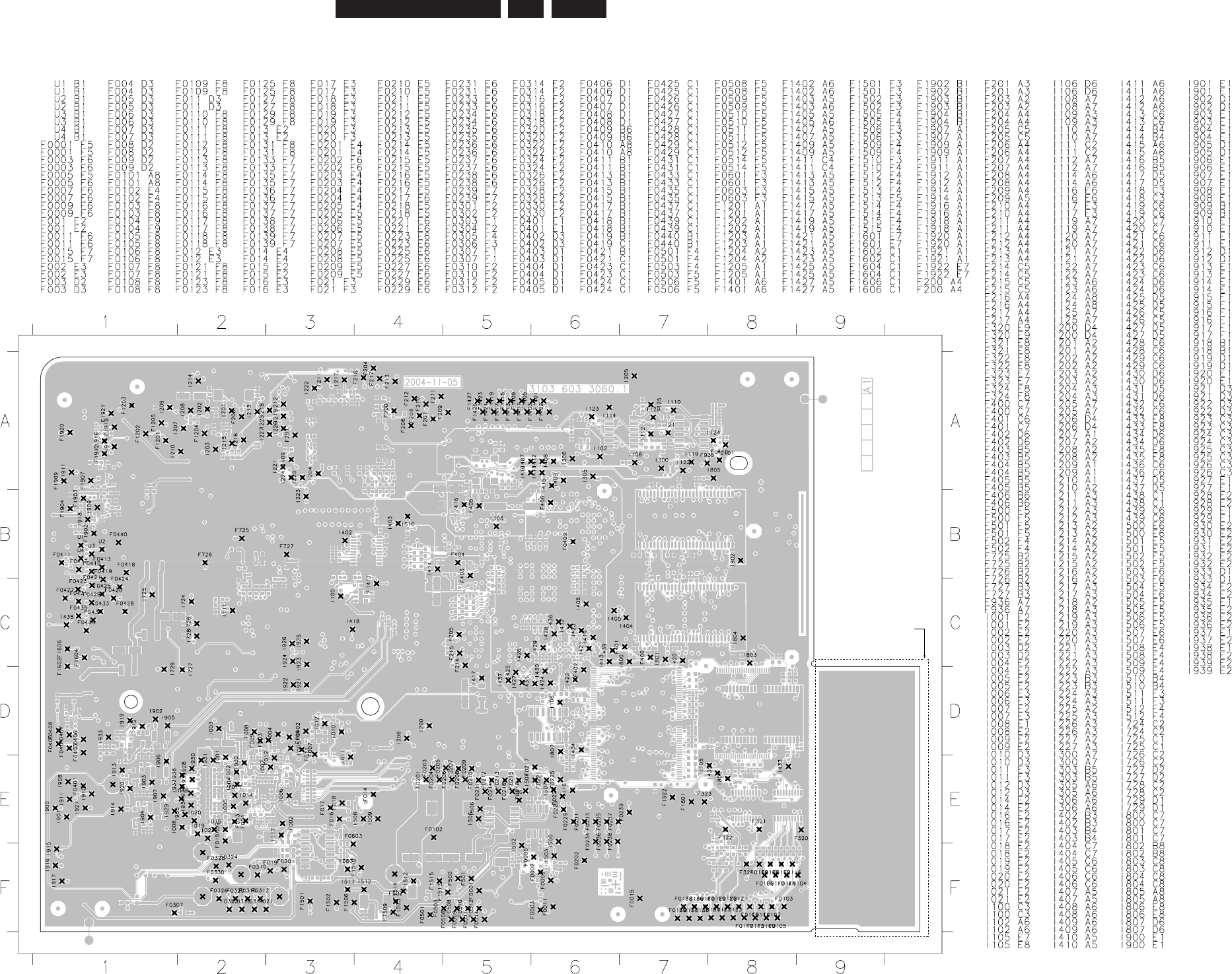
EN 124
3139 785 31532
Test Points Overview for Digital Board
BREAKAWAY
CONNECTOR TO
HDD
6.Block Diagrams, Waveforms, Wiring Diagram.
Digibd_3139_603_30601_testpoint_2.pdf 2005-10-14
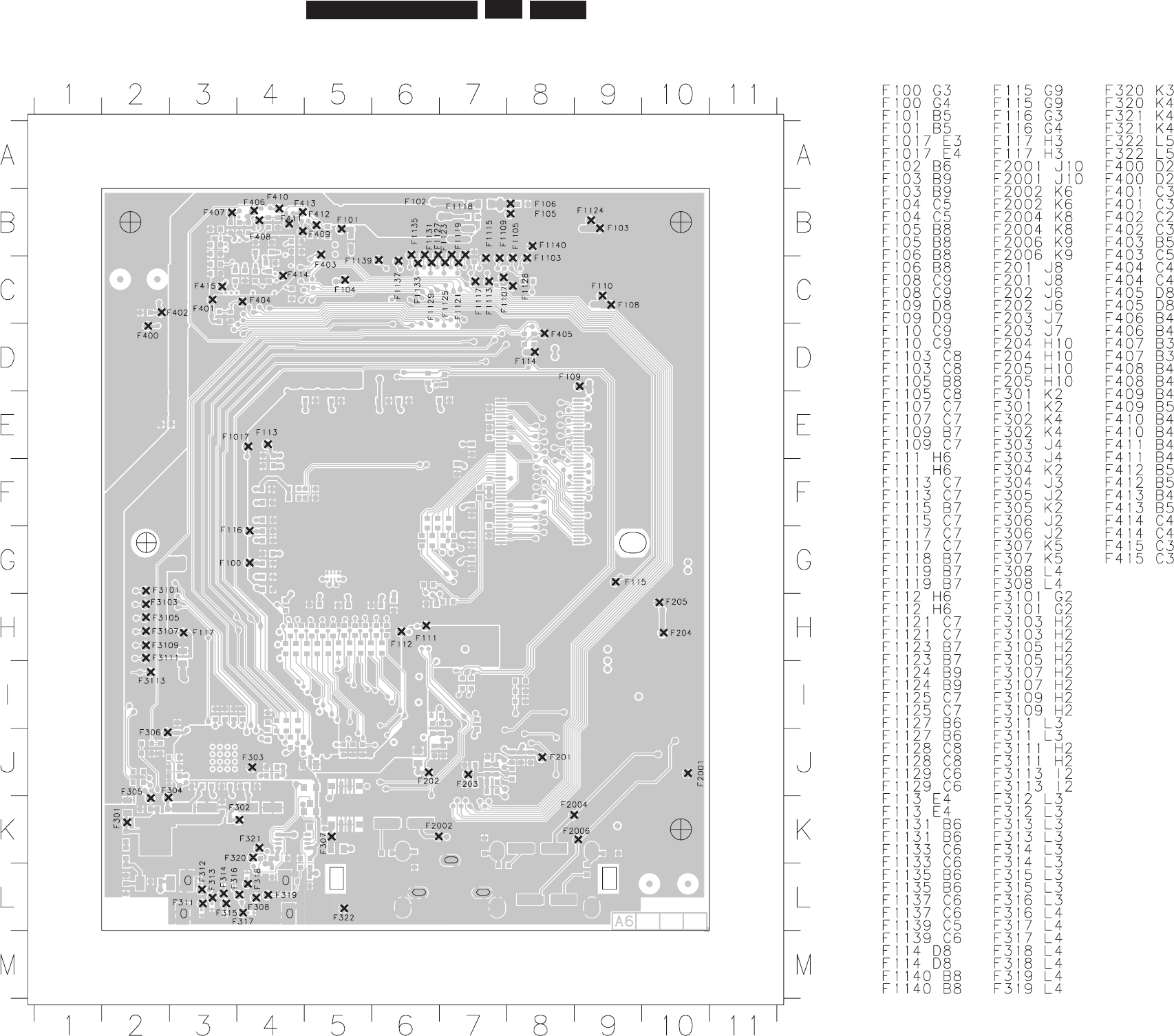
EN 125
3139 785 31532
Test Points Overview for HDMI Board
6.
Block Diagrams, Waveforms, Wiring Diagram.
3103-603-30587-testpoint.pdf 2006-09-04
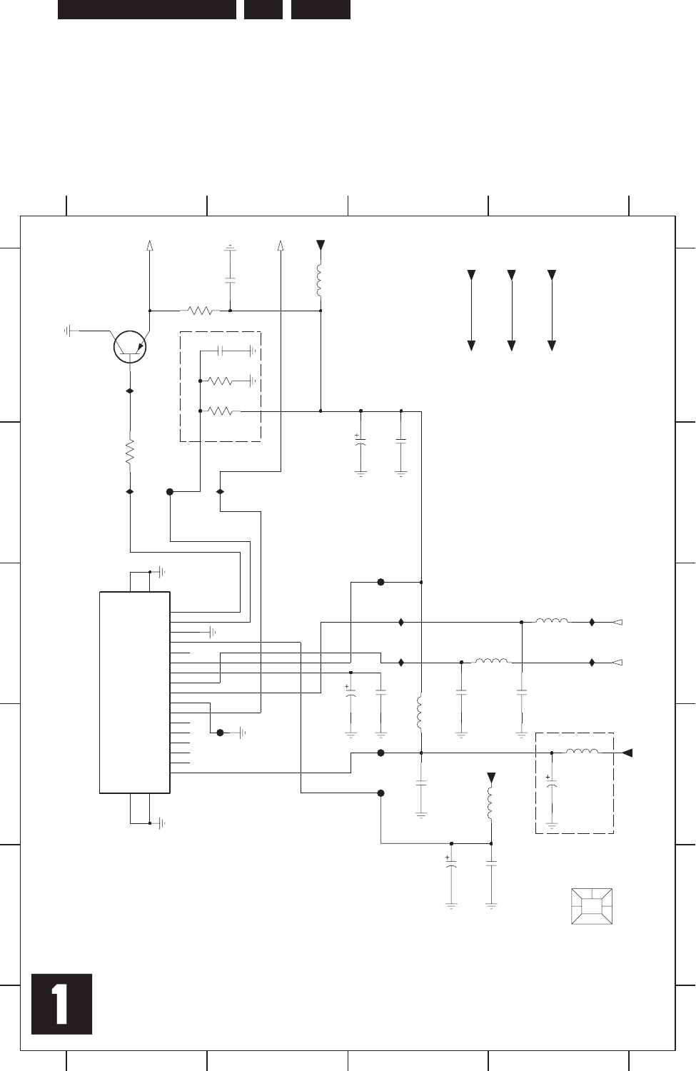
EN 126
3139 785 31532
7. Circuit Diagrams and PWB Layouts
7.Circuit Diagrams and PWB Layouts
Analog: Frontend Video (FV)
for DTTM only
A
3
04-
daeB
des
u
ton
from/to CU
MT
T
D
rof
e
teled
not used
from CU
PSM ot
1234
1234
A
B
C
D
E
A
B
C
D
E
0803 E4
1700 C1
2700 A2
2701 B3
2702 A2
2703 D3
EMOF,VOI ot
desu ton
2704 E3
2705 E3
2707 C3
2708 C4
2709 B3
2710 C3
2711 C2
2712 D4
3700 A2
3701 A2
3704 B1
3706 A1
5700 A2
5702 D3
5703 C4
5704 C4
5705 D3
5706 D4
7701 A1
F701 D2
F702 D3
F703 D3
F704 C3
F705 B1
I700 A1
I701 B1
I703 B2
I704 C3
I705 C4
I706 C3
5V
Bead
from PS
Bead
V
05
I707 C4
F703
1077
WB758CB
107I
I707
5704
3700
47K
I705
I706
5V
SDA
7
SIFOUT
17
VIDOUT
14
VTU
F704
12
2
NC1 3
NC2 4
NC3 5
NC4
NC5 13
RFAGC 11
10
SCL
16
AOUT 6
1
BB
8
9
GND1
15
GND2
12
MB
81
9102
RENUT
1700
TMQZ2
AFT
p74
8072
4
0
7
2
n01
V52
2700
22n
u22
1172
5703
5V
007I
V5
2u
0
1
2
1
7
2
507F
10u
5706
u22
0075
F701
5VSTBY
0803
BARCODE
3072
n00
1
3706
2K2
F702
5VSTBY
7072
p
7
4
I704
n01
n01
33VSTBY
0172
33VSTBY
9072
u
0
1
2075
5VSTBY
2072
n001
5075
Frontend Video FV
V3.6u74
1072
V057
u
4
5072
4073
3701
47K
R001
33VSTBY
307I
SDA_5V
SCL_5V
VFV
1FIS
3103_603_30356_a4_sh130_sh1.pdf 2005-07-07
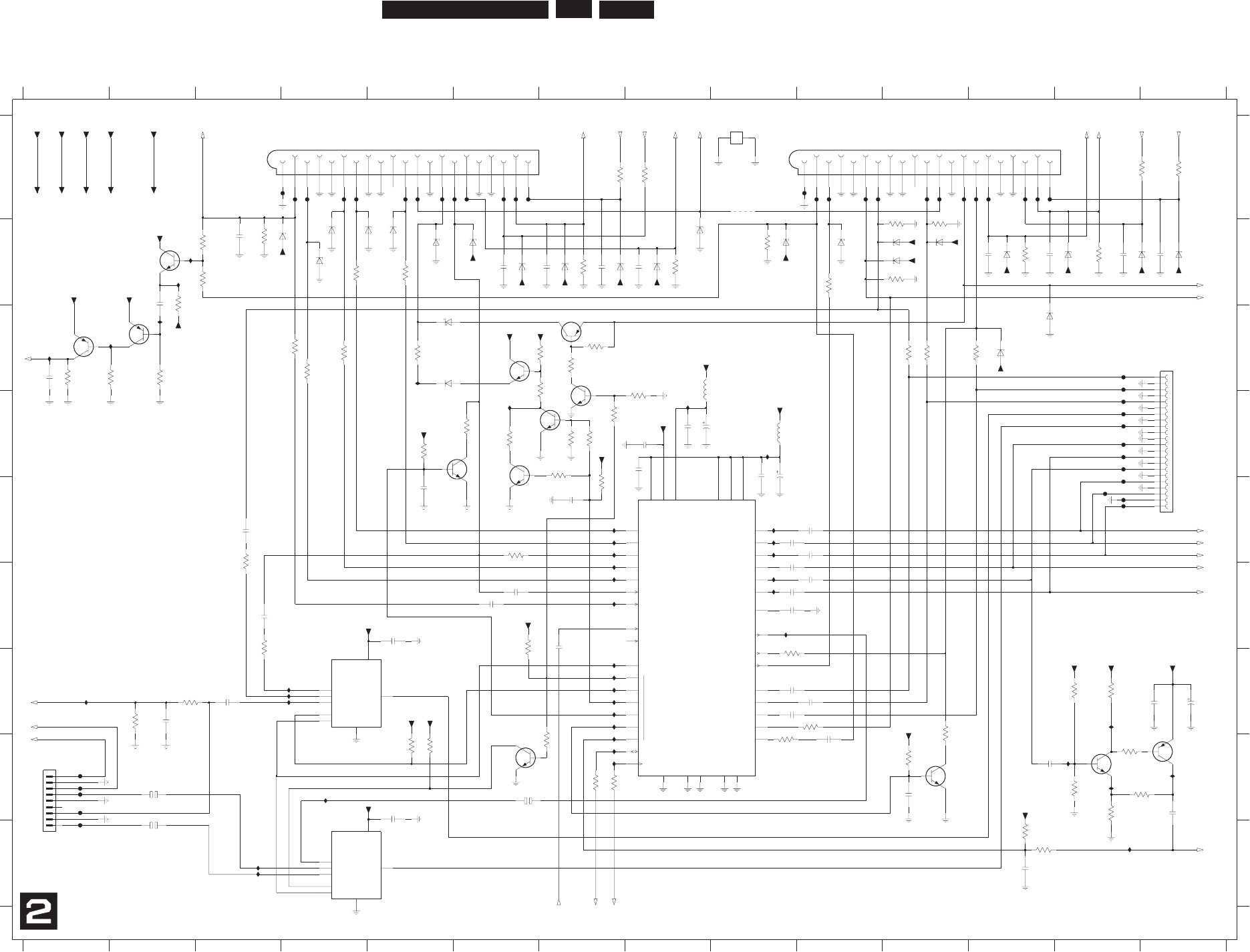
EN 127
3139 785 31532 7.
Circuit Diagrams and PWB Layouts
Analog: Video In / Out (IOV)
GND
V+
B
D
N
G
Y|CVBSIN-AUX
Y|CVBSIN-TV
CIN-TV
1DNG
DIGOUT
FBIN-AUX
B|PBIN-AUX
G|YIN-AUX
R|PR|CIN-AUX
Y|CVBSOUT-AUX
COUT-AUX
Y|CVBSOUT-REC
DECV
YIN-ENC
CIN-ENC
CVBSIN-ENC
B|PBIN-ENC
G|YIN-ENC
R|PR|CIN-ENC
3BCCV
2B
C
CV
1
BC
C
V
CER-BCCV
CCV
D
DV
SCL
SDA
Y|CVBSIN-TUN
6
5
4
3
2
1
D
D
NG
CIN-TUN
C-GATE
Y|CVBSOUT-TV
FBOUT-TV
B|PBOUT-TV
G|YOUT-TV
R|PR|COUT-TV
CER-BDNG
2
DNG
GND
V+
PSM,AOI ot
DNG
DNG
DNG
AOI morf
from PROG
%1
1940-1 A7
1940-2 A13
1940-3 A9
1942 H1
1947 C14
2401 B3
2402 C1
2403 E5
2404 F3
2405 D9
2406 F5
2407 H5
2408 H11
2409 D9
2410 E3
2411 D8
2412 G2
2413 F6
2414 D8
2415 H12
2416 H10
2417 H6
2418 G9
2419 F6
2420 H14
R1TUOA
NIG
1NISBVC
CN
CS
not used
UC ot/morf
DNG
to IOA
GND
L1NIA
1234567891011121314
1234567
DNG
V/
A
T
N
OR
F o
t/morf
TUOCR
PSM,AOI
ot
R
1
NIA
AOI ot
1 TRACS
8 9 10 11 12 13 14
A
B
C
D
E
F
G
H
I
A
B
C
D
E
F
G
H
I
DN
G
AOI ot
to PROG
to PROG
UC o
t
/morf
GND
R2TUOA
2421 I2
2422 I12
2423 G10
2424 B6
2425 B7
2426 B7
2427 G9
2428 H2
2429 B8
2430 G14
2431 B12
2432 G14
2433 F9
2434 D8
2435 D8
2436 E10
2437 F9
2438 F9
2439 F10
2440 E10
2441 E9
2442 B13
2443 B12
2444 B14
2446 F7
to IOA
NIC/TUOB
EM
OF ot
L2TUOA
2447 E7
2450 B2
2459 G3
3401 B11
3402 B11
3403 D6
3404 B3
3405 C1
3406 C2
3407 B2
3408 C1
3409 B4
3410 E6
3411 B10
3412 C4
3413 B5
3414 C4
3415 G13
3416 G13
3417 B11
3418 H13
3419 H14
3420 H13
3421 C6
3422 C5
3423 C6
3424 D6
3425 G11
DNG
05P
TUOBF
desu ton
GND
GND
3426 D7
3427 B9
3428 D7
3429 G2
3430 D5
3431 I12
3432 H7
3433 H7
3434 I12
3435 F3
3436 H11
3437 H5
3438 H5
3439 E7
3440 H13
3441 C7
3442 D7
3443 C7
3444 D8
3445 C4
3446 B3
3447 B3
3448 D7
3449 G9
3450 H7
3451 F6
to PROG
3452 H9
3469 B13
1%
L2NIA
%1
T
UOG
CVBSFIN
GND
2TUOS
B
VC
1
TU
O
S
BVC
Y
CFIN
3470 B12
3471 B8
3472 B7
3475 A7
3476 A8
3477 A14
3478 A13
3489 G2
3490 E3
3491 C11
3492 C11
3493 C12
3494 G10
4401 A9
5402 D9
5406 C8
6401 B3
6402 B4
6403 B5
6404 B6
6405 B6
6406 B7
6407 B7
des
u t
on
DNG
TUOC/NIB
GND
to PROG
GND
GND
1%
GND
R2NIA
%1
%1
CN
6408 B8
6409 B8
6410 C5
6411 B13
6412 B13
6413 B14
6414 B4
6415 B11
6416 B11
6417 C12
6418 C12
6419 B10
6420 B4
6421 C5
6422 B11
6423 B5
6424 B9
6425 B12
7401 C2
from PS
to CU
YFIN
to CU
7402 B2
7403 C1
7404 D5
7405 C6
7406 H11
7407 D6
7408 E8
7409 D7
7410 H14
7411 H13
7412 G4
7413 I4
7414 C7
7415 D7
7416 H6
F4001 A6
F4002 A6
F4003 A6
F4006 A6
F4007 A5
F4008 A5
F4010 A5
F4011 A5
F4015 A4
F4016 A4
F4019 A4
F4020 A4
F4021 A3
DNG
VF
morf
DNG
%1
AO
I
mor
f
%
1
F4101 A12
F4102 A12
F4103 A12
F4106 A12
F4107 A12
F4108 A11
F4110 A11
F4115 A10
F4116 A10
F4119 A10
F4120 A10
F4121 A10
F4201 H1
F4203 H1
F4204 H1
F4207 H1
F4209 I1
F4211 A11
F444 G7
F4701 C13
F4703 C13
F4705 D13
F4707 D13
F4709 D13
F4712 D13
F4714 D13
NIBF
L
1TUOA
GND
to PROG
UC ot/morf
NICR
F4716 D13
F4718 E13
F4720 E13
F4721 E13
F4722 E13
I401 G7
I402 C5
I403 G7
I404 C1
I405 G1
I406 C2
I407 C2
I408 B2
I409 B2
I410 G13
I411 H13
I412 H13
I413 H14
I414 D9
I415 G7
I416 G7
I417 G7
I418 G4
I419 G4
I420 G4
I421 H4
DNG
GND
VS
DNG
AINFL
DNG
DNG
PSM morf
%1
to CU
not used
to CU
I422 I3
I423 I3
I451 I13
I456 D8
I461 E7
I462 E7
I463 E7
I464 F7
I465 F7
I466 F7
I467 D6
I468 G7
I469 H7
I470 H7
I476 F9
I478 F9
I479 F9
I481 E9
I482 E9
I483 E9
DNG
GND
AINFR
to PROG
PSM morf
GND
2NISBVCY
2 TRACS
1%
DNG
NC
DRAOB LATGID ot/morf
GND
3143
R57
2042
n022
I465
4342
V3.6u74
5NESD
75R
3402
5VSTBY
4242
p
0
74
I419
5VSTBY
I420
7401
BC857BW
100R
3440
5VSTBY
F4718
0342
n001
6421
BAT54 COL
I462
4243
K3
3
5V
I411
I416
12VSTBY
7406
BC817-25W
5V
100R
3419
F4703
5VSTBY
R57
7243
10n
2447
I478
R051
5443
1u0
2438
0246
8V6C-
4
83X
Z
B
5NESD
BZX384-C12
6416
16V10u
2428
150R
3452
5NESD
12VSTBY
0743
2
1C-483XZB
1046
K001
3449
75R
I466
5243
R57
8
4
4
3
K00
1
204I
3004F
K0
0
1
0543
5NESD
BC847BW
7405
I409
DSEN5
2413
1u0
I421
7043
3
K3
0542
n
0
01
I408
K33
6243
3943
R051
910
4F
904
2
n
00
1
6
442
0u
1
I464
21C-483XZB
7046
21C-48
3
XZ
B
4246
I406
BC857BW
7403
2416
1u0
B9
I422
B91
B2
B02
B12
B3
B4
B5
B6
B7
B8
B1
B01
B11
B21
B
31
B
41
B
5
1
B61
B71
B8
1
2-0491
B_WOR
CP 01-V120-CRM
p074
2442
100n
2415
6046
21C-483XZB
I468
3428
100K
R001
3343
23
43
R0
01
7
343
5VSTBY
K0
1
7K4
6
3
43
8V6C-483XZB
4
1
4
6
R57
2143
I404
2439
1u0
5VSTBY
21C-483XZB
2146
DSEN5
F4722
2243
R028
F4721
2443
K051
5NESD
R57
3043
5VSTBY
BAS316
6410
014I
BZX384-C12
6415
1
204F
1214F
3417
75R
I481
1u0
2436
5NSTBY
704I
I405
1243
K72
I418
5114F
094
3
R
051
3146
21C-483XZB
10
4
2
p
0
0
1
BC847BW
7409
BZX384-C6V8
2
1
C-483XZB
4
04
6
5NSTBY
6422
2414
100n
2014F
3
4
5
6
7
8
9
14
15
16
17
18
19
2
20
21
22
1947
22FMN-BTRK-A
1
10
11
12
13
K
0
1
7004F
15
43
F444
I417
F4705
5VSTBY
F4707
F4714
5V
9
1
14F
F4716
I482
n001
0142
6743
R001
18K
3444
F4201
5V
BC847BW
7415
F4204
3442
p074
K01
93
43
6104F
0204F
4042
n001
3042
n00
1
I470
BC847BW
7407
2242
n01
8004F
0104F
2418
1u0
5NSTBY
I479
5NESD
5VSTBY
6114F
5V
5VSTBY
1943
R
05
1
I483
I403
75R
3401
0K1
5143
3014F
7410
BC857BW
4401
0214F
5VSTBY
F4203
12VSTBY
6443
K74
214I
VIN2
5VIN3
7
VOUT
Φ
3-INPUT
VIDEO SW
8
2SW1
4SW2
6
1VIN1
3
NJM2234M
7412
75R
3410
2441
1u0
p074
4442
BC857BW
7414
1940-3
MT2
MRC-021V-10 PC
MT1MT2
2406
1u0
0242
n001
1
1
04F
12VSTBY
I401
R051
2943
3
2
43
R093
3443
K74
5VSTBY
8046
2
1
C
-
48
3X
Z
B
0343
7K
4
21
33
K74
7443
8
02
42
03
23
63
7
19
1
41
25
22
93
15
1029
17
931
37
38
44
2
14
16
18
35
34
3
21
62
13
1127
28
6
43
40
23
4
5
42
MATRIX
VIDEO SWITCH
Φ
STV6618D
7408
2427
1u0
I467
BC847BW
I461
7402
21C-483XZB
5246
I451
V61u22
2342
6043
K074
5NESD
1342
p074
A
9
A91
A
2
A02
A1
2
A3
A4
A5
A
6
A7
A8
A1
A01
A11
A2
1
A31
A41
A5
1
A
6
1
A
7
1
A8
1
1-0491 A_W
O
R
CP 01-V
1
20-CRM
2459
100n
984
3
K28
5NESD
0114F
114
2
n001
7146
I463
21C-483XZB
2437
1u0
5V
1743
K0
0
1
5NESD
5046
21
C
-4
8
3XZB
16V 10u
2421
F4207
I476
K72
6143
R
57
9
0
43
u0
1
2045
5043
K22
8143
6004F
K22
Video In/Out IOV
1124F
2433
47n
470K
3441
K001
2743
5V
9046
8
V6
C
-
4
8
3
XZB
6045
u01
4043
R57
2
SW2
4
6
VIN1
1
VIN2
3
VIN3
5VOUT 7
VIDEO SW
3-INPUT
Φ
7413
NJM2235M
8
SW1
BC817-25W
7404
314I
5242
p07
4
1u0
2407
I414
I469
n001
804
2
BC847BW
7411
R001
0243
2
1
C-4
83
XZ
B
F4709
3246
R00
1
5
7
43
8
343
K
01
5042
V3.6u74
R001
8743
5NESD5NESD
BC847BW
7416
K001
9643
5V
5104F
5342
n001
9
2004F
1
2
3
4
5
6
7
8
9242
p074
1942
B9B-PH-K
1143
R57
1u0
2423
5NESD
I456
F4209
R051
5343
n0
1
2
14
2
F4720
3429
47K
F4712
1014F
7K4
1343
7743
R001
4K7
8014F
3434
5V
9146
8
V6
C-
483XZB
I415
8V6C-483XZB
20
4
6
3046
8V6C-48
3
XZ
B
5VSTBY
2417
10u16V
F4701
2440
1u0
5NESD
1146
21C-483XZB
6014F
p074
6242
8043
9K3
1u0
2419
4143
R57
8146
21C-483XZB
7014F
5NESD
1004F
D
S
E
N5
3494
150R
I423
D_VR
D_Y
D_Y
AINFL
2CS8
8SC2
D_UB
D_UB
D_YG
D_YG
D_VR
L2NIA
VF
V
1C
S
8
D_C
A_C
A_YCVBS
A_UB
A_YG
WSFI
WU
D_CVBS
D_CVBS
CRout
AINFR
V5_ADS
V
5_L
C
S
NISBVC
L1
N
IA
R1TUOA
L1TUOA
05P
05P
FB
A_VR
R1NIA
R2NIA
R2TUOA
L2TUOA
3103_603_30356_a2_sh130_sh2.pdf 2005-07-07
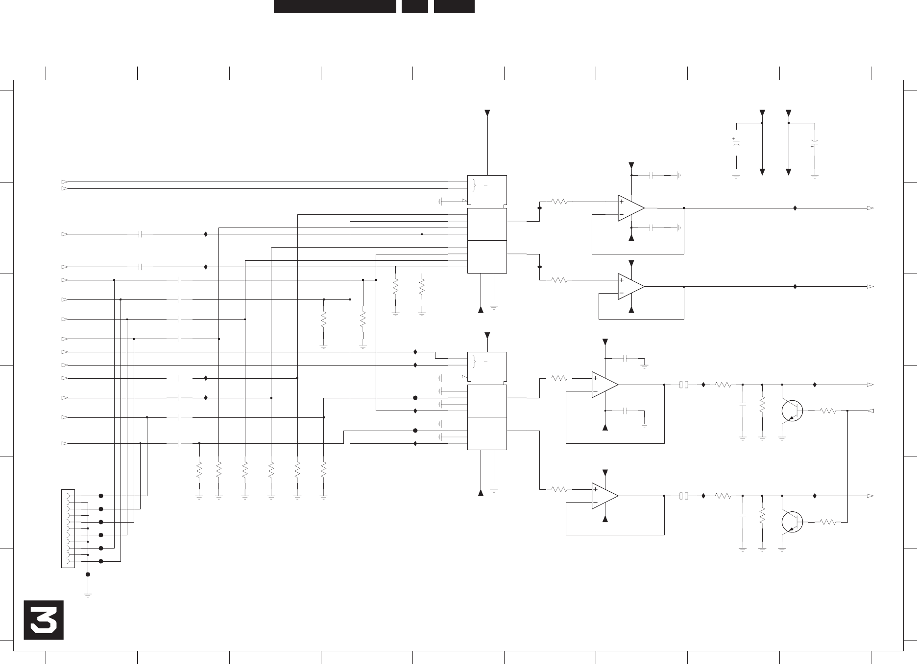
EN 128
3139 785 31532 7.Circuit Diagrams and PWB Layouts
Analog: Audio In / Out (IOA)
G4
0
3
2
VDD
VEE VSS
1
0
3
2
1
4X 0
3
0
1
G4
0
3
2
VDD
VEE VSS
1
0
3
2
1
4X 0
3
0
1
from DAC_ADC
from CU
from IOV
to DAC_ADC
GND
GND
D
E
F
2501 C2
2504 C2
2505 C2
2506 C2
2507 B2
2508 B2
2510 A8
2513 D2
2515 D2
2519 A9
2521 A7
from IOV
from DAC_ADC
from IOV
for RECEIVER only
from DAC_ADC
123456789
123456789
A
B
C
D
E
F
A
B
C
from IOV
GND
from MSP
from IOV
GND
from MSP
X5R
X5R
to IOV
VA XUA ot
2522 E7
2523 E8
2524 D2
2525 D2
2526 D7
2527 D8
2530 B7
2531 C7
2532 D7
3502 C6
3503 C4
3504 C3
3505 C5
3506 C4
3507 E2
3509 B6
3510 E3
3511 E3
3514 E3
3515 E6
3516 E3
3517 D9
from IOV
from CU
to DAC_ADC
from MSP
from PS
3519 E9
3522 E8
3523 D6
3524 E8
3525 D8
3527 D8
3534 E2
7501 A5
7504 C5
7505-1 E7
7505-2 D7
7506 D9
7508 E9
7509-1 C7
7509-2 B7
F501 D5
F502 D5
F503 F1
F505 E1
F506 F1
F507 E1
F508 E1
F509 E1
F510 E1
I502 D2
I504 D2
I505 C9
to IOV
GND
I506 D9
I507 E9
I513 D5
I514 B2
I515 D5
I516 B2
I517 B6
I518 B6
I521 D5
I527 C5
I528 B9
I535 E8
I540 D8
K001
6
053
5053
K
001
I515
5VSTBY
0.02V
0.02V
0.02V
0.02V
0.02V
0.02V
0.02V
0.02V
0.02V
0.02V
0.02V
0.02V
5NSTBY
K
001
4
3
53
F505
220R
3522
9152
V3.6u74
3517
4K7
7253
R028
0n1
BC817-25W
7506
8
15I
7252
I521
0
15
3
K
00
1
K
001
6
1
53
2515
1u0
3523
1K0
5VSTBY
1u0
2513
5NSTBY 7508
BC817-25W
I514
0n1
3252
I507
I506
0152
5NSTBY
V3.6u74
2501
1u0
5NSTBY
4K7
3519
1u0
2524
3502
1K0
F510
F503
I504
Audio In/Out IOA
2530
100n
5VSTBY
2531
100n
2532
8
4
5NSTBY
5NSTBY
100n
7505-2
MC33078D
5
6
7
7505-1
MC33078D
3
2
1
84
3
2
1
84
6
7
84
MC33078D
7509-1
F509
7509-2
MC33078D
5
F508
5NSTBY
5VSTBY
1u0
2506
1K0
3515
I502
2507
1u0
2521
100n
7
05
3
K001
K
0
01
1153
4
15
3
K001
5VSTBY
3509
1K0
I527
I528
7
1
5I
F506
F507
13
3
5NSTBY
61
7
8
12
1
14
5
15
2
11
4
7504
HEF4052B
MDX
10
9
6
3053
I505
K001
16V100u
2526
2508
1u0
I516
1u0
2504
1u0
2525
3525
220R
2505
1u0
16V100u
2522 I535
5VSTBY
K001
4
0
5
3
5VSTBY
F502
5VSTBY
3
F501
7
8
12
1
14
5
15
2
11
4
13
7501
10
9
6
6
1
R028
4253
MDX
HEF4052B
I540
I513
AIN2R
AIN2R
ARDAC
ARDAC
AIN1R
AIN1R
AIN1L
AIN1L
AIN2L
AIN2L
AKILL
ALADC
ARADC
ALDAC
ALDAC
RSA2
AFEL
IMUTE
ASC1
AOUT1R
AOUT1L
AINFR
AFER
AINFL
RSA1
3103_603_30356_a3_sh130_sh3.pdf 2005-07-07
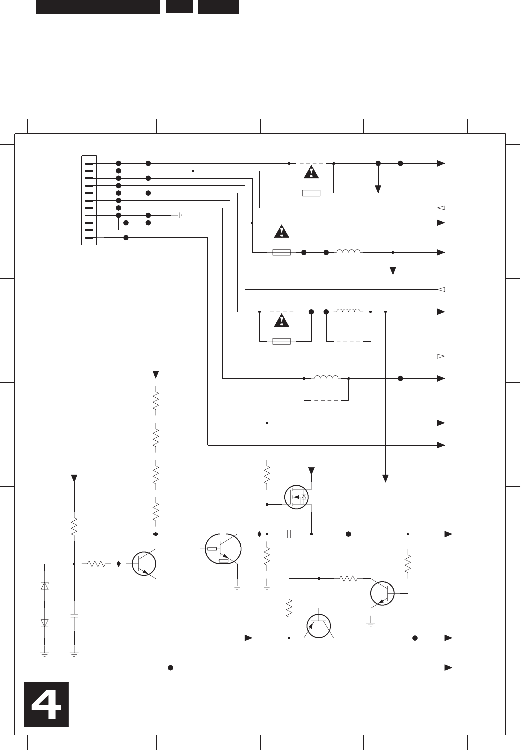
EN 129
3139 785 31532 7.
Circuit Diagrams and PWB Layouts
Analog: Power Supply (PS)
5VSTBY
to DAC_ADC
12VSTBY
to IOV,FOME,FV,MSP,
VGNSTBY
to CU
not used
GND
1234
1234
A
B
C
D
E
A
B
C
D
E
1351 A3
1352 A3
1353 B3
1932 A1
2352 D3
2353 E1
to IOV,IOA,DAC_ADC,CU
5NSTBY
not used
to FV
not used
to CU
from CU
to IOA,IOV,PROG,CU,
to IOV,CU
to CU
IPFAIL
DAC_ADC
YLPPUS REWOP morf
3358 D4
3360 C1
3361 C3
3362 D3
3363 C1
3364 C1
3365 D1
3366 D3
3367 D1
3368 D1
3369 E3
4701 A3
5351 A3
5352 B3
5353 B3
6352 D1
6353 E1
7351 E3
7352 D3
to DAC_ADC
33VSTBY
STBY
to MSP
7353 D2
7354 D2
7355 E4
9702 B3
9703 B3
9704 C3
F351 A4
F352 A4
F353 A3
F354 A3
F355 A1
F356 A2
F357 A2
F358 A1
F359 A2
F360 A1
F361 A2
F362 B4
F363 A1
F364 A1
F365 A1
F366 A2
F367 A1
F368 A1
F369 A1
F370 D3
F371 E2
F372 E4
3V3STBY
from CU
DAC_ADC,DIGIO,PROG,CU
not used
DD_ON
GND
F373 A1
F374 B3
F375 B3
I351 D2
I352 D1
I353 D1
100R
3368
3V3STBY
50V100n
2352
F353
3V3SW
YBTS3V3
2
5
3I
10u
5353
5351
VGNSTBY
1351
500mA
22u
3633
R
7
4
F364
3V3STBY
10u
5352
F361
7351
BC857BW
F357
F369
4701 F352
5NSTBY
12VSTBY
5V
5VSTBY2
Power Supply PS
66
3
3
2M2
5VSTBY
F360
F356
F368
33VSTBY
8VSTBY
1352
800mA
9704
9633
K001
K
0
1
853
3
7355
BC847BW
F358
F355
BC847BW
7354
F362
I351
I353
4633
R3
3
PDTC124EU
7353
F351
F372
125mA
1353
11
2
3
4
5
6
7
8
9
9703
B11B-PH-K
1932
1
10
2
5
3
6
2V8C-48
3
X
Z
B
163
3
2M2
R
3
3
7633
3362
3K3
F354
12VSTBY
R74
0633
9702
5633
7K4
F374
35
3
2
n
0
01
SI2306DS
7352
F370
F371
12VSTBY
5VSTBY
F366
F363
F373
F359
3536
61
3
SAB
F367
12VSTBY
F365
F375
5VSTBY
DD_ON
IPFAIL
STBY
3103_603_30356_a4_sh130_sh4.pdf 2005-07-07
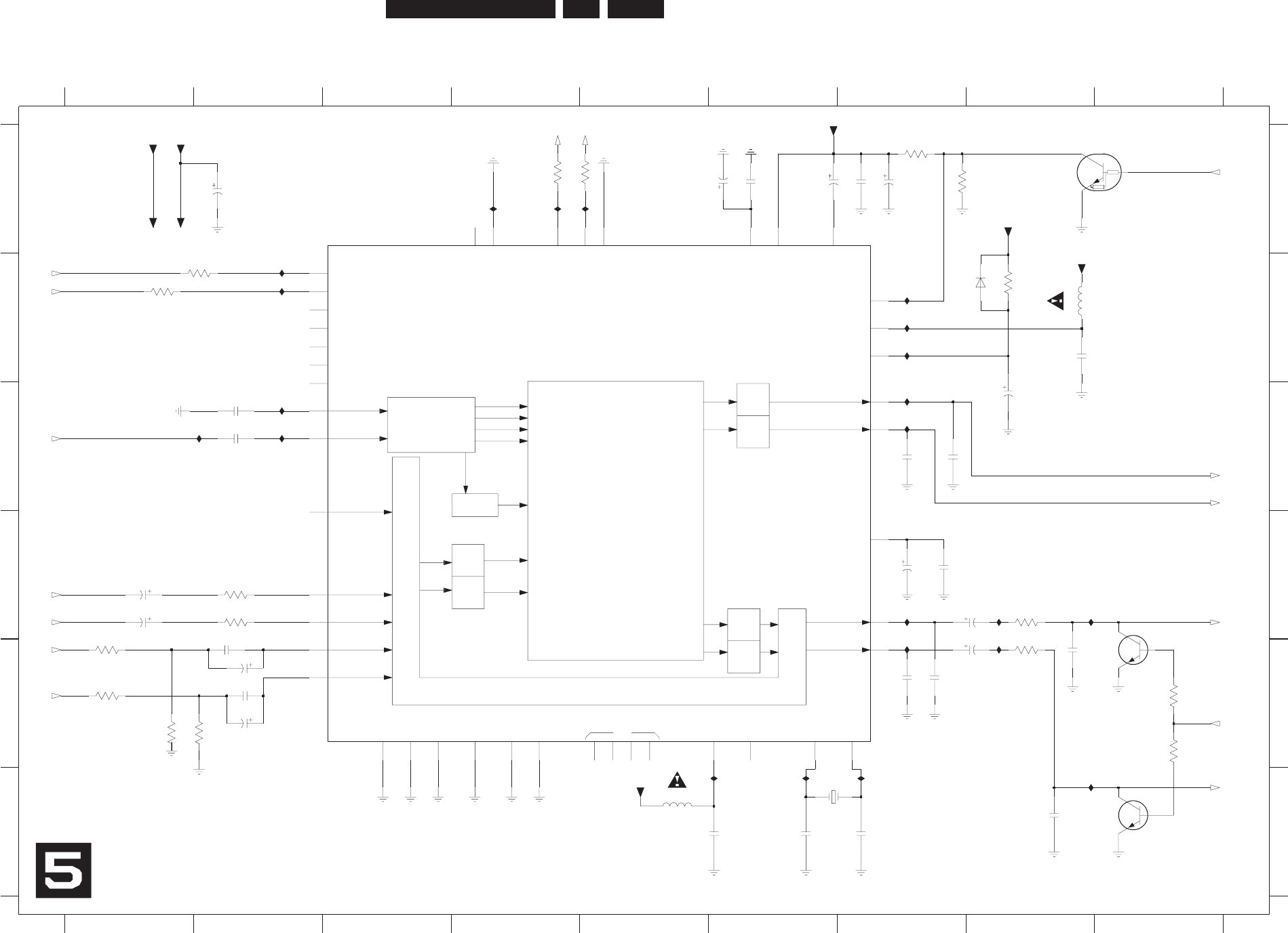
EN 130
3139 785 31532 7.Circuit Diagrams and PWB Layouts
Analog: Multi Sound Processing (MSP)
LOUDSPEAKER L
D/A
D/A
I2SL/R
HEADPHONE R
IDENT
NC
SCART
LOUDSPEAKER R
A/D
D/A
DEMODULATOR
S1...4
FM1
FM2
I2SL/R
NICAM B
NICAM A
SCART-L
HEADPHONE L
IDENT
LOUDSPEAKER
A/D
D/A
SCART-L
SCART-R
DFP
SCART-R
Switching Facilities
from DAC_ADC
from DAC_ADC
AOI ot
to IOV
C
D
E
F
1600 F6
2600 A6
2601 A6
2602 A6
2603 A7
2605 A2
2606 B8
2607 C2
2608 C8
2609 C2
2610 D7
2611 A7
2612 D7
2613 D8
2614 E8
2615 E8
2618 C7
2619 C7
2620 F6
2621 F7
2622 F8
2623 F5
2624 D1
2625 D1
from CU
to IOV
from PS
desu ton
from/to CU
desu ton
123456789
123456789
A
B
C
D
E
F
A
B
from IOV
to IOA
2626 E2
2627 E2
2628 E7
2629 E7
2630 E2
2631 E2
3601 B2
3602 B8
3603 B1
3604 A7
3605 A7
3606 D8
3607 E8
3609 E9
3610 E9
3611 A4
3612 A4
3614 D2
3615 D2
3616 E1
3617 E1
3618 E1
3619 E1
5600 B8
5602 F5
6600 B8
7600 A3
7601 A8
7602 E9
7603 F9
from DAC_ADC
from/to CU
AOI ot
from IOV
I602 A4
I605 B7
I606 C2
I607 C2
I608 C2
I610 F6
I611 F7
I612 D8
I613 F5
I614 B7
I615 B2
I616 B2
I617 B7
I618 C7
I619 C7
I620 D7
I621 D8
I622 D8
I623 E7
I624 A4
I625 A4
I634 F8
from FV
to IOA
I607 2609
56p
7K4
2063
u01
5062
12K
3604
V52
I617
016I
0062
V52u01
I621
526I
I616
5V
1162
V
61u
7
4
0n1
5162
3606
220R
I618
3615
1K0
I620
n001
3062
I623
5V
0262
3p3
1
16I
3p3
1
2
62
216
2
V057u4
50V2u2
2625
I622
I619
25V
8VSTBY
PDTC124EU
2613
10u
7601
1163
K01
3603
100R
316I
I608
K21
9
1
63
8VSTBY
BC817-25W
7603
2626
1u0
Multi Sound Processing MSP
0066
613SAB
220R
3607
1u0
2627
0n1
81
6
2
2614
10u 25V
5602
10u
8163
K21
9
162
0n1
100R
3601
I605
2631
1u0 50V
50V1u0
2630
18M432
1600
8062
u01
5V
1K0
3614
I606
STBYQ 11
NETSET 4
PT
7
1
F
ER
V
92
2
FE
R
V
52
POTFERV 2
4
NI
_
LA
T
X
5
TUO
_
LA
T
X
6
8
2
23
RESETQ 22
SC1_IN_L40
SC1_IN_R41
SC1_OUT_L 31
SC1_OUT_R 30
SC2_IN_L37
SC2_IN_R38
I2S_CL
14
I2S_DA_IN1
17
I2S_DA_IN2
21
I2S_DA_OUT
16
I2S_WS
15
MONO_IN43
32
4
2
DACM_L 27
DACM_R 26
SSVD
0
2
DVSUP 19
0OI_RTC_D 9
1
O
I_
R
T
C
_
D8
I2C_CL
12
I2C_DA
13
53
P
USVHA 33
ANA_IN+2
ANA_IN-3
G
S
A
93
S
S
VA
4
4
P
US
V
A
1
M_LPAC 43
MSP3415G
7600
LC_RDA 81
LE
S
_RDA 01
AGNDC 36
SS
V
HA
3617
3616
2K2
2K2
5V8VSTBY
2262
0n1
21
6
3
I634
K01
n
0
1
0162
7602
BC817-25W
I615
3262
n
00
1
V52u
0
1
2
062
5V
I614
56p
2607
206I
9
0
63
6062
n001
7K4
2624
2u2 50V I612
0065
u01
n0
1
1062
K22
5063
0163
7K4
0n
1
9262
4
26I
82
6
2
0
n1
AIN1L AOUT2R
ARDAC
ALDAC
AKILL
AOUT2L
SCL_5V
SDA_5V
SIF1
AFER
AFEL
AIN1R
2ASR
1AS
R
STBY
3103_603_30356_a3_sh130_sh5.pdf 2005-07-07
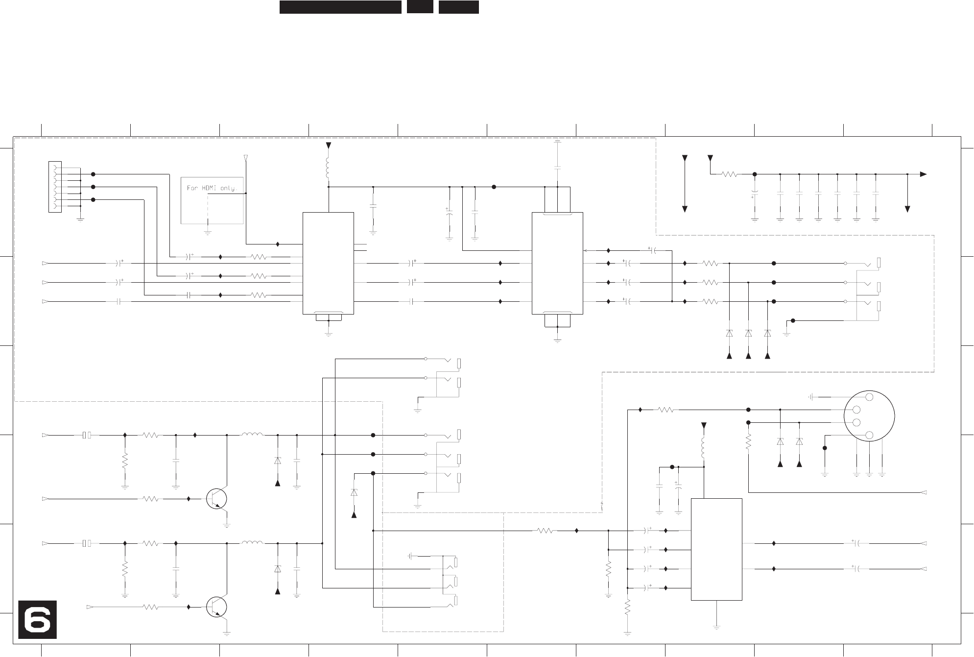
EN 131
3139 785 31532 7.
Circuit Diagrams and PWB Layouts
Analog: Progressive (PROG)
GND
V+
GND
V+
NC
V+
GND
TUO RAER
12345678910
12345678910
A
B
C
D
E
A
B
C
D
E
1920 A1
from DAC_ADC
from DAC_ADC
Aud L
1921 C10
1922-A C5
1922-B A10
1922-C B5
1923 E5
2200 A5
Aud R
Aud R
from IOV
Aud L
1%
2201 A8
2202 A4
2204 A7
2205 A2
2206 B1
2207 B5
2208 B7
2209 B2
2210 B1
2211 B5
2212 B7
2213 B2
2214 B1
2215 B5
2216 B7
2217 C1
2218 D2
2219 D3
2220 D7
2221 D8
2222 E7
2223 E10
2224 E7
2225 E1
2226 E7
2227 E10
2228 E2
from PS
GND
CVBS
delete for PROGRESSIVE
to IOV
Pb
U
Bead
from DAC_ADC
from IOV
2229 E3
2230 E7
2231 A9
2232 A9
2233 A9
2234 A9
2235 A10
2236 A10
2237 A6
2239 A5
3200 A8
3201 B8
3202 B8
3203 B8
3204 C8
3205 D8
3206 C2
3208 D1
3209 D2
3210 E6
3211 E2
3213 E7
REAR OUT
from DAC_ADC
GND
3214 E1
3215 A3
3216 B3
3217 E2
3218 E7
3219 B3
4601 A2
5200 A4
5201 D8
5202 C3
5203 E3
6200 B8
6201 B8
6202 B9
6203 D9
6204 D9
6205 D3
6206 D4
6207 E3
7200 A3
7201 A6
7202 D3
7203 D8
7204 E3
F201 A6
F202 A9
F203 A1
F204 A1
F205 A1
V
from IOV Y
1%
Aud L
REAR OUT
GND
S-VIDEO
Pr
U
C morf
from IOV
Y
for PROGRESSIVE only
F206 B9
F207 B9
F208 B9
F209 B9
F210 C8
F211 C8
F212 D9
F213 C4
F214 D4
F215 D8
F216 D4
I201 A3
I202 A7
I203 A3
I204 A6
I205 A7
I206 A8
I207 B3
1%
CVBS
Bead from IOV
%1
1%
1%
GND
from IOV
Aud R
I208 B6
I209 B7
I210 B8
I211 B3
I212 B6
I213 B7
I214 B8
I215 C7
I216 C1
I217 C2
I218 D2
I219 D7
I220 D8
I221 E9
I222 E8
I223 E1
I224 E2
I225 E8
I226 E9
I227 E8
I228 E2
75R
3203
3322
n001
1026
21C-483XZB
5NESD
I211
n001
7322
I203
1
VIN2
3
VIN3
5
VOUT1 13
VOUT2 11
VOUT3 9
VSAG 8
7201
NJM2580M
Φ
3-CHANNEL
VIDEO AMP
2
4
6
PWR_SAVE
7
41
21
01
VIN1
I210
3204
75R
2209
5NSTBY
16V22u
2205
22u16V
F216
5NESD
R86
5023
2207
0022
n00
1
16V22u
I207
5V
6.3V100u
2224
F201
2026
21C-483XZB
I225
F211
p0
7
4
9222
BC817-25W
7202
5NESD
212F
16V22u
2206
2022
F207
n001
3217
470R
I223
1025
u01
2
1
1u0
2214
5NESD
T-331520-10-10
1922-A
4
3
2230
100u 6.3V
5NESD
F209
6.3V470u
2212
I219
16V10u
2225
u01
0025
V52u01
1022
F203
21C-483XZB
4026
3
4
7
5
6
F210
1921
TCS7927-24-401
1
2
2217
10u 16V
V3.6u74
1222
I216
470R
3209
5NESD
5203
41
2
3
K
001
5NESD
I220
6
5
5NESD
T-331520-10-10
1922-C
7
2213
1u0 I212
5322
n001
50V4u7
2227
2211
22u16V
150R
3219
150R
3216
3215
2226
100u 6.3V
150R
DSEN5
6.3V100u
2222
I227
F208
I228
1322
n001
470u
2208
3210
75R
6.3V
n001
4322
2
3
4
5
6
7
1920
07FMN-BTRK-A
1
2
7
1
VIN1
8
VIN2
4VOUT1
5VOUT2
3VSAG1
VSAG2
6
Φ
DUAL 6dB
VIDEO AMP
NJM2267M
7203
21C-483XZB
0026
I208
F215
1922-B
T-331520-10-10
11
10
9
8
5
6
OUT3
31
IN1B
1
IN2A
11
IN2B
14
8IN3A
9IN3B
2
7
OUT1 3
OUT2
VIDEO SW
3-CIRCUIT
Φ
NJM2584M
7200
12 CTL
5
1
4
01
IN1A
16
6.3V100u
2216
3026
21C-483XZB
2
1
C-48
3
XZ
B
6026
91
2
2
p0
7
4
5202
1u0
2215 I213
I202
022
2
n00
1
1
06
4
270R
I206
3211
5NESD
I217
I222
I205
I214
F206
I224
5V
8
12
3
K001
2204
47u 6.3V
F205
K0
0
1
8
0
23
2223
4u7 50V
p
0
74
81
2
2
K
0
01
31
23
5V
I218
8
2
22
p0
74
3202
75R
F204
Progressive PROG
50
2
6
51
C-
483XZB
n001
6322
7204
BC817-25W
F202
n001
2322
5V
I201
I204
I215
u001
9322
1K0
V3.6
3200
I221
270R
3206
2210
22u 16V
I226
I209
1
75R
3201
1923
LPR6520-G020G
2
3
4
F214
7026
ORPI
F213
51C-483XZ
B
D_CVBSALDAC
D_Y
BKILL
ARDAC
CRout
BKILL
D_VR
D_UB
D_YG
3103_603_30356_a3_sh130_sh6.pdf 2005-07-07
from HDMI Board
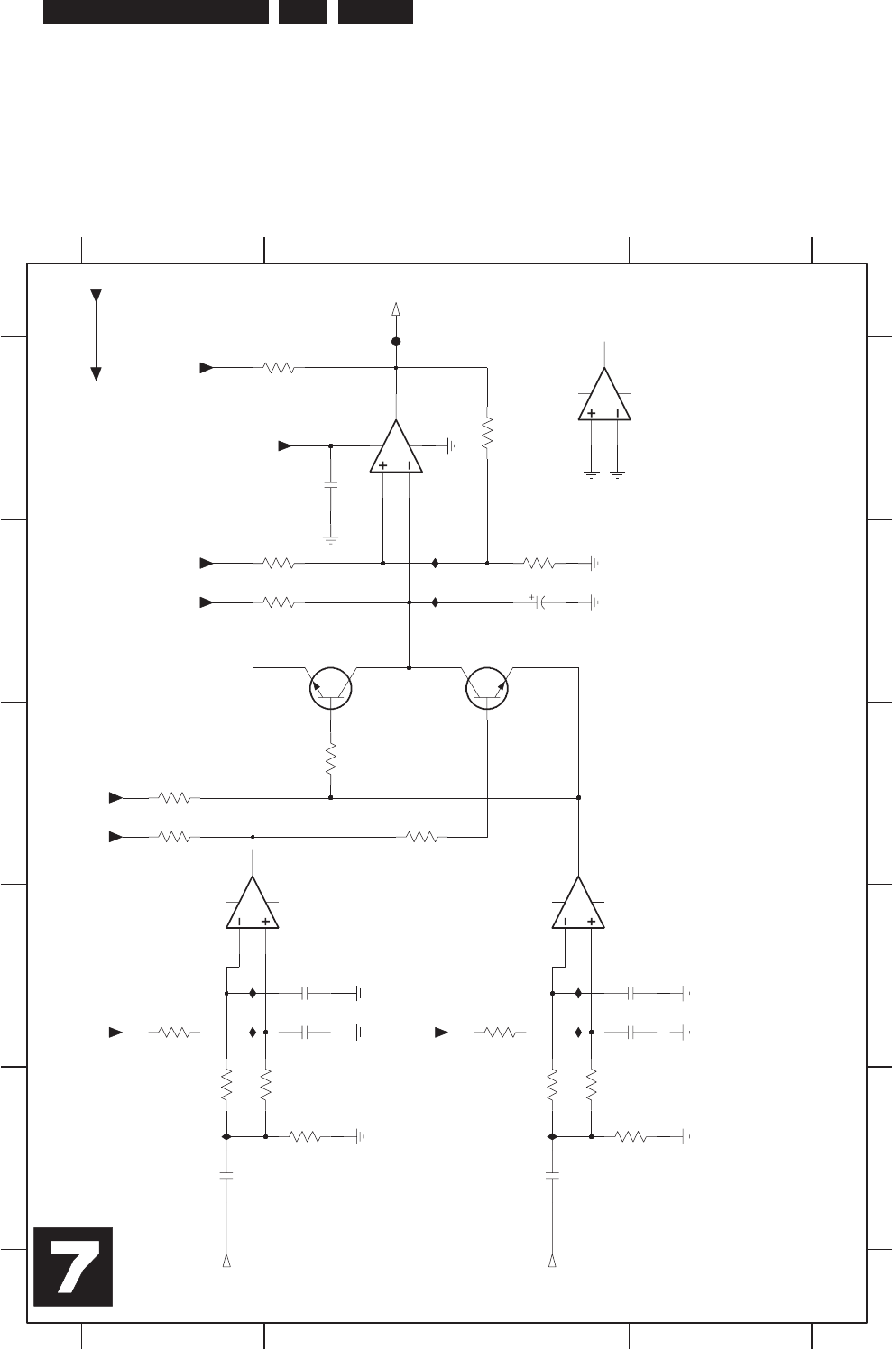
EN 132
3139 785 31532 7.Circuit Diagrams and PWB Layouts
Analog: Follow Me (FOME)
3954 C2
7932 B2
7933 B3
7934-1 D1
7934-2 D3
7934-3 A2
7934-4 A3
F950 A2
I951 B2
I952 B2
I956 D1
I957 D1
I958 D3
I959 D3
I960 E1
I961 E3
V
F m
or
f
V
OI m
o
rf
from PS
UC ot
1234
1234
A
B
C
D
E
A
B
C
D
E
2940 A2
2941 B3
2942 D2
2943 D4
2944 D4
2945 D2
2946 E1
2947 E3
3937 C1
3938 C1
3939 C2
3940 D1
3941 D3
3942 E1
3943 E1
3944 E3
3945 E3
3946 E2
3947 E4
3948 A2
3950 A3
3951 B2
3952 B3
3953 B2
Follow Me
0
69I
5V
3397
I956
5V
WB748CB
10M
3941
I958
059
F
2K2
3937
25V10u
2941
I959
7
6
1
4
-4
397
D933ML
K
3
3
4
4
9
3
0
u
1
7492
3940
10M
2
3
97
WB748CB
I957
2n2
2944
V5
V5
3948
4K7
5
4
9
3
K33
3952
15K
1
6
9I
3951
22K
3947
33K
2942
2n2
K
3
3
3
4
9
3
7K4
4593
3939
4K7
V5
5
4
2
312
V
5
D93
3
ML
3-4397
V
5
0492
n001
V5
4K7
3953
2945
180p
2
-
4
3
9
7
D
9
3
3
ML
1
1
0
1
31
9
8
41
D933
M
L
1-4397
33K
3946
V5
0593
K0
0
1
180p
2943
I951
V5
I952
6
492
0
u1
24
9
3
K
3
3
3938
2K2
EMOF
NIS
B
V
C
VFV
FOME
3103_603_30356_a4_sh130_sh7.pdf 2005-07-07
0.02V
0.02V
0.03V
0.4V
1.1V
0.4V
4.8V
2.2V
0.5V
0.03V
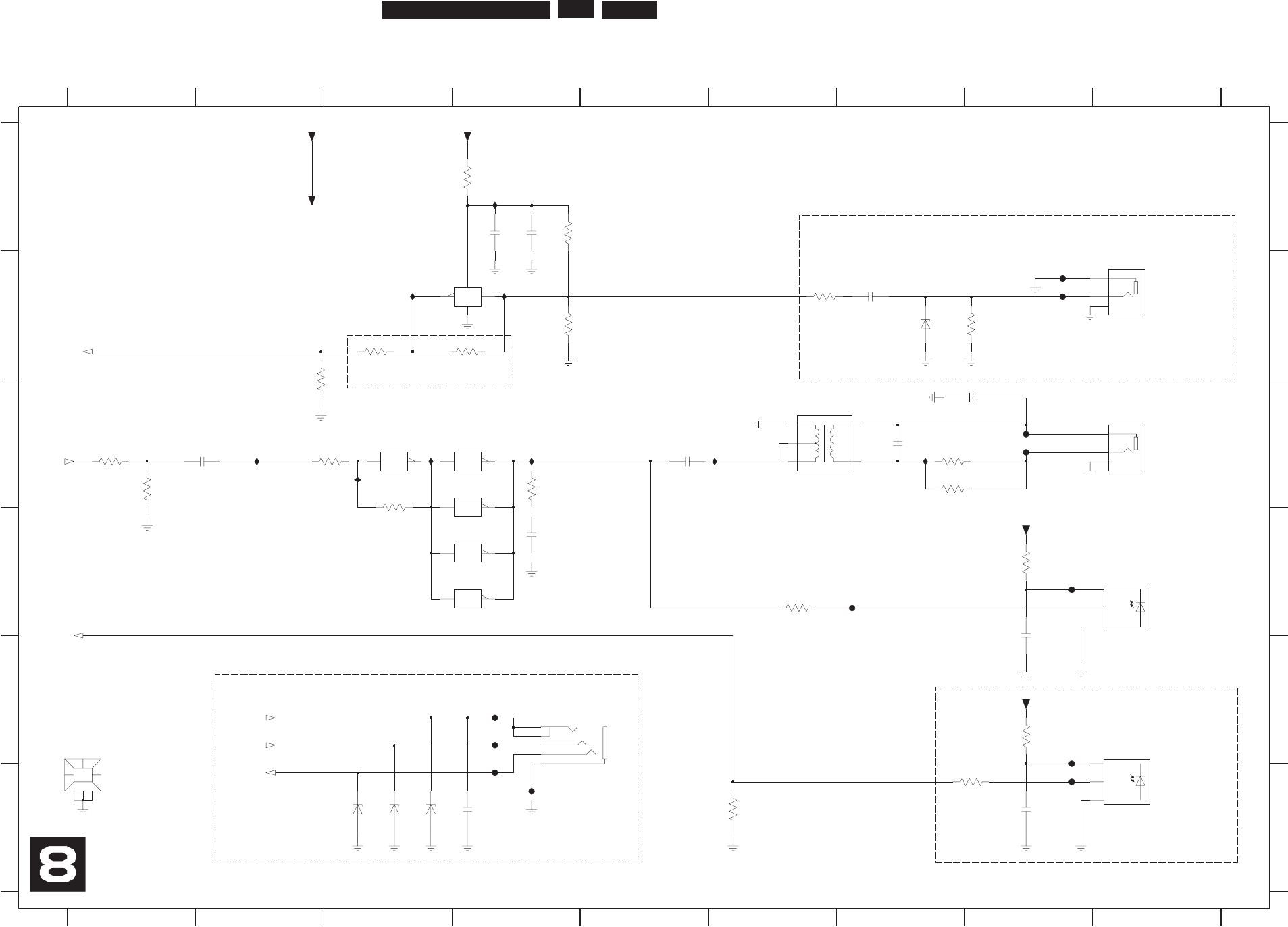
EN 133
3139 785 31532 7.Circuit Diagrams and PWB Layouts
Analog: Digital In / Out (DIGIO)
1
1
1
1
1
1
OUT
from DAC_ADC
OPTICAL
D
E
F
0005 E1
1924 E4
1925 C9
1926 B9
2250 A4
2251 B7
2254 C7
2255 C5
2256 C2
2257 D4
2259 D8
2262 F8
2265 A4
2266 C8
2267 F4
3250 A4
3251 C7
3252 B6
3253 C1
3254 C1
3255 B4
3256 B8
3257 A4
3258 B4
3259 C7
3260 C3
des
u
ton
for DIGITAL OPT IN only
from CU
from PS
IN
123456789
123456789
A
B
C
D
E
F
A
B
C
1%
to DAC_ADC
to DAC_ADC
DIGITAL
CINCH
CHINCH
OPTICAL
DIGITAL
IN
3261 C3
3262 C4
3263 D8
3264 D6
3265 B3
3266 B2
3267 F6
3268 E8
3269 F8
5250 C6
6250 B7
6251 F3
6252 F3
6253 F3
6255 D9
6269 E9
7250-1 C3
7250-2 C4
7250-3 C4
7250-4 D4
7250-5 D4
7250-6 B3
F2401 F4
from CU
DIGITAL
G-Link
OUT
OUT
de
su
ton
for DIGITAL COAX IN only
DIGITAL
for DIGITAL COAX IN only
to CU
F2402 F4
F2403 E4
F2405 E4
F250 F8
F2502 C8
F2503 C8
F251 D7
F2602 B8
F2603 B8
F266 D8
F267 E8
I250 A4
I251 B3
I252 B4
I253 C3
I254 C4
I255 C6
I256 C3
I257 C7
I258 C2
for EPG only
100R
3265
82R
3251
4523
R001
R065
262
3
100R
3252
I253
652I
F2403
100n
2255
7250-4
98
10K
3258
SN74HCU04D
GND
2
OUT
3
VS
1
JFJ2000
6269
I254
2K2
3260
9522
V52n001
5V
1
3
2
F2503
1926
YKC21-3416
F2603
8623
R74
F250
F251
2622
n001
1042F
Digital In/Out DIGIO
F2502
8V
6C-
48
3
XZ
B
3
526
5V
I255
100n
2251
7
62
3
8K1
I250
F2405
I258 SN74HCU04D
12
100n
2266
7250-1
5V
R57
652
3
552
3
K001
052
2
V010u1
3253
750R
2
52
6
8V6C-4
8
3XZB
5V
R
0
74
0523
4522
p051
3GND
1IN
2VS
8
V
6C-483X
Z
B
052
6
JFJ1000
6255
2256
100n
R06
5
6623
13
417
12
4
SN74HCU04D
7250-6
SN74HCU04D
7250-2
3
1
3
2
F267
YKC21-3416
1925
I257
1
5
26
F266
SN74HCU04D
56
8
V
6C-4
8
3X
Z
B
7250-3
7523
K00
1
3259
75R
I251
0n
1
7522
6
100R
3264
1
2
34
10
5V
6RG
5250
SN74HCU04D
11
3261
7250-5
470R
n
01
5622
I252
R74
3623
F2602
F2402 1
180R
3269
5
4
3
2
HSJ1637-010510
1924
0005
BRACKET
0
n1
7
62
2
DAINOPT
DAINCOAX
IROUT
GLINK_TXD
GLINK_RXD
DAOUT
3103_603_30356_a3_sh130_sh8.pdf 2005-07-07
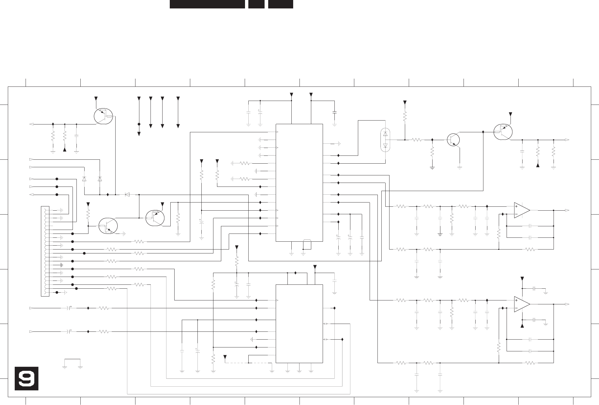
EN 134
3139 785 31532
Analog: Audio Converter (DAC_ADC)
DATAO
BCK
WS
VSSA VSSD
VDDD
VINR
SFOR
VINL
MSSEL
VREF
VRN
VDDA VRP
SYSCLK
PWON
FILTB
FILTR
OUTR+
OUTR-
OUTL+
OUTL-
ZEROP
ZEROL
NC
D
DVA
DDVD
SDATA
DNGD
AGND
MCLK
CLATCH
CCLK
CDATA
192-48_
DEEMP
96-48_
IDPM0
IDPM1
MUTE
PD_-RST
LRCLK
BCLK
2%
from DIGIO
%2
0
P
N
%2 0PN
%2 0PN
GND
10
A
B
C
D
E
A
B
C
D
E
1900 B1
2002 A5
2003 A5
2004 A6
2005 A1
2006 C8
2007 C9
2008 C8
2009 C9
2010 C10
2011 D10
2012 D10
2013 D9
2014 E10
2015 A10
%2
0
P
N
1%
to DIGIO
GND
%1
to IOA,MSP
to PROG,CU
%1
1%
1%
GND
draoB latigiD ot/morf
from DIGIO
12345678910
123456789
1%
GND
to IOA,MSP,PROG
2017 C10
2018 C4
2019 C6
2020 C6
2021 C7
2023 C8
2025 C8
2030 D8
2032 D8
2033 D9
2035 D6
2037 D5
2038 D4
2041 E10
2042 E3
2043 E4
2045 E8
2047 E8
2048 E1
2050 D1
3001 B7
3003 D4
3004 C8
3005 B4
3006 B4
3007 E4
3008 B8
3009 C7
3010 B8
%
1
%2 0PN
3011 A1
3012 C3
3013 C9
3014 D7
3015 A1
3016 C8
3017 C10
3018 E7
3019 C2
3020 B4
3021 B4
3022 C3
3023 C2
3024 C3
3025 A10
3026 D2
3027 D8
3028 D3
3029 A10
3030 D8
3031 B2
3032 D8
3033 D2
3034 C4
3036 E9
1%
%2
0
P
N
to IOA,MSP,PROG
from PS
GND
%1
1%
%2
0
P
N
1%
GND
GND
3037 A8
3039 E8
3040 E10
3046 A7
3047 E2
3050 A8
3053 D2
3054 C3
4001 E4
4002 E5
6003 B2
6004 B2
6005 B2
6006 A7
7001 B3
7002 A2
7003-1 B10
7003-2 D10
7004 A5
7005 A9
7006 C2
1%
GND
from CU
DAINOPT
1%
from IOA
DAOUT
not used
des
u
ton
7007 D5
7010 A8
F001 B1
F002 B1
F003 B1
F004 C1
F005 C1
F006 A3
F007 C1
F008 C1
F009 D1
F010 C1
F012 D1
F013 D1
F014 D1
F015 C2
I001 B2
I002 C5
I004 C5
I005 B5
I006 B5
I007 B5
I009 A1
1%
N.C.
2%
1%
%2 %2
from PS
DAINCOAX
from IOA
not used
1%
GND
not used
I010 A6
I011 A9
I012 A8
I013 D5
I014 D5
I015 D5
I016 B6
I017 B6
I018 D5
I019 B6
I020 B6
I021 E2
I022 E5
I023 C6
I024 B6
I025 B6
I026 B9
I027 B9
I028 D9
I020 B6
d
es
u ton
%2 0PN
I030 D2
I031 E6
I032 E5
I033 D9
I034 D6
c001 E1
PDTA124EU
7005
I005
DN
G
5VSTBY
120
2
n001
I019
I011
A
27p
2010
I023
2012
100n
9
1
3
2
4
5
51
0
1
12
5NSTBY
7007
11
13
14
7
6
8
6
1
24-BIT AUDIO
Φ
ADC
UDA1361TS
3033
22R
DNG
BC847BW
7010
3032
6K8
5VSTBY
630
3
F007
8K6
n22
5002
0202
V52u
0
1
F010
I024
100p
2017
A
GND
I010
A
I031
A
A
5NSTBY
3022
22R
5V
7001
PDTA124EU
5NSTBY
AA
5
4
02
0n1
DNG
I006
A
A
D
N
G
GND
A
I026
A
GND
920
3
K001
5VSTBY
22R
3054
5V
DNG
3V3SW
A
I025
p
0
01
3302
F015
27K
3039
3
2
1
F014
613S
A
B
7003-1
MC33078D
50
0
6
A
4
303
0R1
W65WAB
6
0
0
6
F012
4K7
3006
D
NG
c001
GND
DNG
613SAB
4006
F002
5VSTBY
A
5NSTBY
DNG
3005
4K7
5V
2050
47u 6.3V
K
74
3003
5202
0n1
I016
F004
5V
I013
DN
G
6.3V47u
2048
3017
33K
A
I020
GNDGND
40024001
5VSTBY
A
3023
22R
9
002
p001
GND
3001
A
DNG
A
5K6
DNG
A
DNG
GND
3V3SW
I022
22R
3028
A
7002
PDTA124EU
31
02
100K
3037
DNG
5102
n22
n0
01
2
4
02
GND
3002
n001
0n1
7402
Audio Converter
DAC_ADC
7302
n0
0
1
F001
F008
81
0
2
V52u01
3V3SW
F003
5V
DNG
27K
3008
7K4
1303
5VSTBY
7006
PDTC124EU
I027
DNG
n
0
01
5
30
2
6K8
3010
I007
A
1203
K01
D
NG
BAS316
6003
3009
5K6
22R
3024
A
600F
3V3SW
I001
K
3
3
40
0
3
0
20
3
7K4
DN
G
I002
A
2302
0n1
6002
0n1
V3.
6
u
7
4
34
0
2
5V
3014
5K6
GND
3103
8K6
0n1
0302
I032
10K
3047
I017
I028
A
GND
A
100n
2011
3053
10K
F009
3018
I021
5V
5K6
0n1
8
002
K0
0
1
1103
GND
K22
5103
13
24
27
22
8
GND
19
14
21
20
25
2
23
6
17
16
12
10
11
51 81
26
4
5
3
9
1 82
AD1852JRS
7004
DAC
Φ
7
K22
6403
22R
3019
I033
I004
A
K33
05
0
3
5203
K22
A
2041
100p
I014
I012
3026
22R
I015
5VSTBY
I030
7
002
GND
A
9
5NSTBY
2014
27p
2
20
21
22
3
4
5
6
7
8
11
12
13
14
15
16
17
18
19
1900
22FMN-BTRK-A
1
10
V3.6
GND
2002
u0
0
1
I034
33K
3040
K
33
V52u01
9102
27K
7203
F013
DNG
3030
DNG
3V3SW
7003
K74
3016
27K
0n
1
3202
I009
V3
.
6
u
001
830
2
K01
210
3
A
F005
n
001
4002
7003-2
MC33078D
5
6
7
84
ALDAC
I018
ARADC
DAOUT
DAINCOAX
D_KILL
ARDAC
IMUTE
AKILL
BKILL
A_WCLK
A_DAT
A_PCMCLK
D_BCLK
IPFAIL
D_PCMCLK
ALADC
D_WCLK
D_DATA0
DAINOPT
A_BCLK
3103_603_30356_a3_sh130_sh9.pdf 2005-07-07
7.
Circuit Diagrams and PWB Layouts
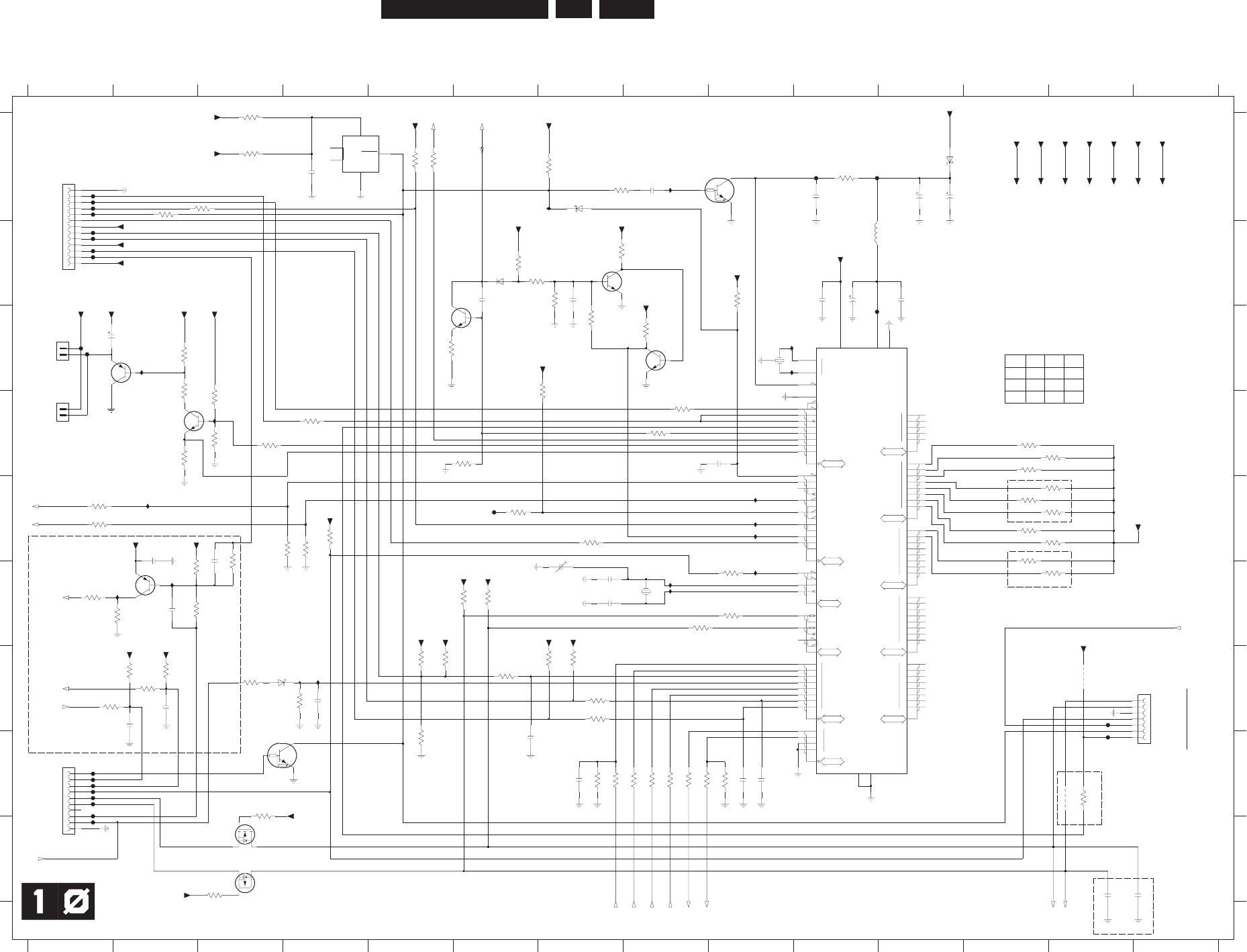
EN 135
3139 785 31532 7.Circuit Diagrams and PWB Layouts
Analog: Control Unit (CU)
VCC
GND
NC RESET
13
12
11
10
7
INT0
INT1
TC2
DVO
TEST
KK
V
DDV
FERA
V
14
13
12
11
10
9
8
23
16
21
20
19
18
17
P4<0:7>
AIN
P5<0:3>
PD<0:4>
V3
P6<0:7>
V
P7<0:7>
V
P8<0:7>
V
P9<0:7>
V
SO1
5
6
7
6
5
4
3
2
1
0
15
SSV
PDO
2
1
XTAL
P0<0:7>
PPG
PWM
TC4
TC1
SCK0
0
1
2
3
4
5
6
SI1
SCK1
RESET
SSA
V
INT3
INT2
INT4
INT5
XTIN
XTOUT
SCL
SDA
22
TC3
P1<0:7>
STOP
P2<0:2>
SI0
SO0
P3<0:2>
AIN
31
30
29
28
27
26
25
24
2
3
4
3166 E4
3168 I3
3140 G6
F1302 C1
3186 C8
for MOBO
F1105 B1
3184 B7
3185 C7
1914 H1
1915 G14
not used
5VSTBY
2k2
GND
PSM,VOI,VF ot
desu ton
%
1
V
OI
m
orf
3171
VOI morf
from DAC_ADC
45
7100 A4
I102 A7
I103 C9
I104 C9
F1403 H1
F1404 H1
%1
ylno MTTD rof
from PS
%1
2109 H9
---
2126 F7
N.C.
%1
4
2125 B10
1%
SDA_5V
E
%1
E
MOF
m
orf
PSM,VOI,VF ot
7112 B7
AOI ot
SCL0
6100 A11
6101 A7
F1401 H1
3183 B6
3125 E7
VOI ot/morf
3124 E1
draoB MTTD ro
*
not used
3122 D3
3123 E1
2117 H7
3152 H8
IPOR_R
2115 G2
2118 D9
3130 F6
3177 E12
3178 E12
3179 F12
7115 I3
F100 E6
F1102 A1
F1112 B1
VERSIONS
3173 E12
3104 B9
F1103 A1
3138 G2
3139 G2
3106 B2
13 14
I107 D2
1101 F8
FAN_P
7108 C11
B
2107 B10
2108 B7
3118 D4
F
3164 G5
3165 H5
GND
7111 H4
1911 A1
7109 F2
23
IRES_S
D
BKILL
7105 D2
3172 D12
7101 A8
7102 C6
7104 D1
2102 A11
3111 H13
3145 G1
3146 G7
3147 G7
F1208 H13
F1209 G13
F124 A10
F125 C10
F1301 C1
SCL_5V
BKILL
F1408 I1
I101 A8
%1
I108 D3
I110 E9
I112 E9
7113 C8
I113 F9
I114 F2
not used
VOI
morf
3170 D12
F1109 B1
F1104 A1
not used
Version Detect
1913 C1
TPClock
F1108 B1
1%
ylno REVIECER rof
A
GND
2 NAF ot
GORP ot
3126 E4
D
R
AOB L
A
TIGI
D ot/
morf
2k2
---
F126 A10
--- ---
F1405 H1
F1406 H1
F1407 H1
3170
IPOR_R
INT1
5VSTBY2
delete for RECEIVER
3129 F1
3174 E12
3175 E12
3176 E12
I119 E9
I120 E2
I123 F2
I115 F8
I117 F8
FAN_P
12VSTBY
I118 G4
E3/5300H
*
SDA_5V
E2
N.C.
3156 H9
3158 H3
3159 A5
1100 C9
9
2104 A4
2105 B6
2106 B11
3116 D2
3117 D8
3150 H7
3121 D8
14
E
12810111 134
2100 A8
3109 C6
3144 G7
4101 G13
4102 H13
5100 B10
3128 F2
2k2
7114 I3
F1402 H1
from IOV
3163 D6
2111 H9
3103 B6
2113 F7
desu
ton
9
3141 G3
2101 A10
to PS,MSP
3160 A5
D
3171 D12
2116 G2
11 12
H
6102 B6
from DIGIO
3161 E2
6106 G3
3
to DIGIO
5
E1
G
H
1 NAF ot
3102 A7
CDA
_
CAD ot
3153 H8
3154 H8
3155 H8
6
A
B
3105 A3
for RECEIVER or DTTM only
G
C
desu
t
on
C
1916 D1
LENAP TNORF ot/morf
3101 A10
1
2123 F2
2124 F3
3136 F9
2110 C1
I
2
to DIGIO
3100 A7
10
F
I
2112 F7
2119 I14
3131 F6
3132 F2
3133 F9
3180 E6
3181 D7
F1111 B1
3113 D3
3115 D3
3148 G7
3149 H7
3182 B7
3151 H8
6
GND
3127 F2
*
to PS
daeB
*
for EPG only
75
3142 G2
3143 G4
3172
INT1
VGNSTBY
draoB VA XUA ot/morf
-50p
7
2120 I13
2121 E2
2122 H6
3134 F8
3135 E4
3162 F3
3137 G5
8
2114 G4
2103 A11
3112 C2
5V
910R
3108
3176
2K2
100R
3133
5V
5VSTBY
3140
10K
7100
NCP301LSN
3
4
51
2
5VSTBY
F1402
3102
470R
2513
0K1
5V
3105
100R
3178
2K2
2K2
3177
F1105
10K
3101
I118
I117
067TAB
0016
3145
1K0
0M1
5
613
12VSTBY
5VSTBY
BC847BW
7113
18p
2113
7102
BC847BW
100n
2118
7112
BC847BW
6012
n001
901
3
R
0
22
F1103
3012
V3.6u74
3V3SW
YBTSV5
0K1
1513
I113
100R
3106
0313
9K3
9
0
12
n
0
01
3
K
3
0
61
3
K
01
2113
K01
5313
100n
2121
2K2
3172
3175
2K2
F1406
2
3
4
5
6
7
8
9
1914
10FMN-BTK-A
1
10
7111
PDTC124EU
2126
6p0
1K0
3141
K74
1813
F1109
5VSTBY
F1208
5VSTBY
F1209
K001
3413
5NSTBY
1113
R001
711
2
n01
6112
p
0
0
1
F124
I123
2K2
3170
7105
BC847BW
5VSTBY
5VSTBY
2K2
3173
2100
220n
3V3STBY
WS3V3
3
0
13
K72
5VSTBY
3183
220K
I114
83
1
3
K00
1
VGNSTBY
7115
BSN20
PDTC124EU
7101
I103
n01
1012
F1404
3134
100R
6
7
8
9
F1302
1
10
11
12
13
2
3
4
5
1911
13FMN-BTRK-A
5813
2
M2
F1408
p00
1
511
2
3129
150R
I119
4013
K01
n001
1112
I115
WS3V3
BC857BW
7109
3136
100R
VGNSTBY
2613
7K4
5012
p022
3125
1K0
1K0
3142
0015
10
13
93
83
04
87
7
9
8
5VSTBY
68
69
70
71
72
73
74
75
76
77
57
58
59
60
61
62
63
64
65
66
67
47
48
49
50
51
52
53
54
55
56
33
34
35
36
37
41
42
43
44
45
46
23
24
25
26
27
28
29
30
31
32
16
17
18
19
20
21
22
14
12
11
79
80
1
2
3
4
5
6
15
7108
TMP87CH74F
MC
Φ
3163
33K
231
3
0K1
12VSTBY
5VSTBY
VGNSTBY
F1111
65
1
3
7K4
2012
V5.5m022
F100
12VSTBY
4212
p
001
I104
6113
R0
8
6
5V
5VSTBY
I108
2K2
3174
6102
BAS316
2213
3V3STBY
7K4
0K1
9
51
3
I101
1K0
3158
I112
1014
0K1
55
13
F1108
6213
3K3
F126
5VSTBY
3168
1K0
7114
BSN20
n001
401
2
941
3
7K4
K01
0013
1913
B2B-EH-A
1
2
3V3STBY
0M1
46
1
3
n
00
1
4
112
I120
7
K
4
8
2
13
1916
1
2
K01
B2B-EH-A
F1102
72
1
3
4813
K28
5VSTBY
867K23
1011
3V3SW
5VSTBY
5VSTBY2
3171
2K2
8012
p022
7012
V3.6u74
5V
3107
47K
K00
1
9
31
3
6101
BAT54 COL
3121
33K
1613
0K1
2
K2
841
3
2K2
3179
9112
p22
F1405
100R
3117
I110
5V
0M80011
74
13
2K
2
5VSTBY2
100R
3123
2014
5VSTBY2
2112
18p
100R
3118
521F
451
3
K01
201I
32
1
2
p0
0
1
5VSTBY
6813
7K
4
0
5
13
8
K6
F1112
9
K3
1313
100R
3146
12VSTBY
p22
0212
2
8
13
K7
4
5VSTBY
12VSTBY
12VSTBY
7
3
13
K
0
1
V
52
u
0
1
0112
n
01
22
1
2
F1403
3124
1K0
F1407
I107
6106
BAT54 COL 1915
1
2
3
4
5
6
7
07FMN-BTRK-A
BC327-25
7104
F1104
5NSTBY
F1401
4K7
12VSTBY
3115
K01
351
3
K
0
1
6
6
13
5V
F1301
3113
7K4
n001
5212
Control Unit CU
3144
100R
1K0
3180
5VSTBY
SCL_F
F_IROUT
RC
DD_ON
IFS
W
EMOF
UW
1C
S
A
ETUMI
SDA_F
TEMP_SENSE
IPOR1
CSN_F
BKILL
V5_LCS
INT
V5_ADS
2CS8
KEY2
KEY1
ORPI
D_IROUT
FAN_N
FAN_N
FB
FB
05P
STBY
IROUT
RESET
RXD
GLINK_RXD
GLINK_TXD
TXD
SDA0
SCL0
3103_603_30356_a3_sh130_sh10.pdf 2005-07-07
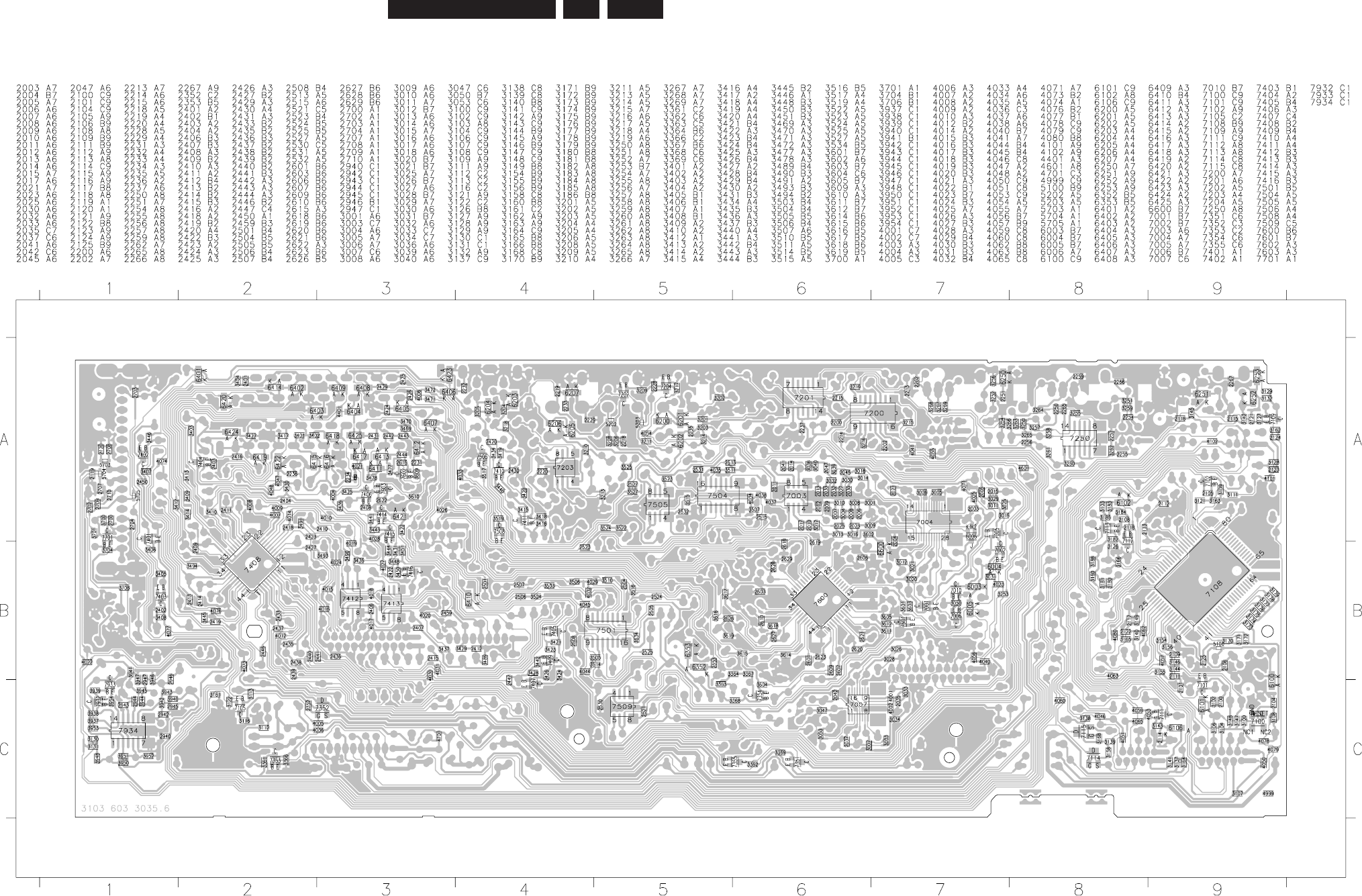
EN 136
3139 785 31532 7.Circuit Diagrams and PWB Layouts
Layout: Analog Component + SMD VIEW
Anabd_3139_603_30356_Bottomview.pdf 2005-10-14
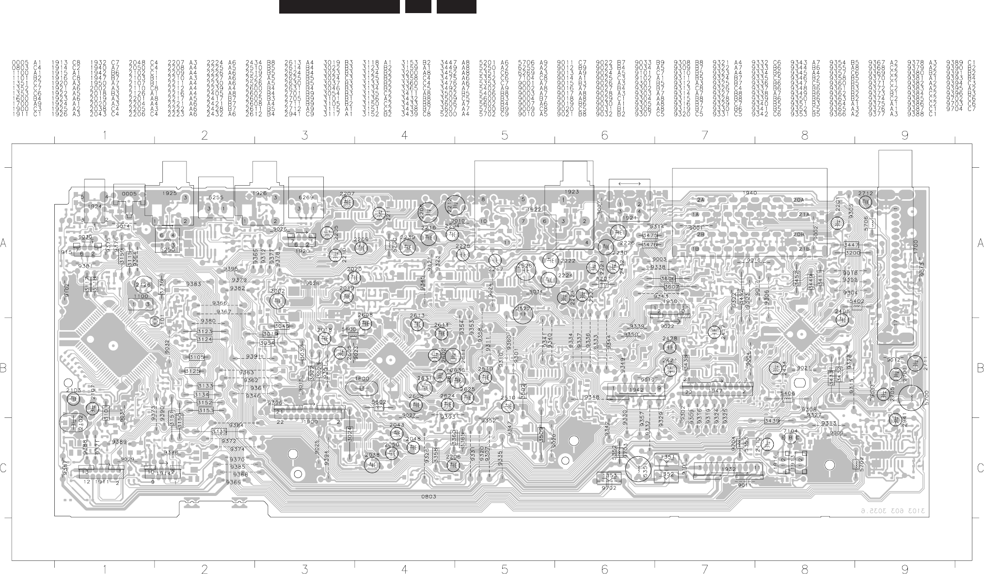
EN 137
3139 785 31532 7.
Circuit Diagrams and PWB Layouts
Layout: Analog Component View
Anabd_3139_603_30356_Topview.pdf 2005-10-14
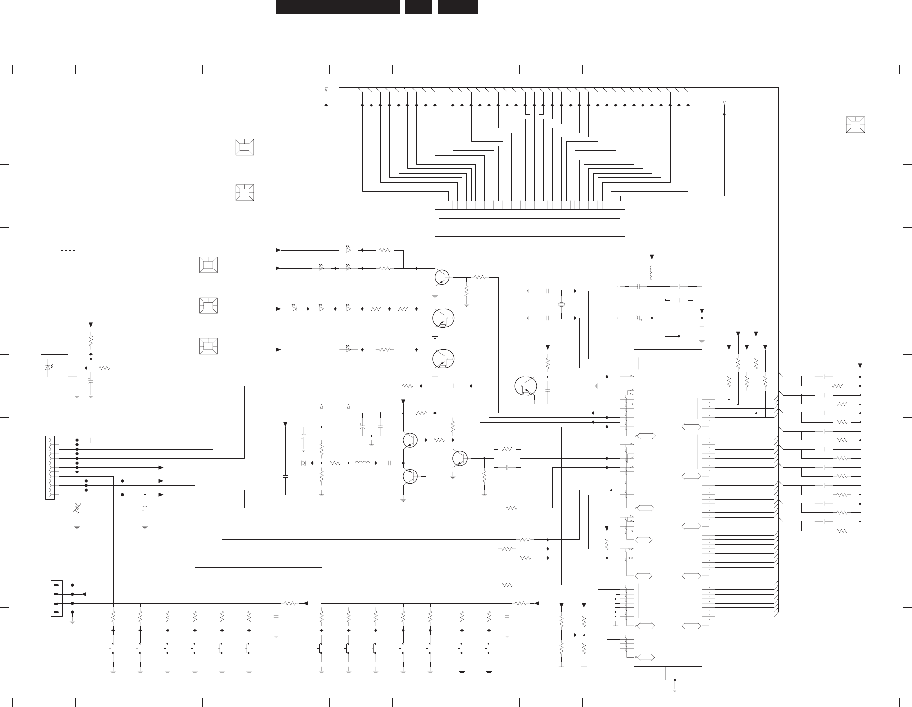
EN 138
3139 785 31532 7.Circuit Diagrams and PWB Layouts
Front: Display Part (DISP)
2
3
15
SSV
INT4
3
2
XTAL
P0<0:7>
DDV
4
16
0
1
2
3
4
5
18
7
TC2
TC3
PD04
PPG
TEST
KKV
SI
SO
SCK
INT5
23
1_
D
DV
21
20
10
9
P31
22
2
P1<0:7>
STOP
6
28
27
RESET
SSVA
PD<0:4>
V3
P6<0:7>
V
P7<0:7>
V
P8<0:7>
V19
18
17
P4<0:7>
INT
XTIN
XTOUT
P30
29
26
25
24
PWM
TC4
21
20
19
P2<0:2>
3
4
P3<0:1>
AIN
31
30
P5<0:3>
8
FERAV
14
13
12
P9<0:7>
V
0
5
6
7
6
5
AIN_STOP
1
11
T
-
I150 D9
I151 D9
I152 D11
I153 E7
I129 A10
I130 A10
F1101 H1
I142 C6
I143 E2
3158 E12
I111 A8
I112 A8
I113 A8
3152 G14
5104 F6
KEY1
+12VSTBY
I110 A8
I124 A10
I125 A10
I126 A10
I127 A10
THGIR
I108 A7
I109 A7
I171 I7
I169 I8
7108 F7
7109 F8
I122 A9
I170 I8
7113 C7
F100 G2
F1001 E2
I138 A11
I139 A11
I140 C5
I185 I5
I182 D5
F1002 F2
F1003 F2
I146 C7
I190 D6
I191 D6
I103 A6
I104 A7
I105 A7
I106 A7
for TRAY LED only
+5VSTBY
3127 G8
3129 I8
I131 A11
I192 D6
I194 D7
3159 E7
I101 A6
I102 A6
3130 I3
3164 I9
3165 I9
5100 C11
I164 F6
I114 A8
I115 A8
I116 A8
I168 I3
I178 A12
I121 A9
I173 G9
I174 H9
3119 F6
3120 F8
3121 D2
3122 F5
3153 G14
3154 E12
I117 A9
I166 I4
I167 I4
I177 A5
I180 I3
YA
L
P
T
N
I
R
P-
Y
B
T
S ot
I123 A9
I181 I2
I137 I10
F1011 G2
F1012 G2
F1013 G2
I141 C6
I186 H9
I183 D6
I144 F9
I100 A6
I147 I2
I148 I6
2129 D11
3100 E14
3101 E14
3102 I9
F1007 F2
F1008 F2
F1010 G2
not used
I195 E10
I196 E10
I197 F10
3163 H8
I199 F10
I162 F7
I163 F8
3151 G14
3108 I4
3109 I2
3110 I4
3155 E12
I118 A9
I179 I6
I120 A9
3116 E7
3161 G10
3162 H9
2111 F6
2112 E9
2113 F6
2114 F8
I172 I7
I175 E10
I165 E2
axial
draobgo
l
a
n
A ot/mor
f
I132 A11
I133 A11
3126 I2
2119 F13
2120 F13
2121 F13
3131 I3
F1102 H1
I189 D6
F1104 I1
2126 G13
3136 D6
3137 D6
D
E
F
G
I154 E8
axial
HDD
GND
not used
I158 F5
I159 F7
I198 F10
I161 E7
3149 F14
3150 F14
3107 H5
1911 H1
2100 I8
2101 C10
3111 C6
3156 E12
I119 A9
3115 H8
2106 D9
3117 D9
3118 F7
7
I128 A10
V05
VERP
POTS
F1004 F2
F1006 F2
3124 F8
3125 F7
2118 E13
C
D
E
2122 G13
3132 I9
F1103 H1
2125 G13
A
2127 E7
2128 C11
4567
I107 A7
+HC
TFEL
ESOLC/NEPO
Tray_Led
I160 F7
3148 F14
3105 I8
3106 I6
1910 E1
2102 D10
3112 E2
3157 E12
2105 C9
2107 G3
2110 F6
0206 B4
0210 D3
0211 D3
0212 C3
3123 F5
DDH
KO
desu ton
LZ
CER
F1005 F2
2116 E2
2117 F5
B
F
2123 E13
3133 I9
I
1
B
C
3
3103 I7
3147 F14
3104 I7
1171 I6
1172 I2
6120 C5
6121 C6
6122 C5
desu ton
2103 I5
3114 G9
-HC
7110 E7
7112 E8
3138 I6
3139 D7
2115 F5
EPG
TX
EN
VGNSTBY
14
A
GND
F_IROUT
RC
G
2124 E13
G
P
E
2
1168 I4
1169 I7
1170 I4
H
V05
11 12 13 14
123
6103 D6
6107 D5
7100 A5
7103 E11
7105 D7
2104 D11
6101 D5
6102 D5
7106 F7
7107 D1
8
1161 I8
1162 I5
1163 I3
1164 I2
1165 I6
1166 I3
91011 13
3140 C8
3141 C8
3142 C6
1167 I7
H
SDA_F
SCL_F
8910
RECORD
I
0005 A4
SCN_F
6100 F5
LIGHT CHAMBER RECORD
0210
456
3134 G1
3135 I5
0803 A14
1110 D9
1160 I7
LIGHT CHAMBER HDD
axial
+12VSTBY
12
R
074
6213
2101
100n
I197
3159
470R
VGNSTBY VGNSTBY
921
3
0
K1
VGNSTBY
7106
BC337-25
7
112
u22
R0
74
321
3
GND
VGNSTBY
n
74
51
12
81
1
I
BC847BW
7109
K001
7
113
2121
100p
3149
22K
VGNSTBY
I152
1K8
3111
10p
2105
0
0
1I
GND
GND
741
I
F1001
7K4
1
413
3140
4K7
F100
6
7
8
93150
22K
1
10
11
12
13
2
3
4
5
OUT
3
VS
1910
13FMN-BTRK-A
TSOP4836ZC1
2
GND
1
GND
GND
7107
6100
BZX384-C6V8
3107
I153
771I
F1101
0
K1
GND
2313
40
1
2
3
131
3
46
45
44
43
42
41
8
4
39 5
78
57
56
55
54
53
52
51
50
49
48
47
67
66
65
64
63
62
61
60
59
58
21
77
76
75
74
73
72
71
70
69
68
30
31
32
33
34
35
36
37
18
19
20
13
14
15
16
17
9
6
7
79
80
22
23
24
25
26
27
28
29
10
11
12
Φ
MC
7103
TMP86PM74A
83
0112
u
01
+5VSTBY
3116
330R
271I
0113
R022
GND
22K
3151
6112
u22
I198
F1008 100u
5104
971I
4
21
3
K
0
1
GND
0206
HOLDER FTD ASSY
6513
K001
K001
5513
8513
K001
8
0
1I
2213
K
01
0
21
I
GND
F1011
VGNSTBY
GND
F1102
F1004
GND
181
I
3153
22K
R033
811
3901I
I196
GND
2125
100p
0015
u0
1
75R
3136
66
1
I
3147
22K
3102
0
1
11
DNG
M
6
1
94-TA
BC327-25
7108
R50
L
11QV
E
16
11
GND
7K
4
7113
BC847BW
DNG
5
313
3162
100R
GND
I140
2
6
11
F1005
R50
L
11
Q
V
E
470R
3119
961I
LW3333
6107
201I
2
K2
4
0
1I
90
13
I182
+12VSTBY
6.0V
6.0V
0.4V
6.0V
I161
3152
22K
+12VSTBY
I160
3137
270R
2127
220n
1n0
PROTECTION FOIL
0005
I151
2114
3127
100R
22K
3101
GND
470R
3125
7105
PDTC124EU
R02
2
3
013
GND
I195
560R
3142
761I
5
6
1I
GND
2120
100p
7012
V0
5
7u
4
GND
2113
680n
921I
22u
2102
LTL-1MHHR
6103
16V
PDTC124EU
7110
3112
1K0
F1010
R022
1
2
13
I144
F1103
DNG
231
I
4999
+5VSTBY
1911
DA
1
2
3
4
GND
I189
6
6
11
R50
L
11
Q
VE
8
21I
0
3
1I
VGNSTBY
I162
I146
BARCODE
0803
I141
VGNSTBY
+5VSTBY
YBTSV
2
1+
I154
I163
621
I
331I
GND
I186
6
0
1I
5
0
1
I
521I
10K
GND
F1104
3163
GND
6121
LTL-42UB6N
I158
GND
911I
2
21I
301I
+5VSTBY
031
3
K01
2118
100p
2126
100p
2122
F1012
931I
100p
GND
171I
n
0
1
0012
n01
21
12
071I
K74
871I
101I
6
0
13
3
21
I
GND
421I
831I
YBTSV
5
+
GND
I183
011I
121I
I190
YBTSV
5
+
7513
K001
131
I
6120
LTL-42UB6N
0
7
11
0212
F1013
R50
L1
1
Q
V
E
4513
LTL-1MHHR
6101
7
2
1I
K001
F1006
100p
2119
I164
I174
3611
R
5
0
L
11
Q
V
E
100p
2124
581I
LTL-42UB6N
6122
R50
L
11QV
E
GND
8
6
1
1
GNDGND
7112
PDTC124EU
0K1
56
13
+5VSTBY
+5VSTBY
GND
0K1
331
3
I137
+5VSTBY
2106
I175
I191
10p
270R
3139
2123
100p
I150
711I
YBTSV21+
0
81
I
6102
LTL-1MHHR
n001
4012
I142
0611
I143
R50
L1
1
Q
V
E
F1003
GND
4
61
3
8
41I
3120
1K0
R074
F1007
1
6
13
K
0
1
8313
GND
GND
I159
2
711
R5
0L
11
Q
V
E
GND
GND
F1002
I199
R50
L1
1
Q
V
E
56
11
R
50
L11Q
V
E
7611
3115
100R
8
0
13
I192
VGNSTBY
GND
K74
I173
22K
3148
+12VSTBY
0211
HOLDER EPG
I194
R50L11QVE
17
11
n7
4
1112
701I
111I
50
13
21
1
I
K
0
1
2K2
4
01
3
100n
2129
GND
4611
Display Part DISP
9611
R50
L
11
Q
V
E
R5
0L
11
Q
V
E
GND
3100
22K
411I
YBTSV5+
311I
5
11I
2128
100n
K
01
+5VSTBY
6P 22
7P 12
8P 02
9P 91
43
1
3
57875B
73
32P 83
42P 9
3
52P
62P 04
72P 14
3P 52
4P 42
5P 32
03
61P
71P 13
81P 23
91P 3
3
2P 62
02P 43
12P 53
22P 63
2F 54
1P 72
01P 8
1
1
1P 71
61
21P
51
31
P
82
4
1
P92
51
P
G
311
G4 01
G
59
G6 8
G7 7
G8 6
G9 5
1F 1
7100
BJ929GNK
DSP
G1 31
G2 21
GND
GND
GND GND
8
61
I
3114
100R
611I
2LIF
301
2
n01
91P
02
P
1
2P
22P
32P
42P
52P
62P
72P
FIL2
5G
6G
8
G
1LIF
01P
21P
2P
4P
6P
8P
9
P
1P
41P
51P
61P
71P
81P
KEY1
TEMP_SENSE
KEY2
1G
3
G
4G
2G
31P
3P
5
P
7P
11
P
G8
G9
P23
P25
P24
P26
P27
P15
P2
P3
P4
P6
P5
P7
P8
G3
G2
G1
P12
G4
G5
G9
G6
G7
G8
9G
7G
IPOR1
P13
P9
P14
P1
P11
P10
P16
P17
P18
P19
P20
P21
P22
G7
G6
G5
G4
G3
G2
G1
1L
I
F
3103_603_30380_130_a2_sh1.pdf 2004-11-14
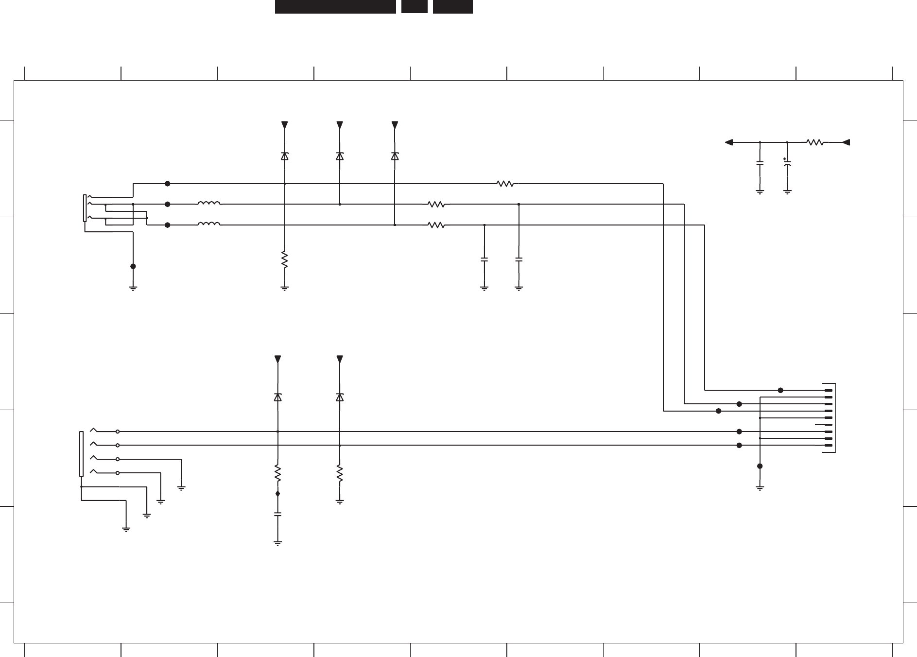
EN 139
3139 785 31532 7.
Circuit Diagrams and PWB Layouts
Front: Front Connector (FC)
Y
E
A
RA
C
N
987654321
21
D
NG
C
F_NI
FS
BVC
LA
C
TO ANALOGBOARD
SBVC
9876
A
1B
0
2
9
1
1E 1291
9C
2
2
9
1
D
NG
B
C
D
E
CF_
NI
FC
5
B
0
0
2
2
543
HCNIC
C
F_
NI
F
Y
NNOC-S
2B 2025
3A
0
0
0
6
4A 1006
4A
2
0
0
6
PSID morf
D
N
G
B
C
D
C
F_IRC
FA
CF_IL
C
FA
3C 3006
4C
4
0
0
6
2
B
1
0
02
F
2A 400
2
F
2
B
5
002F
2A
6
0
0
2F
8C 1022F
8D
20
2
2F
8
C
3
0
22
F
8D 402
2
F
8D
7
0
2
2F
8
D
9022F
3D 102I
3E 2022
8A
3
0
2
2
8A 4022
6B
5
0
2
2
5
B
0
0
2
3
5
A
2023
4D
6
0
2
3
3D 7023
9A
8
0
2
3
5A 9023
2A
1
0
2
5
6002
F
3
B
5023
1
2
3
4
5
6
C
F
DNG
1291
1
5F
KY
CFDNG
3205
75R
3022
F
F2001
10
2I
C
F
D
NG
1
3
2
5
4
6
DSE5D
S
E5
0
2
9
1
0
2
0
0
-
1
0-
7
2
1
1
JP
J
D
S
E5
6001
BZX384-C12
BZX384-C12
6002
BZX384-C12
6000
BZX384-C12
BZX384-C12
6004
C
F
DNG
6003
470p
2200
0023
R074
7022F
F2202
9022F
4022F
CF rotcennoC tnorF
4
5
6
7
8
9
1022F
2291
K
-HP-B9S
1
2
3
5002
F
CFDNG
9023
R57
40
02
F
YBTSV5+
DSE5
D
SE5
D
SE5
8023
K
01
CFDNG
1025
10u 25V
C
FD
NG
2025
2204
CF
D
N
G
2203
10n
2205
470p
R074
2023
CFD
NG
CF
D
NG
C
FDNG
75R
3206
2202
100n
3207
75R
CFD
NG
CFDNG
3103_603_30380_130_a3_sh2.pdf 2004-11-10
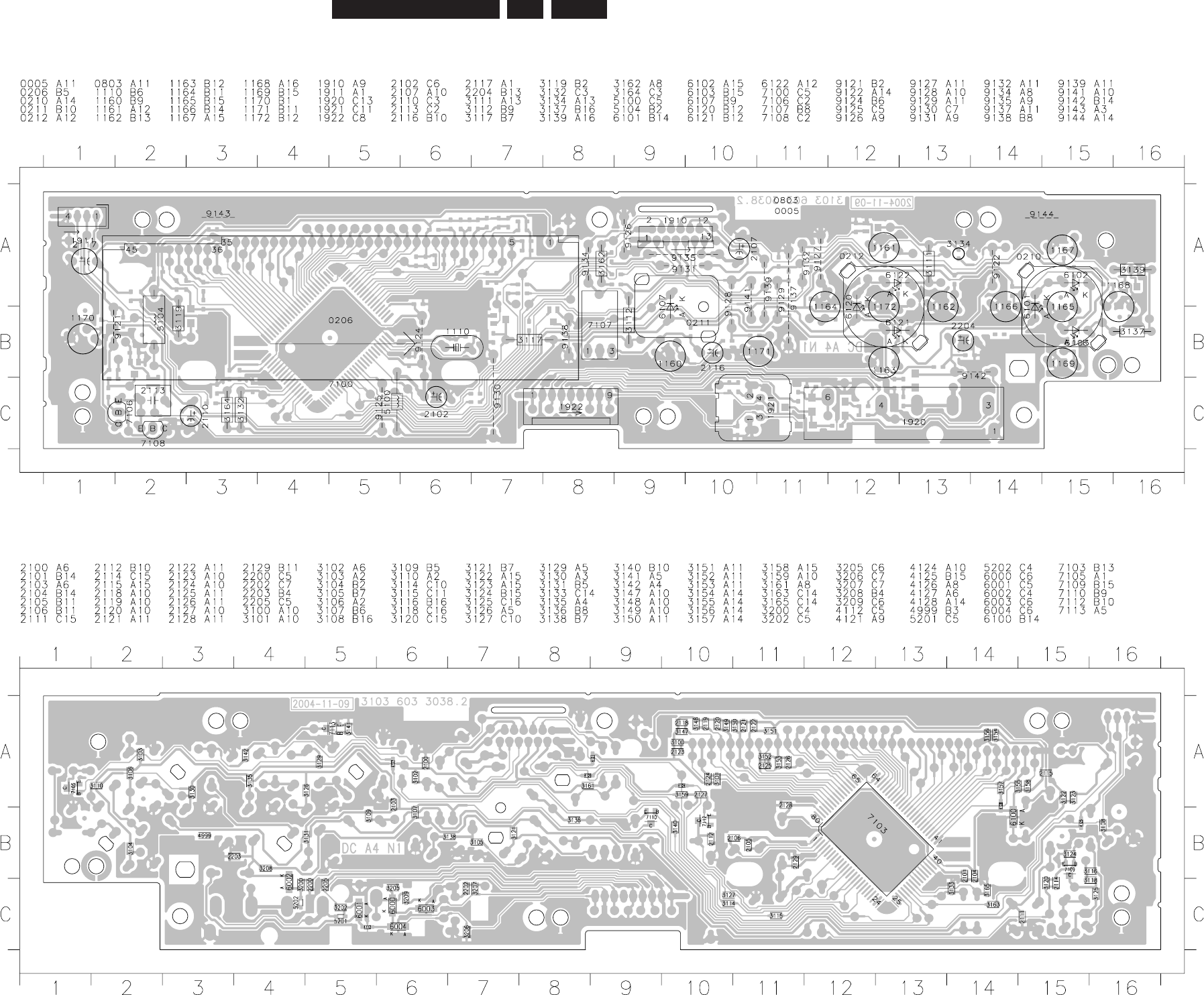
EN 140
3139 785 31532
Layout: Display/Front Connector (Top View)
Layout: Display/Front Connector (Bottom View)
Frontbd_3139_603_30380_Topview.pdf 2005-10-14
Frontbd_3139_603_30380_Bottomview.pdf 2005-10-14
7.Circuit Diagrams and PWB Layouts
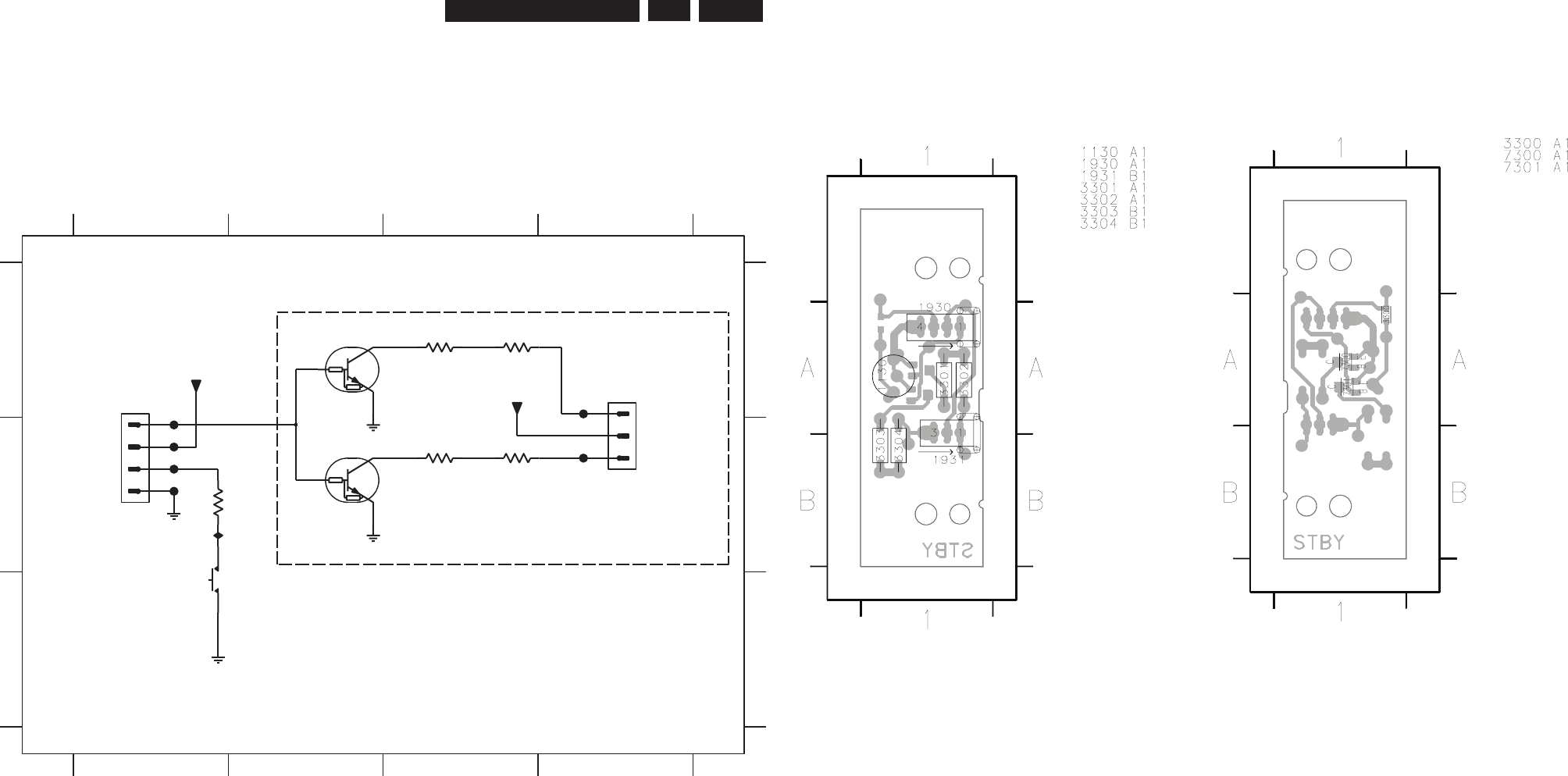
EN 141
3139 785 31532 7.Circuit Diagrams and PWB Layouts
Front: Standby (STBY)
for TRAY LED only
F3001 A1
F3002 B1
F3003 B1
F3004 B1
F3101 A4
F3103 B4
I300 B13303 B3
3304 B3
7300 A2
7301 B2
GND
+12VSTBY
4
1234
A
B
C
A
B
C
1130 C1
1930 A1
TFEL YART ot
1931 A4
3300 B1
3301 A3
3302 A3
+12VSTBY
(not used)
REWOP
DRAOB-CD morf
(not used)
123
7301
PDTC124EU
1
2
3
7300
PDTC124EU
GND
GND
DA
1931
F3103
F3002
F3101
F3003
003I
F3004
+12VSTBY
0311
R
50L11QV
E
1
2
3
4
GND
GND
+12VSTBY
1930
DA
3303
270R
3304
270R
3301
270R
3302
270R
F3001
0033
7K4
Standby STBY
KEY1
TRAY_LED2
TRAY_LED1
Tray_Led
3103_603_30420_130_a4_sh3.pdf 2004-11-24
Layout: Standby (STBY) (Top View) Layout: Standby (STBY) (Bottom View)
Stby_bd_3139_603_30420_btmview.pdf 2005-10-14
Stby_bd_3139_603_30420_topview.pdf 2005-10-14
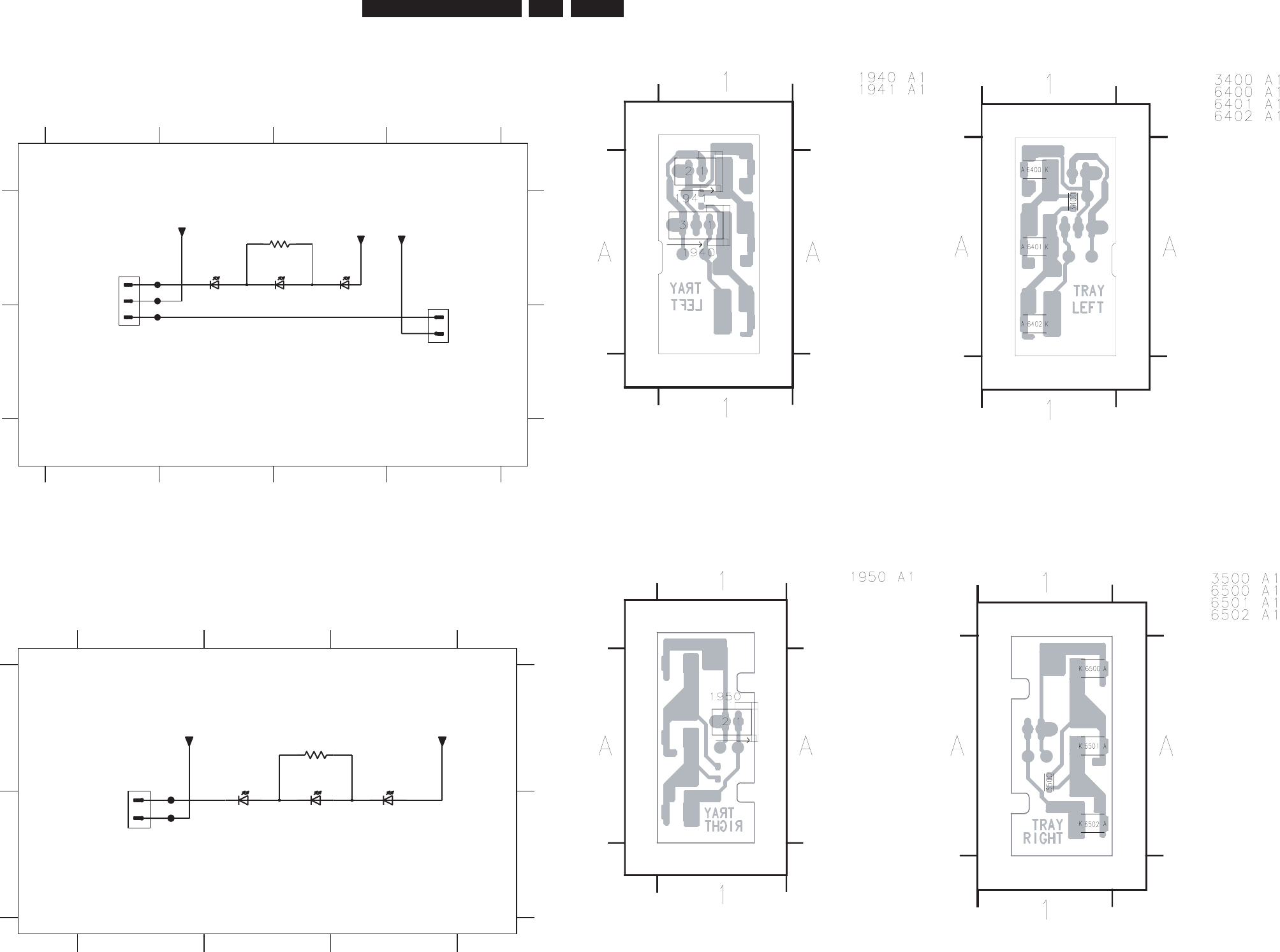
EN 142
3139 785 31532 7.
Circuit Diagrams and PWB Layouts
Front: Tray Left TRL
for TRAY LED only
F4002 A1F4001 A1 F4003 B1
+12VSTBY
2
3400 A3 6400 A3
123
A
6401 A3
+12VSTBY
THGIR-Y
A
RT
ot
1941 B4
TRAY_LED2
6402 A2
YBTS morf
1
4
B
A
B
1940 A1
34
+12VSTBY
+12VSTBY
680R
3400
DA
1940
1
2
3
F4002
F4003
DA
1941
1
2
F4001
+12VSTBY
6401
LST670 LST670
6400
LST670
6402
Tray left TRL
TRAY_LED1
TRAY_LED2
3103_603_30420_130_a4_sh4.pdf 2004-11-24
Front: Tray Right TRR
for TRAY LED only
123
not used B
1950 A1 3500 A2
A
B
A
1
6500 A3 6501 A2 6502 A2
TFEL-YART morf
23
F5001 B1 F5002 B1
3500
680R
F5001
+12VSTBY
F5002 LST670
6502
LST670
6501
LST670
6500
1950
DA
1
2
+12VSTBY
Tray right
TRR
TRAY_LED2
+12VSTBY
3103_603_30420_130_a4_sh5.pdf 2004-11-24
Layout: Tray Led (Left) (Top View) Layout: Tray Led (Left) (Bottom View)
TrayLeft_3139_603_30420_Bottomview.pdf 2005-10-14
TrayLeft_3139_603_30420_Topview.pdf 2005-10-14
Layout: Tray Led (Right) (Top View) Layout: Tray Led (Right) (Bottom View)
TrayRight_3139_603_30420_Bottomview.pdf 2005-10-14
TrayRight_3139_603_30420_Topview.pdf 2005-10-14
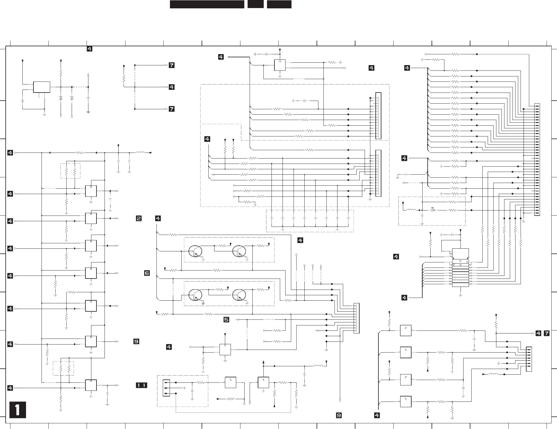
EN 143
3139 785 31532 7.Circuit Diagrams and PWB Layouts
Digital: IDE1, Uarts, Reset, BE
G3
1
2
3EN2
3EN1
not used
A
B
C
D
E
F
G
H
I
A
B
C
D
E
F
G
H
I
1100 A10
1102 B14
1103 H14
1104 G9
1105 C10
1 2 3 4 5 6 7 8 9 10 11 12 13 14
1 2 3 4 5 6 7 8 9 10 11 12 13 14
d
e
su t
on
1106 I5
2025 A8
2101 B1
2102 E7
2103 C3
2104 E8
2105 E8
2106 E8
2107 E8
2108 A7
2109 E9
2110 E9
2111 E9
2112 H13
2113 C11
2114 A2
2115 E12
2116 E11
2117 D3
2118 I3
2119 I12
2120 I8
de
su
t
on
2124 I5
2125 C4
3003 G6
3036 C6
3038 I6
3039 E11
3040 I8
3041 F2
3042 G2
3044 D7
3045 H5
3050 A12
3051 A12
3053 I8
3054 A12
3080 G7
3081 H7
3082 G10
3085 C6
3092 I11
3093 I12
3095 C2
DRAOB GOLANA
not used
3098 I7
3102 B8
3104 B7
3105 B8
3106 A12
3107 B9
3108 A12
3109 B8
3110 A12
3111 B8
3112 A12
3113 A3
3114 A2
3115 C8
3116 A12
3117 H1
3118 B12
3119 I2
3120 B12
3121 A9
3122 B12
not used
not used
3123 E6
3124 B12
3125 E7
3126 B12
3127 F5
3128 B12
3129 F6
3130 B12
3131 C7
3132 F7
3133 C12
3134 G5
3135 C12
3136 C7
3137 F6
3138 C12
3139 C7
3140 C7
3141 D7
not used
for DTTV only
de
su t
on
3142 G8
3143 C12
3144 E5
3145 C12
3147 E13
3149 E13
3150 I5
3152 D7
3154 C12
3156 D12
3157 D7
3159 E13
3160 H2
3161 D12
3162 D2
3163 C2
3164 D12
d
es
u t
on
not used
not used
not used
3165 C2
3166 H2
3167 E13
3168 D12
3170 E13
3172 E13
3173 E2
3175 E14
3178 E14
3180 D12
3184 F2
3185 G12
3186 G13
3187 F2
3189 H12
3191 H11
3192 H12
3195 I10
3197 I12
3199 I12
4110 F8
not used
desu t
on
4111 G7
4112 D11
4113 F9
4115 D2
4116 I2
4117 A2
4118 F5
4119 F8
4120 F8
4122 A4
4123 A4
4124 A8
4125 H7
5100 C4
5102 D11
5103 I13
de
su t
on
5104 H9
6100 A2
6101 A2
6103 D12
7100 E5
7101 E6
7102 F5
7103 A8
7104-1 H2
7104-2 I2
7104-3 D2
7104-4 D2
7105 F6
7106 A1
7107-1 E2
7107-2 F2
7107-3 G2
7107-4 H6
7108 E12
7111-1 G11
7111-2 I11
7111-3 H11
F0603
not used
7111-4 I11
7111-5 I6
7111-6 I7
d
esu to
n
F0001 B9
F0003 B9
F0005 B9
F0007 B9
F0009 B9
F0011 B9
F0015 A10
F0201 A13
F0202 B14
F0203 A13
F0204 A13
F0205 A13
F0206 A13
F0207 A13
F0208 A13
F0209 B13
F0210 B13
F0211 B13
F0212 B13
F0213 B13
F0214 B13
F0215 B13
F0216 C13
F0217 C13
F0218 C13
F0221 C13
F0223 C14
F0225 C14
F0227 C14
F0229 D14
F0231 D14
F0233 D14
F0234 D13
F0235 E13
F0236 E13
F0237 E14
F0238 E14
F0239 D13
F0301 H13
F0302 H13
not used
not used
F0303 H13
F0304 H13
F0305 H13
F0306 H13
F0307 I13
F0401 H9
F0402 H9
F0403 G9
F0404 G9
F0405 G9
F0406 G9
F0407 G9
F0408 G9
F0409 F9
F0410 F9
F0501 D10
F0503 D9
F0506 D9
F0508 C9
F0509 D9
F0510 C9
F0511 C9
desu ton
not used
d
e
s
u
t
on
not used
F0512 C9
F0514 C9
F0601 I5
F0603 I5
F936 G3
I100 A2
I102 A3
I105 A4
I106 B4
I108 D3
I109 D3
I110 E3
I111 F3
I112 C3
I114 C2
not used
not used
I116 D11
I117 H7
I119 D2
I120 E2
I121 E2
I122 F2
I123 H2
I124 G2
I125 I2
R33
5713
2025
10p
F0407
F0201
10
2
3
4
5
6
7
8
9
FMN-BMT
1104
1
K0
01
1
913
2913
8K6
I124
47R
3136
F0221
F0007
7K4
240
3
F0223
F0208
BLMP18P
5102
10K
3053
100n
2115
100R
3150
1
050F
F0204
F0305
100R
3137
p01
221
4
4012
TLMH3100
I109
6103
F0207
PDTC124EU
7102
n
0
01
52
12
K
01
68
13
n
22
10
1
2
F0509
p
01
2012
5K63145
3116 33R
F0406
F0306
I108
33R3108
8
114
F0506
11
7
4
1
10
7111-5
74HCT14D
5214
33R3135
F936
F0239
3104
47R
F0206
I123
R22
7
41
3
2
4
17
3
3131
47R
7107-1
74LVC08AD
1
3
613
7K4
F0404
5
n
1
2112
33R3120
F0005
K00
1
6303
10K
3164
F0303
I102
3130 33R F0215
6320F
3038
100K
3713
7K4
F0511
4111
0
016
01
BS6
7
S
P
1
F0001
2
9
03
K
0
01
41
11
74LVC08AD
7104-4
12
13
7
F0405
K001
2
80
3
F0003
0
112
p0
1
F0409
7K4
78
13
4117
100R
3142
F0410
F0301
F0512
7
8
9
34
35
36
37
38
39
4
40
5
6
25
26
27
28
29
3
30
31
32
33
15
16
17
18
19
2
20
21
22
23
24
1-440090-4
1102
1
10
11
12
13
14
73
20
F
IDE1
n001
6
1
12
3154 82R
74HCT14D
13
7
4
1
12
33R3128
7111-6
911
4
1016
01BS67SP
1
7K4
0613
F0203
071
3
R
33
I110
3114
711
3
7
K
4
F0514
2108
100n
3
90
3
8K6
F0229
4112
p074
5100
7
K
4
5
403
BLMP18P
3139
9
10
417
8
47R
F0210
74LVC08AD
7107-3
I116
100R
3185
4116
3138 33R
0
114
5
417
6
7104-2
74LVC08AD
4
7012
p
01
1
OUTP
BLMP18P
5104
5CD
3
GND
2INP
NC
4
NCP303LSN29
7106
41
7
6
3110 33R
7107-2
74LVC08AD
4
5
33R3122
1R0
3111
I112
F0302
4115
F0508
5100
F
F0212
7101
PDTC124EU
I119
3095
4K7
3141
0
214
47R
p074
811
2
7112
p074
5
012
p01
3126 33R
9
10
4
17
8
3197
100R
F0231
74LVC08AD
7104-3
PDTC124EU
7100
1R0
3107
3157
47R
100R
3080
p0
1
60
12
3125
4K7
F0225
7K4
9113
33R3112
82R3143
F0217
4K7
3156
F0216
I114
7K
4
2
61
3
7
61
3
R33
94
13
R22
4K7
3129
F0402
F0408
F0401
F0403
5
803
K001
33R3133
F0214
1
112
p0
1
I125
F0218
SD-71308
1106
1
2
3
3121
10K
K01
9303
F0227
p01
9012
1R0
3102
4124
5
7
41
6
F0202
7111-3
74HCT14D
3189
10K
K001
8
9
03
IDE1,UARTS,RESET,BE
4K7
3123
3124 33R
I111
7
8
9
I106
10
11
12
13
14
15
2
3
4
5
6
FMN-BMT
1105
1
7K4
4813
6613
7K4
I105
3127
4K7
R33
2
713
1R0
3115
82R3161
3105
1R0
F0601
8
K6
04
03
83
20F
F0510
F0011
F0307
F0503
3180 220R
3134
4K7
33R3050
I100
F0209
11
1
01
19
0
2
R22
95
1
3
6
7
8
9
18
17
16
15
14
13
12
7108
74LVC245APW
2
3
4
5
BLMP18P
5103
3152
47R
F0211
33R3106
I122
I121
74LVC1G32GW
1
2
53
4
7103
30
12
n
0
01
4K7
3044
100R
3144
15
2
3
4
5
6
7
8
9
1
10
11
12
13
14
I120
FMN-BMT
1100
2
3
4
5
6
7
8
9
1103
Service
B7B-PH-SM4-TBT(LF)
1
5
n
1
9112
F0213
7105
PDTC124EU
7107-4
74LVC08AD
12
13
4
17
11
4112
3081
100R
I117
F0304
7K4
4
113
74HCT14D
3
41
7
4
9
7
4
1
8
7111-2
74HCT14D
7111-4
3168 4K7
n0
01
F0234
0212
1
2
41
7
3
7K4
561
3
41
2
74LVC08AD
7104-1
74HCT14D
7111-1
1
7
10p
2113
3199
10K
5320F
F0205
3
21
4
F0009
5913
K001
3109
1R0
42
1
2
5n1
3041
4K7
3003
10K
100R
3118 33R
3054
F0233
3132
4K7
3051 33R
3113
K0
1
3140
47R
8713
R3
3
+3V3
MPIO22_IDE1_En
+3V3
RESET_IDE1n
0
T
R
A
U
+5V_SERV
MPIO19_EEPROM_En
ION
nTESER_0017XNP
2
TRAU
-5V
IDE1_IORDY
IDE1_IORDY
IDE1_DIOWn
IDE1_DIORn
IDE1_DMACKn
IDE1_DA1
IDE1_DA0
IDE1_DA2
IDE1_CS0n
IDE1_CS1n
IDE1_CTL
IDE1_DMARQ
nTE
SE
R_
GO
L
A
N
A
4OI
P
M
n
Q
RI
_
A
N
A_
1
OI
P
M
CTS3
+5V
+3V3
RTS3
+5V
RXD3
+3V3
TXD3
+5V +5V
BE_BCLK
BE_FLAG
BE_SYNC
BE_DATA_WR
BE_DATA
VDD_PNX_PAD
IDE1_CTL
MPIO6_BE_DLOAD
BE_V4
BE_DATA_RD
BE_WCLK
+3V3
1
DX
R
+5V_SERV
RESET_IDE2n
MPIO18_IDE2_RESETn
MPIO17_HD_ON
HD_ON
TXD0
RXD0
RTS0
CTS0
1
DXT
RESET_IDE1n
MPIO14_IEEE1394_RESETn
RESET_1394n
MPIO15_DTTM_RESETn
RESET_DTTMn
MPIO16_PROGSCAN_RESETn
RESET_PROGSCANn
MPIO31_ANA_RESET
ANALOG_RESETn
PNX7100_SYS_RESETn
MPIO20_VIP_RESETn
VIP_RESETn
BE_FAN
+3V3_RES
+3V3+3V3
XIO_SEL0
XIO_SEL_NORFLASH
XIO_SEL_NANDFLASH
MPIO1_ANA_IRQn
MPIO13_IDE1_RESETn
-5V
+3V3
3
V
3+
RTS2
SDA0
SCL0
RESETn
+3V3
+3V3_RES
GI
D_
TESERI
B
F
_
PIV
+3V3
+5V
+5V
-5V
BE_FAN
GI
D_
T
E
S
E
R
I
nTE
S
E
R
_
G
AT
J
E
MPIO6_BE_DLOAD
IDE1_DD(0)
IDE1_DD(15)
IDE1_DD(15:0)
IDE1_IRQ
RESET_IDE1n
+3V3
RXD2
CTS2
RESET_DTTMn
TXD2
+3V3 +3V3
IDE1_DD(7)
IDE1_DD(8)
IDE1_DD(6)
IDE1_DD(9)
IDE1_DD(5)
IDE1_DD(10)
IDE1_DD(4)
IDE1_DD(11)
IDE1_DD(3)
IDE1_DD(12)
IDE1_DD(2)
IDE1_DD(13)
IDE1_DD(1)
IDE1_DD(14)
3103_603_30601_a2_sh130_sh1.pdf 2004-12-01
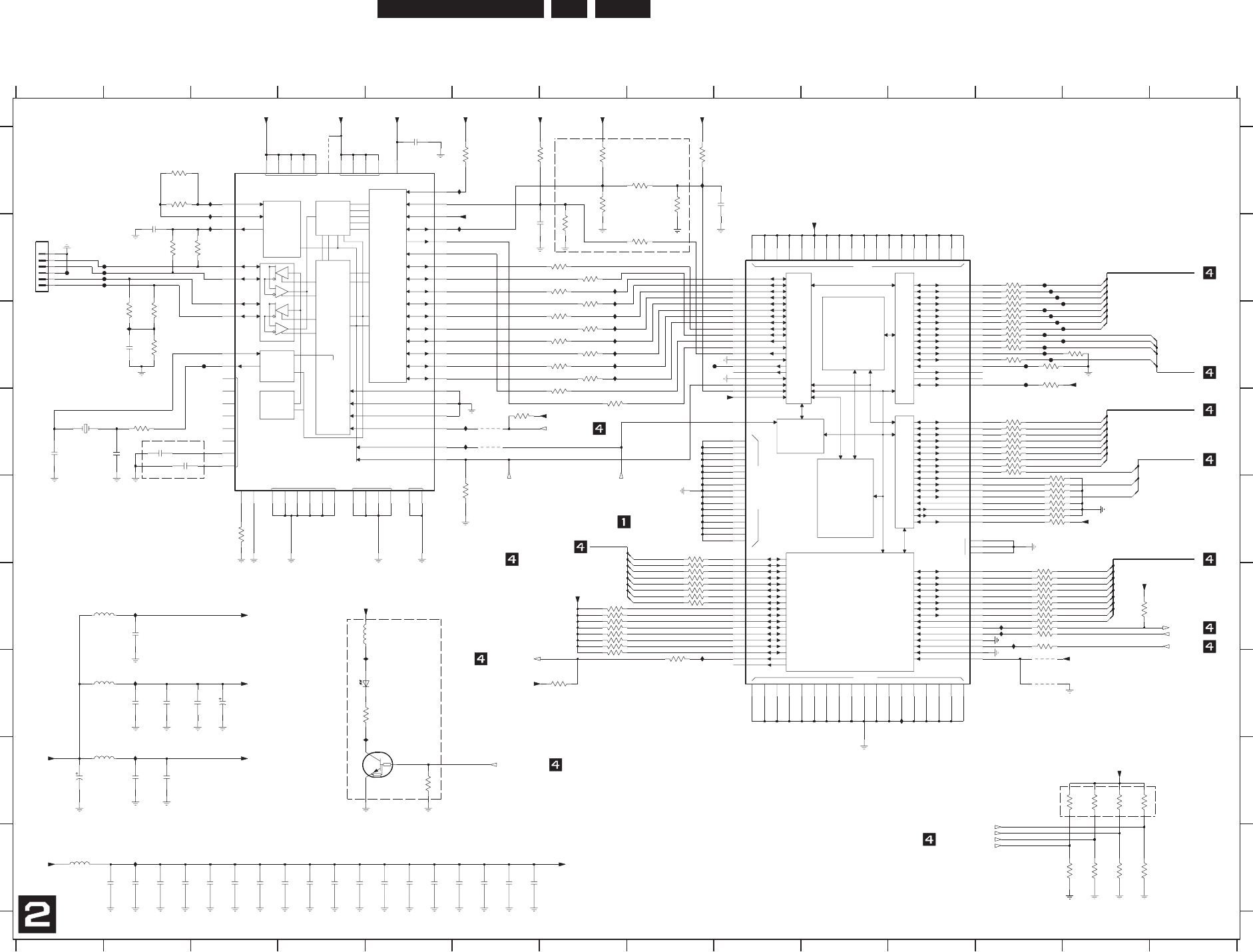
EN 144
3139 785 31532 7.
Circuit Diagrams and PWB Layouts
Digital: 1394
DVDDAVDD
NC
PLLGNDDGNDAGND
DECODER/
BIAS DATA
INTERFACE
LINK
RECEIVED
CONTROL
STATE
MACHINE
LOGIC
TRANSMIT
CLOCK
PLL
XTAL OSC.
ENCODER
DATA
GENERATOR
CURRENT
AND
VOLTAGE
1TSET
0TSET
C|LKON
ISO_
LPS
CPS
PLLVDD
R0
R1
TPBIAS0
TPA0+
TESTM
TPA0-
TPB0+
TPB0-
XI
XO
TIMER
ARBITR’N
AND
PD
RESET_
CNA
PC2
PC1
PC0
D7
D6
D5
D4
D3
D2
D1
D0
CTL1
CTL0
LREQ
SYSCLK
TESTPIN
GND
VDD
DEVRESER
B
C
D
E
F
G
H
I
1201 D1
1203 B1
2200 B2
2201 C2
2202 D1
2203 D2
2204 D2
2205 D2
2206 G3
2207 F2
2208 G3
2209 G2
2210 G2
not used
1 2 3 4 5 6 7 8 9 10 11 12 13 14
12345678
not used
9 1011121314
A
B
C
D
E
F
G
H
I
A
BOARD_ID
2212 H1
2214 H2
2215 H2
2217 I2
2218 I2
2219 I2
2220 I2
2221 I3
2222 I3
2223 I3
2224 I4
2225 I4
2226 I4
2227 I4
2228 I5
2229 I5
2230 I5
2231 I6
2232 I6
2233 I6
2234 I6
2235 A5
2236 A9
2237 B6
3200 E6
3202 F12
3203 H5
3204 D6
3205 A2
3206 A7
3207 A8
3208 B7
3209 B8
3210 B12
3211 B12
3212 B2
3213 B3
3214 B12
d
esu ton
3215 C12
3216 B7
3217 C12
3218 C12
3219 C12
3220 B7
3221 C12
3222 C12
3223 B7
3224 C12
3225 B7
3226 C12
3227 C12
3228 C7
3229 C12
3230 C12
3231 C7
3232 C2
3233 C2
3234 C7
3235 C12
3236 C7
3237 D12
3238 C7
3239 D12
3240 C2
3241 D12
3242 C7
3243 D12
3244 D12
3245 C7
3246 D12
3247 D12
3248 D7
3249 D12
3250 E12
3251 D12
3252 E12
3253 D2
3254 E12
not used
NI VD
desu ton
PHY
not used
3255 E12
3256 E12
3257 E12
3258 E12
3259 E12
3260 F12
3261 E3
3262 F7
3263 F7
3264 F7
3265 F7
3266 F7
3267 F7
3268 F7
3269 G7
3270 F12
3271 F12
3272 F12
3273 G8
3274 F12
3275 G4
3276 G7
3277 F12
3278 F12
3279 F12
3280 A6
3281 A7
3282 A8
3283 A2
3284 A8
3285 A6
3286 H13
3287 H13
3288 H13
3289 H13
3290 I13
3291 I13
3292 I13
3293 I13
3294 F12
3295 F12
3296 F12
3297 E8
3298 F8
3299 F8
3314 F13
3315 F8
3316 F8
3317 F8
3318 F8
3319 F8
4201 D6
4202 D6
4203 G12
4204 G12
4205 A4
5200 F2
5201 F4
5202 G2
5203 H2
5204 I1
6200 G4
7200 A5
7201 B12
7202 H5
not used
LINK
F1201 B2
F1202 B2
F1203 B1
F1204 B2
F1205 B2
F200 C12
F201 C9
F203 C3
F204 C13
F205 C12
F206 C13
F207 C12
F208 C12
F209 C12
F210 C13
F211 B12
F212 B12
F213 B12
F214 C12
F215 C12
F216 C12
F217 C12
I200 H4
I201 F2
I202 G2
I203 H2
I204 I2
I205 G11
I206 G4
I207 A3
I208 A3
I209 B3
I210 C2
I211 B7
I212 B7
I213 D6
I214 D6
I215 A6
I216 B6
I217 A8
I218 C7
I219 C7
I220 F12
I221 F12
I222 C7
I223 F12
I224 G8
I225 C7
I226 C7
I227 C7
3264 4K7
10K
3283
I222
F216
4K73269
2823
K01
K01
PDTC144EU
8023
7202
9222
n001
30
22
I227
p21
4
1
33
K
01
I217
5200
10R3273
BLMP18P
F213
13
2
2
n001
33R3243
I213
I216
2122
u001
0
0
13HMLT
0026
602
2
n001
38
59
60
41
53
2
2928
27
37
36
35
34
45
46
47
20
21
22
14
5758
56
40
6162
23
15
1
54
55
16
43
44
10
11
12
13
17186364
25265152
3
24
4
5
19
6
7
8
9
323339484950
303142 7200
PDI1394P25
PDI1394P25
0122
n001
F201
R65
3323
n001
7222
%1
3230 10K
220R3317
3221 33R
F206
3284
1R0
2205
100n
4122
n001
4202
1923
7K4
220R3274
10R
3220
3277 220R
220R
3296
3294 220R
33R3251
7
K4
98
2
3
3297 220R
K01
6
0
23
F210
n001
52
2
2
33R3214
632
2
n0
0
1
33R3229
3272 220R
0423
10K
3235
%1
1K5
3268 4K7
220R
3318
BLMP18P
5204
7022
n
0
01
3242
10R
3244 33R
3227 33R
2204
100n
F208
7
K4
7823
2235
1n0
I211
3223
10R
p0
72
1
0
22
%1
R65
2
323
3205
6K34
I224
1% I208
33R3222
n001
03
2
2
092
3
7K4
I219
F1201
n0
0
1
02
2
2
I215
91
2
2
n0
0
1
3253
1R0
3322
n001
n001
2322
22K3257
10R
3236
F1205
%1
R65
2123
3255 4K7
82R3224
4K73265
3248
22R
I221
I212
I207
n001
3266 4K7
22
2
2
12
2
2
n001
n001
R033
57
23
432
2
3316 220R
F1203
3210 33R
4204
I205
5202
1823
K01
BLMP18P
7K4
292
3
3238
10R
I218
F1202
F1204
220R
3279
10R
3228
3315 220R
I203
71
2
2
n0
0
1
10R
3231
1R0
3209
8022
V537
u
4
33R3247
4K73263
5024
3319 220R
33R3246
10K3219
33R3211
33R3217
33R3226
220R3298
4K73267
3245
10R
I204
602I
I225
4K73256
1
025
3215 33R
3216
10R
012
I
3218 33R
n001
3222
R01
5823
n001
9022
33R3237
3270 220R
3252 33R
0823
K01
7K4
6823
0023
K01
F217
I214
3276
1K0
220R3202
K01
3023
3249 33R
6222
n0
0
1
n001
7
322
3295 220R
3225
10R
5203
BLMP18P
3241 33R
4203
3239 33R
8222
n001
F214
3259 4K7
220R
3260
10K
3204
002I
K01
7023
F200
220R3278
F211
3262 4K7
4K73250
3
923
7K4
n001
8122
3258 22K
n001
1394
5122
07
10R
3234
31
1
021
2
3
1
8
3
1
2
1
81
4
2
5
3
44
4
5
16
SCLK
62
163
264
3
6
8
7
48
0
9
59
701
3
52 4
58 5
59 6
72 7
71 8
104 9
42 RESET_
88
67 12
68 13
105 14
129 15
144 16
130 17
50 2
51
79 PHYD3
76 PHYD4
75 PHYD5
74 PHYD6
73 PHYD7
49 1
65 10
66 11
91 LPS
87 LREQLREQ
48 PD
86 PHYCTL0
85 PHYCTL1
82 PHYD0
81 PHYD1
80 PHYD2
38 HIFINT_ 46
HIFMUX
HIFRD_ 40
HIFSC_ 36
41 HIFWAIT
HIFWR_ 37
93 ISON
92 LINKON
HIFALE
8HIFD10
7HIFD11
4HIFD12
3HIFD13
2HIFD14
1HIFD15
10 HIFD8
9HIFD9
21 HIFAD1
20 HIFAD2
19 HIFAD3
16 HIFAD4
15 HIFAD5
14 HIFAD6
13 HIFAD7
39
31
HIFA2
30
HIFA3
29
HIFA4
28
HIFA5
27
HIFA6
26
HIFA7
25
HIFA8
22 HIFAD0
71
32
43
34
35
0
6
9
6
45
HIF16BIT
33
HIFA0
32
HIFA1
7
7
3
8
9
8
4
9
6
01
211
9
11
1
31
731
11
125
AV2FSYNC
143
AV2READY
126
AV2SY
128
AV2SYNC
127
AV2VALID
55 CLK50
56 CYCLEIN
57 CYCLEOUT
5
136
AV2D3
139
AV2D4
140
AV2D5
141
AV2D6
142
AV2D7
123
AV2ENDPCK
121AV2ERR0|LTLEND
AV2ERR1|DATINV 122
118
AV1READY
101
AV1SY
103
AV1SYNC
102
AV1VALID
124
AV2CLK
133
AV2D0
134
AV2D1
135
AV2D2
114
AV1D4
115
AV1D5
116
AV1D6
117
AV1D7
98
AV1ENDPCK
96AV1ERR0
97
AV1ERR1
100
AV1FSYNC
47 1394MODE
99
AV1CLK
108
AV1D0
109
AV1D1
110
AV1D2
111
AV1D3
1VA R
EV
IECE
R
/ RET
T
IMSNA
R
T
2VA REVIEC
E
R /
R
ET
TIM
S
NART
ISOCH & ASYNC
INTERFACE
12KB BUFFER
PACKETS
MEMORY
TRANSMITTER
8-BIT
RECEIVER
ASYNC
AND
REGISTERS
CONTROL
STATUS
AND
CORE
LINK
PDI1394L40
7201
I223
3254
I209
33R
F207
F204
42
2
2
n001
F209
I201
24M576
1201
CX-8045G
8823
7K4
F205
F215
F203
I220
I202
R6
5
3123
1203
1
2
3
4
5
6
%1
SR
220R
3299
220R3271
F212
I226
0R1
1
623
p21
20
22
4201
+3V3_LINK
XIO_SEL1
MX_D_CTL
2200
1u0
PCI_AD(3)
PCI_AD(2)
PCI_AD(1)
PCI_AD(0)
L_CLK
L_VAL
L_SYNC
L_FSYNC
PCI_AD(31:0)
PCI_AD(8)
PCI_AD(7)
PCI_AD(6)
PCI_AD(5)
PCI_AD(4)
+3V3_IEEE_A
PCI_AD(31:0)
PCI_AD(31)
PCI_AD(30)
PCI_AD(29)
PCI_AD(28)
PCI_AD(27)
PCI_AD(26)
PCI_AD(25)
PCI_AD(24)
n4931_TESER
+3V3_IEEE_PLL
NWODREWOP_4931_12OIPM
+3V3_IEEE_D
+3V3_IEEE_D
L_D_CTL
MPIO9_BOARD_ID_0
MPIO10_BOARD_ID_1
MPIO11_HDMI_RESETn
MPIO12_HDMI_IRQ
+3V3_IEEE_D
MPIO8_1394_CNA
+3V3_LINK
+3V3_IEEE_D
+3V3_IEEE_D
+3V3_IEEE_PLL
+3V3_IEEE_A
+3V3
L_D(2)
MX_D(6)
MX_D(7)
MX_D(7:0)
MX_VAL
MX_SYNC
MX_CLK
+3V3_LINK
AV1ENDPCK
MPIO23_1394_LED
+5V
+3V3_LINK
MPIO2_1394_IRQn
MX_D(0)
MX_D(1)
MX_D(2)
MX_D(3)
MX_D(4)
MX_D(5)
L_D(7:0)
L_D(7)
L_D(6)
L_D(5)
L_D(4)
L_D(3)
L_D(1)
L_D(0)
+3V3_LINK
+3V3_IEEE_D +3V3_IEEE_D +3V3_LINK
+3V3_LINK
+3V3
+3V3
+3V3_LINK
+3V3_LINK
+3V3_LINK
PCI_CBE(1)
PCI_CBE(2)
3103_603_30601_a2_sh130_sh2.pdf 2004-12-01
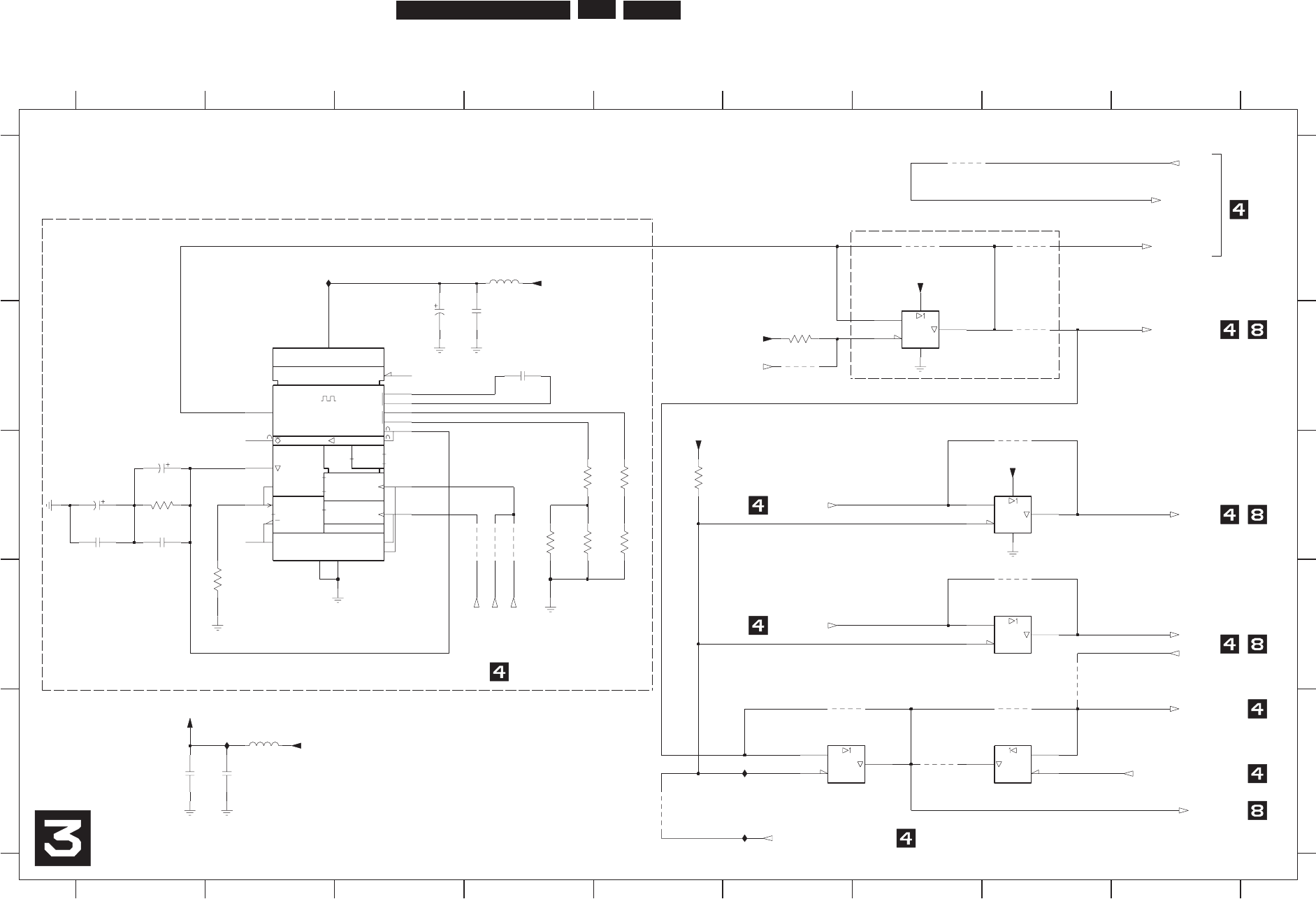
EN 145
3139 785 31532 7.Circuit Diagrams and PWB Layouts
Digital: Audio PLL
EN
EN
EN
Af
EN
EN5 Z3
=1
=1
1&
1
G
6
6
M6
RX Z4
R4
3
RX
CX
5
S
S
EN EN
not used
not used
not used
not used
2300 B3
2301 B4
2302 C1
2303 C1
2304 B4
2305 C1
2306 C1
2308 E1
2310 E2
3300 C1
3301 C4
3302 C5
3303 D2
not used
123456789
123456789
A
B
C
D
E
A
B
C
D
E
not used
3304 C4
3305 C4
3306 C5
3307 B6
3311 C5
4009 E7
4010 E6
4300 E8
4301 C4
4302 B6
4303 C4
4304 A7
4305 A8
not used
4309 C4
4310 B8
4311 E5
4312 C8
4313 D8
4314 A7
4316 D8
5300 A4
5302 E2
7300-1 C7
7300-2 D7
7300-3 E6
7300-4 E7
7301 B2
7302 A7
I300 A2
I303 E6
I305 E2
I306 E6
7
4
14
6
4313
7300-2
74LVC125AD
5
6
134
I300
1133
K01
4302
1034
2K2
5033
3
033
K0
22
00
3
2
7u4
2
7
1
14
3
113
4
7300-1
74LVC125AD
4304
10K
3307
I306
74LVC125AD
9
7
10
14
8
7300-3
I305
4312
9034
4300
5
2
13
11
12
15
14
16
9
4
[PLL]
6
7
3
10
18
4310
74HCT9046AD
7301
n0
0
1
8032
2033
K
21
74LVC1G125GW
7302
2
3
1
5
4
56R
3300
2u2
2302
4010
4033
7
K4
2303
4u7
3034
2304
68p
0
1
32
n001
1032
n001
I303
5300
BLMP18P
Audio PLL
4305
2306
6033
100n
0R1
13
14
11
3K3
1033
7300-4
74LVC125AD
12
7
4314
BLMP18P
100n
5302
2305
MPIO25_ADC_FSCLKE_OEn
PLL_OUT
MPIO26_ADC_FWSCLK012_OEn
PLL_OUT
FSCLK3_OUT
+3V3
4009
WS012_OUT
T
UO
_2
10
K
CS
+5V
FSCLKE_IN_PNX
MPIO25_ADC_FSCLKE_OEn
VDD_PLL_BUF
WSE_IN
SCKE_IN
VDD_PLL_BUF
VDD_PLL_BUF
TUO_3KCS
NI_
E
KC
S
FSCLKE_IN_PNX
VDD_PLL_BUF
FSCLKE_IN
FSCLK012_OUT
SCK012_OUT
VDD_PLL_BUF
3103_603_30601_a3_sh130_sh3.pdf 2004-12-01
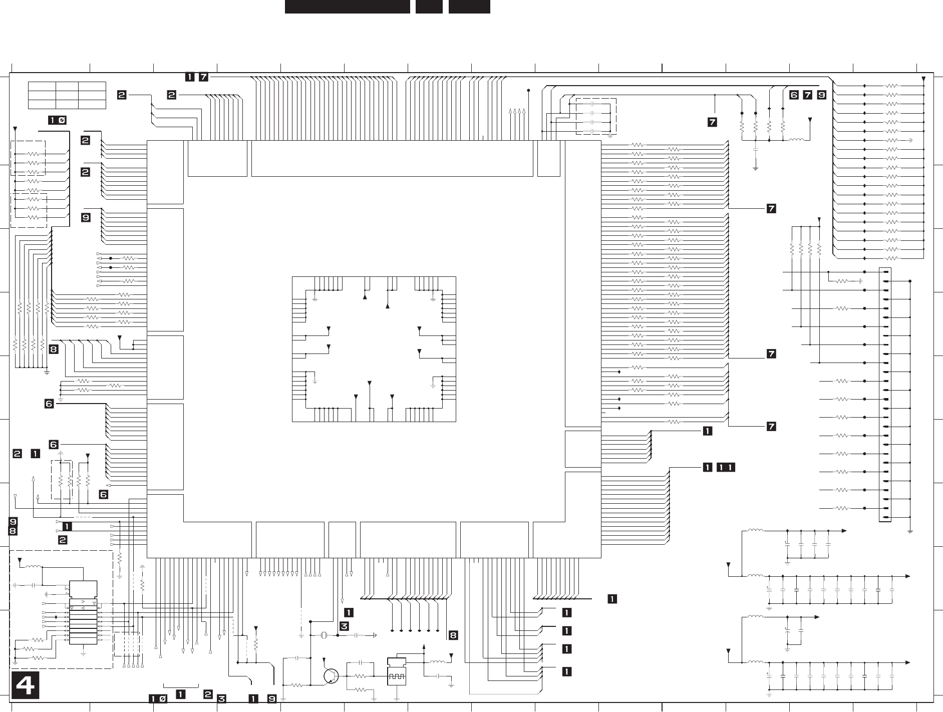
EN 146
3139 785 31532 7.
Circuit Diagrams and PWB Layouts
Digital: Chrysalis
I2C
NI 4931ECAFRETNI OEDIV LATIGIDOEDIV GOLANA
N
A
C
S GORP
PIOS TEST GENERAL DIGITAL AUDIO INTERFACE UARTS
1-EBEDI MARDS
PCI/XIO1394 OUT
G3
1
2
3EN2
3EN1
not used
desu ton
11 12 13 14
A
B
C
D
E
F
G
H
I
A
B
C
D
E
F
G
H
I
1400 C14
ylno 3C rof
32 MB
1 234567891011121314
1 2345678910
UART0: DEBUG / SERVICE
1401 I5
2400 A9
2401 A9
2402 A9
2403 A12
2404 H12
2405 G13
2406 G13
2407 G13
2408 H12
2409 H12
2410 H13
2411 H13
2412 H13
2413 H13
2414 H13
2415 H14
2416 H14
2417 H14
2418 I12
2419 I13
2420 I12
2421 I12
2422 I13
2423 I13
2424 I13
2425 I13
2426 I13
2427 I14
64 MB
y
l
no
4
002 rof
2428 I14
2429 I14
2430 I5
2431 I6
2432 H1
2433 I7
2434 I6
2435 A9
3400 A14
3401 A14
3402 A14
3403 A14
3404 A14
3405 A12
3406 A12
3407 A12
3408 A12
3409 A14
3410 A14
3411 A14
3412 A14
3413 B14
3414 B14
3415 B14
3416 B14
not used
3417 B14
3418 B14
3419 B14
3420 C14
3421 C14
3422 C14
3423 C14
3424 C13
3425 C13
3426 C13
3427 C13
3428 C13
3429 D13
3430 E13
3431 E13
3432 E13
3433 E1
3434 E2
3435 E1
3436 F13
3437 F13
3438 F13
3439 G13
UART1: DEV ONLY
3440 G13
3441 F1
3442 D2
3443 D1
3444 D2
3445 D1
3446 D2
3447 D1
3448 D2
3449 D1
3450 C2
3451 C2
3452 F1
3453 A10
3454 A11
3455 A10
3456 A11
3457 A10
3458 B11
3459 B10
3460 B11
3461 B10
3462 B11
3463 B10
3464 B11
3465 B10
3466 B11
3467 B10
3468 B10
3469 B11
3470 B10
3471 C11
3472 C10
3473 C11
3474 C10
3475 C11
3476 C10
3477 C11
3478 C10
3479 C11
3480 C10
3481 C11
3482 C10
3483 C11
3484 C10
3485 D11
3486 D10
3487 D11
3488 D10
X
d
e
su ton
de
su t
on
3489 D11
3490 D10
3491 D11
3492 D10
3493 D11
3494 D10
3495 D11
3496 D10
3497 I4
3498 F1
3499 F1
3603 C2
3820 D1
3821 D1
3822 D1
3823 D1
3824 D1
3825 D1
3826 D1
3827 D1
3828 A1
*
*
SDRAM
not used
3829 A1
3830 B1
3831 B1
3832 B1
3833 B1
3834 B1
3835 B1
3836 D11
3837 I1
3838 I1
3839 I1
3840 D10
3850 H2
3851 H2
3852 E11
3853 E10
3854 E11
3855 E10
3856 E11
-
*
3857 E10
3858 E11
3859 E11
3860 F11
3861 I6
3862 I5
3863 I6
4401 I5
4402 I4
4403 I4
4404 H2
4405 G1
4406 I2
4407 I2
4408 I2
4409 I2
4410 I2
not used
4411 H3
5400 A13
5401 G12
5402 H12
5403 H1
5404 I7
5405 I12
5406 I12
7400 A2
7401 H1
7402 I6
7403 I5
F1401 C14
F1402 C14
F1403 C14
F1405 D14
F1407 D14
F1409 D14
UART2: DTTM
X
de
su
ton
UART3: G-LINK
F1411 E14
F1413 E14
F1415 E14
F1417 E14
F1419 F14
F1421 F14
F1423 F14
F1425 G14
F1427 G14
F400 A12
F401 A12
F402 A8
F403 C2
F404 C2
F405 I5
F406 I5
)ylno snoisrev wen rof( mm 72.1 hctip GATJE
I402 I1
I403 I4
I404 E10
I405 E10
I406 E10
I407 I6
I408 I6
I409 I6
I410 I7
I411 I7
I412 I7
I413 A12
I414 G12
I415 H12
I416 I12
I417 I12
I418 A14
I419 A14
I420 A14
I421 A14
I422 A14
I423 A14
3831
-
1%
I424 A14
I425 A14
I426 A14
I427 A14
I428 B14
I429 B14
I430 B14
I431 B14
I432 B14
I433 B14
not used
not used
I434 B14
I435 C14
I436 C14
I437 C14
I438 A12
I439 A12
VDD_PNX_PLL
not used
3823
de
s
u
t
on
not used
15R3434
VDD_PNX_PAD
10K
3424
n001
71
4
2
u0
1
22R
8
142
3836
4K7
3403
3470 22R
VDD_PNX_PAD
3852 22R
22R3472
22R3858
3857 22R
3449 22R
2543
K01
4K7
3830
K0
1144
3
4044
33R
3429
6044
3490 22R
n001
8
2
42
+3V3
7
K
4
0
283
70
4
2
n001
I426
4K7
3418
10R3450
7K41283
BLM31
5401
n0
0
1
3242
3K
3
7
043
11
42
n001
22R3859
804
2
u
01
3
K3
5
04
3
22R3459
3448
4K7
3833
22R
10R3451
+3V3
n001
3042
F1402
904I
100p2435
BLMP18P
5404
I404
304
4
3862
330R
VDD_PNX_CORE
33p
2434
VDD_PNX_PAD
I434
3439
33R
1044
3834 4K7
4K7
3411
+3V3
3476 22R
2431
15p
3438
33R
2402 100p
704I
014I
214I
7
242
n001
n0
0
1
5
242
F1427
114I
15p
2430
7
K472
8
3
22R3483
33R
3437
F1409
I432
I419
6
2
43K01
22R3442
22R3446
7403
23
24
25
26
27
28
3
4
5
6
7
8
9
BC847BW
1
10
11
12
13
14
15
16
17
18
19
2
20
21
22
4K7
1400
STL21
VDD_PNX_PAD
3409
22R3474
n
0
01
4142
4405
F1405
3420 4K7
3401 4K7
I415
I417
4K7
8
94
3K
01
3413
I416
BLM31
5406
I403
I430
22R3456
22R
3421 4K7
3477
+1V8
u
01
4042
3417 4K7
22R3471
I421
22R3444
3412 4K7
I428
VDD_PNX_ANA
6242
n001
22R3485
994
3
K01
3419 4K7
22R3464
934I
3460 22R
VDD_PNX_PLL
3484 22R
6142
n001
82
4
3
K
0
1
VDD_PNX_CORE
3496
F1421
22R
3436
33R
I424
F1401
22R3454
VDD_PNX_PAD
3861
1K2
F1423
3478 22R
33R
3432
4K7
3423
8044
2433
100n
I436
02A
K
C
A
-O
I
X9
1
D
0L
E
S-OIX 8B
1
L
E
S
-OIX 8C
2LE
S
-OIX 9
D
NI-LAT
X
9FA
TUO-LATX
01FA
Y-CVBS
N1
F1415
21CA
4PD
DV 31
C
A
VDDP5
P23 VDDP6
N23 VDDP7
M23
8PD
D
V
21D
9PDDV
11D
VREF
M1
VS-IN
F3
VS-OUT
T2
WE0 H25
WE1 J24
TUO-210SW
61
DA
41EA TUO-3SW
NI-ESW
11EA
NI-
K
S
W
21DA
52A
-
OI
X
9
DA
0
D
X
T
71DA
1D
X
T
71FA
2DXT
81DA
3DXT
91D
A
VDDC1 P4
VDDC2 R4
3C
D
DV 41CA
4C
D
DV 51CA
VDDC5
T23 VDDC6
R23
7CDDV
51D
8CDDV
41
D
9CD
D
V
31D
VDDP1 M4
VDDP2 N4
3P
DD
V
E25
SDRAM-DATA30 T26
SDRAM-DATA31 T24
SDRAM-DATA4 F23
SDRAM-DATA5 F25
SDRAM-DATA6 G23
SDRAM-DATA7 G25
SDRAM-DATA8 G26
SDRAM-DATA9 G24
TU
O-FI
DPS
61E
A
NI-
1FI
DP
S
31FA
NI-2FID
PS
31EA
NTES
E
R-S
YS
01
D
A
KCT
8DA
IDT
9C
A
SMT
8EA
TSRT
C26
SDRAM-DATA16 T25
SDRAM-DATA17 U23
SDRAM-DATA18 U25
SDRAM-DATA19 V23
SDRAM-DATA2 D26
SDRAM-DATA20 V25
SDRAM-DATA21 W23
SDRAM-DATA22 W25
SDRAM-DATA23 Y26
SDRAM-DATA24 W26
SDRAM-DATA25 W24
SDRAM-DATA26 V26
SDRAM-DATA27 V24
SDRAM-DATA28 U26
SDRAM-DATA29 U24
SDRAM-DATA3
M25
SDRAM-ADDR2 R24
SDRAM-ADDR3 P26
SDRAM-ADDR4 P24
SDRAM-ADDR5 N25
SDRAM-ADDR6 M26
SDRAM-ADDR7 M24
SDRAM-ADDR8 L25
SDRAM-ADDR9 L23
SDRAM-DATA0 C25
SDRAM-DATA1 D24
SDRAM-DATA10 F26
SDRAM-DATA11 F24
SDRAM-DATA12 E26
SDRAM-DATA13 E24
SDRAM-DATA14 D25
SDRAM-DATA15
6
2
B
TUO-
0
DS
61FA
TUO-1DS
5
1
DA
T
U
O-2D
S
51EA
TUO-3DS
4
1FA
0ADS 5
2A
1ADS 52B
NI-
EDS
11FA
NI-K
D
S
21EA
SDRAM-ADDR0 N26
SDRAM-ADDR1 P25
SDRAM-ADDR10 N24
SDRAM-ADDR11 L24
SDRAM-ADDR12 K23
SDRAM-ADDR13 L26
SDRAM-ADDR14
RAS0 J23
RAS1 J26
NTESER
9EA
RP K24
RSET
M2
2STR
81FA
3STR
91F
A
0DXR
71CA
1DXR
71EA
2D
XR
81CA
3DX
R
91
CA
TUO-
2
10KCS
61
CA
TUO-3KCS
41DA
NI-EKCS
11DA
0LCS 62
A
1LCS
PROGC-OUT1
J2
PROGC-OUT2
J1
PROGC-OUT3
H4
PROGC-OUT4
H3
PROGC-OUT5
H2
PROGC-OUT6
H1
PROGC-OUT7
G1
PROGY-OUT0
J4
PROGY-OUT1
K1
PROGY-OUT2
K2
PROGY-OUT3
K3
PROGY-OUT4
K4
PROGY-OUT5
L1
PROGY-OUT6
L2
PROGY-OUT7
L3
R-CVBS
P3
1F
A
82
O
IP
2FA
92
O
IP
3FA
PIO3
W4
03OIP
4F
A
13OIP
5FA
PIO4
Y1
PIO5
Y2
PIO6
Y3
PIO7
Y4
PIO8
AA1
PIO9
AA2
TUO-LLP
01EA
4
2OI
O
P
3E
A
PROG-OUT-CLK
L4
PROGC-OUT0
J3
21OIP
1BA
31OIP
2B
A
41OIP
3
B
A
5
1OIP
1
CA
61OIP
2C
A
71
OI
P
3CA
8
1OIP
1DA
9
1
OI
P
2DA
PIO2
W3
02OIP
3DA
12
OI
P
4D
A
22OIP
1EA
3
2OIP
2E
A
52OIP
4EA
6
2O
I
P
5EA
7
2
OIP
Q
E
R
-
ICP 32A
AQER-ICP 32B
B
QER-ICP 32C
RRES-IC
P41C
POTS-
ICP 5
1
A
Y
D
RT-ICP 5
1C
0
-
0T
SCP
8CA
1-0TS
CP
7FA
2-0TSCP
7EA
0
-
1T
SCP
6
E
A
1-1TSCP
6DA
2-1TSCP
5D
A
PIO0
W1
PIO1
W2
PIO10
AA3
11OIP
4
A
A
1
1
C
0EBC-ICP 11A
1
EBC-I
C
P4
1
A
2EBC-ICP 71A
3EBC-ICP 91C
K
L
C-I
C
P42A
L
E
SVE
D
-
I
C
P61A
EMARF-ICP 61B
TNG-IC
P2
2
A
A
TNG-IC
P42B
BTNG-ICP 4
2C
LESDI-ICP 81D
ATNI-ICP 22C
YDRI-ICP 61C
RAP-ICP 4
1
B
RREP-IC
P51B
81B
32DA-ICP 91
A
42DA-ICP 91B
52DA-ICP 02C
62DA-ICP 02B
72
D
A-ICP 12A
82DA-ICP 02D
92DA-ICP 12C
3DA-ICP 9C
03DA-ICP 12B
13
D
A-ICP 22B
4DA-ICP 01A
5DA-I
CP 01B
6D
A
-IC
P01C
7DA-ICP 0
1
D
8DA-ICP 11B
9DA-ICP
5B
0
DA-
I
CP 8A
1DA-ICP 9A
01DA-ICP 21
A
11DA-ICP 2
1
B
21DA-ICP 21C
31
DA-I
C
P31A
41DA-I
C
P31B
51D
A-I
CP 31C
6
1DA-IC
P61D
7
1
DA-I
C
P71C
81DA-ICP 71B
91DA-ICP 81A
2DA-ICP 9B
02
DA-IC
P71D
12DA-I
C
P81
C
22D
A-I
CP
A4
L-D6
B4
L-D7
C4
L-FSYNC
B1 L-SYNC
A2 L-VAL
C1
KLC-XM 5A
0D-
X
M6A
1
D-X
M6B
2D-XM 6C
3
D-
X
M7A
4D-XM 7B
5D-XM 7C
6
D-
X
M7
D
7D-XM 8
D
CNY
S-XM 5
C
LAV-XM
ITU-OUT-CLK
T4
ITU-OUT0
V1
ITU-OUT1
V2
ITU-OUT2
V3
ITU-OUT3
V4
ITU-OUT4
U1
ITU-OUT5
U2
ITU-OUT6
U3
ITU-OUT7
U4
L-CLK
A1
L-D0
B2
L-D1
C2
L-D2
A3
L-D3
B3
L-D4
C3
L-D5
52BA Q
RAMD
-EDI
52FA
Y
DR
OI-
EDI
5
2
C
A
IDUMP0
N2
IDUMP1
R1
ITU-IN-CLK
G2 ITU-IN-FID
G4
ITU-IN-VAL
G3
ITU-IN0
D3
ITU-IN1
D2
ITU-IN2
E2
ITU-IN3
D1
ITU-IN4
E3
ITU-IN5
E1
ITU-IN6
F4
ITU-IN7
F1
AF22
IDE-DD11 AD22
IDE-DD12 AE23
IDE-DD13 AF24
IDE-DD14 AD24
IDE-DD15 AB24
IDE-DD2 AD23
IDE-DD3 AF23
IDE-DD4 AE22
IDE-DD5 AD21
IDE-DD6 AF21
IDE-DD7 AF20
IDE-DD8 AE20
IDE-DD9 AE21
R
O
ID-EDI
52D
A
WOID-EDI
52EA
KCAMD-EDI
GND6 N12
GND7 P11
GND8 P12
GND9 R11
M
LA
P
-K
CT
|
D
NG
7CA
HS-IN
F2
HS-OUT
T3
HSCKB K26
0SC-E
DI
62CA 1S
C
-EDI
62B
A0
AD-E
D
I
62EA 1AD-EDI
6
2FA 2A
D
-E
D
I
6
2DA
IDE-DD0 AC24
IDE-DD1 AE24
IDE-DD10
GND39
D23
GND4 M11
04DNG
22D
1
4
DNG
12D
2
4D
N
G
41N
3
4
DNG
41M
4
4
DNG
51L
54DNG
41L
6
4
DNG
31N
7
4
DNG
31M
84DNG
21M
94D
N
G
31L
GND5 N11
05DNG
21L
1
5
DNG
6D
25DNG
5D
42DN
G5
1T
52DNG 12C
A
62DNG 22C
A
GND27
AC23 GND28
AB23 GND29
T16
GND3 L11
GND30
R16 GND31
P16 GND32
P15
GND33
N16 GND34
N15 GND35
M16 GND36
M15 GND37
L16 GND38
E23
GND1 D4
GND10 R12
GND11 T11
GND12 AB4
GND13 AC4
41DNG 5C
A
51DNG 6C
A
61DNG 31P
71
D
NG 31R
81DNG 2
1T
91DNG 31T
GND2 E4
02DNG 41P
12
D
NG 41R
22DNG 51
R
32DNG 41T
2STC
81E
A
3STC
91EA
CVBS
P2
3
D
CD
02CA
DQM0 H23
DQM1 H24
DQM2 R26
DQM3 R25
KLC-USD
7DA
0CPT-USD
8FA
1CPT-U
S
D
6F
A
3RTD
02DA
TUO-210KLCSF
51FA
TUO-3KLC
SF
31DA
NI-
EKLC
SF
21FA
G
R2
AVDD0
M3
AVDD1
P1
AVDD2
R3
KLC-SSVA 0
1
CA
B
T1
BE-BCLK AA23
BE-DATI AA26
BE-DATO Y25
BE-FLAG AA24
BE-SYNC AA25
BE-V4 Y23
BE-WCLK Y24
C-CVBS
N3 CAS0 H26
CAS1 J25
CKE K25
PNX7100EH/G/C3
7400
KLC-DDVA 11CA
4K7
3410
22R3480
22R
I414
3463
3855 22R
I435
I405
20
44
3468 22R
1K23433
3422 4K7
3443 22R
n001
2
24
2
3839
10K
33R
3431
100n
2432
CHRYSALIS
22R3462
3435 15R
3453 22R
7
K42283
3445 22R
4K7
3400
7K46283
9
0
44
7044
3415 4K7
33R
3440
3491 22R F1407
K001
7943
22R
I402
3481 22R
3492
3473 22R
F402
I437
n001
514
2
3414 4K7
I423
3829 4K7
4M0
2
1
4
3
FXO-34FL
7402
K0
1
1583
F1417
3854 22R
3465
3837
10K
22R
1
2
42
n
0
01
3466 22R
4K7
3828
22R3856
3832 4K7
0144
3447 22R
3458 22R
3K3
6043
F403
4242
n
00
1
4K7
3831
I406
VDD_PNX_CORE
22R3493
834I
22R3469
F401
3489 22R
2401 100p
804I
F406
I422
22R3479
3455 22R
VDD_PNX_CORE
BLM31
5405
VDD_PNX_ANA
4K7
01
42
n001
3416
1144
1401
4M
HC-49/S
n0
01
604
2
I418
n0
01
2142
5243K01
10K
3838
n0
0
1
9042
22R3488
3860 33R
3486 22R
22R3457
22R3467
80
4
3
3
K
3
3461 22R
72
43K
01
100p2400
F404
3853 22R
n001
9
142
VDD_PNX_CORE
F1425
10
19
20
I431
8
9
18
17
16
15
14
13
12
11
1
74LVC245APW
7401
2
3
4
5
6
7
22R3494
+3V3
3835 4K7
9
2
42
n001
7
K45283
3482 22R
3495
7K4
42
83
22R
0583
K01
22R3487
+3V3
I429
I433
BLMP18P
5400
n001
50
42
F1413
3475 22R
5402
F1403
BLM31
3840
F1411
22R
33R3603
u0
1
0242
3402 4K7
I420
I427
7
K
432
8
3
F1419
3430
33R
F400
VDD_PNX_PAD
3142
n001
4K7
I413
F405
3404
VDD_PNX_PAD
I425
3863
4K7
5403
VDD_PNX_PAD
BLM18P
PNX7100_ITU_OUT_CLK
IDE1_DD(15:0)
CbCr(0:7)
n
EO_
E
KLCSF_
C
DA_52OI
P
M
QRI_2E
D
I_4OIPM
T
U
O
_
3SW
T
U
O_3K
C
S
TUO_3KL
C
SF
TUO_2DS
T
UO_1
D
S
TUO_3DS
+3V3_7402
RTS1
UART1
MX_D_CTL
nE_1EDI_22OIPM
Y(0:7)
SDRAM_DATA(7)
SDRAM_DATA(5)
SDRAM_DATA(3)
SDRAM_DATA(1)
SDRAM_ADDR(13)
SDRAM_ADDR(11)
SDRAM_ADDR(9)
SDRAM_ADDR(7)
SDRAM_ADDR(5)
SDRAM_ADDR(3)
0STC
1STC
Q
RI_
1E
DI
nE_MORPEE_91OIPM
RAS(0)
DQM(2)
DQM(0)
SDRAM_DATA(31)
SDRAM_DATA(29)
SDRAM_DATA(27)
SDRAM_DATA(25)
SDRAM_DATA(23)
SDRAM_DATA(21)
SDRAM_DATA(19)
SDRAM_DATA(17)
SDRAM_DATA(15)
SDRAM_DATA(13)
SDRAM_DATA(11)
SDRAM_DATA(9)
PNX7100_VS_OUT
Y(0)
Y(1)
Y(2)
Y(3)
Y(4)
Y(5)
Y(6)
4OIP
M
ITU_OUT(2)
)7(T
U
O_UTI
)5(T
U
O_UTI
ITU_OUT(1)
)4(T
U
O_UTI
ITU_OUT(3)
ITU_OUT(0)
ITU_OUT(1)
ITU_OUT(2)
ITU_OUT(3)
ITU_OUT(4)
ITU_OUT(5)
ITU_OUT(6)
ITU_OUT(7)
ITU_OUT(7:0)
PNX7100_HS_OUT
)
1
(0TSCP_0017XNP
)2(0TSCP_0017XNP
)0(1TSCP_0017XNP
)
2
(
1TSCP_0017XN
P
K
CT_0
017
XN
P
IDT_00
17
XNP
S
MT
_0017XNP
)1(1
TSCP_
0
017
X
NP
T
SRT
_0
0
17
X
NP
nTESER_S
YS
_0017XNP
X
NP_N
I
_E
KLC
S
F
TUO_LLP
+3V3_7402
TUO_LA
T
X_
0
017XNP
NI_
L
ATX_001
7
XN
P
P_CLK
IDE1_DD(7)
MPIO4_IDE2_IRQ
+3V3
TESER_ANA_13OIPM
K
L
C_U
S
D
_001
7
X
NP
0CPT_USD_ODT_0017XNP
1CPT_USD_0017XNP
)0(0TSC
P_
0017XNP
PCI_GNTB
n
Q
R
I
_A
NA_1
OI
PM
n
QRI_49
3
1
_
2OIPM
PCI_IRDY
PCI_PERR
PCI_SERR
PCI_STOP
PCI_GNT
PCI_INTA
PCI_REQ
PCI_REQA
PCI_GNTA
PCI_REQB
n
TESE
R
_2EDI_81OIPM
PNX7100_TCK
PCI_CBE(0)
PCI_PAR
PCI_TRDY
PCI_IDSEL
PCI_CBE(1)
PCI_CBE(2)
PCI_CBE(3)
PCI_DEVSEL
PCI_FRAME
n
T
ESER
_IMD
H_1
1
OIPM
SDRAM_CTRL
ITU_OUT(2)
ITU_OUT(1)
ITU_OUT(4)
ITU_OUT(3)
ITU_OUT(6)
ITU_OUT(5)
ITU_OUT(0)
ITU_OUT(7)
OIDUA_
L
A
T
IG
I
D
MPIO9_BOARD_ID_0
VIDEO_OUT
SDRAM_ADDR(0)
n
E
O_210KLCSWF_CDA_62
OI
PM
DEL_4931
_
32OIPM
NWO
D
REW
O
P_
49
3
1_1
2O
I
P
M
nTESER_PIV_02OIPM
NO_
D
H_
71
OIPM
nTESER_NACSG
ORP_61OIPM
n
T
E
SER_MTTD_51
O
IPM
n
TESER_4931EEEI_
41
OIPM
nTESER_1EDI_31OIPM
QRI_IMDH_21OIPM
SDRAM_DATA(20)
SDRAM_DATA(22)
SDRAM_DATA(24)
SDRAM_DATA(30)
IIC1
0LCS
1
A
DS
1LCS
0A
D
S
SDRAM_ADDR(10)
SDRAM_ADDR(14:0)
SDRAM_ADDR(8)
SDRAM_ADDR(6)
SDRAM_ADDR(4)
SDRAM_ADDR(2)
SDRAM_ADDR(1)
MPIO5_VIP_ERROR
RXD1
TXD1
CAS(0)
DQM(1)
DQM(3)
WE(0)
CKE
HSCKB
SDRAM_ADDR(12)
SDRAM_ADDR(14)
SDRAM_DATA(6)
SDRAM_DATA(8)
SDRAM_DATA(10)
NI_XAOC_FIDPS
N
I
_TPO_FIDPS
TUO_FIDPS
T
U
O_21
0
SW
TU
O_2
1
0KC
S
TUO_210KLCSF
TUO
_3
DS
TUO_2DS
T
U
O_1D
S
TUO
_0
DS
TU
O_3
SW
TUO_3KC
S
TUO_3KL
CSF
NI_EDS
NI_
E
SW
NI_EKCS
MPIO19_EEPROM_En
52A_OIX
2L
ES
_
OI
X
KCA_OIX
1
L
ES
_
OIX
0LES_OIX
RAP_ICP
)42(DA_ICP
)52(DA_ICP
)62(DA_ICP
)7
2(D
A_IC
P
)82(DA_I
C
P
)92(
DA
_I
C
P
)03(D
A
_I
C
P
)13(DA_ICP
PCI_AD(31:0)
RTS0
CTS1
IDE1_IRQ
CTS0
)9(DA_ICP
)01(DA
_
ICP
)1
1
(DA_ICP
)21(DA_ICP
)
31(D
A_
ICP
)
4
1
(DA
_
ICP
)
5
1
(
DA_IC
P
)6
1
(D
A_
I
C
P
)
7
1
(
DA_
ICP
)
8
1
(
DA_IC
P
)
9
1
(D
A_
I
C
P
)02(DA_ICP
)
1
2(DA_ICP
)2
2
(DA_ICP
)32(DA
_
ICP
)4(D_XM
)5(D_XM
)
6(
D
_
XM
)7(D_XM
MX_D(7:0)
)
0
(DA_ICP
)1(DA_ICP
)2(DA
_
ICP
)3(DA_ICP
)4(DA_ICP
)5(D
A_
ICP
)
6
(
D
A_
I
CP
)
7
(DA_ICP
)8
(
D
A_
I
CP
L_D(1)
L_D(2)
L_D(3)
L_D(4)
L_D(5)
L_D(6)
L_D(7)
L_D(7:0)
)0(D_XM
)
1(
D_XM
)2(D_XM
)3(D_
X
M
CbCr(2)
CbCr(3)
CbCr(4)
CbCr(5)
CbCr(6)
CbCr(7)
Y(7)
ITU_OUT(0)
)6(TUO_UTI
ITU_IN(0)
ITU_IN(1)
ITU_IN(2)
ITU_IN(3)
ITU_IN(4)
ITU_IN(5)
ITU_IN(6)
ITU_IN(7)
ITU_IN(7:0)
L_D(0)
IDE1_DD(5)
IDE1_DD(4)
IDE1_DD(3)
IDE1_DD(2)
IDE1_DD(1)
IDE1_DD(0)
SDRAM_DATA(28)
SDRAM_DATA(26)
SDRAM_DATA(18)
SDRAM_DATA(16)
SDRAM_DATA(14)
SDRAM_DATA(12)
SDRAM_DATA(4)
SDRAM_DATA(2)
SDRAM_DATA(0)
SDRAM_DATA(31:0)
CbCr(0)
CbCr(1)
POTS_ICP
RRES_ICP
R
R
E
P
_IC
P
Y
D
RI_I
C
P
YDRT_ICP
E
M
A
RF_I
CP
LES
VE
D_I
CP
)3(EBC_ICP
)2(EBC_ICP
)
1
(
EBC_ICP
)0(EBC_ICP
PCI_CON
IDE1_DD(15)
IDE1_DD(14)
IDE1_DD(13)
IDE1_DD(12)
IDE1_DD(11)
IDE1_DD(10)
IDE1_DD(9)
IDE1_DD(8)
IDE1_DD(6)
BE_WCLK
BE_V4
BE_SYNC
BE_FLAG
BE_DATA_WR
BE_DATA_RD
BE_BCLK
BE_DATA
0LCS
0A
D
S
IIC0
1ADS
1LC
S
BTNG_ICP
BQER_ICP
ATNG_ICP
A
Q
E
R
_
I
C
P
Q
ER
_I
C
P
AT
NI_
IC
P
TNG_ICP
0AD_1E
D
I
n1SC_
1
E
D
I
n
0
SC_1EDI
IDE_CTL
RXD0
TXD0
CTS2
RTS2
RXD2
TXD2
CTS3
TXD3
RXD3
RTS3
T
U
O_C
T
U
O_
Y
TUO
_
R
TUO_B
TUO_G
UART0
LESDI_ICP
1AD
_
1E
DI
2A
D
_1
E
D
I
nW
OID_1EDI
n
R
OID
_
1EDI
YDR
O
I
_
1
E
DI
nKCAMD
_
1EDI
QRAMD_1EDI
L_FSYNC
L_SYNC
L_VAL
L_CLK
L_D_CTL
MX_VAL
MX_SYNC
MX_CLK
T
U
O_S
B
VC
MPIO6_BE_DLOAD
MPIO10_BOARD_ID_1
PNX7100_ITU_IN_VAL
PNX7100_ITU_IN_FID
PNX7100_ITU_IN_CLK
PNX7100_HS_IN
EJTAG_RESETn
PNX7100_TRST
PNX7100_VS_IN
nTESER_
0
017XNP
MPIO8_1394_CNA
MPIO7_MUTE_LVn
PNX7100_PCST1(2)
PNX7100_PCST1(1)
PNX7100_PCST1(0)
PNX7100_DSU_TPC1
PNX7100_DSU_CLK
PNX7100_PCST0(2)
PNX7100_PCST0(1)
PNX7100_PCST0(0)
PNX7100_TDO_DSU_TPC0
PNX7100_TMS
PNX7100_TDI
3103_603_30601_a2_sh130_sh4.pdf 2004-12-01
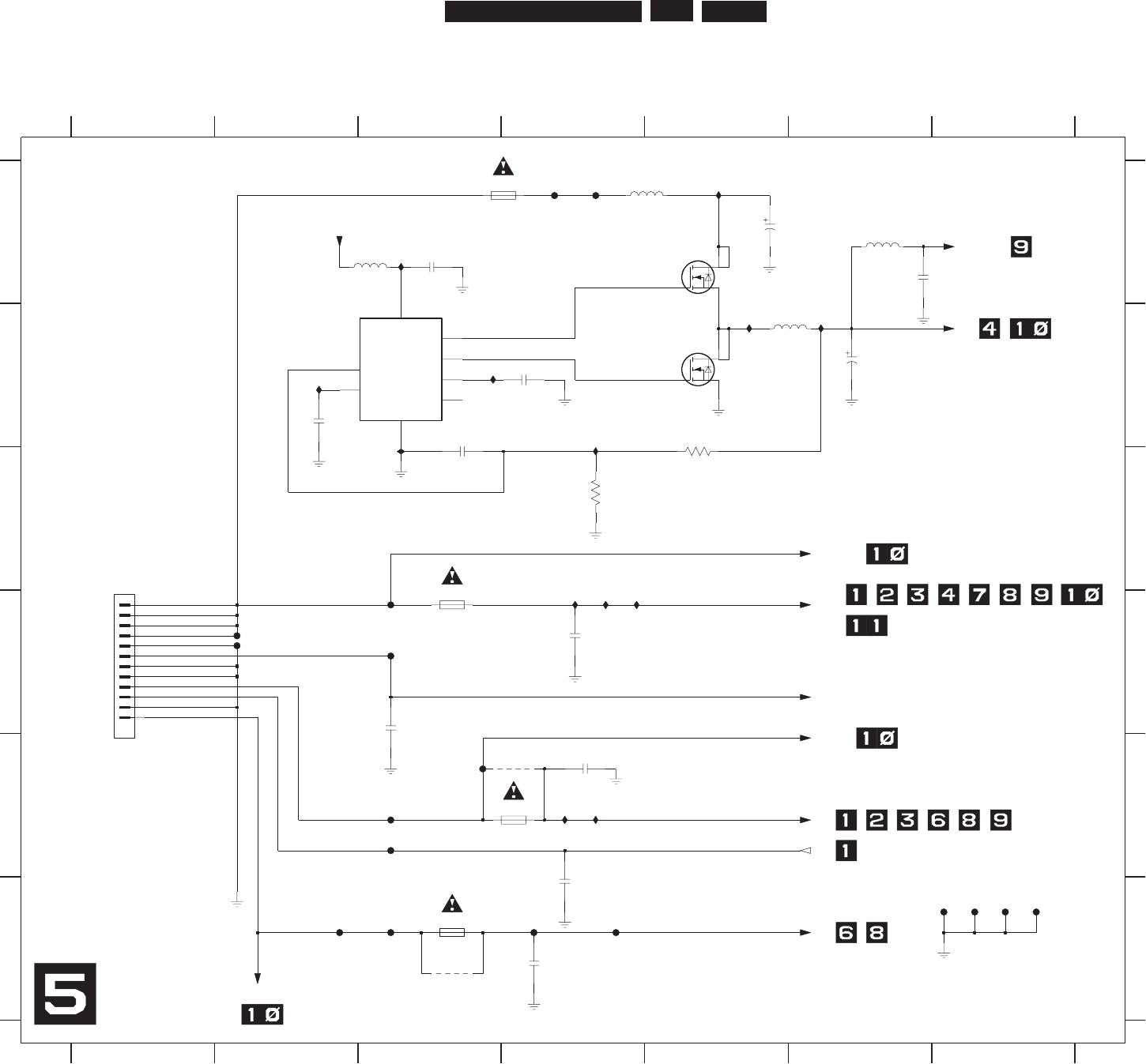
EN 147
3139 785 31532 7.
Circuit Diagrams and PWB Layouts
Digital: Power Supply
GATE-H
PWRGD
VFB
CCV
COMP
GATE-L
PGDELAY
DNG
B
C
D
E
F
A
B
C
D
E
F
1500 D1
1501 F7
1502 F7
1503 F7
1234567
1234567
A
1504 F7
1505 D3
1506 A4
1507 E4
1509 F3
2512 A5
2514 A3
2515 B2
2516 B6
2517 A6
2518 B3
2519 D4
2521 D3
2524 E4
2525 F4
2526 F4
2527 B4
3503 C4
3504 B5
4500 E4
4501 F3
5501 A5
5502 A3
5503 B6
5504 A6
7500-1 A5
7500-2 B5
7501 B3
F1501 D3
F1502 D2
F1505 D2
F1506 D3
F1509 E3
F1510 E3
F1512 F4
not used
F1513 F2
F1514 F4
F1515 F3
F500 A4
F501 A4
F502 E3
I500 B2
I501 C3
I502 A3
I503 B3
I504 B4
I505 A5
I506 B5
I507 B6
I508 D4
not used I509 D4
I510 D4
I511 E4
I512 E4
n
001
5
252
I504
F1501
105I
6152
u001
V3
.6
I511
1501
I509
5501
BLM31
F1A
1507
I503
F501
1509
500mA F
STS5DNF20V
7500-1
78
2
1
F1506
I508
5502
BLMP18P
I510
625
2
n00
1
4501
10
11
12
2
3
4
5
6
7
8
9
B12B-PH-SM4-TBT(LF)
1500
1
F1502
n001
71
52
1503
V
3
.6
u001
21
5
2
n001
9152
BLM18P
5504
1502
I506 I507
2518
100p
4
5
6
8
3
2
1
7
7501
NCP1571D
100n
2514
1%1K5
3504
F1515
n001
1
252
I505
1505
1A F
3053
5
K
1%1
10u
5503
SLF10145
I512
1504
4500
7500-2
STS5DNF20V 56
4
3
I502
I500
F1510
F1514
F1509
F1513
F502
100n
2524
Power Supply
F1505
F1A
1506 F500
10n
2527
F1512
n0
7
4
5152
ION
+12V
1V8_VIP
3V3_HDMI
+5V_HDMI
+1V8
+3V3
-5V
+12V
+5V
-5V_HDMI
3103_603_30601_a3_sh130_sh5.pdf 2004-12-01
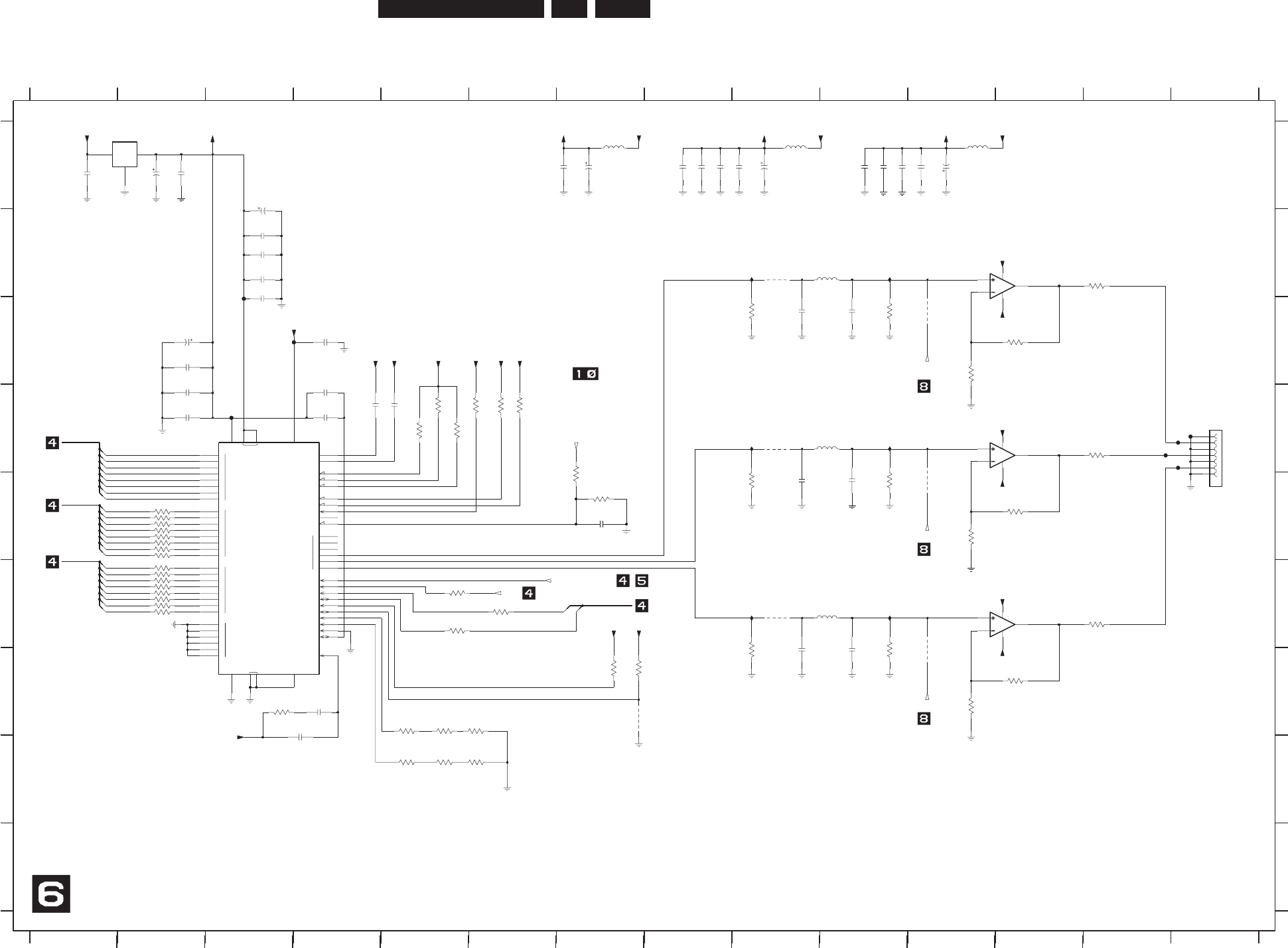
EN 148
3139 785 31532 7.Circuit Diagrams and PWB Layouts
Digital: Prog Scan DAC
TEST
DAC
GND_IO
DGND
6
VREF
3
4
5
2
3
RSET1
ALSB
I2C
SDA
6
7
5
VAA
SCLK
CLKIN_B
4
5
6
7
0
1
2
3
4
5
CLKIN_A
F
4
EXT_LF
E
D
C
B
A
RESET
P_BLANK
P_VSYNC
P_HSYNC
S_BLANK
2
3
0
1
7
0
1
S
C
Y
S_VSYNC
S_HSYNC
COMP2
COMP1
AGND
0
2
1
RSET2
RTC_SCR_TR
VDD VDD_IO
COM
OUTIN
I
GND
GND
GND
%1
desu to
n
B
C
D
E
F
G
H
I
1002 D14
2024 A8
1234567891011121314
123456789101112
13 14
A
B
C
D
E
F
G
H
I
A
GND
2600 A7
2601 A7
2603 A9
2604 A9
2605 A1
2606 A2
2607 A10
2608 A11
2609 A11
2610 A3
2611 B3
2612 B3
2613 B3
2614 C9
2615 C10
2616 C2
2617 C4
2618 C2
2619 D2
2620 D4
2621 D4
2622 D5
2623 D2
2624 D4
2625 E7
2626 E9
2627 E10
2628 G9
2629 G10
2630 G4
%
1
desu ton
Y
DRAOB GOLANA OT
2631 G4
2632 A2
2633 A8
2634 A8
2635 A10
2636 A10
2637 B3
3035 C12
3037 B13
3601 C9
3602 C10
3604 C11
%
1
%1
3605 E7
3606 D5
3607 D6
3608 E7
3609 D5
3610 D5
3611 D13
3612 E9
3613 E10
3614 E12
3615 E11
3616 F13
3617 G9
3618 G10
PR
3619 F6
3620 G3
3621 F5
3622 G7
3623 G7
3624 F5
3625 G12
3626 G11
3627 G5
3628 G5
3629 G6
3630 H5
3631 H5
3632 H6
3633 D6
3634 D6
3635 E2
3636 E2
3637 E2
3638 E2
3639 E2
de
s
u to
n
%
1
3640 E2
3641 E2
3642 E2
3643 F2
3644 F2
3645 F2
3646 F2
3647 F2
3648 F2
3649 F2
3650 F2
4600 G7
4601 C11
4602 E11
4603 G11
5600 A7
5601 A9
5603 A11
d
esu
ton
GND
%
1
5604 B9
5605 B10
5606 D9
5607 D10
5608 F9
5609 F10
7600 A2
7601 B12
7602-1 D12
PB
7602-2 F12
7603 D3
F1601 D14
F1602 D14
F1604 D13
F1606 D14
F725 C3
F726 D3
F727 C3
I724 B9
I725 B10
I726 D9
I727 D10
I728 F9
I729 F10
V61u7
4
1062
3035
GND
1%1K0
GND
5603
4u7
n0
0
1
3062
R003
206
3
3619
7K4
100R
330R
3632
2263
10R
3628
1%
F1606
1%75R
3037
8
2
62
n001
8
062
5608
8p6
5063
0064
R22
527F
F726
3629
330R 1%
75R
3611
1%
D
NG
p33
7262
7601
3
4
1
5
2
AD8091ART
I725
10n
3631
10R
n001
2619
2262
7u4
406
2
7063
K01
GND
4u7
5601
1064
GND
3263
7
K
4
2K7
3630
1%
PROG SCAN DAC
4362
0n1
1n0
2620
536
2
0n
1
0
n1
6362
5606
8p6
6
2
62
GND
K01
3363
21
63
F1604
R003
1%
3616
75R
2618
1n0
2u2
5607
2K7 1%
3650 10R
3627
2
1
8
4
3648 10R
7602-1
AD8092AR
3
3625
1%1K0
GND
R003
3
16
3
F1602
3n9
2630
206430
6
4
40
63
%1
0
K1
n001
5062
I729
12
6
2
n0
0
1
2u2
5609
2624
100n
3639 10R
3638 10R
3637 10R
3636 10R
3635 10R
4363
K01
2637
100n
0
n
1
3362
3621
33R
420
2
I728
n0
0
1
%1
0
K1
626
3
F1601
V537u4
60
62
5
6
7
8
4
AD8092AR
7602-2
100n
2612
12
13
3624
100R
01
65
1
46
4
5
6
7
8
921
48
50
49
2
3
14
15
51
52
14
35
31
53
54
55
58
59
60
61
62
22
11
75
34
46
19
25
23
24
33
47
30
32
63
45
36
44
43
42
39
38
37
04
20
16
17
18
26
27
28
29
VIDEO
Φ
ADV7322KST
7603
ENCODER
1n0
GND
4
5
6
7
2625
PSCAN
07FMN-BMT-A-TFT
1002
1
2
3
10R
7062
n001
3649
3647 10R
4V220u
2610
2362
n
001
BLM21
5600
10R3645
3643 10R
3642 10R
3641 10R
3640 10R
16V47u
2616
1%1K0
3614
3620
680R
R003
7163
R
0
03
8
1
6
3
p
3
3
5
162
2613
10n
K01
9063
I726
R003
1063
10n
2611
p33
9
262
906
2
7u4
0062
n001
2623
100n
8p6
4162
GND
GND
3608
47K
2u2
5605
5604
3
7600
LF25CDT
2
1
72
7F
3646 10R
10n
2617
820p
2631
10R
I724
3644
GND
K0
1
0163
I727
%10K
1
5163
K01
6063
ITU_OUT(2)
ITU_OUT(3)
ITU_OUT(4)
ITU_OUT(5)
ITU_OUT(6)
ITU_OUT(7)
ITU_OUT(7:0)
+5V_PS
PNX7100_ITU_OUT_CLK
+2V5 +2V5
P_CLK
Y
_
D
i
U
iV
ITU_OUT(0)
CbCr(0)
CbCr(2)
CbCr(4)
CbCr(1)
CbCr(3)
CbCr(5)
SCL0
ITU_OUT(1)
+3V3
nNACSGORP_TESER
+5V
CbCr(7)
CbCr(0:7)
Y(4)
Y(0)
Y(2)
Y(6)
Y(1)
Y(3)
Y(5)
Y(7)
+3V3D_VDAC
+2V5
+2V5
+2V5
+3V3D_VDAC
+3V3D_VDAC+3V3D_VDAC
+2V5+2V5+2V5
CbCr(6)
Y(0:7)
-5V_PS
-5V_PS
-5V_PS
+3V3
SDA0
+5V_PS
+5V_PS
-5V
-5V_PS
+5V_PS
3103_603_30601_a2_sh130_sh6.pdf 2004-12-01
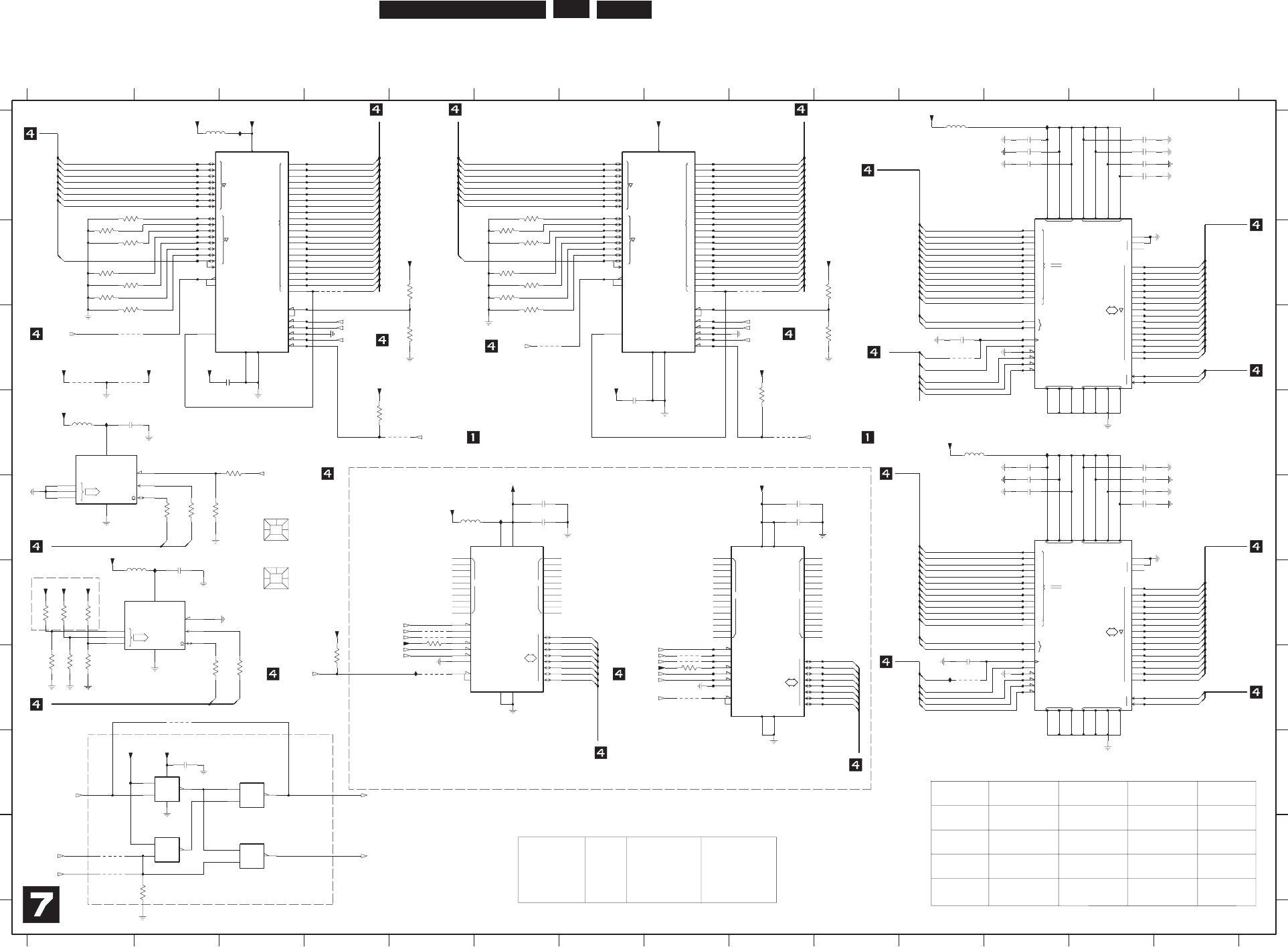
EN 149
3139 785 31532 7.
Circuit Diagrams and PWB Layouts
Digital: Flash, SDRAM, EEPROM
7
1
6
B
R
D
GND
ALE
NC NC
WP
WE
RE
5
CLE
3
4
8
2
CE
SCL
ADR
0
1
2SDA
WC
OE
3
2
1
0
13
2
1
14
WE
BYTE
5
15
16
4
RY
8
10
6
5
RES
15
7
A
21
17
20
11
WP
ACC
18
19
3
4
BY
A-1
6
CE
12
11
10
9
8
7
12
14
D
D
13
9
0
&
&
7
6
5
4
3
2
15
14
11
10
9
8
D
0
1
2
3
4
5
6
7
8
9
10
VSS
VDDQ
4M-1
DQM
VDD
VSSQ
0
A
BA
1
12
H
0
WE
L
NC
CAS
RAS
CS
CKE
CLK
11
1
0
13
12
&
OE
3
2
1
0
13
2
1
14
WE
BYTE
5
15
16
4
RY
8
10
6
5
RES
15
7
A
21
17
20
11
WP
ACC
18
19
3
4
BY
A-1
6
CE
12
11
10
9
8
7
12
14
D
D
13
9
0
7
1
6
BY
RY
D
GND
ALE
NC NC
WP
WE
RE
5
CLE
3
4
8
2
CE
SCL
ADR
0
1
2SDA
WC
&
0
9
OE
3
2
1
0
13
2
1
14
WE
BYTE
5
15
16
4
RY
8
10
6
5
RES
15
7
A
17
20
11
WP
ACC
18
19
3
4
BY
A-1
6
CE
12
11
10
9
8
7
12
14
D
D
13
NC
7
1
6
BY
RY
D
GND
ALE
NC NC
WP
WE
RE
5
CLE
3
4
8
2
CE
7
6
5
4
3
2
15
14
11
10
9
8
D
0
1
2
3
4
5
6
7
8
9
10
VSS
VDDQ
4M-1
DQM
VDD
VSSQ
0
A
BA
1
12
H
0
WE
L
NC
CAS
RAS
CS
CKE
CLK
11
1
0
13
12
CLK
11
1
0
13
12
9
8
7
9
10
VSS
VCCQ
2M-1
DQM
VCC
VSSQ
0
A
BA
1
6
U
0
WE
L
1
CAS
RAS
7
5
4
3
2
15
14
11
10
CS
2
CKE
NC
D
0
1
2
3
4
5
6
8
0
9
OE
3
2
1
0
13
2
1
14
WE
BYTE
5
15
16
4
RY
8
10
6
5
RES
15
7
A
17
20
11
WP
ACC
18
19
3
4
BY
A-1
6
CE
12
11
10
9
8
7
12
14
D
D
13
NC
CLK
11
1
0
13
12
9
8
7
9
10
VSS
VCCQ
2M-1
DQM
VCC
VSSQ
0
A
BA
1
6
U
0
WE
L
1
CAS
RAS
7
5
4
3
2
15
14
11
10
CS
2
CKE
NC
D
0
1
2
3
4
5
6
8
4 MB NORFLASH
0
not used
APPLICATION
*
not used
PCI_AD(23)
for BOARD with
H
I
0605 E3
0609 F3
2806 A12
2807 A13
2808 A12
2809 A13
2810 A12
2811 A13
2812 A13
0
d
es
u t
on
8 MB NORFLASH
1
1
1 234567891011121314
1
0
1
TRUTH TABLE - NORFLASH SELECTION
7801
DEVICE
DEVICE
4800
234567891011
7804, 7808
XIO_SEL_NORFLASH_L
SDRAM NAND FLASH
de
su
t
on
12 13 14
A
B
C
D
E
F
G
H
I
A
B
C
D
E
F
G
NOR FLASH
64 MB SDRAM
not used
2814 C11
2818 E6
2819 E6
2820 D12
2821 D13
2822 E12
2823 E13
2824 E12
2825 E13
2826 E13
2827 E9
2828 E9
2829 G11
2830 C3
CHRY BOOT
1
4800, 4801
7812, 7813
not used
2832 F2
2833 D1
2834 D7
2836 H2
3800 D3
3801 I2
3802 G8
3803 E2
3804 F5
3805 G2
3806 E2
3807 E2
3808 G4
3809 C1
3810 B1
for 16MB FLASH only
1
not used
not used
not used
desu ton
*
1
3811 B1
3812 B1
3813 B1
3814 B1
3815 A1
3816 C5
3817 B5
3818 C10
3819 B10
3841 A6
3842 B6
3843 B6
XIO_SEL_NORFLASH_H
1
7812, 7813
16 MB NORFLASH
not used
3844 B6
3845 B6
3846 B6
3847 C6
3848 D9
3849 D4
3864 F1
3865 G1
3866 F1
3867 G1
3868 F1
3869 G1
0
4800, 4801
0
7805, 7807
32 MB SDRAM
not used
64 MB SDRAM
3870 G3
4800 B4
4801 B9
4802 C1
4803 C1
4804 C1
4805 G8
4806 G8
4807 G8
4808 I1
4809 I1
4810 C11
4811 G11
4812 C6
4813 D5
4814 D9
1
7807
not used
4815 G2
4817 F5
4818 F5
4819 G5
5802 A11
5803 A2
5804 D11
5805 E5
5808 F2
5809 D1
0
not used
not used
1
delete for 16MB FLASH
not used
7801 A3
7802 E5
7803-1 H2
7803-2 I2
7803-3 H2
7803-4 I2
7804 A12
7805 A8
7806 E8
7807 A3
7808 E12
7809 F2
7810 D1
7811 A8
7812 A12
7813 E12
7814 E8
I800 F2
I801 D1
I802 A12
I803 E6
I804 D12
I805 G11
I806 G5
I807 A3
1
XIO_SEL_NORFLASH
4814
7K4
81
83
10p2829
R001
078
3
4800
2823 100n
I804
3814
10K
2819
100n
5808
BLMP18P
4815
100n
2830
100n
2828
4803
14
15
16
42
41
32
44
1
2
2
4
5
35
36
37
38
7
39
8
9
10
13
24
25
26
27
6
17
28
29
30
31
32
3
43
2
40
18
19
20
21
TC58V64AFTI
7802
8-BIT SERIAL
Φ
EEPROM
I800
10K
3811
2807 100n
R00
1
6083
2836
100n
I806
2746
37
13
1
9
AM29DL640G-70EI
7807
ROM
(4Mx16)
[FLASH]
VDD_NOR
7
K
4
80
83
10K
3842
4819
2806 100n
3841
10K
4812
1
2
3
6
5
84
7
(8Kx8)
Φ
EEPROM
M24C64-WMN6
7809
4810
I802
10K
3813
3802 4K7
7K4
7
1
83
100n2822
5
0
83
R001
2824 100n
10K
3809
4K73804
45
6
21
64
25
16
1
4
1
72
3
9
3
4
94
8
2
1
4
5
7
8
10
11
13
42
44
39
15
40
18
38
19
2
4
45
47
48
50
51
53
26
29
30
31
32
33
34
20
21
17
37
4M X 16 X 4
DRAM
Φ
MT48LC16M16A2P
7812
23
24
22
35
36
25
7
14
6
4804
74LVC00AD
7803-2
4
5
14
11
4808
74LVC00AD
7803-4
12
13
7
0605
SOFTWARE
10K
3815
100n2808
6
1
83
7K4
2
7
14
3
7803-1
74LVC00AD
1
5809
BLMP18P
BLMP18P
2810
5804
100n
K01
1
083
3810
10K
4813
100n2821
10K
3846
I805
3812
10K
K01
8483
4806
308
3
K22
2833
100n
I803
94
83
K01
0609
SOFTWARE
2811 100n
28
12
15
37
2746
11
14
41
43
45
33
35
38
40
42
44
30
32
18
8
7
47
26
29
31
34
36
39
48
17
16
9
23
10
13
22
21
20
19
ROM
25
24
6
5
4
3
2
1
AM29DL640G-70EI
7805
[FLASH]
(4Mx16)
4811
4818
5802
BLMP18P
2814 10p
FLASH, SDRAM, EEPROM
1
2
3
6
5
84
7
(8Kx8)
Φ
EEPROM
7810
M24C64-WMN6
8
7
2
1
73
3
1
6
3
18
19
45
46
47
48
3
4
5
10
11
14
15
26
27
28
33
2
34
35
38
39
40
41
42
43
44
1
20
21
22
23
24
25
17
9
16
6
29
30
31
32
TC58256AFTI
7814
EEPROM
Φ
8-BIT SERIAL
2812 100n
2809 100n
3847
10K
3843
10K
3845
10K
4807
4802
100n
2818
7083
R0
0
1
3800
14
8
2K2
7803-3
74LVC00AD
9
10
7
2834
100n
4809
16
100n
2832
3
9
34
94
8
2
14
4
5
6
21
6
4
25
13
42
44
39
15
40
18
1
4
1
72
4
45
47
48
50
51
53
5
7
8
10
11
32
33
34
20
21
17
37
38
19
2
23
24
22
35
36
25
26
29
30
31
7813
MT48LC16M16A2P
Φ
DRAM
4M X 16 X 4
K01
96
8
3
19
4805
11
14
15
8
7
2
1
73
3
1
6
3
18
39
40
45
46
47
48
3
4
5
10
24
25
26
27
28
33
2
34
35
38
31
32
41
42
43
44
1
20
21
22
23
EEPROM
Φ
8-BIT SERIAL
17
9
16
6
29
30
2746
11
14
TC58128AFTI
7806
38
40
42
44
30
32
13
28
12
15
37
29
31
34
36
39
41
43
45
33
35
23
10
22
21
20
19
18
8
7
47
26
6
5
4
3
2
1
48
17
16
9
7811
[FLASH]
(2Mx16)
ROM
25
24
AM29DL324GB-70EI
4801
2
5
16
3
9
34
94
82
14
45
6
2
1
6
4
42
44
15
36
40
18
39
1
4
1
72
47
48
50
51
53
5
7
8
10
11
13
34
20
21
17
37
38
19
2
4
45
24
22
35
25
26
29
30
31
32
33
2M X 16 X 4
DRAM
Φ
MT48LC8M16A2P
7804
23
I801
46
11
14
5803
BLMP18P
42
44
30
32
13
28
12
15
7
3
27
31
34
36
39
41
43
45
33
35
38
40
10
22
21
20
19
18
8
7
47
26
29
5
4
3
2
1
48
17
16
23
ROM
(2Mx16)
[FLASH]
AM29DL324GB-70EI
7801
25
24
6
16
I807
9
34
94
8
2
14
45
6
21
6
4
2
5
44
15
36
40
18
39
1
4
1
72
3
50
51
53
5
7
8
10
11
13
42
20
21
17
37
38
19
2
4
45
47
48
24
22
35
25
26
29
30
31
32
33
34
2M X 16 X 4
DRAM
Φ
MT48LC8M16A2P
7808
23
100n2826
768
3
K01
8
6
8
3
K01
4
68
3
K01
9183
7K
4
K01
568
3
K01
668
3
100n2820
BLMP18P
5805
10K
3844
2825 100n
4817
2827
100n
PCI_AD(11)
PCI_AD(2)
PCI_AD(1)
DQM(2)
DQM(3)
DQM(0)
DQM(1)
)
0:
13
(
D
A
_ICP
PCI_AD(25)
PCI_AD(24)
XIO_SEL_NORFLASH_L
PCI_AD(10)
PCI_AD(9)
PCI_AD(8)
PCI_AD(7)
PCI_AD(6)
PCI_AD(5)
PCI_AD(4)
PCI_AD(21)
PCI_AD(3)
PCI_AD(20)
PCI_AD(19)
PCI_AD(18)
PCI_AD(17)
PCI_AD(16)
PCI_AD(15)
PCI_AD(14)
PCI_AD(13)
PCI_AD(12)
PCI_AD(11)
PCI_AD(2)
PCI_AD(1)
MPIO19_EEPROM_En
+3V3+3V3+3V3
XIO_SEL_NANDFLASH
PCI_CBE(1)
VDD_NOR
PCI_CBE(2)
PCI_AD(31)
PCI_AD(30)
PCI_AD(29)
PCI_AD(28)
PCI_AD(27)
PCI_AD(26)
PCI_AD(0)
PCI_AD(5)
PCI_AD(4)
PCI_AD(21)
PCI_AD(3)
PCI_AD(20)
PCI_AD(19)
PCI_AD(18)
PCI_AD(17)
PCI_AD(16)
PCI_AD(15)
PCI_AD(14)
PCI_AD(13)
PCI_AD(12)
PCI_AD(31)
PCI_AD(30)
PCI_AD(29)
PCI_AD(28)
PCI_AD(27)
PCI_AD(26)
PCI_AD(0)
PCI_AD(25)
PCI_AD(24)
XIO_SEL_NORFLASH_H
PCI_AD(10)
PCI_AD(9)
PCI_AD(8)
PCI_AD(7)
PCI_AD(6)
SDRAM_ADDR(14)
CKE
RAS(0)
CAS(0)
WE(0)
HSCKB
SDRAM_ADDR(10)
SDRAM_ADDR(11)
SDRAM_ADDR(8)
SDRAM_ADDR(9)
SDRAM_ADDR(6)
SDRAM_ADDR(7)
SDRAM_ADDR(4)
SDRAM_ADDR(5)
SDRAM_ADDR(2)
SDRAM_ADDR(3)
SDRAM_ADDR(0)
SDRAM_ADDR(1)
SDRAM_ADDR(13)
SDRAM_CTRL
SDRAM_ADDR(12)
VDD_NOR
SDRAM_ADDR(14:0)
PCI_CBE(1)
VDD_NOR
PCI_CBE(2)
XIO_ACK
)
0:13(DA_ICP
PCI_AD(24)
PCI_AD(25)
PCI_AD(26)
PCI_AD(27)
PCI_AD(28)
PCI_AD(29)
PCI_AD(30)
PCI_AD(31)
VDD_NAND
VDD_NORVDD_NOR
VDD_NOR VDD_NAND
)0
:13(
D
A
_I
CP
+3V3
SDRAM_DATA(30)
SDRAM_DATA(31)
SDRAM_DATA(18)
SDRAM_DATA(19)
SDRAM_DATA(20)
SDRAM_DATA(21)
SDRAM_DATA(22)
SDRAM_DATA(23)
SDRAM_DATA(24)
SDRAM_DATA(25)
PCI_AD(22)
PCI_AD(27)
PCI_AD(26)
PCI_AD(25)
PCI_AD(24)
)
0
:1
3(
DA_IC
P
XIO_ACK
SDRAM_DATA(3)
SDRAM_DATA(2)
SDRAM_DATA(15)
SDRAM_DATA(14)
SDRAM_DATA(13)
SDRAM_DATA(12)
SDRAM_DATA(11)
SDRAM_DATA(10)
SDRAM_DATA(1)
SDRAM_DATA(0)
SDRAM_DATA(16)
SDRAM_DATA(17)
SDRAM_DATA(26)
SDRAM_DATA(27)
SDRAM_DATA(28)
SDRAM_DATA(29)
SDRAM_ADDR(10)
SDRAM_ADDR(1)
SDRAM_ADDR(0)
)0:13(DA_I
C
P
PCI_AD(31:0)
0
L
C
S
IIC0
SDRAM_DATA(31:0)
SDRAM_DATA(31:0)
SDRAM_DATA(9)
SDRAM_DATA(8)
SDRAM_DATA(7)
SDRAM_DATA(6)
SDRAM_DATA(5)
SDRAM_DATA(4)
WE(0)
RAS(0)
CKE
CAS(0)
SDRAM_ADDR(13)
SDRAM_ADDR(14)
SDRAM_ADDR(9)
SDRAM_ADDR(8)
SDRAM_ADDR(7)
SDRAM_ADDR(6)
SDRAM_ADDR(5)
SDRAM_ADDR(4)
SDRAM_ADDR(3)
SDRAM_ADDR(2)
SDRAM_ADDR(11)
VDD_NOR
XIO_SEL_NORFLASH
VDD_NOR
PCI_AD(28)
PCI_AD(29)
PCI_AD(30)
PCI_AD(31)
VDD_NAND
VDD_NAND
PCI_CBE(1)
PCI_CBE(2)
XIO_SEL_NANDFLASH
PCI_CBE(1)
PCI_AD(1)
PCI_AD(0)
PNX7100_RESETn
SDRAM_ADDR(12)
PCI_CBE(2)
XIO_ACK
XIO_ACK
VDD_NOR
VDD_NOR
PNX7100_RESETn
PCI_AD(22)
PCI_AD(23) XIO_SEL_NORFLASH_H
XIO_SEL_NORFLASH_L
+3V3
1
A
DS
1
L
CS
IIC1
0AD
S
+3V3
VDD_NOR
+3V3
VDD_NAND
PCI_AD(1)
PCI_AD(0)
PCI_AD(22)
SDRAM_CTRL
SDRAM_CTRL
HSCKB
SDRAM_ADDR(14:0)
SDRAM_CTRL
+3V3
+3V3
+3V3
3103_603_30601_a2_sh130_sh7.pdf 2004-12-01
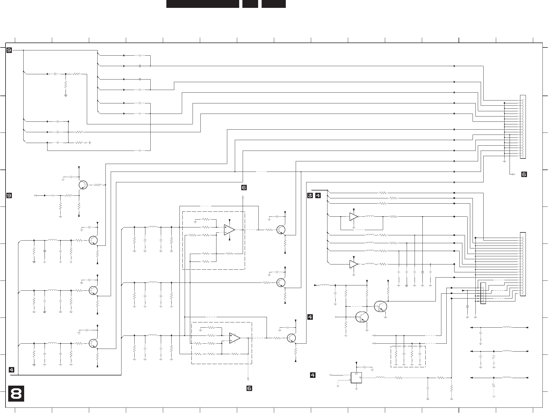
EN 150
3139 785 31532 7.Circuit Diagrams and PWB Layouts
Digital: Video IO
EN
NC
NC
I915 C12
I916 C12
I917 D12
I918 G9
I919 H13
I920 I13
I921 E4
I922 E5
I923 F4
I924 F5
I925 H4
I926 H5
I927 A2
I928 B2
I929 A1
I930 B1
I931 B1
I932 C1
I933 D1
I934 A3
I935 A3
I936 A3
I937 A3
I938 B3
I939 B3
Bead
14
A
B
C
D
E
F
G
H
I
A
B
C
D
E
F
G
H
I
1900 E14
1901 F13
1904 A14
2036 H4
2900 A4
2901 A4
2902 A2
2903 A4
2904 A4
2905 B4
not used
not used
1234567891011121314
12345678910111213
d
e
su
ton
delete for SXC
de
su
ton
d
e
su ton
2906 B4
2907 B2
2908 B2
2909 C2
2910 I10
2911 D2
2912 E3
2913 E8
2914 F1
2915 F2
2916 E4
2917 E4
2918 F11
2919 F11
2920 F11
2921 F11
2922 F12
2923 G9
not used
T
UO/N
I
O
IDU
A
EC
A
FR
ET
NI D
R
AO
B
GOLANA
not used
desu
to
n
1%
2924 F3
2925 F8
2926 G1
2927 G2
2928 G4
2929 G4
2930 H13
2931 I13
2932 I12
2933 H2
2934 H8
2935 H1
2936 H2
2937 H4
2938 D2
2939 I13
2940 I13
2941 C4
2942 H11
2943 H11
2944 G13
not used
3046 E10
3901 A2
3902 A2
3903 H11
3904 H11
3905 B2
3906 C2
3907 D3
3908 D2
3909 D10
3910 D11
3911 D2
3912 D2
3913 D10
3914 E11
3915 G10
3916 E11
3917 F10
3918 F1
3919 F3
3920 E4
3921 E8
3922 F10
3923 G11
3924 G1
3925 H9
3926 G3
3927 G4
3928 G8
3929 I11
3930 H1
3931 I3
3932 H4
3933 H8
3934 F2
3935 E5
3936 G2
3937 G5
3938 H2
3939 H5
3940 G9
3941 E6
3942 E6
3943 E5
3944 E6
%1
not used
not used
1%
3945 F6
3946 F6
3947 F6
3948 H6
3949 H6
3950 H5
3951 H6
3952 H5
3953 H6
3954 H6
3955 I12
3956 I12
3957 E2
3958 G2
3959 H2
3960 E7
3961 G7
3962 H8
4900 H12
T
U
O/NI
O
EDI
V
ECAFR
ET
NI D
R
AO
B
GOLANA
4901 H12
4902 G10
4903 D7
4904 D6
4905 G6
4906 E7
4907 H7
4908 G14
4909 F14
desu ton
1%
ylno NI FIDPS ro
f
4910 G14
4911 E10
5901 G9
5902 H14
5903 I14
5904 I10
5905 E10
5906 E10
5907 E4
5908 E2
5909 E10
5910 G2
5911 F4
5912 H2
5913 H4
5914 F10
5915 F10
5916 H14
delete for DTTV
not used
DAIO
7900 E9
7901 F9
7902 G11
7903 I10
7904 D2
7905 G10
7906 E8
7907 E3
7908 G3
7909 G8
7910-1 E6
7910-2 H7
7911 H3
7912 H8
F1902 G12
F1903 G12
F1904 G12
F1907 F12
F1909 F12
F1911 F12
F1912 E12
VIP_ANALOG_VIDEO_INPUT
not used
F1914 E12
F1916 E12
F1918 D12
F1920 D12
F1921 D12
F1922 E13
I900 B12
I901 B12
I902 E2
I903 G2
I904 H2
I905 E1
I906 G1
I907 H1
I908 A12
I909 B14
I910 A12
I911 A12
I912 B12
I913 C12
I914 C12
1u5
5907
2910
100n
4909
23
93
R57
R065
2093
%1
0
293
R5
7
I931
%1
47n
2901
47n
2903
3
393
0K
1
I936
I924
7908
BC847B
100n
2934
I930
p
22
2
492
I911
I919
p072
6302
n00
1
3
292
9
7K4
51
93
2
20
21
22
3
4
5
6
7
8
10
11
12
13
14
15
16
17
18
19
1904
FMN-BMT
1
4906
2924
100n
I932
I939
3949
1K5 1%
I915
4908
3905
180R
I933
F1918
K01
529
3
I938
p0
7
2
629
2
F1904
5914
BLM18B
R001
6593
I908
5912
1u5
p229192
R57
9393
I921
p0
72
%1
5392
3943
6K8 1%
BC847B
7911
100n
2933
3
2
1
84
3917
7910-1
AD8092AR
9292
p072
47R
I906
F1922
3907
100R
3960
100R
1%
180R
3908
I917
4904
3901
180R
I937
1%
3944
5K6
47n
2908
1u5
5913
I935
6392
p072
7912
BC847B
2902
47n
3916
47R
F1907
5
4
F1920
74HCT1G125GW
7903
2
3
1
5904
68R
3909
2K2
21
93
Video IO
4393
R57 %1
F1911
I927
2
3
1
5
4
329
3
K22
7900
74LVC1G04GW
3492
p22
2912
100n
BC847B
7907
4910
7906
BC847B
F1903
84
I916
7910-2
AD8092AR
5
6
7
K01
049
3
1393
0K1
22n
2911
100R
3961
0K1
8293
3962
100R
I922
p86229
2
1193
R065 %1
560R
3906
2907
47n
6192
p072
7u4
9392
I920
R
57
039
3
%
1
I910
I918
BLM18B
5909
2904
47n
4903
p228192
I912
%1
8393
R57
3947
4K7 1%
3941
750R 1%
100R
3957
BC847B
7904
4901
I902
1
5
4
2900
47n
74LVC1G04GW
7901
2
3
47R
9193
0K1
3046
3910
68R
K0
01
3093
I905
n
001
03
9
2
4u7
5903
2
3
4
5
6
5916
1901
FMN-BMT
1
3942
1K5 1%
p0
7
2
7192
2938
100n
PDTC124EU
7905
4907
I926
04
9
2
n001
BLM18B
5905
F1914
I923
5908
1u5
68R
3914
47n
2906
3913
22R
7392
p
072
1u5
5910
p07
2
7292
1392
7u4
I903
I907
p0
72
4192
p22
1
292
I934
4902
F1916
4911
3952
1K2 1%
I901
6393
R57
p220292
%1
0
K
1
6293
BLM18B
5915
409
3
K0
0
1
F1921
68R
3922
I909
%1
R
57
8193
47n
2905
1%4K7
3945
3955
1R0
1293
0K1
5906
BLM18B
I913
2909
47n
R5
7
53
9
3
%1
2392
p051
100n
2913
I925
I914
56R
3929
%1
R57
7
293
BLMP18P
5901
F1909
3958
100R
5192
p072
1%
I900
3950
1K5
F1902
%1
7393
R57
3951
1%1K5
3953
4K7 1%
100n
2925
22
3
4
5
6
7
8
9
12
13
14
15
16
17
18
19
2
20
21
FMN-BMT
1900
1
10
11
p
07
2
8292
1%1K0
3946
I928
4492
n01
1%750R
3948
BC847B
7909
F1912
4u7
5902
47n
2941
4900
%1
R57
4293
4905
7902
PDTC124EU
1%
I929
3954
1K0
5911
1u5
I904
100R
3959
+5V_Buffer
0.4V
0.4V
-0.2V
0.3V
0.4V
-0.3V
DAOUT
VIDEO_OUT
iV
+5V_Buffer
-5V_Buffer
iU
+5V
D_Y
D_Y
D_CVBS
A_YCVBS
A_C
A_YG
B_OUT
D_UB
D_VR
D_YG
SD0_OUT
+3V3
3V3_I2S
3V3_I2S
3V3_I2S
A_DATA
A_WCLK
A_BCLK
D_C
VDD_125
+5V
VDD_125
MPIO7_MUTE_LVn
A_PCMCLK
A_UB
A_VR
FSCLKE_IN
+5V_Buffer
+5V_Buffer
+5V_Buffer
CVBS_OUT
C_OUT
Y_OUT
SPDIF_COAX_IN
SPDIF_OPT_IN
D_KILL
-5V_Buffer
-5V_Buffer
-5V_Buffer
+5V_Buffer
+5V_Buffer
G_OUT
-5V_Buffer
-5V_Buffer
-5V_Buffer
-0.1V
-0.1V
-0.8V
0.5V
0.6V
0.6V
-0.03V
-0.03V
+5V_Buffer
SCKE_IN
WSE_IN
SDE_IN
FSCLK012_OUT
D_DATA0
D_PCMCLK
D_WCLK
WS012_OUT
D_BCLK
SCK012_OUT
DIGITAL_AUDIO
R_OUT
R_IN_VIP
CVBS_Y_IN_B
CVBS_Y_IN_C
VDD_125
CVBS_OUT_B_VIP
-5V_Buffer
-5V
-5V_Buffer
+5V_Buffer +5V
SPDIF_OUT
CVBS_Y_IN_A
C_IN_VIP
Y_IN_VIP
G_IN_VIP
U_IN_VIP
B_IN_VIP
V_IN_VIP
3103_603_30601_a2_sh130_sh8.pdf 2004-12-01
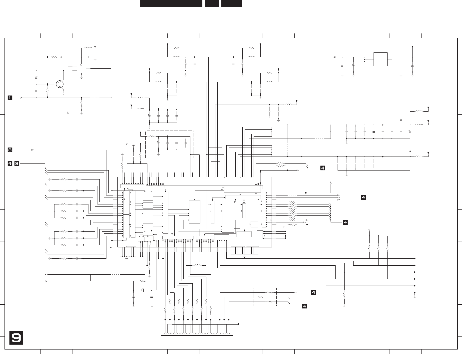
EN 151
3139 785 31532 7.
Circuit Diagrams and PWB Layouts
Digital: VIP
NC
GND
INVOUT
NCVOUT
VOUT
VOUT
Y
OI
D
U
A
COMP
DELAY
SWITCH
FAST
VIDEO
LORT
N
O
C
TUP
T
U
O
R
E
D
O
C
E
D
BOUNDARY
SCAN
T
R
O
P
-I R
E
TTAMRO
F
TUPTUO
1ST TASK IIC REG MAP SCALER
SCALER EVENT CONTROLLER
VIDEO/TEXT
ARBITER
RAW S
Y
S
C
CLK GPO XTAL
S
S
Y
CR
CB
CB
CR
YCBCR
R
C
BC
Y
SR
C
BCY
CBCR
CBCR
RAW
R
E
L
A
C
S
-S
C
B
VDDA VDDE VDDI
VSSA VSSE VSSI
IIC REGISTER MAP
R
COMB
PROC
CHROM
PROC
K
LC
H-PORTX-PORT
2ST TASK IIC REG MAP SCALER
SYNC
PROC
LUM
FIL
L
O
R
T
N
O
C
T
U
P
NI
G
O
L
A
N
A
AD-PORT
CONTROL
1
G
O
LANA
1CDA +
TEXT
FIFO
VBI DATA
SLICER
1GOL
A
N
A
1CDA +
O
F
IF OEDI
V
GNILACS LACITREV
-
E
NI
F
LAT
N
O
Z
IROH
GNILACS )
-
E
S
A
H
P(
REF
F
U
B
O
F
IF
E
NI
L
R
E
T
LI
F
E
R
P-
R
IF
R
ELACSERP
1
G
OLANA
1CDA +
1GOLANA
1CDA +
G
B
for XXXX only
delete for SAA7117
56R for SAA7117
G
H
I
1001 H5
1003 I8
2014 A3
2015 C6
2016 C6
2017 C5
2018 C5
2019 B1
2020 B9
2021 B9
2022 B8
2023 C5
2026 B8
2027 D4
2028 A8
2029 A8
1234567891011121314
1234567891011121314
A
B
C
D
E
F
G
H
I
A
B
C
D
E
F
desu ton
not used
not used
not used
not used
SAA7117AE
2030 G3
2031 G3
2032 F3
2033 F3
2035 F3
2037 E3
2038 E3
2039 E3
2040 D3
2041 A13
56R for SAA7117
2042 A11
2043 A6
2044 A6
2045 A11
2048 B6
2049 B5
2050 C11
2052 C11
2053 C12
2054 C12
2056 C12
2058 C13
2059 C13
2060 C13
2061 D11
2063 D11
2064 D11
2065 D12
2066 D12
2071 D12
2073 D13
2094 D13
2095 D13
2096 H4
56R for SAA7117
56R for SAA7117
7117
A
AS rof
et
ele
d
56R for SAA7117
56R for SAA7117
not used
2097 H5
2098 C6
2099 C5
2100 C5
3000 C5
3001 G12
3002 G12
3004 H11
3005 A2
3006 G12
3007 B2
3008 H8
3009 I7
3010 I7
3011 I6
3012 I6
3013 I6
3014 I5
3015 H9
delete for SAA7117
for SAA7117 only
56R for SAA7117
3016 H7
3017 H6
3018 H6
3019 H6
3020 H6
3021 B3
3022 A9
3023 D5
3024 G2
3025 G2
3026 F2
3027 F2
3028 F2
3029 E2
3030 E2
for DTTV only
yln
o
71
17
AAS r
of
3031 E2
3032 D2
3033 A8
3034 G7
3043 G5
3047-1 E9
3047-2 F9
3047-3 F9
3047-4 F9
3048-1 E9
3048-2 E9
3048-3 E9
3048-4 E9
3049 A5
3052 H5
3086 D4
3087 D9
3088 D9
3089 F9
3090 F9
not used
3091 A6
3099 H9
4000 B3
4001 D4
4002 D9
4003 D10
4004 C10
4005 C10
4006 E9
4007 H4
4008 H3
5001 A3
5005 B9
5008 A9
5009 A8
5010 A6
5016 A5
not used
5017 B13
5018 C13
5019 D13
5020 B5
5021 B5
6000 A1
7002 A3
7003 B2
7006 A12
7007 D9
F001 G5
F002 G5
F003 D9
F004 F9
F005 F9
F006 F9
56R for SAA7117
F007 F9
F008 G5
F009 G5
F011 E10
F012 G5
F013 G13
F014 H13
F015 H13
F016 H13
F017 G13
F018 G13
F019 I7
F020 I7
56R for SAA7117
for SAA7117 only
not used
F021 I7
F0310 I7
F0312 I7
F0314 I7
F0316 I6
F0318 I6
F0320 I6
F0322 I6
F0324 I6
F0326 I6
F0328 I6
F0330 I5
I001 G4
I002 A8
I003 C5
I004 A8
I005 A6
I006 D12
for SAA7117 only
I007 C12
I008 B5
I009 A6
I010 A2
I011 A2
I012 A2
I014 E3
I016 E3
I017 F3
I018 F3
I019 F3
I020 G3
I021 G3
8
2
3
6
7
7006
LD1117D33
1
4
5
70
03
R086
10
03
K0
1
5102
0n1
47R3048-4
47R3047-1
47n
2038
1004
I007
3047-2 47R
9
4
02
n
001
22R3090
120
F
3099
22R
0
103
R
22
I001
613
0F
6
00
3
K0
1
F013
BLM18P
5018
5021
I009
BLM18P
7
u
4
0
60
2
H
R
X7
C
VRX8D
L
AT
X
3
A
IL
ATX4B
TUOT
X
2A
IRTX1
1B
1DPX
8
B
2DPX9A
3DPX9B
4
DPX
01A
5DP
X
01B
6
D
PX11A
7
DPX
1
1
C
YDR
X
6A
11
F
11
J
5L
9
L
DDXV 3
B
SSX
V
4A
KL
CX7A
QD
X
7B
0
D
PX8A
4E
1C
5D
9D
1
1
D
11G
4
L
8L
11L
7D
01D
11M
8C
01C
21F
2
1
J
5
M
9M
2M
4J
3H
4F
A3ADD
V2G
4D
A4ADD
V2E
5C
9C
21
D
21
H
4M
8M
21
B4TSET
21A5TSET
SMT6D
NTSRT6
C
3M
4K
A
1A
D
D
V1L
4
H
A
2
ADD
V1
J
01
PADS
K
CT
6
B
I
DT
5
B
O
DT
5A
31
P
0TSET
31
D1T
SET
41C2T
SET
31
A3TS
ET
7SER 3
1
C
8SE
R1N
9S
E
R2N
5PNO
S
ER
0T
S
R
01
M
1T
SR0
1
N
O
CTR
01L
9NLCS
11SER 3
1N
21SER 41N
31S
E
R2P
2
S
ER 31B
3SER 41B
4SER 3C
5
SER 4C
6SER 21C
IGPV K14
9
P
A_T
N
I
ITRDY N12
ITRI L12
CLL4P
2C
LL5
N
1SER 2B
01SER 3N
IDP4 H13
IDP5 J14
IDP6 J13
IDP7 K11
IDQ L13
IGP0 L14
IGP1 K13
IGPH K12
5D
PH
31F
6DPH41F
7
DP
H
31
G
ICLK M14
IDP0 G14
IDP1 G12
IDP2 H11
IDP3 H14
6
NTXE
KL
C
RL
C
MX
E3P
FSWM13
0
DP
H41D
1D
P
H11E
2DPH31E
3
DP
H21E
4D
P
H41E
A|34G1
A|3DF1
A|41B1
A|42D2
A|43D1
A|44E1
A|4DD3
4
N
EC
A|21G4
A|22G3
A|23H2
A|24J3
A|2DH1
A|31E3
A|32F2
A|33F3
AMXCLK M12
AOUTM1
ASCLK N11
A|11J2
A|12K1
A|13K2
A|14L3
A|1DK3
7N5P
DA
6L6P
D
A
6M
7
PDA
6P8PD
A
D
N
GA
2
C
A
DNGA
2L
ALRCLK P12
AMCLK P11
SAA7118E
7007
8
N
0
PDA
8
P1
PDA
7
M
2
PD
A
7L3PDA
7P4PDA
3028
1R0
I004
0n1
72
02
100R
3049
BLM18P
5005
5010
BLM18P
I011
n
01
16
02
n00
1
7102
7003
BC847B
24M576
5020
BLM18P
VIP
CX-8045G
1001
900F
3091
100R
2202
n
01
100R
3033
2
40
2
u7
4
1R0
3032
140
2
n0
01
n01
91
0F
6102
3048-3 47R
3008
023
0F
22R
I002
9
003
R
22
47n
2030
9102
p051
F016
680R
3005
1R0
0
13
0F
3030
4130F
BLM18P
5009
F006
71
03
R22
1R0
3024
n00
1
8
50
2
1103
3203
7K4
R22
I012
3052
1R0
F007
3403
3000
22R
7
K
4
I005
5
90
2
7u
4
F003
BLMP18P
5001
02
0F
9202
n001
4000
7u4
8
102
4
902
n
0
01
37
02
n00
1
n001
3602
n
0
01
9
502
2039
47n
0330F
6230F
3015
22R
4006
R
22
61
0
3
210F
F005
2K
2
6
8
03
3029
22
3
0F
1R0
8230F
460
2
n
0
0
1
200F
1R0
3027
1
2
5
3
4
n00
1
440
2
74LVC1G32GW
7002
3034
10K
n001
6502
n
00
1
3402
n
01
660
2
8130F
9103
R22
4004
0
50
2
n0
1
100R3087
100R3088
4007
K
0
1
4003
n001
6202
0n1
890
2
7
8
9
I010
4
2
52
62
72
8
2
92
3
03
4
5
6
51
61
71
81
9
1
2
0
2
1
2
22
3
2
1
0
1
11
2
1
3
1
4
1
100F
30FLZ-SM2-TB(LF)(SN)
30
01
2004
47n
100n
2014
2035
1R0
3026
0
2
03
R22
1203
0
K1
1
7
02
F011
n001
n001
2502
3202
7u4
n01
020
2
120
2
n001
K0
1
2
0
03
2037
47n
3022
100R
n01
840
2
BLM18P
5017
4K7
F017
3089
n0
1
8202
I014
F004
4005
I017
I016
I018
I006
n001
56
02
R22
2103
I019
4008
I021
I020
I008
n0
01
54
0
2
R
22
31
03
5008
BLM18P
3048-2 47R
47R3048-1
4
23
0F
n00
1
0012
n
01
9902
F015
47R3047-3
3047-4 47R
2033
47n
3025
1R0
F014
81
03
R22
2130F
5019
BLM18P
2031
47n
3031
1R0
BLM18P
5016
2032
300
4
47n
800F
I003
7902
p3
3
4502
n001
3502
n0
01
41
03
R22
p33
6902
F018
2040
47n
0006
1V8_VIP
1V8_VIP
RESET_DTTMn
1
P
GI_
PI
V
1PGI
_
PIV
0
1
BS67SP
1
G_IN_VIP
JTAG_VIP_TDI
JTAG_VIP_TRSTn
JTAG_VIP_TCK
JTAG_VIP_TMS
VIP_FB
+3V3_VIP
nTESE
R
_P
I
V
PNX7100_HS_IN
VDDI_7118
C_IN_VIP
Y_IN_VIP
VDDE_7118
+3V3_VIP
+3V3_VIP
+3V3_VIP
VDDE_7118
+3V3_VIP
R_IN_VIP
0N
I_
D
D
PNX7100_VS_IN
ITU_IN(7)
ITU_IN(6)
ITU_IN(5)
ITU_IN(4)
ITU_IN(3)
ITU_IN(2)
ITU_IN(1)
ITU_IN(0)
PNX7100_ITU_IN_VAL
1V8_VIP
VDDI_7118
+3V3_VIP
IIC0
V_IN_VIP
B_IN_VIP
CVBS_Y_IN_C
CVBS_Y_IN_B
CVBS_Y_IN_A
U_IN_VIP
SCL0
SDA0
IIC0
S
H_NI
_
D
D
SV_NI
_
DD
KLC_NI_DD
7
NI
_
DD
6NI_DD
5NI_DD
4NI_DD
3NI_D
D
2NI_DD
1
NI
_
D
D
+3V3_VIP
VIP_INTA
+3V3_VIP
+3V3_VIP
+5V
ITU_IN(7:0)
1
STR
_
PIV
CVBS_OUT_B_VIP
SDA0
SCL0
VDDE_7118
+3V3_VIP
PNX7100_ITU_IN_CLK
PNX7100_ITU_IN_FID
+3V3_VIP
MPIO5_VIP_ERROR
VIP_INTA
VIP_ANALOG_VIDEO_INPUT
JTAG_VIP_TDO
3103_603_30601_a2_sh130_sh9.pdf 2004-12-01
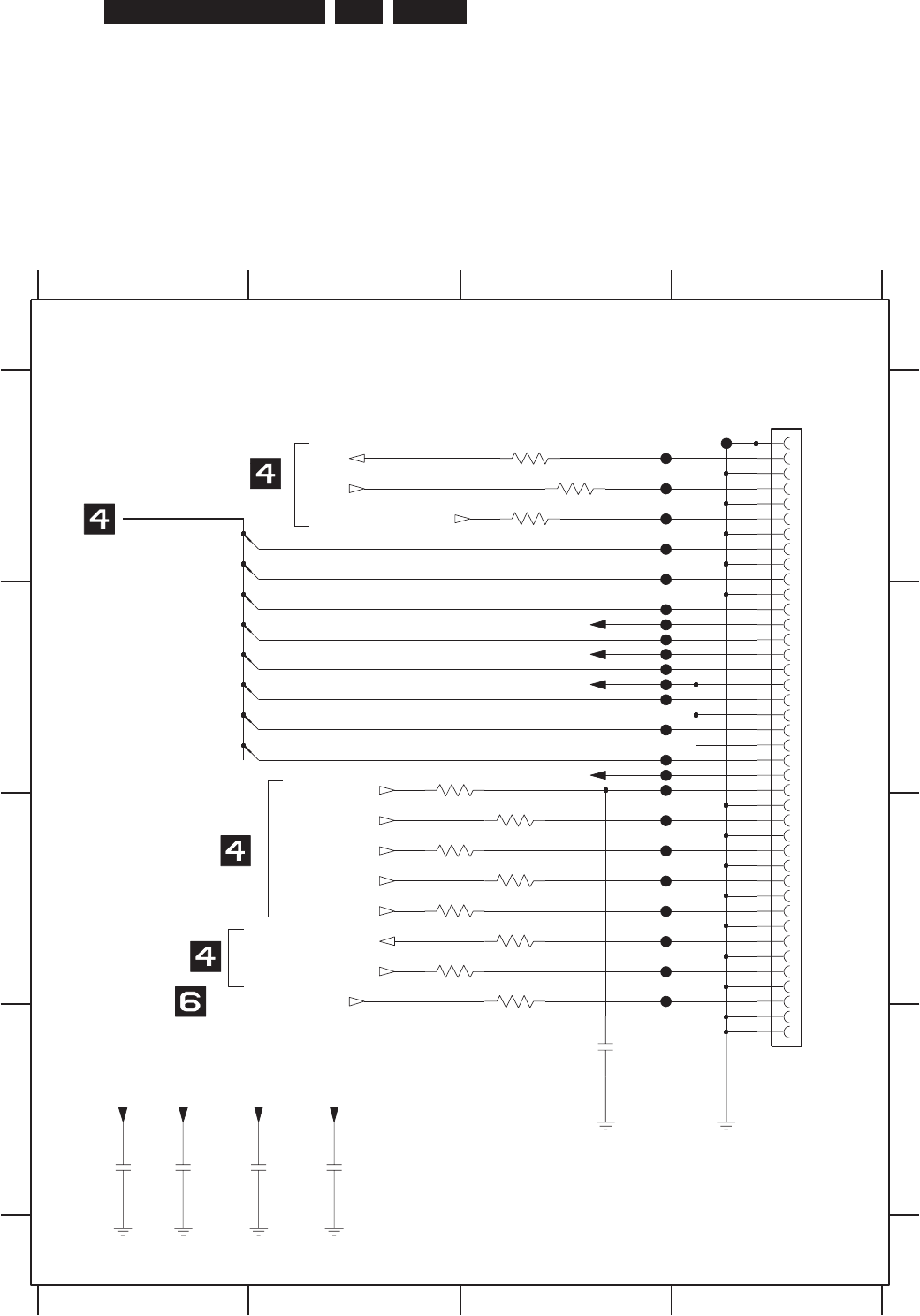
EN 152
3139 785 31532 7.Circuit Diagrams and PWB Layouts
Digital: HDMI Interface
3753 B2
3755 C2
not used
for HDMI only
2
3758 C2
2751 D1
F0426 B3
F0427 B3
F0428 B3
F0429 B3
F0431 A3
F0433 A3
F0435 A3
F0437 A3
F0439 A3
F0440 A4
2752 D1
2753 D1
2754 D2
3750 A3
3751 A3
3752 A3
A
3754 C3
C
3756 C2
3757 C3 F0423 B3
F0424 B3F0407 C3
F0409 C3
F0411 C3
F0413 C3
F0415 C3
F0417 B3
F0418 B3
F0419 B3
3759 C3
2
1
3760 C3
F0403 C3
F0405 C3
D
A
B
C
D
1004 A4
2750 D3
1
F0421 B3
34
F0425 B3
34
n001
4
572
B
n0
0
1
3
572
n001
2572
n001
1572
F0417
F0415
22R
3752
3751
22R
22R
3750
38
39
4
40
5
6
7
8
9
28
29
3
30
31
32
33
34
35
36
37
19
2
20
21
22
23
24
25
26
27
1
10
11
12
13
14
15
16
17
18
40FLT-SM1-TB
1004
F0411
22R
3760
F0418
F0428
F0426
22R
22R
3753
3756
p001
0
5
7
2
F0437
F0427
U1
3759
22R
22R
3758
3757
22R
F0440
F0425
F0423
F0424
F0421
U2
HDMI INTERFACE
F0413
F0431
F0439
F0433
3754
22R
F0419
F0429
U3
U4
22R
3755
ITU_OUT(0:7)
FSCLK012_OUT
DAOUT
+12V +5V_HDMI -5V_HDMI 3V3_HDMI
F0435
ITU_OUT(7)
ITU_OUT(4)
SCL0
SDA0
PNX7100_ITU_OUT_CLK
MPIO12_HDMI_IRQ
WS012_OUT
SCK012_OUT
SD0_OUT
MPIO11_HDMI_RESETn
RESET_PROGSCANn
3V3_HDMI
+12V
-5V_HDMI
+5V_HDMI
ITU_OUT(3)
ITU_OUT(2)
ITU_OUT(1)
ITU_OUT(0)
ITU_OUT(5)
ITU_OUT(6)
3103_603_30601_a4_sh130_sh10.pdf 2004-12-01
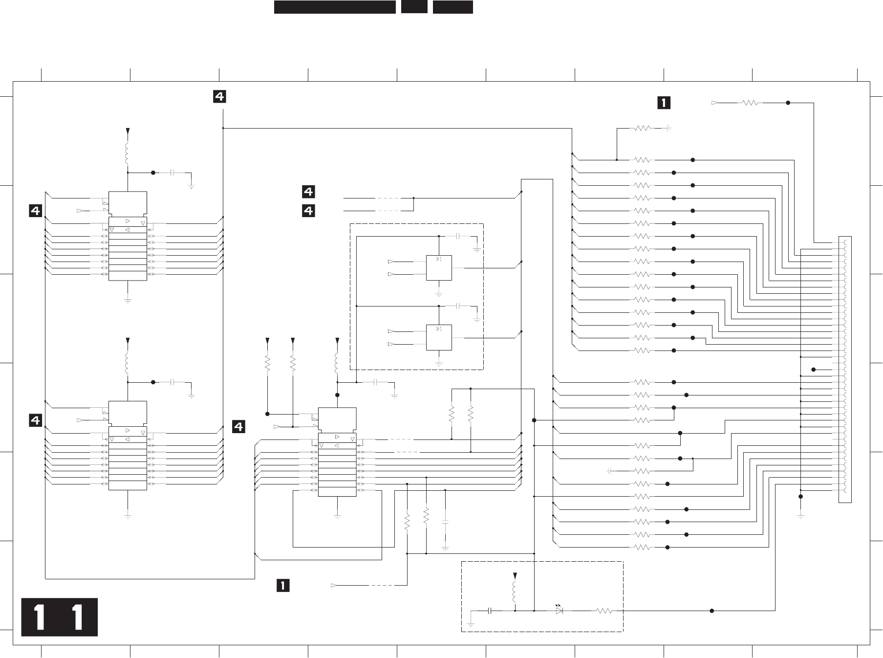
EN 153
3139 785 31532 7.Circuit Diagrams and PWB Layouts
Digital: IDE2
G3
1
2
3EN2
3EN1
G3
1
2
3EN2
3EN1
G3
1
2
3EN2
3EN1
not used
not used
B
C
D
E
F
A
B
C
D
E
F
1101 B9
2320 A2
2321 D2
2322 D4
12345678 9
12345678 9
A
2323 F6
2324 E5
2325 B5
2326 C5
3320 A8
3321 A7
3322 A7
3323 A7
3324 B7
3325 B7
3326 B7
3327 B7
not used
3328 B7
3329 B7
3330 B7
3331 C7
3332 C7
3333 C7
3334 C7
3335 C7
3336 C7
3338 D7
3339 D3
3340 D5
3341 D5
3342 D7
3343 D7
3344 D7
3345 E7
3346 D7
3347 E7
3348 E7
3349 E7
3350 E7
3351 E7
3352 D3
3353 E5
3354 E7
3355 F7
3356 E5
3358 F7
3359 A7
4320 B4
4321 B4
4322 D5
4323 D5
4324 F4
5320 A1
5321 C1
5322 C4
5323 F6
6320 F6
7320 A1
7321 D2
7322 D4
7323 B5
7324 C5
F0101 A9
F0102 E9
F0103 A8
F0104 A8
F0105 A8
F0106 B8
F0107 B8
F0108 B8
F0109 B8
F0110 B8
F0111 B8
F0112 B8
F0113 C8
F0114 C8
F0115 C8
F0116 C8
F0117 C8
F0118 C8
F0121 D9
F0123 D8
F0125 D8
F0127 D8
F0129 D8
F0131 E8
F0133 E8
for IDE_2 only
desu ton
F0135 E8
F0136 E8
F0137 E8
F0138 F8
F0139 F8
F320 A2
F321 D2
F322 D4
F323 D3
F324 D6
not used
P81PMLB
2235
IDE 2
F0104
F0127
13
12
11
1
01
19
02
4
5
6
7
8
9
18
17
16
15
14
74LVC245APW
7320
2
3
223F
F0109
F0121
3334 33R
1
01
19
02
F0115
7
8
9
18
17
16
15
14
13
12
11
74LVC245APW
2
3
4
5
6
7321 100n
3346 47K
2322
F0139
4323
F0110
4322
9333
7
K4
F0106
100n
2323
3323 33R
100n
2326
2325
100n
0433
R074
33R3322
33R3321
3338 22R
F0108
F0118
4320
33R3330
33R3327
33R3355
6320
TLMH3100
3
2
35
F0131
02
P8
1
PML
B
16
15
14
13
12
11
1
0
1
19
2
3
4
5
6
7
8
9
18
17
74LVC245APW
7322
3332 33R
2321
100n
F0116
3347 82R
3335 33R
3348 10K
F0114
R074
14
3
3
3325 33R
3358
220R
F0123
82R3343
F0137
F0135
3
5
33
K
74
F0136
F0133
K
74
6
53
3
p
01
423
2
4324
100n
2320
P81PMLB
0235
2010F
33R3336
F0112
22R3342
F0113
3320
33R
F0111
F0103
3329 33R
3344 4K7
4
4K7
3345
74LVC1G32GW
7324
1
2
53
1
2
53
4
7323
74LVC1G32GW
4321
33R3331
F0129
33R3324
F0105
F323
3351 33R
K01
2
533
3359
F0138
10K
3349 33R
33R3350
F0107
F324
F0117
F320
P81PMLB
1235
7
8
9
33R3326
34
35
36
37
38
39
4
40
5
6
24
25
26
27
28
29
3
30
31
32
33
15
16
17
18
19
2
20
21
22
23
1
10
11
12
13
14
IDE2
1101
40FLZ-RSM2-R-TB(LF)(SN)
33R3333
F0101
3328 33R
3354 33R
F321
F0125
RESET_IDE2n
IDE_DD(15:0)
XIO_SEL2
XIO_SEL2
XIO_SEL2
IDE2_DD(6)
IDE2_DD(8)
IDE2_DD(7)
IDE2_DA1
IDE2_DA0
IDE2_DA2
IDE2_CS0n
IDE2_CS1n
IDE2_CS0n
XIO_SEL2
PCI_AD(15)
XIO_SEL2
PCI_AD(14)
IDE2_CS1n
IDE2_DD(15)
IDE2_DD(0)
IDE2_DD(14)
IDE2_DD(1)
IDE2_DD(13)
IDE2_DD(2)
IDE2_DD(12)
IDE2_DD(3)
IDE2_DD(11)
IDE2_DD(4)
IDE2_DD(10)
IDE2_DD(5)
IDE2_DD(9)
IDE2_DIOWn
IDE2_DIORn
+3V3
IDE2_IORDY
IDE2_DD(10)
IDE2_DD(11)
IDE2_DD(12)
IDE2_DD(13)
IDE2_DD(14)
IDE2_DD(8)
PCI_AD(31)
PCI_AD(25)
PCI_AD(26)
PCI_AD(27)
PCI_AD(28)
PCI_AD(29)
PCI_AD(30)
PCI_AD(24)
IDE2_CS0n
IDE2_DD(4)
IDE2_DD(5)
IDE2_DD(6)
IDE2_DD(0)
PCI_AD(23)
PCI_AD(17)
PCI_AD(18)
PCI_AD(19)
PCI_AD(20)
PCI_AD(21)
PCI_AD(22)
PCI_AD(16)
PCI_AD(8)
IDE2_DD(15)
IDE2_DD(9)
IDE2_DA2
IDE2_CS1n
PCI_AD(9)
PCI_AD(10)
PCI_AD(11)
PCI_AD(12)
PCI_AD(13)
PCI_AD(14)
PCI_AD(15)
PCI_AD(8)
IDE2_DD(7)
IDE2_DD(1)
IDE2_DD(2)
IDE2_DD(3)
+3V3
PCI_AD(31:0)
PCI_GNTB
IDE2_IRQ
MPIO4_IDE2_IRQ
+3V3
PCI_AD(0)
IDE2_DA0
IDE2_DA1
IDE2_IORDY
IDE2_DIORn
IDE2_DIOWn
IDE2_IRQ
IDE2_DMACKn
RESET_IDE2n
+3V3
+3V3
+3V3
3103_603_30601_a3_sh130_sh11.pdf 2004-12-01
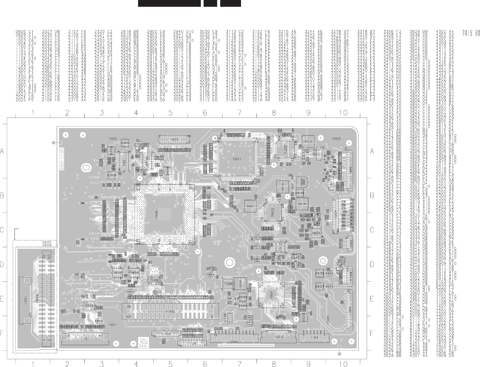
EN 154
3139 785 31532 7.
Circuit Diagrams and PWB Layouts
Layout: Digital Top View
BREAKAWAY
CONNECTOR TO
HDD
DigiBd_3139_603_30601_topview.pdf 2005-10-14
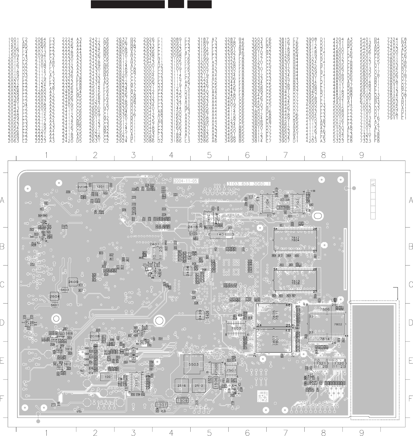
EN 155
3139 785 31532
Layout: Digital Bottom View
7.Circuit Diagrams and PWB Layouts
BREAKAWAY
CONNECTOR TO
HDD
DigiBd_3139_603_30601_bottomview.pdf 2005-10-14
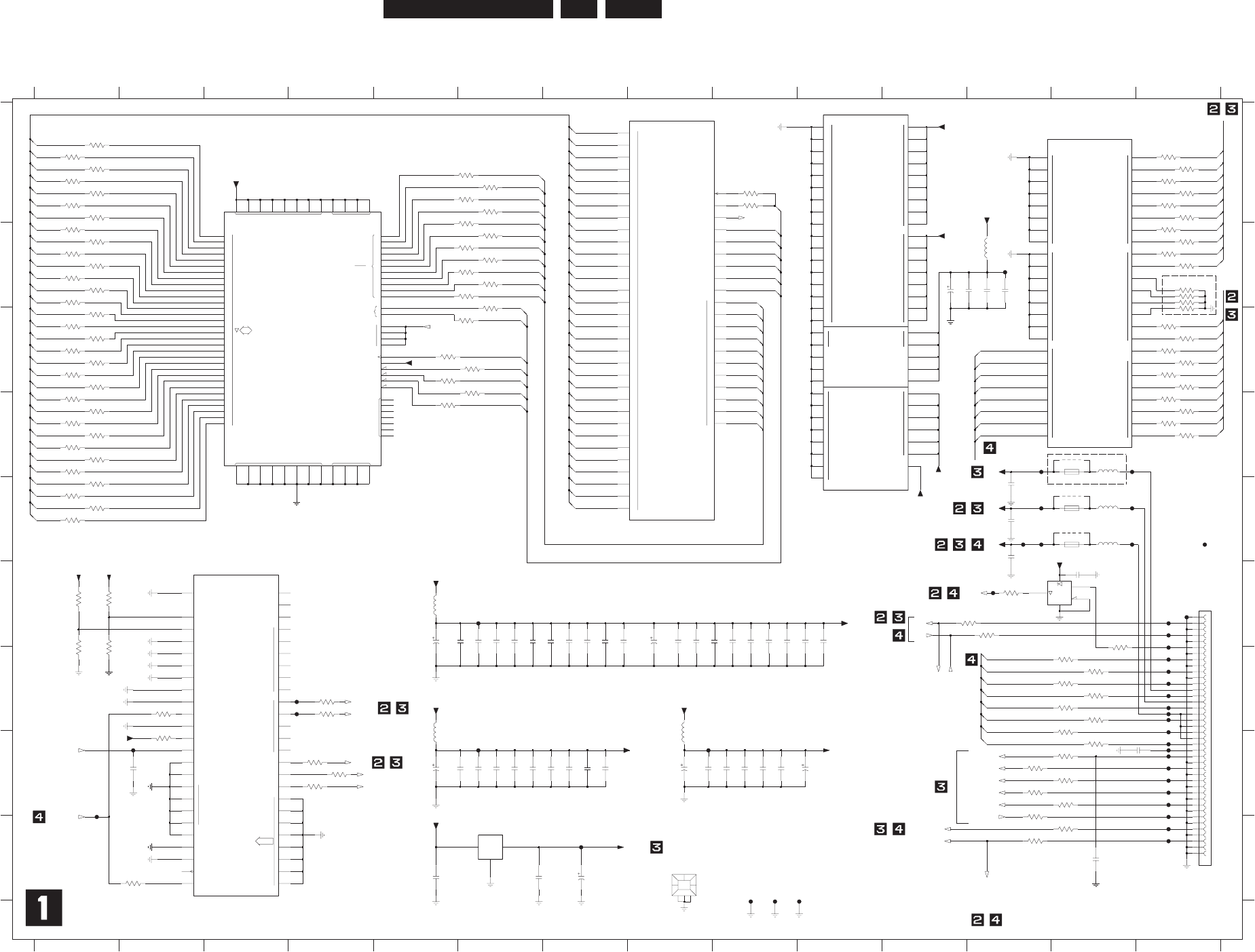
EN 156
3139 785 31532 7.
Circuit Diagrams and PWB Layouts
HDMI: Faroudja
10
16
17
0
10
15
SDRAM_BA1
SDRAM_BA0
SDRAM_CSN
SDRAM_DQM
SDRAM_CLKOUT
26
25
1
0
SDRAM_WEN
SDRAM_RASN
SDRAM_CASN
24
27
28
29
30
31
SDRAM_DATA
19
20
21
22
23
3
4
5
6
7
8
9
SDRAM_ADDR
SDRAM_CLKIN
18
1
2
9
8
7
6
5
4
3
2
11
12
13
14
EN
14
17
18
19
20
16
15
3
4
5
28
27
26
25
24
23
22
1
VDD
0
2
8
7
6
VDDQ
VSSVSSQ
NC
BA
2k-1
0A
D
DQM
13
12
11
10
9
8
7
6
5
4
3
2
1
0
9
10
21
0
1
CLK
CKE
CS
WE
CAS
RAS
0
1
2
3
31
30
29
COM
OUTIN
6
7
0
1
2
3
4
5
6
7
0
1
2
3
6
5
4
B|CB|D1
R|CR|CRCB
G|Y|Y
7
6
5
4
3
2
1
0
7
6
5
4
3
2
1
G|Y|Y_OUT_0
B|U|PB_OUT
R|V|PR_OUT_3
G|Y|Y_OUT
0
2
1
3
4
5
6
77
0
1
2
3
4
5
AVDD_PLL_BE
VSS
AVSS_PLL_BE
8
7
6
5
AVDDPLL_FE
2
1
1
2
3
4
5
6
8
7
6
10
11
12
13
14
PLL_PVDD
R_VDD1.8
6
1
2
AVSSPLL_FE
AVSSPLL_SDI
1
R_VDD
R_VSS
5
6
7
VDD
VDDCORE
8
7
8
9
4
3
2
1
9
15
16
17
5
4
3
2
1
2
3
4
5
2
3
4
1
PLL_PVSS
AVDDPLL_SDI
FIELD_ID1_PORT1
DEV_ADDR0
DEV_ADDR1
FIELD_ID_PORT2
FIELD_ID2_PORT1
CTLOUT
TEST_IN
1
2
3
VSYNC_PORT2
VSYNC1_PORT1
VSYNC2_PORT1
XTAL_IN
0
0
3
2
1
SDATA
CLKOUT
0
1
TEST
3
4
6
D1_IN
2
5
4
3
2
1
IN_SEL
TEST_OUT0
TEST_OUT1
SCLK
XTAL_OUT
4
7
6
5
CLK_PORT2
HSYNC_PORT2
HSYNC1_PORT1
HSYNC2_PORT1
IN_CLK1_PORT1
IN_CLK2_PORT1
OE
RESET_N
RESERVED
TEST
D
E
F
G
H
I
A
1911 F14
desu ton
1234567891011
HDMI
A
B
C
10
B
C
D
E
F
G
H
I
0005 I8
1100 D13
1101 E13
1102 E13
13
12 13 14
123456789 14
11 12
2113 F7
SDRAM
2114 F7
2115 F7
2116 F7
2117 H5
2118 H5
2119 H6
2120 H6
2121 H6
2122 H6
2123 H7
2124 H7
2141 F10
2142 H8
2143 H8
2144 H9
2145 H9
2100 B11
2101 B11
2102 B12
2103 B12
2106 F5
2107 F5
2108 F6
2109 F6
2110 F6
2111 F6
2112 F7
3100 D1
not used
not used
not used
3101 D1
3102 A14
3103 D1
3104 A14
3105 A6
3106 C1
2125 H7
2126 H7
2127 H2
2132 F8
2133 F8
2134 F8
2135 F8
2136 F9
2137 F9
2138 F9
2139 F9
2140 F10
3119 C1
CONTROL BUS
3120 B14
3121 B6
3122 D1
3123 B14
3124 B6
3125 D1
2146 H9
2147 H9
2148 H10
2150 I13
2151 I5
2152 I6
2153 I7
2154 H13
2155 E12
2156 E12
2157 E12
2158 F13
3135 F12
DATA BUS
des
u
to
n
de
s
u ton
3136 B6
3137 E1
3139 B6
3140 E1
3142 C6
3143 E1
3144 C14
3145 B1
3146 C14
3147 A1
3148-1 G13
3148-2 G13
3148-3 G13
3107 A14
3108 A6
3109 C1
3110 A14
3111 A6
3112 C1
3113 A9
3114 A14
3115 A6
3116 C1
3117 A14
3118 A6
3163 A1
ADDRESS BUS
3164-1 H13
3164-2 G13
3164-3 G13
3164-4 G13
3165 D14
3166 D5
3167 A1
3169 D14
3170 A1
3172 D14
3173 B1
3126 B14
3127 B6
3128 D1
3129 B14
3130 B6
3131 D1
3132-1 C14
3132-2 B14
3132-3 B14
3132-4 B14
3133 B6
3134 E1
3187 G1
3148-4 G13
3149 C14
3150 C5
3151 A1
3153 C14
3154 C6
3155 A1
3157 C14
3158 C5
3159 A1
3161 C14
3162 C6
7100-4 A12
7102 F12
7103 D5
7104 I6
F100 B12
F101 D13
F1017 H1
F102 E13
F103 E13
F104 D12
F105 E14
F106 E12
F108 E12
F109 F6
F110 E12
F1103 I14
3175 D14
3176 B1
3177 B1
3178 B1
3179 B1
3180 B1
3181 C1
3182 C1
3183 F1
3184 F1
3185 H12
3186 G1
F1124 G14
desu ton
not used
FAROUDJASDRAM
F1125 G14
F1127 G14
F1128 H14
F1129 G14
F113 H6
F1131 G14
F1133 G14
F1135 G14
F1137 F14
F1139 F14
F114 H2
4101 E13
4103 E13
5100 B12
5101 F5
5102 H5
5104 H8
5105 D13
5106 E13
5107 E13
7100-1 F2
7100-2 A11
7100-3 A8
F1105 I14
F1107 I14
F1109 H14
F111 G4
F1113 H14
F1115 H14
F1117 H14
F1118 H14
F1119 H14
F112 G4
F1121 H14
F1123 G14
3203 I2
3204 I12
3206 H13
3207 G4
3208 G4
3209 H4
3210 H12
3211 A9
F1140 F14
F115 F12
F116 H8
F117 I7
SW01 I9
SW02 I9
SW03 I10
3188 G2
3190 H2
3193 H4
3195 H4
3196 H13
3197 H13
3198 F12
3199 F13
3200 H12
3201 I13
3202 F12
desu ton
not used
4100 D13
V537u4
2412
F1128
3212
n001
3137
10R
3210
22R
0212
n001
7K4
3813
58
59
110
105
104
83
84
85
53
86
87
54
55
56
57
71
72
73
52
74
75
76
77
78
79
82
111
109
50
51
60
61
64
65
66
67
70
99
98
95
94
93
92
108
107
106
114
FLI2310-LF-BD
SDRAM
Φ
7100-3
103
102
91
101
100
3101
10R
0015
P81MLB
7012
n001
n0
01
5312
111
2
n00
1
22R
3199
F115
+3V3
47R
3135 2
3
1
5
4
74LVC1G125GW
7102
n0
01
01
1
2
F1125
3102
47R
22R
3148-4
F116
4103
100n
2158
n001
14
12
3
1
12
n0
01
n001
33
12
3169
47R
BLM31
5107
3131
10R
10R
3128
n001
73
1
2
221
2
n00
1
10R
3162
F1118
n0
0
1
21
1
2
51
12
n001
p00
1
0512
9
0
12
n
0
01
10R
3116
3178
10R
F106
7813
7K4
4
4
12
n
0
01
F1140
+5V
F1115
1V8D
3167
F1103
10R
10R
3143
3139
10R
6212
n0
01
D8V1
SW01
10R
3180
22R
3164-2
BLM18P
5105
5106
BLM18P
F102
P81MLB
F113
10R
3154
2015
F1107
F1113
4K7
3190
3104
47R
6
8
1
3
10R
3155
7K
4
F105
F1124
2512
3100
n001
10R
527884
17
3179
10R
81
44587286612323846
152943393541495575
28
59
14
21
30
57
69
70
73
19
1
7
54
56
8
10
11
13
74
76
16
71
37
39
40
42
45
47
48
50
51
53
77
79
80
82
83
85
31
33
34
36
5
64
65
66
22
23
18
67
68
20
2
4
25
26
24
27
60
61
62
63
7103
MT48LC2M32B2P
SDRAM
2M x 32
Φ
47R
3172
F109
4101
1V8D
3182
n0
01
61
12
10R
2
3
12
V537u4
F111
8112
n001
F1123
6312
n0
01
u74
3512
911
2
V3.6
F1119
n
001
10R
3145
10R
3159
10R
3158
F1109
0005
BRACKET
7
412
n001
F1133
+3V3
10R
3122
n001
3012
3151
10R
3147
10R
3109
10R
10R
3181
3125
D3V3
22R
10R
3206
10R
n001
2012
F1127
3133
3V3D
F1129
7512
n001
10R
3119
2
13
7104
LF18ABDT 3204
22R
4212
n00
1
431
2
n001
3127
10R
3V3D
001F
7K4
4
813
n001
801
2
3140
10R
+1V8
2154
100n
n001
5512
3208 100R
3207 100R
F1105
1R03113
3123
47R
3124
10R
F103
10R
3111
3108
10R
0
n1
7
21
2
F1135
10R
3112
3177
10R
22R
3202
22R 3198
3175
47R
F112
47R
3149
47R
3126
47R
3117
47R
3165
9312
+3V3
0412
n
0
01
n001
3110
47R
F104
R_VDD
3105
10R
22R
3148-3
F1137
F114
3209
100R
n001
+1V8
1012
n001
6512
22R
3148-2
F1131
10R
3106
200mA
1100
3161
47R
22R
3164-4 22R
3148-1
3V3D
F1121
1K53132-4
3188
10R
47R
3144
3195 10R
3193
10R
n001
54
12
F117
3103
n
001
15
12
10R
10R
3121
V53
71
12
7u4
350mA
1101
3153
47R
SW02
3170
10R
47R
3120
140
141
142
143
144
145
155
21
22
23
24
25
26
27
28
136
137
38
39
40
148
149
150
151
152
153
154
131
132
133
134
135
29
32
33
34
35
11
12
13
14
15
18
19
20
126
127
130
7100-4
FLI2310-LF-BD
Φ
VIDEO
10R
3150
4112
n0
0
1
84
1
2
u
01
+3V3
V61
3132-1 1K5
47R
3157
F1017
41 42
3176
10R
36
37
38
39
4
40
5
6
7
8
9
26
27
28
29
3
30
31
32
33
34
35
17
18
19
2
20
21
22
23
24
25
1911
40FLZ-RSM2-R-TB(LF)(SN)
1
10
11
12
13
14
15
16
4100
47R
3114
3166
10R
0012
V537u4
3173
10R
F110
n
001
6
412
3412
n001
10R
47R
3107
F1139
3130
n001
52
12
3134
10R
3200
22R
F1117
22R
3164-1
22R
3196
F101
47R
+3V3
3129
10R
3142
+12V
F108
22R
3201
3211 1R0
69
81
89
129
139
147
194
198
17
31
37
49
63
36
68
80
96
123
138
197
9
97
113
124
8
30
48
62
88
112
128
146
193
16
177
186
187
184
172
175
178
185
167
169
182
166
163
159
162
157158
183
168
171
174
REWOPLLPDEVRESER
FLI2310-LF-BD
165
164
160
161
3V3D
7100-2
P8
1
MLB
4015
3132-2 1K5
SW03
3136
10R
n0
01
12
12
22R
3185
3203
3132-3
10R
1K5
1102
1.5A T
8
3
12
n0
01
47R
192
3146
188
189
190
115
90
116
117
2
6
207
191
181
180
176
173
179
170
47
45
46
42
43
3
7
206
1
5
208
4
10
41
156
122
196
199
200
201
202
203
204
205
44
FLI2310-LF-BD
MISC
125
195
118
119
120
121
3118
7100-1
Φ
10R
3115
10R
1
0
15
13MLB R0
5
601
2
V537u4
22R
3164-3
22R
3197
VO_CLK
3163
10R
SCL0
SCL0
0
LC
S
0
A
DS
SDA0
SDRAM_CLK_F
+1V8
R_VDD R_VDD
PSCAN_RSTn
HDMI_RSTn
D_DATA(22)
D_DATA(21)
D_DATA(20)
D_DATA(19)
D_DATA(18)
D_DATA(17)
D_DATA(31:0)
)0:13(ATAD_D
D_DATA(16)
D_DATA(7)
P_HSYNC
P_VSYNC
P_CLK
SPDIF_OUT
ITU_OUT(6)
ITU_OUT(5)
ITU_OUT(4)
ITU_OUT(3)
ITU_OUT(2)
ITU_OUT(1)
ITU_OUT(0)
ITU_OUT_2(0:7)
nTSR_NACSP
PSCAN_RSTn
FSCLK12_OUT
SCK12_OUT
SD_OUT
WS12_OUT
DQM_F
WEN_F
VO_CLK_2
ITU_OUT(7)
CbCr(2)
CbCr(3)
)11:2(rCbC
)11:2(Y
CbCr(4)
CbCr(5)
CbCr(6)
CbCr(7)
CbCr(8)
CbCr(9)
CbCr(10)
CbCr(11)
Y(2)
Y(3)
Y(4)
Y(5)
Y(6)
Y(7)
Y(8)
Y(9)
Y(10)
Y(11)
D_DATA(14)
D_DATA(15)
D_DATA(16)
D_DATA(17)
D_DATA(18)
D_DATA(19)
D_DATA(2)
D_DATA(20)
D_DATA(21)
D_DATA(22)
D_DATA(23)
D_DATA(24)
D_DATA(25)
D_DATA(26)
D_DATA(27)
D_DATA(28)
D_DATA(29)
D_DATA(3)
D_DATA(30)
D_DATA(31)
D_DATA(4)
D_DATA(5)
D_DATA(6)
D_DATA(7)
D_DATA(8)
D_DATA(9)
DQM_F
INT_HDMI
ITU_OUT_2(6)
ITU_OUT_2(7)
A_ADDR(0)
A_ADDR(1)
A_ADDR(10)
A_ADDR(2)
A_ADDR(3)
A_ADDR(4)
A_ADDR(5)
A_ADDR(6)
A_ADDR(7)
A_ADDR(8)
A_ADDR(9)
D_DATA(0)
D_DATA(1)
D_DATA(10)
D_DATA(11)
D_DATA(12)
D_DATA(13)
SDRAM_CLK_F
CSN_F
CASN_F
RASN_F
BA0_F
BA1_F
CSN_F
WEN_F
RASN_F
CASN_F
BA0_F
BA1_F
ITU_OUT_2(0)
ITU_OUT_2(1)
ITU_OUT_2(2)
ITU_OUT_2(3)
ITU_OUT_2(4)
ITU_OUT_2(5)
D_DATA(4)
D_DATA(5)
D_DATA(6)
D_DATA(8)
D_DATA(9)
D_DATA(10)
D_DATA(11)
D_DATA(12)
D_DATA(13)
D_DATA(14)
D_DATA(15)
D_DATA(23)
D_DATA(24)
D_DATA(25)
D_DATA(26)
D_DATA(27)
D_DATA(28)
D_DATA(29)
D_DATA(30)
D_DATA(31)
R_VDD
SDA0
A_ADDR(0)
A_ADDR(1)
A_ADDR(2)
A_ADDR(3)
A_ADDR(4)
A_ADDR(5)
A_ADDR(6)
A_ADDR(7)
A_ADDR(8)
A_ADDR(9)
A_ADDR(10)
D_DATA(0)
D_DATA(1)
D_DATA(2)
D_DATA(3)
3139_243_32736_a2_sh130_sh1.pdf 2006-02-17
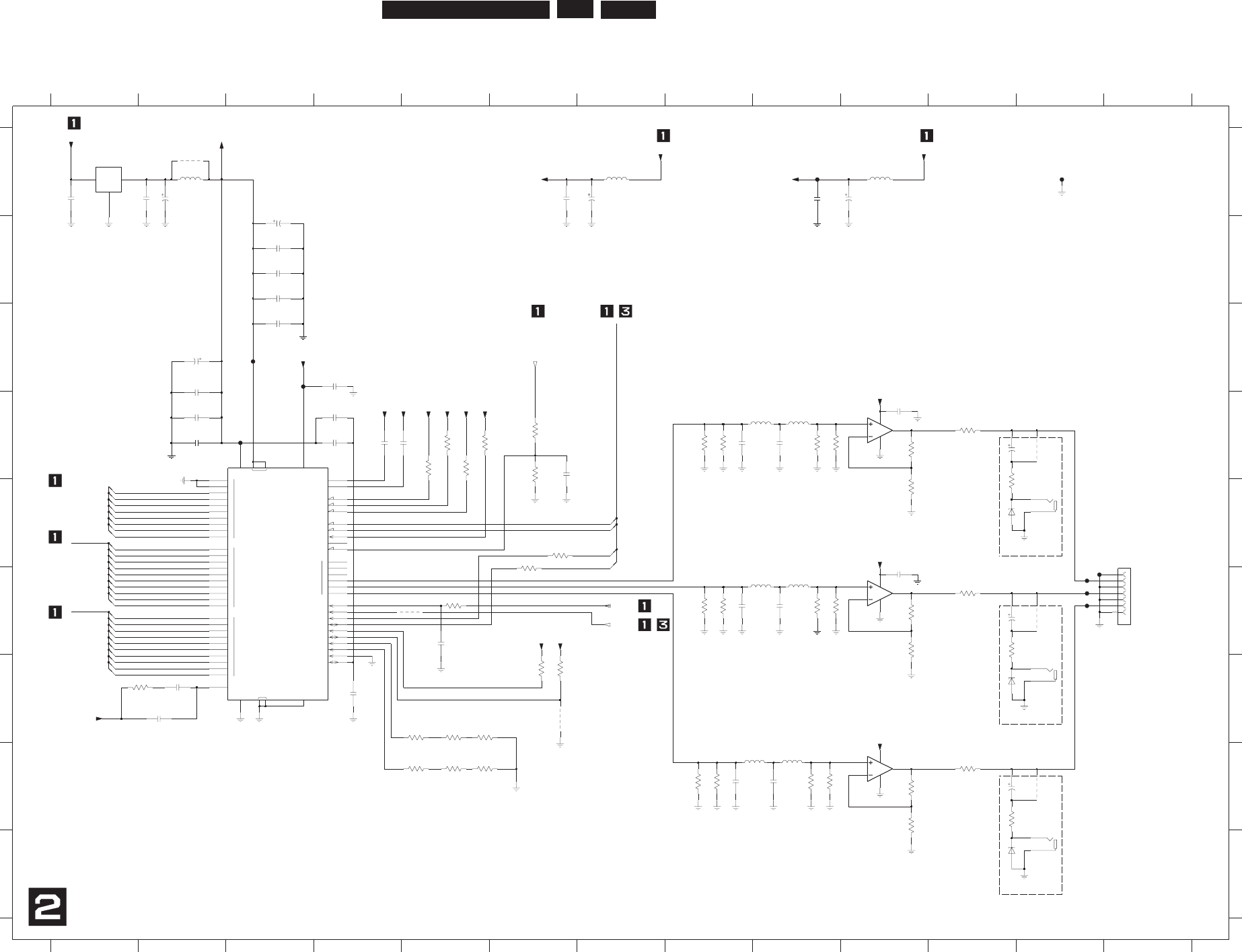
EN 157
3139 785 31532 7.Circuit Diagrams and PWB Layouts
HDMI: Prog Scan DAC
COM
OUTIN
RSET1
ALSB
I2C
SDA
6
7
EXT_LF
VAA
SCLK
CLKIN_B
8
9
8
9
8
9
7
0
1
S
C
Y
S_VSYNC
S_HSYNC
COMP2
COMP1
AGND
0
2
1
RSET2
RTC_SCR_TR
VDD VDD_IO
DAC
GND_IO
DGND
6
VREF
3
4
5
2
3
4
5
6
7
0
1
2
3
4
5
CLKIN_A
F
E
D
C
B
A
RESET
P_BLANK
P_VSYNC
P_HSYNC
S_BLANK
A
B
C
D
E
F
G
H
I
1920 E13
1921-1 E12
1921-2 G12
2345678
1921-3 H12
2250 A6
2251 A7
2252 G4
2253 A9
2254 A10
2255 A2
2256 C3
2258 A1
2259 A2
2260 B3
2261 B3
2262 B3
2263 B3
2266 C2
2267 C4
2268 C2
12345678910111213
1
d
esu ton
2285 D9
2286 D10
2290 F8
910111213
A
B
C
D
E
F
G
H
I
not used
PB
PR
Not used
2269 D2
2270 D4
2271 D4
2272 D4
2273 D2
2274 D4
2275 D6
2276 D11
2277 F11
2278 H11
2280 G2
2281 G2
2282 F5
2284 D8
GND
Y
3269 F8
2291 F9
2292 F10
2296 H8
2297 H9
3255 D8
3256 F8
3257 H8
3258 D8
3259 D6
3260 D5
3261 D5
3262 D6
3263 D5
3264 D5
DRAOB GOLANA
d
es
u
ton
Not used
3284 H5
3285 H5
3286 H5
3287 H9
3288 H11
3265 D9
3266 D11
3267 D10
3268 E10
GND
GND
3270 F9
3271 D9
3272 F11
3273 F10
3274 E6
3275 G2
3276 G6
3277 G6
3278 E6
3279 F10
3280 H8
3281 G5
3282 G5
3283 G5
Not used
d
esu ton
GND
7252-2 H10
7253 D3
F2001 F12
F2002 F12
F2004 F12
F2006 F12
F201 C3
3289 H10
3290 H10
3291 E11
3292 F11
3293 H11
3294 F9
3295 H9
4250 G6
4251 A2
4252 F5
4253 F5
4254 D12
4255 F12
4256 H12
5250 A7
5251 A10
5253 A2
5254 D9
5255 D9
5256 F9
5257 F9
5258 H9
5259 H9
6251 E11
6252 G11
6253 I11
7250 A1
7251 D10
7252-1 F10
4822
p22
F202 C3
F203 D3
F204 A9
F205 A12
d
es
u toN desu
toN d
esu toN
3n9
2280
2292
100n
7
9
22
p
22
2u2
5259
F203
n0
01
2522
F205
8722
V4u022
2K1
1723
762
3
2K
1
n001
8522
F204
F2001
3272
75R 1%
1%2K7
3284
1%75R
3266
1
6
23
K
01
K01
0623
272
2
n001
10R
3282
192
2
2K1
7
52
3
p22
58
2
2
p22
49
23
2K1
3278
10R
6723
7
K4
n
0
0
1
3522
65
2
3
2K1
4u7
5258
100n
7V4C-483XZB
1526
2274
69
22
p
2
2
2268
1n0
V
537u4
9522
4252
1%
10R
%1
3283
330R
3923
R57
5722
5257
2u2
0n1
100n
2261
K
01
4623
102F
5
623
2
K
1
77
23
7K4
4524
K
0
1
3623
6
7
1920
1
2
3
4
5
PSCAN
07FMN-BMT-A-TFT
2281
1n0
2270
6722
V4u022
820p
7722
V4u022
1%75R
3288
%1R57
2923
2
13
7250
LF25CDT
4u7
5254
5523
2K1
2u2
5255
V61u74
1522
p2
2
09
22
3274
10R
100n
2286
202F
2273
100n
6524
F2006
5524
F2004
52
F2002
7251
AD8091ART
3
4
1
37
23
2
K1
R22
9523
BLM21
5250
2K1
8523
0522
n0
0
1
0524
7V4C-483XZB 1923
%1R57
2526
7V4C-483XZB
3526
5256
4u7
282
2
p5
1
3285
10R
7
84
2
K1
0
823
AD8092AR
7252-2
5
6
n001
55
2
2
10n
2267
100n
4253
2269
78
23
2
K
1
2K
1
9623
7u4
45
2
2
16V47u
2266
1722
n001
3275
680R
2
K
1
0923
330R
3286
8623
1%
2K
1
2256
10n
2263
100n
4251
100n
2262
2
K1
0
723
9
723
2K1
1%
5253
3281
2K7
2
6
23
K74
7252-1
AD8092AR
3
2
1
84
2260
4V220u
9
12
13
9
823
2
K1
65
1
46
2
3
4
5
6
7
8
59
60
61
62
22
21
48
50
49
14
01
33
47
35
31
51
52
53
54
55
58
38
37
11
75
34
46
19
25
23
24
29
30 32
63
45
36
44
43
42
39
04
20
14
15
16
17
18
26
27
28
VIDEO
Φ
ADV7320KSTZ
7253
ENCODER
4u7
5251
2K
1
59
2
3
YKC21-3930
YELLOW
1921-1
2
1
YKC21-3930
RED
1921-3
6
5
YKC21-3930
WHITE
1921-2
4
3
VO_CLK
+5V_PS
+5V_PS
ITU_OUT(5)
ITU_OUT(6)
ITU_OUT(7)
P_CLK
+5V_PS
+2V5
+3V3D_VDAC +5V_PS
+2V5 +2V5+2V5
+3V3
ITU_OUT(0:7)
ITU_OUT(0)
ITU_OUT(1)
ITU_OUT(2)
ITU_OUT(3)
ITU_OUT(4)
+5V
CbCr(3)
CbCr(5)
CbCr(7)
CbCr(9)
CbCr(11)
+3V3D_VDAC
P_HSYNC
P_VSYNC
CbCr(2:11)
Y(2:11)
nT
S
R_NACSP
+3V3D_VDAC
+3V3D_VDAC
+2V5+2V5
Y(6)
Y(2)
Y(4)
Y(8)
Y(10)
CbCr(2)
CbCr(4)
CbCr(6)
CbCr(8)
CbCr(10)
Y(3)
Y(5)
Y(7)
Y(9)
Y(11)
+3V3
SDA0
SCL0
+2V5
+2V5
3139_243_32736_a2_sh130_sh2.pdf 2006-02-17
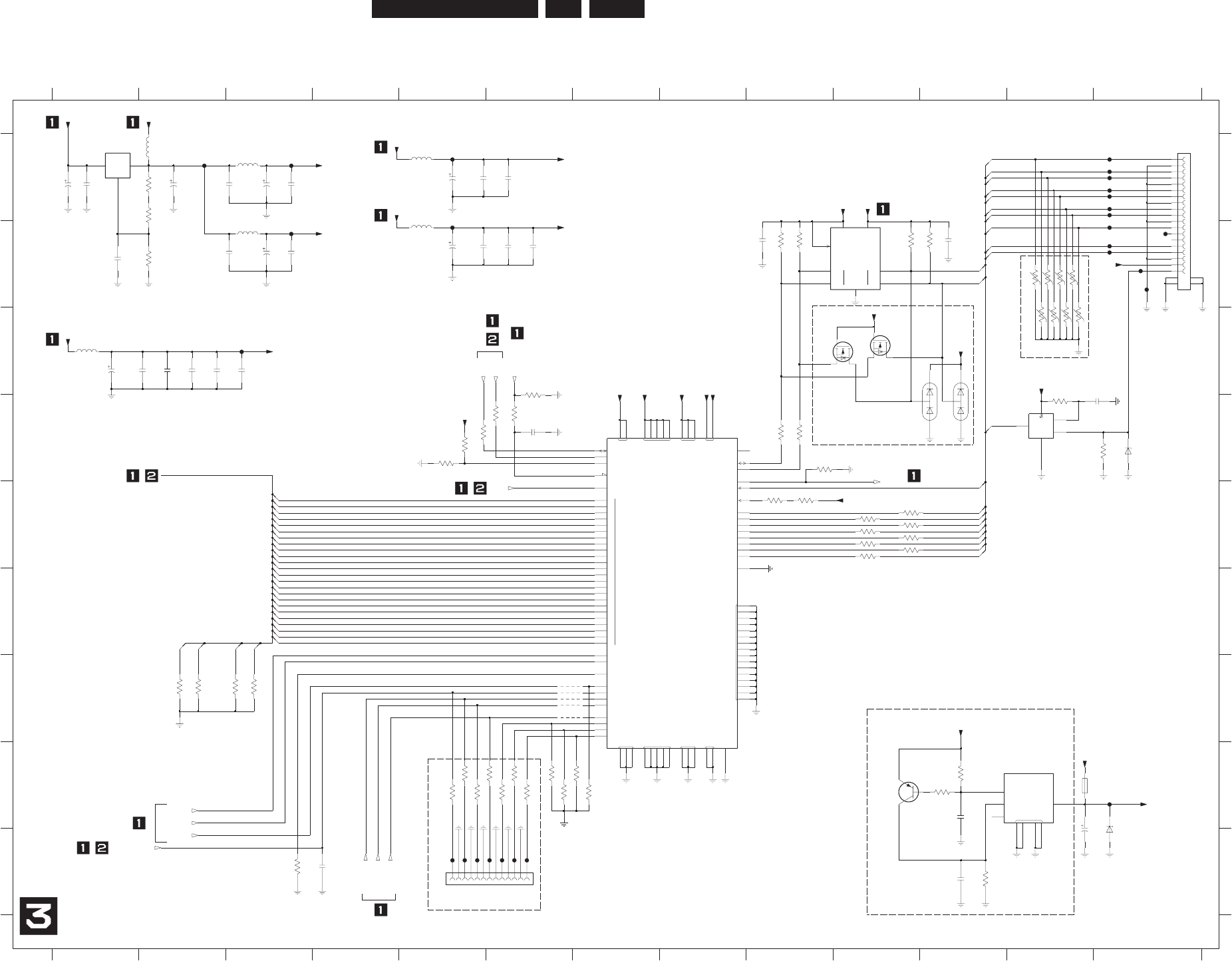
EN 158
3139 785 31532 7.
Circuit Diagrams and PWB Layouts
HDMI: HDMI Tx
V
V
V
V
V
IN OUT
ADJ
NC
VOUTINHIBIT
GND
VIN
VCC
GND
VCC2
ACC
SCL
SDA
SCL
SDA
OUT IN
SH
_
DNG
14
15
16
17
18
19
20
21
22
23
HSYNC
VSYNC
DE
SPDIF
MCLK
CVCC18 IOVCC PVCC
AGND CGND IOGND PGND
D
AVCC
8
7
12
13
CSDA
CSCL
CI2CA
RESET
IDCK
0
1
2
3
4
5
6
NC
DSDA
DSCL
INT
HPD
EXT_SWING
TXC+
TXC-
TX0+
TX0-
TX1+
TX1-
TX2+
TX2-
RSVDL
VIA
SCK
WS
SD0
SD1
SD2
SD3
11
10
9
V
V
V
not used
BLM18A
I
1300 H12
1930 A13
1931 I5
2300 A1
2301 A2
2302 A3
2303 A3
2306 B5
2307 B5
2308 B6
2309 B6
2310 B3
2311 B3
2312 B3
2314 A5
2315 A5
2316 A6
2317 D13
2318 C1
2319 C1
2320 C2
2321 C2
2322 C2
2323 C3
123456
de
su
ton
2304 A3
789101112 13
12345678
d
esu ton
9101112
A
B
C
D
E
F
G
H
I
A
B
C
D
E
F
G
H
2324 D6
2325 I4
2326 H11
2327 I11
2328 I12
2330 B1
2333 B11
2334 B9
3300 E10
3301 E10
3302 E10
3303 E10
3304 E10
3305 A2
3306 E10
3307 E10
3308 E10
3309 A2
3310 B2
3313 C6
3314 B9
3315 D6
not used
3316 B9
3317 D5
3318 D6
3319 B10
3320 B11
3322 D13
13
3324 D9
3325 E9
3326 E9
3328 G2
3329 G2
3332 G3
3333 G3
3339 H6
3340 H6
3341 H6
3342 H7
3343 I3
3344 H5
3345 H5
3346 H6
3347 H5
3348 H5
3349 H6
3350 H6
3351 H11
3352 H11
3353 I11
3354 D9
3355 D5
3356 D5
2329 A1
3361 B12
3362 B12
3363 B12
3364 B12
3365 B12
3366 B12
3367 B12
3368 B12
4300 G6
4301 G6
4302 G6
4303 G6
4304 G6
5300 A3
5301 B5
5302 B3
5303 A5
not used
5304 C1
5305 A2
6301 D13
6304 I13
6305 D10
6306 D11
3323 D9
BLM18A
7300 A1
7301 D11
7302 C9
7303 C10
7304 F8
7305 H11
7306 H10
7307 A9
F301 A2
F302 A3
F303 B5
F304 B3
F305 A5
F306 C3
F307 H13
F308 B13
F3101 I6
3357 D12
F3103 I6
F3105 I6
F3107 I6
F3109 I5
F311 A13
F3111 I5
F3113 I5
F312 A13
F313 A13
F314 A13
F315 A13
F316 A13
F317 A13
F318 B13
F319 B13
F320 B13
F321 B13
F322 B13
not used
9232
n001
10R3308
BLM21
5303
3303 10R
5133
0R1
8633
5
036
W99VAB6036
W9
9
V
A
B
6
133
K
01
1n0
2324
9033
%1R021
90
13
F
F311
4304
F304
Am002
0031
3301 10R
4633
1
013F
2633
F302
K01
4133
K74
2233
2132
n001
10R3302
4032
n001
7R4
1533
1113F
6032
V61u74
1K0
3352
7433
R22
7032
n001
F301
5
1
3
2
n
001
33
33
K0
1
8032
n001
1032
47K
3313
V6
1
u
7
4
10R3306
6433
3633
R22
12MLB
5035
n001
0232
31
13F
943
3
R2
2
5302
6232
n001
7633
n001
2232
K
01
3
4
3
3
1
2
32
n001
u
01
1132
V61
3233
0R1
3032
u0
1
K0
1
93
33
V
61
413
2
V61u74
7303
BSN20
K
01
0
433
F307
0u1
n001
91
3
2
7232
10R3300
K01
3533
F305
8V6C-483XZB
1036
5301
BLM21
701
3F
5304
BLM21
R093
0133
05
33
R22
%1
V05
8232
2u2
3357
F306
4K7
R
2
2
4
4
33
1
2
53
4
74LVC1G08GW
7301
7K4
0233
1%
3326
470R
5
4
8
1
Φ
23 6 7
3325
4R7
7305
LE50ABD
2
7300
LM317MDT
1
3
5013F
7302
BSN20
301
3F
3354
47K
K0
1
82
33
143
3
K
01
100n
2317
90
2
11
F320
94
95
96
97
83
84
85
86
87
88
89
29
33
32
36
35
27
26
82
91
92
93
83
42
21
12
10
9
8
7
5
30
41
74
27
31
84
17
6
40
22
93
32
80
20
19
24
18
18
1
66
17
52
51
50
49
76
75
70
69
68
67
65
64
63
62
61
58
57
56
55
54
53
77
41
43
44
4
6154
95
47
79
78
5
2
13
73
82
43
3
5
1
64
06
37
Φ
HDMI
TRANSMITTER
7304
SII9030CTU
F318
0R
1
4233
F317
%1R021
5033
F308
u74
0032
5300
n001
90
3
2
V61
F303
4302
7
1
33
0R1
32
67
8
1
F321
Φ
PCA9512DP
7307
5
4
3232
n001
4K7
3356
n001
2
0
32
913
3
7K4
3304 10R
n001
01
3
2
23
F322
3
4
5
6
7
8
9
20 21
22
10
11
12
13
14
15
16
17
18
19
2
DC1R019JDA
1930
1
11
2
1
31
2
3
4
5
6
7
8
9
13
91
13FMN-BMT-A-TFT
1
01
1633
BC857BW
7306
R22
5433
843
3
R22
5
232
p
01
2433
R0
93
6633
K
01
8V6C-483XZB
4036
9
23
3
0
u
1
0332
K01
5633
2333
7K4
5533
F316
F315
F314
F312
F313
10R
613
2
n001
3307
4303
V61u74
8
1
3
2
4301
4300
8133
R22
n001
3332
4
3
3
2
n
0
01
F319
TX0+_1
TX0-_1
TXC+_1
TXC+_1
TX_DDC_SCL
TXC-_1
TX2-_1
TX_DDC_SCL
TX_DDC_SDA
+5V
+5V_HDMI
+5V
TX2+_1
TX2+_1
TXC-_1
TX0+_1
TX0-_1
TX1+_1
TX1-_1
TX2-_1
TX1+_1
TX1-_1
)1(Y
)
0(
Y
+5V
+12V
+3V3
+3V3_HDMI_T
+5V
SPDIF_OUT
+3V3_PLL2_T
)
1
(rC
b
C
)0(rC
b
C
FSCLK12_OUT
TUO_
2
1KCS
T
U
O
_2
1
S
W
TUO_
D
S
+3V3_HDMI_T
CbCr(5)
CbCr(7)
CbCr(11)
CbCr(10)
CbCr(9)
CbCr(8)
CbCr(6)
CbCr(4)
+3V3A_HDMI_T
T_IMDH_A3V3+
T_
IM
D
H
_
3V3+
+3V3_HDMI_T
+1V8_HDMI_T
+3V3_HDMI_T
+3V3
+3V3
+1V8
nT
S
R_
I
MD
H
T_1
L
LP_
3
V3+
T_
2LLP
_
3
V
3
+
P_VSYNC
0LCS
0ADS
T_IMDH_3V3+
T
_
I
MD
H
_8
V
1
+
Y(0)
Y(1)
Y(6)
Y(7)
Y(8)
Y(9)
Y(10)
Y(11)
Y(2)
Y(3)
CbCr(0)
CbCr(1)
CbCr(2)
CbCr(3)
Y(4)
Y(5)
HPD
P_HSYNC
P_CLK
INT_HDMI
+3V3_PLL1_T
+3V3_HDMI_T
+5V_HDMI
TX_DDC_SDA
HPD
3139_243_32736_a2_sh130_sh3.pdf 2006-02-17
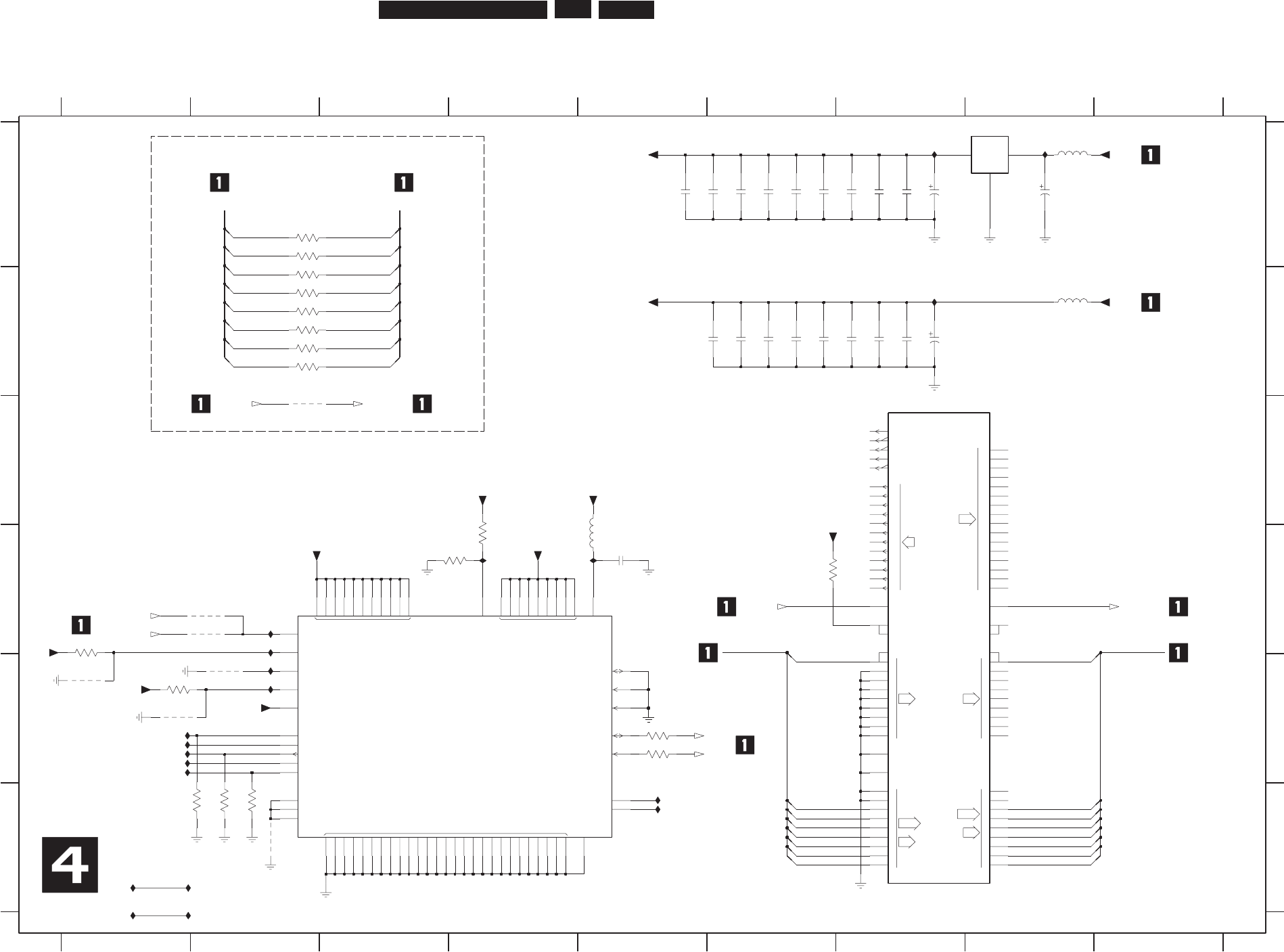
EN 159
3139 785 31532 7.Circuit Diagrams and PWB Layouts
HDMI: Columbus
CLKASA
8
0
1
2
3
4
5
6
7
2
5
3
DQM
WE
6
0
1
2
3
4
5
7
2
1
0
3
4
5
15
6
5
4
8
7
14
5
6
8
11
10
WEA
6
VA
7
YA
0
1
2
4
38
7
11
12
13
HREF
9
8
CLKASB
7
16
8
WEB
3
2
1
0
6
10
9
4
1
A
DAVA
DI9
UVA
DI
UVB
DO
DO9
YB
DAVB
DQ
RAS
CAS
CLK
COM
OUT IN
BISTEN VDDC
VSS
VDDS
A0IIC
RESET
CLKSEL
CLKEXT
656SEL
TRST
TCK
TDO
TMS
TDI
TST3
TST1
TST2
SNRST
SNDA
SCL
AVD
SNCL
SDA
NC1
NC2
AVS F415 F5
4401-1 B2
F410 E1
F411 E1
F412 E1
F413 E1
F414 F5
2409 A8
2411 B7
F407 E2
F408 E2
F409 E1
Not used for DVDR9000H
Jumper
2407 A5
1
4401-2 B2
4401-3 B2
4401-4 B2
4408 C2
4409 D2
4410 D2
4411 E1
4412 E1
4413 E2
4414 F2
5400 A8
5401 B8
5402 D5
7400-1 C7
7400-2 D2
7401 A8
F400 A8
F401 A7
F402 B7
F403 D4
F404 D5
F405 D2
F406 D2
not used
desu ton
not used
2408 A5
2410 A7
2412 B7
2413 B7
2414 B7
2415 B6
2416 B6
2417 B6
2418 B6
2419 B5
2420 D5
3400 D6
3401 D4
3402 D4
3403 D1
3404 E1
3405 E5
3406 E5
3607 F2
3608 F2
3609 F2
4400-1 A2
4400-2 A2
4400-3 B2
4400-4 B2
2403 A6
2404 A6
2405 A6
2406 A6
2401 A7
Not used for DVDR7300H
2402 A7
23456789
123456789
A
B
C
D
E
F
not used
desu
t
on
d
es
u
to
n
A
B
C
D
E
F
2400 A7
3V3_COLUM 3404
4K7
F410
F409
7142
n0
01
n00
1
6142
5142
n001
n
001
414
2
F401
n001
8142
3V3_COLUM 1V5_COLUM
1043
7K4
3402
4K7
7K4
0043
3V3_COLUM
B1
4400-1
A11
B12
A12
G2
F2
E2
E1
D2
D1
C2
C1
A13
B13 A1
J15
B7
B9
A9
B10
A10
B11
B6
A6
M2
M1
L2
L1
K2
K1
J2
J1
H2
L14
A14
K15
A2
B3
A3
B4
A4
B5
A5
M14
M15
L15
R12
P11
P10
R10
P9
P8
R8
R13
P4
K14
J14
H1 G1
P12
R14
R15
P15
N15
R6
R7
P7
P5
R5
R1
R2
R3
P3
R4
ΙΟ
T6TU5XBG
7400-1
P6
1142
+3V3
V61u01
9042
V6
1u
01
F484
3405
100R
3406
100R
4401-4
F411
F412
3V3_COLUM
P81MLB
2045
9142
n001
F415
F402
F414
F400
BLM18P
5400
2420
100n
1V5_COLUM
K0
1
70
6
3
K0
1
906
3
806
3
K01
4412
n001
3V3_COLUM
3142
n
001
5042
n0
01
21
42
4042
n001
3042
n001
01
4
2
2042
n001
3V3_COLUM
V61u01
4410
404F
4408
F483
F406
F407
MU
LOC
_
3
V
3
F405
304F
n001
1042
0
0
42
n
0
01
LF15ABDT
7401
2
13
5401
BLM18P +3V3
F408
4413
804
2
n001
4401-1
4400-4
4401-3
4401-2
F481
1V5_COLUM
4409
41
P
9R
11
R
3
C
5C
6C
9
C
01
C
31C
3
1D
3L
31M
4N
5
N
41B
7N
01N
21
N
31
N
2P
31L
3M
3N
8N
11
N
2B
3
E
3F
31F
3J
3
1
J
31K
31
H
3
K
6
N
9
N
4C
41
N
31
P
21
C
3G
31G
E14
F14
A8
F1
H3
7C
8
C
11C
3D
31E
D4
N2
G15
B15
A15
D14
C14
C15
D15
F15
E15
A7
G14
1
N
1
P
8B
H14
H15
F482
CTRL
T6TU5XBG
7400-2
F413
n001
7042
6042
n001
4400-3
4400-2
4411
4K7
3403
4144
VO_CLK
ITU_OUT_2(7)
ITU_OUT_2(6)
ITU_OUT_2(5)
ITU_OUT_2(4)
ITU_OUT_2(3)
ITU_OUT_2(2)
ITU_OUT_2(1)
ITU_OUT_2(0)
ITU_OUT_2(0:7)
ITU_OUT(7)
ITU_OUT(6)
ITU_OUT(5)
ITU_OUT(4)
ITU_OUT(3)
ITU_OUT(2)
ITU_OUT(1)
ITU_OUT(0)
ITU_OUT(0:7)
VO_CLK_2
ITU_OUT_2(3)
ITU_OUT(4) ITU_OUT_2(4)
ITU_OUT(5) ITU_OUT_2(5)
ITU_OUT(6) ITU_OUT_2(6)
ITU_OUT(7) ITU_OUT_2(7)
VO_CLK VO_CLK_2
ITU_OUT(0:7) ITU_OUT_2(0:7)
PSCAN_RSTn
HDMI_RSTn
ITU_OUT(0) ITU_OUT_2(0)
ITU_OUT(1) ITU_OUT_2(1)
ITU_OUT(2) ITU_OUT_2(2)
ITU_OUT(3)
SCL0
SDA0
3139_243_32736_a2_sh130_sh4.pdf 2006-02-17
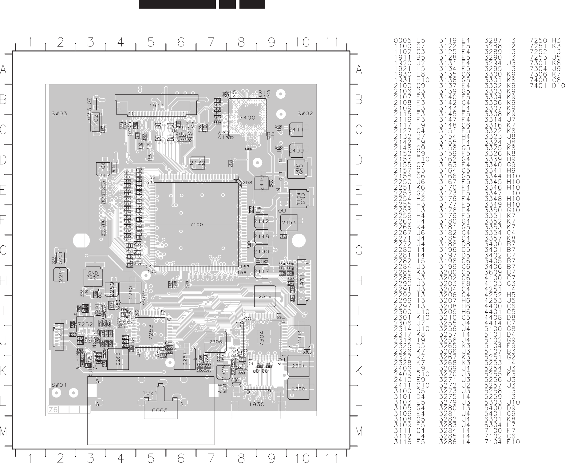
EN 160
3139 785 31532 7.
Circuit Diagrams and PWB Layouts
Layout: HDMI Top View
3103-603-30587-topview.pdf 2006-09-04
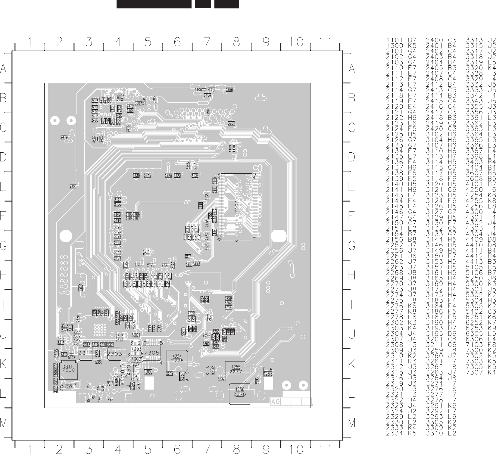
EN 161
3139 785 31532
Layout: HDMI Bottom View
7.Circuit Diagrams and PWB Layouts
3103-603-30587-btmview.pdf 2006-09-04

EN 162
3139 785 31532 7.
Circuit Diagrams and PWB Layouts
Notes:

EN 1633139 785 31532 8.
Alignments & Test Procedures
8. Alignments & Test Procedures
8.1. Reprogramming Procedure of NVM on the
Digital Board
The NVM, item 7809 on the Digital board contains the
following:
• Slash information (or slash version)
• IEEE Unique number
The slash version and IEEE Unique number are stored at the
end of the production line of the set.
In case of failure the NVM is replaced by an empty device.
After replacement of the NVM the set can only startup in
Diagnostic software mode because the Slash version is not in
placed.
By way of commands via the Diagnostic Software (DS) and
hyperterminal connection to the PC, these factory settings
must be restored in the NVM.
8.1.1. Slash Version
The slash version is stored with DS command 1217 followed
by the slash version as parameter.
The slash versions used in DVDR5350H and DVDR7300H
families are as follows:
• DVDR5350H/02: 11201
• DVDR5350H/05: 11205
• DVDR5350H/19: 11201
• DVDR7300H/02: 11207
• DVDR7300H/05: 11208
• DVDR7300H/19: 11207
• DVDR73x0H/75: 11207
• DVDR73x0H/97: 11207
Example:
DS:> 1217 11201
With DS command 1218 the slash version can be displayed
8.1.2. IEEE Unique Number
1. Note the serial number of the set example:
VN050136130156
- VN = production center (VN….Szekesfehervar).
According to UAW-500: V=22 and N=14
- 05 = change code (this is not used for this
calculation)
- 01 = YEAR
- 36 = Production WEEK
- 130156 = Lot and SERIAL number
2. Calculate the unique number: this number always exists
out of 10 hexadecimal numbers
3. First 5 numbers: First we calculate a decimal number
according to formula below:
- 35828*YEAR + 676*WEEK + 26*A + H + 8788
- The fi gures are fi xed, YEAR + WEEK + production
center code (A + H) are variables
- Example: 35828*01 + 676*36 + 26*1 + 8 + 8788 =
68986 (decimal)
- Then we translate this decimal number to a
hexadecimal number.
- Example: 68986 = 10D7A (hex)
4. Last 5 numbers: The last 5 numbers exist out of the Lot
and SERIAL number.
We have to translate the decimal number to the next 5
hexadecimal numbers:
Example: 130156 (decimal) = 1FC6C (hex)
5. This IEEE Unique number (10-digit hexadecimal number)
is stored with DS command 1207.
Example:
DS:>1207 10D7A1FC6C
120700: Test OK@
The set has now its original IEEE unique number.
With DS command 1208 the slash version can be displayed.
8.2. Reprogramming Procedure of NVM on the
Digital Board
The Boot Eeprom, item 7810 on the Digital board contains the
“Diversity String” that tells the software during startup which
hardware version is present. This setting is stored during the
production of the Digital board.
In case of failure the Eeprom must be replaced by a
programmed device containing the boot script.
Via the Dignostic Software the “Diversity String” is stored
with the command 1226, followed by the “Diversity String” as
parameter.
The Diversity strings used in DVDR5350H and DVDR7300H
are as follows:
DVDR5350H:
444248497E0440014630355F3500000056040300000101020
00101004008080044564452323030312E3030310102020808
070000000002010000000000000000
DVDR73x0H:
444248499BFB40014630355F330000005504030000010102
000101004008080044564452323030312E303031010202080
8000000010002010000000000000000
Example:
DS:> 1226
444248499BFB40014630355F330000005504030000010102
000101004008080044564452323030312E303031010202080
8000000010002010000000000000000
Test OK @
With DS command 1229 the settings can be displayed.
8.3. Laser Control Adjustment
In case of exchanging DVD-M or Frontend Board (PCBA
of the Basic Engine) an adjustment to align the OPU and
Frontend Board to each other is necessary.
8.3.1. Adjustment procedure
This adjustment is done with the DSW software nucleus 931.
The adjustments takes about 30 seconds and the data is
stored in the OPU Eeprom.
Example:
DS:> 931
93100
Test OK @
8.4. Procedure for formatting a new HDD:
In case of failure the HDD is replaced by a new unformatted
HDD.
To prepare the new HDD for use it must be formatted with a
Master DVD via the Diagnostic software nucleus 2107.
Example:
DS:> 2107
Please insert the Master DVD <OK>
Executing transfer table 1 of 4……..
Please wait… <OK>
210700: Transfer OK
Test OK @
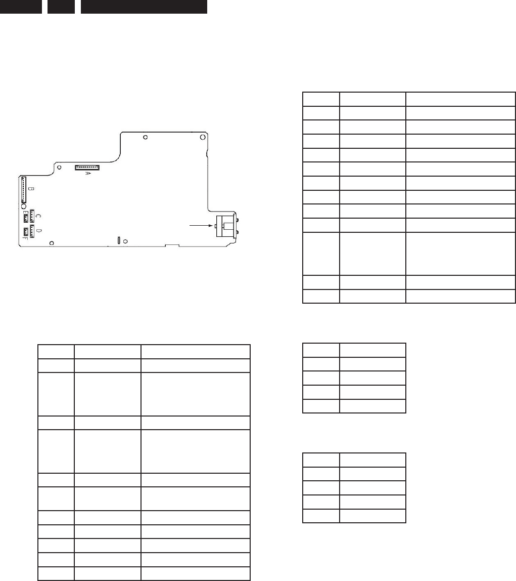
EN 164 3139 785 315329. Circuit- and IC Description
9.1. PSU Board
9.1.1. General
MAINS CONNECTOR
Figure 9-1 PSU Board Layout
The PSU board provides the following connection to the rest
of the set:
• Connector A: Supply/Signal to Analog Board
Pin no. Supply / Signal Remarks
1 12VSTBY
2 STBY control >2.5V = supply for conn. B
is off (Standby mode)
<0.5V = supply for conn. B
is on (On mode)
3 5VSTBY
4 DD_ON >2.5V = supply for conn. D
is on
<0.5V = supply for conn. D
is off
5 3V3STBY
6 IPFAIL >4.0V = power is good
<0.5V = power fail
7 5NSTBY
8GND
9 33VSTBY
10 GND
11 VGNSTBY
9. Circuit- and IC description
• Connector B: Supply to Digital Board
Pin no. Supply / Signal Remarks
13V3D
23V3D
33V3D
43V3D
5 GND
612VD
7 GND
8 GND
95VD
10 HD_ON >2.5V = supply for conn. C
& G is on
<0.5V = supply for conn. C
is off
11 GND
12 5ND
• Connector C: Supply to HDD
Pin no. Supply
112VH
2 GND
3 GND
45VH
• Connector D: Supply to Basic Engine
Pin no. Supply
112VE
2 GND
3 GND
45VE
• Connector E: Not in use
F: Not in use
The PSU is designed with short-circuit protection that will
shutdown the power supply. When this happen, the voltage
stored in capacitor C1 and C40 will prevent the Power Supply
to turn-on, therefore they must be discharged before the PSU
can function normally again.

EN 1653139 785 31532 9.
Circuit- and IC description
9.2. Front Board (Panel – Display + Key)
9.2.1. General
This board consists of the following parts:
• μP driver for the FTD
• Frontend (Audio & Video)
• VFD Heater voltage Generator
9.2.2. μP (IC 7103 : TMP86CM74AFG)
The core element of the Front (Display + Key) board is the
μP [7103].
It runs on a 5V supply & a clock frequency of 16MHz, and is
responsible for the following functions:
• Interface with the Slave μP on the Analog board via I2C
bus
• Driver for the FTD display [1203 : HUV-08SS65T]
9.2.3. VFD Heater Voltage Generator
Pin 12 of μP [7103] provides the necessary sine wave signal
out for transistor [7106, 7108 & 7109] to generate the 50%
duty-cycle 48KHz AC square-wave signal for the fi lament of
the FTD.
9.3. Analog Board
9.3.1. General
The Analog board consists of the following parts:
• Slave μP
• Fan Control
• Simple Power Supply
• Tuner Frontend
• Audio ADC/DAC
9.3.2. Slave μP (IC 7108 : TMP87CH74F)
The slave μP which run on a 5V supply and is responsible for
the following functions:
• Interface with the Chrysalis chip on the Digital Board via
I
2C interface, where it functions in the slave-mode
• Evaluation of the keyboard matrix (network of resistors)
on the Front board via pin 32 and 33.
• Decoding the remote control commands from the infra-red
receiver on the Front board via pin 22.
• Activation and control of the FTD display on the Front
board (with the help of 7103 as driver) via I2C bus
• Timer Wake-up activation
• Fan control via transistors 7104 and 7105
It runs on two clock frequencies namely:
• 8MHz for normal operation
• 32.768KHz for the real time clock
9.3.3. Timer Wake-up activation
During the Standby mode, the slave μP provides a wakeup
call (STBY-line switches to high) to the PSU Board switching
on the Digital Board.
9.3.4. Simple Power Supply
The main power supply for this set is generated in the PSU
board. Within the Analog board only the 5V, 3V3SW and
8VSTBY lines are generated.
Below are the supply lines from the Simple Power supply on
the Analog board:
• 3V3SW to DAC_ADC and CU
• 3V3STBY to CU
• 5V to IOV, CU, PROG, MSP, DIGIO and FV
• 5NSTBY to IOA, PROG, DAC_ADC and Front board
• 5VSTBY to IOA, IOV, FV, CU, DAC_ADC and Front
Board
• 8VSTBY to MSP
• 12VSTBY to CU, IOV, DAC_ADC and Front Board
• 33VSTBY to FV
• VGNSTBY to CU and Front Board
Standby modes:
In Standby mode the STBY control line is low, switching off
the 3V3D, 5VD, 5ND and 12VE supply and thus reducing the
power consumption.
9.3.5. Tuner Frontend [1700 : TMQZ2-439A]
It has a RF IN for antenna connection and RF OUT which
provides a RF loop through for connection to the TV.
The Frontend ( Tuner & IF-demodulator ) is controlled by
I
2C (SCL_5V- and SDA_5V-) lines coming from the
Slave μP [7108].
Complete video processing is done in this unit and the video
output (CVBS) is taken out from the [VIDOUT] pin 17 via
a transistor [7100] as VFV-line to the Video I/O circuitry. The
audio-IF component SIF1 is taken out from the [SIFOUT]
pin 7 for the demodulation by the Multi-sound processor
(MSP).
Audio demodulator
The sound demodulation is done by the MSP3415 [7600],
which is also fully controlled via I2C bus by the Slave μP. The
audio signals are available at pin 26 and pin 27 and fed as
AFER- & AFEL- line to the audio I/O for further processing.
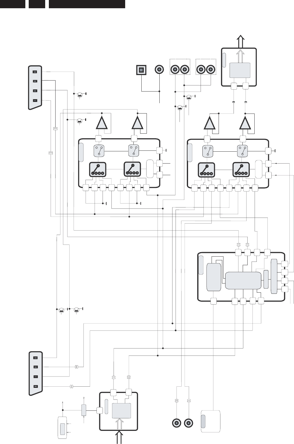
EN 166 3139 785 315329. Circuit- and IC Description
9.3.6. Audio routing
Figure 9-2 Analog Audio In / Out Overview
Audio IO Europe Overview
Scart2
6321
AudInL
AudInR
AudOutL
AudOutR
6321
AudInL
AudInR
AudOutL
AudOutR
Scart1
Tuner
SIF1
AOUT2L
AOUT2R
AKILL
AKILL
AKILL
AKILL
AOUT1L
AOUT1R
AOUT1R
AOUT1L
AFER
AINFR
AINFL
AINFR
AINFL
RSA1
RSA2
AIN2R
AIN2L
AIN1R
AIN1L
ARDAC
AFER
AFEL
AFEL
AIN2L
AIN2R
SIF1
SDA_5V
SCL_5V
ASC1
from CU
ARDAC
ALDAC
AUDIO OUT 1
AUDIO OUT 2
BKILL
BKILL
ALDAC
Dig.Audio Out
from digital board
AL
AR
AL
AR
1
UDA1361TS
ADC
A_DATA
to dig. board
3
ALADC
ARADC
ARDAC
ALDAC
LH
Logic
1
3
5
1
109
LL
HL
MSB LSB
HEF4052B
4
5
15
L
H
L
H
HH
LH
LL
HL
HH
3
1
11
14
12
13
2
6
MSB/LSB
POS.7501
MSP3415G
2
I2C Control
89
12 13
26
27
31
30
37
38
41
40
Q.Peak Det
Source select
Demodulator
DACM_L
DACM_R
SC1_OUT_L
SC1_OUT_R
POS.7600
0dB
0dB
LH
Logic
1
3
5
1
109
LL
HL
MSB LSB
HEF4052B
2
4
12
L
H
L
H
HH
LH
LL
HL
HH
3
5
15
11
14
13
1
6
MSB/LSB
POS.7504
IMUTE
from CU
0dB
0dB
AIN1L
AIN1R
AOUT2R
AOUT2L
ARDAC
ALDAC
DVDR5350H/DVDR7300H Audio IO Eur.eps
POS.7007
from CU
OR
MUTE
IMUTE IPFAIL
AKILL
DKILL BKILL
MUTE
Dig.Optical Out
DAOUT
12
23
AD1852JRS
DAC
17
D_DATA
from dig. board
POS.7004

EN 1673139 785 31532 9.
Circuit- and IC description
The sound processing is always done in stereo (that means
separate left- and right- channel) and the complete switching
is realized by using HEF4052B which is a dual four-to-one
multiplexer and MSP3415G which is a multi-sound processor.
a) Scart 1 – Output path
The multiplexer [7501] selects either signals from the Scart
2 Input (AIN2L/AIN2R) or the Audio DAC (ALDAC/ARDAC) as
the output source for Scart 1 (AOUT1L/AOUT1R).
b) Scart 2 – Output path
The MSP [7600] selects either signals from the Scart 1
Input (AIN1L/AIN1R), the Audio DAC (ALDAC/ARDAC) or the
Tuner Frontend as the output source for Scart 2 (AOUT2L/
AOUT2R).
c) Digital audio-out path
In addition, a digital output (DAOUT) coming from the
Digital board is passed through a 6-fold inverter [7700] for
performance reasons (noise reduction, jitter, …) as digital
Audio / Optical outputs at the rear.
d) Record path
The record-selector [7501] selects either signals from the
Scart 1 Input (AIN1L/AIN1R), Scart 2 Input (AIN2L/AIN2R),
Front Cinch (AINFL/AINFR) or the MSP (AFEL/AFER) and
routes to the audio ADC (ALADC/ARADC) for record
purposes. The switch is controlled via RSA1 and RSA2
signals coming from the MSP.
9.3.7. Audio ADC/DAC
The conversion of analog audio signals from the record-
selector [7501] outputs (ALADC/ARADC) is done via
UDA1361TS [7007]. This IC can process input signals up to
2Vrms by using external resistors in series to the input pins.
All required clock signals are generated on the digital board
and only the audio data (A_DAT-line) are routed to Digital
board for further processing.
The transformation of digital audio back into analog domain
is done by AD1852JRS [7004]. All necessary clock signals
are coming from the digital board and digital audio data
(D_DATA0-line) are converted into analog signals (pin 15 and
18). The output signals from the audio DAC part (ALDAC/
ARDAC) are directly routed to the rear cinch sockets. To
avoid plops and any other audible noise on the output muting
circuits are implemented for each channel.
9.3.8. Muting
Muting for the various outputs (Scart 1, Scart 2 and rear
Cinch sockets) are done via the AKILL, BKILL lines which is
a combination of the D_KILL from the Digital board, IMUTE
from the Slave μP and IPFAIL from power supply.
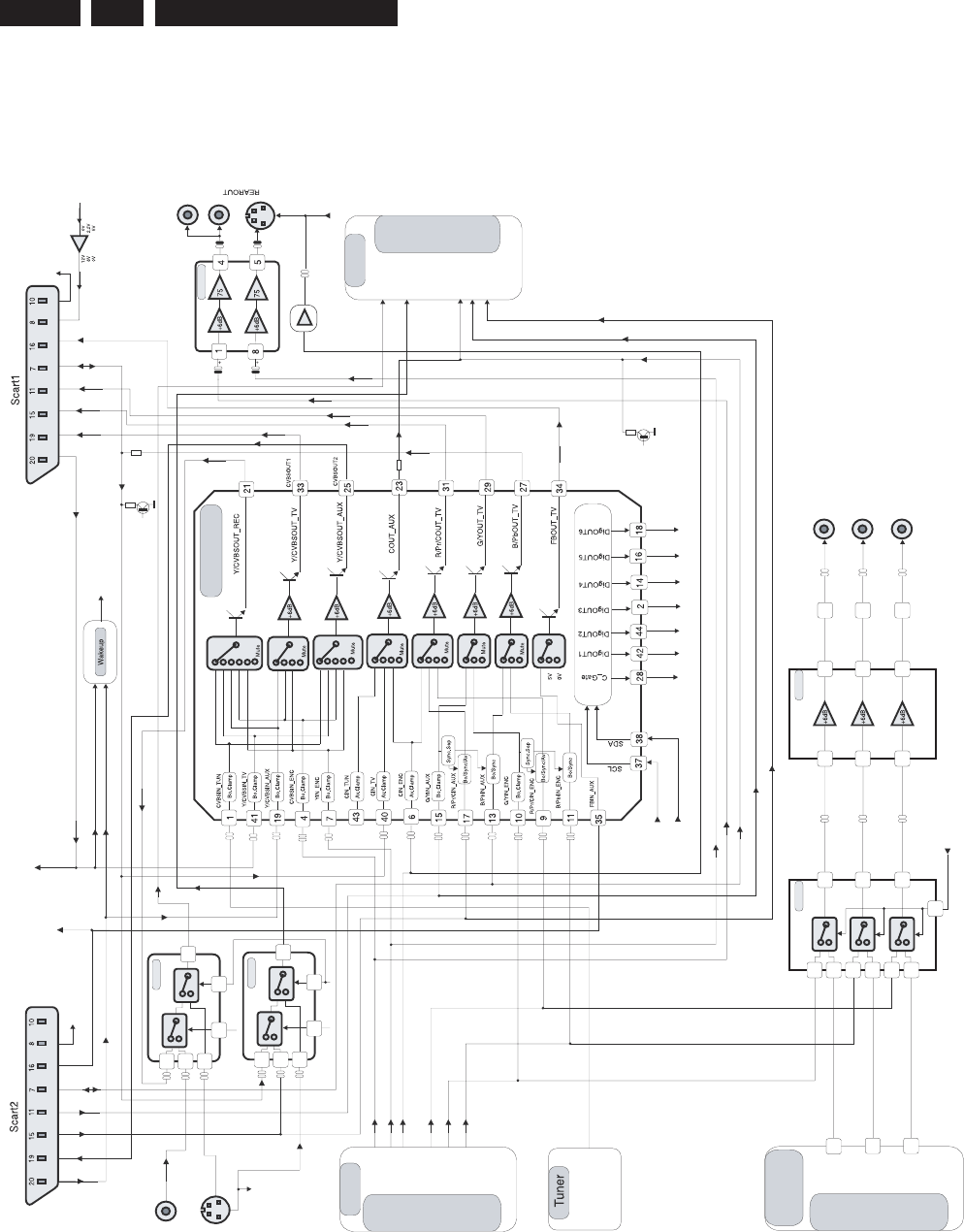
EN 168 3139 785 315329. Circuit- and IC Description
9.3.9. Video-routing
Figure 9-3 Analog Video In / Out Overview
Video IO Europe
WSRO
BCS2
BCS1
8SC1
CS
VS
FR
STV6618D
NJM2235M
5
SW1
SW2
4
2
1
37
Pos 7408
Pos 7413
Pos 7412
ADV7320KTZ
Pos 7253
NJM2267M
Pos 7203
DENC
From digital board
VIDEO
ENCODER
From HDMI board
to VIP
To digital board
CRout
SCL_5V
SDA_5V
from CU
WSRO
IPRO
from CU
P50
to CU
VideoIn
VideoOut
R/C_In
G
Bin/out
FastBlk
8SC2
to CU
SlowBlk
FBIN
to CU
CVBSFIN
CVBS
Y/C
YFIN
FrontIN
NJM2234M
5
SW1
SW2
4
2
1
37
CFIN
VS
CS FR
A_C
A_YCVBS
D_CVBS
D_Y
D_C
D_VR
D_YG
D_UB
Y
Pb
Pr
CVBS VFV
Y/CVBSOUT_REC
CVBSIN
to FOME
A_YCVBS
A_C
VFV
CVBSIN1
CVBSIN2
D_CVBS
D_Y
D_C
GIN
RCIN
BIN
D_G
D_R
D_B
FBIN
D_Y
D_CVBS
A_UB
A_YG
WSFI
to CU
WU
to CU
VideoIn
VideoOut
R/C_Out
G
Bout/Cin
FastBlk
SlowBlk
D_CVBS
D_Y
CVBS OUT 1
CVBS OUT 2
Y
C
GOUT
BOUT
FBOUT
RCOUT
A_UB
A_YG
A_VR
BCSC1
BCSC2
A_VR
CIN
8SC1
DVDR5350H/DVDR7300H Video IO Eur.eps
6
9
12
8
14
11
1
16 6
5
3
4
2
Pos 7200 NJM2584M
9
11
13
11
10
9
6
3
1
Pos 7201 NJM2580M
Y
U
V
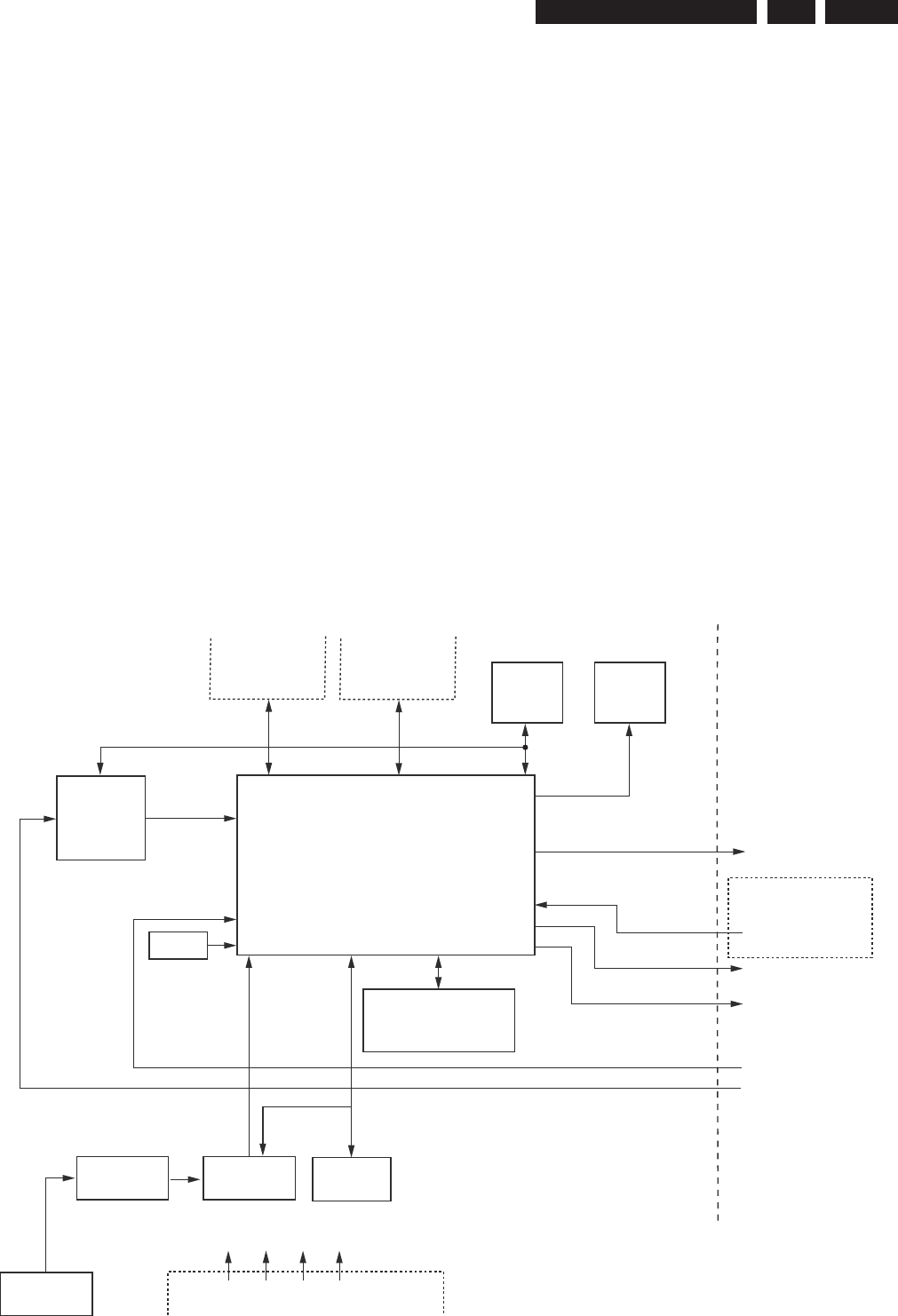
EN 1693139 785 31532 9.
Circuit- and IC description
A matrix switch STV6618D [7408] controlled by the Slave
μP via I2C-bus is used for Video I/O switching. All used
outputs excluding pin 21 (Y/CVBSOUT-REC) have a 6dB-
amplifi cation and a 75 ohms-driver-stage inside. This IC also
includes several digital outputs, which are used for switching
purposes on the Analog board.
This matrix switch routes the selected inputs to the correct
output lines for TV viewing and further processing in the
Digital board.
The record selector inside the switch selects between the
inputs from Tuner Frontend (VFV), CVBS Scart1 (CVBSIN1),
CVBS Scart2 (CVBSIN2) or D_CVBS from the DENC (on
Digital board). The output signal CVBS_REC together with
the other signals CVBSFIN, YFIN & C_FIN from the Front
and RCB from Scart2 are routed directly to the VIP (on Digital
board) for further processing.
The signals D_CVBS and D_Y are fed through NJM2267M
[7203] (6dB amplifi cation) and D_C via transistors [7410 &
7411] as driver to the rear S-Video output socket and CVBS
cinch socket.
9.4. Basic Engine
The VAD8043 module (also known as D4.3 drive) is dual
format DVD-R/+R and DVD-RW/+RW drive video recorder
with an E-IDE/ATAPI interface.
The video recorder engine performs all basic servo tasks.
It reads data from and writes data to the disc and controls
all functions like tray control, start/stop the disc, tracking,
jumping and communicating with the host.
Mechanically, the module consists of a motorized tray
loader that contains the dual laser optical pickup unit and a
PCBA that contains all the electronics needed to control the
drive and interfacing the MPEG encoder/decoder back-end
application.
There is a temperature sensor included in the drive that
prevents malfunction or destruction of the drive in case the
temperature inside the drive gets too high.
9.5. Digital Board
The Digital Board is based on the highly integrated Chrysalis
BGA chip (Ball Grid Array), PNX7100EH and supports 2 IDE
(ATAPI) connection.
The board encodes and multiplexes the analogue video and
digital uncompressed audio (I2S) into an MPEG2 stream. This
MPEG2 stream is formatted for recording by the DVD+RW
engine. In the playback, the board will decode the MPEG2
video into analogue video. In addition, a DV stream can be
received via IEEE 1394 (i-Link), and transformed to MPEG2
format.
SDRAM
4M X 16 x 4
I2C
EEPROM
64Kbit
VIP
SAA7118E
1394
PID1394P25
I2C
EEPROM
64Kbit
CHRYSALIS
PNX7100EH
7400
1FH VIDEO
OUT(2)
DIG. AUDIO IN
OPT. & COAX
DIG. AUDIO OUT
I2S AUDIO OUT
I2S AUDIO IN
1FH VIDEO IN(1)
I2C 0
I2C 1
7007
I2C0
CCIR656
CLOCK
7200
1204
7201
-5V
FROM POWER SUPPLY
5V 12V3V3
XIO_1 XIO_0
1394
PID1394L40
1394
CONNECTOR
FLASH
4M X 16
7812/7813
7807
7809 7810
(1) analogue CVBS, YC, RGB/YUV
(2) analogue CVBS, YC, RGB/YUV
OPTIONAL
TO / FROM
HDD
TO / FROM
D4.3 DRIVE (BE)
IDE1
IDE2
Figure 9-4 Block Diagram of Chrysalis Board
9.5.1. Record Mode
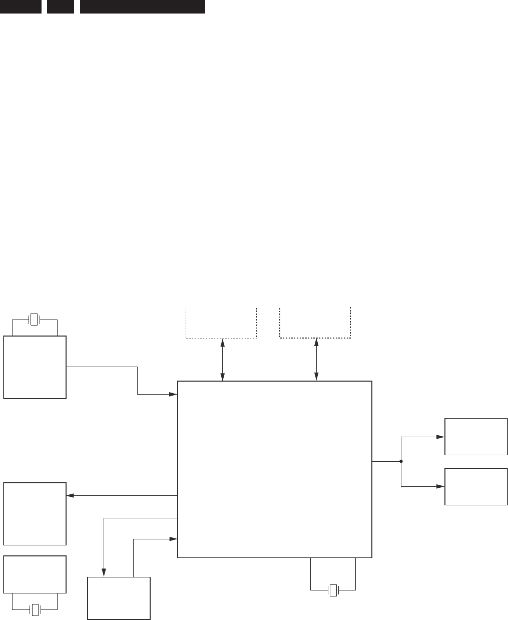
EN 170 3139 785 315329. Circuit- and IC Description
SAA7118E
7007
CHRYSALIS
PNX7100EH
7400
SDRAM
HDD
7812
133MHz
SDRAM
7813
1394 LINK
7201
AUDIO PLL
7301
1394 PHY
24.576 MHz
24.576 MHz
7200
4 MHz
BASIC
ENGINE
IDE1 IDE2
Figure 9-5 Clock Distribution
The Chrysalis chip has a complex system, which is needed to
support the processes running at different frequencies such
as video decoding, audio decoding or peripheral I/O devices
etc. To ensure a synchronous initialization of all the registers
and state machines, all the PLLs are switched to their default
frequency and the reset sequence is run at 4MHz.
Then when the booting control unit is correctly initialized and
once it has captured all the booting parameters, it sets the
PLLs to its functional frequencies to allow the modules to
run at their nominal frequencies. Thanks to a clock blocking
mechanism, the frequency switching is glitch free.
System clocks:
• PNX7100EH (7400, pin AF9 and AF10) : 4MHz provided
by the x’tal 1401
• SAA7118E (7007, pins A3 and B4) : 24.576MHz provided
by x’tal 1001
• 1394-PHY (7200, pins 59 and 60) : 24.576MHz provided
by x’tal 1201
• 1394-LINK (7201, pin 88) : 49.152MHz provided by
1394-PHY
• SDRAM (7812 and 7813, pin 38) : 133MHz provided by
the Chrysalis chip
Video Part
The analogue video input signals CVBS, YC and RGB are
routed via the board to connector 1904 and sent to Video
Input Processor, SAA7118E. The Video Input Processor
encodes the analogue video to digital video stream (CCIR656
format). The output stream, named ITU_IN(7:0), is then
routed to the Chrysalis chip. This IC encodes and decodes
the digital video stream into / from MPEG2 format.
The digital video input signals from the DV-in are routed from
connector 1203 via the 1394 PHY IC [7200] and the 1394
LINK IC [7201] also to the Chrysalis chip.
Audio Part
I2S audio is sent from the Analog board to the Chrysalis chip
via connector 1900.
The Chrysalis chip compresses the I2S audio data into an
MPEG1-L2 / AC3 audio stream.
Front-end I2S
The Chrysalis chip interfaces directly to the Basic Engine and
HDD via the IDE connectors.
It buffers the data streams that are coming from (or going to)
these hardware devices.
In the Chrysalis chip, the video MPEG2 stream and the audio
AC3 stream are multiplexed into an I2S stream. In normal
recording the serial data are send to the HDD for recording.
Only archiving and playback is done with optical drive.
9.5.2. Playback mode
During playback, the serial data from the Basic Engine is
going directly to the Chrysalis chip via ATAPI interface. The
Chrysalis chip has the following outputs:
• Analog video CVBS, YC and RGB outputs on
connector 1904
• I2S audio (PCM format) on connector 1900
• SPDIF audio (digital audio output) on connector 1900
• Progressive Scan output connector 1002
9.5.3. Basic Engine Interface
The Digital board is equipped with 2 IDE bus (ATAPI) for
connecting to the Basic Engine and HDD via connectors 1102
and 1101 respectively.
9.5.4. Clock Distribution
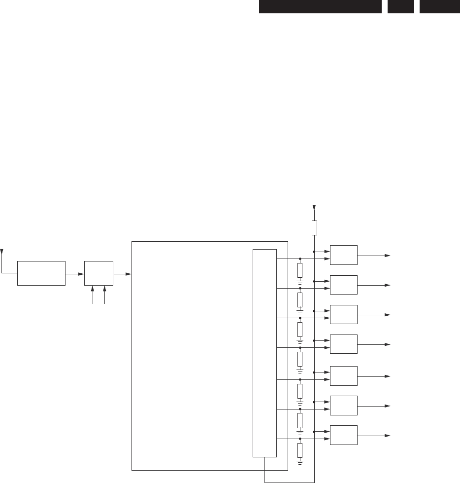
EN 1713139 785 31532 9.
Circuit- and IC description
Reset concept Digital board
The voltage detector NCP303LSN29 [7106] provides the
reset signal PNX7100_RESETn with the correct timing
behavior. This circuitry functions as a Power-on reset module
which detects the minimum functional voltage that is needed
by the device. It also detects any voltage drop. When the
power voltage is outside the nominal range, a reset signal is
generated and fed to the Chrysalis chip to reset the differenct
peripherals and processing units.
• PNX7100_RESETn = High {the Digital board is up and
running}
• PNX7100_RESETn = Low {the Digital board will reset}
There are two control lines which can overrule this reset
signal:
• IRESET_DIG (controlled by the microprocessor on the
Analog Board)
• EJTAG_RESETn (only for production)
The PNX7100_SYS_RESETn is a general enabling signal
for the different reset lines. All other reset lines are directly
driven from the Chrysalis port pins. All reset lines are logically
connected via 74LVC08AD [7104 and 7107] AND-gates. If both
reset signals are low, all other external devices are initialized.
9.5.8. In/Out Connector
Audio In/Out Connector [1900]
The Audio In / Out (AIO) connector is used to interchange
digital audio signals between the Analog and Digital board.
Video In/Out Connector [1904]
The Video In / Out (VIO) Connector is used to interchange
analogue video signals between the Analog and Digital board.
Video Out Connector [1002]
The Video Out Connector is used for Progressive Scan video
signals to the Analog board
9.5.9. Service UART Interface
Hex Inverting Schmitt trigger 74HCT14D [7111] are used to
make a level conversion between LVTTL and 5V (compatible
with most RS232 interfaces) and vice versa. The control
line MPIO19_EEPROM_En is used to activate service and
diagnostic SW at start-up. The connectivity is provided via an
external service tool.
CHRYSALIS
PNX7100EH
7400
GPIO
PNX7100_RESETn
PNX7100_SYS_RESETn
7106
3V3
>1
EJTAG_RESETn
IRESET_DIG
NCP303
7104-3
&
7104-4
&
RESET_IDE1n
7107-1
&
RESET_1394n
7107-2
&
RESET_DTTMn
RESET_PROGSCANn
3V3_RES
7107-3
&
7104-1
&
ANALOG_RESETn
7104-2
&
VIP_RESETn
RESET_IDE2n
Figure 9-6 Reset concept
9.5.5. Power Supply
The Digital board is not powered in standby mode. The
control signal STBY on the analog board will enable the PSU
and power the digital board.
• STBY = High : the digital board is in powered down
standby mode
• STBY = Low : the power supply to the digital board
is enabled. The 3V3, -5V, +5V and
+12V come from the PSU, while the
following voltages are generated in the
digital board:
• 1.8V core voltage generated by a NCP1571D [7501] .
It provides a DC-DC power solution producing a 1.8V
output voltage over a wide current range
• 1.8V_VIP generated by LD1117D18 [7008] for the VIP
• 3.3V_VIP generated by LD1117D33 [7006] for the VIP
• 2.5V generated by a LF25CDT [7600] for Pro-scan Video
Encoder
9.5.6. Memory
Several memories are used on the Digital Board:
• Eeprom IC [7809] : this memory contains all the
parameters for the application
• Eeprom IC [7810] : this memory contains the boot
parameters of the board
• Flash IC [7807] : this memory contains the application
and Service diagnostic fi rmware
9.5.7. Reset
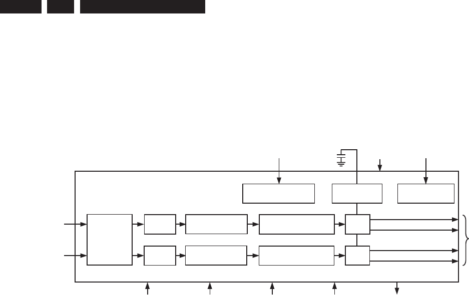
EN 172 3139 785 315329. Circuit- and IC Description
9.6 IC Description
9.6.1 Analog Board
IC7004 - AD1852JRS - Digital to Analogue Converter
BLOCK DIAGRAM
FUNCTIONAL BLOCK DIAGRAM
SERIAL
DATA
INTERFACE
8 x FS
INTERPOLATOR
SERIAL CONTROL
INTERFACE
AUTO-CLOCK
DIVIDE CIRCUIT
VOLUME
MUTE
CONTROL DATA
INPUT
32
DIGITAL
SUPPLY
CLOCK
IN
ANALOG
OUTPUTS
22
ZERO
FLAG
ANALOG
SUPPLY
DE-EMPHASISMUTE
RESET
2
SERIAL
MODE
16-/18-/20-/24-BIT
DIGITAL
DATA INPUT
AD1852
MULTIBIT SIGMA-
DELTA MODULATOR
ATTEN/
MUTE
DAC
MULTIBIT SIGMA-
DELTA MODULATOR
8 x FS
INTERPOLATION
ATTEN/
MUTE
VOLTAGE
REFERENCE
DAC
Figure 9-7

EN 1733139 785 31532 9.
Circuit- and IC description
PIN DESCRIPTION AND CONFIGURATION
Pin Input/Output Pin Name Description
1 I DGND Digital Ground.
2 I MCLK Master Clock Input. Connect to an external clock source at either 256 F
S
, 384 F
S
,
512 F
S
, 768 F
S
, or 1024 F
S
.
3 I CLATCH Latch Input for Control Data. This input is rising-edge sensitive.
4 I CCLK Control Clock Input for Control Data. Control input data must be valid on the rising
edge of CCLK. CCLK may be continuous or gated.
5 I CDATA Serial Control Input, MSB first, containing 16 bits of unsigned data per channel. Used
for specifying channel-specific attenuation and mute.
6 NC No Connect.
7 I 192/48 Selects 48 kHz (LO) or 192 kHz Sample Frequency.
8 O ZEROR Right Channel Zero Flag Output. This pin goes HI when Right Channel has no signal
input for more than 1024 LR Clock Cycles.
9 I DEEMP De-Emphasis. Digital de-emphasis is enabled when this input signal is HI. This is used
to impose a 50 μs/15 μs response characteristic on the output audio spectrum at an
assumed 44.1 kHz sample rate. Curves for 32 kHz and 48 kHz sample rates may be
selected via SPI control register.
10 I 96/48 Selects 48 kHz (LO) or 96 kHz Sample Frequency.
11, 15 I AGND Analog Ground.
12 O OUTR+ Right Channel Positive Line Level Analog Output.
13 O OUTR– Right Channel Negative Line Level Analog Output.
14 O FILTR Voltage Reference Filter Capacitor Connection. Bypass and decouple the voltage refer-
ence with parallel 10 μF and 0.1 μF capacitors to the AGND.
16 O OUTL– Left Channel Negative Line Level Analog Output.
17 O OUTL+ Left Channel Positive Line Level Analog Output.
18 I AVDD Analog Power Supply. Connect to Analog 5 V Supply.
19 FILTB Filter Capacitor Connection. Connect 10 μF capacitor to AGND (Pin 15).
20 I IDPM1 Input Serial Data Port Mode Control One. With IDPM0, defines 1 of 4 serial modes.
21 I IDPM0 Input Serial Data Port Mode Control Zero. With IDPM1, defines 1 of 4 serial modes.
22 O ZEROL Left Channel Zero Flag Output. This pin goes HI when Left Channel has no signal
input for more than 1024 LR Clock Cycles.
23 I MUTE Mute. Assert HI to mute both stereo analog outputs. Deassert LO for normal operation.
24 I RESET Reset. The AD1852 is reset on the rising edge of this signal. The serial control port
registers are reset to the default values. Connect HI for normal operation.
25 I L/RCLK Left/Right Clock Input for Input Data. Must run continuously.
26 I BCLK Bit Clock Input for Input Data. Need not run continuously; may be gated or used in a
burst fashion.
27 I SDATA Serial Input, MSB first, containing two channels of 16, 18, 20, and 24 bits of twos
complement data per channel.
28 I DVDD Digital Power Supply Connect to digital 5 V supply.
Table I. Serial Data Input Mode
IDPM1 (Pin 20) IDPM0 (Pin 21) Serial Data Input Format
0 0 Right-Justified
01 I
2
S-Compatible
1 0 Left-Justified
1 1 DSP
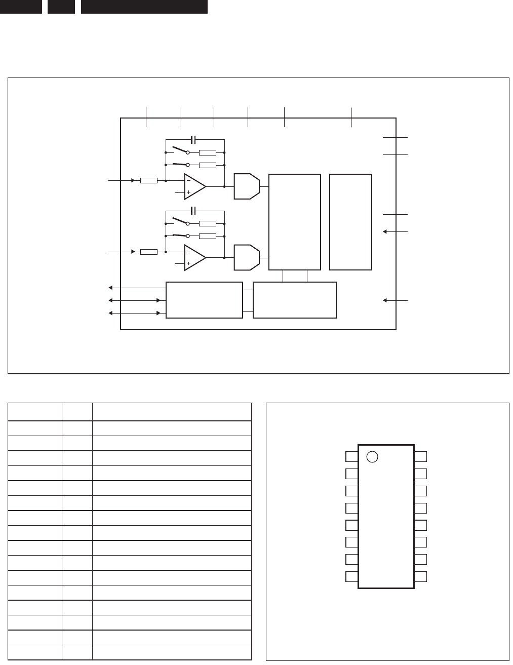
EN 174 3139 785 315329. Circuit- and IC Description
IC7007 - UDA 1361S - Analogue to Digital Converter
BLOCK DIAGRAM, PIN DESCRIPTION AND CONFIGURATION
handbook, full pagewidth
UDA1361TS
MGT451
1
VINL ADC
ΣΔ
DIGITAL
INTERFACE
DC-CANCELLATION
FILTER
DECIMATION
FILTER
CLOCK
CONTROL
3
16
VINR ADC
ΣΔ
13
DATAO
11
BCK
12
WS
6SFOR
7PWON
14 MSSEL
15
10 VSSD
9VDDD
VSSA
5
VRP
4
VRN
2
Vref
8
SYSCLK
VDDA
Fig.1 Block diagram.
PINNING
SYMBOL PIN DESCRIPTION
VINL 1 left channel input
Vref 2 reference voltage
VINR 3 right channel input
VRN 4 negative reference voltage
VRP 5 positive reference voltage
SFOR 6 data format selection input
PWON 7 power control input
SYSCLK 8 system clock 256, 384, 512 or 768fs
VDDD 9 digital supply voltage
VSSD 10 digital ground
BCK 11 bit clock input/output
WS 12 word select input/output
DATAO 13 data output
MSSEL 14 master/slave select
VSSA 15 analog ground
VDDA 16 analog supply voltage
handbook, halfpage
UDA1361TS
MGT452
1
2
3
4
5
6
7
8
16
15
14
13
12
11
10
9
VINL
Vref
VINR
VRN
VRP
SFOR
PWON
SYSCLK VDDD
VSSD
BCK
WS
DATAO
MSSEL
VSSA
VDDA
Fig.2 Pin configuration.
Figure 9-8
EN 1753139 785 31532 9.
Circuit- and IC description
IC7200 - NJM2584M - 2-Input 1-Output 3 Circuit Video Switch
BLOCK DIAGRAM
IN1A
IN2B
IN3B
1
2
3
4
5
6
7
8
16
15
14
13
12
11
10
9
IN1B
IN2A
IN3
A
OUT1
OUT2
OUT3
NC
CTL
NC
GND1
GND2
GND3
V+
BIAS
CLAMP
BIAS
Figure 9-9
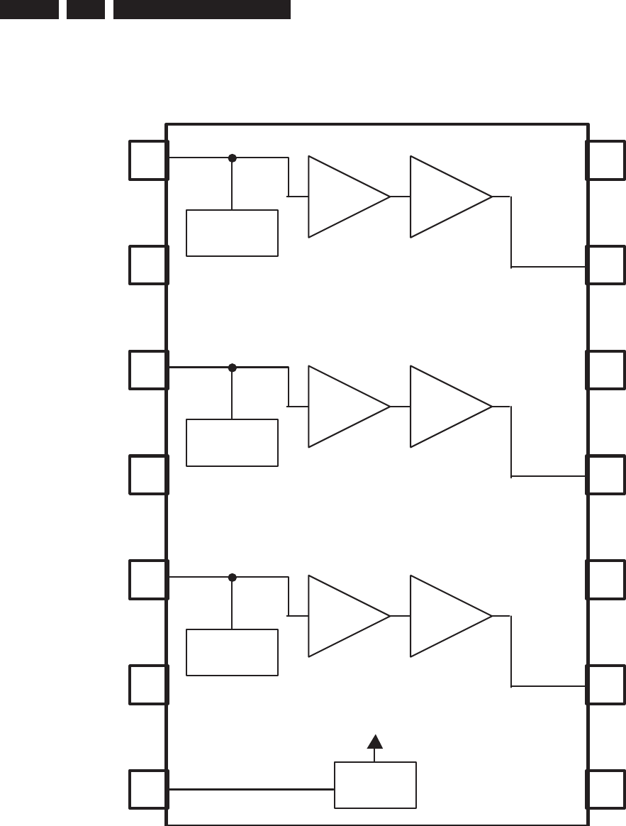
EN 176 3139 785 315329. Circuit- and IC Description
IC7201 - NJM2580M - 3-Channel Video Amplifi er
BLOCK DIAGRAM
13
12
11
REF
1
2
3
4
7
5
6
14
8
10
9
V
+
1
GND1
GND2
GND3
VSAG
VIN1
VIN2
VIN3
VOUT1
VOUT2
VOUT3
Power Save
BIAS
6dB
AMP
75
Driver
BIAS
75
Driver
6dB
AMP
CLAMP
75
Driver
6dB
AMP
V
+
2
V
+
3
Figure 9-10
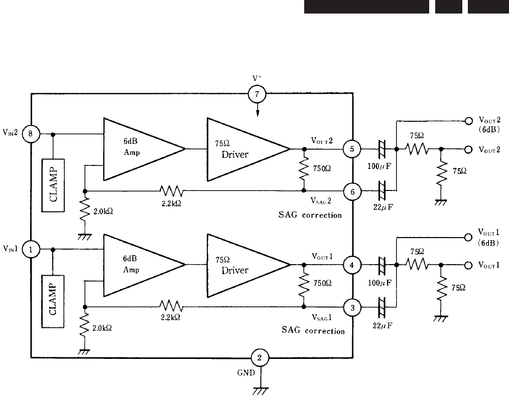
EN 1773139 785 31532 9.
Circuit- and IC description
IC7203 - NJM2267M - Dual Video 6dB Amplifi er
BLOCK DIAGRAM
Figure 9-11
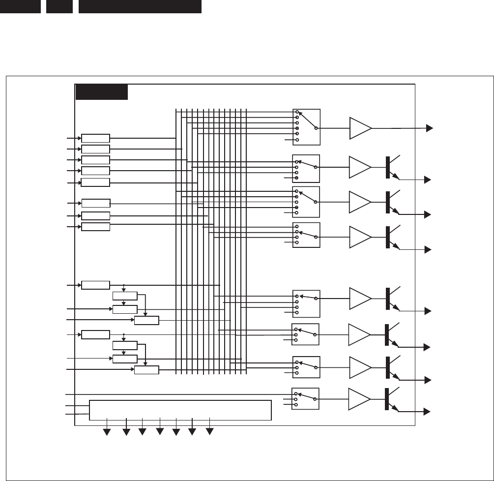
EN 178 3139 785 315329. Circuit- and IC Description
IC7408 - STV6618D - Video Switch Matrix
BLOCK DIAGRAM
Sync Sep
Bo. Clamp
Y/CVBSIN_TUN
Y/CVBSIN_TV
Y/CVBSIN_AUX
CVBSIN_ENC
Bo. Clamp
G/YIN_AUX
R/Pr/CIN_AUX
B/PbIN_AUX
Sync Sep
Bo. Clamp
G/YIN_ENC
R/Pr/CIN_ENC
B/PbIN+ENC
YIN_ENC
CIN_TV
CIN_ENC
mute
0 dB
Y/CVBSOUT_REC
Y/CVBSIN_TUN
Y/CVBSIN_TV
Y/CVBSIN_AUX
CVBSIN_ENC
YIN_ENC
CIN_TV
CIN_ENC
G/YIN_ENC
G/YIN_AUX
R/Pr/CIN_AUX
B/PbIN_AUX
R/Pr/CIN_ENC
B/PbIN_ENC
STV6618D
Recorder
mute
6 dB
Y/CVBSOUT_TV
Scart1
mute
6 dB
Y/CVBSOUT_AUX
Scart2
mute
6 dB
R/Pr/COUT_TV
mute
6 dB
G/YOUT_TV
Scart1
Scart1
mute
6 dB
B/PbOUT_TV
Scart1
Y/CVBS_TUN
Y/CVBS_TV
Y/CVBS_AUX
CVBSIN_ENC
YIN_ENC
CIN_TV
CIN_ENC
G/YIN_ENC
G/YIN_AUX
R/Pr/CIN_AUX
B/PbIN_AUX
R/Pr/CIN_ENC
B/PbIN_ENC
0 dB
FBOUT_TV
SCL
FBIN_AUX
0v
5v
SDA
C_GATE
I2C bus
Bo. Clamp
Bo. Clamp
Bo. Clamp
Bo. Clamp
Av. Clamp
Av. Clamp
Bot/sync/av.
Bo/Sync
Bot/sync
Bot/sync/av.
CVBSIN_TUN
Y/CVBSIN_TV
Y/CVBSIN_AUX
CVBSIN_ENC
YIN_ENC
mute
6 dB
COUT_AUX
Y/CVBSIN_AUX
CVBSIN_ENC
YIN_ENC
CVBSIN_TUN
Y/CVBSIN_TV
CVBSIN_ENC
YIN_ENC
CIN__TV
CIN_ENC
CIN_ENC
R/Pr/CIN_AUX
R/Pr/CIN_ENC
G/YIN_AUX
G/YIN_ENC
B/PbIN_AUX
B/PbIN_ENC
FBIN_AUX
CIN_TUN
Av. Clamp
CIN_TUN CIN_TUN
CIN__TUN
DigOUT1
DigOUT2
DigOUT3
DigOUT4
DigOUT5
DigOUT6
Figure 9-12

EN 1793139 785 31532 9.
Circuit- and IC description
PIN DESCRIPTION AND CONFIGURATION
gp
Pin Number Symbol Description
1 Y/CVBSIN_TUN Y/CVBS Input from tuner
2 digOUT3 Digital output pin 3
3 GND1 ground, video inputs
4 CVBSIN_ENC CVBS Input from Encoder
5 DECV Video decoupling capacitor
6 CIN_ENC chroma Input from Encoder
7 YIN_ENC Y Input from Encoder
8V
cc +5 V Supply, video
9 R/Pr/CIN_ENC Red or Pr or Chroma Input from Encoder
10 G/YIN_ENC Green or Y Input from Encoder
11 B/PbIN_ENC Blue or Pb Input from Encoder
12 GND2 ground, video inputs
13 B/PbIN_AUX Blue or Pb input from Auxiliary (scart2 or external cinch)
14 DigOUT4 Digital output pin 4
15 G/YIN_AUX Green or Y input from Auxiliary (scart2 or external cinch)
16 DigOUT5 Digital output pin 5
17 R/Pr/CIN_AUX Red or Pr or Chroma input from Auxiliary (scart2 or external cinch)
18 DigOUT6 Digital output pin 6
19 Y/CVBSIN_AUX Y/CVBS Input from Auxiliary (scart2 or external cinch)
20 VCCB_REC Video Output recorder Buffer Supply Pin
21 Y/CVBSOUT_REC Y/CVBS Output to Recorder
22 GNDB_REC ground , recorder buffer
23 COUT_AUX Chroma Output to Auxiliary (scart2 or external cinch)
24 VCCB1 Video Output Buffer Supply Pin
25 Y/CVBSOUT_AUX Y/CVBS Output to Auxiliary(scart2 or external cinch)
26 GNDB Ground video buffer
27 B/PbOUT_TV Blue or Pb output to TV (scart1 or external cinch)
28 C_GATE external transistor command for bidirectinnal B/C scart I/O
29 G/YOUT_TV Green or Y output to TV (scart1 or external cinch)
30 VCCB2 Video Buffer
31 R/Pr/COUT_TV Red or Pr or Chroma output to TV (scart1 or external cinch)
32 VCCB3 Video Output Buffer Supply Pin
33 Y/CVBSOUT_TV Y/CVBS output to TV(scart1 or external cinch)
34 FBOUT_TV Fast Blanking Output to TV (scart1)
35 FBIN_AUX Fast blanking Input from auxiliary (scart2))
36 VDD +5V digital supply
37 SCL I2C Bus Clock
38 SDA I2C Bus Data
39 GNDD ground digital
40 CIN_TV Chroma Input from TV (scart1 or external cinch)
41 Y/CVBSIN_TV Y/CVBS Input from TV (scart1 or external cinch)
42 digOUT1 Digital output pin 1
43 CIN_TUN Chroma Input from Tuner
44 digOUT2 Digital output pin 2
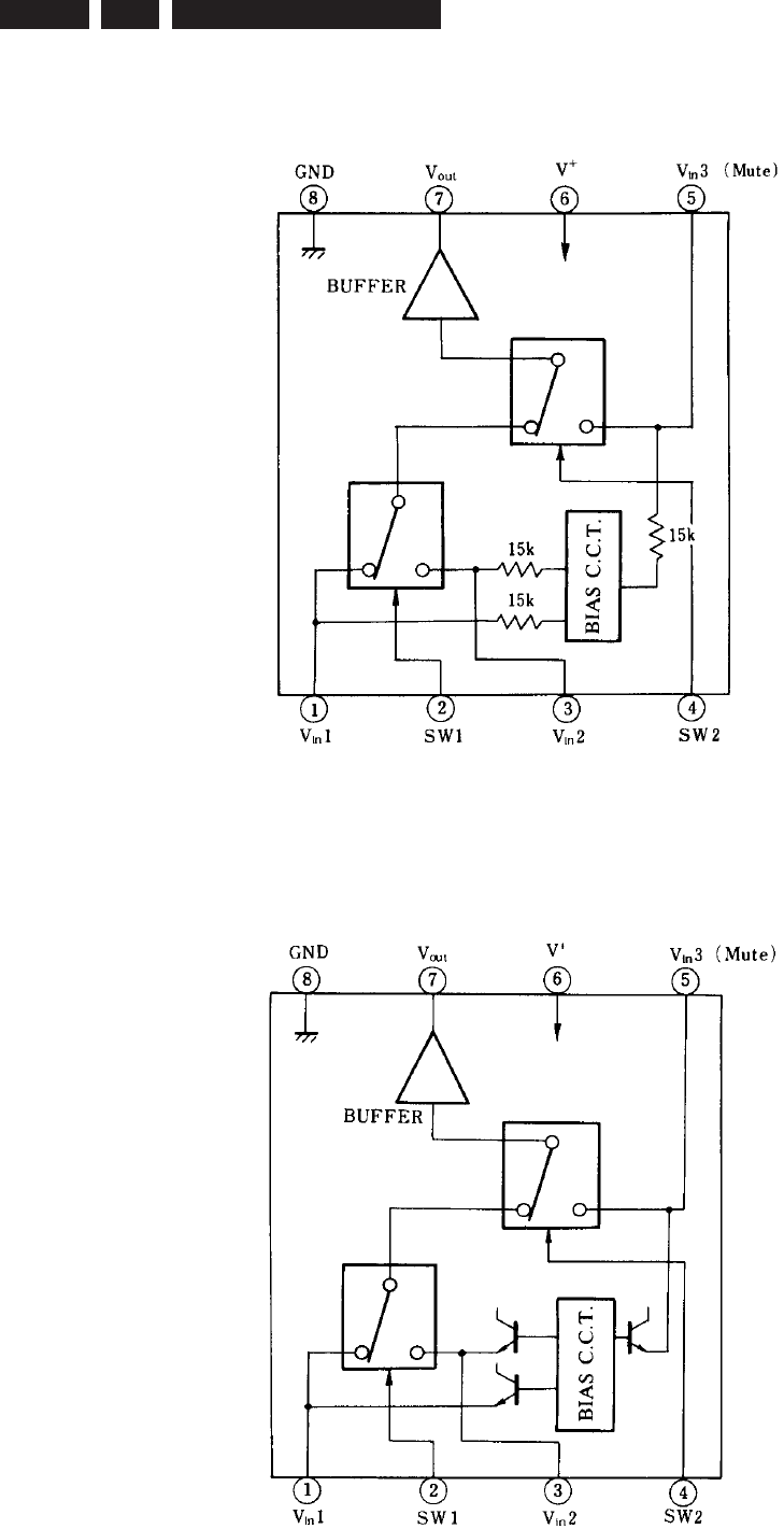
EN 180 3139 785 315329. Circuit- and IC Description
IC7212 - NJM2234M - 3-Input Video Switch
BLOCK DIAGRAM
Figure 9-13
IC7213 - NJM2235M - 3-Input Video Switch
BLOCK DIAGRAM
Figure 9-14
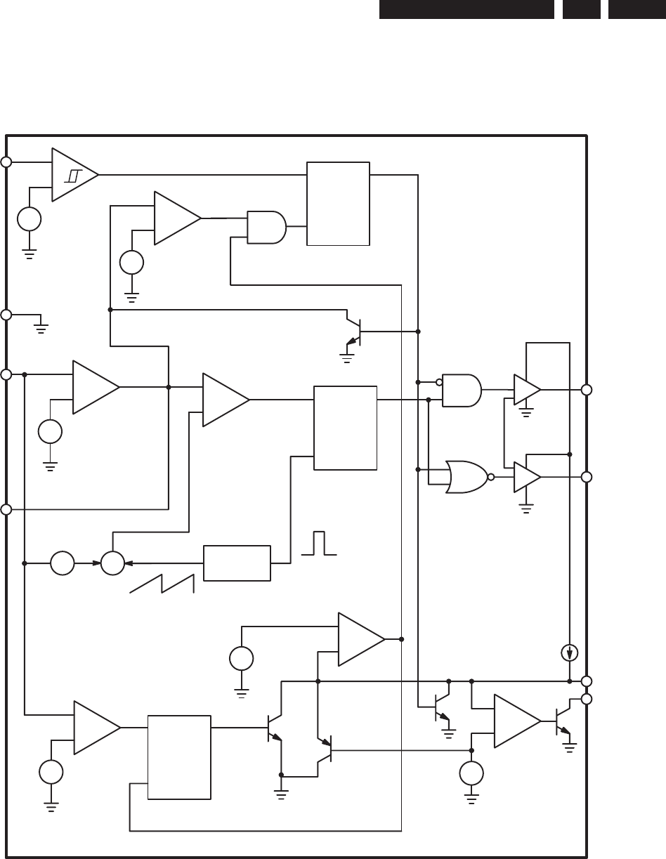
EN 1813139 785 31532 9.
Circuit- and IC description
9.6.2 Digital Board
IC7601 - NCP1571D - Low voltage Synchronous Buck Controller
BLOCK DIAGRAM
–
+
UVLO COMP
–
+
–
+
–
+
Fault Latch
Set Dominant
+
–0.25 V
Error Amp
+
R
S
Q
PWM Latch
Reset Dominant
PWM COMP
+ΣOSC
Art Ramp
80%, 200 kHz
0.525 V
+
–8.5 V/7.5 V
+
–0.980 V
S
R
Q
VCC
GND
VFB
COMP
GATE(H)
GATE(L)
PGDELAY
PWRGD
Non
Overlap
VCC
+
–0.88 V/0.69 V
+
–
+
–
0.25 V
S
R
Q
PGDELAY Latch
Set Dominant
–
+
+
–3.3 V
12 μA
–
–
Figure 9-15
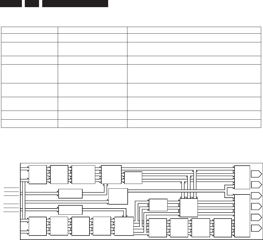
EN 182 3139 785 315329. Circuit- and IC Description
PIN DESCRIPTION AND CONFIGURATION
PACKAGE PIN # PIN SYMBOL FUNCTION
1 VCC Power supply input.
2 PWRGD Open collector output goes low when VFB is out of regulation. User
must externally limit current into this pin to less than 20 mA.
3 PGDELAY External capacitor programs PWRGD low–to–high transition delay.
4 COMP Error amp output. PWM comparator reference input. A capacitor to
LGND provides error amp compensation and Soft Start. Pulling pin
< 0.475 V locks gate outputs to a zero percent duty cycle state.
5 GATE(H) High–side switch FET driver pin. Capable of delivering peak currents
of 1.5 A.
6 GATE(L) Low–side synchronous FET driver pin. Capable of delivering peak
currents of 1.5 A.
7 VFB Error amplifier and PWM comparator input.
8 GND Power supply return.
IC7603 - ADV7322KST - Multi-Format 11-Bit HDTV Video Encoder
BLOCK DIAGRAM
CLKIN_A
P_HSYNC
P_VSYNC
P_BLANK
S_HSYNC
S_VSYNC
S_BLANK
CLKIN_B
HD PIXEL
INPUT
SD PIXEL
INPUT
LUMA
AND
CHROMA
FILTERS
Y
CB
CR TEST
PATTERN
DNR
GAMMA
SYNC
INSERTION
PS 8u
HDTV 2u
RGB
MATRIX
SD 16u
2uOVER-
SAMPLING
DAC
DAC
DAC
DAC
DAC
DAC
F
SC
MODU-
LATION
CGMS
WSS
COLOR
CONTROL
DE-
INTER-
LEAVE
Y
CB
CR
DE-
INTER-
LEAVE
TEST
PATTERN
Y COLOR
CR COLOR
CB COLOR
TIMING
GENERATOR
TIMING
GENERATOR CLOCK
CONTROL
AND PLL
4:2:2
TO
4:4:4
SHARPNESS
AND
ADAPTIVE
FILTER
CONTROL
05067-002
UV SSAF
V
U
Figure 9-16

EN 1833139 785 31532 9.
Circuit- and IC description
PIN DESCRIPTION
p
Mnemonic Input/Output Function
DGND G Digital Ground.
AGND G Analog Ground.
CLKIN_A I Pixel Clock Input for HD (74.25 MHz Only, PS Only (27 MHz), SD Only (27 MHz).
CLKIN_B I Pixel Clock Input. Requires a 27 MHz reference clock for progressive scan mode or a 74.25 MHz (74.1758
MHz) reference clock in HDTV mode. This clock is only used in dual modes.
COMP1,
COMP2
O Compensation Pin for DACs. Connect 0.1 μF capacitor from COMP pin to VAA.
DAC A O CVBS/Green/Y/Y Analog Output.
DAC B O Chroma/Blue/U/Pb Analog Output.
DAC C O Luma/Red/V/Pr Analog Output.
DAC D O In SD Only Mode: CVBS/Green/Y Analog Output; in HD Only Mode and Simultaneous HD/SD Mode:
Y/Green [HD] Analog Output.
DAC E O In SD Only Mode: Luma/Blue/U Analog Output; in HD Only Mode and Simultaneous HD/SD Mode: Pr/Red
Analog Output.
DAC F O In SD Only Mode: Chroma/Red/V Analog Output; in HD Only Mode and Simultaneous HD/SD Mode:
Pb/Blue [HD] Analog Output.
P_HSYNC I Video Horizontal Sync Control Signal for HD in Simultaneous SD/HD Mode and HD Only Mode.
P_VSYNC I Video Vertical Sync Control Signal for HD in Simultaneous SD/HD Mode and HD Only Mode.
P_BLANK I Video Blanking Control Signal for HD in Simultaneous SD/HD Mode and HD Only Mode.
S_BLANK I/O Video Blanking Control Signal for SD Only.
S_HSYNC I/O Video Horizontal Sync Control Signal for SD Only.
S_VSYNC I/O Video Vertical Sync Control Signal for SD Only.
Y7 to Y0 I SD or Progressive Scan/HDTV Input Port for Y Data. Input port for interleaved progressive scan data. The
LSB is set up on Pin Y0.
C7 to C0 I Progressive Scan/HDTV Input Port 4:4:4 Input Mode. This port is used for the Cb [Blue/U] data. The LSB is
set up on Pin C0.
S7 to S0 I SD or Progressive Scan/HDTV Input Port for Cr [Red/V] data in 4:4:4 input mode. LSB is set up on Pin S0.
RESET I This input resets the on-chip timing generator and sets the ADV7322 into default register setting. RESET is
an active low signal.
RSET1, RSET2 I A 3040 Ω resistor must be connected from this pin to AGND and is used to control the amplitudes of the
DAC outputs.
SCLK I I2C Port Serial Interface Clock Input.
SDA I/O I2C Port Serial Data Input/Output.
ALSB I TTL Address Input. This signal sets up the LSB of the I2C address. When this pin is tied low, the I2C filter is
activated, which reduces noise on the I2C interface.
VDD_IO P Power Supply for Digital Inputs and Outputs.
VDD P Digital Power Supply.
VAA P Analog Power Supply.
VREF I/O Optional External Voltage Reference Input for DACs or Voltage Reference Output (1.235 V).
EXT_LF I External Loop Filter for the Internal PLL.
RTC_SCR_TR I Multifunctional Input. Real time control (RTC) input, timing reset input, subcarrier reset input.
I2C I This input pin must be tied high (VDD_IO) for the ADV7322 to interface over the I2C port.
GND_IO Digital Input/Output Ground.
TEST0 to
TEST5
I Not used. Tie to DGND
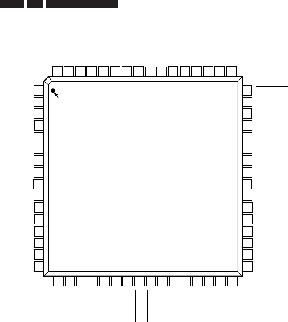
EN 184 3139 785 315329. Circuit- and IC Description
PIN CONFIGURATION
64
GND_IO
63
CLKIN_B
62
S7
61
S6
60
S5
59
S4
58
S3
57
DGND
56
V
DD
55
S2
54
S1
53
S0
52
TEST5
51
TEST4
50
S_HSYNC
49
S_VSYNC
47
R
SET1
46
V
REF
45
COMP1
42
DAC C
43
DAC B
44
DAC A
48
S_BLANK
41
V
AA
40
AGND
39
DAC D
37
DAC F
36
COMP2
35
R
SET2
34
EXT_LF
33
RESET
38
DAC E
2
TEST0
3
TEST1
4
Y0
7
Y3
6
Y2
5
Y1
1
V
DD_IO
8
Y4
9
Y5
10
V
DD
12
Y6
13
Y7
14
TEST2
15
TEST3
16
C0
11
DGND
17
C1
18
C2
19
I
2
C
20
ALSB
21
SDA
22
SCLK
23
P_HSYNC
24
P_VSYNC
25
P_BLANK
26
C3
27
C4
28
C5
29
C6
30
C7
31
RTC_SCR_TR
32
CLKIN_A
PIN 1
ADV7322
TOP VIEW
(Not to Scale)
05067-019
Figure 9-17
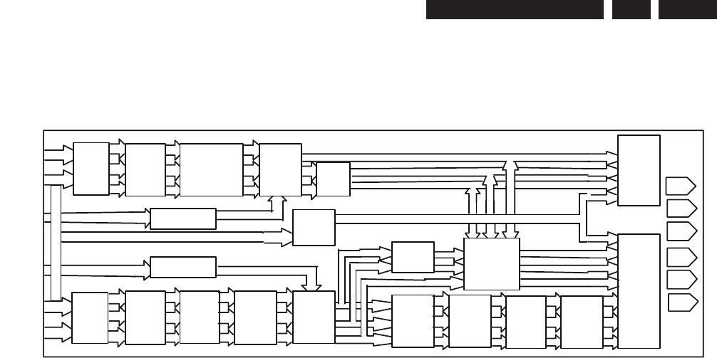
EN 1853139 785 31532 9.
Circuit- and IC description
9.6.3 HDMI Board
IC7253 - ADV7320KSTZ - Multi-Format 216 MHz Video Encoder
BLOCK DIAGRAM
DE-
IN TER -
LEAV E
DE-
INTER-
LEAVE
SHAR PNESS &
ADAPTIVE
FILTER
C ONT ROL
TEST-
PATTER N
Y COLOR
CR COL OR
CB C OL OR 4: 2:2 T O
4:4: 4
TEST-
PATTER N
DN R
GAMMA
COLO R -
CONT ROL
SYNC
INS ER-
TION
UV SSAF R GB
MATRIX
PS 8X
HD TV 2 X
2XOVER-
SAMPLING
FS C
MODULA--
TI O N
CGMS
WSS
LUMA &
CHR OMA
FI LTER S
SD 16X
DAC
DAC
DAC
TIMING
GENERATOR
Y
CR
CB
Y
CB
CR
U
V
HD PIXEL
IN PUT
P_HSYNC \
P_ VSY NC\
P_BL ANK
SD PIXEL
INPUT
CLOCK
CONTROL
&PLL
CLK IN _A
TI MI NG
GEN E RAT O R
CL KIN _B
S_HSYNC\
S_VSYNC\
S_BLANK
DAC
DAC
DAC
Figure 9-18

EN 186 3139 785 315329. Circuit- and IC Description
PIN DESCRIPTION
Pin Name Input/Output Function
DGND G Digital Ground
AGND G Analog Ground
CLKIN_A I Pixel Clock Input for HD (74.25MHz Only , PS Only (27MHz), SD Only
(27MHz).
CLKIN_B I Pixel Clock Input. Requires a 27MHz reference clock for Progressive Scan
Mode or a 74.25MHz (74.1758MHz) reference clock in HDTV mode. This
Clock is only used in dual Modes.
COMP1,2 O Compensation Pin for DACs. Connect 0.1uF Capacitor from COMP pin to
V
AA
.
DAC A O CVBS/ GREEN/ Y / Y analog output.
DAC B O Chroma/ BLUE/ U / Pb analog output.
DAC C O Luma/ RED/ V / Pr analog output.
DAC D O In SD onlyu mode: CVBS/Green/Y analog outptu, in HD only mode and
simultaneous HD/SD mode: Y/Green [HD] analog output.
DAC E O In SD onlyu mode: Luma/Blue/U analog outptu, in HD only mode and
simultaneous HD/SD mode: Pr/Red analog output.
DAC F O In SD onlyu mode: Chroma/Red/ V analog outptu, in HD only mode and
simultaneous HD/SD mode: Pb/Blue [HD] analog output.
P_HSYNC
I Video Horizontal Sync Control Signal for HD in simultaneous Sd/HD
mode and HD mode only.
P_VSYNC
I Video Vertical Sync Control Signal for HD in simultaneous SD/HD mode and
HD mode only.
P_BLANK
I Video Blanking Control signal for HD in simultaneous SD/HD mode and HD
mode only.
S_BLANK
I Video Blanking Control Signal for SD only.
S_HSYNC
I Video Horizontal Sync Control Signal for SD only.
S_VSYNC
I Video Vertical Sync Control Signal for SD only.
Y9-0 I SD or Progressive scan/ HDTV input port for Y data.
Input port for interleaved Progressive Scan data. The LSB is set up
on pin Y0. For 8-bit data input LSB is set up on Y2.
C9-C0 I Progressive Scan/ HDTV input port :4:4 input mode this port is used for
the Cb[Blue/U] data. The LSB is set up on pin C0. For 8-bit data input LSB is
set up on C2.
S9-S0 I SD or Progressive Scan/HDTV input port for Cr [Red/V] data in 4:4:4 input
mode. LSB is set up on pin S0. For 8-bit data input LSB is set up on S2.
RESET
I This input resets the on-chip timing generator and sets the ADV7310/11
into Default Register setting. Reset is an active low signal.
R
SET1,2
I A 3040 Ohms resistor must be connected from this pin to AGND and is used
to control the amplitudes of the DAC outputs.
SCLk I I2C Port Serial Interface Clock Input .
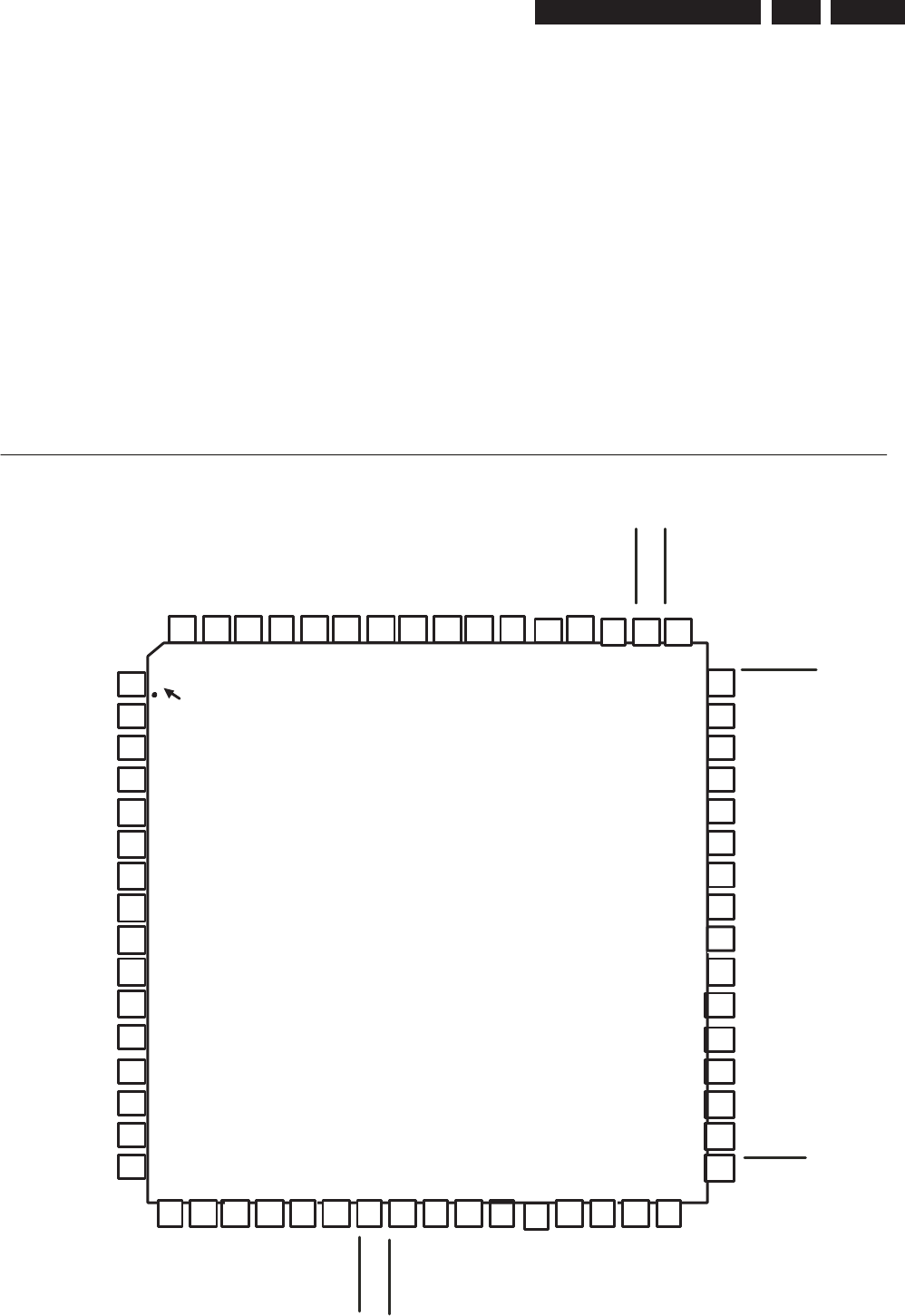
EN 1873139 785 31532 9.
Circuit- and IC description
S D A I/O I2C Port Serial Data Input/Output .
ALSB I/O TTL Address Input. This signal sets up the LSB of the I2C address.
When this pin is tied low the I2C filter is activated which reduces noise on the
I2C interface.
V
DD_IO
P Power supply for digital i/ps and o/ps
V
DD
P Digital power supply
V
AA
P Analog power supply
V
REF
I/O Optional External Voltage Reference Input for DACs or Voltage Reference
Output (1.235V).
EXT_LF I External Loop filter for the internal PLL.
RTC_SCR_TR
I Multifunctional Input: Real Time Control (RTC) input, Timing Reset input,
Subcarrier Reset input.
I
2
C I This Input Pin must be tied High (V
DD_IO
) for the ADV7310/ADV7311 to interface
over the I
2
C port.
GND_IO
PIN CONFIGURATION
12
13
14
15
17 1 8
3
4
5
6
7
1
2
10
11
8
9
56 55 5457585960
47
53
42
43
44
45
40
41
38
39
19 20
DAC A
CLKIN_B
DA C B
AGND
VAA
RTC_SCR_TR
SDA
I2C
ALSB
SCLK
C4
C3
S4
VDD_ IO
Y0
Y1
Y2
Y3
Y4
Y5
Y6
DAC D
C7
C5
P_HSYNC
CLKIN_A
RSE T 2
S_HSYNC
61626364
S_BL AN K
DAC F
DAC C
P_BLANK
C9
C8
GND_IO
EXT_LF
16
21 22 23 24 25 26 27 28 29 30 3 1 32
37
35
33
34
COMP1
RESET
DAC E
COM P2
VREF
48
S_VSYNC
C6
P_VSYNC
49
50
51
52
S0
S1
46
Y7
VDD
Y9
C0
C1
C2
36
S2
VDD
S9
S8
S6
S7
DGND
S5
DG ND
Y8
RSET 1
S3
PIN 1
IDENTIFIER
TOP VIEW
(Not to Scale)
ADV7320
KSTZ
Figure 9-19
EN 188 3139 785 31532
Figure 10-1
0038
3139 247 6117 2005-07-22
Exploded View of Front Portion (DVDR5350H & DVDR7300H)
10. Exploded view & Service parts list
EN 189
3139 785 31532
Figure 10-2
0072
0166
8622 810 12769 2005-09-12
Exploded View of Rear Portion
DVDR5350H
10.
Exploded view & Service parts list
EN 190 3139 785 31532
Figure 10-3
0247
0262
0243
024802490250
0177
0244
0176
0146
0257
0233
0238
0239
1008
0002
PANEL FRONT
COMPLETE ASSY
0106
0100
1010
0072
0166
8622 810 12637 2005-07-12
Exploded View of Rear Portion
DVDR7300H
10. Exploded view & Service parts list
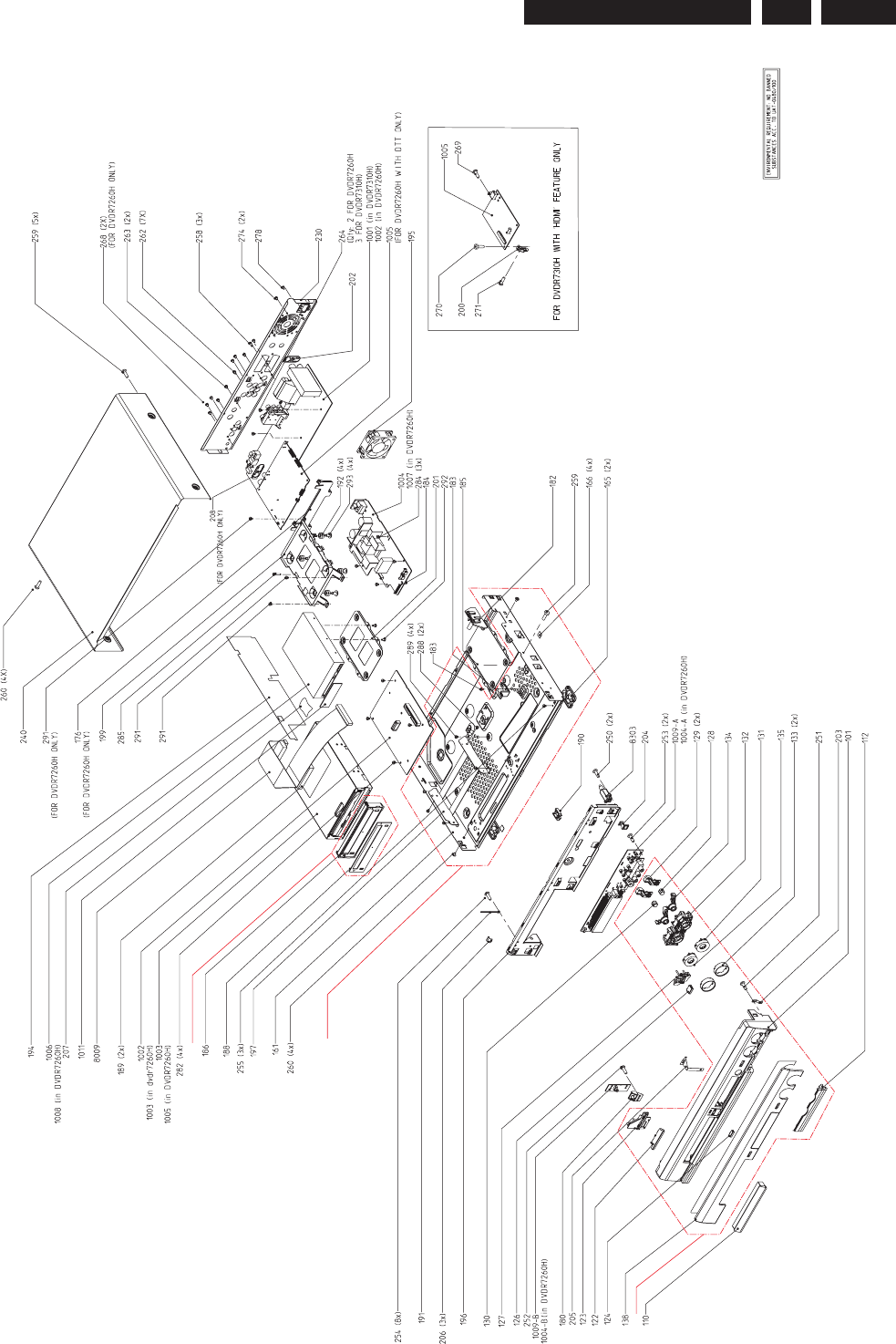
EN 191
3139 785 31532
Figure 10-4
0901
0920
0902
8622 810 13794 dd 2006-09-14
Exploded View of DVDR7310H/75/97
10.
Exploded view & Service parts list

EN 192 3139 785 31532
8001 3103 601 00591 CBLE KR 11P/160/11P KR UL
8002 3103 601 00621 FFC FOIL 7P/290/7P BD FLD UL
8004 3103 601 00631 FFC FOIL 10P/315/10P BD FLD UL
8005 3103 601 00751 FFC FOIL 22P/220/22P BD FLD UL
8008 3103 601 00442 CBLE KR 12P/130/12P UL
8009 3103 601 00611 CBLE IDE 40P/400/40P IDE UL
8010 3103 601 00651 FFC FOIL 13P/600/13P AD UL
8012 3103 601 00561 CBLE EHR 4P/430/4P LC UL
8013 3103 601 00311 KR 9POL GESCH 370MM
8018 3103 601 00861 FFC FOIL 40P/180/40P BD UL
8019 3103 601 00361 IEEE 1394 CHRYSALIS 350MM
8026 3103 601 00721 FFC FOIL 22P/220/22P BD FLD UL
8030 3103 601 00571 CBLE EHR 4P/130/4P LC UL
EXPLODED VIEW - REAR PORTION DVDR7300H
72 3103 607 91131 COVER TRAY ASSY COMPL
DVDR5300
100 3103 607 90911 FRAME ASSY DVDR745
107 3139 243 20441 EMC TAPE (COPPER)
116 3103 604 01311 SPACER 9
130 3103 603 20141 SPACER RUBBER IDE CABLE
145 3103 604 00291 SCREW SAFETY HOLDER
146 3103 600 30021 SCREW-DAMPER-M3
157 3103 601 20612 SPRING GROUND TUNER
166 3103 607 50971 COVER DUST ASSY
169 2822 031 00041 FAN 12VDC 0.8W 3100RPM B
175 3103 603 20201 AIR GUIDE
176 3103 604 01861 DAMPER HDD
179 3103 607 51621 COVER ASSY DVDR5300H
180 3139 247 61211 PLATE BACK HDMI EUR DVDR7300H
247 2522 200 98475 SCR PAN TORX ST BK #6-32X6
248 2522 200 98475 SCR PAN TORX ST BK #6-32X6
249 2522 200 98475 SCR PAN TORX ST BK #6-32X6
250 2522 200 98475 SCR PAN TORX ST BK #6-32X6
349 2422 549 00739 REMOTE CONTR DVDR5350H/7300H
B
351 2422 070 98151 MAINSCORD EUR 1M5 BK B /02/19
351 4822 321 10713 MAINSCORD UK 5A 1M8 VH BK B
/05
352 2422 076 00532 CBLE SCART 1M5 SCART 21P BK B
/02/05/19
352 2422 076 00825* CBLE SCART 1M5 SCART 21P BK B
/02/05/19
353 2422 070 00016 MAINSCORD AUS/NZ 1M9 DET 2P B
/75
354 2422 070 98151 MAINSCORD EUR 1M5 BK B
/97
10. Exploded view & Service parts list
DVDR5350H/DVDR7300H
EXPLODED VIEW - FRONT PORTION
1 3139 247 61171 FRONT ASSY DVDR5350H
/02/05/19
1 3139 247 61191 FRONT ASSY DVDR7300H
/02/05/19
1 3139 247 61391 FRONT ASSY DVDR7300H
/75,/97
38 3103 601 20291 SPRING ESD
140 2422 015 00493 SADDLE WIRE NY6/6 NT 19.1MM B
155 3103 601 20212 SPRING I-LINK
156 3103 601 20231 SPRING GROUND
EXPLODED VIEW - REAR PORTION DVDR5350H
72 3103 607 91131 COVER TRAY ASSY COMPL
DVDR5300
100 3103 607 90911 FRAME ASSY DVDR745
107 3139 243 20441 EMC TAPE (COPPER)
116 3103 604 01311 SPACER 9
130 3103 603 20141 SPACER RUBBER IDE CABLE
145 3103 604 00291 SCREW SAFETY HOLDER
146 3103 600 30021 SCREW-DAMPER-M3
157 3103 601 20612 SPRING GROUND TUNER
166 3103 607 50971 COVER DUST ASSY
169 2822 031 00041 FAN 12VDC 0.8W 3100RPM B
175 3103 603 20201 AIR GUIDE
176 3103 604 01861 DAMPER HDD
179 3103 607 51621 COVER ASSY DVDR5300H
180 3139 247 61201 PLATE BACK EUR DVDR5350H
247 2522 200 98475 SCR PAN TORX ST BK #6-32X6
248 2522 200 98475 SCR PAN TORX ST BK #6-32X6
249 2522 200 98475 SCR PAN TORX ST BK #6-32X6
250 2522 200 98475 SCR PAN TORX ST BK #6-32X6
349 2422 549 00739 REMOTE CONTR DVDR5350H/7300H
B
351 2422 070 98151 MAINSCORD EUR 1M5 BK B
/02/19
351 4822 321 10713 MAINSCORD UK 5A 1M8 VH BK B
/05
352 2422 076 00532 CBLE SCART 1M5 SCART 21P BK B
352 2422 076 00825* CBLE SCART 1M5 SCART 21P BK B
357 4822 320 50377 CONNECT. CABLE PAL
358 2422 076 00522 G-LINK CABLE & TRANSMITTER
363 2422 076 00718 CBLE CINCH 1M5 CINCH RDYEWH B
1001 3103 608 51941 PBAS AB 04 E3/5300H
1002 3139 248 86441 PCBAS CHRY-F05 DVDR5350H
1004 3103 608 51242 PBAS DC 04 N1
1007 3139 247 11362 MODULE DRIVE D4.3 CLOSED
1008 3139 247 11985 MODULE PSU 05H8000 EU
1011 3139 248 86111 PCBAS IDE HDD DVDR7300H
1200 2822 062 00071 HDD 3.5” 160GB WD1600BB-55GUC0
1800 3103 607 10121 ADAPTER HDD-IDE-CON ASSY
180MM
5000 2422 549 00107 FERRITE CORE RP 25X5X12 Y

EN 193
3139 785 31532 10.
Exploded view & Service parts list
357 4822 320 50377 CONNECT. CABLE PAL
358 2422 076 00522 G-LINK CABLE & TRANSMITTER
/02/05/19
363 2422 076 00655 AV CABLE CINCH 3P 1M5 CINCH
/75/97
363 2422 076 00718* CBLE CINCH 1M5 CINCH RDYEWH B
/75/97
1001 3103 608 51941 PBAS AB 04 E3/5300H
1002 3139 248 86101 PCBAS CHRY-F05 DVDR7300H
1004 3103 608 51242 PBAS DC 04 N1
1007 3139 247 11362 MODULE DRIVE D4.3 CLOSED
1008 3139 247 11985 MODULE PSU 05H8000 EU
1010 3103 608 51872 PBAS PSCAN HDMI VIE L
1011 3139 248 86111 PCBAS IDE HDD DVDR7300H
1200 2822 062 00099 HDD 3.5” 250GB 6L250R0 (MAXT)Y
1800 3103 607 10121 ADAPTER HDD-IDE-CON ASSY
180MM
5000 2422 549 00107 FERRITE CORE RP 25X5X12 Y
8001 3103 601 00591 CBLE KR 11P/160/11P KR UL
8004 3103 601 00631 FFC FOIL 10P/315/10P BD FLD UL
8005 3103 601 00751 FFC FOIL 22P/220/22P BD FLD UL
8008 3103 601 00442 CBLE KR 12P/130/12P UL
8009 3103 601 00611 CBLE IDE 40P/400/40P IDE UL
8010 3103 601 00651 FFC FOIL 13P/600/13P AD UL
8012 3103 601 00561 CBLE EHR 4P/430/4P LC UL
8013 3103 601 00311 KR 9POL GESCH 370MM
8018 3103 601 00861 FFC FOIL 40P/180/40P BD UL
8019 3103 601 00361 IEEE 1394 CHRYSALIS 350MM
8026 3103 601 00721 FFC FOIL 22P/220/22P BD FLD UL
8030 3103 601 00571 CBLE EHR 4P/130/4P LC UL
8038 3139 241 01451 FFC FOIL 40P/280/40P BD 0.5MMP
8039 3139 111 02141 FFC FOIL 07P/100/07P BD 1.0MMP
EXPLODED VIEW - DVDR7310H/75/97
110 3139 244 14751 COVER TRAY DVDR7310H
182 3103 604 00291 SCREW SAFETY HOLDER
184 3103 604 01311 SPACER 9
189 3103 603 20141 SPACER RUBBER IDE CABLE
190 2422 015 00493 SADDLE WIRE NY6/6 NT 19.1MM B
192 3103 604 01861 DAMPER HDD
194 3103 603 20201 AIR GUIDE
195 2822 031 00041 FAN 12VDC 0.8W 3100RPM B
202 3103 601 20611 SPRING GROUND TUNER
204 3103 601 20212 SPRING I-LINK
205 3103 601 20291 SPRING ESD
206 3103 601 20231 SPRING GROUND
230 3139 247 61211 PLATE BACK HDMI EUR DVDR7300H
240 3103 607 51621 COVER ASSY DVDR5300H
292 2522 200 98475 SCR PAN TORX ST BK #6-32X6
293 3103 600 30021 SCREW-DAMPER-M3
341 2422 549 00739 REMOTE CONTR DVDR5350H/7300H
B
345 2422 070 00016 MAINSCORD AUS/NZ 1M9 DET 2P B
/75
345 2422 070 98151 MAINSCORD EUR 1M5 BK B
/97
350 2422 076 00718 CBLE CINCH 1M5 CINCH RDYEWH B
353 4822 320 50377 CONNECT. CABLE PAL
0901 3143 027 66281 FRONT CAB ASSY DVDR7310H AP
0902 3143 027 63321 COVER DUST ASSY DVDR9000H
0920 3143 027 66201 FRAME ASSY DVDR7310H
1001 3103 608 51941 PBAS AB 04 E3/5300H
1002 3139 248 86101 PCBAS CHRY-F05 DVDR7300H
1003 3139 247 11362 MODULE DRIVE D4.3 CLOSED
1004 3139 247 11985 MODULE PSU 05H8000 EU
1005 3103 608 51872 PBAS PSCAN HDMI VIE L
1006 2822 062 00099 HDD 3.5” 250GB 6L250R0 (MAXT)Y
1009 3103 608 51242 PBAS DC 04 N1
1011 2422 549 00107 FERRITE CORE RP 25X5X12 Y
1012 3103 601 00861 FFC FOIL 40P/180/40P BD UL
1013 3139 248 86111 PCBAS IDE HDD DVDR7300H
8001 3103 601 00591 CBLE KR 11P/160/11P KR UL
8002 3103 601 00631 FFC FOIL 10P/315/10P BD FLD UL
8003 3103 601 00751 FFC FOIL 22P/220/22P BD FLD UL
8004 3103 601 00441 CBLE KR 12P/130/12P UL
8005 3103 601 00611 CBLE IDE 40P/400/40P IDE UL
8006 3103 601 00561 CBLE EHR 4P/430/4P LC UL
8007 3103 601 00721 FFC FOIL 22P/220/22P BD FLD UL
8008 3103 601 00571 CBLE EHR 4P/130/4P LC UL
8009 3139 241 01451 FFC FOIL 40P/280/40P BD 0.5MMP
8010 3139 111 02141 FFC FOIL 07P/100/07P BD 1.0MMP
8011 3103 601 00651 FFC FOIL 13P/600/13P AD UL
8012 3103 601 00310 KR 9POL GESCH 370MM
8013 3103 601 00360 IEEE 1394 CHRYSALIS 350MM
Note: Only the parts mentioned in this list are normal service spare
parts.

EN 194 3139 785 31532
11. Revision List
11. REVISION LIST
Version 1.0
* Initial Release
Version 1.1
* Addition of DVDR7300H/75 and DVDR7300H/97
* Update service parts list
Version 1.2
* Addition of DVDR5350H/05 and DVDR7310H/75/97
* Update service parts list
* Include DVDR7310H Exploded View
