0. Ł\”ƒ DVL 909 EN_Service_Manual EN Service Manual
User Manual: DVL-909-EN_Service_Manual
Open the PDF directly: View PDF ![]() .
.
Page Count: 47

ORDER NO.
RRV1896
T - IZM APR. 1998 Printed in Japan
PIONEER ELECTRONIC CORPORATION 4-1, Meguro 1-Chome, Meguro-ku, Tokyo 153-8654, Japan
PIONEER ELECTRONICS SERVICE, INC. P.O. Box 1760, Long Beach, CA 90801-1760, U.S.A.
PIONEER ELECTRONIC (EUROPE) N.V. Haven 1087, Keetberglaan 1, 9120 Melsele, Belgium
PIONEER ELECTRONICS ASIACENTRE PTE. LTD. 501 Orchard Road, #10-00 Lane Crawford Place, Singapore 0923
PIONEER ELECTRONIC CORPORATION 1998
c
1. CIRCUIT DESCRIPTION ...................................... 2
2. CIRCUIT DESCRIPTIONS
FOR DV-S9 AND DV-09 ............................... 10
3. TEST MODE ....................................................... 13
4. IC INFORMATION .............................................. 22
5. FL INFORMATION .............................................. 47
CONTENTS
DV-505
DVD PLAYER
DV-S9
DVD LD PLAYER
DVL-909
SERVICE GUIDE
2
DV-505, DVL-909, DV-S9
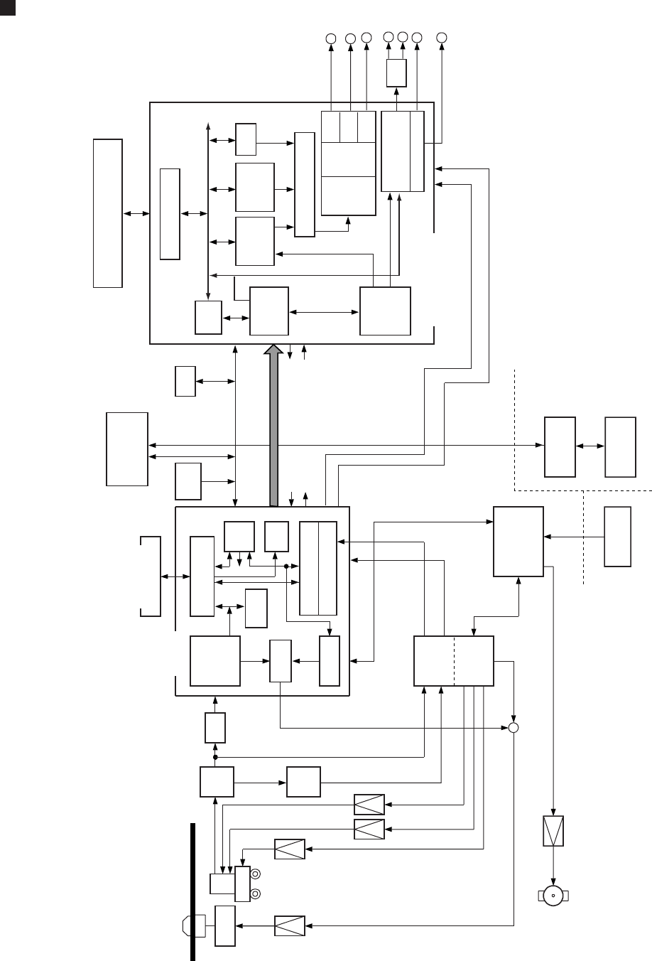
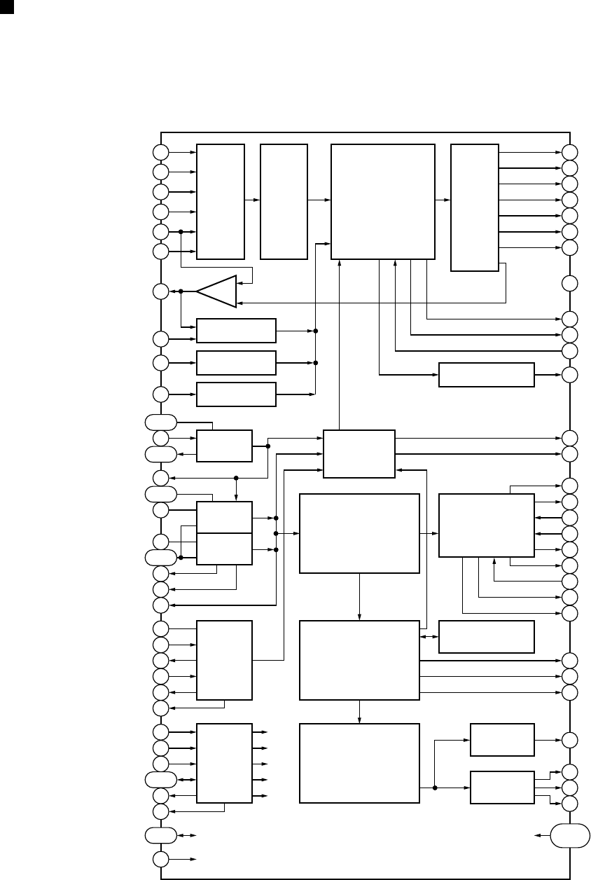
1. CIRCUIT DESCRIPTION
1.1 OVERALL BLOCK DIAGRAM
DV-505
Spindle
Motor TA
FA
Slider
HA
TE
GEN
OEIC A/D Sync
Demod
Spindle
control
ECC &
ID Reg.
Sub-CPU
I/F
DRAM I/F
(bus arbitor)
CPU
I/F
DMA
CD-ROM Sync gen.
Sub-code Buffer
VBR Buffer
4M bit DRAM
SREO
Program Stream
XSACK
CD PCM
CD D. OUT
CD DSP
EFM
Decoder
Servo
DSP
CD PCM
CD Digital Out
Mechanism
Control
CPU
Loading
Motor
Mechanism
sense SW Key-SW
& Display
System CPU
(32 bit RISC)
FLASH
ROM RAM
SREO
XSACK
CPU
I/F
Y
C
Comp.
PCM D-Out
AC3 D-Out
Lt
Rt
Video Out
DVD/V-CD
AV Decoder
Display
CPU
SYSTEM
Decoder
(DMUX)
AV Sync
controller
MPEG2
Video
Decoder
Sub-
picture
Decoder
GUI
Memory Controller
16M bit SDRAM
CODE Buffer
(Video, Audio, Sub-picture,GUI)
MIX
D/A
AC3/MPEG1
Audio Decoder
Copy
Guard
NTSC
/PAL
encode
DAC
DAC
DAC
S/PDIF
LSI-11
IC802
MB811171622A-100FN
IC604
TC551001BFL-85
IC603
VYW1536
IC601
PD3381A
IC701
PD4833A
IC301
TLC5540INS
IC201
LC78650NE
IC702
HM514800CJ-7
IC501
PD4889A
IC101
PD4890A
IC801
MB86371
(MPEG2 Decoder)
3
DV-505, DVL-909, DV-S9
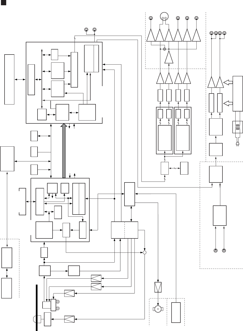
DV-S9 and DV-09
Spindle
Motor TA
FA
Slider
HA
TE
GEN
OEIC A/D Sync
Demod
Spindle
control
ECC &
ID Reg.
Sub-CPU
I/F
DRAM I/F
(bus arbitor)
CPU
I/F
DMA
CD-ROM Sync gen.
Sub-code Buffer
VBR Buffer
4M bit DRAM
SREO
Program Stream
XSACK
CD DSP
EFM
Decoder
Servo
DSP
CD PCM
CD Digital Out
Mechanism
Control
CPU
Loading
Motor
Mechanism
sense SW
Key-SW
& Display
System CPU
(32 bit RISC)
ROM RAM
SREO
XSACK
CPU
I/F
DVD/V-CD
AV Decoder
Display
CPU
GUI
ROM
SYSTEM
Decoder
(DMUX)
AV Sync
controller
MPEG2
Video
Decoder
Sub-
picture
Decoder
GUI
Memory Controller
16M bit SDRAM
CODE Buffer
(Video, Audio, Sub-picture,GUI)
MIX
AC3/MPEG1
Audio Decoder
S/PDIF
LSI-11
IC802
MB811171622A-100FN
IC604
TC551001BFL-85
IC603
VYW1536
IC602
PDK026A
IC601
PD3381A
IC701
PD4833A
IC301
TLC5540INS
IC201
LC78650NE
IC702
HM514800CJ-7
IC501
PD4889A
IC901
PD0259A
IC952
M65677FP
Composite
S-Video
Component
Video Out
Audio Out
Digital
Out
Cb
L ch (Analog)
L ch (Analog)
R ch (Analog)
R ch (Analog)
Cr
Y
10
IC101
PD4890A
IC801
MB86371
(MPEG2 Decoder)
DNR
HIBIT
DATA
SELECTOR
DIGITAL
INTERFACE
RECEIVER
LEGATO S
DRAM
VIDEO
ENCODER,
COPY GUARD
DAC FILTER
96/24 DAC
96/24 DAC
FILTER
FILTER
FILTER
DAC
88
8
8
10
IC951
M65677FP
IC811
IC861
CD0015AF
AUDIO
TRANSFORMER
AC IN
VIDEO OUT
DIRB
DV-S9 Only
AUDIO
10
VIDEO
ENCODER,
COPY GUARD
DAC
DAC
10
AMP.
DRIVER DRIVER
DRIVER
DRIVER
DRIVER
DRIVER
DRIVER
AMP.
AMP.
AMP.
Digital In
(OPTICAL)
(COAXIAL)
AUDIO
POWER SUPPLY
(OPTICAL)
(COAXIAL)
4
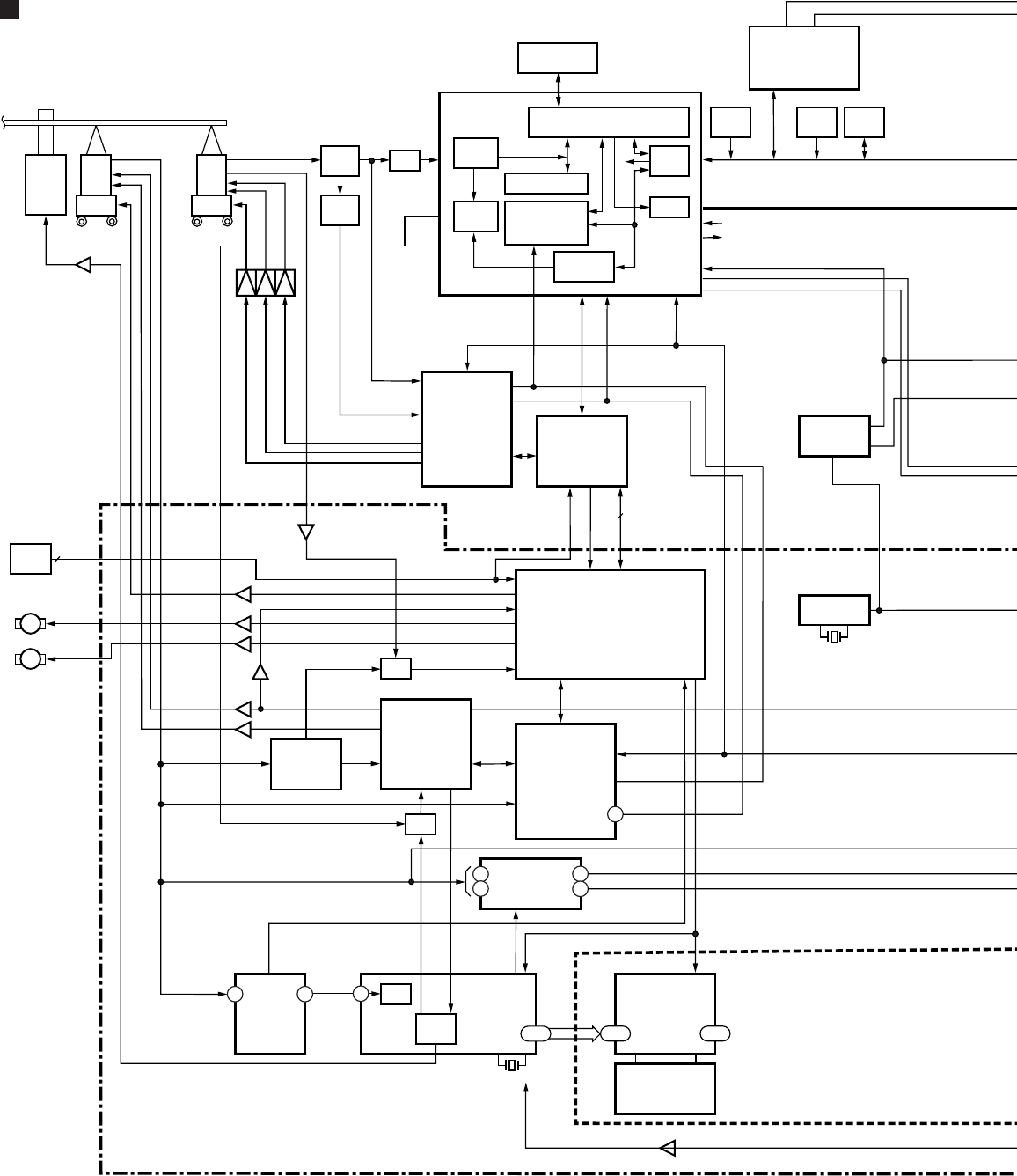
DV-505, DVL-909, DV-S9
Sync
Demod
HA
OEIC
TE
GEN Spindle
Control
DRAM I/F
(Bus Arbiter)
Sub-CPU
I/F
CPU
I/F
FLASH
ROM RAM
GUI
ROM
DMA
ECC & ID Reg.
CD-ROM
Sync gene
Sub-code Buffer
4Mbit DRAM
VBR Buffer
LSI-11
IC702
HM514800CJ-7
IC603 IC602 IC604
IC701
PD4833A
TA
FA
Slider
EFM Decoder
Servo DSP
CD DSP
IC 201
LC78650E-P IC 501
PD4889A
Mechanism
Control
CPU
TA
FA
Slider
For CLD For DVD
SPDL
Motor
SLD POS
XRESET
IC101
PD0260A2
LD Mechanism Control
SI, SO, SCK,
SHAKE
SLD DRV
SLD ERR
LOAD/TILT DRV
TURN DRV
Sel TILT ERR
DVD TILT ERR
M
LOAD/TILT
MOTOR
M
TURN
MOTOR
IC901
LA9430M
Servo
Control IC
(ASP)
TRKG
FOCS
IC801
LA9425
PSP
VCXO ERR
IC908
LC78625E
DSP
EFM Decode
Mecha.
SW
56
Sel
LD DATA
IC352
CA0002AM
Analog Audio
Analog L
Analog R
IC101
PD3212A
Memory
Cont.
(with DNR)
65-72 44-51
IC500
PD6159B
Dual DVP
14-21
SPDL
Cont
A/D
37
ACOM
14M VCXO
IC400
LA7134M
VDEM
1027
Phillips Code
IC102, IC103
MB81C1501PF
Field Memory
VCXO ERR
IC601
PD3381A
System CPU
(32bit RISC)
25
4
15
14
4
LD TILT ERR
16M
18M
16M
CD PCM
CD Digital Out
16M
IC205
TC7S02F
IC 813
CY2081SL
-611
X312
384 × 48k
(18M)
A/D
Program Stream
27M
CD PCM
CD Digital out
27M
36M
DVL-909
5
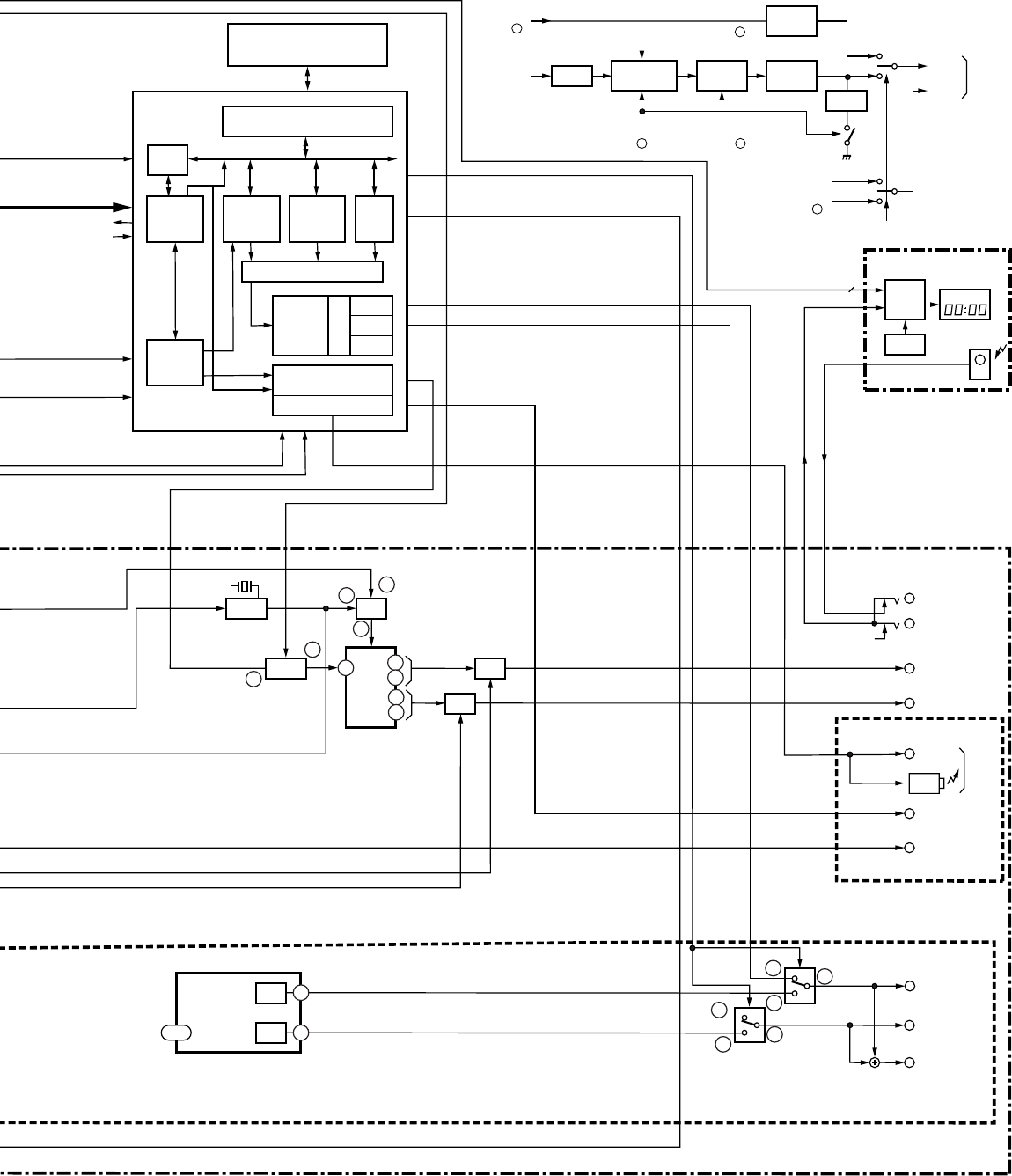
DV-505, DVL-909, DV-S9
MYCB ASSY
Y OUT
H
LD Y
H
KEY
L
L
to
MYCB
C OUT
TRAP
AMP Sync Tip
Clamp
Pedestal
Clamp
D-Extention
Circuit
Sync Tip
Clamp
DVD Y
(IC815 )
LD Y SIGNAL
(from MYCB)
1(from MECHA. CONT. )
D-EXT ON/OFF
41
BLANKING PLUSE
(from AV-1 )
48
BURST FLAG
(from AV-1 )
47
LD C SIGNAL
(from MYCB)
DVD C
(IC815 )
7
IC620
IC620
Memory Controller
CPU
I/F
System
Decoder
(DMUX)
AV Sync
Controller
MPEG 2
Video
Decoder
NTSC
/PAL
Encode
AC3/MPEG1
Audio Decoder
S/PDIF
DAC
DAC
DAC
Copy Gurd
Sub
Picture
Decoder GUI
16Mbit SDRAM
CODE Buffer
(Video, Audio, Sub-picture,GUI)
IC802
MB811171622A
-100FN
AC-3 RF
Hi-Bit
IC202
PD0236AM
16M IC201
PD2029AM (L)
D/A
25 9
10
5
6
Sel
CLK
IC203
TC74HC157AF
VCXO
X311
384 × 44.1k
(16M)
Hi-Bit
DATA
Sel
Sel
L
R
PCM Digital
PD
Key
DVD C.
DVD Y.
IC620
TC74HC4053AF
AC-3/PCM Digital
IC301
CXD2046Q
Y/C SEP.
1-8
D/A
D/A
IC620
Y (DVD)
C (DVD)
Comp. OUT
C OUT
Y OUT
AC-3 RF OUT
PCM
Digital OUT
AC-3
/PCM
Digital
OUT
R OUT
L OUT
SR IN
SR OUT
SEL IR
IR
FL
Cont.
Key
A.B.
FL TUBE
REMOTE
SENSOR
Front Section
CLDM ASSY
14
8
32
4
Y (LD)
C (LD)
33
36
2
4
1
15
3
5
MIX
IC 801
MB86371
DVD/V-CD
AV Decoder
27M
36M
(COAXIAL)
(TOSLINK)
JCKB ASSY
6
DV-505, DVL-909, DV-S9
1.2 EXPLANATION OF EACH MOVEMENT
1.2.1 Sequence Up to Playback
DVD SETUP
RF AGC ON
SPDL ACCEL
Yes
Focus Lock
LD ON
Sweep UP → Down
ATB ON
Layer Det.
Lead-in Search
PLAY
MIRR Modulation
Measurement
T Servo ON
SLDR Servo ON
F Gain Adj.
T Gain Adj.
AFB Adj.
(Auto Focus Bias)
332
35
54
44
49
4
1
2
26
27
54
5
6
7
8
11 12 22
OEIC
PICKUP
CD DVD
FDO
LDON
FE
UP
DRF
(FOK)
IC101
RFIC IC201
DIGITAL
SERVO IC
IC501
MECH.
CONTROL
IC151
DRIVER
• FOCUS SERVO
• FOCUS LOCK TIMING
PH
RF
B1
B2
B3
B4
LD
MD
FOCUS
COIL
FE
OEIC GAIN
LASER
ADDRESS
&
BUS
SGC
FDO DRF
58
31
13
UP
1.2.2 Focus Servo
FE generated in the RF IC is sent to the
Digital servo IC.
For a DVD, the servo is turned on during
the transition from “Up” to “Down” of
the first-order sine wave. For a CD, it
turns on during the transition from
“Down” to “Up” of the first-order sine
wave.
When the servo is turned on, the level of
PH (the envelope of the bright side of RF)
increases, and DRF becomes H. The
kick-brake pulses, such as those for
FOCUS jump, are also output from pin
49 of IC201.
7
DV-505, DVL-909, DV-S9
1.2.3 Tracking / Slider Servo
ATB: The tracking balance compensation is
achieved by outputting the offset from
the TBAL output at pin 46 of the digital
servo IC, and by biasing the charge pump
resistor for phase-difference error of
RFIC.
The difference is detected by processing
TE at pin 34 of IC 201 with an internal
digital equalizer.
TDO: In addition to the servo output, the low-
band components, such as the kick-brake
for jump, are added for TDO output.
SLDO: The low-band components of TE are
processed by the internal digital
equalizer, and deadband is added for
SLDO output. The offset voltage for
pickup movement is also included in the
SLDO output.
434
46
50
24
26
27
16
17
47
5
6
7
8
OEIC
PICKUP
IC101
RFIC IC201
DIGITAL
SERVO IC
IC501
MECH.
CONTROL
IC151
DRIVER
• TRACKING / SLIDER SERVO
TE
TE RF
B1
B2
B3
B4
TRKG
COIL
TBAL ADDRESS
&
BUS
TDO
19
SLDO
M
26
28
CP
SLDR
3
12
41
57
48
25
95
OEIC IC101
RFIC IC301
A/D
IC701
LSI II
IC201
DIGITAL
SERVO
IC161
DRV
• SPDL SERVO
RFO
RF
CLK
(27M) 8 bit
ATC
APC
AFC
ASC
V165
DUTY50
FG
VPWM
PPWM
RPWM
FPWM
31
50
32
RF
IC302
(1/2)
IC271
(2/2)
IC271
(1/2)
FG
SPDL +
SPDL -
SPDL
SPDO
(Base)
SPDO
(Compatible)
3
|
10
200
|
207
179
176
178
180
177
161 163 166 167
159
VCO
12
13
M
1.2.4 SPINDLE SERVO
For a CD, the RF signal output from pin 32 of the RF IC is converted
to binary in IC201. By comparing the binary value with the reference
CLK (clock), the SPDL ERR signal is output from pin 48.
For a DVD, the SPDL ERR signal is generated from the PWM signal
output from LSI-ΙΙ. Upon receiving this signal via pin 31, IC201
also outputs it from pin 48, switching from the CD SPDL ERR
signal.
8
DV-505, DVL-909, DV-S9
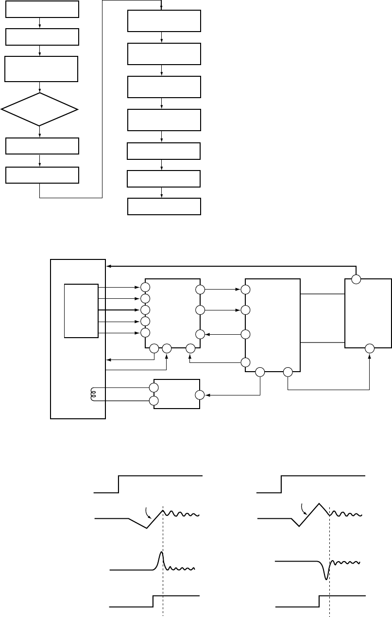
1.2.5 Disc Determination
Determination is achieved by checking the sine wave by sweeping
the lens with the OE IC gain at L and the FSC error amplifier (SGC)
at the default setting. If no sine wave is detected, checking is retried
after switching the OE IC gain to H and increasing the gain of the
FSC error amplifier (SGC). If no sine wave is detected again, it is
regarded as the NO DISC condition.
If one half of the sine wave detected at the first lens sweep is of a
value less than 0.5 V, the OE IC gain is set to H and the peak-to-
peak value of the sine wave is roughly adjusted to 1.8 Vp-p.
By sweeping the lens around the height where the sine wave has
been detected, disc determination is performed, and the sine wave
is finely adjusted to 1.8 Vp-p.
Offset compensation
Lens sweep
Lens sweep
NO DISC
OEIC gain = H
FCS AMP gain up
Checking
the sine wave
Checking
the sine wave
Roughly adjust to
1.8Vp-p sine wave
Finely adjust to 1.8Vp-p
sine wave
Disc determination
END
Level check Less than 0.5V
More than 0.5V
Yes
Yes
None
None
OEIC gain = H
9
DV-505, DVL-909, DV-S9
1.2.6 System Control (DVL-909)
IC501
PD4889A
Mech. Cont.
(DVD)
IC101
PD4890A
Mode Control
(FL Cont.)
IC601
PD3381A
IC801
MB86371
AV-Dec.
System
Cont.
IC601
PD3381A
System
Cont.
KEY
POWER ON
XRESET
Remote
Sensor
22
21
IC101
PD4890A
Mode Control
(FL Cont.)
16
15
14
46
13
108
107
111
65
102
77
39
13 16
19 26
IC201
LC78650E-P
Digital
Servo
65 72
810
IC101
PD0260A2
Tilt / Loading
Drive
Tilt /
Loading
Motor
Turn
Drive
Mech. Cont.
(CLD)
24
9
25
54
55
56
33 35
142 151
SI1,SO1
SCK1,XRDY
102,107,108,111
IC604
Work
RAM
IC603
FLASH
ROM
IC602
GUI
4M ROM
DATA,ADDRESS
MAIN BUS
IC701
PD4833A
LSI-11
MAD0–MAD7
19 21
Slider
Position
SW
Loading
Position
SW
LD/DVD
Carriage
Out position SW
Turn
A/B SW
MM
SLDPOS
SW1–3
XLPO
XTurn A
XTurn B
IC171IC803
FLPB, KEYB DVD MAIN
POWER SUPPLY
ASSY
CLD MAIN
SO1,SI1
SCK1 DVDP PK
DATA
XRDY
LT1
SCK
SI
SO
1) Interface between Mode Cont. and System Cont.
XRDY
LT1
SCK1
SO1
SI1
Timing Chart
If there is no communication for 2 sec.,
Mode Cont. turn off the power and reset.
10
DV-505, DVL-909, DV-S9
2.1 VIDEO SIGNAL PROCESSING BLOCK
2.1.1 PD0259A Block
The major purposes of the PD0259A block are;
(1) Frame-correlative cyclic digital noise reduction
(2) Horizontal and vertical contour compensation
(3) Y/C timing adjustment
(4) Frame freezing
(1) Frame-Correlative Cyclic Digital Noise Reduction
For eight-bit digital video data input to the PD0259A, noise reduction
is performed through subtraction between the data and those of the
corresponding points 1 frame before, delayed for the subtraction
via a 4-bit DRAM by 1 frame.
The noise signal detected as a result is sent to a non-linear circuit. If
the difference is larger than a specific value, it is regarded as “a
change in picture,” and no canceling calculation is made.
This function is the same as that which has been performed in
conventional laser-disc players. The only difference is that the input
video signal here is a DVD digital component signal (4:2:2), while
it is an LD digital composite signal in conventional laser-disc players.
ON/OFF
SW
DATA
Non-linear
circuit
1-frame delay
1H
Delay
1H
Delay
Non-linear
circuit
Non-linear
circuit
Vertical edge generation
Horizontal edge generation
Delay
HPF
BPF
(2) Horizontal and Vertical Contour Compensations
For data after digital noise reduction, horizontal and vertical contour
compensations are made only for the Y-signal.
Horizontal compensation is performed by detecting edge components
from the information of the reference picture elements and those
that horizontally proceed and succeed by several pixels, and then
generating edge-emphasizing components through non-linear
processing of the detected components.
Vertical compensation is performed by detecting edge components
from information on the reference picture elements and those which
vertically proceed and succeed by one line, and then generating edge-
emphasizing components through non-linear processing of the
detected components.
These edge-emphasizing components are added to the main-line
digital data to achieve contour compensations.
(3) Y/C-timing Adjustment
This function changes the output phase of the Y signal with respect
to the Cb and Cr signals in units of the 13.5-MHz clock cycle (approx.
74 ns).
(4) Frame Freezing
In response to a command sent from the system control computer
by serial transmission, data for one frame are frozen, and the frozen
picture is output.
This function is specific to the DV-S9 and is used only for picture-
by-picture reversing by jog/shuttle operation or “Slow 1” playback
operation.
2.1.2 M65677FP Block
The M65677FP block functions as an NTSC encoder that converts
digital component signals to analog Y, C, Cb and Cr signals. While
our popular models other than the DV-S9 use the built-in encoder in
the MB86371 block, an external NTSC encoder is added to the DV-
S9, as it performs digital processing in the PD0259A block.
In addition to NTSC encoding, the M65677FP also performs:
(1) D.EXT(DV-S9)/BLACK LVL(DV-09)
(2) C.LEVEL adjustment
(1) D.EXT(DV-S9)/BLACK LVL(DV-09)
Setup of –7.5 IRE is added to the Y signal. D.EXT(DV-S9)/BLACK
LVL(DV-09) processing using analog signals in conventional laser
disc players is achieved by using digital signals.
(2) C.LEVEL Adjustments
The burst level of the C signal can be varied centering around 40
IRE.
Therefore, it is performed for the S-connector and CVBS-connector
outputs, but not for the color-difference output.
This function is also not available if the connected TV receiver has
no AGC circuit.
2. CIRCUIT DESCRIPTIONS FOR DV-S9 AND DV-09
11
DV-505, DVL-909, DV-S9
2.1.3 Analog Video Signal Processing Block
The video signals output from the built-in 10-bit DA converter of
the M65677FP pass through a low-pass filter and amplifier, and are
output from the DVD MAIN Assy and sent to the VOUT Assy.
In the VOUT Assy, analog noise-reduction processing having three
levels (OFF, low, and high) is initially applied only to the Y signal.
This analog noise reduction is the same as that performed by
conventional laser-disc players. The register port output in serial
communication that the PD0259A receives from the system-control
computer is used as the control signal for analog noise reduction.
After analog noise reduction, a CVBS signal is generated by
composing the Y and C signals (no clamping is performed for the C
signal). The timing pulse BF to be used for pedestal clamping is
supplied from the PD0259A. This signal is adjusted within the
PD0259A so that it provides the timing for the burst portions of the
output video signals.
IC801
MB86371
(AV1)
IC901
PD0259A
(DNR)
IC951
M65677FP
NTSC
ENCODER
LPF
Amp.
H
V
FLD
CLK
V DATA V DATA
H
V
CLK
Cb
µ-COM
Cb
Cr
Y
Y
C
CVBS
V OUT ASSYDVD MAIN ASSY
ANR2
ANR1
BF
IC952
M65677FP
NTSC
ENCODER
LPF
Amp.
Cr
LPF
CLAMP
CLAMP
CLAMP
CLAMP
CLAMP
Analog
NR
Amp.
Y
LPF
Amp.
C
µ-COM
4M DRAM
× 2
12
DV-505, DVL-909, DV-S9
2.2 DIRB BLOCK (DIRB ASSY)
(DV-S9 ONLY)
The two major purposes of the DIRB block are the following:
(1) Switching between data reproduced from a disc and a data signal
in DAC mode
(2) Data decoding in external input mode (DAC mode)
(1) Switching Between Data Reproduced from a
Disc and a Data Signal in DAC Mode
The signal switching is performed at IC811, sending 3-line data
(LRCK, BCK and DATA) to the AUDIO Assy. The switching
control line (DAC MODE) is supplied from the DVD MAIN Assy.
The master clock (MCK) is generated by a crystal on the AUDIO
Assy when reproducing a disc, and by IC861 in DAC mode. MCK
is sent to the AUDIO Assy via RXP.
(2) Data Decoding in External Input Mode (DAC
Mode)
When the user selects DAC mode, the DAC MODE port is set to H
and VCO in IC861 starts oscillating. (VCO does not oscillate in
any other modes than DAC mode.) When there is a toss link of an
external input or a coaxial digital input, the digital input signal is
sent to IC861 from RXP of CN801, generating 3-line data
corresponding to the input sampling frequency. At the same time,
the master clock (MCK) to be used in DAC mode is also generated.
For a 96kHz input, the MCK frequency is divided by 2 by IC831.
When the user selects the internal clock as the system clock, the
clock generated by the crystal on the AUDIO Assy is sent to the
DVD MAIN Assy. When the user selects an external sync as the
system clock, the following parameters are used.
IC901 16M Selector
IC902 18M Selector
IC811 Data Selector
CN801 CN811
IC861
DIR
IC831
Clock Selector
IC835
1/2 Divider
2.3 96K, 24-Bit, HIBIT LEGATO S
SYSTEM (AUDIO ASSY)
All 16-bit and 20-bit sources are converted to 24-bit data by IC101,
which lets a 24-bit data pass through.
As PCM1702P is a 20-bit D/A converter, processing of the upper
20 bits is assigned to it by the shift register.
The lower 4 bits are converted from serial to parallel, then the
significance of each bit is converted digital to analog, functioning
as a 4-bit D/A converter for the lower 4 bits.
By adding the lower 4 bits to the upper 20 bits in the low-pass &
ADD block, D/A conversion is achieved for 24 bits.
Shift Register
TC74HC164AF
Serial to Parallel
and Significance
Conversion
TC74HC163AF
D/A Converter
PCM1702P
Hi Bit
IC101
Legato S
IC111
Low-pass
& ADD
Analog Output
FS(kHz) 16M clock in 18M clock in 16M clock sent to 18M clock sent to
the AUDIO Assy the AUDIO Assy the DVD MAIN Assy the DVD MAIN Assy
32 Oscillates Oscillates Crystal 16M clock Crystal 18M clock
44.1 Stops oscillating Oscillates DIR 16M clock Crystal 18M clock
48 Oscillates Stops oscillating Crystal 16M clock DIR 18M clock
96 Oscillates Stops oscillating Crystal 16M clock DIR 18M clock
If there is no external input or locking onto the input digital signal
cannot be achieved, the ERR signal at pin 43 of IC861 is set to H,
and the crystal in the AUDIO Assy immediately starts oscillating.
In such cases, the clock sent to the DVD MAIN Assy will always be
a crystal clock.
13
DV-505, DVL-909, DV-S9
3. TEST MODE
3.1 HOW TO ENTER THE TEST MODE
There is the three following methods in an enters of the test mode.
1. Short-circuit the terminals (TP6006 and TP6007) for test mode
entry at the side of the system control IC (IC601) of DVDM ASSY,
and turn the power on.
2. Input [ESC] key and [TEST/RANDOM] key of the test mode
remote control unit in order under the power on condition.
3. Connect a personal computer with the RS232C terminal (CN106),
and input entry command (TE) of test mode from the personal
computer.
Note: FL indication and LED come all to light until key operation
is done when entering the test mode.
3.2 RELEASE THE TEST MODE
There is the three following methods in a release of the test mode.
1. Turn the power off.
2. Press [ESC] key of the remote control unit. At this time, reset it
for a while except for during the LD and CDV set.
3. Connect a personal computer with the RS232C terminal (CN106),
and input normal mode entry command (NE) from the personal
computer.
3.3 THE EXPLANATION OF EACH
FUNCTION
The function that can be operated in the test mode is as the following.
Use a LD remote control unit in the test mode.
(1) Door Open/Close
1. Press [REPEAT A-B] (48) key of the remote control unit.
2. Press [OPEN/CLOSE] key of the player from the stop condition.
(2) Stop
1. Press [REPEAT] (44) key of the remote control unit.
2. Press [STOP] key of the remote control unit or the player from
the stop condition.
(3) Play 1 (Demultiplex exist which it tries to output
the playback screen)
1. Press [PLAY] (17) key of the remote control unit.
• CLD rise up at the tracking open condition. However, it becomes
tracking close when entering the test mode during the play.
• DVD rise up at the tracking close. Playback screen may not
appear because the NAVI information isn't read in the test mode.
(4) Play 2 (Demultiplex is absent which performing
trace only)
1. Press [TV/LDP] (0F) key of the remote control unit.
• It is equal to the play 1 with CLD.
• Perform only tracing with DVD, and there are no video and
audio output.
(5) Pause
1. It becomes pause condition by pressing [CX] (0E) key of the
remote control unit in the play.
2. Pause ON/OFF changes alternately by pressing [PAUSE] (18)
key in the play.
(6) Search Address Input Entry
It becomes the address input mode when [+10] key (1F) is pressed.
(indication for the most significant digit : > )
Indicate the last address as the initial condition in this time.
Only in case of DVD, addition search (indication for the most
significant digit : + ) and subtraction search (indication for the most
significant digit : – ) are able to select in order by pressing [+10]
key continuously.
The address where input value was added to the present address is
make to search with addition search.
The address where input value was subtracted to the present address
is make to search with subtraction search.
In case of CD is only absolute time search.
Also address clear and release from the address input mode are able
to perform by 2 steps by pressing [CLEAR] (45) key.
(7) Search Address Input
Press [0] to [9] keys of the remote control unit.
Set up the address by the hexadecimal number with DVD.
When [PROGRAM] (4C) key is pressed in the address input mode,
input mode changes to hexadecimal number input (Indicates "∗"
mark), and [1] to [6] keys are input as [A] to [F].
At this time, [7], [8], [9] and [0] keys are not accepted.
Also the hexadecimal number input and the decimal number input
can be changed with toggle.
(8) Search Practice
1. Press [CHP/TIM] (13) key of the remote control unit.
Practice the on screen no playback (Doesn't demultiplex) after
the search with DVD.
2. Press [PLAY] (17) key of the remote control unit.
Practice the on screen playback (demultiplex exists) after the
search with DVD.
(9) Side Change
This function becomes effective when a set disk is LD.
1. Change a side on the side A from the side B when pressing [SIDE
A] (4D) key of the remote control unit.
2. Change a side on the side B from the side A when pressing [SIDE
B] (4E) key of the remote control unit
(10) Tracking Open
1. Press [STEP FWD] (54) key of the remote control unit in the play
condition.
2. Switch the open/close by pressing [PLAY] key of the remote
control unit or the player during the play (CD only).
14
DV-505, DVL-909, DV-S9
(11) Tracking Close
1. Press [STEP RVS] (50) key of the remote control unit in the play
condition.
2. Switch the open/close by pressing [PLAY] key of the remote
control unit or the player during the play (CD only).
(12) Slider In
1. Press [SCAN RVS] (11) key of the remote control unit in the
tracking off condition.
2. Turn the shuttle of the remote control unit in the REV direction
(2C to 2F) in the tracking off condition. (DVD only)
(13) Slider Out
1. Press [SCAN FWD] (10) key of the remote control unit in the
tracking off condition.
2. Turn the shuttle of the remote control unit in the FWD direction
(28 to 2A) in the tracking off condition. (DVD only)
(14) Scan In
1. Press [SCAN RVS] (11) key of the remote control unit in the
tracking on condition.
2. Turn the shuttle of the remote control unit in the REV direction
(2C to 2F) in the tracking on condition.
• DVD can be scanned only in the case of the play 2 (playback
without demultiplex).
(15) Scan Out
1. Press [SCAN FWD] (10) key of the remote control unit in the
tracking on condition.
2. Turn the shuttle of the remote control unit in the FWD direction
(28 to 2A) in the tracking on condition.
• DVD can be scanned only in the case of the play 2 (playback
without demultiplex).
(16) Loading In/Out
When pressing [SKIP REV] (53) key of the remote control unit in
the open condition, it loads in the clamp direction. Then it loads in
the open direction when pressing [SKIP FWD] (52) key.
• This function can practice only when it is indicated with "OPEN"
in FL.
(17) Tilt Neutral
Press [SPEED DOWN] (46) key of the remote control unit.
(18) Tilt Servo On/Off
a. On
Press [SPEED UP] (47) key of the remote control unit.
b. Off
Press [SKIP REV] (53) key and [SKIP FWD] (52) key of the
remote control unit at the tilt servo on or the tilt neutral.
(19) Tilt Down
A manual moves in the going down direction when [SKIP REV]
(53) key of the remote control unit is pressed during the play at the
time of tilt off.
(20) Tilt Up
A manual moves in the going up direction when [SKIP FWD] (52)
key of the remote control unit is pressed during the play at the time
of tilt off.
(21) Focus Jump +
Focus jumps in 1 layer from 0 layer when [MULTI FWD] (58) key
of the remote control unit is pressed. (DVD only)
(22) Focus Jump –
Focus jumps in 0 layer from 1 layer when [MULTI REV] (55) key
of the remote control unit is pressed. (DVD only)
(23) The First And The Second Screen Switching
Every time [DISPLAY] (43) key of the remote control unit is pressed,
the contents of the version indication part (the bottom right of the
screen) change. (Refer to page 17.)
(24) Screen Display On
1. Press [DISPLAY] (43) key of the remote control unit.
2. Display on/off switches every time [PROGRAM] (4C) key of the
remote control unit is pressed.
• When [DISPLAY] key is pressed in the display on, change the
part number indication of the microprocessor and revision
indication.
• Initial state is screen display on and it becomes the part number
indication of the microprocessor.
(25) Screen Display Off
1. Press [AUDIO] (1E) key of the remote control unit.
2. Display on/off switches every time [PROGRAM] (4C) key of the
remote control unit is pressed.
(26) Background Color Switching
1. Change the background color (eight colors) prepared for in
advance every time [2/R] (49) key of the remote control unit is
pressed in order.
[Blue→Green→Light blue→Red→Purple→Yellow→
Gray→Black→Blue ....]
2. Change the background color (eight colors) prepared for in
advance every time [1/L] (4B) key of the remote control unit is
pressed in order.
[Blue→Black→Gray→Yellow→Purple→Red→
Light blue→Green→Blue ....]
(27) Video Output Switching
1. It becomes component output when pressing [DIGITAL EFFECT]
(5C) key of the remote control unit.
2. It becomes composite output when pressing [STILL WITH
SOUND] (5B) key of the remote control unit.

15
DV-505, DVL-909, DV-S9
Contents of Command Condition Key Name of Mode of
Remote Control Unit Remote Control Unit
Open STOP REPEAT A A8-48
Close OPEN REPEAT A A8-48
Stop PLAY REPEAT B A8-44
Play (DVD is only tracing.) STOP TV/LDP A8-0F
Play (DVD is with decode.) STOP PLAY A8-17
Pause on PLAY CX A8-0E
Pause on/off PLAY/PAUSE PAUSE A8-18
Search address input (0 to 9) 0 to 9 A8-00 to 09
∗Use for other numerical value input
3.4 EXPANSION FUNCTION 1
Set the reception mode of expansion function by pressing [TEST]
(5E) key of the test mode remote control unit, then expansion function
is able to execute by pressing the key of [0] to [9].
Indication for the most significant digit becomes "T" during the
reception mode of expansion function. (This mode can on and off
with toggle.)
(1) LD On
Turn the laser diode to on by pressing [TEST] and [1] keys in order.
(2) Focus On
Focus locks by pressing [TEST] and [2] keys in order.
(3) Focus Sweep
Repeat focus sweep by pressing [TEST] and [3] keys in order.
(4) Spindle FG Servo
Rising up the spindle and FG servo becomes on by pressing [TEST]
and [5] keys in order.
(5) AGC On/Off
Switch the AGC on and off with toggle by pressing [TEST] and [7]
keys in order.
(6) Jitter Value Indication.
It becomes the jitter-value indication mode by pressing [TEST] and
[DIG/ANA] keys in order.
(7) DSP coefficient indication of FTS system.
Set up the address (four digits) of the coefficient that it wants to see
by the point of search address input, then real time indicates the
coefficient in OSD by pressing [TEST] and [9] keys in order.
(8) CD Error Rate Indication
Indicate the value in OSD after measuring is completed by pressing
[TEST] and [0] keys in order after set up the measuring time (1 to 8
seconds) by the point of search address input.
3.5 EXPANSION FUNCTION 2
Set the reception mode of expansion function 2 by pressing [HILITE/
INTRO] (55) key of the remote control unit, then expansion function
2 is able to execute by pressing the key of [0] to [9].
(1) Forced DVD Setting
In the checker mode, set up the condition that DVD is attached
forcibly except for the result of disc distinction by pressing [HILITE/
INTRO] and [1] keys in order.
In the no checker mode (normal test mode), once execute the setting
but abandan it soon.
Therefore, perform the disc distinction again for the safety when
rising up the player in this condition.
(2) Forced CD Setting
In the checker mode, set up the condition that CD is attached forcibly
except for the result of disc distinction by pressing [HILITE/INTRO]
and [3] keys in order.
In the no checker mode (normal test mode), once execute the setting
but abandan it soon.
Therefore, perform the disc distinction again for the safety when
rising up the player in this condition.
(3) Execute The Disk Distinction
In the checker mode, execute the disc distinction result by pressing
[HILITE/INTRO] and [0] keys in order.
3.6 List of Test Mode Function

16
DV-505, DVL-909, DV-S9
Contents of Command Condition Key Name of Mode of
Remote Control Unit Remote Control Unit
Search address input (A to F) During address input PGM+1 to 6
Search address clear During address input CLEAR A8-45
Escape the search input mode Address = 0
Change the search address input mode +10 A8-1F
(Off→absolute address→addition→subtraction→Off)
∗Use for other numerical value input.
Search execution (ignore the wrong address) CHAP/TIME A8-13
Side change (side B→side A) LD SIDE A A8-4D
Side change (side A→side B) LD SIDE B A8-4E
Tracking open PLAY STEP FWD A8-54
Tracking close PLAY STEP REV A8-50
Slider in TR : Off SCAN REV A8-11
Shuttle REV A8-2C to 2F
Low speed scan REV TR : On SCAN REV A8-11
Scan REV (Jump number is variable) TR : On Shuttle REV A8-2C to 2F
Slider out TR : Off SCAN FWD A8-10
Shuttle FWD A8-28 to 2B
Low speed scan FWD TR : On SCAN FWD A8-10
Scan FWD (Jump number is variable) TR : On Shuttle FWD A8-28 to 2B
Loading in STOP SKIP REV A8-53
Loading out STOP SKIP FWD A8-52
Tilt neutral SPEED DOWN A8-46
Tilt servo on SPEED UP A8-47
Tilt servo off Tilt : On/N SKIP REV A8-53
SKIP FWD A8-52
Tilt up PLAY SKIP FWD A8-52
Tilt down PLAY SKIP REV A8-53
LD on TEST + 1 A8-5E + A8-01
Focus on TEST + 2 A8-5E + A8-02
Focus sweep TEST + 3 A8-5E + A8-03
Focus jump +MULTI FWD A8-58
Focus jump – MULTI REV A8-55
Spindle FG on TEST + 5 A8-5E + A8-05
AGC on/off AGC : Off/On TEST + 7 A8-5E + A8-07
Indication of the FTS coefficient After the address four-digit input TEST + 9 A8-5E + A8-09
CD error rate indication PLAY TEST + 0 A8-5E + A8-00
Jitter indication TEST + DIG/ANA A8-5E + A8-0C
Screen indication on/Switching of the first screen and second screen OSD Off/On DISPLAY A8-43
Screen indication off OSD : On AUDIO A8-1E
Screen indication on/off PROGRAM A8-4C
Switching of ID display methods (decimal/hexadecimal) DIG/ANA A8-0C
DISC type designation STOP HILITE/INTRO A8-5A
• Forced designation to DVD +1 +A8-01
• Forced designation to CD +3 +A8-03
• Request for Disk sensing +0 +A8-00
Tray close of disk sense inhibition Checker mode REPEAT A A8-48
Background color (eight colors) switching 2/R A8-49
Background color (eight colors) switching (reverse toggle) 1/L A8-4B
Video : component output DIGITAL EFFECT A8-5C
Video : composite output STILL WITH SOUND A8-5B
17
DV-505, DVL-909, DV-S9
Special Mention Item
(1) Indications for the spindle status are as follows:
A/B : Spindle accelerator and brake
FG : FG servo
SRV : Rough, velocity/phase servo
O_S : Offset addition, rough, velocity/phase servo
(2) The movement of loading in/out starts from the tray open status.
After that, this function is executed unless a play and close
operation are done.
(3) There are three methods for entering a search address:
Absolute address designation
→ Searching for the address entered (indication for the most
significant digit :>)
Additional input
→ Searching for the address with the current ID number plus
an entered number
(indication for the most significant digit :+)
Subtractive input
→ Searching for the address with the current ID number minus
an entered number(indication for the most significant digit :–)
The above modes can be changed by pressing [10] key.
Note : A number for addition or subtraction must be entered in
hexadecimal.
3.7 Test Mode Screen Display (The Second Generation)
Consecutive double-OSD display is supported during test mode. The screen is composed 10 lines with a maximum of 32 characters per line.
It can't be used with the debugging display mode together.
• Screen Composition Character in bold : Item name
: Information display Remote control code
Key code
Mechanical position value
Slider position
FL controller version
System controller revision
Flash ROM version
GUI-ROM number
FL controller version
First screen display
Second screen display (at lower right portion of the screen)
Region setting for the player
Output video system
AV1 classification and
Flash ROM size
DVD mechanism controller revision
AV-1 chip version
Part No. of flash ROM and system controller
Part No. of DVD mechanism controller
Part No. of CLD mechanism controller
CLD mechanism controller revision
Address
Tilt error value, Tilt servo status
Tracking status
Spindle status
AGC setting
FTS servo IC information
C1 error value of CD and DVD
Internal operation mode of
the mechanism control
Disc judgment
Pickup
Caution :
The first screen and second screen switch by
pressing [DISPLAY] key of the remote control
unit.
It is only a version display part on the lower
right of the screen those contents of display
change.
ATB : ON/OFF information display and AGC
manual establishment display deleted with the
second generation.
(4) If you turn the power on while short-circuiting the short-circuit
terminal at the side of the system controller, the player will
forcibly enter the test mode. If the FL controller is set to Checker
mode, disc sensing will not be started, even if a disc is loaded.
Disc sensing will also not be performed if the tray is opend/
closed by your pressing [REPEAT A] key while in Checker
mode.
However, disc sensing will be started if the [OPEN/CLOSE]
key on the player or on the remote control unit is pressed.
(5) If disc-type designation is forcibly executed during a mode other
than Checker mode, the system controller will abandon disc-
type designation after setting the mechanism controller.
Therefore, after startup of the player, disc sensing will be
performed again for safety.
If disc-type designation is forcibly executed during Checker
mode, as disc-type designation is not abandoned, playback will
be immediately started.
(6) A background color change in order of blue → green → light
blue → red → purple → yellow → gray → black → with the [2/
R] key.
It changes in order of gray → yellow → purple → red → light
blue → green → blue → black → in the case of the [1/L] key.
(7) In case of PD0260A∗, tilt servo on function may not move with
DVD.

18
DV-505, DVL-909, DV-S9
• Description of Each Item on the Display
(1) Address indication
The address being traced is displayed in number.
DVD : ID indication (hexadecimal number, 8 digits)
[∗∗∗∗∗∗∗∗]
CD/LD (CLV) : A-TIME (min. sec.) [ ∗∗∗∗]
LD (CAV) : FRAME [ ∗∗∗∗∗]
(Note : For DVDs, decimal-number indication is possible.)
(2) Code indication of the remote control unit [R-∗∗∗∗]
The code for the key pressed on the remote control unit, which is
received by the FL controller, is displayed while the key is pressed.
In the case of the double code, the second code will be displayed.
(3) Key code indication for the main unit [K-∗∗]
The code for the key pressed on the main unit, which is received by
the system controller, is displayed while the key is pressed.
(4) Tilt error value, Tilt servo status [TILT-∗:∗∗∗]
Tilt error value : [0] to [F]
Tilt servo status :
Tilt neutral [N]
Tilt servo on [ON]
Tilt servo off [OFF]
(5) Tracking status [TRKG-∗∗∗]
Tracking on [ON]
Tracking off [OFF]
(6) Spindle status [SPDL-∗∗∗]
Spindle accelerator and brake [A/B]
FG servo [FG]
Rough, velocity phase servo [SRV]
Offset addition, rough, velocity phase servo [O_S]
(7) Mechanism position value [M-∗]
Position code [0] to [8]
(8) Slider position [S-∗∗∗∗]
CD TOC area [IN ]
CD active area [CD ]
CDV video area [CDV ]
LD active area [LD ]
Side B inside [B IN]
(9) AGC setting [AGC-∗∗]
AGC on [ON]
AGC off [OFF]
(10) Output video system [V-∗∗∗∗]
NTSC system [NTSC]
PAL system [PAL ]
Auto-setting [AUTO]
(11) FTS servo IC information
Indications for the following two types of information can be
switched:
DSP coefficient indication [KS-[∗∗∗∗] ∗∗∗∗]
Displays the address (four digits) of the specified coefficient
and the setting value (four digits) with [TEST] and [9] keys.
Jitter value indication [JT-[ ]∗∗∗∗]
Displays the jitter value (four digits) with [TEST] and [DIG/
ANA] keys.
(12) Error rate indication
C1 error value of CD [ER-C1 ∗∗∗∗ ]
C1 error value of DVD [ER-∗∗∗∗ ∗∗∗∗]
(13) Internal operation mode of mechanism controller
[MM-∗∗:∗∗]
Internal mechanism mode (2 digits) and internal mechanism step (2
digits) of the mechanism controller
Note : For details, see the specifications of the mechanism controller.
(14) Disk sensing [DSC-∗∗∗]
The type of discs loaded is displayed.
[DVD], [CD ], [CDV], [LD ], [VCD], [ ]
(15) Pickup [PU-∗∗∗]
The pickup being operating is displayed.
DVD [DVD]
CLD [CLD]
(16) Destination setting of the FL controller
[F:∗∗∗/∗∗∗]
Three characters in front represent the type of model:
505: DV-505, S9: DV-S9
606 : DV-606D, EDU: for education
909: DVL-909, K88: DVL-K88.
Three characters that follow represent the destination code.
J : /J, K: /KU, /KC, /KU/KC, RAM: /RAM (China)
RL : /RL, WY: /WY, RD: /RD.
∗ Furthermore DVL-91/KU/CA indicates as L91/K.
(17) Region setting of the player [REG:∗]
Setting value [1] to [6]
(18) Version of the flash ROM [V:∗.∗∗]
(19) Revision of the system controller [S:∗.∗∗∗/∗.∗∗]
Revision number of the external ROM part (flash ROM) of the
system controller <Front>
Revision of the internal ROM part of the system controller
<Rear>
19
DV-505, DVL-909, DV-S9
(20) Revision of the DVD mechanism controller
[M:∗.∗∗∗/∗.∗∗∗]
Revision number of the external ROM part (flash ROM) of the
DVD mechanism controller <Front>
Revision of the internal ROM (core part) of the DVD mechanism
controller <Rear>
(21) Revision of the CLD mechanism controller
[L:∗.∗∗∗]
(22) Version of the AV-1 chip [AV:∗.∗]
(23) Version of the FL controller [F:∗.∗]
(24) Control number of the GUI-ROM [GUI:∗∗∗]
(25) The part number of the flash ROM and system
controller [S : ∗∗∗∗∗∗/∗∗∗∗∗∗∗]
Part number of the flash ROM <Front>
(Example) VYW1536-A → W1536A
(Example) PD626A9 → 6256A9
Part number of the system controller <Rear>
(Example) PD3381T1 → 3381T1
(26) Part number of the DVD mechanism controller
(Example) PD4889A0 → 4889A0
(27) Part number of the CLD mechanism controller
(Example) PD0260A2 → 0260A2
(28) AV1 classification [AV1 : ∗∗∗]
RAM, E/A, S/C
(29) Flash ROM size [FLSH : ∗∗]
8M : 8M bit, 4M : 4M bit
3.8 DESCRIPTIONS OF NEW FUNC-
TIONS IN TEST MODE
3.8.1 Error Rate
Overview
The error rate of CDs can be measured on basic models, such as the
DV-505, and that of CDs as well as LDs with sub-Q codes can be
measured on DVD/LD-compatible models, such as the DVL-909.
The value is displayed in decimal and indicates the number of C1
errors (including the corrected ones) counted during the specified
measurement time.
An indeterminate measurement result may be caused by a dirty disc,
decentering, surface deflection, birefringence (double reflection),
or a pickup problem (dirty lens, etc.), misadjustments of the pickup,
improper automatic adjustment, or incomplete adjustments. On the
manufacturing line, the value is used for yes/no decision of pickups.
Normally, for a measurement for 5 seconds, the value may be less
than 10 with a clean disc and less than 100 with a disc with some
damage.
Using the Function in Test Mode (The Remote
Control Keys to be Used are Indicated in Brackets)
(1) Set the CD to trace (playback) state.
(2) Set the player to Number input mode by pressing [+10] and
enter the measurement time in a range of 1 to 5 (sec.).
(3) Start measurement by pressing [TEST] + [0]. The SubQ counter
stops during measurement, but this is not a malfunction. When
the specified measurement time has elapsed, the result is
indicated to the right of “ER C1 –” on the screen.
If you skip step 2, the measurement time is set to 5 (sec).
3.8.2 Jitter Value
Overview
The jitter values of DVDs and CDs can be displayed on basic models,
such as the DV-505, and those of DVDs can be displayed on DVD/
LD-compatible models, such as the DVL-909.
The displayed value shows a voltage in three-digit decimal as . V.
For example, the indication “0278” means 2.78 V. The larger the
value, the worse the jitter. The worst value is 3.25 V. When playing
a DVD or a video CD with which the jitter value is extremely high,
mosaics may be seen. As with the error rate, the jitter depends on
the disc and pickup. The jitter value to be displayed has no close
correlation with a jitter measuring device, and is to be regarded just
for reference.
Reference :When the jitter value is 2.9 V or more with a DVD, or
3.0 V or more with a CD (or a video CD), it may cause
a problem (mosaic, audio distortion, etc.) in playback.
Using the Function in Test Mode (The Remote
Control Keys to be Used are Indicated in Brackets)
(1) Set the DVD or CD to trace (playback) state with AGC OFF.
(2) Press [TEST] and [DIGITAL/ANALOG].
The current jitter value appears to the right of “JT: ” on
the display. The jitter value keeps changing unless any additional
key operation is made.
Note : Although a value may be displayed on the screen even with
AGC ON, this is NOT a jitter value.
The jitter value with AFB ON cannot be displayed (see the
next section). The jitter value with AFB ON can be obtained
only by directly measuring the voltage at the JV connector
(pin 94) of the servo DSP (LC78650).

20
DV-505, DVL-909, DV-S9
3.8.3 Startup Sequence
The basic flow is shown below. The parentheses indicate a limitation:
“base” represents base models, such as the DV-505 and DV-S9,
and “compatibles” represents DVD-LD compatible models, such as
the DVL-909.
(1) Closes the tray.
(2) Runs the tilt servo for 1.5 seconds (compatibles).
(3) Detects the peak.
(4) Distinguishes the disc.
(5) SGC
(6) Turns on the focus servo.
(7) Turns on the tilt servo (compatibles).
(8) Starts the spindle rotation.
(9) ATB
(10) Measures the MIRR modulation degree.
(11) Turns on the tracking servo.
(12) Turns on the slider servo.
(13) Turns on the spindle servo.
(14) Focus AGC
(15) Tracking AGC
(16) AFB
(17) Plays AGC (base for CDs)
(18) Plays back.
∗For a 2-layer DVD, steps (9) through (16) are repeated for each
layer.
∗When starting up with [TV/LDP] in Test mode, all the steps (1)
to (18) are performed for a DVD, and steps (1) to (10) are
performed for a CD.
3.8.4 Peak Detection
Overview
This is a new function to measure the size and location of the sine
wave related to focus errors at the beginning. The measurement is
performed in the normal startup process and in Test mode, as well.
If the sine wave is small, the OE IC gain is switched. Only the
judgment for NO DISC is accomplished at this time. The operation
is in effect as for judgment for DISC .
Using the Function in Test Mode
This function is not assigned to any remote control keys. Only an
open/close operation can trigger the function.
3.8.5 Disc Distinction
Overview
This function is almost the same as that with the first-generation
models. The only difference is as follows: If an error occurs in the
startup sequence and playback cannot be started, startup is retried
after forcibly switching the disc distinction from DVD to CD or
vice verse by a backup process. If startup fails again, it is canceled,
and an error is generated. The types of error that triggers the backup
process for disc distinction are discussed in the next section.
Using the Function in Test Mode
This function is not assigned to any remote control keys. Only an
open/close operation can trigger the function.
3.8.6 SGC
Overview
This is a new function to maintain the sine wave related to focus
errors to a certain size so that the sine wave shows 1.8 V for the P-
to-P value.
This operation is performed each time after judging disc presence
and distinction in the normal startup process and in Test mode, as
well. The operation is achieved by switching the FE gain inside the
RF IC (LA9700) by using the voltage at the SGC connector (pin 22)
of the RF IC.
Using the Function in Test Mode
This function is not assigned to any remote control keys. Only an
open/close operation can trigger the function.
3.8.7 Measurement of MIRR Modulation
Degree
Overview
The slice voltage of the RF signal is measured and used in the
calculation to generate the MIRR signal. This operation is made in
synchronization with ATB ON/OFF in normal startup and in Test
mode, as well.
3.8.8 AFB (Auto Focus Bias) Function
Overview
Among the first-generation models, this function supports only CDs
with the basic models, such as the DV-7. Among the new models,
this function supports DVDs with all models, but CDs only with the
basic models. The operation is executed only once (once for each
layer for a 2-layer DVD) after the focus and tracking AGC at startup.
The operation is accomplished not by centering the focus servo to
Vref (2.5 V), but by gradually changing the center value for the
optimum jitter value. Thus, performance with an improper or dirty
disc (by fingerprints, etc.), or the temperature characteristics (at 0°C,
35°C, etc.) will be improved.
OverviewUsing the Function in Test mode
(the Remote Control Keys to be Used are
Indicated in Brackets)
As the function is to be synchronized with AGC, turn on and off
AFB by pressing [TEST] + [7]. The jitter value measurement cannot
be made with AFB ON.

21
DV-505, DVL-909, DV-S9
3.8.9 PLAY AGC
Overview
The SGC voltage is adjusted during playback according to the RF
signal level. (For details on SGC, see section 3.8.6.)
Only for CDs in basic models, such as the DV-505 (including the
DV-S9), this adjustment is made only once immediately after AFB
during startup. In Test mode, it synchronizes with AGC ON/OFF.
The operation is achieved through adjustment in the Servo DSP
(LC78650), and the SGC voltage is output via AUX0 (pin 44).
Using the Function in Test Mode
(the Remote Control Keys to be Used are Indicated
in Brackets)
As the function is to be synchronized with AGC, turn on and off
AFB by pressing [TEST] + [7].
3.9 Additional Descriptions of Error
Generation
This section describes the major errors of the mechanism-control
computer.
(1) DISC Distinction Error (Error 38)
The most common error. The tracking overcurrent error (Error c3),
Defocus error (Error 33), spindle errors (Errors 41 to 4b), auto
sequence errors (Errors 51 to 55) and code misread errors (71 to 74)
often lead to this error.
(2) Search Errors (Errors 11, 12, 19)
Almost all cases where playback suddenly stops may involve these
errors. They may be generated because of defects on the disc, or if
the pickup goes too far over the inner periphery with DVD/LD-
compatible models. As with the code misread errors below, they
can also be generated by a dirty disc or bad jitters.
(3) Code Misread Errors (Errors 71 to 74)
Almost all cases where the inserted disc does not start or immediately
stops playing may involve these errors. They may be generated
because of a dirty disc or bad jitters. A bad jitter may be caused by
a dirty disc, decentering, surface deflection, birefringence (double
reflection), or a pickup problem (dirty lens, etc.), misadjustments of
the pickup, improper automatic adjustment, or incomplete
adjustments.
(4) Spindle Errors (Errors 48, 49)
An FG transition timeout (Error 48) may be generated because of
instability of the FG signal or unavailability of spindle drive voltage.
A PLL transition timeout (Error 49) can be generated with a dirty
disc.
(5) Automatic Sequence Errors (Errors 51 to 55)
If any automatic sequence (auto execution command) of the servo
DSP is not completed, these errors are generated. The causes differ
among error numbers. They may be caused by abnormalities in the
communication line between the mechanism-control computer
(PD4889A) and the servo DSP or instability of the XABUSY
connector (pin 38) of the mechanism-control computer.
(6) DSP Communication Errors (Errors a1 to a6)
These errors will be generated if the mechanism-control computer
cannot properly communicate with the servo DSP. They may be
caused by instability of the XCBUSY connector (pin 8) of the
mechanism-control computer, instability of the communication line
between the mechanism-control computer and the servo DSP, or a
defect in the servo DSP.
(7) DVD Block Noise, etc.
Block noise and momentary picture freeze (∗) with a DVD are not
regarded as errors, but the causes of these symptoms in the Servo
system may be:
(1) A search takes a long time (leading to a search error if it worsens).
(2) Codes cannot be read clearly (leading to a code misread error if
it worsens).
If the value to the right in the “ER: : e–” indication displayed
on the screen by pressing the ESC and DISP keys of the remote
control in Test mode is greater than 5, the cause may be (1). If
the value is less then 3, the cause may be (2).
(∗) With a specific 2-layer disc with which playback continues from
layer 1 to 2 or vice versa, the picture may be seen momentarily
stop. This may be attributed to the performance of the player.
Players of other manufacturers have the same symptoms to
varying degrees.
22
DV-505, DVL-909, DV-S9
4. IC INFORMATION
• The information shown in the list is basic information and may not correspond exactly to that shown in the schematic diagrams.
PD4890A (FLKB ASSY : IC101)
• Mode Control IC
• Block Diagram
• List of IC
PD4890A, PD0260A2, PD0261A2, LA9700M, BA6195FP, LC78650E-P, PD4889A, SRM2B256SLMX70, VYW1536, PD3381A,
MB86371, MB811171622A-100FN, CY2081SL-611, PD2058A
78K/0
CPU CORE ROM
16-bit TIMER/
EVENT COUNTER
TI0/INTP0/P00
TO0/P30
8-bit TIMER/
EVENT COUNTER 1
TI1/P33
TO1/P31
8-bit TIMER/
EVENT COUNTER 2
TI2/P34
TO2/P32
6-bit UP/DOWN
COUNTER
CI0/INTP3/P03
INTERRUPT
CONTROL
INTP3/CI0/P03
INTP0/TI0/P00-
CLOCK OUTPUT
CONTROL
BUZ/P36
PCL/P35
A/D CONVERTER
SO1/P21
SCK1/P22
STB/P23
BUSY/P24
SI1/P20
SERIAL
INTERFACE 0
SERIAL
INTERFACE 1
SO0/SB1/P26
SI0/SB0/P25
SCK0/P27
SYSTEM
CONTROL
WATCHDOG TIMER
WATCH TIMER
BUZZER OUTPUT
P01-P03
P00
P04
P10-P17
P20-P27
P30-P37
P70-P74
P80
P81
P90-P97
P100-P107
P110-P117
P120-P127
FIP0-FIP33
V
LOAD
RESET
X1
X2
XT1/P04
XT2
ANI7/P17
AV
DD
AV
SS
AV
REF
ANI0/P10-
V
DD
V
SS
IC
RAM
PORT0
PORT1
PORT2
PORT3
PORT7
PORT8
PORT9
PORT10
PORT11
PORT12
FIP
CONTROLLER/
DRIVER
47
43
47
34
71
7
6
32
33 48
35
17
31
31
40
42
39
41
44
10
16
14
12
29
30
11
15
37
20
13
9
38
21
28
44
46
9
16
36
43
61
68
53
60
21
28
44
47
8,52
18,19
49-51
1-5
78-80
69,70
72-77
1-7,
53-70
72-80

23
DV-505, DVL-909, DV-S9
• Pin Function
.oNkraMemaNniPO/InoitcnuF
149P7G
ONO:HtuptuognimitLF
239P6G
329P5G
419P4G
509P3G
618P2G
708P1G
8VDDVCC−nipylppusrewoP
972P)CN(
OdesutoN0162P)CN(
1152P)CN(
2142PPMALO NO:HFFO/NOpmalDVD
3132PYDAERXO rellortnocmetsysehthtiwenilekahsdnahnoitacinummoC noitacinummocehttimreP:L
4122PKCSO/IrellortnocmetsysehthtiwtuptuokcolcnoitacinummoC
5112POSO/IrellortnocmetsysehthtiwtuptuoatadnoitacinummoC
6102PISI rellortnocmetsysehthtiwtupniatadnoitacinummoC
71TESERNITESERIteser:LtupniteseR
8147P )505-VD()CN(OdesutoN
)909-LVD(DELAEDISO NO:LFFO/NODELAEDIS
9137P )505-VD()CN(OdesutoN
)909-LVD(DELBEDISO NO:LFFO/NODELBEDIS
02ssVAssV −nipDNG
1271PNOREWOPONO:HFFO/NOV5WS
2261PTUOTESERO teser:LtuptuotesermetsyS
3251P)CN( OdesutoN
4241P)CN(
5231P1NIK ItupniyeK
6221P0NIK
7211P1SM ItupnitnemegdujnoitanitseD
8201P0SM
92VADDVADD−nipylppusrewoP
03VAFERVAFER −egatlovecnerefeR
1340P40PIdesutoN
232TX)CN( −desutoN
33VSSVSS−nipDNG
431X1XI kcolcrossecorporcimatcennoC
532X2X−
6373P)CN(
OdesutoN7363P)CN(
8353P)CN(
9343P43P IdesutoN
0433P33P

24
DV-505, DVL-909, DV-S9
.oNkraMemaNniPO/InoitcnuF
1423P23P IdesutoN
2413P13P
3403P)CN(IdesutoN
4430P30PIdesutoN
5420PREWOPNOI YBTS:LrellortnocLFehtegdegnisirtaNOREWOP/YBTSehthctiwS
6410PTLI rellortnocmetsysehthtiwenilekahsdnahnoitacinummoC noitacinummocehttimreP:H
7400PRILESItupnilangislortnocetomeR
84CICI−−−−−
9427P)CN(OdesutoN
0517P )505-VD(DELFFOLFO NO:LFFO/NODELFFOLF
)909-LVD()CN(OdesutoN
1507P)CN(OdesutoN
25VDDVDD−nipylppusrewoP
35721P )505-VD()CN(OdesutoN
)909-LVD(DELFFOLFO NO:HFFO/NODELFFOLF
45621P)CN(
OdesutoN
55521P)CN(
65421P)CN(
75321P)CN(
85221P)CN(
95121P)CN(
06021P)CN(
16711P51P
ONO:HtuptuotnemgesLF
26611P41P
36511P31P
46411P21P
56311P11P
66211P01P
76111P9P
86011P8P
96701P7P
07601P6P
17V DAOLV72- −NO:HtupniV72–
27501P5P
ONO:HtuptuotnemgesLF
37401P4P
47301P3P
57201P2P
67101P1P
77001P11G
ONO:HtuptuognimitLF
8779P01G
9769P9G
0859P8G

25
DV-505, DVL-909, DV-S9
PD0260A2, PD0261A2 (CLDM ASSY : IC101)(DVL-909 ONLY)
• Mechanism Control IC
• Pin Function
.oNemaNniPO/InoitcnuF
1CCVI V5ylppAnipylppusrewoP ±%01
2CWRO etirW="H"daeR="L"tuptuolangisdnammocetirw/daerPSD
3YALPXO potsdnaekarb,noitareleccagniruD="H"ovresgniruD="L"ovreseldnipsgnirudtuptuolangiS
4KCQC/3KCS:KLCO PSD="L"PVD="H"hctiwskcolcPSD/PVD
5DCXO DL="H"DC=L"tuptuolangishctiwsDC/DL
6RRETLITI langissihttahtosrotomtlitehtlortnoC.tupnilortnocovrestlitehtsadetrevnocD/AsilangissihT•D/A .V5.2semoceb
7RRELABKRTI .tupnilortnoctesffognikcartehtsadetrevnocD/AsilangissihTtupnilangisrorreecnalabgnikcarT•D/A
8RREDLSI .tupnilortnocovresredilsehtsadetrevnocD/AsilangissihT•D/A .V5.2semoceblangissihttahtosrotomredilsehtlortnoC
9SOPDLSI tupnihctiwsnoitcetednoitisoppukciP•D/A .dedividecnatsisererasehctiwshcaehcihweulavtupniD/AgnidaerybnoitisopehttceteD
01QESFI ytimrifnoC="H"ytimrifnoctoN="L"tupnilangisnoitcetedytimrifnoc.cnysedocbuS
11TCETEDCI lamroN="H"tnerrucrevO="L"tupnilangisnoitcetedtnerruc-revoeldnipS
21VRDLABKRTO .tesffognikcartotuarofesuneht,tuptuoMWPotlangistesffognikcartehttuptuO•MWP 019 µZ,L,Hlortnocetats-irt,doirepces
31EKAHSO/I CIlortnocmsinahcemDVDehthtiwnoitacinummocatadroflangisekahsdnaH .tuptuO/tupnIehtlortnocrossecorporcimhcaednaenilatadlaretalibehtsinipsihT
41NOITCERROCFRO erasrehto,puniagtiucricrenniVAC,woL:A-VDC,DCPUniaG="H"tuptuolangishctiwsnoitcerrocFR .hgiH
51TUOQSI QBUStuodaeRPSDmorftupniataddnammoC
61NIOC/3OSO PSD/PVDottuptuoataddnammoC
71KCQC/3KCSO egdegnisirtani-daeRtuptuokcolcdnammocetirw/daerPSD/PVD
81TUODLSO 019POTS=V5.2,VER=V0,DWF=V5tuptuolangislortnocredilS•MWP µlortnocetats-irt,doirepces
911ISI CIlortnocmsinahcemDVDehtmorftupniataD
021OSO CIlortnocmsinahcemDVDehtottuptuoatadlaireS
12KCSO/I CIlortnocmsinahcemDVDehthtiwnoitacinummoclairesrofkcolC CIlortnocmsinahcemDVDehthtiwetacinummoctuohtiwedomtupnisemoceB
22SRC0KRTI tupnilangisssorcorezrorregnikcarT•TNI noitcetedpmalcssimehtnitnuockcartgnihcraesnehwlangissihtrotinoM
32YSBSI tupni.cnyskcolbedocbuS
42TUOTLITO/I tuptuolortnocTLIT/DAOL POTS:V5.2,PUtliT/TUOyarT:V5,NWODtliT/NIyarT:V0tuptuoMWP
52TUONRUTO tuptuolangisevirdnruT
62VBPXI .cnyslacitrevgniruD="L"VDC/DLfotupnilangis.cnyslacitrevkcabyalP
72VNCSSI noisrevnocD/ArofdnuorG
82TESERXI .CIlortnocmsinahcemDVDehthtiwlortnoCteseresaeleR="H"teseR="L"tupnilangisteseR
92NIXI tupninoitallicsokcolczHM9
03TUOXO tuptuonoitallicsokcolczHM9

26
DV-505, DVL-909, DV-S9
.oNemaNniPO/InoitcnuF
13IAHPOdesutoN
23DNGIdnuorG
331WS
InoitcetednoitisoptliT/gnidaoLroftupnihctiwS433WS
532WS
63KCOLCBTI kcoL="H"kcolnU="L"tupnilangiskcoleldnipS
73GFI rossecorporcimehtni2ybgnidividretfadesUnoitatorrepstuptuo61tupnilangisGFrotomeldnipS
83ATADI rellortnocmsinahcemni-tliubhtiwredocededocspillihProftupnI
93HBPXI redocededocspillihProftupniCNYS-HkcabyalP
04VBPXI redocededocspillihProftupniCNYS-VkcabyalP
14TXEDO FFO="L"NO="H"noisnetxeegnarcimanydoedivfotuptuolangislortnoC
24KCOLV/MFWI )yromemhtiw(NEVE="L"DDO="H"PVDmorflangisnoitanimircsiddleiF )yromemonhtiw(nacsraelctalangisKCOLV
34MEMTALO .egdegnillaftasehctaLA2123DPCIlortnocyromemfotuptuohctallortnoclaireS
44RFPXO nur-eerF:LnosirapmocesahP:HtuptuolangislortnocLLPzHM71:2A0620DP desutoN:2A1620DP
542N/PXO LAP:LCSTN:HMEDVgnitpecxetuptuolangisgnihctiwstiucricLAPX/CSTN:2A0620DP desutoN:2A1620DP
64QHO )RNgolana(tiucricytilauQhgiHehtfotuptuolangislortnoC:2A0620DP hguorhttoN:LtiucricQHehthguorhT:H desutoN:2A1620DP
74DLHTI gnitareleced/gnitareleccagniruD="H"srehtO="L"tupnilangisgnitareleced/gnitareleccapmujkcarT
84PVDTALO .egdegnillaftasehctaLtuptuolangishctallairesB9516DP
94CZTLESO noitanimircsidcsidDVD/DCta="L"lamronta="H"tuptuolangishctiwsCZT
05HNICODO eulavetats-irtybtiucricrellikpmalcdnaesluppmalcehtlortnoC
151N/PXO LAP:LCSTN:HMEDVroftuptuolangisgnihctiwstiucricLAPX/CSTN:2A0620DP desutoN:2A1620DP
25FFORNO RNtoN="H"lamroN="L"MEDVybtuptuolortnocnoitcuderesioN
35TEDCSDI edom.U.PDVDehtnimustlitehtybtupnilangisgnitcetedtnesba/tneserpcsiD .U.PDLtatupniTCEFEDtneserP="L"tnesbA="H"
45BNRUTXI BediS="L"nrut/AediS="H"tupnihctiwsnruT
55ANRUTXI AediS="L"nrut/BediS="H"tupnihctiwsnruT
65OPLXI noitisoptuo.U.PDL="L"evitca.U.PDL="H"tupnihctiwsgnitcetednoitisoptuo.U.PDL
75TEDVI lamronbA="H"lamroN="L"troptupnilangislamronbarewoprofesU
85KOFXI ovressucoffonoitcetedkcolrofesUkcolnU="H"kcoL="L"tupnilangiskcolovressucoF
95QRWI KO="H"GN="L"tupnilangisKOgnidaerQedocbuS .kcehcCRCybdessapatadQedocbusnehwHeblliwnipsihT
06ETUM3CAO ETUM="H"ETUMesaeleR="L".kcabyalpgnirudETUMesaeleR3CAroftuptuolangislortnocetuM
161QSO NOhcleuqS="H"FFOhcleuqS="L"L/1tuptuolangisgnihctiwsoiduagolanA
262QSO NOhcleuqS="H"FFOhcleuqS="L"R/2tuptuolangisgnihctiwsoiduagolanA
36XCXO FFOXC="H"NOXC="L"tuptuolangisgnihctiwsnoitcuderesionXCoiduagolanA
46ANAXO latigiD="H"golanA="L"tuptuolangisgnihctiwsoiduagolanA/latigiD
27
DV-505, DVL-909, DV-S9
PDRF–
REF
RFOU
T
PHC
BHC
PHI
BHI
PH
BH
GND
TC
DEPC
DLPC
DEF
DEFI
RFO
EQI
REFI
RFI
PDRF
PD1
PD2
PD3
PD4
PD5
PD6
LDD
LDS
LDON
AGOF
PH/RR
QAGC
QPH/BH
DVD/CD
DPD/TE
CPOF
TEBAL
SGC
TES
TESI
RREC
TE
TLP
CP
TEO
TE–
FE
EFMO
BPI1
VCC
BPO1
EQB
BPO2
N/C
BPI2
N/C
DLAY1
DLAY2
MIXO1
VCC
MIXI1
MIXI2
GND
MIXO2
1
2
3
4
5
6
7
8
9
10
11
12
13
14
15
16
17 18 19 20 21 22 23 24 25 26 27 28 29 30 31 32
50k50k
80k
80k
80k
80k
45k
64 63 62 61 60 59 58 57 56 55 54 53 52 51 50 49
48
47
46
45
44
43
42
41
40
39
38
37
36
35
34
33
BHPHBHPH
Scratch Detection
+
+
+
++
+
–
40k
40k 60k
60k
26p
26p
40k
40k
+
+
+
+
+
+
+
+
PD
PD
PD
PD
LIM
LIM
LIM
LIM
LIM
60k
80k
80k 60k
REF
VCC
26p
REF
REF
REF
VCC
VCC
REF
REF
REF
REF
REF
APC
CP
50k
3k
3k1k3k
3k
1k
20k
10k
10k
15k
15k
10p
10p
–
––
–
–
––
–
–
–
–
–
–
LA9700M (DVDM ASSY : IC101)
• RF IC
• Block Diagram
28
DV-505, DVL-909, DV-S9
BA6195FP (DVDM ASSY : IC161)
• Spindle Driver
• Block Diagram
13
25 24 23 22 21 20 19 18 17 16 15 14
V
CC
121110987654321
10K
10K
IN
10K
10K
10K
DROUT+
NC
OPIN–OPOUT
DROUT–
NC
OPIN+NC
NC
NC
V
CC
NC
NC
NC
MUTE
BIAS
NC
GND
NC
DRIN'
DRIN
NC
NC
GND
Level shift
Driver mute
NC
10K
GND GND
NCNCNCNCNC
NCNC
NCNC
NCNCNCNC
TSD
• Pin Function
.oNemaNniPnoitcnuF.oNemaNniPnoitcnuF
1TUOPOniptuptuo.pmaPO41.C.N
noitcennoCnoN2.C.N noitcennoCnoN 51.C.N
3.C.N61.C.N
4SAIBnipsaiB71VCCnipylppusrewoP
5'NIRDniptnemtsujdaniagrevirD81.C.NnoitcennoCnoN
6NIRDniptupniniagrevirD91DNG nipDNGtiarts-buS
7.C.N
noitcennoCnoN
02DNG
8.C.N12.C.NnoitcennoCnoN
9.C.N22ETUMnipetuM
01.C.N32.C.NnoitcennoCnoN
11.C.N42+NIPOniptupnignitrevni-non.pmaPO
21–TUORD)tupnirof(niptuptuoevitagenrevirD 52–NIPOniptupnignitrevni.pmaPO
31+TUORD)tupnirof(niptuptuoevitisoprevirD
29
DV-505, DVL-909, DV-S9
LC78650E-P (DVDM ASSY : IC201)(DVL-909 only)
• Servo DSP LSI
• Block Diagram
35
FE
34
TE
31
TILTE
32
RF_PH
33
RF_BH
30
JITT
28
TES
63
HFL
83
VPDO
17
XOUT
75
BUSYB
10
XTALOUT
54
LASER
94
JV
2
LEFM
MPX Servo
Processor
(16×16+32→32)
8bit
A/D 8bit
D/A
CMP
Track Counter
58
PP7/EVNT Event Counter
57
PP6/FG
41
EFMIN
82
VCOC
16
XIN
60
CSB
62
WRB
61
RDB
59
RESB
93
CDFR
92
DVDFR
81
VRPFR
3
EFMOUT
SLCIST1,2
FG Counter
SLC CLV
CD-PLL
DVD-PLL
Frame Synchronous
Detection, Protection,
Insertion EFM
Demodulation
Error Detect
Correction
C1-Twofold,
C2-Fourfold
Supplement/Mute
D Attenuate
Deemphasis Filter
Clock
Generator
Command
Interface
36,37
SLCO1,2
38,39
PCKIST1,2
89,90
PD01-3
85-87
P0-7
65-72
PP0-4
96-
100
95
PCK
For De-Interleave
16k SRAM
DOUT
Serial Out
Sub Code
Decode
CRC
LCD Driver
76
SQOUT
49
FDO
50
TDO
47
SLDO
48
SPDO
46
TBAL
45
TILTDO
44
AUXO
26
DRF
61
VREF
55
DVD_CDB
56
LCDCNTL
1
PP5/SYNC
25
V_PB
24
FAST
79
WRQ
19
EMPH
6
ROMCK
7
LRSY
21
DOUT
5
ROMXA
22
EFLG
4
C2F
11
FSX
14
PW
20
SBSY
13
SFSY
77
CQCKB
TEST1-4
78
RWC
12
SBCK
27,29
40,52

30
DV-505, DVL-909, DV-S9
• Pin Function
.oNemaNniPO/InoitcnuF
1CNYS/5PPO/Itupnilangis.cnysDVD/tuptuo/tupnitropesoprup-lareneG
2MFELO .KCPhtiw+MFE/MFEeulavdetats-yranibsawhcihwlangisatuodnatuctahtetatsehttuptuO
3TUOMFEO .+MFE/MFEeulavdetats-yranibsawtahtetatsehttuptuO
4F2COtuptuogalf2C
5AXMORO tuptuoatadAXMOR
6KCMORO tuptuoatadAXMORroftuptuokcolctfihS
7YSRLO tuptuoatadAXMORroftuptuokcolcR/L
82DDVD −ylppusrewopV5
9SSV −DNG
01TUOLATXO tuptuokcolcmetsyslanretxE
11XSFO tuptuolangis.cnysemarf1DC
21KCBSI tupnikcolctuognidaeredocbuS
31YSFSO edocbusfotuptuolangis.cnysemarF
41WPO tuptuoWdnaV,U,T,S,R,Q,PedocbuS
51SSV −tiucricnoitallicsorofDNG
61NIXI )zHM4439.61(rotanoserlatsyrcatcennoC
71TUOXO rotanoserlatsyrcatcennoC
811DDVD −tiucricnoitallicsoehtfoylppusrewopV3.3
91HPMEO sisahpmeedehtrotinoM
02YSBSO kcolbedocbusehtfotuptuolangis.cnyS
12TUODO F/IoidualatigidehtroftuptuO
22GLFEO 2Cdna1CnoitcerrocrorreehtforotinometatsnoitcerrocrorrE
32QESFO langis.cnysemarfDVD/DCehtforotinomnoitceteD
42TSAFO rotinomdeepskcabyalP
52BP_VO lortnocVLC/ovreshguorehtfotuptuorotinoM
62FRDO rotinomsucofnI
723TSETI3tupnitseT
82SETI tupnilangisrorregnikcarT
922TSETI2tupnitseT
03TTIJI LLP+MFE/MFEfotupnilangisgnitcetedytitnauqrettiJ
13ETLITI tupnilangisrorretliT
23HP_FRI tupnilangisdlohkaepFR
33HB_FRI tupnilangisdlohmottobFR
43 ET ItupnilangisrorregnikcarT
53EFI tupnilangisrorresucoF
631TSICLS −CLSrofpmupegrahctnerructnatsnocehtfo1nipgnittestnerruC
732TSICLS −CLSrofpmupegrahctnerructnatsnocehtfo2nipgnittestnerruC
831OCLS −CLSrof1tuptuolortnoC
932OCLS −CLSrof2tuptuolortnoC
041TSETI1tupnitseT
14NIMFEI tupni+MFE/MFE
24DDVA −ovresrofA/DdnaD/AfoylppusrewopV5
34SSVA −ovresrofA/DdnaD/AfoDNG
44OXUAO tuptuoyrailixuaAD
54ODTLITO tuptuolangislortnoctliT
64LABTO tuptuolangislortnocecnalabgnikcarT
74ODLSO tuptuolangislortnocdelS
84ODPSO tuptuolangislortnoceldnipS
94ODFO tuptuolangislortnocsucoF
05ODTO tuptuolangislortnocgnikcarT

31
DV-505, DVL-909, DV-S9
.oNemaNniPO/InoitcnuF
15FERV −ovresrofA/DdnaD/AfolevelecnerefeR
254TSETI4tupnitseT
35LFHO tuptuolangisnoitcetedkcarT
45RESALO lortnocFFO/NOresalroF
55BDC_DVDO tuptuotlusernoitanimircsidcsiD
65LTNCDCLO tuptuolangislortnocrettuhsdiuqilpukciP
75GF/6PPO/ItupnilangisGF/tuptuo/tupnitropesoprup-lareneG
85TNVE/7PPO/ItupniretnuoctnevE/tuptuo/tupnitropesoprup-lareneG
95BSERItupniteseR
06BSCI tupnitcelespihC
16BDRI tupnilangisgnidaeretatslanretnI
26BRWI tupnilangisgnitirwatad/dnammoC
362DDVD −ylppusrewopV5
46SSV −DNG
560P
O/Ituptuo/tupniatad/dnammoC
661P
762P
863P
964P
075P
176P
277P
37SSV −DNG
471DDVD −cigollanretnirofylppusrewopV3.3
57BYSUBO ssecorpdnammocfotuptuolangisysuB
67TUOQSO QedocbusfotuptuolaireS
77BKCQCI Qedocbusfotupnikcolctfihstuo-daerataD
87CWRI QedocbusfotupninoissimrepetadputuptuolaireS
97QRWO QedocbusforotinomydaertuodaeR
08SSV −kcolcmetsyslanretnirofDNGLLP
18RFPRV −kcolcmetsyslanretnirofLLPfognittesegnarnoitallicsoOCV
28COCV −kcolcmetsyslanretnirofretlifLLPatcennoC
38ODPV
48 2DDVD −kcolcmetsyslanretnirofylppusrewopV5LLP
581ODP −kcabyalp+MFE/MFErof1nipnoitcennocretlifLLP
682ODP −kcabyalp+MFE/MFErof2nipnoitcennocretlifLLP
783ODP −kcabyalp+MFE/MFErof3nipnoitcennocretlifLLP
88SSV −kcabyalp+MFE/MFErofDNGLLP
981TSIKCP −kcabyalp+MFE/MFErofpmupegrahctnerructnatsnocLLPfo1gnittestnerruC
092TSIKCP −kcabyalp+MFE/MFErofpmupegrahctnerructnatsnocLLPfo2gnittestnerruC
192DDVD −kcabyalp+MFE/MFErofylppusrewopV5LLP
29RFDVD −kcabyalp+MFErofLLPfognittesegnarnoitallicsoOCV
39RFDC −kcabyalpMFErofLLPfognittesegnarnoitallicsoOCV
49VJO kcabyalp+MFE/MFErofkcolcLLPforotinomrettiJ
59KCPO kcabyalp+MFE/MFEroftuptuokcolctiB
690PP
O/Ituptuo/tupnitropesoprup-lareneG
791PP
892PP
993PP
0014PP

32
DV-505, DVL-909, DV-S9
PD4889A (DVDM ASSY : IC501)
• Mechanism Control IC
• Pin Function
.oNemaNniPO/InoitcnuF.oNemaNniPO/InoitcnuF
1VRDDOLO/ItuptuoevirdrotomgnidaoL33TSRPSDX −"L"PSDovresrofeslupteseR
2DCX/DVDO DC:L,DVD:HhctiwskcolC43BTSAO atad/sserddadexelpitlumfoebortssserddA "H"sub
3FFOGAO "H"rofFFOotCIFRfoCGAnruT53TSRXI "L"tupniteserUPC
4GLFEI etarrorrefotupniatadtnuoC .2dna1remitgnisuybelbaerusaeM 63YSBSTNI tupni.cnysemarfedocbuS )doirep1S+0S:H(
5XSFI ).cnysemarfMFE(tupniaeratnuocetarrorrE 2C:L,1C:H 73EKAHSTNI DLCfoekahsdnahnoitacinummoC )ylno909-LVD("L"rellortnocmsinahcem
6LCP/53P −)nwodllup(desutoN83YSUBAXTNI"L"tupniysubecneuqesotuaPSD
7FFOTXO/I NOTCEFEDta)tupni(ecnadepmihgiH FFOTCEFEDtatuptuo"L" 932QRIXTNI"L"tupnitpurretni11-ISL
8YSUBCXI "L"elbissopsinoitpecerdnammocDVD04DDV −nipylppusrewoP
9VSS−DNG142X−rotanosercimarecatcennoC
010DAM
O/Isubatad/sserddalanretxE
241X−
111DAM34)ppV(CI −DNG
212DAM442TX −desutoN
313DAM54KPPDVDI DVDelbitapmocfonoitcetednoitisopkraP )ylno909-LVD("L"pukcip
414DAM64ssVA −DNG
515DAM74SOPDOLI tupniWSnoitisoppmalcdnagnidaoL
616DAM84SOPDLSI tupniWSnoitisopredilS
717DAM94SOPRODI )ylno9S-VD(tupniWSnoitisoplenaP
818AM
OsubsserddalanretxE
05TEDRUCXI remrof(tupninoitcetedtnerruc-revorotautucA .sm003rofFFOovreS"L")TMLDRT
919AM15DLX/RDO tuptuoMWPfohctiwsgnidaoldnalenaP )ylno9S-VD(L:gnidaol,H:lenaP
0201AM25NOMO "H"tuptuoNOrotomeldnipS
1211AM35X2DCXOdesutoN
2221AM45GCIEOO Bd6otpuniagCIEO:"H"
3231AM55DDVA −nipylppusrewoP
42VSS−DNG65FERVA −nipylppusrewopecnerefeR
5241AM OsubsserddalanretxE 75RRE_POdesutoN
6251AM851OS/12P −)nwodllup(desutoN
72FRDI tupniKOsucoF)KOF(951KSX/22P −)nwodllup(desutoN
82BP_VI langiskcolovresMFE)KCOL( ovresesahp/ovreshguor="L"/"H" 06BSCXO "L"tuptuognittesdnammoclellarapPSD
9226P −)nwodllup(desutoN16DLCO )ylno909-LVD(hctiwskcolbtiucricDLC
03QRWI QedocbusfogalfelbadaeR26OSDLI DLCfotuptuonoitacinummoclairesstupnI )ylno909-LVD(rellortnocmsinahcem
13DRXO "L"eslupdaerUPC36ISDLO DLCfotupninoitacinummoclairesstuptuO )ylno909-LVD(rellortnocmsinahcem
23RWXO "L"eslupetirwUPC46KCSDLI fotuptuokcolcnoitacinummoclairesstupnI )ylno909-LVD(rellortnocmsinahcemDLC
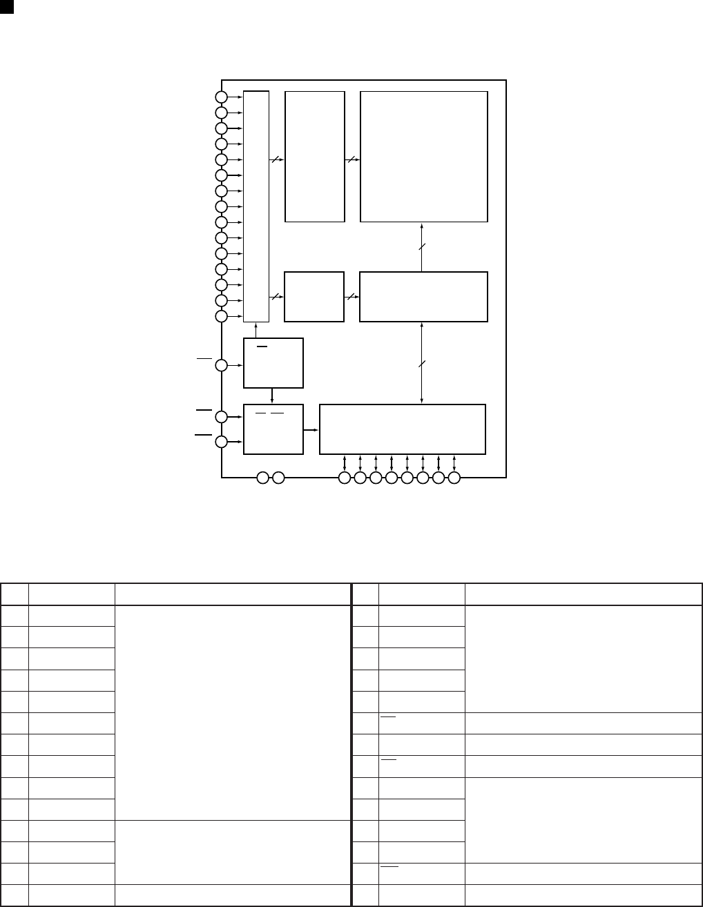
33
DV-505, DVL-909, DV-S9
SRM2B256SLMX70 (DVDM ASSY : IC502)
• 256 K SRAM (For Mechanism Control IC)
• Block Diagram
• Pin Function
10
9
8
7
6
5
4
3
25
24
21
23
2
26
1
Address Buffer
A0
A1
A2
A3
A4
9
A5
A6
A7
A8
A9
A10
A11
A12
A13
A14
20
CS
512
64×8
Line
Decoder
Memory-Cell
Array
512×64×8
6
8
Row
Decoder
64
Row Gate
Control
Logic
Control
Logic I/O Buffer
22
OE
27
11
WE
Vss
I/O1
I/O2
I/O3
I/O4
I/O5
I/O6
I/O7
I/O8
V
DD
CS
OE,WE
1214 18 13 15 16 17 18 19
.oNemaNniPnoitcnuF.oNemaNniPnoitcnuF
141A
tupnisserddA
514O/I
tuptuo/tupniataD
221A615O/I
37A716O/I
46A817O/I
55A918O/I
64A02SC tcelespihC
73A1201AtupnisserddA
82A22EO elbanetuptuO
91A3211A
tupnisserddA
010A429A
111O/I
tuptuo/tupniataD
528A
212O/I6231A
313O/I72EW elbaneetirW
41SSV)V0(DNG82DDV)V5.5ot7.2(ylppusrewoP
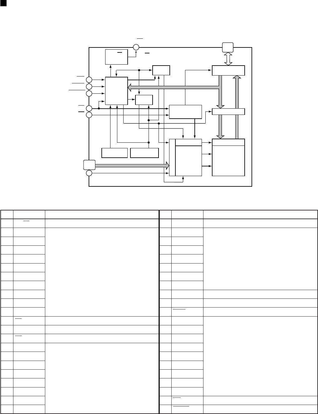
34
DV-505, DVL-909, DV-S9
VYW1536 (DVDM ASSY : IC603)(DV-505 and DVL-909 only)
• Flash ROM
• Block Diagram
• Pin Function
RY/BY
BUFFER RY/BY
WE
43
1
WRITE
CIRCUIT
STB
STB
ERASE
CIRCUIT
CHIP ENABLE
OUTPUT ENABLE
CIRCUIT
WRITE/ERASE
PULSE TIMER
LOW V
CC
DET. CIRCUIT
Y DECODER
ADDRESS LATCH
X DECODER
CONTROL
CIRCUIT
BYTE
RY/BY
33
RESET
44
CE
12
OE
14
A
0
-A
18
A
-1 31
2-11,
34-42
DQ
0
-DQ
15
15-22,
24-31
INPUT/OUTPUT
BUFFER
DATA LATCH
Y GATE
8,388,608
CELL
MATRIX
.oNemaNniPnoitcnuF.oNemaNniPnoitcnuF
1YB/YR tuptuoysuB/ydaeR32VCCV0.5+(ylppusrewoP ±ro%01 ±)%5
281A
tupnisserddA
424QD
tuptuo/tupniataD
371A5221QD
47A625QD
56A7231QD
65A826QD
74A9241QD
83A037QD
92A131-A/51QDtupnisserdda/tuptuo/tupniataD
011A23VSSdnuorG
110A33ETYB sedomtib61dnatib8ehthctiwS
21 EC elbanepihC4361A
tupnisserddA
31VSSdnuorG5351A
41 EO elbanetuptuO6341A
510QD
tuptuo/tupniataD
7331A
618QD8321A
711QD9311A
819QD0401A
912QD149A
0201QD248A
123QD34EW elbaneetirW
2211QD44TESER tesererawdraH
35
DV-505, DVL-909, DV-S9
PD3381A (DVDM ASSY : IC601)
• System Control CPU
• Block Diagram
79
RES
78
67
WDTOVF
82
MD2
81
MD1
80
MD0
76
NMI
77
15
Vcc
Vcc
Vcc
Vcc
Vcc
Vcc
Vcc
Vpp
Vss
Vss
Vss
Vss
Vss
Vss
Vss
Vss
Vss
Vss
43
70
75
83
84
99
3
12
22
31
40
52
61
72
96
106
86
AVref
85
AVcc
91
AVss
71
CK
73
EXTAL
74
XTAL
PA13/IRQ1/DREQ0/TCLKB
66
PA12/IRQ0/DACK0/TCLKA
65
PA11/DPH/TIOCB1
64
PA10/DPL/TIOCA1
63
PA9/AH/IRQOUT/ADTRG
62
PA8/BREQ
60
PA7/BACK
59
PA6/RD
58
PA5/WRH(LBS)
57
PA4/WRL(WR)
56
PA3/CS7/WAIT
55
PA2/CS6/TIOCB0
54
PA1/CS5/RA5/RAS
53
PA0/CS4/TIOCA0
51
CS3/CASL
50
CS2
49
CS1/CASH
48
CS0
47
A21
46
A20
45
A19
44
A18
42
A17
41
39
A16
68
PA14/IRQ2/DACK1
69
PA15/IRQ3/DREQ1
A15
38
A14
37
A13
36
A12
35
A11
34
A10
33
A9
32
A8
30
A7
29
A6
28
A5
27
A4
26
A3
25
A2
24
A1
23
A0(HBS)
21
AD15
20
AD14
19
AD13
18
AD12
17
AD11
16
AD10
14
AD9
13
AD8
11
AD7
10
AD6
9
AD5
8
AD4
7
AD3
6
AD2
5
AD1
4
AD0
PB0/TP0/TIOCA2
PB1/TP1/TIOCB2
100
PB2/TP2/TIOCA3
101
PB3/TP3/TIOCB3
102
PB4/TP4/TIOCA4
103
PB5/TP5/TIOCB4
104
PB6/TP6/TOCXA4/TCLKC
105
PB7/TP7/TOCXB4/TCLKC
107
PB8/TP8/RxD0
108
PB9/TP9/TxD0
109
PB10/TP10/RxD1
110
PB11/TP11/TxD1
111
PB12/TP12/IREQ4/SCK0
112
PB13/TP13/IREQ5/SCK1
PB14/TP14/IREQ6
PB15/TP15/IRQ7
PC0/AN0
PC1/AN1
PC2/AN2
PC3/AN3
PC4/AN4
PC5/AN5
PC6/AN6
95
PC7/AN7
OSCILLATOR
94 93 92 90 89 88 87 2 1 98 97
PORT A ADDRESS
PORT BPORT C
WATCHDOG
TIMER
A/D
CONVERTER
PROGRAMABLE
TIMING
PATTERN
CONTROLLER
SERIAL
COMMUNICATION
INTERFACE
(×2CHANNEL)
16BIT
INTEGRATED
TIMER PULSE UNIT
BUS STATE
CONTROLLER
INTERRUPT
CONTROLLER USER BREAK
CONTROLLER
CPU
DIRECT
MEMORY
ACCESS
CONTROLLER
64k PROM / MASK ROM 4kB RAM1
ADDRESSDATA/ADDRESS
Periphery address bus(24 bit)
Periphery data bus(16 bit)
Internal address bus(24 bit)
Internal upper data(16 bit)
Internal lower data(16 bit)

36
DV-505, DVL-909, DV-S9
• Pin Function
.oNemaNniPO/InoitcnuF
16QRI/41PT/41BP O/I tseuqernoitpurretnI/tuptuonrettapgnimiT/)Btrop(tuptuo/tupnitib61
27QRI/51PT/51BP
3SSVIdnuorG
40DA
O/Isubatadlaretalibtib61
51DA
62DA
73DA
84DA
95DA
016DA
117DA
21SSVIdnuorG
318DA O/Isubatadlaretalibtib61
419DA
51CCVIylppusrewoP
6101DA
O/Isubatadlaretalibtib61
7111DA
8121DA
9131DA
0241DA
1251DA
22SSVIdnuorG
32 )SBH(0A O)langisebortsetybreppu(tuptuosubsserddA
421A
OtuptuosubsserddA
522A
623A
724A
825A
926A
037A
13SSVIdnuorG
238A
OtuptuosubsserddA
339A
4301A
5311A
6321A
7331A
8341A
9351A
04SSVIdnuorG
1461A OtuptuosubsserddA
2471A
34CCVIylppusrewoP

37
DV-505, DVL-909, DV-S9
.oNemaNniPO/InoitcnuF
4481A
OtuptuosubsserddA
5491A
6402A
7412A
84 0SC OlangistcelespihC
94 HSAC/1SC O MARDfoedisreppuehtnolangisgnimitebortssserddanmuloC/langistcelespihC
05 2SC OlangistcelespihC
15 LSAC/3SC O MARDfoedisrewolehtnolangisgnimitebortssserddanmuloC/langistcelespihC
25SSVIdnuorG
350ACOIT/4SC/0APO/I /langistcelespihC/)Atrop(tuptuo/tupnitib61 )0lennahc(tuptuoerapmoctuptuoUTI/tupnierutpactupniUTI
45 SAR/5SC/1AP O/I MARDfolangisgnimitebortssserddawoL/langistcelespihC/)Atrop(tuptuo/tupnitib61
550BCOIT/6SC/2APO/I /langistcelespihC/)Atrop(tuptuo/tupnitib61 )0lennahc(tuptuoerapmoctuptuoUTI/tupnierutpactupniUTI
65 TIAW/7SC/3AP O/I elcycsubroftupnitiaW/langistcelespihC/)Atrop(tuptuo/tupnitib61
75 )RW(LRW/4AP O/I )gnitirwtatuptuo(gnitirwtib8rewollanretxE/)Atrop(tuptuo/tupnitib61
85 )SBL(HRW/5AP O/I )langisebortsetybrewol(gnitirwtib8rreppulanretxE/)Atrop(tuptuo/tupnitib61
95 DR/6AP O/ItuognidaerlanretxE/)Atrop(tuptuo/tupnitib61
06 KCAB/7AP O/IegdelwonkcatseuqermialcsuB/)Atrop(tuptuo/tupnitib61
16SSVIdnuorG
26 QERB/8AP O/ItseuqermialcsuB/)Atrop(tuptuo/tupnitib61
36GRTDA/TUOQRI/HA/9APO/I /evalstatuptuotseuqernoitpurretnI/langisgnimitdlohsserddA/)Atrop(tuptuo/tupnitib61 tupnireggirtnoisrevnocD/A
461ACOIT/LPD/01APO/I /edisrewolehtnoytirapsubataD/)Atrop(tuptuo/tupnitib61 )1lennahc(tuptuoerapmoctuptuoUTI/tupnierutpactupniUTI
561BCOIT/HPD/11APO/I /edisreppuehtnoytirapsubataD/)Atrop(tuptuo/tupnitib61 )1lennahc(tuptuoerapmoctuptuoUTI/tupnierutpactupniUTI
66AKLCT/0KCAD/0QRI/21APO/I /)0lennahc(noitpecertseuqerrefsnartAMD/tseuqernoitpurretnI/)Atrop(tuptuo/tupnitib61 tupnikcolcremitUTI
76 BKLCT/0QERD/1QRI/31AP O/I /)0lennahc(tseuqerrefsnartAMD/tseuqernoitpurretnI/)Atrop(tuptuo/tupnitib61 tupnikcolcremitUTI
86 1KCAD/2QRI/41AP O/I )1lennahc(noitpecertseuqerrefsnartAMD/tseuqernoitpurretnI/)Atrop(tuptuo/tupnitib61
96 1QERD/3QRI/51AP O/I )1lennahc(tseuqerrefsnartAMD/tseuqernoitpurretnI/)Atrop(tuptuo/tupnitib61
07CCVIylppusrewoP
17KCOtuptuokcolcmetsyS
27SSVIdnuorG
37LATXEI tupnikcolclanretxEtupnirotallicsolatsyrC
47LATXItupnirotallicsolatsyrC
57CCVIylppusrewoP
67IMNI tupninoitpurretnielbaksam-noN
77PPVI margorpMORPfoylppusrewoP
87 FVOTDW Otuptuowolf-revoremitgodhctaW
97 SER ItupniteseR
080DM
IsnipgnittesedoM181DM
282DM
38CCV IylppusrewoP
48CCV

38
DV-505, DVL-909, DV-S9
.oNemaNniPO/InoitcnuF
58CCVAIylppusrewopgolanA
68FERVAI ylppusrewopecnerefergolanA
780NA/0CP
ItupnilangisgolanA/)Ctrop(tupnitib8
881NA/1CP
982NA/2CP
093NA/3CP
19SSVAIdnuorGgolanA
294NA/4CP
ItupnilangisgolanA/)Ctrop(tupnitib8
395NA/5CP
496NA/6CP
597NA/7CP
69SSVIdnuorG
792ACOIT/0PT/0BP O/I erapmoctuptuoUTI/tupnierutpactupniUTI/tuptuonrettapgnimiT/)Btrop(tuptuo/tupnitib61 )2lennahc(tuptuo
892BCOIT/1PT/1BP
99CCVIylppusrewoP
0013ACOIT/2PT/2BP O/I erapmoctuptuoUTI/tupnierutpactupniUTI/tuptuonrettapgnimiT/)Btrop(tuptuo/tupnitib61 )3lennahc(tuptuo
1013BCOIT/3PT/3BP
2014ACOIT/4PT/4BP O/I erapmoctuptuoUTI/tupnierutpactupniUTI/tuptuonrettapgnimiT/)Btrop(tuptuo/tupnitib61 )4lennahc(tuptuo
3014BCOIT/5PT/5BP
401CKLCT/4AXCOT/6PT/6BP O/I /)4lennahc(tuptuoerapmoctuptuoUTI/tuptuonrettapgnimiT/)Btrop(tuptuo/tupnitib61 tupnikcolcremitUTI
501DKLCT/4BXCOT/7PT/7BP
601SSVIdnuorG
7010DXR/8PT/8BPO/I )0lennahc(tupniatadevieceR/tuptuonrettapgnimiT/)Btrop(tuptuo/tupnitib61
8010DXT/9PT/9BPO/I )0lennahc(tuptuoatadnoissimsnarT/tuptuonrettapgnimiT/)Btrop(tuptuo/tupnitib61
9011DXR/01PT/01BPO/I )1lennahc(tupniatadevieceR/tuptuonrettapgnimiT/)Btrop(tuptuo/tupnitib61
0111DXT/11PT/11BPO/I )1lennahc(tuptuoatadnoissimsnarT/tuptuonrettapgnimiT/)Btrop(tuptuo/tupnitib61
1110KCS/4QRI/21PT/21BPO/I /tseuqernoitpurretnI/tuptuonrettapgnimiT/)Btrop(tuptuo/tupnitib61 )0lennahc(tuptuo/tupnikcolclaireS
2111KCS/5QRI/31PT/31BPO/I /tseuqernoitpurretnI/tuptuonrettapgnimiT/)Btrop(tuptuo/tupnitib61 )1lennahc(tuptuo/tupnikcolclaireS
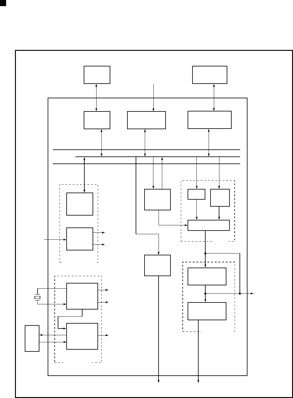
39
DV-505, DVL-909, DV-S9
Memory
Controller Block
Audio
Clock
Generation
Block
System
Clock
Generation
Block
Control
Block
Video
Decoder
Block
Sync.
Control
Block
Reset Signal
Starting
Signal
NTSC/PAL
Video Encoder
DAC
OSD Sub-
picture
MIX
Audio
Decoder
Block
System Clock
Clock for video
Clock for audio
LPF
VCO
Clock
Signal
Video Output (Y,C,Comp/Y,Cb,Cr)
Digital
Signal Output
(Component/
Composite)
System
Decoder Block
CPU
Interface
CPU
Clock
Generation
Block
27MHz
Audio Output
Internal
Bus
Reset
Signal
16Mbit
SDRAM
Exclusive
Parallel port
Input Signal
Picture
Block
Whole Control
Block
Video Output
Block
MB86371 (DVDM ASSY : IC801)
• MPEG2 Decoder LSI For DVD
• Block Diagram

40
DV-505, DVL-909, DV-S9
.oNemaNniPO/InoitcnuF.oNemaNniPO/InoitcnuF
1LESKLCI )FFO:"L",NO:"H"(LLPfolangisFFO/NO72DDV −ylppusrewopV3.3
27NPCGIDO )BSM(tuptuolangistnenopmoclatigiD )BSM()tib-9(tuptuolangisYlatigiD 824PMOCGID
O
tuptuolangisetisopmoclatigiD tuptuolangisClatigiD
3SSV −DNG923PMOCGID
46NPCGID
OtuptuolangistnenopmoclatigiD )tib-9(tuptuolangisYlatigiD
032PMOCGID
55NPCGID131PMOCGID
64NPCGID230PMOCGID )BSL(tuptuolangisetisopmoclatigiD )BSL(tuptuolangisClatigiD
73NPCGID33KCADO tuptuokcolczHM72
82NPCGID43.C.N −noitcennocnoN
91NPCGID533ASSV −)retrevnocA/D(DNG
01DDV −ylppusrewopV3.363CANAO langistuptuo)C(rolocgolanA
110NPCGIDO )BSL(tuptuolangistnenopmoclatigiD )BSL()tib-9(tuptuolangisYlatigiD 733ADDV −retrevnocA/Dni-tliubrof(ylppusrewopV3.3 )ylno
21LESBRO latigidehttalangisnoitanimircsidrCdnabC .tuptuolangistnenopmoc .tuptuolangisYlatigidehttaBSL 832ASSV −)retrevnocA/D(DNG
31SHXO langistuptuo.cnyslatnoziroH93YANAO langistuptuo)Y(ecnanimulgolanA
41SVXO langistuptuo.cnyslacitreV042ADDV −retrevnocA/Dni-tliubrof(ylppusrewopV3.3 )ylno
51 SSV −DNG14FERV IretrevnocA/DrofegatlovecnerefeR
61TESERXI langisteserISL24ORVO retrevnocA/DfonipgnittestnerruclanretnI
71CNYSCDLXI )edomDL(tupnilangis.cnyslanretxE34.C.N −noitcennocnoN
81YEKO yalrevoDSOdnaDLroflangisYEK )edomDL( 441ASSV −)retrevnocA/D(DNG
91DPO folangistuptuotlusernosirapmocesahP )edomDL(.cnyslatnoziroh 54PMOCANAO langistuptuoetisopmocgolanA
02DLFVO langislatigidehttalangisnoitanimircsiddleiF dleifddo:Ldleifneve:Htuptuo 641ADDV −retrevnocA/Dni-tliubrof(ylppusrewopV3.3 )ylno
129PMOCGID
O
)BSM(tuptuolangisetisopmoclatigiD )BSM(tuptuolangisClatigiD 74FBO langisgalftsruB
228PMOCGID
tuptuolangisetisopmoclatigiD tuptuolangisClatigiD
84KLBXO langisgniknalbetisopmocV/H
327PMOCGID94.C.N −noitcennocnoN
426PMOCGID05SSV −DNG
525PMOCGID150TSET −."nepo"ottes,yllamroN
62SSV −DNG251TSET −yllamronsutats"L"
• Pin Function

41
DV-505, DVL-909, DV-S9
.oNemaNniPO/InoitcnuF.oNemaNniPO/InoitcnuF
35NIIADI )FIDPS(tupnilanretxefotupniatadlatigiD2901SRDAHI )BSM(langissubsserddaUPC
45ATADDCI tupnilanretxefotupniatadoiduA )DCotdnopserroc( 399SRDAH
IlangissubsserddaUPC55RLDCI tupnilanretxefotupnikcolclennahcataD )DCotdnopserroc( 498SRDAH
65KCBDCI tupnilanretxefotupnikcolcataD )DCotdnopserroc( 597SRDAH
753ATADOA
OatadedocedoiduA
69SSV −DNG
852ATADOA79DDV −ylppusrewopV3.3
951ATADOA896SRDAH
I
langissubsserddaUPC
06SSV −DNG995SRDAH
16DDV −ylppusrewopV3.30014SRDAH
260ATADOAO atadedocedoiduA1013SRDAH
36MCPOAO tuptuoecafretnioidualatigiD )atadnoisserpmoc( 2012SRDAH)BSL(langissubsserddaUPC
46IADOAO )atadedoced(tuptuoecafretnioidualatigiD30151ATADH
O/I
)BSM(langissubatadUPC
56KCRLO retliflatigiddnaA/DrofkcolclennahcataD40141ATADH
langissubatadUPC66KCMOAO retliflatigiddnaA/DrofkcolcretsaM50131ATADH
76 KCB OretliflatigiddnaA/DrofkcolctiB601 21ATADH
861DECI
−rotalumerofniP ."nepo"ottes,yllamroN
701SSV −DNG
960DECI80111ATADH
O/IlangissubatadUPC
07KRBECI90101ATADH
17TSRPSDX0119ATADH
27SSV −DNG1118ATADH
37.C.N −noitcennocnoN2117ATADH
472TSET
−."nepo"ottes,yllamroN
3116ATADH
573TSET411DDV −ylppusrewopV3.3
674TSET5115ATADH
O/IlangissubatadUPC
775TSET6114ATADH
877DSI tupniatadlellaraP7113ATADH
97DDV −ylppusrewopV3.38112ATADH
086DS
ItupniatadlellaraP
911SSV −DNG
185DS0211ATADH O/I langissubatadUPC
284DS1210ATADH)BSL(langissubatadUPC
383DS221LESSUBI langisnoitceleshtdiwsuB )subtib-61:1,subtib-8:0(
482DS321KCADSOXI langisegdelwonkcaatadDSO
58SSV −DNG421QERDSOXO langistseuqeratadDSO
681DS ItupniatadlellaraP 5211LESUPCH I,CRAPS:00(langisnoitcelesUPC )evreseR:11,metsys86:01,metsys68:10
780DS6210LESUPCH
88RREXI langistupnirorrE7213TNIX
OUPCehtotlangistseuqertpurretnI98KCASXI langisegdelwonkcA8212TNIX
09TSETXI esulamronta"H"otteS9211TNIX
19QERSO langistseuqerataD031SSV −DNG

42
DV-505, DVL-909, DV-S9
.oNemaNniPO/InoitcnuF.oNemaNniPO/InoitcnuF
131DDV −ylppusrewopV3.3071SACRDMXO MARDSroflangisSAC
2310TNIXO UPCotlangistseuqertpurretnI1711MQDRDMXO roflangiselbanetuptuo/ksamtupnI MARDS
331YDRTXEXO UPCotlangisydaeR:metsys86,CRAPS otlangis)KCA(egdelwonkcA:metsys68 UPC 271SSV −DNG
431WRHI langisetirw/daerUPC371EWRDMXO MARDSroflangiselbaneetirW
531NIKLCHI tupnikcolctsoH4710MQDRDMXO roflangiselbanetuptuo/ksamtupnI MARDS
631SCHXI langistcelespihcISL5718TADRDMO/IMARDSroflangissubataD
731SAHXI ebortssserddaUPC:metsys86,CRAPS sutatssserddaUPC:metsys68 671SSV −DNG
8313EBHX
IlangiselbaneetybUPC
7717TADRDM
O/IMARDSroflangissubataD
9312EBHX8719TADRDM
0411EBHX9716TADRDM
1410EBHX08101TADRDM
241SSV −DNG1815TADRDM
3414RDARDM
OMARDSroflangissserddA
281SSV −DNG
4413RDARDM381DDV −ylppusrewopV3.3
541 5RDARDM 481 11TADRDM
O/IMARDSroflangissubataD
6412RDARDM5814TADRDM
741DDV −ylppusrewopV3.368121TADRDM
841SSV −DNG7813TADRDM
9416RDARDM
O
MARDSroflangissserddA
88131TADRDM
0511RDARDM981SSV −DNG
1517RDARDM0912TADRDM
O/I MARDSroflangissubataD2510RDARDM)BSL(MARDSroflangissserddA19141TADRDM
3518RDARDMMARDSroflangissserddA2911TADRDM
451SSV −DNG39151TADRDM)BSM(MARDSroflangissubataD
5516TSET
−yllamronsutats"L"
4910TADRDMO/I)BSL(MARDSroflangissubataD
6517TSET591SSV −DNG
7518TSET691.C.N −noitcennocnoN
8519TSET791M72KCII tupnikcolcmetsyS
95101RDARDM
OMARDSroflangissserddA 891SSV −DNG
0619RDARDM991M72KCOO tuptuokcolcmetsyS
16111RDARDM)BSM(MARDSroflangissserddA002)OCV(ASSV −)ylnoOCVrof(DNG
261SCRDMXO MARDSroflangistcelespihC102)OCV(ADDV −)ylnoOCVrof(ylppusrewopV3.3
361EKCRDMO MARDSroflangiselbanekcolC202FPLIO oiduaroftuptuoretrevnikcolbLLP
461SSV −DNG302FPLMI oiduaroftupniretrevnikcolbLLP
561DDV −ylppusrewopV3.3402FPLOO oiduaroftuptuorotcetedesahP
661SARRDMXO MARDSroflangisSAR502OCVOI kcolcoiduaroftupniOCV
761KLCRDMO MARDSroflangistuptuokcolC602SSV −DNG
861SSV −DNG702TSRLLPXI langistesernoitcesLLP
961NIKLCRDMI MARDSroflangistupnikcolC802TSRCNYSXI langisteserCNYS
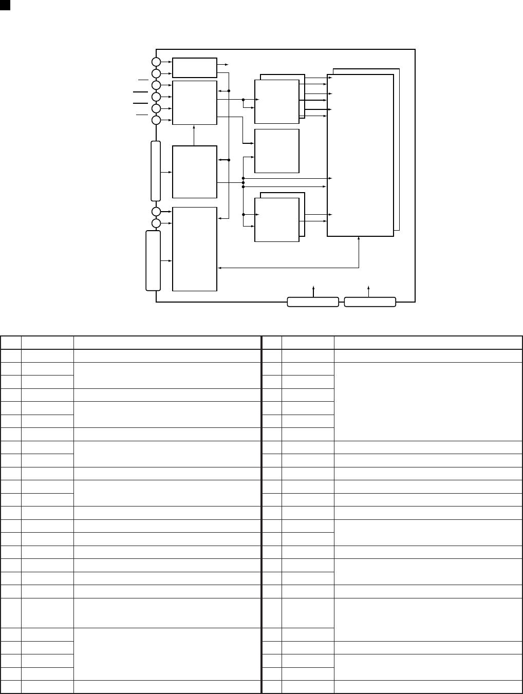
43
DV-505, DVL-909, DV-S9
MB811171622A-100FN (DVDM ASSY : IC802)
• Code Buffer (16M bit SDRAM)
• Block Diagram
• Pin Function
35
34
18
17
16
15
CLK
CKE
CS
RAS
CAS
To
Blocks
Bank 0
Bank 1
RAS
CAS
WE
I/O
Row Address
Column Address
WE
A
0
-A
11
,
AP
Command
Decoder
Mode
Register
DRAM Core
(2,048×256×16)
Address
Buffer/
Register
&
Bank
Select
Clock
Buffer
14
36
DQML
V
CC
/V
CCQ
DQMU
I/O Data
Buffer/
Register
21-24, 27-32, 20, 19
1,7,13,25,38,44
V
SS
/V
SSQ
4,10,26,41,47,50
DQ
0
-DQ
15
2,3,5,6,8,9,11,12,39,
40,42,43,45,46,48,49
Column
Address
Counter
Control
Signal
Latch
.oNemaNniPnoitcnuF.oNemaNniPnoitcnuF
1CCV)V3.3+(ylppusrewoP62SSVdnuorG
20QD tuptuo/tupniataD 724A
tupnisserddA 7Aot0A:nmuloC,01Aot0A:woR
31QD825A
4QSSVdnuorG926A
52QD tuptuo/tupniataD 037A
63QD138A
7QCCV)V3.3+(ylppusrewoP239A
84QD tuptuo/tupniataD 33UD)neporofesu(esut'noD
95QD43EKCelbanekcolC
01QSSVdnuorG53KLCtupnikcolC
116QD tuptuo/tupniataD 63UMQDelbanetuptuO/ksamtupnI
217QD73UD)neporofesu(esut'noD
31QCCV)V3.3+(ylppusrewoP83QCCV)V3.3+(ylppusrewoP
41LMQDelbanetuptuO/ksamtupnI938QD tuptuo/tupniataD
51 EW elbaneetirW049QD
61 SAC ebortssserddanmuloC14QSSVdnuorG
71 SAR ebortssserddawoR2401QD tuptuo/tupniataD
81 SC tcelespihC3411QD
91)AB(11AtcelesknaB44QCCV)V3.3+(ylppusrewoP
02PA/01A tupnisserddA 7Aot0A:nmuloC,01Aot0A:woR elbaneegrahc-erpotuA/ 5421QD tuptuo/tupniataD
120A
tupnisserddA 7Aot0A:nmuloC,01Aot0A:woR
6431QD
221A74QSSVdnuorG
322A8441QD tuptuo/tupniataD
423A9451QD
52CCV)V3.3+(ylppusrewoP05SSVdnuorG
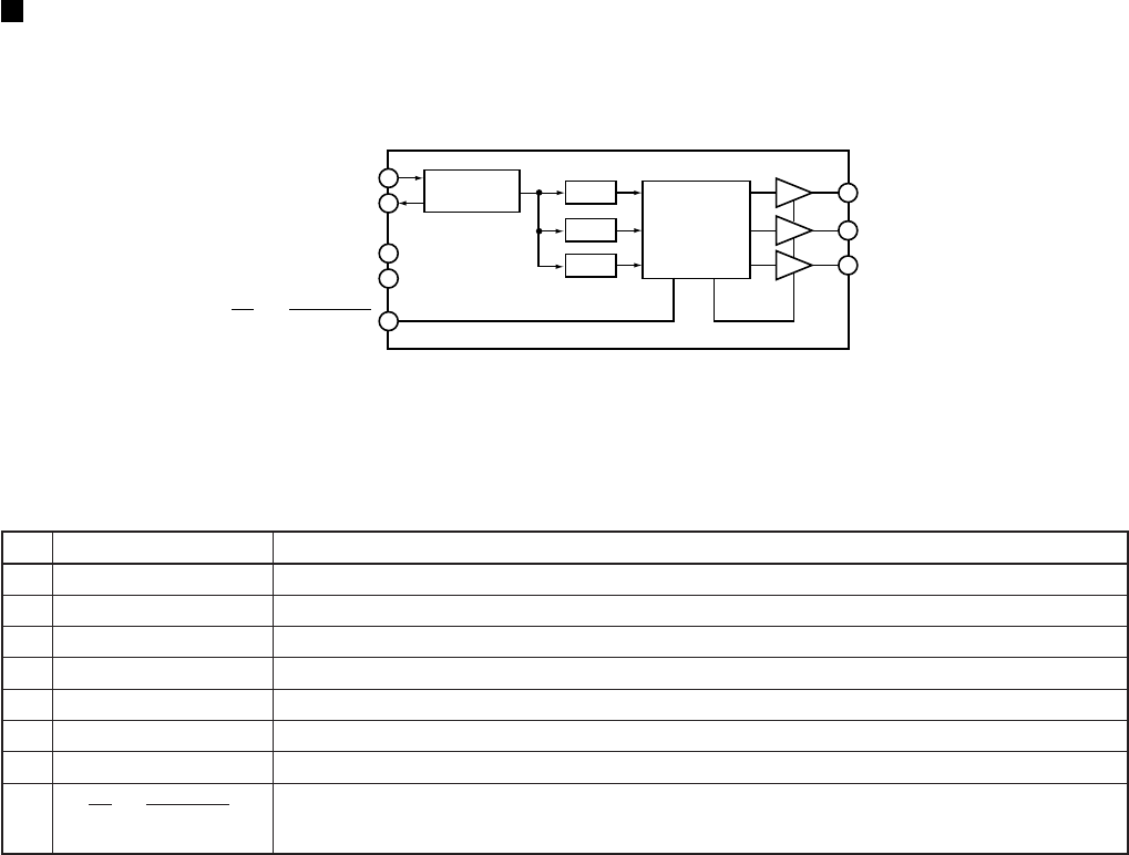
44
DV-505, DVL-909, DV-S9
CY2081SL-611 (DVDM ASSY : IC813)
• Clock Generate IC
• Block Diagram
• Pin Function
3
41
5
6
2
7
8
XTALIN
XTALOUT
GND
CLKA
CLKB
CLKC
V
DD
OE/PD/FS/SUSPEND
Refference
Oscillator PLL1 EPROM-
Configurable
Multiplexer
and
Drive Logic
PLL2
PLL3
.oNemaNniP noitcnuF
1AKLCtuptuokcolcelbarugifnoC
2DNGdnuorG
3NILATX tupnikcolcecnereferlanretxerotupnilatsyrcecnerefeR
4TUOLATXkcabdeeflatsyrcecnerefeR
5BKLCtuptuokcolcelbarugifnoC
6CKLCtuptuokcolcelbarugifnoC
7DDVylppusegatloV
8DNEPSUS/SF/DP/EO niplortnoctuptuO dnepsuswoL-evitcaro,tcelesycneuqerfAKLC,nwodrewopwoL-evitca,elbanetuptuohgiH-evitcarehtiE tupni
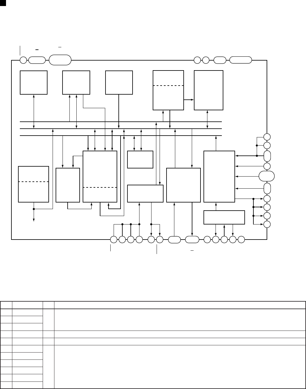
45
DV-505, DVL-909, DV-S9
1–3,6–11,
53–60
Delay RAM
Address
Generating
Circuit
5,14,34,52
17–15
42–44
Data RAM
128w×24b
Program
ROM
1024w×32b
Multiply
and add
Culculator
24b×16b+43b
Delay RAM
4096w×16b
Offset RAM
64w×16b
Coefficient
RAM
320w×16b
Coefficient
ROM
256w×16b
Program
Counter Logical
Arithmetic
Unit(LU) Work
Register
Temporary
Register
Interface
Circuit
Serial Data
Input/Output
Circuit
Input (2 port)
Output (3 port)
Timing
Generation
Circuit
VCO Oscillation
Circuit
32
33
27
24
Interface bus
Data bus
Work register
bus
ELRI1,ELRI0
EBCI1,EBCI0
45 13 12
30
36
35
20
21
22
23
40374149 5148504746 39 38
28,29
25,26
4,31
18,19
CS
IFCD
IFCK
IFDI
IFDO
ACK
SDI1
SDI0
SDO0
SDO2
VDDA
PD
AMPI
A
MPO
VSSA
CKSL
PLOFF
XI
XO
SYNC
ELRO
EBCO
LR
WCK
FS32
FS64
VDDR
RST
TES0
TES2
TPS0
TPS16
VSSR
VDD
VSS
24b 16b
.oNemaNniPO/InoitcnuF
18PT
OniptuptuoatadtseT .nepohtiwesu,yllamroN
27PT
36PT
4DDV −nipylppusrewoP
5SSV −nipdnuorG
65PT
OniptuptuoatadtseT .nepohtiwesu,yllamroN
74PT
83PT
92PT
011PT
110PT
PD2058A ( DVDM ASSY : IC901 )(DV-505 and DVL-909 only)
• Digital Signal Processor For Audio
• Block Diagram
• Pin Function

46
DV-505, DVL-909, DV-S9
.oNemaNniPO/InoitcnuF
21RSSV −)MARLD(MARyaledlanretnirofnipdnuorG
31RDDV −)MARLD(MARyaledlanretnirofnipylppusrewoP
41SSV −nipdnuorG
512ODS
OniptuptuoatadlaireS .rossecorporcimehtgnillortnocybtib-61rotib-42ehttcelesotelbasihtgnelatadtuptuO
611ODS
710ODS
811IDS IniptupniatadlaireS .rossecorporcimehtgnillortnocybtib-61rotib-42ehttcelesotelbasihtgnelatadtupnI
910IDS
02RLO )sf1(niptuptuokcolcRL
12KCWO )sf2(niptuptuokcolcdroW
2223SFO )sf23(niptuptuokcolctiB
3246SFO )sf46(niptuptuokcolctiB
420CBEI .tuptuoatad2/1/0ODSrofkcolctfihsstupnIniptupnikcolctiB
521ICBE IniptupnikcolctiB .tupniatad1/0IDSrofkcolctfihsstupnI
tupniatad1IDSroF
620ICBE tupniatad0IDSroF
72ORLEI .tuptuoatad2/1/0ODSrofkcolcRLstupnIniptupnikcolcRL
821IRLE IniptupnikcolcRL .tupniatad1/0IDSrofkcolcRLstupnI
tupniatad1IDSroF
920IRLE tupniatad0IDSroF
03CNYSI .langisCNYSfoegdeehtybylbicrof"0"otniretnuocmargorpehtnruTniptupnilangis.cnyS .rossecorporcimehtgnillortnocybytiralopehttes,revoeroM
13DDV −nipylppusrewoP
23IXI niptupnikcolclanretxe/nipnoitcennocrotallicsolatsyrC
33OXO nipnoitcennocrotallicsolatsyrC
43SSV −nipdnuorG
53LSKCI sf215otdnopserroc:Hsf483otdnopserroc:LniphctiwskcolcnoitallicsO
63FFOLPI edomnoitallicsolat'X:HedomnoitallicsoOCVni-tliub:LniphctiwsedomnoitallicsoOCV/edomnoitallicsolat'X
73DPO niptuptuoatadnosirapmocesahP
83ASSV −nipdnuorggolanA
93OPMAO retlifssap-wolrofniptuptuo.pmA
04IPMAI retlifssap-wolrofniptupni.pmA
14ADDV −nipylppusrewopgolanA
240SET
IniptseT .neporo"H"rofesu,yllamroN
341SET
442SET
54 TSR IniptupnilangisteseR
64SCI .rossecorporcimehtmorfrefsnartotelbasiatad,evitcaLsiSCnehWniptupnilangistcelespihC
74DCFII rossecorporcimehtmorfnipnoitcelesedomtupniatadrodnammoC .doirep"L"rofatadehtdnadoirep"H"rofdnammocehtezingoceR
84IDFII .tsrifBSLybataddnadnammocehtevieceRniptupniatadrossecorporciM
94ODFIO .tsrifBSLybrossecorporcimehtotsubatadfoatadehttimsnarT)SUBD(subatadfoniptuptuoataD
05KCFII atadrossecorporcimrofniptupnikcolctfihS
15KCAO rossecorporcimrofniptuptuolangisegdelwonkcA .langisegdelwonkcaehtstuptuo,KOsiataddnadnammocfoytirapnehW
25SSV −nipdnuorG
3561PT
OniptuptuoatadtseT .nepohtiwesu,yllamroN
4551PT
5541PT
6531PT
7521PT
8511PT
9501PT
069PT
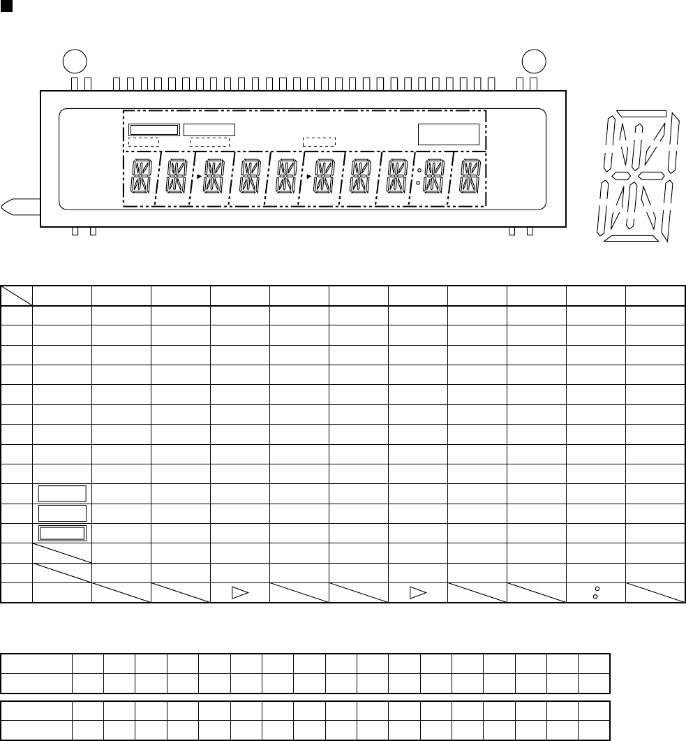
47
DV-505, DVL-909, DV-S9
5. FL INFORMATION
1 34
VAW1046 (FLKB ASSY : V101)(DV-505 and DVL-909 only)
• FL DISPLAY
• ANODE AND GRID ASSIGNMENT
• PIN ASSIGNMENT
G1 G2 G3 G4 G5 G6 G7 G8 G9 G10 G11
P1 P1
ANGLE P2
TITLE P3
LAST MEMO
P4
CONDITION
P5
P6 P6
CHP/TRK P7
P8
REMAIN
P8
P9
P10
P11
P12
P13
P14
TOTAL
P1
P2
P3
P4
P5
P6
P7
P8
P9
P10
P11
P12
P13
P14
P15
Pin No.
Assignment
1
F1
2
F1
3
NP
4
P15
5
P14
6
P13
7
P12
8
P11
9
P10
10
P9
11
P8
12
P7
13
P6
14
P5
15
P4
16
P3
17
P2
Pin No.
Assignment
18
P1
19
G11
20
G10
21
G9
22
G8
23
NL
24
NL
25
G7
26
G6
27
G5
28
G4
29
G3
30
G2
31
G1
32
NP
33
F2
34
F2
F1, F2 : Filament G1~G11 : Grid P1~P15 : Anode NP : No Pin NL : No Lead
P1
P2
P3
P4
P5
P6
P7
P8
P9
P10
P11
P12
P13
P14
P1
P2
P3
P4
P5
P6
P7
P8
P9
P10
P11
P12
P13
P14
P1
P2
P3
P4
P5
P6
P7
P8
P9
P10
P11
P12
P13
P14
P1
P2
P3
P4
P5
P6
P7
P8
P9
P10
P11
P12
P13
P14
P1
P2
P3
P4
P5
P6
P7
P8
P9
P10
P11
P12
P13
P14
P1
P2
P3
P4
P5
P6
P7
P8
P9
P10
P11
P12
P13
P14
P1
P2
P3
P4
P5
P6
P7
P8
P9
P10
P11
P12
P13
P14
P1
P2
P3
P4
P5
P6
P7
P8
P9
P10
P11
P12
P13
P14
DOLBY
DIGITAL
GUI
96kHz96kHz
P1
P2
P3
P4
P5
P6
P7
P8
P9
P10
P11
P12
P13
P14
P4
P6 P7 P9
P5
P8
P3 P10
P13 P1 P12 P2 P11
P14
DOLBY
DIGITAL
CONDITION
GUI
96kHz
MEMOLASTANGLE
TOTALREMAINCHP / TRK
PB
TITLE
P1 P6
G1
G2 G3 G4 G5 G6 G7 G8 G9 G10 G11
